development of a quadrupole iass spectrometer
220
DEVELOPMENT OF A QUADRUPOLE IASS SPECTROMETER by CHARLES EDWARD WOODWARD B.S., Iowa State College , - or-7\ I Ly3 ) J S.M., Massachusetts Institute of Technology (1960) SUBMITTED IN PARTIAL FULFILLMENT OF THE REQUIREMENTS FOR THE DEGREE OF DOCTOR OF PHILOSOPHY at the MASSACHUSETTS INSTITUTE OF TECHNOLOGY June, 1964 Signature of Author ,. ................................................ Department of Electrical Engineering, May 15, 1964 Certified by ........ - t~, ................. V ( Thesis Supervisor Accepted by ........ . ...... - ,, ..... ... .... Chairman, Departmental Committee on Graduate Students
-
Upload
khangminh22 -
Category
Documents
-
view
0 -
download
0
Transcript of development of a quadrupole iass spectrometer

DEVELOPMENT OF A QUADRUPOLE IASS SPECTROMETER
by
CHARLES EDWARD WOODWARD
B.S., Iowa State College, -or-7\
I Ly3 ) J
S.M., Massachusetts Institute of Technology
(1960)
SUBMITTED IN PARTIAL FULFILLMENT OF THE
REQUIREMENTS FOR THE DEGREE OF
DOCTOR OF PHILOSOPHY
at the
MASSACHUSETTS INSTITUTE OF TECHNOLOGY
June, 1964
Signature of Author ,. ................................................Department of Electrical Engineering, May 15, 1964
Certified by ........ -t~, .................V ( Thesis Supervisor
Accepted by ........ . ...... - ,, ..... ... ....Chairman, Departmental Committee on Graduate Students
DE10VELO P ENT OF A QUADRUPOLE ASS SPECROETLER
by
CIRLS EDWARD tWOOhIARD
Submitted to the Department of Electrical Engineeringon May 15, 1_64, in partial fulfillmnent o the require-ments for the degree of Doctor of Philosophy
ABSTRACT
The thesis project was the development of electronic circuitsfor a moderate-resolution quadrupole mass spectrometer intended asa flexible laboratory instrument to cover I to 400 amu in fourranges.
Extension of the theory of the quadrupole mass filter showedThat high transverse ion momenta pose significant problems in ioncollection.
The electronic circuits that supplied voltages to the massfilter were capable of 50:1 spectral range sweeps in 0.1 sec, butresolution over a wide sweep range was limited by nonlinearity inthe control of the r-f voltage. Compensation reduced the nonline-arity over a 10:1 sweep range from 4% to 0.4.
The electron-multiplier ion collector of the spectrometer wasoperated in a particle-detection mode to eliminate the effects ofmultiplier gain variations. The theory of coincidence losses insuch particle-detection systems was extended to a nonparalyzablecounter following a pulse-stretching amplifier. A "delay-line"ratemeter was shown to possess certain signal-to-noise advantagesover the conventional R-C output circuit, but practical limitationseliminated these advantages. Pulse circuits with resolving timesbetter than 5 x 0- 3 sec were used in the particle-detection system.
Mechaxnical imperfections in the quadrupole lens limitedspectrometer resolution to m/Am = 40. The ultimate sensitivitywas a partial pressure of 10-11 torr.
Thesis Supervisor: Arthur R. von HippelTitle: Institute Professor; Professor of Electrophysics
ACIT OWInXDGEMEN TS
The author 'ishes to express his appreciation to
Professor A. R. von ippel for his support,. advice and
encouragement.
Thanks are expressed to Professor C.K. Crawford
for initiating and sustaining the quadrupole mass spectro-
meter project, as well as for designing and constructing
all parts of the instrument that are characterized by the
term "physical electronics."
Recognition is due Messrs. Juri Klonizchii and
Modesto Maidique for construction of some of the apparatus,
to other members of the Laboratory for Insulation Research
who have assisted in the project, and to those who helped
prepare the manuscript: Messrs. John Mara, Douglas Nicoll,
and Michael Hale. who drew many of the figures, and Miss
Aina Sils, who typed the text.

iv
TABLE OF CONTENTS
Abstract ...................
Acknowledgements ...........
List of Figures ............
List of Tables .............
. e . .
.eI·itlt1®.
I. The Electric-Quadrupole Mass Spectrometer ............
A. The mass filter .......................
B. Ion source ................................. ....
C. Ion collector ..... ........................ .
II. Theory of the Quadrupole Mass Filter ..................
A. Description of operation .... ...... ......
B. Equations of motion .... .. .. .. ..............
C. Mass-filter operation ....................
D. Design considerations .......................
III. Mass Spectrometer Construction .. ....................
A. Quadrupole lens ...................................
B. Ion source ............... ....... ........ .......
C. Electron multiplier ............... ................
D. Vacuum system ............ 0.............................
IV. Electronic Drive Circuits for the Mass Filter ........
A. Circuit requirements ..............................
B. Control generator .............. ........ ..........
C. R-f rod driver ....................................
D. D-c rod driver ............... .. ...................
V. Design Considerations for the Electron-Multiplier IonDetector
A. Introduction .............. ..... ...... g....
B. The electron multiplier as a current amplifier.....
C. The electron multiplier as a particle detector ....
D. Spectrometer output noise .........................
E. Pulse signal processing .........*....................
F. Linear signal processing ..........................
Page
ii
iii
vi
viii
1
3
7
7
9
9
9
19
28
.35
35
39
40
46
47
47
49
54
79
84
85
86
90
97
108
... 6
. . .
* . .
. 0. .. 4
0 * .. .
. . .. .
. . .. .
.. .
. . .
.. 0
· · · · ·
· · · · r
· · · · ·
· · · r·

vJ
Table of Contents (cont.)
Page
VI. Electron-Multiplier Ion Detector ................ 125
A. System characteristics .................... . 125
B. Pulse system ..... .. .... ............ 151
C. Output processor ............................ 161
VII. Mass-Spectrometer Performance . ........... 166
A. Line shape .................................. 166
B. Resolving power ....................... 169
C. Mass spectra ....... ........................ 171
VIII. Conclusions .... ............ ..... 175
A. Summary of work ........ ................. 175
B. Suggestions for future work ...... ....... 178
Appendix A. Coefficients in Series Expansion of Solutions 183of Mathieu's Equation
Appendix B. Tank Coil Design .............. 186
Appendix C. Symmetric Signals in Balanced, Inductively 198Coupled Circuits
Appendix D. Self-Checking Balance Detector Algorithm 201
Appendix E. Pulse-System Test Apparatus ............... 204
References .... ............. .............. 209
Biographical Note ............. .......... . ........... 212

LIST OF IGURES
Page
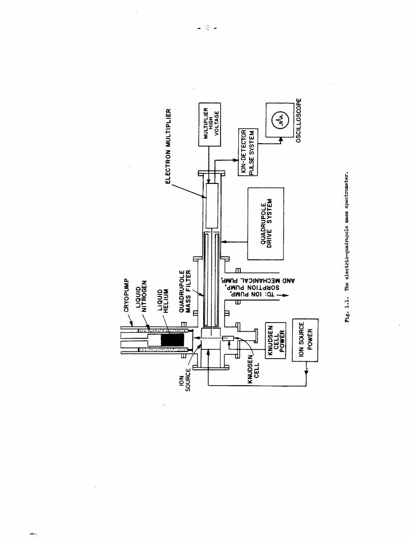
1.1. The electric-quadrupole mass spectrometer. 2
2.1. Stable ion trajectories in the mass filter. i0
2.2. Quad-rupole-mass filter electrodes. 11
2.3. Stability diagram for quadrupole mass filter. 14
2.4. x and y trajectories. 17
3.1. Quadrupole lens. 36
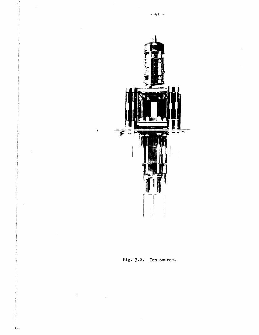
3.2. Ion source. 41
3.. Ion-source circuit diagram. 42
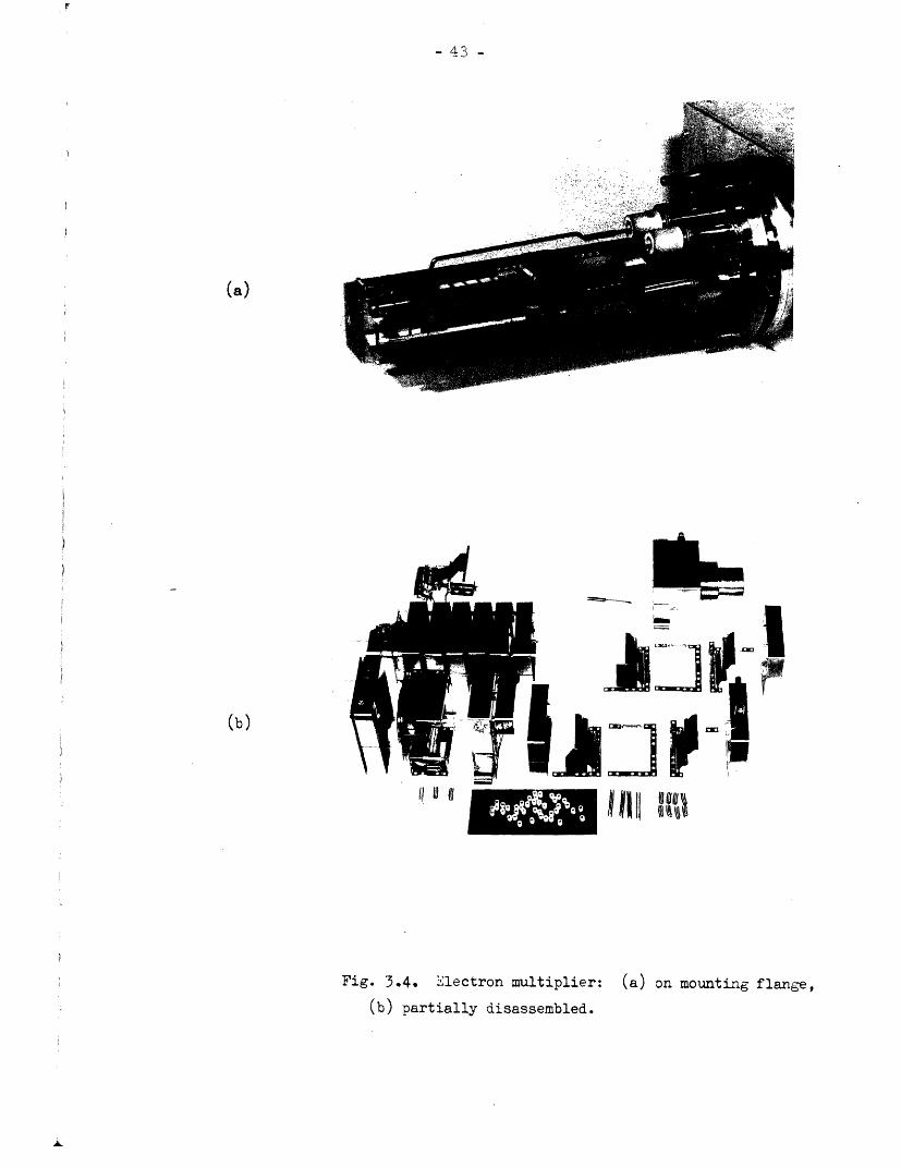
73.4. Electron multiplier. 43
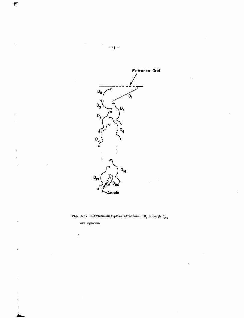
3.5. Electron-multiplier structure. 44
4.i. Block diagram of mass-filter circuits. 48
4.2. Block diagram of control generator. 50
4.5. Circuit diagram of control generator. 51
4.4. Circuit diagram of r-f rod driver. 55
4.5. Deviation of r-f to d-c ratio. 73
4.6. Circuit diagram of d-c rod driver. 80
5.1. Distribution in amplitude of ion-electron-multiplier 91output pulses.
5.2. Probability distribution of pulse amplitudes. 92
5.3. Performance of counter systems. 100
5.4. Delay-line ratemeter. 112
5.5. Response of delay-line ratemeter. 113
5.6. Impulse response of ratemeter circuits. 123
6.1. Differentiator-limiter performance. 130
6.2. Differentiator response. 132
6.35. Ion-detector pulse system. 133
6.4. Electron-multiplier circuit. 135
6.5. Electron-multiplier anode circuit. 139
"List of Figures (cont.)
Page
6.-. Preamplifier circuit. !44
.7. Prearplifier performance. 147
6.8. Interstage limiting mplifiers. 150
6.9. Response of preamplifier-amplifier-limiter 152chain to test pulses.
6.10. Pulse standardizer. 154
6.11. :Pulse standardizer output. 157
6.12. Response of preamplifier-amplifier-limiter 165chain to electron-multiplier output pulses.
7.i. Spectral line shape. 167
7.2. Background-gas mass spectra. 172
8.1. Proposed high-linearity rectifiers. 181
B.1. Thned coupling transformer circuit. 186
B.2. Coupled-coil configuration. 193
C.l. Rod-driver output circuit. 199
C.2. Output circuit collapsed into simpler form. 199
D.i. Balance-detector flow graph. 201
E.l. Pulse-system test apparatus. 205
E.2. Pulse baseline cleaner. 207
E.5. 'Test pulse source. 208

viii
LIST OF TABLES
page
4.1. Buffer-output r-f transformers. 56
4.2. Output tank coils. 57
6.1. Pulse-system resolving times. 160
7.1. Relative amplitude of spectral lines. 173

I. THE ELECTIRIC-QUADRUPOLE MASS SPECTROMETER
The purpose of this thesis was the development of a small
mass spectrometer of modest resolving power m/Am (perhaps 500) but
with sufficient flexibility to permit it to be easily applied to
such diverse problems as the thermal decomposition of dielectric
materials and the study of electron-ionization cross sections of the
vapor states of solids. The instrument was to be capable of sweep-
ing wide spectral ranges (up to 50:1) in relatively short time (as
little as 0.1 second). An electric-quadrupole mass filter (which
had been used by previous workers only in feasibility studies and
as a background-gas analyzer) was selected for this application and
incorporated into a complete spectrometer system as shown in Fig. 1.1.
Ions from an ion source are mass selected by the filter and then
detected by an ion collector. The mass spectrum is recorded on an
oscilloscope or other recording device.
This thesis was part of a joint project with Professor
C.K. Crawford. Those parts of the spectrometer involving physical
electronics (e.g., the ion source, quadrupole lens, ion collector,
and vacuum system) were the responsibility of Professor Crawford;
the associated electronic circuits were the responsibility of the
author.
4a
o
04ax0
reo
4o
0I-4
A. The Mass Filter
Principles of Operation
The mass-separation element of the spectrometer is the
electric-quadrupole mass filter invented by Paul and his co-
workers at Bonn University.1-3 It consists of four long, parallel
cylindrical electrodes, usually circular rods, with d-c and r-f
voltages applied. Ions to be mass selected are injected along the
axis of the electrode assembly. By a proper choice of applied
voltages, ions in a specified mass-to-charge-ratio range (the pass
band of the filter) traverse the quadrupole lens and are collected
at the output end; other mass-to-charge-ratio ions are deflected
sidewise. For operation as a mass spectrometer, the electrode
voltages are varied so as to sweep out a mass spectrum as a func-
tion of time.
The mechanical precision of the quadrupole lens sets an
upper limit on resolving power, but the precision of the quadrupole
voltages is the practical limitation on the resolving power of a
wide-range instrument. A major part of this thesis work was the
development of circuits to provide precise voltages over wide mass-
spectral ranges.
Comparison with other Mass Filters
Any new mass spectrometer has to compete with existing ones.
While many different types exist, only two have gained wide
acceptance as laboratory instruments: the magnetic-deflection
-t4 -spectrometer (single or double focussing), and the time-of-flight
spectrometer, which operates by measuring the times required for
isoenergetic ions to traverse a drift tube.
The magnetic-deflection and electric-quadrupole instruments
use dispersion in space: All ions except those of the desired m/e
ratio are discarded at some location other then the ion collector.
In principle these two types of mass filters are interchangeable;
the quadrupole could be replaced by a magnetic sector. The time-
of-flight, in contrast, uses dispersion in time: All ions reach the
collector; distinction is made by arrival time.
The great advantage of a time-of-flight instrument is that
each mass spectrum is obtained in a short time (100 Isec in one
commercial instrument). Hence spectra may be taken at a high rate
(10 /sec) and rapidly change spectra, as from fast chemical re-
actions, observed. On the other hand, because the source gas is
ionized in a low duty cycle (0.25 sec per 100 sec collecting time),
the effective sensitivity is lower than that of a spatial-filter
instrument. This "sampling in time" also makes impractical experi-
ments with modulated ion beams. Finally, at least at the present
state of the art, the time-of-flight mass spectrometer has a
resolution too low to permit distinction between masses differing by
a fraction of a mass unit.
If one compares the two spatial-filter instruments in resolving
power, the severe requirements on mechanical tolerances of the

quadrupole filter probably make it inferior. Resolving power up to
m/Lm = 8000 has been achieved with great difficulty with the
quadrupole, ' while 500,000 has been reported for a magnetic in-
5strument. Commercial double-focussing magnetic instruments
offer resolutions of 15,000, a value beyond the capability of a
practical analytical-laboratory quadrupole instrument.
At high background-gas pressure the quadrupole may be poten-
tially superior in resolution because collisions of ions with
background gas in the magnetic filter disturb the orbits and
cause resolution degredation ("pressure broadening"). In the quadru-
pole filter such collisions are less disturbing; an ion that should
be rejected still has an unstable orbit after collision, and will
be deflected to the side of the remaining length of the filter.6'7 )
A potential advantage of the quadrupole instrument in some
applications is ease of resolution adjustment. In a magnetic filter
a mechanical adjustment of the slit widths is required; in the quadru-
pole filter onl a simple electrical adjustment. In fact, in the in-
strument described in this thesis, it is possible to change resolu-
tion systematically while sweeping a mass spectrum.
In this as in all other work at Bonn resolution is based on fullline width at half maximum amplitude, which yields numericalvalues at least twice as high as from the more usual definitionsbased on line width near the base. For a better comparison withother instruments, all resolving powers reported by the Bonn grouphave been divided by 2 when used in this thesis. This has involvedappropriate modification of a number of equations in the theory ofthe mass filter.

The quadrupole filter is extremely tolerant of the axial
momentum of entering ions, requiring only that it be below some
limiting value that ensures the ions stay in the filter long
enough for mass selection. In a practical instrument this usual-
ly means an axial momentum corresponding to 100 volts or less.
The instrument is considerably more demanding with respect to
transverse momentum (typical upper limit < 1 volt). However, in
contrast to incorrect momenta in a magnetic filter, a transverse
momentum even in excess of the limit degrades not the instrument
resolution, but only the transmitted intensity. The quadrupole
filter, in short, is more tolerant with respect to entrance con-
ditions than the single-focussing magnetic instrument.
The absence of magnetic fields in the quadrupole filter
permits greater freedom in source design, e.g., permits experi-
ments with low-energy electrons, and makes it easier to use elec-
tron multipliers as ion detectors.
The final test of the quadrupole mass spectrometer is the
market place. The question is: Can a quadrupole instrument be
manufactured with a resolution comparable to that of a large
single-focussing magnetic spectrometer (500 to 1000), but smaller
and more convenient to use and not higher in cost? Results in
the literature and in this thesis seem to give an affirmative
answer to all but the last question. Cost comparison must await
full commercial development of a quadrupole mass spectrometer of
- 7-
analytical quality.
B, Ion Source
A conventional electron-bombardment source serves as ion
source for the spectrometer. The material under study is vaporized
in a Knudsen-cell oven and ionized by a transverse electron beam.
Ions are extracted from the source region and injected into the
mass filter.
8)Much more elaborate sources have been built, but were not
used in the work of this thesis.
C. Ion Collector
The ion current from the quadrupole filter could be collected
by a Faraday cup at the exit and measured by an electrometer. In
that case instrument sensitivity and response speed are limited by
the electrometer with its large time constant (order of seconds)
given by input resistance and stray capacitance. The sensitivity
limitation is tolerable, but the response speed, since the instru-
ment should allow sweeps of mass spectral lines in milliseconds, is
not. The slow response can be overcome by use of an electron multi-
plier as the ion collector. Its gain of more than 10 5 can yield an
output large enough to drive a recording device directly and its
bandwidth of more than 100 Me is high enough for any response speed.
Unfortunately, the electron multiplier has its own drawbacks.
The gain suffers slow degredation because of dynode surface con-

- 4 -
tamination, and, even more serious, the yield of the first dynode
depends on ion species, so apparent mass discrimination may be
introduced. These difficulties can be overcome, at least for
the lower values of ion current, by using the multiplier not as
a current amplifier but as a single-particle detector: Each ion
incident on the first dynode produces a pulse of output current
that is amplified and either counted by digital devices or stand-
ardized in amplitude and width. The average current of the stand-
ard pulses is a signal proportional to the input ion current.
The maximum ion current, or count rate, that can be handled
by a particle-detecting electron-multiplier system is limited by
the response speed of the pulse-processing circuits. A major
part of the work of this thesis was the development of an analog-
output system handling rates up to 5 x 10⁶ ions/sec.
Because the ion currents detected by a particle-detector
system are necessarily small, shot noise is a significant problem.
It is therefore important to choose an output;system that will
provide a maximum ratio of signal to noise. Work in this thesis
showed that the conventional resistance-capacitance low-pass
filter is the best practical output network, although - idealized -
some other linear systems provide slightly superior performance.
- Q I
II. THEORY OF THE QUADRUPOLE MASS FILTER
A. Description of Operation
In principle, the mass filter operates as follows: Ions are
injected -through an entrance aperture (Fig. 2.1) along the axis of
a quadrupole lens (four parallel cylindrical electrodes; cf. Fig. 2.2)
to which d-c and r-f voltages are applied. Ions with mass-to-charge
ratios outside a passband determined by electric-field specifications
have unstable orbits and are ejected from the sides of the filter.
Ions with masses inside the passband follow complicated but bounded
trajectories through the quadrupole to an ion collector at the out-
put (Fig. 2.1). The exact trajectory of an ion depends upon entrance
conditions, but for a suitably limited entrance displacement and
velocity, all trajectory envelopes lie within the quadrupole dimen-
sions (y direction, Fig. 2.1). However, it is possible that some
trajectories exceed filter dimensions, so that some ions of passband
mass are lost by collision with the electrodes (x direction, Fig. 2.1).
Some of the theory necessary for the design of a quadrupole mass
filter will be developed in this chapter.
B. Equations of Motion
In idealized form the quadrupole mass filter consists of four
parallel electrodes of hyperbolic cross section, to which voltages
0o = + (U + V cos t) (2.1)
-I -
uri $ AC10
lo
x
-
L,,A-
' ii i
::: ::::- :: : :: : : ;; ;; :: : ::~:;: :::: z :;:;; ; ; a-::: :::: ::: . .; N~ m~; v;;: :: :: :::: ::· ::::: ::::: : ; : :: ::: :: :: :- :: :- :: :: :: . . . ...... I.....I............. ::ii iliiiiiil::i~ii ..... ·.;:::,ii lii::i:-:::ijiiiil iil iiiiiiiiiiiiiiiii.I....I... i:.. : ... ......
iiiiiiijii iiijiiiiiiiii ii~~~ii~iiiiiiijiiiiiiiiiiiiiijiiiiiiii~~ii iiiiiii....... 1- ....... ..............
y
i''''''''''''''''''''''"'''''"''''"'''''''''''''''
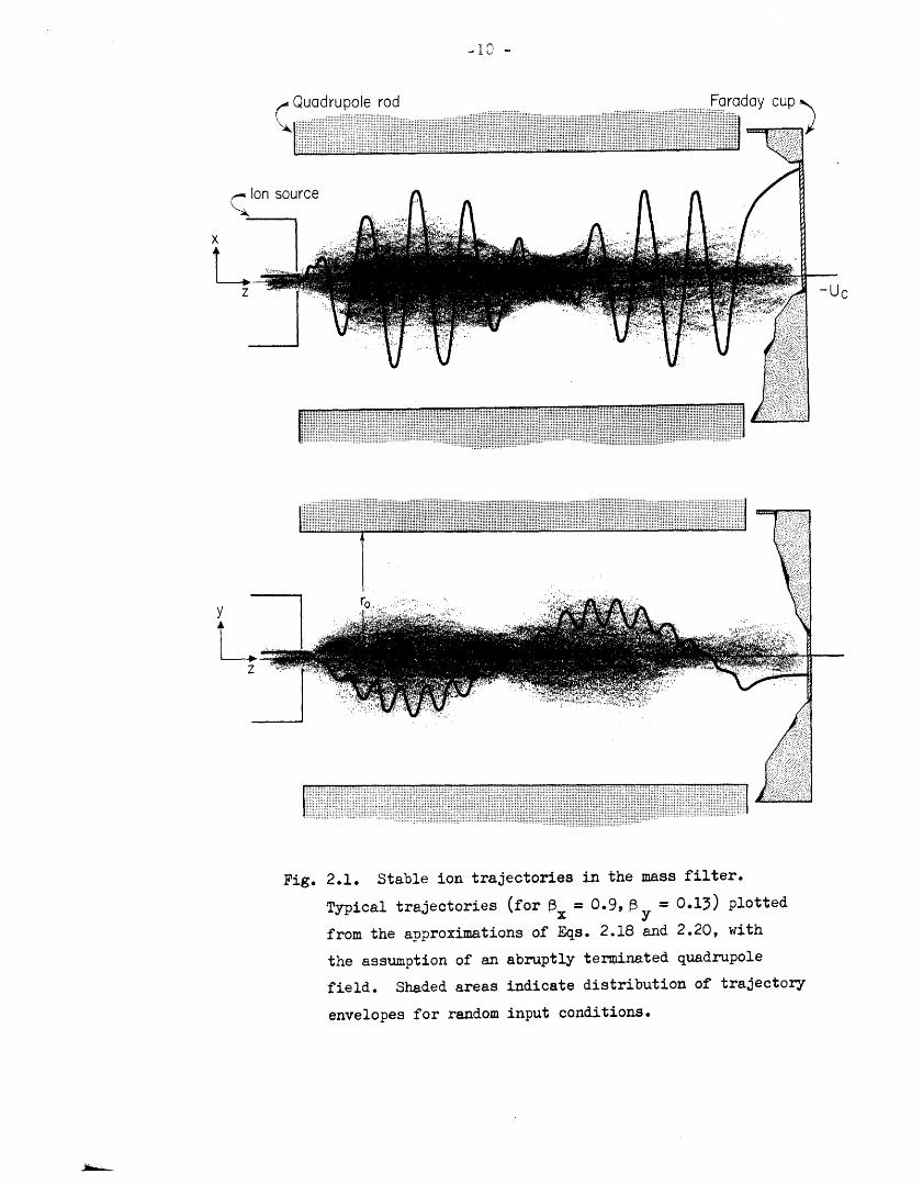
Fig. 2.1. Stable ion trajectories in the mass filter.
Typical trajectories (for Bx = 0.9, y = 0.13) plotted
from the approximations of Eqs. 2.18 and 2.20, with
the assumption of an abruptly terminated quadrupole
field. Shaded areas indicate distribution of trajectory
envelopes for random input conditions.
-Uc
I t I
~l~rmrmm .,..~,,m~····R~n--·--·r·?.m:~l::...
i ..... " :::::: ::i;iz;:;;:;;::;;;;;;;::!::::!::::::::::::!:;;;;;;;;;::;:::::::::::::::;:::
..... .... ...... ·lc:l::: ::;;:;;;::iii:tiii::::::::
:::: ::: :;: 7:;" ;;;:::: : :::: :: :; :: ; ; a :;:: ; :: : w :: : :: : :::: : : ::;:::: :;;;;~ ~;~;;;;;:::. :::.::: :.: ::::::7: ::: : ;; ;;; ;;: .t: ::.:::::.:: :::. .:;::;; :;;::":;; _Iiiit.~ t- ::~; ;~;t~j.:..~..: ........ :: :: :: .... :iiti..:..i....:..:..:..:.:..!::!:::::;Ill: Bell··rlh .... ... .... ................
....::::::
z
:?-.

- l -
,#z - o
Fig. 2.2. Quadrupole mass filter electrodes. From Paul, et al. 6
are applied (Fig. 2.2).
region I:s
The potential at any point in the field
2 2= - (U+ Vcos(t),
2ro
(2.2)
where r designates the inscribed radius of
trodes. The equations of motion for an ion
are
.. 2exmx + 2
0my- 2ey
r
mt = 0.
(U + V .os 'ti) =
(U + V cos t) =
the hyperbolic elec-
of charge e, mass m
0, (2.3)
o, (2.4)
(2.5)
Mathieu's Equation
An ion injected along the z direction will continue with its
velocity in that direction unchanged (Eq. 2.5). In the x-y plane,
however, the ion trajectory is more complicated and described by
Mathieu's equation: The transformations
Wt = 2 ,
8eUa= 22'mr W
o
4eVq= 2 2'
mr
*
(2.6)
(2.7)
(2.8)
Cf. Ref. 6. This entire chapter is basJ- extensively on thispaper; hence statements made without proof refer to it.
reduce the x-y equations of motion to
dx2 + (a + 2q cos 2) x = O (2.9)
and
y - (a+2q cos 2) y = , (2.1o)dt
which correspond, except for signs, to the standard form of the
Mathieu equation:9
d2x2 + (a - 2q cos 2) x =- 0. (2.11)
dS
All solutions to any of the three preceding equations can be
represented in the form
x = al'et Z c2me j2m t + a"e' Ce 2 m (2.12)
The solutions are stable (i.e., bounded) for all initial conditions
only for -= JB (purely imaginary), with not an integer.
The characteristic exponent () depends only on a and q, i.e.,
is independent of initial conditions. The range of values for a and
q for which the solution is stable for each of the Eqs. 2.9 and 2.10
can be plotted as a sequence of regions in the a-q plane; only the
one closest to the origin is of interest for mass-filter operation.
The operating point (a,q) must lie in a stable region of the a-q
plane for both the x and y equations. The combined region of
stability is the curvilinear triangle in Fig. 2.3.

O.
O,6/2
6.
.
a
B,0y60.7
0.,
I q77 42
Fig. 2.3. Stability diagram for quadrupole mass filter.
I'
0.2
I
0./
- 14 -
9OZY
q 7, a-.£6
From Paul, et a6
If the field specifications (r, ,7 U, and V) are held con-
stant, the locus of operating points on the stability diagram as
a function of mass is a straight line through the origin (cf.
Fig. 2.3). The distance from the origin on this locus varies
inversely with ion mass. The ion trajectories will be stable
only for the range of masses with operating points lying within
the stability region - the passband of the filter. As the ratio
of d-c to r-f voltage, U/V, is increased, the slope of the a/q line
increases, and the range of the stable interval is reduced, until
finally ions of only one mass have stable trajectories; all others
are ejected sidewise.
Particle Orbits
Within the stable region the solutions of the equations of
motion have the form
x or y- = i c2m cos(m + )wt + i C2m sin(m + )t
=A c cos [(m + )t + , (2.13)
where c, and aI or A and are determined by initial conditions and
C2m and B by a and q, hence by ion mass and field conditions.
Some insight into the particle trajectories is gained by con-
sidering the truncated form of the series Eq. 2.1l by convention
Co 1,0

-16 -x or y = A cos ( t + 9) + c cos t cos [(1 +
Th ot + e + .. } . (2.14)
For y(t) a continued-fraction expansion of the coefficients
(Appendix A) gives
c2 c2 - 2 (2.15)(2+ ) + a
and Eq. 2.14 may be rewritten as
y(t) Ay cos (2 t + ay) [1 + 2c2 os wtj . (2.16)
Near the vertex of the stability diagram of Fig. 2.3, y << 1,
a 0.23, or
2 - (2.17)
thus
i. . v4~~~t) - A cs ( 4 t ) r - nno wtI . (iF18- -' --- '2 y'- 2 y L 2
This equation, also obtained from direct physical reasoning by
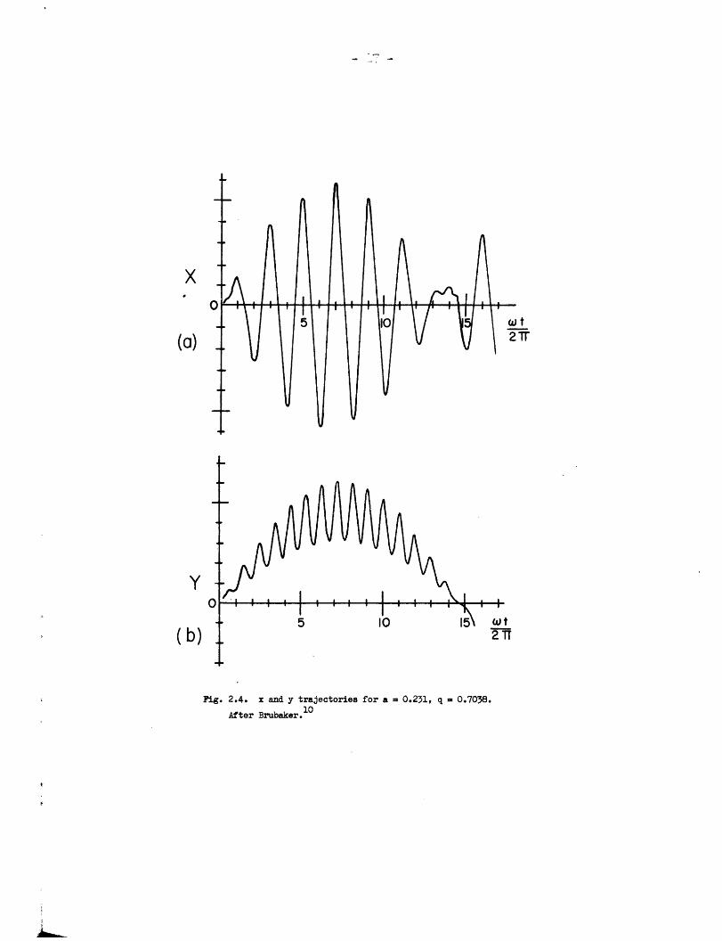
in
Brubaker,- predicts that the motion of the ion in the y direction
will be a low-frequency sine wave to which the second term adds a
moderate perturbation at the frequency of the quadrupole drive.
This is precisely the form of solution shown in Fig. 2.4b obtained
by numerical integration of the original force equation (Eq. 2.10).10
A somewhat different approach must be taken for the approxi-
mate solution of the x equation because 1 - Bx is << 1 for opera-
tion near the vertex (cf. Fig. 2.3). Only the first two terms of
,,
j
5
Fig. 2.4. x and y trajectories for a = 0.231, q - 0.7038.
After Brubaker.10
t'Tr
x
(a)
Y
(b)tTT
- 1J -
Eq. 2.14 are used because (as shown in Appendix A) c2 is small.
Thus
1 1 -1 OX r '
x(t)--Ax cos 2 )wt + ex + c 2 cos [( 2 2
x(t) Ax (1 + c 2)cos t cos [t -
+ (1 - c 2) sin t sin 2 Wt i- e 2.19)
Because c 2 1 (Appendix A), the first term of Eq. 2.19 dominates:
x(t) - A' cos t cos .. t - . (2020)x 2 2 x
The motion of the ion in the x direction is a sine wave at half the
quadrupole drive frequency (a subharmonic oscillation) modulated by a
low-frequency sinusoid. An exact numerical solution is shown in
Fig. 2.4a.
For any individual ion the trajectory in the x-z or y-z plane
has the same form as the trajectory plotted against time, because
z = (t - t), (2.21)
where is the z-direction velocity and t the entrance time. The
description of all possible spatial trajectories for a given ion
species and set of quadrupole voltages is difficult, bedause the
individual trajectories are a function of 5 random variables: two in-
put displacements, two input velocities, and the input time. However,
-19 -
if is constant, all will be contained within constant-wavelength
sinusoidal envelopes. These envelopes can shift in position, but
are constrained to low amplitude at the quadrupole entrance aper-
ture and so at subsequent half wavelengths. For example, the in-
put ensemble consisting of ions entering on the axis with finite
velocity has a generalized x-z trajectory of the form
w z (1 - x) x(z) A' cos 2 (t + ) sin z , (2.22)x 0 (
which has envelope nodes at z =[2zi/(l - x)wn, where n is an
integer. There exist, then, standing waves of ion-trajectory
amplitudes. The range of possible envelopes for one particular
set of operating conditions (i.e., one set of a, q values) is in-
dicated by the shaded areas of Fig. 2.1.
C. Mass-Filter Operation
Mass Spectra
A spectrum is swept,by variation of one or more electrical
parameters. For example, with voltages U and V constant, change
of frequency moves the operating point for any specific mass m along
a straight line that passes through the origin and intercepts a
section of the stability region (cf. Fig. 2.3). The distance from
the origin varies inversely with frequency. Increase of frequency
causes the operating points of a sequence of decreasing masses to
traverse the stability region and the corresponding ions to pass
through the filter.
.

r -20 -If frequency is held constant and the voltages U and V are
varied simultaneously so that their ratio is constant (), a
straight line through the origin is again traversed, this time
with the distance from the origin proportional to the voltage.
Increase of voltage makes a sequence of increasing masses traverse
the stable region and pass through the filter.
Fractional Transmission
In the discussion above it was assumed that all ions on
"stable" orbits traverse the mass filter and are collected at the
exit end, while those with "unstable" orbits are ejected. This is
not precisely true; some ions may have orbits which, while nominal-
ly stable, are so large that they extend beyond the electrodes (cf.
Fig. 2.1, xdirection trajectory). Such ions will be lost from the
filter.
The exact ion trajectory depends both on the operating point
in the a-q diagram and initial conditions. For suitably limited
entrance conditions there will be a section well within the stability
region for which all ions, regardless of individual entrance con-
ditions, describe orbits in the confines of the mass filter (con-
dition of "unity transmission"; Paul's Region I). In the remainder
of the stability region ions will be either transmitted or lost,
depending on the size of the initial-condition-determined orbit
(condition of "fractional transmission"; Paul's Region II). If the
mass-spectrum locus line traverses the inner section of the stability
i
_- 1 -
region the resulting mass lines are trapezoidal in shape, the flat
top corresponding to "unity transmission," the sloping sides to
"fractional transmission." However, if the locus line crosses the
stability region near the vertex, above the inner section, opera-
tion is always under conditions of "fractional transmission" and
the mass lines are triangular in shape.
Resolution
If the sides of the stability region of Fig. 2.3 are
regarded as straight lines, a simple relation can be found
between the mass range for stable ion orbits, the passband In,
and the mass m corresponding to the center of the stability region:
m 0.178 .2
kSm 0023699 - a0.706
ao706 is the ordinate of the mass line in the stability diagram
for q = 0.706. In terms of mass-spectrometer operation this is a
resolution equation, with line width Am measured at the base of the
*mass line.
Maximum Orbit Size
For any given set of entrance conditions - displacement and
velocity - the ion trajectory depends upon the phase of the r-f
quadrupole voltage at the instant of ion entrance. When all possible
entrance phase angles are considered, the maximum x or y displace-
Cf. footnote on page 5.

- 22 -ment of the ion, x or ym, for either injection parallel to them
axis at a fixed displacement x or yo, or injection at the axis
with a radial velocity Xo or yo, varies inversely as 1 - ox or By,
respectively. If straight-line approximations are made for the
constant-s lines in the stability diagram (Fig. 2.3), the maximum
displacements can be expressed in terms of the resolving power of
Eq. 2.23:
{or i~ 2.5 g , (2.24)
or <r 9 25 (2.25)
m o
Since for unity transmission all ions must have maximum amplitudes
less than r, the inscribed radius of the hyperbolic electrodes,
Eqs. 2.24 and 2.25 can be used to postulate maximum input displace-
ment and velocity.
Transverse Exit Velocity
If the ion collector of the mass spectrometer is a sufficiently
large Faraday cup placed near the end of the mass filter, it will
collect almost all the ions cnnina out of the filter even if they
have high transverse exit velocities. On the other hand, if the ion
collector is the relatively small first dynode of a commercial elec-
tron multiplier placed some distance from the end of the filter,
ions with high transverse exit velocities may not be collected.
This lowers apparent mass-filter transmission, and, if the exit-
velocity effect is mass selective, can produce false ion-abundance
ratios. The transverse exit velocities are therefore of some
interest.
The maximum exit transverse velocity is just the maximum
transverse velocity of the ion within the mass filter and can be
estimated from the approximate trajectories (Eqs. 2.18 and 2.20).
These can be regarded as high-frequency ( or /2) sinusoids with
slowly varying amplitudes. Differentiation of the high-frequency
part of Eq. 2.18 gives for the velocity
y(t) :. Ay 2 cos ( CO t + By) sin wt
and if a displacement amplitude ym is assumed, the velocity ampli-
tude is
-m -q (2.26)m 2+q
Differentiation of Eq. 2.20 for the x direction similarly gives
X
~ ~m (2.27)
Because q _ 0.7 (cf. Fig. 2.3), the velocity amplitude in the y
direction is about half that in the x direction (under the assump-
tion of the same displacement amplitude). For the most pessi-
mistic performance characteristic one need, therefore, consider only

the x-direction motion.
Maximum velocity amplitude occurs when displacement ampli-
tude is a maximum. It must therefore be obtained separately for
each of the three limiting values of displacement:
(1) In fractional-transmission operation ions with orbits
larger than electrode boundaries are lost; the maximum displace-
ment amplitude of those that remain is r . Thus the velocity
amplitude of Eq. 2.27 can be squared and express as a transverse
"voltage" (Utm): 22mr 2
0eUtm * -...
Substitution from Eq. 2.8, which relates r and w to the radio-
frequency voltage V, gives
VUtm_ ~ . (2.28)
Since q -_0.7, the maximum transverse exit momentum, expressed as
a voltage, is
Utm 0.7 V . (2.29)
(2) In unity-transmission operation the ion orbits are
limited by entrance conditions. If the limit is given by input
displacement confined to an aperture of diameter d, the maximum
orbit amplitude is given by Eq. 2.24 and the maximum transverse
exit momentum, expressed as a voltage, is
0.8 lr~ 2
tm V q ) m '
or, after the usual approximation for q,

r2
tm 1.2 m V (2.30)
(3) If, in unity-transmission operation, maximum displace-
ment results from the transverse entrance momenta of the ions, the
maximum orbit amplitude is given by Eq. 2.25 and the maximum
transverse exit momentum expressed as a voltage, is
Ut 18 m to (2.31)t'm - m to'
where Uto is the voltage corresponding to the transverse entrance
momentum. It is to be understood that Eqs. 2.30 and 2.31 apply
only when they yield a voltage lower than that of Eq. 2.29.
Heretofore only the maximum velocity occurring along the
filter has been discussed. The transverse exit velocity of a
particular ion depends upon its individual entrance transverse
velocity, displacement, and time, and upon its transit time in the
filter. The entrance time is purely random, the entrance displace-
ment and transverse velocity are widely distributed in some statis-
tical fashion, and even the transit time has some statistical
spread because of a slight variation in entrance longitudinal
velocity. A statistical treatment is necessary to determine
effective output momenta.
The standing-wave amplitudes along the filter are fairly
deterministic, depending most strongly upon the precisely known
for the ion species and upon longitudinal velocity. The transverse
:wo:~~~~~~~~~---- - i_ 4 .:2, ,Y fI 1__. .1a A E gvelocliLe a ne exit, nen, COUIa e exipecceu o rise $ na i i&l
- 26 -
with change in in the scan of a mass line, as the standing wave-
lenghts change and amplitude loops and nodes alternately pass the
exit.
Any more precise treatment requires evaluation of probability
distribution functions of all input variables. Because output dis-
placement and velocity are directly proportional to entrance dis-
placement or velocity, an average over entrance conditions will give
the mean output velocity with respect to those variables. For
example, if the input ion beam is either perfectly collimated and
contained by a circular aperture, or perfectly focussed on the axis
with velocities uniformly distributed to some upper limit, the mean
magnitude in one direction is 4/3ir of the maximum. An average over
entrance time (to) is more difficult; the approximate solutions for
the equations of motion (Eqs. 2.18 and 2.20) are not suitable for
such computation (e.g., they predict infinite amplitudes as a result
of certain entrance times) while more exact solutions are so compli-
cated as to require machine calculation. For lack of a better means,
the effect of entrance time can be estimated from the approximate
solution for the special case of entrance on the axis (Eq. 2.22),
which says output displacement (hence output velocity) is a sinusoidal
function of entrance time. The mean magnitude of output velocity is
then 2/ of the maximum.
The overall mean magnitude of one component of the velocity
is then, by crude estimate, 8/3n2 of the maximum at that point along
.^LI
27 -
the filter. If the effects of simultaneous entrance velocity and
displacement, and of y-axis motion as well as x-axis, were con-
sidered, the mean would be higher.
To summarize: The absolute maximum transverse momentum of
ions at the exit of the mass filter is given by whichever of
Eqs. 2.29 through 2.51 applies. The actual maximum is constrained
by the relative amplitude of the standing wave of ion displacements
at the exit point. The mean transverse momentum must be obtained
by an average over both directions of motion, all input times, and
all possible input conditions; it can be assumed to be more than
30% of the maximum.
An estimate of the actual effect of the transverse exit
momentum can be made by assuming that the region between the mass
filter and the collector has plane-parallel geometry, with a
separation of distance between the collector, assumed to be at
a voltage of magnitude Uc, and the mass-filter end plane. This
is not a totally unrealistic assumption if shielding grids are
placed over the output of the mass filter and input of the ion
collector. The ion trajectory in the transition region is a
parabola, and if the initial axial momentum is negligible, the
additional transverse displacement of the ion at the collector
will be
b =2 t . (2.32)d 2.29, Ut can be in the low kilovolt
Because, according to Eq. 2.29, U can be in the low kilovolt
range, there is a need for a high collection voltage to keep the
ions confined within a reasonable radius.
It should be noticed that because Ut varies with the selected
mass in a voltage-swept spectrometer (Eqs. 2.29 to 2.31), any loss
of ions caused by b > collector radius will be mass discriminatory.
D. Design Considerations
Basic Design Equations
For convenience, the most pertinent mass-filter design equa-
tions are summarized here.
Consider a quadrupole mass filter with electrode voltage
0 = U + V cos 2vt, (2.53)
i where r is the inscribed radius of the electrode assembly and v=0
w/2< is the r-f frequency.
The condition for transmission of a singly charged ion of mass
m at infinite resolution, that is, at the peak of the stability
diagram, may be reduced to
V3 7.219 m (amu)v2 (Mc) r (cm) volts, (2.34)
U = 1.212 m (amu)v2 (Mc) r2 (cm) [volts), (2.35)0
and
U ieU' U .95~ ~= 1 0.16784. (2.56)
Equation 2.34 is also a ood approximation in the case of finite
resolution. The idealized resolution, based on the width at the
foot of the mass line, is approximately

. 12- 29 -
rn 0.126 (2.37)m O0.16784 -
The maximum injection-aperture diameter, so that all ions in-
jected with zero transverse momentum will be contained in a
circle of radius r (the condition for unity transmission), is
d 0.8 -' ro (cm) [cm] . (2.38)
The maximum transverse injection momentum so that all ions in-
jected on the axis of the quadrupole will be contained in a circle
of radius r is, when squared and expressed as a voltage,
3t _,V 6ifl (volts] . (2.39)It is found experimentally that ions30 m
It is found experimentally that ions must remain in the mass
filter 5 Jm/!m' cycles to be mass selected; the maximum axial
injection momentum to ensure this is, expressed as a voltage,
2A2 2 (2.40)Ua 2.1 x 10 v2 (Mc) L (m) m (amu) n volts] , (2.40)a "
where L is the length of the quadrupole lens. The maximum trans-
verse exit momentum, expressed as a voltage,is
Utm .- .7 V (volts) [volts . (2.41)
For resolution m/Am, the required dimensional accuracy and
r-f frequency stability are 1/4 (m/m); the required stability of
the applied voltages is 1/2 (m/m).
The r-f voltage is almost invariably taken from a tank
circuit; the r-f power required is that taken by losses in the

- 0 -
tank, or
= (2V) 2vc (2.42)2Q 7
where C is the end-to-end capacitance of the tank circuit, in-
cluding the mass-filter rods, and Q the "Q" associated with the
tank. Substitution from the resonance condition (Eq. 2.534)
gives
C (pf) m2 (amu)v5 (Me) r4 (cm)P = 6.5 x 10O (c watts) .(2.43)
Momentum-Limited Transmission
The limit on transverse momentum (Eq. 2.39) is usually
the most restrictive entrance condition. If the limit is exceeded,
transmission must be less than unity; if the limit is a function
of the mass selected, transmission will also be a function of mass.
Possible methods of elimination of mass-dependent transmission will
be considered in this section.
I- Equation 2.39 with the r-f amplitude (V) eliminated by use
of the resonance condition (Eq. 2.34) becomes
Uto 0.24v2 (Mc) r2 (cm)Lm (amu) volts) . (2.44)to 0
The design problem is to make the right-hand side of either Eq. 2.39
or 2.44 independent of selected mass. One solution is constant V and
constant m/t~m (Eq. 2.39), which in turn requires constant U/V (Eq.
2.37). Because both voltages must be held constant, operation in this
manner requires the mass range to be swept by a change of frequency.
J
-3 1-
An alternative solution, due to Professor C.K. Crawford, is
constant v and constant 6m (Eq. 2.44). The mass range is then
swept by change of voltage, with a relationship between the r-f and
d-c voltages of the form
U = V - 8, (2.45)
where and 8 are constants. Substitution in the resolution
equation (Eq. 2.37) yields a line width
1.10 Am %Ii 7.94 (0.16784 - 7)m + 2 (amu . (2.46)
v2 (Mc) r (cm)0
If = 0.16784, m is independent of the selected mass.
Both the resolution equation (Eq. 2.37 or-Eq. 2.23) and the
transverse-momentum equation (Eq. 2.39 or 2.25) are based on straight-
line approximations to curves in the stability diagram. In addition,
the latter equation is also based pon a further approximation of
orbit amplitudes in terms of x and by. All these approximations
fail at low values of m/6m, although the errors from the first two
tend to cancel. It would therefore be expected that Eq. 2.46 would
fail at low values of resolution and that line width would not remain
constant, even with = 0.16784.
Two advantages accrue to the constant-Am mode of operation in
aalition o ne eminatlon or transmmssion variation causea Dy n-
put transverse ion momentum. First, it is possible to operate at
lower r-f voltages for a given selected mass without losing trans-
mission at the low end of the mass range; this saving in r-f volt-

- 52-
age and power can be important at the high end. Second, the uni-
form width of the mass lines makes comparison of peaks somewhat
easier.
Operation at constant Am does introduce some complications,
however. The maximum injection-aperture diameter for unity trans-
mission is inversely proportional to the square root of the mass
selected (Eq. 2.38). To avoid mass discrimination, the entrance
aperture must be small enough so that no ions are lost because of
input displacement even at the very highest resolution. This may
impose a severe limit on aperture size.
Operation at constant nm also enhances mass discrimination
in loss of ions by transverse exit momenta, for in Eqs. 2.29
through 2.31 the transverse "voltage" varies as a high power of
selected mass with m constant than with m/lm constant.
Mass-Filter Design
The parameters of the mass filter incorporated in the
quadrupole mass spectrometer were not chosen in one clear and
decisive operation, but rather evolved historically, as various
filter elements were modified to yield improvements in the most
cnnnmieal faohin. The caiz o-f +.hp nArann -field was nrri-al-
ly determined primarily by convenience of mechanical construction.
Frequency-swept operation of the filter was considered, but.
abandoned because of formidable engineering difficulties.
A fixed-frequency, voltage-swept system was used instead, with a
i

choice of frequencies for different mass ranges and provision for
introduction of an incremental d-c voltage 6 for operation at con-
stant m. The r-f frequencies were chosen so that an early version
of the quadrupole, using stainless-steel rods, could operate at
unity transmission with An = 4 amu on an 0-400 amu mass range for
ions with input transverse momenta corresponding to 0.9 volt, a
value that encompasses 99% of Maxwellian-distributed ions of
2000OK.11
The stainless-steel quadrupole has been replaced by a metal-
lized-ceramic one that has, for reasons of constructional simplicity,
slightly different dimensions. The mass filter then no longer exact-
ly complies with the original design requirements. The new quadru-
pole has an inscribed radius r = 0.807 cm and a length L = 0.51 m.
The mass filter has four ranges, 0 to 50, 100, 200, and
400 amu. The r-f frequencies are given by
V= g x 3.2103 (megacycles) , (2.47)
where M is the upper mass of the range being used. The r-f voltage
is
V 50 x 48.5 m (volts] , (2.48)
for a maximum value of 2420 v on all ranges. The maximum transverse
momentum for unity transmission, expressed as a voltage, is
IT 50 x 1.6 Am (voltsl . (2.4Q'-to M - ' - '
The maximum axial injection momentum for mass selection, expressed
as a voltage, isi

r
50 x 560o m volts . (2.50)
The maximum transverse exit momentum is, expressed as a voltage,
Utm 1700 (volts) . (2.51)
III. MASS SPECTROMETER: CONSTRUCTION
Those arts -of the quadrulole mass spectrometer that lie in
the realm of physical electronics were designed and constructed
by Professor C. K. Craword., and so were not a art of the work of
this thesis per se: they are the quadrupole lens, the ion source,
the electron multiplier, and the vacuum system.
A. Quadrupole Lens
The quadrupole lens consists of -four metal-coated-alumina
rods, 0.760 inch in diameter and 22.5 inches long, ground after
metallizing to be round to 0.0001 inch, and mounted in a titanium
holder (Fig. .1). The nominal inscribed radius was 0.318 inch.
Specifications called for the rods to be straight to within 0.0001
inch after grinding. nfortunately, because of an error in
manufacture, the rods are actually uite crooked: deviations of
more than 0.002 inch have been measured. The variation in inscribed
radius (ro) produced by this crookedness held spectrometer resolution
to low levels.
The original design of the lens called for slots to be cut in-
to the metal surface of each rod to electrically isolate a 270°
sector 1.25 inches long on each end. The isolated sectors were to
be gripped in two precision-bored end plates, while the remaining
*Kindly furnished by the Alloyd Corporation.
b S
~ C 0.: <1
S.0
c0a
Iclw
I
I
S
T,
ica
I
_ __
AI
4
0er
CE.24
C
h. S
o
o; 34
oo
0 0A~
id-I
'-4
!- - - · !
-
I
lr7~~~~~~~~~~~~~~'i
;, , i ,p-~vU u_ JJ D- s- -·I _ ~ ! P i ~ dl ·v
N

- 37 -
90 ° sectors would extend the quadrupole field to the end of the
rods. Because the 2700 sector would have been concentric with
the main metal surface of the rod, mounting accuracy would have
been high. Unfortunately, because of another error in manufacture,
the 270° and 90° sectors did not adhere to the ceramic. It was
therefore necessary to grind the exposed ceramic end as accurately
concentric with the electrode surface as possible, and mount the
ceramic stubs in the end plates. This alternative arrangement
lowered mounting accuracy, but errors were masked by the gross
crookedness of the rods.
The major difficulty with the makeshift mount is that the
auadrupole field ends !X inches inside the mechanical lens as-
sembly. At the input end this could be described as annoying; it
requires a strong-focussing lens to transport ions 1 inches from
the source to the small injection channel (used to minimize end
effects). At the output end it is almost catastrophic. If ions
at the exit with transverse momenta given by Eq. 2.51 for a massi
at the upper limit of a range (Utm ' 1700 v) were to be ac-
celerated in a uniform field by a typical accelerating voltage U =c
10 kv, then (by Eq. 2.32) after traversing 1 inches they would be
contained in a circle of radius 1.4 inches - well beyond the actual
exit radius of 0.3 inch. This means that if no special precautions
were taken, there would in fact be a large and mass-selective loss
of ions between the end of the electrodes and an ion collector;
r

- 38-
mounted beyond the end of the rods.
The most obvious cure for the exit problem, extra metal elec-
trodes slipped over the ceramic rod ends to extend the field region,
is impractical because such electrodes can not be positioned with
sufficient accuracy. Instead, the ion collector was extended inside
the rod ends. A beryllium-copper-lined metal tube with a high-
transmission grid on its input end was slipped into the end region
almost up to the quadrupole electrodes, and the first electron-
multiplier dynode mounted directly behind it. This extraction tube,
which is maintained at the full ion-accelerating potential of the
electron-multiplier ion detector, brings the collecting potential
close to the end of the uadrupole to cut down the skew of the exit
trajectories of the ions and increase the fraction that impinge
upon the multiplier first dynode. It also serves as a "zeroth"
multiplier dynode: Those ions that strike the inner walls of the
tube release secondary electrons that are accelerated by a potential
of a few hundred volts to the nominal multiplier first dynode.
The corrective measures for the mounting difficulty were an
attempt to save time and money, although it was known that the
final arrangement would still be not as satisfactory as a large
ion collector butted closely against the end of a correctly con-
structed quadrupole. Unfortunately, the corrections themselves
took enough time (most of an academic year) to prevent both thorough
tests of other arts of' the spectrometer system and use of the spec-
trometer for a study of Jthermal decomposition of solids as a art
of this thesis roject. (t as only at the end of this period
that the crookedness of' the rods - the one obviously uncorrectible
difficulty in the lens - was discovered.)
The use of circular rods to approximate the hyperbolic
electrodes of the ideal quadrupole leads to higher-order perturba-
tion terms in the electric potential. Symmetry considerations show
that the lowest of these is a -twelve-pole term, i.e., one varying
as r cos 6 , where r and f are polar coordinates. Paul, et al.
recommended a ratio of quadrlpole rod radius to inscribed radius of
1.16 to minimize this term.6 The quadrupole lens described above
has a ratio of radii of 1.20, hence a non-minimal twelve-pole term
that could conceivably introduce a fine structure into observed
spectral lines, and possibly even cause multiple ttansmission
12bands. However, no such line degredation has been observed in
instruments with radii ratios of 1.00, so the much smaller deviation
of this one is considered unimportant. 213
It should be pointed out that the radii ratio of 1.16 does not
really apply to a structure of four circular cylinders. It was ob-
tained by minimizing the twelve-pole term for a quadrupole magnet
14that used as pole pieces sectors of circular cylinders. Calcula-
tions for complete circular cylinders are yet to be done.
B. Ion Source
The ion source, constructed of "Electron-Atom-Ion" standard

-4 -
parts8 (Fig. 3.2), is shown schematically in Fig. 3.3. Gas mole-
cules enter the grid-enclosed ionization chamber in paths perpen-
dicular to the paper. It was intended that they come from a solid
vaporized in a Knudsen cell immediately below the ionization
chamber, but such operation was not achieved; only background gas
was analyzed.
Electrons from a tungsten-rhenium filament injected into the
ionization chamber (by source Velect ) ionize the gas molecules.
A small electric field (produced by Vchamber) accelerates the ions
out of the chamber into a strong-focussing lens that conveys them
to the injection canal. From the canal they are injected into the
quadrupole lens, with a longitudinal momentum corresponding to the
aceelerating potential Vio n.
The voltages (and even the circuit connections) on the diagram
are only typical; they are set to optimum values for any particular
experiment.
C. Electron Multiplier
The electron multiplier (Fig. 3.4) has 20 stages of beryllium-
copper dynodes with a structure shown schematically in Fig. 3.5.
The first dynode was made large (2.5 cm limiting aperture) with the
intent that, when placed near the end of a quadrupole it would
accept ions with skew trajectories. The last 17 dynodes are identical
with those used in the 14-stage RCA C-7187J electron mulitplier, which
Kindly furnished by the Radio Corporation of America.
- 41 -
IIM.X- A.
Ion source.
- E6-- . M
a
--
j
i
i
iI
I
i~~~~~~~~~~~~~~~~~
Ii
I
i
I
r
i
I o,
iIIfIt
i
I
c i
w
I
Fig. 3.2.

~ ~~---I ~~~~~~~11I
oEC0
I
0cu
>u
.C0NC0
0
00C0
.C'a
C)
o
o+Io1-
0E
00
-
D
-
,C0
0cDa2
I
o
IIII
II
II
II
- - - - - - -1I
l
II
- 43 -
(a)
94be, ~ ~ ~ ~ I = lit
jI
i -II I IIjI I (Q
Fig. 3.4. Electron multiplier: (a) on mounting flange,(b) partially disassembled.
(b)
=_ .
-44-
Entrance Grid
D2
Di,
P llMW
Fig. 3.5. Electron-multiplier structure. D1 through D20
are dynodes.
r45 -
in turn is identical in structure to the multiplier in the 6810A
photomultiDlier tube. The second and third dynodes were designed
to provide a transition between the large first dynode and the
small RCA dynodes. The anode is a grid structure mounted between
the 19th and 20 dynodes.
Not shown in either the photograph or the diagram is the
"zeroth" dynode, the extraction tube slipped into the space between
the ceramic quadrupole rod extensions. The entrance grid for the
first dynode is placed within a centimeter of two of the output end
of the tube, and a small wire (0.010-inch diameter) run axially up
the tube to introduce an accelerating field.
The dynodes were given no sensitization treatment before use.
Gain, originally 3 x 10 with 8 kv across 20 dynodes, dropped only
slightly over a period of several months. Then a number of internal
arcs, brought about by an open connection, reduced it by several
orders of magnitude, so sensitization was attempted. The arm of the
vacuum system containing the mulitplier was baked for 24 hours at
temperatures of about 400°C and a pressure on the order of 10- 5 torr.
With temperature: held constant at 400°C, oxygen was admitted (at a
pressure somewhat above 1 torr) for 20 minutes and the system
pumped down to about 10- 5 torr and cooled under vacuum. The result-
ing multiplier gain was quite high - an estimated 10 at only 5 kv
applied voltage - but one exposure to the atmosphere reduced it great-
ly, e.g., to 2 x 10⁷ at 8 kv.

r
D. Vacuum System
The vacuum system was designed to avoid organic contaminants,
which may degrade electron-multiplier gain, form insulating films
that can cause erratic potentials on surfaces, and yield a con-
tinuum background spectrum. The system is made of stainless
steel, with copper-gasket seals at all demountable joints. Oil-
free rough vacuum is provided by an alumina-trapped mechanical pump
and a zeolite absorption pump. The principal high-vacuum pump, a
90-liter/sec ion pump, was found inadequate to handle bursts of gas
produced by evaporation of materials in Knudsen-cell sources, and
was therefore augmented during such operation by a liquid-helium
cryopunp.
The entire system was designed to be baked at temperatures up
to 4000C, although this has not yet been done. The vacuum typically
obtained in the unbaked system, without use of the cryopump, is
about 10 torr.
- 1l7 -
IV. ELECTRONIC DRIVE CIRCUITS FOR THE MASS FILTER
A. Circuit Requirements
The quadrupole mass filter requires for its two sets of rods
a pair of voltages, balanced about ground, of the form
+ = U + V cos 2vt . (4.1)-- o
The selected mass is proportional to the r-f amplitude, V. Since
the range of masses should be swept over a time suitable for
oscilloscopic presentation, starting at any arbitrary mass in the
sweep range, the most general form for the r-f amplitude should be
= t + , (4.2)
where a may be adjustable to vary the sweep rate and may even be
zero if the filter is to select a single mass line continuously,
and is of course adjustable. The sweep may be either repetitive
(a sawtooth) or single shot.
For a constant resolving power, m/nm, U should be a fixed
fraction of V, but for constant line width, An, U should in
addition contain a negative constant. The most general form
required for the d-c voltage is therefore
U = yV- . (4.3)
The electronic drive circuitry that produces voltages
described by these equations can be broken into three major parts
i ~,.. 1 -- .
['Fig. .1): T''e llrst is the control generator, wnlcn produces a
voltage of the form ot + 3. The second is the r-f rod driver, whose
output, applied in balanced form to the mass filter, is proportional
i
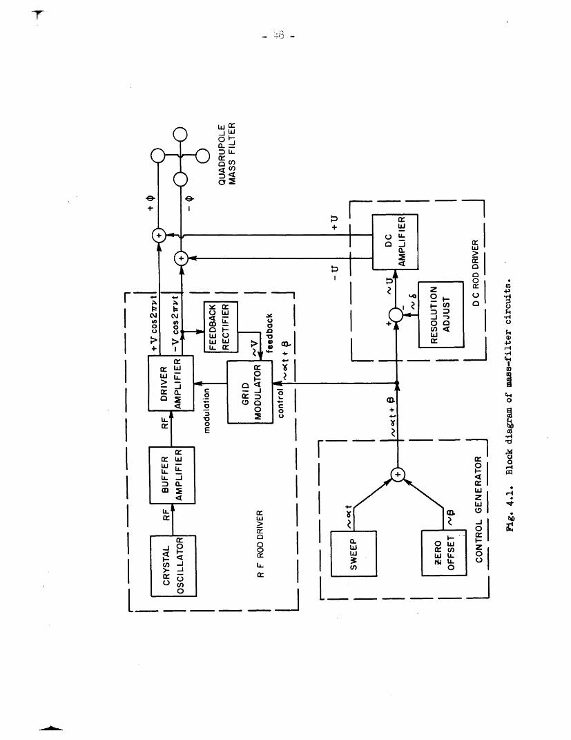
rl
0cI
I Io
$4
.t-
E 4 I 0
z Ic~
0 io
-
II
II
I
I
I
I
_ .a .
.9 . 11
.ll
a a L I _ r ~

in amplitude to the input from the control generator. The third
is the d-c rod driver, a balanced-output d-c amplifier for the
control-generator signal, with provision for the addition of a
resolution-co mpensation voltage.
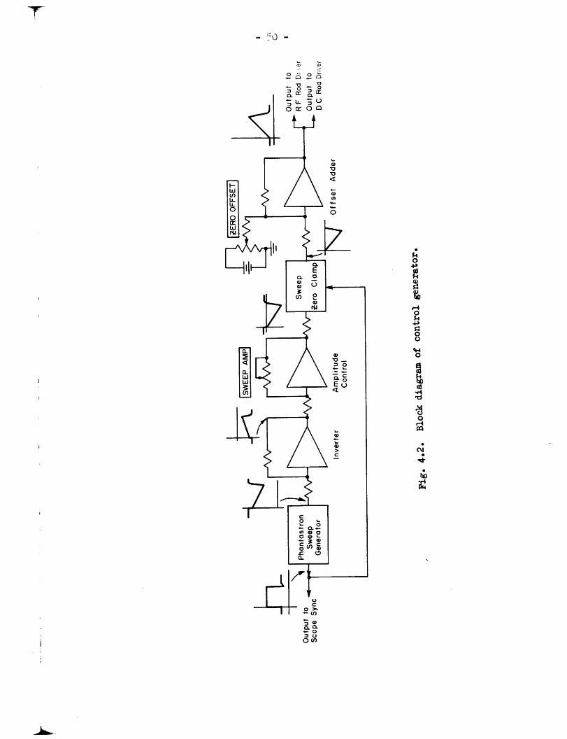
B. Control Generator
A more complete block diagram of the control generator is
shown in Fig. 4.2, and a schematic diagram in Fig. 4.3. The
sweep source is a phantastron sweep generator that produces a
voltage ramp on either a recurrent or a single-shot basis. This
is followed by a pair of operational amplifiers, the first of
which inverts signal polarity, while the second provides an ampli-
tude control for the sweep. The sweep signal is then passed through
a "sweep zero clamp" that holds the voltage at zero during non-
sweep periods. Finally the sweep signal (proportional to at) is
added to a d-c "zero offset" voltage (proportional to ) in a
final operational-amplifier stage.
The phantastron sweep generator (tubes V1 and V2 and associated
circuitry) provides recurrent O.1- and -sec sweeps and manually
triggered, single-shot 1- and lO0-second sweeps. In the single-shot
mode the circuit is quite conventional,1 5 but the recurrent mode
does have one unusual feature: the recovery delay is generated in-
ternally by an R-C circuit involving a regenerative connection of the
6AS6 screen and suppressor.
The rectangular-wave voltage of the phantastron screen
-
-o,
n
-oo0- o0
o,c 0
o Cn
404
or-I
40
0
F ' -
l

0
e
O 80IESCSr4'0
(a
o.4
e-I
0
Q)(D0
0'-0).
4)0p0
Ic'J
I-
U'+1
4o
'-4
4)o00r-014
o
c40o
0Cdtrl
14
T .- 52 -
provides a synchronization signal for the oscilloscope used to dis-
play the mass spectrum, and also drives the sweep zero clamp.
The free-running phantastron was chosen because it seemed to
provide all the needed sweep services with only two tubes. An
alternative sweep circuit considered at the time of the original
design involved a transistor current source feeding a capacitor, a
Schmitt trigger sweep-limit sensor, a one-shot-multivibrator recovery
timer, and a "crowbar" circuit to short the sweep capacitor during
the recovery period, for a total of at least 7 transistors. Despite
this disparity in active devices it is now felt that the phantastron
was a poor choice; it yields a signal with far too many spurious
features.
The phantastron, like all Miller integrator circuits, has in-
herent in its output signal a step preceding the ramp. If this
function were applied to the r-f and d-c rod drivers it would excite
serious transients in the mass-filter rod voltages at the start of
the sweep.
A clamp (transistor Q3) was installed to short the sweep volt-
age to zero during the non-sweep period; this did not completely
eliminate an initial transient because of a delay caused by difference
in rise time of the plate and screen steps.
Another shortcoming of the phantastron sweep circuit lies in
. J_ -, -voltage and tme 1nstalllles. ne pnanmasron generare s a nlgnly
linear sweep with a rate accurately controlled by the supply volt-
age and the passive components of the charging circuit (R1 and C1 ).
However, the voltage range over which the phantastron sweeps, and
thus the sweep time, depends on less stable circuit elements. 'The
initial sweep voltage in the manual mode, in which plate current is
truly zero until the start of the sweep, is not the same as in the
recurrent mode, in which there is finite plate current at the start.
There is even some difference in starting voltage between different
sweep-time settings.
The rest of the control generator consists of operational-
amplifier feedback amplifiers. The phantastron ramp is inverted
by a simple two-transistor amplifier. The next amplifier (a Phil-
brick K2-XA) provides a highly linear sweep-amplitude control and
adds a d-c component to remove the d-c offset of the phantastron
signal. The last amplifier, also a K2-XA, adds the sweep voltage
(ot) and a zero-offset voltage (t). The output is calibrated at
50 volts full scale for either sweep amplitude or zero offset. The
sum can go to 100 volts, but this overloads the r-f and d-c rod
drivers. A neon warning lamp, not shown in the diagram, lights
when the total output voltage exceeds 50 volts.
The unstabilized operational amplifiers suffer from appreci-
able voltage drift. In one test the filament power was turned on
for two minutes, plate power for another ten, and stability
observation begun. The output of the control generator drifted
55 mv in the first 7 minutes, 145 mv in the first 70 minutes.
After d-c power had been removed for 5 minutes (with filament power
on) and then reapplied, the output shifted back 73 my but immediately
- 57, -
Tesumed a rift in teorigina- ._
resumed a drift in the original direction. A drift of 145 mv
amounts to 0.145 amu on an 0-50 mass scale, 1.2 amu on an 0-400
scale;'-this cannot be tolerated in high-resolution operation.
The control generator therefore suffers from both voltage
and time instability in the phantastron circuit and voltage
instability arising in the operational amplifiers. For optimum
performance it should be completely redesigned and rebuilt. The
sweep generator could probably be based on a Miller integrator
using one of the small low-drift, commercial transistor opera-
tional amplifiers now available, with retrace and control func-
tions handled by transistor multivibrators. Two operational ampli-
fiers are necessary to control sweep amplitude and add zero offset.
(A third one might be advisable to produce a zero offset signal that
was a more linear fction of potentiometer setting.) The transis-
tor operational amplifiers should be satisfactory for these applica-
tions also, although it would be necessary to add an additional
amplification stage on the output to achieve 50-volt signal levels.
(Operation at lower voltage levels would not be satisfactory because
a nonlinear network in the input of the r-f rod driver requires
rather large voltages for proper operation.)
C. R-F Rod Driver
The r-f rod driver, shown in block-diagram form in Fig. 4.1,
schematic-diagram form in Fig. 4.4, must produce rather large r-f
voltages variable over an extremely wide amplitude range - at least
L
Ii
-a
- 55 -
BUFFER AMPLITUDE
CONTROL
CRYSTAL OSCILLATOR
RF INI Ht, B
C4
.001
KO
4; alley BH64
.300v X'cl,1135me
/N I ,., ,2_:i 4/ T
BUFFER AMPLIFIER
R16lOOK 2.T vv~ =t --
R5~~~~~1 M.R5, i IOK zw
214Q3 4702n : 620K
032N697 l1a 1
68K IN3A : 2143R1, 'FIN r4 ...
I…1o-35v … 1 Y~/ ?
- c -3 I
'I ~L2 L3
\ tj=>,@ L6 Imh ¢ , T !.i l 2.2mh 52 -
69-7 : -
I r t L 7_ _ IlmhK ! i_ / 11,2 2702m1 i S
S Xtel 3 2103mc IFREOUEYI C |OOpf p1 | 2.,'
A 11A Vl3997
GO ND GK1532R
-30.Ov 300w .nnb270K .OlyN ·.3.Do./R4SO 3921
R29 300v
I30 IO .
t4 " IN1744 10v,
-600v
R53 R54I30K1% 909K 11%Y
168KII%wlOK ~%|
155 L MASS 4Ro
ZS25K IOOK -|
7 IN629 IN629
IN625 (Si)
1191 222 503K Philb2r 2
,LOW MOSS ADJUST| / $'
l40
2 OK _- rR I M I R26 w s3I22 PRF ER M RS I 2 . 1029.o00 .*301. t~~I443
3002
NONLINEAR COMPENSATION
V7 _ _ OLT637-GTA
B~ ~~ ~ TI
I B -300V
.!tlL .. " I 2K 270K1P%,.
I IX~~~~tO41
l00pf071N629
SR4 B.iK )0
2 -~ 2 x 0 396
L .2 L ...- 300vMODULATOR LIMITER
(2)
5112w
: 13
.R34
2R33
/1 Ics oR-I.0 I -r b. I7X 0e 1I"Tu
-100to370v .C
.002262 9
-j
CG31p1p mic
C105ptNPO
t RIDTUNE I
,Cl532NPO
DRIVER AMPUFIER
LTo modulator
--- -(2) Eim. 4-65A 3
6.0N23% CR7.0.
01 4 pl5 2 0 G ,d7 4
C lpI
R13: 68K
R35270K
0 032R 4700f
$ ,4D6BL7-GTA
.Y- - _. - -- L i
.4'j 300oI
FEEDBACK RECTIFIER
001 75%21 N RF FEEDBACK CGALIBRATE
C26 .
Dblower -] I 0 ~ I_ - P ,- do ' - 5000v
_ _ LB5A-Z. - _NPO
4713 i
L8 I11- 0R'4 L II
LIO
'!' I - 0-3 2-O.
I - ~ ~~~~~22 ,I - (D I L13 5m I ..
Aerowx,O IS50 L
L14 5m
C38t (2] 00pf I. h,..q
| {8d througb
L128
L 16
5t
C19 (2) ,1I l
2 'P , i
0W{C3 t C2
1C39 JC2-IOOE i C23
S 1-
L155mh
.700
_ _ _ _ _ _ ___0 | SWITCH 54 PC2 ; ! | I: auff , 2 221t
.300v _ f O | 2: Finl 4r1id
I uJ 1 3 RF output
0-5 4 RF output
54?CI.RN" t.01
-1oF-_
HN
G33 3p 5000vNPO
' ROE120 l BLNG
TIN629 .OOipf
3pt 5000vNPO
|+OUTPUTI......... + U--'
TOMASS-FILTER
RODS
_C 3f5000v NPO
Nq5I
c028 Z 04 oo T NC3 NI34A 14 1 NPI I VOLTAGE MONITOR... T / ~o...
)SITIONS:
0-50mo |
0-500, RF
0-51k RF0-500v RF
PROTECTIVE CLAMP
.2560Ki*
-600,
MODULATOR
Pig. 4.4. Circuit diagram of r-f rod driver. Unless otherwisenoted: (1) all resistors + 5%, 1/2 w; (2) potentiometers,Allen Bradley Type J; (3) capacitors, high-K ceramic.
CI391NPI
N~~~~~~~~~~~_~__
.
, RR38
_L _V1c*rJ�--t------------ I-
_ __
t
I
-ucl
AA* & A
�' ? '' '
L12A
HN '
'"' V
| ~r
t
r wv"I I .011f 02
- f 2NII31
I~
·IEN-T
BNG
LLI�
_)t_
QR
RI8
----- ~n It
-56 -Table 4.1. Buffer-Output R-F Transformers.
The 1-inch-diameter primary and 1 -inch-diameter secondary
coils are coaxial, concentric, and wound as a right-hand screw.
The secondary is center tapped. The Faraday shield, which lies
between the coils and is coaxial and concentric with them, is
made of No. 34 bare copper wire wound 40 turns/in. on 1 -in. o.d.
-in. wall phenolic tubing. Every turn is soldered to a
longitudinal ground bus and is cut diametrically opposite the bus.
High-frequency transformer: 3.2103 and 2.2700 Mc.
Primary: L2 13 Ph. 26 turns, 32 turns/in., B and W
"Miniductor.:
Secondary: L3 = 37 h. 42 turns, 32 turns/in., B and W
"Miniductor."
M = 15 h.
Faraday shield 1 in. long.
Low-frequency transformer: 1.6051 and 1.1350 Mc.
Primary: L4 = 42 Jlh. 64 turns, 32 turns/in., B and W
"Miniductor."
Secondary: L5 = 145 3h. 110 turns No. 30 HF, 40 turns/in.,1
wound on -in.-wall phenolic tubing.
M = 57 h.
Faraday shield 2 in. long.
High- and low-frequency assemblies are mounted at right angles to
minimize stray coupling.

-57 -
Table 4.2. Output Tank Coils.
The coils resonate with - 155 pf, including the capacitance of3 1/2-ft of RG-11/U cable and 81-pf quadrupole capacitance. They arecoaxial, concentric, and wound as a right-hand screw. The primary iscenter tapped, the secondary in two halves with a gap between halvesfor the primary center-tap lead. Unless otherwise noted the coils arecommercial air-wound coil stock (Illumitronic Engineering Corporation,Sunnyvale, California) with Lexen insulation.
3.2103 Mc.
Primary: L1l = 12 lh. 14 turns No. 16 wire, 2 1/2-in. diam.,
10 turns/in.
Secondary: L12 = 16 h. 18 turns No. 12 wire, 3-in. diam.,
6 turns/in., 1-turn gap between sections.
M = 9.4 h. Q = 170.
l v:) T7 M
Primary: f .
Primary: Lll = 20 Sh. 20 turns No. 16 wire, 2 1/2-in. diam.,
10 turns/in.
Secondary: L12 = 32 h. 26 turns No. 14 wire, 3-in. diam.,
8 turns/in., 1-turn gap between sections.
M = 18 h. Q = 170.
1.6051 Mc.
Primary: L1 1 = 51 h. 32 turns No. 14 wire, 3-in. diam., 10 turns/
in. , polystyrene insulation.
Secondary: L12 = 65 ph. 28 turns No. 14 wire, 4 1/8 -in. diam.,
9 turns/in., 2-turn gap between sections. (Modified
B and W 3252.)
M- =37 h. Q =160.
1.1350 Mc.
Primary: L1 1 = 66 I'h. 26 turns No. 20 bare wire, spaced own
diameter on 3 1/2-in. o.d., 1/8-in.-wall phenolic tube.
Length = 1.66 in.
Secondary: h2 = 135 Lh. 42 turns No. 18 bare wire, spaced own
diameter on 3 1/2-in. o.d., 1/8-in-wall phenolie tube.
1/8-in. gap between sections, each section 1.69-in.
long.
M = 65 h. Q < 170.
i
i
to to swee all masses of interest- between and 50. The-
100 to 1 to sweep all masses of interest between 1 and 50. The
simplest circuit, a modulated oscillator, is ruled out because it
is difficult to get an oscillator to stay in oscillation over such
a wide modulation range and because the amplitude modulation is
accompanied by an undesirable frequency modulation. The output of
the r-f driver is therefore obtained rom a modulated push-pull
Class-C amplifier, the "driver" amplifier.
Grid modulation was chosen for the driver amplifier over such
alternatives as plate modulation or combined plate-screen modulation
obtained by a series-tube regulator because it offers fewer problems
in voltage-level shifting and confines problems of high power to
the modulated amplifier. Only one difficulty was encountered: at
high negative grid bias, when low r-f output is to be obtained, the
r-f amplifier plate conduction time is very low, and harmonic dis-
tortion of the output is enhanced.
A grid-modulated amplifier requires a "stiff" r-f driving
voltage because the input power demand increases: rapidly with grid
conduction at high output levels. A feedback-controlled buffer
amplifier was therefore chosen to supply the r-f input to the driver
amplifier. The buffer amplifier was in turn driven by a crystal-
controlled oscillator, which produces a signal of good frequency
stability with simple circuitry.
The mass filter requires the relation between the r-f and
d-c voltages to be maintained with a high degree of precision.
i

- 59 -
No r-f modulation scheme is sufficiently linear in direct operation
to maintain that relation, but adequate linearity over most of the
amplitude range is obtained by a feedback-control system in which
a fraction of the r-f voltage is rectified and summed, at the in-
put of an operational amplifier that drives the grid modulator,
with the signal from the control generator. Nonlinearity, intro-
duced by the rectifier is reduced by a nonlinear compensation net-
work in the control system input.
Because the required r-f power is directly proportional to
the total tank-circuit capacitance (Eq. 2.42), the latter should
be kept as small as possible. The entire r-f rod driver might
have been placed at the vacuum system next to the mass-filter
terminals, to eliminate the capacitance associated with a coupling
cable from the driver to the mass filter. This was not done prima-
rily because of mechanical problems involved in mounting it on
equipment that may be subject to bakeout. Instead the driver was
placed in a rack-mounted chassis and coupled to the mass filter by
high-voltage coaxial cable. Total circuit capacitance was about
155 Pf, so by Eq. 2.42 the maximum required power is 3.7 x 10⁴/Q
watts. For a reasonable value of Q, say Q = 200, this is on the
order of 200 watts.
Remote mounting of the rod driver may have been in error,
because it encourages high-order harmonics in the output. Since
the coil admittance becomes negligible at frequencies appreci-
ably above the operating frequency, the entire tank circuit becomes,
r
in effect, a pair of capacitances on either end of a length of
cable. This transmission-line circuit resonates at various fre-
quencies, some of which necessarily lie very close to harmonics of
the operation frequency. For the apparatus actually constructed,
substantial amounts of 7th to 12th harmonics were observed.
Crystal Oscillator
The crystal oscillator is a single triode (V1) in a Pierce
configuration. The output is taken from the triode grid because
the signal amplitude there can be closely controlled (at 25-v peak
amplitude) by limiting action. Frequency stability was not measured,
but experience with crystal oscillators has shown them to have a
stability of better than 1 part in 10 under almost any conditions
of erat'jt+inr whicrh i te+ar thvain rni"I for mIsiaa rA.
tion.
Buffer Amplifier
The buffer amplifier is a single pentode (V2) with the output
inductively coupled to the grids of the driver amplifier. The out-
put amplitude is regulated by a "buffer amplitude control" feedback
circuit that grid modulates the buffer to maintain constant r-f
voltage on the driver-amplifier grids despite changes in load
caused by grid conduction.
A type 6973 beam-power pentode was chosen for the amplifier
because it combines appreciable power-handling capability in a small
.envlopewithafaorabe -oattoc -
envelope with a favorable plate-to-screen current ratio under con-
ditions in which screen voltage exceeds the plate voltage.
If the output tank circuit of the buffer amplifier were to
be badly detuned, the amplitude-control circuit would attempt to
maintain full r-f output by bringing the pentode grid bias as close
to zero as possible. If no special precautions were taken this
would result in excessive d-c plate current, excessive plate dis-
sipation, and damage to the tube. Transistor Q1 prevents this
by limiting pentode cathode current to 50 ma. Under ordinary
operating conditions (cathode currents of 10 to 40 ma) the tran-
sistor is in saturation and holds the cathode essentially at ground
potential.
The output circuit is one of two switch-selected r-f trans-
formers with a tuned, balanced secondary (Table 4.1; Appendix B).
Mica padding capacitors make possible resonance at the lower of
the two frequencies for each transformer.
The buffer amplitude rcntrnl onnsists of a dide dtec-.tnr
that applies to a transistor amplifier a d-c current proportional
to the r-f voltage on the driver-amplifier grids. The output of the
transistor amplifier grid modulates the buffer amplifier so as to
hold the output constant despite load changes.
The diode detector consists of two capacitively coupled,
shunt-diode, half-wave rectifiers (D2 and D ), one for each side
of the balanced r-f circuit. Each such rectifier has in its out-
-62 -put an r-f current equal in amplitude to the d-c current, but the
balanced arrangement makes it unnecessary to use the customary low-
pass filter with its accompanying phase shift that enhances feed-
back instability problems. The current applied to the input of the
transistor amplifier is the sum of the outputs of two rectifiers
whose d-c components add arithmetically, but whose r-f components
are 1800 out of phase and so subtract arithmetically. If the
circuit were perfectly balanced and the RC time constant infinite,
the current applied to the amplifier would be pure d-c. In fact
there is some residual r-f current of frequency , caused by circuit
unbalance, and some ripple of frequency 2w. The residual ripple is
of amplitude /wRC relative to the d-c, or essentially that which
would be obtained from a full-wave rectifier with a simple R-
I filter.
The feedback amplifier consists of a common-emitter stage
(Q2 ) followed by an emitter follower (Q3) that gives the amplifier
the capability of supplying appreciable output current when there
is buffer-amlifier grid conduction. The amplifier bias was chosen so
that under closed-loop conditions the r-f output of the buffer ampli-
fier is about 225 v.
The buffer amplifier output voltage varies less than 2% as the
operation frequency is switched over all four available values or as
load is increased from zero to the value that causes current-limiting
action by protective transistor Q1. The maximum power output ranges
from 3.2 to 3.8 watts, depending on frequency, 30% beyond the require-
__.�__ ._�..
i
i

ments of the driver amplifier.
Driver Amplifier
The driver amplifier consists of a pair of l4-65A tetrodes
in a push-pull Class C arrangement, with r-f input applied to
the grids in series with d-c bias from the modulator, and a sec-
ondary-tuned, transformer-coupled output.
The amplifier is neutralized to compensate for direct
capacitive coupling of r-f energy from the tube grids to the
tube plates, which would make it impossible to reduce the output
voltage below ca. 10 volts, even with the tubes cut off. Neutrali-
zation is accomplished by capacitors Cnl and Cn2, each of which
consists of a short length of wire extending up from a chassis
feed-through, connected to the grid of one tube and "looking" at
the plate of the other.
The 4-65A filaments are heated with 6.0 volts d-c to eliminate
hum modulation of the r-f output. When the filaments were run from
the usual filament transformer the hum modulation was on the order
of 0.5 volts, even with the most careful hum-bucking arrangements.
This was caused by a strong third-harmonic component in the 60-cps
line voltage, in conjunction with a frequency response in the feed-
back circuitry controlling the r-f amplitude so poor for noise
introduced in the driver amplifier stage that it was unable to
reduce significantly the 180-cps modulation produced.
The protective clamp circuit (V5) was intended, in case of bias
_ .- ·-
failure, to drop the 4-65A screen voltage to such a low value that
the tetrode plates and screens would be protected from overdis-
sipation. However, the 4-65A is so insensitive to screen voltage
that the plate can be overdissipated even with zero screen volt-
age, so the clamp offers little protection. There is still a need
for some arrangement that will sense any of the conditions that
may lead to overdissipation, such as bias failure or plate-tank
detuning, and remove voltages from the 4-65A's to prevent damage.
The d-c plate-supply voltage of 1800 volts is the minimum
with which the driver amplifier can produce full output at
3.2103 Mc. Operation at lower plate voltages and higher plate
currents requires more grid drive than the buffer amplifier can
supply.
The r-f output of the rod driver is taken from the tuned
secondary of one of four plugEin output tank coils (Table 4.2;
Appendix B).
The two-winding output transformer has substantial advan-
tages over the autotransformer used in the earlier version of the
16rod driver. First of all, the d-c voltage for the quadrupole
rods can be applied at the center of the transformer secondary,
thus eliminating the high-loss r-f isolating chokes and one of
the bulky d-c isolating capacitors necessary in the autotrans-
former arrangement. (One large mica capacitor is still necessary
to complete the r-f path across the gap in the secondary winding.)
L
- 64 -
-65 -
Second, the amplitude of the harmonic distortion that appears in
a symmetric mode in the out-out (as contrasted to the antisymmetric
fundamental) is greatly reduced. Elementary theory, which assumes
an output transformer with unity coupling between primary and
secondary, predicts no inductive coupling of symmetric-mode
signals into the output, but, as is shown in Appendix C, there is
such coupling because of flux leakages. Experimentally it is found
that the two-winding output transformer nearly eliminates the
second-harmonic symmetric signal and substantially reduces the
amplitudes of higher harmonics.
The r-f output of the rod driver is supposed to be perfectly
antisymmetric, that is, balanced with respect to ground. The con-
dition of balance is determined by the self-checking balance detec-
tor; any unbalance in the output is indicated by a d-c output volt-
age. The balance of the detector itself is determined by reversing
it in its socket, according to the balancing algorithm (Appendix D).
Output balance is achieved by simultaneous adjustment of capacitors
C2 2 and C2 3, so as to keep end-to-end capacitance constant. A single
adjustment would suffice if C22 and C3 were replaced by a single
capacitor consisting of three parallel plates; two widely separated
stators, one connected to each side of the r-f output, and a single
grounded plate that could be moved between them. Adjustment of the
movable plate would change the end-to-ground capacitances, but leave
the end-to-end capacitance essentially constant.
The driver-amplifier output capability on all frequencies
l_..

- 66-
ranges from a minimum of a few tenths of a volt, set by imperfectly
neutralized r-f leakage from the grids to the plates, to beyond the
full design output of 2400 volts. At 3.2103 Me, the most demanding
output frequency, full output requires 180 ma d-c plate current,
about 225 volts and 2 watts of grid drive, and about 2 watts screen
power. The dissipation of each 4-65A plate at this output, as
measured by observation of plate temperature with an optical pyro-
meter, is about 38 watts. Because the efficiency of a grid-modulated
amplifier drops at lower output levels, maximum plate dissipation
occurs at an output of 1500 v; it is 48 watts, well within the 65-
watt rating of the tube.
The output of the driver amplifier contains harmonics of the
operation frequency in both symmetric and antisymmetric modes. If
the driver amplifier were perfectly balanced the symmetric-mode
harmonics would be even-order, the antisymmetric-mode odd order.
In fact, the observed symmetric-mode voltage does consist primarily
of even-order harmonics, from the second to the twelfth, with the
fourth predominating at most operation frequencies; the antisym-
metric-mode voltage consists primarily of odd-order harmonics, with
the third predominating. The seventh harmonic of 3.2103 Mc appears
strongly in both symmetric and antisymmetric fashion, indicating
both that there is a transmission-line resonance near that frequency
and that- the driver amplifier is slightly unbalanced. (The con-
clusion of amplifier unbalance is supported by the observation that
i
67-
the dissipations of the two 4-65A plates are not quite the same.)
It might be advisable in any circuit redesign to include more
elaborate balancing features in the driver amplifier - perhaps
a balance adjustment for r-f drive in the grid circuit, or
individually adjustable tube grid biases, or both.
The amplitude of the symmetric-mode harmonic output is
relatively small, ranging typically from about 0.5% of the out-
put voltage at low outputs, ca. 100 volts, to 0.05% at the full
2400-v output. The amplitude of the antisymmetric third harmonic
ranges from 0.2% to 0.1% of the output voltage, the amplitudes of
the other antisymmetric odd harmonics considerably smaller.
The effect of the harmonic distortion of the r-f signal on
the mass-filter operation is a matter of some concern. The only
effect of the symmetric-mode voltage is a modulation of the axial
momentum of ions entering the filter. Since this is noncritical,
the symmetric-mode voltages should have little effect. On the other
hand, the antisymmetric harmonics are applied between the quadru-
pole rods in the same fashion as the fundamental, and might be
expected to have a significant effect, but such is not the case;
at most they produce a slight shift of the stable region on an a-q
diagram. 1 2
The harmonics in the output, both symmetric and antisymmetric,
do have an adverse effect on the r-f rod driver itself: because
they are amplitude dependent, they tend to reduce the linearity of
661A

- 68 -
the feedback rectifier for the fundamental component. In addition,
the symmetric-mode signal can also be capacitively coupled to the
anode of the electron-multiplier ion detector, and, if the multi-
plier is used in particle-counting fashion, appear in the output
of the broad-band amplifiers following the multiplier. (In practice
it has been found possible to eliminate .this trouble by careful
shielding of the multiplier rods.)
It may be concluded that, in general, the presence of harmonics
in the r-f voltages applied to the mass-filter rods caused no dif-
ficulties. However, because harmonics increase the problem of non-
linearity of r-f amplitude control, for a very high resolution mass
spectrometer it might be advisable to minimize them by mounting the
rod-driver output tank circuit as close as possible to the rods, and
to operate the driver amplifier so that plate conduction times are a
maximum.
Feedback-Controlled Modulator
The amplitude of the r-f rod driver is controlled, in mass-
spectrometer operation, by a feedback-control system consisting of a
high-gain modulator that modulates the r-f driver amplifier and a
diode rectifier that returns to a summing point at the modulator input
a d-c signal proportional to the r-f output.
The modulator is a commercial operational amplifier driving a
cascaded triode amplifier and cathode follower, capable of supplying
output voltages from -100 v to -370 v and driver-amplifier grid cur-
rent up to 20 ma. For circuit tests, the feedback loop can be
broken by a switch and the modulator either controlled by a
potentiometer (so-called "manual" operation) or set to a fixed
voltage cutoff r-f output.
A limiter circuit (transistor Q4 and triode V) constrains
the output of the operational amplifier to the range of voltages
necessary for modulator action. In essence, the limiter works by
closing a subsidiary feedback loop, involving the "+" input of the
operational amplifier, any time the amplifier output is positive
enough to produce grid conduction in the triode amplifier.
The transmission of a mass filter is a critical function
of the ratio of the d-c and r-f voltages. Differentiation of
Eq. 2.37 gives the change of line width as a function of change
in the voltage ratio:
(mn) 8m8 (). (4.4)
At high masses a small change in the voltage ratio produces a
large change in effective line width. Because in fractional-
transmission operation transmission is roughly proportional to
line width, a large change in apparent ion abundance is also
produced.
Because the d-c rod voltages can be maintained with great
accuracy by conventional feedback circuitry, it is the r-f voltage
that is of concern. Its amplitude can be controlled with no more
precision than it can be measured by the rectifier in the control
- -, Q -
r0
circuit. Hence the rectifier is the most critical single element
in the uadrupole rod drivers.
Two distinct troubles can beset the control rectifier. The
first is instability, a change with time of d-c output for a fixed
r-f input. This can be kept small by careful choice of critical
elements, such as capacitors and resistors, and by such special
precautions as operation of heaters of vacuum-tube diodes from
regulated supplies. The second problem is nonlinearity, which is
simply an expression of the fact that the rectifier output is not
strictly proportional to the r-f input, nor even proportional to
within an additive constant. Over a wide range of inputs, such
as the 100-to-1 range of a mass spectrometer sweeping from below
mass 1 up to mass 50, the nonlinearity produces significant change
of the r-f output relative to the control signal, and therefore a
change in mass-spectrometer resolution and transmission as the mass
range is swept. Nonlinearity of the control rectifier therefore
imposes a fundamental limit on the "(resolution) x (mass-range)"
product of the mass spectrometer.
A single shunt-vacuum-diode, peak-reading rectifier coupled
to the r-f output by a capacitive voltage divider was used as the
control rectifier because it gives the best linearity realizable with
present-day devices and conventional circuits. The most obvious
alternative, a semiconductor-diode rectifier, is slightly inferior.
One improvement could easily be made in the present rectifier, how-

--i -
ever: the single diode could be replaced by two diodes in a balanced
configuration, as in the buffer-amplitude-control circuit. Such an
arrangement would, of course, do nothing for rectifier nonlinearity,
but would make possible improvement of the modulation frequency
response, just as it did in the buffer amplitude control, and also
reduce the sensitivity of the system to unbalance in the rod-driver
output voltage.
A study of rectification techniques was made in an attempt to
obtain a more linear rectifier. It was found that more elaborate
circuits involving slide-back or comparison techniques are no better
than a simple peak-reading detector unless they use a threshold de-
tector (nonlinear element with a sharp break in its voltage-current
curve) better than a conventional diode. A slide-back detector
:_ t 1 f1 _ ar ma, ualJ _UUW:LLg 1 t re.Umely sarp Steet avalla e I n soumi eleteU e avaLanVLWL te
diodes was extensively investigated, but proved impractical because
of the noise inherent in such diodes at low current levels and
because the extremely high junction capacitance (100 pf typical for
_. I_ .1 I * a\ _ _ v t_ ___1a small aioce) made :-ivc operation impossliIe.
A simple alternative to a more linear rectifier, compensating
nonlinearity in the input of the amplitude-control feedback loop, is
used in the r-f rod driver. The voltage-current characteristic of a
1N625 silicon diode (D10 ) is such that when the diode is in series
with the feedback-modulator input resistor, it approximately com-
pensates rectifier nonlinearity. At moderately low inputs the silicon-
diode voltage drop is too high; resistor R 4 8 is then an effective
I
i
I
r
shunt. At the very lowest currents a sharper nonlinearity is
necessary: a germanium diode (D9 ) in series with R48 provides
this. Additional small corrections to the 1N625 voltage drop are
provided by adjustment currents switched in by diodes Dll at all
inputs above 15 v (corresponding to mass 15 on the 0-50 scale)
and D12 at all inputs above 30 v.
The nonlinearity compensator is adjusted by observation of
background-gas mass spectra on the two lowest mass ranges of the
spectrometer, On the 0-100 range the LOW MASS ADJUST control
(R4 8) is set to give the same fractional transmission at mass 14
as at mass 28, for a constant setting of the DC/AC RATIO control
of the d-c rod driver (i.e., a nominally constant ), and the
RESOLUTION control set at zero (i.e., = 0). Then on the 0-50
range the MASS 28 ADJUST is set to give the same transmission at
mass 28 as at mass 14, and the MASS 40 ADJUST to give the same
transmission at mass 40 or mass 44.
The deviation of the r-f-to-d-c ratio from its value at 14
control volts (mass 14 on the 0-50 range, mass 28 on the 0-100
range) is shown in Fig. 4.5 for both the compensated and uncom-
pensated case. The data were obtained from observations of the
d-c rod-driver voltage (as measured by the DC/AC RATIO control)
required for 106 transmission of a number of ion species. In
Constant fractional transmission provides a true indication ofconstant U/V only when ions are lost solely because of entrancedisplacement; transverse entrance momentum enhances loss at lowvalues of mass even with U/V = constant. However, through it isnot exact, simplicity makes constant fractional transmission agood practical test of U/V.
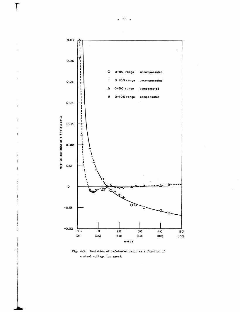
0.07
0.06
0.05
0.04
, 0.03
~i ~~o
o 0,02o
.2a
~I l~~a,
0-0.01
ii ~ -
0. 10 20 30 40 50(0)' (2 0) (40) (60) (80) (100)
macs
Fig. 4.5. Deviation of r-f-to-d-c ratio as a function of
control voltage (or mass).
r
- 74
both the compensated and uncompensated case the r-f voltage is
quite high at low mass values (around mass I and 2), but while
the uncompensated r-f voltage shows a total deviation of some
4% over the upper 90% of the mass range, the compensated volt-
age shows a deviation of only 0.4%.
The performance of the nonlinearity compensator should
not be regarded as the ultimate, for it was intended only to
demonstrate the practicability of compensation. It should be
possible to design a network to hold the r-f voltage within about
0.1% of the desired value over a 10:1 amplitude range.
Four separate problems arise in the feedback-controlled
operation of the r-f rod driver: (1) dynamic stability,
(2) transient response, (3) control dead zone, and (4) long-term
stability.
(1) Dynamic stability. The problem of dynamic stability
was a first consideration in the design of the feedback-control
system. With capacitor C41 omitted, the open-loop transfer func-
tion of the r-f rod driver can be approximated by three poles on
the negative real axis of a root-locus diagram, with no compensa-
ting zeros. The first of these poles arises from the K2-XA
operational amplifier transfer function. The amplifier is designed
to have a 6 db/octave falloff over almost the entire useful range
of frequencies, with a transfer function
K woK) ~K + =
S +WK

F --where K °- 30,000 and wK -
~ 100. The second pole, at atproxi-
mately wf - 2 x 10⁵, arises from the diode-rectifier low-pass
filter. The third pole arises from the bandpass characteristic
of the driver-amplifier plate-tank circuit, and is
21tv
where v is the r-f frequency and Q the tank-circuit "Q". For
the frequencies and coil Q's of interest this pole lies between
I4wQ = 2 x 10 and wd 7 x 10.
Under closed-loop conditions two of the three poles migrate
to the right-hand plane and cause system oscillation.1 7 To
prevent this, compensating capacitor C41 and associated resistor
R_, were ade8d to rnoduce a zero in the onen-loon transfer func-
tion at w = 3 x 10 , which virtually eliminates the pole produced
by the tank-circuit bandpass, wQ.
(2) Transient response. The closed-loop transient response
is a function of the three-open-loop poles, the compensating zero,
another zero arising in the feedback rectifier, and open-loop gain.
Because one of the open-loop zeros, wQ, depends upon the operating
frequency and coil "Q", and the small-signal open-loop gain depends
upon the steady-state r-f output voltage, there is substantial vari-
ation in transient response. Depending upon operating frequency
and steady-state amplitude, the response is characterized by either
a simple exponential or a slightly underdamped sinusoid. To a
first approximation it can be described by a single exponential of
1}me constan 'betwen 150 nd 1-- 76 -
time constant between 30 and 150 sec, with 50 sec being the
typical value.
The r-f rod driver is required to handle only ramp inputs.
The output of an exponential-response system to such an input is,
after an initial transient lasting a few time constants, a ramp
lagging the input by the exponential time constant (5 x 10 5 see
for the r-f rod driver). This lagging error has little effect
on the critical U/V ratio of the mass spectrometer in part because
it is small (onlv O.054 after 01 sec) and in nart because the d-
rod driver has a similar lagging response, so that the only first-
order effect is a negligible delay in mass sweep.
(3) Control dead zone. One special difficulty arises in a
feedback-control system involving a modulated r-f voltage: There
can be no "negative" r-f output to correspond to a negative control
voltage, so the system has a "dead zone" encompassing the entire
negative range. This problem becomes especially severe during
sweep retrace to zero. When the input signal drops abruptly to zero
the modulator cuts off the 4-65A's completely, but the r-f output
drops slowly because of the high Q of the tank circuit. The diode
rectifier sends a large error signal to the modulator, driving it
to saturation in the cutoff direction. The modulator may or may not
recover before the next sweep begins. The modulator limiter circuit
previously described tends to prevent gross saturation of the opera-
tional amplifier K during such periods, but cannot completely
eliminate the problem because there must necessarily be a range of

rI- 77-
operational-amplifier output voltage between that necessary for
complete r-f cutoff and that at which the limiter goes into
operation.
(4) Long-term stability. Because it is necessary to
maintain the r-f voltage to within better than one part in 103
in order to maintain a satisfactorily precise U/V ratio, the
long-term stability, or freedom from drift, of the control
circuit is highly important. The stability of the existing r-f.
control system must be characterized as highly unsatisfactory.
primarily because of drift in the input offset voltage of the
operational amplifier used for K. The K2-XA has a rated drift
of 8 my per day under "optimum" conditions. This would be
marginally adequate if it could be achieved in the rod-driver
circuits, because 8 my represents about 0.1%5 of a typical control
voltage of 10 volts. However, "optimum" conditions evidently
require operation with supply voltages always on and at temper-
atures more constant than those in the mass spectrometer equip-
ment racks, for much greater drift has been found. In one test,
after filament voltage was applied for 2 minutes and both filament
and plate voltages for another 10 minutes, the K2-XA offset volt-
age still drifted 30 mv in the next 5 minutes of operation, and
another 33 mv in the next two hours. After d-c power was removed
for 5 minutes (with filament power on) and then reapplied,the
zero-offset voltage returned to nearly the value it had at the start
1I

- 78-
of the test and began another drift cycle. Because plate power is
frequently removed and reapplied in the operation of the mass spectro-
meter, this sensitivity to power removal is particularly unfortunate.
The K2-XA should be replaced by a more stable operational ampli-
fier, probably because of the output voltages required, a chopper-
stabilized vacuum-tube amplifier, which should reduce drift some
three orders of magnitude.
A more stable operational amplifier would undoubtedly reveal
a number of other sources of d-c drift. The most obvious of these
is a zero-offset current flowing in the vacuum-diode r-f detector
even when the r-f voltage is zero, because of the thermal velocities
of electronsemitted from the diode cathode. This current is appreci-
able in magnitude (approximately 1 Ma in the present circuit, cor-
responding to a voltage offset of about 50 my), highly dependent
upon heater voltage, and subject to long-term drift. The effect of
fluctuations in this current could be greatly reduced by injection
into the summing point of the operational amplifier a compensating
current obtained through a resistor from the cathode of a grounded-
anode vacuum diode.
A second obvious source of drift is the deposited-carbon
resistors and carbon-composition potentiometers used in the control
circuit. These should be replaced by the more stable metal-film
resistors and wire-wound potentiometers.
The nonlinearity-compensation circuit in the input of the
control circuit is a potential source of drift from temperature
fluctuations because it uses semiconductor-device voltages. It
might be necessary to place this circuit in a temperature-
regulating oven.
Incorporation of all these recommended changes should make
it possible to hold long- and short-term drifts in the r-f volt-
ages to less than one part in 103.
D. D-C Rod Driver
The d-c voltages for the mass-filter rods can be obtained
most easily by rectification of the r-f voltage. In as much as
the rectifier is linear, the d-c voltage would be proportional to
the r-f amplitude. However, if d-c voltages are obtained from
separate amplifiers, it is much simpler to obtain high-speed
sweeps, to add a resolution-broadening voltage 5, and to compensate
for nonlinearities in the r-f rod driver.
The d-c rod driver consists of a pair of cascaded inverting
feedback-controlled amplifiers (Fig. 4.6). The first provides gain
for the control-generator output signal adjustable from 0 to 10 by
the DC/AC RATIO control. Its output is applied to one of the pairs
of mass filter rods as the negative or "d-c£' signal, and is also
passed through a 1:1 inverter whose output is the positive, or
"d-c+" signal. A "self-checking" balance detector that uses the
same principle as the r-f balance detector - reversible connections -
ensures that the rod voltages are balanced with respect to ground.
I
i
i
A

r
w
! \
0
4X0002
0 )
a a
i1:,.; arl
- BE
I "- .h
-0
, e z OLL
a.o O>0) ..-X0*0
* 0.0*b 0
*'*
OD
'D
a r
Atr
11
Because the r-f rod driver produces a signal whose amplitude
V is 48.46 times the control signal amplitude, the O-to-lO gain
range of the d-c rod driver gives U/V ratios up to approximately
0.2. However, since the maximum U/V ratio for transmission
through the mass filter is 0.16784, the highest voltage required
from the d-c rod driver is not 480 v but 0.16784 x 2420 = 407 v.
The actual dynamic ranges of the two amplifiers exceed 0 to 450 v.
The resolution-broadening voltage 6, added to the control-
generator signal at the input to the first amplifier stage, can
be varied from 0 to approximately 10 volts by the RESOLUTION
control. If the DC/AC RATIO control is set at the "infinite
resolution" value of 0.16784 and the RESOLUTION control at 10 v,
the actual line width on the O-to-50 mass scale is 1.5 amu.
Each amplifier in the d-c rod driver has two stages, the
first a Philbrick K2-XA operational amplifier, the second a
6S4A triode that provides the necessarily large voltage swing.
The outputs are series fed to the mass-filter rods through the
split-winding output tank coil of the r-f rod driver.
The use of feedback control in each amplifier of the d-c
rod driver presents three of the four problems that arose in the
r-f rod driver: (1) dynamic stability, (2) transient response,
and (3) long-term stability.
(1) Dynamic stability. The open loop transfer function
of either of the two amplifiers with the compensating capacitor
-82 -
C1 or C3 omitted from the circuit has three significant poles, all
on the negative real axis, and no zeros. The first pole is that
arising from the K2-XA transfer function. The second is caused
by the combination of high Miller effect input capacitance of the
K2-XA at its positive input terminal, some 150 to 200 pf, and the
high feedback resistances required by the high-voltage circuitry.
This pole is at about w= 2300 for the "d-c+" and w. 14000 for
the "d-c-" amplifier. The third pole is caused by the combination
of the high open-loop output impedance of the amplifier and the
large shunt capacitance necessary in the r-f rod driver, some
0.009 f effective capacitance from each side to ground. Its
location varies with plate voltage as the plate resistance changes,
but remains between w = 9 x 10³ and w = 3 x 10.0 0
The combination of three low-frequency poles and a high open-
loop gain causes closed-loop oscillation of each amplifier. The
compensating capacitor (C1 or C3) introduces a zero into each
transfer function at approximately the same position as one of the
original poles and thus eliminates the oscillation.
(2) Transient response. Both the "d-c+" and "d-c-" ampli-
fiers have step responses with slightly underdamped sine-wave
ringing, the first with a ringing period on the order of 10 5 sec,
-4the second with a period on the order of 10 sec. The ramp
response of the "d-c-" amplifier then has a small initial transient,
lasting perhaps a few milliseconds, followed by a lagging error that
a

r -83-
varies with amplifier output level, because both system gain and
open-loop output impedance are voltage dependent. The error
ranges between 2 x 10 sec at low voltages to 1 x 10 sec at
the highest output voltages. The "d-c+" amplifier has a sub-
stantially faster response, with transient decay in less than a
millisecond, and a delay of about 10 5 sec for a ramp input.
These transient responses are adequate for the present spectro-
meter, but in the design of an optimum system care should be
taken to minimize "d-c+" delay and to match the "d-c-" and r-f
rod-driver delays.
LI
I
I

_ 34 _
V. DESIGN CONSIDERATIONS FOR THE ELECTRON-MULTIPLIER
ION DETECTOR
A. Introduction
The simplest ion detector for a mass spectrometer is a
Faraday cup connected to an electrometer that amplifies the minute
ion currents. This arrangement has a maximum usable sensitivity of
some 1016 amp amnd a response time that becomes poor at high sensi-
tivities because of input RC time constants on the order of seconds.
.Since , h n'~a '_"dnl . manss .mPtr.mete.~"r 'Wasr i·n'lnrtndr f'or mdert".tel
rapid sweeps of mass spectra, in times as short as 0.1 second, as
well as for the study of ion beams modulated at several hundred cps,
much greater response speed of the ion detector is necessary. This
response speed can be achieved, along with improved sensitivity, by
use of the high gain-bandwidth capabilities of an electron multiplier
in the ion detector.
The simplest way to use an electron multiplier as an ion-
detection amplifier is to let its first dynode serve as the ion
collector of the mass spectrometer, Secondary electrons emitted upon
ion impact are multiplied in the subsequent stages. This technique,
18used for over a quarter of a century, is summarized in a review
article by Akishin.l9 Its principal shortcoming is that it exposes
all electron-multiplier dynodes to surface contamination in the mass-
spectrometer vacuum system.
An alternate method minimizes the dynode contamination problem
by collecting the ions with a scintillator crystal or with a single
.i2L
.1.
F - 85 -
dynode whose electron output goes to a scintillator crystal. A com-
mercial photomultiplier tube outside the vacuum system detects
20-22light from the scintillator. The chief disadvantage of this
arrangement, the difficulty of finding a high-speed scintillator
suitable for use in high vacuum, was considered prohibitive, so
direct ion-electron multiplication was used.
B. The Electron Multiplier as a Current Amplifier
The most obvious method of using the electron mulitplier is
as a current amplifier. The ion current is multiplied by the mean
electron yield of the first dynode and the mean current gain of the
following dynodes, for a typical overall gain on the order of 106
While adequate for many applications of the mass spectrometer,
variations in electron-multiplier gain make this method unsuited
for precise quantitative work, such as a comparison of the relative
abundances of isotopes of a given element or of ions of two differ-
ent elements.
Two distinct variations in gain are troublesome in current-
amplifier operation. The first is a variation in electron yield
of the first dynode as a function of the species, charge, isotopic
mass, energy, and angle of incidence of the ions, and of the nature
and condition of the surface of the first dynode. There is no
a priori way to determine yield, or even relative yield. For
example, Barnett, Evans and Stier2 3 found that for noble-gas ions
incident upon an activated beryllium-copper first dynode, the
L. .A

T -86
secondary-electron yield increased with ion mass fCor incident energies
of appreciably less than 20 key, but decreased with ion mass for
energies appreciably greater than 20 kev. As a further example,
Sugiura found that for He+, Ne+, and A+ ions of the same energy (in
the range 2 to 3 kev), the yields from an electropolished beryllium-
copper dynode were in the ratios 2.45:1.79:1.00, respectively, while
the yields from an oxygen-treated dynode of the same material were in
24the ratios 2.00:1.28:1.00. Results such as these indicate that it
is necessary to calibrate the gain of each electron multiplier for
each ion species to be studied.
The second variation in gain is that caused by contamination of
the electron -multiplier dynodes over a long period of time. If only
the second and following dynodes were affected the result would be a
simple drop in gain, which could be determined by a single measurement
and easily compensated. However, contamination of the first dynode may
very well reduce electron yield more for some ion species than for
others. The results of Sugiura show that two surfaces freshly prepared
by different techniques have different yield ratios; it is prudent to
assume a freshly prepared and a contaminated surface would likewise
have different yield ratios. This secular, selective change in yield
makes long-term calibration of multiplier gain impossible.
C. The Electron Multiplier as a Particle Detector
One method of avoiding the gain variation problems in electron-
multiplier ion collectors is to use the multiplier not as a current

amplifier but as a particle detector. Each ion incident on the first
dynode produces some 106 electrons at the anode; this is a quantity
of charge sufficient to be treated in a quantized or digital fashion
by subsequent electronic apparatus. The output pulses can be ampli-
fied, if necessary, and then passed through a standardizer circuit
that yields pulses of a single selected size despite variations in
multiplier output pulse amplitudes. This scheme is as old as the
18use of electron multipliers as ion detectors, and has been carried
25-2 8out successfully many times.
There are two methods of processing the output of a pulse
standardizer. The pulses may be counted with a digital counter, a
technique of value for long-term measurements of a single mass but
unsuited for scanning a mass spectrum, or they may be integrated, in
what has come to be known as a count-rate meter, to give an average
current or voltage that is proportional to the rate at which ions
arrive at the multiplier first dynode.
The operation of an electron-multiplier ion collector as a
particle detector is, in principle, quite simple. There is, however,
one characteristic of electron multipliers that makes particle-
detection operation rather difficult in practice: dispersion in out-
put pulse amplitudes from the multiplier caused by statistical vari-
ations in the secondary-emission process at each dynode. The pulse
circuitry associated with the electron multiplier must be capable of
handling not only the variations in output pulse amplitudes caused by
-4
38 _
discrimination of ion secies at the first dynode and secular
changes in gain because of contamination, which together might
give one order of magnitude variation in amplitude, but also the
statistical dispersion in output amplitudes for a given ion species
at a given time, which might amount to an additional two orders of
magnitude. The system is therefore required to be insensitive to
an extremely wide range of pulse amplitudes to circumvent relatively
small variations in gain.
The distribution in amplitude of the output pulses of an
M-stage electron multiplier is a function of the distribution in
amplitude of electron yield per incident ion on the first dynode
and of yields per incident electron on the subsequent M-1 dynodes.
It is common to assume that the distribution for an electron-
electron secondary emission process is Poisson, that is,
kn -kp _ )4, n (5.1)n n
where n is the probability of the emission of n electrons and A
is the mean emission, although Shockley and Pierce were able to show
many years ago that noise measurements on electron multipliers
indicated that the distribution could not be truly Poisson,2 9 and
Barrington and Anderson found by direct measurement a non-Poisson
distribution for secondary emission from an activated beryllium-
copper surface.3 Nevertheless, careful measurements of output
pulse amplitude distributions for single electrons incident on the
-I
I

first dynodes of a number of commercial photomultiplier tubes has
-x 31shown a distribution roughly of the form xe 1 which corresponds
fairly well with that predicted under the assumption of Poisson
statistics at each dynode. 2 The Poisson distribution hypothesis,
then, remains useful as at least a first approximation to the
CU LULWL ULb L.LUULUln.
No direct studies have been made of the yield distribution
for the ion-electron process. However, overall pulse amplitude
distributions have been obtained for ion-electron multipliers with
both beryllium-copper2 3 and silver magnesium26 dynodes and found to
have roughly an xe shape. The results of Barnett, et al. are
plotted as a probability density function and compared to an xe x
curve in Fig. 5.1.
Johnson, et al., 3 report a strikingly different amplitude
distribution for a multiplier with silver-magnesium dynodes. They
found a multi-modal distribution, with the modes spaced as the
integers. Apparently the multiplier was more or less faithfully
reproducing the yield distribution of the first or ion-to-electron
dynode. Two factors may have made this possible: First, the
multiplier probably had a rather high gain and low yield dispersion
on all stages except the first. Second, the ions incident on the
first stage had a low energy, 3 kev, that would give a low electron
yield.
The results of Barnett, et al., can probably be taken as more
L.ii
1
F"~~~~~~~~~~~-9 i~~~~~~~~~~~~~~~~~~~~~~~~~~~~~~~'
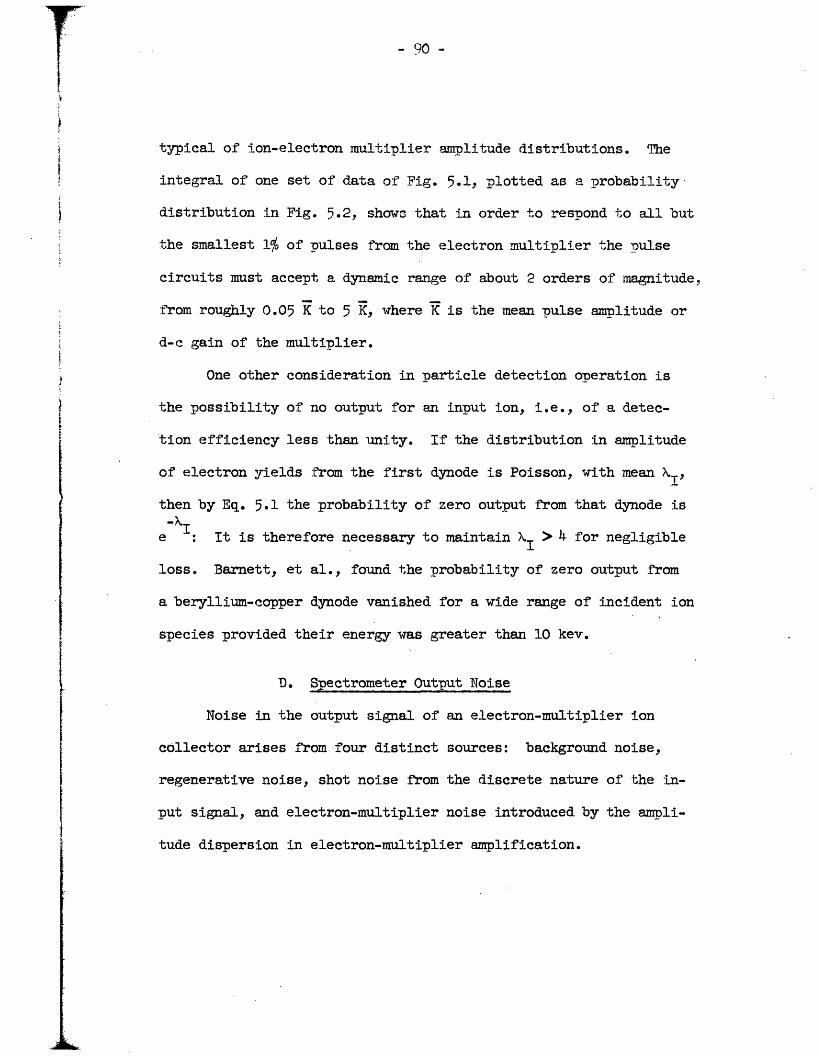
.I~~~~ . - 90 -
typical of ion-electron multiplier amplitude distributions. The
integral of one set of data of Fig. 5.1, plotted as a probability
distribution in Fig. 5.2. shows that in order to respond to all but
the smallest 1 of pulses from the electron multiplier the pulse
circuits must accept a dynamic range of about 2 orders of magnitude,
from roughly 0.05 K to 5 K, where K is the mean pulse amplitude or
d-c gain of the multiplier.
the possibility of no output for an input ion, i.e., of a detec-
tion efficiency less than unity. If the distribution in amplitude
of electron yields from the first dynode is Poisson, with mean i,
then by Eq. 5.1 the probability of zero output from that dynode is
-kXIe : It is therefore necessary to maintain XI > 4 for negligible
loss. Barnett, et al., found the probability of zero output from
a beryllium-copper dynode vanished for a wide range of incident ion
species provided their energy was greater than 10 kevy.
D. Spectrometer Output Noise
Noise in the output signal of an electron-multiplier ion
collector arises from four distinct sources: background noise,
regenerative noise, shot noise from the discrete nature of the in-
put signal, and electron-multiplier noise introduced by the ampli-
tude dispersion in electron-multiplier amplification.
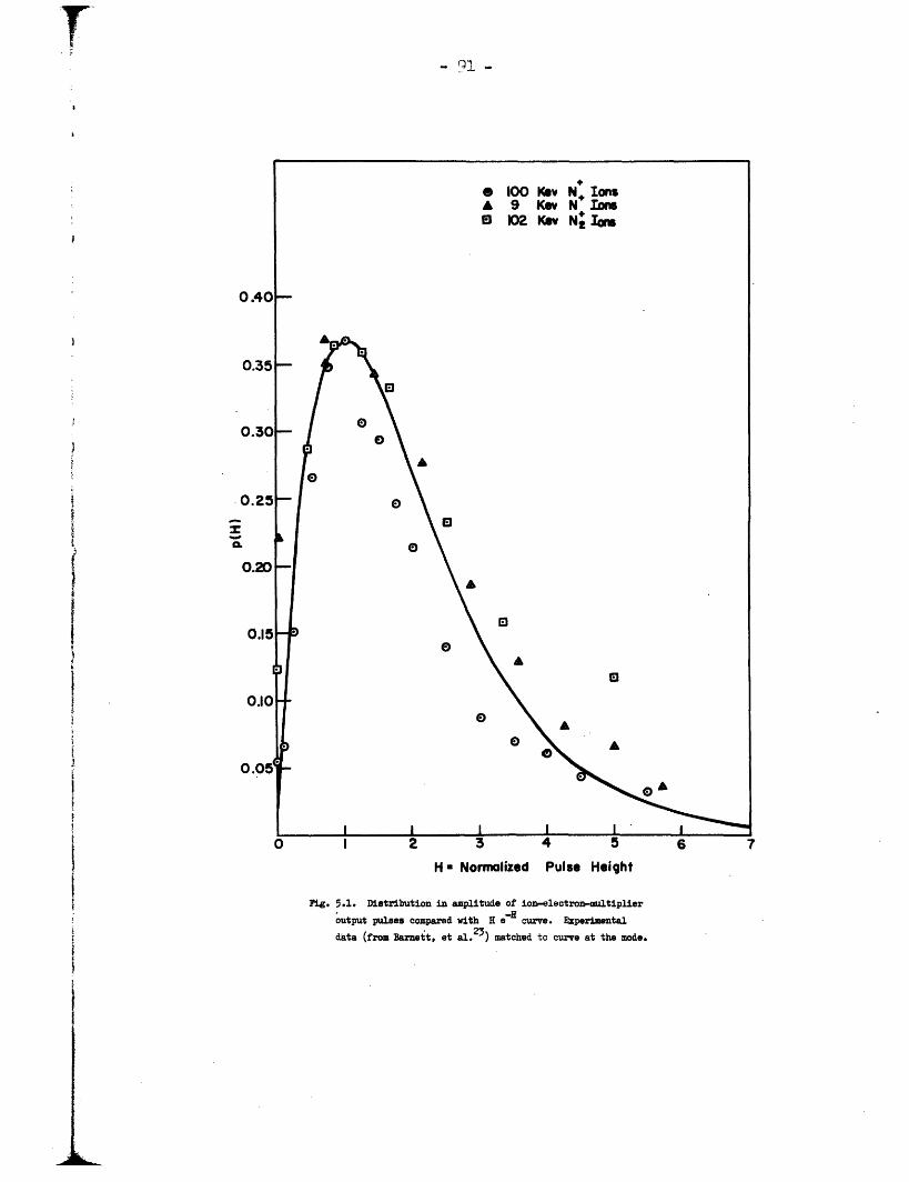
T
H a Normalized Pulse Height
Fig. 5.1. Distribution in amplitude of ion-electron-multiplieroutput pulses compared with H e curve. Experimental
data (from Barnett, et al. 23 ) matched to curve at the mode.
I
L
I
C5
i
7
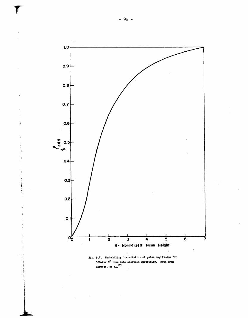
t
1~ ~ ~r~ ~ ~ Z
! ~ ~i
I
i
i
H- Normalized Pulse Height
Fig. 5.2. Probability distribution of pulse amplitudes for
100-kev + ions into electron multiplier. Data from
Barnett, et al.
ST-,~~~~~~~~a
Background Noise
Some of the sources of background noise are:
(1) Stray ions generated within the multiplier that impact
on one of the first dynodes. These are background-gas molecules
ionized by either the high fields or by field-emitted electrons.
This noise is kept low by careful construction that minimizes
high electric fields, and by maintenance of the highest possible
vacuum in the mass spectrometer.
(2) Light from a filament that causes photoemission at the
first dynode. This can be minimized by careful light shielding
and by use of multiplier dynodes with high work functions.
(3) Soft X rays from electron impacts on source electrodes
that causes photoemission. Careful shielding can minimize this
noise.
r ((4) Stray ions produced by the source that leak through or
around the mass filter from the ion source to the collector.
With care, background noise from all sources can be reduced
to a few counts per second.
Regeneration
A source of noise that is more insidious because it accompanies
the signal and so is more difficult to detect is regeneration in the
electron multiplier. Electron-impact processes in the latter stages
can produce emitted light that causes photoemission from an early
dynode, or latter-stage electrons can ionize background-gas molecules,
A, ~~

r
which then find their way to an early dynode to cause secondary
emission of more electrons. In either case there is a second.
spurious pulse, following the first one by the transit time of the
multiplier (on the order of 0.1 sec) or by the transit time of the
multiplier plus the ion travel time (several sec), respectively.
The regeneration process need not stop at one additional spurious
pulse; it can produce two or more, or even become self-sustaining.
The cure for regeneration is careful optical and ion shielding of
the first stages of the multiplier from the last ones, and operation
at the best possible vacuum.
Shot noise
There is inherent in the output of the mass spectrometer shot
noise due to the discrete nature of the output - the arrival of
individual ions.
To a good approximation the ions arrive at the collector at
random times, with the probability of arrival during a given interval
statistically independent of the previous intervals. 'The probability
distribution of ion arrival time is then Poisson:
P(n,T ) ()n e-NT (5.2)
where P(n, ) is the probability thai; n ions will arrive in an interval
T, and N is the average number of ions arriving in one second. If for
each ion of charge q the current flow is iI(t),- the autocorrelation
tunction of the output is
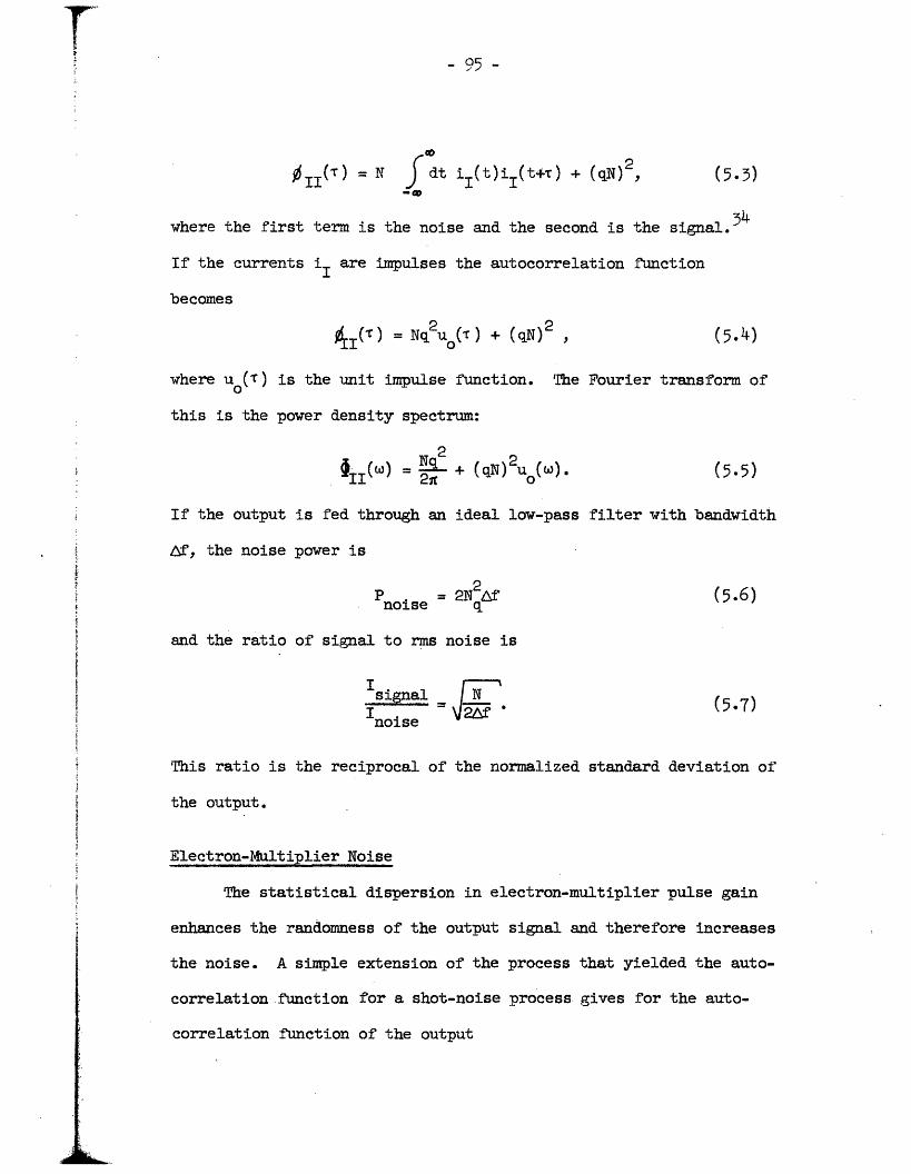
-95 -i(T) = N fdt i(t)ii(t+T) + (qN)2 (5.3)
where the first term is the noise and the second is the signal.
If the currents iI are impulses the autocorrelation function
becomes
I() )= NqUo( ) + (qN)2 (5.4)
where u(T) is the unit impulse function. The Fourier transform of
this is the power density spectrum:
= 2 + (qN)2(w). (5.5)
If the output is fed through an ideal low-pass filter with bandwidth
Lf, the noise power is
noise 2Nq2f (5.6)Pnoise q
and the ratio of signal to rms noise is
Isignal (57I n 2fs (5noise
This ratio is the reciprocal of the normalized standard deviation of
the output.
Electron-Multiplier Noise
The statistical dispersion in electron-multiplier pulse gain
enhances the randomness of the output signal and therefore increases
the noise. A simple extension of the process that yielded the auto-
correlation function for a shot-noise process gives for the auto-
correlation function of the output
ii
.11
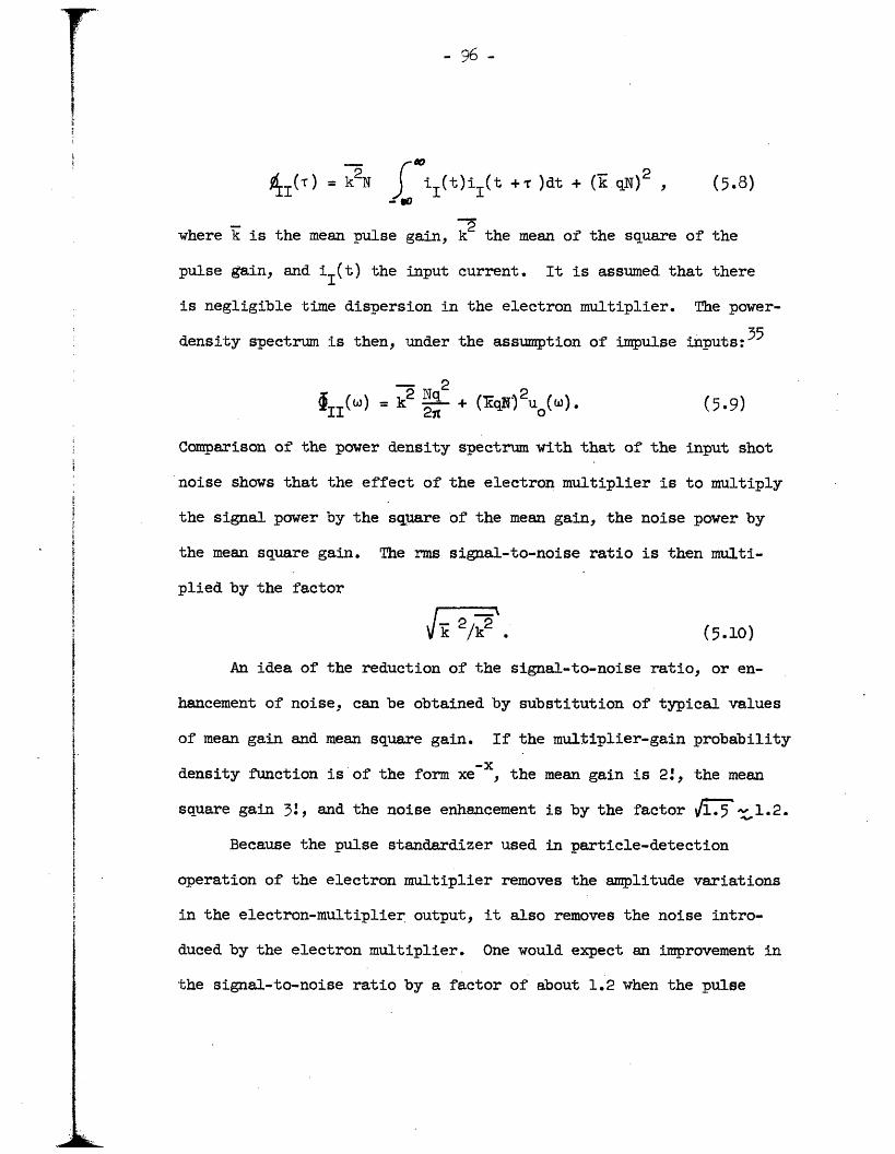
r -- 96 -
I(V) =- k2N ii(t)ii(t + )dt + ( qN)2 (5.8)
where k is the mean pulse gain, k2 the mean of the square of the
pulse gain, and i(t) the input current. It is assumed that there
is negligible time dispersion in the electron multiplier. The power-
density spectrum is then, under the assumption of impulse inputs:35
= k 2 + (TA)uo(w). (5 9)
Comparison of the power density spectrum with that of the input shot
noise shows that the effect of the electron multiplier is to multiply
the signal power by the square of the mean gain, the noise power by
the mean square gain. The rms signal-to-noise ratio is then multi-
plied by the factor
dr k /k2 (5.10)
An idea of the reduction of the signal-to-noise ratio, or en-
hancement of noise, can be obtained by substitution of typical values
of mean gain and mean square gain. If the multiplier-gain probability
-X
density function is of the form xe , the mean gain is 2, the mean
square gain 3, and the noise enhancement is by the factor 1.5 1.2.
Because the pulse standardizer used in particle-detection
operation of the electron multiplier removes the amplitude variations
in the electron-multiplier output, it also removes the noise intro-
duced by the electron multiplier. One would expect an improvement in
the signal-to-noise ratio by a factor of about 1.2 when the pulse
2
r -97 -
standardizer is used. This offers an additional reason for use of
the electron multiplier as a particle detector for low ion currents.
E. Pulse Signal Processing
Pulse Resolving Time
The finite resolving time of the pulse system, i.e. the fact
that the system can respond only to inputs arriving some finite
time apart, distorts the output signal and sets an upper limit on
the mean pulse rate at which the system can operate.
In the most simple analyses of this distortion it is assumed
that the pulse system or "counter" response is controlled by a
single element that behaves in one of two very simple fashions:
(1) Non-paralyzable element. If the counter has a dead
time p after each output pulse, during which it simply ignores all
inputs, it is said to be non-paralyzable. The measured mean output
rate (N') will be, in terms of the input rate N:36
N' = N (5.11)l+ Np
(2) Paralyzable element. If after each input event the
counter is incapable of responding to another input for a resolving
time p, it is said to be paralyzable, for it will respond to only the
first of a sequence of input events all spaced less than p apart.
The output rate is: 7)
N' = N e- N p(5.12)

- Q8 -
The upper limit on mean particle rate would seem to be that
which causes an unacceptable number of pulses, say 0Lo to be lost.
However, if the resolving time p is known, it is possible to use
the appropriate equation above to compute the mean rate from the
measured one, and so operate at appreciably higher rates. For
example, Barton, et al., claim 1A accuracy at a true mean rate of
5 x 10 counts/sec with a non-paralyzable counter with a dead time
28of 1 lsec. For the correction scheme to work the arrival times
of the particles must be truly random, as they are in a mass spec-
trometer with an electron-bombardment ion source. It is interesting
tr nhP thit arrival times mv-r rrv wP1 hnv not hen rndrnm in
the apparatus used by Barton, because it used a surface ionization
source, which tends to give wide fluctuations in the rate of ioniza-
tion.
Two complicating factors are not considered in the correction
equations (Eqs. 5.11 and 5.12). First, there may easily be more
than one element in the system that introduces a characteristic
resolving time. For example, the pulse system of the quadrupole-
mass-spectrometer ion detector used a pulse standardizer preceded by
a chain of amplifiers and limiters, each with its own resolving time.
Second, the system might not be neatly classifiable as "paralyzable"
or "non-paralyzable," but may have some other mode of operation; it
may even have resolving times that are functions of the random input
pulse amplitudes, and so random variables.

38 to treat theMethods developed by Jost can be used o treat the
statistical problems of more realistic models of two or more
devices in cascade. A reasonable representation of an ion-
detector pulse system that is still tractable for analysis breaks
the system into two major components, an amplifier-limiter chain
and a pulse standardizer. The amplifier-limiter performance is
approximated by an idealized pulse stretcher: for every input
pulse there is an output pulse of standard amplitude and width P;
when two pulses overlap, the output amplitude remains unchanged
and the pulse continues for time p, after the last event (Fig.
5.3a and b). The pulse standardizer is assumed to be an ideal
non-paralyzable counter element with resolving time 2 > pi.
There are then two types of performance, depending on how the
standardizer responds to the amplifier output. If it senses the
level of the output, it will, at the end of a response to a first
pulse, respond again if there has been an input in the preceding
P1 seconds; the amplifier in effect remembers for the standardizer
any input events in time P1 before standardizer recovery (Fig. 5.3c).
As a rough approximation, one might guess the output to be that of
a single non-paralyzable counter element with resolving time p =
P2 - P' This obviously cannot hold as P1 - P2, because in that
limit Eq. 15 would predict that no pulses would be lost. If, on
the other hand, the standardizer senses transitions in amplifier
output, that is, if it responds to all positive transitions at its
-e -
t t tt t t
mm im i mm i ·VI
I
I1
I IJ
Fig. 5.3. Performance of counter systems:
(a) Input events.
(b) Output of pulse-stretching amplifier.
(c) Response of level-sensing standardizer.
(d) Response of transition-sensing standardizer.
(a)
(b)
t t
(C) responsedead periods
(d) responsedead periods
4 r- r
-
I
i
rI
f
II
i
I
iIj
1
1
- .01 -
input occurring when it is "live," there is not only no memory of
pulses arriving during the dead time, but also a blocking efffect:
A sequence of pulses starting before the end of the standardizer
dead time generates a level that prevents further transitions until
the amplifier has recovered after the last pulse (Fig. 5d). The
amplifier appears as a paralyzable counter element, and the overall
system consists of a paralyzable element driving a non-paralyzable
one.
Basic Relations in Pulse Processing
Some statistical functions for a sequence of random input
events must be defined.38 Assume that the zeroth event occurs at
time t 0 O. Then the probability density function for the first
event can be defined as P(t); P(t)dt is the probability that the
first event lies on the interval t t + dt. The probability density
function for the nth event is then the n-fold convolution of P(t),
or P (t), defined by
t
P*(n+m)(t) = ) pn(t )P (t-r )d . (5.13)o
One can next define the density of events, F(t); F(t)dt is the
expected number of events on the interval t, t + dt. Then
co
t w~~e,5 _ v Pair+.\ -~C.\ o
/~_- X \ % / ,
n-=l
from this comes the integral equation
F(t) = (t) + F(t - )P(r)dT. (5.14)O
i
- !02 -
It will be convenient throughout this analysis to use Laplace
transformation, by which convolution is transformed to multiplica-
tion. The transform of Eq. 5.14 is
L(s) (s) 1 + f(s)], (5.15)
where
f(s) = e StF(t)dt ,
etc.
It can be shown that the average number of events per unit
time is given by3 9_T
N = lim - F(t)dt. (5.16)
To obtain N directly from the Laplace transform of F(t) one first
defines N(T) to be the function of Eq. 5.16 before the limit is
taken. Its transform is then
r sT c -sT Tn(s) = N(T)e dT = dTe- F(t)dt(s) ds
0o o o s
and by the final-value theorem,
N = lim N(T) = lim sn(s) = lim s dsT ---cs- s-O s
provided the limit exists. Application of L'H8pital's rule gives
N = lim sf(s) . (5.17)s --O 0
The input pulses to the ion-detection system are Poisson dis-
- !0 -
J ~ tributed, and so, from Eq. 5.2, since P(t)dt is the probability of
zero pulses in time t and one pulse in time dt, one obtains
P(t) = Ne . (5.18)
Laplace transformation of P(t) gives
p(s) = N ;(5.19)
use of Eq. 5.15 gives
f(s) s (5.20)
and
F(t) = Nu1l(t), (5.21)
where ul(t) is the unit step function:
u l(t) = O, t < O0
=1, t > O.
Non-Paralyzable Counter With Arbitrary Input
Consider a non-paralyzable counter element with dead time p
and input events represented by the characteristic quantities P(t),
F(t) and N. The corresponding quantities P'(t), F'(t), and N' that
describe the output events can now be determined. The probability
of the first output event between t, t + dt, where t > p is equal
to the sum of the probability of the first input event between t,
t + dt and the sum for all n of the probability of the (n + l)th
input event between t, t + dt, given that the nth occurred before
t = p. Then
Ei.;
'I
A
- 1o -
P'(t) = U- P)P(t) + F(r)P(t - )dl, (5.22)
and application of Eq. 5.14 gives
P'(t) = u l(t - p)F(t) - U U1( - p)F(r)P(t-)dtr.(5.23)
The truncated density function u l(t-p)F(t) will be called G(t)
for convenience. Then the Laplace transform of Eq. 5.23 is
and substitution of p' from this in Eq. 5.15 gives for f'
f'(s) = 1 + f(( g(s) ' (5.25)
Now
g(s) = f(s) -X e StF(t)dt ,
SO f(s) - e-StF(t)dtf'(s) =
1 + f eStF(t)dt
and application of Eq. 5.17 gives
N't = N (5.26)
1 + F(t)dt
Level-Sensing Standardizer Driven by Pulse Stretcher
The results of the previous section must be modified for a
non-paralyzable standardizer of resolving time P2 that responds
to the output level of a pulse-stretching amplifier of resolving
Fr
- 105 -
t
time p. There is now a finite probability that at the end of the
standardizer recovery, at t p, the system will be "waiting" with
a "remembered" pulse, and so will yield another output event. This
probability is equal to the probability L(P1,p2) that there were
one or more input events in the interval p2 - P,' P2 ' Therefore the
probability density of a first output event is equal to the sum of
the probability densities of (1) a "waiting" event, (2) a first
event at time t > P2, and (3) (for all n) an (n+l)th event at
t > P2, given an nth before t = P2-,1. Then
rP2-P
P'(t) = L(Op,O,)u (t-o^)+u (t-o_)[P(t)+ ( F(f)P(t-r)dr .(5.27)" * ' ' - ' I -1 e - Jo -L , - -.
A solution for the output count rate, N', can most easily be ob-
tained by substitution in Eq. 5.27 of the parameters of a Poisson-
distributed input obtained from Eqs. 5.2, 5.18, and 5.21 to give
-Np1 N( 2-p-t)P'(t) = (1-e )uo(t-p 2 )+u_L(t-p2)Ne (5.28)
Laplace transformation of Eq. 5.28 followed by solution of Eq. 5.15
for f' gives
-O s N NPlf'(s) = e 2e1 + s(l- e 1f'() = efl .(5.29)
N +s s(l - eN + s)
Application of the limit theorem (Eq. 5.17) gives
N' = Np (53)-Np1e + Np2
-106 -
the mean output rate for this system. If the exponential in the
denominator is expanded as a power series one has
N
N-1 + N(P2 - Pi)
Comparison of this with the output rate of the non-paralyzable
counter element driven by an ideal Poisson-distributed impulse
source (Eq. 5.11) shows that to a first approximation the effect
of amplifier pulse stretching is to shorten standardizer dead time
'by the pulse width, just as was intuitively predicted.
Transition-Sensing Standardizer Driven by Pulse Stretcher
An entirely different approach must be used to determine the
mean output rate of a transition-sensing standardizer driven by a
pulse-stretching amplifier. This system is equivalent to a para-
lyzable counter element of resolving time P1 driving a non-para-
lyzable one of resolving time p2. The output rate of the second
stage, N", can be obtained from Eq. 5.26, which, with appropriate
notation change, becomes
N'N" = (5.31)
1 + F'(t)dt
where N' is the output rate and F'(t) the output event density func-
tion of the first stage.
The expected number of first stage output pulses in an interval
-107 -
t, t+dt is zero for t < P1. For t > P1 it is eaual to the sum of
the probability of a first pulse in the interval, and the sum for
all n of the probability of an (n+l)th pulse, given that the nth
pulse occurred before t-pl. The output pulse density function of
the paralyzable stage is then
t-p1
F'(t) = u l(t - l)[P(t) + F()P(t -)dt . (5.52)
The input to the first stage is Poisson distributed in time, so
substitution of P(t) and F(t) can be made from Eqs. 5.18 and
5.21 to give
F'(t) = U_ (t - p,)N eNP . (5.353)
Then by the average taken over all time, Eq. 5.16,
N- N p !
N = Ne (5-.4)
and by substitution in Eq. 5.51, the mean output rate is
-NP1Ne
Ng * Ne-Np * (5.35)
1 + N(P2 - Pl)e
This is, as might be expected, lower than the output rate of either
a simple non-paralyzable counter (Eq. 5.11) or of a level-sensing
non-paralyzable standardizer driven by a pulse-stretching amplifier
(Eq. 5.30).
I

r
- l08 -
I4
F. Linear Signal Processing
The output signal of any mass spectrometer is of necessity
subjected to filtering by linear networks, if only the response
characteristic of the recording device. The output signals of a
particle-detecting ion collector are small enough, some 107 events
per second or less, that the problem of extracting the signal - the
mass spectrum - from the noise is significant. The question arises
as to whether or not some sophisticated signal-processing scheme
cannot improve upon such time-honored filtering techniques as
recorder response times and resistance-capacitance low-pass filters.
Unfortunately, as the results in this section show, it seems that
it cannot.
Idealized Counting-Rate Meter
The output of the pulse standardizer of a particle-detecting
ion collector is fed to a ratemeter circuit that should give an out-
put proportional to the mean pulse rate. Ideally, this ratemeter
performs a short-time averaging process on the output of the standard-
izer to give
tr(t) i i(t')dt' . (5.36)
The averaging time T must be short with respect to any variation in
the mean rate of input pulses, N, but long with respect to the
reciprocal of the rate itself.
7
-3
I'0- 109
In the frequency domain the integration operation becomes
Ir(W) 1JT Io(W) (57)= jwT !
where I is the Fourier transform of the standardizer output, Ir0
the transform of the ratemeter output. If the standardizer output
consists of impulses of charge q occurring at random times with a
mean rate N , the output of the averager has a power density spec-
trum obtained by multiplication of Eq. 5.5 by the square of the
magnitude of the system unction of Eq. 5.37, or
Nq2 sin2 ( )
Irr(w ) = (qN)2Uo(W )+ 2 wT (538)
The first term is the signal (a d-c current, qN), the second, noise.
The total noise power, obtained by integration of the second term
over all w, is
Nq2P ~ ms (5.39)noise T '
and the ratio of rms signal to rms noise is
signaI _ N_ * (5.40)
Inoise.
R-C Counting-Rate Meter
The most common ratemeter is a simple parallel combination of
a resistor and capacitor fed by the pulse source. One can show that
this is an approximation to an averaging circuit by writing the
equation for the output current in terms of the signal from the pulse
1

r " 17L0~~~~~~~~~L -F
a+f.nnAP-riF 7-p- ! - 'hininn 10 -matu -
i -t/RCh(4h(t) R 1(t) e t
and by convolution with the input signal the output is
et /RC (t')dt'
i(t) - RC4et C' (5.41)
This rather closely resembles the RC e defining the averaging
This rather closely resembles the equation defining the averaging
process (Eq. 5.36). The input signal is multiplied by an exponen-
tal weighting function and then integrated; the decay of the
exponential approximates the lower limit in the exact averaging
equation.
The exponential rise and fall characteristic of the R-C
circuit introduces error into the observed peak mass line amplitude
and puts a long "tail" on the line. The large ratio of observable
line amplitudes in a mass spectrum makes the tail the speed-limiting
quantity of an R-C ratemeter. If there is to be less than 10% error
in a mass line that follows a line 1000 times as large, the tail of
the first line must have decayed by a factor of at least 10 by the
time of the start of the second; thus the RC time constant must be
at most 1/9 of the time between lines.
The signal-to-noise ratio for the R-C ratemeter can be com-
puted in the same manner as for the idealized averaging circuit. It
is found to be
signal 2N (5.42)noise
I
, 1 -
Delay-Line Counting-Rate Meter
If the equation defining the averaging process, Eq. 5.36,is
rewritten as
iMr(t) = t t tr )dti(t) ) i (t')dtl - i (t')dt', (5.43)
it is obvious that this can be physically realized by an operational
amplifier, a delay line, and a differential amplifier (Fig. 5.4).
If the components of the circuit all performed ideally, the response
of the system to a rectangular input pulse (a very crude approxi-
mation to the shape of a line in a mass spectrum) would be as shown
in Fig. 5.56. The only signal degredation would be the finite rise
and fall time, and the slight increase in the line width at the base.
Any practical delay line degrades the signal because of its
inability to discharge all its stored energy into its load termina-
tions within T seconds of the time the input signal is removed. In
a transmission-line delay this energy storage would be characterized
as mismatch reflections at the terminations. In the lumped-constant
lines necessary for the long delays (on the order of milliseconds)
required by the averaging circuit, the energy storage and dissipation
process is much more complex, but for purposes of analysis can still
be assumed to be caused by reflections. Then an input pulse to the
line will produce a principal output pulse at time T and a sequence
of "reflection" pulses at 3T, 5T, , with amplitudes in a decreasing
geometric progression with ratio defined as r, where r may be positive
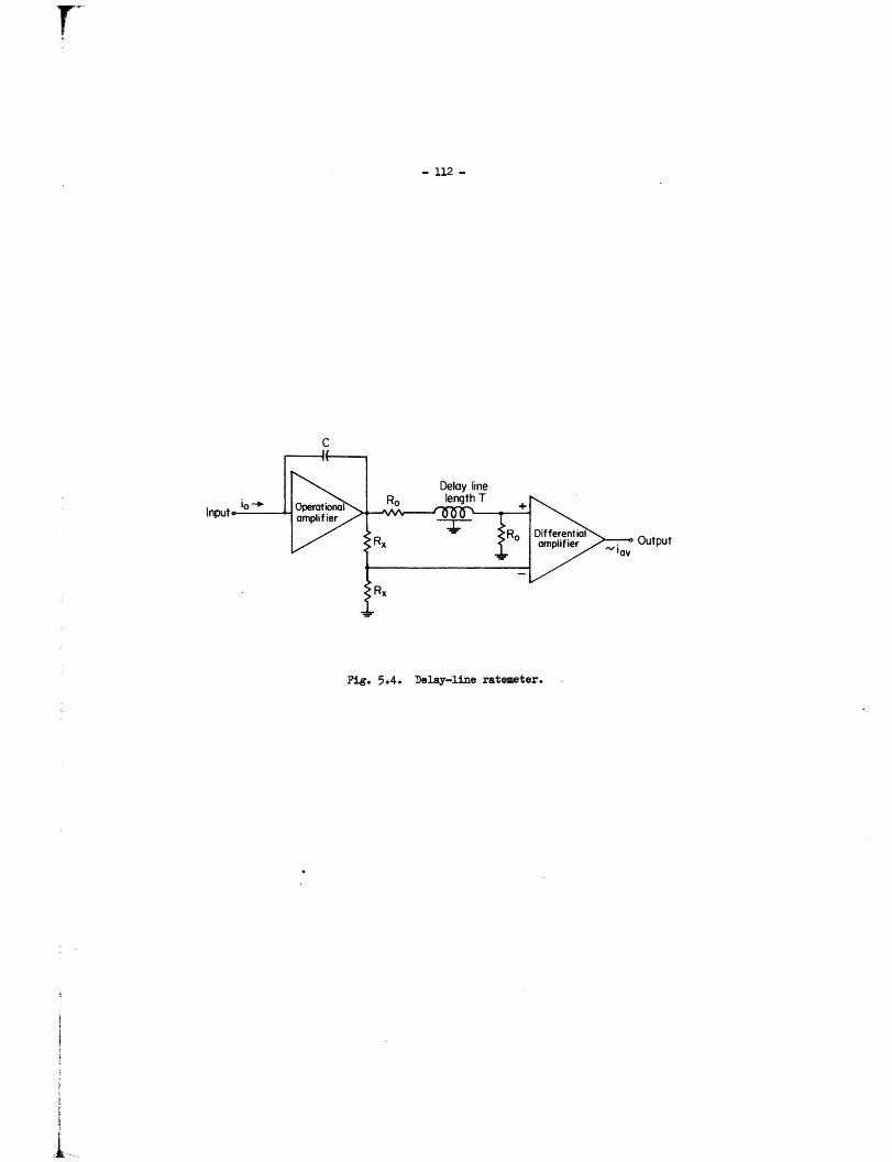
- 112 -
C
Fig. 5.4. Delay-line ratemeter.
i
I
i
I
i
1-
Output
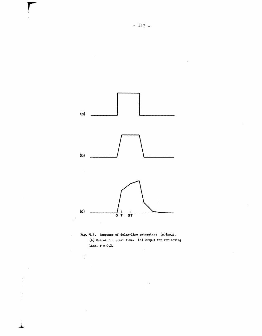
- F L - -
(a)
(b)
(c)
Pig. 5.5. Response of delay-line ratemeter: (a)Input.
(b) Outpu.- .- eal line. (c) Output for reflecting
line, r = 0.2.
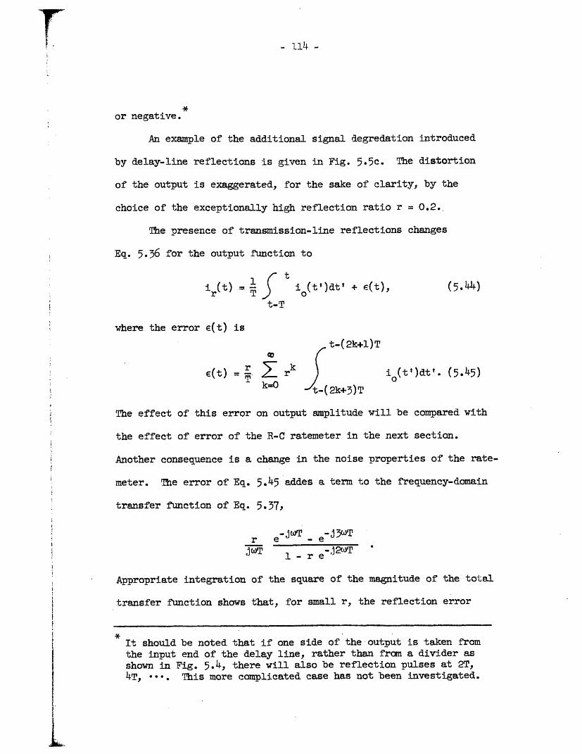
- L-4_
or negative.
An example of the additional signal degredation introduced
by delay-line reflections is given in Fig. 5.5c. The distortion
of the output is exaggerated, for the sake of clarity, by the
choice of the exceptionally high reflection ratio r = 0.2.
The presence of transmission-line reflections changes
Eq. 5.36 for the output function to
ir(t) = i (t')dt' + (t), (5.44)
t-T
where the error c(t) is
t-(2k+l)T
(t) = r rk i(t')dt'. (5.45)k=(O t-(2k+3)T
The effect of this error on output amplitude will be compared with
the effect of error of the R-C ratemeter in the next section.
Another consequence is a change in the noise properties of the rate-
meter. The error of Eq. 5.45 addes a term to the frequency-domain
transfer function of Eq. 5.37,
-jT -j3wTr e - e 3 T
,jwT 1 - r ej2w T
Awnrrinat in+teation nf the auare of the magnitude of the total
transfer function shows that, for small r, the reflection error
It should be noted that if one side of the output is taken fromthe input end of the delay line, rather than from a divider asshown in Fig. 5.4, there will also be reflection pulses at 2T,4T, *e·. This more complicated case has not been investigated.

·
1 ag
multiplies the output noise by the ratio
noise with reflection _ 1 - r6noise without reflection
a negligible change for practical values of r.
Another imperfection in practical delay lines is a finite
rise time. Because the delay time, T, of the line must be chosen
to be not larger than the time in which any change in input signal
can occur, and the rise time of any reasonable delay line is much
smaller, this finite rise time can have little effect on the system
transient response. However, it might have some effect on the
noise characteristics. If it is assumed that the line has an
exponential rise characteristic with time constant T /2.2, wherer'
T is the rise time measured at the 10o and 90% levels, it isr
easily shown that the signal-to-noise ratio of Eq. 5.40 is multi-
plied by the factor
1
r1 +
Since even the poorest commercial lines have T/Tr > 10, this
effect is negligible.
Comparison of Ratemeters
The R-C ratemeter has all advantages of simplicity and
economy over the delay-line circuit, so the latter must give some
definite advantages in performance to be considered for practical
L
I
- 16 -
applications. Comparisons of the two circuits can be made on the
basis of transient response and noise characteristics. The
transient response of interest is the response to a step function;
this should give some idea of the decay of the "'tail" from one
mass-spectral line before the arrival of a second, much smaller
one. The noise characteristic of interest is the ratio of rms signal
to rms shot noise.
To gain some idea of the upper limit of delay-line ratemeter
performance, one incorporating an deal delay line will be compared
to the R-C ratemeter. For a step-function input the output of the
delay-line circuit reaches fll amplitude in time T (Fig. 5.5b)
while the output of the R-C circuit has an exponentially decaying
error,
-t/ /RC4RC(t) = etC (5 47)
If RC = T/2, the two ratemeters will, according to Eqs. 5.40 and
5.42, have identical signal-to-noise ratios. Then at time T the
delay-line circuit will have zero error, but the R-C circuit will
still have an error of e = 0.14.
A somewhat better comparison might be had by a choice of the
RC time constant for some maximum permissible error at time T and
the assumption that there is a minimum acceptable signal-to-noise
ratio for the ratemeter output. The ratio of the ion count rates
that give this signal-to-noise ratio with the two ratemeters can

- 117 -
'then be taken as a comparative figure of merit. If the two
signal-to-noise ratios, Eas. 5.40 and 5.42, are equated one ob-
tains
(N dl)min 2RC(5.48)
NRc)min T
where (Ndl)min and (NRC)min are the minimum count rates for ac-
ceptable signals from the delay-line and R-C ratemeters, respec
tively. In terms of acceptable error at time T this ratio
becomes
(Ndl)min 2
(NC)m ln E RC(T) (59)t ' ~~~~~~~~~~~~~~~~_
If one assumes the desired error at time T to be less than 10 ,
which might be necessary for an extreme case of a low-amplitude
mass line closely following a high-amplitude line, the ratio
becomes
(Ndl) mi;n 2 1TF~,)~= 4lnl *~=~66 ~ (5.50)
In the case most favorable to the delay-line ratemeter, that circuit
will accept a minimum count rate lower than that of the R-C integra-
tor by a factor of 4.6.
The effect of reflections on the transient response of a
delay-line ratemeter must be considered. Application of Eqs. 5.44
and 5.45 to the case of a unit step input to the ratemeter, shows
i
- 118 -that the output is a sequence of straight line segments approaching
a final value in roughly exponential fashion, with nodes at times
t = (2j + 1)T, j = 1, '' , and amplitudes
(r) = i + i + 2r(1- rj )J l-r
According to this, long after the input step there is a constant
error 2r/(1-r); this simple scaling error can be easily eliminated
by changing system gain by the factor (l-r)/(l+r), which changes
the output to
2r + 1(ir)j = + = -l+r (551)
Comparison of the performances of the imperfect. delay-line
ratemeter and the R-C ratemeter is difficult because the two error
curves differ in shape, but one can assume a time constant RC = T/2,
so that the signal-to-noise ratios will be equal, and then compare
errors at the particular time at which the delay-line error is
largest with respect to the other.
Determination of the time at which delay-line error is
relatively largest is a two-step process. The first step involves
determination of the point on each line segment in the error func-
tion at which the relative error is a maximum; the second involves
determination of the line segment in which this error is largest.
In the interval (j+l)T < t < (j+3)T time may be represented
by the parameter xj, defined by
L.
I
r- 119 -
t = (2j + 1)T + 2x.T ;
the error in the delay-line ratemeter output is then defined by
the line segment connecting the jth and (j+l)th node,
2r+ 1 - ( - r)xJ (552)rl = 1+(5.52)~dl 1+r
and if RC = T/j2 the error in the R-C circuit output is
RC = e2(2j+l) - 4x.
The relative error of the delay-line circuit is then
edl_ = 2r + 1 | e2(2j+l) - 4xj 1 - (1- r)xJ . (5.54)
Differentiation with respect to x shows that for small r the
maximum relative error occurs at approximately x = 3/4, and is
dl .4j+5 . (5.55)ICERC = 2 e (5.55)
For r > e 4 this diverges at large j, and the delay-line circuit
is clearly inferior; for r < e the most unfavorable case is
j = 0. The error in the delay-line circuit is then a maximum,
relative to an exponential of time constant T/2, at t 5/2 T
and is
e cdl 5 ' (5.56)
A line with a rather low reflection ratio, r < 0.014, is required
to make possible any improvement over a simple R-C ratemeter.
F- 120 -
One may conclude that because the R-C ratemeter is much
simpler, less expensive, and can be easily adjusted for the best
compromise-time constant for any given input signal, it is still
the best choice for most applications.
It is possible to formulate an upper limit for spectral
sweep speeds for a mass spectrometer with a particle-detecting ion
collector and an R-C ratemeter. The time per spectral line (Tine)line
is the sum of the required decay time (T1) after one line and the
rise time (T2) of a second. Let D be the spectral dynamic range,
i.e., the ratio of largest line amplitude to the smallest, and F
the maximum acceptable "interference factor," i.e., the amplitude
of the tail of a preceding line relative to the total amplitude of
the line under consideration. Then if lines have abrupt rise and
fall transitions and the smallest spectral line follows the
largest, the minimum time between lines is given by
-T1/RC
D e = F . (5.57)
The RC product is defined in terms of a signal-to-shot-noise ratio
and count rate (Eq. 5.42). If the largest line corresponds to a
count rate Nmax ,-the largest the pulse system can handle, the lowest
count rate is Nmax/D. Let Smin be the lowest acceptable signal-to-
noise ratio. Then
D Smin
RC = 2N (5.58)max

r- 121 -
The line rise time can be taken to be the time for a rising
exponential to come within l/Si. or one standard deviation, of
the final value:
e -2 =- 1 (5 59)
rain
The total time er mass line (T, + T2) is, from Eqs. 5.57 through
5.59,
S . D fDS .mIn in m (5.60)
line 2 N L J max
If, for example, it is assumed that 1Na = 5 x 10⁶ , Smin = 1max min
D = 100, and F = 0.1, then
Tli = 9 msec,
and a spectrum of 100 lines can be swept in 0.9 sec. This result
depends strongly on the assumed signal-to-noise ratio; if Smin =min
100, the time for a mass line increases to
Tli = 1.2 sec.line
Optimum Signal Processing
The comparison of the R-C and delay-line ratemeters is a small
part of a much larger question: What linear system attached to the
output of the pulse standardizer gives the "best" output signal in
the presence of noise?
The word "best" must be defined in terms of some quantitative
error criterion that is tractable to an analytical minimization process.
One frequently used criterion, mean square error, leads directly to
the synthesis of a linear optimum~' network in terms of signal and
Itonoise correlation umnctions. However, a mean-square error
criterion is of little value or mass spectrometric signals because
it weights large errors more heavily than small ones, and there-
fore could easily term optimum a linear network that would give a
small error during a mass line but a small but very long tail
following the line.
In one attempt to find an optimum signal-processing system
the criterion was a minimum rms noise relative to a signal given
a fixed mean delay L in the system response. IThe optimum linear
system was found to have an impulse response falling linearly to
zero (Fig. 5.6a). The rms signal-to-noise ratio is then
signal 5.1)I =noise
compared to
signal 7T (5.62)Inoise
for both the simple R-C ratemeter and the delay-line ratemeter
(whose impulse responses are also shown in Fig. 5.6). Because the
"optimum" system yields a signal-to-noise ratio only 6% better than
a simple R-C circuit, and is rather difficult to synthesize in
practice, it was concluded that the R-C circuit was the best prac-
tical compromise.
L

23L
(a) h (t)
C
(b) h(t)
II L 2L 3L
t
0
LL
(c) h(t)
L 2L 3Lt
0 L 2L 3Lt
Fig. 5.6. Impulse'response of ratemeter circuits:
(a) "Optimum" response.
(b) "Delay-line" response.
(c) Conventional R-C response.
From Vincent.4
L
r
I
I2L
- 124 -
The delay-line ratemeter satisfies a different optimization
criterion - minimum "memory" time, or minimum time for complete
response to an input signal. It is interesting that by one cri-
terion, step response, the ideal delay-line circuit shows an ap-
preciable advantage over the conventional R-C circuit, while by
another criterion, average delay, it shows no advantage at all.
This illustrates just how strongly an "optimum" design depends
upon the choice of criteria.
Another work wort1rof mention is concerned with the more
limited problem of the choice of time constant for an R-C rate-
42meter. Frdhner has calculated the response of R-C circuits to
-t /2dinputs whose rates vary as the Gaussian function, e , with
particular attention to such factors as line broadening, line dis-
placement (delay or lag), and line peak attenuation. He has also
computed the "optimum" value of time constant, using as his cri-
terion a maximization of the peak value of the output relative
to the rms noise resulting from a constant background-count rate.
While this may be a useful criterion for gamma-ray spectroscopy
(his intended application) it is of little value in mass spectro-
metry, where the background may be less than one count per second.
I
I

- 125 -
VI. ELECTRON-MULTIPLIER ION DETECTOR
J AA. System Characteristics
General Requirements
Operation of the electron-multiplier ion detector of the
mass spectrometer as a particle detector requires electronic
circuits to amplify the pulses of current from the electron multi-
plier and convert them to pulses of standard amplitude and width.
The design requirements may be summarized as follows:
1. Sensitivity. The system must have adequate sensitivity
to detect the smallest ion-produced pulses from the electron multi-
plier.
2. Amplitude range. The system must be capable of accepting
at least a two-order-of-magnitude dynamic range of input amplitudes
arising from statistical variations in multiplier gain, plus as much
as possible of a third order-of-magnitud range coming from secular
changes and specific discrimination.
3. Output constancy. The output pulse amplitude and width
must be independent of all input variables.
4. Response speed. To make possible operation at high ion
count rates, the system response time must be as near the electron-
multiplier pulse width (several nsec) as possible. The design goal
was a count loss of less than 10% at an input rate of 5 x 10 /sec.
5. Rate insensitivity. The ability to respond to closely
spaced pulses should be independent of the count rate.

- 126 -
6. Noise insensitivity. Response to random noise, or to
extraneous signals such as the r-f voltage applied to the quadru-
l mr isa+ hr nuln hizrl 4l
The requirements of' output constancy can be easily met by
any one of a number of trigger circuits or pulse standardizers
that deliver a standard pulse when their input goes beyond a
certain threshold. The response-speed design goal requires a
standardizer resolving time of 20 nsec. In order to meet the
sensitivity requirement the standardizer must be preceded by an
I, amplifier that will bring the signals up to the trigger threshold;
the amplifier must be a broad-band one in order to avoid degredation
of the response speed. The requirement on noise insensitivity is
rather easily met; the signals from the 20-stage electron multi-
plier are large enough to be well out of the random noise of ampli-
fier input stages.
Amplitude Range
The requirement on amplitude range presents problems that are
not immediately obvious. It would seem that a wide-range system
would require only an amplifier capable of bringing the smallest
pulse from the electron multiplier up to the standardizer trigger
threshold, plus one or more limiting devices to prevent amplifier
and standardizer saturation. However, the response of the amplifier
system to its input pulse (approximately the system impulse response)
will have after the main output a small but finite "tail" of irregular
i.-
i
i
i
- 127 -
nature, which will be called "post-pulse noise." If this post-pulse
noise is above the trigger threshold at the time of the recovery of
the standardizer from the pulse, a second standard output pulse will
result - a "double count." If it is substantially below the zero
level, it can block detection of a small following pulse - a "lost
count." Because of the wide range of input pulse amplitudes, a
relatively small amount of post-pulse noise can cause either double
or lost counts. For example, if the input dynamic range is three
orders of magnitude and the amplifier system is linear, post-pulse
noise of 1 part in 1000 from an input of the largest amplitude will be
as large as the response to an input of the smallest amplitude. The
pulse system must then have a post-pulse noise, measured at the
resolving time of the standardizer, better than one part in one thou-
sand. This makes it mandatory to place amplitude limiters in the
system at the earliest possible stage, preferably before any ampli-
fiers, so the broad-band amplifier circuits are never confronted with
such a wide range in amplitudes.
Rate Insensitivity
The second system requirement warranting special comment, rate
insensitivity, is familiar to all designers of pulse systems. Basical-
ly, the problem is this: Any practical wide-band high-gain amplifier
in a pulse system must be a-c coupled. This presents no special
This remedy was suggested by Mr. Charles Freed of M.I.T. Lincoln
Laboratory.
- 128 -
problem in the amplification of pulses that are either uniformly
or widely spaced. If, however, there occur bursts of closely
spacea pulses, pulse asellne snitr will occur. For example,
assume the input consists of a sequence of positive pulses of
shape described by p(t), a function with unit peak amplitude,
that occur at times t. with relative amplitudes a.:
v = ap(t - t).
j
If the t. and a. are independent random variables, the d-c valueJ. J
of the pulse train is N a P, where N is the mean pulse rate,
is the mean value of aj, and P = j p(t)dt. If the pulse train
is passed through a unity-gain a-c-coupled amplifier, the d-c com-
ponent will be eliminated. The output is then
v0 =i aJp(t - t) - N a P.
All those pulses for which a. < N a P will not even reach zero
d-c level and must lie below the detection threshold of the pulse
standardizer.
The ion-detector pulse system requires that baseline shift
be small enough that no signal pulses be shifted below the stand-
ardizer threshold and no noise pulses be shifted above it.
There are several possible cures for the problem of pulse
baseline shift. Perhaps the simplest is a single-diode d-c
restorer that clamps the most negative point (for positive pulses)

-129 -of the a-c coupled waveform to ground. This method is effective
only when the signal is substantially larger than the forward drop
of the clamp diode. Unfortunately, the signals involved in any
wide-band pulse amplifier are small with respect to the forward
drop of a high-speed diode, so the diode clamp is ruled out. A
second, somewhat more involved system uses a diode rectifier to
sense the d-c level of the amplifier output and a low-speed d-c
feddback amplifier driven by the rectifier to add the necessary
44d-c signal to the pulse signal. Problems of diode forward drop
are not as important for such a circuit because the diode can be
used as a small-signal detector. Another common method of over-
coming baseline shift is differentiation of the pulse to remove
its d-c level. Ideally, the performance of the differentiator would
be as shown in Fig. 6.1a and b. Pulses, assumed triangular for
simplicity, are differentiated to yield doublets. These doublets
can be passed through a-c coupled amplifiers and symmetrical ampli-
tude limiters without change in wave shape or introduction of any
d-c component. Such performance is based upon an assumption of equal
rise and fall times of the input pulse. If, as is actually the case,
the rise and fall times are unequal, as in Fig. 6 .1c, the differ-
entiated doublet has unequal amplitudes and widths for its two lobes.
When this is passed through an amplifier and symmetrical limiter,
the lobes will have equal amplitude but unequal widths (Fig. 6.1e).
There is then a d-c component associated with each pulse, and there
.
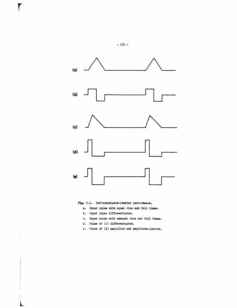
r
- 130 -(a)
(b) -J
(c)
(d)
(e)
Fig. 6.1. Differentiator-limiter performance.
a. Input pulse with equal rise and fall times.
b. Input pulse differentiated.
c. Input pulse with unequal rise and fall times.
d. Pulse of (c) differentiated.
e. Pulse of (d) amplified and amplitude-limited.
L
L.;
-
I"* %
.
rd
'G
: 7
-;ill be baseline shift if the pulse is passed through subsequent
a-c oupled amplifiers. This is precisely the case in the ion-
detector pulse system, except, of course, the pulses do not have
such idealized shapes.
Even if the system input pulse has equal rise and all
times, signal degredation caused by the finite frequency response
of the amplifiers and differentiator wi l l lead to unequal output
lobe widths. For example, if the differentiator is a high-pass
resistance-capacitance filter (which it is in the actual pulse
system), its effect on an ideal triangular input will be as shown
in Fig. 6.2. Again the trailing lobe of the output is wider than
the leading one.
'The use of differentiation was a fundamental design error.
However, at input rates of practical interest (< 107 counts/sec),
the resulting baseline shift lay within the threshold tolerance of
the pulse standardizer, so no attempt was made to correct it. In
any redesign the differentiator should probably be omitted, and
rectifi er-and-d-c-feedback-amplifier compensation used immediately
before each nonlinear operation, e.g., amplitude limiting and
threshold detection.
B. Pulse System
The pulse system is shown in diagrmmnatic form in Fig. 6.3.
The current pulse from -the electron multiplier is applied to an
input "reamplifier" that drives a chain of alternated broad-band
. .
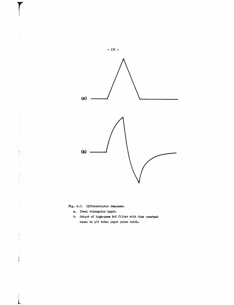
F
- 132 -
(a)
(b)
Fig. 6.2. Differentiator response.
a. Ideal triangular input.
b. Output of high-pass R-C filter with time constant
equal to 1/4 total input pulse width.
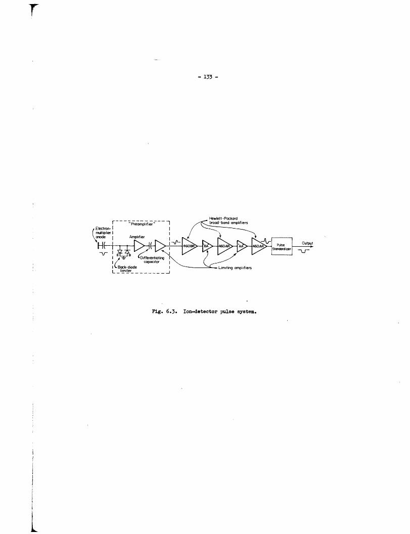
r
- 133 -
HwlItt -Pnrknrd
Fig. 6.3. Ion-detector pulse system.
Li
t
-534 -
distributed amplifiers and transistor limiting amplifiers. The
output of the chain drives a pulse standardizer.
Electron Multiplier
A 20-stage electron multiplier (Chap. III) was constructed
for the ion detection system in order to obtain gains high enough
to permit the use of amplitude limiters before the first pulse
amplifier. The circuit for this multiplier is shown in Fig. 6.4.
One power supply provides the electron-mulitplier-stage accelerating
voltages by means of a voltage divider. Output pulses are capaci-
tively coupled from the multiplier anode to the preamplifier so the
multiplier may be operated at an arbitrary potential with respect
to ground. A second power supply establishes the ion accelerating
voltage independently of the multiplier voltage.
The dynode structure of the RCA 6810A photomultiplier was
chosen for the 20-stage multiplier because it provides low disper-
sion in electron transit times and so a short output pulse for a
single ion incident on the first dynode. The 14-stage 6810A is
rated at a rise time, between the 10% and 90% points, of ..nsec.
If, for ease of computation, the multiplier impulse response is
assumed to be a Gaussian function of time, and if all 20 stages
of the mass-spectrometer multiplier are assumed to have the same
dispersion time, so that the 20-stage rise time is 20/14 of
that of the 6810A, the impulse response for 20 stages is a
Gaussian with full width at half maximum amplitude of 3.3 nsec.
j

rTt -:.
-4
400
J C}
4 8o U-a)43
oa
V HC) 2
. .43c)o m
-I A) .* ~4
.a
D~c
I
I
II
f
ti
I
I
it
I
i
-156 -
The peak amplitude of the response to a single ion is then
i = 4.6 x 10 11 K amperes,
where K is the multiplier gain.
The mass spectrometer multiplier is, strictly speaking,
not a 20-stage device because of the presence of the ion-
extraction tube that serves as a zeroth dynode. This may cause
far greater pulse-width degredation than would be expected by the
mere addition of a single dynode. The first dynode of the multi-
plier was made large for effective ion collection. No particular
care was given to variation in first-to-second-dynode transit time
for electrons emitted from various points on the first-dynode surface,
because all electrons from an incident ion would come from the same
point, and so suffer little time dispersion. With the addition of
the zeroth dynode, however, the first dynode becomes an electron-
to-electron multiplier as well as an ion-to-electron one. Each ion
incident on the zeroth dynode produces several electrons that may
travel to different points on the second dynode. The transit-time
dispersion of their secondaries can be substantial.
The zeroth dynode also brings into the realm of possibility twoor more pulses for an incident ion. Those ions that strike thezeroth dynode do so at an oblique angle. It is possible thatsome of them could produce secondary electrons there, but them-selves be reflected to cause still another ion-to-electron con-version at the first dynode. The transit time of electrons fromthe zeroth dynode to the first would be on the order of nano-seconds, while the transit time of the reflected ion would beseveral hundred times as long. One ion could then produce two
output pulses separated a fraction of a microsecond.
F- 17 -
Thie overall pulse errormance or an electron multiplier is,
of course, much more than a matter of the dispersion time. Any
stray reactance in the multiplier output circuit causes ringing,
or at least pulse broadening, that represents a post-pulse noise
that can only be enhanced in a subsequent limiting operation.
Every element of the output circuit must therefore be designed for
optimum response to nanosecond pulses.
~~~~~~~~~~~~~~~-m a . . _ __ _ ~
To minimize stray reactance, tne multrpller anoae ead
should be as short as possible, but shortness was not easy to
achieve with the existing system. Because the vacuum chamber was
not specifically designed for this mass-filter and multiplier
assembly, the electron-multiplier anode is some 18 cm from the
vacuum wall; there is also an additional 6 cm to the end of the
high-voltage anode-feed-through insulator. In order to minimize
the effect of the inductance of a 24-cm wire for nanosecond pulses,
the anode lead was shielded inside the vacuum system, in an approxi-
mation to a coaxial line. However, because of the non-constant
load impedance presented by the limiter input of the preamplifier,
and line impedance changes associated with changes in dimensions and
dielectric material at a number of points, a sizable amount of
ringing persisted. This could be only partially damped by a resistor
at the anode. Any future system should have the anode as close to
the vacuum wall as possible.
Capacitance between the anode and last dynode can lead to out-
L
-I
put-pulse degredation mnless the dynode -Joltage is held constant.
_he last dynode and anode have an eaul-valent circuit c for Pulses
shown in Fig. 6.5a. Each element has a capacitance o ground,
Cd and C resoectively, and a mutual capacitance C d. An elec-
tron current I flows from the anode to the last dynode, and aa
current I /k from he last dynode to the previous one (k is stage
gain). A Norton equivalent circuit (Fig. 6.5b) of all sources
driving the anode shows that there s substantial reduction in
effective anode current by displacement current - by a factor of
0.7 for a stage gain of 2.5 nd Cad = Cd . The cure is a large Cd -
a 50 pf capacitor mounted inside the vacuum system, right at the
multiplier structure.
The circuit originally had no resistor in the dynode lead.
The dynode capacitance then combined with the inductance of the
lead to constitute a resonant circuit that was excited by multiplier
current pulses. -1he resulting lightly damped sinusoidal oscillation
was capacitively coupled to the anode and amplified and quantized
by the pulse electronics, providing multiple output pulses for a
single input ion. The resistor eliminated this ringing.
In so far as the probability of emission of n electrons from
a dynode is described by a Poisson distribution of mean k, the
probability of zero output is e and the standard deviation of the
distribution, relative to the mean, is i/VT. In order to obtain
the smallest possible gain dispersion and lowest probability of

r
Cad
I'
(a) _- _@ | 0 i_ anode
10~d rnodr 20 ,r Ca loadynode 20
Cd-i
anode
(b) '_Cd Q X-T C: load
s K ) I
(k-I)Cod a
Fig. 6.5. Electron-multiplier anode circuit.
a. Circuit for pulses.
b. Norton equivalent of anode circuit.
j

missed counts, it is advantageous to operate the multiplier with
the highest possible mean yield per ion. Because yield trom an
ion-to-electron dynode increases monotonically ith voltage (for
all ractical voltages), it is desirable to operate the first
dynode at the highest possible voltages. It was intended that
normal multiplier operation be with the first dynode at -15 kv,
the power-supply limit, with the multiplier voltage adjusted to
the value between 5 and 10 kv that gave optimum mean overall gain.
Unfortunately, breakdown occurs from the first dynode when it is
more than 12 kv from ground, and from the anode and last dynode
when they are more than 6 or 7 kv from ground. Operation must
therefore always be at restricted voltages.
To minimize the overall amplitude dispersion of multiplier
gain, it might also be advantageous to operate each of the first
few stages at the voltage giving the highest yield no matter
what overall multiplier gain was desired: 500 volts for beryllium-
copper dynodes. This could easily be accomplished by use of a
corona voltage regulator across the divider string of the first
few stages.
The possibility of operation as either a 20- or 21-stage
mr1 4n1 f Al ao1: Ad 4--L_ -:l·hx I; beet -J._4 Pro P 4 A 7 tUIUL JI Y .L, Ik I=LU±LJP UPU1 WLZLLLJ I Wi± ; 1 I U L±, 6 I U ltjC Ul Z UL 1
dynode, enhances overall gain dispersion by the electron-to-elec-
tron gain of the first stage, probably about 2.5.
Electron multipliers are usually operated from electronical-
k__
- 914 -
ly regulated, low-ripple, high-stability power supplies. because
regulation and ripple modulate multiplier ain, and ripple can
also be electrostatically coupled to the output. However, in
particle-detector operation gain modulation is absorbed in the
dynamic-range capability of the pulse system, and any ripple is
attenuated to negligibility in the high-pass coupling networks of
the pulse amrlifiers. Hence much less sophisticated power sup-
plies are required. Unregulated commercial supplies with sub-
stantial 60-cps ripple (2%?) were used, although additional R-C
filtering was added to reduce ripple an order of magnitude and
lower the dynamic-range requirements of the pulse system.
The electron multiplier may be used simultaneously as a
current amplifier and a particle detector. In this mode the anode
is at ground potential and a single power supply furnishes the
electron-multiplier voltage, so the ion acceleration potential is
equal to the multiplier voltage.
The electron multiplier circuit was not especially designed
for combined operation, so many difficulties arise in addition to
gain variations common to all current-amlifier multipliers. First
of all, there is a problem of excessive anode and dynode current
for the multiplier divider string. Nominal divider currents are
some 300 to 500 a, so to prevent excessive dynode voltage regula-
tion, the d-c anode current must be held below 50 Ila. The ion
count rate in terms of anode current and multiplier gain is
L
-12 -
a
where e is electron charge. With the mean gain normally used in
7particle-detector operation, ~ 5 x 10', the maximum count rate is
about 6 x 10⁶/sec, which corresponds rather closely to the upper
limit for practical operation of the pulse system. However, the
usual reason for operation of the multiplier as a current ampli-
fier is to be able to handle ion count rates beyond the pulse-system
capability. To do this, the mean multiplier gain must be reduced
by lowering the voltage. This also lowers the ion acceleration volt-
age and so increases problems in collection of skew-trajectory ions
coming from the mass filter.
The unregulated power supplies are, primarily because of
ripple, not adequate for most current-amplifier applications of the
electron multiplier, so an electronically regulated supply must be
used.
Finally, low multiplier voltage coupled with the existence of
two ion dynodes can cause an undesirable gain variation. Ions of
low mass require low mass-filter voltages and so have exit trajecto-
ries with low skewness; most of them are collected on the first
dynode. High-mass ions, on the other hand, have exit trajectories
of higher skewness; many of them are collected on the zeroth dynode.
The mean multiplier gain for heavy ions may be higher than for light
ions by as much as the gain of a multiplier stage, a factor of about
2.5. This gain variation is, of course, in addition to the usual
variation introduced by difference in electron yields for different
t

- 14 -ions incident on the initial dynode.
Preamnli fier
The "preamplifier" (Fig. 6.6) consists of an input limiter,
a linear amplifier and differentiator, and a limiting amplifier.
The input limiter is a pair of germanium back diodes ( low-
current tunnel diodes) connected in parallel opposition across
the preamplifier input. For small signals (below 100 a) the
diodes have a constant impedance of about 200 ohms, but for large
signals an increasing conductance limits the voltage applied to
the linear amplifier. At d-c, the diodes in parallel with 220 ohms
(the input resistance of the linear amplifier) give a -200:1 range
in output voltage for an input-current range of 10 a to 10 ma.
The limiting effect is somewhat smaller for pulses because of
L di/dt voltage developed in the stray circuit inductance in series
with the diodes. (The contribution of the inducatance in the diode
itself is negligible.)
One nonperformance aspect of this limiter severely reduces
system reliability. The back diodes, which are easily damaged by
........ ____ _ .____ _ - ~ , _ _ . _ _ I, ._ . _ ~ _ _ · ___
current overloads, are couplea to an anode at a igh voltage (several
kilovolts) by a capacitor large enough to provide appreciable energy
storage. Any voltage breakdown to ground of the anode discharges
the coupling capacitor through the diodes, inevitably degrading
their voltage-current characteristics so as to make them unusable.
Operation of the electron multiplier with the anode at other than

o4 O
D I L
-4
Q) 0 0i) 0. r4
o 4
44 n-d... I W%
sD 4a+ H P:
og 1 RHn A
m 0 04 +-i 4 4
4 4 0 *r0 0 0
0t .-4 '-
FL-I
0o
,o E 10,
II
I-ci
[1C~
2 ) Z :.e
I
t~ ~ ~ ~
i
iI
i
i
17)
r IN
ground potential is therefore fraught with peril.
The linear amplifier is a conventional collector-to-base-
feedback transistor amplifier with inductive peaking applied
4.5according to the technique developed by Reddi, followed by an
emitter follower to drive the differentiating capacitor. Design
voltage gain is about 3.7, design rise time (104 to 90% points)
somewhat better than 2 nsec.
The positive pulse output of the amplifier is differentiated
by capacitor C. Resistor R6, in series with C2, necessarily de-
grades differentiation action, but is necessary to prevent ringing;
the output impedance of the emitter follower is inductive, and
would constitute a resonant circuit with C2 without this damping.
The differentiated pulse is applied to the limiting ampli-
fier, another inductively peaked, collector-to-base-feedback
transistor amplifier. Small-signal current gain is about unity,
the design rise time about 3 nsec. Limiting action is provided by
a pair of germanium back diodes in parallel opposition in the feed-
back network. Ideally, for very small signals diode conduction is
negligible and the circuit functions as a linear amplifier, but
large signals cause diode conduction and so increase feedback and
lower the amplifier gain. (Actually the back diodes always provide
some shunt conduction in the feedback path, and so reduce amplifier
gain even for small signals.) One significant advantage of this
limiter is its constant output impedance (about 200 ohms) that mini-

T-
mizes mismatch reflections in the input line of the distributed
amplifier hat it drives.
The preamplifier has a doublet response to test pulses
(Fig, 6.7a; Appendix E). Figure 6.7b shows the response to an
input pulse of about x 107 electrons, Fig. 6.7c the response
to a pulse 10 times as large. Limiting action is demonstrated
by an output amplitude ratio of 2:1 for an input ratio of 10:1.
The leading or negative lobe of the output is substantial-
ly narrower than the trailing lobe, in part because of a slightly
steeper leading edge of the input pulse, but more because of
imperfect differentiation. The differentiator is actually a
high-pass R-C filter with -time constant of about 2 nsec, half
the 4-nsec transition times of the triangular input pulse. This
corresponds closely to the hypothetical situation for which the
response was drawn in Fig. 6.2.
Amplifier-Limiter Chain
The bulk of the amplification of the pulse system is rovided
by three commercial, vacuum-tube, distributed amplifiers with indi-
vidual rise times of about 3 nsec:Hewlett-Packard 460AR and 460BR,
with gains of 20 db and 15 db, respectively. Both have an approxi-
mately Gaussian frequency response, and so an approximately Gaussian
impulse response, and (at least compared to an amplifier with flatter
frequency response) relative freedom from ringing.
The output of any distributed amplifier for a short pulse input
.i i V
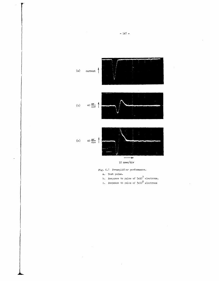
p
- 147 -
(a) current
(b) 4 o T
(c) 40 -
10 nsec/div
Fig. 6.7 Preamplifier performance.
a. Test pulse.
b. Response to pulse of 3x10⁷electrons.
c, Response to pulse of 3x10 electrons
I
T -
contains mismatch reflections at double multiples of the delay
times of the internal transmission lines, some 10 to 15 nsec in
this case. These reflections can, if of sufficient amplitude, con-
stitute post-pulse noise at the system output, so it is necessary
to take every precaution to minimize them. The 460BR was chosen
for the first amplifier in the chain, the most sensitive position,
because it was found to have greater freedom from these reflec-
tions. All amplifiers except the last were terminated at both in-
-put and output in their nominal characteristic impedance: 200 ohms
at all inputs and at the 46OBR output, 270 ohms at the 460AR output.
In addition, it was found that reflections in the 460BR were re-
duced if a small capacitance (2 pf) was placed across its load.
The last 460AR drives the nonlinear load of a trigger circuit in
the pulse standardizer, and so suffers substantial output mis-
match, but at this high-level point reflections are of little im-
portance.
The metal cabinets of the Hewlett-Packard amplifiers give
the appearance of providing electrostatic shielding. However,
paint on all joined surfaces prevents bonding of the various
parts of the cabinet into an effective shield. Leakage from the
r-f rod driver was, under some circumstances, picked up by these
amplifiers and caused false outputs of the pulse system; cabinet
modifications were therefore necessary.
The two interstage limiting amplifiers, the BA and AA
A
T 14Q -
(Fig. 6.8), are of the same type as the limiting output ampli-
fier of the preamplifier; a single-transistor, collector-to-base-
feedback, inverting amplifier with parallel-opposed diodes in the
feedback network to provide limiting action. Here advantage is
taken of the fact that both input and output impedance are essential-
ly constant, independent of limiting action, so that mismatch reflec-
tions of the associated distributed amplifiers are minimized.
The BA limiter, used between the 460BR and first 460AR ampli-
fier, has back diodes as limiting elements in order to hold signal
amplitudes as low as possible at this early stage. The AA limiter,
on the other hand, uses point-contact silicon diodes, because it is
necessary only to keep the output of the last 46OAR, which it drives,
below the 4-volt maximum specified by the manufacturer.
The BA kimiter is designed for nominal small-signal insertion
gain of 1.0, the AA limiter for 1.25. Measured small-signal rise
times are approximately 2 and 3 nsec, respectively. The faster
response of the BA limiter, despite the handicap of a higher para-
sitic shunt conductance and capacitance in its feedback element,
can be attributed to the peaking effect of the capacitor across its
input resistor, plus the fact that the actual amplifier element of
the AA limiter must operate-at reduced bandwidth because it has to
provide appreciably greater gain in order to perform a trans-
formation from a high-impedance (270-ohm) source to a low-impedance
(200-ohm) load.
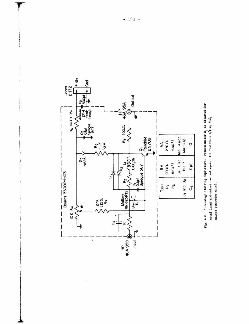
I -1, _
0 Nc-O " CJ
r- Q
1I QLoI
I
IIn1
L-
0hoq.
a4-0)
2 O
Ea . -4 -
6, ox
$42 0 0
O0) 0o-'
.4 0 2
0 a
02.p,a 41
co
Ike
in) 0.a2.O) C:
(0':1
r
+ 0
U-
N '0 IC, (D Q < I
I -
l lo
0
au
ti
ti
I

- 151 -
The armplifier-limiter chain provides an overall small-signal
gain of about 600 with a rise time of about 6 nsec. Its perform-
ance when driven by the preamplifier is shown in Fig. 6.9. For a
small (3 x 10⁶-electron) preamplifier input the output is a
reasonably symmetric doublet confined to about 25 nsec. For larger
inputs, however, as more and more limiting action occurs, the
trailing lobe of the doublet lengthens C'post-pulse noise"), final-
ly extending total doublet length to about 70 nsec. This is, of
course, undesirable in a system intended to have a total response
time of 20 nsec, but is not quite as bad as it might seem. First,
the post-pulse noise is entirely negative; there is no positive
overshoot that could cause double-pulse output from the pulse
standardizer. Second, the system is not prevented from detecting
a second pulse during the long trailing-lobe period; pulses of
effective amplitude greater than the negative-lobe voltage can carry
the net voltage positive, past the pulse-standardizer threshold.
The pulse baseline shift arising from such markedly unsym-
metric outputs must be considered. The integral over all time of
each pulse must be zero; because the negative lobe of each pulse is
larger than the positive, the voltage between pulses must go slight-
ly positive. If the repetition rate is high enough, this positive
level might possibly cause false triggering of the pulse standard-
izer. A quantitative study shows that this cannot happen: The
output pulse for an input of 3 x 10 electrons has a positive lobe
Ab

I r
- 152 -
(a)
(b)
(c)
Fig. 6.9. Response of preamplifier-amplifier-limiter chain
to test pulses of (a) 3x10⁶, (b) 3xlO7, and (c) 3xl08
electrons. Scales: vertical, 0.8 v/major div; horizontal,
10 nsec/major div.
r,
of about In 10 volt-sec, a negative l.obe of about 2.1 x 10⁸
-8volt-sec, for a net negative integral of -1.8 x O volt-sec.
7An input of a sequence of such pulses at a mean rate of 10' counts/
sec would produce a positive shift of the pulse baseline of only
0.18 volts, well below the 0.5-volt threshold of the standardizer.
In actual operation. of course, there would be a statistical
spread in input pulse amplitudes; x 108 electrons would be near
-Xthe top of that spread. For an assumed rxe distribution of in-
put pulse amplitudes, and an assumed mean amplitude of 6 1.07 elec-
trons, the mean pulse integral is - x 10 9 volt-sec, just half the
maximum value. For pulse rates practical for this system, the
effect of pulse baseline shift is negligible.
Pulse Standardizer
The pulse standardizer (Fig. 6.10) consists of an input
threshold element, a timing unit, and an output current switch.
The input threshold element is a -ma tunnel diode, TD1,
that switches to a high-voltage state whenever the input pulse
rises above +0.5 volt, and returns to a low-voltage state when the
input goes negative. This threshold element discriminates against
noise and provides limiting action to prevent spurious responses
to large input signals.
The performance of this threshold detector was somewhat less
than ideal, primarily because it was driven from a relatively low-
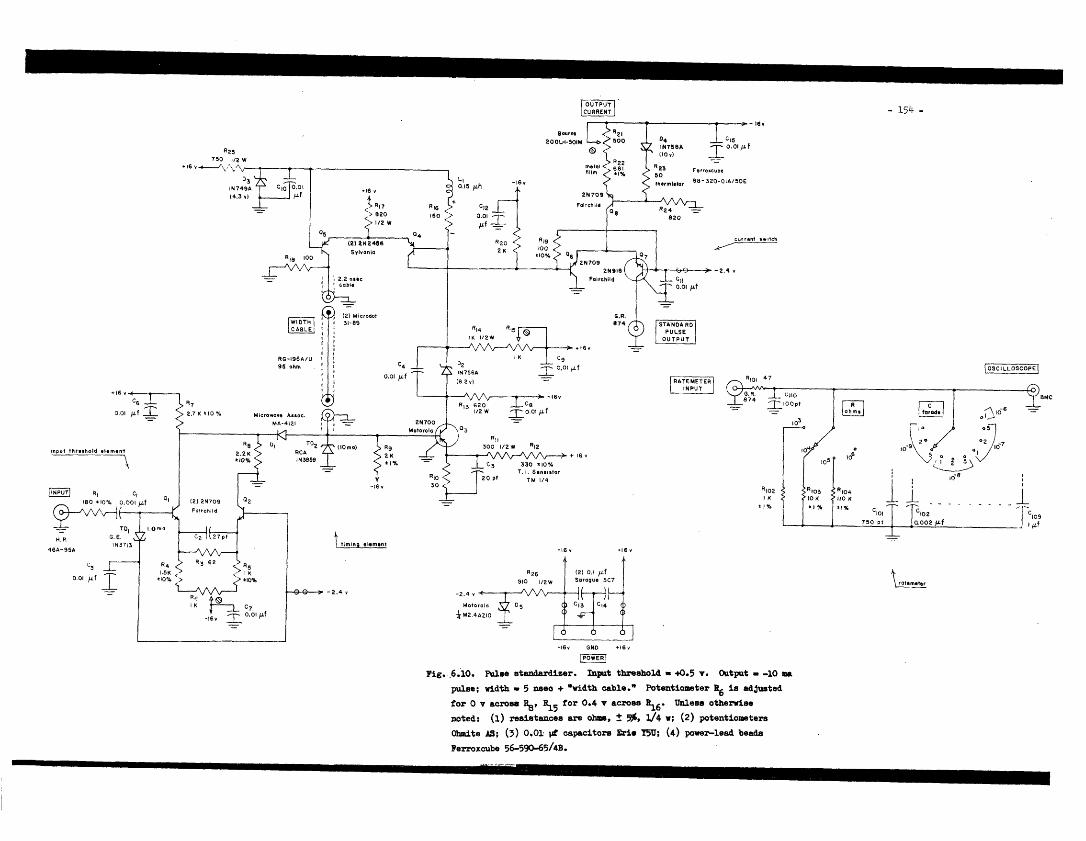
OUTPUT ICURRENT - 154 -
16v
Bourn200L-501M .L Cl5
T_° 'l f
(4.3 )
RG-195A/U95 ohm
R 72.7K t0O%
C4
o.o01 f
CClo.ol f
-2.4 v
STANOA RDPULSE
OUTPUT
C9
OSCILLOSCOPE
FATEMETERI INPUT
Microwave Assoc.
MA-4121
input threshold *lement
C3 330 010%T. . Sensistor
0 Pt TM 1/4
timing element
c -0.01 I
-2.4 v -2.4 v -
Motorolo
T M2.4 AZIO
+ 16v
-16v +16v
rotemeter
-16v GND 6
[POWER|
Fig. 6.10. Pulse standardizer. Input threshold - +0.5 v. Output - -10 ma
pulse; width * 5 nseo + *width cable." Potentiometer R6 is adJusted
for 0 v acrose R8, R15 for 0.4 v across R16. IUnless otherwisenoted: (1) resistances are ohms, ±+ 5, 1/4 w; (2) potentiometersOhmite AS; (3) 0.01 pt capacitors Eri 1J5U; (4) power-leat beads
Ferroxcube 56-590-65/4B.
W

p -1 55 -
impedance (450-ohm) source - the amplifier output plus a series
resistance. There is marked difference in rise time for signals
barely over the 05-v threshold end for those much larger in ampli-
tude. This eventually manifests itself as a slightly narrower
standardizer output pulse for very small inputs than for very large
ones. The rise-time shift could easily be reduced by driving the
tunnel diode with a common-base transistor amplifier, whose high
output impedance would lead to much faster transitions for the
smaller input pulses.
The tunnel-diode voltage is amplified by the differential
amplifier consisting of transistors Q1 and Q2' The differential
arrangement was chosen for d-c stability, but it also makes it
easy to modify the standardizer to trigger on negative-going
signals; it would be necessary only to place a tunnel diloe in ne
Q2 base circuit and couple the input to that diode, instead of to
TD1.
The timing unit, an almost exact copy of a "discriminator"
used in nuclear instrumentation, is centered about the 10-ma
level-sensing tunnel diode TD,. A negative signal from the input-C
threshold amplifier turns TD2 on. The resulting negative voltage
is amplified by Q, whose output switches a current from transistor
Q4 to Q5 of a "long-tailed pair" (a differential-sensitive pair of
transistors with emitters driven from a common current source).
This current is sent through a timing cable to the 10-ma tunnel
diode. At a time equal to the cable delay plus the delay in the
I
two transistor stages, this current urns off the tunnel diode and
holds it off (to -orevent secon se f a time euai -;o ;he
original delay time.
The other output of the Q-QQ long-tailed air is used to
drive the output current switch. The standardizer herefore has
an output pulse of width equal to the delay time and a dead time
just twice as long.
Because the output pulse width should be as independent as
possible of changes in circuit elements with time and temperature,
the design of the timing unit emphasized high-speed operation for
each element so that the total loop delay time would be, as much
as possible, determined solely by the timing cable. Nevertheless,
2.8 nsec was contributed by the amlifier and switching elements.
An additional 2.2-nsec delay was deliberately incorporated in an
internal cable, so that the output pulse width would be 5 nsec
longer than the delay time of the external width cable.
The output current switch consists of a long-tailed pair of
silicon transistors, Q6 and Q7, fed at the emitters by 10 ma rom
a current source (transistor Q). lThe output current from the
collector of (Q is switched from a leakage current of about 10 -0
amp to 10 ma by the pulse from the timing unit. Rise and fall
times are on the order of 1 nsec (Fig. .11).
The ringing shown in Fig. 6 .1 is inherent in the output of
a long-tailed pair, as conventional small-signal analysis of the
L
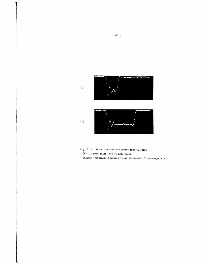
- 157 -
(a)
(b)
Fig. 6.11. Pulse standardizer output into 50 ohms:
(a) lO-nsec pulse, (b) 25-nsec pulse.
Scales: vertical, 4 ma/major div; horizontal, 5 nsec/ajor div.
T-~~~ ~- !58 -
transistor that is passing current shows: The base is held at a
fixed voltage, so the impedance at the emitter is the input im-
pedance of a common-base amplifier. The "intrinsic" transistor,
i.e., the transistor treated as a pure conduction-by-diffusion
device, with no external reactances or resistances, has an in-
ductive input impedance. The capacitance of the emitter-base
junction, plus that of the same junction of the nonconducting
transistor and circuit strays, resonates with the inductance.
The abrupt change of current in this resonant circuit causes
ringing, which then appears in the output of the amplifier, the
transistor collector circuit.
While it is esthetically displeasing, ringing has no
deleterious effect in this application, because it does not cause
variation in the total amount of charge in the output pulse.
The thermistor in the current source for the output switch
was intended to hold output current constant by compensating for
variations in breakdown-diode and transistor voltages and in
transistor current gains. In a test with the standardizer
counting a steady input pulse rate, after 3 hours operation in the
equipment racks of the mass spectrometer, the output current in-
creased by about 1l with a 6C rise in standardizer temperature.
An additional 100C increase, produced by an external heater, caused
another 1% increase in output. These current drifts, which may have
resulted from either inexact compensation of d-c component variations
I
I
i
i
- 159 -
or a change in effective pulse width with temperature, were con-
sidered too small to warrant investigation.
Performance with Test Pulses
The performance of the pulse system as the output element
of the mass spectrometer can in part be predicted by its perform-
ance in response to signals rom a test source tAppenalx ). fTne
minimum input to trigger the standardizer is a pulse of about 106
electrons. The average output current of the pulse standardizer
depends slightly on input pulse amplitude, dropping 3% as the in-
put is reduced from 6 x 10 electrons to 10 electrons; this
probably results from amplitude sensitivity of the standardizer
threshold detector.
The resolving time, or minimum spacing that permits detection
of the second of two pulses, depends on the amplitudes of both
pulses (Table 6.1). For a large pulse following a small one, the
resolving time is less than the nominal standardizer dead time
because of the "memory" effect of a level-sensing standardizer
following a pulse-stretching amplifier. For a small pulse following
a large one the resolving time tends to be longer than standardizer
dead time because of the blocking effect of post-pulse noise produced
in the amplifier chain.
The effect of rapid sequences of pulses was investigated by
measuring average output currents for widely spaced (40 sec)
pulses and for pulses in closely spaced pairs (15 to 30 nsec) with
Aj

r- 16 -
Table 6.1. Pulse-system resolving times.
the same mean rate. A pair consisting of a large pulse following a
small one causes an increase in mean current of up to 3% over that
of the first pulse alone, simply because the larger pulse yields a
larger output. On the other hand, a pair consisting of a large or
small pulse following a large one causes a decrease in mean current
of up to 1.5%, probably because the effective amplitude of the
second pulse is diminished by post-pulse noise from the first.
1st pulse 2nd pulse minimum spacing for minimum spacing foramplitude amplitude lO-nsec standardizer 25-nsec standardizer
pulse pulse
(electrons) (electrons) (nsec) (nsec)
106 106 19 47
107 19 49
108 21 50
10 10 27 44
lO0 15 44
108 17 44
108 106 80 80
107 14 42
108 14 44
- 16 -
C. Output Processor
Linear Count-Rate Meter
The output current of the pulse system is fed to a simple resist-
ance-capacitance count-rate meter mounted on the ulse-standardizer
panel. Resistance can be switched by decades, and capacitance in a
1:2:5 pattern over three orders of magnitude, so it is possible to
adjust the R-C time constant to an optimum value for the signal being
observed.
Recording Oscilloscope
The small commercial oscilloscope (Tektronix 503) used as a
recording device has, except for a tendency to drift, proven highly
satisfactory. Its convenience for observation of the wide range of
spectral-line amplitudes could be enhanced, however, by an apparatus
that rapidly switches (say at a 100-kc rate) between two (or more)
sensitivity values differing by a power of 10, or by some other con-
venient factor. There would then be visible two mass spectra at
different sensitivities. (This would be a trivial problem for a
so-called "dual-trace" oscilloscope - the two inputs could be con-
nected in parallel, and different channel gains selected.)
D. Ion-Detector Performance
Pulse Resnonse
Waveforms at the output of the preamlifier-amplifier-limiter
chain were observed with a sampling oscilloscope. To obtain a dis-
L
162 -
cernible waveform line, rather than a smeared envelope, the
oscilloscope trigger level was adjusted so only the largest pulses
of the amplitude distribution were detected. The output produced
by a 20-stage multiplier (Fig. 6.12a) closely resembles that
produced by a test-pulse input (Fig. 6.9), but that produced by
the 21-stage multiplier (Fig. 6.12b,c,d) has a lower amplitude, as
well as a flatter top and slightly wider positive lobe. The differ-
ences may in part be caused by the higher gain of the 20-stage
multiplier. (The gain of the 21-stage multiplier had been only
partly restored after being lowered by contamination.) However,
the difference in pulse shape indicates something more significant,
possibly a broader output pulse from the 21-stage multiplier.
Because only the largest output ulses were observed, there is a
good chance that most of them arose from ions incident on the
zeroth dynode. The possibility of greater transit-time dispersion
in such a case was discussed in Section B.
It was necessary to operate at relatively high ion count
rates (perhaps 105/sec) to obtain data with the 21-stage multi-
plier, because of a high background-count rate (104/sec). There-
fore a number of second counts were recorded as randomly scattered
dots in the waveform photos.
Ion-Detection Operation
The mass spectrometer was used successfully with the particle-
detection ion collector, but a number of performance aspects must
.,
--- , ,,
.1i

- 163 -
(a)
(b)
(c)
(d)
Fig. 6.12. Response of preamplifier-amplifier-limiter chain to electron-
multiplier output pulses: (a) 20-stage multiplier, 8 kv ion-accel-
eration and electron-multiplier voltages, ions of mass 18; (b) 21-
stage multiplier, 6 kv, ions of mass 28; (c) same, 8 kv; (d) same,
10 kv. Scales: vertical, 0.8 v/major div; horizontal, 10 nsec/
major div.
.k'

- 164 -
be checked before operation can be said to be proven. These in-
elude: tolerance to electron-multiplier gain variations, lost
counts by coincidence at high input rates, multiple counts, and
background count rate. Unfortunately, the operation of the spec-
trometer system was never adequate to perform tests for any but
the last of these. For example, tests of coincidence losses
require: operative pulse electronics, an electron multiplier with
adequate gain (5 x 10⁷) and negligible background-count rate
( < 105/sec), and a source of ions with an output rate high enough
to drive the system near saturation (> 10' ions/sec). All of
these requirements were met at one time or another, but never
simultaneously.
Tolerance to multiplier gain variations represents the most
j questionable aspect of pulse-system performance. The electronic
circuits responded to a test-pulse dynamic range of almost three
orders of magnitude, but it is not obvious that they would respond
as well to multiplier output pulses under the high-repetition-rate
and random-arrival-time conditions of an ion collector. The in-
ability to perform definitive tests is in this respect most un-
fortunate.
A test of coincidence-count losses would have provided a
calibration curve for true ion count rate in terms of standardizer
output current. In the absence of such a test, a first-order cor-
rection can be obtained from one of the count-rate equations of
Chapter V. The pulse system does not correspond exactly to any of
-165 -
the models postulated there, but, provided standardizer resolving
time is chosen to be about as long as the output doublet of the
amplifier chain - say 50 nsec - it probably comes closest to the
pulse-stretching amplifier with level-sensing standardizer
(Eq. 5.30). The "stretch" of the amplifier is the pulse width
from the first +0.5-v point to approximately the zero crossing
between lobes, or about 10 nsec (Fig. 6.12). Output count rate
is therefore down 20% at input rates of 5 x 10⁶/sec, a perform-
ance inferior to the design goal by a factor of two. Coincidence
loss could be reduced by use of shorter standardizer resolving
time, perhaps 20 nsec, but at the price of greater inapplicability
of Eq. 5.30 and the possibility of substantial dependence of coin-
cidence loss on electron-multiplier gain.
It seems unlikely that the electron multiplier would produce
multiple outputs for a single input ion, except as a consequence
P .0 tWJ..L It ;3-- - .-fi zj _4. { -Ad 1: / r ; e. - he-ulI tai 4-ert:-U uynuae expeUxalen tIcLUon Dj; nUwever, sia5TisTica L
examination of the randomness of the pulse-standardizer outputs
f would be advisable.
Background count rates ranged from a few hundred counts/sec
to almost 105 counts/sec for electron-multiplier voltages high
enough (8 kv) for proper pulse-system operation. These high rates,
which apparently resulted from field emission from the mulitplier
structure, could probably be reduced by careful attention to
smoothness of multiplier surfaces.
T- 166-
VII. MASS-SPECTROMETER PERFORMANCE
Precise measures of mass-spectrometer performance were made
impossible by the two defects of the metallized-ceramic quadru-
pole rods: crookedness and obstruction of the regions beyond the
electrode ends. Nevertheless, same minimal observations were
made of line shape, resolving power, and background-gas mass spec-
tra.
A. Line Shape
FTn'"c- /h P At4h m-ee-_ 1;u- - -h -A.1 -o -rae - - -4L-l lJ9rc~ V1 w: siz;UMO 1J .L.DI1 b LU1 U.IaC q-U.LLLyL; I IJ. Op.us i-U-
meter ideally should be either trapezoidal or triangular, depending
on the chosen resolution, with the more gradual slope on the low-
mass edge. In a practical instrument one would also expect long,
low-amplitude "wings" on the lines, caused by inadequate rejection
of ions just outside the stable region of the a-q diagram. In this
instrument, however, the line shape proved much more complex. For
one thing, there was fine structure on the lines, as demonstrated
by a series of spectra centered about mass 28 (Fig. 7.1). Fine
structure of similar form has been observed with both the original51
stainless-steel quadrupole lens and with all modifications of the
ceramic lens. Originally it was attributed to the nonconstant quadru-
pole cross section caused by the crooked stainless-steel rods. When
the supposedly straight ceramic rods were installed, faulty ion col-
lection caused by rod end problems was blamed. Improvement of ion
collection and discovery that the ceramic rods are also crooked

(b)
U/V = 0.1661
10i7 a/div
(d)
U/V = 0.1675
5 x 10⁹a/divt
(f)
U/v = 0.1685
10- 9 a/divf
Fig. 7.1. Spe:tral line shape as a function of voltage ratio. Scales:
horizontal, 27 to 29 amu; vertical, as indicated. Currents are anode
currents of electron multiplier with gain .105. Operating conditions:
Source electron current = 7 ma, other source conditions as shown on
Fig. 3.3. Mass filter on 0-50 range, operating in constant m/sVm mode.
Ions were background gas: total pressure increased from 2 x 1076to
3 x 10- 6
torr during run from (a) through (f).
(a)U/V = 0.1648
10 7 a/divt
(c)U/V = 0.1669
10o7a/div+
(e)
U/V = 0.1679
10- 9
a/divf
_. ('.7 -.'L.J I
- 168 -
has once more shifted the blame to the rods.
It is possible to explain fine structure simply on the
basis of a change in inscribed radius (r ) along the quadrupole.
The simplest model is a step change in r . In effect, ions then
pass through two cascaded mass filters with overlapping pass
bands. If the transition point corresponds to a null in the
standing wave of ion amplitudes along the first filter, the
second filter has low entrance displacements and velocities,
hence high transmission. However, if the transition point is
at a loop in the first-filter standing wave, second-filter
entrance conditions are unfavorable, and transmission is lowered.
Because the lengths of the standing waves change during the
sweep of a mass line, the overall transmission also changes, and
a ripple or fine structure appears in the output ion current.
Because crookedness of the rods not only changes r but
also destroys the symmetry of the electric field, low-order non-
quadrupole field terms are generated that also can cause line
fine structure. 2
With increase in U/V the spectral line shows a long, low-
amplitude leading edge (Fig. 7.lc) that breaks away to become an
apparent separate line - a "precursor" line (Fig. 7.ld). The
precursor does not ecrease in amplitude as rapidly with in-
creasing U/V as does the actual line, so it eventually pre-
dominates (Fig. 7.1e). In fact, when.the U/V ratio is high enough
L
- 19 -
Ito essentially extinguish the actual line, the precursor still has
appreciable amplitude: Fig. 7.1f shows only the precursor lines
for masses 28 and 29.
The precursor line has, like the fine structure, been ob-
served with all mass filters used on this project. Its cause is not
known, but is assumed to be connected with the crookedness of the
rods.
Both the actual line and the precursor persist at nominal U/V
ratios higher than the supposed extinction value of 0.16784 (Fig.
7.le, f). It should therefore be mentioned just how the nominal
U/V ratios were determined. U is directly proportional to the set-
ting of the DC/AC RATIO potentiometer in the d-c rod driver. A plot
of extrapolated width nm of the mass 28 line was made against the
! _ _ , -n _^ I- . s - I-Z-s- o -n- x -a_ --CoI:lroLV.J btti.LLLb. .LLeC Is UW-.LCZULLLSLUUL pU.ulilib krg. ( . LCrpu J LiL.J
along a straight line, as the theory (Eq. 2.37) predicts. The
intersection of this line (as extended) with the axis was assumed
to correspond to U/V = 0.16784. This may not be precisely correct
for this somewhat anomalous system, so the nominal values of U/V may
be high.
B. Resolving Power
Three numbers are required to describe the resolving power of
a quadrupole mass spectrometer: (1) The highest attainable resolu-
tion at unity transmission, which theoretically depends upon the
entrance aperture relative to the size of the quadrupole lens, and
-- · · · rCUI IA·L·LiUI1 IIIUA MI HC�C·A �·C··AC· · ·�A��*CI O·�� CI ·� C· �····

A- 7~~~~~~- O170
upon entrance transverse momenta relative to the applied voltages.
(2) Tntimate resolution of a distinglishable line, w-rhich depends
uion the mechanical precision of the quadrupole lens and the
stability of the applied voltages during the measurement period.
(3) Relative transmission at the ultimate resolution, which, like
unity-transmission resolution, depends upon entrance conditions.
The best agreement with theory is obtained with mass line
width nm defined as the width between axis intersections of
straight lines extrapolated from the sides of the mass line. On
-.hpe ther hand. comparison with other tvoes of sectrometers is
best made by the standard definition of m as the width between
the points at 1% of maximum amplitude. In most intruments these
two figures correspond closely, but in this one, because of the
line shape, they differ widely.
Resolution measurements were made at mass 28 with the 0-50
range of the spectrometer. The entrance aperture was 1.5 mm, so
by Eq. 2.38 the theoretical maximum resolution for unity trans-
mission was m/Zhm = 19. The measured resolutions for unity trans-
mission were approximately 60 and 30, based on extrapolated line
width and on lo amplitude, respectively. That both exceed the
theoretical resolution would seem to indicate t;hat the ion source
was focussing -the ions so that they used only the central portion
of the entrance aperture, while maintaining transverse momentum
well below the UJ = 0.8 volt that Eq. 2.49 allows. This seems
Ii
II
- 171 -
unlikely, particularly in light of the conclusions about trans-
verse momentum in the next section.
Maximum resolution based on extrapolated line width was
200 at a relative transmission of 10%. This is actually better
than one would predict from the measured crookedness of the rods.
However, because of the precursor line. the maximum resolution
based on 1% amplitude was only 40, at a relative transmission of
70%; resolution actually declined at lower values of transmission.
It can be concluded that, because of quadrupole lens defects,
the design goal of a maximum resolving ower of 500 was not even
approached. Indeed, resolution was too low for the intrument to
be of practical service in analytical work.
C. Mass Spectra
A series of background-gas spectra obtained on the three
lower mass ranges in both the constant-m/jm and constant-em modes
are shown in Fig. 7.2. Resolution was adjusted so that the mass
44 line was 0.88 amu wide (extrapolated width) in each spectrum.
It can be deduced from Fig. 7.2 that the transverse
entrance momentum is not negligible. The amplitude of the mass 44
varies as 1.00:0.67:0.48 on the 0-50, 0-100, and 0-200 ranges,
respectively. From Eq. 2.49 one must conclude that at least 33%
of entering ions must have a transverse momentum equivalent to
more than 0.7 volt, and 52% greater than 0.35 volt.
I
Ii
i
(b)0-50 rangeconstant am
5 10-8 a/divt
(d)0-100 rangeconstant A m
5 x 10- 8 a/div f
(r)0-200 rangeconstant a m
2 x 10 8 a/div f
I I
Fig. 7.2. Background-gas mass spectra. Scales: horizontal, 0-50 amu;vertical, indicated currents are anode currents of electron multiplier
with gain 105. Operating conditions: Source electron current
= 5ma, other source conditions as shown on Fig. 3.3. Ilas filter
adjusted for am = 0.88 au at mass 44 on all ranges. All mass
spectra swept in one second. Background-gas total pressure 2 x 10⁻⁶
torr. Spectra taken in the sequence b-a-d-c-f-e.
(a)0-50 rangeconstant m/ m
5 l0 a/div
(c)0-100 rangeconstant m/ m
5 10-8 a/div
(e)0-200 rangeconstant m/o m
2 10 a/div +
The constant-m/m sectra demonstrate the inadequacy of non-
linearity compensation in the ratio of d-c to r-f voltage. In the
0-100- and 0-200-range spectra the amplitudes of lines between 10
and 40 amu are relatively low because r-f voltage V is slightly
high with respect to d-c voltage U, a consequence of overcompensa-
tion. On the other hand, lines 1 and 2 display excessive amplitudes,
because compensation is inadequate at the very lowest masses.
The constant-,m mode should (and does) exhibit greater toler-
ance to both nonlinearity of r-f voltage and transverse entrance
momenta. Even so, apparent ion abundances depend on mass range;
Table 7.1 shows a substantial change in amplitude ratios of the mass
18, 28 and 44 lines with change in mass range.
Table 7.1. Relative amplitudes of mass 18,28 and 44 spectral lines.
Mass range Constant m/nm Constant Am
0-50 1.7 : 3.8 : .0 2.8 : 4.6 : .O
0-100 0.44 : 3.2 : 1.0 2.4 : 5.2 : 1.0
0-200 0.07 : 0.73: 1.O0 2.4 : 3.9 : 1.0
Mass lines 1 and 2 in the constant-Lnm spectra are substantial-
ly wider than 0.88 amu; in fact, they merge into a single line. This
is in part a result of r-f control nonlinearity, but is more a con-
sequence of the failure at low resolution of the approximations on
which the constant-m equation (Eq. 2.46) was based.

174-
An apparent mass line occurs at m = 0 in the constant-m/n
spectra because some of the injected ions traverse the filter on
the basis of their own longitudinal injection momentum and negli-
gible deflecting voltage.
Spectrometer output ion current I. is proportional to the
partial pressure of the corresponding molecule, pM, and the ionizing
electron current, I. Instrument sensitivity can be estimated from
the spectrum of Fig. 7.2a, along with the known total background
pressure (as determined from ion-pump current) and the known elec-
tron current:
Ii 10 p(torr) I (amp) ampere .
With a maximum practical electron current of 10 ma, and a minimum
detectable ion current of perhaps 10 6 amp, the minimum detectable
partial pressure is 10 11 torr.
-175 -VIII. CONCLUSIONS
A. Summary of Work
The work of this thesis was divided into two broad categories:
the electronic circuits that provide voltages for the quadrupole
mass filter, as well as some associated theory of the filter it-
self; and circuits associated with a particle-detection ion col-
lector, including some associated signal and noise problems.
Quadrupole Filter
Extension of the theory of the quadrupole filter showed that
the transverse momenta of ions leaving the filter were high enough
to pose serious collection problems for an electron-multiplier ion
detector.
Quadrupole drive circuits that are capable of rapid sweeps
of wide-range mass spectra were.designed and constructed. However,
their stability was inadequate for long-term, high-resolution
(m/Am = 500) operation, and the nonlinearity of the r-f control
precluded the sweep of wide spectral ranges at anything but the
lowest resolution. A compensation scheme that reduced r-f non-
linearity was demonstrated, but even its performance was inadequate
for high-resolution operation.
The ultimate resolving power of the mass filter fell short
of the design goal of 500 by more than an order of magnitude
because of some unfortunate errors in the manufacture of the quadru-
pole lens.
L.':JA
- 176 -
Ion Collector
The theory of coincident-count losses in particle-detection
system was extended to a model resembling a practical pulse system -
a pulse-stretching amplifier followed by a nonparalyzable standard-
izer. An analysis of the signal and noise requirements on the linear
circuit, or ratemeter, that processes the output of a particle-
counting system, showed that an idealized "dealy-line" ratemeter had
some advantages over the conventional R-C circuit, but that these
essentially disappeared when the practical limitations of delay lines
were considered. An expression for the minimum sweep time for a mass
spectrometer with particle-detecting ion collector and R-C ratemeter
was developed.
The electronic circuits necessary for particle-detection oper-
ation of an electron-multiplier at count rates substantially higher
than those reported in the literature were designed and constructed.
The most significant problem was to maintain minimum pulse width,
and so maximum count-rate capability, while simultaneously accepting
the wide range of pulse amplitudes from an electron multiplier. It
had been hoped that a system could be built with resolving time
controlled by a single system element (the pulse standardizer) and
low enough so that only lO% of input counts would be lost by coinci-
dence at a mean rate of 5 x 10⁶/sec. System resolving time actually
depends in a complicated way on both the standardizer and associated
amplifiers; operation so that the standardizer had predominant control
- 177 -
of the resolving time resulted in 20% coincidence loss at a mean
rate of 5 x 10⁶/sec.
Some practical problems were encountered in application of
the particle-detection ion collector: Electron-multiplier back-
ground noise caused by field emission was always intolerably high.
It is impossible to overcome this problem by lower-voltage opera-
tion, because high voltage ( > 10 kv) is required to prevent loss
of ion counts by zero electron yield on the first dynode. There
may be significant difficulty in constructing an adequately noise-
free multiplier.
Difficulty was also experienced with multiplier gain sta-
bility. The high-speed pulse system requires a high-gain
(> 5 x 10⁷) multiplier. The original 20-stage multiplier con-
- _ I - _ - 1 .: 4wt ,__: a: I d I_ a h a en nov A- I -structea wihn unsensitizea aynoaes yielaea adequate gain over an
extended period of time (several months) that included a number
of exposures at the atmosphere. However, when a sensitization
process was used to restore gain lowered by severe contamination,
the gain became sensitive to exposure to the atmosphere.. This
bodes ill for the practical application of such a system, for it
had been hoped.that only an occasional resensitization by baking
and oxygen exposure would be necessary to maintain multiplier gain
at adequate levels.
I

T.
- iQ
B. Suggestions for Future Work
Mass-Filter Theory
Despite extensive early work by the group at Bonn, any
gaps remain in the theory of the uadrupole mass filter. An
extensive study of ion orbits, with particular attention to the
orbits of rejected ions, is needed. It has been noted that the
empirical maximum ongitudinal entrance velocity for satisfactory
resolution is appreciably less than that predicted from the length
of standing waves of stable orbits. 5 2 This is probably because
the velocity is determined not by the behavior of selected ions,
but by the behavior of nominally rejected ions; ions of improper
mass must stay in the filter long enough to be rejected.
'The effects of multi-ole fields that arise both from in-
advertent field asymmetry and from the circular approximations to
12hyperbolic electrodes also need further investigation. A de-
termination of the optimum ratio of rod radius to inscribed
field radius for full circular rods would be useful.
End effects in the quadrupole filter should also be investi-
gated. At the entrance end some questions to be answered include:
What is the effect of the input transition field on ion motion?
Should the ion injection be from an aperture in a flat plate, or
from a small canal, or from some other geometry? At the output
end questions to be answered include: What is the ion trajectory
as it leaves the field? Should an exit grid be placed over the
I
end of the quadrupole? If so, atwhat potential- should it be-
end of the quadrupole? If so, at what potential should it be
operated?
Mass-Filter Design
It is possible that the performance of the mass filter could
be improved by some fundamental modifications of its design. For
example, it is possible that the filter would show greater toler-
ance for entrance displacement and velocity if ion injection were
confined to a certain phase of the r-f cycle. Or, it might be
advantageous to use short entrance and exit quadrupole sections to
which only r-f voltage is applied, which would act as orbit-sta-
bilizing high-pass filters. (This has been tried experimentally by
several groups. with inconclusive results; a theoretical investiga-
tion is needed.) Alternatively, it might be advantageous to apply
r-f voltage to a set of rectilinear deflection plates placed ahead
of the quadrupole, in order to impart some optimum entrance
velocity to each entering ion.
Mass-Filter-Voltage Circuits
Two major improvements are needed in the circuits that provide
the quadrupole-rod voltages: greater stability and more precise
r-f amplitude control. The stability problem requires only straight-
forward changes involving more drift-free operational amplifiers in
all control circuits. The amplitude-control problem is much more
difficult. Some improvement could be obtained with more elaborate
__j.L.

4onlinearity compensation, combined with an improved scheme for
cormpensation adjustment. However, a much more fundamental p-
proach - a more linear rectifier - is desirable. This is a prob-
lem that defied solution in the course of this thesis work. Tiro
possible schemes were devised too late to be tested: both in-
volve compensation or the forward drop of the diode rectifier,
the principal source of rectifier nonlinearity. The first
(Fig. 8.1a) involves two diode rectifiers, D1 and D2. Both
conduct at the same phase of the r-f cycle, and, to first order
at least, pass equal currents. If the diodes have matched con-
duction characteristics, the forward drops cancel, and the output
of D1 is a linear function of r-f amplitude.
The second scheme (Fig. 8.1b) involves measuring the for-
ward drop of D1 through D2 and subtracting it from the output.
That there is accurate compensation for D forward drop is not
obvious, for only peak drop is measured, and that through another
diode. However, because this scheme is :relatively easy to mple-
ment it might merit investigation.
The Quadrupole as a Voltmeter
The extreme sensitivity of quadrupole performance to the
ratio of r-f -to d-c voltage suggests the possibility of its use
as a precision r-f voltmeter. The r-f' voltage to be measured
would be applied to a high-resolution quadrupole mass filter, and
the applied d-c voltage adjusted for "infinite" resolution.
L
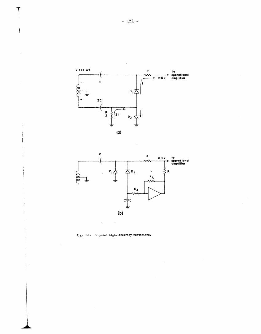
t
Vcos t 0 TV
(a)
C R
I(b)
IFig. 8.1, Proposed high-linearity rectifiers.
I
TU
operationalamplifier
tooperat ionalamplifierj
iIII

- 182 -
Measurement of the d-c voltage would, by Ea. 2.56, determine the
r-f voltage. Obviously this a highly inconvenient process. Its
only value is in calibration of other voltmeters, and then only
if the accuracy exceeds that attainable by such simpler means as
heater-thermocouple combinations.
Ion-Collector Pulse Circuits
Although no clear-cut directions for improvement of the
ion-collector pulse circuits can be given, their overall perform-
ance can undoubtedly be substantially improved by further develop-
ment work. In particular, the scheme of signal differentiation
might well be abandoned and one of the alternative methods of
handling pulse baseline shift employed.
It should be noted that since thesis work was begun nuclear-
instrumentation circuits that might well satisfy all requirements
of the pulse system have become commercially available.
E.g., Edgerton, Germeshausen and Grier, Inc., M100 ModularCounting System.

APPENDIX A
Coefficients in Series ExDansion of Solutions
of Mathieu's Equation
y-Direction Coefficients
Equation 2.16 is based on the assumption that he two co-
efficients c2 and c 2 in the series solution for ion motion are
nearly equal. The proof of that assumption is as follows: The
series coefficients may be evaluated from continued-fraction
48*nsions:expansions:
rC
2m-2
_( 'n-2Kc2)t C
\1112my
_q/(2m + )2 q 2/(2m + )2(+2 + )21a_/(2m + J;2a -(A.1)
1 + a/(2 + )+ a/(2m + y)
-q/(2m - 2 + ey)2 q2 /(2m-2+ 2(2m-4+1 y /(( A 2 1 _ a/n2m2 _ 4f (A2)
+ a/(2m - 2 + .)2 1 + a/(2m - 4 + )2.y y)
If it is assumed that c = 1, y << 1, q 0.7,
sions for c2 and c 2 may be terminated with the
a L 0.2, expan-
first term, so
-q/(2 + y)2 -y2 2 2
+ a/(2 + ) (2 + y) + a-q(-2 + )2 -q
i + a/(-2 + y)2 (2 - )2 +a
(A.3)
(A.4)
Consideration is taken of the fact that ?'-a" of the y-equation(Eq. 2.10) equals "+a" of the canonical Mathieu equation(Eq. 2.11).
_8 -
_ 1Q
If 8 0, the two coefficients are exactly equal. For non-zero,YB one may write
-q 2 2 -(2+ c2-28 (A)C -C y*~ I (A.5)C2 (2 2 + a] (2 - y )2 + a (2 - y2 a
According to Paul. et al.' after a straight-line approximation to
the stability region and constant-n lines, 8y can be approximated
at q = 0.706 by
2 0.23699- a0706y 0.79375 .
Equation 2.23 can be used to eliminated a706 rom Eq. A.6 to give0.706
2 __
13 0.224 ~mE (A.7)y m
which, in turn, can be applied to Eq. A.5 to give, approximately,
c -c 2 -0.45 (m) (A.8)
This shows that for any reasonable resolution, say m/Ln 10, the
difference between c2 and c 2 is small.
x-Direction Coefficients
The continued-fraction expansions for the series-solution
coefficients (Eqs. A.1 and A.2) may be applied to the x solution
as well as to the y, but the signs of a and q in the expansions
must be changed, to correspond to the reversed signs in the original
Mathieu's equation (Eq. 2.9). The irst coefficients may again be
evaluated y terminating te expansion witn the il rst term, out
L._A

- L85 -
this time .with the assumption 1 - ,_ << 1, or x 1. Then
(3) o a IV <<I_ (A. 9)C2 a ( )2 = (1 -9(1 -. ) 0)ru 1-·i C7~:(f / -1o )
and
.... ,(, )" - q (A. 0)C-2 a/(1)2 1 - a (
The second coefficient is approximately unity, as may be observed
from
- _-a= I -a 1- 07 -0 .2322A-L - a a 1- 0.23
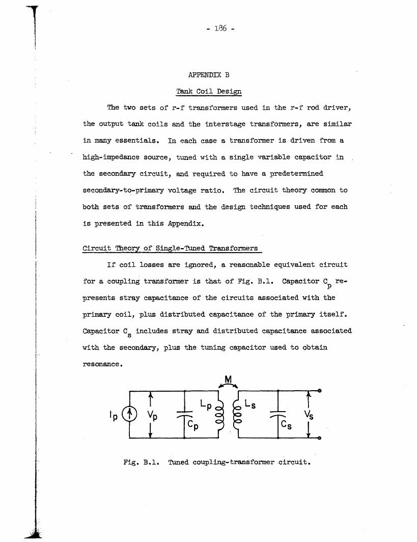
-186 -
APPENDIX B
Tank Coil Design
The two sets of r-f transformers used in the r-f rod driver,
the output tank coils and the interstage transformers, are similar
in many essentials. In each case a transformer is driven from a
high-impedance source, tuned with a single variable capacitor in
the secondary circuit, and required to have a predetermined
secondary-to-primary voltage ratio. The circuit theory common to
both sets of transformers and the design techniques used for each
is presented in this Appendix.
Circuit Theory of Single-Tuned Transformers
If coil losses are ignored, a reasonable equivalent circuit
for a coupling transformer is that of Fig. B.1. Capacitor C re-
presents stray capacitance of the circuits associated with the
primary coil, plus distributed capacitance of the primary itself.
Capacitor Cs includes stray and distributed capacitance associated
with the secondary, plus the tuning capacitor used to obtain
resonance.
M
, 1, _I P VP _
. 'A k y Vp~~~
LP Ls
VsCP Cs
Fig. B.1. Tuned coupling-transformer circuit.
a
i
j
--A
-·\ · · �u · ·
- 187 -
Solution of the loop equations for the circuit gives, for
a frequency w, the following equations for transfer impedance
and voltage ratio:
s jwM (B.)-= 4 MoL 2 - (B 1)p G CC(LL - X (CpL + C L) + Ps p s p s s
s M 2vs~~ . ~~(B.2)p L - w(L pLs
The first equation shows that the circuit has two resonant fre-
quencies, the two pairs of roots of
4C pCs(L - M2 ) - 2 (CL + CLs) + i = 0. (B.3)Psps pp
If Cp is negligible, this resonance equation reduces to
2 1W 2 . 1 (B.4)C Ls s
and the voltage-ratio equation becomes
V LV M (B.5)
In the general case the primary capacitance is, however,
not negligible. It is then necessary to develop tractable
design equations for the inductances in terms of known or
assumed quantities: the capacitances C and Os, the voltagep s
ratio Vs/Vp, and the frequency w. As a first step, the primary
inductance L can be eliminated from the resonancep

- 1i88 -
equation (Eq. B.3), by use of Eq. B.2, to give
VX <LoCs + MC V ) - I. (13.)
Then the definition of coefficient of coupling, k, for two coils,
expressed as
L = (B.7)P k2L
s
can be used to eliminate L from the voltage-ratio equation, whichp
becomes
V Ls s (B.8)
V M12A s s ( k- 1)
The mutual inductance M can be eliminated between Eqs. B.O and B.8
to give an expression for the secondary inductance in terms of the
capacitances, the frequency, and the unknown coefficient of
coupling:
L (- l)C w - L wfC(-Cs 2 ) 1 0(B.)s 2 s S (- s k
The coefficient of coupling varies slowly as a function of coil
structure; for design purposes a reasonable value may be assumed
and Eq. 13.9 solved for2
~2 + tP >^_2+ k 2-
L =k s s .(B.10)
21 Cs
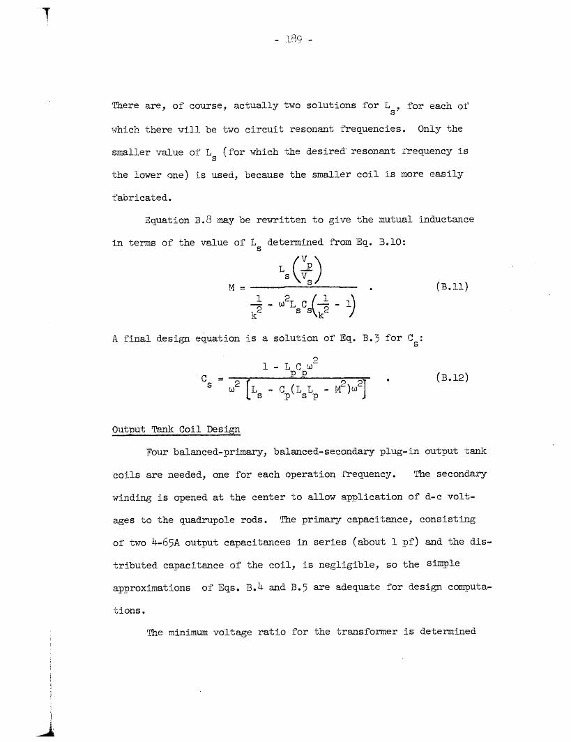
There are, of course, actually two solutions for L for each of
which there will be two circuit resonant frequencies. Only the
smaller value of L (for which the desired resonant frequency is
the lower one) is used, because the smaller coil is more easily
fabricated.
Equation B.8 may be rewritten to give the mutual inductance
in terms of the value of L determined from Eq. B.10:s
M =2 ( B.11)
WLC 1
k- L s ~
A final design equation is a solution of Eq. B.3 for Cs
1 - L C
C P (B.12)2[L C(LL -MT)w~j
Output Tank Coil Design
Four balanced-primary, balanced-secondary plug-in output tank
coils are needed, one for each operation frequency. The secondary
winding is opened at the center to allow application of d-c volt-
ages to the quadrupole rods. The primary capacitance, consisting
of two 4-65A output capacitances in series (about 1 pf) and the dis-
tributed capacitance of the coil, is negligible, so the simple
approximations of Eqs. B.4 and B.5 are adequate for design computa-
tions.
The minimum voltage ratio for the transformer is determined

- 190 -
by the required maximum output voltage for the quadrupole, about
2500 v peak measured across one half of the secondary, and the
permissible plate-voltage swing on the tetrodes. For maximum
energy transfer and minimum plate dissipation the tetrode plate
swing should be as large as possible, or the secondary-primary
voltage ratio as small as possible. The limitation is that on
negative r-f peaks, when the plate voltage is substantially lower
than that of the screen, cathode current is diverted from the plate
to the screen, limiting peak plate current and presenting the pos-
sibility of overdissipation of the screen. It was found experi-
mentally that for a plate supply of 1800 v and a screen voltage
of 300 v the maximum permissible plate voltage swing was about
1500 v, or roughly the amount for which the lowest instantaneous
plate voltage equalled the screen voltage.
There is, however, another factor that makes it desirable to
make the secondary-primary voltage ratio as large as possible: the
introduction of symmetric-mode signals into the secondary because of
the difference in mutual inductance from one half of the primary to
the corresponding half of the secondary and that from one half of
the primary to the opposite side of the secondary (see Appendix C).
Any scheme for cancellation of this effect by special windings, such
as, for example, a bifilar-wound primary; seems fraught with dif-
ficulties involving interwinding capacitance. The simplest method
to reduce the difference in mutual inductances to a minimum is to
191 -
compress the primary winding to a minimal length located at the
center of the secondary. In practice, this means a small value
of overall mutual inductance, M, and a high secondary-to-primary
voltage ratio.
There is still one more benefit in the increase in voltage
ratio: the Class C tetrode driver amplifier perates with longer
conductin times and so lower harmonic distortion.
When all factors are considered, the secondary-to-primary
voltage ratio is therefore a compromise between high output
capability and low symmetric-mode distortion.
A configuration of coaxial, concentric solenoids, with the
high-inductance secondary the outer coil as chosen for the tank
coil. Low-loss "air-wound" coils were used for the three highest
frequencies. The lowest frequency required more inductance than
could be obtained from a mechanically rigid air-wound coil, so a
structure supported on phenolic tubing was used. Primary and
secondary solenoids were wound in the same sense, that of a right-
hand screw, so that adjacent ends would have the same r-f polarity
and energy storage in interwinding capacitance would be minimized.
An even number of turns was used on both coils so that the center
tap could be brought out in the same radial direction as the end
leads of the coil; a gap between the two halves of the secondary
permitted the primary center-tap lead to be brought out. Finally,
high-melting-point Lexan supporting insulation was used for the two
t

- 192 -
highest-frequency coils because of coil heating; even with a
100 cfm cooling blower, the coil temperature rises to 75°C after
several minutes of full output at 3.3103 Mc.
Coil design involves datisfying the specific requirements
on L and M. The most simple equation for a practical solenoids 4
is adequate for calculation of the secondary inductance: 9
22L r l0 ' (B.13)
where n is the total number of turns, r the coil radius and j the
coil length, measured in inches. This equation is solved for the
number of turns (n) in terms of the specified Ls and arbitrarily
selected r and .
The applicable equation for mutual inductance for coaxial,
concentric coils with the outer coil the longer is
2-2r rM = 0.0501 s (1 + ) (B.14)
rs + s
where 2 2
r r8r 2+2 1)(B.15)
and n and ns are primary and secondary turns, rp and rs are
primary and secondary coil radii, and I and are primary andp s
secondary coil lengths, respectively, with all dimensions in
50inches. The correction term c is usually small with respect to
unity.
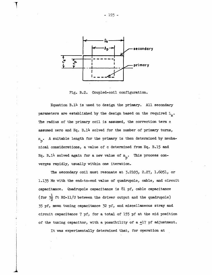
- 93 -
secondary
primary
Fig. B.2. Coupled-coil configuration.
Equation B.14 is used to design the primary. All secondary
parameters are established by the design based on the required L s
The radius of the primary coil is assumed, the correction term c
assumed zero and Eq. B.14 solved for the number of primary turns,
n . A suitable length for the primary is then determined by mecha-
nical considerations, a value of c determined from Eq. B.15 and
Eq. B.14 solved again for a new value of n . This process con-
verges rapidly, usually within one iteration.
The secondary coil must resonate at 3.2103, 2.27, 1.6051, or
1.135 Mc with the end-to-end value of quadrupole, cable, and circuit
capacitance. Quadrupole capacitance is 81 p, cable capacitance
(for 3 ft RG-11/U between the driver output and the quadrupole)
35 pf, mean tuning capacitance 32 pf, and miscellaneous stray and
circuit capacitance 7 pf, for a total of 155 pf at the mid position
of the tuning capacitor, with a possibility of a +17 pf adjustment.
It was experimentally determined that, for operation at
ji
iI
i
Iq
i4
i
i..
3.2103 Mc, power considerations required the secondary-to-primary
voltage ratio to be its minimum value of 2500/1500 = 1.7. Higher
voltage ratios were used to minimize harmonic distortion at the
less demanding lower frequencies: 1.8 at 2.27 and 1.6051 Mc, 2.0
at 1.135 Mc.
The design procedure for the output tank coils can be
illustrated by the design of the .2103 Mc coil. The secondary
must, by Eq. B.4, resonate with 155 pf, which requires Ls = 15.8 ph.
To minimize losses and heating the coil should be as large as pos-
sible, a requirement that leads to a diameter of 3 inches, the
largest available in commercial coil stock, and a length of 3
inches, fixed by the plug strip on which the coil is mounted.
Solution of Eq. B.13 then gives 18 turns for the coil, or a pitch
of 6 turns/inch. With this rather coarse pitch a 1-turn gap in the
center is an adequate space in which to bring out the primary
center-tap lead. The calculation for number of turns on the coil
is repeated with a more accurate estimate of coil length, =
(n + 1)/6, and again it is found that 18 turns is required. Final
inductance calculations show that an 18-turn coil 3 inches in dia-
meter and 1 inches long has an inductance L = 16.1 h.s
By Eq. B.5 a voltage ratio of 1.7 requires a mutual inductance
M = 9.483 h. To minimize symmetric-mode coupling the primary must
be as short as possible. It is therefore made with the largest dia-
meter, 2 inches, that will fit inside the secondary with the
- 194 -

- 195 -
tightest winding pitch available, 10 turns/inch. Use of Eq. B.14
with c - 0 gives n = 14.7 turns. The nearest even integer, 14,
makes c = 0.034. A second solution of Eq. B.14 with this value
of c gives n = 14.2 turns. A value n = 14 turns is thenP P
assumed and M computed from Eq. B.14: M = 9.33 h.
Interstage Transformer Design
Two switch-selected interstage transformers are used, one
for the two lower operation frequencies, one for the two upper
frequencies. Each has an unbalanced primary, a balanced, center-
tapped secondary, and a Faraday shield between (to prevent inter-
winding capacitance from introducing an unbalanced signal in the
output). The secondary is tuned by a variable capacitor and
switched fixed capacitors. The primary capacitance, which con-
sists of the output capacitance of the buffer amplifier, coil dis-
tributed capacitance, and stray circuit capacitance, is not
negligible, so the more involved design equations must be used.
The transformer voltage ratio is determined by the require-
ment that for fixed output voltage the pentode plate swing be at
the highest possible level without excessive screen conduction on
the negative r-f peaks. For the required output voltage of 450
volts peak, measured from end to end of the secondary, and a buffer
d-c plate supply of 300 v, screen supply of 160 v, it was found
experimentally that the optimum secondary-to-primary voltage ratio
was about 2.3:1.

-0o6 -
A systematic design procedure for an nterstage transformer
is as follows:
(1) Assumption of arameters. The upper of the two fre-
quencies at which the transformer will oerate is taken as the
design frequency. The appropriate voltage ratio V /Vp is selected.
A secondary capacitance, C (which consists of the tuning capacitance,
driver-amplifier input capacitance, monitoring capacitances, coil
distributed capacitance and stray circuit capacitance), and a primary
capacitance, C are assumed. The coil coefficient of coupling isp
estimated. (A rough estimate is the square root of the ratio of the
volumes of the primary and secondary.)
(2) The secondary inductance, Ls, is calculated from Eq.B.10
with the parameter values assumed in step (1).
(3) The mutual inductance, M, is calculated from Eq. B.11.
(4) The primary and secondary coils are designed for the
determined values of Ls and M by means of Eas. B.13 through B.15
and the technique employed in the design of the output tank coils.
(5) As a check, the actual C necessary to tune the coils
and the actual voltage ratio V /V are computed by means of
Eqs. B.12 and B.2, respectively.
(6) Equation B.12 is used to compute the C necessary for
resonance and Eq. B.2 to check the voltage ratio for operation at
the lower of the two frequencies.
The technique used to design the .2103 and 2.27 Me inter-

- 197 -
stage transformer provides an example. The design voltage ratio is
Vs /V = 2.3. It is assumed that the secondary capacitance C =
60 pf, the primary capacitance C = 30 pf. This rather high
primary capacitance has been found a reasonable estimate in light
of the high distributed capacitance in the coils used. A first
estimate for coefficient of coupling for coils of the type used
in the interstage transformer is k = 0.7. At 3.2103 Me these values
substituted in Eq. B.10 give L = 37.6 ph, and substituted inS
Eq. B.11 give M = 15.1 Ih.
Commercial coil stock l1 -inch in diameter and 32 turns/inch
is assumed for the secondary coil. Use of a design procedure similar
to that employed for the output tank coil secondary gives n = 42
turns, Ls = 36.7 h. The primary is assumed to be 32-turn/inch,
1-inch-diameter commercial coil stock. Again a design procedure
similar to that previously employed gives n = 26 turns, M = 15.2 Ih,p
L = 13.4 h, and k = 0.68. These values inserted in the checkp
equations give Cs = 61.2 pf, V /V = 2.22. At 2.27 Mc the required
tuning capacitance is Cs = 128 f, the voltage ratio Vs/V = 2.32.5 s p

APPENDIX C
Symmetric Signals in Balanced, Inductively Coupled Circuits
Elementary theory, which assumes a transformer with nity
coupling between primary and secondary, predicts no inductive
coupling of symmetric-mode signals into the output of a balanced
circuit such as that used in the output of the r-f rod driver.
However, there is inductive coupling caused by flux leakage in
the transformer.
A good representation of the output tank coil and associated
circuits for symmetric signals is that shown in Fig. C.1. The
primary consists of two mutually coupled coils driven by two
current sources; an equivalent circuit is a single coil driven
by one current source, as in Fig. C.2. The secondary likewise
consists of two mutually coupled coils, with one side of each
going to the output and the other to ground through an impedance
Zs that represents the impedance of chokes L13 and L14 in the
rod-driver circuit (Fig. 4.4) and the stray capacitance to ground
from the rather bulky "transmitting" mica capacitor, C2 0; an
equivalent circuit is a single coil connected to ground through
Z . There are four primary-to-secondary mutual inductances: two
inductances M1 between adjacent sides of the primary and secondary,
two inductances M2 between opposite sides of the primary and
secondary; these are equivalent to a single mutual inductance
equal to half the difference between ME and M2. It is this mutual
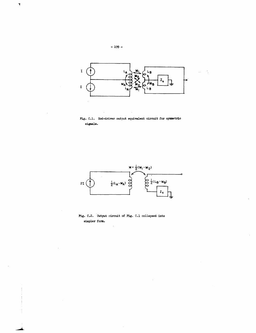
.
- 199 -
I
I
Fig. C.1. Rod-driver output equivalent circuit for symmetricsignals.
21
M = 1(M I - M2 )
{ (L A -MA) 2 s
Fig. C.2. Output circuit of Fig. C.1 collapsed into
simpler form.

- 200 -
inductance that provides the coupling for symmetric signals
between rimary and secondary. Because coils in which = M
are impractical, and it is impossible to completely eliminate
the current path through Zs Fig. C.2 shows that there will be
symmetric, even-order harmonic signals inductively coupled into
the rod-driver output.

- 201 -
APPENDIX D
Self-Checking Balance Detector Algorithm
"Self-checking" balance detectors are used on both the d-c
and r-f rod drivers to ensure the balance, or antisymmetry, of the
d-c and r-f voltages. An algorithm for adjustments of the detectors
is presented in this Appendix.
Either balance detector can be represented by the flow graph
of Fig. D.1. The balance-detector output (Vz) is, within the con-
stant k, the sum of its two inputs multiplied by the factors 1 +
and 1 - . Perfect balance of the detector corresponds to = 0.
The detector is connected through a reversing switch to the two
rod-driver outputs, v and v . It shall be assumed that the rod-
driver outputs are antisymmetric, except for multiplicative error
factors 1 + and 1 - c} that is
v+= VA(1 + ) and v_ = -VA(1- ).
Then = 0 is the condition of perfect antisymmetry.
Vx
V+
Vz
Fig. D.l. Balance-detector flow graph.

- 202 -
According as the reversing switch is in position (a) or (b)
the balance-detector output is
v (a) = 2k( + )VA
or
v(b) = 2k(c - 5)VA
respectively. Clearly v z(a) = v(b) = 0 implies = = 0, and
perfect balance.
The balance algorithm is as follows:
(1) Assume the switch is initially in position (a), and
that e = g° 0 and 8 = 8 f O. Then the initial output voltage is
ZJ 0 0tv(a)] 0 -2kte + )vA
The detector balance, characterized by , is adjusted until the out-
put voltage is zero:
Lz(a) 1 = = 2k( + 81)VA.
Therefore, = -E1 o
(2) The switch is thrown to position (b). The output voltage
is then
Iv(b) 2 = 2k(2Co)VA
(3) The rod-driver balance, characterized by c, is adjusted
until the output voltage is one half [vz(b)J 2 :
[z2(b)3 = 2k(3 o)VA = 2 (2k)(2e) A
Therefore,3 = 0.
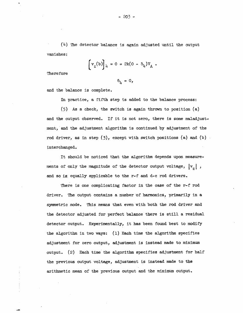
- 20 -3n1
(4) The detector balance is again adjusted until the output
vanishes:
[vz(b) = = 0 2k(0 - 38)VA.
Therefore
84 = 0,
and the balance is complete.
In practice, a fifth step is added to the balance process:
(5) As a check, the switch is again thrown to position (a)
and the output observed. If it is not zero, there is some maladjust-
ment, and the adjustment algorithm is continued by adjustment of the
rod driver, as in step (3), except with switch positions (a) and (b)
interchanged.
It should be noticed that the algorithm depends upon measure-
ments of only the magnitude of the detector output voltage, IVzl ,
and so is equally applicable to the r-f and d-c rod drivers.
There is one complicating factor in the case of the r-f rod
driver. The output contains a number of harmonics, primarily in a
symmetric mode. This means that even with both the rod driver and
the detector adjusted for perfect balance there is still a residual
detector output. Experimentally, it has been found best to modify
the algorithm in two ways: (1) Each time the algorithm specifies
adjustment for zero output, adjustment is instead made to minimum
output. (2) Each time the algorithm specifies adjustment for half
the previous output voltage, adjustment is instead made to the
arithmetic mean of the previous output and the minimum output.

- 204 -
APPENDIX E
Pulse-System Test Apparatus
Special apparatus is necessary to provide pulses with which
to test the circuits of the ion-detector pulse system. The use
of a Tektronix Type N Sampling Unit as the basic pulse measuring
device places two special requirements upon this apparatus:
(1) It must provide a trigger signal for the sampling unit.
(2) For convenience in observation, the source repetion frequency
must be high enough to make possible a sample of a complete wave-
form in less than one second. These two requirements on the basic
pulse generator were met by a Tektronix 111 Pulse Generator, which
uses an avalanche transistor to generate fast (nanosecond rise)
pulses at repetition rates up to 100 kc.
Certain requirements on the nature of the output pulses have
to be met: (1) The pulse width should approximate that of an elec-
tron multiplier, some 4 nsec at half amplitude. (2) The pulse
should come from an effective current source, to approximate an
electron-multiplier anode. (3) The pulse should be free of any
"tail" that would appear as post-pulse noise in the ion-detector
system output. (4) Pulse amplitude should be variable over a wide
range. (5) It should be possible to obtain two or more pulses, of
different amplitudes, in quick succession - within nanoseconds.
A system that meets all these requirements is shown in
Fig. E.1. The output pulse of the Tektronix 111 Pulse Generator
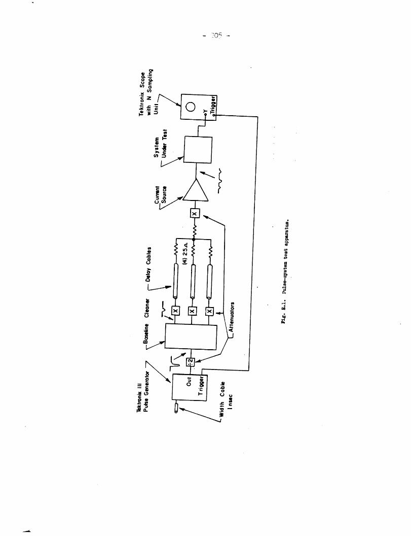
C.o .E
) 17)
C
.cI9
4a4-
.
i,
.:rm14
a;
.ElCe.wCY
'I,- r
- 206 -
has a long, slowly decaying tail that extends more than 50 nsec,
so it is necessary to pass it through a "pulse baseline cleaner"
(Fig. E.2), actually two cascaded diode clippers that pass only
the negative peak of the input pulse to three parallel outputs.
The resulting pulse is carried over as many as three cables of
different lengths to yield three pulses that are combined in a
mixer and applied to the pulse current source, actually a grounded-
base transistor amplifier (Fig. E.3). The output of the current
source drives the preamplifier of the ion-detector system.
The test apparatus has a maximum output pulse of about
6 x 10⁸ electrons with an essentially triangular shape: amplitude
2 ma, full width at half maximum 5 nsec (Fig. 6.7). A narrower
pulse, which may correspond more closely to an electron-multi-
plier output, can be obtained by eliminating the external timing
cable of- the Tektronix 111. This shortened pulse is obtained,
however, at the price of reduced total charge.

U,I--
0.I.-
0
I-
a.Z
t(ID
a
0
o5
0;
dz0a:
,la)
014
Id
'4 I

u2
- xML>
Or
Z5 ca >a;zCY
4-
C
3R
d is
c J040
0 4
* I
oe v 0 40x-
U t0 ae
Ed * 00 o4 "
tI i'
40 ,-A '
4) 04-
4.' 4 pa
00
- 4
=U,C1-9
0
06
N(7
c0
E Oa cCY. >
- 209 -
REFERENCES
1. W. Paul and H. Steinwedel, Z. Naturforschung 8a, 448 (1953).
2. W. Paul and M. Raether, Z. Physik 140, 262 (1955).
35. W. Paul and H. Steinwedel, German Patent 944,900 (1956).
4. U. von Zahn, Z. Physik 168, 129 (1962).
5. H. Matsuda, J. Phys. Soc. Japan 11, 183 (1956).
6. W. Paul, H.P. Reinhard and U. von Zahn, Z. Physik 152, 143 (1958).
7. K. Ginther, Vacuum 10, 293 (1960).
8. C.K. Crawford and C.E. Woodward, Tech. Rep. 175, Lab. Ins. Res.,
Mass. Inst. Tech., November, 1962.
9. N.W. McLachlan, "Theory and Application of Mathieu Functions,"
Oxford University Press, London, 1947, p. 10.
10. W.M. Brubaker, unpublished, Bell and Howell Research Center,
Pasadena, California, December 14, 1960.
11. C.E. Woodward and C.K. Crawford, Tech. Rep. 176, Lab. Ins. Res.,
Mass. Inst. Tech., January, 1963, p. 8.
12. F. von Busch and W. Paul, Z. Physik 164, 588 (1961).
13. H.G. Bennewitz and R. Wedemeyer, Z. Physik 172, 1 (1963).
14. I.E. Dayton, F.C. Shoemaker and R.F. Mozley, Rev. Sci. Instr. 25,
485 (1954).
15. J. Millman and H. Taub, "Pulse and Digital Circuits," McGraw-Hill
Book Co., New York, N.Y., 1956, p. 221.
16. C.E. Woodward and C.K. Crawford, op. cit., p. 16.
17. J. Truxal, "Automatic Feedback Control System Synthesis,"
McGraw-Hill Book Co., New York, N.Y., 1955, p. 221.
18. J.S. Allen, Phys. Rev. 55, 966 (1939).
19. A.I. Akishin, Soviet Phys. - Uspekhi 66,(1) 113 (1958).
I__
- 10 -
2. )P.T. ichards and 2.3. Hays, Rev. Sci. nstr. 21, <9e (1950)
21. E. Sch~nheit, Z7 Naturforschung !la, 81i f(156).
22. F.D.S. Butement and N.P. Finkelstein, J. Sci. instr. 3'7, 28 (1960).
23. C.F. Barnett, G.E. Evans and P.M. Stier, Rev. Sci. nstr. 25,
112 (1754).
24. T. Sugiura, Bull. Chem. Soc. Japan 5, 1257 (1962).
25. F.A. White and T.L. Collins, Arplied Spectroscopy 8, 17 (1954).
26. K. Koyama and R.E. Connally, Rev. Sci. Instr. 28, 833 (1957).
27. L. Cathey, AEC Report DP-498, 1960.
28. G.W. Barton, r., L.E. Gibson and L.F. Tolman, Anal. Chem. 2,
1599 (1960 ).
29. W. Shockley and J.R. Pierce, Proc. IRE 26, 321 (1938).
30. R.E. Barrington and J.M. Anderson, Proc. Phys. Soc. 72, Pt. 5,
717 (1958).
31. R.F. Tustin, Q.A. Kerns, and .K. Knudsen, IRE Trans. Nuc. Sci.
NS-9, No. 3, 118 (1962).
32. P.J. Lombard and F. Martin, Rev. Sci. Instr. 32, 200 (1961).
33. W.H. Johnston, AEC Report JLI-650-8-8, 1962.
34. W.B. Davenport,Jr., and W.L. Root, "Random Signals and Noise,"
McGraw-Hill Book Co., New York, H.Y. 1958, p. 122.
55. W.B. Davenport, Jr., and W.L. Root, oc. cit.. p. 144.
36. R.D. Evans, "The Atomic Nucleus," McGraw-Hill Book Co., New
York, N.Y., 1955, p. 87.
37. R.D. Evans, loc. cit., p. 786.
38. R. Jost, Helv. Phys. Acta 20, 173 (1947). Unfortunately this
paper is marred by numerous typographical errors, so all results
must be checked before use.

- 211 -
59. H. Richter, Math. Ann. 118, 145 (1942).
40. Y.W. Lee, "Statistical Theory of Communication," John Wiley and
Sons, New York, N.Y., 1960, Chapts.14-16.
41. C.H. Vincent, Nucl. Inst. and Meth. 23, lq (1963).
42. Z.H. Frohner, Nukleonik 5, 82 (1963).
43. J. Millmand and H. Taub, o. cit., p. 120.
44. H. Verweij, Nuc. Instr. Meth. 24, 39 (1963).
45. V.G.K. Reddi, Fairchild Semiconductor Application Data, APP-
32/2, Sept. 1961.
46. R. Sugarman, F.C. Merritt and W.A. Higinbotham, AEC Report
BNL-711 (T-248, Brookhaven National Laboratory, February, 1962).
47. R.D. Middlebrook, "Junction Transistor Theory," John Wiley and
Sons, New York, N.Y., 1957, p. 220.
48. N.W. McLachlan, op. cit., p. 106.
49. F.E. Terman, "Radio Engineer's Handbook," McGraw-Hill Book Co.,
New York, N.Y., 1943, p. 55.
50. F.E. Terman, o. cit., p. 71.
51. C.E. Woodward and C.K. Crawford, op. cit., p. 29.
52. U. von Zahn, Rev. Sci. Instr. 34, 1 (1963).
BIOGRAPHICAL NOTE
Charles E. Woodward
Born: Harvard, Nebraska, March 1, 1931.
Eduation: Iowa State College, 1953 to 1957, B.S. in Electrical
Engineering (1957).
Massachusetts Institute of Technology, 1957 to 1964,
S.M. in Electrical Engineering (1960).
Professional Experience: (1) Staff Member, M.I.T. Lincoln Labora-
tory, 1957 to 1960. Designed circuits for digital com-
puters.
(2) Research Assistant, M.I.To Department of Electrical
Engineering, 1957 to 1958. Wrote digital-computer
utility programs.
(3) Teaching Assistant, M.I.T. Department of Electrical
Engineering, 1960. Taught one laboratory course in
electronic circuits.
(4) Research Assistant, M.I.T. Laboratory for Insulation
Research, 1961 to 1964. Designed circuits for quadrupole
mass spectrometer.
Professional Society: Member, Institute of Electrical and Electronics
Engineers.
- 1 !-