Defect detection with CCD-spectrometer and photodiode-based arc-welding monitoring systems
8
Journal of Materials Processing Technology 211 (2011) 2132–2139 Contents lists available at ScienceDirect Journal of Materials Processing Technology j o ur nal ho me p age : www.elsevier.com/locate/jmatprotec Defect detection with CCD-spectrometer and photodiode-based arc-welding monitoring systems J. Mirapeix ∗ , R. Ruiz-Lombera, J.J. Valdiande, L. Rodriguez-Cobo, F. Anabitarte, A. Cobo Grupo de Ingeniería Fotónica, Universidad de Cantabria, Edificio I+D Teleco, Dpto. TEISA, Avda. Los Castros s/n, 39005 Santander, Spain a r t i c l e i n f o Article history: Received 7 April 2011 Received in revised form 19 July 2011 Accepted 21 July 2011 Available online 27 July 2011 Keywords: Arc-welding Quality monitoring Plasma optical spectroscopy Photodiodes CCD-spectrometers Optical filters a b s t r a c t In this paper a detailed study on the ability of a system based on photodiodes to detect a wide variety of weld defects is presented. Narrow optical filters have been included within the setup to analyse their influence in the resulting monitoring signal and a direct comparison to the performance of the spectrom- eter has been also considered. The results obtained during the experimental tests indicate that the use of these filters clearly improves the resulting monitoring signals provided by the photodiodes, suggesting that a photodiode-based setup could become an alternative to the employment of spectrometers in some particular scenarios. © 2011 Elsevier B.V. All rights reserved. 1. Introduction Welding on-line quality monitoring is nowadays an active area of research given the significant complexity inherent to the physics of the process and the lack of commercial efficient and reliable solu- tions. The most extended systems to be found in the industry are those based on the monitoring of the electric signals (current and voltage) supplied by the welding power source. They are reliable in terms of the detection of some defects, mainly provoked by devia- tions of the mentioned parameters (and some directly related, e.g. electrode/plate cut-off distance) by establishing a “process win- dow”. However, there are some weld flaws that are difficult to be detected by these monitoring devices, like deviations of the weld torch over the joint, plate mismatches or perturbations on the pro- tection gas flow. There are other approaches for welding on-line inspection: machine vision, where typically a reduction of the arc disturbance is required as proposed by Zhang et al. (2006) and Wang and Zhao (2001) among other authors have employed the analysis of the acoustic emission generated during the process; and infrared ther- mography, just to mention some examples, but their applicability is commonly limited to some particular scenarios. In this regard plasma optical spectroscopy has demonstrated that is a promising ∗ Corresponding author. Tel.: +34 942 202238; fax: +34 942 200877. E-mail address: [email protected] (J. Mirapeix). solution both for arc and laser welding, exhibiting some remarkable features like the immunity of the optical fibers to the strong electro- magnetic interference associated with arc-welding processes that can prevent the arrangement of electronic devices in the vicinity of the welding torch. On the other hand, the analysis that can be performed by means of this technique is quite versatile, offering the possibility of tracing specific elements or species participating in the plasma, what can be very interesting if, for example, some spurious elements are trying to be detected in the resulting seams: tungsten inclusions, oxygen that can indicate the appearance of oxidation processes or other elements to be avoided in the joint. In addition, it has been demonstrated (Ancona et al., 2001) that different species show distinctive responses to some weld flaws, and even some emission lines belonging to the same species may exhibit different sensitivities in terms of defect detection, as dis- cussed by Garcia-Allende et al. (2009). Several authors have employed CCD (or CMOS) spectrometers to acquire the welding plasma spectra, as these devices enable the resolution of the emission lines to be found in the spectra. Exam- ples in this regard can be found in the works by Ferrara et al. (2000), Sforza and de Blasiis (2002) or Ancona et al. (2004). The common approach has been based on the estimation of the plasma electronic temperature T e , given the known relation between this spectroscopic parameter and the resulting quality of the seams. Other approaches have been also recently suggested, like the use of the so-called RMS signal (Mirapeix et al., 2009) provided by the spectrometer, the wavelength associated with the maximum inten- sity of the plasma continuum (Mirapeix et al., 2006) or the use of 0924-0136/$ – see front matter © 2011 Elsevier B.V. All rights reserved. doi:10.1016/j.jmatprotec.2011.07.011
Transcript of Defect detection with CCD-spectrometer and photodiode-based arc-welding monitoring systems

Dm
JG
a
ARRAA
KAQPPCO
1
oottvtteddtt
mi(amip
0d
Journal of Materials Processing Technology 211 (2011) 2132– 2139
Contents lists available at ScienceDirect
Journal of Materials Processing Technology
j o ur nal ho me p age : www.elsev ier .com/ locate / jmatprotec
efect detection with CCD-spectrometer and photodiode-based arc-weldingonitoring systems
. Mirapeix ∗, R. Ruiz-Lombera, J.J. Valdiande, L. Rodriguez-Cobo, F. Anabitarte, A. Coborupo de Ingeniería Fotónica, Universidad de Cantabria, Edificio I+D Teleco, Dpto. TEISA, Avda. Los Castros s/n, 39005 Santander, Spain
r t i c l e i n f o
rticle history:eceived 7 April 2011eceived in revised form 19 July 2011ccepted 21 July 2011vailable online 27 July 2011
a b s t r a c t
In this paper a detailed study on the ability of a system based on photodiodes to detect a wide varietyof weld defects is presented. Narrow optical filters have been included within the setup to analyse theirinfluence in the resulting monitoring signal and a direct comparison to the performance of the spectrom-eter has been also considered. The results obtained during the experimental tests indicate that the use ofthese filters clearly improves the resulting monitoring signals provided by the photodiodes, suggestingthat a photodiode-based setup could become an alternative to the employment of spectrometers in some
eywords:rc-weldinguality monitoringlasma optical spectroscopyhotodiodesCD-spectrometers
particular scenarios.© 2011 Elsevier B.V. All rights reserved.
ptical filters
. Introduction
Welding on-line quality monitoring is nowadays an active areaf research given the significant complexity inherent to the physicsf the process and the lack of commercial efficient and reliable solu-ions. The most extended systems to be found in the industry arehose based on the monitoring of the electric signals (current andoltage) supplied by the welding power source. They are reliable inerms of the detection of some defects, mainly provoked by devia-ions of the mentioned parameters (and some directly related, e.g.lectrode/plate cut-off distance) by establishing a “process win-ow”. However, there are some weld flaws that are difficult to beetected by these monitoring devices, like deviations of the weldorch over the joint, plate mismatches or perturbations on the pro-ection gas flow.
There are other approaches for welding on-line inspection:achine vision, where typically a reduction of the arc disturbance
s required as proposed by Zhang et al. (2006) and Wang and Zhao2001) among other authors have employed the analysis of thecoustic emission generated during the process; and infrared ther-
ography, just to mention some examples, but their applicabilitys commonly limited to some particular scenarios. In this regardlasma optical spectroscopy has demonstrated that is a promising
∗ Corresponding author. Tel.: +34 942 202238; fax: +34 942 200877.E-mail address: [email protected] (J. Mirapeix).
924-0136/$ – see front matter © 2011 Elsevier B.V. All rights reserved.oi:10.1016/j.jmatprotec.2011.07.011
solution both for arc and laser welding, exhibiting some remarkablefeatures like the immunity of the optical fibers to the strong electro-magnetic interference associated with arc-welding processes thatcan prevent the arrangement of electronic devices in the vicinityof the welding torch. On the other hand, the analysis that can beperformed by means of this technique is quite versatile, offeringthe possibility of tracing specific elements or species participatingin the plasma, what can be very interesting if, for example, somespurious elements are trying to be detected in the resulting seams:tungsten inclusions, oxygen that can indicate the appearance ofoxidation processes or other elements to be avoided in the joint.In addition, it has been demonstrated (Ancona et al., 2001) thatdifferent species show distinctive responses to some weld flaws,and even some emission lines belonging to the same species mayexhibit different sensitivities in terms of defect detection, as dis-cussed by Garcia-Allende et al. (2009).
Several authors have employed CCD (or CMOS) spectrometersto acquire the welding plasma spectra, as these devices enable theresolution of the emission lines to be found in the spectra. Exam-ples in this regard can be found in the works by Ferrara et al.(2000), Sforza and de Blasiis (2002) or Ancona et al. (2004). Thecommon approach has been based on the estimation of the plasmaelectronic temperature Te, given the known relation between thisspectroscopic parameter and the resulting quality of the seams.
Other approaches have been also recently suggested, like the useof the so-called RMS signal (Mirapeix et al., 2009) provided by thespectrometer, the wavelength associated with the maximum inten-sity of the plasma continuum (Mirapeix et al., 2006) or the use of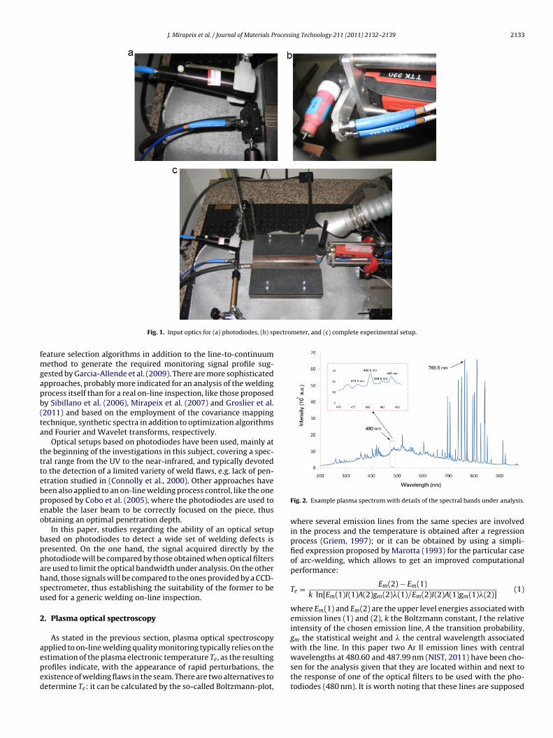
J. Mirapeix et al. / Journal of Materials Processing Technology 211 (2011) 2132– 2139 2133
ectrometer, and (c) complete experimental setup.
fmgapb(ta
tttebpeo
bppahsu
2
aeped
Fig. 1. Input optics for (a) photodiodes, (b) sp
eature selection algorithms in addition to the line-to-continuumethod to generate the required monitoring signal profile sug-
ested by Garcia-Allende et al. (2009). There are more sophisticatedpproaches, probably more indicated for an analysis of the weldingrocess itself than for a real on-line inspection, like those proposedy Sibillano et al. (2006), Mirapeix et al. (2007) and Groslier et al.2011) and based on the employment of the covariance mappingechnique, synthetic spectra in addition to optimization algorithmsnd Fourier and Wavelet transforms, respectively.
Optical setups based on photodiodes have been used, mainly athe beginning of the investigations in this subject, covering a spec-ral range from the UV to the near-infrared, and typically devotedo the detection of a limited variety of weld flaws, e.g. lack of pen-tration studied in (Connolly et al., 2000). Other approaches haveeen also applied to an on-line welding process control, like the oneroposed by Cobo et al. (2005), where the photodiodes are used tonable the laser beam to be correctly focused on the piece, thusbtaining an optimal penetration depth.
In this paper, studies regarding the ability of an optical setupased on photodiodes to detect a wide set of welding defects isresented. On the one hand, the signal acquired directly by thehotodiode will be compared by those obtained when optical filtersre used to limit the optical bandwidth under analysis. On the otherand, those signals will be compared to the ones provided by a CCD-pectrometer, thus establishing the suitability of the former to besed for a generic welding on-line inspection.
. Plasma optical spectroscopy
As stated in the previous section, plasma optical spectroscopypplied to on-line welding quality monitoring typically relies on the
stimation of the plasma electronic temperature Te, as the resultingrofiles indicate, with the appearance of rapid perturbations, thexistence of welding flaws in the seam. There are two alternatives toetermine Te: it can be calculated by the so-called Boltzmann-plot,Fig. 2. Example plasma spectrum with details of the spectral bands under analysis.
where several emission lines from the same species are involvedin the process and the temperature is obtained after a regressionprocess (Griem, 1997); or it can be obtained by using a simpli-fied expression proposed by Marotta (1993) for the particular caseof arc-welding, which allows to get an improved computationalperformance:
Te = Em(2) − Em(1)k ln[Em(1)I(1)A(2)gm(2)�(1)/Em(2)I(2)A(1)gm(1)�(2)]
(1)
where Em(1) and Em(2) are the upper level energies associated withemission lines (1) and (2), k the Boltzmann constant, I the relativeintensity of the chosen emission line, A the transition probability,gm the statistical weight and � the central wavelength associatedwith the line. In this paper two Ar II emission lines with central
wavelengths at 480.60 and 487.99 nm (NIST, 2011) have been cho-sen for the analysis given that they are located within and next tothe response of one of the optical filters to be used with the pho-todiodes (480 nm). It is worth noting that these lines are supposed
2134 J. Mirapeix et al. / Journal of Materials Processing Technology 211 (2011) 2132– 2139
Fig. 3. (a) Defective seam (gas flow perturbation), (b) plasma RMS profile (spectrometer), (c) line-to continuum profile (spectrometer), (d) photodiode voltage profile (766 nmfilter), and (e) photodiode voltage profile (780 nm filter).
with
ttt
ib
wiZtImH
Fig. 4. (a) Defective seam of Fig. 3, (b) plasma spectrum associated
o be free from self-absorption and the plasma is also supposedo be in local thermodynamic equilibrium (LTE), condition that isypically assumed to be valid for arc-welding plasmas.
Another spectroscopic parameter to be used in this frameworks the profile derived from the line-to-continuum method proposedy Bastiaans and Mangold (1985):
εl
Ic(�) = 2.0052 × 10⁻⁵ Amngm
Zi
1Te�
exp(
Ei − Em
kTe
)�
��, (2)
here εl is the line intensity integrated over the line profile, Ic thentensity of the adjacent background radiation (non-integrated),i is the ion partition function, �the free-bound continuum correc-
ion, Ei the ionization potential and �� the wavelength bandwidth.t is worth mentioning that Eq. (2) was originally designed to esti-ate Te, and an iterative method has to be employed in this regard.owever, for monitoring purposes this method can be simplified to
correct seam, and (c) plasma spectrum associated with the defect.
the determination of the IL/IC ratio, where IL stands for the relativeintensity of the selected line and IC for the corresponding back-ground radiation, estimated as suggested in Mirapeix et al. (2008)using a smoothing algorithm. The Ar I 763.5 nm and Fe I 778.06 nmlines have been selected for this analysis, enabling in this way acomparison with the photodiode signals generated with a filter inthis spectral range.
A third approach that will be considered for the analysis of theexperimental results lies in the use of the plasma RMS signal, whichis simply calculated by considering the intensity of each pixel of theCCD sensor:
SRMS =
√√√√1n
n−1∑i=0
x2i, (3)

J. Mirapeix et al. / Journal of Materials Processing Technology 211 (2011) 2132– 2139 2135
Fig. 5. (a) Defective seam (gas flow perturbation), (b) plasma RMS profile (spectrometer), (c) photodiode voltage profile, and (d) photodiode voltage profile (480 nm filter).
Fig. 6. (a) Defective seam (irregularities on the joints), (b) plasma RMS profile (spectrometer), (c) photodiode voltage profile (766 nm filter), and (d) photodiode voltagep
wcaasriootrb
rofile (780 nm filter).
here n is the total number of pixels of the CCD and xi the intensityorresponding to the i-th pixel. SRMS indicates an estimation of theverage intensity of the radiation emitted by the welding plasma,nd, consequently, it is a indirect measurement of the plasmapectrum energy within the spectral range considered, being alsoelated to the total arc power, and consequently to the process heatnput. In practical terms it can be a useful parameter for explorativer initial analyses of welding processes where an a priori knowledge
n the emission lines to be used is not at hand. In addition, the con-rol of the spectrometer via software allows to modify the spectralegion under analysis, thus enabling to look for optimal spectralands in terms of defect detection.These techniques will be used with the data acquired during theexperimental tests to compare the performance of the setups basedon the photodiodes and the spectrometer.
3. Experimental issues
To perform the required experimental tests the welding setupdescribed in (Mirapeix et al., 2006) was employed. The system is
formed by a TIG power source and torch, both remotely controlledvia PC, and Argon was used as protection and backing gas. AISI-304(stainless-steel) plates of different thicknesses were used duringthe tests.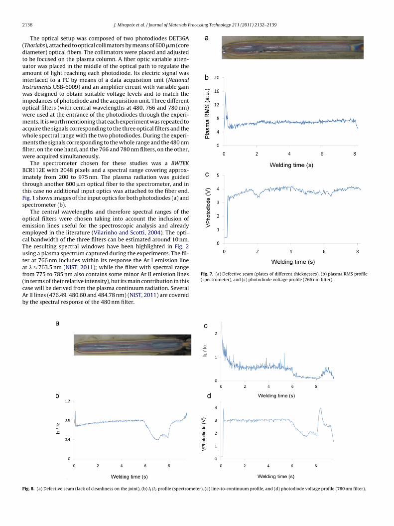
2 rocessing Technology 211 (2011) 2132– 2139
(dtuaiIwiowmawmfiw
BittFs
oeecTutaf(cAb
Fig. 7. (a) Defective seam (plates of different thicknesses), (b) plasma RMS profile(spectrometer), and (c) photodiode voltage profile (766 nm filter).
F
136 J. Mirapeix et al. / Journal of Materials P
The optical setup was composed of two photodiodes DET36AThorlabs), attached to optical collimators by means of 600 �m (coreiameter) optical fibers. The collimators were placed and adjustedo be focused on the plasma column. A fiber optic variable atten-ator was placed in the middle of the optical path to regulate themount of light reaching each photodiode. Its electric signal wasnterfaced to a PC by means of a data acquisition unit (Nationalnstruments USB-6009) and an amplifier circuit with variable gain
as designed to obtain suitable voltage levels and to match thempedances of photodiode and the acquisition unit. Three differentptical filters (with central wavelengths at 480, 766 and 780 nm)ere used at the entrance of the photodiodes through the experi-ents. It is worth mentioning that each experiment was repeated to
cquire the signals corresponding to the three optical filters and thehole spectral range with the two photodiodes. During the experi-ents the signals corresponding to the whole range and the 480 nm
lter, on the one hand, and the 766 and 780 nm filters, on the other,ere acquired simultaneously.
The spectrometer chosen for these studies was a BWTEKCR112E with 2048 pixels and a spectral range covering approx-
mately from 200 to 975 nm. The plasma radiation was guidedhrough another 600 �m optical fiber to the spectrometer, and inhis case no additional input optics was attached to the fiber end.ig. 1 shows images of the input optics for both photodiodes (a) andpectrometer (b).
The central wavelengths and therefore spectral ranges of theptical filters were chosen taking into account the inclusion ofmission lines useful for the spectroscopic analysis and alreadymployed in the literature (Vilarinho and Scotti, 2004). The opti-al bandwidth of the three filters can be estimated around 10 nm.he resulting spectral windows have been highlighted in Fig. 2sing a plasma spectrum captured during the experiments. The fil-er at 766 nm includes within its response the Ar I emission linet � ≈ 763.5 nm (NIST, 2011); while the filter with spectral rangerom 775 to 785 nm also contains some minor Ar II emission linesin terms of their relative intensity), but its main contribution in this
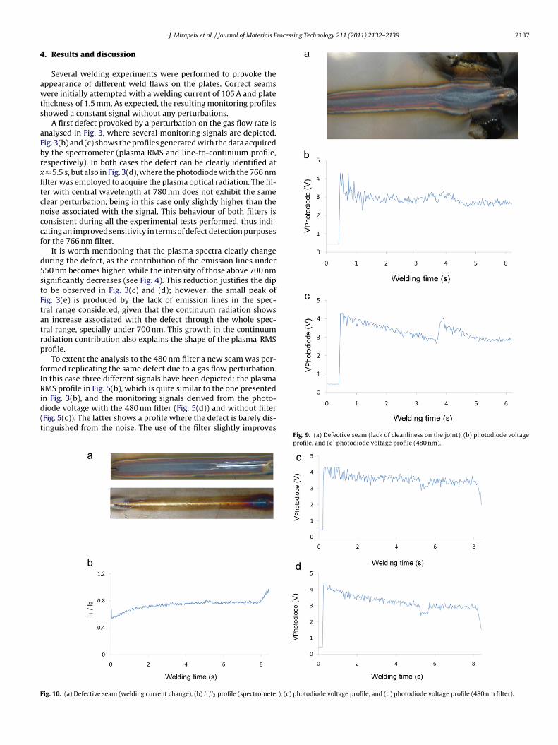
ase will be derived from the plasma continuum radiation. Severalr II lines (476.49, 480.60 and 484.78 nm) (NIST, 2011) are coveredy the spectral response of the 480 nm filter.ig. 8. (a) Defective seam (lack of cleanliness on the joint), (b) I1/I2 profile (spectrometer), (c) line-to-continuum profile, and (d) photodiode voltage profile (780 nm filter).
rocessing Technology 211 (2011) 2132– 2139 2137
4
awts
aFbrxfitcnccf
d5stFtatrp
fIRid(t
F
J. Mirapeix et al. / Journal of Materials P
. Results and discussion
Several welding experiments were performed to provoke theppearance of different weld flaws on the plates. Correct seamsere initially attempted with a welding current of 105 A and plate
hickness of 1.5 mm. As expected, the resulting monitoring profileshowed a constant signal without any perturbations.
A first defect provoked by a perturbation on the gas flow rate isnalysed in Fig. 3, where several monitoring signals are depicted.ig. 3(b) and (c) shows the profiles generated with the data acquiredy the spectrometer (plasma RMS and line-to-continuum profile,espectively). In both cases the defect can be clearly identified at
≈ 5.5 s, but also in Fig. 3(d), where the photodiode with the 766 nmlter was employed to acquire the plasma optical radiation. The fil-er with central wavelength at 780 nm does not exhibit the samelear perturbation, being in this case only slightly higher than theoise associated with the signal. This behaviour of both filters isonsistent during all the experimental tests performed, thus indi-ating an improved sensitivity in terms of defect detection purposesor the 766 nm filter.
It is worth mentioning that the plasma spectra clearly changeuring the defect, as the contribution of the emission lines under50 nm becomes higher, while the intensity of those above 700 nmignificantly decreases (see Fig. 4). This reduction justifies the dipo be observed in Fig. 3(c) and (d); however, the small peak ofig. 3(e) is produced by the lack of emission lines in the spec-ral range considered, given that the continuum radiation showsn increase associated with the defect through the whole spec-ral range, specially under 700 nm. This growth in the continuumadiation contribution also explains the shape of the plasma-RMSrofile.
To extent the analysis to the 480 nm filter a new seam was per-ormed replicating the same defect due to a gas flow perturbation.n this case three different signals have been depicted: the plasmaMS profile in Fig. 5(b), which is quite similar to the one presented
n Fig. 3(b), and the monitoring signals derived from the photo-iode voltage with the 480 nm filter (Fig. 5(d)) and without filterFig. 5(c)). The latter shows a profile where the defect is barely dis-inguished from the noise. The use of the filter slightly improves
Fig. 9. (a) Defective seam (lack of cleanliness on the joint), (b) photodiode voltageprofile, and (c) photodiode voltage profile (480 nm).
ig. 10. (a) Defective seam (welding current change), (b) I1/I2 profile (spectrometer), (c) photodiode voltage profile, and (d) photodiode voltage profile (480 nm filter).
2138 J. Mirapeix et al. / Journal of Materials Process
Fp
toAraatamip
tcs4dfiInsftati
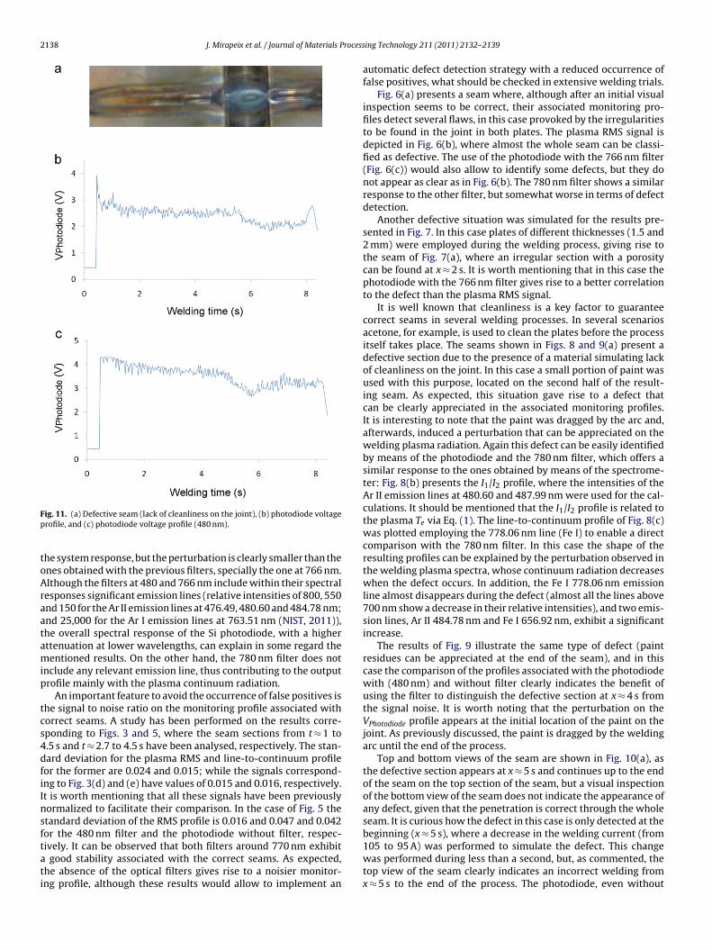
ig. 11. (a) Defective seam (lack of cleanliness on the joint), (b) photodiode voltagerofile, and (c) photodiode voltage profile (480 nm).
he system response, but the perturbation is clearly smaller than thenes obtained with the previous filters, specially the one at 766 nm.lthough the filters at 480 and 766 nm include within their spectralesponses significant emission lines (relative intensities of 800, 550nd 150 for the Ar II emission lines at 476.49, 480.60 and 484.78 nm;nd 25,000 for the Ar I emission lines at 763.51 nm (NIST, 2011)),he overall spectral response of the Si photodiode, with a higherttenuation at lower wavelengths, can explain in some regard theentioned results. On the other hand, the 780 nm filter does not
nclude any relevant emission line, thus contributing to the outputrofile mainly with the plasma continuum radiation.
An important feature to avoid the occurrence of false positives ishe signal to noise ratio on the monitoring profile associated withorrect seams. A study has been performed on the results corre-ponding to Figs. 3 and 5, where the seam sections from t ≈ 1 to.5 s and t ≈ 2.7 to 4.5 s have been analysed, respectively. The stan-ard deviation for the plasma RMS and line-to-continuum profileor the former are 0.024 and 0.015; while the signals correspond-ng to Fig. 3(d) and (e) have values of 0.015 and 0.016, respectively.t is worth mentioning that all these signals have been previouslyormalized to facilitate their comparison. In the case of Fig. 5 thetandard deviation of the RMS profile is 0.016 and 0.047 and 0.042or the 480 nm filter and the photodiode without filter, respec-
ively. It can be observed that both filters around 770 nm exhibitgood stability associated with the correct seams. As expected,he absence of the optical filters gives rise to a noisier monitor-ng profile, although these results would allow to implement an
ing Technology 211 (2011) 2132– 2139
automatic defect detection strategy with a reduced occurrence offalse positives, what should be checked in extensive welding trials.
Fig. 6(a) presents a seam where, although after an initial visualinspection seems to be correct, their associated monitoring pro-files detect several flaws, in this case provoked by the irregularitiesto be found in the joint in both plates. The plasma RMS signal isdepicted in Fig. 6(b), where almost the whole seam can be classi-fied as defective. The use of the photodiode with the 766 nm filter(Fig. 6(c)) would also allow to identify some defects, but they donot appear as clear as in Fig. 6(b). The 780 nm filter shows a similarresponse to the other filter, but somewhat worse in terms of defectdetection.
Another defective situation was simulated for the results pre-sented in Fig. 7. In this case plates of different thicknesses (1.5 and2 mm) were employed during the welding process, giving rise tothe seam of Fig. 7(a), where an irregular section with a porositycan be found at x ≈ 2 s. It is worth mentioning that in this case thephotodiode with the 766 nm filter gives rise to a better correlationto the defect than the plasma RMS signal.
It is well known that cleanliness is a key factor to guaranteecorrect seams in several welding processes. In several scenariosacetone, for example, is used to clean the plates before the processitself takes place. The seams shown in Figs. 8 and 9(a) present adefective section due to the presence of a material simulating lackof cleanliness on the joint. In this case a small portion of paint wasused with this purpose, located on the second half of the result-ing seam. As expected, this situation gave rise to a defect thatcan be clearly appreciated in the associated monitoring profiles.It is interesting to note that the paint was dragged by the arc and,afterwards, induced a perturbation that can be appreciated on thewelding plasma radiation. Again this defect can be easily identifiedby means of the photodiode and the 780 nm filter, which offers asimilar response to the ones obtained by means of the spectrome-ter: Fig. 8(b) presents the I1/I2 profile, where the intensities of theAr II emission lines at 480.60 and 487.99 nm were used for the cal-culations. It should be mentioned that the I1/I2 profile is related tothe plasma Te via Eq. (1). The line-to-continuum profile of Fig. 8(c)was plotted employing the 778.06 nm line (Fe I) to enable a directcomparison with the 780 nm filter. In this case the shape of theresulting profiles can be explained by the perturbation observed inthe welding plasma spectra, whose continuum radiation decreaseswhen the defect occurs. In addition, the Fe I 778.06 nm emissionline almost disappears during the defect (almost all the lines above700 nm show a decrease in their relative intensities), and two emis-sion lines, Ar II 484.78 nm and Fe I 656.92 nm, exhibit a significantincrease.
The results of Fig. 9 illustrate the same type of defect (paintresidues can be appreciated at the end of the seam), and in thiscase the comparison of the profiles associated with the photodiodewith (480 nm) and without filter clearly indicates the benefit ofusing the filter to distinguish the defective section at x ≈ 4 s fromthe signal noise. It is worth noting that the perturbation on theVPhotodiode profile appears at the initial location of the paint on thejoint. As previously discussed, the paint is dragged by the weldingarc until the end of the process.
Top and bottom views of the seam are shown in Fig. 10(a), asthe defective section appears at x ≈ 5 s and continues up to the endof the seam on the top section of the seam, but a visual inspectionof the bottom view of the seam does not indicate the appearance ofany defect, given that the penetration is correct through the wholeseam. It is curious how the defect in this case is only detected at thebeginning (x ≈ 5 s), where a decrease in the welding current (from
105 to 95 A) was performed to simulate the defect. This changewas performed during less than a second, but, as commented, thetop view of the seam clearly indicates an incorrect welding fromx ≈ 5 s to the end of the process. The photodiode, even without
rocess
fisFamsodaauSr
iwva
5
mvgt
•
•
•
ifoiwrIsdo
Wang, Y., Zhao, P., 2001. Noncontact acoustic analysis monitoring of plasma arc
J. Mirapeix et al. / Journal of Materials P
lter, indicates better the defect than the I1/I2 profile, although theignal without the filter is clearly noisier than the one depicted inig. 10(d). An interesting analysis to check the performance of bothlternatives to discriminate the appearance of a defect is the esti-ation of their sensitivity in terms of defect detection (S/N*), as
uggested in (Garcia-Allende et al., 2009). The procedure is basedn the estimation of the signal-to-noise ratio over a section free ofefects; afterwards, the defect detection sensitivity is considereds the difference between the VPhotodiode mean value at the defectnd where the signal indicates a correct seam. Finally, this two val-es are multiplied to generate the S/N* parameter. In this case the/N* for the photodiode with and without filter are 1.03 and 0.62espectively.
This same scenario is again observed in Fig. 11, where the defectn this case was provoked by the use of a plate (bead-on-plate test)
ith an incision orthogonal to the weld direction, thus simulating aariation on the thickness of the plates being welded. As discussedbove, the results are better for the photodiode with filter.
. Conclusions
In this paper it has been demonstrated that an on-line weldingonitoring setup based on a photodiode is able to detect a wide
ariety of welding flaws, what indicates that this solution can be aood alternative in some scenarios. The main results derived fromhis study can be summarized as follows:
The inclusion of optical filters in addition to the photodiode givesrise to an improved monitoring signal in terms of defect detection.In this paper three different filters, with central wavelengths at480, 766 and 780 nm, have been used.The best results have been obtained with the 766 nm filter, dueto the Si-photodiode spectral response and the emission linesincluded in the analysis in each case.The main advantage arising from the use of the photodiodes liesin the great saving in terms of the cost of the whole system: for theoptical setup used in this paper the solution based on photodiodesimplies a reduction of about one order of magnitude.
Some issues remain to be addressed to verify the suitabil-ty of the proposed solution to be employed in a real industrialramework. For instance, an extensive statistical analysis on theccurrence of false positives should be performed, preferably dur-ng field tests. In addition, in terms of the plasma-RMS signal, it
ould be interesting to generate it considering limited spectralanges, thus enabling a correlation with those of the photodiodes.
t would be also interesting to explore the suitability of a featureelection algorithm such as SFFS, already used in on-line weldingiagnostics in (Garcia-Allende et al., 2009), to guide the selectionf the best spectral bands in terms of defect discrimination.ing Technology 211 (2011) 2132– 2139 2139
Acknowledgments
This work has been supported by the project TEC2010-20224-C02-02 and grants AP2009-1403 and AP2007-02230.
References
Ancona, A., Lugara, P.M., Ottonelli, F., Catalano, I.M., 2004. A sensing torch for theon-line monitoring of the gas tungsten arc welding process of steel pipes. Meas.Sci. Technol. 15, 2412–2418.
Ancona, A., Spagnolo, V., Lugara, P.M., Ferrara, M., 2001. Optical sensor for real-timemonitoring of CO2 laser welding process. Appl. Opt. 40 (33), 6019–6025.
Bastiaans, G.J., Mangold, R.A., 1985. The calculation of electron density and tempera-ture in Ar spectroscopic plasmas from continuum and line spectra. Spectrochim.Acta A 40B, 885–892.
Cobo, A., Bardin, F., Mirapeix, J., Hand, D.P., Jones, J.D.C., Lopez-Higuera, J.M., 2005.Optoelectronic device for non-invasive focal point measurement and control ofthe laser welding process. Meas. Sci. Technol. 16 (3), N1–N6.
Connolly, J.O., Beirne, G.J., O’Connor, G.M., Glynn, J.T., Conneely, A.J., 2000. Opti-cal monitoring of laser generated plasma during laser welding. In: HaglundJr., R.F., Wood, R.F. (Eds.), Proceedings of SPIE 3935. San Jose, USA, pp. 132–138.
Ferrara, M., Ancona, A., Lugara, P.M., Sibillano, M., 2000. On-line quality monitoringof welding processes by means of plasma optical spectroscopy. In: Chen, X.,Fujiioka, T., Matsunawa, A. (Eds.), Proc. SPIE. 3888, pp. 750–758.
Garcia-Allende, P.B., Mirapeix, J., Conde, O.M., Cobo, A., Lopez-Higuera, J.M., 2009.Defect detection in arc-welding processes by means of the line-to-continuummethod and feature selection. Sensors 9, 7753–7770.
Griem, H.R., 1997. Principles of Plasma Spectroscopy. Cambridge University Press,Cambridge, pp. 281–283.
Groslier, D., Pellerin, S., Valensi, F., Richard, F., Briand, F., 2011. Explorative approachof the spectral analysis tools to the detection of welding defects in lap welding.Nondestr. Test. Eval. 26 (1), 13–33.
Marotta, A., 1993. Determination of axial thermal plasma temperatures without Abelinversion. J. Phys. D 27, 268–272.
Mirapeix, J., Cobo, A., Conde, O.M., Jaúregui, C., López-Higuera, J.M., 2006. Fastalgorithm for spectral processing with application to on-line welding qualityassurance. Meas. Sci. Technol. 17, 2623–2629.
Mirapeix, J., Cobo, A., Fuentes, J., Davila, M., Etayo, J.M., Lopez-Higuera, J.M., 2009.Use of the plasma spectrum rms signal for arc-welding diagnostics. Sensors 9(7), 5263–5276.
Mirapeix, J., Cobo, A., Fernandez, S., Cardoso, R., Lopez-Higuera, J.M., 2008. Spec-troscopic analysis of the plasma continuum radiation for on-line arc-weldingdefect detection. J. Phys. D 41, 135202–135210.
Mirapeix, J., Cobo, A., González, D.A., Lopez-Higuera, J.M., 2007. Plasma spectroscopyanalysis technique based on optimization algorithms and spectral synthesis.Opt. Express 15, 1884–1897.
NIST, 2011. National Institute of Standards and Technology: Atomic SpectraDatabase Lines Form. http://physics.nist.gov/PhysRefData/ASD/lines form.html.
Sforza, P., de Blasiis, D., 2002. On-line optical monitoring system for arc welding.NDT E Int. 35, 37–43.
Sibillano, T., Ancona, A., Berardi, V., Schingaro, E., Parente, P., Lugara, P.M., 2006.Correlation spectroscopy as a tool for detecting losses of ligand elements inlaser welding of aluminium alloys. Opt. Lasers Eng. 44, 1324–1335.
Vilarinho, L.O., Scotti, A., 2004. Proposal for a modified Fowler-Milne method todetermine the temperature profile in TIG welding at low currents. J. Braz. Soc.Mech. Sci. Eng. 26, 34–39.
welding. Int. J. Press. Vessels Piping 78 (1), 43–47.Zhang, G.J., Yan, Z.H., Wu, L., 2006. Visual sensing of weld pool in variable polarity TIG
welding of aluminium alloy. Trans. Nonferrous Met. Soc. China (English Edition)16 (3), 522–526.