
Design of AHB to APB Bridge - BVM Engineering College
45
Page 1 of 45 Design of AHB to APB Bridge Project Report Submitted by Rutvik Dholiya (16EL032) In fulfilment of the completion of work for the course EL446 : Industry Defined Project/Training Under the guidance of Prof. Chintan S. Patel (Electronics Department, BVM) Mr. Vinod A. (eITRA, eInfochips pvt. Ltd.) Electronics Department Birla Vishvakarma Mahavidyalaya Engineering College 2019-’20
-
Upload
khangminh22 -
Category
Documents
-
view
0 -
download
0
Transcript of Design of AHB to APB Bridge - BVM Engineering College

Page 1 of 45
Design of AHB to APB Bridge
Project Report
Submitted by
Rutvik Dholiya (16EL032)
In fulfilment of the completion of work for the course
EL446 : Industry Defined Project/Training
Under the guidance of
Prof. Chintan S. Patel (Electronics Department, BVM)
Mr. Vinod A. (eITRA, eInfochips pvt. Ltd.)
Electronics Department
Birla Vishvakarma Mahavidyalaya Engineering College
2019-’20

Page 2 of 45
Birla Vishvakarma Mahavidyalaya Engineering College
Electronics Department
2019-’20
CERTIFICATE
Date :
This is to certify that the dissertation entitled “Design of AHB to APB
Bridge” has been completed by Rutvik Dholiya under my guidance in
fulfilment of completetion of work for the course EL446 – Industry
Defined Project/Training offered in the 8th semester of B.Tech.
Electronics by Electronics Department, BVM Engineering College during
the academic year 2019-’20.
Guide :

Page 3 of 45
ACKNOWLEDGEMENT
I would like to highly acknowledge all associates who guided and
supported me throughout my project, Design of AHB to APB Bridge. I
would like to express sincere thanks to the project guides Prof. C. S. Patel
and Mr. Vinod A. for their valuable guidance and advice, insightful
comments and suggessions.
This project is dedicated to all those who contributed for its completion.

Page 4 of 45
ABSTRACT
The Advanced Microcontroller Bus Architecture (AMBA) is an open
System-on-Chip bus protocol for high performance buses to
communicate with low-power devices. In the AMBA High-performance
Bus (AHB) a system bus is used to connect a processor, a DSP, and
high-performance memory controllers where as the AMBA Advanced
Peripheral Bus (APB) is used to connect (Universal Asynchronous
Receiver Transmitter) UART. It also contains a Bridge, which connects
the AHB and APB buses. Bridges are standard bus-to-bus interfaces that
allow IPs connected to different buses to communicate with each other
in a standardized way.
In this project, I have developed synthesizable design of AHB2APB
bridge and testbench for the functional verification of the same in
verilog HDL. I have also written shell script for testing the required
feature only at a time. The software tools that I have used are GVim
(Text Editor), Icarus Verilog 10.3 (Verilog Compiler and Simulator) and
Yosys (Open-Source Synthesizer tool).

Page 5 of 45
List of Figures
_______________________________________________________
Figure No. Figure Description Page No.
1-1 AHB block diagram 10 1-2 AHB master interface 10 1-3 AHB slave interface 11 1-4 ARM Architecture 13 1-5 AHB to APB Bridge block diagram 14 2-1 Bridge module system diagram 20 2-2 AHB to APB transfer state machine 22 3-1 Single read transfer 42 3-2 Single write transfer 42 3-3 Burst read transfer 43 3-4 Burst write transfer 43

Page 6 of 45
Contents
Acknowledgement...................................................................................................3Abstract....................................................................................................................4Chapter 1 Introduction & Theoretical Background
1.1 ARM...............................................................................................7
1.2 ARM AMBA....................................................................................8
1.3 AHB (AMBA High-performance Bus)…..........................................9
1.4 APB (Advanced Peripheral Bus)…................................................12
1.5 AHB to APB Bridge.......................................................................13
Chapter 2 Design
2.1 Bridge Module Description.........................................................20
2.2 Bridge Functional Description.....................................................26
Chapter 3 Implementation
3.1 Software tools used.....................................................................28
3.2 AHB to APB bridge design code..................................................28
3.3 Testbench Code...........................................................................34
3.4 SHELL Script.................................................................................41
Chapter 4 Summary
4.1 Simulation Results.......................................................................42
4.2 Conclusion...................................................................................44
References............................................................................................................45

Page 7 of 45
Chapter 1 : Introduction & Theoretical Background
1.1 ARM :
Acorn RISC Machine, is a family of reduced instruction set computing (RISC)
architectures for computer processors, configured for various environments. Arm
Holdings develops the architecture and licenses it to other companies, who design
their own products that implement one of those architectures including systems-on-
chips (SoC) and systems-on-modules (SoM) that incorporate memory, interfaces,
radios, etc. It also designs cores that implement this instruction set and licenses these
designs to a number of companies that incorporate those core designs into their own
products.
Processors that have a RISC architecture typically require fewer transistors than
those with a complex instruction set computing (CISC) architecture (such as the x86
processors found in most personal computers), which improves cost, power
consumption, and heat dissipation. These characteristics are desirable for light,
portable, battery-powered devices—including smartphones, laptops and tablet
computers, and other embedded systems but are also useful for servers and desktops
to some degree. For supercomputers, which consume large amounts of electricity,
Arm is also a power-efficient solution.
Arm Holdings periodically releases updates to the architecture. Architecture
versions Armv3 to Armv7 support 32-bit address space (pre-Armv3 chips, made
before Arm Holdings was formed, as used in the Acorn Archimedes, had 26-bit
address space) and 32-bit arithmetic; most architectures have 32-bit fixed-length
instructions. The Thumb version supports a variable-length instruction set that
provides both 32- and 16-bit instructions for improved code density. Some older
cores can also provide hardware execution of Java bytecodes; and newer ones have
one instruction for JavaScript. Released in 2011, the Armv8-A architecture added
support for a 64-bit address space and 64-bit arithmetic with its new 32-bit fixed-
length instruction set.

Page 8 of 45
Some recent Arm CPUs have simultaneous multithreading (SMT) with e.g. Arm
Neoverse E1 being able to execute two threads concurrently for improved aggregate
throughput performance. Arm Cortex-A65AE for automotive applications is also a
multithreaded processor, and has Dual Core Lock-Step for fault-tolerant designs
(supporting Automotive Safety Integrity Level D, the highest level). The Neoverse
N1 is designed for "as few as 8 cores" or "designs that scale from 64 to 128 N1 cores
within a single coherent system.
1.2 ARM AMBA :
AMBA (Advanced Microcontroller Bus Architecture) is a freely-available, open
standard for the connection and management of functional blocks in a system-on-
chip (SoC). It facilitates right-first-time development of multi-processor designs,
with large numbers of controllers and peripherals.
AMBA specifications are royalty-free, platform-independent and can be used with
any processor architecture. Due to its widespread adoption, AMBA has a robust
ecosystem of partners that ensures compatibility and scalability between IP
components from different design teams and vendors.

Page 9 of 45
1.3 AHB (AMBA High-performance Bus) :
AMBA AHB is a bus interface suitable for high-performance synthesizable
designs. It defines the interface between components, such as masters,
interconnects, and slaves.
AMBA AHB implements the features required for high-performance, high clock
frequency systems including:
• Burst transfers.
• Single clock-edge operation.
• Non-tristate implementation.
• Wide data bus configurations, 64, 128, 256, 512, and 1024 bits.
The most common AHB slaves are internal memory devices, external memory
interfaces, and high-bandwidth peripherals. Although low-bandwidth peripherals
can be included as AHB slaves, for system performance reasons, they typically
reside on the AMBA Advanced Peripheral Bus (APB). Bridging between the
higher performance AHB and APB is done using an AHB slave, known as an APB
bridge.

Page 10 of 45
Figure 1-1 AHB block diagram
Figure 1-1 shows a single master AHB system design with the AHB master and
three AHB slaves. The bus interconnect logic consists of one address decoder and
a slave-to-master multiplexor. The decoder monitors the address from the master
so that the appropriate slave is selected and the multiplexor routes the
corresponding slave output data back to the master. AHB also supports multi-
master designs by the use of an interconnect component that provides arbitration
and routing signals from different masters to the appropriate slaves.
1.3.1 AHB Master Inteface :
Figure 1-2 AHB master interface
A master provides address and control information to initiate read and write
operations. Figure 1-2 shows a master interface.

Page 11 of 45
1.3.2 AHB Slave Interface :
Figure 1-3 AHB slave interface
A slave responds to transfers initiated by masters in the system. The slave uses the
HSELx select signal from the decoder to control when it responds to a bus transfer.
The slave signals back to the master:
• The completion or extension of the bus transfer.
• The success or failure of the bus transfer.
Figure 1-3 shows a slave interface.

Page 12 of 45
1.4 APB (Advanced Peripheral Bus) :
The Advanced Peripheral Bus (APB) is part of the Advanced Microcontroller Bus
Architecture (AMBA) protocol family. It defines a low-cost interface that is
optimized for minimal power consumption and reduced interface complexity.
The APB protocol is not pipelined, use it to connect to low-bandwidth peripherals
that do not require the high performance of the AXI protocol.
The APB protocol relates a signal transition to the rising edge of the clock, to
simplify the integration of APB peripherals into any design flow. Every transfer
takes at least two cycles.
The APB can interface with:
• AMBA Advanced High-performance Bus (AHB)
• AMBA Advanced High-performance Bus Lite (AHB-Lite)
• AMBA Advanced Extensible Interface (AXI)
• AMBA Advanced Extensible Interface Lite (AXI4-Lite)
You can use it to access the programmable control registers of peripheral devices.

Page 13 of 45
1.5 AHB to APB Bridge :
The AHB to APB bridge interface is an AHB slave. When accessed (in normal
operation or system test) it initiates an access to the APB. APB accesses are of
different duration (three HCLK cycles in the EASY for a read, and two cycles for a
write). They also have their width fixed to one word, which means it is not possible
to write only an 8-bit section of a 32-bit APB register. APB peripherals do not need
a PCLK input as the APB access is timed with an enable signal generated by the
AHB to APB bridge interface. This makes APB peripherals low power consumption
parts, because they are only strobed when accessed.
1.5.1 Importance :
Figure 1-4 ARM Architecture
The AHB to APB bridge is an AHB slave, providing an interface between the high
speed AHB and the low-power APB. Read and write transfers on the AHB are
converted into equivalent transfers on the APB. As the APB is not pipelined, then
wait states are added during transfers to and from the APB when the AHB is
required to wait for the APB.

Page 14 of 45
It is required to bridge the communication gap between low bandwidth peripherals
on APB with the high bandwidth ARM Processors and/or other high-speed devices
on AHB. This ensures that there is no data loss between AHB to APB or APB to
AHB data transfers. AHB2APB interfaces AHB and APB. It buffers address,
controls and data from the AHB, drives the APB peripherals and return data along
with response signal to the AHB.
The AHB2APB interface is designed to operate when AHB and APB clocks have
the any combination of frequency and phase. TheAHB2APB performs transfer of
data from AHB to APB for write cycle and APB to AHB for Read cycle. Interface
between AMBA high performance bus (AHB) and AMBA peripheral bus (APB).
It provides latching of address, controls and data signals for APB peripherals.
1.5.2 Architecture :
Figure 1-5 AHB to APB Bridge block diagram
The main sections of this module are:
• AHB slave bus interface
• APB transfer state machine, which is independent of the device memory map
• APB output signal generation.

Page 15 of 45
To add new APB peripherals, or alter the system memory map, only the address
decode sections need to be modified.
The base addresses of each of the peripherals (timer, interrupt controller, and
remap and pause controller) are defined in the AHB to APB bridge interface,
which selects the peripheral according to its base address. The whole APB address
range is also defined in the bridge.
These base addresses can be implementation-specific. The peripherals standard
specifies only the register offsets (from an unspecified base address), register bit
meaning, and minimum supported function
The APB data bus is split into two separate directions:
• read (PRDATA), where data travels from the peripherals to the bridge
• write (PWDATA), where data travels from the bridge to the peripherals.
This simplifies driving the buses because turnaround time between the peripherals
and bridge is avoided.
In the default system, because the bridge is the only master on the bus, PWDATA
is driven continuously. PRDATA is a multiplexed connection of all peripheral
PRDATA outputs on the bus, and is only driven when the slaves are selected by
the bridge during APB read transfers.
It is possible to combine these two buses into a single bidirectional bus, but
precautions must be taken to ensure that there is no bus clash between the bridge
and the peripherals.

Page 16 of 45
1.5.3 Signals Description :
Signals Type Direction Description
HCLK Bus clock Input This clock times all bus transfers.
HRESETn Reset Input The bus reset signal is active LOW, and is used
to reset the system and the bus.
HADDR[31:0] Address bus Input The 32-bit system address bus.
HTRANS[1:0] Transfer type Input This indicates the type of the current transfer,
which can be NONSEQUENTIAL,
SEQUENTIAL, IDLE or BUSY.
HWRITE Transfer
direction
Input When HIGH this signal indicates a write
transfer, and when LOW, a read transfer.
HWDATA[31:0] Write data
bus
Input The write data bus is used to transfer data from
the master to the bus slaves during write
operations. A minimum data bus width of 32
bits is recommended. However, this may easily
be extended to allow for higher bandwidth
operation.
HSELAPBif Slave select Input Each APB slave has its own slave select signal,
and this signal indicates that the current
transfer is intended for the selected slave. This
signal is a combinatorial decode of the address
bus.
HRDATA[31:0] Read data
bus
Output The read data bus is used to transfer data from
bus slaves to the bus master during read
operations. A minimum data bus width of 32
bits is recommended. However, this may easily
be extended to allow for higher bandwidth
operation.

Page 17 of 45
HREADYin
HREADYout
Transfer done Input/outp
ut
When HIGH the HREADY signal indicates
that a transfer has finished on the bus. This
signal may be driven LOW to extend a transfer.
HRESP[1:0] Transfer
response
Output The transfer response provides additional
information on the status of a transfer. This
module will always generate the OKAY
response.
PRDATA[31:0] Peripheral
read data bus
Input The peripheral read data bus is driven by the
selected peripheral bus slave during read
cycles (when PWRITE is LOW).
PWDATA[31:0] Peripheral
write data
bus
Output The peripheral write data bus is continuously
driven by this module, changing during write
cycles (when PWRITE is HIGH).
PENABLE Peripheral
enable
Output This enable signal is used to time all accesses
on the peripheral bus. PENABLE goes HIGH
on the second clock rising edge of the transfer,
and LOW on the third (last) rising clock edge
of the transfer.
PSELx Peripheral
slave select
Output There is one of these signals for each APB
peripheral present in the system. The signal
indicates that the slave device is selected, and
that a data transfer is required. It has the same
timing as the peripheral address bus. It
becomes HIGH at the same time as PADDR,
but will be set LOW at the end of the transfer.

Page 18 of 45
PADDR[31:0] Peripheral
address bus
Output This is the APB address bus, which may be up
to 32 bits wide and is used by individual
peripherals for decoding register accesses to
that peripheral. The address becomes valid
after the first rising edge of the clock at the start
of the transfer. If there is a following APB
transfer, then the address will change to the
new value, otherwise it will hold its current
value until the start of the next APB transfer.
PWRITE Peripheral
transfer
direction
Output This signal indicates a write to a peripheral
when HIGH, and a read from a peripheral
when LOW.
It has the same timing as the peripheral address
bus.

Page 19 of 45
The APB bridge responds to transaction requests from the currently granted AHB
master. The AHB transactions are then converted into APB transactions.
• the AHB transactions with the HREADYout signal
• the generation of all APB output signals.
The individual PSELx signals are decoded from HADDR, using the state machine
to enable the outputs while the APB transaction is being performed.
If an undefined location is accessed, operation of the system continues as normal,
but no peripherals are selected.

Page 20 of 45
Chapter 2 : Design
2.1 Bridge Module Description :
Figure 2-1 Bridge module system diagram

Page 21 of 45
The AHB to APB bridge comprises a state machine, which is used to control the
generation of the APB and AHB output signals, and the address decoding logic
which is used to generate the APB peripheral select lines.
All registers used in the system are clocked from the rising edge of the system clock
HCLK, and use the asynchronous reset HRESETn.
2.1.1 AHB slave bus interface :
This module uses the standard AHB slave bus interface, which comprises:
• the valid transfer detection logic which is used to determine when a valid transfer
is accessing the slave.
• the address and control registers, which are used to store the information from the
address phase of the transfer for use in the data phase.
Due to the different AHB to APB timing of read and write transfers, either the
current or the previous address input value is needed to correctly generate the APB
transfer. A multiplexor is therefore used to select between the current address input
or the registered address, for read and write transfers respectively.

Page 22 of 45
2.1.2 APB transfer state machine :
Figure 2-2 AHB to APB transfer state machine
The transfer state machine is used to control the application of APB transfers based
on the AHB inputs. The state diagram in Figure 2-2 shows the operation of the state
machine, which is controlled by its current state and the AHB slave interface.

Page 23 of 45
The individual states of the state machine operation are described in the following
sections:
ST_IDLE :-
During this state the APB buses and PWRITE are driven with the last values they
had and PSEL and PENABLE lines are driven LOW.
The ST_IDLE state is entered from:
• reset, when the system is initialized
• ST_RENABLE, ST_WENABLE, or ST_IDLE, when there are no peripheral
transfers to perform.
The next state is:
• ST_READ, for a read transfer, when the AHB contains a valid APB read transfer
• ST_WWAIT, for a write transfer, when the AHB contains a valid APB write
transfer.
ST_READ :-
During this state the address is decoded and driven onto PADDR, the relevant PSEL
line is driven HIGH, and PWRITE is driven LOW. A wait state is always inserted
to ensure that the data phase of the current AHB transfer does not complete until the
APB read data has been driven onto HRDATA.
The ST_READ state is entered from ST_IDLE, ST_RENABLE, ST_WENABLE,
or ST_WENABLEP during a valid read transfer.
The next state will always be ST_RENABLE.
ST_WWAIT
This state is needed due to the pipelined structure of AHB transfers, to allow the
AHB side of the write transfer to complete so that the write data becomes available
on HWDATA. The APB write transfer is then started in the next clock cycle.
The ST_WWAIT state is entered from ST_IDLE, ST_RENABLE, or
ST_WENABLE, during a valid write transfer.
The next state will always be ST_WRITE.

Page 24 of 45
ST_WRITE :-
During this state the address is decoded and driven onto PADDR, the relevant PSEL
line is driven HIGH, and PWRITE is driven HIGH.
A wait state is not inserted, as a single write transfer can complete without affecting
the AHB.
The ST_WRITE state is entered from:
• ST_WWAIT, when there are no further peripheral transfers to perform
• ST_WENABLEP, when the currently pending peripheral transfer is a write, and
there are no further transfers to perform.
The next state is:
• ST_WENABLE, when there are no further peripheral transfers to perform
• ST_WENABLEP, when there is one further peripheral write transfer to perform.
ST_WRITEP :-
During this state the address is decoded and driven onto PADDR, the relevant PSEL
line is driven HIGH, and PWRITE is driven HIGH. A wait state is always inserted,
as there must only ever be one pending transfer between the currently performed
APB transfer and the currently driven AHB transfer.
The ST_WRITEP state is entered from:
• ST_WWAIT, when there is a further peripheral transfer to perform.
• ST_WENABLEP, when the currently pending peripheral transfer is a write, and
there is a further transfer to perform.
The next state will always be ST_WENABLEP.
ST_RENABLE :-
During this state the PENABLE output is driven HIGH, enabling the current APB
transfer. All other APB outputs remain the same as the previous cycle.
The ST_RENABLE state is always entered from ST_READ.

Page 25 of 45
The next state is:
• ST_READ, when there is a further peripheral read transfer to perform.
• ST_WWAIT, when there is a further peripheral write transfer to perform.
• ST_IDLE, when there are no further peripheral transfers to perform.
ST_WENABLE :-
During this state the PENABLE output is driven HIGH, enabling the current APB
transfer. All other APB outputs remain the same as the previous cycle.
The ST_WENABLE state is always entered from ST_WRITE.
The next state is:
• ST_READ, when there is a further peripheral read transfer to perform.
• ST_WWAIT, when there is a further peripheral write transfer to perform.
• ST_IDLE, when there are no further peripheral transfers to perform.
ST_WENABLEP :-
A wait state is inserted if the pending transfer is a read because, when a read follows
a write, an extra wait state must be inserted to allow the write transfer to complete
on the APB before the read is started.
The ST_WENABLEP state is entered from:
• ST_WRITE, when the currently driven AHB transfer is a peripheral transfer.
• ST_WRITEP, when there is a pending peripheral transfer following the current
write.
The next state is:
• ST_READ, when the pending transfer is a read.
• ST_WRITE, when the pending transfer is a write, and there are no further transfers
to perform.
• ST_WRITEP, when the pending transfer is a write.

Page 26 of 45
2.2 Bridge Functional Description :
2.2.1 APB output signal generation :
The generation of all APB output signals is based on the status of the transfer state
machine:
• PWDATA is a registered version of the HWDATA input, which is only enabled
during a write transfer. As the bridge is the only bus master on the APB, then it can
drive PWDATA continuously.
• PENABLE is only set HIGH during one of three enable states, in the last cycle of
an APB transfer. A register is used to generate this output from the next state of the
transfer state machine.
• PSELx outputs are decoded from the current transfer address. They are only valid
during the read, write and enable states, and are all driven LOW at all other times so
that no peripherals are selected when no transfers are being performed.
• PADDR is a registered version of the currently selected address input (HADDR or
the address register) and only changes when the read and write states are entered at
the start of the APB transfer.
• PWRITE is set HIGH during a write transfer, and only changes when a new APB
transfer is started. A register is used to generate this output from the next state of the
transfer state machine.
• The APBen signal is used as an enable on the PSEL, PWRITE and PADDR output
registers, ensuring that these signals only change when a new APB transfer is started,
when the next state is ST_READ, ST_WRITE, or ST_WRITEP.

Page 27 of 45
2.2.2 AHB output signal generation :
HRDATA is directly driven with the current value of PRDATA. APB slaves only
drive read data during the enable phase of the APB transfer, with PRDATA set LOW
at all other times, so bus clash is avoided on HRDATA (assuming OR bus
connections for both the AHB and APB read data buses).
• HREADYout is driven with a registered signal to improve the output timing. Wait
states are inserted by the APB bridge during the ST_READ and ST_WRITEP states,
and during the ST_WENABLEP state when the next transfer to be performed is a
read.
• HRESP is continuously held LOW, as the APB bridge does not generate SPLIT,
RETRY or ERROR responses.

Page 28 of 45
Chapter 3 : Implementation
3.1 Software tools used :
1. GVim (Text Editor) 2. Icarus Verilog (Verilog Compilation and Simulation) 3. GTKWave (Wavefom Visualizer)
3.2 AHB to APB bridge design code :
`define IDLE 3'b000
`define READ 3'b001
`define WWAIT 3'b010
`define WRITE 3'b011
`define WRITEP 3'b100
`define WENABLE 3'b101
`define WENABLEP 3'b110
`define RENABLE 3'b111
`timescale 1ns/1ps
module ahb2apb(HCLK, HRESETn, HSELAPB, HADDR, HWRITE, HTRANS,
HWDATA, HRESP, HRDATA, HREADY, PRDATA, PSEL, PENABLE,
PADDR, PWRITE, PWDATA);
//----------------------AHB Slave Interface---------------------
input wire HCLK, HRESETn, HSELAPB, HWRITE;
input wire [1:0]HTRANS;
input wire [31:0]HADDR, HWDATA;
output reg HRESP, HREADY;
output reg [31:0]HRDATA;

Page 29 of 45
//-----------------------APB Output Signals---------------------
input wire [31:0]PRDATA;
output reg PSEL, PENABLE, PWRITE;
output reg [31:0]PADDR, PWDATA;
//---------------------Implementation signals-------------------
reg [31:0]TMP_HADDR, TMP_HWDATA;
reg [2:0] ps,ns;
reg valid, HWrite;
always @(*)
begin
//------------------Valid logic--------------------
if (HSELAPB==1'b1 && (HTRANS==2'b10 || HTRANS==2'b11))
valid=1'b1;
else
valid=1'b0;
if(HRESETn==1'b0) //Asynchronous Active-low Reset
ns=`IDLE;
HRESP=1'b0; //Always OKAY Response
end
always @(posedge HCLK)
begin
ps=ns;
end
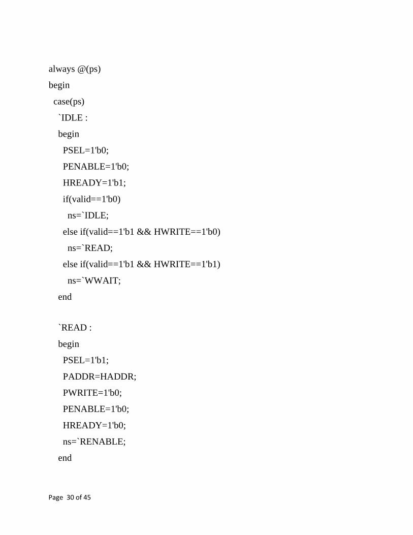
Page 30 of 45
always @(ps)
begin
case(ps)
`IDLE :
begin
PSEL=1'b0;
PENABLE=1'b0;
HREADY=1'b1;
if(valid==1'b0)
ns=`IDLE;
else if(valid==1'b1 && HWRITE==1'b0)
ns=`READ;
else if(valid==1'b1 && HWRITE==1'b1)
ns=`WWAIT;
end
`READ :
begin
PSEL=1'b1;
PADDR=HADDR;
PWRITE=1'b0;
PENABLE=1'b0;
HREADY=1'b0;
ns=`RENABLE;
end

Page 31 of 45
`WWAIT :
begin
PENABLE=1'b0;
TMP_HADDR=HADDR;
HWrite=HWRITE;
if(valid==1'b0)
ns=`WRITE;
else if(valid==1'b1)
ns=`WRITEP;
end
`WRITE :
begin
PSEL=1'b1;
PADDR=TMP_HADDR;
PWDATA=HWDATA;
PWRITE=1'b1;
PENABLE=1'b0;
HREADY=1'b0;
if(valid==1'b0)
ns=`WENABLE;
else if(valid==1'b1)
ns=`WENABLEP;
end
`WRITEP :
begin

Page 32 of 45
PSEL=1'b1;
PADDR=TMP_HADDR;
PWDATA=HWDATA;
PWRITE=1'b1;
PENABLE=1'b0;
HREADY=1'b0;
TMP_HADDR=HADDR;
HWrite=HWRITE;
ns=`WENABLEP;
end
`WENABLE :
begin
PENABLE=1'b1;
HREADY=1'b1;
if(valid==1'b1 && HWRITE==1'b0)
ns=`READ;
else if(valid==1'b1 && HWRITE==1'b1)
ns=`WWAIT;
else if(valid==1'b0)
ns=`IDLE;
end
`WENABLEP :
begin
PENABLE=1'b1;
HREADY=1'b1;

Page 33 of 45
if(valid==1'b0 && HWrite==1'b1)
ns=`WRITE;
else if(valid==1'b1 && HWrite==1'b1)
ns=`WRITEP;
else if(HWrite==1'b0)
ns=`READ;
end
`RENABLE :
begin
PENABLE=1'b1;
HRDATA=PRDATA;
HREADY=1'b1;
if(valid==1'b1 && HWRITE==1'b0)
ns=`READ;
else if(valid==1'b1 && HWRITE==1'b1)
ns=`WWAIT;
else if(valid==1'b0)
ns=`IDLE;
end
endcase
end
endmodule

Page 34 of 45
♦ In the AHB to APB bridge design module, I have used some local signals.
The description of these signals is given below : 1. ns : Refers to the next state. 2. ps : Refers to the present state. 3. valid : The bridge only performs operation if the valid signal is high,
when the bridge is selected by HSELAPB signal and also the AHB
transfer type is NONSEQ or SEQ. 4. TMP_HADDR, TMP_HWRITE : Both the signals holds the address
and the transfer direction information of the pending transfer
respectively.
3.3 Testbench Code :
`timescale 1ns/1ps
module tb;
//----------------------AHB Slave Interface---------------------
reg HCLK, HRESETn, HSELAPB, HWRITE;
reg [1:0]HTRANS;
reg [31:0]HADDR, HWDATA;
wire HRESP;
wire [31:0]HRDATA;
//-----------------------APB Output Signals---------------------
reg [31:0]PRDATA;
wire PSEL, PENABLE, PWRITE, HREADY;
wire [31:0]PADDR, PWDATA;
always #1 HCLK=~HCLK;

Page 35 of 45
`ifdef Single_Read
initial
begin
$dumpfile("Single_Read.vcd");
$dumpvars;
end
initial
begin
//--------------------Single Read Transfer--------------------
HCLK=1'b1;
HRESETn=1'b0;
#2 HRESETn=1'b1;
HWRITE=1'b0;
HSELAPB=1'b1;
HTRANS=2'b10;
HADDR=32;
#2.1 HWRITE=1'bx;
HSELAPB=1'b0;
HTRANS=2'bxx;
HADDR=32'hxxxx_xxxx;
#1.9 PRDATA=16;
#2 $finish;
end
`endif

Page 36 of 45
`ifdef Single_Write
initial
begin
$dumpfile("Single_Write.vcd");
$dumpvars;
end
initial
begin
//--------------------Single WRITE Transfer--------------------
HCLK=1'b1;
HRESETn=1'b0;
#2 HRESETn=1'b1;
HWRITE=1'b1;
HSELAPB=1'b1;
HTRANS=2'b10;
HADDR=32'h0000_0000;
#2 HWDATA=32'h0000_00ff;
HSELAPB=1'b0;
#0.1 HWRITE=1'bx;
HTRANS=2'bxx;
HADDR=32'hxxxx_xxxx;
#6 $finish;
end
`endif

Page 37 of 45
`ifdef Burst_Read
initial
begin
$dumpfile("Burst_Read.vcd");
$dumpvars;
end
initial
begin
//--------------------Burst Read Transfer--------------------
HCLK=1'b1;
HRESETn=1'b0;
#2 //IDLE State
HRESETn=1'b1;
HWRITE=1'b0;
HSELAPB=1'b1;
HTRANS=2'b10;
HADDR=32'h0000_0000;
#2.1 //READ State
HTRANS=2'b11;
HADDR=32'h0000_0100;
#1.9 //RENABLE State
PRDATA=32'hFFFF_FFFF;
#2.1
HADDR=32'h0000_1000;
#1.9

Page 38 of 45
PRDATA=32'hFFFF_FFFB;
#2.1
HADDR=32'h0000_1100;
#1.9
PRDATA=32'hFFFF_FFF8;
#2.1
HWRITE=1'bx;
HADDR=32'hxxxx_xxxx;
HTRANS=2'bxx;
HSELAPB=1'bx;
#1.9
PRDATA=32'hFFFF_FFF4;
#6 $finish;
end
`endif
`ifdef Burst_Write
initial
begin
$dumpfile("Burst_Write.vcd");
$dumpvars;
end
initial
begin
//--------------------Burst WRITE Transfer--------------------

Page 39 of 45
HCLK=1'b1;
HRESETn=1'b0;
#2 //IDLE State
HRESETn=1'b1;
HWRITE=1'b1;
HSELAPB=1'b1;
HTRANS=2'b10;
HADDR=32'h0000_0000;
#2.1 //WWAIT State
HWDATA=32'h0000_000F;
HADDR=32'h0000_0100;
HTRANS=2'b11;
#2 //WRITEP State
HWDATA=32'h0000_00F0;
HADDR=32'h0000_1000;
#4; //WENABLE State
HWDATA=32'h0000_0F00;
HADDR=32'h0000_1100;
#4
HWDATA=32'h0000_F000;
HADDR=32'hxxxx_xxxx;
HWRITE=1'bx;
HSELAPB=1'bx;
HTRANS=2'bxx;
#4

Page 40 of 45
HWDATA=32'hxxxx_xxxx;
#8 $finish;
end
`endif
ahb2apb DUT(HCLK, HRESETn, HSELAPB, HADDR, HWRITE, HTRANS,
HWDATA, HRESP, HRDATA, HREADY, PRDATA, PSEL, PENABLE,
PADDR, PWRITE, PWDATA);
endmodule
__________________________________________________________________
♦ In the testbench code, I have used `ifdef compiler directive, so that the user
can be allowed to simulate the required feature(s) only out of the four
features mentioned below.
1. Single_Read 2. Single_Write
3. Burst_Read
4. Burst_Write

Page 41 of 45
3.4 SHELL Script :
#!/bin/bash
#iverilog -o out.vvp AHB2APB.v AHB2APB_tb.v -D Single_Read
#iverilog -o out.vvp AHB2APB.v AHB2APB_tb.v -D Single_Write
#iverilog -o out.vvp AHB2APB.v AHB2APB_tb.v -D Burst_Read
iverilog -o out.vvp AHB2APB.v AHB2APB_tb.v -D Burst_Write
vvp out.vvp
#gtkwave Single_Read.vcd
#gtkwave Single_Write.vcd
#gtkwave Burst_Read.vcd
gtkwave Burst_Write.vcd
__________________________________________________________________
♦ There are three commmands basically in the above shell script.
1. iverilog... for compilation.
2. Vvp... for simulation.
3. gtkwave... for waveform visualization. ♦ User can remove # (comment symbol) as per the requirement.

Page 42 of 45
Chapter 4 : Summary
4.1 Simulation Results :
Figure 3-1 Single read transfer
Figure 3-2 Single write transfer

Page 43 of 45
Figure 3-3 Burst read transfer
Figure 3-4 Burst write transfer

Page 44 of 45
4.2 Conclusion :
The development of the synthesizable AHB to APB Bridge in verilog HDL was
done. The HCLK and PENABLE mechanism was implemented for making it the
low-power consuming system. The functional verification of the bridge was done by
driving various testcases to the design for testing the features. The multimaster and
multislave AHB to APB bridge is one of the future scope.

Page 45 of 45
References :
[1] ARM AMBA 5 AHB Protocol Specification, ARM.
[2] AMBA APB Protocol (Version 2.0), ARM.
[3] AHB Example AMBA SYstem (Technical Reference Manual), ARM.
[4] Capital Microelectronics, Inc., “AHB2APB Bridge User Guide”.
[5] Aparna Kharade and V. Jayashree, “VLSI Design of AMBA based
AHB2APB Bridge”, International Journal of VLSI design & Communication
Systems (VLSICS) Vol.9, No.3, June 2018.
[6] Vani R. M. and M. Roopa, “Design of AMBA based AHB2APB Bridge”,
IJCSNS International Journal of Computer Science and Network Security, VOL.10
No.11, November 2010.
[7] https://developer.arm.com/architectures/system-architectures/amba
[8] https://www.arm.com/products/silicon-ip-system/embedded-system-
design/amba-specifications
[9] https://en.wikipedia.org/wiki/Advanced_Microcontroller_Bus_Architecture
[10] https://en.wikipedia.org/wiki/Advanced_Microcontroller_Bus_Architecture
[11] http://paper.ijcsns.org/07_book/201011/20101104.pdf
[12] Prof. Ravi Mohan Sairam and Prof. Sumit Sharma, “FSM & Handshaking
based AHB to APB Bridge for High Speed Systems”, International Journal of
Engineering Research & Technology (IJERT) Vol. 2 Issue 11, November – 2013.