Design and l'recess Considerations for a Tunneling Tip ...
19
-
Upload
khangminh22 -
Category
Documents
-
view
1 -
download
0
Transcript of Design and l'recess Considerations for a Tunneling Tip ...

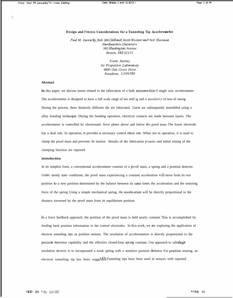
From: Paul M. Zavracky 10: l-rank Harlley Dale: 319195 1 Ime: 15:42.? I Page 1 0118
*
.
‘,
Design and l’recess Considerations for a Tunneling Tip Accckrometer
Paul M. Zawacky Bob McClella)ldt Keith Warner and Neil Sh~~ma)~Noriheastem U}~iversi(y360 Huntingtot7 Avenue
Boston, h!A 02115
Frank HartleyJet Propulsion Laboratc,ry
4800 Oak Grove DrivePasadena, CA 91190
Abstract
In this paper, we discuss issues related to the fabrication of a bulk micromachined single axis accelerometer
The accelerometer is designed to have a full scale range of ten mill ig and a sensitiwty of tens of nanog
During the process, three distinctly different die are fabricated. I’hese are subsequently assembled using a
alloy bonding techmque. During the bonding operation, electrical contacts are made between layers. The
accelerometer is controlled by electrostatic force plates above and below ~he proof mass l’he lower electrode
has a dual role. In operation, ]t provides a necessary control elect] ode. When not m operation, it is used to
clamp the proof mass and prevents its motion Results of the fabrication pI oc.ess and initial testing of the
clamping function are reported
introduction
In its simplest form, a conventional accelerometer consists of a p]c~of mass, a spring and a position detector.
Under steady state conditions, the proof mass experiencing a constant acceleration will move from its rest
position to a new position determined by the balance between its ]nass times the acceleration and the restoring
force of the spring Using a simple mechanical spring, the accele] ation will be directly proportional to the
distance traversed by the proof mass from its equilibrium position
In a force feedback approach, the position of the proof mass is held nearly constant This is accomplished by
feeding back position information to the control electrodes In this work, we arc exploring the application of
electron tunneling tips as position sensors. The resolution of accelerometers is directly proportional to the
pos]tion detection capability and the effective closed-loop spI-ing constant, C)ur approach to ultrahlgh
resolution devices is to incorporated a weak spring with a sensitive position cletector. For pos]tion sensing, an
123 Tunneling tips have been used in sensors with reportedelectron tunneling tip has been suggested
MfIR E)9 ’95 12:132 F’f-IGE .01

From: Paul M. Zavracky 10: l-rank Harlley Date: S/9/95 llme: 15:43:08 Page 20118
.
,!
resolution below 0.001 J$/~HZ4’s’6. However, until now there has been no means of fully protecting tips and
delicate structures during handling under shock loading
A key element of our design is the placement of the tip such that the spacing between the neutral position of
theproofmass andthetop of thetip is zero. This hastwobencflcial effects. It reduces sensit]wtyt ooff-axis
acceleration by eliminating torque, Inthisdesign, thesprings arecomposcd of beam sections. Ifthe proof
mass were notcentered, the beams would be deflected. Lateral accelerationc )ftheproofm assw’ou]dt hen
resolve into anonnal and axial loads on the springs Thenornla lcompcment woulddeflec tthebeamandproof
nlassfutiher, thereby giving afalse acceleration reading lnasimilar manner, thermal effects dueto changesin
spring stiffness are also sgniflcantly reduced.
II) Specifications
l’he basic concept for the accelerometer is derived from a need for higher sensitivity with low mass and small
volumes uitablef orspace-baseda pp]ications. Silicon nlicron~achining techniques provided apotentialn]ethod
to fabricate a small accelerometer, but similar devices reported by others could not achieve the necessary
sensitivity ‘7, These devices had been based one]ther piezorcslstiveol capacitive posit] onsensing elements.
Inthisdesi~, thcuscof anelectro~] tumeling tipisfmdamerltal toitssuperio] performance. The basic
design feahrres include an electron tunneling tip position sensor, electrostatic force feedback control with
pitch and roll capability, and high off-axis sensitivity.
Several important issues have been addressed inthisdesigm loachleve therec~u]re dsensitivit yof10”8g,a
large mass device with an extremely weak spring is required The required mass is achieved by producing a
relatively large(–1 cm2)bulk micromachined deviccin twoscparate wafers tha! areeutectically bonded
together. Weak springs are fabricated byetchir~g backthes ili(onto fo1lll25pr]jthick diaphragms which are
further patterned to form 2 cm long folded spring elements. A second issue is the minimization of off-axis
sensitivity. This can be accomplished by insuring the proof nms when act]ve ]s In the neutral axis of the
springs. This requires that the tunneling tip is designed to be ]n near proximity ( 10 ~ ) to the unpetiurbed
1
r“lt=R @J ’ 9 5 12:D3 FRGE .02
From: Paul M. Zavracky 10: trank Hariley.
Dale: S/9/95 llme: 1S43:5/ Page 30118
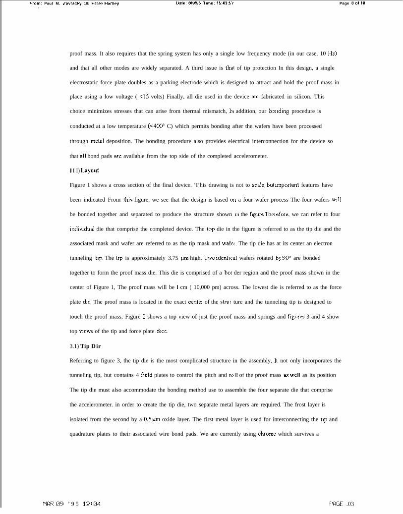
proof mass. It also requires that the spring system has only a single low frequency mode (in our case, 10 I{z)
and that all other modes are widely separated. A third issue is tha{ of tip protection In this design, a single
electrostatic force plate doubles as a parking electrode which is designed to attract and hold the proof mass in
place using a low voltage ( <15 volts) Finally, all die used in the device ale fabricated in silicon. This
choice minimizes stresses that can arise from thermal mismatch, 1]] addition, our bcmding procedure is
conducted at a low temperature (<400° C) which permits bonding after the wafers have been processed
through metal deposition. The bonding procedure also provides electrical interconnection for the device so
that all bond pads arc available from the top side of the completed accelerometer.
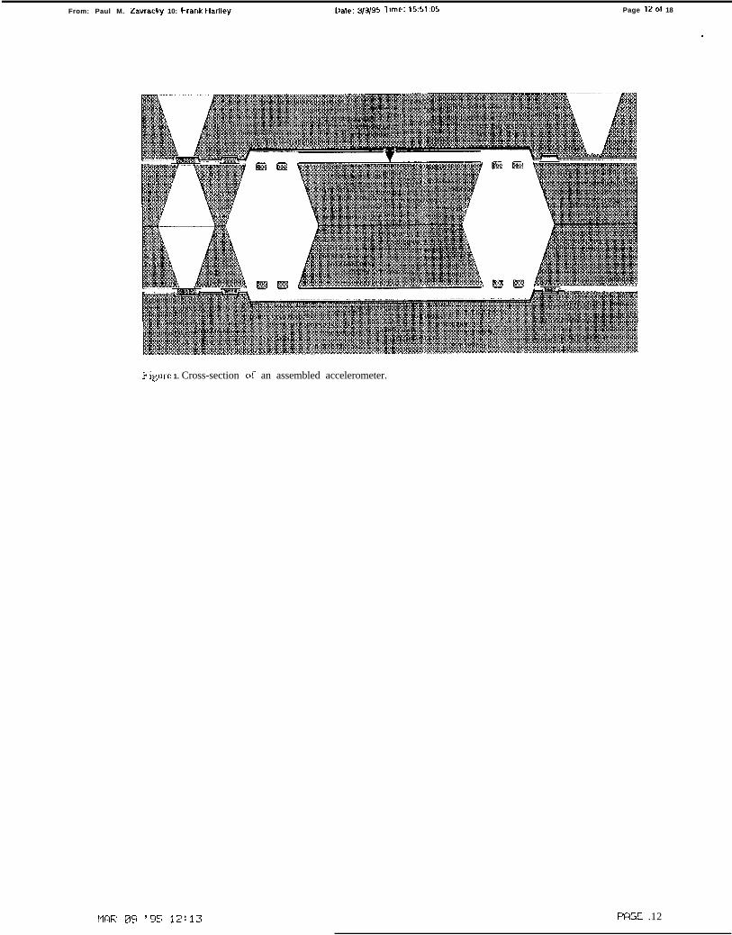
1 I I) Layout
Figure 1 shows a cross section of the final device. ‘I’his drawing is not to scale, bu! mlportant features have
been indicated From th]s figure, we see that the design is based cm a four wafer process The four wafers will
be bonded together and separated to produce the structure shown in the f]gure l“helefore, we can refer to four
individua] die that comprise the completed device. The top die in the figure is referred to as the tip die and the
associated mask and wafer are referred to as the tip mask and wafel. The tip die has at its center an electron
tunneling t]p. The t]p is approximately 3.75 pm high. ‘Iwo ident](.al wafers rotated by 90” are bonded
together to form the proof mass die. This die is comprised of a bo] der region and the proof mass shown in the
center of Figure 1, The proof mass will be 1 cm ( 10,000 pm) across. The lowest die is referred to as the force
plate d]e. The proof mass is located in the exact cente] of the stru[ ture and the tunneling tip is designed to
touch the proof mass, Figure 2 shows a top view of just the proof mass and springs and figures 3 and 4 show
top wews of the tip and force plate d]ce.
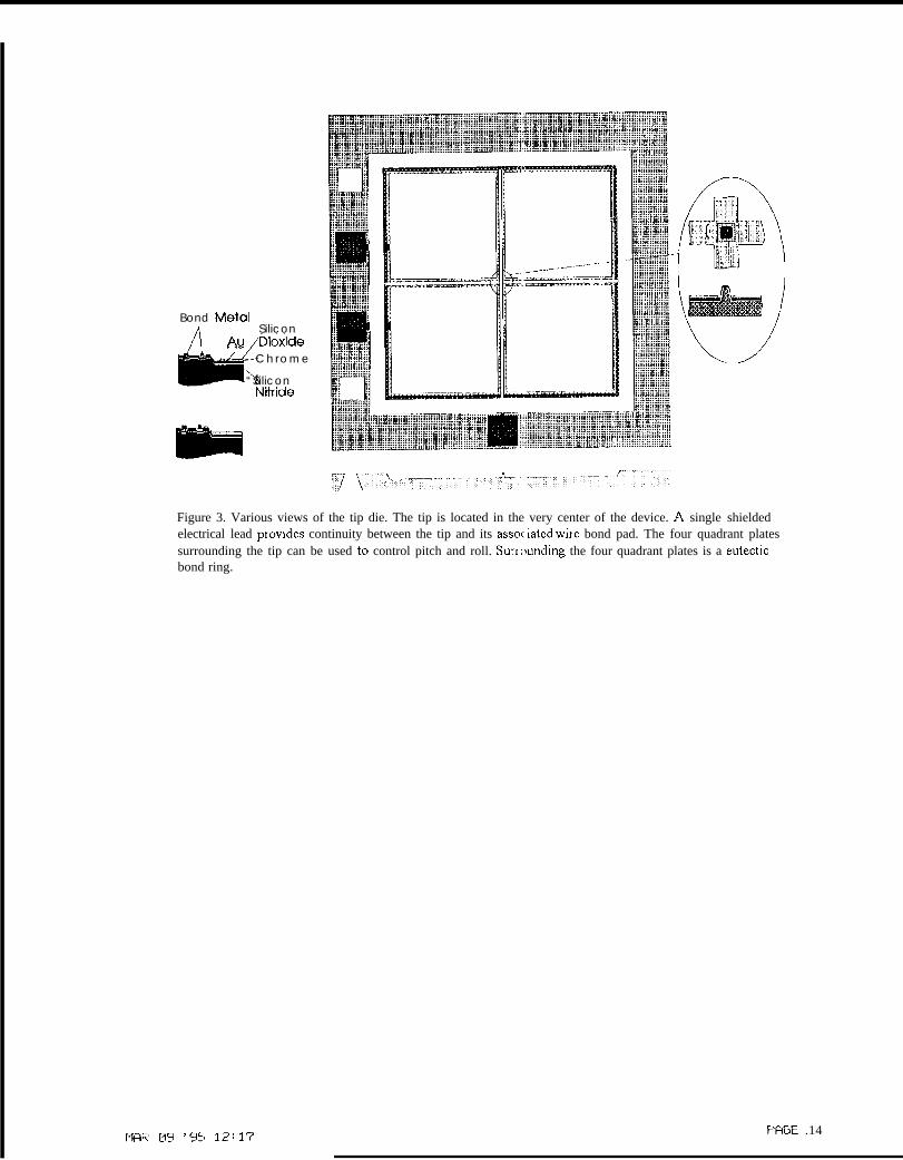
3.1) Tip Dir
Referring to figure 3, the tip die is the most complicated structure in the assembly, H not only incorporates the
tunneling tip, but contains 4 f]eld plates to control the pitch and rc,ll of the proof mass as well as its position
The tip die must also accommodate the bonding method use to assemble the four separate die that comprise
the accelerometer. in order to create the tip die, two separate metal layers are required. The frost layer is
isolated from the second by a 0,5 pm oxide layer. The first metal layer is used for interconnecting the tlp and
MFK’ E19 ’ 9 5 12:Et4
quadrature plates to their associated wire bond pads. We are currently using chrc~mc which survives a
F’FIGE .03
From: Paul M. Zavracky 10: Frank Hariley Date: 31919S > Ime; 1544:41 Page 4 of 18
subsequent LTO deposition process. I“his metal layer covers the tip and can be used as the tip metal
Chromium tips have been tested successfully.
The second metal layer is Cr/Au. It forms the quadrature plates and covers the electrical bond packs. It also
forms a base layer for the eutectic bond ring that surrounds the center of the die I’hc center region of the die
M recessed with respect to the bond ring and bond pads. This IS required to c,btain a spacing between the field
plates and the proof mass When this die is bonded to the proof mass, the perimeter will foml a hermetic seal
and the bond pads will be mechanically bonded and electrically connected to their counterparts on the proof-
rnass die. This electrical connection scheme is a key feature of the design IIy interconnecting the die in the
bonding processes, all electrical connections to the completed accelerometer can be made from its front
surface.
The lower right hand comer of Figure 3 shows a magnified section of the tip “l’his illustrates the relationship
of the tip to the bond perimeter and illustrates the two metal layer desig~]. As can be seen, the electrically
insulating oxide layer is removed from the tip and its surrounding area, exposing the tip metal.
The electrical contact to the tlp is accomplwhed with the frost metal layer which M connected by a single thin
lead to the bond pad. The second metal layer which forms the field plates, bond perimeter and wme bond pads
is deposited above the first metal layer Focusing on the center of the clie, the fu+u-e shows a cross centered in
the bond perimeter which is electrically grounded. It is used to shield the ti], metal lead from electric fields
that exist in the vicinity of the flcld plates. In the upper right hand corner of Figure 3 a detail of the center of
the cross is shown. The cross is open at the very center to ex]>ose the t]p bclo~r. At the end of the tlp wafer
process, metal can be selectively depos]ted on the tip allowini, flexibility in the choice of tip metal.
Not shown in the f]gure is the exact nature of the first metal layer. It is patterned in such a way it underlies
the center cross region. This maintains the electrostatic symmetry of the device Therefore, the tip metal layer
]s sandwiched between the wafer and the second metal layer. Sdicon ox]de M used to Isolate the tip metal
from both the substrate and the second metal, Because the ti] metal also underlles the four electrostatic
control plates, the second metal layer is at the same elevation at the cross as it is at the control plates
MM! E@ ’95 12:ET5 F’fIGE , E14

I FIorQ: Paul M. Zavracky 10: Frank Hartley
,,
Dale: S/!4/95 1 tree: 15:45:3 f Page 5 of 18
To connect the force plates electrically to the bond pack, holes are cut in the oxide layer above the first metal
in the vicinity of the force plates. This allows the force plates to contact the f]rst metal layer. The frost metal
layer is patterned in such a way as to connect each force plate electrically tc, its associated bond pad. The
bond pads also contain a connection between f]rst and second metal as shown in the details to the left of
Figure 3.
Finally, a bond metal layer is deposited and patterned on the bonc~ perimeter. The bond perimeter is also
recessed, but not as deeply as the quad~ature plates. This recess i] nplements a surface referenced bonding
techmque we are using The concept is that the width of the bond metal ring is less than the underlying
chrome/gold layer, but its thickness M greater than the depth c)f the recess. When bcmdlrrg, the eutechc alloy
wets both parts and draws them together through surface tension
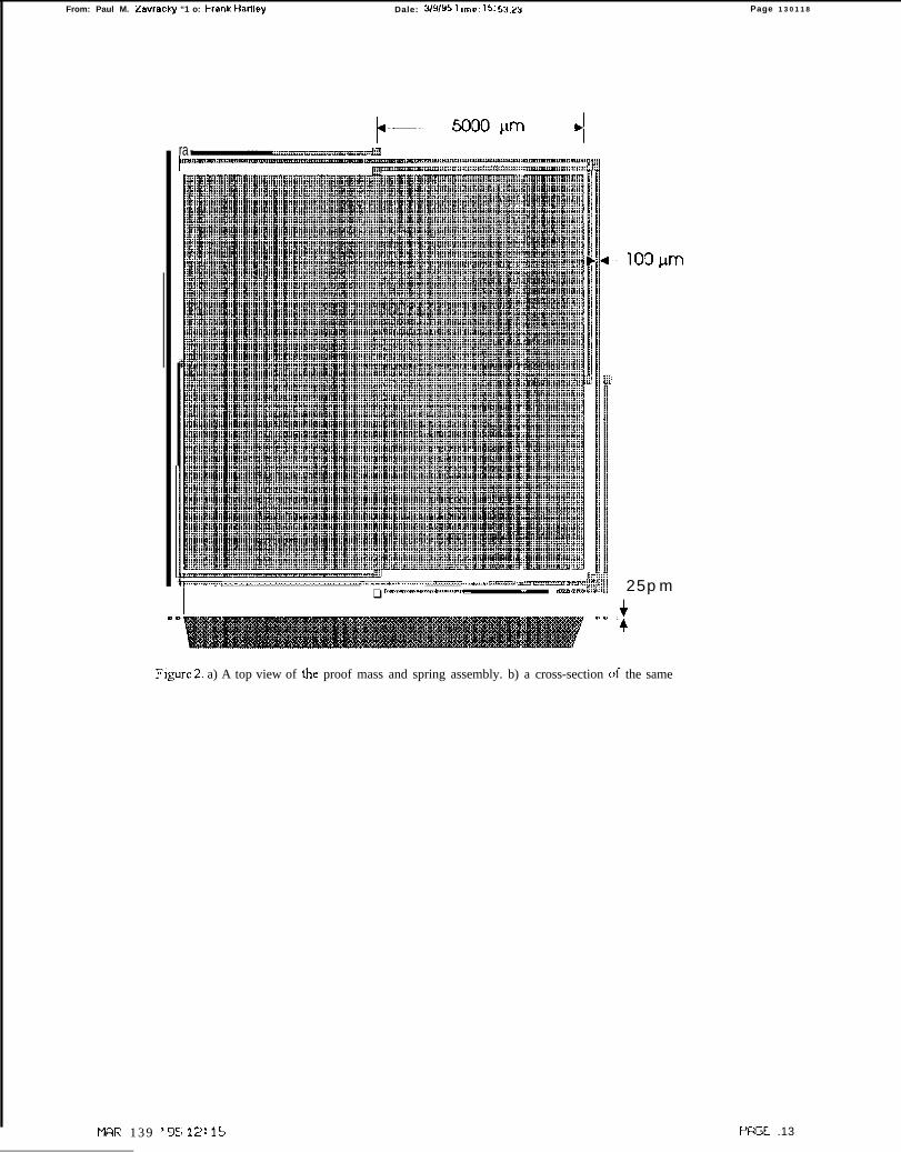
3.2) l’rool Mass Die
Figure 1 shows a cross-section of the proof mass die. ‘l’he proof n~ass is assembled from two identical die. As
a result of the anisotropic etchant used to machine the proof mass, its sides will be tapered at S4. 7“. Since the
wafer is 400 pm thick, the smallest dimension of the p] oof mass \\rill be two t]mcs 2S3.2 pm smaller than the
top surface or 9433.6 pm. The top dimension is 1 cm or 10,000pn_. The volume of silicon lost to this
undercutting is approximately 4,5x10’3 cmz. The volume of a box 1 cm x I cm x 800 pm is 8X 10“2 cm2. Since
the density of silicon is about 2.42 gin/cc, the net weight of t}~e proof mass is the difference of the two
volumes above times the density or 0.18 grn. The proof mass is held to the surrc,unchng frame by a set of
springs referred to as ‘crab legs ‘ In f]gure 1, the target thickness of the crab legs IS 25 pm. Fgure 2 shows a
top view of the proof mass and springs. The detail on the left of the figure gives the spring width, separation
and thickness.
Bach individual crab leg is divided into three spring sections, two short ones and one long one, The length of
the short sections is 5000 pm but the length of the long spring deviates by 200 pm from 10,000 pm due the
requirement to clear the comer ties. The comer ties play no role in the normal mot]on of the proof mass and
MN? B9 ’95 12:EIL PfIGE .05

From: Paul M. Zavracky “1 o: hank Harlley Date: 3/9/SS 1 Ime: 15:46:26 Page 601.18 ‘——
do not alter the stiffness of the device in its sensitive axis, These ties are. added tc, increase the stiffness to
pitch, roll and yawy
The proof mass die is maintained at essentially gToLrrIcl potential and the surface c)f the proof mass is
completely covered by metal. IIowever, at the perimeter of the die, electrical contact between bond pads is
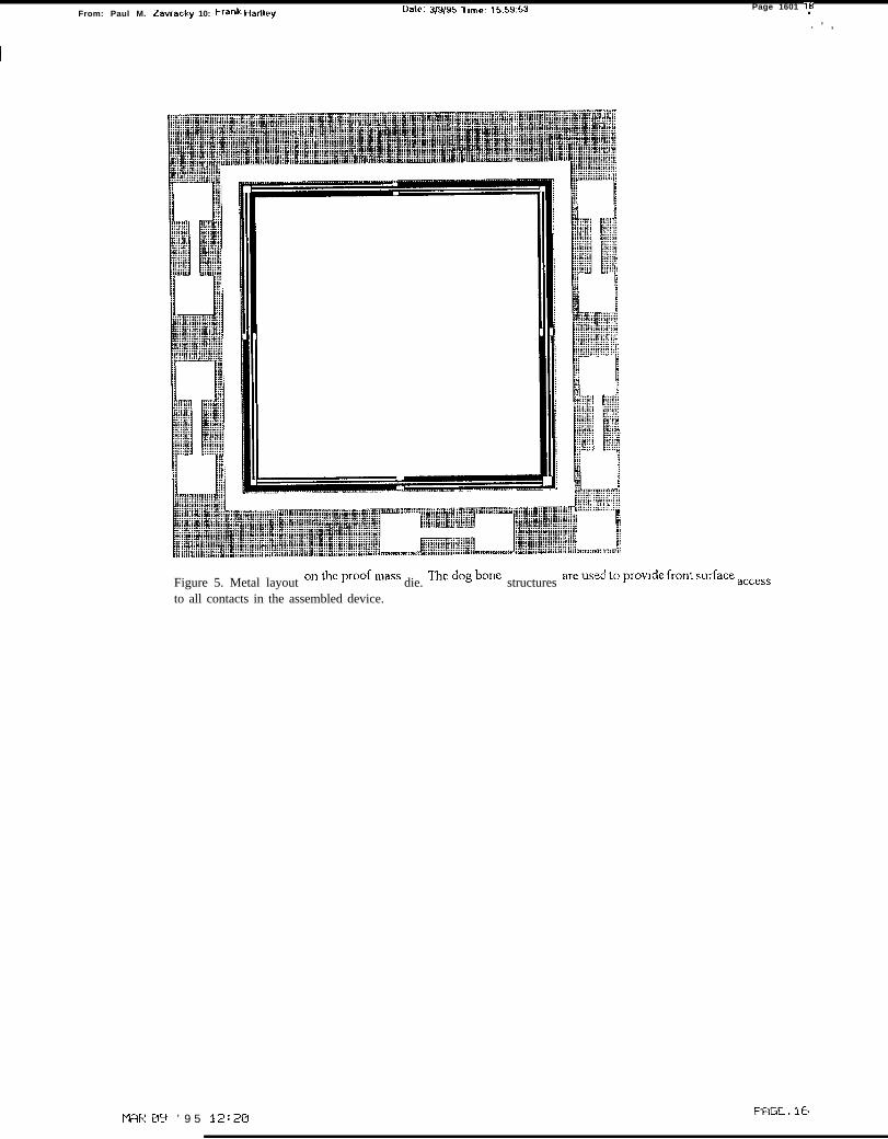
routed to facilitate the front surface only contacting scheme described above. FIEure 5 shows the metal layer
layout for the proof mass. Since the anisotropic etching can ta~:e place prior to metallization, some freedom
exists in the choice of proof mass metal. CJur intention is to provide a complimentary layer to the one used on
the tip and force plate chips.
The bonding of the proof mass wafers reqr.m-es spec]al attentio]l In this case, the bond metal (assummg
eutectic bonding is to be used) is applied to the back side of the wafer. If the bend metal is applied early in
the process, it must survive all subsequent processing steps, This puts a severe and unnecessary restriction on
the choice of bond material. Applying the bond metal at the ef]d of the process, ]rior to cutting the springs is
the preferred method. Two patterning techniques hwe been en,ployed. Since the back side to the wafer has
been deep etched, photolithographic patterning is d] fflcult, but we found, not impossible. Double spinning a
thick resist such as Shipley’s 1827 is effective. Resist accumulated in the lower comers of etch pits is
removed after a long exposure (5 min at 40 row). This technique preserves the hcnnetic sealing capability we
desire. Alternatively, this layer can be deposited t}]ough a shadow mask. Both mct}mds have been used
successfully.
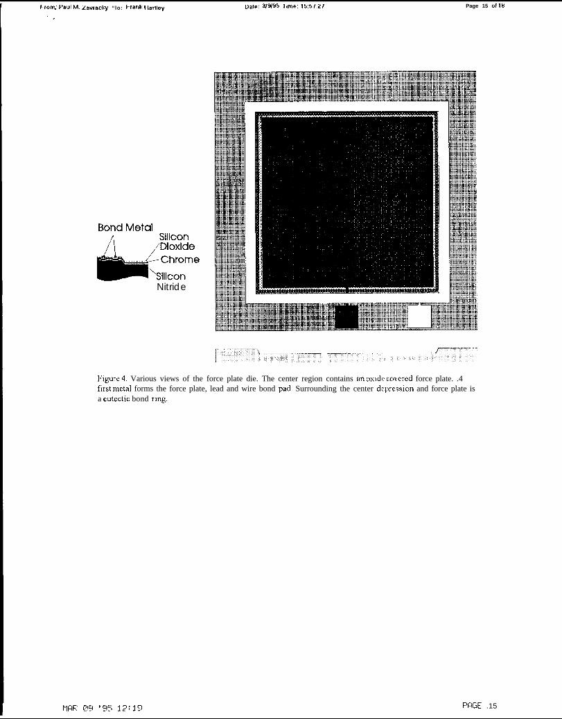
3.3) Force l’lale Die
The force plate die is m many ways similar to the tip die. Aga]n a two metal process is used in order to
provide a bond perimeter which is not electrically connected to the force plate, A contact pad to this perimeter
metal is provided in order to set the potential. The force plate N fabricated in fllst metal which may simply be
a smglc chrome layer similar to that used on the tip wafel. Thr force plate must be covered with a thick oxide
layer (1 pm) The purpose of this ox]de layer 1s to prevent an clectncal contact between the proof mass and
the force plate when the proof mass is being clamped electrostatically. Choices for the bond perimeter and
contact layer (second metal) are identical to those described for the tip wafer
MW! WI ’95 12:LlZ FRGE . EIEJ
From: Paul M. ZavrackY “Io: l-rank Hariley 1.)ale:3/9/fj5 llme:15:4”l:15 Page 70118
.
I\~ Assembly
Figure] sho~'sdrawing ofthccross-section of theasse]nbled acceleromete~ die. Inparticular,t henatureof
the bond pad regions is illuminated Since the bond pads are meant to contact metal lines on the tip die as
well as the force plate die, it is necessary to access bond pads on t}le force plate and tip dice. To the top right
of the f]gurc, an ctchcd groove is showm extending down to the top of the first proof mass die. Contacts to the
t]p and control plates are made at this level. On the extreme left side of the assembled the, a complex
anisotropically etched hole extends down to the force plate wafer. Bond pads for the force plate and its
ground are made through openings of this kind Referring again to fgure 5 which shovs the top of the proof
mass, ‘dog bone’ interconnections are shown Wire bonds are made to one side of each interconnection
through the anlsotropically etch grooves. The five required electrical connections to the tip wafer are made to
the oppos]te end of each interconnection during the eutectic bonding process. Therefore, the pads seen on the
tip wafer are connected to the interconnections on the proof mass \ia the eutectic bonding The opposite side
of each interconnection is accessible through an etched groove fol wire boncling I’hc force plate die has only
two electrical connections, one to the force plate itself and anothe] to the bond rin~ Both are accessible
through deep anisotropic grooves. The bond ring makes electrical connection to the proof mass via the
eutectic bonding process. Substrate contacts are currently being nlade at the penp}]cry of the die during the
packaging process.
l’) Results
Fabrication of devices has revealed several important issues that must be addressed to successfully complete
the device. Our initial work on wafer bonding was performed with Aluminum Germanium alloys. Layers were
deposited in an e-beam evaporator and the thicknesses were adjusted to provide the eutectic alloy when both
layers combined. Although the eutectic alloy should melt at 450 “C, reliable bonding did not occur until 500
“C]o. After bonding the proof mass wafers, it became apparent thot the TiW/Au layers on the proof mass had
degraded While the deg~adation appeared to be minor, we found that the films developed a built-in strain
The effect of the strain manifest itself in bending of the springs out of plane. Experimentation with springs
annealed at various temperatures revealed a safe knlpePdtUTe rmge of 350 ‘C and bc]cnv. We subsequently
changed the eutectic bonding system to Iridium alloys.
MfR (39 ’95 12:W? PRGE . B?

From: Paul M. Zavracky 10: I-rank Harlley Date: 3/9/95 llme: 1548.05 Pig& 8 Of 18
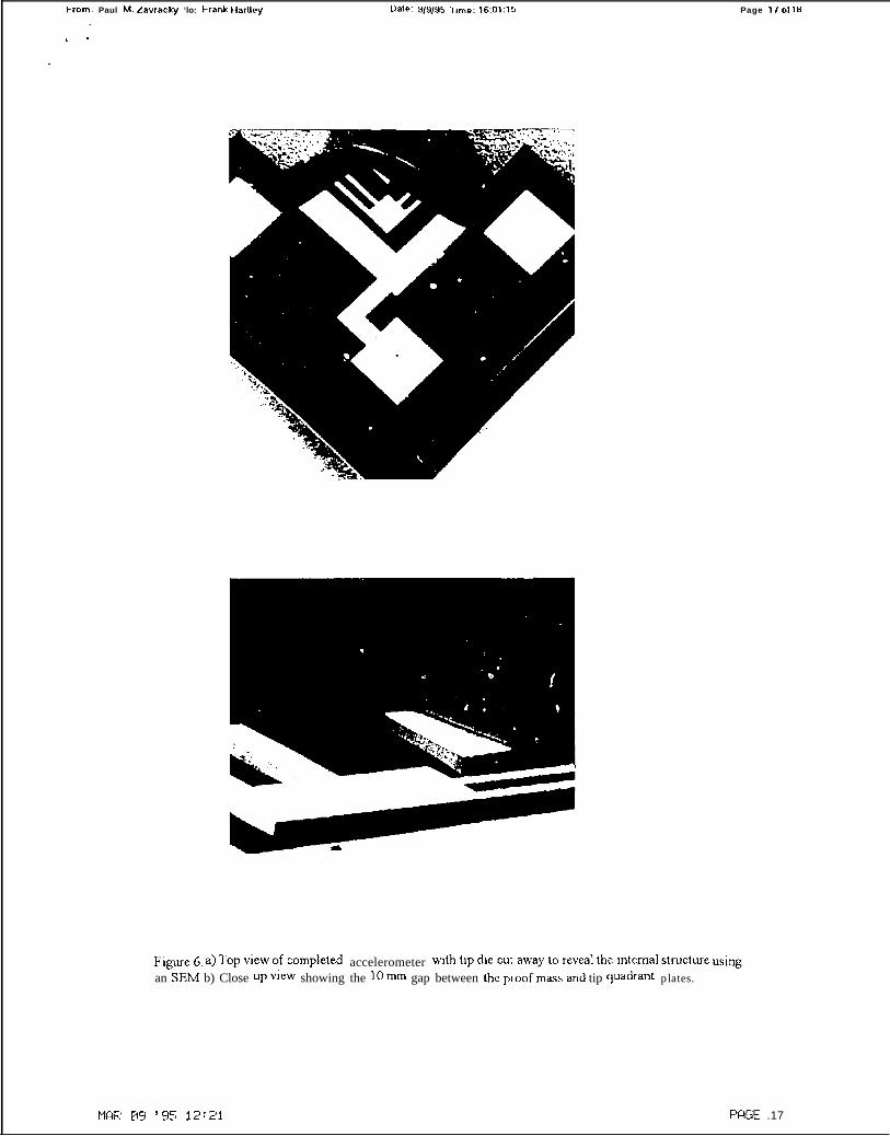
Full accelerometers have been fabricated. Figure 6 shows a top view of an assembled accelerometer where the
comer of the tip die has been broken away revealing the proof mass beneath For test purposes we have
assembled devices in three stages, full, three quarter and on half. A three quarter accelerometer is one which
has both bonded proof mass die and the force plate. A one half accelerometer consists of a single proof mass
die and a force plate.
After assembling the first accelerometers, we found that the voltage required to hold the proof mass in place
against 1 g was much higher than expected The typical value JS about 3 volts compa~ed to a calculated value
of about 0.6 volts Measurements of the capacitance showed tl,at instead of the expected 3 nanofarads, the
actual capacitance was approximately 300 picofarads. These ~esults suggested that either foreign matter
prevented the proof mass for coming into full contact with the force plate, or the proof mass ancl force plate do
not conform to one another. To test the latter theo~, we ran surface profiles of the proof mass and force
plates. Measurements indicated that as much as 10 microns of variation ale typical on proof masses. Tests of
statiing material produced similar results. This suggests that c]ther higher voltag,es are required to implement
the parlcmg procedure effechvely, or that wafer specifications ]oust be improved
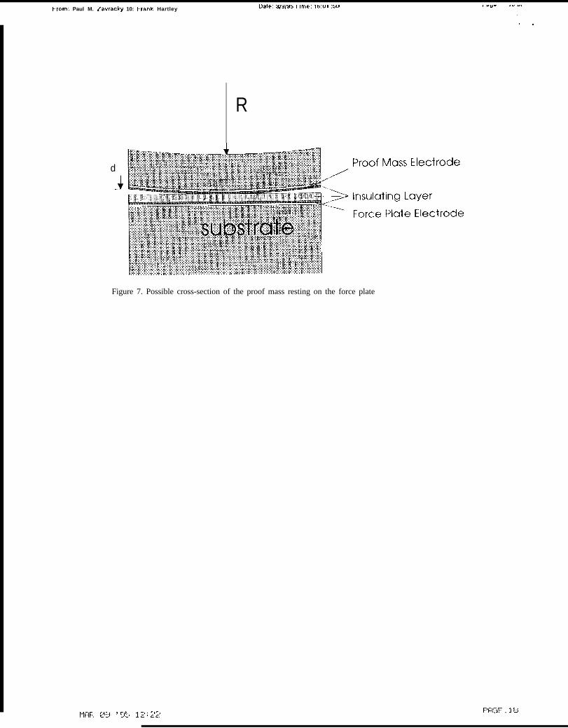
To develop an understanding of the magnitude of this problem a simple model of the proof mass and force
plate was created. This model assumed that the proof mass ha{l a radius of curvature, R. Based on this
spherical model, the electrostatic potential required to generatv a force of 1 g, between the force plate and the
proof mass, w]th the proof mass m contact with the dielectric layer at its center was calculated Figure 7
shows the configuration considered The problem was modeled numerically and showed that if the proof mass
had a radius of curvature of about 100 cm, then ‘d’ would be about 10 pm, the capacitance would be about
350 picofarads, and it would require 3.3 volt-s to support the p] oof mass against 1 g These results are
consistent w]th our observations,
The proof mass is held to the force plate by an electrostatic pc~tential. ‘I o prevent shorting, the force plate has
been covered with a low temperature oxide (LTO) layer It ha~ been su~ested that if a DC f]eld is applied, an
M(W @9 ’ 9 5 12:EK? FRGE . E!
Date: 3/9/S5 “Inie: 15:48.55 Page S 0118From.: Paul M. Zavracky 10: Frank Hartley
opportunity for charging of the insulator surface exists and that the voltage required to hold the proof mass
against 1 g would increase in time. To test this hypothesis, we ha! e experimented with electrically stressing
the silicon dioxide. A half accelerometer as connected to an LCR bridge with DC bias capability, The
accelerometer was oriented such that the proof mass rested on the force plate. A DC bias of about 5 VOILS was
applied. The unit was flipped over and the DC field reduced \vhile monitoring the capacitance until the
apphcd field could no longer hold the proof mass against the force plate, At this point, the capacitance
changes abruptly. A bias voltage of 2.7 volts was recorded, The clevice was then flip over again, and a 10 volt
bias was applied This was held constant for periods up to 24 hours after which the holding voltage was again
measured We observed a slight reduction (50 mv) of the potential requirecl to hold the proof mass wh]ch may
be attributed to charging of the silicon dioxide.
.41though minimal charging has been observed, a tneans to completely obviate this issue is desirable In our
work, wc have been experimenting with the application of AC voltages. Tests with AC fields have proven
successful in countering surface charging. Most of our work has I)een conducted with sinusoidal sources,
with the unfortunate drawback that the peak voltage must be ~fi lhe value of a IX field with equivalent
holding power AC flclds add a ncw dlmcnsion of flexibility that can be exploited for hflBMS. W’lth an AC
appbed field, a captic]ior can be placed in series with t}le device, IImiting current fic>wr, h) an extreme case, a
small series capacitor will behave like a constant current source. Since the electrostatic force applied is
proportional to the square of the current and independent of the s])acing, an AC f]eld can be used to apply a
position independent force to a moving micromechanical device, A second interesting aspect of AC fields is
that they can be used simultaneously for the mcasurcmcnt of position and for cont~ol. In our work, wc have
successfully exploited AC f]elds tu position the proof mass
Conclusions
We have repo~ed a new fabrication process and configuration for an uh.rasensitive accelerometer. The
accelerometer is fabricated using a bulk micromachining approach Three umque (he are processed and
bonded together to form the final dcvicc. l’hc bonding process, which uses cutcct]c alloys, joins the dic and
simultaneously provides hennet]c sealing and e]ectncal interconnection betwee]l d ic T’he accelerometer is
MIX’ D9 ‘ 9 S 12:09 F’fIGE . E19

From: Paul M. Zavracky 10: Frank Hariley Date: ?/9195 1 line: 1549.46 Page 100118
designed with a force plate that can be used to holcl delicate pI oof mass and spr)ng assembly electrostatically
during transportation, It has been determined that concerns about charging of the silicon oxide layer
deposited on the force plate we minor. Changes in the holdinp potential of only about 50 millivolts have been
observed. This issue can be negated through the use of AC rather than I>C elect] ostatic fields. These have
been demonstrated successfully.
.Acknowlcdgments
The authors would like to acknowledge the help and supporI of tieg Jenkins for his assistance in fabricating
devices and Professor Nick McGnrer for his many helpful suggestions. Fundins, for this program has been
provided by NASA through a grant to the Jet Propulsion ],abm stories.

From: Paul M. Zavracky 10: l-rank Harkley Dale: 3/9/95 1 line: 15:50.23 Page 110118
References
1
2
3
4
5
6
7
8
9
10
AA. Braslci, 1’.1< Albrecht, and C. F’. Quate, “l’unnelmg Accelerometer,” J hl]croscopy, Vol. 152, p.100, 1988.S.13. Waltman and W.. J. Kaiser, ''h Electron 'lueling Sensor. '' Sensors tind Actuators, Vol. 19,p]> 201-210, 1989.M,F, Bocko, “The scanning tunneling microscope as a hi~$-gain, low noise displacement sensor,”Rev. Sci Instrum. Vol. 61, No. 12, December 1990.I’.W. Kenny, W.J. Kaiser, H K, Rockstad, J.K Reynolds, J.A Podosek, ancl E C Vote, “Wide-Bandwidth Electromechanical Actuators for Tunneling I~]splacement “transducers,” J. MEMS, Vol.3, No. 3, September 1994.T.W. Kenny, W.J. Kaiser, S.F3. Wa]tman, and .l.K. Reynolds, “A Novel Infrared Detector Based on aTunneling Displacement l’ransducer,” Appl. Phys. Lett, I’ol. 59, 1991.J.J. Yao, S.C. Amey, N.C. MacDonald, ‘T’abdication of Il@ Frequency Two-dimensionalNanoactuators for Scanned Probe Devices,” J. MEMS, vol. ], No 1, p}>. 14-22>1992.E. Peeters, S. Vergote, B. Puers and W. Sansen, “A highly symmetrical capacitive micro-accelerometer with single degree of freedom response.,” J Micromech M]croeng Vol. 2, pp. 104-
112,1992P.M 7,avracky, h’. Hartley, NT. Shem]an, T. Hansen, and K Warner, “A New Force BalancedAccelerometer using Tunneling Tip Position Sensing,” 7th lnt. Conf. on Sensors and Actuators,Yokaharna, Japan, June 7-10, 1993.P.M. Zavracky, F. Hartley, and D Atkins, “New Spring I ksign and Processes for an ElectronI’unnclmg Tip Accelerometer, to be publishedP. M. 7,avracky and 13ao Vu, %rtectic Bonding with Al/( ;e Thin l:ilms,” to be published.
MRR B9 ’95 12:1B FRGE , 11
From: Paul M. Zavracky 10: Frank Harkley ~a~e: ~9/95 llme: 15:51:05 Page lZOI 18
.
Figure 1. Cross-section of an assembled accelerometer.
MtW EISJ ’95 12:13 F’fJGE .12
From: Paul M. Zavracky “1 o: Frank Harlley Dale: 3/9/95 1 Ime: 15: S$.>$ Page 130118
F---”- 5000 pm –-–-ti
ra- ,., JIEmzzEIw.LzccGLcidn
-:-.—..-AZI-i]
+.,,,, ., ..,., . . . . . . . . . . . . . . . . . . . . . . . . . . . . . . . . . . . . . . . . . . .T. ,, M,Z,.. __ __
—- —... (’!, !l, :. . . .,, . . . ,,. . . . . . . . . . . . . . . . . . . . E-l. .U, wuu ,: .,...... .:: ...::
❑ — --
--- ,;ti: ;:,.
100ym
25pm
Figure 2. a) A top view of the proof mass and spring assembly. b) a cross-section of the same
MIW 139 ’95 12:15 FRGE .13
Bond Metalh Silicon
ilifikdAU Dloxlde- -Chrome
“SiliconNitdde
e>iFigure 3. Various views of the tip die. The tip is located in the very center of the device. A single shieldedelectrical lead prowdes continuity between the tip and its asso( lated wi]c bond pad. The four quadrant platessurrounding the tip can be used tc) control pitch and roll. Surl [Junding the four quadrant plates is a eutecticbond ring.
MRR WJ ’95 12:17 ‘FREE .14
Frotr; Paul M. Zavracky “lo: Frank Harkley Dale: 3/9/95 lime: 15:!I/.27 Page 15 0! 18
‘,
-in’Nitride
Figure 4. Various views of the force plate die. The center region contains an ox]de coverecl force plate. .4flr;t metal forms the force plate, lead and wire bond pacl. Surrounding the center dc.pression and force plate isa eutectic bond ring.
M9R @SI “35 12:19 P$2GE .15
From: Paul M. Zavracky 10: Erank Harlley Dale: 3/W5 ltme; 15:59.S3 Page 1601 1,S
. ’ ,
I
Figure 5. Metal layout ontheproof nlass die. Thedogborle structures areused to]>rovide front sLlrface accessto all contacts in the assembled device.
MfW WI ’ 9 5 12:213P13GE.16
From: Paul M. Zavracky ‘lo: Erank Harlley Dale: 3/9/s5 ‘ltme:16:Ol:15 Page 1’/01 18
.
. .
.
Figure6. a) Topview' ofcompleted accelerometer w'ithtip diecutaway toreveal tl]eintemal stmctwe usingan SEM b) Close upview showing the IOmm gap between thep]oofmassancl tip quwhant plates.
MfR E!9 ’95 12:21 FRGE .17
From: Paul M. Zavracky 10: Frank Hartley uale: W91WJ I Ime: lb.ul :w r-~-= J“”.. .
.
,,
R
d
_l
Figure 7. Possible cross-section of the proof mass resting on the force plate
MFR W ’95 12:22F’flGE . lB