
Design Automation for Reconfigurable Interconnection Networks
Upload
independentCategory
view
3download
0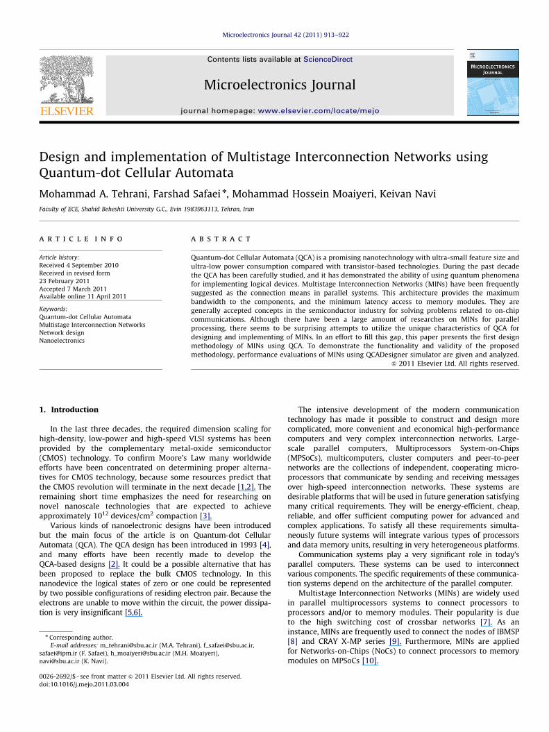
Microelectronics Journal 42 (2011) 913–922
Contents lists available at ScienceDirect
Microelectronics Journal
0026-26
doi:10.1
n Corr
E-m
safaei@
navi@sb
journal homepage: www.elsevier.com/locate/mejo
Design and implementation of Multistage Interconnection Networks usingQuantum-dot Cellular Automata
Mohammad A. Tehrani, Farshad Safaei n, Mohammad Hossein Moaiyeri, Keivan Navi
Faculty of ECE, Shahid Beheshti University G.C., Evin 1983963113, Tehran, Iran
a r t i c l e i n f o
Article history:
Received 4 September 2010
Received in revised form
23 February 2011
Accepted 7 March 2011Available online 11 April 2011
Keywords:
Quantum-dot Cellular Automata
Multistage Interconnection Networks
Network design
Nanoelectronics
92/$ - see front matter & 2011 Elsevier Ltd. A
016/j.mejo.2011.03.004
esponding author.
ail addresses: [email protected] (M.A. Tehr
ipm.ir (F. Safaei), [email protected] (M.H.
u.ac.ir (K. Navi).
a b s t r a c t
Quantum-dot Cellular Automata (QCA) is a promising nanotechnology with ultra-small feature size and
ultra-low power consumption compared with transistor-based technologies. During the past decade
the QCA has been carefully studied, and it has demonstrated the ability of using quantum phenomena
for implementing logical devices. Multistage Interconnection Networks (MINs) have been frequently
suggested as the connection means in parallel systems. This architecture provides the maximum
bandwidth to the components, and the minimum latency access to memory modules. They are
generally accepted concepts in the semiconductor industry for solving problems related to on-chip
communications. Although there have been a large amount of researches on MINs for parallel
processing, there seems to be surprising attempts to utilize the unique characteristics of QCA for
designing and implementing of MINs. In an effort to fill this gap, this paper presents the first design
methodology of MINs using QCA. To demonstrate the functionality and validity of the proposed
methodology, performance evaluations of MINs using QCADesigner simulator are given and analyzed.
& 2011 Elsevier Ltd. All rights reserved.
1. Introduction
In the last three decades, the required dimension scaling forhigh-density, low-power and high-speed VLSI systems has beenprovided by the complementary metal-oxide semiconductor(CMOS) technology. To confirm Moore’s Law many worldwideefforts have been concentrated on determining proper alterna-tives for CMOS technology, because some resources predict thatthe CMOS revolution will terminate in the next decade [1,2]. Theremaining short time emphasizes the need for researching onnovel nanoscale technologies that are expected to achieveapproximately 1012 devices/cm2 compaction [3].
Various kinds of nanoelectronic designs have been introducedbut the main focus of the article is on Quantum-dot CellularAutomata (QCA). The QCA design has been introduced in 1993 [4],and many efforts have been recently made to develop theQCA-based designs [2]. It could be a possible alternative that hasbeen proposed to replace the bulk CMOS technology. In thisnanodevice the logical states of zero or one could be representedby two possible configurations of residing electron pair. Because theelectrons are unable to move within the circuit, the power dissipa-tion is very insignificant [5,6].
ll rights reserved.
ani), [email protected],
Moaiyeri),
The intensive development of the modern communicationtechnology has made it possible to construct and design morecomplicated, more convenient and economical high-performancecomputers and very complex interconnection networks. Large-scale parallel computers, Multiprocessors System-on-Chips(MPSoCs), multicomputers, cluster computers and peer-to-peernetworks are the collections of independent, cooperating micro-processors that communicate by sending and receiving messagesover high-speed interconnection networks. These systems aredesirable platforms that will be used in future generation satisfyingmany critical requirements. They will be energy-efficient, cheap,reliable, and offer sufficient computing power for advanced andcomplex applications. To satisfy all these requirements simulta-neously future systems will integrate various types of processorsand data memory units, resulting in very heterogeneous platforms.
Communication systems play a very significant role in today’sparallel computers. These systems can be used to interconnectvarious components. The specific requirements of these communica-tion systems depend on the architecture of the parallel computer.
Multistage Interconnection Networks (MINs) are widely usedin parallel multiprocessors systems to connect processors toprocessors and/or to memory modules. Their popularity is dueto the high switching cost of crossbar networks [7]. As aninstance, MINs are frequently used to connect the nodes of IBMSP[8] and CRAY X-MP series [9]. Furthermore, MINs are appliedfor Networks-on-Chips (NoCs) to connect processors to memorymodules on MPSoCs [10].
M.A. Tehrani et al. / Microelectronics Journal 42 (2011) 913–922914
Many variations of MINs have been already introduced. Thesearchitectures provide the maximum bandwidth to components(such as DSP, IP, etc.), and the minimum access delay to memorymodules. A MIN is characterized by its topology, switching mechan-ism, routing algorithm, task scheduling strategy, and fault-tolerance[11]. Various topologies of MINs have been proposed and studied inthe last few decades. Most of these topologies are driven from thewell known graph topologies, including mesh, star, shuffle exchange,tree, and cube-connected networks, among different others [7].
The communication platform of the parallel architectures canbe implemented with MINs, which must be reconfigured forvarious purposes. QCA strategy can be used to implement digitallogic systems by properly arranging cells. So far, several studieshave been reported in the literature about QCA-based circuitdesign [12–14]. However, to the best of our knowledge, thereseems to be surprising attempts to design and implement MINsconsidering the unique characteristics of QCA. Indeed, such net-works are very important circuits because they are expected to beused to design and realize large-scale parallel systems [7]. In aneffort to bridge the gap between MIN and QCA, the main concernof this article is to implement and simulate the types of MINssuch as Omega network, Butterfly network, Baseline network, andGeneralized Cube network [7] on the basis of QCA architecture. Anovel QCA switching element is also implemented, which is usedin the fabric switches and MIN networks.
The remaining portion of the paper is organized as follows: InSection 2 an acquaintance to QCA is brought, which describes itsphysical interactions and logical behavior. In Section 3, thearchitecture of a MIN is introduced. Next, the structural designof a generic MIN and its components is presented. Section 4 givesa description for the implementation of MIN on the basis of QCAstrategy. In Section 5, the simulation results and verification offunctionality for the test networks are detailed. Finally, a sum-mary of results and conclusions can be found in Section 6.
Fig. 2. (a) Signal propagation between two normal 901 cells and (b) signal
propagation between two 451 cells.
2. Quantum-dot Cellular Automata
The most important feature of QCA is hidden in cell architecture.Each cell consists of four quantum-dots placed on a square shapedarrangement as shown in Fig. 1(a). There are also two surpluselectrons trapped in these dots. The electrons are unable to movebetween the cells but they can freely tunnel within a cell betweenthe dots. Due to Coulombic repulsion, electrons are arrangeddiagonally in the cell to be placed so as to have the farthest possibledistance with each other. In this case the system energy is minimizedand they are in their ground state. The cell polarization P is definedto measure this alignment, expressed by Eq. (1), where ri is theprobability of presence of an electron in the quantum-dot i. For atypical QCA cell shown in Fig. 1(a), the polarization is given by [4]
P¼r1þr3�r2�r4
r1þr3þr2þr4
ð1Þ
So, the electrons are mostly in two possible arrangements; these areused to represent ‘‘zero’’ and ‘‘one’’ logical values. A QCA cell’spolarizations and its logical values are illustrated in Fig. 1(b).
QuantumElectron 12
3 4
Fig. 1. (a) A QCA cell has four quantum-dots and two surplus
In the case where two QCA cells are together, they affect eachother and the electrons of each cell force the electrons of the othercell. When they are situated as shown in Fig. 2(a), they prefer tohave the same polarization to minimize the Coulombic repulsion.But when they have 451 gradient, their polarizations must bedifferent to have the least repulsion (Fig. 2(b)).
A QCA wire could be made by arranging some cells in a line asshown in Fig. 3(a). When the head of the line has a specifiedpolarization, it propagates the value through the line and everycell gets the same state. A ripple wire could be also made byarranging cells in a line having 451 gradient (Fig. 3(b)). There is avery important feature in the interconnection of normal wires andripple wires. These wires can cross each other without any signalinterference in a coplanar design. However, their signals do notaffect the other’s signal and the signals are propagated to the restof the wires correctly (Fig. 3(c)).
QCA logic gates somehow differ from conventional CMOS design.Majority gate and Inverter are the basic elements of QCA design andeven ‘‘AND’’ and ‘‘OR’’ gates are implemented using Majority gates.A Majority gate consists of four cells: three inputs, one output, andone voter cell. The voter chooses its polarization depending on thestates of the input cells. Subsequently, the signal is propagated tothe output cell and rest of the circuit. Another important gate of QCAis Inverter. Its functionality is just like normal CMOS Inverter. A QCAMajority gate and an Inverter are shown in Fig. 4 [5].
A Majority gate can simply change to an ‘‘AND’’ gate. Whenone of the inputs of the Majority gate is set to the static value of‘‘0’’, it acts like an AND gate (Eq. (2.a)). An ’’OR’’ gate is also aMajority gate, with a static ‘‘1’’ input (Eq. (2.b)).
Majority ðA,B,0Þ ¼ ðA:BþB:0þA:0Þ ¼ A:B ð2:aÞ
Majority ðA,B,1Þ ¼ ðA:BþB:1þA:1Þ ¼ AþB ð2:bÞ
3. Network modeling
In this section, we give a brief introduction to MIN architecturethat is used to design the interconnection platform dedicated forMPSoCs. Later, we will present the necessary background infor-mation that is used in the paper.
3.1. Structure of MINs
Definition 1. [7] A MIN is defined as a network used to inter-connect a group of N inputs to a group of M outputs using several
-dot
Logic: 0Polarization: -1
Logic: 1 Polarization: +1
electrons and (b) illustration of two QCA’s logical states.

Input Columbic
Fig. 3. Illustration of signal propagation through QCA wires: (a) a normal QCA wire does not change the signal value and transfers it intact and (b) a 451 wire changes the
signal in each cell; value of signal at the end depends on the number of passed cells, and (c) two QCA wires can cross each other in just one layer without signal
interference.
Output
Voter
Input A
Input B
Input C
Input Output
Fig. 4. Illustration of two important QCA logic elements. (a) a Majority gate: in a Majority gate, the voter cell chooses its arrangement according to neighbor cells states
and (b) a QCA Inverter.
Fig. 5. Architecture of a generic MIN using 2�2 Switching Elements (SE).
M.A. Tehrani et al. / Microelectronics Journal 42 (2011) 913–922 915
stages of small crossbar switching elements (SE) followed byinterconnection linking stage. It has n stages, G0–Gn�1. Each stageGi has wi switches of size ai,jbi,j, 1r jrwi. Thus stage Gi has pj
inputs and qj outputs such that
pi ¼Xwi
j ¼ 1
ai,j, qi ¼Xwi
j ¼ 1
bi,j ð3Þ
Linking stages are interconnection functions, each of which is abijection of the group of the previous stage switch addresses thatconnect all SEs outputs from a given stage to the inputs of thenext stage. A generic MIN architecture is shown in Fig. 5.
3.2. Classification of MINs
In this section, we present a classification of MIN and restatesome definitions necessary for the proposed classification.
MINs have been classified into three classes depending on theavailability of paths to establish new connections. Fig. 6 illustratesa topological classification of MINs [7].
Definition 2. [7] A Banyan network is defined as a class of MINsin which there is one and only one path from any input node toany output node.
Depending on the kind of channels and switches, MINs can beeither unidirectional or bidirectional [7]. Additionally, each chan-nel can be either multiplexed or be replaced by two or morechannels. The latter case is referred to as a dilated MIN [7].
Definition 3. [7] A uniform MIN is one in which all the SEs of astage are of the same degree.

Fig. 6. Classification of MINs.
M.A. Tehrani et al. / Microelectronics Journal 42 (2011) 913–922916
Definition 4. [7] A Square MIN is one in which a MIN of degree r
is built from SEs of size r.
In this paper, we are concerned only with unidirectional DeltaSquare Uniform Banyan networks (DSUBs), which are a subset ofBanyan networks.
Delta networks, a subset of Banyan networks, were firstproposed by Patel [15,16].
Fig. 7. A typical Delta network.
Definition 5. [7] Delta networks are built using anbn (where n isthe number of stages) digit controlled crossbars of which no inputand output can be left unconnected.Every Delta network is a Banyan network, while the reverse isnot always true. Delta networks have a routing property calledSelf routing property or Delta property. Fig. 7 shows a typicalDelta network.
Since we are concerned only Delta networks, non-Delta Ban-yan networks are not of interest for this article. Uniform BanyanMINs can be either square or non-square. Thus, according tothe Definitions 1–4, a non-uniform network is also non square.A DSUB network is a delta network with all its SEs having thesame size, and is the focus of this paper.
In order to simplify the construction of a Delta MIN as well asthe design of a routing algorithm, Patel [15,16] proposed a regularlink pattern that can be used between all stages and thus avoidthe difficult construction procedure for every different deltanetwork. Patel termed the regular link pattern, the q-shuffle.The q-shuffle of a group of qr elements is a permutation of theseelements denoted by
SqrðiÞ ¼qi mod ðqr�1Þ, 0r ioqr�1
i, i¼ qr�1
(ð4Þ
Applying the q-shuffle function on a number represented inbase q corresponds to the application of a cyclic shift on saidnumbers. This leads to a construction of a class of MINs called‘‘shuffle-exchange MINs’’ [15]. Omega networks, which were firstdefined by Lawrie [17], and one of the most popular types of Deltanetworks are usually described as shuffle-exchange MINs. In fact,all delta networks are shuffle-exchange MINS.
In the next subsection, we describe the different types of Deltanetworks that are considered the most popular ones. It shouldbe noted that we focus primarily on the DSUB network, whichuses a size of power of 2, i.e., Delta MINs that have crossbars ofsize 2�2.
3.3. Types of Delta networks
The topology plays an important role in designing routingstrategy, network latency, throughput, and data transfer. We willrestrict the study to Delta MINs. There exist various popular MINs,which we have grouped to be considered as different types of Deltanetworks. The difference between each of these networks isthe topology of interconnection links between the crossbar stages.A study on equivalence of various types of Delta MINs has beenreported in [18]. All Delta networks are considered to be topologi-cally equivalent as well as functionally equivalent [18]. We thusclassify the popular types of Delta MINs as Omega network,Butterfly network, Baseline network, and Generalized Cube network.It is worth mentioning that Flip network, reverse Butterfly network,reverse Baseline network, and indirect Binary n-cube network aremirror images of the first four network types, respectively. Hence, inthe current study, we focus on the implementation of only the firstfour types.
3.3.1. Omega network
Omega networks are considered to be the most popular Deltanetworks. They use the perfect shuffle, which is a special case of aq-shuffle. A more intelligent way to describe the perfect k-shufflepermutation, sk, is defined as [7]
sk : ðxn�1xn�2. . .x1x0Þ-xn�2. . .x1x0xn�1 ð5Þ
The perfect k-shuffle permutation performs a cyclic shifting of thedigits in x to the left for one position.
Fig. 8 shows a schematic diagram of Omega (16, 2), where thefirst parameter refers to the size of network and the secondparameter corresponds to its degree. It should be noted that thevalues of q and r as defined in k-shuffle formula are S2�2 for thisOmega network.
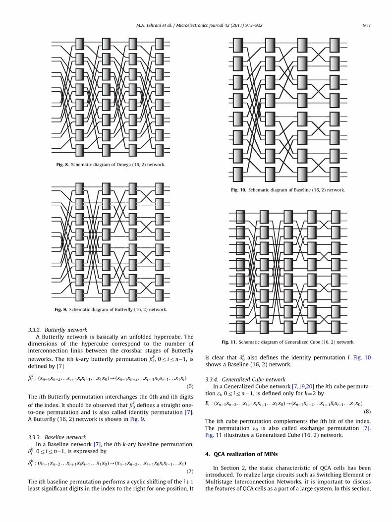
Fig. 8. Schematic diagram of Omega (16, 2) network.
Fig. 10. Schematic diagram of Baseline (16, 2) network.
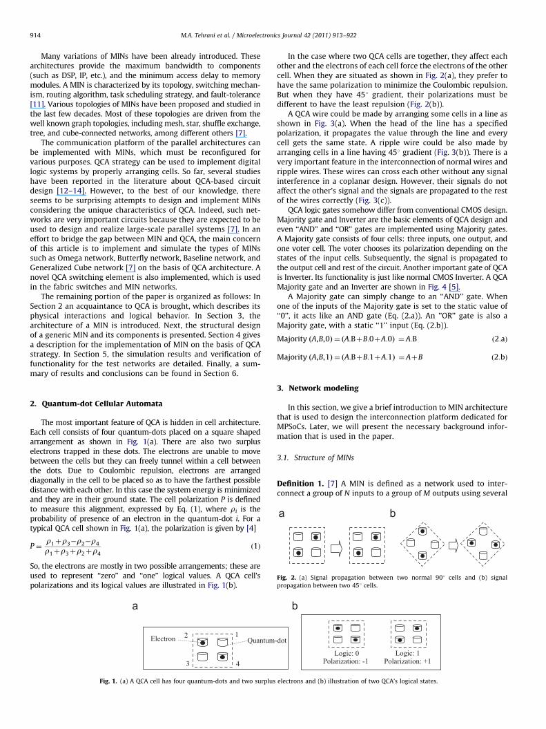
Fig. 9. Schematic diagram of Butterfly (16, 2) network.
Fig. 11. Schematic diagram of Generalized Cube (16, 2) network.
M.A. Tehrani et al. / Microelectronics Journal 42 (2011) 913–922 917
3.3.2. Butterfly network
A Butterfly network is basically an unfolded hypercube. Thedimensions of the hypercube correspond to the number ofinterconnection links between the crossbar stages of Butterfly
networks. The ith k-ary butterfly permutation bki , 0r irn�1, is
defined by [7]
bki : ðxn�1xn�2. . .xiþ1xixi�1. . .x1x0Þ-ðxn�1xn�2. . .xiþ1x0xi�1. . .x1xiÞ
ð6Þ
The ith Butterfly permutation interchanges the 0th and ith digits
of the index. It should be observed that bk0 defines a straight one-
to-one permutation and is also called identity permutation [7].A Butterfly (16, 2) network is shown in Fig. 9.
3.3.3. Baseline network
In a Baseline network [7], the ith k-ary baseline permutation,dk
i , 0r irn�1, is expressed by
dki : ðxn�1xn�2. . .xiþ1xixi�1. . .x1x0Þ-ðxn�1xn�2. . .xiþ1x0xixi�1. . .x1Þ
ð7Þ
The ith baseline permutation performs a cyclic shifting of the iþ1least significant digits in the index to the right for one position. It
is clear that dk0 also defines the identity permutation I. Fig. 10
shows a Baseline (16, 2) network.
3.3.4. Generalized Cube network
In a Generalized Cube network [7,19,20] the ith cube permuta-tion ei, 0r irn�1, is defined only for k¼2 by
Ei : ðxn�1xn�2. . .xiþ1xixi�1. . .x1x0Þ-ðxn�1xn�2. . .xiþ1xixi�1. . .x1x0Þ
ð8Þ
The ith cube permutation complements the ith bit of the index.The permutation e0 is also called exchange permutation [7].Fig. 11 illustrates a Generalized Cube (16, 2) network.
4. QCA realization of MINs
In Section 2, the static characteristic of QCA cells has beenintroduced. To realize large circuits such as Switching Element orMultistage Interconnection Networks, it is important to discussthe features of QCA cells as a part of a large system. In this section,
M.A. Tehrani et al. / Microelectronics Journal 42 (2011) 913–922918
the notation of a tool called QCADesigner [21] is also mentioned,by which the most of figures in this article are drawn.
4.1. QCA clocking
One of the important behaviors of the cells is their response tothe clocking signals. They have a special clocking that canexpedite the signal propagation and reduce the noises through acircuit. The clocking in QCA is somehow different from otherdigital clocking technologies. Clocking in QCA is completelydifferent from CMOS circuits. QCA clock allows data to propagateor force them to stay in their position. The clock raises and lowersthe dots barrier, so the electron can tunnel between dots or itmust stay in its situation. The clock has four phases includingswitch, hold, release, and relax, which describe the raising andlowering of the clock signal (Fig. 12). Each clock phase performssome special activities on quantum-dot’s barrier that affect thevalue of cell as below.
1.
Fig(c)
Switch: The cells passage from having no value to havingdefinite values.
2.
Hold: The barriers are maintained high and the values are thesame as in the switch phase.Fig. 12. Four phases of QCA clocking.
Fig. 13. Illustration of QCA clocking sections in a QCA wire.
. 14. VariousQCADesigner cells: (a) Normal cell, (b) Fix polarization cell,
Vertical cell, and (d) Crossover cell.
Fig. 15. (a) Implementation of a multiplexer with QCA cells and (b)
3.
illu
Release: The barriers are lowered and allow the electrons tostart tunneling. The cells move from a fix polarization to nopolarization.
4.
Relax: The barriers fall down and the cell has no polarization.The clock has four different phases, so the cells can bearranged in four pipelined zones to propagate the signal fasterthrough the circuit. There is a notation for showing the clockingphases in models [22]. A group of cells in the same phase is shownwith the same color (Fig. 13).
4.2. QCADesigner
QCADesigner is a tool generally used for simulating the QCAcircuits. A QCA model might be of single layer or multilayer. In asingle layer design, only normal cells and fix polarization cells areused. Their illustration is depicted in Fig. 14(a) and (b). When aQCA signal moves from one layer to another, it goes via verticalcells (Fig. 14(c)). Then, in the upper layer, it propagates throughcrossover cells (Fig. 14(d)). Finally, it can go down to the mainlayer via vertical cells.
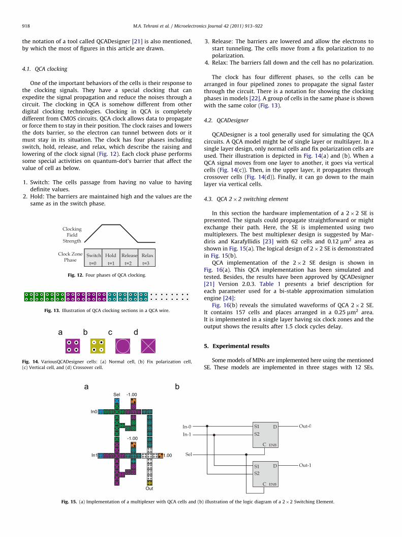
4.3. QCA 2�2 switching element
In this section the hardware implementation of a 2�2 SE ispresented. The signals could propagate straightforward or mightexchange their path. Here, the SE is implemented using twomultiplexers. The best multiplexer design is suggested by Mar-diris and Karafyllidis [23] with 62 cells and 0.12 mm2 area asshown in Fig. 15(a). The logical design of 2�2 SE is demonstratedin Fig. 15(b).
QCA implementation of the 2�2 SE design is shown inFig. 16(a). This QCA implementation has been simulated andtested. Besides, the results have been approved by QCADesigner[21] Version 2.0.3. Table 1 presents a brief description foreach parameter used for a bi-stable approximation simulationengine [24]:
Fig. 16(b) reveals the simulated waveforms of QCA 2�2 SE.It contains 157 cells and places arranged in a 0.25 mm2 area.It is implemented in a single layer having six clock zones and theoutput shows the results after 1.5 clock cycles delay.
5. Experimental results
Some models of MINs are implemented here using the mentionedSE. These models are implemented in three stages with 12 SEs.
stration of the logic diagram of a 2�2 Switching Element.

Fig. 16. (a) Illustration of a QCA 2�2 SE and (b) output signals of QCA 2�2 SE when the number of samples equals 50,000.
Table 1Parameters model in QCADesigner simulator.
Parameter Description Value
Cell width Width of each QCA square (should
be equal to the height)
18 nm
Cell height Height of each QCA square 18 nm
Dot diameter Diameter of each dot in a QCA cell 5 nm
Number of
samples
Number of tested data during the
simulation. Accuracy depends on
this parameter
50,000 and
2,000,000
Convergence
tolerance
Simulation for each sample iterates
until the new value of polarization
deviates from the old value by more
than this predefined error limit
0.001
Radius of effect Radius of effect of a cell is the radius
at which it will interact with other
cells
65 nm
Relative
permittivity
Relation of the permittivity of
fabrication material (for GaAs/
AlGaAs) to the vacuum permittivity
12.9
Clock high Saturation energy of clock signal
when it is high
9.8E�22 J
Clock low Saturation energy of clock signal
when it is low
3.8E�23 J
Clock amplitude
factor
To make an effective clock, top 25%
and bottom 25% of a sine signal is
dismissed
2
Layer separation Distance between two layers 11.5 nm
Maximum
iterations per
sample
When the simulation for each state
is not convergence based on this
parameter, it automatically goes to
the next state
100
M.A. Tehrani et al. / Microelectronics Journal 42 (2011) 913–922 919
As presented in the previous section, each switch has six clockphases delay. When they are put in three stages, it is expected thatthe total delay reaches 18 clock phases. It has totally 18 clock zones
and takes 4.5 clock cycles to generate the output. In this scheme, themaximum number of cells included in one clock phase is reduced toimprove the polarization as well as the transmission of the signalthroughout the wire [25].
All the discussed models are implemented and simulatedusing the QCADesigner tool. As an instance, the QCA implementa-tion of Generalized Cube network is demonstrated in Fig. 17.Moreover, the simulation results are shown in Table 2. Theschemas are single layer implementions and the signal is injectedinto the circuit using coplanar crossover model. All the modelshave the same clock zones having variable cell counting and area.
According to [26], the QCA clock rate could be in range of1–2 THz. Although, there is no frequency setup in QCADesigner,the normal range of QCA clock rate is assumed. Therefore, thedelays can be estimated at these clock frequencies.
MINs have also been designed at 16 nm MOSFET and CNFETnanotechnologies and have been simulated at 0.7 V supplyvoltage using HSPICE circuit simulator. For 16 nm MOSFET tech-nology, the 16 nm PTM model [27–29] has been used. Further-more, for 16 nm CNFET technology the Compact SPICE Modelfor CNFETs including all nonidealities has been utilized [30,31].This standard model has been designed for unipolar, MOSFET-like CNFET devices, which operates correctly for CNFETs withthe minimum channel length of 10 nm. In this model, eachtransistor may have one or more CNTs as its channel(s). Thismodel also considers Schottky Barrier Effects, Parasitics, includingCNT, Source/Drain, and Gate resistances and capacitances andCNT charge screening effects. The parameters of the CNFET modeland their values with brief descriptions are summarized inTable 3.
The simulation results are shown in Table 4 and are plotted inFig. 18. It is worth mentioning that the delay parameter denotesthe critical path delay of the networks. As can be inferred from the

Fig. 17. QCA implementation of Generalized Cube network.
Table 2Characteristics of each MIN network with QCA strategy.
Network Area (lm2) Complexity (#cells) Clock cycle
Baseline 3.85 2491 4.5 (18 zones)
Butterfly 3.81 2503 4.5 (18 zones)
Generalized Cube 3.81 2503 4.5 (18 zones)
Omega 3.94 2617 4.5 (18 zones)
Table 3Characteristics of CNFET devices.
Parameter Description Value
DCNT CNT diameter 1.487 nm
Lch Physical channel length 16 nm
Lss Length of doped CNT source-side extension region 16 nm
Ldd Length of doped CNT drain-side extension region 16 nm
Lgeff Scattering mean free path in the intrinsic CNT channel
and S/D regions
100 nm
Kox Dielectric constant of high-k top gate dielectric
material
16
Ksub Dielectric constant of substrate (10 mm thick SiO2) 4
Tox Thickness of high-k top gate dielectric material 4 nm
Efi Fermi level of the doped S/D tube 6 eV
Csub Coupling capacitance between the channel region and
the substrate (SiO2)
20 aF/
mm
Table 4Simulation results of Delta MINs in QCA, CNFET, and MOSFET technologies.
Delay (�10�12 s)
Network MOSFET-16 nm
CNFET-16 nm
QCA-18 nm(1 THz)
QCA-18 nm(2 THz)
Baseline (8,2) 35.216 17.141 4.500 2.250
Butterfly (8,2) 35.901 17.031 4.500 2.250
Generalized Cube (8,2) 38.550 17.443 4.500 2.250
Omega (8,2) 32.954 17.036 4.500 2.250
Average Improvement(QCA-CNFET) %
73.78 86.89
M.A. Tehrani et al. / Microelectronics Journal 42 (2011) 913–922920
results, QCA-based networks outperform the CNFET and MOSFETbased ones and the delay parameter improvement is about 80% inQCA-based networks even when it has larger width than CNFETand MOSFET processes [27].
5.1. Verification of functionality
The models of the above mentioned MINs have been testedand approved by QCADesigner [21] Version 2.0.3, using 2,000,000tested data during the simulation process. All the models areimplemented in only one layer. It goes without saying that thelogic devices and the interconnecting wires are implemented inthe main layer. Since all the designs are conducted in the verysame simulation, only the output vector of a test data is broughthere. It shows the transition path from the input to the output ofBaseline multistage network. Other transition paths result in thesame manner.
Fig. 19 depicts an output sample of Baseline network gener-ated by the QCADesigner tool in which the data propagate fromInput 3 to Output 7 through S10, S21, and S32. In this scheme,4.5 clock cycles are needed for the inputs to propagate and beavailable at the outputs.
6. Conclusions
The evolution of digital design lies in the ability of shrinkingthe circuit size with each advance in the process technology. Thefuture thus points to nanoelectronics as the way to continue theimprovements, which have been implemented using CMOS tech-nology. One of the nanoelectronic architectures that have beenreorganized as one of the top six emerging technologies in thefuture computers is Quantum-dot cellular automata (QCA). Onthe other hand, Multistage Interconnection networks (MINs) playa very significant role in modern digital logic design, and arewidely used in parallel systems to interconnect the variouscomponents. While, most QCA devices designed to this pointhave focused on the discrete logic elements, the majority of actualcircuits have been implemented using the standard bulk CMOSprocess. This has motivated the need to replace the conventional

Omega (8, 2)
Generalized Cube (8, 2)
Butterfly (8, 2)
Baseline (8, 2)QCA-18 nm (2 THz)
MOSFET-16nmCNFET-16 nm
0
51015
20
2530
35
40
QCA-18nm (1THz)
Fig. 18. Comparison of the average Delta MINs in QCA, CNFET, and MOSFET technologies.
Fig. 19. (a) Outline of the signal path through Baseline network model and (b) baseline network model sample output.
M.A. Tehrani et al. / Microelectronics Journal 42 (2011) 913–922 921
CMOS design process by QCA design process that will allowmoves toward more advanced architectures. In this paper, wedeveloped QCA strategy to construct a generic Delta MIN archi-tecture. We examined the possible implementation types of MINs,such as Omega network, Butterfly network, Baseline network, andGeneralized Cube network. The results presented in this papershow that these networks can be successfully implemented usingQCA cells and outperform the other nanotechnology-based imple-mentations such as 16 nm CMOS and 16 nm CNFET. Further theintroduced network model can be extended to create morecomplex devices, and also the network’s model suggested hereis capable of being rearranged without making any physicalalteration.
Acknowledgment
The authors would like to thank Ms. Sara Hashemi of Nano-technology and Quantum Computing Laboratory ECE department
of Shahid Beheshti University, G.C., for her helps on the QCADe-signer simulations.
References
[1] Semiconductor Industries Association Roadmap, /http://public.itrs.netS,2010.
[2] M.A. Tehrani, K. Navi, A novel quantum dot cellular automata for implemen-tation of multi-valued logic, In: Nano Today Conference, Elsevier, 2009.
[3] N. Kazemifard, M. Ebrahimpour, M. Rahimi, M. Tehrani, and K. Navi,Performance evaluation of in-circuit testing on QCA based circuits,in: Proceedings of the 6th IEEE East–West Design and Test Symposium, 2008.
[4] C.S. Lent, P.D. Tougaw, W. Porod, G.H. Bernstein, Quantum cellular automata,Nanotechnology 4 (1) (1993) 49–57.
[5] M.R. Azghadi, O. Kavehei, K. Navi, A novel design for quantum-dot cellularautomata cells and full adders, Journal of Applied Sciences 7 (22) (2007)3460–3468.
[6] Keivan Navi, Razieh Farazkish, Samira Sayedsalehi, Mostafa Rahimi Azghadi,A new quantum-dot cellular automata full-adder, Microelectronics Journal 41(12) (2010) 820–826.
[7] J. Duato, S. Yalamanchili, L.M. Ni, Interconnection Networks: An EngineeringApproach, Morgan Kaufmann Publishers, 2003.

M.A. Tehrani et al. / Microelectronics Journal 42 (2011) 913–922922
[8] R. Lauwereins, Creating a world of smart reconfigurable devices in: Proceed-ing of the Field Programmable Logic (FPL) conference, 2002, pp. 790–794.
[9] T. Cheung, A simulation study of the Cray X-MP memory system, IEEETransactions on Computers 35 (7) (1986) 613–622.
[10] S. Duquennoy, S. Le Beux, P. Marquet, S. Meftali, and J. Dekeyser, MpNOCdesign: modeling and simulation, in: Proceedings of the 15th IP based SoCDesign Conference, 2006, pp. 229–232.
[11] Y. Aydi, S. Meftali, and M. Abid, Design and performance evaluation of areconfigurable delta MIN for MPSoC, in: Proceedings of the ninth Interna-tional Conference on Microelectronics (ICM), 2007, pp. 115–118.
[12] P.D. Tougaw, C.S. Lent, Logical devices implemented using quantum cellularautomata, Journal of Applied Physics 75 (3) (1994) 1818–1825.
[13] C.R. Graunke, D.I. Wheeler, D. Tougaw, Jeffery D. Will, Implementation of acrossbar network using quantum-dot cellular automata, IEEE Transactions onNanotechnology 4 (4) (2005).
[14] E.N. Ganesh, L. Kishore, M.J.S. Rangachar, Implementation of quantumcellular automata combinational and sequential circuits using majority logicreduction method, International Journal of Nanotechnology and Applications2 (1) (2008) 89–106.
[15] J.H. Patel, Processor–memory interconnections for multiprocessors, in: Pro-ceedings of the sixth Annual Symposium on Computer Architecture, 1979,pp. 168–177.
[16] J.H. Patel, Performance of processor–memory interconnections for Multi-processors, IEEE. Transactions on Computers 30 (10) (1981) 771–780.
[17] D.A. Lawrie, Access and alignment of data in an array processor, IEEETransactions on Computers 24 (12) (1975) 1145–1155.
[18] M. Collier, A systematic analysis of equivalence in multistage networks,Journal of Light Wave Technology 20 (9) (2002) 228–240.
[19] H.J. Siegel, et al., Using the multistage cube network topology in parallelcomputers, Proceedings of the IEEE 77 (12) (1989) 1932–1953.
[20] H.J. Siegel, Interconnection Networks for Large Scale Parallel Processing:Theory and Case Studies, McGraw-Hill, 1990.
[21] K. Wallus, et al., /http://www.atips.ca/projects/qcadesignerS.[22] M.T. Niemier, P.M. Kogge, Exploring and exploiting wire-level pipelining in
emerging technologies, in: Proceeding of the International Symposium ofComputer Architecture (ISCA), 2001, pp. 166–177.
[23] V.A. Mardiris, I.G. Karafyllidis, Design and simulation of modular 2n to1 quantum-dot cellular automata (QCA) multiplexers, International Journalof Circuit Theory and Applications 38 (8) (2010).
[24] K. Walus, T.J. Dysart, G.A. Jullien, R.A. Budiman, QCADesigner: a rapid designand simulation tool for quantum-dot cellular automata, IEEE Transactions onNanotechnology 3 (1) (2004) 26–31.
[25] X. Yang, L. Cai, H. Huang, and X. Zhao, A comparative analysis and design ofquantum-dot cellular automata memory cell architecture, InternationalJournal of Circuit Theory and Applications, DOI: 10.1002/cta.710, 2010.
[26] K. Kim, K. Wu, R. Karri, Quantum-dot cellular automata design guideline,IEICE Transactions on Fundamentals of Electronics, Communications andComputer Sciences E89–A (6) (2006) 1607–1614.
[27] /http://ptm.asu.edu/S, 2010.[28] F. Safaei, M.H. Moaiyeri, M.A. Tehrani, Design and evaluating carbon nano-
tube interconnects for a generic delta MIN, in: Proceedings of the 19thEuromicro International Conference on Parallel, Distributed and Network-Based Computing, 2011.
[29] G. Cho, Y.B. Kim, and F. Lombardi, Performance evaluation of CNFET-basedlogic gates, in: Proceeding of the IEEE International Instrumentation andMeasurement Technology Conference, 2009, pp. 909–912.
[30] J. Deng, H.-S.P. Wong, A compact SPICE model for carbon-nanotube field-effect transistors including nonidealities and its application—part I: model ofthe intrinsic channel region, IEEE Transactions on Electron Devices 54 (12)(2007) 3186–3194.
[31] J. Deng, H.-S.P. Wong, A compact SPICE model for carbon-nanotube field-effect transistors including nonidealities and its application—part II: fulldevice model and circuit performance benchmarking, IEEE Transactions onElectron Devices 54 (12) (2007) 3195–3205.
Copyright © 2022 FDOKUMEN