Design and Implementation of an Improved Arbitrary Waveform Generator Based on Walsh Functions
10
International Journal of Physical Sciences Vol. 7(10), pp. 1554 - 1563, 2 March, 2012 Available online at http://www.academicjournals.org/IJPS DOI: 10.5897/IJPS12.037 ISSN 1992 - 1950 ©2012 Academic Journals Full Length Research Paper Design and implementation of an improved arbitrary waveform generator based on Walsh functions Zulfikar S. 1 *, S. A. Abbasi 2 and A. R. M. Alamoud 2 1 Department of Electrical Engineering, Syiah Kuala University, Darussalam, Banda Aceh 23111, Indonesia. 2 Department of Electrical Engineering, King Saud University, College of Engineering, P. O. Box -800 Riyadh - 11421, Saudi Arabia. Accepted 06 February, 2012 The design and implementation of a new method of generating arbitrary signals was attempted. This new system is based upon the use of Walsh functions, which are derived from Rademacher functions. The VHDL modeling and the Xilinx field programmable gate arrays (FPGA) implementation of the proposed circuit were made. Two Walsh circuits realized using counter and exclusive OR (XOR) gates mainly control the operation of the system. For area efficiency, suitable word lengths at every stage were designed accurately based on arithmetic rules and Matlab analysis. The implementation was targeted to 3 technologies from Xilinx - Spartan 3, Virtex E and Virtex 4. It was found that the proposed system is about two times faster than the previously reported designs. In addition, the occupied area in some cases is less than 25% of the earlier designs. Key words: Arbitrary waveform generation, Walsh functions, Rademacher functions, Walsh Circuit, VHDL Model. INTRODUCTION Arbitrary waveforms are used in a wide range of applications in many commercial and military fields such as radar applications, communication systems, simulation and testing, pulse generation, high-speed, low-jitter data and clock source, mixed-signal design and test, magnetic storage devices and telemetry satellite etc. (Beauchamp, 1975; Maqusi, 1981; Golubov et al., 1991; Karpovsky et al., 2008). Scientists and engineers are able to generate certain unique waveform signals specific to their applications using arbitrary waveform technique. Most of them are designed to simulate “real world” signals. Therefore, it is possible to integrate glitches, drift, noise and other anomalies on an arbitrary waveform. Several techniques have been use for the generation of arbitrary waveforms (Vankka et al., 1998; Chuang et al., 2006). Many possibilities for frequency generation are open to an engineer, ranging from dynamic programming *Corresponding author. E-mail: [email protected]. Tel: +62 651 7554336. of digital to analog converter (DAC) outputs to generate arbitrary waveforms at low frequencies, to phase locked loop (PLL) based techniques for very high frequency synthesis. A technique, which is widely used nowadays in measurement systems and modern communications, is direct digital frequency synthesizers (DDFS). LITERATURE REVIEW The work on arbitrary signal generation is going on around the globe. Many researchers have contributed a lot in this area by proposing some new and novel methods for arbitrary signal generation. Vankka et al. (1998) described the design of a direct digital synthesizer (DDS) fabricated with 0.8-μm BiCMOS technology. They claimed improvements and reduced delays and line loading caused by inter-chip connections. Calbaza et al. (2002) presented another technique called direct digital period synthesis (DDPS). This technique is based upon combining the ability of the DDS to control the frequency, with the speed and accuracy of a delay-locked-loop- based frequency multiplier. The resulting DDPS circuit is
Transcript of Design and Implementation of an Improved Arbitrary Waveform Generator Based on Walsh Functions
International Journal of Physical Sciences Vol. 7(10), pp. 1554 - 1563, 2 March, 2012 Available online at http://www.academicjournals.org/IJPS DOI: 10.5897/IJPS12.037 ISSN 1992 - 1950 ©2012 Academic Journals
Full Length Research Paper
Design and implementation of an improved arbitrary waveform generator based on Walsh functions
Zulfikar S.1*, S. A. Abbasi2 and A. R. M. Alamoud2
1Department of Electrical Engineering, Syiah Kuala University, Darussalam, Banda Aceh 23111, Indonesia.
2Department of Electrical Engineering, King Saud University, College of Engineering, P. O. Box -800 Riyadh - 11421,
Saudi Arabia.
Accepted 06 February, 2012
The design and implementation of a new method of generating arbitrary signals was attempted. This new system is based upon the use of Walsh functions, which are derived from Rademacher functions. The VHDL modeling and the Xilinx field programmable gate arrays (FPGA) implementation of the proposed circuit were made. Two Walsh circuits realized using counter and exclusive OR (XOR) gates mainly control the operation of the system. For area efficiency, suitable word lengths at every stage were designed accurately based on arithmetic rules and Matlab analysis. The implementation was targeted to 3 technologies from Xilinx - Spartan 3, Virtex E and Virtex 4. It was found that the proposed system is about two times faster than the previously reported designs. In addition, the occupied area in some cases is less than 25% of the earlier designs. Key words: Arbitrary waveform generation, Walsh functions, Rademacher functions, Walsh Circuit, VHDL Model.
INTRODUCTION Arbitrary waveforms are used in a wide range of applications in many commercial and military fields such as radar applications, communication systems, simulation and testing, pulse generation, high-speed, low-jitter data and clock source, mixed-signal design and test, magnetic storage devices and telemetry satellite etc. (Beauchamp, 1975; Maqusi, 1981; Golubov et al., 1991; Karpovsky et al., 2008).
Scientists and engineers are able to generate certain unique waveform signals specific to their applications using arbitrary waveform technique. Most of them are designed to simulate “real world” signals. Therefore, it is possible to integrate glitches, drift, noise and other anomalies on an arbitrary waveform.
Several techniques have been use for the generation of arbitrary waveforms (Vankka et al., 1998; Chuang et al., 2006). Many possibilities for frequency generation are open to an engineer, ranging from dynamic programming *Corresponding author. E-mail: [email protected]. Tel: +62 651 7554336.
of digital to analog converter (DAC) outputs to generate arbitrary waveforms at low frequencies, to phase locked loop (PLL) based techniques for very high frequency synthesis. A technique, which is widely used nowadays in measurement systems and modern communications, is direct digital frequency synthesizers (DDFS). LITERATURE REVIEW The work on arbitrary signal generation is going on around the globe. Many researchers have contributed a lot in this area by proposing some new and novel methods for arbitrary signal generation. Vankka et al. (1998) described the design of a direct digital synthesizer (DDS) fabricated with 0.8-µm BiCMOS technology. They claimed improvements and reduced delays and line loading caused by inter-chip connections. Calbaza et al. (2002) presented another technique called direct digital period synthesis (DDPS). This technique is based upon combining the ability of the DDS to control the frequency, with the speed and accuracy of a delay-locked-loop-based frequency multiplier. The resulting DDPS circuit is
able to synthesize clocks with accurately controlled periods. Ashrafi et al. (2004) reported another technique for arbitrary waveform generator (AWG) called DDFS. The main idea of this technique is to divide one period of the desired periodic waveform into m sections, and approximating each section by a series of Chebyshev polynomials, as a result, size of the ROM required was reduced. The design of a programmable AWG suitable for creation of experimental defibrillation shocks was presented later by Dosdall et al. (2004). Wang et al. (2004) proposed another technique. They designed a 13-bit resolution DDFS based on a trigonometric quadruple angle formula. This technique had an advantage that it did not require any RAM at all. Shenghua et al. (2005) presented the design of an AWG specially suitable for synthetic aperture radar (SAR) test-bench application. Orino et al. (2005) presented a technique, generally known as DDS. This technique is based upon the use of DSM signals for digitally synthesizing an arbitrary waveform. However, at lower frequencies, this technique leads to higher spurious-free-dynamic-range than that of ideal linear interpolator output with same phase resolution. Therefore, proposed combination of DSM signal and basic DDS is able to realize high frequency resolution and high spectral-purity at lower frequency band by small circuits. Chuang et al. (2006) presented another design for Radar systems using DDS technique. In addition, Pinhong et al. (2006) introduced another design concept. This is based upon the use of DDS along with system on programmable chip (SOPC). Torres-Company et al. (2006) presented an all-incoherent technique for the generation of arbitrary electromagnetic intensity profiles. This technique is based on spectral filtering of a broadband continuous-wave light source so that the filtered spectral density function (SDF) becomes the user-defined waveform. After large temporal modulation and subsequent distortion in a first-order dispersive medium, the incoherent mapping of the filtered SDF to the time domain occurs.
All of the currently available techniques suffer from many serious drawbacks such as low output frequencies and a large set of the spurious signals very often above the -80 dB level. Furthermore, all of the techniques used so far are analog-based techniques, which typically require disproportionately large amounts of hardware as the signal complexity increases. Most of the techniques make use of look up tables (LUTs) which are inherently noisy; none of the available techniques is thus considered entirely satisfactory. Thus, it is clear that there is an urgent need for further improvement in the existing arbitrary signal generation architectures. Recently, Abbasi et al. (2010) proposed a new AWG design technique for digital arbitrary waveforms. This technique has a lot of promise. It is based upon direct digital realization using Rademacher and Walsh functions. The implementations using 32 samples have been done on FPGAs for two vendors (Xilinx and Altera). This
Zulfikar et al. 1555 technique, however, relies upon direct implementation of Walsh transform (WT). As a result, it requires huge amount of hardware which makes the design inefficient.
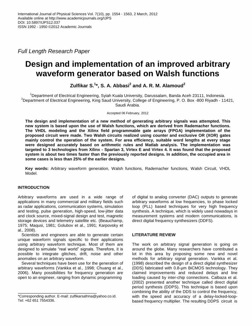
In the present work, we present an improved design based upon the use of Redemacher and Walsh functions. For area efficiency, optimized word lengths at every stage are carefully calculated. In addition, circuit is convert into VHDL code using IEEE standard VHDL synthesis package tool, which is state-of-the- art and has many advantages (www.doulos.com, 2012). IEEE STANDARD VHDL SYNTHESIS PACKAGE Some arithmetic operations in VHDL are performed easily in integer format. Therefore, we use standard package developed by IEEE DASC Synthesis Working Group (Numeric_std 1076.3) in order to convert numbers from/ to standard logic vector format.
The package defines numeric types and arithmetic functions which are used by synthesis tools. There are two numeric types: unsigned to represent unsigned numbers in vector form and signed to represent a signed number in vector form. This package is very useful for area optimization in circuit design (www.doulos.com, 2012).
Figure 1 shows conversion format from/to standard logic vector and standard integer. For example, a number X representing a 6-bit std logic vector, may be converted into integer (Y) and vice versa as follows: Y <= to_integer(signed(X)) X <= std_logic_vector(to_signed(X,6)) RADEMACHER AND WALSH FUNCTIONS Walsh functions, which are derived from Rademacher functions are found to be more appropriate for hardware implementation. The Rademacher functions are defined as follows (Beauchamp, 1975; Maqusi, 1981; Golubov et al., 1991; Karpovsky et al., 2008):
),22(sin),1( xSgnxn n n = 0,1,2,...0 x 1 (1)
Where 1,0 x and the signum function Sgn(y) is defined by:
0 , 1
0 , 1Sgn(y)
y
y
(2) The Walsh functions are defined in terms of product of Rademacher functions as (Beauchamp, 1975; Maqusi, 1981; Golubov et al., 1991; Karpovsky et al., 2008):
1556 Int. J. Phys. Sci.
Figure 1. Numeric standard conversions (www.doulos.com, 2012).
N
iinntitn i
0
}1,0{,),1(),(
(3)
N
ii
i nn0
2
(4) A signal x(t) of length N may be represented as a Walsh series given by (Beauchamp, 1975; Maqusi, 1981; Golubov et al., 1991; Karpovsky et al., 2008):
1
0
),()(N
nn tnAtx
(5)
The Walsh coefficients An are evaluated as (Beauchamp, 1975; Maqusi, 1981; Golubov et al., 1991; Karpovsky et al., 2008):
1
0
),(1 N
kkn tnx
NA
(6)
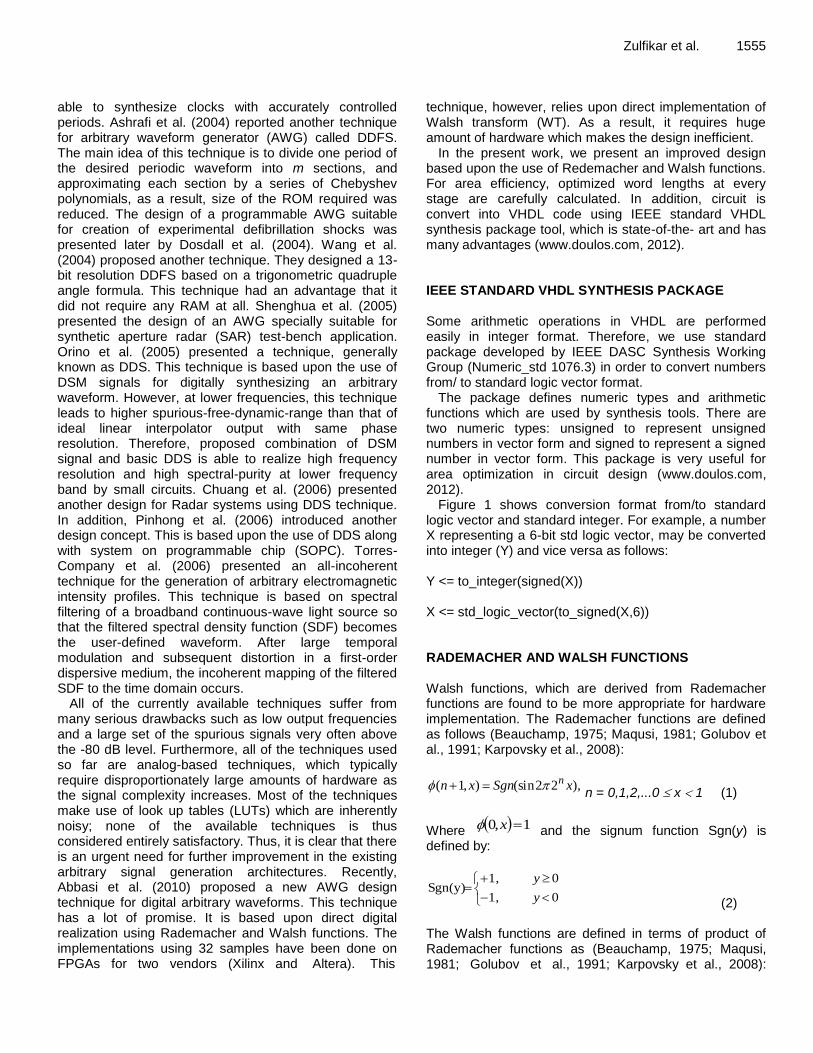
PROPOSED ARBITRARY WAVEFORM GENERATION SYSTEM The block diagram of an AWG of digital signals is shown in Figure 2. The design consists of some basic components like data buffer and output buffer, multiplexer and negative circuit. The design also contains embedded circuits such as an adder and an accumulator. The circuits are controlled by signal enter, reset (not shown), pass and clock. The signal “Enter” defines the instant input data entry. The “Reset” initializes the counters and the signal and “Pass” controls the availability of the result at the output ports. The proposed AWG circuit shown in Figure 2 consists of: (1) Negative circuit (WI bits) – One no. (2) Negative circuit (WO bits) – (N-1) nos. (3) Walsh circuit (N-1 order) – Two nos. (4) 2 to 1 multiplexer (WI bits) – (N-1) nos. (5) 2 to 1 multiplexer (WO bits) – (N-1) nos. (6) Data buffer (WI bits) – N nos. (7) Data buffer (WO bits) – N nos. (8) Output buffer (WI bits) – One no. (9) Accumulator (WO bits) – N nos. (10) Adder (WO bits) – (N-1) nos. VHDL modeling of the proposed architecture The proposed AWG block shown in Figure 2 can be realized and programmed using VHDL code. For convenience, the circuit and VHDL code viewed here are restricted to transform lengths (N=4) and word lengths of input data (WI=4 bits) only.
The circuit consists of negative circuits, which are based on 2’s
Zulfikar et al. 1557
Ne
ga
tive
Circu
it
Walsh
Circuits 1
Enter
X
Da
ta B
uffe
rs
Mu
ltip
lexe
rs
F0
F1
FN-1
.
.
.
.
.
.
M1
MN-1
Accu
mu
lato
rs
A0
A1
AN-1
.
.
.
Clock
H
Mu
ltip
lexe
rs .
.
.
.Ne
ga
tive
Circu
its
Ou
tpu
t
Bu
ffe
r. . .L1
LN-1
-A1
-AN-1
Da
ta B
uffe
rs
G0
GN-1
G1
G2.
.
.
Walsh
Circuits 2
Ad
de
r
N-1
Ad
de
r
1
Ad
de
r
2
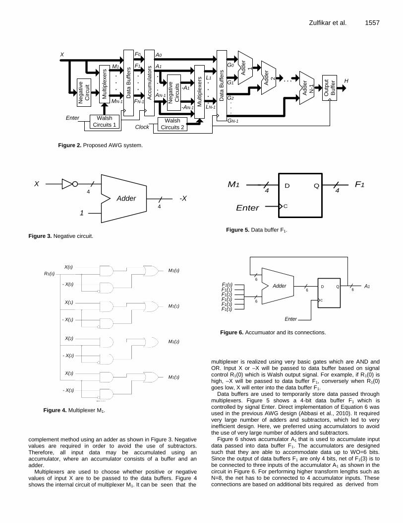
Figure 2. Proposed AWG system.
Adder
1
4
4
X
-X
Figure 3. Negative circuit.
X(0)
X(1)
X(2)
X(3)
- X(0)
- X(1)
- X(2)
- X(3)
M1(0)
M1(1)
M1(2)
M1(3)
R1(0)
Figure 4. Multiplexer M1.
complement method using an adder as shown in Figure 3. Negative values are required in order to avoid the use of subtractors. Therefore, all input data may be accumulated using an accumulator, where an accumulator consists of a buffer and an adder.
Multiplexers are used to choose whether positive or negative values of input X are to be passed to the data buffers. Figure 4 shows the internal circuit of multiplexer M1. It can be seen that the
Q
C
D
Enter
F1M14 4
Figure 5. Data buffer F1.
Q
C
DAdder
6
6
Enter
6A1F1(0)
F1(1)F1(2)F1(3)F1(3)F1(3)
6
Figure 6. Accumuator and its connections.
multiplexer is realized using very basic gates which are AND and OR. Input X or –X will be passed to data buffer based on signal control R1(0) which is Walsh output signal. For example, if R1(0) is high, –X will be passed to data buffer F1, conversely when R1(0) goes low, X will enter into the data buffer F1.
Data buffers are used to temporarily store data passed through multiplexers. Figure 5 shows a 4-bit data buffer F1 which is controlled by signal Enter. Direct implementation of Equation 6 was used in the previous AWG design (Abbasi et al., 2010). It required very large number of adders and subtractors, which led to very inefficient design. Here, we preferred using accumulators to avoid the use of very large number of adders and subtractors.
Figure 6 shows accumulator A1 that is used to accumulate input data passed into data buffer F1. The accumulators are designed such that they are able to accommodate data up to WO=6 bits. Since the output of data buffers F1 are only 4 bits, net of F1(3) is to be connected to three inputs of the accumulator A1 as shown in the circuit in Figure 6. For performing higher transform lengths such as N=8, the net has to be connected to 4 accumulator inputs. These connections are based on additional bits required as derived from
1558 Int. J. Phys. Sci.
Adder
1 Adder
2 Adder
3
6
6
6
6
6
G0
G1
6G2
6G3
Sum
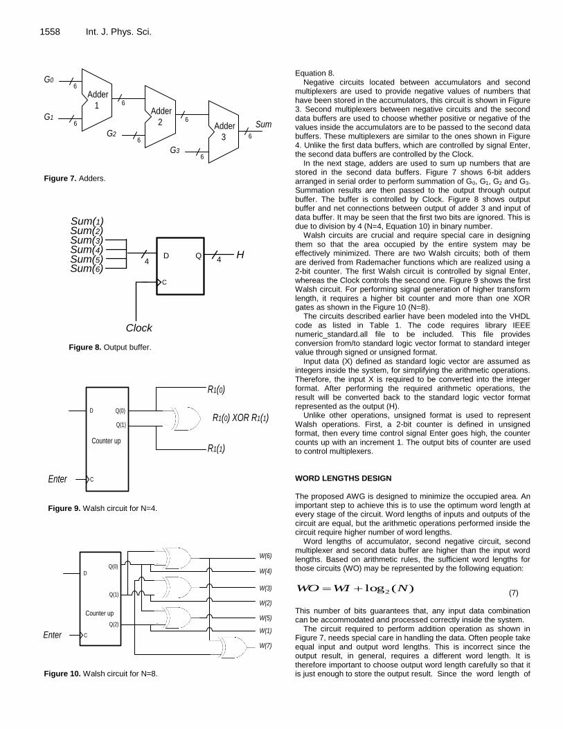
Figure 7. Adders.
Q
C
D4 4
H
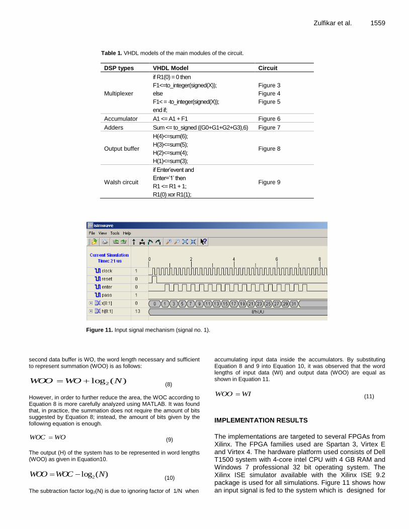
Sum(2)Sum(3)Sum(4)Sum(5)Sum(6)
Sum(1)
Clock
Figure 8. Output buffer.
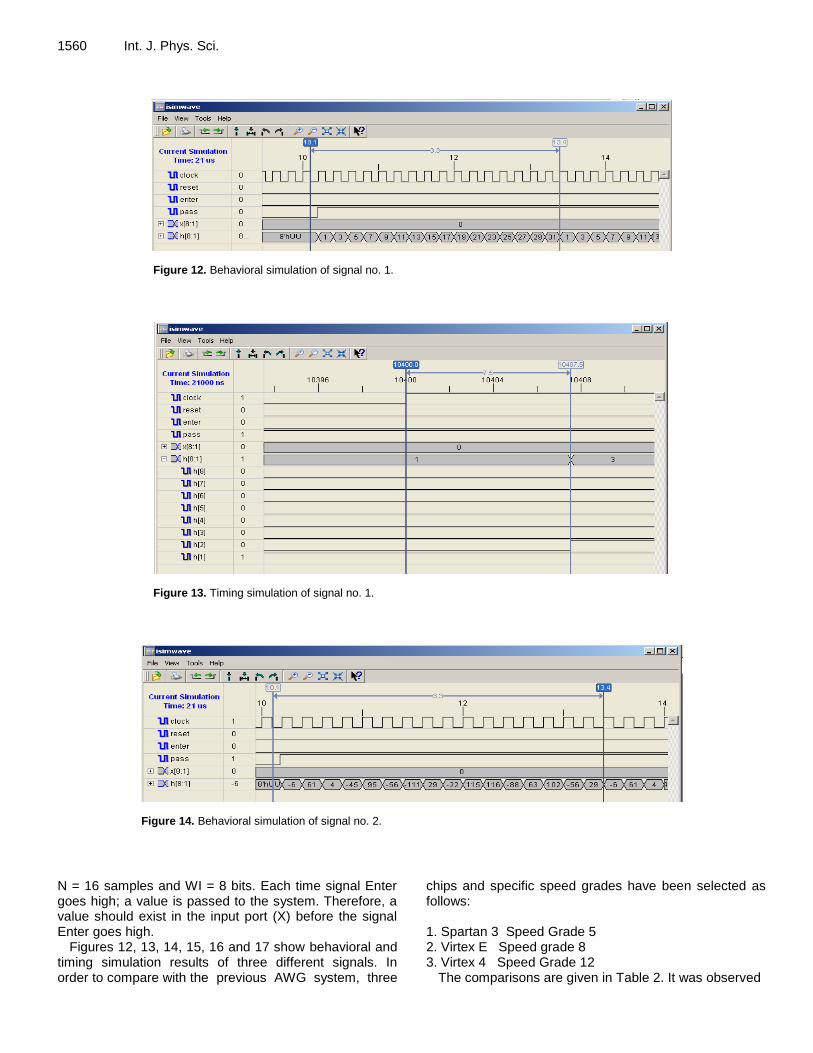
Counter up
C
Q(0)D
Q(1)
R1(0)
R1(0) XOR R1(1)
R1(1)
Enter
Figure 9. Walsh circuit for N=4.
Counter up
C
Q(0)D
Q(1)
W(6)
W(3)
W(5)
Enter
Q(2)
W(7)
W(4)
W(2)
W(1)
Figure 10. Walsh circuit for N=8.
Equation 8.
Negative circuits located between accumulators and second multiplexers are used to provide negative values of numbers that have been stored in the accumulators, this circuit is shown in Figure 3. Second multiplexers between negative circuits and the second data buffers are used to choose whether positive or negative of the values inside the accumulators are to be passed to the second data buffers. These multiplexers are similar to the ones shown in Figure 4. Unlike the first data buffers, which are controlled by signal Enter, the second data buffers are controlled by the Clock.
In the next stage, adders are used to sum up numbers that are stored in the second data buffers. Figure 7 shows 6-bit adders arranged in serial order to perform summation of G0, G1, G2 and G3. Summation results are then passed to the output through output buffer. The buffer is controlled by Clock. Figure 8 shows output buffer and net connections between output of adder 3 and input of data buffer. It may be seen that the first two bits are ignored. This is due to division by 4 (N=4, Equation 10) in binary number.
Walsh circuits are crucial and require special care in designing them so that the area occupied by the entire system may be effectively minimized. There are two Walsh circuits; both of them are derived from Rademacher functions which are realized using a 2-bit counter. The first Walsh circuit is controlled by signal Enter, whereas the Clock controls the second one. Figure 9 shows the first Walsh circuit. For performing signal generation of higher transform length, it requires a higher bit counter and more than one XOR gates as shown in the Figure 10 (N=8).
The circuits described earlier have been modeled into the VHDL code as listed in Table 1. The code requires library IEEE numeric_standard.all file to be included. This file provides conversion from/to standard logic vector format to standard integer value through signed or unsigned format.
Input data (X) defined as standard logic vector are assumed as integers inside the system, for simplifying the arithmetic operations. Therefore, the input X is required to be converted into the integer format. After performing the required arithmetic operations, the result will be converted back to the standard logic vector format represented as the output (H).
Unlike other operations, unsigned format is used to represent Walsh operations. First, a 2-bit counter is defined in unsigned format, then every time control signal Enter goes high, the counter counts up with an increment 1. The output bits of counter are used to control multiplexers. WORD LENGTHS DESIGN The proposed AWG is designed to minimize the occupied area. An important step to achieve this is to use the optimum word length at every stage of the circuit. Word lengths of inputs and outputs of the circuit are equal, but the arithmetic operations performed inside the circuit require higher number of word lengths.
Word lengths of accumulator, second negative circuit, second multiplexer and second data buffer are higher than the input word lengths. Based on arithmetic rules, the sufficient word lengths for those circuits (WO) may be represented by the following equation:
)(log2 NWIWO (7)
This number of bits guarantees that, any input data combination can be accommodated and processed correctly inside the system.
The circuit required to perform addition operation as shown in Figure 7, needs special care in handling the data. Often people take equal input and output word lengths. This is incorrect since the output result, in general, requires a different word length. It is therefore important to choose output word length carefully so that it is just enough to store the output result. Since the word length of
Zulfikar et al. 1559
Table 1. VHDL models of the main modules of the circuit.
DSP types VHDL Model Circuit
Multiplexer
if R1(0) = 0 then
F1<=to_integer(signed(X));
else
F1< = -to_integer(signed(X));
end if;
Figure 3
Figure 4
Figure 5
Accumulator A1 <= A1 + F1 Figure 6
Adders Sum <= to_signed ((G0+G1+G2+G3),6) Figure 7
Output buffer
H(4)<=sum(6);
H(3)<=sum(5);
H(2)<=sum(4);
H(1)<=sum(3);
Figure 8
Walsh circuit
if Enter’event and
Enter=’1’ then
R1 <= R1 + 1;
R1(0) xor R1(1);
Figure 9
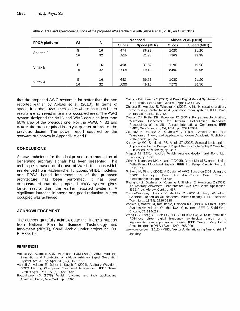
Figure 11. Input signal mechanism (signal no. 1).
second data buffer is WO, the word length necessary and sufficient to represent summation (WOO) is as follows:
)(log2 NWOWOO (8)
However, in order to further reduce the area, the WOC according to Equation 8 is more carefully analyzed using MATLAB. It was found that, in practice, the summation does not require the amount of bits suggested by Equation 8; instead, the amount of bits given by the following equation is enough.
WOWOC (9) The output (H) of the system has to be represented in word lengths (WOO) as given in Equation10.
)(log2 NWOCWOO (10)
The subtraction factor log2(N) is due to ignoring factor of 1/N when
accumulating input data inside the accumulators. By substituting Equation 8 and 9 into Equation 10, it was observed that the word lengths of input data (WI) and output data (WOO) are equal as shown in Equation 11.
WIWOO (11)
IMPLEMENTATION RESULTS
The implementations are targeted to several FPGAs from Xilinx. The FPGA families used are Spartan 3, Virtex E and Virtex 4. The hardware platform used consists of Dell T1500 system with 4-core intel CPU with 4 GB RAM and Windows 7 professional 32 bit operating system. The Xilinx ISE simulator available with the Xilinx ISE 9.2 package is used for all simulations. Figure 11 shows how an input signal is fed to the system which is designed for
1560 Int. J. Phys. Sci.
Figure 12. Behavioral simulation of signal no. 1.
Figure 13. Timing simulation of signal no. 1.
Figure 14. Behavioral simulation of signal no. 2.
N = 16 samples and WI = 8 bits. Each time signal Enter goes high; a value is passed to the system. Therefore, a value should exist in the input port (X) before the signal Enter goes high.
Figures 12, 13, 14, 15, 16 and 17 show behavioral and timing simulation results of three different signals. In order to compare with the previous AWG system, three
chips and specific speed grades have been selected as follows: 1. Spartan 3 Speed Grade 5 2. Virtex E Speed grade 8 3. Virtex 4 Speed Grade 12
The comparisons are given in Table 2. It was observed

Zulfikar et al. 1561
Figure 15. Timing simulation of signal no. 2.
Figure 16. Behavioral simulation of signal no. 3.
Figure 17. Timing simulation of signal no. 3.
1562 Int. J. Phys. Sci.
Table 2. Area and speed comparisons of the proposed AWG technique with (Abbasi et al., 2010) on Xilinx chips.
FPGA platform WI N Proposed Abbasi et al. (2010)
Slices Speed (MHz) Slices Speed (MHz)
Spartan 3 8 16 474 36.85 1020 21.20
16 32 1915 21.32 7263 12.39
Virtex E 8 16 498 37.57 1190 19.58
16 32 1905 19.19 8490 10.06
Virtex 4 8 16 482 86.89 1030 51.20
16 32 1890 49.18 7273 28.50
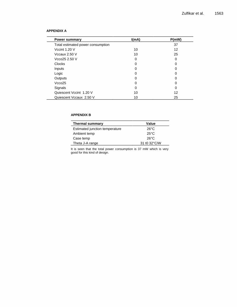
that the proposed AWG system is far better than the one reported earlier by Abbasi et al. (2010). In terms of speed, it is about two times faster where as much better results are achieved in terms of occupied area. The AWG system designed for N=16 and WI=8 occupies less than 50% area of the previous one. For the AWG, N=32 and WI=16 the area required is only a quarter of area of the previous design. The power report supplied by the software are shown in Appendix A and B.
CONCLUSIONS
A new technique for the design and implementation of generating arbitrary signals has been presented. This technique is based on the use of Walsh functions which are derived from Rademacher functions. VHDL modeling and FPGA based implementation of the proposed architecture has been performed. It has been demonstrated that the proposed AWG system gives better results than the earlier reported systems. A significant increase in speed and good reduction in area occupied was achieved. ACKNOWLEDGEMENT The authors gratefully acknowledge the financial support from National Plan for Science, Technology and Innovation (NPST), Saudi Arabia under project no. 09-ELE854-02. REFERENCES Abbasi SA, Alamoud ARM, Al Shahrani JM (2010). VHDL Modeling,
Simulation and Prototyping of a Novel Arbitrary Signal Generation System. Am. J. Eng. Appl. Sci., 3(4): 670-677.
Ashrafi A, Adhami R, Joiner L, Kaveh P (2004). Arbitrary Waveform DDFS Utilizing Chebyshev Polynomial Interpolation. IEEE Trans. Circuits Syst., Part-I, 51(8): 1468-1475.
Beauchamp KG (1975). Walsh functions and their applications. Academic Press, New York, pp. 5-132.
Calbaza DE, Savaria Y (2002). A Direct Digital Period Synthesis Circuit. IEEE Trans. Solid-State Circuits, 37(8): 1039-1045.
Chuang E, Hensley S, Wheeler K (2006). A highly capable arbitrary waveform generator for next generation radar systems. IEEE Proc. Aerospace Conf., pp. 7-13.
Dosdall DJ, Rothe DE, Sweeney JD (2004). Programmable Arbitrary Waveform Generator for Internal Defibrillation Research. Proceedings of the 26th Annual International Conference, IEEE EMBS, San Francisco, CA, USA., pp. 3971-3974.
Golubov B, Efimov A, Skvorstov V (1991). Walsh Series and Transforms: Theory and Applications. Kluwer Academic Publishers. Netherlands, p. 384.
Karpovsky MG, Stankovic RS, Astola JT (2008). Spectral Logic and Its Applications for the Design of Digital Devices. John Wiley & Sons Inc. Publication. New Jersey, pp. 36-71.
Maqusi M (1981). Applied Walsh Analysis.Heyden and Sons Ltd., London, pp. 3-50.
Orino Y, Kurosawa MK, Katagiri T (2005). Direct-Digital Synthesis Using Delta-Sigma Modulated Signals. IEEE Int. Symp. Circuits Syst., 2: 1706-1709.
Pinhong M, Ping L (2006). A Design of AWG Based on DDS Using the SOPC Technique. Proc. 4th Asia-Pacific Conf. Environ. Electromagnetics, pp. 610-615.
Shenghua Z, Dazhuan X, Xueming J, Shishan Z, Hongrong Z (2005). An Arbitrary Waveform Generator for SAR Test-Bench Application. IEEE Proc. Microw. Conf., p. 487.
Torres-Company, Lancis V, Andrés P (2006).Arbitrary Waveform Generator Based on All-Incoherent Pulse Shaping. IEEE Photonics Tech. Lett., 18(24): 2626-2628.
Vankka J, Waltari M, KosunenM, Halonen KAI (1998). A Direct Digital Synthesizer with an On-chip D/A- Converter. IEEE J. Solid-State Circuits, 33: 218-227.
Wang CC, Tseng YL, She HC, Li CC, Hu R (2004). A 13-bit resolution ROM-less direct digital frequency synthesizer based on a trigonometric quadruple angle formula. IEEE Trans. Very Large Scale Integration (VLSI) Syst., 12(9): 895-900.
www.doulos.com (2012) - VHDL Vector Arithmetic using Nueric_std, 9th
January.
Zulfikar et al. 1563
APPENDIX A
Power summary I(mA) P(mW)
Total estimated power consumption 37
Vccint 1.20 V 10 12
Vccaux 2.50 V 10 25
Vcco25 2.50 V 0 0
Clocks 0 0
Inputs 0 0
Logic 0 0
Outputs 0 0
Vcco25 0 0
Signals 0 0
Quiescent Vccint 1.20 V 10 12
Quiescent Vccaux 2.50 V 10 25
APPENDIX B
Thermal summary Value
Estimated junction temperature 26°C
Ambient temp 25°C
Case temp 26°C
Theta J-A range 31 t0 32°C/W
It is seen that the total power consumption is 37 mW which is very good for this kind of design.