Defect behavior in aluminum interconnect lines deformed thermomechanically by cyclic joule heating
8
Defect behavior in aluminum interconnect lines deformed thermomechanically by cyclic joule heating Roy H. Geiss * , David T. Read Materials Reliability Division, National Institute of Standards and Technology, 325 Broadway, Boulder, CO 80305, USA Received 1 December 2006; received in revised form 11 September 2007; accepted 17 September 2007 Available online 26 November 2007 Abstract Al–1wt.% Si lines were deformed thermomechanically by cyclic joule heating induced by applying an AC current. Scanning elec- tron microscopy revealed arrays of wavelike surface intrusions/extrusions aligned along low-index crystallographic directions after a few thousand thermal cycles. Transmission electron microscopy observations of cross-sections of selected regions shows that in grains that developed intrusions/extrusions, dislocations nucleated at the film–substrate interface, glided to the surface, and escaped. The densities of dislocations and prismatic loops observed here are similar to those observed in mechanical fatigue experiments on bulk aluminum. Published by Elsevier Ltd on behalf of Acta Materialia Inc. Keywords: Aluminum; Dislocations; Fatigue; TEM; Thin films 1. Introduction Interest in the reliability of thin-film metal lines on sili- con substrates arises because narrow lines of physical vapor deposition (PVD) aluminum and electrodeposited copper are widely used to form interconnect structures in ultra large scale integration (ULSI) microchips. While the lines studied in this work are not buried in dielectric like most interconnects, the test techniques and failure mecha- nisms explored here may provide useful information for designers of future interconnect structures. Scanning electron microscopy (SEM) showed that arrays of wavelike surface features were generated when passing low-frequency, high-density AC through long nar- row lines of thin-film aluminum [1–3]. However, in those works the specific mechanism by which the surface features were formed was not discussed. It should be noted that similar wavelike surface features have been observed in sev- eral studies of copper films subjected to AC current and attributed to thermomechanical or AC fatigue [4–6]. Here also there were no discussions detailing the mechanism by which the surface features were formed. Surface features that result from cyclic mechanical strain are well documented in research on the mechanics of fati- gue deformation in both thin films and bulk specimens. Almost all of the studies have been done on copper [7,8]. Schwaiger et al. [9] studied mechanical fatigue of polycrys- talline copper films of various thicknesses on polyimide substrates. They observed extrusions on the film surfaces and voids at the film–substrate interface, and described transmission electron microscopy (TEM) investigations that showed that no long-range dislocation structures developed during fatigue. Probably the best classic example of the extrusion/intrusion surface structure resulting from fatigue in a bulk material was given by Basinski and Basin- ski [10]. Cord and tweed surface structures were described by Videm and Ryum in cyclically deformed [0 0 1] alumi- num single crystals [11]. Some previous reports of TEM observations on ther- mally cycled aluminum thin films are available. Legros et al. [12,13] reported TEM observations of dislocation 1359-6454/$30.00 Published by Elsevier Ltd on behalf of Acta Materialia Inc. doi:10.1016/j.actamat.2007.09.033 * Corresponding author. Tel.: +1 303 497 4367; fax: +1 303 497 5030. E-mail address: [email protected] (R.H. Geiss). www.elsevier.com/locate/actamat Available online at www.sciencedirect.com Acta Materialia 56 (2008) 274–281
Transcript of Defect behavior in aluminum interconnect lines deformed thermomechanically by cyclic joule heating

Available online at www.sciencedirect.com
www.elsevier.com/locate/actamat
Acta Materialia 56 (2008) 274–281
Defect behavior in aluminum interconnect lines deformedthermomechanically by cyclic joule heating
Roy H. Geiss *, David T. Read
Materials Reliability Division, National Institute of Standards and Technology, 325 Broadway, Boulder, CO 80305, USA
Received 1 December 2006; received in revised form 11 September 2007; accepted 17 September 2007Available online 26 November 2007
Abstract
Al–1wt.% Si lines were deformed thermomechanically by cyclic joule heating induced by applying an AC current. Scanning elec-tron microscopy revealed arrays of wavelike surface intrusions/extrusions aligned along low-index crystallographic directions after afew thousand thermal cycles. Transmission electron microscopy observations of cross-sections of selected regions shows that in grainsthat developed intrusions/extrusions, dislocations nucleated at the film–substrate interface, glided to the surface, and escaped. Thedensities of dislocations and prismatic loops observed here are similar to those observed in mechanical fatigue experiments on bulkaluminum.Published by Elsevier Ltd on behalf of Acta Materialia Inc.
Keywords: Aluminum; Dislocations; Fatigue; TEM; Thin films
1. Introduction
Interest in the reliability of thin-film metal lines on sili-con substrates arises because narrow lines of physicalvapor deposition (PVD) aluminum and electrodepositedcopper are widely used to form interconnect structures inultra large scale integration (ULSI) microchips. While thelines studied in this work are not buried in dielectric likemost interconnects, the test techniques and failure mecha-nisms explored here may provide useful information fordesigners of future interconnect structures.
Scanning electron microscopy (SEM) showed thatarrays of wavelike surface features were generated whenpassing low-frequency, high-density AC through long nar-row lines of thin-film aluminum [1–3]. However, in thoseworks the specific mechanism by which the surface featureswere formed was not discussed. It should be noted thatsimilar wavelike surface features have been observed in sev-eral studies of copper films subjected to AC current and
1359-6454/$30.00 Published by Elsevier Ltd on behalf of Acta Materialia Inc
doi:10.1016/j.actamat.2007.09.033
* Corresponding author. Tel.: +1 303 497 4367; fax: +1 303 497 5030.E-mail address: [email protected] (R.H. Geiss).
attributed to thermomechanical or AC fatigue [4–6]. Herealso there were no discussions detailing the mechanismby which the surface features were formed.
Surface features that result from cyclic mechanical strainare well documented in research on the mechanics of fati-gue deformation in both thin films and bulk specimens.Almost all of the studies have been done on copper [7,8].Schwaiger et al. [9] studied mechanical fatigue of polycrys-talline copper films of various thicknesses on polyimidesubstrates. They observed extrusions on the film surfacesand voids at the film–substrate interface, and describedtransmission electron microscopy (TEM) investigationsthat showed that no long-range dislocation structuresdeveloped during fatigue. Probably the best classic exampleof the extrusion/intrusion surface structure resulting fromfatigue in a bulk material was given by Basinski and Basin-ski [10]. Cord and tweed surface structures were describedby Videm and Ryum in cyclically deformed [001] alumi-num single crystals [11].
Some previous reports of TEM observations on ther-mally cycled aluminum thin films are available. Legroset al. [12,13] reported TEM observations of dislocation
.

R.H. Geiss, D.T. Read / Acta Materialia 56 (2008) 274–281 275
behavior in passivated aluminum films strained by ther-mal cycling between room temperature and 450 �C. Theyobserved a decrease in the dislocation density and anincrease in the grain size with the number of cycles. Aconvergent-beam electron diffraction (CBED) study ofstrains in cross-section samples of Al film cycled approx-imately 10 times between 150 and 250 �C showed largevariations in the strains generated both within grains aswell as from grain to grain [14]. TEM studies of the typ-ical dislocation structures of tangles and cell walls thatresult from uniaxial fatigue of bulk polycrystalline alumi-num have also been described in the literature [15,16]. Acombined TEM/focused ion beam (FIB) study of fatiguedthin copper films [17] reported that when the film thick-ness was less than 1 lm, with correspondingly smallgrains, tangled dislocation structures were replaced byindividual dislocations.
A combined SEM and EBSD analysis of grain growthand rotation under AC fatigue as used here was reportedby Keller et al. [18]. The grains that grew and rotated werethe same ones that showed the most pronounced surfaceintrusions/extrusions.
In this paper we describe what we believe to be the firstdetailed analysis of dislocations and vacancies resultingfrom AC fatigue of thin aluminum lines. We interpret theSEM and TEM observations to establish the mechanismof the deformation and to relate it to known effects inmechanical fatigue tests of bulk materials.
2. Experimental
The samples were patterns developed originally for elec-tromigration studies. The aluminum films were fabricatedby PVD of Al–1wt.% Si onto oxidized silicon wafers. Theline patterns plus test pads were fabricated in a photolitho-graphic process. The dimensions of the lines were 3.3 lmwide by 800 lm long and 450 nm thick (see Fig. 1).
Application of the AC testing technique to interconnectlines has been discussed in detail [3,4,19]. Here we used the
Fig. 1. Typical patterned aluminum sample used in the AC tests. The aluminumcontact pads are labeled C and V, respectively. The substrate is oxidized silico
same experimental approach. The four test pads associatedwith each line, defined in Fig. 1, were used for electricalcontacts. AC was applied at 100 Hz with an amplitude of220 mA, resulting in a current density of 14.8 MA cm�2.DC resistance measurements on similar lines indicated thatthe maximum temperature range was about 220 �C. TheAC testing was done with the chip at room temperature(20 �C), suggesting that the maximum temperature in theline reached approximately 240 �C. Because the coefficientsof thermal expansion (CTE) of aluminum and silicon arequite different, with aAl = 2.31 · 10�5 K�1 and aSi = 2.6 ·10�6 K�1, this temperature change, DT, imposes a signifi-cant biaxial strain, De = DT Æ Da, of approximately 0.3%on the aluminum line. The data reported in this paper wereobtained from a sample that was cycled for 40 s, resultingin 8 · 103 temperature cycles. Under these testing condi-tions, the lines typically exhibit a lifetime (to open circuit)of approximately 1.2 · 105 cycles.
After 8 · 103 cycles, the line exhibited some regions withsurface extrusions/intrusions as well as regions with noobvious surface damage. A cross-section including bothintrusions/extrusions and undeformed regions was pre-pared for TEM by focused-ion-beam (FIB) milling. TEMwas done at 200 kV using a LaB6 gun and a double-tiltgoniometer sample holder. Images were collected with a 1Mpixel CCD camera.
Dislocation densities were obtained from a number ofmicrographs by digitally measuring the total length of dis-location lines visible and calculating the length per unit vol-ume. The dislocation densities given are a lower boundsince we did not do a complete diffraction vector analysisof every region. Prismatic dislocation loops were alsoobserved; their densities were obtained by digitally definingthe visible loops in a micrograph and obtaining the meandiameter and total number of loops in each micrograph.Again, the densities given are a lower bound. Artifactsfrom the FIB milling were handled by utilizing the differ-ence between tested and untested lines, both prepared byFIB milling.
line is 800 lm long by 3.3 lm wide and 450 nm thick. Current and voltagen/silicon.

276 R.H. Geiss, D.T. Read / Acta Materialia 56 (2008) 274–281
3. Results
The SEM and the companion EBSD inverse pole figureimages of a plan section including both intrusions/extru-sions and undeformed regions before FIB milling areshown in Fig. 2 with the FIB section outlined. The EBSDdata (Fig. 2b) show that the region with the intrusions/extrusions is a single grain. The orientation matrix for thisgrain was determined by EBSD to be
G ¼0:6958 0:0382 0:7173
0:5648 0:6460 �0:5135
�0:4437 0:7624 0:4710
264
375 ð1Þ
where the column [�0.0382,0.6460,0.7624] that can bereduced to [�11619] corresponds to the crystallographicdirection along the line, which is 5.4� from [011]. ThisEBSD orientation was confirmed with TEM by selectedarea diffraction from the same region.
Fig. 3 is a bright-field TEM image of a grain that showsno surface intrusions/extrusions in either plan view SEM orcross-section TEM images. The image shows dislocationsmost likely of edge type with b ¼ ½101� on the (�111) slipplane. The visible dislocation density in this micrograph is
Fig. 2. SEM and EBSD images of the region of the test sample prepared for Tsurface protrusions and a rectangle depicting the approximate FIB cut; (b) thedirection (RD), from the same area showing that the region with the protrusionslightly different orientation and shows very little surface deformation. The co
Fig. 3. Cross-section TEM image from grain 14 in Fig. 2. The dislocations in thg are assumed to be edge dislocations. The tiny dots are thought to be prismatthe sample preparation. The mean loop diameter is around 8.4 nm and the lo
7.9 · 1013 m�2. Other regions examined showed visible dis-location densities that ranged from 5.4 · 1013 m�2 to8.4 · 1013 m�2. Many of the dislocations exhibit bowingthat corresponds to a residual stress in the films. The meanvalue for this stress was about 25 MPa, which was calcu-lated from measurements of the radius of curvature ofbowed dislocations using the expression r = Gb/2R, wherer is the residual stress on a bowed dislocation, G = 26 GPais the shear modulus for Al, b = 0.286 nm is the Burgersvector, and R is the radius of curvature for the bowed dis-locations (nm), which had a mean value of 153 nm for 25measurements.
Fig. 4 is a weak-beam dark-field (WBDF) image withg = [022] from a segment of the grain that showed the sur-face protrusions. The thickness of the TEM section wasdetermined to be approximately 140 nm by use of theCBED technique described in [20,21] and the simulationsoftware given by De Graef [22]. An aluminum oxide film�15 nm thick was found on the surface of the tested lines.
The dislocation density here is very high, 8.4 · 1013 m�2.However, the dislocations are not distributed as uniformlyas those in Fig. 3, but are concentrated at the aluminum/silicon oxide interface and bowed away from the interface,suggesting that they could have been nucleated there. For
EM that were taken before the FIB cut: (a) the SEM image showing theEBSD map, colored according to an inverse pole figure (IPF) in the rollings is a single grain, denoted 11. The large grain next to it, denoted 14, has alor depicts grains having different orientations.
e figure are uniformly distributed and the dislocation lines perpendicular toic dislocation loops which are mostly the result of Ga+ ion damage duringop density is about 9.7 · 1020 m�3.
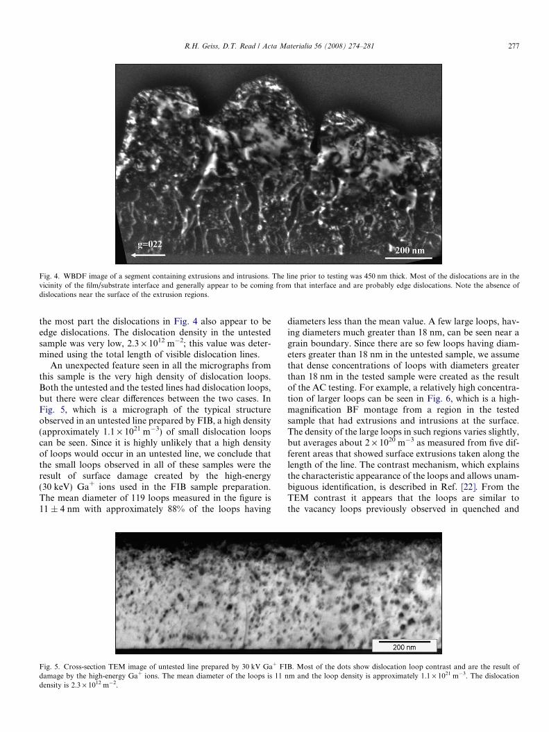
Fig. 4. WBDF image of a segment containing extrusions and intrusions. The line prior to testing was 450 nm thick. Most of the dislocations are in thevicinity of the film/substrate interface and generally appear to be coming from that interface and are probably edge dislocations. Note the absence ofdislocations near the surface of the extrusion regions.
R.H. Geiss, D.T. Read / Acta Materialia 56 (2008) 274–281 277
the most part the dislocations in Fig. 4 also appear to beedge dislocations. The dislocation density in the untestedsample was very low, 2.3 · 1012 m�2; this value was deter-mined using the total length of visible dislocation lines.
An unexpected feature seen in all the micrographs fromthis sample is the very high density of dislocation loops.Both the untested and the tested lines had dislocation loops,but there were clear differences between the two cases. InFig. 5, which is a micrograph of the typical structureobserved in an untested line prepared by FIB, a high density(approximately 1.1 · 1021 m�3) of small dislocation loopscan be seen. Since it is highly unlikely that a high densityof loops would occur in an untested line, we conclude thatthe small loops observed in all of these samples were theresult of surface damage created by the high-energy(30 keV) Ga+ ions used in the FIB sample preparation.The mean diameter of 119 loops measured in the figure is11 ± 4 nm with approximately 88% of the loops having
Fig. 5. Cross-section TEM image of untested line prepared by 30 kV Ga+ FIdamage by the high-energy Ga+ ions. The mean diameter of the loops is 11 ndensity is 2.3 · 1012 m�2.
diameters less than the mean value. A few large loops, hav-ing diameters much greater than 18 nm, can be seen near agrain boundary. Since there are so few loops having diam-eters greater than 18 nm in the untested sample, we assumethat dense concentrations of loops with diameters greaterthan 18 nm in the tested sample were created as the resultof the AC testing. For example, a relatively high concentra-tion of larger loops can be seen in Fig. 6, which is a high-magnification BF montage from a region in the testedsample that had extrusions and intrusions at the surface.The density of the large loops in such regions varies slightly,but averages about 2 · 1020 m�3 as measured from five dif-ferent areas that showed surface extrusions taken along thelength of the line. The contrast mechanism, which explainsthe characteristic appearance of the loops and allows unam-biguous identification, is described in Ref. [22]. From theTEM contrast it appears that the loops are similar tothe vacancy loops previously observed in quenched and
B. Most of the dots show dislocation loop contrast and are the result ofm and the loop density is approximately 1.1 · 1021 m�3. The dislocation
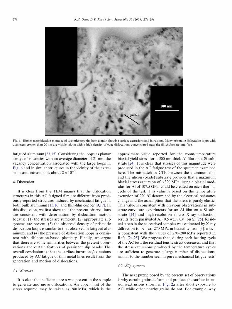
Fig. 6. Higher-magnification montage of two micrographs from a grain showing surface extrusions and intrusions. Many prismatic dislocation loops withdiameters greater than 20 nm are visible, along with a high density of edge dislocations concentrated near the film/substrate interface.
278 R.H. Geiss, D.T. Read / Acta Materialia 56 (2008) 274–281
fatigued aluminum [23,15]. Considering the loops as planararrays of vacancies with an average diameter of 21 nm, thevacancy concentration associated with the large loops inFig. 6 and in similar structures in the vicinity of the extru-sions and intrusions is about 2 · 10�5.
4. Discussion
It is clear from the TEM images that the dislocationstructures in this AC fatigued film are different from previ-ously reported structures induced by mechanical fatigue inboth bulk aluminum [15,16] and thin-film copper [9,17]. Inthis discussion, we first show that the present observationsare consistent with deformation by dislocation motionbecause: (1) the stresses are sufficient; (2) appropriate slipsystems are present; (3) the observed density of prismaticdislocation loops is similar to that observed in fatigued alu-minum; and (4) the presence of dislocation loops is consis-tent with dislocation-based plasticity. Finally, we arguethat there are some similarities between the present obser-vations and certain features of persistent slip bands. Theoverall conclusion is that the surface intrusions/extrusionsproduced by AC fatigue of thin metal lines result from thegeneration and motion of dislocations.
4.1. Stresses
It is clear that sufficient stress was present in the sampleto generate and move dislocations. An upper limit of thestress required may be taken as 280 MPa, which is the
approximate value reported for the room-temperaturebiaxial yield stress for a 500 nm thick Al film on a Si sub-strate [24]. It is clear that stresses of this magnitude wereproduced in the AC fatigue test of the specimen examinedhere. The mismatch in CTE between the aluminum filmand the silicon (oxide) substrate provides that a maximumbiaxial stress excursion of �320 MPa, using a biaxial mod-ulus for Al of 107.5 GPa, could be created on each thermalcycle of the test. This value is based on the temperatureexcursion of 220 �C determined by the electrical resistancechange and the assumption that the stress is purely elastic.This value is consistent with previous observations in sub-strate-curvature experiments for an Al film on a Si sub-strate [24] and high-resolution micro X-ray diffractionresults from passivated Al (0.5 wt.% Cu) on Si [25]. Resid-ual stress in the as-received samples was estimated by X-raydiffraction to be near 270 MPa in biaxial tension [3], whichis consistent with the values of 230–280 MPa reported inRefs. [24,25]. We propose that, during each heating cycleof the AC test, the residual tensile stress decreases, and thatthe stress excursions produced by the temperature cyclesare sufficient to generate a large number of dislocations,similar to the number seen in pure mechanical fatigue tests.
4.2. Slip systems
The next puzzle posed by the present set of observationsis why certain grains deform and produce the surface intru-sions/extrusions shown in Fig. 2a after short exposure toAC, while other nearby grains do not. For example, why

R.H. Geiss, D.T. Read / Acta Materialia 56 (2008) 274–281 279
did the grain shown in Fig. 4 show extrusions/intrusionswhile the grain in Fig. 3 did not, even though they are adja-cent to each other (grains 14 and 11, respectively, inFig. 2b). A naıve expectation might be that some grainsare oriented favorably for single slip of dislocations, drivenby the thermomechanical stress along the line axis, whileother grains are less favorably oriented for single slip. Butthe orientations of the grains examined in the present studyof regularly spaced linear surface intrusions/extrusions ori-ented perpendicular to the line axis were measured unam-biguously by EBSD, and were found to be inconsistentwith this expectation. The reasoning is that in the deformedgrain in Fig. 2 the line direction is near [011] and the surfacenormal is near [111]; therefore the direction parallel to theextrusions is near [211], which does not include traces fromany of the possible (111) slip planes. Consequently, theresolved shear stress for single slip is not the appropriatevariable to consider as the effective driving force for disloca-tion motion for the present case, although single slip may bepossible in regions with different crystallographic orienta-tions, such as the one pictured in Fig. 1 in Ref. [1].
Cheng and Laird [26] studied mechanical fatigue in cop-per crystals with various orientations deformed under uni-axial stress. They found that single slip occurred for someorientations of the stress, while double slip occurred for oth-ers, and they developed a criterion for double slip. TheCheng and Laird findings cannot be applied directly tothe present case because the stress in the present case wasnot uniaxial, but rather biaxial, because it arose from differ-ential thermal expansion. Finite element modeling (FEM)calculations for the line-on-substrate system, with theappropriate thickness-to-width ratio, show that the stressin the present case is biaxial over most of the line width,with the stress component across the line equal to about60% of the stress component along the line. Calculationsof the total resolved shear stress (RSS) resulting from thisbiaxial stress in grains 11 and 14 of Fig. 2 show that the(111)[10 1] and the (111)[1 10] slip systems have aboutequal RSS on them, but that the RSS on the relatively unde-formed grain (grain 14 in Fig. 2) is 10–15% less than that ingrain 11, which showed clear surface intrusions/extrusions.This is consistent with the findings of Cheng and Laird [26],who proposed that multiple slip will occur only if the ratioof Schmid factors on the considered slip systems is greaterthan 0.9. It is interesting to note that if only uniaxial stressalong the line is considered then the RSS numbers reverseand grain 14 should have shown intrusions/extrusionsbefore grain 11. Thus we conclude that the biaxial stresspredicted by the FEM model does apply, and that thosegrains with the highest biaxial RSS were indeed the grainsthat initially showed surface intrusions/extrusions.
4.3. Prismatic loops
A prismatic dislocation loop density of about 1021 m�3
was reported for 99.995% Al quenched from 600 �C to icedbrine by Hirsch et al. [23]. Considering the average loop
diameter to be 20 nm, this density translated to a vacancyconcentration of approximately 10�4, which is approxi-mately the saturation concentration calculated at 600 �Cfrom thermodynamic considerations. The equivalentvacancy concentrations in the present specimens are muchlower. On the other hand, Segall and Partridge [15]reported prismatic loop densities of 5 · 1020 m�3 in thin99.99% Al sheet specimens fatigued by reverse bending.This value is very close to our measured value for the den-sity of the large loops of 2 · 1020 m�3 in areas showing sur-face extrusions. Since Segall and Partridge obtained theirdata in a mechanical fatigue experiment, the similarity ofthese results suggests that the AC test conducted here isrelated to mechanical fatigue testing.
The observation that loops are still present in the spec-imen after the test allows us to estimate that the maximumtemperature was certainly less than 325 �C. This limitingvalue was determined by extrapolating the data of Silcoxand Whelan [27] to determine that dislocation loops in alu-minum would disappear at about 325 �C in 0.005 s, thetime per cycle at 200 Hz.
This value of the maximum temperature implies that thevacancies are generated by dislocation activity, rather thanpurely thermal processes, as follows. If we consider thatvacancies were generated only by thermal processes andthat the maximum temperature reached by the line duringthe thermal fatigue was less than 325 �C, the vacancy con-centration would be �2.7 · 10�6, which is approximately afactor of 100 below the measured concentration. The crea-tion of vacancies by moving dislocations is well established[28–30]. Under the temperature cycles associated with theAC test, the vacancies can diffuse short distances and coa-lesce to form the loops [31].
Thus we conclude that the bulk of the vacancies are gen-erated by dislocation activity, both as glide debris and asthe result of intersections.
4.4. Comparison and contrast with persistent slip bands
Because persistent slip bands (PSB) are characteristic ofsome fatigue processes in fcc metals, and because PSBs areused to explain the surface intrusions/extrusions observedin those experiments [10,33–35], it is of interest to compareand contrast the present results with PSBs. Initial examina-tion of the TEM micrographs reveals no features character-istic of PSBs. Figs. 3 and 6, which are bright-field imagesrepresentative of the dislocation structures in regions with-out and with extrusions/intrusions, respectively, show adistribution of dislocations similar to what might beobserved in Stage I deformation of a fcc single crystal.They do not show, however, the matrix channel-veinand/or the PSB ladder-like structure associated with intru-sions/extrusions in fatigued metals [34,36]. In Fig. 6, and inthe WBDF Fig. 4, from regions showing surface extrusionsand intrusions, the visible dislocations are not uniformlydistributed but concentrated near the film/substrate inter-face compared with the more uniform distribution seen in

Fig. 7. Low-magnification montage showing the extrusions and intrusions at the specimen surface. A horizontal line is drawn at 450 nm, the originalsample thickness, to provide a guide for visualizing the extent of the extrusions and intrusions. The extrusion marked A is discussed in the text.
280 R.H. Geiss, D.T. Read / Acta Materialia 56 (2008) 274–281
Fig. 3. Careful measurement shows the dislocation densityto be similar in both Figs. 3 and 6 with a value of approx-imately 1.6 · 1014 m�2, which is much higher than wouldbe expected in Stage I deformation. This value is, however,within an order of magnitude of the value of 1015 m�2 pro-posed by Grosskreutz and Mughrabi [32] for the disloca-tion density in PSB walls.
Although the film does not exhibit the typical PSB andchannel-vein structure seen in fatigued bulk specimens,the general appearance and size scale of the extrusionsand intrusions is similar to that modeled by Brinckmannand Van der Giessen [33], and as such suggests that similardislocation activity might be involved. An estimate of thenumber of dislocations required to form a surface extru-sion of the height observed, considering a distribution ofslip bands like that postulated by Brinckmann [34], showsthat about one dislocation must exit the surface for everytwo fatigue cycles. This is consistent with the value ofabout one Burgers vector per cycle inferred by Basinskiand Basinski [10,35].
Consider the extrusion labeled A in Fig. 7 to be rectan-gular with height 100 nm and width 200 nm. If we assumethis extrusion is the result of escaping edge dislocationswith a [110] Burgers vector, b ¼ 0:286nm, on parallel(111) glide planes that are 70b ¼ 20nm apart, followingGrosskreutz and Mughrabi [32], approximately 3500dislocations ((100 nm/0.286 nm) · (200 nm/20 nm) = 3500)would have to escape from the surface to account for the100 nm height of the 200 nm wide extrusion. Considering8000 fatigue cycles, this reduces to about one dislocationevery two fatigue cycles.
We also found that EBSD patterns from grains with sur-face intrusions/extrusions have a higher image quality fac-tor than grains without, indicating less variable elasticstrain. This is due to lower dislocation content, and is con-sistent with our hypothesis that many dislocations haveexited the surface in the extruded regions. This is consistentwith the TEM observations of lower dislocation contentnear the surface of the extrusions as seen in Fig. 6.
The overall picture that emerges is that the surface intru-sions/extrusions discussed here are clearly not PSBs sincethe matrix vein and PSB ladder structures are not presenthere. Another difference is that the surface intrusions/extrusions observed here occurred after fewer than 104 fati-gue cycles, while PSBs typically occur after 105 cycles. On
the other hand, this AC fatigue experiment does have cer-tain features in common with PSBs. Specifically, weobserve regions where many dislocations escaped the spec-imen surface, leaving behind intrusions/extrusions, and wealso observe adjacent regions with dislocation density equalto, within an order of magnitude, the dislocation density inthe walls within PSBs.
5. Summary and conclusions
We have shown that a very high density of dislocationsexists in films subjected to AC fatigue. They are generatedby stresses that result from the difference in the CTEbetween the aluminum film and the silicon substrate, mostlikely at the film substrate interface. The stress system isbiaxial, with the major component along the length ofthe line. The grains that show intrusions/extrusions are ori-ented such that they have the highest resolved shear stressesin the available double-slip systems, providing the mecha-nism for the dislocations to glide to and exit from the sur-face. Along with the dislocations, there is a moderatedensity of prismatic dislocation loops. Their presence isconsistent with the dislocation mechanism and providesan upper limit to the temperature, but does not contributeto the deformation. The TEM observations reported hereconfirm that the regular wavelike surface features producedby AC fatigue are a result of dislocation motion, ratherthan any purely thermal process like mass diffusion or localmelting.
Acknowledgements
We are grateful to the NIST Office of MicroelectronicsPrograms for support. We thank D.S. Finch (AISthesis,LLC) for preparation of TEM specimens by FIB, andacknowledge discussions with R.R. Keller and experimen-tal measurements by Y. Cheng. This work is a contributionof the US Department of Commerce and is not subject tocopyright in the USA.
References
[1] Geiss RH, Roshko A, Bertness KA, Keller RR. Electron microscopy:its role in materials science. TMS symposia, San Diego, CA; 2003.p. 329.
R.H. Geiss, D.T. Read / Acta Materialia 56 (2008) 274–281 281
[2] Philofsky E, Ravi K, Hall E, Black J. Ninth annual proceedings ofreliability physics. New York: IEEE; 1971. p. 120.
[3] Keller RR, Monig R, Volkert CA, Arzt E, Schwaiger R, Kraft O.Stress-induced phenomena in metallization: 6th international work-shop. New York: AIP; 2002. p.119.
[4] Monig R. Ph.D. thesis, Max-Planck-Institut fur Metallforschlung,Stuttgart; 2004.
[5] Park YB, Monig R, Volkert CA. Thin Solid Films 2006;504:321.[6] Zhang GP, Monig R, Park YB, Volkert CA. Proceedings of the 6th
international conference on electronic packaging technology. NewYork: IEEE; 2005. p.653.
[7] Mughrabi H. In: Haasen P et al., editors. Proceedings of theinternational conference on strength of metals and alloys. Aachen(Oxford): Pergamon Press; 1979. p. 1615.
[8] Mughrabi H. Phil Mag 2004;84:259.[9] Schwaiger R, Dehm G, Kraft O. Phil Mag 2003;83:693.
[10] Basinski ZS, Basinski SJ. Progr Mater Sci 1992;36:89.[11] Videm M, Ryum N. Mater Sci Eng 1996;A219:1.[12] Legros M, Dehm G, Balk TJ, Arzt E, Bostrom RO, Gergaud P, et al.
Mater Res Soc Symp Proc 2003;779:W4.2.[13] Legros M, Dehm G, Balk TJ. Mater Res Soc Proc 2005;875:O9.1.[14] Nucci J, Kramer S, Arzt E, Volkert CA. J Mater Res 2005;20:1851.[15] Segall RL, Partridge PG. Phil Mag 1959;4:912.[16] El-Madhoun Y, Mohamed A, Bassim MN. Mater Eng A
2003;359:220.[17] Zhang GP, Volkert CA, Schwaiger R, Wellner P, Arzt E, Kraft O.
Acta Mater 2006;54:3127.[18] Keller RR, Geiss RH, Barbosa III N, Slifka AJ, Read DT. Metall
Mater Trans 2007;38A:2263.
[19] Monig R, Keller RR, Volkert CA. Rev Sci Instrum 2004;75:4997.[20] Kelley PM, Jostsons A, Blake RG, Napier JG. Phys Stat Sol A
1975;31:771.[21] Williams DB, Carter CB. Transmission electron microscopy: a
textbook for materials science. New York: Plenum Press; 1996.p.331.
[22] DeGraef M. Introduction to conventional transmission electronmicroscopy. Cambridge University Press; 2003. p.482.
[23] Hirsch PB, Silcox J, Smallman RE, Westmalcott KH. Phil Mag1958;3:897.
[24] Nix WD. Metall Trans 1989;20A:2217.[25] Tamura N, MacDowell AA, Celestre RS, Padmore HA, Valek B,
Bravman JC, et al. Appl Phys Lett 2002;80:3724.[26] Cheng AS, Laird C. Mater Sci Eng 1981;51:111.[27] Silcox J, Whelan MJ. Phil Mag 1960;5:1.[28] Kuhlmann-Wilsdorf D, Laird C. Mater Sci Eng 1977;27:137.[29] Kuhlmann-Wilsdorf D, Wilsdorf HGF. Electron microscopy and the
strength of crystals. New York: Interscience Publishers; 1963. p. 575.[30] Zehetbauer MJ, Steiner G, Schafler E, Korznikov A, Korznikova E.
Mater Sci Forum 2006;303–304:57.[31] Hu C. Microelectron Reliab 1998;38:1.[32] Grosskreutz JC, Mughrabi H. Constitutive equations in plastic-
ity. Cambridge (MA): MIT Press; 1975. p. 301.[33] Brinckmann S, Van der Giessen E. Proceedings of the international
conference on computational and experimental engineering andsciences. Greece: Corfu; 2003.
[34] Brinckmann S. Ph.D. thesis, University of Groningen; 2005.[35] Basinski ZS, Basinski SJ. Acta Metall 1985;33:1319.[36] Ahmed J, Roberts SG, Wilkinson AJ. Phil Mag 2006;86:4965.


![Optical-packet-switched interconnect for supercomputer applications [Invited]](https://static.fdokumen.com/doc/165x107/633648acb5f91cb18a0bc31d/optical-packet-switched-interconnect-for-supercomputer-applications-invited.jpg)