Deep levels characterizations in SiC to optimize high voltage ...
169
HAL Id: tel-02124529 https://tel.archives-ouvertes.fr/tel-02124529 Submitted on 9 May 2019 HAL is a multi-disciplinary open access archive for the deposit and dissemination of sci- entific research documents, whether they are pub- lished or not. The documents may come from teaching and research institutions in France or abroad, or from public or private research centers. L’archive ouverte pluridisciplinaire HAL, est destinée au dépôt et à la diffusion de documents scientifiques de niveau recherche, publiés ou non, émanant des établissements d’enseignement et de recherche français ou étrangers, des laboratoires publics ou privés. Deep levels characterizations in SiC to optimize high voltage devices Teng Zhang To cite this version: Teng Zhang. Deep levels characterizations in SiC to optimize high voltage devices. Electronics. Université de Lyon, 2018. English. NNT: 2018LYSEI108. tel-02124529
-
Upload
khangminh22 -
Category
Documents
-
view
0 -
download
0
Transcript of Deep levels characterizations in SiC to optimize high voltage ...

HAL Id: tel-02124529https://tel.archives-ouvertes.fr/tel-02124529
Submitted on 9 May 2019
HAL is a multi-disciplinary open accessarchive for the deposit and dissemination of sci-entific research documents, whether they are pub-lished or not. The documents may come fromteaching and research institutions in France orabroad, or from public or private research centers.
L’archive ouverte pluridisciplinaire HAL, estdestinée au dépôt et à la diffusion de documentsscientifiques de niveau recherche, publiés ou non,émanant des établissements d’enseignement et derecherche français ou étrangers, des laboratoirespublics ou privés.
Deep levels characterizations in SiC to optimize highvoltage devices
Teng Zhang
To cite this version:Teng Zhang. Deep levels characterizations in SiC to optimize high voltage devices. Electronics.Université de Lyon, 2018. English. �NNT : 2018LYSEI108�. �tel-02124529�

Teng ZHANG / Thèse en Génie électrique / 2018 / Institut national des sciences appliquées de Lyon
N°d’ordre NNT : 2018LYSEI108
THESE de DOCTORAT DE L’UNIVERSITE DE LYON opérée au sein de
INSA de Lyon
Ecole Doctorale N° ED160
Électronique, Électrotechnique, Automatique
Spécialité de doctorat : Génie Électrique
Soutenue publiquement le 13/12/2018, par :
Teng ZHANG
Caractérisations des défauts profonds du SiC et pour l'optimisation des
performances des composants haute
tension
Devant le jury composé de :
TARTARIN, Jean-Guy Professeur des Universités Labo. LAAS Président
TARTARIN, Jean-Guy Professeur des Universités Labo. LAAS Rapporteur
BI, Jinshun Professeur des Universités UCAS, Beijing Rapporteur
LOCATELLI, Marie-Laure Chargée de Recherche Labo. LAPLACE Examinatrice
JUILLAGUET, Sandrine Maître de Conférences Labo. L2C Examinatrice
PLANSON, Dominique Professeur des Universités INSA de Lyon Directeur de thèse
RAYNAUD, Christophe Maître de Conférences INSA de Lyon Co- encadrant
Cette thèse est accessible à l'adresse : http://theses.insa-lyon.fr/publication/2018LYSEI108/these.pdf © [T. Zhang], [2018], INSA Lyon, tous droits réservés

Cette thèse est accessible à l'adresse : http://theses.insa-lyon.fr/publication/2018LYSEI108/these.pdf © [T. Zhang], [2018], INSA Lyon, tous droits réservés

Teng ZHANG / Thèse en Génie électrique / 2018 / Institut national des sciences appliquées de Lyon
Cette thèse est accessible à l'adresse : http://theses.insa-lyon.fr/publication/2018LYSEI108/these.pdf © [T. Zhang], [2018], INSA Lyon, tous droits réservés

Cette thèse est accessible à l'adresse : http://theses.insa-lyon.fr/publication/2018LYSEI108/these.pdf © [T. Zhang], [2018], INSA Lyon, tous droits réservés

Teng ZHANG / Thèse en Génie électrique / 2018 / Institut national des sciences appliquées de Lyon I
Acknowledgement
Sincere appreciation to my advisors Christophe Raynaud and Dominique Planson, as
huge hints along with precious guidance and support have been provided which help me to
unlock the door to the physics throughout these 3 years of my PhD study that is worshipful.
In addition, I’d like to acknowledge my dear colleges in laboratory Ampère, INSA
who helped a lot: R. Caillaud, S. O. Avino, S. Niu, B. Asllani, M. Beye el al., as well as
enlightening professors such as B. Allard and G. Bermond. Thanks to my friends of China
namely B. Yu, C. Zhou, X. Wang, B. Cuan, X. Jiang, C. Xu, X. Zhu, Y. MA, F. Liu, Y. Li
et al. as well for the skylark.
Remarkable acknowledgment to the Labo Ampère, INSA de Lyon, and the CSC also
quenching any menace from the “rear” that could come across to me: from delicious menu
I appreciate a lot, basic funding for the comfortable lives, to the well-designed curriculum
enlarging my knowledge about the fundamental modern theory and keeping my brain CPU
lighting for overcoming those struggles that block the road to scientific accomplishment.
At last, I would like to give my sincere and special to my family for supporting the
journey for studying in France, the one that had been attracting me a lot, and this footmark
I left in Lyon and INSA is so glittering that will never come to the ennui.
Cette thèse est accessible à l'adresse : http://theses.insa-lyon.fr/publication/2018LYSEI108/these.pdf © [T. Zhang], [2018], INSA Lyon, tous droits réservés

Teng ZHANG / Thèse en Génie électrique / 2018 / Institut national des sciences appliquées de Lyon II
Abstract
Due to the increasing appeal to the high voltage, high temperature and high frequency
applications, Silicon Carbide (SiC) is continuing attracting world’s attention as one of the
most competitive candidate for replacing silicon in power electric field. Meanwhile, it is
important to characterize the defects in semiconductors and to investigate their influences
on power devices since they are directly linked to the carrier lifetime. Moreover, reliability
that is also affected by defects becomes an unavoidable issue now in power electrics.
Defects, including point defects and extended defects, can introduce additional ener-
gy levels in the bandgap of SiC due to various metallic impurities such as Ti, Fe or intrin-
sic defects (vacancies, interstitial…) of the cristalline lattice itself. As one of the widely
used defect characterization method, Deep Level Transient Spectroscopy (DLTS) is supe-
rior in determining the activation energy AE , capture cross section and defect concen-
tration TN as well as the defect profile in the depletion region thanks to its diverse testing
modes and advanced numerical analysis.
Determination of Schottky Barrier Height (SBH) has been confusing for long time.
Apart from experimental measurement according to I-V or C-V characteristics, various
models from Gaussian distribution of SBH to potential fluctuation model have been put
forward. Now it was found that these models are connected with the help of flat-band bar-
rier height BF . The Richardson plot based on
BF along with the potential fluctuation
model becomes a powerful tool for SBH characterization. SBHs with different metal con-
tacts were characterized, and the diodes with multi-barrier are verified by different models.
Electron traps in SiC were studied in Schottky and PiN diodes, while hole traps were
investigated under strong injection conditions in PiN diodes. 9 electron traps and 4 hole
traps have been found in our samples of 4H-SiC. A linear relationship between the extract-
ed AE and log( ) indicates the existence of the intrinsic temperature of each defects.
However, no obvious difference has been found related to either barrier inhomogeneity or
contact metal. Furthermore, the electron traps near interface and fixed positive charges in
the oxide layer were investigated on SiC power MOSFETs by High Temperature Gate Bi-
as (HTGB) and Total Ionizing Dose (TID) caused by irradiation. An HTGB-assist-TID
model was established in order to explain the synergetic effect.
Two carrier freeze-out regions were found near 40 K and 100 K that will degenerate
the accuracy of traditional capacitance DLTS test. Meanwhile, concentration of certain de-
fects can be reduced by high temperature annealing, that is also a cause to the multi-barrier
effect. Special attentions were paid on defects with tiny activation energy at extremely low
temperature as well as the abnormal DLTS signal caused by negative-U centers. Irregular
switch on DLTS transient (i.e. between capture and emission) is found related to width of
detection zone in depletion region.
Cette thèse est accessible à l'adresse : http://theses.insa-lyon.fr/publication/2018LYSEI108/these.pdf © [T. Zhang], [2018], INSA Lyon, tous droits réservés

Abstract
Teng ZHANG / Thèse en Génie électrique / 2018 / Institut national des s ciences appliquées de Lyon III
Future works are mainly focused on interface characterization as well as improve-
ment on trapping models at low temperature. In addition, the stress effect especially intro-
duced by the characterization method should be paid attention as well.
Cette thèse est accessible à l'adresse : http://theses.insa-lyon.fr/publication/2018LYSEI108/these.pdf © [T. Zhang], [2018], INSA Lyon, tous droits réservés

Teng ZHANG / Thèse en Génie électrique / 2018 / Institut national des sciences appliquées de Lyon IV
List of figures
Figure 1.1. Comparison of material properties of Si, SiC and GaN [3]. ......................... 5
Figure 1.2. Major territories of individual unipolar and bipolar power devices for Si
and SiC in terms of the rated blocking voltage [13]. .............................................. 7
Figure 1.3. Double barrier phenomenon in Schottky diode. ........................................... 8
Figure 1.4. Temperature dependence of forward I-V characteristics for 4H-SiC
rectifier reported in [19]. ....................................................................................... 9
Figure 1.5. Number of articles which report defects with certain activation energy
(C TE E ) in 4H-SiC. ............................................................................................. 13
Figure 2.1. Formation of an ideal Schottky barrier between a metal and an n -type
semiconductor (a) neutral and isolated, (b) electrically connected by a wire, (c)
separated by a narrow gap, (d) in perfect contact. Cross and circle marks in (b)
denote donor ion and electron in conduction band respectively. .......................... 16
Figure 2.2. Metal-semiconductor contact with interface states. ................................... 17
Figure 2.3. Main current transport processes in a forward-biased Schottky barrier. .. 19
Figure 2.4. Image-force lowing of SBH. ....................................................................... 23
Figure 2.5. (a) Schematic of the Tung model. A random distribution of circular patches
of size 0R and barrier height 0
B in the otherwise homogeneous background of
SBH 0
B . (b) A patch of size comparable to or smaller than the semiconductor
Debye length gives rise to a potential saddle-point S beneath the patch center O.
(c) Potential profile along the interface normal (along O-S) for zero applied bias
aV , and for a reverse bias ( 0)aV . Reverse bias reduces the potential maximum
(i.e., an increased depth) near S. (d) Lateral profile of the potential maximum
projected normally onto the MS interface. The dashed line is the exact potential,
the dash-dot line is Tung’s parabolic approximation, and the solid line is the
truncated paraboloid used to calculate the microscopic BHD. (e), Calculated
probability density for a single low-barrier patch of strength , with
min 0 ( )B B D and max 0
B B [102]. .......................................................................... 34
Figure 2.6. The barrier height obtained from I-V measurements as a function of
inverse temperature in [86]. ................................................................................. 35
Figure 3.1. Schematic of electron capture-emission through trap levels. ..................... 40
Figure 3.2. Lambda shift under either reverse bias or pulse voltage. .......................... 42
Cette thèse est accessible à l'adresse : http://theses.insa-lyon.fr/publication/2018LYSEI108/these.pdf © [T. Zhang], [2018], INSA Lyon, tous droits réservés

List of figures
Teng ZHANG / Thèse en Génie électrique / 2018 / Institut national des s ciences appliquées de Lyon V
Figure 3.3. A schematic of the DLTS transient signal generation. (a): Steady state
reverse bias, (b): Applying pulse; (c): Just after removing pulse; (d): Capacitance
transient due to thermal emission of carriers. ..................................................... 44
Figure 3.4. Capacitance and band diagram evolution based on bias condition. ........... 45
Figure 3.5. Difference in capacitance between two time points at various temperatures
[113]. .................................................................................................................... 46
Figure 3.6. Original capacitance transient signal (upper plot) and its Laplace
transform spectra (lower plot). Inner table lists the extracted parameters of two
different levels, where their fitting curve is presented in the upper plot as solid
line. ...................................................................................................................... 49
Figure 3.7. Isothermal DLTS signal (b1) with variation of pulse width logarithmically
on 4H-SiC SBD with metal contact of tungsten. Three signals were measured at
different temperature marked in the plot. ........................................................... 53
Figure 3.8. Schematic illustration of pulse shape and capacitance transient in DDLTS
[111]. .................................................................................................................... 55
Figure 4.1. Map of cell of SBD samples, diodes within each cell are labeled from D1 to
D6. ........................................................................................................................ 58
Figure 4.2. Mapping of barrier height on 3 SBD samples. Those marked “no diode” are
lack of effective diodes due to wafer cutting. ....................................................... 60
Figure 4.3. Cryostat system used for I-V and C-V measurements. ............................... 61
Figure 4.4. DLTS test system (left) and its inside view on head part for sample
installation (right). ............................................................................................... 62
Figure 4.5. Forward I-V characteristic on diode Ti/W liftoff. ...................................... 66
Figure 4.6. Calculated Schottky barrier height and shallow doping concentration on
Ti/W liftoff diode based on C-V characterization. ............................................... 67
Figure 4.7. Richardson plot on Ti/W liftoff diode. ....................................................... 67
Figure 4.8. Modified Richardson plot and its modification based on flat-band barrier
height. .................................................................................................................. 68
Figure 4.9. Zero-bias barrier height 0B and 1 1n as a function of 2q kT . .............. 69
Figure 4.10. Comparison of zero-bias barrier height 0B ,
0Bn , SBH determined by
C-V C V and flat-band barrier height
BF . ...................................................... 69
Figure 4.11. DLTS signal (correlation b1) and the simulation fitting curve according to
the parameters of 6 trap levels extracted by Arrhenius analysis list in Table 4.6
on Ti/W liftoff diode between 200 K and 550 K. .................................................. 70
Cette thèse est accessible à l'adresse : http://theses.insa-lyon.fr/publication/2018LYSEI108/these.pdf © [T. Zhang], [2018], INSA Lyon, tous droits réservés

List of figures
Teng ZHANG / Thèse en Génie électrique / 2018 / Institut national des sciences appliquées de Lyon VI
Figure 4.12. Current DLTS (I-DLTS) signal (correlation b1) on Ti/W liftoff diode from
70 K to 170 K and between 20 K and 60 K (inner plot), with a period width of
204.8 ms. .............................................................................................................. 71
Figure 4.13. Forward I-V characteristics on two diodes (a) and (b) of Mo-etch samples.
............................................................................................................................. 72
Figure 4.14. Calculated SBH C V based on C-V characterization. Inner plot shows
the extracted doping concentration. ..................................................................... 73
Figure 4.15. Modified Richardson plot based on the flat -band barrier height BF on
diode (a) and (b). n and SI were calculated in the different linear zones of the I-
V curves. .............................................................................................................. 74
Figure 4.16. 1 1n as a function of 2q kT on diode (a) and (b). ................................. 74
Figure 4.17. DLTS signal (correlation b1) with a period width of 204.8 ms on the
diodes (a) and (b) of Mo sample between 200 K and 550 K. The inserts are I-
DLTS spectrum between 20 K and 60 K (top right) and 70 K to 170 K (top left). 75
Figure 4.18. DLTS signal (b1) with a period width TW = 204.8 ms of different scan
cycles on Ti/W sputtering 1 min diode (A). .......................................................... 76
Figure 4.19. Forward I-V characteristic on diode (A) of Ti/W sputtering 1 min between
200 K and 400 K measured during the DLTS test of (a) : 1st
scan and (b) : 3nd
scan
illustrated in Figure 4.18. ..................................................................................... 77
Figure 4.20. Evolution on forward I-V characteristic due to (a):annealing before DLTS
scan with high temperature and (b) room temperature annealing after high
temperature DLTS scan on diode (B) of Ti/W sputtering 1 min with labels
illustrated in Table 4.9. ........................................................................................ 78
Figure 4.21. Evolution on forward I-V characteristic due to DLTS scan on diode (B) of
Ti/W sputtering 1 min with labels illustrated in Table 4.9. .................................. 79
Figure 4.22. DLTS signal (b1) with a period width TW = 204.8 ms of different scan
cycles on Ti/W sputtering 1 min diode (B). The labels indicate the number of
DLTS scan cycles (Tempscan) marked in Table 4.9. ............................................ 79
Figure 4.23. Isothermal DLTS scan with variation of period width (T W) from 0.6 ms to
3 s on diode (B) of Ti/W sputtering 1 min sample. Labels o f test number are
illustrated in Table 4.9. ........................................................................................ 80
Figure 4.24. Forward I-V characteristics between 80 K and 400 K measured in the
cryostat with a step of 20 K on samples of (a): Tungsten (S7); (b):
Titanium/Tungsten (S3); (c): Nickel (S2) and (d): Molybdenum (S8). Sample
descriptions are illustrated in Table 4.1. .............................................................. 81
Cette thèse est accessible à l'adresse : http://theses.insa-lyon.fr/publication/2018LYSEI108/these.pdf © [T. Zhang], [2018], INSA Lyon, tous droits réservés

List of figures
Teng ZHANG / Thèse en Génie électrique / 2018 / Institut national des s ciences appliquées de Lyon VII
Figure 4.25. Comparison of forward I-V curve at 80 K, 300 K and 400 K on four SBDs
with different metal contacts. ............................................................................... 82
Figure 4.26. Modified Richardson plot according to flat-band SBH of 4 diodes with
different metal contacts. ...................................................................................... 82
Figure 4.27. (a): 1 1n as a function of 2q kT (potential fluctuation model) and (b)
zero-bias barrier height 0B as a function of 2q kT (Gaussian distribution model)
on 4 diodes with different metal contacts. ............................................................ 83
Figure 4.28. Temperature dependence on (a): zero-bias barrier height 0B and (b): the
SBH extracted from C-V C V of diodes with 4 different metal contacts. ........... 85
Figure 4.29. Comparison of DLTS signal (correlation b1) between 200 K and 550 K on
4 diodes with different metal contacts. ................................................................. 85
Figure 4.30. Comparison of I-DLTS signal (b1) with a period width of 204.8 ms and
temperature range (a): 20 K to 60 K and (b): 70 K to 170 K. .............................. 86
Figure 4.31. Mapping of defect activation energy compared to the conduction band
and its capture cross section with the help of Arrhenius analysis based on DLTS
results on 4 diodes with different metal contacts. Those points circled with dash
lines are suggested to originate from the same defect labeled beside. .................. 87
Figure 5.1. Forward I-V characteristics on diode (L) from 20 K to 550 K. .................. 90
Figure 5.2. (a): Extracted ideal factor n and saturation current 0I at different
temperatures according to linear regions with relatively high current illustrated
in Figure 5.1. and (b): plot of 2
0ln I T as a function of 1/ nT . Three points
marked with red circles were those measured at lowest temperatures (labeled
beside the circles) and are not involved in the linear fitting. ............................... 90
Figure 5.3. (a): DLTS spectra under different pulse voltages PU between 20 K and 550
K with Tw 204.8 ms, RU –10 V,
PT 100 µs. (b) shows the same signals with a
temperature range from 60 K to 90 K. ................................................................. 92
Figure 5.4. (a) DLTS spectra under different pulse width from 20 K to 550 K with
Tw 204.8 ms, RU –10 V,
PU –0.1 V. (b) is the same signals with a temperature
range from 60 K to 85 K. ..................................................................................... 93
Figure 5.5. DLTS spectra (20 K – 550 K) with three different period widths for (a):
strong hole injection with PU –0.1 V and (b) weak hole injection with
PU –2 V.
Other parameters are as follows: RU –10 V,
PT 100 µs. The flat area with no
peak identified above 400 K in (b) are hided for better illustration. .................... 94
Cette thèse est accessible à l'adresse : http://theses.insa-lyon.fr/publication/2018LYSEI108/these.pdf © [T. Zhang], [2018], INSA Lyon, tous droits réservés
List of figures
Teng ZHANG / Thèse en Génie électrique / 2018 / Institut national des sciences appliquées de Lyon VIII
Figure 5.6. I-DLTS signal with a period width of 204.8 ms of both weak and strong
injection condition for the PiN diode within the temperature range of (a): 20 K –
60 K and (b): 60 K – 200 K. ................................................................................. 94
Figure 5.7. HERA analysis results for the defect between 250 K and 450 K, the
extracted level 1 and 2 indicate the possible overlap of the trap levels. ............... 97
Figure 5.8. (a): Original threshold voltage for all 20 samples involved in HTGB t est
and (b): Dispersion of normalized Vth before (left part) and after HTGB (right
part), with 10 MOSFETs for each group (162 h or 332 h). The first 10 samples (ID
R2201 to R2210) belong to 332 h HTGB test and the rest 10 are in the 162 h group.
Normalized thV was separately calculated. ......................................................... 100
Figure 5.9. Input capacitance issC as a function of applied drain-source voltage
dsV on
162h-HTGB device (R2217) and 332h-HTGB device (R2207) before and after
HTGB along with data measured after room temperature annealing for a week.
........................................................................................................................... 100
Figure 5.10. Time dependence of normalized threshold voltage during one week after
HTGB. No bias was added during this annealing at room temperature. ............ 101
Figure 5.11. Threshold voltage shift as a function of radiation dose with different
HTGB time, compared to the value right before the radiation experiment. Open
symbols present data measured after annealing. X-axis is slighted adjusted within
each TID dose group for better reading. ............................................................ 101
Figure 5.12. Drain-source leakage current @dsV = 1200 V and the shift on threshold
voltage as a function of radiation dose and HTGB time. Several dssI much lower
in 1 kGy group are not shown here. Open symbols present data measured after
annealing and the half-filled symbols are the threshold shift compared to their
original values. X-axis is slighted adjusted within each TID dose group for better
reading. .............................................................................................................. 102
Figure 5.13. Gate leakage current @gsV = 22 V as a function of radiation dose and
HTGB time. Open symbols present data measured after annealing. X-axis is
slighted adjusted within each TID dose group for better reading. ..................... 103
Figure 5.14. Normalized input capacitance @dsV = 0.1 V as a function of radiation dose
and HTGB time. Open symbols present data measured after annealing. X-axis is
slighted adjusted within each TID dose group for better reading. The insert shows
the variation of issC due to HTGB before TID. .................................................. 103
Figure 5.15. Illustration of band diagram near interface during HTGB (right) and TID
(left), with the marked process (a): electrons directly tunneling and capture (b):
Cette thèse est accessible à l'adresse : http://theses.insa-lyon.fr/publication/2018LYSEI108/these.pdf © [T. Zhang], [2018], INSA Lyon, tous droits réservés

List of figures
Teng ZHANG / Thèse en Génie électrique / 2018 / Institut national des s ciences appliquées de Lyon IX
electron-hole pairs generation due to irradiation and (c): holes displacement and
capture. .............................................................................................................. 104
Figure 5.16. (a): pulse capacitance and (b): reverse capacitance with a bias of –10 V
measured during DLTS scan between 20 K and 550 K on PiN diode discussed in
section 5.1........................................................................................................... 106
Figure 5.17. DLTS signal and the peak analysis by Origin on (a): diode (L) with PT = 1
ms, WT = 100 ms and (b): diode (S) with
PT = 1 ms, WT = 200 ms between 80 K and
400 K. The sizes of the Alphabets represent the height of each individual peak.108
Figure 5.18. Extracted (a): activation energy relate to conduction band C TE E and (b):
capture cross section as a function of the test batch with different PT -
WT
combinations of peak E on diode (L), along with their correlation on linear fitting
during Arrhenius analysis. ................................................................................. 108
Figure 5.19. Linear relationship between activation energy and capture cross section of
(a): peak E and (b): peak H on diode (L). Two points marked red in (b) are
suggested to be the error data and are not used in the linear fitting. ................. 109
Figure 5.20. Linear relationship between activation energy and capture cross section of
all three peaks (A, E, and H) on diode (L) and diode (S). Several points of peak H
are suggested to be the error data and are marked red. .................................... 109
Figure 5.21. DLTS signal (correlation b1) with a period width of 204.8 ms on (a): Ti/W
sputtering 1min sample (S4) and (b): Ni sputtering sample (S2) during
temperature scan in different directions (heat up or cool down). The waiting time
between scan of 300 K – 600 K and 600 K – 300 K is limited to minutes and can be
neglected. ........................................................................................................... 111
Figure 5.22. Signal DLTS on different correlations (a): a1(Tw/2) and (b): b1M on the
Ti/W sample with the same scan 300 K – 600 K – 300 K as in Figure 5.21(a). ... 112
Figure 5.23. DLTS signal (correlation b1) between 300 K and 550 K on PiN diode
discussed in section 5.1 with a period width of 20.48 ms and 2.048 s (top-right
plot). Before the DLTS scan 550 K – 300 K, an additional waiting time of 30 min
are applied with tiny bias (–0.1 V) right after the heat-up scan (300 K – 550 K).
........................................................................................................................... 113
Figure 5.24. DLTS spectra with 3 different period widths on diode Ti/W liftoff (S3)
between (a): 60 K and 600 K, while (b) is the same signal between 60 K and 120 K
in order for better illustration, with RU = –10 V,
PU = –0.1 V and PT = 100 µs. 114
Figure 5.25. (a): DLTS spectra (b1) between 60 K and 120 K with 7 different period
widths on Tungsten diode (S7) and (b) is its Arrhenius plot extracted. ............. 115
Cette thèse est accessible à l'adresse : http://theses.insa-lyon.fr/publication/2018LYSEI108/these.pdf © [T. Zhang], [2018], INSA Lyon, tous droits réservés

List of figures
Teng ZHANG / Thèse en Génie électrique / 2018 / Institut national des sciences appliquées de Lyon X
Figure 5.26. 3D-plot of Figure 5.25(a). The blue and red dash lines indicate the
evolution trend on two peaks. ............................................................................ 115
Figure 5.27. I-DLTS signal (correlation b1) on Ti/W sputtering 1 min sample (S4) at
low temperature. The black squares are that discussed in Chapter 4, while the red
circles are the focus in this section. .................................................................... 117
Figure 5.28. Arrhenius plot from maximum analysis of DLTS on diode S4 at
temperature below 25 K. The pulse width is 5 μs and the bias condition on (a) and
(b) are listed inside plot. Some points extracted with maximum analysis that do
not belong to these two levels are not shown in the plot. .................................... 118
Figure 5.29. I-DLTS signal (correlation b1) from ITS period scan at 17.35 K on sample
S4 with PT = 5 μs,
RU = –5 V and PU = –0.1 V. ................................................. 118
Figure 5.30. I-DLTS signal (correlation b1)of isothermal variation of PT at 17.35 K
with a fixed period width of 200 ms. .................................................................. 119
Figure 5.31. I-DLTS signal (correlation b1)of isothermal variation of (a): PU and (b):
RU at 17.35 K. .................................................................................................... 120
Figure 5.32. I-DLTS signal (correlation b1)of isothermal variation of both PU and
RU
with pulse heights keep constant. ....................................................................... 120
Figure 5.33. I-DLTS signal (correlation b1)of isothermal variation of PT at 17.35 K
with a fixed period width of 1 ms. ...................................................................... 122
Figure 5.34. I-DLTS signal (correlation b1)of isothermal variation of PU at 17.35 K
with (a): RU = –10 V and (b):
RU = –20 V. The pulse width is 30 μs and period
width is 1 ms. Inner plot in (a) shows the trap concentration profile calculated
based on results in (a). ....................................................................................... 122
Figure 5.35. Left plot : I-DLTS signal (correlation b1)of isothermal variation of PT at
17.35 K with a fixed period width of 200 µs. And right plot: the measured
transient curve at different PT in the left plot. ................................................... 123
Figure 5.36. Left plot : I-DLTS signal (correlation b1)of isothermal variation of RU at
17.35 K with a fixed period width of 200 µs. And right plot: the measured
transient curve at different RU in the left plot. .................................................. 123
Figure 5.37. Relationship between the observed transient curve and P RU U during the
DLTS shown in Figure 5.36. The blue dots surrounded by rad dash square
indicate the measured transient signals which correspond to that in Figure 5.36
with the same label. ............................................................................................ 124
Cette thèse est accessible à l'adresse : http://theses.insa-lyon.fr/publication/2018LYSEI108/these.pdf © [T. Zhang], [2018], INSA Lyon, tous droits réservés

List of figures
Teng ZHANG / Thèse en Génie électrique / 2018 / Institut national des s ciences appliquées de Lyon XI
Figure 5.38. The maxima and minima voltage illustrated in Figure 5.37 as a function of
pulse voltage used in the DLTS isothermal variation of RU measures. Different
voltage sources were used that (a): low voltage module up to 20 V and (b): high
voltage module up to 100 V. ............................................................................... 124
Figure 5.39. The maxima and minima voltage illustrated in Figure 5.37 as a function of
reverse bias used in the DLTS isothermal variation of PU measures. Different
voltage sources were used that (a): low voltage module up to 20 V and (b): high
voltage module up to 100 V. ............................................................................... 125
Figure 5.40. I-DLTS signal (correlation b1)of isothermal variation of PU and
RU at
17.35 K with fixed difference of (a): P RU U = –9 V and (b):
P RU U = –11 V. . 126
Cette thèse est accessible à l'adresse : http://theses.insa-lyon.fr/publication/2018LYSEI108/these.pdf © [T. Zhang], [2018], INSA Lyon, tous droits réservés

Teng ZHANG / Thèse en Génie électrique / 2018 / Institut national des sciences appliquées de Lyon XII
List of tables
Table 1.1. Main Physical Properties of 3C-, 6H-, 4H-SiC, and Si [10, 11]. ..................... 6
Table 1.2. The maximum blocking voltage available for some commercial high power
SiC devices and their fabricants. Information is updated to August 2018. ............ 7
Table 1.3. Classification on defects in crystals. ............................................................ 10
Table 1.4. Several defects reported in 4H-SiC. ............................................................ 14
Table 3.1. Comparison of different DLTS modes from our DLTS manual, it marks
with ‘+’ as good, ‘o’ as medium and ‘-’ as bad. .................................................... 51
Table 4.1. 4H-SiC SBD samples used in this study. ...................................................... 58
Table 4.2. Size parameters of diodes illustrated in Figure 4.1. ..................................... 59
Table 4.3. Statistics on each sample from the preliminary I-V charactrization. .......... 60
Table 4.4. Typical parameters used for capacitance DLTS scan. ................................. 64
Table 4.5. Common isothermal DLTS modes. .............................................................. 64
Table 4.6. Calculated deep level parameters based on Arrhenius plot by DLTS
measurement between 200 K and 550 K and those interpretations. The defects are
indicated by the position of the positive peak shown in Figure 4.11. ................... 71
Table 4.7. Calculated deep level parameters based on Arrhenius plot by I-DLTS
measurement between 20 K and 170 K and those interpretations. The defects are
indicated by the position of the negative peak shown in Figure 4.12. ................... 72
Table 4.8. Comparison of the parameters of the Gaussian model and the potential
fluctuation model. The two parameters 0B and 2
0S are calculated from the Eq.
(2.46) with extraction of the MR plot of Figure 4.15. ........................................... 75
Table 4.9. Measure steps and addition condition on diode (B) of Ti/W sputtering 1 min
sample. General measure condition of I-V and DLTS temperature scan are given
in section 4.2, while that of Isothermal DLTS tests are illustrated in Figure 4.23.
............................................................................................................................. 77
Table 4.10. Flat-band SBH and effective Richardson constant of diodes with different
metal contacts extracted from MR plot shown in Figure 4.26. ............................. 83
Table 4.11.Parameters in potential fluctuation and Gaussian distribution model of
diodes with different metal contacts extracted from plots shown in Figure 4.27
between 80 K and 400 K. ...................................................................................... 84
Table 5.1. Calculated deep level parameters based on Arrhenius plot by I-DLTS
measurement between 20 K and 280 K for both strong and week hole injection.
Cette thèse est accessible à l'adresse : http://theses.insa-lyon.fr/publication/2018LYSEI108/these.pdf © [T. Zhang], [2018], INSA Lyon, tous droits réservés

List of tables
Teng ZHANG / Thèse en Génie électrique / 2018 / Institut national des s ciences appliquées de Lyon XIII
The defects are indicated by the position of the negative peak shown in Figure 5.6.
............................................................................................................................. 95
Table 5.2. Calculated deep level parameters based on Arrhenius plot by C-DLTS
measurement for both strong and weak hole injection. The defects are indicated
by the position of the peak shown in Figure 5.4 and Figure 5.5 with the period
width of 204.8 ms, while the activation energy is related to either conduction band
(electron traps) or valence band (hole traps). ...................................................... 96
Table 5.3. Trap levels identification. The type C or I indicates the measure used (C -
DLTS or I-DLTS), while the (e) or (h) in identification points out the defect type
(electron trap of hole trap). .................................................................................. 97
Table 5.4. Main electric parameters tested and test condition. .................................... 99
Table 5.5. Maximum time delay between the end of radiation and first characterization
following TID test. ............................................................................................... 99
Table 5.6. Activation energies of common SiC doping impurities summarized in [159].
........................................................................................................................... 107
Table 5.7. Calculated trap parameters on average based on Eq. (5.4) along with he
slope and intercept of linear fitting of each peak shown in Figure 5.20. ............ 110
Table 5.8. Extracted trap parameters on Ti/W and Ni samples with the help of
Maximum (maximum Arrhenius analysis) and HERA analysis. ........................ 112
Table 5.9. Extracted IV of sample S4 at different temperature according to C-V
analysis measured by DLTS system during the tempscan. ................................. 121
Cette thèse est accessible à l'adresse : http://theses.insa-lyon.fr/publication/2018LYSEI108/these.pdf © [T. Zhang], [2018], INSA Lyon, tous droits réservés

Teng ZHANG / Thèse en Génie électrique / 2018 / Institut national des sciences appliquées de Lyon XIV
List of symbols
A Richardson constant / Amplitude of transient *A Effective Richardson constant
B Offset during transient
C Capacitance
C t Capacitance as a function of time
( )C t Capacitance as a function of time after the second pulse of DDLTS
C Amplitude of capacitance transient
iC Amplitude of individual capacitance transient
0C Capacitance before transient
issC Input capacitance of MOSFET
RC Capacitance at reverse bias
D Positive charge state
D Negative charge state
0D Neutral charge state
nD Diffusion constant of electron
SD Interface states density
Electric field
aE Activation energy
B Breakdown field
CE Energy level of conduction band
FE Fermi level
m
FE Fermi level in the metal
s
FE Fermi level in the semiconductor
gE Energy gap between conduction band and valence band
eff
gE Measured effective forbidden band gap
(0)gE Energy gap between conduction band and valence band at 0 K
VE Energy level of valence band
nF Discrete Fourier Transform
i Electric field between metal and semiconductor
max Maximum electric field over the barrier
S Surface electric field
TE Energy level of trap
I Current
Cette thèse est accessible à l'adresse : http://theses.insa-lyon.fr/publication/2018LYSEI108/these.pdf © [T. Zhang], [2018], INSA Lyon, tous droits réservés

List of symbols
Teng ZHANG / Thèse en Génie électrique / 2018 / Institut national des s ciences appliquées de Lyon XV
I t Current as a function of time
0I Saturation current of p-n junction
dssI Drain-source leakage current of MOSFET
gssI Gate leakage current of MOSFET
RI Current at reverse bias
sI Saturation current of SBD
J Current density
0J Saturation current density of rectifier
msJ Current density from metal to semiconductor
rJ Recombination current density
smJ Current density from semiconductor to metal
teJ Current density according to thermal emission theory
L Distance intersection Fermi level and trap level
N Number of sampling values
CN Electron effective density of states
AN Doping concentration of acceptor
DN Doping concentration of donor
SN Shallow doping concentration
TN Trap concentration
dQ Net positive charge in the semiconductor
mQ Negative charge on the surface of metal
ssQ Net positive charge due to interface state
onR On-resistance
SR Series resistance
S Effective surface
iS Effective surface of region i.
T Temperature
0T Parameter involved in 0T effect
PT Pulse width in DLTS
WT Period width in DLTS
U Energy between donor and acceptor level in negative-U system
rU Recombination ratio
HU Pulse height in DLTS
PU Pulse voltage in DLTS
PU Second pulse voltage in DDLTS
Cette thèse est accessible à l'adresse : http://theses.insa-lyon.fr/publication/2018LYSEI108/these.pdf © [T. Zhang], [2018], INSA Lyon, tous droits réservés

List of symbols
Teng ZHANG / Thèse en Génie électrique / 2018 / Institut national des sciences appliquées de Lyon XVI
RU Reverse bias in DLTS
V Bias voltage
BV Breakdown voltage
dV Difference between B and
0dV Difference between B and at balance condition
dsV Drain-source voltage
gsV Gate-source voltage
IV Intersection with x-axis of 21 C ~rV plot during C-V analysis
iV Voltage drop between metal and semiconductor if electrically connected
rV Reverse bias voltage
thV Gate threshold voltage of MOSFET
nX Entropy factor during emission process
ia Fraction of effective surface of individual region with total contact surface
na Cosine coefficient of Fourier transform
nb Sine coefficient of Fourier transform
1c Electron capture rate between trap level and conduction band
2c Electron capture rate between trap level and valence band
nc Electron capture rate / Complex Fourier coefficient
D
nc Discrete Fourier coefficients
d Distance where the barrier falls by a value of kT q from its maximum
e Electron
1e Electron emission rate between trap level and conduction band
2e Electron emission rate between trap level and valence band
ne Electron emission rate
f t Continuous function of time
kf Discrete sampling value
h Planck constant
k Boltzmann constant
l Carrier mean free path
m Free electron mass
*m Electron effective mass
n Electron concentration / Ideality factor
0n Concentration of free electrons
in Electron concentration in intrinsic semiconductor
Tcn Filled traps during the capture process
Cette thèse est accessible à l'adresse : http://theses.insa-lyon.fr/publication/2018LYSEI108/these.pdf © [T. Zhang], [2018], INSA Lyon, tous droits réservés

List of symbols
Teng ZHANG / Thèse en Génie électrique / 2018 / Institut national des s ciences appliquées de Lyon XVII
Ten Filled traps during the emission process
p Hole concentration
tp Tunneling probability
q Magnitude of the electron charge
0t Time between end of charging pulse and the first sampling value
v Average thermal velocity
thv Thermal velocity of carrier
,th nv Thermal velocity of electrons
Sv Saturation drift velocity
w Depletion region width
effw Effective depletion region width where traps can be detected by DLTS
Pw Depletion region width at pulse voltage
Rw Depletion region width at reverse bias
mx Position where the maximum value of Schottky potential height is reached
B Schottky barrier height
B Average of Schottky barrier height
0B Calculated average of SBH based on
BF and 2
0B Schottky barrier height at zero bias
0B Average of Schottky barrier height at zero bias
BF Schottky barrier height on flat-band condition
,Bn i Individual constant barrier height of a series of ideal regions
,Bn l Individual constant barrier with the lowest barrier height
eff
B Effective Schottky barrier height involving image-force lowering
C V Schottky barrier height determined by C-V
i Reduction on barrier height due to image-force lowering
m Work function of metal
s Work function of semiconductor
Effective tunneling constant
Temperature coefficient of band gap
s Electron affinity of semiconductor
Distance between metal and semiconductor
0 Permittivity in the vacuum
i Permittivity of the interfacial layer
ir Relative permittivity of the interfacial layer
s Permittivity of the semiconductor
Cette thèse est accessible à l'adresse : http://theses.insa-lyon.fr/publication/2018LYSEI108/these.pdf © [T. Zhang], [2018], INSA Lyon, tous droits réservés

List of symbols
Teng ZHANG / Thèse en Génie électrique / 2018 / Institut national des sciences appliquées de Lyon XVIII
s Permittivity of the semiconductor under high frequency
0 Neutral level of interface states
Temperature coefficient of saturation current in p-n junction
Carrier mobility
n Electron mobility
2 Linearity coefficient of B varies with bias voltage
3 Linearity coefficient of S varies with bias voltage
Capture cross section
n Capture cross section of electrons
p Capture cross section of holes
S Standard deviation in Gaussian distribution
S Calculated standard deviation in Gaussian distribution based on BF and
3
0S Standard deviation in Gaussian distribution at zero bias
Time constant
c Capture time constant
e Emission time constant
r Carrier lifetime within the depletion region
0 Angular velocity involved in Fourier transform
Difference between FE and
CE
Constant parameter in the expression of saturation current of p-n junction
Cette thèse est accessible à l'adresse : http://theses.insa-lyon.fr/publication/2018LYSEI108/these.pdf © [T. Zhang], [2018], INSA Lyon, tous droits réservés

Teng ZHANG / Thèse en Génie électrique / 2018 / Institut national des sciences appliquées de Lyon XIX
Table of contents
ACKNOWLEDGEMENT I
ABSTRACT II
LIST OF FIGURES IV
LIST OF TABLES XII
LIST OF SYMBOLS XIV
TABLE OF CONTENTS XIX
INTRODUCTION 1
CHAPTER 1 START OF ART 4
1.1 Background 5
1.1.1 Development of modern power electronics and its limitation 5
1.1.2 Silicon carbide (SiC) 6
1.1.3 Schottky barrier diodes (SBD) 8
1.1.4 Multi-barrier in SBD 8
1.2 Reliability and Defects 10
1.2.1 Classification of defects 10
1.2.2 Defects reported in SiC devices 12
CHAPTER 2 BARRIER HEIGHT DETERMINATION OF SCHOTTKY
DIODES 15
2.1 Energy band diagram and formation of Schottky barrier diode 16
2.1.1 Ideal Schottky contact 16
Cette thèse est accessible à l'adresse : http://theses.insa-lyon.fr/publication/2018LYSEI108/these.pdf © [T. Zhang], [2018], INSA Lyon, tous droits réservés

Table of contents
Teng ZHANG / Thèse en Génie électrique / 2018 / Institut national des sciences appliquées de Lyon XX
2.1.2 The effect of interface states 17
2.2 Current transport mechanisms though Schottky barrier 19
2.2.1 Introduction 19
2.2.2 The diffusion theory 20
2.2.3 The thermionic-emission (TE) theory 20
2.2.4 Tunneling and Thermionic-Field Emission (TFE) model 21
2.2.5 Recombination in the depletion region 22
2.2.6 Image-force lowering of SBH 23
2.3 Measurement of SBH 25
2.3.1 I-V characteristics 25
2.3.2 C-V measurements 26
2.4 Review on SBH models 27
2.4.1 Ideality factor and zero-bias barrier height 27
2.4.2 T0 effect 27
2.4.3 Gaussian distribution 28
2.4.4 Potential Fluctuation model 28
2.4.5 Flat-band barrier height 29
2.4.6 Modified Richardson plot 29
2.4.7 Relationships between different models 29
2.5 Barrier inhomogeneity in Schottky devices 32
2.5.1 Introduction 32
2.5.2 Parallel diode model 32
2.5.3 Tung’s model 33
2.5.4 Multi Gaussian distribution model 35
CHAPTER 3 DEEP LEVELS DETECTION 36
3.1 Overview 37
3.2 Electron capture-emission mechanism 38
3.2.1 Capture 38
3.2.2 Emission 39
3.2.3 Steady state capture-emission 39
3.2.4 Transient 41
Cette thèse est accessible à l'adresse : http://theses.insa-lyon.fr/publication/2018LYSEI108/these.pdf © [T. Zhang], [2018], INSA Lyon, tous droits réservés

Table of contents
Teng ZHANG / Thèse en Génie électrique / 2018 / Institut national des sciences appliquées de Lyon XXI
3.2.5 Limitation on trap detection 42
3.3 DLTS Principle 44
3.3.1 Basic DLTS principle 44
3.3.2 Fourier transform and DLTFS 46
3.3.3 HERA DLTS 48
3.4 Category of DLTS 50
3.4.1 DLTS transient modes 50
3.4.2 Isothermal DLTS 52
3.4.3 Other DLTS 54
CHAPTER 4 EXPERIMENTAL STUDY ON SIC SBD 57
4.1 Sample used in this study 58
4.1.1 Overview 58
4.1.2 Preliminary statistics 59
4.2 Measurements setup 61
4.2.1 Hardware setup 61
4.2.2 I-V measurements 63
4.2.3 C-V measurements 63
4.2.4 DLTS measurement 63
4.3 Experimental results 66
4.3.1 Case study: Ti/W liftoff sample 66
4.3.2 Research on diode with multi-barriers 72
4.3.3 Comparison on samples with different metal contacts 81
CHAPTER 5 CHARACTERIZATION ON OTHER SAMPLES AND
DISCUSSION 88
5.1 PiN diode 89
5.1.1 Sample overview 89
5.1.2 Experiment setup 89
5.1.3 Static Characterization 89
5.1.4 DLTS characterization 91
Cette thèse est accessible à l'adresse : http://theses.insa-lyon.fr/publication/2018LYSEI108/these.pdf © [T. Zhang], [2018], INSA Lyon, tous droits réservés

Table of contents
Teng ZHANG / Thèse en Génie électrique / 2018 / Institut national des sciences appliquées de Lyon XXII
5.2 MOSFET 98
5.2.1 Introduction 98
5.2.2 Experiments setup 98
5.2.3 Experimental results 99
5.2.4 Discussion 104
5.3 Discussion 106
5.3.1 Freeze-out effect 106
5.3.2 Relationship between activation energy and capture cross section of certain
defect level. 107
5.3.3 Annealing effect during DLTS 111
5.3.4 Negative-U center 113
5.3.5 Behavior at extremely low temperature 117
CHAPTER 6 CONCLUSION AND PROSPECTIVE 127
6.1 Conclusion 128
6.2 Perspective 130
REFERENCE 131
Cette thèse est accessible à l'adresse : http://theses.insa-lyon.fr/publication/2018LYSEI108/these.pdf © [T. Zhang], [2018], INSA Lyon, tous droits réservés

Benoit Rossignol / Thèse en biochimie / 1996 / Institut national des sciences appliquées de Lyon 1
Introduction
Cette thèse est accessible à l'adresse : http://theses.insa-lyon.fr/publication/2018LYSEI108/these.pdf © [T. Zhang], [2018], INSA Lyon, tous droits réservés

Introduction
Teng ZHANG / Thèse en Génie électrique / 2018 / Institut national des sciences appliquées de Lyon 2
Silicon carbide, as one of the well-known potential substitute materials of silicon in
power electrics, has been attracting attention due to its high temperature, high power, and
high frequency applications. The mature on large size of SiC wafer as well as cutting pro-
cess bring hope to the commercial massive production, which in turn speeds up the re-
search on SiC as the material of new generation.
Reliability is another vital issue throughout the practical application of power devices,
and its importance has becoming more and more prominent. As a consequence, studying
the failure mechanism and maintaining high performance of devices especially under harsh
environment such as space application have turned into a significant branch of power elec-
trics.
The crystal models are widely studied as a fundamental basis in semiconductor re-
search. However, it is never possible to find perfect crystal in nature. As all materials are
tangible with finite volume, the periodical array of atoms will be destroyed at the boundary
which leads to large friction of broken bonds near material surface. In addition, other
things such as impurities or stress that occur during the growth or formation of the crystal
can contribute to the departure from the perfect crystal as well. Furthermore, the process of
device fabrication (cutting, polishing, doping, etching etc.) will also introduce the defect in
the semiconductor crystal with no doubt. Defects can not only result in degradation on per-
formance of power semiconductor devices, but could also lead to the destruction under
certain circumstances. On top of that, the impact on those optical devices such as LED
chips due to defects should not be ignored. Since those defects and the related trap levels
are inevitable, the improvements on the semiconductor process technology have never
stopped in order to get rid of the disadvantages as much as possible. On the other hand,
doping is one of the most widely used technologies for changing the conductivity by modi-
fying the free carrier concentration. Moreover, carrier life time has to be carefully con-
trolled in some bipolar devices though introduced trap levels as recombination centers.
Therefore, it is significant to make use of imperfect crystal and study the effects due to the
trap levels.
This work mainly focuses on the investigation of deep levels in the 4H-SiC power
devices, especially their influence on Schottky barrier height. The thesis is organized as
follows.
Chapter 1 gives a brief introduction on development of wide band gap SiC power de-
vices as well as the multi-barrier effect discovered in those Schottky barriers. Meanwhile,
the classification of defects is discussed and a review is given on those defects reported in
4H-SiC with DLTS measurement
Chapter 2 is an introduction of Schottky contact, including the basic structure, current
transportation mechanisms, determination and measurement of barrier height. A review on
different models related is given and their relationships are discussed as well as those
models on barrier height inhomogeneity.
Chapter 3 focuses on deep levels detection, especially on behalf of DLTS measure-
ment. After a review on basic theory of capture, emission and transient due to trap levels,
Cette thèse est accessible à l'adresse : http://theses.insa-lyon.fr/publication/2018LYSEI108/these.pdf © [T. Zhang], [2018], INSA Lyon, tous droits réservés

Introduction
Benoit Rossignol / Thèse en biochimie / 1996 / Institut national des sciences appliquées de Lyon 3
DLTS principle is mainly introduced as well as either different category of DLTS or their
optimizations.
Chapter 4 is dedicated to the experimental results on SiC Schottky diodes with either
static measurements (I-V and C-V) or DLTS test within wide temperature range. Follow-
ing a typical case study of Ti/W SBD, the comparison on both single/multi barrier diodes
and SBDs with different metal contact is presented. Furthermore, the evolution of barrier
height on Ti/W sputtering sample is discussed.
Chapter 5 provides the study on PiN diodes as well as the influence of irradiation on
MOSFETs. Some effects revealed during the experiments are discussed such as freeze-out
and annealing on high temperature. The behavior at extremely low temperature is explored
as well.
Chapter 6 is the conclusion and perspective.
Cette thèse est accessible à l'adresse : http://theses.insa-lyon.fr/publication/2018LYSEI108/these.pdf © [T. Zhang], [2018], INSA Lyon, tous droits réservés

Teng ZHANG / Thèse en Génie électrique / 2018 / Institut national des sciences appliquées de Lyon 4
Chapter 1 Start of art
Cette thèse est accessible à l'adresse : http://theses.insa-lyon.fr/publication/2018LYSEI108/these.pdf © [T. Zhang], [2018], INSA Lyon, tous droits réservés

1.1 Background
Teng ZHANG / Thèse en Génie électrique / 2018 / Institut national des sciences appliquées de Lyon 5
1.1 Background
1.1.1 Development of modern power electronics and its limitation
After invention of the first transistor fabricated with germanium in 1947, Ge had been
considered as the most useful material for semiconductor technology the following decade
until 1960s, when Silicon replaced germanium thanks to its superior thermal stability, reli-
able oxide and abundance [1]. From then on, the semiconductor industry has been entering
a golden, not only specifically in the evolution on integrated circuit which influences eve-
rywhere in our daily lives, but also in the various inventions of power devices such as PiN
diode, Vertical Diffused Metal Oxide Semiconductor Field Effect Transistor (VDMOS),
Insulated-Gate Bipolar Transistor (IGBT) and their derivatives.
Even though nowadays most of the commercial power semiconductor devices such as
VDMOSs or IGBTs are silicon-based, the performance of these Si devices is facing their
limitation in power applications owing to the material properties. As an example, the well-
known ‘silicon limit’ that describes the relationship for high power MOSFET between the
on-resistance onR and its breakdown voltage
BV can be presented as: [2]
9 2.55.93 10on BR V (1.1)
Therefore the onR will increase dramatically at high voltage application, which is al-
ways the problem when it comes to the unipolar device like Schottky diode. Even if this
drawback can be overcame by either bipolar device such as IGBT or special structure like
Super Junction, the storage of minority carriers in bipolar devices as well as the complicate
manufacturing process of novel structure should still be challenging. As a result, it is sig-
nificant to turn to those new generation after-silicon materials.
Figure 1.1. Comparison of material properties of Si, SiC and GaN [3].
Cette thèse est accessible à l'adresse : http://theses.insa-lyon.fr/publication/2018LYSEI108/these.pdf © [T. Zhang], [2018], INSA Lyon, tous droits réservés

Chapter 1
Start of art
Teng ZHANG / Thèse en Génie électrique / 2018 / Institut national des sciences appliquées de Lyon 6
As shown in Figure 1.1, the breakthrough of wide bandgap semiconductor material
made by silicon carbide (SiC) and gallium nitride (CaN) brings hope for the development
of a new generation of power electronics thanks to their superior characteristics relate to
high power application compared to silicon. And these new generation materials have been
attracting more and more attentions in the power field.
1.1.2 Silicon carbide (SiC)
Silicon carbide, as was first discovered by Jons Jakob Berzelius in 1824 [4], is one of
the attractive semiconductors for high temperature, high power, and high frequency appli-
cation [5]. The commercial value of SiC has been discovered early days such as abrasive,
high-temperature ceramics and fireproofing thanks to its advantages in either hardness or
melting characteristics [6]. Soon it has emerged as the most mature of the wide-bandgap
semiconductors since the release of commercial 6H-SiC bulk substrates in 1991 and 4H-
SiC substrates in 1994 [7]. As is shown in Table 1.1, SiC is superior to Si especially for
power device application due to its large bandgap, high breakdown field and high thermal
conductivity. As a result, the SiC devices can benefit from higher blocking voltage, lower
on-resistance, reduced leakage current and higher operation temperature/frequency com-
pared to that made by Si. Therefore, silicon carbide is an ideal alternative to silicon for de-
vices over 10 kV, as shown in Figure 1.2. A great deal of SiC devices with ultra-high
breakdown voltage have been reported such as 15~20 kV 4H-SiC IGBTs [8] and 20 kV
4H-SiC gate turn-off thyristors [9].
Table 1.1. Main Physical Properties of 3C-, 6H-, 4H-SiC, and Si [10, 11].
Properties 3C-SiC 6H-SiC 4H-SiC Si
Energy gap: ( )gE eV 2.4 3.0 3.2 1.12
Electron mobility: 2( )n Scm V 1000 500 1000 1350
Breakdown field: 6( ) 10B V cm 2 2.5 2.2 0.25
Thermal conductivity ( )W cm C 5 5 5 1.5
Saturation drift velocity: 7( ) 10Sv cm s 2.5 2 2 1
Maximum operating temperature ( )C 1240 1240 1240 300
The crystal lattice of SiC is recognized as closely packed silicon-carbon bilayers (or
Si-C double layers), which can be regarded as the alternately arranged planar sheets of sil-
icon or carbon atoms. Due to the variation of stacking sequences, different polytypes can
be presented. Among over 150 polytypes found in SiC, however, only the 6H- and 4H-SiC
Cette thèse est accessible à l'adresse : http://theses.insa-lyon.fr/publication/2018LYSEI108/these.pdf © [T. Zhang], [2018], INSA Lyon, tous droits réservés

1.1 Background
Teng ZHANG / Thèse en Génie électrique / 2018 / Institut national des sciences appliquées de Lyon 7
polytypes are commercially available in both bulk wafers and custom epitaxial layers. Be-
tween the two polytypes, 4H-SiC is preferred for power devices primarily because of its
high carrier mobility, particularly in c-axis direction and its low dopant ionization energy
[12].
Figure 1.2. Major territories of individual unipolar and bipolar power devices for
Si and SiC in terms of the rated blocking voltage [13].
Apart from those breakthroughs reported from the laboratories, as listed in Table 1.2,
lots of commercial SiC power devices are now available on thousand volt class with re-
duced on-resistance compared to Si devices. With the development on breakthrough of
SiC wafer fabrication and maturity of the process, SiC devices will continue to expend
their influences in power field.
Table 1.2. The maximum blocking voltage available for some commercial high pow-
er SiC devices and their fabricants. Information is updated to August 2018.
SiC device Blocking voltage Typical Fabricants
MOSFET 1.7 kV Cree, GeneSiC, IXYS, Microsemi, Rohm
SBD 1.7 kV Cree, Microsemi
Thyristors 6.5 kV GeneSiC
IGBT 600 V IXYS
PiN Diode 15 kV GeneSiC
Cette thèse est accessible à l'adresse : http://theses.insa-lyon.fr/publication/2018LYSEI108/these.pdf © [T. Zhang], [2018], INSA Lyon, tous droits réservés

Chapter 1
Start of art
Teng ZHANG / Thèse en Génie électrique / 2018 / Institut national des sciences appliquées de Lyon 8
1.1.3 Schottky barrier diodes (SBD)
SiC p-n junctions could suffer a higher forward power loss compared to Si due to its
higher built-in voltage. However, this can be avoided by a Schottky structure [14]. Nowa-
days, the 4H-SiC Schottky-barrier diodes (SBDs) have already shown much attraction in
power systems because of their low conduction loss, fast switching speed and high operat-
ing temperature [15]. Junction Barrier Schottky (JBS) diode is another significant family
of SiC power devices which consist of an interconnected grid of p-type regions in the n-
type drift layer. As a result, JBS combine the advantages of both SBD and PiN diode and
are wildly used in various fields such as power supplies, aerospace power systems, high-
performance communication systems, and power conversion systems [16].
Both the electric and dielectric properties of the Schottky Barrier Diodes (SBDs) are
dependent on various factors. The most effective of them among interface states are the
impurity, the thickness and homogeneity of interfacial layer and barrier height (BH) at
M/S interface [17].
1.1.4 Multi-barrier in SBD
During the characterization of Shottky diodes in our laboratory, a double barrier phe-
nomenon has been discovered, which can be identified as abnormal high current under low
forward bias, as is shown in Figure 1.3. This has shown up not only among different met-
als such as Ni, Ti/W, Mo, but also in various metal processes like sputtering or lift-off.
0.0 0.5 1.010-10
10-9
10-8
10-7
10-6
10-5
10-4
10-3
10-2
Cu
ren
t (A
)
Voltage (V)
Figure 1.3. Double barrier phenomenon in Schottky diode.
Similar phenomenons have been reported, and it was highlighted that these ‘non-ideal’
diodes occurred regardless of growth technique, pre-deposition cleaning method, or con-
tact metal [18]. Moreover, this double barrier was found to be more common at lower
Cette thèse est accessible à l'adresse : http://theses.insa-lyon.fr/publication/2018LYSEI108/these.pdf © [T. Zhang], [2018], INSA Lyon, tous droits réservés
1.1 Background
Teng ZHANG / Thèse en Génie électrique / 2018 / Institut national des sciences appliquées de Lyon 9
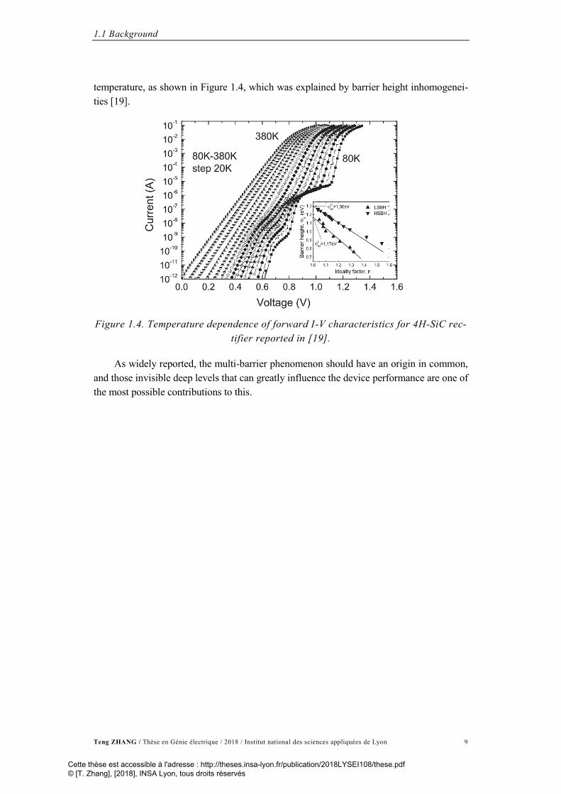
temperature, as shown in Figure 1.4, which was explained by barrier height inhomogenei-
ties [19].
Figure 1.4. Temperature dependence of forward I-V characteristics for 4H-SiC rec-
tifier reported in [19].
As widely reported, the multi-barrier phenomenon should have an origin in common,
and those invisible deep levels that can greatly influence the device performance are one of
the most possible contributions to this.
Cette thèse est accessible à l'adresse : http://theses.insa-lyon.fr/publication/2018LYSEI108/these.pdf © [T. Zhang], [2018], INSA Lyon, tous droits réservés

Chapter 1
Start of art
Teng ZHANG / Thèse en Génie électrique / 2018 / Institut national des sciences appliquées de Lyon 10
1.2 Reliability and Defects
Defects and impurities in semiconducting materials can result in poorer property such
as a carrier lifetime reduction [20]. Especially those deep level defects, which are close to
midgap, can be efficient recombination centers or carrier traps. Meanwhile, charged inter-
face traps directly affect the device performance by increasing the threshold voltage, de-
grading the channel mobility and causing leakage current for MOS applications [21]. On
the other hand, trap levels can be sometimes important for carrier lifetime adjustment as
well as in the application of LEDs. These deep level defects can not only be caused by ir-
radiation [22] or impurities such as Ti, V, Cr [23] but also be intrinsic defects introduced
by manufacturing process such as carbon vacancy (VC) [24, 25]. Activation Energy (aE ),
capture cross section ( ) and defect concentration (TN ) are all significant parameters for
deep level defects identification.
1.2.1 Classification of defects
1.2.11 Forms of defects
According to different forms in semiconductor, defects can be simply classified as
point defects and extended defects, while extended defects includes various of defect types
based on their dimension and characteristics, one example is listed in Table 1.3.
Table 1.3. Classification on defects in crystals.
Dimension Defect type Examples
0 Point defects
Vacancies
Interstitial defects
Substitutional defects
Frenkel defects
1 Line defects Edge dislocations
Screw dislocations
2 Planar defects
Stacking faults
Twins
Grain boundaries
Surface defects
3 Volume defects Precipitates (Cluster)
Voids
Cette thèse est accessible à l'adresse : http://theses.insa-lyon.fr/publication/2018LYSEI108/these.pdf © [T. Zhang], [2018], INSA Lyon, tous droits réservés

1.2 Reliability and Defects
Teng ZHANG / Thèse en Génie électrique / 2018 / Institut national des sciences appliquées de Lyon 11
Some common defects are explained as follows:
Vacancies
A vacancy, one of the simplest point defect also known as a Schottky defect [26],
comes from the absence of an atom in the lattice [27], while the missing usually takes
place in pairs in those ionic crystals (e.g. the alkali halide crystals) to maintain charge bal-
ance [28]. Irradiation is regarded as a common way to introduce vacancies by using vari-
ous particles (electrons, protons, neutron or even He+) with wide energy range [29-32], and
part of them can be annealed at high temperature [33-35]. On the other hand, secondary
defects can be produced after annealing at 400 ℃ [35] and the agglomeration of defects to
larger vacancy complexes has been reported as well [36, 37].
Substitutional defects
Substitutional defects stand for the replacement of original atom by an impurity such
as the doping process of semiconductor that usually contributes to introducing shallow
levels in the bandgap. This normally refers to those atoms of either original ones or impu-
rities that have the comparable size (e.g. N or Al in SiC or Si), otherwise the interstitial de-
fects will be formed.
Interstitial and Frenkel defects
If the gap of lattice is occupied where no atom should exist, this type of defect is
known as interstitial. Another possibility is the share of one lattice site by two or more at-
oms. Frenkel defects can be regarded as the combination of both an interstitial atom and
related vacancies caused by lattice atoms.
Dislocations
As a common example of extended defects, dislocation stands for the bending of at-
om planes surrounding due to the termination of the atom plane in the crystal. It was first
put forward by Volterra in 1970 [38], and can be classified as screw dislocation or edge
dislocation according to different types. By studying the dislocations parallel to the
Schottky contact, FIGIELS has discussed that the kinetics of electron emission from dislo-
cation will be drastically modified due to the configuration entropy. As a consequence, the
Deep Level Transient Spectroscopy (DLTS) transients no longer follow the exponential
law and results in the broadening of DLTS signal [39].
Stacking faults
Stacking faults refer to the locally changed stacking order of atom layer(s) in the
structure. For example, instead of the typical stacking sequence ABCABCABC of face-
centered cubic (fcc) structure, the structure with stacking fault may be ABCABABCAB.
Furthermore, the correlation between stacking faults and double barrier phenomenon has
been reported [40].
Surface defects
Cette thèse est accessible à l'adresse : http://theses.insa-lyon.fr/publication/2018LYSEI108/these.pdf © [T. Zhang], [2018], INSA Lyon, tous droits réservés
Chapter 1
Start of art
Teng ZHANG / Thèse en Génie électrique / 2018 / Institut national des sciences appliquées de Lyon 12
Surface defect is another significant category of defect. Generally speaking, surface
defects do not refer to the specific defect type as discussed before, but focus on the posi-
tion where large fraction of dialing bond occur and the periodic of lattice is destroyed. As
a result, the carrier lifetime, mobility etc. can be affected near the surface. In addition, sim-
ilar defects can lie in the interface between semiconductor and metal/oxide and is recog-
nized as interface states, which can be the decisive factor of Schottky barrier height under
certain circumstance instead of the metal type.
1.2.12 Shallow and deep levels
Apart from the classification of defects according to their forms or crystal condition,
defects can also be classified as shallow or deep defects based on the location of their en-
ergy levels in the bandgap of the semiconductor. A defect level is regarded as shallow lev-
el if its energy level is located near the band edges (conduction or valence band) of the
semiconductor. One of the most common shallow levels is those impurities introduced by
doping, which directly modifies the electrical properties (conductivity, carrier mobility etc.)
of the semiconductors. In addition to impurities that usually take place as substitutions, the
interstitial atoms that contribute to shallow levels have been reported as well [41, 42].
On the other hand, generally the deep levels have less contribution to conduction
compared with the shallow levels of dopants due to their relatively low concentration and
large activation energy. However, these deep levels can play an important role in the re-
combination process and are regarded as a significant limitation on carrier lifetime espe-
cially when the energy levels lie near the middle of the bandgap. As one of the applica-
tions, it is possible to release the carrier storage effect by limiting carrier life time with the
help of recombination center introduced by Au impurities in silicon devices, since Au is
known as a lifetime killer in silicon [43].
1.2.2 Defects reported in SiC devices
Since 1990s, a great deal of researches about deep level defects in SiC has been done
with the help of DLTS or other investigation methods. The donor deep levels with almost
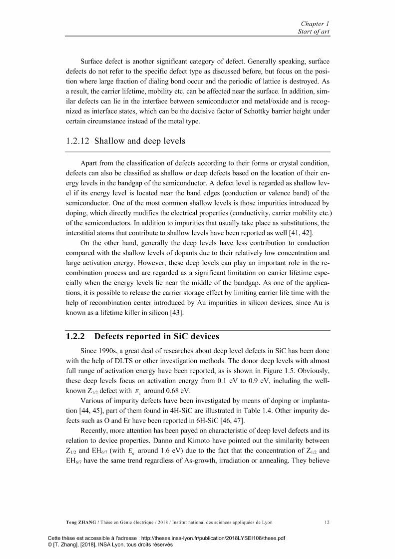
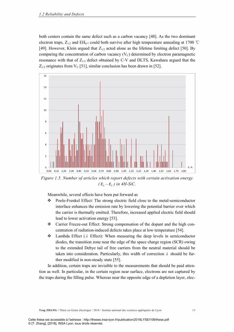
full range of activation energy have been reported, as is shown in Figure 1.5. Obviously,
these deep levels focus on activation energy from 0.1 eV to 0.9 eV, including the well-
known Z1/2 defect with aE around 0.68 eV.
Various of impurity defects have been investigated by means of doping or implanta-
tion [44, 45], part of them found in 4H-SiC are illustrated in Table 1.4. Other impurity de-
fects such as O and Er have been reported in 6H-SiC [46, 47].
Recently, more attention has been payed on characteristic of deep level defects and its
relation to device properties. Danno and Kimoto have pointed out the similarity between
Z1/2 and EH6/7 (with aE around 1.6 eV) due to the fact that the concentration of Z1/2 and
EH6/7 have the same trend regardless of As-growth, irradiation or annealing. They believe
Cette thèse est accessible à l'adresse : http://theses.insa-lyon.fr/publication/2018LYSEI108/these.pdf © [T. Zhang], [2018], INSA Lyon, tous droits réservés
1.2 Reliability and Defects
Teng ZHANG / Thèse en Génie électrique / 2018 / Institut national des sciences appliquées de Lyon 13
both centers contain the same defect such as a carbon vacancy [48]. As the two dominant
electron traps, Z1/2 and EH6/7 could both survive after high temperature annealing at 1700 ℃
[49]. However, Klein argued that Z1/2 acted alone as the lifetime limiting defect [50]. By
comparing the concentration of carbon vacancy (VC) determined by electron paramagnetic
resonance with that of Z1/2 defect obtained by C-V and DLTS, Kawahara argued that the
Z1/2 originates from VC [51], similar conclusion has been drawn in [52].
Figure 1.5. Number of articles which report defects with certain activation energy
(C TE E ) in 4H-SiC.
Meanwhile, several effects have been put forward as
Poole-Frenkel Effect: The strong electric field close to the metal-semiconductor
interface enhances the emission rate by lowering the potential barrier over which
the carrier is thermally emitted. Therefore, increased applied electric field should
lead to lower activation energy [53].
Carrier Freeze-out Effect: Strong compensation of the dopant and the high con-
centration of radiation-induced defects takes place at low temperature [54].
Lambda Effect ( Effect): When measuring the deep levels in semiconductor
diodes, the transition zone near the edge of the space charge region (SCR) owing
to the extended Debye tail of free carriers from the neutral material should be
taken into consideration. Particularly, this width of correction should be fur-
ther modified in non-steady state [55].
In addition, certain traps are invisible to the measurements that should be paid atten-
tion as well. In particular, in the certain region near surface, electrons are not captured by
the traps during the filling pulse. Whereas near the opposite edge of a depletion layer, elec-
Cette thèse est accessible à l'adresse : http://theses.insa-lyon.fr/publication/2018LYSEI108/these.pdf © [T. Zhang], [2018], INSA Lyon, tous droits réservés
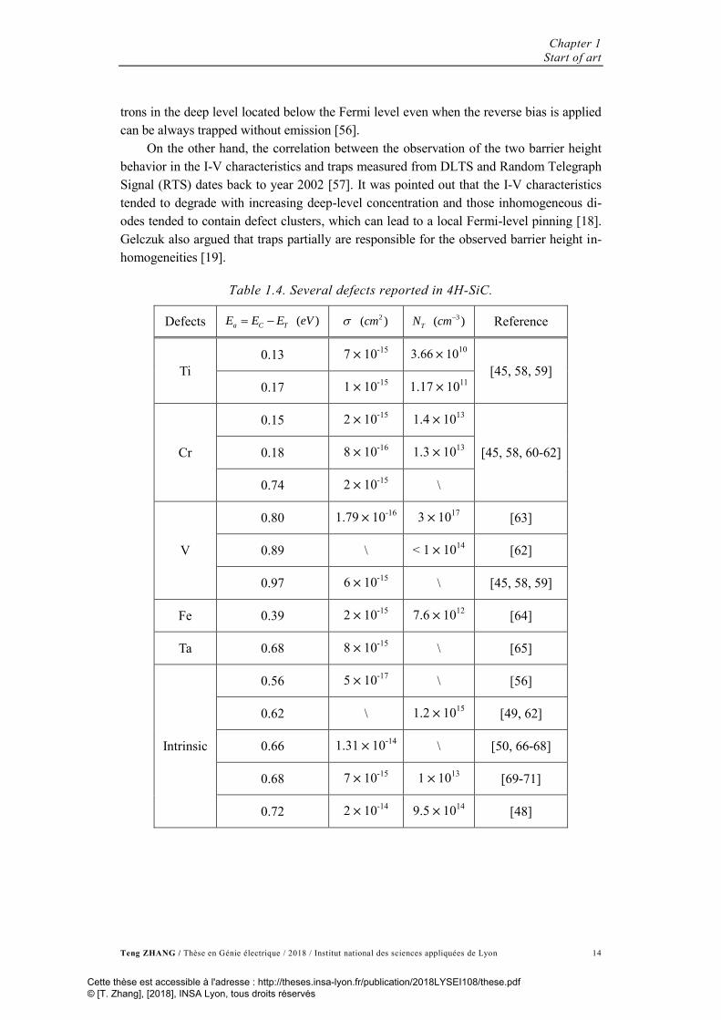
Chapter 1
Start of art
Teng ZHANG / Thèse en Génie électrique / 2018 / Institut national des sciences appliquées de Lyon 14
trons in the deep level located below the Fermi level even when the reverse bias is applied
can be always trapped without emission [56].
On the other hand, the correlation between the observation of the two barrier height
behavior in the I-V characteristics and traps measured from DLTS and Random Telegraph
Signal (RTS) dates back to year 2002 [57]. It was pointed out that the I-V characteristics
tended to degrade with increasing deep-level concentration and those inhomogeneous di-
odes tended to contain defect clusters, which can lead to a local Fermi-level pinning [18].
Gelczuk also argued that traps partially are responsible for the observed barrier height in-
homogeneities [19].
Table 1.4. Several defects reported in 4H-SiC.
Defects a C TE E E ( )eV 2( )cm TN 3( )cm Reference
Ti
0.13 7×10-15
3.66×10¹⁰
[45, 58, 59]
0.17 1×10-15
1.17×10¹¹
Cr
0.15 2×10-15
1.4×10¹³
[45, 58, 60-62] 0.18 8×10-16
1.3×10¹³
0.74 2×10-15
\
V
0.80 1.79×10⁻¹⁶
3×10¹⁷
[63]
0.89 \ < 1×10¹⁴
[62]
0.97 6×10-15
\ [45, 58, 59]
Fe 0.39 2×10-15
7.6×10¹²
[64]
Ta 0.68 8×10-15
\ [65]
Intrinsic
0.56 5×10-17
\ [56]
0.62 \ 1.2×10¹⁵
[49, 62]
0.66 1.31×10⁻¹⁴
\ [50, 66-68]
0.68 7×10-15
1×10¹³
[69-71]
0.72 2×10-14
9.5×10¹⁴
[48]
Cette thèse est accessible à l'adresse : http://theses.insa-lyon.fr/publication/2018LYSEI108/these.pdf © [T. Zhang], [2018], INSA Lyon, tous droits réservés

Teng ZHANG / Thèse en Génie électrique / 2018 / Institut national des sciences appliquées de Lyon 15
Chapter 2 Barrier height determination of Schottky diodes
Cette thèse est accessible à l'adresse : http://theses.insa-lyon.fr/publication/2018LYSEI108/these.pdf © [T. Zhang], [2018], INSA Lyon, tous droits réservés

Chapter 2
Barrier height determination of Schottky diodes
Teng ZHANG / Thèse en Génie électrique / 2018 / Institut national des sciences appliquées de Lyon 16
2.1 Energy band diagram and formation of Schottky barrier diode
2.1.1 Ideal Schottky contact
Figure 2.1. Formation of an ideal Schottky barrier between a metal and an n-type
semiconductor (a) neutral and isolated, (b) electrically connected by a wire, (c)
separated by a narrow gap, (d) in perfect contact. Cross and circle marks in (b) de-
note donor ion and electron in conduction band respectively.
Consider an n-type semiconductor with a work function s less than that of the met-
al m , as shown in Figure 2.1(a). In this case, electrons will transfer from semiconductor
to metal if they are connected by using a wire, and eventually the Fermi level in both metal
and semiconductor would be consistent with uncompensated donor charge left near inter-
face which leads to band bending and formation of a depletion layer as shown in Figure
2.1(b). Since the electron affinity of semiconductor s does not change, the difference of
work function between metal and semiconductor falls on the voltage drop iV between
them, as presented by i iV if we assume the electric field
i between two materials
keeps constant, and the depletion layer near interface. As a result, the band bending be-
Cette thèse est accessible à l'adresse : http://theses.insa-lyon.fr/publication/2018LYSEI108/these.pdf © [T. Zhang], [2018], INSA Lyon, tous droits réservés

2.1 Energy band diagram and formation of Schottky barrier diode
Teng ZHANG / Thèse en Génie électrique / 2018 / Institut national des sciences appliquées de Lyon 17
comes stronger with larger depletion region if the separation reduces which leads to re-
duction on iV , as illustrated in Figure 2.1(c). When they finally keep in touch [Figure
2.1(d)], the barrier owing to the vacuum no longer exists and it contributes to the ideal
Schottky contact. In this case, the Schottky barrier height relates to the Fermi level is given
by
B m s (2.1)
In order to obtain Eq. (2.1) namely Schottky-Mott limit, a series of assumptions have
been made:
The surface dipole contributions to m and
s does not change or at least their
difference does not change when the metal and semiconductor keep in touch.
No localized states exist on the semiconductor surface.
The contact between the metal and semiconductor is perfect.
Similar analysis could be done with Schottky contact on p-type semiconductor where
m s , while m s with n-type semiconductor or
m s with p-type semiconduc-
tor result in ohmic contact without rectifying effect. In this thesis we focus only on the n-
type Schottky contact.
2.1.2 The effect of interface states
According to Eq. (2.1), the barrier height should directly depend on the metal work
function m or in other words, the type of the metal. However, it has been experimentally
found that the B is less sensitive to
m as indicated by Eq. (2.1), and under certain cir-
cumstances it could be almost independent of the metal type. This is because that the ideal
situation illustrated in Figure 2.1(d) is never reached in real case. Even though the metal-
semiconductor is well fabricated, a thin insulating film still exists at the interface due to
the surface oxidation layer (~10 to 20 Å ) on the side of semiconductor, which results in
the case more closed to that shown in Figure 2.1(c).
Figure 2.2. Metal-semiconductor contact with interface states.
Cette thèse est accessible à l'adresse : http://theses.insa-lyon.fr/publication/2018LYSEI108/these.pdf © [T. Zhang], [2018], INSA Lyon, tous droits réservés

Chapter 2
Barrier height determination of Schottky diodes
Teng ZHANG / Thèse en Génie électrique / 2018 / Institut national des sciences appliquées de Lyon 18
In order to explain this weak dependence on m , the effect due to surface state has
been put forward by Bardeen [72]. As shown in Figure 2.2, a thin insulating layer with a
continuous distribution of interface states is assumed between the metal and semiconduc-
tor. The interface states are characterized by a neutral level 0 and the ‘absolute-zero’ ap-
proximation on Fermi level is purposed, namely all energy levels above the Fermi level are
empty while those levels below the Fermi level are occupied. In this case, if 0 is above
the Fermi level (Figure 2.2), a net positive charge ssQ shows up at the interface than the
neutral condition (or without interface states). In this case, instead of the relation under
ideal circumstance that 0m dQ Q , where mQ is the negative charge on the surface of
metal and dQ represents those positive charge due to the uncompensated donors in the
semiconductor, the interface charge should also take into consideration which results in
0m d ssQ Q Q .
Now consider the case shown in Figure 2.2 where 0 lies above the Fermi level. Ow-
ing to the existence of ssQ ,
dQ should be smaller than where interface states were absent,
which leads to the reduction of the depletion region width w . Since the barrier height B
equals to the sum of band bending 0dV and [Figure 2.1(d)],
B would be reduced com-
pared to the ideal case. This reduction on B will in turn reduce the positive charge in the
interface states by pushing the 0 towards the Fermi level. This functions as a negative-
feedback loop which forces to reduce the difference between the Fermi level and 0 . Even-
tually, if the interface states density is large enough, the Fermi level will be pinned to 0
and the barrier height will be expressed as
0B gE (2.2)
This is the so-called Bardeen limit. On the other hand, with similar analysis, the re-
sults would be somewhat the same if 0 is below
FE at the initial state. Now trying to fo-
cus on the interface states with a limited density, that is more approach to the real case.
With the help of the flat-band analysis, the barrier height on flat-band condition BF (un-
der certain bias) could be expressed as [73]
0( ) (1 )( )BF m s gE (2.3)
where
i
i sq D
(2.4)
here 0i ir is the permittivity of the interfacial layer and
sD the interface states
dentity.
It could be seen that if the density of interface states is small enough to be ignored,
tend to be unit which leads to the ideal case. On the other hand, approaches zero and the
barrier height is closed to the Barden limit with thick interfacial layer and large sD .
Cette thèse est accessible à l'adresse : http://theses.insa-lyon.fr/publication/2018LYSEI108/these.pdf © [T. Zhang], [2018], INSA Lyon, tous droits réservés

2.2 Current transport mechanisms though Schottky barrier
Teng ZHANG / Thèse en Génie électrique / 2018 / Institut national des sciences appliquées de Lyon 19
2.2 Current transport mechanisms though Schottky barrier
2.2.1 Introduction
Figure 2.3. Main current transport processes in a forward-biased Schottky barrier.
If a Schottky contact is forward biased (the electric potential on the metal side is
higher than the semiconductor for the n-type case), electrons will flow though the Schottky
barrier which contributes to the diode current. If we ignore the hole injection that usually
takes place when the SBH is greater than half of the band gap and a high density of holes
appear near the interface of the semiconductor, three main current transport processes are
illustrated in Figure 2.3: [74]
(a) Electron emission over the top of the barrier;
(b) Tunneling through the barrier;
(c) Recombination in the space charge region;
Practically (a) takes charge of the main current transportation. In this process, elec-
trons are first transported from interior of the semiconductor to the interface under the
mechanisms of diffusion within the depletion region, and then emitted into the metal. By
contributing the limitation of current transportation to different processes discussed above,
two theories namely diffusion theory and thermionic-emission (TE) theory have been put
forward. Meanwhile, (b) often shows up at high bias condition with the help of strong
electric field or low temperature where carriers do not have enough energy to emit through
the barrier. On top of that, (c) could greatly influence the forward characteristics if there
are a huge number of recombination centers namely deep levels.
Cette thèse est accessible à l'adresse : http://theses.insa-lyon.fr/publication/2018LYSEI108/these.pdf © [T. Zhang], [2018], INSA Lyon, tous droits réservés

Chapter 2
Barrier height determination of Schottky diodes
Teng ZHANG / Thèse en Génie électrique / 2018 / Institut national des sciences appliquées de Lyon 20
2.2.2 The diffusion theory
According to the diffusion theory discussed by Wagner and Schottky, the electron
transportation within the depletion region should be the limiting factor [75, 76]. That is
usually the case when the width of the depletion region is large compared to the carrier
mean free path. As a result, the current density over the junction could be expressed based
on the carrier diffusion-drift:
n n
dnJ nq qD
dx (2.5)
where n is the electron concentration in the n-type semiconductor, n the carrier
mobility, nD the diffusion constant, the electric field over the barrier and q the magni-
tude of the charge on electron.
By assuming that only drift and diffusion in the depletion region contributes to the
entire current flow, the current density J on function of forward bias V could be deduced
as:
22 ( 1)BqqV
kT kTCJ kT N a w e e
(2.6)
or
max ( 1)
Bq qV
kT kTCJ qN e e
(2.7)
where 2 1 2( 2 )D sa q N kT and 2
max 2D sqN w kTa w q .
Even though Eq. (2.7) has the form closed to that of the ideal rectifier
0[exp( ) 1]J J qV kT , the max
arises with increase of the bias voltage and is proportional
to 1 2
0( )dV V , which results in the growth of saturation current under increasing reverse
bias.
2.2.3 The thermionic-emission (TE) theory
Unlike in the diffusion theory, the transportation of electrons over the interface of
metal-semiconductor is considered as the current-limiting process in the TE theory. In oth-
er words, it is assumed that the quasi-Fermi level for electrons keeps constant throughout
the depletion region and the electron mobility on the semiconductor side near interface is
infinite and thus the effects of drift & diffusion in the depletion region could be neglected.
This condition could be reached if the mean free path l is large compared with w , or with
a much weaker condition for the validity that l only needs to exceed the distance d where
the barrier falls by a value of kT q from its maximum as cited by Bethe [77].
By analyzing the tunneling process through the barrier with a probability tp , the cur-
rent density owing to the electrons passing from the semiconductor into the metal could be
expressed as:
Cette thèse est accessible à l'adresse : http://theses.insa-lyon.fr/publication/2018LYSEI108/these.pdf © [T. Zhang], [2018], INSA Lyon, tous droits réservés

2.2 Current transport mechanisms though Schottky barrier
Teng ZHANG / Thèse en Génie électrique / 2018 / Institut national des sciences appliquées de Lyon 21
( )
4
Bq V
t C kTsm
p qN vJ e
(2.8)
where v is the average thermal velocity of electrons in the semiconductor and with a
value of * 1 2(8 )kT m for a Maxwellian distribution.
By taking into consideration the reverse process namely electrons passing through the
barrier from metal to the semiconductor that is independent on the bias due to a constant
barrier height, the current density from metal to semiconductor msJ could be deduced in
the same way and the total current density should be the sum of these two:
( 1)4
Bq qV
t C kT kTsm ms
p qN vJ J J e e
(2.9)
Being aware that * 2 3 22(2 )CN m kT h and replacing tp by 1, which has been proved
by Baccarani [78] and Berz [79], the TE theory could be finally expressed as:
* 2 ( 1)Bq qV
kT kTJ A T e e
(2.10)
where
* 2*
3
4 m qkA
h
(2.11)
Compared with the Richardson constant A , *A namely effective Richardson constant
could be regarded as replacing the free-electron mass m by the effective mass *m , with a
value of
* *120( )A m m 2 2A cm K (2.12)
2.2.4 Tunneling and Thermionic-Field Emission (TFE) model
Thanks to the quantum-mechanical tunneling effect, it may be possible for an electron
passing through the barrier which is higher than its energy under certain circumstances. As
is known to all that tunneling probability strongly depends on the density of states and the
width of the potential barrier instead of barrier height, current transport mechanisms could
be greatly affected especially under low temperature and high electric field.
Apart from the thermal emission that dominates at high temperature as discussed be-
fore, if the semiconductor is heavily doped, electrons could still overcome the barrier at
low temperature with the help of tunneling, which is known as ‘field’ emission (FE).
Therefore, when the electric field becomes higher, the electron will not only directly emit
over the Schottky barrier as discussed in the TE model, but also tunnel though the barrier,
which could dominate the whole current under high bias (e.g. 48 10 V cm for Au-GaAs or 54 10 V cm for Au-Si [80]). This is the Thermionic-Field Emission (TFE) model. By as-
Cette thèse est accessible à l'adresse : http://theses.insa-lyon.fr/publication/2018LYSEI108/these.pdf © [T. Zhang], [2018], INSA Lyon, tous droits réservés

Chapter 2
Barrier height determination of Schottky diodes
Teng ZHANG / Thèse en Génie électrique / 2018 / Institut national des sciences appliquées de Lyon 22
suming that the current increases exponentially with surface field S
, the current flow
could be expressed as [81]
( )
2B Sq
kTJ AT e
(2.13)
where is an effective tunneling constant given by ln SkT q d J d .
2.2.5 Recombination in the depletion region
In addition to the emission process (either TE or FE), recombination sometimes plays
an important role in current transportation as well. According to the recombination process,
there are two types of recombination: (a) direct recombination that is due to the direct
transition of carriers between conduction band and valence band. and (b) indirect recom-
bination that functions with the help of localized states, which is also called Shockley-
Read-Hall (SRH) recombination [82, 83].
According to SRH theory of semiconductor, the recombination ratio rU with a single
trapping center could be denoted as
2( )
[ exp ] [ exp ]
p n th t i
r
t i i tn i p i
v N np nU
E E E En n p n
kT kT
(2.14)
where tE is the energy level of localized state,
tN its concentration, thv the thermal
velocity of carrier, p and
n the capture cross section of holes and electrons.
It is clear that those defect centers with the energy levels near the middle of forbidden
band (namely deep levels) can be the most effective combination centers. As a result, the
recombination may become the major mechanism under low forward bias where a consid-
erable width of depletion region remains if those effective trapping centers participate in.
The current rJ due to recombination through a Schottky barrier is:
20 (1 )
qV qV
kT kTr rJ J e e
(2.15)
where 0 2r i rJ qn w , and
r is the lifetime within the depletion region which strong-
ly depend on the combination center as illustrated in (2.15).
This recombination current has the similar form as discussed in TE theory unless
there is a factor of 2 in the denominator of the main exponential term. Taking into consid-
eration of current owing to both emission and recombination, the total current density is
given by:
20 0( )(1 )
qV qV qV
kT kT kTte r t rJ J J e J e e
(2.16)
Cette thèse est accessible à l'adresse : http://theses.insa-lyon.fr/publication/2018LYSEI108/these.pdf © [T. Zhang], [2018], INSA Lyon, tous droits réservés

2.2 Current transport mechanisms though Schottky barrier
Teng ZHANG / Thèse en Génie électrique / 2018 / Institut national des sciences appliquées de Lyon 23
On top of that, it has been uncovered that carrier lifetime could greatly depend on the
shape of the sample and its surface states, which due to the accelerated recombination pro-
cess at the surface because of those surface states and defects. This indicates that the re-
combination owing to the interface states of the Schottky contact could also have a big im-
pact on I-V characteristic.
2.2.6 Image-force lowering of SBH
Figure 2.4. Image-force lowing of SBH.
Image-force lowering or in other words, Schottky barrier lowering describes the phe-
nomenon that the SBH will be reduced due to the image force when the carrier transfers
from the semiconductor to the metal under forward bias.
In order to analyze the image force, we first consider a metal-vacuum system. When
an electron is presented in front of the metal with a distance of x , the induced electric
field at the surface of metal could be regarded as if there were a positive charge of magni-
tude q located at the mirror-image of electron with respect to the metal surface. Therefore,
the force on the electron towards the metal is:
2
016
qF
x
(2.17)
As a result, the reduction on Schottky barrier owing to the image force is its integra-
tion from infinite, and the potential of the barrier should be
2
max( )16 s
qE x q x
x
(2.18)
Cette thèse est accessible à l'adresse : http://theses.insa-lyon.fr/publication/2018LYSEI108/these.pdf © [T. Zhang], [2018], INSA Lyon, tous droits réservés

Chapter 2
Barrier height determination of Schottky diodes
Teng ZHANG / Thèse en Génie électrique / 2018 / Institut national des sciences appliquées de Lyon 24
where max
is the electric field in the semiconductor and regarded constant with the
maximum value of that in the semiconductor. Here s is the permittivity of the semicon-
ductor under high frequency rather than the static permittivity since no enough time is
permitted for the semiconductor to become fully polarized by the electric field, as is indi-
cated by Sze [84].
As shown in Figure 2.4, by calculating the position mx where the maximum value of
potential height is reached, the reduction on effective Schottky barrier height compared to
that without image force in reduced as
max
4i
s
q
(2.19)
Image-force lowering is one of the important factors that drive the I-V characteristic
of Schottky diode away from the ideal case. However, it is significant to be aware of the
basic precondition that electrons should transfer into the metal through the barrier. In other
words, image-force lowering should be taken into consideration only in the I-V case. On
the other hand, the C-V test without carrier transportation over the barrier should not be af-
fected by the image-force lowering.
Cette thèse est accessible à l'adresse : http://theses.insa-lyon.fr/publication/2018LYSEI108/these.pdf © [T. Zhang], [2018], INSA Lyon, tous droits réservés

2.3 Measurement of SBH
Teng ZHANG / Thèse en Génie électrique / 2018 / Institut national des sciences appliquées de Lyon 25
2.3 Measurement of SBH
As discussed above, the SBH not only depends on the type of metal/semiconductor
along with its doping concentration, but is also influenced by the interface states. There-
fore it is more practical to determine the SBH with experimental measurements. A number
of methods are developed in order to measure the barrier height, for example:
forward current-voltage characteristics
reverse capacitance-voltage measurements
photoelectric measurements
photoelectron emission spectroscopy
Thanks to the easy setup and convenient to analyze, I-V and C-V characteristics are
widely adopted for SBH determination, which will be mainly introduced in this section.
2.3.1 I-V characteristics
Based on the discussion on current transport mechanisms, the true behavior in practi-
cal seems to lie somewhere between the TE theory and the diffusion theory if we ignore
the low temperature or high electric field conditions. However, normally the TE theory is
more suitable to forecast the I-V characteristics on those well fabricated diodes based on
high mobility semiconductors [74]. According to TE theory, if the forward bias is low
enough that the voltage drops on the series resistance could be ignored, the forward current
is given by:
1qV
kTsI I e
(2.20)
where sI is the saturation current that is
* 2Bq
kTsI SA T e
(2.21)
where S is the effective surface of Schottky diode.
Since transportation of carriers takes place under forward bias, image-force lowering
should be taken into consideration. Therefore, instead of real barrier height B , it should
be replace by the effective barrier height eff
B here as shown in Figure 2.4, which is given
by eff
B B i . However, as though the target is to measure the barrier height from
experimental method, it makes no sense to separate these two concepts and as a result, on-
ly B will be used for discussion in the following sections.
According to Eq. (2.20), if the forward bias is large enough that qV kT while the
series resistance could still be neglected, the plot ln(I)-V should be linear with a slope
equals to q kT and the ordinate at the origin gives the saturation current sI and as a result,
B could be calculated if *A is known. However, *A could not always be a known pa-
Cette thèse est accessible à l'adresse : http://theses.insa-lyon.fr/publication/2018LYSEI108/these.pdf © [T. Zhang], [2018], INSA Lyon, tous droits réservés

Chapter 2
Barrier height determination of Schottky diodes
Teng ZHANG / Thèse en Génie électrique / 2018 / Institut national des sciences appliquées de Lyon 26
rameter. To determine the effective Richardson constant *A , the Richardson plot is com-
monly used in practical case. Based on Eq. (2.21), 2ln( ) . 1SI T vs T should be linear with a
slope related to the barrier height and an ordinate originally bound to *A .
2.3.2 C-V measurements
If the Schottky diode is nearly ideal where the effect due to the minority carriers can
be neglected and a uniform donor concentration is presented in the semiconductor as as-
sumed in the TE model, the electric field at the interface is due to only the uncompensated
donors. Thus the differential capacitance under reverse bias is linked to the width of the
space charge region w and doping concentration D AN N as
sSCw
(2.22)
2 s
I r
D A
w V Vq N N
(2.23)
where s is the dielectric constant of semiconductor and
rV is the reverse bias.
Since the uniform doping concentration is assumed, the function of 21 rC f V
ought to be a straight line, where the intersection with x-axis IV gives the barrier height
B as [85]:
b I C F
kTV E E
q (2.24)
At the same time, doping concentration could also be extracted base on the slope:
2
2D A
s
N Nq S slope
(2.25)
Since no mechanism of carrier transportation over the barrier takes charge during C-
V characterization, the effect of image-force lowing should be wiped out. Therefore the
SBH obtained from C-V should always higher than that from I-V on the same Schottky
contact in the ideal case.
Cette thèse est accessible à l'adresse : http://theses.insa-lyon.fr/publication/2018LYSEI108/these.pdf © [T. Zhang], [2018], INSA Lyon, tous droits réservés

2.4 Review on SBH models
Teng ZHANG / Thèse en Génie électrique / 2018 / Institut national des sciences appliquées de Lyon 27
2.4 Review on SBH models
2.4.1 Ideality factor and zero-bias barrier height
Generally speaking, the slope of log(I)-V plot discussed in 2.3.1 could never be found
unit due to the dependence of SBH on bias as well as the effect of image-force lowering.
Considering the bias dependence of barrier height as linear, such that 0B B V ,
where 0B is the barrier height at zero bias and B V is positive, Eq. (2.20) can
be modified to
1qV qV
nkT kTsI I e e
(2.26)
with the saturation current SI as
0
* 2Bq
kTsI SA T e
(2.27)
Here 1 (1 )n is called the ideality factor of the diode [86].
Based on Eq. (2.26) and Eq. (2.27), if the series resistance is small enough to be ig-
nored, the relationship between log( )I and V should be linear. Therefore, either ideality
factor or zero bias barrier height can be deduced via direct I-V plot.
On consideration of the effect of a thin interfacial layer as well as the effect of image
force and surface charges on the barrier height, that also manifests at 0 V and results in
1n , Hackam and Harrop [87] have proposed that it is necessary to involve ideality factor
n into the expression of saturation current SI , and Eq. (2.27) is amended as follows:
0
* 2Bq
nkTsI SA T e
(2.28)
2.4.2 T0 effect
In order to precisely fit the experimental I-V characteristics of Schottky diodes, where
a variation of n with temperature is observed, Padovani and Sumner [88] have suggested
replacing T by 0T T in the thermos-ionic emission model, therefore Eq. (2.20) becomes
(neglecting series resistance):
0
0 0( ) ( )* 2 1Bq qV
k T T k T TI SA T e e
(2.29)
Cette thèse est accessible à l'adresse : http://theses.insa-lyon.fr/publication/2018LYSEI108/these.pdf © [T. Zhang], [2018], INSA Lyon, tous droits réservés

Chapter 2
Barrier height determination of Schottky diodes
Teng ZHANG / Thèse en Génie électrique / 2018 / Institut national des sciences appliquées de Lyon 28
where 0T neither depends on temperature nor voltage over a wide temperature range.
Therefore, this relation amounts to introducing an ideality factor in the two exponential
terms:
01T
nT
(2.30)
2.4.3 Gaussian distribution
To explain the difference between SBH measured by I-V and C-V over the range of
measurement temperatures, Song et al. [89] assumed that barrier height is normally dis-
tributed with a probability density:
221
( )2
B B
S
B
S
P e
(2.31)
where B is the average of SBH and
S is its standard deviation.
In this case, the SBH can be expressed as:
2
2
SB B
kT q
(2.32)
Practically, the SBH at 0 V 0B can be calculated at each temperature based on Eq.
(2.28) if we know the value of *A . Thus Eq. (2.32) is usually modified to:
2
00 0
2
SB B
kT q
(2.33)
where 0S is the standard deviation of
0B at 0 V. Therefore it is possible to extract
0B and 0S by plotting
0B vs. 2q kT .
2.4.4 Potential Fluctuation model
This model was developed by Werner and Guttler [90] to explain the temperature de-
pendence of the ideality factor. The barrier height is assumed to be normally distributed,
but the mean and standard deviation are assumed to vary linearly with voltage as
0 2B B V (2.34)
and
2 2
0 3S S V (2.35)
Cette thèse est accessible à l'adresse : http://theses.insa-lyon.fr/publication/2018LYSEI108/these.pdf © [T. Zhang], [2018], INSA Lyon, tous droits réservés

2.4 Review on SBH models
Teng ZHANG / Thèse en Génie électrique / 2018 / Institut national des sciences appliquées de Lyon 29
to explain the temperature dependence of the ideality factor. We can then show that
the ideality factor can be expressed in the form:
32
11
2
q
n kT
(2.36)
The valus of 2 and
3 can be obtained from the slope and the ordinate at the origin
on the 1 1n vs. 2q kT plot.
2.4.5 Flat-band barrier height
Since the barrier height depends on the electrical voltage, i.e. in fact on the electric
field, Wagner et al. [91] proposed to define the barrier height in flat bands (under zero
field) BF , which would be a more fundamental magnitude because independent of the
applied voltage and given by:
0 ( 1) ln C
BF B
D
NkTn n
q N (2.37)
2.4.6 Modified Richardson plot
As is discussed, to determine the effective Richardson constant *A , the Richardson
plot is commonly used and the plot on 2ln( ) . 1SI T vs T should be linear based on Eq.
(2.21). However, owing to the deviation from linear region on traditional Richardson plot,
the so-called modified Richardson (MR) plot is adopted as 2ln( ) . 1SI T vs nT based on Eq.
(2.28) [87]. Meanwhile, other types of MR plot have also been put forward according to
model of Gaussian distribution as 2 2 2 2 2
0ln( ) 2 .S SI T q K T vs q kT [92] and on the basis of
flat-band barrier height as 2ln( ) (1 1 )ln . 1S C DI T n N N vs nT [93]. These could help
us to determine *A and the relative SBH (0B ,
0B or BF ).
On top of that, adjustment of modified Richardson plot has been put forward by
BHUIYAN et.al. [94] as 2( )log( ) .1Sn T I ST vs T by considering the linear change of SBH
due to temperature.
2.4.7 Relationships between different models
T0 Effect
Even though a number of well fitted 0T on Au/GaAs, Cr/Si and Cu/Si have been re-
ported, it was pointed out by Werner and Güttler that Eq. (2.29) could not be generally val-
id for n prediction, especially on high temperature [90]. Meanwhile, they explained the 0T
effect as follows:
According to Eq. (2.36), one obtains that
Cette thèse est accessible à l'adresse : http://theses.insa-lyon.fr/publication/2018LYSEI108/these.pdf © [T. Zhang], [2018], INSA Lyon, tous droits réservés

Chapter 2
Barrier height determination of Schottky diodes
Teng ZHANG / Thèse en Génie électrique / 2018 / Institut national des sciences appliquées de Lyon 30
2 3
1
1 2n
kT q
(2.38)
In case of 2 3 (2 ) 1kT q , Eq. (2.38) can be expressed as
321
2n
kT q
(2.39)
Consider that in most cases it exists that 2 3 2 1kT q , and as a result, a sec-
ond approximation could be drawn as
3 01 12
Tn
kT q T
(2.40)
Compare Eq. (2.40) with Eq. (2.30), it is clear that
30
2T
k q
(2.41)
which reveals the relationship between 0T and the Gaussian barrier distribution nar-
rowing coefficient 3 upon the application of a bias voltage.
Modified Richardson plot
If we introduce 0T effect as a well approximation among wide temperature range to
the expression of the flat-band barrier height, Eq. (2.37) could be approximated by
00 ln C
BF B
D
kT Nn
q N (2.42)
As the determined 0T is small (~ 100 K) in our case, and as a result, the second item
in Eq. (2.42) could normally be neglected compared to the first one. Therefore the BF
can be simply degenerated as
0BF Bn (2.43)
This could explain the conventional MR plot based on Eq. (2.28), which extracts the
value of SBH approach to the BF . However, as the negative item is neglected when using
the approximation Eq. (2.43), the *A obtained from the conventional MR plot is always
larger than that from MR plot according to flat-band barrier height. Meanwhile, at high
temperature where ideality factor is usually approach unity, the value of 0B is closed to
BF . As a result, the Richardson plot keeps linear at high temperature region even though
the *A extract is much smaller. Examples will be shown and discussed in the experimental
results in section 4.3.
Gaussian distribution model and potential fluctuation model
Cette thèse est accessible à l'adresse : http://theses.insa-lyon.fr/publication/2018LYSEI108/these.pdf © [T. Zhang], [2018], INSA Lyon, tous droits réservés

2.4 Review on SBH models
Teng ZHANG / Thèse en Génie électrique / 2018 / Institut national des sciences appliquées de Lyon 31
According to Eq. (2.43), if we replace 0B by
BF n in Eq.(2.33), the relation be-
tween the ideality factor and the parameters of the Gaussian distribution can be revealed in
the form:
2
0 011
2
B BF S
BF BF
q
n kT
(2.44)
Comparing with Eq.(2.36), it can be shown that:
02
2
03
BF B
BF
S
BF
(2.45)
or
0 2
2
0 3
(1 )B BF
S BF
(2.46)
This highlights the links between the Gaussian distribution model and the potential
fluctuation model. Our results that will be given in Chapter 4 fit well with this relation on
either single barrier diodes or those diodes with multi-barrier.
Cette thèse est accessible à l'adresse : http://theses.insa-lyon.fr/publication/2018LYSEI108/these.pdf © [T. Zhang], [2018], INSA Lyon, tous droits réservés

Chapter 2
Barrier height determination of Schottky diodes
Teng ZHANG / Thèse en Génie électrique / 2018 / Institut national des sciences appliquées de Lyon 32
2.5 Barrier inhomogeneity in Schottky devices
2.5.1 Introduction
Various non-ideal behaviors are frequently observed in Ti, Ni, and Pt-based 4H-SiC
Schottky barrier diodes as well as metal insulator semiconductor (MIS) GaAs Schottky di-
odes [95, 96], and these are widely recognized owing to the so-called barrier inhomogenei-
ty. As an intuitive feeling, the inhomogeneity of SBH should be able to analyze as individ-
ual area where the SBH is uniform within each region. This is known as the parallel diode
model. In addition, Tung’s model which explains also the pinch-off of low SBH region as
well as the Fermi level pinning and the multi Gaussian distribution of barrier height is
widely recognized and discussed.
Based on determining the nature and energy levels of the defects with EBIC and
DLTS, Ewing et al. suggested that the low-SBH are caused by defect clusters which local-
ly pin the Fermi level [18]. However, Bolen and Capano argued that single threading edge
and threading screw dislocations do not significantly affect the electrical characteristics of
4H-SiC SBDs based on the fact that no significant conglomeration of defects found clus-
tered together [97]. Furthermore, Dohyun Lee et al. reported the uniformity of Schottky
barrier height could be improved by post-oxidation annealing in nitric oxide ambient (NO
POA) [98].
2.5.2 Parallel diode model
By assuming that the Schottky contact consists of a series of ideal regions with indi-
vidual constant barrier height ,Bn i and corresponding effective area given by the fraction
of total contact surface /i iS S a , the total current though this Schottky contact under for-
ward bias V is given by the sum of current from each individual area based on TE model:
,
* 2
1
Bn iq qVm
kT nkTi
i
I S A T e e
(2.47)
where m is the number of parallel diodes (i.e. individual homogeneous SBH regions).
By introducing the lowest barrier height ,Bn l among those regions, Brezeanu et. al. pro-
vided the expression of conventional barrier height ,Bn T as
,
, ,
1
1ln exp
mBn i
Bn T Bn l
i i
qkT
q a kT
(2.48)
and its limit on temperature [99]:
Cette thèse est accessible à l'adresse : http://theses.insa-lyon.fr/publication/2018LYSEI108/these.pdf © [T. Zhang], [2018], INSA Lyon, tous droits réservés

2.5 Barrier inhomogeneity in Schottky devices
Teng ZHANG / Thèse en Génie électrique / 2018 / Institut national des sciences appliquées de Lyon 33
, ,0
lim Bn T Bn lT
(2.49)
,
,
1
limm
Bn i
Bn TT
i ia
(2.50)
This indicates that the limit of SBH measured at low temperature is determined by the
parallel path with the lowest SBH, while that should be the weighted average based on
their effective areas if the temperature is high enough. And this high temperature limit
should be exactly the mean barrier height B described in the Gaussian distribution model.
However, J. L. Freeouf et. al. have reported that the low barrier region will be more
effectively “pinched off” by large area with higher SBH. (i.e. Even though the ratio for
high SBH and low SBH keeps constant, the overall barrier height and ideality factor will
shift towards the value on larger surface area with higher SBH.) Only those areas with lin-
ear dimensions larger than Debye length of the substrate could be treated as separate paral-
lel diodes [100]. This “pinch-off” effect has been discussed in various bibliographies [89].
And the barrier height determined by C-V measurement is dominated by the phase with
larger contact area [89].
2.5.3 Tung’s model
Early in 1992, Tung highlighted that leakage, edge-related currents, greater-than-
unity ideality factors, 0T and other dependences of the ideality factor on temperature, soft
reverse characteristics, and the dependence of the SBH on the measurement technique are
all natural results of SBH inhomogeneity, which could be explained by model containing
low-SBH regions shown in Figure 2.5. The localized low barrier height patches were later
strongly suggested though electron beam induced current (EBIC) [95]. Meanwhile, the
phenomenon that conduction-band minimum (CBM) potential pinch-off in the low-SBH
region was illustratred in [101]. However, Im et al. argued that Tung model can account
for highly nonideal behavior only by assuming an unphysical patch distribution in which
the excess current is dominated by a few patches in the extreme tail of the patch distribu-
tion, and suggested that all the diodes contain a broad ‘‘intrinsic’’ distribution of shallow
patches, while the large excess current in highly nonideal diodes is due to a few large de-
fects of extrinsic origin [102].
Sabih Uddin Omar et al. pointed out that Tung model is applicable for SiC Schottky
diodes with ideality factor n < 1.2, and indicated the presence of high-density of electron
traps at the Schottky interface with a uniform distribution across the wafer which can ex-
plain the hysteresis and the associated Schottky nonideality [40]. Apart from [18, 19] men-
tioned before, S. Tumakha et al. also suggested that SiC defect levels can account for the
maximum range of barrier heights [103].
Cette thèse est accessible à l'adresse : http://theses.insa-lyon.fr/publication/2018LYSEI108/these.pdf © [T. Zhang], [2018], INSA Lyon, tous droits réservés

Chapter 2
Barrier height determination of Schottky diodes
Teng ZHANG / Thèse en Génie électrique / 2018 / Institut national des sciences appliquées de Lyon 34
Figure 2.5. (a) Schematic of the Tung model. A random distribution of circular
patches of size 0R and barrier height 0
B in the otherwise homogeneous back-
ground of SBH 0
B . (b) A patch of size comparable to or smaller than the semicon-
ductor Debye length gives rise to a potential saddle-point S beneath the patch cen-
ter O. (c) Potential profile along the interface normal (along O-S) for zero applied
bias aV , and for a reverse bias ( 0)aV . Reverse bias reduces the potential maximum
(i.e., an increased depth) near S. (d) Lateral profile of the potential maximum pro-
jected normally onto the MS interface. The dashed line is the exact potential , the
dash-dot line is Tung’s parabolic approximation, and the solid line is the truncated
paraboloid used to calculate the microscopic BHD. (e), Calculated probability den-
sity for a single low-barrier patch of strength , with min 0 ( )B B D and max 0
B B
[102].
Cette thèse est accessible à l'adresse : http://theses.insa-lyon.fr/publication/2018LYSEI108/these.pdf © [T. Zhang], [2018], INSA Lyon, tous droits réservés
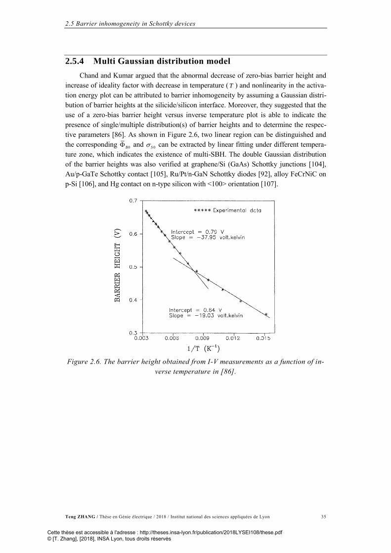
2.5 Barrier inhomogeneity in Schottky devices
Teng ZHANG / Thèse en Génie électrique / 2018 / Institut national des sciences appliquées de Lyon 35
2.5.4 Multi Gaussian distribution model
Chand and Kumar argued that the abnormal decrease of zero-bias barrier height and
increase of ideality factor with decrease in temperature (T ) and nonlinearity in the activa-
tion energy plot can be attributed to barrier inhomogeneity by assuming a Gaussian distri-
bution of barrier heights at the silicide/silicon interface. Moreover, they suggested that the
use of a zero-bias barrier height versus inverse temperature plot is able to indicate the
presence of single/multiple distribution(s) of barrier heights and to determine the respec-
tive parameters [86]. As shown in Figure 2.6, two linear region can be distinguished and
the corresponding 0B and
0S can be extracted by linear fitting under different tempera-
ture zone, which indicates the existence of multi-SBH. The double Gaussian distribution
of the barrier heights was also verified at graphene/Si (GaAs) Schottky junctions [104],
Au/p-GaTe Schottky contact [105], Ru/Pt/n-GaN Schottky diodes [92], alloy FeCrNiC on
p-Si [106], and Hg contact on n-type silicon with <100> orientation [107].
Figure 2.6. The barrier height obtained from I-V measurements as a function of in-
verse temperature in [86].
Cette thèse est accessible à l'adresse : http://theses.insa-lyon.fr/publication/2018LYSEI108/these.pdf © [T. Zhang], [2018], INSA Lyon, tous droits réservés

Teng ZHANG / Thèse en Génie électrique / 2018 / Institut national des sciences appliquées de Lyon 36
Chapter 3 Deep levels detection
Cette thèse est accessible à l'adresse : http://theses.insa-lyon.fr/publication/2018LYSEI108/these.pdf © [T. Zhang], [2018], INSA Lyon, tous droits réservés

3.1 Overview
Teng ZHANG / Thèse en Génie électrique / 2018 / Institut national des sciences appliquées de Lyon 37
3.1 Overview
Unlike doping in semiconductor, deep levels could hardly be detected directly with
simple I-V or C-V measurement. However, with the development of modern technology,
deep levels can be investigated thanks to the DLTS, Laplace Deep Level Transient Spec-
troscopy (LDLTS), PL (Photoluminescence), Low Temperature Photoluminescence
(LTPL), Deep Level Optical Spectroscopy (DLOS) Optical Absorption (OA), and Hall Ef-
fect [46, 53, 108, 109]. In addition to conventional DLTS, alternative improvement such as
Double Correlation Deep Level Transient Spectroscopy (DDLTS) [110, 111] and Con-
stant-Capacitance Deep Level Transient Spectroscopy (CCDLTS) [112] were also report-
ed.
Shortcomings of early used defect detection methods such as photocapacitance and
admittance spectroscopy are remarkable. For example, even though benefiting from high
sensitivity, photocapacitance is less practical due to complex data collection and analysis
in order to obtain the accurate parameters of traps. Moreover, it is not applicable to those
traps with aE less than 0.3 eV. On the other hand, only majority carrier traps could be in-
vestigated by using admittance spectroscopy and its sensitivity will decrease for those
deeper traps with large activation energy [113].
Cette thèse est accessible à l'adresse : http://theses.insa-lyon.fr/publication/2018LYSEI108/these.pdf © [T. Zhang], [2018], INSA Lyon, tous droits réservés

Chapter 3
Deep levels detection
Teng ZHANG / Thèse en Génie électrique / 2018 / Institut national des sciences appliquées de Lyon 38
3.2 Electron capture-emission mechanism
3.2.1 Capture
If the trap level is capable of electron accommodation, the capture will take place
when there are free carriers in the conduction band, or in other worlds when the Fermi lev-
el approaches the CE , and the filled traps
Tcn during the capture process is:
( ) (1 )c
t
Tc Tn t N e
(3.1)
where TN is the trap concentration and
c is the capture time constant with the ex-
pression as:
, 0
1c
n th nv n
(3.2)
with n the capture cross section for electrons,
,th nv the thermal velocity of eletrons
and 0n the concentration of free carriers. The electron thermal velocity can be calculated
based on effective mass of electrons *m and Boltzman constant k at each temperature T
as:
, *
3th n
kTv
m (3.3)
and 0n is usually regarded as shallow doping concentration for the electron traps and
with the expression as:
0
C FE E
kTCn N e
(3.4)
where CN is the state density of conduction band that is:
3* 2
2
22C
m kTN
h
(3.5)
with h the Planck constant.
As a consequence, the capture rate nc can be expressed as:
, 0 1n n th n cc v n (3.6)
Cette thèse est accessible à l'adresse : http://theses.insa-lyon.fr/publication/2018LYSEI108/these.pdf © [T. Zhang], [2018], INSA Lyon, tous droits réservés

3.2 Electron capture-emission mechanism
Teng ZHANG / Thèse en Génie électrique / 2018 / Institut national des sciences appliquées de Lyon 39
3.2.2 Emission
As the opposite process, the electrons can also emit from the trap level to the conduc-
tion band, and the filled traps Ten during the emission process can be expressed as:
( ) e
t
Te Tn t N e
(3.7)
with the emission time constant e as:
1
,
C TE E
kTe n th n n Cv X N e
(3.8)
where nX is the entropy factor.
The emission rate ne should be the reciprocal of the emission time constant:
1n ee (3.9)
By transforming Eq. (3.8), certain Arrhenius-equation exist:
,
1ln lnC T
e th n C n n
E Ev N X
k T
(3.10)
where the n nX is the capture cross section extracted by the experiments, also called
sigma ( ).
According to Eq. (3.10), if the emission time constant at different temperature can be
measured, the activation energy of trap level and its capture cross section can be deduced
from the Arrhenius plot by linear fitting of ,ln( )e th n Cv N vs. 1 T .
Another possibility for the y-axis of the Arrhenius plot can be expressed as 2ln( )eT C ,
where C is all the constants other than the temperature or in other words:
,
2
th n Cv NC
T (3.11)
3.2.3 Steady state capture-emission
Figure 3.1 illustrates the combination effect of carrier capture-emission through a trap
level. Even though the capture (1c ,
2c ) and emission (1e ,
2e ) processes take place
throughout and obey the corresponding law introduced above, the trap state can be deter-
mined by one or certain main process that depends on the state of semiconductor. Here an
n-type semiconductor is assumed for discussion, while that should be similar when it
comes to the p-type one.
Common state
Cette thèse est accessible à l'adresse : http://theses.insa-lyon.fr/publication/2018LYSEI108/these.pdf © [T. Zhang], [2018], INSA Lyon, tous droits réservés

Chapter 3
Deep levels detection
Teng ZHANG / Thèse en Génie électrique / 2018 / Institut national des sciences appliquées de Lyon 40
The ‘common state’ indicates that the conduction band is full of free electrons and no
obvious minority carrier injection takes place, which is the common case for the n-type
semiconductor without external interference. If the capture rates for those trap levels are
much larger than the emission rates, the emission process can be neglected on steady state
and as a result, only capture process should be taken into consideration in the expression of
trapped electrons Tn :
1
1 2
T T
cn N
c c
(3.12)
where 1c is the majority carrier (electron) capture rate (recombination rate) propor-
tional to the majority carrier concentration and 2c is the minority carrier (hole) capture rate
proportional to the concentration of injected minority carriers. As no obvious injection of
minority carrier is assumed in this common state, certain relation holds that 1 2c c . As a
result, the trap level is filled with electrons with the concentration closed to that of the trap.
Figure 3.1. Schematic of electron capture-emission through trap levels.
Depletion
When the n-type material keeps in contact with a p-type one or certain metal in order
to present a Schottky contact, a depletion region is formed and those trap levels lie in the
n-type side within the depletion region are regarded as in the depletion state. Since almost
no free carrier exists in the depletion region, the capture rates tend to be zero and the trap
state Tn is dominated by the emission process:
2
1 2
T T
en N
e e
(3.13)
In that case, if 1 2e e , it should be regarded as electron (majority carrier) trap and is
almost empty at depletion state. On the other hand, if 1 2e e , this trap is capable of trap-
ping holes and tend to be full here. According to Eq. (3.8) and (3.9), the emission rate is
largely depend on the difference between trap level and the conduction band (electron
traps) or the valence band (hole traps). As a result, those electron traps usually lies in the
upper half of the bandgap with their activation energies marked as a C TE E E , while
those hole traps tend to be in the lower half with their activation energies as a T VE E E .
Cette thèse est accessible à l'adresse : http://theses.insa-lyon.fr/publication/2018LYSEI108/these.pdf © [T. Zhang], [2018], INSA Lyon, tous droits réservés

3.2 Electron capture-emission mechanism
Teng ZHANG / Thèse en Génie électrique / 2018 / Institut national des sciences appliquées de Lyon 41
Injection
When the minority carrier concentration is large enough to reach the level of the ma-
jority carrier (e.g. due to the forward bias in the p-n junction if we focus on the depletion
region), the capture rate of minority carrier (hole) could exceed that of the majority ones
(electron) and so 2 1c c . In that case, almost no trap level will be captured by electron ac-
cording to Eq. (3.12) and these trap centers are filled with holes instead. In other words,
those minority traps could only be detected under the injection state with the help of large
forward bias in a p-n junction namely saturating injection pulse [113].
3.2.4 Transient
In order to characterize trap levels, the measurement of pulsed bias capacitance tran-
sients are commonly adopted. As discussed above, if the trapping state is switched, which
usually can be realized by changing the voltage bias through the sample under test, the
transient of carrier will take place due to the unbalanced state by either emission or capture
that comply with the time law [Eq. (3.1) or Eq. (3.7)]. Because of the relatively long emis-
sion process compared to capture due to larger time constant, the emission process is much
easier to characterize and measure by the capacitance transient. For example, the transient
of electrons will take place if the Fermi level is forced to shift by applying different bias
through a Schottky contact or p-n diode, and a direct performance, the change of capaci-
tance will be observed during the transient. To discuss this kind of capacitance transient,
the applied bias is considered to switch from a relatively high value (pulse voltage PU ) to
a lower one (reverse voltage RU ). In that case, the transient of capacitance due to the emis-
sion process is:
( ) e
t
RC t C Ce
(3.14)
where the transient amplitude C is:
2 2
22
T R PR
S R
N L LC C
N w
(3.15)
and
, ,R P R PL w (3.16)
where L is the distance intersection Fermi level and trap level. Here the index R resp.
P means the value at reverse bias RU resp. at pulse voltage
PU . The lambda shift involved
is illustrated in Figure 3.2, with the voltage independent distance :
0
2
0
2 )s F TE E
q n
(3.17)
Cette thèse est accessible à l'adresse : http://theses.insa-lyon.fr/publication/2018LYSEI108/these.pdf © [T. Zhang], [2018], INSA Lyon, tous droits réservés

Chapter 3
Deep levels detection
Teng ZHANG / Thèse en Génie électrique / 2018 / Institut national des sciences appliquées de Lyon 42
where 0F TE E is the energy difference between trap level and Fermi level in the
undisturbed semiconductor.
Figure 3.2. Lambda shift under either reverse bias or pulse voltage.
If proper bias condition is selected that makes 0PL and Rw , Eq. (3.15) can be
simplified with the approximation:
2
TR
S
NC C
N (3.18)
In short, if the transient can be measured, the emission rate of trap and its concentra-
tion can be deduced from the time constant and amplitude of capacitance transient respec-
tively.
3.2.5 Limitation on trap detection
Even though the transient measurement for trap characterization is suitable for most
condition, several limitations exist and cannot be ignored especially at low temperature.
Carrier freeze-out
According to Eq. (3.15), the defect concentration is determined with the help of the
shallow doping concentration. However, when temperature is below 120 K, carriers will
be partly frozen on shallow levels that results in reduction of free carriers in the conduc-
tion band. Meanwhile, as a prerequisite that T SN N , traditional transient measurement
will no more provide the accurate results if most carriers are frozen out at low temperature.
This freeze-out effect is especially prominent at temperature below 40 K, and will be dis-
cussed in detail in 5.3.1.
Poole-Frenkel (PF) effect
Similar as the TFE model discussed in 2.2.4, the strong electric field close to the met-
al-semiconductor interface will enhance the emission rate at the same time by lowering the
potential barrier over which the carrier is thermally emitted. Therefore, increased applied
Cette thèse est accessible à l'adresse : http://theses.insa-lyon.fr/publication/2018LYSEI108/these.pdf © [T. Zhang], [2018], INSA Lyon, tous droits réservés

3.2 Electron capture-emission mechanism
Teng ZHANG / Thèse en Génie électrique / 2018 / Institut national des sciences appliquées de Lyon 43
electric field should lead to lower activation energy, which is recognized as the Poole-
Frenkel (PF) effect [53]. This PF effect not only lies in wide bandgap semiconductors, but
should also be taken into consideration when it comes to the narrow bandgap semiconduc-
tor materials [114]. The emission rate of PF increases exponentially with the square root of
the applied electric field, that leads to the decrease of the activation energy of trap level,
and this PF emission can be the dominate mechanism for electron emission from trapping
centers for temperatures above 250 K [115]. Furthermore, the PF effect related to the dis-
location will be affected by the presence of attractive dislocation deformation potential as
well [116]. On the other hand, the electron trap levels are considered as acceptor type if no
Poole-Frenkel effect is observed [117, 118].
Cette thèse est accessible à l'adresse : http://theses.insa-lyon.fr/publication/2018LYSEI108/these.pdf © [T. Zhang], [2018], INSA Lyon, tous droits réservés

Chapter 3
Deep levels detection
Teng ZHANG / Thèse en Génie électrique / 2018 / Institut national des sciences appliquées de Lyon 44
3.3 DLTS Principle
As one of the well-known defect detection methods, Deep Level Transient Spectros-
copy (DLTS) is widely used thanks to its high sensitivity, wide detection range of trap
depths, reduced measurement time and easy analysis. The defect type, activation energy
and its concentration could be determined from the sign, position and height of those peaks
shown up on the DLTS signal [113].
3.3.1 Basic DLTS principle
It is commonly accepted as logarithmic filling law that a DLTS signal can be regard-
ed as the fingerprint of an extended defect, and particularly of dislocations [39]. And as a
result, it becomes one of the most versatile techniques to determine the abovementioned
deep levels over a wide range of depths in semiconductor material.
Figure 3.3. A schematic of the DLTS transient signal generation. (a): Steady state
reverse bias, (b): Applying pulse; (c): Just after removing pulse; (d): Capacitance
transient due to thermal emission of carriers.
Based on basic theory of emission/recombination in semiconductors, the DLTS
measures the change of junction capacitance of the sample due to the emission of charge
carriers from the defects existing in the space charge region. To better understand the
DLTS theory, let’s consider a reverse biased n-type semiconductor Schottky device with a
deep level marked as TE , as is shown in Figure 3.3 [6]. When a pulse
PU is applied
[Figure 3.3(b)] the SCR is reduced and thus the capacitance increases drastically. There-
Cette thèse est accessible à l'adresse : http://theses.insa-lyon.fr/publication/2018LYSEI108/these.pdf © [T. Zhang], [2018], INSA Lyon, tous droits réservés

3.3 DLTS Principle
Teng ZHANG / Thèse en Génie électrique / 2018 / Institut national des sciences appliquées de Lyon 45
fore the traps begin to gather carriers from the bulk region, and will be fulfilled if the pulse
duration PT is long enough. With return of the reverse bias
RU to its quiescent level, the
width of the SCR restores [Figure 3.3(c)]. As the filled traps are above the Fermi level, the
system will relax into thermal equilibrium by emitting trapped charge carriers [Figure
3.3(d)], and the capacitance will gradually increase until the steady-state value of Figure
3.3(a).
In that case, a transient of capacitance occurs during carrier emission, as is shown in
Figure 3.4. While the capacitances are measured at fixed time (double boxcar) under vari-
ous temperatures, the relationship between difference of capacitance C and temperature
can be obtained, as illustrated in Figure 3.5. Here the time different 2 1t t is regarded as
the period width WT of DLTS measurement if the time delay
1t keeps constant during the
whole characterization. However WT becomes more complicate in real DLTS test system
and will not be explained in detail here. The temperature where maximum appears corre-
sponds to specific deep level. By locating the maximum temperature point under different
period width, the Arrhenius plot can be drawn to extract the trap parameters, and this is the
so-called DLTS maximum analysis.
Figure 3.4. Capacitance and band diagram evolution based on bias condition.
To pursue higher resolution, an inverse Laplace transform of a digitally averaged
transient is adapted to replaces Lang’s double boxcar, which could remove the instrumen-
tal broadening from DLTS. This is the so-called Laplace DLTS or LDLTS. As an isother-
Cette thèse est accessible à l'adresse : http://theses.insa-lyon.fr/publication/2018LYSEI108/these.pdf © [T. Zhang], [2018], INSA Lyon, tous droits réservés

Chapter 3
Deep levels detection
Teng ZHANG / Thèse en Génie électrique / 2018 / Institut national des sciences appliquées de Lyon 46
mal measurement, it can separate defects with very similar emission rates 1 2( / )e e ~ 2, i.e.
a resolution of ~2 meV at 100 K due to dynamic determination of regularisation parame-
ters based on Tikhonov approach [119]. These high resolution DLTS will be explained in
the following sections.
Figure 3.5. Difference in capacitance between two time points at various tempera-
tures [113].
3.3.2 Fourier transform and DLTFS
Fourier transform
Consider a digital system that scans the periodic analog signal f t with the help of
an analog-digital converter (ADC) in N discrete equidistant times and the sampling inter-
val t . Thus the period width WT N t contains N intervals and 1N real values
(0 ,..., Nf f ).
For the continuous Fourier transform, the coefficients nc of the Fourier series are:
0
0
1exp
WT
n
W
c f t in t dtT
(3.19)
with
Cette thèse est accessible à l'adresse : http://theses.insa-lyon.fr/publication/2018LYSEI108/these.pdf © [T. Zhang], [2018], INSA Lyon, tous droits réservés

3.3 DLTS Principle
Teng ZHANG / Thèse en Génie électrique / 2018 / Institut national des sciences appliquées de Lyon 47
0
2
WT
(3.20)
and the corresponding cosine coefficients na and the sine coefficients
nb can be ex-
pressed as:
1
( )2
n n nc a ib (3.21)
On the other hand, the continuous time-dependent signal f t can be recorded and
reconstructed by using the discrete sampling if the sampling law is fulfilled, and it exists
the Discrete Fourier Transform (DFT) that:
1
0
exp 2N
n k
k
F f ink N
(3.22)
If it does not follow the trapezium rule that 0 Nf f , the first term
0f in Eq. (3.22)
should be replaced by 0 2Nf f , and the discrete Fourier coefficients D
nc are:
D
n nc F N (3.23)
DLTFS
In order to improve the basic DLTS method where two time points are preset, the
Deep Level Transient Fourier Spectroscopy (DLTFS) has been put forward thanks to the
Fourier transform [120]. Consider the transient signal that follows the exponential time
law:
0t t
f t Ae B
(3.24)
where A is the amplitude of transient, B the offset and the time constant, the co-
efficients can be expressed as:
0
0
2(1 ) 2
Wt T
W
Aa e e B
T
(3.25)
0
2 2
02
2 1(1 )
1
Wt T
n
W
Aa e e
Tn
(3.26)
00
2 2
02
2(1 )
1
Wt T
n
W
nAb e e
Tn
(3.27)
Cette thèse est accessible à l'adresse : http://theses.insa-lyon.fr/publication/2018LYSEI108/these.pdf © [T. Zhang], [2018], INSA Lyon, tous droits réservés

Chapter 3
Deep levels detection
Teng ZHANG / Thèse en Génie électrique / 2018 / Institut national des sciences appliquées de Lyon 48
These coefficients should relate to the corresponding coefficients obtained from Dis-
crete Fourier Transform (DFT), which means that instead of the double boxcar function,
all coefficients that contain the information of original transient signal can be calculated
and analyzed.
Furthermore, the time constant can be deduced from the ratio of different coefficients
such as:
0
1, n
n n
n
ba b
n a
(3.28)
where neither signal amplitude nor offset are included in the expression any more.
3.3.3 HERA DLTS
Even though the maximum analysis of traditional DLTS and its corresponding Ar-
rhenius plot is convenient with high accuracy on single trap analysis, large numbers of
deep levels can lie closed to each other, given overlapped peaks on the traditional DLTS
signal. As a result, apart from the maximum analysis, a series of mathematic tools such as
Laplace transformation or multi exponential transient fit are involved in the High Energy
Resolution Analysis (HERA) in order to improve the accuracy especially for separation of
trap levels.
Backtracking to Eq. (3.14) which describes the capacitance transient from single level,
if multi trap levels are involved in the same emission process, the capacitance should be
calculated separately and thus the total response on capacitance is:
0
1
( ) i
N t
i
i
C t C C e
(3.29)
where i represents the individual emission from each trap level and N is the maxi-
mum number of traps. Therefore if the transient curve that contains several trap emissions
is recorded, it is possible to separate these individual processes and to calculate the corre-
sponding time constant with the help of a proper mathematic tool for multi exponential fit.
On the other hand, thanks to Laplace transformation, Eq. (3.29) can also be expressed
as:
0
0
( ) ( ) stC t C F s e ds
(3.30)
where ( )F s is the spectral density function.
In this way, the resolution of analysis can be improved by more than an order of
magnitude compared to the traditional one [119].
An example of HERA (Laplace) from our experimental DLTS system is given in
Figure 3.6. Instead of analysis of the DLTS signal from whole temperature range, here the
Cette thèse est accessible à l'adresse : http://theses.insa-lyon.fr/publication/2018LYSEI108/these.pdf © [T. Zhang], [2018], INSA Lyon, tous droits réservés

3.3 DLTS Principle
Teng ZHANG / Thèse en Génie électrique / 2018 / Institut national des sciences appliquées de Lyon 49
Laplace analysis focuses on deconvolution of signal transient curve and two levels are ob-
tained with their time constants and activation energies, and the fitted curve is in great ac-
cordance with original transient data. Therefore even if these two levels belong to a broad
peak in conventional DLTS signal that can hardly separate, it is possible to distinguish
them with the contribution of Laplace analysis.
Figure 3.6. Original capacitance transient signal (upper plot) and its Laplace
transform spectra (lower plot). Inner table lists the extracted parameters of two dif-
ferent levels, where their fitting curve is presented in the upper plot as solid line.
Unfortunately, as a noise signal is inevitably involved in the original transient signal,
sometimes the HERA can be too sensitive and will identify those strong noise signal or
fake levels as well, which can in turn affect the true trap analysis. As a consequence, the
resolution or sensitivity should be properly chosen and set.
Cette thèse est accessible à l'adresse : http://theses.insa-lyon.fr/publication/2018LYSEI108/these.pdf © [T. Zhang], [2018], INSA Lyon, tous droits réservés

Chapter 3
Deep levels detection
Teng ZHANG / Thèse en Génie électrique / 2018 / Institut national des sciences appliquées de Lyon 50
3.4 Category of DLTS
In the previous sections the DLTS principles have been introduced according to the
capacitance transient. However, apart from the common capacitance DLTS (C-DLTS)
mode, transients of current DLTS (I-DLTS), voltage DLTS (U-DLTS) or Charge DLTS
(Q-DLTS) are all available with their advantages as the supplement of traditional C-DLTS
measurement. On top of that, other types of DLTS mode such as Deep Level Optical Spec-
troscopy (DLOS) that is based on photostimulated capacitance transients measurements af-
ter electrical, thermal, or optical excitation [121] and optical current DLTS (O-I-DLTS) in
order to fill both majority and minority carrier traps [122] have been reported as well.
On the other hand, isothermal DLTS measurement is another significant category that
measures the transient at fixed temperature instead of the traditional DLTS Tempscan
(DLTS temperature scan) method that records the transient signal in wide temperature
range with a relative small interval (usually few Kelvins). With the help of isothermal
DLTS, it is easier to characterize doping profile or capture cross section if the activation
energies of trap levels have been investigated in advance.
3.4.1 DLTS transient modes
C-DLTS
As the widely used DLTS mode, C-DLTS (or DLTS if not emphasized) benefits from
its simplicity on both measure and analysis, and the sensitivity can be terrific when capaci-
tance compensation is used in the DLTS system. However, it is hard to provide the accu-
rate DLTS results if the resistance of the device under test is high [123]. Moreover, the
freeze-out as introduced in 3.2.5 can be another drawback for C-DLTS to investigate those
trap levels with tiny activation energies.
I-DLTS
Current DLTS (I-DLTS) is a candidate for trap characterization in order to overcome
those drawbacks mentioned with C-DLTS, which can be suitable for investigation on ma-
terial with large resistivity [122]. Different from the capacitance transient described in Eq.
(3.14), in the case of I-DLTS the current transient is:
1 1
( )2
e
t
R R T
e
I t I qSw N e
(3.31)
As the time constant is also involved outside the exponential term, the amplitude of
current transient is temperature depending, which adds up the complexity of analysis.
Meanwhile, as the leakage is strongly depend on temperature, the noise of I-DLTS can be
quite large which leads to inaccurate results at high temperature where considerable leak-
age current shows up especially on Schottky diodes. Moreover, the sensitivity of I-DLTS
Cette thèse est accessible à l'adresse : http://theses.insa-lyon.fr/publication/2018LYSEI108/these.pdf © [T. Zhang], [2018], INSA Lyon, tous droits réservés

3.4 Category of DLTS
Teng ZHANG / Thèse en Génie électrique / 2018 / Institut national des sciences appliquées de Lyon 51
is also limited by the sensitivity of current measurement, which is normally lower than ca-
pacitance measurement.
Q-DLTS
Even though similar as I-DLTS that current transients are measured at charge DLTS
(Q-DLTS), these transients are calculated by numerical integration which overcomes the
disadvantages that the amplitude is temperature dependent at I-DLTS. However, these in-
tegrations need correct information of current offset. Otherwise the signal will be over-
lapped by a linear noise signal which will ruin the useful information. In addition, it is a
powerful tool for investigation on the structure with the high frequency capacitance that is
independent of the charge state of either interface or bulk traps, that can be the case for
MIS with Fermi level pinning [124]. As a result, Q-DLTS is active in bulk and interface
traps characterization due to its relatively high sensitivity [125].
U-DLTS
Voltage DLTS (U-DLTS), also known as Constant Capacitance DLTS (CC-DLTS),
measures the voltage transient produced by trap emission when the capacitance is kept
constant with the help of feedback loop to adjust the applied bias. Since the capacitance is
kept constant, the investigation zone of the deep level traps is well defined and controlled
during the measurement. As a result, it can rule out the refilling effect owing to the dis-
placement of the space charge region edge while the C-DLTS fails [126].
However, due to the complexity of the measurement set up for U-DLTS where fast
feedback and control system is necessary, it is not generally use for defect characterization.
Furthermore, as the capacitance should depend on voltage in U-DLTS, this method is im-
possible to adapt to the region where C-V curve is flat, which can be the case on MIS
samples under accumulation and deep inversion.
Table 3.1. Comparison of different DLTS modes from our DLTS manual, it marks
with ‘+’ as good, ‘o’ as medium and ‘-’ as bad.
DLTS mode C I Q U
Sensitivity + - o o
Recovery time - o o -
Offset compensation + - - +
Measurement + + o o
Exponential o + o +
TN calculation + o o +
TN s, depth profile o - - +
Comparison of DLTS modes
Cette thèse est accessible à l'adresse : http://theses.insa-lyon.fr/publication/2018LYSEI108/these.pdf © [T. Zhang], [2018], INSA Lyon, tous droits réservés

Chapter 3
Deep levels detection
Teng ZHANG / Thèse en Génie électrique / 2018 / Institut national des sciences appliquées de Lyon 52
In short, the conventional C-DLTS offers high sensitivity and is suitable for most of
trap characterizations. However, it is important to switch to I-DLTS or Q-DLTS when
T SN N no longer holds. On the other hand, if the hardware permits, the U-DLTS can
provide focus on specific region. The comparison on 4 DLTS modes from our DLTS
manual is listed in Table 3.1.
3.4.2 Isothermal DLTS
The discussion on DLTS above mainly focuses on the DLTS Tempscan where transi-
ent curves are measured at different temperatures with wide range and small steps (e.g.
2~3 K). Therefore it is unrealistic to reach stable temperature at each measure point since
too many transient are being recorded. As a result, a temperature difference is unfortunate-
ly introduced during each transient measurement (e.g. the T for the transient with a
measurement time of 10 s and temperature step of 2 K could be 0.2 ~ 0.6 K if no addition-
al waiting time is applied). Even if this difference can be neglected for most of the trap
identifications, it is wise to reduce that as much as possible when characterizing those sen-
sitive traps. In that case, the isothermal DLTS can be quite convenient owing to its small
T (less than 0.1 K if the parameters are well set). In addition, the isothermal DLTS can
improve the characterization on either capture cross section or profile of defect concentra-
tion under different variation modes.
3.4.21 Variation of period width
This period scan method namely Isothermal Transient Spectroscopy (ITS) is the most
used method among isothermal measurements, which can investigate the trap levels with
higher accuracy. Instead of the temperature scan used in Tempscan, ITS scans the period
width WT and records the transient of each
WT at a fixed temperature. After the period
scan at several temperatures that are closed to the peak in the traditional Tempscan and
with a relative large step (e.g. 10 K), the maximum analysis or HERA can be done for trap
identification just as discussed in Tempscan. In order to locate the target temperature
where the researched trap lies, a pre-Tempscan is always needed for ITS, which can be a
drawback. However, ITS is rather significant for characterization on those traps sensitive
to temperature variation.
3.4.22 Variation of pulse width
If pulse width PT is chosen as the scan parameter with others parameters kept con-
stant (including the period width), it is working at the DLTS mode with variation of pulse
width. According to the variation step (linear or logarithmic), it can be used for either cap-
ture cross section calculation or trap identification.
Logarithmic variation of PT
Cette thèse est accessible à l'adresse : http://theses.insa-lyon.fr/publication/2018LYSEI108/these.pdf © [T. Zhang], [2018], INSA Lyon, tous droits réservés

3.4 Category of DLTS
Teng ZHANG / Thèse en Génie électrique / 2018 / Institut national des sciences appliquées de Lyon 53
When discussing the DLTS principle, the time constant of capture c is assumed
small compared to the common used PT , which leads to the filling on all trap levels. How-
ever, this no more fulfills if PT is comparable with
c or even smaller. In that case, the
traps filled during the pulse Tcn rises up with increase of
PT , which results in larger ampli-
tude of the transient signal during emission. On the other hand, the point defect is likely to
saturate with large PT while those cluster traps such as dislocation can hardly saturate even
at large pulse width and will still increase with the growth of PT . Therefore, if the pulse
width is scanned with a logarithmic width on a large range (e.g. from 10 nm to 10 ms),
both trap type and the overlap (if exists) can be identified.
10-7 10-6 10-5 10-4 10-3 10-2
0.000
0.002
0.004
0.006
0.008
b1
(pF
)
TP (s)
Peak #1 @82K
Peak #2 @410K
Peak #3 @555K
Figure 3.7. Isothermal DLTS signal (b1) with variation of pulse width logarithmi-
cally on 4H-SiC SBD with metal contact of tungsten. Three signals were measured
at different temperature marked in the plot.
As an example, three signals measured at different temperatures are shown in Figure
3.7. Apart from the signal heights that are related to the trap concentrations, the trends of
signals with increase of the pulse width are distinct. #1 that is measured at 82 K saturates
with relative low PT (200 ns) and then keeps constant, that indicates that it belongs to the
point defect. On the other hand, the signal at 410 K rises up rapidly with PT lower than
200 ns, and continue to increase at large PT without any appearance of saturation. This is
the feature of extended traps such as dislocation. On top of that, two regions can be identi-
fied from signal #3 with a demarcation point around 3 μs, which is suggested to be due to
the overlapped trap levels. Therefore the isothermal DLTS with PT variation on logarithm
is a powerful auxiliary tool for trap identification.
Linear variation of PT
Cette thèse est accessible à l'adresse : http://theses.insa-lyon.fr/publication/2018LYSEI108/these.pdf © [T. Zhang], [2018], INSA Lyon, tous droits réservés

Chapter 3
Deep levels detection
Teng ZHANG / Thèse en Génie électrique / 2018 / Institut national des sciences appliquées de Lyon 54
Call back to Eq. (3.1), if the pulse width is so small where p cT exists, the capture
process can be simplified as:
( )Tc T
c
tn t N
(3.32)
Since the signal height correspond to the occupied trap levels, in that case the plot
amplitude vs. pulse width should be almost linear within certain region (p cT ), and in
turn the capture cross section can be determined from its slope.
3.4.23 Variation of bias voltage
As explained in DLTS principle, the effective zone of trap investigation is based on
the depletion region under different bias, or in other words, is determined by the RU and
PU values. Therefore it is possible to focus on certain region by selecting proper bias con-
dition. Moreover, it is easy to draw the profile of trap concentration with the help of volt-
age scan, and this can be realized by the isothermal DLTS with variation of bias conditions.
According to the sweep parameter, three modes are commonly available:
Variation of PU
Measure the transients at different PU while
RU keeps constant. It is possible to cal-
culate the trap concentration by the amplitude vs. PU plot.
Variation of RU
Measure the transients at different RU while
PU keeps constant. It is possible to cal-
culate the trap concentration by the amplitude vs. RU plot.
Variation of PU and
RU
PU and RU varies simultaneously with its difference
P RU U keeps unchanged. The
concentration profile is more intuitive at this mode.
3.4.3 Other DLTS
3.4.31 DDLTS
Double correlation DLTS (DDLTS) was first put forward by Lefevre et al. [111] as
an improvement to conventional DLTS method. In order to rule out the field dependence
of the capture cross section and those undesired effects in the contact area, a second pulse
is used and its capacitance transient is measured and analyzed. Deep level profiles with
low concentration (i.e. 410 times lower than the background doping) can now be deter-
mined thanks to DDLTS.
Cette thèse est accessible à l'adresse : http://theses.insa-lyon.fr/publication/2018LYSEI108/these.pdf © [T. Zhang], [2018], INSA Lyon, tous droits réservés

3.4 Category of DLTS
Teng ZHANG / Thèse en Génie électrique / 2018 / Institut national des sciences appliquées de Lyon 55
Figure 3.8. Schematic illustration of pulse shape and capacitance transient in
DDLTS [111].
The principle of DDLTS is shown in Figure 3.8 as a two-step process [111]. 1) A
normal pulse (P RU U ) is added as the conventional DLTS. If measuring the difference
from capacitance transient namely 1 2( ) ( )C C t C t , the DLTS signal will be obtained. 2)
A second pulse (P RU U ) is adopted and its transient is measured where time
1t and 2t are
fixed as the former one. By calculating the new correlation function which is
1 1 2 2( ) ( ) ( ) ( )C t C t C t C t or 1 2( ) ( )C t C t , only those traps filled solely during the
higher pulse will be observed.
Since the capacitance variation during DLTS are required to be large enough, even
though DDLTS is similar as setting the reverse and pulse bias as PU and
PU , the signal-
to-noise ratio is greatly improved. Another thinking is to present two conventional DLTS
Tempscans with only difference of pulse heights PU . In that case, similar signal will be
obtained as the DDLTS when the difference of two Tempscans is calculated.
S. Loualiche also argued that when it comes to multi deep traps involving acceptor-
like defects, modification should be done to the expression of trap concentration as given
by Lefevre [110].
3.4.32 Developments on CC-DLTS
CR-DLTS
The Constant Resistance DLTS (CR-DLTS) was first put forward by Plamen for
MOSFETs characterization. Similar to the CC-DLTS, the CR-DLTS measure the voltage
that keeps the conductance constant with the help of the feed-back system [127]. Com-
Cette thèse est accessible à l'adresse : http://theses.insa-lyon.fr/publication/2018LYSEI108/these.pdf © [T. Zhang], [2018], INSA Lyon, tous droits réservés

Chapter 3
Deep levels detection
Teng ZHANG / Thèse en Génie électrique / 2018 / Institut national des sciences appliquées de Lyon 56
pared to the CC-DLTS, only those traps inside space charge region that can be controlled
by the gate are investigated. CR-DLTS is regarded as simple, sensitive and device area in-
dependent technique which is useful for characterization on FETs where the drain-source
conductance can be affected by the charge emission [128].
CS-DLTS
As a compromise between C-DLTS and U-DLTS, the Constant Space charge region
DLTS (CS-DLTS) can avoid the setup problem with U-DLTS. Instead of keeping the ca-
pacitance constant by real time feed-back during transient of U-DLTS, the equilibrium or
static values of capacitance of reverse bias and pulse voltage are set constant with variation
of RU and
PU . This can be simply realized by the lookup method with measuring the RC
and PC in advance before each transient. As a result, even if the capacitance during the
transient is never sure to be constant, it does benefit from U-DLTS method to some extent.
CC-DLOS
If the idea of constant capacitance is applied in DLOS mentioned before, it comes up
with the Constant Capacitance DLOS (CC-DLOS), which can be used for investigation on
very deep interface states [129].
LT-CC-DLTS
As a complement to the conventional CC-DLTS, the long-time constant-capacitance
DLTS (LT-CC-DLTS) was introduced by Bassler which allows the use of remarkable long
time constant that can be up to 1 h in practice [130].
Cette thèse est accessible à l'adresse : http://theses.insa-lyon.fr/publication/2018LYSEI108/these.pdf © [T. Zhang], [2018], INSA Lyon, tous droits réservés

Teng ZHANG / Thèse en Génie électrique / 2018 / Institut national des sciences appliquées de Lyon 57
Chapter 4 Experimental study on SiC SBD
Cette thèse est accessible à l'adresse : http://theses.insa-lyon.fr/publication/2018LYSEI108/these.pdf © [T. Zhang], [2018], INSA Lyon, tous droits réservés

Chapter 4
Experimental study on SiC SBD
Teng ZHANG / Thèse en Génie électrique / 2018 / Institut national des sciences appliquées de Lyon 58
4.1 Sample used in this study
4.1.1 Overview
Table 4.1. 4H-SiC SBD samples used in this study.
Label ID Metal contact Identification T-annealing (℃)
S2 Ni 1000 Å 500
S3 Ti/W lift-off 350
S4 Ti/W sputtering etch 1 min 350
S5 Ti/W sputtering etch 3 min 350
S6 Mo lift-off 500
S7 W barrier high 500
S8 Mo etch 500
Figure 4.1. Map of cell of SBD samples, diodes within each cell are labeled from
D1 to D6.
Cette thèse est accessible à l'adresse : http://theses.insa-lyon.fr/publication/2018LYSEI108/these.pdf © [T. Zhang], [2018], INSA Lyon, tous droits réservés

4.1 Sample used in this study
Teng ZHANG / Thèse en Génie électrique / 2018 / Institut national des sciences appliquées de Lyon 59
Seven SiC Schottky samples with 4 different metal contacts provided by our collabo-
rator were fabricated under various conditions as listed in Table 4.1. Unfortunately, no fur-
ther detailed information about fabrication process is available in addition to those listed in
the column Identification. All samples are fabricated with the same cell illustrated in Fig-
ure 4.1, including 5 square diodes and 1 rectangle diode. The specific size parameters and
surface information for each diode can be found in Table 4.2. Although all diodes were in-
volved in a preliminary measurement (I-V and C-V characterization at room temperature),
considering the DLTS installation where the metal probe is used as surface contact, further
characterization and DLTS test only took place on those large diodes (D3 and D6) if no
additional highlight is given in this study.
Table 4.2. Size parameters of diodes illustrated in Figure 4.1.
Diode ID Size (µm) Radius of curvature (µm) Surface (mm2)
D1 400×400 75 0.155
D2 400×400 75 0.155
D3 1600×1600 300 2.48
D4 400×1600 75 0.63
D5 1200×1200 300 1.36
D6 1600×1600 300 2.48
4.1.2 Preliminary statistics
The primary I-V and C-V measurements have been done by using ACS software,
Keithley 2636A System SourceMeter, B1505A Power Device Analyzer and the semi-
automatic probe station. The primary parameters, especially ideality factor and Schottky
barrier height were deduced based on either I-V or C-V results in order to locate those di-
odes with double barrier. As an example, Figure 4.2 presents the mapping of SBH on sam-
ples with three metal contacts. With the help of Python for data processing, those SBHs
and ideality factors were calculated according to those formulas discussed in Chapter 2.
Complete statistics for all samples are listed in Table 4.3. It is clear that diodes characteris-
tics vary a lot from one to another, and could also be influenced by manufacturing process.
Ni diodes always shows a multi-barrier phenomenon regardless of diode size, while those
double barrier diodes have only been found on the smallest squares when it comes to the
Ti/W liftoff sample. After the first characterization, samples are cut into small pieces for
subsequent measurements, owing to the limited size of our characterizing system. Thanks
to this mapping on preliminary measurements, those big diodes, especially the ones with
Cette thèse est accessible à l'adresse : http://theses.insa-lyon.fr/publication/2018LYSEI108/these.pdf © [T. Zhang], [2018], INSA Lyon, tous droits réservés

Chapter 4
Experimental study on SiC SBD
Teng ZHANG / Thèse en Génie électrique / 2018 / Institut national des sciences appliquées de Lyon 60
double barrier phenomenon have been located, that is the main focus in the following
characterization as discussed before.
Figure 4.2. Mapping of barrier height on 3 SBD samples. Those marked “no diode”
are lack of effective diodes due to wafer cutting.
Table 4.3. Statistics on each sample from the preliminary I-V charactrization.
Label Total diodes High leakage current Double barrier
S2 80 10 67
S3 72 12 15
S4 67 18 28
S5 81 28 22
S6 64 22 10
S7 81 23 17
S8 82 33 9
Cette thèse est accessible à l'adresse : http://theses.insa-lyon.fr/publication/2018LYSEI108/these.pdf © [T. Zhang], [2018], INSA Lyon, tous droits réservés

4.2 Measurements setup
Teng ZHANG / Thèse en Génie électrique / 2018 / Institut national des sciences appliquées de Lyon 61
4.2 Measurements setup
Due to relatively high series resistance and large temperature mismatch on DLTS sys-
tem especially at high temperature, cryostat system is adopted for I-V and C-V measure-
ments under wide temperature range in order to determine those electric parameters. On
the other hand, various of DLTS tests have been taken out by DLTS system as well as I-V
curves measured for qualitative analysis.
4.2.1 Hardware setup
Figure 4.3. Cryostat system used for I-V and C-V measurements.
Cryostat
As illustrated in Figure 4.3, samples were set in the vacuum cryostat and insulated by
a potassium aluminosilicate plate. Silver lacquer was used to paste the sample on the plate
in order to make back-contact and ensure good thermal conductivity. I-V and C-V charac-
teristics were measured with Keithley K2410 and Keysight E4990A Impedance Analyser
by four-point measurement. Temperature was automatically and accurately controlled with
liquid nitrogen and input heater adjusted by the temperature value measured by PT100. All
measure has been performed in the dark to rule out the influence of light.
DLTS
Cette thèse est accessible à l'adresse : http://theses.insa-lyon.fr/publication/2018LYSEI108/these.pdf © [T. Zhang], [2018], INSA Lyon, tous droits réservés

Chapter 4
Experimental study on SiC SBD
Teng ZHANG / Thèse en Génie électrique / 2018 / Institut national des sciences appliquées de Lyon 62
The DLTS tests have been realized with FT-1230 HERA DLTS (High Energy Reso-
lution Analysis Deep Level Transient Spectroscopy) system by PhysTech. As shown in
Figure 4.4, samples are kept in dark vacuum as that in cryostat. Meanwhile, samples are
isolated and pressed by ceramic plate in order to enhance the thermal contact and finally
high accuracy was achieved on measured temperature. However, large temperature mis-
match has still been found at high temperature especially over 600 K. Unlike the four-
point measurement described above, only two contacts are used for DLTS that will inevi-
tably induces additional series resistance around 100 Ω in this case. However, since our at-
tentions are drawn on transient of capacitance and the compensations are taken out, this se-
ries resistance could be ignored during DLTS characterization.
Capacitances are measured by Boonton 7200 capacitance meter in DLTS system,
with 4 ranges of 2 pF, 20 pF, 200 pF and 2000 pF for static measures and can achieve the
accuracy of fF class during the transient measurement thanks to the compensation system.
The bias and pulse source are controlled by the software within a range of –20 V to
+20 V with a resolution of 1mV, and can be extended to –100 V or +100 V if height volt-
age module is used.
The current resolution is 10 pA for measuring current or current transient by the
DLTS system, with 5 different range of 1 μA, 10 μA, 100 μA, 1 mA and 10 mA. There-
fore the current limit during DLTS test is limited to 10 mA. However, this current limit
can hardly be reached owing to the existence of series resistance.
Figure 4.4. DLTS test system (left) and its inside view on head part for sample in-
stallation (right).
Cette thèse est accessible à l'adresse : http://theses.insa-lyon.fr/publication/2018LYSEI108/these.pdf © [T. Zhang], [2018], INSA Lyon, tous droits réservés

4.2 Measurements setup
Teng ZHANG / Thèse en Génie électrique / 2018 / Institut national des sciences appliquées de Lyon 63
4.2.2 I-V measurements
Cryostat
Owing to the temperature limitation of liquid nitrogen, I-V measurements in the cryo-
stat are limited to 80 K at cryogenic temperature, while a maximum of 400 K is adopted
with a step of 20 K. Forward characteristics were measured every 0.01 V with a limitation
of 30 mA which is high enough for the study on linear region of the diodes. Meanwhile,
reverse characteristics were measure from 0 V to –40 V with a step of 1 V. However, leak-
age current would not be used for calculation but only to filter diodes with high leakage
current due to the sensitivity limitation on Keithley K2410.
DLTS
Same voltage step is adopted for the current measurement by using the DLTS system.
However, as the existence of high series resistance discussed before, the DLTS software
will recalculate the voltage applied directly on sample. As a result, the current is usually
lower than 10 mA with the converted sample voltage limited to a certain value rather than
input value. (e.g. when the voltage applied is 1.5 V, the sample voltage could be only 1.1
V due to the series resistance.)
For those I-V curves measured during DLTS scan, the step is around 20 K when tem-
perature is higher than 150 K, and becomes shorter at lower temperature. (see 4.2.4)
4.2.3 C-V measurements
Cryostat
Same temperature range and step as I-V measurements were adopted for C-V charac-
teristics performed in the cryostat. Applied voltage varies from 0 V to –10 V with a fre-
quency of 100 kHz to examine the linear performance on the plot of 21 C vs. V , while
only those data with bias form 0 V to –5 V are used for calculation in order to improve the
accuracy.
DLTS
The C-V measurements were usually taken out between –10 V and 0 V with a step of
0.25 V under 1 MHz AC signal in DLTS system. However, C-V curves measured with
DLTS are not used for parameters extraction but only for providing an intuitive impression,
especially the measured RC and
PC during DLTS scan.
4.2.4 DLTS measurement
Due to the freeze-out effect which will be discussed in section 5.3.1, the conventional
capacitance DLTS scan mainly took place at relevantly high temperature, while current
DLTS took charge of the rest part. On top of that the isothermal DLTS measurement was
also used especially for researches under extremely low temperature.
Cette thèse est accessible à l'adresse : http://theses.insa-lyon.fr/publication/2018LYSEI108/these.pdf © [T. Zhang], [2018], INSA Lyon, tous droits réservés

Chapter 4
Experimental study on SiC SBD
Teng ZHANG / Thèse en Génie électrique / 2018 / Institut national des sciences appliquées de Lyon 64
Capacitance DLTS
Due to huge experimental error between sample temperature and the value measured
by sensors in DLTS, C-DLTS was typically used between 200 K and 550 K with 3 win-
dows (WT ) in order to extract those energy levels from either Arrhenius plot for maximum
search or HERA analysis. The main measurement parameters are listed in Table 4.4. Fur-
thermore, under certain circumstances, 60 K could be a possible start of scan for signal
comparison.
Table 4.4. Typical parameters used for capacitance DLTS scan.
DLTS parameters Value(s)
Pulse width pT (µs) 100
Reverse bias RU (V) –10
Pulse voltage PU (V) –0.1
Period width WT (ms) 20.48, 204.8, 2048
Current DLTS
Same DLTS parameters were used for I-DLTS with the temperature range of 20 K to
60 K. However, WT was limited to 2.048, 20.48 and 204.8 ms rather than that listed above
due to high noise results from large WT between 70 K and 170 K.
Table 4.5. Common isothermal DLTS modes.
Type Description Function
pT (lin) pT varies with a linear step Determine
S
pT (log) pT varies with an exponential step Defect overview
WT WT varies with an exponential step Defect analysis
RU RU varies with fixed
PU Defect profile
PU PU varies with fixed
RU Defect profile
P RU U PU and
RU varies with fixed P RU U Defect profile
Isothermal DLTS
Cette thèse est accessible à l'adresse : http://theses.insa-lyon.fr/publication/2018LYSEI108/these.pdf © [T. Zhang], [2018], INSA Lyon, tous droits réservés

4.2 Measurements setup
Teng ZHANG / Thèse en Génie électrique / 2018 / Institut national des sciences appliquées de Lyon 65
Different from DLTS temperature scan (C-DLTS or I-DLTS), the isothermal DLTS
measurement will improve the accuracy by fixing the test temperature. Common modes
used are explained in Table 4.5.
Apart from those listed above, the period scan (variation of WT ) could be done at dis-
tinct temperature of with different parameter variation (e.g. PU ). This will be discussed in
specific section.
Cette thèse est accessible à l'adresse : http://theses.insa-lyon.fr/publication/2018LYSEI108/these.pdf © [T. Zhang], [2018], INSA Lyon, tous droits réservés

Chapter 4
Experimental study on SiC SBD
Teng ZHANG / Thèse en Génie électrique / 2018 / Institut national des sciences appliquées de Lyon 66
4.3 Experimental results
4.3.1 Case study: Ti/W liftoff sample
4.3.11 Statistic measurements
Forward I-V characteristics
The forward I-V curves of the diode Ti/W liftoff is shown in Figure 4.5 in a wide
temperature range (80 K to 400 K). Considering the existence of series resistance, maxi-
mum current is limit to 0.01 A in the figure in order to highlight the linear region where
we pay attention. It is clear that the forward I-V curves keep linear over whole studied
temperatures.
0.0 0.5 1.010-10
10-9
10-8
10-7
10-6
10-5
10-4
10-3
10-2
80K
100K
120K
140K
160K
180K
200K
220K
240K
260K
280K
300K
320K
340K
360K
380K
400K
Curr
ent
(A)
Voltage (V)
Figure 4.5. Forward I-V characteristic on diode Ti/W liftoff.
C-V characteristics
Results calculated according to the C-V characterization within the same temperature
range are illustrated in Figure 4.6. Even though the shallow doping concentration rises up
with the increase of the temperature, the total shift is rather limited ( 1% ) except the val-
ue around 80 K, where an obvious gap shows up due to carrier freeze-out. Meanwhile, the
SBH by C-V is somewhat symmetric with a maximum around 250 K.
Cette thèse est accessible à l'adresse : http://theses.insa-lyon.fr/publication/2018LYSEI108/these.pdf © [T. Zhang], [2018], INSA Lyon, tous droits réservés

4.3 Experimental results
Teng ZHANG / Thèse en Génie électrique / 2018 / Institut national des sciences appliquées de Lyon 67
100 200 300 400
1.13
1.14
1.15
1.16
C-V
NS
Ba
rrie
r H
eig
ht
(C-V
) (e
V)
Temperature (K)
5.54x10¹⁵
5.56x10¹⁵
5.58x10¹⁵
5.60x10¹⁵
NS (c
m-3)
Figure 4.6. Calculated Schottky barrier height and shallow doping concentration on
Ti/W liftoff diode based on C-V characterization.
Conventional Richardson plot & modified Richardson plot
In order to obtain the effective Richardson constant, Richardson plot (Figure 4.7) is
drawn thanks to the saturation current calculated with forward I-V characterization based
on Eq. (2.21). Even the points could be linear at high temperature on this plot, the devia-
tion becomes distinct at low temperature. Furthermore, the calculated Richardson constant
is too small compared to the theoretical value, and so is the SBH according that from C-V.
0.000 0.005 0.010 0.015
-105
-85
-65
-45
-25
: 0.96 eV
A* : 0.58 Acm-2K-2
ln(I
S/T
2)
(AK
-2)
1/T (K-1)
Figure 4.7. Richardson plot on Ti/W liftoff diode.
Cette thèse est accessible à l'adresse : http://theses.insa-lyon.fr/publication/2018LYSEI108/these.pdf © [T. Zhang], [2018], INSA Lyon, tous droits réservés

Chapter 4
Experimental study on SiC SBD
Teng ZHANG / Thèse en Génie électrique / 2018 / Institut national des sciences appliquées de Lyon 68
On the other hand, the modified Richardson plot based on Eq. (2.28) and its modifica-
tion relates to the flat-band barrier height according to Eq. (2.37) could be drawn, as
shown in Figure 4.8, thanks to those values obtained from I-V and C-V characterization.
The Richardson plots are much more linear on both modifications over whole tem-
perature, with a reasonable value of SBH closed to that calculated from C-V. Moreover,
the modified Richardson plot based on BF is more linear fitted with 2R = 0.99999 com-
pared to that of the conventional modified Richardson plot 2R = 0.99995. Taking into
consideration the more reasonable value of Richardson constant, the modified Richardson
plot based on BF functions better and will be adopted as main tool for extraction of ef-
fective Richardson constant in this work.
0.002 0.004 0.006 0.008
-110
-90
-70
-50
-30
-110
-90
-70
-50
-30
ln (IS /T
2)+(1
-1/n
)ln(N
C/N
D) (A
K-2)
MR plot
MR plot based on BF
BF: 1.11 eV
A* : 36.67 Acm-2K-2
B: 1.17 eV
A* : 156.5 Acm-2K-2
ln(I
S/T
2)
(AK
-2)
1/nT (K-1)
Figure 4.8. Modified Richardson plot and its modification based on flat-band barri-
er height.
Gaussian distribution model and potential fluctuation model
According to the effective Richardson constant obtained ( *A 36.67 A·cm-2·K-2
), the
zero-bias barrier height could be extracted at each temperature based on Eq. (2.27).
Meanwhile, those variables of Gaussian distribution model (section 2.4.3) and potential
fluctuation model (section 2.4.4) are possible to determine. As shown in Figure 4.9, both
calculated values stay linear from 120 K to 320 K, with those main parameters marked be-
side the fitting lines. Regarding the relationship of these two model discussed in section
2.4.7, if we adopt BF above, the calculated 0B and 2
0S are 1.24 eV and 0.009 V2 based
on Eq. (2.46), which is rather closed to the value directly from the Gaussian distribution
model (1.25 eV and 0.01 V2). Owing to the convenience and high accuracy, the potential
fluctuation model where only ideality factor n is desired is mainly adopted for further
characterization.
Cette thèse est accessible à l'adresse : http://theses.insa-lyon.fr/publication/2018LYSEI108/these.pdf © [T. Zhang], [2018], INSA Lyon, tous droits réservés

4.3 Experimental results
Teng ZHANG / Thèse en Génie électrique / 2018 / Institut national des sciences appliquées de Lyon 69
10 20 30 40 50 60 70 80
0.6
0.7
0.8
0.9
1.0
1.1
: 1.25 eV
2S0 : 0.01 V2
2: -0.12
3: 8.37 mV
B0
1/n-1
B
0 (
eV
)
q/2kT (V-1)
B0
-0.4
-0.3
-0.2
-0.1
0.0
1/n
-1
Figure 4.9. Zero-bias barrier height 0B and 1 1n as a function of 2q kT .
Discussion
After recalculating BF at each temperature based on Eq. (2.37), the barrier heights
determined by different models are compared in Figure 4.10. The 0Bn values are closed
to BF , and their differences are tolerable even under low temperature, that well explains
the perfect linear fitting even in the conventional modified Richardson plot as discussed
before. All values are approach and almost keep constant over the temperature range stud-
ied except 0B , and as a result, the simple zero-bias barrier height
0B is not generally
recommended for SBH determination.
100 200 300 400
0.6
0.8
1.0
1.2
n
C-V
BF
Ba
rrie
r H
eig
ht
(eV
)
Temperature (K)
Figure 4.10. Comparison of zero-bias barrier height 0B , 0Bn , SBH determined by
C-V C V and flat-band barrier height BF .
Cette thèse est accessible à l'adresse : http://theses.insa-lyon.fr/publication/2018LYSEI108/these.pdf © [T. Zhang], [2018], INSA Lyon, tous droits réservés

Chapter 4
Experimental study on SiC SBD
Teng ZHANG / Thèse en Génie électrique / 2018 / Institut national des sciences appliquées de Lyon 70
4.3.12 DLTS results
DLTS scans have been taken out after statistic measurements. In order to relieve the
influence due to freeze-out effect (discussed in 5.3.1), the I-DLTS was adopted for low
temperature region (below 200 K) instead of conventional DLTS measurement that takes
charge of higher temperature part.
200 300 400 500
0
2
4
6
8
TW = 204.8 ms
TP = 100 us
UR = -10 V
UP = -0.1 V
DLTS signal
Fitting curve
b1
(fF
)
Temperature (K)
Figure 4.11. DLTS signal (correlation b1) and the simulation fitting curve accord-
ing to the parameters of 6 trap levels extracted by Arrhenius analysis list in Table
4.6 on Ti/W liftoff diode between 200 K and 550 K.
Figure 4.11 illustrates the capacitance DLTS signal at high temperature region. 3
peaks can clearly be distinguished (260 K, 380 K and 510 K) while a fourth one shows up
at around 300 K in the form of shoulder. With the help of correlation functions based on
Fourier Transform, different deep levels could be identified as shown in Table 4.6, and the
simulating results is shown as the red line in Figure 4.11 according to those extracted trap
levels. Most of the defect levels are well fitted especially the highest peak, except the one
around 295 K, that shows up as a shoulder of the higher peak at 265 K. In addition to the
often reported Z1/2 defects, the defect level at around 385 K with the highest concentration
detected is close to the one labeled as NB center. Meanwhile, the peak over 500 K is ana-
lyzed as double defects with energy levels approaching 1 eV. Even though a sixth defect
level marked EH1 shows up at 227 K, no obvious peak locates from the signal of correla-
tion b1 and the concentration is rather low compare to other defects. In this case, existence
of noise can be foreseen that will reduce the accuracy from the Arrhenius analysis. It needs
to be pointed out that except the famous Z1/2, the origins of other defects found are not
clearly identified to the best of author’s knowledge.
Cette thèse est accessible à l'adresse : http://theses.insa-lyon.fr/publication/2018LYSEI108/these.pdf © [T. Zhang], [2018], INSA Lyon, tous droits réservés

4.3 Experimental results
Teng ZHANG / Thèse en Génie électrique / 2018 / Institut national des sciences appliquées de Lyon 71
Table 4.6. Calculated deep level parameters based on Arrhenius plot by DLTS
measurement between 200 K and 550 K and those interpretations. The defects are
indicated by the position of the positive peak shown in Figure 4.11.
T (K) C TE E (eV) (cm2) TN (cm
-3) Interpretation Reference
227 0.470 1.45×10⁻¹⁵
4.21×10¹¹
EH1 [131]
265 0.514 2.36×10⁻¹⁶
1.16×10¹²
Z1/2 [62, 132-134]
295 0.602 4.25×10⁻¹⁶
7.19×10¹¹
385 0.794 4.74×10⁻¹⁶
2.35×10¹²
NB center [135]
515 0.945 4.89×10⁻¹⁷
9.99×10¹¹
RD1/2 [25, 132, 133]
515 0.995 4.00×10⁻¹⁷
1.62×10¹²
100 150
-0.5
-0.3
-0.1
0.1
20 40 60
-200
-100
0
b1
(p
A)
Temperature (K)
b1 (
pA
)
Temperature (K)
Figure 4.12. Current DLTS (I-DLTS) signal (correlation b1) on Ti/W liftoff diode
from 70 K to 170 K and between 20 K and 60 K (inner plot), with a period width of
204.8 ms.
On the other hand, four defect levels as negative peaks illustrated in Figure 4.12 are
recognized and the analysis results are listed in Table 4.7. The two highest peaks with
largest defect concentrations result from nitrogen level, which is the shallow level of dop-
ing in this case. However, the energy level around 0.15 eV could not attribute to those lev-
els reported even though the concentration is too high to be ignored.
Cette thèse est accessible à l'adresse : http://theses.insa-lyon.fr/publication/2018LYSEI108/these.pdf © [T. Zhang], [2018], INSA Lyon, tous droits réservés

Chapter 4
Experimental study on SiC SBD
Teng ZHANG / Thèse en Génie électrique / 2018 / Institut national des sciences appliquées de Lyon 72
Table 4.7. Calculated deep level parameters based on Arrhenius plot by I-DLTS
measurement between 20 K and 170 K and those interpretations. The defects are
indicated by the position of the negative peak shown in Figure 4.12.
T (K) C TE E (eV) (cm2) TN (cm
-3) Interpretation Reference
35 0.074 7.39×10⁻¹³
7.81×10¹³
N [24, 70, 136]
42 0.083 4.65×10⁻¹⁴
5.35×10¹³
83 0.149 8.46×10⁻¹⁶
1.44×10¹³
\ \
115 0.246 4.79×10⁻¹⁴
6.09×10¹¹
Metal impurities [23]
4.3.2 Research on diode with multi-barriers
4.3.21 Mo-etch samples
Forward I-V characteristics
0.0 0.5 1.0 1.510-10
10-9
10-8
10-7
10-6
10-5
10-4
10-3
10-2
0.0 0.5 1.0 1.510-10
10-9
10-8
10-7
10-6
10-5
10-4
10-3
10-2
400K
80K
100K
120K
140K
160K
180K
200K
220K
240K
260K
280K
300K
320K
340K
360K
380K
400K
Curr
ent (A
)
Voltage (V)
(a)
80K
80K
100K
120K
140K
160K
180K
200K
220K
240K
260K
280K
300K
320K
340K
360K
380K
400K
Curr
ent (A
)
Voltage (V)
(b)
400K 80K
Figure 4.13. Forward I-V characteristics on two diodes (a) and (b) of Mo-etch
samples.
Two diodes of Mo-etch with the largest surface were characterized and labeled diode
(a) and (b). As shown in Figure 4.13, the characteristics log(I)-V of diode (a) are almost
linear over the entire temperature range. On the contrary, for the diode (b), the I-V curves
clearly show a phenomenon of multi-barrier, especially at low temperature. Indeed, under
high current (> 10 μA) even at 80 K, log (I)-V still keeps linear as for diode (a). While un-
der low voltage, the current is abnormally strong compared to the diode (a), although its
variation log (I) vs. V is also linear up to about 100 nA. Such multi-barrier behavior has
Cette thèse est accessible à l'adresse : http://theses.insa-lyon.fr/publication/2018LYSEI108/these.pdf © [T. Zhang], [2018], INSA Lyon, tous droits réservés

4.3 Experimental results
Teng ZHANG / Thèse en Génie électrique / 2018 / Institut national des sciences appliquées de Lyon 73
been observed by Gelczuck et al. [19] who attributed these two parts of the I-V curve to
inhomogeneity of barrier height, low SBH L-SBH and higher SBH H-SBH. In this case,
the log(I)-V characteristics can be divided into two linear regions, each giving a coefficient
of ideality and a saturation current extracted from equations (2.26) and (2.27).
C-V characteristics
100 200 300 4001.40
1.42
1.44
1.46
1.48
1.50
(a)
(b)
Barr
ier
heig
ht (C
-V)
(eV
)
Temperature (K)
100 200 300 4005.0x1015
5.4x10¹⁵
5.8x10¹⁵
6.2x10¹⁵
Ns (
cm
-3)
Temperature (K)
Figure 4.14. Calculated SBH C V based on C-V characterization. Inner plot shows
the extracted doping concentration.
Figure 4.14 shows the barrier height and doping concentration extracted from C-V as
a function of temperature. C V has a maximum of about 200 K, that is similar as that of
the Ti/W liftoff sample. On the other hand, doping increases very slightly with temperature
except at 80 K that may be due to experimental errors.
Modified Richardson plot
Although the I-V curves appear linear throughout the temperature range for diode (a),
the modified Richardson (MR) plot [Figure 4.15(a)] shows two distinct regions: between
80 and 200 K, BF = 1.20 eV and between 220 and 400 K
BF = 1.50 eV. Diode (b)
[Figure 4.15(b)] has similar barrier heights (1.30 eV between 80 and 160 K, and 1.59 eV
between 300 and 400 K). Furthermore, an additional lower barrier height BF = 0.67 eV
can be recognized over the entire temperature range (80 - 400 K). This lower barrier
height is responsible for the excess current at low temperature on (b). *A was also calcu-
lated in each linear region of the MR plot using the diode surface S , and the value ob-
tained is used for subsequent calculations. Another solution would be to use a constant
value *A (the high value extracted, 1.50 eV), and to calculate a ratio between the areas of
the high and low SBH regions. The *A values are substantially different from several or-
ders of magnitude in different regions, which indicate the surface ratio could be rather
small for L-SBH region. Even for a ratio of 105.7 10 (area of the low SBH on the total
surface of the diode), its influence on the I-V characteristic cannot be neglected.
Cette thèse est accessible à l'adresse : http://theses.insa-lyon.fr/publication/2018LYSEI108/these.pdf © [T. Zhang], [2018], INSA Lyon, tous droits réservés

Chapter 4
Experimental study on SiC SBD
Teng ZHANG / Thèse en Génie électrique / 2018 / Institut national des sciences appliquées de Lyon 74
0.002 0.003 0.004 0.005 0.006 0.007-110
-90
-70
-50
-30
0.002 0.003 0.004 0.005-60
-50
-40
-30
BF: 1.50 eV
A* : 208 Acm-2K-2
BF: 1.20 eV
A* : 1.0110-3 Acm-2K-2
ln(I
S/T
2)+
(1-1
/n)ln
(NC/N
D)
(A*K
-2)
ln(I
S/T
2)+
(1-1
/n)ln
(NC/N
D)
(A*K
-2)
1/nT (K-1)
(a)
BF: 1.30 eV
A* : 0.0203 Acm-2K-2
BF: 0.668 eV
A* : 6.8610-7 Acm-2K-2
BF: 1.59 eV
A* : 1190 Acm-2K-2
1/nT (K-1)
(b)
Figure 4.15. Modified Richardson plot based on the flat-band barrier height BF
on diode (a) and (b). n and SI were calculated in the different linear zones of the I-
V curves.
For the transition zone between 180 K and 280 K on the diode (b), which can result
from the coexistence of two different barriers, the value used for further calculation is that
obtained at high temperature.
Potential fluctuation model
10 20 30 40 50 60 70 80-0.5
-0.4
-0.3
-0.2
-0.1
0.0
10 20 30 40 50 60 70 80
-0.8
-0.6
-0.4
-0.2
0.0
2: 0.0535
3: -5.58 mV
2: -0.175
3: -15.2 mV
1/n
-1
q/2kT (V-1)
(a)
2: 0.443
3: -4.64 mV
2: -0.224
3: -23.6 mV
2: -0.0149
3: -8.94 mV
1/n
-1
q/2kT (V-1)
(b)
Figure 4.16. 1 1n as a function of 2q kT on diode (a) and (b).
Figure 4.16 shows the experimental plot of 1 1n vs. 2q kT . The values of 2 and
3 are obtained from the slope and the intercept of each linear region. It is clear that these
separated linear regions are similar to that determined by modified Richardson plot above
even though ideality factor is merely analyzed in this model, which has proved the accura-
cy of these two models.
Parameters of Gaussian distribution have also been extracted based on the corre-
sponding plot. Mean barrier heights and standard deviations calculated according to Eq.
(2.46) are given in Table 4.8, as well as the other parameters used in these two models.
Cette thèse est accessible à l'adresse : http://theses.insa-lyon.fr/publication/2018LYSEI108/these.pdf © [T. Zhang], [2018], INSA Lyon, tous droits réservés

4.3 Experimental results
Teng ZHANG / Thèse en Génie électrique / 2018 / Institut national des sciences appliquées de Lyon 75
The calculated 0B and
0B , 2
0S and 2
0S values are in good agreement, which means it
functions well even on those diodes with multi-barrier, especially for diode (a). On the di-
ode (b) the slight disagreement could come from the errors related to the linear approxima-
tions of the experimental curves or to the approximation of the Eq. (2.43).
Table 4.8. Comparison of the parameters of the Gaussian model and the potential
fluctuation model. The two parameters 0B and 2
0S are calculated from the Eq.
(2.46) with extraction of the MR plot of Figure 4.15.
Diode BF
(eV)
2
3
(mV)
0B
(eV)
2
0S
(V2)
0B
(eV)
2
0S
(V2)
(a)
1.50 –0.175 –15.23 1.75 0.021 1.76 0.023
1.20 0.0535 –5.58 1.17 0.0068 1.14 0.0067
(b)
1.59 –0.224 –23.57 1.92 0.034 1.95 0.037
1.30 0.443 –4.64 0.81 0.0066 0.72 0.0060
0.67 –0.0149 –8.94 0.73 0.0067 0.68 0.0060
DLTS
200 300 400 500
0
4
8
12
(a)
(b)
b1
(fF
)
Temperature (K)
20 30 40 50 60
-200
-100
0
b1 (
pA
)
Temperature (K)
70 95 120 145 170
-0.4
-0.2
0.0
b1
(p
A)
Temperature (K)
Figure 4.17. DLTS signal (correlation b1) with a period width of 204.8 ms on the
diodes (a) and (b) of Mo sample between 200 K and 550 K. The inserts are I-DLTS
spectrum between 20 K and 60 K (top right) and 70 K to 170 K (top left).
Cette thèse est accessible à l'adresse : http://theses.insa-lyon.fr/publication/2018LYSEI108/these.pdf © [T. Zhang], [2018], INSA Lyon, tous droits réservés

Chapter 4
Experimental study on SiC SBD
Teng ZHANG / Thèse en Génie électrique / 2018 / Institut national des sciences appliquées de Lyon 76
Figure 4.17 shows the DLTS spectra of the diodes obtained after their I-V and C-V
characterizations. In order to avoid an annealing effect due to the temperature ramp, a fast
preliminary DLTS scan was carried out on the two diodes (from 300 to 550, then back to
300 K for a total time of 3 hours). The I-DLTS spectra are dominated by two negative
peaks between 70 and 170 K, and two other peaks below 60 K, which are similar as the
spectra obtained on Ti/W liftoff sample (Figure 4.12), and so are the DLTS results on high
temperature part. All deep levels found on Mo diodes have the values and their origins
similar as that discussed on diode Ti/W liftoff (Table 4.6 and Table 4.7). Meanwhile, as
can be seen in Figure 4.17, the DLTS results are rather similar between the two diodes,
with the exception of the peak around 280 K. Considering the uncertainties inherent in the
Arrhenius analysis, the energies extracted for this peak are very close to each other, which
means that the defects observed are common to the two Mo diodes.
4.3.22 Ti/W sputtering 1 min samples
200 300 400 500
0
5
10
1st scan
3rd scan
b1 (
fF)
Temperature (K)
Figure 4.18. DLTS signal (b1) with a period width TW = 204.8 ms of different scan
cycles on Ti/W sputtering 1 min diode (A).
During DLTS study, several temperature scans could be applied on the same diode,
for example the diode (A) of Ti/W sputtering 1 min sample shown in Figure 4.18. Even
with almost the same results on DLTS spectra, the I-V characteristics could be rather dif-
ferent, as illustrated in Figure 4.19. Considering that samples are reserved in the vacuum
dark chamber of DLTS system, the evolution of I-V characteristic could only be attributed
to the multi DLTS scan applied.
In order to study the origin of this I-V characteristic evolution, DLTS temperature
scan and Isothermal DLTS tests have been applied on another diode (B) of Ti/W sputter-
ing 1 min sample, as listed in Table 4.9, by tracking the deep level defects and defect lev-
els with tiny activation energy. Meanwhile, pure temperature treatments with small bias
Cette thèse est accessible à l'adresse : http://theses.insa-lyon.fr/publication/2018LYSEI108/these.pdf © [T. Zhang], [2018], INSA Lyon, tous droits réservés

4.3 Experimental results
Teng ZHANG / Thèse en Génie électrique / 2018 / Institut national des sciences appliquées de Lyon 77
that could be neglected have also been adopted during the test targeting on research on
high temperature annealing effect as well as annealing at room temperature.
0.0 0.5 1.010-10
10-9
10-8
10-7
10-6
10-5
10-4
10-3
10-2
0.0 0.5 1.010-10
10-9
10-8
10-7
10-6
10-5
10-4
10-3
10-2
212.4K
232.21K
252.0K
271.81K
291.52K
311.19K
332.46K
353.58K
374.6K
395.52K
Curr
ent (A
)
Voltage (V)
(a)
400K 200K
200.4K
220.85K
240.88K
261.15K
281.29K
301.9K
322.3K
342.55K
362.74K
382.78K
402.83K
Curr
ent (A
)
Voltage (V)
(b)
400K 200K
Figure 4.19. Forward I-V characteristic on diode (A) of Ti/W sputtering 1 min be-
tween 200 K and 400 K measured during the DLTS test of (a) : 1st scan and (b) : 3
nd
scan illustrated in Figure 4.18.
Table 4.9. Measure steps and addition condition on diode (B) of Ti/W sputtering 1
min sample. General measure condition of I-V and DLTS temperature scan are giv-
en in section 4.2, while that of Isothermal DLTS tests are illustrated in Figure 4.23.
Step Measure Temperature (K) Condition Label
1 Isothermal DLTS 17.5 \ ITS-0
2 I-V 60 \ IV-0
3 DLTS scan 60 – 300 2.5 h Tempscan-1
4 I-V 60 \ IV-1
5 Annealing 550 AC track signal, 200 min \
6 I-V 60 \ IV-2
7 Isothermal DLTS 17.5 \ ITS-1
8 DLTS scan 60 – 300 2.5 h Tempscan-2
9 Annealing 300 Bias = –0.1 V, 3 days \
10 I-V 60 \ IV-3
11 Isothermal DLTS 17.5 \ ITS-2
12 DLTS scan 60 – 550 6 h Tempscan-3
13 Isothermal DLTS 17.5 \ ITS-3
14 I-V 60 \ IV-4
15 DLTS scan 60 – 550 UP = 0.5 V, 6 h Tempscan-4
16 Isothermal DLTS 17.5 \ ITS-4
17 I-V 60 \ IV-5
Cette thèse est accessible à l'adresse : http://theses.insa-lyon.fr/publication/2018LYSEI108/these.pdf © [T. Zhang], [2018], INSA Lyon, tous droits réservés

Chapter 4
Experimental study on SiC SBD
Teng ZHANG / Thèse en Génie électrique / 2018 / Institut national des sciences appliquées de Lyon 78
18 DLTS scan 60 – 300 3 h Tempscan-5
19 Annealing 300 Bias = –0.1 V, 100 h \
20 Isothermal DLTS 17.5 \ ITS-5
21 I-V 60 \ IV-6
22 DLTS scan 60 – 300 3 h Tempscan-6
As shown is Figure 4.20(a), the multi-barrier shows up right after annealing at 550 K
for 200 minutes with only tiny bias applied (–0.01 V). Moreover, the second barrier that
generated from high temperature treatment seems not smooth enough, which indicate the
possible existence of additional SBH(s). Meanwhile, annealing at room temperature with-
out bias does not affect the I-V characteristic.
0.6 0.7 0.8 0.9 1.0 1.1 1.210-10
10-9
10-8
10-7
10-6
10-5
10-4
10-3
0.6 0.7 0.8 0.9 1.0 1.1 1.210-10
10-9
10-8
10-7
10-6
10-5
10-4
10-3
IV-1
IV-2
IV-3
Cu
rre
nt
(A)
Voltage (V)
(a)
IV-5
IV-6
Cu
rre
nt
(A)
Voltage (V)
(b)
Figure 4.20. Evolution on forward I-V characteristic due to (a):annealing before
DLTS scan with high temperature and (b) room temperature annealing after high
temperature DLTS scan on diode (B) of Ti/W sputtering 1 min with labels illustrated
in Table 4.9.
On the other hand, the DLTS temperature scan with reverse bias –10 V that is nor-
mally applied in our case could be regarded as the combination effect of bias stress and
high temperature, or in other words the accelerated bias stress under high temperature, es-
pecially for long time DLTS test involving high temperature zone. As illustrated in Figure
4.21, even though no obvious influence on I-V curve could be found owing to low temper-
ature DLTS scan, evolution on I-V characteristic can be identified due to high temperature
DLTS scan (IV-3 to IV-5). However, thanks to high temperature scan, the form of I-V
curve becomes smoother and the additional SBH is reduced, which indicates that bias
stress under high temperature possibly takes charge of reform on SBH especially those low
SBH regions. (i.e. to flat the surface and ‘pinch-off’ of those region with low SBH.)
Meanwhile, the effect on the low SBH regions’ ‘pinch-off’ could be recovered at room
temperature to some degree, as can be seen from Figure 4.20(b).
Cette thèse est accessible à l'adresse : http://theses.insa-lyon.fr/publication/2018LYSEI108/these.pdf © [T. Zhang], [2018], INSA Lyon, tous droits réservés

4.3 Experimental results
Teng ZHANG / Thèse en Génie électrique / 2018 / Institut national des sciences appliquées de Lyon 79
0.6 0.7 0.8 0.9 1.0 1.1 1.210-10
10-9
10-8
10-7
10-6
10-5
10-4
10-3 IV-0
IV-1
IV-3
IV-4
IV-5
Curr
ent
(A)
Voltage (V)
Figure 4.21. Evolution on forward I-V characteristic due to DLTS scan on diode (B)
of Ti/W sputtering 1 min with labels illustrated in Table 4.9.
100 200 300 400 500
0
2
4
6
8
10
160 180 200 220
0
2 1
2
3
4
5
6
b1
(fF
)
Temperature (K)
b1
(fF
)
Temperature (K)
Figure 4.22. DLTS signal (b1) with a period width TW = 204.8 ms of different scan
cycles on Ti/W sputtering 1 min diode (B). The labels indicate the number of DLTS
scan cycles (Tempscan) marked in Table 4.9.
Figure 4.22 illustrates the DLTS scan signals on diode (B). The main evolutions of
DLTS signal take place at around 190 K. As indicated by the height of DLTS signal, the
Cette thèse est accessible à l'adresse : http://theses.insa-lyon.fr/publication/2018LYSEI108/these.pdf © [T. Zhang], [2018], INSA Lyon, tous droits réservés

Chapter 4
Experimental study on SiC SBD
Teng ZHANG / Thèse en Génie électrique / 2018 / Institut national des sciences appliquées de Lyon 80
concentration of defect identified at 190 K is reduced owing to high temperature annealing.
However, this reduction recovers after storing at room temperature. On the contrary this
reduction in concentration due to high temperature DLTS scan (bias stress at high tem-
perature) could not be recovered even after 100 hours’ annealing at room temperature.
Another change on DLTS signals is uncovered at around 330 K, which indicates that cer-
tain deep level is annealed out during temperature scan. Annealing effect on this defect
level will be detailed discussed in section 5.3.2.
Isothermal DLTS tests have also been tracked as a complementary of simple profile
on low energy defect levels. Two negative peaks and one positive peak could be identified
in Figure 4.23. The concentration of energy level showing up with a period width of 1 ms
is always reduced after each experimental step. At present, there is no explanation to this
trend of such tiny energy level due to low temperature and small WT to the best of author’s
knowledge. Apart from the pure treatment at either high temperature or room temperature
where the influence on DLTS signal could be neglect, the effect according to bias stress
with high temperature is highlighted. However, the evolution is still odd, especially the
sharp increase after the last 100 hours’ annealing at ambient temperature (ITS-4 → ITS-5).
Even though the manner is strange on these two defect levels, there trend are consistent.
(i.e. The peak heights increase/decrease at the same time.) Considering the corresponding
I-V characteristics, it is safe to say that no special link exists between double-barrier be-
havior and those energy levels detected at extremely low temperature, and these levels at
extremely low temperature will be discussed in 5.3.5.
0.001 0.01 0.1 1
-1
0
1
2
3
4
ITS-0
ITS-1
ITS-2
ITS-3
ITS-4
ITS-5
b1
(nA
)
Tw (s)
UP = -0.1 V
UR = -5 V
TP = 5 us
3
4
5
Figure 4.23. Isothermal DLTS scan with variation of period width (TW) from 0.6 ms
to 3 s on diode (B) of Ti/W sputtering 1 min sample. Labels of test number are illus-
trated in Table 4.9.
Cette thèse est accessible à l'adresse : http://theses.insa-lyon.fr/publication/2018LYSEI108/these.pdf © [T. Zhang], [2018], INSA Lyon, tous droits réservés

4.3 Experimental results
Teng ZHANG / Thèse en Génie électrique / 2018 / Institut national des sciences appliquées de Lyon 81
In short, the double-barrier on Ti/W sputtering 1 min samples results directly from
high temperature treatment, which cannot be annealed out at room temperature. This high
temperature annealing could also reduce the concentration of the defect level at round 190
K, which can be recovered to some degree. On the other hand, the DLTS scan namely bias
stress under high temperature could reform and smooth the interface, if we think this une-
ven curve is due to the inhomogeneity of the Schottky contact, which leads to reduction on
low SBH region that can be annealed and smooth the interface condition. Furthermore, the
reduction on defect level around 190 K due to DLTS scan could not be recovered. Mean-
while, no clear connection between these two treatments (pure high temperature and bias
under high temperature) and those defects with tiny activation energy is found, and no in-
fluence is uncovered on I-V curves due to these defects.
4.3.3 Comparison on samples with different metal contacts
Static measure
0.0 0.5 1.0 1.510-10
10-9
10-8
10-7
10-6
10-5
10-4
10-3
10-2
0.0 0.5 1.010-10
10-9
10-8
10-7
10-6
10-5
10-4
10-3
10-2
0.0 0.5 1.0 1.510-10
10-9
10-8
10-7
10-6
10-5
10-4
10-3
10-2
0.0 0.5 1.0 1.510-10
10-9
10-8
10-7
10-6
10-5
10-4
10-3
10-2
80K
100K
120K
140K
160K
180K
200K
220K
240K
260K
280K
300K
320K
340K
360K
380K
400K
Cu
rre
nt (A
)
Voltage (V)
(a)W Ti/W
80K
100K
120K
140K
160K
180K
200K
220K
240K
260K
280K
300K
320K
340K
360K
380K
400K
Cu
rre
nt (A
)
Voltage (V)
(b)
Ni 80K
100K
120K
140K
160K
180K
200K
220K
240K
260K
280K
300K
320K
340K
360K
380K
400K
Cu
rre
nt (A
)
Voltage (V)
(c) Mo 80K
100K
120K
140K
160K
180K
200K
220K
240K
260K
280K
300K
320K
340K
360K
380K
400K
Cu
rre
nt (A
)
Voltage (V)
(d)
Figure 4.24. Forward I-V characteristics between 80 K and 400 K measured in the
cryostat with a step of 20 K on samples of (a): Tungsten (S7); (b): Titani-
um/Tungsten (S3); (c): Nickel (S2) and (d): Molybdenum (S8). Sample descriptions
are illustrated in Table 4.1.
Cette thèse est accessible à l'adresse : http://theses.insa-lyon.fr/publication/2018LYSEI108/these.pdf © [T. Zhang], [2018], INSA Lyon, tous droits réservés

Chapter 4
Experimental study on SiC SBD
Teng ZHANG / Thèse en Génie électrique / 2018 / Institut national des sciences appliquées de Lyon 82
Figure 4.24 shows the forward I-V curves on diodes with 4 different metal contacts
(W, Ti/W, Ni and Mo) within a wide temperature range (80 K – 400 K). It is clear that
Ti/W and Mo diodes keep linear on log(I)-V curve under whole temperature range studied,
while the Ni sample always reveals a multi-barrier phenomenon. Furthermore, barrier in-
homogeneity shows up only under temperature below 100 K on W diode. The forward I-V
characteristics vary tremendously from one metal contact to another, especially the status
of SBH.
0.0 0.5 1.0 1.510-10
10-9
10-8
10-7
10-6
10-5
10-4
10-3
10-2
80K W
80K Ti/W
80K Ni
80K Mo
300K W
300 K Ti/W
300K Ni
300K Mo
400K W
400 K Ti/W
400K Ni
400K Mo
Cu
rre
nt
(A)
Voltage (V)
Figure 4.25. Comparison of forward I-V curve at 80 K, 300 K and 400 K on four
SBDs with different metal contacts.
0.002 0.004 0.006 0.008
-120
-90
-60
-30
W
Ti/W
Ni
Mo
ln(I
S/T
2)+
(1-1
/n)ln
(NC/N
D)
(AK
-2)
1/nT (K-1)
Figure 4.26. Modified Richardson plot according to flat-band SBH of 4 diodes with
different metal contacts.
Cette thèse est accessible à l'adresse : http://theses.insa-lyon.fr/publication/2018LYSEI108/these.pdf © [T. Zhang], [2018], INSA Lyon, tous droits réservés

4.3 Experimental results
Teng ZHANG / Thèse en Génie électrique / 2018 / Institut national des sciences appliquées de Lyon 83
In order to compare the I-V characteristics of samples with 4 metal contacts, their I-V
curves at 80 K, 300 K and 400 K are shown in the same plot (Figure 4.25). Apart from the
different SBH behaviors (i.e. single barrier or multi-barrier) discussed above, the incre-
ments of SBH differs as well. For example, the W diode appears with the highest SBH
among four diodes at 80 K, while its SBH value could be lower than that of the Mo sample
at high temperature.
Table 4.10. Flat-band SBH and effective Richardson constant of diodes with differ-
ent metal contacts extracted from MR plot shown in Figure 4.26.
Metal BF (eV) *A ( 2 2A cm K )
W 1.48 585
Ti/W 1.11 32.7
Ni 0.82 4.84×10
-6
1.16 4.60×10⁻³
Mo 1.20 1.01×10
-3
1.50 208
10 20 30 40 50 60 70
-0.8
-0.6
-0.4
-0.2
0.0
15 25 35 45 55 65 75
0.4
0.6
0.8
1.0
1.2
1.4 W
Ti/W
Ni
Mo
1/n
-1
q/2kT (V-1)
(a)
W
Ti/W
Ni
Mo
B
0 (
eV
)
q/2kT (V-1)
(b)
Figure 4.27. (a):1 1n as a function of 2q kT (potential fluctuation model) and (b)
zero-bias barrier height 0B as a function of 2q kT (Gaussian distribution model)
on 4 diodes with different metal contacts.
The modified Richardson plots according to BF on 4 diodes are illustrated in Figure
4.26, with the correspondent BF and *A extracted listed in Table 4.10. As is discussed in
4.3.21, two SBH regions are identified with MR plot on Mo diode even though its I-V
characteristic is always linear enough. Considering that different temperature zones are
dominated by different SBH on Mo, it is indicated that these two SBHs have similar I-V
Cette thèse est accessible à l'adresse : http://theses.insa-lyon.fr/publication/2018LYSEI108/these.pdf © [T. Zhang], [2018], INSA Lyon, tous droits réservés

Chapter 4
Experimental study on SiC SBD
Teng ZHANG / Thèse en Génie électrique / 2018 / Institut national des sciences appliquées de Lyon 84
performance especially during the transient region, which results in the quasi-linear behav-
ior over the whole temperature range. On the other hand, only one SBH has been marked
on W diode since too little data on multi-barrier region (below 100 K) are measured to ex-
tract the lower SBH value. On top of that, the Ni diode always presents multi SBHs, which
results in two straight lines in the MR plot that cover full temperature range. However, the
calculated *A are rather small even when it comes to the high SBH region compared with
other diodes, which indicates the complex SBH status on the Ni sample.
Figure 4.27 shows the comparison of potential fluctuation model and Gaussian distri-
bution model, and those parameters extracted are listed in Table 4.11. It is clear that differ-
ent SBH regions can also be separated according to the potential fluctuation model, as pre-
sented in their MR plots. However, linearity degenerated on potential fluctuation fitting at
high temperature among all samples except the Mo one. Especially when it comes to the
Ni sample, no specific linear trend shows up at temperature higher than 300 K. Consider-
ing the excellent linearity on MR plot shown in Figure 4.26, the experiment error on tem-
perature and the calculation of ideality factor should be well controlled. On the other hand,
even though linear fitting works better on Gaussian distribution model at high temperature
(Figure 4.27b), same problem still exists, which indicates that other effect may take charge
when the temperature is high enough.
Furthermore, since 2
0S reflects the speed that the measured 0B increases when the
temperature rises up (Eq. (2.32)), large 2
0S on Mo sample of high SBH part compared to
that of W sample indicates the differences between measured 0B (W) and
0B (Mo)
should be reduced at higher temperature, which corresponds well with the I-V curves as
discussed above.
Table 4.11.Parameters in potential fluctuation and Gaussian distribution model of
diodes with different metal contacts extracted from plots shown in Figure 4.27 be-
tween 80 K and 400 K.
Metal 2 3 (mV)
0B (eV) 2
0S (V2)
W 0.079 –7.48 1.61 0.01
Ti/W –0.117 –8.37 1.25 0.01
Ni –0.078 –9 1.10 0.01
0.208 –11.55 1.05 0.02
Mo –0.175 –15.23 1.75 0.02
0.054 –5.58 1.17 0.01
In addition, this trend of growth could be much easily identified in Figure 4.28(a).
Apart from the irregular Ni diode, the SBH determined by C-V is closed to the highest
SBH (if multi-barrier exists) obtained from MR plot (Table 4.10).
Cette thèse est accessible à l'adresse : http://theses.insa-lyon.fr/publication/2018LYSEI108/these.pdf © [T. Zhang], [2018], INSA Lyon, tous droits réservés

4.3 Experimental results
Teng ZHANG / Thèse en Génie électrique / 2018 / Institut national des sciences appliquées de Lyon 85
100 200 300 400
0.4
0.6
0.8
1.0
1.2
1.4
1.6
100 200 300 400
1.0
1.1
1.2
1.3
1.4
1.5
1.6
1.7
1.8
W
Ti/W
Ni
Mo
B
0 (
eV
)
Temperature (K)
(a) W
Ti/W
Ni
Mo
C
-V (
eV
)
Temperature (K)
(b)
Figure 4.28. Temperature dependence on (a): zero-bias barrier height 0B and (b):
the SBH extracted from C-V C V of diodes with 4 different metal contacts.
DLTS results
DLTS tests have taken place on these 4 samples within the temperature range of 60 K
– 550 K, while I-DLTS was adopted for the temperature below 200 K, as shown in Figure
4.29 and Figure 4.30. The formats of DLTS signals above 200 K are similar: a double peak
below 300K; a sharp high one near 380 K and another overlapped peak around 550 K.
200 300 400 500
0
5
10
RD1/2
NB W
Ti/W
Ni
Mo
b1
(fF
)
Temperature (K)
TW = 204.8 ms
TP = 100 us
UR = -10 V
Up = -0.1 V
Z1/2
Figure 4.29. Comparison of DLTS signal (correlation b1) between 200 K and 550 K
on 4 diodes with different metal contacts.
Regarding the overlapped peak at high temperature (550 K), signals almost complete-
ly coincides except the Ti/W one, which indicates this overlapped peaks namely RD1/2
could be intrinsic defect levels on SiC regardless of metal contact or fabrication process.
Cette thèse est accessible à l'adresse : http://theses.insa-lyon.fr/publication/2018LYSEI108/these.pdf © [T. Zhang], [2018], INSA Lyon, tous droits réservés

Chapter 4
Experimental study on SiC SBD
Teng ZHANG / Thèse en Génie électrique / 2018 / Institut national des sciences appliquées de Lyon 86
Meanwhile, it could be found on Ti/W sample that the right side of the overlapped peak
corresponds well with other signals, which means the error from temperature record could
be ruled out. However, the left side of this peak on Ti/W diode is lower compared to others,
which indicates the defect levels with lower activation energy do differ from diodes with
other contacts.
When it comes to the highest peak around 380 K, the difference only lies in the signal
magnitude. In other words, this defect level (NB center) should also be a common one but
could be influenced by the surface contact or treatment process.
In addition, the defects below 300 K which have been marked as Z1/2 (or Z1/Z2) are
more complex among samples studied. This should mainly be due to the variation of de-
fect concentrations and their proportions, which result from different manufacturing pro-
cesses.
20 30 40 50 60
-200
0
60 90 120 150 180
-0.5
-0.4
-0.3
-0.2
-0.1
0.0
0.1
W
Ti/W
Ni
Mo
b1
(p
A)
Temperature (K)
(a)
nitrogen
W
Ti/W
Ni
Mo
b1
(p
A)
Temperature (K)
(b)
metal impurities
Figure 4.30. Comparison of I-DLTS signal (b1) with a period width of 204.8 ms and
temperature range (a): 20 K to 60 K and (b): 70 K to 170 K.
However, on the other hand no obvious difference can be distinguished on lower
temperature part (60 K – 200 K). Considering the shallow doping controlled during pro-
cess are similar among all samples according to the C-V measurements, these defects dis-
covered with low activation energy should be intrinsic common defects (e.g. shallow lev-
els of nitrogen doping).
Furthermore, more negative signal appears at 20 K especially on W and Ni samples,
that suggests the existence of levels with tiny energy. These energy levels that show up at
extremely low temperature will be discussed in 5.3.5.
Figure 4.31 shows the activation energies and their capture cross sections of defect
levels from Arrhenius analysis according to the DLTS spectra in Figure 4.29 and Figure
4.30. Defect concentrations are not presented here as they directly relate to the heights of
DLTS signals. No specific defect level owing to different metal contacts is recognized
among these diodes. Most defects could be separated with no doubt since there activation
energies are closed to each other and near the defects that have been identified, except the
double level Z1/2 and RD1/2 where larger error may exist during the analysis.
Cette thèse est accessible à l'adresse : http://theses.insa-lyon.fr/publication/2018LYSEI108/these.pdf © [T. Zhang], [2018], INSA Lyon, tous droits réservés

4.3 Experimental results
Teng ZHANG / Thèse en Génie électrique / 2018 / Institut national des sciences appliquées de Lyon 87
0.0 0.4 0.8 1.210-18
10-17
10-16
10-15
10-14
10-13
10-12
10-11
W
Ti/W
Ni
MoC
aptu
re c
ross s
ection
(cm
2)
Activation energy (eV)
N
Metal impurity
Z1/Z2
NB center
RD1/2
Figure 4.31. Mapping of defect activation energy compared to the conduction band
and its capture cross section with the help of Arrhenius analysis based on DLTS re-
sults on 4 diodes with different metal contacts. Those points circled with dash lines
are suggested to originate from the same defect labeled beside.
An interesting phenomenon is that a linear relation could be identified from the ex-
tracted activation energies and capture cross sections, especially on NB center and the en-
ergy level around 0.15 eV where the defect level is easy to analyze thanks to the sharp
peak of DLTS signal. This will be detailed studied in section 5.3.2.
Cette thèse est accessible à l'adresse : http://theses.insa-lyon.fr/publication/2018LYSEI108/these.pdf © [T. Zhang], [2018], INSA Lyon, tous droits réservés

Teng ZHANG / Thèse en Génie électrique / 2018 / Institut national des sciences appliquées de Lyon 88
Chapter 5 Characterization on other samples and discussion
Cette thèse est accessible à l'adresse : http://theses.insa-lyon.fr/publication/2018LYSEI108/these.pdf © [T. Zhang], [2018], INSA Lyon, tous droits réservés

5.1 PiN diode
Teng ZHANG / Thèse en Génie électrique / 2018 / Institut national des sciences appliquées de Lyon 89
5.1 PiN diode
5.1.1 Sample overview
The 10 kV 8 A 4H-SiC PiN diodes fabricated by Supergrid have been characterized
with static measurements and DLTS. The diodes with a square size of 3 µm×3 µm have
been realized by Junction Termination Extension (JTE) technique. On top of that, in addi-
tion to a short annealing of 2 minutes at 950 ℃ following the deposition and etching of
Ti/Al/Ni, a 2 hours′ annealing at 300 ℃ has been performed after the final passivation.
5.1.2 Experiment setup
Two PiN diodes on the same wafer labeled (L) and (R) have been investigated, while
the second diode (R) was only involved in the annealing test that will be discussed later.
All measurements here have been taken out with the help of DLTS system described in the
former chapters. I-V characteristics were normally measured during the DLTS Tempscan
with a range of forward bias from 0 V to 4 V at every 0.01 V, while current limit (0.01 A)
has never been reached due to the relatively high series resistance of DLTS system. The
temperature interval for I-V was 20 K if above 150 K, while that became smaller when
cooling down. Capacitances at either reverse bias or pulse condition have also been
marked during DLTS.
In order to rule out the effect on high temperature annealing during DLTS, two quick
tempscan were adopted from 300 K to 550 K and back to 300 K with almost 2 hours on
each direction. An additional 30 min annealing at 550 K has been added with tiny bias (–
0.01 V) between these two tempscans.
After a first DLTS tempscan from 20 K to 550 K along with the I-V characterization
explained above, other DLTS with variation of either PU or
PT have been used to investi-
gate the characteristics of defect levels. I-DLTS mainly took charge of extracting the de-
fect levels at low temperature, where two temperature ranges (20 K – 60 K) and (60 K –
280 K) were separated to avoid losing accuracy. On top of that, those energy levels closed
to conduction band have also been discovered thanks to the isothermal DLTS at 17.4 K.
Specific conditions on DLTS measurements will be explained at each part.
5.1.3 Static Characterization
Figure 5.1 shows the forward I-V curves measured during the DLTS tempscan. It is
clear that those curves on log(I)-V plot show traditional characteristics of PiN diode except
those three below 40 K, where the free-out effect of shallow levels cannot be ignored.
Measured current deviate linear under small bias with smaller slope, which is mainly due
to the recombination current similar to that discussed in Schottky diode, while the charac-
Cette thèse est accessible à l'adresse : http://theses.insa-lyon.fr/publication/2018LYSEI108/these.pdf © [T. Zhang], [2018], INSA Lyon, tous droits réservés

Chapter 5
Characterization on other samples and discussion
Teng ZHANG / Thèse en Génie électrique / 2018 / Institut national des sciences appliquées de Lyon 90
teristics with higher bias seem more ‘ideal’ and will be the main region for extracting elec-
tric parameters. Considering the series resistance as cited, even those maximum voltage
applied should always be 4 V for each measure, the sample bias after normalization could
seldom reach that and results in the bending of log(I)-V curve at high current levels.
0 1 2 3 410-10
10-9
10-8
10-7
10-6
10-5
10-4
10-3
10-2 22.56K
30.16K
39.21K
48.7K
59.75K
71.13K
83.75K
97.68K
112.83K
129.38K
147.33K
168.86K
190.37K
211.86K
233.3K
254.65K
275.89K
297.32K
318.78K
340.04K
360.44K
380.67K
400.81K
420.74K
441.62K
462.4K
483.21K
503.95K
524.74K
545.39K
Curr
ent (A
)
Voltage (V)
Figure 5.1. Forward I-V characteristics on diode (L) from 20 K to 550 K.
0 100 200 300 400 500
0.8
1.2
1.6
2.0
0.000 0.005 0.010 0.015 0.020
-600
-400
-200
0
n
n
Temperature (K)
(a)
-600
-400
-200
0
ln(I0 )
0 20 40 60 80 1000
5
10
15
20
n
Temperature (K)
39.21 K
30.16 K
ln(I0/T2)
ln(I
0/T
2)
(AK
1/nT (K-1)
22.56 K
(b)
Figure 5.2. (a): Extracted ideal factor n and saturation current 0I at different tem-
peratures according to linear regions with relatively high current illustrated in
Figure 5.1. and (b): plot of 2
0ln I T as a function of 1/ nT . Three points marked
with red circles were those measured at lowest temperatures (labeled beside the
circles) and are not involved in the linear fitting.
Cette thèse est accessible à l'adresse : http://theses.insa-lyon.fr/publication/2018LYSEI108/these.pdf © [T. Zhang], [2018], INSA Lyon, tous droits réservés

5.1 PiN diode
Teng ZHANG / Thèse en Génie électrique / 2018 / Institut national des sciences appliquées de Lyon 91
As shown in Figure 5.2(a), if we ignore those values measured below 80 K where
freeze-out takes charge, the ideality factor first rises up with increase of temperature, and
then drops almost linearly after reaching its maximum at 275 K. Since n represents the
component of current, or in other words, whether diffusion current ( 1n ) or recombina-
tion current becomes the main issue, the recombination current plays an important role un-
der the middle temperature (250 K – 450 K). On the other hand, 0I increases rapidly at
low temperature, and becomes almost saturate after 300 K.
More interesting result could be seen in Figure 5.2(b), where a relationship similar as
the so called Modified Richardson plot discussed in 2.4.6 is perfect represented if those
three points with carrier freeze-out are ruled out. Consider the ideal equation that describes
the general I-V characteristics of the PiN diode:
0 1
qV
nkTI I e
(5.1)
The linear relationship shown in Figure 5.2(b) indicates that the saturation current 0I
obey certain temperature relation:
2
0nTI ST e
(5.2)
where S is the effective surface of the diode, is the constant parameter determined
by the plot. By reminding the temperature relationship given by diffusion theory that
0
gE
kTI T e
(5.3)
where the forbidden band gap (0)g gE E T if we assume it changes linearly with
temperature. By comparing Eq. (5.3) with (5.2), it could be found that 2 in this case.
Moreover, instead of linear increase on gE with temperature, the measured effective for-
bidden band gap eff
gE that given by (0) /eff
g gE E n should be more suitable for characteris-
tic analysis. By introducing eff
gE , the band gap calculated according to the slope in Figure
5.2(b) is 3.11 eV, which matches well with the theoretical value listed in Table 1.1.
5.1.4 DLTS characterization
Tempscan: variation of PU
Figure 5.3 shows DLTS spectra under various PU . Generally speaking, the absolute
height of both positive peak and negative peak rise up with increase of the pulse voltage.
This could be simply explained by enlarged depletion region under bias approach to zero,
which results in more active volume on defect detection. However, 3 different types of
negative peaks show up in this case: (a) The height of the signal peak increases gradually
for the negative peaks around 75 K [Figure 5.3(b)]; (b) The peak could only be identified
Cette thèse est accessible à l'adresse : http://theses.insa-lyon.fr/publication/2018LYSEI108/these.pdf © [T. Zhang], [2018], INSA Lyon, tous droits réservés

Chapter 5
Characterization on other samples and discussion
Teng ZHANG / Thèse en Génie électrique / 2018 / Institut national des sciences appliquées de Lyon 92
with a minimum pulse voltage (–1 V) and increase obviously with variation of PU (the
peak near 130 K); (c) with the same threshold as (b), but is almost independent on PU (the
peaks around 270 K and 500 K). This indicates the existence of three different hole traps.
For the first one (75 K), they should be the common defect levels all over the diode,
and the freeze-out effect could also contribute to this phenomenon as the freeze-out can be
affected by the bias voltage.
It can be easily come up with that the second one (130 K) owing to the hole trap that
lies close to the interface with large concentration, which may originate from the interface
states. As a result, the detected defects depend not only on the trap concentration, but also
on the concentration of hole injected in the zone of investigation. Therefore if the pulse is
too small, the effective detection zone could not be reached where enough holes exist, and
leads to no peak shown up at small reverse bias. Meanwhile, even when the PU is large
enough to show the peak in the DLTS signal, the concentration of hole injected is still not
able to fill all the traps under relatively small PU , and this could be released by increasing
the bias, which leads to the obvious increase on DLTS results with large PU .
The threshold for the 3rd
type of defect levels should be the same as the second one,
while the difference should lie in the defect type. Unlike the 2nd
type that is possibly due to
the interface traps, this trap level may be due to intrinsic hole defects, which exists among
the material except the region near interface. In that case, the peak height of DLTS signal
trends to saturate even under high pulse bias because of the boundary of the defect.
Meanwhile, the effect of increasing on injected hole concentration in the detective zone
should also be neglected since the defect concentration is small and easy to be fulfilled.
On top of that, the positive peak at around 300 K performs commonly except under
large pulse voltage, where the height of peak should be influenced by the appearance of
the negative one.
100 200 300 400 500
-0.6
-0.4
-0.2
0.0
0.2
60 70 80 90
-0.02
-0.01
0.00
Up = -0.1 V
Up = -0.5 V
Up = -1 V
Up = -2 V
Up = -4 V
Up = -6 V
Up = -8 V
b1
(pF
)
Temperature (K)
(a)
20 40 60
0
1
2
3
b1 (
pF
)
Temperature (K)
Up = -0.1 V
Up = -0.5 V
Up = -1 V
Up = -2 V
Up = -4 V
Up = -6 V
Up = -8 V
b1
(pF
)
Temperature (K)
(b)
Figure 5.3. (a): DLTS spectra under different pulse voltages PU between 20 K and
550 K with Tw 204.8 ms, RU –10 V, PT 100 µs. (b) shows the same signals with
a temperature range from 60 K to 90 K.
Cette thèse est accessible à l'adresse : http://theses.insa-lyon.fr/publication/2018LYSEI108/these.pdf © [T. Zhang], [2018], INSA Lyon, tous droits réservés

5.1 PiN diode
Teng ZHANG / Thèse en Génie électrique / 2018 / Institut national des sciences appliquées de Lyon 93
Tempscan: variation of PT
Figure 5.4 shows the DLTS spectra with various of PT from 1 µs to 100 µs. It can be
seen that all negative peaks only appear with pulse width no smaller than 20 µs, which
should be the minimum time for hole injection. Most of the negative peaks tend to saturate
even with larger PT as is the feature of the point defect, except those around 70 K. This in-
dicate that the hole defects detected at low temperature are complex defects such as line
defects or dislocations.
On the other hand, the defect of electrons according to the positive peak at 300 K
shows up with small PT (1 µs). Meanwhile, this electron level should also be due to the
point defect since the signal no more changes under large pulse width.
100 200 300 400 500
-0.6
-0.4
-0.2
0.0
0.2
60 65 70 75 80 85
-0.02
-0.01
0.00
0.01
Tp = 1 us
Tp = 2 us
Tp = 5 us
Tp = 10 us
Tp = 20 us
Tp = 50 us
Tp = 100 us
b1
(pF
)
Temperature (K)
(a)
20 40 60
0
1
2
3
b1
(p
F)
Temperature (K)
Tp = 1 us
Tp = 2 us
Tp = 5 us
Tp = 10 us
Tp = 20 us
Tp = 50 us
Tp = 100 us
b1
(pF
)
Temperature (K)
(b)
Figure 5.4. (a) DLTS spectra under different pulse width from 20 K to 550 K with
Tw 204.8 ms, RU –10 V,
PU –0.1 V. (b) is the same signals with a temperature
range from 60 K to 85 K.
DLTS spectra with different WT : strong and weak hole injection
As discussed before, the threshold voltage for the hole defect detection lies around
PU –1 V. Therefore, we define here the conditions of strong hole injection with PU –
0.1 V and weak hole injection with PU –2 V, as shown in Figure 5.5(a) and (b). A nega-
tive peak around 80 K shows up under bother strong and weak hole injection conditions.
This abnormal phenomenon may be linked to the negative-U center discussed in 5.3.4. In
addition, unlike other peaks that do not change their heights with different period widths,
the height of the negative peak around 130 K increases with decrease of the period width.
This may due to the freeze-out effect that will be discussed later. Generally speaking, un-
der the temperature region where freeze-out takes place, the smaller WT we use, the higher
temperature the peak will appear on the DLTS spectra, the less freeze-out will influence
and as a result, the higher the signal peak will be obtained due to larger reverse capaci-
tance. However, this negative peak still exist at weak hole injection condition with a period
width of 2.048 s, which could hardly be explained as the height of the signal peak should
Cette thèse est accessible à l'adresse : http://theses.insa-lyon.fr/publication/2018LYSEI108/these.pdf © [T. Zhang], [2018], INSA Lyon, tous droits réservés

Chapter 5
Characterization on other samples and discussion
Teng ZHANG / Thèse en Génie électrique / 2018 / Institut national des sciences appliquées de Lyon 94
be the smallest compared to those short WT , except it performs as negative-U centers dis-
cussed later.
60 160 260 360 460 560
-1.6
-1.2
-0.8
-0.4
0.0
60 160 260 360
-0.10
-0.05
0.00
0.05
0.10
0.15
Tw1 = 20.48 ms
Tw2 = 204.8 ms
Tw3 = 2.048s
b1
(p
F)
Temperature (K)
(a)
Up = -0.1 V20 40 60
0
2
4b1
(pF
)
Temperature (K) Up = -2 V
Tw1 = 20.48 ms
Tw2 = 204.8 ms
Tw3 = 2.048s
b1
(p
F)
Temperature (K)
(b)
20 40 60
0
2
4
b1
(pF
)
Temperature (K)
Figure 5.5. DLTS spectra (20 K – 550 K) with three different period widths for (a):
strong hole injection with PU –0.1 V and (b) weak hole injection with
PU –2 V.
Other parameters are as follows: RU –10 V,
PT 100 µs. The flat area with no
peak identified above 400 K in (b) are hided for better illustration.
On top of that, attention should be paid on the positive peak around 90 K as shown in
Figure 5.5(b), which reveals the existence of an electron trap. Even though it could be
clearly identified under weak hole injection, it is easy to be ignored under strong hole in-
jection, due to either signal compensation or scale effects due to the large negative signal.
Current DLTS spectra at low temperature region
20 30 40 50 60
-600
-400
-200
0
50 100 150 200
-40
-30
-20
-10
0
Up = -0.1 V
Up = -2 V
b1 (
pA
)
Temperature (K)
(a) Up = -0.1 V
Up = -2 V
b1 (
pA
)
Temperature (K)
(b)
Figure 5.6. I-DLTS signal with a period width of 204.8 ms of both weak and strong
injection condition for the PiN diode within the temperature range of (a): 20 K – 60
K and (b): 60 K – 200 K.
As explained, I-DLTS were adopted in order to extract the defect levels accurately
with Arrhenius analysis. The I-DLTS spectra for conditions of both strong and weak hole
Cette thèse est accessible à l'adresse : http://theses.insa-lyon.fr/publication/2018LYSEI108/these.pdf © [T. Zhang], [2018], INSA Lyon, tous droits réservés

5.1 PiN diode
Teng ZHANG / Thèse en Génie électrique / 2018 / Institut national des sciences appliquées de Lyon 95
injection between 20 K and 200 K are illustrated in Figure 5.6. Those results of I-DLTS
over 200 K are not shown here because no further peak could be recognized till 280 K.
Same settings for I-DLTS were adopted as explained in 4.2.4 except the pulse voltage. 5
peaks can be recognized including the one at ~ 20 K which is not fully displayed. However,
only negative peaks are obtained from I-DLTS, which is quite different from the capaci-
tance DLTS spectra where the defect levels according to either electrons or holes are indi-
cated by the sign of the peak among DLTS signal. Therefore to characterize the defect lev-
els, C-DLTS are also taken into consideration in the Arrhenius analysis.
Arrhenius analysis: I-DLTS
Table 5.1. Calculated deep level parameters based on Arrhenius plot by I-DLTS
measurement between 20 K and 280 K for both strong and week hole injection. The
defects are indicated by the position of the negative peak shown in Figure 5.6.
T (K) aE ( )eV 2( )cm
TN 3( )cm aE ( )eV 2( )cm TN 3( )cm
Strong hole injection Weak hole injection
22 0.032 3.04×10⁻¹⁶
2.32×10¹³
0.033 6.87×10⁻¹⁶
1.81×10¹³
46 0.098 1.62×10⁻¹³
2.36×10¹³
0.097 7.32×10⁻¹⁴
1.74×10¹³
75 0.117 2.22×10⁻¹⁵
1.19×10¹⁴
0.099 1.91×10⁻¹⁶
8.73×10¹³
127 0.167 2.51×10⁻¹⁸
1.00×10¹³
0.163 1.92×10⁻¹⁸
8.67×10¹²
152 0.178 5.25×10⁻¹⁹
1.11×10¹⁴
0.194 1.81×10⁻¹⁸
1.94×10¹³
As listed in Table 5.1, those extracted trap levels are quite similar for both strong hole
injection and weak hole injection. Therefore the extracted defect levels are due to electron
levels only. Compared with that form the SiC SBD as listed in Table 4.7, some common
defects can be identified (e.g. the level of shallow doping).
Arrhenius analysis: C-DLTS
Those calculated trap parameters according to the convention DLTS as shown in Fig-
ure 5.4 and Figure 5.5 are listed in Table 5.2 by means of condition on both strong and
weak hole injection. Owing to the influence of the hole trap under strong hole injection
where a compensation of signal could take place, most of the electron traps could not be
well recognized under strong hole injection except the one near 300 K. As will be dis-
cussed in detail later, this electron trap should be identified as Z1/2 even though it could not
be accurately separated at present. No direct link can be found between the extracted hole
traps and that list in Table 5.1, which suggests that hole traps could not be well recognized
with I-DLTS.
Cette thèse est accessible à l'adresse : http://theses.insa-lyon.fr/publication/2018LYSEI108/these.pdf © [T. Zhang], [2018], INSA Lyon, tous droits réservés

Chapter 5
Characterization on other samples and discussion
Teng ZHANG / Thèse en Génie électrique / 2018 / Institut national des sciences appliquées de Lyon 96
Table 5.2. Calculated deep level parameters based on Arrhenius plot by C-DLTS
measurement for both strong and weak hole injection. The defects are indicated by
the position of the peak shown in Figure 5.4 and Figure 5.5 with the period width of
204.8 ms, while the activation energy is related to either conduction band (electron
traps) or valence band (hole traps).
T (K) aE ( )eV 2( )cm TN 3( )cm Type
Strong hole injection
66 0.160 5.71×10⁻¹³
2.68×10¹³
hole
125 0.296 9.97×10⁻¹⁴
4.15×10¹³
hole
270 0.625 2.16×10⁻¹⁴
6.58×10¹²
hole
300 0.667 6.19×10⁻¹⁵
4.47×10¹²
electron
515 1.431 7.02×10⁻¹³
1.86×10¹²
hole
Weak hole injection
85 0.166 2.80×10⁻¹⁵
4.00×10¹¹
electron
296 0.656 4.45×10⁻¹⁵
4.89×10¹²
electron
382 0.806 9.13×10⁻¹⁶
8.19×10¹⁰
electron
Trap levels identification
Taking into consideration of the results from both C-DLTS and I-DLTS, the extracted
trap levels in the investigated PiN diode are listed in Table 5.2. Those calculated based on
C-DLTS under low temperature are ruled out and are only used for reference owing to the
freeze-out effect. Apart from those electron levels discovered in SiC SBDs, two hole traps
are reported here. The electron traps around 76 K and 382 K are extracted with weak hole
injection condition, while they tend to disappear under strong hole injection due to the in-
fluence of the hole trap at 66 K and 515 K.
In addition, when it comes to the Z1/2 that usually reported as the overlapped energy
levels, we fail to separate that with accurate analysis. However, the existence of the second
energy level around 300 K could be suggested from the HERA analysis as shown in Fig-
ure 5.7, even only few points are involved in the trap determination on the first level. And
considering the peak position in the spectra and its activation energy compared to that of
the SBD discussed, it is safe to classify it as the intrinsic defect Z1/2.
Cette thèse est accessible à l'adresse : http://theses.insa-lyon.fr/publication/2018LYSEI108/these.pdf © [T. Zhang], [2018], INSA Lyon, tous droits réservés

5.1 PiN diode
Teng ZHANG / Thèse en Génie électrique / 2018 / Institut national des sciences appliquées de Lyon 97
Table 5.3. Trap levels identification. The type C or I indicates the measure used (C-
DLTS or I-DLTS), while the (e) or (h) in identification points out the defect type
(electron trap of hole trap).
Type T (K) aE (eV) (cm2) TN (cm
-3) Identification Reference
I
22 0.032 3.04×10⁻¹⁶
2.32×10¹³
(e) Nitrogen [24, 70, 136]
46 0.098 1.62×10⁻¹³
2.36×10¹³
75 0.099 1.91×10⁻¹⁶
8.73×10¹³
(e) \
127 0.167 2.51×10⁻¹⁸
1.00×10¹³
(e) Cr/Ti [45, 58, 136]
152 0.178 5.25×10⁻¹⁹
1.11×10¹⁴
C
270 0.625 2.16×10⁻¹⁴
6.58×10¹²
(h) V/p [137, 138]
300 0.667 6.19×10⁻¹⁵
4.47×10¹²
(e) Z1/2 [62, 133, 134]
382 0.806 9.13×10⁻¹⁶
8.19×10¹⁰
(e) NB center [135]
515 1.431 7.02×10⁻¹³
1.86×10¹²
(h) VC [139]
Figure 5.7. HERA analysis results for the defect between 250 K and 450 K, the ex-
tracted level 1 and 2 indicate the possible overlap of the trap levels.
Cette thèse est accessible à l'adresse : http://theses.insa-lyon.fr/publication/2018LYSEI108/these.pdf © [T. Zhang], [2018], INSA Lyon, tous droits réservés

Chapter 5
Characterization on other samples and discussion
Teng ZHANG / Thèse en Génie électrique / 2018 / Institut national des sciences appliquées de Lyon 98
5.2 MOSFET
5.2.1 Introduction
As another important structure, Metal Oxide Semiconductor Field Effect Transistor
(MOSFET) based on SiC is commercially available for thousand voltage class, and is quite
active in especially the space applications. However, the reliability of the gate oxide is al-
ways a key focus that could greatly influence the device performances. In major position
in the risk sheet will appear the failure modes related to the SiC MOSFET and failure
mechanisms related to the gate oxide.
High Temperature Gate Bias (HTGB) test, as part of the existing standard tests, is
widely adopted for power MOSFETs’ reliability qualification, especially the gate oxide
robustness [140-142]. Based on test conditions, Threshold Voltage (thV ) could be either
improved or degraded after HTGB [143].
SiC devices in satellites face harsh radiation environment with high energy charged
particles, where Total Ionizing Dose (TID) effect becomes a significant issue by reducing
channel mobility and generating electron-hole pairs which could be trapped by increased
oxide/interface trap concentration, and the electronic characteristic may be strongly affect-
ed [144, 145]. The annealing effect under high temperature has also been proved for de-
vice recovery, especially when proper electric field is applied during annealing process
[146, 147]. Furthermore, for long lifespan exploration mission, SiC devices will encounter
electro-thermal aging and TID issues at the same time. There is a large literature on TID
effects on SiC diodes, MOS capacitors and transistors [147, 148]. But to our best
knowledge, there are few reports on the synergetic effects of HTGB and TID on SiC
MOSFETs. Therefore it is necessary to investigate the synergetic combination of HTGB
and TID, which should be considered as an candidate to evaluate SiC MOSFETs.
5.2.2 Experiments setup
30 n-type 1200 V, 22 A commercial SiC power MOSFETs (Rohm SCT2160KE)
were characterized. HTGB test has been performed under 200 ℃ and gate bias of 22 V
(other terminals grounded) for 0 hour (reference), 162 hours and 332 hours respectively.
Samples after HTGB were sorted out in two groups (10 for each) before radiation, while
the rest 10 were stored at room temperature for control purpose. Co60 γ-ray TID radia-
tion was carried out in IONISOS Company (Lyon, France) with a Gamma reactor and total
dose of 1 kGy, 3 kGy, 5 kGy and 10 kGy respectively. Devices were kept in small card-
board boxes and pins were all grounded during the dynamic TID radiation at room tem-
perature and in air, in order to ensure no additional stress was applied. Even though the
dose rate was not constant, which varied in the range 0.5 to 1 kGy/h, total dose was closely
controlled by dosimeters on 2 opposite sides of the cardboard boxes. The average doses
Cette thèse est accessible à l'adresse : http://theses.insa-lyon.fr/publication/2018LYSEI108/these.pdf © [T. Zhang], [2018], INSA Lyon, tous droits réservés

5.2 MOSFET
Teng ZHANG / Thèse en Génie électrique / 2018 / Institut national des sciences appliquées de Lyon 99
measured were 1.1 kGy, 3.3 kGy, 5.1 kGy and 10.7 kGy. However no separation will be
drawn between target dose and real dose below as their deviation is negligible.
dssI thV and output characteristic of MOSFETs were measured using B1505A Power
Device Analyzer / Curve Tracer (Keysight), while gssI and
issC were characterized using
B1506A Analyzer (Keysight) before and after each experiment (HTGB and/or radiation).
Detailed characterization conditions are listed in Table 5.4.
Table 5.4. Main electric parameters tested and test condition.
Symbol Name Measure Condition
thV gate threshold voltage gsV @
dsI = 2.5 mA, dsV =2.8 V
dssI drain-source leakage current gsV = 0 V,
dsV from 0 V to –1200 V
issC input capacitance dsV from 100 mV to 100 V, AC = 0.03 V
gssI gate leakage current dsV = 0 V,
gsV from –6 V to 22 V
A time delay was unfortunately introduced between HTGB and/or radiation and char-
acterization: i.e. about 30 minutes to one hour of natural cooling down to room tempera-
ture for HTGB and several hours for collecting back samples after TID from the remote
facility. The time delay on part of TID is listed in Table 5.5.
Table 5.5. Maximum time delay between the end of radiation and first characteriza-
tion following TID test.
Target dose (kGy) Real dose (kGy) Time delay (h)
1 1.1 42
3 3.3 16
5 5.1 6
10 10.7 76
5.2.3 Experimental results
5.2.31 HTGB
As shown in Figure 5.8, thV shifts by 14.1% and 16.4% after 162 and 332 hours of
HTGB. However, the changes in gssI are negligible. As the Bias Temperature Instability
(BTI) has been well explained by electrons directly electric-bias depending tunneling to
and from near-interfacial oxide traps namely E′-type oxide defect associated with an oxy-
gen vacancy, this observed thV increase is due to accumulation of trapped electrons [143,
149, 150]. Unlike High Temperature Reverse Bias (HTRB) which commonly leads to
Cette thèse est accessible à l'adresse : http://theses.insa-lyon.fr/publication/2018LYSEI108/these.pdf © [T. Zhang], [2018], INSA Lyon, tous droits réservés

Chapter 5
Characterization on other samples and discussion
Teng ZHANG / Thèse en Génie électrique / 2018 / Institut national des sciences appliquées de Lyon 100
leakage current increase [141, 143, 149], no obvious high drain-source leakage current was
observed. Meanwhile, shift of issC curve could also reflects the enhancement of
thV , as
shown in Figure 5.9, because issC evolution mainly originates changes in gate-to-drain ca-
pacitance (gdC ) when it comes to commercial power MOSFETs, which is directly related
to threshold voltage [151]. After HTGB stress, the DUTs not involved in TID test re-
mained at room temperature for a week without electrical bias, as shown in Figure 5.10.
The variation of thV is rather limited over time so it is considered as negligible. The varia-
tion of issC is also considered as non-significant over time but not with
dsV (Figure 5.9).
R2205 R2210 R2215 R2220
2.6
2.7
2.8
2.9
Vth
(0) (V
)V
th(0
) (V
) (b)
(a)
Sample ID
0 162 332
2.4
2.6
2.8
3.0
HTGB Time (h)
1.10
1.12
1.14
1.16
1.18
1.20
Vth /V
th(0
)
Figure 5.8. (a): Original threshold voltage for all 20 samples involved in HTGB test
and (b): Dispersion of normalized Vth before (left part) and after HTGB (right part),
with 10 MOSFETs for each group (162 h or 332 h). The first 10 samples (ID R2201
to R2210) belong to 332 h HTGB test and the rest 10 are in the 162 h group. Nor-
malized thV was separately calculated.
0.1 1 10
1.3
1.5
1.7
1.9
2.1
2.3
original
HTGB
annealing
332h 162h
Cis
s (
nF
)
Vds (V)
0.1 0.15 0.22.1
2.2
Cis
s (
nF
)
Vds (V)
Figure 5.9. Input capacitance issC as a function of applied drain-source voltage dsV
on 162h-HTGB device (R2217) and 332h-HTGB device (R2207) before and after
HTGB along with data measured after room temperature annealing for a week .
Cette thèse est accessible à l'adresse : http://theses.insa-lyon.fr/publication/2018LYSEI108/these.pdf © [T. Zhang], [2018], INSA Lyon, tous droits réservés

5.2 MOSFET
Teng ZHANG / Thèse en Génie électrique / 2018 / Institut national des sciences appliquées de Lyon 101
0 50 100 150 2000.10
0.12
0.14
0.16
0.18
0.20
R2207(332h)
R2209(332h)
R2217(162h)
R2219(162h)
(Vth
-Vth
(0) )
/ V
th(0
)
Annealing Time (h)
Figure 5.10. Time dependence of normalized threshold voltage during one week af-
ter HTGB. No bias was added during this annealing at room temperature.
5.2.32 TID radiation effect
Threshold voltage thV
0 2 4 6 8 10
-1.6
-1.4
-1.2
-1.0
-0.8
-0.6 No HTGB
HTGB 162h
HTGB 332h
Vth
- V
th(0
) (V
)
Radiation dose (kGy)
Figure 5.11. Threshold voltage shift as a function of radiation dose with different
HTGB time, compared to the value right before the radiation experiment . Open
symbols present data measured after annealing. X-axis is slighted adjusted within
each TID dose group for better reading.
Even though no electric field was applied during TID radiation, threshold voltage thV
was still greatly affected by radiation dose on all samples, as illustrated in Figure 5.11.
Cette thèse est accessible à l'adresse : http://theses.insa-lyon.fr/publication/2018LYSEI108/these.pdf © [T. Zhang], [2018], INSA Lyon, tous droits réservés

Chapter 5
Characterization on other samples and discussion
Teng ZHANG / Thèse en Génie électrique / 2018 / Institut national des sciences appliquées de Lyon 102
This means that a considerable part of holes generated due to radiation should have been
captured within the oxide near interface even under zero-bias condition. The samples with
HTGB of both 162 h and 332 h suffered in a larger manner with larger thV shift. On top of
that, considering the positive shift in thV as Figure 5.8 shows, even though HTGB does
amplify degradation during TID test, the total shift in thV was still no larger than the one in
non-HTGB samples compared to their virgin values.
Drain-source leakage current dssI
As shown in Figure 5.12, all samples suffered a higher drain-source leakage current
with increased radiation dose. HTGB could mitigate this deterioration. However, leakage
current of samples with 332 h HTGB is much larger than in 162 h HTGB ones. So regard-
ing dssI , HTGB combined with radiation do not produce similar trend as for
thV . This in-
creased leakage levels either due to thV lowering or sidewall/peripheral leakage path for-
mation [151]. The latter one could especially dominate in thin gate oxide MOSFETs due to
build-up of defects in the sidewalls of the shallow trench isolation oxide near the main
conduction channel [152]. The shifts on thV correspond well with the
dssI increase as
shown in Figure 5.12, which indicates that leakage current should mainly be related to the
degradation on thV . Meanwhile, we suggest that although all the samples in TID benefit
lower dssI from HTGB, long HTGB samples (HTGB-332h) suffer higher leakage current
due to formation of sidewall leakage path that results from additional activated defects
near interface during long time HTGB compared to HTGB-162h samples.
0 2 4 6 8 1010-10
10-9
10-8
10-7
10-6
10-5
No HTGB
HTGB 162h
HTGB 332h
I dss (
A)
Radiation dose (kGy)
0.2
0.4
0.6
0.8
1.0
1.2
Vth
(0) -V
th (V)
Figure 5.12. Drain-source leakage current @dsV = 1200 V and the shift on thresh-
old voltage as a function of radiation dose and HTGB time. Several dssI much lower
in 1 kGy group are not shown here. Open symbols present data measured after an-
nealing and the half-filled symbols are the threshold shift compared to their origi-
nal values. X-axis is slighted adjusted within each TID dose group for better read-
ing.
Cette thèse est accessible à l'adresse : http://theses.insa-lyon.fr/publication/2018LYSEI108/these.pdf © [T. Zhang], [2018], INSA Lyon, tous droits réservés
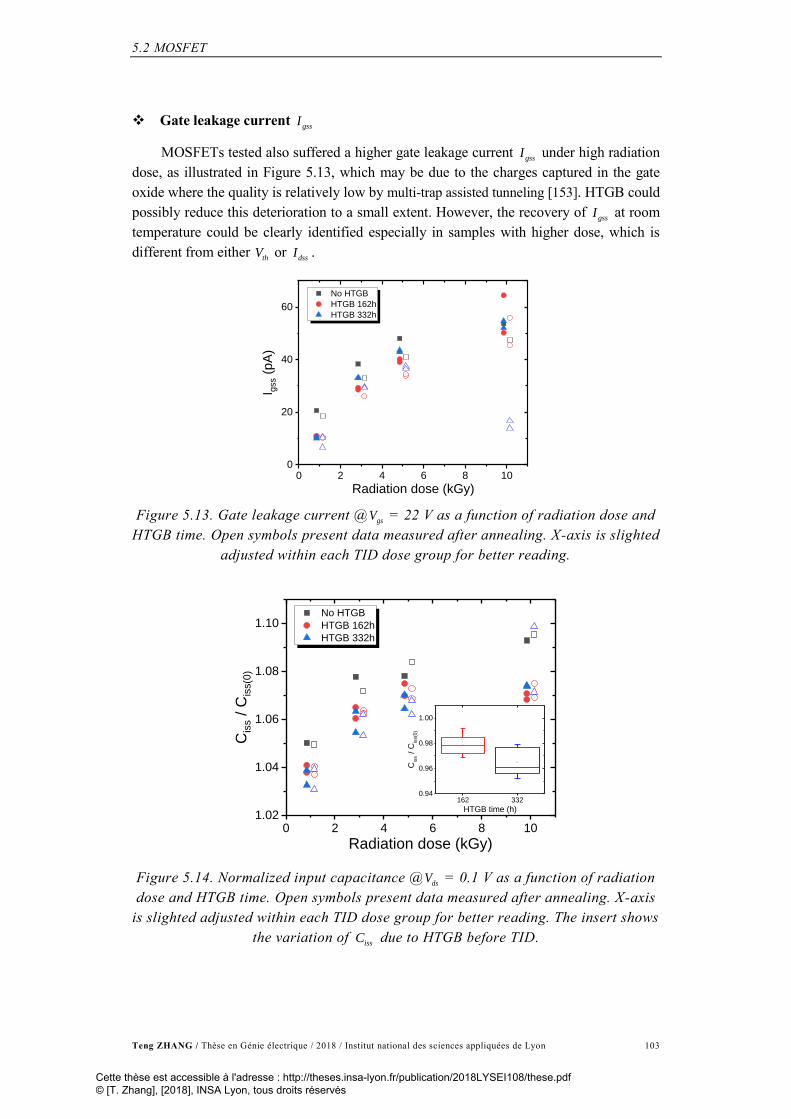
5.2 MOSFET
Teng ZHANG / Thèse en Génie électrique / 2018 / Institut national des sciences appliquées de Lyon 103
Gate leakage current gssI
MOSFETs tested also suffered a higher gate leakage current gssI under high radiation
dose, as illustrated in Figure 5.13, which may be due to the charges captured in the gate
oxide where the quality is relatively low by multi-trap assisted tunneling [153]. HTGB could
possibly reduce this deterioration to a small extent. However, the recovery of gssI at room
temperature could be clearly identified especially in samples with higher dose, which is
different from either thV or
dssI .
0 2 4 6 8 100
20
40
60
No HTGB
HTGB 162h
HTGB 332h
I gss (
pA
)
Radiation dose (kGy)
Figure 5.13. Gate leakage current @gsV = 22 V as a function of radiation dose and
HTGB time. Open symbols present data measured after annealing. X-axis is slighted
adjusted within each TID dose group for better reading.
0 2 4 6 8 101.02
1.04
1.06
1.08
1.10
162 3320.94
0.96
0.98
1.00
HTGB time (h)
Cis
s /
Cis
s(0
)
HTGB 162h
HTGB 332h
No HTGB
HTGB 162h
HTGB 332h
Cis
s / C
iss(0
)
Radiation dose (kGy)
Figure 5.14. Normalized input capacitance @dsV = 0.1 V as a function of radiation
dose and HTGB time. Open symbols present data measured after annealing. X-axis
is slighted adjusted within each TID dose group for better reading. The insert shows
the variation of issC due to HTGB before TID.
Cette thèse est accessible à l'adresse : http://theses.insa-lyon.fr/publication/2018LYSEI108/these.pdf © [T. Zhang], [2018], INSA Lyon, tous droits réservés

Chapter 5
Characterization on other samples and discussion
Teng ZHANG / Thèse en Génie électrique / 2018 / Institut national des sciences appliquées de Lyon 104
Input capacitance issC
Input capacitance increased with the increase of radiation dose (Figure 5.14). This in-
crease was enhanced on samples with HTGB.
Annealing Effect at Room Temperature
Since some time-delay exists between sample collection after TID radiation and char-
acterization, it is difficult to evaluate any quick annealing right after the radiation. Howev-
er, almost no annealing was observed at room temperature except gssI during our track for
one week starting several hours after radiation. It is safe to say that no quick annealing was
involved.
5.2.4 Discussion
The whole synergetic effects could be explained by a HTGB-assist-TID model as
shown in Figure 5.15. A negative charged layer is generated after HTGB due to tunneling
and capture of electrons. This will generate electric field that can accelerate the hole dis-
placement during TID irradiation. However, as the electron-hole pairs’ generation process
takes place in each device, the influence on the accumulated electron layer should be ne-
glected. In this case, the electric parameters shift would be enhanced with HTGB samples
when focus only on TID process. Nevertheless, as the net charge near interfacial is more
negative compared to the case of no HTGB samples, the total degradation is always lower
if pre-HTGB is presented. This corresponds well with our result in thV and
issC .
Figure 5.15. Illustration of band diagram near interface during HTGB (right) and
TID (left), with the marked process (a): electrons directly tunneling and capture (b):
electron-hole pairs generation due to irradiation and (c): holes displacement and
capture.
As the synergetic effects mainly focus on charge capture near semiconductor/oxide
interface, post-oxidation annealing in NO could be a candidate solution for reducing the
generated field by electrons X
XXXXXXXX
*******
*******
HTGBTID
applied gate bias during HTGB
EC
EF
EV
*******
*
**
*
*
*
**
(a)
(b)
(c)
electrons holes X interface traps * oxide traps
Cette thèse est accessible à l'adresse : http://theses.insa-lyon.fr/publication/2018LYSEI108/these.pdf © [T. Zhang], [2018], INSA Lyon, tous droits réservés

5.2 MOSFET
Teng ZHANG / Thèse en Génie électrique / 2018 / Institut national des sciences appliquées de Lyon 105
instability due to traps passivation, especially those interface traps [154, 155]. Irradiation
resisted dielectrics such as HfO2 are also worth trying according to lower trapping effi-
ciency during TID [156]. Meanwhile, proper pre-HTGB treatment (162 hours in this work)
could greatly improve the performance after TID radiation, especially on drain-source
leakage current, which could be of interest for further investigation.
Cette thèse est accessible à l'adresse : http://theses.insa-lyon.fr/publication/2018LYSEI108/these.pdf © [T. Zhang], [2018], INSA Lyon, tous droits réservés

Chapter 5
Characterization on other samples and discussion
Teng ZHANG / Thèse en Génie électrique / 2018 / Institut national des sciences appliquées de Lyon 106
5.3 Discussion
5.3.1 Freeze-out effect
According to Eq. (2.22) and (2.23), the measured capacitance under certain reverse
bias should decrease gradually when the sample cools down. However, that is no longer
valid under cryogenic temperature. As shown in Figure 5.16, two sharp drops of capaci-
tance appear at around 40 K and 100 K on both forward and reverse bias conditions.
Moreover, similar trend shows up among all the SiC devices tested including those SBDs
with different metal contacts. This measured capacitance gap at 40 K with DLTS test has
also been report by Menichelli et. al., and is contributed to the freeze-out of the shallow
doping [66].
0 100 200 300 400 500
0
500
1000
1500
2000
2500
0 100 200 300 400 500
0
100
200
300
Up = -0.1 V
Up = -2 V
Capa
citan
ce (
pF
)
Temperature (K)
a
20 40 60 80 100 1200
200
400
Ca
pacitance (
pF
)
Temperature (K)
Capa
citan
ce (
pF
)
Temperature (K)
b
20 40 60 80 100 1200
100
200
Ca
pa
citan
ce (
pF
)
Temperature (K)
Figure 5.16. (a): pulse capacitance and (b): reverse capacitance with a bias of –10
V measured during DLTS scan between 20 K and 550 K on PiN diode discussed in
section 5.1.
Even though energy level of shallow dopant usually lies near the conduction band (n-
type) or valence band (p-type), a number of dopant will still be frozen and cannot be fully
activated if the temperature is too low compared to their activation energy. These majority
traps have been investigated through various techniques during experiments such as admit-
tance spectroscopy on 6H-SiC [157] or traveling-wave method on 4H-SiC [158]. The
more general case has been summarized by Los et al. as list in Table 5.6 [159].
Due to the structure especially the atomic stacking arrangement of either 4H- or 6H-
SiC where two types of bonding namely zinc bonding (cubic) and wurtzite (hexagonal) ex-
ist, the activation energy of doping traps are separated with h-site (hexagonal) and k-site
(cubic) respectively [7]. Therefore the capacitance gaps in Figure 5.16 present the transient
region where carriers on certain site start to be frozen and trapped. And as a result, the tra-
ditional DLTS with capacitance measurement could no more provide the accurate results
Cette thèse est accessible à l'adresse : http://theses.insa-lyon.fr/publication/2018LYSEI108/these.pdf © [T. Zhang], [2018], INSA Lyon, tous droits réservés

5.3 Discussion
Teng ZHANG / Thèse en Génie électrique / 2018 / Institut national des sciences appliquées de Lyon 107
and the current DLTS or other types discussed in 3.4.1 should be used in low temperature
region in order to extract the information on traps with the help of Arrhenius analysis.
Table 5.6. Activation energies of common SiC doping impurities summarized in
[159].
N donor Al acceptor B acceptor
4H-SiC 52.1 mV h-site
0.19-0.23 eV 0.258-0.39 eV 91.8 mV k-site
6H-SiC
81 mV h-site
0.20-0.25 eV 0.27-0.40 eV 137.6 mV k1-site
142.4 mV k2-site
5.3.2 Relationship between activation energy and capture cross section of certain defect level.
As is indicated by Figure 4.31, there seems to be certain relationship between the ex-
tracted activation energy aE and its capture cross section for those trap levels with the
same origin. Another two SBDs of Ti/W sputtering 1min (S4) have been investigated with
the help of DLTS in order to reveal more details on this phenomenon.
Test setup
In order to introduce the uncertainty, a diode with the largest surface (2.48 mm2) la-
beled diode (L) and another with the smallest surface (0.155 mm2) labeled diode (S) were
involved in this test. DLTS have been taken out between 80 K and 400 K with numerous
combinations of PT and
WT , and the parameters extracted from Arrhenius plot are based on
single period width which is different from that we did in Chapter 4. A bias range from -0.5 V (
RU ) to 0.6 V (PU ) were adopted for all the DLTS scans which is commonly not
recommended for DLTS as more noise will be involved if the pulse height (P RU U ) is too
small.
Results
As shown in Figure 5.17, a number of possible peaks labeled from A to J have been
revealed with peak analysis from Origin software, while another peak K is marked for the
diode (S) which may due to the signal noise of single point and can be neglected. Similar
trap levels could be corresponded between these two diodes even though the height of
peaks can vary a lot. This may due to the different surface conditions since the target re-
gion of DLTS test here is more closed to the interface and can be much easily influenced
by noise. Three clear peaks namely A, E and H have been analyzed with DLTS Maximum
Analysis in order to ensure the accuracy. However, not all combination of PT and
WT re-
sulted in the effective analysis on these three defect levels, and only those valuable data
Cette thèse est accessible à l'adresse : http://theses.insa-lyon.fr/publication/2018LYSEI108/these.pdf © [T. Zhang], [2018], INSA Lyon, tous droits réservés

Chapter 5
Characterization on other samples and discussion
Teng ZHANG / Thèse en Génie électrique / 2018 / Institut national des sciences appliquées de Lyon 108
are used in the following discussion which leads to the difference on number of tests of
these trap levels.
Figure 5.17. DLTS signal and the peak analysis by Origin on (a): diode (L) with PT
= 1 ms, WT = 100 ms and (b): diode (S) with
PT = 1 ms, WT = 200 ms between 80 K
and 400 K. The sizes of the Alphabets represent the height of each individual peak.
0 5 10 15 20 25
0.3
0.4
0.5
0.6
0.7
0.8
0.9
Ec-Et
Correl
Test batch
Activation e
nerg
y (
eV
)
(a)0.0
0.2
0.4
0.6
0.8
1.0
Corre
latio
n
0 5 10 15 20 2510-16
10-14
10-12
10-10
10-8
10-6
10-4
Ec-Et
Correl
Test batch
Captu
re c
ross s
ection
(cm
2)
(b)0.0
0.2
0.4
0.6
0.8
1.0
Corre
latio
n
Figure 5.18. Extracted (a): activation energy relate to conduction band C TE E and
(b): capture cross section as a function of the test batch with different PT -
WT com-
binations of peak E on diode (L), along with their correlation on linear fitting dur-
ing Arrhenius analysis.
As an example, the extracted activation energy and capture cross section of peak E on
diode (L) are illustrated in Figure 5.18. Most of the analyzed results are well fitted with
high correlation, especially the first 15 data. An interesting thing is that both activation en-
ergy and capture cross section in logarithmic coordinates have the same form, which indi-
cates a linear connection between them. By plotting the log( ) as a function of aE as
shown in Figure 5.19(a), a perfect line appears. This relationship suggests that even though
the correlation of no. 16 point in Figure 5.18 is not high enough, this extracted data should
still belong to the level of peak E. On the contrary, two points marked red in Figure 5.19(b)
largely deviate from the linear fitting of other points, which suggests that these two points
Cette thèse est accessible à l'adresse : http://theses.insa-lyon.fr/publication/2018LYSEI108/these.pdf © [T. Zhang], [2018], INSA Lyon, tous droits réservés

5.3 Discussion
Teng ZHANG / Thèse en Génie électrique / 2018 / Institut national des sciences appliquées de Lyon 109
extracted from the Arrhenius plot may belong to other trap levels (e.g. peak I) or due to the
experiment error during the analysis.
0.3 0.4 0.5 0.6 0.7 0.8 0.910-16
10-14
10-12
10-10
10-8
10-6
10-4
0.40 0.45 0.50 0.55 0.60 0.65 0.70 0.7510-18
10-17
10-16
10-15
10-14
10-13
Captu
re c
ross s
ection
(cm
2)
Activation energy (eV)
(a)
Captu
re c
ross s
ection
(cm
2)
Activation energy (eV)
(b)
Figure 5.19. Linear relationship between activation energy and capture cross sec-
tion of (a): peak E and (b): peak H on diode (L). Two points marked red in (b) are
suggested to be the error data and are not used in the linear fitting.
0.1 0.2 0.3 0.4 0.5 0.6 0.7 0.8 0.910-19
10-17
10-15
10-13
10-11
10-9
10-7
10-5
10-3 Diode (S) Peak-A
Linear Fit of Diode (S) Peak-A
Diode (S) Peak-E
Linear Fit of Diode (S) Peak-E
Diode (S) Peak-H
Linear Fit of Diode (S) Peak-H
Diode (L) Peak-A
Linear Fit of Diode (L) Peak-A
Diode (L) Peak-E
Linear Fit of Diode (L) Peak-E
Diode (L) Peak-H
Linear Fit of Diode (L) Peak-H
Ca
ptu
re c
ross s
ectio
n (
cm
2)
Activation energy (eV)
Figure 5.20. Linear relationship between activation energy and capture cross sec-
tion of all three peaks (A, E, and H) on diode (L) and diode (S). Several points of
peak H are suggested to be the error data and are marked red.
This linear relationship will be clearer if we draw all the points of three trap levels to-
gether, as shown in Figure 5.20. Although the overlap of extracted aE exists between peak
Cette thèse est accessible à l'adresse : http://theses.insa-lyon.fr/publication/2018LYSEI108/these.pdf © [T. Zhang], [2018], INSA Lyon, tous droits réservés

Chapter 5
Characterization on other samples and discussion
Teng ZHANG / Thèse en Génie électrique / 2018 / Institut national des sciences appliquées de Lyon 110
E and peak H, three groups of fitting lines are distinct and relate to different peaks illus-
trated in DLTS signals. We define the analytical average here as
1
1
( )
1 ( )( )
1
1 ( )
N
n
N
n
Y n
CorrelY nAvg Y
CorrelY n
(5.4)
where Y could be either a ,
TN or log( ) and the ( )CorrelY n represents the corre-
sponding correlation of fitting during Arrhenius analysis as explained in Figure 5.18.
Therefore, the average parameters of each trap level could be calculated and listed in Table
5.7 along with the corresponding linear fitting parameters shown in Figure 5.20.
Table 5.7. Calculated trap parameters on average based on Eq. (5.4) along with he
slope and intercept of linear fitting of each peak shown in Figure 5.20.
Parameter Diode (S) Diode (L)
Peak A
Average aE (eV) 0.142 0.131
Average (cm2) 1.23×10
-15 3.86×10
-16
Average TN (cm
-3) 3.00×10
11 3.19×10
11
Fitting slope 50.0 54.0
Fitting intercept –22.0 –22.5
Peak E
Average aE (eV) 0.395 0.427
Average (cm2) 3.98×10
-15 2.32×10
-14
Average TN (cm
-3) 1.51×10
12 2.43×10
12
Fitting slope 23.6 24.0
Fitting intercept –23.7 –23.9
Peak H
Average aE (eV) 0.568 0.608
Average (cm2) 5.69×10
-16 1.17×10
-15
Average TN (cm
-3) 3.29×10
12 1.84×10
12
Fitting slope 18.5 14.4
Fitting intercept –26.0 –23.6
The averaged trap parameters of each defect level are similar on both diodes, with a
relatively large mismatch on peak H due to the complicity of the overlapped energies. On
the other hand, those slopes and intercepts are also in great agreement on each peak, ex-
cept the slope of peak H on diode (S) which is owing to the limited arrange of extracted
data compared to diode (L) as shown in Figure 5.20. Meanwhile, whatever the diode is, the
Cette thèse est accessible à l'adresse : http://theses.insa-lyon.fr/publication/2018LYSEI108/these.pdf © [T. Zhang], [2018], INSA Lyon, tous droits réservés

5.3 Discussion
Teng ZHANG / Thèse en Génie électrique / 2018 / Institut national des sciences appliquées de Lyon 111
fitting intercept of all three levels are quite close to a value around –23 while the slopes are
distinct on each peak. This indicates that certain relation between aE and exists and can
be expressed as:
log( ) au E v (5.5)
where u and v are constant parameters only related to the trap. By using the natural
logarithm and bringing Eq. (5.5) in the expression of Arrhenius plot [Eq. (3.10)], it can be
deduced that:
,
1ln( )e th n C av N E u v
kT
(5.6)
where the left part of the equation mark usually relates to the y-axis of the Arrhenius
plot. This means that if the temperature equals 1
ku
, the value of y-axis on Arrhenius
plot should always be v when focusing on certain trap level. Or in other words, this ‘fixed
point’ on Arrhenius plot indicates that at one trap level is easier to be discovered around
this ‘fixed temperature’, which could be an intrinsic characteristics to separate different
defect levels.
5.3.3 Annealing effect during DLTS
In addition to the annealing effect on trap level around 190 K as shown in Figure 4.22
and discussed in 4.3.22, the annealing (or to be more precise, the bias stress under high
temperature scan) during DLTS will influence the trap levels that appear at higher temper-
ature region as well.
300 400 500 600
0.000
0.005
0.010
0.015
300 400 500 600
0.000
0.004
0.008
0.012
0.016
DLTS scan 300K to 600K
DLTS scan 600K to 300K
b1
(pF
)
Temperature (K)
a 1st scan 300K to 600K
1st scan 600K to 300K
2nd scan 300K to 600K
2nd scan 600K to 300K
b1
(pF
)
Temperature (K)
b
Figure 5.21. DLTS signal (correlation b1) with a period width of 204.8 ms on (a):
Ti/W sputtering 1min sample (S4) and (b): Ni sputtering sample (S2) during tem-
perature scan in different directions (heat up or cool down). The waiting time be-
tween scan of 300 K – 600 K and 600 K – 300 K is limited to minutes and can be
neglected.
Cette thèse est accessible à l'adresse : http://theses.insa-lyon.fr/publication/2018LYSEI108/these.pdf © [T. Zhang], [2018], INSA Lyon, tous droits réservés

Chapter 5
Characterization on other samples and discussion
Teng ZHANG / Thèse en Génie électrique / 2018 / Institut national des sciences appliquées de Lyon 112
For example, ‘something’ diminished at around 330 K after two high temperature
DLTS scan with different directions as illustrated in Figure 5.21(a), and this has been ob-
served among all of the Schottky samples. However, the problem becomes more compli-
cate when it comes to the Ni sample. As shown in Figure 5.21(b), another possible trap
level at around 430 K diminished after annealing, and the mismatch of the peak position
on temperature shows up. This shift on maximum of the peak owing to the error of tem-
perature record by sensors, but can be ignored if we only compare the signal height. Fur-
thermore, the whole signal height decreases after each scan cycle (300 K – 600 K – 300 K)
and recovers at room to a certain degree, which is similar to but different from that shown
in Figure 4.22. Considering that the signal of cooling down on Ni diode during both 1st and
2nd
scans well overlaps, this vanished signal height should present as the unique ‘white
noise’ of trap levels in Ni SBDs (e.g. the fast states at interface with a distribution of AE
and [160]) and can be totally removed by high temperature-bias stress process.
300 350 400 450
0
2
4
6
8
300 350 400
0
2
4
6
8
10 DLTS scan 300K to 600K
DLTS scan 600K to 300K
a1
(Tw
/2)
(fF
)
Temperature (K)
(a) DLTS scan 300K to 600K
DLTS scan 600K to 300Kb1
M (
fF)
Temperature (K)
(b)
Figure 5.22. Signal DLTS on different correlations (a): a1(Tw/2) and (b): b1M on
the Ti/W sample with the same scan 300 K – 600 K – 300 K as in Figure 5.21(a).
Table 5.8. Extracted trap parameters on Ti/W and Ni samples with the help of Max-
imum (maximum Arrhenius analysis) and HERA analysis.
Sample Tool aE (eV) (cm
2)
TN (cm-3
)
Ti/W Maximum 0.667 2.83×10
-16 6.58×10
11
HERA 0.720 2.80×10⁻¹⁵
5.52×10¹¹
Ni Maximum 0.661 1.91×10
-16 7.01×10
11
HERA 0.676 2.40×10⁻¹⁶
6.76×10¹¹
Other correlation functions are also involved to analyze the disappeared trap level
around 330 K, and this peak is much clear shown with certain correlation parameter such
as a1(Tw/2) and b1M as illustrated in Figure 5.22. In order to cut back the error from the
strong trap levels near our target, both HERA and maximum analysis have been used to
Cette thèse est accessible à l'adresse : http://theses.insa-lyon.fr/publication/2018LYSEI108/these.pdf © [T. Zhang], [2018], INSA Lyon, tous droits réservés

5.3 Discussion
Teng ZHANG / Thèse en Génie électrique / 2018 / Institut national des sciences appliquées de Lyon 113
extract the trap parameters. Those Arrhenius results are listed in Table 5.8 which indicates
that they originate from the same defect level with activation energy near 0.67 eV where
the Z1/2 are usually reported. However, no more reference can be obtained on this trap lev-
el found here. Unfortunately, the trap level appears at 430 K of the Ni sample cannot be
precisely analyzed due to the significant influence on defect levels at 380 K and 530 K.
300 400 500
-0.12
-0.08
-0.04
0.00
0.04
0.08
0.12
300K to 550K
550K to 300K
b1
(pF
)
Temperature (K)
300 400 500-0.05
-0.04
-0.03
-0.02
-0.01
0.00
Tw = 2.048 s
b1
(p
F)
Temperature (K)
Tw = 20.48 ms
Figure 5.23. DLTS signal (correlation b1) between 300 K and 550 K on PiN diode
discussed in section 5.1 with a period width of 20.48 ms and 2.048 s (top-right plot).
Before the DLTS scan 550 K – 300 K, an additional waiting time of 30 min are ap-
plied with tiny bias (–0.1 V) right after the heat-up scan (300 K – 550 K).
On the other hand, no specific trap levels disappear on PiN diode after high tempera-
ture DLTS scan, as shown in Figure 5.23. Meanwhile, only the increase (negative shift) on
the peak near 500 K has been observed, and this difference is clearer revealed with large
WT . One assumption is that the trap level found above among all SBDs is influenced by the
hole trap level in PiN diode, and as a result, the vanishing of this trap level cannot be ob-
served.
In short, considering also the results discussed in 4.3.22, the high temperature DLTS
scan does influence the DLTS results namely trap conditions. This can be quite significant
especially when that leads to the disappearance of certain trap levels, and should be taken
special care of. Therefore in this paper, all DLTS results given for device characterization
are those temperature scan after a first high temperature scan (usually 300 – 550 – 300 K)
in order to rule out the influence of that.
5.3.4 Negative-U center
As has been discussed in 5.1.4 where an abnormal peak shows up at around 80 K
(Figure 5.5), this irregular phenomenon has also been uncovered on those SBDs. Figure
5.24 shows the DLTS spectra with 3 values of WT . Except that around 80 K, a clear trend
Cette thèse est accessible à l'adresse : http://theses.insa-lyon.fr/publication/2018LYSEI108/these.pdf © [T. Zhang], [2018], INSA Lyon, tous droits réservés

Chapter 5
Characterization on other samples and discussion
Teng ZHANG / Thèse en Génie électrique / 2018 / Institut national des sciences appliquées de Lyon 114
for all peaks is revealed from the spectra: peaks shift to left with large period width while
their heights slightly increase. This increase on signal heights is normally owing to the
change of reverse/pulse capacitance at different temperatures. However, even if this trend
of signal height is taken into consideration, the peak at around 80 K with WT = 2.048 s
should be the dash line illustrated in Figure 5.24(b) rather than the experimental one.
200 400 600
0
2
4
6
8
60 70 80 90 100 110 120
0
2
4
6
8
Tw = 20.48 ms
Tw = 204.8 ms
Tw = 2.048 s
b1
(fF
)
Temperature (K)
(a) Tw = 20.48 ms
Tw = 204.8 ms
Tw = 2.048 s
b1
(fF
)
Temperature (K)
(b)
Figure 5.24. DLTS spectra with 3 different period widths on diode Ti/W liftoff (S3)
between (a): 60 K and 600 K, while (b) is the same signal between 60 K and 120 K
in order for better illustration, with RU = –10 V,
PU = –0.1 V and PT = 100 µs.
In order to study this irregular peak at around 80 K, DLTS has been taken out on
Tungsten sample (S7) that also presents this strange behavior, with more WT and smaller
steps as shown in Figure 5.25(a), while more intuitional description can be obtained from
its plot in 3D (Figure 5.26). As illustrated in the 3D-plot, 2 distinct peaks can be recog-
nized: a normal peak with its center temperature shifts to left under large WT (black dash
line), and an abnormal one with its center temperature moves to right when the period in-
creases (red dash line). Meanwhile, the height of both peaks changes differently: the peak
heights of normal one almost keeps constant with the period less than 2 s, and dramatically
decrease with increase of WT . On the other hand, the special peak overlaps with the normal
one and cannot be well separated with WT less than 1 s, while greatly increase with large
period width. This can somewhat explain the only irregular signal with the period width of
2.048 s shown in Figure 5.24(b). Furthermore, a negative peak appears at 80 K with large
WT which may lead to the sharply decrease of normal peak height. However, this negative
peak is unrealistic to analyze due to lack on experimental data.
In order to study on this special peak, the Arrhenius plot is used according to search
on maximum peak position with various correlations. As can be seen in Figure 5.25(b), an
irregular but perfect fitting line shows up as presented by the red circles in addition to the
normal peak (black squares). However this special peak can be only found in those corre-
lations of ‘series b or sine coefficients’ namely the odd items in the Fourier transform
which results in relatively less points presented on the Arrhenius plot of the special peak.
Since the slope of fitting line in the Arrhenius plot corresponds to the activation energy,
Cette thèse est accessible à l'adresse : http://theses.insa-lyon.fr/publication/2018LYSEI108/these.pdf © [T. Zhang], [2018], INSA Lyon, tous droits réservés

5.3 Discussion
Teng ZHANG / Thèse en Génie électrique / 2018 / Institut national des sciences appliquées de Lyon 115
the negative slope of special peak indicate the existence of negative activation energy
which cannot be analyzed by our DLTS software rather than the positive activation energy
obtained from the positive slope of the normal one. And this negative activation energy is
different from the hole trap discovered in p-n junction with the help of negative peak in the
DLTS spectra, which highlights its particularity.
60 80 100 120
-2
-1
0
1
2
3
4
5
8 10 12
54
56
58
60
102.4ms
204.8ms
409.6ms
1.024s
2.048s
4.096s
12.04s
b1
(fF
)
Temperature (K)
(a)
Normal Peak
Special Peak
ln(V
thN
C)
1000/T (K-1)
(b)
Figure 5.25. (a): DLTS spectra (b1) between 60 K and 120 K with 7 different period
widths on Tungsten diode (S7) and (b) is its Arrhenius plot extracted.
Figure 5.26. 3D-plot of Figure 5.25(a). The blue and red dash lines indicate the
evolution trend on two peaks.
This irregular peak detected can be partly explained with the negative-U system. If a
defect can trap two electrons (or holes) while the second bond is more tight than the first
Cette thèse est accessible à l'adresse : http://theses.insa-lyon.fr/publication/2018LYSEI108/these.pdf © [T. Zhang], [2018], INSA Lyon, tous droits réservés

Chapter 5
Characterization on other samples and discussion
Teng ZHANG / Thèse en Génie électrique / 2018 / Institut national des sciences appliquées de Lyon 116
one, it can be regarded as a negative-U system or with the negative-U properties [161]. For
example, three possible charge states ( D , 0D and D ) exist for a simple point defect with
a single donor (0/+) and acceptor (–/0) level. However, if it has negative-U properties, the
neutral level 0D can be no more stable. Instead of stay neutral, certain process will take
place as
02D D D U (5.7)
where U is the energy between donor and acceptor level.
As a results, if Fermi level coincident the half way between the donor and acceptor
levels, there will be the compound of D and D rather than 0D .
The negative-U centers have been observed not only in 4H- (Z1/2) and 6H- (E1/2) SiC
[162-164], but also in 3C-SiC [165], and have been suggested to result from the carbon
vacancies (VC) with the first-principles calculations [165, 166].
As a feature of negative-U center, the DLTS signal height should be twice the trap
concentration since during the emission process that
0 2D D e D e (5.8)
If the second emission process is much faster than the first one, almost no time delay
appears before the neutral level loose its second electron. Therefore, second emission will
not show up as a peak in DLTS signal and instead, the signal height of the first process is
doubled due to the emitted electrons on pair. However, as has been pointed out by Do-
bacrewski, the neutral can stay at a high concentration with a certain time during the same
process if the emission rate of D level is much larger than 0D [167].
Based on the negative-U system, the special peak that appears at around 80 K in our
DLTS experiment can be explained by the combination effect of emission and capture in
the negative-U trap. It is suggested that the emission rate of D is smaller than 0D , and
most of the traps stay at 0D because the pulse width is not long enough for all traps enter
the balance states as indicated by Eq. (5.7). In that case, after PU withdraws, not only the
emission of neutral level (second process in Eq. (5.8)) takes place, but also the process in-
dicated by Eq.(5.7) and could be somewhat the major process. However, only the emission
can be detected in this stage since no electron is released in Eq.(5.7). As a result, only the
emission from neutral level appears in the DLTS signal with small WT . On the other hand,
after the first stage entering its end where certain traps become negative charged, the
whole process in the Eq. (5.8) becomes major, which results in the extremely high peak in
DLTS signal detected with large period width. Furthermore, the negative activation energy
extracted from the special peak in Figure 5.25(b) is due to the process implied by Eq. (5.7)
in first stage works with energy emission. Or in other word, instead of the conventional
emission process with energy absorption, this energy emission process is presented by the
negative activation energy in the Arrhenius plot. Meanwhile, the phenomenon that the
height of special peak in DLTS signal increases with large WT is owing to either slow pro-
cess of emission from D or the less freeze-out effect at higher temperature.
Cette thèse est accessible à l'adresse : http://theses.insa-lyon.fr/publication/2018LYSEI108/these.pdf © [T. Zhang], [2018], INSA Lyon, tous droits réservés

5.3 Discussion
Teng ZHANG / Thèse en Génie électrique / 2018 / Institut national des sciences appliquées de Lyon 117
5.3.5 Behavior at extremely low temperature
As mentioned in 4.3.22, the behavior can be quite weird under extremely low temper-
ature (below 20 K). On the other hand, the investigation method is limited due to either
freeze-out effect or the restriction of our DLTS system (the valid temperature is limited to
15 K). As a result, the isothermal DLTS becomes the main tool for research on this low
temperature region.
Tempscan below 25 K
In the previous study on SiC SBD within the temperature range of 20 K – 60 K, the
signal increases towards lower temperature part near 20 K, as presented by the black
squares in Figure 5.27, which indicates the existence of higher peak at lower temperature,
or in other words the additional trap levels with large concentration and tiny activation en-
ergy can be forecasted. This is true if we expend the temperature until 15 K, as shown by
the red circles. However, owing to the temperature restriction, the whole profile at low
temperature cannot be drawn by using the DLTS tempscan even another clear peak ap-
pears at 20 K.
20 30 40 50 60
-600
-400
-200
0
b1
(pA
)
Temperature (K)
Figure 5.27. I-DLTS signal (correlation b1) on Ti/W sputtering 1 min sample (S4)
at low temperature. The black squares are that discussed in Chapter 4, while the
red circles are the focus in this section.
In order to investigate these trap levels at extremely low temperature, the isothermal
DLTS have been adopted. The ITS have been measured between 15 K and 25 K with a
temperature step of 0.5 K, which is much smaller than the one commonly used (~ 10 K).
Both positive and negative peaks show up after ITS of I-DLTS, and the results of Arrheni-
us analysis are shown in Figure 5.28. Even with different bias condition, similar trap levels
are extracted with aE 0.03 eV and 1×10-15
cm2. As the electron trap levels reported
Cette thèse est accessible à l'adresse : http://theses.insa-lyon.fr/publication/2018LYSEI108/these.pdf © [T. Zhang], [2018], INSA Lyon, tous droits réservés

Chapter 5
Characterization on other samples and discussion
Teng ZHANG / Thèse en Génie électrique / 2018 / Institut national des sciences appliquées de Lyon 118
in 4H-SiC closest to the conduction band are those defect of nitrogen with aE around 0.05
eV [70], it is hard to sort these two trap levels with lower aE . Meanwhile, it is hard to
make a conclusion about the accuracy of determined levels owing to the small step used in
ITS test although both levels in Figure 5.28 are rather linear fitted. Whatever, it is sure that
some traps do exist at low temperature with large concentration.
Figure 5.28. Arrhenius plot from maximum analysis of DLTS on diode S4 at tem-
perature below 25 K. The pulse width is 5 μs and the bias condition on (a) and (b)
are listed inside plot. Some points extracted with maximum analysis that do not be-
long to these two levels are not shown in the plot.
0.001 0.01 0.1 1
-5
0
5
10
TP = 5 s
UR = -5 V
UP = -0.1 V
b1
(n
A)
period width Tw (s)
Figure 5.29. I-DLTS signal (correlation b1) from ITS period scan at 17.35 K on
sample S4 with PT = 5 μs,
RU = –5 V and PU = –0.1 V.
Further studies on these trap levels at low temperature have been taken out at the
lowest temperature available on sample (~17.5 K) in our DLTS system with isothermal
Cette thèse est accessible à l'adresse : http://theses.insa-lyon.fr/publication/2018LYSEI108/these.pdf © [T. Zhang], [2018], INSA Lyon, tous droits réservés

5.3 Discussion
Teng ZHANG / Thèse en Génie électrique / 2018 / Institut national des sciences appliquées de Lyon 119
DLTS tests. As shown in Figure 5.29, two clear peaks show up with different signs in the
period width scan, while the region at lower period width part (< 0.6 ms) that is limited by
the measurement also draws attention.
As I-DLTS commonly presents those trap levels as negative peaks, two minima (~
200 ms and 1 ms) have been specially focused on as well as the blank region (WT < 600 µs)
in Figure 5.29 with WT chosen as 200 µs.
ITS WT = 200 ms
10-6 10-5 10-4 10-3 10-2 10-1 100
-2.0
-1.5
-1.0
-0.5
0.0
b1
(nA
)
Pulse width (s)
TW = 200 ms
UR = -5 V
UP = -0.1 V
Figure 5.30. I-DLTS signal (correlation b1)of isothermal variation of PT at 17.35 K
with a fixed period width of 200 ms.
As shown in Figure 5.30, only negative signal is obtained with the period width of
200 ms. However, different from the normal ITS with variation of PT which performs as a
monotonic function, a peak with a minimum value shows up with PT near 20 ms. It is sug-
gested that there are at least two highly compensated trap levels with opposite defect types
and different . Therefore it appears as the traditional trap when the capture of the normal
trap level takes charge at small PT , while it saturates and the compensation effect take
place due to additional trap level at large PT . Finally, signal trends to zero when the pulse
is large enough where high compensation is reached due to relatively closed active con-
centration. Another possibility relates to the negative-U center discussed in the previous
chapter. If the trap levels detected here come from the negative-U center, this abnormal
behavior can be explained as the majority captured levels with different pulse width. It is
assumed that only the fast emission process can be detected with the period width of 200
ms, while the signal that originates the slow progress can be neglected. As a result, most of
the trap levels are occupied as oD with small PT , and the fast process presents as the nega-
Cette thèse est accessible à l'adresse : http://theses.insa-lyon.fr/publication/2018LYSEI108/these.pdf © [T. Zhang], [2018], INSA Lyon, tous droits réservés

Chapter 5
Characterization on other samples and discussion
Teng ZHANG / Thèse en Génie électrique / 2018 / Institut national des sciences appliquées de Lyon 120
tive signal in Figure 5.30. However, more and more traps will be in the D states when PT
becomes larger, and finally almost all defects are trapped as D centers if PT is large
enough. Since the emission form D level is limited and presented as slow process, it can
hardly be detected and this contributes to the tiny negative signal at large PT . As the nega-
tive-U center can be regarded as two trap levels, only the condition of two trap level with
opposite defect types will be further discussed, and those conclusions can be applied to the
case of negative-U centers as well.
-20 -15 -10 -5 0
-1.0
-0.8
-0.6
-0.4
-0.2
0.0
-20 -15 -10 -5 0
-2.0
-1.5
-1.0
-0.5
0.0
TW = 200 ms
UR = -20 V
TP = 5 s
b1
(n
A)
Pulse voltage (V)
(a)
TW = 200 ms
UP = -0.1 V
TP = 5 s
b1
(n
A)
Reverse bias (V)
(b)
Figure 5.31. I-DLTS signal (correlation b1)of isothermal variation of (a): PU and
(b): RU at 17.35 K.
-20 -15 -10 -5
-1.6
-1.2
-0.8
-0.4
TW = 200 ms
TP = 5 s
UP-UR = 4.5 V
UP-UR = 6 V
b1
(nA
)
Reverse bias (V)
Figure 5.32. I-DLTS signal (correlation b1)of isothermal variation of both PU and
RU with pulse heights keep constant.
However, more interesting results can be found from Figure 5.31, where a negative
peak and one negative shoulder can be clearly identified in both plots. This reveals the ex-
istence of third trap level. Due to the mirror relationship between Figure 5.31 (a) and (b), it
can be assumed that the major trapping level that determines the measured DLTS signal
only depends on the voltage difference P RU U during the transient process, and this is
Cette thèse est accessible à l'adresse : http://theses.insa-lyon.fr/publication/2018LYSEI108/these.pdf © [T. Zhang], [2018], INSA Lyon, tous droits réservés

5.3 Discussion
Teng ZHANG / Thèse en Génie électrique / 2018 / Institut national des sciences appliquées de Lyon 121
verified by Figure 5.32, where the transient type is somewhat fixed with constant P RU U
value.
Table 5.9. Extracted IV of sample S4 at different temperature according to C-V
analysis measured by DLTS system during the tempscan.
Temperature (K) IV (V) Correlation coefficient of linear fitting
21.84 17340 0.502
29.33 2175 0.946
38.18 6.5 0.999
48.48 1.5 0.999
Even though the conventional C-V analysis discussed in section 2.3.2 can no longer
provide precise results at extremely low temperature owing to the carrier freeze-out effect,
it can still be a reference for approximation. It can be found from Table 5.9 that IV be-
comes so huge that ( )I R PV U U at low temperature with worse linearity where carrier
freeze-out occurs. As a result, the approximation of the effective detection zone effw can
be expressed as:
2
P Reff R P I R I P
I
U Uw w w V U V U
V
(5.9)
where Rw and
Pw are the widths of depletion region at reverse bias and pulse condi-
tion.
Therefore the electric distribution within the effective zone that relates to only effw if
the doping near interface is assumed uniform is determined exclusively by the bias differ-
ence P RU U at a fixed low temperature. In that case, the weird behavior in Figure 5.31
can be caused by the Poole-Frenkel effect under strong electric field of at least one trap
level at high P RU U .
ITS WT = 1 ms
The 3-phase evolution (a-b, b-c and c-d) is clearer shown in Figure 5.33 with a period
width of 1 ms, which indicates the existence of a pair of compensated defect levels and
another cluster trap level. However, the sign is somewhat opposite compared to that shown
in Figure 5.30. Furthermore, even though the normal signal obtained can offer its relative-
ly large concentration during the isothermal test with variation of bias under small P RU U
condition, as illustrated in Figure 5.34(a), the circumstance becomes much complicated
with large P RU U as (b) shows. On the other hand, Figure 5.34(a) can be regarded as part
Cette thèse est accessible à l'adresse : http://theses.insa-lyon.fr/publication/2018LYSEI108/these.pdf © [T. Zhang], [2018], INSA Lyon, tous droits réservés

Chapter 5
Characterization on other samples and discussion
Teng ZHANG / Thèse en Génie électrique / 2018 / Institut national des sciences appliquées de Lyon 122
of the signal in (b) with PU less than –10 V. This will be discussed in detail in the case
followed (WT = 200 µs) with similar condition.
10-6 10-5 10-4 10-3 10-2 10-1 100
0.0
0.5
1.0
d
c
b
TW = 1 ms
UR = -5 V
UP = -0.1 V
b1
(n
A)
Pulse width (s)
a
Figure 5.33. I-DLTS signal (correlation b1)of isothermal variation of PT at 17.35 K
with a fixed period width of 1 ms.
-8 -6 -4 -2 0
0
100
200
300
400
0.8 0.9 1.0 1.11013
1014
1015
1016
1017
1018
-20 -15 -10 -5 0
-400
-200
0
200
b1
(n
A)
Up (V)
(a)
Nt
(cm
-3)
Depth (m)
b1
(n
A)
Up (V)
(b)
Figure 5.34. I-DLTS signal (correlation b1)of isothermal variation of PU at 17.35
K with (a): RU = –10 V and (b):
RU = –20 V. The pulse width is 30 μs and period
width is 1 ms. Inner plot in (a) shows the trap concentration profile calculated
based on results in (a).
ITS WT = 200 µs
In order to draw a brief profile of the trap presented at low WT where no information
has been provided by ITS scan shown in Figure 5.29 due to system limitation, a period
width of 200 µs was chosen for further investigation. The scan of PT shown in Figure 5.35
is more closed to the one discussed above with WT = 1ms (Figure 5.33). The 3-phase (a-b,
Cette thèse est accessible à l'adresse : http://theses.insa-lyon.fr/publication/2018LYSEI108/these.pdf © [T. Zhang], [2018], INSA Lyon, tous droits réservés

5.3 Discussion
Teng ZHANG / Thèse en Génie électrique / 2018 / Institut national des sciences appliquées de Lyon 123
b-c and c-d) in the plot presents 3 different trap levels, which corresponds with the previ-
ous results and can be examined by those transient curves illustrated on the right part of
Figure 5.35. However, the height of signal tend to decrease at large PT , which is different
from the case of either WT = 1 ms or 200 ms.
10-6 10-5 10-4 10-3 10-2 10-1 100
-2
0
2
4
(d)
(c)
(b)
(a)
TW = 200 s
UR = -5 V
UP = -0.1 V
b1
(n
A)
Pulse width (s)
500 600 700-2.0
-1.5
-1.0Tp = 2 s
Tra
nsie
nt (n
A)
Time (s)
(a)
500 600 700
-10
-8
-6
-4
-2
(b)
Tp = 33.5 s
Tra
nsie
nt (n
A)
Time (s)
500 600 700
-26
-24
-22(d)(c)
Tp = 1.12 ms
Tra
nsie
nt (n
A)
Time (s)
500 550 600 650 700
-42
-41
-40
-39
-38
Tp = 0.63 s
Tra
nsie
nt (n
A)
Time (s)
Figure 5.35. Left plot : I-DLTS signal (correlation b1)of isothermal variation of PT
at 17.35 K with a fixed period width of 200 µs. And right plot: the measured transi-
ent curve at different PT in the left plot.
-20 -15 -10 -5 0
-1
0
1
(d)
b1
(
A)
UR (V)
(a)
(b)
(c) (e)
500 600 700
-500
-400
-300
-200
UR = -17.50 V
Tra
nsie
nt (n
A)
Time (s)
500 600 700
-3000
-2000
-1000
UR = -10.02 V
Tra
nsie
nt (n
A)
Time (s)
500 600 700
-230
-220
-210
-200
-190
UR = -8.30 V
Tra
nsie
nt (n
A)
Time (s)
500 600 700-92
-91
-90
-89
TW = 200 s
TP = -1 ms
UP = -0.1 V
(d)(c)
(b)(a)
UR = -6.95 V
Tra
nsie
nt (n
A)
Time (s)
Figure 5.36. Left plot : I-DLTS signal (correlation b1)of isothermal variation of RU
at 17.35 K with a fixed period width of 200 µs. And right plot: the measured transi-
ent curve at different RU in the left plot.
The isothermal with variation of RU has also been taken out with a period width of
200 µs. As shown in the left plot of Figure 5.36, the signal is similar to that shown in Fig-
ure 5.34(b), but should be regarded as mirror relationship, which indicates the dependence
on only pulse height P RU U as has been discussed with Figure 5.31. Furthermore, the
transient information presented in Figure 5.36 describes the signal evolution, which is il-
Cette thèse est accessible à l'adresse : http://theses.insa-lyon.fr/publication/2018LYSEI108/these.pdf © [T. Zhang], [2018], INSA Lyon, tous droits réservés

Chapter 5
Characterization on other samples and discussion
Teng ZHANG / Thèse en Génie électrique / 2018 / Institut national des sciences appliquées de Lyon 124
lustrated in Figure 5.37. (The transient curve with the label (e) is similar as that of (a), but
not shown in the plot owing to the limitation of space.) In order to simply the discussion,
the transient is regarded as ‘positive’ if the corresponding DLTS signal (b1) is positive
such as (c), and the ‘negative transient’ describe those transients result in negative DLTS
signal for example (a) and (e). Therefore at low pulse height the transient is negative, and
the amplitude increases when the pulse height rises up. After a minima point is reached
around (b), the transient become positive until its maxima (d). If the pulse is high enough,
it enters the region (e) with a trend as one normal trap level.
Figure 5.37. Relationship between the observed transient curve and P RU U during
the DLTS shown in Figure 5.36. The blue dots surrounded by rad dash square indi-
cate the measured transient signals which correspond to that in Figure 5.36 with
the same label.
-10 -8 -6 -4 -2 0
7
8
9
10
-40 -30 -20 -10 0
6
8
10
12
ymin = -0.0887x+6.90
Maxima
Minima
UP-U
R (
V)
UP (V)
ymax = -0.0636x+9.81
(a)
Maxima
Minima
UP-U
R (
V)
UP (V)
ymax = -0.0460x+9.93
ymin = -0.0751x+7.02
(b)
Figure 5.38. The maxima and minima voltage illustrated in Figure 5.37 as a func-
tion of pulse voltage used in the DLTS isothermal variation of RU measures. Differ-
ent voltage sources were used that (a): low voltage module up to 20 V and (b): high
voltage module up to 100 V.
Cette thèse est accessible à l'adresse : http://theses.insa-lyon.fr/publication/2018LYSEI108/these.pdf © [T. Zhang], [2018], INSA Lyon, tous droits réservés

5.3 Discussion
Teng ZHANG / Thèse en Génie électrique / 2018 / Institut national des sciences appliquées de Lyon 125
In order to verify if the type of transient depend only on pulse height, the maxima and
minima voltages illustrated in Figure 5.37 [(d) and (b)] are extracted based on either iso-
thermal variation of RU with different
PU values (Figure 5.38) or variation of PU with
different RU values (Figure 5.39). It is clear that pulse height at both maxima and minima
stay linear at low bias (within –20 V), while the linearity drops at high bias condition (up
to –50 V). Even though less precise on voltage can be achieved when using high voltage
module exceed –20 V, this system error can never lead to the same trend on linearity that
the slope become less negative with large bias on both sample and points studied.
-20 -15 -10 -5
7
8
9
10
11
-50 -40 -30 -20 -10
7
8
9
10
11
12
Maxima
Minima
UP-U
R (
V)
UR (V)
ymax = -0.0608x+9.28
ymin = -0.0932x+6.35
(a)
Maxima
Minima
UP-U
R (
V)
UR (V)
ymax = -0.0445x+9.54
ymin = -0.0692x+6.64
(b)
Figure 5.39. The maxima and minima voltage illustrated in Figure 5.37 as a func-
tion of reverse bias used in the DLTS isothermal variation of PU measures. Differ-
ent voltage sources were used that (a): low voltage module up to 20 V and (b): high
voltage module up to 100 V.
On the other hand, this linear trend can be deduced with the help of Eq. (5.9). Here
the pulse height HU is defined as
H P RU U U , therefore the depletion width at fixed
temperature is only related to that:
Heff I R I P
I R I H R
Uw V U V U
V U V U U
(5.10)
In order to keep the depletion constant at different bias condition, Eq. (5.10) should
results in a constant value c , therefore HU can be written as:
H I R I H RU c V U V U U (5.11)
by ignoring the HU in the square root term, the differential can be expressed as:
1 1
2 2
H
R I R I H R
Uc
U V U V U U
(5.12)
Cette thèse est accessible à l'adresse : http://theses.insa-lyon.fr/publication/2018LYSEI108/these.pdf © [T. Zhang], [2018], INSA Lyon, tous droits réservés

Chapter 5
Characterization on other samples and discussion
Teng ZHANG / Thèse en Génie électrique / 2018 / Institut national des sciences appliquées de Lyon 126
According to Eq. (5.12), when the bias is small compared to IV the plot of
HU vs.
RU is linear with a negative slope value proportional to 1
2
IV . As the bias becomes larger,
RU can no more be neglected and results in the smaller value of the slope magnitude of
linear fitting. This corresponds well with the experimental results. The conclusion is simi-
lar when RU is replaced by
PU from those isothermal tests with variation of RU as is
shown in Figure 5.38. By comparing Figure 5.38(a) and Figure 5.39(a), it can be found
that the slopes are closed to each other on either minima points or maxima points, which
means the feasibility of the approximation made at low bias condition.
-100 -80 -60 -40 -20 0
-10
0
10
20
30
40
50
60
-100 -80 -60 -40 -20 0
-400
-300
-200
-100
0
100
TW = 200 s
TP = 1 ms
UP-UR = 9 V
b1
(n
A)
UR (V)
(a)
TW = 200 s
TP = 1 ms
UP-UR = 11 V
b1
(n
A)
UR (V)
(b)
Figure 5.40. I-DLTS signal (correlation b1)of isothermal variation of PU and
RU at
17.35 K with fixed difference of (a): P RU U = –9 V and (b):
P RU U = –11 V.
Since the transient type mainly depends on HU , conventional isothermal DLTS curve
with bias variation can be obtained by selecting proper HU , for example Figure 5.40(a).
Meanwhile, since the quasi-linear relationship on HU with
RU or PU is suggested, change
of transient type can still be observed under certain circumstance as shown in Figure
5.40(b) even though the HU is set constant.
Even though the behavior of trap at extremely low temperature has merely been stud-
ied and the mechanisms contributing to these performances discussed above is not yet
clear, this work still provide a possible way to snoop the trap with tiny activation energy at
low temperature. Meanwhile, certain trap behavior can be focused on by choosing the
proper bias parameters during the DLTS test. However, special attention should be paid
when it comes to the transient zone of DLTS signal [e.g. Figure 5.40(b)].
Cette thèse est accessible à l'adresse : http://theses.insa-lyon.fr/publication/2018LYSEI108/these.pdf © [T. Zhang], [2018], INSA Lyon, tous droits réservés

Teng ZHANG / Thèse en Génie électrique / 2018 / Institut national des sciences appliquées de Lyon 127
Chapter 6 Conclusion and prospective
Cette thèse est accessible à l'adresse : http://theses.insa-lyon.fr/publication/2018LYSEI108/these.pdf © [T. Zhang], [2018], INSA Lyon, tous droits réservés

Chapter 6
Conclusion and prospective
Teng ZHANG / Thèse en Génie électrique / 2018 / Institut national des sciences appliquées de Lyon 128
6.1 Conclusion
This dissertation mainly studies the deep level defects and their influences on SiC
power devices especially Schottky diodes. The main conclusions can be summarized in the
following aspects.
Determination of SBH
Based on the fundamental theory of Schottky contact, various of SBH models have
been reviewed such as Gaussian distribution model, potential fluctuation model and flat-
band barrier height. The Richardson plot based on BF is revealed to be suitable for de-
termination of Richardson constant. The equivalence of Gaussian distribution model and
potential fluctuation model has been discussed. Moreover, both parallel diode assumption
and Tung’s model on Schottky barrier inhomogeneity have been introduced.
Deep level detection
Following an overview on defect classification, the detection of defect levels with
DLTS has been mainly introduced according to basic capture-emission theory in semicon-
ductor. Apart from different transient models in DLTS, the isothermal tests have been
highlighted.
Investigation on SBDs and PiN diodes
Both static and DLTS tests have been taken on SBDs and PiN diodes. The compari-
son on either single/multi barrier SBD or SBD with different metal contacts (Ti/W, W, Ni
and Mo) have been presented along with the DLTS results. 9 trap levels are commonly
found in SiC SBDs including the overlapped energy level such as RD1/2. However, no ob-
vious difference has been found related to either barrier inhomogeneity or contact metal.
The hole traps have been investigate with PiN diodes under strong injection condition, and
the interaction between electron traps and hole traps under different bias has been dis-
cussed.
Radiation effect and bias stress instability on power MOSFET
The synergetic effects of HTGB and TID on SiC power MOSFETs have been inves-
tigated. It is found that thV seems sensitive to both HTGB and TID, while the trend is op-
posite under separate tests (i.e. HTGB tend to increase thV while
thV decreases after TID).
This results from different types of charges captured in the gate oxide. Meanwhile, accel-
eration of thV degradation due to HTGB was observed, which may result from the generat-
ed electric field due to captured electrons near interface after HTGB. However, No clear
annealing effect was observed over the short period of test at room temperature for either
HTGB or TID radiation.
Temperature related effects
The carrier freeze-out has been revealed in both SiC SBD and PiN diodes. A nega-
tive-U behavior is suggested to show up at around 80 K. The annealing effect at high tem-
Cette thèse est accessible à l'adresse : http://theses.insa-lyon.fr/publication/2018LYSEI108/these.pdf © [T. Zhang], [2018], INSA Lyon, tous droits réservés

6.1 Conclusion
Teng ZHANG / Thèse en Génie électrique / 2018 / Institut national des sciences appliquées de Lyon 129
perature is proved to take responsibility for the reduction on certain trap levels as well as
direct impact on the direct I-V performance which leads to the double barrier phenomenon.
On top of that, the DLTS behavior at extremely low temperature has been studied with iso-
thermal test and the abnormal signal has been obtained, which indicates the existence of
the trap level with tiny activation energy and large cententration.
Cette thèse est accessible à l'adresse : http://theses.insa-lyon.fr/publication/2018LYSEI108/these.pdf © [T. Zhang], [2018], INSA Lyon, tous droits réservés

Chapter 6
Conclusion and prospective
Teng ZHANG / Thèse en Génie électrique / 2018 / Institut national des sciences appliquées de Lyon 130
6.2 Perspective
As one of the most attractive “after-silicon” materials for power application, the im-
pact of SiC and related devices is becoming more and more important in the future thanks
to the development of modern technology on SiC wafer fabrication and manufacturing
process. Not only reliability but also the demand of precisely control of carrier lifetime in
device has highlighted the significance of defect investigation, which is a large wasteland
that has not yet been well investigated.
The future work mainly includes:
Interface characterization
As illustrated in Tung’s model (2.5.3), interface condition plays a significant role in
forward characteristics. Therefore, it is possible to find links between abnormal forward I-
V behavior and the interface states. Both investigations of interface traps and direct map-
ping of surface states by photos (e.g. Atomic Force Microscopy, AFM) as well as mapping
current distribution during device operation should be powerful tools.
Improvement on trapping models at low temperature
The model that suits the extremely low temperature involving the negative-U center
should be well developed, especially the detailed capture / emission process along with the
trap distribution.
Investigation of stress effect.
As has been pointed out, high temperature annealing, bias stress and radiation can
greatly affect the characteristic of device as well as the trap states. Further study can focus
on the combination effect of bias stress at high temperature, which is often the case to
many high temperature characterization methods.
Reverse characterization
Even though the characteristics under reverse bias have not been well studied due to
the precision limit of current measurement, the behavior under reverse bias is an important
characteristic related to trap centers. It is also a complement to the forward characteristics
study.
Cette thèse est accessible à l'adresse : http://theses.insa-lyon.fr/publication/2018LYSEI108/these.pdf © [T. Zhang], [2018], INSA Lyon, tous droits réservés

Teng ZHANG / Thèse en Génie électrique / 2018 / Institut national des sciences appliquées de Lyon 131
Reference
[1] R. H. Mari, "DLTS characterisation of defects in III-V compound
semiconductors grown by MBE," University of Nottingham, 2011.
[2] J. Baliga, "Modern power devices," 1987.
[3] R. Brown, "A novel AlGaN/GaN based enhancement-mode high electron
mobility transistor with sub-critical barrier thickness," PHD thesis of
University of Glasgow, 2015.
[4] J. J. Berzelius, "Untersuchungen über die Flussspathsäure und deren
merkwürdigsten Verbindungen," Annalen der Physik, vol. 77, pp. 169-230,
1824.
[5] D. Zhuang and J. H. Edgar, "Wet etching of GaN, AlN, and SiC: a review,"
Materials Science and Engineering: R: Reports, vol. 48, pp. 1-46, 2005.
[6] M. A. Mannan, "Defect Characterization of 4H-SIC by Deep Level
Transient Spectroscopy (DLTS) and Influence of Defects on Device
Performance," 2015.
[7] J. B. Casady and R. W. Johnson, "Status of silicon carbide (SiC) as a wide-
bandgap semiconductor for high-temperature applications: A review," Solid-
State Electronics, vol. 39, pp. 1409-1422, 1996.
[8] T. Tamaki, G. G.Walden, Y. Sui, and J. A. Cooper, "Optimization of on-
State and Switching Performances for 15–20-kV 4H-SiC IGBTs," IEEE
TRANSACTIONS ON ELECTRON DEVICES, vol. 55, pp. 1920-1927, 2008.
[9] L. Cheng, A. K. Agarwal, C. Capell, M. O'Loughlin, K. Lam, J. Richmond ,
et al., "20 kV, 2 cm 2, 4H-SiC gate turn-off thyristors for advanced pulsed
power applications," in 2013 19th IEEE Pulsed Power Conference (PPC),
2013, pp. 1-4.
[10] Itoh, Akira, Matsunami, and Hiroyuki, "Single crystal growth of SiC and
electronic devices," Critical Reviews in Solid State and Materials Sciences,
vol. 22, pp. 111-197, 1997.
[11] C.-M. Zetterling, "Silicon dioxide and aluminium nitride as gate dielectric
for high temperature and high power silicon carbide MOSFETs," 1997.
[12] A. Elasser and T. P. Chow, "Silicon carbide benefits and advantages for
power electronics circuits and systems," Proceedings of the IEEE, vol. 90,
pp. 969-986, 2002.
[13] T. Kimoto and Ieee, "SiC Technologies for Future Energy Electronics,"
2010 Symposium on Vlsi Technology, Digest of Technical Papers, pp. 9-14,
2010.
[14] M. Ruff, H. Mitlehner, and R. Helbig, "Sic Devices: Physics and Numerical
Simulation," IEEE TRANSACTIONS ON ELECTRON DEVICES, vol. 41, pp.
1040-1054, 1994.
[15] H. Yuan, X.-Y. Tang, Y.-M. Zhang, Y.-M. Zhang, Q.-W. Song, F. Yang, et
al., "4H-SiC Schottky barrier diodes with semi-insulating polycrystalline
silicon field plate termination," Chinese Physics B, vol. 23, p. 057102, 2014.
[16] Q. Song, H. Yuan, C. Han, Y. Zhang, X. Tang, Y. Zhang, et al.,
"Fabrication of a monolithic 4H-SiC junction barrier schottky diode with the
capability of high current," Science China Technological Sciences, vol. 58,
pp. 1369-1374, 2015.
Cette thèse est accessible à l'adresse : http://theses.insa-lyon.fr/publication/2018LYSEI108/these.pdf © [T. Zhang], [2018], INSA Lyon, tous droits réservés

Reference
Teng ZHANG / Thèse en Génie électrique / 2018 / Institut national des sciences appliquées de Lyon 132
[17] E. E. Tanrıkulu, D. E. Yıldız, A. Günen, and Ş. Altındal, "Frequency and
voltage dependence of electric and dielectric properties of Au/TiO2/n-4H-
SiC (metal-insulator-semiconductor) type Schottky barrier diodes," Physica
Scripta, vol. 90, p. 095801, 2015.
[18] D. J. Ewing, Q. Wahab, R. R. Ciechonski, M. Syväjärvi, R. Yakimova, and
L. M. Porter, "Inhomogeneous electrical characteristics in 4H-SiC Schottky
diodes," Semiconductor Science and Technology, vol. 22, pp. 1287-1291,
2007.
[19] Ł. Gelczuk, P. Kamyczek, E. Płaczek-Popko, and M. Dąbrowska-Szata,
"Correlation between barrier inhomogeneities of 4H-SiC 1A/600V Schottky
rectifiers and deep-level defects revealed by DLTS and Laplace DLTS,"
Solid-State Electronics, vol. 99, pp. 1-6, 2014.
[20] J. P. Doyle, M. O. Aboelfotoh, B. G. Svensson, A. Schoner, and N. Nordell,
"Characterization of electrically active deep level defects in 4H and 6H
SiC," Diamond and Related Materials, vol. 6, pp. 1388-1391, Aug 1997.
[21] V. Afanasev, M. Bassler, G. Pensl, and M. Schulz, "Intrinsic SiC/SiO2
interface states," physica status solidi (a), vol. 162, pp. 321-337, 1997.
[22] Z. Q. Fang, B. Claflin, D. C. Look, and G. C. Farlow, "Effects of Electron
Irradiation on Deep Centers in High-Purity Semi-Insulating 6H-SiC,"
Journal of Electronic Materials, vol. 36, pp. 307-311, 2007.
[23] A. Uddin, H. Mitsuhashi, and T. Uemoto, "Investigation of deep levels and
residual impurities in sublimation-grown SiC substrates," Japanese Journal
of Applied Physics Part 2-Letters, vol. 33, pp. L908-L911, Jul 1994.
[24] T. Kimoto, A. Itoh, H. Matsunami, S. Sridhara, L. L. Clemen, R. P. Devaty ,
et al., "Nitrogen donors and deep levels in high-quality 4H–SiC epilayers
grown by chemical vapor deposition," Applied Physics Letters, vol. 67, p.
2833, 1995.
[25] K. Danno, T. Kimoto, and H. Matsunami, "Midgap levels in both n- and p-
type 4H–SiC epilayers investigated by deep level transient spectroscopy,"
Applied Physics Letters, vol. 86, p. 122104, 2005.
[26] W. Bollmann, "Formation Volume of Schottky Defects (Vacancies) in
Inorganic and Organic Compounds and the Defect Formation Mechanism of
Melting," Crystal Research and Technology, vol. 27, pp. 673-684, 1992.
[27] K. Harafuji and K. Kawamura, "Point defects induced by physical sputter ing
in wurtzite-type GaN crystal," Japanese Journal of Applied Physics, vol. 49,
p. 011001, 2010.
[28] B. S. Rao and S. Sanyal, "Charge transfer effect on formation and binding
energies of vancancy pairs in NaCl and KCl," physica status solidi (b), vol.
164, pp. 351-356, 1991.
[29] L. Storasta, J. Bergman, E. Janzén, A. Henry, and J. Lu, "Deep levels
created by low energy electron irradiation in 4 H-SiC," Journal of applied
physics, vol. 96, pp. 4909-4915, 2004.
[30] H. Itoh, A. Kawasuso, T. Ohshima, M. Yoshikawa, I. Nashiyama, S.
Tanigawa, et al., "Intrinsic defects in cubic silicon carbide," physica status
solidi (a), vol. 162, pp. 173-198, 1997.
[31] S. Orlinski, J. Schmidt, E. Mokhov, and P. Baranov, "Silicon and carbon
vacancies in neutron-irradiated SiC: A high-field electron paramagnetic
resonance study," Physical Review B, vol. 67, p. 125207, 2003.
Cette thèse est accessible à l'adresse : http://theses.insa-lyon.fr/publication/2018LYSEI108/these.pdf © [T. Zhang], [2018], INSA Lyon, tous droits réservés

Reference
Teng ZHANG / Thèse en Génie électrique / 2018 / Institut national des sciences appliquées de Lyon 133
[32] S. J. Zinkle, "Effect of H and He irradiation on cavity formation and
blistering in ceramics," Nuclear Instruments and Methods in Physics
Research Section B: Beam Interactions with Materials and Atoms, vol. 286,
pp. 4-19, 2012.
[33] A. Kawasuso, H. Itoh, S. Okada, and H. Okumura, "Annealing processes of
vacancy‐type defects in electron‐irradiated and as‐grown 6 H‐SiC studied by
positron lifetime spectroscopy," Journal of applied physics, vol. 80, pp.
5639-5645, 1996.
[34] A. Kawasuso, F. Redmann, R. Krause-Rehberg, P. Sperr, T. Frank, M.
Weidner, et al., "Annealing process of defects in epitaxial SiC induced by
He and electron irradiation: Positron annihilation study," in Materials
Science Forum, 2001, pp. 537-542.
[35] Z. Chen, M. Maekawa, A. Kawasuso, S. Sakai, and H. Naramoto, "Electron
irradiation-induced defects in ZnO studied by positron annihilation,"
Physica B: Condensed Matter, vol. 376, pp. 722-725, 2006.
[36] S. Brunner, W. Puff, A. Balogh, and P. Mascher, "Induced defects in ZnS by
electron and proton irradiation and defect-annealing behavior," Physica B:
Condensed Matter, vol. 273, pp. 898-901, 1999.
[37] S. Dannefaer, P. Mascher, and D. Kerr, "Annealing studies of vacancies in
proton irradiated silicon," Journal of applied physics, vol. 73, pp. 3740-
3743, 1993.
[38] V. Volterra, "Sur l'équilibre des corps élastiques multiplement connexes," in
Annales scientifiques de l'École normale supérieure, 1907, pp. 401-517.
[39] T. Figiels, "Electron Emission from Extended Defects : DLTS Signal in
Case of Dislocation Traps," phys. stat. sol. (a), vol. 121, pp. 187-193, 1990.
[40] S. U. Omar, T. S. Sudarshan, TawhidA.Rana, H. Song, and M. V. S.
Chandrashekhar, "Interface Trap-Induced Nonideality in As-Deposited
Ni/4H-SiC Schottky Barrier Diode," IEEE TRANSACTIONS ON
ELECTRON DEVICES, vol. 62, pp. 615-621, 2015.
[41] H. Kim, K. E. Kweon, C.-Y. Chou, J. G. Ekerdt, and G. S. Hwang, "On the
nature and behavior of Li atoms in Si: a first principles study," The Journal
of Physical Chemistry C, vol. 114, pp. 17942-17946, 2010.
[42] A. B. Anderson and S. Mehandru, "n-type dopants and conduction-band
electrons in diamond: Cluster molecular-orbital theory," Physical Review B,
vol. 48, p. 4423, 1993.
[43] J. Fairfield and B. Gokhale, "Gold as a recombination centre in silicon,"
Solid-State Electronics, vol. 8, pp. 685-691, 1965.
[44] A. Uddin and T. Uemoto, "TRAP CENTERS IN GERMANIUM-
IMPLANTED AND IN AS-GROWN 6H-SIC," Japanese Journal of Applied
Physics Part 1-Regular Papers Short Notes & Review Papers, vol. 34, pp.
3023-3029, Jun 1995.
[45] N. Achtziger, D. Forkel-Wirth, J. Grillenberger, T. Licht, and W. Witthuhn,
"Identification of deep bandgap states in 4H- and 6H-SiC by radio-tracer
DLTS and PAC-spectroscopy," Nuclear Instruments & Methods in Physics
Research Section B-Beam Interactions with Materials and Atoms, vol. 136,
pp. 756-762, Mar 1998.
[46] T. Dalibor, H. Trageser, G. Pensl, T. Kimoto, H. Matsunami, D. Nizhner , et
al., "Oxygen in silicon carbide: shallow donors and deep accepters,"
Cette thèse est accessible à l'adresse : http://theses.insa-lyon.fr/publication/2018LYSEI108/these.pdf © [T. Zhang], [2018], INSA Lyon, tous droits réservés

Reference
Teng ZHANG / Thèse en Génie électrique / 2018 / Institut national des sciences appliquées de Lyon 134
Materials Science and Engineering B-Solid State Materials for Advanced
Technology, vol. 61-2, pp. 454-459, Jul 1999.
[47] O. Klettke, S. A. Reshanov, G. Pensl, Y. Shishkin, R. P. Devaty, and W. J.
Choyke, "Electrical and optical properties of erbium-related centers in 6H
silicon carbide," Physica B-Condensed Matter, vol. 308, pp. 687-690, Dec
2001.
[48] A. Castaldini, A. Cavallini, and L. Rigutti, "Assessment of the intrinsic
nature of deep levelZ1/Z2by compensation effects in proton-irradiated 4H-
SiC," Semiconductor Science and Technology, vol. 21, pp. 724-728, 2006.
[49] K. Kawahara, G. Alfieri, and T. Kimoto, "Detection and depth analyses of
deep levels generated by ion implantation in n- and p-type 4H-SiC," Journal
of Applied Physics, vol. 106, p. 013719, 2009.
[50] P. B. Klein, "Identification and carrier dynamics of the dominant lifetime
limiting defect in n-4H-SiC epitaxial layers," physica status solidi (a), vol.
206, pp. 2257-2272, 2009.
[51] K. Kawahara, X. Thang Trinh, N. Tien Son, E. Janzen, J. Suda, and T.
Kimoto, "Investigation on origin of Z[sub 1/2] center in SiC by deep level
transient spectroscopy and electron paramagnetic resonance," Applied
Physics Letters, vol. 102, p. 112106, 2013.
[52] K. Kawahara, X. Thang Trinh, N. Tien Son, E. Janzén, J. Suda, and T.
Kimoto, "Quantitative comparison between Z1 ∕2 center and carbon vacancy
in 4H-SiC," Journal of Applied Physics, vol. 115, p. 143705, 2014.
[53] A. O. Evwaraye, S. R. Smith, M. Skowronski, and W. C. Mitchel,
"Observation of surface defects in 6H-SiC wafers," Journal of Applied
Physics, vol. 74, p. 5269, 1993.
[54] M. Gong, S. Fung, C. D. Beling, and Z. You, "Electron-irradiation-induced
deep levels in n-type 6H–SiC," Journal of Applied Physics, vol. 85, p. 7604,
1999.
[55] S. Brotherton, "The width of the non-steady state transition region in deep
level impurity measurements," Solid-state electronics, vol. 26, pp. 987-990,
1983.
[56] K. Danno and T. Kimoto, "Investigation of deep levels in n-type 4H-SiC
epilayers irradiated with low-energy electrons," Journal of Applied Physics,
vol. 100, p. 113728, 2006.
[57] N. Sghaier, A. Souifi, J. M. Bluet, and G. Guillot, "Correlation between
direct characteristic deficiencies and deep levels in 6H-SiC Schottky
diodes," Materials Science & Engineering C-Biomimetic and
Supramolecular Systems, vol. 21, pp. 283-286, Sep 2002.
[58] N. Achtziger and W. Witthuhn, "Band gap states of Ti, V, and Cr in 4H–
silicon carbide," Applied Physics Letters, vol. 71, p. 110, 1997.
[59] K. V. Nguyen and K. C. Mandal, "Ru-Induced Deep Levels in Ru/4H-SiC
Epilayer Schottky Diodes by Deep Level Transient Spectroscopy," ECS
Journal of Solid State Science and Technology, vol. 5, pp. P3078-P3081,
2015.
[60] A. Castaldini, A. Cavallini, L. Rigutti, F. Nava, S. Ferrero, and F. Giorgis,
"Deep levels by proton and electron irradiation in 4H–SiC," Journal of
Applied Physics, vol. 98, p. 053706, 2005.
Cette thèse est accessible à l'adresse : http://theses.insa-lyon.fr/publication/2018LYSEI108/these.pdf © [T. Zhang], [2018], INSA Lyon, tous droits réservés

Reference
Teng ZHANG / Thèse en Génie électrique / 2018 / Institut national des sciences appliquées de Lyon 135
[61] I. Thurzo, R. Beyer, and D. R. T. Zahn, "Experimental evidence for
complementary spatial sensitivities of capacitance and charge deep-level
transient spectroscopies," Semiconductor Science and Technology, vol. 15,
pp. 378-385, Apr 2000.
[62] Z. Q. Fang, D. C. Look, A. Saxler, and W. C. Mitchel, "Characterization of
deep centers in bulk n-type 4H-SiC," Physica B-Condensed Matter, vol. 308,
pp. 706-709, Dec 2001.
[63] J. R. Jenny, J. Skowronski, W. C. Mitchel, H. M. Hobgood, R. C. Glass, G.
Augustine, et al., "Deep level transient spectroscopic and Hall effect
investigation of the position of the vanadium acceptor level in 4H and 6H
SiC," Applied Physics Letters, vol. 68, p. 1963, 1996.
[64] F. C. Beyer, C. G. Hemmingsson, S. Leone, Y. C. Lin, A. Gallstrom, A.
Henry, et al., "Deep levels in iron doped n- and p-type 4H-SiC," Journal of
Applied Physics, vol. 110, p. 123701, 2011.
[65] J. Grillenberger, N. Achtziger, R. Sielemann, and W. Witthuhn,
"Radiotracer identification of a Ta-related deep level in 4H–SiC," Journal of
Applied Physics, vol. 88, p. 3260, 2000.
[66] D. Menichelli, M. Scaringella, F. Moscatelli, M. Bruzzi, and R. Nipoti,
"Characterization of energy levels related to impurities in epitaxial 4H-SiC
ion implanted p+n junctions," Diamond and Related Materials, vol. 16, pp.
6-11, 2007.
[67] S.-i. Nakamura, T. Kimoto, and H. Matsunami, "High-Sensitivity Analysis
of Z1Center Concentration in 4H-SiC Grown by Horizontal Cold-Wall
Chemical Vapor Deposition," Japanese Journal of Applied Physics, vol. 41,
pp. 2987-2988, 2002.
[68] F. C. Beyer, C. Hemmingsson, H. Pedersen, A. Henry, J. Isoya, N. Morishita ,
et al., "Defects in low-energy electron-irradiated n-type 4H-SiC," Physica
Scripta, vol. T141, p. 014006, 2010.
[69] K. Fujihira, T. Kimoto, and H. Matsunami, "Growth and characterization of
4H–SiC in vertical hot-wall chemical vapor deposition," Journal of Crystal
Growth, vol. 255, pp. 136-144, 2003.
[70] F. Nava, A. Castaldini, A. Cavallini, P. Errani, and V. Cindro, "Radiation
detection properties of 4H-SiC Schottky diodes irradiated up to 10(16)
n/cm(2) by 1 MeV neutrons," Ieee Transactions on Nuclear Science, vol. 53,
pp. 2977-2982, Oct 2006.
[71] I. D. Booker, J. U. Hassan, L. Lilja, F. C. Beyer, R. Karhu, J. P. Bergman , et
al., "Carrier Lifetime Controlling DefectsZ1/2and RB1 in Standard and
Chlorinated Chemistry Grown 4H-SiC," Crystal Growth & Design, vol. 14,
pp. 4104-4110, 2014.
[72] J. Bardeen, "Surface states and rectification at a metal semi-conductor
contact," Physical Review, vol. 71, p. 717, 1947.
[73] A. Cowley and S. Sze, "Surface states and barrier height of metal‐
semiconductor systems," Journal of Applied Physics, vol. 36, pp. 3212-3220,
1965.
[74] E. Rhoderick and R. Williams, "Metal-Semiconductor Contacts. 1988.
Clarendon," Oxford, 1988.
[75] C. Wagner, "Theory of current rectifiers," Phys. Z, vol. 32, pp. 641-645,
1931.
Cette thèse est accessible à l'adresse : http://theses.insa-lyon.fr/publication/2018LYSEI108/these.pdf © [T. Zhang], [2018], INSA Lyon, tous droits réservés

Reference
Teng ZHANG / Thèse en Génie électrique / 2018 / Institut national des sciences appliquées de Lyon 136
[76] W. Schottky, "W. Schottky and E. Spenke, Wiss. Veroff. Siemens-Werke 18,
225 (1939)," Wiss. Veroff. Siemens Werken, vol. 18, p. 225, 1939.
[77] H. A. Bethe, Theory of the boundary layer of crystal rectifiers vol. 43-12.
Cambridge, Mass., [Cambridge, Mass.]: Radiation Laboratory,
Massachusetts Institute of Technology, 1942.
[78] G. Baccarani, "Current transport in Schottky‐barrier diodes," Journal of
Applied Physics, vol. 47, pp. 4122-4126, 1976.
[79] F. Berz, "The Bethe condition for thermionic emission near an absorbing
boundary," Solid-state electronics, vol. 28, pp. 1007-1013, 1985.
[80] C. Crowell and S. Sze, "Current transport in metal-semiconductor barriers,"
Solid-state electronics, vol. 9, pp. 1035-1048, 1966.
[81] J. Shannon, "Thermionic-field emission through silicon Schottky barriers at
room temperature," Solid-State Electronics, vol. 20, pp. 869-872, 1977.
[82] W. Shockley and W. Read Jr, "Statistics of the recombinations of holes and
electrons," Physical review, vol. 87, p. 835, 1952.
[83] R. N. Hall, "Electron-hole recombination in germanium," Physical review,
vol. 87, p. 387, 1952.
[84] S. Sze, C. Crowell, and D. Kahng, "Photoelectric determination of the image
force dielectric constant for hot electrons in Schottky barriers," Journal of
Applied Physics, vol. 35, pp. 2534-2536, 1964.
[85] C. Raynaud, "Caracterisations électriques de matériaux et composants en
carbure de silicium," Lyon, INSA, 1995.
[86] S. Chand and J. Kumar, "Evidence for the double distribution of barrier
heights in Schottky diodes from I - V - T measurements," Semicond. Sci.
Technol, vol. 11, pp. 1203-1208, 1996.
[87] R. Hackam and P. Harrop, "Electrical properties of nickel-low-doped n-type
gallium arsenide Schottky-barrier diodes," IEEE Transactions on Electron
Devices, vol. 19, pp. 1231-1238, 1972.
[88] F. Padovani and G. Sumner, "Experimental Study of Gold‐Gallium Arsenide
Schottky Barriers," Journal of Applied Physics, vol. 36, pp. 3744-3747,
1965.
[89] Y. Song, R. Van Meirhaeghe, W. Laflere, and F. Cardon, "On the difference
in apparent barrier height as obtained from capacitance-voltage and current-
voltage-temperature measurements on Al/p-InP Schottky barriers," Solid-
State Electronics, vol. 29, pp. 633-638, 1986.
[90] J. H. Werner and H. H. Güttler, "Barrier inhomogeneities at Schottky
contacts," Journal of Applied Physics, vol. 69, pp. 1522-1533, 1991.
[91] L. Wagner, R. Young, and A. Sugerman, "A note on the correlation between
the Schottky-diode barrier height and the ideality factor as determined from
IV measurements," IEEE electron device letters, vol. 4, pp. 320-322, 1983.
[92] N. N. K. Reddy and V. R. Reddy, "Barrier characteristics of Pt/Ru Schottky
contacts on n-type GaN based on I–V–T and C–V–T measurements,"
Bulletin of Materials Science, vol. 35, pp. 53-61, 2012.
[93] S. Chand and J. Kumar, "Current-voltage characteristics and barrier
parameters of Pd2Si/p-Si (111) Schottky diodes in a wide temperature
range," Semiconductor science and technology, vol. 10, p. 1680, 1995.
[94] A. Bhuiyan, A. Martinez, and D. Esteve, "A new Richardson plot for non-
ideal schottky diodes," Thin Solid Films, vol. 161, pp. 93-100, 1988.
Cette thèse est accessible à l'adresse : http://theses.insa-lyon.fr/publication/2018LYSEI108/these.pdf © [T. Zhang], [2018], INSA Lyon, tous droits réservés

Reference
Teng ZHANG / Thèse en Génie électrique / 2018 / Institut national des sciences appliquées de Lyon 137
[95] B. Skromme, E. Luckowski, K. Moore, M. Bhatnagar, C. Weitzel, T.
Gehoski, et al., "Electrical characteristics of Schottky barriers on 4H-SiC:
The effects of barrier height nonuniformity," ELECTRONIC MATERIALS,
vol. 29, pp. 376-383, 2000.
[96] M. K. Hudait and S. B. Krupanidhi, "Effects of thin oxide in metal–
semiconductor and metal–insulator–semiconductor epi-GaAs Schottky
diodes," Solid-State Electronics, vol. 44, pp. 1089-1097, 2000.
[97] M. L. Bolen and M. A. Capano, "Defect Analysis of Barrier Height
Inhomogeneity in Titanium 4H-SiC Schottky Barrier Diodes," Journal of
Electronic Materials, vol. 38, pp. 574-580, 2009.
[98] D. Lee, C. Kim, H. Lee, S. Lee, H. Kang, H. Kim, et al., "Improving the
Barrier Height Uniformity of 4H–SiC Schottky Barrier Diodes by Nitric
Oxide Post-Oxidation Annealing," IEEE ELECTRON DEVICE LETTERS,
vol. 35, pp. 868-870, 2014.
[99] G. Brezeanu, G. Pristavu, F. Draghici, M. Badila, and R. Pascu,
"Characterization technique for inhomogeneous 4H-SiC Schottky contacts:
A practical model for high temperature behavior," Journal of Applied
Physics, vol. 122, p. 084501, 2017.
[100] J. L. Freeouf, T. N. Jackson, S. E. Laux, and J. M. Woodall, "Effective
barrier heights of mixed phase contacts: Size effects," Applied Physics
Letters, vol. 40, pp. 634-636, 1982.
[101] R. T. Tung, "Electron transport at metal-semiconductor interfaces: General
theory," Physical Review B, vol. 45, pp. 13509-13523, 1992.
[102] H. J. Im, Y. Ding, J. P. Pelz, and W. J. Choyke, "Nanometer-scale test of the
Tung model of Schottky-barrier height inhomogeneity," Physical Review B,
vol. 64, 2001.
[103] S. Tumakha, D. J. Ewing, L. M. Porter, Q. Wahab, X. Ma, T. S. Sudharshan,
et al., "Defect-driven inhomogeneities in Ni ∕4H–SiC Schottky barriers,"
Applied Physics Letters, vol. 87, p. 242106, 2005.
[104] D. Tomer, S. Rajput, L. J. Hudy, C. H. Li, and L. Li, "Inhomogeneity in
barrier height at graphene/Si (GaAs) Schottky junctions," Nanotechnology,
vol. 26, p. 215702, May 29 2015.
[105] M. Gülnahar and H. Efeoğlu, "Double barrier nature of Au/p-GaTe Schottky
contact: Linearization of Richardson plot," Solid-State Electronics, vol. 53,
pp. 972-978, 2009.
[106] A. N. Beştaş, S. Yazıcı, F. Aktaş, and B. Abay, "Double Gaussian
distribution of barrier height for FeCrNiC alloy Schottky contacts on p-Si
substrates," Applied Surface Science, vol. 318, pp. 280-284, 2014.
[107] A. Bobby, S. Verma, K. Asokan, P. M. Sarun, and B. K. Antony, "Phase
transition induced double-Gaussian barrier height distribution in Schottky
diode," Physica B: Condensed Matter, vol. 431, pp. 6-10, 2013.
[108] E. Omotoso, W. E. Meyer, F. D. Auret, A. T. Paradzah, and M. J. Legodi,
"Electrical characterization of deep levels created by bombarding nitrogen-
doped 4H-SiC with alpha-particle irradiation," Nuclear Instruments and
Methods in Physics Research Section B: Beam Interactions with Materials
and Atoms, vol. 371, pp. 312-316, 2016.
[109] V. Lauer, G. Bremond, A. Souifi, G. Guillot, K. Chourou, M. Anikin , et al.,
"Electrical and optical characterisation of vanadium in 4H and 6H-SiC,"
Cette thèse est accessible à l'adresse : http://theses.insa-lyon.fr/publication/2018LYSEI108/these.pdf © [T. Zhang], [2018], INSA Lyon, tous droits réservés

Reference
Teng ZHANG / Thèse en Génie électrique / 2018 / Institut national des sciences appliquées de Lyon 138
Materials Science and Engineering B-Solid State Materials for Advanced
Technology, vol. 61-2, pp. 248-252, Jul 1999.
[110] S. Loualiche, A. Nouailhat, and G. Guillot, "Study of E3 trap annealing in
GaAs by DDLTS technique," Solid State Communications, vol. 44, pp. 41-
45, 1982.
[111] H. Lefevre and M. Schulz, "Double correlation technique (DDLTS) for the
analysis of deep level profiles in semiconductors," Applied physics, vol. 12,
pp. 45-53, 1977.
[112] A. F. Basile, J. Rozen, J. R. Williams, L. C. Feldman, and P. M. Mooney,
"Capacitance-voltage and deep-level-transient spectroscopy characterization
of defects near SiO2/SiC interfaces," Journal of Applied Physics, vol. 109, p.
064514, 2011.
[113] D. V. Lang, "Deep‐level transient spectroscopy: A new method to
characterize traps in semiconductors," Journal of Applied Physics, vol. 45,
pp. 3023-3032, 1974.
[114] S. Zachman, E. Finkman, and G. Bahir, "Adaptation of deep level transient
spectroscopy for narrow bandgap semiconductor materials," Semiconductor
Science and Technology, vol. 8, p. S90, 1993.
[115] O. Mitrofanov and M. Manfra, "Poole-Frenkel electron emission from the
traps in AlGaN/GaN transistors," Journal of Applied Physics, vol. 95, pp.
6414-6419, 2004.
[116] M. Trushin and O. F. Vyvenko, "Impact of Electric Field on
Thermoemission of Carriers from Shallow Dislocation-Related Electronic
States," in Solid State Phenomena, 2014, pp. 299-304.
[117] G. Alfieri, E. V. Monakhov, and B. G. Svensson, "Evidence for a deep two
charge state defect in high energy electron irradiated 4H-SiC," in Materials
Science Forum, 2004, pp. 481-484.
[118] M. Kato, K. Yoshihara, M. Ichimura, T. Hatayama, and T. Ohshima,
"Observation of deep levels and their hole capture behavior in p-type 4H-
SiC epilayers with and without electron irradiation," Japanese Journal of
Applied Physics, vol. 53, p. 04EP09, 2014.
[119] L. Dobaczewski, P. Kaczor, I. Hawkins, and A. Peaker, "Laplace transform
deep‐level transient spectroscopic studies of defects in semiconductors,"
Journal of applied physics, vol. 76, pp. 194-198, 1994.
[120] S. Weiss and R. Kassing, "Deep Level Transient Fourier Spectroscopy
(DLTFS)—A technique for the analysis of deep level properties," Solid-
State Electronics, vol. 31, pp. 1733-1742, 1988.
[121] A. Chantre, G. Vincent, and D. Bois, "Deep-level optical spectroscopy in
GaAs," Physical Review B, vol. 23, p. 5335, 1981.
[122] E. Gaubas, D. Bajarūnas, T. Čeponis, D. Meškauskaitė, and J. Pavlov,
"Optically induced current deep level spectroscopy of radiation defects in
neutron irradiated Si pad detectors," Lithuanian Journal of Physics, vol. 53,
2013.
[123] K. Yoshihara, M. Kato, M. Ichimura, T. Hatayama, and T. Ohshima, "Deep
levels in p-type 4H-SiC induced by low-energy electron irradiation," in
Materials Science Forum, 2013, pp. 373-376.
[124] V. Polyakov, A. Rukovishnikov, N. Rossukanyi, V. Varnin, I. Teremetskaya,
B. Druz, et al., "Charge transient spectroscopy study of deep centers in
Cette thèse est accessible à l'adresse : http://theses.insa-lyon.fr/publication/2018LYSEI108/these.pdf © [T. Zhang], [2018], INSA Lyon, tous droits réservés

Reference
Teng ZHANG / Thèse en Génie électrique / 2018 / Institut national des sciences appliquées de Lyon 139
CVD diamond and diamond-like films," MRS Online Proceedings Library
Archive, vol. 442, 1996.
[125] T. Okamoto, J. Long, R. H. Wilke, J. Stitt, R. Maier, and C. A. Randall , "A
charge-based deep level transient spectroscopy measurement system and
characterization of a ZnO-based varistor and a Fe-doped SrTiO3 dielectric,"
Japanese Journal of Applied Physics, vol. 55, p. 026601, 2016.
[126] L. Enriquez, S. Duenas, J. Barbolla, I. Izpura, and E. Muñoz, "Influence of
refilling effects on deep‐level transient spectroscopy measurements in Se‐
doped Al x Ga1− x As," Journal of applied physics, vol. 72, pp. 525-530,
1992.
[127] P. V. Kolev and M. Deen, "Constant Resistance DLTS in Submicron
MOSFETs," in Proceedings of the Fourth Symposium on Low Temperature
Electronics and High Temperature Superconductivity , 1997, p. 147.
[128] P. V. Kolev, M. J. Deen, J. Kierstead, and M. Citterio, "Constant-resistance
deep-level transient spectroscopy in Si and Ge JFET's," IEEE Transactions
on Electron Devices, vol. 46, pp. 204-213, 1999.
[129] C. M. Jackson, A. R. Arehart, E. Cinkilic, B. McSkimming, J. S. Speck, and
S. A. Ringel, "Interface trap characterization of atomic layer deposition
Al2O3/GaN metal-insulator-semiconductor capacitors using optically and
thermally based deep level spectroscopies," Journal of Applied Physics, vol.
113, p. 204505, 2013.
[130] M. Bassler and G. Pensl, "Long-time constant-capacitance DLTS
investigations of 6H SiC/MOS structures: comparison of dry and wet
oxidation," Materials Science and Engineering B, vol. 61-62, pp. 490-492,
1990.
[131] C. Hemmingsson, N. T. Son, O. Kordina, E. Janzen, J. L. Lindstrom, S.
Savage, et al., "Capacitance transient studies of electron irradiated 4H-SiC,"
Materials Science and Engineering B-Solid State Materials for Advanced
Technology, vol. 46, pp. 336-339, Apr 1997.
[132] D. V. Davydov, A. A. Lebedev, V. V. Kozlovski, N. S. Savkina, and A. M.
Strel'chuk, "DLTS study of defects in 6H-and 4H-SiC created by proton
irradiation," Physica B-Condensed Matter, vol. 308, pp. 641-644, Dec 2001.
[133] T. Dalibor, G. Pensl, T. Kimoto, H. Matsunami, S. Sridhara, R. P. Devaty, et
al., "Radiation-induced defect centers in 4H silicon carbide," Diamond and
Related Materials, vol. 6, pp. 1333-1337, Aug 1997.
[134] E. Kalinina, G. Onushkin, D. Davidov, A. Hallen, A. Konstantinov, V. A.
Skuratov, et al., Electrical study of 4H-SiC irradiated with swift heavy ions,
2002.
[135] M. Kato, S. Tanaka, M. Ichimura, E. Arai, S. Nakamura, T. Kimoto , et al.,
"Optical cross sections of deep levels in 4H-SiC," Journal of Applied
Physics, vol. 100, p. 053708, 2006.
[136] E. Omotoso, W. E. Meyer, S. M. M. Coelho, M. Diale, P. N. M. Ngoepe,
and F. D. Auret, "Electrical characterization of defects introduced during
electron beam deposition of W Schottky contacts on n-type 4H-SiC,"
Materials Science in Semiconductor Processing, vol. 51, pp. 20-24, 2016.
[137] S. Mitra, M. V. Rao, K. Jones, N. Papanicolaou, and S. Wilson, "Deep
levels in ion implanted field effect transistors on SiC," Solid-State
Electronics, vol. 47, pp. 193-198, Feb 2003.
Cette thèse est accessible à l'adresse : http://theses.insa-lyon.fr/publication/2018LYSEI108/these.pdf © [T. Zhang], [2018], INSA Lyon, tous droits réservés

Reference
Teng ZHANG / Thèse en Génie électrique / 2018 / Institut national des sciences appliquées de Lyon 140
[138] S. Mitra, "Deep-level transient spectroscopy study on double implanted
n[sup +]–p and p[sup +]–n 4H-SiC diodes," Journal of Applied Physics, vol.
95, p. 69, 2004.
[139] K. Danno and T. Kimoto, "High-Temperature Deep Level Transient
Spectroscopy on As-Grown P-Type 4H-SiC Epilayers," Japanese Journal of
Applied Physics, vol. 45, pp. L285-L287, 2006.
[140] R. Green, A. Lelis, and D. Habersat, "Application of reliability test
standards to SiC Power MOSFETs," in Reliability Physics Symposium
(IRPS), 2011 IEEE International, 2011, pp. EX. 2.1-EX. 2.9.
[141] R. Green, A. J. Lelis, and D. B. Habersat, "Charge trapping in SiC power
MOSFETs and its consequences for robust reliability testing," in Materials
Science Forum, 2012, pp. 1085-1088.
[142] E. Pomès, J.-M. Reynès, P. Tounsi, and J.-M. Dorkel, "Investigation of
failure mechanisms in low-voltage power VDMOSFETs linked with gate
oxide process quality," in Microelectronics (MIEL), 2012 28th International
Conference on, 2012, pp. 251-254.
[143] A. J. Lelis, R. Green, D. B. Habersat, and M. El, "Basic mechanisms of
threshold-voltage instability and implications for reliability testing of SiC
MOSFETs," IEEE Transactions on Electron Devices, vol. 62, pp. 316-323,
2015.
[144] A. C. Ahyi, S. Wang, and J. R. Williams, "Gamma irradiation effects on 4H-
SiC MOS capacitors and MOSFETs," in Materials science forum, 2006, pp.
1063-1066.
[145] S. K. Dixit, "Radiation-induced charge trapping studies of advanced Si and
SiC based MOS devices," 2008.
[146] S. Dhombres, A. Michez, J. Boch, F. Saigne, S. Beauvivre, D. Kraehenbuehl ,
et al., "Study of a Thermal Annealing Approach for Very High Total Dose
Environments," IEEE Transactions on Nuclear Science, vol. 61, pp. 2923-
2929, 2014.
[147] C. X. Zhang, E. X. Zhang, D. M. Fleetwood, R. D. Schrimpf, S. Dhar, S.-H.
Ryu, et al., "Effects of bias on the irradiation and annealing responses of
4H-SiC MOS devices," IEEE Transactions on Nuclear Science, vol. 58, pp.
2925-2929, 2011.
[148] T. Ohshima, S. Onoda, N. Iwamoto, T. Makino, M. Arai, and Y. Tanaka,
"Radiation response of silicon carbide diodes and transistors," Physics and
Technology of Silicon Carbide Devices], Intech, Rijeka, pp. 378-402, 2013.
[149] L. Yang and A. Castellazzi, "High temperature gate-bias and reverse-bias
tests on SiC MOSFETs," Microelectronics Reliability, vol. 53, pp. 1771-
1773, 2013.
[150] A. J. Lelis, D. Habersat, R. Green, A. Ogunniyi, M. Gurfinkel, J. Suehle , et
al., "Time dependence of bias-stress-induced SiC MOSFET threshold-
voltage instability measurements," IEEE Transactions on Electron Devices,
vol. 55, pp. 1835-1840, 2008.
[151] A. Akturk, J. McGarrity, S. Potbhare, and N. Goldsman, "Radiation effects
in commercial 1200 V 24 a silicon carbide power MOSFETs," IEEE
Transactions on Nuclear Science, vol. 59, pp. 3258-3264, 2012.
[152] I. S. Esqueda, H. J. Barnaby, and M. P. King, "Compact modeling of total
ionizing dose and aging effects in MOS technologies," IEEE Transactions
on Nuclear Science, vol. 62, pp. 1501-1515, 2015.
Cette thèse est accessible à l'adresse : http://theses.insa-lyon.fr/publication/2018LYSEI108/these.pdf © [T. Zhang], [2018], INSA Lyon, tous droits réservés

Reference
Teng ZHANG / Thèse en Génie électrique / 2018 / Institut national des sciences appliquées de Lyon 141
[153] E. Vianello, F. Driussi, D. Esseni, L. Selmi, M. Van Duuren, and F.
Widdershoven, "Does multi-trap assisted tunneling explain the oxide
thickness dependence of the statistics of SILC in FLASH memory arrays?,"
in 2006 European Solid-State Device Research Conference, 2006, pp. 403-
406.
[154] M. Gurfinkel, H. D. Xiong, K. P. Cheung, J. S. Suehle, J. B. Bernstein, Y.
Shapira, et al., "Characterization of transient gate oxide trapping in SiC
MOSFETs using fast I-V techniques," IEEE Transactions on Electron
Devices, vol. 55, pp. 2004-2012, 2008.
[155] T. Chen, Z. Luo, J. D. Cressler, T. F. Isaacs-Smith, J. R. Williams, G.
Chung, et al., "The effects of NO passivation on the radiation response of
SiO2/4H-SiC MOS capacitors," Solid-State Electronics, vol. 46, pp. 2231-
2235, 2002.
[156] Y. Xu, J. Bi, G. Xu, K. Xi, B. Li, and M. Liu, "Total ionizing dose effects
and annealing behaviors of HfO 2-based MOS capacitor," Science China
Information Sciences, vol. 60, p. 120401, 2017.
[157] C. Raynaud and G. Guillot, "Dopant level freeze-out in 6H-SiC Schottky
diodes and junctions," in Semiconducting and Semi-Insulating Materials
Conference, 1996. IEEE, 1996, pp. 227-230.
[158] T. Takase, M. Sakaino, Y. Sun, and T. Miyasato, "Measurement of
Ionization Energies of Nitrogen in 4H-SiC by Traveling-Wave Method,"
Japanese Journal of Applied Physics, vol. 52, p. 091301, 2013.
[159] A. V. Los and M. S. Mazzola, "Influence of carrier freeze-out on SiC
Schottky junction admittance," Journal of electronic materials, vol. 30, pp.
235-241, 2001.
[160] H. Yoshioka, T. Nakamura, and T. Kimoto, "Generation of very fast states
by nitridation of the SiO2/SiC interface," Journal of Applied Physics, vol.
112, p. 024520, 2012.
[161] G. Watkins, "Negative-U properties for point defects in silicon," MRS
Online Proceedings Library Archive, vol. 2, 1980.
[162] C. Hemmingsson, N. Son, A. Ellison, J. Zhang, and E. Janzén, "Negative-U
centers in 4H silicon carbide," Physical Review B, vol. 58, p. R10119, 1998.
[163] C. Hemmingsson, N. Son, and E. Janzén, "Observation of negative-U
centers in 6H silicon carbide," Applied physics letters, vol. 74, pp. 839-841,
1999.
[164] M. Weidner, G. Pensl, H. Nagasawa, A. Schöner, and T. Ohshima,
"Negative-U-centers in 4H-and 6H-SiC detected by spectral light
excitation," in Materials Science Forum, 2004, pp. 485-488.
[165] J. Furthmüller, A. Zywietz, and F. Bechstedt, "Monovacancies in 3C and 4H
SiC," Materials Science and Engineering: B, vol. 61, pp. 244-247, 1999.
[166] A. Zywietz, J. Furthmüller, and F. Bechstedt, "Vacancies in SiC: Influence
of Jahn-Teller distortions, spin effects, and crystal structure," Physical
Review B, vol. 59, p. 15166, 1999.
[167] L. Dobaczewski and P. Kaczor, "Ionization and capture kinetics of DX
centres in AlGaAs and GaSb: approach for a negative-U defect,"
Semiconductor Science and Technology, vol. 6, p. B51, 1991.
Cette thèse est accessible à l'adresse : http://theses.insa-lyon.fr/publication/2018LYSEI108/these.pdf © [T. Zhang], [2018], INSA Lyon, tous droits réservés

Teng ZHANG / Thèse en Génie électrique / 2018 / Institut national des sciences appliquées de Lyon
FOLIO ADMINISTRATIF
THESE DE L’UNIVERSITE DE LYON OPEREE AU SEIN DE L’INSA LYON
NOM : ZHANG DATE de SOUTENANCE : 13/12/2018
Prénoms : Teng TITRE : Caractérisations des défauts profonds du SiC et pour l'optimisation des performances des composants haute tension
NATURE : Doctorat Numéro d'ordre : 2018LYSEI108
Ecole doctorale : Électronique, Électrotechnique, Automatique Spécialité : Génie Électrique RESUME : Il est important de caractériser les défauts des semi-conducteurs et d'évaluer leur influence sur les dispositifs de puissance. De plus, la fiabilité, qui est également affectée par les défauts, devient une question incontournable dans le domaine de l'électricité de puissance. Les défauts, que ce soit des défauts ponctuels ou des défauts étendus, peuvent introduire des niveaux d'énergie supplémentaires dans la bande interdite du SiC. En tant que méthode de caractérisation des défauts largement utilisée. La spectroscopie des transitoires de capacité ou de courant (DLTS) est une méthode de caractérisation des défauts Le tracé de Richardson basé sur Hauteur de barrière en bandes plates ainsi que le modèle de fluctuation potentielle deviennent un outil puissant pour la caractérisation HBS. Les HBSs avec différents contacts métalliques ont été caractérisées, et les diodes à barrières multiples sont vérifiées par différents modèles. 9 pièges à électrons et 4 pièges à trous ont été trouvés dans nos échantillons SiC-4H. Une relation linéaire entre l’énergies d'activation extrait et le log(sigma) indique l'existence de la température intrinsèque de chaque défaut. Cependant, aucune différence évidente n'a été constatée en ce qui concerne l'inhomogénéité de la barrière ou le métal de contact. De plus, les pièges à électrons près de la surface et les charges fixes positives dans la couche d'oxyde ont été étudiés sur des MOSFET de puissance SiC par des stress HTGB (tension de grille constante à haute température) et dose ionisante totale (TID) provoquées par irradiation. Un modèle HTGB-assisté par-TID a été établi afin d’expliquer la synergie entre ces deux effets.D'autres effets tels que le gel du support, le recuit à haute température et le comportement U-négatif ont également été discutés. Une attention particulière a été portée aux défauts à faible énergie d'activation à très basse température. MOTS-CLÉS : Défaut, HBS, SiC-4H, inhomogénéité du contact, DLTS, HTGB, TID, Fiabilité Laboratoire (s) de recherche : AMPÈRE, UMR CNRS 5005 Directeur de thèse: Dominique PLANSON, AMPERE, INSA de Lyon Président de jury : J. TARTARIN Composition du jury : M. J. TARTARIN Professeur, LAAS M. J. BI Professeur, UCAS Mme. M. LOCATELLI Chargée de Recherche, LAPLACE Mme. S. UILLAGUET Maître de Conférences, L2C M. D. PLANSON Professeur, INSA de Lyon M. C. RAYNAUD Maître de Conférences, INSA de Lyon
Cette thèse est accessible à l'adresse : http://theses.insa-lyon.fr/publication/2018LYSEI108/these.pdf © [T. Zhang], [2018], INSA Lyon, tous droits réservés