
D2.5 - Description of MaMi digital modulation and ... - CORDIS
25
D2.5 Description of MaMi digital modulation and architectures for efficient MaMi transmission Project number: 619086 Project acronym: MAMMOET Project title: MAMMOET: Massive MIMO for Efficient Transmission Start date of the project: 1 st January, 2014 Duration: 36 months Programme: FP7/2007-2013 Deliverable type: Report Deliverable reference number: ICT-619086 / D2.5/ 1.0 Work package contributing to the deliverable: WP 2 Due date: 31 st December 2015 Actual submission date: 24 th February 2016 Responsible organisation: KU Leuven Editor: Wim Dehaene, Ibrahim Kazi Dissemination level: PU Revision: 1.0 Abstract: This deliverable describes digital modulator architectures and its implementation. Keywords: Digital Modulator, Time based processing, RF PWM, Chip prototype. This project has received funding from the European Union’s Seventh Framework Programme for research, technological development and demonstration under grant agreement no 619086. Ref. Ares(2016)1198371 - 09/03/2016
-
Upload
khangminh22 -
Category
Documents
-
view
4 -
download
0
Transcript of D2.5 - Description of MaMi digital modulation and ... - CORDIS
D2.5
Description of MaMi digital modulation and architectures for efficient MaMi transmission
Project number: 619086
Project acronym: MAMMOET
Project title: MAMMOET: Massive MIMO for Efficient
Transmission
Start date of the project: 1st January, 2014
Duration: 36 months
Programme: FP7/2007-2013
Deliverable type: Report
Deliverable reference number: ICT-619086 / D2.5/ 1.0
Work package contributing to the
deliverable: WP 2
Due date: 31st December 2015
Actual submission date: 24th February 2016
Responsible organisation: KU Leuven
Editor: Wim Dehaene, Ibrahim Kazi
Dissemination level: PU
Revision: 1.0
Abstract: This deliverable describes digital modulator
architectures and its implementation.
Keywords: Digital Modulator, Time based processing,
RF PWM, Chip prototype.
This project has received funding from the European Union’s Seventh Framework Programme for research, technological development and
demonstration under grant agreement no 619086.
Ref. Ares(2016)1198371 - 09/03/2016
D2.5 – Description of MaMi digital modulation and architectures for efficient MaMi transmission
MAMMOET D2.5 Page I
Editor
Wim Dehaene (KU Leuven)
Ibrahim Kazi (KU Leuven)
Contributors (ordered according to beneficiary numbers)
Ibrahim Kazi (KU Leuven)
Disclaimer
The research leading to these results has received funding from the European Union’s
Seventh Framework Programme (FP7/2007-2013) under grant agreement n° ICT-619086
(MAMMOET).
D2.5 – Description of MaMi digital modulation and architectures for efficient MaMi transmission
MAMMOET D2.5 Page II
Executive Summary
In this deliverable digital modulator architectures are described. Based on the needs of a transmitter for MaMi, (power efficient and low-cost), a digital modulator implementation is presented. The motivation behind time based signal processing in tandem with digital modulators is presented.
Next the test chip implemented in collaboration with IFAT on these principles is described and simulation results are provided.
Results from D2.2 are also incorporated in D2.5.
D2.5 – Description of MaMi digital modulation and architectures for efficient MaMi transmission
MAMMOET D2.5 Page III
Contents
Chapter 1 Introduction ............................................................................................. 2
Chapter 2 Digital Modulators ................................................................................... 3
2.1 Modulator types ............................................................................................... 3
2.2 Digital Outphasing Transmitter......................................................................... 5
Chapter 3 System Design & Chip Implementation ................................................ 9
3.1 Multiple Phase Generator ................................................................................ 9
3.1.1 Delay line variation ................................................................................................12
3.1.2 On chip delay measurement. ................................................................................13
3.2 Phase Select Multiplexers and retime blocks ................................................. 14
3.3 AND gate and Output drivers. ........................................................................ 16
3.4 Pre-Layout and post-layout Simulations ........................................................ 19
Chapter 4 Summary and conclusion..................................................................... 20
List of Abbreviations .............................................................................................. 21
D2.5 – Description of MaMi digital modulation and architectures for efficient MaMi transmission
MAMMOET D2.5 1
List of Figures
Figure 1: Single standard analog transmitter ..........................................................................2 Figure 2: Motivation for time based signal processing using digital circuits .............................2 Figure 3: IQ modulator ............................................................................................................3 Figure 4: Polar modulation......................................................................................................3 Figure 5: Implementation of a polar modulator........................................................................4 Figure 6: Expansion of amplitude and phase bandwidth as compared to IQ ...........................4 Figure 7: Outphasing principal ................................................................................................4 Figure 8: Outphasing Modulator .............................................................................................5 Figure 9: Digital Outphasing Using PWM................................................................................6 Figure 12: Baseband PWM and RF PWM ..............................................................................7 Figure 10: Upsampled baseband PWM spectrum ...................................................................7 Figure 11: Upconverted baseband PWM spectrum ................................................................7 Figure 13: Upsampled baseband signal using sampling frequency = carrier frequency ..........8 Figure 14: Digital Phase modulator.........................................................................................9 Figure 15: Using phase modulators and “AND” gate to generate RF-PWM ............................9 Figure 16: Basic Delay unit ...................................................................................................10 Figure 17: Rise and fall time variation ...................................................................................10 Figure 18: Effect of resolution on EVM and ACPR ................................................................10 Figure 19: Changing rise and fall time of signal ....................................................................11 Figure 20: System block diagram with fine delay blocks .......................................................11 Figure 21: Capacitance modulation ......................................................................................11 Figure 22: NMOS as a variable capacitor .............................................................................12 Figure 23: Effect of mismatch on transmitter performance ....................................................12 Figure 24: Delay line variation ..............................................................................................13 Figure 25: Effect of pre distortion and increased resolution ..................................................13 Figure 26: On Chip delay line characterization .....................................................................14 Figure 27: Example of a 16 to 1 tree MUX ............................................................................14 Figure 28: Multiplexer building blocks ...................................................................................15 Figure 29: Transmission gate based 4 to 1 Multiplexer .........................................................15 Figure 30: Differential flip-flops .............................................................................................15 Figure 31: Typical NAND gate ..............................................................................................16 Figure 32: Symmetric NAND ................................................................................................16 Figure 33: Pulse Swalloing ...................................................................................................17 Figure 34: Pulse swallowing effect on EVM ..........................................................................17 Figure 37: Full chip layout ....................................................................................................18 Figure 35: RF-PWM and Outphasing ....................................................................................18 Figure 36: Full chip block diagram ........................................................................................18 Figure 38: (a) Far out view of carrier spectrum. (b) Close in view of the spectrum ................19 Figure 39: Two adjacent phases of the phase modulator ......................................................19
D2.5 – Description of MaMi digital modulation and architectures for efficient MaMi transmission
MAMMOET D2.5 2
Chapter 1 Introduction
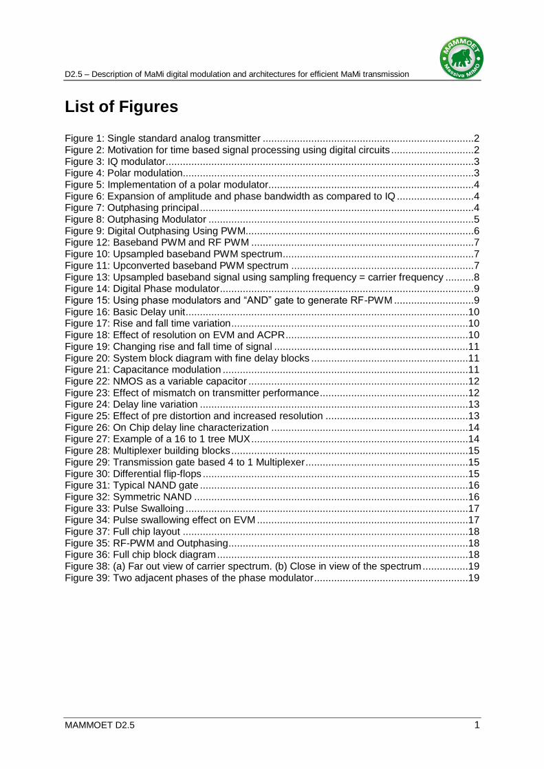
State of the art wireless devices need to support multiple communications standards and in doing so must also be efficient in power consumption and cost. Being efficient in cost means having small area and easily integrate-able on the same chip along with the baseband digital circuitry. To support multiple standards either a number of different transmitters can be used for each standard or the same transmitter can be reconfigured. It is much easier to reconfigure digital circuits and since they are digital, there is no issue of integration with baseband hardware on the same chip. In context of Massive MIMO, where potentially 100’s of transmitters are used the hardware need to be low power and the transmitter is a known bottle neck to achieving low power implementations. A typical transmitter architecture is shown in Figure 1.
Figure 1: Single standard analog transmitter
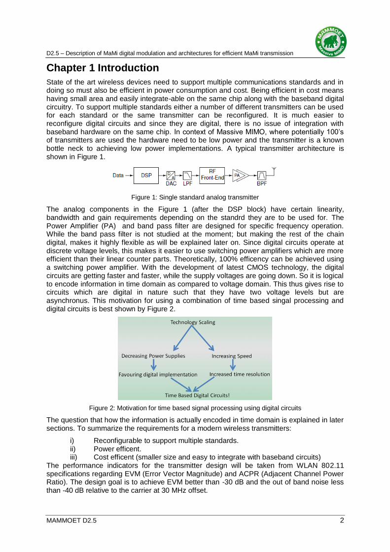
The analog components in the Figure 1 (after the DSP block) have certain linearity, bandwidth and gain requirements depending on the standrd they are to be used for. The Power Amplifier (PA) and band pass filter are designed for specific frequency operation. While the band pass filter is not studied at the moment; but making the rest of the chain digital, makes it highly flexible as will be explained later on. Since digital circuits operate at discrete voltage levels, this makes it easier to use switching power amplifiers which are more efficient than their linear counter parts. Theoretically, 100% efficency can be achieved using a switching power amplifier. With the development of latest CMOS technology, the digital circuits are getting faster and faster, while the supply voltages are going down. So it is logical to encode information in time domain as compared to voltage domain. This thus gives rise to circuits which are digital in nature such that they have two voltage levels but are asynchronus. This motivation for using a combination of time based singal processing and digital circuits is best shown by Figure 2.
Figure 2: Motivation for time based signal processing using digital circuits
The question that how the information is actually encoded in time domain is explained in later sections. To summarize the requirements for a modern wireless transmitters:
i) Reconfigurable to support multiple standards. ii) Power efficent. iii) Cost efficent (smaller size and easy to integrate with baseband circuits)
The performance indicators for the transmitter design will be taken from WLAN 802.11 specifications regarding EVM (Error Vector Magnitude) and ACPR (Adjacent Channel Power Ratio). The design goal is to achieve EVM better than -30 dB and the out of band noise less than -40 dB relative to the carrier at 30 MHz offset.

D2.5 – Description of MaMi digital modulation and architectures for efficient MaMi transmission
MAMMOET D2.5 3
Chapter 2 Digital Modulators
2.1 Modulator types
There are various type of modulator architectures but they can be broadly classified as IQ modulators (or quadrature modulators), polar modulators and outphasing modulators. IQ modulators are the more common type of implementation where i(t) and q(t) are the input signals.
Figure 3: IQ modulator
The input signals are multiplied with the carrier signal as shown in Figure 3 and up-converted in the frequency domain. As compared to the other modulator types described in this section below, they have the advantage that the I and Q signals have a smaller bandwidth as compared to the amplitude and phase signal. Also the I and Q signals have symmetrical paths which are easier to match as compared to polar modulators. A disadvantage In case of a digital implementation of an IQ modulator is that sampling rates for the building blocks must satisfy the Nyquist criteria. So if Fc is the carrier frequency and B is the bandwidth of the base band signals, then the sampling frequency must be at least 2*(Fc + B). So for a transmitter working at 4 GHz this means a sampling frequency of 8GHz which is too high.
Polar modulators on the other hand separate the IQ signal into phase (φ(t)) and amplitude (a(t)) components. The phase signal is used to modulate the carrier (cos (2 fct) ) and then this high frequency phase modulated signal is multiplied with the amplitude signal. So the
carrier in the end has both phase and amplitude modulation: v(t) = a(t) . cos (2 fct + φ(t)) as shown in Figure 4.
Figure 4: Polar modulation
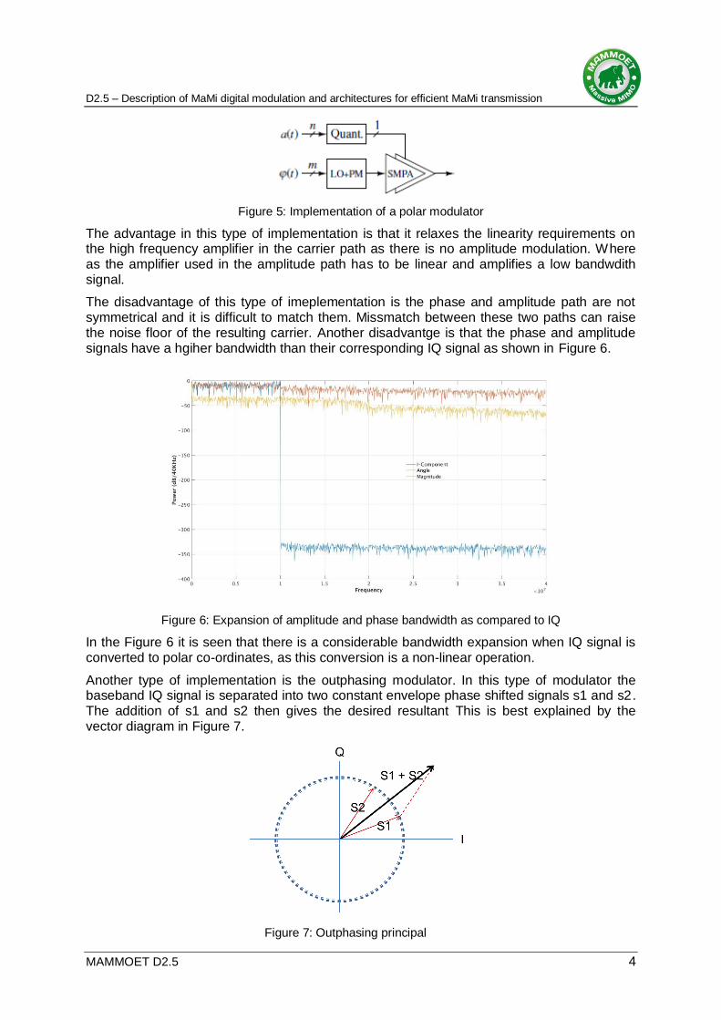
Since the phase modulated carrier does not have any amplitude modulation, it can be amplified using a SMPA. Where as the amplitude signal a(t), can be amplified by a linear, low bandwidth amplifier which modulates the supply of SMPA as shown in Figure 5.
D2.5 – Description of MaMi digital modulation and architectures for efficient MaMi transmission
MAMMOET D2.5 4
Figure 5: Implementation of a polar modulator
The advantage in this type of implementation is that it relaxes the linearity requirements on the high frequency amplifier in the carrier path as there is no amplitude modulation. Where as the amplifier used in the amplitude path has to be linear and amplifies a low bandwdith signal.
The disadvantage of this type of imeplementation is the phase and amplitude path are not symmetrical and it is difficult to match them. Missmatch between these two paths can raise the noise floor of the resulting carrier. Another disadvantge is that the phase and amplitude signals have a hgiher bandwidth than their corresponding IQ signal as shown in Figure 6.
Figure 6: Expansion of amplitude and phase bandwidth as compared to IQ
In the Figure 6 it is seen that there is a considerable bandwidth expansion when IQ signal is converted to polar co-ordinates, as this conversion is a non-linear operation.
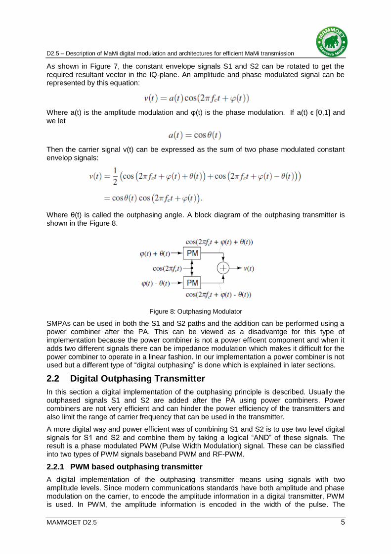
Another type of implementation is the outphasing modulator. In this type of modulator the baseband IQ signal is separated into two constant envelope phase shifted signals s1 and s2. The addition of s1 and s2 then gives the desired resultant This is best explained by the vector diagram in Figure 7.
Figure 7: Outphasing principal
D2.5 – Description of MaMi digital modulation and architectures for efficient MaMi transmission
MAMMOET D2.5 5
As shown in Figure 7, the constant envelope signals S1 and S2 can be rotated to get the required resultant vector in the IQ-plane. An amplitude and phase modulated signal can be represented by this equation:
Where a(t) is the amplitude modulation and φ(t) is the phase modulation. If a(t) ϵ [0,1] and we let
Then the carrier signal v(t) can be expressed as the sum of two phase modulated constant envelop signals:
Where θ(t) is called the outphasing angle. A block diagram of the outphasing transmitter is shown in the Figure 8.
Figure 8: Outphasing Modulator
SMPAs can be used in both the S1 and S2 paths and the addition can be performed using a power combiner after the PA. This can be viewed as a disadvantge for this type of implementation because the power combiner is not a power efficent component and when it adds two different signals there can be impedance modulation which makes it difficult for the power combiner to operate in a linear fashion. In our implementation a power combiner is not used but a different type of “digital outphasing” is done which is explained in later sections.
2.2 Digital Outphasing Transmitter
In this section a digital implementation of the outphasing principle is described. Usually the outphased signals S1 and S2 are added after the PA using power combiners. Power combiners are not very efficient and can hinder the power efficiency of the transmitters and also limit the range of carrier frequency that can be used in the transmitter.
A more digital way and power efficient was of combining S1 and S2 is to use two level digital signals for S1 and S2 and combine them by taking a logical “AND” of these signals. The result is a phase modulated PWM (Pulse Width Modulation) signal. These can be classified into two types of PWM signals baseband PWM and RF-PWM.
2.2.1 PWM based outphasing transmitter
A digital implementation of the outphasing transmitter means using signals with two amplitude levels. Since modern communications standards have both amplitude and phase modulation on the carrier, to encode the amplitude information in a digital transmitter, PWM is used. In PWM, the amplitude information is encoded in the width of the pulse. The

D2.5 – Description of MaMi digital modulation and architectures for efficient MaMi transmission
MAMMOET D2.5 6
equation below is the Fourier series for a RF-pulse width modulated (RF-PWM) square wave.
If we filter out the harmonics of this square wave for n > 1, then we are left with:
Where the amplitude scaling term has been ignored (2/ ). The term d(t) is the time varying dutycycle of the square wave. As can be seen the dutycycle actually corresponds to the
amplitude modulation of the cos( t) carrier. Though a pre-distortion of the form asin(d(t)) / is needed for the dutycyle to directly correspond to the amplitude modulation of the carrier. The term φ(t) represents the phase modulation of the carrier.
Hence it is shown that by modulating the pulse width of a square wave and changing its phase and then filtering all its hamrmonics we get a sinosoidal carrier which has both amplitude and phase modulation. So fully digital transmiters can be used to generate carrier signals having both amplitude and phase modulation, thus suporting modern communication standards.
Figure 9 shows how two squarewaves with 50% dutycycle can be used to generate PWM in each carrier period. By doing a logical AND of two phase shifted signals (which correspond to s1 and s2 from section 2.1 outphasing transmiter ) we get a carrier signal which has both amplitude and phase modulation.
The fourier series shown in this section are for a special case of PWM called RF-PWM. RF-PWM and Baseband PWM and two different types of PWM techniques that can be used in digital transmitters and they are describred next.
2.2.2 Baseband PWM
In baseband PWM, the amplitude signal is sampled at some frequency fs which is less than the carrier frequency fc. The spectrum of this up-sampled baseband signal is shown in Figure 10.
Figure 9: Digital Outphasing Using PWM

D2.5 – Description of MaMi digital modulation and architectures for efficient MaMi transmission
MAMMOET D2.5 7
Figure 10: Upsampled baseband PWM spectrum.
We see that it has images at multiples of the sampling frequency fs. Now when this signal is up-converted to the carrier frequency fc, all of its images are also up converted to multiples of fc as shown in Figure 11. This may cause some images to fall back into the signal band and also produces images very close to the signal band (fc + fs). Thus degrading the in-band signal quality and also the out of band spectrum. The images at fc + fs are very close to the band of interest and it is very difficult to make a sharp filter at such high frequencies. Probably some SAW filters will be required.
Figure 11 Upconverted baseband PWM spectrum.
Because of these reasons it was decided to use RF-PWM which is described next.
2.2.3 RF PWM
In RF PWM, instead of multiplying a PWM signal with the carrier, the carrier itself is pulse width modulated as shown in Figure 12.
Figure 12: Baseband PWM and RF PWM There still are harmonics in this case too, but the closest one is at twice the carrier frequency and in case of differential implementation, the closest harmonic is at three times the carrier frequency which makes the filtering much easier as compared to baseband PWM. Figure 13
Figure 10: Upsampled baseband PWM spectrum
Figure 11: Upconverted baseband PWM spectrum
D2.5 – Description of MaMi digital modulation and architectures for efficient MaMi transmission
MAMMOET D2.5 8
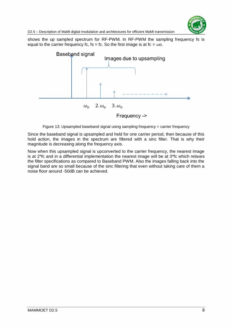
shows the up sampled spectrum for RF-PWM. In RF-PWM the sampling frequency fs is
equal to the carrier frequency fc, fs = fc. So the first image is at fc = o.
Since the baseband signal is upsampled and held for one carrier period, then because of this hold action, the images in the spectrum are filtered with a sinc filter. That is why their magnitude is decreasing along the frequency axis.
Now when this upsampled signal is upconverted to the carrier frequency, the nearest image is at 2*fc and in a differential implementation the nearest image will be at 3*fc which relaxes the filter specifications as compared to Baseband PWM. Also the images falling back into the signal band are so small because of the sinc filtering that even without taking care of them a noise floor around -50dB can be achieved.
Figure 13: Upsampled baseband signal using sampling frequency = carrier frequency
D2.5 – Description of MaMi digital modulation and architectures for efficient MaMi transmission
MAMMOET D2.5 9
Chapter 3 System Design & Chip Implementation
In this chapter the system level simulations are presented and based on these simulations design decision are taken. Implementation of the RF-PWM test chip designed is also described. Before describing system level simulations, the simulation conditions should be described. The test signal used is 2.4GHz WLAN OFDM signal with 20 MHz bandwidth, unless otherwise stated.
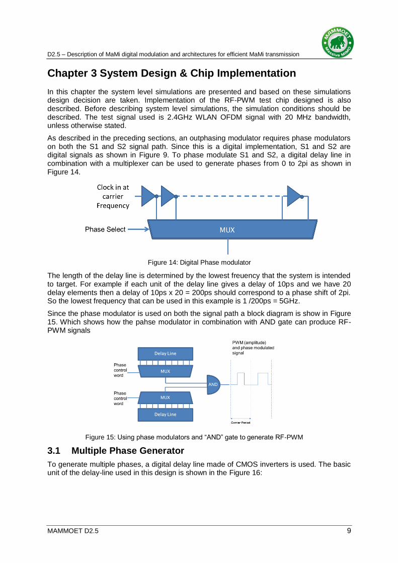
As described in the preceding sections, an outphasing modulator requires phase modulators on both the S1 and S2 signal path. Since this is a digital implementation, S1 and S2 are digital signals as shown in Figure 9. To phase modulate S1 and S2, a digital delay line in combination with a multiplexer can be used to generate phases from 0 to 2pi as shown in Figure 14.
The length of the delay line is determined by the lowest freuency that the system is intended to target. For example if each unit of the delay line gives a delay of 10ps and we have 20 delay elements then a delay of 10ps x 20 = 200ps should correspond to a phase shift of 2pi. So the lowest frequency that can be used in this example is 1 /200ps = 5GHz.
Since the phase modulator is used on both the signal path a block diagram is show in Figure 15. Which shows how the pahse modulator in combination with AND gate can produce RF-PWM signals
3.1 Multiple Phase Generator
To generate multiple phases, a digital delay line made of CMOS inverters is used. The basic unit of the delay-line used in this design is shown in the Figure 16:
Figure 14: Digital Phase modulator
Figure 15: Using phase modulators and “AND” gate to generate RF-PWM

D2.5 – Description of MaMi digital modulation and architectures for efficient MaMi transmission
MAMMOET D2.5 10
Figure 16: Basic Delay unit
This differential implementation helps to reduce the length of the delay line by half as compared to non-differential implementation as now half of the phases (pi to 2pi) can be generated from the differential side. So now the length of the delay line should be such that it covers half the carrier period of the lowest carrier frequency that the system is to support. Due to process variation, the threshold voltage of the nmos and pmos in the inverter can change which can change the rise and fall time of the squarewave carrier. This in effect changes the dutycycle of the signal as shown in Figure 17.
Figure 17: Rise and fall time variation
To keep the rise and fall times the same, small cross coupled inverters are used in between the differential delay lines.
A cascade of this basic delay unit gives the complete delay line. Post-layout simulation show that the delay generated using this type of a delay unit is 12 pico-seconds (ps). In Figure 18 are plotted the EVM and ACPR vs Carrier frequency for different time reolutions.
Fiugre 18: Effect of resolution on EVM and ACPR.
It is seen that 12ps is not enough to meet modern wireless communication standards. So therefore the resolution is further increased by using varactors (controlled by digital control words) to further fine tune the delay. The varactors work by changing the load seen by the inverters and thus chaging the delay of the signal. This changes the rise and fall times fo the signal thus changing its phase as shown in Figure 19.
Figure 17: Rise and fall time variation
Figure 18: Effect of resolution on EVM and ACPR

D2.5 – Description of MaMi digital modulation and architectures for efficient MaMi transmission
MAMMOET D2.5 11
Figure 19: Changing rise and fall time of signal.
The varactors provide a delay of 1ps. The varactors and the delay line are used in a coarse fine configuration. So a modified block diagram incorporating the varactors is shown in the Figure 20.
Figure 20: System block diagram with fine delay blocks
A possible implementation of the capacitance modulation block is shown in Figure 21:
But in the implementation done in D2.5, instead of using switches to change the load capacitor, variable-capacitor or varactors, as they are more commonly known, are used.
Figure 21: Capacitance modulation.
Figure 19: Changing rise and fall time of signal
Figure 20: System block diagram with fine delay blocks
Figure 21: Capacitance modulation
D2.5 – Description of MaMi digital modulation and architectures for efficient MaMi transmission
MAMMOET D2.5 12
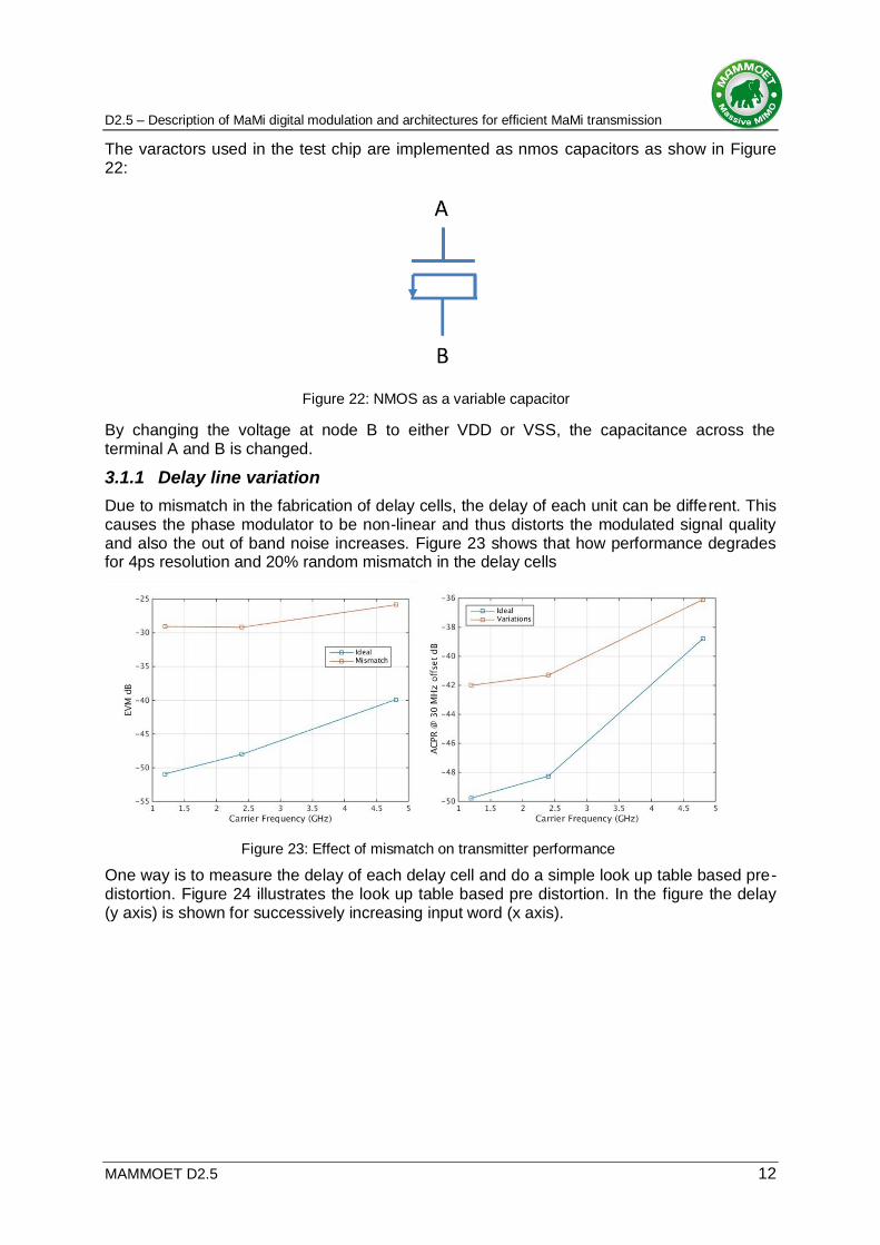
The varactors used in the test chip are implemented as nmos capacitors as show in Figure 22:
By changing the voltage at node B to either VDD or VSS, the capacitance across the terminal A and B is changed.
3.1.1 Delay line variation
Due to mismatch in the fabrication of delay cells, the delay of each unit can be different. This causes the phase modulator to be non-linear and thus distorts the modulated signal quality and also the out of band noise increases. Figure 23 shows that how performance degrades for 4ps resolution and 20% random mismatch in the delay cells
Figure 23: Effect of mismatch on transmitter performance
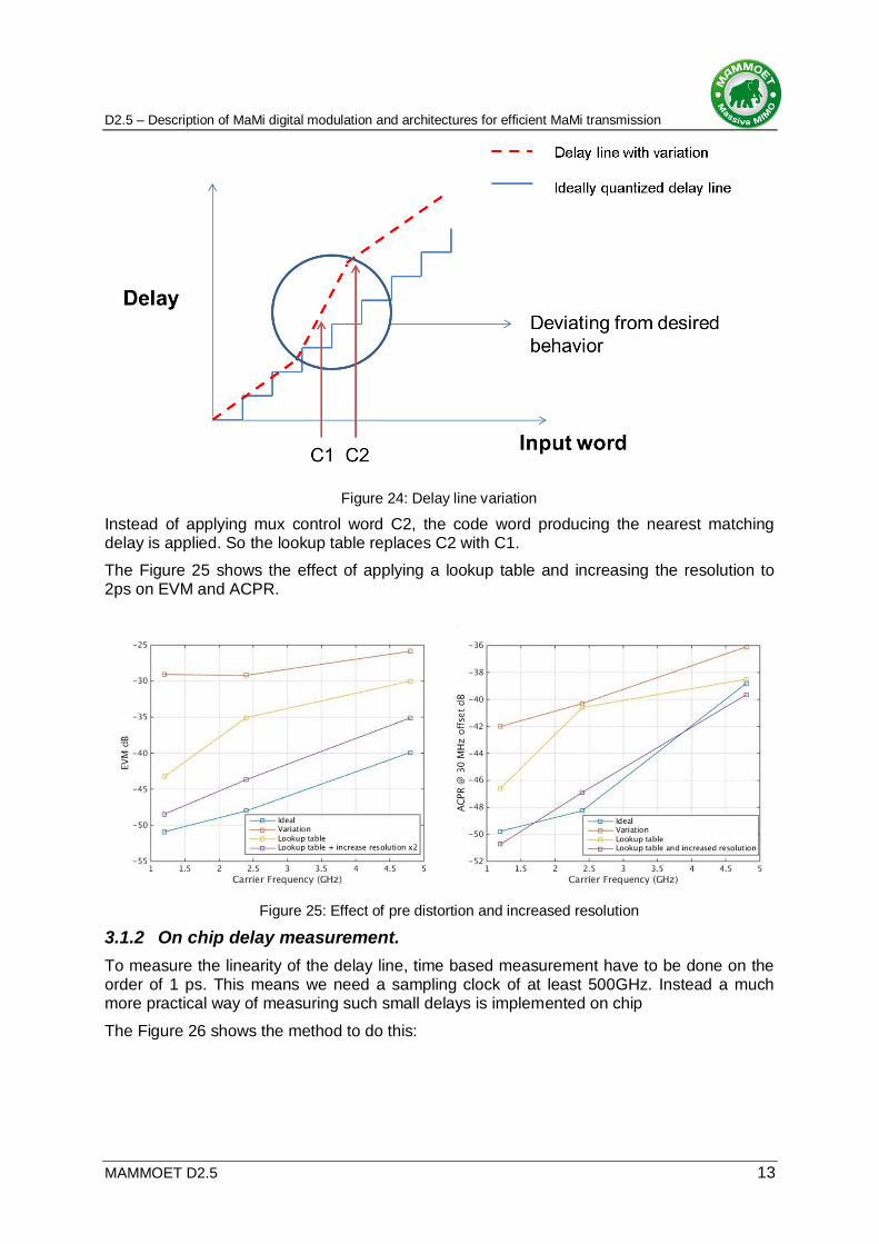
One way is to measure the delay of each delay cell and do a simple look up table based pre-distortion. Figure 24 illustrates the look up table based pre distortion. In the figure the delay (y axis) is shown for successively increasing input word (x axis).
Figure 22: NMOS as a variable capacitor
Figure 23: Effect of mismatch on transmitter performance
D2.5 – Description of MaMi digital modulation and architectures for efficient MaMi transmission
MAMMOET D2.5 13
Figure 24: Delay line variation.
Instead of applying mux control word C2, the code word producing the nearest matching delay is applied. So the lookup table replaces C2 with C1.
The Figure 25 shows the effect of applying a lookup table and increasing the resolution to 2ps on EVM and ACPR.
Figure 25: Effect of pre distortion and increased resolution.
3.1.2 On chip delay measurement.
To measure the linearity of the delay line, time based measurement have to be done on the order of 1 ps. This means we need a sampling clock of at least 500GHz. Instead a much more practical way of measuring such small delays is implemented on chip
The Figure 26 shows the method to do this:
Figure 24: Delay line variation
Figure 25: Effect of pre distortion and increased resolution
D2.5 – Description of MaMi digital modulation and architectures for efficient MaMi transmission
MAMMOET D2.5 14
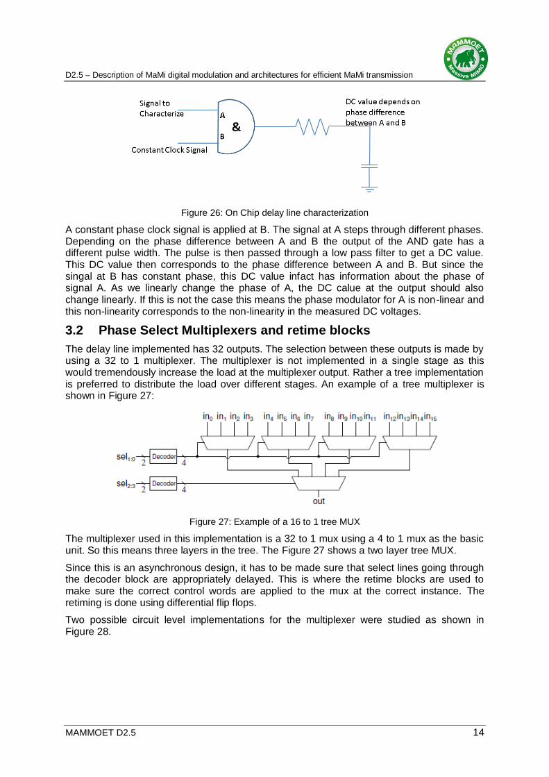
Figure 26: On Chip delay line characterization
A constant phase clock signal is applied at B. The signal at A steps through different phases. Depending on the phase difference between A and B the output of the AND gate has a different pulse width. The pulse is then passed through a low pass filter to get a DC value. This DC value then corresponds to the phase difference between A and B. But since the singal at B has constant phase, this DC value infact has information about the phase of signal A. As we linearly change the phase of A, the DC calue at the output should also change linearly. If this is not the case this means the phase modulator for A is non-linear and this non-linearity corresponds to the non-linearity in the measured DC voltages.
3.2 Phase Select Multiplexers and retime blocks
The delay line implemented has 32 outputs. The selection between these outputs is made by using a 32 to 1 multiplexer. The multiplexer is not implemented in a single stage as this would tremendously increase the load at the multiplexer output. Rather a tree implementation is preferred to distribute the load over different stages. An example of a tree multiplexer is shown in Figure 27:
Figure 27: Example of a 16 to 1 tree MUX
The multiplexer used in this implementation is a 32 to 1 mux using a 4 to 1 mux as the basic unit. So this means three layers in the tree. The Figure 27 shows a two layer tree MUX.
Since this is an asynchronous design, it has to be made sure that select lines going through the decoder block are appropriately delayed. This is where the retime blocks are used to make sure the correct control words are applied to the mux at the correct instance. The retiming is done using differential flip flops.
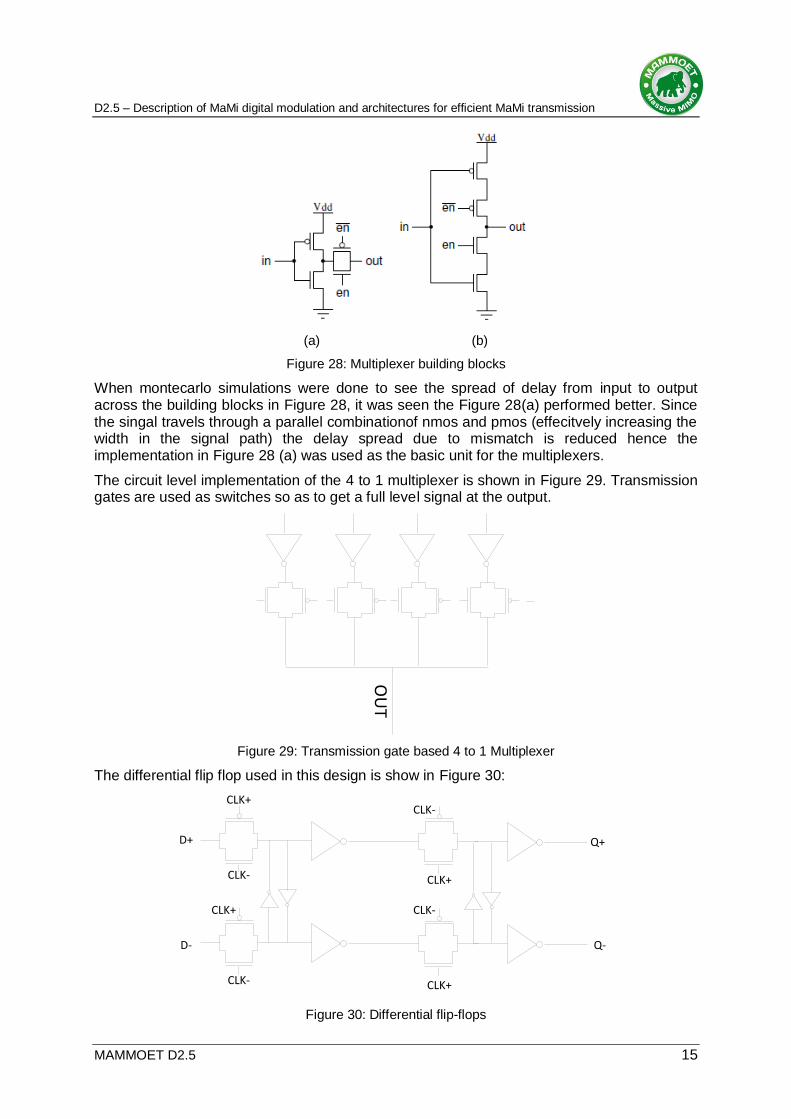
Two possible circuit level implementations for the multiplexer were studied as shown in Figure 28.
D2.5 – Description of MaMi digital modulation and architectures for efficient MaMi transmission
MAMMOET D2.5 15
(a) (b)
Figure 28: Multiplexer building blocks
When montecarlo simulations were done to see the spread of delay from input to output across the building blocks in Figure 28, it was seen the Figure 28(a) performed better. Since the singal travels through a parallel combinationof nmos and pmos (effecitvely increasing the width in the signal path) the delay spread due to mismatch is reduced hence the implementation in Figure 28 (a) was used as the basic unit for the multiplexers.
The circuit level implementation of the 4 to 1 multiplexer is shown in Figure 29. Transmission gates are used as switches so as to get a full level signal at the output.
OU
T
Figure 29: Transmission gate based 4 to 1 Multiplexer
The differential flip flop used in this design is show in Figure 30:
CLK-
CLK-
CLK-
CLK-CLK+
CLK+
CLK+
CLK+
D+
D-
Q+
Q-
Figure 30: Differential flip-flops

D2.5 – Description of MaMi digital modulation and architectures for efficient MaMi transmission
MAMMOET D2.5 16
The cross coupling inverters in the flip flop help to maintain a defined voltage at the desired node.
3.3 AND gate and Output drivers.
The AND gate is implemented by a NAND gate followed by an inverter. The typical NAND gate implementation shown in Figure 31 is not suitable for this asynchronous design as delay from input to output becomes dependent on the signals A and B. For example if B = 1 and A changes from 0 to 1, the only capacitance that needs to be discharged is the out put capacitance as the parasitic capacitance associated with NMOS B has already discharged. Now consider the other case where A = 1 and B goes from 0 to 1 then in this case both the internal node parasitic capacitance and the output capacitance need to be discharged and this causes a longer delay.
A
A
B
B
Figure 31: Typical NAND gate
A more symmetrical implementation of the NAND gate is shown in Figure 32. So now the different delay problem is not there in this case
A
A
B
B A
B
Figure 32: Symmetric NAND

D2.5 – Description of MaMi digital modulation and architectures for efficient MaMi transmission
MAMMOET D2.5 17
However there is still the case that both A and B signals go high at the same time and this will reduce the delay by half as now the resistance (the on resistance of NMOS) through which the output capacitance dishcarges has been reduced by half.
After the AND gate there are drivers to drive off chip 50 ohm load. For this the drivers have to be large to get a decent voltage swing across the 50 ohm load. The output of the AND gate can be very short pulses as we are doing PWM here. These small pulses when they propagate through the driver chain, they might get swallowed as shown in the Figure 33.
Figure 33 Pulse Swalloing
A system level simulation was done to see the effect of pulse swallowing on the transmitter performance as shown in Figure 34.
Figure 34: Pulse swallowing effect on EVM.
In this simulation the pulse swallowing limit was set as 40ps. So pulse width between 0 and 20 ps were rounded to 0 and pulses with width between 20ps and 40ps were rounded to 40ps. A 40ps pulse width corresponds to 5% of the period @ 1.2GHz, 10% @ 2.4GHz, 20% @ 4.8GHz. The simulation results show the pulse swalloing has more profound effect at higher frequencies. For this reasons a separate path on the chip is included where the drivers bring out the 50% dutycycle signals from the input of the AND gate. Which can then be recombined (added) externally. In this way short pulses are not generated on chip. The Figure 35 explains how this is done.
Figure 33: Pulse Swalloing
Figure 34: Pulse swallowing effect on EVM
D2.5 – Description of MaMi digital modulation and architectures for efficient MaMi transmission
MAMMOET D2.5 18
Figure 35: RF-PWM and Outphasing.
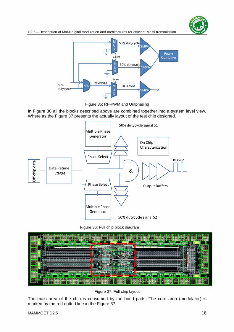
In Figure 36 all the blocks described above are combined together into a system level view. Where as the Figure 37 presents the actually layout of the test chip designed.
Figure 36: Full chip block diagram
Figure 37: Full chip layout
The main area of the chip is consumed by the bond pads. The core area (modulator) is marked by the red dotted line in the Figure 37.
Figure 35: RF-PWM and Outphasing
Figure 36: Full chip block diagram

D2.5 – Description of MaMi digital modulation and architectures for efficient MaMi transmission
MAMMOET D2.5 19
3.4 Pre-Layout and post-layout Simulations
Pre-layout simulation with a carrier of 2.65GHz and 40MHz DMT signal show that the inband and out of band noise is well within limits and has a margin for any fabrication imperfections that may show up.
Figure 38: (a) Far out view of carrier spectrum. (b) Close in view of the spectrum
The simulations were done using blocks designed in 40nm CMOS. Because of the time it takes to simulate the system with modulated signals, only the signal path blocks were at transistor level where as the blocks for I/O’s etc were simulated at Verilog A level for faster simulation results. The simulations are done in IFAT co-simulation setup. The control signals for the transmitter are generated in MATLAB and then applied to the netlist. The circuit is simulated in cadence spectre. The output is then again analysed in MATLAB to generate the figures for ACPR and EVM. For post layout simulations, an R+C extraction of the whole chip was done to ensure there are no timing violations. The resolution of the phase modulator after RC extraction is found to be around 1ps. Figure 39 shows two adjacent phases plotted together for a 4GHz carrier. The time difference on the plot is also measured which is 1.1 ps.
Figure 39: Two adjacent phases of the phase modulator
D2.5 – Description of MaMi digital modulation and architectures for efficient MaMi transmission
MAMMOET D2.5 20
Chapter 4 Summary and conclusion
This deliverable starts with a motivation for time based digital circuits. The main reason being that since voltage supplies are decreasing and the circuits are becoming faster, this would favour a digital circuits and time based signal processing. Next a brief description of some modulator architectures is given. The advantages and disadvantages are listed, for IQ, polar and outphasing modulators. It is seen that outphasing modulators are best suited for digital implementations because of their use of constant envelope signals. The constant envelope signals enable the use of digital circuits and square wave carrier signals. The outphasing architecture is then modified into a PWM architecture which enables a full digital implementation of the transmitter and the use of SMPAs. Two sub-categories of the PWM modulator (RF and baseband PWM) are studied and based on a cleaner output spectrum; RF-PWM is chosen to be implemented. In chapter 3 system level simulations which were done in MATLAB are presented. Based on these simulation some design decisions at implementation level are done as explained in the preceding sections. Transistor level circuits are built and optimized for asynchronous operation. This means that the circuits in the signal path are time critical and need to be designed as such. Different building blocks for the transmitter are described at transistor level and a complete block diagram of the test chip implemented is shown to get a full view of the system. Simulations at transistor level are done to ensure the proper operation of the circuits. The final transmitter architecture is able to support carrier frequencies from 900 MHz to 4 GHz. The reconfiguration of this digital architecture is very easy. In fact just the input clock to the system needs to be changed to the desired carrier frequency. Also the core modulator area is small because of the digital implementation. This study goes on to show that such type of modulator architectures are well suited in terms of area and re-configurability for future MIMO systems.
D2.5 – Description of MaMi digital modulation and architectures for efficient MaMi transmission
MAMMOET D2.5 21
List of Abbreviations
PA Power Amplifier
PWM Pulse Width Modulation
ps Pico-second
IQ Inphase and Quadrature
MUX Multiplexer
EVM Error Vector Magnitude