CS5501 CS5503 16 & 20-Bit A/D Converter - Octopart
54
1 Copyright Cirrus Logic, Inc. 2003 (All Rights Reserved) Cirrus Logic, Inc. www.cirrus.com CS5501 CS5503 16 & 20-Bit A/D Converter Features Monolithic CMOS ADC with Filtering - 6-pole, Low-pass Gaussian Filter Up to 4 kHz Output Word Rates - On Chip Self-calibration Circuitry - Linearity Error: ±0.0003% - Differential Nonlinearity: CS5501: 16-bit, No Missing Codes (DNL ±1/8 LSB) CS5503: 20-bit, No Missing Codes System Calibration Capability Flexible Serial Communications Port - Microcontroller-compatible Formats - 3-state Data and Clock Outputs - UART Format (CS5501 only) Pin-selectable Unipolar/Bipolar Ranges Low Power Consumption: 25 mW - 10 μW Sleep Mode for Portable Applications Description The CS5501 and CS5503 are CMOS A/D converters ideal for measuring low-frequency signals representing physical, chemical, and biological processes. They uti- lize charge-balance techniques to achieve 16-bit (CS5501) and 20-bit (CS5503) performance with up to 4 kSps word rates. The converters continuously sample at a rate set by the user in the form of either a CMOS clock or a crystal. On- chip digital filtering processes the data and updates the output register at up to a 4 kSps rate. The converters' low- pass, 6-pole Gaussian response filter is designed to al- low corner frequency settings from 0.1 Hz to 10 Hz in the CS5501 and 0.5 Hz to 10 Hz in the CS5503. Thus, each converter rejects 50 Hz and 60 Hz line frequencies as well as any noise at spurious frequencies. The CS5501 and CS5503 include on-chip self-calibra- tion circuitry which can be initiated at any time or temperature to insure offset and full-scale errors of typi- cally less than 1/2 LSB for the CS5501 and less than 4 LSB for the CS5503. The devices can also be applied in system calibration schemes to null offset and gain er- rors in the input channel. Each device's serial port offers two general purpose modes of operation for direct interface to shift registers or synchronous serial ports of industry-standard micro- controllers. In addition, the CS5501's serial port offers a third, UART-compatible mode of asynchronous communication. ORDERING INFORMATION See page 33. I Calibration CAL AIN AGND DGND BP/UP SLEEP SRAM SC1 SC2 Calibration Microcontroller Analog Modulator 6-Pole Gaussian Low-Pass Digital Filter Charge-Balanced A/D Converter Clock Generator Serial Interface Logic VA+ VA- VD+ VD- SDATA CLKOUTCLKIN DRDY CS MODESCLK VREF 10 9 8 5 12 11 4 13 14 7 15 6 20 2 3 18 16 1 19 SEP ‘04 DS31F4 Copyright © Cirrus Logic, Inc. 2005 (All Rights Reserved) http://www.cirrus.com CS5501 CS5503 Non-aliasing, 16- & 20-bit A/D Converters I AUG ‘05 DS31F5 Charge-balanced A/D Converter Calibration SRAM Calibration Microcontroller 6-pole Gaussian Low-pass Digital Filter Analog Modulator Clock Generator Serial Interface Logic VREF BP/UP SLEEP AIN AGND DGND CAL VA+ VD+ VD- VA- SDATA DRDY CS MODE SCLK CLKIN CLKOUT SC1 SC2 10 9 8 5 13 7 15 14 6 20 12 11 4 17 3 2 18 16 1 19 CS5501 CS5503
-
Upload
khangminh22 -
Category
Documents
-
view
1 -
download
0
Transcript of CS5501 CS5503 16 & 20-Bit A/D Converter - Octopart
1
Copyright Cirrus Logic, Inc. 2003(All Rights Reserved)
Cirrus Logic, Inc.www.cirrus.com
CS5501 CS5503
16 & 20-Bit A/D ConverterFeatures
Monolithic CMOS ADC with Filtering- 6-pole, Low-pass Gaussian Filter
Up to 4 kHz Output Word Rates- On Chip Self-calibration Circuitry- Linearity Error: ±0.0003%- Differential Nonlinearity:
CS5501: 16-bit, No Missing Codes(DNL ±1/8 LSB)
CS5503: 20-bit, No Missing CodesSystem Calibration CapabilityFlexible Serial Communications Port
- Microcontroller-compatible Formats- 3-state Data and Clock Outputs- UART Format (CS5501 only)
Pin-selectable Unipolar/Bipolar RangesLow Power Consumption: 25 mW
- 10 µW Sleep Mode for Portable Applications
DescriptionThe CS5501 and CS5503 are CMOS A/D convertersideal for measuring low-frequency signals representingphysical, chemical, and biological processes. They uti-lize charge-balance techniques to achieve 16-bit(CS5501) and 20-bit (CS5503) performance with up to 4kSps word rates.
The converters continuously sample at a rate set by theuser in the form of either a CMOS clock or a crystal. On-chip digital filtering processes the data and updates theoutput register at up to a 4 kSps rate. The converters' low-pass, 6-pole Gaussian response filter is designed to al-low corner frequency settings from 0.1 Hz to 10 Hz in theCS5501 and 0.5 Hz to 10 Hz in the CS5503. Thus, eachconverter rejects 50 Hz and 60 Hz line frequencies aswell as any noise at spurious frequencies.
The CS5501 and CS5503 include on-chip self-calibra-tion circuitry which can be initiated at any time ortemperature to insure offset and full-scale errors of typi-cally less than 1/2 LSB for the CS5501 and less than4 LSB for the CS5503. The devices can also be appliedin system calibration schemes to null offset and gain er-rors in the input channel.
Each device's serial port offers two general purposemodes of operation for direct interface to shift registersor synchronous serial ports of industry-standard micro-controllers. In addition, the CS5501's serial port offers athird, UART-compatible mode of asynchronouscommunication.
ORDERING INFORMATIONSee page 33.
I
Calibration CAL
AIN
AGND
DGND
BP/UPSLEEP
SRAM
SC1 SC2
CalibrationMicrocontroller
AnalogModulator
6-Pole GaussianLow-Pass Digital Filter
Charge-Balanced A/D Converter
Clock Generator Serial Interface Logic
VA+VA-VD+VD-
SDATA
CLKOUTCLKIN DRDY CS MODESCLK
VREF 10
9
8
5
12 11 413
147
156
20
2 3 18 16 1 19
SEP ‘04DS31F4
Copyright © Cirrus Logic, Inc. 2005(All Rights Reserved)http://www.cirrus.com
CS5501 CS5503
Non-aliasing, 16- & 20-bit A/D Converters I
AUG ‘05DS31F5
Charge-balanced A/D Converter
CalibrationSRAM
CalibrationMicrocontroller
6-pole GaussianLow-pass Digital Filter
AnalogModulator
Clock Generator Serial Interface Logic
VREF
BP/UP SLEEP
AIN
AGND
DGND
CAL
VA+
VD+
VD-
VA-
SDATA
DRDY CS MODE SCLKCLKIN CLKOUT
SC1 SC2
10
9
8
5
13
7
15
14
6
20
12 11 4 17
3 2 18 16 1 19
CS5501CS5503
CS5501 ANALOG CHARACTERISTICS (TA = TMIN to TMAX; VA+, VD+ = 5V; VA-, VD- = -5V; VREF = 2.5V; CLKIN = 4.096MHz; Bipolar Mode; MODE = +5V; Rsource = 750Ω with a 1nFto AGND at AIN (see Note 1); Digital Inputs: Logic 0 = GND; Logic 1 = VD+; unless otherwise specified.)
CS5501-A, B, C CS5501-S, T
Parameter* Min Typ Max Min Typ Max Units
Specified Temperature Range -40 to +85 -55 to +125 °CAccuracy
Linearity Error -A, S-B, T
-C
---
0.00150.00070.0003
0.0030.00150.0012
--
-0.0007
0.0030.0015
±%FS±%FS±%FS
Differential Nonlinearity TMIN to TMAX - ±1/8 ±1/2 - ±1/8 ±1/2 LSB16
Full Scale Error (Note 2) - ±0.13 ±0.5 - ±0.13 ±0.5 LSB16
Full Scale Drift (Note 3) - ±1.2 - - ±2.3 - LSB16
Unipolar Offset (Note 2) - ±0.25 ±1 - ±0.25 ±1 LSB16
Unipolar Offset Drift (Note 3) - ±4.2 - - +3.0-25.0
- LSB16
Bipolar Offset (Note 2) - ±0.25 ±1 - ±0.25 ±1 LSB16
Bipolar Offset Drift (Note 3) - ±2.1 - - +1.5-12.5
- LSB16
Bipolar Negative Full Scale Error (Note 2) - ±0.5 ±2 - ±0.5 ±2 LSB16
Bipolar Negative Full Scale Drift (Note 3) - ±0.6 - - ±1.2 - LSB16
Noise (Referred to Output) - 1/10 - - 1/10 - LSBrmsNotes: 1. The AIN pin presents a very high input resistance at dc and a minor dynamic load which scales to the
master clock frequency. Both source resistance and shunt capacitance are therefore critical in determining the CS5501’s source impedance requirements. For more information refer the text section Analog Input Impedance Considerations.
2. Applies after calibration at the temperature of interest.3. Total drift over the specified temperature range since calibration at power-up at 25°C (see Figure 11).
This is guaranteed by design and /or characterization. Recalibration at any temperature will removethese errors.
Unipolar Mode Bipolar ModeµV LSB’s %FS ppm FS LSB’s %FS ppm FS10 0.26 0.0004 4 0.13 0.0002 219 0.50 0.0008 8 0.26 0.0004 438 1.00 0.0015 15 0.50 0.0008 876 2.00 0.0030 30 1.00 0.0015 15152 4.00 0.0061 61 2.00 0.0030 30
CS5501 Unit Conversion Factors, VREF = 2.5V
* Refer to the Specification Definitions immediately following the Pin Description Section.
CS5501/CS5503
2 DS31F4
CS5501 CS5503
2 DS31F5

CS5503 ANALOG CHARACTERISTICS (TA = TMIN to TMAX; VA+, VD+ = 5V; VA-, VD- = -5V; VREF = 2.5V; CLKIN = 4.096MHz; Bipolar Mode; MODE = +5V; Rsource = 750. with a 1nF to AGND at AIN (see Note 1): unless otherwise specified.)
CS5503-A, B, C CS5503-S, T
Parameter* Min Typ Max Min Typ Max Units
Specified Temperature Range -40 to +85 -55 to +125 °C
Accuracy Linearity Error -A, S
-B, T -C
- - -
0.0015 0.0007 0.0003
0.003 0.0015 0.0012
- -
- 0.0007
0.003 TBD
±%FS±%FS ±%FS
Differential Nonlinearity T MIN to T MAX (Not Missing Codes)
- 20 - - 20 - Bits
Full Scale Error (Note 2) - ±4 ±16 - ±4 ±16 LSB20
Full Scale Error Drift (Note 3) - ±19 - - ±37 - LSB20
Unipolar Offset (Note 2) - ±4 ±16 - ±4 ±16 LSB20
Unipolar Offset Drift (Note 3) - ±67 - - +48 -400
- LSB20
Bipolar Offset (Note 2) - ±4 ±16 - ±4 ±16 LSB20
Bipolar Offset Drift (Note 3) - ±34 - - +24 -200
- LSB20
Bipolar Negative Full Scale Error (Note 2) - ±8 ±32 - ±8 ±32 LSB20
Bipolar Negative Full Scale Drift (Note 3) - ±10 - - ±20 - LSB20
Noise (Referred to Output) - 1.6 - - 1.6 - LSBrms (20)
Unipolar Mode Bipolar Mode . V LSB’s %FS ppm Fs LSB’s %FS ppm FS
0.596 0.25 0.0000238 0.24 0.13 0.0000119 0.12 1.192 0.50 0.0000477 0.47 0.26 0.0000238 0.24 2.384 1.00 0.0000954 0.95 0.50 0.0000477 0.47 4.768 2.00 0.0001907 1.91 1.00 0.0000954 0.95 9.537 4.000 0.0003814 3.81 2.00 0.0001907 1.91
CS5503 Unit Conversion Factors, VREF = 2.5V
* Refer to the Specification Definitions immediately following the Pin Description Section.
CS5501/CS5503
DS31F4 3
CS5501 CS5503
DS31F5 3

ANALOG CHARACTERISTICS (Continued)
CS5501/3-A, B, C CS5501/3-S, T
Parameter* Min Typ Max Min Typ Max Units
Power Supplies
DC Power Supply CurrentsIA+IA-ID+ID- (Note 4)
Power DissipationSLEEP HighSLEEP Low (Note 4)
----
--
221
0.03
2510
3.23.21.50.1
4020
----
--
221
0.03
2510
3.23.21.50.1
4040
mAmAmAmA
mWµW
Power Supply RejectionPositive SuppliesNegative Supplies (Note 5)
--
7075
--
--
7075
--
dBdB
Analog Input
Analog Input Range Unipolar 0 to +2.5 0 to +2.5 V
Bipolar - ±2.5 - - ±2.5 - V
Input Capacitance - 20 - - 20 - pFDC Bias Current (Note 1) - 1 - - 1 - nASystem Calibration Specifications
Positive Full Scale Calibration Range VREF+0.1 VREF+0.1 VPositive Full Scale Input Overrange VREF+0.1 VREF+0.1 VNegative Full Scale Input Overrange -(VREF+0.1) -(VREF+0.1) VMaximum Offset Calibration Range (Notes 6, 7)
Unipolar ModeBipolar Mode
-(VREF +0.1)-40%VREF to +40%VREF
-(VREF +0.1)-40%VREF to +40%VREF
VV
Input Span (Note 8) 80%VREF
2VREF+0.2
80%VREF
2VREF+0.2 V
Notes: 4. All outputs unloaded.5. 0.1Hz to 10Hz. PSRR at 60 Hz will exceed 120 dB due to the benefit of the digital filter.6. In unipolar mode the offset can have a negative value (-VREF) such that the unipolar mode can mimic
bipolar mode operation.7. The specifications for Input Overrange and for Input Span apply additional constraints on the offset
calibration range.8. For Unipolar mode, Input Span is the difference between full scale and zero scale. For Bipolar mode,
Input Span is the difference between positive and negative full scale points. When using less than the maximum input span, the span range may be placed anywhere within the range of ±(VREF + 0.1).
Specifications are subject to change without notice.
CS5501/CS5503
4 DS31F4
CS5501 CS5503
4 DS31F5
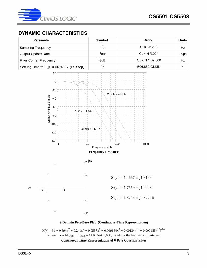
DYNAMIC CHARACTERISTICSParameter Symbol
t s
f sf out
f -3dB
CLKIN/ 256
Units
Hz
s
Sps
Hz
Settling Time to +0.0007% FS (FS Step)_
Sampling Frequency
Output Update Rate
Filter Corner Frequency
CLKIN /1024
CLKIN /409,600
Ratio
506,880/CLKIN
Continuous-Time Representation of 6-Pole Gaussian Filter
H(x) = [1 + 0.694x2 + 0.241x4 + 0.0557x6 + 0.009664x8 + 0.00134x10 + 0.000155x12]-1/2
where x = f/f-3dB, f-3dB = CLKIN/409,600, and f is the frequency of interest.
S-Domain Pole/Zero Plot (Continuous-Time Representation)
S1,2 = -1.4667 ± j1.8199
S3,4 = -1.7559 ± j1.0008
S5,6 = -1.8746 ± j0.32276
Frequency Response
-1-2
-j2
-j1
j2
j1
1 10 100 1000Frequency in Hz
-140
-120
-100
-80
-60
-40
-20
0
20
Out
put A
mpl
itude
in d
B
CLKIN = 2 MHz
CLKIN = 1 MHz
CLKIN = 4 MHz
-σ
jω
CS5501/CS5503
DS31F4 5
CS5501 CS5503
DS31F5 5
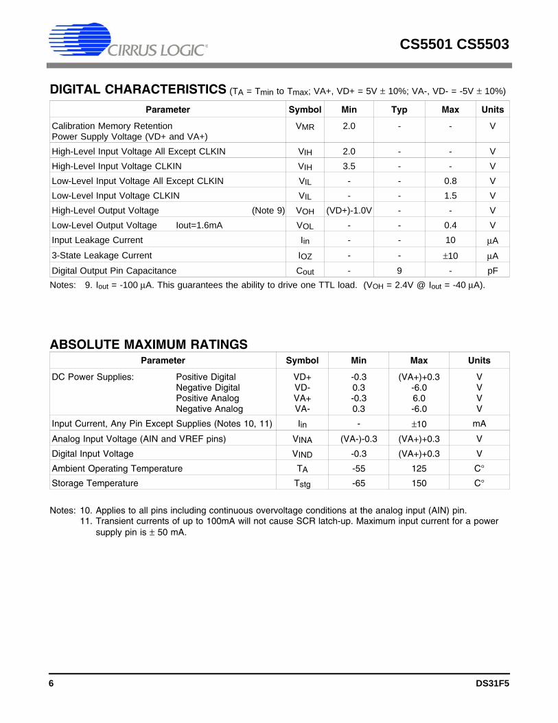
DIGITAL CHARACTERISTICS (TA = Tmin to Tmax; VA+, VD+ = 5V ± 10%; VA-, VD- = -5V ± 10%)
Parameter Symbol Min Typ Max Units
Calibration Memory RetentionPower Supply Voltage (VD+ and VA+)
VMR 2.0 - - V
High-Level Input Voltage All Except CLKIN VIH 2.0 - - VHigh-Level Input Voltage CLKIN VIH 3.5 - - VLow-Level Input Voltage All Except CLKIN VIL - - 0.8 VLow-Level Input Voltage CLKIN VIL - - 1.5 VHigh-Level Output Voltage (Note 9) VOH (VD+)-1.0V - - VLow-Level Output Voltage Iout=1.6mA VOL - - 0.4 VInput Leakage Current Iin - - 10 µA3-State Leakage Current IOZ - - ±10 µADigital Output Pin Capacitance Cout - 9 - pFNotes: 9. Iout = -100 µA. This guarantees the ability to drive one TTL load. (VOH = 2.4V @ Iout = -40 µA).
ABSOLUTE MAXIMUM RATINGSParameter Symbol Min Max Units
DC Power Supplies: Positive DigitalNegative DigitalPositive AnalogNegative Analog
VD+VD-VA+VA-
-0.30.3-0.30.3
(VA+)+0.3-6.06.0-6.0
VVVV
Input Current, Any Pin Except Supplies (Notes 10, 11) Iin - ±10 mA
Analog Input Voltage (AIN and VREF pins) VINA (VA-)-0.3 (VA+)+0.3 V
Digital Input Voltage VIND -0.3 (VA+)+0.3 V
Ambient Operating Temperature TA -55 125 C°
Storage Temperature Tstg -65 150 C°
Notes: 10. Applies to all pins including continuous overvoltage conditions at the analog input (AIN) pin.11. Transient currents of up to 100mA will not cause SCR latch-up. Maximum input current for a power
supply pin is ± 50 mA.
CS5501/CS5503
6 DS31F4
CS5501 CS5503
6 DS31F5
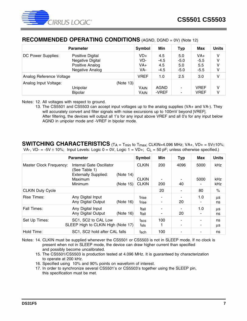
Notes: 14. CLKIN must be supplied whenever the CS5501 or CS5503 is not in SLEEP mode. If no clock is present when not in SLEEP mode, the device can draw higher current than specified and possibly become uncalibrated.
15. The CS5501/CS5503 is production tested at 4.096 MHz. It is guaranteed by characterizationto operate at 200 kHz.
16. Specified using 10% and 90% points on waveform of interest.17. In order to synchronize several CS5501’s or CS5503’s together using the SLEEP pin,
this specification must be met.
SWITCHING CHARACTERISTICS (TA = Tmin to Tmax; CLKIN=4.096 MHz; VA+, VD+ = 5V±10%; VA-, VD- = -5V ± 10%; Input Levels: Logic 0 = 0V, Logic 1 = VD+; CL = 50 pF; unless otherwise specified.)
Parameter Symbol Min Typ Max Units
Master Clock Frequency: Internal Gate Oscillator(See Table 1)Externally Supplied: (Note 14)MaximumMinimum (Note 15)
CLKIN
CLKINCLKIN
200
-200
4096
-40
5000
5000-
kHz
kHzkHz
CLKIN Duty Cycle 20 - 80 %
Rise Times: Any Digital InputAny Digital Output (Note 16)
trisetrise
--
-20
1.0-
µsns
Fall Times: Any Digital Input Any Digital Output (Note 16)
tfalltfall
--
-20
1.0-
µsns
Set Up Times: SC1, SC2 to CAL LowSLEEP High to CLKIN High (Note 17)
tscstsls
1001
--
--
nsµs
Hold Time: SC1, SC2 hold after CAL falls tsch 100 - - ns
RECOMMENDED OPERATING CONDITIONS (AGND, DGND = 0V) (Note 12)
Parameter Symbol Min Typ Max Units
DC Power Supplies: Positive DigitalNegative DigitalPositive AnalogNegative Analog
VD+VD-VA+VA-
4.5-4.54.5-4.5
5.0-5.05.0-5.0
VA+-5.55.5-5.5
VVVV
Analog Reference Voltage VREF 1.0 2.5 3.0 V
Analog Input Voltage: (Note 13)UnipolarBipolar
VAINVAIN
AGND-VREF
--
VREFVREF
VV
Notes: 12. All voltages with respect to ground.13. The CS5501 and CS5503 can accept input voltages up to the analog supplies (VA+ and VA-). They
will accurately convert and filter signals with noise excursions up to 100mV beyond |VREF|. After filtering, the devices will output all 1’s for any input above VREF and all 0’s for any input below AGND in unipolar mode and -VREF in bipolar mode.
CS5501/CS5503
DS31F4 7
CS5501 CS5503
DS31F5 7

SWITCHING CHARACTERISTICS (continued) (TA = Tmin to Tmax; VA+, VD+ = 5V ± 10%; VA-, VD- = -5V ± 10%; Input Levels: Logic 0 = 0V, Logic 1 = VD+; CL = 50 pF)
Parameter Symbol Min Typ Max Units
SSC Mode (Mode = VD+)
Access Time CS Low to SDATA Out tcsd1 3/CLKIN - - ns
SDATA Delay Time SCLK Falling to New SDATA bit tdd1 - 25 100 ns
SCLK Delay Time SDATA MSB bit to SCLK Rising(at 4.096 MHz)
tcd1 250 380 - ns
Serial Clock Pulse Width High (at 4.096 MHz)(Out) Pulse Width Low
tph1tpl1
--
240730
300790
ns
Output Float Delay SCLK Rising to Hi-Z tfd2 - 1/CLKIN+ 100
1/CLKIN+ 200
ns
Output Float Delay CS High to Output Hi-Z (Note 18) tfd1 - - 4/CLKIN+200
ns
SEC Mode (Mode = DGND)
Serial Clock (In) fsclk dc - 4.2 MHz
Serial Clock (In) Pulse Width HighPulse Width Low
tph2tpl2
50180
--
--
ns
Access Time CS Low to Data Valid (Note 19) tcsd2 - 80 160 ns
Maximum Data Delay Time (Note 20)SCLK Falling to New SDATA bit tdd2 - 75 150 ns
Output Float Delay CS High to Output Hi-Z tfd3 - - 250 ns
Output Float Delay SCLK Falling to Output Hi-Z tfd4 - 100 200 ns
Notes: 18. If CS is returned high before all data bits are output, the SDATA and SCLK outputs will complete the current data bit and then go to high impedance.
19. If CS is activated asynchronously to DRDY, CS will not be recognized if it occurs when DRDY is highfor 4 clock cycles. The propagation delay time may be as great as 4 CLKIN cycles plus 160 ns. To guarantee proper clocking of SDATA when using asychronous CS, SCLK(i) should not be taken high sooner than 4 CLKIN cycles plus 160ns after CS goes low.
20. SDATA transitions on the falling edge of SCLK(i).
SDATA
CS
fd1t
Output Float DelaySSC Mode (Note 19)
slst
CLKIN
SLEEP
Sleep Mode Timing forSynchronization
VALID
CAL
SC1, SC2
scst scht
Calibration Control Timing
CS5501/CS5503
8 DS31F4
CS5501 CS5503
8 DS31F5
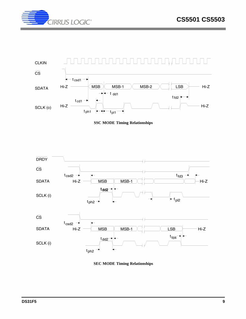
Hi-Z Hi-ZLSBMSB MSB-1
tcsd2
t fd4dd2t
tph2
Hi-Z MSB MSB-1fd3ttcsd2
Hi-Z
tpl2tph2
dd2t
SDATA
SCLK (i)
DRDY
CS
SCLK (i)
SDATA
CS
dd2t
t csd1
fd2tt dd1
Hi-Zt ph1 tpl1
cd1tHi-Z
Hi-Z Hi-ZMSB-2 LSBMSB MSB-1
SCLK (o)
CLKIN
SDATA
CS
SEC MODE Timing Relationships
SSC MODE Timing Relationships
CS5501/CS5503
DS31F4 9
CS5501 CS5503
DS31F5 9
SWITCHING CHARACTERISTICS (continued) (TA = Tmin to Tmax; VA+, VD+ = 5V ± 10%; VA-, VD- = -5V ± 10%; Input Levels: Logic 0 = 0V, Logic 1 = VD+; CL = 50 pF)
Parameter Symbol Min Typ Max Units
AC Mode (Mode = VD-) CS5501 only
Serial Clock (In) fsclk dc - 4.2 MHz
Serial Clock (In) Pulse Width HighPulse Width Low
tph3tpl3
50180
--
--
nsns
Set-up Time CS Low to SCLK Falling tcss - 20 40 ns
Maximum Data Delay Time SCLK Fall to New SDATA bit tdd3 - 90 180 ns
Output Float Delay CS High to Output Hi-Z (Note 21) tfd5 - 100 200 ns
Notes: 21. If CS is returned high after an 11-bit data packet is started, the SDATA output will continue to output data until the end of the second stop bit. At that time the SDATA output will go to high impedance.
Low Byte
STOP1 STOP2
t fd5t pl3
Hi-Z Hi-ZBIT7BIT6BIT9START
t ph3
t dd3
High Byte
SCLK(i)
SDATA
CS
DRDY
BIT8
t css
AC MODE Timing Relationships (CS5501 only)
CS5501/CS5503
10 DS31F4
CS5501 CS5503
10 DS31F5
GENERAL DESCRIPTION
The CS5501/CS5503 are monolithic CMOS A/Dconverters designed specifically for high resolu-tion measurement of low-frequency signals. Eachdevice consists of a charge-balance converter (16-Bit for the CS5501, 20-Bit for the CS5503),calibration microcontroller with on-chip SRAM,and serial communications port.
The CS5501/CS5503 A/D converters performconversions continuously and update their outputports after every conversion (unless the serial portis active). Conversions are performed and the se-rial port is updated independent of externalcontrol. Both devices are capable of measuringeither unipolar or bipolar input signals, and cali-bration cycles may be initiated at any time toensure measurement accuracy.
The CS5501/CS5503 perform conversions at arate determined by the master clock signal. Themaster clock can be set by an external clock orwith a crystal connected to the pins of the on-chipgate oscillator. The master clock frequency deter-mines:1. The sample rate of the analog input signal.2. The corner frequency of the on-chip digital filter.3. The output update rate of the serial output port.
The CS5501/CS5503 design includes several self-calibration modes and several serial port interfacemodes to offer users maximum system designflexiblity.
The Delta-Sigma Conversion Method
The CS5501/CS5503 A/D converters use charge-balance techniques to achieve low cost, highresolution measurements. A charge-balance A/Dconverter consists of two basic blocks: an analogmodulator and a digital filter. An elementary ex-ample of a charge-balance A/D converter is aconventional voltage-to-frequency converter andcounter. The VFC’s 1-bit output conveys infor-
mation in the form of frequency (or duty cycle),which is then filtered (averaged) by the counterfor higher resolution.
The analog modulator of the CS5501/CS5503 is amulti-order delta-sigma modulator. The modulatorconsists of a 1-bit A/D converter (that is, a com-parator) embedded in an analog feedback loopwith high open loop gain (see Figure 1). Themodulator samples and converts the input at a ratewell above the bandwidth of interest. The 1-bitoutput of the comparator is sampled at intervalsbased on the clock rate of the part and this infor-mation (either a 1 or 0) is conveyed to the digitalfilter. The digital filter is much more sophisticatedthan a simple counter. The filter on the chip has a6-pole low pass Gaussian response which rolls offat 120 dB/decade (36 dB/octave). The corner fre-quency of the digital filter scales with the masterclock frequency. In comparison, VFC’s and dualslope converters offer (sin x)/x filtering for highfrequency rejection (see Figure 2 for a compari-son of the characteristics of these two filter types).When operating from a 1 MHz master clock thedigital filter in the CS5501/CS5503 offers betterthan 120 dB rejection of 50 and 60 Hz line fre-quencies and does not require any type of linesynchronization to achieve this rejection. It shouldbe noted that the CS5501/CS5503 will update itsoutput port almost at 1000 times per second whenoperating from the 1 MHz clock. This is a muchhigher update rate (typically by a factor of at least50 times) than either VFCs or dual-slope convert-ers can offer.
For a more detailed discussion on the delta-sigmamodulator see the Application note "Delta-Sigma
DAC
Comparator
LP Filter 1-bit
16-bits
Digital Filter
S/H Amp
Figure 1. Charge Balance (Delta-Sigma) A/D Converter
CS5501/CS5503
DS31F4 11
CS5501 CS5503
DS31F5 11
A/D Conversion Technique Overview" in the ap-plication note section of the data book. Theapplication note discusses the delta-sigma modu-lator and some aspects of digital filtering.
OVERVIEW
As shown in the block diagram on the front pageof the data sheet, the CS5501/CS5503 can be seg-mented into five circuit functions. The heart of thechip is the charge balance A/D converter (16-bitfor the CS5501, 20-bit for the CS5503). The con-verter and all of the other circuit functions on thechip must be driven by a clock signal from theclock generator. The serial interface logic outputsthe converted data. The calibration microcontrol-ler along with the calibration SRAM (staticRAM), supervises the device calibration. Eachsegment of the chip has control lines associatedwith it. The function of each of the pins is de-scribed in the pin description section of the datasheet.
Clock Generator
The CS5501/CS5503 both include gates whichcan be connected as a crystal oscillator to providethe master clock signal for the chip. Alternatively,an external (CMOS compatible) clock can be in-put to the CLKIN pin as the master clock for thedevice. Figure 3 illustrates a simple model of theon-chip gate oscillator. The gate has a typicaltransconductance of 1500 µmho. The gate modelincludes 10 pf capacitors at the input and outputpins. These capacitances include the typical straycapacitance of the pins of the device. The on-chip
0 20 40 60 80 100 -100
-80
-60
-40
-20
0
CLKIN = 2 MHz
CLKIN=1 MHz
Mag
nitu
de (
dB)
0
-20
-40
-60
-80
-100 0 20 40 60 80 100
Frequency (Hz)M
agni
tude
(dB
)Frequency (Hz)
CLKIN = 4 MHz
Figure 2. Filter Responses
a. Averaging (Integrating) Filter Response (tavg = 100 ms) b. 6-Pole Gaussian Filter Response
3
10pF
C1 * Y1 C2 *
* See Table 1
1500 umhogm
2
10pF
CLKIN CLKOUT
500 k ΩR1
Figure 3. On-chip Gate Oscillator Model
CS5501/CS5503
12 DS31F4
CS5501 CS5503
12 DS31F5
gate oscillator is designed to properly operatewithout additional loading capacitors when usinga 4.096 MHz (or 4 MHz) crystal. If other crystalfrequencies or if ceramic resonators are used,loading capacitors may be necessary for reliableoperation of the oscillator. Table 1 illustrates sometypical capacitor values to be used with selectedresonating elements.
CLKOUT (pin 2) can be used to drive one exter-nal CMOS gate for system clock requirements. Inthis case, the external gate capacitance must betaken into account when choosing the value ofC2.
Caution: A clock signal should always be presentwhenever the SLEEP is inactive (SLEEP = VD+).If no clock is provided to the part when not inSLEEP, the part may draw excess current andpossibly even lose its calibration data. This is be-cause the device is built using dynamic logic.
Serial Interface Logic
The CS5501 serial data output can operate in anyone of the following three different serial interfacemodes depending upon the MODE pin selection:
SSC (Synchronous Self-Clocking) mode; MODE pin tied to VD+ (+5V).
SEC (Synchronous External Clocking) mode;MODE pin tied to DGND.
and AC (Asynchronous Communication) mode;CS5501 only
MODE pin tied to VD- (-5V)
The CS5503 can only operate in the first twomodes, SEC and SSC.
Synchronous Self-Clocking Mode
When operated in the SSC mode (MODE pin tiedto VD+), the CS5501/CS5503 furnish both serialoutput data (SDATA) and an internally-generatedserial clock (SCLK). Internal timing for the SSCmode is illustrated in Figure 4. Figure 5 showsdetailed SSC mode timing for both theCS5501/CS5503. A filter cycle occurs every 1024cycles of CLKIN. During each filter cycle, thestatus of CS is polled at eight specific times dur-ing the cycle. If CS is low when it is polled, theCS5501/CS5503 begin clocking the data bits out,MSB first, at a SCLK output rate of CLKIN/4.Once transmission is complete, DRDY rises andboth SDATA and SCLK outputs go into a highimpedance state. A filter cycle begins each timeDRDY falls. If the CS line is not active, DRDYwill return high 1020 clock cycles after it falls.Four clock cycles later DRDY will fall to signalthat the serial port has been updated with newdata and that a new filter cycle has begun. Thefirst CS polling during a filter cycle occurs 76clock cycles after DRDY falls (the rising edge ofCLKIN on which DRDY falls is considered clockcycle number one). Subsequent pollings of CS oc-cur at intervals of 128 clock cycles thereafter (76,204, 332, etc.). The CS signal is polled at the be-ginning of each of eight data output windowswhich occur in a filter cycle. To transmit data dur-ing any one of the eight output windows, CS mustbe low at least three CLKIN cycles before it ispolled. If CS does not meet this set-up time, datawill not be transmitted during the window time.Furthermore, CS is not latched internally andtherefore must be held low during the entire datatransmission to obtain all of the data bits.
Crystals
None None4.096 MHz
20pF 20pF3.579 MHz
30pF 30pF2.000 MHz
100pF 100pF455 kHz
50pF 50pF1.0 MHz
20pF 20pF2.0 MHz
330pF 470pF200 kHz
C1 C2Resonators
Ceramic
Table 1. Resonator Loading Capacitors
CS5501/CS5503
DS31F4 13
CS5501 CS5503
DS31F5 13

The eighth output window time overlaps the timein which the serial output port is to be updated. Ifthe CS is recognized as being low when it ispolled for the eighth window time, data will beoutput as normal, but the serial port will not beupdated with new data until the next serial portupdate time. Under these conditions, the serialport will experience an update rate of only 2 kSps
(CLKIN = 4.096 MHz) instead of the normal4 kSps serial port update rate.
Upon completion of transmission of all the databits, the SCLK and SDATA outputs will go to ahigh impedance state even with CS held low. Inthe event that CS is taken high before all data bitsare output, the SDATA and SCLK outputs will
Analog Time 1 Digital Time1
64/CLKIN
=1024/CLKIN
76/CLKIN
SCLK (o)
SDATA (o)
Hi-Z
Hi-Z
Analog Time 0 Digital Time 0
(MSB) (LSB)
64/CLKIN
Hi-Z
Hi-Z
Note 1
CS PolledDRDY (o)
CS (i)
InternalStatus
CS5501
CS5501
SCLK (o)
SDATA (o)
Hi-Z
Hi-Z(MSB) (LSB)
Hi-Z
Hi-Z
CS5503
CS5503
fout
Note: 1. There are 16 analog and digital settling periods per filter cycle (4 are shown). Data can be output in the SSC mode in only 1 of the 8 digital time periods in each filter cycle.
Figure 4. Internal Timing
Hi-Z B0B1 Hi-Z
Hi-ZHi-ZSCLK (o)
SDATA (o)
DRDY (o)
CS (i)
CLKIN (i)
(MSB) (LSB)
76 CLKIN cycles
B15*B19**
B14*B18**
CS5501CS5503
***
Figure 5. Synchronous Self-Clocking (SSC) Mode Timing
CS5501/CS5503
14 DS31F4
CS5501 CS5503
14 DS31F5

complete the current data bit output and go to ahigh impedance state when SCLK goes low.
Synchronous External Clocking Mode
When operated in the SEC mode (MODE pin tiedto DGND), the CS5501/CS5503 outputs the datain its serial port at a rate determined by an exter-nal clock which is input into the SCLK pin. Inthis mode the output port will be updated every1024 CLKIN cycles. DRDY will go low whennew data is loaded into the output port. If CS isnot active, DRDY will return positive 1020CLKIN cycles later and remain so for fourCLKIN cycles. If CS is taken low it will be rec-ognized immediately unless it occurs whileDRDY is high for the four clock cycles. As soonas CS is recognized, the SDATA output will comeout of its high-impedance state and present theMSB data bit. The MSB data bit will remain pre-sent until a falling edge of SCLK occurs toadvance the output to the MSB-1 bit. If the CSand external SCLK are operated asynchronouslyto CLKIN, errors can result in the output data un-less certain precautions are taken. If CS isactivated asynchronously, it may occur during thefour clock cycles when DRDY is high and there-fore not be recognized immediately. To be certainthat data misread errors will not result if CS oc-curs at this time, the SCLK input should nottransition high to latch the MSB until fourCLKIN cycles plus 160 ns after CS is taken low.
This insures that CS will be recognized and theMSB bit will become stable before the SCLKtransitions positive to latch the MSB data bit.
When SCLK returns low the serial port will pre-sent the MSB-1 data bit on its output.Subsequent cycles of SCLK will advance the dataoutput. When all data bits are clocked out, DRDYwill then go high and the SDATA output will gointo a high impedance state. If the CS input goeslow and all of the data bits are not clocked out ofthe port, filter cycles will continue to occur butthe output serial port will not be updated withnew data (DRDY will remain low). If CS is takenhigh at any time, the SDATA output pin will go toa high impedance state. If any of the data bits inthe serial port have not been clocked out, theywill remain available until DRDY returns high forfour clock cycles. After this DRDY will fall andthe port will be updated with a new 16-bit wordin the CS5501 or 20-bit word in the CS5503. Itis acceptable to clock out less than all possibledata bits if CS is returned high to allow the portto be updated. Figure 6 illustrates the serial porttiming in the SEC mode.
Asynchronous Communication Mode (CS5501Only)
In the CS5501, the AC mode is activated whenthe MODE pin is tied to VD- (-5 V). When oper-ating in the AC mode the CS5501 is designed to
DRDY (o)
CS (i)
SCLK (i)
SDATA (o) Hi-ZHi-Z B0B1
(MSB) (LSB)B15* B14*B19** B18**
CS5501CS5503
***
Figure 6. Synchronous External-Clocking (SEC) Mode Timing
CS5501/CS5503
DS31F4 15
CS5501 CS5503
DS31F5 15

provide data output in UART compatible format.The baud rate of the SDATA output will be deter-mined by the rate of the SCLK input. The datawhich is output of the SDATA pin will be format-ted such that it will contain two 11 bit datapackets. Each packet includes one start bit, eightdata bits, and two stop bits. The packet which car-ries the most-significant-byte data will be outputfirst, with its lsb being the first data bit outputafter the start bit.
In this mode, DRDY will occur every 1024 clockcycles. If the serial port is not outputting a databyte, DRDY will return high after 1020 clock cy-cles and remain high for 4 clock cycles. DRDYwill then go low to indicate that an update to theserial output port with a new 16 bit word has oc-curred. To initiate a transmission from the port theCS line must be taken low. Then SCLK, which isan input in this mode, must transition from a highto a low to latch the state of CS internal to theCS5501. Once CS is recognized and latched as alow, the port will begin to output data. Figure 7details the timing for this output. CS can be re-turned high before the end of the 11-bittransmission and the transmission will continueuntil the second stop bit of the first 11-bit packetis output. The SDATA output will go into a highimpedance state after the second stop bit is output.To obtain the second 11-bit packet CS must againbe brought low before DRDY goes high or thesecond 11-bit data packet will be overwritten with
a serial port update. For the second 11-bit packet,CS need only to go low for 50 ns; it need not belatched by a falling edge of SCLK. Alternately,the CS line can be taken low and held low untilboth 11-bit data packets are output. This is thepreferred method of control as it will prevent los-ing the second 11-bit data packet if the port isupdated. Some serial data rates can be quite slowcompared to the rate at which the CS5501 can up-date its output port. A slow data rate will leaveonly a short period of time to start the second 11-bit packet if CS is returned high momentarily. IfCS is held low continuously (CS hard-wired toDGND), the serial port will be updated only afterall 22 bits have been clocked out of the port.
Upon the completion of a transmission of the two11-bit data packets the SDATA output will go intoa high impedance state. If at any time duringtransmission the CS is taken back high, the cur-rent 11-bit data packet will continue to be output.At the end of the second stop bit of the datapacket, the SDATA output will go into a high im-pedance state.
Linearity Performance
The CS5501/CS5503 delta-sigma converters arelike conventional charge-balance converters inthat they have no source of nonmonotonicity. Thedevices therefore have no missing codes in theirtransfer functions. See Figure 8 for a plot of the
SCLK (i)
SDATA (o)
DRDY (o)
CS (i)
Stop1 2
StopStop1 2
StopHi-Z Start B8 B9 B14 B15 Start B0 B1 B6 B7
Figure 7. CS5501 Asynchronous (UART) Mode Timing
CS5501/CS5503
16 DS31F4
CS5501 CS5503
16 DS31F5
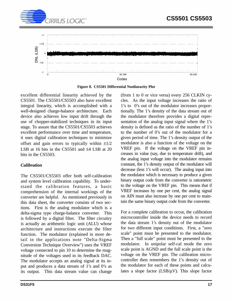
excellent differential linearity achieved by theCS5501. The CS5501/CS5503 also have excellentintegral linearity, which is accomplished with awell-designed charge-balance architecture. Eachdevice also achieves low input drift through theuse of chopper-stabilized techniques in its inputstage. To assure that the CS5501/CS5503 achievesexcellent performance over time and temperature,it uses digital calibration techniques to minimizeoffset and gain errors to typically within ±1/2LSB at 16 bits in the CS5501 and ±4 LSB at 20bits in the CS5503.
Calibration
The CS5501/CS5503 offer both self-calibrationand system level calibration capability. To under-stand the calibration features, a basiccomprehension of the internal workings of theconverter are helpful. As mentioned previously inthis data sheet, the converter consists of two sec-tions. First is the analog modulator which is adelta-sigma type charge-balance converter. Thisis followed by a digital filter. The filter circuitryis actually an arithmetic logic unit (ALU) whosearchitecture and instructions execute the filterfunction. The modulator (explained in more de-tail in the applications note "Delta-SigmaConversion Technique Overview") uses the VREFvoltage connected to pin 10 to determine the mag-nitude of the voltages used in its feedback DAC.The modulator accepts an analog signal at its in-put and produces a data stream of 1’s and 0’s asits output. This data stream value can change
(from 1 to 0 or vice versa) every 256 CLKIN cy-cles. As the input voltage increases the ratio of1’s to 0’s out of the modulator increases propor-tionally. The 1’s density of the data stream out ofthe modulator therefore provides a digital repre-sentation of the analog input signal where the 1’sdensity is defined as the ratio of the number of 1’sto the number of 0’s out of the modulator for agiven period of time. The 1’s density output of themodulator is also a function of the voltage on theVREF pin. If the voltage on the VREF pin in-creases in value (say, due to temperature drift), andthe analog input voltage into the modulator remainsconstant, the 1’s density output of the modulator willdecrease (less 1’s will occur). The analog input intothe modulator which is necessary to produce a givenbinary output code from the converter is ratiometricto the voltage on the VREF pin. This means that ifVREF increases by one per cent, the analog signalon AIN must also increase by one per cent to main-tain the same binary output code from the converter.
For a complete calibration to occur, the calibrationmicrocontroller inside the device needs to recordthe data stream 1’s density out of the modulatorfor two different input conditions. First, a "zeroscale" point must be presented to the modulator.Then a "full scale" point must be presented to themodulator. In unipolar self-cal mode the zeroscale point is AGND and the full scale point is thevoltage on the VREF pin. The calibration micro-controller then remembers the 1’s density out ofthe modulator for each of these points and calcu-lates a slope factor (LSB/µV). This slope factor
0 65,535
Codes32,768
DN
L (L
SB
)+1
0
-1
+1/2
-1/2
Figure 8. CS5501 Differential Nonlinearity Plot
CS5501/CS5503
DS31F4 17
CS5501 CS5503
DS31F5 17
represents the gain slope for the input to outputtransfer function of the converter. In unipolarmode the calibration microcontroller determinesthe slope factor by dividing the span between thezero point and the full scale point by the totalresolution of the converter (216 for the CS5501,resulting in 65,536 segments or 220 for theCS5503, resulting in 1,048,578 segments). In bi-polar mode the calibration microcontroller dividesthe span between the zero point and the full scalepoint into 524,288 segments for the CS5503 and32,768 segments for the CS5501. It then extendsthe measurement range 524,288 segments for theCS5503, 32,768 segments for the CS5501, belowthe zero scale point to achieve bipolar measure-ment capability. In either unipolar or bipolarmodes the calculated slope factor is saved andlater used to calculate the binary output codewhen an analog signal is present at the AIN pinduring measurement conversions.
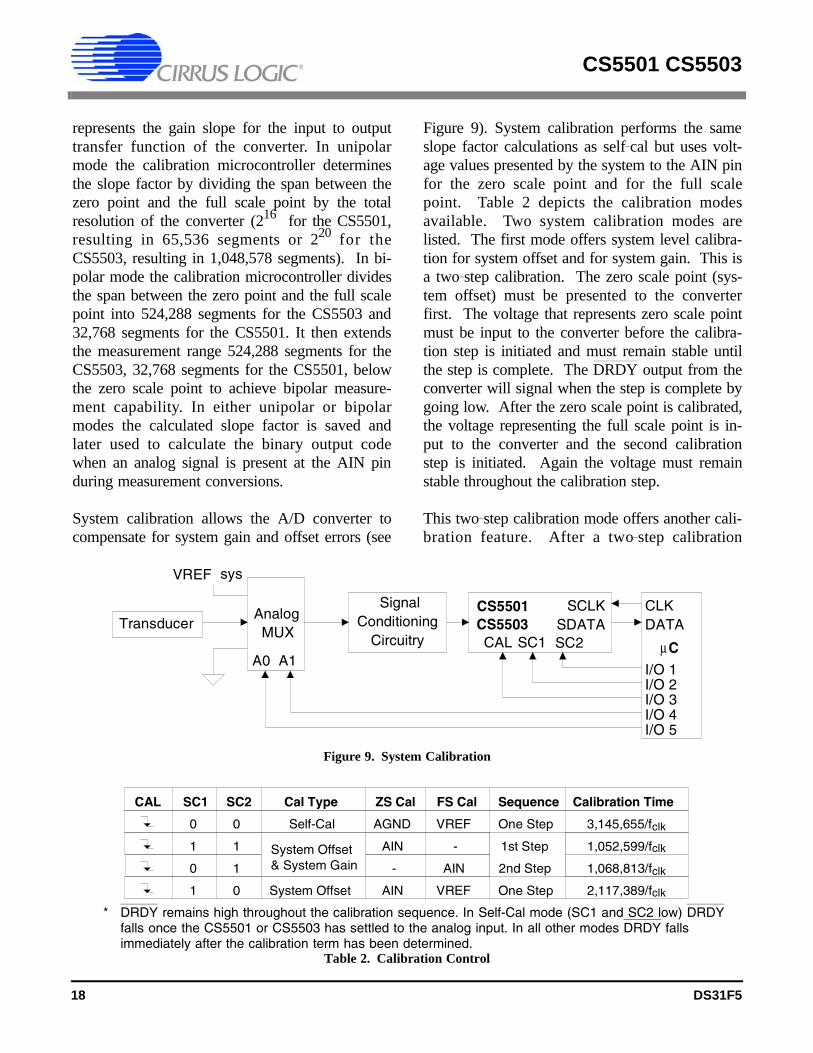
System calibration allows the A/D converter tocompensate for system gain and offset errors (see
Figure 9). System calibration performs the sameslope factor calculations as self cal but uses volt-age values presented by the system to the AIN pinfor the zero scale point and for the full scalepoint. Table 2 depicts the calibration modesavailable. Two system calibration modes arelisted. The first mode offers system level calibra-tion for system offset and for system gain. This isa two step calibration. The zero scale point (sys-tem offset) must be presented to the converterfirst. The voltage that represents zero scale pointmust be input to the converter before the calibra-tion step is initiated and must remain stable untilthe step is complete. The DRDY output from theconverter will signal when the step is complete bygoing low. After the zero scale point is calibrated,the voltage representing the full scale point is in-put to the converter and the second calibrationstep is initiated. Again the voltage must remainstable throughout the calibration step.
This two step calibration mode offers another cali-bration feature. After a two step calibration
SequenceFS CalZS CalSC2SC1CAL Cal Type Calibration Time
One StepVREFAGND00 Self-Cal 3,145,655/f
1st Step-AIN11 1,052,599/f
2nd StepAIN-10 1,068,813/f
One StepVREFAIN01 System Offset 2,117,389/f
System Offset& System Gain
clk
clk
clk
clk
* DRDY remains high throughout the calibration sequence. In Self-Cal mode (SC1 and SC2 low) DRDY falls once the CS5501 or CS5503 has settled to the analog input. In all other modes DRDY falls immediately after the calibration term has been determined.
Table 2. Calibration Control
VREF sys
TransducerAnalogMUX
µC
CLKDATA
I/O 1I/O 2I/O 3I/O 4I/O 5
CAL SC1 SC2SDATA
SCLKCS5501CS5503
A0 A1
SignalConditioning
Circuitry
Figure 9. System Calibration
CS5501/CS5503
18 DS31F4
CS5501 CS5503
18 DS31F5

sequence (system offset and system gain) hasbeen properly performed, additional offset calibra-tions can be performed by themselves toreposition the gain slope (the slope factor is notchanged) to adjust its zero reference point to thenew system zero reference value.
A second system calibration mode is availablewhich uses an input voltage for the zero scalecalibration point, but uses the VREF voltage asthe full scale calibration point.
Whenever a system calibration mode is used,there are limits to the amount of offset and to theamount of span which can be accommodated.The range of input span which can be accommo-dated in either unipolar or bipolar mode isrestricted to not less than 80% of the voltage onVREF and not more than 200% of (VREF +0.1) V. The amount of offset which can be cali-brated depends upon whether unipolar or bipolarmode is being used. In unipolar mode the systemcalibration modes can handle offsets as positive as20% of VREF (this is restricted by the minimumspan requirement of 80% VREF) or as negative as-(VREF + 0.1) V. This capability enables theunipolar mode of the CS5501/CS5503 to be cali-brated to mimic bipolar mode operation.
In the bipolar mode the system offset calibrationrange is restricted to a maximum of ±40% ofVREF. It should be noted that the span restrictionslimit the amount of offset which can be calibrated.The span range of the converter in bipolar modeextends an equidistance (+ and -) from the voltageused for the zero scale point. When the zero scalepoint is calibrated it must not cause either of thetwo endpoints of the bipolar transfer function toexceed the positive or the negative input over-range points (+(VREF + 0.1) V or - (VREF +0.1) V). If the span range is set to a minimum(80% VREF) the offset voltage can move ±40%VREF without causing the end points of the trans-fer function to exceed the overrange points.Alternatively, if the span range is set to 200% of
VREF, the input offset cannot move more than+0.1 or 0.1 V before an endpoint of the transferfunction exceeds the input overrange limit.
Initiating Calibration
Table 2 illustrates the calibration modes availablein the CS5501/CS5503. Not shown in the table isthe function of the BP/UP pin which determineswhether the converter is calibrated to measure bi-polar or unipolar signals. A calibration step isinitiated by bringing the CAL pin (13) high for atleast 4 CLKIN cycles to reset the part and thenbringing CAL low. The states of SC1 (pin 4) andSC2 (pin 17) along with the BP/UP (pin 12) willdetermine the type of calibration to be performed.The SC1 and SC2 inputs are latched when CALgoes low. The BP/UP input is not latched andtherefore must remain in a fixed state throughoutthe calibration and measurement cycles. Any timethe state of the BP/UP pin is changed, a new cali-bration cycle must be performed to enable theCS5501/CS5503 to properly function in the newmode.
When a calibration step is initiated, the DRDYsignal will go high and remain high until the stepis finished. Table 2 illustrates the number ofclock cycles each calibration requires. Once acalibration step is initiated it must finish before anew calibration step can be executed. In the twostep system calibration mode, the offset calibra-tion step must be initiated before initiating thegain calibration step.
When a self-cal is completed DRDY falls and theoutput port is updated with a data word that repre-sents the analog input signal at the AIN pin.When a system calibration step is completed,DRDY will fall and the output port will be up-dated with the appropriate data value (zero scalepoint, or full scale point). In the system calibra-tion mode, the digital filter must settle before theoutput code will represent the value of the analoginput signal.
CS5501/CS5503
DS31F4 19
CS5501 CS5503
DS31F5 19
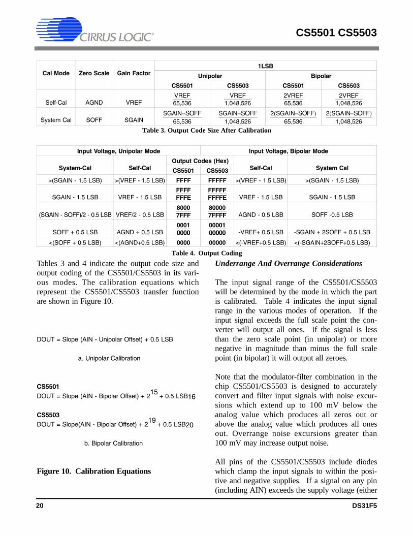
Tables 3 and 4 indicate the output code size andoutput coding of the CS5501/CS5503 in its vari-ous modes. The calibration equations whichrepresent the CS5501/CS5503 transfer functionare shown in Figure 10.
DOUT = Slope (AIN - Unipolar Offset) + 0.5 LSB
a. Unipolar Calibration
CS5501DOUT = Slope (AIN - Bipolar Offset) + 2
15 + 0.5 LSB16
CS5503DOUT = Slope(AIN - Bipolar Offset) + 2
19 + 0.5 LSB20
b. Bipolar Calibration
Figure 10. Calibration Equations
Underrange And Overrange Considerations
The input signal range of the CS5501/CS5503will be determined by the mode in which the partis calibrated. Table 4 indicates the input signalrange in the various modes of operation. If theinput signal exceeds the full scale point the con-verter will output all ones. If the signal is lessthan the zero scale point (in unipolar) or morenegative in magnitude than minus the full scalepoint (in bipolar) it will output all zeroes.
Note that the modulator-filter combination in thechip CS5501/CS5503 is designed to accuratelyconvert and filter input signals with noise excur-sions which extend up to 100 mV below theanalog value which produces all zeros out orabove the analog value which produces all onesout. Overrange noise excursions greater than100 mV may increase output noise.
All pins of the CS5501/CS5503 include diodeswhich clamp the input signals to within the posi-tive and negative supplies. If a signal on any pin(including AIN) exceeds the supply voltage (either
Cal Mode Zero Scale Gain Factor1LSB
Unipolar Bipolar
CS5501 CS5503 CS5501 CS5503
Self-Cal AGND VREFVREF65,536
VREF1,048,526
2VREF65,536
2VREF1,048,526
System Cal SOFF SGAINSGAIN−SOFF
65,536SGAIN−SOFF
1,048,5262(SGAIN−SOFF)
65,5362(SGAIN−SOFF)
1,048,526
Table 3. Output Code Size After Calibration
Input Voltage, Unipolar Mode Input Voltage, Bipolar Mode
System-Cal Self-CalOutput Codes (Hex)
Self-Cal System CalCS5501 CS5503
>(SGAIN - 1.5 LSB) >(VREF - 1.5 LSB) FFFF FFFFF >(VREF - 1.5 LSB) >(SGAIN - 1.5 LSB)
SGAIN - 1.5 LSB VREF - 1.5 LSBFFFFFFFE
FFFFFFFFFE VREF - 1.5 LSB SGAIN - 1.5 LSB
(SGAIN - SOFF)/2 - 0.5 LSB VREF/2 - 0.5 LSB80007FFF
800007FFFF AGND - 0.5 LSB SOFF -0.5 LSB
SOFF + 0.5 LSB AGND + 0.5 LSB00010000
0000100000 -VREF+ 0.5 LSB -SGAIN + 2SOFF + 0.5 LSB
<(SOFF + 0.5 LSB) <(AGND+0.5 LSB) 0000 00000 <(-VREF+0.5 LSB) <(-SGAIN+2SOFF+0.5 LSB)
Table 4. Output Coding
CS5501/CS5503
20 DS31F4
CS5501 CS5503
20 DS31F5
+ or -) a clamp diode will be forward-biased. Un-der these fault conditions the CS5501/CS5503might be damaged. Under normal operating con-ditions (with the power supplies established), thedevice will survive transient currents through theclamp diodes up to 100 mA and continuous cur-rents up to 10 mA. The drive current into the AINpin should be limited to a safe value if an over-voltage condition is likely to occur. See theapplication note "Buffer Amplifiers for theCS501X Series of A/D Converters" for furtherdiscussion on the clamp diode input structure andon current limiting circuits.
System Synchronization
If more than one CS5501/CS5503 is included in asystem which is operating from a common clock,all of the devices can be synchronized to sampleand output at exactly the same time. This can beaccomplished in either of two ways. First, a singleCAL signal can be issued to all theCS5501/CS5503’s in the system. To insure syn-chronization on the same clock signal the CALsignal should go low on the falling edge ofCLKIN. Or second, a common SLEEP controlsignal can be issued. If the SLEEP signal goespositive with the appropriate set up time toCLKIN, all parts will be synchronized on thesame clock cycle.
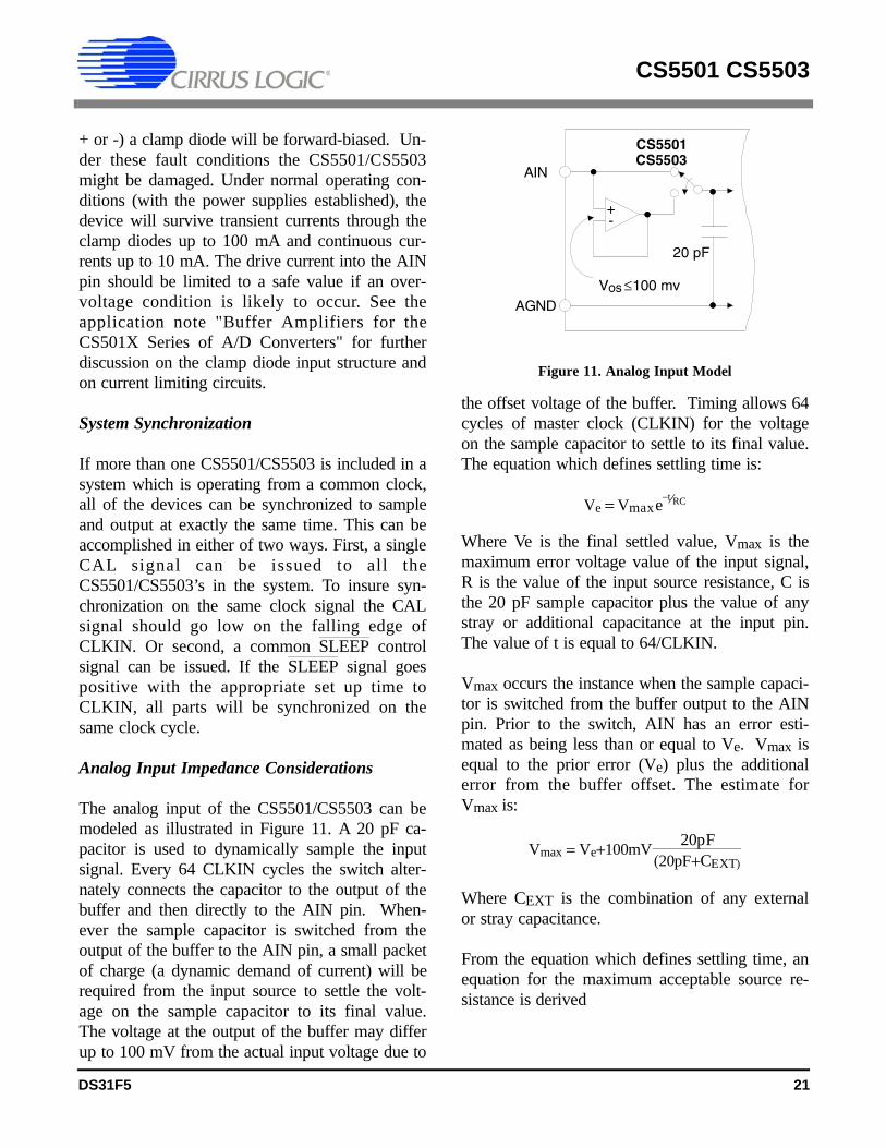
Analog Input Impedance Considerations
The analog input of the CS5501/CS5503 can bemodeled as illustrated in Figure 11. A 20 pF ca-pacitor is used to dynamically sample the inputsignal. Every 64 CLKIN cycles the switch alter-nately connects the capacitor to the output of thebuffer and then directly to the AIN pin. When-ever the sample capacitor is switched from theoutput of the buffer to the AIN pin, a small packetof charge (a dynamic demand of current) will berequired from the input source to settle the volt-age on the sample capacitor to its final value.The voltage at the output of the buffer may differup to 100 mV from the actual input voltage due to
the offset voltage of the buffer. Timing allows 64cycles of master clock (CLKIN) for the voltageon the sample capacitor to settle to its final value.The equation which defines settling time is:
Ve = Vmax e−t⁄RC
Where Ve is the final settled value, Vmax is themaximum error voltage value of the input signal,R is the value of the input source resistance, C isthe 20 pF sample capacitor plus the value of anystray or additional capacitance at the input pin.The value of t is equal to 64/CLKIN.
Vmax occurs the instance when the sample capaci-tor is switched from the buffer output to the AINpin. Prior to the switch, AIN has an error esti-mated as being less than or equal to Ve. Vmax isequal to the prior error (Ve) plus the additionalerror from the buffer offset. The estimate forVmax is:
Vmax = Ve+100mV20pF
(20pF+CEXT)
Where CEXT is the combination of any externalor stray capacitance.
From the equation which defines settling time, anequation for the maximum acceptable source re-sistance is derived
+-
CS5501
AIN
AGNDV 100 mvos
20 pF
CS5503
≤
Figure 11. Analog Input Model
CS5501/CS5503
DS31F4 21
CS5501 CS5503
DS31F5 21
equation which defines settling time, an equationfor the maximum acceptable source resistance isderived
Rsmax = −64
CLKIN (20pF+CEXT ) ln
Ve
Ve + 20pF(100mv)
( 20pF+CEXT )
This equation assumes that the offset voltage ofthe buffer is 100 mV, which is the worst case.The value of Ve is the maximum error voltagewhich is acceptable.
For a maximum error voltage (Ve) of 10 µV inthe CS5501 (1/4LSB at 16-bits) and 600 nV inthe CS5503 (1/4LSB at 20-bits), the above equa-tion indicates that when operating from a4.096 MHz CLKIN, source resistances up to84 kΩ in the CS5501 or 64 kΩ in the CS5503 areacceptable in the absence of external capacitance(CEXT = 0). If higher input source resistancesare desired the master clock rate can be reducedto yield a longer settling time for the 64 cycle pe-riod.
Analog Input Drift Considerations
The CS5501/CS5503 analog input uses chopper-stabilization techniques to minimize input offset
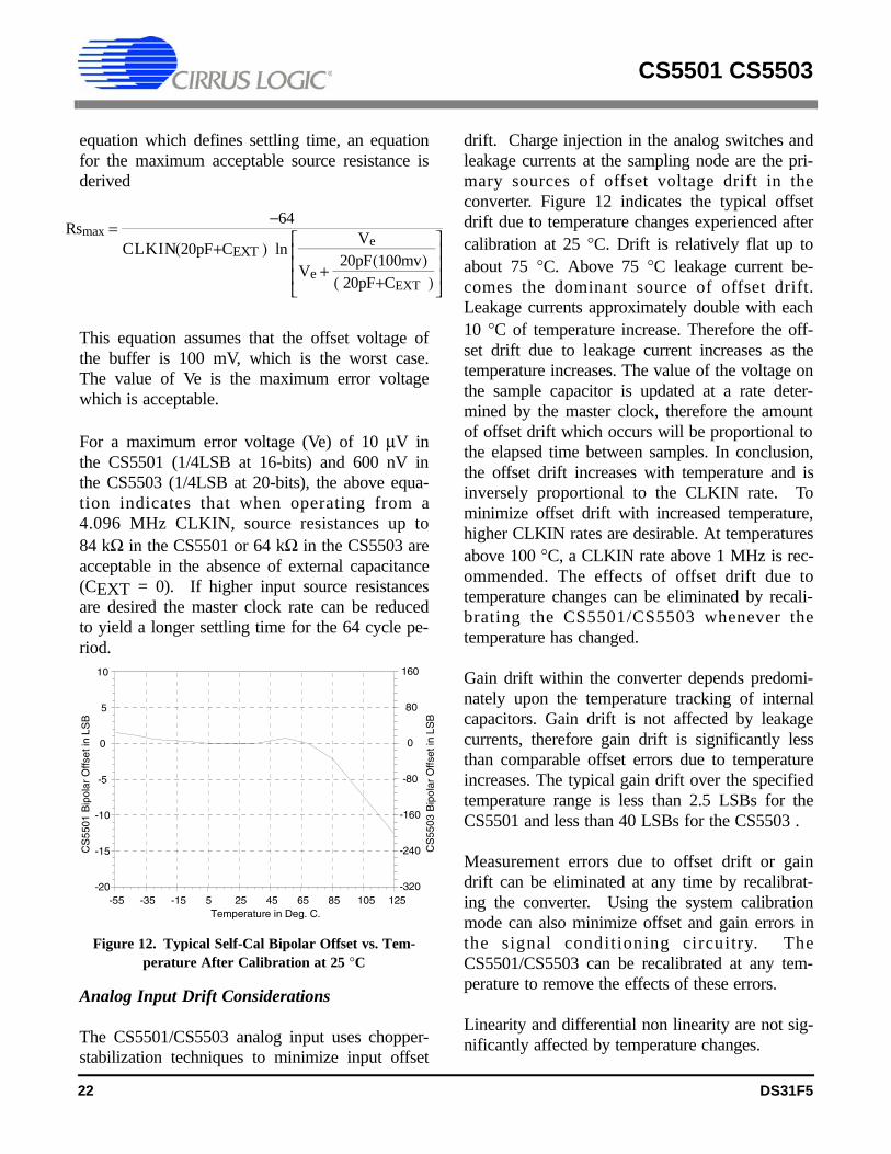
drift. Charge injection in the analog switches andleakage currents at the sampling node are the pri-mary sources of offset voltage drift in theconverter. Figure 12 indicates the typical offsetdrift due to temperature changes experienced aftercalibration at 25 °C. Drift is relatively flat up toabout 75 °C. Above 75 °C leakage current be-comes the dominant source of offset drift.Leakage currents approximately double with each10 °C of temperature increase. Therefore the off-set drift due to leakage current increases as thetemperature increases. The value of the voltage onthe sample capacitor is updated at a rate deter-mined by the master clock, therefore the amountof offset drift which occurs will be proportional tothe elapsed time between samples. In conclusion,the offset drift increases with temperature and isinversely proportional to the CLKIN rate. Tominimize offset drift with increased temperature,higher CLKIN rates are desirable. At temperaturesabove 100 °C, a CLKIN rate above 1 MHz is rec-ommended. The effects of offset drift due totemperature changes can be eliminated by recali-brating the CS5501/CS5503 whenever thetemperature has changed.
Gain drift within the converter depends predomi-nately upon the temperature tracking of internalcapacitors. Gain drift is not affected by leakagecurrents, therefore gain drift is significantly lessthan comparable offset errors due to temperatureincreases. The typical gain drift over the specifiedtemperature range is less than 2.5 LSBs for theCS5501 and less than 40 LSBs for the CS5503 .
Measurement errors due to offset drift or gaindrift can be eliminated at any time by recalibrat-ing the converter. Using the system calibrationmode can also minimize offset and gain errors inthe signal conditioning circuitry. TheCS5501/CS5503 can be recalibrated at any tem-perature to remove the effects of these errors.
Linearity and differential non linearity are not sig-nificantly affected by temperature changes.
Temperature in Deg. C.
CS
5501
Bip
olar
Offs
et in
LS
B
-20
-15
-10
-5
0
5
10
-55 -35 -15 5 25 45 65 85 105 125
CS
5503
Bip
olar
Offs
et in
LS
B
-320
-240
-160
-80
0
80
160
Figure 12. Typical Self-Cal Bipolar Offset vs. Tem-perature After Calibration at 25 °C
CS5501/CS5503
22 DS31F4
CS5501 CS5503
22 DS31F5
Filtering
At the system level, the digital filter in theCS5501/CS5503 can be modeled exactly likean analog filter with a few minor differences.Digital filtering resides behind the A/D conver-sion and can thus reject noise injected duringthe conversion process (i.e. power supply rip-ple, voltage reference noise, or noise in theADC itself). Analog filtering cannot.
Also, since digital filtering resides behind theA/D converter, noise riding unfiltered on anear-full-scale input could potentially over-range the ADC. In contrast, analog filteringremoves the noise before it ever reaches theconverter. To address this i ssue, theCS5501/CS5503 each contain an analog modu-lator and digital filter which reserve headroomsuch that the device can process signals with100mV "excursions" above full-scale and stilloutput accurately converted and filtered data.Filtered input signals above full-scale still resultin an output of all ones.
The digital filter’s corner frequency occurs atCLKIN/409,600, where CLKIN is the masterclock frequency. With a 4.096MHz clock, the
filter corner is at 10Hz and the output register isupdated at a 4kHz rate. CLKIN frequency can bereduced with a proportional reduction in the filtercorner frequency and in the update rate to the out-put register. A plot of the filter response is shownin the specification tables section of this datasheet.
Both the CS5501/CS5503 employ internal digi-tal filtering which creates a 6-pole Gaussianrelationship. With the corner frequency set at10Hz for minimized sett l ing t ime, theCS5501/CS5503 offer approximately 55dB re-jection at 60Hz to signals coming into eitherthe AIN or VREF pins. With a 5Hz cut-off,60Hz rejection increases to more than 90dB.
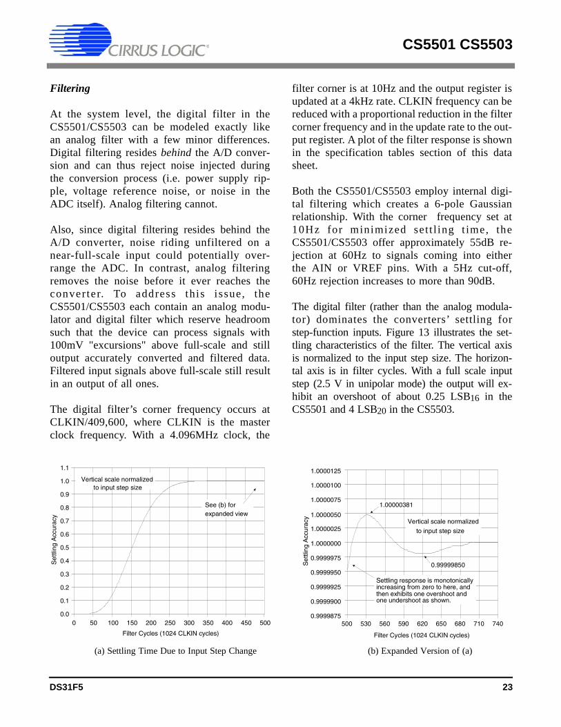
The digital filter (rather than the analog modula-tor) dominates the converters’ settling forstep-function inputs. Figure 13 illustrates the set-tling characteristics of the filter. The vertical axisis normalized to the input step size. The horizon-tal axis is in filter cycles. With a full scale inputstep (2.5 V in unipolar mode) the output will ex-hibit an overshoot of about 0.25 LSB16 in theCS5501 and 4 LSB20 in the CS5503.
(a) Settling Time Due to Input Step Change (b) Expanded Version of (a)
Set
tling
Acc
urac
y
0.0
0.1
0.2
0.3
0.4
0.5
0.6
0.7
0.8
0.9
1.0
1.1
See (b) for expanded view
Vertical scale normalized to input step size
Filter Cycles (1024 CLKIN cycles)
0 50 100 150 200 250 300 350 400 450 500
1.00000381
0.99999850
Vertical scale normalized
to input step size
Settling response is monotonicallyincreasing from zero to here, and then exhibits one overshoot andone undershoot as shown.
Set
tling
Acc
urac
y
0.9999875
0.9999900
0.9999925
0.9999950
0.9999975
1.0000000
1.0000025
1.0000050
1.0000075
1.0000100
1.0000125
Filter Cycles (1024 CLKIN cycles)
500 530 560 590 620 650 680 710 740
CS5501/CS5503
DS31F4 23
CS5501 CS5503
DS31F5 23
Anti-Alias Considerations
The digital filter in the CS5501/CS5503 does notprovide rejection around integer multiples of theoversampling rate [(N*CLKIN)/256, whereN = 1,2,3,...]. That is, with a 4.096 MHz masterclock the noise on the analog input signal withinthe narrow ±10 Hz bands around the 16 kHz,32 kHz, 48 kHz, etc., passes unfiltered to the digi-tal output. Most broadband noise will be verywell filtered because the CS5501/CS5503 use avery high oversampling ratio of 800 (16 kHz:2x10 Hz). Broadband noise is reduced by:
eout = ein √2f−3dB ⁄ fs
eout = 0.035 ein
where ein and eout are rms noise terms referred tothe input. Since f-3dB equals CLKIN/409,600 andfs equals CLKIN/256, the digital filter reduceswhite, broadband noise by 96.5% independent ofthe CLKIN frequency. For example, a typical op-erational amplifier’s 50µV rms noise would bereduced to 1.75µV rms (0.035 LSB’s rms at the16-bit level in the CS5501 and 0.4 LSB’s rms atthe 20-bit level in the CS5503).
Simple high frequency analog filtering in the sig-nal conditioning circuitry can aid in removingenergy at multiples of the sampling rate.
Post Filtering
Post filtering is useful to enhance the noise per-formance of the CS5503. With a constant inputvoltage the output codes from the CS5503 willexhibit some variation due to noise. The CS5503has typically 1.6 LSB20 rms noise in its outputcodes. Additional variation in the output codescan arise due to noise from the input signal sourceand from the voltage reference. Post filtering(digital averaging) will be necessary to achieveless than 1 LSB p-p noise at the 20-bit level. TheCS5503 has peak noise less than the 18-bit levelwithout additional filtering if care is exercised inthe design of the voltage reference and the inputsignal condition circuitry. Noise in the bandwidthfrom dc to 10 Hz on both the AIN and VREFinputs should be minimized to ensure maximumperformance. As the amount of noise will behighly system dependent, a specific recommenda-tion for post filtering for all applications cannot bestated. The following guidelines are helpful. Real-ize that the digital filter in the CS5503, like anyother low pass filter, acts as an information stor-age unit. The filter retains past information for aperiod of time even after the input signal haschanged. The implication of this is that immedi-ately sequential 20-bit updates to the serial portcontain highly correlated information. To most ef-ficiently post filter the CS5503 output data,uncorrelated samples should be used. Sampleswhich have sufficiently reduced correlation can beobtained if the CS5503 is allowed to execute 200filter cycles between each subsequent data wordcollected for post filtering.
The character of the noise in the data will influ-ence the post filtering requirements. As a generalrule, averaging N uncorrelated data samples willreduce noise by 1/√N. While this rule assumesthat the noise is white (which is true for theCS5503 but not true for all real system signalsbetween dc and 10Hz), it does offer a startingpoint for developing a post filtering algorithm forremoving the noise from the data. The algorithm
348,160364,544398,336445,440470,016486,400497,664506,880512,000516,096518,144519,168
Filter Cycles
340356389435459475486495500504506507
CLKINCycles
91011121314151617181920
Bits ofOutput
Accuracy
Table 5. Settling Time of the 6 Pole Low Pass Filter inthe CS5501 to 1/2 LSB Accuracy with a Full Scale
Step Input
CS5501/CS5503
24 DS31F4
CS5501 CS5503
24 DS31F5

will have to be empirically tested to see if it meetsthe system requirements. It is recommended thatany testing include input signals across the entireinput span of the converter as the signal level willaffect the amount of noise from the reference in-put which is transferred to the output data.
Voltage Reference
The voltage reference applied to the VREF inputpin defines the analog input range of theCS5501/CS5503. The preferred reference is 2.5V,but the device can typically accept referencesfrom 1V to 3V. Input signals which exceed 2.6V(+ or -) can cause some linearity degradation. Fig-ure 14 illustrates the voltage referenceconnections to the CS5501/CS5503.
The circuitry inside the VREF pin is identical tothat as seen at the AIN pin. The sample capacitor(see Figure 12) requires packets of charge fromthe external reference just as the AIN pin does.Therefore the same settling time requirements ap-ply. Most reference IC’s can handle this dynamicload requirement without inducing errors. Theyexhibit sufficiently low output impedance andwide enough bandwidth to settle to within thenecessary accuracy in the requisite 64 CLKIN cy-cles.
Noise from the reference is filtered by the digitalfilter, but the reference should be chosen to mini-mize noise below 10 Hz. The CS5501/CS5503typically exhibit 0.1 LSB rms and 1.6 LSB rmsnoise respectively. This specification assumes aclean reference voltage. Many monolithic
band-gap references are available which can sup-ply 2.5 V for use with the CS5501/CS5503.Many of these devices are not specified for noise,especially in the 0.1 to 10 Hz bandwidth. Someof these devices may exhibit noise characteristicswhich degrade the performance of theCS5501/CS5503.
Power Supplies And Grounding
The CS5501/CS5503 use the analog ground con-nection, AGND, as a measurement referencenode. It carries no power supply current. TheAGND pin should be used as the reference nodefor both the analog input signal and for the refer-ence voltage which is input into the VREF pin.
The analog and digital supply inputs are pinnedout separately to minimize coupling between theanalog and digital sections of the chip. Toachieve maximum performance, all four suppliesfor the CS5501/CS5503 should be decoupled totheir respective grounds using 0.1 µF capacitors.This is illustrated in the System Connection Dia-gram, Figure 15, at the beginning of this datasheet.
As CMOS devices, the CS5501/CS5503 requirethat the positive analog supply voltage always begreater than or equal to the positive digital supplyvoltage. If the voltage on the positive digital sup-ply should ever become greater than the voltageon the positive analog supply, diode junctions inthe CMOS structure which are normally reverse-biased will become forward-biased. This maycause the part to draw high currents and experi-ence permanent damage. The connections shownin Figure 15 eliminate this possibility.
To ensure reliable operation, be certain that poweris applied to the part before signals at AIN, VREF,or the logic input pins are present. If current issupplied into any pin before the chip is powered-up, latch up may result. As a system, it isdesirable to power the CS5501/CS5503, the volt-
CS5501
+5V
AGND
VREF
LT1019 -2.5
2.5 V
VA+
For Example
CS5503
Figure 14. Voltage Reference Connections
CS5501/CS5503
DS31F4 25
CS5501 CS5503
DS31F5 25

age reference, and the analog signal conditioningcircuitry from the same primary source. If sepa-rate supplies are used, it is recommended that theCS5501/CS5503 be powered up first. If a com-mon power source is used for the analog signalconditioning circuitry as well as the A/D con-verter, this power source should be appliedbefore application of power to the digital logicsupply.
The CS5501/CS5503 exhibit good power supplyrejection for frequencies within the passband (dcto 10 Hz). Any small offset or gain error causedby long term drift of the power supplies can be
removed by recalibration. Above 10 Hz the digi-tal filter will provide additional rejection. Whenthe benefits of the digital filter are added to theregular power supply rejection the effects of linefrequency variations (60 Hz) on the power sup-plies will be reduced greater than 120 dB. If thesupply voltages for the CS5501/CS5503 are gen-erated with a dc-dc converter the operatingfrequency of the dc-dc converter should not oper-ate at the sampling frequency of theCS5501/CS5503 or at integer multiples thereof.At these frequencies the digital filter will not aidin power supply rejection. See Anti-Alias Consid-erations section of this data sheet.
CS5501CS5503
+5VAnalogSupply
2
3
0.1 µF
CLKIN
CLKOUT
VD+
15
10 Ω
VA+
14
11
1MODE
19SCLK
OptionalClock
Source
Sleep ModeControl
OutputMode Select
SerialData
Interface20
SDATA
16
18ControlLogic
CAL
SC1
SC2
13
4
17
12BP/UP
AIN9
CalibrationControl
Bipolar/Unipolar
Input Select
VREF
AGND8
10
5DGND
VD-6
VA-7
0.1 µF
AnalogSignalSource
0.1 µF
-5VAnalogSupply
SLEEP
DRDY
CS
0 VREFor
±VREF
0.0047 µF NPO
* Recommended toreduce high
frequency noise
+5VAnalogSupply
VoltageReference
200 Ω∗
Unused Logic Inputsmust be connectedto DGND or VD+
+2.5V
10 Ω
0.1 µF
Figure 15. Typical Connection Diagram
CS5501/CS5503
26 DS31F4
CS5501 CS5503
26 DS31F5

The recommended system connection diagram forthe CS5501/CS5503 is illustrated in Figure 15.Note that any digital logic inputs which are to beunused should be tied to either DGND or theVD+ as appropriate. They should not be left float-ing; nor should they be tied to some other logicsupply voltage in the system.
Power-up and Initialization
Upon power-up, a calibration cycle must be initi-ated at the CAL pin to insure a consistent startingcondition and to initially calibrate the device. TheCAL pin must be strobed high for a minimum of4 clock cycles. The falling edge will initiate acalibration cycle. A simple power-on reset circuitcan be built using a resistor and capacitor (seeFigure 16). The resistor and capacitor valuesshould allow for clock or oscillator startup time,and the voltage reference stabilization time.
Due to the devices’ low power dissipation andlow temperature drift, no warm-up time is re-quired to accommodate any self-heating effects.
Sleep Mode
The CS5501/CS5503 include a sleep mode(SLEEP = DGND) which shuts down the internalanalog and digital circuitry reducing power con-sumption to less than 10 µW. All calibrationcoefficients are retained in memory such that notime is required after "awakening" for recalibra-tion. Still, the CS5501/CS5503 will require timefor the digital filter to settle before an accurate
reading will occur after a rising edge on SLEEPoccurs.
Battery Backed-up Calibrations
The CS5501/CS5503 use SRAM to store calibra-tion information. The contents of the SRAM willbe lost whenever power is removed from the chip.Figure 17 shows a battery back-up scheme thatcan be used to retain the calibration memory dur-ing system down time and/or protect it againstintermittent power loss. Note that upon loss ofpower, the SLEEP input goes low, reducingpower consumption to just 10 µW. Lithium cellsof 3.6 V are available which average 1750 mA-hours before they drop below the typical 2 Vmemory-retention specification of theCS5501/CS5503.
When SLEEP is active (SLEEP = DGND), bothVD+ and VA+ must remain powered to no lessthan 2 V to retain calibration memory. The VD-and VA- voltages can be reduced to 0 V but mustnot be allowed to go above ground potential. Thenegative supply must exhibit low source imped-ance in the powered-down state as the current intothe VA+ pin flows out the VA- pin. (AGND isonly a reference node. No power supply currentflows in or out of AGND.) Care should be taken
CS5501
R
+5V
CALC
SC2
SC1
Figure 16. Power-On Reset Circuitry (Self-Calibration Only)
CS5501VD+
15
10 Ω
VA+14
0.1 µF+5V
1N4148
Vd
Vb8
AGND
11SLEEP
0.1 µF
1N4148
1N41485 DGND
VD-VA-7 6
10 Ω0.1 µF
-5V
0.1 µF
47kΩ
CS5503
(2V+Vd) < Vb < 4.5V
Figure 17. Example Calibration Memory BatteryBack-Up Circuit
CS5501/CS5503
DS31F4 27
CS5501 CS5503
DS31F5 27
CS5501 CS5503
28 DS31F4
to ensure that logic inputs are maintained at eitherVD+ ar DGND potential when SLEEP is low.
Note that battery life could be shortened if the +5 Vsupply drops slowly during power-down. As thesupply drops below the battery voltage but not yetbelow the logic threshold of the SLEEP pin, thebattery will be supplying the CS5501/CS5503 atfull power (typically 3 mA). Faster transitions atSLEEP can be triggered using a resistive divider ora simple resistor network to generate the SLEEP in-put from the +5 V supply.
Output Loading Considerations
To maximize performance of the CS5501/ CS5503,the output drive currents from the digital outputlines should be minimized.
Schematic & Layout Review Service
CS5501 CS5503
28 DS31F5
PIN DESCRIPTIONS
Clock Generator
CLKIN; CLKOUT -Clock In; Clock Out, Pins 3 and 2.A gate inside the CS5501/CS5503 is connected to these pins and can be used with a crystal orceramic resonator to provide the master clock for the device. Alternatively, an external (CMOScompatible) clock can be input to the CLKIN pin as the master clock for the device. When notin SLEEP mode, a master clock (CLKIN) should be present at all times.
Serial Output I/O
MODE -Serial Interface Mode Select, Pin 1.Selects the operating mode of the serial port. If tied to VD- (-5V), the CS5501 will operate inthe UART-compatible AC mode for Asynchronous Communication. The SCLK pin willoperate as an input to set the data rate, and data will transmit formatted with one start and twostop bits. If MODE is tied to DGND, the CS5501/CS5503 will operate in the SEC(Synchronous External-Clocking) mode, with the SCLK pin operating as an input and theoutput appearing MSB-first. If MODE is tied to VD+ (+5V), the CS5501/CS5503 will operatein its SSC (Synchronous Self-Clocking) mode, with SCLK providing a serial clock output ofCLKIN/4 (25% duty-cycle).
DRDY -Data Ready, Pin 18.DRDY goes low every 1024 cycles of CLKIN to indicate that new data has been placed in theoutput port. DRDY goes high when all the serial port data is clocked out, when the serial portis being updated with new data, when a calibration is in progress, or when SLEEP is low.
CS -Chip Select, Pin 16.An input which can be enabled by an external device to gain control over the serial port of theCS5501/CS5503.
SERIAL INTERFACE MODE SELECT MODE SDATA SERIAL DATA OUTPUTCLOCK OUT CLKOUT SCLK SERIAL CLOCK INPUT/OUTPUT
CLOCK IN CLKIN DRDY DATA READYSYSTEM CALIBRATION 1 SC1 SC2 SYSTEM CALIBRATION 2
DIGITAL GROUND DGND CS CHIP SELECTNEGATIVE DIGITAL POWER VD- VD+ POSITIVE DIGITAL POWERNEGATIVE ANALOG POWER VA- VA+ POSITIVE ANALOG POWER
ANALOG GROUND AGND CAL CALIBRATEANALOG IN AIN BP/UP BIPOLAR/UNIPOLAR SELECT
VOLTAGE REFERENCE VREF SLEEP SLEEP
1
2
3
4
5
6
7
8
9
10
20
19
18
17
16
15
14
13
12
11
* Pinout applies to both DIP and SOIC packages
CS5501/CS5503
DS31F4 29
CS5501 CS5503
DS31F5 29
SDATA -Serial Data Output, Pin 20.Data from the serial port will be output from this pin at a rate determined by SCLK and in aformat determined by the MODE pin. It furnishes a high impedance output state when nottransmitting data.
SCLK -Serial Clock Input/Output, Pin 19.A clock signal at this pin determines the output rate of the data from the SDATA pin. TheMODE pin determines whether the SCLK signal is an input or output. SCLK may provide ahigh impedance output when data is not being output from the SDATA pin.
Calibration Control Inputs
SC1; SC2 -System Calibration 1 and 2, Pins 4 and 17. Control inputs to the CS5501/CS5503’s calibration microcontroller for calibration. The state ofSC1 and SC2 determine which of the calibration modes is selected for operation (see Table 2).
BP/UP -Bipolar/Unipolar Select, Pin 12.Determines whether the CS5501/CS5503 will be calibrated to measure bipolar (BP/UP = VD+)or unipolar (BP/UP = DGND) input signals. Recalibration is necessary whenever the state ofBP/UP is changed.
CAL -Calibrate, Pin 13.If brought high for 4 clock cycles or more, the CS5501/CS5503 will reset and upon returninglow a full calibration cycle will begin. The state of SC1, SC2, and BP/UP when CAL isbrought low determines the type and length of calibration cycle initiated (see Table 2). Also, asingle CAL signal can be used to strobe the CAL pins high on several CS5501/CS5503’s tosynchronize their operation. Any spurious glitch on this pin may inadvertently place the chip inCalibration mode.
Other Control Input
SLEEP -Sleep, Pin 11.When brought low, the CS5501/CS5503 will enter a low-power state. When brought highagain, the CS5501/CS5503 will resume operation without the need to recalibrate. After SLEEPgoes high again, the device’s output will settle to within +0.0007% of the analog input valuewithin 1.3/f-3dB, where f-3dB is the passband frequency. The SLEEP input can also be used tosynchronize sampling and the output updates of several CS5501/CS5503’s.
Analog Inputs
VREF -Voltage Reference, Pin 10.Analog reference voltage input.
AIN -Analog Input, Pin 9.
CS5501/CS5503
30 DS31F4
CS5501 CS5503
30 DS31F5

Power Supply Connections
VD+ -Positive Digital Power, Pin 15.Positive digital supply voltage. Nominally +5 volts.
VD- -Negative Digital Power, Pin 6.Negative digital supply voltage. Nominally -5 volts.
DGND -Digital Ground, Pin 5.Digital ground.
VA+ -Positive Analog Power, Pin 14.Positive analog supply voltage. Nominally +5 volts.
VA- -Negative Analog Power, Pin 7.Negative analog supply voltage. Nominally -5 volts.
AGND -Analog Ground, Pin 8.Analog ground.
CS5501/CS5503
DS31F4 31
CS5501 CS5503
DS31F5 31

SPECIFICATION DEFINITIONS
Linearity ErrorThe deviation of a code from a straight line which connects the two endpoints of the A/DConverter transfer function. One endpoint is located 1/2 LSB below the first code transitionand the other endpoint is located 1/2 LSB beyond the code transition to all ones. Units inpercent of full-scale.
Differential LinearityThe deviation of a code’s width from the ideal width. Units in LSB’s.
Full-Scale ErrorThe deviation of the last code transition from the ideal (VREF-3/2 LSB’s). Units in LSBs.
Unipolar OffsetThe deviation of the first code transition from the ideal (1/2 LSB above AGND) when inunipolar mode (BP/UP low). Units in LSBs.
Bipolar OffsetThe deviation of the mid-scale transition (011...111 to 100...000) from the ideal (1/2 LSBbelow AGND) when in bipolar mode (BP/UP high). Units in LSBs.
Bipolar Negative Full-Scale ErrorThe deviation of the first code transition from the ideal when in bipolar mode (BP/UP high).The Ideal is defined as lying on a straight line which passes through the final and mid-scalecode transitions. Units in LSBs.
Positive Full-Scale Input Overrange The absolute maximum positive voltage allowed for either accurate system calibration oraccurate conversions. Units in volts.
Negative Full-Scale Input OverrangeThe absolute maximum negative voltage allowed for either accurate system calibration oraccurate conversions. Units in volts.
Offset Calibration RangeThe CS5501/CS5503 calibrate their offset to the voltage applied to the AIN pin when in systemcalibration mode. The first code transition defines Unipolar Offset when BP/UP is low and themid-scale transition defines Bipolar Offset when BP/UP is high. The Offset Calibration Rangespecification indicates the range of voltages applied to AIN that the CS5501 or CS5503 canaccept and still calibrate offset accurately. Units in volts.
Input SpanThe voltages applied to the AIN pin in system-calibration schemes define the CS5501/CS5503analog input range. The Input Span specification indicates the minimum and maximum inputspans from zero-scale to full-scale in unipolar, or from positive full scale to negative full scalein bipolar, that the CS5501/CS5503 can accept and still calibrate gain accurately. Units involts.
CS5501/CS5503
32 DS31F4
CS5501 CS5503
32 DS31F5
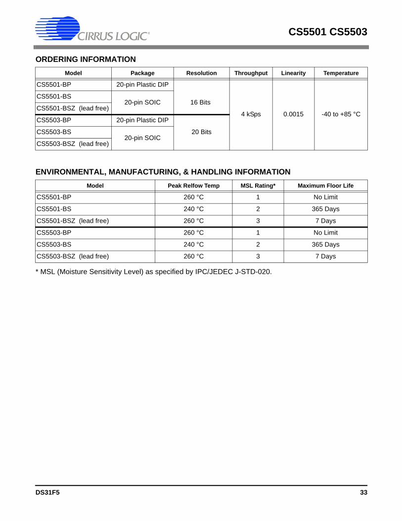
CS5501 CS5503
DS31F5 33
ORDERING INFORMATION
ENVIRONMENTAL, MANUFACTURING, & HANDLING INFORMATION
* MSL (Moisture Sensitivity Level) as specified by IPC/JEDEC J-STD-020.
Model Package Resolution Throughput Linearity Temperature
CS5501-BP 20-pin Plastic DIP
4 kSps 0.0015 -40 to +85 °C
CS5501-BS20-pin SOIC 16 Bits
CS5501-BSZ (lead free)
CS5503-BP 20-pin Plastic DIP
20 BitsCS5503-BS20-pin SOIC
CS5503-BSZ (lead free)
Model Peak Relfow Temp MSL Rating* Maximum Floor Life
CS5501-BP 260 °C 1 No Limit
CS5501-BS 240 °C 2 365 Days
CS5501-BSZ (lead free) 260 °C 3 7 Days
CS5503-BP 260 °C 1 No Limit
CS5503-BS 240 °C 2 365 Days
CS5503-BSZ (lead free) 260 °C 3 7 Days

APPENDIX A: APPLICATIONS
Parallel Interface
Figures A1 and A2 show two serial-to-parallelconversion circuits for interfacing the CS5501 inits SSC mode to 16- and 8-bit systems respec-tively. Each circuit includes an optional74HCT74 flip-flop to latch DRDY and generatea level-sensitive interrupt.
Both circuits require that the parallel read processbe synchronized to the CS5501’s operation. Thatis, the system must not try to enable the regis-ters’ parallel output while they are acceptingserial data from the CS5501. The CS5501’sDRDY falls just prior to serial data transmission
and returns high as the last bit shifts out. There-fore, the DRDY pin can be polled for a risingtransition directly, or it can be latched as a level-sensitive interrupt.
With the CS input tied low the CS5501 will shiftout every available sample (4kHz word rate witha 4MHz master clock). Lower output rates (andinterrupt rates) can be generated by dividingdown the DRDY output and applying it to CS.
Totally asynchronous interfaces can be createdusing a Shift Data control signal from the systemwhich enables the CS5501’s CS input and/or theshift registers’ S1 inputs. The DRDY output canthen be used to disable serial data transmissiononce an output word has been fully registered.
+5V +5V
S2
A
S1
OE2 OE1
PAPBPCPDPEPFPGPH
D0
D1
D2
D3
D4
D5
D6
D7
74H
CT
299
Q H
S2
A
S1
OE1 PAPBPCPDPEPFPGPH
D8
D9
D10
D11
D12
D13
D14
D15
74H
CT
299
CS
DRDY(For polling)
MODE
CS
SDATA
SCLK
DRDY
+5V
D Q
Q
SET
RESET
INT
74H
CT
74
OE2 Only needed forinterrupt driven systems
CS5501CS5503
Figure A1. 16-bit Parallel Interface
CS5501/CS5503
34 DS31F4
CS5501 CS5503
34 DS31F5

In such asynchronous configurations the CS5501is operated much like a successive-approximationconverter with a Convert signal and a subsequentread cycle.
If it is required to latch the 16-bit data, then 274HC595 8-bit "shift register with latch" partsmay be used instead of 74HC299’s.
Serial Interfaces
Figures A3 to A8 offer both the hardware andsoftware interfaces to several industry-standardmicrocontrollers using the CS5501’s SEC andAC output modes. In each instance a system in-itialization routine is provided which configuresthe controller’s I/O ports to accept the CS5501’sserial data and clock outputs and/or generate its
own serial clock. The routine also sets theCS5501 into a known state.
For each interface, a second subroutine is alsoprovided which will collect one complete 16-bitoutput word from the CS5501. Figure A5 illus-trates the detailed timing throughout thesubroutine for one particular interface - theCOPS family interface of Figure A4.
Figure A2. 8-Bit Parallel Interface
+5V +5V
S2
A
S1
OE2 OE1
74H
CT
299
Q H
OE2
S2
A
S1
OE1D8
D9
D10
D11
D12
D13
D14
D15
74H
CT
299
PAPBPCPDPEPFPGPH
PAPBPCPDPEPFPGPH
D0
D1
D2
D3
D4
D5
D6
D7
DB0
DB1
DB2
DB3
DB4
DB5
DB6
DB7
MODE
CS
SDATA
SCLK
DRDY
+5V
D Q
Q
SET
RESET
INT
74H
CT
74
Only needed forinterrupt driven systems
CS
DRDY(For polling)
A0
CS5501CS5503
CS5501/CS5503
DS31F4 35
CS5501 CS5503
DS31F5 35
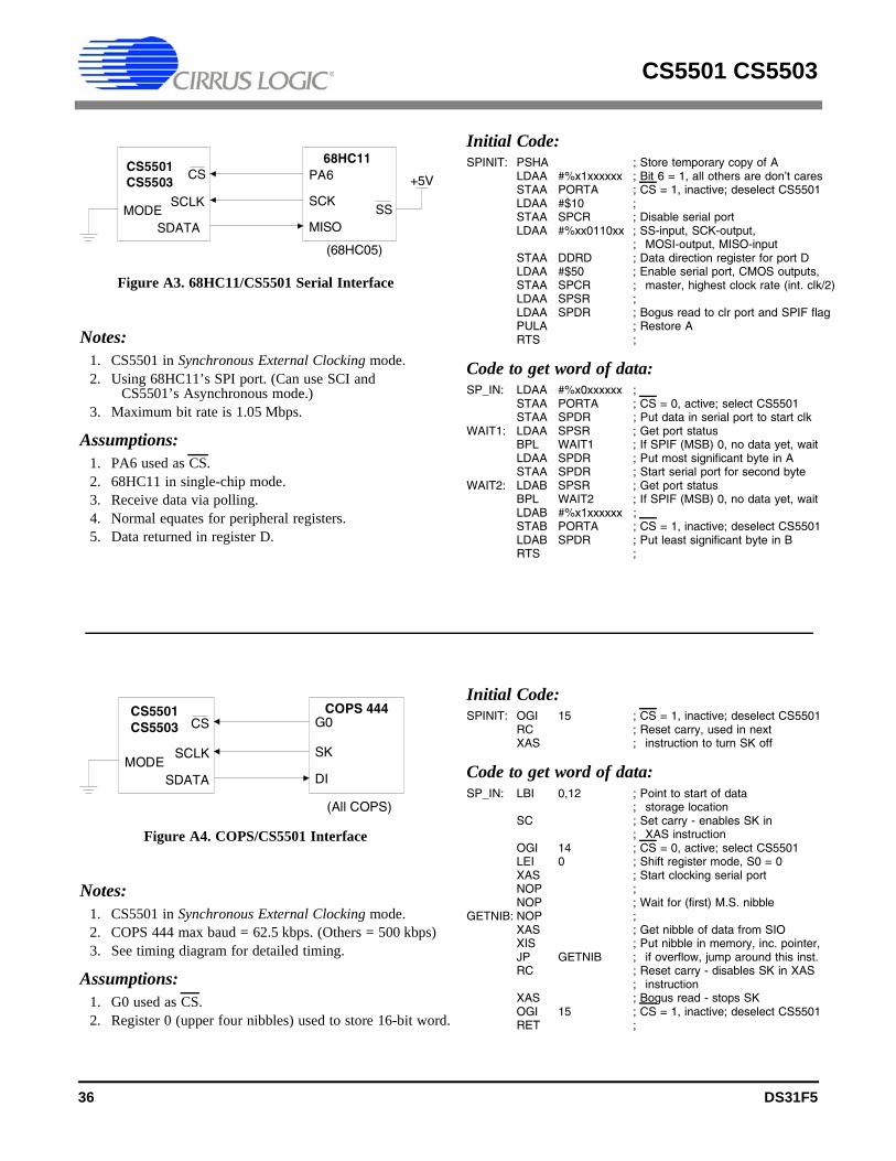
Notes:1. CS5501 in Synchronous External Clocking mode.2. COPS 444 max baud = 62.5 kbps. (Others = 500 kbps)3. See timing diagram for detailed timing.
Assumptions:1. G0 used as CS.2. Register 0 (upper four nibbles) used to store 16-bit word.
Initial Code:SPINIT: OGI 15 ; CS = 1, inactive; deselect CS5501
RC ; Reset carry, used in next XAS ; instruction to turn SK off
Code to get word of data:SP_IN: LBI 0,12 ; Point to start of data
; storage locationSC ; Set carry - enables SK in
; XAS instructionOGI 14 ; CS = 0, active; select CS5501LEI 0 ; Shift register mode, S0 = 0XAS ; Start clocking serial portNOP ;NOP ; Wait for (first) M.S. nibble
GETNIB: NOP ;XAS ; Get nibble of data from SIOXIS ; Put nibble in memory, inc. pointer,JP GETNIB ; if overflow, jump around this inst.RC ; Reset carry - disables SK in XAS
; instructionXAS ; Bogus read - stops SKOGI 15 ; CS = 1, inactive; deselect CS5501RET ;
Figure A4. COPS/CS5501 Interface
CS5501 COPS 444
(All COPS)
DI
G0
SK
SDATA
CS
SCLKMODE
CS5503
Notes:1. CS5501 in Synchronous External Clocking mode.2. Using 68HC11’s SPI port. (Can use SCI and
CS5501’s Asynchronous mode.)3. Maximum bit rate is 1.05 Mbps.
Assumptions:1. PA6 used as CS.2. 68HC11 in single-chip mode.3. Receive data via polling.4. Normal equates for peripheral registers.5. Data returned in register D.
Initial Code:SPINIT: PSHA ; Store temporary copy of A
LDAA #%x1xxxxxx ; Bit 6 = 1, all others are don’t caresSTAA PORTA ; CS = 1, inactive; deselect CS5501LDAA #$10 ; STAA SPCR ; Disable serial portLDAA #%xx0110xx ; SS-input, SCK-output,
; MOSI-output, MISO-inputSTAA DDRD ; Data direction register for port DLDAA #$50 ; Enable serial port, CMOS outputs, STAA SPCR ; master, highest clock rate (int. clk/2)LDAA SPSR ;LDAA SPDR ; Bogus read to clr port and SPIF flagPULA ; Restore ARTS ;
Code to get word of data:SP_IN: LDAA #%x0xxxxxx ;
STAA PORTA ; CS = 0, active; select CS5501STAA SPDR ; Put data in serial port to start clk
WAIT1: LDAA SPSR ; Get port statusBPL WAIT1 ; If SPIF (MSB) 0, no data yet, waitLDAA SPDR ; Put most significant byte in ASTAA SPDR ; Start serial port for second byte
WAIT2: LDAB SPSR ; Get port statusBPL WAIT2 ; If SPIF (MSB) 0, no data yet, waitLDAB #%x1xxxxxx ;STAB PORTA ; CS = 1, inactive; deselect CS5501LDAB SPDR ; Put least significant byte in BRTS ;
Figure A3. 68HC11/CS5501 Serial Interface
CS550168HC11
(68HC05)
MISOMODE SS
+5VPA6
SCK
SDATA
CS
SCLK
CS5503
CS5501/CS5503
36 DS31F4
CS5501 CS5503
36 DS31F5
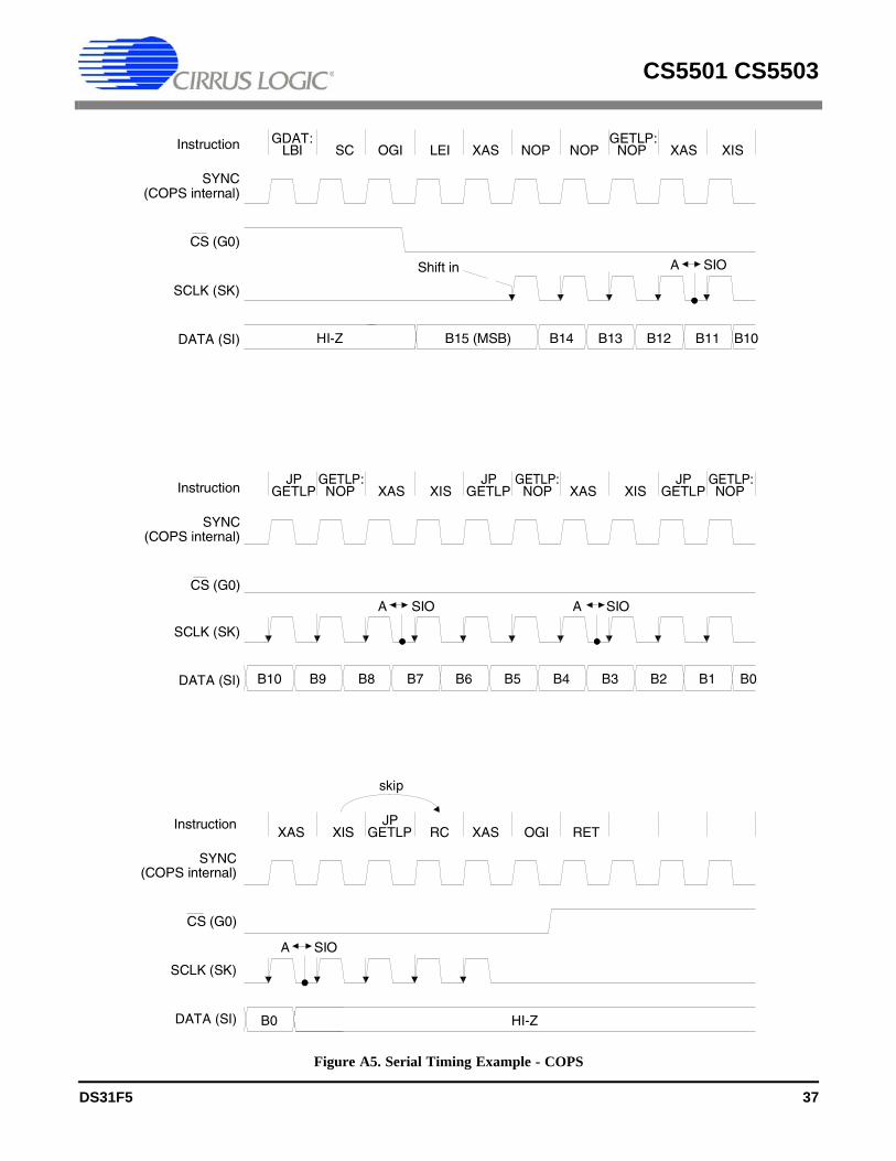
Figure A5. Serial Timing Example - COPS
SC OGI LEI XAS NOP NOP XAS XISGDAT:
LBIGETLP:
NOP
SCLK (SK)
DATA (SI)
CS (G0)
Instruction
SYNC(COPS internal)
Shift in A SIO
SCLK (SK)
DATA (SI)
CS (G0)
Instruction
SYNC(COPS internal)
XAS XIS XAS XISGETLP:NOP
GETLP:NOP
GETLP:NOP
JPGETLP
JPGETLP
JPGETLP
SCLK (SK)
DATA (SI)
CS (G0)
Instruction
SYNC(COPS internal)
XAS XISJP
GETLP RC XAS OGI RET
A SIOA SIO
A SIO
skip
B10B12 B11B13B14B15 (MSB)HI-Z
B0B1B2B3B4B5B6B7B8B9B10
HI-ZB0
CS5501/CS5503
DS31F4 37
CS5501 CS5503
DS31F5 37

Notes:1. CS5501 in Synchronous External Clocking mode.2. Interrupt driven I/O on 8051 (For polling, connect
DRDY to another port pin).
Assumptions:1. INT1 external interrupt used.2. Register bank 1, R6, R7 used to store data word,
R7 MSbyte.3. EA enabled elsewhere.
Initial Code:CS EQU P1.1SCLK EQU P1.2DATA EQU P1.3SPINIT: CLR EX1 ; Disable INT1
SETB IT1 ; Set INT1 for falling edge triggeredSETB DATA ; Set DATA to be input pinSETB CS ; CS = 1; deselect CS5501CLR SCLK ; SCLK lowSETB EX1 ; Enable INT1 interrupt
Code to get word of data:ORG 0003HLJMP GETWD ; Interrupt vector
GETWD: PUSH PSW ; Save temp. copyPUSH A ; Save temp. copyMOV PSW,#08 ; Set register bank 1 activeMOV R6,#8 ; number of bits in a byteCLR CS ; CS = 0; select CS5501
MSBYTE:SETB SCLK ; Toggle SCLK highMOV C,DATA ; Put bit of data into carry bitCLR SCLK ; Toggle SCLK low; next data bitRLC A ; Shift DATA bit into A registerDJNZ R6,MSBYTE ; Dec. R6, if not 0, get another bitMOV R7,A ; Put MSbyte into R7MOV R6,#8 ; Reset R6 to number of bits in byte
LSBYTE: SETB SCLK ; Toggle SCLK highMOV C,DATA ; Put bit of data into carry bitCLR SCLK ; Toggle SCLK low; next data bitRLC A ; Shift DATA bit into A registerDJNZ R6,LSBYTE ; Dec. R6, if not 0, get another bitMOV R6,A ; Put LSbyte into R6SETB CS ; CS = 1; deselect CS5501POP A ; Restore original valuePOP PSW ; Restore original valueRETI
Figure A6. MCS51 (8051) /CS5501 Serial Interface
CS5501
MODE
8051
P1.1
P1.3
P1.2
INT1
CS
SDATA
SCLK
DRDY
Notes:1. CS5501 in Asynchronous (UART-like) mode.2. 8051 in mode 2, with OSC = 12 MHz,
max baud = 375 kbps.
Assumptions:1. P1.2 (port 1, bit 2) used as CS.2. Using serial port mode 2, Baud rate = OSC/32.
(Assumptions cont.)3. Word received put in A (ACC) and B registers,
A = MSbyte.4. No error checking done.5. Equates used for peripheral names.
Initial Code:SPINIT: SETB SMOD ; Set SMOD = 1, baud = OSC/32
SETB P1.2 ; CS = 1, inactiveMOV SCON,#1001000B ; Enable serial port mode 2,
; receiver enabled, transmitter disabledCLR ES ; Disable serial port interrupts (polling)RET ;
Code to get word of data:SP_IN: CLR P1.2 ; CS = 0, active; select CS5501
JNB RI,$ ; Wait for first byteCLR RI ; MOV A,SBUF ; Put most significant byte in AJNB RI,$ ; wait for second byteCLR RI ; MOV B,SBUF ; Put least significant byte in BSETB P1.2 ; CS = 1, inactive; deselect CS5501 RET ;
Figure A7. MCS51 (8051) /CS5501 UART Interface
CS5501
RXDMODE
8051
-5V
OSC32
P1.2
SDATA
SCLK
CS
CS5501/CS5503
38 DS31F4
CS5501 CS5503
38 DS31F5
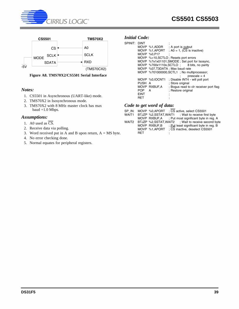
Notes:1. CS5501 in Asynchronous (UART-like) mode.2. TMS70X2 in Isosynchronous mode.3. TMS70X2 with 8 MHz master clock has max
baud =1.0 Mbps.
Assumptions:1. A0 used as CS.2. Receive data via polling.3. Word received put in A and B upon return, A = MS byte.4. No error checking done.5. Normal equates for peripheral registers.
Initial Code:SPINIT: DINT ;
MOVP %1,ADDR ; A port is outputMOVP %1,APORT ; A0 = 1, (CS is inactive)MOVP %0,P17 ; MOVP %>10,SCTLO ; Resets port errorsMOVP %?x1x01101,SMODE ; Set port for Isosync, MOVP %?00x1110x,SCTLO ; 8 bits, no parityMOVP %07,T3DATA ; Max baud rateMOVP %?01000000,SCTL1 ; No multiprocessor;
; prescale = 4MOVP %0,IOCNT1 ; Disable INT4 - will poll portPUSH A ; Store originalMOVP RXBUF,A ; Bogus read to clr receiver port flagPOP A ; Restore originalEINT ; RET ;
Code to get word of data:SP_IN: MOVP %0,APORT ; CS active, select CS5501WAIT1 BTJZP %2,SSTAT,WAIT1 ; Wait to receive first byte
MOVP RXBUF,A ; Put most significant byte in reg. AWAIT2 BTJZP %2,SSTAT,WAIT2 ; Wait to receive second byte
MOVP RXBUF,B ; Put least significant byte in reg. BMOVP %1,APORT ; CS inactive, deselect CS5501RET ;
Figure A8. TMS70X2/CS5501 Serial Interface
CS5501
RXDMODE
TMS70X2
(TMS70CX2)-5V
A0
SCLK
SDATA
CS
SCLK
CS5501/CS5503
DS31F4 39
CS5501 CS5503
DS31F5 39
CS5501 CS5503
Contacting Cirrus Logic SupportFor all product questions and inquiries contact a Cirrus Logic Sales Representative. To find the one nearest to you go to www.cirrus.com
IMPORTANT NOTICECirrus Logic, Inc. and its subsidiaries (“Cirrus”) believe that the information contained in this document is accurate and reliable. However, the information is subject tochange without notice and is provided “AS IS” without warranty of any kind (express or implied). Customers are advised to obtain the latest version of relevant information to verify, before placing orders, that information being relied on is current and complete. All products are sold subject to the terms and conditions of sale suppliedat the time of order acknowledgment, including those pertaining to warranty, indemnification, and limitation of liability. No responsibility is assumed by Cirrus for theuse of this information, including use of this information as the basis for manufacture or sale of any items, or for infringement of patents or other rights of third partiesThis document is the property of Cirrus and by furnishing this information, Cirrus grants no license, express or implied under any patents, mask work rights, copyrightstrademarks, trade secrets or other intellectual property rights. Cirrus owns the copyrights associated with the information contained herein and gives consent for copiesto be made of the information only for use within your organization with respect to Cirrus integrated circuits or other products of Cirrus. This consent does not extendto other copying such as copying for general distribution, advertising or promotional purposes, or for creating any work for resale. CERTAIN APPLICATIONS USING SEMICONDUCTOR PRODUCTS MAY INVOLVE POTENTIAL RISKS OF DEATH, PERSONAL INJURY, OR SEVERE PROPERTY OR ENVIRONMENTAL DAMAGE (“CRITICAL APPLICATIONS”). CIRRUS PRODUCTS ARE NOT DESIGNED, AUTHORIZED OR WARRANTED FOR USE INAIRCRAFT SYSTEMS, MILITARY APPLICATIONS, PRODUCTS SURGICALLY IMPLANTED INTO THE BODY, AUTOMOTIVE SAFETY OR SECURITY DEVICESLIFE SUPPORT PRODUCTS OR OTHER CRITICAL APPLICATIONS. INCLUSION OF CIRRUS PRODUCTS IN SUCH APPLICATIONS IS UNDERSTOOD TO BEFULLY AT THE CUSTOMER'S RISK AND CIRRUS DISCLAIMS AND MAKES NO WARRANTY, EXPRESS, STATUTORY OR IMPLIED, INCLUDING THE IMPLIEDWARRANTIES OF MERCHANTABILITY AND FITNESS FOR PARTICULAR PURPOSE, WITH REGARD TO ANY CIRRUS PRODUCT THAT IS USED IN SUCH AMANNER. IF THE CUSTOMER OR CUSTOMER'S CUSTOMER USES OR PERMITS THE USE OF CIRRUS PRODUCTS IN CRITICAL APPLICATIONS, CUSTOMER AGREES, BY SUCH USE, TO FULLY INDEMNIFY CIRRUS, ITS OFFICERS, DIRECTORS, EMPLOYEES, DISTRIBUTORS AND OTHER AGENTS FROM ANYAND ALL LIABILITY, INCLUDING ATTORNEYS' FEES AND COSTS, THAT MAY RESULT FROM OR ARISE IN CONNECTION WITH THESE USES.Cirrus Logic, Cirrus, and the Cirrus Logic logo designs are trademarks of Cirrus Logic, Inc. All other brand and product names in this document may be trademarks oservice marks of their respective owners.
40 DS31F5
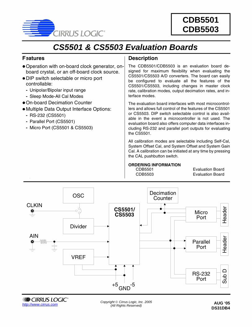
41
Copyright Cirrus Logic, Inc. 1998(All Rights Reserved)
Cirrus Logic, Inc.Crystal Semiconductor Products DivisionP.O. Box 17847, Austin, Texas 78760(512) 445 7222 FAX: (512) 445 7581http://www.crystal.com
CDB5501 CDB5503
CS5501/CS5503 Evaluation BoardFeatureslOperation with on-board clock generator, on-
board crystal, or an off-board clock source.lDIP switch selectable or micro port
controllable:- Unipolar/Bipolar input range- Sleep Mode-All Cal Modes
lOn-board Decimation CounterlMultiple Data Output Interface Options:
- RS-232 (CS5501)- Parallel Port (CS5501)- Micro Port (CS5501 & CS5503)
DescriptionThe CDB5501/CDB5503 is an evaluation board de-signed for maximum flexibility when evaluating theCS5501/CS5503 A/D converters. The board can easilybe configured to evaluate all the features of theCS5501/CS5503, including changes in master clockrate, calibration modes, output decimation rates, and in-terface modes.
The evaluation board interfaces with most microcontrol-lers and allows full control of the features of the CS5501or CS5503. DIP switch selectable control is also avail-able in the event a microcontroller is not used. Theevaluation board also offers computer data interfaces in-cluding RS-232 and parallel port outputs for evaluatingthe CS5501.
All calibration modes are selectable including Self-Cal,System Offset Cal, and System Offset and System GainCal. A calibration can be initiated at any time by pressingthe CAL pushbutton switch.
ORDERING INFORMATIONCDB5501 Evaluation BoardCDB5503 Evaluation Board
I
CLKIN
AIN
Divider
OSC
VREF
DecimationCounter
ParallelPort
Hea
der
MicroPort
Hea
der
RS-232Port S
ub D
GND-5+5
CS5501/CS5503
MAR ‘95DS31DB3
Copyright © Cirrus Logic, Inc. 2005(All Rights Reserved)http://www.cirrus.com
CDB5501 CDB5503
CS5501 & CS5503 Evaluation Boards I
AUG ‘05DS31DB4

INTRODUCTION
The CDB5501/CDB5503 evaluation board pro-vides maximum flexibility for controlling andinterfacing to the CS5501/CS5503 A/D convert-ers. The CS5501 or the CS5503 require a minimalamount of external circuitry. The devices can op-erate with a crystal (or ceramic resonator) and avoltage reference.
The evaluation board includes several clocksource options, a 2.5 volt trimmable reference,and circuitry to support several data interfaceschemes. The board operates from +5 and -5 voltpower supplies.
Evaluation Board Overview
The CDB5501/CDB5503 evaluation board in-cludes extensive support circuitry to aidevaluation of the CS5501/CS5503. The supportcircuitry includes the following sections:
1) A clock generator which has an on-board oscillator and counter divider IC.
2) A 2.5 volt trimmable voltage reference.
3) A Decimation Counter.
4) A parallel output port (for CS5501 only).
5) An RS-232 interface (for CS5501 only).
6) A micro port (for CS5501 or CS5503).
7) DIP switch and CAL pushbutton.
Clock Generator
The CS5501/CS5503 can operate off its on-chiposcillator or an off-chip clock source. The evalu-ation board includes a 4.9152 MHz gate oscillatorand counter-divider chain as the primary clocksource for the CS5501/CS5503. The counter-di-vider outputs offer several jumper-selectablefrequencies as clock inputs to theCS5501/CS5503. The 4.9152 MHz crystal fre-quency was chosen to allow the counter-dividerchain to also provide the common serial data rates
(1200, 2400, 4800, etc.) when the CDB5501evaluation board is configured to provide RS-232data output. If a different operating frequency forthe CS5501/CS5503 is desired, three options ex-ist. First, a BNC input is provided to allow anexternal CMOS (+5V) compatible clock to beused. Second, the crystal (Y1) in the on-boardgate oscillator can be changed. Or, third, the on-chip oscillator of the CS5501/CS5503 can beused with a crystal connected in the Y2 position.
2. 5 Volt Reference
A 2.5 volt (LT1019CN8-2.5) reference is pro-vided on the board. Potentiometer R9 allows theinitial value of the reference to be accuratelytrimmed.
Decimation Counter
The CS5501/CS5503 updates its internal outputregister with a 16-bit word every 1024 clock cy-cles of the master clock. Each time the outputregister is updated the DRDY line goes low. Al-though output data is updated at a high rate itmay be desirable in certain applications to acti-vate the CS to read the data at a much lower rate.A decimation counter is provided on the board forthis purpose. The counter reduces the rate atwhich the CS line of the CS5501 is activated byonly allowing CS to occur at a sub-multiple of theDRDY rate.
Parallel Output Port (for CS5501 only)
The output data from the CS5501/CS5503 is inserial form. Some applications may require thedata to be read in parallel format. Therefore theevaluation board includes two 8-bit shift registerswith three-state outputs. Data from the CS5501 isshifted into the registers and then read out in16 bit parallel fashion. The parallel port comes setup for 16-bit parallel output but can be reconfig-ured to provide two 8-bit reads. The parallel portsupports the CS5501 only, since the CS5503 out-puts 20-bit words.
CDB5501/CDB5503
42 DS31DB3
CDB5501 CDB5503
42 DS31DB4

RS-232 Port (for CS5501 only)
The CS5501 has a data output mode in which itformats the data to be UART compatible; eachserial output byte is preceded by a start bit andterminated with two stop bits. Serial data in thisformat is commonly transferred using the RS-232data interface. Therefore the evaluation board in-cludes an RS-232 driver and output connector.The CS5503 does not provide this output mode.
Micro Port
The CS5501/CS5503 was designed to be compat-ible with many micro-controllers. Therefore theevaluation board provides access to all of the dataoutput pins and the control pins of theCS5501/CS5503 on header connectors.
DIP Switch and CAL Pushbutton
Although all of the control lines to theCS5501/CS5503 are available on header connec-tors at the edge of the board, it is preferable to notrequire software control of all of these pins.Therefore DIP switch control is provided on someof these control lines. The CAL input to theCS5501/CS5503 is made available at a header pinfor remote control, but pushbutton control of CALis also provided.
Jumper Selections
The evaluation board has many jumper selectableoptions. This table describes the jumper selectionsavailable.
P1 Selects between the on-board 4.9152 MHz oscillator (INT) or an external (EXT) clock source as the input to the clock generator/divider chain.
P2 Allows any of the counter/divider output clock rates to be selected as the input clock to the CS5501/CS5503.
P3 Allows selection of baud rate clocks when the CS5501 is in the UART compatible mode. When using the on-board 4.9152 MHz stand-ard baud rates between 1200 and 19,200 are available.
P4 Selects the divide ratio of the Decimation Counter.
P5 Selects one of the three available output data modes of the CS5501 or one of two availableoutput data modes of the CS5503.
P9 Enables the output of the Decimation Counter to control the CS line of the CS5501/CS5503.
P11 Connects the baud clock from the on-board clock divider as the input to the SCLK pin of the CS5501/CS5503.
V+
P2
P3
1 2 3 4 5 6 7 8 9 10 11 12
CL
R
TP4
CLKIN (fig. 2)
BRCLK (fig. 2)
16
8
9 7 6 5 3 2 4 13 12 14 15 1
10
11
TP3
V+
109 8
7
1114
12
13
INTCLK
EXTCLK
45 6
TP2
1
2
3
4.9152 MHz
CLKIN
TP174HC00 P1
47 k
47 k
N = 0 1 2 3 4 5 6 7 8 9 10 11 12Master Clock Baud Clock
TP5
Y1
U1AU1C
RN
1.2
RN
1.3
U1D
5.1 kR2
10 MR1
30 pFC1
30 pFC2
200R3
0.1 µFC3
0.1 µFC574HC4040
U2U1B
Figure 1. Clock Generator
CDB5501/CDB5503
DS31DB3 43
CDB5501 CDB5503
DS31DB4 43
CDB5501 CDB5503
DS31DB4 43
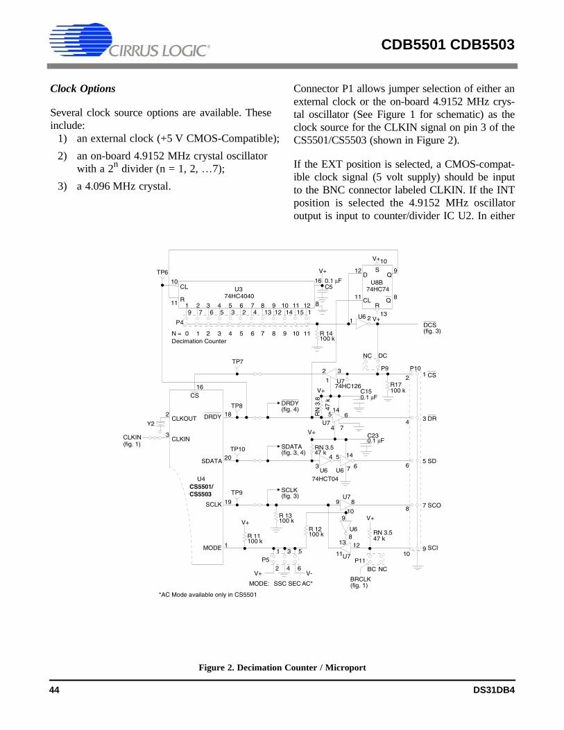
Clock Options
Several clock source options are available. Theseinclude:
1) an external clock (+5 V CMOS-Compatible);
2) an on-board 4.9152 MHz crystal oscillator with a 2n divider (n = 1, 2, …7);
3) a 4.096 MHz crystal.
Connector P1 allows jumper selection of either anexternal clock or the on-board 4.9152 MHz crys-tal oscillator (See Figure 1 for schematic) as theclock source for the CLKIN signal on pin 3 of theCS5501/CS5503 (shown in Figure 2).
If the EXT position is selected, a CMOS-compat-ible clock signal (5 volt supply) should be inputto the BNC connector labeled CLKIN. If the INTposition is selected the 4.9152 MHz oscillatoroutput is input to counter/divider IC U2. In either
Figure 2. Decimation Counter / Microport
CS16
18
20
19
1
TP8
TP9
TP10
SDATA
SCLK
MODE
V+
V+
V+
TP7
P55
6
3
4
1
2V+ V-
MODE: SSC SEC AC*
89
109
8
111213
1
2 3
4
5 6
7
14
5
67
14
3
4
V+
BRCLK
P11BC NC
2
4
6
8
10
P10P9
SD
SCO
SCI
CS
DR
TP6 D
CL
Q
R
S
V+
V+
Q 8
9
10
11
12
13P4
V+
CL
R
10
11
16
8
CLKOUT
CLKINCLKIN(fig. 1)
2
3
DRDY
SDATA
SCLK
DRDY(fig. 4)
(fig. 3, 4)
(fig. 3)
(fig. 1)
NC DC
(fig. 3)DCS
47 k
100 kR 11
100 kR 13
100 kR 12
CS5501/U4
Y2
RN
3.8
0.1 µFC23
47 kRN 3.5
47 kRN 3.5
0.1 µFC15 100 k
R17
R 14100 k
C50.1 µF
74HC4040U3
U8B74HC74
U674HCT04
U7
U7
U6
U7
U7
U6
Decimation CounterN = 0 2 3 4 5 6 7 8 9 10 111
1 2U6
74HC126
9 7 6 5 3 2 4 13 12 14 15 11 2 3 4 5 6 7 8 9 10 11 12
1
3
5
7
9
*AC Mode available only in CS5501
CS5503
CDB5501/CDB5503
44 DS31DB3
CDB5501 CDB5503
44 DS31DB4
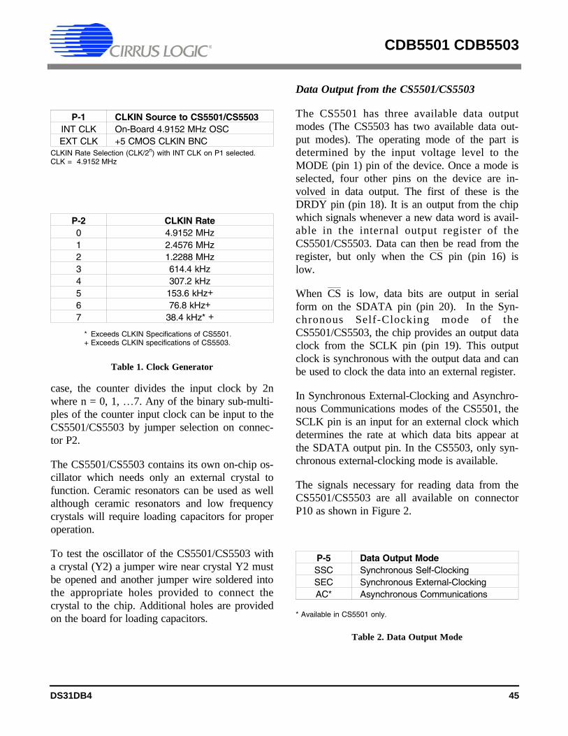
case, the counter divides the input clock by 2nwhere n = 0, 1, …7. Any of the binary sub-multi-ples of the counter input clock can be input to theCS5501/CS5503 by jumper selection on connec-tor P2.
The CS5501/CS5503 contains its own on-chip os-cillator which needs only an external crystal tofunction. Ceramic resonators can be used as wellalthough ceramic resonators and low frequencycrystals will require loading capacitors for properoperation.
To test the oscillator of the CS5501/CS5503 witha crystal (Y2) a jumper wire near crystal Y2 mustbe opened and another jumper wire soldered intothe appropriate holes provided to connect thecrystal to the chip. Additional holes are providedon the board for loading capacitors.
Data Output from the CS5501/CS5503
The CS5501 has three available data outputmodes (The CS5503 has two available data out-put modes). The operating mode of the part isdetermined by the input voltage level to theMODE (pin 1) pin of the device. Once a mode isselected, four other pins on the device are in-volved in data output. The first of these is theDRDY pin (pin 18). It is an output from the chipwhich signals whenever a new data word is avail-able in the internal output register of theCS5501/CS5503. Data can then be read from theregister, but only when the CS pin (pin 16) islow.
When CS is low, data bits are output in serialform on the SDATA pin (pin 20). In the Syn-chronous Self-Clocking mode of theCS5501/CS5503, the chip provides an output dataclock from the SCLK pin (pin 19). This outputclock is synchronous with the output data and canbe used to clock the data into an external register.
In Synchronous External-Clocking and Asynchro-nous Communications modes of the CS5501, theSCLK pin is an input for an external clock whichdetermines the rate at which data bits appear atthe SDATA output pin. In the CS5503, only syn-chronous external-clocking mode is available.
The signals necessary for reading data from theCS5501/CS5503 are all available on connectorP10 as shown in Figure 2.
P-5 Data Output ModeSSC Synchronous Self-ClockingSEC Synchronous External-ClockingAC* Asynchronous Communications
Table 2. Data Output Mode
P-1 CLKIN Source to CS5501/CS5503INT CLK On-Board 4.9152 MHz OSCEXT CLK +5 CMOS CLKIN BNC
P-2 CLKIN Rate0 4.9152 MHz1 2.4576 MHz2 1.2288 MHz3 614.4 kHz4 307.2 kHz5 153.6 kHz+
6 76.8 kHz+
7 38.4 kHz* +
Table 1. Clock Generator
CLKIN Rate Selection (CLK/2n) with INT CLK on P1 selected.CLK = 4.9152 MHz
* Exceeds CLKIN Specifications of CS5501.+ Exceeds CLKIN specifications of CS5503.
* Available in CS5501 only.
CDB5501/CDB5503
DS31DB3 45
CDB5501 CDB5503
DS31DB4 45

CS5501/CS5503 Data Output Mode Selection
Connector P5 (see Figure 2) allows jumper selec-tion of any one of the three data output modes.These modes are:
1) SSC (Synchronous Self-Clocking);2) SEC (Synchronous External Clocking);3) AC (Asynchronous Communication).
(AC mode is available only in the CS5501)
SSC (Synchronous Self-Clocking) Mode
The SSC mode is designed for interface to thosemicrocontrollers which allow external clocking oftheir serial inputs. The SSC mode also allowseasy connection to serial-to-parallel conversioncircuitry.
In the SSC mode serial data and serial clock areoutput from the CS5501/CS5503 whenever theCS line is activated. As illustrated in Figure 2, allof the signals are available at connector P10. Ifthe CS signal is to be controlled remotely thejumper on P9 should be placed in the NC (NoConnection) position. This removes the Decima-tion Counter output from controlling the CS line.
Data Output Interface: Parallel Port (forCS5501 evaluation only).
Whenever the CS5501 is operated in the SSCmode the 16-bit output data is clocked into two8-bit shift registers. The registers have three-stateparallel outputs which are available at P7 (seeFigure 3). A flip-flop (U8A) is used to signal theremote reading device whenever the registers areupdated. The PDR (Parallel Data Ready) signalfrom the flip-flop is available on P7. The Q-baroutput from the flip-flop locks out any further up-dates to the registers until their data is read and aDACK (Data ACKnowledge) signal is receivedfrom the remote device.
Activation of the CS line determines the rate atwhich the CS5501 will attempt to update the out-put shift registers. Data will be shifted into the
registers only if a DACK signal has occurredsince the last update.
The CS line can be controlled remotely at P10 orby the output of the Decimation Counter. If CS iscontrolled remotely, the Decimation dividejumper on P4 should be placed in the "0" posi-tion. This insures that the DCS signal will occurat the same rate CS is activated. The positive go-ing edge of DCS toggles the U8A flip-flop whichsignals an update to the parallel port.
The parallel registers are set up to be read in 16-bit parallel fashion but can be configured to beread separately as two 8-bit bytes on an 8-bit bus.To configure the board for byte-wide reads, thebyte-wide jumpers must be soldered in place. Inaddition, for proper "one byte at a time" addressselection, a connection on the circuit board needsto be opened and a jumper wire soldered in theproper place to determine which register is to beread when A0 is a "1" and vice versa. See Figure3 for schematic details. The evaluation boardcomponent layout diagram, Figure 7, indicates thelocation of the byte-wide jumpers and A0 addressselection jumpers.
After data is read from the registers a DACK(Data Acknowledge) signal is required from theoff-board controller to reset flip-flop U8A. Thisenables the registers to accept data input onceagain.
The DRB and CSB signals on connector P10should be used to monitor and control theCS5501 output to the serial to parallel conversionregisters. Be aware that an arbitrarily timedDACK signal may cause the output data regis-ters to be enabled in the middle of an outputword if the CS signal to the CS5501 is notproperly sequenced. This will result in incorrectdata in the output registers.
If the Decimation Counter is used to control theoutput of the CS5501 (Jumper on P9 in the DCposition), the CSB signal on P10 can be moni-
CDB5501/CDB5503
46 DS31DB3
CDB5501 CDB5503
46 DS31DB4
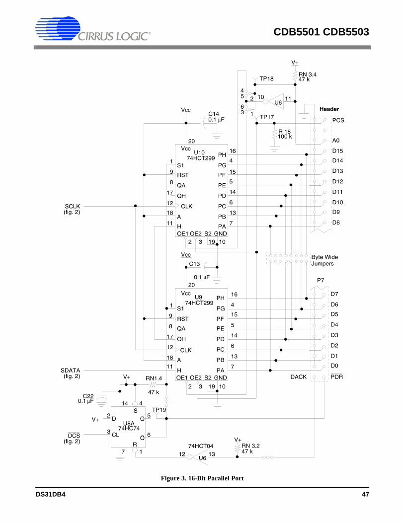
Header
D8
D9
D10
D11
D12
D13
D14
D15
A0
PCS
1S1
CLK
H
A
Vcc
QH
QA8
9
11
12
17
18
RST
PA
PB
PC
PD
PE
PF
PG
PH
GNDS2OE2OE1
1 S1
CLK
H
A
Vcc
QH
QA8
9
11
12
17
18
RST
PA
PB
PC
PD
PE
PF
PG
PH
GNDS2OE2OE1
Vcc
2 3 19 10
20
C13
2 3 19 10
20
4
5
6
7
13
14
15
16
DACK
SCLK
V+
D
CL
V+
SDATA
1
2 10 11
TP17
V+ RN1.4
TP18
Byte WideJumpers
D0
D1
D2
D3
D4
D5
D6
D7
TP19
1
2
3
4
7
S
RQ 6
14
V+
12 13
Q 5
(fig. 2)
(fig. 2)
(fig. 2)DCS
P7
PDR
4
5
6
7
13
14
15
16U974HCT299
U1074HCT299
0.1 µF
C140.1 µF
R 18100 k
RN 3.447 k
47 k
RN 3.247 k
C220.1 µF
U8A74HC74
U6
U6
74HCT04
3
45
6Vcc
Figure 3. 16-Bit Parallel Port
CDB5501/CDB5503
DS31DB3 47
CDB5501 CDB5503
DS31DB4 47
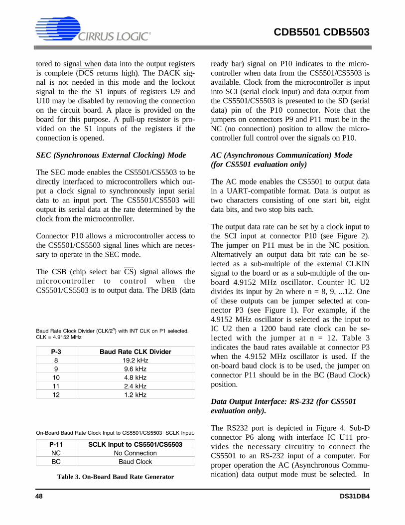
tored to signal when data into the output registersis complete (DCS returns high). The DACK sig-nal is not needed in this mode and the lockoutsignal to the the S1 inputs of registers U9 andU10 may be disabled by removing the connectionon the circuit board. A place is provided on theboard for this purpose. A pull-up resistor is pro-vided on the S1 inputs of the registers if theconnection is opened.
SEC (Synchronous External Clocking) Mode
The SEC mode enables the CS5501/CS5503 to bedirectly interfaced to microcontrollers which out-put a clock signal to synchronously input serialdata to an input port. The CS5501/CS5503 willoutput its serial data at the rate determined by theclock from the microcontroller.
Connector P10 allows a microcontroller access tothe CS5501/CS5503 signal lines which are neces-sary to operate in the SEC mode.
The CSB (chip select bar CS) signal allows themicrocontroller to control when theCS5501/CS5503 is to output data. The DRB (data
ready bar) signal on P10 indicates to the micro-controller when data from the CS5501/CS5503 isavailable. Clock from the microcontroller is inputinto SCI (serial clock input) and data output fromthe CS5501/CS5503 is presented to the SD (serialdata) pin of the P10 connector. Note that thejumpers on connectors P9 and P11 must be in theNC (no connection) position to allow the micro-controller full control over the signals on P10.
AC (Asynchronous Communication) Mode(for CS5501 evaluation only)
The AC mode enables the CS5501 to output datain a UART-compatible format. Data is output astwo characters consisting of one start bit, eightdata bits, and two stop bits each.
The output data rate can be set by a clock input tothe SCI input at connector P10 (see Figure 2).The jumper on P11 must be in the NC position.Alternatively an output data bit rate can be se-lected as a sub-multiple of the external CLKINsignal to the board or as a sub-multiple of the on-board 4.9152 MHz oscillator. Counter IC U2divides its input by 2n where n = 8, 9, ...12. Oneof these outputs can be jumper selected at con-nector P3 (see Figure 1). For example, if the4.9152 MHz oscillator is selected as the input toIC U2 then a 1200 baud rate clock can be se-lected with the jumper at n = 12. Table 3indicates the baud rates available at connector P3when the 4.9152 MHz oscillator is used. If theon-board baud clock is to be used, the jumper onconnector P11 should be in the BC (Baud Clock)position.
Data Output Interface: RS-232 (for CS5501evaluation only).
The RS232 port is depicted in Figure 4. Sub-Dconnector P6 along with interface IC U11 pro-vides the necessary circuitry to connect theCS5501 to an RS-232 input of a computer. Forproper operation the AC (Asynchronous Commu-nication) data output mode must be selected. In
P-3 Baud Rate CLK Divider8 19.2 kHz9 9.6 kHz10 4.8 kHz11 2.4 kHz12 1.2 kHz
Table 3. On-Board Baud Rate Generator
Baud Rate Clock Divider (CLK/2n) with INT CLK on P1 selected.CLK = 4.9152 MHz
P-11 SCLK Input to CS5501/CS5503NC No ConnectionBC Baud Clock
On-Board Baud Rate Clock Input to CS5501/CS5503 SCLK Input.
CDB5501/CDB5503
48 DS31DB3
CDB5501 CDB5503
48 DS31DB4
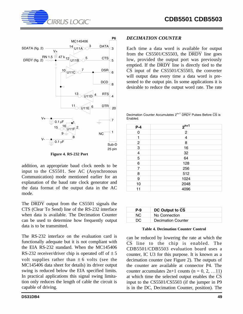
addition, an appropriate baud clock needs to beinput to the CS5501. See AC (AsynchronousCommunication) mode mentioned earlier for anexplanation of the baud rate clock generator andthe data format of the output data in the ACmode.
The DRDY output from the CS5501 signals theCTS (Clear To Send) line of the RS-232 interfacewhen data is available. The Decimation Countercan be used to determine how frequently outputdata is to be transmitted.
The RS-232 interface on the evaluation card isfunctionally adequate but it is not compliant withthe EIA RS-232 standard. When the MC145406RS-232 receiver/driver chip is operated off of ± 5volt supplies rather than ± 6 volts (see theMC145406 data sheet for details) its driver outputswing is reduced below the EIA specified limits.In practical applications this signal swing limita-tion only reduces the length of cable the circuit iscapable of driving.
DECIMATION COUNTER
Each time a data word is available for outputfrom the CS5501/CS5503, the DRDY line goeslow, provided the output port was previouslyemptied. If the DRDY line is directly tied to theCS input of the CS5501/CS5503, the converterwill output data every time a data word is pre-sented to the output pin. In some applications it isdesirable to reduce the output word rate. The rate
can be reduced by lowering the rate at which theCS line to the chip is enabled. TheCDB5501/CDB5503 evaluation board uses acounter, IC U3 for this purpose. It is known as adecimation counter (see Figure 2). The outputs ofthe counter are available at connector P4. Thecounter accumulates 2n+1 counts (n = 0, 2, …11)at which time the selected output enables the CSinput to the CS5501/CS5503 (if the jumper in P9is in the DC, Decimation Counter, position). The
P-4 2n+1
0 21 42 83 164 325 646 1287 2568 5129 102410 204811 4096
P-9 DC Output to CSNC No ConnectionDC Decimation Counter
Table 4. Decimation Counter Control
Decimation Counter Accumulates 2n+1 DRDY Pulses Before CS isEnabled.
DATA
CTS
DSR
DCD
RTS
DTR
P6
3
5
7
4
6
2
14
12
10
13
11
15
3
5
6
8
4
20
7
1U11F
U11A
U11B
U11C
U11D
U11E
NC
V+
V+
V-
1
89
16
SDATA (fig. 2)
DRDY (fig. 2)
Sub-D25 pin
RN 1.5 47 k
MC145406
0.1 µF
0.1 µF
Figure 4. RS-232 Port
CDB5501/CDB5503
DS31DB3 49
CDB5501 CDB5503
DS31DB4 49

"D" input to flip-flop U8B is enabled to a "1" atthe same time CS goes low. When DRDY returnshigh flip-flop U8B is toggled and resets thecounter back to zero which terminates the CS en-able. The counter then accumulates counts untilthe selected output activates CS low once again.
DIP Switch Selections/Calibration Initiation
Several control pins of the CS5501/CS5503 canbe level activated by DIP switch selection, or bymicrocontroller at P8, as shown in Figure 5. DIPswitch SW1 selections are depicted in Tables 5and 6. The CAL pushbutton is used to initiate acalibration cycle in accordance with DIP switchpositions 1 and 2. The CAL pushbutton should be
activated any time power is first applied to theboard or any time the conversion mode (BP/UP)is changed on the DIP switch. Remote control ofthe CAL signal is available on connector P8.Connector P8 also allows access to the DIPswitch functions by a microcomputer/microcon-troller. The DIP switches should be placed in theoff position if off-board control of the signals onconnector P8 is implemented.
Voltage Reference
The evaluation board includes a 2.5 volt refer-ence. Potentiometer R9 can be used to trim thereference output to a precise value.
Analog Input Range: Unipolar Mode
The value of the reference voltage sets the analoginput signal range. In unipolar mode the analoginput range extends from AGND to VREF. If theanalog input goes above VREF the converter willoutput all "1’s". If the input goes below AGND,the CS5501/CS5503 will output all "0’s".
Analog Input Range: Bipolar Mode
The analog signal input range in the bipolar modeis set by the reference to be from +VREF to -VREF. If the input signal goes above +VREF, theCS5501/CS5503 will output all "1’s". Input sig-nals below -VREF cause the output data to be all"0’s".
Table 5. DIP Switch Selections Table 6. Calibration Mode Table
01
10
FS CalZS CalSC2SC1CAL Cal Type
VREFAGND00 Self-Cal
-AIN11AIN-
VREFAINSystem Offset
System Offset& System Gain
Sequence
One Step
1st Step2nd Step
One Step
Switch
SW1-1
SW1-2SW1-3
SW1-4
ONSC2 = 0
SC1 = 0
UNIPOLAR
SLEEP
OFF
BIPOLAR
AWAKE
SC2 = 1
SC1 = 1
Figure 5. DIP Switch / Header Control Pin Selection
P8
SW2
SC2 SC1
V+
1 2 3 4
17 4 12 11
SW1
CAL
SC2 SLPB/U CAL
V+
CAL
13
SLEEPBP/UP
CS5501/U4
R 1
5
10
k
RN
2.3
RN
2.4
RN
2.5
RN
2.6
47 k
47 k
47 k
47 k
CS5503
WARNING: Some evaluation boards were produced with the SC1 and SC2 labels reversed on the silkscreen
SC1
CDB5501/CDB5503
50 DS31DB3
CDB5501 CDB5503
50 DS31DB4

Analog Input: Overrange Precautions
In normal operation the value of the referencevoltage determines the range of the analog inputsignal. Under abnormal conditions the analog sig-nal can extend to be equal to the VA+ and VA-supply voltages. In the event the signal exceedsthese supply voltages the input current should be
limited to ± 10 mA as the analog input of the chipis internally diode clamped to both supplies. Ex-cess current into the pin can damage the device.On the evaluation board, resistor R16 (see Figure6) does provide some current limiting in the eventof an overrange signal which exceeds the supplyvoltage.
CS5501/
U4
VA+
VD+
VREF
AGND
AIN
GND
VIN2
4
5
6
TP14
TP11
TP13
+5V
-5V
GND
V+R4
TP15
VA-
VD-
TP12
V-R5
C9C8
TP16
AIN
CW
DGND
14
15
5
10
8
9
7
6
R610
C70.1 µF
C60.1 µF
R102.4
C16
0.1 µF
C19
10 µF
0.1 µF 0.1 µF
R710
R16200
C210.0047 µF
X7R
U5LT1019-2.5 R8
1 MR950 k
C18
10 µF
C10
0.1 µF
C2010 µF
10
10C1710 µF
D16.8
D26.8
VOUT
TRIM
CS5503
Figure 6. Voltage Reference / Analog Input
CDB5501/CDB5503
DS31DB3 51
CDB5501 CDB5503
DS31DB4 51

Oscilloscope Monitoring of SDATA
The output data from either the CS5501 or theCS5503 can be observed on a dual trace oscillo-scope with the following hook-up. Set theevaluation board to operate in the SSC mode.Connect scope probes to TP9 (SCLK) and TP10(SDATA). Use a third probe connected to TP8(DRDY) to provide the external trigger input tothe scope (use falling edge of DRDY to trigger).With proper horizontal sweep, the SDATA outputbits from the A/D converter can be observed.Note that if the input voltage to the CS5501 isadjusted to a mid-code value, the converter willremain stable on the same output code. This illus-trates the low noise level of the CS5501. TheCS5503 will exhibit a few LSB’s of noise in itsobserved output in agreement with its noise speci-fications.
Evaluation Board Component Layout andDesign Considerations
Figure 7 is a reproduction of the silkscreen com-ponent placement of the PC board.
The evaluation board includes design features toinsure proper performance from the A/D con-verter chip. Separate analog and digital groundplanes have been used on the board to insuregood noise immunity to digital system noise.
Decoupling networks (R6, C7, and R7, C9 in Fig-ure 6) have been used to eliminate the possibilityof noise on the power supplies on the digital sec-tion from affecting the analog part of the A/Dconverter chip.
The RC network (R10, C16 and C19) on theoutput of the LT1019-2.5 reference may not beneeded in all applications. It has been included toinsure the best noise performance from the refer-ence .
CDB5501/CDB5503
52 DS31DB3
CDB5501 CDB5503
52 DS31DB4

Figure 7. CDB5501/CDB5503 Component Layout
CDB5501/CDB5503
DS31DB3 53
CDB5501 CDB5503
DS31DB4 53

CDB5501 CDB5503
Contacting Cirrus Logic SupportFor all product questions and inquiries contact a Cirrus Logic Sales Representative. To find the one nearest to you go to www.cirrus.com
IMPORTANT NOTICECirrus Logic, Inc. and its subsidiaries (“Cirrus”) believe that the information contained in this document is accurate and reliable. However, the information is subject tochange without notice and is provided “AS IS” without warranty of any kind (express or implied). Customers are advised to obtain the latest version of relevant information to verify, before placing orders, that information being relied on is current and complete. All products are sold subject to the terms and conditions of sale suppliedat the time of order acknowledgment, including those pertaining to warranty, indemnification, and limitation of liability. No responsibility is assumed by Cirrus for theuse of this information, including use of this information as the basis for manufacture or sale of any items, or for infringement of patents or other rights of third partiesThis document is the property of Cirrus and by furnishing this information, Cirrus grants no license, express or implied under any patents, mask work rights, copyrightstrademarks, trade secrets or other intellectual property rights. Cirrus owns the copyrights associated with the information contained herein and gives consent for copiesto be made of the information only for use within your organization with respect to Cirrus integrated circuits or other products of Cirrus. This consent does not extendto other copying such as copying for general distribution, advertising or promotional purposes, or for creating any work for resale. CERTAIN APPLICATIONS USING SEMICONDUCTOR PRODUCTS MAY INVOLVE POTENTIAL RISKS OF DEATH, PERSONAL INJURY, OR SEVERE PROPERTY OR ENVIRONMENTAL DAMAGE (“CRITICAL APPLICATIONS”). CIRRUS PRODUCTS ARE NOT DESIGNED, AUTHORIZED OR WARRANTED FOR USE INAIRCRAFT SYSTEMS, MILITARY APPLICATIONS, PRODUCTS SURGICALLY IMPLANTED INTO THE BODY, AUTOMOTIVE SAFETY OR SECURITY DEVICESLIFE SUPPORT PRODUCTS OR OTHER CRITICAL APPLICATIONS. INCLUSION OF CIRRUS PRODUCTS IN SUCH APPLICATIONS IS UNDERSTOOD TO BEFULLY AT THE CUSTOMER'S RISK AND CIRRUS DISCLAIMS AND MAKES NO WARRANTY, EXPRESS, STATUTORY OR IMPLIED, INCLUDING THE IMPLIEDWARRANTIES OF MERCHANTABILITY AND FITNESS FOR PARTICULAR PURPOSE, WITH REGARD TO ANY CIRRUS PRODUCT THAT IS USED IN SUCH AMANNER. IF THE CUSTOMER OR CUSTOMER'S CUSTOMER USES OR PERMITS THE USE OF CIRRUS PRODUCTS IN CRITICAL APPLICATIONS, CUSTOMER AGREES, BY SUCH USE, TO FULLY INDEMNIFY CIRRUS, ITS OFFICERS, DIRECTORS, EMPLOYEES, DISTRIBUTORS AND OTHER AGENTS FROM ANYAND ALL LIABILITY, INCLUDING ATTORNEYS' FEES AND COSTS, THAT MAY RESULT FROM OR ARISE IN CONNECTION WITH THESE USES.Cirrus Logic, Cirrus, and the Cirrus Logic logo designs are trademarks of Cirrus Logic, Inc. All other brand and product names in this document may be trademarks o
54 DS31DB4
service marks of their respective owners.