
3823 Group - Octopart
76
DESCRIPTION The 3823 group is the 8-bit microcomputer based on the 740 fam- ily core technology. The 3823 group has the LCD drive control circuit, an 8-channel A/ D converter, a serial interface, a watchdog timer, a ROM correc- tion function, and as additional functions. The various microcomputers in the 3823 group include variations of internal memory size and packaging. For details, refer to the section on part numbering. FEATURES ●Basic machine-language instructions ...................................... 71 ●The minimum instruction execution time ........................... 0.4 μs (at f(XIN) = 10 MHz, High-speed mode) ●Memory size ROM ............................................................... 16 K to 60 K bytes RAM ................................................................. 640 to 2560 bytes ●ROM correction function .............................. 32 bytes ✕ 2 blocks ●Watchdog timer .............................................................. 8-bit ✕ 1 ●Programmable input/output ports ............................................ 49 ●Input ports .................................................................................. 5 ●Software pull-up/pull-down resistors (Ports P0-P7 except port P40) ●Interrupts ................................................. 17 sources, 16 vectors (includes key input interrupt) ●Key Input Interrupt (Key-on Wake-Up) ...................................... 8 ●Timers ........................................................... 8-bit ✕ 3, 16-bit ✕ 2 ●Serial interface ............ 8-bit ✕ 1 (UART or Clock-synchronized) ●A/D converter ............ 10-bit ✕ 8 channels or 8-bit ✕ 8 channels ●LCD drive control circuit Bias ................................................................................... 1/2, 1/3 Duty ........................................................................... 1/2, 1/3, 1/4 Common output .......................................................................... 4 Segment output ........................................................................ 32 ●Main clock generating circuits .............. Built-in feedback resistor (connect to external ceramic resonator or quartz-crystal oscillator) ●Sub-clock generating circuits (connect to external quartz-crystal oscillator or on-chip oscillator) ●Power source voltage In frequency/2 mode (f(XIN) ≤ 10 MHz) ................... 4.5 to 5.5 V In frequency/2 mode (f(XIN) ≤ 8 MHz) ..................... 4.0 to 5.5 V In frequency/4 mode (f(XIN) ≤ 10 MHz) ................... 2.5 to 5.5 V In frequency/4 mode (f(XIN) ≤ 8 MHz) ..................... 2.0 to 5.5 V In frequency/4 mode (f(XIN) ≤ 5 MHz) ..................... 1.8 to 5.5 V In frequency/8 mode (f(XIN) ≤ 10 MHz) ................... 2.5 to 5.5 V In frequency/8 mode (f(XIN) ≤ 8 MHz) ..................... 2.0 to 5.5 V In frequency/8 mode (f(XIN) ≤ 5 MHz) ..................... 1.8 to 5.5 V In low-speed mode .................................................... 1.8 to 5.5 V ●Power dissipation In frequency/2 mode ............................................... 18 mW (std.) (at f(XIN) = 8 MHz, Vcc = 5 V, Ta = 25 °C) In low-speed mode at XCIN ................................................ 18 μW (std.) (at f(XIN) stopped, f(XCIN) = 32 kHz, Vcc = 2.5 V, Ta = 25 °C) In low-speed mode at on-chip oscillator .................. 35 μW (std.) (at f(XIN) stopped, f(XCIN) = stopped, Vcc = 2.5 V, Ta = 25 °C) ●Operating temperature range .................................. – 20 to 85 °C APPLICATIONS Camera, audio equipment, household appliances, consumer elec- tronics, etc. 3823 Group SINGLE-CHIP 8-BIT CMOS MICROCOMPUTER REJ03B0146-0202 Rev.2.02 Jun.19.2007 Rev.2.02 Jun 19, 2007 page 1 of 73 REJ03B0146-0202
-
Upload
khangminh22 -
Category
Documents
-
view
3 -
download
0
Transcript of 3823 Group - Octopart
DESCRIPTIONThe 3823 group is the 8-bit microcomputer based on the 740 fam-ily core technology.The 3823 group has the LCD drive control circuit, an 8-channel A/D converter, a serial interface, a watchdog timer, a ROM correc-tion function, and as additional functions.The various microcomputers in the 3823 group include variationsof internal memory size and packaging. For details, refer to thesection on part numbering.
FEATURES Basic machine-language instructions ...................................... 71 The minimum instruction execution time ........................... 0.4 µs
(at f(XIN) = 10 MHz, High-speed mode) Memory size
ROM ............................................................... 16 K to 60 K bytesRAM ................................................................. 640 to 2560 bytes
ROM correction function .............................. 32 bytes 2 blocks Watchdog timer .............................................................. 8-bit 1 Programmable input/output ports ............................................ 49 Input ports .................................................................................. 5 Software pull-up/pull-down resistors (Ports P0-P7 except port P40) Interrupts ................................................. 17 sources, 16 vectors
(includes key input interrupt) Key Input Interrupt (Key-on Wake-Up) ...................................... 8 Timers ........................................................... 8-bit 3, 16-bit 2 Serial interface ............ 8-bit 1 (UART or Clock-synchronized) A/D converter ............ 10-bit 8 channels or 8-bit 8 channels
LCD drive control circuitBias ................................................................................... 1/2, 1/3Duty ........................................................................... 1/2, 1/3, 1/4Common output .......................................................................... 4Segment output ........................................................................ 32
Main clock generating circuits .............. Built-in feedback resistor(connect to external ceramic resonator or quartz-crystal oscillator)
Sub-clock generating circuits(connect to external quartz-crystal oscillator or on-chip oscillator)
Power source voltageIn frequency/2 mode (f(XIN) ≤ 10 MHz) ................... 4.5 to 5.5 VIn frequency/2 mode (f(XIN) ≤ 8 MHz) ..................... 4.0 to 5.5 VIn frequency/4 mode (f(XIN) ≤ 10 MHz) ................... 2.5 to 5.5 VIn frequency/4 mode (f(XIN) ≤ 8 MHz) ..................... 2.0 to 5.5 VIn frequency/4 mode (f(XIN) ≤ 5 MHz) ..................... 1.8 to 5.5 VIn frequency/8 mode (f(XIN) ≤ 10 MHz) ................... 2.5 to 5.5 VIn frequency/8 mode (f(XIN) ≤ 8 MHz) ..................... 2.0 to 5.5 VIn frequency/8 mode (f(XIN) ≤ 5 MHz) ..................... 1.8 to 5.5 VIn low-speed mode .................................................... 1.8 to 5.5 V
Power dissipationIn frequency/2 mode ............................................... 18 mW (std.)(at f(XIN) = 8 MHz, Vcc = 5 V, Ta = 25 °C)In low-speed mode at XCIN ................................................ 18 µW (std.)(at f(XIN) stopped, f(XCIN) = 32 kHz, Vcc = 2.5 V, Ta = 25 °C)In low-speed mode at on-chip oscillator .................. 35 µW (std.)
(at f(XIN) stopped, f(XCIN) = stopped, Vcc = 2.5 V, Ta = 25 °C) Operating temperature range .................................. – 20 to 85 °C
APPLICATIONSCamera, audio equipment, household appliances, consumer elec-tronics, etc.
3823 GroupSINGLE-CHIP 8-BIT CMOS MICROCOMPUTER
REJ03B0146-0202Rev.2.02
Jun.19.2007
Rev.2.02 Jun 19, 2007 page 1 of 73REJ03B0146-0202
Rev.2.02 Jun 19, 2007 page 2 of 73REJ03B0146-0202
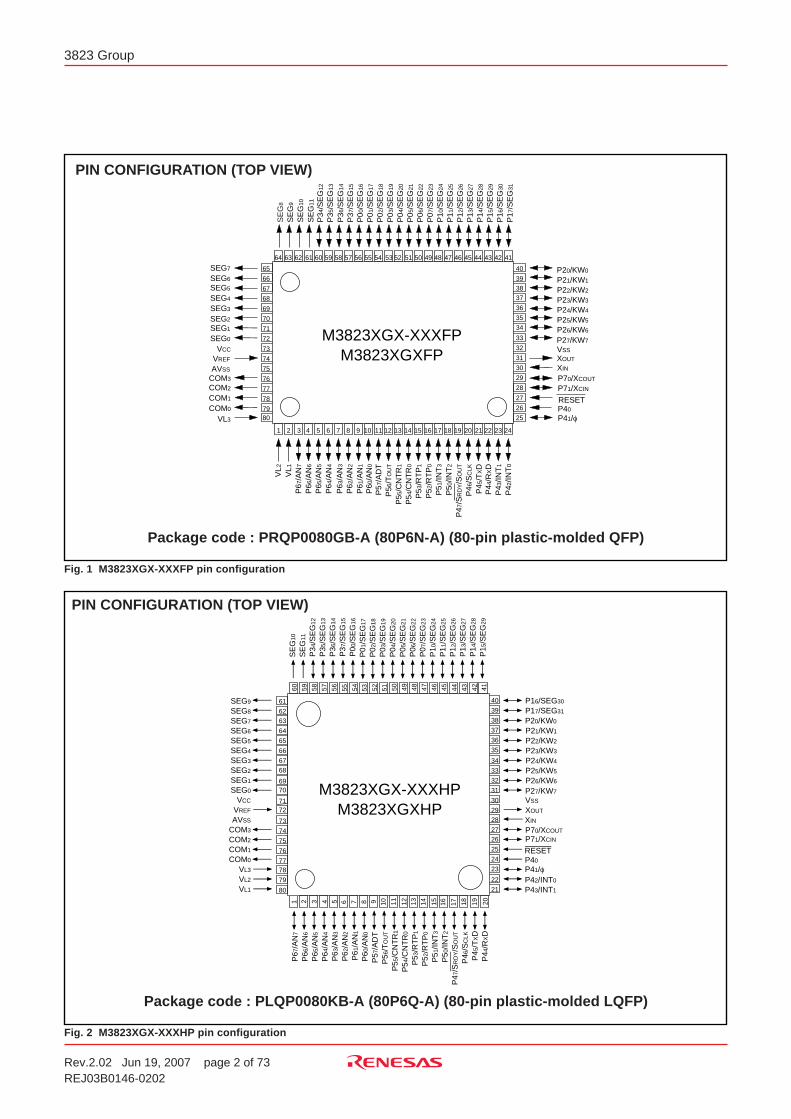
3823 Group
Package code : PLQP0080KB-A (80P6Q-A) (80-pin plastic-molded LQFP)
PIN CONFIGURATION (TOP VIEW)
Fig. 2 M3823XGX-XXXHP pin configuration
1 2 3 4 7 8 9 10 11 12 13 14 15 16 17 18 19 205 6
21
22
23
24
25
2627
2829
30
31
32
33
34
35
36
37
38
39
40
4142434445464748495051525354555657585960
61
6263
64
65
66
6768
6970
7172
73
74
75
76
7778
79
80
P14
/SE
G28
P15
/SE
G29
P16/SEG30
P17/SEG31
P42/INT0
VCC
XIN
XOUT
VSS
RESET
P70/XCOUT
P71/XCIN
P41/φP40
P43/INT1
SE
G10
P35
/SE
G13
P36
/SE
G14
P37
/SE
G15
P00
/SE
G16
P03
/SE
G19
P04
/SE
G20
P05
/SE
G21
P06
/SE
G22
P07
/SE
G23
P11
/SE
G25
P12
/SE
G26
P10
/SE
G24
P01
/SE
G17
P02
/SE
G18
P13
/SE
G27
COM3
P60
/AN
0
P57
/AD
TP
56/T
OU
T
P54
/CN
TR
0
P53
/RT
P1
P52
/RT
P0
P51
/INT
3
P55
/CN
TR
1
P46
/SC
LK
P45
/TXD
P50
/INT
2
P47
/SR
DY/S
OU
T
P44
/RXD
SEG1
SEG2
SEG3
SEG4
SEG6
SEG5
SEG7
SEG0
SEG8
SEG9
COM2
COM1
COM0
VL3
VL2
VL1
VREF
AVSS
P61
/AN
1
P62
/AN
2
P63
/AN
3
P64
/AN
4
P65
/AN
5
P66
/AN
6
P67
/AN
7S
EG
11
P34
/SE
G12
M3823XGX-XXXHPM3823XGXHP
P27/KW7
P26/KW6
P25/KW5
P24/KW4
P23/KW3
P22/KW2
P21/KW1
P20/KW0
Fig. 1 M3823XGX-XXXFP pin configuration
PIN CONFIGURATION (TOP VIEW)
Package code : PRQP0080GB-A (80P6N-A) (80-pin plastic-molded QFP)
S E
G
8
S E
G
9
P 34
/
S
E
G1
2
P 35
/
S
E
G1
3
P 00
/
S
E
G1
6
P 03
/
S
E
G1
9
P 04
/
S
E
G2
0
P 05
/
S
E
G2
1
P 06
/
S
E
G2
2
P 07
/
S
E
G2
3
P 11
/
S
E
G2
5
P 12
/
S
E
G2
6
P 13
/
S
E
G2
7
P 14
/
S
E
G2
8
P 15
/
S
E
G2
9
P 16
/
S
E
G3
0
P 17
/
S
E
G3
1
V L1
P 67
/
A
N7
M
3
8
2
3
X
G
X
-
X
X
X
F
PM
3
8
2
3
X
G
X
F
PP
57/
A
D
T
P 50
/
I
N
T2
P 46
/
SC
L
K
P 45
/
TXD
P 43
/
I
N
T1
P 42
/
I
N
T0
A
VS
S
VR
E
F
VC
C
S
E
G0
P41/φP40
XIN
XOUT
VSS
P27/KW7
P26/KW6
P25/KW5
P24/KW4
P23/KW3
P22/KW2
P21/KW1
P
20/
K
W0
R
E
S
E
T
P 51
/
I
N
T3
P 55
/
C
N
T
R1
P 54
/
C
N
T
R0
P 53
/
R
T
P1
P 52
/
R
T
P0
P 56
/
TO
U
T
P 10
/
S
E
G2
4
P 01
/
S
E
G1
7
P 02
/
S
E
G1
8
P 47
/
SR
D
Y/
S
O
U
T
S E
G
1
0
S E
G
1
1
P 36
/
S
E
G1
4
P 37
/
S
E
G1
5
P
70/
XC
O
U
T
P
71/
XC
I
N
C
O
M0
V
L3
P 66
/
A
N6
P 65
/
A
N5
P 64
/
A
N4
P 63
/
A
N3
P 62
/
A
N2
P 61
/
A
N1
P 60
/
A
N0
V L2
C
O
M1
C
O
M2
C
O
M3
SEG1
S
E
G2
S
E
G3
S
E
G4
S
E
G5
S
E
G6
S
E
G7
P 44
/
RXD
1 2 3 4 5 6 7 8 9 1 0 1
1 12 1
3 14 15 1
6 17 1
8 19 20 2
1 22 2
3 2
4
25
26
27
28
29
30
31
32
33
34
35
36
37
38
39
40
414243444546474849505152535455565758596061626364
6 5
6 6
6 7
6 8
6 9
7 0
7 1
7 2
7 3
7 4
7 5
7 6
7 7
7 8
7 9
8 0
Rev.2.02 Jun 19, 2007 page 3 of 73REJ03B0146-0202
3823 Group
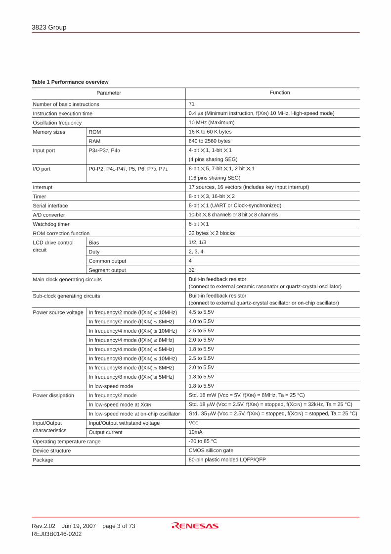
Table 1 Performance overview
Parameter
71
0.4 µs (Minimum instruction, f(XIN) 10 MHz, High-speed mode)
10 MHz (Maximum)
16 K to 60 K bytes
640 to 2560 bytes
4-bit 1, 1-bit 1
(4 pins sharing SEG)
8-bit 5, 7-bit 1, 2 bit 1
(16 pins sharing SEG)
17 sources, 16 vectors (includes key input interrupt)
8-bit 3, 16-bit 2
8-bit 1 (UART or Clock-synchronized)
10-bit 8 channels or 8 bit 8 channels
8-bit 1
32 bytes 2 blocks
1/2, 1/3
2, 3, 4
4
32
Built-in feedback resistor(connect to external ceramic rasonator or quartz-crystal oscillator)
Built-in feedback resistor(connect to external quartz-crystal oscillator or on-chip oscillator)
4.5 to 5.5V
4.0 to 5.5V
2.5 to 5.5V
2.0 to 5.5V
1.8 to 5.5V
2.5 to 5.5V
2.0 to 5.5V
1.8 to 5.5V
1.8 to 5.5V
Std. 18 mW (Vcc = 5V, f(XIN) = 8MHz, Ta = 25 °C)
Std. 18 µW (Vcc = 2.5V, f(XIN) = stopped, f(XCIN) = 32kHz, Ta = 25 °C)
Std. 35 µW (Vcc = 2.5V, f(XIN) = stopped, f(XCIN) = stopped, Ta = 25 °C)
VCC
10mA
-20 to 85 °C
CMOS sillicon gate
80-pin plastic molded LQFP/QFP
Number of basic instructions
Instruction execution time
Oscillation frequency
Memory sizes ROM
RAM
Input port P34-P37, P40
I/O port P0-P2, P41-P47, P5, P6, P70, P71
Interrupt
Timer
Serial interface
A/D converter
Watchdog timer
ROM correction function
LCD drive control Biascircuit Duty
Common output
Segment output
Main clock generating circuits
Sub-clock generating circuits
Power source voltage In frequency/2 mode (f(XIN) ≤ 10MHz)
In frequency/2 mode (f(XIN) ≤ 8MHz)
In frequency/4 mode (f(XIN) ≤ 10MHz)
In frequency/4 mode (f(XIN) ≤ 8MHz)
In frequency/4 mode (f(XIN) ≤ 5MHz)
In frequency/8 mode (f(XIN) ≤ 10MHz)
In frequency/8 mode (f(XIN) ≤ 8MHz)
In frequency/8 mode (f(XIN) ≤ 5MHz)
In low-speed mode
Power dissipation In frequency/2 mode
In low-speed mode at XCIN
In low-speed mode at on-chip oscillator
Input/Output Input/Output withstand voltagecharacteristics Output current
Operating temperature range
Device structure
Package
Function
Rev.2.02 Jun 19, 2007 page 4 of 73REJ03B0146-0202
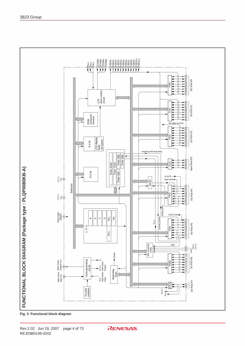
3823 Group
FU
NC
TIO
NA
L B
LO
CK
DIA
GR
AM
(P
acka
ge
typ
e :
PL
QP
0080
KB
-A)
Fig. 3 Functional block diagram
K
e
y
o
n
w
a
k
e
u
p
R
e
a
l
t
i
m
e
p
o
r
t
f
u
n
c
t
i
o
n
I N
T2,
I
N
T3
C N
T
R
0,
C
N
T
R1
TO
U
T
A
D
T
I N
T0,
I
N
T1
φ,
XC
I
N
R T
P
0,
R
T
P1
D a
t
a
b
u
s
C
P
U
A X Y S
P C
HP
CL
P S
R E
S
E
T
VC
C
VS
S
R e
s
e
t
I
n
p
u
t
( 5
V
)
( 0
V
) R
O
M
R
A
M
L C D
d
i
s
p
l
a
y
R
A
M
( 1
6
b
y
t
e
s
)
2 57 1
3 0
I / O
P
o
r
t
P
5
P 4
(
8
)
I / O
P
o
r
t
P
4
I / O
P
o
r
t
P
2
P 2
(
8
)
I / O
P
o
r
t
P
0
P 0
(
8
)
I / O
P
o
r
t
P
1
P 1
(
8
)
P 6
(
8
)
I n p
u
t
P
o
r
t
P
3
P 3
(
4
)
I / O
P
o
r
t
P
6
P 5
(
8
)
I / O
P
o
r
t
P
7
P 7
(
2
)
8 0 7 9 7 8 7 7 7 6 7 5 7 4
7 0 6 9 6 8 6 7 6 6 6 5 6 4 6 3 6 2 6 1 6 0 5 9
4 74 8
4 95 0
5 15 2
5 35 4
3 94 0
4 14 2
4 34 4
4 54 6
3 13 2
3 33 4
3 53 6
3 73 8
5 55 6
5 75 8
1 92 0
2 12 2
2 32 4
1 71 8
2 62 7
12
34
56
78
7 37 2
1 01 1
1 21 3
1 41 5
1 69
C l
o
c
k
g
e
n
e
r
a
t
i
n
g
c
i
r
c
u
i
t
M a
i
n
C
l
o
c
k
I n
p
u
t
XI
N
M a
i
n
C
l
o
c
k
O
u
t
p
u
t
XO
U
T
XC
O
U
T
S
u
b
-
C
l
o
c
k
O
u
t
p
u
t
XC
I
N
S
u
b
-
C
l
o
c
k
I n
p
u
t
S I
/
O
(
8
)
VR
E
F A
VS
S
(
0
V
)
A
/
D
c
o
n
v
e
r
t
e
r(
1
0
/
8
)
T i
m
e
r
X
(
1
6
)
T i
m
e
r
Y
(
1
6
)
T i
m
e
r
1
(
8
)
T i
m
e
r
2
(
8
)
T i
m
e
r
3
(
8
)
L C D
d r
i
v
e
c
o
n
t
r
o
l
c i
r
c
u
i
t
VL
1
VL
2
VL
3
C O
M
0
C O
M
1
C O
M
2
C O
M
3
S E
G
0
S E
G
1
S E
G
2
S E
G
3
S E
G
4
S E
G
5
S E
G
6
S E
G
7
S E
G
8
S E
G
9
S E
G
1
0
S E
G
1
1
φ
XC
I
NXC
O
U
T
2 82 9
O n
-
c
h
i
p
o
s
c
i
l
l
a
t
o
rR
O
M
c o
r
r
e
c
t
i
o
n
f u
n
c
t
i
o
n
W
a
t
c
h
d
o
gt
i
m
e
rR
e
s
e
t
Rev.2.02 Jun 19, 2007 page 5 of 73REJ03B0146-0202
3823 Group
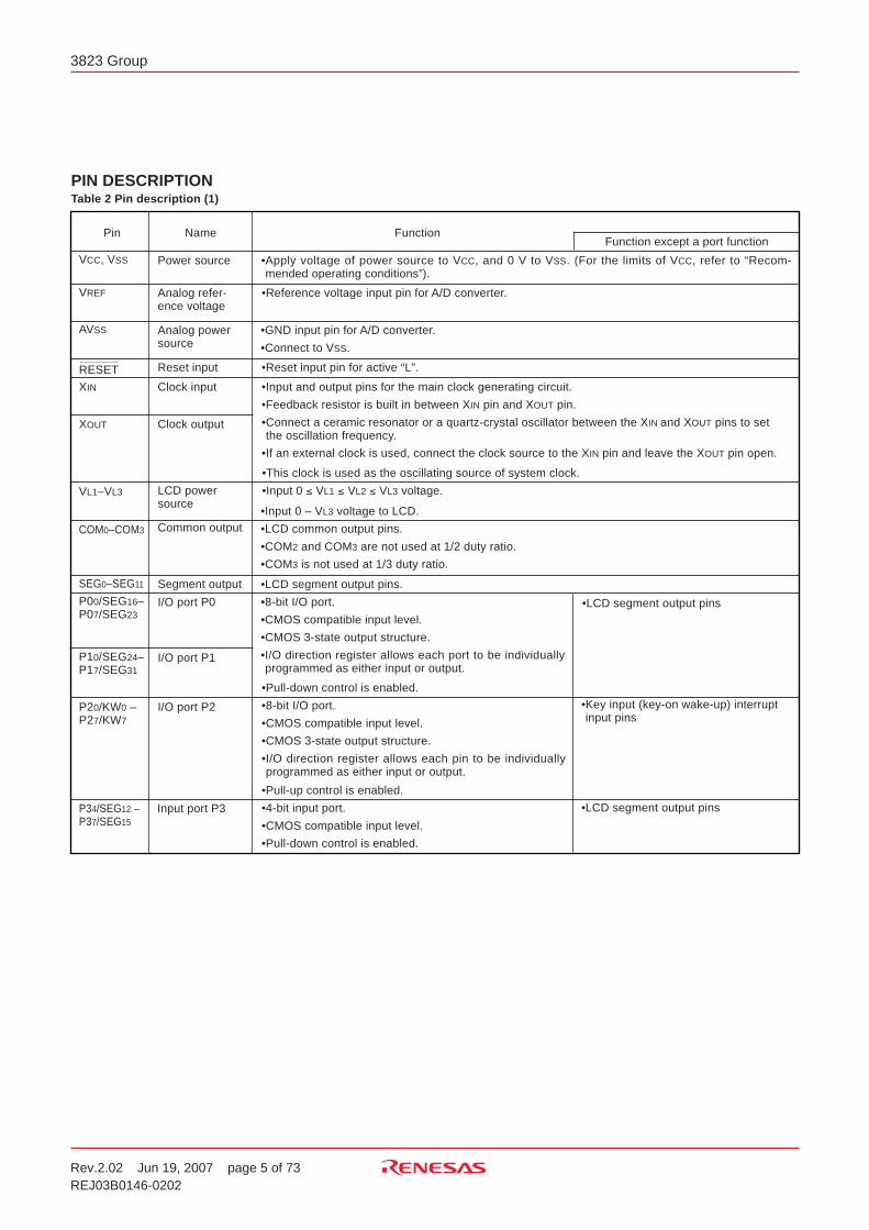
PIN DESCRIPTIONTable 2 Pin description (1)
VCC, VSS
FunctionPin NameFunction except a port function
•LCD segment output pins
Power source •Apply voltage of power source to VCC, and 0 V to VSS. (For the limits of VCC, refer to “Recom-mended operating conditions”).
VREF
AVSS
RESET
XIN
XOUT
VL1–VL3
COM0–COM3
SEG0–SEG11
P00/SEG16–P07/SEG23
P10/SEG24–P17/SEG31
P20/KW0 –P27/KW7
P34/SEG12 –P37/SEG15
Analog refer-ence voltage
Analog powersource
Reset input
Clock input
Clock output
LCD powersource
Common output
Segment output
I/O port P0
I/O port P1
I/O port P2
•Reference voltage input pin for A/D converter.
•GND input pin for A/D converter.
•Connect to VSS.
•Reset input pin for active “L”.
•Input and output pins for the main clock generating circuit.
•Feedback resistor is built in between XIN pin and XOUT pin.
•Connect a ceramic resonator or a quartz-crystal oscillator between the XIN and XOUT pins to setthe oscillation frequency.
•If an external clock is used, connect the clock source to the XIN pin and leave the XOUT pin open.
•This clock is used as the oscillating source of system clock.
•Input 0 ≤ VL1 ≤ VL2 ≤ VL3 voltage.
•Input 0 – VL3 voltage to LCD.
•LCD common output pins.
•COM2 and COM3 are not used at 1/2 duty ratio.
•COM3 is not used at 1/3 duty ratio.
•LCD segment output pins.
•8-bit I/O port.
•CMOS compatible input level.
•CMOS 3-state output structure.
•I/O direction register allows each port to be individuallyprogrammed as either input or output.
•Pull-down control is enabled.
•8-bit I/O port.
•CMOS compatible input level.
•CMOS 3-state output structure.
•I/O direction register allows each pin to be individuallyprogrammed as either input or output.
•Pull-up control is enabled.
•4-bit input port.
•CMOS compatible input level.
•Pull-down control is enabled.
•Key input (key-on wake-up) interruptinput pins
•LCD segment output pinsInput port P3
Rev.2.02 Jun 19, 2007 page 6 of 73REJ03B0146-0202
3823 Group
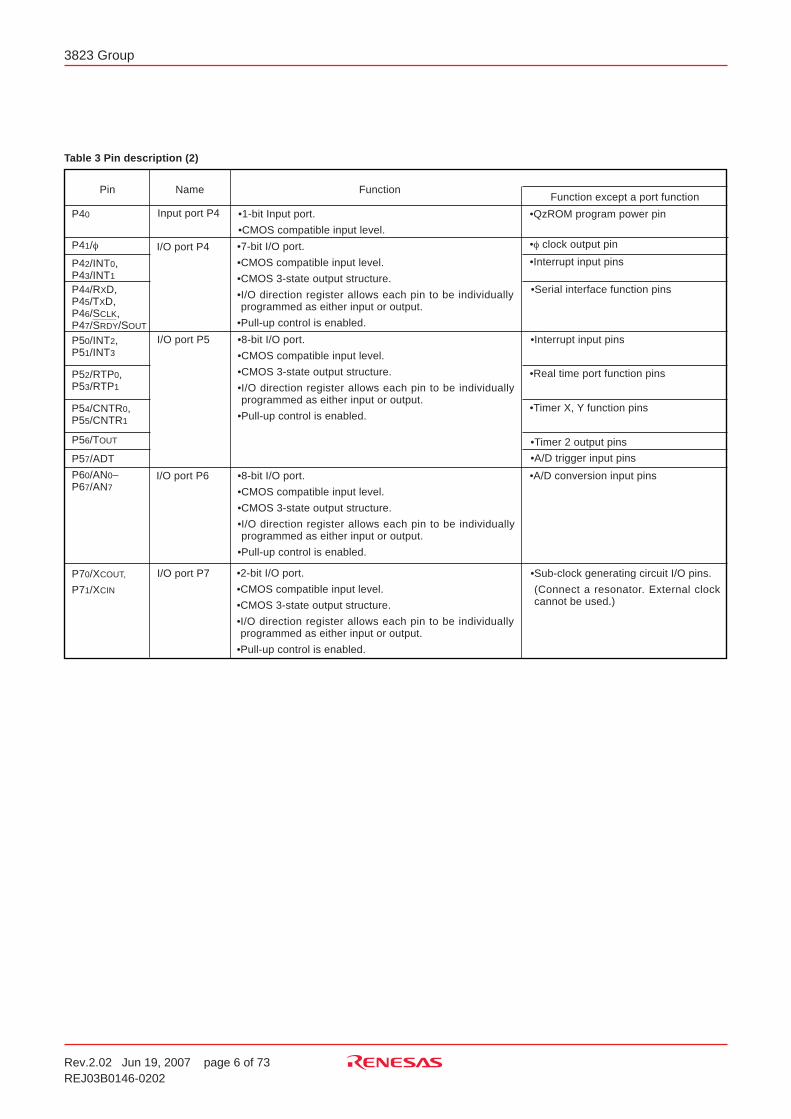
Table 3 Pin description (2)
FunctionPinFunction except a port function
P40
P42/INT0,P43/INT1
P44/RXD,P45/TXD,P46/SCLK,P47/SRDY/SOUT
P50/INT2,P51/INT3
P52/RTP0,P53/RTP1
P54/CNTR0,P55/CNTR1
P56/TOUT
P57/ADT
P60/AN0–P67/AN7
P70/XCOUT,
P71/XCIN
•1-bit Input port.
•CMOS compatible input level.
•7-bit I/O port.
•CMOS compatible input level.
•CMOS 3-state output structure.
•I/O direction register allows each pin to be individuallyprogrammed as either input or output.
•Pull-up control is enabled.
•8-bit I/O port.
•CMOS compatible input level.
•CMOS 3-state output structure.
•I/O direction register allows each pin to be individuallyprogrammed as either input or output.
•Pull-up control is enabled.
•8-bit I/O port.
•CMOS compatible input level.
•CMOS 3-state output structure.
•I/O direction register allows each pin to be individuallyprogrammed as either input or output.
•Pull-up control is enabled.
•2-bit I/O port.
•CMOS compatible input level.
•CMOS 3-state output structure.
•I/O direction register allows each pin to be individuallyprogrammed as either input or output.
•Pull-up control is enabled.
•φ clock output pin
•Interrupt input pins
•Interrupt input pins
•Real time port function pins
•Timer X, Y function pins
•Timer 2 output pins
•A/D conversion input pins
•Sub-clock generating circuit I/O pins.
(Connect a resonator. External clockcannot be used.)
P41/φ
•Serial interface function pins
•A/D trigger input pins
Name
I/O port P4
I/O port P5
I/O port P6
I/O port P7
Input port P4 •QzROM program power pin
Rev.2.02 Jun 19, 2007 page 7 of 73REJ03B0146-0202
3823 Group
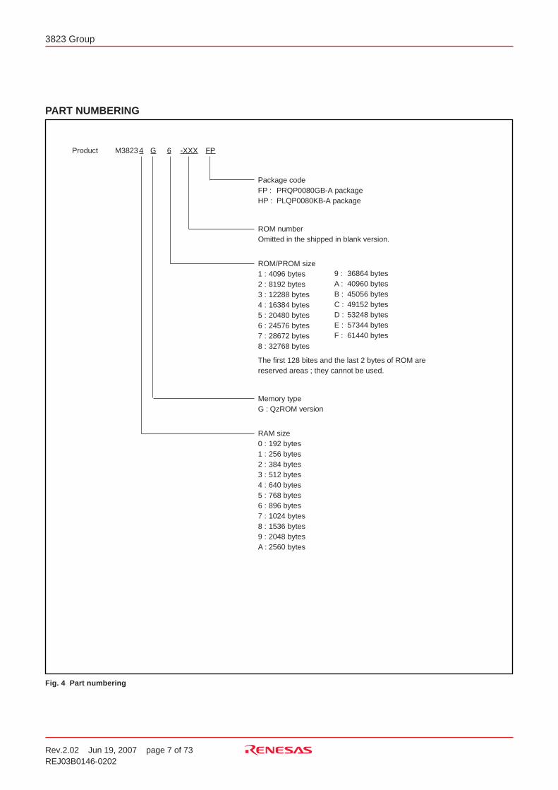
PART NUMBERING
Fig. 4 Part numbering
Package codeFP : PRQP0080GB-A packageHP : PLQP0080KB-A package
ROM numberOmitted in the shipped in blank version.
ROM/PROM size1 : 4096 bytes2 : 8192 bytes3 : 12288 bytes4 : 16384 bytes5 : 20480 bytes6 : 24576 bytes7 : 28672 bytes8 : 32768 bytes
The first 128 bites and the last 2 bytes of ROM arereserved areas ; they cannot be used.
Memory typeG : QzROM version
RAM size0 : 192 bytes1 : 256 bytes2 : 384 bytes3 : 512 bytes4 : 640 bytes5 : 768 bytes6 : 896 bytes7 : 1024 bytes8 : 1536 bytes9 : 2048 bytesA : 2560 bytes
Product M3823 4 G 6 -XXX FP
9 : 36864 bytesA : 40960 bytesB : 45056 bytesC : 49152 bytesD : 53248 bytesE : 57344 bytesF : 61440 bytes
Rev.2.02 Jun 19, 2007 page 8 of 73REJ03B0146-0202
3823 Group
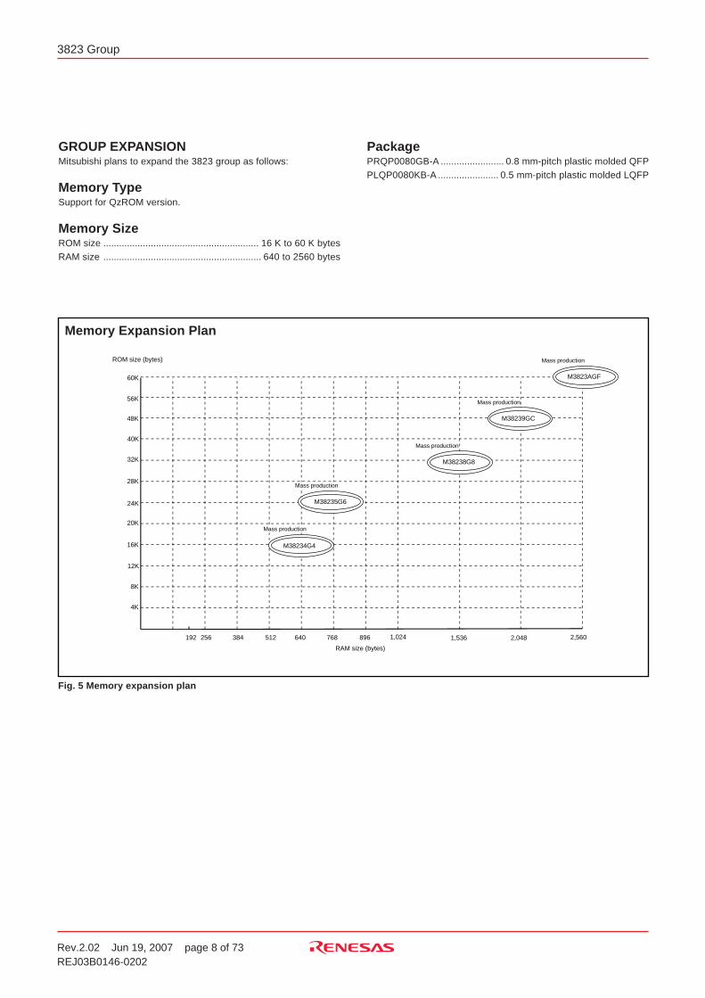
GROUP EXPANSIONMitsubishi plans to expand the 3823 group as follows:
Memory TypeSupport for QzROM version.
Memory SizeROM size ........................................................... 16 K to 60 K bytesRAM size ............................................................ 640 to 2560 bytes
PackagePRQP0080GB-A ........................ 0.8 mm-pitch plastic molded QFPPLQP0080KB-A ....................... 0.5 mm-pitch plastic molded LQFP
Memory Expansion Plan
Fig. 5 Memory expansion plan
32K
28K
24K
20K
16K
12K
8K
4K
256 384 512 640 768 896 1,024192
40K
48K
1,536 2,048
56K
60K
ROM size (bytes)
RAM size (bytes)
2,560
M3823AGF
Mass production
M38239GC
M38238G8
Mass production
Mass production
M38235G6
M38234G4
Mass production
Mass production
Rev.2.02 Jun 19, 2007 page 9 of 73REJ03B0146-0202
3823 Group
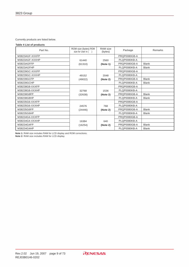
Currently products are listed below.
RemarksPackage Part No.RAM size
(bytes)
61440
(61310)
49152
(49022)
32768
(32638)
24576
(24446)
16384
(16254)
ROM size (bytes) ROMsize for User in ( )
Table 4 List of products
M3823AGF-XXXFP
M3823AGF-XXXHP
M3823AGFFP
M3823AGFHP
M38239GC-XXXFP
M38239GC-XXXHP
M38239GCFP
M38239GCHP
M38238G8-XXXFP
M38238G8-XXXHP
M38238G8FP
M38238G8HP
M38235G6-XXXFP
M38235G6-XXXHP
M38235G6FP
M38235G6HP
M38234G4-XXXFP
M38234G4-XXXHP
M38234G4FP
M38234G4HP
2560
(Note 1)
2048
(Note 2)
1536
(Note 2)
768
(Note 2)
640
(Note 2)
PRQP0080GB-A
PLQP0080KB-A
PRQP0080GB-A
PLQP0080KB-A
PRQP0080GB-A
PLQP0080KB-A
PRQP0080GB-A
PLQP0080KB-A
PRQP0080GB-A
PLQP0080KB-A
PRQP0080GB-A
PLQP0080KB-A
PRQP0080GB-A
PLQP0080KB-A
PRQP0080GB-A
PLQP0080KB-A
PRQP0080GB-A
PLQP0080KB-A
PRQP0080GB-A
PLQP0080KB-A
Blank
Blank
Blank
Blank
Blank
Blank
Blank
Blank
Blank
Blank
Note 1: RAM size includes RAM for LCD display and ROM corrections.Note 2: RAM size includes RAM for LCD display.

Rev.2.02 Jun 19, 2007 page 10 of 73REJ03B0146-0202
3823 Group
FUNCTIONAL DESCRIPTIONCENTRAL PROCESSING UNIT (CPU)The 3823 group uses the standard 740 family instruction set. Re-fer to the table of 740 family addressing modes and machineinstructions or the 740 Family Software Manual for details on theinstruction set.Machine-resident 740 family instructions are as follows:The FST and SLW instruction cannot be used.The STP, WIT, MUL, and DIV instruction can be used.The central processing unit (CPU) has six registers. Figure 6shows the 740 Family CPU register structure.
[Accumulator (A)]The accumulator is an 8-bit register. Data operations such as datatransfer, etc., are executed mainly through the accumulator.
[Index Register X (X)]The index register X is an 8-bit register. In the index addressingmodes, the value of the OPERAND is added to the contents ofregister X and specifies the real address.
[Index Register Y (Y)]The index register Y is an 8-bit register. In partial instruction, thevalue of the OPERAND is added to the contents of register Y andspecifies the real address.
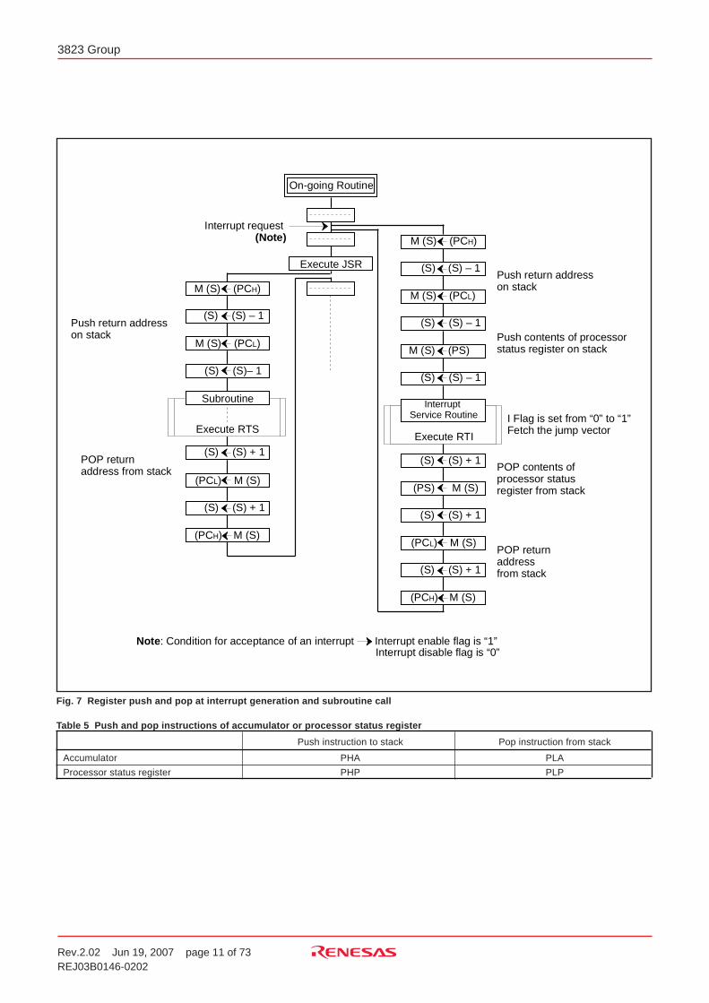
[Stack Pointer (S)]The stack pointer is an 8-bit register used during subroutine callsand interrupts. This register indicates start address of stored area(stack) for storing registers during subroutine calls and interrupts.The low-order 8 bits of the stack address are determined by thecontents of the stack pointer. The high-order 8 bits of the stack ad-dress are determined by the stack page selection bit. If the stackpage selection bit is “0” , the high-order 8 bits becomes “0016”. Ifthe stack page selection bit is “1”, the high-order 8 bits becomes“0116”.The operations of pushing register contents onto the stack andpopping them from the stack are shown in Figure 7.Store registers other than those described in Table 4 with programwhen the user needs them during interrupts or subroutine calls.
[Program Counter (PC)]The program counter is a 16-bit counter consisting of two 8-bitregisters PCH and PCL. It is used to indicate the address of thenext instruction to be executed.
Fig. 6 740 Family CPU register structure
A Accumulator
b7
b7
b7
b7 b0
b7b15 b0
b7 b0
b0
b0
b0
X Index register X
Y Index register Y
S Stack pointer
PCL Program counterPCH
N V T B D I Z C Processor status register (PS)
Carry flagZero flagInterrupt disable flagDecimal mode flagBreak flagIndex X mode flagOverflow flagNegative flag
Rev.2.02 Jun 19, 2007 page 11 of 73REJ03B0146-0202
3823 Group
Table 5 Push and pop instructions of accumulator or processor status register
Accumulator
Processor status register
Push instruction to stack
PHA
PHP
Pop instruction from stack
PLA
PLP
Fig. 7 Register push and pop at interrupt generation and subroutine call
N
o
t
e:
C
o
n
d
i
t
i
o
n
f
o
r
a
c
c
e
p
t
a
n
c
e
o
f
a
n
i
n
t
e
r
r
u
p
t
I
n
t
e
r
r
u
p
t
e
n
a
b
l
e
f
l
a
g
i
s
“
1
”
E
x
e
c
u
t
e
J
S
R
O
n
-
g
o
i
n
g
R
o
u
t
i
n
e
M
(
S
) (
P
CH)
( S
)
(
S
)
–
1
M
(
S
) (
P
CL)
E
x
e
c
u
t
e
R
T
S
( P
CL) M
(
S
)
( S
)
(
S
)
–
1
( S
)
(
S
)
+
1
( S
)
(
S
)
+
1
( P
CH) M
(
S
)
S
u
b
r
o
u
t
i
n
e
P
O
P
re
t
u
r
na
d
d
r
e
s
s
f
r
o
m
s
t
a
c
k
P
u
s
h
r
e
t
u
r
n
a
d
d
r
e
s
s
o
n
s
t
a
c
k
M
(
S
) (
P
S
)
E
x
e
c
u
t
e
R
T
I
( P
S
) M
(
S
)
( S
)
(
S
)
–
1
( S
)
(
S
)
+
1
I
n
t
e
r
r
u
p
t
S
e
r
v
i
c
e
R
o
u
t
i
n
e
P
O
P
c
o
n
t
e
n
t
s
o
f
p
r
o
c
e
s
s
o
r
s
t
a
t
u
s
r
e
g
i
s
t
e
r
f
r
o
m
s
t
a
c
k
M
(
S
) (
P
CH)
( S
)
(
S
)
–
1
M
(
S
) (
P
CL)
( S
)
(
S
)
–
1
( P
CL) M
(
S
)
( S
)
(
S
)
+
1
( S
)
(
S
)
+
1
( P
CH) M
(
S
)
P
O
P
r
e
t
u
r
na
d
d
r
e
s
s
f
r
o
m
s
t
a
c
k
I
F
l
a
g
i
s
s
e
t
f
r
o
m
“
0
”
t
o
“
1
”
F
e
t
c
h
t
h
e
j
u
m
p
v
e
c
t
o
r
P
u
s
h
r
e
t
u
r
n
a
d
d
r
e
s
s
o
n
s
t
a
c
k
P
u
s
h
c
o
n
t
e
n
t
s
o
f
p
r
o
c
e
s
s
o
r
s
t
a
t
u
s
r
e
g
i
s
t
e
r
o
n
s
t
a
c
k
I
n
t
e
r
r
u
p
t
r
e
q
u
e
s
t
(
N
o
t
e
)
I n
t
e
r
r
u
p
t
d
i
s
a
b
l
e
f
l
a
g
i
s
“
0
”
Rev.2.02 Jun 19, 2007 page 12 of 73REJ03B0146-0202
3823 Group
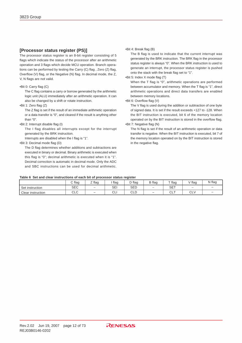
[Processor status register (PS)]The processor status register is an 8-bit register consisting of 5flags which indicate the status of the processor after an arithmeticoperation and 3 flags which decide MCU operation. Branch opera-tions can be performed by testing the Carry (C) flag , Zero (Z) flag,Overflow (V) flag, or the Negative (N) flag. In decimal mode, the Z,V, N flags are not valid.
•Bit 0: Carry flag (C)The C flag contains a carry or borrow generated by the arithmeticlogic unit (ALU) immediately after an arithmetic operation. It canalso be changed by a shift or rotate instruction.
•Bit 1: Zero flag (Z)The Z flag is set if the result of an immediate arithmetic operationor a data transfer is “0”, and cleared if the result is anything otherthan “0”.
•Bit 2: Interrupt disable flag (I)The I flag disables all interrupts except for the interruptgenerated by the BRK instruction.Interrupts are disabled when the I flag is “1”.
•Bit 3: Decimal mode flag (D)The D flag determines whether additions and subtractions areexecuted in binary or decimal. Binary arithmetic is executed whenthis flag is “0”; decimal arithmetic is executed when it is “1”.Decimal correction is automatic in decimal mode. Only the ADCand SBC instructions can be used for decimal arithmetic.
•Bit 4: Break flag (B)The B flag is used to indicate that the current interrupt wasgenerated by the BRK instruction. The BRK flag in the processorstatus register is always “0”. When the BRK instruction is used togenerate an interrupt, the processor status register is pushedonto the stack with the break flag set to “1”.
•Bit 5: Index X mode flag (T)When the T flag is “0”, arithmetic operations are performedbetween accumulator and memory. When the T flag is “1”, directarithmetic operations and direct data transfers are enabledbetween memory locations.
•Bit 6: Overflow flag (V)The V flag is used during the addition or subtraction of one byteof signed data. It is set if the result exceeds +127 to -128. Whenthe BIT instruction is executed, bit 6 of the memory locationoperated on by the BIT instruction is stored in the overflow flag.
•Bit 7: Negative flag (N)The N flag is set if the result of an arithmetic operation or datatransfer is negative. When the BIT instruction is executed, bit 7 ofthe memory location operated on by the BIT instruction is storedin the negative flag.
Table 6 Set and clear instructions of each bit of processor status register
Set instruction
Clear instruction
C flag
SEC
CLC
Z flag
–
–
I flag
SEI
CLI
D flag
SED
CLD
B flag
–
–
T flag
SET
CLT
V flag
–
CLV
N flag
–
–
Rev.2.02 Jun 19, 2007 page 13 of 73REJ03B0146-0202
3823 Group
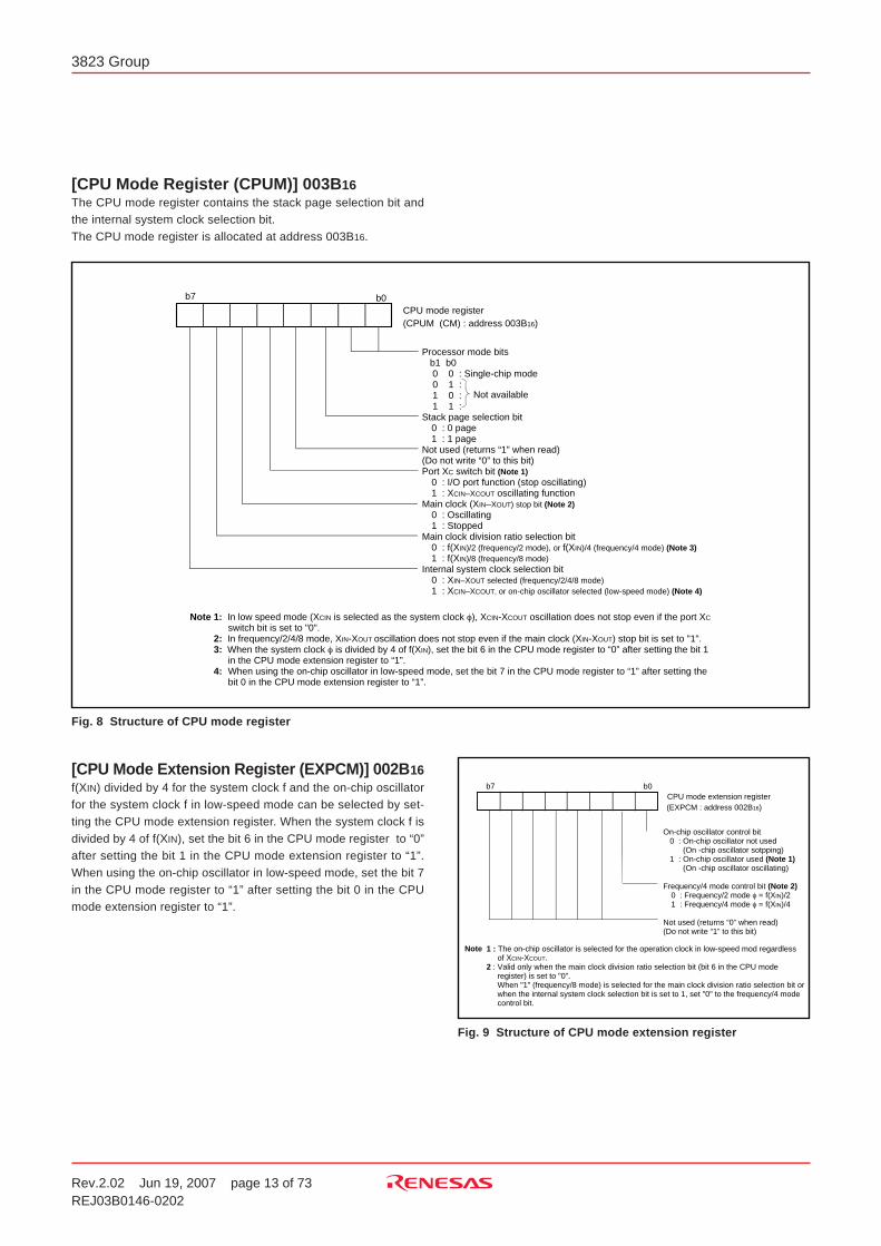
[CPU Mode Register (CPUM)] 003B16The CPU mode register contains the stack page selection bit andthe internal system clock selection bit.The CPU mode register is allocated at address 003B16.
Fig. 8 Structure of CPU mode register
Not available
Processor mode bits b1 b0 0 0 : Single-chip mode 0 1 : 1 0 : 1 1 :Stack page selection bit
0 : 0 page1 : 1 page
Not used (returns “1” when read)(Do not write “0” to this bit)Port XC switch bit (Note 1)
0 : I/O port function (stop oscillating)1 : XCIN–XCOUT oscillating function
Main clock (XIN–XOUT) stop bit (Note 2)0 : Oscillating1 : Stopped
Main clock division ratio selection bit0 : f(XIN)/2 (frequency/2 mode), or f(XIN)/4 (frequency/4 mode) (Note 3)1 : f(XIN)/8 (frequency/8 mode)
Internal system clock selection bit0 : XIN–XOUT selected (frequency/2/4/8 mode)1 : XCIN–XCOUT, or on-chip oscillator selected (low-speed mode) (Note 4)
CPU mode register(CPUM (CM) : address 003B16)
b7 b0
Note 1: In low speed mode (XCIN is selected as the system clock φ), XCIN-XCOUT oscillation does not stop even if the port XC switch bit is set to "0".
2: In frequency/2/4/8 mode, XIN-XOUT oscillation does not stop even if the main clock (XIN-XOUT) stop bit is set to "1". 3: When the system clock φ is divided by 4 of f(XIN), set the bit 6 in the CPU mode register to “0” after setting the bit 1
in the CPU mode extension register to “1”. 4: When using the on-chip oscillator in low-speed mode, set the bit 7 in the CPU mode register to “1” after setting the
bit 0 in the CPU mode extension register to “1”.
[CPU Mode Extension Register (EXPCM)] 002B16f(XIN) divided by 4 for the system clock f and the on-chip oscillatorfor the system clock f in low-speed mode can be selected by set-ting the CPU mode extension register. When the system clock f isdivided by 4 of f(XIN), set the bit 6 in the CPU mode register to “0”after setting the bit 1 in the CPU mode extension register to “1”.When using the on-chip oscillator in low-speed mode, set the bit 7in the CPU mode register to “1” after setting the bit 0 in the CPUmode extension register to “1”.
Fig. 9 Structure of CPU mode extension register
On-chip oscillator control bit 0 : On-chip oscillator not used (On -chip oscillator sotpping) 1 : On-chip oscillator used (Note 1) (On -chip oscillator oscillating)
Frequency/4 mode control bit (Note 2) 0 : Frequency/2 mode φ = f(XIN)/21 : Frequency/4 mode φ = f(XIN)/4
Not used (returns “0” when read)(Do not write “1” to this bit)
CPU mode extension register(EXPCM : address 002B16)
b7 b0
1 : The on-chip oscillator is selected for the operation clock in low-speed mod regardless of XCIN-XCOUT.2 : Valid only when the main clock division ratio selection bit (bit 6 in the CPU mode register) is set to "0". When "1" (frequency/8 mode) is selected for the main clock division ratio selection bit or when the internal system clock selection bit is set to 1, set "0" to the frequency/4 mode control bit.
Note
Rev.2.02 Jun 19, 2007 page 14 of 73REJ03B0146-0202
3823 Group
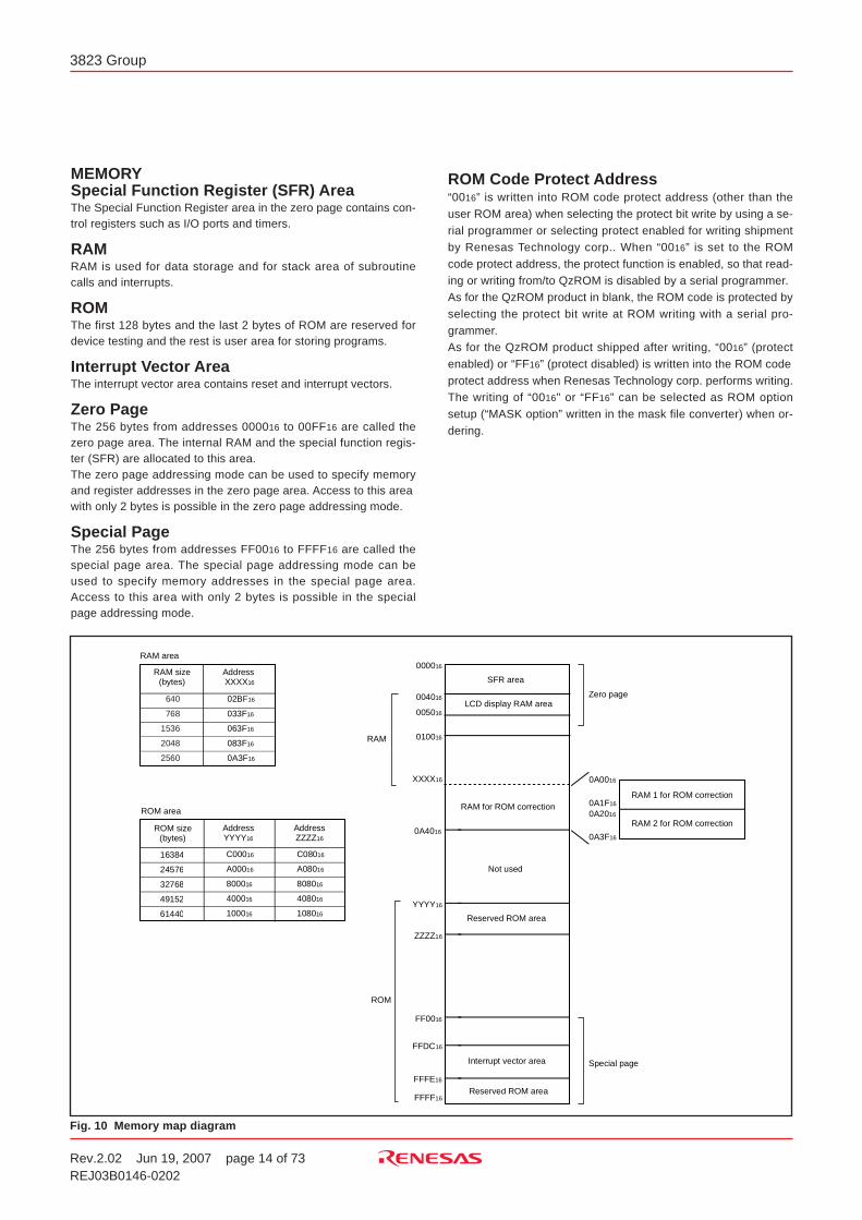
MEMORYSpecial Function Register (SFR) AreaThe Special Function Register area in the zero page contains con-trol registers such as I/O ports and timers.
RAMRAM is used for data storage and for stack area of subroutinecalls and interrupts.
ROMThe first 128 bytes and the last 2 bytes of ROM are reserved fordevice testing and the rest is user area for storing programs.
Interrupt Vector AreaThe interrupt vector area contains reset and interrupt vectors.
Zero PageThe 256 bytes from addresses 000016 to 00FF16 are called thezero page area. The internal RAM and the special function regis-ter (SFR) are allocated to this area.The zero page addressing mode can be used to specify memoryand register addresses in the zero page area. Access to this areawith only 2 bytes is possible in the zero page addressing mode.
Special PageThe 256 bytes from addresses FF0016 to FFFF16 are called thespecial page area. The special page addressing mode can beused to specify memory addresses in the special page area.Access to this area with only 2 bytes is possible in the specialpage addressing mode.
Fig. 10 Memory map diagram
6
4
0
7
6
8
1
5
3
6
2
0
4
8
2
5
6
0
0
2
B
F1
6
0
3
3
F1
6
0
6
3
F1
6
0
8
3
F1
6
0
A3
F1
6
RAM area
R
A
M
s
i
z
e(
b
y
t
e
s
)A
d
d
r
e
s
s
X
X
X
X1
6
1
6
3
8
4
2
4
5
7
6
3
2
7
6
8
4
9
1
5
2
6
1
4
4
0
C
0
0
01
6
A
0
0
01
6
8
0
0
01
6
4
0
0
01
6
10
0
01
6
C
0
8
01
6
A
0
8
01
6
8
0
8
01
6
4
0
8
01
6
10
8
01
6
R
O
M
a
r
e
a
R
O
M
s
i
z
e(
b
y
t
e
s
)A
d
d
r
e
s
s
Y
Y
Y
Y1
6
A
d
d
r
e
s
sZ
Z
Z
Z1
6
010016
000016
004016
0A4016
FF0016
F
F
D
C1
6
FFFE16
FFFF16
XXXX16
ZZZZ16
RAM
R
O
M
RAM for ROM correction
SFR area
N
o
t
u
s
e
d
Interrupt vector area
R
e
s
e
r
v
e
d
R
O
M
a
r
e
a
Zero page
S
p
e
c
i
a
l
p
a
g
e
R
e
s
e
r
v
e
d
R
O
M
a
r
e
a
005016LCD display RAM area
R
A
M
1
f
o
r
R
O
M
c
o
r
r
e
c
t
i
o
n
R
A
M
2
f
o
r
R
O
M
c
o
r
r
e
c
t
i
o
n
0A0016
0A1F16
0
A
2
01
6
0
A
3
F1
6
Y
Y
Y
Y1
6
ROM Code Protect Address“0016” is written into ROM code protect address (other than theuser ROM area) when selecting the protect bit write by using a se-rial programmer or selecting protect enabled for writing shipmentby Renesas Technology corp.. When “0016” is set to the ROMcode protect address, the protect function is enabled, so that read-ing or writing from/to QzROM is disabled by a serial programmer.As for the QzROM product in blank, the ROM code is protected byselecting the protect bit write at ROM writing with a serial pro-grammer.As for the QzROM product shipped after writing, “0016” (protectenabled) or “FF16” (protect disabled) is written into the ROM codeprotect address when Renesas Technology corp. performs writing.The writing of “0016" or “FF16” can be selected as ROM optionsetup (“MASK option” written in the mask file converter) when or-dering.
Rev.2.02 Jun 19, 2007 page 15 of 73REJ03B0146-0202
3823 Group
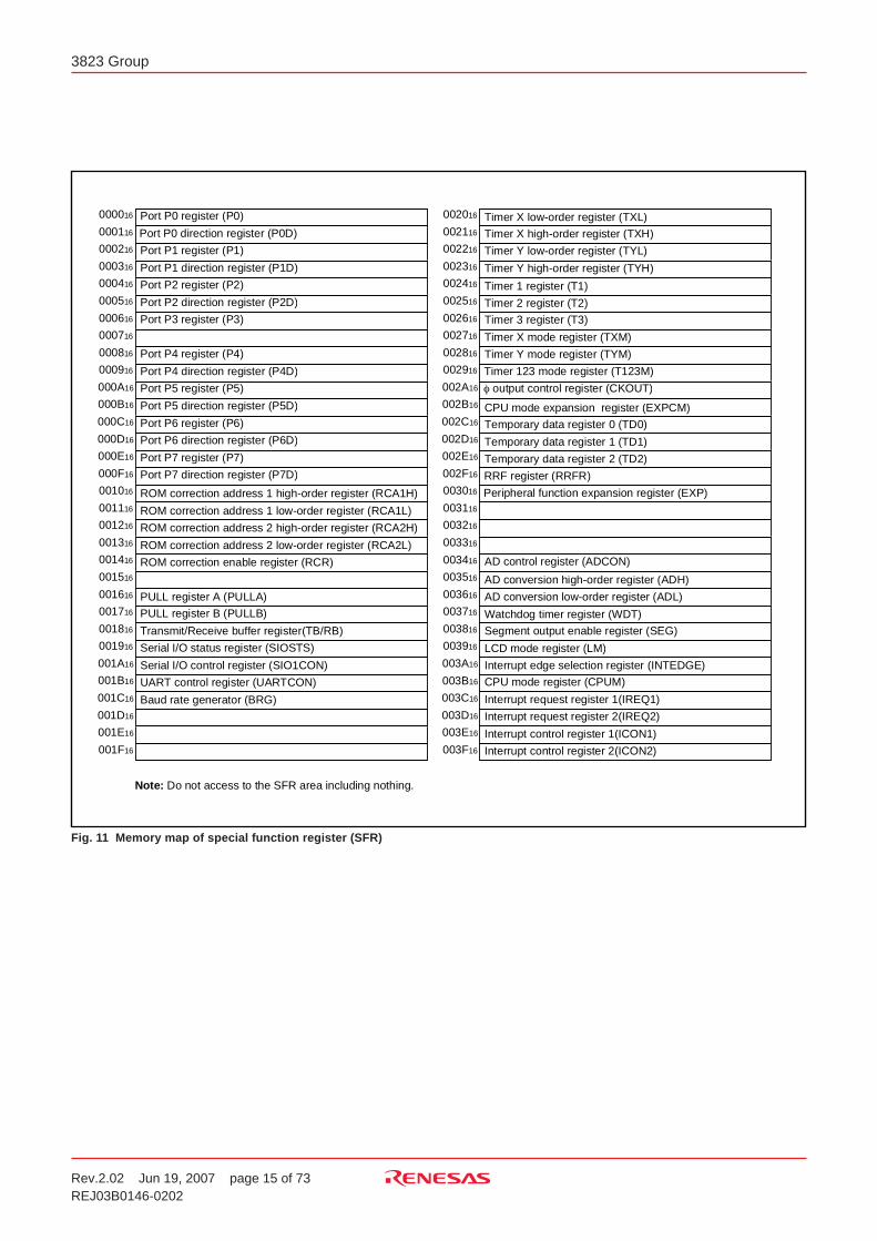
Fig. 11 Memory map of special function register (SFR)
0
0
2
01
6
0
0
2
11
6
0
0
2
21
6
0
0
2
31
6
0
0
2
41
6
0
0
2
51
6
0
0
2
61
6
0
0
2
71
6
0
0
2
81
6
0
0
2
91
6
0
0
2
A1
6
0
0
2
B1
6
002C16
002D16
002E16
0
0
2
F1
6
0
0
3
01
6
0
0
3
11
6
0
0
3
21
6
0
0
3
31
6
0
0
3
41
6
0
0
3
51
6
0
0
3
61
6
0
0
3
71
6
003816
003916
003A16
0
0
3
B1
6
003C16
003D16
003E16
0
0
3
F1
6
0
0
0
01
6
0
0
0
11
6
0
0
0
21
6
0
0
0
31
6
0
0
0
41
6
0
0
0
51
6
0
0
0
61
6
0
0
0
71
6
0
0
0
81
6
0
0
0
91
6
0
0
0
A1
6
0
0
0
B1
6
0
0
0
C1
6
0
0
0
D1
6
000E16
0
0
0
F1
6
0
0
1
01
6
0
0
1
11
6
0
0
1
21
6
0
0
1
31
6
0
0
1
41
6
0
0
1
51
6
0
0
1
61
6
0
0
1
71
6
001816
001916
001A16
0
0
1
B1
6
0
0
1
C1
6
001D16
001E16
0
0
1
F1
6 I n
t
e
r
r
u
p
t
c
o
n
t
r
o
l
r
e
g
i
s
t
e
r
2
(
I
C
O
N
2
)
T
i
m
e
r
3
r
e
g
i
s
t
e
r
(
T
3
)
T
i
m
e
r
X
m
o
d
e
r
e
g
i
s
t
e
r
(
T
X
M
)
Interrupt edge selection register (INTEDGE)
C
P
U
m
o
d
e
r
e
g
i
s
t
e
r
(
C
P
U
M
)
Interrupt request register 1(IREQ1)
Interrupt request register 2(IREQ2)
I n
t
e
r
r
u
p
t
c
o
n
t
r
o
l
r
e
g
i
s
t
e
r
1
(
I
C
O
N
1
)
T
i
m
e
r
X
l
o
w
-
o
r
d
e
r
r
e
g
i
s
t
e
r
(
T
X
L
)
T
i
m
e
r
Y
l
o
w
-
o
r
d
e
r
r
e
g
i
s
t
e
r
(
T
Y
L
)
T
i
m
e
r
1
r
e
g
i
s
t
e
r
(
T
1
)
T
i
m
e
r
2
r
e
g
i
s
t
e
r
(
T
2
)
T
i
m
e
r
X
h
i
g
h
-
o
r
d
e
r
r
e
g
i
s
t
e
r
(
T
X
H
)
T
i
m
e
r
Y
h
i
g
h
-
o
r
d
e
r
r
e
g
i
s
t
e
r
(
T
Y
H
)
T
i
m
e
r
Y
m
o
d
e
r
e
g
i
s
t
e
r
(
T
Y
M
)
Timer 123 mode register (T123M)
φ output control register (CKOUT)
S
e
g
m
e
n
t
o
u
t
p
u
t
e
n
a
b
l
e
r
e
g
i
s
t
e
r
(
S
E
G
)
LCD mode register (LM)
A
D
c
o
n
t
r
o
l
r
e
g
i
s
t
e
r
(
A
D
C
O
N
)
A
D
c
o
n
v
e
r
s
i
o
n
h
i
g
h
-
o
r
d
e
r
r
e
g
i
s
t
e
r
(
A
D
H
)
P
o
r
t
P
0
r
e
g
i
s
t
e
r
(
P
0
)
P
o
r
t
P
1
r
e
g
i
s
t
e
r
(
P
1
)
P
o
r
t
P
1
d
i
r
e
c
t
i
o
n
r
e
g
i
s
t
e
r
(
P
1
D
)
P
o
r
t
P
2
r
e
g
i
s
t
e
r
(
P
2
)
P
o
r
t
P
2
d
i
r
e
c
t
i
o
n
r
e
g
i
s
t
e
r
(
P
2
D
)
P
o
r
t
P
3
r
e
g
i
s
t
e
r
(
P
3
)
P
o
r
t
P
4
r
e
g
i
s
t
e
r
(
P
4
)
P
o
r
t
P
4
d
i
r
e
c
t
i
o
n
r
e
g
i
s
t
e
r
(
P
4
D
)
P
o
r
t
P
5
r
e
g
i
s
t
e
r
(
P
5
)
P
o
r
t
P
5
d
i
r
e
c
t
i
o
n
r
e
g
i
s
t
e
r
(
P
5
D
)
P
o
r
t
P
6
r
e
g
i
s
t
e
r
(
P
6
)
P
o
r
t
P
6
d
i
r
e
c
t
i
o
n
r
e
g
i
s
t
e
r
(
P
6
D
)
P
o
r
t
P
7
r
e
g
i
s
t
e
r
(
P
7
)
P
o
r
t
P
7
d
i
r
e
c
t
i
o
n
r
e
g
i
s
t
e
r
(
P
7
D
)
S
e
r
i
a
l
I
/
O
s
t
a
t
u
s
r
e
g
i
s
t
e
r
(
S
I
O
S
T
S
)
Serial I/O control register (SIO1CON)
UART control register (UARTCON)
Baud rate generator (BRG)
P
U
L
L
r
e
g
i
s
t
e
r
A
(
P
U
L
L
A
)
P
U
L
L
r
e
g
i
s
t
e
r
B
(
P
U
L
L
B
)
T
r
a
n
s
m
i
t
/
R
e
c
e
i
v
e
b
u
f
f
e
r
r
e
g
i
s
t
e
r( T
B
/
R
B
)
P
o
r
t
P
0
d
i
r
e
c
t
i
o
n
r
e
g
i
s
t
e
r
(
P
0
D
)
R
O
M
c
o
r
r
e
c
t
i
o
n
a
d
d
r
e
s
s
1
h
i
g
h
-
o
r
d
e
r
r
e
g
i
s
t
e
r
(
R
C
A
1
H
)
R
O
M
c
o
r
r
e
c
t
i
o
n
a
d
d
r
e
s
s
1
l
o
w
-
o
r
d
e
r
r
e
g
i
s
t
e
r
(
R
C
A
1
L
)
R
O
M
c
o
r
r
e
c
t
i
o
n
a
d
d
r
e
s
s
2
h
i
g
h
-
o
r
d
e
r
r
e
g
i
s
t
e
r
(
R
C
A
2
H
)
R
O
M
c
o
r
r
e
c
t
i
o
n
a
d
d
r
e
s
s
2
l
o
w
-
o
r
d
e
r
r
e
g
i
s
t
e
r
(
R
C
A
2
L
)
R
O
M
c
o
r
r
e
c
t
i
o
n
e
n
a
b
l
e
r
e
g
i
s
t
e
r
(
R
C
R
)
T
e
m
p
o
r
a
r
y
d
a
t
a
r
e
g
i
s
t
e
r
0
(
T
D
0
)
T
e
m
p
o
r
a
r
y
d
a
t
a
r
e
g
i
s
t
e
r
1
(
T
D
1
)
C
P
U
m
o
d
e
e
x
p
a
n
s
i
o
n
r
e
g
i
s
t
e
r
(
E
X
P
C
M
)
T
e
m
p
o
r
a
r
y
d
a
t
a
r
e
g
i
s
t
e
r
2
(
T
D
2
)
RRF register (RRFR)
Peripheral function expansion register (EXP)
A
D
c
o
n
v
e
r
s
i
o
n
l
o
w
-
o
r
d
e
r
r
e
g
i
s
t
e
r
(
A
D
L
)
Watchdog timer register (WDT)
N
o
t
e
:
D
o
n
o
t
a
c
c
e
s
s
t
o
t
h
e
S
F
R
a
r
e
a
i
n
c
l
u
d
i
n
g
n
o
t
h
i
n
g
.
Rev.2.02 Jun 19, 2007 page 16 of 73REJ03B0146-0202
3823 Group
I/O PORTSDirection Registers (ports P2, P41-P47, andP5-P7)The 3823 group has 49 programmable I/O pins arranged in sevenI/O ports (ports P0–P2, P41–P47 and P5-P7). The I/O ports P2,P41–P47 and P5-P7 have direction registers which determine theinput/output direction of each individual pin. Each bit in a directionregister corresponds to one pin, and each pin can be set to be in-put port or output port.When “0” is written to the bit corresponding to a pin, that pin be-comes an input pin. When “1” is written to that bit, that pin be-comes an output pin.If data is read from a pin set to output, the value of the port outputlatch is read, not the value of the pin itself. Pins set to input arefloating. If a pin set to input is written to, only the port output latchis written to and the pin remains floating.
Direction Registers (ports P0 and P1)Ports P0 and P1 have direction registers which determine the in-put/output direction of each individual port.Each port in a direction register corresponds to one port, each portcan be set to be input or output. When “0” is written to the bit 0 ofa direction register, that port becomes an input port. When “1” iswritten to that port, that port becomes an output port. Bits 1 to 7 ofports P0 and P1 direction registers are not used.
Ports P3 and P40These ports are only for input.
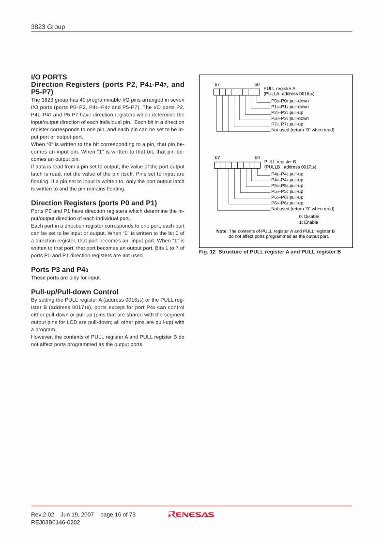
Pull-up/Pull-down ControlBy setting the PULL register A (address 001616) or the PULL reg-ister B (address 001716), ports except for port P40 can controleither pull-down or pull-up (pins that are shared with the segmentoutput pins for LCD are pull-down; all other pins are pull-up) witha program.However, the contents of PULL register A and PULL register B donot affect ports programmed as the output ports.
Fig. 12 Structure of PULL register A and PULL register B
P00–P07 pull-downP10–P17 pull-downP20–P27 pull-upP34–P37 pull-downP70, P71 pull-upNot used (return “0” when read)
PULL register A(PULLA: address 001616)
b7 b
0
P41–P43 pull-upP44–P47 pull-upP50–P53 pull-upP54–P57 pull-upP60–P63 pull-upP64–P67 pull-upNot used (return “0” when read)
0
:
D
i
s
a
b
l
e1
:
E
n
a
b
l
e
PULL register B(PULLB : address 001716)
b7 b0
Note: The contents of PULL register A and PULL register B do not affect ports programmed as the output port.
Rev.2.02 Jun 19, 2007 page 17 of 73REJ03B0146-0202
3823 Group
Real time portfunction output
A/D conversion input
A/D trigger input
Diagram No.Related SFRsInput/OutputNamePin Non-Port FunctionI/O Format
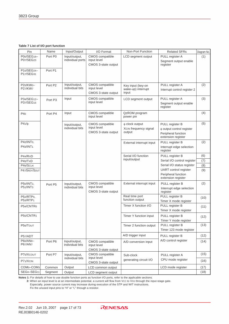
Table 7 List of I/O port function
P00/SEG16–P07/SEG23
P10/SEG24–P17/SEG31
P20/KW0–P27/KW7
P34/SEG12–P37/SEG15
P40
P41/φ
P42/INT0,
P43/INT1
P44/RXD
P45/TXDP46/SCLK
P47/SRDY/SOUT
P50/INT2,P51/INT3
P52/RTP0,P53/RTP1
P54/CNTR0
Port P0
Port P1
Port P2
Port P3
Port P4
Input/output,individual ports
Input/output,individual bits
Input
Input
Input/output,individual bits
CMOS compatibleinput level
CMOS 3-state output
CMOS compatibleinput level
CMOS 3-state output
CMOS compatibleinput level
CMOS compatibleinput level
CMOS compatibleinput level
CMOS 3-state output
CMOS compatibleinput level
CMOS 3-state output
CMOS compatibleinput level
CMOS 3-state output
CMOS compatibleinput level
CMOS 3-state output
LCD segment output
Key input (key-onwake-up) interruptinput
LCD segment output
φ clock output
XCIN frequency signaloutput
External interrupt input
Serial I/O functioninput/output
External interrupt input
Timer X function I/O
Timer Y function input
Timer 2 function output
PULL register A
Segment output enableregister
PULL register A
Interrupt control register 2
PULL register A
Segment output enableregister
PULL register B
φ output control register
Peripheral functionextension register
PULL register B
Interrupt edge selectionregister
PULL register B
Serial I/O control register
Serial I/O status register
UART control register
Peripheral functionextension register
PULL register B
Interrupt edge selectionregister
PULL register B
Timer X mode register
PULL register B
Timer X mode register
PULL register B
Timer Y mode register
PULL register B
Timer 123 mode register
PULL register B
A/D control register
PULL register A
CPU mode register
(1)
(2)
(3)
(4)
(6)
(5)
(2)
(8)
(7)
Port P5
(9)
(2)Input/output,individual bits
(10)
P55/CNTR1
(11)
(12)
(13)
(12)
(14)
P56/TOUT
P57/ADT
P60/AN0–P67/AN7
(15)P70/XCOUT
P71/XCIN
COM0–COM3
SEG0–SEG11
(16)
(17)
(18)
Input/output,individual bits
Input/output,individual bits
Output
Output
Sub-clock
generating circuit I/O
LCD common output
LCD segment output
Port P6
Port P7
Common
Segment
LCD mode register
Notes 1: For details of how to use double function ports as function I/O ports, refer to the applicable sections.2: When an input level is at an intermediate potential, a current will flow from VCC to VSS through the input-stage gate.
Especially, power source current may increase during execution of the STP and WIT instructions.Fix the unused input pins to “H” or “L” through a resistor.
QzROM programpower pin
Rev.2.02 Jun 19, 2007 page 18 of 73REJ03B0146-0202
3823 Group
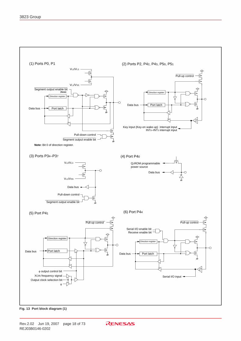
Fig. 13 Port block diagram (1)
( 3
)
P
o
r
t
s
P
34–
P
37
VL
2/
VL
3
VL1/VSS
S
e
g
m
e
n
t
o
u
t
p
u
t
e
n
a
b
l
e
b
i
t
VL
2/
VL
3
VL
1/
VS
S
( N
o
t
e
)
( 2
)
P
o
r
t
s
P
2
,
P
42,
P
43,
P
50,
P
51
D
i
r
e
c
t
i
o
n
r
e
g
i
s
t
e
r
(5) Port P41 ( 6
)
P
o
r
t
P
44
R
e
c
e
i
v
e
e
n
a
b
l
e
b
i
t
Direction register
( 4
)
P
o
r
t
P
40
D
a
t
a
b
u
s
Pull-down control
S
e
g
m
e
n
t
o
u
t
p
u
t
e
n
a
b
l
e
b
i
t
D
a
t
a
b
u
s
D
i
r
e
c
t
i
o
n
r
e
g
i
s
t
e
r
P
o
r
t
l
a
t
c
h
P
u
l
l
-
d
o
w
n
c
o
n
t
r
o
l
Segment output enable bit
Data bus Port latch
Pull-up control
Key input (Key-on wake-up) interrupt inputINT0–INT3 interrupt input
Pull-up control
Serial I/O enable bit
Serial I/O input
Data bus Port latch
(1) Ports P0, P1
N
o
t
e
:
B
i
t
0
o
f
d
i
r
e
c
t
i
o
n
r
e
g
i
s
t
e
r
.
Data bus
QZROM programmable power source
φ
φ
o
u
t
p
u
t
c
o
n
t
r
o
l
b
i
t
Port latchD
a
t
a
b
u
s
D
i
r
e
c
t
i
o
n
r
e
g
i
s
t
e
r
Pull-up control
XCIN frequency signal
O
u
t
p
u
t
c
l
o
c
k
s
e
l
e
c
t
i
o
n
b
i
t
Rev.2.02 Jun 19, 2007 page 19 of 73REJ03B0146-0202
3823 Group
Fig. 14 Port block diagram (2)
(
7
)
P
o
r
t
P
45
(
8
)
P
o
r
t
P
46
Serial I/O clock-synchronized selection bit
Serial I/O enable bit
Serial I/O mode selection bitSerial I/O enable bit
Direction register
Port latch
S
e
r
i
a
l
I
/
O
c
l
o
c
k
o
u
t
p
u
t
D
a
t
a
b
u
s
S
e
r
i
a
l
I
/
O
c
l
o
c
k
i
n
p
u
t
P
u
l
l
-
u
p
c
o
n
t
r
o
l
(10) Ports P52, P53
Direction register
Port latchData bus
Pull-up control
R
e
a
l
t
i
m
e
p
o
r
t
c
o
n
t
r
o
l
b
i
tD
a
t
a
f
o
r
r
e
a
l
t
i
m
e
p
o
r
t
Direction register
Port latchD
a
t
a
b
u
s
Pull-up control
( 1
2
)
P
o
r
t
s
P
55
,
P
57
CNTR1 interrupt inputA/D trigger interrupt input
( 1
1
)
P
o
r
t
P
54
D
i
r
e
c
t
i
o
n
r
e
g
i
s
t
e
r
P
o
r
t
l
a
t
c
hD
a
t
a
b
u
s
Pull-up control
T
i
m
e
r
X
o
p
e
r
a
t
i
n
g
m
o
d
e
b
i
t
T
i
m
e
r
o
u
t
p
u
t
CNTR0 interrupt input
(Pulse output mode selection)
D
a
t
a
b
u
s
Serial I/O enable bitTransmit enable bit
S
e
r
i
a
l
I
/
O
o
u
t
p
u
t(
s
y
n
c
h
r
o
n
o
u
s
o
r
a
s
y
n
c
h
r
o
n
o
u
s
)
P-Channel output disabled selection bit
P
o
r
t
l
a
t
c
h
D
i
r
e
c
t
i
o
n
r
e
g
i
s
t
e
r
P
u
l
l
-
u
p
c
o
n
t
r
o
lP
45/
T
x
D
,
P
47/
SR
D
Y/
SO
U
T
P
-
c
h
a
n
n
e
l
o
u
t
p
u
t
d
i
s
a
b
l
e
b
i
t
As
y
n
c
h
r
o
n
o
u
s
s
e
r
i
a
l
I
/
O
o
u
t
p
u
t
Sy
n
c
h
r
o
n
o
u
s
s
e
r
i
a
l
I
/
O
o
u
t
p
u
t
p
i
n
s
e
l
e
c
t
i
o
n
b
i
t
D
a
t
a
b
u
s
S
e
r
i
a
l
I
/
O
r
e
a
d
y
o
u
t
p
u
t
Port latch
Serial I/O mode selection bitSerial I/O enable bit
SRDY,SOUT output enable bitD
i
r
e
c
t
i
o
n
r
e
g
i
s
t
e
r
Pull-up controlP-Channel output disabled selection bit
Synchronous serial I/O output pin selection bit
Synchronous serial I/O output
P
45/
T
x
D
,
P
47/
SR
D
Y/
SO
U
T
P
-
c
h
a
n
n
e
l
o
u
t
p
u
t
d
i
s
a
b
l
e
b
i
t
(9) Port P47
Rev.2.02 Jun 19, 2007 page 20 of 73REJ03B0146-0202
3823 Group
Fig. 15 Port block diagram (3)
VL
2/
VL
3
VL
1/
VS
S
( 1
3
)
P
o
r
t
P
56
D
a
t
a
b
u
s
D
i
r
e
c
t
i
o
n
r
e
g
i
s
t
e
r
P
o
r
t
l
a
t
c
h
P
u
l
-
u
p
c
o
n
t
r
o
l
TO
U
T
o
u
t
p
u
t
c
o
n
t
r
o
l
b
i
tT
i
m
e
r
o
u
t
p
u
t
( 1
4
)
P
o
r
t
P
6
Data bus
Direction register
Port latch
P
u
l
l
-
u
p
c
o
n
t
r
o
l
A
/
D
c
o
n
v
e
r
s
i
o
n
i
n
p
u
tA
n
a
l
o
g
i
n
p
u
t
p
i
n
s
e
l
e
c
t
i
o
n
b
i
t
( 1
5
)
P
o
r
t
P
70
D
a
t
a
b
u
s
D
i
r
e
c
t
i
o
n
r
e
g
i
s
t
e
r
P
o
r
t
l
a
t
c
h
P
o
r
t
XC
s
w
i
t
c
h
b
i
t
+
P
u
l
l
-
u
p
c
o
n
t
r
o
l
P
o
r
t
XC
s
w
i
t
c
h
b
i
t
O
s
c
i
l
l
a
t
i
o
n
c
i
r
c
u
i
t
P
o
r
t
P
71
P
o
r
t
XC
s
w
i
t
c
h
b
i
t
( 1
6
)
P
o
r
t
P
71
D
a
t
a
b
u
s
Direction register
Port latch
Port XC switch bit
P
o
r
t
XC
s
w
i
t
c
h
b
i
t
+
P
u
l
l
-
u
p
c
o
n
t
r
o
l
S
u
b
-
c
l
o
c
k
g
e
n
e
r
a
t
i
n
g
c
i
r
c
u
i
t
i
n
p
u
t
VL
3
VL
2
VL
1
( 1
7
)
C
O
M0–
C
O
M3 (
1
8
)
S
E
G0–
S
E
G1
1
T
h
e
g
a
t
e
i
n
p
u
t
s
i
g
n
a
l
o
f
e
a
c
h
t
r
a
n
s
i
s
t
o
r
i
s
c
o
n
t
r
o
l
l
e
d
b
y
t
h
e
L
C
D
d
u
t
y
r
a
t
i
o
a
n
d
t
h
e
b
i
a
s
v
a
l
u
e
.
T
h
e
v
o
l
t
a
g
e
a
p
p
l
i
e
d
t
o
t
h
e
s
o
u
r
c
e
s
o
f
P
-
c
h
a
n
n
e
l
a
n
d
N
-
c
h
a
n
n
e
l
t
r
a
n
s
i
s
t
o
r
s
i
s
t
h
e
c
o
n
t
r
o
l
l
e
d
v
o
l
t
a
g
e
b
y
t
h
e
b
i
a
s
v
a
l
u
e
.

Rev.2.02 Jun 19, 2007 page 21 of 73REJ03B0146-0202
3823 Group
Termination of unused pins• Termination of common pinsI/O ports: Select an input port or an output port and follow
each processing method.Output ports: Open.Input ports: If the input level become unstable, through current
flow to an input circuit, and the power supply currentmay increase.Especially, when expecting low consumption current(at STP or WIT instruction execution etc.), pull-up orpull-down input ports to prevent through current(built-in resistor can be used). Pull-down the P40/(VPP) pin.We recommend processing unused pins through aresistor which can secure IOH(avg) or IOL(avg).Because, when an I/O port or a pin which have anoutput function is selected as an input port, it mayoperate as an output port by incorrect operation etc.
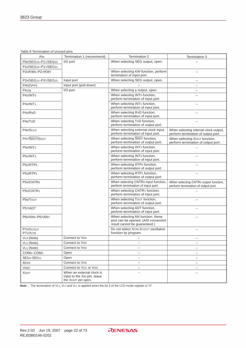
Rev.2.02 Jun 19, 2007 page 22 of 73REJ03B0146-0202
3823 Group
Table 8 Termination of unused pins
Pin
P00/SEG16–P17/SEG23
P10/SEG24–P17/SEG31
P20/KW0–P27/KW7
P34/SEG12–P37/SEG15
P40/(VPP)
P41/φ
P42/INT0
P43/INT1
P44/RxD
P45/TxD
P46/SCLK
P47/SRDY/SOUT
P50/INT2
P51/INT3
P52/RTP0
P53/RTP1
P54/CNTR0
P55/CNTR1
P56/TOUT
P57/ADT
P60/AN0–P67/AN7
P70/XCOUTP71/XCIN
VL3 (Note)
VL2 (Note)
VL1 (Note)
COM0–COM3
SEG0–SEG11
AVSS
VREF
XOUT
Termination 2
When selecting SEG output, open.
When selecting KW function, performtermination of input port.
When selecting SEG output, open.
–
When selecting φ output, open.
When selecting INT0 function,perform termination of input port.
When selecting INT1 function,perform termination of input port.
When selecting RXD function,perform termination of input port.
When selecting TXD function,perform termination of output port.
When selecting external clock input,perform termination of input port.
When selecting SRDY function,perform termination of output port.
When selecting INT2 function,perform termination of input port.
When selecting INT3 function,perform termination of input port.
When selecting RTP0 function,perform termination of output port.
When selecting RTP1 function,perform termination of output port.
When selecting CNTR0 input function,perform termination of input port.
When selecting CNTR1 function,perform termination of input port.
When selecting TOUT function,perform termination of output port.
When selecting ADT function,perform termination of input port.
When selecting AN function, thesepins can be opened. (A/D conversionresult cannot be guaranteed.)
Do not select XCIN-XCOUT oscillationfunction by program.
–
–
–
–
–
–
–
–
Termination 3
–
–
–
–
–
–
–
–
–
When selecting internal clock output,perform termination of output port.
When selecting SOUT function,perform termination of output port.
–
–
–
–
When selecting CNTR0 output function,perform termination of output port.
–
–
–
–
–
–
–
–
–
–
–
–
–
Termination 1 (recommend)
I/O port
Input port
Input port (pull-down)
I/O port
Connect to VSS
Connect to VSS
Connect to VSS
Open
Open
Connect to VSS
Connect to VCC or VSS
When an external clock isinput to the XIN pin, leavethe XOUT pin open.
Note : The termination of VL3, VL2 and VL1 is applied when the bit 3 of the LCD mode register is “0”

Rev.2.02 Jun 19, 2007 page 23 of 73REJ03B0146-0202
3823 Group
INTERRUPTSThe 3823 group interrupts are vector interrupts with a fixed prior-ity scheme, and generated by 16 sources among 17 sources: 8external, 8 internal, and 1 software.The interrupt sources, vector addresses (1) , and interrupt priorityare shown in Table 9.
Each interrupt except the BRK instruction interrupt has the inter-rupt request bit and the interrupt enable bit. These bits and theinterrupt disable flag (I flag) control the acceptance of interrupt re-quests. Figure 16 shows an interrupt control diagram.
Notes1: Vector addresses contain interrupt jump destination addresses.2: Reset function in the same way as an interrupt with the highest priority.
Table 9 Interrupt vector addresses and priority
RemarksInterrupt Request
Generating Conditions
At reset
At detection of either rising orfalling edge of INT0 input
At detection of either rising orfalling edge of INT1 input
At completion of serial interfacedata reception
At completion of serial interfacetransmit shift or when transmis-sion buffer is empty
Interrupt SourceLowHigh
PriorityVector Addresses (Note 1)
Reset (Note 2)INT0
INT1
Serial I/Oreception
Serial I/Otransmission
Timer X
Timer Y
Timer 2Timer 3
CNTR0
CNTR1
Timer 1
INT2
INT3
Key input(Key-on wake-up)
ADT
A/D conversion
BRK instruction
12
3
4
5
6
7
8
9
10
11
12
13
14
15
16
17
FFFD16
FFFB16
FFF916
FFF716
FFF516
FFF316
FFF116
FFEF16
FFED16
FFEB16
FFE916
FFE716
FFE516
FFE316
FFE116
FFDF16
FFDD16
FFFC16
FFFA16
FFF816
FFF616
FFF416
FFF216
FFF016
FFEE16
FFEC16
FFEA16
FFE816
FFE616
FFE416
FFE216
FFE016
FFDE16
FFDC16
At timer X underflow
At timer Y underflow
At timer 2 underflow
At timer 3 underflow
At detection of either rising orfalling edge of CNTR0 input
At detection of either rising orfalling edge of CNTR1 input
At timer 1 underflow
At detection of either rising orfalling edge of INT2 input
At detection of either rising orfalling edge of INT3 input
At falling of conjunction of inputlevel for port P2 (at input mode)
At falling of ADT input
At completion of A/D conversion
At BRK instruction execution
Non-maskable
External interrupt(active edge selectable)
External interrupt(active edge selectable)
Valid when serial interface is se-lected
Valid when serial interface is se-lected
External interrupt(active edge selectable)
External interrupt(active edge selectable)
External interrupt(active edge selectable)
External interrupt(active edge selectable)
External interrupt(Valid at falling)
Valid when ADT interrupt is se-lected, External interrupt(Valid at falling)
Valid when A/D interrupt is se-lected
Non-maskable software interrupt
An interrupt requests is accepted when all of the followingconditions are satisfied:
• Interrupt disable flag.................................“0”• Interrupt disable request bit ..................... “1”• Interrupt enable bit................................... “1”
Though the interrupt priority is determined by hardware, priorityprocessing can be performed by software using the above bitsand flag.
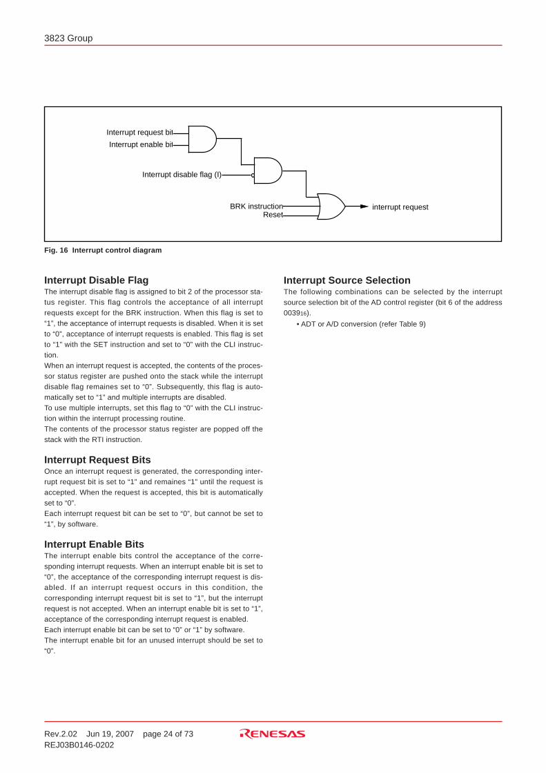
Rev.2.02 Jun 19, 2007 page 24 of 73REJ03B0146-0202
3823 Group
Fig. 16 Interrupt control diagram
I
n
t
e
r
r
u
p
t
r
e
q
u
e
s
t
b
i
t
I
n
t
e
r
r
u
p
t
e
n
a
b
l
e
b
i
t
I
n
t
e
r
r
u
p
t
d
i
s
a
b
l
e
f
l
a
g
(
I
)
B
R
K
i
n
s
t
r
u
c
t
i
o
nR
e
s
e
ti n
t
e
r
r
u
p
t
r
e
q
u
e
s
t
Interrupt Disable FlagThe interrupt disable flag is assigned to bit 2 of the processor sta-tus register. This flag controls the acceptance of all interruptrequests except for the BRK instruction. When this flag is set to“1”, the acceptance of interrupt requests is disabled. When it is setto “0”, acceptance of interrupt requests is enabled. This flag is setto “1” with the SET instruction and set to “0” with the CLI instruc-tion.When an interrupt request is accepted, the contents of the proces-sor status register are pushed onto the stack while the interruptdisable flag remaines set to “0”. Subsequently, this flag is auto-matically set to “1” and multiple interrupts are disabled.To use multiple interrupts, set this flag to “0” with the CLI instruc-tion within the interrupt processing routine.The contents of the processor status register are popped off thestack with the RTI instruction.
Interrupt Request BitsOnce an interrupt request is generated, the corresponding inter-rupt request bit is set to “1” and remaines “1” until the request isaccepted. When the request is accepted, this bit is automaticallyset to “0”.Each interrupt request bit can be set to “0”, but cannot be set to“1”, by software.
Interrupt Enable BitsThe interrupt enable bits control the acceptance of the corre-sponding interrupt requests. When an interrupt enable bit is set to“0”, the acceptance of the corresponding interrupt request is dis-abled. If an interrupt request occurs in this condition, thecorresponding interrupt request bit is set to “1”, but the interruptrequest is not accepted. When an interrupt enable bit is set to “1”,acceptance of the corresponding interrupt request is enabled.Each interrupt enable bit can be set to “0” or “1” by software.The interrupt enable bit for an unused interrupt should be set to“0”.
Interrupt Source SelectionThe following combinations can be selected by the interruptsource selection bit of the AD control register (bit 6 of the address003916).
• ADT or A/D conversion (refer Table 9)
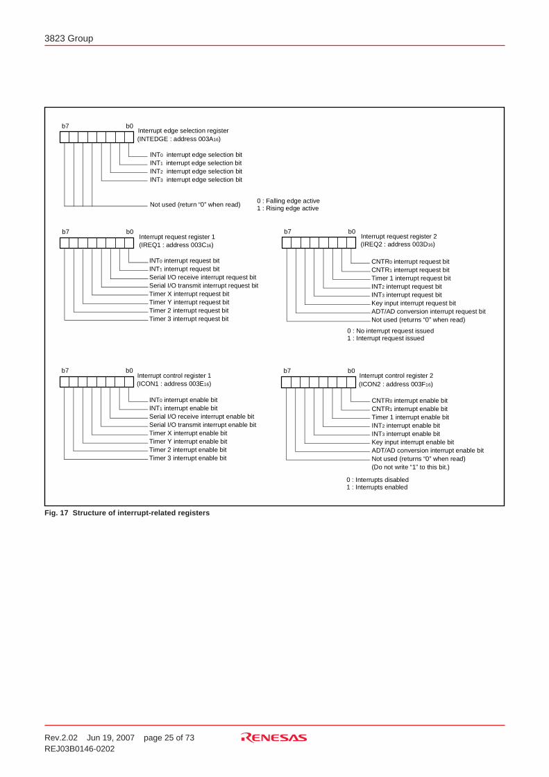
Rev.2.02 Jun 19, 2007 page 25 of 73REJ03B0146-0202
3823 Group
Fig. 17 Structure of interrupt-related registers
b
7 b
0I n
t
e
r
r
u
p
t
e
d
g
e
s
e
l
e
c
t
i
o
n
r
e
g
i
s
t
e
r
I N
T0
i
n
t
e
r
r
u
p
t
e
d
g
e
s
e
l
e
c
t
i
o
n
b
i
t
I
N
T1
i
n
t
e
r
r
u
p
t
e
d
g
e
s
e
l
e
c
t
i
o
n
b
i
tI
N
T2
i
n
t
e
r
r
u
p
t
e
d
g
e
s
e
l
e
c
t
i
o
n
b
i
tI
N
T3
i
n
t
e
r
r
u
p
t
e
d
g
e
s
e
l
e
c
t
i
o
n
b
i
t
N
o
t
u
s
e
d
(
r
e
t
u
r
n
“
0
”
w
h
e
n
r
e
a
d
)
( I
N
T
E
D
G
E
:
a
d
d
r
e
s
s
0
0
3
A1
6)
I n
t
e
r
r
u
p
t
r
e
q
u
e
s
t
r
e
g
i
s
t
e
r
1
I N
T0
i
n
t
e
r
r
u
p
t
r
e
q
u
e
s
t
b
i
t
I
N
T1
i
n
t
e
r
r
u
p
t
r
e
q
u
e
s
t
b
i
tS
e
r
i
a
l
I
/
O
r
e
c
e
i
v
e
i
n
t
e
r
r
u
p
t
r
e
q
u
e
s
t
b
i
t
S
e
r
i
a
l
I
/
O
t
r
a
n
s
m
i
t
i
n
t
e
r
r
u
p
t
r
e
q
u
e
s
t
b
i
tT
i
m
e
r
X
i
n
t
e
r
r
u
p
t
r
e
q
u
e
s
t
b
i
tT
i
m
e
r
Y
i
n
t
e
r
r
u
p
t
r
e
q
u
e
s
t
b
i
tT
i
m
e
r
2
i
n
t
e
r
r
u
p
t
r
e
q
u
e
s
t
b
i
tT
i
m
e
r
3
i
n
t
e
r
r
u
p
t
r
e
q
u
e
s
t
b
i
t
Interrupt control register 1
I N
T0
i
n
t
e
r
r
u
p
t
e
n
a
b
l
e
b
i
t
I
N
T1
i
n
t
e
r
r
u
p
t
e
n
a
b
l
e
b
i
tS
e
r
i
a
l
I
/
O
r
e
c
e
i
v
e
i
n
t
e
r
r
u
p
t
e
n
a
b
l
e
b
i
tS
e
r
i
a
l
I
/
O
t
r
a
n
s
m
i
t
i
n
t
e
r
r
u
p
t
e
n
a
b
l
e
b
i
tT
i
m
e
r
X
i
n
t
e
r
r
u
p
t
e
n
a
b
l
e
b
i
tT
i
m
e
r
Y
i
n
t
e
r
r
u
p
t
e
n
a
b
l
e
b
i
tT
i
m
e
r
2
i
n
t
e
r
r
u
p
t
e
n
a
b
l
e
b
i
tT
i
m
e
r
3
i
n
t
e
r
r
u
p
t
e
n
a
b
l
e
b
i
t
0
:
N
o
i
n
t
e
r
r
u
p
t
r
e
q
u
e
s
t
i
s
s
u
e
d1
:
I
n
t
e
r
r
u
p
t
r
e
q
u
e
s
t
i
s
s
u
e
d
( I
R
E
Q
1
:
a
d
d
r
e
s
s
0
0
3
C1
6)
( I
C
O
N
1
:
a
d
d
r
e
s
s
0
0
3
E1
6)
I n
t
e
r
r
u
p
t
r
e
q
u
e
s
t
r
e
g
i
s
t
e
r
2
C
N
T
R0
i
n
t
e
r
r
u
p
t
r
e
q
u
e
s
t
b
i
tC
N
T
R1
i
n
t
e
r
r
u
p
t
r
e
q
u
e
s
t
b
i
tT
i
m
e
r
1
i
n
t
e
r
r
u
p
t
r
e
q
u
e
s
t
b
i
tI
N
T2
i
n
t
e
r
r
u
p
t
r
e
q
u
e
s
t
b
i
tI
N
T3
i
n
t
e
r
r
u
p
t
r
e
q
u
e
s
t
b
i
t
K
e
y
i
n
p
u
t
i
n
t
e
r
r
u
p
t
r
e
q
u
e
s
t
b
i
tA
D
T
/
A
D
c
o
n
v
e
r
s
i
o
n
i
n
t
e
r
r
u
p
t
r
e
q
u
e
s
t
b
i
tN
o
t
u
s
e
d
(
r
e
t
u
r
n
s
“
0
”
w
h
e
n
r
e
a
d
)
(IREQ2 : address 003D16)
Interrupt control register 2
CNTR0 interrupt enable bitCNTR1 interrupt enable bitTimer 1 interrupt enable bitINT2 interrupt enable bitINT3 interrupt enable bit Key input interrupt enable bitADT/AD conversion interrupt enable bitNot used (returns “0” when read)(Do not write “1” to this bit.)
0 : Interrupts disabled1 : Interrupts enabled
(ICON2 : address 003F16)
0
:
F
a
l
l
i
n
g
e
d
g
e
a
c
t
i
v
e1
:
R
i
s
i
n
g
e
d
g
e
a
c
t
i
v
e
b7 b
0
b7 b0
b
7 b0
b7 b0
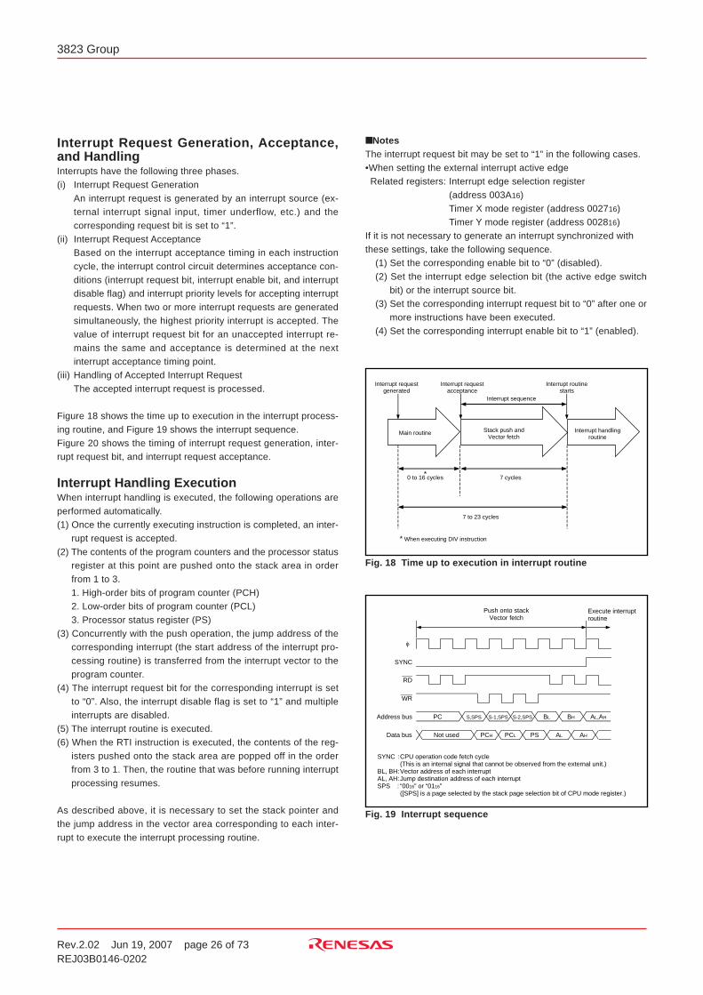
Rev.2.02 Jun 19, 2007 page 26 of 73REJ03B0146-0202
3823 Group
Interrupt Request Generation, Acceptance,and HandlingInterrupts have the following three phases.(i) Interrupt Request Generation
An interrupt request is generated by an interrupt source (ex-ternal interrupt signal input, timer underflow, etc.) and thecorresponding request bit is set to “1”.
(ii) Interrupt Request AcceptanceBased on the interrupt acceptance timing in each instructioncycle, the interrupt control circuit determines acceptance con-ditions (interrupt request bit, interrupt enable bit, and interruptdisable flag) and interrupt priority levels for accepting interruptrequests. When two or more interrupt requests are generatedsimultaneously, the highest priority interrupt is accepted. Thevalue of interrupt request bit for an unaccepted interrupt re-mains the same and acceptance is determined at the nextinterrupt acceptance timing point.
(iii) Handling of Accepted Interrupt RequestThe accepted interrupt request is processed.
Figure 18 shows the time up to execution in the interrupt process-ing routine, and Figure 19 shows the interrupt sequence.Figure 20 shows the timing of interrupt request generation, inter-rupt request bit, and interrupt request acceptance.
Interrupt Handling ExecutionWhen interrupt handling is executed, the following operations areperformed automatically.(1) Once the currently executing instruction is completed, an inter-
rupt request is accepted.(2) The contents of the program counters and the processor status
register at this point are pushed onto the stack area in orderfrom 1 to 3.1. High-order bits of program counter (PCH)2. Low-order bits of program counter (PCL)3. Processor status register (PS)
(3) Concurrently with the push operation, the jump address of thecorresponding interrupt (the start address of the interrupt pro-cessing routine) is transferred from the interrupt vector to theprogram counter.
(4) The interrupt request bit for the corresponding interrupt is setto “0”. Also, the interrupt disable flag is set to “1” and multipleinterrupts are disabled.
(5) The interrupt routine is executed.(6) When the RTI instruction is executed, the contents of the reg-
isters pushed onto the stack area are popped off in the orderfrom 3 to 1. Then, the routine that was before running interruptprocessing resumes.
As described above, it is necessary to set the stack pointer andthe jump address in the vector area corresponding to each inter-rupt to execute the interrupt processing routine.
NotesThe interrupt request bit may be set to “1” in the following cases.•When setting the external interrupt active edgeRelated registers: Interrupt edge selection register
(address 003A16)Timer X mode register (address 002716)Timer Y mode register (address 002816)
If it is not necessary to generate an interrupt synchronized withthese settings, take the following sequence.
(1) Set the corresponding enable bit to “0” (disabled).(2) Set the interrupt edge selection bit (the active edge switch
bit) or the interrupt source bit.(3) Set the corresponding interrupt request bit to “0” after one or
more instructions have been executed.(4) Set the corresponding interrupt enable bit to “1” (enabled).
Fig. 18 Time up to execution in interrupt routine
Fig. 19 Interrupt sequence
Main routine Interrupt handlingroutine
Interrupt requestgenerated
Interrupt requestacceptance
Interrupt routine starts
Interrupt sequence
7 cycles
7 to 23 cycles
* When executing DIV instruction
Stack push andVector fetch
0 to 16 cycles*
φ
SYNC
RD
WR
Address bus
Data bus
PC
Not used
S,SPS S-1,SPS S-2,SPS BL BH AL,AH
PCH PCL PS AL AH
SYNC :CPU operation code fetch cycle(This is an internal signal that cannot be observed from the external unit.)
BL, BH:Vector address of each interruptAL, AH:Jump destination address of each interruptSPS : “0016” or “0116”
([SPS] is a page selected by the stack page selection bit of CPU mode register.)
Push onto stackVector fetch
Execute interruptroutine
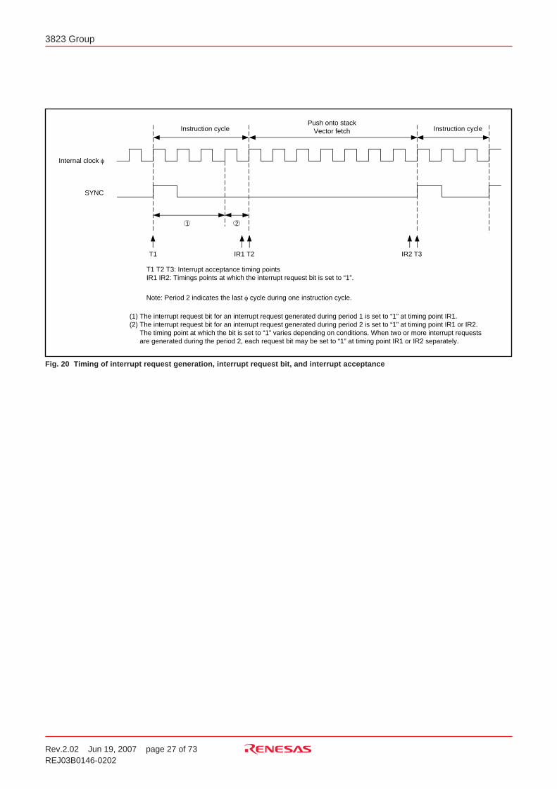
Rev.2.02 Jun 19, 2007 page 27 of 73REJ03B0146-0202
3823 Group
Fig. 20 Timing of interrupt request generation, interrupt request bit, and interrupt acceptance
Internal clock φ
SYNC
Instruction cycle
T1 IR1 T2
T1 T2 T3: Interrupt acceptance timing pointsIR1 IR2: Timings points at which the interrupt request bit is set to “1”.
Push onto stackVector fetch Instruction cycle
IR2 T3
Note: Period 2 indicates the last φ cycle during one instruction cycle.
(1) The interrupt request bit for an interrupt request generated during period 1 is set to “1” at timing point IR1.(2) The interrupt request bit for an interrupt request generated during period 2 is set to “1” at timing point IR1 or IR2.
The timing point at which the bit is set to “1” varies depending on conditions. When two or more interrupt requests are generated during the period 2, each request bit may be set to “1” at timing point IR1 or IR2 separately.
21
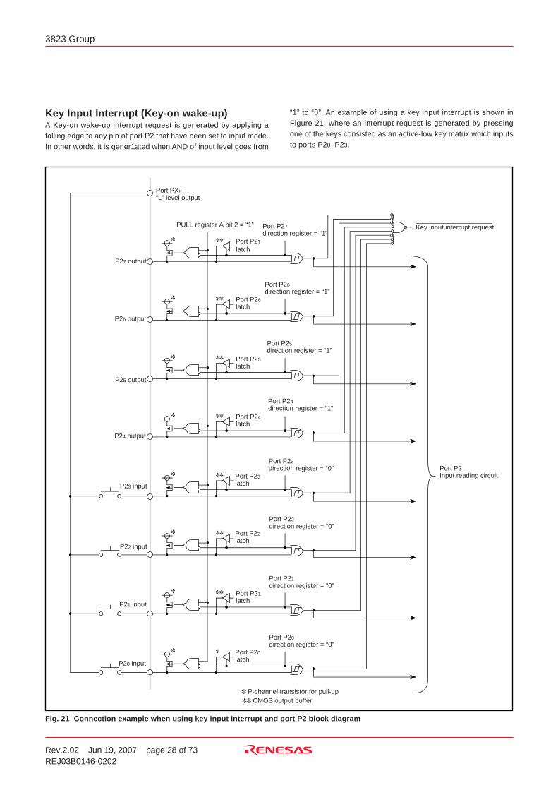
Rev.2.02 Jun 19, 2007 page 28 of 73REJ03B0146-0202
3823 Group
Key Input Interrupt (Key-on wake-up)A Key-on wake-up interrupt request is generated by applying afalling edge to any pin of port P2 that have been set to input mode.In other words, it is gener1ated when AND of input level goes from
“1” to “0”. An example of using a key input interrupt is shown inFigure 21, where an interrupt request is generated by pressingone of the keys consisted as an active-low key matrix which inputsto ports P20–P23.
Fig. 21 Connection example when using key input interrupt and port P2 block diagram
Port PXX
“L” level output
Port P27direction register = “1”
P
27
o
u
t
p
u
t
P
26
o
u
t
p
u
t
P
U
L
L
r
e
g
i
s
t
e
r
A
b
i
t
2
=
“
1
”
P25 output
P24 output
P
23
i
n
p
u
t
Port P26 latch
Port P25latch
Port P24 latch
Port P23 latch
Port P27
latch
Port P25direction register = “1”
Port P24direction register = “1”
P
o
r
t
P
23d
i
r
e
c
t
i
o
n
r
e
g
i
s
t
e
r
=
“
0
”
P22 input
P
21
i
n
p
u
t
P20 input
Port P22 latch
Port P21latch
Port P20 latch
Port P22direction register = “0”
Port P21direction register = “0”
Port P20direction register = “0”
P
o
r
t
P
2I
n
p
u
t
r
e
a
d
i
n
g
c
i
r
c
u
i
t
P-channel transistor for pull-up CMOS output buffer
Key input interrupt request
P
o
r
t
P
26d
i
r
e
c
t
i
o
n
r
e
g
i
s
t
e
r
=
“
1
”
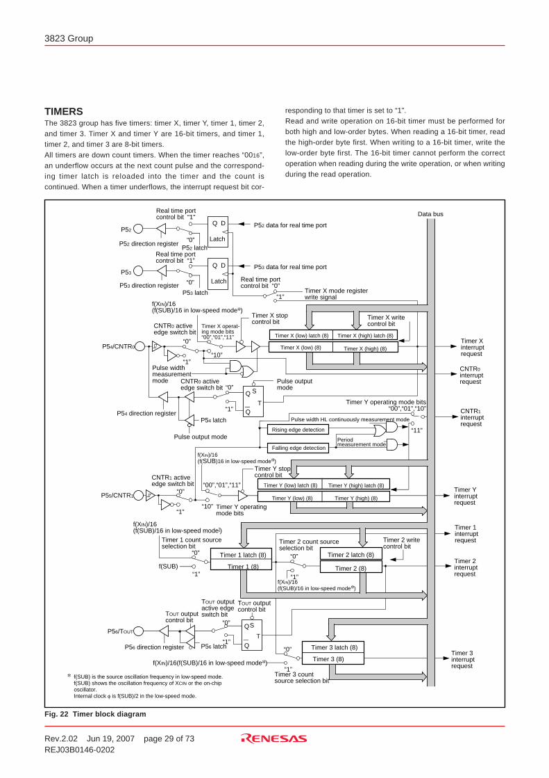
Rev.2.02 Jun 19, 2007 page 29 of 73REJ03B0146-0202
3823 Group
TIMERSThe 3823 group has five timers: timer X, timer Y, timer 1, timer 2,and timer 3. Timer X and timer Y are 16-bit timers, and timer 1,timer 2, and timer 3 are 8-bit timers.All timers are down count timers. When the timer reaches “0016”,an underflow occurs at the next count pulse and the correspond-ing timer latch is reloaded into the timer and the count iscontinued. When a timer underflows, the interrupt request bit cor-
responding to that timer is set to “1”.Read and write operation on 16-bit timer must be performed forboth high and low-order bytes. When reading a 16-bit timer, readthe high-order byte first. When writing to a 16-bit timer, write thelow-order byte first. The 16-bit timer cannot perform the correctoperation when reading during the write operation, or when writingduring the read operation.
Fig. 22 Timer block diagram
CNTR0 activeedge switch bit
Timer 1 count sourceselection bit
Real time portcontrol bit “0”
“1”
P55/CNTR1“0”
f(XIN)/16(f(SUB)16 in low-speed mode )
CNTR1 activeedge switch bit
“10”
Timer Y stopcontrol bit
Falling edge detection
Periodmeasurement mode
Timer Yinterruptrequest
Pulse width HL continuously measurement mode
Rising edge detection
“00”,“01”,“11”
Timer Y operating mode bits
Timer Xinterruptrequest
Timer X mode registerwrite signal
P54/CNTR0
Q
QT
S
P54 direction register
Pulse output mode
P54 latch
Timer X stopcontrol bit
“0”
“1”
Timer X writecontrol bit
Q D
Latch
Q D
Latch
“1”
“0”
“1”“10”
Timer X operat-ing mode bits“00”,“01”,“11”
f(XIN)/16(f(SUB)/16 in low-speed mode )
Pulse widthmeasurement mode
CNTR0 activeedge switch bit
Pulse output mode
Q
Q
T
S
“0”
P56 direction register P56 latch“1”
TOUT outputactive edge switch bit
Timer 2 writecontrol bit
“0”
“1”
TOUT outputcontrol bit
“1”
P56/TOUT
f(SUB)
Timer 3 countsource selection bit
“0”
“1”
Timer 2interruptrequest
Timer 3interruptrequest
Timer 2 count sourceselection bit
Timer 1interruptrequest
Data bus
f(XIN)/16(f(SUB)/16 in low-speed mode])
f(XIN)/16(f(SUB)/16 in low-speed mode )
f(XIN)/16(f(SUB)/16 in low-speed mode )
CNTR0interruptrequest
CNTR1interruptrequest
Timer Y operating mode bits“00”,“01”,“10”
“11”
Real time port control bit “1”
P52 latchReal time port control bit “1”
P53 latch
Timer Y (low) (8) Timer Y (high) (8)
Timer 3 latch (8)
Timer 3 (8)
Timer 1 latch (8)
Timer 1 (8)
Timer 2 latch (8)
Timer 2 (8)
Timer X (low) (8) Timer X (high) (8)
Timer X (low) latch (8) Timer X (high) latch (8)
Timer Y (low) latch (8) Timer Y (high) latch (8)
TOUT outputcontrol bit
“0”
“0”
“0”
P52
P53
P52 direction register
P53 direction register
P52 data for real time port
P53 data for real time port
f(SUB) is the source oscillation frequency in low-speed mode. f(SUB) shows the oscillation frequency of XCIN or the on-chiposcillator.Internal clock φ is f(SUB)/2 in the low-speed mode.
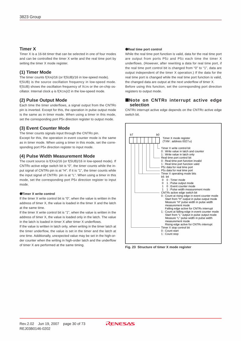
Rev.2.02 Jun 19, 2007 page 30 of 73REJ03B0146-0202
3823 Group
Timer XTimer X is a 16-bit timer that can be selected in one of four modesand can be controlled the timer X write and the real time port bysetting the timer X mode register.
(1) Timer ModeThe timer counts f(XIN)/16 (or f(SUB)/16 in low-speed mode).f(SUB) is the source oscillation frequency in low-speed mode.f(SUB) shows the oscillation frequency of XCIN or the on-chip os-cillator. Internal clock φ is f(XCIN)/2 in the low-speed mode.
(2) Pulse Output ModeEach time the timer underflows, a signal output from the CNTR0
pin is inverted. Except for this, the operation in pulse output modeis the same as in timer mode. When using a timer in this mode,set the corresponding port P54 direction register to output mode.
(3) Event Counter ModeThe timer counts signals input through the CNTR0 pin.Except for this, the operation in event counter mode is the sameas in timer mode. When using a timer in this mode, set the corre-sponding port P54 direction register to input mode.
(4) Pulse Width Measurement ModeThe count source is f(XIN)/16 (or f(SUB)/16 in low-speed mode). IfCNTR0 active edge switch bit is “0”, the timer counts while the in-put signal of CNTR0 pin is at “H”. If it is “1”, the timer counts whilethe input signal of CNTR0 pin is at “L”. When using a timer in thismode, set the corresponding port P54 direction register to inputmode.
Timer X write controlIf the timer X write control bit is “0”, when the value is written in theaddress of timer X, the value is loaded in the timer X and the latchat the same time.If the timer X write control bit is “1”, when the value is written in theaddress of timer X, the value is loaded only in the latch. The valuein the latch is loaded in timer X after timer X underflows.If the value is written in latch only, when writing in the timer latch atthe timer underflow, the value is set in the timer and the latch atone time. Additionally, unexpected value may be set in the high-or-der counter when the writing in high-order latch and the underflowof timer X are performed at the same timing.
Real time port controlWhile the real time port function is valid, data for the real time portare output from ports P52 and P53 each time the timer Xunderflows. (However, after rewriting a data for real time port, ifthe real time port control bit is changed from “0” to “1”, data areoutput independent of the timer X operation.) If the data for thereal time port is changed while the real time port function is valid,the changed data are output at the next underflow of timer X.Before using this function, set the corresponding port directionregisters to output mode.
Note on CNTR0 interrupt active edgeselection
CNTR0 interrupt active edge depends on the CNTR0 active edgeswitch bit.
Fig. 23 Structure of timer X mode register
T
i
m
e
r
X
m
o
d
e
r
e
g
i
s
t
e
r(
T
X
M
:
a
d
d
r
e
s
s
0
0
2
71
6)
T
i
m
e
r
X
w
r
i
t
e
c
o
n
t
r
o
l
b
i
t0
:
W
r
i
t
e
v
a
l
u
e
i
n
l
a
t
c
h
a
n
d
c
o
u
n
t
e
r1
:
W
r
i
t
e
v
a
l
u
e
i
n
l
a
t
c
h
o
n
l
yR
e
a
l
t
i
m
e
p
o
r
t
c
o
n
t
r
o
l
b
i
t0
:
R
e
a
l
t
i
m
e
p
o
r
t
f
u
n
c
t
i
o
n
i
n
v
a
l
i
d1
:
R
e
a
l
t
i
m
e
p
o
r
t
f
u
n
c
t
i
o
n
v
a
l
i
dP
52
d
a
t
a
f
o
r
r
e
a
l
t
i
m
e
p
o
r
tP
53
d
a
t
a
f
o
r
r
e
a
l
t
i
m
e
p
o
r
tT
i
m
e
r
X
o
p
e
r
a
t
i
n
g
m
o
d
e
b
i
t
sb
5
b
4
0
0
:
T
i
m
e
r
m
o
d
e
0
1
:
P
u
l
s
e
o
u
t
p
u
t
m
o
d
e
1
0
:
E
v
e
n
t
c
o
u
n
t
e
r
m
o
d
e
1
1
:
P
u
l
s
e
w
i
d
t
h
m
e
a
s
u
r
e
m
e
n
t
m
o
d
eC
N
T
R0
a
c
t
i
v
e
e
d
g
e
s
w
i
t
c
h
b
i
t0
:
C
o
u
n
t
a
t
r
i
s
i
n
g
e
d
g
e
i
n
e
v
e
n
t
c
o
u
n
t
e
r
m
o
d
e
S
t
a
r
t
f
r
o
m
“
H
”
o
u
t
p
u
t
i
n
p
u
l
s
e
o
u
t
p
u
t
m
o
d
e
M
e
a
s
u
r
e
“
H
”
p
u
l
s
e
w
i
d
t
h
i
n
p
u
l
s
e
w
i
d
t
h
m
e
a
s
u
r
e
m
e
n
t
m
o
d
e
F
a
l
l
i
n
g
e
d
g
e
a
c
t
i
v
e
f
o
r
C
N
T
R0
i
n
t
e
r
r
u
p
t
1
:
C
o
u
n
t
a
t
f
a
l
l
i
n
g
e
d
g
e
i
n
e
v
e
n
t
c
o
u
n
t
e
r
m
o
d
e
S
t
a
r
t
f
r
o
m
“
L
”
o
u
t
p
u
t
i
n
p
u
l
s
e
o
u
t
p
u
t
m
o
d
e
M
e
a
s
u
r
e
“
L
”
p
u
l
s
e
w
i
d
t
h
i
n
p
u
l
s
e
w
i
d
t
h
m
e
a
s
u
r
e
m
e
n
t
m
o
d
e
R
i
s
i
n
g
e
d
g
e
a
c
t
i
v
e
f
o
r
C
N
T
R0
i
n
t
e
r
r
u
p
tT
i
m
e
r
X
s
t
o
p
c
o
n
t
r
o
l
b
i
t0
:
C
o
u
n
t
s
t
a
r
t1
:
C
o
u
n
t
s
t
o
p
b
7 b
0
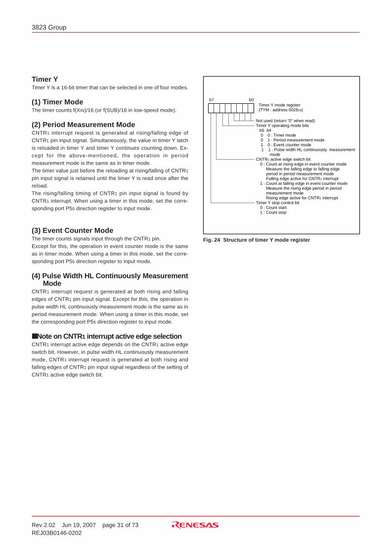
Rev.2.02 Jun 19, 2007 page 31 of 73REJ03B0146-0202
3823 Group
Timer YTimer Y is a 16-bit timer that can be selected in one of four modes.
(1) Timer ModeThe timer counts f(XIN)/16 (or f(SUB)/16 in low-speed mode).
(2) Period Measurement ModeCNTR1 interrupt request is generated at rising/falling edge ofCNTR1 pin input signal. Simultaneously, the value in timer Y latchis reloaded in timer Y and timer Y continues counting down. Ex-cept for the above-mentioned, the operation in periodmeasurement mode is the same as in timer mode.The timer value just before the reloading at rising/falling of CNTR1
pin input signal is retained until the timer Y is read once after thereload.The rising/falling timing of CNTR1 pin input signal is found byCNTR1 interrupt. When using a timer in this mode, set the corre-sponding port P55 direction register to input mode.
(3) Event Counter ModeThe timer counts signals input through the CNTR1 pin.Except for this, the operation in event counter mode is the sameas in timer mode. When using a timer in this mode, set the corre-sponding port P55 direction register to input mode.
(4) Pulse Width HL Continuously MeasurementMode
CNTR1 interrupt request is generated at both rising and fallingedges of CNTR1 pin input signal. Except for this, the operation inpulse width HL continuously measurement mode is the same as inperiod measurement mode. When using a timer in this mode, setthe corresponding port P55 direction register to input mode.
Note on CNTR1 interrupt active edge selectionCNTR1 interrupt active edge depends on the CNTR1 active edgeswitch bit. However, in pulse width HL continuously measurementmode, CNTR1 interrupt request is generated at both rising andfalling edges of CNTR1 pin input signal regardless of the setting ofCNTR1 active edge switch bit.
Fig. 24 Structure of timer Y mode register
T
i
m
e
r
Y
m
o
d
e
r
e
g
i
s
t
e
r(
T
Y
M
:
a
d
d
r
e
s
s
0
0
2
81
6)
b7 b
0
N
o
t
u
s
e
d
(
r
e
t
u
r
n
“
0
”
w
h
e
n
r
e
a
d
)T
i
m
e
r
Y
o
p
e
r
a
t
i
n
g
m
o
d
e
b
i
t
sb
5
b
4
0
0
:
T
i
m
e
r
m
o
d
e
0
1
:
P
e
r
i
o
d
m
e
a
s
u
r
e
m
e
n
t
m
o
d
e
1
0
:
E
v
e
n
t
c
o
u
n
t
e
r
m
o
d
e
1
1
:
P
u
l
s
e
w
i
d
t
h
H
L
c
o
n
t
i
n
u
o
u
s
l
y
m
e
a
s
u
r
e
m
e
n
t
m
o
d
eC
N
T
R1
a
c
t
i
v
e
e
d
g
e
s
w
i
t
c
h
b
i
t0
:
C
o
u
n
t
a
t
r
i
s
i
n
g
e
d
g
e
i
n
e
v
e
n
t
c
o
u
n
t
e
r
m
o
d
e
M
e
a
s
u
r
e
t
h
e
f
a
l
l
i
n
g
e
d
g
e
t
o
f
a
l
l
i
n
g
e
d
g
e
p
e
r
i
o
d
i
n
p
e
r
i
o
d
m
e
a
s
u
r
e
m
e
n
t
m
o
d
e
F
a
l
l
i
n
g
e
d
g
e
a
c
t
i
v
e
f
o
r
C
N
T
R1
i
n
t
e
r
r
u
p
t
1
:
C
o
u
n
t
a
t
f
a
l
l
i
n
g
e
d
g
e
i
n
e
v
e
n
t
c
o
u
n
t
e
r
m
o
d
eM
e
a
s
u
r
e
t
h
e
r
i
s
i
n
g
e
d
g
e
p
e
r
i
o
d
i
n
p
e
r
i
o
d
m
e
a
s
u
r
e
m
e
n
t
m
o
d
e
R
i
s
i
n
g
e
d
g
e
a
c
t
i
v
e
f
o
r
C
N
T
R1
i
n
t
e
r
r
u
p
t
T
i
m
e
r
Y
s
t
o
p
c
o
n
t
r
o
l
b
i
t
0
:
C
o
u
n
t
s
t
a
r
t1
:
C
o
u
n
t
s
t
o
p
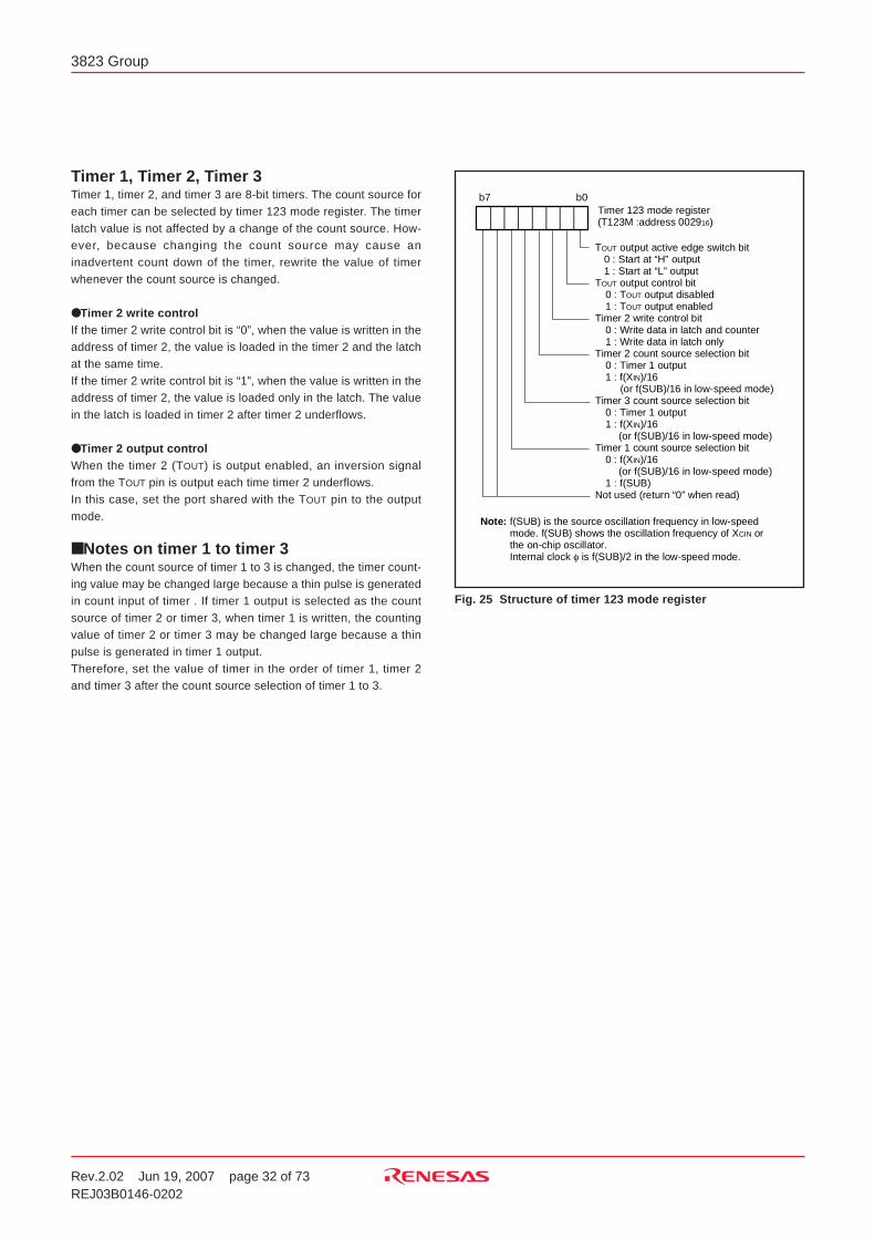
Rev.2.02 Jun 19, 2007 page 32 of 73REJ03B0146-0202
3823 Group
Timer 1, Timer 2, Timer 3Timer 1, timer 2, and timer 3 are 8-bit timers. The count source foreach timer can be selected by timer 123 mode register. The timerlatch value is not affected by a change of the count source. How-ever, because changing the count source may cause aninadvertent count down of the timer, rewrite the value of timerwhenever the count source is changed.
Timer 2 write controlIf the timer 2 write control bit is “0”, when the value is written in theaddress of timer 2, the value is loaded in the timer 2 and the latchat the same time.If the timer 2 write control bit is “1”, when the value is written in theaddress of timer 2, the value is loaded only in the latch. The valuein the latch is loaded in timer 2 after timer 2 underflows.
Timer 2 output controlWhen the timer 2 (TOUT) is output enabled, an inversion signalfrom the TOUT pin is output each time timer 2 underflows.In this case, set the port shared with the TOUT pin to the outputmode.
Notes on timer 1 to timer 3When the count source of timer 1 to 3 is changed, the timer count-ing value may be changed large because a thin pulse is generatedin count input of timer . If timer 1 output is selected as the countsource of timer 2 or timer 3, when timer 1 is written, the countingvalue of timer 2 or timer 3 may be changed large because a thinpulse is generated in timer 1 output.Therefore, set the value of timer in the order of timer 1, timer 2and timer 3 after the count source selection of timer 1 to 3.
Fig. 25 Structure of timer 123 mode register
TO
U
T
o
u
t
p
u
t
a
c
t
i
v
e
e
d
g
e
s
w
i
t
c
h
b
i
t0
:
S
t
a
r
t
a
t
“
H
”
o
u
t
p
u
t1
:
S
t
a
r
t
a
t
“
L
”
o
u
t
p
u
tTO
U
T o
u
t
p
u
t
c
o
n
t
r
o
l
b
i
t0
:
TO
U
T o
u
t
p
u
t
d
i
s
a
b
l
e
d1
:
TO
U
T o
u
t
p
u
t
e
n
a
b
l
e
dT
i
m
e
r
2
w
r
i
t
e
c
o
n
t
r
o
l
b
i
t0
:
W
r
i
t
e
d
a
t
a
i
n
l
a
t
c
h
a
n
d
c
o
u
n
t
e
r1
:
W
r
i
t
e
d
a
t
a
i
n
l
a
t
c
h
o
n
l
yT
i
m
e
r
2
c
o
u
n
t
s
o
u
r
c
e
s
e
l
e
c
t
i
o
n
b
i
t0
:
T
i
m
e
r
1
o
u
t
p
u
t1
:
f
(
XI
N)
/
1
6(
o
r
f
(
S
U
B
)
/
1
6
i
n
l
o
w
-
s
p
e
e
d
m
o
d
e
)T
i
m
e
r
3
c
o
u
n
t
s
o
u
r
c
e
s
e
l
e
c
t
i
o
n
b
i
t0
:
T
i
m
e
r
1
o
u
t
p
u
t1
:
f
(
XI
N)
/
1
6(
o
r
f
(
S
U
B
)
/
1
6
i
n
l
o
w
-
s
p
e
e
d
m
o
d
e
)T
i
m
e
r
1
c
o
u
n
t
s
o
u
r
c
e
s
e
l
e
c
t
i
o
n
b
i
t0
:
f
(
XI
N)
/
1
6(
o
r
f
(
S
U
B
)
/
1
6
i
n
l
o
w
-
s
p
e
e
d
m
o
d
e
)1
:
f
(
S
U
B
)N
o
t
u
s
e
d
(
r
e
t
u
r
n
“
0
”
w
h
e
n
r
e
a
d
)
T
i
m
e
r
1
2
3
m
o
d
e
r
e
g
i
s
t
e
r(
T
1
2
3
M
:
a
d
d
r
e
s
s
0
0
2
91
6)
N
o
t
e
: f
(
S
U
B
)
i
s
t
h
e
s
o
u
r
c
e
o
s
c
i
l
l
a
t
i
o
n
f
r
e
q
u
e
n
c
y
i
n
l
o
w
-
s
p
e
e
d
m
o
d
e
.
f
(
S
U
B
)
s
h
o
w
s
t
h
e
o
s
c
i
l
l
a
t
i
o
n
f
r
e
q
u
e
n
c
y
o
f
XC
I
N
o
r
t
h
e
o
n
-
c
h
i
p
o
s
c
i
l
l
a
t
o
r
.I
n
t
e
r
n
a
l
c
l
o
c
k
φ
i
s
f
(
S
U
B
)
/
2
i
n
t
h
e
l
o
w
-
s
p
e
e
d
m
o
d
e
.
b7 b
0

Rev.2.02 Jun 19, 2007 page 33 of 73REJ03B0146-0202
3823 Group
SERIAL INTERFACESerial I/OSerial I/O can be used as either clock synchronous or asynchro-nous (UART) serial I/O. A dedicated timer (baud rate generator) isalso provided for baud rate generation.
(1) Clock Synchronous Serial I/O ModeClock synchronous serial I/O can be selected by setting the modeselection bit of the serial I/O control register to “1”.For clock synchronous serial I/O, the transmitter and the receivermust use the same clock. If an internal clock is used, transfer isstarted by a write signal to the transmit/receive buffer register.The MSB first transfer is selected as the transfer direction by settingthe bit 0 in the peripheral function expansion register to “1”. Also, thesynchronous serial I/O output switches to the P47/SRDY/SOUT pin bysetting the bit 1 in the peripheral function expansion register to “1”.
Fig. 26 Block diagram of clock synchronous serial I/O
Fig. 27 Operation of clock synchronous serial I/O function
P
46/
SC
L
K
P47/SRDY1/SOUT
P44/RXD
P45/TXD
f (
XI
N) 1
/
4
1
/
4
F
/
F
S
e
r
i
a
l
I
/
O
s
t
a
t
u
s
r
e
g
i
s
t
e
r
S
e
r
i
a
l
I
/
O
c
o
n
t
r
o
l
r
e
g
i
s
t
e
r
R
e
c
e
i
v
e
b
u
f
f
e
r
r
e
g
i
s
t
e
r
A
d
d
r
e
s
s
0
0
1
81
6
R
e
c
e
i
v
e
s
h
i
f
t
r
e
g
i
s
t
e
r
R
e
c
e
i
v
e
b
u
f
f
e
r
f
u
l
l
f
l
a
g
(
R
B
F
)
R
e
c
e
i
v
e
i
n
t
e
r
r
u
p
t
r
e
q
u
e
s
t
(
R
I
)
C
l
o
c
k
c
o
n
t
r
o
l
c
i
r
c
u
i
tShift clock
S
e
r
i
a
l
I
/
O
c
l
o
c
k
s
e
l
e
c
t
i
o
n
b
i
t
F
r
e
q
u
e
n
c
y
d
i
v
i
s
i
o
n
r
a
t
i
o
1
/
(
n
+
1
)
B
a
u
d
r
a
t
e
g
e
n
e
r
a
t
o
r
A
d
d
r
e
s
s
0
0
1
C1
6
B
R
G
c
o
u
n
t
s
o
u
r
c
e
s
e
l
e
c
t
i
o
n
b
i
t
Clock control circuitF
a
l
l
i
n
g
-
e
d
g
e
d
e
t
e
c
t
o
r
Data bus
A
d
d
r
e
s
s
0
0
1
81
6
Shift clock Transmit shift register shift completion flag (TSC)
T
r
a
n
s
m
i
t
b
u
f
f
e
r
e
m
p
t
y
f
l
a
g
(
T
B
E
)
T
r
a
n
s
m
i
t
i
n
t
e
r
r
u
p
t
r
e
q
u
e
s
t
(
T
I
)
T
r
a
n
s
m
i
t
i
n
t
e
r
r
u
p
t
s
o
u
r
c
e
s
e
l
e
c
t
i
o
n
b
i
t
Address 001916
D
a
t
a
b
u
s
A
d
d
r
e
s
s
0
0
1
A1
6
T
r
a
n
s
m
i
t
b
u
f
f
e
r
r
e
g
i
s
t
e
r
T
r
a
n
s
m
i
t
s
h
i
f
t
r
e
g
i
s
t
e
r
( f
(
S
U
B
)
i
n
l
o
w
-
s
p
e
e
d
m
o
d
e
)
T
r
a
n
s
f
e
r
d
i
r
e
c
t
i
o
n
s
e
l
e
c
t
i
o
n
b
i
t
Serial output pin selection bit
S
e
r
i
a
l
o
u
t
p
u
t
p
i
n
s
e
l
e
c
t
i
o
n
b
i
t T
r
a
n
s
f
e
r
d
i
r
e
c
t
i
o
ns
e
l
e
c
t
i
o
n
b
i
t
N
o
t
e
:
f
(
S
U
B
)
i
s
t
h
e
s
o
u
r
c
e
o
s
c
i
l
l
a
t
i
o
n
f
r
e
q
u
e
n
c
y
i
n
l
o
w
-
s
p
e
e
d
m
o
d
e
.
f
(
S
U
B
)
s
h
o
w
s
t
h
e
o
s
c
i
l
l
a
t
i
o
n
f
r
e
q
u
e
n
c
y
o
f
XC
I
N
o
r
t
h
e
o
n
-
c
h
i
p
o
s
c
i
l
l
a
t
o
r
.
R
e
c
e
i
v
e
e
n
a
b
l
e
s
i
g
n
a
l
SR
D
Y
D7D0 D1 D2 D3 D4 D5 D6
RBF = 1TSC = 1
T
B
E
=
0T
B
E
=
1T
S
C
=
0
Transfer shift clock(1/2 to 1/2048 of the internal clock, or an external clock)
Serial output TXD(or SOUT)
S
e
r
i
a
l
i
n
p
u
t
RXD
W
r
i
t
e
s
i
g
n
a
l
t
o
r
e
c
e
i
v
e
/
t
r
a
n
s
m
i
t
b
u
f
f
e
r
r
e
g
i
s
t
e
r
(
a
d
d
r
e
s
s
0
0
1
81
6)
O
v
e
r
r
u
n
e
r
r
o
r
(
O
E
)
d
e
t
e
c
t
i
o
n
N
o
t
e
s 1
:
T
h
e
t
r
a
n
s
m
i
t
i
n
t
e
r
r
u
p
t
(
T
I
)
c
a
n
b
e
g
e
n
e
r
a
t
e
d
e
i
t
h
e
r
w
h
e
n
t
h
e
t
r
a
n
s
m
i
t
b
u
f
f
e
r
r
e
g
i
s
t
e
r
h
a
s
e
m
p
t
i
e
d
(
T
B
E
=
1
)
o
r
a
f
t
e
r
t
h
e
t
r
a
n
s
m
i
t
s
h
i
f
t
o
p
e
r
a
t
i
o
n
h
a
s
e
n
d
e
d
(
T
S
C
=
1
)
,
b
y
s
e
t
t
i
n
g
t
h
e
t
r
a
n
s
m
i
t
i
n
t
e
r
r
u
p
t
s
o
u
r
c
e
s
e
l
e
c
t
i
o
n
b
i
t
(
T
I
C
)
o
f
t
h
e
s
e
r
i
a
l
I
/
O
c
o
n
t
r
o
l
r
e
g
i
s
t
e
r
.2
:
I
f
d
a
t
a
i
s
w
r
i
t
t
e
n
t
o
t
h
e
t
r
a
n
s
m
i
t
b
u
f
f
e
r
r
e
g
i
s
t
e
r
w
h
e
n
T
S
C
=
0
,
t
h
e
t
r
a
n
s
m
i
t
c
l
o
c
k
i
s
g
e
n
e
r
a
t
e
d
c
o
n
t
i
n
u
o
u
s
l
y
a
n
d
s
e
r
i
a
l
d
a
t
a
i
s
o
u
t
p
u
t
c
o
n
t
i
n
u
o
u
s
l
y
f
r
o
m
t
h
e
TXD
p
i
n
.
3
:
T
h
e
r
e
c
e
i
v
e
i
n
t
e
r
r
u
p
t
(
R
I
)
i
s
s
e
t
w
h
e
n
t
h
e
r
e
c
e
i
v
e
b
u
f
f
e
r
f
u
l
l
f
l
a
g
(
R
B
F
)
b
e
c
o
m
e
s
“
1
”
.
D7D0 D1 D2 D3 D4 D5 D6
T
x
D
a
n
d
R
x
D
a
b
o
v
e
s
h
o
w
s
t
h
e
o
p
e
r
a
t
i
o
n
w
h
e
n
s
e
l
e
c
t
i
n
g
L
S
B
f
i
r
s
t
t
r
a
n
s
f
e
r
.

Rev.2.02 Jun 19, 2007 page 34 of 73REJ03B0146-0202
3823 Group
(2) Asynchronous Serial I/O (UART) ModeClock asynchronous serial I/O mode (UART) can be selected byclearing the serial I/O mode selection bit of the serial I/O controlregister to “0”.Eight serial data transfer formats can be selected, and the transferformats used by a transmitter and receiver must be identical.The transmit and receive shift registers each have a buffer regis-
ter, but the two buffers have the same address in memory. Sincethe shift register cannot be written to or read from directly, transmitdata is written to the transmit buffer, and receive data is read fromthe receive buffer.The transmit buffer can also hold the next data to be transmitted,and the receive buffer register can hold a character while the nextcharacter is being received.
Fig. 28 Block diagram of UART serial I/O
Fig. 29 Operation of UART serial I/O function
f(XIN)
1
/
4
O
E
P
E F
E
1
/
1
6
1/16
Data bus
R
e
c
e
i
v
e
b
u
f
f
e
r
r
e
g
i
s
t
e
r
Address 001816
R
e
c
e
i
v
e
s
h
i
f
t
r
e
g
i
s
t
e
r
R
e
c
e
i
v
e
b
u
f
f
e
r
f
u
l
l
f
l
a
g
(
R
B
F
)R
e
c
e
i
v
e
i
n
t
e
r
r
u
p
t
r
e
q
u
e
s
t
(
R
I
)
Baud rate generator
Frequency division ratio 1/(n+1)
Address 001C16
S
T
/
S
P
/
P
A
g
e
n
e
r
a
t
o
r
Transmit buffer register
D
a
t
a
b
u
s
Transmit shift register
Address 001816
Transmit shift register shift completion flag (TSC)
Transmit buffer empty flag (TBE)
Transmit interrupt request (TI)
Address 001916
S
T
d
e
t
e
c
t
o
r
S
P
d
e
t
e
c
t
o
r UART control registerA
d
d
r
e
s
s
0
0
1
B1
6
C
h
a
r
a
c
t
e
r
l
e
n
g
t
h
s
e
l
e
c
t
i
o
n
b
i
t
Address 001A16
B
R
G
c
o
u
n
t
s
o
u
r
c
e
s
e
l
e
c
t
i
o
n
b
i
t
T
r
a
n
s
m
i
t
i
n
t
e
r
r
u
p
t
s
o
u
r
c
e
s
e
l
e
c
t
i
o
n
b
i
t
Serial I/O synchronous clock selection bit
C
l
o
c
k
c
o
n
t
r
o
l
c
i
r
c
u
i
t
C
h
a
r
a
c
t
e
r
l
e
n
g
t
h
s
e
l
e
c
t
i
o
n
b
i
t
7
b
i
t
s
8
b
i
t
s
Serial I/O control register
P
46/
SC
L
K
Serial I/O status register
P
44/
RXD
P45/TXD
( f
(
S
U
B
)
i
n
l
o
w
-
s
p
e
e
d
m
o
d
e
)
N
o
t
e
: f
(
S
U
B
)
i
s
t
h
e
s
o
u
r
c
e
o
s
c
i
l
l
a
t
i
o
n
f
r
e
q
u
e
n
c
y
i
n
l
o
w
-
s
p
e
e
d
m
o
d
e
.
f
(
S
U
B
)
s
h
o
w
s
t
h
e
o
s
c
i
l
l
a
t
i
o
n
f
r
e
q
u
e
n
c
y
o
f
XC
I
N
o
r
t
h
e
o
n
-
c
h
i
p
o
s
c
i
l
l
a
t
o
r
.I
n
t
e
r
n
a
l
c
l
o
c
k
φ
i
s
f
(
S
U
B
)
/
2
i
n
t
h
e
l
o
w
-
s
p
e
e
d
m
o
d
e
.
T
S
C
=
0T
B
E
=
1
R
B
F
=
0
T
B
E
=
0 TBE=0
RBF=1 RBF=1
S
TD0 D1 S
P D0 D1S
T SP
TBE=1 TSC=1
S
TD0 D1 S
P D0 D1ST S
P
T
r
a
n
s
m
i
t
b
u
f
f
e
r
w
r
i
t
e
s
i
g
n
a
l
G
e
n
e
r
a
t
e
d
a
t
2
n
d
b
i
t
i
n
2
-
s
t
o
p
-
b
i
t
m
o
d
e
1
s
t
a
r
t
b
i
t7
o
r
8
d
a
t
a
b
i
t
s1
o
r
0
p
a
r
i
t
y
b
i
t1
o
r
2
s
t
o
p
b
i
t
(
s
)
1 : Error flag detection occurs at the same time that the RBF flag becomes “1” (at 1st stop bit, during reception).2 : The transmit interrupt (TI) can be selected to occur when either the TBE or TSC flag becomes “1” by the setting of the transmit interrupt source
selection bit (TIC) of the serial I/O control register.3 : The receive interrupt (RI) is set when the RBF flag becomes “1”.4 : After data is written to the transmit buffer register when TSC=1, 0.5 to 1.5 cycles of the data shift cycle is necessary until changing to TSC=0.
N
o
t
e
s
S
e
r
i
a
l
o
u
t
p
u
t
TXD
S
e
r
i
a
l
i
n
p
u
t
RXD
Receive buffer read signal
Transmit or receive clock
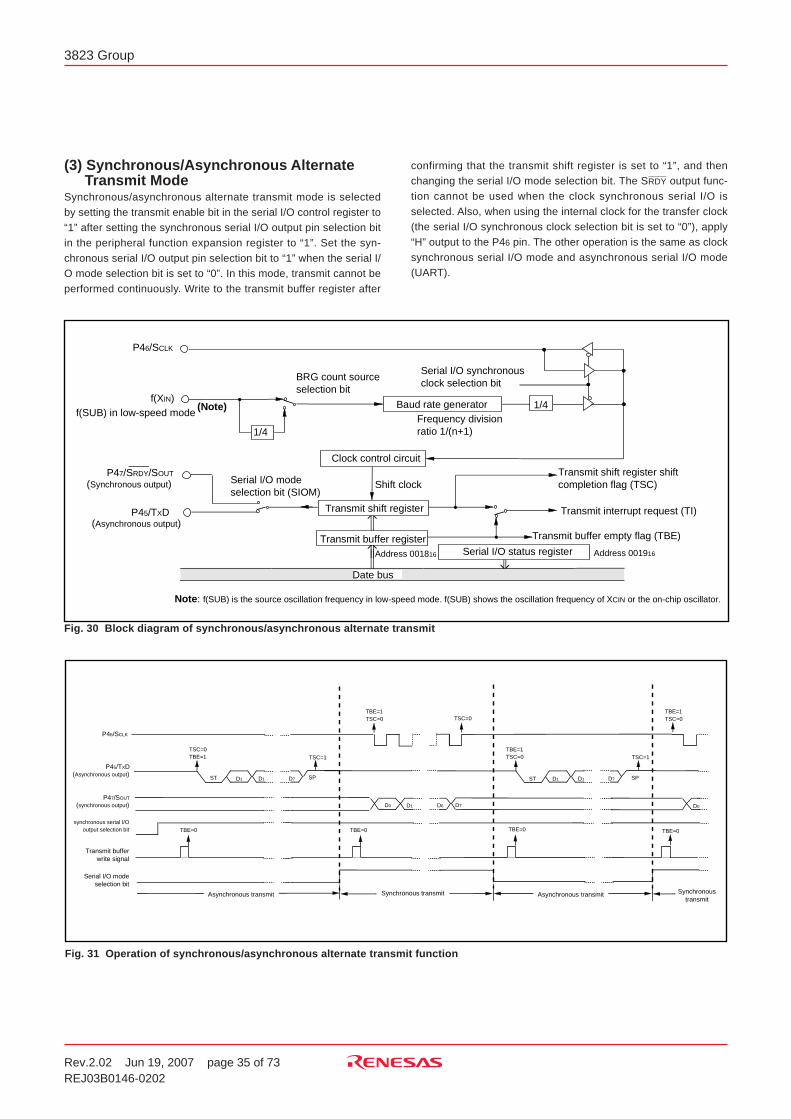
Rev.2.02 Jun 19, 2007 page 35 of 73REJ03B0146-0202
3823 Group
(3) Synchronous/Asynchronous Alternate Transmit ModeSynchronous/asynchronous alternate transmit mode is selectedby setting the transmit enable bit in the serial I/O control register to“1” after setting the synchronous serial I/O output pin selection bitin the peripheral function expansion register to “1”. Set the syn-chronous serial I/O output pin selection bit to “1” when the serial I/O mode selection bit is set to “0”. In this mode, transmit cannot beperformed continuously. Write to the transmit buffer register after
Fig. 30 Block diagram of synchronous/asynchronous alternate transmit
Fig. 31 Operation of synchronous/asynchronous alternate transmit function
confirming that the transmit shift register is set to “1”, and then______
changing the serial I/O mode selection bit. The SRDY output func-tion cannot be used when the clock synchronous serial I/O isselected. Also, when using the internal clock for the transfer clock(the serial I/O synchronous clock selection bit is set to “0”), apply“H” output to the P46 pin. The other operation is the same as clocksynchronous serial I/O mode and asynchronous serial I/O mode(UART).
1/4
1 /
4
S
e
r
i
a
l
I
/
O
s
t
a
t
u
s
r
e
g
i
s
t
e
r
P45/TXD
N
o
t
e:
f
(
S
U
B
)
i
s
t
h
e
s
o
u
r
c
e
o
s
c
i
l
l
a
t
i
o
n
f
r
e
q
u
e
n
c
y
i
n
l
o
w
-
s
p
e
e
d
m
o
d
e
.
f
(
S
U
B
)
s
h
o
w
s
t
h
e
o
s
c
i
l
l
a
t
i
o
n
f
r
e
q
u
e
n
c
y
o
f
XC
I
N
o
r
t
h
e
o
n
-
c
h
i
p
o
s
c
i
l
l
a
t
o
r
.
Baud rate generatorFrequency division ratio 1/(n+1)
Clock control circuit
T
r
a
n
s
m
i
t
b
u
f
f
e
r
r
e
g
i
s
t
e
r
Date bus
T
r
a
n
s
m
i
t
s
h
i
f
t
r
e
g
i
s
t
e
r
Address 001816
T
r
a
n
s
m
i
t
s
h
i
f
t
r
e
g
i
s
t
e
r
s
h
i
f
t
c
o
m
p
l
e
t
i
o
n
f
l
a
g
(
T
S
C
)
T
r
a
n
s
m
i
t
b
u
f
f
e
r
e
m
p
t
y
f
l
a
g
(
T
B
E
)
Transmit interrupt request (TI)
A
d
d
r
e
s
s
0
0
1
91
6
B
R
G
c
o
u
n
t
s
o
u
r
c
e
s
e
l
e
c
t
i
o
n
b
i
t
Serial I/O synchronous clock selection bit
P46/SCLK
P
47/
SR
D
Y/
SO
U
T
f (
XI
N)
f(SUB) in low-speed mode
(S
y
n
c
h
r
o
n
o
u
s
o
u
t
p
u
t)
(Asynchronous output)
S
e
r
i
a
l
I
/
O
m
o
d
e
s
e
l
e
c
t
i
o
n
b
i
t
(
S
I
O
M
)Shift clock
(Note)
T
S
C
=
0T
B
E
=
1 TSC=1
STD1 D1S
T SPD1 D7
T
S
C
=
1
S
P D1 D7
D0
T
B
E
=
0 T
B
E
=
0 T
B
E
=
0 T
B
E
=
0
D1 D6 D7
T
B
E
=
1T
S
C
=
0 TSC=0TBE=1TSC=0
D0
T
B
E
=
1T
S
C
=
0
P46/SCLK
P
45/
TXD
P
47/
SO
U
T
(s
y
n
c
h
r
o
n
o
u
s
o
u
t
p
u
t)
(Asynchronous output)
s
y
n
c
h
r
o
n
o
u
s
s
e
r
i
a
l
I
/
Oo
u
t
p
u
t
s
e
l
e
c
t
i
o
n
b
i
t
T
r
a
n
s
m
i
t
b
u
f
f
e
rw
r
i
t
e
s
i
g
n
a
l
S
e
r
i
a
l
I
/
O
m
o
d
es
e
l
e
c
t
i
o
n
b
i
t
A
s
y
n
c
h
r
o
n
o
u
s
t
r
a
n
s
m
i
t A
s
y
n
c
h
r
o
n
o
u
s
t
r
a
n
s
m
i
tS
y
n
c
h
r
o
n
o
u
s
t
r
a
n
s
m
i
t Synchronoustransmit
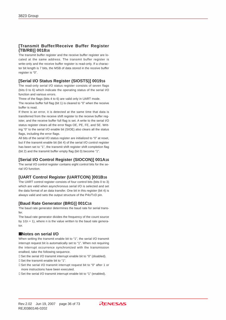
Rev.2.02 Jun 19, 2007 page 36 of 73REJ03B0146-0202
3823 Group
[Transmit Buffer/Receive Buffer Register(TB/RB)] 001816The transmit buffer register and the receive buffer register are lo-cated at the same address. The transmit buffer register iswrite-only and the receive buffer register is read-only. If a charac-ter bit length is 7 bits, the MSB of data stored in the receive bufferregister is “0”.
[Serial I/O Status Register (SIOSTS)] 001916The read-only serial I/O status register consists of seven flags(bits 0 to 6) which indicate the operating status of the serial I/Ofunction and various errors.Three of the flags (bits 4 to 6) are valid only in UART mode.The receive buffer full flag (bit 1) is cleared to “0” when the receivebuffer is read.If there is an error, it is detected at the same time that data istransferred from the receive shift register to the receive buffer reg-ister, and the receive buffer full flag is set. A write to the serial I/Ostatus register clears all the error flags OE, PE, FE, and SE. Writ-ing “0” to the serial I/O enable bit (SIOE) also clears all the statusflags, including the error flags.All bits of the serial I/O status register are initialized to “0” at reset,but if the transmit enable bit (bit 4) of the serial I/O control registerhas been set to “1”, the transmit shift register shift completion flag(bit 2) and the transmit buffer empty flag (bit 0) become “1”.
[Serial I/O Control Register (SIOCON)] 001A16The serial I/O control register contains eight control bits for the se-rial I/O function.
[UART Control Register (UARTCON) ]001B16The UART control register consists of four control bits (bits 0 to 3)which are valid when asynchronous serial I/O is selected and setthe data format of an data transfer. One bit in this register (bit 4) isalways valid and sets the output structure of the P45/TXD pin.
[Baud Rate Generator (BRG)] 001C16The baud rate generator determines the baud rate for serial trans-fer.The baud rate generator divides the frequency of the count sourceby 1/(n + 1), where n is the value written to the baud rate genera-tor.
Notes on serial I/OWhen setting the transmit enable bit to “1”, the serial I/O transmitinterrupt request bit is automatically set to “1”. When not requiringthe interrupt occurrence synchronized with the transmissionenalbed, take the following sequence.➀ Set the serial I/O transmit interrupt enable bit to “0” (disabled).➁ Set the transmit enable bit to “1”.➂ Set the serial I/O transmit interrupt request bit to “0” after 1 or
more instructions have been executed.➃ Set the serial I/O transmit interrupt enable bit to “1” (enabled).
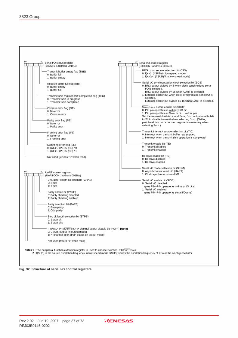
Rev.2.02 Jun 19, 2007 page 37 of 73REJ03B0146-0202
3823 Group
Fig. 32 Structure of serial I/O control registers
BRG count source selection bit (CSS)0: f(XIN) (f(SUB) in low-speed mode) 1: f(XIN)/4 (f(SUB)/4 in low-speed mode)
Serial I/O synchronization clock selection bit (SCS)0: BRG output divided by 4 when clock synchronized serial I/O is selected. BRG output divided by 16 when UART is selected.
1: External clock input when clock synchronized serial I/O is selected. External clock input divided by 16 when UART is selected.
SRDY, SOUT output enable bit (SRDY)0: P47 pin operates as ordinary I/O pin1: P47 pin operates as SRDY or SOUT output pinSet the transmit disable bit and SRDY, SOUT output enable bits to “0” to disable transmit when selecting SOUT. (Setting peripheral function extension register is necessary when selecting SOUT.)
Transmit interrupt source selection bit (TIC)0: Interrupt when transmit buffer has emptied1: Interrupt when transmit shift operation is completed
Transmit enable bit (TE)0: Transmit disabled1: Transmit enabled
Receive enable bit (RE)0: Receive disabled1: Receive enabled
Serial I/O mode selection bit (SIOM)0: Asynchronous serial I/O (UART) 1: Clock synchronous serial I/O
Serial I/O enable bit (SIOE)0: Serial I/O disabled (pins P44–P47 operate as ordinary I/O pins)
1: Serial I/O enabled (pins P44–P47 operate as serial I/O pins)
Serial I/O control register(SIOCON : address 001A16)
b 7 b
0
T
r
a
n
s
m
i
t
b
u
f
f
e
r
e
m
p
t
y
f
l
a
g
(
T
B
E
)0
:
B
u
f
f
e
r
f
u
l
l1
:
B
u
f
f
e
r
e
m
p
t
y
R
e
c
e
i
v
e
b
u
f
f
e
r
f
u
l
l
f
l
a
g
(
R
B
F
)0
:
B
u
f
f
e
r
e
m
p
t
y1
:
B
u
f
f
e
r
f
u
l
l
T
r
a
n
s
m
i
t
s
h
i
f
t
r
e
g
i
s
t
e
r
s
h
i
f
t
c
o
m
p
l
e
t
i
o
n
f
l
a
g
(
T
S
C
)0
:
T
r
a
n
s
m
i
t
s
h
i
f
t
i
n
p
r
o
g
r
e
s
s1
:
T
r
a
n
s
m
i
t
s
h
i
f
t
c
o
m
p
l
e
t
e
d
O
v
e
r
r
u
n
e
r
r
o
r
f
l
a
g
(
O
E
)0
:
N
o
e
r
r
o
r1
:
O
v
e
r
r
u
n
e
r
r
o
r
P
a
r
i
t
y
e
r
r
o
r
f
l
a
g
(
P
E
)0
:
N
o
e
r
r
o
r1
:
P
a
r
i
t
y
e
r
r
o
r
F
r
a
m
i
n
g
e
r
r
o
r
f
l
a
g
(
F
E
)0
:
N
o
e
r
r
o
r1
:
F
r
a
m
i
n
g
e
r
r
o
r
S
u
m
m
i
n
g
e
r
r
o
r
f
l
a
g
(
S
E
)0
:
(
O
E
)
U
(
P
E
)
U
(
F
E
)
=
01
:
(
O
E
)
U
(
P
E
)
U
(
F
E
)
=
1
N
o
t
u
s
e
d
(
r
e
t
u
r
n
s
“
1
”
w
h
e
n
r
e
a
d
)
S
e
r
i
a
l
I
/
O
s
t
a
t
u
s
r
e
g
i
s
t
e
r(
S
I
O
S
T
S
:
a
d
d
r
e
s
s
0
0
1
91
6)
b 7 b
0
UART control register (UARTCON : address 001B16)
Character length selection bit (CHAS)0: 8 bits1: 7 bits
Parity enable bit (PARE)0: Parity checking disabled1: Parity checking enabled
Parity selection bit (PARS)0: Even parity1: Odd parity
Stop bit length selection bit (STPS)0: 1 stop bit1: 2 stop bits
P45/TXD, P47/SRDY/SOUT P-channel output disable bit (POFF) (Note)0: CMOS output (in output mode)1: N-channel open-drain output (in output mode)
Not used (return “1” when read)
b7 b0
1
: T
h
e
p
e
r
i
p
h
e
r
a
l
f
u
n
c
t
i
o
n
e
x
t
e
n
s
i
o
n
r
e
g
i
s
t
e
r
i
s
u
s
e
d
t
o
c
h
o
o
s
e
P
45/
TXD
,
P
47/
SR
D
Y/
SO
U
T.2
: f
(
S
U
B
)
i
s
t
h
e
s
o
u
r
c
e
o
s
c
i
l
l
a
t
i
o
n
f
r
e
q
u
e
n
c
y
i
n
l
o
w
-
s
p
e
e
d
m
o
d
e
.
f
(
S
U
B
)
s
h
o
w
s
t
h
e
o
s
c
i
l
l
a
t
i
o
n
f
r
e
q
u
e
n
c
y
o
f
XC
I
N
o
r
t
h
e
o
n
-
c
h
i
p
o
s
c
i
l
l
a
t
o
r
.Notes
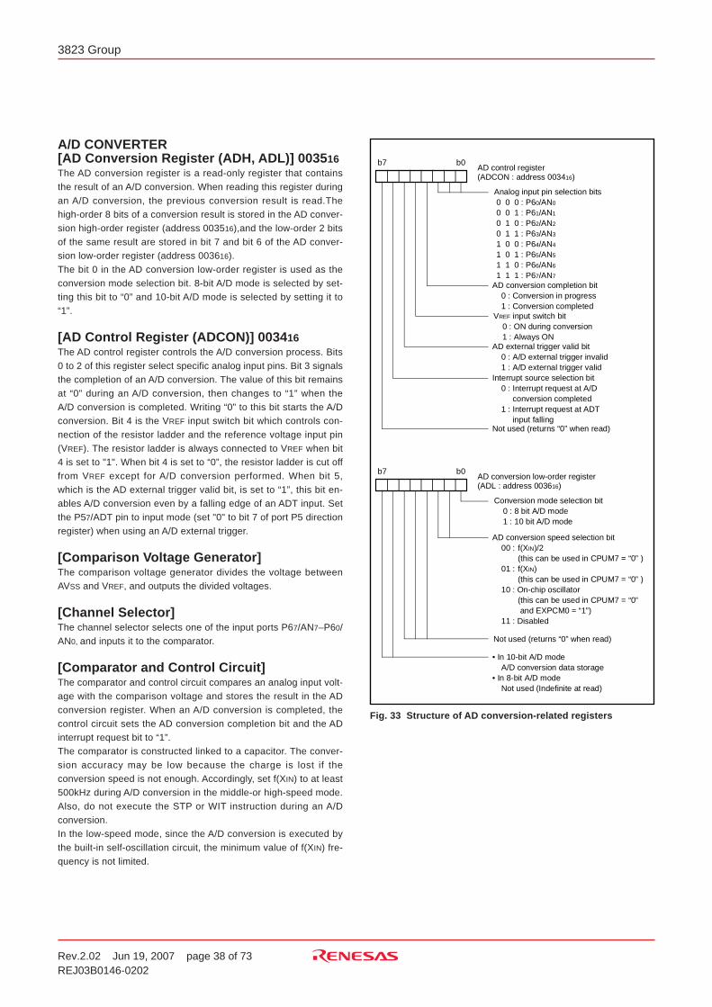
Rev.2.02 Jun 19, 2007 page 38 of 73REJ03B0146-0202
3823 Group
A/D CONVERTER[AD Conversion Register (ADH, ADL)] 003516The AD conversion register is a read-only register that containsthe result of an A/D conversion. When reading this register duringan A/D conversion, the previous conversion result is read.Thehigh-order 8 bits of a conversion result is stored in the AD conver-sion high-order register (address 003516),and the low-order 2 bitsof the same result are stored in bit 7 and bit 6 of the AD conver-sion low-order register (address 003616).The bit 0 in the AD conversion low-order register is used as theconversion mode selection bit. 8-bit A/D mode is selected by set-ting this bit to “0” and 10-bit A/D mode is selected by setting it to“1”.
[AD Control Register (ADCON)] 003416The AD control register controls the A/D conversion process. Bits0 to 2 of this register select specific analog input pins. Bit 3 signalsthe completion of an A/D conversion. The value of this bit remainsat “0” during an A/D conversion, then changes to “1” when theA/D conversion is completed. Writing “0” to this bit starts the A/Dconversion. Bit 4 is the VREF input switch bit which controls con-nection of the resistor ladder and the reference voltage input pin(VREF). The resistor ladder is always connected to VREF when bit4 is set to "1". When bit 4 is set to “0”, the resistor ladder is cut offfrom VREF except for A/D conversion performed. When bit 5,which is the AD external trigger valid bit, is set to “1”, this bit en-ables A/D conversion even by a falling edge of an ADT input. Setthe P57/ADT pin to input mode (set "0" to bit 7 of port P5 directionregister) when using an A/D external trigger.
[Comparison Voltage Generator]The comparison voltage generator divides the voltage betweenAVSS and VREF, and outputs the divided voltages.
[Channel Selector]The channel selector selects one of the input ports P67/AN7–P60/AN0, and inputs it to the comparator.
[Comparator and Control Circuit]The comparator and control circuit compares an analog input volt-age with the comparison voltage and stores the result in the ADconversion register. When an A/D conversion is completed, thecontrol circuit sets the AD conversion completion bit and the ADinterrupt request bit to “1”.The comparator is constructed linked to a capacitor. The conver-sion accuracy may be low because the charge is lost if theconversion speed is not enough. Accordingly, set f(XIN) to at least500kHz during A/D conversion in the middle-or high-speed mode.Also, do not execute the STP or WIT instruction during an A/Dconversion.In the low-speed mode, since the A/D conversion is executed bythe built-in self-oscillation circuit, the minimum value of f(XIN) fre-quency is not limited.
Fig. 33 Structure of AD conversion-related registers
A
D
c
o
n
t
r
o
l
r
e
g
i
s
t
e
r(
A
D
C
O
N
:
a
d
d
r
e
s
s
0
0
3
41
6)
AD conversion completion bit 0 : Conversion in progress 1 : Conversion completed
A
n
a
l
o
g
i
n
p
u
t
p
i
n
s
e
l
e
c
t
i
o
n
b
i
t
s
0
0
0
:
P
60/
A
N0
0
0
1
:
P
61/
A
N1
0
1
0
:
P
62/
A
N2
0
1
1
:
P
63/
A
N3
1
0
0
:
P
64/
A
N4
1
0
1
:
P
65/
A
N5
1
1
0
:
P
66/
A
N6
1
1
1
:
P
67/
A
N7
VREF input switch bit 0 : ON during conversion 1 : Always ON
AD external trigger valid bit 0 : A/D external trigger invalid 1 : A/D external trigger valid
b7 b
0
Interrupt source selection bit 0 : Interrupt request at A/D conversion completed 1 : Interrupt request at ADT input falling
Not used (returns “0” when read)
AD conversion low-order register(ADL : address 003616)
AD conversion speed selection bit 00 : f(XIN)/2
(this can be used in CPUM7 = “0” ) 01 : f(XIN)
(this can be used in CPUM7 = “0” ) 10 : On-chip oscillator
(this can be used in CPUM7 = “0” and EXPCM0 = “1”)
11 : Disabled
Conversion mode selection bit 0 : 8 bit A/D mode 1 : 10 bit A/D mode
Not used (returns “0” when read)
• In 10-bit A/D mode A/D conversion data storage
• In 8-bit A/D mode Not used (Indefinite at read)
b7 b
0
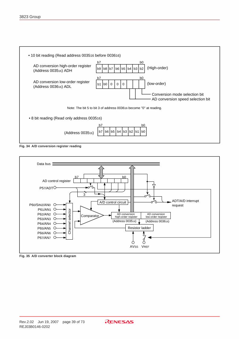
Rev.2.02 Jun 19, 2007 page 39 of 73REJ03B0146-0202
3823 Group
Fig. 34 A/D conversion register reading
Fig. 35 A/D converter block diagram
AD conversion high-order register
D
a
t
a
b
u
s
A
/
D
c
o
n
t
r
o
l
c
i
r
c
u
i
t
R
e
s
i
s
t
o
r
l
a
d
d
e
r
AVSS VREF
C
o
m
p
a
r
a
t
o
r
A
D
T
/
A
/
D
i
n
t
e
r
r
u
p
t
r
e
q
u
e
s
t
b7 b0A
D
c
o
n
t
r
o
l
r
e
g
i
s
t
e
r
3
P
60/
SI
N
2/
A
N0
P
61/
A
N1
P62/AN2
P
63/
A
N3
P
64/
A
N4
P
65/
A
N5
P66/AN6
P67/AN7
P
57/
A
D
T
(Address 003516) (Address 003616)
AD conversion low-order register
C h
a
n
n
e
l
s
e
l
e
c
t
o
r
Conversion mode selection bitAD conversion speed selection bit
A
D
c
o
n
v
e
r
s
i
o
n
l
o
w
-
o
r
d
e
r
r
e
g
i
s
t
e
r
(
A
d
d
r
e
s
s
0
0
3
61
6)
A
D
L
A
D
c
o
n
v
e
r
s
i
o
n
h
i
g
h
-
o
r
d
e
r
r
e
g
i
s
t
e
r
(
A
d
d
r
e
s
s
0
0
3
51
6)
A
D
H
b1 b
0
b
7 b0
•
1
0
b
i
t
r
e
a
d
i
n
g
(
R
e
a
d
a
d
d
r
e
s
s
0
0
3
51
6
b
e
f
o
r
e
0
0
3
61
6)
b
7
b9 b8
b0
b7 b6 b5 b4 b3 b2 (High-order)
(low-order)
Note: The bit 5 to bit 3 of address 003616 become "0" at reading.
• 8 bit reading (Read only address 003516)
b7
b7 b
6
b
0
b
5 b
4 b
3 b
2 b1 b
0( A
d
d
r
e
s
s
0
0
3
51
6)
0 0 0
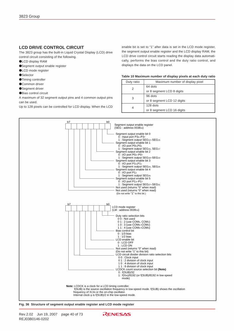
Rev.2.02 Jun 19, 2007 page 40 of 73REJ03B0146-0202
3823 Group
LCD DRIVE CONTROL CIRCUITThe 3823 group has the built-in Liquid Crystal Display (LCD) drivecontrol circuit consisting of the following. LCD display RAM Segment output enable register LCD mode register Selector Timing controller Common driver Segment driver Bias control circuitA maximum of 32 segment output pins and 4 common output pinscan be used.Up to 128 pixels can be controlled for LCD display. When the LCD
Fig. 36 Structure of segment output enable register and LCD mode register
enable bit is set to “1” after data is set in the LCD mode register,the segment output enable register and the LCD display RAM, theLCD drive control circuit starts reading the display data automati-cally, performs the bias control and the duty ratio control, anddisplays the data on the LCD panel.
Table 10 Maximum number of display pixels at each duty ratio
Duty ratio Maximum number of display pixel
64 dots
or 8 segment LCD 8 digits
96 dots
or 8 segment LCD 12 digits
128 dots
or 8 segment LCD 16 digits
2
3
4
LCD mode register(LM : address 003916)
S
e
g
m
e
n
t
o
u
t
p
u
t
e
n
a
b
l
e
r
e
g
i
s
t
e
r(
S
E
G
:
a
d
d
r
e
s
s
0
0
3
81
6)
Duty ratio selection bits0 0 : Not used0 1 : 2 (use COM0, COM1)1 0 : 3 (use COM0–COM2)1 1 : 4 (use COM0–COM3)
Bias control bit0 : 1/3 bias1 : 1/2 bias
LCD enable bit0 : LCD OFF1 : LCD ON
Not used (returns “0” when read)(Do not write “1” to this bit)LCD circuit divider division ratio selection bits
0 0 : Clock input0 1 : 2 division of clock input1 0 : 4 division of clock input1 1 : 8 division of clock input
LCDCK count source selection bit (Note)0 : f(SUB)/321 : f(XIN)/8192 (or f(SUB)/8192 in low-speed
mode)
N
o
t
e
:
L
C
D
C
K
i
s
a
c
l
o
c
k
f
o
r
a
L
C
D
t
i
m
i
n
g
c
o
n
t
r
o
l
l
e
r
.
f
(
S
U
B
)
i
s
t
h
e
s
o
u
r
c
e
o
s
c
i
l
l
a
t
i
o
n
f
r
e
q
u
e
n
c
y
i
n
l
o
w
-
s
p
e
e
d
m
o
d
e
.
f
(
S
U
B
)
s
h
o
w
s
t
h
e
o
s
c
i
l
l
a
t
i
o
n
f
r
e
q
u
e
n
c
y
o
f
XC
I
N
o
r
t
h
e
o
n
-
c
h
i
p
o
s
c
i
l
l
a
t
o
r
.I
n
t
e
r
n
a
l
c
l
o
c
k
φ
i
s
f
(
S
U
B
)
/
2
i
n
t
h
e
l
o
w
-
s
p
e
e
d
m
o
d
e
.
Segment output enable bit 00 : Input port P34–P37
1 : Segment output SEG12–SEG15
Segment output enable bit 10 : I/O port P00,P01
1 : Segment output SEG16, SEG17
Segment output enable bit 20 : I/O port P02–P07
1 : Segment output SEG18–SEG23
Segment output enable bit 30 : I/O port P10,P11
1 : Segment output SEG24, SEG25
Segment output enable bit 40 : I/O port P12
1 : Segment output SEG26
Segment output enable bit 50 : I/O port P13–P17
1 : Segment output SEG27–SEG31
Not used (returns “0” when read)Not used (returns “0” when read)(Do not write “1” to this bit.)
b 7 b
0
b7 b0
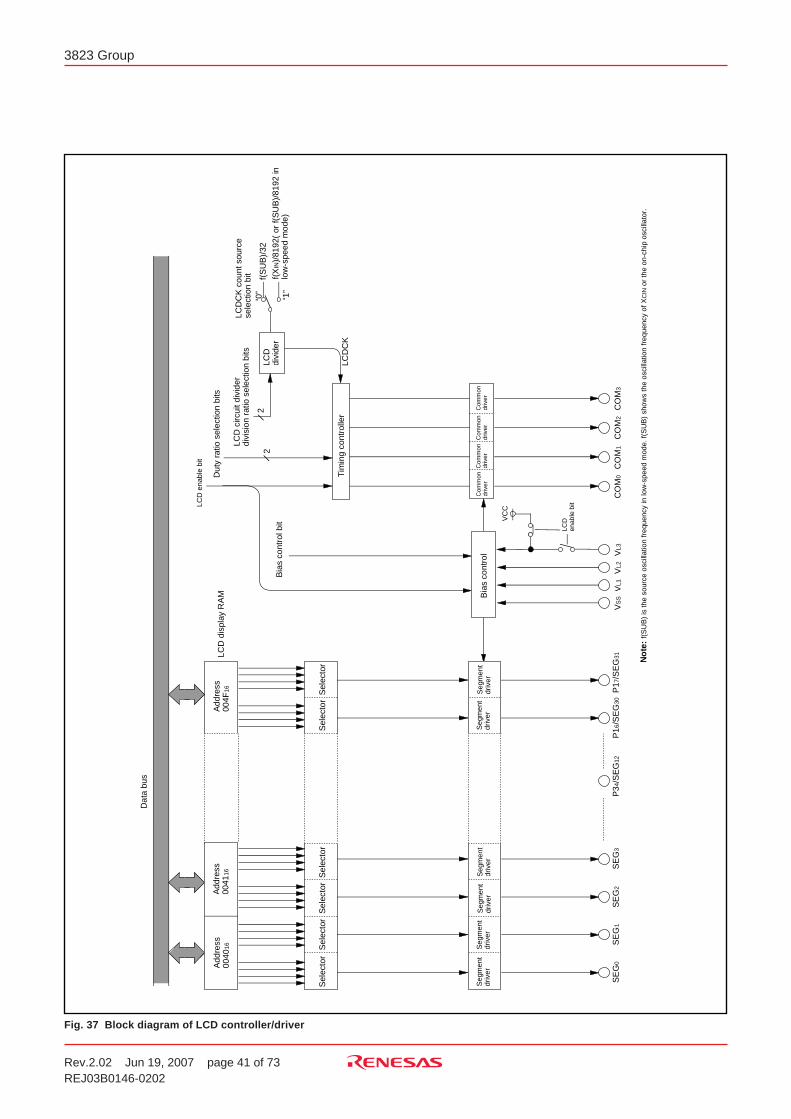
Rev.2.02 Jun 19, 2007 page 41 of 73REJ03B0146-0202
3823 Group
Fig. 37 Block diagram of LCD controller/driver
C O
M
0C
O
M1
C O
M
2C
O
M3
VS
S
VL
1
VL
2
VL
3
S E
G
3S
E
G2
S E
G
1S
E
G0
“ 1 ”
“ 0 ”
L C D
C
K
22
P 17
/
S
E
G3
1
P 16
/
S
E
G3
0
P 34
/
S
E
G1
2
f ( S
U
B
)
/
3
2
f ( X
I
N)
/
8
1
9
2
(
o
r
f
(
S
U
B
)
/
8
1
9
2
i
n
l o
w
-
s
p
e
e
d
m
o
d
e
)
D a
t
a
b
u
s
A d
d
r
e
s
s
0 0
4
0 1
6
A d
d
r
e
s
s
0 0
4
1 1
6
A d
d
r
e
s
s
0 0
4
F1
6
S e
l
e
c
t
o
r
S e
l
e
c
t
o
r
S e
l
e
c
t
o
r
S e
l
e
c
t
o
r
S e
l
e
c
t
o
r
S e
l
e
c
t
o
r
S e
g
m
e
n
t
d r
i
v
e
rS
e
g
m
e
n
td r
i
v
e
rS
e
g
m
e
n
td r
i
v
e
rS
e
g
m
e
n
td r
i
v
e
rS
e
g
m
e
n
td r
i
v
e
rS
e
g
m
e
n
td r
i
v
e
rB
i
a
s
c
o
n
t
r
o
l
L C D
d i
v
i
d
e
r
T i
m
i
n
g
c
o
n
t
r
o
l
l
e
r
C o
m
m
o
n
d r
i
v
e
r
D u
t
y
r
a
t
i
o
s
e
l
e
c
t
i
o
n
b
i
t
s
C o
m
m
o
n
d r
i
v
e
rC
o
m
m
o
nd r
i
v
e
rC
o
m
m
o
nd r
i
v
e
r
B i
a
s
c
o
n
t
r
o
l
b
i
t
L C D
c
i
r
c
u
i
t
d
i
v
i
d
e
r
d i
v
i
s
i
o
n
r
a
t
i
o
s
e
l
e
c
t
i
o
n
b
i
t
sL C
D
C
K
c
o
u
n
t
s
o
u
r
c
es e
l
e
c
t
i
o
n
b
i
t
L C D
d
i
s
p
l
a
y
R
A
M
L C D
e
n
a
b
l
e
b
i
t
V C
C
L C D
e n
a
b
l
e
b
i
t
N o
t
e
:
f
(
S
U
B
)
i
s
t
h
e
s
o
u
r
c
e
o
s
c
i
l
l
a
t
i
o
n
f
r
e
q
u
e
n
c
y
i
n
l
o
w
-
s
p
e
e
d
m
o
d
e
.
f
(
S
U
B
)
s
h
o
w
s
t
h
e
o
s
c
i
l
l
a
t
i
o
n
f
r
e
q
u
e
n
c
y
o
f
X
C
I
N
o
r
t
h
e
o
n
-
c
h
i
p
o
s
c
i
l
l
a
t
o
r
.
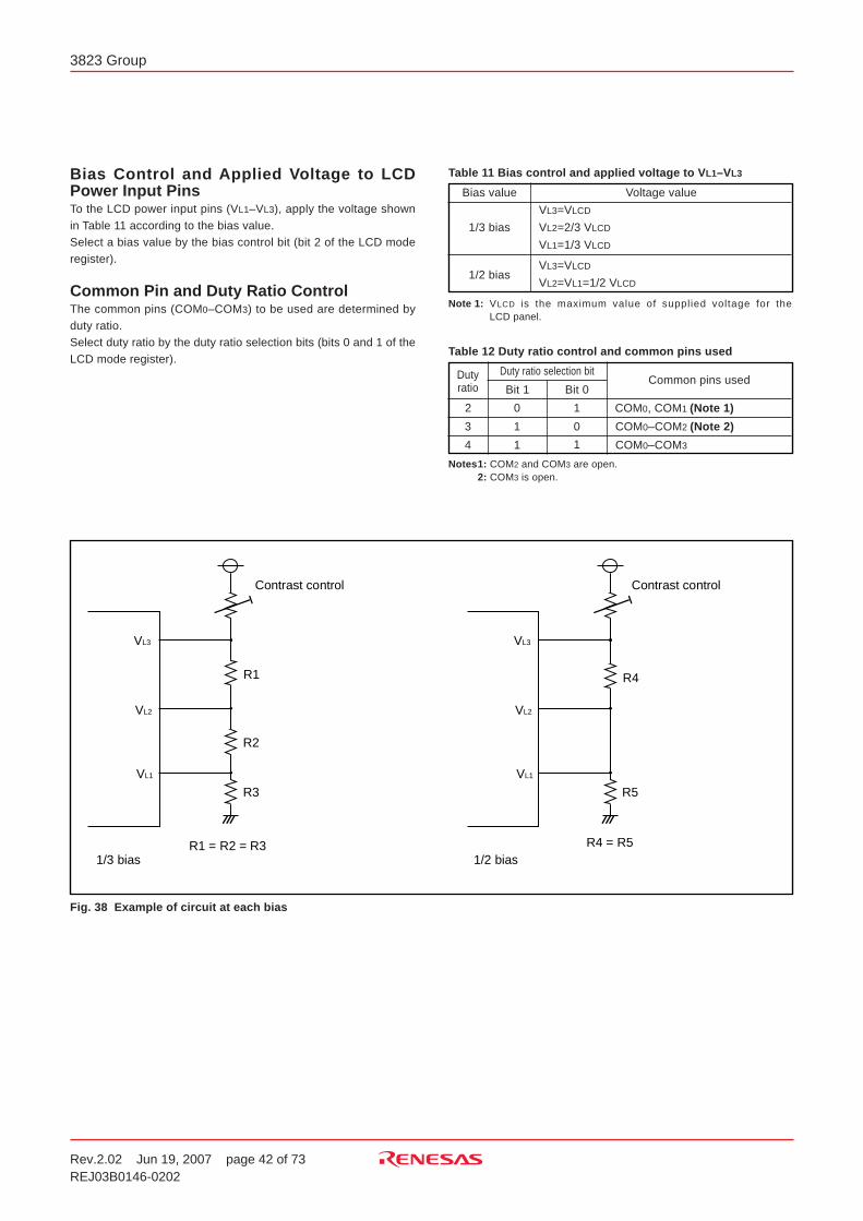
Rev.2.02 Jun 19, 2007 page 42 of 73REJ03B0146-0202
3823 Group
Bias Control and Applied Voltage to LCDPower Input PinsTo the LCD power input pins (VL1–VL3), apply the voltage shownin Table 11 according to the bias value.Select a bias value by the bias control bit (bit 2 of the LCD moderegister).
Common Pin and Duty Ratio ControlThe common pins (COM0–COM3) to be used are determined byduty ratio.Select duty ratio by the duty ratio selection bits (bits 0 and 1 of theLCD mode register).
Fig. 38 Example of circuit at each bias
Table 12 Duty ratio control and common pins used
Dutyratio
Common pins used
Notes1: COM2 and COM3 are open.2: COM3 is open.
Bit 1 Bit 0
COM0, COM1 (Note 1)
Duty ratio selection bit
2
3
4
0
1
1
1
0
1
COM0–COM2 (Note 2)
COM0–COM3
Table 11 Bias control and applied voltage to VL1–VL3
Bias value
1/3 bias
Voltage value
VL3=VLCD
VL2=2/3 VLCD
VL1=1/3 VLCD
Note 1: VLCD is the maximum value of supplied voltage for theLCD panel.
1/2 biasVL3=VLCD
VL2=VL1=1/2 VLCD
Contrast control
1 /
2
b
i
a
s1
/
3
b
i
a
s
Contrast control
VL3
R
4
R
5
R
4
=
R
5
R
1
R2
R
3
R
1
=
R
2
=
R
3
VL
2
VL1
VL3
VL
2
VL1
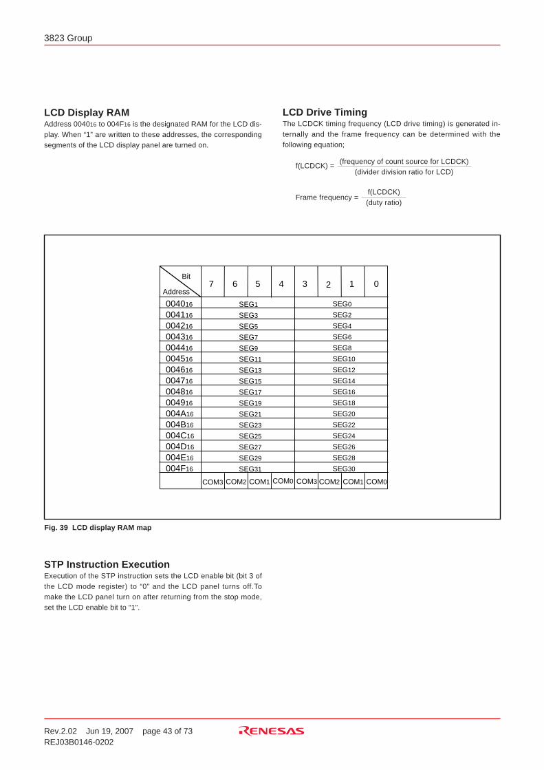
Rev.2.02 Jun 19, 2007 page 43 of 73REJ03B0146-0202
3823 Group
LCD Display RAMAddress 004016 to 004F16 is the designated RAM for the LCD dis-play. When “1” are written to these addresses, the correspondingsegments of the LCD display panel are turned on.
Fig. 39 LCD display RAM map
LCD Drive TimingThe LCDCK timing frequency (LCD drive timing) is generated in-ternally and the frame frequency can be determined with thefollowing equation;
f(LCDCK) =
Frame frequency =
(frequency of count source for LCDCK)(divider division ratio for LCD)
f(LCDCK)(duty ratio)
B
i
t
A
d
d
r
e
s
s7
004016
004116
004216
004316
004416
004516
004616
004716
004816
004916
004A16
004B16
004C16
004D16
004E16
004F16
COM3
0123456
COM0COM1 COM2 COM3 COM0COM1COM2
SEG1
SEG3
SEG5
SEG7
SEG9
SEG11
SEG13
SEG15
SEG17
SEG19
SEG21
SEG23
SEG25
SEG27
SEG29
SEG31
SEG0
SEG2
SEG4
SEG6
SEG8
SEG10
SEG12
SEG14
SEG16
SEG18
SEG20
SEG22
SEG24
SEG26
SEG28
SEG30
STP Instruction ExecutionExecution of the STP instruction sets the LCD enable bit (bit 3 ofthe LCD mode register) to “0” and the LCD panel turns off.Tomake the LCD panel turn on after returning from the stop mode,set the LCD enable bit to “1”.
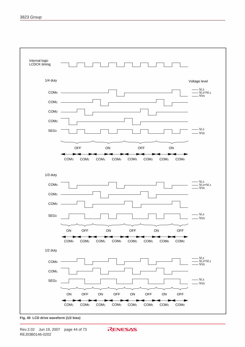
Rev.2.02 Jun 19, 2007 page 44 of 73REJ03B0146-0202
3823 Group
Fig. 40 LCD drive waveform (1/2 bias)
I n
t
e
r
n
a
l
l
o
g
i
cL
C
D
C
K
t
i
m
i
n
g
1
/
4
d
u
t
y Voltage level
VL
3VL
2=
VL
1VSS
VL
3
VS
S
C
O
M0
C
O
M1
C
O
M2
C
O
M3
S
E
G0
O
F
F O
N OFF O
N
C
O
M3 COM2 COM1 COM0 COM3 C
O
M2 C
O
M1 C
O
M0
1
/
3
d
u
t
y
VL
3VL2=VL1VSS
VL
3
VSS
O
F
FO
N O
N OFF O
N O
F
F
1
/
2
d
u
t
y
C
O
M0
COM1
C
O
M2
SEG0
C
O
M0
C
O
M1
S
E
G0
VL3VL
2=
VL
1VS
S
VL
3
VS
S
OFFON OFFON OFFON OFFON
C
O
M0 C
O
M2 C
O
M1 COM0 C
O
M2 C
O
M1 C
O
M0 C
O
M2
C
O
M1 C
O
M0 C
O
M1 COM0 C
O
M1 C
O
M0 C
O
M1 C
O
M0
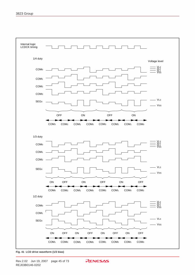
Rev.2.02 Jun 19, 2007 page 45 of 73REJ03B0146-0202
3823 Group
Fig. 41 LCD drive waveform (1/3 bias)
I n
t
e
r
n
a
l
l
o
g
i
cL
C
D
C
K
t
i
m
i
n
g
1
/
4
d
u
t
yV
o
l
t
a
g
e
l
e
v
e
l
VL
3
VS
S
C
O
M0
COM1
C
O
M2
C
O
M3
SEG0
O
F
F ON O
F
F O
N
COM3 COM2 COM1 COM0 COM3 COM2 COM1 COM0
1
/
3
d
u
t
y
OFFO
N ON OFF O
N OFF
1/2 duty
COM0
C
O
M1
C
O
M2
SEG0
C
O
M0
C
O
M1
SEG0
OFFO
N O
F
FO
N O
F
FO
N OFFO
N
VL
3VL
2
VS
SVL
1
VL
3VL
2
VSSVL
1
VL3
VSS
VL3VL
2
VSSVL
1
VL
3
VS
S
C
O
M0 COM2 COM1 COM0 C
O
M2 C
O
M1 C
O
M0 C
O
M2
C
O
M1 C
O
M0 C
O
M1 C
O
M0 C
O
M1 C
O
M0 C
O
M1 C
O
M0
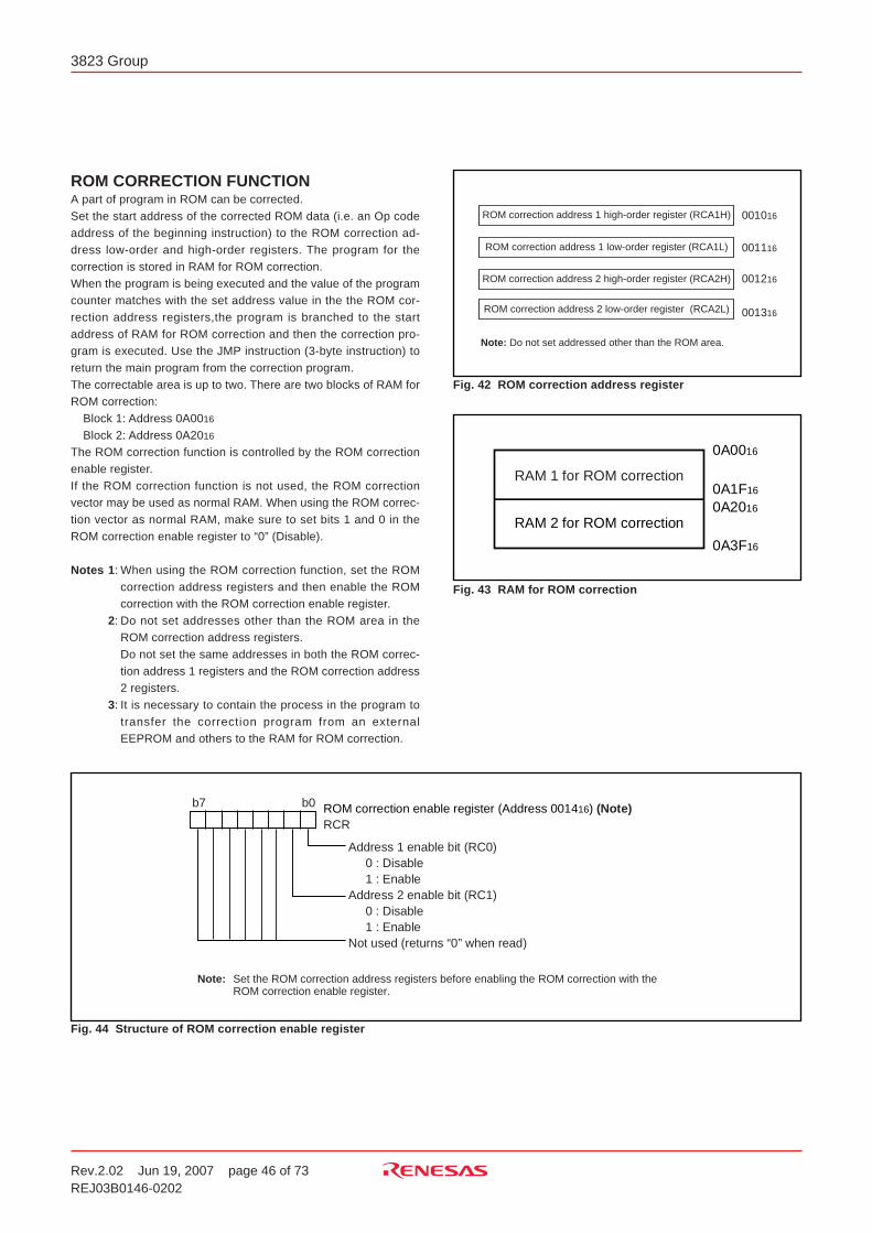
Rev.2.02 Jun 19, 2007 page 46 of 73REJ03B0146-0202
3823 Group
ROM CORRECTION FUNCTIONA part of program in ROM can be corrected.Set the start address of the corrected ROM data (i.e. an Op codeaddress of the beginning instruction) to the ROM correction ad-dress low-order and high-order registers. The program for thecorrection is stored in RAM for ROM correction.When the program is being executed and the value of the programcounter matches with the set address value in the the ROM cor-rection address registers,the program is branched to the startaddress of RAM for ROM correction and then the correction pro-gram is executed. Use the JMP instruction (3-byte instruction) toreturn the main program from the correction program.The correctable area is up to two. There are two blocks of RAM forROM correction:
Block 1: Address 0A0016
Block 2: Address 0A2016
The ROM correction function is controlled by the ROM correctionenable register.If the ROM correction function is not used, the ROM correctionvector may be used as normal RAM. When using the ROM correc-tion vector as normal RAM, make sure to set bits 1 and 0 in theROM correction enable register to “0” (Disable).
Notes 1: When using the ROM correction function, set the ROMcorrection address registers and then enable the ROMcorrection with the ROM correction enable register.
2: Do not set addresses other than the ROM area in theROM correction address registers.Do not set the same addresses in both the ROM correc-tion address 1 registers and the ROM correction address2 registers.
3: It is necessary to contain the process in the program totransfer the correction program from an externalEEPROM and others to the RAM for ROM correction.
Fig. 42 ROM correction address register
Fig. 44 Structure of ROM correction enable register
0 0
1
01
6ROM correction address 1 high-order register (RCA1H)
0 0
1
11
6
001216
001316
ROM correction address 1 low-order register (RCA1L)
ROM correction address 2 low-order register (RCA2L)
ROM correction address 2 high-order register (RCA2H)
Note: Do not set addressed other than the ROM area.
A
d
d
r
e
s
s
1
e
n
a
b
l
e
b
i
t
(
R
C
0
)
0
:
D
i
s
a
b
l
e
1
:
E
n
a
b
l
eA
d
d
r
e
s
s
2
e
n
a
b
l
e
b
i
t
(
R
C
1
)
0
:
D
i
s
a
b
l
e
1
:
E
n
a
b
l
eN
o
t
u
s
e
d
(
r
e
t
u
r
n
s
“
0
”
w
h
e
n
r
e
a
d
)
R
O
M
c
o
r
r
e
c
t
i
o
n
e
n
a
b
l
e
r
e
g
i
s
t
e
r
(
A
d
d
r
e
s
s
0
0
1
41
6)
(
N
o
t
e
)R
C
R
b 7 b
0
N
o
t
e
: S
e
t
t
h
e
R
O
M
c
o
r
r
e
c
t
i
o
n
a
d
d
r
e
s
s
r
e
g
i
s
t
e
r
s
b
e
f
o
r
e
e
n
a
b
l
i
n
g
t
h
e
R
O
M
c
o
r
r
e
c
t
i
o
n
w
i
t
h
t
h
e
R
O
M
c
o
r
r
e
c
t
i
o
n
e
n
a
b
l
e
r
e
g
i
s
t
e
r
.
Fig. 43 RAM for ROM correction
R
A
M
1
f
o
r
R
O
M
c
o
r
r
e
c
t
i
o
n
R
A
M
2
f
o
r
R
O
M
c
o
r
r
e
c
t
i
o
n
0A0016
0A1F16
0A2016
0A3F16
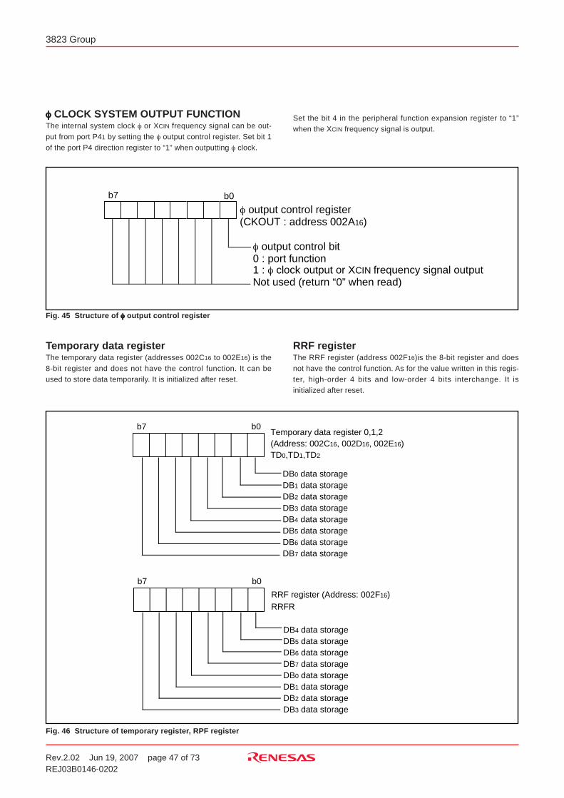
Rev.2.02 Jun 19, 2007 page 47 of 73REJ03B0146-0202
3823 Group
φφφφφ CLOCK SYSTEM OUTPUT FUNCTIONThe internal system clock φ or XCIN frequency signal can be out-put from port P41 by setting the φ output control register. Set bit 1of the port P4 direction register to “1” when outputting φ clock.
Fig. 45 Structure of φφφφφ output control register
φ output control register(CKOUT : address 002A16)
φ output control bit0 : port function1 : φ clock output or XCIN frequency signal outputNot used (return “0” when read)
b
7 b
0
Temporary data registerThe temporary data register (addresses 002C16 to 002E16) is the8-bit register and does not have the control function. It can beused to store data temporarily. It is initialized after reset.
RRF registerThe RRF register (address 002F16)is the 8-bit register and doesnot have the control function. As for the value written in this regis-ter, high-order 4 bits and low-order 4 bits interchange. It isinitialized after reset.
Fig. 46 Structure of temporary register, RPF register
Set the bit 4 in the peripheral function expansion register to “1”when the XCIN frequency signal is output.
b7 b0T
e
m
p
o
r
a
r
y
d
a
t
a
r
e
g
i
s
t
e
r
0
,
1
,
2(
A
d
d
r
e
s
s
:
0
0
2
C1
6,
0
0
2
D1
6,
0
0
2
E1
6)
D
B0
d
a
t
a
s
t
o
r
a
g
eD
B1
d
a
t
a
s
t
o
r
a
g
eD
B2
d
a
t
a
s
t
o
r
a
g
eD
B3
d
a
t
a
s
t
o
r
a
g
eD
B4
d
a
t
a
s
t
o
r
a
g
eD
B5
d
a
t
a
s
t
o
r
a
g
eD
B6
d
a
t
a
s
t
o
r
a
g
eD
B7
d
a
t
a
s
t
o
r
a
g
e
TD0,TD1,TD2
b
7 b
0
R
R
F
r
e
g
i
s
t
e
r
(
A
d
d
r
e
s
s
:
0
0
2
F1
6)
D
B4
d
a
t
a
s
t
o
r
a
g
eD
B5
d
a
t
a
s
t
o
r
a
g
eD
B6
d
a
t
a
s
t
o
r
a
g
eD
B7
d
a
t
a
s
t
o
r
a
g
eD
B0
d
a
t
a
s
t
o
r
a
g
eD
B1
d
a
t
a
s
t
o
r
a
g
eD
B2
d
a
t
a
s
t
o
r
a
g
eD
B3
d
a
t
a
s
t
o
r
a
g
e
R
R
F
R
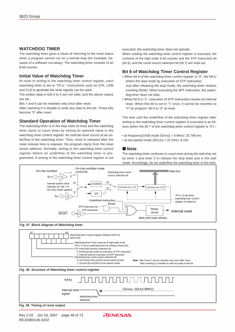
Rev.2.02 Jun 19, 2007 page 48 of 73REJ03B0146-0202
3823 Group
WATCHDOG TIMERThe watchdog timer gives a mean of returning to the reset statuswhen a program cannot run on a normal loop (for example, be-cause of a software run-away). The watchdog timer consists of an8-bit counter.
Initial Value of Watchdog TimerAt reset or writing to the watchdog timer control register, eachwatchdog timer is set to “FF16.” Instructions such as STA, LDMand CLB to generate the write signals can be used.The written data in bits 0 to 5 are not valid, and the above valuesare set.Bits 7 and 6 can be rewritten only once after reset.After rewriting it is disable to write any data to this bit. These bitsbecome “0” after reset.
Standard Operation of Watchdog TimerThe watchdog timer is in the stop state at reset and the watchdogtimer starts to count down by writing an optional value in thewatchdog timer control register. An internal reset occurs at an un-derflow of the watchdog timer. Then, reset is released after thereset release time is elapsed, the program starts from the resetvector address. Normally, writing to the watchdog timer controlregister before an underflow of the watchdog timer is pro-grammed. If writing to the watchdog timer control register is not
executed, the watchdog timer does not operate.When reading the watchdog timer control register is executed, thecontents of the high-order 6-bit counter and the STP instruction bit(bit 6), and the count source selection bit (bit 7) are read out.
Bit 6 of Watchdog Timer Control Register• When bit 6 of the watchdog timer control register is “0”, the MCU
enters the stop mode by execution of STP instruction.Just after releasing the stop mode, the watchdog timer restartscounting (Note). When executing the WIT instruction, the watch-dog timer does not stop.
• When bit 6 is “1”, execution of STP instruction causes an internalreset. When this bit is set to “1” once, it cannot be rewritten to“0” by program. Bit 6 is “0” at reset.
The time until the underflow of the watchdog timer register afterwriting to the watchdog timer control register is executed is as fol-lows (when the bit 7 of the watchdog timer control register is “0”) ;
• at frequency/2/4/8 mode (f(XIN)) = 8 MHz): 32.768 ms• at low-speed mode (f(XCIN) = 32 KHz): 8.19s
NoteThe watchdog timer continues to count even during the wait time setby timer 1 and timer 2 to release the stop state and in the waitmode. Accordingly, do not underflow the watchdog timer in this time.
Fig. 47 Block diagram of Watchdog timer
Fig. 48 Structure of Watchdog timer control register
Fig. 49 Timing of reset output
I n
t
e
r
n
a
l
r
e
s
e
t
s
i
g
n
a
lW
a
t
c
h
d
o
g
t
i
m
e
r
d
e
t
e
c
t
i
o
n
=
3
2m
s
e
c
(
f
(
XI
N)
=
8
M
HZ)
f (
XI
N
)
Watchdog timer H (for read-out of high-order 6 bit)“FF16” is set to watchdog timer by writing to these bits.
Watchdog timer count source selection bit 0: f(XIN)/1024 (f(SUB)/1024 at low-speed mode) 1: f(XIN)/4 (f(SUB)/1024 at low-speed mode)
STP instruction function selection bit 0: Entering stop mode by execution of STP instruction 1: Internal reset by execution of STP instruction
Watchdog timer control register (Address 003716)WDTCON
b7 b0
Note : Bits 6 and 7 can be rewritten only once after reset.After rewriting it is disable to write any data to this bit.
XIN
Data bus
XCIN
Internal system clock selection bit (bit 7 of the CPU mode register)
1/1024Watchdog timer H (6)
Watchdog timer count source selection bit
Resetcircuit
Undefined instructionReset
“FF16” is set when watchdog timer control register is written to.
Internal resetRESET
Wait until reset release
Watchdog timer L (2)
STP instruction STP instruction bit
1/4
“0”
“1”
“1”
“0”
On-chip oscillator mode control bitOn-chip oscillator
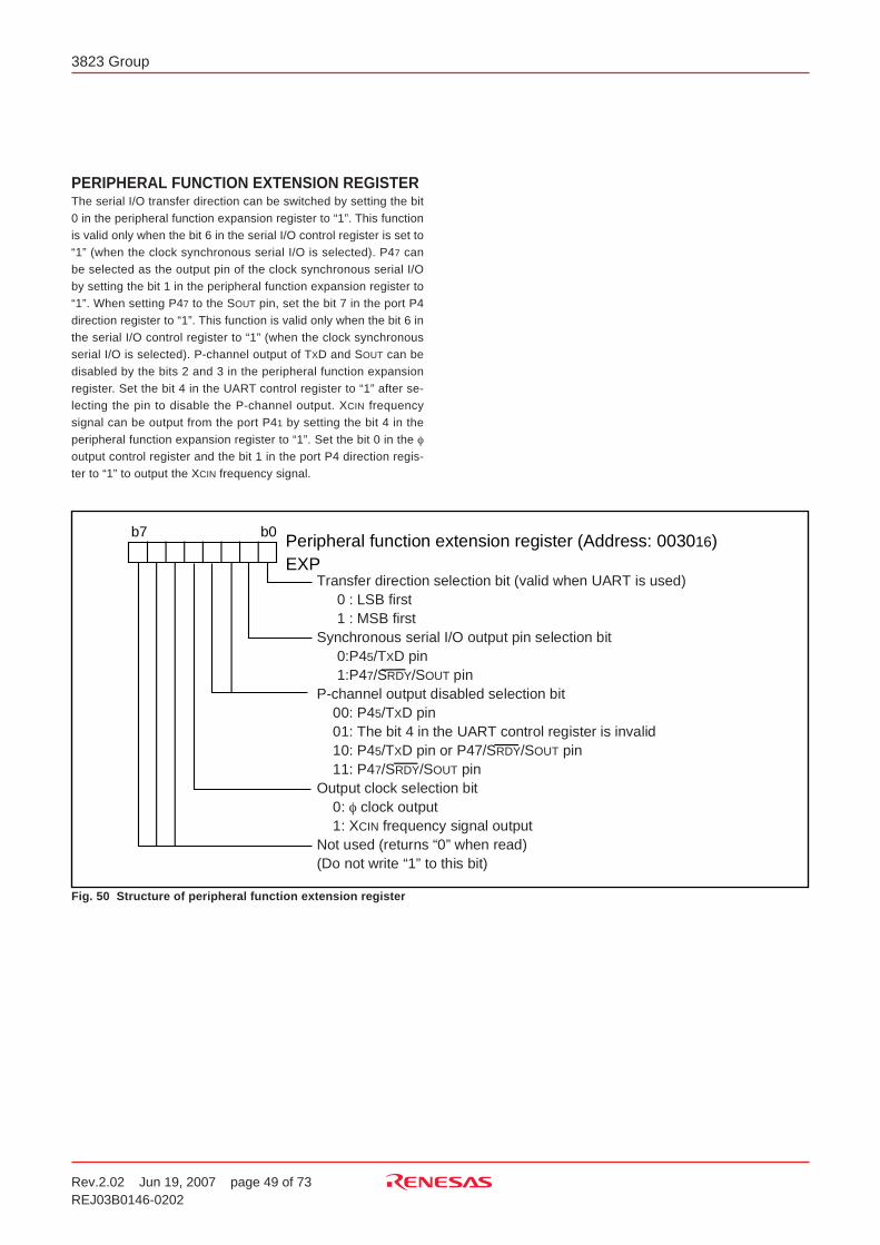
Rev.2.02 Jun 19, 2007 page 49 of 73REJ03B0146-0202
3823 Group
PERIPHERAL FUNCTION EXTENSION REGISTERThe serial I/O transfer direction can be switched by setting the bit0 in the peripheral function expansion register to “1”. This functionis valid only when the bit 6 in the serial I/O control register is set to“1” (when the clock synchronous serial I/O is selected). P47 canbe selected as the output pin of the clock synchronous serial I/Oby setting the bit 1 in the peripheral function expansion register to“1”. When setting P47 to the SOUT pin, set the bit 7 in the port P4direction register to “1”. This function is valid only when the bit 6 inthe serial I/O control register to “1” (when the clock synchronousserial I/O is selected). P-channel output of TXD and SOUT can bedisabled by the bits 2 and 3 in the peripheral function expansionregister. Set the bit 4 in the UART control register to “1” after se-lecting the pin to disable the P-channel output. XCIN frequencysignal can be output from the port P41 by setting the bit 4 in theperipheral function expansion register to “1”. Set the bit 0 in the φoutput control register and the bit 1 in the port P4 direction regis-ter to “1” to output the XCIN frequency signal.
Fig. 50 Structure of peripheral function extension register
Transfer direction selection bit (valid when UART is used) 0 : LSB first 1 : MSB firstSynchronous serial I/O output pin selection bit 0:P45/TXD pin 1:P47/SRDY/SOUT pinP-channel output disabled selection bit 00: P45/TXD pin 01: The bit 4 in the UART control register is invalid 10: P45/TXD pin or P47/SRDY/SOUT pin 11: P47/SRDY/SOUT pinOutput clock selection bit 0: φ clock output 1: XCIN frequency signal outputNot used (returns “0” when read)(Do not write “1” to this bit)
Peripheral function extension register (Address: 003016) EXP
b 7 b
0
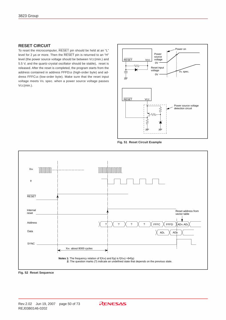
Rev.2.02 Jun 19, 2007 page 50 of 73REJ03B0146-0202
3823 Group
RESET CIRCUITTo reset the microcomputer, RESET pin should be held at an “L”level for 2 µs or more. Then the RESET pin is returned to an “H”level (the power source voltage should be between VCC(min.) and5.5 V, and the quartz-crystal oscillator should be stable), reset isreleased. After the reset is completed, the program starts from theaddress contained in address FFFD16 (high-order byte) and ad-dress FFFC16 (low-order byte). Make sure that the reset inputvoltage meets VIL spec. when a power source voltage passesVCC(min.).
Fig. 51 Reset Circuit Example
Fig. 52 Reset Sequence
P
o
w
e
r
o
n
P
o
w
e
r
s
o
u
r
c
ev
o
l
t
a
g
e
R
e
s
e
t
i
n
p
u
tv
o
l
t
a
g
e
P
o
w
e
r
s
o
u
r
c
e
v
o
l
t
a
g
ed
e
t
e
c
t
i
o
n
c
i
r
c
u
i
t
VI
L
s
p
e
c
.
0 V
0 V
VC
CR
E
S
E
T
VC
CR
E
S
E
T
R
E
S
E
T
I n
t
e
r
n
a
l
r
e
s
e
t
A
d
d
r
e
s
s
D
a
t
a
S
Y
N
C
φ
XIN
XI
N
:
a
b
o
u
t
8
0
0
0
c
y
c
l
e
s
R
e
s
e
t
a
d
d
r
e
s
s
f
r
o
mv
e
c
t
o
r
t
a
b
l
e
N
o
t
e
s
1
:
T
h
e
f
r
e
q
u
e
n
c
y
r
e
l
a
t
i
o
n
o
f
f
(
XI
N)
a
n
d
f
(φ)
i
s
f
(
XI
N)
=
8
•
f
(φ)2
:
T
h
e
q
u
e
s
t
i
o
n
m
a
r
k
s
(
?
)
i
n
d
i
c
a
t
e
a
n
u
n
d
e
f
i
n
e
d
s
t
a
t
e
t
h
a
t
d
e
p
e
n
d
s
o
n
t
h
e
p
r
e
v
i
o
u
s
s
t
a
t
e
.
F
F
F
C F
F
F
D A
DH
,
A
DL
ADL ADH
? ? ? ?
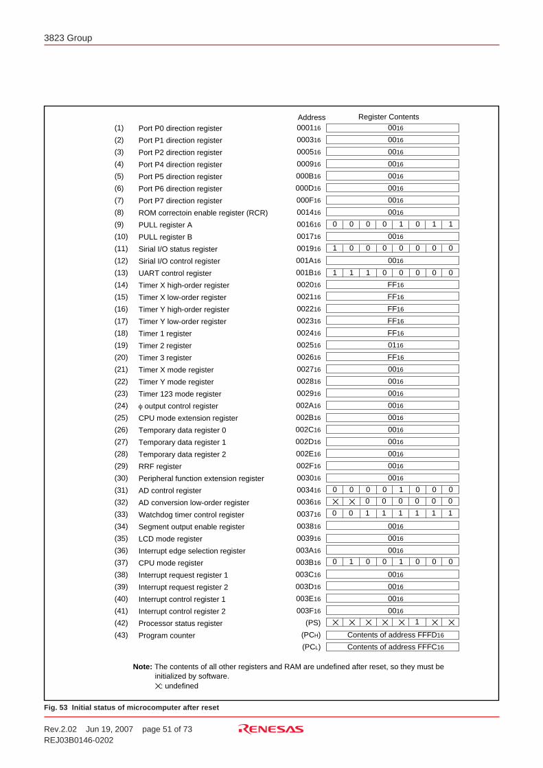
Rev.2.02 Jun 19, 2007 page 51 of 73REJ03B0146-0202
3823 Group
Fig. 53 Initial status of microcomputer after reset
P
o
r
t
P
0
d
i
r
e
c
t
i
o
n
r
e
g
i
s
t
e
r
P
o
r
t
P
1
d
i
r
e
c
t
i
o
n
r
e
g
i
s
t
e
r
P
o
r
t
P
2
d
i
r
e
c
t
i
o
n
r
e
g
i
s
t
e
r
P
o
r
t
P
4
d
i
r
e
c
t
i
o
n
r
e
g
i
s
t
e
r
P
o
r
t
P
5
d
i
r
e
c
t
i
o
n
r
e
g
i
s
t
e
r
P
o
r
t
P
6
d
i
r
e
c
t
i
o
n
r
e
g
i
s
t
e
r
P
o
r
t
P
7
d
i
r
e
c
t
i
o
n
r
e
g
i
s
t
e
r
R
O
M
c
o
r
r
e
c
t
o
i
n
e
n
a
b
l
e
r
e
g
i
s
t
e
r
(
R
C
R
)
P
U
L
L
r
e
g
i
s
t
e
r
A
P
U
L
L
r
e
g
i
s
t
e
r
B
S
i
r
i
a
l
I
/
O
s
t
a
t
u
s
r
e
g
i
s
t
e
r
S
i
r
i
a
l
I
/
O
c
o
n
t
r
o
l
r
e
g
i
s
t
e
r
U
A
R
T
c
o
n
t
r
o
l
r
e
g
i
s
t
e
r
T
i
m
e
r
X
h
i
g
h
-
o
r
d
e
r
r
e
g
i
s
t
e
r
T
i
m
e
r
X
l
o
w
-
o
r
d
e
r
r
e
g
i
s
t
e
r
T
i
m
e
r
Y
h
i
g
h
-
o
r
d
e
r
r
e
g
i
s
t
e
r
T
i
m
e
r
Y
l
o
w
-
o
r
d
e
r
r
e
g
i
s
t
e
r
T
i
m
e
r
1
r
e
g
i
s
t
e
r
T
i
m
e
r
2
r
e
g
i
s
t
e
r
T
i
m
e
r
3
r
e
g
i
s
t
e
r
T
i
m
e
r
X
m
o
d
e
r
e
g
i
s
t
e
r
T
i
m
e
r
Y
m
o
d
e
r
e
g
i
s
t
e
r
T
i
m
e
r
1
2
3
m
o
d
e
r
e
g
i
s
t
e
r
φ
o
u
t
p
u
t
c
o
n
t
r
o
l
r
e
g
i
s
t
e
r
C
P
U
m
o
d
e
e
x
t
e
n
s
i
o
n
r
e
g
i
s
t
e
r
Te
m
p
o
r
a
r
y
d
a
t
a
r
e
g
i
s
t
e
r
0
T
e
m
p
o
r
a
r
y
d
a
t
a
r
e
g
i
s
t
e
r
1
T
e
m
p
o
r
a
r
y
d
a
t
a
r
e
g
i
s
t
e
r
2
R
R
F
r
e
g
i
s
t
e
r
P
e
r
i
p
h
e
r
a
l
f
u
n
c
t
i
o
n
e
x
t
e
n
s
i
o
n
r
e
g
i
s
t
e
r
A
D
c
o
n
t
r
o
l
r
e
g
i
s
t
e
r
A
D
c
o
n
v
e
r
s
i
o
n
l
o
w
-
o
r
d
e
r
r
e
g
i
s
t
e
r
W
a
t
c
h
d
o
g
t
i
m
e
r
c
o
n
t
r
o
l
r
e
g
i
s
t
e
r
S
e
g
m
e
n
t
o
u
t
p
u
t
e
n
a
b
l
e
r
e
g
i
s
t
e
r
L
C
D
m
o
d
e
r
e
g
i
s
t
e
r
I
n
t
e
r
r
u
p
t
e
d
g
e
s
e
l
e
c
t
i
o
n
r
e
g
i
s
t
e
r
C
P
U
m
o
d
e
r
e
g
i
s
t
e
r
I
n
t
e
r
r
u
p
t
r
e
q
u
e
s
t
r
e
g
i
s
t
e
r
1
I
n
t
e
r
r
u
p
t
r
e
q
u
e
s
t
r
e
g
i
s
t
e
r
2
I
n
t
e
r
r
u
p
t
c
o
n
t
r
o
l
r
e
g
i
s
t
e
r
1
I
n
t
e
r
r
u
p
t
c
o
n
t
r
o
l
r
e
g
i
s
t
e
r
2
P
r
o
c
e
s
s
o
r
s
t
a
t
u
s
r
e
g
i
s
t
e
r
P
r
o
g
r
a
m
c
o
u
n
t
e
r
Note: The contents of all other registers and RAM are undefined after reset, so they must be initialized by software. : undefined
R
e
g
i
s
t
e
r
C
o
n
t
e
n
t
sAddress0
01
6
0
01
6
0
01
6
0
01
6
0
01
6
0
01
6
0
01
6
0
01
6
0
01
6
0
01
6
F
F1
6
F
F1
6
F
F1
6
F
F1
6
F
F1
6
0
11
6
F
F1
6
0
01
6
0
01
6
0
01
6
0
01
6
0
01
6
0
01
6
0
01
6
0
01
6
0
01
6
0
01
6
0
01
6
0
01
6
0
01
6
0
01
6
0
01
6
0
01
6
0
01
6
C
o
n
t
e
n
t
s
o
f
a
d
d
r
e
s
s
F
F
F
D1
6
C
o
n
t
e
n
t
s
o
f
a
d
d
r
e
s
s
F
F
F
C1
6
( 1
)
(
2
)
(
3
)
(
4
)
(
5
)
(
6
)
(
7
)
(
8
)
(
9
)
(
1
0
)
(
1
1
)
(
1
2
)
(
1
3
)
(
1
4
)
(
1
5
)
(
1
6
)
(
1
7
)
(
1
8
)
(
1
9
)
(
2
0
)
(
2
1
)
(
2
2
)
(
2
3
)
(
2
4
)
(
2
5
)
(
2
6
)
(
2
7
)
(
2
8
)
(
2
9
)
(
3
0
)
(
3
1
)
(
3
2
)
(
3
3
)
(
3
4
)
(
3
5
)
(
3
6
)
(
3
7
)
(
3
8
)
(
3
9
)
(
4
0
)
(
4
1
)
(
4
2
)
(
4
3
)
000116
000316
000516
000916
000B16
000D16
000F16
001416
001616
001716
001916
001A16
001B16
002016
002116
002216
002316
002416
002516
002616
002716
002816
002916
002A16
002B16
002C16
002D16
002E16
002F16
003016
003416
003616
003716
003816
003916
003A16
003B16
003C16
003D16
003E16
003F16
(PS)
(PCH)
(PCL)
0 0 0 0 1 0 00
1 1 1 0 0 0 00
1 0 0 0 0 0 00
0 0 0 0 1 1 10
0 0 0 0 00
0 0 1 1 1 1 11
1
0 1 0 0 1 0 00
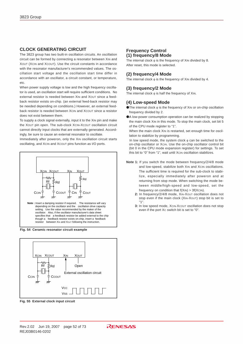
Rev.2.02 Jun 19, 2007 page 52 of 73REJ03B0146-0202
3823 Group
CLOCK GENERATING CIRCUITThe 3823 group has two built-in oscillation circuits. An oscillationcircuit can be formed by connecting a resonator between XIN andXOUT (XCIN and XCOUT). Use the circuit constants in accordancewith the resonator manufacturer's recommended values. The os-cillation start voltage and the oscillation start time differ inaccordance with an oscillator, a circuit constant, or temperature,etc.When power supply voltage is low and the high frequency oscilla-tor is used, an oscillation start will require sufficient conditions. Noexternal resistor is needed between XIN and XOUT since a feed-back resistor exists on-chip. (an external feed-back resistor maybe needed depending on conditions.) However, an external feed-back resistor is needed between XCIN and XCOUT since a resistordoes not exist between them.To supply a clock signal externally, input it to the XIN pin and makethe XOUT pin open. The sub-clock XCIN-XCOUT oscillation circuitcannot directly input clocks that are externally generated. Accord-ingly, be sure to cause an external resonator to oscillate.Immediately after poweron, only the XIN oscillation circuit startsoscillating, and XCIN and XCOUT pins function as I/O ports.
Fig. 55 External clock input circuit
XI
N
E
x
t
e
r
n
a
l
o
s
c
i
l
l
a
t
i
o
n
c
i
r
c
u
i
t
Open
VC
C
VS
S
CC
I
N CC
O
U
T
Rf Rd
XC
I
N
XC
O
U
T XO
U
T
Frequency Control(1) frequency/8 ModeThe internal clock φ is the frequency of XIN divided by 8.After reset, this mode is selected.
(2) frequency/4 ModeThe internal clock φ is the frequency of XIN divided by 4.
(3) frequency/2 ModeThe internal clock φ is half the frequency of XIN.
(4) Low-speed Mode The internal clock φ is the frequency of XIN or on-chip oscillation
frequency divided by 2. A low-power consumption operation can be realized by stopping
the main clock XIN in this mode. To stop the main clock, set bit 5of the CPU mode register to “1”.When the main clock XIN is restarted, set enough time for oscil-lation to stabilize by programming.
In low speed mode, the system clock φ can be switched to theon-chip oscillator or XCIN. Use the on-chip oscillator control bit(bit 0 in the CPU mode expansion register) for settings. To setthis bit to “0” from “1”, wait until XCIN oscillation stabilizes.
Note 1: If you switch the mode between frequency/2/4/8 modeand low-speed, stabilize both XIN and XCIN oscillations.The sufficient time is required for the sub-clock to stabi-lize, especially immediately after poweron and atreturning from stop mode. When switching the mode be-tween middle/high-speed and low-speed, set thefrequency on condition that f(XIN) > 3f(XCIN).
2: In frequency/2/4/8 mode, XIN-XOUT oscillation does notstop even if the main clock (XIN-XOUT) stop bit is set to"1".
3: In low speed mode, XCIN-XCOUT oscillation does not stopeven if the port XC switch bit is set to "0".
Fig. 54 Ceramic resonator circuit example
XCIN XCOUT XIN XOUT
CIN COUTCCIN CCOUT
Rf RdRd
Note : Insert a damping resistor if required. The resistance will vary depending on the oscillator and the oscillation drive capacity setting. Use the value recommended by the maker of the oscillator. Also, if the oscillator manufacturer's data sheet specifies that a feedback resistor be added external to the chip though a feedback resistor exists on-chip, insert a feedback resistor between XIN and XOUT following the instruction.
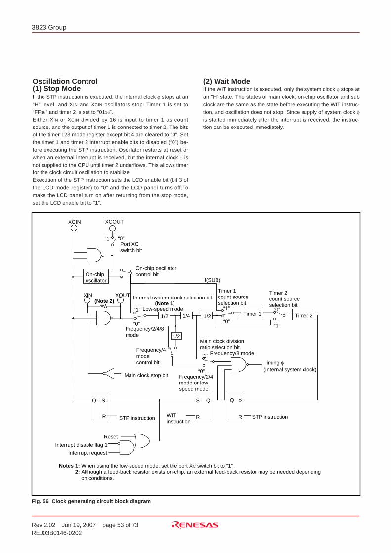
Rev.2.02 Jun 19, 2007 page 53 of 73REJ03B0146-0202
3823 Group
Fig. 56 Clock generating circuit block diagram
Oscillation Control(1) Stop ModeIf the STP instruction is executed, the internal clock φ stops at an“H” level, and XIN and XCIN oscillators stop. Timer 1 is set to“FF16” and timer 2 is set to “0116”.Either XIN or XCIN divided by 16 is input to timer 1 as countsource, and the output of timer 1 is connected to timer 2. The bitsof the timer 123 mode register except bit 4 are cleared to “0”. Setthe timer 1 and timer 2 interrupt enable bits to disabled (“0”) be-fore executing the STP instruction. Oscillator restarts at reset orwhen an external interrupt is received, but the internal clock φ isnot supplied to the CPU until timer 2 underflows. This allows timerfor the clock circuit oscillation to stabilize.Execution of the STP instruction sets the LCD enable bit (bit 3 ofthe LCD mode register) to “0” and the LCD panel turns off.Tomake the LCD panel turn on after returning from the stop mode,set the LCD enable bit to “1”.
(2) Wait ModeIf the WIT instruction is executed, only the system clock φ stops atan "H" state. The states of main clock, on-chip oscillator and subclock are the same as the state before executing the WIT instruc-tion, and oscillation does not stop. Since supply of system clock φis started immediately after the interrupt is received, the instruc-tion can be executed immediately.
Timing φ(Internal system clock)
Main clock stop bit
Timer 2Timer 11/2 1/4
XIN XOUT
WITinstruction
STP instruction
S
R
Q
STP instruction
S
R
Q S
R
Q
Interrupt request
Interrupt disable flag 1
Reset
1/2
“1”
“0”
Timer 1count source selection bit
“0”
“1”
Timer 2count source selection bit
Low-speed mode
Frequency/2/4/8 mode
(Note 1)
Frequency/8 mode
Frequency/2/4 mode or low-speed mode
Internal system clock selection bit
Main clock division ratio selection bit
“1”
“0”
“0”
“1”
Notes 1: When using the low-speed mode, set the port XC switch bit to “1” .2: Although a feed-back resistor exists on-chip, an external feed-back resistor may be needed depending
on conditions.
Frequency/4 modecontrol bit
1/2
XCOUTXCIN
Port XCswitch bit
“0”“1”
On-chip oscillator
On-chip oscillatorcontrol bit
f(SUB)
(Note 2)
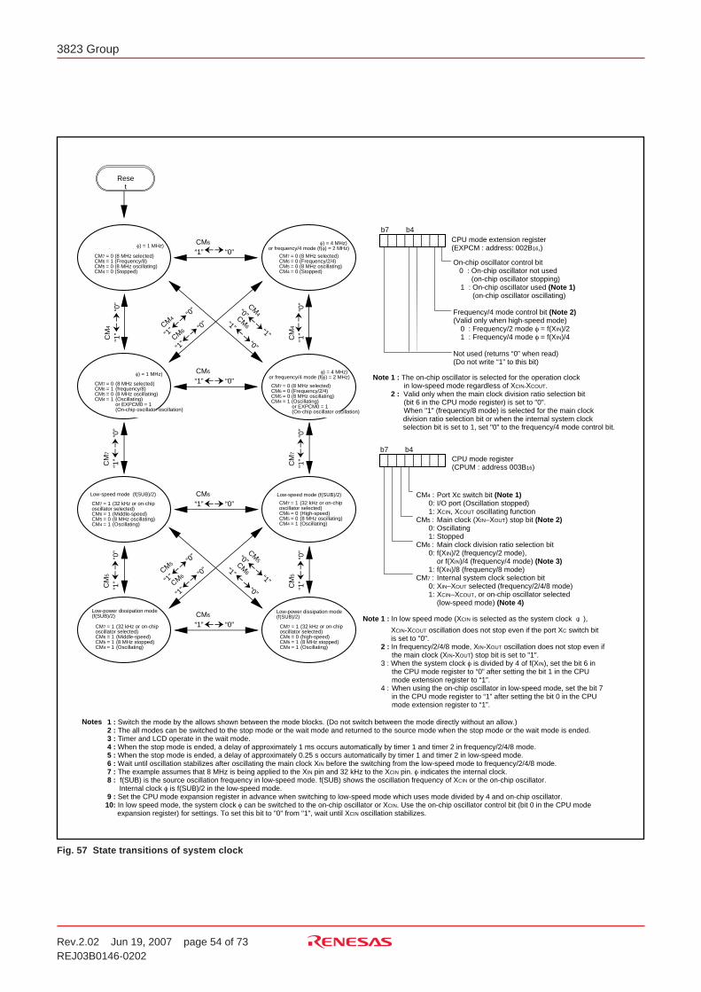
Rev.2.02 Jun 19, 2007 page 54 of 73REJ03B0146-0202
3823 Group
Notes 1 : Switch the mode by the allows shown between the mode blocks. (Do not switch between the mode directly without an allow.) 2 : The all modes can be switched to the stop mode or the wait mode and returned to the source mode when the stop mode or the wait mode is ended. 3 : Timer and LCD operate in the wait mode. 4 : When the stop mode is ended, a delay of approximately 1 ms occurs automatically by timer 1 and timer 2 in frequency/2/4/8 mode. 5 : When the stop mode is ended, a delay of approximately 0.25 s occurs automatically by timer 1 and timer 2 in low-speed mode. 6 : Wait until oscillation stabilizes after oscillating the main clock XIN before the switching from the low-speed mode to frequency/2/4/8 mode. 7 : The example assumes that 8 MHz is being applied to the XIN pin and 32 kHz to the XCIN pin. φ indicates the internal clock. 8 : f(SUB) is the source oscillation frequency in low-speed mode. f(SUB) shows the oscillation frequency of XCIN or the on-chip oscillator. Internal clock φ is f(SUB)/2 in the low-speed mode. 9 : Set the CPU mode expansion register in advance when switching to low-speed mode which uses mode divided by 4 and on-chip oscillator.10: In low speed mode, the system clock φ can be switched to the on-chip oscillator or XCIN. Use the on-chip oscillator control bit (bit 0 in the CPU mode expansion register) for settings. To set this bit to "0" from "1", wait until XCIN oscillation stabilizes.
CM4 : Port Xc switch bit (Note 1)0: I/O port (Oscillation stopped)1: XCIN, XCOUT oscillating function
CM5 : Main clock (XIN–XOUT) stop bit (Note 2)0: Oscillating1: Stopped
CM6 : Main clock division ratio selection bit 0: f(XIN)/2 (frequency/2 mode),
or f(XIN)/4 (frequency/4 mode) (Note 3)1: f(XIN)/8 (frequency/8 mode)
CM7 : Internal system clock selection bit0: XIN–XOUT selected (frequency/2/4/8 mode)1: XCIN–XCOUT, or on-chip oscillator selected
(low-speed mode) (Note 4)
CPU mode register(CPUM : address 003B16)
b7 b4
Reset
CM6
“0”“1”
CM
4
“0”
“1”
CM7 = 0 (8 MHz selected)CM6 = 1 (Frequency/8)CM5 = 0 (8 MHz oscillating)CM4 = 0 (Stopped)
Frequency/8 mode (f(φ) = 1 MHz)
Frequency/8 mode (f(φ) = 1 MHz)
CM7 = 0 (8 MHz selected)CM6 = 0 (Frequency/2/4)CM5 = 0 (8 MHz oscillating)CM4 = 0 (Stopped)
Frequency/2 mode (f(φ) = 4 MHz)or frequency/4 mode (f(φ) = 2 MHz)
Frequency/2 mode (f(φ) = 4 MHz)or frequency/4 mode (f(φ) = 2 MHz)
CM7 = 1 (32 kHz or on-chip oscillator selected)CM6 = 1 (Middle-speed)CM5 = 0 (8 MHz oscillating)CM4 = 1 (Oscillating)
Low-speed mode (f(SUB)/2)
CM7 = 1 (32 kHz or on-chip oscillator selected)CM6 = 0 (High-speed)CM5 = 0 (8 MHz oscillating)CM4 = 1 (Oscillating)
Low-speed mode (f(SUB)/2)
CM7 = 1 (32 kHz or on-chip oscillator selected)CM6 = 1 (Middle-speed)CM5 = 1 (8 MHz stopped)CM4 = 1 (Oscillating)
Low-power dissipation mode (f(SUB)/2)
CM6
“0”“1”
CM6
“0”“1”
CM6
“0”“1”
CM
4
“0”
“1”
CM
7
“0”
“1”
CM
7
“0”
“1”
CM
5
“0”
“1”
CM
5
“0”
“1”
CM4
CM6“0
”
“1”
“0”
“1”
CM4
CM6
“0”
“1” “1”
“0”
CM5
CM6 “0”
“1”
“0”
“1”
CM5
CM6
“0”
“1” “1”
“0”
CM7 = 0 (8 MHz selected)CM6 = 1 (frequency/8)CM5 = 0 (8 MHz oscillating)CM4 = 1 (Oscillating)
or EXPCM0 = 1(On-chip oscillator oscillation)
CM7 = 1 (32 kHz or on-chip oscillator selected)CM6 = 0 (high-speed)CM5 = 1 (8 MHz stopped)CM4 = 1 (Oscillating)
Low-power dissipation mode (f(SUB)/2)
CM7 = 0 (8 MHz selected)CM6 = 0 (Frequency/2/4)CM5 = 0 (8 MHz oscillating)CM4 = 1 (Oscillating)
or EXPCM0 = 1(On-chip oscillator oscillation)
On-chip oscillator control bit 0 : On-chip oscillator not used (on-chip oscillator stopping)
1 : On-chip oscillator used (Note 1) (on-chip oscillator oscillating)
Frequency/4 mode control bit (Note 2)(Valid only when high-speed mode)
0 : Frequency/2 mode φ = f(XIN)/21 : Frequency/4 mode φ = f(XIN)/4
Not used (returns “0” when read)(Do not write “1” to this bit)
CPU mode extension register(EXPCM : address: 002B16,)
b7 b4
Note 1 : The on-chip oscillator is selected for the operation clock in low-speed mode regardless of XCIN-XCOUT.
2 : Valid only when the main clock division ratio selection bit (bit 6 in the CPU mode register) is set to "0".
When "1" (frequency/8 mode) is selected for the main clock division ratio selection bit or when the internal system clock selection bit is set to 1, set "0" to the frequency/4 mode control bit.
Note 1 : In low speed mode (XCIN is selected as the system clock φ),
XCIN-XCOUT oscillation does not stop even if the port XC switch bit is set to "0". 2 : In frequency/2/4/8 mode, XIN-XOUT oscillation does not stop even if
the main clock (XIN-XOUT) stop bit is set to "1". 3 : When the system clock φ is divided by 4 of f(XIN), set the bit 6 in
the CPU mode register to “0” after setting the bit 1 in the CPU mode extension register to “1”.
4 : When using the on-chip oscillator in low-speed mode, set the bit 7 in the CPU mode register to “1” after setting the bit 0 in the CPU mode extension register to “1”.
Fig. 57 State transitions of system clock
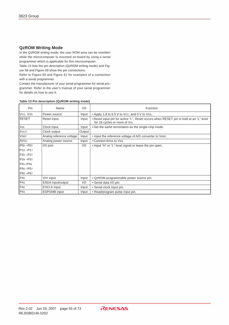
Rev.2.02 Jun 19, 2007 page 55 of 73REJ03B0146-0202
3823 Group
QzROM Writing ModeIn the QzROM writing mode, the user ROM area can be rewrittenwhile the microcomputer is mounted on-board by using a serialprogrammer which is applicable for this microcomputer.Table 13 lists the pin description (QzROM writing mode) and Fig-ure 58 and Figure 59 show the pin connections.Refer to Figure 60 and Figure 61 for examples of a connectionwith a serial programmer.Contact the manufacturer of your serial programmer for serial pro-grammer. Refer to the user’s manual of your serial programmerfor details on how to use it.
Table 13 Pin description (QzROM writing mode)
• Apply 1.8 to 5.5 V to VCC, and 0 V to VSS.
• Reset input pin for active “L”. Reset occurs when RESET pin is hold at an “L” levelfor 16 cycles or more of XIN.
• Set the same termination as the single-chip mode.
• Input the reference voltage of A/D converter to VREF.
• Connect AVss to Vss.
• Input “H” or “L” level signal or leave the pin open.
• QzROM programmable power source pin.
• Serial data I/O pin.
• Serial clock input pin.
• Read/program pulse input pin.
VCC, VSS
RESET
XIN
XOUT
VREF
AVSS
P00 –P07
P10 –P17
P20 –P27
P34 –P37
P41–P44
P50 –P57
P60 –P67
P40
P44
P42
P43
Power source
Reset input
Clock input
Clock output
Analog reference voltage
Analog power source
I/O port
VPP input
ESDA input/output
ESCLK input
ESPGMB input
FunctionPin Name
Input
Input
Input
Output
Input
Input
I/O
Input
I/O
Input
Input
I/O
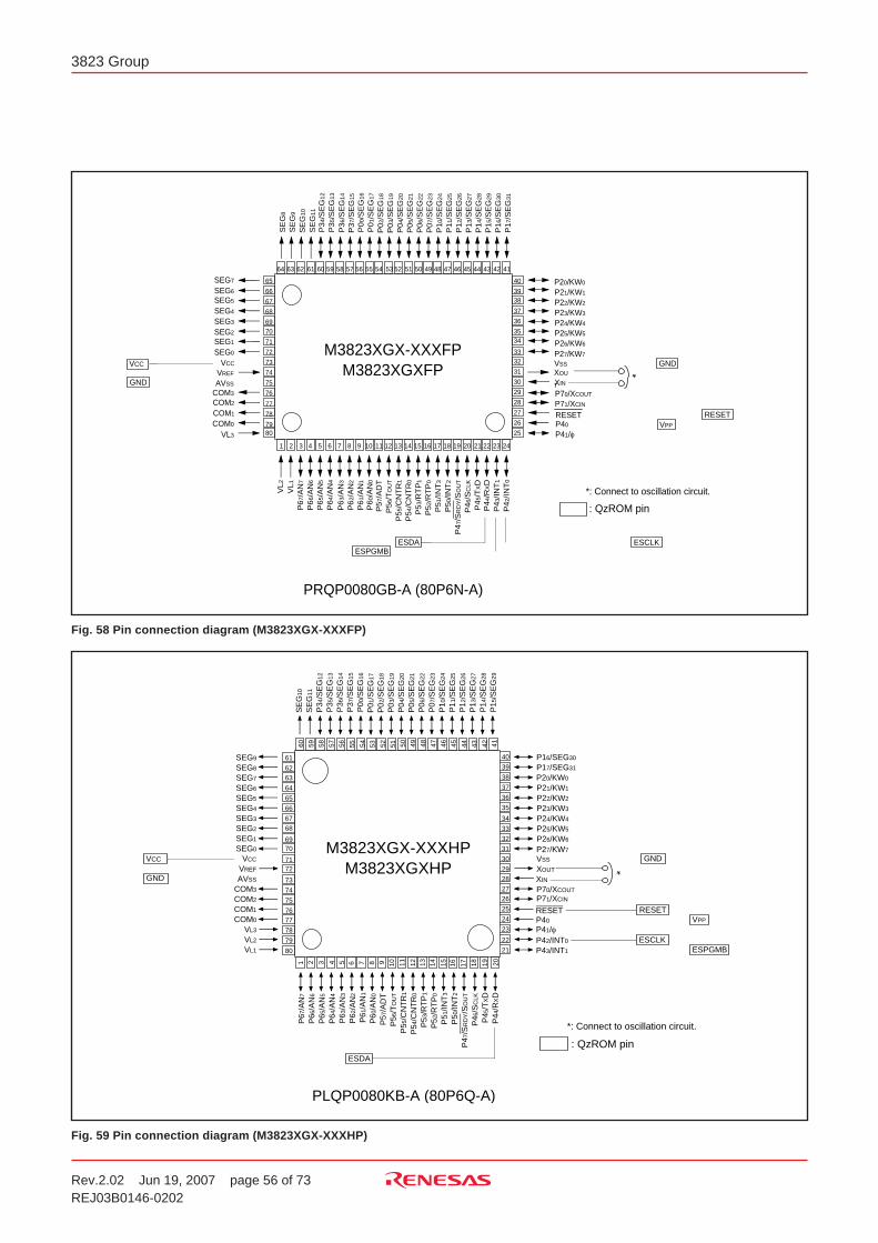
Rev.2.02 Jun 19, 2007 page 56 of 73REJ03B0146-0202
3823 Group
Fig. 58 Pin connection diagram (M3823XGX-XXXFP)
SE
G8
SE
G9
P3
4/S
EG
12
P3
5/S
EG
13
P0
0/S
EG
16
P0
3/S
EG
19
P0
4/S
EG
20
P0
5/S
EG
21
P0
6/S
EG
22
P0
7/S
EG
23
P1
1/S
EG
25
P1
2/S
EG
26
P1
3/S
EG
27
P1
4/S
EG
28
P1
5/S
EG
29
P1
6/S
EG
30
P1
7/S
EG
31
VL
1
P6
7/A
N7
M3823XGX-XXXFPM3823XGXFP
P5
7/A
DT
P5
0/IN
T2
P4
6/S
CL
K
P4
5/T
XD
P4
3/IN
T1
P4
2/IN
T0
AVSS
VREF
VCC
SEG0
P41/φP40
XIN
XOU
T
VSS
P27/KW7
P26/KW6
P25/KW5
P24/KW4
P23/KW3
P22/KW2
P21/KW1
P20/KW0
RESET
P5
1/IN
T3
P5
5/C
NT
R1
P5
4/C
NT
R0
P5
3/R
TP
1
P5
2/R
TP
0
P5
6/T
OU
T
P1
0/S
EG
24
P0
1/S
EG
17
P0
2/S
EG
18
P4
7/S
RD
Y/S
OU
T
SE
G1
0
SE
G1
1
P3
6/S
EG
14
P3
7/S
EG
15
P70/XCOUT
P71/XCIN
COM0
VL3
P6
6/A
N6
P6
5/A
N5
P6
4/A
N4
P6
3/A
N3
P6
2/A
N2
P6
1/A
N1
P6
0/A
N0
VL
2
COM1
COM2
COM3
SEG1
SEG2
SEG3
SEG4
SEG5
SEG6
SEG7
P4
4/R
XD
1 2 3 4 5 6 7 8 9 10 11 12 13 14 15 16 17 18 19 20 21 22 23 24
25
26
27
28
29
30
31
3233
3435
36
37
3839
40
414243444546474849505152535455565758596061626364
65
66
67
68
6970
71
72
73
74
75
76
77
78
7980
*: Connect to oscillation circuit.
: QzROM pin
PRQP0080GB-A (80P6N-A)
*
ESDA ESCLKESPGMB
GND
RESETVPP
GND
VCC
Fig. 59 Pin connection diagram (M3823XGX-XXXHP)
1 2 3 4 7 8 9 10 11 12 13 14 15 16 17 18 19 205 6
21
22
23
24
25
2627
2829
30
31
32
33
34
35
36
37
38
39
40
4142434445464748495051525354555657585960
61
6263
64
65
66
6768
6970
7172
73
74
75
7677
78
79
80
P14
/SE
G28
P15
/SE
G29
P16/SEG30
P17/SEG31
P42/INT0
VCC
XIN
XOUT
VSS
RESET
P70/XCOUT
P71/XCIN
P41/φP40
P43/INT1
SE
G10
P35
/SE
G13
P36
/SE
G14
P37
/SE
G15
P00
/SE
G16
P03
/SE
G19
P04
/SE
G20
P05
/SE
G21
P06
/SE
G22
P07
/SE
G23
P11
/SE
G25
P12
/SE
G26
P10
/SE
G24
P01
/SE
G17
P02
/SE
G18
P13
/SE
G27
COM3
P60
/AN
0
P57
/AD
TP
56/T
OU
T
P54
/CN
TR
0
P53
/RT
P1
P52
/RT
P0
P51
/INT
3
P55
/CN
TR
1
P46
/SC
LK
P45
/TXD
P50
/INT
2
P47
/SR
DY/S
OU
T
P44
/RXD
SEG1
SEG2
SEG3
SEG4
SEG6
SEG5
SEG7
SEG0
SEG8
SEG9
COM2
COM1
COM0
VL3
VL2
VL1
VREF
AVSS
P61
/AN
1
P62
/AN
2
P63
/AN
3
P64
/AN
4
P65
/AN
5
P66
/AN
6
P67
/AN
7S
EG
11
P34
/SE
G12
M3823XGX-XXXHPM3823XGXHP
P27/KW7
P26/KW6
P25/KW5
P24/KW4
P23/KW3
P22/KW2
P21/KW1
P20/KW0
PLQP0080KB-A (80P6Q-A)
*
*: Connect to oscillation circuit.
: QzROM pin
GND
ESDA
ESCLKESPGMB
GND
RESETVPP
VCC
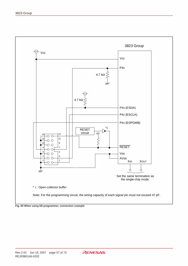
Rev.2.02 Jun 19, 2007 page 57 of 73REJ03B0146-0202
3823 Group
Fig. 60 When using E8 programmer, connection example
3
8
2
3
G
r
o
u
p
RESETcircuit
Set the same termination asthe single-chip mode.
V
c
c
P
44 (
E
S
D
A
)
P
42
(
E
S
C
L
K
)
P43 (ESPGMB)
R
E
S
E
T
Vss
A
V
s
sXI
N XOUT
4
.
7
kΩ
* 1 : Open-collector buffer
Note: For the programming circuit, the wiring capacity of each signal pin must not exceed 47 pF.
V
c
c
14
1
2
1
0
8
1
3
1
1
9
7
4
2
6
3
1
*1
P
40
4 .
7
kΩ
5
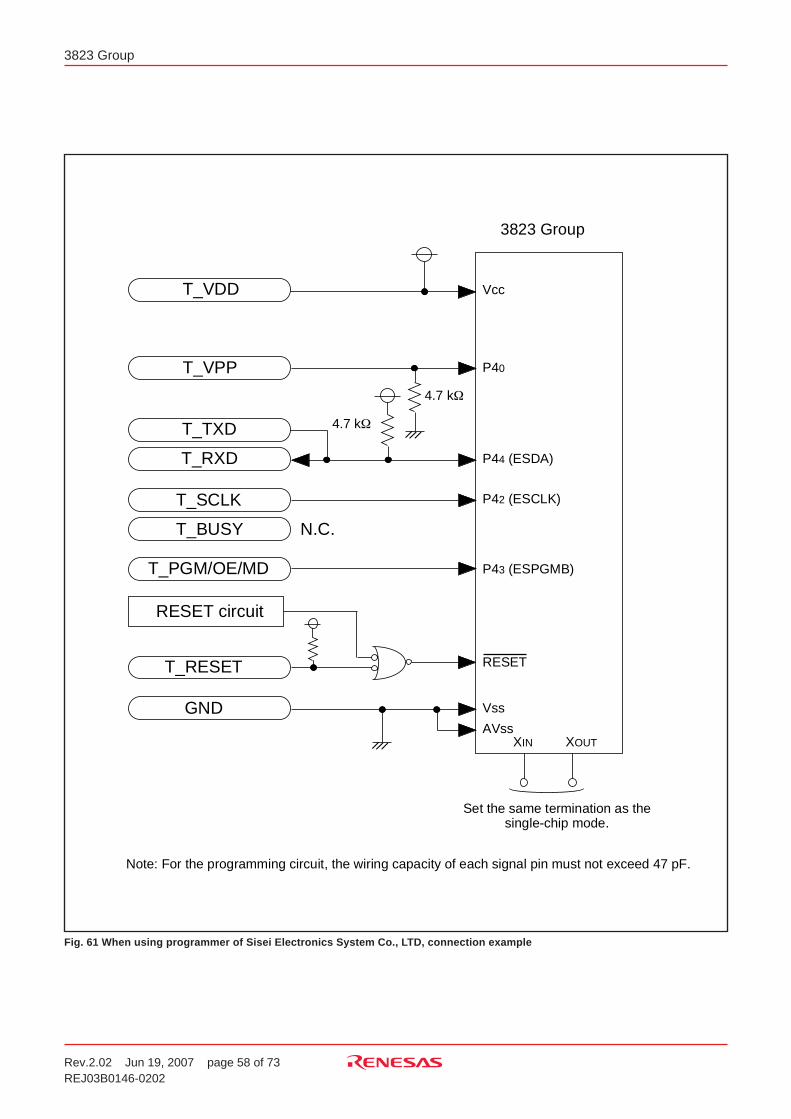
Rev.2.02 Jun 19, 2007 page 58 of 73REJ03B0146-0202
3823 Group
Fig. 61 When using programmer of Sisei Electronics System Co., LTD, connection example
3
8
2
3
G
r
o
u
p
T
_
V
D
D
T
_
V
P
P
T_RXD
T
_
S
C
L
K
T
_
P
G
M
/
O
E
/
M
D
T_RESET
G
N
D
RESET circuit
S
e
t
t
h
e
s
a
m
e
t
e
r
m
i
n
a
t
i
o
n
a
s
t
h
es
i
n
g
l
e
-
c
h
i
p
m
o
d
e
.
Vcc
P40
P44 (ESDA)
P42 (ESCLK)
P43 (ESPGMB)
RESET
Vss
AVssXI
N XOUT
4.7 kΩ
4 .
7
kΩ
Note: For the programming circuit, the wiring capacity of each signal pin must not exceed 47 pF.
T
_
T
X
D
T_BUSY N.C.
Rev.2.02 Jun 19, 2007 page 59 of 73REJ03B0146-0202
3823 Group
NOTES ON PROGRAMMINGProcessor Status RegisterThe contents of the processor status register (PS) after a reset areundefined, except for the interrupt disable flag (I) which is “1”. Af-ter a reset, initialize flags which affect program execution.In particular, it is essential to initialize the index X mode (T) andthe decimal mode (D) flags because of their effect on calculations.Initialize these flags at the beginning of the program.
InterruptThe contents of the interrupt request bits do not change immedi-ately after they have been written. After writing to an interruptrequest register, execute at least one instruction before perform-ing a BBC or BBS instruction.
Decimal Calculations• To calculate in decimal notation, set the decimal mode flag (D)
to “1”, then execute an ADC or SBC instruction. After executingan ADC or SBC instruction, execute at least one instruction be-fore executing a SEC, CLC, or CLD instruction.
• In decimal mode, the values of the negative (N), overflow (V),and zero (Z) flags are invalid.
TimersIf a value n (between 0 and 255) is written to a timer latch, the fre-quency division ratio is 1/(n + 1).
Multiplication and Division InstructionsThe index mode (T) and the decimal mode (D) flags do not affectthe MUL and DIV instruction.The execution of these instructions does not change the contentsof the processor status register.
PortsThe contents of the port direction registers cannot be read.The following cannot be used:• The data transfer instruction (LDA, etc.)• The operation instruction when the index X mode flag (T) is “1”• The addressing mode which uses the value of a direction regis-
ter as an index• The bit-test instruction (BBC or BBS, etc.) to a direction register• The read-modify-write instruction (ROR, CLB, or SEB, etc.) to a
direction registerUse instructions such as LDM and STA, etc., to set the port direc-tion registers.
Serial InterfaceIn clock synchronous serial I/O, if the receive side is using an ex-ternal clock and it is to output the SRDY signal, set the transmitenable bit, the receive enable bit, and the SRDY output enable bitto “1”.Serial I/O continues to output the final bit from the TXD pin aftertransmission is completed.
A/D ConverterThe comparator is constructed linked to a capacitor. The conver-sion accuracy may be low because the charge is lost if theconversion speed is not enough. Accordingly, set f(XIN) to at least500kHz during A/D conversion in the middle-or high-speed mode.Also, do not execute the STP or WIT instruction during an A/Dconversion.In the low-speed mode, since the A/D conversion is executed bythe on-chip oscillator, the minimum value of f(XIN) frequency is notlimited.
LCD Drive Control CircuitExecution of the STP instruction sets the LCD enable bit (bit 3 ofthe LCD mode register) to “0” and the LCD panel turns off.Tomake the LCD panel turn on after returning from the stop mode,set the LCD enable bit to “1”.
Instruction Execution TimeThe instruction execution time is obtained by multiplying the fre-quency of the internal clock φ by the number of cycles needed toexecute an instruction.The number of cycles required to execute an instruction is shownin the list of machine instructions.The frequency of the internal clock φ is half of the XIN frequency.
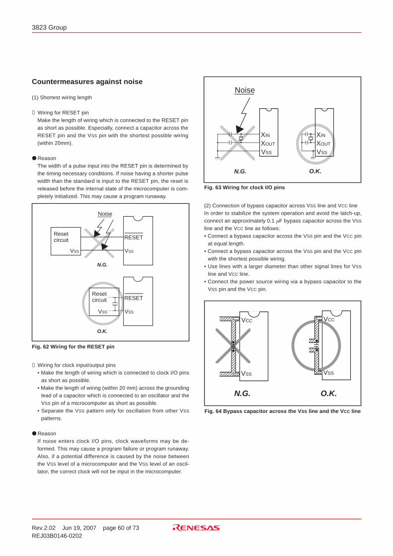
Rev.2.02 Jun 19, 2007 page 60 of 73REJ03B0146-0202
3823 Group
Countermeasures against noise
(1) Shortest wiring length
➀ Wiring for RESET pinMake the length of wiring which is connected to the RESET pinas short as possible. Especially, connect a capacitor across theRESET pin and the VSS pin with the shortest possible wiring(within 20mm).
ReasonThe width of a pulse input into the RESET pin is determined bythe timing necessary conditions. If noise having a shorter pulsewidth than the standard is input to the RESET pin, the reset isreleased before the internal state of the microcomputer is com-pletely initialized. This may cause a program runaway.
(2) Connection of bypass capacitor across VSS line and VCC lineIn order to stabilize the system operation and avoid the latch-up,connect an approximately 0.1 µF bypass capacitor across the VSS
line and the VCC line as follows:• Connect a bypass capacitor across the VSS pin and the VCC pin
at equal length.• Connect a bypass capacitor across the VSS pin and the VCC pin
with the shortest possible wiring.• Use lines with a larger diameter than other signal lines for VSS
line and VCC line.• Connect the power source wiring via a bypass capacitor to the
VSS pin and the VCC pin.
➁ Wiring for clock input/output pins• Make the length of wiring which is connected to clock I/O pins
as short as possible.• Make the length of wiring (within 20 mm) across the grounding
lead of a capacitor which is connected to an oscillator and theVSS pin of a microcomputer as short as possible.
• Separate the VSS pattern only for oscillation from other VSS
patterns.
ReasonIf noise enters clock I/O pins, clock waveforms may be de-formed. This may cause a program failure or program runaway.Also, if a potential difference is caused by the noise betweenthe VSS level of a microcomputer and the VSS level of an oscil-lator, the correct clock will not be input in the microcomputer.
RESETReset circuit
Noise
VSSVSS
Reset circuit
VSS
RESET
VSS
N.G.
O.K.
Noise
XIN
XOUT
VSS
XIN
XOUT
VSS
N.G. O.K.
VSS
VCC
VSS
VCC
N.G. O.K.
Fig. 63 Wiring for clock I/O pins
Fig. 62 Wiring for the RESET pin
Fig. 64 Bypass capacitor across the VSS line and the VCC line
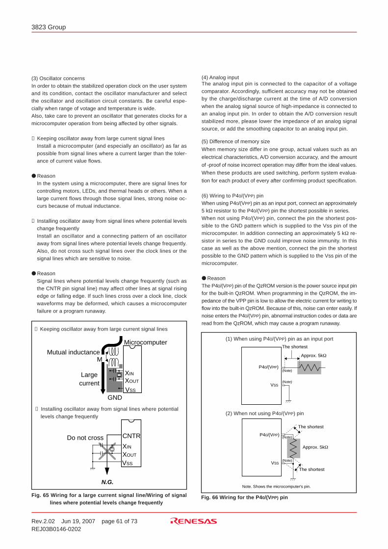
Rev.2.02 Jun 19, 2007 page 61 of 73REJ03B0146-0202
3823 Group
(3) Oscillator concernsIn order to obtain the stabilized operation clock on the user systemand its condition, contact the oscillator manufacturer and selectthe oscillator and oscillation circuit constants. Be careful espe-cially when range of votage and temperature is wide.Also, take care to prevent an oscillator that generates clocks for amicrocomputer operation from being affected by other signals.
➀ Keeping oscillator away from large current signal linesInstall a microcomputer (and especially an oscillator) as far aspossible from signal lines where a current larger than the toler-ance of current value flows.
ReasonIn the system using a microcomputer, there are signal lines forcontrolling motors, LEDs, and thermal heads or others. When alarge current flows through those signal lines, strong noise oc-curs because of mutual inductance.
➁ Installing oscillator away from signal lines where potential levelschange frequentlyInstall an oscillator and a connecting pattern of an oscillatoraway from signal lines where potential levels change frequently.Also, do not cross such signal lines over the clock lines or thesignal lines which are sensitive to noise.
ReasonSignal lines where potential levels change frequently (such asthe CNTR pin signal line) may affect other lines at signal risingedge or falling edge. If such lines cross over a clock line, clockwaveforms may be deformed, which causes a microcomputerfailure or a program runaway.
➀ Keeping oscillator away from large current signal lines
➁ Installing oscillator away from signal lines where potentiallevels change frequently
Fig. 66 Wiring for the P40/(VPP) pinFig. 65 Wiring for a large current signal line/Wiring of signallines where potential levels change frequently
A
p
p
r
o
x
.
5
kΩ
T
h
e
s
h
o
r
t
e
s
t
P
40/
(
VP
P)
VS
S
P
40/
(
VP
P)
VS
S
T
h
e
s
h
o
r
t
e
s
t
T
h
e
s
h
o
r
t
e
s
t
A
p
p
r
o
x
.
5
kΩ
( N
o
t
e
)
( N
o
t
e
)
( N
o
t
e
)
( N
o
t
e
)
N
o
t
e
.
S
h
o
w
s
t
h
e
m
i
c
r
o
c
o
m
p
u
t
e
r
'
s
p
i
n
.
(4) Analog inputThe analog input pin is connected to the capacitor of a voltagecomparator. Accordingly, sufficient accuracy may not be obtainedby the charge/discharge current at the time of A/D conversionwhen the analog signal source of high-impedance is connected toan analog input pin. In order to obtain the A/D conversion resultstabilized more, please lower the impedance of an analog signalsource, or add the smoothing capacitor to an analog input pin.
(5) Difference of memory size
When memory size differ in one group, actual values such as an
electrical characteristics, A/D conversion accuracy, and the amount
of -proof of noise incorrect operation may differ from the ideal values.
When these products are used switching, perform system evalua-
tion for each product of every after confirming product specification.
(6) Wiring to P40/(VPP) pinWhen using P40/(VPP) pin as an input port, connect an approximately5 kΩ resistor to the P40/(VPP) pin the shortest possible in series.When not using P40/(VPP) pin, connect the pin the shortest pos-sible to the GND pattern which is supplied to the Vss pin of themicrocomputer. In addition connecting an approximately 5 kΩ re-sistor in series to the GND could improve noise immunity. In thiscase as well as the above mention, connect the pin the shortestpossible to the GND pattern which is supplied to the Vss pin of themicrocomputer.
ReasonThe P40/(VPP) pin of the QzROM version is the power source input pinfor the built-in QzROM. When programming in the QzROM, the im-pedance of the VPP pin is low to allow the electric current for writing toflow into the built-in QzROM. Because of this, noise can enter easily. Ifnoise enters the P40/(VPP) pin, abnormal instruction codes or data areread from the QzROM, which may cause a program runaway.
XIN
XOUT
VSS
Microcomputer
Mutual inductance
Large current
GND
M
XIN
XOUT
VSS
CNTRDo not cross
N.G.
(1) When using P40/(VPP) pin as an input port
(2) When not using P40/(VPP) pin
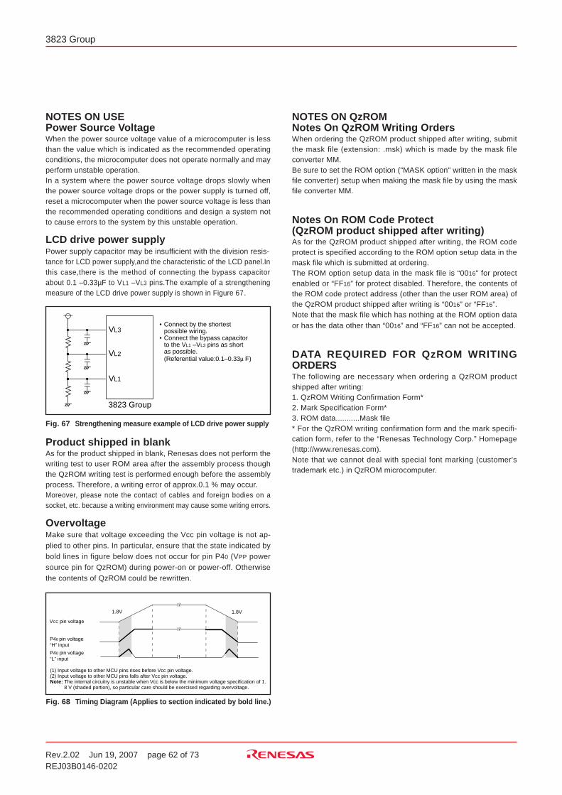
Rev.2.02 Jun 19, 2007 page 62 of 73REJ03B0146-0202
3823 Group
Fig. 67 Strengthening measure example of LCD drive power supply
3823 Group
VL
3
VL
2
VL1
• C
o
n
n
e
c
t
b
y
t
h
e
s
h
o
r
t
e
s
t
p
o
s
s
i
b
l
e
w
i
r
i
n
g
.• C
o
n
n
e
c
t
t
h
e
b
y
p
a
s
s
c
a
p
a
c
i
t
o
r
t
o
t
h
e
VL
1 –
VL
3
p
i
n
s
a
s
s
h
o
r
t
a
s
p
o
s
s
i
b
l
e
.(
R
e
f
e
r
e
n
t
i
a
l
v
a
l
u
e
:
0
.
1
–
0
.
3
3µ
F
)
NOTES ON USEPower Source VoltageWhen the power source voltage value of a microcomputer is lessthan the value which is indicated as the recommended operatingconditions, the microcomputer does not operate normally and mayperform unstable operation.In a system where the power source voltage drops slowly whenthe power source voltage drops or the power supply is turned off,reset a microcomputer when the power source voltage is less thanthe recommended operating conditions and design a system notto cause errors to the system by this unstable operation.
LCD drive power supplyPower supply capacitor may be insufficient with the division resis-tance for LCD power supply,and the characteristic of the LCD panel.Inthis case,there is the method of connecting the bypass capacitorabout 0.1 –0.33µF to VL1 –VL3 pins.The example of a strengtheningmeasure of the LCD drive power supply is shown in Figure 67.
Product shipped in blankAs for the product shipped in blank, Renesas does not perform thewriting test to user ROM area after the assembly process thoughthe QzROM writing test is performed enough before the assemblyprocess. Therefore, a writing error of approx.0.1 % may occur.Moreover, please note the contact of cables and foreign bodies on asocket, etc. because a writing environment may cause some writing errors.
OvervoltageMake sure that voltage exceeding the Vcc pin voltage is not ap-plied to other pins. In particular, ensure that the state indicated bybold lines in figure below does not occur for pin P40 (VPP powersource pin for QzROM) during power-on or power-off. Otherwisethe contents of QzROM could be rewritten.
NOTES ON QzROMNotes On QzROM Writing OrdersWhen ordering the QzROM product shipped after writing, submitthe mask file (extension: .msk) which is made by the mask fileconverter MM.Be sure to set the ROM option ("MASK option" written in the maskfile converter) setup when making the mask file by using the maskfile converter MM.
Notes On ROM Code Protect(QzROM product shipped after writing)As for the QzROM product shipped after writing, the ROM codeprotect is specified according to the ROM option setup data in themask file which is submitted at ordering.The ROM option setup data in the mask file is “0016” for protectenabled or “FF16” for protect disabled. Therefore, the contents ofthe ROM code protect address (other than the user ROM area) ofthe QzROM product shipped after writing is “0016” or “FF16”.Note that the mask file which has nothing at the ROM option dataor has the data other than “0016” and “FF16” can not be accepted.
DATA REQUIRED FOR QzROM WRITINGORDERSThe following are necessary when ordering a QzROM productshipped after writing:1. QzROM Writing Confirmation Form*2. Mark Specification Form*3. ROM data...........Mask file* For the QzROM writing confirmation form and the mark specifi-cation form, refer to the “Renesas Technology Corp.” Homepage(http://www.renesas.com).Note that we cannot deal with special font marking (customer'strademark etc.) in QzROM microcomputer.
P40 pin voltage“H” input
VCC pin voltage
P40 pin voltage“L” input
(1) Input voltage to other MCU pins rises before Vcc pin voltage.(2) Input voltage to other MCU pins falls after Vcc pin voltage.Note: The internal circuitry is unstable when Vcc is below the minimum voltage specification of 1.
8 V (shaded portion), so particular care should be exercised regarding overvoltage.
1.8V 1.8V
~ ~~ ~
~ ~
Fig. 68 Timing Diagram (Applies to section indicated by bold line.)
Rev.2.02 Jun 19, 2007 page 63 of 73REJ03B0146-0202
3823 Group
VO
VO
Pd
Topr
Tstg
–0.3 to 6.5 VPower source voltage
Input voltage P00–P07, P10–P17, P20–P27,P34–P37, P40–P47, P50–P57P60–P67, P70, P71
VCC
VI
Symbol Parameter Conditions Ratings Unit
All voltages are based on VSS.When an input voltage is mea-sured, output transistors are cutoff.
VI
VI
VI
VI
VO
VO
VO
Input voltage VL1
Input voltage VL2
Input voltage VL3
Input voltage RESET, XIN
Output voltage P00–P07, P10–P17
Output voltage P34–P37
Output voltage P20–P27, P41–P47,P50–P57,P60–P67, P70, P71
Output voltage SEG0–SEG11
Output voltage XOUT
Power dissipationOperating temperature
Storage temperature
At output port
At segment output
At segment output
–0.3 to VCC +0.3
–0.3 to VL2
VL1 to VL3
VL2 to 6.5
–0.3 to VCC +0.3
–0.3 to VCC +0.3
–0.3 to VL3
–0.3 to VL3
–0.3 to VCC +0.3
–0.3 to VL3
–0.3 to VCC +0.3
300
–20 to 85
–40 to 150
V
V
V
V
V
V
V
V
V
V
V
mW
°C
°C
Ta = 25°C
(VCC = 1.8 to 5.5 V, Ta = –20 to 85 °C, unless otherwise noted)
5.5
5.5
5.5
5.5
5.5
5.5
5.5
5.5
5.5
5.5
5.5
5.5
VCC
VREF
VCC
Symbol ParameterLimits
Min.
V
V
V
V
V
V
V
V
V
V
V
V
V
V
V
V
Unit
4.5
4.0
2.0
1.8
2.5
2.0
1.8
2.5
2.0
1.8
1.8
2.5
1.8
AVSS
5.0
5.0
5.0
5.0
5.0
5.0
5.0
5.0
5.0
5.0
5.0
0
0
Typ. Max.
Power source voltage(Note 1)
Frequency/2 mode f(XIN) = 10 MHz
f(XIN) = 8 MHz
f(XIN) = 5 MHz
f(XIN) = 2.5 MHz
Frequency/4 mode f(XIN) = 10 MHz
f(XIN) = 8 MHz
f(XIN) = 5 MHz
Frequency/8 mode f(XIN) = 10 MHz
f(XIN) = 8 MHz
f(XIN) = 5 MHz
Low-speed mode (OCO included)
Table 14 Absolute maximum ratings
Table 15 Recommended operating conditions (1)
Note : When the A/D converter is used, refer to the recommended operating condition for A/D converter.
VSS
VL 3
VREF
AVSS
VIA
Power source voltage
LCD power voltage
A/D conversion reference voltage
Analog power source voltage
Analog input voltage AN0–AN7
ELECTRICAL CHARACTERISTICS
Rev.2.02 Jun 19, 2007 page 64 of 73REJ03B0146-0202
3823 Group
(VCC = 1.8 to 5.5 V, Ta = –20 to 85 °C, unless otherwise noted)
“H” input voltage P00–P07, P10–P17,P34–P37, P40, P41, P45, P47, P52,P53,P56,P60–P67,P70,P71 (CM4= 0)
“H” input voltage P20–P27, P42–P44,P46,P50, P51, P54, P55, P57
“H” input voltage RESET
“H” input voltage XIN
“L” input voltage P00–P07, P10–P17,P34–P37, P40, P41, P45, P47, P52, P53,P56,P60–P67,P70,P71 (CM4= 0)
“L” input voltage P20–P27, P42–P44,P46,P50, P51, P54, P55, P57
“L” input voltage RESET
“L” input voltage XIN
VCC
VCC
VCC
VCC
0.3 VCC
0.2 VCC
0.2 VCC
0.2 VCC
VIH
VIH
VIH
VIH
VIL
VIL
VIL
VIL
Symbol ParameterLimits
Min.
V
V
V
V
V
V
V
V
Unit
0.7VCC
0.8VCC
0.8VCC
0.8VCC
0
0
0
0
Typ. Max.
Table 16 Recommended operating conditions (2)
Rev.2.02 Jun 19, 2007 page 65 of 73REJ03B0146-0202
3823 Group
P00–P07, P10–P17, P20–P27 (Note 1)
P41–P47, P50–P57, P60–P67, P70, P71 (Note 1)
P00–P07, P10–P17, P20–P27 (Note 1)
P41–P47, P50–P57, P60–P67, P70, P71 (Note 1)
P00–P07, P10–P17, P20–P27 (Note 1)
P41–P47, P50–P57, P60–P67, P70, P71 (Note 1)
P00–P07, P10–P17, P20–P27 (Note 1)
P41–P47, P50–P57, P60–P67, P70, P71 (Note 1)
P00–P07, P10–P17 (Note 2)
P20–P27, P41–P47, P50–P57, P60–P67, P70, P71(Note 2)
P00–P07, P10–P17 (Note 2)
P20–P27, P41–P47, P50–P57, P60–P67, P70, P71(Note 2)
P00–P07, P10–P17 (Note 3)
P20–P27, P41–P47, P50–P57, P60–P67, P70, P71(Note 3)
P00–P07, P10–P17 (Note 3)
P20–P27, P41–P47, P50–P57, P60–P67, P70, P71(Note 3)
–40
–40
40
40
–20
–20
20
20
–2
–5
(VCC = 1.8 to 5.5 V, Ta = –20 to 85 °C, unless otherwise noted)
Notes 1: The total output current is the sum of all the currents flowing through all the applicable ports. The total average current is an average valuemeasured over 100 ms. The total peak current is the peak value of all the currents.
2: The peak output current is the peak current flowing in each port.3: The average output current is an average value measured over 100 ms.4: When the A/D converter is used, refer to the recommended operating condition for A/D converter.5: When using the microcomputer in low-speed mode, make sure that the sub-clock input oscillation frequency on condition that f(XCIN) < f(XIN)/3.
“H” total peak output current
“H” total peak output current
“L” total peak output current
“L” total peak output current
“H” total average output current
“H” total average output current
“L” total average output current
“L” total average output current
“H” peak output current
“H” peak output current
ΣIOH(peak)
ΣIOH(peak)
ΣIOL(peak)
ΣIOL(peak)
ΣIOH(avg)
ΣIOH(avg)
ΣIOL(avg)
ΣIOL(avg)
IOH(peak)
IOH(peak)
Symbol ParameterLimits
Min.
mA
mA
mA
mA
mA
mA
mA
mA
mA
mA
UnitTyp. Max.
IOL(peak)
IOL(peak)
IOH(avg)
IOH(avg)
IOL(avg)
5
10
–1.0
–2.5
mA
mA
mA
mA
mA
mA
“L” peak output current
“L” peak output current
“H” average output current
“H” average output current
“L” average output current
“L” average output current
Input frequency for timers X and Y(duty cycle 50%)
IOL(avg)
f(CNTR0)f(CNTR1)
MHz
MHz
MHz
MHz
MHz
MHz
MHz
MHz
MHz
MHz
MHz
MHz
MHz
MHz
kHz
(4.5 V ≤ VCC ≤ 5.5 V)
(4.0 V ≤ VCC ≤ 4.5 V)
(2.0 V ≤ VCC ≤ 4.0 V)
(VCC ≤ 2.0 V)
Frequency/2 mode(4.5 V ≤ VCC ≤ 5.5 V)
Frequency/2 mode(4.0 V ≤ VCC ≤ 4.5 V)
Frequency/2 mode(2.0 V ≤ VCC ≤ 4.0 V)
Frequency/2 mode(1.8 V ≤ VCC ≤ 2.0 V)
Frequency/4 mode(2.5 V ≤ VCC ≤ 5.5 V)
Frequency/4 mode(2.0 V ≤ VCC ≤ 2.5 V)
Frequency/4 mode(1.8 V ≤ VCC ≤ 2.0 V)
Frequency/8 mode(2.5 V ≤ VCC ≤ 5.5 V)
Frequency/8 mode(2.0 V ≤ VCC ≤ 2.5 V)
Frequency/8 mode(1.8 V ≤ VCC ≤ 2.0 V)
32.768
Main clock input oscillation frequency(duty cycle 50%)(Note 4)
Sub-clock input oscillation frequency(duty cycle 50%)(Note 5)
f(XIN)
2.5
5.0
5.0
2 VCC – 4
0.75 VCC + 1
6.25 VCC - 10
10.0
4 VCC – 8
1.5 VCC + 2
12.5 VCC - 20
10.0
4 VCC
15 VCC – 22
10.0
4 VCC
15 VCC – 22
80
Table 17 Recommended operating conditions (3)
f(XCIN)

Rev.2.02 Jun 19, 2007 page 66 of 73REJ03B0146-0202
3823 Group
IOL = 10 mA
IOL = 2.5 mA
IOL = 2.5 mAVCC = 2.5 V
IOL = 5 mA
IOL = 1.25 mA
IOL = 1.25 mAVCC = 2.5 V
VOL
IOH = –2.5 mA
IOH = –0.6 mAVCC = 2.5 V
IOH = –5 mA
IOH = –1.25 mA
IOH = –1.25 mAVCC = 2.5 V
VVCC–2.0“H” output voltage
P00–P07, P10–P17
Symbol ParameterLimits
Min.Unit
0.5
Typ. Max.Test conditions
VOH
2.0
0.5
(VCC = 4.0 to 5.5 V, Ta = –20 to 85 °C, unless otherwise noted)
RESET : VCC = 2.0 V to 5.5 V
VI = VCCPull-downs “off”
VCC = 5 V, VI = VCCPull-downs “on”
VCC = 3 V, VI = VCCPull-downs “on”
VI = VCC
“H” output voltageP20–P27, P41–P47, P50–P57, P60–P67,P70, P71 (Note)
“L” output voltageP00–P07, P10–P7
“L” output voltageP20–P27, P41–P47, P50–P57, P60–P67,P70, P71 (Note)
HysteresisINT0–INT3, ADT, CNTR0, CNTR1, P20–P27
Hysteresis SCLK, RXD
Hysteresis RESET
“H” input current
P00–P07, P10–P17, P34–P37
“H” input current
P20–P27, P40–P47, P50–P57, P60–P67,P70, P71 (Note)
VOH
VOL
VT+ – VT–
VT+ – VT–
VT+ – VT–
IIH
IIH
IIH
VCC–2.0
VCC–0.5
30
6.0
–30
–6.0
0.5
0.5
70
2.0
0.5
45
140
5.0
5.0
–5.0
–5.0
–140
–45
V
V
V
V
V
V
V
V
V
IIH
IIL
VCC–1.0
VCC–1.0
V
V
V1.0
V1.0
5.0 µA
25
VI = VCC
VI = VCC
VI = VSS
VI = VSSPull-ups “off”
VCC = 5 V, VI = VSSPull-ups “on”
VCC = 3 V, VI = VSSPull-ups “on”
VI = VSS
VI = VSS
When clock is stopped
“H” input current RESET
“H” input current XIN
“L” input currentP00–P07, P10–P17, P34–P37,P40
“L” input current
P20–P27, P41–P47, P50–P57, P60–P67,P70, P71 (Note)
“L” input current RESET
“L” input current XIN
RAM hold voltage
4.0
–5.0
–70
µA
µA
µA
µA
µA
µA
µA
µA
µA
µA
µA
IIL
IIL
IIL
VRAM
–25
–4.0
Note: When “1” is set to the port XC switch bit (bit 4 at address 003B16) of CPU mode register, the drive ability of port P70 is different from the value abovementioned.
Table 18 Electrical characteristics (1)
1.8 5.5 V
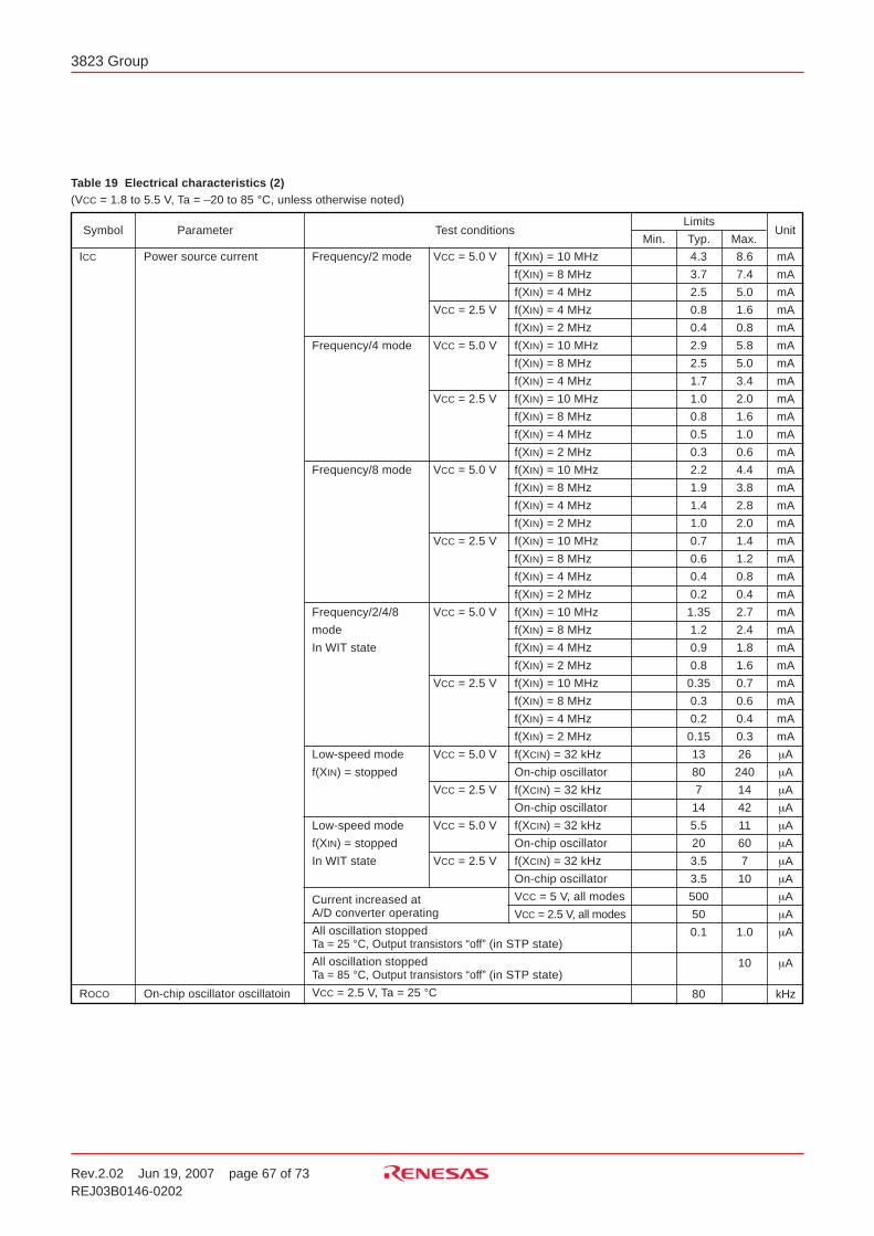
Rev.2.02 Jun 19, 2007 page 67 of 73REJ03B0146-0202
3823 Group
(VCC = 1.8 to 5.5 V, Ta = –20 to 85 °C, unless otherwise noted)
Frequency/2 mode
Frequency/4 mode
Frequency/8 mode
Frequency/2/4/8
mode
In WIT state
Low-speed mode
f(XIN) = stopped
Low-speed mode
f(XIN) = stopped
In WIT state
Current increased atA/D converter operating
All oscillation stoppedTa = 25 °C, Output transistors “off” (in STP state)
All oscillation stoppedTa = 85 °C, Output transistors “off” (in STP state)
VCC = 2.5 V, Ta = 25 °C
Symbol Parameter Test conditions
ICC Power source current
Table 19 Electrical characteristics (2)
VCC = 5.0 V
VCC = 2.5 V
VCC = 5.0 V
VCC = 2.5 V
VCC = 5.0 V
VCC = 2.5 V
VCC = 5.0 V
VCC = 2.5 V
VCC = 5.0 V
VCC = 2.5 V
VCC = 5.0 V
VCC = 2.5 V
f(XIN) = 10 MHz
f(XIN) = 8 MHz
f(XIN) = 4 MHz
f(XIN) = 4 MHz
f(XIN) = 2 MHz
f(XIN) = 10 MHz
f(XIN) = 8 MHz
f(XIN) = 4 MHz
f(XIN) = 10 MHz
f(XIN) = 8 MHz
f(XIN) = 4 MHz
f(XIN) = 2 MHz
f(XIN) = 10 MHz
f(XIN) = 8 MHz
f(XIN) = 4 MHz
f(XIN) = 2 MHz
f(XIN) = 10 MHz
f(XIN) = 8 MHz
f(XIN) = 4 MHz
f(XIN) = 2 MHz
f(XIN) = 10 MHz
f(XIN) = 8 MHz
f(XIN) = 4 MHz
f(XIN) = 2 MHz
f(XIN) = 10 MHz
f(XIN) = 8 MHz
f(XIN) = 4 MHz
f(XIN) = 2 MHz
f(XCIN) = 32 kHz
On-chip oscillator
f(XCIN) = 32 kHz
On-chip oscillator
f(XCIN) = 32 kHz
On-chip oscillator
f(XCIN) = 32 kHz
On-chip oscillator
VCC = 5 V, all modes
VCC = 2.5 V, all modes
ROCO On-chip oscillator oscillatoin
Limits
Min.Unit
Typ. Max.
4.3
3.7
2.5
0.8
0.4
2.9
2.5
1.7
1.0
0.8
0.5
0.3
2.2
1.9
1.4
1.0
0.7
0.6
0.4
0.2
1.35
1.2
0.9
0.8
0.35
0.3
0.2
0.15
13
80
7
14
5.5
20
3.5
3.5
500
50
0.1
80
mA
mA
mA
mA
mA
mA
mA
mA
mA
mA
mA
mA
mA
mA
mA
mA
mA
mA
mA
mA
mA
mA
mA
mA
mA
mA
mA
mA
µA
µA
µA
µA
µA
µA
µA
µA
µA
µA
µA
µA
kHz
8.6
7.4
5.0
1.6
0.8
5.8
5.0
3.4
2.0
1.6
1.0
0.6
4.4
3.8
2.8
2.0
1.4
1.2
0.8
0.4
2.7
2.4
1.8
1.6
0.7
0.6
0.4
0.3
26
240
14
42
11
60
7
10
1.0
10
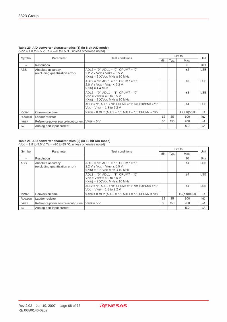
Rev.2.02 Jun 19, 2007 page 68 of 73REJ03B0146-0202
3823 Group
(VCC = 1.8 to 5.5 V, Ta = –20 to 85 °C, unless otherwise noted)
Symbol ParameterLimits
Min.Unit
Typ. Max.Test conditions
–
ABS
tCONV
RLADDER
IVREF
IIA
Resolution
Absolute accuracy(excluding quantization error)
Conversion time
Ladder resistor
Reference power source input current
Analog port input current
ADL2 = “0”, ADL1 = “0”, CPUM7 = “0”2.2 V ≤ VCC = VREF ≤ 5.5 Vf(XIN) = 2 VCC MHz ≤ 10 MHz
ADL2 = “0”, ADL1 = “0”, CPUM7 = “0”2.0 V ≤ VCC = VREF < 2.2 Vf(XIN) = 4.4 MHz
ADL2 = “0”, ADL1 = “1”, CPUM7 = “0”VCC = VREF = 4.0 to 5.5 Vf(XIN) = 2 VCC MHz ≤ 10 MHz
ADL2 = “1”, ADL1 = “0”, CPUM7 = “1” and EXPCM0 = “1”VCC = VREF = 1.8 to 2.2 V
f(XIN) = 8 MHz (ADL2 = “0”, ADL1 = “0”, CPUM7 = “0”)
VREF = 5 V
Bits
LSB
LSB
LSB
LSB
µs
kΩ
µA
µA
8
±2
±3
±3
±4
TC(XIN) 100
100
200
5.0
Table 20 A/D converter characteristics (1) (in 8 bit A/D mode)
12
50
35
150
(VCC = 1.8 to 5.5 V, Ta = –20 to 85 °C, unless otherwise noted)
Symbol ParameterLimits
Min.Unit
Typ. Max.Test conditions
–
ABS
tCONV
RLADDER
IVREF
IIA
Resolution
Absolute accuracy(excluding quantization error)
Conversion time
Ladder resistor
Reference power source input current
Analog port input current
ADL2 = “0”, ADL1 = “0”, CPUM7 = “0”2.2 V ≤ VCC = VREF ≤ 5.5 Vf(XIN) = 2 VCC MHz ≤ 10 MHz
ADL2 = “0”, ADL1 = “1”, CPUM7 = “0”VCC = VREF = 4.0 to 5.5 Vf(XIN) = 2 VCC MHz ≤ 10 MHz
ADL2 = “1”, ADL1 = “0”, CPUM7 = “1” and EXPCM0 = “1”VCC = VREF = 1.8 to 2.2 V
f(XIN) = 8 MHz (ADL2 = “0”, ADL1 = “0”, CPUM7 = “0”)
VREF = 5 V
Bits
LSB
LSB
LSB
µs
kΩ
µA
µA
10
±4
±4
±4
TC(XIN) 100
100
200
5.0
Table 21 A/D converter characteristics (2) (in 10 bit A/D mode)
12
50
35
150
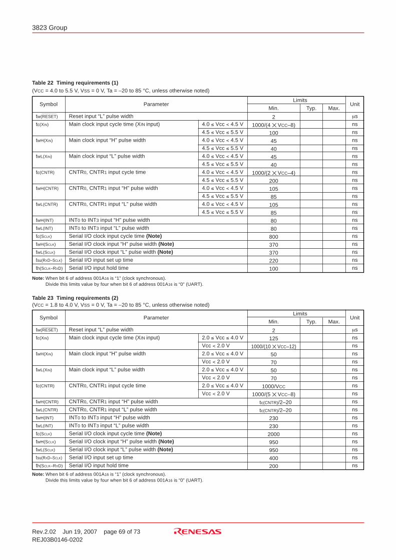
Rev.2.02 Jun 19, 2007 page 69 of 73REJ03B0146-0202
3823 Group
(VCC = 4.0 to 5.5 V, VSS = 0 V, Ta = –20 to 85 °C, unless otherwise noted)
Note: When bit 6 of address 001A16 is “1” (clock synchronous).Divide this limits value by four when bit 6 of address 001A16 is “0” (UART).
Table 22 Timing requirements (1)
Note: When bit 6 of address 001A16 is “1” (clock synchronous).Divide this limits value by four when bit 6 of address 001A16 is “0” (UART).
(VCC = 1.8 to 4.0 V, VSS = 0 V, Ta = –20 to 85 °C, unless otherwise noted)Table 23 Timing requirements (2)
2
1000/(4 VCC–8)
100
45
40
45
40
1000/(2 VCC–4)
200
105
85
105
85
80
80
800
370
370
220
100
Reset input “L” pulse width
Main clock input cycle time (XIN input)
Main clock input “H” pulse width
Main clock input “L” pulse width
CNTR0, CNTR1 input cycle time
CNTR0, CNTR1 input “H” pulse width
CNTR0, CNTR1 input “L” pulse width
INT0 to INT3 input “H” pulse width
INT0 to INT3 input “L” pulse width
Serial I/O clock input cycle time (Note)
Serial I/O clock input “H” pulse width (Note)
Serial I/O clock input “L” pulse width (Note)
Serial I/O input set up time
Serial I/O input hold time
tw(RESET)
tc(XIN)
twH(XIN)
twL(XIN)
tc(CNTR)
twH(CNTR)
twL(CNTR)
twH(INT)
twL(INT)
tc(SCLK)
twH(SCLK)
twL(SCLK)
tsu(RXD–SCLK)
th(SCLK–RXD)
Symbol ParameterLimits
Min.
µs
ns
ns
ns
ns
ns
ns
ns
ns
ns
ns
ns
ns
ns
ns
ns
ns
ns
ns
ns
UnitTyp. Max.
4.0 ≤ Vcc < 4.5 V
4.5 ≤ Vcc ≤ 5.5 V
4.0 ≤ Vcc < 4.5 V
4.5 ≤ Vcc ≤ 5.5 V
4.0 ≤ Vcc < 4.5 V
4.5 ≤ Vcc ≤ 5.5 V
4.0 ≤ Vcc < 4.5 V
4.5 ≤ Vcc ≤ 5.5 V
4.0 ≤ Vcc < 4.5 V
4.5 ≤ Vcc ≤ 5.5 V
4.0 ≤ Vcc < 4.5 V
4.5 ≤ Vcc ≤ 5.5 V
2
125
1000/(10 VCC–12)
50
70
50
70
1000/VCC
1000/(5 VCC–8)
tc(CNTR)/2–20
tc(CNTR)/2–20
230
230
2000
950
950
400
200
Reset input “L” pulse width
Main clock input cycle time (XIN input)
Main clock input “H” pulse width
Main clock input “L” pulse width
CNTR0, CNTR1 input cycle time
CNTR0, CNTR1 input “H” pulse width
CNTR0, CNTR1 input “L” pulse width
INT0 to INT3 input “H” pulse width
INT0 to INT3 input “L” pulse width
Serial I/O clock input cycle time (Note)
Serial I/O clock input “H” pulse width (Note)
Serial I/O clock input “L” pulse width (Note)
Serial I/O input set up time
Serial I/O input hold time
tw(RESET)
tc(XIN)
twH(XIN)
twL(XIN)
tc(CNTR)
twH(CNTR)
twL(CNTR)
twH(INT)
twL(INT)
tc(SCLK)
twH(SCLK)
twL(SCLK)
tsu(RXD–SCLK)
th(SCLK–RXD)
Symbol ParameterLimits
Min.
µs
ns
ns
ns
ns
ns
ns
ns
ns
ns
ns
ns
ns
ns
ns
ns
ns
ns
UnitTyp. Max.
2.0 ≤ Vcc ≤ 4.0 V
Vcc < 2.0 V
2.0 ≤ Vcc ≤ 4.0 V
Vcc < 2.0 V
2.0 ≤ Vcc ≤ 4.0 V
Vcc < 2.0 V
2.0 ≤ Vcc ≤ 4.0 V
Vcc < 2.0 V
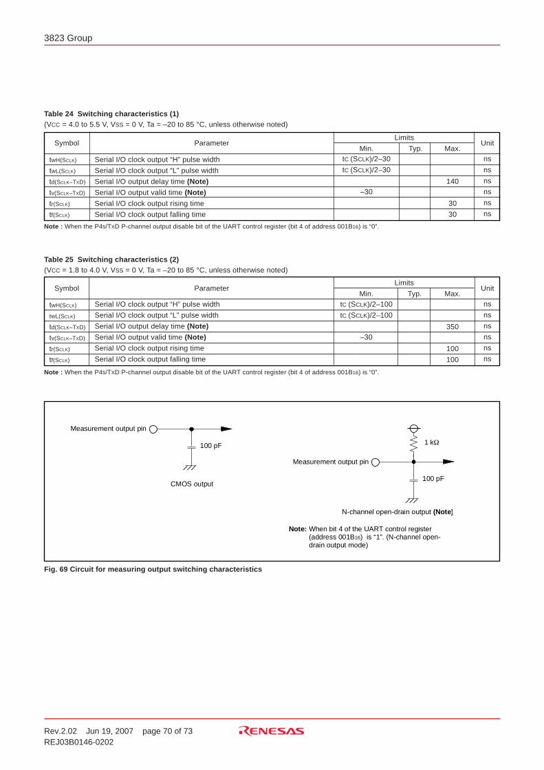
Rev.2.02 Jun 19, 2007 page 70 of 73REJ03B0146-0202
3823 Group
(VCC = 4.0 to 5.5 V, VSS = 0 V, Ta = –20 to 85 °C, unless otherwise noted)
Note : When the P45/TXD P-channel output disable bit of the UART control register (bit 4 of address 001B16) is “0”.
Serial I/O clock output “H” pulse width
Serial I/O clock output “L” pulse width
Serial I/O output delay time (Note)
Serial I/O output valid time (Note)
Serial I/O clock output rising time
Serial I/O clock output falling time
140
30
30
Symbol ParameterLimits
Min.ns
ns
ns
ns
ns
ns
Unit
tC (SCLK)/2–30
tC (SCLK)/2–30
–30
Typ. Max.
twH(SCLK)
twL(SCLK)
td(SCLK–TXD)
tv(SCLK–TXD)
tr(SCLK)
tf(SCLK)
(VCC = 1.8 to 4.0 V, VSS = 0 V, Ta = –20 to 85 °C, unless otherwise noted)
ns
ns
ns
ns
ns
ns
Unit
Note : When the P45/TXD P-channel output disable bit of the UART control register (bit 4 of address 001B16) is “0”.
Serial I/O clock output “H” pulse width
Serial I/O clock output “L” pulse width
Serial I/O output delay time (Note)
Serial I/O output valid time (Note)
Serial I/O clock output rising time
Serial I/O clock output falling time
350
100
100
Symbol ParameterLimits
Min.tC (SCLK)/2–100
tC (SCLK)/2–100
–30
Max.
twH(SCLK)
twL(SCLK)
td(SCLK–TXD)
tv(SCLK–TXD)
tr(SCLK)
tf(SCLK)
Typ.
Fig. 69 Circuit for measuring output switching characteristics
Table 24 Switching characteristics (1)
Table 25 Switching characteristics (2)
M
e
a
s
u
r
e
m
e
n
t
o
u
t
p
u
t
p
i
n
1
0
0
p
F
C
M
O
S
o
u
t
p
u
t
Note: When bit 4 of the UART control register (address 001B16) is “1”. (N-channel open-drain output mode)
N-channel open-drain output (Note)
1
kΩ
100 pF
Measurement output pin
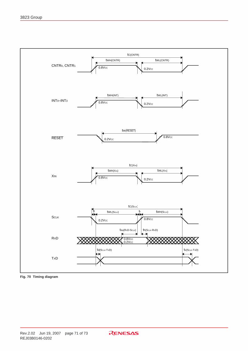
Rev.2.02 Jun 19, 2007 page 71 of 73REJ03B0146-0202
3823 Group
Fig. 70 Timing diagram
tW
(
R
E
S
E
T
)
0.8VCC0.2VCCR
E
S
E
T
tC(XIN)
tC
(
C
N
T
R
)
tW
H
(
C
N
T
R
) tW
L
(
C
N
T
R
)
0
.
8
VC
C 0.2VCC
C
N
T
R0,
C
N
T
R1
tW
H
(
I
N
T
) tW
L
(
I
N
T
)
0
.
8
VC
C 0.2VCC
I N
T0–
I
N
T3
tW
H
(
XI
N) tW
L
(
XI
N)
0.8VCC 0.2VCC
XIN
tC(SCLK)
tWL(SCLK) tW
H
(
SC
L
K)
0
.
2
VC
C0.8VCC
SCLK
trtf
td
(
SC
L
K-
TXD
) tv(SCLK-TXD)
TXD
RXD0.2VCC
0.8VCC
tsu(RXD-SCLK) th(SCLK-RXD)
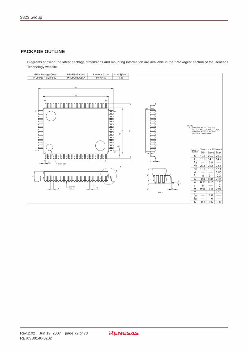
Rev.2.02 Jun 19, 2007 page 72 of 73REJ03B0146-0202
3823 Group
PACKAGE OUTLINE
y
F
*3
*1
*2
1 24
25
40
4164
65
80
Index mark
c
bp
D
E HE
A
e
ZD
ZE
HD
Detail F
L
A1
A2
INCLUDE TRIM OFFSET.DIMENSION "*3" DOES NOT
NOTE)
DO NOT INCLUDE MOLD FLASH.DIMENSIONS "*1" AND "*2"1.
2.
Previous CodeJEITA Package Code RENESAS Code
PRQP0080GB-A 80P6N-A
MASS[Typ.]
1.6gP-QFP80-14x20-0.80
0.20.150.13
0.450.350.3
MaxNomMin
Dimension in MillimetersSymbol
Reference
20.220.019.8D
14.214.013.8E
2.8A2
23.122.822.5
17.116.816.5
3.05A
0.20.10
0.80.60.4L
10°0°
c
0.8e
0.10y
HD
HE
A1
bp
ZD
ZE
0.65 0.95
0.8
1.0
Diagrams showing the latest package dimensions and mounting information are available in the “Packages” section of the RenesasTechnology website.
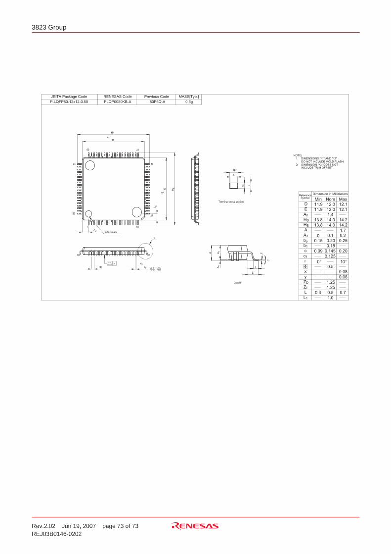
Rev.2.02 Jun 19, 2007 page 73 of 73REJ03B0146-0202
3823 Group
Detail F
cA
L1
LA1
A2
Index mark
y
*2
*1
*3
F
80
61
60 41
40
21
201
x
ZE
ZD
E HE
D
HD
e bp
2.
1. DIMENSIONS "*1" AND "*2"DO NOT INCLUDE MOLD FLASH.
NOTE)
DIMENSION "*3" DOES NOTINCLUDE TRIM OFFSET.
Previous CodeJEITA Package Code RENESAS Code
PLQP0080KB-A 80P6Q-A
MASS[Typ.]
0.5gP-LQFP80-12x12-0.50
1.0
0.125
0.18
1.25
1.25
0.08
0.200.1450.09
0.250.200.15
MaxNomMin
Dimension in MillimetersSymbol
Reference
12.112.011.9D
12.112.011.9E
1.4A2
14.214.013.8
14.214.013.8
1.7A
0.20.10
0.70.50.3L
x
10°0°
c
0.5e
0.08y
HD
HE
A1
bp
b1
c1
ZD
ZE
L1
Terminal cross section
c
bp
c 1
b1

REVISION HISTORY 3823 GROUP DATA SHEET
Rev. Date Description
Page Summary
(1/2)
1.00 05/13/05 First edition
2.00 05/07/07 6 Table 3 is partly revised8 Fig.5 is partly added9 Table 4 is revised14 “ROM Code Protect Address” is added
Fig.10 is revised40 “STP instruction Execution” is revised49 “Oscillation Control” (1) Stop Mode is partly revised52 “LCD drive Control Circuit” is revised54 “(6) Wiring to P40/(VPP) pin” is revised
Fig.59 is revised55 Fig.60 is partly deleted
“NOTES ON QzROM” is added60 Table 18 is partly added
2.01 05/11/08 6 Table 3 is partly revised61 Table 19, 20 are partly revised
65-66 PACKAGE OUTLINE revised
2.02 07/06/19 − “RENESAS TECHNICAL UPDATE” reflected: TN-740-A111A/E
6 Table 3: Function except a port function; •Serial I/O function pins → •Serial inter-face function pins
8 Fig. 5 M38234G4, M38235G6: Under development → Mass productionNote deleted
9 Table 4: Under development deleted10 FUNCTIONAL DESCRIPTION CENTRAL PROCESSING UNIT (CPU):
Description added15 Fig. 11: Note added
CPU mode extension register (002B16) → CPU mode expansion registerPeripheral function extension register (003016) → Peripheral functionexpansion register
22 Table 8: AVSS added, Note revised23-27 INTERRUPTS: Description revised, Fig. 18-20 added
46 ROM CORRECTION FUNCTION: Description added48 Initial Value of Watchdog Timer: Description added
Standard Operation of Watchdog Timer: A part of description deletedBit 6 and bit 7 of Watchdog Timer Control Register: added and revisedFig. 48 revised, Note added
51 Fig. 53: Port P0 direction register (000016) → (000116)52 Frequency Control: Description revised53 Fig. 56: revised54 Fig. 57: revised
55-58 QzROM Writing Mode: added58 Processor Status Register: added59 Overvoltage: Description revised and Fig. 68 added63 Table 15
VCC: Frequency/4 mode → Frequency/8 modeVREF: Limits Min. 2.0 → 1.8
66 Table 18: VRAM added
REVISION HISTORY 3823 GROUP DATA SHEET
Rev. Date Description
Page Summary
(2/2)
2.02 07/06/19 67 Table 19ROCO: Ta = 25 °C added
72 Note added
Notes:1. This document is provided for reference purposes only so that Renesas customers may select the appropriate Renesas products for their use. Renesas neither makes warranties or representations with respect to the accuracy or completeness of the information contained in this document nor grants any license to any intellectual property rights or any other rights of Renesas or any third party with respect to the information in this document. 2. Renesas shall have no liability for damages or infringement of any intellectual property or other rights arising out of the use of any information in this document, including, but not limited to, product data, diagrams, charts, programs, algorithms, and application circuit examples.3. You should not use the products or the technology described in this document for the purpose of military applications such as the development of weapons of mass destruction or for the purpose of any other military use. When exporting the products or technology described herein, you should follow the applicable export control laws and regulations, and procedures required by such laws and regulations.4. All information included in this document such as product data, diagrams, charts, programs, algorithms, and application circuit examples, is current as of the date this document is issued. Such information, however, is subject to change without any prior notice. Before purchasing or using any Renesas products listed in this document, please confirm the latest product information with a Renesas sales office. Also, please pay regular and careful attention to additional and different information to be disclosed by Renesas such as that disclosed through our website. (http://www.renesas.com )5. Renesas has used reasonable care in compiling the information included in this document, but Renesas assumes no liability whatsoever for any damages incurred as a result of errors or omissions in the information included in this document.6. When using or otherwise relying on the information in this document, you should evaluate the information in light of the total system before deciding about the applicability of such information to the intended application. Renesas makes no representations, warranties or guaranties regarding the suitability of its products for any particular application and specifically disclaims any liability arising out of the application and use of the information in this document or Renesas products. 7. With the exception of products specified by Renesas as suitable for automobile applications, Renesas products are not designed, manufactured or tested for applications or otherwise in systems the failure or malfunction of which may cause a direct threat to human life or create a risk of human injury or which require especially high quality and reliability such as safety systems, or equipment or systems for transportation and traffic, healthcare, combustion control, aerospace and aeronautics, nuclear power, or undersea communication transmission. If you are considering the use of our products for such purposes, please contact a Renesas sales office beforehand. Renesas shall have no liability for damages arising out of the uses set forth above.8. Notwithstanding the preceding paragraph, you should not use Renesas products for the purposes listed below: (1) artificial life support devices or systems (2) surgical implantations (3) healthcare intervention (e.g., excision, administration of medication, etc.) (4) any other purposes that pose a direct threat to human life Renesas shall have no liability for damages arising out of the uses set forth in the above and purchasers who elect to use Renesas products in any of the foregoing applications shall indemnify and hold harmless Renesas Technology Corp., its affiliated companies and their officers, directors, and employees against any and all damages arising out of such applications. 9. You should use the products described herein within the range specified by Renesas, especially with respect to the maximum rating, operating supply voltage range, movement power voltage range, heat radiation characteristics, installation and other product characteristics. Renesas shall have no liability for malfunctions or damages arising out of the use of Renesas products beyond such specified ranges.10. Although Renesas endeavors to improve the quality and reliability of its products, IC products have specific characteristics such as the occurrence of failure at a certain rate and malfunctions under certain use conditions. Please be sure to implement safety measures to guard against the possibility of physical injury, and injury or damage caused by fire in the event of the failure of a Renesas product, such as safety design for hardware and software including but not limited to redundancy, fire control and malfunction prevention, appropriate treatment for aging degradation or any other applicable measures. Among others, since the evaluation of microcomputer software alone is very difficult, please evaluate the safety of the final products or system manufactured by you. 11. In case Renesas products listed in this document are detached from the products to which the Renesas products are attached or affixed, the risk of accident such as swallowing by infants and small children is very high. You should implement safety measures so that Renesas products may not be easily detached from your products. Renesas shall have no liability for damages arising out of such detachment.12. This document may not be reproduced or duplicated, in any form, in whole or in part, without prior written approval from Renesas. 13. Please contact a Renesas sales office if you have any questions regarding the information contained in this document, Renesas semiconductor products, or if you have any other inquiries.
Sales Strategic Planning Div. Nippon Bldg., 2-6-2, Ohte-machi, Chiyoda-ku, Tokyo 100-0004, Japan
http://www.renesas.comRefer to "http://www.renesas.com/en/network" for the latest and detailed information.
Renesas Technology America, Inc.450 Holger Way, San Jose, CA 95134-1368, U.S.ATel: <1> (408) 382-7500, Fax: <1> (408) 382-7501 Renesas Technology Europe LimitedDukes Meadow, Millboard Road, Bourne End, Buckinghamshire, SL8 5FH, U.K.Tel: <44> (1628) 585-100, Fax: <44> (1628) 585-900
Renesas Technology (Shanghai) Co., Ltd.Unit 204, 205, AZIACenter, No.1233 Lujiazui Ring Rd, Pudong District, Shanghai, China 200120Tel: <86> (21) 5877-1818, Fax: <86> (21) 6887-7898 Renesas Technology Hong Kong Ltd.7th Floor, North Tower, World Finance Centre, Harbour City, 1 Canton Road, Tsimshatsui, Kowloon, Hong Kong Tel: <852> 2265-6688, Fax: <852> 2730-6071
Renesas Technology Taiwan Co., Ltd.10th Floor, No.99, Fushing North Road, Taipei, TaiwanTel: <886> (2) 2715-2888, Fax: <886> (2) 2713-2999 Renesas Technology Singapore Pte. Ltd.1 Harbour Front Avenue, #06-10, Keppel Bay Tower, Singapore 098632 Tel: <65> 6213-0200, Fax: <65> 6278-8001
Renesas Technology Korea Co., Ltd.Kukje Center Bldg. 18th Fl., 191, 2-ka, Hangang-ro, Yongsan-ku, Seoul 140-702, KoreaTel: <82> (2) 796-3115, Fax: <82> (2) 796-2145 Renesas Technology Malaysia Sdn. BhdUnit 906, Block B, Menara Amcorp, Amcorp Trade Centre, No.18, Jalan Persiaran Barat, 46050 Petaling Jaya, Selangor Darul Ehsan, MalaysiaTel: <603> 7955-9390, Fax: <603> 7955-9510
RENESAS SALES OFFICES
© 2007. Renesas Technology Corp., All rights reserved. Printed in Japan.
Colophon .7.0