IQS127 Datasheet - - ProxSense - Octopart
25
Azoteq IQS127S/D IQS127 Datasheet IQ Switch ® - ProxSense TM Series Single Channel Capacitive Proximity/Touch Controller The IQS127 ProxSense™ IC is a fully integrated capacitive sensor produced in 2 variants: IQS127D: Dual outputs (Touch and Proximity outputs). IQS127S: Incorporating a Driven Shield. Features Automatic Antenna Tuning Implementation (ATI) - Automatic adjustment for optimal performance. Internal Capacitor Implementation (ICI) – reference capacitor on-chip Supply voltage: 2V to 5.5V Minimum external components Data streaming option Advanced on-chip digital signal processing User selectable (OTP): 4 Power Modes (15uA min) IO sink / source Time-out for stuck key Output mode (Direct / Latch / Toggle) Proximity and Touch Button sensitivity Keys: Touch: 5mm x 5mm or larger (overlay thickness dependent) Proximity: Various electrical options (wire / PCB trace / ITO / conductive foil) Dielectric: Material: Various non-metal materials (i.e. glass, plastic, painted surfaces) Thickness: 6 mm plastic, 10 mm glass Applications LCD, Plasma & LED TVs GSM cellular telephones – On ear detection / touch keys LED flashlights or headlamps White goods and appliances Office equipment, toys, sanitary ware Flame proof, hazardous environment Human Interface Devices Proximity detection enables backlighting activation Wake-up from standby applications Replacement for electromechanical switches Find-In-The-Dark (FITD) applications Automotive: Door pocket lighting, electric window control GUI trigger on Proximity detected Available options T A TSOT23-6 -40°C to 85°C IQS127D -40°C to 85°C IQS127S 6 pin TSOT23-6
-
Upload
khangminh22 -
Category
Documents
-
view
0 -
download
0
Transcript of IQS127 Datasheet - - ProxSense - Octopart

Azoteq
IQS127S
/D
IQS127 Datasheet
IQ Switch® - ProxSense
TM Series
Single Channel Capacitive Proximity/Touch Controller
The IQS127 ProxSense™ IC is a fully integrated capacitive sensor produced in 2 variants:
IQS127D: Dual outputs (Touch and Proximity outputs).
IQS127S: Incorporating a Driven Shield.
Features
Automatic Antenna Tuning Implementation (ATI) - Automatic adjustment for optimal performance.
Internal Capacitor Implementation (ICI) – reference capacitor on-chip
Supply voltage: 2V to 5.5V
Minimum external components
Data streaming option
Advanced on-chip digital signal processing
User selectable (OTP): 4 Power Modes (15uA min)
IO sink / source
Time-out for stuck key
Output mode (Direct / Latch / Toggle)
Proximity and Touch Button sensitivity
Keys: Touch: 5mm x 5mm or larger (overlay thickness dependent)
Proximity: Various electrical options (wire / PCB trace / ITO / conductive foil)
Dielectric: Material: Various non-metal materials (i.e. glass, plastic, painted surfaces)
Thickness: 6 mm plastic, 10 mm glass
Applications
LCD, Plasma & LED TVs
GSM cellular telephones – On ear detection / touch keys
LED flashlights or headlamps
White goods and appliances
Office equipment, toys, sanitary ware
Flame proof, hazardous environment Human Interface Devices
Proximity detection enables backlighting
activation
Wake-up from standby applications
Replacement for electromechanical switches
Find-In-The-Dark (FITD) applications
Automotive: Door pocket lighting, electric window control
GUI trigger on Proximity detected
Available options
TA TSOT23-6
-40°C to 85°C IQS127D
-40°C to 85°C IQS127S
6 pin TSOT23-6
IQ Switch®
ProxSense™ Series
Copyright © Azoteq (Pty) Ltd 2010 IQS127 Datasheet v1.8 Page 2 of 25
All Rights Reserved. May 2011
Contents
IQS127 DATASHEET .................................................................................................................................................... 1
1 OVERVIEW ......................................................................................................................................................... 4
1.1 APPLICABILITY ........................................................................................................................................................ 4
2 ANALOGUE FUNCTIONALITY............................................................................................................................... 4
3 PACKAGING AND PIN-OUT ................................................................................................................................. 5
3.1 IQS127D ............................................................................................................................................................. 5 3.1.1 Pin-out ........................................................................................................................................................... 5 3.1.2 Schematic ...................................................................................................................................................... 5 3.1.3 Typical values ................................................................................................................................................ 5
3.2 IQS127S ............................................................................................................................................................. 6 3.2.1 Pin-out ........................................................................................................................................................... 6 3.2.2 Schematic ...................................................................................................................................................... 6 3.2.3 Typical values ................................................................................................................................................ 6
4 USER CONFIGURABLE OPTIONS .......................................................................................................................... 7
4.1 CONFIGURING OF DEVICES ....................................................................................................................................... 7
5 MEASURING CAPACITANCE USING THE CHARGE TRANSFER METHOD ................................................................ 9
6 DESCRIPTIONS OF USER OPTIONS ...................................................................................................................... 9
6.1 PROXIMITY / TOUCH SENSOR.................................................................................................................................. 10 6.2 LOGIC SELECT FOR OUTPUT(S) ................................................................................................................................. 10 6.3 OUTPUT PIN FUNCTION ......................................................................................................................................... 10
6.3.1 Output function: Active ............................................................................................................................... 10 6.3.2 Output function: Latch (for tLATCH) ............................................................................................................... 10 6.3.3 Output function: Toggle .............................................................................................................................. 11
6.4 PROXIMITY THRESHOLD ......................................................................................................................................... 11 6.5 TOUCH THRESHOLD .............................................................................................................................................. 11 6.6 POWER MODES ................................................................................................................................................... 12 6.7 FILTERS USED BY THE IQS127 ................................................................................................................................. 12
6.7.1 Long Term Average (LTA) ............................................................................................................................ 12 6.7.2 IIR Raw Data filter ....................................................................................................................................... 13
7 1-WIRE DATA STREAMING MODE......................................................................................................................14
8 ANTENNA TUNING IMPLEMENTATION (ATI)......................................................................................................15
8.1 AUTOMATIC ATI .................................................................................................................................................. 15 8.2 IQS127 NOISE IMMUNITY ..................................................................................................................................... 16
9 ELECTRICAL SPECIFICATIONS .............................................................................................................................17
9.1 ABSOLUTE MAXIMUM SPECIFICATIONS ..................................................................................................................... 17 9.2 GENERAL CHARACTERISTICS (MEASURED AT 25°C) ..................................................................................................... 17 9.3 OUTPUT CHARACTERISTICS (MEASURED AT 25°C) ...................................................................................................... 18 9.4 ELECTROMAGNETIC COMPATIBILITY ......................................................................................................................... 19
9.4.1 Electrostatic discharge (ESD) ...................................................................................................................... 19 9.4.2 EMI (Radio frequency Interference) – IEC61000-4-3 ................................................................................... 20 9.4.3 Static Latch-Up (LU) .................................................................................................................................... 20
9.5 TIMING CHARACTERISTICS ...................................................................................................................................... 21 9.6 PACKAGING INFORMATION ..................................................................................................................................... 22 9.7 PACKAGE MSL .................................................................................................................................................... 22
10 DATASHEET AND PART-NUMBER INFORMATION ..............................................................................................23
IQ Switch®
ProxSense™ Series
Copyright © Azoteq (Pty) Ltd 2010 IQS127 Datasheet v1.8 Page 3 of 25
All Rights Reserved. May 2011
10.1 ORDERING INFORMATION ...................................................................................................................................... 23 10.2 STANDARD DEVICES .............................................................................................................................................. 23 10.3 DEVICE PACKAGING CONVENTION ........................................................................................................................... 24
10.3.1 Top .......................................................................................................................................................... 24 10.3.2 Bottom .................................................................................................................................................... 24
10.4 DATASHEET REVISION HISTORY ............................................................................................................................... 24
11 CONTACT INFORMATION ..................................................................................................................................25

IQ Switch®
ProxSense™ Series
Copyright © Azoteq (Pty) Ltd 2010 IQS127 Datasheet v1.8 Page 4 of 25
All Rights Reserved. May 2011
1 Overview
The IQS127 family is a single channel capacitive proximity and touch device which employs an internal voltage regular and reference capacitor (Cs).
The IQS127D device has a dedicated pin for the connection of a sense antenna (Cx) and output pins for proximity events on POUT and touch event on TOUT. The output pins can be configured for various output methods including a serial data streaming option on TOUT.
The IQS127S employs an active driven shield pin, which replaces the POUT pin, to drive a shield for protection of the sense antenna signal. The TOUT pin becomes a general OUT pin in the IQS127S, which is configurable either as a proximity output or a touch output.
Device configuration is determined by one time programmable (OTP) options.
The devices automatically track slow varying environmental changes via various filters, detect noise and has an automatic Antenna Tuning Implementation (ATI) to tune the device to the sense antenna.
1.1 Applicability
All specifications, except where specifically mentioned otherwise, provided by this datasheet are applicable to the following ranges:
Temperature:-40C to +85C
Supply voltage (VDDHI): 2.95V to 5V
Supply voltage (VDDHI): 2.V to 5V – Low voltage device
2 Analogue Functionality
The analogue circuitry measures the capacitance of a sense antenna attached to the Cx pin through a charge transfer process (refer to section 5) that is periodically initiated by the digital circuitry. The measuring process is referred to a conversion and consists of the discharging of reference capacitor and Cx, the charging of Cx and then a series of charge transfers from Cx to Cs until a trip voltage is reached. The number of charge transfers required to reach the trip voltage is referred to as the current sample (CS).
The capacitance measurement circuitry makes use of an internal Cs and voltage reference (VREF).
The analogue circuitry further provides functionality for:
Power on reset (POR) detection.
Brown out detection (BOD).
Detection of a watch dog timer (WDT) expiry.
The IQS127S employs circuitry to drive a shield that will follow the voltage sensed on Cx.
IQ Switch®
ProxSense™ Series
Copyright © Azoteq (Pty) Ltd 2010 IQS127 Datasheet v1.8 Page 5 of 25
All Rights Reserved. May 2011
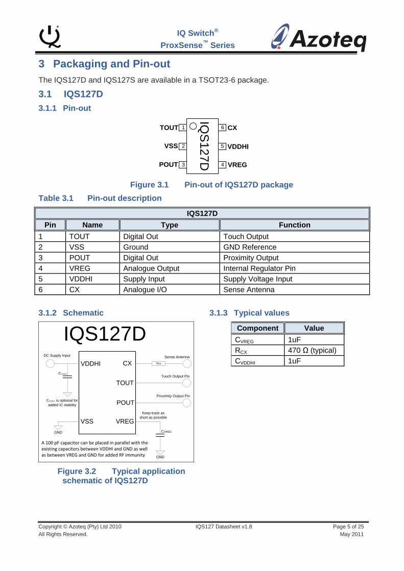
3 Packaging and Pin-out
The IQS127D and IQS127S are available in a TSOT23-6 package.
3.1 IQS127D
3.1.1 Pin-out
1
2
3
TOUT
VSS
POUT
6
5
4
CX
VDDHI
VREG
IQS
12
7D
Figure 3.1 Pin-out of IQS127D package
Table 3.1 Pin-out description
IQS127D
Pin Name Type Function
1 TOUT Digital Out Touch Output
2 VSS Ground GND Reference
3 POUT Digital Out Proximity Output
4 VREG Analogue Output Internal Regulator Pin
5 VDDHI Supply Input Supply Voltage Input
6 CX Analogue I/O Sense Antenna
3.1.2 Schematic
IQS127D
Rcx
TOUT
VSS
POUT
CXVDDHI
VREG
Touch Output Pin
Proximity Output Pin
GND
GND
CVREG
Keep track as
short as possible
DC Supply Input Sense Antenna
CVDDHI
C is optional for
added IC stability
VDDHI
A 100 pF capacitor can be placed in parallel with the existing capacitors between VDDHI and GND as well as between VREG and GND for added RF immunity
Figure 3.2 Typical application schematic of IQS127D
3.1.3 Typical values
Component Value
CVREG 1uF
RCX 470 Ω (typical)
CVDDHI 1uF

IQ Switch®
ProxSense™ Series
Copyright © Azoteq (Pty) Ltd 2010 IQS127 Datasheet v1.8 Page 6 of 25
All Rights Reserved. May 2011
3.2 IQS127S
3.2.1 Pin-out
1
2
3
OUT
VSS
SHLD
6
5
4
CX
VDDHI
VREG
IQS
12
7S
Figure 3.3 Pin-out of IQS127S package
Table 3.2 Pin-out description
IQS127S
Pin Name Type Function
1 OUT Digital Out Touch or Proximity Output
2 VSS Ground GND Reference
3 SHLD Analogue Output Shield Output
4 VREG Analogue Output Internal Regulator Pin
5 VDDHI Supply Input Supply Voltage Input
6 CX Analogue I/O Sense Antenna
3.2.2 Schematic
IQS127S
Rcx
OUT
VSS
SHLD
CXVDDHI
VREG
GND
GND
Keep track as short
as possible
DC Supply
Input
Rcx is optional for
added ESD protection.
Coaxial cable
Sense Antenna
RS
HL
D
Output Pin VDDHI
GND
CVREG
CVDDHI
A 100 pF capacitor can be placed in parallel with the existing capacitors between VDDHI and GND as well as between VREG and GND for added RF immunity
VDDHI
Figure 3.4 Typical application schematic of IQS127S
3.2.3 Typical values
Component Value
CVREG 1uF
RCX 470 Ω (typical)
CVDDHI 1uF
RSHLD 2kΩ to ∞
Note: Lower values of RSHLD provide a better shielding effect but require more current.

IQ Switch®
ProxSense™ Series
Copyright © Azoteq (Pty) Ltd 2010 IQS127 Datasheet v1.8 Page 7 of 25
All Rights Reserved. May 2011
4 User Configurable Options
The IQS127 provides One Time Programmable (OTP) user options (each option can be modified only once). The device is fully functional in the default (unconfigured) state. OTP options are intended for specific applications.
The configuration of the device can be done on packaged devices or in-circuit. In-circuit configuration may be limited by values of external components chosen.
A number of standard device configurations are available (refer to Table 10.1). Azoteq can supply pre-configured devices for large quantities.
4.1 Configuring of Devices
Azoteq offers a Configuration Tool (CTxxx) and accompanying software (USBProg.exe) that can be used to program the OTP user options for prototyping purposes. More details regarding the configuration of the device with the USBProg program is explained by application note: “AZD007 – USBProg Overview” which can be found on the Azoteq website.
Alternate programming solutions of the IQS127 also exist. For further enquiries regarding this matter please contact Azoteq at [email protected] or the local distributor
Table 4-1: User Selectable Configuration Options: Bank 0
TTHR1 TTHR0 PTHR1 PTHR0 FUNC1 FUNC0 LOGIC PT bit 7 bit 0
Bank 1: bit 0, Bank 0: bit 7-6
TTHR<2:0>: Touch Thresholds -Section 6.5
000 = 1/16 001 = 1/32 010 = 2/16 011 = 3/16 100 = 4/16 101 = 6/16 110 = 8/16 111 = 10/16 Bank0: bit 5-4 PTHR<1:0>: Proximity Thresholds -Section 6.4 00 = 2 01 = 4 10 = 8 11 = 16 Bank0: bit 3-2 FUNC<1:0>: OUTPUT Pins‟ functions -Section 6.3 IQS127D 00 = POUT active, TOUT active 01 = POUT latch, TOUT active 10 = POUT active, TOUT toggle 11 = POUT latch, TOUT toggle IQS127S 00 = OUT active 01 = OUT latch (for tLATCH) 10 = OUT toggle 11 = Unimplemented, read as „00‟ Bank0: bit 1 LOGIC: Output logic select - -Section 6.2 0 = Active Low 1 = Active High Bank0: bit 0 PT: Proximity / Touch Output (IQS127S only) -Section 6.1 0 = Touch 1 = Proximity output

IQ Switch®
ProxSense™ Series
Copyright © Azoteq (Pty) Ltd 2010 IQS127 Datasheet v1.8 Page 8 of 25
All Rights Reserved. May 2011
Table 4-2: User Selectable Configuration Options: Bank 1
STREAMING - SHORT
STREAMING tHALT1 tHALT0 PMODE1 PMODE0 TTHR2
bit 7 bit 0
Bank 1: bit 7 STREAMING: 1-wire streaming mode -Section 0 0 = disabled 1 = enabled Bank1: bit 6 Not used
Bank1: bit 5 SHORT STREAMING: Short word streaming enable (Function enabled if this bit together with STREAMING bit is set) –Section 0
Bank1: bit 4-3 tHALT<1:0>: Halt time of Long Term Average -Section 6.7 00 = 18.6 seconds 01 = 74.5 seconds 10 = Never 11 = Always Bank1: bit 2-1 PMODE<1:0>:Power Modes -Section 6.6 00 = Boost Mode 01 = Normal Power Mode 10 = Low Power Mode 1 11 = Low Power Mode 2 Bank1: bit 0 TTHR<2:0>: Touch Thresholds -Section 6.5 See Table 4-1

IQ Switch®
ProxSense™ Series
Copyright © Azoteq (Pty) Ltd 2010 IQS127 Datasheet v1.8 Page 9 of 25
All Rights Reserved. May 2011
5 Measuring capacitance using the Charge Transfer method
The charge transfer method of capacitive sensing is employed on the IQS127. (The charge transfer principle is thoroughly described in the application note: “AZD004 - Azoteq Capacitive Sensing”.)
A charge cycle is used to take a measurement of the capacitance of the sense antenna (connected to Cx) relative to ground. It consists of a series of pulses charging Cx and discharging Cx to the reference capacitor, at the charge transfer frequency (FCX - refer to Section 9). The count of the pulses required to reach a trip voltage on the reference capacitor is referred to as a current sample (CS) which is the instantaneous capacitive measurement. The CS is used to determine if either a physical contact or proximity event occurred (refer to section 6.7.1), based on the change in CS detected. The typical values of CS, without a touch or proximity condition range between 650 and 1150, although higher and lower counts can be used based on the application requirements. With CS larger than +/-1150
the gain of the system may become too high causing unsteady current samples.
The IQS127 schedules a charge cycle every tSAMPLE seconds to ensure regular samples for processing of results. The duration of the charge cycle is defined as tCHARGE. (refer to 0) and varies according to the counts required to reach the trip voltage. Following the charge cycle other activities such as data streaming is completed (if in streaming mode), before the next charge cycle is initiated.
Please note: Attaching a probe to the Cx pin will increase the capacitance of the sense plate and therefore CS. This may have an immediate influence on CS (decrease tCHARGE – thus CS) and cause a proximity or touch event. After tHALT seconds the system will adjust to accommodate for this change. If the total load on Cx, with the probe attached is still lower than the maximum Cx load the system will continue to function normally after tHALT seconds with the probe attached.
Cx pin
1 2 3 4
tCHARGE
tSAMPLE
Figure 5.1 Charge cycles as can be seen on Cx
6 Descriptions of User Options
This section describes the individual user programmable options of the IQS127 in more detail.
User programmable options are programmed to One Time Programmable (OTP) fuse registers (refer to section 1). The options differ slightly between the IQS127D and IQS127S devices.
Note:
HIGH=Logical „1‟ and LOW=Logical „0‟.
The following sections are explained with the OUT, POUT and TOUT taken as „Active LOW‟.
The default is always where bits are set to 0.

IQ Switch®
ProxSense™ Series
Copyright © Azoteq (Pty) Ltd 2010 IQS127 Datasheet v1.8 Page 10 of 25
All Rights Reserved. May 2011
Refer to section 0 for the sourcing and sinking capabilities of OUT, POUT and TOUT. These pins are sourced from VDDHI and will be turned HIGH (when active high) for a minimum time of tHIGH, and LOW for a minimum time of tLOW (when active low).
6.1 Proximity / Touch Sensor
The IQS127S can either be configured to provide a Proximity or a Touch (default) output on the OUT pin.
The IQS127D provides a Proximity output on POUT and a Touch output on TOUT, and does not need to be configured.
Both devices will provide proximity and touch data while streaming (refer to section 0)
Configuration: Bank0 bit0
PT: Proximity / Touch Output (IQS127S only) Bit Selection 0 Touch output 1 Proximity output
6.2 Logic select for output(s)
The logic used by the device can be selected as active HIGH or active LOW. The output pins POUT, TOUT and OUT will function based on the selection.
Configuration: Bank0 bit1
LOGIC: Output logic select - Bit Selection 0 Active Low 1 Active High
6.3 Output pin function
Various options for the function of the output pin(s) are available. These are selected as follow:
Configuration: Bank0 bit2-3
FUNC1:FUNC0 OUTPUT Pins‟ functions IQS127D Bit Selection 00 POUT active, TOUT active 01 POUT latch, TOUT active 10 POUT active, TOUT toggle 11 POUT latch, TOUT toggle IQS127S Bit Selection 00 OUT active 01 OUT latch (for tLATCH) 10 OUT toggle 11 Unimplemented, read as „00‟
6.3.1 Output function: Active
With a Proximity or Touch event, the output pin will change to LOW and stay LOW for as long as the event remains (see Figure 6.1). Also refer to the use of tHALT section 6.7.1 that may cause the termination of the event.
Figure 6.1 Active Mode Output Configuration
6.3.2 Output function: Latch (for tLATCH)
With a Proximity or Touch event, the output pin will latch LOW for tLATCH seconds.
When the event terminates prior to tLATCH the output pin will remain LOW.
When the event remains active longer than tLATCH the output pin will remain LOW as long as the event remains active (see Figure 6.2).
User Actuation
Output Pin
1
0
1
0

IQ Switch®
ProxSense™ Series
Copyright © Azoteq (Pty) Ltd 2010 IQS127 Datasheet v1.8 Page 11 of 25
All Rights Reserved. May 2011
tLATCH + time that User Actuation stays activeOutput Pin
1
0
1
0
User Actuation
tLATCH tLATCH
Figure 6.2 Latch Mode Output Configuration
6.3.3 Output function: Toggle
The output pin will toggle with every Proximity or Touch event occurring. Thus when an event
occurs and the output is LOW the output will become HIGH and when the output is HIGH the output will become LOW (see Figure 6.3).
Figure 6.3 Toggle Mode Output Configuration
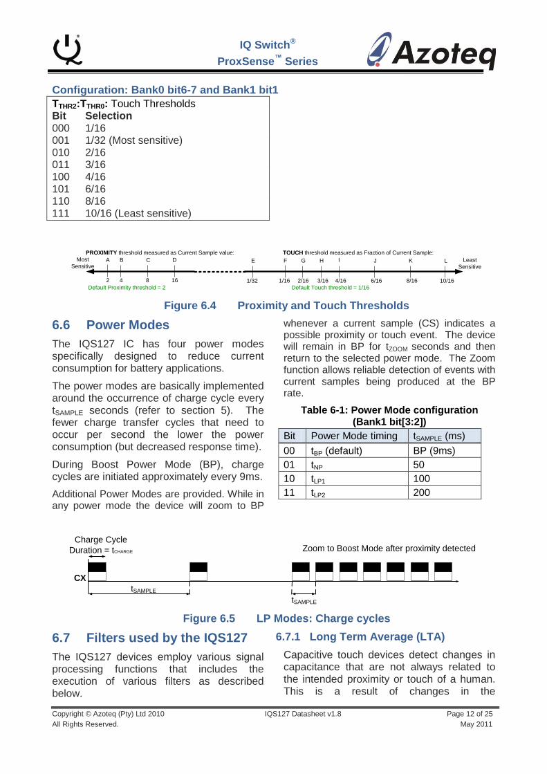
6.4 Proximity Threshold
The IQS127 has 4 proximity threshold settings. The proximity threshold is selected by the designer to obtain the desired sensitivity and noise immunity. The proximity event is triggered based on the selected proximity threshold; the CS and the LTA (Long Term Average). The threshold is expressed in terms of counts; the same as CS (refer to 5)
Configuration: Bank0 bit4-5
PTHR1:PTHR0 Proximity Thresholds Bit Selection 00 2 (Most sensitive) 01 4 10 8 11 16 (Least sensitive)
A proximity event is identified when for at least 6 consecutive samples the following equation holds:
PTH =< LTA-CS
Where LTA is the Long Term Average (refer to 6.7.1)
6.5 Touch Threshold
The IQS127 has 8 touch threshold settings. The touch threshold is selected by the
designer to obtain the desired touch sensitivity. The touch threshold is expressed as a fraction of the LTA as follows:
TTH = Selected Touch Threshold x LTA
Where LTA is the Long Term Average (refer to 6.7.1)
The touch event is triggered based on TTH, CS and LTA. A touch event is identified when for at least 3 consecutive samples the following equation holds:
TTH =< LTA-CS
With lower average CS (therefore lower LTA) values the touch threshold will be lower and visa versa.
Output Pin
1
0
1
0
User Actuation
IQ Switch®
ProxSense™ Series
Copyright © Azoteq (Pty) Ltd 2010 IQS127 Datasheet v1.8 Page 12 of 25
All Rights Reserved. May 2011
Configuration: Bank0 bit6-7 and Bank1 bit1
TTHR2:TTHR0: Touch Thresholds Bit Selection 000 1/16 001 1/32 (Most sensitive) 010 2/16 011 3/16 100 4/16 101 6/16 110 8/16 111 10/16 (Least sensitive)
Figure 6.4 Proximity and Touch Thresholds
6.6 Power Modes
The IQS127 IC has four power modes specifically designed to reduce current consumption for battery applications.
The power modes are basically implemented around the occurrence of charge cycle every tSAMPLE seconds (refer to section 5). The fewer charge transfer cycles that need to occur per second the lower the power consumption (but decreased response time).
During Boost Power Mode (BP), charge cycles are initiated approximately every 9ms.
Additional Power Modes are provided. While in any power mode the device will zoom to BP
whenever a current sample (CS) indicates a possible proximity or touch event. The device will remain in BP for tZOOM seconds and then return to the selected power mode. The Zoom function allows reliable detection of events with current samples being produced at the BP rate.
Table 6-1: Power Mode configuration (Bank1 bit[3:2])
Bit Power Mode timing tSAMPLE (ms)
00 tBP (default) BP (9ms)
01 tNP 50
10 tLP1 100
11 tLP2 200
CX
Zoom to Boost Mode after proximity detectedCharge Cycle
Duration = tCHARGE
tSAMPLE
tSAMPLE
Figure 6.5 LP Modes: Charge cycles
6.7 Filters used by the IQS127
The IQS127 devices employ various signal processing functions that includes the execution of various filters as described below.
6.7.1 Long Term Average (LTA)
Capacitive touch devices detect changes in capacitance that are not always related to the intended proximity or touch of a human. This is a result of changes in the
Most
SensitiveA B DC
Default Proximity threshold = 2
2 4
PROXIMITY threshold measured as Current Sample value:
8 16
Least
SensitiveF G IH
Default Touch threshold = 1/16
TOUCH threshold measured as Fraction of Current Sample:
1/16 2/16 3/16
J
6/164/16
K
8/16
L
10/16
E
1/32

IQ Switch®
ProxSense™ Series
Copyright © Azoteq (Pty) Ltd 2010 IQS127 Datasheet v1.8 Page 13 of 25
All Rights Reserved. May 2011
environment of the sense plate and other factors. These changes need to be compensated for in various manners in order to reliably detect touch events and especially to detect proximity events. One mechanism the IQS127 employs is the use of a Long Term Averaging filter (IIR type filter) which tracks slow changes in the environment (expressed as changes in the current sample). The result of this filter is a Long Term Average (LTA) value that forms a dynamic reference used for various functions such as identification of proximity and touch events.
The LTA is calculated from the current samples (CS). The filter only executes while no proximity or touch event is detected to ensure compensation only for environmental changes. However there may be instances where sudden changes in the environment or changes in the environment while a proximity or touch event has been detected cause the CS to drift away from the LTA. To compensate for these situations a Halt Timer (tHALT) has been defined.
The Halt Timer is started when a proximity or touch event occurs and when it expires the LTA filter is recalibrated. Recalibration causes LTA < CS, thus the disappearance of proximity or touch events (refer to 6.4 and 6.5).
The designer needs to select a Halt Timer value to best accommodate the required application.
Configuration: Bank1 bit4-5
tHALT1:tHATL0: Halt time of Long Term Average Bit Selection 00 18.6 seconds 01 74.5 seconds
10 NEVER 11 ALWAYS
Notes:
The “NEVER” option indicates that the execution of the filters will never be halted.
With the „ALWAYS‟ option and the detection of a proximity event the execution of the filter will be halted for only 18.6 seconds and with the detection of a touch event the execution of the filter will be halted as long as the touch condition applies.
Refer to Application note “AZD024 - Graphical Representation of the IIR Filter” for detail regarding the execution of the LTA filter.
6.7.2 IIR Raw Data filter
The extreme sensitivity of the IQS127 makes it susceptible to external noise sources. This causes a decreased signal to noise (S/N) ratio, which could potentially cause false event detections.
Noise can also couple into the device as a result of poor PCB, sense antenna design and other factors influencing capacitive sensing devices.
In order to compensate for noise the IQS127 uses an IIR filter on the raw data to minimize result of noise in the current sample. This filter is implemented on all of the IQS127 devices, and cannot be disabled.

IQ Switch®
ProxSense™ Series
Copyright © Azoteq (Pty) Ltd 2010 IQS127 Datasheet v1.8 Page 14 of 25
All Rights Reserved. May 2011
7 1-Wire Data Streaming Mode
The IQS127 has the capability to stream data to a MCU. This provides the designer with the capability to obtain the parameters within the device in order to aid design into applications. Data streaming may further be used by an MCU to control events or further process results obtained from the IQS127 devices. Data streaming is performed as a 1-wire data protocol on one of the output pins (TOUT for IQS127D devices and OUT for IQS127S devices). The function of this pin is therefore lost when the device is put in streaming mode. Data Streaming can be enabled as indicated below:
Configuration: Bank1 bit8
STREAMING: 1-wire data streaming mode Bit Selection 0 Disabled 1 Enabled
The IQS127D has a short data streaming mode where a reduced set of data is streamed to the MCU. This option can be used only when data streaming has been activated.
Configuration: Bank1 bit6
SHORT STREAMING: Short data streaming Bit Selection 0 Disabled 1 Enabled
Data streaming is initiated by the IQS127. When data streaming is enabled data is sent following each charge cycle (refer to 5).
Figure 7.1 illustrates the communication protocol for initialising and sending data with the 1 wire communication protocol.
1. Communication is initiated by a START bit. Bit defined as a low condition for tSTART.
2. Following the START bit, is a synchronisation byte (TINIT = 0xAA). This byte is used by the MCU for clock synchronisation.
3. Following TINIT the data bytes will be sent. With short data streaming mode enabled, 5 bytes of data will be sent, otherwise 8 bytes will be sent after each charge cycle.
4. Each byte sent will be preceded by a START bit and a STOP bit will follow every byte.
5. STOP bit indicated by taking pin 1 high. The STOP bit does not have a defined period.
D7 D6 D5 D4 D3 D2 D1 D0TOUT
/OUT
tINITtSTOPtDATA
Stop – Start
Stop – Start
Start
Figure 7.1 1-wire data streaming mode
The following tables define the data streamed from the IQS127 devices during Short Data Streaming and Normal Data Streaming modes.

IQ Switch®
ProxSense™ Series
Copyright © Azoteq (Pty) Ltd 2010 IQS127 Datasheet v1.8 Page 15 of 25
All Rights Reserved. May 2011
Table 7.1 Byte Definitions for Short Data Streaming Mode
Byte Bit Value
0 7:0 Current sample High byte
1 15:8 Current sample Low byte
4 23
22
21
20
19
18
17
16
Proximity event detected
Touch event detected
Not used (always 0)
Zoom active
Non-user data
Non-user data
Non-user data
Non-user data
Table 7.2 Byte Definitions for Normal Data Streaming Mode
Byte Bit Value
0 7:0 CS High byte
1 15:8 CS Low byte
2 23:16 LTA High byte
3 31:24 LTA Low byte
4 39
38
37
36
35
34
33
32
ATI busy
Compensation (P5)
PTH0 – Proximity threshold
PTH1 – Proximity threshold
Not used (always 0)
Zoom active
Touch event detected
Proximity event detected
5 47
46
45
44
43
42
41
40
ATI Multiplier (I)
ATI Multiplier (S)
ATI Multiplier (S)
Compensation (P4)
Compensation (P3)
Compensation (P2)
Compensation (P1)
Compensation (P0)
6 55:48 Non-user data
7 63:56 Counter
Azoteq provides an application tool: “VisualProxSense” that can be utilised to capture and visualise the data streamed from the IQS127 (refer to application note AZD006 – VisualProxSense Overview).
Long 1-wire data streaming mode used when all data is required from IC. Short 1-wire data streaming mode used when only instantaneous measurement and Prox/Touch event is needed.
Sample code available: “AZD017 - IQS127 1-Wire Protocol SAMPLE CODE”
8 Antenna Tuning Implementation (ATI)
ATI is a sophisticated technology implemented in the latest generation ProxSense
TM devices that optimises the
performance of the sensor in a wide range of applications and environmental conditions (refer to application note AZD0027 - Antenna Tuning Implementation).
ATI makes adjustments through external reference capacitors (as required by most other solutions) to obtain optimum performance.
ATI adjusts internal circuitry according to two parameters, the ATI multiplier and the ATI compensation. The ATI multiplier can be viewed as a course adjustment and the ATI compensation as a fine adjustment.
The adjustment of the ATI parameters will result in variations in the current sample and sensitivity. Sensitivity can be observed as the change in current sample as the result of a fixed change in sensed capacitance. The ATI parameters have been chosen to provide significant overlap. It may therefore be possible to select various combinations of ATI multiplier and ATI compensation settings to obtain the same current sample. The sensitivity of the various options may however be different for the same current sample.
8.1 Automatic ATI
The IQS127 implements an automatic ATI algorithm. This algorithm automatically adjusts the ATI parameters to optimise the sensing antenna‟s connection to the device.
The device will execute the ATI algorithm whenever the device starts-up and when the

IQ Switch®
ProxSense™ Series
Copyright © Azoteq (Pty) Ltd 2010 IQS127 Datasheet v1.8 Page 16 of 25
All Rights Reserved. May 2011
current samples are not within a predetermined range.
While the Automatic ATI algorithm is in progress this condition will be indicated in the streaming data and proximity and touch events cannot be detected. The device will only briefly remain in this condition and it will be entered only when relatively large shifts in the current sample has been detected.
The automatic ATI function aims to maintain a constant current sample, regardless of the capacitance of the sense antenna (within the maximum range of the device).
The effects of auto-ATI on the application are the following:
Automatic adjustment of the device configuration and processing parameters for a wide range of PCB and application designs to maintain a optimal configuration for proximity and touch detection.
Automatic tuning of the sense antenna at start-up to optimise the sensitivity of the application.
Automatic re-tuning when the device detects changes in the sensing antenna‟s capacitance to accommodate a large range of changes in the environment of the application that influences the sensing antenna.
Re-tuning only occurs during device operation when a relatively large sensitivity reduction is detected. This is to ensure smooth operation of the device during operation.
Re-tuning may temporarily influences the normal functioning of the device, but in most instances the effect will be hardly noticeable.
Shortly after the completion of the re-tuning process the sensitivity of a Proximity detection may be reduced slightly for a few seconds as internal filters stabilises.
Automatic ATI can be implemented so effectively due to:
Excellent system signal to noise ratio (SNR).
Effective digital signal processing to
remove AC and other noise.
The very stable core of the devices.
The built in capability to accommodate a large range of sensing antenna capacitances.
8.2 IQS127 Noise Immunity
The IQS127 has advanced immunity to RF noise sources such as GSM cellular telephones, DECT, Bluetooth and WIFI devices. Design guidelines should however be followed to ensure the best noise immunity. The design of capacitive sensing applications can encompass a large range of situations but as a summary the following should be noted to improve a design:
A ground plane should be placed under the IC, except under the Cx line.
All the tracks on the PCB must be kept as short as possible.
The capacitor between VDDHI and VSS as well as between VREF and VSS, must be placed as close as possible to the IC.
A 100 pF capacitor can be placed in parallel with the 1uF capacitor between VDDHI and VSS. Another 100 pF capacitor can be placed in parallel with the 1uF capacitor between VREF and VSS.
When the device is too sensitive for a specific application a parasitic capacitor (max 5pF) can be added between the Cx line and ground.
Proper sense antenna and button design principles must be followed.
Unintentional coupling of sense antenna to ground and other circuitry must be limited by increasing the distance to these sources or making use of the driven shield.
In some instances a ground plane some distance from the device and sense antenna may provide significant shielding from undesired interference.
When then the capacitance between the sense antenna and ground becomes too large the sensitivity of the device may be influenced.

IQ Switch®
ProxSense™ Series
Copyright © Azoteq (Pty) Ltd 2010 IQS127 Datasheet v1.8 Page 17 of 25
All Rights Reserved. May 2011
9 Electrical Specifications
9.1 Absolute Maximum Specifications
Exceeding these maximum specifications may cause damage to the device.
Operating temperature -40°C to 85°C
Supply Voltage (VDDHI – VSS) 5.5V
Maximum pin voltage (OUT, TOUT, POUT) VDDHI + 0.5V
Pin voltage (Cx) 2.5V
Minimum pin voltage (VDDHI, VREG, OUT, TOUT, POUT, Cx) VSS - 0.5V
Minimum power-on slope 100V/s
ESD protection1 (VDDHI, VREG, VSS, TOUT/OUT, POUT/SHLD, Cx) 2kV
9.2 General Characteristics (Measured at 25°C)
Standard IQS127 devices are rated for supply voltages between 2.95V and 5V. The low voltage version of the IQS127 is rated for supply voltages between 2.0V and 5V. For supply voltages below 2.95V the device is operating below the voltage required by the internal regulator and some of the characteristics of the device may be different than those for the Standard IQS127. This low voltage device is only available for the IQS127D.
Table 9.1 IQS127D General Operating Conditions
DESCRIPTION IC Conditions PARAMETER MIN TYP MAX UNIT
Supply voltage 2 D VDDHI 2.95 5.50 V
Internal regulator output D 2.95 ≤ VDDHI ≤ 5.0 VREG 2.35 2.50 2.65 V
Internal regulator output 3 D 2.0 ≤ VDDHI ≤ 2.95 VREG 1.80 VDDHI VDDHI V
Boost operating current D 2.95 ≤ VDDHI ≤ 5.0 IIQS127D BP 60 77 μA
Normal operating current D 2.95 ≤ VDDHI ≤ 5.0 IIQS127D NP 23 29 μA
Low power operating current 2.95 ≤ VDDHI ≤ 5.0 IIQS127D LP1 17 22 μA
Low power operating current 2.95 ≤ VDDHI ≤ 5.0 IIQS127D LP2 13 17 μA
Boost operating current D VDDHI =2V IIQS127D BP 50 60 μA
Low power operating current D VDDHI =2V IIQS127D LP2 9 12.5 μA
Table 9.2 IQS127S General Operating Conditions
DESCRIPTION IC Conditions PARAMETER MIN TYP MAX UNIT
Supply voltage S VDDHI 4.50 5.50 V
Boost operating current S VDDHI =4.50V IIQS127S BP 125 μA
Low power operating current S VDDHI =4.50V IIQS127S LP2 75 μA
1 See Section 9.4.1 for further details
2 Applicable to standard version IQS127D
3 Low voltage version of IQS127D

IQ Switch®
ProxSense™ Series
Copyright © Azoteq (Pty) Ltd 2010 IQS127 Datasheet v1.8 Page 18 of 25
All Rights Reserved. May 2011
Table 9.3 Start-up and shut-down slope Characteristics
DESCRIPTION IC Conditions PARAMETER MIN MAX UNIT
POR D/S VDDHI Slope ≥ 100V/s POR 1.45 1.70 V
BOD D/S BOD 1.30 1.40 V
9.3 Output Characteristics (Measured at 25°C)
Table 9.4 OUT and TOUT Characteristics
Symbol Description ISOURCE (mA) Conditions MIN TYP MAX UNIT
VOH Output High voltage
1 VDDHI = 5V 4.5
V 1 VDDHI = 3.3V 2.97
1 VDDHI = 2.5V 2.25
Symbol Description ISINK (mA) Conditions MIN TYP MAX UNIT
VOL Output Low voltage
1 VDDHI = 5V 0.30 0.50
V 1 VDDHI = 3.3V 0.20 0.33
1 VDDHI = 2.5V 0.20 0.25
Table 9.5 POUT Characteristics
Symbol Description ISOURCE (mA) Conditions MIN TYP MAX UNIT
VOH Output High voltage
5.0 VDDHI = 5V 4.5
V 2.5 VDDHI = 3.3V 2.97
2.5 VDDHI = 2.5V 2.25
Symbol Description ISINK (mA) Conditions MIN TYP MAX UNIT
VOL Output Low voltage
3.0 VDDHI = 5V 0.1 0.5
V 2.5 VDDHI = 3.3V 0.1 0.33
2.5 VDDHI = 2.5V 0.1 0.25

IQ Switch®
ProxSense™ Series
Copyright © Azoteq (Pty) Ltd 2010 IQS127 Datasheet v1.8 Page 19 of 25
All Rights Reserved. May 2011
9.4 Electromagnetic Compatibility
EMC tests conducted and classified with the following classes:
Table 9.6 Operational level after/during test
Class Condition
A
Module to operate as intended during test. No degradation of performance or loss of function is allowed below a performance level specified.
(Only applicable to IEC61000-4-3 and IEC61000-4-6)
B
The module shall continue to operate as intended after the test. No degradation of performance or loss of function is allowed below a performance level specified. During the test, degradation of performance is however allowed. No change of actual operating state is allowed
C A temporary loss of function is allowed, provided the function is self recoverable or can be restored by operating the controls or by any operation specified in the instructions for use.
D A complete malfunction and even a destruction of the electronic control is allowed but the apparatus shall not become unsafe.
9.4.1 Electrostatic discharge (ESD)
Table 9.7 ESD Characteristics
Symbol Ratings Conditions Level/Class
Maximum Value
UNIT
VESD(HBM) Electrostatic discharge voltage (Human body model)
TA = +25°C, conforming to JESD22-A114
2 2000 V
VESD(CDM) Electrostatic discharge voltage (Charge device model)
TA = +25°C, conforming to
JESD22-C101-D IV 1000 V
VESD(Product) Electrostatic discharge voltage (Product specification)1
TA = +25°C, conforming to
IEC61000-4-2, Air-discharge on Cx,
SHLD
4 ±8 kv
VESD(Product) Electrostatic discharge voltage (Product specification)4
TA = +25°C, conforming to IEC61000-4-2,
Contact-discharge on Cx, SHLD
1 ±1 kv
VESD(Product) Electrostatic discharge voltage (Product specification)4
TA = +25°C, conforming to IEC61000-4-2,
Contact-discharge on VDDHI, VSS
3 ±6 kv
1 Product specification is dependent on PCB layout

IQ Switch®
ProxSense™ Series
Copyright © Azoteq (Pty) Ltd 2010 IQS127 Datasheet v1.8 Page 20 of 25
All Rights Reserved. May 2011
9.4.2 EMI (Radio frequency Interference) – IEC61000-4-3
Table 9.8 EMI (Radio frequency Interference) – IEC61000-4-3
Monitored frequency band (Mhz) Immunity
level (V/m) Level/Class Conditions
80-270 3 2/A
VDDHI = 5V, TA = +25°C, TSOT23-6
270-1000 10 3/A
850-1000 30 4/A
1800-1900 30 4/A
2300-2500 30 4/A
9.4.3 Static Latch-Up (LU)
Table 9.9 Static Latch-Up (LU)
Class Symbol Parameter Conditions
A LU Static latch-up class TA = +25°C, conforming to EIA/JESD 78 IC latch-up
standard
For further details on test results please request from Azoteq.

IQ Switch®
ProxSense™ Series
Copyright © Azoteq (Pty) Ltd 2010 IQS127 Datasheet v1.8 Page 21 of 25
All Rights Reserved. May 2011
9.5 Timing Characteristics
Table 9.10 Main Oscillator NP mode1
SYMBOL DESCRIPTION Conditions MIN TYP MAX UNIT
FOSC IQS127D Main oscillator 2.95 ≤ VDDHI ≤ 5.0 0.9 1 1.1 MHz
FOSC IQS127S Main oscillator 4.5 ≤ VDDHI ≤ 5.0 0.9 1 1.1 MHz
FOSC IQS127D Main oscillator 2.0 ≤ VDDHI ≤ 2.95 0.9 1.1 1.3 MHz
Table 9.11 General Timing Characteristics for 2.95V ≤ VDDHI ≤ 5.0V
SYMBOL DESCRIPTION Conditions MIN TYP MAX UNIT
tHIGH Output high minimum time
9 ms
tLOW Output low minimum time
9 ms
FCX Charge transfer frequency
125 kHz
tLATCH OUT high time in latch mode (active high)
4.6 sec
tCHARGE Charge cycle duration CS = 900 7.2 ms
tSAMPLE Refer to section 5 ms
tBP Sampling period in BP tCHARGE - 2 ≤ tSAMPLE 9 ms
tBP Sampling period in BP tCHARGE ≥ tSAMPLE tCHARGE+2 ms
tSTART Refer to section 0 14.4 17 18.8 us
tINIT Refer to section 0 136 us
tDATA Refer to section 0 136 us
tNP Sampling period in NP 50 ms
tLP1 Sampling period in LP1 100 ms
tLP2 Sampling period in LP2 200 ms
tZOOM Period in BP after possible event
4.6 s
Table 9.12 IQS127 Response Times
Power Mode Proximity
IC Batch # Min Max Unit
Boost Power 54 63 ms All
Normal Power 95 145 ms All
Low Power 1 145 245 ms All
Low Power 2 245 445 ms All
Power Mode Touch
IC Batch # Typical Unit
All 250 ms Up to 127DBD
All 120 ms From 127DBx
1 All timings are derived from the main oscillator.

IQ Switch®
ProxSense™ Series
Copyright © Azoteq (Pty) Ltd 2010 IQS127 Datasheet v1.8 Page 22 of 25
All Rights Reserved. May 2011
9.6 Packaging Information
D
A
C
E
F
G
H
I
B
J
Figure 9.1 TSOT23-6 Packaging1
Table 9.13 TSOT23-6 Dimensions
Dimension Min Max Tolerance
A 2.80 mm typ Basic
B 1.60 mm typ Basic
C 2.90 mm typ Basic
D 0.40 mm ±0.10mm
E 0.95 mm typ Basic
F 1.00mm Max
G 0.05 mm ±0.05mm
H 0.40 mm ±0.10mm
I 4° ±4°
J 0.127 mm typ +0.07/-0.007
9.7 Package MSL
Moisture Sensitivity Level (MSL) relates to the packaging and handling precautions for some semiconductors. The MSL is an electronic standard for the time period in which a moisture sensitive device can be exposed to ambient room conditions (approximately 30°C/60%RH) before reflow occur.
Table 9-1: MSL
Package Level (duration
TSOT23-6 MSL 1 (Unlimited)
1 Drawing not on Scale

IQ Switch®
ProxSense™ Series
Copyright © Azoteq (Pty) Ltd 2010 IQS127 Datasheet v1.8 Page 23 of 25
All Rights Reserved. May 2011
10 Datasheet and Part-number Information
10.1 Ordering Information
Orders will be subject to a MOQ (Minimum Order Quantity) of a full reel. Contact the official distributor for sample quantities. A list of the distributors can be found under the “Distributors” section of www.azoteq.com.
For large orders, Azoteq can provide pre-configured devices.
The Part-number can be generated by using USBProg.exe or the Interactive Part Number generator on the website.
Standard IQS127 devices are rated for 2.95V <= VDDHI <= 5V. The low voltage version of the IQS127D devices (2.0V <= VDDHI <= 5V) must be specifically ordered. Please contact Azoteq directly for these orders, as it will have a different MOQ and price from the standard ICs.
IC NAME IQS127D = IQS127 with Dual outputs
IQS127S = IQS127 with driven Shield
CONFIGURATION zzzzz = IC Configuration (hexadecimal)
PACKAGE TYPE TS = TSOT23-6
BULK PACKAGING R = Reel (3000pcs/reel) – MOQ = 3000pcs
10.2 Standard Devices
The default (unconfigured) device will be suitable for most applications. Some popular configurations are kept in stock and do not require further programming. (Ordering codes given for Device IDs: 03 0D / 03 0E or later (the Device ID will be read in USBProg))
Table 10.1 Standard Devices Available
1 All configurations „default‟ except those mentioned under Function
IQS127y zzzzz pp b
IC NAME
CONFIGURATION PACKAGE TYPE
BULK PACAKAGING
Standard Devices1 Function
IQS127S-00000TSR Default
IQS127D-00000TSR Default
IQS127D-00002TSR Active HIGH outputs
IQS127D-00008TSR Touch = toggle output mode (Light Switch mode)
IQS127D-00200TSR Normal Power Mode

IQ Switch®
ProxSense™ Series
Copyright © Azoteq (Pty) Ltd 2010 IQS127 Datasheet v1.8 Page 24 of 25
All Rights Reserved. May 2011
10.3 Device Packaging Convention
10.3.1 Top
IC Name 127S 127D
BATCH XX1
10.3.2 Bottom
10.4 Datasheet Revision History
Version 1.0 – First official release
Version 1.1 – Add BOD and POR
Correct formatting errors
Correct minor errors
Version 1.2 – Edited version (Final Production release)
Version 1.3 – Updated current consumption
Version 1.4 – Corrected version number
Fixed Section 10.3
Version 1.4 – Fixed bookmarks and added patents on last page
Version 1.6 – Updated power mode descriptions and Section 4
Removed EMI test results
Version 1.7 – Updated Short and Long 1-Wire protocol data string (removed LTN)
Removed the word „debug‟ when describing the 1-wire data mode
Added MSL data
Version 1.8 – Corrected Section 4.1
1 Sequential alphabetical combination. Starting at BA (prod. version) following with BB, BC etc
127y xx
BATCHIC NAME
zzzzz
Configuration

IQ Switch®
ProxSense™ Series
Copyright © Azoteq (Pty) Ltd 2010 IQS127 Datasheet v1.8 Page 25 of 25
All Rights Reserved. May 2011
11 Contact Information
PRETORIA OFFICE
Physical Address 160 Witch Hazel Avenue Hazel Court 1, 1st Floor Highveld Techno Park Centurion, Gauteng Republic of South Africa
Tel: +27 12 665 2880 Fax: +27 12 665 2883
Postal Address PO Box 16767 Lyttelton 0140 Republic of South Africa
PAARL OFFICE
Physical Address 109 Main Street Paarl 7646 Western Cape Republic of South Africa
Tel: +27 21 863 0033 Fax: +27 21 863 1512
Postal Address PO Box 3534 Paarl 7620 Republic of South Africa
The following patents relate to the device or usage of the device: US 6,249,089 B1, US 6,621,225 B2, US 6,650,066 B2, US 6,952,084 B2, US 6,984,900 B1, US 7,084,526 B2, US 7,084,531 B2, US 7,119,459 B2, US 7,265,494 B2, US 7,291,940 B2, US 7,329,970 B2, US 7,336,037 B2, US 7,443,101 B2, US 7,466,040 B2, US 7,498,749 B2, US 7,528,508 B2, US 7,755,219 B2, US7,772,781, US 7,781,980 B2, EP 1 120 018 B1, EP 1 206 168 B1, EP 1 308 913 B1, EP 1 530 178 B1, ZL 99 8 14357.X, AUS 761094
IQ Switch®, ProxSense™, AirButton® and the IQ Logo are trademarks of Azoteq.
The information appearing in this Datasheet is believed to be accurate at the time of publication. However, Azoteq assumes no responsibility arising from the use of the specifications described. The applications mentioned herein are used solely for the purpose of illustration and Azoteq makes no warranty or representation that such applications will be suitable without further modification, nor recommends the use of its products for application that may present a risk to human life due to malfunction or otherwise. Azoteq products are not authorized for use as critical components in life support devices or systems. No licenses to patents are granted, implicitly or otherwise, under any intellectual property rights. Azoteq reserves the right to alter its products without prior notification. For the most up-to-date information, please contact [email protected] or refer to the website.
WWW.AZOTEQ.COM