Crystallization and grain growth behavior of CoFeB and MgO layers in multilayer magnetic tunnel...
8
Crystallization and grain growth behavior of CoFeB and MgO layers in multilayer magnetic tunnel junctions Sankha S. Mukherjee, Feiming Bai, David MacMahon, Chih-Ling Lee, Surendra K. Gupta, and Santosh K. Kurinec Citation: Journal of Applied Physics 106, 033906 (2009); doi: 10.1063/1.3176501 View online: http://dx.doi.org/10.1063/1.3176501 View Table of Contents: http://scitation.aip.org/content/aip/journal/jap/106/3?ver=pdfcov Published by the AIP Publishing Articles you may be interested in Boron diffusion in magnetic tunnel junctions with MgO (001) barriers and CoFeB electrodes Appl. Phys. Lett. 96, 262501 (2010); 10.1063/1.3457475 Transmission electron microscopy study on the crystallization and boron distribution of CoFeB/MgO/CoFeB magnetic tunnel junctions with various capping layers Appl. Phys. Lett. 94, 122501 (2009); 10.1063/1.3106624 Three-dimensional atom probe investigation of boron distribution in Co Fe B ∕ Mg O ∕ Co Fe B magnetic tunnel junctions Appl. Phys. Lett. 93, 071901 (2008); 10.1063/1.2973045 Noise in MgO barrier magnetic tunnel junctions with CoFeB electrodes: Influence of annealing temperature Appl. Phys. Lett. 90, 252501 (2007); 10.1063/1.2749433 Characterization of growth and crystallization processes in CoFeB ∕ MgO ∕ CoFeB magnetic tunnel junction structure by reflective high-energy electron diffraction Appl. Phys. Lett. 87, 242503 (2005); 10.1063/1.2140612 [This article is copyrighted as indicated in the article. Reuse of AIP content is subject to the terms at: http://scitation.aip.org/termsconditions. Downloaded to ] IP: 58.185.160.28 On: Fri, 15 May 2015 01:48:51
Transcript of Crystallization and grain growth behavior of CoFeB and MgO layers in multilayer magnetic tunnel...
Crystallization and grain growth behavior of CoFeB and MgO layers in multilayermagnetic tunnel junctionsSankha S. Mukherjee, Feiming Bai, David MacMahon, Chih-Ling Lee, Surendra K. Gupta, and Santosh K.Kurinec Citation: Journal of Applied Physics 106, 033906 (2009); doi: 10.1063/1.3176501 View online: http://dx.doi.org/10.1063/1.3176501 View Table of Contents: http://scitation.aip.org/content/aip/journal/jap/106/3?ver=pdfcov Published by the AIP Publishing Articles you may be interested in Boron diffusion in magnetic tunnel junctions with MgO (001) barriers and CoFeB electrodes Appl. Phys. Lett. 96, 262501 (2010); 10.1063/1.3457475 Transmission electron microscopy study on the crystallization and boron distribution of CoFeB/MgO/CoFeBmagnetic tunnel junctions with various capping layers Appl. Phys. Lett. 94, 122501 (2009); 10.1063/1.3106624 Three-dimensional atom probe investigation of boron distribution in Co Fe B ∕ Mg O ∕ Co Fe B magnetic tunneljunctions Appl. Phys. Lett. 93, 071901 (2008); 10.1063/1.2973045 Noise in MgO barrier magnetic tunnel junctions with CoFeB electrodes: Influence of annealing temperature Appl. Phys. Lett. 90, 252501 (2007); 10.1063/1.2749433 Characterization of growth and crystallization processes in CoFeB ∕ MgO ∕ CoFeB magnetic tunnel junctionstructure by reflective high-energy electron diffraction Appl. Phys. Lett. 87, 242503 (2005); 10.1063/1.2140612
[This article is copyrighted as indicated in the article. Reuse of AIP content is subject to the terms at: http://scitation.aip.org/termsconditions. Downloaded to ] IP:
58.185.160.28 On: Fri, 15 May 2015 01:48:51
Crystallization and grain growth behavior of CoFeB and MgO layersin multilayer magnetic tunnel junctions
Sankha S. Mukherjee,1,a� Feiming Bai,1,b� David MacMahon,2 Chih-Ling Lee,3,c�
Surendra K. Gupta,1 and Santosh K. Kurinec1
1Rochester Institute of Technology, Rochester, New York 14623, USA2Micron Technology, Manassas, Virginia, 20110, USA3Veeco Instruments Inc., Fremont, California 94538, USA
�Received 23 March 2009; accepted 18 June 2009; published online 5 August 2009�
The relationship between crystallization, grain growth behavior, and the diffusion of B out of CoFeBhas been investigated in annealed film stacks of sputtered CoFeB�MgO using a combination of twodimensional x-ray diffraction, transmission electron microscopy, and parallel electron energy lossspectroscopy �PEELS�. The analysis shows grain growth in MgO layers. It shows crystallization atapproximately 350 °C, and subsequent grain growth in CoFeB layers with annealing. Theorientations of the grains of MgO and CoFe are definitively shown to be �002� in the out-of-planedirection. The MgO lattice is seen to have an in-plane tensile stress, while CoFe lattice is shown tohave an in-plane compressive stress. CoFe grains are observed to be smaller than MgO grains, ratherthan being of equal size as previously understood. The physical process of B diffusion into MgO hasalso been investigated using PEELS and is determined that the diffusion of B through MgO ismediated through vacancies and defect states by the formation of BOx complexes. © 2009American Institute of Physics. �DOI: 10.1063/1.3176501�
I. INTRODUCTION
Magnetic tunnel junctions �MTJs� with a MgO, ratherthan the previously conventional amorphous Al–O,1 tunnel-ing layer have been implemented after theoretical predictionsof significantly higher tunneling magnetoresistance �TMR�for Fe�MgO�Fe have been reported.2,3 Calculations forCo�MgO�Co and CoFe�MgO�CoFe by Zhang et al. reportedsimilar predictions of higher TMR.4 Improvement overamorhous Al–O results from the band matching between theelectrodes and the slowly decaying �1 band of the barrier.5
Steady improvements in the TMR have been achieved overthe years. Recently, TMRs of 500% at room temperature and1010% at 5 K for CoFeB�MgO�CoFeB structures have beenachieved.6 Sputter-deposited MTJs with subsequent anneal-ing have been observed to yield the highest TMRs due to theabsence of Fe oxidation at the interface that occurs in epi-taxial MTJs,7,8 drastically reducing the TMR in such epitaxi-ally grown MTJs.9 Further, since CoFe naturally tends toform either �111� or �011� out-of-plane oriented films,10
while MgO naturally tends to form �100� out-of-plane ori-ented films, the epitaxial growth of such films on top of eachother becomes inherently difficult. Thus amorphous CoFeBthin films11 are annealed using MgO as a template12,13 toform the desired crystal structure.
Although several investigative studies have been carriedout14–19 correlating annealing temperature with measurableattributes such as TMR, few studies have been undertaken toquantify the physical nature of the grain growth during the
annealing process. Further, several experiments have pro-posed that the crystallization of the CoFeB occurs due to themigration of B from the CoFeB during annealing, resultingin the formation of CoFe grains. However, the nature of bo-ron segregation is still unclear. Some experiments suggestthat the B segregates to the CoFeB�MgO interface,20 whileothers suggest that B penetration into the MgO layer is anecessary criterion for the crystallization of CoFeB layers.21
The study of grain growth and the associated boron outdif-fusion is of utmost importance in understanding the physicalprocess of crystallization, so that further improvements inprocess development and process stability may be achieved.
In this paper, detailed x-ray diffraction �RD� studies us-ing a two dimensional detector �XRD2� have been conductedto investigate the �001� out-of-plane oriented growth of thecolumnar grains predicted by Choi et al.22 The objectives areto identify the crystallization temperature, the temperaturedependence of grain growth, relative sizes of the grains, thenature of the epitaxy between the CoFe and the MgO layers,and the stress/strain relationships between the layers as afunction of temperature. Parallel electron energy loss spec-troscopy �PEELS� studies have been used for identifying thechemical nature of the interface, the type of bond formationresulting in B diffusion, and the nature of the boron move-ment at the interface, as a function of temperature.
II. EXPERIMENTAL
Samples comprising of seven bilayers of MgO�2 nm�and CoFeB�6 nm�, followed by a 25 nm MgO monitor layer,were prepared by sputter deposition, on top of 100 nm ofthermal oxide, on a silicon substrate, using a multitargetphysical vapor deposition �PVD� tool. The seven bilayerstructure was designed for obtaining sufficient diffracted
a�Electronic mail: [email protected]�Presently at the State Key Laboratory of Electronic Thin Films and De-
vices, University of Electronic Science and Technology, Chengdu 610054,P. R. China.
c�Presently at Hitachi Global Storage Technologies.
JOURNAL OF APPLIED PHYSICS 106, 033906 �2009�
0021-8979/2009/106�3�/033906/7/$25.00 © 2009 American Institute of Physics106, 033906-1
[This article is copyrighted as indicated in the article. Reuse of AIP content is subject to the terms at: http://scitation.aip.org/termsconditions. Downloaded to ] IP:
58.185.160.28 On: Fri, 15 May 2015 01:48:51
x-ray signal while still maintaining structural resemblance tothe most successful and conventional MTJ geometries. Thetop MgO layer serves the dual purposes of protecting the restof the layers and of acting as a monitor layer for studyingboron diffusion via PEELS measurements. The previouslyreported electrode composition of Co40Fe40B20 yielding thehighest TMR �Ref. 23� has been used in the present study.The wafers were cleaved into 1�1 cm2 squares and an-nealed in a nitrogen ambient environment. The anneal tem-perature was varied from 250 to 395 °C, which is a com-monly used temperature range in the MTJ fabricationprocess.24,25 A previous study has shown that, even thoughthe crystallization process initially advances quite rapidly,the rate of crystallization falls off exponentially with time.26
As such, between 60 and 120 min is sufficient for crystalli-zation to occur, and so these times have also been adoptedfor the present study. XRD analysis was carried out using aBruker-AXS D8 Discover system equipped with a Vantec2000 area detector, a 1
4 -circle Eulerian cradle and a Göbelmirror for conditioning the incident beam. The sample-to-detector distance was set at 23.35 cm, resulting in a 2� res-olution of �0.027°. A Hitachi HD-2300A scanning tunnelingelectron microscopy �STEM� fitted with a Gatan EnfinaPEELS spectrometer without a monochrometer or an aberra-tion corrector was used for the B diffusion study. A probediameter of approximately 4–5 Å, a probe current of ap-proximately 150 pA, a convergence semiangle of 10.6 mrad,and a PEELS acceptance semiangle of 21.8 mrad were used.The spectroscope dispersion was set to 0.5 eV per channelwith a total of 1340 parallel channels, resulting in an energyresolution of approximately 1 eV.
III. RESULTS AND DISCUSSION
A. XRD characterization of MgO and CoFe
The MgO peak was observed at a 2� peak position ofapproximately 43°, as shown in Fig. 1�a�, for unannealed
samples, in the out-of-plane orientation ��=90° �. The pres-ence of a strong �200� texture with a NaCl structure for MgOlayers can be seen from the concentrated distribution of peakintensity in the two dimensional �2D� image. A sample wasthen rotated by 45° along � direction to find the �220� peak.A single-crystal would result in a well-defined peak at a par-ticular � angle. However, the �220� peak was not observed,even when the sample was rotated in � from 0° to 90° witha step size of 1°. The �220� peak was absent in both unan-nealed and annealed samples. Therefore, the result confirmsthe presence of MgO polycrystalline grains, all of whichhave a strong �200� texture perpendicular to the wafer, butare randomly oriented in the direction parallel to the wafer.This is in accordance with previous transmission electronmicroscopy �TEM� observations of columnar MgO grainformation.22
CoFe peaks were not observed in unannealed samples.However, for samples annealed above 350 °C, a �200� peakin the out-of-plane orientation ��=90° � is observed at ap-proximately 66°. Further, CoFe samples annealed beyond350 °C resemble the MgO layers, in that they are polycrys-talline, have a strong out-of-plane �200� texture, and are ran-domly oriented in the in-plane direction. It is important tonote that the degree of crystallinity cannot be directly ascer-tained from XRD2 data that has been presented. However,high-resolution TEM images provide a convenient methodfor observing whether the whole layer is crystallized or onlya part of the layer has been crystallized. Figure 1�c� showsthe TEM image of a sample annealed at 385 °C. This, andseveral other high-resolution images �not shown�, for an-nealed and unannealed samples unequivocally show that theMgO is fully crystalline, while the CoFe only partially crys-tallizes into grains across layers.
Full range XRD results obtained by combining several2D images for unannealed and annealed samples are shownin Fig. 2. The progressive increase in the intensity of theCoFe �200� peak with increased annealing temperature isclearly evident. The MgO �200� peak intensity also steadilyincreases, but is more difficult to observe from Fig. 2. Inorder to analyze grain growth as a function of anneal tem-perature, each of the peaks was individually fitted with a
FIG. 1. �Color online� 2D-XRD images obtained for the MgO �200� peak�a� and a CoFe �200� peak �b� are shown. A grain of crystalline CoFe is seensurrounded by uncrystallized CoFeB at the CoFeB�MgO interface in �c�.
FIG. 2. Relative XRD intensities as a function of 2� is plotted with theanneal temperature as a parameter, showing the MgO �200� and the CoFe�200� peak. The data are extracted from 2D measurements similar to thoseshown in Fig. 1.
033906-2 Mukherjee et al. J. Appl. Phys. 106, 033906 �2009�
[This article is copyrighted as indicated in the article. Reuse of AIP content is subject to the terms at: http://scitation.aip.org/termsconditions. Downloaded to ] IP:
58.185.160.28 On: Fri, 15 May 2015 01:48:51
Gaussian function, and its amplitude, full width at half maxi-mum �FWHM� and 2� peak position obtained. These areplotted as a function of anneal temperature in Fig. 3. Circlesrepresent samples annealed for 120 min, while squares rep-resent samples annealed for 60 min. Dashed lines are gener-ally representative of the behavior of the peaks as a functionif anneal temperature, and do not represent any form of lin-ear or polynomial data fitting. These plots are used for study-ing the behavior of the grain growth of MgO, the appearanceof CoFe peaks at temperatures greater than 350 °C, suggest-ing the crystallization of CoFe and subsequent grain growthof CoFe on annealing, the stress/strain between the differentlayers, and the average size of the individual grains as afunction of temperature.
As can be seen from Fig. 3�a�, the amplitude of the MgO�200� peak has an upward trend, indicative of grain growthwith temperature. However, the amplitude itself is not thebest indicator of the crystalline phase, since the total inten-sity is dependent on a number of factors such as the samplesize, temporal changes in the x-ray tube conditions, as wellas in the temporal changes in the detector sensitivity. The2�-peak positions as well as the FWHM, however, are realindicators of material parameters, independent of the tempo-ral variations in environmental conditions. From Fig. 3�b�, itis evident that the FWHM decreases nearly linearly with an-nealing temperature. This corroborates the fact that there issteady increase in grain growth of the MgO with annealingtemperature. In addition to corroborating the findings ofWang et al.26 with regard to the weak temporal dependenceof the crystallization of CoFeB with annealing beyond60 min, current observations also indicate that there is littletemporal dependence of grain-growth properties of MgOupon annealing beyond 1 h.
The 2�-peak position of MgO �indicative of uniformstress in the MgO films� shown in Fig. 3�c� shows a shift inthe slope of the peak shift at 325 °C, coinciding with a shiftin the slope of the amplitude of the CoFe peaks at approxi-mately the same temperature, as shown in Fig. 3�d�. Belowthis temperature, the amplitude of the CoFe peaks is practi-cally zero. Thus, 325 °C marks the beginning of the forma-
tion of several crystal grains in the CoFe, which then subse-quently increase in size when the samples are annealed athigher temperatures.
The grain growth of CoFe samples beyond 325 °C isshown in Fig. 3�e�. As in the case of MgO, the growth ofCoFe grains appears to be dependent on the annealing tem-perature and practically independent of the annealing time.
The bulk value of the MgO lattice parameter is reportedto be 2.107 Å.27 The lattice parameter is plotted in Fig. 4�a�as a function of temperature with squares. Open squares cor-respond to data for samples annealed for 120 min, whileclosed squares correspond to data for samples annealed for60 min, respectively. The fact that the lattice parameter isconsistently greater than the reported bulk value is indicativeof the fact that the MgO film itself is under in-plane tensilestress. Further, the stress is greatly relieved with annealingand this stress relief is directly proportional to temperature.The bulk value of CoFe lattice parameter is 1.4252 Å.28 Thelattice parameter is plotted using circles in Fig. 4�a�. Opencircles represent data for samples annealed for 120 min,while closed circles represent data annealed for samples an-nealed for 60 min. CoFe crystals are under in-plane com-pressive stress.
Since there is a significant difference between the latticeparameters of CoFe and MgO, the only possible stress-freelattice structure is one where the �110� plane of the CoFe bcccrystal is parallel to the �100� crystal plane of the fcc MgOcrystal at the interface. The lattice mismatch between theMgO and the CoFe crystal structure for the different crystalstructure configurations is shown in Fig. 4�b�. This is veryclose to the mismatch predicted by Refs. 2 and 22. Squaresrepresent samples annealed for 120 min, while circles repre-
FIG. 3. Characteristics of Gaussian data fits �represented by amplitude,FWHM, and the 2� peak position� are plotted as a function of anneal tem-perature, for the MgO �200� peaks ��a�–�c�� and for the CoFe �200� peaks��d�–�f��.
FIG. 4. The �200� lattice parameters for MgO �squares� and CoFe �circles�are plotted as a function of anneal temperature is plotted in �a�. The percent-age mismatch between the CoFe lattice and the MgO lattice as a function oftemperature is shown in �b�.
033906-3 Mukherjee et al. J. Appl. Phys. 106, 033906 �2009�
[This article is copyrighted as indicated in the article. Reuse of AIP content is subject to the terms at: http://scitation.aip.org/termsconditions. Downloaded to ] IP:
58.185.160.28 On: Fri, 15 May 2015 01:48:51
sent samples annealed for 60 min. The consistent lattice mis-match between the CoFe and the MgO films, and the conse-quent stress buildup in the MgO films, results in significantstructural defects evident in the PEELS spectrum for theoxygen atoms in MgO, as will be discussed later. Thesestructural defects facilitate the diffusion of B atoms throughthe MgO layer upon annealing.
When the grain sizes are small, they contribute signifi-cantly toward the broadening of the 2� peaks. The FWHM isused for estimating the size of the grains of MgO and CoFeas they are annealed. Before this is done, however, the peakbroadening due to the instrument and nonuniform strainneeds to be subtracted. The peak broadening due to nonuni-form strain may be assumed to be zero due to the fact thatthe FWHMs for the different samples were independent ofthe position of the wafer from whence the cleaved piece wasobtained. In order to find the peak broadening due to theinstrument, a Si �100� peak from a bare silicon wafer is used.Since the wafer used is made of single-crystal silicon, thepeak FWHM ideally should be zero. Peak broadening is thenonly due to the instrument. The silicon peak is fitted with aGaussian function, and its FWHM is calculated to be0.090 06°. Since all calculations of FWHM have been car-ried out using Gaussian functions, the peak broadening dueto crystal size alone is calculated using29
Bcrystal2 = Bexperiment
2 − Binstrument2 , �1�
where Bcrystal is the peak broadening due to the finite size ofthe crystal, Bexperiment the FWHM obtained from direct ex-perimental measurement, and Binstrument is the peak broaden-ing due to the instrumental errors. Once the peak broadeningdue to the crystal has been determined, the crystal thicknessin nanometers may subsequently be determined by29
tMgO�CoFe =0.9�
Bcrystal cos �. �2�
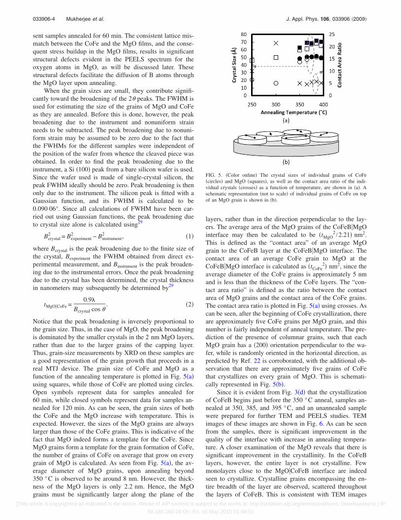
Notice that the peak broadening is inversely proportional tothe grain size. Thus, in the case of MgO, the peak broadeningis dominated by the smaller crystals in the 2 nm MgO layers,rather than due to the larger grains of the capping layer.Thus, grain-size measurements by XRD on these samples area good representation of the grain growth that proceeds in areal MTJ device. The grain size of CoFe and MgO as afunction of the annealing temperature is plotted in Fig. 5�a�using squares, while those of CoFe are plotted using circles.Open symbols represent data for samples annealed for60 min, while closed symbols represent data for samples an-nealed for 120 min. As can be seen, the grain sizes of boththe CoFe and the MgO increase with temperature. This isexpected. However, the sizes of the MgO grains are alwayslarger than those of the CoFe grains. This is indicative of thefact that MgO indeed forms a template for the CoFe. SinceMgO grains form a template for the grain formation of CoFe,the number of grains of CoFe on average that grow on everygrain of MgO is calculated. As seen from Fig. 5�a�, the av-erage diameter of MgO grains, upon annealing beyond350 °C is observed to be around 8 nm. However, the thick-ness of the MgO layers is only 2.2 nm. Hence, the MgOgrains must be significantly larger along the plane of the
layers, rather than in the direction perpendicular to the lay-ers. The average area of the MgO grains of the CoFeB�MgOinterface may then be calculated to be �tMgO
2 /2.21� nm2.This is defined as the “contact area” of an average MgOgrain to the CoFeB layer at the CoFeB�MgO interface. Thecontact area of an average CoFe grain to MgO at theCoFeB�MgO interface is calculated as �tCoFe
2� nm2, since theaverage diameter of the CoFe grains is approximately 5 nmand is less than the thickness of the CoFe layers. The “con-tact area ratio” is defined as the ratio between the contactarea of MgO grains and the contact area of the CoFe grains.The contact area ratio is plotted in Fig. 5�a� using crosses. Ascan be seen, after the beginning of CoFe crystallization, thereare approximately five CoFe grains per MgO grain, and thisnumber is fairly independent of anneal temperature. The pre-diction of the presence of columnar grains, such that eachMgO grain has a �200� orientation perpendicular to the wa-fer, while is randomly oriented in the horizontal direction, aspredicted by Ref. 22 is corroborated, with the additional ob-servation that there are approximately five grains of CoFethat crystallizes on every grain of MgO. This is schemati-cally represented in Fig. 5�b�.
Since it is evident from Fig. 3�d� that the crystallizationof CoFeB begins just before the 350 °C anneal, samples an-nealed at 350, 385, and 395 °C, and an unannealed samplewere prepared for further TEM and PEELS studies. TEMimages of these images are shown in Fig. 6. As can be seenfrom the samples, there is significant improvement in thequality of the interface with increase in annealing tempera-ture. A closer examination of the MgO reveals that there issignificant improvement in the crystallinity. In the CoFeBlayers, however, the entire layer is not crystalline. Fewmonolayers close to the MgO�CoFeB interface are indeedseen to crystallize. Crystalline grains encompassing the en-tire breadth of the layer are observed, scattered throughoutthe layers of CoFeB. This is consistent with TEM images
FIG. 5. �Color online� The crystal sizes of individual grains of CoFe�circles� and MgO �squares�, as well as the contact area ratio of the indi-vidual crystals �crosses� as a function of temperature, are shown in �a�. Aschematic representation �not to scale� of individual grains of CoFe on topof an MgO grain is shown in �b�.
033906-4 Mukherjee et al. J. Appl. Phys. 106, 033906 �2009�
[This article is copyrighted as indicated in the article. Reuse of AIP content is subject to the terms at: http://scitation.aip.org/termsconditions. Downloaded to ] IP:
58.185.160.28 On: Fri, 15 May 2015 01:48:51
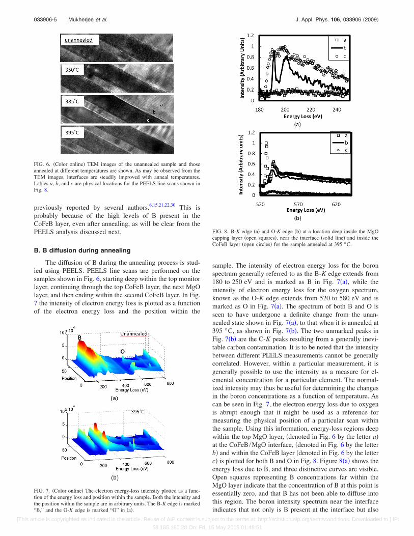
previously reported by several authors.6,15,21,22,30 This isprobably because of the high levels of B present in theCoFeB layer, even after annealing, as will be clear from thePEELS analysis discussed next.
B. B diffusion during annealing
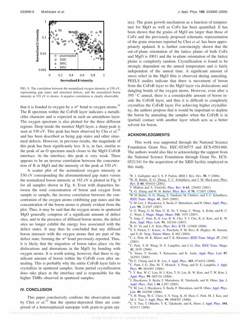
The diffusion of B during the annealing process is stud-ied using PEELS. PEELS line scans are performed on thesamples shown in Fig. 6, starting deep within the top monitorlayer, continuing through the top CoFeB layer, the next MgOlayer, and then ending within the second CoFeB layer. In Fig.7 the intensity of electron energy loss is plotted as a functionof the electron energy loss and the position within the
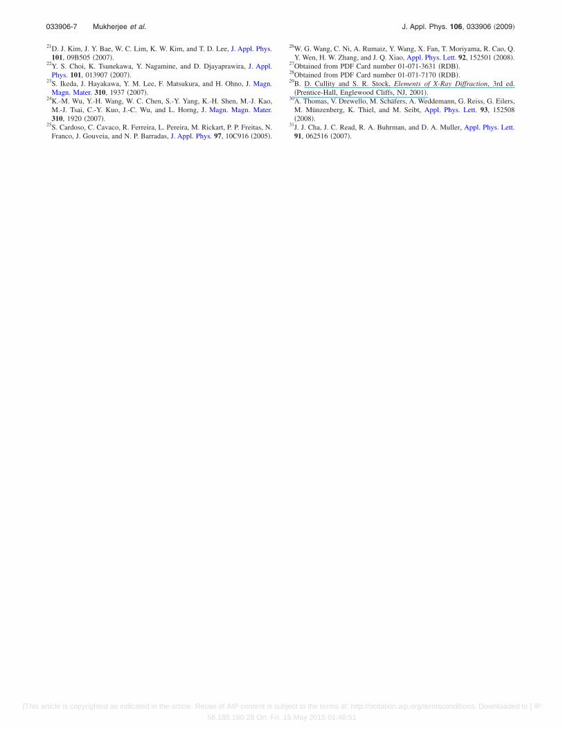
sample. The intensity of electron energy loss for the boronspectrum generally referred to as the B-K edge extends from180 to 250 eV and is marked as B in Fig. 7�a�, while theintensity of electron energy loss for the oxygen spectrum,known as the O-K edge extends from 520 to 580 eV and ismarked as O in Fig. 7�a�. The spectrum of both B and O isseen to have undergone a definite change from the unan-nealed state shown in Fig. 7�a�, to that when it is annealed at395 °C, as shown in Fig. 7�b�. The two unmarked peaks inFig. 7�b� are the C-K peaks resulting from a generally inevi-table carbon contamination. It is to be noted that the intensitybetween different PEELS measurements cannot be generallycorrelated. However, within a particular measurement, it isgenerally possible to use the intensity as a measure for el-emental concentration for a particular element. The normal-ized intensity may thus be useful for determining the changesin the boron concentrations as a function of temperature. Ascan be seen in Fig. 7, the electron energy loss due to oxygenis abrupt enough that it might be used as a reference formeasuring the physical position of a particular scan withinthe sample. Using this information, energy-loss regions deepwithin the top MgO layer, �denoted in Fig. 6 by the letter a�at the CoFeB /MgO interface, �denoted in Fig. 6 by the letterb� and within the CoFeB layer �denoted in Fig. 6 by the letterc� is plotted for both B and O in Fig. 8. Figure 8�a� shows theenergy loss due to B, and three distinctive curves are visible.Open squares representing B concentrations far within theMgO layer indicate that the concentration of B at this point isessentially zero, and that B has not been able to diffuse intothis region. The boron intensity spectrum near the interfaceindicates that not only is B present at the interface but also
FIG. 6. �Color online� TEM images of the unannealed sample and thoseannealed at different temperatures are shown. As may be observed from theTEM images, interfaces are steadily improved with anneal temperatures.Lables a, b, and c are physical locations for the PEELS line scans shown inFig. 8.
FIG. 7. �Color online� The electron energy-loss intensity plotted as a func-tion of the energy loss and position within the sample. Both the intensity andthe position within the sample are in arbitrary units. The B-K edge is marked“B,” and the O-K edge is marked “O” in �a�.
FIG. 8. B-K edge �a� and O-K edge �b� at a location deep inside the MgOcapping layer �open squares�, near the interface �solid line� and inside theCoFeB layer �open circles� for the sample annealed at 395 °C.
033906-5 Mukherjee et al. J. Appl. Phys. 106, 033906 �2009�
[This article is copyrighted as indicated in the article. Reuse of AIP content is subject to the terms at: http://scitation.aip.org/termsconditions. Downloaded to ] IP:
58.185.160.28 On: Fri, 15 May 2015 01:48:51
that it is bonded to oxygen by a �* bond to oxygen atoms.31
The B spectrum within the CoFeB layer indicates a metalli-clike character and is expected in such an amorphous layer.The oxygen spectrum is also plotted for the three differentregions. Deep inside the monitor MgO layer, a sharp peak isseen at 530 eV. This peak has been observed by Cha et al.31
and has been described as being gap states and other struc-tural defects. However, in previous results, the magnitude ofthis peak has been significantly less. It is, in fact, similar tothe peak of an O spectrum much closer to the MgO /CoFeBinterface. At the interface, this peak is very weak. Thereappears to be an inverse correlation between the concentra-tion of B in MgO and the intensity of the peak at 530 eV.
A scatter plot of the normalized oxygen intensity at530 eV corresponding the aforementioned gap states versusthe normalized boron intensity at 192 eV is plotted in Fig. 9for all samples shown in Fig. 6. Even with disparities be-tween the total concentration of boron and oxygen fromsample to sample, the inverse correlation between the con-centration of the oxygen atoms exhibiting gap states and theconcentration of the boron atoms is plainly evident from theplot. Thus, it may be said that the oxygen atoms in sputteredMgO generally comprise of a significant amount of defectsites, and in the presence of diffused boron atoms, the defectsites no longer exhibit the energy loss associated with thedefect states. It may thus be concluded that any diffusedboron interacts with the oxygen atoms that are part of thedefect state, forming the �* bond previously reported. Thus,it is likely that the migration of boron takes place via thedislocations and aberrations in the MgO, by bonding withoxygen atoms. It is worth noting, however, that there is sig-nificant amount of boron within the CoFeB even after an-nealing. This is probably why the entire CoFeB layer fails tocrystallize in sputtered samples. Some partial crystallizationdoes take place at the interface and is responsible for thehigher TMRs observed in sputtered samples.
IV. CONCLUSION
This paper conclusively confirms the observation madeby Choi et al.22 that the sputter-deposited films are com-prised of a heteroepitaxial nanopipe with grain-to-grain epi-
taxy. The grain growth mechanism as a function of tempera-ture for MgO as well as CoFe has been quantified. It hasbeen shown that the grains of MgO are larger than those ofCoFe and the previously proposed schematic representationof the grain structure reported by Choi et al. has been appro-priately updated. It is further convincingly shown that theout-of-plane orientation of the lattice plains of both CoFeand MgO is �001� and the in-plane orientation of the latticeplains is completely random. Crystallization is found to bestrongly dependent on the anneal temperature and is fairlyindependent of the anneal time. A significant amount ofstress relief in the MgO film is observed during annealing.PEELS studies indicate that there is movement of boronfrom the CoFeB layer to the MgO layer via dislocations anddangling bonds of the oxygen atoms. However, even after a395 °C anneal, there is a considerable amount of boron in-side the CoFeB layer, and thus it is difficult to completelycrystallize the CoFeB layer. For achieving higher crystallin-ity, the authors propose that it would be important to depletethe boron by annealing the samples when the CoFeB is in�partial� contact with another layer which acts as a bettersolvent for boron.
ACKNOWLEDGMENTS
This work was supported through the National ScienceFoundation Grant Nos. EEC-0530575 and ECS-0501460.The authors would also like to acknowledge the support fromthe National Science Foundation through Grant No. ECS-0521341 for the acquisition of the XRD facility employed inthis study.
1W. J. Gallagher and S. S. P. Parkin, IBM J. Res. Dev. 50, 5 �2006�.2W. H. Butler, X.-G. Zhang, T. C. Schulthess, and J. M. MacLaren, Phys.Rev. B 60, 054416 �2001�.
3J. Mathon and A. Umerski, Phys. Rev. B 63, 220403 �2001�.4X.-G. Zhang and W. H. Butler, Phys. Rev. B 70, 172407 �2004�.5W. H. Butler, X.-G. Zhang, S. Vutukuri, M. Chshiev, and T. C. Schulthess,IEEE Trans. Magn. 41, 2645 �2005�.
6Y. M. Lee, J. Hayakawa, S. Ikeda, F. Matsukura, and H. Ohno, Appl. Phys.Lett. 90, 212507 �2007�.
7S. G. Wang, G. H. Han, G. H. Yu, Y. Jaing, C. Wang, A. Kohn, and R. C.C. Ward, J. Magn. Magn. Mater. 310, 1935 �2007�.
8Y. Jang, C. Nam, K.-S. Lee, B. K. Cho, Y. J. Cho, K.-S. Kim, and K. W.Kim, Appl. Phys. Lett. 91, 102104 �2007�.
9B. D. Yu and J.-S. Kim, Phys. Rev. B 73, 125408 �2006�.10S. S. Parkin, C. Kaiser, A. Panchula, P. M. Rice, B. Hughes, M. Samant,
and S.-H. Yang, Nature Mater. 3, 862 �2004�.11C. L. Platt, M. K. Minor, and T. K. Klemmer, IEEE Trans. Magn. 37, 2302
�2001�.12C. Park, Y.-H. Wang, D. E. Laughlin, and J.-G. Zhu, IEEE Trans. Magn.
42, 2639 �2006�.13S. Yuasa, Y. Suzuki, T. Katayama, and K. Ando, Appl. Phys. Lett. 87,
242503 �2005�.14H.-C. Chung and S.-R. Lee, J. Appl. Phys. 103, 07A914 �2008�.15C. Park, J.-G. Zhu, M. T. Moneck, Y. Peng, and D. E. Laughlin, J. Appl.
Phys. 99, 08A901 �2006�.16J. Y. Bae, W. C. Lim, H. J. Kim, T. D. Lee, K. W. Kim, and T. W. Kim, J.
Appl. Phys. 99, 08T316 �2006�.17J. Hayakawa, S. Ikeda, F. Matsukura, H. Takahashi, and H. Ohno, Jpn. J.
Appl. Phys., Part 2 44, L587 �2005�.18Y. M. Lee, J. Hayakawa, S. Ikeda, F. Matsukura, and H. Ohno, Appl. Phys.
Lett. 89, 042506 �2006�.19Y.-H. Wang, W.-C. Chen, S.-Y. Yang, K.-H. Shen, C. Park, M.-J. Kao, and
M.-J. Tsai, J. Appl. Phys. 99, 08M307 �2006�.20C. Y. You, T. Ohkubo, Y. K. Takahashi, and K. Hono, J. Appl. Phys. 104,
033517 �2008�.
FIG. 9. The correlation between the normalized oxygen intensity at 530 eV,representing gap states and structural defects, and the normalized boronintensity at 193 eV is shown. A negative correlation is clearly observable.
033906-6 Mukherjee et al. J. Appl. Phys. 106, 033906 �2009�
[This article is copyrighted as indicated in the article. Reuse of AIP content is subject to the terms at: http://scitation.aip.org/termsconditions. Downloaded to ] IP:
58.185.160.28 On: Fri, 15 May 2015 01:48:51
21D. J. Kim, J. Y. Bae, W. C. Lim, K. W. Kim, and T. D. Lee, J. Appl. Phys.101, 09B505 �2007�.
22Y. S. Choi, K. Tsunekawa, Y. Nagamine, and D. Djayaprawira, J. Appl.Phys. 101, 013907 �2007�.
23S. Ikeda, J. Hayakawa, Y. M. Lee, F. Matsukura, and H. Ohno, J. Magn.Magn. Mater. 310, 1937 �2007�.
24K.-M. Wu, Y.-H. Wang, W. C. Chen, S.-Y. Yang, K.-H. Shen, M.-J. Kao,M.-J. Tsai, C.-Y. Kuo, J.-C. Wu, and L. Horng, J. Magn. Magn. Mater.310, 1920 �2007�.
25S. Cardoso, C. Cavaco, R. Ferreira, L. Pereira, M. Rickart, P. P. Freitas, N.Franco, J. Gouveia, and N. P. Barradas, J. Appl. Phys. 97, 10C916 �2005�.
26W. G. Wang, C. Ni, A. Rumaiz, Y. Wang, X. Fan, T. Moriyama, R. Cao, Q.Y. Wen, H. W. Zhang, and J. Q. Xiao, Appl. Phys. Lett. 92, 152501 �2008�.
27Obtained from PDF Card number 01-071-3631 �RDB�.28Obtained from PDF Card number 01-071-7170 �RDB�.29B. D. Cullity and S. R. Stock, Elements of X-Ray Diffraction, 3rd ed.
�Prentice-Hall, Englewood Cliffs, NJ, 2001�.30A. Thomas, V. Drewello, M. Schäfers, A. Weddemann, G. Reiss, G. Eilers,
M. Münzenberg, K. Thiel, and M. Seibt, Appl. Phys. Lett. 93, 152508�2008�.
31J. J. Cha, J. C. Read, R. A. Buhrman, and D. A. Muller, Appl. Phys. Lett.91, 062516 �2007�.
033906-7 Mukherjee et al. J. Appl. Phys. 106, 033906 �2009�
[This article is copyrighted as indicated in the article. Reuse of AIP content is subject to the terms at: http://scitation.aip.org/termsconditions. Downloaded to ] IP:
58.185.160.28 On: Fri, 15 May 2015 01:48:51