CrossLink-NX Evaluation Board User Guide
54
CrossLink-NX Evaluation Board User Guide FPGA-EB-02028-1.0 December 2019
-
Upload
khangminh22 -
Category
Documents
-
view
2 -
download
0
Transcript of CrossLink-NX Evaluation Board User Guide

CrossLink-NX Evaluation Board
User Guide
FPGA-EB-02028-1.0
December 2019

CrossLink-NX Evaluation Board User Guide
© 2019 Lattice Semiconductor Corp. All Lattice trademarks, registered trademarks, patents, and disclaimers are as listed at www.latticesemi.com/legal. All other brand or product names are trademarks or registered trademarks of their respective holders. The specifications and information herein are subject to change without notice.
2 FPGA-EB-02028-1.0
Disclaimers Lattice makes no warranty, representation, or guarantee regarding the accuracy of information contained in this document or the suitability of its products for any particular purpose. All information herein is provided AS IS and with all faults, and all risk associated with such information is entirely with Buyer. Buyer shall not rely on any data and performance specifications or parameters provided herein. Products sold by Lattice have been subject to limited testing and it is the Buyer's responsibility to independently determine the suitability of any products and to test and verify the same. No Lattice products should be used in conjunction with mission- or safety-critical or any other application in which the failure of Lattice’s product could create a situation where personal injury, death, severe property or environmental damage may occur. The information provided in this document is proprietary to Lattice Semiconductor, and Lattice reserves the right to make any changes to the information in this document or to any products at any time without notice.
CrossLink-NX Evaluation Board User Guide
© 2019 Lattice Semiconductor Corp. All Lattice trademarks, registered trademarks, patents, and disclaimers are as listed at www.latticesemi.com/legal. All other brand or product names are trademarks or registered trademarks of their respective holders. The specifications and information herein are subject to change without notice.
FPGA-EB-02028-1.0 3
Contents Acronyms in This Document ................................................................................................................................................. 5 1. Introduction .................................................................................................................................................................. 6
1.1. CrossLink-NX Evaluation Board ........................................................................................................................... 6 1.2. Features .............................................................................................................................................................. 6 1.3. CrossLink-NX Device ............................................................................................................................................ 9 1.4. Applying Power to the Board .............................................................................................................................. 9
2. Jumpers and Test Connection .................................................................................................................................... 10 3. Power Scheme ............................................................................................................................................................ 12 4. Programming and I2C .................................................................................................................................................. 13
4.1. JTAG Download Interface .................................................................................................................................. 13 4.2. Alternate JTAG Download Interface .................................................................................................................. 13 4.3. JTAG to MSPI Pass-through Interface ............................................................................................................... 14 4.4. SPI Flash Device Selection in Programmer ........................................................................................................ 14 4.5. Other JTAG Configuration Pins .......................................................................................................................... 15
5. CrossLink-NX Clock Sources ........................................................................................................................................ 16 6. Control Buses – I2C, UART, and SPI ............................................................................................................................. 17
6.1. I2C ...................................................................................................................................................................... 17 6.2. UART Topology .................................................................................................................................................. 17 6.3. SPI Topology ...................................................................................................................................................... 18
SPI Configuration .......................................................................................................................................... 18 7. LEDs and Switches ...................................................................................................................................................... 19
7.1. DIP Switch ......................................................................................................................................................... 19 7.2. General Purpose Push Buttons ......................................................................................................................... 19 7.3. General Purpose LEDs ....................................................................................................................................... 20 7.4. Indicator LEDs.................................................................................................................................................... 20
8. Headers/Connectors and LIFCL-40 Device Ball Mapping ............................................................................................ 21 8.1. FMC LPC Connector ........................................................................................................................................... 21 8.2. Parallel FMC Configuration Header ................................................................................................................... 23 8.3. Raspberry Pi Board GPIO Header ...................................................................................................................... 23 8.4. Camera Connector ............................................................................................................................................ 24 8.5. D-PHY1 Header .................................................................................................................................................. 25 8.6. PMOD Header ................................................................................................................................................... 26 8.7. JTAG Header ...................................................................................................................................................... 26 8.8. Parallel Configuration Header ........................................................................................................................... 27 8.9. ADC Test Header ............................................................................................................................................... 27
9. Software Requirements .............................................................................................................................................. 28 10. Storage and Handling ............................................................................................................................................. 28 11. Ordering Information .............................................................................................................................................. 28 Appendix A. CrossLink-NX Evaluation Board Schematics ................................................................................................... 29 Appendix B. CrossLink-NX Evaluation Board Bill of Materials ............................................................................................ 43 References .......................................................................................................................................................................... 51
Lattice Semiconductor Documents ................................................................................................................................. 51 Technical Support Assistance .............................................................................................................................................. 52 Revision History .................................................................................................................................................................. 53

CrossLink-NX Evaluation Board User Guide
© 2019 Lattice Semiconductor Corp. All Lattice trademarks, registered trademarks, patents, and disclaimers are as listed at www.latticesemi.com/legal. All other brand or product names are trademarks or registered trademarks of their respective holders. The specifications and information herein are subject to change without notice.
4 FPGA-EB-02028-1.0
Figures Figure 1.1. Top View of CrossLink-NX Evaluation Board ....................................................................................................... 7 Figure 1.2. Bottom View of CrossLink-NX Evaluation Board ................................................................................................. 8 Figure 2.1. Top View of CrossLink-NX Evaluation Board – Jumper Locations ..................................................................... 10 Figure 3.1. Board Power Scheme ........................................................................................................................................ 12 Figure 4.1. Configuration and I2C Architecture ................................................................................................................... 13 Figure 4.2. SPI Flash Operation Dialog ................................................................................................................................ 14 Figure 6.1. I2C Architecture and UART Options .................................................................................................................. 17 Figure A.1. Title Page .......................................................................................................................................................... 29 Figure A.2. Block Diagram ................................................................................................................................................... 30 Figure A.3. USB Interface .................................................................................................................................................... 31 Figure A.4. Camera Interface (DPHYs) ................................................................................................................................ 32 Figure A.5. Raspberry Pi and User I/O Interface ................................................................................................................. 33 Figure A.6. SERDES SMAs/Switches/FMC Control .............................................................................................................. 34 Figure A.7. I2C LEDs and Push Buttons ............................................................................................................................... 35 Figure A.8. PMODs .............................................................................................................................................................. 36 Figure A.9. Configuration and ADC ..................................................................................................................................... 37 Figure A.10. FMC-LPC .......................................................................................................................................................... 38 Figure A.11. Power CSI and Banks ...................................................................................................................................... 39 Figure A.12. Power Decoupling ........................................................................................................................................... 40 Figure A.13. Power Regulators ........................................................................................................................................... 41 Figure A.14. Power Block Diagram ...................................................................................................................................... 42
Tables Table 2.1. Jumper Table ...................................................................................................................................................... 11 Table 3.1. CrossLink-NX VCCIO Supply Options .................................................................................................................. 12 Table 4.1. JTAG Connections ............................................................................................................................................... 13 Table 4.2. Other JTAG Signals ............................................................................................................................................. 15 Table 5.1. Clock Sources ..................................................................................................................................................... 16 Table 7.1. I2C Global Bus Connections ................................................................................................................................ 17 Table 6.2. CrossLink-NX SPI Connections ............................................................................................................................ 18 Table 8.1. Eight-Position DIP Switch Signals ....................................................................................................................... 19 Table 6.1. FMC LPC Header Pin Connections ...................................................................................................................... 21 Table 11.1. Ordering Information ....................................................................................................................................... 28

CrossLink-NX Evaluation Board User Guide
© 2019 Lattice Semiconductor Corp. All Lattice trademarks, registered trademarks, patents, and disclaimers are as listed at www.latticesemi.com/legal. All other brand or product names are trademarks or registered trademarks of their respective holders. The specifications and information herein are subject to change without notice.
FPGA-EB-02028-1.0 5
Acronyms in This Document A list of acronyms used in this document.
Acronym Definition
caBGA Chip Array Ball Grid Array
CMOS Complementary Metal-Oxide Semiconductor
DIP Dual Inline Package
DNI Do Not Install
ESD Electro Static Discharge
FMC LPC FPGA Mezzanine Low Pin Count Connector
FPGA Field Programmable Logic Array
FTDI Future Technology Devices International
GPIO General Purpose Input/Output
I2C Inter-Integrated Circuit
JTAG Joint Test Action Group
LVDS Low-Voltage Differential Signaling
PMOD Peripheral Module
SPI Serial Peripheral Interface
UART Universal Asynchronous Receiver Transmitter
USB Universal Serial Bus
CrossLink-NX Evaluation Board User Guide
© 2019 Lattice Semiconductor Corp. All Lattice trademarks, registered trademarks, patents, and disclaimers are as listed at www.latticesemi.com/legal. All other brand or product names are trademarks or registered trademarks of their respective holders. The specifications and information herein are subject to change without notice.
6 FPGA-EB-02028-1.0
1. Introduction The Lattice Semiconductor CrossLink-NX™ Evaluation Board allows designers to investigate and experiment with the features of the CrossLink-NX Field Programmable Gate Array (FPGA). The features of the CrossLink-NX Evaluation Board can assist engineers with the rapid prototyping and testing of their specific designs.
The CrossLink-NX Evaluation Board is part of the CrossLink-NX Evaluation Kit, which includes the following:
CrossLink-NX Evaluation Board pre-loaded with the shipping demo design
12V AC/DC power adapter and international plug adapters
Lattice Radiant® Software license information
USB-A to USB-B (Mini) Cable for programming FPGA through a PC
Quick Start Guide
The contents of this user guide include top-level functional descriptions of the various portions of the development board, descriptions of the on-board headers, diodes and switches and a complete set of schematics.
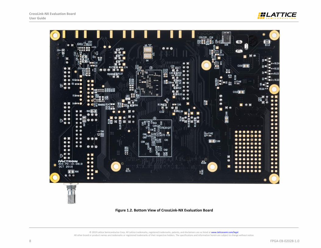
1.1. CrossLink-NX Evaluation Board The CrossLink-NX Evaluation Board features the CrossLink-NX FPGA in the 400-ball caBGA package (LIFCL-40-9BG400C) w the ability to expand the usability of the CrossLink-NX with Raspberry Pi, PMOD, FMC LPC connector, along with access to PCIe channel. 118 wide range I/O and 37 high speed differential pairs are available for user-defined applications.
Figure 1.1 shows the top view of the CrossLink-NX Evaluation Board. Figure 1.2 shows the bottom view of the board. Figure 2.1 shows the jumper locations.
1.2. Features The CrossLink-NX Evaluation Board includes the following features:
CrossLink-NX FPGA (LIFCL-40-9BG400C)
General Purpose Input/Output (GPIO) breakout with Raspberry Pi, PMOD, and FMC connector
MIPI CSI-2 Camera connector and D-PHY connector
118 wide range I/O and 37 high speed differential pair I/O with on board termination
x1 Gen2 PCIe interface
USB-B connection for device programming and Inter-Integrated Circuit (I2C) utility
On-board Boot Flash – 128 Mbit Serial Peripheral Interface (SPI) Flash, with Quad read feature
Eight input DIP switches, four push buttons, three status LEDs and 14 LEDs for demo purposes
Lattice Radiant® Software programming support
Multiple reference clock sources
Caution: The CrossLink-NX Evaluation Board contains ESD-sensitive components. ESD safe practices should be followed while handling and using the development board.

CrossLink-NX Evaluation Board User Guide
© 2019 Lattice Semiconductor Corp. All Lattice trademarks, registered trademarks, patents, and disclaimers are as listed at www.latticesemi.com/legal. All other brand or product names are trademarks or registered trademarks of their respective holders. The specifications and information herein are subject to change without notice.
FPGA-EB-02028-1.0 7
Power
Status
LEDs
(D19-D27)
Status
LEDs
UserSwitches(SW1)
RaspberryPI Conn(JP5)
PrototypeArea
Potentiometer
(U8)
ADC Test
Header
(J26)
FMC Parallel
Config
Header (J27)
FPGA
Mezzanine
Carrier Card
Conn (U9)
Push Buttons
(SW5-SW2)
Output LEDs
(D16-D3)
PMOD
Conn
(J17-J19)
JTAG Header(J1)
Parallel Config Header (J20)
LIFCL-40Device (U3)
SPI Flash Memory (U6)
FTDI Interface Chip (U1)
Mini USB
12 V
Power Input
Camera
Conn
(CN1)
xD-Phy 1
Header (J6)Serdes Test SMA Conn
(J11, J15, J12, J16, J10 and J14)
Figure 1.1. Top View of CrossLink-NX Evaluation Board
CrossLink-NX Evaluation Board User Guide
© 2019 Lattice Semiconductor Corp. All Lattice trademarks, registered trademarks, patents, and disclaimers are as listed at www.latticesemi.com/legal. All other brand or product names are trademarks or registered trademarks of their respective holders. The specifications and information herein are subject to change without notice.
8 FPGA-EB-02028-1.0
Figure 1.2. Bottom View of CrossLink-NX Evaluation Board

CrossLink-NX Evaluation Board User Guide
© 2019 Lattice Semiconductor Corp. All Lattice trademarks, registered trademarks, patents, and disclaimers are as listed at www.latticesemi.com/legal. All other brand or product names are trademarks or registered trademarks of their respective holders. The specifications and information herein are subject to change without notice.
FPGA-EB-02028-1.0 9
1.3. CrossLink-NX Device The CrossLink-NX Evaluation Board features the CrossLink-NX device in a 400-ball caBGA package, also referred to as LIFCL-40-9BG400C, offers a variety of features and programmability. For more information on the capabilities of CrossLink-NX, see CrossLink-NX Family Data Sheet (FPGA-DS-02049).
1.4. Applying Power to the Board You should see all the power LEDs light on after applying 12 V power to CrossLink-NX Evaluation Board, this indicates the board is powered on and functioning. Early I/O demo design is programmed into onboard boot flash, you should observe LED0 (D3) as mapped an early I/O immediately turns on as soon as 12 V power is supplied to the board. After about two seconds, as configuration is successfully completed, DONE LED (D18) should light up, then LED2 (D5), and LED3 (D6) alternately in a heartbeat pattern.

CrossLink-NX Evaluation Board User Guide
© 2019 Lattice Semiconductor Corp. All Lattice trademarks, registered trademarks, patents, and disclaimers are as listed at www.latticesemi.com/legal. All other brand or product names are trademarks or registered trademarks of their respective holders. The specifications and information herein are subject to change without notice.
10 FPGA-EB-02028-1.0
2. Jumpers and Test Connection
FTDI Reset
(JP1)
FTDI OSC
Reset (JP2)
Raspberry Pi
Conn Power
(JP3 and JP4)
Serdes Test
125 MHz/200 MHz
Ref CLK Selection
(J13)
ADC Test
Selection (J21,
J22, and J24-J26)
FMC VADJ 1.8 V,
2.5 V, and 3.3 V
Selection (J6-J8)
VCCIO0 Power
Selection (J44)
VCCIO6 Power
Selection (J33)
Current
Measurement 2 Pin
Header (J3-J5, J32,
and J40)
Current Measurement
2 Pin Header
(J7-J9)
Current
Measurement 2 Pin
Header (J28-J30,
and J37)
Current
Measurement 2 Pin
Header (J34-J36,
J41-J43, J23, J31,
and J38)
Figure 2.1. Top View of CrossLink-NX Evaluation Board – Jumper Locations

CrossLink-NX Evaluation Board User Guide
© 2019 Lattice Semiconductor Corp. All Lattice trademarks, registered trademarks, patents, and disclaimers are as listed at www.latticesemi.com/legal. All other brand or product names are trademarks or registered trademarks of their respective holders. The specifications and information herein are subject to change without notice.
FPGA-EB-02028-1.0 11
Table 2.1. Jumper Table
Part Description Setting
JP1 FTDI Reset Jumper Default Open (active FTDI)/Short (reset FTDI)
JP2 FTDI Oscillator Jumper Default Short (12 MHz OSC connected)/Open (12 MHz OSC unconnected)
JP3 Raspberry Pi Connector Power Default Open (Raspberry Pi self-power)/Short (3.3v applies Paspberry Pi connector )
JP4 Raspberry Pi Connector Power Default Open (Raspberry Pi self-power)/Short (5.0v applies Paspberry Pi connector )
JP6, JP7, and JP8
VADJ Selection Jumper For FMC LPC Carrier Connector
NO Jumper -> 1.5 V (JP6, JP7, and JP8 open)
Only JP8* Short -> 1.8 V
Only JP7* Short -> 2.5 V
Only JP6* Short -> 3.3 V
J13 125 Mhz / 200 Mhz OSC Selection Jumper
Default 1–2 (125 MHz)/2-3 (200 MHz)
J21 ADC_REFP0 Selection Jumper Default 1–2 (V1P8_ADC_VREF)/2-3 (J26 connector Input Voltage)
J22 ADC_REFP1 Selection Jumper Default 1–2 (V1P8_ADC_VREF)/2-3 (J26 connector Input Voltage)
J24 ADC_DP0 Selection Jumper Default 1–2 (POT)/2-3 (J26 connector)
J25 ADC_DN0 Selection Jumper Default 1–2 (POT)/2-3 (J26 connector)
J44 VCCIO0 Supply Voltage Selection Jumper
Default 1–2 (3.3 V)/2-3 (1.8 V)
J33 VCCIO6 Supply Voltage Selection Jumper
Default 1–2 (3.3 V)/2-3 (1.8 V)
J3,J4,J5,J7,J8,J9, J23,J28,J29,J30, J31,J32,J34,J35, J36,J37,J38,J40, J41,J42, and J43
Current Measurement 2 Pin Header
*Note: Only one jumper at a time. Otherwise, damage could occur.

CrossLink-NX Evaluation Board User Guide
© 2019 Lattice Semiconductor Corp. All Lattice trademarks, registered trademarks, patents, and disclaimers are as listed at www.latticesemi.com/legal. All other brand or product names are trademarks or registered trademarks of their respective holders. The specifications and information herein are subject to change without notice.
12 FPGA-EB-02028-1.0
3. Power Scheme The CrossLink-NX Evaluation Board has most of its power supplied by onboard regulators powered by an external 12 V power. Refer to Appendix A. CrossLink-NX Evaluation Board Schematics to see the details of these power supply options. Figure 3.1 shows the high-level power supply architecture of the board. Table 3.1 shows the voltage options available for the various VCCIO supplies.
V1P8_DPHY
VCCIO0
VCCIO5
VCCIO1
V1P8_VCCADC18
VCCIO4
V1P0_VCCSD0V1P8_VCCPLLSD0
V1P8_LDO V1P0_LDO
V1P8
VCCIO3ADC
V1P0_LDO
V3P3/V1P8
V3P3
V3P3
V3P3/V1P8
V3P3
V1P8 V1P8
Serde sV1P0_DPHY
VCCIO7
VCCIO6
VCCIO2
V1P8_LDO
V1P8_LDO V1P8_LDO VCC_CORE_V1P0
V1P8_VCCAUX VCC
+12.0 V
SW
(U
15
)S
W (
U1
6)
V1P0_LDO
V1P2
+1.0 V
VCC_CORE_1P0
+1.0 V
LDO
(U
14)
LDO
(U
11)
Cam
era
(C
N1
)V1P8
+1.8 V
V2P8
+1.2 V
+2.8 V
LDO
(U
12)
V1P8_LDO
+1.8 V
LDO
(U
13)
FTDI (U1)
Raspberry (JP5)
V5P0
+5.0 V
V3P3
+3.3 V
LIFCL-40 (U3)
V3P3
12 V
3.3 V
VADJ
FPGA Me zza ni ne Card (FMC) Low P in Count (LPC)(U9)
S W - 3 A ( U 1 0)1 . 5 V / 1 . 8 V / 2 . 5 V / 3 . 3 V
Figure 3.1. Board Power Scheme
Table 3.1. CrossLink-NX VCCIO Supply Options
VCCIO Bank Selection V3P3 V1P8
VCCIO0 J44 Connector Default Selectable
VCCIO1 — Fixed N/A
VCCIO2 — Fixed N/A
VCCIO3 — N/A Fixed
VCCIO4 — N/A Fixed
VCCIO5 — N/A Fixed
VCCIO6 J42 Connector Default Selectable
VCCIO7 — Fixed N/A

CrossLink-NX Evaluation Board User Guide
© 2019 Lattice Semiconductor Corp. All Lattice trademarks, registered trademarks, patents, and disclaimers are as listed at www.latticesemi.com/legal. All other brand or product names are trademarks or registered trademarks of their respective holders. The specifications and information herein are subject to change without notice.
FPGA-EB-02028-1.0 13
4. Programming and I2C The JTAG/SPI programming architecture and I2C interface of the CrossLink-NX Evaluation Board is shown in Figure 4.1.
Mini USB (J2)
FT2232H (U1)
rst#
UART (DNI2)
I2C
JTAG
LIFCL (U3)
JTAG Header (J1) DNI1 Raspberry Pi (JP5)
Raspberry Pi (JP5)
DN
I3
SPI Flash (U6)
SPI Header (J20)
Port 0
Port 1
JP1Notes: 1. Via DNI 0 resistors R35, R36, R37 and R382. Via DNI 0 resistors R15 and R173. Via DNI 0 resistors R39 and R40
Figure 4.1. Configuration and I2C Architecture
4.1. JTAG Download Interface The CrossLink-NX Evaluation Board has a built-in download controller for programming the CrossLink-NX device. It uses an FT2232H Future Technology Devices International (FTDI) part to convert USB to JTAG. To use the built-in download cable, connect the USB cable from a PC with Radiant Programmer tool installed to the mini USB connector on the board (J2). A mini USB to USB-A cable is included in the CrossLink-NX Evaluation Kit. The USB hub on the PC detects the cable of the USB function on Port 0, making the built-in cable available for use with the Radiant programming software.
4.2. Alternate JTAG Download Interface J1 is an 8-pin standalone JTAG header used with an external Lattice download cable that is available separately, when the FTDI part is disabled from the JTAG chain after setting the JP1 jumper. A USB download cable can be attached to the board using J1 to interface with the CrossLink-NX. For details on the connection between the USB download cable and J1, refer to Programming Cable User’s Guide (FPGA-UG-02042).
J1 can also be used as test point when USB to JTAG is working. Additionally, you can enable the JTAG access path through the Raspberry Pi header (JP5) for customer applications. This is done by connecting the JP5 header to the J1 header through some onboard resistors. The JTAG connections between J1 and JP5 are listed in Table 4.1.
Table 4.1. JTAG Connections
J1 Pin Number
JTAG Signal Name
CrossLink-NX Ball Location for JTAG
Raspberry Pi Header (JP8) Pin Number
J1 to JP5 Isolation (Assembly)
Raspberry Pi GPIO
1 VCCIO1 — — — —
2 TDO F19 10 R36 (DNI) IO15
3 TDI F17 11 R38 (DNI) IO17
4 — — — — —
5 — — — — —
6 TMS F15 12 R37 (DNI) IO18
7 GND — — — —
8 TCK G18 8 R35 (DNI) IO14

CrossLink-NX Evaluation Board User Guide
© 2019 Lattice Semiconductor Corp. All Lattice trademarks, registered trademarks, patents, and disclaimers are as listed at www.latticesemi.com/legal. All other brand or product names are trademarks or registered trademarks of their respective holders. The specifications and information herein are subject to change without notice.
14 FPGA-EB-02028-1.0
4.3. JTAG to MSPI Pass-through Interface The download controller can also access the JTAG to MSPI pass-through circuit that allows the slave SPI Flash to be erased, programmed, and read with Radiant Programmer.
4.4. SPI Flash Device Selection in Programmer The Flash device on this board is a Macronix MX25L12833F.
Figure 4.2. SPI Flash Operation Dialog
You may proceed with the Flash device programming by following the procedure in CrossLink-NX sysCONFIG Usage Guide (FPGA-TN-02099).
CrossLink-NX Evaluation Board User Guide
© 2019 Lattice Semiconductor Corp. All Lattice trademarks, registered trademarks, patents, and disclaimers are as listed at www.latticesemi.com/legal. All other brand or product names are trademarks or registered trademarks of their respective holders. The specifications and information herein are subject to change without notice.
FPGA-EB-02028-1.0 15
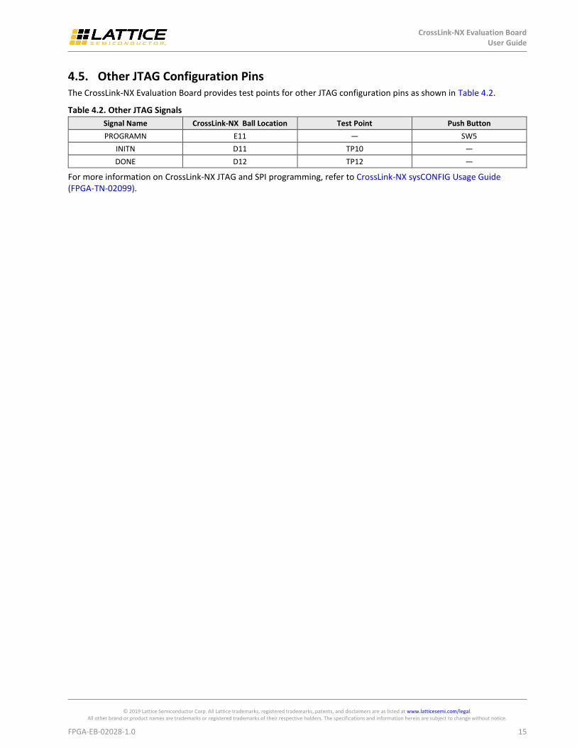
4.5. Other JTAG Configuration Pins The CrossLink-NX Evaluation Board provides test points for other JTAG configuration pins as shown in Table 4.2.
Table 4.2. Other JTAG Signals
Signal Name CrossLink-NX Ball Location Test Point Push Button
PROGRAMN E11 — SW5
INITN D11 TP10 —
DONE D12 TP12 —
For more information on CrossLink-NX JTAG and SPI programming, refer to CrossLink-NX sysCONFIG Usage Guide (FPGA-TN-02099).
CrossLink-NX Evaluation Board User Guide
© 2019 Lattice Semiconductor Corp. All Lattice trademarks, registered trademarks, patents, and disclaimers are as listed at www.latticesemi.com/legal. All other brand or product names are trademarks or registered trademarks of their respective holders. The specifications and information herein are subject to change without notice.
16 FPGA-EB-02028-1.0
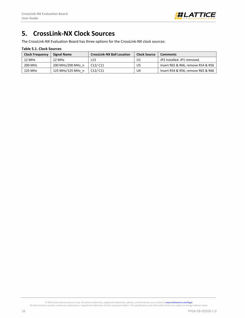
5. CrossLink-NX Clock Sources The CrossLink-NX Evaluation Board has three options for the CrossLink-NX clock sources:
Table 5.1. Clock Sources
Clock Frequency Signal Name CrossLink-NX Ball Location Clock Source Comments
12 MHz 12 MHz L13 U1 JP2 installed. JP1 removed.
200 MHz 200 MHz/200 MHz_n C12/ C11 U5 Insert R65 & R66, remove R54 & R56
125 MHz 125 MHz/125 MHz_n C12/ C11 U4 Insert R54 & R56, remove R65 & R66

CrossLink-NX Evaluation Board User Guide
© 2019 Lattice Semiconductor Corp. All Lattice trademarks, registered trademarks, patents, and disclaimers are as listed at www.latticesemi.com/legal. All other brand or product names are trademarks or registered trademarks of their respective holders. The specifications and information herein are subject to change without notice.
FPGA-EB-02028-1.0 17
6. Control Buses – I2C, UART, and SPI This section describes the topology of the various configuration and communication buses.
6.1. I2C The CrossLink-NX Evaluation Board uses the I2C bus to support CrossLink-NX configuration, and optionally to support Raspberry Pi communication. The global I2C bus has the signal names SDA and SCL and they are routed close to Raspberry Pi header as shown in Figure 4.1 and in more detail in Figure 6.1.
Raspberry Pi connector is connected to a dedicated CrossLink-NX GPIO bank with a direct local I2C bus. Local I2C bus can optionally connect to the global I2C bus through resistors. The local I2C connections are summarized in Table 7.1.
FTDI 2232H (UI)
BDBUS0
BDBUS1/2 SDA
SCL
Instantiated I2CResistors (R18, R19)
RASP_ID_SD
RASP_ID_SC
Bank6 (U3)
Bank1 (U3)
SDA
SCL
TXD_UART
RXD_UART
Figure 6.1. I2C Architecture and UART Options
Table 7.1. I2C Global Bus Connections
CrossLink-NX Bank Component (Reference)
Header Pin CrossLink-NX -85 Ball
Local Signal Name (Global I2C Signal) Resistor
6 Raspberry Pi header (JP5)
27 M7 RASP_ID_SD (SDA) R40 (DNI)
28 M4 RASP_ID_SC (SCL) R39 (DNI)
6.2. UART Topology The board provides support for UART configuration by providing an uninstalled connection between the FTDI and CrossLink-NX. Two 0 Ω resistors (R16 and R17) can be installed to connect Port 1 to two general purpose I/O (PR8A/F16 and PR10A/F18) in Bank 6 as shown in Figure 6.1.

CrossLink-NX Evaluation Board User Guide
© 2019 Lattice Semiconductor Corp. All Lattice trademarks, registered trademarks, patents, and disclaimers are as listed at www.latticesemi.com/legal. All other brand or product names are trademarks or registered trademarks of their respective holders. The specifications and information herein are subject to change without notice.
18 FPGA-EB-02028-1.0
6.3. SPI Topology
SPI Configuration
One of the major functions of SPI connections on the board is to support CrossLink-NX configuration from the SPI Flash or the Parallel Configuration Header. The CrossLink-NX Evaluation Board can support both Master SPI (MSPI) and Slave SPI (SSPI) modes for CrossLink-NX configuration.
Table 6.2. CrossLink-NX SPI Connections
Signal Name CrossLink-NX Ball Parallel Configuration Header Pin
SPI_MCLK E12 12
DQ0_MOSI D13 5
DQ1_MISO D15 7
CSSPIN E13 8
DQ2 D14 11
DQ3 D16 9
MCSNO E16 3

CrossLink-NX Evaluation Board User Guide
© 2019 Lattice Semiconductor Corp. All Lattice trademarks, registered trademarks, patents, and disclaimers are as listed at www.latticesemi.com/legal. All other brand or product names are trademarks or registered trademarks of their respective holders. The specifications and information herein are subject to change without notice.
FPGA-EB-02028-1.0 19
7. LEDs and Switches This section describes the CrossLink-NX Evaluation Board LEDs and switches that can be used in demo and customer designs.
7.1. DIP Switch Eight CrossLink-NX pins are connected to the SW1 DIP switch to allow for manually actuated inputs to the FPGA. One side of each switch is connected to GPIOs within the VCCIO2 bank and pulled up through 4.7 kΩ resistors. The other side is grounded. The designated pins are connected as shown in Table 8.1.
Table 8.1. Eight-Position DIP Switch Signals
Signal Name CrossLink-NX Ball CrossLink-NX Bank
SWITCH0 N14 2
SWITCH1 M14 2
SWITCH2 M16 2
SWITCH3 M15 2
SWITCH4 N15 2
SWITCH5 N16 2
SWITCH6 M17 2
SWITCH7 M18 2
7.2. General Purpose Push Buttons The CrossLink-NX Evaluation Board provides three push button switches – SW2, SW3 and SW4 for demos and user applications. Two of the buttons control pre-defined functional pins, and the third is generic. Pressing these buttons drives a logic level “0” to the corresponding I/O pins.
Table 8.2. Push Button Switch Signals
Signal Name CrossLink-NX Ball Push Button Reference Logic Level at Button Pressed
GSRN G19 SW4 0
PROGRAMN E11 SW5 0
PUSHBUTTON0 G14 SW2 0
PUSHBUTTON1 G15 SW3 0
Information on PROGRAMN, refer to CrossLink-NX sysCONFIG Usage Guide (FPGA-TN-02099). SW2 is intended to be used as a global set/reset pin when active low, but can be substituted for another function if the user desires. SW2 and SW3 can be used as a generic input.

CrossLink-NX Evaluation Board User Guide
© 2019 Lattice Semiconductor Corp. All Lattice trademarks, registered trademarks, patents, and disclaimers are as listed at www.latticesemi.com/legal. All other brand or product names are trademarks or registered trademarks of their respective holders. The specifications and information herein are subject to change without notice.
20 FPGA-EB-02028-1.0
7.3. General Purpose LEDs The CrossLink-NX Evaluation Board provides fourteen LEDs that are connected to I/O within Bank 1 & 0. The LEDs are lighted when the output is driven LOW.
Table 8.3. General Purpose LED Signals
Signal Name CrossLink-NX Ball CrossLink-NX Bank / Color
LED0 E17 1 (Green)
LED1 F13 1 (Green)
LED2 G13 1 (Green)
LED3 F14 1 (Green)
LED4 L16 1 (Green)
LED5 L15 1 (Green)
LED6 L20 1 (Green)
LED7 L19 1 (Green)
LED8 R17 2 (Green)
LED9 R18 2 (Green)
LED10 U20 2 (Green)
LED11 T20 2 (Green)
LED12 W20 2 (Yellow)
LED13 V20 2 (Yellow)
7.4. Indicator LEDs Table 8. lists various LEDs and describes their purpose.
Table 8.4. Various LED Signals
LEDs Signal Name CrossLink-NX Ball Color Purpose
D1 UART_ACT F18 Green If installed, lights in UART mode
D17 INITN D11 Red Lights if configuration error
D18 DONE D12 Green Lights if successful configuration
D19 +12.0 V — Green Lights if voltage present (external connection)
D20 +5.0 V — Green Lights if voltage present
D21 +3.3 V — Green Lights if voltage present
D22 +2.8 V — Green Lights if voltage present
D23 +1.2 V — Green Lights if voltage present
D24 +1.8 V — Green Lights if voltage present
D25 +1.0 V (VCC_CORE_V1P0) — Green Lights if voltage present
D26 +1.8 V (V1P8_LDO) — Green Lights if voltage present
D27 +1.0 V (V1P0_LDO) — Green Lights if voltage present
CrossLink-NX Evaluation Board User Guide
© 2019 Lattice Semiconductor Corp. All Lattice trademarks, registered trademarks, patents, and disclaimers are as listed at www.latticesemi.com/legal. All other brand or product names are trademarks or registered trademarks of their respective holders. The specifications and information herein are subject to change without notice.
FPGA-EB-02028-1.0 21
8. Headers/Connectors and LIFCL-40 Device Ball Mapping This section describes the CrossLink-NX Evaluation Board headers/connectors and ball mapping.
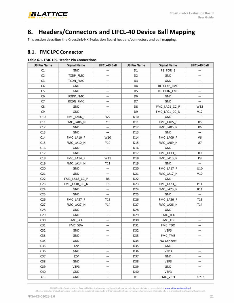
8.1. FMC LPC Connector
Table 6.1. FMC LPC Header Pin Connections
U9 Pin Name Signal Name LIFCL-40 Ball U9 Pin Name Signal Name LIFCL-40 Ball
C1 GND — D1 PS_POR_B —
C2 TXDP_FMC — D2 GND —
C3 TXDN_FMC — D3 GND —
C4 GND — D4 REFCLKP_FMC —
C5 GND — D5 REFCLKN_FMC —
C6 RXDP_FMC — D6 GND —
C7 RXDN_FMC — D7 GND —
C8 GND — D8 FMC_LA01_CC_P W13
C9 GND — D9 FMC_LA01_CC_N V12
C10 FMC_LA06_P W9 D10 GND —
C11 FMC_LA06_N Y9 D11 FMC_LA05_P R5
C12 GND — D12 FMC_LA05_N R6
C13 GND — D13 GND —
C14 FMC_LA10_P W10 D14 FMC_LA09_P V6
C15 FMC_LA10_N Y10 D15 FMC_LA09_N U7
C16 GND — D16 GND —
C17 GND — D17 FMC_LA13_P R9
C18 FMC_LA14_P W11 D18 FMC_LA13_N P9
C19 FMC_LA14_N Y11 D19 GND —
C20 GND — D20 FMC_LA17_P U10
C21 GND — D21 FMC_LA17_N V10
C22 FMC_LA18_CC_P R8 D22 GND —
C23 FMC_LA18_CC_N T8 D23 FMC_LA23_P P11
C24 GND — D24 FMC_LA23_N R11
C25 GND — D25 GND —
C26 FMC_LA27_P Y13 D26 FMC_LA26_P T13
C27 FMC_LA27_N Y14 D27 FMC_LA26_N T14
C28 GND — D28 GND —
C29 GND — D29 FMC_TCK —
C30 FMC_SCL — D30 FMC_TDI —
C31 FMC_SDA — D31 FMC_TDO —
C32 GND — D32 V3P3 —
C33 GND — D33 FMC_TMS —
C34 GND — D34 NO Connect —
C35 12V — D35 GND —
C36 GND — D36 V3P3 —
C37 12V — D37 GND —
C38 GND — D38 V3P3 —
C39 V3P3 — D39 GND —
C40 GND — D40 V3P3 —
G1 GND — H1 FMC_VREF T6 Y18

CrossLink-NX Evaluation Board User Guide
© 2019 Lattice Semiconductor Corp. All Lattice trademarks, registered trademarks, patents, and disclaimers are as listed at www.latticesemi.com/legal. All other brand or product names are trademarks or registered trademarks of their respective holders. The specifications and information herein are subject to change without notice.
22 FPGA-EB-02028-1.0
U9 Pin Name Signal Name LIFCL-40 Ball U9 Pin Name Signal Name LIFCL-40 Ball
G2 FMC_CLK1_P R7 H2 FMC_PRSNT —
G3 FMC_CLK1_N T7 H3 GND —
G4 GND — H4 FMC_CLK0_P Y12
G5 GND — H5 FMC_CLK0_N W12
G6 FMC_LA00_CC_P V11 H6 GND —
G7 FMC_LA00_CC_N U11 H7 FMC_LA02_P Y2
G8 GND — H8 FMC_LA02_N Y3
G9 FMC_LA03_P W6 H9 GND —
G10 FMC_LA03_N Y6 H10 FMC_LA04_P V1
G11 GND — H11 FMC_LA04_N W1
G12 FMC_LA08_P Y7 H12 GND —
G13 FMC_LA08_N Y8 H13 FMC_LA07_P W7
G14 GND — H14 FMC_LA07_N V7
G15 FMC_LA12_P U1 H15 GND —
G16 FMC_LA12_N T1 H16 FMC_LA11_P P10
G17 GND — H17 FMC_LA11_N R10
G18 FMC_LA16_P P7 H18 GND —
G19 FMC_LA16_N P8 H19 FMC_LA15_P W8
G20 GND — H20 FMC_LA15_N V9
G21 FMC_LA20_P T10 H21 GND —
G22 FMC_LA20_N T11 H22 FMC_LA19_P U12
G23 GND — H23 FMC_LA19_N T12
G24 FMC_LA22_P V14 H24 GND —
G25 FMC_LA22_N U14 H25 FMC_LA21_P P13
G26 GND — H26 FMC_LA21_N R13
G27 FMC_LA25_P R12 H27 GND —
G28 FMC_LA25_N P12 H28 FMC_LA24_P W14
G29 GND — H29 FMC_LA24_N W15
G30 FMC_LA29_P Y15 H30 GND —
G31 FMC_LA29_N Y16 H31 FMC_LA28_P U15
G32 GND — H32 FMC_LA28_N U16
G33 FMC_LA31_P Y17 H33 GND —
G34 FMC_LA31_N U16 H34 FMC_LA30_P V17
G35 GND — H35 FMC_LA30_N U16
G36 ADC_IN1P — H36 GND —
G37 ADC_IN1N — H37 VREF2_CON —
G38 GND — H38 NO Connect —
G39 VADJ — H39 GND —
G40 GND — H40 VADJ —
CrossLink-NX Evaluation Board User Guide
© 2019 Lattice Semiconductor Corp. All Lattice trademarks, registered trademarks, patents, and disclaimers are as listed at www.latticesemi.com/legal. All other brand or product names are trademarks or registered trademarks of their respective holders. The specifications and information herein are subject to change without notice.
FPGA-EB-02028-1.0 23
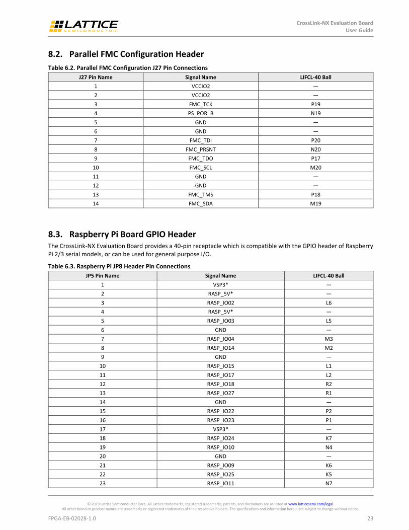
8.2. Parallel FMC Configuration Header
Table 6.2. Parallel FMC Configuration J27 Pin Connections
J27 Pin Name Signal Name LIFCL-40 Ball
1 VCCIO2 —
2 VCCIO2 —
3 FMC_TCK P19
4 PS_POR_B N19
5 GND —
6 GND —
7 FMC_TDI P20
8 FMC_PRSNT N20
9 FMC_TDO P17
10 FMC_SCL M20
11 GND —
12 GND —
13 FMC_TMS P18
14 FMC_SDA M19
8.3. Raspberry Pi Board GPIO Header The CrossLink-NX Evaluation Board provides a 40-pin receptacle which is compatible with the GPIO header of Raspberry Pi 2/3 serial models, or can be used for general purpose I/O.
Table 6.3. Raspberry Pi JP8 Header Pin Connections
JP5 Pin Name Signal Name LIFCL-40 Ball
1 VSP3* —
2 RASP_5V* —
3 RASP_IO02 L6
4 RASP_5V* —
5 RASP_IO03 L5
6 GND —
7 RASP_IO04 M3
8 RASP_IO14 M2
9 GND —
10 RASP_IO15 L1
11 RASP_IO17 L2
12 RASP_IO18 R2
13 RASP_IO27 R1
14 GND —
15 RASP_IO22 P2
16 RASP_IO23 P1
17 VSP3* —
18 RASP_IO24 K7
19 RASP_IO10 N4
20 GND —
21 RASP_IO09 K6
22 RASP_IO25 K5
23 RASP_IO11 N7

CrossLink-NX Evaluation Board User Guide
© 2019 Lattice Semiconductor Corp. All Lattice trademarks, registered trademarks, patents, and disclaimers are as listed at www.latticesemi.com/legal. All other brand or product names are trademarks or registered trademarks of their respective holders. The specifications and information herein are subject to change without notice.
24 FPGA-EB-02028-1.0
JP5 Pin Name Signal Name LIFCL-40 Ball
24 RASP_IO08 P6
25 GND —
26 RASP_IO07 N5
27 RASP_ID_SD M7
28 RASP_ID_SC M4
29 RASP_IO05 K8
30 GND —
31 RASP_IO06 L7
32 RASP_IO12 L8
33 RASP_IO13 M5
34 GND —
35 RASP_IO19 M6
36 RASP_IO16 N6
37 RASP_IO26 P5
38 RASP_IO20 R3
39 GND —
40 RASP_IO21 R4
*Note: 3.3 V and 5 V provide the power to the Raspberry Pi board when JP3 and JP4 are installed. When JP3 and JP4 are not installed, Raspberry Pi needs its own 3.3 V and 5 V power.
When connecting directly to a Raspberry Pi board, depending on the individual setup, there may need to be an adapter to avoid mechanical interference between the two boards. A generic 40-pin (2×20), 100-mil spacing header extender serves this function. Alternately, the two boards can be connected by a length of ribbon cable with 2×20 connectors on either end.
8.4. Camera Connector
Table 6.4. Camera CN1 Connector Pin Connections
CN1 Pin Name Signal Name LIFCL-40 Ball
1 NO Connect —
2 CAM0_CLKN B1
3 CAM0_CLKP A2
4 GND —
5 CAM0_3N B4
6 CAM0_3P A4
7 GND —
8 CAM0_1N B3
9 CAM0_1P A3
10 GND —
11 CAM0_0N C1
12 CAM0_0P B2
13 GND —
14 CAM0_2N D1
15 CAM0_2P C2
16 GND —
17 GND —
18 V2P8 —
19 NO Connect —
20 CAM0_MCLK —

CrossLink-NX Evaluation Board User Guide
© 2019 Lattice Semiconductor Corp. All Lattice trademarks, registered trademarks, patents, and disclaimers are as listed at www.latticesemi.com/legal. All other brand or product names are trademarks or registered trademarks of their respective holders. The specifications and information herein are subject to change without notice.
FPGA-EB-02028-1.0 25
CN1 Pin Name Signal Name LIFCL-40 Ball
21 NO Connect —
22 CAM_SDA W5
23 CAM_SCL Y5
24 CAM_RESET W18
25 V1P2 —
26 V1P8 —
27 GND —
28 GND —
29 V2P8 —
30 GND —
8.5. D-PHY1 Header
Table 6.5. D-PHY1 J6 Header Pin Connections
J6 Pin Name Signal Name LIFCL-40 Ball
1 GND —
2 GND —
3 DPHY1_CKP A8
4 DPHY1_CKN B8
5 GND —
6 GND —
7 DPHY1_DP0 A7
8 DPHY1_DN0 B7
9 GND —
10 GND —
11 DPHY1_DP1 A9
12 DPHY1_DN1 B9
13 GND —
14 GND —
15 DPHY1_DP2 A6
16 DPHY1_DN2 B6
17 GND —
18 GND —
19 DPHY1_DP3 A10
20 DPHY1_DN3 B10

CrossLink-NX Evaluation Board User Guide
© 2019 Lattice Semiconductor Corp. All Lattice trademarks, registered trademarks, patents, and disclaimers are as listed at www.latticesemi.com/legal. All other brand or product names are trademarks or registered trademarks of their respective holders. The specifications and information herein are subject to change without notice.
26 FPGA-EB-02028-1.0
8.6. PMOD Header The J17, J18 and J19 header can be used as GPIO or as a connector to a PMOD interface.
Table 6.6. J17, J18 and J19 Header Pin Connections
Pin Name Signal Name LIFCL-40 Ball
J17 Pin Name
1 PMOD0_1 D10
2 PMOD0_2 D9
3 PMOD0_3 D7
4 PMOD0_4 D8
5 PMOD0_7 D6
6 PMOD0_8 D5
7 PMOD0_9 D4
8 PMOD0_10 D3
J18 Pin Name
1 PMOD1_1 E10
2 PMOD1_2 E9
3 PMOD1_3 E7
4 PMOD1_4 E8
5 PMOD1_7 E4
6 PMOD1_8 E3
7 PMOD1_9 E2
8 PMOD1_10 F1
J19 Pin Name
1 PMOD2_1 J2
2 PMOD2_2 J1
3 PMOD2_3 K2
4 PMOD2_4 K1
5 PMOD2_7 K3
6 PMOD2_8 K4
7 PMOD2_9 D17
8 PMOD2_10 E18
8.7. JTAG Header The J1 header is used to access the JTAG port of the CrossLink-NX or the Raspberry Pi interface.
Table 6.7. J1 Header Pin Connections
J1 Pin Name Signal Name LIFCL-40 Ball
1 VCCIO1 —
2 TDO F19
3 TDI F17
4 No Connect —
5 No Connect —
6 TMS F15
7 GND —
8 TCK E19

CrossLink-NX Evaluation Board User Guide
© 2019 Lattice Semiconductor Corp. All Lattice trademarks, registered trademarks, patents, and disclaimers are as listed at www.latticesemi.com/legal. All other brand or product names are trademarks or registered trademarks of their respective holders. The specifications and information herein are subject to change without notice.
FPGA-EB-02028-1.0 27
8.8. Parallel Configuration Header The J27 header is used to access the SPI port of the CrossLink-NX.
Table 6.8. J27 Header Pin Connections
J27Pin Name Signal Name LIFCL-40 Ball
1 VCCIO2 —
2 VCCIO2 —
3 FMC_TCK P19
4 PS_POR_B N19
5 GND —
6 GND —
7 FMC_TDI P20
8 FMC_PRSNT N20
9 FMC_TDO P17
10 FMC_SCL M20
11 GND —
12 GND —
13 FMC_TMS P18
14 FMC_SDA M19
8.9. ADC Test Header
Table 6.9. J26 Header Pin Connections
J26 Pin Name Signal Name LIFCL-40 Ball
1 GND —
2 GND —
3 J24 PIN3 —
4 GND —
5 J25 PIN3 —
6 GND —
7 GND —
8 GND —
9 ADC_IN1P T17
10 GND —
11 ADC_IN1N U17
12 GND —
13 GND —
14 GND —
15 VREF2_CON —
16 GND —
17 GND —
18 GND —
19 VREF1_CON —
20 GND —

CrossLink-NX Evaluation Board User Guide
© 2019 Lattice Semiconductor Corp. All Lattice trademarks, registered trademarks, patents, and disclaimers are as listed at www.latticesemi.com/legal. All other brand or product names are trademarks or registered trademarks of their respective holders. The specifications and information herein are subject to change without notice.
28 FPGA-EB-02028-1.0
9. Software Requirements The following software versions are required to develop designs for the CrossLink-NX Evaluation Board:
Lattice Radiant Software 2.0 or later
Lattice Radiant Programmer 2.0 or later
10. Storage and Handling Static electricity can shorten the life span of electronic components. Observe these tips to prevent damage that can occur from electrostatic discharge:
Use antistatic precautions such as operating on an antistatic mat and wearing an antistatic wristband.
Store the development board in the provided packaging.
Touch a metal USB housing to equalize voltage potential between you and the board.
11. Ordering Information Table 11.1. Ordering Information
Description Ordering Part Number China RoHS Environment-Friendly Use Period (EFUP)
CrossLink-NX Evaluation Board LIFCL-40-EVN
CrossLink-NX Evaluation Board User Guide
© 2019 Lattice Semiconductor Corp. All Lattice trademarks, registered trademarks, patents, and disclaimers are as listed at www.latticesemi.com/legal. All other brand or product names are trademarks or registered trademarks of their respective holders. The specifications and information herein are subject to change without notice.
FPGA-EB-02028-1.0 29
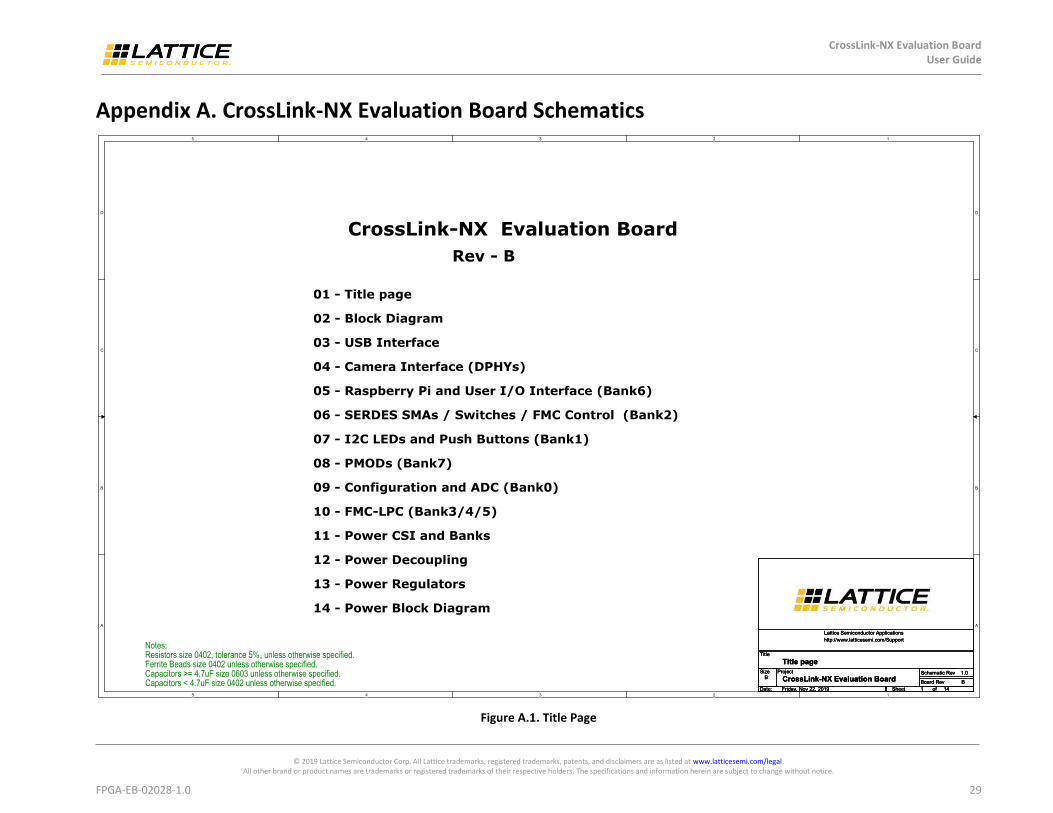
Appendix A. CrossLink-NX Evaluation Board Schematics
Figure A.1. Title Page
5
5
4
4
3
3
2
2
1
1
D D
C C
B B
A A
CrossLink-NX Evaluation BoardRev - B
01 - Title page
02 - Block Diagram
03 - USB Interface
04 - Camera Interface (DPHYs)
05 - Raspberry Pi and User I/O Interface (Bank6)
06 - SERDES SMAs / Switches / FMC Control (Bank2)
07 - I2C LEDs and Push Buttons (Bank1)
08 - PMODs (Bank7)
09 - Configuration and ADC (Bank0)
10 - FMC-LPC (Bank3/4/5)
11 - Power CSI and Banks
12 - Power Decoupling
13 - Power Regulators
14 - Power Block Diagram
Notes:Resistors size 0402, tolerance 5%, unless otherwise specified.Ferrite Beads size 0402 unless otherwise specified.Capacitors >= 4.7uF size 0603 unless otherwise specified.Capacitors < 4.7uF size 0402 unless otherwise specified.
Date:
Size Schematic Rev
ofSheet
Title
Lattice Semiconductor Applications http://www.latticesemi.com/Support
Board Rev
Project
Friday, Nov 22, 2019
B1.0
141
Title page
CrossLink-NX Evaluation Board BDate:
Size Schematic Rev
ofSheet
Title
Lattice Semiconductor Applications http://www.latticesemi.com/Support
Board Rev
Project
Friday, Nov 22, 2019
B1.0
141
Title page
CrossLink-NX Evaluation Board BDate:
Size Schematic Rev
ofSheet
Title
Lattice Semiconductor Applications http://www.latticesemi.com/Support
Board Rev
Project
Friday, Nov 22, 2019
B1.0
141
Title page
CrossLink-NX Evaluation Board B
CrossLink-NX Evaluation Board User Guide
© 2019 Lattice Semiconductor Corp. All Lattice trademarks, registered trademarks, patents, and disclaimers are as listed at www.latticesemi.com/legal. All other brand or product names are trademarks or registered trademarks of their respective holders. The specifications and information herein are subject to change without notice.
30 FPGA-EB-02028-1.0
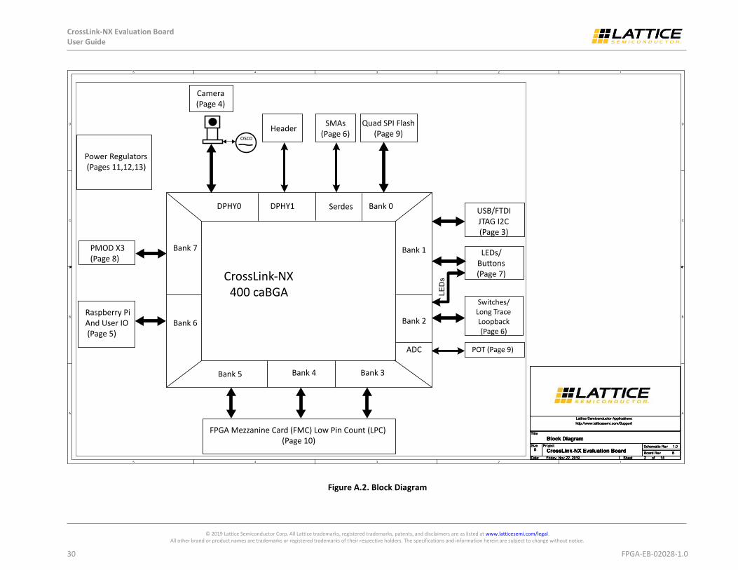
Figure A.2. Block Diagram
5
5
4
4
3
3
2
2
1
1
D D
C C
B B
A A
Date:
Size Schematic Rev
ofSheet
Title
Lattice Semiconductor Applications http://www.latticesemi.com/Support
Board Rev
Project
Friday, Nov 22, 2019
B1.0
142
Block Diagram
CrossLink-NX Evaluation Board BDate:
Size Schematic Rev
ofSheet
Title
Lattice Semiconductor Applications http://www.latticesemi.com/Support
Board Rev
Project
Friday, Nov 22, 2019
B1.0
142
Block Diagram
CrossLink-NX Evaluation Board BDate:
Size Schematic Rev
ofSheet
Title
Lattice Semiconductor Applications http://www.latticesemi.com/Support
Board Rev
Project
Friday, Nov 22, 2019
B1.0
142
Block Diagram
CrossLink-NX Evaluation Board B
DPHY1 Bank 0
Bank 1
Bank 2
Bank 3Bank 4Bank 5
Bank 7
Bank 6
CrossLink-NX400 caBGA
OSC0
Quad SPI Flash (Page 9)
LEDs/Buons (Page 7)
USB/FTDI JTAG I2C (Page 3)
Switches/Long Trace Loopback (Page 6)
FPGA Mezzanine Card (FMC) Low Pin Count (LPC) (Page 10)
PMOD X3 (Page 8)
Raspberry PiAnd User IO (Page 5)
DPHY0 Serdes
ADC
SMAs (Page 6)
Camera (Page 4)
POT (Page 9)
Power Regulators (Pages 11,12,13)
Header
LED
s

CrossLink-NX Evaluation Board User Guide
© 2019 Lattice Semiconductor Corp. All Lattice trademarks, registered trademarks, patents, and disclaimers are as listed at www.latticesemi.com/legal. All other brand or product names are trademarks or registered trademarks of their respective holders. The specifications and information herein are subject to change without notice.
FPGA-EB-02028-1.0 31
Figure A.3. USB Interface
5
5
4
4
3
3
2
2
1
1
D D
C C
B B
A A
Route USB pair 90 ohm impedance
JP1 Reset FTDIDefault Open
FT_VPLL
FT_VPHY
DMDP
FT_RSTb
FT_REF
FT_EECSFT_EECLK
FT_EEDATA
FT_OSCI
FT_OSCO
ADBUS3
ADBUS1ADBUS2SHLD
VBUS
DP
DM DM
DP
FT_RSTb
UART_ACT
ADBUS0
V3P3
V3P3
VCC1_8FT V3P3
VCC1_8FTV3P3
V3P3
V3P3
VCCIO1
VCCIO1
VBUS_5V
VBUS_5V
V3P3
VCCIO1
VCCIO0
12MHz7
TCK 5,7TDI 5,7TDO 5,7TMS 5,7
RXD_UART 7TXD_UART 7
SCL 5,7
SDA 5,7
PROGRAMN 9
Date:
Size Schematic Rev
ofSheet
Title
Lattice Semiconductor Applications http://www.latticesemi.com/Support
Board Rev
Project
Friday, Nov 22, 2019
B1.0
143
USB Interface
CrossLink-NX Evaluation Board BDate:
Size Schematic Rev
ofSheet
Title
Lattice Semiconductor Applications http://www.latticesemi.com/Support
Board Rev
Project
Friday, Nov 22, 2019
B1.0
143
USB Interface
CrossLink-NX Evaluation Board BDate:
Size Schematic Rev
ofSheet
Title
Lattice Semiconductor Applications http://www.latticesemi.com/Support
Board Rev
Project
Friday, Nov 22, 2019
B1.0
143
USB Interface
CrossLink-NX Evaluation Board B
R10
10K
R2
4.7KL3
600ohm 500mA12
C12
0.1uF
R172
10K
R220
R3
4.7K
TP2 1
C1
0.1uFC510uF
R1
4.7K
R533
TP1 1
R70
93LC56C-I/SN
U2
CS1
CLK2
DI3
DO4
VSS5 ORG6 NU7 VCC8
C4
0.1uF
J2USB_MINI_B
Part Number = 1734035-2
VCC1
D-2
D+3
GND5NC4
CASE7
CASE8
CASE9
CASE6
X1
7M-12.000MAAJ
11
33
G12
G24
C13
0.1uF
R9 2.2K
R80
C64.7uF
R184.7K
D2
ESDR0502N-UDFN6
GND1
NC22
NC33
D-4
VBUS6
D+5
R42.2K
R12
10K
C8
0.1uF
G
D1
LED
_GR
EE
N_0
603
C1718pF
R60
C15
0.1uF
L1
600ohm 500mA12
R150 DNI
FTDI High-Speed USB
FT2232H
FT2232HL
U1
VREGIN50
VREGOUT49
DM7
DP8
REF6
RESET#14
EECS63
EECLK62
EEDATA61
OSCI2
OSCO3
TEST13
ADBUS016
ADBUS117
ADBUS218
ADBUS319
VP
HY
4
VP
LL9
VC
OR
E12
VC
OR
E37
VC
OR
E64
VC
CIO
20
VC
CIO
31
VC
CIO
42
VC
CIO
56
AG
ND
10
GN
D1
GN
D5
GN
D11
GN
D15
GN
D25
GN
D35
GN
D47
GN
D51
PWREN#60
SUSPEND#36
ADBUS421
ADBUS522
ADBUS623
ADBUS724
ACBUS026
ACBUS127
ACBUS228
ACBUS329
ACBUS430
ACBUS532
ACBUS633
ACBUS734
BDBUS038
BDBUS139
BDBUS240
BDBUS341
BDBUS443
BDBUS544
BDBUS645
BDBUS746
BCBUS048
BCBUS152
BCBUS253
BCBUS354
BCBUS455
BCBUS557
BCBUS658
BCBUS759
C1410uF
L2
600ohm 500mA
12
R170 DNI
C1618pF
C2
0.1uF
R11
10K R14
2K
C7
0.1uF
R1731.0 KDNI
R194.7K
C104.7uF
JP2 JUMPER
12
R200
C11
0.1uF
R1612K
J1
Header 1x8DNI
11
22
33
44
55
66
77
88
C9
0.1uF
R210
R13 12K
JP1JUMPER
12
C3
0.1uF

CrossLink-NX Evaluation Board User Guide
© 2019 Lattice Semiconductor Corp. All Lattice trademarks, registered trademarks, patents, and disclaimers are as listed at www.latticesemi.com/legal. All other brand or product names are trademarks or registered trademarks of their respective holders. The specifications and information herein are subject to change without notice.
32 FPGA-EB-02028-1.0
Figure A.4. Camera Interface (DPHYs)
5
5
4
4
3
3
2
2
1
1
D D
C C
B B
A A
DNI
LVDS RX Termination Resistors
NOTE: Place close to FPGA
NOTE: 1. Match length within pair <= 0.1mm, match length between pairs <=1.0mm.2. Differential impedance should be 100 ohms and 50 ohms as a single ended signal3. All the power rails should be capable of carrying 1A current
OSCILLATOR
Keep LEDs away from Camera
CAM0_3PCAM0_3N
CAM0_CLKNCAM0_CLKP
CAM0_0PCAM0_0N
CAM0_1PCAM0_1N
CAM0_2PCAM0_2N
CAM_SCL
CAM0_0NCAM0_0P
CAM0_3PCAM0_3N
CAM0_1PCAM0_1N
CAM0_2NCAM0_2P
CAM0_CLKPCAM0_CLKN
CAM_SDA
CAM0_CLKN
CAM0_CLKP
CAM0_0N
CAM0_0P
CAM0_1N
CAM0_1P
CAM0_2N
CAM0_2P
CAM0_3N
CAM0_3P
CAM0_MCLK
DPHY1_CKPDPHY1_CKNDPHY1_DP0DPHY1_DN0DPHY1_DP1DPHY1_DN1DPHY1_DP2DPHY1_DN2DPHY1_DP3DPHY1_DN3
DPHY1_CKP
DPHY1_DP0
DPHY1_DP1
DPHY1_DP2
DPHY1_DP3
DPHY1_CKN
DPHY1_DN0
DPHY1_DN1
DPHY1_DN2
DPHY1_DN3
V1P8_LDO
V1P0_LDO
V2P8
V1P8V1P2
VCCIO5
V2P8 V1P2 V1P8V1P8
V1P8_LDO
V1P0_LDO
V1P0_LDO
CAM_RESET 10
CAM_SDA 10
CAM_SCL 10
Date:
Size Schematic Rev
ofSheet
Title
Lattice Semiconductor Applications http://www.latticesemi.com/Support
Board Rev
Project
Friday, Nov 22, 2019
B1.0
144
Camera Interface (DPHYs)
CrossLink-NX Evaluation Board BDate:
Size Schematic Rev
ofSheet
Title
Lattice Semiconductor Applications http://www.latticesemi.com/Support
Board Rev
Project
Friday, Nov 22, 2019
B1.0
144
Camera Interface (DPHYs)
CrossLink-NX Evaluation Board BDate:
Size Schematic Rev
ofSheet
Title
Lattice Semiconductor Applications http://www.latticesemi.com/Support
Board Rev
Project
Friday, Nov 22, 2019
B1.0
144
Camera Interface (DPHYs)
CrossLink-NX Evaluation Board B
C23
1uF
ASE3-27.000MHz-K-T
X2
GND2
VDD4
STDBY#1
OUT3
R2422
C35
0.1uF
C30
10uF
LIFCL-40-BG400
U3I
VCCADPHY0D2
VCCDPHY0C4
VCCPLLDPHY0B5
DPHY0_DP3A4
DPHY0_DN3B4
DPHY0_DP1A3
DPHY0_DN1B3
DPHY0_CKPA2
DPHY0_CKNB1
DPHY0_DP0B2
DPHY0_DN0C1
DPHY0_DP2C2
DPHY0_DN2D1
L7220ohm 500mA
1 2
R30100 ohmDNI
J3
Header_2x1
11
22
R23 100k
C34
10uF
J5
Header_2x1
11
22
R31100 ohmDNI
C19
0.1uF
C29
0.1uF
R33
0.1
06031%
R29100 ohmDNI
C22
10uF
C32
10uF
L4220ohm 500mA
1 2
camconn_imx258_1x30
CN1 NC11
CLK_N2
CLK_P3
DGND14
DATA3_N5
DATA3_P6
DGND27
DATA1_N8
DATA1_P9
DGND310
DATA0_N11
DATA0_P12
DGND413
DATA2_N14
DATA2_P15
DGND516
DGND617
AF_VDD2V818
NC219
MCLK20
SYNC21
SDA22
SCL23
XCLR24
DVDD1V225
DVDD1V826
DGND727
DGND828
AVDD2V829
DGND930
Header_2x10
J6
11
33
55
77
99
1111
1313
1515
1717
1919
22
44
66
88
1010
1212
1414
1616
1818
2020
C27
0.1uF
L8220ohm 500mA
1 2
C25
0.1uF
R28100 ohmDNI
C24
0.1uF
R34
0.1
06031%
R32
0.1
06031%
C33
0.1uF
L9220ohm 500mA
1 2
C28
10uF
C31
0.1uF
R27100 ohm
R25
4.7k
C26
10uF
C36
10uF
C21
1uF
C200.1uF
C18
0.1uF
L5220ohm 500mA
1 2
LIFCL-40-BG400
U3J
VCCADPHY1C7
VCCDPHY1C5
VCCPLLDPHY1C9
DPHY1_DP3A10
DPHY1_DN3B10
DPHY1_DP1A9
DPHY1_DN1B9
DPHY1_CKPA8
DPHY1_CKNB8
DPHY1_DP0A7
DPHY1_DN0B7
DPHY1_DP2A6
DPHY1_DN2B6
L6220ohm 500mA
1 2
R26
4.7k
J4
Header_2x1
11
22
CrossLink-NX Evaluation Board User Guide
© 2019 Lattice Semiconductor Corp. All Lattice trademarks, registered trademarks, patents, and disclaimers are as listed at www.latticesemi.com/legal. All other brand or product names are trademarks or registered trademarks of their respective holders. The specifications and information herein are subject to change without notice.
FPGA-EB-02028-1.0 33
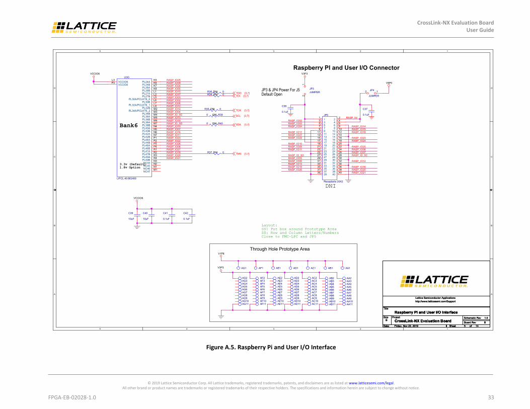
Figure A.5. Raspberry Pi and User I/O Interface
5
5
4
4
3
3
2
2
1
1
D D
C C
B B
A A
Raspberry PI and User I/O Connector
Bank6
3.3v (Default)1.8v Option
Through Hole Prototype Area
Layout: SS: Put box around Prototype AreaSS: Row and Column Letters/NumbersClose to FMC-LPC and JP5
JP3 & JP4 Power For J5Default Open
DNI
RASP_5V
RASP_IO22
RASP_IO26
RASP_IO27
RASP_ID_SC
RASP_IO09RASP_IO10
RASP_IO25
RASP_IO23RASP_IO24
RASP_IO11RASP_IO07RASP_IO08
RASP_IO13
RASP_IO05RASP_IO06
RASP_IO04
RASP_IO12
RASP_IO03
RASP_IO21RASP_IO20RASP_IO16RASP_IO19
RASP_ID_SD
RASP_IO18RASP_IO17
RASP_IO02
RASP_IO14RASP_IO15
RASP_IO25RASP_IO09RASP_IO24RASP_IO05RASP_IO15RASP_IO17RASP_IO03RASP_IO02RASP_IO06RASP_IO12RASP_IO14RASP_IO04
RASP_IO19
RASP_IO07RASP_IO16RASP_IO11RASP_IO23RASP_IO22RASP_IO26RASP_IO08RASP_IO27RASP_IO18
RASP_ID_SCRASP_IO13
RASP_ID_SDRASP_IO10
RASP_IO20RASP_IO21
V5P0
V3P3
VCCIO6
VCCIO6
V3P3
V1P8
TMS 3,7
SCL 3,7
SDA 3,7
TCK 3,7
TDO 3,7TDI 3,7
Date:
Size Schematic Rev
ofSheet
Title
Lattice Semiconductor Applications http://www.latticesemi.com/Support
Board Rev
Project
Friday, Nov 22, 2019
B1.0
145
Raspberry Pi and User I/O Interface
CrossLink-NX Evaluation Board BDate:
Size Schematic Rev
ofSheet
Title
Lattice Semiconductor Applications http://www.latticesemi.com/Support
Board Rev
Project
Friday, Nov 22, 2019
B1.0
145
Raspberry Pi and User I/O Interface
CrossLink-NX Evaluation Board BDate:
Size Schematic Rev
ofSheet
Title
Lattice Semiconductor Applications http://www.latticesemi.com/Support
Board Rev
Project
Friday, Nov 22, 2019
B1.0
145
Raspberry Pi and User I/O Interface
CrossLink-NX Evaluation Board B
AB6
AC9
AE5
AE10
AB5
AC1
AD5
JP5
Receptacle 20X2
11
22
33
44
55
66
77
88
99
1010
1111
1313
1515
1717
1919
2121
2323
2525
2727
2929
3131
3333
3535
3737
3939
1212
1414
1616
1818
2020
2222
2424
2626
2828
3030
3232
3434
3636
3838
4040
AE4
C38
0.1uF
AF10AB9
AB1
AD4AG4
C42
0.1uF
JP3JUMPER
12
AA4
AB8
AD1
AD3
AF5
AA3
C40
10uF
JP4
JUMPER
12
AB7
AG1
LIFCL-40-BG400
U3G
VCCIO6L3
VCCIO6P3 PL24A
K5
PL24BK6
PL26AK7
PL26BK8
PL27AL1
PL27BL2
PL30A/PCLKT6_0L5
PL30BL6
PL32A/PCLKT6_1L7
PL32BL8
PL34A/PCLKT6_2M2
PL34BM3
PL36AM4
PL36BM5
PL38AM6
PL38BM7
PL40AN4
PL40BN5
PL42AN6
PL42BN7
PL44AP1
PL44BP2
PL46AP5
PL46BP6
PL47AR1
PL47BR2
PL49AR3
PL49BR4
NC44N3
NC45N2
NC46N1
NC47M1
AD7
R400 DNI
AG5
AA7
AB11
AE1
AD6AE7
AA6
R36 0DNI
AB10AD10
AE6AA5
AF1
AC6
AD9
AG6
R37 0DNI
AA9
AC3
AD8AF8
AA11
C39
10uF
AC2AF2
AF7AA8
R390 DNI
AC7
AG2
AE8AG8
AC5
AD11
AG7
AA10
AC4
R38 0DNI
AE2
AF6
AE11
AC8
AG3
AF9
AB2
AG9
AC11
C41
0.1uF
AF4
AA2
C37
0.1uF
AG11
AB4
R35 0DNI
AD2AF3
AE9
AA1
AB3
AG10 AC10
AE3
AF11

CrossLink-NX Evaluation Board User Guide
© 2019 Lattice Semiconductor Corp. All Lattice trademarks, registered trademarks, patents, and disclaimers are as listed at www.latticesemi.com/legal. All other brand or product names are trademarks or registered trademarks of their respective holders. The specifications and information herein are subject to change without notice.
34 FPGA-EB-02028-1.0
Figure A.6. SERDES SMAs/Switches/FMC Control
5
5
4
4
3
3
2
2
1
1
D D
C C
B B
A A
Serdes Bank
DIP SWITCH
Switch Signal Map
1
8
432
765
M14N14
N15M15M16
M18M17N16
SWITCHU3C Pin Signal
SWITCH1SWITCH0
SWITCH7
SWITCH4SWITCH3SWITCH2
SWITCH6SWITCH5
3.3v
Bank2
PLL filter with DCR<=0.1 ohmDC must be <<5% drop acrossanti-resonance resistor under worst case
R_ext is chosen for 100 ohm Diff
Place PLL series resistor, two caps and r_ext right underneath the chip on the reverse side of the board
Two 50 ohm Lookbacks Traces: 6 inches and 10 inchesPlace TPs close to FPGA
Minimize length as short as possible short_stub_trace. TP close to FPGA
Route SMA pairs as 100 ohm differential
1-2 = 125 Mhz (Default)2-3 = 200 Mhz
Use little to no stubbetween selectionresistors
DNI
SWITCH3SWITCH2SWITCH1SWITCH0
SWITCH5SWITCH6
SWITCH4
SWITCH7
SWITCH7SWITCH6
SWITCH3
SWITCH0
SWITCH2
SWITCH4SWITCH5
R_extRXDPFRXDNFRef_return_pll
REFCLKPREFCLKN
RXDP_SMA
RXDN_SMA
TXDP_SMA
TXDN_SMA
R_ext
Ref_return_pll
10_inch_long_trace
short_stub_trace
LED8LED9
LED10LED11LED12LED13
REFCLKN_SMA
REFCLKP_SMA
Ref_return_pll
SWITCH1
TXDPFTXDNF
6_inch_long_trace
RXDPRXDPF RXDP_SMA
RXDNRXDNF RXDN_SMA
TXDPTXDPF TXDP_SMA
TXDNTXDNF TXDN_SMA
OSCP
OSCN
125MHz
125MHz_N
200MHz
200MHz_N
REFCLKP REFCLKP_SMA
REFCLKN REFCLKN_SMA
OSCP
OSCN
V3P3
VCCIO2
VCCIO2
V1P0_LDO
V1P8_LDO
VCCIO2
V1P8_LDO
V3P3
FMC_SDA 10FMC_SCL 10PS_POR_B 10FMC_PRSNT 10
FMC_TMS 10FMC_TDO 10FMC_TDI 10FMC_TCK 10
LED8 7LED9 7LED10 7LED11 7LED12 7LED13 7
REFCLKP_FMC 10
REFCLKN_FMC 10
TXDP_FMC 10
TXDN_FMC 10
RXDP_FMC 10
RXDN_FMC 10
Date:
Size Schematic Rev
ofSheet
Title
Lattice Semiconductor Applications http://www.latticesemi.com/Support
Board Rev
Project
Friday, Nov 22, 2019
B1.0
146
Serdes SMAs/Switches/FMC Control
CrossLink-NX Evaluation Board BDate:
Size Schematic Rev
ofSheet
Title
Lattice Semiconductor Applications http://www.latticesemi.com/Support
Board Rev
Project
Friday, Nov 22, 2019
B1.0
146
Serdes SMAs/Switches/FMC Control
CrossLink-NX Evaluation Board BDate:
Size Schematic Rev
ofSheet
Title
Lattice Semiconductor Applications http://www.latticesemi.com/Support
Board Rev
Project
Friday, Nov 22, 2019
B1.0
146
Serdes SMAs/Switches/FMC Control
CrossLink-NX Evaluation Board B
C600.1uF
J15
SMA
DNI
12345
R54 0
U4 AK5DAF1-125.0000T2
OE1
NC2
GN
D3
OP4
ON5
VC
C6
J12
SMA
DNI
12345
LIFCL-40-BG400
U3L
VCCPLLSD0C13
SD0_REXTC14
SD0_RXDPA16
SD0_RXDNA15
SD0_REFRETB14
SD0_TXDPA13
SD0_TXDNA12
SD0_REFCLKPC12
SD0_REFCLKNC11
VCCSD0_1B15
VCCSD0_2B13
VCCAUXSDB11
L10
600ohm 500mA12
RN1AEXB2HV472JV
4_7K1 16R63 0
R52 0DNI
LIFCL-40-BG400
U3C
VCCIO2U19
VCCIO2N17
PR49AW19
PR49BY19
PR47AV18
PR47BV19
PR46AT18
PR46BU18
PR44AW20
PR44BV20
PR42AU20
PR42BT20
PR40AR17
PR40BR18
PR38AP17
PR38BP18
PR36AP19
PR36BP20
PR34A/PCLKT2_2N19
PR34BN20
PR32A/PCLKT2_1M19
PR32BM20
PR30A/PCLKT2_0M17
PR30BM18
PR27AN15
PR27BN16
PR26AM16
PR26BM15
PR24AN14
PR24BM14
NC26R20NC27R19
NC28P16NC29P15
SW1
SMD SW DIP-8
Part Number = 219-8MST
R6210K
C48
1U
F-1
6V-0
805
SM
T
R64 0DNI
FB3
MPZ1005S121CT000
TP3
1
J16
SMA
DNI
12345
U5 AK5DAF1-200.0000T2
OE1
NC2
GN
D3
OP4
ON5
VC
C6
C470.1uF
R46 0
FB2
MPZ1005S121CT000
J9
Header_2x1
11
22
R66 0 DNI
C440.1uF
R51 0DNI
R42
0.1
06031%
TP_V1P8_VCCPLLSD
1
R44
0.1
06031%
R55 0
RN1HEXB2HV472JV
4_7K8 9
C490.1uF
R53
0.1
06031%
C4310uF
R56 0
RN1GEXB2HV472JV
4_7K7 10
J8
Header_2x1
11
22
TP_V1P8_VCCAUXSD
1
J13
CON3
123
J11
SMA
DNI
12345
R57 0DNI
R41 100 ohmDNI
R451.15K
TP_V1P0_VCCSD
1
RN1FEXB2HV472JV
4_7K6 11
J7
Header_2x1
11
22
R47 0DNI
RN1EEXB2HV472JV
4_7K5 12
C46
0.1uF
C53
0.1uF
J10
SMA
DNI
12345
TP4
1
C56
1UF
-16V
-0805
SM
T
RN1DEXB2HV472JV
4_7K4 13
C520.1uF
C45
10uF
R58 0
C54
0.1uF
R49 0
TP5
1
R59 0DNI
R48 0DNI
RN1CEXB2HV472JV
4_7K3 14
C58
10uF
R5010K
R65 0 DNI
R60 0
R43 100 ohmDNI
L11
600ohm 500mA12
J14
SMA
DNI
12345
C590.1uF
C570.1uF
FB1
MPZ1005S121CT000
C50
0.1uF
RN1BEXB2HV472JV
4_7K2 15
R61 0DNI
C5110uF
C55
0.1uF

CrossLink-NX Evaluation Board User Guide
© 2019 Lattice Semiconductor Corp. All Lattice trademarks, registered trademarks, patents, and disclaimers are as listed at www.latticesemi.com/legal. All other brand or product names are trademarks or registered trademarks of their respective holders. The specifications and information herein are subject to change without notice.
FPGA-EB-02028-1.0 35
Figure A.7. I2C LEDs and Push Buttons
5
5
4
4
3
3
2
2
1
1
D D
C C
B B
A A
Bank1
3.3v
D3
D4
D5
D6
D7
D8
D9
D10
LEDs Signal Map
LED0
LED1
LED2
LED3
LED4
LED5
LED6
LED7
E17
F13
G13
F14
L16
L15
L20
L19
U3B pin Signal LED
GSRN
Group LEDs 4,4,4,212bit ADC shown groups of 4 + 1 led for PWM brightness+ 1 led for other use
LEDs
D11
D12
D13
LED8
LED9
LED10
R17
R18
U20
D14
D15
D16
LED11
LED12
LED13
T20
W20
V20
U3C pin Signal LED
PUSHBUTTON0PUSHBUTTON1
GSRN
LED8
LED9
LED10
LED11
LED12
LED13
LED3
LED5LED4
LED6LED7
GSRN
LED0LED1LED2
PUSHBUTTON0PUSHBUTTON1
VCCIO1
VCCIO1
VCCIO1
VCCIO1VCCIO1 VCCIO1
VCCIO2
VCCIO2
VCCIO1
TDI 3,5TMS 3,5TCK 3,5
TDO 3,5
LED86
LED96
LED106
LED116
LED126
LED136
12MHz 3
SDA 3,5SCL 3,5
TXD_UART 3RXD_UART 3
Date:
Size Schematic Rev
ofSheet
Title
Lattice Semiconductor Applications http://www.latticesemi.com/Support
Board Rev
Project
Friday, Nov 22, 2019
B1.0
147
I2C LEDs And Push Buttons
CrossLink-NX Evaluation Board BDate:
Size Schematic Rev
ofSheet
Title
Lattice Semiconductor Applications http://www.latticesemi.com/Support
Board Rev
Project
Friday, Nov 22, 2019
B1.0
147
I2C LEDs And Push Buttons
CrossLink-NX Evaluation Board BDate:
Size Schematic Rev
ofSheet
Title
Lattice Semiconductor Applications http://www.latticesemi.com/Support
Board Rev
Project
Friday, Nov 22, 2019
B1.0
147
I2C LEDs And Push Buttons
CrossLink-NX Evaluation Board B
R751k
C64
10uF
R180 2K R0402
R70 100
TP9
C66
0.1uF
GD16LED_YELLOW_0603
GD7LED_GREEN_0603
R69
10k
GD12LED_GREEN_0603
GD6LED_GREEN_0603
C65
0.1uF
R175 2K R0402
GD15LED_YELLOW_0603
TP6
C6310nF
GD11LED_GREEN_0603
R184 2K R0402
R187 2K R0402
GD8LED_GREEN_0603
R177 2K R0402
SW4GSRN
1234
GD13LED_GREEN_0603
R174 2K R0402
GD10LED_GREEN_0603
TP7R72100
R179 2K R0402
R68
10k
R182 2K R0402
LIFCL-40-BG400
U3B
VCCIO1J18
VCCIO1G17
PR20A/PCLKT1_0L20
PR20BL19
PR19A/PCLKT1_1L16
PR19BL15
PR17A/PCLKT1_2L13
PR17BL14
PR15AG14
PR15BG15
PR13A/TCK/SCLK/PMU_EXT_CLKG18
PR13B/PMU_WAKEUPG19
PR11A/SDAE20
PR11B/SCLF20
PR10AF18
PR10B/TDO/SSOF19
PR8AF16
PR8B/TDI/SSIF17
PR6AF14
PR6B/TMS/SCSNF15
PR4AF13
PR4BG13
JTAG_EN/JTAGE19
PR3BE17
NC1G20NC2H13NC3H14NC4H15NC5J15
NC6J16
NC7J19
NC8J20
NC9K13
NC10J13
NC11K14
NC12J14
NC13H16
NC14K15
NC15K16
NC16H19NC17H20
NC18H17
NC19K17
NC20K18
NC21K19
NC22K20
NC23L18
NC24L17
NC25H18
R181 2K R0402
R185 2K R0402
SW3PB1
1234
GD3LED_GREEN_0603
R730
C6210nF
GD14LED_GREEN_0603
R176 2K R0402
GD4LED_GREEN_0603
R67
10k
R71 100
SW2PB0
1234
R178 2K R0402R740
GD9LED_GREEN_0603
R183 2K R0402
R186 2K R0402
C6110nF
TP8
GD5LED_GREEN_0603

CrossLink-NX Evaluation Board User Guide
© 2019 Lattice Semiconductor Corp. All Lattice trademarks, registered trademarks, patents, and disclaimers are as listed at www.latticesemi.com/legal. All other brand or product names are trademarks or registered trademarks of their respective holders. The specifications and information herein are subject to change without notice.
36 FPGA-EB-02028-1.0
Figure A.8. PMODs
5
5
4
4
3
3
2
2
1
1
D D
C C
B B
A A
3.3v
Bank7
J17, J18 and J19 All Right-Angle PMOD connectors
PMOD2 unavailable when Bank0 / Flash set to 1.8V
PMOD0_1
PMOD0_2
PMOD0_3
PMOD0_4
PMOD0_7
PMOD0_8
PMOD0_9
PMOD0_10
PMOD1_1
PMOD1_2
PMOD1_3
PMOD1_4
PMOD1_7
PMOD1_8
PMOD1_9
PMOD1_10
PMOD0_1PMOD0_2PMOD0_3PMOD0_4PMOD0_7PMOD0_8PMOD0_9PMOD0_10PMOD1_1PMOD1_2PMOD1_3PMOD1_4PMOD1_7PMOD1_8PMOD1_9PMOD1_10
PMOD2_1
PMOD2_2
PMOD2_3
PMOD2_4
PMOD2_7
PMOD2_8
PMOD2_1PMOD2_2PMOD2_3PMOD2_4PMOD2_7PMOD2_8
VCCIO7
VCCIO7VCCIO7VCCIO7
VCCIO7
PMOD2_9 9
PMOD2_10 9
Date:
Size Schematic Rev
ofSheet
Title
Lattice Semiconductor Applications http://www.latticesemi.com/Support
Board Rev
Project
Friday, Nov 22, 2019
B1.0
148
PMODs
CrossLink-NX Evaluation Board BDate:
Size Schematic Rev
ofSheet
Title
Lattice Semiconductor Applications http://www.latticesemi.com/Support
Board Rev
Project
Friday, Nov 22, 2019
B1.0
148
PMODs
CrossLink-NX Evaluation Board BDate:
Size Schematic Rev
ofSheet
Title
Lattice Semiconductor Applications http://www.latticesemi.com/Support
Board Rev
Project
Friday, Nov 22, 2019
B1.0
148
PMODs
CrossLink-NX Evaluation Board B
J19
PMOD 2x6
82
4
6
7
5
3
1
10
9
12
11
J18
PMOD 2x6
82
4
6
7
5
3
1
10
9
12
11
C68
10uF
C73
0.1uF
C71
0.1uF
C69
10uF
LIFCL-40-BG400
U3H
VCCIO7E5
VCCIO7H3PL3A/ULC_GPLL0T_IN
D10
PL3B/ULC_GPLL0C_IND9
PL4AD7
PL4BD8
PL6AD6
PL6BD5
PL8AD4
PL8BD3
PL10AE10
PL10BE9
PL11AE7
PL11BE8
PL13AE4
PL13BE3
PL15AE2
PL15BF1
PL17A/PCLKT7_2J2
PL17BJ1
PL19A/PCLKT7_1K2
PL19BK1
PL20A/PCLKT7_0K3
PL20BK4
NC48F7
NC49F6
NC50F5
NC51F4
NC52G2
NC53G1
NC54G8
NC55H8
NC56H7
NC57H6
NC58H5
NC59G7
NC60G6
NC61F8
NC62H2
NC63H1
NC64F3
NC65F2
NC66G5
NC67G4
NC68J8
NC69J7
NC70G3
NC71J6
NC72J5
NC73J4
NC74J3
J17
PMOD 2x6
82
4
6
7
5
3
1
10
9
12
11
C72
0.1uF
C70
0.1uFC67
0.1uF

CrossLink-NX Evaluation Board User Guide
© 2019 Lattice Semiconductor Corp. All Lattice trademarks, registered trademarks, patents, and disclaimers are as listed at www.latticesemi.com/legal. All other brand or product names are trademarks or registered trademarks of their respective holders. The specifications and information herein are subject to change without notice.
FPGA-EB-02028-1.0 37
Figure A.9. Configuration and ADC
5
5
4
4
3
3
2
2
1
1
D D
C C
B B
A A
128 Mb SPI Flash
PROGRAMN
DNI
3.3v
Bank0
Place close to Flash
Parallel / SPI Config Header
DNI
DONE indicator will light whenconfiguration is successfullycompleted
INITN indicator will lightif an error occurs duringconfiguration programming
DONE
INITN
1.8v 10K POT
Keep noisy signals away from ADC circuit
J21: 1-2 V1P8_ADC_VREF (Default) 2-3 J26 connector input
J22: 1-2 V1P8_ADC_VREF (Default) 2-3 J26 connector input
J24 ADC_DP0 Select1-2 = POT (Default)2-3 = J26 Connector
J25 ADC_DN0 Select1-2 = Ground (Default)2-3 = J26 Connector
DQ2
FLASH_CSDQ1_MISO
SPI_MCLKDQ3
CSSPIN
DQ0_MOSI
MCSNO
DONE
INITNPROGRAMN
DQ1_MISODQ0_MOSI
CSSPIN
DQ3DQ2
SPI_MCLKDQ1_MISODQ0_MOSI
DQ3DQ2
PROGRAMNMCSNO
DONE
INITNSPI_MCLK
FLASH_CSDONEINITN
CSSPIN
ADC_IN0 A_IN0
VREF1_CON
VCCIO0
VCCIO0
VCCIO0
VCCIO0
VCCIO0
VCCIO0
VCCIO0
VCCIO0
V1P8_LDO
V1P8_VCCADC18
V3P3
VREF2_CON
V1P8_ADC_VREFVREF1_CON
V1P8_VCCADC18
PMOD2_9 8PMOD2_10 8
VREF2_CON10
ADC_IN1P10ADC_IN1N10
PROGRAMN 3
Date:
Size Schematic Rev
ofSheet
Title
Lattice Semiconductor Applications http://www.latticesemi.com/Support
Board Rev
Project
Friday, Nov 22, 2019
B1.0
149
Configuration and ADC
CrossLink-NX Evaluation Board BDate:
Size Schematic Rev
ofSheet
Title
Lattice Semiconductor Applications http://www.latticesemi.com/Support
Board Rev
Project
Friday, Nov 22, 2019
B1.0
149
Configuration and ADC
CrossLink-NX Evaluation Board BDate:
Size Schematic Rev
ofSheet
Title
Lattice Semiconductor Applications http://www.latticesemi.com/Support
Board Rev
Project
Friday, Nov 22, 2019
B1.0
149
Configuration and ADC
CrossLink-NX Evaluation Board B
C88
1600pFDNI
SW5PROGRAMN
1234
C7710nF
R97100
R854.7k
C7610nF
Header_2x7
J20
11
33
55
77
99
1111
1313
22
44
66
88
1010
1212
1414
J24
CON3
123
R98 100
R88 0
U7
MAX6070BAUT18+T
IN4
EN3
FILTER1
OUTF6
OUTS5
GND2
R95 100
C8120pFDNI
R792.0k
C8020pF
DNI
C87
1600pF
C780.1uF
FB4
MPZ1005S121CT000
C74
10uF
R92 0
R
D17
LED_RED_0603
LIFCL-40-BG400
U3K
VCCADC18R15
VSSADCR14
ADC_REFP0N13
ADC_REFP1P14
ADC_DN0T16ADC_DP0R16
ADC_DN1U17ADC_DP1T17
Header_2x10
J26
11
33
55
77
99
1111
1313
1515
1717
1919
22
44
66
88
1010
1212
1414
1616
1818
2020
R90 0
2.2kR93
C75
0.1uF
J21
CON3
123
R94
0.1
06031%
Q12N2222/SOT23
3
1
2
C7920pFDNI
J25
CON3
123
R8210k
R861k
R8310k
J23
Header_2x1
11
22
R844.7k
J22
CON3
123
U8PTD901-1015K-B103
1
2
3
TP12
R80100
C8510uF
R89 0
C83
0.1uF
LIFCL-40-BG400
U3A
VCCIO0E15
PT84BE18PT84AD17PT82B/MCSNO/MSDOE16
PT82A/MD3D16PT80B/MD2D14PT80A/MISO/MD1/OSC_HID15PT78B/MOSI/MD0D13PT78A/MCSN/PCLKT0_1E13
PT76B/DONED12
PT76A/MCLK/PCLKT0_0E12
PT74B/PROGRAMNE11PT74A/INITND11
G
D18
LED
_GR
EE
N_0
603
C860.1uF
R77100
R81
2.0
k
C821uF
12
C89
1600pFR99 100
U6
MX25L12833FM2I-10G
CS#1
S0/SIO12
W#/SIO23
GND4
SI/SIO05SCLK6RESET#/SIO37VCC8
C84
0.1uF
R96
1K
L12
600ohm 500mA12
R91 0
TP10
R78
33
C90
1600pFDNI
R874.7k
R7610k

CrossLink-NX Evaluation Board User Guide
© 2019 Lattice Semiconductor Corp. All Lattice trademarks, registered trademarks, patents, and disclaimers are as listed at www.latticesemi.com/legal. All other brand or product names are trademarks or registered trademarks of their respective holders. The specifications and information herein are subject to change without notice.
38 FPGA-EB-02028-1.0
Figure A.10. FMC-LPC
5
5
4
4
3
3
2
2
1
1
D D
C C
B B
A A
Bank3
Bank4
1.8v1.8v
Bank5
1.8v
DNI
Parallel FMC CFG Header
Use only below Jumpers:No Jumper 1.5VOnly JP8 1.8VOnly JP7 2.5VOnly JP6 3.3V
FMC_CLK1_P
FMC_LA01_CC_NFMC_LA01_CC_P
FMC_LA22_PFMC_LA22_N
FMC_LA19_PFMC_LA19_NFMC_LA25_PFMC_LA25_NFMC_LA27_PFMC_LA27_N
FMC_LA21_PFMC_LA21_NFMC_LA24_PFMC_LA24_N
FMC_LA30_PFMC_LA30_N
FMC_LA26_PFMC_LA26_NFMC_LA29_PFMC_LA29_NFMC_LA28_PFMC_LA28_N
FMC_LA31_PFMC_LA31_N
FMC_LA31_PFMC_LA31_N
GND
FMC_VREFFMC_PRSNT
GND
FMC_CLK0_PFMC_CLK0_N
FMC_LA02_PFMC_LA02_N
FMC_LA04_PFMC_LA04_N
FMC_LA07_PFMC_LA07_N
FMC_LA11_PFMC_LA11_N
FMC_LA15_PFMC_LA15_N
FMC_LA19_PFMC_LA19_N
FMC_CLK1_PFMC_CLK1_N
FMC_LA00_CC_PFMC_LA00_CC_N
FMC_LA03_PFMC_LA03_N
FMC_LA08_PFMC_LA08_N
FMC_LA12_PFMC_LA12_N
FMC_LA16_PFMC_LA16_N
FMC_LA20_PFMC_LA20_N
FMC_LA22_PFMC_LA22_N FMC_LA21_P
FMC_LA21_N
FMC_LA24_PFMC_LA24_N
FMC_LA28_N
FMC_LA30_PFMC_LA30_N
FMC_LA25_PFMC_LA25_N
FMC_LA29_PFMC_LA29_N
PS_POR_B
FMC_LA01_CC_PFMC_LA01_CC_N
FMC_LA05_PFMC_LA05_N
FMC_LA09_PFMC_LA09_N
FMC_LA13_PFMC_LA13_N
FMC_LA17_PFMC_LA17_N
FMC_LA23_PFMC_LA23_N
FMC_LA26_PFMC_LA26_N
FMC_TCKFMC_TDIFMC_TDO
FMC_TMS
FMC_LA06_PFMC_LA06_N
FMC_LA10_PFMC_LA10_N
FMC_LA14_PFMC_LA14_N
FMC_LA18_CC_PFMC_LA18_CC_N
FMC_LA27_PFMC_LA27_N
FMC_SCL
VADJ
FMC_LA28_P
VADJ
FMC_SDA
FMC_TDIFMC_TDO
FMC_PRSNTFMC_SCL
FMC_TCKFMC_TDIFMC_TDOFMC_TMS
PS_POR_BFMC_PRSNT
FMC_LA04_PFMC_LA04_NFMC_LA02_PFMC_LA02_N
FMC_LA00_CC_NFMC_LA00_CC_P
FMC_CLK0_PFMC_CLK0_N
FMC_TDIFMC_TDO
FMC_TMS
FMC_TCK
FMC_VREF
FMC_LA12_NFMC_LA12_P
FMC_CLK1_N
FMC_LA03_PFMC_LA03_N
FMC_LA08_PFMC_LA08_N
FMC_LA11_PFMC_LA11_N
FMC_LA20_PFMC_LA20_N
FMC_LA07_PFMC_LA07_N
FMC_LA13_PFMC_LA13_N
FMC_LA15_PFMC_LA15_N
FMC_LA16_PFMC_LA16_NFMC_LA18_CC_PFMC_LA18_CC_N
FMC_LA06_PFMC_LA06_N
FMC_LA23_PFMC_LA23_N
FMC_LA10_PFMC_LA10_N
FMC_LA17_PFMC_LA17_N
FMC_LA09_NFMC_LA09_P
FMC_TCK PS_POR_B
FMC_TMS FMC_SDA
FMC_LA05_PFMC_LA05_N
FMC_VREF
FMC_LA14_NFMC_LA14_P
GND
CAM_RESET
VADJ
VADJ
VCCIO4
VCCIO4
VCCIO3
VCCIO3
V3P3
+12.0V
V3P3
VCCIO2
VCCIO5
VCCIO5
VCCIO2
VCCIO2
V3P3
+12.0V
FMC_SDA6FMC_SCL6
FMC_TDI6FMC_TCK6
FMC_TMS6FMC_TDO6
FMC_PRSNT6PS_POR_B6
CAM_SCL 4CAM_SDA 4
CAM_RESET 4
RXDP_FMC6RXDN_FMC6
TXDP_FMC6TXDN_FMC6
REFCLKP_FMC 6REFCLKN_FMC 6
ADC_IN1P9ADC_IN1N9 VREF2_CON 9
Date:
Size Schematic Rev
ofSheet
Title
Lattice Semiconductor Applications http://www.latticesemi.com/Support
Board Rev
Project
Friday, Nov 22, 2019
B1.0
1410
FMC-LPC
CrossLink-NX Evaluation Board BDate:
Size Schematic Rev
ofSheet
Title
Lattice Semiconductor Applications http://www.latticesemi.com/Support
Board Rev
Project
Friday, Nov 22, 2019
B1.0
1410
FMC-LPC
CrossLink-NX Evaluation Board BDate:
Size Schematic Rev
ofSheet
Title
Lattice Semiconductor Applications http://www.latticesemi.com/Support
Board Rev
Project
Friday, Nov 22, 2019
B1.0
1410
FMC-LPC
CrossLink-NX Evaluation Board B
R112422 1%
C96
0.1uF
C101
0.1nF
R1091.02k 1%
ASP-134603-01
U9A
GNDC1
DP0-C2M_PC2
DP0-C2M_NC3
GNDC4
PG_C2MD1
GNDD2
GNDD3
GBTCLK0-M2C_PD4
GNDC5
DP0-M2C_NC7 DP0-M2C_PC6
GNDC8
GNDC9
LA06_PC10
LA06_NC11
GNDC12
GNDC13
LA10_PC14
LA10_NC15
GNDC16
GNDC17
LA14_PC18
LA14_NC19
GNDC20
GNDC21
LA18_P_CCC22
LA18_N_CCC23
GNDC24
GNDC25
LA27_PC26
LA27_NC27
GNDC28
GNDC29
GNDC32
GNDC33
SDAC31 SCLC30
GA0C34
12V0C35
GNDC36
12V0C37
GNDC38
GNDC40 3V3C39
GBTCLK0-M2C_ND5
GNDD6
GNDD7
LA01_P_CCD8
LA01_N_CCD9
GNDD10
LA05_PD11
LA05_ND12
GNDD13
LA09_PD14
LA09_ND15
GNDD16
LA13_PD17
LA13_ND18
GNDD19
LA17_P_CCD20
LA17_N_CCD21
GNDD22
LA23_PD23
LA23_ND24
GNDD25
LA26_PD26
LA26_ND27
GNDD28
TCKD29
TDID30
TDOD31
TMSD33
GA1D35
3V3AUXD32
3V3D36
TRST_LD34
GNDD37
3V3D38
GNDD39
3V3D40
C102
1uF
R1711.0k
C95
0.1uF
U10 BD9D321EFJ
VIN8
EN1
GND5
VREG3
SS4
BOOT7
SW6
FB2
EP
AD
9
TP_VADJ
1
R111750 1%
ASP-134603-01
U9B
GNDG1
CLK1_M2C_PG2
CLK1_M2C_NG3
GNDG4
VREF-A-M2CH1
PRSNT-M2C_LH2
GNDH3
CLK0-M2C_PH4
GNDG5
LA00_P_CCG6
LA00_N_CCG7
GNDG8
LA03_PG9
LA03_NG10
GNDG11
LA08_PG12
LA08_NG13
GNDG14
LA12_PG15
LA12_NG16
GNDG17
LA16_PG18
LA16_NG19
GNDG20
LA20_PG21
LA20_NG22
GNDG23
LA22_PG24
LA22_NG25
GNDG26
LA25_PG27
LA25_NG28
GNDG29
LA29_PG30
LA29_NG31
GNDG32
LA31_PG33
LA31_NG34
GNDG35
LA33_PG36
LA33_NG37
GNDG38
VADJ1G39
GNDG40
CLK0-M2C_NH5
GNDH6
LA02_PH7
LA02_NH8
GNDH9
LA04_PH10
LA04_NH11
GNDH12
LA07_PH13
LA07_NH14
GNDH15
LA11_PH16
LA11_NH17
GNDH18
LA15_PH19
LA15_NH20
GNDH21
LA19_PH22
LA19_NH23
GNDH24
LA21_PH25
LA21_NH26
GNDH27
LA24_PH28
LA24_NH29
GNDH30
LA28_PH31
LA28_NH32
GNDH33
LA30_PH34
LA30_NH35
GNDH36
LA32_PH37
LA32_NH38
GNDH39
VADJ2H40
JP6
JUM
PE
R
12
JP7
JUM
PE
R
12
TP13
LIFCL-40-BG400
U3D
VCCIO3V15
VCCIO3U13 PB54A/PCLKT3_0/VREF3_1/ADC_CP5
W11
PB54B/PCLKC3_0/ADC_CN5Y11
PB56A/ADC_CP7V11
PB56B/ADC_CN7U11
PB58A/PCLKT3_1/ADC_CP6Y12
PB58B/PCLKC3_1/ADC_CN6W12
PB60A/ADC_CP9W13
PB62A/ADC_CP10U12PB60B/ADC_CN9V12
PB62B/ADC_CN10T12
PB64A/ADC_CP4R12
PB64B/ADC_CN4P12
PB66A/COMP1IPY13
PB66B/COMP1INY14
PB68A/ADC_CP8V14
PB68B/ADC_CN8U14
PB70A/COMP2IPP13
PB70B/COMP2INR13
PB72A/PCLKT3_2/ADC_CP13W14
PB72B/PCLKC3_2/ADC_CN13W15
PB74A/PCLKT3_3/ADC_CP14T13
PB74B/PCLKC3_3/ADC_CN14T14
PB76A/COMP3IPY15
PB78A/ADC_CP11U15PB76B/COMP3INY16
PB78B/ADC_CN11V16
PB80A/ADC_CP12V17
PB80B/ADC_CN12U16
PB82A/ADC_CP15Y17
PB82B/ADC_CN15W17
PB84A/LRC_GPLL0T_INW18
PB84B/LRC_GPLL0C_IN/VREF3_2Y18
LIFCL-40-BG400
U3E
VCCIO4T9
VCCIO4V8 PB16A/VREF4_1
T6
PB16BU6
PB18A/PCLKT4_3R7
PB18B/PCLKC4_3T7
PB20AV6
PB20BU7
PB22AW6
PB24A/PCLKT4_2W7PB22BY6
PB24B/PCLKC4_2V7
PB26AP7
PB26BP8
PB28AR8
PB28BT8
PB30AY7
PB30BY8
PB32AR9
PB32BP9
PB34AP10
PB34BR10
PB36AW8
PB36BV9
PB38AW9
PB40A/PCLKT4_1T10PB38BY9
PB40B/PCLKC4_1T11
PB42AU10
PB42BV10
PB44A/PCLKT4_0W10
PB44B/PCLKC4_0Y10
PB46AP11
PB46B/VREF4_2R11
C97
10uF
25V
120
6
R104
4.7K
R1102.55k 1%
C99
0.1uF
R10110k
Header_2x7
J27
11
33
55
77
99
1111
1313
22
44
66
88
1010
1212
1414
C104
22uF
C107
0.1uF
R1052.2K
JP8
JUM
PE
R
12
C100
0.1uF
R1074.7k
C108
10uF
C93
0.1uF
LIFCL-40-BG400
U3F
VCCIO5V3
PB4A/CDR_RXP0/VREF5_1/ADC_CP0/COMP1PU1
PB4B/CDR_RXN0/ADC_CN0/COMP1NT1
PB6A/PCLKT5_0/CDR_RXP1/ADC_CP1/COMP2PV1
PB6B/PCLKC5_0/CDR_RXN1/ADC_CN1/COMP2NW1
PB8A/PCLKT5_1/LLC_GPLL0T_IN/ADC_CP3Y2
PB8B/PCLKC5_1/LLC_GPLL0C_IN/ADC_CN3Y3
PB10A/PCLKT5_2/ADC_CP2/COMP3PR5
PB12A/PCLKT5_3Y5PB10B/PCLKC5_2/ADC_CN2/COMP3NR6
PB12B/PCLKC5_3/VREF5_2W5
NC30T5
NC31U5
NC32V5
NC33T4
NC34U4
NC35V4
NC36W4
NC37Y4
NC38T3
NC39U3
NC40T2
NC41U2
NC42V2
NC43W2
R103
4.7K
R1081.00k 1%
R1064.7k
R102
4.7K
C98
10uF
25V
120
6
L13
2.2uH SPM6530T-2R2M
C106
0.1uF
C105
3.3nF
C91
10uF
C103
22uF
C94
10uF
R10010k
C92
0.1uF

CrossLink-NX Evaluation Board User Guide
© 2019 Lattice Semiconductor Corp. All Lattice trademarks, registered trademarks, patents, and disclaimers are as listed at www.latticesemi.com/legal. All other brand or product names are trademarks or registered trademarks of their respective holders. The specifications and information herein are subject to change without notice.
FPGA-EB-02028-1.0 39
Figure A.11. Power CSI and Banks
5
5
4
4
3
3
2
2
1
1
D D
C C
B B
A A
2.8v1.2v 1.8v
5v 3.3v
1.0v (LDO)1.8v (LDO)
12VIN GOOD
1.0v (CORE)
Group LEDs together
RPI / User I/O Voltage Select1-2 3.3V (Default)2-3 1.8V
Flash Voltage Select1-2 3.3V (Default)2-3 1.8V (Note PMOD2 unavailable)
V3P3
V3P3 V3P3
V1P2V1P8
V2P8
V5P0 V3P3
V3P3
V1P0_LDO
V3P3
V1P8_LDO
+12.0V
VCCIO4 VCCIO5
V1P2V3P3 V2P8
VCCIO0 VCCIO1 VCCIO2
V1P8
VCCIO3 VCCIO6 VCCIO7
V5P0
VCCIO0
V1P8 VCCIO3
VCCIO6
V3P3
VCC_CORE_V1P0
V2P8
V1P2V1P8
V3P3
V1P8
VCC_CORE_V1P0 V1P8_LDO V1P0_LDO
V3P3 VCCIO1 V3P3 VCCIO2V3P3 VCCIO7
V1P8 VCCIO4 V1P8 VCCIO5
V3P3
V1P8
Date:
Size Schematic Rev
ofSheet
Title
Lattice Semiconductor Applications http://www.latticesemi.com/Support
Board Rev
Project
Friday, Nov 22, 2019
B1.0
1411
Power CSI and Banks
CrossLink-NX Evaluation Board BDate:
Size Schematic Rev
ofSheet
Title
Lattice Semiconductor Applications http://www.latticesemi.com/Support
Board Rev
Project
Friday, Nov 22, 2019
B1.0
1411
Power CSI and Banks
CrossLink-NX Evaluation Board BDate:
Size Schematic Rev
ofSheet
Title
Lattice Semiconductor Applications http://www.latticesemi.com/Support
Board Rev
Project
Friday, Nov 22, 2019
B1.0
1411
Power CSI and Banks
CrossLink-NX Evaluation Board B
G D23LED_GREEN_0603
R1262.0k
G D25LED_GREEN_0603
R127
0.1
06031%
R135
0.1
06031%
TP_V1P8
1
Q22N2222/SOT23
3
1
2
J32
Header_2x1
11
22
R131
0.1
06031% Q6
2N2222/SOT23
3
1
2
J34
Header_2x1
11
22
Q32N2222/SOT23
3
1
2
C1101.0uF
R122
2.2k
TP_VCCIO0
1
R1172.0k
1.0kR116
TP_VCCIO6
1
Q42N2222/SOT23
3
1
2
TP_V5P0
1
C1111.0uF
G D20LED_GREEN_0603
TP_V1P0_LDO
1
U11
NCP110AMX120TBG
IN4
EN3
OUT1
GND2
EP
AD
5
TP_VCCIO4
1
J33
CON3
123
C1121.0uF
C1091.0uF
R113
15k
TP_VCCIO1
1
R133
2.2k
TP_VCCIO5
1
R136
0.1
06031%
J44
CON3
123
R115
2.0k
R128
0.1
06031%
G D19LED_GREEN_0603
J31
Header_2x1
11
22
TP_V3P3
1
J36
Header_2x1
11
22
R123
2.2k
G D21LED_GREEN_0603
R134
0.1
06031%
TP_V1P2
1
R132
4.7k
G D24LED_GREEN_0603
G D26LED_GREEN_0603
TP_V1P8_LDO
1
TP_VCCIO3
1
R114
4.7k
R1252.0k
TP_VCCIO2
1
J35
Header_2x1
11
22
J30
Header_2x1
11
22
G D22LED_GREEN_0603
R1182.0kU12
NCP110AMX280TBG
IN4
EN3
OUT1
EP
AD
5
GND2
Q52N2222/SOT23
3
1
2
TP_V2P8
1
J29
Header_2x1
11
22
J28
Header_2x1
11
22
R130
0.1
06031%
R1211.5k
TP_VCCIO7
1
R124
4.7k
G D27LED_GREEN_0603
R1192.0k
2.0kR120
TP_VCC_CORE_V1P0
1
R129
0.1
06031%

CrossLink-NX Evaluation Board User Guide
© 2019 Lattice Semiconductor Corp. All Lattice trademarks, registered trademarks, patents, and disclaimers are as listed at www.latticesemi.com/legal. All other brand or product names are trademarks or registered trademarks of their respective holders. The specifications and information herein are subject to change without notice.
40 FPGA-EB-02028-1.0
Figure A.12. Power Decoupling
5
5
4
4
3
3
2
2
1
1
D D
C C
B B
A A
VCC_CORE = 1.0 V
V1P8_VCCAUXV1P8_LDO
VCC_CORE_V1P0
V1P8_LDO
Date:
Size Schematic Rev
ofSheet
Title
Lattice Semiconductor Applications http://www.latticesemi.com/Support
Board Rev
Project
Friday, Nov 22, 2019
B1.0
1412
Power Decoupling
CrossLink-NX Evaluation Board BDate:
Size Schematic Rev
ofSheet
Title
Lattice Semiconductor Applications http://www.latticesemi.com/Support
Board Rev
Project
Friday, Nov 22, 2019
B1.0
1412
Power Decoupling
CrossLink-NX Evaluation Board BDate:
Size Schematic Rev
ofSheet
Title
Lattice Semiconductor Applications http://www.latticesemi.com/Support
Board Rev
Project
Friday, Nov 22, 2019
B1.0
1412
Power Decoupling
CrossLink-NX Evaluation Board B
C129
0.1uF
R138
0.1
06031%
J37
Header_2x1
11
22
C126
0.1uF
C121
10uF
-16V
-0603S
MT
C131
0.1uF
C114
0.1
uF
C122
10uF
-16V
-0603S
MT
C132
0.1uF
FB5MPZ1005S121CT000
C116
0.1
uF
R137
0.1
06031%
C133
10u
F-1
6V
-060
3SM
T
C115
0.1
uF
C113
0.1
uF
LIFCL-40-BG400
U3M
NC75B20
NC76C20
NC77A19
NC78A18
NC79B18
NC80C18
NC81B17
C128
0.1uF
C134
10u
F-1
6V
-060
3SM
T
C118
0.1
uF
LIFCL-40-BG400
U3O
VSSN18
VSSJ17
VSSG16
VSSE14
VSSM13
VSSG12
VSSM12
VSSF11
VSSG11
VSSH11
VSSJ11
VSSK11
VSSL11
VSSM11
VSSF10
VSSG10
VSSH10
VSSJ10
VSSK10
VSSL10
VSSM10
VSSG9
VSSM9
VSSM8
VSSE6
VSSH4
VSSL4
VSSP4
VSSW3
VSSADPHYC10
VSSADPHYC8
VSSADPHYC6
VSSADPHYA5
VSSADPHYC3
VSSADPHYE1
VSSSD1C15
VSSSD2B19
VSSSD3A20
VSSSD4B12
VSSSD5A11
VSSY20
VSST19
VSSW16
VSST15
VSSV13
VSSU9
VSSU8
VSSY1
VSSADPHYA1
VSSSD6A14
NC82D18
NC83C16
VSSSD7D20
VSSSD8C19
VSSSD9B16VSSSD10C17VSSSD11A17VSSSD12D19
C124
0.1uF
C127
0.1uF
C117
0.1
uF
LIFCL-40-BG400
U3N
VCCF12
VCCJ12
VCCL12
VCCN11
VCCN9
VCCF9
VCCJ9
VCCL9
VCCAUXH9
VCCAUXK12
VCCAUXK9
VCCAUXAH12
VCCAUXH5N8
VCCAUXH3N12
VCCAUXH4N10
C130
0.1uF
C123
10uF
-16V
-0603S
MT
C125
10uF
-16V
-0603S
MT
FB6MPZ1005S121CT000
C119
0.1
uF
J38
Header_2x1
11
22
C120
0.1
uF

CrossLink-NX Evaluation Board User Guide
© 2019 Lattice Semiconductor Corp. All Lattice trademarks, registered trademarks, patents, and disclaimers are as listed at www.latticesemi.com/legal. All other brand or product names are trademarks or registered trademarks of their respective holders. The specifications and information herein are subject to change without notice.
FPGA-EB-02028-1.0 41
Figure A.13. Power Regulators
5
5
4
4
3
3
2
2
1
1
D D
C C
B B
A A
1.2v/ms
+3.3 V1.35 A
Vout = 0.8*(R155/R160+1) = 3.32 V
3.3 V
1.2v/ms
+5.0 V1.1 A
Vout = 0.8*(R154/R156+1) = 5.00 V
5.0 VRight anglemount, cableto board edge
POWER INPUT
+11v to +16v 1 2
K
+1.8 V 500 mA
Analog VCCA 1.0 V Power For DPHY And Serdes
+1.0 V300 mA
DPHY, Serdes, ADC And VCCAUXAnalog 1.8 V Power
+1.8 V1.1 A
1.2v/ms
1.2v/ms
+1.0 V1.35 A
Vout = 0.8*((R164/R169)+1) = 1.01 V Vout = 0.8*((R165/R170)+1) = 1.81 V
Core Power 1.8 V1.0 V
Vout = 0.8*(R143/R148+1) = 1.81 V
V1P8 V3P3V1P8_LDOV1P0_LDO
V5P0 V3P3
V3P3V5P0
+12.0V+12.0V
+12.0V
VCC_CORE_V1P0 V1P8
V1P8
VCC_CORE_V1P0
VCC_CORE_V1P0 V1P0_LDOV1P8 V1P8_LDO
Date:
Size Schematic Rev
ofSheet
Title
Lattice Semiconductor Applications http://www.latticesemi.com/Support
Board Rev
Project
Friday, Nov 22, 2019
B1.0
1413
Power Regulators
CrossLink-NX Evaluation Board BDate:
Size Schematic Rev
ofSheet
Title
Lattice Semiconductor Applications http://www.latticesemi.com/Support
Board Rev
Project
Friday, Nov 22, 2019
B1.0
1413
Power Regulators
CrossLink-NX Evaluation Board BDate:
Size Schematic Rev
ofSheet
Title
Lattice Semiconductor Applications http://www.latticesemi.com/Support
Board Rev
Project
Friday, Nov 22, 2019
B1.0
1413
Power Regulators
CrossLink-NX Evaluation Board B
D341N4448W
21
C14
710
pF
-0402
SM
T
R170909-0603SMT1%
C13810uF
C157220NF-0402SMT16V
L14
4.7uH-SPD62R-472M
C143220NF-0402SMT16V
R1460DNI
C159 1000pF-0402SMT
R15151K-0402SMT
C156220NF-0402SMT
16V
C14
633
0pF
-040
2SM
T
U14
TLV73310PDQNT
IN4
EN3
OUT1
GND2
TP5
C14110uF,25V-1206SMT
RLP-134
J42
Header_2x1
11
22
R149
0DNI
R165
1.15K-0603SMT
1%
U16LT3508EUF
FB218
VC219
PG220
RT/SYNC22
SH
DN
21
FB11
TRACK/SS12
BOOST17
SW18
VIN
19
VC124
VIN
210
PG123
SW211
BOOST212
TRACK/SS217
GN
D5
25
GN
D6
13
GN
D7
14
GN
D4
6G
ND
35
GN
D2
4G
ND
13
GN
D8
15
GN
D9
16
R14210k
C1581000pF-0402SMT
R16820K-0402SMTC165
22uF,6.3V-0805SMT
R160340-0603SMT1%
D31DFLS220L
12
R169768-0603SMT
1%
C1391uF
C1371uF R143
1.15K-0603SMT1%
R1450DNI
D291N4448W
21
C14
810
pF
-0402
SM
T
R162
0.1
06031%
C168
22uF,6.3V-0805SMTC170
22uF,6.3V-0805SMT
1kR144
L15
4.7uH-SPD62R-472M
U15LT3508EUF
FB218
VC219
PG220
RT/SYNC22
SH
DN
21
FB11
TRACK/SS12
BOOST17
SW18
VIN
19
VC124
VIN
210
PG123
SW211
BOOST212
TRACK/SS217
GN
D5
25
GN
D6
13
GN
D7
14
GN
D4
6G
ND
35
GN
D2
4G
ND
13
GN
D8
15
GN
D9
16
R16
630_
1K-0
402S
MT
R150
0DNI
C142
220NF-0402SMT16V
1kR141
R153
0.1
06031%
C14
933
0pF
-040
2SM
T
C1351uF
R16151K-0402SMT
C16
210p
F-0
402
SM
T
DNI
D36DFLS220L
12
C144 1000pF-0402SMT
C16
110p
F-0
402
SM
T
DNI
FB7
MPZ1005S121CT000
J41
Header_2x1
11
22
L16
4.7uH-SPD62R-472M
J39PJ-002A
Male Power Jack 2.1mm
13
2
C145 1000pF-0402SMT
FB8
MPZ1005S121CT000
R164200-0603SMT
1%
C164
10pF-0402SMT
C14010uF
R15
751K
-040
2SM
T
R16
763_
4K-0
402S
MT
1%
Freq = 625 KHz
C16
0330
pF-0
402S
MT
D301N4448W
21
J43
Header_2x1
11
22
C16
3330
pF-0
402S
MT
U13
BD00IC0WHFV-GTR
VO1
FB2
GND3
VCC6
EN4
NC5
EPAD7
R152
0.1
06031%
D35DFLS220L
12
D331N4448W
21
F1
F1251CT-ND5A Fast-Blo SMT Socketed Fuse
R15951K-0402SMT
D32DFLS220L
12
R156
200 -0603SMT
1%
C166 22uF,6.3V-0805SMT
C152
22uF,6.3V-0805SMT
C167
10pF-0402SMT
C15510uF,25V-1206SMT
D28SCHOTTKY/VISHAY-V12P10
C15022uF,6.3V-0805SMT
R1541.05K-0603SMT1%
L17
4.7uH-SPD62R-472M
R1551.07K-0603SMT
1% C153
22uF,6.3V-0805SMT
R1470DNI
R14010k
R148909-0603SMT1%
C1361uF
C169
22uF,6.3V-0805SMT
R15
834K
-040
2SM
T
1%
Freq = 1.0 MHz
J40
Header_2x1
11
22
C151
22uF,6.3V-0805SMT
R163
0.1
06031%
C154
22uF,6.3V-0805SMT
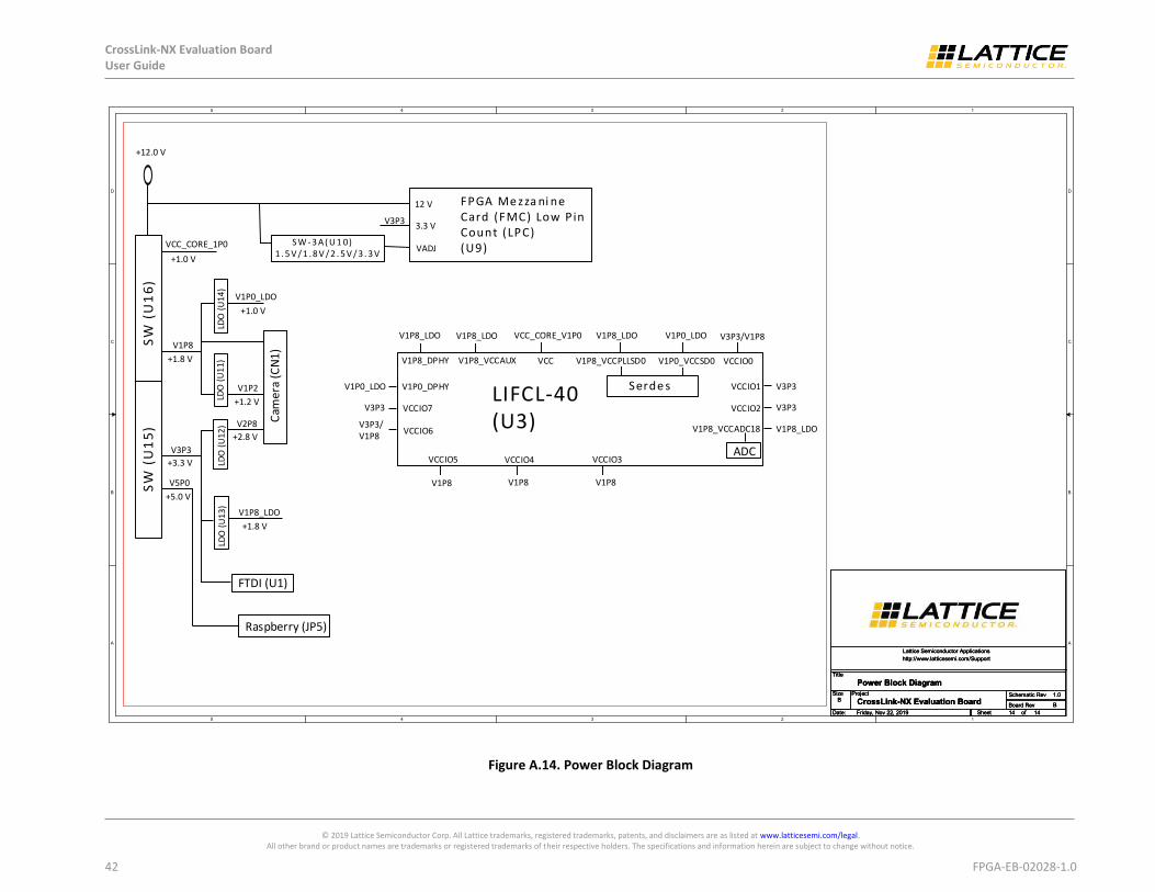
CrossLink-NX Evaluation Board User Guide
© 2019 Lattice Semiconductor Corp. All Lattice trademarks, registered trademarks, patents, and disclaimers are as listed at www.latticesemi.com/legal. All other brand or product names are trademarks or registered trademarks of their respective holders. The specifications and information herein are subject to change without notice.
42 FPGA-EB-02028-1.0
Figure A.14. Power Block Diagram
5
5
4
4
3
3
2
2
1
1
D D
C C
B B
A A
Date:
Size Schematic Rev
ofSheet
Title
Lattice Semiconductor Applications http://www.latticesemi.com/Support
Board Rev
Project
Friday, Nov 22, 2019
B1.0
1414
Power Block Diagram
CrossLink-NX Evaluation Board BDate:
Size Schematic Rev
ofSheet
Title
Lattice Semiconductor Applications http://www.latticesemi.com/Support
Board Rev
Project
Friday, Nov 22, 2019
B1.0
1414
Power Block Diagram
CrossLink-NX Evaluation Board BDate:
Size Schematic Rev
ofSheet
Title
Lattice Semiconductor Applications http://www.latticesemi.com/Support
Board Rev
Project
Friday, Nov 22, 2019
B1.0
1414
Power Block Diagram
CrossLink-NX Evaluation Board B
V1P8_DPHY
VCCIO0
VCCIO5
VCCIO1
V1P8_VCCADC18
VCCIO4
V1P0_VCCSD0V1P8_VCCPLLSD0
V1P8_LDO V1P0_LDO
V1P8
VCCIO3ADC
V1P0_LDO
V3P3/V1P8
V3P3
V3P3
V3P3/V1P8
V3P3
V1P8 V1P8
Serde sV1P0_DPHY
VCCIO7
VCCIO6
VCCIO2
V1P8_LDO
V1P8_LDO V1P8_LDO VCC_CORE_V1P0
V1P8_VCCAUX VCC
+12.0 VS
W (
U1
5)
SW
(U
16
)
V1P0_LDO
V1P2
+1.0 V
VCC_CORE_1P0
+1.0 V
LDO
(U
14
)LD
O (
U1
1)
Cam
era
(CN
1)V1P8
+1.8 V
V2P8
+1.2 V
+2.8 V
LDO
(U
12)
V1P8_LDO
+1.8 V
LDO
(U
13)
FTDI (U1)
Raspberry (JP5)
V5P0
+5.0 V
V3P3
+3.3 V
LIFCL-40 (U3)
V3P3
12 V
3.3 V
VADJ
FPGA Me zza ni ne Card (FMC) Low P in Count (LPC)(U9)
S W - 3 A ( U 1 0)1 . 5 V / 1 . 8 V / 2 . 5 V / 3 . 3 V

CrossLink-NX Evaluation Board User Guide
© 2019 Lattice Semiconductor Corp. All Lattice trademarks, registered trademarks, patents, and disclaimers are as listed at www.latticesemi.com/legal. All other brand or product names are trademarks or registered trademarks of their respective holders. The specifications and information herein are subject to change without notice.
FPGA-EB-02028-1.0 43
Appendix B. CrossLink-NX Evaluation Board Bill of Materials Item Reference Qty Part PCB Footprint Comments Part Number Manufacturer Description
1 AG1,AF1,AE1,AD1,AC1,AB1,AA1,AG2,AF2,AE2,AD2,AC2,AB2,AA2,AG3,AF3,AE3,AD3,AC3,AB3,AA3,AG4,AF4,AE4,AD4,AC4,AB4,AA4,AG5,AF5,AE5,AD5,AC5,AB5,AA5,AG6,AF6,AE6,AD6,AC6,AB6,AA6,AG7,AF7,AE7,AD7,AC7,AB7,AA7,AG8,AF8,AE8,AD8,AC8,AB8,AA8,AG9,AF9,AE9,AD9,AC9,AB9,AA9,AG10,AF10,AE10,AD10,AC10,AB10,AA10,AG11,AF11,AE11,AD11,AC11,AB11,AA11
77 T POINT R TP DNL — — —
2 CN1 1 camconn_imx258_1x30 camconn — 24-5804-030-000-829+ Kyocera / Sunny Optical
Sony IMX214 CSI Camera sensor
3 C1,C2,C3,C4,C7,C8,C9, C11,C12,C13,C15,C18, C19,C20,C24,C25,C27, C29,C31,C33,C35,C37, C38,C41,C42,C44,C46, C47,C49,C50,C52,C53, C54,C55,C57,C59,C60, C65,C66,C67,C70,C71, C72,C73,C75,C78,C83, C84,C86,C92,C93,C95, C96,C99,C100,C106, C107,C113,C114,C115, C116,C117,C118,C119, C120,C124,C126,C127, C128,C129,C130,C131, C132
73 0.1uF 0201 C0201 — GRM033R61E104KE14J Murata CAP CER 0.1UF 25V 10% X5R 0201
4 C5,C14,C22,C39,C40, C58,C64,C68,C69,C74, C91,C94,C108,C121, C122,C123,C125,C133, C134,C138,C140
21 10uF-0603SMT C0603 — CL10A106MO8NQNC Samsung CAP CER 10UF 16V X5R 0603

CrossLink-NX Evaluation Board User Guide
© 2019 Lattice Semiconductor Corp. All Lattice trademarks, registered trademarks, patents, and disclaimers are as listed at www.latticesemi.com/legal. All other brand or product names are trademarks or registered trademarks of their respective holders. The specifications and information herein are subject to change without notice.
44 FPGA-EB-02028-1.0
Item Reference Qty Part PCB Footprint Comments Part Number Manufacturer Description
5 C6,C10 2 4.7uF-0603SMT C0603 — CL10A475KA8NQNC Samsung CAP CER 4.7UF 25V X5R 0603
6 C16,C17 2 18pF C0402 — CL05C180JB5NNNC Samsung CAP CER 18PF 50V C0G/NP0 0402
7 C21,C23,C82,C102, C109,C110,C111,C112, C135,C136,C137,C139
12 1uF C0603 — TMK107B7105KA-T Taiyo Yuden CAP CER 1UF 25V 10% X7R 0603
8 C26,C28,C30,C32,C34, C36,C43,C45,C51,C85
10 10uF C0402 — CL05A106MP8NUB8 Samsung CAP CER 10UF 10V X5R 0402
9 C48,C56 2 1UF-16V-0805SMT RLP-133 — CL21B105KOFNNNG Samsung CAP CER 1UF 16V X7R 0805
10 C61,C62,C63,C76,C77 5 10nF RLP-130-A — GRM155R61C103KA01D Murata CAP CER 10000PF 16V X5R 0402
11 C79,C80,C81 3 20pF RLP-132 DNL — — —
12 C87,C89 2 1600pF C0805 — C0805C162J5GAC7800 Kemet CAP CER 1600PF 50V NP0 0805
13 C88,C90 2 1600pF C0805 DNL C0805C162J5GAC7800 Kemet CAP CER 1600PF 50V NP0 0805
14 C97,C98,C141,C155 4 10uF 25V 1206 C1206 — TMK316BJ106KL-T Taiyo Yuden CAP CER 10UF 25V X5R 1206
15 C101 1 0.1nF C0603 — CC0603JRNPO9BN101 Yageo CAP CER 100PF 50V C0G/NPO 0603
16 C103,C104 2 22uF C0603 — GRM188R61A226ME15D Murata CAP CER 22UF 10V X5R 0603
17 C105 1 3.3nF C0201 — GRM033R71E332KA12D Murata CAP CER 3300PF 25V X7R 0201
18 C142,C143,C156,C157 4 220NF-0402SMT RLP-130-A — CL05A224KO5NNNC Samsung CAP CER 0.22UF 16V X5R 0402
19 C144,C145,C158,C159 4 1000pF-0402SMT RLP-130-A — CL05B102KB5NFNC Samsung CAP CER 1000PF 50V X7R 0402
20 C146,C149,C160,C163 4 330pF-0402SMT RLP-130-A — CL05B331KB5NNNC Samsung CAP CER 330PF 50V X7R 0402
21 C147,C148,C164,C167 4 10pF-0402SMT RLP-130-A — CL05C100CB5NNNC Samsung CAP CER 10PF 50V C0G/NP0 0402
22 C150,C151,C152,C153,C154,C165,C166,C168, C169,C170
10 22uF,6.3V-0805SMT RLP-133 — CL21A226KPCLRNC Samsung CAP CER 22UF 10V X5R 0805
23 C161,C162 2 10pF-0402SMT RLP-130-A DNL — — —

CrossLink-NX Evaluation Board User Guide
© 2019 Lattice Semiconductor Corp. All Lattice trademarks, registered trademarks, patents, and disclaimers are as listed at www.latticesemi.com/legal. All other brand or product names are trademarks or registered trademarks of their respective holders. The specifications and information herein are subject to change without notice.
FPGA-EB-02028-1.0 45
Item Reference Qty Part PCB Footprint Comments Part Number Manufacturer Description
24 D1,D3,D4,D5,D6,D7,D8,D9,D10,D11,D12,D13, D14,D18,D19,D20,D21,D22,D23,D24,D25,D26,D27
23 LED_GREEN_0603 APT1608 — 150060GS75000 Wurth LED GREEN CLEAR 0603 SMD
25 D2 1 ESDR0502N-UDFN6 UDFN6_040 — ESDR0502NMUTBG ON semi TVS DIODE 5.5VWM 6UDFN
26 D15,D16 2 LED_YELLOW_0603 APT1608 — 150060YS75000 Wurth LED YELLOW CLEAR 0603 SMD
27 D17 1 LED_RED_0603 APT1608 — 150060RS75000 Wurth LED RED CLEAR 0603 SMD
28 D28 1 SCHOTTKY/VISHAY-V12P10
V12P10 — V12P10-M3/86A Vishay DIODE SCHOTTKY 100V 12A TO277A
29 D29,D30,D33,D34 4 1N4448W 1N4448W — 1N4448WS On Semi DIODE GEN PURP 75V 150MA SOD323F
30 D31,D32,D35,D36 4 DFLS220L DFLS220L — DFLS220L-7 Diodes Incorporated
DIODE SCHOTTKY 20V 2A POWERDI123
31 FB1,FB2,FB3,FB4,FB5, FB6,FB7,FB8
8 MPZ1005S121CT000 FB0402 — MPZ1005S121CT000 TDK Corporation FERRITE BEAD 120 OHM 0402 1LN
32 F1 1 F1251CT-ND 154010 — 0154010.DR Littelfuse Inc. FUSE BRD MNT 10A 125VAC/VDC SMD
33 JP1,JP2,JP3,JP4,JP6,JP7,JP8
7 JUMPER Header_1x2 — 61300211121 Wurth CONN HEADER VERT 2POS 2.54MM
34 JP5 1 Receptacle 20X2 HDR254-2X20_socket
DNL ESQ-120-23-T-D Samtec Inc. 40 Position Elevated Socket Connector Through Hole
35 J1 1 Header 1x8 hdr_amp_87220_8_1x8_100
DNL 22284081 Molex CONN HEADER 8POS .100 VERT TIN
36 J2 1 USB_MINI_B USB_MINI_B-1734035-2
— 1734035-2 TE Connectivity AMP Connectors
CONN RCPT USB2.0 MINI B SMD R/A
37 J3,J4,J5,J7,J8,J9,J23,J28,J29,J30,J31,J32,J34,J35,J36,J37,J38,J40,J41,J42,J43
21 Header_2x1 Header_2x1 Regular 100 Mil Header
— — —
38 J6,J26 2 Header_2x10 Header_2x10 — 61302021121 Wurth CONN HEADER VERT 20POS 2.54MM
39 J10,J11,J12,J14,J15,J16 6 SMA 901-10309 DNL 901-10309 Amphenol CONN SMA RCPT STR 50OHM EDGE MNT

CrossLink-NX Evaluation Board User Guide
© 2019 Lattice Semiconductor Corp. All Lattice trademarks, registered trademarks, patents, and disclaimers are as listed at www.latticesemi.com/legal. All other brand or product names are trademarks or registered trademarks of their respective holders. The specifications and information herein are subject to change without notice.
46 FPGA-EB-02028-1.0
Item Reference Qty Part PCB Footprint Comments Part Number Manufacturer Description
40 J13,J21,J22,J24,J25,J33,J44
7 CON3 CON3 Default : Pin 1 and 2
61300311121 Wurth CONN HEADER VERT 3POS 2.54MM
41 J17,J18,J19 3 PMOD 2x6 PPPC062LJBN-RC
— PPPC062LJBN-RC Sullins CONN HDR 12POS 0.1 GOLD PCB R/A
42 J20,J27 2 Header_2x7 Header_2x7 DNL — — Regular 100 Mil Header
43 J39 1 PJ-002A pj_002a_3p — 694106301002 Wurth CONN PWR JACK 2.1X5.5MM SOLDER
44 L1,L2,L3,L10,L11,L12 6 600ohm 500mA fb0603 — BLM18AG601SN1D Murata FERRITE CHIP 600 OHM 500MA 0603
45 L4,L5,L6,L7,L8,L9 6 220ohm 500mA FB0402 — CIM05U221NC Samsung FERRITE BEAD 220 OHM 0402 1LN
46 L13 1 2.2uH SPM6530T-2R2M SPM6530T-2R2M
— SPM6530T-2R2M TDK Corporation FIXED IND 2.2UH 8.2A 19 MOHM SMD
47 L14,L15,L16,L17 4 4.7uH-SPD62R-472M SPD62R — SPD62R-472M API Delevan Inc. FIXED IND 4.7UH 2A 150 MOHM SMD
48 Q1,Q2,Q3,Q4,Q5,Q6 6 2N2222/SOT23 MMBT2222ALT-1
— MMBT2222ALT1G ON Semiconductor
TRANS NPN 40V 0.6A SOT23
49 RN1 1 EXB2HV472JV EXB-2HV — EXB2HV472JV Panasonic RES ARRAY 8 RES 4.7K OHM 1506
50 R1,R2,R3,R102,R103, R104
6 4.7K R0603 — RC0603FR-074K7L yageo RES SMD 4.7K OHM 1% 1/10W 0603
51 R4,R9,R105 3 2.2K R0603 — RC0603FR-072K2L yageo RES SMD 2.2K OHM 1% 1/10W 0603
52 R5,R78 2 33 R0402 — ERJ-2RKF33R0X Panasonic RES SMD 33 OHM 1% 1/10W 0402
53 R6,R7,R8,R20,R21,R22 6 0 R0603 — RC0603JR-070RL Yageo RES SMD 0 OHM JUMPER 1/10W 0603
54 R10,R11,R12,R172 4 10K R0603 — RC0603FR-0710KL Yageo RES SMD 10K OHM 1% 1/10W 0603
55 R13,R16 2 12K R0603 — RC0603FR-0712KL yageo RES SMD 12K OHM 1/10W 1% 0603
56 R14 1 2K-0603SMT RLP-101 — RC0603FR-072KL Yageo RES SMD 2K OHM 1% 1/10W 0603
57 R15,R17,R35,R36,R37, R38,R39,R40,R145, R146,R147,R149,R150
13 0 R0603 DNL RC0603JR-070RL Yageo RES SMD 0 OHM JUMPER 1/10W 0603
58 R18,R19 2 4_7K-0603SMT RLP-101 — CRCW06034K70FKEA Vishay RES SMD 4.7K OHM 1% 1/10W 0603
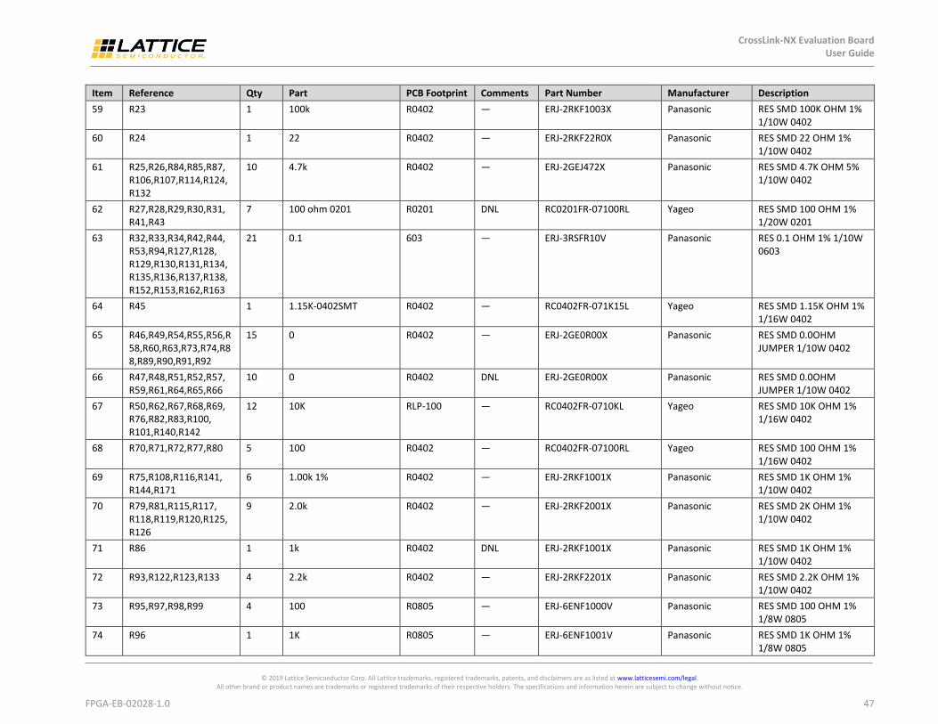
CrossLink-NX Evaluation Board User Guide
© 2019 Lattice Semiconductor Corp. All Lattice trademarks, registered trademarks, patents, and disclaimers are as listed at www.latticesemi.com/legal. All other brand or product names are trademarks or registered trademarks of their respective holders. The specifications and information herein are subject to change without notice.
FPGA-EB-02028-1.0 47
Item Reference Qty Part PCB Footprint Comments Part Number Manufacturer Description
59 R23 1 100k R0402 — ERJ-2RKF1003X Panasonic RES SMD 100K OHM 1% 1/10W 0402
60 R24 1 22 R0402 — ERJ-2RKF22R0X Panasonic RES SMD 22 OHM 1% 1/10W 0402
61 R25,R26,R84,R85,R87, R106,R107,R114,R124, R132
10 4.7k R0402 — ERJ-2GEJ472X Panasonic RES SMD 4.7K OHM 5% 1/10W 0402
62 R27,R28,R29,R30,R31, R41,R43
7 100 ohm 0201 R0201 DNL RC0201FR-07100RL Yageo RES SMD 100 OHM 1% 1/20W 0201
63 R32,R33,R34,R42,R44, R53,R94,R127,R128, R129,R130,R131,R134, R135,R136,R137,R138, R152,R153,R162,R163
21 0.1 603 — ERJ-3RSFR10V Panasonic RES 0.1 OHM 1% 1/10W 0603
64 R45 1 1.15K-0402SMT R0402 — RC0402FR-071K15L Yageo RES SMD 1.15K OHM 1% 1/16W 0402
65 R46,R49,R54,R55,R56,R58,R60,R63,R73,R74,R88,R89,R90,R91,R92
15 0 R0402 — ERJ-2GE0R00X Panasonic RES SMD 0.0OHM JUMPER 1/10W 0402
66 R47,R48,R51,R52,R57, R59,R61,R64,R65,R66
10 0 R0402 DNL ERJ-2GE0R00X Panasonic RES SMD 0.0OHM JUMPER 1/10W 0402
67 R50,R62,R67,R68,R69, R76,R82,R83,R100, R101,R140,R142
12 10K RLP-100 — RC0402FR-0710KL Yageo RES SMD 10K OHM 1% 1/16W 0402
68 R70,R71,R72,R77,R80 5 100 R0402 — RC0402FR-07100RL Yageo RES SMD 100 OHM 1% 1/16W 0402
69 R75,R108,R116,R141, R144,R171
6 1.00k 1% R0402 — ERJ-2RKF1001X Panasonic RES SMD 1K OHM 1% 1/10W 0402
70 R79,R81,R115,R117, R118,R119,R120,R125, R126
9 2.0k R0402 — ERJ-2RKF2001X Panasonic RES SMD 2K OHM 1% 1/10W 0402
71 R86 1 1k R0402 DNL ERJ-2RKF1001X Panasonic RES SMD 1K OHM 1% 1/10W 0402
72 R93,R122,R123,R133 4 2.2k R0402 — ERJ-2RKF2201X Panasonic RES SMD 2.2K OHM 1% 1/10W 0402
73 R95,R97,R98,R99 4 100 R0805 — ERJ-6ENF1000V Panasonic RES SMD 100 OHM 1% 1/8W 0805
74 R96 1 1K R0805 — ERJ-6ENF1001V Panasonic RES SMD 1K OHM 1% 1/8W 0805

CrossLink-NX Evaluation Board User Guide
© 2019 Lattice Semiconductor Corp. All Lattice trademarks, registered trademarks, patents, and disclaimers are as listed at www.latticesemi.com/legal. All other brand or product names are trademarks or registered trademarks of their respective holders. The specifications and information herein are subject to change without notice.
48 FPGA-EB-02028-1.0
Item Reference Qty Part PCB Footprint Comments Part Number Manufacturer Description
75 R109 1 1.02k 1% R0402 — ERJ-2RKF1021X Panasonic RES SMD 1.02K OHM 1% 1/10W 0402
76 R110 1 2.55k 1% R0402 — ERJ-2RKF2551X Panasonic RES SMD 2.55K OHM 1% 1/10W 0402
77 R111 1 750 1% R0402 — ERJ-2RKF7500X Panasonic RES SMD 750 OHM 1% 1/10W 0402
78 R112 1 422 1% R0402 — ERJ-2RKF4220X Panasonic RES SMD 422 OHM 1% 1/10W 0402
79 R113 1 15k RLP-103 — ERJ-8GEYJ153V Panasonic RES SMD 15K OHM 5% 1/4W 1206
80 R121 1 1.5k R0402 — ERJ-2GEJ152X Panasonic RES SMD 1.5K OHM 5% 1/10W 0402
81 R143,R165 2 1.15K-0603SMT RLP-101 — RC0603FR-071K15L Yageo RES SMD 1.15K OHM 1% 1/10W 0603
82 R148,R170 2 909-0603SMT RLP-101 — RC0603FR-07909RL Yageo RES SMD 909 OHM 1% 1/10W 0603
83 R151,R157,R159,R161 4 51K-0402SMT RLP-100 — RC0402FR-0751KL yageo RES SMD 51K OHM 1% 1/16W 0402
84 R154 1 1.05K-0603SMT RLP-101 — RC0603FR-071K05L Yageo RES SMD 1.05K OHM 1% 1/10W 0603
85 R155 1 1.07K-0603SMT RLP-101 — RC0603FR-071K07L Yageo RES SMD 1.07K OHM 1% 1/10W 0603
86 R156,R164 2 200 -0603SMT RLP-101 — RC0603FR-07200RL Yageo RES SMD 200 OHM 1% 1/10W 0603
87 R158 1 34K-0402SMT RLP-100 — RC0402FR-0734KL Yageo RES SMD 34K OHM 1% 1/16W 0402
88 R160 1 340-0603SMT RLP-101 — RC0603FR-07340RL Yageo RES SMD 340 OHM 1% 1/10W 0603
89 R166 1 30_1K-0402SMT RLP-100 — ERJ-2RKF3012X Panasonic RES SMD 30.1K OHM 1% 1/10W 0402
90 R167 1 63_4K-0402SMT RLP-100 — ERJ-2RKF6342X Panasonic RES SMD 63.4K OHM 1% 1/10W 0402
91 R168 1 20K-0402SMT RLP-100 — ERJ-2RKF2002X Panasonic RES SMD 20K OHM 1% 1/10W 0402
92 R169 1 768-0603SMT RLP-101 — RC0603FR-07768RL Yageo RES SMD 768 OHM 1% 1/10W 0603
93 R173 1 1.0 K R0603 DNL RC0603FR-071KL Yageo RES SMD 1K OHM 1% 1/10W 0603

CrossLink-NX Evaluation Board User Guide
© 2019 Lattice Semiconductor Corp. All Lattice trademarks, registered trademarks, patents, and disclaimers are as listed at www.latticesemi.com/legal. All other brand or product names are trademarks or registered trademarks of their respective holders. The specifications and information herein are subject to change without notice.
FPGA-EB-02028-1.0 49
Item Reference Qty Part PCB Footprint Comments Part Number Manufacturer Description
94 R174,R175,R176,R177, R178,R179,R180,R181, R182,R183,R184,R185, R186,R187
14 2K R0402 — ERJ-2GEJ202X Panasonic RES SMD 2K OHM 5% 1/10W 0402
95 SW1 1 SMD SW DIP-8 219-8MST — 219-8MST CTS Electrocomponents
SWITCH SLIDE DIP SPST 100MA 20V
96 SW2,SW3,SW4,SW5 4 Push Button 4psmd_switch — 434153017835 Wurth SWITCH TACTILE SPST-NO 0.05A 12V
97 TP_VCCIO1,TP_VCCIO2,TP_VCCIO3,TP_VCCIO4,TP_VCCIO5,TP_VCCIO6,TP_VCCIO7, TP_VCC_CORE_V1P0, TP_V1P0_VCCSD, TP_V1P0_LDO, TP_V1P2, TP_V1P8_VCCPLLSD, TP_V1P8_VCCAUXSD, TP_V1P8_LDO, TP_V1P8,TP_V2P8, TP_V3P3,TP_V5P0, TP_VCCIO0,TP_VADJ
20 TP_S_40_63 tp_s_40_63 DNL — — —
98 TP1,TP2,TP3,TP4,TP5 5 TP_S_40_63 TP DNL — — —
99 TP6,TP7,TP8,TP9,TP10, TP12,TP13
7 TestPoint TP50 DNL — — —
100 U1 1 FT2232HL tqfp64_0p5_12p2x12p2_h1p6
Customer Supplied
FT2232HL FTDI IC USB HS DUAL UART/FIFO 64-LQFP
101 U2 1 93LC56C-I/SN so8_50_244 — 93LC56C-I/SN Microchip IC EEPROM 2KBIT 3MHZ 8SOIC
102 U3 1 LIFCL-40-BG400 LIFCL-40-BG400
Customer Supplied
— — —
103 U4 1 AK5DAF1-125.0000T2 XTAL_AK5DAF1 — AK5DAF1-125.0000T2 Abracon LLC XTAL OSC XO 125MHZ 3.3V LVDS
104 U5 1 AK5DAF1-200.0000T2 XTAL_AK5DAF1 DNL AK5DAF1-200.0000T2 Abracon LLC XTAL OSC XO 200MHZ 3.3V LVDS
105 U6 1 MX25L12833FM2I-10G SO8_MX25L12833FM2I10G
— MX25L12833FM2I-10G Macronix IC FLASH 128MBIT 133MHZ 8SOP

CrossLink-NX Evaluation Board User Guide
© 2019 Lattice Semiconductor Corp. All Lattice trademarks, registered trademarks, patents, and disclaimers are as listed at www.latticesemi.com/legal. All other brand or product names are trademarks or registered trademarks of their respective holders. The specifications and information herein are subject to change without notice.
50 FPGA-EB-02028-1.0
Item Reference Qty Part PCB Footprint Comments Part Number Manufacturer Description
106 U7 1 MAX6070BAUT18+T SOT23-6_MAX6070
— MAX6070BAUT18+T Maxim Integrated IC VREF SERIES 1.8V SOT23-6
107 U8 1 PTD901-1015K-B103 PTD901_1015K_B103
— PTD901-1015K-B103 Bourns Inc. POT 10K OHM 1/20W CARBON LINEAR
108 U9 1 ASP-134603-01 ASP_134603_01
— ASP-134603-01 Samtec Inc. CONN ARRAY RCPT 160POS SMD GOLD
109 U10 1 BD9D321EFJ HTSOP_8_BD9D321
— BD9D321EFJ-E2 Rohm Semiconductor
IC REG BUCK ADJ 3A 8HTSOP-J
110 U11 1 NCP110AMX120TBG 4XDFN_NCP110
— NCP110AMX120TBG ON Semiconductor
IC REG LINEAR 1.2V 200MA 4XDFN
111 U12 1 NCP110AMX280TBG 4XDFN_NCP110
— NCP110AMX280TBG ON Semiconductor
IC REG LINEAR 2.8V 200MA 4XDFN
112 U13 1 BD00IC0WHFV-GTR 6HVSOF_BD00IC0WHFV
— BD00IC0WHFV-GTR Rohm Semiconductor
IC REG LINEAR POS ADJ 1A 6HVSOF
113 U14 1 TLV73310PDQNT 4X2SON — TLV73310PDQNT Texas Instruments
IC REG LINEAR 1V 300MA 4X2SON
114 U15,U16 2 LT3508EUF LT3508EUF — LT3508EUF#PBF Linear Technology/Analog Devices
IC REG BUCK ADJ 1.4A DL 24QFN
115 X1 1 7M-12.000MAAJ xtal_4p_7m — 7M-12.000MAAJ-T TXC CRYSTAL 12MHZ 18PF SMD
116 X2 1 ASE3-27.000MHz-K-T 27MHZ — ASE3-27.000MHz-K-T ABRACON Standard Clock Oscillators 27.000M 1.8V 30ppm
117 Shunt For Headers (BOM Line Item 40): J13,J21,J22,J24,J25,J33,J44
7 — — — SPC02SYAN Sullins Connectors Solutions
CONN JUMPER SHORTING GOLD FLASH
118 CN1 1 Camera Module with IMX258
— DNL — — —
119 Camera Bracket 1 — — DNL — — —
120 #8-32 Screw 1 — — DNL — — —
121 CrossLink NX Evaluation Board PCB RevB
1 — — — 305-PD-19-0943 PACTRON —

CrossLink-NX Evaluation Board User Guide
© 2019 Lattice Semiconductor Corp. All Lattice trademarks, registered trademarks, patents, and disclaimers are as listed at www.latticesemi.com/legal. All other brand or product names are trademarks or registered trademarks of their respective holders. The specifications and information herein are subject to change without notice.
FPGA-EB-02028-1.0 51
References
Lattice Semiconductor Documents Related documents available from your Lattice Semiconductor sales representative are listed on the table below.
Document Title
FPGA-UG-02042 Programming Cables
FPGA-DS-02049 CrossLink-NX Family Data Sheet
FPGA-TN-02099 CrossLink-NX sysCONFIG Usage Guide

CrossLink-NX Evaluation Board User Guide
© 2019 Lattice Semiconductor Corp. All Lattice trademarks, registered trademarks, patents, and disclaimers are as listed at www.latticesemi.com/legal. All other brand or product names are trademarks or registered trademarks of their respective holders. The specifications and information herein are subject to change without notice.
52 FPGA-EB-02028-1.0
Technical Support Assistance Submit a technical support case through www.latticesemi.com/techsupport.
CrossLink-NX Evaluation Board User Guide
© 2019 Lattice Semiconductor Corp. All Lattice trademarks, registered trademarks, patents, and disclaimers are as listed at www.latticesemi.com/legal. All other brand or product names are trademarks or registered trademarks of their respective holders. The specifications and information herein are subject to change without notice.
FPGA-EB-02028-1.0 53
Revision History Revision 1.0, December 2019
Section Change Summary
All Initial release