Dynamically Controlled Resource Allocation in SMT Processors
Upload
khangminh22Category
view
7download
0
eman ta zabal zazu
Universidad
del País Vasco
Euskal Herriko
Unibertsitatea
Bilboko Ingeniaritza Eskola
Teknologia Elektronikoa Saila
DOCTORAL THESIS.
Contributions to the Fault Tolerance of
Soft-Core Processors Implemented in
SRAM-based FPGA Systems
Author: Julen Gomez-Cornejo Barrena
Supervisor: Dr. Aitzol Zuloaga
Bilbao, June 2018
(cc)2018 JULEN GOMEZ-CORNEJO BARRENA (cc by 4.0)


ii
Eskerrak - Thanks
Lan hau aurrera atera ahal izan dut inguruan izan dudan jendearen laguntza etababesari esker. Lehenik, nire zuzendaria izan den Aitzol Zuloaga eskertu nahikonuke. Era berean, lan honetan eragin zuzena izan duten Uli Kretzschmar eta IgorVillalta lankideei esker berezia luzatu nahi nieke. Bestalde, Iraide Lopez eskertunahi dut dokumentuaren portadaren diseinuarekin laguntzeagatik.
Ezin ahaztu APERT taldeko parte diren edo izan diren gainontzeko lankide etalagunak, esker bereziak: Inigo Kortabarria, Inigo Martınez de Alegrıa, Jon An-dreu, Carlos Cuadrado, Jose Luis Martın, Armando Astarloa, Jesus Lazaro, Jai-me Jimenez, Unai Bidarte, Edorta Ibarra, Naiara Moreira, Vıctor Lopez, AngelPerez, Asier Matallana, Itxaso Aranzabal, Oier Onederra, Estafania Planas, Mar-kel Fernandez, David Cabezuelo, Iker Aretxabaleta eta Endika Robles. Baita ere,Javier Del Ser, Roberto Fernandez eta Leire Lopez-i eskeinitako laguntza bihotzezeskertu nahi nieke.
I also would like to thank all the kind people from the Computer Architectureand Embedded Systems research group for making me feel like home during thestay at TU Ilmenau, especially to Bernd Dane.
Ezin ahaztu, nire ondoan egon diren eta jasan nauten familia, lagunak eta Ufa.Eta bereziki eskerrak zuri ama, eredu zarelako.
Bukatzeko, UPV/EHU erakundea eta euskal gizartea eskertu nahi nituzke niredoktoretza aurrera eramateko baliabideak jartzeagatik.
Bilbon, 2018ko Ekainean.

iv Agradecimientos
Laburpena
Zirkuitu elektronikoak integrazio-maila apartetara iritsi dira diseinu eta ekoizpentekniken garapenari esker. Hau dela eta, gaur egun posible da sistema osatueta konplexuak gauzatzea gailu bakar batean. Kontzeptu honi SoC (System-on-Chip) deritzo. FPGA (Field Programmable Gate Array) teknologia da sistemahoriek gauzatzeko euskarri interesgarrienetakoa, batez ere eskeintzen duen mal-gutasunari esker, bere inguruan ematen ari diren etengabeko ikerkuntza berriengarrantzia ahaztu gabe.
FPGAek duten konfigurazio ahalmenari esker, funtzio ezberdinetarako programa-tuak izateko aukera eskeintzen dute. SRAM eta flash teknologietan oinarritutakoFPGA batzuek eskeitzen duten errekonfigurazio partzial dinamikoaren gaitasunabatuz gero, potentzial ikaragarrizko teknologia dela baiezta daiteke. Errekonfigu-razio partzial dinamikoari esker, posiblea da FPGA baten matrizean konfiguratu-tako zirkuitoaren zati bakar bat aldatzea, bitartean gainontzeko zirkuitu-atalakfuntzionatzen jarraitu dezaketelarik. Era horretan, hainbat diseinu partzial era-biltzeko aukera dago, FPGAaren baliabideen erabilera murriztuz.
Erradiazio kosmikotik datozen partikula energetikoekiko duten sentikortasuna daSRAM eta flash teknologietan oinarritutako gailuen erabilerak suposatzen duenarazo garrantzitsuenetakoa bat. Horien eraginez, hainbat arazo gerta daitez-ke, arazo arbuiagarrigarrietatik hasita, arazo benetan larrietara iritsi arte. Izanere, gizakiak arriskuan jar daitezke alor konkretu batzuen sistemetan hutsegi-teak izanez gero, esaterako: trenbide garraioetan, automozioan edo egiaztatzeindustrialean.
Hutsegite horiek sor ditzaketen arazoek hutsegite-tolerantzia kontzeptuaren ga-rrantzia indartzen dute. Sistema digitaleei atxikitutako ezaugarria da hutsegite-tolerantzia. Horren bidez, funtzionamenduan kalitate maila jakin bat bermatzenda akatsen aurrean. Horrela, sistema hariek hutsegiteen efektuak jasan behar di-tuzte aldioro, funtzionamendu egokia mantenduz. Helburu hori lortzeko gogortze
vi Laburpena
teknikak atxikitzen zaizkie, hori da, erredundantzia software edota hardwareanoinarritutako teknikak, esate baterako.
Bestalde, eguneroko bizitzan erabiltzen diren produktu elektroniko gehienek siste-ma txertatuak izaten dituzte beraien diseinuetan. Sistema txertatu horien baitanprozesadore bat edo gehiago izatea da ohikoena. Sistemen konplexutasun-mailakgora egiten duen heinean, oso interresgarria suertatzen da aurrediseinatutako etafrogatutako sistema elektronikoen erabilera. IP core (Intellectual Property co-res) bezala ezagutzen dira sistema hauek. Bereziki, azken urteotan zabaldu daIP core bidezko prozesadoreen (soft-core prozesadore bezala ezagunak) erabilerakgarrantzia irabazi du.
Lan honetan, SRAM motako FPGA teknlogietan implementatutako soft-coreprozesadoreen hutsegite-tolerantzia bermatzeko tekniken inguruan ikerketa buru-tu da. Era berean, prozesadore horien hutsegiteei aurre egiteko gogortze teknikaberriak proposatzen dira. Hala nola, lockstep metodologia berriak, TMR im-plementazioetan moduluen sinkronizaziorako teknikak, kaltetutako interfazedunmemorien datuen berreskurapena, etb. Bestalde, erabiltzaile-datuak bitstream-ren bidez maneilatzea ahalbideratzen duten teknikak proposatu dira. Teknikahoriek nahitaezkoak izan dira aurkeztutako zenbait hutsegite-tolerantzia handi-tzeko tekniken garapenerako.
Resumen
Gracias al desarrollo de las tecnologıas de diseno y fabricacion, los circuitoselectronicos han llegado a grandes niveles de integracion. De esta forma, hoyen dıa es posible implementar completos y complejos sistemas dentro de un unicodispositivo incorporando gran variedad de elementos como: procesadores, oscila-dores, lazos de seguimiento de fase (PLLs), interfaces, conversores ADC y DAC,modulos de memoria, etc. A este concepto de diseno se le denomina comunmenteSoC (System-on-Chip).
Una de las plataformas para implementar estos sistemas que mas importancia estacobrando son las FPGAs (Field Programmable Gate Array). Historicamente laplataforma mas utilizada para albergar los SoCs han sido las ASICs (Application-Specific Integrated Circuits), debido a su bajo consumo energetico y su granrendimiento. No obstante, su costoso proceso de desarrollo y fabricacion haceque solo sean rentables en el caso de producciones masivas. Las FPGAs, por elcontrario, al ser dispositivos configurables ofrecen, la posibilidad de implementardisenos personalizados a un coste mucho mas reducido. Por otro lado, los conti-nuos avances en la tecnologıa de las FPGAs estan haciendo que estas compitancon las ASICs a nivel de prestaciones (consumo, nivel de integracion y eficiencia).
Ciertas tecnologıas de FPGA, como las SRAM y Flash, poseen una caracterısti-ca que las hace especialmente interesantes en multitud de disenos: la capacidadde reconfiguracion. Dicha caracterıstica, que incluso puede ser realizada de for-ma autonoma, permite cambiar completamente el diseno hardware implementadocon solo cargar en la FPGA un archivo de configuracion denominado bitstream.La reconfiguracion puede incluso permitir modificar una parte del circuito con-figurado en la matriz de la FPGA, mientras el resto del circuito implementadocontinua inalterado. Esto que se conoce como reconfiguracion parcial dinamica,posibilita que un mismo chip albergue en su interior numerosos disenos hardwareque pueden ser cargados a demanda. Gracias a la capacidad de reconfiguracion,las FPGAs ofrecen numerosas ventajas como: posibilidad de personalizacion de
viii Resumen
disenos, capacidad de re-adaptacion durante el funcionamiento para responder acambios o corregir errores, mitigacion de obsolescencia, diferenciacion, menorescostes de diseno o reducido tiempo para el lanzamiento de productos al mercado.
Los SoC basados en FPGAs allanan el camino hacia un nuevo concepto de in-tegracion de hardware y software, permitiendo que los disenadores de sistemaselectronicos sean capaces de integrar procesadores embebidos en los disenos pa-ra beneficiarse de su gran capacidad de computacion. Gracias a esto, una parteimportante de la electronica hace uso de la tecnologıa FPGA abarcando un granabanico de campos, como por ejemplo: la electronica de consumo y el entreteni-miento, la medicina o industrias como la espacial, la avionica, la automovilısticao la militar.
Las tecnologıas de FPGA existentes ofrecen dos vıas de utilizacion de procesado-res embebidos: procesadores hard-core y procesadores soft-core. Los hard-core sonprocesadores discretos integrados en el mismo chip de la FPGA. Generalmenteofrecen altas frecuencias de trabajo y una mayor previsibilidad en terminos derendimiento y uso del area, pero su diseno hardware no puede alterarse para serpersonalizado. Por otro lado, un procesador soft-core, es la descripcion hardwareen lenguaje HDL (normalmente VDHL o Verilog) de un procesador, sintetizablee implementable en una FPGA. Habitualmente, los procesadores soft-core suelenbasarse en disenos hardware ya existentes, siendo compatibles con sus juegos deinstrucciones, muchos de ellos en forma de IP cores (Intellectual Property co-res). Los IP cores ofrecen procesadores soft-core predisenados y testeados, quedependiendo del caso pueden ser de pago, gratuitos u otro tipo de licencias. De-bido a su naturaleza, los procesadores soft-core, pueden ser personalizados parauna adaptacion optima a disenos especıficos. Ası mismo, ofrecen la posibilidadde integrar en el diseno tantos procesadores como se desee (siempre que hayadisponibles recursos logicos suficientes). Otra ventaja importante es que, graciasa la reconfiguracion parcial dinamica, es posible anadir el procesador al disenounicamente en los casos necesarios, ahorrando de esta forma, recursos logicos yconsumo energetico.
Uno de los mayores problemas que surgen al usar dispositivos basados en lastecnologıas SRAM o la flash, como es el caso de las FPGAs, es que son especial-mente sensibles a los efectos producidos por partıculas energeticas provenientesde la radiacion cosmica (como protones, neutrones, partıculas alfa u otros ionespesados) denominados efectos de eventos simples o SEEs (Single Event Effects).Estos efectos pueden ocasionar diferentes tipos de fallos en los sistemas: desdefallos despreciables hasta fallos realmente graves que compromentan la funcio-nalidad del sistema. El correcto funcionamiento de los sistemas cobra especialrelevancia cuando se trata de tecnologıas de elevado costo o aquellas en las que
ix
peligran vidas humanas, como por ejemplo, en campos tales como el transporteferroviario, la automocion, la avionica o la industria aeroespacial.
Dependiendo de distintos factores, los SEEs pueden causar fallos de operaciontransitorios, cambios de estados logicos o danos permanentes en el dispositivo.Cuando se trata de un fallo fısico permanente se denomina hard-error, mientrasque cuando el fallo afecta el circuito momentaneamente se denomina soft-error.Los SEEs mas frecuentes son los soft-errors y afectan tanto a aplicaciones comer-ciales a nivel terrestre, como a aplicaciones aeronauticas y aeroespaciales (conmayor incidencia en estas ultimas). La contribucion exacta de este tipo de fallosa la tasa de errores depende del diseno especıfico de cada circuito, pero en generalse asume que entorno al 90% de la tasa de error se debe a fallos en elementos dememoria (latches, biestables o celdas de memoria). Los soft-errors pueden afectartanto al circuito logico como al bitstream cargado en la memoria de configuracionde la FPGA. Debido a su gran tamano, la memoria de configuracion tiene masprobabilidades de ser afectada por un SEE.
La existencia de problemas generados por estos efectos reafirma la importanciadel concepto de tolerancia a fallos. La tolerancia a fallos es una propiedad relativaa los sistemas digitales, por la cual se asegura cierta calidad en el funcionamientoante la presencia de fallos, debiendo los sistemas poder soportar los efectos dedichos fallos y funcionar correctamente en todo momento. Por tanto, para lo-grar un diseno robusto, es necesario garantizar la funcionalidad de los circuitosy asegurar la seguridad y confiabilidad en las aplicaciones crıticas que puedanverse comprometidos por los SEE. A la hora de hacer frente a los SEE existe laposibilidad de explotar tecnologıas especıficas centradas en la tolerancia a fallos,como por ejemplo las FPGAs de tipo fusible, o por otro lado, utilizar la tecno-logıa comercial combinada con tecnicas de tolerancia a fallos. Esta ultima opcionva cobrando importancia debido al menor precio y mayores prestaciones de lasFPGAs comerciales.
Generalmente las tecnicas de endurecimiento se aplican durante la fase de di-seno. Existe un gran numero de tecnicas y se pueden llegar a combinar entre si.Las tecnicas prevalentes se basan en emplear algun tipo de redundancia, ya seahardware, software, temporal o de informacion. Cada tipo de tecnica presentadiferentes ventajas e inconvenientes y se centra en atacar distintos tipos de SEEy sus efectos. Dentro de las tecnicas de tipo redundancia, la mas utilizada es lahardware, que se basa en replicar el modulo a endurecer. De esta forma, cada unade las replicas es alimentada con la misma entrada y sus salidas son comparadaspara detectar discrepancias. Esta redundancia puede implementarse a diferentesniveles. En terminos generales, un mayor nivel de redundancia hardware implicauna mayor robustez, pero tambien incrementa el uso de recursos. Este incremento

x Resumen
en el uso de recursos de una FPGA supone tener menos recursos disponibles parael diseno, mayor consumo energetico, el tener mas elementos susceptibles de serafectados por un SEE y generalmente, una reduccion de la maxima frecuenciaalcanzable por el diseno. Por ello, los niveles de redundancia hardware mas utili-zados son la doble, conocida como DMR (Dual Modular Redundancy) y la tripleo TMR (Triple Modular Redundancy).
La DMR minimiza el numero de recursos redundantes, pero presenta el problemade no poder identificar el modulo fallido ya que solo es capaz de detectar que seha producido un error. Ello hace necesario combinarlo con tecnicas adicionales.Al caso de DMR aplicado a procesadores se le denomina lockstep y se suele com-binar con las tecnicas checkpoint y rollback recovery. El checkpoint consiste enguardar periodicamente el contexto (contenido de registros y memorias) de ins-tantes identificados como correctos. Gracias a esto, una vez detectado y reparadoun fallo es posible emplear el rollback recovery para cargar el ultimo contextocorrecto guardado. Las desventajas de estas estrategias son el tiempo requeridopor ambas tecnicas (checkpoint y rollback recovery) y la necesidad de elementosadicionales (como memorias auxiliares para guardar el contexto).
Por otro lado, el TMR ofrece la posibilidad de detectar el modulo fallido me-diante la votacion por mayorıa. Es decir, si tras comparar las tres salidas unade ellas presenta un estado distinto, se asume que las otras dos son correctas.Esto permite que el sistema continue funcionando correctamente (como sistemaDMR) aun cuando uno de los modulos quede inutilizado. En todo caso, el TMRsolo enmascara los errores, es decir, no los corrige. Una de las desventajas masdestacables de esta tecnica es que incrementa el uso de recursos en mas de un300%. Tambien cabe la posibilidad de que la salida discrepante sea la realmentecorrecta (y que por tanto, las otras dos sean incorrectas), aunque este caso es bas-tante improbable. Uno de los problemas que no se ha analizado con profundidaden la bibliografıa es el problema de la sincronizacion de procesadores soft-coreen sistemas TMR (o de mayor nivel de redundancia). Dicho problema reside enque, si tras un fallo se inutiliza uno de los procesadores y el sistema continuafuncionando con el resto de procesadores, una vez reparado el procesador fallido,este necesita sincronizar su contexto al nuevo estado del sistema.
Una practica bastante comun en la implementacion de sistemas redundantes escombinarlos con la tecnica conocida como scrubbing. Esta tecnica basada en lareconfiguracion parcial dinamica, consiste en sobrescribir periodicamente el bits-tream con una copia libre de errores apropiadamente guardada. Gracias a ella,es posible corregir los errores enmascarados por el uso de algunas tecnicas deendurecimiento como la redundancia hardware. Esta copia libre de errores sueleomitir los bits del bitstream correspondientes a la memoria de usuario, por lo que

xi
solo actualiza los bits relacionados con la configuracion de la FPGA. Por ello, aesta tecnica tambien se la conoce como configuration scrubbing. En toda la lite-ratura consultada se ha detectado un vacio en cuanto a tecnicas que proponganestrategias de scrubbing para la memoria de usuario.
Con el objetivo de proponer alternativas innovadoras en el terreno de la toleran-cia a fallos para procesadores soft-core, en este trabajo de investigacion se handesarrollado varias tecnicas y flujos de diseno para manejar los datos de usuarioa traves del bitstream, pudiendo leer, escribir o copiar la informacion de registroso de memorias implementadas en bloques RAMs de forma autonoma. Ası mismose ha desarrollado un abanico de propuestas tanto como para estrategias lockstepcomo para la sincronizacion de sistemas TMR, de las cuales varias hacen usode las tecnicas desarrolladas para manejar las memorias de usuario a traves delbitstream. Estas ultimas tecnicas tienen en comun la minimizacion de utilizacionde recursos respecto a las estrategias tradicionales. De forma similar, se propo-nen dos alternativas adicionales basadas en dichas tecnicas: una propuesta descrubbing para las memorias de usuario y una para la recuperacion de informa-cion en memorias implementadas en bloques RAM cuyas interfaces hayan sidoinutilizadas por SEEs.
Todas las propuestas han sido validadas en hardware utilizando una FPGA deXilinx, la empresa lıder en fabricacion de dispositivos reconfigurables. De estaforma se proporcionan resultados sobre los impactos de las tecnicas propuestas enterminos de utilizacion de recursos, consumos energeticos y maximas frecuenciasalcanzables.

xii Resumen

Abstract
In the last years, the integration level of electronic circuits has been widely in-creased with the development of design and manufacturing techniques. As aresult, complex system can be implemented inside of a single device. This highlevel of integration concept, in connection with design, is commonly known asSoC (System-on-Chip). One of the most interesting platforms to implement thesesystems are the FPGAs (Field Programmable Gate Array), due to their flexibilityand the continued innovation in their technology.
The FPGAs can be programmed with different configurations to perform distinctfunctions. This capacity together with the partial dynamic reconfiguration ofsome SRAM-based or flash-based FPGAs, provide them with a valuable potential.The employment of partial dynamic reconfiguration permits modifying just onepart in the array of the FPGA, while the rest of the circuit remains unchanged.Consequently, FPGAs may be programmed by different partial designs, increasingtheir functionality and decreasing the resource usage.
However, one of the most remarkable problems using SRAM and flash technolo-gies is that certain FPGAs are especially sensitive to effects caused by energeticparticles from the cosmic radiation. Owing to these effects, different system fail-ures can be produced, from worthless ones to really serious ones. The worstfailures might even hinder the correct performance of several important systemsin relation to railway, automotion or industrial control. Hence, a wrong per-formance of these systems might cause permanent damages in highly expensiveequipment and even endanger the human life itself.
The existence of these problems as a result of the aforesaid effects makes theimportance of the fault tolerance concept unavoidable. Fault tolerance, is aproperty related to digital systems and ensures certain quality of operation inthe presence of failures. Because of fault tolerance, the systems are supposedto work properly at any time even though failures take place. For this purpose,
xiv Abstract
hardening techniques are applied to these systems, such as, ones which are basedon the redundancy of software and/or hardware.
On the other hand, most of the electronic devices which are used daily make useof embedded systems which incorporate one ore more processor cores for the exe-cution of the different tasks. In addition, the increase in complexity of the designsmakes the electronic systems which have been designed and tested beforehandmore attractive. Those designs are called IP cores (Intellectual Property cores).Due to those reasons, the utilization of processor IP cores (known as soft-coreprocessors) in FPGA designs is gaining momentum.
Following this idea this work performs a research in the field of fault tolerancefor SRAM based FPGA designs especially focusing on soft-processors. With theaim of improving the well established hardening techniques, this work proposesseveral approaches that deal with distinct aspects related to fault tolerance. Inthis way, three lockstep (a dual redundancy based technique) approaches, fivesynchronization methods for repaired modules in modular redundancy schemes,a method to recover information from memories with damaged interfaces and auser-data scrubbing approach are proposed in this work. Several of these pro-posed methods are based on the utilization of two methodologies to manage userdata of both, flip-flops and BRAMs, through the bitstream that have been alsodeveloped in this work.
The proposed methods provide the designers with valuable tools when developingfault tolerant designs implemented in SRAM based FPGA devices.

Contents
Laburpena v
Resumen vii
Abstract xiii
List of Figures xix
List of Tables xxiii
List of Acronyms xxv
1 Introduction 11.1 Motivation . . . . . . . . . . . . . . . . . . . . . . . . . . . . . . . 31.2 Objectives . . . . . . . . . . . . . . . . . . . . . . . . . . . . . . . . 41.3 Structure of the Document . . . . . . . . . . . . . . . . . . . . . . 5
2 Soft-Core Processors Implemented in SRAM Based FPGAs 72.1 General Aspects of Soft-Core Processors . . . . . . . . . . . . . . . 9
2.1.1 Basic Architectures of Soft-Core Processors . . . . . . . . . 102.1.2 Soft-Core Processor IPs . . . . . . . . . . . . . . . . . . . . 12
2.2 SRAM Based FPGAs . . . . . . . . . . . . . . . . . . . . . . . . . 202.2.1 Introducing Programmable Logic Devices . . . . . . . . . . 202.2.2 Architecture of 7 Series Devices and Zynq-7000 All Pro-
grammable SoC by Xilinx . . . . . . . . . . . . . . . . . . . 242.2.3 Zynq-7000 All Programmable SoC . . . . . . . . . . . . . . 322.2.4 Bitstream Structure of 7 series FPGAs . . . . . . . . . . . . 372.2.5 Managing Data Content by Utilizing the Bitstream . . . . . 40
2.3 Radiation Effects on Soft-Core Processors implemented in SRAMFPGAs . . . . . . . . . . . . . . . . . . . . . . . . . . . . . . . . . 46

xvi Contents
3 Hardening Soft-Core Processors Implemented in SRAM FPGAs 533.1 Scrubbing . . . . . . . . . . . . . . . . . . . . . . . . . . . . . . . . 553.2 Hardware Redundancy . . . . . . . . . . . . . . . . . . . . . . . . . 59
3.2.1 Dual Modular Redundancy . . . . . . . . . . . . . . . . . . 623.2.2 Triple Modular Redundancy . . . . . . . . . . . . . . . . . . 66
3.3 Other Types of Redundancy . . . . . . . . . . . . . . . . . . . . . . 693.3.1 Data Redundancy . . . . . . . . . . . . . . . . . . . . . . . 693.3.2 Software Redundancy . . . . . . . . . . . . . . . . . . . . . 723.3.3 Time Redundancy . . . . . . . . . . . . . . . . . . . . . . . 74
3.4 Dynamic Partial Reconfiguration to Fix Permanent Faults . . . . . 763.4.1 Detection of Permanent Faults . . . . . . . . . . . . . . . . 763.4.2 Repairing Permanent Faults . . . . . . . . . . . . . . . . . . 773.4.3 Synchronization of Repaired Modules . . . . . . . . . . . . 80
3.5 Other Fault Tolerance Approaches . . . . . . . . . . . . . . . . . . 833.6 Evaluation of Hardening Techniques . . . . . . . . . . . . . . . . . 86
3.6.1 Physical Fault Injection Techniques . . . . . . . . . . . . . 883.6.2 Bitstream Based Fault Injection Techniques . . . . . . . . . 92
3.7 Conclusions . . . . . . . . . . . . . . . . . . . . . . . . . . . . . . . 98
4 Contributions in Fault Tolerance for Soft-Core Processors 1034.1 PICDiY: Target Soft-Core Processor . . . . . . . . . . . . . . . . . 104
4.1.1 PICDiY’s Architecture . . . . . . . . . . . . . . . . . . . . . 1054.1.2 PICDiY’s Instructions . . . . . . . . . . . . . . . . . . . . . 111
4.2 Bitstream Based BRAM Approach: Contribution in BRAM DataManagement through the Bitstream in 7 Series . . . . . . . . . . . 1144.2.1 Proposed Method to Obtain the Bitstream Structure of
Data in BRAMs . . . . . . . . . . . . . . . . . . . . . . . . 1154.2.2 Managing Data Content of BRAMs with the BBBA . . . . 119
4.3 Approach to Manage Data of Registers with the Bitstream . . . . 1234.3.1 Proposed Flow to Protect/Unprotect Partial Regions in 7
series . . . . . . . . . . . . . . . . . . . . . . . . . . . . . . 1264.3.2 Proposed Flow to Generate Equal Implementations of a
Design in Different Reconfigurable Regions . . . . . . . . . 1294.4 Data Content Scrubbing Approach . . . . . . . . . . . . . . . . . . 1314.5 Approach to Extract Data From Damaged Memories Using the
BBBA . . . . . . . . . . . . . . . . . . . . . . . . . . . . . . . . . . 1334.6 Lockstep Approaches . . . . . . . . . . . . . . . . . . . . . . . . . . 135
4.6.1 Hardware Based Fast Lockstep Approach . . . . . . . . . . 1354.6.2 Bitstream Based Low Overhead Lockstep Approach . . . . 1394.6.3 Bitstream Based Autonomous Lockstep Approach . . . . . 1434.6.4 Lockstep Approaches Overview . . . . . . . . . . . . . . . . 145

Contents xvii
4.7 Proposed Synchronization Approaches for Repaired Soft-Core Pro-cessors in Hardware Redundancy Based Schemes . . . . . . . . . . 1464.7.1 Cyclic Resets Based Synchronization Approach . . . . . . . 1494.7.2 Memory and Address Force Based Synchronization Approach1514.7.3 Synchronization Approach Based on Using an Interruption
and a Synchronization Memory . . . . . . . . . . . . . . . . 1524.7.4 Complete Hardware-Based Synchronization Approach . . . 1534.7.5 Complete Bitstream-Based Synchronization . . . . . . . . . 1554.7.6 Synchronization Approaches Overview . . . . . . . . . . . . 158
5 Validation of Fault Tolerance Approaches 1595.1 Experimental Setup . . . . . . . . . . . . . . . . . . . . . . . . . . 1605.2 Validation of PICDiY Soft-Core Processor . . . . . . . . . . . . . . 1625.3 Validation of the Bitstream Based BRAM Approach . . . . . . . . 1665.4 Validation of the Approach to Manage Data of Registers with the
Bitstream . . . . . . . . . . . . . . . . . . . . . . . . . . . . . . . . 1715.5 Validation of the Data Content Scrubbing Approach . . . . . . . . 1765.6 Validation of Approach to Extract Data From Damaged Memories
Using the BBBA . . . . . . . . . . . . . . . . . . . . . . . . . . . . 1775.7 Validation of the Lockstep Approaches . . . . . . . . . . . . . . . . 1785.8 Validation of the Synchronization Approaches . . . . . . . . . . . . 183
6 Conclusions and future work 1896.1 Conclusions . . . . . . . . . . . . . . . . . . . . . . . . . . . . . . . 1896.2 Main Contributions . . . . . . . . . . . . . . . . . . . . . . . . . . . 1916.3 Scientific Publications in the Context of this Work . . . . . . . . . 1936.4 Future work . . . . . . . . . . . . . . . . . . . . . . . . . . . . . . . 194
A Hardware Implementation details of the Proposed Approaches 197


List of Figures
1.1 FPGA application fields examples. . . . . . . . . . . . . . . . . . . 2
2.1 Block diagram of Harvard architecture. . . . . . . . . . . . . . . . . 102.2 Block diagram of Von Neumann architecture. . . . . . . . . . . . . 112.3 Block diagram of PicoBlaze. . . . . . . . . . . . . . . . . . . . . . . 142.4 Block diagram of SPARC core. . . . . . . . . . . . . . . . . . . . . 172.5 Picture of a silicon array of the XC157. . . . . . . . . . . . . . . . 212.6 Block diagram of the Xilinx XC2064 logic cell array. . . . . . . . . 222.7 Arrangement of CLBs and switch matrices within the FPGA. . . . 252.8 7 series CLB example. . . . . . . . . . . . . . . . . . . . . . . . . . 252.9 7 series flip-flop and flip-flop/LATCH block symbols. . . . . . . . . 262.10 VHDL code example of a flip-flop with INIT and SRVAL values. . 262.11 RAMB36 Block RAM primitive symbol. . . . . . . . . . . . . . . . 282.12 CAPTUREE2 primitive symbol. . . . . . . . . . . . . . . . . . . . . . 282.13 STARTUPE2 primitive symbol. . . . . . . . . . . . . . . . . . . . . . 292.14 ILA core symbol. . . . . . . . . . . . . . . . . . . . . . . . . . . . . 312.15 Diagram of the functional blocks that constitute the Zynq-7000. . . 332.16 Replacing reconfigurable modules with the dynamic partial recon-
figuration. . . . . . . . . . . . . . . . . . . . . . . . . . . . . . . . . 362.17 A relocation alternative. . . . . . . . . . . . . . . . . . . . . . . . . 442.18 Flow chart of a context capture and restoration alternative. . . . . 452.19 Flow chart of an FPGA protection and unprotection alternative. . 452.20 Classification of Single Event Effects . . . . . . . . . . . . . . . . . 482.21 Configuration memory SEU example in an FPGA design. . . . . . 50
3.1 On-chip scrubbing. . . . . . . . . . . . . . . . . . . . . . . . . . . . 563.2 Scrubbing with an external device. . . . . . . . . . . . . . . . . . . 573.3 Scrubbing with a hard processor in a SoC device. . . . . . . . . . . 583.4 Example of hardware redundancy with N modules. . . . . . . . . . 60
xx List of Figures
3.5 Intermediate voter for the interconnection of tripled modules. . . . 623.6 Error detection in a DMR scheme. . . . . . . . . . . . . . . . . . . 633.7 Flow charts of lockstep approaches. . . . . . . . . . . . . . . . . . . 643.8 Basic error detection implementation for a DMR setup. . . . . . . 653.9 Examples of different TMR scenarios. . . . . . . . . . . . . . . . . 673.10 Voter alternatives for TMR approaches. . . . . . . . . . . . . . . . 683.11 Example of error detection using Hamming code. . . . . . . . . . . 713.12 Example of a basic time redundancy scheme. . . . . . . . . . . . . 743.13 Flow chart for detection and correction of permanent faults. . . . . 773.14 Permanent error repair with tiling strategy. . . . . . . . . . . . . . 793.15 Permanent error repair with spare reconfigurable partitions. . . . . 803.16 Block diagram of the PIHS3TMR. . . . . . . . . . . . . . . . . . . 823.17 Block diagram of the HETA approach. . . . . . . . . . . . . . . . . 863.18 The Isochronous Cyclotron U-120M. . . . . . . . . . . . . . . . . . 913.19 ISIS pulsed neutron source at the Science and Technology Facilities 913.20 Different laser testing setups. . . . . . . . . . . . . . . . . . . . . . 923.21 Basic flow of bitstream based fault injection. . . . . . . . . . . . . 933.22 Different bitstream based fault injection setups. . . . . . . . . . . . 95
4.1 Block diagram of the PIC16. . . . . . . . . . . . . . . . . . . . . . 1064.2 Block diagram of the PICDiY. . . . . . . . . . . . . . . . . . . . . 1074.3 STATUS register. . . . . . . . . . . . . . . . . . . . . . . . . . . . . 1074.4 PCL and PCLATH registers. . . . . . . . . . . . . . . . . . . . . . 1084.5 State diagram of IDC’s FSM. . . . . . . . . . . . . . . . . . . . . . 1094.6 Mapping of PICDiY’s user-data memory and registers. . . . . . . . 1104.7 Byte-oriented file register operations instruction format. . . . . . . 1114.8 Bit-oriented file register operations instruction format. . . . . . . . 1134.9 Literal operations instruction format. . . . . . . . . . . . . . . . . . 1134.10 Control operations instruction format. . . . . . . . . . . . . . . . . 1134.11 Block diagram of the implementation scheme. . . . . . . . . . . . . 1154.12 Example of the flow used to determine the BRAM data location
in the bitstream. . . . . . . . . . . . . . . . . . . . . . . . . . . . . 1174.13 Flow diagram of the BRAM copy procedure. . . . . . . . . . . . . 1204.14 Different copying types. . . . . . . . . . . . . . . . . . . . . . . . . 1214.15 Context save and restore approach for 7 series devices with external
memory. . . . . . . . . . . . . . . . . . . . . . . . . . . . . . . . . . 1244.16 Effect of the RESET AFTER RECONFIG=TRUE property in FPGA pro-
tection. . . . . . . . . . . . . . . . . . . . . . . . . . . . . . . . . . 1264.17 Approach to unprotect several regions in 7 series devices based on
the RESET AFTER RECONFIG property. . . . . . . . . . . . . . . . . . 1284.18 Flow chart of the Location Constraints Flow. . . . . . . . . . . . . 130

List of Figures xxi
4.19 Flow charts of the Data Content Scrubbing Approach. . . . . . . . 1334.20 Example of an SEU affecting the interface of a BRAM. . . . . . . . 1344.21 Simplified example of extracting and relocating data from a dam-
aged memories. . . . . . . . . . . . . . . . . . . . . . . . . . . . . . 1344.22 Simplified block diagram of the HW Fast Lockstep approach. . . . 1364.23 Finite state machine diagram of the adapted FSM. . . . . . . . . . 1374.24 Original and adapted registers. . . . . . . . . . . . . . . . . . . . . 1384.25 Simplified block diagram of the Bitstream Based Low Overhead
Lockstep approach. . . . . . . . . . . . . . . . . . . . . . . . . . . . 1414.26 Context saving strategies. . . . . . . . . . . . . . . . . . . . . . . . 1424.27 Simplified block diagram of the Bitstream Based Autonomous
Lockstep Approach. . . . . . . . . . . . . . . . . . . . . . . . . . . . 1434.28 State diagram of the Lockstep Controller block. . . . . . . . . . . . 1444.29 SEU recovery process and impact of synchronization times. . . . . 1484.30 Simplified diagram of the Reset Sync approach. . . . . . . . . . . . 1494.31 Proposed software flows when using Reset Sync . . . . . . . . . . . 1504.32 Simplified diagram of the Force Sync approach. . . . . . . . . . . . 1514.33 Simplified diagram of the Interrupt Sync approach. . . . . . . . . . 1534.34 Simplified diagram of the Hw Sync approach. . . . . . . . . . . . . 1544.35 Simplified diagram of the Bitstream Sync approach. . . . . . . . . 1564.36 Synchronization routine of the Bitstream Sync approach. . . . . . . 157
5.1 ZedBoard Zynq-7000 ARM/FPGA SoC development board. . . . . 1605.2 Flow chart of the utilized validation strategy. . . . . . . . . . . . . 1615.3 TestApp experimental setup. . . . . . . . . . . . . . . . . . . . . . 1625.4 Output operation and FPGA interface for PicoBlaze. . . . . . . . . 1655.5 Block diagrams of the implemented approaches. . . . . . . . . . . . 1685.6 Device image of the design with placement constraints from Vivado.1725.7 Fragment of the .ll file from the design with placement constraints. 1725.8 Device image of the TMR design without placement constraints
from Vivado. . . . . . . . . . . . . . . . . . . . . . . . . . . . . . . 1745.9 Device image of the TMR design witht placement constraints from
Vivado. . . . . . . . . . . . . . . . . . . . . . . . . . . . . . . . . . 1755.10 Test procedure for the lockstep approaches validation. . . . . . . . 1785.11 Test procedure for the synchronization validation. . . . . . . . . . . 183
A.1 Vivado block design of the validation setup for the Approach toManage Data of Registers with the Bitstream. . . . . . . . . . . . . 198
A.2 Vivado block design of the validation setup for the Approach toExtract Data From Damaged Memories Using the BBBA. . . . . . 199
A.3 Vivado block design of the validation setup for the HW Fast Lockstep.200

xxii List of Figures
A.4 Vivado block design of the validation setup for the Bitstream BasedLow Overhead Lockstep. . . . . . . . . . . . . . . . . . . . . . . . . 201
A.5 Vivado block design of the validation setup for the Bitstream BasedAutonomous Lockstep. . . . . . . . . . . . . . . . . . . . . . . . . . 202
A.6 Vivado block design of the validation setup for the Reset Sync. . . 203A.7 Vivado block design of the validation setup for the Force Sync. . . 204A.8 Vivado block design of the validation setup for the Interrupt Sync. 205A.9 Vivado block design of the validation setup for the Hw Sync. . . . 206A.10 Vivado block design of the validation setup for the Bitstream Sync. 207

List of Tables
2.1 Packet header types (R: reserved bit; x: data bit). . . . . . . . . . 38
2.2 Frame Address Register (FAR) format. . . . . . . . . . . . . . . . . 39
4.1 Instruction set of the PICDiY. . . . . . . . . . . . . . . . . . . . . 112
4.2 FAR addresses of BRAM columns in Z7020. . . . . . . . . . . . . . 116
4.3 Bit distribution example of the first data word of the first 18KBRAM in Z7020. . . . . . . . . . . . . . . . . . . . . . . . . . . . . 118
4.4 Data organization example of one frame of a 18K BRAM columnin Z7020. . . . . . . . . . . . . . . . . . . . . . . . . . . . . . . . . 119
4.5 Init addresses (hex) of 18K BRAMs in Z7020. . . . . . . . . . . . . 119
4.6 Lockstep approaches overview. . . . . . . . . . . . . . . . . . . . . 145
4.7 General synchronization objects and accessibility for PICDiY, Pi-coBlaze and MicroBlaze processors. . . . . . . . . . . . . . . . . . . 148
4.8 Synchronization methods overview. . . . . . . . . . . . . . . . . . . 158
5.1 Implementation results summary of the soft-core processors(@100MHz). . . . . . . . . . . . . . . . . . . . . . . . . . . . . . . . 164
5.2 Primitive utilization of the soft-core processors (@100MHz). . . . . 164
5.3 Comparison of FSM coding examples for PICDiY and PicoBlazeprocessors. . . . . . . . . . . . . . . . . . . . . . . . . . . . . . . . . 166
5.4 Implementation results summary of BRAM data copy and com-parison tests (@100MHz). . . . . . . . . . . . . . . . . . . . . . . . 170
5.5 Implementation results summary of a reconfigurable TMR imple-mentation with and without placement constraints (@60MHz). . . 176
5.6 Primitive utilization of a reconfigurable TMR implementation withand without placement constraints (@60MHz). . . . . . . . . . . . 176
5.7 Implementation results summary of the lockstep approaches, a sin-gle PICDiY and a coarse grained TMR (@60MHz). . . . . . . . . . 180

xxiv List of Tables
5.8 Primitive utilization of the lockstep approaches, a single PICDiYand a coarse grained TMR (@60MHz). . . . . . . . . . . . . . . . . 181
5.9 Implementation results summary of the synchronization approaches(@60MHz). . . . . . . . . . . . . . . . . . . . . . . . . . . . . . . . 186
5.10 Primitive utilization of the synchronization approaches (@60MHz). 187

List of Acronyms
ALU Arithmetic Logic UnitAMBA Advanced Micro-controller Bus ArchitectureAPU Aplication Processor UnitASIC Application Specific Integrated Circuit
ASMBL Advanced Silicon Modular BlockASTERICS Advanced System for the TEst under Radiation of Integrated
Circuits and SystemsBBBA Bitstream Based BRAM ApproachBRAM BlockRAM
BSD Berkeley Software DistributionCISC Complex Instruction Set ComputerCLB Configurable Logic BlockCLK ClockCMD Command Register
CMOS Complementary Metal-Oxide SemiconductorCMT Clock Management TilesCOTS Commercial Off-The-ShelfCPLD Complex Programmable Logic DeviceCPU Controling Process UnitCRC Cyclic Redundancy Check
CSoPC Configurable-System-on-ChipDD Displacement DamageDFI Direct Fault Injection
DMIP Dhrystone Million Instructions Per SecondDSP Digital Signal ProcessorDUT Device Under Test

xxvi List of Acronyms
ECC Error Correction CodeEDAC Error Detection and CorrectionEDC Error Detection Code
EMIO Extended Multiplexed I/OEPLD Erasable Programmable Logic DeviceFAR Frame Address RegisterFDRI Frame Data Input RegisterFDRO Frame Data Output Register
FI Fault InjectionFIFA Fault-Injection Fault Analysis toolFITO FPGA-based Fault Injection ToolFPGA Field Programmable Gate ArrayFSBL First Stage Boot LoaderFSM Finite State Machine
FUSE Fault injection Using SemulationGNU General Public LicenseGPIO General Purpose Input/OuputsGSR Global Set ResetHAL Hardware Abstraction LayerHDL Hardware Description LanguajeIDC Instruction Decode and ControlIDE Integrated Device ElectronicILA Integrated Logic AnalyzerIOB Input-Output-BlockIP Intellectual Proprietary
IPF In-place X-FilingISR Interrupt Service Routine
KCPSM Constant(K) Coded Programmable State MachineLET Linear Energy Transfer
LGPL GNU Lesser General Public LicenseLRR Least Recently ReplacedLUT Look-Up TableMBU Multiple Bit Upset
MCSoPC Multiprocessor-Configurable-System-on-ChipMCU Multiple Cell UpsetsMIO Multiplexed I/OMIPS Million Instructions Per Second

xxvii
MIT Massachusetts Institute of TechnologyMMU Memory Management UnitMPU Memory Protection Unit
NETFI NETlist Fault InjectionPL Programmable Logic
PLD Programmable Logic DevicePowerPC Performance Optimization With Enhanced RISC - Performance Computing
PS Processing SystemPWM Pulse-Width ModulationRAM Random Access MemoryRCRC Reset Cyclic Redundancy CheckRISC Reduced Instruction Set ComputerROM Read Only MemoryRTC Real Time ClockRTL Register-Transfer-Level
SCFIT Shadow Components-based Fault Injection TechniqueSCHJ Self-Checking Hardware JournalSEB Single Event BurnoutSEE Single Event EffectSEFI Single Event Functional Interrupt
SEGR Single Event Gate RuptureSEL Single Event Latch-upSEM Soft Error MitigationSER Soft Error RateSET Single Event TransientMBUSEU Single Event UpsetSFR Special Function RegistersSHE Single Hardware Errors
SIHFT Software Implemented Hardware Fault ToleranceSoC System-On-ChipSOI Silicon on Insulator
SoPC System-on-Programmable-ChipSPARC Scalable Processor ArchitectureSPLD Simple Programmable Logic DeviceSRAM Static Random Access MemorySWIFT Software Implemented Fault Tolerance
TID Total Ionizing Dose

xxviii List of Acronyms
TMR Triple Modular RedundancyUART Universal Asynchronous Receiver TransmitterVHDL VHSIC Hardware Description LanguajeVLSI Very-Large-Scale Integration
Chapter 1
Introduction
Nowadays, thanks to the continuous improvement of technology, complex systemsthat incorporate a wide range of components (processors, oscillators and phase-locked loops, external interfaces, ADCs and DACs, memory modules, etc.) canbe integrated in a single device. This concept is commonly known as System-on-Chip (SoC). Several technologies are available to be used as an implementationplatform for SoC, such as, Application-Specific Integrated Circuits (ASICs), FieldProgrammable Gates Arrays (FPGAs) or Application Specific Standard Products(ASSPs). ASICs are devices utilized to develop specific applications. Hence, theycan be considered as custom made chips, mainly designed and used by a singlecompany. The main benefits of this technology are high performance and lowpower consumption. Nevertheless, their development is very complex process(resource-intensive and time-consuming). Due to this, ASICs’ cost effectivenessis directly related to the production volume. While large production volumesprovide reduced per-unit costs, small ones generate prohibitive results. The de-sign and development of ASSPs is similar to ASIC’s, providing the same benefitsand drawbacks. The most remarkable difference comparing with ASICs is thatASSPs are more general-purpose devices, making possible to be used by differentcustomers.
FPGAs, especially SRAM-based ones, are lately gaining momentum as an al-ternative to implement SoCs due to the advantages they provide. FPGAs areintegrated circuits that contain a huge number of programmable fabric that canbe configured to implement desired functions. One of the most relevant featuresof certain FPGA types, like flash or SRAM based FPGAs, is their reconfigurationcapability. It makes them suitable for achieving customizable designs, capable of

2 Introduction
re-adapting in the field in response to the changes and correct possible issues, pro-viding high flexibility, obsolescence mitigation, differentiation, low non-recurringengineering costs and short time to market with adequate levels of integration,power consumption and performance.
FPGA-based SoCs pave the way towards a new concept of hardware and softwareintegration. As a consequence, designers can take advantage of the complexcomputation power of an embedded processor and the mentioned benefits ofFPGAs. Furthermore, these SoC systems also are also suitable to create customaccelerators that enhance the performance of designs adapted to the requirementsof particular applications. Hence, as Figure 1.1 illustrates, much of the electronicproducts used in daily life are starting to utilize SoCs implemented in FPGAs,such as, consumer electronics and entertainment industry [12, 13], automotiveindustry [14, 15], medicine [16, 17], military [18, 19], space and avionics [20, 21],etc.
����
Figure 1.1: FPGA application fields examples.
SoC designs commonly incorporate one (or more) processor core(s) [22] for theexecution of the different tasks or to control the overall system. In many casesthe processor can be considered as one of the most crucial elements of a SoC. Em-bedded processors are available either as built-in hard-cores or soft-cores (usingthe FPGA reconfigurable logic resources). Although hard-core processors providebetter performance [23] [24], their usability is restricted. This is because, in caseof having, the amount of embedded processors available in each SoC is very lim-ited. In contrast, soft core processors are more flexible, since a large number ofsoft-core processors can be implemented (depending on the available resources of
1.1 Motivation 3
the device) [25]. Besides, several soft-core processors with different architecturesand complexities are available, enabling an accurate adaptation of the designs tospecific requirements. An additional advantage is that due to the reconfigurationcapability of FPGAs, soft-core processors can be implemented only on neces-sary cases, reducing the power consumption and maximizing the functionality ofFPGA implementations. Furthermore, soft-cores can be designed independentlyof the platform [26], achieving greater immunity to obsolescence than the circuitor logic level descriptions.
1.1 Motivation
The continued innovation in the technology for developing and manufacturingFPGAs has allowed to increase the integration level. For instance, the latestXilinx UltraScale+ are 16 nm FinFET+ based devices. This high integrationenables features, such as, high capacity, low-power consumption and faster oper-ation. However, the high integration level comes with different drawbacks. Oneof the most relevant one is the increase of the susceptibility to space radiationinduced faults [27]. Hence, a susceptibility that initially was a problem in avionicor spacial applications, has become an actual concern even for ground-level ap-plications. The group of different possible effects of these faults is called SingleEvent Effects (SEEs). When working with SRAM based FPGA, the most criticaleffect of this group are SEUs. SEUs are non-permanent soft errors [28] producedby contaminant alpha particles in electronics or when protons and cosmic raysfrom outer space interact with the atmosphere and generate subatomic particlesthat collide with silicon atoms. SEUs can affect FPGAs flipping bits in both,user memories or the configuration memory. SEUs located in the configurationmemory are the most critical case because they can alter the implemented designby changing the configuration of crucial elements or their interconnections. Therepercussion of the SEUs on the configurations relies on the application in whichthe FPGA device is implemented, including the number of configuration bits.FPGAs typically have one order of magnitude more configuration memory thanBRAM [29–31]. However, faults in user memories can also be critical. Besides,some applications may contain a considerably large user memory. Hence, thereliability of user memories is also a concern in terms of fault tolerance.
As a result of an upset the entire system or a critical part of it can be unavailableor present malfunction. For this reason, in certain applications, especially infields related to human safety or very valuable technologies, such as railway,avionic or spacial applications the result of a single error can be catastrophic. Inthose cases, high levels of reliability are required, which demands to apply fault
4 Introduction
tolerance techniques to harden the designs.
Plenty of fault tolerance approaches have been proposed in the literature to in-crease the robustness of FPGA designs. Most of them are based on adopting someredundancy level distinct fields, like hardware, software, time or data. Other,methods exploit the dynamic partial reconfiguration capability of FPGAs. Inany case, despite that all the alternatives can increase the reliability of FPGAimplementations, each solution affects negatively to original designs in terms ofresource overhead, performance penalty and/or availability.
Among the different options the most extended techniques to harden soft-coreprocessor designs are based on both, double and triple, modular hardware redun-dancies. This is because they provide adequate reliability levels and acceptableperformance penalties. However, the price to pay is the increase of hardwareoverhead.
The scarcity of low hardware-overhead demanding solutions has motivated toresearch for new alternatives that contribute to increase the fault tolerance levelof soft-core processor designs for SRAM FPGAs, without drastically increasingthe resource overhead. The increase of resource utilization commonly impliesa variety of drawbacks, such as, higher power consumption, more resources aresusceptible to induced faults, longer datapaths (which means on performancepenalty), etc.
On the other hand, as it has been observed there is a lack of alternatives tomanage user data through the bitstream, especially for the case of newer FPGAdevices, like Xilinx 7 series. Bearing in mind the idea that a bitstream based userdata management could provide new ways to harden FPGA designs, it has beenalso considered especially convenient to conduct a research in this field.
1.2 Objectives
The major objectives of this work can be summarized in the following ideas:
• To make an analysis of the state-of-the-art in fault-tolerance techniques toharden SRAM-based designs focusing on soft-core processors. This studyincludes different redundancy based schemes and reconfiguration basedtechniques.
• To propose new approaches to harden for soft-core processors implementedin SRAM-based FPGAs or improve existing ones in terms of reliability,hardware overhead, performance penalty and/or availability.
1.3 Structure of the Document 5
• To study the possibility of utilizing the bitstream to manage user data toprovide new ways to harden FPGA designs and propose novel methods toexploit the potential of this approach.
• To design and implement different FPGA-based designs and tests in orderto validate the proposed approaches, including several comparisons withwell stablished schemes in order evaluate the results.
1.3 Structure of the Document
In addition to the actual introduction chapter, this document is divided into fivemain chapters:
• Chapter 2. The most remarkable aspects of soft-core processors, includingthe relevant IPs, and the most outstanding features and the architecture ofSRAM-based FPGAs (especially focusing on the Zynq and the 7 series byXilinx) are presented in Chapter 2. This chapter also discusses about thestructure of the bitstream and the approaches available to manage user datautilizing it. This chapter closes introducing radiation effects on soft-coreprocessors implemented in SRAM FPGAs related to the fault tolerance.
• Chapter 3. The state of the art of techniques to provide fault tolerance ofSRAM-based FPGAs applicable to soft-core processors are introduced inChapter 3. This chapter also introduces the main fault tolerance evaluationmethods, including the physical fault injection methods and the bitstreambased fault injection methods.
• Chapter 4. Chapter 4 presents the main contributions of this work, in-cluding a specifically designed soft-core processor IP and bitstream basedapproaches to manage user data from both, BRAM memories and registers.Based on those two main contributions different approaches related to faulttolerance application are also proposed in this chapter.
• Chapter 5. The validation of the different proposed approaches and theutilized evaluation platform are presented in Chapter 4. The results ob-tained in different validation and comparison tests are also provided.
• Chapter 6. The document closes with Chapter 6, which summarizes theentire work and provides an outlook to future researches based on the ap-proaches proposed in it.

6 Introduction

Chapter 2
Soft-Core ProcessorsImplemented in SRAMBased FPGAs
Electronic systems and electronic products used in daily life usually incorporateone (or more) processor core(s) [22] for the execution of the different tasks, thanksto their wide compatibility with high-level applications. Due to the tendency ofobtaining compact designs and the benefits that they provide, such as flexibility,hardware and software cost reduction, obsolescence mitigation and hardware ac-celeration [23, 32], embedded processors are gaining relevance over CommercialOff-The-Shelf (COTS) processors. Embedded processors can be implemented ashard-cores (also known as hard-macros) or soft-cores. While a soft-core is imple-mented in logic fabric, a hard-core processor is built similar to regular integratedcircuits but maintaining a direct connection with the logic fabric. Although hardcore processors may provide better performance and predictability [23] [24], theiruse may be limited taking into account that each implementation platform (inthe case of having any) has a limited and, usually, small number of processors.In addition, hard-core designs are fixed designs that cannot be modified. In con-trast, soft core processors are more flexible, since a large number of soft coreprocessors can be implemented (depending on the available logic resources ofthe implementation platform). Besides, several soft-core processors with variousarchitectures and complexities are available, enabling accurate adaptations of de-signs to specific requirements. Due to their platform independence [26], a widerange of soft-cores are available.

8 Soft-Core Processors Implemented in SRAM Based FPGAs
Two principal technologies are available to be used as an implementation platformfor soft-core processors [33, 34]: Application Specific Integrated Circuits (ASICs)and Field Programmable Gate Arrays (FPGAs).
When implementing complex systems, ASIC circuits are more efficient in termsof resource usage compared to FPGA. It takes less logic gates to implementthe same application in ASIC than in FPGA. In addition, FPGA designs leadto a higher power consumption and lower processing speed compared to similardesigns implemented in ASICs [35]. Nevertheless, using ASICs the design processis extremely slow and the manufacturing requires high production volumes to beeconomically feasible.
FPGA systems offer several advantages like low cost design, powerful and easysoftware design environments, simulation and synthesis, short time to marketand reconfigurability. Due to that, FPGAs provide high capability to imple-ment complex designs with a reasonable level of idle power consumption. One ofthe greatest benefits provided by this technology is the dynamic reconfigurationcapability of SRAM-based FPGAs. Thanks to this feature an entire hard imple-mentation, or a part of it, can be completely modified even during operation.
These benefits make SRAM-based FPGAs one of the most remarkable candidatesto implement soft-core processors. Although a soft-core processor implementedin SRAM-based FPGAs is commonly slower (it is limited by the speed of itstechnology) than its hard equivalent [23, 24], it provides interesting features [25]like flexibility and low design cost. This flexibility means that it is possible tocustomize the design for the applications that require particular characteristics asin [36]. Since the programming is done in Hardware Description Language (HDL)language with a high level of abstraction, the design task can be performed in astraightforward fashion. Another benefit of SRAM-based soft-core processors isthat they can be implemented only when required. It is also possible to instan-tiate as many cores as desired (bearing in mind the limitations of the FPGA),maximizing the functionality and saving energy and logic resources. Consideringthat soft-cores can be designed independent to platform [26] and that FPGAimplementation can be updated thanks to the reconfiguration, SRAM FPGA de-signs based soft-core processor provide a high level of immunity to obsolescence.As stated in [37], the obsolescence of Motorola 6800 hard processor present insome equipment of French nuclear plants became a problem. The study devel-oped in [37] compares a soft-core version of the 6800 hard processor as a solutionto cope with processor obsolescence.
An embedded soft-core processor uses the logic resources of the FPGA to buildthe different elements, such as internal memory, registers, processors and internalperipheral buses and external peripheral controllers. The more elements are

2.1 General Aspects of Soft-Core Processors 9
added to the processor, the larger power and usability are provided. Nevertheless,a big size comes with a performance reduction and higher FPGA area usage. Dueto these reasons, the selection of a proper soft-core is a relevant decision to beadopted by designers. An interesting strategy may be to utilize different smallsoft-core processors in a large system, as in [38, 39], in a way that they canmanage different small tasks (not critical in terms of time by themselves) to themain processor with more strict coupling with the hardware circuits.
This chapter opens with Section 2.1, discussing basic aspects of soft-core proces-sors, including the common basic architectures and the most relevant IP coresavailable. Next, the technology of SRAM FPGAs is presented in Section 2.2, fo-cusing on Xilinx 7 series devices. This section also introduces the structure of thebitstream of these devices and available methods to manage user data throughits utilization. This chapter closes discussing radiation effects in SRAM FPGAs,especially targeting soft-core processor implementations.
2.1 General Aspects of Soft-Core Processors
Soft-core processors share the majority of features with their COTS counterparts.In fact, a large number of soft-core available processors are based on the designof classic microcontrollers or processing units. The more generalised soft-coreis, the less closely it fits the low-level target architecture. Thus, the less effi-ciency is obtained in terms of area and performance. Thanks to the flexibilityprovided by a soft-core design, the basic architecture of original designs can becustomized, enabling to develop soft-core implementations highly coupled withspecific requirements. Nevertheless, the price to pay when making adaptationsis a higher designing effort and the possibility of damaging the design. Hence,the designing process of a soft-core processor requires a trade-off between severalaspects like, portability, efficiency, performance, power consumption, scalability,maintainability, extensibility, complexity, customisability, design-cost and devel-opment tool-chain support.
When customizing a design, aspects, such as, the available number of in/outports, interfaces for memories or communications buses, timers, different periph-erals, etc. have to be considered. Although they can increase the flexibilityand functionality, they also come with a hardware overhead and a performancepenalty. For that reason, while some of the developed soft-cores implement com-plete microcontroller architectures, other designs only implement the processorsection.
Although each processor design has its own characteristics and elements, there
10 Soft-Core Processors Implemented in SRAM Based FPGAs
are some fundamental components shared by them. The core piece of a processoris the controller mechanism, which can be a single module or it can be divided invarious blocks. It is usually implemented by utilizing Finite State Machine (FSM)structures and its purpose is to manage and synchronize the different elements.
Another crucial element is the Arithmetic Logic Unit (ALU), which performsarithmetic and bitwise logic operations. Due to the inherent need of storingvarious data, such as, instructions, user data or execution information, memorycomponents are other elementary aspects in processor’s architectures. Since eachstorage function requires different characteristics, distinct memory elements areusually implemented, like registers, memory stacks or large memory modules.
2.1.1 Basic Architectures of Soft-Core Processors
The most crucial aspect of a soft-core processor is its architecture because itdetermines the entire design. Harvard and Von Neumann are the two prevalentarchitectures.
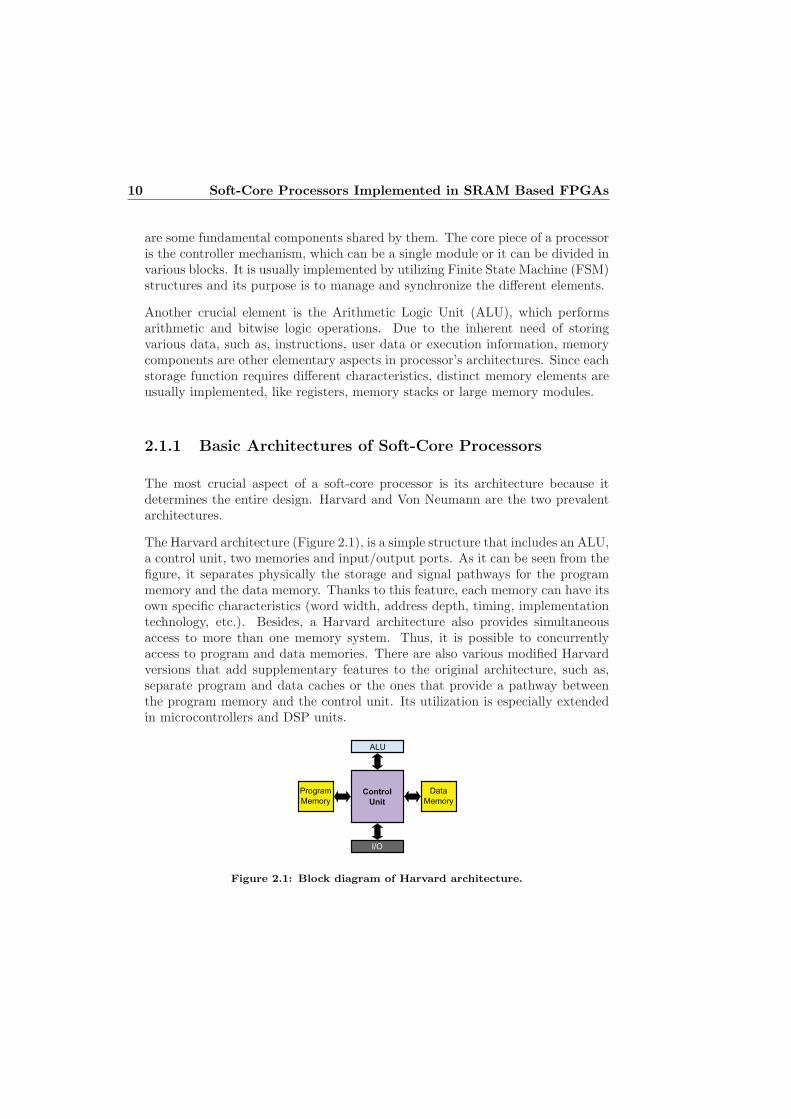
The Harvard architecture (Figure 2.1), is a simple structure that includes an ALU,a control unit, two memories and input/output ports. As it can be seen from thefigure, it separates physically the storage and signal pathways for the programmemory and the data memory. Thanks to this feature, each memory can have itsown specific characteristics (word width, address depth, timing, implementationtechnology, etc.). Besides, a Harvard architecture also provides simultaneousaccess to more than one memory system. Thus, it is possible to concurrentlyaccess to program and data memories. There are also various modified Harvardversions that add supplementary features to the original architecture, such as,separate program and data caches or the ones that provide a pathway betweenthe program memory and the control unit. Its utilization is especially extendedin microcontrollers and DSP units.
���
��������
���
�����
���
�������
���
���
Figure 2.1: Block diagram of Harvard architecture.

2.1 General Aspects of Soft-Core Processors 11
As Figure 2.2 depicts, the Von Neumann architecture is simpler than the Harvard.It consists of a Central Processing Unit (CPU) that includes an ALU and a controlunit, a shared memory for user data and program instructions and input/ouputdevices. The shared memory and the usage of the same bus implies that it isnot possible to read an instruction and to write/read to/from the memory atthe same time. During program execution the CPU fetches a single instructionfrom the shared memory and executes it. This sequential instruction executionproduces a relatively slow operation. This problem is usually referred as the VonNeuman Bottleneck. For this reason, usually the common application scope ofthis architecture usually are interface and control applications.
�������������� ���
������ ���
�����
������� ���
������������� ����� �
������
Figure 2.2: Block diagram of Von Neumann architecture.
Another decision that has to be adopted when designing a processor is to deter-mine its instruction set. The two major strategies in this context are the ReducedInstruction Set Computing (RISC) and the Complex Instruction Set Computing(CISC):
• The CISC strategy is based on utilizing a single instruction to executevarious low-level operations, enabling multi-step operations or different ad-dressing modes within a single instruction. To do so, this strategy focuseson building the complex instructions in the hardware. Thanks to this aCISC architecture can complete tasks with few instructions which reducesthe memory needs. In addition, a CISC scheme significantly reduces com-plier’s work.
• The RISC strategy relies on the idea that a simplified instruction set canprovide higher performance levels due to the more limited usage of clockcycles to execute each instruction. To adopt this strategy implies moreinstructions and, hence, larger program memories. In addition, the com-piler has to perform more work to convert high-level code into assembler.Nevertheless, the utilization of reduced instruction strategies demands lesshardware to implement the functionality of the instructions. Another sig-nificant advantage is that due to the uniform demand of clock cycles from

12 Soft-Core Processors Implemented in SRAM Based FPGAs
instructions, it is possible to utilize pipelining, which enables to increaseperformance.
The number of clock cycles required to execute each instruction is a relevantfactor, which is known as instruction cycle. In many cases the demanded cyclesmay vary depending on the instruction type. For instance, some processors needmore cycles to execute conditional branches than regular instructions. In anycase, the less clock cycles needed for each instruction, the faster is executed theprogram. Execution with reduced clock cycles commonly comes with hardwarecomplexity. Which on the other hand, can affect the design’s overall performanceand/or the resource overhead. In [39], three versions of the same microcontrollerwere developed, each of them with different structures of the instruction cycle: asingle clock cycle with a dual clock, a double clock cycle, and a single clock cycle.The results obtained in terms of maximum achievable frequency were 36 MHz,86.1 MHz and 55 MHz, respectively. In addition, the third version significantlyincreased the hardware overhead. Due to those aspects, a good design practiceis to study the application or system requirements (system’s clock frequency,available resources, etc.) in order to make a trade-off decision that fits better.
2.1.2 Soft-Core Processor IPs
Soft-core designs are usually available as Intellectual Property (IP) cores, whichcan be protected under intellectual property laws or patents. An IP core is areusable unit of logic design that belongs to a designer or to a party. Hence,once a soft-core IP has been designed, it is available to be re-used across severaldesigns. IPs often are available in HDL, such as, VHDL or Verilog, providing asynthesizable Register-Transfer Level (RTL) description. This allows developersto adapt designs at functional level by modifying the HDL code. However, consid-ering that not all the IP vendors offer support or warranty for modified designs,this possibility can be an arduous task depending on the situation. In cases wherevendors find protection against reverse engineering, the IP cores are provided asnetlists. A netlist is a generic gate-level description of the connectivity of circuitelements.
Thanks to their adaptability, reusability, potential and the relative ease of de-signing HDL models, there is a remarkable quantity of soft-core IP processorsavailable. Depending on the objective of developers, their utilization scope canbe commercial or a decentralized development model that encourages open collab-oration, known as open source. Commercial IP cores are commonly distributedunder restrictive commercial licenses that have to be purchased by the client.Open source is commonly distributed under more flexible and free licenses. A

2.1 General Aspects of Soft-Core Processors 13
remarkable aspect of the open-source project is that, since they are based oncommunity-work (which implies constant improvement), they can be classified indifferent stages of development, starting from the initial alpha and beta phasesto the stable or mature categories.
One of the most remarkable open-source site is OpenCores [40]. OpenCores is acommunity for development of hardware IP cores as open source. Despite of thefact that OpenCores initially was a commercially owned organization, since 2015is an independent Free and Open Source Silicon Foundation (FOSSi). Its sitehosts source code of a great number of digital hardware projects including vari-ous sof-core processors. Projects from OpenCores have been used in a number ofresearches and even in private companies. Most of the projects in OpenCores usethe GNU Lesser General Public License (LGPL) [41], a free software license thatpermits developers and vendors to utilize the IP without being required to releasethe source code of their own designs. However, any modification done in a com-ponent under LGPL has to be shared with the OpenCores community. Anotherwidely used license is the Berkeley Software Distribution (BSD) [42], which isless restrictive and disclaims any warranty. Sourceforge is another relevant opensource site that contains several soft-core processor projects. Nevertheless, thescope of this site is more general since it gathers a wide range of project types.
Several publications have compared most of the existing soft-core processors [23–25, 43–48]. For that reason, the following section only covers a brief summary ofsome of the most remarkable soft-core processors available from both, the majorvendors and the open-source community.
Commercial Soft-Core Processor IPs
Most of FPGA vendors provide one or more soft-core processors to be used withtheir devices. These IPs are optimized for the vendor’s technology which, usuallyare platform dependant. Other commercial vendors that do not manufacturehardware are exclusively focused on designing IPs. In these cases, the designedIPs have in general platform independence, which enables to implement them indifferent devices. In the following, a brief description of the major commercialsoft-core processor IPs is presented.
• MicroBlaze. The MicroBlaze is a Xilinx’s proprietary 32-bit soft-coreprocessor. It has a RISC architecture that can be customized with differentperipheral and memory configurations. It is highly optimized for Xilinxdevices, in a way that occupies significantly less area than the majority ofits counterparts, such as the OpenRISC 1200 or the LEON. Due to these

14 Soft-Core Processors Implemented in SRAM Based FPGAs
benefits, the MicroBlaze has been widely used in a number of projects[8, 21, 49–62].
• PicoBlaze. The PicoBlaze is a 8-bit proprietary soft-core processor pro-vided by Xilinx. This small RISC microcontroller developed by Ken Chap-man [38], is one of the most popular small soft-cores when using Xilinxdevices [54, 58, 60, 63–76]. As Figure 2.3 shows, it is a simple design whichhas been a key factor for its success. The PicoBlaze was released underthe KCPSM name. Despite that the official meaning of this acronym isConstant(K) Coded Programmable State Machine, the initial meaning wasrelated with its creator (”Ken Chapman’s PSM”). Xilinx provides distinctPicoBlaze versions for its device families (KCPSM, KCPSM2, KCPSM3and KCPSM6). Third parties like Mediatronix and open-source projectsprovide various development tool-sets for the PicoBlaze.
1Kx18
Instruction
PROM
64-Byte
Scratchpad RAM
Instruction
Decoder
16 Byte-Wide
RegistersIN_PORT
INTERRUPT
OUT_PORT
PORT_ID
Constants
Pro
gra
m C
ounte
r
CA
LL/R
ET
UR
N
Sta
ck
ALU
IE Enable
C Carry
Z Zero
Figure 2.3: Block diagram of PicoBlaze.
• Nios. Nios was Altera’s first 16-bit soft-core processor that was later re-placed by the newer Nios II version. NiosII is a 32-bit soft-core designedspecifically for the Intel (formerly Altera) family of FPGAs. It has a Hard-ware Abstraction Layer (HAL) architecture. Intel also allows to choosedifferent Nios II versions (Nios II/f ”Fast”, Nios II/e ”Economy” and NiosII/s ”Standard” ), each of them being optimized for specific applications.In addition, a software tool chain is available for all versions that permitsto customize a set of peripherals, instruction, memories, and I/O circuitry.Bearing in mind that Nios II is limited to operating systems that utilize asimplified protection and virtual memory-model, an optional Memory Man-agement Unit (MMU) can be implemented. This MMU allows to work withhardware-based paging and protection operating systems, like the Linuxkernel. Finally, an also optional and more simpler Memory Protection Unit(MPU) is available to provide a similar memory protection. The main ben-

2.1 General Aspects of Soft-Core Processors 15
efit of using the MPU over the MMU is its better performance. Despitethat the usage of this soft-core is less extended, various studies have usedit. In [77], UT Nios, an adaptation of the Nios II, was introduced.
• Cortex - M1. This proprietary soft-core is a 32-bit RISC ARM processorlicensed by ARM Holdings plc. Its design is based on the ARMv6-M archi-tecture and is especially optimized for FPGAs. It has a three-stage pipeline,configurable instruction and data memories, and 1 to 32 interrupts. Theutilization of this core in the literature is more limited.
• Xtensa. Xtensa is a set of 32-bit soft-core processors with RISC architec-ture featured by Tensilica. These are highly adaptable IPs that allow tocustomize several features like bus width, cache size, memory managementand interrupt control. In addition, thanks to the supplied tools, users canextend Xtensa’s instruction set by introducing new instructions.
• TSK3000A. TSK3000A is a 32-bit, no royalty-free, Wishbone-compatibleand platform independent RISC soft-core processor from Altium Limited.It provides a fast register access and a zero-wait state block RAM amountthat can be defined by the user, with a dual-port access. It has a five-stagepipeline and it can handle up to 32 interrupts that work in two modes(standard and vectored). Altium also provides the TSK51/52 IP, an 8-bitIntel 8051 instruction set compatible soft-core processor.
• eSi-RISC. As its name indicates, it is a RISC soft-core processor archi-tecture developed by Ensilica. This IP has a five-stage pipeline, supportsmultiprocessing, can handle up to 32 interrupts and is available in five ver-sions: eSi-1600, eSi-1650, eSi-3200, eSi-3250 and eSi-3260. While the firsttwo IPs feature 16-bit data-path implementations, the rest feature 32-bitdata-paths. Its instruction set can be freely intermixed. It supports both,floating-point and fixed-point arithmetic.
• Other propietary IPs. Further to the mentioned IPs, additional com-mercial soft-core processors are available, such as the ARC by SynopsysInc., MCL51 and MCL86 by MicroCore Labsm, etc.
Open-Source Soft-Core Processor IPs
The majority of the open-source soft-core processors are based on existing ar-chitectures. While in many cases the reference design for these IPs is a classichardware processor or a microcontroller, in other cases the IPs are open-sourceand platform independent version of a proprietary soft-core. Besides, some de-signers have developed new soft-core processor architectures. The majority of
16 Soft-Core Processors Implemented in SRAM Based FPGAs
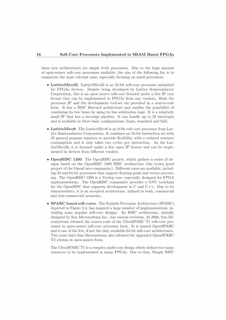
these new architectures are simple 8-bit processors. Due to the huge amountof open-source soft-core processors available, the aim of the following list is toenumerate the most relevant ones, especially focusing on small processors.
• LatticeMico32. LatticeMico32 is an 32-bit soft-core processor optimizedfor FPGAs devices. Despite being developed by Lattice SemiconductorCorporation, this is an open source soft-core licensed under a free IP corelicense that can be implemented in FPGAs from any vendors. Both theprocessor IP and the development tool-set are provided in a source-codeform. It has a RISC Harvard architecture and enables the possibility ofcombining its two buses by using its bus arbitration logic. It is a relativelysmall IP that has a six-stage pipeline. It can handle up to 32 interruptsand is available in three basic configurations (basis, standard and full).
• LatticeMico8. The LatticeMico8 is an 8-bit soft-core processor from Lat-tice Semiconductor Corporation. It combines an 18-bit instruction set with32 general purpose registers to provide flexibility with a reduced resourceconsumption and it only takes two cycles per instruction. As the Lat-ticeMico32, it is licensed under a free open IP license and can be imple-mented in devices from different vendors.
• OpenRISC 1200. The OpenRISC project, which gathers a series of de-signs based on the OpenRISC 1000 RISC architecture (the crown jewelproject of the OpenCores community). Different cores are available, includ-ing 32 and 64-bit processors that support floating point and vector process-ing. The OpenRISC 1200 is a Verilog core, especially designed for FPGAimplementations. The OpenRISC community provides a GNU toolchainfor the OpenRISC that supports development in C and C++. Due to itscharacteristics, it is an accepted architecture, utilized in both, commercialand non-commercial scenarios.
• SPARC based soft-cores. The Scalable Processor Architecture (SPARC),depicted in Figure 2.4, has inspired a large number of implementations, in-cluding some popular soft-core designs. Its RISC architecture, initiallydesigned by Sun Microsystems Inc., has various revisions. In 2006, Sun Mi-crosystems released the source-code of the UltraSPARC T1 soft-core pro-cessor in open-source soft-core processor form. It is named OpenSPARCand is one of the few, if not the only, available 64-bit soft-core architectures.Two years later Sun Microsystems also released the upgraded OpenSPARCT2 version in open-source form.
The UltraSPARC T1 is a complex multi-core design which utilizes too manyresources to be implemented in many FPGAs. Due to that, Simply RISC
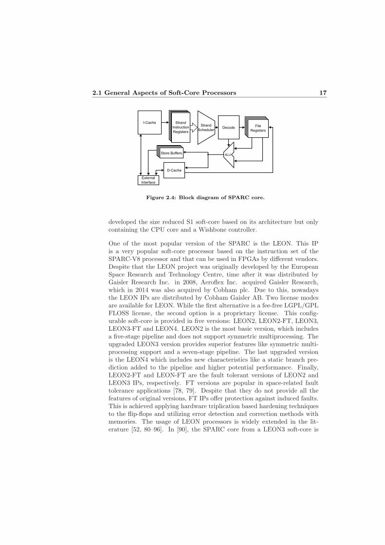
2.1 General Aspects of Soft-Core Processors 17
Store BuffersStore Buffers
File
RegistersFile
Registers
Strand
Instruction
Registers
Strand
Instruction
Registers
Strand
Instruction
Registers
I-Cache
Store BuffersALU
Strand
Instruction
RegistersDecode
File
RegistersFile
Registers
Store Buffers
D-Cache
External
Interface
Strand
Scheduler
Figure 2.4: Block diagram of SPARC core.
developed the size reduced S1 soft-core based on its architecture but onlycontaining the CPU core and a Wishbone controller.
One of the most popular version of the SPARC is the LEON. This IPis a very popular soft-core processor based on the instruction set of theSPARC-V8 processor and that can be used in FPGAs by different vendors.Despite that the LEON project was originally developed by the EuropeanSpace Research and Technology Centre, time after it was distributed byGaisler Research Inc. in 2008, Aeroflex Inc. acquired Gaisler Research,which in 2014 was also acquired by Cobham plc. Due to this, nowadaysthe LEON IPs are distributed by Cobham Gaisler AB. Two license modesare available for LEON. While the first alternative is a fee-free LGPL/GPLFLOSS license, the second option is a proprietary license. This config-urable soft-core is provided in five versions: LEON2, LEON2-FT, LEON3,LEON3-FT and LEON4. LEON2 is the most basic version, which includesa five-stage pipeline and does not support symmetric multiprocessing. Theupgraded LEON3 version provides superior features like symmetric multi-processing support and a seven-stage pipeline. The last upgraded versionis the LEON4 which includes new characteristics like a static branch pre-diction added to the pipeline and higher potential performance. Finally,LEON2-FT and LEON-FT are the fault tolerant versions of LEON2 andLEON3 IPs, respectively. FT versions are popular in space-related faulttolerance applications [78, 79]. Despite that they do not provide all thefeatures of original versions, FT IPs offer protection against induced faults.This is achieved applying hardware triplication based hardening techniquesto the flip-flops and utilizing error detection and correction methods withmemories. The usage of LEON processors is widely extended in the lit-erature [52, 80–96]. In [90], the SPARC core from a LEON3 soft-core is
18 Soft-Core Processors Implemented in SRAM Based FPGAs
substituted by a MIPS based core, adapting its functionality to differentbuses and peripherals.
• MicroBlaze based soft-cores. The extended use of the MicroBlaze fromXilinx has motivated the development of several open-source alternatives.The most representative ones are: aeMB (beta), MB-Lite (stable), Open-Fire Processor Core (alpha) and myBlaze (mature) from OpenCores and se-cretBlaze developed by LIRMM, University of Montpellier. Although eachof them provides distinct features, for instance not implementing floating-point support or utilizing different stage pipelines, all of them are MicroB-laze compatible cores. In addition, [97] proposes a multiprocessor systembased on the MicroBlaze.
• PicoBlaze based soft-cores . This popular soft-core from Xilinx has alsoinspired different platform-independent open-source projects like the Pa-coBlaze (beta) and the copyBlaze (mature), available in Verilog and VHDLrespectively. In [26], another platform-independent version was presented.As this work itself states, making adaptations in the highly optimized de-sign of the PicoBlaze commonly comes with a resource overhead and per-formance penalty.
• 8080 based soft-cores. Released in 1974 by Intel, the 8080 is consideredone of the first usable microprocessors. Its architecture inspired differentprocessors such as the Am9080 by AMD, Z80 by Zilog of the upgraded8085 version by Intel. Several soft-core processors have been also devel-oped inspired in its designs. Some of the most remarkable ones are avail-able in OpenCores community: Lightweight 8080 compatible (stable), T80cpu (stable), Wishbone High Performance Z80 (stable), z80control (alpha)and 80e - Z80/Z180 compatible processor extended by eZ80 instructions(stable).
• 6800 based soft-cores The MC6800, known as 6800, is an 8-bit processorwith a Von Neumann architecture released by Motolora in 1974. Its usewas widely extended in control designs for computer peripherals and testequipment. OpenCores provides different soft-cores based on this processor:System68 (stable), System11 (alpha), 68HC05/68HC08 (stable) and HC11compatible Gator Microprocessor (stable).
• 6502 based soft-cores. The 6502 is another classic architecture that wasdeveloped in 1975 by two of the former designers of the 6800. Due to itsreduced price, this microcontroller became very popular in its time. Open-Cores provides several soft-core alternatives based on this design: T65 CPU(stable), ag 6502 soft core with phase-level accuracy (beta), CPU6502 TC -
2.1 General Aspects of Soft-Core Processors 19
CPU65C02 TC Processor Soft Core with accurate timing (stable), T6507LP(beta) and Lattice 6502 (beta), which is a 6502 based core optimized forFPGAs from Lattice.
• PIC16 based soft-cores. PIC is a series of microcontrollers developed byMicrochip Technology, based on the PIC1650 by General Instrument’s Mi-croelectronics Division. Since its first release in 1976, the microcontrollersfrom the PIC series have gained a remarkable acceptance in both the in-dustrial field and the hobbyists community. One of the most remarkableversions is the PIC16, which is an 8-bit minimalistic design with a HarvardRISC architecture. Aspects like its reduced price, wide availability, exten-sive user base, large documentation and the free development tools availablehave helped to increase its relevance. This popularity has motivated the de-velopment of a number of PIC16 based soft-cores, many of the available inOpenCores: RISC 16F84, PPX16 MCU (stable), ClaiRISC (stable), MINI-RISC core (stable), RISC5x (stable), risc16f84 (stable). In addition, severalsoft-cores based on the PIC16 architecture have been proposed in the litera-ture, such as the CQPIC [98], the UMASScore [45] and the microcontrollerfrom [39]. In [99], a PIC16F84A based FPGA design was presented, whichimproves the power stability over the commercial microcontroller.
• 8051 based soft-cores. In 1980 Intel released the 8051 microcontrollerbased on the previous 8048, 8051 and 8052 units. Its 8-bit Harvard archi-tecture has also been a reference for several soft-core implementations. Themost relevant IPs from OpenCores are: T51 MCU (stable), Lightweight8051 compatible CPU (beta), Turbo 8051 (beta) and 8051 core (alpha). In[100], the LP805X, a low power, modular and adaptable implementation ofthe 8051 was presented.
• AVR compatibles. The AVR microcontroller developed by Atmel is an-other reference design for various soft-core implementations. Initially de-signed to execute C code, its simple RISC Harvard architecture and its easeof programming are the main reasons for its popularity. OpenCores pro-vides several open-source soft-cores: AVR Core (stable), AVR HP (stable),Hyper Pipelined AVR Core (stable) and AVRtinyX61core (beta).
• Other soft-core processors. A large number of additional soft-core im-plementations are available based on other architectures or designed fromscratch. The most remarkable IPs are: the DSPuva16 [34] by the Univer-sity of Valladolid, the MicroSimplez based on the architecture presented in[101], the MSL16 proposed in [102] and the DSP block based iDEA soft-coreprocessor developed in [103].

20 Soft-Core Processors Implemented in SRAM Based FPGAs
2.2 SRAM Based FPGAs
Field Programmable Gate Arrays (FPGAs) are one of the most interesting plat-forms for implementing soft-core processors, thanks to their flexibility, perfor-mance, low-cost design and short time to market. Furthermore, their reconfig-uration capability makes them suitable for achieving flexible designs, capable ofre-adapting in the field in response to changes and correct possible issues. Thisprovides high reliability and obsolescence mitigation. For these reasons, the plat-form selected in this work is a SoC device that includes an SRAM-based FPGA.The following section summarizes the most relevant aspects of FPGAs, focusingon the SRAM-based FPGAs and the Zynq device used in this work.
2.2.1 Introducing Programmable Logic Devices
FPGAs are Programmable Logic Devices (PLDs) utilized in electronic designs toimplement reconfigurable digital circuits. Unlike monolithic integrated circuitsthat integrate fixed designs, PLDs are manufactured with an unsettled function.This feature makes possible developing customized hardware designs that coupleclosely with requirements of the application.
Before the rise of PLD technologies, the only available programmable deviceswhere memories, such as ROMs (Read Only Memories), PROMs (ProgrammableROMs), EPROMs (Erasable PROMs) and EEPROMs (Electrically ErasablePROMs). Despite they were a valuable alternative to store data, they presentedseveral drawbacks, such as a slow operation (compared with dedicated logic cir-cuits), unreliable asynchronous function, high power consumption and high costs.Besides, due to the lack of input/output registers they were not a stand-alonealternative to implement sequential logic designs.
Due to the described limitations, there was a significant need for new approaches.This is the reason why the XC157 Multi-Gate Array (released by Motorola in1968) depicted in Figure 2.5 (obtained from its data sheet) was a milestone inthe history of programmable logic devices. This first programmable logic de-vice was a simple gate array with 30 input/output pins and 12 gates. In thefollowing years several devices arose, such as the TMS2000 from Texas Instru-ments Inc., the first erasable PLD developed by General Electric, the DM7575 (amask-programmable logic array) from National Semiconductor or the MMI 5760(programmable associative logic array) by General Electric.
Since these first release the programmable logic technology has experimented ahuge evolution offering a wide range of devices. Despite the complexity and the
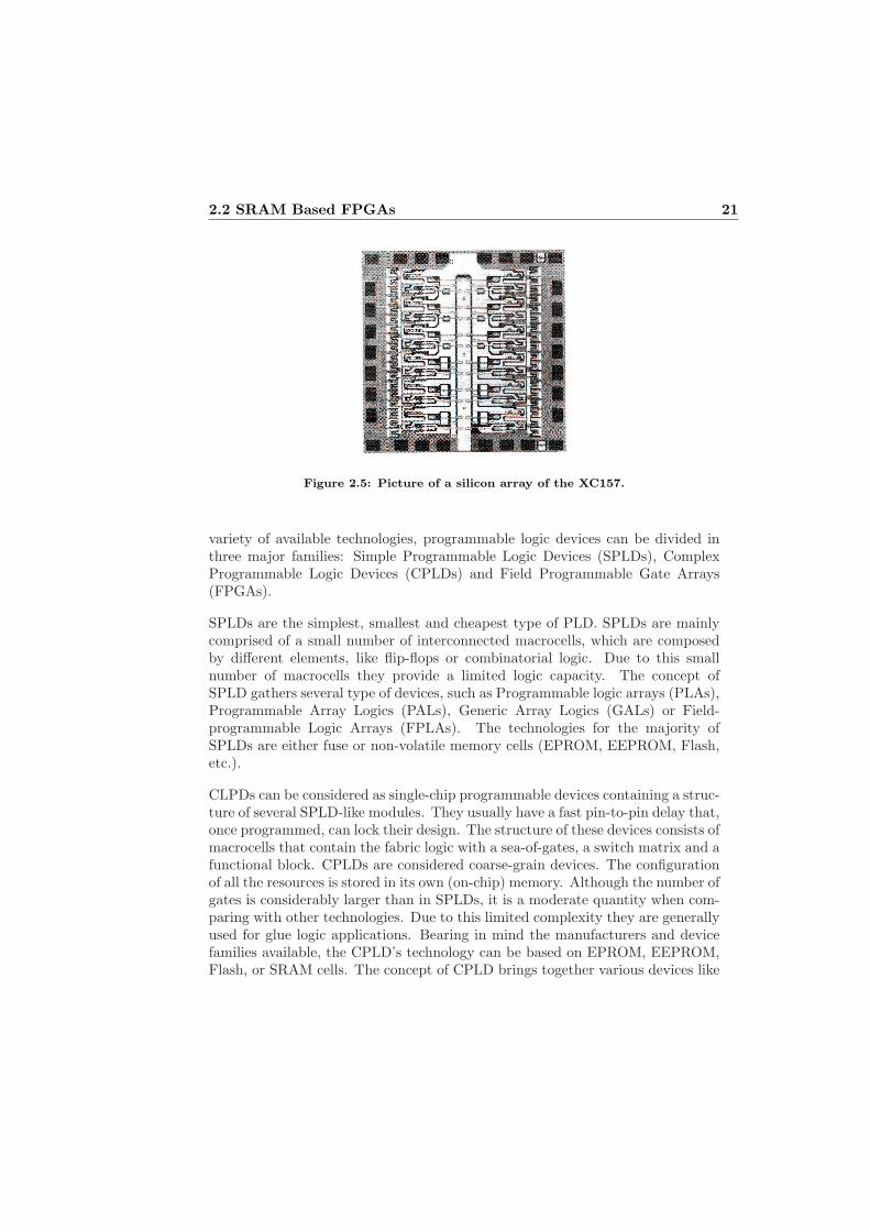
2.2 SRAM Based FPGAs 21
Figure 2.5: Picture of a silicon array of the XC157.
variety of available technologies, programmable logic devices can be divided inthree major families: Simple Programmable Logic Devices (SPLDs), ComplexProgrammable Logic Devices (CPLDs) and Field Programmable Gate Arrays(FPGAs).
SPLDs are the simplest, smallest and cheapest type of PLD. SPLDs are mainlycomprised of a small number of interconnected macrocells, which are composedby different elements, like flip-flops or combinatorial logic. Due to this smallnumber of macrocells they provide a limited logic capacity. The concept ofSPLD gathers several type of devices, such as Programmable logic arrays (PLAs),Programmable Array Logics (PALs), Generic Array Logics (GALs) or Field-programmable Logic Arrays (FPLAs). The technologies for the majority ofSPLDs are either fuse or non-volatile memory cells (EPROM, EEPROM, Flash,etc.).
CLPDs can be considered as single-chip programmable devices containing a struc-ture of several SPLD-like modules. They usually have a fast pin-to-pin delay that,once programmed, can lock their design. The structure of these devices consists ofmacrocells that contain the fabric logic with a sea-of-gates, a switch matrix and afunctional block. CPLDs are considered coarse-grain devices. The configurationof all the resources is stored in its own (on-chip) memory. Although the number ofgates is considerably larger than in SPLDs, it is a moderate quantity when com-paring with other technologies. Due to this limited complexity they are generallyused for glue logic applications. Bearing in mind the manufacturers and devicefamilies available, the CPLD’s technology can be based on EPROM, EEPROM,Flash, or SRAM cells. The concept of CPLD brings together various devices like

22 Soft-Core Processors Implemented in SRAM Based FPGAs
Erasable Programmable Logic Devices (EPLDs), Simple Programmable LogicDevices (SPLDs), etc.
At the beginning of the 1980’s there was a gap in the digital electronic business.On the one hand, they were configurable SPLD and CPLD technologies thatprovide a fast designing but couldn’t implement large or complex applications.On the other hand, ASIC technology was able to support highly complex designsthat required an extremely expensive and complicated design process. In orderto fulfil this gap Xilinx Inc. released the XC2064, in 1985, which is consideredthe first commercial FPGA device. Figure 2.6 (obtained from its data sheet)shows the entire block diagram of the XC2064, which was based on the CMOStechnology, that also used SRAM cells for configuration functions.
Figure 2.6: Block diagram of the Xilinx XC2064 logic cell array.
Despite that originally FPGAs started competing with CPLDs sharing similarapplication scopes, thanks to their evolution, FPGAs increased their capabilitiesand speed taking over new application fields. Nowadays, FPGAs are utilized toimplement complete and autonomous SoC designs. Basically FPGAs are inte-grated circuits that can be configured by the final user after the manufacturingprocess. They are fine-grain devices, since they are composed by a large numberof small logic blocks that contain distinct logic resources. Those logic blocks aredistributed following an array structure and are interconnected with reconfig-urable connections. Due to this FPGAs offer higher complexity and versatilitylevels. Distinct architectures are used to manufacture FPGAs. Some of the mostrelevant are: the CMOS based and one-time programmable Antifuse FPGAswidely used in fault tolerant space application, the CMOS and static memory
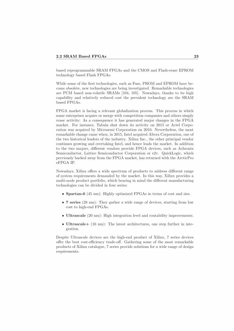
2.2 SRAM Based FPGAs 23
based reprogrammable SRAM FPGAs and the CMOS and Flash-erase EPROMtechnology based Flash FPGAs.
While some of the first technologies, such as Fuse, PROM and EPROM have be-come obsolete, new technologies are being investigated. Remarkable technologiesare PCM based non-volatile SRAMs [104, 105]. Nowadays, thanks to its highcapability and relatively reduced cost the prevalent technology are the SRAMbased FPGAs.
FPGA market is facing a relevant globalization process. This process in whichsome enterprises acquire or merge with competition companies and others simplycease activity: As a consequence it has generated major changes in the FPGAmarket. For instance, Tabula shut down its activity on 2015 or Actel Corpo-ration was acquired by Microsemi Corporation on 2010. Nevertheless, the mostremarkable change came when, in 2015, Intel acquired Altera Corporation, one ofthe two historical leaders of the industry. Xilinx Inc., the other principal vendorcontinues growing and overtaking Intel, and hence leads the market. In additionto the two majors, different vendors provide FPGA devices, such as AchronixSemiconductor, Lattice Semiconductor Corporation or e2v. QuickLogic, whichpreviously backed away from the FPGA market, has returned with the ArcticProeFPGA IP.
Nowadays, Xilinx offers a wide spectrum of products to address different rangeof system requirements demanded by the market. In this way, Xilinx provides amulti-node product portfolio, which bearing in mind the different manufacturingtechnologies can be divided in four series:
• Spartan-6 (45 nm): Highly optimized FPGAs in terms of cost and size.
• 7 series (28 nm): They gather a wide range of devices, starting from lowcost to high-end FPGAs.
• Ultrascale (20 nm): High integration level and routability improvements.
• Ultrascale+ (16 nm): The latest architectures, one step further in inte-gration.
Despite Ultrascale devices are the high-end product of Xilinx, 7 series devicesoffer the best cost-efficiency trade-off. Gathering some of the most remarkableproducts of Xilinx catalogue, 7 series provide solutions for a wide range of designrequirements.

24 Soft-Core Processors Implemented in SRAM Based FPGAs
2.2.2 Architecture of 7 Series Devices and Zynq-7000 AllProgrammable SoC by Xilinx
Xilinx 7 series include four FPGA families (Spartan-7, Artix-7, Kintex-7 andVirtex-7) and the Zynq-7000 all programmable SoC whicht are based on a 28 nmhigh-k metal gate process technology. Each device of the different families targetsa particular market segment. They offer distinct alternatives in terms of pricerange, form factor, high-end connectivity bandwidth, logic resources capacity, sig-nal processing capability, etc. The technical evolution of 7 series devices has leadto considerably enhance system performance with 2.9 Tb/s of I/O bandwidth,obtaining capacities of up to 2 million logic cells and cutting power consumptionby 50% compared with previous generations [106].
Despite that in many cases the synthesis tool decides and assigns the resourceswithout needing any action from the designer, it is advisable to understand someconcepts of the architecture and logic resources of FPGAs to take advantage ofits full potential.
As Figure 2.7 shows, the architecture of 7 series devices, like most FPGAs, isbased on a logic block array structure interconnected with the general routingnetwork via switch matrices and surrounded by a periphery of I/O blocks. Thisreprogrammable network of signal paths is called routing. Due to the varietyof resources and the interconnection options available, in most designs severalrouting alternatives that may produce different results in terms of efficiency orperformance can be obtained. The complexity of the designs and the intercon-nection features require the usage of routing and placement tools. These toolsprovide optimized routings by using various analysis and algorithms. Althoughthat in some cases it can help to understand and improve the design, generallyis not necessary to acquire a specific knowledge about interconnection features.Usually the routing process is transparent to developers.
7 series FPGAs include several dedicated resources and primitives, some of themost relevant ones are introduced in the following lines.
Configurable Logic Block (CLB)
In Xilinx devices the fundamental building logic blocks used for implementingboth, combinational and sequential circuits, are named Configurable Logic Block(CLB) [1]. As Figure 2.8 illustrates, each of the 7 series CLBs (which are iden-tical to the CLBs of Virtex-6 FPGAs) contains two slices that are comprised bythe following resources: four Look-Up Tables (LUTs), wide-function multiplex-ers, eight flip-flops and a dedicated high-speed carry logic. Depending on the
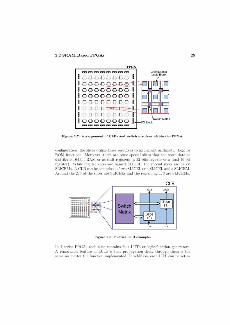
2.2 SRAM Based FPGAs 25
FPGA
Switch Matrix
I/O Block
Configurable Logic Block
Figure 2.7: Arrangement of CLBs and switch matrices within the FPGA.
configuration, the slices utilize these resources to implement arithmetic, logic orROM functions. Moreover, there are some special slices that can store data asdistributed 64-bit RAM or as shift registers (a 32 bits register or a dual 16-bitregister). While regular slices are named SLICEL, the special slices are calledSLICEMs. A CLB can be comprised of two SLICEL or a SLICEL and a SLICEM.Around the 2/3 of the slices are SLICELs and the remaining 1/3 are SLICEMs.
Switch
MatrixSlice(0)
Slice(1)
COUT COUT
CIN CIN
CLB
Figure 2.8: 7 series CLB example.
In 7 series FPGAs each slice contains four LUTs or logic-function generators.A remarkable feature of LUTs is that propagation delay through them is thesame no matter the function implemented. In addition, each LUT can be set as
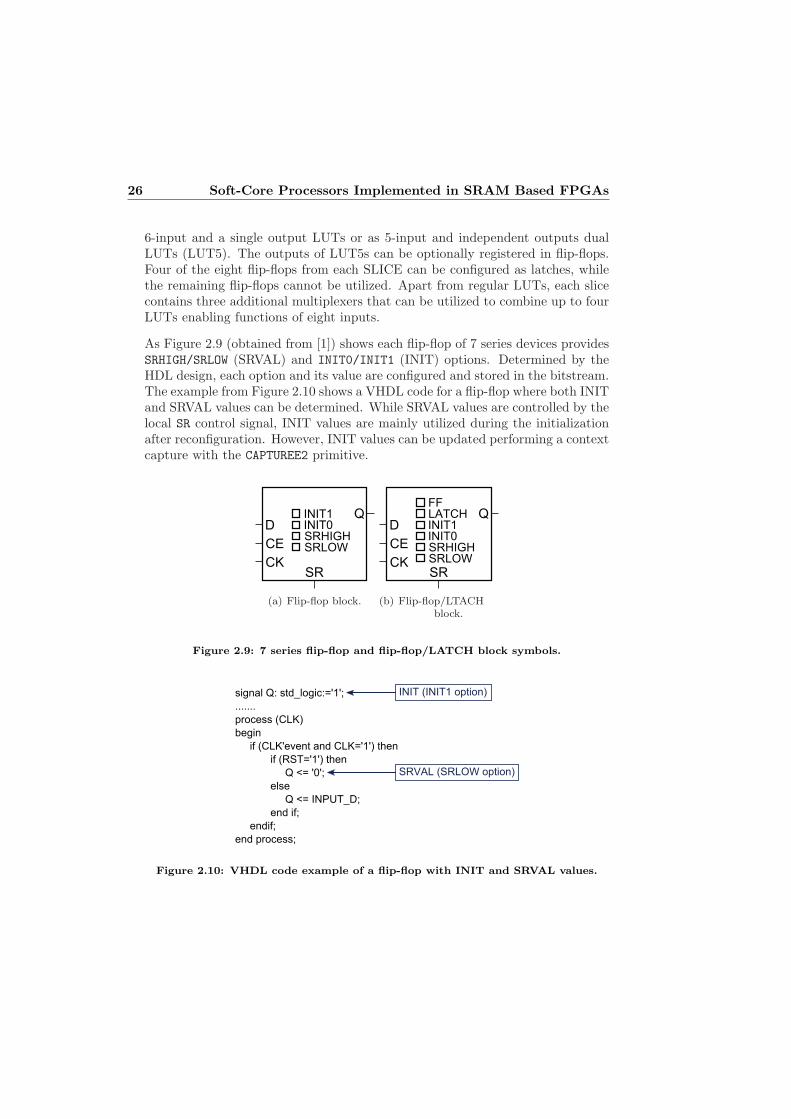
26 Soft-Core Processors Implemented in SRAM Based FPGAs
6-input and a single output LUTs or as 5-input and independent outputs dualLUTs (LUT5). The outputs of LUT5s can be optionally registered in flip-flops.Four of the eight flip-flops from each SLICE can be configured as latches, whilethe remaining flip-flops cannot be utilized. Apart from regular LUTs, each slicecontains three additional multiplexers that can be utilized to combine up to fourLUTs enabling functions of eight inputs.
As Figure 2.9 (obtained from [1]) shows each flip-flop of 7 series devices providesSRHIGH/SRLOW (SRVAL) and INIT0/INIT1 (INIT) options. Determined by theHDL design, each option and its value are configured and stored in the bitstream.The example from Figure 2.10 shows a VHDL code for a flip-flop where both INITand SRVAL values can be determined. While SRVAL values are controlled by thelocal SR control signal, INIT values are mainly utilized during the initializationafter reconfiguration. However, INIT values can be updated performing a contextcapture with the CAPTUREE2 primitive.
INIT1INIT0SRHIGHSRLOW
SR
D
CE
CK
Q
(a) Flip-flop block.
INIT1INIT0SRHIGHSRLOW
SR
D
CE
CK
QLATCHFF
(b) Flip-flop/LTACHblock.
Figure 2.9: 7 series flip-flop and flip-flop/LATCH block symbols.
������������� ��������
�������
�� ����������
�����
����������������������������������
���������������� !"���������
�������������������#���$��
����������������
�������������������#��%&'("�)�
�������������������
�����������
������ �����
%&%"��%&%"�� �� ��
! *+���! �,-� �� ��
Figure 2.10: VHDL code example of a flip-flop with INIT and SRVAL values.
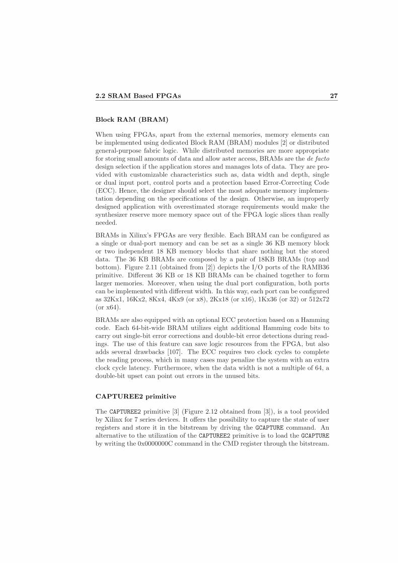
2.2 SRAM Based FPGAs 27
Block RAM (BRAM)
When using FPGAs, apart from the external memories, memory elements canbe implemented using dedicated Block RAM (BRAM) modules [2] or distributedgeneral-purpose fabric logic. While distributed memories are more appropriatefor storing small amounts of data and allow aster access, BRAMs are the de factodesign selection if the application stores and manages lots of data. They are pro-vided with customizable characteristics such as, data width and depth, singleor dual input port, control ports and a protection based Error-Correcting Code(ECC). Hence, the designer should select the most adequate memory implemen-tation depending on the specifications of the design. Otherwise, an improperlydesigned application with overestimated storage requirements would make thesynthesizer reserve more memory space out of the FPGA logic slices than reallyneeded.
BRAMs in Xilinx’s FPGAs are very flexible. Each BRAM can be configured asa single or dual-port memory and can be set as a single 36 KB memory blockor two independent 18 KB memory blocks that share nothing but the storeddata. The 36 KB BRAMs are composed by a pair of 18KB BRAMs (top andbottom). Figure 2.11 (obtained from [2]) depicts the I/O ports of the RAMB36primitive. Different 36 KB or 18 KB BRAMs can be chained together to formlarger memories. Moreover, when using the dual port configuration, both portscan be implemented with different width. In this way, each port can be configuredas 32Kx1, 16Kx2, 8Kx4, 4Kx9 (or x8), 2Kx18 (or x16), 1Kx36 (or 32) or 512x72(or x64).
BRAMs are also equipped with an optional ECC protection based on a Hammingcode. Each 64-bit-wide BRAM utilizes eight additional Hamming code bits tocarry out single-bit error corrections and double-bit error detections during read-ings. The use of this feature can save logic resources from the FPGA, but alsoadds several drawbacks [107]. The ECC requires two clock cycles to completethe reading process, which in many cases may penalize the system with an extraclock cycle latency. Furthermore, when the data width is not a multiple of 64, adouble-bit upset can point out errors in the unused bits.
CAPTUREE2 primitive
The CAPTUREE2 primitive [3] (Figure 2.12 obtained from [3]), is a tool providedby Xilinx for 7 series devices. It offers the possibility to capture the state of userregisters and store it in the bitstream by driving the GCAPTURE command. Analternative to the utilization of the CAPTUREE2 primitive is to load the GCAPTUREby writing the 0x0000000C command in the CMD register through the bitstream.

28 Soft-Core Processors Implemented in SRAM Based FPGAs
Figure 2.11: RAMB36 Block RAM primitive symbol.
By virtue of this functionality, current register (flip-flop and latch) values canbe stored in the configuration memory by triggering the CAP input from thisprimitive. Once the CAP has been asserted, the content of registers is capturedat next low-to-high clock transition. These register values are stored in the sameconfiguration memory cell that programs the init state configuration of registers(INIT values). These register values can be read from the device along with allother configuration memory contents utilizing the readback function. Althoughthe default option is to capture data after every trigger when transition on CLK
while CAP is asserted, this primitive provides the ONESHOT=TRUE attribute to limitthe readback operation to a single data capture. One significant limitation of thisprimitive is that it does not capture the content of SRL, LUT RAM and BRAM.
CAPTUREE2CAP
CLK
Figure 2.12: CAPTUREE2 primitive symbol.

2.2 SRAM Based FPGAs 29
Another relevant limitation of this method is that it stores in the bitstreamthe content of all the registers from the device, even when only some particularregisters are needed to be captured. Hence, the information of the registers thatshould remain unchanged would also be updated. In order to solve this problem,the resources of the device that must remain unchanged have to be protected bysetting certain bits of the bitstream. This process requires a complex bitstreammodification process, especially bearing in mind that Xilinx has not releasedenough information for 7 series devices bitstream.
To take advantage of the CAPTUREE2 primitive, it is necessary to previously knowthe location of each data bit in the bitstream. The most straightforward way toobtain this information is to use Xilinx’s software (Vivado, ISE, etc.) to generatethe logic location text file (*.ll).
STARTUPE2 primitive
The STARTUPE2 is a primitive that features an interface that relates the userlogic resources with the status signal and the configuration logic control. Thisprimitive can be utilized in an implementation to obtain user control over certainselected configuration signals during the operation. As Figure 2.13 (obtainedfrom [4]) illustrates, it provides with different input and output ports, some ofthem being associated with the startup sequence. The startup sequence, whichlasts a minimum of eight clock cycles, is an initialization process managed by aneight-phase sequence that is commonly performed after loading the configurationbitstream. The specific order of the initialization phases can be varied by theuser through bitstream commands.
Figure 2.13: STARTUPE2 primitive symbol.
One of the most relevant ports of this primitive is the GSR (Global Set/Reset).The GSR resets the device by driving the GRESTORE command. This active high in-put port leads an asynchronous set/reset signal that enables to initialize CLB/IO

30 Soft-Core Processors Implemented in SRAM Based FPGAs
flip-flops and DSP registers of the entire device in their initial state. The ini-tialization values of flip-flops are determined by the INIT0/INIT1 options (2.9)defined in the bitstream. Furthermore, INIT values can be updated with actualvalues of registers via GCAPTURE command. A remarkable aspect of the utilizationof GSR signal is that it does not require general-purpose routing.
In 7 series FPGAS the GRESTORE command can be driven with the GSR signalof the STARTUPE2 or loading the 0x0000000A command in the CMD register.GRESTORE command is commonly asserted during the initialisation process afterconfiguring the FPGA to load the INIT values. Considering that the skew andrelease processes are done asynchronously, some flip-flops may be released indifferent clock cycles causing metastable events. For this reason, it is advisableto stop the clock before asserting the GSR signal and to wait until it spreads acrossthe entire device. Another recommendable practice when using the GSR signalis to cluster tightly all the registers in order to minimize the path length.
Other Resources
Other remarkable resources available in 7 series FPGAs are the I/O banks, DSPslices, clocking resources and the ILA core.
• Devices from the 7 series feature high-performance and high-range I/Obanks, each of them containing (with some exceptions) 50 SelectIO pinsthat can be configured for different standards. While high-performance I/Obanks are designed for high-speed interfacing with low voltages (up to 1.8V),high-range I/O banks are tailored to support a variety I/O standards withhigher voltages (up to 3.3V). 7 series FPGAs contain different combinationsof these banks distributed along the periphery of the device. Moreover,additional I/O logic design primitives that provide specific features areavailable.
• An FPGA contains several clocking resources distributed (CLBs, BRAMs,DSPs, etc.) in different clock regions, which number varies depending onthe device. Each clock region spans 50 CLBs from top to bottom up withinan horizontal clock row. The management of regional and global I/O andclocking resources from 7 series devices enables to meet both simple andcomplex clocking requirements. This clock management is performed byutilizing the Clock Management Tiles (CMTs) that enable different func-tionalities, such as removing skews, synthesis of the clock frequency andjitter filtering. When utilizing clock management functions, it is advisableto avoid the use of non-clock resources, like the local routing. On the otherhand, utilizing global clock trees permits clocking the synchronous elements

2.2 SRAM Based FPGAs 31
placed within the devices. 7 series FPGAs also support user clocks by usingthe dedicated clock-capable inputs available in each I/O bank.
• FPGAs usually include several dedicated Digital Signal Processors (DSPs),which are used to enhance the performance and save resources, like bi-nary multipliers and accumulators, when implementing fully parallel algo-rithms. In 7 series FPGAs the DSP element is the DSP48E1 slice, whichprovides a small footprint, full adaptability, low-power consumption andhigh speed. In addition to signal processing applications, DSPs are useful toenhance several functions, like memory address generators, wide dynamicbus shifters, etc. Some of the most relevant features of DSP slices are:a 25x18 2’s-complement multiplier, a 48-bit accumulator, a power savingpre-adder, a single-instruction-multiple-data arithmetic unit and a patterndetector.
• 7 series FPGAs integrate a customizable Integrated Logic Analyzer (ILA)IP core, Figure 2.14 shows its symbol (obtained from [5]). When utilizingthe Vivado Desing Suite from Xilinx, this enables to monitor internal signalsof an implementation. This logic analyser supports a number of features,such as boolean trigger equations or edge transition triggers. It also enablesto utilize multiple probe ports that may be combined into a single conditionor triggering. Bearing in mind that the ILA is a synchronous core, the clockconstraints of the design are also included in the elements inside the ILAcore. The ILA core utilizes resources from the FPGA to implement differentfeatures, such as BRAMs to store the processed data. This aspect has to beconsidered when analysing the utilization reports of implemented designs.
Figure 2.14: ILA core symbol.
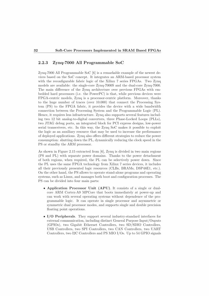
32 Soft-Core Processors Implemented in SRAM Based FPGAs
2.2.3 Zynq-7000 All Programmable SoC
Zynq-7000 All Programmable SoC [6] is a remarkable example of the newest de-vices based on the SoC concept. It integrates an ARM-based processor systemwith the reconfigurable fabric logic of the Xilinx 7 series FPGAs. Two Zynqmodels are available: the single-core Zynq-7000S and the dual-core Zynq-7000.The main difference of the Zynq architecture over previous FPGAs with em-bedded hard processors (i.e. the PowerPC) is that, while previous devices wereFPGA-centric models, Zynq is a processor-centric platform. Moreover, thanksto the huge number of traces (over 10.000) that connect the Processing Sys-tem (PS) to the FPGA fabric, it provides the device with a wide bandwidthconnection between the Processing System and the Programmable Logic (PL).Hence, it requires less infrastructure. Zynq also supports several features includ-ing two 12 bit analog-to-digital converters, three Phase-Locked Loops (PLLs),two JTAG debug ports, an integrated block for PCI express designs, low-powerserial transceivers, etc. In this way, the Zynq SoC makes it possible to exploitthe logic as an auxiliary resource that may be used to increase the performanceof deployed applications. Zynq also offers different strategies to reduce the powerconsumption: shutting down the PL, dynamically reducing the clock speed in thePS or standby the ARM processor.
As shown in Figure 2.15 extracted from [6], Zynq is divided in two main regions(PS and PL) with separate power domains. Thanks to the power detachmentof both regions, when required, the PL can be selectively power down. Sincethe PL uses the same FPGA technology from Xilinx 7 series devices, it includesall their previously presented logic resources (CLBs, BRAMs, DSP48E1, etc.).On the other hand, the PS allows to operate stand-alone programs and operatingsystems, such as Linux, and manages both boot and configuration processes. ThePS can be divided into four main parts:
• Application Processor Unit (APU). It consists of a single or dual-core ARM Cortex-A9 MPCore that boots immediately at power-up andcan work with several operating systems without dependence of the pro-grammable logic. It can operate in single processor and asymmetric orsymmetric dual processor modes, and supports single and double precisionfloating point operations.
• I/O Peripherals. They support several industry-standard interfaces forexternal communication, including distinct General Purpose Input/Ouputs(GPIOs), two Gigabit Ethernet Controllers, two SD/SDIO Controllers,USB Controllers, two SPI Controllers, two CAN Controllers, two UARTControllers, two I2C Controllers and PS MIO I/Os. Up to 54 GPIO signals

2.2 SRAM Based FPGAs 33
are available for device pins routed through the Multiplexed I/O (MIO)and 192 GPIO signals communicate the PS and the PL via the ExtendedMIO (EMIO).
• Memory interfaces. It includes static and dynamic memory interface con-trollers. While the static memory controller enables to work with NANDand Quad-SPI flash, parallel NOR flash, and parallel data bus interfaces,the dynamic memory controller supports DDR2, LPDDR2, DDR3 andDDR3L memories.
• Interconnection elements. These elements provide communication be-tween the PL, the APU, the memory interface and I/O peripherals via anon-blocking multilayered ARM AMBA AXI interconnection, which sup-ports simultaneous master-slave operations.
Figure 2.15: Diagram of the functional blocks that constitute the Zynq-7000.

34 Soft-Core Processors Implemented in SRAM Based FPGAs
Zynq Reset
The system reset process is a sequence that initializes the system and executes theFirst Stage Boot Loader (FSBL) from the selected boot memory. This processprovides the user with the possibility to customize the PS and PL. The Zynqsupports several reset types whitin the PS. For instance, a peripheral reset thatresets a subsystem controlled by software or a power-on reset which resets thecomplete system. These reset sources conform the system reset, which drivesreset signals to each module and system. Various alternatives are available toinitiate a reset process:
• A hardware reset driven by the system reset signal (PS SRST B) and thepower-on reset signal (PS POR B)
• A a software reset able to generate both system-level or a sub-module reset.
• A reset generated by the JTAG controller, which can reset both the entiresystem or a debug portion of the PS.
• A reset generated by the three watchdog timers available.
Xilinx also provides the LogiCORE IP Processor System Reset Module thatenables to reset the complete PS, including the processor and peripherals. Thiscore allows to customize several parameters by enabling or disabling differentfeatures in order to adapt it to user’s specifications.
Zynq Boot
The boot of Zynq-7000 devices is a two-stage process managed by the PS. Itenables to choose between a non-secure booting or a secure booting (JTAG dis-abled) that supports 256-bit AES, 256-bit SHA and 2048-bit public key decryp-tion/authentication. During the booting process the ARM (or one of the ARMs)reads the boot program from the on-chip ROM, executes it and copies a FSBLcode from of the flash memories (or downloaded through JTAG) to the on-chipmemory. FSBL boot code can be entirely controlled by the user, enabling thecustomization of the boot code. After loading the FSBL, it is executed by theARM, providing the possibility of loading the bitstream to configure the PL.
Reconfiguration on the Zynq
One of the most remarkable features of 7 series FPGAs, like most SRAM-basedFPGAs, is that they can be reconfigured dynamically (while system running)
2.2 SRAM Based FPGAs 35
[108]. The configuration and reconfiguration processes are done by loading spe-cific configuration bit stream files, named configuration bitstreams or .BIT files.The reconfiguration process can be performed by external systems (e.g. a micro-processor or a PC) or the FPGA can load bitstreams himself from an externalnon-volatile memory module.
Xilinx provides two data paths connected to special configuration pins to config-ure its 7 series FPGAs: the low pin demanding serial datapath and the paralleldatapath (8-bit, 16-bit, or 32-bit) that provides higher performance and accessto several standard interfaces. The pins from these datapaths serve as an in-terface for different configurations: master and slave serial configuration, masterand slave SelectMAP parallel configuration, JTAG/boundary-scan configuration,master serial and byte peripheral interface flash configuration. Moreover, theZynq can reconfigure itself by the programmable logic, or by any other process-ing system through the device configuration interface (DevC). This interface issupported by a dedicated DMA controller capable of transferring bitstreams froman external memory through the Processor Configuration Access Port (PCAP).The 7 series FPGAs also have an Internal Configuration Access Port (ICAPE2)[3], which provides the user logic with access to the 7 series FPGA configura-tion interface. In [109], both existing internal configuration interfaces, PCAPand ICAPE2, have been extensively evaluated in other to select the most conve-nient alternative. An additional architecture has been implemented in order todynamically reconfigure the FPGA without the Processing System at the maxi-mum bandwidth of 400 MB/s.
Besides reprogramming the entire device, most SRAM-based FPGAs feature par-tial reconfiguration, enabling to reconfigure a specific region while the rest of re-gions of the FPGA continue running. Due to this feature, it is possible to reduceboth cost and area usage. Moreover, bearing in mind that a partial bitstreamgathers only the information of the target reconfigurable zone, it contains muchless information than a complete bitstream. Hence, the utilization of partial re-configuration schemes allows to reduce the bitstream storage requirements andreconfiguration time.
Designing partial reconfigurable implementations is analogous to designing vari-ous complete reconfigurable designs that share certain resources. The first stepis to designate a reconfigurable region, which has to be defined determining botha proper placement and an adequate size of the reconfigurable region. A properfloorplanning requires to consider several aspects, such as the resources demandedby the different designs to be loaded, the size and placement of the static zone orthe other reconfigurable regions, etc. A wide number of 7 series FPGAs resources,like CLBs, BRAMs, DSPs or routing elements are available for reconfiguration

36 Soft-Core Processors Implemented in SRAM Based FPGAs
purposes. Nevertheless, several components like clocks and clock managementblocks (e.g. BUFG, BUFR, MMCM and PLL), I/O and I/O related components,serial transceivers and some dedicated elements (e.g. BSCAN, STARTUP, ICAPand XADC) do not support reconfiguration. These non-reconfigurable elementsmust be placed in the static region of the device.
The regular way to configure an FPGA is to load at first a complete bitstreamthat contains one of the partial reconfiguration designs. After configuring theentire device, the partial bitstream can be loaded to partially reconfigurable re-gions, while the rest of the FPGA remains uninterrupted. After reconfiguration,it is advisable to initialize reconfigurable modules in order to ensure a predictablestarting situation. Another recommendable practice is to disconnect the recon-figurable and the static regions during the reconfiguration process by utilizingdecoupling logic.
The partial reconfiguration can also be used to reduce power consumption bydisabling certain region(s). In [110], partial reconfiguration is utilized to replacecircuits during idle periods with power saving circuits. In a similar way, [111]proposes to utilize empty bitstreams to blank partially reconfigurable regions.
Figure 2.16 illustrates an outstanding benefit of the partial reconfiguration, whichis the feasibility of adapting the design in the field by loading distinct circuitswithin the reconfigurable region. This aspect enables to improve the fault tol-erance, accelerates the configurable computing and provides real-time flexibilitymaking it possible to develop new techniques in design security.
FPGA
Figure 2.16: Replacing reconfigurable modules with the dynamic partialreconfiguration.
One of the most significant drawbacks of the reconfiguration process is its dura-tion, which is limited by the maximum frequencies of the configuration interfaces.For instance, the PCAP’s maximum frequency is 100 MHz. However, although itstheoretical speed of reconfiguration is 400 MB/s, the real speed decreases becauseof the internal ARM interconnect architecture [112]. In addition, the durationof the reconfiguration process varies depending on the size of bitstream to be
2.2 SRAM Based FPGAs 37
configured. Hence, partial bitstreams are less time demanding than completeones. The common duration of this process goes from microseconds to millisec-onds [113]. A possible solution to reduce the reconfiguration time is to compressthe bitstream, however it requires to previously process the bitstream and limitsit usability. In [114], an alternative reconfiguration controller coined as ZyCAPwas presented, which improves the reconfiguration throughput in Zynq whencompared to standard methods. This controller allows overlapped executions,enhancing the system performance. ZyCAP can be used with soft-processors,but driver software modifications are required. In [112] an adaptive partial re-configurable system to maximize the output performance is proposed reducingthe reconfiguration time to 12% over a full configuration time.
2.2.4 Bitstream Structure of 7 series FPGAs
Bearing in mind that the hardware platform of this work is a Xilinx Z-7020Zynq-7000 All Programmable SoC and that it makes use of its reconfigurationcapability, some aspects of the configuration bitstream of the Xilinx 7 seriesfamily must be introduced.
The information around the bitstream is limited, especially since 1998, when theXC6200 series were discontinued [115]. Vendors have published scarce informa-tion about the bitstream composition of their devices, but the majority of themare still unknown. Thanks to various studies, the knowledge about the bitstreamhas continued growing over the last years [116, 117]. However, there is a lack ofstudies dealing with the new Xilinx 7 series devices.
In [118], a bitstream generator that does not use reverse-engineering was pre-sented. This generator is able to imprint small changes onto existing bitstreamsand to embed the bitstream generation inside the system that it targets. Al-though it does not support the full set of device resources, it is a good exampleof the potential of this field. In [119], a bitstream manipulation tool for XilinxFPGAs based on C language and capable of creating partial bitstreams was pre-sented. Although this work was implemented in a Xilinx Virtex II Pro FPGA,several aspects of the structure of the bitstreams exposed in this contributionare useful to understand the bitstream’s composition of Xilinx 7 series FPGAs.Following this baseline, this section presents several interesting aspects of the 7series bitstream based on previous literature, Xilinx’s documentation [4, 120] andseveral off-line tests performed within for this research work.
The 7 series configuration memory is organized in frames that are tiled about theFPGA. A frame is the smallest addressable segment of the configuration memoryand, for this reason, all operations have to act upon whole configuration frames.

38 Soft-Core Processors Implemented in SRAM Based FPGAs
The frame size is 101 words (32 bits), but may vary across families. Frames areorganized with an interleaving mechanism, which imposes that adjacent bits donot belong to the same frame. This is a protection strategy against SEUs inconsecutive bits, avoiding two errors in the same frame, but also making moredifficult the inference of the location of the data content in the bitstream. Thereis a correspondence between the information in the bitstream and the tile mapof the device. Therefore, the number of frames of the bitstream depends on theconfiguration array size and the additional options of the bitstream. In mostcases of the FPGA’s resources, the mapping of memory addresses to resourcesis unknown, because this relation is usually extremely complex. However, somespecific resources, such as CLBs, DSP blocks and BRAM columns are representedexplicitly in the bitstream addressing. The efforts in this work have been focusedon understanding the distribution of data in BRAM columns.
The bitstream file starts with a header consisting of a concatenation of differentcommand words. All commands are executed by reading or writing the differentconfiguration registers of the FPGA. The commands can send two packet types:Type 1 and Type 2 (used to write long blocks). Both packets consist of a headerfollowed by a specific data section. This data section contains the number of 32-bit words specified by the word count portion of the header. Table 2.1 shows theformat of the header of each packet type. The opcode field defines the functionmode, which can be read, write or no operation. The register address field inthe Type 1 packet indicates the address of the target register of the operation athand. The Type 2 does not use the register address field, because it must alwaysfollow a Type 1 packet and it uses its packet address. Between the available 20registers, the most interesting ones for this research are the Cyclic RedundancyCheck (CRC), the Frame Address Register (FAR), the Frame Data Input (FDRI),the Frame Data Output (FDRO) and Command (CMD). The data stored in theCRC register is used to carry out error detection over the bitstream data. TheFAR is used to set the address of the FPGA logic over which the reading orwriting process is performed.
Table 2.1: Packet header types (R: reserved bit; x: data bit).(a) Type 1.
Header Type Opcode Register Address Reserved Word Count[31:29] [28:27] [26:13] [12:11] [10:0]001 xx RRRRRRRRRxxxxx RR xxxxxxxxxxx
(b) Type 2.
Header Type Opcode Word Count[31:29] [28:27] [26:0]010 RR xxxxxxxxxxxxxxxxxxxxxxxxxxx
2.2 SRAM Based FPGAs 39
As shown in Table 2.2, the FAR register is split into 5 parts: block type (CLB,I/O, CLK, BRAM content or CFG CLB), top/bottom bit, row address, col-umn address and minor address. The FDRI register is used to configure framedata at the address specified in the FAR register. The FDRO register providesreadback data for configuration following the address stored in the FAR register.Finally, the CMD is used for the commands, such as, RCRC (Reset Cyclic Redun-dancy Check), START (FPGA initialization) and DESYNC(end of configurationto desynchronize the device).
Table 2.2: Frame Address Register (FAR) format.
Address Type Bit IndexBlock Type [25:23]
Top/Bottom Bit 22Row Address [21:17]
Column Address [16:7]Minor Address [6:0]
The first words of the bitstream header define the boot sequence and provide ad-ditional information for synchronization purposes. The next commands specifythe width of the configuration bus. Then, a set of optional commands specifyparameters related with transfer bitrate, encryption, authentication and CRCcheck. The last part of the header defines the address in the configuration mem-ory and the amount of words that are going to be loaded. The header is followedby the body, which contains the information that is stored in the device. Thestructure of this is usually not specified by the FPGA manufacturers, and theonly way to obtain information is reverse engineering. Finally, the trailer definesthe finishing sequence, which contains CRC verification, the start command (op-tionally) and finally the DESYNQ command to end the communication. Alongthe entire bitstream many no operation (0x20000000) words are included. Afterperforming several tests it has been observed that the data content of BRAMscannot be written through the bitstream if the BRAM segment contains these0x20000000 words. Due to this, is can be assumed that these 0x20000000 wordsact as mask words to protect/unprotect BRAM content against rewriting.
Bearing in mind that the FPGA configuration can be complete or partial, com-plete or partial bitstreams are accordingly produced. Both options share manycommon aspects, but several particular differences deserve special attention. Tobegin with, the complete bitstream uses the START command for starting thedevice, which it is not necessary for its partial counterpart. This occurs becausethe partial reconfiguration is usually performed dynamically, i.e. while the deviceis running. In the case of a complete bitstream, the FAR is filled with 0’s and thenumber of words stored in the FDRI register corresponds to the total words ofthe entire bitstream. The FAR and number of words of the bitstream are strictly
40 Soft-Core Processors Implemented in SRAM Based FPGAs
related to the defined reconfigurable region. As a result, if the reconfigurableregion is deployed over no consecutive zones following the address of the FAR,the bitstream is divided in different fragments. Each fragment is defined by itsparticular FAR and word amount. Therefore, the partial bitstream indicates theFAR and word amount of each resource column used in the design. For this rea-son, partial bitstreams have been used in this work to extract information aboutthe data content of BRAMs.
The word amount stored in the FDRI register is a multiple of the frame size.Each frame is related to the configuration bits and initial values of a particularcolumn of resources. Each resource may have a different number of frames, andthese values may also vary among device families. In the case of the Z7020device used in this study, the total number of frames is 10008. After severalpartial configuration experiments it has been observed that each column of slicesincludes 36 frames, each column of DSPs contains 28 frames and each column ofBRAMs embeds 28 configuration frames and 128 data content frames.
The Z7020 device has a total number of 133 CLB columns, 11 DSP48 columnsand 14 BRAM columns. Hence, the total number of configuration frames in thisdevice is 5502 and the total number of BRAM data frames is 1972. Given thetotal number of frames of the complete bitstream, it can be assumed that theremaining frames are used for the configuration of other resources, such as IOBsor BUFGPs. However, since these resources cannot be used in partial bitstreamsit is complex to determine the exact number of frames that they possess.
Xilinx enables to generate a logic location text file (*.ll) which contains the lo-cation of each user data bit in terms of relative offset to a frame of the entiredesign. In this way, knowing the location of a particular region, it can easily findthe nets of the design that belong to the partial region. This file can be generatedwith the software provided by Xilinx, such as ISE or VIVADO.
2.2.5 Managing Data Content by Utilizing the Bitstream
Memories are essential elements in SoC designs as a standard way to store dataon a temporary or permanent basis. This data may have different purposes.In SRAM FPGA based systems the most common functionality is to store in-formation of specific applications, entire programs or sequences of instructions,program state information and/or configuration information of the device. As ithas been introduced, when implementing memory elements in FPGAs the twoalternatives that can be used, which are the BRAM resources and the distributedgeneral-purpose logic fabric. In the case of soft-core processors, while programand data memories are commonly implemented as BRAM structures, the small
2.2 SRAM Based FPGAs 41
memory elements, such as the registers, are implemented by utilizing distributedfabric logic.
The standard way to access and manage data in memory modules is to use theirinput ports, such as data output, data input, write-enable and address.This access method requires a control mechanism to manage the inputs andread the outputs in a coordinated fashion. This is often accomplished by amemory controller, which can be implemented in different ways, such as usingsoft-core or hard processors, specific IP cores or custom FSM based modules.Frequently, additional elements are also required, like bus interfaces or auxiliarymemories to store processed data. The implementation of all the above elementsdemands the usage of a variety of resources of the FPGA, further increasing theresource overhead. Besides, if it is required to read or write large amounts ofdata, resources committed to storing such data will be blocked and unavailablefor other purposes. For example, it is not possible to read the data from the firsttwo memory addresses while the last ten data addresses are being written.
Due to the limitations of standard data management, there are several scenarioswhere new data management alternatives could improve some applications orsolve different existing issues. Bearing in mind that the user data is also storedin the configuration bitstream, the idea of using this bitstream to manage datacontent is an attractive alternative.
The impossibility of modifying data content of ROM memories, widely used asprogram memories in soft-core processors represents another relevant issue sincethis functionality may be needed in order to change the purpose of a processor orto recover after an SEU in the program memory. The regular way to modify thecontent of a ROM memory in an FPGA design is to re-synthesize and re-deploythe entire design with the new data onto the FPGA. In the best case scenario,if the program memory has been implemented as a reconfigurable partition, onlythis part should be re-synthesized and re-implemented. Following this approach,the program memory is implemented as a RAM in [39], and a dedicated IP coreloads new memory content during the system operation by using a serial interface.However, this scheme increases requirements in terms of logic resources, and anupset in the input port of the memory may lead to changes in the memorycontent, increasing the probability of malfunction due to SEUs. Thus, modifyingthe program memory could be a good application example for a bitstream baseddata content management.
Another scenario where a bitstream based management can be an interestingalternative is the damage of the interfaces on memory resources. Thus, as aconsequence of an SEU, an error can disable or affect to relevant ports of thememory, which it is likely to provoke permanent damages. Moreover, if ports
42 Soft-Core Processors Implemented in SRAM Based FPGAs
such as, address, reset, clock or data output are affected by the fault, it couldmake it unsuitable to recover the information stored in memories when resort-ing to conventional, off-the-self methods. This scenario can be a critical issuewhen the memory has not been hardened and the information stored has a spe-cial operational relevance. The extraction of such information by utilizing thedata content stored in the bitstream could allow recovering the information in astraightforward manner.
Considering the direct relation between the integrity of the user data and thereliability, several fault tolerance related strategies could also take advantage ofa bitstream based data management.
Bearing in mind the potential benefits that can be obtained with this strategy,there is a scarcity of investigations around this strategy. The lines below presentthe most significant works proposed in the literature, especially focusing in Xilinxdevices.
When reading and writing back user data from one memory block to another, twomain cases can be found: Homogeneous and heterogeneous architectures. Whilehomogeneous memory modules share main characteristics, such as size, shape,and used resources (with only different fabric locations), heterogeneous modulessupport distinct features due to the usage of different resources and granular-ity levels. Data management utilizing the bitstream is more straightforward inthe case of homogeneous implementations, since it mainly requires simple bit-stream manipulations in order to relocate the data. Nevertheless, the utilizationof heterogeneous architectures restraints the designing process.
In any case, extracting and writing user data content through the bitstreamrequires certain knowledge of its structure. Thus, they are device dependantstrategies. While devices from the 7 series by Xilinx share the majority of thecharacteristics of the bitstream structure, many of them are different in previousFPGA series from the same vendor. Thus, despite in several cases the flows andthe main ideas can be adapted to different devices, the developed approaches arecommonly related with a particular FPGA vendor, a particular FPGA series oreven to a particular device.
With the latest FPGA series (Virtex-4, Virtex-5, Virtex-6, Spartan-3A, Spartan-3AN, Spartan-3A DSP, Spartan-6 and 7 Series), Xilinx offers the possibility touse the Data2MEM [121] data translation software to initialize BRAMs. Amongother features, Data2MEM can replace the contents of BRAMs in configurationbitstreams in a straightforward fashion, without requiring any implementationtool. However, this application undergoes several limitations. One of the mostrelevant is that this software must be executed by an operating system (Windows
2.2 SRAM Based FPGAs 43
or Linux). In addition, this program requires previously generated files to createthe output files, such as BRAM Memory Map (BMM) files or Linkable Format(ELF) files. The configuration bitstream files to be updated by the tool must becreated without compression and/or encryption. To sum up, this is a quite com-plex solution, not supported for partial bitstreams, feasible only for data writingin BRAMs and not for reading. It is therefore not proper data managementapproaches for autonomous standalone systems based on partial reconfiguration.
Jbits [122] was one of the first tools reported to be able to modify the bitstream,including the data content. It consisted on a set of Java classes that providedan application program interface into the configuration bitstream for XC4000and Virtex families by Xilinx (by utilizing the SelectMAP interface). One ofthe biggest advantages of this approach was that it did not require additionalhardware structures. Nevertheless, it came with a poor data efficiency. This wasbecause it required to read the entire bitstream, while the user data only uses arelative small percentage of the bitstream. This tool became obsolete and it isnot suitable for 7 series devices.
The work presented in [7] is a step forward towards bitstream based data contentmanagement. As Figure 2.17 extracted from that work describes, the approachproposed focuses on saving an relocating the context a of a soft-core processor,by extracting (and writing back once processed) the bitstream through the Se-lectMAP interface. In this process the entire configuration data is not read back,but only the frames that contain the target information. This context extractionis done while reading the configuration data and requires to stop the clock of theparticular hardware task to prevent chances during the read process. In [123],a similar approach that proposes a partial displacement defragmentation algo-rithm for heterogeneous reconfigurable systems was presented. However, theseapproaches have several drawbacks. The most remarkable one is that, since theyare only usable with the old one-dimensional partial reconfiguration FPGA fam-ilies from Xilinx, they cannot be utilized in the newest devices. In addition, theyrequire high processing effort (the use of tools, such as a configuration manager,PARTBIT software and the REPLICA filter) and to use a complex database tostore the placement of each data bit.
Further approaches focused on dealing with newer Xilinx devices that supporttwo-dimensional partial reconfiguration can be found. The approach presentedin [61] is capable of capturing, storing and copying the content of flip-flops withina Virtex-V FPGA device on a particular reconfigurable region by utilizing thebitstream in combination with the STARTUP VIRTEX5 primitive, the GCAPTURE
commands and the ICAP interface. In a later work [8], the previous approachwas extended to enable to copy the content of flip-flops between heterogeneous
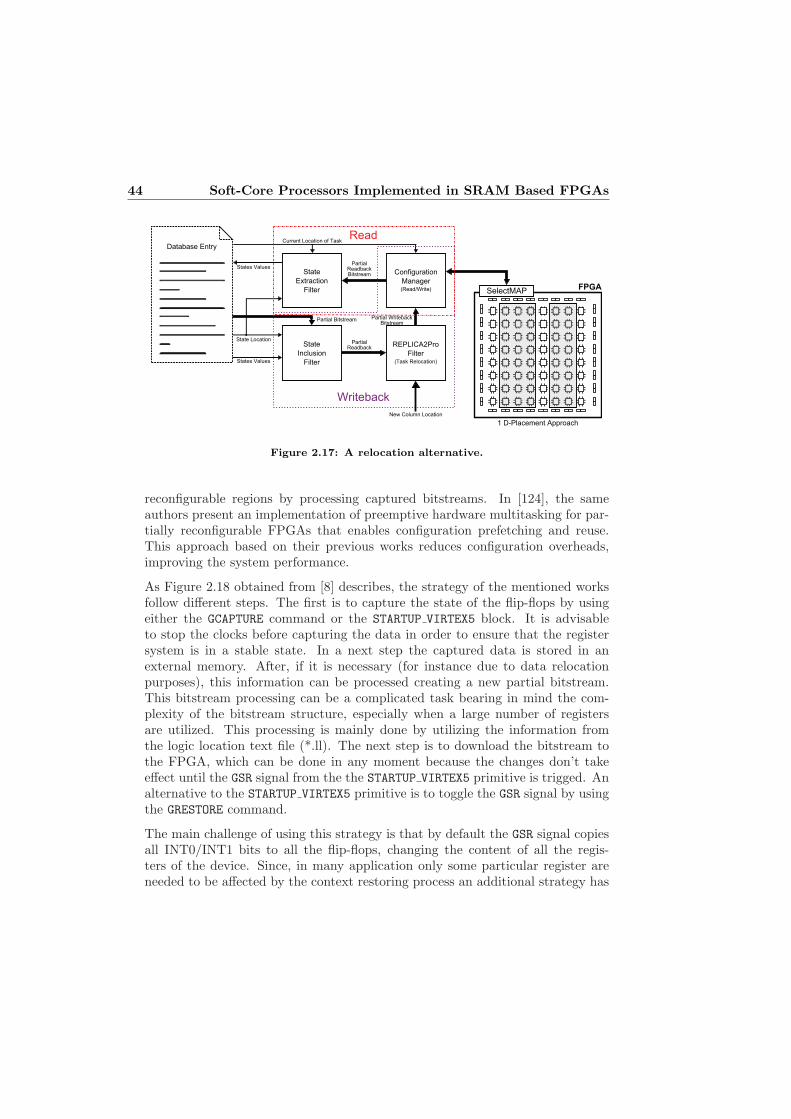
44 Soft-Core Processors Implemented in SRAM Based FPGAs
FPGASelectMAP
State
Extraction
Filter
Configuration
Manager(Read/Write)
State
Inclusion
Filter
REPLICA2Pro
Filter(Task Relocation)
Database Entry
Writeback
Read
PartialReadbackBitstream
PartialReadback
Partial WritebackBitstream
States Values
State Location
Partial Bitstream
States Values
New Column Location
1 D-Placement Approach
Current Location of Task
Figure 2.17: A relocation alternative.
reconfigurable regions by processing captured bitstreams. In [124], the sameauthors present an implementation of preemptive hardware multitasking for par-tially reconfigurable FPGAs that enables configuration prefetching and reuse.This approach based on their previous works reduces configuration overheads,improving the system performance.
As Figure 2.18 obtained from [8] describes, the strategy of the mentioned worksfollow different steps. The first is to capture the state of the flip-flops by usingeither the GCAPTURE command or the STARTUP VIRTEX5 block. It is advisableto stop the clocks before capturing the data in order to ensure that the registersystem is in a stable state. In a next step the captured data is stored in anexternal memory. After, if it is necessary (for instance due to data relocationpurposes), this information can be processed creating a new partial bitstream.This bitstream processing can be a complicated task bearing in mind the com-plexity of the bitstream structure, especially when a large number of registersare utilized. This processing is mainly done by utilizing the information fromthe logic location text file (*.ll). The next step is to download the bitstream tothe FPGA, which can be done in any moment because the changes don’t takeeffect until the GSR signal from the the STARTUP VIRTEX5 primitive is trigged. Analternative to the STARTUP VIRTEX5 primitive is to toggle the GSR signal by usingthe GRESTORE command.
The main challenge of using this strategy is that by default the GSR signal copiesall INT0/INT1 bits to all the flip-flops, changing the content of all the regis-ters of the device. Since, in many application only some particular register areneeded to be affected by the context restoring process an additional strategy has

2.2 SRAM Based FPGAs 45
Capturecontext
Store DataData relocation
process(optional)
Download bitstream
Trig GSR signal
Figure 2.18: Flow chart of a context capture and restoration alternative.
to be followed. Every stack of configuration resource is related with a specificbit, commonly named mask bit. GCAPTURE/GRESTORE commands only affect thestate of the flip-flops not marked with the mask bit. Each column is related toa single frame in the mask column. In this way, for every mask frame set, theentire related column in the clock region of DSP/CLB is protected/unprotected.Further information of this bit (for Virtex-V devices) can be found in either [30]or in [8]. This feature makes it possible to protect/unprotect specific areas de-termining which resources are to be modified. In this way, [8, 61] follow thestrategy depicted in Figure 2.19 (extracted from [8]). Since the entire FPGAdesign is unprotected by default, in a first step the entire FPGA design is pro-tected. When context is needed to be saved the target region has to be protectedbefore capturing the data. After, capturing data the target region can optionallybe protected, in any case before restoring the context the target region has to beunprotected. After finishing context saving/restoring processes the target regioncan be protected in order to avoid undesired changes in future startup sequences.
Protect entire FPGA
Un-protecttarget region
Protecttarget region
Initially unprotected FPGA
target region target region target region target region
Capture/Restore
Figure 2.19: Flow chart of an FPGA protection and unprotection alternative.
In general terms, these published approaches present some common drawbacks.First, they require a controller module and a memory block to store the readdata. In addition, considering that the reconfiguration is a time demandingprocess, the price to pay when using these strategies is a low availability. Anotherlimitation of these approaches is that they require to disable the CRC feature ofthe generated bitstream. This is because due to the modification of the bitstreamcontent the original CRC value would not be valid, making unsuitable to use itfor the reconfiguration. Hence, the utilization of the CRC feature would requireto generate the new CRC value which requires a high processing effort. Finally,

46 Soft-Core Processors Implemented in SRAM Based FPGAs
no approaches have been proposed to perform such applications in newer devices,such as, 7 series vy Xilinx.
In summary, despite of the presented disadvantages, bitstream based user datacontent management techniques provide an alternative access to data contentwithout increasing the area overhead and without interfering the logic of theFPGA logic which, in many cases, can be an interesting way to overcome certainlimitations of the classic memory management.
2.3 Radiation Effects on Soft-Core Processorsimplemented in SRAM FPGAs
Thanks to the continued innovation in the technology for developing and manu-facturing electronics, the integration level has been increasing, enabling features,such as, high capacity, low-power consumption and fast devices. However, thehigh integration level comes with a drawback since it increases the susceptibilityto induced faults [27]. These faults are mainly generated by contaminant alphaparticles [28] or ionizing radiation from protons and cosmic rays from outer spacewhich interact with the atmosphere and generate subatomic particles that collidewith solid-state devices and integrated circuits [125]. Alpha particles are causedby impurities (mostly Thorium and Uranium) in integrated circuit encapsulatecompounds and by atmospheric neutrons that slam into the silicon.
The effects provoked by space radiation can be mainly divided into two categories[126]: Single Event Effect (SEE) and accumulative effects like Total Ionizing Dose(TID) or Displacement Damage (DD). SEE are the result from the prompt effectsof a strike by a single ionizing particle in a sensitive region of the device. TID iscaused by the gradual accumulation of ionizing dose deposition over a long time.Finally, DD is the consequence of an accumulation of crystal lattice defects leadby high energy radiation.
In the case of FPGA devices, the different technologies (SRAM, flash, and anti-fuse) present distinct susceptibility levels to radiation effects [127], mainly becauseof the specific characteristics of their switch technology. Nevertheless, due to theutilization of CMOS based logic modules they share some level of susceptibilityto SEE and TID. The switch of the non-volatile anti-fuse and flash devices iscompletely immune to SEE, for this reason they are less sensitive to them thantheir SRAM counterparts. Regarding TID, while the switch of anti-fuse devicesare immune to these effects, it is known that they affect SRAM and flash basedFPGAs [128–130].

2.3 Radiation Effects on Soft-Core Processors implemented in SRAMFPGAs 47
Due to its benefits as a platform for soft-core implementation described in 2.2, thescope of this work is the reliability of SRAM FPGA technology. Although bothaccumulative effects and SEE are a main concern for SRAM designers, SEE arethe prevalent case of study in the literature [131–136]. A reason for this is that,although there is a risk of performance degradation and an eventual malfunction,the effects of TID and DD do not commonly lead to system-level failures (as longas the degradation does not surpasses system tolerances). In addition, as [137]states the effect given by TID neglected in the typical task cycle and environment.The mitigation of TID effects is typically done by using radiation hardened byprocess techniques and/or shielding. On the other hand the hardening by designin SRAM FPGA is quite expensive in terms of resource usage since the majorityof switches should to be hardened.
Since the first detection in 1975 [138], SEEs have become a main issue in spaceapplications [62, 83, 139–142] because when the devices work in this environmentthey are directly exposed to space radiation. Nevertheless, despite the fact thatat ground level and avionics systems are less exposed to radiation effects due tothe planet’s atmospheric and magnetic radiation shields, they are also sensitiveto SEE [143]. In fact, the first reference to deal with SEE, published in the early60’s [144], was related with microelectronics at terrestrial level. The detectionof SEE in terrestrial applications [145] came few years after the mentioned firstdetection at space level. Since then, the concern on SEE has continuously beenincreasing due to several factors. One of them is that, thanks to their obviousbenefits, the application fields of microelectronics also continues growing daily. Infact, trying to imagine application fields with no presence of electronics is a trickytask. In addition, several of these application fields, such as, medical, military,avionics, space or automotive. require high fault tolerance levels. Another rele-vant factor is the continuous technology shrinking, for instance, Xilinx and Alterahave presented 16nm and 14nm devices [146, 147], respectively. This density in-crease demands lower polarization voltages, which increases the susceptibility toSEE, since the necessary energy to generate upsets for charged particles is alsodecreased [148] and a single particle strike can affect more than a single transistorat a time. The increase of working frequencies is another relevant aspect factor.Due to this speed boost, the delay levels of logic gates are becoming comparableto the duration of SEE, leading to a higher error propagation probability. Onthe other hand, studies like [149] by the NASA in 2009 or the newer ones [150],reveal that the intensity of cosmic beans is increasing.
SEE gather a number of effects caused high energy particles that have beenclassified in two main groups in the literature [126, 151, 152]: soft errors andhard errors. Figure 2.20 summarizes the different SEE types.

48 Soft-Core Processors Implemented in SRAM Based FPGAs
SEE(Single Event Effects)
SEL(Single Event Latch-Up)
SEB(Single Event Burnout)
SEGR(Single Event Gate Rupture)
SET(Single Event Transient)
SEU(Single Event Upset)
SEFI(Single Event
Functional Interrupt)
SBU(Single Bit Upset)
MBU(Multiple Bit Upset)
Soft Errors (Recoverable) Hard Errors (Unrecoverable)
Figure 2.20: Classification of Single Event Effects
Soft errors are non-destructive upsets that can be self-corrected in time or thatcan be corrected by rewriting a memory element. It has to be mentioned that,although these effects do not cause a permanent damage in the device in whichthe effect occurred they can lead to permanent faults in the system in which thatdevice resides. These effects can be divided in three subclasses:
1. Single Event Upsets (SEUs). They appear when high-energy particlesprovoke bit-flips in memory elements (flip-flop, latch, SRAM, or flash).Depending on the quantity of flipped bits they can be categorized as MultiBit Upsets (MUBs) or Single Bit Upsets (SBU). Despite the fact that SBUsare known to be the most prevalent type of SEE, MUBs are also studied inthe literature [153].
2. Single Event Transients (SETs). The effect caused by a transient isdetermined by its duration and magnitude, and by if the transient is latchedturning it into an upset at system level. They occur when a high energyparticle impacts FPGA’s internal interconnection system inducing a currentor voltage spike. Depending on when the impact occurs and the pulse-width the SET could be registered, and as a consequence, it may propagatethought the circuit and, eventually, provoke errors. When this latching ofoccurs the SET becomes an SEU. In the rest of scenarios the repercussionof these effects is negligible. The increase of clock frequencies incrementsthe likelihood of an SET registration, and as a consequence, increases theprobability of faults.
3. Single Event Function Interrupts (SEFIs). SEFIs cause a malfunctionin the device, such as, reset or lock up. They usually are related with upsetsin a bit or a register of device’s control [154].
2.3 Radiation Effects on Soft-Core Processors implemented in SRAMFPGAs 49
Hard errors are permanent or unrecoverable upsets. These types of SEE are alsodivided in three subclasses:
1. Single Event Latch-up (SEL). This is an induced circuit latch-up. AnSEL can be either permanent or fixable by power cycling.
2. Single Event Burnout (SEB). An SEB occurs when a high-energy parti-cle strikes a transistor source causing a short-circuit due to forward biasing.An SEB can lead to overheating related issues.
3. Single Event Gate Rupture (SEGR). An SEGR is the damagingburnout of a gate insulator in a power MOSFET.
Xilinx states in [151] that their FPGA devices are not susceptible to latch-up andgate rupture caused by neutron radiation. In addition, Xilinx space-grade partsare said to be immune to latch-up from heavy ions as well.
Among all the SEE types, SEUs are the prevalent source of errors in SRAMFPGAs [73, 155], especially those produced by radiation [151]. SEUs can affectnot only user memory bits but also configuration bits in FPGA based design.Bearing in mind that the configuration memory determines the entire functional-ity of devices (interconnection and configuration of resources, data content, etc.),SEUs in configuration memory can provoke a wide variety of issues in designs.They can even affect the power consumption of the device [156]. Hence, they area special concern. Figure 2.21 shows an example of an SEU in the configurationmemory affecting the functionality of the hardware implementation. SEUs in usermemory are less likely to happen, because generally this data content is an orderof magnitude smaller than configuration memory’s content. However, the relativeupset ratio is very much alike in both, user and configuration memories. Follow-ing this idea, in FPGA designs with big data module implementations or complexregisters systems, the risk becomes higher. Despite that an SEU in user’s datadoes not affect the functionality of designs, depending of the application bothtypes of SEUs can lead to a critical malfunction.
Although most frequently SEUs affect to configuration memory, many bits ofthe bitstream are unused. In fact, it is considered that in a regular design lessthan 20% of the configuration bitstream bits are critical to designs’ functionality[157]. The quantity of critical bit vary depending on different implementationfactors of a design, such as, resource quantity, routing, type of resources utilized,designed application, etc. Nevertheless, the critical bit rate is usually a smallnumber [158, 159]. In the majority of cases a bit-flip in configuration memorydoes not affect the functionality.
The Soft Error Rate (SER) in a relevant concept when evaluating fault tolerance

50 Soft-Core Processors Implemented in SRAM Based FPGAs
Configuration memory
FPGA
D Q D Q D Q
Figure 2.21: Configuration memory SEU example in an FPGA design.
of a design [160]. The SER is the rate at which an FPGA (or other electronicdevices/systems) is predicted to undergo soft errors. The exact contribution ofSEE to SER vary depending on the design. For instance, asynchronous designsare less susceptible to SEE than synchronous ones [161]. However, asynchronousversions of digital designs are normally 10 times slower and they need 10 timesmore resources. The SER is determined by two factors: Failure in Time (FIT)and Meant Time to Failure (MTTF), also known as Mean Time Between Failures(MTBF). As Equation 2.1 shows, FIT is the measure of failure rate in 109 devicehours. On the other hand, MTTF defined in Equation 2.2 is the mean of thelife allocation for the number of devices under operation or expected lifetimeduration of an individual.
FIT = Fail quantity · 109 · (Device quantity ·Working hours) (2.1)
MTBF (h) =Fail quantity · 109
Device quantity · FIT(2.2)
2.3 Radiation Effects on Soft-Core Processors implemented in SRAMFPGAs 51
In SRAM FPGAs the SER can be estimated performing fault injection cam-paigns, simulations or analytic approaches [162–165]. The Rosetta Experimentis the most remarkable exponent of SER estimation performed by Xilinx. Thisexperiment was conducted in 2005 [166] and it linked two well-known techniquesof estimating atmospheric neutron SEUs and undocumented real effects of atmo-spheric particles on electronic devices. Thanks to that, it correlated atmosphericupsets to simulated results, and to beam tests. Due to the publication of thisarticle several previous works, such as, the JEDEC89A standard [167] were cor-rected. It also showed that the sensibility to atmospheric radiation is at leasteight times lower than Boeing predicted [143]. The Rosetta Experiment contin-ues performing a wide range of studies at ten different altitudes and analysingnew trends of Xilinx devices [168].
Another aspect to be considered is the resource overhead since it is directlyrelated with the fault tolerance. First, the more resources utilized in an FPGAimplementation, the more resources are susceptible to induced faults. Secondly,the number of bits from the configuration memory sensitive to SEE increases withthe resource overhead. In addition, more utilized resources means more resourcesto be hardened when hardening a design. In conclusion, the reduction of resourceoverhead is a highly recommendable practice in terms of fault tolerance.
Once the most significant aspects of the SRAM based FPGA technology havebeen introduced, the next chapter gathers the most significant alternatives toharden designs implemented in such devices, specially focusing on soft-core im-plementations.

52 Soft-Core Processors Implemented in SRAM Based FPGAs

Chapter 3
Hardening Soft-CoreProcessors Implemented inSRAM FPGAs
An ideal design should always work without malfunction. Nevertheless, in a realscenario, especially when dealing with SRAM based FPGAs, electronic designsare exposed to certain risks. A dependable design should try both, to avoid theimpact off errors and to repair the produced ones. Related with those ideas, twoconcepts have to be remarked: availability and reliability. While availability isdetermined by the mean time to repair after a failure, reliability is determinedby the design itself, the platform utilized and the operation-environment. It isimportant to obtain a proper balance of both concepts. For instance, a designwith poor reliability level but with a fast repairing method most probably willmeet its goals in presence of faults. On the other hand, a very reliable design thatneeds complex and time demanding repairing techniques perhaps will not achieveits goals after an error. Reliability is a valuable characteristic, but availabilityis what the final user is going to experience. In order to provide satisfactoryreliability and availability levels for FPGA designs, an adequate fault tolerancelevel must be guaranteed. Due to this, increasing fault tolerance level of SRAMdesigns is one of the main objectives of this research work. Different strategiescan be adopted to increase the fault tolerance level of FPGA designs in order toavoid possible negative consequences of induced faults.
The most obvious way to mitigate faults is to improve production aspects to
54 Hardening Soft-Core Processors Implemented in SRAM FPGAs
manufacture less susceptible technology. In fact, several manufacturers have de-veloped hardened FPGA products [169–173]. Regularly these devices are regu-larly based on older technologies (i.e. anti-fuse FPGAs), offering significantly lessresources and lower working frequencies at higher prices than the newest commer-cial FPGAs. An alternative strategy that is being followed is to use packagingswith lower alpha particle content. Manufacturers like Xilinx have progressedfrom low alpha to ultra-low alpha materials. Nevertheless, these are not secureenough to ignore the package alpha contribution to the atmospheric alpha upsetrate. Another fabrication aspect to improve fault tolerance is to provide highersusceptibility to SRAM cells utilized to store the configuration memory and theBRAM content. However, despite of all the efforts to improve the fabricationprocesses, the fast grown of configuration memories makes it a hard race.
Another alternative that can be utilized to harden electronic designs against bothSEEs and TIDs is to protect them with shielding. Although that provides properreliability levels, it is not practical for most applications since the amount ofmaterial required to build the shield is too expensive, e.g., as much as 30 metersof water for neutrons with high energy [174]. It also increases the weight and sizeof designs, which in many cases could be a significant limitation.
A further relevant way to harden FPGA based designs is trying to avoid using ofunsafe design practices. Several examples can be found in [175], such as, avoidinguse of asynchronous reset signals, not incorporate more circuitry than necessary,distribute the clock signals inside the FPGA in a safe and stable way, performa worst/best case timing analysis, an adequate floorplanning, etc. Despite theseaspect could improve the reliability of a design, commonly they are not enoughto guarantee a certain fault tolerance level.
Nevertheles, due to the limitations and drawbacks of presented strategies, thereis a main tendency of utilizing commercial SRAM FPGAs and providing themwith fault tolerance by using design-based hardening techniques [49, 89]. Hence,an adequately hardened design implemented in a commercial FPGA representsan attractive alternative, even for space applications [176], due to their flexibility,good working frequencies and their competitive price.
When implemented in SRAM FPGA, soft-core processors are exposed to the samerisks than any FPGA design. Nevertheless, their architecture may require toexploit certain specific aspects. This fact has motivated a number of researches,like in [79] where the reliability analysis of a LEON 3FT soft-core processor(designed to be fault tolerant in a low ion flux operational environment) hasbeen done. The research presented in [155] is a remarkable reliability study of asoft-core processor. In this case, a methodology to evaluate the critical elementswhen exposing the device to SET effects is proposed using an in-house developed

3.1 Scrubbing 55
PIC18 soft-core processor. Bearing in mind the relevance of the fault toleranceissue, this research work seeks to contribute with new hardening alternatives toharden soft-core processors implemented in SRAM FPGAs, improving existingtechniques and providing new alternatives. Hence, a study of existing hardeningtechniques to harden soft-core processors implemented in SRAM FPGAs is aespecially relevant step.
The present chapter gathers the most relevant fault mitigation techniques toincrease the reliability and availability levels of SRAM based FPGA designs, es-pecially focusing on soft-core processors. In this way, Section 3.1 presents thescrubbing, which a widely utilized technique for mainly repair fault in the con-figuration memory. Next, Section 3.2 introduces hardware redundancy basedtechniques, giving special importance to Dual Modular Redundancy (DMR) andTriple Modular Redundancy (TMR), the most utilized redundancy levels. Sec-tion 3.3.1 continues presenting techniques based on other types of redundancy(time, software and data). The utilization of Dynamic Partial Reconfiguration(DPR) based approaches to fix permanent faults is studied in Section 3.4. Section3.5 introduces other, less utilized but interesting approaches to harden designs.All presented hardening strategies are summarized in Section 3.7. Finally, thischapter closes with Section 3.6, which discusses about the most remarkable faulttolerance evaluation alternatives utilized to determine the reliability level of de-signs.
3.1 Scrubbing
The most straightforward method to account for and overcome potential faults isthe so-called bitstream scrubbing [57, 95, 177] which takes advantage of the par-tial reconfiguration capability of FPGAs. It is performed by rewriting a knownbitstream (named golden bitstream) with a correct configuration. The scrub-bing cleans upsets from the configuration memory, prevents the accumulation ofconfiguration upsets and significantly reduces the probability of two SEUs beingpresent at the same time.
Two strategies can be adopted to decide when performing the scrubbing. Thefirst consists in periodically reconfiguring the device by utilizing the golden bit-stream. This strategy is known as blind scrubbing [178]. The second strategy isbased on carrying out the scrubbing after a fault detection [179]. Based on thisstrategy, [180] presented the lazy scrubbing approach. This method was appliedto a hardware redundancy based scheme in which, the configuration bitstreamwas read from all replicated modules analyzing data and offsets to repair the
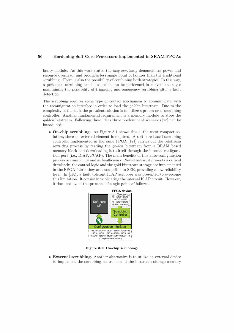
56 Hardening Soft-Core Processors Implemented in SRAM FPGAs
faulty module. As this work stated the lazy scrubbing demands less power andresource overhead, and produces less single point of failures than the traditionalscrubbing. There is also the possibility of combining both strategies. In this way,a periodical scrubbing can be scheduled to be performed in convenient stagesmaintaining the possibility of triggering and emergency scrubbing after a faultdetection.
The scrubbing requires some type of control mechanism to communicate withthe reconfiguration interface in order to load the golden bitstream. Due to thecomplexity of this task the prevalent solution is to utilize a processor as scrubbingcontroller. Another fundamental requirement is a memory module to store thegolden bitstream. Following these ideas three predominant scenarios [73] can beintroduced:
• On-chip scrubbing. As Figure 3.1 shows this is the most compact so-lution, since no external element is required. A soft-core based scrubbingcontroller implemented in the same FPGA [181] carries out the bitstreamrewriting process by reading the golden bitstream from a BRAM basedmemory block and downloading it to itself through the internal configura-tion port (i.e., ICAP, PCAP). The main benefits of this auto-configurationprocess are simplicity and self-sufficiency. Nevertheless, it presents a criticaldrawback: the control logic and the gold bitstream storage are implementedin the FPGA fabric they are susceptible to SEE, providing a low reliabilitylevel. In [182], a fault tolerant ICAP scrubber was presented to overcomethis limitation. It consist in triplicating the internal ICAP circuit. However,it does not avoid the presence of single point of failures.
����������������������������������
����������������������������������
����������������������������������
�������� ������ � �����
���������
��� �����
��
��������������
��������������
��������������
���������� � �����
������� ������ ������
���������� ������
����������
Figure 3.1: On-chip scrubbing.
• External scrubbing. Another alternative is to utilize an external deviceto implement the scrubbing controller and the bitstream storage memory
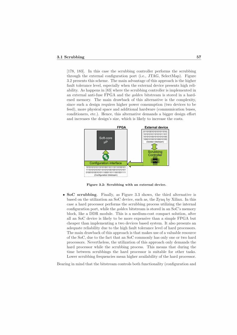
3.1 Scrubbing 57
[178, 183]. In this case the scrubbing controller performs the scrubbingthrough the external configuration port (i.e., JTAG, SelectMap). Figure3.2 presents this scheme. The main advantage of this approach is the higherfault tolerance level, especially when the external device presents high reli-ability. As happens in [83] where the scrubbing controller is implemented inan external anti-fuse FPGA and the golden bitstream is stored in a hard-ened memory. The main drawback of this alternative is the complexity,since such a design requires higher power consumption (two devices to befeed), more physical space and additional hardware (communication buses,conditioners, etc.). Hence, this alternative demands a bigger design effortand increases the design’s size, which is likely to increase the costs.
����������������������������������
����������������������������������
����������������������������������
�������� ������ � �����
����
��� �����
��
������ ������
��������������������
��������������������
��������������������
��������������������
���������� � �����
������� ������ ������
���������� ������
Figure 3.2: Scrubbing with an external device.
• SoC scrubbing. Finally, as Figure 3.3 shows, the third alternative isbased on the utilization an SoC device, such as, the Zynq by Xilinx. In thiscase a hard processor performs the scrubbing process utilizing the internalconfiguration port, while the golden bitstream is stored in an SoC’s memoryblock, like a DDR module. This is a medium-cost compact solution, afterall an SoC device is likely to be more expensive than a simple FPGA butcheaper than implementing a two devices based system. It also presents anadequate reliability due to the high fault tolerance level of hard processors.The main drawback of this approach is that makes use of a valuable resourceof the SoC, due to the fact that an SoC commonly has only one or two hardprocessors. Nevertheless, the utilization of this approach only demands thehard processor while the scrubbing process. This means that during thetime between scrubbings the hard processor is suitable for other tasks.Lower scrubbing frequencies mean higher availability of the hard processor.
Bearing in mind that the bitstream controls both functionality (configuration and

58 Hardening Soft-Core Processors Implemented in SRAM FPGAs
�����������������������������
�����������������������������
�����������������������������
�������� ������ � �����
���������
��� �����
���������������
�������������
�������������
���������� � �����
������� ������ ������
���������� ������
� �������
����� ����
��� �
Figure 3.3: Scrubbing with a hard processor in a SoC device.
interconnection of logic resources) and user data content (BRAM, registers, etc.),two types of scrubbing can be defined: configuration and memory (data content)scrubbing. While the configuration content is a static portion, the data contentis generally constantly changing during the operation. By virtue of this fact,while the configuration is valid for almost all cases, the data content scrubbing isonly suitable for certain cases, such as soft-core processors’ program memories.The most elementary approach is to perform a complete scrubbing by rewriting abitstream with both, configuration and data content information. This scenariorequires a power-cycling, which needs to stop the application. Hence, it is not avalid solution for applications that need to be continuously active.
In addition, as a result of the data content rewriting the system is brought back toa previous state of operation, which is a handicap. For this reason, the commonpractice is to perform a configuration scrubbing repairing the static portion of theconfiguration memory that controls the logic of the FPGA. This can be performedin an straightforward fashion thanks to the possibility of masking the bits relatedto data content. On the contrary, the logic configuration bits of the bitstreamcannot be masked and for this reason few data content scrubbing solution areavailable.
In [184], a user memory scrubbing approach to clean errors in memories wasproposed. This user memory scrubbing hinges on the addition of an FSM basedmodule to the design. Similar approach were presented in [182, 185]. Thesemethods increase resource overhead and need to use a second memory port. SinceXilinx FPGA BRAMs can only be implemented as single or dual-port memories,if a BRAM memory block is already being used as a dual-port memory this
3.2 Hardware Redundancy 59
approach not be feasible. In [177], the memory coherence problem is described,which occurs when configuration data contain user information that is updated bysystem-level user operations between the configuration readback and writebackoperations. It proposes a dirty-bit technique which deals with this problem.Although it shows to outperform previous approaches, it also comes along witha performance penalty.
Xilinx also provides with the possibility of taking advantage of the ECC protec-tion of the bitstream by utilizing the so-called Soft Error Mitigation (SEM) Core[186] or the SEU controller macro [74]. They check the ECC code for SEUs inthe configuration memory repairing it when it is necessary. In [187], a similarstrategy was presented.
The main weakness of the scrubbing resides in its slowness. The reconfigurationis a time demanding process due to the limitations of configuration interfaces. Inaddition the more data is to be rewritten (bigger partial bitstreams) the more timeis required. Different solutions can be adopted to alleviate this handicap. Themost straightforward, as presented in [95, 188], is to use the placing constraints tolocate the utilized resources in near placements. Due to this, the size of the partialbitstream is likely to be smaller. Nevertheless, placement constraints limit thefreedom of the implementation software that can lead to worst results in termsof resource usage an performance. Other researches propose compressing thebitstream [189] to shrink it and reduce the duration of the partial reconfigurationprocess. Nevertheless, these methods are relatively complex since they require acompression mechanism, and they are also time demanding.
Considering that scrubbing is not able to repair certain elements of the FPGA(digital clocks managers, power on resets, selectMAP interfaces, etc.) it is nota definitive solution. In addition, considering the time demand on the reconfig-uration operation, even in scenarios where a periodical scrubbing is a suitablealternative, the frequency of the scrubbing process is usually lower than appli-cation’s, and hence the scrubbing by itself is not generally sufficient. Due tothese factors, the majority of approaches utilize the scrubbing in combinationwith other hardening techniques, like hardware redundancy based approaches[52, 53, 83, 189–195].
3.2 Hardware Redundancy
Hardware-based techniques result to be the most frequently addressed by bothindustry and academia in diverse technological architectures [196]. In the case ofFPGA designs, these techniques are a widely used solution to harden them. As
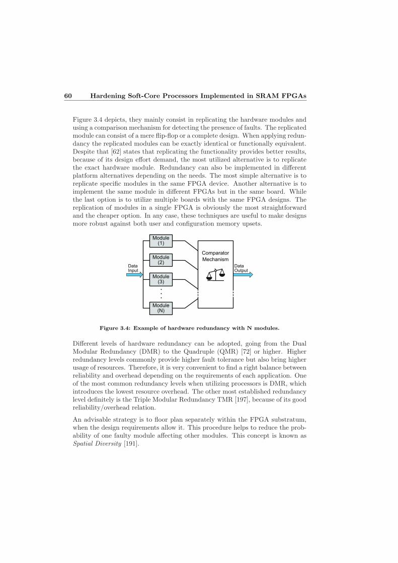
60 Hardening Soft-Core Processors Implemented in SRAM FPGAs
Figure 3.4 depicts, they mainly consist in replicating the hardware modules andusing a comparison mechanism for detecting the presence of faults. The replicatedmodule can consist of a mere flip-flop or a complete design. When applying redun-dancy the replicated modules can be exactly identical or functionally equivalent.Despite that [62] states that replicating the functionality provides better results,because of its design effort demand, the most utilized alternative is to replicatethe exact hardware module. Redundancy can also be implemented in differentplatform alternatives depending on the needs. The most simple alternative is toreplicate specific modules in the same FPGA device. Another alternative is toimplement the same module in different FPGAs but in the same board. Whilethe last option is to utilize multiple boards with the same FPGA designs. Thereplication of modules in a single FPGA is obviously the most straightforwardand the cheaper option. In any case, these techniques are useful to make designsmore robust against both user and configuration memory upsets.
��������
��� �����
��������
��������
��������
����������
���������
��������
Figure 3.4: Example of hardware redundancy with N modules.
Different levels of hardware redundancy can be adopted, going from the DualModular Redundancy (DMR) to the Quadruple (QMR) [72] or higher. Higherredundancy levels commonly provide higher fault tolerance but also bring higherusage of resources. Therefore, it is very convenient to find a right balance betweenreliability and overhead depending on the requirements of each application. Oneof the most common redundancy levels when utilizing processors is DMR, whichintroduces the lowest resource overhead. The other most established redundancylevel definitely is the Triple Modular Redundancy TMR [197], because of its goodreliability/overhead relation.
An advisable strategy is to floor plan separately within the FPGA substratum,when the design requirements allow it. This procedure helps to reduce the prob-ability of one faulty module affecting other modules. This concept is known asSpatial Diversity [191].

3.2 Hardware Redundancy 61
Taking into account that it provides the output of the entire system, the mostrelevant element of a hardware redundancy scheme is the comparison mechanism.Depending on the adopted hardware redundancy approach the implementation ofthis element requires different characteristics. However, it mostly is a relativelysimple implementation. Hence, a small number of configuration bits are relatedto it. For this reason, an SEU in the comparator block is an unlikely situation.Nevertheless, if such scenario occurs, the response of the entire system will beaffected. These fatal consequences commonly demand to apply an additionalredundancy based hardening to the comparator block. In any case, regardless ofthe redundancy level or the hardening of the comparator block, there is alwaysa risk of an SEU in the output of the comparator. This situation represents asingle point of failure, since if the output fails, the reliability of the entire systemis compromised. Therefore, it has to be remarked that, despite of their valuableresults as hardening solutions, hardware redundancy techniques cannot providean absolute fault tolerance.
Another relevant aspect related to hardware redundancy is the granularity level.Three general granularity levels are defined in the literature [198]: logic level(fine grained), block level (medium grained) and a complete module level (coarsegrained). The robustness level rises when redundancy is performed on fine gran-ular modules [199–201].
Considering that more voters have to be implemented, fine grained implementa-tions come with a price in terms of FPGA resources usage and design complexity.Nevertheless, fine granularity offers the possibility of prioritizing which elementsare tripled depending on the available space, as [202] proposes. In this way, themost sensitive components can be mitigated first and, if the available area al-lows, others may also be hardened. [203] proposes the utilization of intermediatevoters, like depicted in Figure 3.5, to connect different replicated partitions inorder to eliminate single point of failures in the interconnections. In [204], threedifferent algorithms for determining where to insert voters were proposed. Be-sides, a fine granularity may reduce the performance since the voters are addedto the critical path. In addition, as [205] states depending on the design, a biggernumber of voters does not assure better performance for all scenarios. This isbecause the physical placement of resources can affect to their effectiveness.
On the other hand, the design of coarse-grained redundancies demands the lowestdesign effort and it utilizes less area than fine grained ones. Coarse grained imple-mentations are capable to mask all single points of failure within the replicatedmodules, but they are unsafe against the accumulation of errors or some multipleerror types. For these reasons, depending on the system requirements, design-ers should select a trade-off among robustness level, overhead and performance,

62 Hardening Soft-Core Processors Implemented in SRAM FPGAs
applying different granularity levels.
.
.
.
In1
In2
In3
Out2.
Out3
Out1
.
. .
.
.
.
.. .
.
.
.
.
Figure 3.5: Intermediate voter for the interconnection of tripled modules.
3.2.1 Dual Modular Redundancy
Dual Modular Redundancy (DMR) or Duplication With Comparison (DWC) isone of the prevailing hardware redundancy based strategies. The main advantageover higher redundancy levels is that the DMR requires less hardware overhead.This is an interesting characteristic when designing complex architectures, suchas soft-core processors [86, 89, 189, 206, 207]. When the duplication is applied toprocessors, the structure is named lockstep. This approach is based on utilizingtwo identical processors executing the same application in parallel, feed by thesame inputs and comparing the outputs. Most commonly, the output checkingprocess is done at every clock cycle. Both processors must be synchronized tostart at the same time initialized with the same context.
As is shown in Figure 3.6, when an input discrepancy is detected an error flag istriggered. A DMR scheme permits to detect errors but neither mask nor correctthem. This is because it is not possible to identify the faulty module, requiringa further solution that will stop the operation. Figure 3.7(a) depicts the mostbasic approach, which is to restart the process or program after detecting a fault.A further straightforward solution is to perform a configuration scrubbing like in[189]. However, since the scrubbing does not affect to the state of the registersand the memory content, this strategy is only valid for errors in logic and not forregistered data. In [66], the RESO method was introduced to detect the faultycore and to switch the correct core to output. The idea behind this approachis to modify the operands before performing the re-computation so that a faultaffects different parts of the circuits. Due to this, the computations are carriedout twice, once on the basic input and once on the shifted input.
Due to obvious reasons, both presented approaches are not commonly sufficient tomeet requirements of most applications. In this way, the prevalent approach when
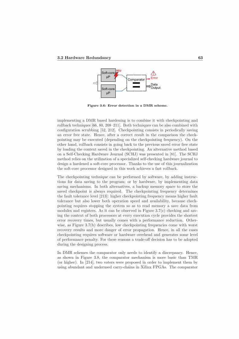
3.2 Hardware Redundancy 63
Soft-core
µP
Soft-core
µP
SEU
ErrorComparator
= DataOutput
Figure 3.6: Error detection in a DMR scheme.
implementing a DMR based hardening is to combine it with checkpointing androllback techniques [66, 80, 208–211]. Both techniques can be also combined withconfiguration scrubbing [52, 212]. Checkpointing consists in periodically savingan error free state. Hence, after a correct result in the comparison the check-pointing may be executed (depending on the checkpointing frequency). On theother hand, rollback consists in going back to the previous saved error free stateby loading the context saved in the checkpointing. An alternative method basedon a Self-Checking Hardware Journal (SCHJ) was presented in [81]. The SCHJmethod relies on the utilization of a specialized self-checking hardware journal todesign a hardened a soft-core processor. Thanks to the use of this journalizationthe soft-core processor designed in this work achieves a fast rollback.
The checkpointing technique can be performed by software, by adding instruc-tions for data saving to the program; or by hardware, by implementing datasaving mechanisms. In both alternatives, a backup memory space to store thesaved checkpoint is always required. The checkpointing frequency determinesthe fault tolerance level [213]: higher checkpointing frequency means higher faulttolerance but also lower both operation speed and availability, because check-pointing requires stopping the system so as to read memory a save data frommodules and registers. As it can be observed in Figure 3.7(c) checking and sav-ing the context of both processors at every execution cycle provides the shortesterror recovery times, but usually comes with a performance reduction. Other-wise, as Figure 3.7(b) describes, low checkpointing frequencies come with worstrecovery results and more danger of error propagation. Hence, in all the casescheckpointing requires software or hardware overhead and generates some levelof performance penalty. For these reasons a trade-off decision has to be adoptedduring the designing process.
In DMR schemes the comparator only needs to identify a discrepancy. Hence,as shown in Figure 3.8, the comparator mechanism is more basic than TMR(or higher). In [214], two voters were proposed in order to implement them byusing abundant and underused carry-chains in Xilinx FPGAs. The comparator
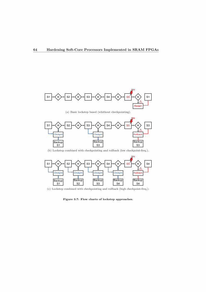
64 Hardening Soft-Core Processors Implemented in SRAM FPGAs
S1 S2 S3 S4 S5 S1= = = = =
SEU
Restart
(a) Basic lockstep based (whithout checkpointing).
S1 S2 S3 S4 S5 S3= = = = =
SEU
Backup BackupBackupS1 S3 S3
Chckpnt Chckpnt Rollback
(b) Lockstep combined with checkpointing and rollback (low checkpoint-freq.).
S1 S2 S3 S4 S5 S4= = = = =
SEU
Backup Backup Backup BackupBackupS1 S2 S3 S4 S4
Chckpnt Chckpnt Chckpnt Chckpnt Rollback
(c) Lockstep combined with checkpointing and rollback (high checkpoint-freq.).
Figure 3.7: Flow charts of lockstep approaches.
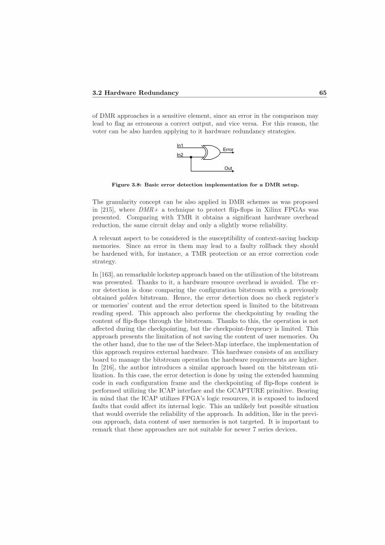
3.2 Hardware Redundancy 65
of DMR approaches is a sensitive element, since an error in the comparison maylead to flag as erroneous a correct output, and vice versa. For this reason, thevoter can be also harden applying to it hardware redundancy strategies.
In1
In2
Out
Error
.
Figure 3.8: Basic error detection implementation for a DMR setup.
The granularity concept can be also applied in DMR schemes as was proposedin [215], where DMR+ a technique to protect flip-flops in Xilinx FPGAs waspresented. Comparing with TMR it obtains a significant hardware overheadreduction, the same circuit delay and only a slightly worse reliability.
A relevant aspect to be considered is the susceptibility of context-saving backupmemories. Since an error in them may lead to a faulty rollback they shouldbe hardened with, for instance, a TMR protection or an error correction codestrategy.
In [163], an remarkable lockstep approach based on the utilization of the bitstreamwas presented. Thanks to it, a hardware resource overhead is avoided. The er-ror detection is done comparing the configuration bitstream with a previouslyobtained golden bitstream. Hence, the error detection does no check register’sor memories’ content and the error detection speed is limited to the bitstreamreading speed. This approach also performs the checkpointing by reading thecontent of flip-flops through the bitstream. Thanks to this, the operation is notaffected during the checkpointing, but the checkpoint-frequency is limited. Thisapproach presents the limitation of not saving the content of user memories. Onthe other hand, due to the use of the Select-Map interface, the implementation ofthis approach requires external hardware. This hardware consists of an auxiliaryboard to manage the bitstream operation the hardware requirements are higher.In [216], the author introduces a similar approach based on the bitstream uti-lization. In this case, the error detection is done by using the extended hammingcode in each configuration frame and the checkpointing of flip-flops content isperformed utilizing the ICAP interface and the GCAPTURE primitive. Bearingin mind that the ICAP utilizes FPGA’s logic resources, it is exposed to inducedfaults that could affect its internal logic. This an unlikely but possible situationthat would override the reliability of the approach. In addition, like in the previ-ous approach, data content of user memories is not targeted. It is important toremark that these approaches are not suitable for newer 7 series devices.
66 Hardening Soft-Core Processors Implemented in SRAM FPGAs
3.2.2 Triple Modular Redundancy
Unlike what happens with DMR, TMR and higher redundancy levels enable thepossibility of identifying the faulty module and provides higher fault tolerancelevels. However, increasing the redundancy level also implies a resource overheaddirectly related with the redundancy level. Among the different hardware re-dundancy alternatives the Triple Modular Redundancy (TMR) is considered tobe the most extended one to harden FPGA designs because it offers a remark-able trade-off between reliability and resource overhead. Since first introduced in[217] this technique has become in a standard hardening approach inspiring a vastnumber of researches in the literature [54, 59, 66, 137, 218–223]. Nevertheless,its biggest handicap is the resource overhead, which is usually about %200. Thework [224] presents a TMR alternative with a resource overhead reduction. Itproposes to implement a TMR scheme composed by a full precision module andtwo reduced precision modules. These two reduced-precision blocks will generatean upper and lower bound on the correct function output. The research itselfstates that despite the acceptable results with complex functions, the result withsimple operations are not efficient in terms off fault tolerance.
Essentially in a TMR scheme, three exactly alike or functionally equivalent unitsof the element to be hardened are used. Once the element is tripled, the finaloutput is determined by a majority voting. Thanks to that, as is shown in 3.9(a),even when a fault is present in one of the three replicas, a voter would still befed with two correct values. Hence, the wrong third result is masked providing avalid output without stopping the operation.
However, as depicted in Figure 3.9(b), when multiple errors are induced in dif-ferent modules at the same time provoking an equal faulty output, they can beset as correct. This is an unlikely but possible situation. Another remarkabledrawback of using a voter is that in the best scenario errors are masked but notcorrected. Hence, when utilizing hardware redundancy there is an inherent riskof accumulation of SEUs. Due to this, as it has been mentioned in section 3.1the common practice is to combine it with the scrubbing.
Considering the crucial relevance of the voter in these type of schemes, its designis a main concern [191, 225, 226]. Figure 3.10(a) depicts the most basic votingand as it can be observed it consists of three 2-input AND gates connected to a3-input OR gate. This scheme is capable of providing a correct output in presenceof a faulty module. However, this affirmation presumes that the voter cannot beaffected by induced faults, which does not match reality.
When a fault affects the voter it can provoke wrong behaviour, from partialfailures to total disruptions. The criticalness of such scenario have motivated a
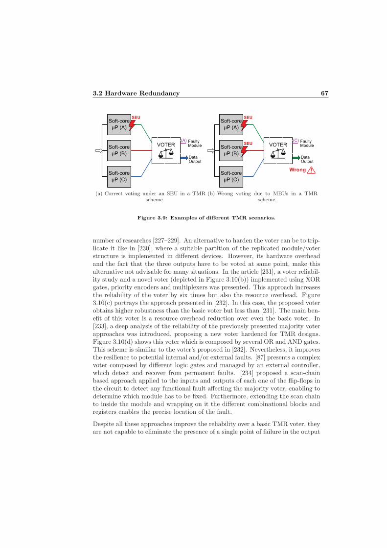
3.2 Hardware Redundancy 67
Soft-core
µP (A)
Soft-core
µP (B)
Soft-core
µP (C)
VOTER
SEU
DataOutput
FaultyModule
(A)
(a) Correct voting under an SEU in a TMRscheme.
Soft-core
µP (A)
Soft-core
µP (B)
Soft-core
µP (C)
VOTER
SEU
DataOutput
SEUFaultyModule
(C)
Wrong
(b) Wrong voting due to MBUs in a TMRscheme.
Figure 3.9: Examples of different TMR scenarios.
number of researches [227–229]. An alternative to harden the voter can be to trip-licate it like in [230], where a suitable partition of the replicated module/voterstructure is implemented in different devices. However, its hardware overheadand the fact that the three outputs have to be voted at same point, make thisalternative not advisable for many situations. In the article [231], a voter reliabil-ity study and a novel voter (depicted in Figure 3.10(b)) implemented using XORgates, priority encoders and multiplexers was presented. This approach increasesthe reliability of the voter by six times but also the resource overhead. Figure3.10(c) portrays the approach presented in [232]. In this case, the proposed voterobtains higher robustness than the basic voter but less than [231]. The main ben-efit of this voter is a resource overhead reduction over even the basic voter. In[233], a deep analysis of the reliability of the previously presented majority voterapproaches was introduced, proposing a new voter hardened for TMR designs.Figure 3.10(d) shows this voter which is composed by several OR and AND gates.This scheme is similiar to the voter’s proposed in [232]. Nevertheless, it improvesthe resilience to potential internal and/or external faults. [87] presents a complexvoter composed by different logic gates and managed by an external controller,which detect and recover from permanent faults. [234] proposed a scan-chainbased approach applied to the inputs and outputs of each one of the flip-flops inthe circuit to detect any functional fault affecting the majority voter, enabling todetermine which module has to be fixed. Furthermore, extending the scan chainto inside the module and wrapping on it the different combinational blocks andregisters enables the precise location of the fault.
Despite all these approaches improve the reliability over a basic TMR voter, theyare not capable to eliminate the presence of a single point of failure in the output
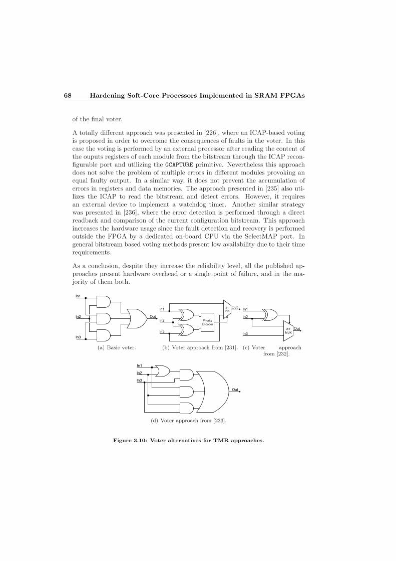
68 Hardening Soft-Core Processors Implemented in SRAM FPGAs
of the final voter.
A totally different approach was presented in [226], where an ICAP-based votingis proposed in order to overcome the consequences of faults in the voter. In thiscase the voting is performed by an external processor after reading the content ofthe ouputs registers of each module from the bitstream through the ICAP recon-figurable port and utilizing the GCAPTURE primitive. Nevertheless this approachdoes not solve the problem of multiple errors in different modules provoking anequal faulty output. In a similar way, it does not prevent the accumulation oferrors in registers and data memories. The approach presented in [235] also uti-lizes the ICAP to read the bitstream and detect errors. However, it requiresan external device to implement a watchdog timer. Another similar strategywas presented in [236], where the error detection is performed through a directreadback and comparison of the current configuration bitstream. This approachincreases the hardware usage since the fault detection and recovery is performedoutside the FPGA by a dedicated on-board CPU via the SelectMAP port. Ingeneral bitstream based voting methods present low availability due to their timerequirements.
As a conclusion, despite they increase the reliability level, all the published ap-proaches present hardware overhead or a single point of failure, and in the ma-jority of them both.
.
.
.
In1
In2
In3
Out
(a) Basic voter.
.
.
.
In1
In2
In3
Out
Priority
Encoder
2:1
MUX
(b) Voter approach from [231].
.In1
In2
In3
Out2:1
MUX
(c) Voter approachfrom [232].
Out
...
In1
In2
In3
.
(d) Voter approach from [233].
Figure 3.10: Voter alternatives for TMR approaches.
3.3 Other Types of Redundancy 69
In contrast to coarse grained, the implementation of fine grained TMR schemescan be a tedious task. To help the designers to deal with providing TMR hard-ening to design, several software tools are available. The TMRTool by Xilinx[237] is a remarkable tool when working with Xilinx’s Virtex-4QV and Virtex-5QV FPGAs. Nevertheless, since it has been discontinued, new tools has to beconsidered especially when working with newer devices, such as the Zynq. An-other relevant tool is the BLTmr developed at Brigham Young University (incollaboration with Los Alamos National Laboratory) [202]. BLTmr is a CADtool to implement partial TMR designs by applying selective triplication in orderto target the most sensitive components of designs, hence, reducing the hardwareoverhead. Another alternative is Synplify Premier by the Synopsys, Inc. [238].This software offers multiple options for implementing error detection and mit-igation circuitry, such as, memory protection by inferring error correcting code(ECC) memory primitives and by inserting triple modular redundancy (TMR) onBRAMs to mitigate single-bit errors, safe FSM implementation and fault-tolerantFSMs with Hamming-3 encoding. In [236], a set of tools that allow to manipulatepartial bitstreams to perform fine and coarse grained redundancy was presented.
3.3 Other Types of Redundancy
As an alternative to hardware redundancy other three redundancy types can beapplied: data redundancy, time redundancy and software redundancy. Each typeexploits distinct features providing specific benefits and introducing particulardrawbacks. The present section introduces the features of each type, discussingthe most remarkable approaches proposed in the literature.
3.3.1 Data Redundancy
Data redundancy is another remarkable fault tolerance alternative to hardenSRAM based FPGA designs. This concept is based on adding additional datain order to be able of verifying and even correcting the original information.Data redundancy is mainly used to reduce error rates in memories, which isespecially interesting in SRAM based ones. The prevalent alternative is the useof built-in Cyclic Redundancy Check (CRC) and Error Correction Code (ECC)or Error Detection and Correction (EDAC) strategies [59, 60, 73, 239]. Withthese techniques a bit-flip can be detected, automatically corrected and evenrecorded, with the possibility of saving a time stamp for further actions. ECCtechniques can be implemented in hardware or by software [240]. With software
70 Hardening Soft-Core Processors Implemented in SRAM FPGAs
ECC approaches, transient faults in the combinational logic are not stored instorage cell, and bit-flips in the storage cells can be avoided or instantly corrected.
However, single-bit errors may cause failures in software ECC if an error occurswhen reading data from a memory and it is coincident with the time between thelast scrubbing and the time of reading. In contrast, hardware ECC checks all thedata read from the memory correcting single-bit errors. Hence, bearing in mindthat hardware ECC provides better reliability, it is a most advisable strategy.
Thanks to the reliability and the limited hardware overheard introduced by thesetechniques, they are a widely used alternative to TMR schemes when harden-ing memories in FPGA designs [194, 241]. While TMR boost the reliability byincreasing significantly the area of memory cells (especially with fine granular-ity), ECC codes produces a small hardware overhead but it needs large logicblocks (with multiple levels) to implement coders and decoders, which increasesthe length of the critical paths. Due to this, the convenience of each approachdepends on the design needs.
Several ECCs are available in the literature [242, 243], such as, Hamming,One-Step Majority-Logic Decoder (serial and parallel), Majority Gate, BoseChaudhuri Hocquenghem, Berger, m-Of-n, m-Out-n, Residue codes, Reed,Solomon, Hsiao, Checksum, etc. One of the most utilized is the Hamming code[66, 75, 192, 194, 241, 244, 245]. As depited in Figure 3.11, it adopts the parityconcept, but uses more than a single parity bit. To detect k -single bit error, theminimum number of bit positions at which the corresponding symbols are dis-tinct or minimum hamming distance (D) is D= k+1. A code word of n bits withm data bits and p check bits, where n = m+p, can correct (D-1)/2 errors andcan detect D-1 errors. Moreover, with the addition of an extra parity bit, it canbe determined whether it is 1-bit or 2-bit error. Nevertheless, even being a goodcandidate to be used in memories or register files, the Hamming code can be anon advisable alternative in some scenarios. Specially when the huge number ofbits leads to long path of serial XOR gates in the decoding and coding modules.In this scenario a suitable alternative is to divide the data in smaller data words.As [241] states, in the case of data words up to 16 bits, the difference in area anddelay between hamming code and TMR is nearly negligible. Due to this a TMRscheme is commonly an interesting alternative for blocks made-up of registersand pipelines, while Hamming ECC is more appropriate to harden register filesand embedded memories.
Xilinx has a built-in ECC module to protect the BRAM structures [192]. Thismodule is developed for BRAM primitives of data widths greater than 64 bits[246] by using Hamming code. Its goal is to detect and correct errors with a goodperformance and small resource utilization. Using this module one single bit error
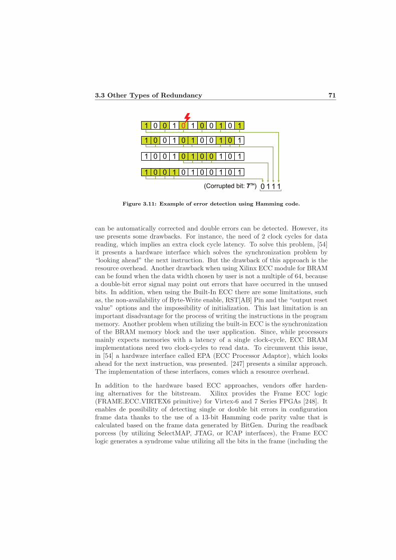
3.3 Other Types of Redundancy 71
1 0 1 1 1 10 0 0 0 0
1 0 1 1 1 10 0 0 0 0
1 0 1 1 1 10 0 0 0 0
1 0 1 1 1 10 0 0 0 0
0(Corrupted bit: 7TH) 1 11
Figure 3.11: Example of error detection using Hamming code.
can be automatically corrected and double errors can be detected. However, itsuse presents some drawbacks. For instance, the need of 2 clock cycles for datareading, which implies an extra clock cycle latency. To solve this problem, [54]it presents a hardware interface which solves the synchronization problem by“looking ahead” the next instruction. But the drawback of this approach is theresource overhead. Another drawback when using Xilinx ECC module for BRAMcan be found when the data width chosen by user is not a multiple of 64, becausea double-bit error signal may point out errors that have occurred in the unusedbits. In addition, when using the Built-In ECC there are some limitations, suchas, the non-availability of Byte-Write enable, RST[AB] Pin and the “output resetvalue” options and the impossibility of initialization. This last limitation is animportant disadvantage for the process of writing the instructions in the programmemory. Another problem when utilizing the built-in ECC is the synchronizationof the BRAM memory block and the user application. Since, while processorsmainly expects memories with a latency of a single clock-cycle, ECC BRAMimplementations need two clock-cycles to read data. To circumvent this issue,in [54] a hardware interface called EPA (ECC Processor Adaptor), which looksahead for the next instruction, was presented. [247] presents a similar approach.The implementation of these interfaces, comes which a resource overhead.
In addition to the hardware based ECC approaches, vendors offer harden-ing alternatives for the bitstream. Xilinx provides the Frame ECC logic(FRAME ECC VIRTEX6 primitive) for Virtex-6 and 7 Series FPGAs [248]. Itenables de possibility of detecting single or double bit errors in configurationframe data thanks to the use of a 13-bit Hamming code parity value that iscalculated based on the frame data generated by BitGen. During the readbackporcess (by utilizing SelectMAP, JTAG, or ICAP interfaces), the Frame ECClogic generates a syndrome value utilizing all the bits in the frame (including the
72 Hardening Soft-Core Processors Implemented in SRAM FPGAs
ECC bits). If no bit change happens from the original programmed values, the[12:00] bits from the SYNDROME word are all zeros. On the contrary, if a faultprovokes a bit-flip (including the ECC bits), the [11-0] bits from the SYNDROMEword indicate its location. If the flipped bits are two or more, the [12:00] bitsfrom SYNDROME are indeterminate. In this scenario, the error output of theblock is asserted. In addition, after reading each frame the syndrome valid signalis asserted. Repairing flipped bits demands a user design since the frame ECClogic does not repair them. Xilinx provides an SEU controller IP [186] capable ofrepairing, an even injecting, configuration-frame faults. In any case, the designhas to be able to save at least one data-frame or be able to fetch original data-frames for reloading them. In [248], it is addressed that the simplest operation isto read the frame through the configuration interface, store it in a BRAM, anal-yse it and if it required repair it before writing it back. However, if the BRAMwhich stores the frame is affected by an induced fault, the entire design can becompromised.
Different alternatives have been proposed in the literature to deal with the frameECC issue. In [249] an embedded IP core, which can be implanted into theFPGAs to detect and correct soft errors automatically was proposed. [250] alsopresents an SEU-Monitor System which is able of injecting, detecting and correct-ing single-bit errors and injecting and detecting double-bit errors in the FPGAconfiguration memory. On the other hand, in [251] a low-cost ECC was presentedto detect and correct MBUs in configuration frames. This code is based on theconception of Erasure codes and utilized vertical and horizontal parity-bits toavoid redundant data. It also proposed the utilization of Mutation codes. Asit states by using Erasure or Mutation codes the delay can be reduced. Thisapproach does not demand alterations in the FPGA design. The parity bit oper-ation is performed for all configuration frames increasing the computation time.
3.3.2 Software Redundancy
Software redundancy is a well known alternative to the hardware redundancywhen protecting processors because it does not require any modification at hard-ware level. Hence, the impact in terms of hardware overhead is very limited.Software redundancy is based on replicating the program code and adding extrainstructions to perform comparison functions. Due to this fact, software basedapproaches require to increase program memories. Another remarkable draw-back is the performance penalty generated by the execution of a larger numberof instructions.
Another software based approach commonly utilized in combination with software
3.3 Other Types of Redundancy 73
redundancy is the utilization of consistency checks. This technique consists inperiodically executing a specific set of instructions with the purpose of verifyingthe faultlessness of memories and their functionality.
In [252, 253], similar software redundancy approaches were presented. Dependingon if the faults provoke errors in the program execution flow or in the stored data,different strategies were proposed. In order to deal with errors in the programexecution, a modification of the application code by introducing new instructionsis done, either in low assembler code or high-level code. Due to this, a checkingis performed allowing to know if faults have affected the expected instructionflow. When working with errors affecting stored data, proposed methods mainlyconsist in providing information redundancy in order to store several copies ofthe information and in adding consistency checks. Thanks to the utilization of aproper combination of these approaches, permanent and transient errors can bedetected and repaired. In addition, their use provides the capability of addressingfault detections without the need of additional hardware.
In [254], the so-called N-version programming technique was presented. This clas-sical approach hardens program with an high-level code, which mainly consists intripling the instruction and utilizing a majority voting. Hence, the performancepenalty is significant. In addition, since this approach demands a triplication ofinstructions and data, it demands bigger memory modules.
The approach proposed in [255] hardens programs against transient faults withoutthe drawback that comes with tripled instructions. It also reduces the perfor-mance penalty over the instruction triplication. This fault tolerance method isable to overcome SEUs in processor-based system memory. The basis of this ap-proach is to duplicate the program variables and the operations and performing achecksum, which is updated every time the content of a variable is written. Thefault detection is done by checking the coherence of both copies. An error re-covery procedure, which corrects the error by relying on the duplicated variablesand the stored checksum, is launched after detecting an error.
The Software Implemented Fault Tolerance (SWIFT) approach presented in [256]is a software redundancy technique designed to detect upsets in processor’s mem-ories and registers. The SWIFT approach can be divided in two parts. The firstpart’s goal is to protect the processor against upsets in data by instruction du-plication. While the second part’s aim is to protect the design against controlerrors but utilizing a software control-flow monitoring. The study [94] extendsthe intended use of SWIFT to protect the processor logic and routing. It alsoperforms consistency checks as an interrupt service routine to detect upsets inthe logic and routing leading to the units.
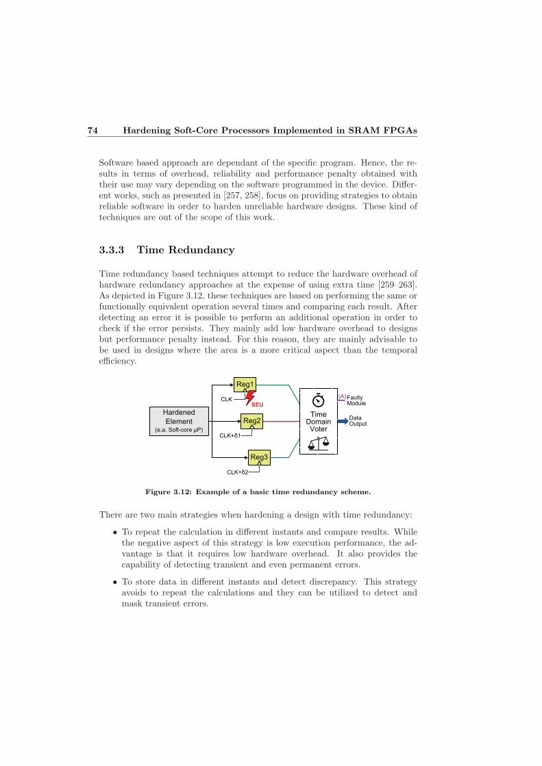
74 Hardening Soft-Core Processors Implemented in SRAM FPGAs
Software based approach are dependant of the specific program. Hence, the re-sults in terms of overhead, reliability and performance penalty obtained withtheir use may vary depending on the software programmed in the device. Differ-ent works, such as presented in [257, 258], focus on providing strategies to obtainreliable software in order to harden unreliable hardware designs. These kind oftechniques are out of the scope of this work.
3.3.3 Time Redundancy
Time redundancy based techniques attempt to reduce the hardware overhead ofhardware redundancy approaches at the expense of using extra time [259–263].As depicted in Figure 3.12, these techniques are based on performing the same orfunctionally equivalent operation several times and comparing each result. Afterdetecting an error it is possible to perform an additional operation in order tocheck if the error persists. They mainly add low hardware overhead to designsbut performance penalty instead. For this reason, they are mainly advisable tobe used in designs where the area is a more critical aspect than the temporalefficiency.
DataOutput
FaultyModule
(A)
Reg1
Reg2
Reg3
Hardened
Element (e.a. Soft-core µP)
CLK
CLK+ 1
CLK+ 2
TimeDomainVoter
SEU
Figure 3.12: Example of a basic time redundancy scheme.
There are two main strategies when hardening a design with time redundancy:
• To repeat the calculation in different instants and compare results. Whilethe negative aspect of this strategy is low execution performance, the ad-vantage is that it requires low hardware overhead. It also provides thecapability of detecting transient and even permanent errors.
• To store data in different instants and detect discrepancy. This strategyavoids to repeat the calculations and they can be utilized to detect andmask transient errors.
3.3 Other Types of Redundancy 75
Although redundancy based techniques are especially suitable to detect or/andmask transient fault due to their temporal character, they can be utilized incombination with coding and decoding techniques to improve the detection ofpermanent faults [264].
In [193], an approach based on a temporal data sampling mechanism was pre-sented for error detection and correction. It is based on sampling data at threedifferent time intervals, requiring three clocks for proper operation. This workstates that thanks to the utilization of this approach the performance can beincreased by 55.93 percent over conventional TMR schemes, while providing near100% fault coverage.
The approach proposed in [265] is an hybrid technique that combines hardwareand time redundancies with some special consideration to provide a dissimilarcondition for hard copies over the time. The main advantage of the proposedmethod is that it reduces SEU propagation among the replicated modules. Theresults of this study conclude that reliability of the harden design increases upto 70 times with respect to a standard TMR.
The logic-level circuit transformation technique based on time redundancy forthe automatic insertion of fault-tolerance properties was proposed in [266]. Thisapproach permits to adapt the time redundancy dynamically. In this way, thefault-tolerance characteristics can be traded-off for throughput during the run-ning. This permits to activate the hardening only in critical situations.
In [267], automated behavioural design flow based on a parametrizable architec-ture to enable time redundancy of loosely coupled hardware accelerators mappedas slaves onto a memory mapped shared bus was presented. The proposed methodconcurrently re-computes the output twice or thrice from each hardware accelera-tor while sending and receiving data from and to the master to detect soft-errors.This scheme makes it possible to determine if a transient fault has been pro-duced. Thanks to re-computing three times, masking the errors is also suitable.Despite that the proposed approach reduces the hardware overhead, it cannotguarantee full fault tolerance if the performance of the design to be harden hasto be preserved.
Although time redundancy presents lower resource overhead than hardware re-dundancy, it requires some kind of logic to store the results of the different re-dundant operations, perform the comparisons, etc. Bearing in mind that thisstoring and control logic is susceptible to induced faults, the utilization of thistype of techniques requires additional hardening strategies to avoid single pointsof failure. Due to this, they can be considered as complementary tools for certaintype of design able to tolerate their inherent performance penalty. These type
76 Hardening Soft-Core Processors Implemented in SRAM FPGAs
of hardening techniques are mainly program/application dependant, and for thisreason they are out of the scope of this work.
3.4 Dynamic Partial Reconfiguration to Fix Per-manent Faults
While transient faults can be fixed by reprogramming strategies, such as scrub-bing, permanent faults produced by Single Hardware Errors (SHE), SEGRs,SELs, SEBs, the TID or the ageing of the die, demand the utilization of spareelements to avoid the use of damaged resources [268]. Due to this, the approachesproposed to overcome from permanent faults are based on utilizing a combinationof different techniques, such as, hardware redundancy, permanent fault detection,partial reconfiguration and repaired module synchronization.
3.4.1 Detection of Permanent Faults
The first step before adopting any repairing action is to determine whether thedetected fault is transient or permanent. A straightforward solution is describedin Figure 3.13. First, the error has to be detected during the application run-ning, by utilizing a technique with error detection capability, like DMR or TMR.After detecting the error a repairing strategy, like scrubbing, must be applied tofix configuration errors. After performing the repairing process a second errordetection has to be performed in order to detect the error persistence. In thisstep, the MTBF has to be analysed, since it is assumed that a permanent faulthas produced if two faults are reported at the same element in a time intervalsmaller than the MTBF. Following the fault identification, the fault fixing mech-anism based on partial reconfiguration has to be launched. Once again, after therepairing process a fault persistence check has to be conducted in order to ensurethe correctness of the design. If the fault persist the error can be classified asunrecoverable. In [268, 269], different algorithms to determine the presence ofpermanent errors based on the same idea were presented.
In addition to this, [270] proposed a LUT and CLB level approach to detectpermanent faults in a TMR scheme. Despite that this of approach provides aneasy identification in both, the replicated modules and the voter, it is technologydependant and its implementation implies significant complexity. A special votermechanism to detect permanent faults was proposed in [87]. This voter utilizesthree input signals that are derived by a special controller which employs two

3.4 Dynamic Partial Reconfiguration to Fix Permanent Faults 77
internal registers to identify permanent errors. In [271], an algorithm for the dis-crimination of faults in FPGAs based on their recovery possibility was proposed.This algorithm is executed each time an error signal from the independently re-coverable areas detects a fault. The identification of a permanent fault is basedon the analysis of the fault’s frequency thanks to recording of faults in subsequentobservations.
Error Fixing(Scrubbing, e.a.)
DPR Repair(Partial bitstream,
Sync., e.a.)
Run
Application
Error DetectionError
Persistence
Error
Persistance
Unrecoverable Error
NO NO NO
YES YES YES
Permanent Error
Figure 3.13: Flow chart for detection and correction of permanent faults.
3.4.2 Repairing Permanent Faults
The replacement of faulty resources by utilizing dynamic partial reconfigurationpermits reprogramming the FPGA using alternative configurations with the samelogic design, but implemented with a different set of fault-free resources and omit-ting the faulty ones. This strategy commonly requires to generate previously thedifferent back-up partial bitstreams, and to store them in a fault tolerant memory(i.e. a hardened memory or a memory implemented in a reliable technology). Inaddition a controlling mechanism is required to perform operations, such as, sys-tem management, permanent faults identification, reconfiguration, synchroniza-tion tasks, etc. Due to its importance, this module has also to be implementedin a fault tolerant manner. Bearing in mind that this alternative makes use ofpartial reconfiguration is closely dependent on the FPGA technology selected. Inaddition, the utilization of a partial configuration, with the technology availablenowadays, implies a reduction of the MTBF.
In [180], the jiggling approach which avoids the use of previously generated bit-streams was introduced. The jiggling repairs permanent errors generating alter-native configuration bitstreams for a faulty module by making use of the healthymodules. In this way, this technique utilizes the remaining healthy functionalmodules as a template for an algorithm which can generate different bitstreamversions of the demanded behaviour that avoid the utilization of faulty resources.The algorithm creates mutations using single bit-flips in the FPGA configurationbitstream of the faulty module. This apporach also reserves spare resources to

78 Hardening Soft-Core Processors Implemented in SRAM FPGAs
relocate generated modules. In this way, permanent faults can be repaired untilall the spare elements are consumed.
This idea can be carried out in different granularities. The most utilized one isthe fine granularity known as the tiling technique [21, 60, 191, 191, 269, 272],which is described in Figure 3.14 extracted from [9]. It consists in pre-generatingseveral partial bitstreams of the same design for the same reconfigurable blockin order to avoid the utilization of the faulty tile. Each of the pre-generatedpartial bitstreams has to contain a forbidden zone. Thanks to that, a permanenterror can be masked by downloading a convenient partial bitstream, in which theforbidden zone overlaps the faulty tile. A straightforward way to define the for-bidden zone when utilizing devices by Xilinx, is to utilize placement constraints,like PROHIBIT [273]. The smaller is the forbidden zone (finer granularity) themore partial bitstreams have to be generated, increasing the developing timeand the external memory space need. A solution to decrease data size of par-tial bitstreams is the usage of compression techniques, as proposed in [189]. Inaddition to this, as is stated in [9], storage needs can be noticeably reduced bygenerating only the differential bitstream between two adjacent columns. This isbecause whether a forbidden zone corresponds to a column the number of neededpartial bitstreams equals the number of columns utilized by the target block.In [274, 275], CLB column overlapping strategies were proposed. The utiliza-tion of adjacent columns requires to use strict constraints in order to generatethe almost equal (except for the forbidden zone) partial bitstreams. In additionthe occurrence of persistent errors inside the configuration frame that containsa permanent fault within a column can generate relevant issues. This happensbecause, since a tile may contain data content shared by several modules. Thereconfiguration process can affect not only damaged modules, but also adjacentcorrect modules corrupting the stored data. To avoid this problem additionalstrategies, such as, the utilization of a checkpointing and rollback mechanism,are utilized.
In [276], a self-healing strategy with fault diagnosis was proposed. This processis carried out by executing evolutionary runs which generate evolved circuits thatcan avoid the faults being accumulated in the configuration matrix.
A coarse-grained approach can be adopted when the tiling is not able to repaira permanent fault. In this case, the strategy consists in reserving spare reconfig-urable partitions for the different modules [21, 206]. Figures from 3.15(a) explainsthis idea applied to a TMR scheme. As Figure 3.15(a) shows, during normal oper-ation the three modules work together while three spare reconfigurable partitionsremain reserved as backup spaces. After the detection of a permanent fault, thefaulty block is discarded while the remaining modules continue working. In the
3.4 Dynamic Partial Reconfiguration to Fix Permanent Faults 79
AA
A
D
D
DC
B
BB
B
AA
A
D
D
D
B
BB
B
AA
A
D
D
B
BB
B
C
C
AA
A
B
BB
B
C
C
AA
A
B
BB
B
C
C
D
D
D
t=1 t=2 t=3 t=4 t=5
t=6 t=7 t=8 t=9 t=10
Next error:
Unrecoverable
A A
A
B
B
B
B
C
C
D
D
D
A
A
B
B
B
B
C
C
D
D
D
B
B
B
B
C
C
D
D
D AA
A
B
BB
D
D
DC
C
AA
A
D
D
DC
C
Start
B D
CAWorking
Tiles
Failure tile
Error-source tile
Reconfigured tile
Spare tile
Figure 3.14: Permanent error repair with tiling strategy.
repairing process a new partial bitstream containing a version of the module iswritten into the FPGA, as is shown in 3.15(b). Thanks to this approach, theutilization of a defective hardware is avoided in a straightforward fashion. Thismethod permits to implement repaired modules in distant reconfigurable regionsalong the FPGA. This idea can be especially interesting when a remarkable areahas been damaged which permanent faults. Nevertheless, the main drawback ofthis method is that a substantial area remains unavailable to be reserved as sparereconfigurable partitions. The number of spare partition is a design decision, themore partitions reserved the more possibility of obtaining alternative error-freespaces. Hence, it increases the unavailable device-area and requires to gener-ate and store more partial bitstreams. As is stated in [189], a medium-grainedspare allocation strategy obtains better results in both storage and performancefrequency overhead. However, a coarse-grained approach presents better reliabil-ity level than a fine-grained approach (especially when the faults take place inattached slices).
Some references suggest the possibility of transforming the TMR scheme into aDMR system when a faulty module cannot be recovered [277, 278]. Neverthe-less, this implies to lost the benefits of the TMR strategy and also demands toimplement the additional mechanism necessary for DMR schemes.

80 Hardening Soft-Core Processors Implemented in SRAM FPGAs
µP1
µP2
µP3
Reconf. Part.1
Reconf. Part.2
Reconf. Part.3
Voting
Logic
Spare
Reconf. Part.1
Spare
Reconf. Part.2
Spare
Reconf. Part.3
SHE
FPGA
(a) Permanent error detection.
µP2
µP3
Defective
Reconf. Part.
Reconf. Part.2
Reconf. Part.3
Voting
Logic
Spare
Reconf. Part.2
Spare
Reconf. Part.3
FPGA
µP1
Spare. Part.
(b) Faulty module repair.
Figure 3.15: Permanent error repair with spare reconfigurable partitions.
3.4.3 Synchronization of Repaired Modules
In the majority of cases a reconfiguration by itself does not suffice for recoveringfaulty systems hardened by the combination of hardware redundancy and partialreconfiguration techniques. If the repaired instance features some kind of internalstate, it needs to be synchronized with the rest of the healthy instances after thereconfiguration.
The straightforward way to synchronize a redundancy scheme is to reset theentire system and to start the execution in all the replicas at the same point.Nevertheless, this kind of approach provides poor availability results. Anotheralternative to obtain higher availability levels is the utilization of the combinationof checkpointing and rollback techniques, which has been widely discussed in3.2.1.
A common synchronization technique for redundancy based schemes is the socalled roll-forward [60, 68, 68, 89, 210, 213]. This technique consists in copyingthe correct state from the fault-free replicas and downloading it to the repairedunit. This approach avoids the utilization of any re-computation process and, asis stated in [263], it presents lower performance overhead and increases the reli-ability over re-starting and re-executing the entire process. The main drawbackof this approach is that if error-free modules continue operating, their states con-tinue changing which makes this approach unsuitable for this scenario. A solution
3.4 Dynamic Partial Reconfiguration to Fix Permanent Faults 81
for this issue is to pause the system during the synchronization, which comes witha significant performance reduction. The approach presented in [279] proposes amodified roll-forward approach that also includes checkpointing. After detectingan error, the three replicas stop operation while the inputs are buffered. Afterrepairing the faulty module, the buffered data feed the three instances. Thisapproach does not add any re-computation delay. Nevertheless, it increases re-source overhead because of the required buffers and the synchronization reducesthe system’s availability. In addition, it is less capable of recovering multiplefaults than the voting scheme.
In [280], the ScTMR technique was introduced. This technique proposes a roll-forward approach which re-utilizes the scan chain implemented in the processorsfor testability purposes to recover the system’s fault-free state. This avoids anyre-computation and meets the specifications for real-time systems adding a lowresource overhead. Although this approach significantly decreases susceptibility,it is unable to recover the system from simultaneous errors in two modules andfrom masked errors in single faulty modules. In [87], an updated version of thisapproach that addresses the shortcomings of ScTMR was presented. In this case,the proposed technique named scan chain-based multiple error recovery TMR(SMERTMR) is a roll-forward technique for TMR-based designs which offers thecapability of fault recovery in the presence of multiple masked error and also twofaulty modules. This technique is only applicable to systems where the replicasare always synchronized and it introduces a performance penalty.
The work presented in [10] proposes a present-input and healthy-state based syn-chronization method for TMR schemes called PIHS3TMR, which is depicted inFigure 3.16 (obtained from [10]). This real-time approach avoids the utilization ofcheckpointing and provides availability during the synchronization process with-out stopping the operation. The PIHS3TMR is based on modifying the FSM byintroducing a healthy present state and a synchronization control signal. This ap-proach is an interesting synchronization alternative. However, its implementationfor more complex designs like soft-core processors can be impractical.
The so-called known-blocking method was presented in [86]. This approach in-creases de reliability of soft-core processors implemented in SRAM FPGAs byutilizing TMR in combination with DPR. Its key feature is to avoid system fromblocking situations. To perform this technique the both processors that are stillrunning properly are lead to a known safe-loop (all outputs reset to low logiclevel). Due to this, the system continues running in a safe mode. Although thisapproach enables the possibility of non stopping the system, the processors arenot available for the target application. Hence, it cannot continue working duringthe safe-loop.

82 Hardening Soft-Core Processors Implemented in SRAM FPGAs
Combinational
Logic Circuits
Flip-Flops
inputs
x
MODULE Y
x0y
xiy
q0
qm
...
...q0h
qmh
...
q0y
qmy
...
...
healthy
state Qh
sync ctrly
native
state Qy
z0y
ziy
...
d0y
dky
...
c0
cpn
...
outputs
z
Clk
inputs
excitation
inputs D
Figure 3.16: Block diagram of the PIHS3TMR.
Another synchronization method valid for small FSM was proposed in [281],introducing the notion of state prediction. This suggests that each FSM has (atleast) one state to which the machine always returns after a finite amount oftime. Therefore, by setting the FSM of a reconfigured module to this state itis possible to wait for the other two instances to reach this point during theirnormal operation, and thereafter continue seamlessly operating with all threeinstances. The work presented in[282] proposes a similar approach which dealswith the synchronization of a recovered module in a TMR scheme. It suggests toperform the synchronization while the other two modules kept running, waitingfor a predictive a future state in which converge. These approaches are useful forsimple designs, such as, FSMs. Nevertheless, they are not advisable alternativesfor complex architectures where future states cannot be predicted.
Synchronization has been also considered in [59], where a fault tolerant MicroB-laze architecture using TMR and DPR was presented. In that work, three Mi-croBlaze processors sharing peripherals and memory are implemented in partiallyreconfigurable regions. The peripherals and the shared memory are protected byTMR and ECC, respectively. Sharing one memory between the three proces-sors reduces synchronization to a process of reading and writing to the memory.Whenever the processors write data to the memory a voting process is started.It masks wrong data from the newly reconfigured instance, by storing the correctvalues sent from the two remaining functional instances. In a subsequent readcycle the three processors can read the synchronized value back to their memo-ries. While this synchronization approach is suitable for MicroBlaze processors,it is not applicable to all processor architectures. For the MicroBlaze processorit is possible to access all registers of relevance for synchronization, such as e.g.the stack pointer, the status register and the program counter. In this manner, asynchronization by reading and writing to the shared memory becomes feasible.
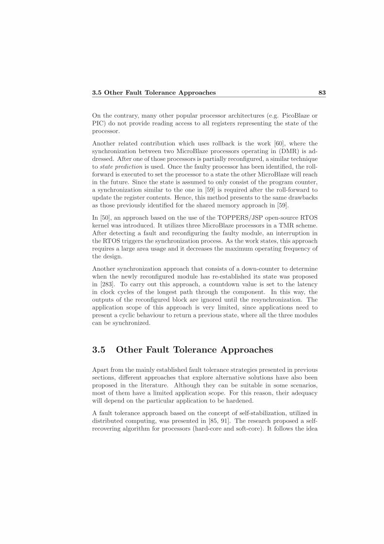
3.5 Other Fault Tolerance Approaches 83
On the contrary, many other popular processor architectures (e.g. PicoBlaze orPIC) do not provide reading access to all registers representing the state of theprocessor.
Another related contribution which uses rollback is the work [60], where thesynchronization between two MicroBlaze processors operating in (DMR) is ad-dressed. After one of those processors is partially reconfigured, a similar techniqueto state prediction is used. Once the faulty processor has been identified, the roll-forward is executed to set the processor to a state the other MicroBlaze will reachin the future. Since the state is assumed to only consist of the program counter,a synchronization similar to the one in [59] is required after the roll-forward toupdate the register contents. Hence, this method presents to the same drawbacksas those previously identified for the shared memory approach in [59].
In [50], an approach based on the use of the TOPPERS/JSP open-source RTOSkernel was introduced. It utilizes three MicroBlaze processors in a TMR scheme.After detecting a fault and reconfiguring the faulty module, an interruption inthe RTOS triggers the synchronization process. As the work states, this approachrequires a large area usage and it decreases the maximum operating frequency ofthe design.
Another synchronization approach that consists of a down-counter to determinewhen the newly reconfigured module has re-established its state was proposedin [283]. To carry out this approach, a countdown value is set to the latencyin clock cycles of the longest path through the component. In this way, theoutputs of the reconfigured block are ignored until the resynchronization. Theapplication scope of this approach is very limited, since applications need topresent a cyclic behaviour to return a previous state, where all the three modulescan be synchronized.
3.5 Other Fault Tolerance Approaches
Apart from the mainly established fault tolerance strategies presented in previoussections, different approaches that explore alternative solutions have also beenproposed in the literature. Although they can be suitable in some scenarios,most of them have a limited application scope. For this reason, their adequacywill depend on the particular application to be hardened.
A fault tolerance approach based on the concept of self-stabilization, utilized indistributed computing, was presented in [85, 91]. The research proposed a self-recovering algorithm for processors (hard-core and soft-core). It follows the idea
84 Hardening Soft-Core Processors Implemented in SRAM FPGAs
of that the self-stabilization permits to distributed systems to reach a correct stateregardless of in which state has been initialized with in a finite number of execu-tion steps. The proposed algorithm utilizes a specific interruption code combinedwith asynchronous interruption signals at random clock cycles to modify the con-tent of memory cells randomly. In the presence of corrupt data cause by failures,the algorithm leads the system to an arbitrary configuration that corrects thebehaviour in a finite amount of time. The approach focuses on specific resources,such as, registers (special and general purpose), internal SRAM, memoy caches,etc. Due to this approach, the system can bear transient failures, especially thosefailures that do not affect the code executed by any node. However, since thisapproach is program dependant and especially focused on preserving the con-vergence of transmitted data, its application scope is limited. In addition, theapproach is not effective if an error affects one of the registers that contain thevariables utilized by the processor while executing the self-converging program.
The approach presented in [239] is another algorithm-based hardening alterna-tive. The proposed Algorithm-Based Fault Tolerance (ABFT) technique reducesthe susceptibility by 99% with a limited resource overhead (about 25%) by hard-ening both the datapath and the configuration memory. The application scopefor the ABFT is linear-algebra operations. However, as the author states, for ap-plications that are not comprised of linear algebra operations the ABFT cannotprovide sufficient protection.
A different strategy was proposed in [284] where the configuration bitstreamis modified by the hardware inside the chip. A controller implemented withlogic resources of the FPGA manages the bitstream adaptation following twoalgorithms (Modify Placement and Modify Routing). This approach affects thedesign negatively in terms of area and performance. Besides, bearing in mind thatthe controller is implemented with logic resources of the FPGA it is susceptibleto induced faults.
Other fault tolerance approaches hinge on design aspects in order to hardenFPGA based designs. In [65], a methodology for the hardware/software co-design of embedded systems has been proposed. This method takes the advan-tage of different software and hardware strategies (hardware or software redun-dancy, etc.). It presents the concept of Software Implemented Hardware FaultTolerance (SIHFT), which allows to achieve a trade-off solution that meets thespecific requirements of designs. In this way, after defining the specific require-ments, different SIHFT approaches are used in an incremental way in order toobtain a concrete number of candidate implementations of the software. Afterthat, all of these generated candidates are compared to estimate the code andexecution time overheads. After discarding the implementations that not meet

3.5 Other Fault Tolerance Approaches 85
requirements, the selected candidates are tested by an SEU emulation tool. Theones that present better fault tolerance results are again tested in deeper faultinjection campaigns identifying the critical elements in order to protect themwith hardware redundancy. In this way, a range of trade-offs hardware/softwareimplementations is obtained. Although the positive results achieved hardeninga PicoBlaze based design this approach is a software and hardware dependantsolution and it demands high design efforts.
Another alternative to harden FPGA systems in the design process is to hardendesigns during the synthesis like in [285], where the In-place X-Filing (IPF) tech-nique was introduced. The IPF is a synthesis-based algorithm that masks SEUsat a logic level in both LUTs and interconnects. This approach requires to anal-yse the configuration bits in other to identify the bits with no failure rate. Thisprocess demands some kind of analysis mechanism such as a logic simulation. Af-ter identifying the bits with no failure rate, they are filled in order to mask errors.The more of these bits are reconfigured to mask errors, the smaller failure rateis obtained. The utilization of this solution also requires a high design effort andits results are dependant of the number or configuration bits with no failure rate.In addition, the results in terms of resource overhead of performance obtainedwhen utilizing this kind of approaches may be worst than the ones achieved whenutilizing vendor’s tools, which are optimized for their devices.
In [11], a hybrid error-detection technique based on assertions and a non-intrusiveenhanced watchdog module to recognize induced faults in processors, namedHETA, was introduced. This technique depicted in Figure 3.17 (obtained from[11]), utilizes the combination of software-based techniques in tandem with anon-intrusive hardware module. By virtue of this idea, the approach analysesand adds static instructions to the original program-code. During operation italso constantly updates the content of a signature register, which is connected todifferent program nodes. These program nodes are the basis for the error detect-ing control flow. On the other hand, the purpose of the hardware module is todetect incorrect jumps to unused memory positions and control flow loops. Thisapproach utilizes 66% less resources than a TMR implementation. However, thereliability level is lower and the performance is considerably reduced.
An approach inspired by the immune system that can be found in higher organ-isms was presented in [286]. The proposed hardware immune system is basedon the negative-selection algorithm, which utilizes binary matching rules to dis-criminate invalid states. These matching rules are implemented utilizing the logicresources of the FPGA in order to obtain a higher operation speed with more log-ical gates cost. Bearing in mind that almost hardware systems can be representedas an individual or a set of interconnected FSM, the discrimination methods are
86 Hardening Soft-Core Processors Implemented in SRAM FPGAs
Enhanced
HW Module
Processor
Program
Memory
address
data
read_write
Figure 3.17: Block diagram of the HETA approach.
implemented using an FSM in order to represent the system to be immunized.The detection of faults is performed following the idea that an error creates aninvalid state. In this way a controller module brings together the inputs, com-bining them with previous states to generate different strings for the FSM andthe detection. Monitoring the internal states of the FPGA makes it possible todetect an error before it propagates to the output. The results in terms of capac-ity and performance are non optimal and the utilization of an internal controllercompromises the reliability of the entire design.
3.6 Evaluation of Hardening Techniques
After designing hardening techniques it is necessary to evaluate the fault toler-ance level that they provide. Nevertheless, apart from the hardening technique tobe evaluated, several factors affect the tolerance level of a hardened design, suchas, the platform device, the environment, the design itself or even the running ap-plication. Due to this, the evaluation process is frequently performed in differentlevels. The first evaluation could be to check the concept to be designed itself byanalysing its architecture (the selection and configuration of the elements, etc.).Being the root of the whole designing process, taking care of those aspects couldsignificantly improve the result for future steps. Another aspect to be previouslyanalysed is the reliability of the device to be utilized as an implementation plat-form. This task is usually performed by manufacturers. The exponent of thisidea is the previously presented Rosetta Experiment [166] in which Xilinx is con-tinuously evaluation the reliability level of their devices under several conditions,such as, different altitudes and geographic locations.

3.6 Evaluation of Hardening Techniques 87
After obtaining a satisfactory design, the hardening strategy has to be selected. Anumber of features have to be considered before adopting a design decision, suchas, the available resources, the acceptable performance penalty, susceptibility andavailability levels, etc. An aspect that helps to optimize the hardening approachto fit with these requirements is to detect the most susceptible elements andevaluate their reliability. This analysis permits to identify in which elements hasto be focused when hardening the entire system. Finally, after developing andapplying the different hardening strategies the entire design has to be validatedin order to confirm its robustness. The idea of fault tolerance evaluation is alsoutilize to hardening techniques as a way to validate the effectiveness of developedapproaches.
Fault tolerance evaluation of a particular design also considers the determinationof the critical or essential bits from the configuration memory. A bit can beclassified as critical if its faulty state can affect the functionality. Not all thebit from the bitstream are critical. In fact in regular designs less than 20% ofthe configuration memory bits are usually classified as essential or critical to thefunctionality of a design [157, 289]. Nevertheless, their reliability is a crucialfactor, since they jeopardize the integrity of the entire design.
Considering the typical error rates, analysing the reliability during normal op-erating conditions would drastically delay the designing process. Hence, severalstrategies have been proposed to estimate systems’ behaviour under the presenceof errors.
The easiest fashion to evaluate the fault tolerance level of a design is to simu-late a fault by utilizing an HDL simulator [200, 245]. Several HDL simulatorsare available. There are commercial releases like Modelsim by Mentor Graph-ics or Vivado Simulator by Xilinx, or open-source software, such as, Verilatorby Veripool and OSS CVC by Tachyon Design Automation. These alternativesprovide a straightforward way to analyse the behaviour of a design by utiliz-ing its HDL file due to the observability and controllability provided. This isespecially helpful to improve hardening techniques, since it enables to adjust dif-ferent characteristics and check them in a relative easy way. HEARTLESS [290],MEFISTO-C [291] and VERIFY [292] remarkable simulation based tools andmethods. Comparing with other existing strategies simulation is a very time de-manding alternative. In addition, considering that these simulations in a betterscenario are post-synthesis simulations, the accuracy obtained is limited becausethey are many physical aspects that can’t be checked.
Another alternative is to use circuit instrumentation to substitute cells of the tar-get device by equivalent instrumentation hardware cells, obtaining a prototypeddesign. In [293], an approach called Autonomous Emulation which follows this
88 Hardening Soft-Core Processors Implemented in SRAM FPGAs
idea was presented. The AMUSE (Autonomous MUltilevel emulation system forSoft Error evaluation) approach presented in [294] extends this idea to emulateSETs. SETs are more difficult to evaluate than SEUs because they are manymore possible SETs than SEUs. For this reason, this approach implements alldemanded functionalities in the FPGA along with the circuit model, without re-quiring any FPGA-host iteration which improves the injection speed. However,bearing in mind that the circuit tested is not exactly the target design itself, theaccuracy of the obtained results is not optimal.
The most effective and extended way to evaluate the fault tolerance of a designis to inject faults in it. In these cases the device to be tested is usually referredas Device Under Test (DUT). The two main strategies to inject faults in SRAMbased FPGA designs are to induce faults physically by utilizing radiation emittingdevices and to inject fault in the bitstream [11, 265]. Each of them offer differentbenefits that also come with their subsequent drawbacks. Another alternative isto combine both strategies, like in [295], in order to obtain the benefits of bothworlds. These two strategies have inspired a large number of researches, someof the most relevant ones and the main characteristics of these strategies arediscussed in the following lines.
3.6.1 Physical Fault Injection Techniques
Physical Injection Techniques are the most realistic and fast way to inject faultsin SRAM-Based FPGA systems since they can simulate the real environment ina direct fashion. In addition, they don not require to have access to RTL andnetlists of designs. They consist in exposing the DUT to a certain radiation levelby utilizing specific instrumentation. The most common physical fault injectiontechniques are laser testing and particle beam testing. Although the utilizationof these techniques provides the most realistic results, they require the utilizationof very expensive machinery (in the range of $100K per day) and they provide asmall sample of faults. Despite the combination of multiple techniques is not themost extended practice, the work [20] proposes a complete and deep fault toler-ance evaluation which performs multiple tests. It includes simulation modeling,fault emulation and laser fault injection. Nevertheless, the most remarkable factis that the DUT has been also tested in a flight experiment, as part of the SpaceTest Program-Houston 4-ISS SpaceCube Experiment 2.0 (STP-H4-ISE 2.0). Ex-posing devices to space radiation in real-time is one the most accurate approachesthat can be adopted. However, this is not an available alternative for regular de-signers, since the economical cost and the time. In addition, as is mentioned in[296], in some cases it is necessary to reset and reprogram the device increasingthe time requirements.

3.6 Evaluation of Hardening Techniques 89
The characterization of the resistance of a device to induced errors is done bythe cross section (σ), given by expression 3.1 [297]. Fluence (φ) is the particledensity (particle number per 1 cm2 area), utilized to describe the output of thelaser beam. n in the quantity of configuration bits utilized in the DUT. Finally,e is the number of detected errors.
σ =e
φ× n(3.1)
There are two validation schemes to evaluate the fault tolerance when utilizingthese fault injection methods [298]:
• Static test This test type is useful to determine the device static crossarea, which is defined as the ratio between the fluence of hitting particlesand the SEU quantity. Their main advantage is that they provide a wayto quantify the device’s susceptibility to a particular radiation type. Statictest are based on initializing the DUT with a golden copy of the bitstream,which is used as a reference in periodical comparisons between it and thebitstreams read after the different radiation exposures.
• Dynamic test These test are utilized to evaluate the device dynamic crosssection, which is defined as the ratio between the fluence of hitting particlesand the quantity of SEUs that cause incorrect outputs. These test are avaluable tool to determine the sensitivity of a particular FPGA implemen-tation to a particular radiation type. Dynamic tests consists in checkingoutputs during the running of a specific application implemented in a de-vice. To obtain valuable information, the inputs have to be predefined andthe outputs have to be pre-calculated. An alternative, solution is a parallel-execution of an equal or equivalent application implemented in a stable andsecure platform and utilize it as a reference. There is also the possibilityof reading back the bitstream of the DUT in case of mismatch in order todetermine the faulty resource.
After performing one of these or both tests the results have to be collected andanalysed in order to identify the modifications in the resources of the FPGAinduced by SEUs [70, 298]. In [298], the CILANTO (CIrcuit-Level ANalysisTOol) is utilized for this task. This tool takes advantage of a database with arelation of configuration memory bits and the related FPGA resources. In thisway, it can be used to carry out a bit-level comparison between the gold copy ofthe bitstream and the recollected data.
Depending on the technology and physical principles used, physical fault injectiontechniques can be divided in two groups: Particle-beam testing and laser testing.

90 Hardening Soft-Core Processors Implemented in SRAM FPGAs
Particle-Beam Testing
Particle beam testing is the most extended physical fault injection method [128,178, 297–300]. This testing consists in exposing the DUT to radiation beamsthat produce a particular quantity of particles per second per area. The SEUis generated when an ionized particle interacts with a sensitive area portion ofthe FPGA, producing bit-flips. Three different particle types can be producedfor these test: Heavy-ion, Proton and Neutron. Each of them is more relevant inspecific environments at certain time intervals. Based on these concepts differenttests can be performed, like in [301] where neutrons test, high energy protonstest, thermal neutrons test and alpha foil test were conducted.
The concept of Linear Energy Transfer (LET) is closely related to particle-beamtesting. LET is the amount of ionizing energy transferred to the material inthe from of ionizations and excitations. Hence, LET can help to determine thepotential radiation damage.
The main objective of heavy-ion tests is to determine the lowest LET rate thatproduces detectable SEUs. Despite different LET ranges can be found in thespace, the more prevalent LET for heavy-ion particles are those with high LET.Before performing heavy-ion tests the adequate dose has to be determined [299].
Protons commonly present lower LET rates compared with heavy-ions. Protonscan produce ionization directly or indirectly. While in direct ionization the protonitself creates the charge that provokes the SEU, in indirect ionization the charge isproduced by a collinsion a proton-nucleus. Despite both ways can generate SEEsin electronics, only indirect ionization has been demonstrated to affect FPGA’slogic. This is because the direct ionization does not generate sufficient charge.The configuration memory of SRAM FPGAs have shown to be highly susceptibleto protons [302]. Figure 3.18 shows the Isochronous-Cyclotron located at theNuclear Physics Institute of the Academy of Sciences of the Czech Republic,which can provide proton beams tests. Scheduling of particle beam facilities isquite difficult and rigid.
Neutrons are generated by the spallation process [298], which consists in bom-barding a heavy-metal target (tungsten) with pulses of highly energetic protons.Due to this process neutrons are produced from the nuclei of the target atoms.The energy of the produced neutrons is normally reduced through a modera-tor module. Due the high cost of the infrastructure, only a limited number ofdedicated facilities able to perform test based on neutron beams matching theterrestrial flux are available, such as, ISIS, LANSCE, TRIUMF, and RCNP.
In general terms, fault tolerance evaluation by particle beam technologies presents

3.6 Evaluation of Hardening Techniques 91
Figure 3.18: The Isochronous Cyclotron U-120M.
Figure 3.19: ISIS pulsed neutron source at the Science and Technology Facilities
the challenge of synchronizing, locating and controlling the bean precisely. Hence,the implementation of an accurate SEU injection at a precise area in the FPGAis a complicated task. Moreover, the risks that come with the utilization of thistechnology demand special precautions for managing the radiation source, andrunning with the vacuum interface.
Laser Testing
The principle of this type of test is that when the laser energy is accumulated ina semiconductor it produces free charge carriers that are able to generate upsets.In fact, the impact of laser induced faults in SRAM-based FPGAs are analogousto SEUs produced by energetic particles [303]. Unlike particle beam, laser testingoffers a finer control in means of space and time. Due to this, laser tests permit

92 Hardening Soft-Core Processors Implemented in SRAM FPGAs
to have a precise control of the injection target to the micron level. Differentlaser-testing setups are shown in Figure 3.20(a) and Figure 3.20(b).
(a) Laser testing setup from [303]. (b) Laser testing setup by Riscure Inc.
Figure 3.20: Different laser testing setups.
The laser pulse can ionize a specific region of the DUT, inducing bit-flips inboth, combinational or sequential logic elements. Unlike collision tests, due tothe differences in the physical fault mechanisms of both methods, laser testingis not able to characterize the rates of raw faults. Nevertheless, thanks to theprecision in the transient fault generation it is possible to characterize the fault-to-error probability. Another interesting characteristic is that, unlike bitstreambased fault injections, the laser testing permits to create realistic multi-bit upsetsand SETs.
Like in particle bean testing, one of the main drawbacks of this method is thatthe technology necessary perform the test is highly costly. The preparation anddevelopment efforts demanded for a system-level test are high also. Anotherproblem when utilizing laser testing at application-levels is to inject single faultsper application execution [304]. The work [295] circumvents this problem bydriving a trigger signal to a control block that opens or closes a specific shutterin the laser path, while the energy magnitude is measured by a photo-detectionbased module. Maintaining the laser correctly aligned during the entire test isanother challenging task.
3.6.2 Bitstream Based Fault Injection Techniques
Bitstream based fault injection techniques, also known as fault emulation tech-niques, are an inexpensive and a widely extended tool [73, 85, 87, 198, 234, 239,

3.6 Evaluation of Hardening Techniques 93
305–307] to characterize specific design implementations. They enable to col-lect huge amount of data due to continuous injection over a period of hours ormonths and they are a valuable tool for studying the behaviour of DUT underthe presence of bit errors. Despite being less realistic than radiation test, theresults obtained with these techniques are highly accurate. For this reason, faultemulation is commonly utilized as a complementary tool to physical injection.
They mainly consist in reconfiguring the DUT with a corrupted configurationbitstream and checking its behaviour in order to evaluate the reliability. Figure3.21 shows the basic flow of a bitstream based fault injection.
����������������� ��������
��������������
��������������
�����������������������
�������
�������
�������
������
�������
�������
�
Figure 3.21: Basic flow of bitstream based fault injection.
First, the corrupted bitstream has to be created. The usual way is to flip thedesired bits of the configuration bitstream. When determining the critical bits ofa particular implementation, an alternative is to generate as much of corruptedbitstream as configuration bits in order to check the effects produced of eachconfiguration bit. Another way is to generate random positions of the corruptedbits like in [307]. Considering the large amount of bits of a configuration bit-stream, these alternatives require lots of time and large memory storages. Sincethe reconfiguration is a time demanding process, the size of the bitstream to beloaded will directly affect the duration of the fault injection process. Due tothis, instead of loading the entire bitstream, an alternative is to generate partialbitstreams and utilize the dynamic partial reconfiguration capability of SRAM-based FPGA [308, 309]. This practice reduces both, the injection time and the

94 Hardening Soft-Core Processors Implemented in SRAM FPGAs
memory demand to store the different corrupted bitstreams.
If the hardening approach is focused on the memory elements, it is relevant toput special efforts in injecting errors in the stored data. This strategy requires tostudy the bitstream structure. In the case of Xilinx devices the .ll location file itis a very helpful resource. However, it requires certain level of processing effort.
The second step in the basic fault injection flow is to reprogram the FPGA withthe corrupted file. Since this can be done utilizing different configuration inter-faces, this aspect directly involves the experimental setup. Figure 3.22(a) showsthe most inexpensive strategy, which is to utilize a single FPGA device, as both,DUT and fault injector. Despite this approach can be practical to test particulardesign portions, it requires to perform a deep study of the implementation andits bitstream and it does not permit to perform a complete fault injection test.This is because it implies to implement the fault injection logic in the DUT itself.Hence, a faulty bitstream could also affect the fault injection, and even the testlogic. A widely extended practice, as Figure 3.22(b) depicts, is to utilize andadditional external board to the manage the reconfiguration of the DUT [310].This scheme avoids the possibility of corrupting the fault injection logic itself.Nevertheless, it increases the costs due to the need of additional devices. Anin-between solution is to utilize SoC devices like in [165], where the Zynq devicehas been utilized. As Figure 3.22(c) shows, in this case the Processing Systemmanages the creation of the corrupted bitstream and downloads it through thePCAP interface to configure the programmable logic. This approach avoids both,the need of additional hardware and corrupting the fault injection controller.
After reconfiguring the FPGA with the corrupted bitstream the functionality hasto be tested by running the test application and comparing the results obtainedwith reference values. There are several alternatives to obtaining these referenceresults. The most simple one is to pre-calculate and store the responses of theapplication to be tested under specific inputs and conditions. In this way afterrunning the application the results can be compared with the pre-calculatedresponses. Another alternative is to utilize an additional implementation of thetarget application and run both, the DUT and the replica in parallel, checkingthe outputs in runtime.
An extended practice to increase the efficiency of functionality tests is to utilizetest vectors. This implies that each injected fault is tested with a vector ofdifferent inputs. Bearing in mind that different input can affect to distinct bitsthis strategy opens the range of possible generated errors. After performing theactual test the results obtained can be saved in a file permitting to run a nexttest. In this way all the obtained results can be analysed in future fault toleranceevaluations.
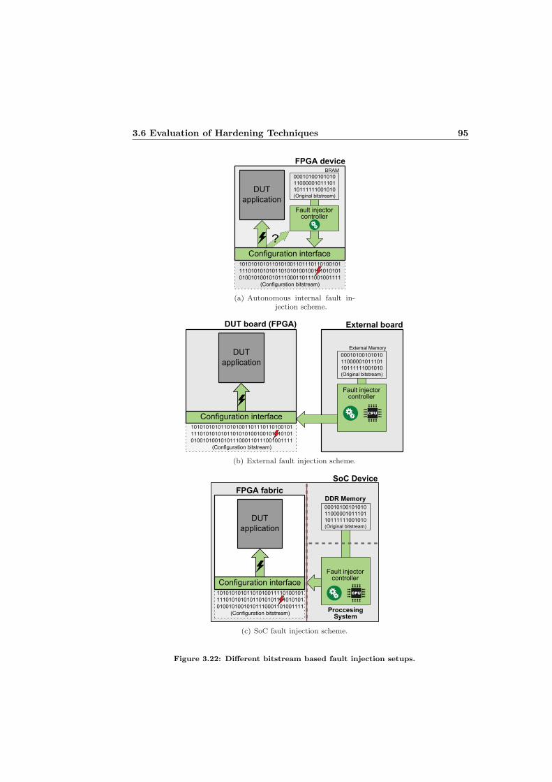
3.6 Evaluation of Hardening Techniques 95
1010101010110101001101110110100101
1110101010101101010100100101010101
0100101001010111000110111001001111
(Configuration bitstream)
FPGA device
DUT
application
00010100101010
11000001011101
10111111001010(Original bitstream)
Configuration interface
Fault injectorcontroller
BRAM
?
(a) Autonomous internal fault in-jection scheme.
1010101010110101001101110110100101
1110101010101101010100100101010101
0100101001010111000110111001001111
(Configuration bitstream)
DUT board (FPGA) External board
Configuration interface
00010100101010
11000001011101
10111111001010(Original bitstream)
Fault injectorcontroller
External Memory
(b) External fault injection scheme.
10101010101101010011110100101
11101010101011010101101010101
01001010010101110001101001111
(Configuration bitstream)
FPGA fabric
Configuration interface
SoC Device
00010100101010
11000001011101
10111111001010(Original bitstream)
Fault injectorcontroller
DDR Memory
ProccesingSystem
(c) SoC fault injection scheme.
Figure 3.22: Different bitstream based fault injection setups.
96 Hardening Soft-Core Processors Implemented in SRAM FPGAs
Several fault injection tools have been presented in the literature. Some of themost representative ones are listed in the lines below:
• Xilinx provides a so called Soft Error Mitigation Controller (SEM) [186]that can be used to inject, detect and correct errors in the configurationmemory of 7 series devices. Nevertheless, it is only suitable for the config-uration memory and not for BRAMs or distributed memories. RegardingBRAMs, Xilinx offers a fault injection mechanism for BRAMs with itsCORE Generator. However, due to its limitations this mechanism is notpractical for many applications.
• Fault Injection (FI) tool presented in [311] is a bitstream based tool forVirtex FPGAs that addresses only configuration memory cells and userregisters. This tool is especially designed to fit with the requirements ofthose applications in which the FPGA undergoes in frequent reconfigura-tions. It modifies the configuration bitstream while this is loaded into thedevice without utilizing standard synthesis tools making it independent tothe system utilized. Nevertheless, since this tool cannot access to the built-in FSM state transitions it requires the utilization additional fault injectiontechniques to test them.
• XRTC Virtex-5 Fault Injector is another fault injection tool for Virtexdevices presented in [312]. This FPGA fault injection system for testingdigital FPGA circuits has been designed in conjunction with the XilinxRadiation Test Consortium. The main goal is that it achieves a high cus-tomization and full bitstream coverage at a high fault injection rates.
• FPGA-based Fault Injection TOol (FITO) proposed in [313] permits toinject faults emulating SEUs and SETs at RTL level of an FPGA designby adding extra ports and connections to the flip-flops.
• FLIPPER tool presented in [314], as its name suggests, is able to provokebit-flips within the configuration memory utilizing the partial reconfigura-tion capability of SRAM-FPGAs.
• Fault injection Using SEmulation FUSE [315] is a tool that includes theconcept of semulation (a combination of simulation and emulation). It per-mits to take advantage of the benefits of both techniques: the higher faultinjection speed of the emulation and the flexibility and the observability ofthe HDL simulation.
• Shadow Components-based Fault Injection Technique (SCFIT) [93] toolis also based on the semulation. It utilizes TCL scripts to access to theFPGA by using the JTAG configuration interface.

3.6 Evaluation of Hardening Techniques 97
• Flexible on-chip fault Injector for run-time Dependability validation withtarget specific COmmand language, FIDYCO [316] is a tool that combinesboth hardware and software schemes. While, the hardware includes the tar-get FPGA implementation, the software is located in an external computer.Due to the flexibility provided by this tool, the designer is able to test a va-riety of components. It mainly consists in moving the fault injector towardsthe target and after it, translating the target to the FPGA.
• Direct Fault Injection (DFI) [96] is focused on injecting errors in soft-coreprocessors implementations. This approach is a combination of multiplefault-injection methods such as FITO, FUSE, etc.
• NETlist Fault Injection (NETFI) [317] is a tool that permits to injectfaults in designs written in any HDL language (Verilog, VHDL, etc.). Themain idea of this approach resides on modifyin the built-in FPGA resourcesthat are to be used by the netlist after the synthesis process.
• Fault-Injection Fault Analysis tool (FIFA) [318] allows to inject faults atRTL level. It implements two versions of the DUT in the FPGA device.
• The platform presented in [319] called FT-UNSHADES2 is an approachfocused on carrying out the fault injection utilizing a hardware assistantthat can accelerate the analysis process. It uses a mother board connectedto two daughter boards. It has different operating modes to deal with ASICsand FPGAs. The FPGA mode injects the fault utilizing the bitstream.However, it also has an additional Beam Testing mode to be used with thesystem inserted in an ion beam. This mode allows to place one daughterboard exposed to the ion beam and maintain the other safe in other tocompare them acting as a coincidence detector.
• Advanced System for the TEst under Radiation of Integrated Circuits andSystems (ASTERICS) is a platform used in [91]. This upgraded versionof the THESIC+ platform, is built utilizing two FPGAs. While the first onemanages the communication between a computer and the ASTERIC boardutilizing a hard processor, the second contains the DUT with the user designto be tested, the injection module and the memory controller. A watchdogimplemented in the first board checks the possible errors generating a lossin the sequence.
• In [310], a low hardware overhead injection approach for FPGA designs,avoiding the need of special injection boards was presented. This worksoffers two fault injection approaches: An external SEU flow which is a faultinjection approach managed by an external device, and a single bit errortest flow, that utilizes the internal reconfiguration obtaining a high injection
98 Hardening Soft-Core Processors Implemented in SRAM FPGAs
performance.
• The work [320] proposes a high-speed fault injection system along with amethodology able to test the sensitivity of a design’s bitstream to SEUs.This system is especially designed for soft-core processors and it also canbe utilized for radiation testing purposes.
One relevant drawback of these techniques is that they are not able to injectfaults across all sequential elements of the design, especially when the designutilizes proprietary IP cores, where physical mapping is unspecified. Anotherdrawback is that these techniques tend to overemphasize cache and register er-rors [295]. Due to the inherent nature of bitstreams these techniques are highlytechnology dependant. Although the flows and concepts can be utilized in dif-ferent devices, the implementation of each approach has to be adapted to theparticular specifications of the DUT, which may require to investigate its design.
Despite the utilization of this tool represents a very helpful aspect, to investigatenew fault injection approaches is out of the scope of this work.
3.7 Conclusions
Taking into account the diverse application fields and the different soft-core pro-cessor implementations available, providing them with fault tolerance requirestrade-off decisions to develop a tailored design. The aspect to evaluate mainlyare the hardware overhead, the reliability level, the performance penalty and theavailability. The work presented in [287] proposes several models to evaluatethe reliability and availability of the most relevant fault tolerance techniques forSRAM-based FPGAs. This kind of researches provide valuable information toobtain appropriate mitigation schemes.
The most relevant item to be hardened in any FPGA design is the configurationmemory, since it manages the settings, interconnections and data content of al-most the components within the device. Many manufacturers provide ECC basedprotection for the configuration memory. However, due to its limitations (i.e. it isnot able to repair multiple errors), in some cases this hardening technique is notsufficient. In those scenarios, a periodical configuration scrubbing is a remarkablecomplementary alternative. This technique is able to repair most of configura-tion errors, even those masked in hardware redundancy schemes. Nevertheless,this technique comes with some drawbacks, such as, lack of protection for datacontent, time demand and requirement of a controller mechanism. Hence, boththe ECC and scrubbing techniques are mainly combined (or substituted) with

3.7 Conclusions 99
other hardening methods, like hardware, data, software or time redundancies.
Data redundancy techniques are based on encoding data when writing it in mem-ory and decode it when reading, for checking and fixing errors. The advantages ofECC techniques are good performance and small resource utilization, especiallywith large data width. This is because the added encoding data decreases propor-tionally with data width. Software redundancy based techniques increase faulttolerance level with a low resource overhead. However, they are time demandingand relatively reliable strategies. The benefits or drawbacks of these techniquesare closely related to the characteristics of each application program. Time re-dundancy based approaches offer similar features: the reduced hardware overheadimpact comes with a performance penalty and an improvable reliability. Hence,the most utilized approaches are based on hardware redundancy. Despite beingresource demanding techniques, they offer high availability and dependability.
When hardening a soft-core processor with a hardware redundancy scheme, thetwo main alternatives are TMR and lockstep combined with checkpointing androllback. While TMR provides higher reliability and availability the area impactof the lockstep is smaller. After selecting the redundancy level, an appropriategranularity has to be adopted, choosing between a range of possibilities thatstart from the lower hardware overhead and simply design of coarse grainedimplementation and that end in the higher reliability level of a fine grained one.Is has to be remarked that due to the use of a voter, hardware redundancyschemes always present a single point of failure.
In any case, considering that a soft-core processor consists of several elements, itis interesting to analyse the different alternatives to harden each of them. Whileelements, such as, the ALU, the control logic, etc. based on logic operations,have to be hardened with hardware redundancy, user memory elements mayaccept distinct techniques like ECC strategies.
There are four main user data storage elements in a soft-core processor. Thefirst one is the program memory, which is a read only memory. The second isthe data memory block that can be read and written. The third are the regis-ters, that can be user registers (read/write) or special function registers (onlyread or read/write). Last but no least, there is a stack memory block, thatcan’t be accessed. Bearing in mind the unique characteristics of each memoryelement, the available methods and their adequacy for each module may differ.Recent spacial experiments have proved that BRAMs are especially sensitive toradiation-induced upsets, indicating that distributed RAM based memory struc-tures present higher reliability leveld [288]. Hence the study of BRAM protectingtechniques gains special relevance.

100 Hardening Soft-Core Processors Implemented in SRAM FPGAs
When hardening data and program memories the most suitable alternatives arean ECC encoding and TMR implementation. DMR scheme is not a valid optionfor these modules, since the errors can only be detected and cannot be fixed,requiring an additional backup memory block to save the checkpoints. In fact, theuse of this backup memory together with the duplicated memory blocks impliesa TMR implementation. When selecting an ECC hardening, the data memoryrequires both encoding and decoding modules, while the program memory onlyneeds a decoding module, because the coding has to be done in the programmingprocess. There are not big implementation differences between data and programmemory blocks when picking out a TMR hardening. Is has to be rememberedthat both, ECC and TMR, do not repair fault but mask them. This problemcould be less crucial in the case of data memories, since in many application casesthe data is constantly be re-written during program execution, cleaning maskederrors. For program memories, a memory data scrubbing would be an interestingalternative to wipe the masked faults.
The stack memory can be hardened with TMR or ECC approaches because,DMR scheme does not offer a proper reliability. Depending on the depth ofthis module, ECC can be too costly in terms of area. In this way, a TMRimplementation is the adequate alternative to harden this element in most cases.Bearing in mind that the stack memory is mostly frequently being written duringthe program execution, the masked errors are likely to been wiped during theprogram execution. Nevertheless, considering that an error in the stack memorycan affect the entire execution flow of the program, it is highly advisable to hardenit properly.
On the other hand, when hardening registers the most advisable method is theTMR. Considering the small data width of registers and that each register de-mands its own coding and encoding logic the resource overhead added by theECC makes it unreasonable to use it. An alternative to use an ECC strategyreducing the resource overhead can be to utilize a single ECC coding/decodingcombined with a multiplexer. However, the integrity of the multiplexer couldcompromise the reliability of the entire system. The reason to discard a DMRhardening is the same as in data and program memory blocks.
Regarding the evaluation of the fault tolerance level of a hardened soft-core pro-cessors the most suitable alternatives are bitstream based fault injection or/andphysical fault injection strategies. While bitstream based fault injection tech-niques provide an inexpensive way to estimate the failure rate, physical faultinjection strategies offer more accurate information at higher costs. Althoughboth strategies provide valuable information, they also require complex and timeconsuming experimental setups. Due to this, in some scenarios more basic alter-
3.7 Conclusions 101
natives like modifying the hardware design to provoke faults, could offer fasterand adequate enough ways to evaluate the correctness of a hardening strategy.
Considering all these aspects it can be stated that there is no hardening solutionthat is completely efficient for all types of designs, so the implementation offault tolerant architectures and its validation requires a special study of system’scharacteristics and the application requirements.

102 Hardening Soft-Core Processors Implemented in SRAM FPGAs
Chapter 4
Contributions in FaultTolerance for Soft-CoreProcessors
This chapter introduces the different approaches developed in this work that havebeen focused on improving the fault tolerance of soft-core processors implementedin SRAM based FPGAs. These approaches address different aspects related tofault tolerance. Thus, in some cases they improve specific deficient features ofexisting techniques and in others propose new alternatives to circumvent knownissues.
The first contribution presents the PICDiY, a soft-core processor developedspecifically for this work. This soft-processor offers simplicity, modularity andself-sufficiency, making it easily adaptable. Due to those features it has beenutilized as an experimental subject to develop and test the fault tolerance ap-proaches presented.
In next contributions two novel approaches that deal with the data managementutilizing the bitstream have been developed. While one approached focuses onmanaging BRAM data the other deals with register’s data. Both novel data man-agement approaches have been utilized as a basis to develop new fault toleranceapproaches. roaches.
The rest of the contributions deal with different fault tolerance aspects: data con-tent scrubbing, extracting data from BRAM memories with damaged interfaces,
104 Contributions in Fault Tolerance for Soft-Core Processors
checkpointing and rollback in locktstep schemes and synchronization of repairedsoft-core processors in TMR schemes. Although most of the proposed techniqueshave been applied to the PICDiY soft-core processor, the majority of them canbe adapted to other soft-cores and even other types of architectures for SRAMFPGA based designs.
4.1 PICDiY: Target Soft-Core Processor
The amount of logic resources required to implement a soft-core processor de-pends on several factors, such as, data width, memory size, special features, etc.The more elements and larger data widths selected in the designing of a soft-coreprocessor, the larger usability and processing capability are obtained. Never-theless, usually the price to pay is a resource overhead and also a performancepenalty due to the increase of critical paths’ length. In addition to the obviouslower area availability, the resource overhead generally implies several drawbacks:higher power consumption, since logic elements need to be powered; more logicresources susceptible to errors, decreasing the fault tolerance level of the design;and in relation with hardening techniques, more logic resources have to be repli-cated when implementing redundancy schemes. Thus, from the designers’ pointof view, a simple and clear design of a small processor composed by the com-mon and basic elements of most common architectures is an interesting platformin order to develop new fault tolerance approaches, where a big processor wouldbring unnecessary complexity. Furthermore, the simplicity of the target processorcomes with a significant reduction of the amount of time demanded by synthesisand implementation tools. Due the presented benefits of utilizing small architec-tures, an 8-bit small processor has been selected as a candidate to be used withthe different proposed tests and approaches.
The first step in the study of new hardening alternatives for soft-core processorshas been the definition of the target soft-core processor. After studying thedifferent existing IP soft-core processors it has been decided to design a new soft-core processor from scratch. The main reason to make this decision has been tohave a total control of all the aspects of the architecture which would expandthe customization potential. Modifying the design of existing IPs is mostly atedious work that commonly comes with unexpected issues. For instance, in[321] a PicoBlaze IP was adapted for synchronization purposes, as a result, theobtained design offered worse characteristics than the original design. The reasonfor this negative effect is that the PicoBlaze has such a highly optimized andcomplex design to fit perfectly in Xilinx’s devices and to provide them with highperformance and small resource usage, that even small changes could lead the

4.1 PICDiY: Target Soft-Core Processor 105
synthesizer to deteriorate this optimization level. Similar results were obtainedin [322, 323] where the original design of the PicoBlaze was modified to obtain aplatform independent version of this IP.
In a next step ,it has been decided to base the design of the target soft-coreprocessor on the PIC16 microcontroller due to several reasons: it is a RISC ar-chitecture that offers a good code density [43]; its Harvard architecture uses aminimalist design which allows fast access and a different bus width for instruc-tion and data (a 14-bits width for the program memory and 8-bits width forthe data memory); it has a good execution speed (each instruction takes 4 clockcycles); it is a simple, efficient and stand-alone device; it works properly withstate machines; and it is a well known architecture that can be encountered inmany engineering applications [324–326]. Furthermore, the existing free toolkitsavailable for the PIC microcontroller can be used to develop application softwarelike IDEs (Integrated Development Environment). Thus, the PICDiY has ade-quate characteristics for a number applications, such as, memory peripherals orreconfiguration interface tasks where larger processors would be wasted.
The next subsection describes the architecture of the designed 8-bit and platform-independent soft-core processor, which for the sake of simplicity will be referredto it as PICDiY throughout the document.
4.1.1 PICDiY’s Architecture
The design of the PICDiY has been developed from scratch by utilizing VHDLlanguage and basing on PIC16’s functionality, its architecture’s block diagramand its instruction set. Figure 4.1, obtained from the 16F84A data sheet, showsthe block diagram of the PIC16. In order to obtain the simplest design, nonessential elements of PIC16’s architecture have been discarded. The dismissedcomponents are the timers (Power-up, oscillator Start-up, Watchdog and TMR0)and certain ports (only two ports are included). In addition, several adaptationshave been introduced in order to optimize the architecture’s characteristics andfunctionality. Thanks to all these modifications, the design developed in this workis a small processor with flexible functionality and complete self-sufficiency. Themain features of the architecture, the different components and the adaptationsmade are discussed in detail through this section.
As shown in Figure 4.2, the PICDiY consist of different blocks: the ArithmeticLogic Unit (ALU), the program counter, the Instruction Decoder and Controller(IDC), the 8-level stack, program and data memory blocks, address and datamultiplexers and the different special function registers. Due to its Harvard ar-chitecture, separate storage and buses for instructions and data are implemented,

106 Contributions in Fault Tolerance for Soft-Core Processors
FLASHProgramMemory
Program Counter13
ProgramBus
Instruction Register
8 Level Stack(13-bit)
Direct Addr
8
InstructionDecode &
Control
TimingGeneration
OSC2/CLKOUTOSC1/CLKIN
Power-upTimer
OscillatorStart-up Timer
Power-onReset
WatchdogTimer
MCLR VDD, VSS
W reg
ALU
MUX
I/O Ports
TMR0
STATUS reg
FSR reg
IndirectAddr
RA3:RA0
RB7:RB1
RA4/T0CKI
EEADR
EEPROMData Memory
64 x 8EEDATA
Addr Mux
RAM Addr
RAMFile Registers
EEPROM Data Memory
Data Bus
5
7
7
RB0/INT
14
8
8
1K x 14
68 x 8
Figure 4.1: Block diagram of the PIC16.
allowing faster access and different bus width for instruction and data. Thewidths are 14 bits for the program memory and 8 bits for the data memory. Thedata bus includes a multiplexer structure, not shown in the figure to facilitatethe comprehension. Control signals, such as, enables, mux controls, etc. (whichmainly are generated by the IDC) are also omitted for the same reason. Theprocessor also has an 8-bit PORTA, clock, reset and interrupt inputs (both clockand reset inputs are also not shown in the figure) and an 8-bit PORTB outputdirectly connected to the PORTB register. In this way, PORTA and PORTBare physical connections between the processor and external peripherals for datatransmission. Only two ports are implemented for achieving a minimal usageof FPGA resources, nevertheless, the number of ports can be easily changed bymodifying the VHDL files of the design.
The special function registers are an area of data memory dedicated to registersthat are required for configuration and control, which can not be used as generalpurpose registers by the user. Since each of the special function register has a spe-cific functionality, in the case of the PICDiY, each of them have been implementedon separated blocks outside the data memory block. In this way, the PICDiY con-tains seven register-blocks (FSR, STATUS, PCL, PCLATH, INTCON, PORTBand W) of eight bit width. The registers related to the discarded components
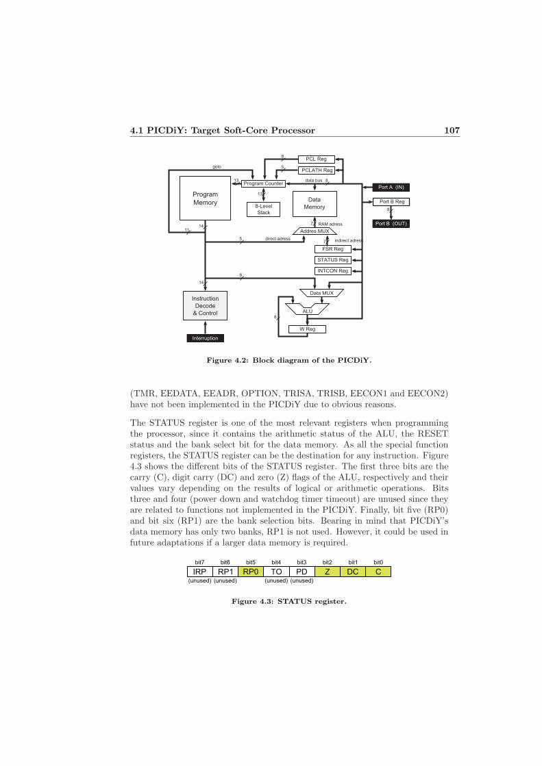
4.1 PICDiY: Target Soft-Core Processor 107
Interruption
Port B (OUT)
Port A (IN)
Program
Memory
Program Counter
Port B Reg
FSR Reg
STATUS Reg
INTCON Reg
Data
Memory
Addres MUX
Data MUX
ALU
W Reg
Instruction
Decode
& Control
14
8
5
1114
13 8
8
8
7
7
goto
direct adress indirect adress
RAM adress
data bus
5PCLATH Reg
PCL Reg8
8-Level
Stack
13
Figure 4.2: Block diagram of the PICDiY.
(TMR, EEDATA, EEADR, OPTION, TRISA, TRISB, EECON1 and EECON2)have not been implemented in the PICDiY due to obvious reasons.
The STATUS register is one of the most relevant registers when programmingthe processor, since it contains the arithmetic status of the ALU, the RESETstatus and the bank select bit for the data memory. As all the special functionregisters, the STATUS register can be the destination for any instruction. Figure4.3 shows the different bits of the STATUS register. The first three bits are thecarry (C), digit carry (DC) and zero (Z) flags of the ALU, respectively and theirvalues vary depending on the results of logical or arithmetic operations. Bitsthree and four (power down and watchdog timer timeout) are unused since theyare related to functions not implemented in the PICDiY. Finally, bit five (RP0)and bit six (RP1) are the bank selection bits. Bearing in mind that PICDiY’sdata memory has only two banks, RP1 is not used. However, it could be used infuture adaptations if a larger data memory is required.
IRP RP1 RP0 TO PD Z DC C
bit0bit1bit2bit3bit4bit7 bit6 bit5
(unused) (unused) (unused) (unused)
Figure 4.3: STATUS register.
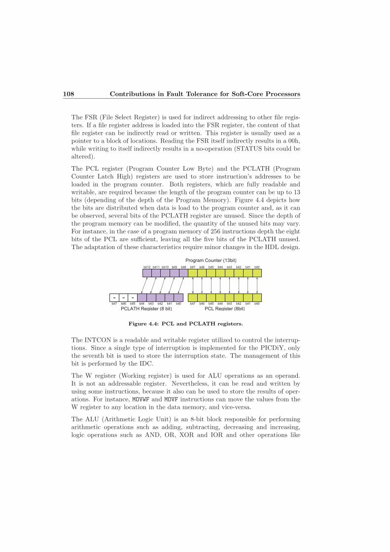
108 Contributions in Fault Tolerance for Soft-Core Processors
The FSR (File Select Register) is used for indirect addressing to other file regis-ters. If a file register address is loaded into the FSR register, the content of thatfile register can be indirectly read or written. This register is usually used as apointer to a block of locations. Reading the FSR itself indirectly results in a 00h,while writing to itself indirectly results in a no-operation (STATUS bits could bealtered).
The PCL register (Program Counter Low Byte) and the PCLATH (ProgramCounter Latch High) registers are used to store instruction’s addresses to beloaded in the program counter. Both registers, which are fully readable andwritable, are required because the length of the program counter can be up to 13bits (depending of the depth of the Program Memory). Figure 4.4 depicts howthe bits are distributed when data is load to the program counter and, as it canbe observed, several bits of the PCLATH register are unused. Since the depth ofthe program memory can be modified, the quantity of the unused bits may vary.For instance, in the case of a program memory of 256 instructions depth the eightbits of the PCL are sufficient, leaving all the five bits of the PCLATH unused.The adaptation of these characteristics require minor changes in the HDL design.
bit0bit1bit2bit3bit4bit7 bit6 bit5bit10 bit9 bit8
bit0bit1bit2bit3bit4bit7 bit6 bit5bit0bit1bit2bit3bit4bit7 bit6 bit5
Program Counter (13bit)
PCL Register (8bit)PCLATH Register (8 bit)
- - - - -
bit12 bit11
Figure 4.4: PCL and PCLATH registers.
The INTCON is a readable and writable register utilized to control the interrup-tions. Since a single type of interruption is implemented for the PICDiY, onlythe seventh bit is used to store the interruption state. The management of thisbit is performed by the IDC.
The W register (Working register) is used for ALU operations as an operand.It is not an addressable register. Nevertheless, it can be read and written byusing some instructions, because it also can be used to store the results of oper-ations. For instance, MOVWF and MOVF instructions can move the values from theW register to any location in the data memory, and vice-versa.
The ALU (Arithmetic Logic Unit) is an 8-bit block responsible for performingarithmetic operations such as adding, subtracting, decreasing and increasing,logic operations such as AND, OR, XOR and IOR and other operations like
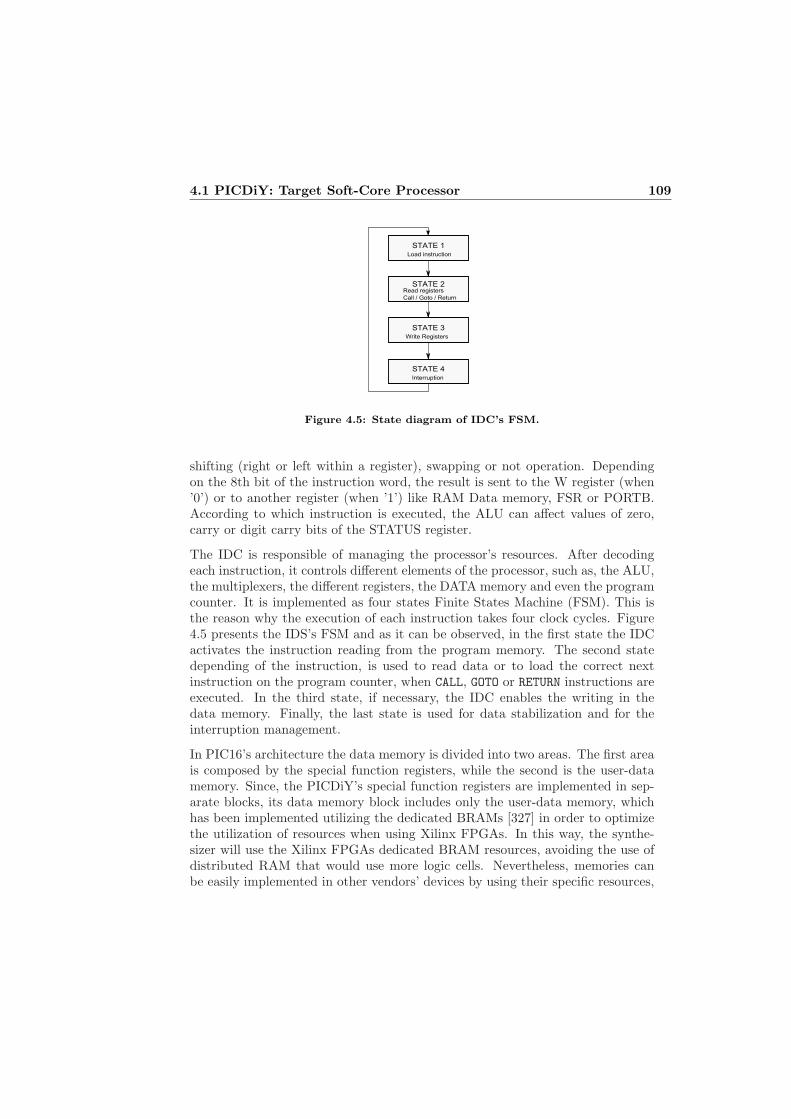
4.1 PICDiY: Target Soft-Core Processor 109
�������
�������
�������
������
�� ������������
���������������
��� ����������
��������������������
������������
Figure 4.5: State diagram of IDC’s FSM.
shifting (right or left within a register), swapping or not operation. Dependingon the 8th bit of the instruction word, the result is sent to the W register (when’0’) or to another register (when ’1’) like RAM Data memory, FSR or PORTB.According to which instruction is executed, the ALU can affect values of zero,carry or digit carry bits of the STATUS register.
The IDC is responsible of managing the processor’s resources. After decodingeach instruction, it controls different elements of the processor, such as, the ALU,the multiplexers, the different registers, the DATA memory and even the programcounter. It is implemented as four states Finite States Machine (FSM). This isthe reason why the execution of each instruction takes four clock cycles. Figure4.5 presents the IDS’s FSM and as it can be observed, in the first state the IDCactivates the instruction reading from the program memory. The second statedepending of the instruction, is used to read data or to load the correct nextinstruction on the program counter, when CALL, GOTO or RETURN instructions areexecuted. In the third state, if necessary, the IDC enables the writing in thedata memory. Finally, the last state is used for data stabilization and for theinterruption management.
In PIC16’s architecture the data memory is divided into two areas. The first areais composed by the special function registers, while the second is the user-datamemory. Since, the PICDiY’s special function registers are implemented in sep-arate blocks, its data memory block includes only the user-data memory, whichhas been implemented utilizing the dedicated BRAMs [327] in order to optimizethe utilization of resources when using Xilinx FPGAs. In this way, the synthe-sizer will use the Xilinx FPGAs dedicated BRAM resources, avoiding the use ofdistributed RAM that would use more logic cells. Nevertheless, memories canbe easily implemented in other vendors’ devices by using their specific resources,

110 Contributions in Fault Tolerance for Soft-Core Processors
thus, maintaining platform independence. The data memory is banked in twoblocks to permit a larger memory storage and each bank extends up to 7Fh (128bytes). As it has been commented before, the bank selection is done by writingthe STATUS register’s RP0 bit. In this way, Bank 0 is selected by clearing theRP0 bit of the STATUS register and the selection of Bank 1 is done by settingthis bit to one. All the data memory addresses can be accessed either directlyby utilizing the absolute address of each register or indirectly. When indirectoption is selected, using the zero address in the data memory, the processor usesthe FSR register to store the data in the correct address. Indirect addressingalso utilizes the value of the RP0 bit to access the banked areas of data memory.Figure 4.6 shows the mapping of the memories. As it can be seen, the first twelvelocations of each bank are reserved for the special function registers and the re-maining locations are used for the user-data memory. The reason to reserve thoseinitial addresses unused is to maintain coherence with PIC16’s architecture andits instruction set. In this way, despite the fact that the special function registersare implemented outside the data memory module, they can be accessed usingtheir original addresses thanks to the IDC, which controls the enable port of eachregister.
���
���
���
���
���
���
���
��
��
���
���
� �
��
���
������
���
������
������
� ����
��� ��
������ !�����"
� �
��#�$%���
&#&��'
$
$
$
$
������
���
������
������
� ����
��� ��
������ !�����"
� �
��#�$%���
&#&��'
$
$
$
$
���
���
���
���
���
���
���
��
��
���
���
� �
���
���
��(�
�����))
��(�
�����))����� �����
Figure 4.6: Mapping of PICDiY’s user-data memory and registers.

4.1 PICDiY: Target Soft-Core Processor 111
The program memory block is responsible to store the instructions to be executedby the processor. Similarly to the data memory block, it is implemented by usingBRAMs. However, the data length is 14 bits. Another remarkable difference isthat it is implemented as a read only memory. Thus, the instructions must bewritten in the HDL file. In favour of easing the programming task, the HEX2VHDfor PICDiY software has been developed in this work. This software generatesa VHDL file of the program memory from a HEX file. This HEX file can beobtained in a straightforward fashion by using a PIC16-compatible IDE, like theMPLAB by Microchip Technology Inc.
The program counter block manages the execution sequence of program memory’sinstructions, loading the next instruction or jumping to another one when CALL,GOTO, RETURN, indirect instructions or an interrupt are executed. It is a 13 bitblock capable of addressing an 8K x 14 memory space.
4.1.2 PICDiY’s Instructions
The RISC architecture of the PICDiY, allows higher CPU operating frequenciesand implies that it has a reduced number of instructions, which means simplicityin programming, since it is necessary to manage just a small number of instruc-tions. As Table 4.1 shows, the processor uses 33 instructions of a 14 bit width,divided into byte-oriented file register operations (18 instructions), bit-orientedfile register operations (4 instructions) and literal and control operations (11 in-structions). It has to be remarked that, due to the removal of the timers, PIC16’sSLEEP and CLRWDT instructions are not available. Each instruction takes a sin-gle machine cycle consisting of four clock periods for the execution, that is animprovement over the PIC16, since it uses two machine cycles for instructionswhich modify the value of the program counter. All of the instruction are storedin the program memory.
Figure 4.7 shows the general instruction format for byte-oriented file registeroperations. As it can be observed, the highest five bits are mainly used to definethe opcode, the 7th bit is used to set the direction of result’s value (d) for theALU and the lowest 7 bits are the file registers address.
������ � ���� ������������
�� � � � �
���� ��� ����
Figure 4.7: Byte-oriented file register operations instruction format.
Figure 4.8 shows bit-oriented file register operations instruction format. The

112 Contributions in Fault Tolerance for Soft-Core Processors
Instruction Description Instruction Code Flags STATUS
Byte-Oriented File Register Operation
ADDWF f, d f + W 00 0111 dfff ffff C, DC, Z
ANDWF f, d f AND W 00 0101 dfff ffff Z
CLRF f Clear f 00 0001 1fff ffff Z
CLRW - Clear W 00 0001 0fff ffff Z
COMF f, d Complement f 00 1001 dfff ffff Z
DECF f, d Decrement f 00 0011 dfff ffff Z
DECFSZ f, d Decrement f, skip if 0 00 1011 dfff ffff -
INCF f, d Increment f 00 1010 dfff ffff Z
INCFSZ f, d Increment f, skip if 0 00 1111 dfff ffff -
IORWF f, d f OR W 00 0100 dfff ffff Z
MOVF f, d Move f 00 1000 dfff ffff Z
MOVWF f Move W to f 00 0000 1fff ffff -
NOP - No operation 00 0000 0xx0 0000 -
RLF f, d Rotate left f through carry 00 1101 dfff ffff C
RRF f, d Rotate right f through carry 00 1100 dfff ffff C
SUBWF f, d f - W 00 0010 dfff ffff C, DC, Z
SWAPF f, d Swap nibbles in f 00 1110 dfff ffff -
XORWF f, d f OR W 00 0110 dfff ffff Z
Bit-Oriented File Register Operation
BCF f, b Bit clear f 01 00bb bfff ffff -
BSF f, b Bit set f 01 01bb bfff ffff -
BTFSC f, b Bit test, skip if clear 01 10bb bfff ffff -
BTFSS f, b Bit test, skip if set 01 11bb bfff ffff -
Control and Literal Operations
ADDLW k Literal + W 11 111x kkkk kkkk C, DC, Z
ANDLW k Literal AND W 11 1001 kkkk kkkk Z
CALL k Call a subroutine 10 0kkk kkkk kkkk -
GOTO k Go to k address 10 1kkk kkkk kkkk -
IORLW k Literal OR W 11 1000 kkkk kkkk Z
MOVLW k Move literal to W 11 00xx kkkk kkkk -
RETFIE - Return from interrupt 00 0000 0000 1001 -
RETLW k Return with literal in W 11 01xx kkkk kkkk -
RETURN - Return from subroutine 00 0000 0000 1000 -
SUBLW k Literal - W 11 110x kkkk kkkk C, DC, Z
XORLW k Literal XOR W 11 1010 kkkk kkkk Z
Table 4.1: Instruction set of the PICDiY.
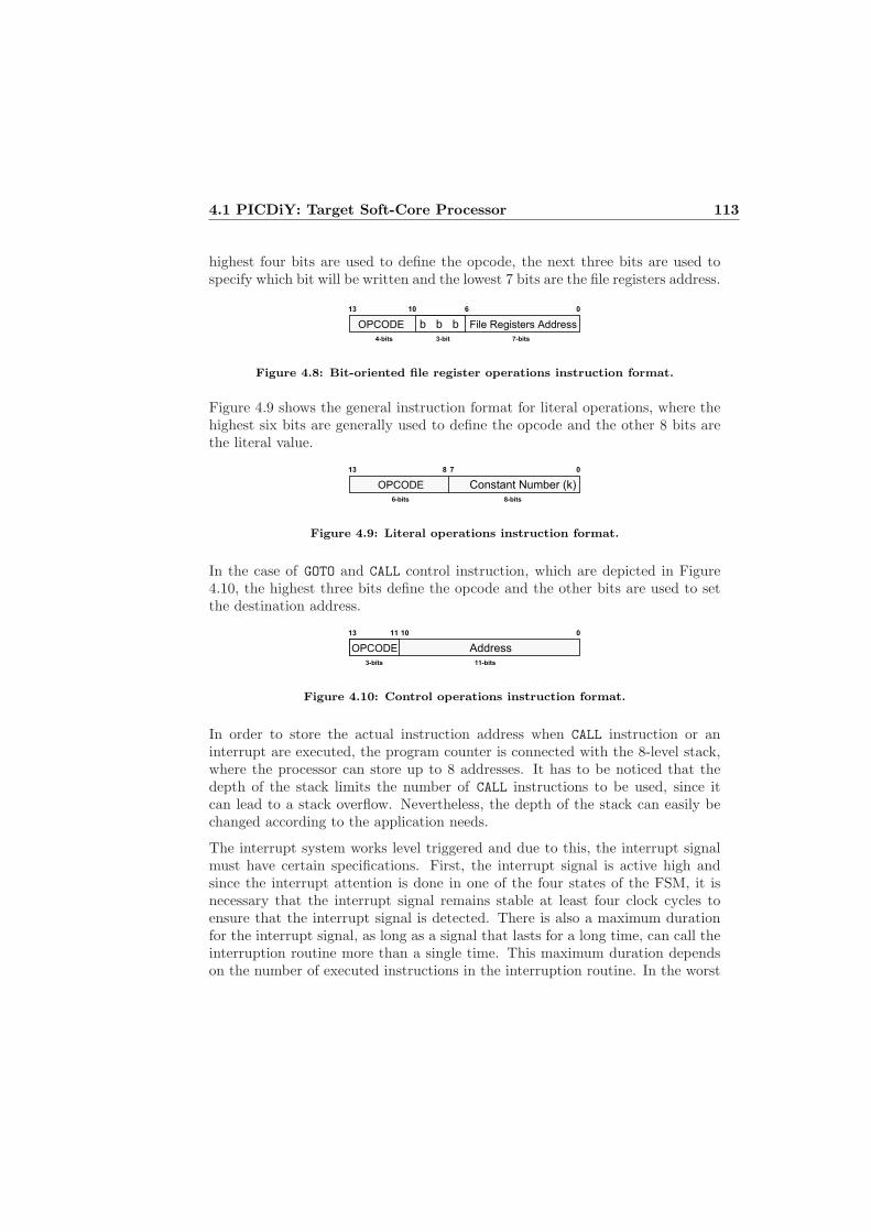
4.1 PICDiY: Target Soft-Core Processor 113
highest four bits are used to define the opcode, the next three bits are used tospecify which bit will be written and the lowest 7 bits are the file registers address.
������ �
�� �� � �
� � ���� ������������
���� ���� ����
Figure 4.8: Bit-oriented file register operations instruction format.
Figure 4.9 shows the general instruction format for literal operations, where thehighest six bits are generally used to define the opcode and the other 8 bits arethe literal value.
������
�� � � �
������� ������������ ����
Figure 4.9: Literal operations instruction format.
In the case of GOTO and CALL control instruction, which are depicted in Figure4.10, the highest three bits define the opcode and the other bits are used to setthe destination address.
������
�� �� �� �
����
������ �������
Figure 4.10: Control operations instruction format.
In order to store the actual instruction address when CALL instruction or aninterrupt are executed, the program counter is connected with the 8-level stack,where the processor can store up to 8 addresses. It has to be noticed that thedepth of the stack limits the number of CALL instructions to be used, since itcan lead to a stack overflow. Nevertheless, the depth of the stack can easily bechanged according to the application needs.
The interrupt system works level triggered and due to this, the interrupt signalmust have certain specifications. First, the interrupt signal is active high andsince the interrupt attention is done in one of the four states of the FSM, it isnecessary that the interrupt signal remains stable at least four clock cycles toensure that the interrupt signal is detected. There is also a maximum durationfor the interrupt signal, as long as a signal that lasts for a long time, can call theinterruption routine more than a single time. This maximum duration dependson the number of executed instructions in the interruption routine. In the worst

114 Contributions in Fault Tolerance for Soft-Core Processors
case, after the execution of the RETURN FROM INTERRUPT instruction the interruptsignal must be in low level. When, in order to respond to external events, theinterrupt input is set to high level and the interrupt conditions are fulfilled, theprogram counter changes the program flow jumping to the fourth address of theprogram memory to execute the interrupt routine, after this execution it continuesfrom the previous point on.
As the presented features imply, thanks to the basic and modular architectureof 8-bits, an easily adaptable, self-sufficient and platform-independent soft-coreprocessor has been designed.
4.2 Bitstream Based BRAM Approach: Contri-
bution in BRAM Data Management through
the Bitstream in 7 Series
Due to their particular characteristics and the differences in the architectures ofthe bitstream, the existing methods for Virtex-V devices cannot be utilized tomanage data using the bitstream in 7 series devices. No methods able to extractor write user data in BRAM memories nor in registers of 7 series by Xilinx deviceshave been found in the literature during this research work.
This section introduces the Bitstream Based BRAM Approach (BBBA) to ac-cess and manage the content of BRAM based memories using the configurationbitstream. This approach is able to access and manage data in BRAM basedmemory designs for 7 series FPGA SoC implementations. It access to the con-figuration bitstream to manage the data content of different BRAMs. Since thismethod does not add extra elements to the original design, there is no impact onthe resource usage. This is relevant because the resource overhead involves longerdatapaths, more power consumption, worse susceptibility and less resources avail-able. Besides, although it is not a recommended procedure in the majority ofcases, it provides the possibility of accessing the memory even when it is beingread or written. Therefore, some of the common drawbacks of classical memorymanagement strategies can be solved by using the proposed BBBA approach,such as, the resource overhead, the appearance of single points of failure or thelower availability of memory blocks. This and several other advantages unleashesa myriad of possibilities when working with BRAM memories. In addition, unlikeother existing techniques related to different devices, by virtue of the use of thePCAP it avoids single point of failures that appear when utilizing reconfigurationinterfaces that make use of logic resources like the ICAP port.

4.2 Bitstream Based BRAM Approach: Contribution in BRAM DataManagement through the Bitstream in 7 Series 115
4.2.1 Proposed Method to Obtain the Bitstream Structureof Data in BRAMs
The aim of this method is to manage different BRAMs of the FPGA by solelyresorting to the bitstream. For that purpose it is necessary to read and generatebitstreams containing the data to be loaded in such memories. As it has been pre-sented in Section 2.2.4 Xilinx provides certain information about the bitstream in[4, 120] and in the .ll location file generated by Vivado during the write bitstreamprocess. However, the information about the bitstream composition provided bymanufacturer is not detailed enough. In addition, the utilization of the data pro-vided by the .ll location file demands a huge processing effort and big memorystorage to manage big data blocks. For these reasons reverse engineering hasbeen performed so as to find out relevant information about the structure of datain BRAMs. In this section, the utilized setup and the different flows and softwareprograms are described in depth.
As it has been previously introduced, the target device selected for this work isthe Xilinx Z-7020 Zynq-7000 All Programmable SoC. Figure 4.11 shows a sim-plified block diagram of the overall scheme utilized. The I/O peripheral signalsof the programmable logic and the Processing System are connected through theExtended Multiplexed I/O (EMIO) interface, allowing the I/O peripheral con-troller to access the programmable logic. The Processing System reaches theconfiguration data through the PCAP interface in order to perform a readback,which stands for the process of reading the bitstream data from the configurationmemory. The software running in the Processing System used for the readbackhas been developed using the XDevCfg library. During the bitstream processing aDDR memory peripheral has been used to store the bitstream and additional ap-plication data. This simple approach permits isolating the configuration memoryfrom any other component in the design.
Partial
Bitstream
BitstreamPCAP
Processing
System (ARM9)
Memory(DDR) Programmable
Logic(FPGA)
Config. memory
EMIO
interface
Figure 4.11: Block diagram of the implementation scheme.
The FAR address of each of the 14 BRAM columns has been identical to de-

116 Contributions in Fault Tolerance for Soft-Core Processors
termine in wich words of the bitstream the data content of BRAMs is stored.This information can be extracted from the .ll location file. However, it has beendecided to to use reverse engineering for verification purposes. In this way, areconfigurable region for each BRAM column has been created, and thereafterthe generated partial bitstreams have been examined. The FAR addresses of allBRAM columns obtained are shown in table 4.2. In the next step each BRAMcolumn has been studied under different implementations within the FPGA sec-tion. Considering that each column of the Z7020 contains 20 18K BRAMs, thisset of implementations consists of 20 memories of 512Kb depth and 32 bits each.Using this memory size, each 18K-sized BRAM is entirely utilized. In order toease the interpretation of the obtained data, all BRAMs have been specificallyarranged by following an increasing order by using location constraints. Theimplementation also includes an FSM based memory filler module to write thedata in all addresses in the memories and a multiplexer to selectively activate thewrite-enable ports.
Table 4.2: FAR addresses of BRAM columns in Z7020.
Resource FAR (hex) Resource FAR (hex)BRAM1 0x00c20000 BRAM8 0x00c00180BRAM2 0x00c20080 BRAM9 0x00c00200BRAM3 0x00c20100 BRAM10 0x00c00280BRAM4 0x00c20180 BRAM11 0x00800100BRAM5 0x00c20200 BRAM12 0x00800180BRAM6 0x00c20280 BRAM13 0x00800200BRAM7 0x00c00100 BRAM14 0x00800280
Figure 4.12 depicts an example of the utilized flow to determine in which wordsof the bitstream is located the data of each 18K BRAM. Starting with the first(BRAM which is located in the bottom part of the device), the memory fillermodule writes zeroes in all data positions within the memory. Right after that,the portion of bitstream of the column defined by the specific FAR and thenumber of frames of a BRAM column are read by using the readback functionality.This content is stored in the DDR memory. Subsequently, a similar process isdone but writing all ones (0xFFFFFFF) instead. The data content obtainedin both bitstreams is compared, storing the address and the content of eachdifferent word in a spreadsheet. These steps have been performed for every ofthe 20 memories of each column, after which new implementations have beencarried out by changing the location constraints and by using a proper FAR tostudy all BRAM columns.
Different conclusions have been drawn from the analysis of the obtained infor-mation. To begin with, it has been confirmed that the content of each BRAMis distributed along the partial bitstream of its BRAM column. This is probably
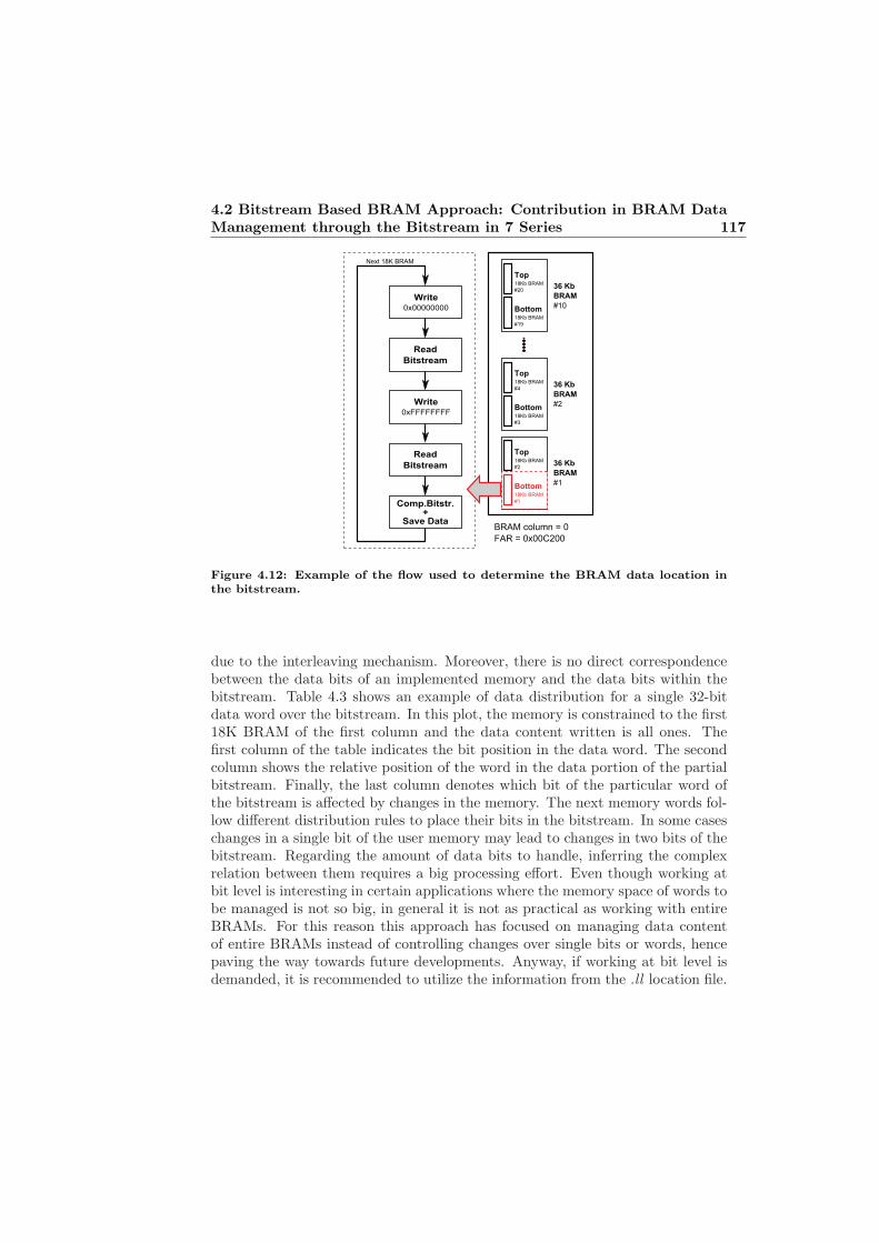
4.2 Bitstream Based BRAM Approach: Contribution in BRAM DataManagement through the Bitstream in 7 Series 117
Top18Kb BRAM
#2
Bottom18Kb BRAM
#1
36 Kb
BRAM
#1
Top18Kb BRAM
#4
Bottom18Kb BRAM
#3
36 Kb
BRAM
#2
Top18Kb BRAM
#20
Bottom18Kb BRAM
#19
36 Kb
BRAM
#10
BRAM column = 0
FAR = 0x00C200
Write0x00000000
Read
Bitstream
Write0xFFFFFFFF
Read
Bitstream
Comp.Bitstr.+
Save Data
Next 18K BRAM
Figure 4.12: Example of the flow used to determine the BRAM data location inthe bitstream.
due to the interleaving mechanism. Moreover, there is no direct correspondencebetween the data bits of an implemented memory and the data bits within thebitstream. Table 4.3 shows an example of data distribution for a single 32-bitdata word over the bitstream. In this plot, the memory is constrained to the first18K BRAM of the first column and the data content written is all ones. Thefirst column of the table indicates the bit position in the data word. The secondcolumn shows the relative position of the word in the data portion of the partialbitstream. Finally, the last column denotes which bit of the particular word ofthe bitstream is affected by changes in the memory. The next memory words fol-low different distribution rules to place their bits in the bitstream. In some caseschanges in a single bit of the user memory may lead to changes in two bits of thebitstream. Regarding the amount of data bits to handle, inferring the complexrelation between them requires a big processing effort. Even though working atbit level is interesting in certain applications where the memory space of words tobe managed is not so big, in general it is not as practical as working with entireBRAMs. For this reason this approach has focused on managing data contentof entire BRAMs instead of controlling changes over single bits or words, hencepaving the way towards future developments. Anyway, if working at bit level isdemanded, it is recommended to utilize the information from the .ll location file.

118 Contributions in Fault Tolerance for Soft-Core Processors
Table 4.3: Bit distribution example of the first data word of the first 18K BRAMin Z7020.
N. Bit Word Addr. N. Bit in Word N. Bit Word Addr. N. Bit in Word0 0 0 16 2 01 0 16 17 2 82 1 0 18 1940 03 1 16 19 1940 164 2 16 20 1941 05 3 0 21 1941 166 3 16 22 1942 167 4 0 23 1943 08 0 8 24 1943 169 0 24 25 1944 010 1 8 26 1940 811 1 24 27 1940 2412 2 24 28 1941 813 3 8 29 1941 2414 3 24 30 1942 2415 4 8 31 1943 8
The remaining conclusions are related to the location of data words within thebitstream. First, the location scheme of data words in each column is the same.That is to say, all BRAM columns have the same word organization structure tostore data within the bitstream. Second, the data content of each 18K BRAM isplaced by performing cyclic jumps along the frames of the bitstreams of BRAMcolumns. These jumps can be noted in Table 4.4, which depicts an example ofthe data organization within one frame of the two 18K BRAMs (top and bottom)that compose a 36K BRAM. The data content written in the memories for thisexample is all ones, thus the data content in all words of the frame is composedof ’F’s. The jump sequence begins with an address jump defined by the productof the frame number (relative to the partial bitstream of the BRAM column)and by the initial address of the particular BRAM. Table 4.5 displays the initialaddresses for each 18K BRAM of a BRAM column in the Z7020. The next fouraddresses are also consecutively used to store data. Thereafter a jump of 101words to continue in the next frame. As it can be also observed in Table 4.4,the data organization in the top 18K BRAM differs from that in the bottom 18KBRAM. For instance, referring to Figure 4.12 the data in the first 18K BRAMis arranged differently when compared to the second or the fourth BRAM, butsimilar to its third or fifth counterpart. In the case of 36K BRAMs, since theyare composed by a 18K BRAM pair (top and bottom), the organization in all ofthem is the same. Albeit feasible the inference of the relationship between the topand bottom 18K BRAM has been discarded due to its complexity (it is necessaryto process at bit level) and subsequent lack of practicability for real applications.In this way, this approach supports the inner data exchange between BRAMs at

4.2 Bitstream Based BRAM Approach: Contribution in BRAM DataManagement through the Bitstream in 7 Series 119
the same deployment level (i.e. top-top or bottom-bottom).
Table 4.4: Data organization example of one frame of a 18K BRAM column inZ7020.
Data word address Data in bottom BRAM Data in top BRAMInit addr. + (frame number × 101) + 0 FFFFFFFF FFFF0000Init addr. + (frame number × 101) + 1 FFFFFFFF FFFFFFFFInit addr. + (frame number × 101) + 2 FFFFFFFF FFFFFFFFInit addr. + (frame number × 101) + 3 FFFFFFFF FFFFFFFFInit addr. + (frame number × 101) + 4 0002FFFF FFFFFFFF
Table 4.5: Init addresses (hex) of 18K BRAMs in Z7020.BRAM num. 1 2 3 4 5 6 7 8 9 10 11 12 13 14 15 16 17 18 19 20Init addr. 0 5 A F 14 19 1E 23 28 2D 33 38 3D 42 47 4C 51 56 5B 60
4.2.2 Managing Data Content of BRAMs with the BBBA
As argued in Section 2.2.5, the Bitstream Based BRAM Approach (BBBA) pro-vides a great potential for a number of applications. Apart from data readingand writing, the most essential operations required to implement many commonapplications are data copy and comparison. This section delves into these twooperations, with emphasis on how to apply them using the bitstream.
BRAM Content Copy using the Bitstream
The process to copy the data stored in BRAMs using the bitstream can be heldin two main scenarios: 1) data copy of entire BRAM columns and 2) data copyof individual BRAMs. Although the concepts of the latter case are also directlyapplicable to groups of consecutive BRAMs of 18K or 36K, for the sake of sim-plicity and clarity, this document will refer to individual 18K BRAMs. At thispoint it is also important to recall that, in the case of 18K BRAMs, if the sourceBRAM is a top 18K BRAM the destination must be also a top BRAM (and viceversa). Moreover, it is important to remark that it is not necessary to implementthe destination memory in a reconfigurable region of the design, this approachworks properly in both, reconfigurable and non configurable areas.
When dealing with single BRAMs, two subcases can be also distinguished de-pending on whether the data stored in the destination BRAM can be overwrittenor not. Overwriting data is useful when the content of all the BRAMs of the col-umn is not relevant, since this method writes the copied data in the destinationBRAM and resets the rest of data bits of the other BRAMs within the column.

120 Contributions in Fault Tolerance for Soft-Core Processors
The second sub-case arises when the content of other BRAMs from the desti-nation column want to be preserved, which comes along with penalties in termsof code and execution overheads. From a global perspective, all the aforemen-tioned cases comply with the flow diagram shown in Figure 4.13, which hinges onreading the partial bitstream of the source BRAM and copying its data contentinto the destination BRAM column. The main difference between the three casesresides in the frame reading and data processing tasks.
Read frames
Create header
(Destiny FAR)
Process frame's data
(Copying / comparing)
Create trailer
Disable CRC
Transfer
bitstream
n> n. frames
n=n+1
n=0
Figure 4.13: Flow diagram of the BRAM copy procedure.
The first task of the flow consists of creating the header of the new partial bit-stream that will be transferred with the copied data. The header of the BRAMcolumn’s partial bitstream is composed by 30 words of 32 bits. This header isalmost the same for each BRAM column, being the difference that the 27th wordof this header contains the FAR address of the destination BRAM column.
After creating the header, the data content must be stored. This task is carriedout in two steps that are performed for each frame within the partial bitstream ofthe BRAM column. First, the frames of the source and, if needed (only necessarywhen the data overwriting has to be avoided), the destination BRAMs have tobe read by utilizing the readback functionality. The data content from the sourceframe has to be processed in order to organize it properly for the destinationBRAM. After performing a readback, several bits of the obtained bitstream areset to logic high. Since, these bits are the mask bits that protect the content ofBRAMs, they must be reset in order to transfer the bitstream successfully. Each

4.2 Bitstream Based BRAM Approach: Contribution in BRAM DataManagement through the Bitstream in 7 Series 121
Source
Column
Dest.
Column
Bitstream processing SW
- Source FAR
- Destination FAR
10101010100010011001011
01010101010101000001100
(Readback) (Transf.)
Dest.
Column
(a) Entire BRAM columncopy.
Source
Column
Dest.
Column
Bitstream processing SW
- Source FAR + Init Address
- Destination FAR+ Init Address
10101010100010011001011
01010101010101000001100
(Readback) (Transf.)
Dest.
Column
(b) BRAM copy withoverwriting.
Source
Column
Dest.
Column
Bitstream processing SW
- Source FAR + Init Address
- Destination FAR + Init Address
10101010100010011001011
01010101010101000001100
(Readback) (Transf.)
Dest.
Column
(c) BRAM copy withoutoverwriting.
Figure 4.14: Different copying types.
of these bits is located in the 18th position of the 4th, 14th, 24th, 34th, 44th, 55th,65th, 75th, 85th and 95th words of the data section of each frame. For this reason,during the processing task all set bits have to be reset by resorting to a binarymask.
The specific data processing performed on the data content differs among applica-tion cases. Figure 4.14 exemplifies the three most basic scenarios: entire BRAMcolumn copy, single BRAM copy overwriting the rest of the BRAMs of the col-umn and single BRAM copy without overwriting. However, based on these casesit is possible to implement more complex applications, such as, copying variousBRAMs into different locations or swapping data between distinct columns, etc.
The most elementary case is to copy entire BRAM columns. Taking into account1) that the data organization has found to be equal in all BRAM columns and2) that the content of the destination BRAM column is not necessary, only thesource frames have to be read, copying them directly onto the destination frames.Obviously, in this case all BRAMs from the destination column are overwritten.
In the case of copying single BRAMs with overwriting, the process is slightlydifferent because the data read from the source frame must be reorganized to beplaced properly in the destination BRAM. Thus, the exact placing of the source
122 Contributions in Fault Tolerance for Soft-Core Processors
and destination BRAMs must be known. The use of placement constraints isvery useful in this context, but it is also possible to determine the placementby analysing the implementation results. Based on the known positions of theBRAMs in the columns and by using Table 4.5 the initial addresses can be ob-tained. With this information and following the address jump pattern describedin the previous subsection data can be properly arranged and written in the newpartial bitstream. It is important to note that if the source BRAM and the des-tination BRAM are placed in the same column, the content of the source BRAMwill be lost.
Copying single BRAMs without overwriting is more complex, especially in termsof program code (in quantitative more than twenty times more lines of code thanwith overwriting), because it is necessary to take into account several hypotheses.The data of the destination column must be read and copied in the new partialbitstream, and the bit set must be reset in all the words where they are setin the readback. By contrast, the cases with overwriting only require resettingthe words of the read BRAM because the rest of data words are sent empty.Another singular aspect when copying without overwriting is that if source anddestination columns are the same, the program is more efficient since only onereadback must be performed for each frame. In any case, the initial addressesof source and destination BRAMs and the address jump pattern must be knownbeforehand.
After organizing and writing all the data, the trailer must be added in the endof the created partial bitstream. Most of the trailer words mean ”no operation”(NOP) words, but it also contains CRC data. Considering that as it has beenmentioned the CRC method for 7 series is still unknown [117], these words relatedto the CRC are written with the NOP word. In this manner, the trailer is thesame for all created partial bitstreams. Finally, the produced partial bitstream istransferred to the device via PCAP port, reconfiguring dynamically and partiallythe specific logic portion.
BRAM Content Comparison using the Bitstream
BBBA can be also used to compare the data content of different BRAM columnsor single BRAMs. In both cases, if the data content is changing during therunning process it is advisable to halt the system so also avoid data changes duringthe bitstream reading process and obtain a correct result. However, in those caseswhere the information stored in BRAMs remains unchanged for certain time(i.e. program memories) the comparison can be performed without stoppingthe system. Depending on the requirements the comparison can be performed in
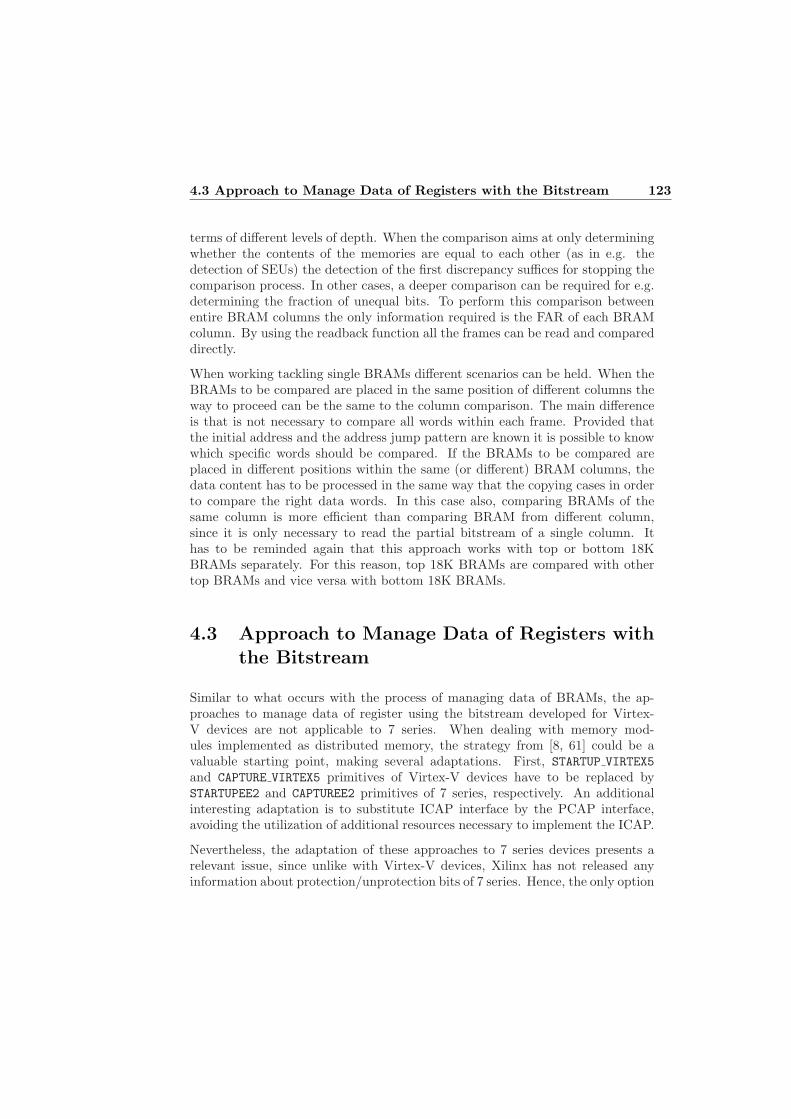
4.3 Approach to Manage Data of Registers with the Bitstream 123
terms of different levels of depth. When the comparison aims at only determiningwhether the contents of the memories are equal to each other (as in e.g. thedetection of SEUs) the detection of the first discrepancy suffices for stopping thecomparison process. In other cases, a deeper comparison can be required for e.g.determining the fraction of unequal bits. To perform this comparison betweenentire BRAM columns the only information required is the FAR of each BRAMcolumn. By using the readback function all the frames can be read and compareddirectly.
When working tackling single BRAMs different scenarios can be held. When theBRAMs to be compared are placed in the same position of different columns theway to proceed can be the same to the column comparison. The main differenceis that is not necessary to compare all words within each frame. Provided thatthe initial address and the address jump pattern are known it is possible to knowwhich specific words should be compared. If the BRAMs to be compared areplaced in different positions within the same (or different) BRAM columns, thedata content has to be processed in the same way that the copying cases in orderto compare the right data words. In this case also, comparing BRAMs of thesame column is more efficient than comparing BRAM from different column,since it is only necessary to read the partial bitstream of a single column. Ithas to be reminded again that this approach works with top or bottom 18KBRAMs separately. For this reason, top 18K BRAMs are compared with othertop BRAMs and vice versa with bottom 18K BRAMs.
4.3 Approach to Manage Data of Registers with
the Bitstream
Similar to what occurs with the process of managing data of BRAMs, the ap-proaches to manage data of register using the bitstream developed for Virtex-V devices are not applicable to 7 series. When dealing with memory mod-ules implemented as distributed memory, the strategy from [8, 61] could be avaluable starting point, making several adaptations. First, STARTUP VIRTEX5
and CAPTURE VIRTEX5 primitives of Virtex-V devices have to be replaced bySTARTUPEE2 and CAPTUREE2 primitives of 7 series, respectively. An additionalinteresting adaptation is to substitute ICAP interface by the PCAP interface,avoiding the utilization of additional resources necessary to implement the ICAP.
Nevertheless, the adaptation of these approaches to 7 series devices presents arelevant issue, since unlike with Virtex-V devices, Xilinx has not released anyinformation about protection/unprotection bits of 7 series. Hence, the only option
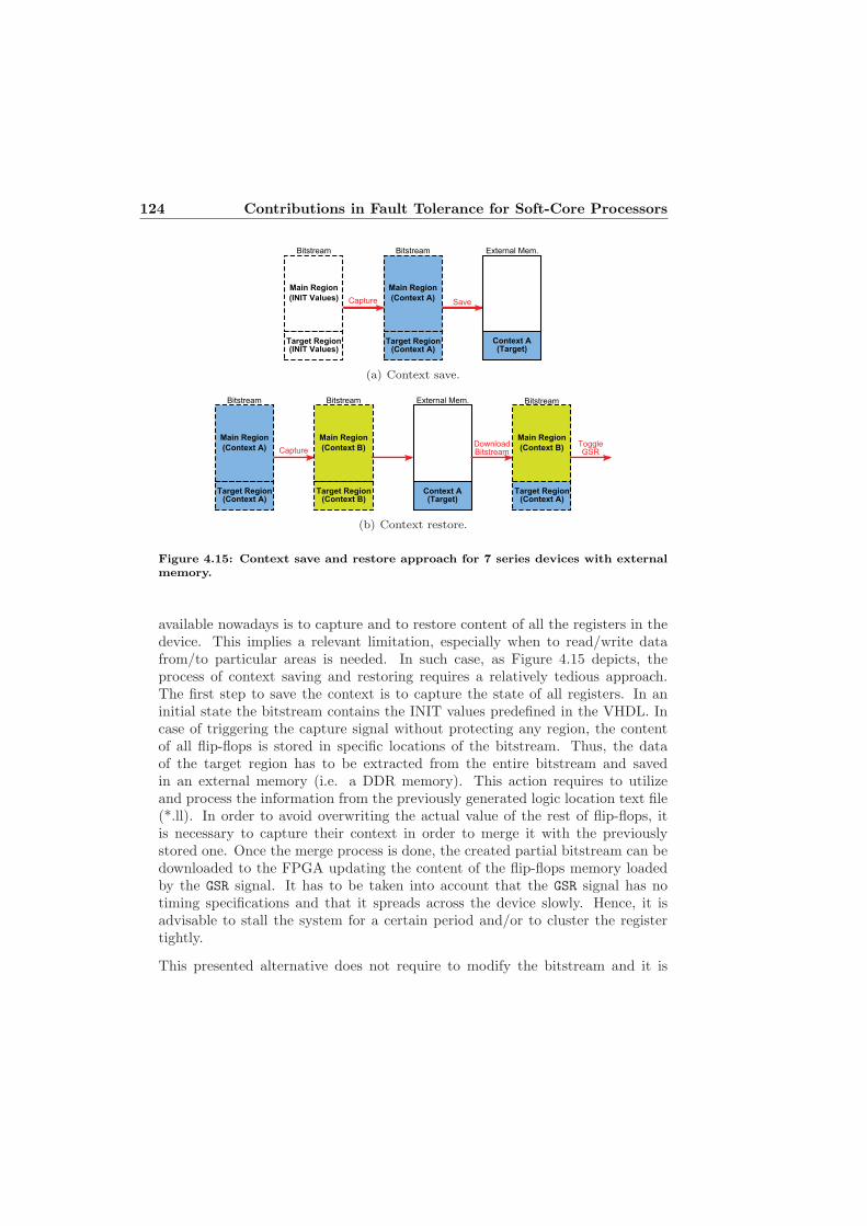
124 Contributions in Fault Tolerance for Soft-Core Processors
Bitstream
Context A (Main Reg.)
External Mem.
Capture
Save
Bitstream
Context A (Main Reg.)
Target Region(INIT Values)
Main Region
(INIT Values)
Main Region
(Context A)
Target Region(Context A)
Context A(Target)
(a) Context save.
Bitstream External Mem.
Capture
DownloadBitstream
Bitstream
Context A (Main Reg.)
Main Region
(Context A)
Target Region(Context A)
Main Region
(Context B)
Target Region(Context B)
Context A(Target)
Bitstream
Context A (Main Reg.)
Main Region
(Context B)
Target Region(Context A)
ToggleGSR
(b) Context restore.
Figure 4.15: Context save and restore approach for 7 series devices with externalmemory.
available nowadays is to capture and to restore content of all the registers in thedevice. This implies a relevant limitation, especially when to read/write datafrom/to particular areas is needed. In such case, as Figure 4.15 depicts, theprocess of context saving and restoring requires a relatively tedious approach.The first step to save the context is to capture the state of all registers. In aninitial state the bitstream contains the INIT values predefined in the VHDL. Incase of triggering the capture signal without protecting any region, the contentof all flip-flops is stored in specific locations of the bitstream. Thus, the dataof the target region has to be extracted from the entire bitstream and savedin an external memory (i.e. a DDR memory). This action requires to utilizeand process the information from the previously generated logic location text file(*.ll). In order to avoid overwriting the actual value of the rest of flip-flops, itis necessary to capture their context in order to merge it with the previouslystored one. Once the merge process is done, the created partial bitstream can bedownloaded to the FPGA updating the content of the flip-flops memory loadedby the GSR signal. It has to be taken into account that the GSR signal has notiming specifications and that it spreads across the device slowly. Hence, it isadvisable to stall the system for a certain period and/or to cluster the registertightly.
This presented alternative does not require to modify the bitstream and it is

4.3 Approach to Manage Data of Registers with the Bitstream 125
valid for any design (even for the not reconfigurable ones). However, it is a timedemanding process, since it requires several operations (i.e. saving the contextinto the external memory, capturing the actual state, downloading partial bit-streams, etc.) in each context saving/restoring action. This implies a significanttime demand. It also requires an external memory and processing the bitstreamto extract the data for each capture and restore. To circumvent these drawbacks,this work proposes a method to unprotect as many as need reconfigurable regions.I this way, maintaining the rest of the design protected the necessity of savingthe data from the other regions (those can are to be protected) can be avoided.
On the other hand, when utilizing a bitstream based strategy to copy the contentof registers from one reconfigurable region to others’, one of the biggest draw-back is the processing effort demanded. This aspect gains special relevance indesigns with a significant amount of registers, such as soft-core processors. Themain reason behind this disadvantage is that, even using the same HDL designfor different reconfigurable blocks, due to the default resource placement free-dom of the implementation tool, it creates a distinct implementation for eachblock. This results in different locations for the same resource in the differentreconfigurable blocks. Hence, the location of each data bit within the bitstreamvaries, increasing the complexity of the relocating processing when copying datathrough the bitstream. In this scenario, the source and destination locations ofeach data bit of each flip-flop must be identified in the .ll file in order to utilizethis information during the copying process. It also implies that, in the majorityof cases, the copying of each data bit requires a combination of a reading and awriting operations. In addition, in several cases the portion of the destinationbitstream (the bitstream portion where the captured data is going to be copyied)has to be read in order to preserve the content of other registers that save thecontent in the same bitstream frame. This case also requires a process to mergethe captured content with the saved information of the destination bitstream. Allthose steps have to be performed in each context saving/restoring action, whichresults in a remarkable instruction overhead. It also requires a complete study ofthe .ll file.
For this reason, an interesting solution could be to obtain exactly alike imple-mentations in the different regions for each design, placing each resource in thesame positions of different columns (reconfigurable regions). This would allowto perform the copying process by copying entire bitstream portions and usinga significantly simpler relocation process and avoiding the need of data merging.Hence considerably reducing the number of instruction required. However, ob-taining identical implementation of a design in different reconfigurable regions isa tedious task. Therefore, this work proposes a design flow which allows to easethis task by making use of the location constraints.

126 Contributions in Fault Tolerance for Soft-Core Processors
4.3.1 Proposed Flow to Protect/Unprotect Partial Regionsin 7 series
Following the idea suggested in [124], an interesting alternative could be utilizedto read and write registers’ data of a particular region without affecting the rest ofthe device. As that work states, a property named RESET AFTER RECONFIG=TRUE
[108] can be utilized with 7 series devices to implement partially reconfigurablemodules in order to avoid the manual unprotection/protection actions. Whenimplementing partial reconfigurable designs with this property in 7 series (forUltraScale devices is always enabled), the partial bitstream created by Vivadocontains the commands to protect the rest of the device (including static andremaining partial regions), maintaining the actual partial region unprotected.Hence, this property enables to protect a particular partial region in a straight-forward fashion. Nevertheless, as Figure 4.16 shows, this method can only un-protect (open padlock) a single partial region at once. As it can be observed,every downloaded partial bitstream unprotects the target reconfigurable moduleand protects (closed padlock) the rest of the device, even if the a partial re-configurable module has been previously unprotected. Thus, there is no way tounprotect more than one partial region in the same device.
FPGA
PBLOCK_B
STATIC AREA
PBLOCK_A
EMPTY DESIGN
PBLOCK_B
STATIC AREA
PBLOCK_A PBLOCK_B
STATIC AREA
PBLOCK_A
FPGA FPGA FPGA
Complete Bitstream
A Partial Bitstream
B PartialBitstream
010101100001011010101101111010101010010101
010101100001011010101101111010101010010101
010101100001011010101101111010101010010101
RESET_AFTER_RECONFIG=TRUE RESET_AFTER_RECONFIG=TRUE
Figure 4.16: Effect of the RESET AFTER RECONFIG=TRUE property in FPGA protection.
With the aim of solving the issue of unprotecting more than a single partial re-gion in 7 series devices, a novel design flow has been developed in this work.As a first step, two reconfigurable regions (PblockA and PblockB) have beendesigned. In the implementation process only PblockA has been implementedwith the RESET AFTER RECONFIG property. After that, both generated partialbitstreams have been analysed and compared. The comparison has shown re-markable differences in the content, making it difficult to identify any specialbit or command word. However, after a further analysis, a special word in 51stposition of the frame with a particular content (0xE00009BC) has been observed

4.3 Approach to Manage Data of Registers with the Bitstream 127
through the partial bitstream. Afterwards, a new comparison has been performedto detect discrepancies in the 0xE00009BC special word. The comparison resultsindicate that only two 0xE00009BC words appear in the A partial bitstreamand do not appear in the B partial bitstream. Hence, it has been initially as-sumed that these two words were the protection words for the B reconfigurableregion. In this way, different tests has been carried out modifying the partialbitstream of PblockA, downloading it and performing physical tests. These testshave concluded that erasing one of both special words has an effective protect-ing/unprotecting effect of PblockB.
Using the obtained information from the test the procedure described in Figure4.17 has been developed. It utilizes the RESET AFTER RECONFIG=TRUE propertyin combination with the edition of the partial bitstream, as a straightforwardmethod to protect or unprotect as many as desired partially reconfigurable mod-ules. This edition only requires to erase or to add the proper 0xE00009BC specialword of the previously generated partial bitstream.
Once the partial regions have been unprotected, the content of the registers ofthe unprotected regions can be easy read and written by using the GCAPTURE
and the GRESTORE, respectively without affecting the protected regions. Whenusing the RESET AFTER RECONFIG=TRUE property it is advisable to also utilizethe SNAPPING MODE constraint, which automatically creates legal reconfigurableblocks. This method, combined with a proper bitstream processing, also enablesto modify data of registers, for instance for copying the content from one registerto another.
The proposed method has a number of advantages and drawbacks that shouldbe taken into account in order to choose the most adequate solution for eachdesign. The most remarkable benefit of this alternative is that it is relativelyfast, especially when capturing and restoring the context, because both GCAPTURE
and GRESTORE operations are not time consuming processes. Thus, the timerequirements are related to the time needed by the GSR signal to spread acrossthe partial reconfigurable circuit, which is design dependant. In addition, thisapproach does not demand any additional element, neither external memoriesnor logical resources.
The most relevant drawback of this approach is the need of implementing par-tially reconfigurable blocks. In fact, when using the RESET AFTER RECONFIG=TRUE
property, the partially reconfigurable module’s height must align to clock regionboundaries, which means occupying an entire column of resources (there is noblock width restriction). Depending on the design, this could limit the avail-able resources for other purposes. It is interesting to mention that in UltraScaledevices there is no height requirement, since the RESET AFTER RECONFIG=TRUE
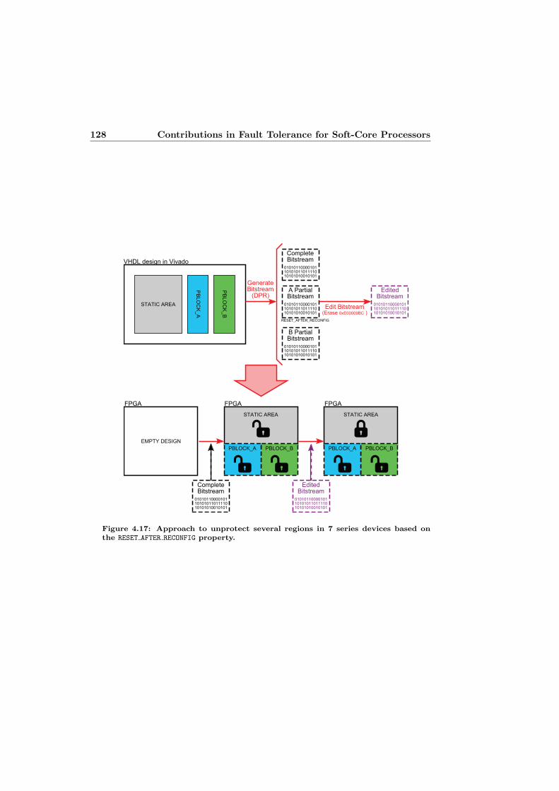
128 Contributions in Fault Tolerance for Soft-Core Processors
VHDL design in Vivado
STATIC AREA
PB
LO
CK
_A
PB
LO
CK
_B
Complete Bitstream
010101100001011010101101111010101010010101
A Partial Bitstream
010101100001011010101101111010101010010101
RESET_AFTER_RECONFIG
B PartialBitstream
010101100001011010101101111010101010010101
GenerateBitstream
(DPR)
Edit Bitstream(Erase 0xE00009BC )
EditedBitstream
010101100001011010101101111010101010010101
FPGA
PBLOCK_B
STATIC AREA
PBLOCK_A
EMPTY DESIGN
PBLOCK_B
STATIC AREA
PBLOCK_A
FPGA FPGA
Complete Bitstream
010101100001011010101101111010101010010101
EditedBitstream
010101100001011010101101111010101010010101
Figure 4.17: Approach to unprotect several regions in 7 series devices based onthe RESET AFTER RECONFIG property.

4.3 Approach to Manage Data of Registers with the Bitstream 129
property is always enabled. Moreover, if the XADC component is used, its inter-face cannot respond during the partial reconfiguration period, blocking its access.Another remarkable disadvantage of the use of the RESET AFTER RECONFIG=TRUE
property is that, since the partial bitstream created contains the commands toprotect the rest of the device and to unprotect the partial region, the size of thebitstream significantly increases.
Another important limitation when using approaches that utilize partial recon-figuration schemes is that the maximum achievable operating frequency of thedesign can be reduced. Although two identical designs, one static and anotherreconfigurable, can be logically exactly equal from an RTL description point ofview, the way both are synthesized and implemented is significantly different.The partial reconfiguration flow demands to synthesize each reconfigurable mod-ule out of context, which limits cross-boundary optimizations. The reason for thisis to guarantee that logical interfaces between static and reconfigurable partitionsremain fixed. During the implementation, the Pblocks are required to physicallydivide the static and reconfigurable partitions. This implies layout requirementsthat also restrict the optimization of the placement process.
4.3.2 Proposed Flow to Generate Equal Implementationsof a Design in Different Reconfigurable Regions
This section presents the proposed design flow to obtain identical implementa-tions of a particular HDL design in distinct reconfigurable regions, which for thesake of simplicity, will be referred to it as Location Constraints Flow. This flowis specially interesting in some desings that make use of hardware redundancystrategies. The main problem when trying to obtain three alike implementationsresides in the implementation tool, which in order to optimize the design pro-cess, places each resource of the replicated instances in different locations. Thisgenerates totally distinct implementations.
Since the partial bitstream generated for each reconfigurable block only can beused in its particular reconfigurable region, the most suitable solution is to utilizelocation constraints when implementing each instance. Nevertheless, the utiliza-tion of location constraints with a high number of resources, and specially inreconfigurable designs, is a tedious procedure.
The most simple alternative is to place all the resources of each instance manuallyin the same custom positions of each resource column utilized by the differentreconfigurable regions. After synthesizing the entire HDL design, this placementtask can be easily done by means of Vivado’s graphical interface by selectingeach resource within the netlist and dragging it to the chosen resource position.
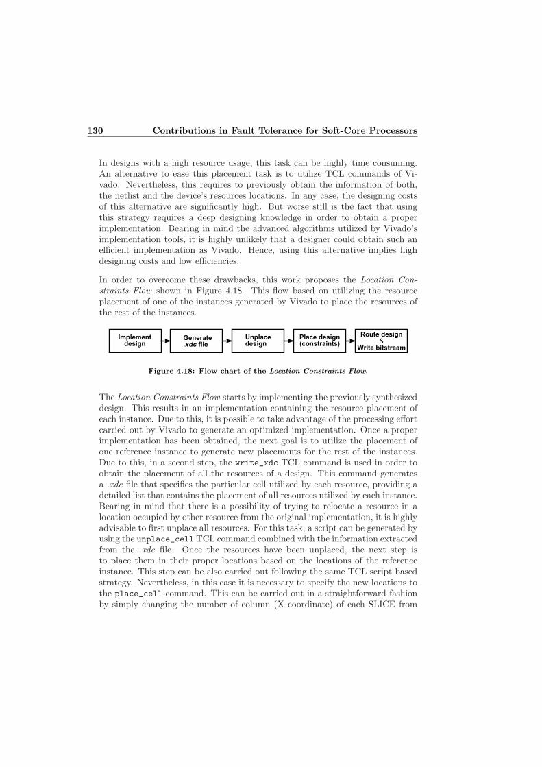
130 Contributions in Fault Tolerance for Soft-Core Processors
In designs with a high resource usage, this task can be highly time consuming.An alternative to ease this placement task is to utilize TCL commands of Vi-vado. Nevertheless, this requires to previously obtain the information of both,the netlist and the device’s resources locations. In any case, the designing costsof this alternative are significantly high. But worse still is the fact that usingthis strategy requires a deep designing knowledge in order to obtain a properimplementation. Bearing in mind the advanced algorithms utilized by Vivado’simplementation tools, it is highly unlikely that a designer could obtain such anefficient implementation as Vivado. Hence, using this alternative implies highdesigning costs and low efficiencies.
In order to overcome these drawbacks, this work proposes the Location Con-straints Flow shown in Figure 4.18. This flow based on utilizing the resourceplacement of one of the instances generated by Vivado to place the resources ofthe rest of the instances.
Route design&
Write bitstream
Implementdesign
Generate .xdc file
Unplacedesign
Place design(constraints)
Figure 4.18: Flow chart of the Location Constraints Flow.
The Location Constraints Flow starts by implementing the previously synthesizeddesign. This results in an implementation containing the resource placement ofeach instance. Due to this, it is possible to take advantage of the processing effortcarried out by Vivado to generate an optimized implementation. Once a properimplementation has been obtained, the next goal is to utilize the placement ofone reference instance to generate new placements for the rest of the instances.Due to this, in a second step, the write_xdc TCL command is used in order toobtain the placement of all the resources of a design. This command generatesa .xdc file that specifies the particular cell utilized by each resource, providing adetailed list that contains the placement of all resources utilized by each instance.Bearing in mind that there is a possibility of trying to relocate a resource in alocation occupied by other resource from the original implementation, it is highlyadvisable to first unplace all resources. For this task, a script can be generated byusing the unplace_cell TCL command combined with the information extractedfrom the .xdc file. Once the resources have been unplaced, the next step isto place them in their proper locations based on the locations of the referenceinstance. This step can be also carried out following the same TCL script basedstrategy. Nevertheless, in this case it is necessary to specify the new locations tothe place_cell command. This can be carried out in a straightforward fashionby simply changing the number of column (X coordinate) of each SLICE from

4.4 Data Content Scrubbing Approach 131
the reference instance. Once the placement constraint script has been loaded,the route_design and write_bitstream commands can be executed to obtainthe bitstream and to create the complete and the partial bitstreams.
Thanks to the proposed Location Constraints Flow, an implementation with aproper placement can be obtained with minimal designing costs. In addition,it almost preserves the implementation tool’s efficiency, barely affecting perfor-mance when compared with an unconstrained design.
4.4 Data Content Scrubbing Approach
Related to soft-core processors, performing data content scrubbing is an inter-esting technique to fix errors in memories. This is because most used techniquesto harden memory elements (TMR, ECC, etc.) mask errors and do not cor-rect them. Nevertheless, data content scrubbing is mainly advisable for programmemories, because the content remains unchanged. For the rest of memory ele-ments (data memory, registers, etc.) the data scrubbing usually is not practicalbecause the content is constantly updated during operation. However, even withthose elements, in certain cases, this method could be an interesting alternativeto initialize specific memory positions or registers. For instance, this could helpto avoid the need of initialization instructions after resetting the system.
When creating a partial bitstream that includes initialized memory elements thebitstream generated contains the initialization data for such elements. Down-loading this partial bitstream would refresh data content of memory elementsinitialized by design. Despite this procedure could be considered as a data con-tent scrubbing method, it has to be remarked that this implies to reconfigure theentire reconfigurable block. Hence, the reconfiguration will affect all elementsof the reconfigurable region, which in many cases could not be feasible. In ad-dition, this practice requires to stop the operation of the reconfigurable blockand commonly resetting it. Moreover, since the partial bitstream contains manymore frames in addition to the frames with the data content, it increases the timedemand of reconfiguration.
In order to circumvent these issues, a Data Content Scrubbing Approach for mem-ory modules implemented with BRAMs based on the previously presented BBBAis proposed. It utilizes its simple implementation scheme shown in Figure 4.11.The proposed approach consists in downloading the data content of the BRAMmemory by applying the BRAM copying method (with the BBBA). Dependingon the number and placement of the BRAMs utilized by the remaining memorymodules of the design, the most suitable alternative has to be chosen. This is
132 Contributions in Fault Tolerance for Soft-Core Processors
because it has to be determined if the actual content of the remaining BRAMshas to be preserved or not. Thus, while in cases where a BRAM column onlycontains memory blocks to be scrubbed, all the three proposed alternatives aresuitable. In implementations in which program and data memories are placed inthe same BRAM column, the BRAM copy without overwriting approach has tobe adopted in order to preserve the information of data memory. Bearing in mindthat the BRAM copy without overwriting approach demands higher processingeffort, and consequently more time, it is advisable to avoid its utilization, whenit is possible.
Considering that depending on the design the BRAM column could be overwrit-ten or not, two design flows are proposed to perform data content scrubbing. Asit can be seen in Figure 4.19, both flows share the first four steps, which are usedto obtain the golden copy bitstream. The first step is to configure the FPGAby downloading the bitstream. In a next step, a readback process is performedthrough the PCAP interface. Thanks to this, the data obtained is properlystructured and can be utilized to create the partial golden copy bitstream file ina straightforward fashion. These first steps could be substituted by extracting thedata from the bitstream file. However, due to the complex data distribution inthe bitstream file this process would require a high processing effort. In addition,each design requires specific processing due to the different BRAM locations.
Once the golden copy is obtained and stored in an external memory (i.e. a DDR)the scrubbing process can be triggered. In the case that the remaining BRAMs ofthe BRAM column can be overwritten the golden copy can be directly downloadas is described in Figure 4.19(a). But in cases were they cannot be overwritten,as depicted in 4.19(b), a readback operation has to be performed in order tostore the actual data content and to be able of merging it with the golden copy.Depending on the design this process may require to stop the clock signal in orderto assure stable information.
In this way, in contrast to what [184] states, by using BBBA it is feasible toperform an user memory scrubbing in BRAM based structures by using the bit-stream information. Just as it occurs with the configuration scrubbing, neitherresource overhead nor performance penalty are incurred by the design. In addi-tion, thanks to this proposed approach, the memory coherence problem describedin Section 3.1 can be solved. Besides, in designs where the BRAM column canbe overwritten the configuration scrubbing can performed in runtime withoutstopping the system, thus, without adding any performance penalty.
One limitation of this approach is the scrubbing frequency, since the time de-manded by BBBA affects to the time between consecutive scrubbings, which isless the upper bound for the majority of the applications. Another drawback of

4.5 Approach to Extract Data From Damaged Memories Using theBBBA 133
Configure FPGA
Readback (bitstream)
Trig Scrubbing?
Create Golden copy
Download Golden copy
Yes
(a) Content scrubbing with overwriting.
Configure FPGA
Readback (bitstream)
Trig Scrubbing?
Create Golden copy
Yes
ReadbackBRAM content
Merge read withGolden Copy
DownloadCreated bitstream
(b) Content scrubbing without overwrit-ing.
Figure 4.19: Flow charts of the Data Content Scrubbing Approach.
this technique is that it demands a Processing System and an external memory.
4.5 Approach to Extract Data From Damaged
Memories Using the BBBA
A potential consequence of SEUs is the damage on the interfaces of memory re-sources. Thus, as Figure 4.20 describes, if such an error disables or affects torelevant ports of the memory it is likely to provoke permanent damages. More-over, if ports, such as, address, reset, clock or data output are affected by thefault, this can eliminate any possibility of recovering the data stored in memories,at least with regular off-the-self methods. This case can be more likely to happenin cases where memories have not been hardened. This situation could be espe-cially critical if the information stored has a special value. The method based onthe BBBA technique proposed in this section allows to recover the data contentstored in BRAM based memories with damaged interfaces in a straightforwardmanner.
Due to the simplicity of this approach it could be considered as a specific ap-plication of the BBBA. Considering that it only uses the BBBA it shares itsimplementation scheme shown in Figure 4.11, requiring a Processing System andan external memory. It is mainly based on utilizing the bitstream information

134 Contributions in Fault Tolerance for Soft-Core Processors
Configuration memory
FPGA
DI
DIP
RDADDR
RDCLK
DO
DOP
RDEN
REGCE
SSR
WE
WRADDR
WRCLK
WREN
64
8
15
8
15
64
8
36 Kb Memory Array
Figure 4.20: Example of an SEU affecting the interface of a BRAM.
FPGA device fragment
PCAP
Readback
Processing
System
1010101010010010101
0101010010000010100
0010011001101010110
0101010010011011010
0000101001000001100
0101010010000011010
0101010010000011001
0111101001000001100
0101010000011000111
0101001000001001100
0101000111001001100
1001011001000001100
DDR memory
Damaged
BRAMs
(a) Extracting data from BRAMs.
FPGA device fragment
PCAP
Reconfig.
Processing
System
1010101010010010101
0101010010000010100
0010011001101010110
0101010010011011010
0000101001000001100
0101010010000011010
0101010010000011001
0111101001000001100
0101010000011000111
0101001000001001100
0101000111001001100
1001011001000001100
DDR memory
Relocated
BRAMs
(b) Relocating saved data.
Figure 4.21: Simplified example of extracting and relocating data from a damagedmemories.

4.6 Lockstep Approaches 135
obtained after using the BBBA as described in Figure 4.21(a). After acquiringthe bitstream portion with data content, different alternatives can be utilizeddecode it. Since obtaining data content directly from a bitstream is a complexprocess, the most effortless way is to relocate the saved bitstream downloading itto a not damaged memory of the design with a similar implementation as shownin Figure 4.21(b). However, since this is an unlikely scenario, an alternative canbe to implement the original design (or a simpler design with only the damageddesign) in an additional FPGA device and downloading the read bitstream. Log-ically, this approach is not suitable in cases where the fault affects the bitstreamcontent related to the BRAM data.
4.6 Lockstep Approaches
This section proposes three approaches to deal with the most challenging issuesof lockstep schemes, which are related to checkpointing and rollback processes.While the first approach adopts a full hardware solution to provide fast check-pointing and rollback, the second applies the BBBA to reduce resource usage byutilizing bitstream information. Finally, the third proposed approach combinesthe first two methods to provide a trade-off solution.
All three approaches have been developed focusing on recovering from faults inuser memory elements. In this way, a fault fixing of the configuration memoryhas not been considered. Nevertheless, it is possible to add this aspect to theapproaches by performing a configuration scrubbing after the error detection. Inthis case, it is necessary to mask configuration bits related to user data contentelements of the golden copy to protect saved data against overwriting during thescrubbing.
The proposed approaches have been applied to the PICDiY designed in this work.However, they can be adapted to other existing soft-core processors in a straight-forward manner. In addition, different ideas from proposed techniques can bealso applied to other designs that share characteristics with soft-core processors,like memory modules. Hence, these approaches can be valuable tools when hard-ening soft-core processors with DMR techniques, providing the designers withmore alternatives when making trade-off design decisions.
4.6.1 Hardware Based Fast Lockstep Approach
This section presents a novel lockstep approach which is focused on circumvent-ing the problem of the latency in context saving (checkpointing) and reloading
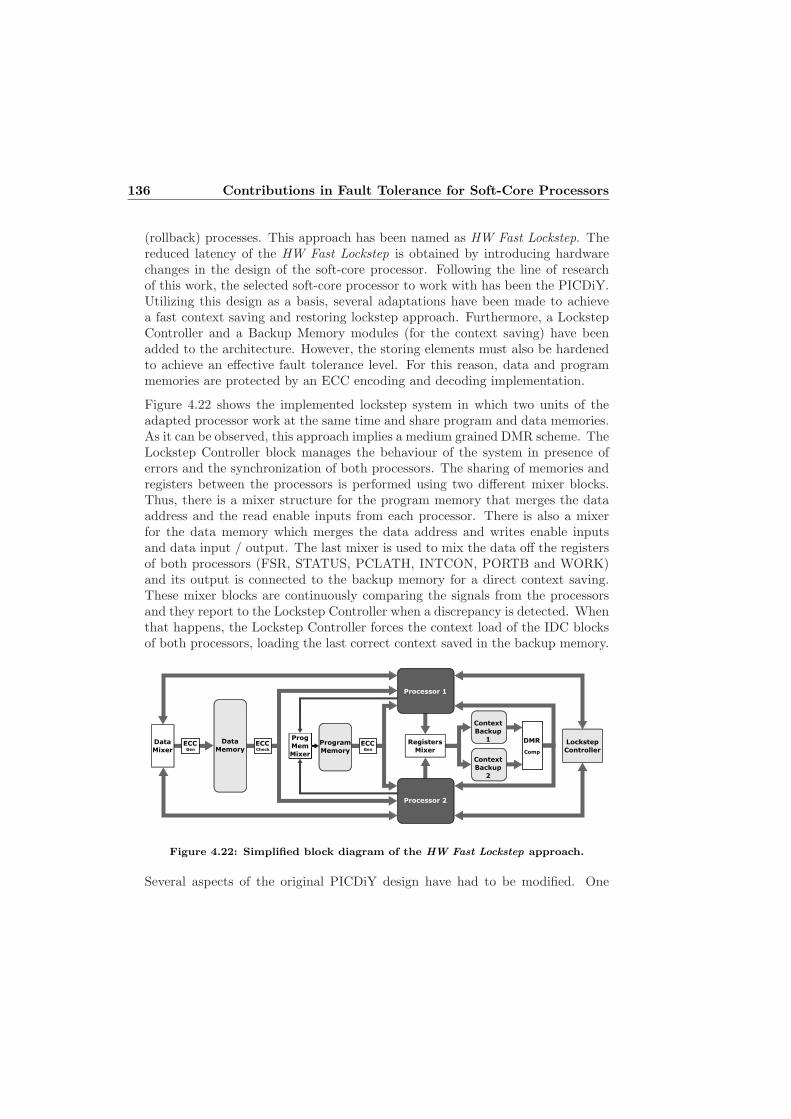
136 Contributions in Fault Tolerance for Soft-Core Processors
(rollback) processes. This approach has been named as HW Fast Lockstep. Thereduced latency of the HW Fast Lockstep is obtained by introducing hardwarechanges in the design of the soft-core processor. Following the line of researchof this work, the selected soft-core processor to work with has been the PICDiY.Utilizing this design as a basis, several adaptations have been made to achievea fast context saving and restoring lockstep approach. Furthermore, a LockstepController and a Backup Memory modules (for the context saving) have beenadded to the architecture. However, the storing elements must also be hardenedto achieve an effective fault tolerance level. For this reason, data and programmemories are protected by an ECC encoding and decoding implementation.
Figure 4.22 shows the implemented lockstep system in which two units of theadapted processor work at the same time and share program and data memories.As it can be observed, this approach implies a medium grained DMR scheme. TheLockstep Controller block manages the behaviour of the system in presence oferrors and the synchronization of both processors. The sharing of memories andregisters between the processors is performed using two different mixer blocks.Thus, there is a mixer structure for the program memory that merges the dataaddress and the read enable inputs from each processor. There is also a mixerfor the data memory which merges the data address and writes enable inputsand data input / output. The last mixer is used to mix the data off the registersof both processors (FSR, STATUS, PCLATH, INTCON, PORTB and WORK)and its output is connected to the backup memory for a direct context saving.These mixer blocks are continuously comparing the signals from the processorsand they report to the Lockstep Controller when a discrepancy is detected. Whenthat happens, the Lockstep Controller forces the context load of the IDC blocksof both processors, loading the last correct context saved in the backup memory.
�������
�����
���������
���������
�����
�����
�����
���
����
�������
�����
�����
�����
�������
����������������
�������
������
����
���
�����
����������
�������
�����
�
Figure 4.22: Simplified block diagram of the HW Fast Lockstep approach.
Several aspects of the original PICDiY design have had to be modified. One

4.6 Lockstep Approaches 137
of the most important adaptation has been made in the IDC module. Since itcontrols most of the elements during the execution of instructions, it has beenmodified to adapt its behaviour. The FSM of four states that manages the IDChas been adapted by adding an new state to perform the context saving andreloading. Figure 4.23 shows the flow diagram of the adapted FSM. As it canbe observed, in the absence of errors the execution follows the original sequenceof four states. In the first state, the IDC activates the instruction reading fromthe program memory. The second state, depending on the loaded instruction,is used to read data or to load the next instruction on the program counterwhen CALL, GOTO or RETURN instructions are executed. In the third state, ifnecessary, the IDC enables writing data memory or registers and the fourth stateis used for data stabilization, interruption attention management and contextsaving in the backup memory. Thanks to the adaptation, during the fourthstate, each processor sends out a signal to the Lockstep Controller to be usedin the synchronization of both processors. When an error is detected the statemachine changes to the new context reload state, loading the last correct contextsaved into both processors. The checkpointing is regularly performed every 4clock cycles without any extra latency for the processors. In the same way, therollback only takes a 2 extra clock cycles.
���������� ��
� ����� ����
���� ��
�������� ���
�������������
����� ��
������������
������������
����������
����������
����������
����������
Figure 4.23: Finite state machine diagram of the adapted FSM.
Another significant modification has been made in the processor’s registers topermit data load simultaneously. As shown in Figure 4.24. an extra data inputcontrolled by an extra write enable input has been added to each register. Due tothis, when the Lockstep Controller sends the reload command, all the informationsaved in the backup memory can be reloaded simultaneously in the registers
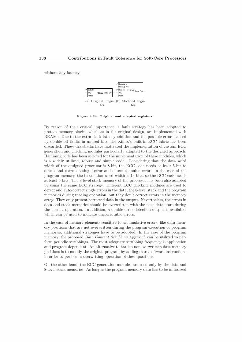
138 Contributions in Fault Tolerance for Soft-Core Processors
without any latency.
Data In
WE
Reset
Data OutREG
(a) Original regis-ter.
BackUp In
WE
Reset
Data OutREGData In
BackUp WE
(b) Modified regis-ter.
Figure 4.24: Original and adapted registers.
By reason of their critical importance, a fault strategy has been adopted toprotect memory blocks, which as in the original design, are implemented withBRAMs. Due to the extra clock latency addition and the possible errors causedby double-bit faults in unused bits, the Xilinx’s built-in ECC fabric has beendiscarded. These drawbacks have motivated the implementation of custom ECCgeneration and checking modules particularly adapted to the designed approach.Hamming code has been selected for the implementation of these modules, whichis a widely utilized, robust and simple code. Considering that the data wordwidth of the designed processor is 8-bit, the ECC code needs at least 5-bit todetect and correct a single error and detect a double error. In the case of theprogram memory, the instruction word width is 13 bits, so the ECC code needsat least 6 bits. The 8-level stack memory of the processor has been also adaptedby using the same ECC strategy. Different ECC checking modules are used todetect and auto-correct single errors in the data, the 8-level stack and the programmemories during reading operation, but they don’t correct errors in the memoryarray. They only present corrected data in the output. Nevertheless, the errors indata and stack memories should be overwritten with the next data store duringthe normal operation. In addition, a double error detection output is available,which can be used to indicate uncorrectable errors.
In the case of memory elements sensitive to accumulative errors, like data mem-ory positions that are not overwritten during the program execution or programmemories, additional strategies have to be adopted. In the case of the programmemory, the proposed Data Content Scrubbing Approach can be utilized to per-form periodic scrubbings. The most adequate scrubbing frequency is applicationand program dependant. An alternative to harden non overwritten data memorypositions is to modify the original program by adding extra software instructionsin order to perform a overwriting operation of these positions.
On the other hand, the ECC generation modules are used only by the data and8-level stack memories. As long as the program memory data has to be initialized
4.6 Lockstep Approaches 139
with the correct instructions during the synthesis and implementation processes,a ECC generation module would not be useful in the case of this memory. Asa result, a visual basic application has been developed to generate the programmemory HDL modules. This application uses the .HEX file generated by theassembler with the source code to create the program memory VHDL file withthe ECC encoded data.
The implementation of the backup memory for the processor context saving de-mands a different method, because a parallel load of the data of all registers isnecessary to achieve a low latency context saving. Taking into account that theXilinx BRAM structure can only write to a single memory address at the sametime, the data has been saved using a register structure. Considering this fact,the ECC alternative has been discarded for the hardening of the backup memory,because it will dramatically increases the overhead. So, the strategy adopted hasbeen the DMR implementation. In this case, this is adequate because the prob-ability of two consecutive SEUs is usually very low [174]. So, if an SEU affectsa register it is extremely rare that another SEU will affect the backup memorysimultaneously. In the same way, if an SEU affects the backup memory it isnot probable that one of the processors will be affected by another SEU at thesame time, and the wrong data will be overwritten in the next context saving.Nevertheless, if this rare situation occurs it will be detected by the comparatorsof the backup memory.
Thanks to the proposed architecture, a lockstep approach which performs a fastcheckpointing and rollback is obtained. Due to this fact, the saving process canbe regularly performed every 4 clock cycles without causing any extra latency,nor affecting the processor’s performance. In the same way, a context loadingprocess can be achieved only with 2 extra clock cycles. The main drawbackof this approach is that the logic added to the design increases the hardwareoverhead. For this reason, it also reduces the maximum achievable operatingfrequency. Finally, it has to be remarked that this design can be implemented inFPGA devices from different vendors and the main ideas of this approach can beadapted to designs based on different soft-core processors.
4.6.2 Bitstream Based Low Overhead Lockstep Approach
The Bitstream Based Low Overhead Lockstep approach is focused on performingthe rollback and checkpointing processes by making use of the bitstream in orderto limit the resource overhead. Figure 4.25 represents the simplified scheme of thisapproach. As it can be observed, in this minimalistic approach the FPGA fabriccontains two soft-core processors connected to a comparator. This scheme also

140 Contributions in Fault Tolerance for Soft-Core Processors
includes the Processing System, which is responsible for performing the check-pointing and rollback processes. These operations are performed via PCAP in-terface and controlling both, STARTUPEE2 and CAPTUREE2 primitives. In orderto stop the clock when it is necessary, the Processing System also controls thedesign’s clock signal by using the CLOCKING WIZARD IP. With the aim to protectthe content of registers of the rest of the design when utilizing the STARTUPEE2
primitive a reconfigurable region has been created. While both utilized soft-coreprocessors are contained in the reconfigurable region, the rest of the design re-mains in the static region. Thanks to the use of a single reconfigurable regionwith the RESET AFTER RECONFIG=TRUE property, the generated partial bitstreamcontains by default the instructions necessary to protect (closed padlock) thestatic region and unprotect (open padlock) the reconfigurable region.
Although both processors can also be implemented in two different reconfigurableregions, this strategy does not provide significant benefits. Since in DMR schemesit is not possible to determine which is the faulty module, it is not necessary toindependently repair nor relocate each processor in the presence of permanenterrors. However, in some cases, it could be necessary depending on design re-quirements. For instance, implementing two independent reconfigurable modulesprovide more design flexibility when relocating them in case of permanent errors.In this case, the second reconfigurable region has to be unprotected by using theproposed design flow to protect/unprotect partial regions (introduced in Section4.3).
During the normal operation (absence of errors) the Processing Systems performsa checkpointing by reading the partial bitstream of each soft-core processor copy.In this way, the data content from BRAM memories is extracted utilizing theBBBA and saved in the external memory (DDR). In a similar way, the contentof registers can be obtained using the CAPTUREE2 primitive and processing theread partial bitstream based on the information of the .ll file.
Two strategies can be adopted to perform the storage of the context in the ex-ternal memory. As Figure 4.26(a) shows, the first one consists in reading thecontext of a single processor. After, the read data has to be processed in or-der to create a proper partial bitstream for the second processor. Thus, bothpartial bitstreams with the context of the processors are stored and ready to beused in future rollbacks. Bearing in mind that the bitstream readback’s timedemand increases with the bitstream size, this alternative results faster. Never-theless, this approach also requires a high processing effort to create the secondpartial bitstream. This processing effort depends on the registers quantity andtheir floorplanning. For instance, if both processors have similar floorplanning,which could be obtained by utilizing placement constraints, the processing effort

4.6 Lockstep Approaches 141
Contex
Storage
Bitstream
PCAP
Config. Memory
Bitstream
FPGA
EMIOinterface
P1
Error!
P2
Comparator
=?
010101010101011110101010101110001100101010110001010101011100010101011110001010111101010101011111
CAPTUREE2
STARTUPEE2
CAP
GSR
ProcessingSystem(ARM)
DDR
Pblock (reconfig. Region)
Static Region
CLOCKING
WIZARD
Clk_CE
Figure 4.25: Simplified block diagram of the Bitstream Based Low Overhead Lockstep
approach.
can be lower. The second alternative, as depicted in Figure 4.26(b), is to readpartial bitstreams with the context of both processors and store them. Sincethis approach needs to read double information, the readback takes more time.However, when dealing with small processors like the PICDiY the time increasecould be negligible. On the other hand, this strategy does not require to processthe bitstream making the storing process faster. Hence, in this case, the secondstrategy has been adopted.
Storing the context in an external DDR provides higher reliability than storingit the FPGA fabric, since as [328] states the probability of having a radiation-induced error in data stored in the DDR is significantly lower. Besides, it is alsopossible to duplicate data stored in the DDR in order to increase the reliability,since commonly this software redundancy implies minimal costs in terms of data.
Nevertheless, storing data in a DDR memory demands a significant processingeffort. For this reason, to use the configuration memory to store the content ofregisters is an interesting alternative way to avoid the need of any processing.After running the GCAPTURE command, the content of flip-flops is stored in theirrespective INIT0/INIT1 positions. Hence, the information is automatically storedin the configuration memory. This implies that after performing the checkpoint-

142 Contributions in Fault Tolerance for Soft-Core Processors
Config. Memory
P1
10101010101
10101001101
10110100101
11101010101
01101010100
00101010101
01001010010
P2
10101010101
10101001101
10110100101
11101010101
01101010100
00101010101
01001010010
Partial
Bitstream
Partial
Bitstream
Processing
System(ARM)
PCAP interface
Context
Storage
Bitstream
Relocation
DDR
P1Context
Bitstream
P2Context
Bitstream
(a) Context saving of a single processor.
Config. Memory
P1 P2
10101010101
10101001101
10110100101
11101010101
01101010100
00101010101
01001010010
PartialBitstream
PartialBitstream
PCAP interface
10101010101
10101001101
10110100101
11101010101
01101010100
00101010101
01001010010
DDR
P1Context
Bitstream
P2Context
Bitstream
101101001011011010010110110100101
Processing
System(ARM)
(b) Context saving of both processors.
Figure 4.26: Context saving strategies.
ing the context of registers is stored in two way: in the reconfiguration memoryand in hardware resources. Bearing in mind this fact, the case of simultaneouserrors in INIT0/INIT1 positions of the bitstream and the flip-flop resources is anunlikely scenario. Hence, considering that it is not necessary to process the bit-stream to extract the content of flip-flops and the adequate robustness provided,this strategy has been adopted instead of using the external DDR to store thecontent of registers.
After detecting a failure due to discrepancy in the outputs of both processors,the comparator asserts an error signal, which is connected with the ProcessingSystem via EMIO interface. This signal triggers the rollback recovery process.This process is performed by downloading the data memory content saved in theDDR memory (by using the BBBA) and triggering the GRESTORE command withthe STARTUPEE2 primitive to restore the saved content of registers.
This approach allows to perform both, rollback and checkpointing with a minimalimpact in terms of resource overhead. Its main handicap is a relatively hightime demand, which comes due to the utilization of the BBBA. It also requiresthe utilization of the Processing System and an external memory to control thedifferent processes and store context, respectively.
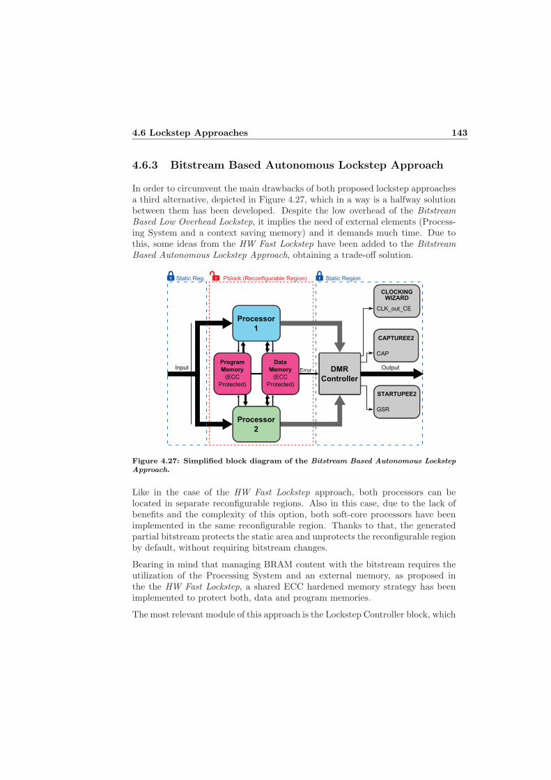
4.6 Lockstep Approaches 143
4.6.3 Bitstream Based Autonomous Lockstep Approach
In order to circumvent the main drawbacks of both proposed lockstep approachesa third alternative, depicted in Figure 4.27, which in a way is a halfway solutionbetween them has been developed. Despite the low overhead of the BitstreamBased Low Overhead Lockstep, it implies the need of external elements (Process-ing System and a context saving memory) and it demands much time. Due tothis, some ideas from the HW Fast Lockstep have been added to the BitstreamBased Autonomous Lockstep Approach, obtaining a trade-off solution.
STARTUPEE2
GSR
CAPTUREE2
CAP
Program
Memory
(ECC
Protected)
Data
Memory
(ECC
Protected)
DMR
Controller
OutputInput
Pblock (Reconfigurable Region) Static RegionStatic Reg.
CLOCKINGWIZARD
CLK_out_CE
Processor
1
Processor
2
Error
Figure 4.27: Simplified block diagram of the Bitstream Based Autonomous Lockstep
Approach.
Like in the case of the HW Fast Lockstep approach, both processors can belocated in separate reconfigurable regions. Also in this case, due to the lack ofbenefits and the complexity of this option, both soft-core processors have beenimplemented in the same reconfigurable region. Thanks to that, the generatedpartial bitstream protects the static area and unprotects the reconfigurable regionby default, without requiring bitstream changes.
Bearing in mind that managing BRAM content with the bitstream requires theutilization of the Processing System and an external memory, as proposed inthe the HW Fast Lockstep, a shared ECC hardened memory strategy has beenimplemented to protect both, data and program memories.
The most relevant module of this approach is the Lockstep Controller block, which

144 Contributions in Fault Tolerance for Soft-Core Processors
detects discrepancies between both processors’ outputs and controls checkpoint-ing and rollback processes. This module is based on an FSM structure which isshown in Figure 4.28. The first four states are mainly utilized to run synchro-nized with four states FSM of the PICDiY’s. The second state is also used toperform the context saving by triggering the CAP port of the CAPTUREE2 prim-itive. In the fourth state, the outputs of both processors are compared. In caseof discrepancy, whether the error is unrecoverable or not has to be determined.This is done by utilizing a register to control if the error has been produced alsoin the previous FSM cycle. In case of a non permanent error the recovering pro-cess starts by stepping into the fifth state, which stops clocks of processors andtriggers the GSR signal from the STARTUPEE2 primitive. Bearing in mind thatthe GSR is asynchronous and it spreads across the device relatively slow a sixthstate is used as a waiting state to ensure that all registers are properly set. Thesixth state follows to the second state to synchronize with the four-states FMS ofPICDiY processors. In the case of defining the error as unrecoverable the FSMgets stuck in the seventh state. An unrecoverable error may be due to two ormore faulty bits in memories (ECC fault) or due to permanent errors. In thecase of ECC fault, reseting both processors and the rest of the system can be afeasible solution. On the other hand, a permanent error scenario will require arelocation of both processors in a different fabric logic region.
Capture
error free
=? Compare
State 1 (µP Sync)
State 2 (µP Sync)
State 4 (µP Sync)
State 3 (µP Sync)Trig GSR
Stop CLK=
State 5 (Error)
error Permanent ?
No action
No action
State 7 (Error)
UnrecoverableError
Wait (GSR)
Stop CLK
State 6 (Error)
=
yes
no
Figure 4.28: State diagram of the Lockstep Controller block.
In addition to the relatively fast lockstep and rollback processes, a relevant ben-efit of this approach is that, since no bitstream data read, write nor relocation is
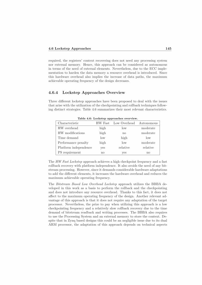
4.6 Lockstep Approaches 145
required, the registers’ context recovering does not need any processing systemnor external memory. Hence, this approach can be considered as autonomousin terms of the need of external elements. Nevertheless, due to the ECC imple-mentation to harden the data memory a resource overhead is introduced. Sincethis hardware overhead also implies the increase of data paths, the maximumachievable operating frequency of the design decreases.
4.6.4 Lockstep Approaches Overview
Three different lockstep approaches have been proposed to deal with the issuesthat arise with the utilization of the checkpointing and rollback techniques follow-ing distinct strategies. Table 4.6 summarizes their most relevant characteristics.
Table 4.6: Lockstep approaches overview.
Characteristic HW Fast Low Overhead Autonomous
HW overhead high low moderate
HW modifications high no moderate
Time demand low high low
Performance penalty high low moderate
Platform independence yes relative relative
PS requirement no yes no
The HW Fast Lockstep approach achieves a high checkpoint frequency and a fastrollback recovery with platform independence. It also avoids the need of any bit-stream processing. However, since it demands considerable hardware adaptationsto add the different elements, it increases the hardware overhead and reduces themaximum achievable operating frequency.
The Bitstream Based Low Overhead Lockstep approach utilizes the BBBA de-veloped in this work as a basis to perform the rollback and the checkpointingand does not introduce any resource overhead. Thanks to this fact, it does notaffect to the maximum operating frequency of the design. Another relevant ad-vantage of this approach is that it does not require any adaptation of the targetprocessor. Nevertheless, the prize to pay when utilizing this approach is a lowcheckpointing frequency and a relatively slow rollback recovery due to the timedemand of bitstream readback and writing processes. The BBBA also requiresto use the Processing System and an external memory to store the context. De-spite that in Zynq based designs this could be an negligible issue due to its dualARM processor, the adaptation of this approach depends on technical aspects

146 Contributions in Fault Tolerance for Soft-Core Processors
of the hardware platform utilized. Hence, it could be considered as a relativelyplatform-independent solution.
The Bitstream Based Autonomous Lockstep approach combines several aspects ofthe two previous methods, implying a trade-off solution. In this way, it utilizesthe Approach to Manage Data of Registers with the Bitstream to save and loadthe context of registers and protects data and program memories following anECC strategy. Due to this it also avoids the need of processing the bitstream.In this way, this approach provides an autonomous fast checkpoint and recoveryprocesses with a moderate hardware overhead. The drawbacks of this methodare related to the implementation of the ECC logic, which increases the hardwareoverhead and reduces the maximum frequency. Furthermore, due to the usage ofdifferent Xilinx primitives is a platform dependant technique. However, it couldbe possible to adapt the main ideas to other vendor’s technology.
All the proposed approaches provide different solutions, depending on the re-quirements of the application to be designed. When the availability is a crucialaspect the HW Fast Lockstep approach could be more advisable. On the otherhand, in applications that don’t demand real time response, the Bitstream BasedLow Overhead Lockstep approach could be a good candidate in order to saveresources and power. The Bitstream Based Autonomous Lockstep approach is ahalfway solution that provides fast context saving and recovering operations butrequires small adaptations on designs to be hardened.
4.7 Proposed Synchronization Approaches for
Repaired Soft-Core Processors in HardwareRedundancy Based Schemes
This section addresses the scarcity of investigations around synchronization inhardware redundancy based systems by proposing, implementing and evaluatingfive different synchronization methodologies. Since the triple redundancy methodis one of the most established redundancy levels, the approaches in this sectionwill be based on TMR (Triple Modular Redundancy) schemes. Nevertheless,the majority of concepts presented can be applied to other redundancy levels.The five approaches span a broad spectrum of possible alternatives from minimalhardware overhead to completely hardware-based synchronization. This allowsbalancing the trade-off between implementation cost and synchronization speed,depending on the requirements of the target application at hand. The perfor-mance of the proposed techniques is verified and compared to each other on the

4.7 Proposed Synchronization Approaches for Repaired Soft-CoreProcessors in Hardware Redundancy Based Schemes 147
PICDiY processor. However, all the approaches are of general nature and caneasily be migrated to other processor architectures. The presented methods arefurthermore not restricted to a set-up implementing TMR and DPR (DynamicPartial Reconfiguration). They are applicable to any TMR protected processorsystem to recuperate a processor element, which was forced out of sync by anSEE.
When implementing a combination of TMR and DPR for the realization of faulttolerant systems, a pure reconfiguration of a faulty module is not sufficient giventhat the reconfigured module comprises of an internal state. This synchronizationis especially critical for processors, because their state is composed of a numberof different registers. For the PICDiY processor the following elements need tobe synchronized: the program counter, the stack-pointer and the stack content,the special function registers (FSR, STATUS, INTCON, PCL, PCLATH andINTCON) and the data memory. These elements will be referred to as synchro-nization objects in the remainder of this work.
In general, finding an adequate synchronization strategy for a given applicationimplies balancing a trade-off. On the one hand, adding specialized hardwarefor the processor synchronization will enable a very fast synchronization process.On the other hand, implementing the synchronization with little extra, or none,hardware combined with software will result in less implementation overhead anda lower impact on the critical path of the design.
The structure of the synchronization method impacts the duration of two sub-steps of the whole recovery process. Firstly, the time required to copy the correctvalues of the different synchronization elements to a recently reconfigured proces-sor instance in the coarse-grain TMR setup. This time will be called copy-time.The second aspect of the synchronization speed is the time from the detection ofan error by the voter until the point in time where the system is ready to startthe synchronization process. This second time is named wait-for-sync. Someapproaches can not begin directly with the synchronization, but they first needto finish ongoing calculations before CPU time can be spent for updating a re-configured processor instance in the system. The time from the detection of anerror to the re-synchronization has implications on the overall system robustness,because in this time period the TMR system operates only with two functionalinstances, making it vulnerable to consecutive SEUs.
The whole SEU recovery process is illustrated in Figure 4.29, where the time re-quirement is defined by the sum of four components: the time needed to detect theerror, the wait-for-sync time, the time consumed for repairing the SEU by partialreconfiguration and the copy-time. Whereas the time for partial reconfigurationis proportional to the size of the reconfigured partition and the reconfiguration
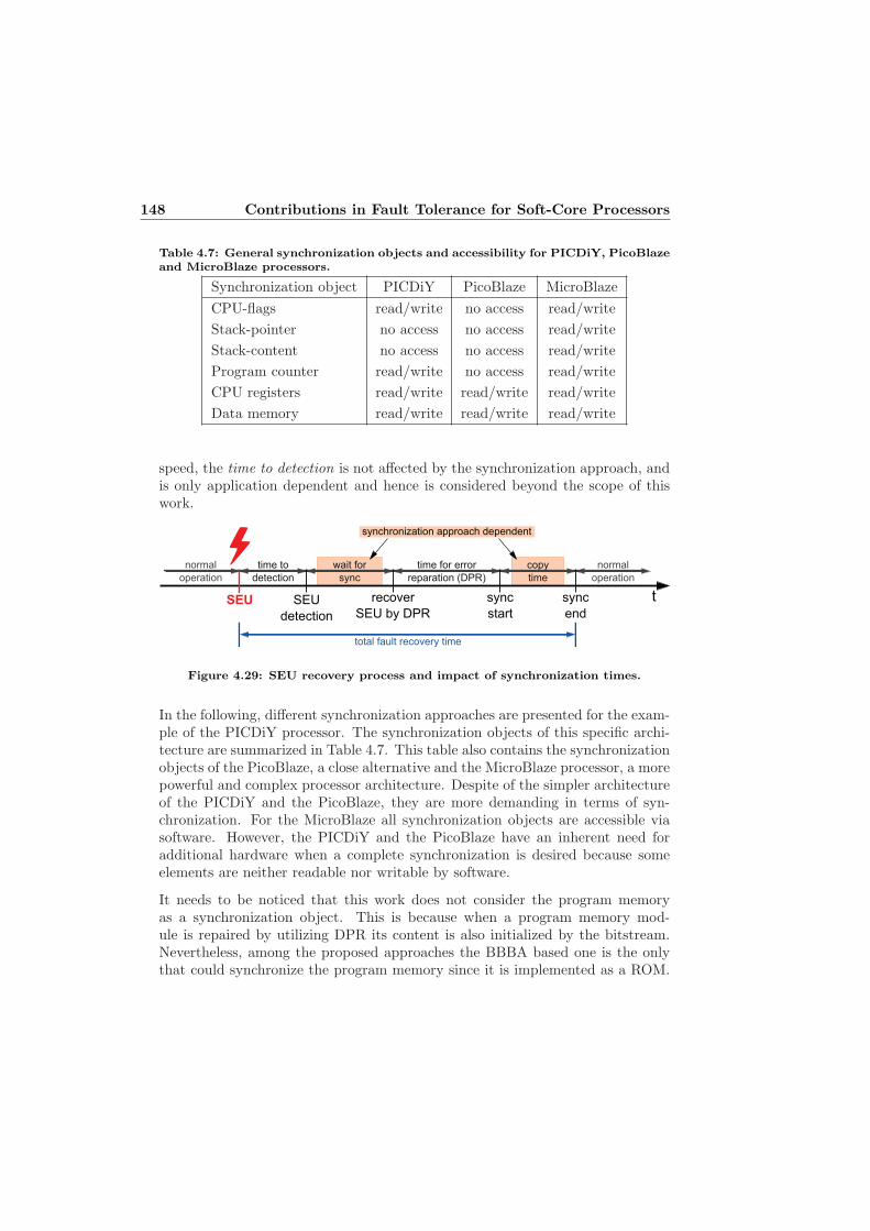
148 Contributions in Fault Tolerance for Soft-Core Processors
Table 4.7: General synchronization objects and accessibility for PICDiY, PicoBlazeand MicroBlaze processors.
Synchronization object PICDiY PicoBlaze MicroBlaze
CPU-flags read/write no access read/write
Stack-pointer no access no access read/write
Stack-content no access no access read/write
Program counter read/write no access read/write
CPU registers read/write read/write read/write
Data memory read/write read/write read/write
speed, the time to detection is not affected by the synchronization approach, andis only application dependent and hence is considered beyond the scope of thiswork.
copy
time
t
normal
operation
time to
detection
wait for
sync
normal
operation
time for error
reparation (DPR)
recover
SEU by DPR
synchronization approach dependent
total fault recovery time
sync
end
sync
startSEU
detection
SEU
Figure 4.29: SEU recovery process and impact of synchronization times.
In the following, different synchronization approaches are presented for the exam-ple of the PICDiY processor. The synchronization objects of this specific archi-tecture are summarized in Table 4.7. This table also contains the synchronizationobjects of the PicoBlaze, a close alternative and the MicroBlaze processor, a morepowerful and complex processor architecture. Despite of the simpler architectureof the PICDiY and the PicoBlaze, they are more demanding in terms of syn-chronization. For the MicroBlaze all synchronization objects are accessible viasoftware. However, the PICDiY and the PicoBlaze have an inherent need foradditional hardware when a complete synchronization is desired because someelements are neither readable nor writable by software.
It needs to be noticed that this work does not consider the program memoryas a synchronization object. This is because when a program memory mod-ule is repaired by utilizing DPR its content is also initialized by the bitstream.Nevertheless, among the proposed approaches the BBBA based one is the onlythat could synchronize the program memory since it is implemented as a ROM.
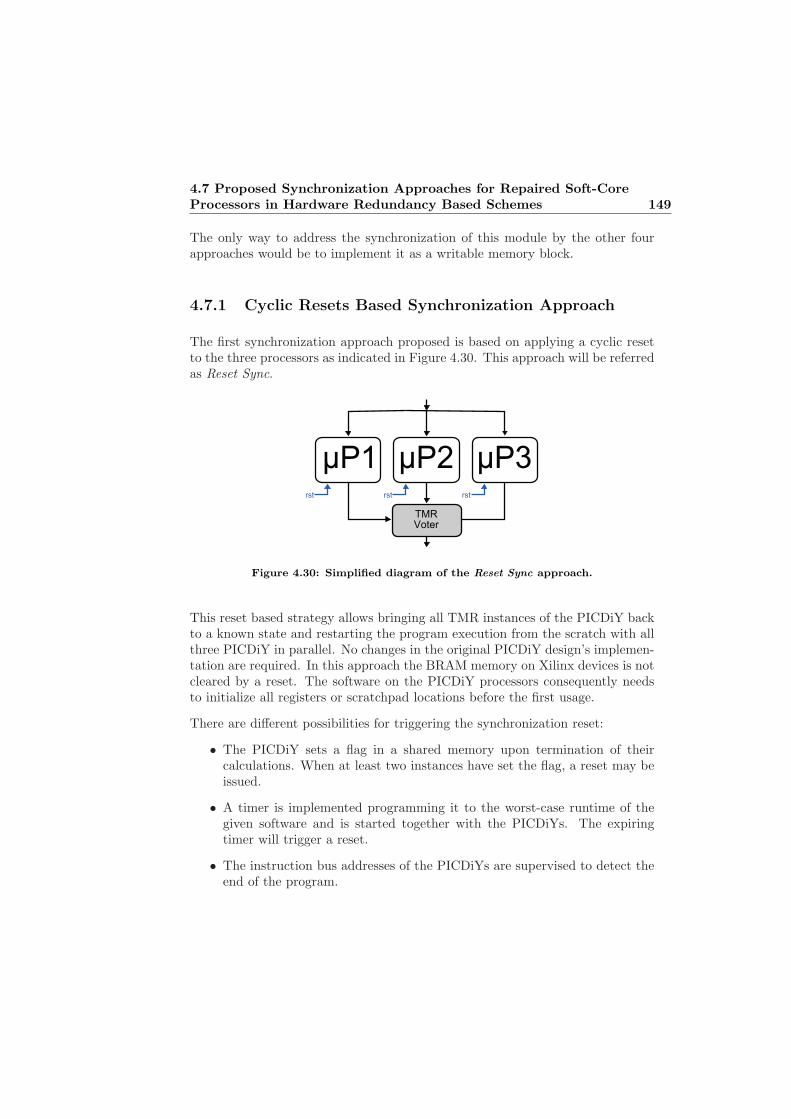
4.7 Proposed Synchronization Approaches for Repaired Soft-CoreProcessors in Hardware Redundancy Based Schemes 149
The only way to address the synchronization of this module by the other fourapproaches would be to implement it as a writable memory block.
4.7.1 Cyclic Resets Based Synchronization Approach
The first synchronization approach proposed is based on applying a cyclic resetto the three processors as indicated in Figure 4.30. This approach will be referredas Reset Sync.
��� ���
������
�� �� �� ��
Figure 4.30: Simplified diagram of the Reset Sync approach.
This reset based strategy allows bringing all TMR instances of the PICDiY backto a known state and restarting the program execution from the scratch with allthree PICDiY in parallel. No changes in the original PICDiY design’s implemen-tation are required. In this approach the BRAM memory on Xilinx devices is notcleared by a reset. The software on the PICDiY processors consequently needsto initialize all registers or scratchpad locations before the first usage.
There are different possibilities for triggering the synchronization reset:
• The PICDiY sets a flag in a shared memory upon termination of theircalculations. When at least two instances have set the flag, a reset may beissued.
• A timer is implemented programming it to the worst-case runtime of thegiven software and is started together with the PICDiYs. The expiringtimer will trigger a reset.
• The instruction bus addresses of the PICDiYs are supervised to detect theend of the program.

150 Contributions in Fault Tolerance for Soft-Core Processors
• Very simple applications, where it is admissible to lose one packet, maytrigger the reset directly upon detection of an SEU.
For the first three possible trigger methods, the worst-case of the synchronizationtime wait-for-sync is one complete algorithm runtime. On the other hand, thecopy-time does not exist because no values are copied.
Bearing in mind that this proposed approach does not synchronize the devicein its entirety, some aspects must be considered for the software running on theprocessors. This fact implies that the are software restrictions when utilizing thistechnique. On this purpose, the two different software flows shown in Figure 4.31are hereafter presented in order to enable its utilization.
Start
Execute Program
While (1)
reset
(a)
Sync?yes
no
Start
Execute Program
While (1)
reset
(b)
Figure 4.31: Proposed software flows when using Reset Sync
The flow chart in Figure 4.31(a) schedules a reconfiguration after each iteration ofthe algorithm implemented on the processor. After the software finishes its exe-cution a waiting state is entered (e.g. an endless loop). After it has been detectedthat at least two processors reached this waiting state or after the expiration ofa synchronization timer a resynchronization is triggered. This is executed inde-pendently of whether a fault occurred or not, in order to leave the waiting stateand prepare the following iteration of the algorithm.
A software flow triggering reconfigurations only if necessary is presented in Figure4.31(b). After finishing one calculation iteration the processors read the TMR-protected information of the system voter if a resynchronization is required. If thisis the case, then the software flow proceeds to a waiting state as in Figure 4.31(a)and waits for synchronization by reset. If, on the other hand, no synchronizationis required, the processors may directly continue with the next calculation.

4.7 Proposed Synchronization Approaches for Repaired Soft-CoreProcessors in Hardware Redundancy Based Schemes 151
4.7.2 Memory and Address Force Based SynchronizationApproach
The Reset Sync approach implies a high number of restrictions to the softwarerunning on the hardware. One important restriction is that it is not possibleto leave permanent data in the processor registers or in its internal memory.Although this memory is not affected by the resets, it can not be assumed to beerror-free, because it is not synchronized by any means.
This drawback is addressed in this synchronization approach based on memoryand address jump forces, which would be referred as Force Sync. (Figure 4.32),which builds upon and enhances a synchronization idea presented in [59] basedon a shared memory. Adding a TMR-protected shared memory to the systemallows a synchronization of the processors by concurrent writing to this memory,followed by a concurrent reading of the data. The actual synchronization of thedata is executed when all PICDiYs write concurrently to the TMRmemory, wherethe voters on the input of the TMR memory are able to mask an incorrect inputfrom one processor. The proposed method utilizes a synchronization memory ofonly one byte (i.e. the datawidth of the PICDiY) yielding in a minimal hardwareoverhead.
P1 P2
TMRVoter
P3
VoterSyncMemory
Figure 4.32: Simplified diagram of the Force Sync approach.
The synchronization process is triggered by externally forcing a GOTO instructionto all three PICDiY instances. The destination of this GOTO is the synchroniza-tion software sequence, which is executed by all processors simultaneously. At thesame time the program counters of the PICDiYs are synchronized utilizing thissimple method. In the synchronization sequence all PICDiY memory locationsrequiring synchronization are first written to and then read from the synchroniza-tion memory. It needs to be ensured that the synchronization is only triggeredwhen the processors are not serving any interrupt. The software restriction ac-

152 Contributions in Fault Tolerance for Soft-Core Processors
companying this approach demands to utilize similar program flows as proposedfor Reset Sync (in Section 4.7.1). However, in the case of the Force Sync, thereset has to be replaced by the execution of the GOTO instruction.
The rationale behind forcing a GOTO to execute the synchronization code as op-posed to using an Interrupt Service Routine (ISR) is that the Force Sync approachfollows a ”black box” approach, which does not require changes in the implemen-tation of the used processor. Using an ISR for synchronization would require asynchronization of the processor stack, which would imply changes to be madeto the HDL code of the processor.
The synchronization time wait-for-sync in the Force Sync approach has a worst-case of the complete algorithm runtime, whereas the copy-time equals the bestcase of 16 clock cycles per each byte of synchronized register or data memoryaddress. Each writing and reading requires two instructions (MOVWF and MOVF),which each takes four cycles.
4.7.3 Synchronization Approach Based on Using an Inter-ruption and a Synchronization Memory
This third synchronization approach, that will be referred as Interrupt Sync, usesa synchronization memory and the synchronization software residing in the ISR.
Under this approach the processors do not need to wait for the current calcu-lation to finish, but it is possible to almost directly react on a detected SEUby assigning the synchronization interrupt. Along with this improvement comesthe need for modifications in the PICDiY implementation. When using an ISRfor synchronization, it is essential to synchronize the processor stack in order tosynchronize the return addresses of all processors, because before entering theISR the program counter of the reconfigured processor will have a different valuethan the other two.
In Figure 4.33 the Sync Control block represents the logic block added to theoverall system for the synchronization of the stack-pointer and the stack content.As these elements are not software accessible, it is not possible to implement theInterrupt Sync in the same ”black box” fashion as Force Sync and Reset Syncapproaches. The Sync Control module is a FSM based structure that, once thesynchronization has been triggered, synchronizes the stack content. This processis carried out by reading and voting the stack position of each PICDiY andwriting the voted data in the three processor instances. This strategy requires toadapt the PICDiY to give access of the stack memory ports to the Sync Controlblock.

4.7 Proposed Synchronization Approaches for Repaired Soft-CoreProcessors in Hardware Redundancy Based Schemes 153
P1 P2
TMRVoter
P3
VoterSyncMemory
int
int int intint
SyncControl
Figure 4.33: Simplified diagram of the Interrupt Sync approach.
The advantages of this synchronization approach become visible when focusingon the wait-for-sync synchronization time. This is reduced to be only a few cycleslong, namely the time needed for triggering the interrupt. The copy-time remainsalmost the same as in Force Sync, since the software for the copying is identicaland the Sync Control block only takes 16 clock cycles to synchronize the stackcontent. Nevertheless, due to the demanded adaptations, this approach increasesboth, the resource overhead and designing costs. In the case of the PICDiYprocessor the design costs are limited. However, when using other processorsthese costs depend on the complexity of the soft-core design and the designerskills. For instance, adapting the PicoBlaze requires a substantial designing effort.
4.7.4 Complete Hardware-Based Synchronization Approach
The fourth proposed approach is a completely hardware based synchronizationmethod that follows a similar strategy to the HW Fast Lockstep. This approachwith the largest hardware overhead is illustrated in Figure 4.34 and it will bereferred as Hw Sync. In this case, the Sync Control module is expanded tocontrol the synchronization of the registers and the data memory as well withoutrequiring any specific synchronization software.
This approach requires to increase the FSM structure of the Sync Control modulein order to be able to synchronize the stack memory, the registers and the datamemory. It also requires notable adaptations in the processor design to giveaccess to the Sync Control module to the data and control ports of all memoryelements (registers and memories). With these modifications, all registers can besynchronized at once. On the other hand, synchronizing both, stack and data

154 Contributions in Fault Tolerance for Soft-Core Processors
P1 P2
TMRVoter
P3
int
int int int
SyncControl
Figure 4.34: Simplified diagram of the Hw Sync approach.
memories, requires to access all data positions during the reading and writingprocesses.
When the hardware based synchronization is executed, simultaneous access toregisters or memories must be avoided. As almost all PICDiY instructions useregisters in their operations, this work proposes to stall the processor while thehardware based synchronization takes place. An easy implementation of thisstalling can be achieved by externally forcing all PICDiY instruction addressesto the fourth position of the program memory. This address is the interrupt en-trance point and thus always implies an unconditional jump to the ISR. Anotheralternative is to use a dedicated buffered clock output of the Clocking Wizard.
A tailored optimization of the stall time can be achieved in a variety of ways. Ife.g. the usage of the memory in the first part of the ISR is forbidden, the stallingcan be as short as the register synchronization time. The stalling can also beshortened, when only a subset of data memory locations require synchronization.
The Hw Sync approach has the same short wait-for-sync time as the InterruptSync, but it has a significantly reduced synchronization time for the registersand data content (copy-time). Whereas software based synchronization in thePICDiY takes 16 clock cycles (two MOV instructions for reading and other two forwriting) per memory cell, hardware based synchronization needs only two cycles(single cycle for reading and another for storing). In this case, considering a 128address depth data program and the 7 special registers to be synchronized thisapproach takes 272 clock cycles for this task. An additional benefit of hardwaresynchronization is that the copying of registers and data memory can be executedin parallel. The most significant drawbacks of this approach are the impact in the
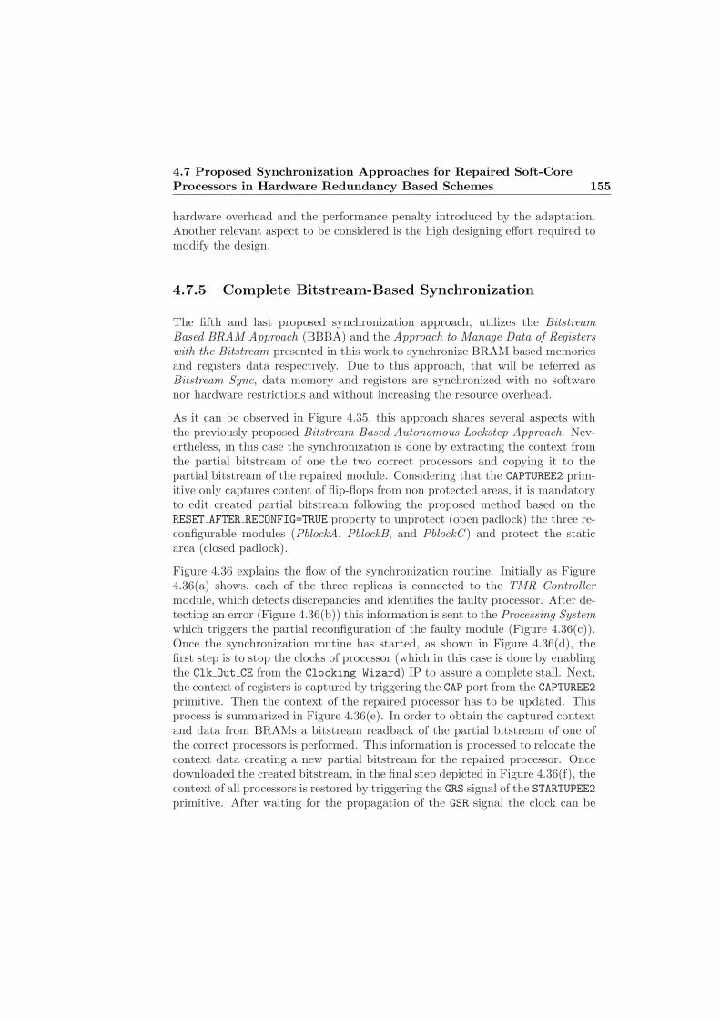
4.7 Proposed Synchronization Approaches for Repaired Soft-CoreProcessors in Hardware Redundancy Based Schemes 155
hardware overhead and the performance penalty introduced by the adaptation.Another relevant aspect to be considered is the high designing effort required tomodify the design.
4.7.5 Complete Bitstream-Based Synchronization
The fifth and last proposed synchronization approach, utilizes the BitstreamBased BRAM Approach (BBBA) and the Approach to Manage Data of Registerswith the Bitstream presented in this work to synchronize BRAM based memoriesand registers data respectively. Due to this approach, that will be referred asBitstream Sync, data memory and registers are synchronized with no softwarenor hardware restrictions and without increasing the resource overhead.
As it can be observed in Figure 4.35, this approach shares several aspects withthe previously proposed Bitstream Based Autonomous Lockstep Approach. Nev-ertheless, in this case the synchronization is done by extracting the context fromthe partial bitstream of one the two correct processors and copying it to thepartial bitstream of the repaired module. Considering that the CAPTUREE2 prim-itive only captures content of flip-flops from non protected areas, it is mandatoryto edit created partial bitstream following the proposed method based on theRESET AFTER RECONFIG=TRUE property to unprotect (open padlock) the three re-configurable modules (PblockA, PblockB, and PblockC ) and protect the staticarea (closed padlock).
Figure 4.36 explains the flow of the synchronization routine. Initially as Figure4.36(a) shows, each of the three replicas is connected to the TMR Controllermodule, which detects discrepancies and identifies the faulty processor. After de-tecting an error (Figure 4.36(b)) this information is sent to the Processing Systemwhich triggers the partial reconfiguration of the faulty module (Figure 4.36(c)).Once the synchronization routine has started, as shown in Figure 4.36(d), thefirst step is to stop the clocks of processor (which in this case is done by enablingthe Clk Out CE from the Clocking Wizard) IP to assure a complete stall. Next,the context of registers is captured by triggering the CAP port from the CAPTUREE2primitive. Then the context of the repaired processor has to be updated. Thisprocess is summarized in Figure 4.36(e). In order to obtain the captured contextand data from BRAMs a bitstream readback of the partial bitstream of one ofthe correct processors is performed. This information is processed to relocate thecontext data creating a new partial bitstream for the repaired processor. Oncedownloaded the created bitstream, in the final step depicted in Figure 4.36(f), thecontext of all processors is restored by triggering the GRS signal of the STARTUPEE2primitive. After waiting for the propagation of the GSR signal the clock can be
156 Contributions in Fault Tolerance for Soft-Core Processors
Contex
Storage
Bitstream
PCAP
Config. Memory
Bitstream
FPGA
EMIOinterface Faulty block #
!
010101010101011110101010101110001100101010110001010101011100010101011110001010111101010101011111
CAPTUREE2
STARTUPEE2
CAP
GSR
ProcessingSystem(ARM)
DDR
PblockA PblockB
Static Area
CLOCKING
WIZARD
Clk_Out_CE
PblockC
P1 P2
TMRController
P3
Figure 4.35: Simplified diagram of the Bitstream Sync approach.
activated to resume to normal operation.
Considering that by default each processor commonly presents distinct imple-mentations due to the default resource placement freedom of the implementationtool this implies a complex process of copying and relocating the bitstream data.This drawback gains importance bearing in mind the size of soft-core proces-sors which gather a significant quantity of memory elements to be synchronized.Hence, it requires a big processing effort, especially taking into account that eachdesign implementation requires to the Processing System to specifically adapt thedata relocation processes. For this reason, the BRAMs of each soft-core proces-sor have located in the same position of each BRAM column by using placementconstraints. In a similar way, the registers of each of the three replicas havebeen implemented following the proposed Location Constraints Flow. Thanks toboth strategies three alike implementations in each reconfigurable region can beobtained. This strategy reduces complexity of the bitstream manipulation pro-cess because, in this case, each replica of the tripled memory resources presentssimilar data structure and locations within the bitstream.
This approach provides the remarkable benefits of not requiring hardware adapta-tions. Hence, the utilization of the Bitstream Sync does not increase the hardware

4.7 Proposed Synchronization Approaches for Repaired Soft-CoreProcessors in Hardware Redundancy Based Schemes 157
P1
Context A
10101010
01010100
00100110
01010100
00001010
01010100
P2
Context A
10101010
01010100
00100110
01010100
00001010
01010100
P3
Context A
10101010
01010100
00100110
01010100
00001010
01010100
VOTER
No error
Clkrunning
Bitstreams(INIT values)
(a) Normal operation.
P1
Context B
P2
Context B
P3
Context B
VOTER
Error!
Clkrunning
Bitstreams(INIT values)
10101010
01010100
00100110
01010100
00001010
01010100
10101010
01010100
00100110
01010100
00001010
01010100
10101010
01010100
00100110
01010100
00001010
01010100
(b) Error detection: a faulty processor.
P2
Context C
P3
Context C
VOTER
Error!
Clkrunning
Bitstreams(INIT values)
10101010
01010100
00100110
01010100
00001010
01010100
10101010
01010100
00100110
01010100
00001010
01010100
10101010
01010100
00100110
01010100
00001010
01010100
(c) Repare processor (reconfigure).
P1
Context -
10101010
01010100
00100110
01010100
00001010
01010100
P2
Context D
11111111
11000011
11001111
00011100
00111000
01111110
P3
Context D
11111111
11000011
11001111
00011100
00111000
01111110
VOTER
Error!
StopClk
=
Bitstreams(INIT values)
(d) Capture context.
P1
Context -
10101010
01010100
11001111
00011100
00111000
01111110
P2
Context D
P3
Context D
VOTER
Error!
11111111
11000011
11001111
00011100
00111000
01111110
Clkstopped
=
Bitstreams(INIT values)
11111111
11000011
11001111
00011100
00111000
01111110
(e) Relocate data and reconfigure processor.
P1
Context D
P2
Context D
P3
Context D
VOTER
No error
Wait GSR /resume Clk
Bitstreams(INIT values)
11111111
11000011
11001111
00011100
00111000
01111110
11111111
11000011
11001111
00011100
00111000
01111110
11111111
11000011
11001111
00011100
00111000
01111110
Trig GSR
(f) Final synchronization phase.
Figure 4.36: Synchronization routine of the Bitstream Sync approach.
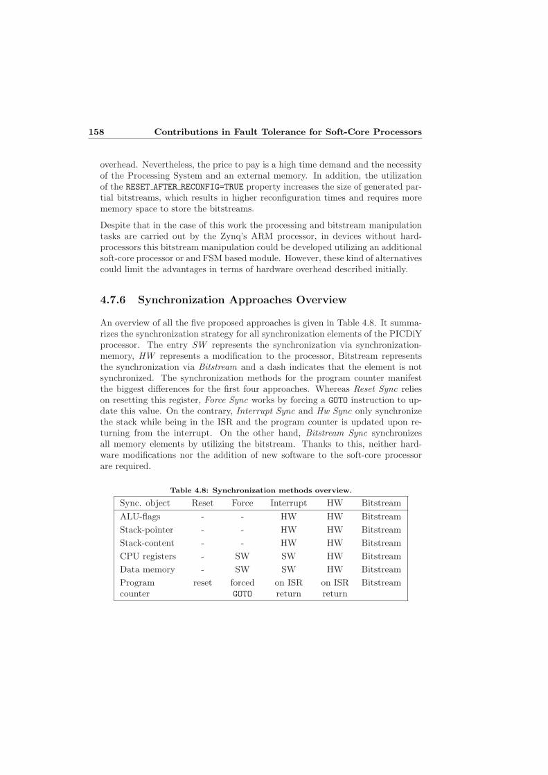
158 Contributions in Fault Tolerance for Soft-Core Processors
overhead. Nevertheless, the price to pay is a high time demand and the necessityof the Processing System and an external memory. In addition, the utilizationof the RESET AFTER RECONFIG=TRUE property increases the size of generated par-tial bitstreams, which results in higher reconfiguration times and requires morememory space to store the bitstreams.
Despite that in the case of this work the processing and bitstream manipulationtasks are carried out by the Zynq’s ARM processor, in devices without hard-processors this bitstream manipulation could be developed utilizing an additionalsoft-core processor or and FSM based module. However, these kind of alternativescould limit the advantages in terms of hardware overhead described initially.
4.7.6 Synchronization Approaches Overview
An overview of all the five proposed approaches is given in Table 4.8. It summa-rizes the synchronization strategy for all synchronization elements of the PICDiYprocessor. The entry SW represents the synchronization via synchronization-memory, HW represents a modification to the processor, Bitstream representsthe synchronization via Bitstream and a dash indicates that the element is notsynchronized. The synchronization methods for the program counter manifestthe biggest differences for the first four approaches. Whereas Reset Sync relieson resetting this register, Force Sync works by forcing a GOTO instruction to up-date this value. On the contrary, Interrupt Sync and Hw Sync only synchronizethe stack while being in the ISR and the program counter is updated upon re-turning from the interrupt. On the other hand, Bitstream Sync synchronizesall memory elements by utilizing the bitstream. Thanks to this, neither hard-ware modifications nor the addition of new software to the soft-core processorare required.
Table 4.8: Synchronization methods overview.
Sync. object Reset Force Interrupt HW Bitstream
ALU-flags - - HW HW Bitstream
Stack-pointer - - HW HW Bitstream
Stack-content - - HW HW Bitstream
CPU registers - SW SW HW Bitstream
Data memory - SW SW HW Bitstream
Programcounter
reset forcedGOTO
on ISRreturn
on ISRreturn
Bitstream

Chapter 5
Validation of FaultTolerance Approaches
After introducing the different contributions focused on improving existing faulttolerance techniques for SRAM-based FPGAs, this chapter introduces a detailedanalysis of the proposed approaches. Aspects such as, impact on resource over-head, effects in terms of performance penalty, availability and functionality areevaluated utilizing a hardware platform. The results extracted from these experi-ments provide relevant information for fault-tolerance designers in order to maketrade-off decisions and to choose the best solution to fit with design specifications.
In Section 5.1 the basis of the experimental setup is introduced, by means ofdescribing the hardware platform and the employed test application. Section 5.2validates the designed soft-core processor and compares it with two representativesoft-core processor IPs. Section 5.3 evaluates the proposed BBBA approach tomanage BRAM data through bitstream and compares it with a basic FSM basedimplementation. In next Section, Section 5.4, the proposed Approach to ManageData of Registers with the Bitstream is validated by using basic implementationswhich include 8-bit registers in different scenarios. In a next step, the test torefute the Data Content Scrubbing Approach is described in Section 5.5. Sec-tion 5.6 follows describing the evaluation of the Approach to Extract Data FromDamaged Memories Using the BBBA. Furthermore, in Section 5.7 the validationof the three proposed lockstep approaches is detailed. Finally, Section 5.8 dealswith the validation of the different proposed approaches to synchronize repairedsoft-core processors in hardware redundancy based schemes.

160 Validation of Fault Tolerance Approaches
5.1 Experimental Setup
All experimental setups of this research work have been implemented in a generalpurpose development board from AVNET named ZedBoard [329], which is de-picted in depicted in Figure 5.1. Zedboard includes a Xilinx Zynq-7000 AP SoCXC7Z020-CLG484 device that contains tightly coupled 7-series programmablelogic and dual-core ARM Cortex-A9 centric processing-system. The leading po-sition of Xilinx in the field of all programmable FPGAs and SoCs devices makesthis device a remarkable candidate to be used as a validation platform. Due to itsadvanced technology, Xilinx’s products are widely used in several fields, such as,medical devices, industrial control, etc. For instance, NASA has recently utilizedXilinx technology to implement the scope of CubeSat Launch initiative [141].
Figure 5.1: ZedBoard Zynq-7000 ARM/FPGA SoC development board.
The software utilized to develop and implement the different FPGA designs hasbeen Vivado Design Suite (16.2). It provides the tools needed to develop com-plex designs, optimizing the implementation for Xilinx devices, providing IP sub-systems reuse and accelerating the design process by enabling to work at a highlevel of abstraction.
Due to the PIC16 instruction set compatibility of the PICDiY processor, theprogramming has been done using MPLAB IDE8.76 IDE by Microchip Technol-ogy Inc. to obtain the .HEX files with the application programs. After that,

5.1 Experimental Setup 161
the processors program memory block has been generated using a visual basicapplication developed for this work combined with previously generated .HEXfiles to generate the VHDL file of the programmed program memory.
Additional software like PuTTY [330] has also been utilized to perform serialcommunications between ZedBoard and computer. PuTTY is a free implemen-tation of Telnet and SSH for Windows and Unix platforms.
In order to obtain reliable and comparable results in the different validation teststhe methodology shown in Figure 5.2 has been mainly followed. Once the VHDLcode of the design has been properly written and checked, the first validation stephas been to synthesize and simulate it. This step has been done by using Vivado16.2 and its simulator. Different configurations have been thoroughly simulated,starting with independently checking of each module or IP that constitute thesystem and ending with full design simulations. In several cases the debuggingof this physical implementation process has been performed with the help ofVivado’s Integrated Logic Analyzer (ILA), which permits to visualize internalsignals of the FPGA design. After debugging and improving the designs, thenext step has been to implement and generate the bitstream to be download intothe FPGA. Also Vivado 16.2 suite was employed to carry out these processes.
VHDLDesign
Synthesis and
Simulation
PhysicalImplementation
TestApplication
Comparison(Optional)
Figure 5.2: Flow chart of the utilized validation strategy.
In a further phase, the designs have been validated by running real case appli-cations on the soft-core processors under test. This have provided the insightinto correctness of the results obtained in a real world scenario. Despite that insome cases specific applications have utilized, the mainly used one has been aRS232 serial transmission based application, which hereinafter will be referredto as TestApp. This application sends a sequence of ASCII characters storedin the program memory thanks to a finite state machine based program. Thecommunication setup uses 8-bits data word without parity and a single stop bit.The baud rate of 9600 is generated with a special block in the FPGA but outsidethe processor design, is based on a counter based structure. The signal generatedon the baud generation block is connected to the processors interrupt inputs andthe transmission process is performed by a specific interrupt routine. Thanks tothat, with the correct setting in the baud rate generation block, the transmissioncan work with different baud rates and with distinct clock frequencies. The ba-sic experimental setup (a stand-alone processor) is presented in Figure 5.3. TheFPGA transmits the information generated by the processor through output port
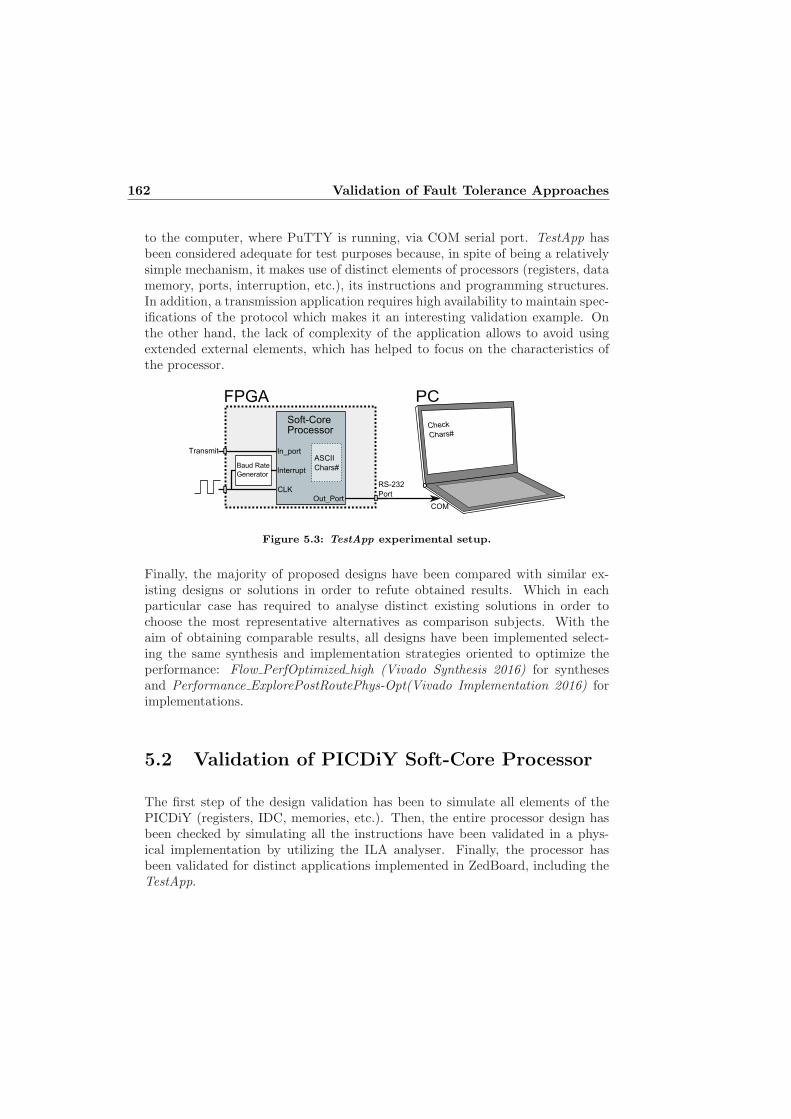
162 Validation of Fault Tolerance Approaches
to the computer, where PuTTY is running, via COM serial port. TestApp hasbeen considered adequate for test purposes because, in spite of being a relativelysimple mechanism, it makes use of distinct elements of processors (registers, datamemory, ports, interruption, etc.), its instructions and programming structures.In addition, a transmission application requires high availability to maintain spec-ifications of the protocol which makes it an interesting validation example. Onthe other hand, the lack of complexity of the application allows to avoid usingextended external elements, which has helped to focus on the characteristics ofthe processor.
RS-232
PortOut_Port
In_port
Interrupt
ASCII
Chars#
CLK
Transmit
FPGA
Soft-CoreProcessor
Baud Rate
Generator
COM
PC
Chars#Check
Chars#
Figure 5.3: TestApp experimental setup.
Finally, the majority of proposed designs have been compared with similar ex-isting designs or solutions in order to refute obtained results. Which in eachparticular case has required to analyse distinct existing solutions in order tochoose the most representative alternatives as comparison subjects. With theaim of obtaining comparable results, all designs have been implemented select-ing the same synthesis and implementation strategies oriented to optimize theperformance: Flow PerfOptimized high (Vivado Synthesis 2016) for synthesesand Performance ExplorePostRoutePhys-Opt(Vivado Implementation 2016) forimplementations.
5.2 Validation of PICDiY Soft-Core Processor
The first step of the design validation has been to simulate all elements of thePICDiY (registers, IDC, memories, etc.). Then, the entire processor design hasbeen checked by simulating all the instructions have been validated in a phys-ical implementation by utilizing the ILA analyser. Finally, the processor hasbeen validated for distinct applications implemented in ZedBoard, including theTestApp.
5.2 Validation of PICDiY Soft-Core Processor 163
After the validation process the PICDiY has been compared with other 8-bitsoft-core processors in order to evaluate it. Two processors have been chosen forthis task: a widely used soft-core processor and a PIC based one.
The first selected soft-core processor has been the PicoBlaze, since is a prevailingIP for Xilinx based designs [58, 67, 69, 70]. Being optimized for 7-series devices,it presents a very reduced size (small as 26 slices depending on device family)and high performance (up to 240 MHz). In addition, it is highly integratedfor implementing non-time critical state machine and presents a predictable fastinterrupt response. All these characteristics make the PicoBlaze an ideal referencefor a comparison.
Regarding the second soft-core processor, different IP cores based on the PIC16’sarchitecture are available (CQPIC, PPX16mcu, RISC5X, RISC16F84, MINI-RISC, Synthetic PIC, UMASS, etc.). All of these cores differ slightly in theirarchitectures, but they all implement the main features of a PIC16 microcon-troller. The selected PIC16 based soft-core processor has been the PPX16mcu[331]. The main reason to select the PPX16mcu has been that it is the closestalternative to the PICDiY, since PPX16mcu is a minimalist open source versionthat does not has neither Watchdog nor EEPROM. PPX16mcu is a single cycleand, four times faster, VHDL implementation of the 16F84.
For the comparison tests, the three soft-core processors have been implementedwith the same timing constraints (100 MHz) and without including the logic re-sources necessary to implement the Testapp. Additional implementations havebeen also performed in order to determine the maximum frequency achievablewith each soft-core processor. Implementation results (at 100 MHz) are shownin Table 5.1. As it can be observed, PICDiY presents a significantly lower deviceutilization compared to PPX16mcu, while PicoBlaze is the one with the lowestoverhead. As this table shows, those results are closely related with the dynamicpower consumption of each soft-core. Due to the limited resource usage of theanalysed soft-cores, there is only a slight difference between them. In any case,these results prove that the power consumption of the three soft-cores is moder-ate. Regarding the maximum achievable frequencies, the tests have shown thatPicoBlaze provides the best results (150 MHz). On the other hand, the maximumfrequencies for PICDiY and PPX16mcu are similar.
Furthermore, Table 5.2 shows a detailed list of the primitives utilized by each im-plementation. Apart from the resource overhead information given by this table,it is interesting to note that PICDiY uses distributed memory resources (RAMS64Eand RAMS32 primitives) instead of BRAM blocks to implement the data memorymodule. This is because Vivado changes the initial BRAM based implementationdefined by the VHDL design in order to meet the timing constraints. Additional

164 Validation of Fault Tolerance Approaches
tests with more moderate timing constraints (e.a. 90 MHz) have shown thatVivado implements the data memory by using a RAMB18E1 primitive. A similarsituation has been observed in case of PPX16mcu. While in a 100 MHz designall memories are implemented with distributed memory resources, a design withlower frequency utilizes a RAMB18E1 primitive.
Table 5.1: Implementation results summary of the soft-core processors(@100MHz).
Resource PICDiY PPX16mcu PicoBlazeSlice LUTs 266 478 130Slice Registers 82 223 114F7 Muxes 17 2 16F8 Muxes 8 - 8Block RAM Tile 0.5 - 0.5fmax (MHz) 107 110 150Dynamic p. (W) 0.129 0.120 0.123Static p. (W) 0.125 0.125 0.125
Table 5.2: Primitive utilization of the soft-core processors (@100MHz).
Primitive PICDiY PPX16mcu PicoBlazeFDRE 80 119 111FDCE - 66 3FDSE 2 - -FDPE - 38 -CARRY4 8 9 10LUT1 1 16 1LUT2 32 53 1LUT3 11 54 1LUT4 18 55 1LUT5 37 100 42LUT6 131 173 76MUXF7 17 2 16MUXF8 8 - 8RAMB18E1 1 - 1RAMD32 - 12 24RAMS32 7 4 8RAMD64E - 24 -RAMS64E 32 - 32
Further aspects must be considered when comparing three soft-core processors.Although the functionality and programming of PPX16mcu is quite similar toPICDiY’s, PPX16mcu requires extra instructions to configure ports, since theycan work as input or output. In this way, compared to PICDiY’s, the programcode of PPX16mcu needs six extra instructions to configure both, input andoutput ports. Besides, while PPX16mcu needs eight clock cycles to executeinstructions with conditional jumps, PICDiY needs only 4 clock cycles for all the
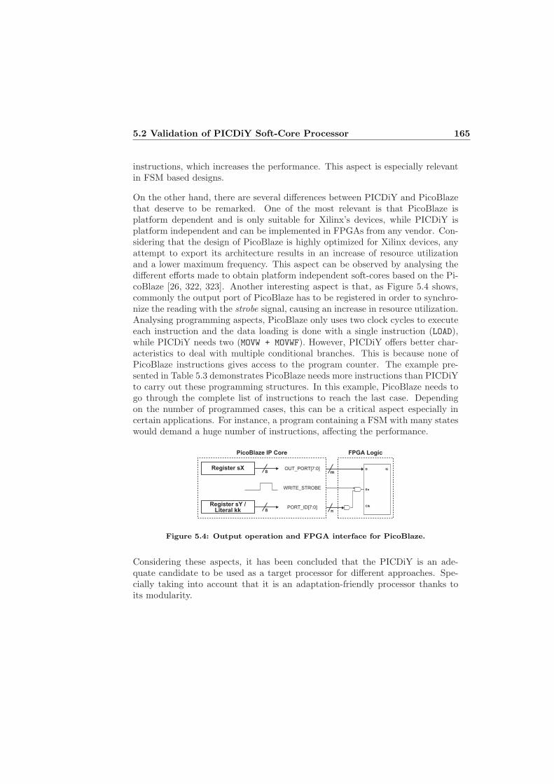
5.2 Validation of PICDiY Soft-Core Processor 165
instructions, which increases the performance. This aspect is especially relevantin FSM based designs.
On the other hand, there are several differences between PICDiY and PicoBlazethat deserve to be remarked. One of the most relevant is that PicoBlaze isplatform dependent and is only suitable for Xilinx’s devices, while PICDiY isplatform independent and can be implemented in FPGAs from any vendor. Con-sidering that the design of PicoBlaze is highly optimized for Xilinx devices, anyattempt to export its architecture results in an increase of resource utilizationand a lower maximum frequency. This aspect can be observed by analysing thedifferent efforts made to obtain platform independent soft-cores based on the Pi-coBlaze [26, 322, 323]. Another interesting aspect is that, as Figure 5.4 shows,commonly the output port of PicoBlaze has to be registered in order to synchro-nize the reading with the strobe signal, causing an increase in resource utilization.Analysing programming aspects, PicoBlaze only uses two clock cycles to executeeach instruction and the data loading is done with a single instruction (LOAD),while PICDiY needs two (MOVW + MOVWF). However, PICDiY offers better char-acteristics to deal with multiple conditional branches. This is because none ofPicoBlaze instructions gives access to the program counter. The example pre-sented in Table 5.3 demonstrates PicoBlaze needs more instructions than PICDiYto carry out these programming structures. In this example, PicoBlaze needs togo through the complete list of instructions to reach the last case. Dependingon the number of programmed cases, this can be a critical aspect especially incertain applications. For instance, a program containing a FSM with many stateswould demand a huge number of instructions, affecting the performance.
m
n8
8Register sX
Register sY /Literal kk
OUT_PORT[7:0]
WRITE_STROBE
PORT_ID[7:0]
PicoBlaze IP Core
D
En
Q
Clk
FPGA Logic
Figure 5.4: Output operation and FPGA interface for PicoBlaze.
Considering these aspects, it has been concluded that the PICDiY is an ade-quate candidate to be used as a target processor for different approaches. Spe-cially taking into account that it is an adaptation-friendly processor thanks toits modularity.

166 Validation of Fault Tolerance Approaches
Table 5.3: Comparison of FSM coding examples for PICDiY and PicoBlazeprocessors.
N. Instr. PICDiY PicoBlaze1 MOVF state, w COMP state,02 ADDWF PLC, F JUMP Z, state03 GOTO state0 COMP state,14 GOTO state1 JUMP Z, state15 GOTO state2 COMP state,26 GOTO state3 JUMP Z, state27 GOTO state4 COMP state,38 GOTO state5 JUMP Z, state39 GOTO state6 COMP state,4
10 GOTO state7 JUMP Z, state411 GOTO state8 COMP state,512 GOTO state9 JUMP Z, state513 GOTO state10 COMP state,614 JUMP Z, state615 COMP state,716 JUMP Z, state717 COMP state,818 JUMP Z, state819 COMP state,920 JUMP Z, state921 COMP state,1022 JUMP Z, state10
5.3 Validation of the Bitstream Based BRAM
Approach
In order to assess in practice the performance of the proposed Bitstream BasedBRAM Approach (BBBA), a ZedBoard has been utilized as an experimental plat-form. The validation of the proposed approach has been carried out by meansof several tests based on the scheme presented in Figure 4.11. The systems im-plemented for these tests are aiming at reading, copying, writing and comparingdifferent data blocks from different BRAM columns, single 18K BRAMs and36K BRAMs. The performance scores analysed in this study are the resourceoverhead, the execution time and the availability.
In the first step the bitstream approach has been compared with a commonimplementation. Most of the memory controllers are based on the use of proces-sors, previously generated generic IP cores or specifically built FSMs. In orderto account for the worst case scenario in terms of execution time, the contentwritten in both memories has been equal. As a consequence, the comparing pro-cedure traverses the entire memory space and, hence, the highest execution timeis achieved. A dedicated soft-core processor would be a waste of resources; there-

5.3 Validation of the Bitstream Based BRAM Approach 167
fore, in this case, a FSM based controller is the most efficient and fastest methodto control the memories.
The implemented test applications are memory copying and memory comparing.For each application, different tests have been performed including entire BRAMcolumn and single BRAM experiments. Both applications have been designedto be commanded by a ready signal, which permits choosing when the actionat hand is executed over the second memory. In this way, both approaches (theFSM based and the bitstream based) feature the same functionality. However,in all tests the ready signal has been set to active, so as to avoid the effect ofthe waiting time in the measurement of processing time. All applications beginby fully writing the source memory, which has not been taken into account whenmeasuring the processing time. Thereafter, the next step to perform the data copyprocess is to read the source memory, for which the application waits the ready
signal from the destination memory. Upon receiving this signal, the data contentis copied to the destination memory and cross-checked with the original data ofthe source memory in order to detect data discrepancies. To this end, once thewriting process is done the cross-check starts by reading the first memory. Afterreceiving the ready signal from the second memory, the data therein are readand compared to the previously read memory. In order to account for the worstcase scenario in terms of execution time and evaluate the highest execution timecase, the content written in both memories has been equal. No errors have beendetected and all the memory addresses have been analysed during the comparingprocesses.
Figure 5.5 depicts the simplified block diagrams of the different testing designsimplemented in the programmable logic part of the Zynq device. The originalsystem has been implemented as a reference in order to evaluate the resourceoverhead. As shown in 5.5(a), it consists of different modules where the mostrelevant ones are the two memory blocks, the FSM based memory filler, the pulsecounter and the output logic. The two memory blocks are the target memories,which are equally implemented with different sizes depending on the test to beaddressed. The memory filler is an FSM based module used to fill the memorieswith specific test data. The pulse counter, which is composed by a counter andan FSM, measures the time spent by each approach. Finally, the output logicselects the signals to be displayed as outputs.
As evinced Figure in 5.5(b), the proposed BBBA is similar to the original systemscheme. This is because it does not need any logic resource. The only differenceis that the pulse counter is controlled by the ARM processor available in theprocessing system part of the Zynq device, which is only necessary to measurethe time. The number of instructions to be executed by the ARM vary depending

168 Validation of Fault Tolerance Approaches
Output
Logic
Memory
Filler
Mem
A
(BRAM)
Mem
B
(BRAM)
Pulse
Counter
(a) Original system.
Output
Logic
Memory
Filler
Mem
A
(BRAM)
Mem
B
(BRAM)
Pulse
Counter
ARM Proces.
(b) System with the BBBA.
Memory
FillerOutput
Logic
Mem
A
(BRAM)
Mem
B
(BRAM)
Pulse
Counter
FSM App.
M
U
X
M
U
X
Auxiliar Mem.
(c) System with the FSM applications.
Figure 5.5: Block diagrams of the implemented approaches.

5.3 Validation of the Bitstream Based BRAM Approach 169
on the location of the BRAMs and the possibility of data overwriting. Bothapplications, memory copying and memory comparing, have been implementedwith source and destination BRAMs in the same or different column and with orwithout overwriting.
Figure 5.5(c) presents the scheme for the FSM based memory copying and mem-ory comparing operations. In this case, further modifications have been incor-porated with respect to the original scheme. The most remarkable one is theaddition of the FSM application module. For each test (copying and comparing)a specific FSM has been implemented, minimizing the number of states for anefficient coupling. In order to wait the ready signal, an auxiliary BRAM memoryhas been allocated in these modules. Both FSM applications also manage thepulse counter module. Finally, additional multiplexer modules have been addedto manage the inputs of the target memories. As opposed to BBBA, when usingFSMs there is no functional difference related to the location of the BRAMs, norany the problem of data overwriting of the rest of BRAMs from the same BRAMcolumn.
Table 5.4 summarizes the results of copying and comparing tests. In both tests,the analysed parameters are the same. The first five columns (Slice Registers,Slice LUTs, Occupied Slices, LUT FF pairs and 18K BRAMs) quantify the usageof FPGA resources. The number in parenthesis indicates the relative resourceoverhead with respect to the original system. The remaining parameter is thetime used to perform each application extracted from the pulse counter module.It should be noted that, since the Processing System presents a non-deterministicresponse (due to uncontrollable side conditions e.g. hardware interruptions andhardware-software communication), there are small variations in the measuredtime for each experiment. Consequently, the provided scores represent averagedvalues after 10 experiments. In the same table, the first two rows correspond tothe parameters of the original system without any additional element with theaim of being used as a reference. In this case, since no data operation is involved,there is no information for the time parameter. The next four rows are the valuesof the monitored parameters corresponding to the FSM based applications. Lastbut no least, the results of the bitstream manipulation based applications areshown in the last parameter set.
The conclusions drawn by observing the above table support the research hy-pothesis stared in Section 4.2. The BBBA based applications obtain significantlybetter results in terms of resources overhead. While the overhead in BBBA isessentially zero, the overheads of the FSM based approaches are between 50%and 180%. However, the results also confirm that the BBBA based applicationsare the most time consuming options in the benchmark. Different performed
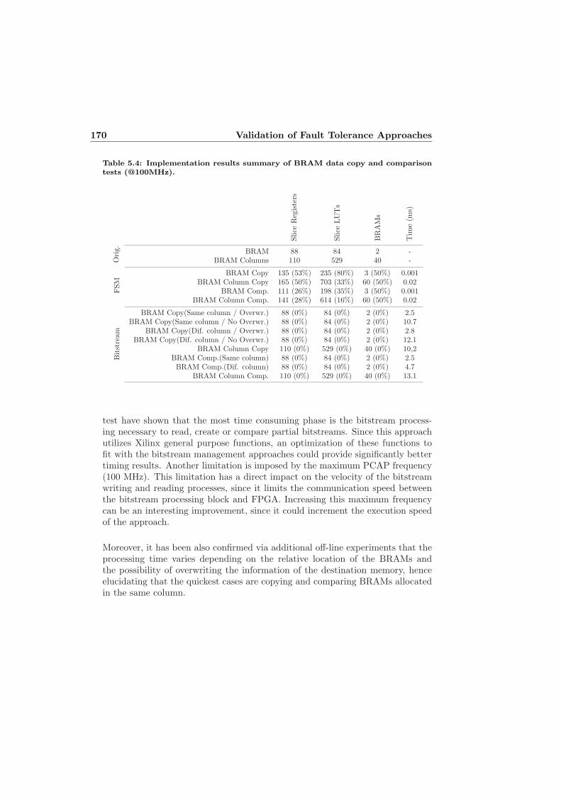
170 Validation of Fault Tolerance Approaches
Table 5.4: Implementation results summary of BRAM data copy and comparisontests (@100MHz).
Slice
Registers
Slice
LUTs
BRAMs
Tim
e(m
s)
BRAM 88 84 2 -
Orig.
BRAM Columns 110 529 40 -
BRAM Copy 135 (53%) 235 (80%) 3 (50%) 0.001BRAM Column Copy 165 (50%) 703 (33%) 60 (50%) 0.02
FSM
BRAM Comp. 111 (26%) 198 (35%) 3 (50%) 0.001BRAM Column Comp. 141 (28%) 614 (16%) 60 (50%) 0.02
BRAM Copy(Same column / Overwr.) 88 (0%) 84 (0%) 2 (0%) 2.5BRAM Copy(Same column / No Overwr.) 88 (0%) 84 (0%) 2 (0%) 10.7
BRAM Copy(Dif. column / Overwr.) 88 (0%) 84 (0%) 2 (0%) 2.8BRAM Copy(Dif. column / No Overwr.) 88 (0%) 84 (0%) 2 (0%) 12.1
BRAM Column Copy 110 (0%) 529 (0%) 40 (0%) 10,2
Bitstream
BRAM Comp.(Same column) 88 (0%) 84 (0%) 2 (0%) 2.5BRAM Comp.(Dif. column) 88 (0%) 84 (0%) 2 (0%) 4.7
BRAM Column Comp. 110 (0%) 529 (0%) 40 (0%) 13.1
test have shown that the most time consuming phase is the bitstream process-ing necessary to read, create or compare partial bitstreams. Since this approachutilizes Xilinx general purpose functions, an optimization of these functions tofit with the bitstream management approaches could provide significantly bettertiming results. Another limitation is imposed by the maximum PCAP frequency(100 MHz). This limitation has a direct impact on the velocity of the bitstreamwriting and reading processes, since it limits the communication speed betweenthe bitstream processing block and FPGA. Increasing this maximum frequencycan be an interesting improvement, since it could increment the execution speedof the approach.
Moreover, it has been also confirmed via additional off-line experiments that theprocessing time varies depending on the relative location of the BRAMs andthe possibility of overwriting the information of the destination memory, henceelucidating that the quickest cases are copying and comparing BRAMs allocatedin the same column.

5.4 Validation of the Approach to Manage Data of Registers with theBitstream 171
5.4 Validation of the Approach to Manage Dataof Registers with the Bitstream
The validation of the Approach to Manage Data of Registers with the Bitstreamhas been performed in a simple manner and most of tests have been performedduring the developing process of the technique. Non-essential elements havebeen avoided to elude any possible impact in bitstream’s content and structure.Considering that it is a very particular approach no alternatives have been foundto be compared with.
The development and validation design is shown in Figure A.1, which has beenobtained from the utilized Vivado’s project. In this design, the reset ports of thetwo 8-bit register modules are managed by the Processing System via EMIO inter-face. The Processing System also controls the CAP and GSR ports from CAPTUREE2
and STARTUPEE2 primitives, respectively. With the aim of maintaining simplicityand a faithful physical reading, the data input and output ports are connecteddirectly to ZedBoard’s switches and LEDs, respectively. The switch connectedto the first data bit also controls the multiplexer, providing the possibility ofvisualizing the connection between both registers in real time. The bitstream isreadback from the FPGA combining the PCAP and the Processing System, andstored in the DDR memory. The content of INIT values are obtained from thebitstream thanks to the location of flip-flop’s content provided by a previouslygenerated .ll file.
In a first validation step, the functionally of GRESTORE and GCAPTURE commandshave been checked in a non-reconfigurable design with successful results. Inaddition, several data content copying experiments have been conducted withthis setup. The basis of these tests has been a basic procedure. First, as Figure5.6 shows, specific placement constraints have been used in order to utilize thesame flip-flops of different resource columns for both registers. As showed insegments of .ll files represented in Figure 5.7, it has been confirmed that samestructures (same frame offsets) are contained in the bitstream for the data ofboth registers, differing only in the FARs. Utilizing this information, the contentof one registers has been copied to the other with the bitstream confirming theviability of the proposed approach.
After the first experiment, one of the registers has been implemented as reconfig-urable module enabling the RESET AFTER RECONFIG=TRUE property, maintainingthe other register and the rest of the design in the static region. In this second ex-periment, the combination of information extracted from read bitstreams, the .llfile and LEDs has proved that the utilization of the RESET AFTER RECONFIG=TRUE
property protects the static area from the effect of the GCAPTURE command. In ad-
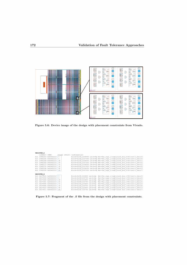
172 Validation of Fault Tolerance Approaches
Figure 5.6: Device image of the design with placement constraints from Vivado.
REGISTER_A
<offset> <FAR> <frame offset> <information>
Bit 15982243 0x0040221f 3 Block=SLICE_X106Y50 Latch=AQ Net=Two_regs_i/reg8_black_box_0/U0/inst/o_Data[0]
Bit 15982244 0x0040221f 4 Block=SLICE_X107Y50 Latch=AQ Net=Two_regs_i/reg8_black_box_0/U0/inst/o_Data[4]
Bit 15982268 0x0040221f 28 Block=SLICE_X106Y50 Latch=BQ Net=Two_regs_i/reg8_black_box_0/U0/inst/o_Data[1]
Bit 15982269 0x0040221f 29 Block=SLICE_X107Y50 Latch=BQ Net=Two_regs_i/reg8_black_box_0/U0/inst/o_Data[5]
Bit 15982273 0x0040221f 33 Block=SLICE_X106Y50 Latch=CQ Net=Two_regs_i/reg8_black_box_0/U0/inst/o_Data[2]
Bit 15982274 0x0040221f 34 Block=SLICE_X107Y50 Latch=CQ Net=Two_regs_i/reg8_black_box_0/U0/inst/o_Data[6]
Bit 15982298 0x0040221f 58 Block=SLICE_X106Y50 Latch=DQ Net=Two_regs_i/reg8_black_box_0/U0/inst/o_Data[3]
Bit 15982299 0x0040221f 59 Block=SLICE_X107Y50 Latch=DQ Net=Two_regs_i/reg8_black_box_0/U0/inst/o_Data[7]
REGISTER_B
Bit 24275555 0x0042221f 3 Block=SLICE_X106Y0 Latch=AQ Net=Two_regs_i/reg8_black_box_1/U0/inst/o_Data[0]
Bit 24275556 0x0042221f 4 Block=SLICE_X107Y0 Latch=AQ Net=Two_regs_i/reg8_black_box_1/U0/inst/o_Data[4]
Bit 24275580 0x0042221f 28 Block=SLICE_X106Y0 Latch=BQ Net=Two_regs_i/reg8_black_box_1/U0/inst/o_Data[1]
Bit 24275581 0x0042221f 29 Block=SLICE_X107Y0 Latch=BQ Net=Two_regs_i/reg8_black_box_1/U0/inst/o_Data[5]
Bit 24275585 0x0042221f 33 Block=SLICE_X106Y0 Latch=CQ Net=Two_regs_i/reg8_black_box_1/U0/inst/o_Data[2]
Bit 24275586 0x0042221f 34 Block=SLICE_X107Y0 Latch=CQ Net=Two_regs_i/reg8_black_box_1/U0/inst/o_Data[6]
Bit 24275610 0x0042221f 58 Block=SLICE_X106Y0 Latch=DQ Net=Two_regs_i/reg8_black_box_1/U0/inst/o_Data[3]
Bit 24275611 0x0042221f 59 Block=SLICE_X107Y0 Latch=DQ Net=Two_regs_i/reg8_black_box_1/U0/inst/o_Data[7]
Figure 5.7: Fragment of the .ll file from the design with placement constraints.
5.4 Validation of the Approach to Manage Data of Registers with theBitstream 173
dition, it has been demonstrated that when generating bitstreams, the size of thebitstream considerably increases by enabling the RESET AFTER RECONFIG=TRUE
property. In this example in particular, it has been observed that while thesize of a regular .bit file is 88.492 bytes, the size of a .bit file generated theRESET AFTER RECONFIG=TRUE property is 240.108 bytes. As a consequence, anincrease of 271.3% in the size of the bitstream has been detected. The main rea-sons for this elevated percentage is that, considering the small size of the partialbitstream, the instructions added to the bitstream to protect the reconfigurableregion imply a significant data overhead. In bigger reconfigurable designs theimpact of these instruction is be lower.
In a further step, the proposed approach to protect/unprotect partial regions in7 series devices by editing the partial bitstream has been validated. In this case,both registers have been implemented in each reconfigurable Pblock. After edit-ing one of the generated partial bitstreams by erasing the proper 0xE00009BCspecial words, it has been downloaded so as to reconfigure the FPGA. The infor-mation provided by the LEDs and bitstream readbacks in different GCAPTURE andGRESTORE tests have successfully demonstrated that both reconfigurable regionsare unprotected while the static region remains protected.
The final validation step has been to test the proposed flow to generate equalimplementations of a design in different reconfigurable regions. In this case, aTMR design with three instances of the PICDiY soft-core processor have beenimplemented in three reconfigurable regions (Pblock0, Pblock1 and Pblock2). Inthis first implementation all resources of each instance have been freely placedby the tool. Thus, as can be observed in Figure 5.8 obtained from the devicediagram of Vivado, the three resultant implementations present distinct place-ments. Afterwards, the Location Constraints Flow has been utilized to generatethree equal implementation (selecting the Pblock0 as a reference). As it can beobserved in Figure 5.9 the resource placement of the three entities within threePblocks. In a similar way, the generated partial bitstreams of the three Pblockshave been compared in order to check if the location of data bits within the bit-stream is the same. Furthermore, as Tables 5.5 and 5.6 demonstrate the resourceusage of both implementations is almost the same. Table 5.5 also confirms thatthe proposed design flow does not affect the implementation in terms of powerconsumption and maximum operation frequency.

174 Validation of Fault Tolerance Approaches
Figure 5.8: Device image of the TMR design without placement constraints fromVivado.

5.4 Validation of the Approach to Manage Data of Registers with theBitstream 175
Figure 5.9: Device image of the TMR design witht placement constraints fromVivado.
176 Validation of Fault Tolerance Approaches
Table 5.5: Implementation results summary of a reconfigurable TMR implemen-tation with and without placement constraints (@60MHz).
Resource Bitstream Bitstream w/placeSlice LUTs 678 679Slice Registers 187 187F7 Muxes 3 3Block RAM Tile 3 3fmax (MHz) 80 80Dynamic p. (W) 1.668 1.668Static p. (W) 0.161 0.161
Table 5.6: Primitive utilization of a reconfigurable TMR implementation with andwithout placement constraints (@60MHz).
Resource Bitstream Bitstream w/placeFDRE 181 181FDSE 6 6CARRY4 24 24LUT1 3 3LUT2 90 90LUT3 47 47LUT4 55 55LUT5 109 109LUT6 405 405MUXF7 3 3RAMB18E1 6 6RAMS32 21 21CAPTUREE2 1 1STARTUPE2 1 1PS7 1 1PLLE2 ADV 1 1
5.5 Validation of the Data Content ScrubbingApproach
Bearing in mind that the Data Content Scrubbing Approach is directly basedon the previously validated Bitstream Based BRAM Approach (BBBA), its val-idation has been a straightforward operation. A PICDiY IP has been utilizedto implement the TestApp. In a first step, the content of the program mem-ory BRAM of the processor has been readback and stored as a golden copy inthe external DDR memory. After that, several corrupted versions of the goldencopy have been generated, by flipping different data-related bits. The corruptedpartial bitstreams have been utilized to perform several error injection tests.
Thanks to performed tests it has been proved that this approach successfullyperforms a scrubbing of the data content of BRAMs without affecting the restof resources. Hence, neither resource overhead increase nor performance penalty

5.6 Validation of Approach to Extract Data From Damaged MemoriesUsing the BBBA 177
has been observed. Due to the lack of data content scrubbing alternatives thisapproach has not been compared against other approaches.
5.6 Validation of Approach to Extract DataFrom Damaged Memories Using the BBBA
Similar to what happens in the case of the Data Content Scrubbing Approach’svalidation, the validation of the Approach to Extract Data From Damaged Mem-ories Using the BBBA is based on the validation of the Bitstream Based BRAMApproach (BBBA). Figure A.2 shows the block diagram of the utilized imple-mentation extracted from Vivado. The design contains two memory blocks, witha depth of 256 8-bit words, extracted from the PICDiY design. Both memoriescan be written or read by the FSM based BRAM Filler block. An additionalenable port has been used to select, via external switch, if each memory has tobe written. The outputs of both memories are connected to a multiplexer modulein order to select which ones are shown on the LEDs. The validation design alsoincludes the Processing System to perform readbacks and reconfigure the FPGAthrough PCAP interface.
The blue module in Figure A.2 represents the memory block that has been im-plemented as a reconfigurable module, while the rest of modules, including thegreen memory block, has been located in the static region. The reconfigurablemodule has been utilized as a target memory block. In this way, the generatedpartial bitstream has been utilized to create several corrupted files by flippingdifferent bits. After distinct error injection attempts the interface of the targetmemory block has been damaged impeding to read data. Next, with the aim ofextracting data content of the damaged memory, the BBBA has been used tocopy the bitstream portion with the required information to the memory blockon the static area. This have provided the possibility of successfully extract allthe stored information.
This validation test has proved the efficacy of the Data Content Scrubbing Ap-proach, which can recover data from BRAM based data memories without affect-ing the design in terms of resource usage and performance.
178 Validation of Fault Tolerance Approaches
5.7 Validation of the Lockstep Approaches
In order to evaluate the correct functionality of the lockstep approaches, thethree proposed methods have been physically tested by running the TestApp ina ZedBoard.
Despite partial reconfiguration based injection provides a wider range of results,especially in terms of robustness, it increases design and implementation times.Furthermore, considering the vast existing literature the lockstep has been provento be a consolidated and thoroughly analysed technique in terms of robustness.Thus, bearing in mind these aspects and that proposed approaches are focused onimproving both checkpointing and rollback processes, fault simulation tests havebeen carried out by manually flipping data bits from user registers rather thanpartial reconfiguration based fault injections. This strategy has considerablysimplified test tasks, enabling to focus them on the correct behaviour of theapproaches.
As depicted in Figure 5.10, one of the processors has been corrupted by modifyingcertain registers by an additional input to force errors. The most significantsignals, such as outputs of lockstep controller, W register or IDC have beenmonitored by Integrated Logic Analyzer (ILA) module from Vivado.
LockstepController
P1 P2
Integrated Logic Analyzer (ILA)
P1
P2
Errorport
OriginalAdapted
error!
Figure 5.10: Test procedure for the lockstep approaches validation.
In both, Bitstream Based Low Overhead Lockstep and Bitstream Based Au-tonomous Lockstep approaches, the duplicated PICDiY processors have beenimplemented in a single same reconfigurable region. Thus, reducing the com-plexity of checkpointing and rollback processes. In addition, this permitsto avoid the need of editing partial bitstreams and the utilization of the
5.7 Validation of the Lockstep Approaches 179
RESET AFTER RECONFIG=TRUE property to protect static regions.
The validation tests have been executed following these steps:
1. Configure the entire device and constantly run the TestApp.
2. Observe the context before the error injection with ILA.
3. Emulate a failure by triggering the adapted register’s error signal.
4. Check correct rollback (compare with pre-fault injection context) using ILA.
This validation flow has been utilized in all three proposed approaches. It isimportant to observe the context before injecting the fault in order to be able tocheck if the rollback has been performed successfully. For this reason, fault injec-tions and pre-error context checkings have been carried out taken into accountthe checkpointing frequency of each method. Due to its time demand, monitor-ing the entire rollback process of the Bitstream Based Low Overhead Lockstepapproach would require a huge resource usage. Thus, this approach has beenpartially monitored with ILA by utilizing the Processing System and the EMIOinterface in order to define trigger events related to specific moments and onlycapture signals in required instants.
During different performed tests all three proposed lockstep approaches havebeen able to successfully recover from induced errors, proving the validity of allproposed methods.
The obtained results are summarized in Table 5.7. As it can be observed, thefirst column includes the results for a single PICDiY. This data has been usedas the reference value for the percentage information. The next three columnscontain the results of each of the three proposed approaches. The last columnincludes the results for a coarse-grained TMR implementation included for com-parison purposes. Regarding the information provided, while the first five rowsof the table are a summary of the utilized resources, the next three rows containtiming related information (maximum operating frequency and the time require-ments for both checkpointing and rollback processes). Finally, the last two rowsprovide information of the power consumption (static and dynamic). The imple-mentations utilized to obtain these results do not include the logic resources usedfor error-injections and the TestApp, and the employed ILA module. For a faircomparison, all the results have been obtained implementing the designs withthe same clocking constraints (60 MHz). Table 5.8 includes primitive utilizationresults, providing with further information in terms of resource utilization.
As results reveal the HW Fast Lockstep approach provides very fast checkpointingand rollback operations. Nevertheless, the hardware increase introduced is sub-

180 Validation of Fault Tolerance Approaches
Table
5.7:Im
plem
enta
tion
resu
ltssu
mm
ary
ofth
elockste
papproaches,
asin
gle
PIC
DiY
and
acoarse
grain
ed
TM
R(@
60M
Hz).R
eso
urce
PIC
DiY
HW
Fast
Low
Overh
ead
Auto
nomous
TM
RSlice
LUTs
232(100%
)690
(297%)
400(172%
)435
(188%)
726
(313%)
Slice
Registers
74(100%
)272
(368%)
130(176%
)141
(191%
)193
(261%)
F7Muxes
1(100%
)28
(2800%)
2(200%
)34
(3400%)
3(300%
)F8Muxes
(100%)
2(-%
)14
(-%)
Block
RAM
Tile
1(100%
)1
(200%)
2(100%
)1
(200%
)3
(600%)
fm
ax(M
Hz)
107(100%
)64
(60%)
85(79
%)
70(65
%)
90(84%
)Check
pointtim
e(m
s)-
3.33
×10−
82.64
1.67
×10−
8-
-Rollb
ack
time(m
s)-
6.67
×10−
80.03
3.33
×10−
8-
-Dynamic
p.(W
)0.133
(100%)
0.139(105%
)1.638
(1232%)
0.125(92%
)0.139
(105%
)Static
p.(W
)0.125
(100%)
0.125(100%
)0.160
(100%)
0.125(100%
)0.125
(100%)
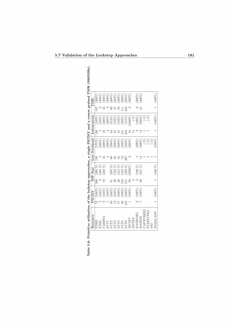
5.7 Validation of the Lockstep Approaches 181
Table
5.8:Prim
itiveutilization
ofth
elockstep
approaches,
asingle
PIC
DiY
and
acoarse
grain
ed
TM
R(@
60M
Hz).
Reso
urce
PIC
DiY
HW
Fast
Low
Overh
ead
Auto
nomous
TM
RFDRE
72(100
%)
266
(369
%)
126
(175
%)
136
(189
%)
187
(260
%)
FDSE
2(100
%)
6(300
%)
4(200
%)
5(250
%)
6(300
%)
CARRY4
8(100
%)
19(238
%)
16(200
%)
16(200
%)
24(300
%)
LUT1
1(100
%)
2(200
%)
2(200
%)
3(300
%)
LUT2
30
(100
%)
61(203
%)
60(200
%)
64(213
%)
90(300
%)
LUT3
13
(100
%)
99(762
%)
26(200
%)
25(192
%)
47(362
%)
LUT4
17
(100
%)
36(212
%)
34(200
%)
31(182
%)
56(329
%)
LUT5
36
(100
%)
159
(442
%)
72(200
%)
141
(392
%)
111
(308
%)
LUT6
132
(100
%)
315
(239
%)
267
(202
%)
204
(155
%)
402
(305
%)
MUXF7
1(100
%)
28(280
0%)
2(200
%)
34(340
0%)
3(300
%)
MUXF8
214
(-%)
RAMB18
E1
2(100
%)
2(100
%)
4(200
%)
2(100
%)
6(300
%)
RAMS32
7(100
%)
26(371
%)
14(200
%)
14(200
%)
21(300
%)
CAPTUREE2
1(-%)
1(-%)
STARTUPE2
1(-%)
1(-%)
PS7
1(-%)
PLLE2ADV
1(100
%)
1(100
%)
1(100
%)
1(100
%)
1(100
%)
182 Validation of Fault Tolerance Approaches
stantial, reaching almost the same overhead as the TMR implementation (overthe 300%). Due to this similar resource overhead in both implementations thepower consumption is the same. Although this is not a significant overhead andpower consumption reduction for a lockstep approach (compared to the TMR),these results could be improved when applying the approach to larger processors.The reason for this overhead in the HW Fast Lockstep approach resides in therelation between the number of resources used to implement the processor andadditional resources needed for its adaptation. This additional logic implies asignificant increase in the overhead due to required modifications of registers andIDC module, and the implementation of context backup and lockstep modules.Nevertheless, applying the approach to a larger processor should not imply aproportional increase of resources usage. Hence, the obtained results should beimproved in comparison with a TMR implementation, which will always increaseits overhead proportionally. Another relevant drawback of this approach is theperformance penalty introduced in the design. In this case, due to the increase ofdata paths the maximum operation frequency reached decreases a 40% comparingwith the design with a single PICDiY.
Moreover, it has been demonstrated that Bitstream Based Low Overhead Lockstepis the less resource consuming approach. Related with this fact, the performancepenalty introduced is moderate, decreasing only the 21%. However, the weakestpoint of this approach is the time demand of the checkpointing operation since itutilizes the BBBA. Another handicap of this approach is its the power consump-tion. The utilization of the Processing System increases drastically the powerconsumption, specially the dynamic power. However, in designs where the Pro-cessing System is already utilized, this power increase can be considered inherentto the design. Hence, applying this hardening approach in such scenarios will notimply any increase of the power consumption.
The Bitstream Based Autonomous Lockstep provides interesting trade-off results.Its hardware overhead is comparable to the results of the Bitstream Based LowOverhead Lockstep. On the other hand, the results in terms of checkpointing androllback speed are even better that the HW Fast Lockstep. The main drawback ofthis technique is that several data paths are increased, specially due to the logicintroduced for the ECC hardening of memories. Hence, it noticeably decreasesthe maximum operation frequency. Related with the power consumption thisapproach presents remarkable results. After performing a deeper analysis of thepower results it has been observed that the power consumption is related to theMMCM primitive used by the Clocking Wizard. Unlike the other implementationsthis one requires to configure the Clocking Wizard to generate a second clockingsignal (used to be able to halt the design). This different configuration appearsto reduce the power consumption of the MMCM primitive.
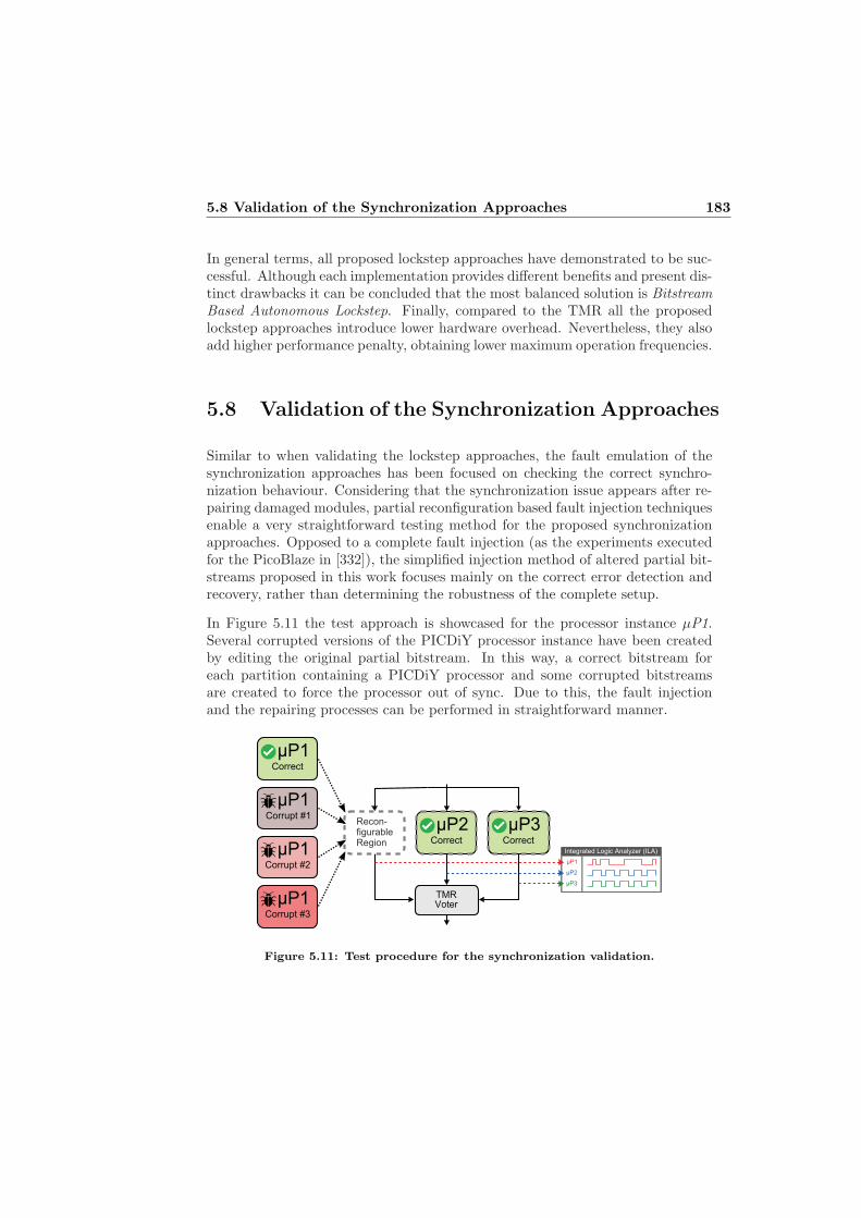
5.8 Validation of the Synchronization Approaches 183
In general terms, all proposed lockstep approaches have demonstrated to be suc-cessful. Although each implementation provides different benefits and present dis-tinct drawbacks it can be concluded that the most balanced solution is BitstreamBased Autonomous Lockstep. Finally, compared to the TMR all the proposedlockstep approaches introduce lower hardware overhead. Nevertheless, they alsoadd higher performance penalty, obtaining lower maximum operation frequencies.
5.8 Validation of the Synchronization Approaches
Similar to when validating the lockstep approaches, the fault emulation of thesynchronization approaches has been focused on checking the correct synchro-nization behaviour. Considering that the synchronization issue appears after re-pairing damaged modules, partial reconfiguration based fault injection techniquesenable a very straightforward testing method for the proposed synchronizationapproaches. Opposed to a complete fault injection (as the experiments executedfor the PicoBlaze in [332]), the simplified injection method of altered partial bit-streams proposed in this work focuses mainly on the correct error detection andrecovery, rather than determining the robustness of the complete setup.
In Figure 5.11 the test approach is showcased for the processor instance µP1.Several corrupted versions of the PICDiY processor instance have been createdby editing the original partial bitstream. In this way, a correct bitstream foreach partition containing a PICDiY processor and some corrupted bitstreamsare created to force the processor out of sync. Due to this, the fault injectionand the repairing processes can be performed in straightforward manner.
���������
����� �������������
������
���������
���
���
���
���
������
���������
���������
���������
������������������� !���"���#
���
���
���
Figure 5.11: Test procedure for the synchronization validation.
184 Validation of Fault Tolerance Approaches
A synchronization test is executed as follows:
1. Configure the entire device.
2. Emulate a failure by loading a corrupt partial bitstream.
3. Repair the failure by loading the correct partial bitstream.
4. Trigger synchronization routine.
5. Check correct synchronization using ILA.
The use of ILA permits to validate the synchronization process on the actualFPGA by monitoring the external processor signals, such as the instruction ad-dress for observation of the program counter and also internal signals like thestack pointer for validation of Interrupt Sync and Hw Sync approaches. In orderto circumvent possible issues with the trigger settings when using ILA for bothpartial reconfiguration and logic analysis, the synchronization has been triggeredmanually instead of invoking this step automatically after a partial reconfigura-tion. Due to the time required by the BBBA technique, in the case of BitstreamSync the utilization of ILA has required a special treatment. Consequently, eachtest has consisted in two captures, one triggered with the synchronization and theother after applying the BBBA approach. This is because monitoring the entireprocess would require a huge resource usage (especially BRAMs) to implementthe ILA in the FPGA.
All five proposed synchronization methods have been implemented on the Zed-Board to validate their correct operation. Fault injection tests have been exe-cuted as defined previously. After repairing faulty modules the synchronizationhas been triggered. Functional behaviours have been validated by observing thesynchronization processes of the different approaches with the ILA.
Results of the different synchronization approaches are unveiled in Table 5.9,where the values of the different implementations are summarized as absolutevalues and in relation to Reset Sync (in brackets). As it can be observed in thefirst five rows that contain a resource utilization summary, the Hw Sync approachintroduces the biggest hardware overhead. Besides, while Force Sync and Inter-rupt Sync approaches increase the resource utilization moderately, both, ResetSync and Bitstream Sync approaches, do not affect the hardware overhead. Sim-ilar conclusions can be obtained from Table 5.10, which includes the utilizationof primitives. Considering the proposed approaches, the increase in resource re-quirements is significant, especially if a high degree of hardware synchronizationis supported. When implementing a processor as small as the PICDiY, addingmodules such as the synchronization memory or the Sync Control block has astronger relative weight as compared to bigger processors. Regarding power con-
5.8 Validation of the Synchronization Approaches 185
sumption, Bitstream Sync presents the worst results due to the use of the Pro-cessing System. The power consumption results of the rest of implementationsare closely related with the resource overhead: higher resource utilization comeswith higher power consumption. Furthermore, although the are not big differ-ences in the possible operation frequency for all designs (90 MHz), the BitstreamSync approach presents the lowest value (80 MHz).
Another relevant information included in Table 5.9 is the synchronization timedemanded for each approach implementation. As it can be observed, despite itslimitations, the Reset Sync approach synchronizes the system instantaneously.On the contrary, the Bitstream Sync is the most time consuming method. Thisis because of the time needed to read, process and write the bitstream. The syn-chronization times for the rest of approaches depends on the number of registersand memory positions to be synchronized. It has to be remarked that the re-sults of these approaches are closely dependant of the system clocking frequency.Besides, for these tests the worst case scenario has been considered, synchroniz-ing all the registers and the entire data memory. In this way, the Force Syncneeds 0.036 ms (112 clock cycles for the 7 special registers and 2048 clock cyclesfor 128 positions of the data memory) to synchronize the design. Similarly, theInterrupt Sync needs 0.0363 ms. This slight difference resides in the need of 16clock cycles to synchronize the stack. Finally, Hw Sync significantly improves thesynchronization time to 0.0045 ms (272 clk cycles).
Based on the trade-off between the three factors of the synchronization ap-proaches (the FPGA resource overhead, the synchronization speed and the el-ements which support synchronization) different applications might benefit fromdifferent synchronization techniques. A simple algorithm, like the Advanced En-cryption Standard (AES), does not require a very elaborate synchronization. Ifthe key does not need to be stored, a cyclic reset (Reset Sync) might be a suffi-cient solution. If only a small amount of data needs to be kept on the processor(for example in cyclic sensor readouts) Force Sync is a suitable option. The lastreadouts can be kept in the scratchpad memory and the rest of the system canbe forced to a sync whenever this is required. Both, Interrupt Sync and Hw Syncapproaches, represent almost no restrictions to the device software and only mi-nor considerations need to be taken into account for the development of the ISR.Bitstream Sync is able to synchronize all memory elements of a design withoutany software restrictions. However, its time demand makes it suitable only forapplications with loose time constraints.

186 Validation of Fault Tolerance Approaches
Table
5.9:Im
plem
enta
tion
resu
ltssu
mm
ary
ofth
esy
nchronizatio
napproaches(@
60M
Hz).
Reso
urce
Reset
Force
Interru
pt
HW
Bitstre
am
Slice
LUTs
675(100%
)684
(101%)
760(113%
)1008
(149%)
679
(100%)
Slice
Registers
187(100%
)205
(110%)
239(128%
)437
(234%)
187
(100%)
F7Muxes
3(100%
)3
(100%)
36(1200%
)57
(1900%)
3(100%
)F8Muxes
6(-%
)21
(-%)
Block
RAM
Tile
3(100%
)3
(100%)
3(100%
)3
(100%
)3
(100%)
fm
ax(M
Hz)
90(100%
)90
(100%)
90(100%
)90
(100%
)80
(89%
)Sync.
time(m
s)-
0.0360.0363
0.004512.9
Dynamic
p.(W
)0.139
(100%)
0.139(100%
)0.140
(101%)
0.147(106%
)1.66
8(1200000%
)Static
p.(W
)0.125
(100%)
0.125(100%
)0.125
(100%)
0.125(100%
)0.161
(129%)

5.8 Validation of the Synchronization Approaches 187
Table
5.10:Prim
itiveutilization
ofth
esy
nchronization
approaches(@
60M
Hz).
Reso
urce
Reset
Force
Interrupt
HW
Bitstre
am
FDRE
181
(100
%)
199
(110
%)
233
(129
%)
430
(238
%)
181
(100
%)
FDSE
6(100
%)
6(100
%)
6(100
%)
7(117
%)
6(100
%)
CARRY4
24(100
%)
24(100
%)
24(100
%)
27(113
%)
24(100
%)
LUT1
3(100
%)
3(100
%)
9(300
%)
56(186
7%)
3(100
%)
LUT2
90(100
%)
90(100
%)
78(87%
)85
(94%
)90
(100
%)
LUT3
47(100
%)
48(102
%)
94(200
%)
270
(574
%)
47(100
%)
LUT4
55(100
%)
64(116
%)
45(82%
)60
(109
%)
55(100
%)
LUT5
108
(100
%)
109
(101
%)
148
(137
%)
188
(174
%)
109
(101
%)
LUT6
403
(100
%)
402
(100
%)
392
(97%
)42
3(105
%)
405
(100
%)
MUXF7
3(100
%)
3(100
%)
36(120
0%)
57(190
0%)
3(100
%)
MUXF8
6(-%)
21RAMB18
E1
6(100
%)
6(100
%)
6(100
%)
6(100
%)
6(100
%)
RAMD32
72(-%)
72(-%)
RAMS32
21(100
%)
21(100
%)
24(114
%)
24(100
%)
21(-%)
CAPTUREE2
1(-%)
STARTUPE2
1(-%)
PS7
1(-%)
PLLE2ADV
1(100
%)
1(100
%)
1(100
%)
1(100
%)
1(-%)

188 Validation of Fault Tolerance Approaches

Chapter 6
Conclusions and future work
6.1 Conclusions
In this work, a basis for fault tolerance of SRAM-based FPGA implementations,especially focusing on soft-core processor designs, has been presented. In orderto provide a context, the technology of SRAM FPGAs has been introduced em-phasizing certain aspects of 7 series Xilinx devices. In direct relation with faulttolerance of SRAM FPGAs, the issue of radiation induced faults (mostly singleevents upsets) has been also discussed, studying their adverse effects.
The spotlight of the state of the art pivots around hardening techniques for SRAMbased designs, focusing on soft-core processors. Considering that induced faultscan affect both user data and configuration memories, different strategies havebeen studied in this field. Most of existing hardening techniques are based onproviding different redundancy types, such as, hardware, data, software or time.Existing hardening techniques improve reliability levels but they also come withdrawbacks, such as, resource overhead, performance penalty, appearance of singlepoints of failure or availability. It has to be remarked that resource overhead alsoyields lower maximum frequencies (longer data paths), higher power consump-tion (more active elements), worst fault tolerance (more susceptible elements) andless resources available for implementation purposes. Among the studied redun-dancy types the prevalent one is the hardware redundancy due to the reliabilityand availability levels that it provides. The most extended redundancy levelsare the Triple Modular Redundancy (TMR) and the Dual Modular Redundancy(DMR). While DMR techniques provide less resource usage, TMR approaches
190 Conclusions and future work
present higher reliability and availability levels. When applying DMR strategiesto soft-core processors they are commonly implemented combining checkpointingand rollback techniques. That introduces either hardware overhead and perfor-mance penalty to designs. On the other hand, one of the most recurrent issueswhen utilizing TMR schemes to harden soft-core processor designs is the synchro-nization after repairing modules with reconfiguration. Due to this, in this workthe need for synchronization techniques has been underlined when using hardwareredundancy techniques and partial reconfiguration for building reliable systems.Furthermore, bearing in mind that TMR strategies only mask errors and do notfix them, the accumulation of masked errors is a recurrent potential problem. Themost utilized technique to address this issue is to perform bitstream scrubbings.This technique consists in reloading correct partial bitstreams in order to correctmasked configuration errors. The state of the art have highlighted an importantgap in user data content scrubbing.
Additionally, another area of interest in the state of the art has been addressedin order to investigate the possibility of managing user data content through thebitstream. This possibility has been considered because its potential to provideuseful features to existing hardening techniques. Distinct approaches related tothis topic have been published. Nevertheless, the state of the art has highlighteda scarcity of methods addressing the features of newer FPGA devices like 7 seriesby Xilinx.
Based on the knowledge acquired in the state of the art, distinct approacheshaven been developed. Five different synchronization approaches for TMR (orhigher) and partial reconfiguration protected soft-core processor designs havebeen proposed so as to cover a wide spectrum of synchronization complexitylevels. In a similar way three different lockstep approaches have been developedto provide distinct solutions able to fit to specific DMR scenarios.
On the other hand, two approached to manage user data content through thebitstream have been proposed. While one is suitable to manage the content ofBRAM based memories, the other targets managing content of registers. Bothapproaches represent a new way to manage user data without introducing hard-ware overhead in designs, opening new application paths. In addition, thanks tothe use of dynamic partial reconfiguration these new data management strategiescan be performed in runtime. For this reason, despite its higher time demand,proposed techniques does not degrade the system overall performance in a num-ber of applications. Thanks to bitstream based data management it is feasible tomodify entire programs or single instructions without making any new synthesisor implementation. Both techniques have been applied to distinct fault toler-ance schemes proposing new approaches, such as, user data content scrubbing
6.2 Main Contributions 191
and data extraction from memories with damaged interfaces. These bitstreambased techniques have been also utilized in two of the three proposed locksted ap-proaches. In a similar way, the bitstream based user data management has beenutilized in one of the five proposed approaches to synchronize repaired soft-coreprocessors in hardware redundancy schemes.
All proposed approaches have been validated in both simulations and in actualFPGA implementation, by executing different kinds of applications. The selectedhardware platform has been a Zynq SoC based board. In addition, the PICDiY,a specifically designed 8-bit modular soft-core processor, has been developed forthis work. The PICDiY has been utilized as a target unit in both designing andvalidation processes of proposed soft-core processor hardening approaches. Thecorrect operation of all suggested methods has been proven and the advantagesand disadvantages have been thoroughly discussed. Different application scenar-ios have been suggested depending on the implementation and features of theproposed approaches.
6.2 Main Contributions
This section lists the main contributions of this thesis, providing a brief descrip-tion of each point and including a reference to the corresponding section of themanuscript where the topic is discussed in detail.
1. Soft-core processor. The PICDiY, an 8-bit soft-core processor has beendeveloped in this work. Its minimalist design and complete self-sufficiencyprovide interesting characteristics to be used in several scenarios withoutsignificantly impacting the design’s resource usage. In addition its modu-larity makes it a great candidate for adaptations, enabling it to fit closelyto specific designs. Thanks to its platform-independence it can be imple-mented in devices from any vendor. In addition, free Basic based toolshave been developed to generate the program memory HDL modules of thesoft-core processor. The architecture of PICDiY is introduced in Section4.1.
2. BRAM content management through bitstream. The proposed ap-proach is able to read and write the data content from BRAMs in FPGAbased designs by reading and processing the information stored in the bit-stream. Thanks to this method it is possible to extract, load, copy orcompare the information of BRAMs without neither resource overhead norperformance penalty in the design. It can also be applied to existing designswithout the need of re-synthesizing. These advantages makes it an interest-

192 Conclusions and future work
ing tool to carry out several existing applications improving relevant aspectsand it also opens the doors to the design of cutting-edge applications. Forthis reason it has been utilized in several of the proposed approaches. De-spite this approach has been developed focusing on Zynq, it is possible tomigrate several of this ideas to other Xilinx devices. Section 4.2 describesthe approach in depth.
3. Registers data management through bitstream. This method en-ables to manage data content of registers utilizing the bitstream. Thanksto the proposed method the content of registers can be captured or writtenwithout significantly affecting the resource usage nor design’s performance.A relevant benefit of this technique is that in several scenarios can be uti-lized autonomously, with no need of any processing module. This approachincludes two design flows to carry out this data management. While thefirst proposed flow allows to protect/unprotect partial regions, the secondpermits to generate equal implementations of a design in different reconfig-urable regions. Developed for 7 series devices by Xilinx, several conceptsproposed in this approach can be adapted to other Xilinx devices. Detailsof this method are presented in Section 4.3.
4. Data content scrubbing. This technique permits to performs data con-tent scrubbings in BRAM based memories. Bearing in mind that memoryhardening techniques mainly mask errors and they do no fix them, it is aninteresting alternative to correct masked errors in memories. Related withsoft-core processors it is especially interesting to repair program memorymodules. Section 4.4 provides the relevant aspects of this approach.
5. Extract data from damaged memories. Induced faults can affect mem-ory interfaces impeding to obtain the stored information. Despite that theprobability of such scenario is not especially high, this situation can becritical when the stored data is sensitive information. Section 4.5 presentsthe proposed method to recover data from damaged BRAM memories.
6. Lockstep approaches for soft-core processors. Three approaches areproposed providing different solutions for the common issues of checkpointand rollback techniques when hardening soft-core processors in lockstepschemes. Each approach focuses on improving specific features, such as, re-duced hardware overhead, minimum checkpoint frequency and fast rollback.Features of each proposed approaches are detailed in Section 4.6.
7. Synchronization of hardware redundancy protected soft-core pro-cessors. Five approaches are proposed to deal with the synchronizationproblem that arises after partially reconfiguring a faulty soft-copre proces-

6.3 Scientific Publications in the Context of this Work 193
sor module. Each approach provides different solutions in terms of resourceusage, self-sufficiency, synchronization and availability. These techniquesare valuable tools that could help designers when trade-off decisions haveto be made. Section 4.7 discusses the main characteristics of proposedtechniques.
6.3 Scientific Publications in the Context of thisWork
In this Section all scientific publications published during the development processof this work are presented. The publication are divided into journal publicationsand conference publications.
Journal publications
J1) I. Villalta, U. Bidarte, J. Gomez-Cornejo, J. Jimenez and J. Lazaro.“SEU Emulation in Industrial SoCs Combining Microprocessor and FPGA”,Reliability Engineering & System Safety, vol. 170, pages 53 - 63, 2018. Im-pact Factor (JCR): 3.153. Ranking: Q1.
J2) I. Villalta, U. Bidarte, J. Gomez-Cornejo, J. Jimenez and A. Astarloa.“Estimating the SEU Failure Rate of Designs Implemented in FPGAs inPresence of MCUs”, Microelectronics Reliability, vol. 78, pages 85 - 92,2017. Impact Factor (JCR): 1.371. Ranking: Q3.
J3) J. Gomez-Cornejo, A. Zuloaga, I. Villalta, J. Del Ser, U. Kretzschmarand J. Lazaro. “A Novel BRAM Content Accessing and Processing Methodbased on FPGA Configuration Bitstream”, Microelectronic Engineering,vol. 49, pages 64 - 67, 2017. Impact Factor (JCR): 1.025. Ranking: Q3.
J4) U. Kretzschmar, J. Gomez-Cornejo, A. Astarloa, U. Bidarte and J. DelSer. “Synchronization of Faulty Processors in Coarse-Grained TMR Pro-tected Partially Reconfigurable FPGA Designs”, Reliability Engineering &System Safety, vol. 151, pages 1 - 9, 2016. Impact Factor (JCR): 3.153.Ranking: Q1.
Conference publications
C1) I. Villalta, U. Bidarte, J. Gomez-Cornejo, A. Zuloaga, and C. Cuadrado,“Emulation of Multiple Cell Upsets in FPGAs”, Conference on Design of

194 Conclusions and future work
Circuits and Integrated Systems (DCIS), Barcelona (Spain), 2017.
C2) I. Villalta, U. Bidarte, J. Gomez-Cornejo, J. Jimenez and C. Cuadrado,“Effect of Different Design Stages on the SEU Failure Rate of FPGA Sys-tems”, Conference on Design of Circuits and Integrated Systems (DCIS),Granada (Spain), 2016.
C3) I. Villalta, U. Bidarte, J. Gomez-Cornejo, J. Lazaro and C. Cuadrado,“Dependability in FPGAs, a Review”, Conference on Design of Circuits andIntegrated Systems (DCIS), Estoril (Portugal), 2015.
C4) U. Kretzschmar, J. Gomez-Cornejo, N. Moreira, U. Bidarte and A. As-tarloa. “A versatile FPGA Demonstration Platform for academic Use”,Tecnologıas, Aprendizaje y Ensenanza de la Ensenanza de la Electronica(TAEE), 2014.
C5) J. Gomez-Cornejo, A. Zuloaga, U. Kretzschmar, U. Bidarte, J. Jimenez.“Study of Implementation Alternatives for a Lockstep Approach in FPGASoft Core Processors”, Conference on Design of Circuits and IntegratedSystems (DCIS), Donostia (Spain), 2013.
C6) J. Gomez-Cornejo, A. Zuloaga, U. Kretzschmar, U. Bidarte, A. Astar-loa. “Fast Context Reloading Lockstep Approach for SEUs Mitigation in aFPGA Soft Core Processor”, Conference of the IEEE Industrial ElectronicsSociety (IECON), Vienna (Austria), 2013.
C7) J. Gomez-Cornejo, A. Zuloaga, U. Kretzschmar, U. Bidarte, A. Astar-loa. “Interface Tasks Oriented 8-bit Soft-Core Processor”. FPGAworld,Tampere (Finland), 2012.
C8) J. Gomez-Cornejo, A. Zuloaga, U. Kretzschmar, U. Bidarte, A. Astarloa.“Implementacion en FPGA de un Procesador Soft-Core PIC16”. SeminarioAnual de Automatica, Electronica Industrial e Instrumentacion (SAAEI),Guimaraes (Portugal), 2012.
6.4 Future work
This Section proposes some lines of research in order to give continuity to thework presented in this thesis. These lines are the following:
• Further analysis of proposed fault tolerance approaches. The ex-perimental work presented in this manuscript has been focused on validat-ing proposed approaches in terms of functionality. In particular, the aim

6.4 Future work 195
of validation tests carried out for synchronization and lockstep have beenfocused on determining correct error detection and recovery behaviours,rather than to evaluate the robustness level of designs. An interestingfurther step could be applying complete fault injection emulation tests inorder to obtain more accurate results in terms of fault tolerance. Similarly,applying physical fault injection campaigns could provide additional valu-able information. Another interesting alternative is to apply the proposedhardening approaches to additional soft-core processors. The case of morecomplex processors, such as, LEON3 [334] or Mico32 [333] is an interestingoption to obtain complementary information, especially in terms of impactin the resource overhead.
• Improve time specifications of the bitstream based approaches.The most remarkable drawback of the approaches based on manipulatingbitstream is their time demand. The main reason for this time consumptionresides in the bitstream reading, manipulation and transferring processes.The programs utilized for these approaches are based in Xilinx functionsthat can be optimized to obtain a faster responses. Hence, an interest-ing path is to optimize the programs used in the proposed approaches bycustomizing Xilinx functions. For instance, the bitstream reading is doneframe by frame, and consequently is it affects the overall processing timeof the proposed method. Therefore, the optimization of the functions toread more than one frame at once (i.e. bulk read) could make the tech-nique faster. Another, aspect that limits the speed of the approaches is thelimited speed of the configuration port. Thus, an interesting research linecould be to investigate new ways to enhance the reconfiguration speed. Aremarkable example in this direction is the ZyCAP [114]. It is reported thatthe ZyCAP achieves a reconfiguration throughput of 382 MB/s, improvingover PCAP by almost 3x.
• Adapt the bitstream based approaches to different technologies.Proposed approaches have been closely developed for Xilinx 7 series device.An interesting research line can be to adapt these approaches to other fam-ilies from Xilinx and even to other vendors’ devices, such as, Intel (Altera),Microsemi, etc.
• Expand the application scope of bitstream based approaches. Be-sides fault tolerance related scenarios, the bitstream based approaches pro-posed in this paper pave the way for other avant garde applications. Forinstance, it may serve as a novel method to store data under privacy re-quirements. Since by using proposed approaches based on the bitstream,memories can be managed without using any port, the existence of such
196 Conclusions and future work
memory resources can be hidden in the design, implementing them as iso-lated memory blocks that can be accessed with no buses. Another exampleof a possible application is the management with multiprocessor systemsshared memory. In order to guarantee the memory coherence and min-imize the performance overhead, different protocols have been proposed[335, 336]. Proposed bitstream based approaches could represent an in-teresting alternative to avoid the use of these complex protocols, busesand interconnections. This could simplify designs by enabling new waysof exchanging data between processors. It even makes it possible for oneprocessor of the system to change or adjust the functionality of another byonly changing a number of instructions of its program memory.
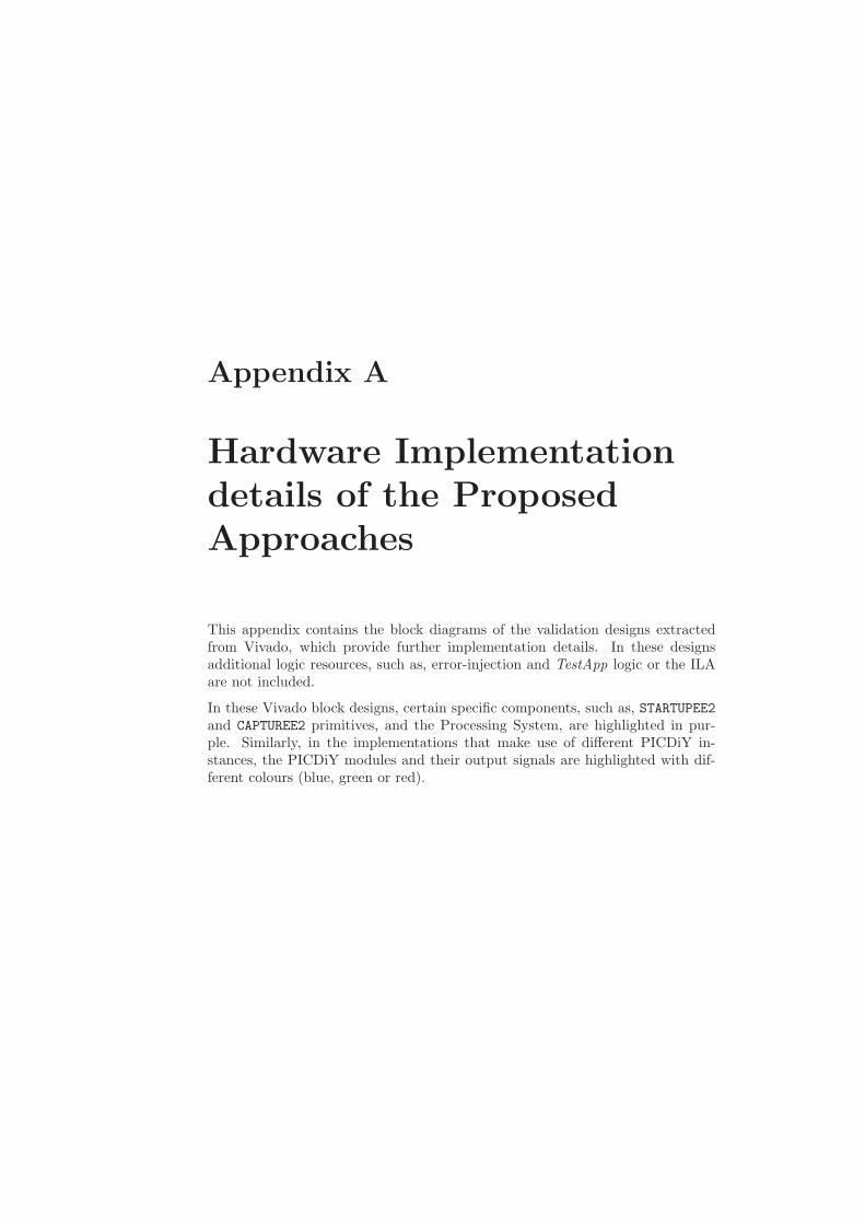
Appendix A
Hardware Implementationdetails of the ProposedApproaches
This appendix contains the block diagrams of the validation designs extractedfrom Vivado, which provide further implementation details. In these designsadditional logic resources, such as, error-injection and TestApp logic or the ILAare not included.
In these Vivado block designs, certain specific components, such as, STARTUPEE2and CAPTUREE2 primitives, and the Processing System, are highlighted in pur-ple. Similarly, in the implementations that make use of different PICDiY in-stances, the PICDiY modules and their output signals are highlighted with dif-ferent colours (blue, green or red).
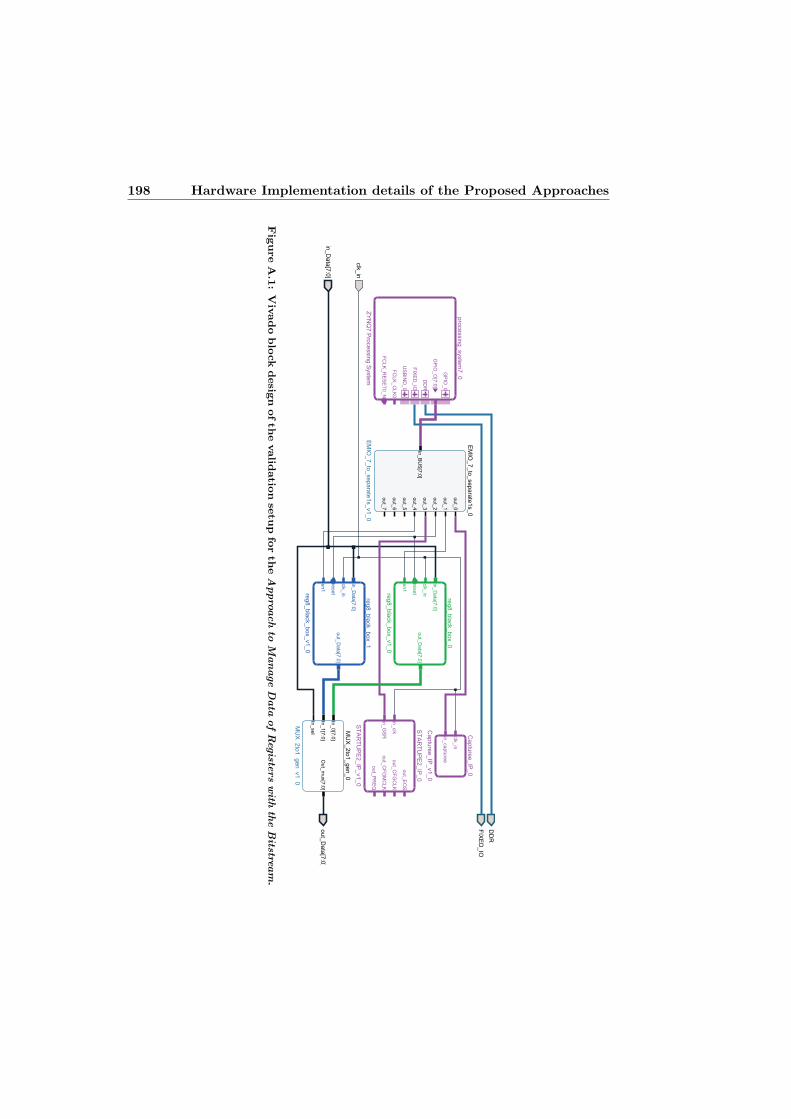
198 Hardware Implementation details of the Proposed Approaches
out_
Data
[7:0
]
MU
X_
2to
1_
gen_
0
MU
X2to
1gen
v1
0
In_
0[7
:0]
In_
1[7
:0]
In_
sel
Out_
mux[7
:0]
in_
Data
[7:0
]
reg8_
bla
ck_
box_
1
reg8_
bla
ck_
box_
v1_
0
in_
Data
[7:0
]
clk
_in
reset
en1
out_
Data
[7:0
]
clk
_in
ST
AR
TU
PE
2_
IP_
0
ST
AR
TU
PE
2_
IP_
v1_
0
in_
clk
in_
GS
R
out_
EO
S
out_
CF
GC
LK
out_
CF
GM
CLK
out_
PR
EQ
pro
cessin
g_
syste
m7_
0
ZY
NQ
7 P
rocessin
g S
yste
m
GP
IO_
0
GP
IO_
O[7
:0]
DD
R
FIX
ED
_IO
US
BIN
D_
0
FC
LK
_C
LK
0
FC
LK
_R
ES
ET
0_
N
reg8_
bla
ck_
box_
0
reg8_
bla
ck_
box_
v1_
0
in_
Data
[7:0
]
clk
_in
reset
en1
out_
Data
[7:0
]
EM
IO_
7_
to_
separa
te1s_
0
EM
IO_
7_
to_
separa
te1s_
v1_
0
in_
BU
S[7
:0]
out_
0
out_
1
out_
2
out_
3
out_
4
out_
5
out_
6
out_
7
Captu
ree_
IP_
0
Captu
ree_
IP_
v1_
0
clk
_in
in_
captu
ree
FIX
ED
_IO
DD
R
FigureA.1:Vivadoblockdesig
nofth
evalid
atio
nse
tupforth
eApproachto
ManageData
ofRegisterswith
theBits
tream.
199
In_
sel
in_
read
in_
fill
Bla
ckB
ox_
RA
M_
0
Bla
ckB
ox_
RA
M_
v1_
0
clk
en
we
adr[
7:0
]
data
_in
[7:0
]
data
_out[7:0
]in
_em
pty
BR
AM
_F
ILLE
R_
FF
_0
BR
AM
_F
ILLE
R_
FF
_v1_
1
in_
clk
in_
rst
in_
em
pty
in_
fill
in_
read
out_
data
[7:0
]
out_
addr[
7:0
]
out_
wena
out_
fill_
done
out_
em
pt_
done
Out_
mux[7
:0]
MU
X_
2to
1_
gen_
0
MU
X_
2to
1_
gen_
v1_
0
In_
0[7
:0]
In_
1[7
:0]
In_
sel
Out_
mux[7
:0]
enB
enA
DD
R
FIX
ED
_IO
pro
cessin
g_
syste
m7_
0
ZY
NQ
7 P
rocessin
g S
yste
m
GP
IO_
0
DD
R
FIX
ED
_IO
US
BIN
D_
0
FC
LK
_C
LK
0
FC
LK
_R
ES
ET
0_
N
RA
M_
PIC
DiY
_0
RA
M_
PIC
DiY
_v1_
1
clk
en
we
adr[
7:0
]
data
_in
[7:0
]
data
_out[7:0
]
Figure
A.2:
Vivado
block
design
ofth
evalidation
setu
pforth
eApproach
toExtractData
Fro
mDamaged
Memories
Usin
gtheBBBA.

200 Hardware Implementation details of the Proposed Approaches
RAM_ECC_Gen_0
RAM_ECC_Gen_v1_0
in_data[7:0]
out_data[12:0]
Input_register_3
Input_register_v1_1
in_port[0:0]
in_clk
out_port[0:0]
interrupt[0:0]
Lockstep_controller_1
Lockstep_controller_v1_0
in_STATE1
in_STATE2
in_ERR_BckUp
in_ERR_ROM
in_ERR_RAM
in_PORT_B1[7:0]
in_PORT_B2[7:0]
out_PORT_B[7:0]
out_en_BckUp
out_error
ROM_ECC_Check_0
ROM_ECC_Check_v1_0
in_data[19:0]
error_out
out_direct[6:0]
out_k[7:0]
out_IDC[13:0]
out_goto[10:0]
error_out
ROM_MIX_BOX_0
ROM_MIX_BOX_v1_0
in_ROM_a1[7:0]
in_ROM_a2[7:0]
in_ROM_en1
in_ROM_en2
out_ROM_a[7:0]
out_ROM_en
out_error_to_ROM
PIC_DIY_0
PIC_DIY_v1_0
PORTA[7:0]
INTERRUPT
in_CLK
in_RST
PORTB[7:0]
FSR_in[7:0]
WR_in[7:0]
SR_in[7:0]
INTCON_in[7:0]
PCLATH_in[2:0]
PORTB_in[7:0]
PC_in[11:0]
FSR_out[7:0]
WR_out[7:0]
SR_out[7:0]
INTCON_out[7:0]
PCLATH_out[2:0]
PORTB_out[7:0]
PC_out[11:0]
comp_error
stack_ECC_error
out_stateD
out_ROM_en
out_ROM_a[7:0]
in_ROM_out_direct[6:0]
in_ROM_out_k[7:0]
in_ROM_out_IDC[13:0]
in_ROM_out_goto[10:0]
out_RAM_we
out_RAM_adr[7:0]
out_RAM_data_in[7:0]
in_RAM_data_out[7:0]
stack_ECC_error
Input_register_0
Input_register_v1_1
in_port[0:0]
in_clk
out_port[0:0]
in_RST
RAM_0
RAM_v1_0
clk
we
adr[7:0]
data_in[12:0]
data_out[12:0]
BackUpRAM_1
BackUpRAM_v1_0
clk
reFSR_in[7:0]
WR_in[7:0]
SR_in[7:0]
INTCON_in[7:0]
PCLATH_in[2:0]
PORTB_in[7:0]
PC_in[11:0]
FSR_out[7:0]
WR_out[7:0]
SR_out[7:0]
INTCON_out[7:0]
PCLATH_out[2:0]
PORTB_out[7:0]
PC_out[11:0]
rom_1
rom_v1_1
in_clk
in_en
in_addr[7:0]
out_data[19:0]
BackUpRAM_MIX_BOX_0
BackUpRAM_MIX_BOX_v1_0
in_FSR1[7:0]
in_WR1[7:0]
in_SR1[7:0]
in_INTCON1[7:0]
in_PCLATH1[2:0]
in_PORTB1[7:0]
in_PC1[11:0]
in_FSR2[7:0]
in_WR2[7:0]
in_SR2[7:0]
in_INTCON2[7:0]
in_PCLATH2[2:0]
in_PORTB2[7:0]
in_PC2[11:0]
out_FSR[7:0]
out_WR[7:0]
out_SR[7:0]
out_INTCON[7:0]
out_PCLATH[2:0]
out_PORTB[7:0]
out_PC[11:0]
error_BckP
Input_register_1
Input_register_v1_1
in_port[7:0]
in_clk
out_port[7:0]
input_port[7:0]
out_port[7:0]
Input_register_2
Input_register_v1_1
in_port[7:0]
in_clk
out_port[7:0]
PIC_DIY_1
PIC_DIY_v1_0
PORTA[7:0]
INTERRUPT
in_CLK
in_RST
PORTB[7:0]
FSR_in[7:0]
WR_in[7:0]
SR_in[7:0]
INTCON_in[7:0]
PCLATH_in[2:0]
PORTB_in[7:0]
PC_in[11:0]
FSR_out[7:0]
WR_out[7:0]
SR_out[7:0]
INTCON_out[7:0]
PCLATH_out[2:0]
PORTB_out[7:0]
PC_out[11:0]
comp_error
stack_ECC_error
out_stateD
out_ROM_en
out_ROM_a[7:0]
in_ROM_out_direct[6:0]
in_ROM_out_k[7:0]
in_ROM_out_IDC[13:0]
in_ROM_out_goto[10:0]
out_RAM_we
out_RAM_adr[7:0]
out_RAM_data_in[7:0]
in_RAM_data_out[7:0]
error_out_1
in_CLK
RAM_ECC_Check_0
RAM_ECC_Check_v1_0
in_data[12:0]
out_data[7:0]
error_out
clk_wiz_0
ClockingWizard
reset
clk_in1
clk_out1
reset
BackUpRAM_0
BackUpRAM_v1_0
clk
reFSR_in[7:0]
WR_in[7:0]
SR_in[7:0]
INTCON_in[7:0]
PCLATH_in[2:0]
PORTB_in[7:0]
PC_in[11:0]
FSR_out[7:0]
WR_out[7:0]
SR_out[7:0]
INTCON_out[7:0]
PCLATH_out[2:0]
PORTB_out[7:0]
PC_out[11:0]
RAM_MIX_BOX_0
RAM_MIX_BOX_v1_0
in_we1
in_we2
in_adr1[7:0]
in_adr2[7:0]
in_data1_in[7:0]
in_data2_in[7:0]
out_we
out_adr[7:0]
out_data[7:0]
out_error
stack_ECC_error_
FigureA.3:Vivado
block
desig
nofth
evalid
atio
nse
tup
forth
eHW
FastLockstep.
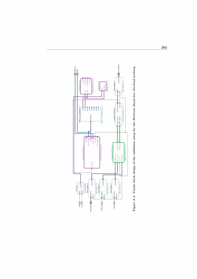
201
FIX
ED
_IO
DD
R
reset
clk
_w
iz_
0
Clo
ckin
g W
izard
reset
clk
_in
1clk
_o
ut1
in_
clk
ST
AR
TU
PE
2_
IP_
0
ST
AR
TU
PE
2_
IP_
v1_
0
in_
clk
in_
GS
R
out_
EO
S
out_
CF
GC
LK
out_
CF
GM
CLK
out_
PR
EQ
EM
IO_
7_
to_
separa
te1s_
0
EM
IO_
7_
to_
separa
te1s_
v1_
0
in_
BU
S[7
:0]
out_
0
out_
1
out_
2
out_
3
out_
4
out_
5
out_
6
out_
7
input_
port
[7:0
]
pro
cessin
g_
syste
m7_
0
ZY
NQ
7 P
rocessin
g S
yste
m
GP
IO_
0
GP
IO_
O[7
:0]
DD
R
FIX
ED
_IO
Core
0_
nF
IQ
FC
LK
_C
LK
0
FC
LK
_R
ES
ET
0_
N
Input_
regis
ter_
0
Input_
regis
ter_
v1_
1
in_
po
rt[7
:0]
in_
clk
ou
t_p
ort
[7:0
]
in_
RS
T_
hig
h
Input_
regis
ter_
3
Input_
regis
ter_
v1_
1
in_
po
rt[0
:0]
in_
clk
ou
t_p
ort
[0:0
]
Captu
ree_
IP_
0
Captu
ree_
IP_
v1_
0
clk
_in
in_
captu
ree
inte
rrupt
Input_
regis
ter_
1
Input_
regis
ter_
v1_
1
in_
po
rt[0
:0]
in_
clk
ou
t_p
ort
[0:0
]
Bla
ckB
ox_
PIC
DiY
x2_
0
Bla
ckB
ox_
PIC
DiY
x2_
v1_
0
INT
ER
RU
PT
_x2
PO
RT
A_
x2[7
:0]
PO
RT
B_
1[7
:0]
PO
RT
B_
2[7
:0]
in_
CLK
_x2
in_
RS
T_
hig
h_
x2
Lockste
p_
contr
olle
r_0
Lockste
p_
contr
olle
r_v1_
0
in_
PO
RT
_B
1[7
:0]
in_
PO
RT
_B
2[7
:0]
out_
PO
RT
_B
[7:0
]
out_
err
or
Input_
regis
ter_
2
Input_
regis
ter_
v1_
1
in_
port
[7:0
]
in_
clk
out_
port
[7:0
]out_
port
[7:0
]
FigureA.4:Vivado
block
design
ofth
evalidation
setu
pforth
eBitstream
Based
Low
Overhead
Lockstep.

202 Hardware Implementation details of the Proposed Approaches
In_Out_Register_Gen_0
InOutRegisterGenv10
In_port[0:0]
In_CLK
Out_port[0:0]
interrupt
In_Out_Register_Gen_3
In_Out_Register_Gen_v1_0
In_port[0:0]
In_CLK
Out_port[0:0]
in_RST_lckstp
out_error[0:0]
In_Out_Register_Gen_2
In_Out_Register_Gen_v1_0
In_port[0:0]
In_CLK
Out_port[0:0]
util_vector_logic_0
Utility
VectorLogic
Op1[0:0]
Op2[0:0]
Res[0:0]
In_Out_Register_Gen_1
In_Out_Register_Gen_v1_0
In_port[0:0]
In_CLK
Out_port[0:0]
in_RST
BlackBox_Lckstep_Auto1PB_0
BlackBox_Lckstep_Auto1PB_v1_0
input_PORTA[7:0]
input_INTERRUPT
input_CLK
input_RST_high
output_error
output_PORTB1[7:0]
output_PORTB2[7:0]
Lockstep_controller_0
Lockstep_controller_v1_0
in_CLK
in_RST_high
in_PORT_B1[7:0]
in_PORT_B2[7:0]
out_PORT_B[7:0]
out_Capture
out_GSR
out_clk_ctrl
out_fatal_error
out_port[7:0]
Capturee_IP_0
Capturee_IP_v1_0
clk_in
in_capturee
clk_wiz_0
ClockingWizard
clk_out2_ce
reset
clk_in1
clk_out1
clk_out2
reset
in_CLK
STARTUPE2_IP_1
STARTUPE2_IP_v1_1
in_clk
in_GSR
input_port[7:0]
In_Out_Register_Gen_4
In_Out_Register_Gen_v1_0
In_port[7:0]
In_CLK
Out_port[7:0]
In_Out_Register_Gen_5
In_Out_Register_Gen_v1_0
In_port[7:0]
In_CLK
Out_port[7:0]
FigureA.5:Vivado
block
desig
nofth
evalid
atio
nse
tup
forth
eBits
tream
Based
AutonomousLockstep.
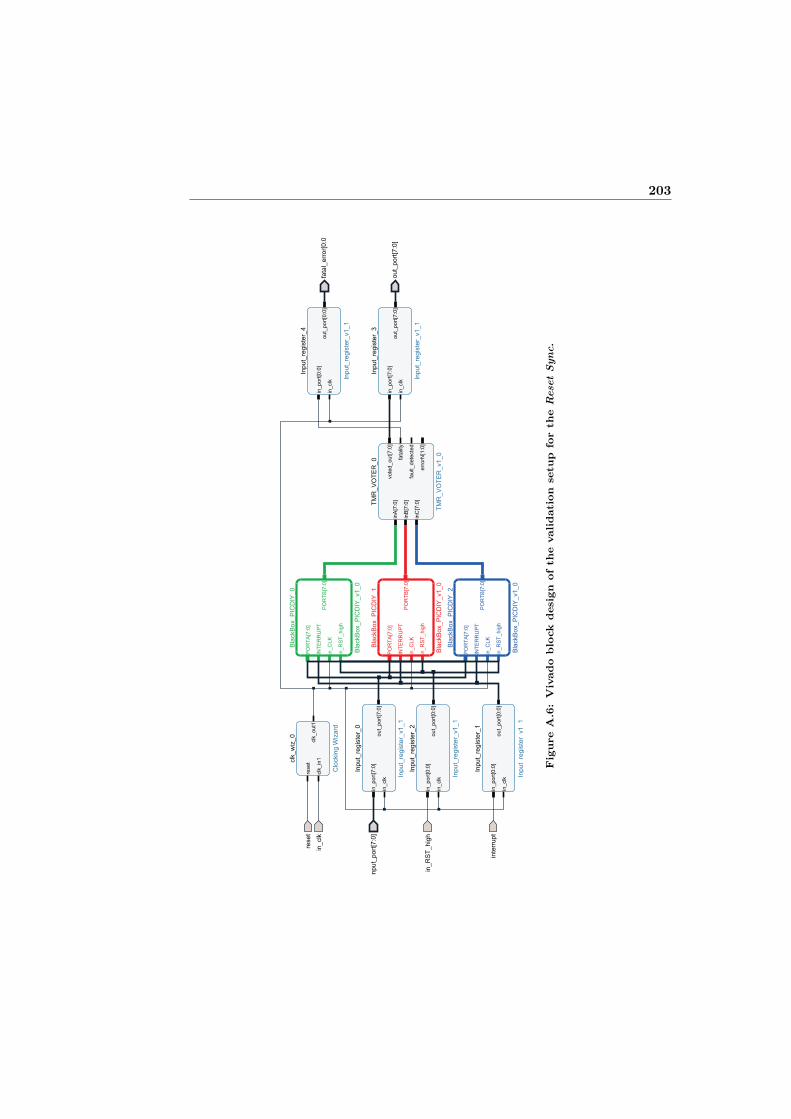
203
reset
clk
_w
iz_
0
Clo
ckin
g W
izard
reset
clk
_in
1clk
_out1
in_
clk
Bla
ckB
ox_
PIC
DIY
_0
Bla
ckB
ox_
PIC
DIY
_v1_
0
PO
RT
A[7
:0]
INT
ER
RU
PT
in_
CLK
in_
RS
T_
hig
h
PO
RT
B[7
:0]
Input_
regis
ter_
4
Input_
regis
ter_
v1_
1
in_
port
[0:0
]
in_
clk
out_
port
[0:0
]fa
tal_
err
or[
0:0
input_
port
[7:0
]
Input_
regis
ter_
0
Input_
regis
ter_
v1_
1
in_
port
[7:0
]
in_
clk
out_
port
[7:0
]In
put_
regis
ter_
3
Input_
regis
ter_
v1_
1
in_
port
[7:0
]
in_
clk
out_
port
[7:0
]out_
port
[7:0
]
Bla
ckB
ox_
PIC
DIY
_1
Bla
ckB
ox_
PIC
DIY
_v1_
0
PO
RT
A[7
:0]
INT
ER
RU
PT
in_
CLK
in_
RS
T_
hig
h
PO
RT
B[7
:0]
TM
R_
VO
TE
R_
0
TM
R_
VO
TE
R_
v1_
0
inA
[7:0
]
inB
[7:0
]
inC
[7:0
]
vote
d_
out[7:0
]
fata
lity
fault_
dete
cte
d
err
orN
[1:0
]in
_R
ST
_hig
h
Input_
regis
ter_
2
Input_
regis
ter_
v1_
1
in_
port
[0:0
]
in_
clk
out_
port
[0:0
]
Bla
ckB
ox_
PIC
DIY
_2
Bla
ckB
ox_
PIC
DIY
_v1_
0
PO
RT
A[7
:0]
INT
ER
RU
PT
in_
CLK
in_
RS
T_
hig
h
PO
RT
B[7
:0]
inte
rrupt
Input_
regis
ter_
1
Input
regis
ter
v1
1
in_
port
[0:0
]
in_
clk
out_
port
[0:0
]
FigureA.6:Vivado
block
design
ofth
evalidation
setu
pforth
eResetSync.
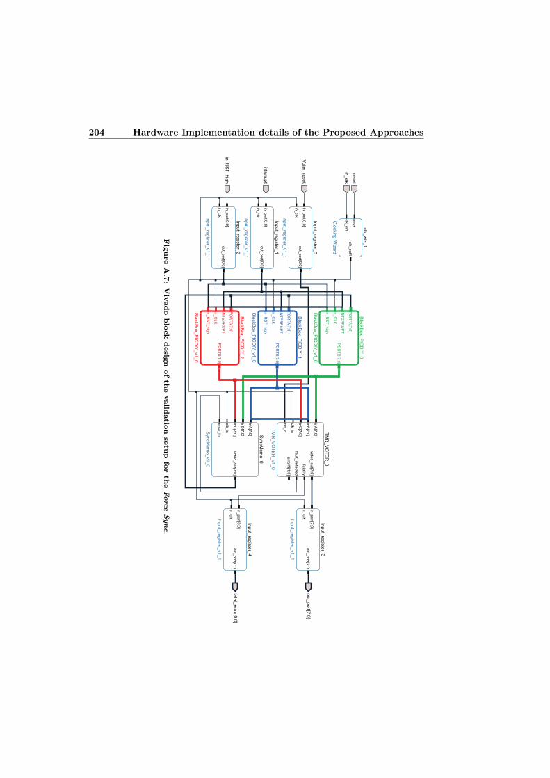
204 Hardware Implementation details of the Proposed Approaches
reset
clk
_w
iz_
1
Clo
ckin
g W
izard
reset
clk
_in
1clk
_out1
in_
clk
Bla
ckB
ox_
PIC
DIY
_0
Bla
ckB
ox_
PIC
DIY
_v1_
0
PO
RT
A[7
:0]
INT
ER
RU
PT
in_
CLK
in_
RS
T_
hig
h
PO
RT
B[7
:0]
Input_
regis
ter_
3
Input_
regis
ter_
v1_
1
in_
port[7
:0]
in_
clk
out_
port[7
:0]
out_
port[7
:0]
Vote
r_re
set
TM
R_
VO
TE
R_
0
TM
R_
VO
TE
R_
v1_
0
inA
[7:0
]
inB
[7:0
]
inC
[7:0
]
clk
_in
rst_
in
vote
d_
out[7
:0]
fata
lity
fault_
dete
cte
d
erro
rN[1
:0]
Input_
regis
ter_
0
Input_
regis
ter_
v1_
1
in_
port[0
:0]
in_
clk
out_
port[0
:0]
Bla
ckB
ox_
PIC
DIY
_1
Bla
ckB
ox_
PIC
DIY
_v1_
0
PO
RT
A[7
:0]
INT
ER
RU
PT
in_
CLK
in_
RS
T_
hig
h
PO
RT
B[7
:0]
inte
rrupt
Input_
regis
ter_
1
Input_
regis
ter_
v1_
1
in_
port[0
:0]
in_
clk
out_
port[0
:0]
SyncM
em
o_
0
SyncM
em
o_
v1_
0
inA
[7:0
]
inB
[7:0
]
inC
[7:0
]
clk
_in
erro
r_in
vote
d_
out[7
:0]
Input_
regis
ter_
4
Input_
regis
ter_
v1_
1
in_
port[0
:0]
in_
clk
out_
port[0
:0]
fata
l_erro
r[0:0
]
in_
RS
T_
hig
h
Input_
regis
ter_
2
Input_
regis
ter_
v1_
1
in_
port[0
:0]
in_
clk
out_
port[0
:0]
Bla
ckB
ox_
PIC
DIY
_2
Bla
ckB
ox_
PIC
DIY
_v1_
0
PO
RT
A[7
:0]
INT
ER
RU
PT
in_
CLK
in_
RS
T_
hig
h
PO
RT
B[7
:0]
FigureA.7:Vivado
block
desig
nofth
evalid
atio
nse
tup
forth
eForceSync.
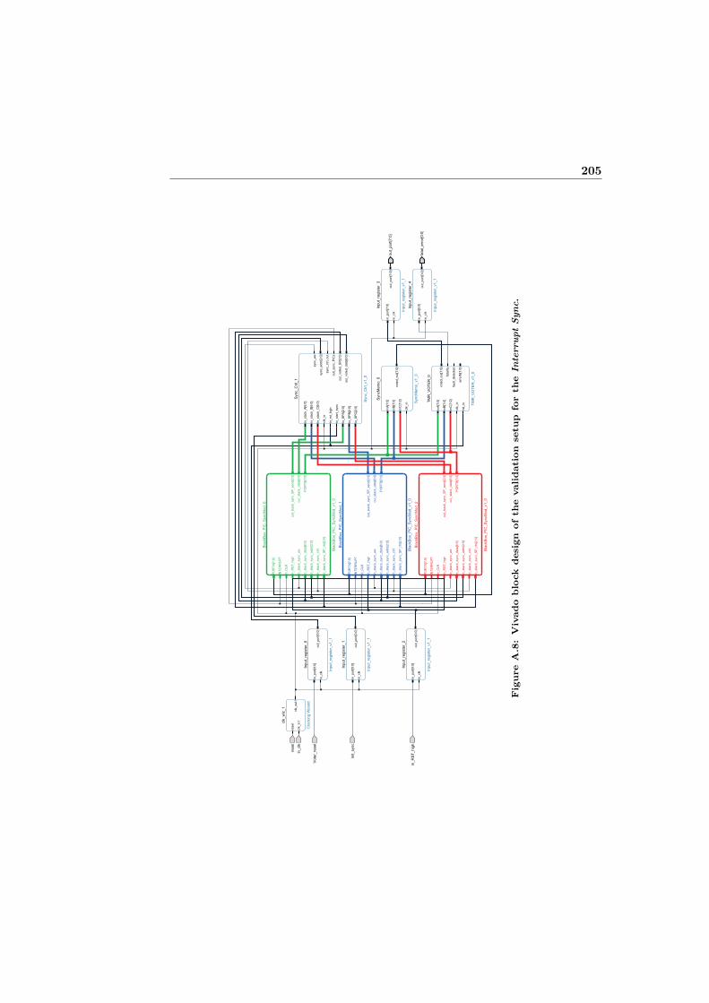
205
TMR_VOTER_0
TMR_VOTER_v1_0
inA[7:0]
inB[7:0]
inC[7:0]
clk_in
rst_in
voted_out[7:0]
fatality
fault_detected
errorN[1:0]
BlackBox_PIC_SyncMod_2
BlackBox_PIC_SyncMod_v1_0
PORTA[7:0]
INTERRUPT
in_CLK
in_RST_high
in_stack_sync_we
in_stack_sync_data[6:0]
in_stack_sync_addr[2:0]
in_stack_sync_ctrl
in_stack_sync_SP_rtn[2:0]
out_stack_sync_SP_send[2:0]
out_stack_data[6:0]
PORTB[7:0]
fatal_error[0:0]
Input_register_4
Input_register_v1_1
in_port[0:0]
in_clk
out_port[0:0]
Input_register_2
Input_register_v1_1
in_port[0:0]
in_clk
out_port[0:0]
in_RST_high
SyncMemo_0
SyncMemo_v1_0
inA[7:0]
inB[7:0]
inC[7:0]
clk_in
voted_out[7:0]
out_port[7:0]
Input_register_3
Input_register_v1_1
in_port[7:0]
in_clk
out_port[7:0]
BlackBox_PIC_SyncMod_1
BlackBox_PIC_SyncMod_v1_0
PORTA[7:0]
INTERRUPT
in_CLK
in_RST_high
in_stack_sync_we
in_stack_sync_data[6:0]
in_stack_sync_addr[2:0]
in_stack_sync_ctrl
in_stack_sync_SP_rtn[2:0]
out_stack_sync_SP_send[2:0]
out_stack_data[6:0]
PORTB[7:0]
Input_register_1
Input_register_v1_1
in_port[0:0]
in_clk
out_port[0:0]
init_sync
Sync_Ctrl_1
Sync_Ctrl_v1_0
in_stack_A[6:0]
in_stack_B[6:0]
in_stack_C[6:0]
clk_in
in_rst_high
in_start_sync
in_SPA[2:0]
in_SPB[2:0]
in_SPC[2:0]
sync_we
sync_addr[2:0]
sync_ctrl_out
out_sync_PICs
out_voted_SP[2:0]
out_voted_data[6:0]
Input_register_0
Input_register_v1_1
in_port[0:0]
in_clk
out_port[0:0]
Voter_reset
in_clk
BlackBox_PIC_SyncMod_0
BlackBox_PIC_SyncMod_v1_0
PORTA[7:0]
INTERRUPT
in_CLK
in_RST_high
in_stack_sync_we
in_stack_sync_data[6:0]
in_stack_sync_addr[2:0]
in_stack_sync_ctrl
in_stack_sync_SP_rtn[2:0]
out_stack_sync_SP_send[2:0]
out_stack_data[6:0]
PORTB[7:0]
clk_wiz_1
ClockingWizard
reset
clk_in1
clk_out1
reset
FigureA.8:Vivado
block
design
ofth
evalidation
setu
pforth
eInterruptSync.

206 Hardware Implementation details of the Proposed ApproachesBlackBox_PICDiY_HWSync_mod_0
BlackBox_PICDiY_HWSync_mod_v1_0
PORTA[7:0]
INTERRUPT
in_CLK
in_RST_high
in_REGs_en_Sync
in_stack_sync_we
in_stack_sync_data[6:0]
in_stack_sync_addr[2:0]
in_stack_sync_ctrl
in_stack_sync_SP_rtn[2:0]
in_PC_in_Sync[11:0]
out_PC_out_Sync[11:0]
in_Status_in_Sync[7:0]
out_Status_out_Sync[7:0]
in_Wreg_in_Sync[7:0]
out_Wreg_out_Sync[7:0]
in_FSR_in_Sync[7:0]
out_FSR_out_Sync[7:0]
in_PortB_in_Sync[7:0]
out_PortB_out_Sync[7:0]
in_PCLATCH_in_Sync[2:0]
out_PCLATCH_out_Sync[2:0]
in_INTCON_in_Sync[7:0]
out_INTCON_out_Sync[7:0]
in_RAM_sync_ctrl
in_RAM_sync_data_in[7:0]
in_RAM_sync_addr_in[7:0]
in_RAM_sync_we_in
out_RAM_data_out[7:0]
out_stack_sync_SP_send[2:0]
out_stack_data[6:0]
PORTB[7:0]
reset
clk_wiz_1
ClockingWizard
reset
clk_in1
clk_out1
in_clk
Voter_reset
Input_register_0
Input_register_v1_1
in_port[0:0]
in_clk
out_port[0:0]
input_port[7:0]
Input_register_5
Input_register_v1_1
in_port[7:0]
in_clk
out_port[7:0]
BlackBox_PICDiY_HWSync_mod_1
BlackBox_PICDiY_HWSync_mod_v1_0
PORTA[7:0]
INTERRUPT
in_CLK
in_RST_high
in_REGs_en_Sync
in_stack_sync_we
in_stack_sync_data[6:0]
in_stack_sync_addr[2:0]
in_stack_sync_ctrl
in_stack_sync_SP_rtn[2:0]
in_PC_in_Sync[11:0]
out_PC_out_Sync[11:0]
in_Status_in_Sync[7:0]
out_Status_out_Sync[7:0]
in_Wreg_in_Sync[7:0]
out_Wreg_out_Sync[7:0]
in_FSR_in_Sync[7:0]
out_FSR_out_Sync[7:0]
in_PortB_in_Sync[7:0]
out_PortB_out_Sync[7:0]
in_PCLATCH_in_Sync[2:0]
out_PCLATCH_out_Sync[2:0]
in_INTCON_in_Sync[7:0]
out_INTCON_out_Sync[7:0]
in_RAM_sync_ctrl
in_RAM_sync_data_in[7:0]
in_RAM_sync_addr_in[7:0]
in_RAM_sync_we_in
out_RAM_data_out[7:0]
out_stack_sync_SP_send[2:0]
out_stack_data[6:0]
PORTB[7:0]
Sync_Ctrl_0
Sync_Ctrl_v1_0
in_stack_A[6:0]
in_stack_B[6:0]
in_stack_C[6:0]
clk_in
in_rst_high
in_START_sync
in_SPA[2:0]
in_SPB[2:0]
in_SPC[2:0]
out_SP_sync_we
SP_sync_addr[2:0]
SP_sync_ctrl_out
out_voted_SP[2:0]
out_voted_stack_data[6:0]
out_Sync_FINISHED
in_REGs_en_Sync
rtn_A_PC_in_Sync[11:0]
rtn_A_Status_in_Sync[7:0]
rtn_A_Wreg_in_Sync[7:0]
rtn_A_FSR_in_Sync[7:0]
rtn_A_PortB_in_Sync[7:0]
rtn_A_PCLATCH_in_Sync[2:0]
rtn_A_INTCON_in_Sync[7:0]
rtn_B_PC_in_Sync[11:0]
rtn_B_Status_in_Sync[7:0]
rtn_B_Wreg_in_Sync[7:0]
rtn_B_FSR_in_Sync[7:0]
rtn_B_PortB_in_Sync[7:0]
rtn_B_PCLATCH_in_Sync[2:0]
rtn_B_INTCON_in_Sync[7:0]
rtn_C_PC_in_Sync[11:0]
rtn_C_Status_in_Sync[7:0]
rtn_C_Wreg_in_Sync[7:0]
rtn_C_FSR_in_Sync[7:0]
rtn_C_PortB_in_Sync[7:0]
rtn_C_PCLATCH_in_Sync[2:0]
rtn_C_INTCON_in_Sync[7:0]
snd_PC_out_Sync[11:0]
snd_Status_out_Sync[7:0]
snd_Wreg_out_Sync[7:0]
snd_FSR_out_Sync[7:0]
snd_PortB_out_Sync[7:0]
snd_PCLATCH_out_Sync[2:0]
snd_INTCON_out_Sync[7:0]
rtn_RAM_dataA[7:0]
rtn_RAM_dataB[7:0]
rtn_RAM_dataC[7:0]
snd_RAM_sync_ctrl
snd_RAM_sync_data_in[7:0]
snd_RAM_sync_addr_in[7:0]
snd_RAM_sync_we_in
in_RST_high
Input_register_2
Input_register_v1_1
in_port[0:0]
in_clk
out_port[0:0]
init_sync
Input_register_1
Input_register_v1_1
in_port[0:0]
in_clk
out_port[0:0]
BlackBox_PICDiY_HWSync_mod_2
BlackBox_PICDiY_HWSync_mod_v1_0
PORTA[7:0]
INTERRUPT
in_CLK
in_RST_high
in_REGs_en_Sync
in_stack_sync_we
in_stack_sync_data[6:0]
in_stack_sync_addr[2:0]
in_stack_sync_ctrl
in_stack_sync_SP_rtn[2:0]
in_PC_in_Sync[11:0]
out_PC_out_Sync[11:0]
in_Status_in_Sync[7:0]
out_Status_out_Sync[7:0]
in_Wreg_in_Sync[7:0]
out_Wreg_out_Sync[7:0]
in_FSR_in_Sync[7:0]
out_FSR_out_Sync[7:0]
in_PortB_in_Sync[7:0]
out_PortB_out_Sync[7:0]
in_PCLATCH_in_Sync[2:0]
out_PCLATCH_out_Sync[2:0]
in_INTCON_in_Sync[7:0]
out_INTCON_out_Sync[7:0]
in_RAM_sync_ctrl
in_RAM_sync_data_in[7:0]
in_RAM_sync_addr_in[7:0]
in_RAM_sync_we_in
out_RAM_data_out[7:0]
out_stack_sync_SP_send[2:0]
out_stack_data[6:0]
PORTB[7:0]
Input_register_3
Input_register_v1_1
in_port[7:0]
in_clk
out_port[7:0]
out_port[7:0]
TMR_VOTER_0
TMR_VOTER_v1_0
inA[7:0]
inB[7:0]
inC[7:0]
clk_in
rst_in
voted_out[7:0]
fatality
fault_detected
errorN[1:0]
Input_register_4
Input_register_v1_1
in_port[0:0]
in_clk
out_port[0:0]
fatal_error[0:0
FigureA.9:Vivado
block
desig
nofth
evalid
atio
nse
tup
forth
eHw
Sync.

207
Capturee_IP_0
STARTUPE2_IP_0
Input_register_5
Inputregisterv11
in_port[0:0]
in_clk
out_port[0:0]
interrupt[0:0]
BlackBox_PICDIY_2
PORTA[7:0]
INTERRUPT
in_CLK
in_RST_high
PORTB[7:0]
fatal_error[0:0
Input_register_1
Input_register_v1_1
in_port[0:0]
in_clk
out_port[0:0]
Input_register_4
Input_register_v1_1
in_port[7:0]
in_clk
out_port[7:0]
input_port[7:0]
TMR_VOTER_1
TMR_VOTER_v1_0
inA[7:0]
inB[7:0]
inC[7:0]
voted_out[7:0]
fatality
fault_detected
errorN[1:0]
BlackBox_PICDIY_1
PORTA[7:0]
INTERRUPT
in_CLK
in_RST_high
PORTB[7:0]
out_port[7:0]
Input_register_0
Input_register_v1_1
in_port[7:0]
in_clk
out_port[7:0]
Input_register_3
Input_register_v1_1
in_port[0:0]
in_clk
out_port[0:0]
in_RST_high[0:0]
BlackBox_PICDIY_0
PORTA[7:0]
INTERRUPT
in_CLK
in_RST_high
PORTB[7:0]
DDR
FIXED_IO
reset
clk_wiz_0
ClockingWizard
reset
clk_in1
clk_out1
in_clk
EMIO_7_to_separate1s_0
EMIO_7_to_separate1s_v1_0
in_BUS[7:0]
out_0
out_1
out_2
out_3
out_4
out_5
out_6
out_7
processing_system7_0
ZYNQ7ProcessingSystem
GPIO_0
GPIO_I[7:0]
GPIO_O[7:0]
DDR
FIXED_IO
USBIND_0
Core0_nFIQ
FCLK_CLK0
FCLK_RESET0_N
STARTUPE2_IP_v1_0
in_clk
in_GSR
out_EOS
out_CFGCLK
out_CFGMCLK
out_PREQ
Capturee_IP_v1_0
clk_in
in_capturee
FigureA.10:Vivado
block
design
ofth
evalidation
setu
pforth
eBitstream
Sync.


Bibliography
[1] Xilinx Corp., “7 series FPGAs configurable logic block UG474 (v1.8),”Xilinx Documentation, http://www.xilinx.com, 2016.
[2] Xilinx Corp., “7 series FPGAs memory resources UG473 (v1.12),” XilinxDocumentation, http://www.xilinx.com, 2016.
[3] Xilinx Corp., “Vivado design suite 7 series FPGA and Zynq-7000 all pro-grammable SoC libraries guide UG953 (v2014.4),” Xilinx Documentation,http://www.xilinx.com, 2014.
[4] Xilinx Corp., “7 series FPGAs configuration UG470 (v1.9),” Xilinx Docu-mentation, http://www.xilinx.com, 2014.
[5] Xilinx Corp., “Integrated logic analyzer PG172 (v6.2),” Xilinx Documen-tation, http://www.xilinx.com, 2016.
[6] Xilinx Corp., “Zynq-7000 all programmable SoC technical reference manualUG585 (v1.9.1),” Xilinx Documentation, http://www.xilinx.com, 2014.
[7] H. Kalte and M. Porrmann, “Context saving and restoring for multitask-ing in reconfigurable systems,” in International Conference on Field Pro-grammable Logic and Applications. IEEE, 2005, pp. 223 – 228.
[8] A. Morales-Villanueva and A. Gordon-Ross, “HTR: On-chip hardware taskrelocation for partially reconfigurable FPGAs,” in Reconfigurable Comput-ing: Architectures, Tools and Applications. Springer Berlin Heidelberg,2013, vol. 7806, pp. 185 – 196.
[9] A. Kanamaru, H. Kawai, Y. Yamaguchi, and M. Yasunaga, “Tile-basedfault tolerant approach using partial reconfiguration,” in InternationalWorkshop on Applied Reconfigurable Computing. Springer, 2009, pp. 293– 299.

210 BIBLIOGRAPHY
[10] R. Yao, J. Wu, M. Wang, X. Zhong, P. Zhu, and J. Liang, “State synchro-nization technique based on present input and healthy state for repairableTMR systems,” IEICE Electronics Express, pp. 20 161 000 – 20 161 000,2016.
[11] J. Azambuja, M. Altieri, J. Becker, and F. Kastensmidt, “Heta: Hybriderror-detection technique using assertions,” IEEE Transactions on NuclearScience, pp. 2805 – 2812, 2013.
[12] B. Tietche, O. Romain, B. Denby, and F. Dieuleveult, “FPGA-based simul-taneous multichannel FM broadcast receiver for audio indexing applicationsin consumer electronics scenarios,” IEEE Transactions on Consumer Elec-tronics, pp. 1153 – 1161, 2012.
[13] C. Ttofis, C. Kyrkou, and T. Theocharides, “A low-cost real-time embed-ded stereo vision system for accurate disparity estimation based on guidedimage filtering,” IEEE Transactions on Computers, pp. 2678 – 2693, 2016.
[14] M. Komorkiewicz, K. Turek, P. Skruch, T. Kryjak, and M. Gorgon,“FPGA-based Hardware-in-the-Loop environment using video injectionconcept for camera-based systems in automotive applications,” in Designand Architectures for Signal and Image Processing (DASIP), 2016, pp. 183– 190.
[15] A. Melzer, F. Starzer, H. Jager, and M. Huemer, “Real-time mitigationof short-range leakage in automotive FMCW radar transceivers,” IEEETransactions on Circuits and Systems II: Express Briefs, pp. 1 – 5, 2016.
[16] M. Schirmer, F. Stradolini, S. Carrara, and E. Chicca, “Fpga-based ap-proach for automatic peak detection in cyclic voltammetry,” in Interna-tional Conference on Electronics, Circuits and Systems (ICECS), 2016, pp.65 – 68.
[17] E. Min, Y. Jung, H. Lee, J. Jang, K. Kim, S. Joo, and K. Lee, “Develop-ment of a multipurpose gamma-ray imaging detector module with enhancedexpandability,” IEEE Transactions on Nuclear Science, pp. 1 – 7, 2017.
[18] W. Pawgasame, “Evaluation of digital codings on the soc-based software-defined radio for the military communication,” in Asian Conference onDefence Technology (ACDT), 2017, pp. 81 – 87.
[19] H. Irwanto, “Development of instrumentation, control and navigation(ICON) for anti tank guided missile (ATGM),” in International Confer-ence on Science in Information Technology (ICSITech), 2016, pp. 137 –141.
BIBLIOGRAPHY 211
[20] A. Schmidt and T. Flatley, “Radiation hardening by software techniqueson FPGAs: Flight experiment evaluation and results,” in IEEE AerospaceConference, 2017.
[21] V. Dumitriu, L. Kirischian, and V. Kirischian, “Run-time recovery mech-anism for transient and permanent hardware faults based on distributed,self-organized dynamic partially reconfigurable systems,” IEEE Transac-tions on Computers, pp. 2835 – 2847, 2016.
[22] C. Stoif, M. Schoeberl, B. Liccardi, and J. Haase, “Hardware synchroniza-tion for embedded multi-core processors,” in IEEE International Sympo-sium on Circuits and Systems (ISCAS), 2011, pp. 2557 – 2560.
[23] B. H. Fletcher, “FPGA embedded processors: Revealing true system per-formance,” in Embedded Systems Conference, 2005.
[24] A. Ben Salem, S. Ben Othman, and S. Ben Saoud, “Hard and soft-coreimplementation of embedded control application using RTOS,” in IEEEInternational Symposium on Industrial Electronics (ISIE), 2008, pp. 1896– 1901.
[25] J. Tong, I. Anderson, and M. Khalid, “Soft-core processors for embeddedsystems,” in International Conference on Microelectronics (ICM), 2006, pp.170 – 173.
[26] F. Merchant, S. Pujari, and M. Manish Patil, “Platform independent 8-bit soft-core for SoPC,” in International MultiConference of Engineers andComputer Scientists, 2009, pp. 1541 – 1544.
[27] E. Stott, P. Sedcole, and P. Cheung, “Fault tolerant methods for reliabilityin FPGAs,” in International Conference on Field Programmable Logic andApplications (FPL), 2008, pp. 415 – 420.
[28] Y. Z. Xu, H. Puchner, A. Chatila, O. Pohland, B. Bruggeman, B. Jin,D. Radaelli, and S. Daniel, “Process impact on SRAM alpha-particle SEUperformance,” in IEEE International Reliability Physics Symposium, 2004,pp. 294 – 299.
[29] Xilinx Corp., “Device reliability report, fourth quarter 2010,” Xilinx Doc-umentation, UG116, http://www.xilinx.com, feb. 2011.
[30] Xilinx Corp., “Xilinx-5 FPGA Configuration User Guide,” Xilinx Docu-mentation, UG191, http://www.xilinx.com, aug. 2010.
[31] Xilinx Corp., “Virtex-5 Family Overview,” Xilinx Documentation, DS100,http://www.xilinx.com, feb. 2009.
212 BIBLIOGRAPHY
[32] M. Schutti, M. Pfaff, and R. Hagelauer, “VHDL design of embedded pro-cessor cores: The industry-standard microcontroller 8051 and 68HC11,” inAnnual IEEE International ASIC Conference 1998, 1998, pp. 265 – 269.
[33] E. Ayeh, K. Agbedanu, Y. Morita, O. Adamo, and P. Guturu, “FPGAimplementation of an 8-bit simple processor,” in IEEE Region 5 Conference,2008, pp. 1 – 5.
[34] S. de Pablo, J. Cebrian, L. C. Herrero, and A. B. Rey, “A soft fixed-point digital signal processor applied in power electronics,” in FPGAworldConference, Stockholm. Electrum-Kista, 2005.
[35] A. Le Masle, W. Luk, and C. Moritz, “Parametrized hardware architec-tures for the lucas primality test,” in International Conference on EmbeddedComputer Systems (SAMOS), 2011, pp. 124 – 131.
[36] A. Gour, A. Raj, R. Behera, N. Murali, and S. Murty, “Design and de-velopment of soft-core processor based remote terminal units for nuclearreactors,” in International Conference on Field-Programmable Technology(FPT), 2011, pp. 1 – 4.
[37] L. Anghel, R. Velazco, S. Saleh, S. Deswaertes, and A. El Moucary, “Pre-liminary validation of an approach dealing with processor obsolescence,”in IEEE International Symposium on Defect and Fault Tolerance in VLSISystems, 2003, pp. 493 – 500.
[38] K. Chapman, “Creating embedded microcontrollers (programmable statemachines),” in The Authoritative Journal For Programmable Logic Users,2004.
[39] Z. Hajduk, “An FPGA embedded microcontroller,” Microprocessors andMicrosystems, vol. 38, no. 1, pp. 1 – 8, 2014.
[40] OpenCores, “Official website,” http://www.OpenCores.org, 2012.
[41] Wikipedia, “GNU lesser general public license,”http://en.wikipedia.org/wiki/LGPL, 2012.
[42] Wikipedia, “BSD licenses,” http://en.wikipedia.org/wiki/BSD licenses,2012.
[43] M. Palmer, “A comparison of 8-bit microcontrollers,” in Microchip Tech-nology Inc., 2002.
[44] D. Mattsson and M. Christensson, “Evaluation of synthesizable CPUcores,” Master’s thesis, Chalmers University Of Technology, 2004.

BIBLIOGRAPHY 213
[45] D. Gomez-Prado and M. Ciesielski, “Embedded microcontrollers andFPGAs soft-cores,” Electronica UNMSM, 2006.
[46] P. Borisonv and V. Stoianova, “Implementation of soft-core processors inFPGAs,” in Unitech International Scientific Conference, 2007.
[47] D. Gallegos, B. Welch, J. Jarosz, V. Houten, and M. Learn, “Soft-core pro-cessor study for node-based architectures,” Sandia National Laboratories,Tech. Rep., 2008.
[48] J. Nade and R. Sarwadnya, “The soft core processors: A review,” Inter-national Journal of Innovative Research in Electrical, Electronics, Instru-mentation and Control Engineering, pp. 197 – 203, 2015.
[49] F. Schmidt, “Fault tolerant design implementation on radiation hardenedby design SRAM-based FPGAs,” Ph.D. dissertation, Massachusetts Insti-tute of Technology, 2013.
[50] S. Tanoue, T. Ishida, Y. Ichinomiya, M. Amagasaki, M. Kuga, andT. Sueyoshi, “A novel states recovery technique for the TMR softcore pro-cessor,” in International Conference on Field Programmable Logic and Ap-plications (FPL), 2009, pp. 543 – 546.
[51] D. Sheldon, R. Kumar, R. Lysecky, F. Vahid, and D. Tullsen, “Application-specific customization of parameterized FPGA soft-core processors,” inIEEE/ACM International Conference on Computer-Aided Design (IC-CAD), 2006, pp. 261 – 268.
[52] A. Sari, M. Psarakis, and D. Gizopoulos, “Combining checkpointing andscrubbing in FPGA-based real-time systems,” in IEEE VLSI Test Sympo-sium (VTS), 2013, pp. 1 – 6.
[53] S. Rezgui, G. Swift, K. Somervill, J. George, C. Carmichael, and G. Allen,“Complex upset mitigation applied to a re-configurable embedded proces-sor,” IEEE Transactions on Nuclear Science, pp. 2468 – 2474, 2005.
[54] C. Hong, K. Benkrid, X. Iturbe, and A. Ebrahim, “Design and implemen-tation of fault-tolerant soft processors on FPGAs,” in International Con-ference on Field Programmable Logic and Applications (FPL), 2012, pp.683 – 686.
[55] M. Learn, “Evaluation of soft-core processors on a Xilinx Virtex-5 fieldprogrammable gate array,” Sandia National Laboratories, Tech. Rep., 2011.
[56] M. Hubner, D. Gohringer, J. Noguera, and J. Becker, “Fast dynamic andpartial reconfiguration data path with low hardware overhead on Xilinx

214 BIBLIOGRAPHY
FPGAs,” in IEEE International Symposium on Parallel Distributed Pro-cessing, Workshops and Phd Forum (IPDPSW), 2010, pp. 1 – 8.
[57] J. Heiner, B. Sellers, M. Wirthlin, and J. Kalb, “FPGA partial reconfigu-ration via configuration scrubbing,” in International Conference on FieldProgrammable Logic and Applications (FPL), 2009, pp. 99 – 104.
[58] S. M. Borawake and P. G. Chilveri, “Implementation of wireless sensornetwork using microblaze and picoblaze processors,” in International Con-ference on Communication Systems and Network Technologies, 2014, pp.1059 – 1064.
[59] Y. Ichinomiya, S. Tanoue, M. Amagasaki, M. Iida, M. Kuga, andT. Sueyoshi, “Improving the robustness of a softcore processor against SEUsby using TMR and partial reconfiguration,” in IEEE Annual InternationalSymposium on Field-Programmable Custom Computing Machines (FCCM),2010, pp. 47 – 54.
[60] H. Pham, S. Pillement, and S. Piestrak, “Low overhead fault-tolerancetechnique for dynamically reconfigurable softcore processor,” IEEE Trans-actions on Computers, pp. 1179 – 1192, 2013.
[61] A. Morales-Villanueva and A. Gordon-Ross, “On-chip context save andrestore of hardware tasks on partially reconfigurable FPGAs,” in Inter-national Symposium on Field-Programmable Custom Computing Machines(FCCM), 2013, pp. 61 – 64.
[62] F. Veljkovic, J. Mora, T. Riesgo, L. Berrojo, R. Regada, A. Sanchez,and E. De la Torre, “Prospection of reconfiguration capabilities usingspace qualified SRAM-based FPGAs for a satellite communications ap-plication,” in AIAA International Communications Satellite Systems Con-ference, 2013.
[63] A. Ebrahim, K. Benkrid, X. Iturbe, and C. Hong, “A novel high-performance fault-tolerant ICAP controller,” in NASA/ESA Conferenceon Adaptive Hardware and Systems (AHS), 2012, pp. 259 – 263.
[64] D. Antonio-Torres, D. Villanueva-Perez, E. Sanchez-Canepa, N. Segura-Meraz, D. Garcia-Garcia, D. Conchouso-Gonzalez, J. Miranda-Vergara,J. Gonzalez-Herrera, A.-M. de Ita, B. Hernandez-Rodriguez, R.-E. de losMonteros, F. Garcia-Chavez, V. Tellez-Rojas, and A. Bautista-Hernandez,“A picoblaze-based embedded system for monitoring applications,” in In-ternational Conference on Electrical, Communications, and Computers(CONIELECOMP), 2009, pp. 173 – 177.

BIBLIOGRAPHY 215
[65] F. Restrepo-Calle, A. Martinez-alvarez, H. Guzman-Miranday, F. Palomoy,and S. Cuenca-Asensi, “Application-driven co-design of fault-tolerant in-dustrial systems,” in IEEE International Symposium on Industrial Elec-tronics (ISIE), 2010, pp. 2005 – 2010.
[66] I. Safarulla and K. Manilal, “Design of soft error tolerance technique forFPGA based soft core processors,” in International Conference on Ad-vanced Communication Control and Computing Technologies (ICACCCT),2014, pp. 1036 – 1040.
[67] C. Lung, S. Sabou, and A. Buchman, “Emergency radio communicationnetwork controller implemented in FPGA,” in IEEE International Sympo-sium for Design and Technology in Electronic Packaging (SIITME), 2014,pp. 193 – 196.
[68] J. Mathew and R. Dhayabarani, “Fault tolerance technique for dynamicallyreconfigurable processor,” International Journal of Advanced Research inElectrical, Electronics and Instrumentation Engineering, pp. 6656 – 6663.
[69] C. Lung, S. Sabou, and A. Buchman, “Modelling and implementation ofintelligent sensor networks with applications in emergency situations man-agement,” in IEEE International Symposium for Design and Technology inElectronic Packaging (SIITME), 2015, pp. 315 – 318.
[70] J. Tarrillo, J. Tonfat, L. Tambara, F. L. Kastensmidt, and R. Reis, “Multi-ple fault injection platform for SRAM-based FPGA based on ground-levelradiation experiments,” in Latin-American Test Symposium (LATS), 2015,pp. 1 – 6.
[71] J. Adair, “Pushing picoblaze - part1,” Xilinx.com - PicoBlaze User Re-sources, 2005.
[72] M. Niknahad, O. Sander, and J. Becker, “QFDR-an integration of quaddedlogic for modern FPGAs to tolerate high radiation effect rates,” in Euro-pean Conference on Radiation and Its Effects on Components and Systems(RADECS), 2011, pp. 119 – 122.
[73] U. Legat, A. Biasizzo, and F. Novak, “SEU recovery mechanism for SRAM-based FPGAs,” IEEE Transactions on Nuclear Science, vol. 59, no. 5, pp.2562 – 2571, 2012.
[74] K. Chapman, “SEU strategies for Virtex-5,” in Application Note: Virtex-5Family, 2009.
[75] B. F. Dutton and C. E. Stroud, “Single event upset detection and correction

216 BIBLIOGRAPHY
in Virtex-4 and virtex-5 FPGAs,” in ISCA International Conference onComputers and Their Applications, 2009, pp. 57 – 62.
[76] L. Claudiu, S. Sebastian, and B. Cristian, “Smart sensor implemented withpicoblaze multi-processors technology,” in IEEE International Symposiumfor Design and Technology in Electronic Packaging (SIITME), 2012, pp.241 – 245.
[77] F. Plavec, B. Fort, Z. Vranesic, and S. Brown, “Experiences with soft-core processor design,” in International Parallel and Distributed ProcessingSymposium, 2005, pp. 4 – pp.
[78] J. Gaisler, “A portable and fault-tolerant microprocessor based on theSPARC v8 architecture,” in International Conference on Dependable Sys-tems and Networks (DSN), 2002, pp. 409 – 415.
[79] A. Jordan, C. Hafer, J. Mabra, S. Griffith, J. Nagy, M. Lahey, and D. Har-ris, “SEU data and fault tolerance analysis of a Leon 3FT processor,” inEuropean Conference on Radiation and Its Effects on Components and Sys-tems (RADECS), 2009, pp. 617 – 619.
[80] M. Reorda, M. Violante, C. Meinhardt, and R. Reis, “A low-cost SEE mit-igation solution for soft-processors embedded in systems on pogrammablechips,” in Design, Automation Test in Europe Conference Exhibition, 2009,pp. 352 – 357.
[81] M. Amin, A. Ramazani, F. Monteiro, C. Diou, and A. Dandache, “A self-checking hardware journal for a fault-tolerant processor architecture,” Int.J. Reconfig. Comput., pp. 11 – 11, 2011.
[82] J. Becker, A. Thomas, M. Vorbach, and V. Baumgarten, “An indus-trial/academic configurable system-on-chip project (CSoC): Coarse-grainXXP-/Leon-based architecture integration.” IEEE Computer Society,2003, pp. 1120 – 1121.
[83] M. Reorda, M. Violante, C. Meinhardt, and R. Reis, “An on-board data-handling computer for deep-space exploration built using commercial-off-the-shelf SRAM-based FPGAs,” in IEEE International Symposium on De-fect and Fault Tolerance in VLSI Systems, 2009, pp. 254 – 262.
[84] M. Learn, “Evaluation of the Leon3 soft-core processor within a Xilinxradiation-hardened field-programmable gate array,” Sandia National Lab-oratories, Tech. Rep., 2012.
[85] R. Velazco, W. Mansour, F. Pancher, G. Marques-Costa, D. Sohier, andA. Bui, “Improving SEU fault tolerance capabilities of a self-converging
BIBLIOGRAPHY 217
algorithm,” in European Conference on Radiation and its Effects on Com-ponents and Systems (RADECS), 2011, pp. 138 – 143.
[86] A. Morillo, A. Astarloa, J. Lazaro, U. Bidarte, and J. Jimenez, “Known-blocking. Synchronization method for reliable processor using TMR & DPRin SRAM FPGAs,” in Southern Conference on Programmable Logic (SPL),2011, pp. 57 – 62.
[87] M. Ebrahimi, S. Miremadi, H. Asadi, and M. Fazeli, “Low-cost scan-chain-based technique to recover multiple errors in TMR systems,” IEEE Trans-actions on Very Large Scale Integration (VLSI) Systems, vol. 21, no. 8, pp.1454 – 1468, 2013.
[88] L. Sterpone and A. Ullah, “On the optimal reconfiguration times for TMRcircuits on SRAM based FPGAs,” in NASA/ESA Conference on AdaptiveHardware and Systems (AHS), 2013, pp. 9 – 14.
[89] N. H. Rollins and M. J. Wirthlin, “Reliability of a softcore processor in acommercial SRAM-based FPGA,” in ACM/SIGDA International Sympo-sium on Field Programmable Gate Arrays. ACM, 2012, pp. 171 – 174.
[90] A. Ioannis and M. Dimitrios, “Replacing the SPARC-based core of theLeon3 HDL microprocessor model with a MIPS-based core,” in SECE Con-ference, 2010.
[91] R. Velazco, G. Foucard, F. Pancher, W. Mansour, G. Marques-Costa, D. So-hier, and A. Bui, “Robustness with respect to SEUs of a self-convergingalgorithm,” in Latin American Test Workshop (LATW), 2011, pp. 1 – 5.
[92] J. Becker and A. Thomas, “Scalable processor instruction set extension,”IEEE Design Test of Computers, 2005.
[93] A. Mohammadi, M. Ebrahimi, A. Ejlali, and S. Miremadi, “SCFIT: AFPGA-Basedased Fault Injection Technique for SEU Fault Model,” in De-sign Automation Test in Europe Conference Exhibition (DATE), 2012, pp.586 – 589.
[94] N. H. Rollins and M. J. Wirthlin, “Software fault-tolerant techniques forsoftcore processors in commercial SRAM-based FPGAs,” ARCS Work-shops, 2011.
[95] A. Sari and M. Psarakis, “Scrubbing-based SEU mitigation approach forsystems-on-programmable-chips,” in International Conference on Field-Programmable Technology (FPT), 2011, pp. 1 – 8.
218 BIBLIOGRAPHY
[96] W. Mansour and R. Velazco, “Seu fault-injection in VHDL-based proces-sors: A case study,” Journal of Electronic Testing, pp. 87 – 94, 2013.
[97] P. Huerta Pellitero, “Sistemas de multiprocesamiento simetrico sobreFPGA,” Ph.D. dissertation, Universidad Rey Juan Carlos, 2009.
[98] S. Morioka, “VHDL implementation of the PIC16F84 in FPGA,” in Tran-sistor Gijutsu Magazine, 1999.
[99] S. Yuan, C. P., and S. Liao, “The power stability of FPGA-based micro-controller design and measurement,” in Asia-Pacific Symposium on Elec-tromagnetic Compatibility (APEMC), 2010, pp. 1096 – 1099.
[100] T. Lobo, S. Pinto, V. Silva, S. Lopes, J. Cabral, A. Tavares, S. Yoowattana,W. Sritriratanarak, and M. Ekpanyapong, “LP805X: A customizable andlow power 8051 soft core for FPGA applications,” in IEEE InternationalSymposium on Industrial Electronics (ISIE), 2013, pp. 1 – 7.
[101] G. Fernandez, Conceptos Basicos de Arquitectura y Sistemas Operativos.Ed. Syserso., 1998.
[102] P. Leong, P. Tsang, and T. Lee, “A FPGA based forth microprocessor,” inIEEE Symposium on FPGAs for Custom Computing Machines, 1998, pp.254 – 255.
[103] H. Y. Cheah, S. Fahmy, and D. Maskell, “iDEA: A DSP block based FPGAsoft processor,” in International Conference on Field-Programmable Tech-nology (FPT), 2012, pp. 151 – 158.
[104] P. Gaillardon, M. Ben-Jamaa, G. Beneventi, F. Clermidy, and L. Perniola,“Emerging memory technologies for reconfigurable routing in FPGA archi-tecture,” in IEEE International Conference on Electronics, Circuits, andSystems (ICECS), 2010, pp. 62 – 65.
[105] K. Huang, Y. Ha, R. Zhao, A. Kumar, and Y. Lian, “A low active leakageand high reliability phase change memory (PCM) based non-volatile FPGAstorage element,” IEEE Transactions on Circuits and Systems I: RegularPapers, pp. 2605 – 2613, 2014.
[106] M. Klein and S. Kol, “Leveraging power leadership at 28 nm with Xilinx 7series FPGAs,” 2013.
[107] J. Gomez-Cornejo, A. Zuloaga, U. Kretzschmar, U. Bidarte, andJ. Jimenez, “Fast context reloading lockstep approach for SEUs mitiga-tion in a FPGA soft core processor,” in Conference of the IEEE IndustrialElectronics Society, IECON, 2013, pp. 2261 – 2266.

BIBLIOGRAPHY 219
[108] Xilinx Corp., “Vivado design suite user guide. partial reconfigurationUG909 (v2015.1),” Xilinx Documentation, http://www.xilinx.com, 2015.
[109] J. Correa and K. Ackermann, “Leveraging partial dynamic reconfigurationon Zynq SoC FPGAs,” in International Symposium on Reconfigurable andCommunication-Centric Systems-on-Chip (ReCoSoC), 2014, pp. 1 – 6.
[110] S. Liu, N. Pittman, and A. Forin, “Energy reduction with run-time partialreconfiguration,” Microsoft, Tech. Rep., 2009.
[111] S. Liu, R. Pittman, A. Form, and J. Gaudiot, “On energy efficiency ofreconfigurable systems with run-time oartial reconfiguration,” in IEEE In-ternational Conference on Application-specific Systems, Architectures andProcessors, 2010, pp. 265 – 272.
[112] I. Yoon, H. Joung, and J. Lee, “Zynq-based reconfigurable system for real-time edge detection of noisy video sequences,” Journal of Sensors, vol. 2016,2016.
[113] M. Al Kadi, P. Rudolph, D. Gohringer, and M. Hubner, “Dynamic andpartial reconfiguration of Zynq 7000 under Linux,” in International Con-ference on Reconfigurable Computing and FPGAs (ReConFig), 2013, pp. 1– 5.
[114] K. Vipin and S. Fahmy, “ZyCAP: Efficient partial reconfiguration manage-ment on the Xilinx Zynq,” Embedded Systems Letters, IEEE, vol. 6, no. 3,pp. 41 – 44, 2014.
[115] A. Megacz, “A library and platform for FPGA bitstream manipulation,”in IEEE Symposium on Field-Programmable Custom Computing Machines(FCCM), 2007, pp. 45 – 54.
[116] F. Benz, A. Seffrin, and S. Huss, “Bil: A tool-chain for bitstream reverse-engineering,” in International Conference on Field Programmable Logic andApplications (FPL), 2012, pp. 735 – 738.
[117] R. Chakraborty, I. Saha, A. Palchaudhuri, and G. Naik, “Hardware trojaninsertion by direct modification of FPGA configuration bitstream,” IEEEDesign Test, vol. 30, no. 2, pp. 45 – 54, 2013.
[118] R. Soni, N. Steiner, and M. French, “Open-source bitstream generation,”in EEE Annual International Symposium on Field-Programmable CustomComputing Machines (FCCM), 2013, pp. 105 – 112.
[119] C. Morford, “BitMaT - bitstream manipulation tool for Xilinx FPGAs,”
220 BIBLIOGRAPHY
Master’s thesis, Faculty of the Virginia Polytechnic Institute and StateUniversity, 2005.
[120] Xilinx Corp., “Partial reconfiguration user guide UG702 (v14.1),” XilinxDocumentation, http://www.xilinx.com, 2012.
[121] Xilinx Corp., “Data2MEM. user guide UG658 (v2012.4),” Xilinx Documen-tation, http://www.xilinx.com, 2012.
[122] D. L. S. Guccione and P. Sundararajan, “JBit: Java based interface forreconfigurable computing,” in Annual Military and Aerospace Applicationsof Programmable Devices and Technologies Conference (MAPLD), 1999,pp. 28 – 30.
[123] M. Koester, H. Kalte, and M. Porrmann, “Relocation and defragmentationfor heterogeneous reconfigurable systems,” in ERSA, 2006, pp. 70 – 76.
[124] A. Morales-Villanueva, R. Kumar, and A. Gordon-Ross, “Configurationprefetching and reuse for preemptive hardware multitasking on partiallyreconfigurable FPGAs,” in Design, Automation & Test in Europe (DATE).IEEE, 2016, pp. 1505 – 1508.
[125] J. Srour and J. McGarrity, “Radiation effects on microelectronics in space,”Proceedings of the IEEE, pp. 1443 – 1469, 1988.
[126] R. Ladbury, “Radiation hardening at the system level,” in IEEE NSRECShort Course, 2007, pp. 1 – 94.
[127] J. Wang, “Radiation effects in FPGAs,” in Workshop on Electronics forLHC Experiments, 2003.
[128] C. Farber, U. Uwer, D. Wiedner, B. Leverington, and R. Ekelhof, “Radia-tion tolerance tests of SRAM-based FPGAs for the potential usage in thereadout electronics for the lhcb experiment,” Journal of Instrumentation,p. C02028, 2014.
[129] S. Clark, K. Avery, and R. Parker, “TID and SEE testing results of alteracyclone field programmable gate array,” in IEEE Radiation Effects DataWorkshop, 2004, pp. 88 – 90.
[130] N. Rezzak, J. J. Wang, D. Dsilva, and N. Jat, “TID and SEE characteri-zation of microsemi’s 4th generation radiation tolerant RTG4 flash-basedFPGA,” in IEEE Radiation Effects Data Workshop (REDW), 2015, pp. 1– 6.
[131] G. Allen, G. Madias, E. Miller, and G. Swift, “Recent single event effects re-

BIBLIOGRAPHY 221
sults in advanced reconfigurable field programmable gate arrays,” in IEEERadiation Effects Data Workshop (REDW), 2011, pp. 1 – 6.
[132] G. R. Allen and G. M. Swift, “Single event effects test results for advancedfield programmable gate arrays,” in IEEE Radiation Effects Data Work-shop, 2006, pp. 115 – 120.
[133] P. Dodd and L. Massengill, “Basic mechanisms and modeling of single-eventupset in digital microelectronics,” IEEE Transactions on Nuclear Science,pp. 583 – 602, 2003.
[134] H. Wei, W. Yueke, X. Kefei, and D. Wei, “SEE vulnerability bit analysismethod for switch matrix of SRAM-based FPGA circuits,” in IEEE In-ternational Conference on Mechatronics and Automation, 2016, pp. 2355 –2359.
[135] J. Nunes, J. Cunha, and M. Zenha-Rela, “On the effects of cumulative SEUsin FPGA-based systems,” in European Dependable Computing Conference(EDCC), 2016, pp. 89 – 96.
[136] C. Du, X.and He, S. Liu, Y. Zhang, Y. Li, and W. Yang, “Measurementof single event effects induced by alpha particles in the Xilinx Zynq-7010System-on-Chip,” Journal of Nuclear Science and Technology, pp. 1 – 6,2016.
[137] J. Fu and C. Zhang, “The fault-tolerant design in space information pro-cessing system based on COTS,” in International Workshop on ComputerScience and Engineering (WCSE), 2009, pp. 568 – 571.
[138] D. Binder, E. C. Smith, and A. B. Holman, “Satellite anomalies from galac-tic cosmic rays,” IEEE Transactions on Nuclear Science, pp. 2675 – 2680,1975.
[139] F. Siegle, T. Vladimirova, J. Ilstad, and O. Emam, “Mitigation of radiationeffects in SRAM-based FPGAs for space applications,” ACM ComputingSurveys (CSUR), 2015.
[140] M. Violante, C. Meinhardt, R. Reis, and M. Reorda, “A low-cost solutionfor deploying processor cores in harsh environments,” IEEE Transactionson Industrial Electronics, pp. 2617 – 2626, 2011.
[141] X. Iturbe, D. Keymeulen, P. Yiu, D. Berisford, R. Carlson, K. Hand, andE. Ozer, “On the use of system-on-chip technology in next-generation in-struments avionics for space exploration,” in IEEE International Confer-ence on Very Large Scale Integration, VLSI-SoC. Springer InternationalPublishing, 2016, pp. 1 – 22.

222 BIBLIOGRAPHY
[142] P. Adell, G. Allen, G. Swift, and S. McClure, “Assessing and mitigatingradiation effects in Xilinx SRAM FPGAs,” in European Conference on Ra-diation and Its Effects on Components and Systems (RADECS), 2008, pp.418 – 24, radiation effect mitigation;Xilinx SRAM;FPGA;.
[143] E. Normand, “Single event upset at ground level,” IEEE Transactions onNuclear Science, pp. 2742 – 2750, 1996.
[144] J. T. Wallmark and S. M. Marcus, “Minimum size and maximum packingdensity of nonredundant semiconductor devices,” Proceedings of the IRE,vol. 50, no. 3, pp. 286 – 298, 1962.
[145] T. May and M. Woods, “Alpha-particle-induced soft errors in dynamicmemories,” IEEE Transactions on Electron Devices, pp. 2 – 9, 1979.
[146] Xilinx Corp., “Ultrascale architecture and product overview,” Xilinx Doc-umentation, http://www.xilinx.com, 2016.
[147] I. Corp., “Stratix 10 device datasheet,” Altera Documentation,http://www.altera.com, 2016.
[148] M. McCormack, “Trade study and application of symbiotic softwareand hardware fault-tolerance on a microcontroller-based avionics system,”Ph.D. dissertation, Massachusetts Institute of Technology, 2011.
[149] T. Phillips, “Cosmic rays hit space age high,” NASA, Tech. Rep., 2009.
[150] D. Matthia, M. Meier, and G. Reitz, “Numerical calculation of the ra-diation exposure from galactic cosmic rays at aviation altitudes with thePANDOCA core model,” Space Weather, vol. 12, no. 3, pp. 161 – 171, 2014.
[151] D. White, “Considerations surrounding single event effects in FPGAs,ASICs, and processors,” Xilinx Corp., Tech. Rep., 2012.
[152] “Introduction to single-event upsets,” Altera Documentation,http://www.altera.com, Altera, Tech. Rep., 2013.
[153] H. Quinn, P. Graham, J. Krone, M. Caffrey, and S. Rezgui, “Radiation-induced multi-bit upsets in SRAM-based FPGAs,” IEEE Transactions onNuclear Science, vol. 52, no. 6, pp. 2455 – 2461, 2005.
[154] “Understanding single event functional interrupts in FPGA designs,” Al-tera Documentation, http://www.altera.com, Altera, Tech. Rep., 2013.
[155] L. Entrena, A. Lindoso, M. Valderas, M. Portela, and C. Ongil, “Analy-sis of SET effects in a PIC microprocessor for selective hardening,” IEEETransactions on Nuclear Science, vol. 58, no. 3, pp. 1078 – 1085, 2011.

BIBLIOGRAPHY 223
[156] A. Aloisio, V. Bocci, R. Giordano, V. Izzo, L. Sterpone, and M. Violante,“Power consumption versus configuration SEUs in Xilinx Virtex-5 FPGAs,”2013, pp. 1 – 1.
[157] R. Le, “Soft error mitigation using prioritized essential bits,” Xilinx Docu-mentation, http://www.xilinx.com, 2012.
[158] M. Ceschia, M. Violante, M. Reorda, A. Paccagnella, P. Bernardi, M. Re-baudengo, D. Bortolato, M. Bellato, P. Zambolin, and A. Candelori, “Iden-tification and classification of single-event upsets in the configuration mem-ory of SRAM-based FPGAs,” IEEE Transactions on Nuclear Science,vol. 50, no. 6, pp. 2088 – 2094, 2003.
[159] M. Bellato, P. Bernardi, D. Bortolato, A. Candelori, M. Ceschia,A. Paccagnella, M. Rebaudengo, M. Reorda, M. Violante, and P. Zam-bolin, “Evaluating the effects of SEUs affecting the configuration memoryof an SRAM-based FPGA,” in Proceedings Design, Automation and Testin Europe Conference and Exhibition, 2004, pp. 584 – 589.
[160] W. Vigrass, “Calculation of semiconductor failure rates,” Harris Semicon-ductor, 2010.
[161] B. Rahbaran and A. Steininger, “Is asynchronous logic more robust thansynchronous logic?” IEEE Transactions on Dependable and Secure Com-puting, pp. 282 – 294, 2009.
[162] H. Jahanirad, K. Mohammadi, and P. Attarsharghi, “Single fault reliabilityanalysis in FPGA implemented circuits,” in International Symposium onQuality Electronic Design (ISQED), 2012, pp. 49 – 56.
[163] G. Asadi and M. Tahoori, “Soft error rate estimation and mitigationfor SRAM-based FPGAs,” in ACM/SIGDA International Symposium onField-Programmable Gate Arrays. ACM, 2005, pp. 149 – 160.
[164] A. Souari, C. Thibeault, Y. Blaquiere, and R. Velazco, “Optimization ofSEU emulation on SRAM FPGAs based on sensitiveness analysis,” in IEEEInternational On-Line Testing Symposium (IOLTS), 2015, pp. 36 – 39.
[165] I. Villata, U. Bidarte, U. Kretzschmar, A. Astarloa, and J. Lazaro, “Fastand accurate SEU-tolerance characterization method for Zynq SoCs,” in24th International Conference on Field Programmable Logic and Applica-tions (FPL), 2014, pp. 1 – 4.
[166] A. Lesea, S. Drimer, J. Fabula, C. Carmichael, and P. Alfke, “The Rosettaexperiment: Atmospheric soft error rate testing in differing technology
224 BIBLIOGRAPHY
FPGAs,” IEEE Transactions on Device and Materials Reliability, vol. 5,no. 3, pp. 317 – 328, 2005.
[167] A. Lesea, “Continuing experiments of atmospheric neutron effectson deep submicron integrated circuits,” Xilinx Documentation,http://www.xilinx.com, 2013.
[168] “Continuing experiments of atmospheric neutron effects on deep sub-micron integrated circuits. WP286 (v2.0),” Xilinx Documentation,http://www.xilinx.com, Xilinx Corp., Tech. Rep., 2016.
[169] Xilinx Corp., “Radiation-hardened, space-grade virtex-5qv family overviewds192(v1.4),” Xilinx Documentation, http://www.xilinx.com, 2014.
[170] Microsemi Corp., “RTG4 FPGA, DS0131 datasheet,” Microsemi Documen-tation, http://www.microsemi.com, 2016.
[171] Microsemi Corp., “RTAX-S/SL and RTAX-DSP Radiation-Tolerant FPGAs, Datasheet,” Microsemi Documentation,http://www.microsemi.com, 2015.
[172] Actel Corp., “HiRel SX-A Family FPGAs, Datasheet,” Actel Documenta-tion, http://www.actel.com, 2006.
[173] Actel Corp., “Radiation-Tolerant ProASIC3 FPGAs Radiation Effects,”Actel Documentation, http://www.actel.com, 2010.
[174] J. Hussein and G. Swift, “Mitigating single-event upsets,” Xilinx Documen-tation, http://www.xilinx.com, 2015.
[175] S. Habinc, “Lessons learned from FPGA developments,” Gaiser Research,Tech. Rep., 2002.
[176] S. Habinc, “Suitability of reprogrammable FPGAs in space applications,”Gaisler Research,” Feasibility Report, 2002.
[177] W. J. Huang and E. J. McCluskey, “A memory coherence technique foronline transient error recovery of fpga configurations,” in ACM/SIGDAInternational Symposium on Field Programmable Gate Arrays. ACM,2001, pp. 183 – 192.
[178] M. Berg, C. Poivey, D. Petrick, D. Espinosa, A. Lesea, K. LaBel,M. Friendlich, H. Kim, and A. Phan, “Effectiveness of internal versus ex-ternal seu scrubbing mitigation strategies in a Xilinx FPGA: Design, test,and analysis,” IEEE Transactions on Nuclear Science, pp. 2259 – 2266,2008.

BIBLIOGRAPHY 225
[179] N. Imran, R. A. Ashraf, and R. DeMara, “On-demand fault scrubbing usingadaptive modular redundancy,” in International Conference on Engineeringof Reconfigurable Systems and Algorithms (ERSA), 2013, p. 1.
[180] M. Garvie and A. Thompson, “Scrubbing away transients and jigglingaround the permanent: Long survival of FPGA systems through evolu-tionary self-repair,” in IEEE International On-Line Testing Symposium,2004, pp. 155 – 160.
[181] C. Carmichael and C. Wei Tseng, “Correcting single-event upsetsin Virtex-4 FPGA configuration memory,” Xilinx Documentation,http://www.xilinx.com, Xilinx Corp., Tech. Rep., 2009, xAPP1088 (v1.0).
[182] J. Heiner, N. Collins, and M. Wirthlin, “Fault tolerant ICAP controller forhigh-reliable internal scrubbing,” in IEEE Aerospace Conference, 2008, pp.1 – 10.
[183] M. Kumar, D. Digdarsini, N. Misra, and T. Ram, “SEU mitigation of rad-tolerant Xilinx FPGA using external scrubbing for geostationary mission,”in India Conference (INDICON), 2016 IEEE Annual. IEEE, 2016, pp. 1– 6.
[184] N. Rollins, M. Fuller, and M. Wirthlin, “A comparison of fault-tolerantmemories in SRAM-based FPGAs,” in IEEE Aerospace Conference, 2010,pp. 1 – 12.
[185] N. H. Rollins, “Hardware and software fault-tolerance of softcore processorsimplemented in SRAM-based FPGAs,” Ph.D. dissertation, Brigham YoungUniversity, 2012.
[186] Xilinx Corp., “Soft error mitigation controller. PG036 (v4.1),” Xilinx Doc-umentation, http://www.xilinx.com, 2014.
[187] G. Vera, S. Ardalan, X. Yao, and K. Avery, “Fast local scrubbing for field-programmable gate array’s configuration memory,” Journal of AerospaceInformation Systems, pp. 144 – 153, 2013.
[188] G. Asadi and M. Tahoori, “Soft error mitigation for SRAM-based FPGAs,”in IEEE VLSI Test Symposium, 2005, pp. 207 – 212.
[189] A. Vavousis, A. Apostolakis, and M. Psarakis, “A fault tolerant approachfor FPGA embedded processors based on runtime partial reconfiguration,”Journal of Electronic Testing: Theory and Applications (JETTA), pp. 1 –19, 2013.
[190] E. Kamanu, P. Reddy, K. Hsu, and M. Lukowaik, “A new architecture
226 BIBLIOGRAPHY
for single-event detection and reconfiguration of SRAM-based FPGAs,” inIEEE High Assurance Systems Engineering Symposium (HASE), 2007, pp.291 – 298.
[191] X. Iturbe, M. Azkarate, I. Martinez, J. Perez, and A. Astarloa, “A novelSEU, MBU and SHE handling strategy for Xilinx Virtex-4 FPGAs,” inInternational Conference on Field Programmable Logic and Applications(FPL), 2009, pp. 569 – 573.
[192] M. Palmer, P. Zicari, F. Frustaci, S. Perri, and P. Corsonello, “An ef-ficient and low-cost design methodology to improve SRAM-based FPGArobustness in space and avionics applications,” in International Workshopon Reconfigurable Computing: Architectures, Tools and Applications, 2009,pp. 74 – 84.
[193] N. Avirneni and A. Somani, “Low overhead soft error mitigation techniquesfor high-performance and aggressive designs,” IEEE Transactions on Com-puters, pp. 488 – 501, 2012.
[194] Z. Qian, Y. Ichinomiya, M. Amagasaki, M. Iida, and T. Sueyoshi, “A novelsoft error detection and correction circuit for embedded reconfigurable sys-tems,” IEEE Embedded Systems Letters, pp. 89 – 92, 2011.
[195] Y. Ichinomiya, M. Amagasaki, M. Iida, M. Kuga, and T. Sueyoshi, “Im-proving the soft-error tolerability of a soft-core processor on an FPGAusing triple modular redundancy and partial reconfiguration,” Journal ofNext Generation Information Technology, pp. 35 – 48, 2011.
[196] A. Fort, M. Mugnaini, V. Vignoli, V. Gaggii, and M. Pieralli, “Fault toler-ant design of a field data modular readout architecture for railway applica-tions,” Reliability Engineering & System Safety, pp. 456 – 462, 2015.
[197] K. Morgan, D. McMurtrey, B. Pratt, and M. Wirthlin, “A comparison ofTMR with alternative fault-tolerant design techniques for FPGAs,” IEEETransactions on Nuclear Science, pp. 2065 – 2072, 2007.
[198] U. Kretzschmar, A. Astarloa, J. Lazaro, and G. M., “Robustness of differentTMR granularities in shared wishbone architectures on SRAM FPGA,”in International Conference on ReConFigurable Computing and FPGAs(ReConFig), 2012.
[199] M. Niknahad, O. Sander, and J. Becker, “Fine grain fault tolerance- a keyto high reliability for FPGAs in space,” in IEEE Aerospace Conference,2012, pp. 1 – 10.

BIBLIOGRAPHY 227
[200] F. Lahrach, A. Abdaoui, A. Doumar, and E. Chatelet, “A novel SRAM-based FPGA architecture for defect and fault tolerance of configurable logicblocks,” in IEEE International Symposium on Design and Diagnostics ofElectronic Circuits and Systems (DDECS), 2010, pp. 305 – 308.
[201] M. Niknahad, O. Sander, and J. Becker, “FGTMR - fine grain redundancymethod for reconfigurable architectures under high failure rates,” in North-East Asia Symposium on Nano, Information Technology and Reliability(NASNIT), 2011, pp. 186 – 191.
[202] B. Pratt, M. Caffrey, P. Graham, K. Morgan, and M. Wirthlin, “ImprovingFPGA design robustness with partial TMR,” in Annual IEEE InternationalReliability Physics Symposium Proceedings, 2006, pp. 226 – 232.
[203] X. Wang, “Partitioning triple modular redundancy for single event upsetmitigation in FPGA,” in International Conference on E-Product E-Serviceand E-Entertainment (ICEEE), 2010, pp. 1 – 4.
[204] J. Johnson and M. Wirthlin, “Voter insertion techniques for fault tolerantFPGA design,” NSF Center for High Performance Reconfigurable Comput-ing (CHREC), 2009.
[205] F. Kastensmidt, L. Sterpone, L. Carro, and M. Reorda, “On the optimaldesign of triple modular redundancy logic for SRAM-based FPGAs,” inDesign, Automation and Test in Europe, 2005, pp. 1290 – 1295.
[206] C. Bolchini, D. Quarta, and M. Santambrogio, “SEU mitigation for SRAM-based FPGAs through dynamic partial reconfiguration,” in ACM GreatLakes symposium on VLSI, 2007, pp. 55 – 60.
[207] V. Tiwari and P. S. Patwal, “Design and analysis of software fault-toleranttechniques for soft-core processors in reliable sram-based FPGA,” Int. J.Compo Tech. Appl., pp. 1812 – 1819, 2006.
[208] K. M. Chandy and C. V. Ramamoorthy, “Rollback and recovery strategiesfor computer programs,” IEEE Transactions on Computers, pp. 546 – 556,1972.
[209] A. L. Sartor, A. Lorenzon, L. Carro, F. Kastensmidt, S. Wong, and A. Beck,“Exploiting idle hardware to provide low overhead fault tolerance for VLIWprocessors,” ACM Journal on Emerging Technologies in Computing Sys-tems (JETC), 2017.
[210] D. K. Pradhan and N. H. Vaidya, “Roll-forward and rollback recovery:Performance-reliability trade-off,” in IEEE International Symposium onFault- Tolerant Computing, 1994, pp. 186 – 195.

228 BIBLIOGRAPHY
[211] F. Abate, L. Sterpone, and M. Violante, “A new mitigation approach forsoft errors in embedded processors,” IEEE Transactions on Nuclear Sci-ence, pp. 2063 – 2069, 2008.
[212] F. Abate, L. Sterpone, C. Lisboa, L. Carro, and M. Violante, “New tech-niques for improving the performance of the lockstep architecture for SEEsmitigation in FPGA embedded processors,” IEEE Transactions on NuclearScience, pp. 1992 – 2000, 2009.
[213] J. Arm, Z. Bradac, and R. Stohl, “Increasing safety and reliability of roll-back and roll-forward lockstep technique for use in real-time systems,”IFAC Conference on Programmable Devices and Embedded Systems, pp.413 – 418, 2016, iFACPDES.
[214] M. Zheng, Z. Wang, and L. Li, “Fault injection method and voter design fordual modual redundancy FPGA hardening,” in International Conferenceon Electronics Information and Emergency Communication (ICEIEC),2016, pp. 109 – 112.
[215] P. Reviriego, M. Demirci, J. Tabero, A. Regadıo, and J. Maestro, “Dmr+:An efficient alternative to TMR to protect registers in xilinx FPGAs,”Microelectronics Reliability, pp. 314 – 318, 2016.
[216] S. Fouad, F. Ghaffari, M. Benkhelifa, and B. Granado, “Context-aware re-sources placement for SRAM-based FPGA to minimize checkpoint recoveryoverhead,” in International Conference on ReConFigurable Computing andFPGAs (ReConFig), 2014, pp. 1 – 6.
[217] J. van Neumann, “Probabilistic logics and synthesis of reliable organismsfrom unreliable components, automata studies,” Annals of MathematicalStudies, pp. 43 – 98, 1956.
[218] S. Venkataraman, R. Santos, and A. Kumar, “A flexible inexact TMRtechnique for SRAM-based FPGAs,” in Conference on Design, Automation& Test in Europe, 2016, pp. 810 – 813.
[219] C. Bolchini, A. Miele, and M. Santambrogio, “TMR and partial dynamicreconfiguration to mitigate SEU faults in FPGAs,” in IEEE InternationalSymposium on Defect and Fault-Tolerance in VLSI Systems (DFT), 2007,pp. 87 – 95.
[220] K. Siozios and D. Soudris, “A low-cost fault tolerant solution targetingcommercial FPGA devices,” Journal of Systems Architecture, pp. 1255 –1265, 2013.
[221] D. Agiakatsikas, N. T. Nguyen, Z. Zhao, T. Wu, E. Cetin, O. Diessel, and
BIBLIOGRAPHY 229
L. Gong, “Reconfiguration control networks for TMR systems with module-based recovery,” in International Symposium on Field-Programmable Cus-tom Computing Machines (FCCM). IEEE, 2016, pp. 88 – 91.
[222] M. Psarakis, “Reliability-aware overlay architectures for FPGAs: Featuresand design challenges,” arXiv preprint arXiv:1606.06452, 2016.
[223] F. Brosser and E. Milh, “SEU mitigation techniques for advanced repro-grammable FPGA in space,” Chalmers University of Technology, 2014.
[224] M. Sullivan, H. Loomis, and A. Ross, “Employment of reduced precisionredundancy for fault tolerant FPGA applications,” in IEEE Symposium onField Programmable Custom Computing Machines (FCCM), 2009, pp. 283– 286.
[225] J. Johnson, “Synchronization voter insertion algorithms for FPGA designsusing triple modular redundancy,” Ph.D. dissertation, 2010.
[226] F. Veljkovic, T. Riesgo, and E. de la Torre, “Adaptive reconfigurable votingfor enhanced reliability in medium-grained fault tolerant architectures,” inNASA/ESA Conference on Adaptive Hardware and Systems (AHS), 2015,pp. 1 – 8.
[227] M. Krstic, M. Stojcev, G. Djordjevic, and I. Andrejic, “A mid-value selectvoter,” Microelectronics Reliability, pp. 733 – 738, 2005.
[228] H. Kim, H. Lee, and K. Lee, “The design and analysis of avtmr (all votingtriple modular redundancy) and dual–duplex system,” Reliability Engineer-ing & System Safety, pp. 291 – 300, 2005.
[229] M. Amiri and V. Prenosil, “Design of a simple reliable voter for modularredundancy implementations,” Distance Learning, Simulation and Com-munication, p. 8, 2013.
[230] S. D’Angelo, C. Metra, S. Pastore, A. Pogutz, and G. Sechi, “Fault-tolerantvoting mechanism and recovery scheme for TMR FPGA-based systems,”in IEEE International Symposium on Defect and Fault Tolerance in VLSISystems, 1998, pp. 233 – 240.
[231] R. Kshirsagar and R. Patrikar, “Design of a novel fault-tolerant voter cir-cuit for TMR implementation to improve reliability in digital circuits,”Microelectronics Reliability, pp. 1573 – 1577, 2009.
[232] T. Ban and L. de Barros Naviner, “A simple fault-tolerant digital votercircuit in TMR nanoarchitectures,” in IEEE International NEWCAS Con-ference, 2010, pp. 269 – 272.
230 BIBLIOGRAPHY
[233] P. Balasubramanian, K. Prasad, and N. Mastorakis, “A fault toleranceimproved majority voter for TMR system architectures,” arXiv preprintarXiv:1605.03771, 2016.
[234] M. Gericota, L. Lemos, G. Alves, and J. Ferreira, “A framework forself-healing radiation-tolerant implementations on reconfigurable FPGAs,”in IEEE Design and Diagnostics of Electronic Circuits and Systems(DDECS), 2007, pp. 1 – 6.
[235] U. Legat, A. Biasizzo, and F. Novak, “Self-reparable system on FPGA forsingle event upset recovery,” in International Workshop on ReconfigurableCommunication-centric Systems-on-Chip (ReCoSoC), 2011, pp. 1 – 6.
[236] A. Upegui, J. Izui, and G. Curchod, “Fault mitigation by means of dynamicpartial reconfiguration of Virtex-5 FPGAs,” in International Conference onReconfigurable Computing and FPGAs (ReConFig), 2012, pp. 1 – 6.
[237] Xilinx Corp., “Xilinx tmrtool user guide.UG156 (v9.0),” Xilinx Documen-tation, http://www.xilinx.com, 2009.
[238] “No room for error: Creating highly reliable, high-availability fpga designs,”Synopsys Documentation, http://www.Synopsys.com, Synopsys Inc., Tech.Rep., 2012.
[239] A. Jacobs, G. Cieslewski, and A. George, “Overhead and reliability analy-sis of algorithm-based fault tolerance in FPGA systems,” in InternationalConference on Field Programmable Logic and Applications (FPL), 2012,pp. 300 – 306.
[240] S. Sharma and P. Vijayakumar, “An HVD based error detection and correc-tion of soft errors in semiconductor memories used for space applications,”in International Conference on Devices, Circuits and Systems (ICDCS),2012, pp. 563 – 567.
[241] R. Hentschke, F. Marques, F. Lima, L. Carro, A. Susin, and R. Reis, “Ana-lyzing area and performance penalty of protecting different digital moduleswith Hamming code and triple modular redundancy,” in Symposium onIntegrated Circuits and Systems Design. IEEE, 2002, pp. 95 – 100.
[242] S. Liu, G. Sorrenti, P. Reviriego, F. Casini, J. Maestro, M. Alderighi, andH. Mecha, “Comparison of the susceptibility to soft-errors of SRAM-basedFPGA error correction codes implementations,” IEEE Transactions on Nu-clear Science, pp. 619 – 24, 2012.
[243] G. Prakash and M. Muthamizhan, “FPGA implementation of Bose Chaud-huri Hocquenghem Code (BCH) encoder and decoder for multiple error
BIBLIOGRAPHY 231
correction control,” in International Journal of Innovative Research in Sci-ence, Engineering and Technology (IJIRSET), 2016.
[244] S. Park, D. Lee, and K. Roy, “Soft-error-resilient FPGAs using built-in 2-DHamming product code,” IEEE Transactions on Very Large Scale Integra-tion (VLSI) Systems, vol. 20, no. 2, pp. 248 – 56, 2012.
[245] S. Esmaeeli, M. Hosseini, B. Vosoughi Vahdat, and B. Rashidian, “A multi-bit error tolerant register file for a high reliable embedded processor,”in IEEE International Conference on Electronics, Circuits and Systems(ICECS), 2011, pp. 532 – 537.
[246] Xilinx Corp., “Virtex-5 user guide UG190 (v5.4),” Xilinx Documentation,http://www.xilinx.com, 2012.
[247] S. Sarode and A. Patil, “Implementation of fault tolerant soft processor onFPGA,” IJAR, pp. 781 – 784, 2016.
[248] Xilinx Corp., “Virtex-6 fpga configuration UG360 (v3.9),” Xilinx Docu-mentation, http://www.xilinx.com, 2015.
[249] W. Yang, L. Wang, and X. Zhou, “CRC circuit design for SRAM-basedFPGA configuration bit correction,” in IEEE International Conference onSolid-State and Integrated Circuit Technology (ICSICT), 2010, pp. 1660 –1664.
[250] V. Savani and N. Gajjar, “Development of SEU monitor system for SEUdetection and correction in Virtex-5 FPGA,” in Nirma University Interna-tional Conference on Engineering (NUiCONE), 2011, pp. 1 – 6.
[251] S. Aishwarya and G. Mahendran, “Multiple bit upset correction in SRAMbased FPGA using Mutation and Erasure codes,” in International Con-ference on Advanced Communication Control and Computing Technologies(ICACCCT), 2016, pp. 202 – 206.
[252] P. Cheynet, B. Nicolescu, R. Velazco, M. Rebaudengo, M. R. Sonza, andM. Violante, “Experimentally evaluating an automatic approach for gener-ating safety-critical software with respect to transient errors,” IEEE Trans-actions on Nuclear Science, pp. 2231 – 2236, 2000.
[253] N. Oh, P. Shirvani, and E. McCluskey, “Error detection by duplicatedinstructions in super-scalar processors,” IEEE Transactions on Reliability,pp. 63 – 75, 2002.
[254] A. Avizienis, “The n-version approach to fault-tolerant software,” IEEETransactions on Software Engineering, pp. 1491 – 1501, 1985.
232 BIBLIOGRAPHY
[255] M. Rebaudengo, M. Reorda, and M. Violante, “A new software-based tech-nique for low-cost fault-tolerant application,” in Reliability and Maintain-ability Symposium, 2003, pp. 25 – 28.
[256] G. A. Reis, J. Chang, N. Vachharajani, R. Rangan, D. August, andS. Mukherjee, “Software-controlled fault tolerance,” ACM Transactions onArchitecture and Code Optimization (TACO), pp. 366 – 396, 2005.
[257] S. Rehman, “Reliable software for unreliable hardware-a cross-layer ap-proach,” Ph.D. dissertation, Karlsruhe, Karlsruher Institut fur Technologie(KIT), 2015.
[258] P. Popov and L. Strigini, “Assessing asymmetric fault-tolerant software,”in International Symposium on Software Reliability Engineering (ISSRE).IEEE, 2010, pp. 41 – 50.
[259] B. Johnson, J. Aylor, and H. Hana, “Efficient use of time and hardwareredundancy for concurrent error detection in a 32-bit VLSI adder,” IEEEJournal of Solid-State Circuits, pp. 208 – 215, 1988.
[260] K. Shin and H. Kim, “A time redundancy approach to TMR failures usingfault-state likelihoods,” IEEE Transactions on Computers, pp. 1151 – 1162,1994.
[261] M. Nicolaidis, “Time redundancy based soft-error tolerance to res-cue nanometer technologies,” in IEEE VLSI Test Symposium (Cat.No.PR00146), 1999, pp. 86 – 94.
[262] L. Anghel, D. Alexandrescu, and M. Nicolaidis, “Evaluation of a soft errortolerance technique based on time and/or space redundancy,” in Symposiumon Integrated Circuits and Systems Design (Cat. No.PR00843), 2000, pp.237 – 242.
[263] J. Yoon and H. Kim, “Time-redundant recovery policy of TMR failuresusing rollback and roll-forward methods,” IEEE Proceedings - Computersand Digital Techniques, pp. 124 – 132, 2000.
[264] D. Pradhan, Fault Tolerant Computer System Design. Prentice-Hall, 1996.
[265] R. Gosheblagh and K. Mohammadi, “Hybrid time and hardware redun-dancy to mitigate SEU effects on SRAM-FPGAs: Case study over theMicroLAN protocol,” Microelectronics Journal, pp. 870 – 879, 2014.
[266] D. Burlyaev, P. Fradet, and A. Girault, “Time-redundancy transformationsfor adaptive fault-tolerant circuits,” in NASA/ESA Conference on AdaptiveHardware and Systems (AHS), 2015, pp. 1 – 8.
BIBLIOGRAPHY 233
[267] A. Balachandran, N. Veeranna, and B. Schafer, “On time redundancy offault tolerant C-based MPSoCs,” in IEEE Computer Society Annual Sym-posium on VLSI (ISVLSI), 2016, pp. 631 – 636.
[268] S. Pontarelli, M. Ottavi, V. Vankamamidi, G. Cardarilli, F. Lombardi,and A. Salsano, “Analysis and evaluations of reliability of reconfigurableFPGAs,” Journal of Electronic Testing, pp. 105 – 116, 2008.
[269] A. Astarloa, J. Lazaro, U. Bidarte, J. Jimenez, and A. Zuloaga, “A FPGAbased platform for autonomous fault tolerant systems,” in Trends in Ap-plied Intelligent Systems. DCIS Proceedings, 2010, pp. 234 – 239.
[270] S. D’Angelo, C. Metra, and G. Sechi, “Transient and permanent fault di-agnosis for FPGA-based TMR systems,” in International Symposium onDefect and Fault Tolerance in VLSI Systems (DFT), 1999, pp. 330 – 338.
[271] C. Bolchini, C. Sandionigi, L. Fossati, and D. Codinachs, “A reliable faultclassifier for dependable systems on SRAM-based FPGAs,” in IEEE Inter-national On-Line Testing Symposium (IOLTS), 2011, pp. 92 – 97.
[272] J. Lach, W. Mangione-Smith, and M. Potkonjak, “Efficiently supportingfault-tolerance in FPGAs,” in ACM/SIGDA International Symposium onField Programmable Gate Arrays, 1998, pp. 105 – 115.
[273] Xilinx Corp., “Vivado design suite. using constraints. tutorial.UG945(v2013.3),” Xilinx Documentation, http://www.xilinx.com, 2013.
[274] W. Huang and E. McCluskey, “Column-based precompiled configurationtechniques for FPGA,” in IEEE Symposium on Field-Programmable Cus-tom Computing Machines. IEEE, 2001, pp. 137 – 146.
[275] S. Mitra, W. Huang, N. Saxena, S. Yu, and E. McCluskey, “Reconfigurablearchitecture for autonomous self-repair,” IEEE Design Test of Computers,pp. 228 – 240, 2004.
[276] R. Salvador, A. Otero, J. Mora, E. de la Torre, L. Sekanina, and T. Riesgo,“Fault tolerance analysis and self-healing strategy of autonomous, evolvablehardware systems,” in International Conference on Reconfigurable Comput-ing and FPGAs (ReConFig), 2011, pp. 164 –169.
[277] M. Jing and L. Woolliscroft, “A fault-tolerant multiple processor systemfor space instrumentation,” in International Conference on Control. IET,1991, pp. 411 – 416.
[278] S. Yu and E. McCluskey, “Permanent fault repair for FPGAs with limited
234 BIBLIOGRAPHY
redundant area,” in IEEE International Symposium on Defect and FaultTolerance in VLSI Systems, 2001, pp. 125 – 133.
[279] S. Yu and E. McCluskey, “On-line testing and recovery in TMR systemsfor real-time applications,” in Proceedings International Test Conference,2001, pp. 240 – 249.
[280] M. Ebrahimi, S. Miremadi, and H. Asadi, “ScTMR: A scan chain-basederror recovery technique for TMR systems in safety-critical applications,”in Design, Automation Test in Europe, 2011, pp. 1 – 4.
[281] J. Azambuja, F. Sousa, L. Rosa, and F. Kastensmidt, “Evaluating largegrain TMR and selective partial reconfiguration for soft error mitigation inSRAM-based FPGAs,” in IEEE International On-Line Testing Symposium(IOLTS), 2009, pp. 101 – 106.
[282] C. Pilotto, J. R. Azambuja, and F. L. Kastensmidt, “Synchronizing triplemodular redundant designs in dynamic partial reconfiguration applica-tions,” in Symposium on Integrated Circuits and Systems Design (SBCCI),2008, pp. 199 – 204.
[283] E. Cetin and O. Diessel, “Guaranteed fault recovery time for FPGA-basedTMR circuits employing partial reconfiguration,” in International Work-shop on Computing in Heterogeneous. Autonomous ‘N’Goal-oriented Envi-ronments, 2012.
[284] N. Goel and K. Paul, “Hardware controlled and software independent faulttolerant FPGA architecture,” in International Conference on AdvancedComputing and Communications (ADCOM), 2007, pp. 497 – 502.
[285] Z. Feng, N. Jing, and L. He, “IPF: In-place X-Filling Algorithm for thereliability of modern FPGAs,” 2013, pp. 1 – 1.
[286] Y. Liu and W. Li, “Study on hardware implementation of artificial im-mune system,” in International Conference on Information Engineeringand Computer Science (ICIECS), 2010, pp. 1 – 4.
[287] Z. Wang, L. L. Ding, Z. B. Yao, H. X. Guo, H. Zhou, and M. Lv, “Thereliability and availability analysis of SEU mitigation techniques in SRAM-based FPGAs,” in European Conference on Radiation and Its Effects onComponents and Systems (RADECS), 2009, pp. 497 – 503.
[288] A. Ramos, A. Ullah, P. Reviriego, and J. Maestro, “Efficient protectionof the register file in soft-processors implemented on xilinx fpgas,” IEEETransactions on Computers, no. 99, pp. 1 – 1, 2017.
BIBLIOGRAPHY 235
[289] Altera, “Robust SEU mitigation with stratix III FPGAs,” Altera Docu-mentation, http://www.altera.com, 2007.
[290] C. Rousselle, M. Pflanz, A. Behling, T. Mohaupt, and H. Vierhaus, “Aregister-transfer-level fault simulator for permanent and transient faults inembedded processors,” in Conference and Exhibition Design, Automationand Test in Europe., 2001, p. 811.
[291] P. Folkesson, S. Svensson, and J. Karlsson, “A comparison of simulationbased and scan chain implemented fault injection,” in International Sym-posium on Fault-Tolerant Computing, 1998, pp. 284 – 293.
[292] V. Sieh, O. Tschache, and F. Balbach, “VERIFY: Evaluation of reliabilityusing VHDL-models with embedded fault descriptions,” in InternationalSymposium on Fault Tolerant Computing, 1997, pp. 32 – 36.
[293] C. Lopez-Ongil, M. Garcia-Valderas, M. Portela-Garcia, and L. Entrena,“Autonomous fault emulation: A new FPGA-based acceleration system forhardness evaluation,” IEEE Transactions on Nuclear Science, pp. 252 –261, 2007.
[294] L. Entrena, M. Garcia-Valderas, R. Fernandez-Cardenal, A. Lindoso,M. Portela, and C. Lopez-Ongil, “Soft error sensitivity evaluation of mi-croprocessors by multilevel emulation-based fault injection,” IEEE Trans-actions on Computers, pp. 313 – 322, 2012.
[295] J. Walters, K. Zick, and M. French, “A practical characterization of aNASA SpaceCube application through fault emulation and laser testing,” inIEEE/IFIP International Conference on Dependable Systems and Networks(DSN), 2013, pp. 1 – 8.
[296] M. Bellato, M. Ceschia, M. Menichelli, A. Papi, J. Wyss, andA. Paccagnella, “Ion beam testing of SRAM-based FPGA’s,” in EuropeanConference on Radiation and Its Effects on Components and Systems, 2001,pp. 474 – 480.
[297] T. Vanat, J. Pospiil, F. Kriek, J. Ferencei, and H. Kubatova, “A systemfor radiation testing and physical fault injection into the fpgas and otherelectronics,” in Euromicro Conference on Digital System Design, 2015, pp.205 – 210.
[298] M. Violante, L. Sterpone, A. Manuzzato, S. Gerardin, P. Rech, M. Bagatin,A. Paccagnella, C. Andreani, G. Gorini, A. Pietropaolo, G. Cardarilli,S. Pontarelli, and C. Frost, “A new hardware/software platform and a

236 BIBLIOGRAPHY
new 1/e neutron source for soft error studies: Testing FPGAs at the ISISfacility,” IEEE Transactions on Nuclear Science, pp. 1184 – 1189, 2007.
[299] E. Fuller, M. Caffrey, A. Salazar, C. Carmichael, and J. Fabula, “Radia-tion testing update, SEU mitigation, and availability analysis of the VirtexFPGA for space re-configurable computing,” in International Conferenceon Military and Aerospace Programmable Logic Devices, 2000.
[300] M. French, P. Graham, M. Wirthlin, and L. Wang, “Cross functional designtools for radiation mitigation and power optimization of FPGA circuits,”in NASA Earth Science Technology Conference. Citeseer, 2006.
[301] P. Maillard, M. Hart, J. Barton, P. Jain, and J. Karp, “Neutron, 64 mevproton, thermal neutron and alpha single-event upset characterization ofXilinx 20nm UltraScale Kintex FPGA,” in IEEE Radiation Effects DataWorkshop (REDW), 2015, pp. 1 – 5.
[302] M. Berg, “Field Programmable Gate Array (FPGA) Single Event Effect(SEE) radiation testing,” NASA Electronic Parts and Packaging (NEPP),2012.
[303] W. Moreno, J. Samson, and F. Falquez, “Laser injection of soft faults forthe validation of dependability design,” Journal of Universal ComputerScience (J-UCS), pp. 712 – 729, 1999.
[304] V. Pouget, A. Douin, G. Foucard, P. Peronnard, D. Lewis, P. Fouillat, andR. Velazco, “Dynamic testing of an SRAM-based FPGA by time-resolvedlaser fault injection,” in IEEE International On-Line Testing Symposium.IEEE, 2008, pp. 295 – 301.
[305] G. Saggese, N. Wang, Z. Kalbarczyk, S. Patel, and R. Iyer, “An experi-mental study of soft errors in microprocessors,” IEEE Micro, vol. 25, no. 6,pp. 30 – 39, 2005.
[306] J. Azambuja, G. Nazar, P. Rech, L. Carro, F. Lima Kastensmidt, T. Fair-banks, and H. Quinn, “Evaluating neutron induced SEE in SRAM-basedFPGA protected by hardware- and software-based fault tolerant tech-niques,” IEEE Transactions on Nuclear Science, pp. 4243 – 4250, 2013.
[307] U. Kretzschmar, A. Astarloa, J. Lazaro, J. Jimenez, and A. Zuloaga, “Anautomatic experimental set-up for robustness analysis of designs imple-mented on SRAM FPGAS,” in International Symposium on System onChip (SoC), 2011, pp. 96 – 101.
[308] Z. Jing, L. Zengrong, C. Lei, W. Shuo, W. Zhiping, C. Xun, and Q. Chang,
BIBLIOGRAPHY 237
“An accurate fault location method based on configuration bitstream anal-ysis,” in NORCHIP, 2012, pp. 1 – 5.
[309] I. Villalta, U. Bidarte, J. Gomez-Cornejo, J. Jimenez, and C. Cuadrado,“Effect of different design stages on the SEU failure rate of FPGA systems,”in Conference on Design of Circuits and Integrated Systems (DCIS), 2016,pp. 1 – 6.
[310] U. Kretzschmar, “Estimating the resilience against single event upsets inapplications implemented on SRAM based FPGAs,” Ph.D. dissertation,Basque Country University UPV/EHU, 2014.
[311] M. Alderighi, F. Casini, S. D’Angelo, M. Mancini, A. Marmo, S. Pastore,and G. Sechi, “A tool for injecting SEU-like faults into the configurationcontrol mechanism of Xilinx Virtex FPGAs,” in IEEE International Sym-posium on Defect and Fault Tolerance in VLSI Systems, 2003, pp. 71 –78.
[312] N. Harward, M. Gardiner, L. Hsiao, and M. Wirthlin, “A fault injectionsystem for measuring soft processor design sensitivity on virtex-5 FPGAs,”in FPGAs and Parallel Architectures for Aerospace Applications. Springer,2016, pp. 61 – 74.
[313] M. Shokrolah-Shirazi and S. Miremadi, “FPGA-based fault injection intosynthesizable Verilog HDL models,” in International Conference on SecureSystem Integration and Reliability Improvement, 2008, pp. 143 – 149.
[314] M. Alderighi, F. Casini, S. D’Angelo, M. Mancini, D. Codinachs, S. Pastore,C. Poivey, G. Sechi, G. Sorrenti, and R. Weigand, “Experimental validationof fault injection analyses by the FLIPPER tool,” IEEE Transactions onNuclear Science, pp. 2129 – 2134, 2010.
[315] M. Jeitler, M. Delvai, and S. Reichor, “FuSE - a hardware acceleratedHDL fault injection tool,” in Southern Conference on Programmable Logic(SPL), 2009, pp. 89 – 94.
[316] B. Rahbaran, A. Steininger, and T. Handl, “Built-in fault injection in hard-ware - the FIDYCO example,” in IEEE International Workshop on Elec-tronic Design, Test and Applications (DELTA), 2004, pp. 327 – 332.
[317] W. Mansour and R. Velazco, “An automated SEU fault-injection methodand tool for HDL-based designs,” IEEE Transactions on Nuclear Science,pp. 2728 – 2733, 2013.
[318] L. Naviner, J. Naviner, G. dos Santos, E. Marques, and N. Paiva, “FIFA: A
238 BIBLIOGRAPHY
Fault-Injection–Fault-Analysis-based tool for reliability assessment at RTLlevel,” Microelectronics Reliability, pp. 1459 – 1463, 2011.
[319] J. Mogollon, H. Guzman-Miranda, J. Napoles, J. Barrientos, andM. Aguirre, “FTUNSHADES2: A novel platform for early evaluation ofrobustness against SEE,” in European Conference on Radiation and ItsEffects on Components and Systems (RADECS), 2011, pp. 169 – 174.
[320] N. Harward, “Measuring soft error sensitivity of fpga soft processor designsusing fault injection,” 2016.
[321] U. Kretzschmar, J. Gomez-Cornejo, A. Astarloa, U. Bidarte, and J. D.Ser, “Synchronization of faulty processors in coarse-grained TMR protectedpartially reconfigurable FPGA designs,” Reliability Engineering & SystemSafety, pp. 1 – 9, 2016.
[322] OpenCores - Meziti ElIbrahimi, Abdallah and Zied, ABBASSI, “Copy-Blaze,” http://opencores.org, 2011.
[323] OpenCores - Bleyer, P., “PacoBlaze,” http://bleyer.org/pacoblaze/, 2007.
[324] W. M. El-Medany, A. Alomary, R. Al-Hakim, S. Al-Irhayim, and M. Nousif,“Implementation of GPRS-based positioning system using PIC microcon-troller,” in International Conference on Computational Intelligence, Com-munication Systems and Networks (CICSyN), 2010, pp. 365 – 368.
[325] P. N. Rivera-Arzola, J. C. Ramos-Fernandez, J. M. O. Franco,M. Villanueva-Ibanez, and M. A. Flores-Gonzalez, “A PIC microcontrollerembedded system for medical rehabilitation using ultrasonic stimulationthrough controlling planar X-Y scanning trajectories,” in IEEE Electron-ics, Robotics and Automotive Mechanics Conference (CERMA), 2011, pp.307 – 310.
[326] S. Genovesi, A. Monorchio, M. B. Borgese, S. Pisu, and F. M. Valeri,“Frequency-reconfigurable microstrip antenna with biasing network drivenby a PIC microcontroller,” IEEE Antennas and Wireless Propagation Let-ters, vol. 11, pp. 156 – 1 59, 2012.
[327] M. Bales, “Xilinx implementation tutorial,” in IEEE/ACM InternationalConference on Computer Aided Design (ICCAD), 2007.
[328] T. Santini, L. Carro, F. R. Wagner, and P. Rech, “Reliability analysis ofoperating systems for embedded SoC,” in European Conference on Radia-tion and Its Effects on Components and Systems (RADECS), 2015, pp. 1– 5.

BIBLIOGRAPHY 239
[329] Xilinx Corp., “Zynq-7000 all programmable SoC technical reference man-ual UG585 (v1.9.1),” AVNET Documentation, http://www.zedboard.org,2014.
[330] T. Simon, PuTTY, http://www.putty.org, 2000.
[331] OpenCores - Wallner, Daniel, “PPX16 MUC project,”http://opencores.org, 2002.
[332] U. Kretzschmar, A. Astarloa, J. Lazaro, J. Jimenez, and A. Zuloaga, “AnAutomatic Experimental Set-up for Robustness Analysis of Designs Im-plemented on SRAM FPGAs,” in International Symposium on System onChip (SoC), nov. 2011, pp. 96 –101.
[333] Lattice Semiconductor Corporation, “LatticeMico32 processoruser’s guide,” Lattice Semiconductor Corporation Documentation,http://www.latticesemi.com/, 2011.
[334] Gaisler, “Leon3 product sheet,” Gaisler Documentation,http://www.gaisler.com/, 2010.
[335] M. S. Papamarcos and J. H. Patel, “A low-overhead coherence solution formultiprocessors with private cache memories,” SIGARCH Comput. Archit.News, pp. 348 – 354, 1984.
[336] J. Archibald and J. Baer, “Cache coherence protocols: Evaluation using amultiprocessor simulation model,” ACM Trans. Comput. Syst., pp. 273 –298, 1986.
Copyright © 2022 FDOKUMEN