co an active filter primer, mod 2 - DTIC
153
NSWC TR 87-174 CO AN ACTIVE FILTER PRIMER, MOD 2 Lf' BY ARTHUR D. DELAGRANGE CV UNDERWATER SYSTEMS DEPARTMENT 1 SEPTEMBER 1987 D TIC S UELEC T ED I 7roved for public release; distribution is unlimited.D NAVAL SURFACE WARFARE CENTER Dahlgren, Virginia 22448-5000 0 Silver Spring, Maryland 20903-5000 . 88 .
-
Upload
khangminh22 -
Category
Documents
-
view
0 -
download
0
Transcript of co an active filter primer, mod 2 - DTIC

NSWC TR 87-174
CO AN ACTIVE FILTER PRIMER, MOD 2Lf'
BY ARTHUR D. DELAGRANGECV
UNDERWATER SYSTEMS DEPARTMENT
1 SEPTEMBER 1987 D TIC
S UELEC T ED I
7roved for public release; distribution is unlimited.D
NAVAL SURFACE WARFARE CENTERDahlgren, Virginia 22448-5000 0 Silver Spring, Maryland 20903-5000
.88 .
O10901 NEW HAMPSHIRE AVE.DEPARTMENT OF THE NAVY SILVER SPRING, MD. 20903-5000NAVAL SURFACE WEAPONS CENTER (202) 394-
DAHLGREN, VIRGINIA 22448-6000 OAHLGREN. VA. 22448-5000(703) 663-
IN REPLY REFER TO:
E 2 1: dbi
Change 1To all holders of NSWC TR 87-174
Title: AN ACTIVE FILTER PRIMLER, MOD 2 1 August ]1J -
5page (sI
This publication is changed as follows:
;emcre thu - ] Wi>:*' g .. rII1 iUce witi .: w sles suppl ieu:
Insert this change sheet between the cover and the DD Form 1473 in your copy.Write on the cover "Change I inserted"
Approved by:
C. A. KAIVRLTENOS, lleaducnsrs ind Electrucnics D[iviion

REPORT DOCUMENTATION PAGEd 4E 4 L 4In RESTRC'v\) VAR, VIS
ClBi~ AA DP 'F6PORr
G % ~Appruved fo~r publii rele~ise;'0 ~ disu ibution is uii1 United.
N 3WC TR 87-174
* "111 :AN I n (0 C S, 'MBO 'a %AVE 0,-> 0 MON.ROP, ORGAN ZA- ON
NL tv iZL e irt neeCeniter W(tapplbciole)
Cr> ' rw w i Cooe)' A RSS CUty State and ZIP Code)
I . Nt i Avenue
.~~~ p( 8'i'C ''C P~REVEN' V, noV ~ (
lli v Oa 4i d P '!F Codie) 'I SO0uR CE Oi NC D( MR -C
-QOCRAV - E,
z-EVEN- NCO %0
* 30 Yea, Mcnrh D.3 ,
,~Continue on receo f neccsayaC d-tf ,0 '
Ai t-i i'.-(2 1 U r e lr I~ . T I t I )ier
r tor E-ico: te 1? 17- d.
ne ss), JJi), i~ pinb b loc u br
Ar t1
-i'~ ",l' ac teet iU. s su- i
F., ~ ~ ~ ~ ~ ~ ~ ~ ~ ~ ~ 7NL~I Vt -EPE-Al SR)I ,sER N A -IE

tACLASSIF FLED49CUMIY CLAS6IPICATION OF THIs PAOR
SECURITY CLASSIFICATION OF TH4IS PAGE

NSWC TR 87-174
FOREWORD
This report gives the basics of active filter design, both theory andpractice. it is an update and expansion of a previous report written in 1982.It will be of interest to persons working in the fields of analog filter designor signal processing.
Approved by:
C. A. KALIVRETENOS, HeadSensors and Electronics Division
iii/iv
NSWC TR 87-174
CONTENTS
Page
INTRODUCTION...................................1ADVANTAGES AND DISADVANTAGES...........................3BASIC DEFINITIONS................................4SPECIFYING A FILTER................................6TRANSFORMATIONS.................................8
RESONIATORS...................................10'GAIN AND IMPEDANCE VARIATIONS......................... .1.INDEPENDENT RC SECTION FILTERS.........................12BUJTTERWORTH FILTERS. ......................... .......... .. ...... 14CHEBYSHEV FILTERS.................................15BESSEL FILTERS.................................16ELLIPTIC FILTERS................................17CONSTANT-K FILTERS................................18LERNER FILTERS.................................19BANDPASS AND BANDSTOP FILTERS..........................21ALL-PASS FILTERS................................25COMPARISON OF FILTER TYPES............................26COMMUTATING FILTERS...............................28SWITCHED-CAPACITOR FILTERS...........................29TRANSVERSAL FILTERS...............................29REFERENCES................................... . .. .. 3APPENDIX A--FILTER RESPONSE DATA..................... .. . . .... .. . . . ..DISTRIBUTION............................ .. .. .. .... 1
v
NSWC TR 87-174
ILLUSTRATIONS
Figure Page
1 COMMON FILTER AMPLITUDE FUNCTIONS ........ ................. 312 GENERALIZED FILTER RESPONSE ........ .................... 323 GRAPHICAL METHODS OF FILTER SPECIFICATION.. .... ............ 334 CIRCUIT TRANSFORMATIONS ......... ..................... 345 RESONATOR CIRCUITS ........... ......................... 356 GAIN AND IMPEDANCE VARIATIONS ....... ................... 367 INDEPENDENT PC SECTION FILTERS .......... ................... 37
8 PROTOTYPE CIRCUITS (BUTTERWORTH, CHEBYSHEV, BESSEL) . ........ 38
9 FILTER RESPONSES (BUTTERWOrH, CHEBYSHEV, BESSEL) ......... 39
10 ELLIPTIC FILTER RESPONSES ....... . ...................... 4011 ELLIPTIC FILTER CIRCUITS ......... ...................... 41
12 CONSTANT-K FILTERS ............. ......................... 313 LERNER FILTER METHOD .......... ........................ 4414 12-POLE BANDPASS LERNER FILTER .......... ................... 45
15 11-POLE LOW-PASS LERNER FILTER . ................... 4616 11-POLE HIGH-PASS LERNER FILTER ......................... 417 BANDPASS AND BANDSTOP TRAINSFORMATIONS . ............ ........ 48
18 FLOATING SYNTHETIC INDUCTOR ........ .................... 4919 ACTIVE BANDPASS CIRCUIT ...................... 5020 BANDPASS FILTER PERFORMANCE .................... 5121 BANDSTOP FILTER PERFORMANCE ........... ................... 5222 SINGLE-OP-AMP RESONATOR WITH ZEROS ...... .................. -. 5323 ELLIPTIC BANDPASS WITH SINGLE-OP-AMP SECTIONS ........... 54
24 PERFORMANCE OF ELLIPTIC BANDPASS WITH SINGLE-OP-AMP SECTIONS . . . . 5
25 RESONATOR WITH ZEROS WITH NO OP-AMP . . .............. 56
26 ELLIPTIC BANDPASS WITHOUT OP-AMPS ................. 57
27 PERFORMANCE OF ELLIPTIC BANDPASS WITHOUT OP-AMPS .......... 98
28 QUASI-ELLIPTIC BANDPASS CIRCUIT ..... .................. 59
29 NARROWBAND FILTERS ....... .......................... 60
30 NOTCH FILTERS ........... ......................... 6131 ALL-PASS FILTERS .............. .......................... 6232 COMMUTATING FILTER ............ ......................... 6333 SWITCHED-CAPACITOR FILTER METHOD ....... .................. 64
34 TRANSVERSAL FILTER .......... ......................... 65A-I I-POLE RC LOW-PASS RESPONSE .......... .................... A-S
A-2 1-POLE RC HIGH-PASS RESPONSE ......... .................... A-6A-3 2-POLE EQUAL-RC LOW-PASS RESPONSE ...... ................. A-7A-4 2-POLE EQUAL-RC HIGH-PASS RESPONSE .......................... A-
A-5 4-POLE EQUAL-RC LOW-PASS RESPONSE ................. A-9A-6 4-POLE EQUAL-RC HIGH-PASS RESPONSE ........ ................. A-10A-7 2-POLE BUTTERWORrH LOW-PASS RESPONSE ...... ................ A-il
A-8 2-POLE BUTTERWORTH HIGH-PASS RESPONSE ........ ............... A-1
vi

NSWC TR 87-174
ILLUSTRATIONS (Cont.)
Figure Page
A-9 4-POLE BUTTERWORTH LOW-PASS RESPONSE ..... ................ A-13A-10 4-POLE BUTTERWORTH HIGH-PASS RESPONSE ..... ............... A-14A-l 6-POLE BUTTERWORTH LOW-PASS RESPONSE ..... ................ A-15A-12 6-POLE BUTTERWORTH HIGH-PASS RESPONSE ....... ............... A-16A-13 8-POLE BUTTERWORTH LOW-PASS RESPONSE ...... ............... A-17A-14 8-POLE BUTTERWORTH HIGH-PASS RESPONSE ..... ............... A-18A-15 2-POLE 1 dB RIPPLE CHEBYSHEV LOW-PASS RESPONSE .... .......... A-19A-16 2-POLE 1 dB RIPPLE CHEBYSHEV HIGH-PASS RESPONSE ... .......... A-20A-17 4-POLE 1 dB RIPPLE CHEBYSHEV LOW-PASS RESPONSE ................ ... A-21A-18 4-POLE 1 dB RIPPLE CHEBYSHEV HIGH-PASS RESPONSE ... ......... A-22A-19 6-POLE 1 dB RIPPLE CHEBYSHEV LOW-PASS RESPONSE .... ......... . A-23A-20 6-POLE 1 dB RIPPLE CHEBYSHEV HIGH-PASS RESPONSE ... .......... A-24A-21 8-POLE 1 dB RIPPLE CHEBYSHEV LOW-PASS RESPONSE .. .......... .. A-25A-22 8-POLE 1 dB RIPPLE CHEBYSHEV HIGH-PASS RESPONSE .... .......... A-26A-23 2-POLE BESSEL LOW-PASS RESPONSE ....... .................. A-27A-24 4-POLE BESSEL LOW-PASS RESPONSE ...... .................. A-28A-25 6-POLE BESSEL LOW-PASS RESPONSE ....... .................. A-29A-26 8-POLE BESSEL LOW-PASS RESPONSE ...... .................. A-30A-27 5-POLE 4-ZERO 1.25 dB/39 dB ELLIPTIC LOW-PASS RESPONSE ........ . A-31A-28 5-POLE 4-ZERO 1 dB/69 dB ELLIPTIC LOW-PASS RESPONSE .. ........ A-32A-29 5-POLE 4-ZERO 1 dB/69 dB ELLIPTIC HIGH-PASS RESPONSE .. ........ A-33A-30 7-POLE 6-ZERO I dB/104 dB ELLIPTIC LOW-PASS RESPONSE .. ........ A-34A-31 SWITCHED-CAPACITOR ELLIPTIC RESPONSE ...... ................ A-35A-32 SWITCHED-CAPACITOR ELLIPTIC CIRCUIT ...... ................ A-36A-33 7-POLE CONSTANT-K LOW-PASS RESPONSE ...... ................ A-37A-34 7-POLE CONSTANT-K HIGH-PASS RESPONSE ...... ................ A-38A-35 ELLIPTIC-LIKE RESPONSE ......... ....................... A-39A-36 ELLIPTIC-LIKE CIRCUIT ......... ....................... A-40A-37 12-POLE LERNER BANDPASS RESPONSE ....... .................. A-41A-38 li-POLE LERNER LOW-PASS RESPONSE ....... .................. A-42A-39 l1-POLE LERNER HIGH-PASS RESPONSE ...... ................. A-43A-40 6-POLE 4-ZERO 1.25 dB/39 dB ELLIPTIC BANDPASS RESPONSE ........ . A-44A-41 6-POLE 6-ZERO 1.25 dB/39 dB ELLIPTIC BAND REJECT RESPONSE ..... .. A-45A-42 6-POLE 4-ZERO QUASI-ELLIPTIC BANDPASS RESPONSE ... ........... . A-46A-43 Q-OF-10 NARROWBAND RESPONSE ........ .................... A-47A-44 Q-OF-3 NOTCH RESPONSE ......... ....................... A-48A-45 1-POLE 1-ZERO ALL-PASS RESPONSE ...... .................. A-49A-46 2-POLE 2-ZERO 90 DEGREE-PHASE-DIFFERENCE NETWORK RESPONSE ..... .. A-50A-47 Q-OF-400 COMMUTATING BANDPASS RESPONSE ..... ............... . A-51A-48 Q-OF-400 COMMUTATING BANDPASS CIRCUIT ..... ............... A-52A-49 8-STAGE TRANSVERSAL FILTER RESPONSE ...... ................ A-53A-50 8-STAGE TRANSVERSAL FILTER CIRCUIT ....... ................ A-54
vii

NSWC TR 87-174
TABLES
Table Page
I RECOMMENDED SOURCES ........... ........................ 66
2 COMPARISON OF FILTER METHODS ......... .................... 673 APPROXIMATE DECIBEL CONVERSION ........ .................. 684 BUTTERWORTH VALUES ............... ......................... 9
5 CHEBYSHEV 0.1 dB RIPPLE VALUES ......... ................. 70
6 CHEBYSHEV 0.5 dB RIPPLE VALUES ........ ...................
7 CHEBYSHEV I dB RIPPLE VALUES ....... ..................... 72
8 CHEBYSHEV 3 dB RIPPLE VALUES ....... ...... ... . . 73
9 BESSEL VALUES . . . . . . . . . . . . . . . . . . .. 74
10 ELLIPTIC 0.28 dB RIPPLE 3-POLE 2-ZERO VALUES .............. 75
11 ELLIPTIC 0.2b dB RIPPLE 5-POLE 4-ZERO VALUES ...... ............ 6
12 ELLIPTIC 0.28 dB RIPPLE 7-POLE 6-ZERO VALUES .... ............ 7"13 ELLIPTIC 1.25 dB RIPPLE 3-POLE 2-ZERO VALUES .... ..............
14 ELLIPTIC 1.25 dcB RIPPLE 5-POLE 4-ZERO VALUES .... ............. 9I5 ELLIPTIC 1.25 dB RIPPLE 7-POLE 6-ZERO VALUES .... .............16 COMPARISON OF FILTER TYPES ....... ...................
viii

NSWC TR 87-174
INTRODUCTION
This report is an update of a previous editionI written in 1982 which, inturn, was preceded by one in 1979. The report has been used as a textbook in anin-house course for seven years. This edition includes some material previouslygiven only in the class. It includes some material not available five yearsago. There is a considerable amount not available in textbooks to this author'sknowledge, largely drawn from magazine articles. Some text and someillustrations have been changed for better clarity. The graphs in the appendixwere done with a digital spectrum analyzer and printer, and are far better forpublication than the previous storage oscilloscope photographs. Lastly, someerrors have been found and corrected.
In the past 10 years or so, active filters have become quite popular.Probably the biggest single cause is the availability ot good monolithicintegrated-circuit (IC) operational amplifiers (op-amps). Other factors are
improvements in resistors and capacitors (both discrete and monolithic) someadvances in the basic theory, new methods for achieving certain functions,availability of computers for analysis and simulation, particularly the betterhand-held calculators, and simply the need for more exotic filters as part ofmore sophisticated systems.
To some extent the term "active filter" has become a magic "buzzword," andmisconceptions about them have become widespread. The primary advantage ofmodern active filters is that they are -he most practical solution to a largenumber of common filter design problems. Most of the theory is not new at all,some of it having been around for more than half a century. The applications arenew. In theory, active filters can do no more than passive filters and simpleamplifiers can do. The difference is in practicality. Active filters cannot doeverything imaginable; there are definite limits. Often on a given project, thefilter considerations are left until last and the filter designer is handed animpossible job. There is no such thing as a "best" type of active filter. Thereare many tradeoffs and the designer must realistically decide what properties nemust have and what he can do without.
Active filter design theory could fill a large book, and indeed a number ofbooks have sprung up recently. Some are very good and some are not so good.Table I gives the author's preferences. Number one was used as the basis for theoriginal report. Number two is another good, easy to understand book. Numbersthree and four are very thorough references on active filters and op-amps,respectively. Some of the material in this report was previously published innumbers five and six. This report is really a companion to number five. Numberseven is a classic reference on filter theory, but done entirely for passive
NSWC TR 87-174
oircuits. Number eight is a newer book which can be used to replace number
seven. Number nine is one of the better simple "cookbooks." Number ten is a
thorough book covering the most recent techniques.
Most of the books attempt to simplify the design to the point where an
engineer with no further experience can build a working filter. That will be
done in this report, too; however, the less one knows of the theory, the more
likely it is that one will run into problems. Therefore, this report will begin
with a review of the theory and then proceed to actual designs. The novice
reader should not be discouraged if he has trouble with some of the early
sections dealing with theory, as later examples will make some points more
clear. (on the other hand, the experienced designer will be bored by some of the
background material.) Many of the statements will be generalizations or
approximations, but all are accurate enough for most engineering design. The
filter circuits shown have all been tested and work. The curves shown in
Appendix A are all obtained from actual circuits; they are not theoretical or
computer-simulation curves.
There are several reasonaMle assumptions implicit in these or any other
filter designs. The filters must be driven from a low impedance; a simple op-amp
voltage follower can be added at the input if necessary. A reasonable load isassumed; since all circuits here are arranged to have an op-amp at the output,this means, simply, a load that can be driven by an op-amp. The frequency range
must be such that the op-amps perform pretty much like ideal op-amps. Note that
an op-amp with a gain-bandwidth of 1 MHz is useless at 1 MHz; the useful rangewould typically be 10 'Ciz. And, of course, the allowable op-amp voltage swing
must not be exceeded.
This report is limited princlpaliy to analog, linear, frequency-domain
filters. Although there are many types that fall outside this scope, they
comprise a relatively small percentage of actual use. Note that although digital
filters are active devices, they are normally considered a separate category andnot included in the term "active filters."
This report is hopefully an improvement over the previous editions. it has
become more sophisticated, including more options and some new, advance
material. The basic approach is unchanged, though, and it should be onlyslightly more difficult for 2-, 3-, and 4-pole beginners. Whereas the original
included only two, three and four-pole versions of the basic filter types thisversion uses a unified approach where component values are listed in a table and
go up to 9-poles. This report gives the basic filters in a more desirable form
where capacitance values are all equal and only resistors need be selected; also
the need for 3-pole sections is eliminated. Elliptic filters are often mentionedonly as an idea; here practical methods for building them are presented. A
general method of converting any passive prototype, including bandpass andbandstop, to an active version is given. The original report should be retained,
as occasionally the old alternate filter forms might be desired. The op-ampreport (source 5) also contains different forms of some filters.
2

NSWC TR 87-17
ADVANTAGES AND DISADVkL.AGES
Table 2 gives a summary of the characteristics of active filters as comparedto passive and digital. Passive filters were the forerunners of active filters,and much of the basic theory carries over. (Crystal and mechanical filters canbe reasonably well thrown in with passive filters here.) Digital filters areconsidered the next step beyond analog active filters, although a directcomparison is not completely fair. For example, a digital filter usuallyrequires an analog prefilter anyway. Many digital filters are derived directlyfrom analog counterparts, and the theory carries over with modification, but manyothers perform functions one would never attempt with analog circuitry. Toconfuse the issue farther, there is a class of filters that uses both analog anddigital techniques. These will be mentioned at the end of the report.
A word or two of justification for the entries of Table 2. Inductors arethe most serious handicap of passive filters. The requirement of a power supplyis no longer a significant handicap; but note that active filters require betterregulation while digital usually require more power. Passive filters havevirtually no high-frequency limit, but become bulky below 10 KHz and virtuallyunacceptable below 1 :KHz. Active filters suit the mid-range from I Hz to 1 KHz,but can be used with some care to 10 KHz and in limited applications as high as1 MHz. Digital filters have no inherent low-frequency limit because the clockcan always be slowed down, but are limited on the high end by s~lmple frequencyand are generally used belcw 1 3CHz, with limited application to 10 'iq z or 100 "iz.Passive filters usually must be impedance-matched on both input and output.Active filters normally have high enough input impedance and low enough outputimpedance that impedance is not a problem. In digital filters, impedance is notdirectly relevant; instead one must observe loading rules and compatibilitybetween logic types. Some types of passive filters can have many sections;23-pole crystal filters are common. Active filter design becomes difficultbeyond 10 poles. Digital filters may be expanded nearly indefinitely by addingmore hardware (or software) if possible. Similarly, with dynamic range, passivehas no inherent limi. beyond practical considerations; active is limited by powersupply on the high end and semiconductor noise on the low end; digital can beexpanded, but note that more bits means more expense and slower operation.Passive tends to be expensive because of inductors, and digital expensive becauseof the number of parts; however, large-scale integration (LSI) will soon provideexceptions to the latter. Passive filters often show large discrepancies betweencalculated and actual performance, while active ones tend to be good, especiallyif tolerance errors are accounted for; and digital is, of course, exact ifquantization is included in the analysis. Note that the chief problem withinductors is the resistance of the wire. If the present rapid advance insuperconductor technology results in room-temperature superconductors, passivefilters will suddenly become much more nearly ideal.
3

NSWC TR 87-174
BASIC DEFINITIONS
The reader should be familiar with the basic definitions and facts of thissection. Otherwise, difficulties are almost inevitable. Decibels (dB) isdefined as 20 times the logarithm (base ten) of a voltage ration. In thisreport, it is always the ration of the output voltage to the input voltage,equivalent to gain. Attenuation is the opposite of gain, the reciprocal of thevoltage ratio or simply the negative number of decibels. Table 3 givesapproximate numbers for the most common conversions. By memorizing these fewnunbers, most other combinations can quickly be estimated mentally. For example,a gain of I00 is 10 squared, so the conversion is 40 dB. An attenuation of1/5 is an attenuation of 1/10 plus a gain of 2 of -14 dB; a gain of 35 dB is40 dB - 6 dB + 1 dB, or (100/2)(1.1) = 55; and so forth.
An octave is a factor of two, normally applied to frequency; a decade is afactor of ten. Thus, a function that is directly proportional to frequency (orthe reciprocal), such as a simple single-pole filter, has a slope of 6 dB/octave,equivalent to 20 dB/decade.
The radian frequency w is equal to 21f where f is in Hertz (cycles persecond). The factor 21 appears often in filter theory; =l/- where i is thetime constant of a simple RC; f=!/T where T is the time period of the corre-sponding sine wave. So again, there is a factor of 2,r between T and T.Unfortunately, the component values work out best in terms of _J or ', but filter
time-domain responses are most meaningful in terms of f or T. For phase, onecomplete cycle is equivalent to either 360 degrees (0) or 27 radians (rads) andagain the factor of 21 occurs between cycles and radians. Phase response issometimes olotted in terms of group delay, which is the derivative of pnase shiftwith respect to frequency (do/df), so a linear phase shift curve corresponds toconstant (flat) group delay.
The Laplace transform variable S (also called generalized frequency) isequal to a + ju, where j = vT. The real part, 3, has to do with damping orexponential decay or energy dissipation and is associated with transientbehavior. The imaginary part, -w, is the same as previously mentioned and nasto do with periodic signals and energy storage; in particular to obtain theresponse of a filter to a sine wave of arbitrary frequency (frequency response),simply take the filter transfer function and substitute ju in place of S,implying that any transients have died out and the filter is operating in asteady-state condition.
The usual filter amplitude functions are shown schematically in Figure 1. Alow-pass filter retains the low frequencies while rejecting the higherfrequencies as completely as possible. A high-pass is the exact opposite,rejecting the lower frequencies. A bandpass retains some band of frequencieswhile rejecting both highs and lows. A band-reject is the opposite of bandpass,retaining all but a specific band. An all-pass is constant over allfrequencies. Here the amplitude is left undisturbed; the properties of interestare phase or time response, and further graphs are necessary.
4

NSWC TR 87-174
Figure 2 shows sp'?les of the graphs of filter performance used in thisreport. The amplitude response versus frequency, also simply called thefrequency response, is usually the plot of interest. Either axis may be eitherlinear (fin) or logarithmic (log); always be careful to note which is used in anygiven graph, as the apparent shape changes considerably when the scale ischanged. The best method is log/log, but unfortunately, oscilloscopes are linearon both axes, and oscillators and spectrum analyzers often do not have a logsweep capability. The plots in this report (see Appendix A) are usually log/lin.
The amplitude response (see Figure 2A; low-pass is shown) has threeregions. Response in the passband is as flat (constant) as possible. The graphis usually normalized to unity gain (0 dB) although the filter itself may notbe. It may have droop toward the edge of the band and/or ripple throughout theband; the latter is usually of constant amplitude, i.e., the peaks and valleysare all a given deviation from the gain at DC. Response in the stopband willeventually approach a straight line on a log/log (or lin/lin) plot. Thetransition band is simply the region between the twc', usually desired to be assteep as possible. Note that we will not quibble that a true high-pass must passinfinite frequency, but tacitly admit that it need pass only up to some range ofinterest.
The filter cutoff frequency, or simply filter frequency, is the edge of thepassband; it may be defined in at least five different ways, which may or may notgive the same point, and the user should understand which is used for any givenplot. The most common is the 3 dB down point (F1 ). However, if the filter isa type that has ripple, the cutoff frequency is better defined as the point thecurve leaves the ripple band (F2 ), which is usually less than 3 dB. The cutofffrequency may be defined at the intersection of the linear extensions of thecurve from the response at low and high frequency, (F3), as both will eventuallybecome straight lines on a log/log plot. It may be some convenient number thatfalls out of the mathematical analysis (F4 ; not shown). Lastly, it may bedefined by phase, even for an amplitude filter; for example, the frequency atwhich the phase shift is 450 times the number of sections (F5 ; not shown).This report in various places uses F1 , F2 , and F3; F4 and F5 are.sometimes thesame as the one used. Designs are normalized to a cutoff frequency of I rad/secwhere it makes sense. Amplitude response versus frequency is often the onlyspecification required.
Usually ignored, but of increasing interest especially in feedback, correla-tion, or direction-determining systems, is the phase response (see Figure 2B).The vertical may be plotted in either degrees or radians, differing by only ascale factor; in phase lag or phase lead, differing by only a minus sign; but inany case, linear. The horizontal may be either linear or log; linear is best,but the graph then may not correspond to the amplitude response. On a logfrequency scale, the curve will flatten out to a constant at both high and lowends; however, phase response is usually not of interest in the stopband. Phaselag usually increases with increasing frequency. It will always approach aconstant at high frequency. As noted, instead of phase, the plot may be forgroup delay, which would be the derivative of the curve shown. Actually groupdelay is more often the quantity of interest, but phasemeters exist anddelay-meters do not. Appendix A uses phase. Phase and frequency responsetogether completely define a filter.
5

NSWC TR 87-174
The third quantity of interest is the time domain response, also called
transient response or step response. Mathematically, the function of primary
interest is the impulse response, the time response of the filter to a pulse ofinfinite amplitude and infinitesimal width. Since the Fourier transform of an
impulse is a flat frequency spectrum and a flat phase spectrum, the Fourier
transform of the filter impulse responso gives the amplitude and phase response;hence the impulse response completely defines the filter. Unfortunately, anideal impulse cannot be generated in the real world, so instead the step response
is usually used. A unit step is the integral of a unit impulse, so the filterresponse is the integral of the impulse response. Step response also often hasdirect physical significance.
For a unity gain filter, the output of a low-pass filtPr will eventuallyrise to the input value. (Graphs for non-unity are often normalized to unityanyway.) It will always have a finite slope, may exhibit a noticeable delayand/or overshoot/ringing. Filter rise time is often of interest, and may bedefined in a number of ways. It may be the point on the curve (1-I/e),
e=2.718...(T1 ), the 90% point (T2 ), the time it crosses unity (T3 ), or the time
it enters and stays within some arbitrary (ite) error band (T4 ). Rise times are
listed in some references. They are not given here, but they, may be obtainedapproximately from the curves of Appendix A. Step response is generally most
meaningfully normalized to 2/7 seconds (sec) for a filter normalized to radianfrequency of unity, which is done here. Scale is, by definition, lin/lin.
SPECIFYING A F:LTER
A filter problem is typically specified as an amplitude response curve.For instance, a low-pass filter would ideally have rectangular characteristics(Figure 3A): the passband perfectly flat, the transition band infinitely steep,and the reject band having complete rejection everywhere. Such a filter cannotbe built, at least not with a finite number of parts. The first step toward a
more realistic filter is to add a finite slope (refer to Figure 3A); however, itturns out that this is still unrealizable because the corner is infinitely
sharp. If the corner is rounded, the characteristic may be achievable, but thereis no indication yet of how to go about it. (Note again that the filter is not
completely specified without adding phase response, but we usually don't care,and for the common types there is a direct relationship between the amplitude andphase anyway.) Linear filters have transfer functions specified by polyncmials,or more precisely by a ratio of polynomials, such as:
HS S+2
S 3 3S2 +4S+2
Each term after the first in either the numerator or the denominator creates onebend in the amplitude response curve, which usually corresponds to one reactivecomponent in a circuit. Thus a ratio of finite polynomials implies a finitenumber of parts. There are techniques for deriving a filter design from the
polynomial, but it does not yet imply a realizable design, as the filter may be
6

NSWC TR 87-174
unstable or some components with negative values might be required. There are
also mathematical tests for determining which polynomials are realizable. Even
so, the correspondence between the polynomials and the shape of the curve is not
obvious, but requires plotting by hand or by computer. To make the frequency
response plot, recall that S must be replaced by jw; the example polynomialbecomes:
(ju) + 2(jw)J+ 3 (jw)
2+4 (jw)+2
This can be reduced to two terms, one real (having no j's) and the other
imaginary (multiplied by j). If amplitude is of interest, the magnitude is found
by taking the square root of the sum of the squares of the real and imaginary
parts; if phase is required, it is found by taking the arctangent of the ratio of
the imaginary part to the real part.
The next step toward realization (for the method used here) is to factor
both numerator and denominator into a product of terms. The example above becomes
H I) (S+2)( ) (S I)(S+l+j)(S-l-j)
This can always be done (although it may require a computer). The numerator
factors are termed zeros and the denominator factors are termed poles. The
transfer function becomes zero at the zeros and infinite at the poles. The poles
and zeros may be plotted on a two-dimensional plot of real part versus imaginary
part, called the pole-zero plot, S-plane or complex plane (Figure 3B). A zero is
indicated by a "0" and pole by an "X." (The word complex should be used only to
mean "having both real and imaginary parts" and not "complicated"). Both axes are
fin. This plot turns out to be useful for several reasons. The poles are the
natural frequencies of the filter; they give the modes of oscillation and decay
that will occur if the filter is hit with a bunch of energy (such as an impulse)
and then left to its own devices. The poles cannot be in the right half-plane,
or the natural response would be an indefinitely increasing function instead of
eventually dying out. Note then that the transfer function becoming infinite at
some (generalized) frequency may or may not imply instability! A practical filter
cannot have poles directly on the imaginary (ju) axis either, as this implies a
sinusoidal response that continues forever--an oscillator. In fact filters having
poles very close to the imaginary axis may have problems because a small drift
(in component values) may cause the pole to move into the right half-plane. In a
transfer function, there is no restriction on the placement of the zeros; as long
as the response is zero, we don't really care what caused it. The poles and zeros
must be placed symetrically about the real (a) axis (complex conjugates) so
that when the factors are multiplied out, the imaginary parts cancel; otherwise
the design would require components having imaginary values (imaginary compo-
nents?). Since a sinewave at a given frequency represents a point on the
imaginary axis, the magnitude of the filter response at that frequency will be
the product of the magnitudes of the vectors from that point to each of the zeros
divided by the product of the magnitudes of the vectors from that point to each
of the poles. The phase angle* is the sum of the vector angles from the zeros
*Angles are measured counterclockwise from the positive real axis.
. ' . ••- mmm n•~lm ~ i 7|

NSWC TR 87-174
minus the sum of the vector angles from the poles. As the frequency passes neara pole, the response will obviously become larger because one denominator factorwill become small, vice-versa for a zero. if the frequency passes through a zeroon the imaginary axis, phase will jump 1800. And so forth. Thus, the responsecan be mentally estimated to some degree, and the effect of moving one of thepoles or zeros can be observed. Frequency may be positive or negative; responsewill be the same due to the symmetry of the plot and really only half of it needbe plotted. The pole-zero plot completely defines the filter except for gainfactor, which we will consider unimportant because there are simple techniques forcorrecting it later. The pole-zero plot also shows how to break down a designinto manageable sized sections: Any zero requires a corresponding pole* and anycomplex pole or zero requires a corresponding complex conjugate. The most compli-cated section type ever type needed, therefore, would be two zeros and two poles.
An alternate method which is sometimes useful is to separate the polynomialinto a sum of terms instead of a product; a partial fraction expansion. Thepolynomial becomes:
1 H 1 (l-j) I (l+j)S I 2 (s+l-j) 2 (S-]l+j)
Again this may be plotted in the complex plane, and is called a pole-residue plot(Figure 3C). The zeros are not shown; instead each pole has associated with it aresidue, which is the value of the function at that point if the "infinity" iseliminated by removing the denominator factor. Residues must be complexconjugates so the polynomial will be real when multiplied out. Again filterresponse may be visualized by vectors, but this now requires adding vectoriallywhile correcting for residues, which is difficult. The pole-residue plotcompletely describes the filter, although the gain factor may be ignored. Notethat Figures 3B and 3C correspond to each other but not to Figure 3A,
Of course, what is actually done in 99% of the design problems is to use astandard filter type that is already well-known and well-documented. Thesetypes usually exhibit some special property in frequency, phase or transientresponse or circuit realization, are named by that property or the man responsiblefor the polynomial or the circuit design, and often exhibit noticeable patterns inthe pole plot. Most texts, including this one, tabulate these filters; but usingthe tabulations requires another element of theory which is described in the nextsection.
TRANSFORMATIONS
Because of the large number of variables (characteristic, function, numberof sections, frequency, impedance, etc.) involved in filter design, it isimpossible to provide a complete catalog of ready-to-use circuits. That would
*for the linear types discussed here
8
!
NSWC TR 87-174
fill a library, so some generalization is necessary. What is done is to give afilter in "normalized" or "prototype" form, typically having a cutoff frequency
of 1 rad/sec and an impedance level of 1 ohm. The prototype would never be useddirectly, but a filter having the desired frequency and impedance may be obtainedfrom the prototype by simple transformations. In some texts, the prototype isalways given as a low-pass, and an additional transformation is necessary ifhigh-pass is desired, but both are given in this report. An example of anormalized 1 rad/sec ohm design is shown in Figure 4A.
If all capacitor values (and inductors if any) are reduced by a factor KF, itis fairly evident that the filter will act the same way as before, only KF times
faster. In other words, the frequency characteristic will have the same shape,but all frequencies will be KF times higher. This is termed "frequency scaling."Figure 4B shows the same filter scaled up to 10,000 rad/sec (about 1.6 KHz).
Already the capacitor values look more reasonable.
If all resistors (and inductors if any) are multiplied by a factor K, and allcapacitors are (divided) by the same factor KI, it can be shown fairly easily thatthe voltage transfer ratio will be unchanged. All currents will be KI times less,but this does not affect any voltage ratio. This is termed "impedance scaling."Figure 4C shows the circuit of Figure 4B scaled up by a factor of 10,000 inimpedance. For our purposes, performance is identical for the two. The component
values are now entirely reasonable; that is a working filter. These two transfor-mations are all the reader need know to use this report. However, the following
additional ones are useful at times, and indeed some were used to generate some
of the circuits given.
To change a low-pass function to a high-pass function, S can be replaced by
1/S everywhere in the polynomial. It can be shown that the new prototype circuiit
can be obtained by replacing each capacitor with an inductor (for this transfor-mation). This is not directly useful because the point of using active filters in
the first place was to avoid inductors. Further transformations may or may not be
possible to eliminate the inductors. Alternately, in some circuits the resistorsand capacitors may be simply interchanged; Figure 4D is the high-pass version of
Figure 4A. The component values are inverted because the impedance of a capacitoris inversely proportional to its value; they appear to interchange only because
the capacitor values in Figure 4A happen to be reciprocals for this example.Note: Component values are given to four significant figures to prevent possible
roundoff errors when making transformations. The usual components for filter
design are ±1% tolerance (three significant figures) with ±5% or ±10% (twosignificant figures) adequate in some applications.
A low-pass may be transformed to a bandpass by replacing S by S+i/S in the
polynomial, which replaces each capacitor with a capacitor in parallel with an
inductor. This is less useful to us, and there is no equivalent RC transforma-tion. Similarly, a band-reject is generated by replacing S by I/(S+l/S),equivalent to replacing each capacitor with a capacitor in series with an
inductor.
Thevenin's theorem says that any network of sources and resistors may be
replaced by a single voltage source in series with a single resistor. An example
is shown in Figure 4E; the two circuits act identically at the output for any KT.Norton's theorem is similar but uses a current source in parallel with a resistor.
9
NSWC TR 87-174
Sometimes an inductor may be replaced with a synthetic inductor, a circuitmade using op-amps, resistors, and capacitors which looks like an inductor at its
terminals. It turns out this works best for cases where one terminal is grounded.If the inductor is "floating" (neither end grounded), a transformation using"super-capacitors," also referred to as D-elements or Frequency-Dependent Negative
Resistors (FDNRs)2 may be possible. Here each inductor is replaced with a resis-tor, each resistor with a capacitor, and each capacitor with a super-capacitor, anactive circuit having an impedance of 1/DS 2 . Each impedance in the filter issimply multiplied by I/S and the voltage transfer ratio remains unchanged. An
example is shown in Figure 4F.
RESONATORS
Usually the easiest way to realize a filter characteristic is to use acombination of standard "building block" circuits. Caution: There is oftenconfusion between filter characteristics (polynomials) and filter circuits(topology). The two are virtually independent. A given basic circuit design mightbe used to realize several different characteristics by simply changing componentvalues; conversely, a given filter characteristic might be realized using a numberof different circuit topologies.
The pole-zero and pole-residue plots indicate that any filter may be built by
assembling a number of individual single real axis poles and zeros and pairs ofcomplex-conjugate poles and zeros (referred to simply as pole-pairs andzero-pairs). Caution again: Filters are often specified by the number ofsections, but a section may have either one pole or a pole-pair." To make mattersworse, a pole-pair is sometimes referred to simply as a pole, particularly inbandpass circuits. Filters are often specified by the number of poles and zeros,but the zeros are sometimes ignored. The number of poles may be also referred toas the "order" of the filter, but this becomes less clear when zeros are added.
Single real-axis poles are realized by simple RC circuits without feedback.Pole-pairs are obtained with circuits termed resonators, second-order activefeedback circuits which may also be described in terms of the feedback theoryparameters natural frequency and damping ratio. In general, zeros are difficult togenerate; few filters use them. Zeros always come with associated poles that mustbe accounted for in the linear filters given here.
Figure 5A shows the most common circuit for generating a complex pole-pair,attributed to Sallen and Key. The low-pass version is shown; the equivalenthigh-pass version has the resistors and capacitors interchanged. Either circuitlooks somewhat like an oscillator; indeed a resonator may be thought of as an
oscillator that can't quite maintain oscillation but exhibits a ringing which
dies out.
The universal active filter (Figure 5B), also in slightly different formsknown as the state-variable or bi-quad, is so-called because it simultaneouslyprovides low-pass, high-pass, and bandpass outputs. With the addition of a
10
NSWC TR 87-174
summing amp, it can also provide a bad-reject or all-pass output. It is indeedan oscillator circuit with negative feedback added to damp the oscillation. Itis somewhat complicated but is becoming more popular now that a quad of op-ampsin a single package is available, sometimes with matched resistors for thisspecific application.
As indicated earlier a passive inductor-capacitor (IC) circuit may beadapted by synthesizing the inductor. The dotted line in Figure 5C indicatesthat it actually contains not an inductor but an entire active RC circuit.Figure 5C then provides a high-pass pole-pair. For low-pass the super-capacitortransformation should be used (Figure 5D); again the dotted line indicates not asimple two-terminal component (which is not possible), but an activeresistance-capacitor (RC) circuit.
There are methods of making resonators using gyrators, Generalized ImpedanceConverters (GICs), Negative Immittance Converters (NICs), etc. Often a circuitusing these that works in theory will not work properly when built because of theactual limitations of these devices. The theory is also more complicated; noneare included here.
GAIN AND IMPEDANCE VARIATIONS
Since a frequency-domain filter by its very purpose removes part of theenergy in the signal, the output is often considerably lower in amplitude thanthe input, so some gain may be desired. All filters given here are arranged tohave an op amp at the output, and the op-amp can also provide gain. 3 Figure 6Ashows the 2-pole high-pass of Figure 4D modified to have a gain or two 46 dB).The buffer is modified to be a gain-of-two amplifier, and the feedback resistoris changed to an attenuator having the same impedance but a gain of one-half tocancel the op-amp gain (Thevenin equivalent). This particular example isattractive because the resistors in the RC network happen to be all equal,whereas they would not be in the unity gain version. In fact, since theimpedance of the negative feedback network is arbitrary and the resistors areequal, a trivial change gives the circuit of Figure 6B where now all fiveresistors are equal. Figure 6C is the low-pass version having a gain of two.Note that the negative feedback network need not be transformed to a capacitivedivider; indeed that would not work as the op-amp requires a small DC inputcurrent. The feedback capacitor is now a capacitive divider, which places acapacitive load on the op-amp; most op-amps will tolerate this but some typeswill not. Again, all capacitors are equal and all resistors are equal.Impedance transformation could be used to make the capacitor values unity(standard value) instead of the resistors.
Another way of obtaining equal capacitance values is to let the amplifiergain be the variable. The circuit of Figure 6D has lie same characteristic asFigure 6C, but the gain must be 1.58 for the capacitors to be equal. There is no
11
NSWC TR 87-174
simple transformation to obtain this circuit from one of t1e others; some
calculations must be done. The product of the capacitors stays the same. The
gain is given by the formula:
G =3 - 2 CLCK
where CL and CH are the lower and higher capacitance values of the unity gain
case (Figure 4A).
In some cases the resonator must be adjusted to tighter tolerances than the
available resistors and/or capacitors. That may be done here by adding a
potentiometer at the op-amp inverting terminal to adjust gain up or downslightly, and reducing the input resistor somewhat and adding a series
potentiometer as a variable resistor to adjust frequency slightly in either
direction. If the denominator polynomial for a particular resonator is given as:
S2 + aS + b
inject a signal at the frequency
90a = V "
and adjust the potentiometers alternately for a phase shift of 90 and a gainof:
G
a
If instead the poles are given as:
S = a ± jW
convert to polynomial form by transformation:
a = 2ob = a 2 + w2
The resonator may also be configured to have a gain of exactly two.4
INDEPENDENT RC SECTION FILTERS
The simplest possible filter is a number of independent single RC sections
(Figure 7). This really isn't even an active filter, but we might as well startfrom scratch. Figure 7A shows a 2-pole low-pass; Figure 7B shows a 2-pole
high-pass. Higher orders are not shown because they are obtained simply by
adding more sections. (Of course a single pole may also be used.) All sections
12

.NSWC TR 87-174
normally have the same frequency and, hence, these are sometimes calledsynchronous filters: A slight improvement in the amplitude response may beobtained by shifting the poles somewhat, but this isn't really worth the effort.
The pole-zero plot for the low-pass is shown in Figure 7C. As stated, allpoles are on the real axis, usually at the same point. The poles and zeros forthe high-pass are obtained by reflecting the locations through the unit circle.Thus the pole-zero plot for the synchronous high-pass would have the same polesbut also an equal number of zeros at the origin (zero on both axes). Thelow-pass may be said to have its zeros at infinity, but this is inconvenient todraw on the plot and is usually ignored.
The amplitude (frequency) response is shown in Figure 7D. It exhibits justa gradual bend downward. A steeper slope may be obtained by adding moresections, but each section adds another 3 dB of droop at the bandedge. Here isone of the many trade-offs that will be encountered. Amplitude response for thehigh-pass would be the mirror image if a log/log scale were used.
The phase response (Figure 7E) for the low-pass is an arctangent curve. Itis fairly linear near the origin only. At the bandedge it is 1/4 (450) times then'mber of sections. Eventually it flattens out to 7/2 (900) times the number ofsections. Phase response for the high-pass would be similar, but would end at amultiple of 2r (=00) at infinity.
The step response is shown in Figure 7F. In general for a low-pass filterthere is a delay before the filter responds, followed by a fairly linear rise,then a settling to the final value (unity for a completely normalized filter).The identical section independent RC exhibits no overshoot or ringing, and issometimes used where this is critical but the other requirements are not. Infact, it can be shown for a two-pole filter that if the poles are not on the realaxis, the step response must have overshoot. The familiar Krohn-Hite* 3200series 5 has a switch on the back to convert the filter to independent RC. Stepresponse for the high-pass is less useful; it begins at unity and falls to zero,and does exhibit overshoot.
The independent RC section filter is really the crudest possible filter, andis used mostly where filtering requirements are minimal. It is the simplest todesign and may be expanded, simply by adding more sections. It is an exact modelfor some real-life situations, for example, a long transmission system having anumber of identical amplifiers. If the amplifiers are AC coupled, each may bethought of as a single-pole high-pass filter. Also, each will have some highfrequency limit; usually past some point the response falls off at 6 dB/octave,equivalent to a single-pole low-pass filter.
(The sketches that will accompany each set of circuits are not exact. Theyare intended to point out particular features of each type, and may not allcorrespond to the same number of sections. For exact curves the reader shouldrefer to one of the texts or Appendix A. Responses are usually indicated forlow-pass only.)
*Registered Trademark
13

NSWC TR 87-174
BUTTERWORTH FILTERS
The most popular type of filter is the Butterworth, or maximally flat. Thelatter name indicates that this type is as flat as possible at zero frequency.The name may be misleading, for if the requirement is that the filter response beas flat as possible all the way to the cutoff frequency, this is not necessarilythe best type.
The prototype circuits for Butterworth high-pass and low-pass are shown inFigure 8. Note that the same basic circuit also serves for Chebyshev and Bessel(and others); only component values will change. Component values are obtainedfrom Table 4; frequency and impedance scaling are then applied. The circuits arenot unity-gain as in the previous report; in fact, the gain depends on thecharacteristic chosen and the number of poles used. This form is used herebecause it greatly reduces the paperwork. Also, the two capacitors in each stageare equal; in fact, impedance scaling can be done separately for each stage insuch a way as to make all the capacitors not only equal but a standard value(i.e., factor of ten). The overall gain is the product of all the stage gains;it can easily be corrected back to unity if desired. Each gain setting networkcan be scaled to a different convenient impedance value, or each could be apotentiometer (pot), which is often good enough as only the resistance ratio needbe stable.
Noise bandwidth is the width of an equivalent ideal rectangular-characteristic filter which would pass equal noise power for white (flatfrequency spectrum) noise in. For the ideal filter noise power out would besimply proportional to bandwidth; but for a realizable filter, some power is lostin passband droop and some is added in the imperfect transLtion and reject bands,so equivalent bandwidth may be either greater or less than unity. (One must alsobe careful with even-order filters with ripple; if filter gain is set to unity atDC, the peaks will be above unity, increasing apparent noise bandwidth. Thereverse is true for odd-order.) Noise bandwidth is meaningless for high-pass.
Characteristics and responses are shown in Figure 9. As indicated, forButterworth the poles lie equally spaced on a circle (a unit circle for thenormalized filter) except that the mirror image poles in the right-half plane areabsent. The poles for the high-pass are the same for Butterworth.
The amplitude response is very flat at the low frequency end, but begins tobend downward approaching the edge of the passband and then is down 3 dB at thecutoff frequency. As more poles are added, the response remains 3 dB down atthat point, but the cutoff becomes steeper and the passband stays flat closer tot.he bandedge, approaching the ideal rectangular shape.
The phase response is fairly linear at the lower frequencies, but bendsupward near the bandedge. The vertical axis is not labeled because the totalamount of phase shift is a function of the number of poles used. The stepresponse shows slight overshoot.
14
NSWC TR 87-174
The Butterworth then is a good general-purpose filter, with reasonableamplitude response, fair phase response, and reasonable transient response. Itis the most often used type. The Krohn-Hite Model 3200 series 5 has a 4-poleButterworth characteristic.
A filter having slightly improved transition band steepness is the Legendrefilter. In fact the Legendre has the maximum possible steepness without having arise in the passband, i.e., still be monotonically decreasing. However, it isseldom used and will not be included here.
CHEBYSHEV FILTERS
The Chebyshev (also spelled Tshebycheff or various other ways) filter, alsocalled the equiripple, achieves improved steepness in the transition band at theexpense of having ripple in the passband. It is derived in such a way that allpeaks and valleys have the same magnitude; hence the second name. Often a filterpassband requirement will be that the response simply stay within some fixedlimits; the Chebyshev fits this application well. For this reason the cutofffrequency is best specified as the point thre curve passes through the ripplelevel on its way down, hence the question mark on Figure 9B2. In this report itis specified at the ripple point, but some use the 3 dB point. Note also thatthe ripple may be specified as either peak or peak-to-peak; here it is the latter.
The poles are located on an ellipse (see Figure 9B1); the height/widthratio depends on the amount of ripple specified. The phase response has a rathersharp bend near the bandedge. The transient response has considerable overshootand ringing. Note that for the normalized filter, one cycle of the ringing takesabout 21 seconds.
Since the ripple must be specified, another variable is added, making theChebyshev more difficult to catalog. Tables 5-8 are provided corresponding toseveral different values of ripple. Note that the frequency-determiningresistors are not equal to unity, and values must be inverted for high-pass.Since the bandedge here is given at the ripple point which is not necessarily3 dB, the relative bandwidth at the 3 dB point is listed. Note that althoughthere is little difference between the two for the sharper filters usually used,there is considerable difference for the low-order low-ripple cases. Noisebandwidth is correspondingly high for the latter cases; for comparison to otherfilter types (e.g., Butterworth) one should divide the noise bandwidth value by
the 3 dB-bandwidth value.
There is also a characteristic called the inverse Chebyshev which has theripple in the stopband instead of the passband. This is seldom used and will notbe included here. Chebyshev minimizes the least-square error in the passband; ageneralization called "least-squares" may be made to incorporate a weighingfunction to emphasize portions of the passband having more importance than others.
15

ISWC TR 87-174
The Chebyshev, then, is used where better transition band steepness isrequired and passband ripple can be tolerated. Larger ripple means steeperslope, so we have another tradeoff. Note, however, that past the transition tandthe slope in the reject band is the same as for the Butterworth. This is true ingeneral since the ultimate slope is determined only by the number of poles andzeros. Any two filters having an equal number of poles (and equal number ofzeros if used) will ultimately have the same slope. For Chebyshev a wider spreadof component values occurs than for the Butterworth. This can cause a problembecause high- and low-valued components may be made out of different materials(even within a given type designation) and hence may not track with temperature;however, it is minimized in this design by making the capacitors equal, asresistors are better in this respect.
BESSEL FILTERS
The Bessel, or Thompson, or maximally-linear-phase filter is derived by thetechnique that is ased for the Butterworth except the phase characteristic ratherthan amplitude is made as linear as possible at zero frequency.
The poles lie approximately on an ellipse again (see Figure 9) but relativelyclose to the real axis. The amplitude response falls off 7tr, gradually. Thecutoff frequency is usually taken to be tne 3 dB down point for any number ofpoles (it may instead be specified in terms of phase or time delay); out uInli.ethe Butterworth for a large number of. poles, the shape approaches not a rectang-ular characteristic but a Gaussian "bell" snape. Here the 3 dB point is used(see Table 9).
The phase characteristic is very linear to the 3 dB point and beyond. Thestep response achieves a fairly sharp rise with little overshoot (less than 1%).(Some texts incorrectly say no overshoot.) In fact, it can be shown that tiesharpest possible rise without overshoot is for the Gaussian frequency response.This shape is interesting because it transforms into an impulse response which isalso Gaussian. However, this extends to infinity in both directions, so an exactGaussian is not possible without an infinite time delay.
The Bessel characteristic is used only where phase linearity or transientresponse is of driving importance and the attenuation characteristic is secondary.The high-pass versions are of lesser interest, as the linear phase characteristicdoes not transform in a meaningful way and the step response does nave si niflcantovershoot. Some Ithaco* filters6 offer both Butterworth and Bessel characteristics.
There is a class of filters called transitional filters which are a compro-mise between Butterworth and Bessel. These combine the advantages of both, or thedisadvantages of both, depending on how you look at it. These are seldom used andwill not be included here. One company 7 markets a type they term Besselwcrth*
*Registered Trademark
16

NSWC TR 87-174
which appears to be a phase-corrected Butterworth, having a Butterworth amplitudecharacteristic but good phase linearity. Equiripple (Chebyshev) or least-squarestechniques may also be applied to phase linearity. The filter type having thefastest realizable rise with no overshoot is the prolate, an obscure type seldomused. An approximation to the Gaussian filter may be made by expressing theGaussian as a power series, truncating at a finite number of terms, and _sreferrted to as a Gaussian filter.
ELLIPTIC FILTERS
An extension of the Chebyshev approach is elliptic filters (Figure 10), alsocalled Cauer or double-equiripple, which achieve even better transition-bandsteepness at the expense of ripple in both passband and stopband. The ellipticis essentially a Chebyshev modified by adding zeros in the stopband. Strictlyspeaking the number of zeros equals the number of poles, but in practice filtershaving an arbitrary number of zeros are included in tnis category. The poles areagain all on an ellipse, although not quite the same as for the Chebyshev, andthe zeros are all on the imaginary axis. The cutoff frequency may be specifiedin the same two ways as the Chebyshev, and the amount of passband ripple mustagain be specified. Additionally, the height of the stopband peaks, called thestopband rejection, must be specified, making this type doubly difficult tocatalog. (The valleys are all zero amplitude, wnich is minus infinity on alogscale.) The response at very high frequencies falls off relatively slowly, :ornot at all if the number of zeros exactly equals the number of poles. For tftisreason most designs use an extra oole.
The phase response in the passband is similar to the Chebyshev, but it hasdiscontinuities due to the zeros. A filter requirement may specify that the pass-ha:id response stay within certain limits and the stopband response reach a certainrejection at a specified frequency, then stay below that limit; the ellipticfilter suits such a specification well. This is often encountered with sampled(digital) systems such as spectrum analyzers in which the higher frequencies wouldbe "aliased' or folded back into the passband. The Rockland* ModU1 753A EllipticFilter8 advertises 115 dB/octave, but this is a misieading specification forthis type of filter, as the response is not down 115 dB at one octave.
Circuits for elliptic filters are difficult not only to catalog due to thenumber of variables, but to design, the problem being the creation of therequired zeros. Each zero-pair comes with a pole-pair, which must be made tocorrespond to one of the pole-pairs required. Early active circuits, employingtwin-tees which require redundant components, were clumsy. Recent texts pointout that elliptic filters may be constructed using universal active filters asthe resonator elem ts, but a conversion must be made between the roles and zercsnormally cataloged and the element values required. Also, a large number ofop-amps are required.
*Registered Trademark
17

NSWC TR 87-174
A unified approach9 has been devised which takes advantage of the fact thatelliptic filters are easier to design in the passive domain. Furthermore, forpassive filters the com uter programs have been written, 10 the element valuesextensively catalogued. The passive low-pass prototype is shown in Figure IA.The best way to convert the low-pass to an active circuit is to use super-capacitors. Capacitors in the passive prototype are changed to super-capacitors,resistors are changed to capacitors, and inductors are changed to resistors (seeFigure 1lB). This gets rid of the inductors while giving a configuration wherethe active elements are grounded. Each element impedance in the passiveprototype has been multiplied by 1/S, so the overall voltage transfer ratio isunchanged. Extra resistors are needed to provide DC continuity, which gets lostin the transformation. To convert the passive low-pass to a passive high-pass,inductors become capacitors and vice versa (Figure IIC). The high-pass Isconverted to an active version simply by synthesizing the inductors, since theyare all grounded (Figure liD); the active circuit within the dotted lines appearsat its input as a grounded inductor. Circuit behavior in the saturated state isundefined; the extra resistors here prevent circuit latch-up.
Element values have been assigned so the same table can apply to all fourcases. Tables ]0-15 give a sampling of designs, taken from Reference 11. Notethat among steepness of the transition band, passband ripple, and stopbandattenuation, any one may be traded off for any other. The active low-pass hasbeen arranged so all capacitors are equal; this cannot be done for the others.
CONSTANT K-FILTERS
One of the oldest filter types is the constant-K ladder (Figure 12); thesimplest form has all sections identical as shown. (See Reference 12 for a moredetailed explanation.) These are derived by an approximation technique, notanalytical, and are not optimized with respect to any particular variable. Theoriginal circuits were passive (Figures 12A and 12B). The dotted lines Indicatethat more sections can be added, hence the descriptor "n-pole."
The pole-plot is difficult to calculate and is not shown. The amplitudecharacteristic does have ripples which are not equal; the amount cannot becontrolled and depends on the number of sections used. The attenuation slope canbe quite steep simply because many poles can be easily added. The cutofffrequency is approximate and is calculated from the component values. It isexact for the 3-pole (Reference 12 mistakenly says 5); higher orders nave moreattenuation at the cutoff frequency. The phase characteristic is fairly linearmost of the way across the passband, but bends sharply upward at the bandedge.The step response exhibits considerable overshoot and ringing; however, it is afair approximatior to a delay line, having a rise time noticeably shorter thanthe delay time.
The active circuits (Figures 12C and 12D) are similar to the ellipticfilters. These dezigns have been juggled so most of the capacitors and resistorsare equal. Since the values on the ends of the ladder are Just different by a
1.8

NSWC TR 87-174
factor of two, they too may be obtained using the same components andparalleling. Impedance transformation may then be used to make all capacitancesunity. These filters are a general-purpose compromise; they are useful in alarge number of applications which simply require a filter with reasonableperformance for all parameters but no stringent requirements on any one.
LERNER FILTERS
In the filters covered thus far, there has been an implied trade-off betweensquareness of amplitude response and linearity of phase. This occurs becausethey were all "minimum phase," a term which has not been explained yet. Thinkingof the pole-zero plot, consider a zero in the left-half plane and its mirrorimage in the right-half plane. The effect on amplitude response would be thesame for either one, as a vector from any point on the imaginary axis will besame length to either or.e. However, the phase angle is different. It can beshown that the phase angle is always less if the zero(s) are in the left-halfplane. A filter having no zeros in the right-half plane is said to be minimumphase. (Remember that poles in the right-half plane are not allowed.) In aminimum-phase filter, the amplitude and phase response are directly related by anequation called the Hilbert transform; improving one characteristic unfortunatelyalways makes the other worse.
For years no one pursued the problem much further, but in 1963 Lerner1 3
pointed out that having minimum-phase is not a requirement in most systems, andthat if right-half plane zeros are used, good performance may be achieved in bothamplitude and phase response. Furthermore, he devised a method for generating agood filter. Lerner's work has been nearly ignored, but has recently beenupdated; 14 the results will be summarized in this section.
Lerner derived his filters as passive filters; Figure 13A shows his basicdesign. Figure 13B shows a conversion to an active filter by means of super-capacitors. (The device on the right is a differential summer.) Lerner's methodutilizes the pole-residue plot (Figure 13C), not the pole-zero plot. Theprototype filter is a bandpass, not the usual low-pass. Basically, the poles arespaced parallel to the imaginary axis, with the sign of the residue alternating.The distance from the axis is half the spacing. At each end of the string are"corrector" or "termination" poles having half the spacing but the same distancefrom the axis, and half the residue.
The pole-residue plot converts directly to the passive filter (seeFigure 13A). Each pole-pair is created by an LC; two sets are driven fromopposite sides of a differential transformer to give the alternating signs.(This creates the zeros which are required, although they are not explicitlyshown in the pole-residue plot.) The residues are determined by the inductors,which are hence all equal except for the two on the end. The capacitorsdetermine the frequency of the resonators. The filter is terminated on each end
19

NSWC TR 87-174
with half the usual matching impedance. The circuit may be transformed to anactive circuit in several ways; suffice it to say the one shown (Figure 13B) isthe best found by this author.
The Lerner filter has ripple in both amplitude and phase, although theamount is not directly controllable, as decreasing one would increase the other.Theoretically, the amplitude ripple is within I dB and the phase ripple is within50; in practice errors due to component value tolerances are usually predominantover the theoretical limitations. The amplitude response (Figure 13D) typicallyfalls quite steeply at the edges because ripple is allowed and a fairly largenumber of poles are normally used. The phase response is quite linear clear pastthe bandedge, and then does weird things (irrelevant anyway). Step response ofthe low-pass is much like a delay line due to the good phase linearity, showing aclear delay, quick rise, and considerable ringing. Note the "pre-shoot." Thestep response of the bandpass is not particularly meaningful, since both high andlow frequencies are missing, and is not shown.
An actual circuit for a 12-pole bandpass filter of approximately octavebandwidth is shown in Figure 14. The double op-amp circuits are the super-capacitors; the three op-amps on the right are a standard differential amplifier(summer). The values have been juggled so all capacitors are the same; resonatorfrequencies are determined by resistances, which are varied in pairs to minimizethe range of values required. Again the super-capacitor transformation removesthe bias path for the op-amps so dribble resistors must be added. The cutofffrequency points are taken as the corrector (termination) resonator frequencieswhich may be read directly from the reciprocals of the resistor values in the endresonators; these of course represent peaks in the response so the bandwidth atI dB or 3 dB down will be slightly wider.
For the low-pass the poles continue down to and include the real axis withequal spacing (not shown, see Reference 14); hence the lower termination becomesa single real pole. in the circuit (Figure 15) this corresponds to eliminatingthe super-capacitor from the lowest frequency resonator. Note that the cutofffrequency is not normalized to unity; instead the lowest resonator frequency isnormalized to unity, which means the cutoff frequency depends on the number ofpoles used.
The transformation to high-pass is a little more obscure. The uppercorrector pole-pair of the bandpass is replaced with a single real pole of cutofffrequency equivalent to the next pole-pair if it were equally spaced (notshown). In the circuit (Figure 16) this corresponds to eliminating the resistoronly in the highest frequency resonator; the frequency-determining resistors inthe super-capacitor acquire a square-root over the expected value. Since theLerner characteristic is derived on a linear frequency scale, the high-passcutoff on a log scale may appear either very sharp or very gradual dependingentirely on where the poles are placed. Note also that linear phase shift cannotbe continued indefinitely without an infinite number of stages; phase shift ofthe high-pass version flattens out to a constant above the frequency of thetermination pcle. Still, it is the only linear high-pass having anything likelinear-phase available.
20

NSWC TR 87-174
Lerner filters are to be used when both sharp amplitude cutoff and linearphase response are required. They are practical only when using a fairly largenumber of poles because they are basically an ideal repetitive design withnon-ideal terminations, which makes the filters rather large. However, thedesign is fairly simple, and the large number of poles insures a sharp cutoff.Stopband attenuation is limited, however, by the accuracy of the differentialamplifier, typically about 60 dB. For more detail see Reference 14.
BANDPASS AND BANDSTOP FILTERS
Thus far, except for the I.ener filters, only low-pass and high-pass filtershave been discussed. Many texts include the bandpass version of each filter
type, but the usual transformations produce circuits requiring inductors.Typically half of the inductors and half of the capacitors are not grounded, soneither the synthetic inductors or the super capacitors used earlier will work.We will nieed either more complicatcd circuits or different techniques.
The most common bandpass transformation1 5 is to make the substitution
S + uo
S
in the low-pass filter function. This moves the function (including its mirror
image) up to a center frequency of wO (on a geometric basis) and compresses itby a factor of two, so the bandwidth is essentially unchanged. It preserves thecharacteristic properties, e.g., equiripple. In the circuit it adds a parallel
inductor to each capacitor and adds a series capacitor to each inductor (seeFigures 17A and 17B), with each resonator having a frequency of uo . Theconversion to bancstop (also called band-reject) (Figure 17C) is complementary;it adds a series inductor to each capacitor and a parallel capacitor to eachinductor. Here each new -apacitor or inductor has a value equal to thereciprocal of the value of the original inductor or capacitor respectively (sameimpedance magnitude), and the original inductor or capacitor is then chosen toresonate at the desired center frequency. The example shown is a 1.25 dB, 39 dBstopband elliptic design taken from Reference 9. Center frequency was chosen tobe 1 rad/sec, which gives about an octave band.
There are exotic techniques for getting around the problem of floatinginductors such as GIC embedding,16 but these are fairly involved and applicable
only to certain forms. It is easier to extend the synthetic inductor designalready given to make it floating; Figure 18 gives such a circuit. 17 It isequivalent to a 1-Henry floating inductor; larger/smaller values are obtained by
scaling the capacitor in direct proportion. The dotted resistors may or may not- necessary for stability. Substitution of this circuit for each inductor of
Figure 17B and appropriately scaled for 10KQ, 1.OKrad/sec (160 Hz) gives thecircuit of Figure 19; the bandstop for the special case of octave-band consistsof the same circuit sections simply rearranged.
21

NSWC TR 87-174
Figure 20 shows the bandpass circuit performance; the solid line is almost"textbook." The dashed line represents raising the center frequency to 1.6 KHzby reducing the capacitors by a factor of ten; the stability resistors had to bereduced considerably and performance is noticeably degraded. Figure 21 shows theperformance of the bandstop version. The dotted line represents the firstattempt. The resonator frequencies were mismatched so the high impedance of theuiiunt parallel resonator was not cancelled by tne two series resonators ap itshould be (see Figure 17C), allowing signal leak-through at the center frequency;slight tweaking gave the solid curve.
This technique, although direct, places difficult demands on the op-amps, asevidenced by the poor performance at even moderate frequencies. At higherfrequencies it is desirable to use single op-amp sections realizing minimum-sizedpole-zero groups. First we need the transformation giving the locations of thenew (bandpass) poles and zeros.18 It is:
S - 2 ± (cosOTjsin) 4+
where
0 = arctan[ ( 42_ ( 4 + ()
and the original (prototype)(low-pass) pole (or zero)(pair) was
S = -o j
The first ± and the + go together (when one is plus, the other is minus).Positive roots are used. Therefore each pole (or zero) in the low-pass becomes apair shifted by ±wo in the bandpass.
For this example (elliptic), we need resonator soctions providing zeros.The simplest known to this author is also given in Reference 18, and is shown inFigure 22. Alpha (m) and a are voltage dividers, only one of which will beused in a given case. Combining with a well-known bandpass resonator19 andscaling to an impedance of 104 ohms and a radian frequency of 104 (1.6 KHz),the overall circuit is shown in Figure 23. Performance is given by the solidline in Figure 24, and is nearly ideal. The dotted line is for moving the centerfrequency up a factor of ten by reducing the capacitors by a factor of ten, andis only slightly off. Note the expanded scale in the passband.
The basic design may be made to work at even higher frequencies by eliminat-ing the op-amps altogether2O and using fixed-gain amplifiers instead. Figure 25shows the resonator section. Figure 26 shows the overall circuit for a centerfrequency of 160 KHz. Figure 27 shows the performance; it is nearly ideal exceptthe distortion is high enough to give extraneous frequency components, as shown
*NOTE: if either a or u is zero, then e = -
2
Change 1 22
NSWC TR 87-174
by the dotted curve taken with a simple meter. Also, the particular amplifiers
used are not gain-stable with temperature, and the characteristic changes
noticeably at non-room temperatures.
Band-reject filters can also be made with this technique. The pole/zero
transformation is:
St= 1 - ± (cos jsine)
where
0 = arctan o 2 4(1 2 + + 2ow 44
Approximation techniques may also be used. A bandpass may be constructed
with a high-pass followed by a low-pass (or vice versa). A hand reject may be
made by adding the outputs of a high-pass and a low-pass. Unfortunately, the two
sections interfere; each destroys the properties of the other, e.g., equilipple.However, in the case of the elliptic, it does so in a special way: ripple may
double (at worst). For the bandpass, one simply uses a prototype having half the
required passband ripple; for a band-reject, one having 6 dB extra stopband
rejection. Figure 2S shows an octave bandpass derived from the 1.25 dB/39 dBprototype. Ripple is 1.75 dB (see Appendix A), considerably better than double
that of the prototype. This filter is not optimum in the sense of having unequalripple and an extra op-amp, but it is easier to compute, construct and test.
These techniques are required for bandwidths on the ordc:. of one octave.There are two special cases, which fortunately are easier to handle: If a widebandpass (much greater than one octave) is required, the signal may be passed
through a low-pass and a high-pass in tandem with little interaction of thecharacteristics. If a narrow bandpass is required (the common problem of pickingout one frequency from all others), a special class of circuits called narrowbandor tuned circuits exists. Indeed, any resonator circuit theoretically can bemade into a tuned circuit, but there are a number of practical problems. Tunedcircuits near resonance exhibit large voltage and/or current swings. This is nota serious problem with passive circuits, but an active circuit may go intolimiting and the calculated linear characteristic then becomes meaningless.
The pole-zero plot of a bandpass tuned circuit is shown in Figure 29. Thepoles are much closer to the imaginary axis than the real axis; there is a singlezero at the origin. Obviously the amplitude is large when the frequency is in
the vicinity of one of the poles. One of the practical problems is that for somecircuits a variation in component values or addition of stray capacitance or
inductance may move the poles into the right half-plane, meaning the circuit willoscillate. The amplitude response is a single peak at the resonant frequency u0,or unity for the normalized case. The response is by definition down 3 dB at thebandedges. However, these circuits are usually not inherently unity gain, hencethe question mark in Figure 29D. In fact, the gain is usually high, causingproblems. The ratio of the center frequency to the bandwidth Au is defined asthe "quality factor" or simply "Q."
23 Change 1

NSWC TR 87-174
The phase response is a constant 3n/2 at low-frequency (equivalent to W-/2,but irrelevant anyway as the amplitude is near zero), increasing by 1r/4 at thebandedge, through zero at the center frequency, another 7/4 at the other bandedge,and to constant +N/2 at high frequency (irrelevant again). The response of anarrowband filter to any input whatsoever is essentially a sine wave at itscenter frequency. The step response is an exponentially decaying sine wave, witheach peak smaller than the previous; the vertical axis is not labeled because theamplitude depends cn the filter bandwidth.
Many different circuits are given in the texts for narrowband filters; allseem to have drawbacks, especially for high Q. The circuit shown in Figure 29Ais one of the most common. The Q is determined by the ratio of the capacitors;it is thus limited by available capacitance values, but is quite stable. Thegain is very high for high Q, but an attenuator can easily be added at theinput. The center frequency can be adjusted somewhat by adding a potentiometerto one or both of the resistors, with minimal effect on Q.
Several modifications to this circuit are possible, as shown in Figure 29B.The capacitors and resistors in the bridged-tee may be interchanged. This makesthe capacitors equal, but the op-amp sees a capacitive load at medium frequenciesand a low-impedance resistive load at high frequencies, either of which may makethe op-amp unhappy. The circuit may also be put in inverting form, as shown; thehigh gain is compensated to unity by connecting a large input resistor to thesmall resistor. Note that putting the circuit in unity-gain form does not relaxthe requirement on the op-amp; its gain must still be high compared to 2Q2
.
Here the center frequency and Q may both be adjusted by pots, but the adjustments
are not independent.
Narrowband filters can also be built using the state variable filter or apassive design with a synthesized inductor. In either case, both centerfrequency and Q can be adjusted by pots, but adjustability often implies lack of
stability.
The band-reject problem is similar to the bandpass, except worse. If awideband is desired, separate low-pass and high-pass filters may be used and theoutputs summed. The narrowband-reject filter is termed a notch (Figure 30); thegoal here is to reject one frequency while retaining all others. The pole-zeroplot is a pair of zeros on the imaginary axis with a pair of poles close by (on asemicircle, to be precise). All vectors will be nearly equal. except in thevicinity of the zeros. The amplitude response is unity except for a dip at thecenter frequency. Bandwidth and Q are usually defined in terms of the 3 dB-downfrequencies (as is done here), but occasionally in terrs of the points 3 dB upfrom the bottom of the notch, which may not be a true zero.
Phase response is near zero at low frequency and near 2n at highfrequencies, which is the same. It passes through 7/4 phase shift at thebandedges and jumps from +ff/2 to 3ir/2 (same as -n/2) at the center frequency.
The step response is basically a step, as both high and low frequencies arepassed, but it does exhibit a decaying ringing because the circuit is, in asense, a tuned circuit.
24
NSWC TR 87-174
Notch circuits hdve all the problems of the narrowband and have theadditional problem that finite-frequency zeros must be realized. The standardcircuit is the twin-tee with feedback shown in Figure 30A. The frequency isdetermined by RC's of equal value (if components are paralleled); components mustbe matched for good performance. Q is adjustable; note that the resistorsaffecting Q add up to unity, i.e., they may be a pot. Frequency is essentiallynonadjustable, as a triple or quadruple pot with good matching would be required.
Recently it has been pointed out that a similar circuit can be built using amodified Wien bridge.21 There are several mistakes in the article, but thecircuit does work. The circuit (Figure 30B) is quite similar to 30A, but has theadvantage that it uses only two equal capacitors and resistors. Contrary to thearticle, they must be matched. Q is again adjustable. Frequency couldconceivably be adjusted with a double pot.
Notch filters may also be built using the state-variable filter orsynthesized inductors. The most obvious synthesized inductor circuit turns outto have a maximum input amplitude limit proportional to l/Q, making it virtuallyuseless in high-Q applications.
ALL-PASS FILTERS
All-pass filters, not surnrisingly, are filters that pass all frequencies.The object here is not to alter the amplitude response but to impart a desiredphase shift (or time delay), or often to correct for an undesired phase shiftthat has already occurred elsewhere. There are several types of all-passfilters, as indicated in the pole-zero plots of Figure 31. Usually for each polethere is a mirror-image zero so the vector magnitudes cancel and the gain isunity everywhere. However, this need not be true; the amplitude may not beexactly flat but only an equiripple approximation. The poles and zeros may bespaced in simple pairs along the real axis (Figure 31B) or in conjugate pairsalong the imaginary axis (Figure 31C). They may be spaced logarithmically(Figure 31B), usually for case for constant phase; or linearly (Figure 31C),usually the case for constant delay.
The circuit of Figure 31A gives a single real pole and matching zero. Theamplitude response (Figure 31D) is perfectly flat. The phase response is anarctangent curve, going from 0* at zero frequency through 90' at the "breakpoint"frequency to 180' at high frequency. The step response is amusing; since thehigh frequency response is of negative sign, it steps in the "wrong" directionand then recovers exponentially to the "correct" value. The frequency may beadjusted by adding a pot in the RC without affecting the gain. Since the DC gainis set by resistors, a trimming pot must be added at the junction if exactlyunity gain is required; this does not affect the frequency. This ease ofadjustment is important. There are circuits available which give a pair of polesand matching zeros; the state-variable filter may be used. However, these aremore difficult to adjust as there are four variables, requiring four pots. The
25

NSWC TR 87-174
Lerner filter may be made into an all-pass by taking the bandpass and applyingboth the low-pass and high-pass modifications. This gives the equirippleapproximation and not true unity gain.
All-pass networks are sometimes used to provide linear phase shift (delaylines). In most cases, though, a linear-phase low-pass can be used. More oftenthey are used to provide constant phase shift, normally 900. It is difficult todesign a single network to maintain a constant phase shift. Often it isacceptable instead to substitute i pair of networks whose overall phase shift isarbitrary but which maintain a fixed 90* phase difference between their outputs,which is easier. (See Reference 22 for an example.) In any case, the designusually consists of cascading a number of sections, each having a single pole orpole-pair.
COMPARISON OF FILTER TYPES
Table 16 gives a direct comparison of filter types (here meaning primarilythe characteristic but also, to a lesser extent, the circuit realization) withrespect to the various filter parameters. These descriptors are generalizationsand perhaps, to some extent, the opinion of the author. Although there are anumber of different parameters, in any given application they will fortunatelynot all be important. This report has gone through the filters by type (column);now we will summarize by comparing them by each parameter (row).
Passband droop is worst in the independent RC and Bessel. it is variable inthe Chebyshev and Elliptic because the amount of ripple is controllable. Note,however, that decreased ripple amplitude implies worse transition band steepness;a 0.01 dB ripple Chebyshev is essentially a Butterworth.
Transition band steepness correlates with passband droop, since the bandsare adjacent. Again the Independent RC and Bessel are worst. The Chebyshev hasa tradeoff with the amount of ripple. The Elliptic is the best available becauseof the stopband zeros.
Response in the reject band is normally monotonic (continually decreasing),but the Elliptic is an exception. Note that if the number of zeros equals thenumber of poles, the reject band response is eventually flat and does not dropoff any further. Ultimate attenuation is tied to monotonicity. Thus theElliptic is poor. The Lerner eventually reaches a "floor" because of theaccuracy of the difference amplifier. The constant-K ib best simply because alarge number of sections can be added. Whether or not the design is all-pole (nozeros) directly affects monotonicity and ultimate attenuation.
Noise bandwidth is often important in signal processing systems wheresignal-to-noise-ratio (SNR) must be calculated. This parameter is affected bytransition band steepness, monotonicity, the ultimate attenuation. Again the
26

NSWC TR 87-174
Independent RC and Bessel are poor. The Elliptic can range from poor to gooddepending on the parameters chosen. The constant-K is generally best, again
because a large number of sections may be used and it is monotonic.
Whether or not a filter is minimum, phase is determined by the presence orabsence of zeros in the right half-plane. Most are, but the Lerner is an
exception. In a minimum-phase filter if either the amplitude or phase is good,
the other must be poor, as can be seen by comparing the phase linearity with the
transition steepness for the other types. However, it is possible for both to be
poor, as the Independent RC shows. The only filter type that does well in both
is the Lerner, which is not minimum-phase. It has the best linearity for all
frequencies passed with any significant amplitude, but if the phase response is
of interest primarily at the lower part of the band, the Bessel is preferable.
Transient response correlates closely with phase linearity. Recall that the
Bessel exhibits quick rise with minimal overshoot.
Component sensitivity is defined as:
S U awl Li AWl/LL Su =- u/--- A--/-
c c C' Ac/c
That is, the sensitivity of some filter parameter (for example a frequency w)
with respect to some circuit value (say a capacitance C) is the calculated
partial derivative of the parameter with respect to the value, normalized by
their ratio. For practical purposes (also the way it is measured
experimentally), the sensitivity is the percent change that occurs in the
parameter when the value is changed one percent. For passive components the
ratio should be on the order of unity; in some undesirable circuits it can be
tens or hundreds, meaning the design will be very sensitive to component
tolerance. For active components the ratio should be near zero, as parameters
such as op-amp gain may be expected to vary widely; fortunately, this is usually
easy to achieve. The actual calculation from circuit equations can be very
tedious; Reference 23 is a sensitivity analysis of a simple bandpass filter which
takes 135 pages. The descriptors of sensitivity in Table 16 are a general
judgement by the author based on working with the filters. The simpler filters
tend to be better with respect to sensitivity.
As indicated in the next line of the table, filters are not usually
expandable by adding sections without recalculations. Exceptions are the
Independent RC, which doesn't make a very good filter for any number of sections,
and the constant-K, where the cutoff frequency varies only slightly. More
sections can be added to the Lerner fairly easily, but the cutoff frequency
changes directly with each new section added.
Complexity is again a general estimate covering number of parts, number of
different values, and circuit design. Cost tends to go right along with
complexity. Here the Independent RC finally stands out. The more exotic filters
are usually more complicated, and the Elliptic is the worst in this category.
High-frequency capability correlates negatively with complexity. Of course any
type made to work at high frequencies in passive form.
27

NSWC TR 87-174
COMMUTATING FILTERS
Several special types of filters deserve at least passing mention. They
have all been around as curiosities for some time, but some have recently become
practical due to advanced integrated circuit techniques. They belong to a class
which may be termed uasi-linear. To a first approximation the circuits behave
as linear fitters, but the internaf circuit is actually nonlinear, which produces
some side effects.
The most common is the commutating filter (Figure 32), usually given as a
narrow bandpass. A bank of low-pass filters, shown here as simple RC's, are
isolated by input and output switches which connect one at a time into the
circuit. The switches "commutate" through the bank at a repetition rate f,. If
the input signal is a sine wave at fo, each capacitor acquires a DC value equal
to the average of that particular segment of the sine wave, and the output is a
"stepped" version of the sine wave. If the input frequency is slightly different
from the commutating frequency, the "DC" values will change slowly, in fact at
the difference frequency. If the difference frequency exceeds the frequency of
the low-pass filters, they cannot respond rapidly enough, and the output level
drops. In general, the half-bandwidth of the overall filter is equal to the
bandwidth of the low-passes; the low-pass characteristic (Figure 32D) is simply
-moved up and reflected about a center frequency f. (Figure 32E). For the
single-pole switches shown here, the bandwidth is reduced by the number of
sections (eight) as each resistor is connected to charge/discharge the capacitor
only one-eighth of the time. Alternately, if the input switches connect each RC
to ground during the time it is not connected to the input, the (half) bandwidth
is unchanged, but the amplitude is reduced by one-eight. The center frequencywill be determined by an oscillator and, hence, can be made either extremely
accurate or externally variable. The filter shape is determined by the
low-passes, and can be closely controlled.
There is obviously quantization noise in the output, but if the sections arematched, it is above the eighth harmonic of the center frequency, and can usually
be removed by a simple linear filter. Switching noise is simi.lar. Input and
output buffers are often required. The circuit will also pass the second and
fourth harmonics. It is not useful above half the switching frequency due to
sampling error, known as aliasing or frequency folding.
Switches are normally field-effect transistor (FET) gates, as contained in a
mutiplexer IC. A simpler version requiring only one set of switches and one
resistor is possible, but the general version shown here allows variations such
as using multi-pole filters to give a squarer characteristic, or commutating the
input and output switches at a different rate to simultaneously modulate the
signal to a different frequency band.24 The components may be rearranged togive a notch, or the output simply subtracted from the input.
28

NSWC TR 87-174
SWITCHED-CAPACITOR FILTERS
Consider the circuit of Figure 33A. When the capacitor is connected to theinput, it acquires a charge VinCsw. When the switch is changed, the charge ;sdumped into the output. Average current is charge flow per second, which is thenlout = VinCswfsw. On the average, then, the circuit is equivalent to a resistanceVin/Iout-i/CswFsw (Figure 33B). The circuit must operate into a ground, but anop-amp can provide a virtual ground. It must be averaged, but an integrator cando that. The overall circuit, which works quite nicely, is shown in Figure 33C.We need some resistance to limit peak currents, but that is inherent in the FETswitches that are normally used anyway. Even though the absolute value ofintegrated circuit capacitors may vary, the time constant of the integratordepends only on their ratio, which can be closely controlled.
We can take two of these integrators and an ordinary invertor and make auniversal active filter. The frequency of the overall resonator will becontrolled by the switching frequency; in fact, it is directly proportional.Thus we have a resonator where the frequency is controlled externally and hencemay be made either extremely stable or variable. Furthermore, the clock maycontrol several stages, giving a multipole filter with continuously variablefrequency, which is difficult (impossible is a better word) to do with lineartechniques.
There will be noise present, principally at the clock frequency. This istypically a hundred times the resonant frequency and can be eliminated by asimple linear filter, at least for the low-pass case. It can be a problem forthe high-pass case. Sometimes cancellation techniques can be used, since theoffending frequency is known and is readily available.
TRANSVERSAL FILTERS
Another class of filters can be built, different in the sense that they areconstructed basically from time response properties rather than frequency. Themost common is built around a delay line (Figure 34). The different stages aresummed with different weights and may have either sign. A pulse input willproduce an output seven periods long (in this simple example) whose amplitude ineach one is the weighing. Mathematically, the frequency response of the circuitis the Fourier transform of this pulse response. Circuit-wise it should beapparent the circuit will respond to some frequencies more than others. Forexample, let the weights be of equal magnitude but alternating sign. If the
input frequency is half the shift frequency, then the "contents" of the stageswill have alternating sign and all stage outputs will reinforce, first in onedirection and then the other. For an input frequency much lower than the shiftfrequency, the contents will be nearly the same and, with alternating sign, will
29

NSWC TR 87-174
average to nearly zero. For an input frequency much higher than the shiftfrequency the signs of the contents would be virtually random, again averaging tonearly zero. This would obviously be a bandpass filter of sorts.
This type of filter has become feasible with the advent of charge-coupleddevices (CCDs) the first really practical analog delay line. Transversal filtersare especially attractive for two special cases. The first is matched filteringwhere the transmitter response is the reverse in time of the receiver, achievedsimply be reversing the tap weights. The other is linear phase: if the weightsare arranged symmetrically about the center tap, then that tap represents thedelay and each pair around it represent relative phase shifts that are equal inmagnitude but opposite in sign. Hence the phase errors relative to the puredelay cancel.
30
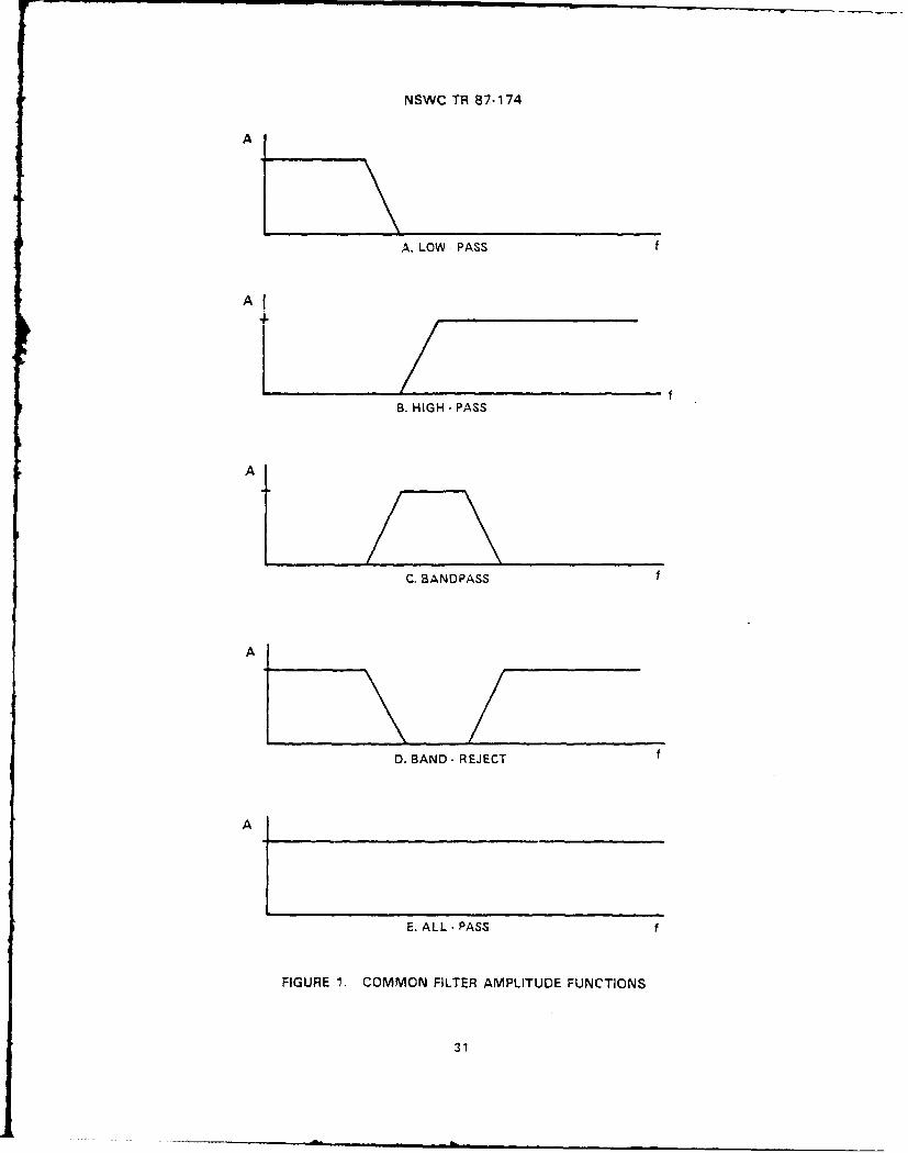
NSWC TR 87-174
A
A. LOW PASS f
At
B. HIGH - PASS
C BANOPASS
A
D. BAND - REJECT
A
E.ALL-PASS f
FIGURE 1. COMMON FILTER AMPLITUDE FUNCTIONS
31
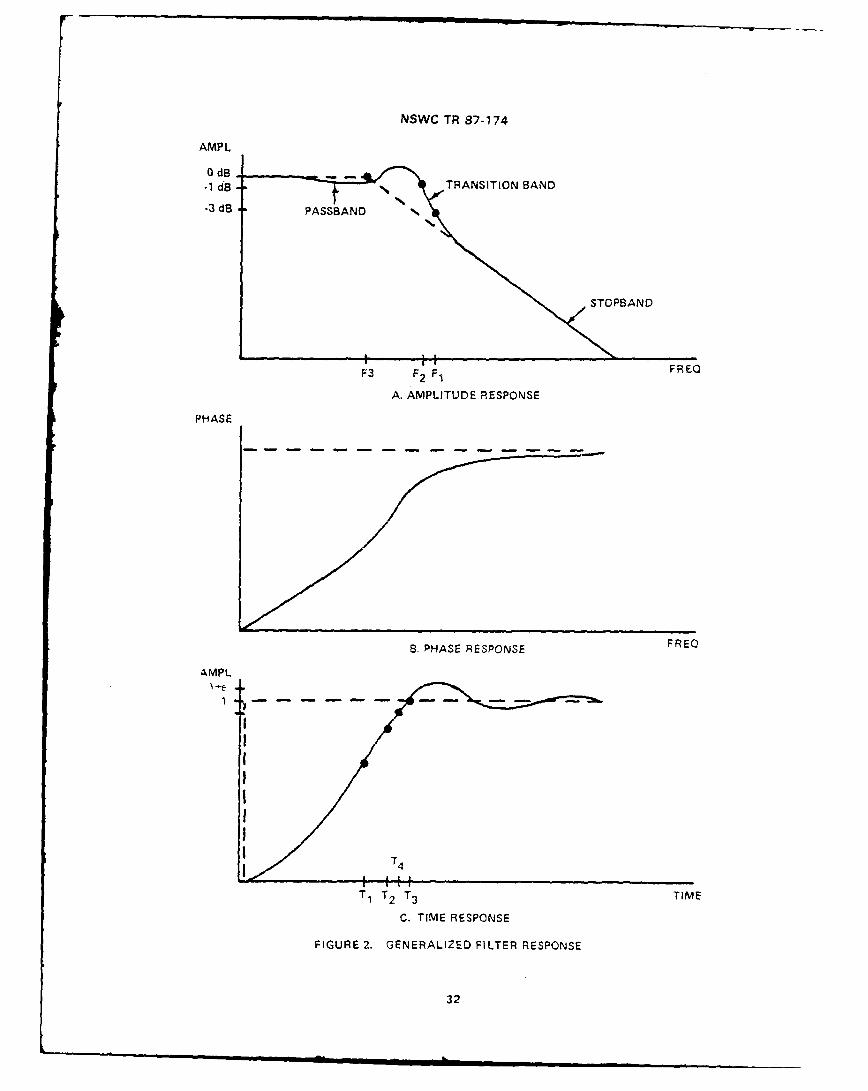
NSWC TR 87-174
AMP L
o dB-1 dB TRANSITION BAND
-3 dB PASSBAND
STDPBAND
F3 F2 Fl REA. AMPLITUDE RESPONSE
PHASE
S. PHASE RESPONSE FREO
AMPL
T4
Ti T'2 T3 TIME
C. TIME RESPONSE
FIGURE 2. GENERALIZED FILTER RESPONSE
32
NSWC TR 87-174
AMPL
SMOHFINITE SLOPESMOOTH
CORNER
IDEAL
FREQA. FREQUENCY RESPONSE
1w
x
B. POLE - ZERO PLOT
S/2(1 - J)X
.~1 X, - -" 2 ( l + j ) X
C. POLE- RESIDUE PLOT
FIGURE 3. GRAPHICAL METHODS OF FILTER SPECIFICATION
33
NSWC TR 87-174
A. NORMALIZED LOW-PASS FILTER
B. FREQUENCY SCALING
C. IMPEDANCE SCALtNG
if if L
-'L >0.7071 ~2 1.414 ~
D. HIGH - PASS TRANSFORMATION
1V 10 KTV K
KT1
E. THEVENIN EQUIVALENTL R
C R _ C
F. SUPER - CAPACITOR TRANSFORMATION
FIGURE 4. CIRCUIT TRANSFORMATIONS
34

NSWC TR 87-174
>+
1. LOW-PASS 2. HIGH-PASS
A. SALLEN-KEY CIRCUITS
HIGH -PASS BANDPASS LOW-PASS
BAND - REJECTORALL - PASS
B. UNIVERSAL ACTIVE FILTER
LI
C. SYNTHETIC INDUCTOR
_[_- I
D. SUPER - CAPACITOR
FIGURE 5. RESONATOR CIRCUITS
35

NSWC TR 87-174
if if
1.414 Q 1.4142 4142
A. HIGH-PASS GAIN OF 2
1.4142 1.414,n
if if
1.4142.1.4'42 14142
B. HIGH-PASS, GAIN OF 2. RESISTORS EQUAL
12
0.7071f 70_ -oT71f ='"0.7071 f
C, LOW-PASS, GAIN OF 2
10 0.5858n
-. I
1If - f -
D tOW-PASS, RESISTORS AND CAPACITORS EQUAL
FIGURE S. GAIN AND IMPEDANCE VARIATIONS
36
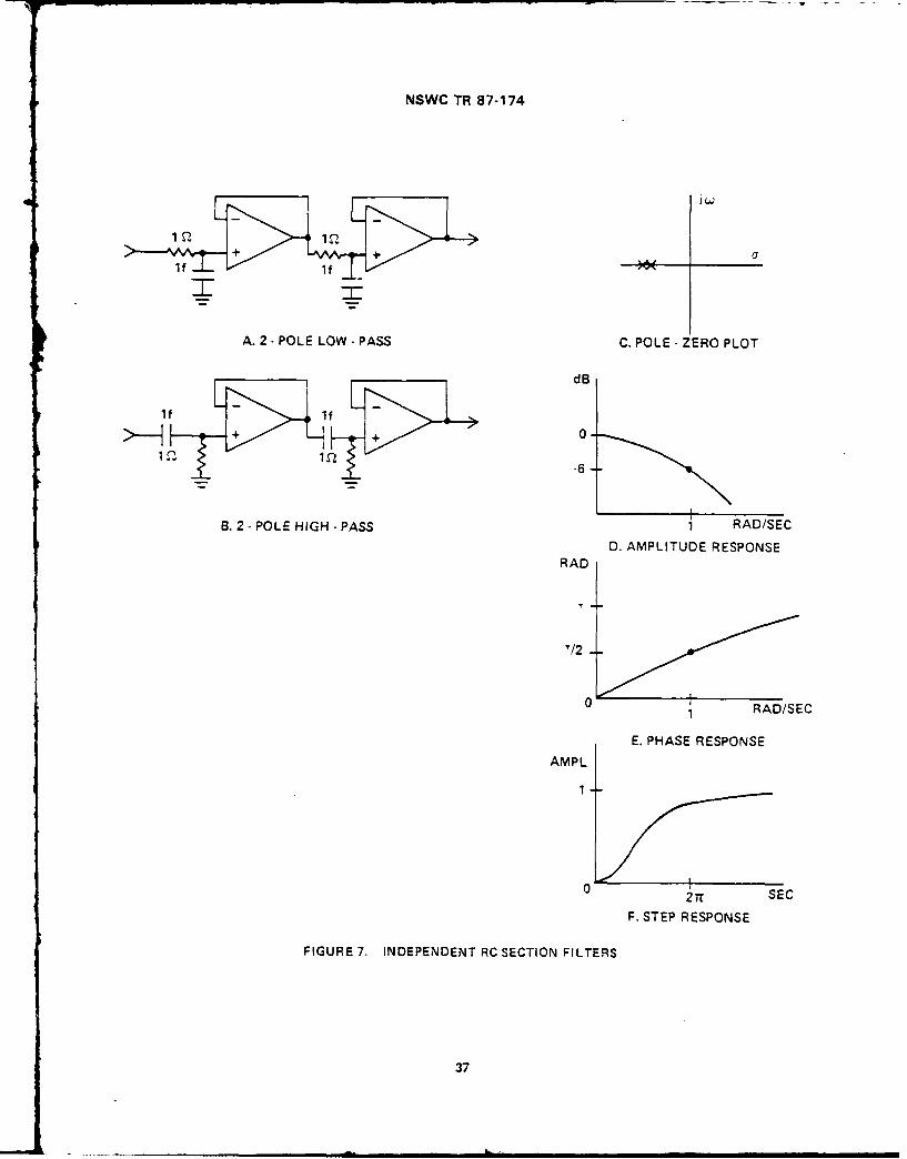
NSWC TR 87-174
ifc
A. 2 - POLE LOW - PASS C. POLE - ZERO PLOT
if if Ld
>- + + 0-
+.-
B. 2 -POLE HIGH - PASS RAD/SECD. AMPLITUDE RESPONSE
RADL
1 RAD/SEC
E. PHASE RESPONSE
AMPL
0 27T SEC
F. STEP RESPONSE
FIGURE 7. INDEPENDENT RC SECTION FILTERS
37
NSWC TR 87-174
* 0
* °+ I 4*
CE,
HI,,
F-li'38

NSWC TR 87.174
LU ca LU LCZ
-~ 0 Ouo
a. Lui
CLLU C,,
LU ui
Co L
0 ~ &- LU
0 wJC
LU
CAUL
C.ULU) Co L
0 U
~~LU C4 C
0 z >UL0 0 4U
x CL =
LU 0j 2LU-j LU cn
Co Co
N 1 L Co I
LU LU a
Co V) C
a. a. 2
CN LUujU
0j - L
- 39

NSWC TR 87-174
0-1-3-
0 1 RAD."SEC
D, AMPLITUDE RESPONSE
C. POLE-ZERO PLOT
0 1 RADiSEC 0 21T SEC
E. PHASE RESPONSE F STEP RESPONSE
FIGURE 10, ELLIPTIC FILTER RESPONSES
40
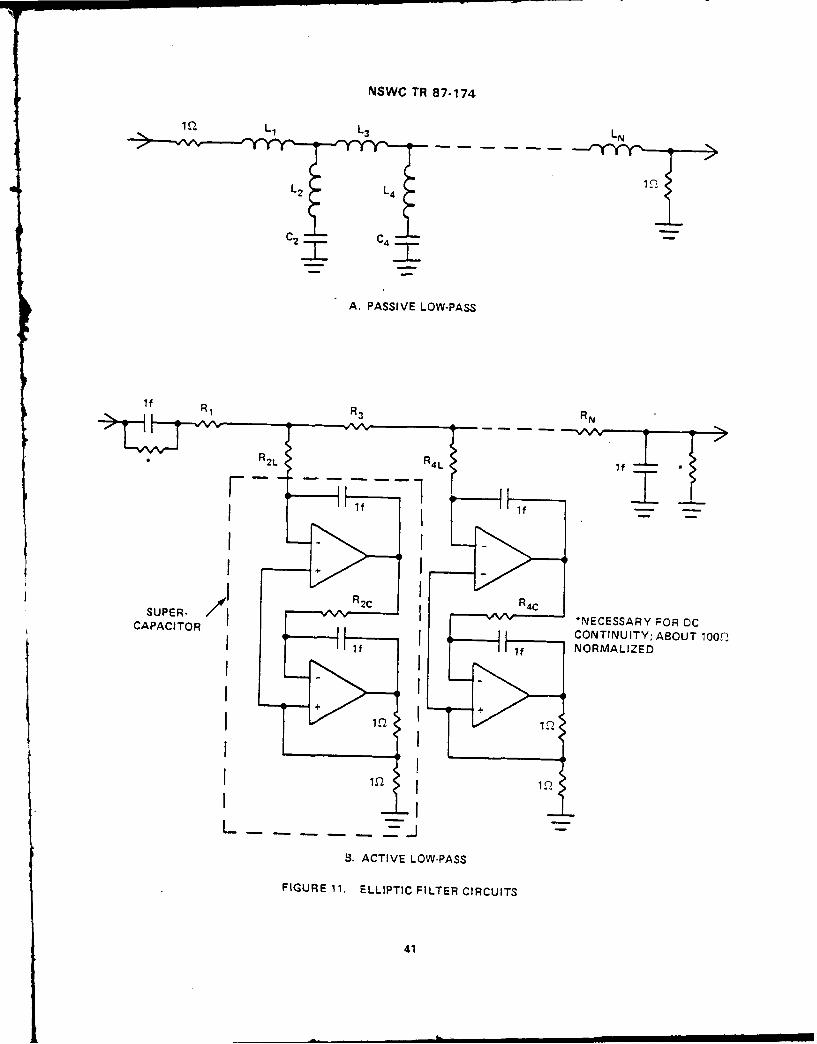
NSWC TR 87-174
L3 LN
A. PASSIVE LOW-PASS
if RR3FN
If ifi
R2 R4 NECESSARY FOR DCSUPER-
CAPACITOR CONTINUITY; ABOUT 100~2
ifI if NORMALIZED
B. ACTIVE LOW-PASS
FIGURE ii. ELLIPTIC FILTER CIRCUITS
41
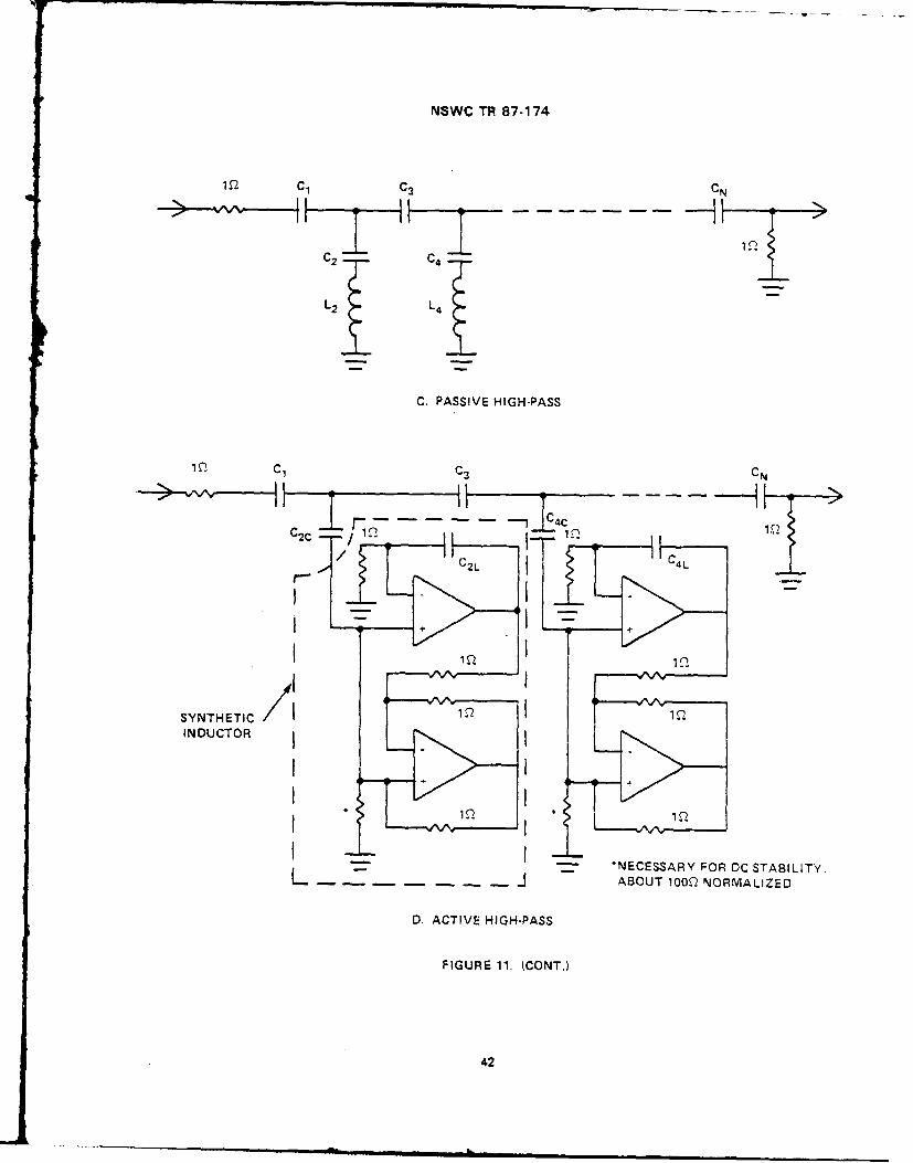
NSWC TR 87-174
1.Q C1 C3 CNI - _->
C2 C4
L2 L4
C. PASSIVE HIGH-PASS
C, C3 CN
cC4L
'- "
++
SYNTHETIC IINDUCTOR
- NECESSARY FOR DC STABILITY.L -.... -I JABOUT 1000 NORMALIZED
D. ACTIVE HIGH-PASS
FIGURE 11. (CONT.)
42

NSWC TR 87-174
12 1Hy 2Hy 2Hy 2Hy 1Hy2fa 2f=-2f__----2
A. N-POLE PASSIVE LOW-PASS
in if 1/2f 1/2f 1/2f if 0 1 (?) RADSEC
E. AMPLITUDE RESPONSE
B. N-POLE PASSIVE HIGH-PASS
2f 1/20. 1 1 n i1 n 1
I _Tf FORDCBIAS_0 - OR GREATER
2f SUPER CAPACITORS
- 0 1 RAD/SEC
__J F. PHASE RESPONSE
C. N-POLE ACTIVE LOW-PASS
in if 1/2f 1/2f 1/2f if
r"- 10-.
112f T I T
Iin I SYNTHETIC INDUCTORS
I inE - I MAY BE NECESSARY
FOR STABILITY 0- - I- 1 OR GREATER 2717 SEC
D. N-POLE ACTIVE HIGH-PASS G. STEP RESPONSE
FIGURE 12. CONSTANT-K FILTERS
43

NSWC TR 87-174
C, 2L 2R Di
C3 LR 03
R R/2 H
C2 L-
C4 LIC
Cs 2L H..
A PASSIVE VERSION R 0 J
+1/2 X H-lx 2 ~ -
.lX
- x B. ACTIVE VERSION-IX
-112 X
- )/2X f-1 XI-lx
-1X 0 5.5 RAD/SEC-lx
-1/2 X D AMPLITUDE RESPONSE
C POLE-RESIDUE PLOT
0 5.5 RAD/SEC 0
E. PHASE RESPONSE F. STEP RESPnNSE'
*FOR LOW-PASS VERSION
FIGURE 13. LERNER FILTEP METHOD
44

NSWC TIR 87-174
1 f
2 +
1/7.v2p. +
l iff 1/6n
+ +
1/6 2
1 f
iflp if ifIT -1 /4 J-Q-1/4212 g 1 .4 2
ip.+
>OUT
0(i
>
:L1 f
+
L- 1 f if1/ 7 ++ *NECESSARY FOR OP AMP BIAS;
117 2 100. OR GREATER NORMALIZEDNOTE: FREQUENCY BAND 3.5-7.5 RAO/SEC
1 f
12 1/5 L2
sz1 f
20-20 1 f 1 f
+ +
FIGURE 14. 12-POLE BANDPASS LERNER FILTER
45
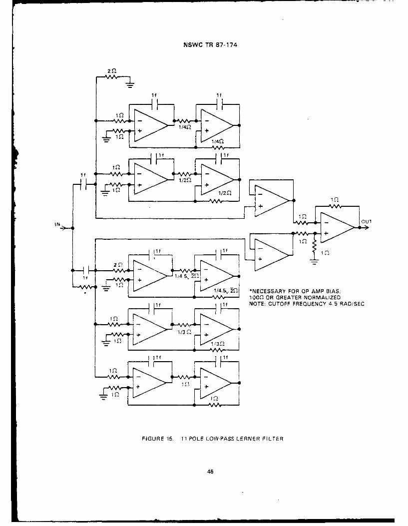
NSWC TR 87-174
2n2
10.2
10.2
4n
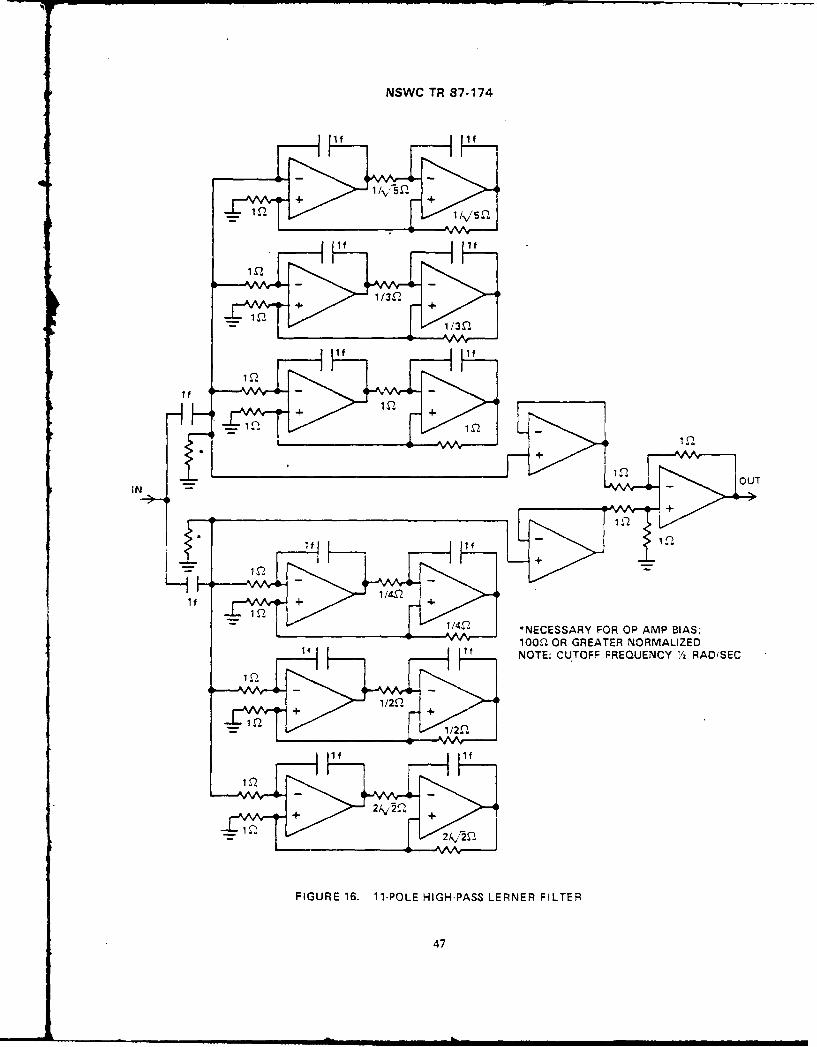
NSWC TR 87-174
if if
i /V,-5 P.+ +
if
I f I f
1/30.1 0/30.
1 f 1 f
if
+ + in
_NNN____j 10,
in
IN OUT
+
if 1 f L
if + 1/4n +
1142 *NECESSARY FOR OP AMP BIAS;100.rl OR GREATER NORMALIZED
if if NOTE: CUTOFF FREQUENCY '/2 RADISEC
+ +
1/2nf
1 f 1 f
-
1 f
+ 2A,./ n + 22 A V
FIGURE 16. 11-POLE HIGH-PASS LERNER FILTER
47
NSWC TR 87-174
A. PASSIVE LOW-PASS PROTOTYPE
12.07 0.48 0.48 2.07
5. 77~
0.17-
0.85 1 17
B. PASSIVE BANDPASS PROTOTYPE
Z07 2.07
C. PASSIVE BANDSTOP PROTOTYPE
FIGURE 17 BANOPASS AND BANDSTOP TRANJSFORMATIONS
48
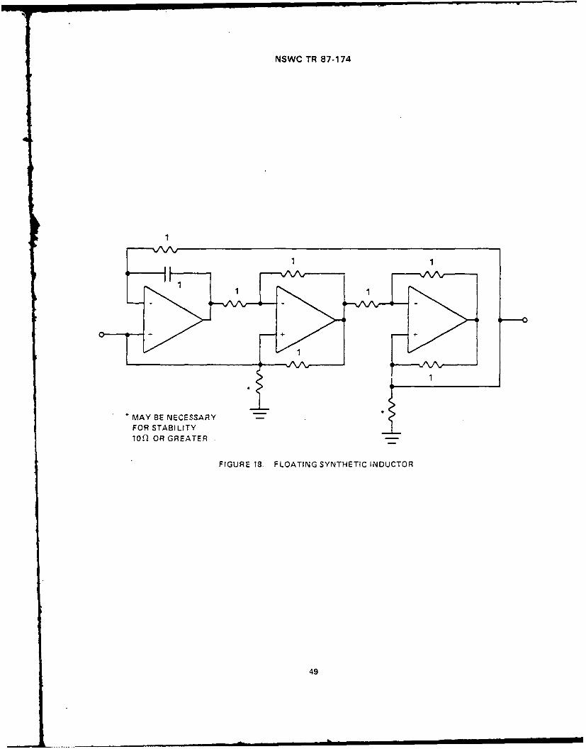
NSWC TR 87-174
1
* MAY BE NECESSARY-FOR STABILITY10f) OR GREATER
FIGURE 18. FLOATING SYNTHETIC INDUCTOR
49

NSWC TR 87-174
II
I -~
-6- +
+ I
1%0 -N -o 0-
zI-
-r - -- 0
0
cd~o r-.* ~- a.o 0lIe 2
o wo i-lII
C.)
0
* +w
U.
* 4.
0
1~0 (1,N -
'I, ~
4- ~Ja-
<0
LU
0
2
so
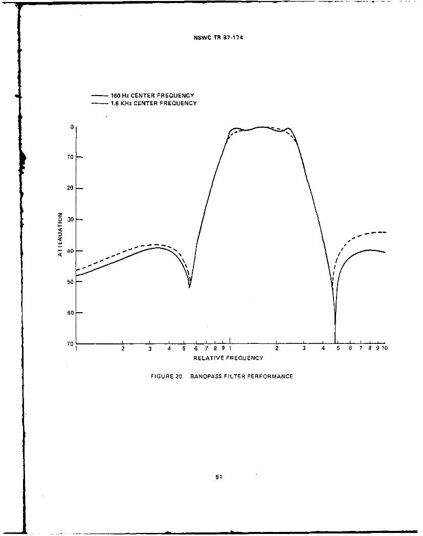
NSWC TR 87-174
-160 Hz CENTER FREQUENCY-- 1.6 KHz CENTER FREQUENCY
0
10
20
z0 30
40 -
50 -
607
70 I I I
12 3 4 5 67 8 91 2 3 4 6 678 910
RELATIVE FREQUENCY
FIGURE 20. BANDPASS FILTER PERFORMANCE
51

NSWC TR 87-174
10-
20-
BEFORE ADJUSTMENTS30-z 30AFTER ADJUSTMENT
40
50
60-
2 3 4 5 6 7 8 91 2 3 4 5 6 7 8 910
RELATIVE FREQUENCY
FIGURE 21. BANDSTOP FILTER PERFORMANCE
52
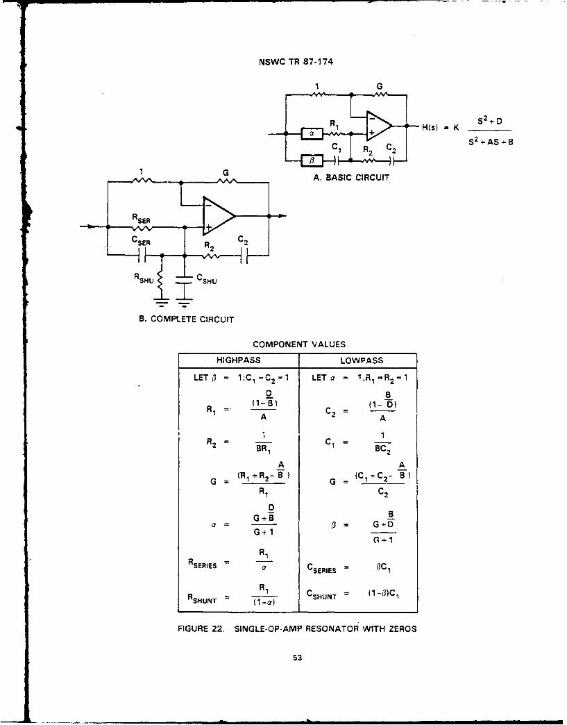
NSWC TR 87-174
1 G
Rx + H(s) K __
C R c2 S2 +AS--B
G A. BASIC CIRCUIT
R SEU C
B. COMPLETE CIRCUIT
COMPONENT VALUES
HIGHPASS LOWPASS
LET3 = 1;C 1 =C 2 =1 LETa = 1,R1 =R 2 =1
D B(1-B) (- D
RAC 2 = (1 D)
A 2A
; 1R2 = B 1 C 1 =
R 2B R i c B C 2
A A
G - (Ri+R 2-) G = (Cl C2 -B
R1 C2
DG+B
= + /3 = G+DG+I
R1RSERIES - CSEREs = 3C,
R R, CSHUNT = (1-3)C1RSHUNT = (1-ar) I
FIGURE 22. SINGLE-OP-AMP RESONATOR WITH ZEROS
53
NSWC TR 87-174
1O.OC 23.2k lOOk 10,2k 10OOk 10,2k
14.1k 0.01 OF 1.084 0.01 O~F TL084 10,0k TL084 0
0.01 OF 93.0 4.20 1080 pF 10.0k
O7k00 F ;579 pF 0.0237 OF
FIGURE 23. ELLIPTIC BANDPASS WITH SINGLE-OP-AMP SECTIONS
54

NSWC TR 87-174
0-
20 "
07LU 30-
LU
50-
60 - 1.6 KHz CENTER FREQUENCY
16 KHz CENTER FREQUENCY
I I I I I I I I I I I I I10.1 0.2 04 0.6 0.8 1.0 2 4 6 8 10
RELATIVE FREQUENCY
FIGURE 24. PERFORMANCE OF ELLIPTIC BANDPASS WITH SINGLE-OP-AMP SECTIONS
55

NSWC TR 87-174
LU L" Au u
'A ~ + 0 0 00 -
- LU
N L
cc 2
zz
+- LU
4. CL
LuL
a 0~
0. j N N.-IA I A.
LL 0 rA 0 0, a -l
NL0 N 4 . L C
2 0CL CL R~ w 0
56~
NSWC TR 87-174
lO p 11K59K
757

NSWC TR 87-1741000900800
- 700
U -,= 600
- 500
-. 4.00
300
200
LO-
> C C
go . .
70 "Q
8,.60 :50 2
40 L-
a.30
20 x
10
(0) 0L 0 0 00058
NSWC TR 87-174
10K 10.345K 10K 10.345K
975.86K 001363
FIGURE 28. QUASI-ELLIPTIC BANDPASS CIRCUIT
59

NSWC TR 87-174
NOTE: GAIN = 202 20
1/20 f
1 n op
A. BRIDGED-TEE FEEDBACK . ALTERNATE FORM
x N (1) 0 r /
-3-
A' I'
1 RAD SEC
C. POLE-ZERO PLOT 0. AMPLITUDE RESPONSE
T
~x~r~SC
1 RAD/SEC F STEP RESPONSE
P ,HASE RESPONSE
FIGURE 29. NARROWBAND FILTERS
60

NSWC TR 87-174
A. TWIN-TEE WITH FEEDBACK
ii
A1 RAD/SEC
C. POLE ZERO PLOT D. AMPLITUDE RESPONSE
I RAD/SEC 271 SEC
E. PHASE RESPONSE F STEP RESPONSE
FIGURE 30. NOTCH FILTERS
61
NSWC TR 87 174
10-
A, ONE-POLE, ONE ZERO CIRCUIT B. POLE-ZERO PLOT
ALSO: X 0
x 0 0
x0
x 0x 00 1 RAD,SEC
C, ALTERNATE POLE-ZERO PLOT D. AMPLITUDE RESPONSE
,r 0
0 RAD/SEC
E. PHASE RESPONSE F. Sl EP RESPONSE
FIGURE 31. ALLPASS FILTERS
62

NSWC TR 87-174
IN >1OUT
I --
A. CIRCUIT
B. INPUT C. OUTPUT
D LOW-PASS CHARACTERISTIC f
E. BAN OPASS CHARACTERISTIC
FIGURE 32. COMMUTATING FILTER
63

NSWC TR 87-174
V IN s
Cs4/ OUT
VII
A. EQRUIATCIUT
VIN ...........1
B~~ EQIALN CIRCUI
C. SWITCH E DCA PACI TOP INIEGRATOR
FIGURE 33. SWITCHED-CAPACITOR FILTER METHOD
64
NSWC TR 87-174
IN
OUT
FIGURE 34. TRANSVERSAL FILTER

NSWC TR 87-174
TABLE 1. RECOMMENDED SOURCES
. Williams, A. B., Active Filter Design, Artech House, 1975.
2. Hilburn and Johnson, Manual of Active Filter Design, McGraw-Hill Book Co.,Inc., New York, NY, 1973.
3. Blinchikoff and Zverev, Filtering in Time and Frequency Domain, John Wiley &Sons, Inc., New York, NY, 1976.
4. Tobey, Graeme and Huelsman, OFerational Amplifiers, Design and Anplications,McGraw-Hill Book Co., Inc., New York, NY, 1971.
5. Delagrange, A. D., An Operational Amplifier Primer, NOL TR 72-166,14 Aug 1972.
6. Delagrange, A. D., A Useful Filter Fam-ly, NSWC WOL TR 75-170, 20 Oct 1975.
7. Guillemin, E. A., Synthesis of Passive Networks, john Wiley & Sons, Inc..New York, NY, 1 57.
8. Lam, H. Y-F., Analog and Digital Filters; Design and Realization,Prentice-Hall, 1979.
9. Lancaster, D., Active Filter Cookbook, Howard W. Sams, Inc., 19-5.
10, Huelsman and Allen, Introduction to tne Theory and Design of Active Fiiters,McGraw-Hill Book Co., Inc., New York, NY, 1980.
66

NSWC TR 87-174
TABLE Z COMPARISON OF FILTER METHODS
Method
Property Passive Active/Analog Digital
Uses Inductors? Yes No No
Requires Power Supply? No Yes Yes
High-Frequency Good Fair ?oorCapability
Low-Frequency Poor Fair GoodCapabil Por ai Go
Input Impedance Matched High Irrelevant
1iOutput Impedance Matched Low irrelevant
Number of Sections Many Few Expandable
Dynamic Range Good Fair Expandable
Expense Medium I Low I High
Mat-h to Calculations Poor Good Exact
67
NSWC TR 87-174
TABLE 3. APPROXIMATE DECIBLE CONVERSON
Number of Equivalent EquivalentDecibels Gain Attenuation
00 1 9
3 1.4 0,7
6 20.
10 3 0,3
20 10 0.1
68

NSWC TR 87-174
TABLE 4. BUTTERWORTH VALUES
NOISEOrder GI G2 G3 G4 BANDWIDTH
1 1.571
2 1.5858 1,110
3 2.0000 1,047
4 1.1522 2.2346 1.026
5 1.3820 2.3820 1.017
6 1.0681 1.5858 2.4824 1.012
7 1.1981 1.7530 2.5550 1.008
8 1.0385 1.3371 1.8889 2.6098 1.006
9 1.1206 1.4679 2.00C0 2.6527 1.005
NOTE: ALL RESISTORS 1.000 EXCEPT GAIN-SETTING
69
NSWC TR 87.174
=0~. .7 ~ .~ ~ .0 .7 ~
-3 - .7 ~ -c.."
I- ~- o~ 0 C~ 0~ r.~ .7 - -0 .7 = - .0 -~ .7z .0 0' ~ - 0 0 0 0'0
o o~'0 .C., O~ ~
0 0 -
.0 -r-. 00wc." ~ .0
-J
0 0 0 0w - 'C 0 .7.7C' 0' - 0
0. 0 0 - -
.0 0.7 C"
~, -. 0 4. .00
~ c.-. '~wU, - 0 -~ 0
.7 0 0 -.0 - C' .'~ ~ -0 C' - - X~ .7 -w
*0 0~r-3
w 0 .0 - -- -, C" 0 .7 C'.7 C., .7 S~ 4~.fl .C ~ .7 -
C'~ C'~ N~ .0
~' 0 0 '0 ('.~ .0 .0C' C' - 0.7 '0 '0 fl .7 .7 ~
C" 0 - - - '-'4
0 ~ C' 4~ 0 4') ~ .7.0 .7 .0 - 0 .7 .~C' -i~ 0 -.0 C~ ~ -, 0 -~ -
-
.0 .0 '0 -- a') .7
0 0 .70 .
034. - "~ '') .7 4.) .0 - 0 ~?' .04.'- C.
0 C.
70

NSWC TR 87-174
a, e- Z0 -
..
ual
0..
co
::o a, D
C, C
>
-j
020
017
71
0
NSWC TR 87-174
,a - -0 0 0
m n 0
o0 U
.072
NSWC TR 87-174
- -
oCL ~ - - - '
CL 0 0 0
-z .
.0 7
w7

NSWC TR 87174
- ~ ~-, - - - -~
- ~ h- c:* - ~
V V. V.V
Cd, V. C V.
4
wCd,
4
0.
74

NSWC TR 87-174
kn L-
crJ CX~
cc cn t-C\Ae Lo C~
C-,i
Cw cc, -
c~ c ZC4 X) Ci C D*
CC-4
< vi- - C ~<
I- -
(D < -c - ~zu- -
C- 5

NSWC TR 87-174
Ln- cn ccr C C) LOl C\4
j ~- L Cl (n~
~~C~ <-C C -
CC
C n Lf . l L O C Ui
(Ni C C - (')C ~ .r-.
S C) LO~
rn CDJ C'') L.n r-, CN (j
- rC - m C C4UI l
0
N LO In
-2i
C L
co<
- ,- L-<
C-
LAI 'A
k-I - ,Z r
V) '- -
76

NSWC TR 87-174
fl C -C - u C
C C Z ~ ~ r .
C ~ C
Cn C' i rn co -~ Io~~\J CD* . c
LO C~ C CLCO CD 1. C'N C
C:
LU C. - ~
LULUJC < C- <
I- L--
uj~
C.,-
I- <77

NSWC TR 87-174
TABLE 13. ELLIPTIC 1.25 dB RIPPLE 3-POLE 2-ZERO VALUES
STOPBAND/PASSBAND RATIO 1415 ],52 2.28 5 24
STOPSAND ATTE;IUATION 15.3 26. 39,4 62.2
PASSIVE ACTIVE PASSIVE ACTIVELOW-PASS LOW-PASS HIGH-PASS HIGH-PASS
L, i. 1'C! 1 4922 1.8694 2.0701 2.1P9
R. /C;r 1.4198 0 4322 0 1732 0 0294
CR R;C 1/L I,'CL 0.4547 0.710 0.8537 0 932"
R I/C ,'C3 1 a922 13694 2.0701 2.819
78

NSWC TR 87-174
TABLE 14. ELLIPTIC 1.25 dB RIPPLE 5-POLE 4-ZERO VALUES
STOPBAND/PASSBAND RATIO i,15 1.52 2.28 5.2
STOPBAND ATTENUATION 36,5 55,9 76.9 114.9
PASSIVE ACTIVE PASSIVE ACTIVELOW-PASS LOW-PASS HIGH-PASS HIGH-PASS
L R I/C I/C, 1,944 2.1590 2.2572 2.3086
Lz R L I/C2 I/C' C 0,4805 0.1898 0.0715 0 0121
I- o/C21 0.79 5 0.9318 0.09i9 1.023C
R/C3 lC3 2.1125 2.6321 2.9919 3.156
R4L I/C. i/Cc 1 ,4882 0.5206 J.1398 0.0325
R ,C 1,L !/CL 0 1 798 0.7662 0.9250 1.0152
LzC R/C, 1,4228 1,897a 2.1d82 2.23"7
79
NSWC TR 87-174
TABLE 15. ELLIPTIC 1.25 dB RIPPLE 7-POLE 6-ZERO VALUES
STOPBANO/PASSSAND RATIO 1.15 1.52 2.23 5.24
STOPBAND ATTENUATION 57.8 35 0 114.4 167>6
PASSIVE ACTIVE PASSIVE ACTIVELOW-PASS LOW-PASS HIGH-PASS HIGH-PASS
L- R,/C1 I/C 2.1357 2.2625 223175 2.3457
L- R2L 02 I!C/c 0.2535 0.1012 0,03k82 0 036
C, R2C 1/L I/C2L 0.9142 0 9954 !>0310 . a93
SP 3 !!C 1/C 2.259, 2.8064 3.0977 2612
1,Cu 1 1CC 1 3297 0 4952 0 18,12 0 2318
* , ( JL !CL 0 5504 0.3366 0,9966 i 0880
R/C 5 2/C5 1.902S 2.628d 3.02413 3.2d79
R L C; C 0.8835 0,3359 0.1250 0.0216
C R6C /; L 0 6462 0.8665 0.9786 1.0399
R7/C. I/C7 7004 2 0580 2.2350 2 33(9
80
NSWC TR 87-174
uI-
z )- C 0 ~ z<z-W LL. LL .a U. CL a
xwi
-j -
LU w -j Wi -j 4U Wi W> C > u > wU LL L- > -
U
cn0 0 LULUL
a.
u LUJ _j zCO -i 0 C d
LL LW >- U CL >. CLL U.~f
w w
> I.wj -J Oz ~
> w U J Ci - -occx - >CU > c > Cc C LULUL - C. C L4
-i =. 0 U. U.ux
LU U L U- LL U. U. U.
2 - -z -
w z. -a2A. > C LL C >U C
c x x xz Lu LU I z
z >. 9- Lui
0. Z.C~ 'LUC Zu
UJ . 2.=C 2Z LCL. _ -. - - a.- - J -W V) - -
81/82

NSWC TR 87-174
REFERENCES
1. Delagrange, A. D., An Active Filter Primer, Mod 1, NSWC TR 82-252,2 Feb 1983.
2. Bruton and Trelevan, "Active Filter Design Using Generalized Impedance
Converters," EDN Magazine, 5 Feb 1973.
3. Delagrange, A. D., "Op-Amp in Active Filter Can Also Provide Gain," EDNMagazine, 5 Feb 1973.
4. Delagrange, A. D., 'Gain of Two Simplifies LP-Filter Design," EDN Magazine,17 Mar 1983. (Note: There is a misprint in the article; the gain formula
given here is the correct one.)
5. "Solid-State Variable Filter Model 3200, Operating and Maintenance Manual,"
Krohn-Hite Corp., Cambridge, MA.
6. "Instruction and Maintenance Manual, Ithaco 4210 Series Variable Electronic
Filters,' ithaco Inc., Ithaca, NY.
7. "Linear Phase, Maximally Flat Gain, Low Pass Filter,' EIT Corp.,
Sterling, VA.
8. "Dual Section High-Pass/Low-Pass Brickwall Filter, Model 753A,' Wavetek
Rockland, :nc., Rockleigh, NJ, Apr 1982.
9. Delagrange, A. D., "Design Active Elliptic Filters With a 4-Function
Calculator," EDN Magazine, 3 Mar 1982.
10, Baezlopez, D. J., Sensitivity and Synthesis of Elliptic Function, Ph.D.
Dissertation, University of Arizona, Tucson, AZ, 1978.
!I. Zverev, A. I., Handbook of Filter Synthesis, John Wiley & Sons, :nc.,
New York, NY, 1967.
12. Delagrange, A. D., A Useful Filter Family, NSWC/WOL TR 85-170, 20 Oct 1975.
13. Lerner, R. M., "Bandpass Filters wit" Linear Phase," Proceedings of the
IEEE, Mar 1964.
14. Delagrange, A. D., "Design Lerner Filters Using Op-Amps,' Electronic 2esiznMagazine, 15 Feb 1979.
33

NSWC TR 87-174
REFERENCES (Cont.)
15. Guillemin, E. A., Synthesis of Passive Networks, John Wiley & Sons, Inc.,New York, NY, 1957.
16. Active Filters, Report No. S-166, Amperex Corp., 1977.
17. Delagrange, A. D., "Make Passive Filters Active With a Floating SvntnetlcInductor," EDN Magazine, Vol. 28, 23 Jun 1933, p. 13.
18. Delagrange, A. D., and Danyon, R., "Pocket Calculator Eases Filter Design,"EDN Magazine, 24 Jan 1985.
19. Huelsman and Allen, Introduction to the Theory and Design of Active Filters,McGraw-Hill Book Co., Inc., New York, NY, 1980.
20. Delagrange, A. D., "Build Active Filters Without Op-Amps," EDN Magazine,20 Feb 1986.
21. Fellot, D., "Wein Bridge and Op-Amp Select Notch Filter's Bandwidth,"Electronics Magazine, 7 Dec 1978.
22. Delagrange, A. 0., An Improved Translating Filter Design, NSWC/WOL
TR 77-172, 30 Nov 1977.
23. Martin, S., Minimizing the Worst-Case Drift of an Active Bandpass F.iter,NSWC,/WOL TR 78-2, 11 Apr 1978,
24. Leehey, J., Frequencv Samp.lin and Translaton -'sing Commutating Fuiters,A. S. Thesis, Massachusetts Institute of Technology, 1979,
34

NSWC TR 87-174
APPENDIX A
FILTER RESPONSE DATA
The filter designs given in this series of reports have become too numerousto catalog all the responses, so only a sampling will be given. Circuits werebuilt from the prototypes and tables given in this report, or in a few cases thelisted references and the actual responses recorded.
The three curves normally sketched for each filter type are generated here--amplitude, phase and step response. The plots were made using a Hewlett-Packard*3561A Dynamic Signal Analyzer with a Thinkjet* printer. Amplitude response,termed MAG by the analyzer, was done by inserting a pseudo-noise signal, -whichhas flat frequency spectrum, and recording the spectrum of the output. Thepseudo-noise was internal to the analyzer and hence synchronized to produce asmooth trace, but the filters having their own clocks were not synchronized, andirregular traces sometLmes resulted. Vertical scale is indicated on the graphs,in most cases 6 dB/large division so direct comoarison is oossible. Horizontalscale is usually linear. Use of a linear scale makes high-pass filters appearsharper than low-pass, but is desirable for direct comparison to the phaseplots. Filter frequency is usually 1000 rad/sec (about 160 Hz) and a full scaleof 400 Hz used, showing slightly more than an octave above for the low-pass case.
Phase response was done similarly. Vertical scale is always 45 deg/largedivision, running from -180 degrees to +180 degrees. Horizontal scale is alwaysthe same as for the amplitude plot. The cursor is place at the filter frequency.
The step response, termed TIME by the analyzer, was done by converting theinternally generated impulse to a step with a flip-flop. The time signal of theoutput was then recorded, normally with a delay of zero. Scales are cf courselinear. Vertical amplitude was normalized to four large divisions, starting fromthe bottom for low-pass but from the center for high-pass (and bandpass).Horizontal full scale is usually 16 msec. One cycle at the normlized frequency
is about 6.3 msec, close to the cursor setting of 6.4 msec. Thus slightly morethan two cycles are presented. The same settings were used as much as possible,but they don't make sense for some cases, and some examples were circuits alreadvin use and hence hard-wired.
The circuits were constructed mostly using 1% capacitors and 2% resistors;sometimes tweaking was necessary to prevent oscillation or serious errors, mostlywith the higher-order filters. FET-input op-amps (which are about an order ofmagnitude faster than 741's) were used. The curves at tLmes will show noticeable
*Registered Trademark
A-1
NSWC TR 87-174
deviations from the ideal. If exact curves are required the mathematicalfunction must be plotted, which is done in some of the references, usually bycomputer. Some of the more pertinent aspects of some of the photographs will notbe discussed.
The simple RC low-pass (Figure A-1) offers only about 6 dB rejection anoctave above cutoff, a minimal filter. The phase shift appears linear onlybecause it is so low; a straight edge will confirm this. The step response is asimple exponential, about 1/6 of the period due to the 2, factor. The i-poleRC high-pass (Figure A-2) appears to have a sharper cutoff only because a linearfrequency scale is used; any high-pass must go to zero (- dB) at zerofrequency. Conversely, the high-pass cannot reach 0 dB on the picture as thelow-pass does. If a log frequency scale were used, the low-pass and high-passwould be mirror images in most cases. The phase plot drops to zero at lowfrequency because there is insufficient amplitude to make a measurement. Thestep response is also a simple exponential, but falling, as a high-pass shows theinitial step but must return to zero. The 4-pole eual-RC (Figure A-5) showsfour times as much attenuation at an octave, but also at the cutoff. Note thatat +180 degrees the phasemeter shifts to -180 degrees. Note also that for fourpoles phase response is identical for low-pass and high-pass. The step responseshows no overshoot. The no-overshoot property does not carry Gver to thehigh-pass.
For the Butterworth curves (Figures A-7 through A-14), note that theattenuation at the cutoff frequency remains 3 dB but the attenuation at an octaveimproves with increasing order. On the other hand, rinaing in the step responsebecomes worse,
The Chebyshyev cur-ves (Figures A-iS through A-22) show now the cutoff si,'emay be made considerably steeper by allowing 1 dB ripple in the passband.However, the ringing in the step response is worse than Butter-worth.Misadjustment is evident as the 1 dB limit is exceeded in some of the pictures.Filters with less than 1 dB ripple were not attempted. Three dB filters are notshown, as this is more ripple than is commonly used, and the improvement in.steeoness over 1 dB is not all that much.
The Besse! filters (Figures A-23 t'hrough A-26) show excellent phaselinearity clear to the bandedge and beyond. The attenuation at an octave,though, is pitiful. The step response overshoot is barely detectable. The phaselinearity does not carry over to the high-pass versions, so they are not shown,
The elliptics offer the steepest transition band. The 5-pole 4-zerolow-pass (Figure A-27) nits the stopband about 20% past the cutoff frequency,The zeros are clearly evident, Note that the stopband ripple is not equai as itshould be. .A 5-pole 4-zero cesign having less ripple but more rejection, andhence less steepness, is shown in Figure A-28, Note that the scale is differeitand that the stopband is below the noise floor of the measuring system. The5-pole 4-zero high-pass (Figure A-29) only appears steeper, The 7-ole S-zerolow-pass (Figure A-30) appears comparable only because of the distortion of thelinear scale; it ;s really steeper than the 5-pole 4-zero high-pass. Phase s-ftand step response are similar to Chebyshev filters of the same steeoness.(Compare Figures A-21 and A-30. The elliptic appears tn nave a faster tirneresponse primarily becaus- the analyzer dces not have a fast enough tame sweepthe two riirscrs are set atoqui'olent jpDiima,) Figure A-3i shows tne response of
A-2

NSWC TR 87-174
a 7-pole 6 zero 1.25 dB/58 dB Zlliptic built with switched-capacitor'technology,so the cutoff frequency may be varied as shown. Note that the characteristicchanges slightly as the frequency is varied; it should not. This type of filteris relatively noisy, so the stopband appears higher than it really is. In actualoperation one may or may not get the full benefit of the true rejection level,depending on the system application. The actual circuit is shown in Figure A-32.
The constant-K filters (Figures A-33 and A-34) are reasonably well behaved.A good amplitude characteristic is obtained'with no tweaking. The low-pass makesa good delay line; the phase response is nearly linear over most of the passband,and the step response exhibits a delay comparable to the rise time. The highpass is interesting in that the ringing is not a constant frequency, but slowsdown as it dies out. Figure A-35 shows the result of adding two zeros to aconstant-K filter to reject two specific frequencies. This is easily donebecause the passive prototypes are similar. The result is similar to anelliptic, but the ripple is unequal since it was the frequency of the notchesthat was specified. The notches cause a slight droop at the edge of thepassband, but this may be compensated to a certain extent by modifying theterminations (see Reference A-l). The phase linearity is still quite good. Notethe altered scales. The actual circuit is shown in Figure A-36.
The good phase linearity of the Lerner filters (Figures A-37 through A-39)is evident. That of the high-pass is less than ideal, but it is the best shownyet for a high pass. Step response is meaningful only for the low-pass. Againwe have a good delay line; observe the "pre-shoot." The sweeps here have beenlenathened to show the details of the wiggles. Cutoff freauencv 's notnormalized.
Figure A-40 shows the response of an Elliptic bandoass using floatingsynthetic inductors, after considerable tweaking. Ripple misses the
specification significantly. Log frequency scale is used to show the symmretry ofthe transformation. Figure A-41 is the response with the components rearrangedinto a band-reject. Linear frequency scale is used here. Figure A-42 is for abandpass made simply by combining high-pass and low-pass sections. Performancecannot be as good as that of Figure A-40, since the latter is optimum.
The narrowband response (Figure A-43) was obtained from the equal-capacitorversion. The phase response rises sharply by 180 degrees as the peak istraversed. The response of the narrowband filter to any input is, of course, asine wave at the center frequency. The height of each peak can be seen to bediminishing. The initial amplitude is not normalized, as it depends on 2. Thenotch filter (Figure A-44) was constructed using the Wein-bridge circuit. Thedepth of the notch depends on the accuracy of the components. The phase shiftjumps 130 degrees going through the notch. it might be surprising that the stepresponse rings at the center frequency, since that is the frequency at which thefilter transmits least. One way to explain this is to observe that the ringing
is upside down; what we are seeing is all frequencies (the step) except (minus'the center frequency. Log frequency scale is used in both cases; the plots lookstrange otherwise.
Figure A-47 shows the response of an eight-section commutating f-iter navlnaa center frequency of 160 Hz and a bandwidth of 0.4 Hz, equivalent to a 2 of400. Note that the filter bandwidth is less than the analyzer bandwidth, so t e
A-3
NSWC TR 87-174
amplitude plot is not accurate. The phase plot shows an almost vertical jump atthe center frequency(s) because the filter is so narrow. The step responsereflects the additional passband at DC; it is an exponential corresponding to theRC low-pass, but "ratchets" up in steps corresponding to the repetition (center)frequency. The circuit is shown in Figure A-48.
Figure A-49 gives the response of a demonstration eight-stage transversalfilter using a digital shift register instead of analog, which effectively 71iosthe input. Taps were adjusted to yive one cycle of a sine wave. The frequencyresponse is basically a sin f/f centered at the repetition frequency, complicatedby the addition of the mirror image at negative frequency. The phase responseplot is ragged due to the interaction of the sampling frequencies of the filterand the analyzer, but the linear phase property is evident. The impulse is oftnterest here rather than step, and can be shown because it is really a pulseresponse, which is physically possible (as opposed to impulse). The actualcircuit is shown in Figure A-50,
The amplitude response of the all-pass (Figure A-45) is decided'vuninteresting. The phase is the arctangent curve, exactly double that of -hesimple RC low-pass. The step response is interesting Ln that it _nltialky stepsZn the wrong direction, due to the inversion at nigh frequenc es, then recoversexponentially to the final va!ue. Vertical scale is shifted and horizonta- isdelayed to give a good picture. Figure A-46 shows the performance of thephase-difference network, two 2-pole 2-zero networks whose outputs are 90 degreesapart across the frequency range 200 Hz-1400 Hz. Phase shift is shown for eacnoutput and the difference between them whict is nearly constant 90 degrees. 1Cfrequency scale ,is used, as the construction s basca iv ogaritmic. T:efalling portions of tne curves snould be rertcal -he finite SloDe resu7ts frominterpolation by the ana-.zer being exaggerated du % to ne converslon to ocscale.
A- 4

AD-AI97 538 amMD DRA~*~ L a'a7c AD 2( W A SRN WARFARE
UNLASIIE ! -q 4F/G 9,'L ML
I liii1.8
flfl 1.25 1
NSWC TR 87-174
AMPLITUDE
iC -- :
0- H
-----... ... ..... .....----- -- -: ----- - - --- - -- ---- -------------------------- --... .... ...
PHASE
STEP - -...................
FIGURE A-1. 1-POLE RIC LOW-PASS RESPONSE
A-5
NSWC TR 87-174
AMPLITUDE
D- 1
--- - -- --- ---- ---
STEP --------
FIGURE A-2. I-POLE RC HIGH-PASS RESPONSE
A-6

NSWC TR 87-174
AMPLITUDE
!rT4
I~ 71
I O
PHASE
- . .......... ....
, v[
7 4-
STEP
• .) - -
FIGURE A-3. 2-POLE EQUAL-RC LOW-PASS RESPONSE
A-7
NSWC TR 87-174
AMPLITUDE
PHASE
DE t
37.
FIGURE A-4, 2-POLE EQUAL-RC HIGH-PASS RESPONSE
A-8

NSWC TR 87-174
- ,. -. ,
AMPLITUDE
I : -.- -,* - , . :
; 7 : 3' .CT iE.
I
PHASE
*I -,
STEP
FIGURE A-5. 4-POLE EOUAL-RC LOW-PASS RESPONSE
A-9

NSWC TR 87-174
AMPLITUDE -
r
PHASE -____
SI
STEP j ----------
-~
I :
-
________-___________________
_________________
_____
ff
:
FIGURE A-6. 4-POLE EQUAL-RC HIGH-PASS RESPONSE
A-10
NSWC TR 87-174
AMPLITUDE
I -
M'ATH r'cri P4ASE - tt 'lGIT: 1 : / i.! ,*;. .
:,E I
PHASE ZE3
),N~ 6 IB'' ~
,. . ..
-E
STEP-/
/
FIGURE A-7. 2-POLE BUTTERWORTH LOW-PASS RESPONSE
A-il

NSWC TR 87-174
--I -- ..... . ; --- - r-
it. .. ---
AMPLITUDE r
I i' ri ,
PHASE -
H-
I ------
A-1
STEP ~~~~~~--- -- - -____ __
A-

NSWC TR 87-174
AMPLITUDE "
-r, ,
PHASE 4
STEP
=/
q/!/
FIGURE A-9. 4-POLE BUTTERWORTH LOW-PASS RESPONSE
A- 13

NSWC TR 87-174
AMPLITUDE "
CH H
PHASE
r T
FIGURE A-10. 4-POLE BzUTTERWORTH HIGH-PASS RESPONSE
A-14
NrSWC TR 87-174
AMPLITUDE - .
""-, .... ,
-' rt E. " . ='-'':-. ,., ,=
PHASE
.--i
STEP - 7 -
, //
: /- /
FIGUREA-11. 6-POLE BUTTERWORTH LOW-PASS RESPONSE
A-15

NSWC TR 87-174
AMPLITUDE -
ST RT /i -o
-~ L.
-- ,' -i
PHASE -
: L-
J
STEP :1. / ._,....
FIGURE A-12. 6-POLE BUTTERWORTH HIGH-PASS RESPONSE
A-16

NSWC TR 87-174
AMPLITUDE
" a
S t P-S -DEI
I /"
PHASE "= "
STEP
t/
I/
I- - "
Ic i ' .
FIGURE A-13. 8-POLE BUTTERWORTH LOW-PASS RESPONSE
A- 17

NSWC TR 87-174
4 h
°4 GE 15 tV7
AMPLITUDE € L .
............................ ....... /. . 1
ETAPT: 0 H= W:H
.. . . . 16;j Hz _
Q F A- f --
k-. . -..
PHASEDEGDI.
r
HZ ~
STEP
r r~
-
FIGURE A-14. 8-POLE BUTTERWORTH HIGH-tPASS RESPONSE
A-18
NSWC TR 87-174
RkG:1 dBV- ___-- _-._---. __.. .. .__ -,___ _ __.,._ _ __ _ _ _ __ _ _ _
AMPLITUDE
'1TR1 3 14 p -: :70F: -00j H1 6 0 H z - 2 .5 ,
.I B ' ,. ' - 4T T u1 : F . L I E D
lee.
0 E:"3 I.- - - - - - -- -
11
4
PHASE ' EG
3: A z : Hz HE,3; ")EG
,fli5E: 16 .IB', r
a H.
L
STEP ;:
FIGURE A-15 2-POLE ldB RIPPLE CHEBYSHEV LOW-PASS RESPONSE
/A-19IjF/l,,,mi,
NSWC TR 87-174
L -, - " -.
I V'16" H :
PHASE
6 HZ
INM E:~ j iE- -IU RE A -16. -I RE
A--
. rK/
FIGURE..... dRILECE IEVHG-ASRSOS
, A 20

NSWC TR 87-174
AMPLITUDE -
SisT: ;j HZ Bu. :H:DP 4;jO H:X:160 H= B
A MAT H PHHPE AB, Ti1L7 P4 i
PHASE
t-IF
A-21

NSWC TR 87-174
'5 dBY 7 T : ,
6 "
AMPLITUDE L
3{ ,. MiT
I I.
I I
F- 6e . . - e :Il.'
Hz f: .5
j - ; ] , .. ,'" F' J: '
F E, ! M T I E :'~
fl "
PHASE 4DEG
L
I 4-
.: } .,,)E
.-. _ ..,..-_- _--- --- _,__ _ .,
STEP
FIGURE A-18. 4-POLE 1dB RIPPLE CHEBYSHEV HIGH-PASS RESPONSE
A-22

NSWC TR 87-174
I-
AMPLITUDE L 4:1B
I " 5 .- .
.I I
IST IRT- ,w: 1 6CF': 4.6a Hz
! .L . 42- ! -i.': -~
PHASE 1 4- 7" '
• , E
, A
STEP . -,
;
I I,
FIGUREE A-19. 6-POL .' IPECHBS O -SS .+ RES.PONSE
A -
+7
* /!
FIUEAI.6PL d RIPPL CHBSE O-ASRSOS
[ .,,-23
NSWC TR 87-174
, - , -'A' ,qt3E: . . .'-..' ' iE~
AMPLITUDE
=w i A'...
7
I h
PHASE ____________________________ __
STEP -
A--
L g3 .-3_
FIGUE A20.6-PLE 1B RPPL CHBYSEV HGH-ASSRESONS
PHAS-24

NSWC TR 87-174
I L I.
II ,
FA GE 35 4 ;i
AMPLITUDE -'I"L. ,I
I ,I
STRT -- 4-1 PIZE - . ~ - ~ ~
PHASE
S/ t -
4 , -z,
I ''sI ,I
.i 'E, .
STEP .
/
! ./
FIGURE A-21. 8-POLE ldB RIPPLE CHEBYSHEV LOW-PASS RESPONSE
A.2
IIA

NSWC TR 87-174
AMPLITUDE
i mR rw - I
~R~1IJE: TT~ .;tTU3: F,./3Efl
rPHASE .±
A:-2

NSWC TR 87-174
AMPLITUDE
T;J . : ME
4 -:
FIUE -3 2-': EE LO-PAS RESPONSE
A-2

NSWC TR 37.174
AMPLITUDE -
; a
HZ. Z
I--
STEP --
/T'
FIGURE A-24. 4-POLE BESSEL LOW-PASS RESPONSE
A-28
NSWC TR 87-174
-P.4GE V I T,-Tj:
I L
AMPLITUDE '
I
.,
37 PT 'w: IF ~H:~T ':- 3 E4 34.
EH~~ - NGE: -
I o
I -
STTE"P - ---------------------
:--.-...
I I-
PHASE
-I-1
' :,"i. act
I,.
A-2
S T E P L . ........ ......... ...... _ _ _
I /i _ _ __ __ __ _
FIGURE A-2. 6-POLE BESSEL LOW-PASS RESPONSE
A-29

NSWC TR 87-174
I
-. "
AMPLITUDE
F
.-
L -
-
"I
A33
.." - H
1 .30
.4
o4
PHASE -
r
STEP
/1
I L~/
FIGURE A-26. 8-POLE BESSEL LOW-PASS RESPONSE
A-30

NSWC TR 87.174
-a:~1PA 0N153E 15 dlBV J
AMPLITUDE '
3sI
v F
STE P E/E
:74APT: F *-
FIGURE A-27. 5-POLE 4-ZERO 1.25dB/3gdB ELLIPTIC LOW-?ASS RESPONSE
A-31
NSWC TR 87-174
r H .-. ;Hi :; 0
': MV
AMPLITUDE L
P14H PHkSE Y~GE: V3' $Ti4~j : P-4UiEf
PHASE 4
.. . . .. . - -*" ,: -
'-,4p -
Cl : T P ':.L - . "-
I m
STEP ')
/
i !/
S T E P ___ __.__ _ ---_ -____ _-- --_______ __--
3TPP: *0.e
FIGURE A-28. 5-POLE 4-ZERO ldB/69d6 ELLIPTIC LOW-PASS RESPONSE
A-32
NSWC TR 87-174
:- GE 15 :'B
AMPLITUDE I J
, -
IISTPT: a HZ U: 10 H= -00. .:
PW IE 1: 1, .:1 V
:MOTH PH-SE - MI
PHASE 0E 0 H ,C H: -- :c 4
-13-o
-E , , .~i3E ' 1I: HY
L
A
STEP, !
- V
STHE:PT:: ',: S AT S = :E
FIGURE A-29. 5-POLE 4-ZERO ldB/69dB ELLIPTIC HIGH-PASS RESPONSE
A-33

NSWC TR 87-174
AMPLITUrE 1
H: w,: !0 Hj= S'OP: 4 36303 HZ-X H166363 Hz
Pf MI4H H E M
I E
PHASE -___________
IB
L
FIGURE A-30. 7-POLE 6-ZERO ldB/104d8 ELLIPTIC LOW-PASS RESPONSE
A-34
NSWC TR 87-174
AMPLITUDEST RT= 0 H= ?W. Z._HZ _----------HiI
A~ M.G PAQ : !1 iw
F L
AMPLITUDE2 A
I
AMPLITUDE -
3L
! ,
FIUE -1. WTHD-AAIO ELLIPTIC RSOS
A-35

NSWC TR 87-1 74
03 L0
CN2
U
CL3

NSWC TR 87-174
FNING-~' E : 5 dIsvC
I i
AMPLITUDE -./DtI
I n i
; L
8: 32 HZ. T:-4I.::: ,*lE:'
_ _____T _ _ H=
mE: -: ,- i
H. .
."
PHASE :.
T,=PT: 3 H .L: -: -P: :' k"l
STEP
'34 P : 7,' S'T.P : I SE
, ::M: 3.rGE 171" w.g'. q'. '.3
.. * I. ,7 )
FIGURE A-33. 7-POLE CONSTANT-K LOW-PASS RESPONSE
A-37
NSWC TR 87.1 74
AMPLITUDE
m z :7. I
PHASE '
~~~~~~E 7:1: ~ il - -'
STEP>r~
FIGURE A-34. 7-PO LE CONSTANT- K H IGH-PASS RESPONSE
A-38

NSWC TR 87-174
RANGE, : 15 1 , US 1_ _
I -1 -- ,
AMPLITUDE : L
IV
PHASE - ----
.-- T "S p
STEP ...
DI.'
r *
FIGUREA-35. ELLIPTIC-LIKE RESPONSE
A-39

NSWC TR 87* 174
o ~cn
00
LAU
CLU
-H LU
CL,
00
I.-.
Aci
A-40

NSWC TR 87-174
PANG ir3 z 15 B,3' 3T 4 : T JS P E'
AMPLITUDE /
TA -H 9 -I=
- . . .,.
J Ilk TH. T /
PHASE
-U- .. .. .
-3 - P D'
i : :
-- >;
1 1, I,.
STEPDiv
- "ST PT: @ e, T,-,P ': .
FIGURE A-37. 12-POLE LERNER BANDPASS RESPONSE
A-41
NSWC TR 87-174
.4 N
AMPLITUDE I ,
L T. R: BjJ W .5 H7 PA 700 4 Z (: ?* 717 .B'
PHASEI M
I L.
STEP 7 -
IA : a- -
29!( 1
FIGURE A-38. 11-POLE LERNER LOW-PASS RESPONSE,
A-42
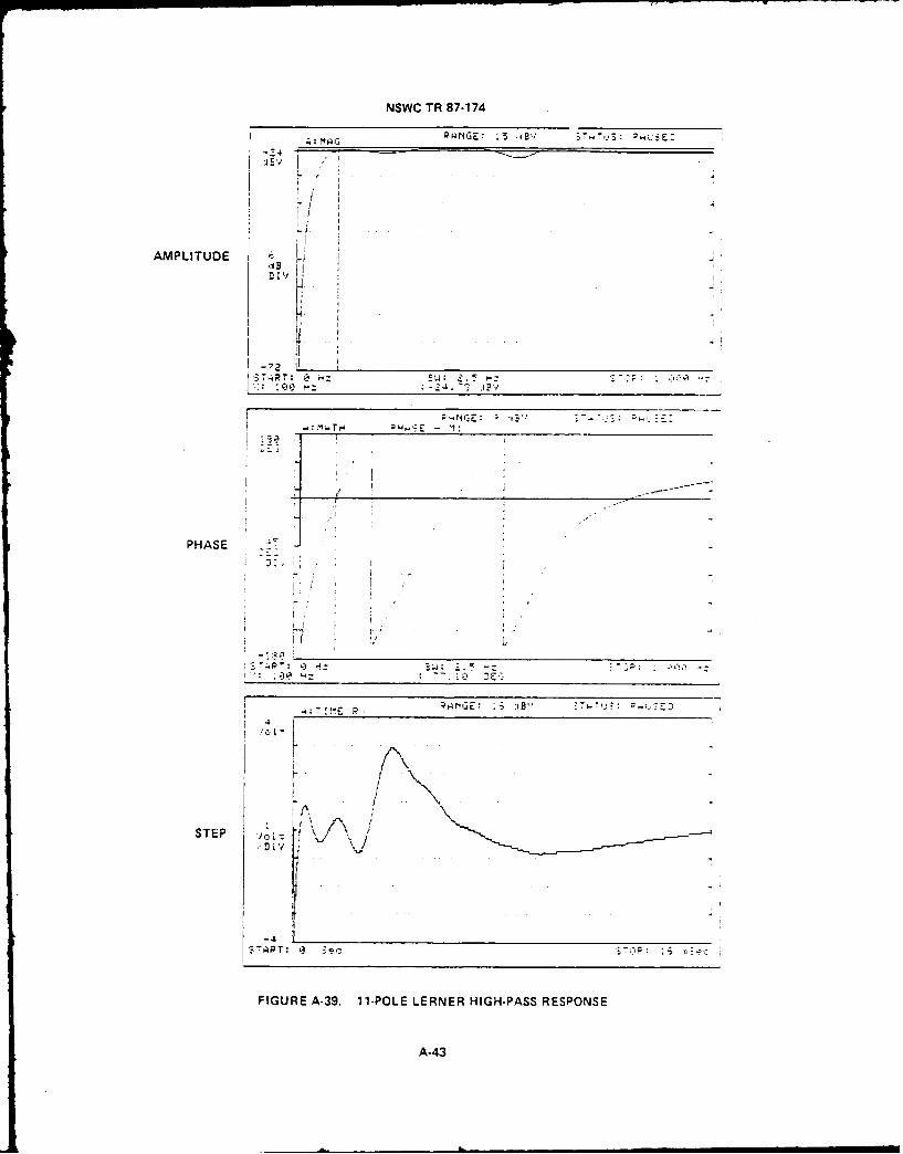
NSWC TR 87-174
S'
AMPLITUDE L
DIV i
~ HZ ~ w HZ
PHASE] ".ME Pj RANG 6-... 2 : IB
STE P
, v
!": "¢ w- : r-. i: >;
FIGURE A-39. 11-POLE LERNER HIGH-PASS RESPONSE
A-43
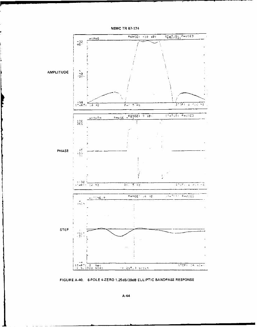
NSWC TR 87-174
PfNIE: -! J BV
AMPLITUDE BI /
1"'
PHASE - -
TE P
3 p 7: . s-
FIGURE A-40. 6-POLE 4-ZERO 1.25dB/39d6 ELLIPTIC BANDPASS RESPONSE
'DI' A-44

NSWC TR 87-174
. .
AMPLITUDE 6 L
• B
- k: '
71;~PT: .3 H:" !a, Hz .',F . 0 :'
P H!GE: ? :B,
4: M -- l
-- - -- - ---
P H A S E -- ---- ---- ---:.. ----.. .. ... .. .... .... . ... ...................... ...
74 7:H
T :1ME 4 1
i ,
STEP "'
I : --/. . .
4.....................--
7:T ; ?r , '
, /
FIGURE A-41. 6-POLE 6-ZERO I.25dB/39d8 ELLIPTIC BAND REJECT RESPONSE
A-45
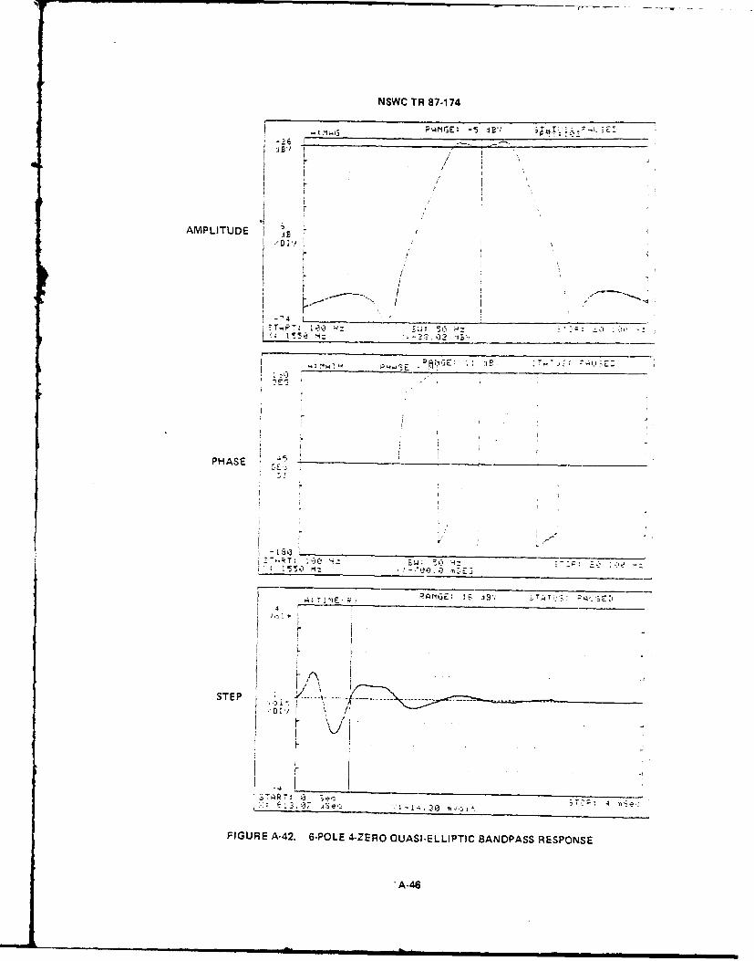
NSWC TR 87-174
~~~~~,) ~ ~ ~ N E F-5 __ _ _ __ _ _ __ _ _ B_ _ __ _ __V__
AMPLITUDE
-'P47 1 __ _ _ _ __ _ _ _ _ H___S,4:_ ____0
'I !
PHASE -
18 6I3
STE ---- ----
3ThkRT: L0 T.)~* 4 .2. 7 0 7 1
FIGURE A-42. 6-POLE 4-ZERO QUASI-ELLIPTIC BANDPASS RESPONSE

NSWC TR 87-174
7 T
/ I
AMPLITUDE -
ST HP : 1-" H S : * irj4 i H: .-. Y~~
: MHTH
PHASE
STEP v.
1. :'r~ r 7
FIGURE A-43. Q-OF-10 NARROWBANO RESPONSE
A-47
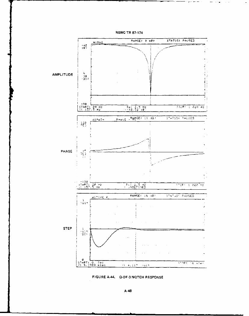
NSWC TR 87-174
QMPGE: ' dBY STATUS: P t'SED
[ '!,"
AMPLITUDE -
l ')
"TART: 20 Hz W . Hz .TOP q z
_-1 T7,E5 Hz ,B'
,'.,,T S L/E
A:MA m
E
PHASE
L
STEP ___
FIGURE A-44. Q-OF*3 NOTCH RESPONSE
A-48

NSWC TR 87-174
AMPLITUDE
~ T~T:~ ,i: w: I Hz:,:4~-
m..'IArH PHWSE -mI ls f
PHASE -
TH H: H=~ H:
A; T ME - QME ~ 3,; .~.f
STEP
4; .. !o I
FIGUREA-AS. 1-POLE 1-ZERO ALL-PASS RESPONSE
A-49
NSWC TR 87-174
PHASE 'I
H..PTH 2 H: CF L3~ 0 -
4.kTH PHP'3E -
PHASE l
RA GE I: I JR H: TJS 2 E
4I m - H PH6.-E Ml-iv
PHASEDIFFERENCE
j~PT 5 H= 114: 2~5 H: 4
FIGURE A-46. 2-POLE 2-ZERO 90 DEGREE-PHASE-DIFFERENCE NETWORK RESPONSE
A-50
NSWC TR 87-174
..: = 15 l ,,. S: i
II
AMPLITUDE .. i
P. .. I H .
.P.,T..GE, ;t ',I B' 1, 1 ' 77m,
W4 'I j I "\L i:PA! 'u . -*
PHASE -
IO-I
S .P-7-1B . :7'' ;.H
PAN'GE: .6 ,JBY .' 7:,+Tj- =q,.SED
a
1,7P, !0
FIGUREA-47. Q-OF-400COMMUTATING BANOPASS RESPONSE
A-51
NSWC TR 87.174
IN OUT
CD4051
99CLOCK 10 4040 10
FIGURE A-48. Q-OF-400 COMMUTATING BANOPASS CIRCUIT
A-52
NSWC TR 87-174
p14NGE: ?.3 d8V STTiTUS: Psi U-ED,~~JB ,/,
. . ... -
L /I . .. . . " . .-
A M P L IT U D E ....... . ..
.
,""
-47 • _S T A R T : 3 H : T : -: 4 C3 , H :
> -: : ~~~w I E I6
:, : 5 . 5 < £ ,
I}
.1h1IMl ! ilii:,'. ; l ,I. jI I
I -ti
PH/ASE I•I
'r. -I
Rii;NGE 1t 217.7
S T E P - : ",
4 .'
: .P 3 [T : 6: m E -I,.
FIGURE A-49. 8-STAGE TRANSVERSAL FILTER RESPONSE
A-53

NSWC TR 87-174
CLOCK
9 10 1
S
D 4
0 1
| FIGURE A-50. 8-STAGE TRANSVERSAL FILTER CIRCUIT
A-1A
111.
OU
A-54

NSWC TR 87-174
REFE RENCES
A-. Delagrange, A. D., A Useful Filter Family, NS4iC/WOL TR 85-170, 20 Oct 1975.
A-5 5/A-56

NSWC TR 87-174
DISTRIBUTION
Copies Copies
Commander Commanding OfficerNaval Air Systems Command Naval Research LaboratoryDepartment of the Navy Attn: Dr. J. MunsonWashington, DC 20361 1 Washington, DC 20390
Chief of Naval Operations Director
Attn: OP-562 1 Woods Hole Oceanographic InstituteDepartment of the Navy Woods Hole, MA 02543Washington, DC 20350-2000
Chief of Naval ResearchCommander Attn: Code ONR-715Naval Sea Systems Command Washington, DC 20375
?rtn: SEA-03b 1SEA-09G32 1 Commanding Officer
Department of the Navy Naval Air Development CenterWashington, DC 20362 Attn: Mr. J. Howard
Warminster, PA 18974CommanderNaval Ocean Systems Center Director
Attn: Code 521 (J. Stegman) I Marine Physical LaboratorySan Diego, CA 92152-5000 San Diego, CA 92132
Commander NASA Scientific and TechnicalU.S. Naval Oceanographic Office Information Facility
Attn: 037-B 1 P.O. Box 5700Washington, DC 20390 Bethesda, MD 20546
Commander The Pennsylvania State UniversityDTRDC Applied Research Laboratory
Bethesda, MD 20084 1 P.O. Box 30State College, PA 16804
CommanderNaval Weapons Center Defense Technical InformationChina Lake, CA 93555 1 Center
Cameron Station
Commanding Officer Alexandria, VA 22304-6145 12Naval Underwater Systems CenterNewport, RI 02840 1
(1)
NSWC TR 97-174
DISTRIBUTION (Cont.)
Ccpies Copies
Director Lincoln LaboratoryScripps Institute of Oceanography Attn: Dr. B. GoldUniversity of California Lexington, MA 02173La Jolla, CA 93105
Raytheon CompanyDirector 1847 West Main RoadApplied Physics Laboratory P.O, Box 360University of Washington Portsmouth, RZ 02871Seattle, WA 98105 1
Bunker-Ramo CorporationBell Telephone Laboratory Electronic Systems DivisionAttn: Mr. J. L. Rosier I Attn. Mr. R. DelaneyGreensboro, NC 27401 31317 La Tienda Drive
Westlake Village, CA 91359Magnavox Government and Industrial
Electronics Co. Emerson Electric1313 Production Rcad Attn: Mr. Carl Lehne
Fort Wayne, IN 46808 1 8100 Floussant DriveSt, Louis, MO 63136
Sanders Associates, Inc.95 Canal Street General Electric CompanyNashua, NH 03060 1 Aerospace Group Prograns
Attn, Mr. R. McCabeA.C, Electronics Defense Research 3198 Chestnut Street
Laboratory Philadelphia, PA i9101
General Motors CorporationDelco Division Litton Systems, Inc.Santa Barbara Operations Data Systems Division6767 Hollister Avenue Attn: Dr. M. Basin
Goleta, CA 93017 1 8000 Woodley AvenueVan Nuys, CA 91409
Hughes Aircraft Co.Ground Systems Group Commanding Officer
P.O. Box 3310 Naval Coastal Systems CenterFullerton, CA 92634 1 Attn- J. Horn
Panama City, FL 32407Interstate Electronics Corporation
Attn: J. Williams Director707 E. Vermont Avenue Applied Research LaboratoryAnaheim, CA 92803 University of Texas at Austin
Attn- L. Mellenbruch
University of Rhode Island Austin, TX 78713-8029Attn: Dr. D. Tufts
Electrical Engineering Dept. Itek Applied, :nc.Kingston, RI 02881 Attn: W. H. From
645 ALmanor AvenueSunnyvale, CA 94086
(2)

NSWC TR 87-174
DISTRIBUTION (Cont.)
Copies Copies
Honeywell, Inc. RCA SelectavisionMarine Systems Center Attn: John Amery5303 Shilshole Avenue N.W. 7900 W. Rockville Rd.Seattle, WA 98107 1 Indianapolis, IN 46224
Underwater Systems, Inc. Library of Congress1776 E. Jefferson Street Attn: Gift and Exchange Division 4Rockville, MD 20852 1 Washington, DC 20540
Lockheed Missiles & Space Co. Internal Distribution:
Attn: A. B. Faris 1 U25 (Delagrange) 10Li1 Lockheed Way U25 (Hebbert) 1Sunnyvale, CA 94088 U25 (Hein) i
U25 (Pruessner) 1Wilcoxon Research U25 (Cook) IAttn: F. Wilcoxon 1 !725 (Davis) 12096 Gaither Rd. U25 (Laanisto) 1Rockville, MD 20850 U25 (Warner) 1
U25 (Watts) IWestinghouse Defense and U202 (Ballard) I
Electronics Center U04 (Biloanis) 1P. 0. Box 746 U23 (Bronstein)Attn: Jin Mayhew 1 U24 (C. Berstein) IBaltimore, MD 21203 E231 2
E232 15University of Minnesota E35 I
Dept. of Physics H14 (R. S. Reed)Attn: Prof. Donald Olson 1 K34 (Gallagher) 1
Duluth, L 55812 R41 (G. Goo) 4C72W (F. Wein)
(3)