2246 MOD - xDevs.com
380
and 2246 MOD PORTABLE OSCILLOSCOPE SERVICE SN 1570~1 UO ana ABUJE (2246 i Y, ZH) SN B100100 and ABOVE (2246 MOD P
-
Upload
khangminh22 -
Category
Documents
-
view
3 -
download
0
Transcript of 2246 MOD - xDevs.com

and 2246 MOD PORTABLE OSCILLOSCOPE SERVICE
SN 1570~1 UO ana ABUJE (2246 i Y, ZH)
SN B100100 and ABOVE (2246 MOD P
TEK SERVICE Part No. 070-7062-00 r MANUAL Product Group 46 I
and 2246 MOD A
I WARNING b
PORTABLE OSCILLOSCOPE SERVICE
SN B700100 and ABOVE (2246 IY, 2R) SN BlOOlOO and ABOVE (2246 MOD A)
The 2246 2R Is a rackmount verslon of the 2246 1 Y This senflce manual and the 2240F1 R lnstructlon sheet (Tektronix part number 070-6332-00) are requlred to fully senflce the 2246 2R oscllloscope.
The following servicing instructions are for use by qualified service personnel only. To avoid personal injury, do not perform any servicing unless you are qualified to do so. Refer to the Safety Summary prior to performing any service.
Please check for CHANGE INFORMATION at the rear of this manual.

Copyright O 1988Tektronix, Inc. All rights resewed. Contents of this publication may not be reproduced in any form without the written permission of Tektronix, Inc.
Products of Tektronix, Inc., and itHsubsidiaries are covered by U.S. and foreign patents issued and pending.
TEKTRONIX, TEK, SCOPE-MOBILE, and are registered trademarks of Tektronix, Inc.
Printed in U.S.A. Specification and price change privileges are resewed.
INSTRUMENT SERIAL NUMBERS
Each instrument has a serial number on a panel insert, tag, or stamped on the chassis. The first two digits designate the country of manufacture. The last five digits of the serial number are unique to each instrument. The country of manufacture is identified as follows:
BOO0000 Tektronix, lnc., Beaverton, Oregon, U.S.A.
E200000 Tektronix United Kingdom, Ltd., Marlow
GI 00000 Tektronix Guernsey, Ltd., Channel Islands
HKOOOOO Hong Kong
H700000 Tektronix Holland, NV, Heerenveen, The Netherlands
JPOOOOO Sonyflektronix, Japan
2246 1Y and 2246 Mod A Service
TABLE OF CONTENTS
Page
LIST OF ILLUSTRATIONS.. . . . . . . . . . . . . . . . . . v i LIST OF TABLES . . . . . . . . . . . . . . . . . . . . . . . . . . vi i OPERATORS SAFETY SUMMARY . . . . . . . . . . . vii i SERVICING SAFETY SUMMARY . . . . . . . . . . . . . ix
Section 1 SPEClFlCATlON
INTRODUCTION . . . . . . . . . . . . . . 1-1
. . . . STANDARD ACCESSORIES 1-1
RECOMMENDED RECALIBRATION . . . . . . . . . . . . . . . . . SCHEDULE 1-1
PERFORMANCE CONDITIONS . . 1-2
Section 2 PREPARATION FOR USE
SAFETY . . . . . . . . . . . . . . . . . . . . 2-1
LlNE VOLTAGE AND POWER CORD . . . . . . . . . . . . . . . . . . . . . 2-1 LINE FUSE . . . . . . . . . . . . . . . . . 2-1
INSTRUMENT COOLING ... . . . . . 2-2
START-UP . . . . . . . . . . . . . . . . . . 2-2 DETAILED OPERATING INFORMATION . . . . . . . . . . . . . . . 2-2
Section 3 THEORY OF OPERATION
. . . . . SECTION ORGANIZATION 3-1
INTEGRATED CIRCUIT DESCRIPTIONS . . . . . . . . . . . . . . 3-1
BLOCK DIAGRAM DESCRIPTION . . . . . . . . . . . . . . . . . 3-1
INTRODUCTION . . . . . . . . . . . . . . 3-1
Page
VERTICAL INPUTS . . . . . . . . . . . . . . . (Diagram 1 ) 3-1
VERTICAL PREAMPS AND OUTPUT AMPLIFIER
. . . . . . . . . . . . . . . (Diagram 2) 3-2
A AND B TRIGGER SYSTEM . . . . . . . . . . . . . . . (Diagram 3) 3-2
DISPLAY AND TRIGGER LOGIC AND PROCESSOR INTERFACE
. . . . . . . . . . . . . . . (Diagram 4) 3-3 A AND B SWEEPS AND DELAY COMPARATORS (Diagram 5) . . . . . . . . . . . . . . . 3-4
HORIZONTAL OUTPUT . . . . . . AMPLIFIER (Diagram 6) 3-4
Z-AXIS, CRT, PROBE ADJUST, AND CONTROL MUX (Diagram 7) . . . . . . . . . . . . . . . 3-4
MEASUREMENT PROCESSOR (Diagram 8) . . . . . . . . . . . . . . . 3-5
READOUT SYSTEM . . . . . . . . . . . . . . . (Diagram 9) 3-5
SWITCH BOARD AND INTERFACE (Diagram 10) . . . . . . . . . . . . . . 3-6
ADC AND DAC SYSTEM (Diagram 1 1 ) . . . . . . . . . . . . . . 3-6
POWER SUPPLY (Diagram 12) . . . . . . . . . . . . . . 3-6
DETAILED CIRCUIT DESCRIPTION 3-6
VERTICAL INPUTS (Diagram 1 ) . . . . . . . . . . . . . . . 3-6
VERTICAL PREAMPS AND OUTPUT AMPLIFIER (Diagram 2) . . . . . . 3-9
A AND B TRIGGER SYSTEM (Diagram 3) . . . . . . . . . . . . . . 3-1 2
DISPLAY AND TRIGGER LOGIC AND PROCESSOR INTERFACE (Diagram 4) . . . . . . . . . . . . . . 3-1 6
REV OCT 1991

2246 1Y and 2246 Mod A Service
TABLE OF CONTENTS (cont)
Page
A AND B SWEEPS AND DELAY COMPARATORS (Diagram 5) . . . . . . . . . . . . . . . 3-31
HORIZONTAL OUTPUT AMPLIFIER (Diagram 6) . . . . . . . . . . . . . . . 3-37
Z-AXIS, CRT, PROBE ADJUST, AND CONTROL MUX (Diagram 7) . . . . . . . . . . . . . . . 3-38
MEASUREMENT PROCESSOR (Diagram 8) . . . . . . . . . . . . . . . 3-42
READOUT SYSTEM (Diagram 9) . . . . . . . . . . . . . . . 3-45
SWITCH BOARD AND INTERFACE (Diagram 10) . . . . 3-51
ADC AND DAC SYSTEM (Diagram 1 1 ) . . . . . . . . . . . . . . 3-52
POWER SUPPLY (Diagram 12) . . . . . . . . . . . . . . 3-53
MAIN BOARD POWER DISTRIBUTION (Diagram 13) . . . . . . . . . . . . . . 3-58
PROCESSOR POWER BOARD DISTRIBUTION (Diagram 14) . . 3-58
INTERCONNECTION DIAGRAM (Diagram 15) . . . . . . . . . . . . . . 3-58
Section 4 PERFORMANCE CHECK PROCEDURE
INTRODUCTION . . . . . . . . . . . . . . . . 4-1 TEST EQUIPMENT REQUIRED . . 4-1
PERFORMANCE CHECK INTERVAL . . . . . . . . . . . . . . . . . . 4-1
PREPARATION . . . . . . . . . . . . . . . 4-1
INDEX TO PERFORMANCE CHECK PROCEDURE . . . . . . . . . 4-4
DISPLAY . . . . . . . . . . . . . . . . . . . . . 4-5
TRACE ROTATION . . . . . . . . . . . 4-5
GEOMETRY . . . . . . . . . . . . . . . . . 4-5
Page
VERTICAL . . . . . . . . . . . . . . . . . . . 4-6
lnput COUPLING Functional Check . . . . . . . . . . . . . . . . . . . . 4-6
CH 1 and CH 2 VOLTSIDIV Trace Shift . . . . . . . . . . . . . . . . 4-6
CH 3 and CH 4 VOLTSIDIV Trace Shift . . . . . . . . . . . . . . . . 4-7
CH 1 and CH 2 VAR VOLTSIDIV Trace Shift . . . . . . . . . . . . . . . . 4-7
CH 1 and CH 2 lnput COUPLING Trace Shift . . . . . . . 4-7
CH 2 INVERT Trace Shift . . . . . 4-7
CH 1 and CH 2 VAR VOLTSIDIV Range . . . . . . . . . . 4-7
Low-Frequency Linearity . . . . . 4-8
CH 1 and CH 2 Vertical Deflection Accuracy . . . . . . . . . 4-8
Ch 3 and CH 4 Vertical Deflection Accuracy . . . . . . . . . 4-8
ADD Mode and CH 2 INVERT Deflection Accuracy . . . . . . . . . 4-9
Vertical POSITION Range (all channels) . . . . . . . . . . . . . . 4-9
CH 1 to CH 2 Signal Delay Match . . . . . . . . . . . . . . 4-1 0
CH 1 to CH 4 Signal Delay Match . . . . . . . . . . . . . . 4-1 0
CH 3 to CH 4 Signal Delay Match . . . . . . . . . . . . . . 4-1 0
CH 1 and CH 2 Vertical Bandwidth . . . . . . . . . . . . . . . . 4-1 0
CH 3 and CH 4 Vertical Bandwidth . . . . . . . . . . . . . . . . 4-1 1
CH 1 and CH 2 Aberrations . 4-1 1 SCOPE BW (Bandwidth Limit) Accuracy . . . . . . . . . . . 4-1 1 Common-mode Rejection Ratio . . . . . . . . . . . . . . . . . . . . 4-1 2
Channel Isolation . . . . . . . . . . 4-1 2
REV OCT 1991

2246 1Y and 2246 Mod A Service
TABLE OF CONTENTS (cont)
Page
AC-Coupled Lower -3 dB Point . . . . . . . . . . . . . . . . . . . . . 4-1 3 Vertical ALT and CHOP Modes . . . . . . . . . . . . . . . . . . . . 4-13 BEAM FIND Functional Check . . . . . . . . . . . . . . . . . . . . 4-1 3
A and B Trace Separation . . . . . . . . . . . . . . . . 4-1 3
TRIGGERING . . . . . . . . . . . . . . . . . 4-1 4
500 Hz Trigger Sensitivity . . . . . . . . . . . . . . . . . 4-1 4
500 kHz Trigger Sensitivity . . . . . . . . . . . . . . . . . 4-1 5 25 MHz Trigger
. . . . . . . . . . . . . . . . . Sensitivity 4-1 5
100 MHz Trigger Sensitivity . . . . . . . . . . . . . . . . . 4-1 5
100 MHz NOISE REJ Trigger Sensitivity . . . . . . . . . . 4-1 6
Single Sweep Mode . . . . . . . . . 4-1 6
Trigger LEVEL Control Range . . . . . . . . . . . . . . . . . . . . 4-16
TV Field Trigger . . . . . . . . . . . . . . . . . Sensitivity 4-1 7
TV Line Trigger . . . . . . . . . . . . . . . . . Sensitivity 4-1 7
Line Trigger Functional Check . . . . . . . . . . . . . . . . . . . . 4-1 7
HORIZONTAL . . . . . . . . . . . . . . . . 4-1 8
A and B Sweep Length . . . . . . 4-18
Horizontal POSITION Range . . . . . . . . . . . . . . . . . . . . 4-1 8
VAR SECIDIV Range . . . . . . . . 4-18 Magnifier Registration . . . . . . . 4-1 9
A and B Timing Accuracy and Linearity . . . . . . . . . . . . . . . 4-1 9
A and B Magnified Timing Accuracy . . . . . . . . . . . . . . . . . 4-1 9 Delay Time Jitter . . . . . . . . . . . 4-20
Delay Time Accuracy . . . . . . . 4-21
Page
Delay Time Position Range . . . . . . . . . . . . . . . . . . . 4-21
X-Axis Gain Accuracy . . . . . . 4-21
X-Y Phase Difference . . . . . . 4-22 X-Axis Bandwidth . . . . . . . . . . 4-22
TIME AND CURSORS MEASUREMENTS . . . . . . . . . . . . 4-23
I+ SEC 4 and Ic I ISEC 4
. . . . . . . . . . Cursor Accuracy
Delta Time Accuracy . . . . . . . Ic PHASE +I Cursor
. . . . . . . . . . . . . . . . . Accuracy
It VOLTS 4 Cursor Accuracy . . . . . . . . . . . . . . . . . /h V O L T S 4 Cursor
. . . . . . . . . . . . . . . . . Accuracy
Tracking Cursors Position Accuracy . . . . . . . . . . . . . . . . .
CHI lCH2 VOLTMETER MEASUREMENTS . . . . . . . . . . . .
DC Volts Accuracy . . . . . . . . . DC Volts Normal Mode Rejection Ratio . . . . . . . . . . . . +Peak. -Peak. Peak-to-Peak Volts Accuracy . . . . . . . . . . . . 4-26
25 MHz +Peak. -Peak. and Peak-to-Peak Volts Accuracy . . . . . . . . . . . . . . . . . 4-26
100 MHz +Peak. -Peak. and Peak-to-Peak Volts Accuracy . . . . . . . . . . . . . . . . . 4-26
Gated Volts Accuracy . . . . . . 4-26
EXTERNAL Z-AXIS. PROBE ADJUST AND FRONT-PANEL SETUP FUNCTIONS . . . . . . . . . . . 4-28
Check External Z-Axis Input . . . . . . . . . . . . . . . . . . . . 4-28 PROBE ADJUST Output . . . . . 4-28
Run MAKE FACTORY SETTINGS Routine . . . . . . . . . . . . . . . . . . 4-28
REV OCT 1991 iii
2246 1V and 2246 Mod A Service
TABLE OF CONTENTS (cont)
Page
Section 5 ADJUSTMENT PROCEDURE
. . . . . . . . . . . . . . . . INTRODUCTION 5-1
PURPOSE . . . . . . . . . . . . . . . . . . 5-1
TEST EQUIPMENT . . . . . . . . . . . . . . . . . . REQUIRED 5-1
. . . . . LIMITS AND TOLERANCES 5-1
. . . . . . . PARTIAL PROCEDURES 5-1 INTERNAL ADJUSTMENTS AND
. . . ADJUSTMENT INTERACTION 5-1 PREPARATION FOR
. . . . . . . . . . . . . . . ADJUSTMENT 5-3
INDEX TO ADJUSTMENT . . . . . . . . . . . . . . . . PROCEDURE 5-3
POWER SUPPLY. DISPLAY. . . . . . . . . . . . . . . . . . . AND Z-AXIS 5-4
INITIAL CONTROL . . . . . . . . . . . . . . . . . . SETTINGS 5-4
. . . . . . . . . . . . . . . . PROCEDURE 5-4
Power Supply DC Levels (R2252) . . . . . . . . . . . . . . . . . . . . 5-4
. . . . . . . . . . . Grid Bias (R2719) 5-5
. . . . . . . . . Astigmatism (R2788) 5-5
Trace Rotation (Front Panel) . . 5-5
. . . . . . . . . . . Geometry (R2784) 5-5
2-Axis Response (C2704) on instruments with serial numbers of below B110100 for the 2246 MOD A or below B710100
. . . . . . . . . . . . . for the 2246 1Y 5-5
. . . . . . . . Readout Jitter (R724) 5-6
VERTICAL . . . . . . . . . . . . . . . . . . . . 5-7
INITIAL CONTROL SETTINGS . . . . . . . . . . . . . . . . . . 5-7
. . . . . . . . . . . . . . . . PROCEDURE 5-7
Vertical Output Gain (R703) and Readout Vertical Centering (R260) . . . . . . . . . . . . . . . . . . . . . 5-7
CH 1 Step Balance (R12) . . . . . 5-7
CH 2 Step Balance (R22) . . . . . 5-8
Page
. . . CH 3 Step Balance (R141) 5-8
. . . CH 4 Step Balance (R161) 5-8
CH 1 MFILF Gain (R13) and . . . . . . . . . Compensation (C1) 5-8
CH 1 lnput Capacitance (61 14) 5-8
CW 1 lnput Compensation X I 0 . . . . . . . . . . . . . . . . . . . . . (C11) 5-8
CH 1 lnput Compensation . . . . . . . . . . . . . . . XI00 (C10) 5-8
. . . . . . . . . . CH 1 Gain (R211) 5-8
CH 2 MFILF Gain (R23) and Compensation (C2) . . . . . . . . . 5-8
CH 2 lnput Capacitance ((3124) 5-9
CH 2 lnput Compensation . . . . . . . . . . . . . . . . . XlO (C21) 5-9
CH 2 lnput Compensation XI00 (C20) . . . . . . . . . . . . . . . . 5-9
. . . . . . . . . . CH 2 Gain (R221) 5-9
CH 3 MFILF Compensation (C134) . . . . . . . . . . . . . . . . . . . . 5-9
. . . . . . . . . . CH 3 Gain (R231) 5-9
CH 4 MFILF Compensation ((2154) . . . . . . . . . . . . . . . . . . . . 5-9
. . . . . . . . . . CH 4 Gain (R241) 5-9
Delay-line HF Compensation (R272. R273. R275. C274. C273) . . . . . . . . . . . . . . . . . . . 5-10
CH 3 HF Compensation . . . . . . . . . . . . . . . . . . . (C138) 5-10
CH 4 HF Compensation (C158) . . . . . . . . . . . . . . . . . . . 5-10
CH 1 and CH 2 Bandwidth Check . . . . . . . . . . . . . . . . . . . 5-10
CH 3 and CH 4 Bandwidth . . . . . . . . . . . . . . . . . . . Check 5-11
HORIZONTAL . . . . . . . . . . . . . . . . 5-12 INITIAL CONTROL SETTINGS . . . . . . . . . . . . . . . . 5-12
PROCEDURE . . . . . . . . . . . . . . 5-12
Horizontal X I Gain (Timing) (R826) . . . . . . . . . . . . . . . . . . . 5-12
REV OCT 1991


2246 1Y and 2246 Mod A Service
LIST OF ILLUSTRATIONS
Figure
The 2246 1Y and Mod A . . . . . . . . . . . . . . . . Portable Oscilloscope x
1-1 Maximum input voltage vs frequency derating curve for the CH 1, CH 2, CH 3, or CH 4 input connectors . . . . 1-14
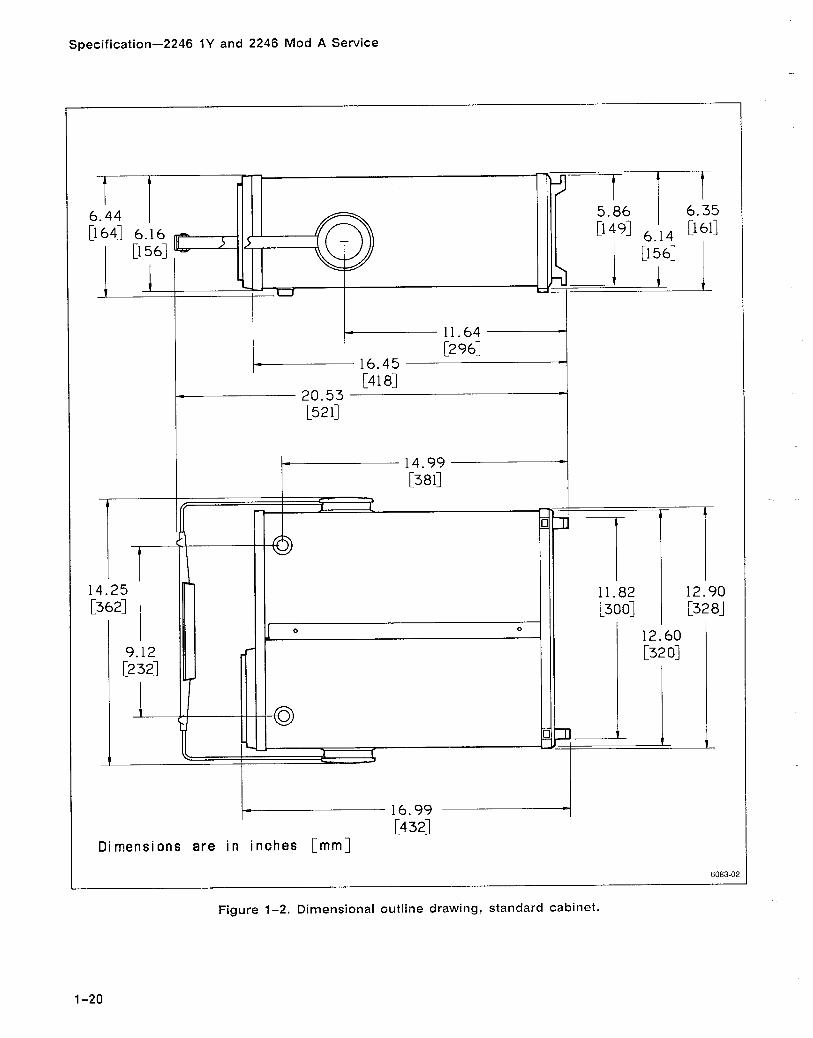
1-2 Dimensional outline drawing, standard cabinet . . . . . . . . . . . . . . . . . 1-20
1-3 Dimensional outline drawing, rackmount cabinet . . . . . . . . . . . . . . . . 1-21
2-1 Optional power cords . . . . . . . . . . . . . . 2-1
3-1 Display Sequencer IC (SLIC, U600) pin-out diagram . . . . . . . . . . . . . . . . . . 3-1 6
3-2 Readout interface relative signal timing . . . . . . . . . . . . . . . . . . . . . 3-25
3-3 Trigger Logic IC (FLIC, U602) pin-out diagram . . . . . . . . . . . . . . . . . . 3-26
3-4 Simplified Sweep Circuit . . . . . . . . . . . 3-32
3-5 A Sweep Start circuit waveforms . . . . 3-36
3-6 Simplified diagram of the DC Restorer circuitry . . . . . . . . . . . . . . . . . 3-40
3-7 Display addresses . . . . . . . . . . . . . . . . 3-48
3-8 Character pixel arrangement . . . . . . . 3-50
3-9 Power Supply block diagram . . . . . . . 3-54
3-10 Preregulator switching waveforms . . . 3-56
5-1 Areas of waveform affected by HF compensation . . . . . . . . . . . . . . . . . 5-1 0
5-2 2-5 ns Timing . . . . . . . . . . . . . . . . . . . . 5-13
6-1 Power-on test failure codes . . . . . . . . 6-10
6-2 Initial SERVICE MENU . . . . . . . . . . . . . . 6-1 1
Page
6-3 SERVICE MENU with DIAGNOSE . . . . . . . . . . . . . . . . . choice selected 6-1 2
. . . . . . . . . . . . . . 6-4 Main board removal 6-44
6-5 Delay-line connections to top of . . . . . . . . . . . . . . . . . . . . . Main board 6-45
9-1 Color codes for resistors
9-2 Semiconductor lead configurations
9-3 Locating components on schematic diagrams and circuit board illustrations
9-4 Simplified 2246 1Y and 2246 Mod A block diagram
9-5a Detailed 2246 1Y or 2246 Mod A block diagram-part 1
9-5b Detailed 2246 1Y or 2246 Mod A block diagram-part 2
9-6a A1 0-Main board for SN 8715000 and above (2246 1 Y) , and B120000 and above (2246 Mod A)
9-6b A1 0-Main board for SN 871 0100 to B714999 (2246 1 Y), and SN 81 101 00 to B119999 (2246 Mod A)
9-6c A1 0-Main board for SN B710099 and below (2246 lY) , and B1 10099 and below (2246 Mod A)
9-7 A9-2 mV Bandwidth board for SN 8700100 to B714999 (2246 1Y) , and SN B100100 to B119999 (2246 Mod A)
9-8 Hybrid pin identifiers
9-9 A8-CRT Control board
9-1 0 A1 6-Processor board
9-1 1 A14-Switch board
9-1 2 A1 2-Potentiometer board
9-1 3 A1 8-Power Supply board
9-1 4 A1 0-Main board adjustment locations
REV OCT 1991

2246 1Y and 2246 Mod A Service
LIST OF TABLES
Table Page Page
. . . . . . . . . . . . 1-1 Electrical Characteristics 1-3 3-25 Front-Panel Multiplexer Channel . . . . . . . . . . . . . . . . . . . . . . 1-2 Environmental Characteristics 1-15 Select Bits 3-41 . . . . . . .
. . . . 1-3 Mechanical Characteristics 1-1 7 3-26 Measurement Processor Signals 3-44 . . . . . . . . . . . . . . 3-27 Position Enable Bit Assignment 3-49
3-1 Shift Register 0 Bit Assignment . . . . . . 3-7 3-28 Field and Mixer Attribute Bit Assignment . . . . . . . . . . . . . . . . . . . . . 3-50 . . . . . 3-2 Input Coupling Control Bit States 3-8
3-29 Display Possibilities . . . . . . . . . . . . . . 3-51 3-3 CH 1 and CH 2 Attenuator and Gain
Control Bit States 3-9 3-30 Possible Signal Conditions . . . . . . . . . . . . . . . . . . to U2416 . . . . . . . . . . . . . . . . . . . . . . . 3-51
3-4 CH 2 INVERT Control Bit . . . . . . . . . . . . 3-9
3-5 CH 3 and CH 4 Gain Control Bit . . . . . 3-10
3-6 Trigger Selection Logic . . . . . . . . . . . . 3-13
3-7 Display Sequencer (U600) Control Bit Assignments . . . . . . . . . . . . . . . . . . 3-1 8
3-8 A Trigger Source Select Bits . . . . . . . 3-19
3-9 Horizontal Display Mode Select Bits . . 3-19
3-10 Shift Register 1 Control Bit Data . . . . 3-20
3-1 1 Trigger Source Select . . . . . . . . . . . . . 3-21
3-12 Vertical MODE Select . . . . . . . . . . . . . 3-21
3-13 Horizontal MODE Select . . . . . . . . . . . 3-21
3-14 Holdoff Counter Encoding . . . . . . . . . . 3-22
3-1 5 Display Sequencer Channel Select Logic Bits . . . . . . . . . . . . . . . . . . . . . . . 3-23
3-1 6 Horizontal and Vertical Display Response . . . . . . . . . . . . . . . . . . . . . . . 3-24
3-17 Trigger Logic IC Addressing Logic . . . 3-27
3-18 Control Register Signal-bit Names . . . 3-28
3-1 9 Delay Mode Selection Control Bits . . . 3-28
3-20 Peak Volts Detection Mode Logic . . . 3-28
3-21 Z-Axis Switching Logic . . . . . . . . . . . . 3-30
3-22 A Sweep Timing Selections . . . . . . . . 3-34
3-23 B Sweep Timing Selections . . . . . . . . . 3-35
3-24 HDO and HD1 Logic . . . . . . . . . . . . . . . 3-37
4-1 Test Equipment Required . . . . . . . . . . 4-2
4-2 Signal-to-Graticule Accuracy . . . . . . . 4-8
4-3 Settings for Timing Accuracy Checks . . . . . . . . . . . . . . . . . . . . . . . . 4-20
4-4 Delay Time Accuracy . . . . . . . . . . . . . 4-21
5-1 Adjustment Interactions . . . . . . . . . . . . 5-2
5-2 Power Supply Voltage Limits . . . . . . . . 5-5
6-1 Relative Susceptibility to Static-Discharge Damage . . . . . . . . . . 6-1
6-2 External Inspection Checklist . . . . . . . . 6-3
6-3 Internal Inspection Checklist . . . . . . . . 6-3
6-4 Power Supply Voltage and Ripple Limits . . . . . . . . . . . . . . . . . . . . . 6-8
6-5 SERVICE MENU Selections . . . . . . . . 6-12
6-6 DIAGNOSE ROUTINES . . . . . . . . . . . . . 6-16
6-7 Horizontal Display State Logic . . . . . . 6-22
6-8 Measurement Processor I10 Memory Map . . . . . . . . . . . . . . . . . . . . 6-23
6-9 Measurement Error Troubleshooting Hints . . . . . . . . . . . . . . . . . . . . . . . . . . 6-26
6-1 0 Maintenance Aids . . . . . . . . . . . . . . . . 6-36
9-1 Signal Line Locations
REV OCT 1991

2246 1Y and 2246 Mod A Service
OPERATORS SAFETY SUMMARY
The safety information in this summary is for operating personnel. Warnings and cautions will also be found throughout the manual where they apply.
Terms in this Manual Grounding the Product
CAUTION statements identify conditions or practices This product is grounded through the grounding con- that could result in damage to the equipment or ductor of the power cord. To avoid electrical shock, other property. plug the power cord into a properly wired recep-
tacle before making any connections to the product WARNING statements identify conditions or practices input or output terminals. A protective ground con- that could result in personal injury or loss of life. nection, by way of ttie grounding conductor in the
power cord, is essential for safe operation.
Terms as Marked on Equipment Danger Arising From Loss of Ground
CAUTION indicates a personal injury hazard not im- mediately accessible as one reads the markings, or Upon loss of the protective-ground connection, all
a hazard to property, including the equipment itself, accessible conductive Parts, including knobs and controls that may appear to be insulating, can ren-
DANGER indicates a personal injury hazard im- der an electric mediately accessible as one reads the marking.
Use the Proper Power Cord
Symbols in this Manual Use only the power cord and connector specified for your product.
This svmbol indicates where a ~ ~ l i c a b l e cautiohary or other information' is to be found. For maximum input voltage
Use only a power cord that is in good condition.
see Table 1-1. For detailed information on power cords and con- nectors, see Figure 2-2.
Symbols as Marked on Equipment
DANGER-High voltage.
Use the Proper Fuse
To avoid fire hazard, use only a fuse of the correct type, voltage rating and current rating as specified in the parts list for your product.
@ Protective ground (earth) terminal. Do Not Operate in an Explosive
ATTENTION-~efer to manual. Atmosphere
Power Source
To avoid explosion, do not operate this instrument in an explosive atmosphere unless it has been spe- cifically certified for such operation.
This product is intended to operate from a power source that does not apply more than 250 V rms DO Not Remove Covers or between the supply conductors or between either supply conductor and ground. A protective ground To avoid personal injury, do not remove the product connection, by way of the grounding conductor in covers or panels. Do not operate the product with- the power cord, is essential for safe operation. out the covers and panels properly installed.
viii

2246 1Y and 2246 Mod A Service
SERVICING SAFETY SUMMARY
FOR QUALIFIED SERVICE PERSONNEL ONLY
Refer also to the preceding Operators Safety Summary
Do Not Service Alone Disconnect power before removing protective panels, soldering, or replacing components.
Do not perform internal service or adjustment of this product unless another person capable of rendering first aid and resuscitation is present.
Power Source
Use Care When Servicing With Power On This product is intended to operate from a power source that does not apply more than 250 volts rms
Dangerous voltages exist at several points in this between the supply conductors or between either product. To avoid personal injury, do not touch supply conductor and ground. A protective ground exposed connections or components while power is connection by way of the grounding connector in the on. power cord is essential for safe operation.

2246A Service
The 2246 1Y or 2246 Mod A Portable Oscilloscope.
INTRODUCTION
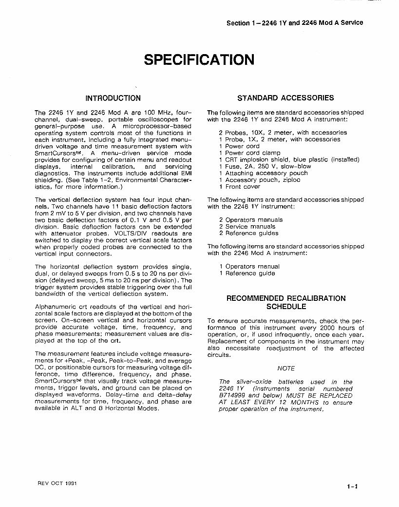
Section 1 -2246 1Y and 2246 Mod A Service
SPECIFICATION
The 2246 1Y and 2246 Mod A are 100 MHz, four- channel, dual-sweep, portable oscilloscopes for general-purpose use. A microprocessor-based operating system controls most of the functions in each instrument, including a fully integrated menu- driven voltage and time measurement system with SmartCursors@. A menu-driven service mode provides for configuring of certain menu and readout displays, internal calibration, and servicing diagnostics. The instruments include additional EM1 shielding. (See Table 1-2, Environmental Character- istics, for more information.)
The vertical deflection system has four input chan- nels. Two channels have 11 basic deflection factors from 2 mV to 5 V per division, and two channels have two basic deflection factors of 0.1 V and 0.5 V per division. Basic deflection factors can be extended with attenuator probes. VOLTSIDIV readouts are switched to display the correct vertical scale factors when properly coded probes are connected to the vertical input connectors.
The horizontal deflection system provides single, dual, or delayed sweeps from 0.5 s to 20 ns per divi- sion (delayed sweep, 5 ms to 20 ns per division). The trigger system provides stable triggering over the full bandwidth of the vertical deflection system.
Alphanumeric crt readouts of the vertical and hori- zontal scale factors are displayed at the bottom of the screen. On-screen vertical and horizontal cursors provide accurate voltage, time, frequency, and phase measurements; measurement values are dis- played at the top of the crt.
The measurement features include voltage measure- ments for +Peak, -Peak, Peak-to-Peak, and average DC, or positionable cursors for measuring voltage dif- ference, time difference, frequency, and phase. SmartCursors@ that visually track voltage measure- ments, trigger levels, and ground can be placed on displayed waveforms. Delay-time and delta-delay measurements for time, frequency, and phase are available in ALT and B Horizontal Modes.
STANDARD ACCESSORIES
The following items are standard accessories shipped with the 2246 1Y and 2246 Mod A instrument:
2 Probes, IOX, 2 meter, with accessories 1 Probe, l X , 2 meter, with accessories 1 Power cord 1 Power cord clamp 1 CRT implosion shield, blue plastic (installed) 1 Fuse, 2A, 250 V, slow-blow 1 Attaching accessory pouch 1 Accessory pouch, ziploc 1 Front cover
The following items are standard accessories shipped with the 2246 1Y ins1:rument:
2 Operators manuals 2 Service manuals 2 Reference guides
The following items are standard accessories shipped with the 2246 Mod A instrument:
1 Operators manual 1 Reference guide
RECOMMENRED RECALIBRATION SCHEDULE
To ensure accurate measurements, check the per- formance of this instrument every 2000 hours of operation, or, if used infrequently, once each year. Replacement of components in the instrument may also necessitate readjustment of the affected circuits.
NOTE
The silver-oxide batteries used in the 2246 1 Y (instruments serial numbered 8714999 and below) MUST BE REPLACED AT LEAST EVERY 12 MONTHS to ensure proper operation of the instrument.
REV OCT 1991

Specification-2246 1Y and 2246 Mod A Service
PERFORMANCE CONDITIONS
The electrical characteristics given in Table 1-1 are valid when the instrument has been adjusted at an ambient temperature betweeri +20°C and +30°C, has had a warm-up period of at least 20 minutes, and is operating at an ambient temperature between -lO°C and +55'C (unless otherwise noted).
Items listed in the Performance Requirements column are verifiable qualitative or quantitative limits
that define the measurement capabilities of the instrument.
Environmental characteristics are given in Table 1-2. This instrument meets the requirements of MIL-T-28800D, for Type Ill, Class 3, Style D equipment, as described in this section.
Physical characteristics of the instrument are listed in Table 1-3.

--- -- -
Specification-2246 1Y and 2246 Mod A Service
Table 1-1
Electrical Characteristics
VERTICAL DEFLECTION SYSTEM - CH 1 AND Cti 2
Characteristics
Deflection Factor
Performance Requirements
Range ( 2 mVldiv to 5 Vldiv in 1-2-5 sequencea I
Accuracy (includes ADD MODE and CH 2 INVERT)
15°C to 35°C 1 Within +2%.
-10°C to 15°C
and 35°C to 55°C Within + 3%.a
Variable Range
Frequency Response (-3 dB bandwidth)
1X Probe
Increases deflection factor by at least 2.5: l .
2 mV/div to 5 Vldiv
AC Coupled Lower -3 dB Point
1 10 HZ or less.
Dc to 100 MHz (at the input BNC and with a 10X probe).
--
1 OX Probe
Step Response (5-division
step)
Rise Time
1 Hz or less.
Positive-Going Step
5 mV/div to 0.5 Vldiv
1 Vldiv to 5 Vldiv
2 mV/div to 5 Vldiv
Aberrations
+5%, -5%, 5% p-p or less.
3.5 ns or less (calculated) ?
+lo%, - lo%, 10% p-p or less.
Negative-Going Step Add 2% to all positive-going step s~ecifications.
a Per formance Requirement not c h e c k e d in manual .
Position Effect
Temperature Effect
Aberrations measured anywhere on screen do not exceed those measured at center screen by more than 1%.
Add 0.15% per "C above or below 25°C.
Specification-2246 1Y and 2246 Mod A Service
Table 1-1 (cont) Electrical Characteristics
Common Mode Rejection Ratio (CMRR)
Characteristics
Delay Match (CH 1 to CH 2)
At least 25: 1 up to 10 MHz and at least 10: 1 up to 100 MHz for signals of eight divisions or less with VOLTSIDIV VAR adjusted for best CMRR at 50 kHz.
Performance Requirements
Less than 400 ps difference.
Channel Isolation (attenuation of deselected channel)
10 MHz 100 MHz
50 dB ( z 316: l ) 34 dB ( 5 0 : l ) or more or more
Trace Shift as VAR VOLTSIDIV is Turned
1 division or less.
Invert Trace Shift I 1 division or less.
Trace Shift Between VOLTSIDIV Switch Positions
0.2 division or less.
Trace Shift Between GND and DC input Coupling
-10°C to 35OC I Less than 0 .5 mV.
I Less than 2 m v a
lnput Characteristics
Resistance
Capacitance
a Performance Requirement not checked in manual.
1 M a +2%.a
20 pF +2 p ~ . ~
Capacitance Match Between Any Two VOLTSIDIV Settings
Maximum Input
volts A 5 0 . 5 pF.
400 V (dc + peak ac); 800 V p-p at 10 kHz or less; 800 V p-p at 10 kHz or less; 5 V (dc + peak ac) at
100 MHz or less.a

-- - -
Specification-2246 1Y and 2246 Mod A Service
Table 1-1 (cont)
Electrical Characteristics
Deflection Factor
Range
Characteristics
0.1 V per division and 0.5 V per division?
Performance Requirements
Accuracy
15OC to 35OC
VERTICAL DEFLECTION SYSTEM - CH 3 AND CH 4
Within k2%.
Step Response (5-division step) Rise Time
-10°C to 55°C
Frequency Response (-3 dB bandwidth)
3.5 ns or less (calculated) .a
Within k 3%.
Dc to 100 MHz (at the input BNC and with a 1 OX probe).
Delay Match (CH 3 to CH 4) I Less than 400 ps difference
Channel Isolation (attenuation of deselected channel)
Trace Shift Between VOLTS/DIV Settings
1 34 dB or more at 100 MHz
1 division or less.
Channel isolation tested with eight-division input signa!.
lnput Characteristics
Resistance
Capacitance
Maximum lnput Volts n 400 V (dc + peak ac); 800 V p-p at 10 kHz or less;
800 V p-p at 10 kHz or less; 5 V (dc + peak ac) at 100 MHz or less.a
a Performance Requirement not checked in manual.

Specification-2246 1Y and 2246 Mod A Service
Table 1-1 (cont) Electrical Characteristics
I
VERTICAL DEFLECTION SYSTEM - ALL CHANNELS
Characteristics
Bandwidth Limit (-3 dB bandwidth)
Performance Requirements
20 MHz f25%.
Low Frequency Linearity (Relative to center screen) Within + 5%.
Linearity is measured by positioning a two-division test signal anywhere on screen and noting the amplitude change.
Position Range / At least 210 divisions form graticule center.
CHOP Mode Clock Rate ( 625 kHz
TRACE SEP Control Position Range
Delay Match (CH 1 or CH 2 to CH 3 or CH 4)
At least + 4 divisions.
Less than 800ps difference.
HORIZONTAL DEFLECTION SYSTEM
Sweep Range
A Sweep 0.5 sldiv to 20 nsldiv in a 1-2-5 ~ e q u e n c e . ~
X I 0 magnifier extends maximum sweep speed to 2 nsldiv.
B Sweep 5.0 msldiv to 20 nsldiv in a 1-2-5 sequencea
X I 0 magnifier extends maximum sweep speed to 2 nsldiv.
Sweep Accuracy applies over the center eight divisions. Excludes the first 114 division or 25 ns from the start of the magnified sweep and anything beyond the 100th magnified division.
Accuracy
15°C to 35OC
-10 "C to 15°C
and 35°C to 55OC
a Performance Requirement not checked in manual.
Unmagnified
f 2%
f 3%
Magnified
+ 3%
rt 4%

--
Specification-2246 1Y and 2246 Mod A Service
Table 1-1 (cont) Electrical Characteristics
Characteristics I Performance Requirements
Sweep Linearity applies over the center eight divisions of an unmagnified sweep. Excludes the first 114 division or 25 ns from the start of the sweep.
Sweep Linearity
Sweep linearity is determined by the error of a single time mark relative to two adjacent time marks spaced at one time mark per division.
2 5%.
POSITION Control Range I
X I 0 Magnifier
Registration (X I0 to X I )
Normal Displays
X-Y Displays
Expands the normal sweep by ten times around that portion of the sweep positioned at the center vertical graticule line.a
Able to move the start of the sweep to the right of the center vertical graticule; able to move a time mark corresponding to the end of the tenth division of an unmagnified sweep to the left of the center graticule.
At least +13 divisionsna
1 2 divisions or less shift.
Variable Control Range Continuously variable between calibrated SECIDIV settings. Extends both the A and B sweep time per division by at least a factor of 2.5.
Sweep Length
Delay Time
Jitter
Greater than 10 divisions.
Delay Control Range
1 part in 20,000, or less, peak-to-peak, during a two- second time interval.
Less than 0.1 division to 10 times the A SECIDIV switch setting. Maximum value does not exceed end of the A sweep.
Delta Time
Delta Control Range From 0.5 division or less to the right of setting of DELAY control to within 1.5 divisions of the end of the A sweep.
a Performance Requirement not checked in manual.

Specification-2246 1Y and 2246 Mod A Service
Table 1-1 (cont) Electrical Characteristics
Characteristics I Performance Requirements
Sensitivity-CH 1 through CH 4: AUTO LEVEL, NORM AND SINGLE SEQUENCE
COUPLING
A AND B TRIGGER
Trigger sensitivity is defined as the minimum peak-to-peak sine-wave trigger signal amplitude required to show the test signal with horizontal jitter of less than 3.0% of one period (p-p viewed over two seconds).
0.35 division from dc to 25 MHz, increasing to 1.0 division at 100 MHz.
NOISE REJECT 1.4 division from dc to 25 MHz; increasing to 2.2 division at 100 MHz. 0.5 division or less will not trigger.
HF REJECT 0.35 division from dc to 50 kHz; attenuates signals above upper -3 dB cutoff frequency of 70 kHz.
LF REJECT 0.35 division from 100 kHz to 25 MHz, increasing to 1 .0 division at 100 MHz attenuates signals below the lower -3 dB cutoff frequency of 50 kHz.
0.35 division from 50 Hz to 25 MHz, increasing to 1 .0 division at 100 MHz; attenuates signals below the lower -3 dB cutoff frequency of 10 Hz.
TV LINE, TV FIELD 1 0.5 division of composite sync will achieve a stable display
--
LEVEL Control Range
AUTO LEVEL and AUTO MODE Trigger Low-Frequency Limit
i ? 20 divisions referred to the appropriate vertical input.
10 Hz.
This range is sufficient to allow triggering at any point on a displayed waveform for all modes except "ADD". In ADD, the combined range of the two position controls exceeds the trigger level range, making it possible (though unlikely) to pull a signal on screen for display but fail to trigger to it due to insufficient trigger level range.

-- -- -
Specification-2246 1Y and 2246 Mod A Service
Table 1-1 (cont)
Electrical Characteristics
FUNCTIONS WITH DIGITAL READOUT
Characteristics
TRIGGER LEVEL READOUT Accuracy
HOLDOFF Control Range
Specifications for functions with digital readout are valid only when the ambient temperature is within 210°C of the temperature at the time of the last SELF CAL. For maximum performance, a recent SELF CAL is recommended.
Performance Requirements
2 (0.3% of reading + 10% of one vertical division).
Increases A Sweep holdoff time by at least a factor of 2.a
a~erformance Requirement not checked in manual.
VOLTMETER FUNCTIONS
DC VOLTS
Accuracy
Normal Mode Rejection Ratio
PLUS or MINUS Peak
Accuracy-Full Bandwidth
25 Hz to 25 MHz
Greater Than 25 MHz to 100 MHz (90 MHz at 35" C to 55" C)
Accuracy-Bandwidth Limited (25 Hz to 10 MHz)
Gated Region Minimum Width (when gated)
2 (0.5% of reading + 2% of the VOLTS/DIV setting + 250 pV).
Greater than 50 dB at 50 or 60 Hz.
f (2.0% of reading + 15% of one vertical division + 1 mV).
+0.5 dB/-3 dB 21 mV. Follows the trigger system frequency response curve.
f (2.0% of reading + 10% of one vertical division + 0.3 mV).
(0.2 division + 50 ns) or less.
Specification - 2246 1 Y and 2246 Mod A Service
Characteristics
PK-PK VOLTS
Accuracy- Full Bandwidth
25 Hz to 25 MHz
Greater Than 25 MHz to 100 MHz (90 MHz at 35" C to 55" C)
Accuracy- Bandwidth Limited
25 Hz to 10 MHz
Gated Region Minimum Width (when gated)
CURSOR FUNCTIONS
It SEC 4 (manually position cursors)
Accuracy
0.5 sldiv to 0.1 ~.~s/div
Jt 1/SEC 4 (manually position cursors)
Accuracy
J~VOLTS+ (manually position cursors)
Accuracy
/f/ VOLTS+ (manually position cursors)
Accuracy
Table 1-1 (cont) Electrical Characteristics
Performance Requirements
+ (2.0% of reading + 15% of one vertical division + 1.5 mV).
+ 0.5 dB/-3 dB + 1.5 mV. Follows the trigger system frequency re- sponse curve.
+ (2.0% of reading + 10% of one vertical division + 0.5 mV).
(0.2 division + 50 ns) or less.
+ (0.5% of reading + 2% of the SECIDIV setting).
+ (1.2% of reading + 2% of the SECIDIV setting).
Readout calculated from k SEC cursor positions.
+ (0.5% of reading + 2% of the VOLTS/DIV setting + high-frequency display errors).
+ (0.5% of reading + 2% of the VOLTSIDIV setting + high-frequency display errors).
REV JUN 1991
- -
Characteristics
k- PHASE 4 (manually positioned cursors)
Accuracy
TRACK MEASUREMENT
Position Accuracy (Cursor position on waveform versus digitally displayed measurement value)
TRACK TRIG LEVEL
Position Accuracy (Cursor position on waveform versus digitally displayed measurement value)
TRACK GROUND
Position Accuracy (Cursor position on waveform versus baseline displayed with grounded input)
DELTA TlME FUNCTIONS
DELTA TlME Accuracy
-10" C to 15" C and 35" C to 55" C
DELTA 1 /TIME Accuracy
DELTA Phase Accuracy
Delay Accuracy, A Sweep Trigger Point to start of B Sweep
-
Specification-2246 1Y and 2246 Mod A Service
Table 1-1 (cont)
Electrical Characteristics
Performance Requirements
Readout calculated from /+ SEC * cursor positions. '
Within + 0.05 vertical division.
Within 2 0.05 vertical division.
Within ?r 0.05 vertical division.
f (1 .O% of reading + 1 .O% of one division of the A Sweep).
f (2.0% of reading + 1.0% of one division of the A Sweep).
Readouts calculated using DELTA TlME difference.
Readouts calculated using DELTA TlME difference.
f (0.5% of reading + 5.0% of one division of the A Sweep + 25 ns).

Specification-2246 1Y and 2246 Mod A Service
Table 1-1 (cont)
Electrical Characteristics
Characteristics
EXTERNAL Z-AXIS INPUT
Performance Requirements
Deflection Factors
Accuracy
Y Axis
15°C to 35°C
-10°C to 15°C and 35°C to 55°C
X Axis
15°C to 35°C
-10°C to 15°C and 35°C to 55°C
Horizontal (X-Axis) -3 dB Bandwidth
Phase Match (DC Coupled)
X-Y OPERATION
Same as Vertical deflection system with the VOLTSIDIV variable controls in calibrated detent p ~ s i t i o n . ~
Within f 3%.
Within f 4%. a
Within f 3%.
Within t 3%.a
3 MHz or more.
f 3 degrees from dc to 100 kHz.
PROBE ADJUST OUTPUT
Active Region Lower Threshold (intensity decreases above this voltage)
Signal Required to Modulate an A or B Trace of Normal Intensity
Maximum Input Voltage A Input Loading
Overshoot (rising and falling edge) I 0.1% or less.
+1.8 volts or less.
+3.8 volts or less (usable frequency: DC - 10 MHz).
External Z-Axis signal does not affect the readout or the intensified zone intensity.
30 V (dc + peak ac); 30 V p-p ac at 1 kHz or less.a
Represents less than one LSTTL load.a
Output Voltage on PROBE ADJUST Jack ( 0 . 5 V f l % i n t o l M a load.
a Performance Requirement not checked in manual.
Repetition Rate 1 kHz f 25%.

Specification-2246 1Y and 2246 Mod A Service
Table 1-1 (cont)
Electrical Characteristics
Characteristics Performance Requirements
-
FRONT PANEL SETUP MEMORY
Lithium
Battery Type 2246 lY, 2R
SN 87001 00-B714999 - - - - -
SN B715000 and above
2246 Mod A
Battery Life Silver-oxide
1 At least five years.a
Two 1.5 V, 43 mAH, silver-oxide button cells in seriesa
One, dry, 3.0 V, Lithium.a
One, dry, 3.0 V, Lithium.a
At least one year. a
WARNING -To avoid injury, have battery replaced by a qualified service person for proper handling and disposal of Lithium batteries.
POWER SOURCE
CRT DISPLAY
a Performance Requirement not checked in manual.
REV OCT 1991

Specification-2246 1Y and 2246 Mod A Service
10 10 kHz 50 kHz 100 kHz 500 kHz 1 MHz
FREQUENCY 6555-21
Figure 1-1. Maximum input voltage vs frequency derating curve for the CH 1, CH 2, CH 3, or CH 4 input connectors.

-- -- - -- --
Specification-2246 1Y and 2246 Mod A Service
Table 1-2
Environmental Characteristics
STANDARD INSTRUMENT
Characteristics Description
a Performance not checked in manual.
Environmental Requirements
Temperature
Operating
Non-operating
Altitude
Operating
Non-Operating
Humidity (Operating and Non-operating)
Radiated and conducted Emission required per VDE 0871
Electrostatic Discharge
Instrument meets or exceeds the environmental requirements of MIL-T-28800D for Type Ill, Class 3, Style D equipment, as described be1ow.a
-10°C to +55"C (+14"F to +I31 OF).
-51 OC to +71 OC (-60°F to +I 60°F).
Tested to MIL-T-28800D paragraphs 4.5.5.1.3 and 4.5.5.1.4, except in 4.5.5.1.3, steps 4 and 5 (-1 0 "C operating test) are performed ahead of step 2 (-51 "C non-operating test). Equipment shall remain off upon return to room ambient during step 6. Excessive condensation shall be removed before operating during step 7.
To 4,572 m (1 5,000 ft). Maximum operating temperature decreases 1°C per 1000 ft above 5000 ft.
To 15,240 m (50,000 ft).
Exceeds requirements of MIL-T-28800D, paragraph 4.5.5.2.
Five cycles (1 20 hours) referenced to MIL-T-28800D paragraph 4.5.5.1.2.2, for type Ill, class 3 instruments.
Non-operating and operating at 95%, -0% to +2% relative humidity. Operating at +30°C and +55OC for all modes of operation. Non-operating at +30°C to +60°C.
Meets Category B.
Withstands discharge of up to 20 kV. Test performed with probe containing a 500 pF capacitor with 1 K R series resistance charged to the test voltage.
Conforms to Tektronix Standard 062-2862-00.
Specification-2246 1Y and 2246 Mod A Service
Table 1-2 (cont) Environmental Characteristics
Characteristics I Description
Meets the following requirements in accordance with MIL-T-28800D and MIL-STD-461 C.
CE 01 :Part 2, narrow band requirements up to 15 kHz. CE 03 : Part 4. CS 0l:Part 2. CS 02:Part 2. CS 06:Part 5, limited to 300 V. RE 01: Parts 5 and 6, except measured at 12 inches. RE 02: Part 2, full limits to 1 GHz. RS 02: Part 2, part I. RS 02: Part 2, part II, limited to 5 A at 60 Hz. RS 03: Part 2, limited to 1 GHz.
Vibration (operating) 15 minutes along each of 3 major axes at a total displacement of 0.25 inch p-p (4 g at 55 Hz) with frequency varied from 10 Hz to 55 Hz in 1-minute sweeps. Hold from 10 minutes at 55 Hz in each of the three major axes. All major resonances must be above 55 Hz.
Meets requirements of MIL-T-28800D, paragraph 4.5.5.3.1. I
Bench Handling Test (cabinet on and cabinet off)
Each edge lifted four inches and allowed to free fall onto a solid wooden bench surface.
Transportation
Meets requirements of MIL-T-28800D, paragraph 4.5.5.4.3.
Packaged Vibration Test Meets the limits of the National Safe Transit Association test procedure 1 A-B-1; excursion of 1 inch p-p at 4.63 Hz (1 .1 g) for 30 minutes on the bottom and 30 minutes on the side (for a total of 60 minutes).
Package Drop Test Meets the limits of the National Safe Transit Association test procedure 1A-b-2; 10 drops of 36 inches.

-- - -- -
Specification-2246 1Y and 2246 Mod A Service
Table 1-3
Mechanical Characteristics
Characteristics Description
Weight
With Front Cover, Accessories, and Accessories Pouch (without manual)
With Power Cord
Shipping Weight (Domestic)
Overall Dimensions
Height
With Feet and Accessories Pouch (empty)
Without Accessories Pouch
Width (with handle)
Depth
With Front Cover on
With Handle Extended
Cooling
Finish
Construction
STANDARD INSTRUMENT
8.9 kg (19.6 Ib).
7.9 kg (1 7.4 lb) .
11.7 kg (25.8 lb).
See Figure 1-2, Dimensional drawing.
Approx. 176.5 m m (6.95 in).
164 m m (6.46 in).
362 m m (14.26 in).
445.3 m m (17.53 in).
521 m m (20.51 in).
Forced air circulation; no air filter.
Tek Blue, pebble-grain finish painted on aluminum cabinet.
Aluminum alloy chassis. Plastic-laminate front panel.

Specification-2246 1Y and 2246 Mod A Service
Table 1-3 (cont)
Mechanical Characteristics
Characteristics Description
Overall Dimensions See Figure 1-3, Dimensional drawing.
Height
464 m m (18.3 in).
mounting rail (inside) 465 m m (1 8.3 in).
RACKMOUNT INSTRUMENT
Front panel to rear of mounting rail (outside)
Handles
472 m m (18.6 in).
44 m m (1.73 in).

-- ----
Specification-2246 1Y and 2246 Mod A Service
Table 1-3 (cont) Mechanical Characteristics
Characteristics
Required Clearance dimensions
Height
Width
Depth
Cooling
Finish
Construction
Description
2 1 78 mm (7 in).
2448 mm (1 7-518 in).
2508 mm (20 in).
Forced air circulation; no air filter.
Tek Blue, pebble-grain finish painted on aluminum cabinet.
Aluminum alloy chassis, front-panel frame, and rear support. Plastic-laminate front panel. Glass-laminate circuit boards.
Specification-2246 1Y and 2246 Mod A Service
1- 16.99 [4 321
Dimensions a r e in inches [mm]
Figure 1-2. Dimensional outline drawing, standard cabinet.

--
Specification-2246 1Y and 2246 Mod A Service
L
2.0 In 51 mm
CLEARANCE RECOMMENDED I AT REAR AND 1
SIDES FOR TOP VIEW COOLING AND I INSTRUMENT 1
CONNECTIONS 16.8 In
427 rnm
LEFT S I D E VIEW
1 750 In 44 mm
1.5 In 1
4 0 In "-1 FFiONT VIEW 102 mm d 1.5 In " 0 0
38 mrn
19.0 In + 483 mrn
ALL DIMENSIONS ROUNDED TO NEAREST TENTH
REAR VIEW
8332-0 1
Figure 1-3. Dimensional outline drawing, rackmount cabinet.


Section 2-2246 1Y and 2246 Mod A Service
PREPARATION FOR USE
SAFETY
This section tells how to prepare for and to proceed with the initial start-up of the TEKTRONIX 2246 1Y or 2246 Mod A Oscilloscope.
Refer to the Safety Summary at the front of this manual for power source, grounding, and other safety considerations pertaining to the use of the instrument. Before connecting the oscilloscope to a power source, read this section and the Safety Summary.
LlNE VOLTAGE AND POWER CORD
The 2246 1Y and 2246 Mod A operate on line voltages from 90 to 250 V with line frequencies ranging from 48 to 440 Hz. No line voltage selecting is necessary. The detachable power cord may have to be changed to match the power source outlet (see Figure 2-1).
The detachable three-wire power cord has a three- contact plug for connection to both the power source and the protective ground. The power cord is secured to the rear panel by a securing clamp. The protective ground contact on the plug connects (through the power cord protective grounding con- ductor) to the accessible metal parts of the instru- ment. For electrical-shock protection, insert this plug into a power-source outlet that has a properly grounded protective-ground contact.
a A 6A, type C fuse is also installed inside the plug of the Option A2 power cord.
Reference Standards Abbreviations:
ANSI-American National Standards Institute AS-Standards Association of Australia BS-British Standards Institution CEE-International Commission on Rules for the Approval of Electrical Equipment IEC-International Electrotechnical Commission NEMA-National Electrical Manufacturer's Association SEV-Schweizervischer Elektrotechnischer Verein UL-Underwriters Laboratories Inc.
Figure 2-1. Optional power cords.
LlNE FUSE
Instruments are shipped with the required power cord as ordered by the customer (see Figure 2-1). Contact your Tektronix representative or local Tektronix Field Office for additional power-cord information.
The instrument may be damaged if operated with the wrong type and rating line fuse installed.

Preparation For Use-2246 1Y and 2246 Mod A Service
To verify the proper value of the power-input fuse for the 2246 1Y or 2246 Mod A, use the following procedure.
1. Disconnect the ac-power source from the instrument.
2. Press in the fuse-holder cap with a straight- bladed screwdriver, then release it with a slight counterclockwise rotation.
3. Pull cap (containing fuse) out of fuse holder
4. Check that the fuse is of the type and rating as specified on the rear panel.
5. If the installed fuse is not of the correct type and rating, replace it with a proper fuse and reinstall the fuse-holder cap.
fails to come on and operate normally, the Trigger MODE LEDs may be flashing to indicate the circuit location of a start-up error. Also, under certain conditions, the Tektronix Part Number of the device where the error exists may be displayed on the screen. Refer to Troubleshooting in the Maintenance section of this manual for an explanation of the start-up error codes.
When the instrument is turned on, a self-cal routine may run to set the voltage- and timing- measurement constants. During normal operation, the power-on self cal happens only if the stored constants have been lost as the result of a dead memory back-up battery. The instrument may be used with no reduction in the measurement accuracy by running the SELF CAL MEASUREMENTS routine from the SERVICE MENU after the instrument has warmed up for at least 20 minutes.
INSTRUMENT COOLING To run the SELF CAL MEASUREMENTS routine:
You must provide adequate airflow into the instru- ment to prevent possible damage from overheated components. Before turning on the power, make sure that ventilation holes on the bottom and right side of the cabinet are not blocked. After turning the instrument on, check that air is being exhausted from the right side ventilation holes.
Press the top and bottom menu-item select buttons. Select INTERNAL SETTINGS MENU, then SELF CAL MEASUREMENTS. Press RUN to start the routine, then QUIT to return to the normal oscilloscope mode.
DETAILED OPERATING INFORMATION START-UP
When the power is turned on, the instrument per- forms a self-diagnostic routine. If the instrument
For operating information for specific instrument functions, refer to the 2246 1Y and 2246 Mod A Operators Manual.

Section 3-2246 1Y and 2246 Mod A Service
THEORY OF OPERATION
SECTION ORGANIZATION
This section contains general and detailed descrip- tions of the 2246 1Y and 2246 Mod A Oscilloscope circuitry. The Block Diagram Description describes the general operation of the instrument functional circuits. Each major circuit is explained in detail in the Detailed Circuit Description. Schematic and block diagrams show the circuit components and interconnections between parts of the circuitry. The circuit descriptions are arranged in the same order as the schematic diagrams.
The detailed block diagrams and the schematic diaarams are in the Diaarams section at the rear of thismanual. Smaller functional diagrams are in this section near the associated text. The schematic diagram associated with each circuit description is identified in the text. For best understanding of the circuit being described, refer to the applicable sche- matic and functional block diagrams.
circuits are represented by logic symbology and terminology. Most logic functions are described using the positive-logic convention. Positive logic is a system where the more positive of two levels is the TRUE (or 1) state; the more negative level is the FALSE (or 0) state. In this logic description, the TRUE state is high, and the FALSE state is low. Voltages of a high or low state vary among individual devices. For specific device characteristics of common parts, refer to the manufacturer's data book.
Hybrids
The Channel 1 and Channel 2 attenuators and input buffers are hybrid devices combining thick-film and semiconductor technologies. These devices are made with interconnected circuitry on a single ceramic carrier and have improved performance characteristics over a more discrete type circuit.
INTEGRATED CIRCUIT DESCRIPTIONS Linear Devices
Digital Logic Conventions The operation of individual linear integrated circuit devices is described in this section using waveforms
Digital logic circuits perform many functions within or graphic techniques when needed to illustrate their the instrument. Functions and operation of the logic circuit action.
BLOCK DIAGRAM DESCRlPTlOM
INTRODUCTION
The Block Diagram Description gives an overview of the schematic circuit functions (see Figures 9-4, 9-5a, and 9-5b). It is provided as an aid in under- standing the overall operation of the 2246 1Y and 2246 Mod A Oscilloscope circuitry before individual circuits are discussed in detail. The Simplified Block Diagram illustration shows the basic interconnec- tions for signal flow and control signals. Schematic diagram numbers that are referred to in the text are shown by a diamond symbol in each block of the figure.
VERTICAL INPUTS (Diagram 1)
The signals for viewing or for triggering are applied to the CH 1 through CH 4 vertical input BNC con- nectors via coaxial cables or probes. Channels 1 and 2 have a choice of AC or DC input coupling or GND. Channels 3 and 4 have DC input coupling only. Scaling of the Channel 1 and Channel 2 input signals has a range of 2 mV per division to 5 V per division without the use of external attenuators. Channels 3 and 4 are limited to two input attenuator choices: 0.1 V per div and 0.5 V per div.

Theory of Operation-2246 1Y and 2246 Mod A Service
Scaling of the Channel 1 and Channel 2 signals is done by a series of switchable attenuators that pro- vide either no attenuation, X I0 attenuation, or XI00 attenuation of the input signal. A low-impedance attenuator following an input signal buffer produces X I , X2, and X5 attenuation steps. Additional control of input signal scaling is provided by the selectable gain Vertical Preamplifiers (shown in Diagram 2).
Channel 3 and Channel 4 input signals are buffered by high input impedance FET amplifiers; no input attenuation of the signal is provided. The gain choices for Channel 3 and Channel 4 are selected by the choice of Vertical Preamplifier gain setting only.
The Measurement Processor controls the operation of much of the switchable circuitry of the 2246 1Y and 2246 Mod A via a common shift register data line (SR DATA). Data bits loaded into the attenuator control and gain shift register (designated SRO) set the magnetic relay switches for the input coupling and attenuator settings and select the gain settings of the Preamplifiers.
VERTICAL PREAMPS AND OUTPUT AMPLIFIER (Diagram 2)
compensated to drive the vertical delay line. The delay line produces enough delay in the signal to permit the trigger circuitry to start the sweep before the vertical signal arrives at the crt deflection plates, and the rising edge of the triggering signal may be viewed.
From the output of the delay line, the signals are applied to the Vertical Output integrated circuit. The Vertical Output IC (U701) has provisions for vertical BEAM FIND, bandwidth limiting, vertical gain, and readout display jitter. External filter elements on the Vertical Output IC produce the bandwidth limiting when switched into the amplifier circuitry. The output signal from U701 is then applied to the Vertical Out- put Amplifier where it gets its final boost in power to drive the vertical crt deflection plates.
An auxiliary Vertical Comparator circuit (U702 and Q703) is shown in Diagram 2. Its purpose is to measure the gains and offsets during SELF CAL to determine the vertical calibration constants needed for the measurements and tracking cursor displays.
A AND B TRIGGER SYSTEM (Diagram 3)
The A and B Tr ig~er System provides the circuitry for trigger source; slope, coupling, and bandwidth
Each vertical channel has identical selectable-gain selection; trigger level comparison; tv trigger detec- Preamplifiers. The calibrated gain for each is tion; and dc measurements of the measurement manually set during adjustment. Enabling of the source signal, Pream~lifiers to d is~ lav a channel i n ~ u t sianal is con- trolled'by the SLlC bigplay Logic ( ~ 6 0 0 , Diagram 4). Preamplifier gain settings are controlled by the Measurement Processor via control bits loaded into the attenuator control and gain shift register (Diagram 1). Vertical channel trigger signal outputs are produced by each of the Preamplifiers for trig- gering the sweep from the applied signal.
The vertical outputs of each preamplifier are con- nected to a summing node at the input to the Delay- Line Driver. There, the signal current (from the enabled Preamplifiers) and the no-signal standing currents (from the disabled Preamplifiers) are added with the current from the position signal switching circuit.
The signal current for the enabled channel (vertical channel signal plus its position offset) or the readout position current (enabled to the summing node during text and cursor displays) is applied to the Delay-Line Driver. There, it is buffered and
Trigger selection signals from the Display Logic IC (U600, Diagram 4) drive the switching circuitry internal to U421 and U431. The signals select the correct trigger source, slope, and coupling choice for the present front-panel control setting. For VERT MODE triggering with more than one vertical channel displayed, the trigger source selection changes as each channel is displayed. When the ADD vertical Mode is selected, a special amplifier arrangement in U421 (for A) or U431 (for B) sums the CH 1 and CH 2 signals to provide an ADD trigger signal for display of the ADD waveform.
The Trigger CPLG (coupling) selections are AC, DC, HF REJ (high-frequency reject), LF REJ (low- frequency reject), and NOISE REJ. Of these, all but NOISE REJ coupling are produced by selecting a filter path with the necessary bandwidth character- istics. NOISE REJ coupling is done in the Trigger Level Comparator circuit by decreasing the sensi- tivity of the comparator.

Theory of Operation-2246 1Y and 2246 Mod A Service
When the trigger signal level crosses the com- parator threshold set by the Trigger LEVEL and SLOPE control settings, the comparator output changes states. That state change is applied to the Trigger Logic IC (U602, Diagram 4). The Trigger Logic circuitry then produces the gating that starts the A or B Sweep as appropriate.
Separate A and B Trigger bandwidth limit circuits before the Trigger Level Comparators allow the flexi- bility that is needed for using the B Trigger circuitry as the measurement signal channel. Even when the B Trigger signal itself is bandwidth limited, full bandwidth is used for making measurements. Signals are measured by using the B Trigger Level Comparator as a successive-approximation analog- to-digital converter to determine the peaks or dc level of the applied signal. When making a measure- ment, the B Trigger Level signal is driven in a binary search by the Measurement Processor (via the DAC system, Diagram 9) while the output of the B Trigger Level Comparator is monitored. When the smallest resolution output of the DAC system causes the comparator output to change states, the Measure- ment Processor stops the search and uses the DAC input value at that point as the measured value of the applied signal.
Video signal processing to obtain either Field or Line triggering is done in the TV Trigger Detector. Peak detectors determine the negative or positive peaks of the applied video signal. Those levels set the voltage at the reference input of the video signal comparator at a level that strips off all the video information (when the slope selection is correct for the polarity of the applied signal). The remaining composite sync signal is applied directly to the trig- ger system for Line triggering. Field triggering is obtained by filtering the composite sync to obtain only the vertical sync pulse.
The operating modes of the Trigger circuitry are controlled by the Measurement Processor. Auxiliary Data Shift Register U1 103 (the last device in shift register 1) is serially loaded with control bits from the SR DATA line by the SR1 TTL clock. The state (high or low) of the control bits select the bandwidth setting of the A and B Triggers, TV LINE or TV FIELD triggering for the A Trigger system, and either the TV FIELD signal or the average DC voltage of the measurement channel for the B Trigger system. Additional control bits output from the Auxiliary Data Shift Register - are the MAG signal (XI0 Magnification on or off), X-Y signal (X-Y or Y-T displays), and the VERT COMP ENABLEsignal (when vertical SELF CAL is done).
The average dc voltage of a signal being measured is found by filtering all the ac signal components
from the measurement channel signal. That dc level is then applied to the B Trigger Level Comparator where its value is determined by successive approxi- mation as described earlier.
DISPLAY AND TRIGGER LOGIC AND PROCESSOR INTERFACE (Diagram 4)
Control of the display states and the trigger system is done by two special devices. The Display Logic IC (U600, also know as SLlC or slow-logic IC) controls activities that enable the vertical channels for display and select the A and B Trigger System operating states. The Trigger Logic IC (U602, also known as FLlC or fast-logic IC) monitors the A and B Trigger signals, the A and B SWP END signals, the DLY END 0 and DLY END 1 signals, and controlling signals from the Display Logic IC. It outputs the A and B GATE and the Z-Axis signals that start the sweeps and unblank the crt at the appropriate times.
Setup data to the internal registers of the two logic devices is sent from the Measurement Processor over the MB DATA line. A register is enabled for loadina bv the address that is latched on the ADDRG-ADDR~ lines (from Diagram 8). Data bits are written to U600 with the SLlC WR strobe, and to U602 with the FLlC WR strobe. The contents of the internal registers of the Display Logic IC may also be read by the Measurement Processor using the SLlC RD strobe.
The Processor Interface portion of Diagram 4 han- dles the serial communications between the serial shift registers and the Measurement Processor. This circuitry is the Measurement Processor's means of controlling the circuit hardware setups in response to a front panel control setting. Data controlling the state of the serial data bit to be loaded into the shift registers is placed on the ADDRO-ADDR2 bus lines. That address is decoded to produce either a high or a low that is latched on the SR DATA signal line. The appropriate shift register clock is then generated to load the latched bit. Each bit is loaded in succession until all the control bits of a shift register are loaded.
The purpose of shift register (U502) is to permit the Measurement Processor to read back the outputs of the shift registers for diagnostic purposes and the output of the Vertical Comparator during vertical SELF CAL. The last bit from shift reaister 0 and shift - register 1 ( RO FREEZE and BW LIMIT respectively) and the Vertical Comparator (VERT COMP) state are loaded in parallel and serially shifted out onto the MB RETURN line to be read by the Measurement Processor.

Theory of Operation-2246 1Y and 2246 Mod A Service
A AND B SWEEPS AND DELAY COMPARATORS (Diagram 5)
The A and B Sweep circuitry sets the timing and produces the A and B ramp signals to drive the crt horizontal deflection plates. The Measurement Pro- cessor sets the hardware states using control bits loaded into shift register 1. One register (U302) holds the bits for selecting the A Sweep timing resistors and capacitors and one register (U303) holds the B Sweep control bits. The timing resistors are selected by multiplexers (U307 and U308 for A Sweep timing; U310 and U311 for B Sweep timing) that are switched by the states of the control bits; timing capacitors are selected directly by the control bits.
The starting level of the sweeps is held steady by a Baseline Stabilizing circuit, and the sweep ends are determined by two Sweep-End Comparators. A and B GATE signals from the Trigger Logic IC (U602, Diagram 4) control the start of the sweep ramps. A constant charging current to the timing capacitors produces a linear voltage rise across the capacitors. That voltage is buffered by the A and B Sweep Buffers for application to the Horizontal Output Amplifier (Diagram 6).
(decreases horizontal gain), and the horizontal position signal for positioning the display. The X-Y signal controlling U301B reduces the range of the Horizontal POSITION signal delivered to the Hori- zontal Preamplifier when in the X-Y display mode.
Five manual adjustments are associated with the Horizontal Preamplifier. They are the XI0 and X I gain, the Readout gain, the X-Axis signal gain, and Mag Registration. Mag Registration compensates for offset between X I0 and X I gains, but it is primarily used to center the readout displays horizontally.
The active single-ended deflection signal input to the Horizontal Preamplifier is amplified and con- verted to a differential output signal. That signal is further amplified and compensated by the Horizontal Output Amplifier to drive the horizontal deflection plates of the crt. The final output amplifier consists of four MOSFET transistors (Q801, Q802, Q805, and Q806). Two transistors are used for each deflection plate (left and right) to divide the power handling requirements.
Z-AXIS, CRT, PROBE ADJUST, AND CONTROL MUX (Diagram 7)
The SEC,DIV VAR control, when out of the calibrated This block of circuitry is divided into several different
detent position, changes the charging current functions. The largest division is the Z-Axis and CRT
delivered to the sweep timing capacitors pro- circuitry. A INTEN, B INTEN, and RO INTEN input sig-
portional to its rotation. Decreasing the current nals are applied to the Z-Axis circuit to set the
lengthens the ramp to decrease the sweep speed. associated display intensities. Enabling gates from the Display Controller (Diagram 4) select the
Two comparator circuits are used to check the A Sweep ramp amplitude against the Reference Delay and Delta Delay voltages. Both Delay End Com- parator outputs are applied to the Trigger Logic IC (U602, Diagram 4). The Trigger Logic IC monitors the delays to determine when the B Sweep may either run (for RUNS AFTER B Trigger Mode) or accept a B Trigger (for any of the triggered B Sweep modes).
HORIZONTAL OUTPUT AMPLIFIER (Diagram 6)
Deflection signals applied to the Horizontal Pre- amplifier (U802) are the A Sweep Ramp, the B Sweep Ramp, the horizontal readout, and the X-Axis input signal for X-Y displays. Mode control signals HDO and HDI (from Display Logic IC U600 to the Horizontal Preamplifier) select the horizontal display mode (A Sweep, B Sweep, Readout, or X-Y display). Other control signals to the Horizontal Preamplifier are the MAG signal (for X I0 magni- fication of the sweep), the BEAM FIND signal
appropriat6 Z-Axis input signal for application to the Z-Axis amplifier as the different display types are enabled. The amplified Z-Axis signals are then level shifted to the negative voltage of the crt cathode (-2.7 kV) in a dc restorer circuit. A similar dc restorer circuit provides auto focusing (at the fixed focus level set by the front panel FOCUS control) in response to the intensity level changes. The intensity and auto focus control voltages are applied to the crt where they modulate the electron beam flow that produces the display seen on the screen.
Multiplexer U506, under control of the Measurement Processor, scans the front panel intensity potentiometers and the probe code lines to check for a change. Signal selection for routing through the multiplexer is controlled by the three bits on the POT5-POT7 bus lines from the Pot Data Latch (Diagram 11). Output from the multiplexer is routed to the Front-Panel Multiplexer (U2309, Diagram 11) and multiplexed with other front-panel control levels. Outputs from U2309 are routed to the A-to-D Converter (U2306, Diagram 1 1 ) where a digital value representing their analog voltage level is determined. That value is checked against the pre- viously obtained value for a selected potentiometer

Theory of Operation-2246 1Y and 2246 Mod A Service
or probe code to determine if a change has occurred and, if so, the amount and direction of the change. The Measurement Processor uses that information to generate new control voltages to the circuitry affected by the change.
The Probe Adjust circuit (U930 and associated circuitry) produces a square-wave signal which is output to the front panel PROBE ADJUST jack for compensating voltage probes and checking the vertical deflection system of the oscilloscope.
The Volts Cal circuit (U931 and an associated pre- cision voltage divider) provides the accurate dc voltage levels used during vertical SELF CAL to check the gain and offset of the measurement channels.
The Scale Illumination circuit is made up of three incandescent graticule lamps and current-source transistors. The SCALE ILLUM potentiometer sets the bias level on the transistors' emitters.
MEASUREMENT PROCESSOR (Diagram 8)
Many of the oscilloscope circuitry functions are directed by the Measurement Processor (U2501). The Measurement Processor, under firmware con- trol, monitors the front-panel controls and sets up the circuitry under its control according to the set- tings made and the instructions contained in the System ROM.
The Measurement Processor communicates directly with the devices on its eight-bit data bus. The Measurement Processor selects the device to transfer data to or from by placing the address of the device on the Measurement Processor Address Bus. That address is decoded to produce a strobe that enables the bus device corresponding to the address. Writing to or reading from the enabled device is controlled by write or read (WR and RD) pulses from the Measurement Processor. Com- munication on the data bus is usually limited to high speed data transfer only (to and from the System RAM and from the System ROM) and not direct control of any circuit functions.
For controlling most of the circuit operating states, the Measurement Processor places serial bits on the bidirectional MB DATA line. Appropriate enabling strobes and clocks are generated either in its address decoding circuitry or by the Processor Inter- face circuitry (Diagram 4) to load the control data into 24-bit or 32-bit shift registers. The outputs of these registers control such things as attenuator set- tings, preamplifier gains, sweep timing, and trigger
operating modes; all circuit operating functions that either change with front panel settings only or at a slow rate.
Scanning of the front panel controls and lighting of the front-panel LEDs that back light the buttons is under control of the Measurement Processor. These events occur at long intervals compared to the operating speed of the Measurement Processor. The front-panel switch closures are read by the Measurement Processor over a serial com- munication line (SW BD DATA).
READOUT SYSTEM (Diagram 9)
Readout System
The Readout Processor (U2400) controls the display of text and cursor readouts as directed by the Measurement Processor. The ASCll code of each character (blanks included) in a full screen of readout (one field) is loaded into the appropriate memory location of the Character Code RAM (U2406) by the Measurement Processor. It is then up to the Readout Processor to control the display process.
When the Readout Processor addresses the Charac- ter Code RAM for display of the loaded characters, the address of a memory location dictates the place that the addressed character will appear on the face of the crt. The ASCll code found at the addressed location in the Character Code RAM then accesses the character to be displayed from the Character Dot Position ROM (U2408). The screen position of an individual dot within an addressed character is directed by the character data obtained from the Character Dot Position ROM.
The data bits specifying the character position on screen and the dot position within a given character are converted to analog vertical and horizontal position signals by the readout DACs (U2412 for vertical and U2413 for horizontal). For cursors and cursor related text, voltages representing the cursor positions are added in the output mixer circuitry (U2414, U2415, and U2416) to place the readout correctly on screen. Vertical position information needed for the measurement-tracking cursors and readouts is added in the Vertical Position Switching circuit (Diagram 2).
The dots are continually refreshed to maintain a flicker-free readout. When the readout data needs changing, the Measurement Processor halts the refreshing and loads the new screen of data into the Character Codes RAM.

Theory of Operation-2246 1V and 2246 Mod A Service
SWITCH BOARD AND INTERFACE (Diagram 10)
Most of the front panel switches that can be read by the Measurement Processor are "soft" switches; they are not connected directly into the circuit to be controlled. The front-panel control physical parame- ters of capacitance, leakage resistance, and induc- tance, therefore, cannot affect the operation of the controlled circuit. The wiper voltage of some of the potentiometers is digitized, and that digitized data is used by the Measurement Processor to set up the circuitry under its control as dictated by the control change.
The momentary push-button switches are rapidly scanned at short intervals by the ~easurement Processor to check if one is being pressed. When a switch closure is detected, the Measurement Processor makes the necessary circuit or display changes as directed by its firmware instructions for that button and the existing operating states.
Functions are shown to be on by turning on the LED (light-emitting diode) that back lights the push but- ton or panel label. The Measurement Processor con- trols the lighting via control registers (U2523 and U2524) that it reloads with control data to enable the
When the Measurement Processor does a scan to determine the front panel control settings, the DAC system drives the input to the A-to-D converter comparator (U2306) in a binary search pattern to determine the voltage level applied to the other input of the comparator. The smallest incremental change in the DAC input data that produces a switch in the comparator's output identifies the digital value of the unknown voltage. The output of the comparator (AD COMP) is applied to the Data Buffer U2515 on Diagram 8.
POWER SUPPLY (Diagram 12)
The low and high voltages required to power the 2246 1Y and 2246 Mod A are produced by a high- efficiency, switching power supply. Input ac voltage from 90 to 250 volts and from 48 to 445 Hz is con- verted to a dc voltage that powers a preregulator circuit. The preregulator supplies regulated power to an inverter switching circuit in the primary of the power transformer (T2204). The secondary voltages produced at the secondary windings of the trans- former are rectified and filtered to provide the low voltage power requirements of the instrument.
correct LED with each button or mode change.
High voltage to drive the crt is generated by a multi- plier circuit (U2203) that provides the +14 kV post- deflection anode voltage and the -2.7 kV to the
ADC AND DAC SYSTEM (Diagram 11) cathode. The 6.2 Vac heater voltage is supplied by a isolated secondary winding from the power trans-
The ADC and DAC system is the Measurement former that is referenced to the -2.7 kV cathode Processor's control link to the analog circuitry. voltage.
DETAILED CIRCUIT DESCRIPTION
VERTICAL INPUTS (Diagram 1)
Channel 1 and Channel 2 input circuits on this sche- matic diagram are arranged identically. Only Channel 1 circuit numljers are referred to in the discussion. CH 3 and CH 4 are also arranged identically to each other and described separately from CH 1 and CH 2.
Attenuator and Vertical Mode Control Registers
The switching relays of Channel 1 are driven by tran- sistor array U174. Drive to each of the transistors in
the array to switch the relay states is supplied by the Measurement Processor (U2501) via U171. That device is a portion of a shift register formed by U171, U172 (for channel 2 relays), and U173 (for Preamplifier gains). The devices are connected in series to form one long shift register (designated Shift Register 0). Serial data bits for the entire register string are loaded at pin 2 of U171 from the SR DATA line by the SRO CLOCK applied to pin 3 of all three devices. See Table 3-1 for data bit assign- ments. Tables 3-2, 3-3, 3-4, and 3-5 define the bit states for controlling the switching.

Theory of Operation-2246 1Y and 2246 Mod A Service
Table 3-1 Shift Register O Bit Assignment
Controls Pin
U171
Signal
K101-CH 1 GND Coupling (last bit) K100-CH 1 AC Coupling K102-CH 1 X I0 Attenuator 1
K103-CH 1 X I 0 Attenuator 2 K105-CH 1 X1 Buffer Attenuation
No connection
K104-CH 1 X5 Buffer Attenuation U210-CH 1 Preamplifier Gain
4 5
6 7
14
13 12
11
lnput Coupling
CH 1 GND CH 1 AC CH 1 XI0 1 CH 1 X I0 2 CH 1 X I
NOT USED
CH 1 X5 CH 1 PREAMP 1
U210-CH 1 Preamplifier Gain K108-CH 2 GND Coupling K107-CH 2 AC Coupling KIO9-CH 2 XI0 Attenuator 1
K110-CH 2 X I 0 Attenuator 2 K112-CH 2 X1 Buffer Attenuation No connection K111 -CH 2 X5 Buffer Attenuation
4 5
6 7
14
13 12 11
Signals applied to the CH 1 BNC connector are coupled to the CH 1 attenuator via the CH 1 lnput Coupling circuit. Switching logic for those con- nections is shown in Table 3-2. Relay Kl00 switches between direct (DC) and capacitive coupling (AC) of the input signal; K101 switches between connecting the applied input signal and the VOLT CAL signal to the input of the attenuator. The VOLT CAL signal line
CH 1 PREAMP 0 CH 2 GND CH 2 AC CH 2 X I0 1
CH 2 X I0 2
CH 2 X I NOT USED CH 2 X5
U220-CH 2 Preamplifier Gain U220-CH 2 Preamplifier Gain
U220-CH 2 Preamplifier Invert
U230-CH 3 Preamplifier Gain
U240-CH 4 Preamplifier Gain U431 C-B Trigger Comparator Hysteresis U509C-Controls Readout for SELF CAL
(first bit loaded)
4 5
6 7
14
13 11
provides either the ground for GND Coupling in normal oscilloscope operation or a test voltage input for characterization during vertical SELF CAL.
CH 2 PREAMP 1 CH 2 PREAMP 0 CH 2 INVERT
CH 3 PREAMP 1 CH 4 PREAMP 1 ZERO HYST RO FREEZE
With the lnput Coupling set to GND (both AC and DC off), the signal path is bypassed by (3113. That capacitor filters any noise from the VOLT CAL signal line. There is no precharge of the input coupling capacitor ((3112) when the coupling is in ground (GND) . Resistor (R111) , in series with the BNC input, is a damping resistor.

Theory of Operation-2246 1Y and 2246 Mod A Service
Table 3-2 lnput Coupling Control Bit States
The probe coding signal (CH 1 PRB) is applied to a multiplexer (U500, Diagram 7) where it is selected to be digitized in turn with the other probe-code signals and the front panel potentiometers. The Measure- ment Processor determines, from the digitized value of the voltage, the attenuation factor of any attached coded probe (Tektronix coded probes). The scale factor of the VOLTSIDIV readout is then switched to reflect the correct scaling of the displayed signal. Uncoded probes and coaxial cables are interpreted as having no attenuation for setting the readout scale factors.
High-Impedance Attenuator
CH 1 AC or CH 2 AC
1
1
0
Coupling
GNDICAL
AC
DC
Switching relays K102 and K103 control the signal path through the high-impedance attenuator, AT117. Signal attenuation is done by two 10X attenuator sections; for 100X attenuation, the two sections are cascaded (see Table 3-3 for switching logic). The 1 MR termination resistance at the out- put of the attenuator is divided into two parts: 750 kR and 250 k f i . An o u t ~ u t taken across the total
CH 1 GND or CH 2 GND
0
1
1
resistance is applied to the'buffer amplifier fast-path input; another output taken across the 250 kCl section is applied to the slow-path input. Low- frequency compensation for the hybrid attenuators is adjusted by C10 and C11 (parts are part of the hybrid circuit on the ceramic carrier); input C is adjusted using (2114.
lnput Buffer Amplifier and l X , 2X, 5X Attenuators
lnput Buffer Amplifier U112 (for CH 1) is a hybrid device. The amplifier portion of the circuitry is a fast-pathlslow-path buffer having unity voltage gain that presents a high-resistance, low-capacitance load to the signal from the high-impedance attenuator and a low output impedance to the
low-impedance attenuator at the output of the amplifier. The switchable low-impedance, voltage divider network of U112 provides 1, 2, and 5 times attenuation of the output signal for application to the Vertical Preamplifier.
The input signal is applied to pin 2 (fast-path input) and pin 4 (slow-path input) of U112 from the 1 M f i divider at the output of the high-impedance attenuator. Internal circuitry of U112 isolates the signal from loading of the low-impedance attenuator and provides the slow-path and fast-path signal amplification. The fast amplifier path quickly passes the fast leading and falling edges of an input signal with the slow path catching up to complete the signal transfer. The output of the buffer sees a 300 R input impedance to the low-impedance attenuator, and the preamplifier sees a 75 R output impedance at pin 8 of U112 for all VOLTSIDIV switch settings. At 2 mVIdiv, additional capacitive loading is applied to the output of the input buffer amplifier by C185 and Q181. This increases the high-gain bandwidth of the amplifier.
CH 3 and CH 4 lnput Amplifiers
The CH 3 and CH 4 input buffer amplifiers are identi- cal discrete FET amplifiers. lnput coupling for these two vertical inputs is always DC; there is no coupling switch. The 1 MR input is formed by a series voltage divider that attenuates the input signal by five times for application to the gate of the input FETs. The VOLTSIDIV setting (either 0.1 V or 0.5 V) is made in the Preamplifier stage of the channel. Operation of CH 3 is described; like components in CH 4 do the same job.
From the gate of Q131 A, diode CR131 provides pro- tection from negative overvoltages exceeding about -8 V. lnput C is adjusted by C134 for low-frequency compensation. High-frequency response is com- pensated by C138 across load resistor R137. Step balance is adjusted by R141 in the source lead of Q131 B. The single-ended output of U131A is applied via R139 (a 75 fi resistor) to the CH 3 Preamplifier. The impedance seen by the other differential input of the Preamplifier (U230, pin 8, Diagram 2) is matched by the parallel combination of R158 and C159 in series with R160.
The probe-coding signal, CH 3 PRB, is read the same way as the CH 1 and CH 2 probe-coding signals. The VOLTSIDIV readout for Channel 3 is switched to correctly match the probe attenuation factor (when properly coded probes are used).

Theory of Operation-2246 1Y and 2246 Mod A Service
Table 3-3 CH 1 and CH 2 Attenuator and Gain Control Bit States
VERTICAL PREAMPS AND OUTPUT AMPLIFIER (Diagram 2)
Vertical Preamplifiers
Each input channel has it own Vertical Preamplifier (CH 1 -U210, CH 2-U220, CH 34230, CH 4-U240). The gain setting of the Preamplifier is controlled by Measurement Processor U2501 via the assigned con- trol bits from Shift Register 0 (see Table 3-3). Chan- nel 1 and Channel 2 gains require two control bits (on pins 1 and 2 of the Preamplifiers) to set three different gains for 2 mV, 5 mV, and 10 mV VOLTSIDIV scaling. From 10 mV per division and up, the gain of the CH 1 and CH 2 Vertical Preamplifiers is set to 10 mV per division. The 1, 2, 5 scaling sequence for the remain- ing VOLTSIDIV switch settings is obtained by switch- ing the high- and low-impedance attenuators. Gain of the CH 3 and CH 4 preamplifiers is controlled by one bit each (on pin 2), since there are only two scal- ing settings (0.1 V and 0.5 V per division) to select (see Table 3-5 for the gain-control bit states).
The internal circuitry of each Vertical Preamplifier is matched for the 2 mV, 5 mV, and 10 mV gain settings
and the dc offsets. The output gain of each Preampli- fier is adjusted by varying the common-mode resis- tance across the output pins (pin 13 to pin 14) to pro- duce calibrated gain for each of the vertical channels.
Each Vertical Preamplifier has a trigger pickoff (pins 17, 18, 19, and 20) for supplying the internal trigger signal to the A and B Trigger Source Selector Multi- plexers. Capacitor coupling from pins 17 and 18 to pins 19 and 20 provides a fast-path signal into a dupli- cate, but level-shifted, slow-path signal line. The negative side of the differential trigger signal is termi- nated in a capacitor to ground (from pin 19) to pro- vide a balance for the transmission line.
Table 3-4 CH 2 INVERT Control Bit
Normal
REV OCT 1991 3-9

Theory of Operation-2246 1Y and 2246 Mod A Service
Table 3-5 CH 3 and CH 4 Gain Control Bit
VOLTSlDlV PREAMP1
The VOLTSIDIV VAR controls for CH 1 and CH 2 (R2101 and R2103) directly vary the gain of the Ver- tical Preamplifiers between the calibrated VOLTS/DIV settings. The Measurement Processor detects whether the VAR control for a channel is in or out of its detent position; and, if out, a greater-than symbol (>) is placed in front of the VOLTSIDIV readout to show that the channel is uncalibrated.
Each Preamplifier produces a standing current of about 11 mA into a common summing node. Output of the vertical signal from a Preamplifier is controlled by enabling signals (CH 1 EN through CH 4 EN) from Display Logic IC U600 (shown on Diagram 4). The enabling signal that turns on a vertical channel signal also enables the position signal current for that channel through the Vertical Position Switching circuit (either U202 or U201) into the summing node.
Delay Line Driver
The Delay Line Driver is a differential amplifier that provides the signal amplification needed to drive the delay line. The circuit is compensated to pro- duce the needed circuit response at the output of the delay line. Both sides of the differential amplifier are identical and circuit operation of the positive side components is described.
Transistors Q250 and Q252 are arranged as a feed- back amplifier. The parallel combination of R250F and R250G supplies the feedback from the emitter of Q252 back to the base of Q250. Diode CR260 provides a one-diode voltage drop in the feedback loop for proper biasing of the base-to-collector junction of the input transistor (Q250). Gain of the amplifier is set by the value of common-mode re- sistor R278 (there is a small dc voltage gain). If the Vertical Preamplifier and Vertical Position circuit out- put currents are exactly 11 mA (no signal and no offsets) the feedback current is zero. Some standing feedback current will be present if the sum of the input currents is not exactly 55 mA. A 1 mA current change of the input base current to Q250 produces a 41 mV change at the collector of Q252.
The no-signal dc output voltage from Q252 is +7.5 V, and the standing current is about 15 mA. The differential voltage between the positive and negative side of the delay line with no signal input is 0 V 20.5 V. The differential signal voltage input to the delay line is about 29 mV per graticule division of deflection.
Biasing of the input transistor bases is supplied by R262 and R264 (for Q250) and R263 and R265 (for Q251). Two resistors in series are used to provide the power handling needed (they are low-wattage precision resistors). The dc voltage at the bases of Q250 and Q251 is maintained at 7.5 V by a bias stabilization circuit. Operational amplifier U260 com- pares the common-mode voltage at the junction of R254 and R255 to the +7.5 V supply on its pin 3 in- put. If the base voltage is too low, U260 raises the common-mode emitter voltage (and thereby the base voltage) of the two input transistors.
Compensation components peak up the circuit response to counteract the roll off effects of the delay line. The three series-rc combinations (C272 and R272, C273 and R273, and C274 and R247) between the emitters of Q252 and Q253 com- pensate different frequency ranges to correctly shape the circuit response. The series-rc circuit between the collectors of Q252 and Q253 (C275 and R275) damps the gain at high frequencies to prevent oscillation. Voltage-variable capacitors CR262 and CR263 are used to compensate for increased rolloff at high operating temperature. As the temperature increases, thermistor RT201 reduces the bias across CR262 and CR263. This causes the capacitance of the series combination of CR262 and CR263 to in- crease, peaking the response further. Impedance matching and input termination of the 75 fl delay line is done by the parallel-series combination of R278, R279, R280, and R281.
Vertical Position Switching
The Vertical Position Switching circuit consists of buffer amplifiers for the four vertical channel position signals (U203A, B, C, and D), two solid state switch arrays (U201 and U202), and a transistor paraphase amplifier circuit (U280, Q284, and Q285).
The vertical positioning voltages from the front panel POSITION controls are applied to the noninverting in- puts of the four voltage-follower buffer amplifiers (U203A through U203D). The inputs and outputs of the amplifiers are capacitively bypassed to elim,inate noise from the position signals. The buffered output signals are applied to switching arrays U201 and U202 for selection at the correct time for positioning the displayed trace and position-related readouts.

Theory of Operation-2246 1Y and 2246 Mod A Service
POSITION VOLTAGE SWITCHES. Selection of the channel or readout position signals to be supplied to the paraphase amplifier summing node is controlled by several sources. The vertical channel enable sig- nals (CH 1 EN through CH 4 EN) from Display Control- ler U600 (Diagram 4) turn on the appropriate channel position signal for the enabled Vertical Preamplifier when displaying waveforms. The nominal position range of the vertical signal is 512 divisions.
When position-dependent readout (labeled cursors that follow the vertical channel position controls) is displayed, the RO CH 1 POS EN through RO CH 4 POS EN signals from tri-state latch U2403 (shown on Dia- gram 9) enable the appropriate vertical position sig- nal into the summing node at the input to the paraphase amplifier. The Readout Position Enable signal lines are tri-stated (open) during display of the channel signals so that the Vertical Channel Enable signals have control of the position enable lines. Also, the Readout Position signals cannot override the Ver- tical Channel Enable signal levels to turn on a Vertical Channel Preamplifier with the series resistors (R212, R222, R232, and R242) in the signal path. The vertical position of the enabled vertical channel is added to the position of the readout so that the cursors appear at the correct vertical position in the display.
When non-position tracking readout is displayed (i.e., menus and scale-factor readouts), the vertical screen position of the readout is conveyed by the RO VERT signal only. The RO VERT signal is enabled into the summing node input of the paraphase amplifier by the RO VERT EN signal for both readout types (po- sition-tracking or fixed). Extra noise bypassing pro- vided by decoupling components R205, R207, and C268 on the RO VERT signal line reduces jitter of the readout display.
more. The higher value of R206 on pin 13 of U201 reduces the TRACE SEP range to 24 divisions as compared to + 12 divisions for the vertical signals.
POSITION PARAPHASE AMPLIFIER. The Position Paraphase amplifier circuitry is formed by a transistor array (U280) driving two discrete transistors (Q284 and Q285). The circuit is configured as two negative- feedback amplifiers that produce a differential output current from the summed single-ended input cur- rent. Transistors U280B and U280E are constant-cur- rent sources for their associated amplifier pairs in the array. The feedback path for the U280A-U280F am- plifier combination is via R286 from the emitter of Q284. The no-signal feedback current through R286 is 1 mA. Feedback for the U280C-U280D combina- tion is via R289 from the emitter of Q285. Feedback current in R289 is 100 FA. Both Q284 and Q285 are high beta transistors requiring little base-drive cur- rent. The overall vertical displacement response from the input (at the base of U280F) to the output is 200 pA per division of vertical screen displacement.
The signal applied to the base of U280C is the inverted position signal developed across R290 in the emitter of Q284. The signal is again inverted by U280C to drive the base of Q285 in the opposite direction from the signal at the base of Q284. The standing dc current (no signal input) output current into the delay line input summing node is I 1 mA; the same as the output of the vertical preamplifiers. Ver- tical centering of the menu and readout displays within the graticule area is done using VERTICAL READOUT CENTERING potentiometer R260.
Vertical Output Amplifier
During vertical SELF CAL, the RO CH 1 POS EN through RO CH 4 POS EN signals enable the appropri- ate vertical position signal into the summing node at the input to the paraphase amplifier without turning on a channel Vertical Preamplifier. The gain and offset of the voltage followers and position switches may then be calculated independently from the vertical channel signal. The computed offsets are then used by the Measurement Processor to correctly place the posi- tion-tracking readouts (cursors) on the display rela- tive to the vertical position of the waveform.
The TRACE SEP EN and RO TR SEP EN signals operate the same as described for the channel enable and readout position enable signals. A slight difference between the channel vertical position signals and the TRACE SEP signal is that TRACE SEP is attenuated
Vertical Output IC U701 runs hot and can burn you i f touched. The metal tab on fop of the de- vice is NOT ground; i t is the -5 V supply to the I P .
Vertical Output IC U701 buffers the signal output of the delay line and provides the circuitry for the BW LIMIT and BEAM FIND functions and for the vertical signal gain adjustment. The inputs to the Vertical Am- plifier are terminated in 75 fl by external resistors R706 and R707. External filter components C707, L701, and L702 produce the bandwidth limiting of the vertical signal when internally switched into the output amplifier circuitry of U701.
REV OCT 1991
Theory of Operation-2246 1Y and 2246 Mod A Service
Manual calibration of the vertical signal display to the crt graticule is done using VO Gain potentiometer R703. The components between pins 12 and 22 of U701 (Q704, R726, R727, and R728) provides gain correction for the small difference in gain between full bandwidth and bandwidth-limited operation of the Vertical Output IC. Correction for a thermal change between display of the signal and display of the readout is provided by the RO Jitter adjustment (R724).
WARNING , Vertical Output Amplifiers Q701 and Q702 run hot and can burn you i f touched.
Vertical Output Amplifiers Q701 and Q702 provide the signal gain necessary to drive the vertical crt deflection plates. The deflection plates have a com- paratively large capacitance, and to change the voltage as fast as necessary to deflect the crt beam, the Vertical Output Amplifiers have to handle large current demands. A reduction in circuit capacity is made by reducing the collector capacitance of the output transistors. The cases of Q701 and Q702 are NOT the collectors; they are connected to the transistors' base material; the case tabs mark the collector leads. In the collector circuits, T-coils L703 and L704 boost the vertical bandwidth of the output amplifiers; and R731 and R732 are damping resistors.
Vertical Comparator
The Vertical Comparator circuit (U702, Q703, and associated components) allows the Measurement Processor to determine the gain and offset of the vertical system up to the input to the Vertical Pre- amplifier. The circuit is enabled only during the verti- cal self characterization routine. Known dc voltage levels are applied to the attenuator inputs, and U702 compares the voltage from the delay line to the HORIZ POS signal which is being driven in a binary search pattern. The output voltage is found by successively narrowing the search levels until the smallest change possible from the DAC system causes the Vertical Comparator output to change states. Using the measured value to compare against the known input voltage, the Measurement Processor determines a Vertical Calibration constant that must be applied to produce accurate voltage measurements.
A AND B TRIGGER SYSTEM (Diagram 3)
Most of the trigger signal switching and trigger level comparator circuitry is contained on two integrated circuit devices (U421 and U431). Within the devices is the logic circuitry that drives the selectable variables of Trigger SOURCE, Trigger CPLG, and Trigger SLOPE for both the A and the B Triggers. Selection of the trigger variables is done by control bits generated by Display Sequencer U600 (Diagram 4). The remaining portions of the circuitry shown in Diagram 3 include the A and B Trigger bandwidth limiting circuitry, the TV Trigger Detector circuitry, the Auxiliary Control Register (part of Shift Register I ) , and the DC Filter for the measurement system. The B Trigger circuitry does double duty in that measurements for the DC, +PEAK, -PEAK, and PEAK-to-PEAK values of a signal are done in the B Trigger channel. Consequently, voltage measure- ments cannot be done in ALT or B Horizontal Display Modes when the B Trigger circuitry is in use.
A and B Trigger Source Selectors
Analog switching of the Trigger signal sources is done by the circuitry in U421A (for the A Trigger) and U431 A (for the B Trigger). The possible Trigger SOURCE selections are the same for both the A and the B Trigger system. They are CH 1, CH 2, CH 3, CH 4, LINE, and VERT. In ALT Vertical MODE, when VERT is the selected source a trigger is obtained in succession for each displayed channel. A stably trig- gered display will be obtained for each channel signal without regard to frequency relationships between the applied signals. If ADD Vertical MODE is selected, a special adder circuit in U421A and U431A, adds the CH 1 and CH 2 signals to produce an ADD trigger signal composed of the two inputs. The LlNE Trigger signal is a sample of the power-line input voltage. Multiplexer U1106A, in the input path for the LlNE trigger signal, selects between the LlNE signal (for oscilloscope operation) and the TB CAL signal (used for horizontal self characterization).
When a Voltage Measurement is being done, U431A in the B Trigger circuit acts as the measurement channel selector and selects either the CH 1 or the CH 2 input signal to be measured.
A and B Trigger Coupling Selector
Coupling selections for DC, AC, HF REJ, and LF REJ are done by U421 B for the A Trigger and U431 B for the B Trigger. The trigger signal path is through a filter circuit having the proper bandpass character- istics for the selected trigger coupling. NOISE REJ coupling is done differently. The two Trigger LEVEL Comparators (U421 C and U431 C) have selectable hysteresis. For NOISE REJ Trigger CPLG, the

- --
Theory of Operation-2246 1Y and 2246 Mod A Service
hysteresis is increased so that a larger signal change is required to produce a state change at the output of the comparators. Trigger Coupling control logic is shown in Table 3-6.
Another signal source selectable in the Trigger Coupling Selectors is the output of the TV Trigger Detector (TV LlNE or TV FIELD). An applied com- posite video signal is separated so that the hori- zontal line or vertical field sync pulse can be used to
trigger the oscilloscope for Television signal display (see TV Trigger Detector description). Selection between LlNE or FIELD for the A Trigger source is done by multiplexer U1104A with its output being applied to pin 18 of U421 B. Pin 18 of U431 B in the B Trigger system has an input of either the TV Line sync signal, for TV triggering of the B Sweep, or the output of the Measurement Signal Low-Pass Filter, when the DC measurement mode is active.
Table 3-6
Trigger Selection Logic
A Sweep Mode (U421) AUTO LEVEL, AUTO, NORM, or SGL SEQ
Front Panel
Coupling Selection
A Sweep Mode (U421) TV LlNE or TV FIELD
Description Latched Bit Values
DC
NOISE REJ
HF REJ
LF REJ
AC
B Sweep Mode (U431) AUTO LEVEL, RUNS AFTER or NORM
0
1
0
0
0
DC
NOISE REJ
HF REJ
LF REJ
AC
TSO SLOPE
0
0
1
0
1
B Sweep Mode (U432) TV LlNE
0
0
1
1
0
1
1
0
1
0
1
1
1
1
1
DC
NOISE REJ
HF REJ
LF REJ
AC
TS2
DC Coupled
DC Coupled, Noise Reject
HF Reject
LF Reject
AC Coupled
TS1
0
0
0
0
0
0
1
0
0
0
DC
NOISE REJ
HF REJ
LF REJ
AC
0
0
0
0
0
0
0
1
0
1
1
1
1
1
1
0
0
0
0
0
1
1
0
1
0
0
0
0
0
0
TV Input, Noise Reject
TV Input, Noise Reject
TV Input, Noise Reject
TV Input, Noise Reject
TV Input, Noise Reject
0
0
1
1
0
0
0
0
0
0
DC Coupled
DC Coupled, Noise Reject
HF Reject
LF Reject
AC Coupled
0
0
0
0
0
TV Input, Noise Reject
TV Input, Noise Reject
TV Input, Noise Reject
TV Input, Noise Reject
TV Input, Noise Reject

Theory of Operation-2246 1Y and 2246 Mod A Service
MEASUREMENT SIGNAL LOW-PASS FILTER. The average dc level of a signal is obtained for measure- ment by filtering the measurement channel signal to remove all but the dc component of the signal. A active RC filter circuit formed by UI lOlB, R1154, R1155, C1154, and C1155 does the filtering with U1101 B buffering the filtered output voltage to isolate it from loading. The dc level is applied back to the Trigger Coupling switch (U431 B, pin 18) for input to the B Trigger Comparator (U431C) where the actual measurement is done (see the B Trigger Comparator description).
A and B Trigger Bandwidth Limit Circuits
The A Trigger Bandwidth Limit circuit components (Q440, U441F, CR432, C432, L432, R432, Q444, and U441E) act to roll off the trigger circuit bandwidth when BW LlMlT is active (low). The B Trigger Bandwidth Limit circuit components do the same job (with some additional compensation com- ponents), but can be selected independently of the SCOPE BW front panel setting (by the Measurement Processor using the BW FULL B signal). That is because the B Trigger Channel is used for the Measurement system, and the circuit bandwidth must be full for making measurements. The actual circuit operation for both is the same, and only the A Trigger Bandwidth limiting action is described.
For full trigger bandwidth, the BW LlMlT signal from Auxiliary Register U1103 is written high by the Measurement Processor. That high is inverted to a low by U441 E and U441 F and applied to the bases of Q440 and Q444. The low output turns off Q444 and disconnects C444 from ground. The purpose of C444 is to act as part of an LC filter that rolls off the signal. The low applied to the base of Q440 turns that transistor on pulling the anode of CR432 up and forward biasing it. The trigger signal ac path then bypasses L432 and R432 through CR432 and C432. The dc component of the trigger signal is still via L432 and R432.
When the bandwidth is limited, the BW LlMlT signal is low. That is inverted to a high that turns on Q444 (connecting C444 to ground) and turns off Q440 (reverse biasing CR432). The trigger signal path is now through L432 and R432 with C444 connected to ground to roll off the circuit bandwidth.
is set using the front panel Trigger LEVEL control. A fixed amount of hysteresis in the A Trigger Level Comparator prevents double triggering on signals accompanied by normal noise. NOISE REJ coupling increases the hysteresis by a factor of four to reduce the Comparator's sensitivity to noise if trig- gering on very noisy signals is required. Once a level state change occurs, a larger change in the opposite direction is required (because of the circuit hysteresis) to reverse the state change. The dif- ferential output of U421C is applied to the Trigger Logic IC (U602, Diagram 4) where the gating signals to start the display sweep are generated.
B Trigger Comparator and Measurement A-to-D Converter
For B Trigger signal comparison, the B Trigger Level Comparator (U431C) works the same as the A Trig- ger Level Comparator. Its differences lay in its use as the Measurement Channel A-to-D Converter for making signal voltage measurements. When a measurement is being done, the ZERO HYST control bit from Shift Register 0 (U173, Diagram 1) is set high. This high turns off Q480 and disconnects U431C pin 28 from ground. The biasing combination of R476 and R486 between the -5 V supply and ground reduces the hysteresis of the B Trigger Com- parator to zero. A small incremental change in sig- nal level to the comparator will then cause it to change output states. The B REF TRIG LVL signal on pin 24 of U431C is driven in a binary search pattern by the Measurement Processor (via the DAC System) while monitoring for state changes at the output. The smallest incremental input change of the B REF TRIG LVL that produces an output change then defines the voltage point being measured (+PEAK, -PEAK, or DC). When peak-to-peak voltage measurement is done, the Measurement Processor merely measures one peak voltage of the signal, then the other.
The output of the B Trigger Level Comparator is applied to the B Trigger input of U602 (Diagram 4) via delay line DL22. The 18 ns delay produced per- mits the leading edge of the B trigger signal to be viewed when displaying the B Sweep.
Auxiliary Shift Register
A Trigger Comparator Auxiliary Shift Register U1 103 is the last register in Shift Register 1. Control bits loaded into the register
The Trigger signal is compared with the A Trigger from the AUX DATA signal line (from U303 pin 9, LEVEL setting by U421C to determine the signal level Diagram 5) are serially shifted through Sweep Shift and slope of the trigger signal that produces a Register U302 and U303 (Diagram 5). Circuit sweep trigger. The comparator slope is set internally functions controlled by the bits in U1103 are the by the switching logic; the Trigger comparison level following:

Theory of Operation-2246 1Y and 2246 Mod A Service
B TV TRIG EN: Switches between the B TV Trigger signal and the DC measurement signal voltage (U1106C).
TV FIELD SEL: Switches the A Trigger between TV FIELD and TV LlNE (U1104A).
MAG: Controls the X I0 Magnification function of the Horizontal Output Preamplifier (U802, Diagram 6).
VERT COMP EN : Turns on the Vertical Comparator (U702, Diagram 2) during voltage self characterization.
TB CAL: Switches the time-base calibration signal into the B trigger system during horizontal self characterization (U1106A).
BW FULL B: Switches between full and limited B Trigger bandwidth.
BW LIMIT : Switches between full and limited A Trig- ger bandwidth. The BW LIMIT signal has a second use. As the last bit in Shift Register 1, it is fed back to the Measurement Processor during diagnostic checks done on the Shift Registers. - X Y : Switches the range of the horizontal position signal (HORIZ POS) between that needed for Y-T display and that needed for X-Y display (U301B, Diagram 6).
Multiplexer (U1 106A) normally provides the Line Trigger signal picked off from the Power Supply input. For self characterization (SELF CAL) of the Time Base, the switch outputs the TB CAL signal obtained from the Measurement Processor (U2501, Diagram 8).
TV Trigger Detector
INPUT AMPLIFIER. The signal at pin 19 of U421 A is applied to pin 3 of U1 lO1A via a low-pass filter formed by R426, L426, and C426. The filter limits the bandwidth of the X-AXIS signal to about 5 MHz for application to the Horizontal Preamplifier (U802, Diagram 6) and to the TV Trigger Detector circuitry. Operational amplifier U1101 A provides low-pass gain of the applied composite video signal that further attenuates the video portion of the signal relative to the sync pulses. The output signal from U1101A is applied to the Peak Detectors and the Sync Comparator.
selects the correct sync polarity for the applied sig- nal, the middle of the sync tips is at the threshold level of the comparator. The output of the com- parator then switches only on the sync tips of the applied signal. The peak detectors are comple- mentary in that the positive-peak detector tran- sistors (Q1101, Q1102, and Q1103) and the negative-peak detector transistors (Q1104, Q1105, and Q1106) are complementary types (PNP-NPN) . Both detectors are driven from the same input signal; the positive peaks of the video signal forward bias Q1101, and the negative peaks forward bias Q1104. The operation of the positive peak detector is described.
The composite video signal is applied to the emitter of Q l 101 . A positive-going signal increases the current through Q1101, causing the collector voltage to rise. The rising collector voltage biases on Q1102 harder, and C1114 charges up rapidly following the positive-going signal up to its positive peak. When the input signal starts negative, Q1101 is turned off immediately by the charge held on C1114. That leaves C1114 holding the positive peak voltage of the input signal. Emitter-follower Q1103 applies that peak voltage level to U1104B pin 3 via R1117. R1136 to the -7.5 V from pin 3 provides a fixed offset to the signal level. The negative-peak detector does the same type of operation on the signal to apply the negative peak voltage to pin 5 of U1104B.
When the sync polarity is selected to match the sync of the applied video signal (by the user with the A SLOPE switch), the voltage level at the selected input of U1104B is at the middle of the sync-tip voltage. If the wrong polarity is selected, triggering will take place on the video signal. For signal generator signals, the effect may not be noticeable, except for a shift of the trigger point; but if com- posite video signals are being viewed, the display will be unstable when the wrong polarity is selected.
SYNC COMPARATOR. The incoming composite video signal is applied to the plus input (pin 3) of the Video Sync Comparator (U1102A). The Video Sync Comparator looks at the signal level on pin 2 and compares it with the incoming video signal level. When the incoming level crosses the comparison threshold, the output of U1102A switches state. That state change occurs at the mid level of the sync pulses. The output signal of U1102A (TV LINE) is applied directly to U1104A pin 2 and U l lO6C pin 1 to be available for selection for the A and the B Trigger systems for TV LlNE triggering.
PEAK DETECTORS. The peak detectors determine FIELD SYNC FILTER. The filter circuit composed of the positive and negative peaks of the applied corn- R1132, R1133, C1106, C1107, and U1102B posite video signal. Those peaks voltages are processes the output of U1102A further to applied across a voltage divider circuit used to set determine when the vertical field sync signal is the comparison level (slice level) to one input of a present. The time constant of the filter elements is comparator. That level is such that, when the user such that the line sync pulses between vertical fields

Theory of Operation-2246 1Y and 2246 Mod A Service
cannot move the voltage on U1102B pin 5 across the The readout interface circuit responds to the comparison threshold (ground on pin 6). readout request and readout blanking inputs, and
generates a blanking signal (BLANK, pin 18) to During the vertical field sync pulse, the frequency of control the Z-Axis Amplifier enabling signals from the serration pulses (line and equalizing) doubles. U602. The chop blanking signal also gets routed The filter capacitors will then be discharged enough through this circuit. to go below ground and switch the output state of U1102B. That signal is applied to U1104A pin 1 to be available as the TV FIELD Sync trigger signal for the A Trigger system. Pin Description
SYNC SWITCHING. Solid-state switches U1104A The following is a description of Display Sequencer and U1106C provide switching between the TV FIELD U600 pin functions (see Figure 3-1 for pin and the TV LlNE signal for the A Trigger and between numbers) TV LlNE from A SOURCE and the average DC level of the measurement channel for the B Trigger. The switching states are controlled by the Measurement Processor via the TV FIELD SEL and the B TV TRIG , EN control signals from the Auxiliary Control Register (U1103).
DISPLAY AND TRIGGER LOGIC AND PROCESSOR INTERFACE (Diagram 4)
The Display Sequencer or SLlC (slow-logic inte- grated circuit, U600) performs most of the slow logic functions required to run the display functions. This integrated circuit contains a microprocessor interface, the display sequencer logic circuitry, the trigger holdoff timer, the chop clock, and an inter- face to the on-screen readout control logic.
The microprocessor interface of U600 provides the capability to serially load the internal control register, write the internal readlwrite memory, do some limited real-time control over a few sequencer functions, and monitor status information.
The Display Sequencer contains a readlwrite memory for storing the display states to be sequenced through and logic for sequencing the A and B Sweep displays and trigger sources. The sequencer also provides control signals that are needed to do waveform measurements.
An internal trigger holdoff timer provides a pulse with programmable width that is triggered on at the end of A Sweep (or at the end of B Sweep). The pulse width may be set from 1 JLS to greater than 0.5 s, depending on the internal counter divide ratio, and the holdoff oscillator frequency at pin 15.
The chop clock circuit generates a phase-dithered chop clock and blanking signal, derived from an external freauencv source. With 10 MHz applied, the chop rate '25 MHz Or 625 with a Figure 3-1, Display Sequencer [C (SLIC, "600) blanking time of about 200 ns (625 kHz is used in the 2246 1Y and 2246 Mod A).
pin-out diagram.
Theory of Operation-2246 1Y and 2246 Mod A Service
DIO: Data 10 pin. This pin is tied to the Measurement Processor MB DATA line. Data to be clocked into the control register is pre- sented here, and status data can be read out on this pin when the input is low (tri-state output). See Table 3-7.
TDI: Trigger data input pin. When A3=A2=1, data on this pin is sent to the Dl0 pin (when - RD is low).
- RD: Read enable input (active low). Bringing this pin low causes internal status data (selected with A3-AO) to be presented on the Dl0 pin for transfer to the Measurement Processor.
- WR: Write enable input (active low). A negative-going pulse on this pin performs actions described in the Table 3-7.
SOUT: Strobe output pin (active low). When A3, A2, A l , and A0 = 11 11, goes low when the WR pin is pulled low. Otherwise,
is always high.
A3, A2, A l , AO: Address inputs. The ADDRO-ADDR3 selection bits are latched from the Measurement Processor address bus by U2512, Diagram 8.
A GATE: A Sweep Gate input (active low).
B GATE: B Sweep Gate input (active low).
TC: Timing clock input.
LFC: Low-frequency clock input. A signal derived from the calibrator circuit is used for skewing the chop-clock phase.
- ROR: Readout request input (active low). A low causes the CH 1 EN, CH 2 EN, CH 3 EN, CH 4 EN, HD1, HDO, - and TS outputs to all go low, and allows the ROB input to have com- plete control of the BLANK output. If is - low when ROR goes low, then the internal timing will be such that the BLANK output will go high quickly enough to blank the display before switching transients can be shown on screen (see the detailed description of the readout interface).
- ROB : Readout blank input (active low). Dur- - ing readout active time ( m = l o w ) , the ROB input is inverted and sent to the BLANK output.
OSC OUT: The external holdoff oscillator output drives this pin. A falling edge causes the internal holdoff counter to increment.
OSC RST: Oscillator reset output. Internal logic causes this output to go high to dis- charge the external holdoff oscillator timing capacitor at the end of holdoff (see detailed description of the holdoff timer operation).
CH 1 EN: Channel 1 enable output (active high).
CH 2 EN: Channel 2 enable output (active high) .
CH 3 EN: Channel 3 enable output (active high).
CH 4 EN: Channel 4 enable output (active high).

Theory of Operation-2246 1Y and 2246 Mod A Service
Table 3-7
Display Sequencer (U600) Control Bit Assignments
Notes:
(a) Data Is clocked into the control register on the rising edge of fi
Action when WR Strobed
Dl0 clocked into Control Reg. (a)
RAM written from Control Reg.
RAM address incremented (b)
RESET is strobed (d l
MRESET is strobed (el
RAM load mode enabled (f)
A/B GATE-detected flags reset
Set A slope output (g)
Forces B1 /B2 Source/Slope/Delay (i)
Forces B Slope output (j)
Sets BLANK output HI (k)
Sets THO output HI (k) -
(see description of TEST input)
(see description of TEST input)
Sets norm B Source/Slope/Delay (1)
SOUT pin gets strobed
A3 A2 A1 A0
0 0 0 0
0 0 0 1
0 0 1 0
0 0 1 1
0 1 0 0
0 1 0 1
0 1 1 0
0 1 1 1
1 0 0 0
1 0 0 1
1 0 1 0
1 0 1 1
1 1 0 0
1 1 0 1
1 1 1 0
1 1 1 1
(b) RAM load mode must be enabled; the address increments on the rising edge of m. (c) EOS (end of sequence) goes high for the last state of any display sequence. EOS is read out for test purposes. (d) The THO output should be set high when RESET is strobed for proper Initialization. This does the following:
Dl0 when RD LO
Control Reg. msb
RAM comparator
EOSS flag
EOS signal (c)
A Gate Detect flag
B Gate Detect flag
A Gate Detect flag
B Gate Detect flag
(h)
(h)
(h)
(h)
TDI data
TDI data
TDI data
TDI data
a. It initializes the display sequencer back to the first display state (RAM address 000). In ALT VERT Mode, all verti- cal enable, horizontal enable, and trig source outputs are initialized. In CHOP VERT Mode, the horizontal enable and trig source outputs are initialized, but the vertical enable outputs continue to cycle at the chop clock rate.
b. It resets the EOSS (end of single sequence) flag. c . It resets the trigger holdoff timer.
(e) Used for initialization, during testing of the device.
(f) A rising edge on WR with D l0 = 1 enables the RAM load mode; a rising edge on WR with D l0 = 0 disables the RAM load mode.
(g) A rising edge on WR with D l 0 = 1 sets the A Slope output high; a rising edge on WR with D l 0 = 0 sets the A Slope output low.
(h) Used for device testing only.
(I) A rising edge on WR with D l0 = 1 forces the B1 Trigger Source, the B1 Slope, and sets the DS output high; a rising edge on WR with D l 0 = 0 forces the 82 Trigger Source, the B2 Slope, and sets the DS output low.
( j) A rising edge on WR with D l0 = 1 forces the B SLOPE output high; a rising edge on m with D l0 = 0 forces the B SLOPE output low. This forcing function takes precedence over the force 81/82 Source/Slope/Delay feature de- scribed In note (i) above. This forcing function is canceled by applying a negative strobe to the WR input with the address = 1110.
(k) A rising edge on WR with D l0 = 1 sets the output high; a rising edge on WR with D l0 = 0 allows the output to behave normally.
(I) A negative pulse on WR with address = 11 10 will cancel the effects of (i) above and allow the B Source, B Slope, and DS outputs to behave normally.

Theory of Operation-2246 1Y and 2246 Mod A Service
ATS 2, ATS 1, ATS 0: A Trigger Source Select outputs. These bits either correspond to three bits of the control register, or they track with the vertical channel enable out- puts (in ALT Vertical Mode with VERT MODE trigger selected). These outputs change state on the rising edge of the THO output, or when RESET is strobed while THO is high. The encoding scheme is shown in Table 3-8.
Table 3-8 A Trigger Source Select Bits
A SLOPE: A Trigger slope output.
ATS 2 ATS 1 ATS 0
0 0 0
0 0 1
0 1 0 0 1 1
1 0 0 1 0 1
BTS 2, BTS 1, BTS 0: B Trigger Source Select outputs. These bits correspond to either one of two sets of three bits in the control register, or they can track with the vertical channel enable outputs (in ALT Vertical MODE). These outputs normally change state on the rising edge of the THO output, or when RESET is strobed while THO is high. If B1 or B2 Source/Slope/Delay is being forced, the outputs will correspond directly with one of the two three-bit sets in the control register. The encoding scheme matches that used for the A trigger source select bits shown in Table 3-8.
SOURCE
CH 1
CH 2 CH 1 + CH 2
CH 3 CH 4 Line
B SLOPE: B Trigger Slope output. This out- put is set to either one of two bits in the con- trol register. This output normally changes state on the rising edge of the THO output, or when RESET is strobed while THO is high. It may also be forced high or low by the Measurement Processor via the processor interface.
HD1, HDO: Horizontal display enable out- puts. These outputs normally change state on the rising edge of the THO output, or when RESET is strobed while THO is high. The encoding scheme is shown in Table 3-9.
Table 3-9 Horizontal Display Mode Select Bits
DS: Delay select output. This output normally changes state on the rising edge of the THO output, or when RESET is strobed while THO is high. It may also be forced by the Measurement Processor via the processor interface. DS high selects the first delay (B l ) , and DS low selects the second delay (82).
HD1 HDO
0 0
0 1
1 0 1 1
TS: Trace separation output. This output changes state on the rising edge of the THO output, or when RESET is strobed while THO is high. TS goes high to enable trace separation; TS goes low during a readout request cycle.
SOURCE
Readout displayed
A Sweep displayed
B Sweep displayed
X-Y mode
- ZEN: Z-Axis enable output (active low). This output goes low when the ZAP control bit is set high, or when the selected B trigger source channel (as presented on the BTS 2, BTS 1, and BTS 0 output pins) is the same as the channel being enabled for display.
- MGE : Measurement gate enable output (active low). This output behaves the same way as ZEN, except in chop vertical mode, in which MGE stays in a low state. Also, the ZAP control bit has no effect on MGE.
THO: Trigger holdoff output (active high). Outputs the variable holdoff pulse. In single sequence mode, this output will go high after the last A Sweep of the sequence and stay high until RESET is strobed. This output may also be forced high via the Measure- ment Processor interface.
BLANK: This output is controlled from three sources. At theend of a readout request cycle (when ROR goes high), the BLANK output will be asserted for four to six timing clock periods (to hide vertical source switching transients). Chop blanking pulses can - be routed to this output (however, when ROR is low, chop blanking is automatically

Theory of Operation-2246 1Y and 2246 Mod A Service
inhibited). Lastly, this output may be forced Table 3-10 high via the Measurement Processor interface. Shift Register 1 Control Bit Data
TEST: Test mode enable input (active low). Bit Nr
TEST is held high and not used in normal operation. This pin is pulled high to force 1 normal operation, but may be pulled low to enable the test mode. Enabling test mode
2
does the following: 3
1. Disables single sequence and B Ends A modes, no matter what code is in the control register.
Control Signal Name (s)
2. Reconfigures the trigger holdoff timer to 7
make it more easily testable (see control 8 register description for control bits 9 H4-HO) . 10
3. A3, A2, A1, A0 = 1100 allows a negative- 11 going pulse on WR to reset only the 12 control register.
13 4. A3, A2, A l , A0 = LO1 allows a negative- 14
going pulse on WR to preset control register bits B1-B6. 15
16
Control Register Description 17
The Display Sequencer internal control register is a 26-bit, serial-shift register that receives control-bit data from the Measurement Processor. Table 3-10 lists the control signal name(s) associated with each register bit. Bit number 1 receives the data from the Dl0 pin (via the Processo~nterface) after one low- to-high transition on the WR input pin (A3 = A2 = A1 = A0 = 0). Bit number 26 receives thisAata after 25 more low-to-high transitions on the WR input. Bit number 26 is the most-significant bit position of the internal shift register.
4
5
6
RD5-RDO: Data inputs to the internal RAM. The RAM address comes from a three-bit, binary up-counter. To write data into the RAM, the first six bits are loaded into the control register with the RAM data word. With A3, A2, A l , A0 = 0001, a negative- going pulse on the WR input will write the data into RAM. To set the RAM address, the RAM load mode must be enabled. In RAM load mode, a low-to-high transition on the - WR input (with A3, A2, A1, A0 = 0010) will increment the RAM address by one. There are eight consecutive RAM locations (addresses 000 to 1 1 1 ) ; the. address counter will increment to 11 1, then wrap around to 000. Strobing RESET resets the counter to 000. See the Display Sequencer detailed description to find out what the RAM outputs do.
ZAP RD2
B1 S2 RD1 BC3 B1 S1 RDO BC2
B1 SO
B1 SLOPE B2S2
B2S1
B2SO
B2SLOPE VM 1
VMO HM 1
HMO DD
SSE B ENDS A H4
H3 H 2 H 1
HO FSEL CBEN
BC 1
BCO
The RD5-RDO bits also go to the inputs of an internal RAM comparator. The RAM outputs are sensed by the other comparator input. If the two inputs match, the comparator output will be high. The RAM comparator output can be read by the Measurement Processor through the processor interface.
AC3-ACl: The A Trigger CPLG select bits. BC3-BCO are the B Trigger CPLG and SLOPE select bits. To write these bits into the trig- ger coupling circuits, the Measurement Processor loads the control register as fol- lows: Bits 1, 2, and 3 are set to AC3, AC2, and ACl respectively, and the A SLOPE output is set to ACO. Bits 5, 6, 7, and 8 are set to BC3, BC2, BC1, and BCO respectively. The RAM load mode is enabled, the force

Theory of Operation-2246 1Y and 2246 Mod A Service
mode is enabled, the force B1 /B2 feature is disabled, and THO is strobed once (or RESET is strobed once while THO is high). At this point, output pins ATS2, ATS1, ATSO, and A SLOPE are set to AC3, AC2, AC1 , and ACO respectively; and output pins BTS2, BTS1, BTSO, and B SLOPE are set to BC3, BC2, BC1, and BCO respectively. The Measure- ment Processor then strobes the latches in the Trigger Coupling Select Logic circuits to make the trigger coupling selections. The RAM load mode is then disabled to resume normal Display Sequencer operation.
B2S2, B2S1, B2SO: 82 Trigger SOURCE select bits. Encoded the same as A Trigger SOURCE select bits, except that code 11 1 does not select VERT Mode trigger. Selection between B1 SOURCE and B2 SOURCE is nor- mally made with the DS (delay select) output signal. DS = 1 selects B1, and DS = 0 selects 82. If the B1 select bits are 11 1 and the B1 SOURCE is selected (not forced), then the data on output pins BTS2, BTS1, and BTSO will track with the selected vertical channel (similar to the A Trigger SOURCE select out- puts).
AS2, AS1, ASO: A Trigger SOURCE select B1 SLOPE, 82 SLOPE: B Trigger SLOPE bits. bits. See Table 3-1 1 for the bit encoding of One of these two bits is presented on the B the control signals when not loading the RAM SLOPE output pin (if B SLOPE isn't being or coupling circuits. forced), in the same way that the B1 and B2
sources are selected. When B1 SOURCE is selected, then B1 SLOPE is also selected,
Table 3-1 1 and B2 SLOPE gets selected when 82 Trigger Source Select SOURCE is selected.
VM1, VMO: Vertical MODE control bits. See Table 3-12 for encoding.
AS2 AS 1 AS0
0 0 0
0 0 1
0 1 0
0 1 1
1 0 0 1 0 1 1 1 0
1 1 1
Table 3-12 Vertical MODE Select
SOURCE
CH 1
CH 2
CH 1 + CH 2
CH 3
CH 4 Line --
VERT MODE
For any binary code except 1 1 1 ; AS2, AS1 , and AS0 are presented on output pins ATS2, ATS1, and ATSO respectively after a THO rising edge. For binary code 11 1, the data on the three output pins will correspond to the channel being enabled for display; it HM1, HMO: Horizontal MODE control bits. alternates as the channel displays alternate See Table 3-1 3 for encoding. and change state on the rising edges of THO. The RAM load mode is disabled to get the A Trigger SOURCE to alternate.
Table 3-13 - Horizontal MODE Select
ZAP: Setting this bit high forces the ZEN out- put low. T h i s is low to allow normal opera- tion of the ZEN output.
VM1 VMO
0 0
0 1
1 0
1 1
BlS2, BlS1, BlSO: B1 Trigger SOURCE select bits. Bit encoding is the same as the encoding for the A Trigger SOURCE select bits.
MODE
Not used
Chop Mode
Alt Mode (with no measurement)
Alt Mode (with measurement)
REV OCT 1991
HM1 HMO
0 0
0 1
1 0 1 1
MODE
A only
A LT
B only
X-Y

Theory of Operation-2246 1Y and 2246 Mod A Service
Table 3-14
Holdoff Counter Encoding
a Strobing RESET presets the holdoff counter to 499999 to simplify testing.
DD: Dual-delay control bit. DD = 1 for dual delay (delta time), and DD = 0 for single delay.
Count Length
10000
20000
50000
50000
100000
200000
500000
500000
100000
200000
500000
500000
100000
200000
500000
1 a
H4 H3 H2 H1 HO
0 0 0 0 0
0 0 0 0 1
0 0 0 1 0
0 0 0 1 1
0 0 1 0 0
0 0 1 0 1
0 0 1 1 0
0 0 1 1 1
0 1 0 0 0
0 1 0 0 1
0 1 0 1 0
0 1 0 1 1
0 1 1 0 0
0 1 1 0 1
0 1 1 1 0
0 1 1 1 1
CBEN: Chop blank enable bit. CBEN = 1 allows the chop blanking signal to be passed out the BLANK output pin (when WR is high); CBEN = 0 inhibits chop blanking.
SSE: SGL SEQ enable. SSE = 1 for single sequence mode or 0 for repetitive mode.
Count Length
1
2
5
5
10
20
50
50
100
200
500
500
1000
2000
5000
5000
Display Sequencer Operation
H4 H3 H2 H I HO
1 0 0 0 0
1 0 0 0 1
1 0 0 1 0
1 0 0 1 1
1 0 1 0 0
1 0 1 0 1
1 0 1 1 0
1 0 1 1 1
1 1 0 0 0
1 1 0 0 1
1 1 0 1 0
1 1 0 1 1
1 1 1 0 0
1 1 1 0 1
1 1 1 1 0
1 1 1 1 1
B ENDS A: B ends A enable (active high)
H4, H3, H2, H I , HO: Holdoff time. Encoded as in Table 3-14. With the TEST pin held high for normal operation.)
FSEL: Chop frequency select bit. With 10 MHz on the TC input pin, FSEL = 1 provides a chop frequency of 625 kHz; FSEL = 0 produces 1.25 MHz (625 kHz is used).
The internal RAM is programmed for the desired vertical channel display sequence, for both CHOP and ALT Vertical Modes. In ALT mode, the RAM also controls the horizontal display control outputs. In CHOP mode, the RAM still controls the vertical channel displays, but different logic controls the horizontal display selection.
RAM data bits RD5, RD4, and RD3 are programmed for a particular channel display (see Table 3-15).

Theory of Operation-2246 1Y and 2246 Mod A Service
Table 3-15 In CHOP Vertical Mode, the leading edge of the chop
Display Sequencer Channel Select Logic Bits
Bit RD2 selects between the A Sweep display and the B Sweep display (only used in ALT Vertical Mode (with measurement). The A Sweep is displayed if this bit is set high (outputs HD1 , HDO = Ol), other- wise the B Sweep is displayed (outputs HDI, HDO = 10). Bit RDl controls the DS (delay select) output pin in ALT Vertical Mode (with or without measurement). Finally, bit RDO marks the last state in a display sequence. When the RDO bit goes high, the sequencer finishes its current state and jumps back to the initial state (RAM address 000 is the initial state). In ALT Vertical Mode, the sequencer will advance to the next state either on each rising edge of the trigger holdoff pulse (ALT Vertical Mode with measurement), or on every other rising edge of the trigger holdoff pulse (ALT Vertical Mode with no measurement).
RD5 RD4 RD3
0 0 0
0 0 1
0 1 0
0 1 1
1 0 0
The first type of ALT Mode is used when there is an intensified zone (with or without an accompanying B Sweep) for only one or two of the displayed channel (s) ; every display state can be completely specified by programming the RAM properly (no more than eight display states are ever needed for any measurement display sequence; hence, the RAM is limited to eight addresses). The second type of ALT Mode is used when there are intensified zones and B Sweeps for all channels displayed. In this mode, HD1 and HDO automatically alternate between the A sweep and the B Sweep on each rising edge of the trigger holdoff pulse. Whenever HDI and HDO switch from the B Sweep back to the A Sweep, the vertical sequencer advances to its next state. This second type of ALT Vertical Mode is used only when more than eight RAM locations are needed to define a long display sequence in ALT Horizontal Mode.
Channel
CH 1
CH 2
CH 1 + CH 2
CH 3
CH 4
In ALT Vertical Mode, the vertical and horizontal dis- play enable outputs are initialized as follows: the trigger holdoff output is forced high (via the processor interface), RESET is strobed, then trigger holdoff is unforced to allow sweeps to occur. This procedure ensures that the display enable and trig- ger source outputs are initialized to the first state of the programmed display sequence.
blanking pulses advance the vertical display enable outputs. RAM bits RD5, RD4, and RD3 still determine the vertical channel displayed, and RAM bit RDO marks the last display state in the sequence. RAM bits RD2, and RD1 are not used in CHOP Mode. Other circuitry, clocked by the trigger holdoff pulse, drives the horizontal display control outputs. The same initialization procedure as described above for ALT Vertical Mode is used. However, only the trigger source and horizontal display enable outputs are initialized. The vertical-display-enable outputs cycle at the CHOP rate. Table 3-16 specifies the behavior of the horizontal- display-enable outputs for all hori- zontal and vertical modes.
Trigger Holdoff Timer
When the B ENDS A control bit is low, the holdoff timer is triggered by the rising edge of A GATE. When the B ENDS A control bit is high, the holdoff timer is triggered by either the rising edge of B GATE, or the rising edge of A GATE, whichever occurs first. The THO output pin will go high immediately, and go low after the programmed number of holdoff oscillator cycles. In SGL SEQ Mode (again, with the TEST input pin high), the EOSS (end of single sequence) flag will go high and the THO output will stay high after the last A Sweep of the programmed sequence. Strobing RESET will reset the EOSS flag, and set the THO output back low again, if THO hasn't been forced high via the Measurement Processor interface.
HOLDOFF OSCILLATOR. A relaxation oscillator circuit formed by U601, Q600, Q601 and associated com- ponents is connected between the OSC OUT and OSC RST pins to provide the input count pulses to the holdoff timer. The HOLDOFF voltage applied to the base of Q600 sets up a charging current into timing capacitor C600. When the holdoff timer is inactive, the OSC RST output pin is high, and C600 is held discharged. With the capacitor discharged, the output of the oscillator is held high. When a rising edge of A GATE (or in B ends A mode) occurs, the OSC RST output will go low and allow the voltage across C600 to ramp up. When this voltage crosses an upper threshold, the output of U601 at pin 7 goes low. This negative transition increments the internal holdoff counter, and causes the OSC RST output to go high, again discharging C600. When the voltage drops below a lower threshold, the oscillator output again goes high to repeat the oscil- lation cycle. After the last negative transition on the OSC OUT pin for a particular count length, the OSC RST output will go high and stay there until the next time the THO timer is triggered.

Theory of Operation-2246 1Y and 2246 Mod A Service
Table 3-16
Horizontal and Vertical Display Response
NOTES:
(a) NSSS = Complete A Sweep cycles in a slngle sequence.
(b) Not applicable in single sequence mode.
(c) Signal state not affected by readout. -
(d) Signal changes state after each rising edge of THO; initialized to a high state in single sequence mode.
(e) Signal changes state after every other rising edge of THO; it is initialized to a high state in SGL SEQ mode.
(f) NSSS = Two times the number of states programmed into the vertical sequencer. In ALT Vertical Mode with no measurement, the vertical sequencer advances to its next state at the end of every other A GATE.
Delay and
Vertical
DD
0
0
1
1
0
0
1
1
Readout
Active - (ROR = 0)
(c) (c)
LO LO LO
(c) (c)
LO LO LO
(c)
(c) LO LO LO
(c) (c)
LO LO LO
(c) (c)
LO LO LO
(c) (c)
LO LO LO
Signal
Names
NSSS (a) DS
HDO HDl TS
NSSS (a) DS
HDO HD1 TS
NSSS (a) DS
HDO HD1 TS
NSSS (a) DS
HDO HD1 TS
NSSS (a) DS
HDO HD1 TS
NSSS (a) DS
HDO HD1 TS
Modes
VM1
0 or 0
0 or 0
1
1
1
1
HORIZONTAL CONTROL SIGNAL OUTPUTS -
Readout Inactive (ROR = 1)
VMO
0
1
0
1
0
1
0
1
A Only
(0 0)
1 HI HI LO LO
2 (dl
HI LO LO
( f
HI HI LO LO
(9) HI HI LO LO
(f (i)
HI LO LO
(9) (h )
HI LO LO
Horizontal Modes
A Alt B
(0 1)
2 HI (d l
Firm HDl
4 (e l
(d l
HDO HD1
(f
HI (d l
HDO HD1
(el
HI (h)
mu HD1
(f (i)
(h)
Rm HD1
(9) (h)
(h)
mu5 HD1
(HM1 HMO)
B Only
(1 0)
1 HI HI HI LO
2 (d l
LO HI LO
(f
HI LO HI LO
(9) HI LO HI LO
(f (1)
LO HI LO
(9) (h)
LO HI LO
'
XIY
(1 1)
(b)
HI LO HI LO
(b)
LO HI HI LO
(b)
HI HI HI LO
(b) HI HI HI LO
(b) (1)
HI HI LO
(b) (h)
HI HI LO
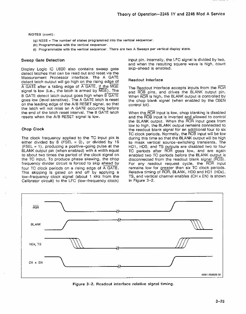
-- -
Theory of Operation-2246 1Y and 2246 Mod A Service
NOTES (cont) :
(g) NSSS = The number of states programmed into the vertical sequencer. (h) Programmable with the vertlcal sequencer. (i) Programmable with the vertical sequencer. There are two A Sweeps per vertical display state.
Sweep Gate Detection input pin. Internally, the LFC signal is divided by two, and when the resulting square wave is high, count
Display Logic IC U600 also contains sweep gate skip-ahead is enabled. detect latches that can be read out and reset via the Measurement Processor interface. The A GATE detect latch output will go high on the rising edge of A GATE after a falling edge of A E , i fe MGE signal is low (i.e., the latch is armed by MGE). The B GATE detect latch output goes high when B GATE goes low (level sensitive). The A GATE latch is reset on the leading edge of the A/B RESET signal, so that the latch will not miss an A GATE occurring before the end of the latch reset interval. The B GATE latch resets when the A/B RESET signal is low.
Chop Clock
The clock frequency applied to the TC input pin is either divided by 8 (FSEL = 0), or divided by 16 (FSEL = I ) , producing a positive-going pulse at the BLANK output pin (when enabled) with a width equal to about two times the period of the clock signal on the TC input. To produce phase skewing, the chop frequency divider circuit is forced to skip ahead by four TC clock periods on a rising edge of A GATE. This skipping is gated on and off by applying a low-frequency clock signal (about 1 kHz from the Calibrator circuit) to the LFC (low-frequency clock)
Readout lnterface
The Readout, Interface accepts inputs from the ROR and ROB pins, and drives the BLANK output pin. When SR is high, the BLANK output is controlled by the chop blank signal (when enabled by the CBEN control bit).
- When theROR input is low, chop blanking is disabled and the ROB input is inverted amallowed to control the BLANK output. When the ROR input goes from low to high, the BLANK output remains connected to the readout blank signal for an additional four to six TC clock periods. Normally, the ROB input will be low during this time so that the BLANK output will be high to mask vertical source-switching transients. The HDl, HDO, and TS outputs are disabled two to four TC periods after ROR goes low, and are again enabled two TC periods before the BLANK outputis disconnected from the readout blank s i g a ( R 0 B ) . For any readout request cycle, the ROR input remains low for g w t e r than six TC clock periods. Relative timing of ROR, BLANK, HDO and HD1 (HDx), TS, and vertical channel enables (CH x EN) is shown in Figure 3-2.
BLANK pp HDx, TS Ss CH x EN cc
(6081 -05)6555-30
Figure 3-2. Readout interface relative signal timing.

Theory of Operation-2246 1Y and 2246 Mod A Service
Trigger Logic IC (FLIC)
The Trigger Logic IC or FLIC (fast-logic integrated circuit, U602 Diagram 4) does most of the fast logic functions required to run the oscilloscope. The func- tions are: A Sweep control, B Sweep control and measurement gate generation, Z-Axis control, and trigger status detection.
The A Sweep logic generates the A Sweep gate signal (A GATE), and provides trigger status infor- mation about the state of the A Trigger. The B Sweep logic interfaces to the Delay Time Com- parators (Diagram 3) and generates the B Sweep gate (B GATE) and measurement gate signals. There is also some logic that monitors the B Trigger signal status when making voltage measurements with the B Trigger circuit. The Z-Axis control logic provides outputs for controlling the crt beam intensity.
The Trigger Logic circuit is done in an ECL (emitter- coupled logic) gate array, and all inputs and outputs are compatible with standard ECL components.
Pin Description
The following is a description of the fast logic pin outs (see Figure 3-3).
BLANK: Blanking input, from the Display Logic IC (U600).
HD1, HDO: Horizontal display select inputs, from the Display Logic IC.
- ZEN : Z-Axis enable input, from the Display Logic IC. Active low.
BUSY : Counter busy signal. Not used in the 2246 1Y and 2246 Mod A.
ATRIG: A Sweep trigger input.
EOAS: End of A Sweep. This signal goes high when the A Sweep ramp crosses its end-of-sweep threshold.
THO: Trigger holdoff input from the Display Logic IC.
Figure 3-3. Trigger Logic IC (FLIC, U602) pin-out diagram.
SIN: Strobe input. Latches data into the in- ternal register. Active low.
A1, AO: Address inputs. See Table 3-1 7 for addressing codes.
EOBS: End of B Sweep. This signal goes high when the B Sweep ramp crosses its end-of-sweep threshold.
DLYl2: Input from first delay comparator. The comparator for the delay input switches from low to high after the end of either the first or the second sweep delay.

Theory of Operation-2246 1Y and 2246 Mod A Service
DLY2: Input from second delay comparator. B GATE: B Sweep gate output. Starts the B This comparator normally switches from low Sweep ramp. Active high. to high after the end of the second sweep delay (in dual-delay mode). -
BUB : B Sweep unblanking output. Active low.
B TRIG: B Sweep trigger input.
m: Measurement gate enable input from C GATE : Measurement gate output. Not the Display Logic IC. Active low. used externally in the 2246 1Y and 2246 Mod
A.
MSEL: Measurement select input. MSEL=I causes the DLY12 signal rising edges to sample the B TRIG input in strobed volts measurements. MSEL=O selects the DLY2 Table 3-17 signal rising edges. Trigger Logic IC Addressing Logic
DS: Delay select signal from the Display Logic IC. DS=1 selects first delay.
DATA: Data input to the internal, control shift register.
S1 : Crt beam-intensity control output. Turns on the beam current for the A Sweep displays. Active low.
- S2 : Crt beam-intensity control output. Turns on the beam current for the B Sweep displays. Active low.
- S3 : Crt beam-intensity control output. Turns on the beam current for the A Sweep intensified zone displays. Active low.
- S4 : Crt beam-intensity control output. Turns on the beam current for the Readout displays. Active low.
A GATE: A Sweep gate output. Starts the A Sweep ramp. Active high.
TDO: Trigger data output. Data to be read is selected via the A1 and A0 inputs (see Table 3-1 7).
Trigger Logic IC Control Register Description
The control register of U602 is an 8-bit shift register that receives input from the DATA pin. Bit 1 reeives the data on a low-to-high transition on the SIN pin (A1 = A0 = 0). Bit 8 receives this d G after seven more low-to-high transitions on the SIN pin. Bit 8 is the most significant bit of the control register. Table 3-18 lists the control signal name associated with each control register bit.
Action when SIN Strobed
DATA clocked into Control Reg
Resets Auto base- line Latch
Resets A Trigger Latch
Resets Peak Volts Latch
A1 A0
0 0
0 1
1 0
1 1
DM1, DMO: These bits select the delay mode (see Table 3-1 9).
Output of TDO pin
Strobed Volts Latch
Auto baseline Latch
A Trigger Latch
Peak Volts Latch
BRUN: This bit determines whether the B Sweep is in RUNS AFTER delay mode or Trig- gered After delay mode. BRUN=l selects RUNS AFTER Mode.
PM1, PMO: These bits select the peak volts detection mode as shown in Table 3-20.

Theory of Operation-2246 1Y and 2246 Mod A Service
Table 3-18 Control Register Signal-bit Names
Table 3-19 Delav Mode Selection Control Bits
Bit
1
2
3
4
5
6
7
8
ARUN: This bit determines whether the A Sweep is in the free-run mode or in the trig- gered mode. ARUN=l selects the free-run mode. Name
DM0
DM 1
BRUN
PMO
PM 1
ZMO
ZM 1
ARUN
A Sweep Logic
When ARUN is high, the A Sweep logic works as fol- lows. A high on the THO input causes the A GATE output to go low. As soon as THO goes low, the A GATE output will go high and the A Sweep runs. At the end of the A Sweep there is a low-to-high tran- sition on the EOAS input. That sets the the internal end-of-A-sweep latch causing the A GATE output to go low, and the A Sweep shuts off. This state exists during sweep retrace and the baseline stabilization period until the end of holdoff when the THO input once again goes high. That resets the end-of-A-sweep latch and starts another A Sweep cycle. Normally, the falling edge of A GATE will cause an externally generated pulse to be presented on the THO input, thus completing the loop and allowing the A Sweep to free-run (auto-level and auto triggered mode when the sweep is not triggered).
When ARUN is low, the operation is similar except that after a pulse on the THO input, A GATE won't go high until a low-to-high transition is presented on the A TRlG input (triggered sweep mode).
DM1 DM0
0 0
0 1
1 0
1 1
For either free-run or triggered modes, THO going high will cause the A GATE output to immediately go low, if the end-of-A-Sweep latch is set or not. Once the end-of-A-Sweep latch has been set, no more A Sweeps can happen until the THO input is pulsed (at the end of the holdoff). The end-of-A-Sweep latch can only be set with the EOAS input when A GATE is high.
Delay Mode
First delay set to zero
First and second delays set to zero
Normal delay mode
B Sweep disabled
Table 3-20
Peak Volts Detection Mode Logic
1 1 I Gated with A GATE
PM1 PMO
0 0
0 1
1 0
a- C GATE not used externally in 2246A.
Peak Detection Mode
Nongated
Gated from end of delay to end of A Sweep
Gated with ma
ZM1, ZMO: These bits determine the intensi- fied zone mode. See the Z-Axis logic discussion.
The A Sweep logic of U602 also monitors the A TRlG input to latch certain A Trigger events. One latch (the auto-baseline latch) will set on any low-to-high transition on the A TRlG input. Another latch (the A Trigger latch) is level sensitive and will set when the A TRlG input is high. Both latches may be read out through the TDO (trigger-data out) pin, selected by the A1 and A0 address input pins. That data is applied to the TDI (trigger data in) pin of U600 and placed in the Display Logic IC's internal register to be read by the Measurement Processor. Both latches may also be r e s e t i a the SIN pin (see description of A l , AO, and SIN input pins).
B Sweep Logic
The B Sweep logic functions about the same as the A Sweep logic, except that more signals must be monitored to determine when the B Sweep can run. When DM1 and DM0 = 11, the B Sweep can't run at

Theory of Operation-2246 1Y and 2246 Mod A Service
all. When DM1 and DM0 = 10, the B Sweep won't be allowed to run or trigger until the DLY12 input goes high while the A GATE signal is also high (the normal delayed sweep mode). When DM1 and DM0 = 01, the B Sweep will be allowed to run or trigger immedi- ately after the A GATE signal goes high (no B Sweep delay). When DM1 and DM0 = 00, then the B Sweep will be allowed to run or trigger immediately after the A GATE signal goes high, if the DS (delay select) input is high. If DS is low, the B Sweep is allowed to run or trigger as soon as the DLY12 input goes high while the A GATE signal is also high.
The B Sweep logic b e h a s as follows. The B GATE signal goes high and BUB (B Sweep unblanking) goes low together when the appropriate conditions (described in the preceding paragraph) are met. A low-to-high transition on the EOBS inputwill then set the end-of-B-sweep latch, causing BUB to go high. B GATE doesn't go low until the A GATE signal goes low. This is used internally to generate the 9 and S3 outputs in some modes, and is used externally to carry out the B ends A mode.
The DLY12 input goes to a level-sensitive latch; if A GATE is high and DLY12 momentarily goes high, the latch will be set, so that the DLY12 input does not need to be held high throughout the sweep cycle. A high level on the THO input will cause the A GATE signal to go low. That resets this latch and causes the reset of therest of the sweep logic, forcing B GATE low and BUB high.
The DLY2 input also goes to a level sensitive latch. This second latch also gets reset when A GATE goes low. Together with the DLYl latch output, A GATE, - and the MGE input, the C GATE output signal gets generated (not used externally in the 2246 1Y and 2246 Mod A). C GATE goes low if A GATE is high, the DLYl latch =been set, the DLY2 latch is still reset, and the MGE input is low.
can be read at the TDO pin with A1 and A0 set this way. The Measurement Processor reads the state of the peak volts latch to determine when it has found the correct digital value of the signal peak being measured by the B Trigger Level Comparator.
The peak-detect latch output will go high when the B TRlG input goes high (if the gating condition selected by PM1 and PMO is satisfied). The latch output goes low when reset.
Strobed Volts Logic
This logic samples the state of the B TRlG signal with the delay comparator outputs when making gated voltage measurements. The strobed volts latch con- sists of an edge-triggered flip-flop with a multiplexer driving the clock input, and the 5 TRlG signal driving the D input. When MSEL=I, the DLY12 latch output clocks the flip-flop. When MSEL=O, the DLY2 latch output clocks the flip-flop. The state of the flip-flop is read out at the TDO pin by the Measurement Processor w h e n y , A0 = 00. The flip-flop is reset by strobing the SIN input with A1 , A0 = 11.
Z-Axis Logic
This logic drives the Z-Axis control outputs (s - g ) . These outputs have the following control action:
- S1 Turns on the A intensity current switch
(active low).
S2 Turns on the B intensity current switch (active low).
S3 Turns on the A intensified current switch (active low).
Peak Volts Logic
S4 Turns on the Readout intensity current switch The peak volts logic detects the positive and nega- (active low). tive peaks of the B TRlG signal. It consists of a level- sensitive latch that can be gated by the C GATE signal, the A GATE signal, the DLY12 latch output, or Table 3-21 describes what the - outputs do continuously. The latch may be reset by strobing the as a function of ZM1, ZMO, HDI, HDO, A GATE, 7
SIN input with A1 and A0 set to 11. The latch output m, C GATE, BUSY, BLANK, and ZEN.

Theory of Operation-2246 1Y and 2246 Mod A Service
Table 3-21 Z-Axis Switching Logic
Notes:
( a ) = BLANK or A GATE (b ) = BLANK or A or BUB or ZEN (c) = BLANK - ( d ) = BLANK or A or C GATE or ZEN - - - (e) = BLANK or A GATE or BUSY or ZEN
or is a logical-or function.
ZM1 ZMO HD1 HDO
0 0 0 0
0 0 0 1 0 0 1 0
0 0 1 1
0 1 0 0
0 1 0 1 0 1 1 0
0 1 1 1
1 0 0 0
1 0 0 1 1 0 1 0
1 0 1 1
1 1 0 0
1 1 0 1 1 1 1 0 1 1 1 1
ECL-to-CMOS Level Shifters only to produce a differential output signal. That
- S3
1
(el
1
1
1
(dl
1
1
1 (b )
1
1
1
1 1 1
The Trigger Logic IC, U602, is an ECL device. Its output signal swing is the standard ECL range of about 0.6 V. All the ECL logic devices in the 2246 1Y and 2246 Mod A are powered from the +5 V supply rather than a -5 V supply. The resulting output voltage swing is from about 4.5 V to about 3.9 V between the high and low ECL logic levels. As U602 must pass signals to the Display Sequencer IC (U600) at CMOS highs and lows (about 3.9 V and 0 V respectively in this application), logic level trans- lators are required. That job is done by an identical translator circuit for each of the three signals that must be sent. The circuit action of U603C, Q604, and Q605 (the A GATE translator) is described.
- S 1
1 ( a )
1
(c)
1
( a )
1
(c)
1 ( a )
1
( c )
1
( a )
1 ( c )
The single-ended A GATE output signal of U602 at pin 14 is applied to pin 4 of U603B. With its other input pin left open, U603B is used as a line driver
- S4
( c )
1 1
1
( C )
1 1
1
(b )
1 1
1
( C )
1 1 1
- S 2
1
1 (b )
1 1
1 1
1
1
1 (b )
1
1
1 1 1
differential signal is applied to the bases of a differential amplifier pair of pnp transistors (Q604 and Q605). The output signal is taken across R612 in the emitter of Q604. The emitter of Q605 is con- nected directly to ground. When the A GATE output of U602 is high (at 4.5 V) , the voltage applied to the base of Q604 is 4.5 V, and the voltage on the base of Q605 is 3.9 V. These voltage levels bias Q605 on and Q604 off, with a resulting output level across emitter resistor R612 of 0 V to the A GATE (active low) input of U600. When the A GATE output of U602 goes low at the end of the sweep, the bias voltage levels on Q604 and (3605 reverse, and Q604 is biased on (and Q605 off). Signal current through emitter resistor R612 develops a voltage of about 3.9 V (the unasserted level) to the A GATE input of U600.
Display Mode
Readout
A Sweep intensified by BUSY B Sweep
XIY
Readout
A Sweep intensified by C GATE Blank
XIY
Readout
A Sweep intensified by BUB B Sweep
XIY
Readout
A Sweep no intensified zone Blank X/Y

Theory of Operation-2246 1Y and 2246 Mod A Service
Display Logic Clock
The Display Logic clock signal at 10 MHz is generated by a transistor oscillator circuit composed of Q608, Y600, and associated components. The frequency of oscillation is controlled by a ceramic resonator, Y600, in the feedback path from the collector to the base of Q608.
A AND B SWEEPS AND DELAY COMPARATORS (Diagram 5)
voltage divider formed by resistor pack R313. The voltages at the taps of the voltage divider set the for- ward bias on the charging-current pass transistor, Q307, via operational amplifier U304. When the SECIDIV VAR control is in its detent (calibrated) posi- tion, diode CR301 is reverse biased, and the divider formed by R311 and R314 between the +2.5 V refer- ence and ground precisely sets the input voltage to the noninverting input of U309B. With a fixed voltage output from U309B, the current through Q301 and R313 is also a fixed value. When the SECIDIV VAR control is rotated out of its detent position, the volt- age at the junction of R309 and ~ 3 1 0 decreases to forward bias CR301. The input voltage to U309B and, therefore, the current to R-313 decreases in propor- tion to the amount of rotation of the SECIDIV VAR
Sweep Control Shift Registers control. A decreasing voltage at the output taps of R313 decreases the charging current through Q307 to
Two serial shift registers provide the control interface increase the sweep ramp time. between the Measurement Processor and the A and B Sweep circuitry. Control bits loaded into registers U302 for A Sweep and U303 for B Sweep are serially clocked from the'% DATA line by the dl CLK pulse. The states of the loaded bits select the A and B Sweep timing by choosing the correct charging cur- rent and timing capacitor to provide the full range of sweep speeds. Other control bits loaded into the two registers select the delay voltage applied to the Delay Comparators and the output voltage from the VOLTS CAL circuit (used for measurement SELF CAL) . Extra bits are shifted through the two shift registers into the Auxiliary Data Register (U1 103, Diagram 3) via the AUX DATA signal line to control the trigger bandwidth, the TV Sync Detector switching, and the functions of 10X MAG, X-Y display, and Vertical Comparator enabling.
A and B Sweep Timing
Refer to Figure 3-4 for a simplified schematic of the A Sweep circuitry.
TIMING RESISTORS. The Sweep Timing resistors in resistor pack R313 are shared between the A Sweep and the B Sweep circuitry; those in resistor pack R321 are divided between the two sweep circuits. Timing Resistor selection is done by multiplexers U308 and U307 for the A Sweep and by U310 and U311 for the B Sweep. The multiplexers are driven by the Measurement Processor via control bits loaded into Shift Register 1 (U302 and U303). (See Table 3-22 for the control bit coding.)
SEClDlV VAR CIRCUIT. Variable sweep speed is con- trolled by the TIME VAR voltage applied to operational amplifier U309B. The amplifier controls the current passing through Darlington transistor Q301 to the
A AND B SWEEP TIMING CAPACITORS. The timing capacitor selection circuitry is similar for the A and the B Sweep, but the B Sweep has fewer range steps and doesn't require two selectable capacitors. Only the A Sweep timing capacitor selection is described; like components in the B Sweep circuit do the same job.
Timing capacitance for the A Sweep is made up of a combination of fixed, variable, stray, and selectable components. Sweep timing for the fastest A Sweep speeds is done with a combination of the fixed, variable, and stray capacitance and the selectable charging current supplied through R321, U308, Q307 and Q330. When the slower sweep speeds are selected, additional capacitors must be switched into the circuit to produce a longer charging time. The ca- pacitors that are always in the A Sweep charging path are C315 (a fixed capacitor), C314 (a variable ca- pacitor used to adjust the A Sweep timing at the fast- est sweep speeds), and the stray circuit capacitance.
The base-to-collector junction capacitance Q330 changes as the voltage between the base and collec- tor of Q330 increases during ramp up. At the fastest A Sweep speeds, that change would affect the timing at the start of the charging ramp. To compensate for the junction-capacity effect of Q330, transistor Q328 (connected as a diode) is added between the charg- ing current path and the A Sweep Buffer output. The capacitive current through the reverse-biased junc- tion of Q328 adds current to the output to make up for the current required to charge the base-to-collector capacity of Q330 in the input of the Sweep Buffer.
REV OCT 1991 3-31

Theory of Operation-2246 1Y and 2246 Mod A Service
+15 V
FROM
SWEEP START
STABILIZER
Q310A. 03108. 0312
SELECTION FROM
6081-07
Figure 3-4. Simplified Sweep Circuit.

Theory of Operation-2246 1Y and 2246 Mod A Service
The selectable sweep timing capacitors come in a matched set of three capacitors, two for the A Sweep timing (C307A and C307B) and one for the B Sweep timing (C307C). When added capacitance is needed for a sweep speed setting, the Measurement Processor loads selection control bits into Shift Register 1 (U302 for the A Sweep) that turn on either Q305 or Q306 or both. Assume that Q305 is biased on by a high control bit from pin 5 of U302. Capacitor C307B is then added in parallel to the capacitors in the charging path, and a longer ramp time is needed to reach the end-of-sweep voltage level. Control bits selecting the charging current are also loaded at the same time. See Table 3-22 for the A Sweep timing and control bit selections (as0-as5) and Table 3-23 for the B Sweep bit selections (bs0-bs4).
baseline, run-up, and retrace (see Figure 3-5). Sweep start and length of sweep run-up is controlled by the A GATE and A GATE signals from the Trigger Logic IC (U602, Diagram 4).
A GATE SIGNALS. The A GATE and A signals are applied via 8.2 V zener diodes (VR301 and VR302) to the bases of Q308 and Q309 in a dif- ferential amplifier configuration. The input circuit to the differential pair level shifts the ECL signals (4.3 V to 3.4 V) to the proper biasing levels (-3.9 V to -4.8 V) for the bases of the differential amplifier transistors. Transistor Q326 in the emitter circuit of Q308 and Q309 is the current source for the differ- ential pair. Transistor Q311 is part of the bias circuit for ~ 3 2 6 and provides feedback to the base of Q326 that controls the current provided to Q308 while the sweep is being held at the baseline level.
Baseline Stabilizer
The job of the Baseline Stabilizer circuit ((2302, Q303, and Q304 for the A Sweep and Q315, (2316, and Q317 for the B Sweep) is to tie the start of the sweep ramps to the same fixed level for each sweep. Operation of the A Sweep stabilizer is described.
A differential circuit formed by Q302 and Q303 com- pares the A Sweep feedback signal on the base of Q303 against the reference voltage on the base of (2302, to control the base bias current to Q304 and thereby the sweep baseline level. Operational ampli- fier U309A generates the fixed reference that the baseline voltage level is compared against. The reference voltage amplifier has a gain of -0.8 (less than one and inverted) ; and, with +2.5 V applied to the inverting input and the noninverting input grounded, the output level is -2 V. Capacitor C305 filters the output to eliminate noise that could cause sweep start jitter. The filtered voltage is applied to the junction of R317, R354, and C305 and references both Baseline Stabilizer circuits.
A and B Sweep Start
The A and B Sweep Start circuits operate the same way with like components in each doing the same job; only the A Sweep Start circuit is described. Sweep time may be divided into three periods:
BASELINE STATE. In the baseline slate (during sweep holdoff), Q308 and Q304 are on and Q309 is off, and the level at the collector of Q308 is held at -2.8 V. That voltage is buffered by the A Sweep Buffer (with about a 0.7 V rise across the base-to- emitter junction of Q312) and fed back to the base of Q303 where it is compared with the -2 V reference produced by operational amplifier U309A. If the baseline voltage is too low compared to the output of U309A, Q303 (the retrace current regu- lator) is biased on a little harder. Additional base current is available to (2304, and it conducts harder to raise the output baseline voltage to the reference voltage level. The opposite action occurs if the baseline voltage is too high.
A smaller feedback loop formed by Q311 and R305 controls the gain of Q326 so that the standing cur- rent available (about 3 mA) is just enough to keep Q304 biased on during the baseline state. When the states of the gate signals reverse, Q309 is turned on and Q308 turns off. The standing current then con- ducts through Q309 to rapidly pull the base of Q304 down to shut it off. When the base voltage reaches about -2.7 V, Q333 conducts. That action clamps the base voltage of Q304 (and the collector voltage of Q309) at that level and prevents Q309 from saturating so that it will have a short turn-off time when the sweep ends.
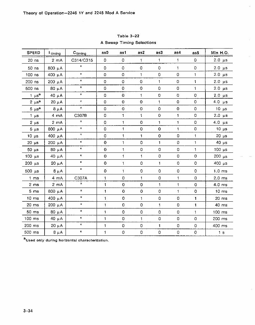
Theory of Operation-2246 1Y and 2246 Mod A Service
Table 3-22
A Sweep Timing Selections
a ~ s e d only during horizontal characterization.
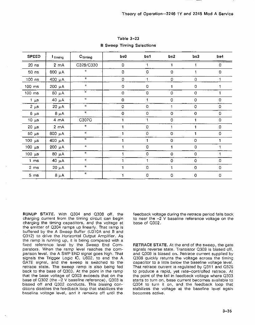
Theory of Operation-2246 1Y and 2246 Mod A Service
Table 3-23
B Sweep Timing Selections
RUNUP STATE. With Q304 and Q308 off, the charging current from the timing circuit can begin charging the timing capacitors, and the voltage at the emitter of Q304 ramps up linearly. That ramp is buffered by the A Sweep Buffer (U310A and B and Q312) to drive the Horizontal Output Amplifier. As the ramp is running up, it is being compared with a fixed reference level by the Sweep End Com- parators. When the ramp level reaches the com- parison level, the A SWP END signal goes high. That signals the Trigger Logic IC, U602, to end the A GATE signal, and the sweep is switched to the retrace state. The sweep ramp is also being fed back to the base of Q303. At the point in the ramp that the base voltage of Q303 exceeds that on the base of Q302 (the -2 V baseline reference), Q303 is biased off and Q302 conducts. This biasing con- ditions disables the feedback loop that stabilizes the baseline voltage level, and it remains off until the
feedback voltage during the retrace period falls back to near the -2 V baseline reference voltage on the base of Q302.
RETRACE STATE. At the end of the sweep, the gate signals reverse state. Transistor Q309 is biased off, and Q308 is biased on. Retrace current supplied by Q308 quickly returns the voltage across the timing capacitor to a little below the baseline voltage level. That retrace current is regulated by Q311 and Q326 to produce a rapid, yet rate-controlled retrace. At the point of the fall in feedback voltage where Q303 starts to turn on, base current becomes available to Q304 to turn it on, and the feedback loop that stabilizes the voltage at the baseline level again becomes active.

Theory of Operation-2246 1Y and 2246 Mod A Service
Figure 3-5. A Sweep Start circuit waveforms.
EMITTER 0304
-- - -2.75 v 4 - --3.30 V I
- - --2 .11 v I I
BASE - --2.61 V
0304 I I I 1 I I I I
BASE I I I I
A and B Sweep Buffers
0309 (A GATE)
The A Sweep Buffer (Q310A and B, and Q312) and B Sweep Buffer (Q323A and B, and Q325) buffer the voltage ramp as the timing capacitors charge. In the A Sweep circuit, Q310A and Q310B are high- impedance FET amplifiers driving emitter follower Q312. The output signal from the emitter of Q312 is applied to the Delay Time Comparators, the End-of- Sweep Comparators, fed back to the Baseline Stabilizer circuit, and sent to the Horizontal Output Amplifier (Diagram 6) as the A RAMP horizontal deflection signal.
Sweep End Comparators
I I I I I I
RETRACE-! BASELINE,- RUNUP-, I
6081-08
I I I
The sweep ramp signals must horizontally deflect the electron beam across the entire face of the crt. Comparators U316A, B, C, and D determine when the A and B Sweeps have reached the required amplitude. These comparators check the sweep voltage against the reference level that defines the end of the sweep and generate the A SWP END and B SWP END signals when that level is reached. The sweep-end signals are applied to the Trigger Logic IC (U602) so that device knows when the sweeps
1 -4.00 V
- - - -4 .70 V I I
are done. The Trigger Logic IC then switches the states of the A GATE or the B GATE signal (as appropriate) to reset the sweep circuitry to its baseline level.
Delay Time Comparators
When the A Sweep ramp runs, its amplitude is com- pared against two delay levels by the comparators of U313. The differential outputs of the REF delay comparator change states when the A Sweep crosses the first delay level. The differential output signal from the delay comparator is applied to ECL line receiver U315C. That device has a high gain and produces a fast-rise signal at an ECL level. When the DLY END 0 (reference delay completed) is received by the Trigger Logic IC (U602, Diagram 4), a B GATE is produced to start the B Sweep in RUNS AFTER B Trigger mode. That B Sweep displays the applied waveform at the first (reference) delay setting. At the end of the delay in RUNS AFTER mode, the Trigger Logic IC begins watching for a B Trigger signal that must occur before a B GATE is produced.
The differential output of the second delay com- parator in U313 changes states when the A Sweep

Theory of Operation-2246 1Y and 2246 Mod A Service
ramp at pin 9 crosses the second (delta) delay level signal source is the CH 1 trigger signal from applied to pin 6. At that point, the DLY END 1 signal U421A (Diagram 3). Adjustment of R827 is produced at the output of U315A (pin 2) and sets the gain of the X-Axis signal. applied to U602. A second B GATE signal is then produced to start another B Sweep ramp to display HDO (Pin 8): Pin 8 (HDO) and pin 11 (HDI) the signal at the delta delay setting. are logic lines that select the horizontal input
signal to output differentially at pins 18 and 19. Table 3-24 gives the selection logic.
Delay Time Switching
The DELTA DELAY and REF DELAY voltage level are applied to multiplexer U301 from the DAC circuit. The Measurement Processor established those voltages based on the settings of the CURSOR/TIME POSITION controls made by the user from the front panel. Switch section U301A is held permanently switched to direct the DELTA DELAY signal to its output pin.
HORIZONTAL OUTPUT AMPLIFIER (Diagram 6)
Table 3-24
Horizontal Preamplifier VEE (Pin 9): -5 V supply to U802.
HDO and HD1 Logic
Horizontal Preamplifier IC U802 converts single- ended horizontal signals (A sweep, B sweep, horizontal readout, and X-Axis) into differential out- puts to drive the crt horizontal deflection plates. The horizontal preamplifier signals are selected by the HDO and HD1 logic signals from Display Sequencer U600 on Diagram 4. Magnified sweep, beam find, horizontal positioning, and horizontal gain adjust- ments (XI and X10) are provided in U802 and associated components.
HD1 HDO
0 0
0 1
1 0
1 1
The function of each pin of U802 is as follows:
Horiz Signal Selected
RO HORlZ
A SWEEP
B SWEEP
X-AXIS
RO (Pin 1): RO HORIZ. lnput for horizontal component of the readout display.
GAl (Pin 2): Adjustment of R825 sets the horizontal X I gain.
A RAMP (Pin 3): lnput for the A Sweep signal.
GND (Pin 4): Ground connection for U802.
B RAMP (Pin 5): lnput for the B Sweep signal.
MAG (Pin 6): Selects X I0 magnified sweep when high or normal sweep when low. Mag- nified mode is selected when in X-Y hori- zontal mode.
X (Pin 7): X-AXIS. This is the X-Axis signal input when in X-Y horizontal mode. The
GA10 (Pin 10): Adjustment of R826 sets the horizontal X I 0 gain.
HD1 (Pin 11): See the description for HDO above.
ROUT (Pin 12): Horizontal Preamplifier dif- ferential output signal for the right deflection plate.
LOUT (Pin 13): Horizontal Preamplifier dif- ferential output signal for the left deflection plate.
BF (Pin 14): The BEAM FlND signal from U503 (Diagram 4) switch the Beam Find feature on or off. BEAM FIND on reduces the horizontal deflection to within the graticule area. Vertical deflection is also reduced and the intensity is set to a fixed viewing level to aid in locating off-screen, over-def lected, or under-intensified displays.
POSITION (Pin 15): lnput for the horizontal position control signal. Multiplexer section U301B switches to reduce the range of the Horizontal POSITION control to match that of the Vertical POSITION controls when in X-Y horizontal mode. When X-Y display mode is selected, a low XY signal on Pin 9 of U301 B connects the pin 5 input to the horizontal position input of U802. The signal at pin 5 is a reduced horizontal positioning signal produced by the R353lR358 voltage divider.
Vcc (Pin 16): +7 V supply to U802.

Theory of Operation-2246 1Y and 2246 Mod A Service
Driver Amplifiers
The differential output current signal from U802 passes through common-base current amplifiers Q809 and (2810. These transistors drive current-to- voltage converters (28034804 and Q807-Q808. Emitter followers Q804 and Q803 convert the current signal to a voltage signal to drive the complementary-FET output amplifiers, Q801 and Q802, to produce the negative-going deflection voltage. Emitter followers Q808 and Q807 convert the other side of the differential current to drive Q805 and Q806 to produce the positive-going hori- zontal deflection voltage.
The circuit of Q804 and Q803 is configured to respond rapidly to a negative-going feedback signal; the circuit of Q807 and Q808 is configured to respond quickly to the positive-going feedback signal. Zener diode VR802 and associated resistors R843 and R844 maintain the collector bias of Q803 and (2808 at 24 V.
Magnifier registration and horizontal readout cen- tering is set by MAG REG potentiometer R809. Adjustment of R809 is done to balance the currents into the emitters of Q809 and Q810 to obtain the correct horizontal position of the readout within the graticule display area.
Output Amplifier
The differential circuitry of both sides of the Hori- zontal Output Amplifier is similar; operation of only one side of the amplifier is described. Complementary-FET amplifiers Q801 and (2802 produce the negative-going horizontal signal to drive the left deflection plate. Two transistors are used to provide adequate power handling. Since the two gates are at different bias levels, signal voltage is applied to the gate of transistor Q801 via C803. Resistor R828, connected between the source and drain of Q801, is a parallel current path around Q801 that balances the power handling requirements of the two FETs. The amplifier FETs are high gain devices, and the overall gain must be reduced to maintain circuit stability at the faster sweep rates. To provide the high-frequency gain reduction, resistor R850 is in series with C802, from the source of Q802 to the drain of Q801, to damp the driving-energy to Q801 supplied by C802 during the sweep retrace transitions. Feedback resistor R806 provides positive feedback and sets the overall gain of the output amplifier stage. A parallel trimmer capacitor across the feedback resistor, C807, adjusts the 2 ns sweep timing for its best linearity. Impedance matching to the deflection plate and additional signal damping is provided by R802.
As the gate voltage of Q802 increases to follow the input ramp signal, the drain voltage goes negative from about 87 V toward the 15 V source voltage. At the same time, the signal on the gate of complementary-FET Q801 is reducing the current through Q801, thereby allowing its source voltage to fall. At the end of the ramp signal, the input voltage falls, and through the positive feedback, Q802 is rapidly biased off. That also biases Q801 on, and the energy stored in C802 quickly returns the deflection plate voltage back to its starting point.
Common-Mode Stabilizer
Operation amplifier U801A compares the node voltage at the junction of R820, R821, and R822 to ground. Its output drives the amplifier input common-mode point (at the junction of R811 and R812). The purpose of this dc feedback circuit is to keep the average voltage level on the right and left horizontal deflection plates set to the center of the amplifier's dynamic operating range (about 70 V).
Z-AXIS, CRT, PROBE ADJUST, AND CONTROL MUX (Diagram 7)
Z-Axis and Auto Focus Amplifiers
The Z-Axis and Auto Focus Amplifiers circuit operate on the same principle and both get their drive signal from the Z-Axis Focus Driver. However, the differences are enough that both circuits are described.
Z-AXIS AMPLIFIER. Intensity control signal current from the Z-Axis/Focus driver is applied to the Z-Axis amplifier via Q2707. That transistor acts as a current buffer amplifier. The input signal line is clamped at 5.4 V by (22715 to prevent an overdrive of the Z- Axis circuit. The Z-Axis Amplifier output transistors consist of (22701 and Q2702 on one side of the complementary-symmetry totem-pole output ampli- fier and Q2703 and Q2704 on the other side. Two transistors are used on each side to divide the power handling requirements needed to drive the crt control grid. The crt grid capacity is large, and requires a relatively large amount of power to change the intensity level quickly.
In the base circuit of Q2704, CR2705 prevents the base-to-emitter voltage from exceeding 0.6 V. Zener diode VR2701 dc level-shifts the signal voltage level at the emitter of Q2705 for proper biasing of Q2704. The ac signal components are bypassed around \/R2701 by C2703. Base biasing for Q2702 and Q2703 is taken from a series- resistance divider formed by R2711, R2712, R2713, and R2714 between ground and the +I30 V supply.

Theory of Operation-2246 1Y and 2246 Mod A Service
Base biasing for Q2701 is provided by R2715 and R2716 in series between ground and the +I30 V supply.
A negative-going input signal to the base of Q2705 causes that transistor to decrease conduction, and the voltage at the top of C2705 goes negative fol- lowing the input signal. Transistor Q2701 is biased on harder by the negative transition, and Q2704 decreases in conduction. At the Z-Axis output signal line (collector of Q2702), the increasing conduction causes the voltage to rise towards the +I30 V supply level. A positive-going input signal has the reverse effect on the output signal. The full output-voltage swing of about 60 V is produced by a 3 mA current change of the Z-Axis Focus/Driver signal current.
Gain of the Z-Axis Amplifier stage is set by the feed- back through R2708 and R2709 from the collector of (22702 to the base of Q2705. The amplifier is com- pensated by the variable capacitor (C2704, Z-Axis Response) in parallel with the feedback resistors.
BEAM FIND. The Z-Axis portion of the BEAM FlND circuit consists of R2705 and Q2706. When BEAM FlND is active, Q2706 is biased on. This clamps the Z-Axis signal line via R2706 and raises the voltage at the base of Q2705 to a level that produces a bright trace.
Auto Focus Amplifier
The Auto Focus Amplifier (Q2708, Q2709, Q2711, Q2712, and Q2713) uses a sample of the Z-Axis/Focus Driver signal current from W2701 to drive the auto-focus circuit. The input signal is inverted by Q2708 to drive Q2711 in a comple- mentary fashion to Q2705 in the Z-Axis Amplifier circuit (as the opposite circuit action must happen to produce the correct auto-focus response). The auto-focus output amplifier is similar to the Z-Axis amplifier, but it uses only one complementary tran- sistor on each side (not as much power is needed to drive the focus grid as needed to drive the intensity grid).
Dc Restorers
The Z-Axis and the Auto Focus DC Restorers are similar in operation. Both circuits are described, but only the added portions of Auto Focus circuitry are included in the discussion of the Auto Focus circuit.
The Dc Restorers set the crt control-grid and focus- grid biases and couple the ac and dc components of
the 2-Axis and the Auto Focus Amplifier outputs to the crt grids. Direct coupling of the Z-Axis and Auto Focus signals to the crt control grid is not employed because of the high potential differences involved. Refer to Figure 3-6 during the following discussion.
Z-AXIS DC RESTORER. Ac drive to the Z-Axis Dc Restorer circuit is obtained from pin 12 of T2204. The drive voltage has a peak amplitude of about ?I30 V at a frequency of about 18 kHz and is coupled into the Z-Axis Dc Restorer circuit through R2722 and C2713. The cathode of diode CR2704 is biased by Grid Bias potentiometer R2719 and ref- erenced to ground via R2720. The ac-drive voltage is clamped to the voltage set by the Grid Bias potentiometer wiper whenever the positive peaks forward bias diode CR2704. Capacitor C2710 prevents significant loading of the potentiometer wiper voltage when CR2704 conducts.
The Z-Axis Amplifier output voltage, which varies between +16 V and +66 V, is applied to the Dc Restorer at the anode of CR2703. The ac-drive voltage holds CR2703 reverse biased until the voltage falls below the Z-Axis Amplifier output voltage level. At that point, CR2703 becomes for- ward biased and clamps the junction of CR2703, CR2704, and C2713 to the Z-Axis output level. Thus, the 18 kHz ac-drive voltage is clamped at two levels to produce a roughly square-wave 18 kHz signal with a positive dc-offset level.
The Dc Restorer is referenced to the ,-2750 V crt cathode voltage through CR2702 and R2723. Initially, both C2712 and C2711 charge up to a level determined by the difference between the Z-Axis output voltage and the crt cathode voltage. Ca- pacitor C2712 charges from the Z-Axis output through R2721, R2723, CR2702, and CR2703, to the crt cathode. Capacitor C2711 charges through R2723 (a series damping resistor), CR2702, and CR2701 to the crt cathode.
During the positive transitions of the ac drive (from the lower clamped level toward the higher clamped level) the charge on C2712 increases due to the rising voltage. The voltage increase across C2712 is equal to the amplitude of the positive transition. The negative transition is coupled through C2712 to reverse bias CR2702 and forward bias CR2701. The increased charge of C2712 is then transferred to C2711 as C2712 discharges toward the Z-Axis output level. Successive cycles of the ac input to the Dc Restorer charge C2711 to a voltage equal to the initial level plus the amplitude of the clamped square-wave input.

Theory of Operation-2246 1Y and 2246 Mod A Service
- 2 7 0 0 - 3 = ' ~
+16 C2711 Z-AXIS SIGNAL 1
h -2.7 KV CRT
(CATHODE REFERENCE)
CR2704
& CR2703 $ CR2701
Figure 3-6. Simplified diagram of the DC Restorer circuitry.
- GRID BIAS LEVEL
- Z-AXIS LEVEL
FROM 130 v AC Cz713 R2722
The charge held by C2711 sets the control-grid bias held constant by the long time-constant discharge voltage. If more charge is added to that already path of C2711 through R2724. present on C2711, the control grid becomes more negative (display dimmer). Conversely, if less charge is added, the control-grid voltage level Fast-rise and fast-fall transitions of the Z-Axis out- becomes closer to the cathode-voltage level, and put signal are coupled to the crt control grid through the display becomes brighter. During periods that C2711 to start the crt writing-beam current toward C2712 is charging, the crt control-grid voltage is the new intensity level. The Dc Restorer output level
C2712 R2721 I f w b R2724
6.2 M
R2723
ZZ CR2702 T2204 ' I \ PIN 12
4 -
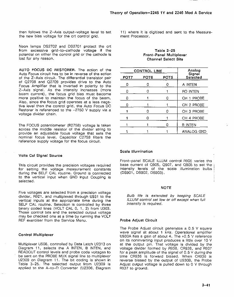
Theory of Operation-2246 1Y and 2246 Mod A Service
then follows the Z-Axis output-voltage level to set 11) where it is digitized and sent to the Measure- the new bias voltage for the crt control grid. ment Processor.
Neon lamps DS2702 and DS2701 protect the crt from excessive grid-to-cathode voltage if the potential on either the control grid or the cathode is lost for any reason.
AUTO FOCUS DC RESTORER. The action of the Auto Focus circuit has to be in reverse of the action of the Z-Axis circuit. The differential transistor pair of Q2708 and Q2709 provides drive to the Auto Focus Amplifier that is inverted in polarity to the Z-Axis signal. As the intensity increases (more beam current), the focus grid bias must become more positive to maintain the focus of the beam. Also, since the focus grid operates at a less nega- tive level than the control grid, the Auto Focus DC Restorer is referenced to the -2750 V supply via a voltage divider chain.
The FOCUS potentiometer (R2758) voltage is taken across the middle resistor of the divider string to provide an adjustable focus voltage that sets the nominal focus level. Capacitor C2758 filters the reference supply voltage for the focus circuit.
Table 3-25 Front-Panel Multiplexer
Channel Select Bits
CONTROL LINE I Analog Sianal .a ~ - ~ -
POT7 POT6 POT5 I ~ e l e c t e d I
Scale Illumination
0 0 1
0 1 0
0 1 1
1 0 0
1 0 1
1 1 0
1 1 1
Volts Cal Signal Source
RO INTEN
CH 1 PROBE
CH 2 PROBE
CH 3 PROBE
CH 4 PROBE
B INTEN
ANALOG GND
This circuit provides the precision voltages required for setting the voltage measurement constants during the SELF CAL routine. Ground is connected to the vertical input when GND Input Coupling is selected.
Five voltages are selected from a precision voltage divider, R921, and multiplexed through U931 to the vertical inputs at the appropriate time during the SELF CAL routine. Selection is controlled by three binary coded lines (VOLT CAL 0, 1 , 2) from U303. Those control bits and the selected output voltage may be checked one at a time by running the VOLT REF exerciser from the Service Menu.
Control Multiplexer
Multiplexer U506, controlled by Data Latch U2313 on Diagram 11, selects the A INTEN, B INTEN, and READOUT control levels and probe code voltages to be sent on the PROBE MUX signal line to multiplexer U2309 on Diagram 11. The bit coding is shown in Table 3-25. The selected output from U2309 is applied to the A-to-D Converter (U2306, Diagram
Front-panel SCALE ILLUM control R905 varies the / base current of Q905, Q907, and Q908 to set the / intensity levels of the scale illumination bulbs , (DS901, DS902, DS903).
NOTE
Bulb life is extended by keeping SCALE ILLUM control set low or off except when full intensity is required.
Probe Adjust Circuit
The Probe Adjust circuit generates a 0.5 V square wave signal at about 1 kHz. Operational amplifier U930A has a gain of about 4. The +2.5 Y reference on its noninverting input produces a little over 10 V at the output pin. That voltage is divided by the voltage divider formed by R936, CR936, and R937 for a peak amplitude of the signal of 0.5 V during the time CR936 is forward biased. When CR936 is reverse biased by the output of U930B, the Probe Adjust output voltage is pulled down to O V through R937 to ground.

Theory of Operation-2246 1Y and 2246 Mod A Service
Operational amplifier U930B is a free-running oscillator circuit with a period of about 1 ms. The oscillator frequency is determined mainly by the charging time constant of C935 and R935. The voltage divider formed by R938, R934, and R939 divides the + I5 V supply to provide a positive voltage on pin 5 of the oscillator to get the circuit into oscillation. (When the circuit is oscillating, the feedback signal switches the pin 5 voltage between about +8 V to 0 V.) The gain of the amplifier is high enough to drive pin 7 to the positive supply voltage level at about 14 V, and the signal voltage level on pin 5 rises to a little over 8 V from the feedback current supplied by R933. The CLK 1K signal taken from the junction of R934 and R939 is supplied to U600 and is used to skew the chop-clock frequency. The skew prevents the oscilloscope from triggering on the chop frequency when displaying multiple traces in CHOP Mode.
At that level CR935 is reverse biased, and CR936 is forward biased (by the output of U930A) to pass the Probe Adjust high level output signal current. Charging current through feedback resistor R934 charges C935 up from 0 V toward the output voltage level. As soon as the charge on C935 (and the voltage on pin 6 of U930B) reaches the voltage level on pin 5, the output level at pin 7 drops to about -5 V, and C935 must then begin discharging to the new voltage level. At that point CR935 is forward biased and that reverse biases CR936 so that the Probe Adjust output voltage drops to 0 V. Resistor R940, in series with CR935, limits current flow to protect U930 and CR935 in the event of a static dis- charge to the PROBE ADJUST output connector.
Crt
The Trace Rotation adjustment, R911, varies the current through the Trace Rotation coil. The Trace Rotation coil is located between the crt face and the vertical and horizontal deflection plates, and it affects both the vertical and horizontal alignment of the trace.
The Geometry adjustment, R2784, varies the voltage level on the horizontal deflection-plate shields to control the overall geometry of the display (minimizes bowing of the display).
The Astigmatism adjustment, R2788, varies the voltage level on the astigmatism grid to obtain the best-focused display over the whole face of the crt.
MEASUREMENT PROCESSOR (Diagram 8)
The Measurement Processor circuitry includes the Processor (U2501), the System RAM (U2521), the System ROM (U2519), communication bus latches
and transceivers, the Address Decoding circuitry, and the Power-On Reset IC (U2502).
Power-On Reset
The +5 V supply is monitored by U2502 to generate the reset signals throughout the instrument. These reset signals initialize the states of the logic devices and ensure that memory writes to any of the RAM spaces cannot occur until the +5 V supply is up to its correct operating level. The RESET signal output at pin 6 is initially high during power up (as soon as the voltage has reached the operating level of the RESET IC, U2502). That high signal is inverted by U2506C to produce the SYS RESET signal. The SYS RESET signal holds Processor U2501 in its reset state.
The SYS RESET signal also resets and initializes the Readout Processor (U2400, Diagram 9). At pin 5 of U2502, a RESET signal is generated. That signal biases Q2507 off to prevent System RAM U2521 from being selected by any random states that might occur on the address lines during reset as the voltage is rising.
About 5 ms after the +5 V supply reaches the operating level required for the Processor, the RESET condition is removed, allowing the Processor to operate. At power off (and for a momentary drop in the +5 V supply), when the +5 V supply falls below the safe operating level of the logic devices, the RESET condition occurs to prevent random operation.
Measurement Processor
FUNCTION. Measurement Processor U2501 is a multitasking device. Its major functions are the following:
1. Continually refreshes the front panel indicator LEDs. One column of the six-column LED matrix is refreshed every 2.048 ms.
2. Continually scans the front panel switch set- tings, sensing rotation of rotary switches and closures or openings of momentary-contact switches. One column of the six-column switch matrix (the same column number of LEDs being refreshed) is read every 2.048 ms.
3. Communicates with the Readout Processor and Readout RAM to set attributes for each readout field, put text into each field, and turn the readout fields on or off.
4. Scans the front panel pots and sets control voltage levels. The Measurement Processor

Theory of Operation-2246 1Y and 2246 Mod A Service
selects a pot to be scanned by connecting it to Comparator U2306 in the d-to-a circuitry. The Measurement Processor does a successive-approximation a-to-d conversion on each pot, using the DAC (U2302) to out- put the search values to the Comparator. Pot values are scanned, processed, and con- verted to analog control values by the DAC. The analog levels from the DAC are output to the controlled devices via sample-and-hold circuits (U2304, U2305 on Diagram 1 1 ) .
5. Sets up the hardware state of the instrument, including shift registers 0 and 1, BEAM FIND, and the operating states of U600 (SLIC) and U602 (FLIC). This setup takes place as needed for every change of a front panel momentary-contact or rotary-contact switch.
6. Keeps track of trigger status and controls the trigger levels when in AUTO LEVEL mode. It uses FLlC (U602) to find the A Trigger status (writing to FLlC to reset the A Trigger latch, and reading from it to get the status). It uses SLlC (U600) to find the B Trigger status (writing to SLlC to reset the 8 Gate latch, and reading from it to get the status). To reacquire the trigger level (positive and negative peaks of the trigger source waveform) it uses the Trigger ICs (U421 and U431), and the Trigger Comparators in FLlC (it writes to FLlC to reset the Trigger com- parator latches, and reads from FLlC to get the status of the latches). To switch between free-running and triggered mode in AUTO LEVEL and AUTO trigger modes, it writes to the control register in FLIC; it switches to trig- gered mode when trigger frequency is sufficiently high and to f;ee-run mode when too low.
7. Tracks the trigger level and ground with cur- sors. The cursors are displayed by directing the Readout system to display cursor charac- ters, and using the DAC system to set the REF CURSOR and DELTA CURSOR level to match the trigger or ground point on the waveform.
8. Does automated measurements. Some measurements are knob-driven. They are:
I 6 SEC 4
When these measurements are running, a new digital value is displayed, and the cursor or delay-zone position is changed only when the user changes the setting of one of the continuous- rotation CURSORITIME POSITION controls. Other measurements are waveform-driven. 'They are:
DC +PEAK -PEAK PK-PK GATED +PEAK GATED -PEAK GATED PK-PK
When these measurements are running, a new digital value is displayed and the cursor position is changed each time a measurement cycle occurs. These measurements use the B trigger system; and, for DC, the low-pass circuit formed by U l 101 B and associated filter components (Diagram 3).
9. Calibrates the measurement system. The vertical and horizontal gains of the instrument are set by manual potentiometer adjust- ments; therefore, the Processor does not control the match between the waveform dis- play and the graticule. However, it does adjust the measurement results to compen- sate for any error in the vertical or horizontal gain. (An example of this is that there could be more than 0.5% error in matching a time base signal to the graticule, but less than 0.5% error in a time measurement done on that signal).
In the Time Base calibration routine, the Measure- ment Processor uses the TB Cal signal, the Trigger circuitry, the A Sweep system, and U602 (FLIC) to find the match between the delay levels (REF DELAY and DELTA DELAY) and edges of the calibration signal. In the Vertical System calibration, the Processor uses the Voltage Reference Generator (U931, Diagram 7), the Readout System, the Vertical Preamplifiers, the Delay Line Driver, and the Vertical Comparator (U702) to find the match between Readout REF CURSOR and DELTA CURSOR levels and vertical outputs generated by the pre- amplifiers. It uses the Voltage Reference Generator, the Vertical Preamplifiers, and the Trigger circuitry to find the match between trigger levels and trigger signals picked off from the Vertical Preamplifiers.
MEASUREMENT PROCESSOR SIGNALS. Table 3-26 is a listing of signal name and function of the Measurement Processor signals.
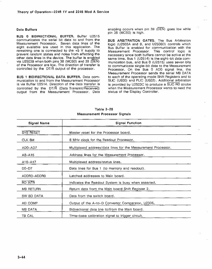
Theory of Operation-2246 1Y and 2246 Mod A Service
Data Buffers
BUS 0 BlDlRECTlONAL BUFFER. Buffer U2515 communicates the serial bit data to and from the Measurement Processor. Seven data lines of the eight available are used in this application. The remaining one is connected to the +5 V supply to prevent random states and noise from affecting the other data lines in the device. The buffer is enabled via U2503B when both pins 38 (MCSO) and 39 (DEN) of the Processor are lgw. The direction of transfer is controlled by the DTIR output of the processor.
BUS 1 BIDIRECTIONAL DATA BUFFER. Data com- munication to and from the Measurement Processor is via Buffer U2514. Direction of the data transfer is controlled by the DTIR (Data TransmitIReceived) output from the Measurement Processor. Data
- enabling occurs when pin 39 (DEN) goes low while pin 38 (MCSO) is high.
BUS ARBITRATION GATES. The Bus Arbitration logic (U2503A and B, and U2506D) controls which Bus Buffer is enabled for communication with the Measurement Processor. This control logic is necessary since both buffers cannot be active at the same time. Bus 1 (U2514) is the eight-bit data com- munication bus, and Bus 0 (U2515) uses seven bits to communicate single-bit data to the Measurement Processor. On the Bus 0 ADO signal line, the Measurement Processor sends the serial MB DATA to each of the operating mode Shift Registers and to SLlC (U600) and FLlC (U602). Additional arbitration is provided by U2503C to produce a SLlC RD strobe when the Measurement Processor wants to read the status of the Display Controller.
Table 3-26 Measurement Processor Signals
--
Signal Name Signal Function
SYS RESET Master reset for the Processor board.
CLK 8M
ADO-AD7
I 8 MHz clock for the Readout Processor.
Multiplexed address/data lines for the Measurement Processor.
A8-A 1 5 Address lines for the Measurement Processor.
A1 6-A1 7
DO-D7
Multiplexed address/status lines.
Data lines for Bus 1 (to memory and readout).
ADDR3-AWDRO
RO INTR
MB RETURN
Latched addresses to Main board.
Indicates the Readout System is busy when asserted.
Return data from the Main board Shift Register 2.
SW BD DATA Data from the switch board.
AD COMP
MB DATA
TB CAL
Output of the A-to-D Converter Comparator, U2306.
Bidirectional data line tolfrom the Main board.
Time-base calibration signal to trigger circuit.
Theory of Operation-2246 1Y and 2246 Mod A Service
Address Latches
MULTIPLEXED AD BUS ADDRESS LATCH. Since the ADO through AD7 bits are multiplexed between address and data information, the addressing infor- mation needs to be latched to hold it for stable addressing (demultiplexed) . The ALE (Address Latch Enable) signal from the Measurement Pro- cessor (pin 61) goes high when the address bits are stable, and the bits are latched into U2513. The device is permanently enabled by the grounded enable pin.
NONMULTIPLEXED ADDRESS BUS ADDRESS LATCH (U2512). Some of the nonmultiplexed address bits are also latched to maintain them between ALE strobes. The latching also prevents address line problems on the Main board from locking up the Measurement Processor. From U2512, latched addresses ADDRO-ADDR3 (A12-A15) are routed to the Display Controller (U600) for addressing the internal registers in that device. Those address lines are also applied to U501 (Diagram 4) for additional decoding to load the Analog Control Shift Registers with the serial data supplied from the MB DATA signal line. Two address lines (A1 6-A1 7) are latched in U2512 for use by the System ROM U2519.
Measurement Processor ROM
The operating code for the Measurement Processor is stored in the System ROM (U2519). Immediately after the Power On Reset ends, the Measurement Processor fetches the first command from the reset vector and begins running the program.
Measurement Processor RAM
The Measurement Processor RAM (U2521) provides storage space for intermediate-step calculation results, the front-panel settings, and the system calibration constants. The Processor RAM is battery backed up so that data stored during operation remains intact during periods of power off. When the instrument is turned on again, the stored front panel settings return the oscilloscope to the same oper- ating state that was present at power off. The stored calibration constants preserve the accuracy of the measurement system (assuming the instrument is warmed up and was warmed up when the SELF CAL routine was last done). If the backup battery is dead, or if the stored calibration constants are lost for some other reason, the instrument will do a SELF CAL at power on. This restores accuracy to the instrument (unless the problem is a RAM fault, in which case the instrument cannot SELF CAL), but
the battery circuitry should be checked and the bat- tery replaced if necessary. Also, the SELF CAL routine should be run again after the instrument is warmed up to generate accurate calibration constants at the operating temperature. If the power-off front panel settings are lost for any reason, the power-on conditions that are set up are only restored in valid states (but not any predefined setup).
Address Decoder
The Address Decoders (U2517 and U2518) allow the Measurement Processor to enable any device on the busses for communication. Enabling signals BUS0 SEL and DAC SEL from the processor select the Address Decoder (either U2517 or IJ2518) that is actively decoding when the WR signal is low.
Backup Battery
To keep the data stored in the Measurement Processor RAM (U2521) during power off, a back-up battery system, BT2501 (and BT2502 in 2246 Opt. 1 Y) , CR2502, and R2506, is used. The battery sup- plies the energy to maintain the memory states of the static RAM. The battery is not rechargeable and has an operating life of one or five years, depending on battery type (see "FRONT PANEL SETUP MEMORY" in Table 1-1 for more information). When the instrument is on, CR2502 becomes reverse biased to prevent any reverse current; when off, CR2501 is reverse biased to isolate the back-up bat- tery from the +5 V supply. If the battery requires replacement, observe the proper safety precautions in the handling and disposition of the replaced battery (see the WARNING under "Battery" in the Specification).
READOUT SYSTEM (Diagram 9)
Readout Processor
The Readout Processor (U2400) is an eight-bit microcomputer, containing its own internal ROM and RAM. The Readout Processor controls the display of text and cursors on the crt. It refreshes each character in the display every 16 ms. When the refresh rate becomes too high, refresh stops until the rate is low enough again. When the refresh rate becomes too low, refresh is done by taking control of the crt beam for a character at a time (Fast mode), until the refresh catches up. When the refresh rate is just right, refresh is done a dot at a time (Slow mode).
Theory of Operation-2246 1Y and 2246 Mod A Service
Each refreshed dot or character is refreshed with the appropriate display position attributes. The attributes define the characters or dots as:
Stationary text that stays put at a fixed point on screen (examples are scale factor and menu displays) ;
Cursor-level offset text whose position is determined by the REF CURSOR or DELTA CURSOR control levels only (examples are the time-measurement cursors) ; or
Cursor-level and position-level offset text whose display position is determined by both the cursor levels and the vertical position controls (an example is the TRACK TRIG LEVEL cursor).
The Readout Processor also communicates with the Measurement Processor system to obtain its RAM programming (for determining the display types) and report its status.
MeasurementlReadout Processor Communication Protocol
A data byte is transmitted between the Measure- ment Processor and Readout Processor as follows:
1. The Measurement Processor waits until RO INTR is unasserted (the Readout Processor is ready to receive).
2. The Measurement Processor writes a byte to tri-state Write Latch U2401 by strobing RO BUF WR; this asserts RO INTR (from Interrupt Latch U2417C and D) and causes an interrupt to the Readout Processor.
3. The Readout Processor, when interrupted, reads the Write Latch (U2401); it then unasserts RO INTR by clocking the Interrupt Latch to reset it. (This is the same clock used when the Readout Processor writes to tri- state Read Latch U2402.)
1. The Readout Processor waits until RO INTR is asserted (the Measurement Processor is ready to receive).
2. The Readout Processor writes a byte to tri- state latch U2402; the clock that does the write also unasserts RO INTR .
3. The Measurement Processor waits until RO INTR is unasserted, then reads tri-state latch U2402. It then strobes RO BUF WR to assert RO INTR (if another byte is coming from the Measurement Processor).
Display Refreshing
READOUT FIELD. A Readout field is refreshed in this way:
1. The display field is selected by latching the top address bits for the field into U2411 (FLD2-FLDO) .
2. The mixing attributes for the field are latched into U2411 (MIX3-MIXO) .
3. The position-tracking attributes for the field are latched into U2403 (CH 4 POS EN through CH 1 POS EN and RO TRACE SEP EN).
4. The starting address for the field (set by communication with the Measurement Processor) is latched into counters U2404 and U2405 (CH7-CHO) .
5. One character at a time, all the characters in the field are refreshed until the top address for the field (set by communication with the Measurement Processor) has been refreshed.
READOUT CHARACTER. A Readout character is refreshed in this way:
1. RO RUN is asserted. This tells the Dot Refresher PAL (U2410) to begin the char- acter refresh and releases the reset on the Dot Counter (U2407) and the Dot Refresher divider (U2409B).
Communication from the Readout Processor to the Measurement Processor is done for diagnostics only 2. For each dot in the character, the next dot is
and can be started only by the Measurement refreshed.
Processor. The Measurement Processor may check the communication link by comparing bytes sent to 3. When the final dot is refreshed, EOCH (end-
of-character at U2408 pin 17) becomes bytes received, query the Character Code RAM con- tents, and check the Character ROM identification asserted, and Q EOCH (the latched version) header. The replies are all sent between the becomes asserted. The Readout Processor Readout Processor and Measurement Processor a unasserts RO RUN, and increments the char- byte at a time as follows. acter address counter lines CH7-CHO.

Theory of Operation-2246 1Y and 2246 Mod A Service
READOUT DOT. A Readout dot is refreshed in this way:
1. is unasserted (this causes RO HORIZ and RO VERT to control the crt horizontal and vertical) briefly to show the dot.
2. RO BLANK is unasserted then asserted (this unblanks then blanks the crt beam).
3. DOT CLK is asserted and unasserted (this in- crements the dot counter lines DOT4-DOTO).
FAST REFRESH. Fast refresh occurs when the Processor asserts FAST (whenever the refresh rate is too low) or when A GATE is unasserted (the sweep is in holdoff). In this mode, RO REQ is asserted at the start of a character, and unasserted at the end. Whenever RO REQ is asserted, the Readout system controls the crt beam intensity and the vertical and horizontal position of the beam. Dots are refreshed every 1.6 ps during fast refresh.
SLOW REFRESH. Slow refresh occurs when the Processor unasserts FAST (when the refresh rate is not falling behind in refreshing the readout) and A GATE is asserted. In this mode, RO REQ is asserted before each dot in a character, and unasserted after each dot.
Data flow for the dots in a character is roughly this:
1. FLD2-FLDO give the current field being refreshed.
2. CH7-CHO give the position of the character within that field. CH7-CH5 gives the row within the Readout (row 0 at the bottom, and 7 at the top), and CH4-CHO gives the column (column 0 at the left, column I f hex at the right).
3. Given the field and character position, the RAM (U2406) outputs the character code (the code for the character that is to be dis- played at that position) on R7-RO.
4. DOT4-DOT0 gives the dot that is being re- freshed within the character.
5. Given the character code and dot number, ROM U2408 outputs the position of the dot within the character. There are up to 31 dots in a character, in an array of 128 possible dot positions (16 vertical by 8 horizontal). DD6-DD3 gives the vertical position of the dot, and DD2-DDO gives the horizontal position.
6. Given the row and column containing the character, and the vertical and horizontal position of the dot, U2412 generates the vertical analog current for the dot, and U2413 the horizontal analog current.
7. U2414 sets up the mixing for the vertical out- put signal (see Readout Position Mixer).
8. U2415 sets up the mixing for the horizontal output signal.
lnterrupt Request Latch
When the Measurement Processor wants to write new display data to the Readout Processor or Character Codes RAM (U2406), it latches the new data into the Readout Write Latch (U2401) from the DO-D7 bus lines by issuing the RO BUF WR (readout buffer write) strobe to the lnterrupt Request Latch (U2417). The output of U2417D (pin 11) is latched low and the Readout Processor is interrupted from its display processes ( RO INTR goes low). The Readout Processor enables the Readout Write Latch and reads in the new data. When the character is received, the Readout Processor transfers the byte to the Character Code RAM and resets the lnterrupt Request Latch (U2417D) to let RO INTR go high again.
Communication Latches
Communication from the Measurement Processor and the Readout Processor is done via the Readout Write Latch (U2401). The Readout Read Latch (U2402) is used only for diagnostics communication.
Character Position Address Counter
The starting address of a readout field to be displayed is loaded into the Character Position Address Counter (U2404 and U2405). The counter then sequences through the addresses of the characters loaded in Character Code RAM U2406. The vertical and horizontal position of the character being displayed is also defined by the output of the counter and is supplied to the Vertical and Horizontal DACS on the CHO-CH7 bus lines.
Character Codes RAM
The ASCII codes needed to display a field of readout are loaded into the Character Codes RAM (U2406) from the Measurement Processor via the Readout Writer Buffer (U2401) on the RO-R7 bus lines. When the field is displayed, the RAM is addressed in sequence by the Character Position Address Counter to output those codes for a display refresh. The field of codes accessed by the FLDO-FLD2

Theory of Operation-2246 1Y and 2246 Mod A Service
address lines defines either text (menus, measure- character is finished and the next character can be ment readouts, and error messages), vertical started. cursors, or horizontal cursors. Each field has space for up to 255 characters, and each field is super- imposed over the others on the crt. The difference Dot ~~f~~~~~~ between vertical and horizontal orientation of the
eo t f f
c 0 d f 0)
a0 2 a
b f a
80 2 9 f a
60 7 f 0) Q
40 5 f U Z
3 f
20 0 0 L I N C I I E A S T N G ADDRESSES- i f
Cursors types is done by rotating the character field Dot Refresher U2410 is a programmable-AND, 90 degrees. Hexadecimal addresses for a field are fixed-OR logic (PAL) device. It monitors RO RUN for shown in Figure 3-7. its low states to determine when a refresh cycle
starts. It then assert RO REQ to take control of the display for refreshing the displayed character dots. RO BLANK goes high then low again for each dis- played dot. The clock signal then goes low and high again to clock the Character Dot Counter (U2407A and U2407B) to the address of the next dot in the character being refreshed. In Fast mode (when there is low demand for display time or the refresh rate is getting too slow), each character is com- pletely refreshed. In Slow mode, the dots are refreshed at the rate of only one dot per each readout request.
When all the dots in a character have been refreshed, the EOCH (end-of-character) signal from Character Dot Position ROM U2408 tells U2410 that there are no more pixels to be refreshed in that character. RO REQ is then unasserted to release
6081-10 control of the display system and Q EOCH (U2410, Figure 3-7. Display addresses. pin 18) is sent to the Readout Processor to tell it that
the Dot Refresher is finished with the character.
Character Dot Counter
The Character Dot Counter lU2407A and 8) is reset before the start of each character display. When RO RUN goes low (the start of a refresh cycle), the reset is released and the clock signal from the Dot Refresher (U2410) clocks the output of the counter through the number of counts needed to address all the dots in a character stored in the Character Dot Position ROM (U2408).
Character Dot Position ROM
The dot sequence and dot position to display each character is stored in the Character Dot Position ROM (U2408). Character addressing for the display is provided by the Character Codes RAM (U2406) on the RO-R6 bus lines. Addressing of the individual dots within a character is provided from the Charac- ter Dot Counter (U2407A and U2407B) on the DOTO-DOT4 signal lines. The pixel information out- put by the Character Dot Position ROM defines the vertical and horizontal position of the dot to be dis- played. At the end of a character display, the EOCH signal is generated from U2408 pin 17 to the Dot Refresher (U2410) to let that device know that the
The Dot Refresher also asserts the POS EN signal low (pin 19) when readout associated with any of the traces is being displayed. That signal enables the Readout Position Enable Latch (U2403).
The 8 MHz System Clock is divided down to 4 MHz by DividertCounter U2409A for clocking the Readout Processor and to 2 MHz to clock the Dot Refresher (after inversion by U2417B). The 2 MHz signal also clocks U2409B, a second divider that produces the signals that cycle the Dot Refresher through its internal states.
Readout Position Enable Latch
When the readouts must follow the Channel Vertical POSITION controls or the TRACE SEP control, the vertical position information must be added to the readout position. This job is done in the Vertical Position Switching circuitry (Diagram 2). The time of enabling and the readout position that is enabled is determined by the Readout Processor. The correct enabling data for the next field of characters to be displayed is latched into U2403 from the RO-R7 (bits 0-4 only) bus by the POS STB signal (U2403, pin

Theory of Operation-2246 1Y and 2246 Mod A Service
11). See Table 3-27. When a field is being refreshed, the outputs of U2403 are enabled by the POS EN signal from the Dot Refresher, U2410 in 19.
Table 3-27 Position Enable Bit Assignment
Horizontal Character and Dot position data bytes are converted to analog current for application to the Horizontal Preamplifier (U802, Diagram 6) by Hori- zontal Readout DAC U2413. The horizontal signal current is applied to both signal mixer multiplexers (U2414 and U2415). When fixed position text is dis- played, the output mixer selects a fixed position value to mix with the horizontal output signal to define the readout position on the display. When positionable text is displayed (such as time cursors), the cursor position signal is mixed with the horizontal character position signal. That summed signal then defines (horizontally) where a character dot is displayed on the crt. None of the readout (text or
b4 b3 b2 b l bO
x x x x 0
Enable CH 1 position cursors) is positionable using the Horizontal
current POSITION control.
current Field and Mixer Control Latch
Value
Disable CH 1 position current
Selection signals for switching the Readout Position Mixer multiplexers (U2414 and U2415) are latched into Field and Mixer Control Latch U2411 by the MIX STB output from the Readout Processor (U2400 pin 25). Three field selection bits used in addressing the Character Code RAM are also loaded from the data byte output from U2400 on the RO-R7 data bus. The MIX3-MIX0 bits select the combination of fixed, positionable, and character (dots) signals that are mixed to produce the required readout positions on the crt.
x x x 1 x
x x 0 x , x
x x 1 x x
x 0 x x x
x 1 x x x
O x x Disable Trace Sep current
Enable CH 2 position current
Disable CH 3 position current
Enable CH 3 position current
Disable CH 4 position current
Enable CH 4 position current
Readout DACs
1 x x x x
Vertical Character and Dot position data bytes are converted to analog current for eventual application to the Vertical Delay Line by Vertical Readout DAC U2412. The vertical signal current is applied to both signal mixer multiplexers (U2414 and U2415). When fixed position text is displayed, the output mixer selects a fixed position value to mix with the hori- zontal output signal to define the readout position on the display. When positionable text is displayed (such as time cursors), the cursor position signal is mixed with the horizontal output signal. That summed signal then defines (vertically) where a character (dot) is displayed on the crt. Vertical Readouts that follow the Channel Vertical POSITION controls (tracking cursors and associated text) have their position information summed with the Vertical Position Switching circuitry (Diagram 2) just before the Delay Line Driver.
Enable Trace Sep current
The Field signals (FLDO, FLD1, and FLD2) access the type of characters that are displayed (menus and readout labels, vertical cursors, or horizontal cursors). Each of the three fields contains space for 255 characters. Characters from each field are superimposable over the other field's characters in the display. The attributes implicitly affect the field specified by bO, b l , and b2 (b2 is always handled as if zero, even if not communicated as zero).
Readout Position Mixers
The Readout Position Mixer (U2414, U2415) selects either fixed or cursor-position voltages to mix with the character signals to position them in the display. Selection is done with the MIXO-MIX3 signal levels set by the Measurement Processor for the particular field of characters being displayed (see Table 3-28).
The 2246 1Y and 2246 Mod A Readout Output Mixer allows three modes of display to present the text and vertical or horizontal cursors.
TEXT OUTPUT MODE. The vertical output displays vertical text information, locked to crt vertical screen position. The horizontal output displays horizontal text information, locked to crt horizontal screen position.

Theory of Operation-2246 1Y and 2246 Mod A Service
Table 3-28
Field and Mixer Attribute Bit Assignment
MIX3 MIX2 MIX1 MIX0 NC FLD2 FLDl FLDO
x x x x x b2 b l bO
Value
Field number (0,1, or 2)
x x 0 0 x x x x Route Horiz DAC to Horiz Ampl
x x 0 1 x x x x
x x 1 0 x x x x
I Route Cursor0 to Horiz Amplifier
Route Cursor1 to Horiz Arn~lifier
x x 1 1 x x x x
0 0 x x x x x x
1 0 x x x x x x 1 Route Horiz DAC to Vert A r n ~ l
Unassigned
Route Vert DAC to Vert Ampl
0 1 x x x x x x
1 0 x x x x x x
HORIZONTAL CURSOR MODE. The vertical output displays vertical text information, whose position is controlled by an analog cursor level control. The horizontal output displays horizontal text information, locked to crt horizontal screen position.
Route Vert DAC + Cursor0 to Vert Amplifier
Route Vert DAC + Cursor1 to Vert Am~lifier
VERTICAL CURSOR MODE. The vertical output pro- vides a ramp signal, locked to crt vertical screen position. The horizontal output matches the voltage of an analog cursor level control.
zontal VOLTS cursors). When straight text is to be displayed, dc levels for offsetting the vertical and horizontal text display outputs are added. Horizontal and vertical signals to be mixed for a particular readout are selected by the MIXO-3 outputs of latch U2411. The data is latched from the Readout Processor bus when MIX STB clock is generated by the Readout Processor.
Output Buffers
OPERATION' The 'ystem The Output Buffers (U2416A and U241 GD-vertical, text in a pixel-type representation. For example, an underlined letter "A" may be represented as in and U2416B and U2416C-horizontal) are voltage
Figure 3-8. Blackened spaces in the illustration follower circuits that mix the signals selected by the
denote a displayed pixel. Readout Position Multiplexers and buffer them for application to the vertical delay line (RO VERT) and
For each character, one pixel at a time is displayed the Horizontal Preamplifier (RO HORIZ) .
by driving the vertical and horizontal outputs to values representing the vertical and horizontal position of a pixel within the character and then unblanking the Z-Axis.
Multiplexers U2414 and U2415 are ganged electronic switches that mix current and voltage settings. Verti- cal Readout DAC U2412 (vertical text generator) provides an output current from pin 2 that is proportionate to the vertical position of the pixel being displayed; the minimum output is 0 mA. Horizontal Readout DAC U2413 (horizontal text gen- erator) provides an output current that is pro- portionate to the horizontal position of the pixel being displayed. Its minimum output is also 0 mA. The REF CURSOR and DELTA CURSOR levels are voltages that offset the text output for the type of cursor being displayed (vertical TIME cursors or hori- Figure 3-8. Character pixel arrangement.
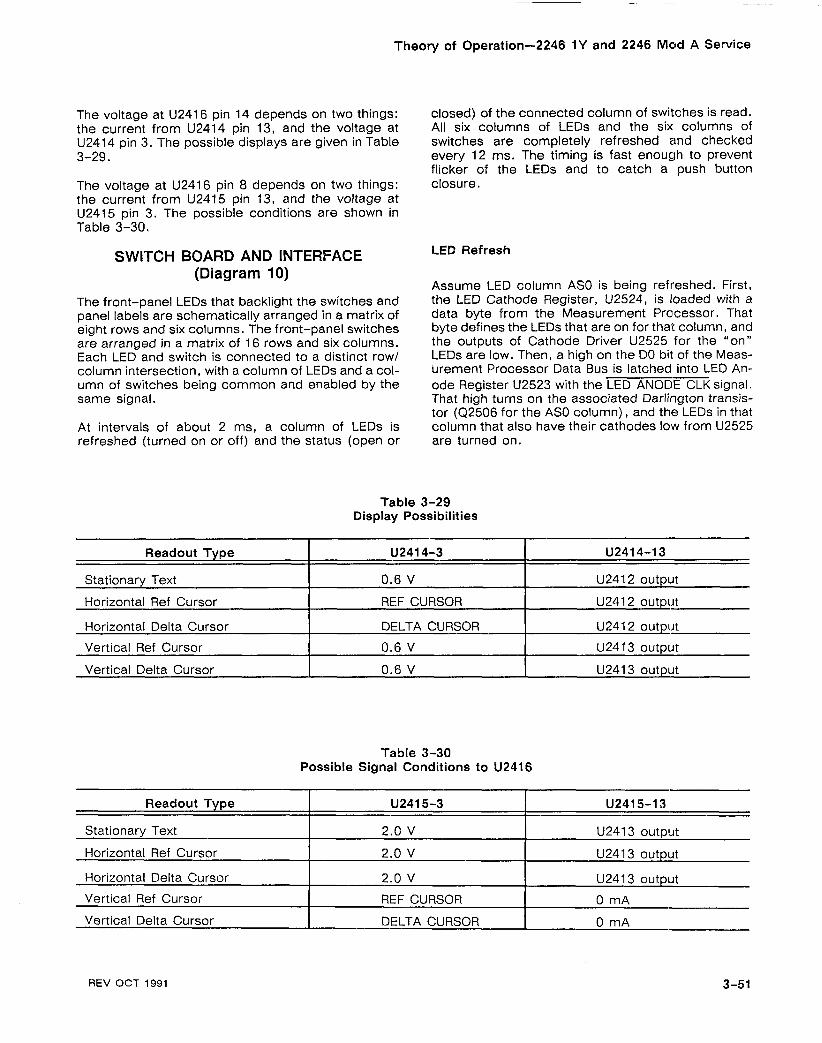
Theory of Operation-2246 1Y and 2246 Mod A Service
The voltage at U2416 pin 14 depends on two things: closed) of the connected column of switches is read. the current from U2414 pin 13, and the voltage at All six columns of LEDs and the six columns of U2414 pin 3. The possible displays are given in Table switches are completely refreshed and checked 3-29. every 12 ms. The timing is fast enough to prevent
flicker of the LEDs and to catch a push button The voltage at U2416 pin 8 depends on two things: closure. the current from U2415 pin 13, and the voltage at U2415 pin 3. The possible conditions are shown in Table 3-30.
SWITCH BOARD AND INTERFACE LED Refresh
(Diagram 10)
The front-panel LEDs that backlight the switches and panel labels are schematically arranged in a matrix of eight rows and six columns. The front-panel switches are arranged in a matrix of 16 rows and six columns. Each LED and switch is connected to a distinct row/ column intersection, with a column of LEDs and a col- umn of switches being common and enabled by the same signal.
At intervals of about 2 ms, a column of LEDs is refreshed (turned on or off) and the status (open or
Assume LED column AS0 is being refreshed. First, the LED Cathode Register, U2524, is loaded with a data byte from the Measurement Processor. That byte defines the LEDs that are on for that column, and the outputs of Cathode Driver U2525 for the "on" LEDs are low. Then, a high on the DO bil: of the Meas- urement Processor Data Bus is latched into LED An- ode Register U2523 with the LED ANODE CLK signal. That high turns on the associated Darlington transis- tor (Q2506 for the AS0 column), and the LEDs in that column that also have their cathodes low from U2525 are turned on.
Table 3-29 Display Possibilities
Vertical Ref Cursor 0.6 V U2413 output
Table 3-30 Possible Signal Conditions to U2416
Vertical Delta Cursor
REV OCT 1991
0.6 V U2413 output
Theory of Operation-2246 1Y and 2246 Mod A Service
Switch Reading
At the same time the AS0 LED column is refreshed, the connected AS0 switch column is pulled high through CR2006. The switch status (low for open or high for closed) for the active switch column is parallel loaded into the Switch Board Shift Registers (U2001 and IJ2002). This switch status data is then shifted out serially (by 15 SW BD SR SHIFT clocks) to the Measurement Processor on the SW BD DATA return line. The position of a high in the serial data stream, and knowing the active column, tells the Measurement Processor the switch in column AS0 that is closed (the CH 1 VOLTSIDIV setting). Columns with push-button switches may or may not have a switch closed. A switch closure is interpreted by the Measurement Processor, and any new operating conditions needed (determined from the firmware routines called up to handle a particular switch closure) are set up.
At the next 2 ms interrupt, the Measurement Processor loads new data into Cathode Register U2524 to enable the LED rows, and the column is advanced to enable the A01 column for refresh and switch reading. The process described is continual while the oscilloscope is on.
Part of the Measurement Processor routine stores the new front panel settings in the System RAM each time a change is made. At power on (after being turned off), the stored front-panel settings are recalled from the System RAM to return the oscilloscope to the same operating state that existed at power off (with some exceptions).
Diagnostic
When the Measurement Processor is running the register checks during the DIAGNOSTIC, it can check the condition of registers U2001 and U2002. Serial data is placed on the AS0 line from the DO bit of the Meas~~rement Processor data bus. That data is serially shifted through the two registers to the SW BD DATA return line. The Measurement Processor compares the returned data stream with what was sent. A difference in the data bits shows an error; a correct comparison passes the test.
ADC AND DAC SYSTEM (Diagram 11)
The ADC and DAC System permits the Measurement Processor to provide analog control voltages to the circuitry under its control and to find out certain analog voltage levels that it-must have to do its con- trol and measurement functions.
Pot Multiplexer Latch
Latch U2313 latches data from the data bus (DO-D7) to control multiplexers U2308 and U2309 on this diagram and U506 on Diagram 7.
Front-Panel Control Multiplexers
Multiplexers U2308 and U2309, controlled by the Measurement Processor via Pot Mux Latch U2313, select the front-panel control levels that are com- pared with the output of the D-to-A Converter (U2302). The result of that comparison is sent via signal line AD COMP to the Measurement Processor (U2501, Diagram 8).
Input Data Latches
Binary data bytes to be converted to analog voltages are loaded into two latches (U2300 and U2301). Data Latch U2301 latches data to the DAC Multi- plexer (U2303). Data Latch U2300 latches data to D-to-A Converter (U2302).
Digital-to-Analog Converter
The D-to-A Converter (U2302), using 12 data bits, can produce 4096 discrete output signal current levels from 0 to 2 mA. Signal current flows through R2303 to the +2.5 V reference voltage. The resulting voltage drop across the resistor moves the voltage at pin 3 of voltage follower U2314 away from +2.5 V toward 0 V and below. When there is 0 mA output, the voltage at pin 3 is +2.5 V. At maximum output current, the voltage at pin 3 is -2.5 V. Voltage fol- lower U2314 buffers the voltage and applies it to the input pin of analog multiplexer U2303, where it is di- rected to the control circuit selected by the Meas- urement Processor.
A-TO-D CONVERSION. The output from U2314 is also applied to comparator U2306. When analog-to- digital conversion is being done, the Measurement Processor drives the DAC to produce comparison voltage levels in a binary search pattern. The output of U2306 is monitored to determine the smallest DAC input change that will produce an output change from the comparator. That value is then used as the digital representation of the analog voltage applied to the other pin of the comparator from the output of Multiplexer U2308 or U2309. Signals on that multiplexed line are the front panel potentiometers' wiper voltages and the probe-code levels.
Sample-and-Hold Circuits
The analog voltages from the multiplexer U2303 remain stable only for the short period of time that the DAC is at a fixed output level. Control voltages to the analog circuitry must remain constant except

Theory of Operation-2246 1Y and 2246 Mod A Service
for changes to the control settings. Those control Both overvoltage and overcurrent protection are voltages are held constant between refreshes by provided to protect the oscilloscope circuitry from sample-and-hold circuits formed by a capacitor (to further damage if a circuit component fails. hold the voltage) and a voltage follower (to buffer the voltage held by capacitor). The voltage follower circuits are ~rov ided bv the o~erational am~lif iers of Input U2304 and '~2305. ~ a c h of 'the hold voltages are protected from humidity degradation of the voltage follower's high-impedance input by an active guard shield on the circuit board. Extra noise filtering for two of the control voltages (REF DELAY and DELTA DELAY) is provided by using an RC pi-type filter input circuit to the voltage follower.
POWER SUPPLY (Diagram 12)
The Power Supply (Diagram 12) provides the various low-voltages needed to operate the 2246 1Y and 2246 Mod A and the high-voltage required by the cathode-ray tube (crt). The supply circuitry is arranged in the following functional blocks: AC Input, Primary Power Rectifier, Start-Up circuit, Preregulator Control circuit, Preregulator Power Switching circuit, lnverter Control circuit, lnverter Power Switching circuit, Low-Voltage Secondary Supplies, and High-Voltage Supply (see Figure 3-9).
Ac power via the power cord is rectified and filtered by the Primary Power Rectifier to supply the dc voltage to Preregulator circuitry. The output voltage level from the Primary Power Rectifier depends on the ac supply voltage level and may vary between about 125 V and 350 V. This unregulated, filtered, dc voltage is supplied to the Preregulator Start-Up circuit and the Preregulator Switching circuit. The Preregulator Power Switching circuit supplies +44 Vdc output power to drive the lnverter Power Switching circuit.
The +44 V Preregulator output voltage is switched by the lnverter Power Switching circuit to produce an alternating current through the primary of the lnverter power transformer. The current source to the lnverter switching transistors is monitored and regulated by the lnverter Control circuit to maintain a constant output voltage level across the transformer secondaries.
The Low-Voltage Secondary Supplies rectify and fil- ter the low-voltage secondary ac voltages to provide the dc power requirements for the instrument. Two other secondary windings on the lnverter Power Transformer are used in the High-Voltage Supply, a high-voltage winding and a crt filament winding. Voltage from the high-voltage winding is further multiplied and converted to dc voltage for the crt anode, cathode, and intensity-grid voltages.
Applied source voltage is input to the Primary Power Rectifier via surge protection circuitry and noise fil- tering circuitry. A sealed line filter (FL2201), L2207, L2208, C2214, C2213, C2216, C2215, R2260, R2227, and R2228 form a low-pass filter designed to prevent transmission of high-frequency noise sig- nals either into or out of the instrument. Bleeder resistor R2215 across the input line filter drains off any charge retained by the capacitors in the input circuitry when the power is disconnected. Ther- mistor RT2201 prevents a sudden rush of input current into the rectifier and filter capacitor, C2202, when the power switch is turned on. The thermistor presents a relatively high resistance when cold, then quickly reduces to a low value when warmed up. Varistor VR2204 acts as a surge limiter .to reduce the effects of any power line surges that may damage the input circuit components. The varistor is a voltage-sensitive device that quickly reduces its resistance value when its voltage! limits are exceeded. Line fuse F2201 protects the instrument from additional damage in case of of a severe short in the power supply.
Primary Power Rectifier
Rectification of the input ac source voltage is done by rectifiers CR2231-CR2234. Simple capacitive fil- tering of the rectifier output is done by C2202. The filtered output voltage may range between about 125 Vdc and 350 Vdc, depending on the amplitude of the ac input voltage. A line trigger signal is picked off by T2206 for use when the Trigger SOURCE is set to LINE. Bleeder resistor R2256 drains off the charge on C2202 when the instrument is turned off.
Start-Up Circuit
The Start-Up circuit provides the operating supply voltage to the Preregulator. At power on, C2204 in the Start-Up circuit begins charging through R2203 and R2204 from the output of the Primary Power Rectifier. When the voltage across (32204 reached 20 V, the voltage at the base of Q2204 is about 6.8 V. This base voltage level causes C12204 to con- duct (there is a 6.2 V zener diode in the emitter path), and Q2211 also is then biased on. Positive feedback to the base of Q2204 (from the collector of Q2211 through R2220) then keeps both transistors on. The dc voltage to U2201 (Vcc) for start up (and continued running after start up) is provided by the charge on C2204 via Q2211.
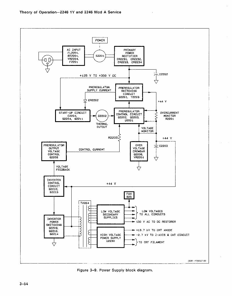
Theory of Operation-2246 1Y and 2246 Mod A Service
OVERCURRENT MONITOR
R220 1
t 4 4 v
CONTROL 02208
PREREGULATOR OUTPUT I VOLTAGE
VOLTAGE FEEDBACK
I INVERTER 1 I
CONTROL CURRENT
CONTROL t 4 4 V CIRCUIT 4 1 02212. 02213
r I
OVER VOLTAGE
C2203
'220
LOW VOLTAGE LOW VOLTAGES TO ALL CIRCUITS
3 0 V AC TO DC REST
I CROWBAR I T I
'ORER
t 1 3 . 7 kV TO CRT ANODE
HIGH VOLTAGE -2.7 kV TO Z-AXIS 6 CRT POWER SUPPLY
)TO CRT FILAMENT
CIRCUIT
Figure 3-9. Power Supply block diagram.

Theory of Operation-2246 1Y and 2246 Mod A Service
With U2201 on and drawing current from C2204, the voltage across C2204 begins to fall. If the Preregulator output rises to +44 V before the voltage across C2204 falls to 10 V, then CR2202 becomes forward biased, and current pulses are supplied by a winding (pins 8 and 9) on T2203 to keep C2204 charged (and U2201 operating).
If the Preregulator output does not rise to +44 V within the time it takes to discharge C2204 below 10 V (about 1 I10 of a second), the voltage at the base of Q2204 will drop too low for the feedback voltage to keep it on. That will cause (2221 1 to also shut off. The start-up cycle repeats when the voltage across C2204 again reaches 20 V (recharging from the output of the Primary Power Rectifier output via R2203 and R2204). Continued failure of the Preregulator to start up and the repeated attempts to do so is called the "Chirp" mode. Zener diode VR2206 prevents the voltage across C2204 from exceeding about 30 V if no start-up attempt occurs.
Preregulator Control Circuit
The Preregulator Control IC, U2201, is a pulse-width modulator used to control the on time of Preregulator Switching FET Q2201. It contains an oscillator, comparators, voltage and current error amplifiers, and logic circuitry that controls its operation. The modulated output pulses drive switching transistor Q2201 through a buffer amplifier composed of Q2202 and (22203. Pulse width (the time that FET (22201 is on) is inversely proportional to the control voltage at pin 3 of U2201 (i.e., a lower voltage at pin 3 makes the pulse width wider to keep Q2201 on longer.
Pin 7 of U2201 is the IC ground reference, and it is tied directly to the +44 V output voltage. Therefore, the Preregulator IC and the Start-Up circuitry operating potentials "float" on the regulated output voltage (developed across C2203).
Pin 2 of U2201 is the current-summing node to the voltage-error amplifier. The error amplifier will try to keep the voltage on pin 2 equal to the voltage on pin 1 (the +44 V supply voltage). The error amplifier maintains pin 2 at +44 V by raising (or lowering as necessary) the voltage at pin 3. This raises (or lowers) the voltage across C2203 so that less (or more) current will be drawn out of the current summing node.
The major current injected into the summing node is from the regulated 5 V output, from pin 12 of U2201, via R2212. That current is about 0.6 mA. The current through R2206 adds to the current shunted by the Preregulator Output Voltage Control transistor, (22208, to produce about 0.6 mA to keep t h e current
into and out of the summing node balanced. The actual current through R2206 is the output voltage (+44 V across C2203) divided by the resistance value of R2206 (100 kf i ) or about 0.4 mA.
SOFT START. At the initial turn-on of the instru- ment, C2203 is discharged. If no action were taken to prevent it, the initial charging current to that capacitor would exceed safe limits. To avoid such a problem, a "soft start" of the charging path is done.
At turn-on, the +5 V output of U2201 steps to +5 V immediately. A +5 V pulse is coupled to pin 4 of U2201 via C2207. This pin is the "dead time control" input, and when it is high, the dead time between switching pulses to Q2201 is increased to 100%. Switching transistor (22201 does not turn on, and no charging of C2203 occurs. Then, as C2207 charges, the voltage on pin 4 begins to decrease toward the ground reference value (on pin 7). This decreases the dead time, allowing increasingly wider conduc- tion pulses to occur.
The on-time gradually increases until the charging current is limited by the internal current limit ampli- fier of U2201. At that point, the Preregulator is acting as a current source. When the voltage across C2203 reaches +44 V, the voltage error amplifier starts to limit the output, and the Preregulator has reached its operating level and acts as a voltage source.
CURRENT LIMIT. The output current of the Preregulator switching FET, (22201, is limited to a safe value. If the current exceeds 2.4 amperes, the voltage dropped across R2201 causes pin 14 of U2201 (one input of the current limit amplifier) to exceed the voltage on pin 13 of U2201 (the other input pin of the current limit amplifier). The output of the current limit amplifier then goes high, raising the voltage on pin 3 of U2201. Increased voltage on pin 3 narrows the width of the turn-on pulses to switching FET Q2201 and limits the output current.
Usually, with a circuit failure, the excess loading remains, and the pulses remain narrow. The Preregulator Control IC then shuts down because the charge on C2204 is not maintained via the Preregulator supply winding on T2203, and the Preregulator goes into the chirp mode (continual shut down and restart attempts).
OVERVOLTAGE CROWBAR. If the output voltage across C2203 exceeds about +51 V, VR2201 in the crowbar circuit conducts. The gate of SCR (22206 then rises; and, if the rise is enough, the SCR latches on. When on, Q2206 shorts out (22203, and the current limit circuit causes the switching pulses to (22201 to become very narrow. Preregulator IC U2201 then shuts down (as described in the Current Limit discussion). The Preregulator will attempt a
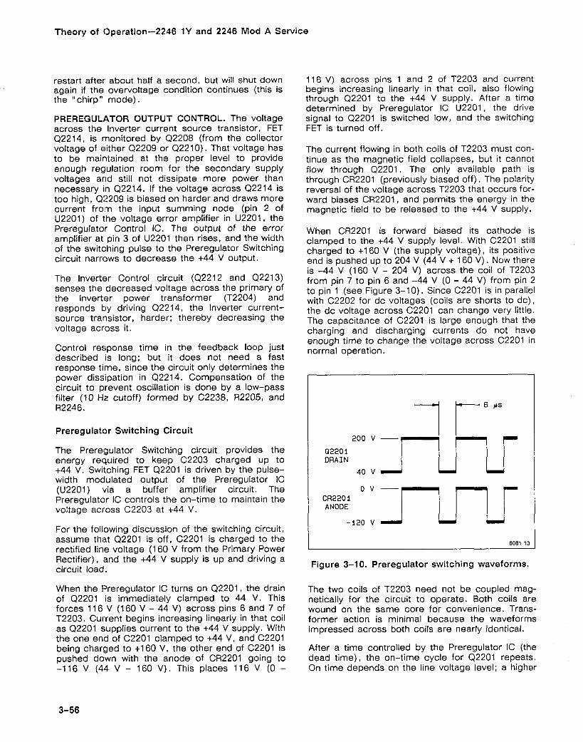
Theory of Operation-2246 1Y and 2246 Mod A Service
restart after about half a second, but will shut down again if the overvoltage condition continues (this is the "chirp" mode).
PREREGULATOR OUTPUT CONTROL. The voltage across the lnverter current source transistor, FET Q2214, is monitored by Q2208 (from the collector voltage of either Q2209 or Q2210). That voltage has to be maintained at the proper level to provide enough regulation room for the secondary supply voltages and still not dissipate more power than necessary in Q2214. If the voltage across Q2214 is too high, Q2209 is biased on harder and draws more current from the input summing node (pin 2 of U2201) of the voltage error amplifier in U2201, the Preregulator Control IC. The output of the error amplifier at pin 3 of U2201 then rises, and the width of the switching pulse to the Preregulator Switching circuit narrows to decrease the +44 V output.
The Inverter Control circuit (Q2212 and Q2213) senses the decreased voltage across the primary of the Inverter power transformer (T2204) and responds by driving Q2214, the Inverter current- source transistor, harder; thereby decreasing the voltage across it.
Control response time in the feedback loop just described is long; but it does not need a fast response time, since the circuit only determines the power dissipation in Q2214. Compensation of the circuit to prevent oscillation is done by a low-pass filter (10 Hz cutoff) formed by C2238, R2205, and R2246.
Preregulator Switching Circuit
The Preregulator Switching circuit provides the energy required to keep C2203 charged up to +44 V. Swi.tching FET Q2201 is driven by the pulse- width moclulated output of the Preregulator IC (U2201) via a buffer amplifier circuit. The Preregulator IC controls the on-time to maintain the voltage across C2203 at +44 V.
For the following discussion of the switching circuit, assume that Q2201 is off, C2201 is charged to the rectified line voltage (1 60 V from the Primary Power Rectifier), and the +44 V supply is up and driving a circuit load.
When the Preregulator IC turns on Q2201, the drain of Q2201 is immediately clamped to 44 V. This forces 11 6 V (1 60 V - 44 V) across pins 6 and 7 of T2203. Current begins increasing linearly in that coil as Q2201 supplies current to the +44 V supply. With the one end of C2201 clamped to +44 V, and C2201 being charged to +I60 V, the other end of C2201 is pushed dawn with the anode of CR2201 going to -1 16 V (44 V - 160 V). This places 116 V (0 -
116 V) across pins 1 and 2 of T2203 and current begins increasing linearly in that coil, also flowing through Q2201 to the +44 V supply. After a time determined by Preregulator IC U2201, the drive signal to Q2201 is switched low, and the switching FET is turned off.
The current flowing in both coils of T2203 must con- tinue as the magnetic field collapses, but it cannot flow through Q2201. The only available path is through CR2201 (previously biased off). The polarity reversal of the voltage across T2203 that occurs for- ward biases CR2201, and permits the energy in the magnetic field to be released to the +44 V supply.
When CR2201 is forward biased its cathode is clamped to the +44 V supply level. With C2201 still charged to +I 60 V (the supply voltage), its positive end is pushed up to 204 V (44 V + 160 V) . Now there is -44 V (160 V - 204 V) across the coil of T2203 from pin 7 to pin 6 and -44 V (0 - 44 V) from pin 2 to pin 1 (see Figure 3-1 0). Since C2201 is in parallel with C2202 for dc voltages (coils are shorts to dc), the dc voltage across C2201 can change very little. The capacitance of C2201 is large enough that the charging and discharging currents do not have enough time to change the voltage across C2201 in normal operation.
2 0 0 v - 0 2 2 0 1 DRAIN
1 rps 40 V
CR220 1 ANODE
0 O V V -120 v
6081-13
Figure 3-1 0. Preregulator switching waveforms.
The two coils of T2203 need not be coupled mag- netically for the circuit to operate. Both coils are wound on the same core for convenience. Trans- former action is minimal because the waveforms impressed across both coils are nearly identical.
After a time controlled by the Preregulator IC (the dead time), the on-time cycle for Q2201 repeats. On time depends on the line voltage level; a higher

Theory of Operation-2246 1Y and 2246 Mod A Service
line voltage level means a shorter on time of Q2201 T2205. Current rapidly ramps up through the primary is needed to maintain +44 V across C2203. of T2205 and induces a positive feedback base
current in one-half of its center-tapped secondary that keeps Q2210 turned on. Current in the other
Inverter Power Switching Circuit half of the secondary biases on CR2227 to prevent a high reverse base-to-emitter voltage from being
The lnverter Power Switching circuit is composed of developed across ~ 2 2 0 9 . switching transistors Q2209 and Q2210, current source transistor Q2214, inverter power transformer T2204, base-drive transformer T2205, and asso- ciated components. Current supplied by the +44 volts output from the Preregulator circuit is alter- nately switched through each side of the center- tapped primary of T2204 to drive the loads on the secondary windings of the inverter transformer.
INVERTER STARTER. As the Preregulator turns on, the +44 V supply increases from 0 V. The increasing voltage forward biases CR2236 and charges C2248 through the base-emitter junctions of Q2209 and Q2210. Current is drawn through each side of T2204, from the center tap, as the transistors conduct. One of the two transistors will have a slightly higher gain than the other, and its collector voltage will decrease more than the other. The voltage difference across the primary of T2204 also appears across the primary winding of T2205, and a feedback voltage is induced in the secondary winding of T2204. The polarity of the transformer is such that the conduction of the higher gain transistor is reinforced (positive feedback), and that transistor quickly saturates while the other is cut off. One end of the primary of T2204 is driven toward around
After about 25 ps, the current through the primary of T2205 saturates the magnetic core and the primary impedance of the transformer drops to a low value. When saturation occurs, the impedance presented by L2206 by comparison to that of T2205 is large, and most of the voltage applied from the secondary of T2204 is then dropped across L2206. The secon- dary voltage of T2205 drops to zero, and with no base-drive current to Q2210, that transistor switches off.
With both Q2209 and Q2210 off, the magnetic energy stored in the primary of T2205 a.nd in L2206 causes current to flow in the primary of T2204, reversing the voltage polarity on this winding. The voltage reversal is not instantaneous because of the parasitic capacitance of the T2204 windings. When the reverse voltage gets high enough, base current flows to Q2209 and that transistor turns on. The cycle then repeats with current flow through T2204 reversed. This process induces ac in the various secondary windings of the inverter power transformer.
while the other end is opened. After about-half a tNVERTER CONTROL LOOP. either C2248 charges up' becomes Q2209 or 02210 is on. the collector voltage of the and that path current the on transistor forward biases either CR2205 (if Q2209
conducting transistor is blocked. is on) or CR2204 (if Q2210 is on). Capacitor C2219
If the lnverter Power Switching circuit stops, the lnverter Starter circuit will not restart it until C2248 is discharged. Furthermore, C2248 will not discharge until the +44 V supply falls.
INVERTER POWER SWITCHING. Switching is started by one or the other of either Q2209 or Q2210 conducting more that the other, and circuit action biases the other one off. Assume for this discussion that Q2210 is biased on and Q2209 is off. Current flows through current-source FET Q2214, on- transistor Q2210, and half of the primary of T2204 (pins 9 and 1 1). The voltage drop across current- source transistor Q2214 holds the emitter voltage of Q2209 and Q2210 at 3 V. Voltage across pins 9 and 11 is therefore 41 V (44 V - 3 V).
Through autotransformer action, 41 V is induced in the other half of the primary winding of T2204 from pin 8 to the center-tap pin. That voltage adds to the 41 V from pins 9 to 11 to produce a potential of 82 volts across the primary of switching transformer
is then charged to nearly the same voltage that is applied to the center tap of the primary winding of lnverter Transformer T2204.
A resistive voltage divider formed by R2239, R2238, and potentiometer R2252 (+7.5 V ADJUST) applies a fraction of the voltage across C2219 to the base of Q2213 (one-half of a differential amplifier formed by Q2212 and Q2213). The voltage on the base of Q2213 is compared to a voltage on the base of Q2212 that is referenced back to the +44 V center tap voltage of T2204. If the collector voltage of the conducting inverter switching transistor (Q2009 or Q2210) is not the correct level (about 3 \ I ) , the gate voltage of current-source FET Q2214 will be raised or lowered as needed to correct the error.
Low-Voltage Secondary Supplies
The low-voltage power supply circuitry on the pin 12 to pin 22 and pin 13 to pin 15 secondary windings of

Theory of Operation-2246 1Y and 2246 Mod A Service
the lnverter power transformer consist of rectifier and filter components only. All the regulation is done by the Preregulator and lnverter Control circuitry in the primary side of the transformer. Both half-wave and full-wave rectifiers are used, and either simple capacitor or capacitive-input PI filter circuits are used. RectPfier and filter type used for each of the secondary voltages depends on the load require- ment. A single 130 Vac output from pin 12 of T2204 supplies the drive to the 2-Axis dc restorer circuitry. Power for the blower fan is supplied by the -15 V power supply line.
The center-tapped secondary winding from pins 13 to 15 of T2204 is used for the +5 V and -5 V supplies. Both are full-wave rectified and filtered using capaci- tive-input PI filters.
High-Voltage Supply
The high-voltage power supply uses two secondary windings of T2204: one for high-voltage multiplier U2230 and the other for the crt filament. Flying leads from the top of the transformer make the circuit con- nections into the high-voltage circuitry. The crt fila- ment winding consists of a few turns of insulated wire.
filter. A neon lamp across the second section of the filter provides protection against arcing if there is a failure that can cause a large difference of potential to develop between the crt heater and cathode cir- cuits.
MAIN BOARD POWER DISTRIBUTION (Diagram 13)
The Main Board Power Distribution diagram schemati- cally displays the distribution paths and decoupling circuits for the low voltages from the Power Supply. The supply and ground connections to the various in- tegrated circuits in the instrument are also shown. Use this diagram to aid circuit tracing when trying to locate a power supply loading problem associated with the Main Board.
PROCESSOR BOARD POWER DISTRIBUTION (Diagram 14)
The continuing power distribution from the Main Board to the top board (Processor Board, A1 6) is depicted in the Processor Board Power Distribution schematic diagram. Use Diagram 14 to aid in locating power supply loading problems that are isolated to the Proc- essor Board.
INTERCONNECTION DIAGRAM (Diagram 15)
The high-voltage winding attaches directly to the HV Multiplier. Outputs from HV Multiplier U2230 are the Circuit board interconnections with the plug, jack, pin 13.3 kV to the crt anode via a high-voltage-insulated numbers, and signal names shown are found in sche- connecting lead and the -2.7 kV.supplied to the crt matic Diagram 15. The diagram is useful in checking cathode, focus grid, and intensity grid. The -2.7 kV continuity of cable runs and signal paths from board supply is filtered by a two-section capacitive input RC to board through the instrument.
REV OCT 1991
-- - -
Section 4-2246 1Y and 2246 Mod A Service
PERFORMANCE CHECK PROCEDURE
INTRODUCTION
PURPOSE
This Performance Check Procedure verifies the Perform- ance Requirements of the 2246 1Y or 2246 Mod A as listed in the Specification (Section 1) and helps deter- mine the need for readjustment. These checks may also be used as an acceptance test or as a preliminary troubleshooting aid.
You do not have to remove the wrap-around cabinet from the 2246 1Y or 2246 Mod A to do this procedure. All checks can be made with controls and connectors ac- cessible from the outside.
TEST EQUIPMENT REQUIRED
Table 4-1 lists all the test equipment required to do the Performance Check Procedure. Test equipment specifi- cations described are the minimum necessary to pro- vide accurate results. For test equipment operating infor- mation, refer to the appropriate test equipment instruc- tion manual.
When you use equipment other than that recommended, you may have to make some changes to the test setups. If the exact example equipment in Table 4-1 is not avail- able, use the Minimum Specification column to deter- mine if any other available test equipment might be ade- quate to do the check.
PERFORMANCE CHECK INTERVAL
To ensure instrument accuracy, check the performance of the 2246 1 Y or 2246 Mod A after every 2000 hours of operation, or once each year if used infrequently. If the checks indicate a need for readjustment or repair, refer the instrument to a qualified service person.
NOTE
The silver-oxide batferies used in the 2246 1 Y (instruments serial numbered B714!999 and below) MUST BE REPUCED AT LEAST EVERY 12 MONTHS to ensure proper opera- tion of the instrument.
PREPARATION
This procedure is divided into subsections to let you check individual sections of the instrument when it is not necessary to do the complete Performance Check. An Equipment Required block at the beginning of each sub- section lists the equipment from Table 4-1 that is needed to do the checks in that subsection.
The initial front-panel control settings at the beginning of each subsection prepare the instrument for the first step of the subsection. Do each of the steps in a subsection completely and in order to ensure the correct control set- tings for steps that follow. To ensure performance ac- curacies stated in the Specification (Section I) , let the in- strument warm up for 20 minutes and run the SELF CAL MEASUREMENTS routine.
To run the SELF CAL MEASUREMENTS routine:
Press the top and bottom menu-item select buttons to display the SERVICE MENU. Underline and select SELF CAL MEASUREMENTS. Press RUN to start the routine, then QUIT to return to the normal oscillosc:ope mode.
NOTE
Performance accuracies are ensured only when the SELF CAL MEASUREMENTS are done AFTER the 20-minute warmup.
REV OCT 1991

Performance Check Procedure - 2246 1 Y and 2246 Mod A Service
Table 4-1 Test Equipment Required
Item and Description I --
Minimum Specification
Leveled Sine-Wave Generator
Calibration Generator
Time-Mark Generator
Function Generator
Coaxial Cable (2 required)
Precision Coaxial Cable
Frequency: 250 kHz to above 150 MHz. Output amplitude: variable from 10 mV to 5 V p-p. Out- put impedance: 50 SZ. Amplitude accuracy: constant within 1.5% of reference frequency to 100 MHz.
Standard-amplitude signal levels (dc and square wave) : 5 mV to 50 V. Accuracy: t 0.25%. High-amplitude signal levels: 1 V to 60 V. Repetition rate: 1 kHz. Fast-rise signal level: 1 V. Repetition rate: 1 MHz. Rise time: 1 ns or less. Flatness: 2 0.5%.
Example of Use Test Equipment
Vertical, horizontal, TEKTRONIX SG 503 triggering, measure- Leveled Sine-Wave ment bandwidth, and Generator. a Z-Axis checks and
Signal source for gain TEKTRONIX PG 506A and transient response Calibration checks and adjustments. Generator. a
Marker outputs: 5 ns to 0.5 s. Marker accuracy: + 0.1 %. Trigger output: - 1 ms to 0.1 ps time- coincident with markers.
Range: less than 1 Hz to 100 kHz; sinusoidal out- put; amplitude variable up to greater than 10 V p-p open circuit with dc offset adjust.
Horizontal checks and adjustments. Display adjustment. Time cursor checks.
Low-frequency checks, X-Y phase check.
TEKTRONIX TG 501 A Time-Mark Generator. a
TEKTRONIX FG 502 Function Generatora
Impedance: 50 SZ. Length: 42 in. Connectors: BNC.
Impedance: 50 SZ. Length: 36 in. Connectors: BNC.
Signal interconnection.
I I Used with PG 506A Cali-
bration Generator and SG 503 Sine-Wave Generator.
Tektronix Part Number 01 2-0057-01 .
Tektronix Part Number 01 2-0482-00.
a~equires a TM500-se~ries power module.
REV OCT 1991

Performance Check Procedure-2246 1Y and 2246 Mod A Service
Table 4-1 (cont)
Item and Description
Termination (2 required)
2X Attenuator
Minimum Specification
1 OX Attenuator
Ratio: 2X. Impedance: 50 a. Connectors: BNC.
Impedance: 50 a. Connectors: BNC.
Triggering checks.
Use
Signal termination. Tektronix Part Number 01 1-0049-01.
Ratio: 1OX. Impedance: 50 a. Connectors: BNC.
Tektronix Part Number 01 1-0069-02.
Example of Test Equipment
Triggering checks. Tektronix Part Number 01 1-0059-02.
Adapter
Alignment Tool
Connectors: BNC male-to-miniature-probe tip.
Signal interconnection.
Length: 1 -in shaft. Bit size: 3/32 in. Low capacitance; insulated.
Tektronix Part Number 01 3-0084-02.
Test Oscilloscope
Adjust TRACE ROTATION pot. Adjust variable capacitors and resistors.
Bandwidth: 20 MHz.
Z-Axis response adjustment.
Tektronix Part Number 003-0675-00.
TEKTRONIX 2246A.
Dual-Input Coupler
T-Connector
Precision Normalizer
REV OCT 1991
Connectors: BNC female-to-dual-BNC male.
TV Signal Generator
Digital Multimeter (DMM)
BNC Coupling Capacitor
Connectors, BNC.
Input resistance: 1 M a. Input capacitance: 20 pF.
Signal interconnection.
Signal interconnection. Tektronix Part Number 103-0030-00.
Input capacitance Tektronix Part Number adjustments. 0 067-1 129-00.
a Requires a TM500-series power module.
Provide composite TV video and line sync signals.
Dc volts range: 0 to 140 V. Dc voltage accuracy ? 0.15%. 4 1 /2 digit display.
0.047 kF.
Tektronix Part Number 067-0525-02.
Check TV Trigger circuit.
Power supply voltage checks and adjustments.
CHI /CH2 Voltmeter DC rejection ratio check.
Tektronix 067-0601 -00. Calibration fixture with 067-5002-00 (525160) and 067-501 0-00 (1 201 160) plug-ins.
Tektronix DM 501A Digital Multimeter?
TEKTRONIX 01 5-0221 -00 Coupling Capacitor

Performance Check Procedure-2246 1Y and 2246 Mod A Service
INDEX TO PERFORMANCE CHECK PROCEDURE
DISPLAY
1 . TRACE ROTATION . . . . . . . . . . . . . . . . . 4-5 2 . Geometry . . . . . . . . . . . . . . . . . . . . . . . . . 4-5
VERTICAL
1 . Input COUPLING Functional Check . . . . 4-6 2 . CH 1 and CH 2 VOLTS/DIV
Trace Shift . . . . . . . . . . . . . . . . . . . . . . . . 4-6 3 . CH 3 and CH 4 VOLTS/DIV
Trace Shift . . . . . . . . . . . . . . . . . . . . . . . . 4-7 4 . CH 1 and CH 2 VAR VOLTSIDIV
Trace Shift . . . . . . . . . . . . . . . . . . . . . . . 4-7 5 . CH 1 and CH 2 lnput COUPLING
Trace Shift . . . . . . . . . . . . . . . . . . . . . . . . 4-7 6 . CH 2 INVERT Trace Shift . . . . . . . . . . . 4-7 7 . CH 1 and CH 2 VAR VOLTSIDIV
Range . . . . . . . . . . . . . . . . . . . . . . . . . . . . 4-7 8 . Low Frequency Linearity . . . . . . . . . . . 4-8 9 . CH 1 and CH 2 Vertical Deflection
Accuracy . . . . . . . . . . . . . . . . . . . . . . . . . 4-8 10 . CH 3 and CH 4 Vertical Deflection
Accuracy . . . . . . . . . . . . . . . . . . . . . . . . . 4-8 11 . ADD Mode and CH 2 INVERT
Deflection Accuracy . . . . . . . . . . . . . . . . 4-9 1 2 . Vertical POSITION Range
(all channels) . . . . . . . . . . . . . . . . . . . . . 4-9 13 . CH 1 to CH 2 Signal Delay Match . . . . 4-10 14 . CH 1 to CH 4 Sianal Delav Match . . . . 4-10 15 . CH 3 to CH 4 signal ~ela; Match . . . . 4-10 16 . CH 1 and CH 2 Vertical Bandwidth . . . 4-10 17 . CH 3 and CH 4 Vertical Bandwidth . . . 4-1 1 18 . CH 1 and CH 2 Aberrations . . . . . . . . . 4-1 1 19 . SCOPE BW (Bandwidth Limit)
Accuracy . . . . . . . . . . . . . . . . . . . . . . . . 4-11 20 . Common-mode Rejection Ratio . . . . 4-1 2 21 . Channel Isolation . . . . . . . . . . . . . . . . . . 4-1 2 22 . AC-Coupled Lower -3 dB Point . . . . 4-13 23 . Vertical ALT and CHOP Modes . . . . . . 4-13 24 . BEAM FIND Functional Check . . . . . . 4-13 25 . A and B Trace Separation . . . . . . . . . . 4-13
TRIGGERING
1 . 500 Hz Trigger Sensitivity . . . . . . . . . . 4-14 2 . 500 kHz Trigger Sensitivity . . . . . . . . . 4-15 3 . 25 MHz Trigger Sensitivity . . . . . . . . . . 4-1 5
. . . . . . . . . 4 . 100 MHz Trigger Sensitivity 4-1 5 5 . 100 MHz NOISE REJ Trigger
Sensitivity . . . . . . . . . . . . . . . . . . . . . . . . 4-1 6
6 . Single Sweep Mode . . . . . . . . . . . . . . 4-16 7 . Trigger LEVEL Control Range . . . . . . 4-16 8 . TV Field Trigger Sensitivity . . . . . . . . . 4-17 9 . TV Line Trigger Sensitivity . . . . . . . . . 4-17
10 . Line Trigger Functional Check . . . . . . 4-17
HORIZONTAL
1 . A and B Sweep Length . . . . . . . . . . . 2 . Horizontal POSITION Range . . . . . . . . 3 . VAR SECIDIV Range . . . . . . . . . . . . . 4 . Magnifier Registration . . . . . . . . . . . . . 5 . A and B Timing Accuracy
and Linearity . . . . . . . . . . . . . . . . . . . . 6 . A and B Magnified Timing
Accuracy . . . . . . . . . . . . . . . . . . . . . . . 7 . Delay Time Jitter . . . . . . . . . . . . . . . . . 8 . Delay Time Accuracy . . . . . . . . . . . . . 9 . Delay Time Position Range . . . . . . . . .
10 . X-Axis Gain Accuracy . . . . . . . . . . . . 11 . X-Y Phase Difference . . . . . . . . . . . . . 12 . X-Axis Bandwidth . . . . . . . . . . . . . . . .
TIME AND CURSORS MEASUREMENTS
1 . I t SEC +I and I t l /SEC +I Cursor Accuracy . . . . . . . . . . . . . . . . . . . . . . . 4-23
2 . Delta Time Accuracy . . . . . . . . . . . . . 4-23 3 . I t PHASE 4 Cursor Accuracy . . . . . . . 4-24 4 . I t VOLTS +I Cursor Accuracy . . . . . . . 4-24 5 . /j7 VOLTS4 Cursor Accuracy . . . . . . 4-24 6 . Tracking Cursors Position Accuracy . 4-24
CHI ICH2 VOLTMETER MEASUREMENTS
1 . DC Volts Accuracy . . . . . . . . . . . . . . . 4-25 2 . DC Volts Normal Mode
Rejection Ratio . . . . . . . . . . . . . . . . . . . 4-25 3 . +Peak. - Peak. and Peak-to-Peak
Volts Accuracy . . . . . . . . . . . . . . . . . . 4-26 4 . 25 MHz +Peak. -Peak. and
Peak-to-Peak Volts Accuracy . . . . . . 4-26 5 . 100 MHz +Peak. -Peak. and
Peak-to-Peak Volts Accuracy . . . . . . 4-26 6 . Gated Volts Accuracy . . . . . . . . . . . . . 4-26
EXTERNAL Z-AXIS AND PROBE ADJUST AND FRONT-PANEL SETUP FUNCTIONS
. . . . . . . 1 .Check External Z-Axis Input 4-28 . . . . . . . . . . . 2.PROBE ADJUST Output 4-28
3 .Run MAKE FACTORY SETTINGS . . . . . . . . . . . . . . . . . . . . . . . . . Routine 4-28
- -- - --
Performance Check Procedure-2246 1Y and 2246 Mod A Service
DISPLAY
Equipment Required (See Table 4-1)
Time-mark generator 50 BNC coaxial cable
50 SZ BNC termination
1. TRACE ROTATION
a. Set:
READOUT (Intensity)
Vertical MODE CH 1 VOLTSIDIV CH 1 COUPLING AIB SELECT Trigger MODE Trigger SOURCE Trigger CPLG Trigger SLOPE Trigger HOLDOFF Trigger LEVEL Horizontal MODE Horizontal POSITION A SECIDIV Measurements
FOCUS
SCOPE BW
For a viewable readout For a viewable trace CH I 0.1 v AC A Trigger AUTO LEVEL VERT DC s (positive)
Min 12 o'clock A 12 o'clock 2 FS All off (press CLEAR DISPLAY three times) For best defined display Off
b. Position trace vertically to the center graticule line.
c. CHECK-trace rotation control range is adequate to align trace with center graticule line using a small straight-bladed alignment tool.
d. ADJUST-trace parallel to center horizontal graticule line.
2. Geometry
a. Connect time-mark generator (TG 501) to CH 1 via a 50 fi BNC coaxial cable and a 50 0 BNC termination.
b. Set generator for 0.2 JLS time marks.
c . Position the bottom of the CH 1 signal below the bottom graticule line.
d. CHECK-deviation of any vertical line within the center eight horizontal divisions does not exceed 0.1 division (half a minor division).
e. Set CH 1 COUPLING to GND.
f. Position trace slowly from the bottom graticule line to the top graticule line while making the fol- lowing check.
g. CHECK-bowing or tilt of baseline trace doesn't exceed 0.1 division (half a minor division) within the eight vertical divisions.
h. Disconnect test signal from the 2246 1Y or 2246 Mod A.

Performance Check Procedure-2246 1Y and 2246 Mod A Service
VE WTICAL
Equipment Required (See Table 4-1)
Leveled sine-wave generator 50 R precision BNC coaxial cable
Calibration generator 50 R termination
Function generator Adapter BNC-male-to-miniature probe tip
50 R BNC coaxial cable Dual-input coupler
1. lnput COUPLING Functional Check
a. Set:
READOUT (Intensity)
Vertical MODE CH 1 and CH 2 VOLTSIDIV CH 1 and CH 2 lnput COUPLING AIB SELECT Trigger MODE Trigger SOURCE Trigger CPLG Trigger SLOPE Trigger LEVEL rigger HOLDOFF Horizontal POSITION Horizontal MODE SECIDIV FOCUS
Measurements
SCOPE BW CH 2 INVERT
For a viewable readout For a viewable trace CH 1 and CH 2
DC A Trigger AUTO LEVEL VERT DC s (positive) 12 o'clock Min 12 o'clock A 0.5 ms For best defined display All off (press CLEAR DISPLAY three times) Off Off
b. Set Vertical MODE to CH 1 (CH 2 off)
c. Connect calibration generator (PG 506) STD AMPL output to the CH 1 input via a 50 R BNC coaxial cable.
d. Set calibration generator to STD AMPL and AM- PLITUDE to 5 V.
e. Position the bottom of the signal to the center horizontal graticule line.
f. Set CH 1 lnput COUPLING to AC.
g. CHECK-display is roughly centered about the center horizontal graticule line.
h. Move the test signal to the CH 2 input.
i. Set Vertical MODE to CH 2 (CH 1 off).
j . Repeat the procedure for CH 2.
k. Disconnect the test signal from the 2246 1Y or 2246 Mod A.
2. CH 1 and CH 2 VOLTSlDlV Trace Shift
a. Set:
CH 1 and CH 2 Vertical MODE CH 1 and CH 2 VOLTSIDIV CH 1 and CH 2 lnput COUPLING SCOPE BW
GND 0 n
b. Set Vertical MODE to CH 1 (CH 2 off).
c. Position trace to center horizontal graticule line.
d. Switch CH 1 VOLTSIDIV through all positions from 2 mV to 5 V.
e. CHECK-trace shift does not exceed 0.2 division between steps.
f. Set Vertical MODE to CH 2 (CH 1 off).
g. Position CH 2 trace to the center horizontal graticule line.
Performance Check Procedure-2246 l Y and 2246 Mod A Service
h. Switch CH 2 VOLTSIDIV through all positions 5. CH 1 and CH 2 lnput COUPLING Trace Shift from 2 mV to 5 V.
a. Position trace to center graticule line. i. CHECK-trace shift does not exceed 0.2 division
between steps. b. Set CH 2 Input COUPLING to DC.
3. CH 3 and CH 4 VOLTSlDlV Trace Shift c. CHECK-trace shift does not exceed 0.25 division.
a. Set Vertical MODE to CH 3 (CH 2 off). d. Set:
b. Position trace to the center horizontal graticule line. Vertical MODE CH 1 (CH 2
off) c. Switch CH 3 VOLTSIDIV between 0.1 V and CH 1 Input COUPLING GND
0.5 V. e. Position trace to center graticule line -
d. CHECK-trace shift does not exceed one f . set cH C ~ U P L I N ~ to D ~ . division.
e. Set Vertical MODE to CH 4 (CH 3 off). g. CHECK-trace shift does not exceed 0.25 division.
f. Position trace to the center horizontal graticule line, 6. CH 2 INVERT Trace Shift
g. Switch CH 4 VOLTSIDIV between 0.1 V and a. Set: 0.5 V.
Vertical MODE to CH 2 (CH 1 off) h. CHECK-trace shift does not exceed one CH 2 input Coupling GND
division. b. Position trace to center horizontal graticule line.
4. CH 1 and CH 2 VAR VOLTSlDlV Trace Shift c. Set CH 2 INVERT On.
a. Set: d. CHECK-trace shift does not exceed one
Vertical MODE CH 1 (CH 4 off) division.
CH 1 VOLTSIDIV 2 mV e. Set:
b. Position trace to center graticule line.
c . Set CH 1 VAR VOLTSIDIV fully CCW.
CH 2 INVERT CH 2 COUPLING
Off DC
d. CHECK-trace shift does not exceed one 7. CH 1 and CH 2 VAR VOLTSIDIV Range division.
a. Set Vertical MODE to CH 1. e. Set:
CH 1 VAR VOLTSIDIV Detent b. Position CH 1 trace to the center horizontal
graticule line. (calibrated)
Vertical MODE CH 2 (CH 1 off) c . Connect calibration generator (PG 506) STD CH 2 VOLTS/DIV 2 mV AMPL output to the CH 1 input via 50 fl precision
BNC coaxial cable. Set calibration generator to
f. Position trace to center graticule line. STD AMPL and AMPLITUDE to 50 mV.
g. Set CH 2 VAR VOLTSIDIV fully CCW. d. Set:
h. CHECK-trace shift does not exceed one division.
CH 1 VOLTS/DIV CH 1 VAR VOLTSIDIV
10 mV Fully CCW
i. Set CH 2 VAR VOLTS/DIV to detent (calibrated) e. CHECK-the signal amplitude is two divisions or
position. less.
Performance Check Procedure- 2246 1Y and 2246 Mod A Service
f. Set: f. Move the test signal to the CH 1 input.
CH 1 VAR VOLTS/DIV Detent g. Set: (calibrated)
Vertical MODE CH 2 (CH 1 off) Vertical MODE CH 2 VOLTS/DIV 10 mV CH 1 VOLTS/DIV
CH 1 (CH 2 off) 2 mV
g. Position CH 2 trace to the center horizontal graticule h. Position the trace two graticule lines below the cen- line. ter graticule line.
h. Move the test signal to the CH 2 input. i. Repeat CHECK procedure for CH 1
i. Set CH 2 VAR VOLTS/DIV fully CCW.
j. Repeat the CHECK procedure for CH 2.
k. Set CH 2 VAR VOLTSIDIV to detent (calibrated) posi- tion.
8. Low-Frequency Linearity
a. Set:
Vertical MODE CH 1 (CH 2 off) CH 1 VOLTSIDIV 10 mV SCOPE BW On
b. Set calibration generator AMPLITUDE to 20 mV.
c. Move the test signal to the CH 1 input.
d. Position the top of the signal to top graticule line.
e. Check the signal amplitude is between 1.9 and 2.1 divisions.
f. Set bottom of the signal to bottom graticule line.
g. Check the signal amplitude is between 1.9 and 2.1 divisions.
h. Repeat the procedure for CH 2.
9. CH 1 and CH 2 Vertical Deflection Accuracy
a. Set CH 2 VOLTSIDIV to 2 mV.
b. Set calibration generator AMPLITUDE to 10 mV.
c. Position the trace two graticule lines below the cen- ter graticule line.
d. CHECK-all positions of the VOLTS/DIV settings for correct signal-to-graticule accuracy, using the set- tings in Table 4-2 for the checks.
e. Set calibration generator to Std Ampl output, 10 mV.
Table 4-2 Signal-to-Graticule Accuracy
10. CH 3 and CH 4 Vertical Deflection Accuracy
a. Set:
Vertical MODE CH 3 (CH 1 off) CH 3 & CH 4 VOLTSIDIV 0.1 V
b. Position the trace two graticule lines below the cen- ter horizontal graticule line.
c. Move CH 1 test setup to the CH 3 input.
d. Set calibration generator AMPLITUDE to 0.5 V.
e. CHECK-the signal amplitude is between 4.90 and 5.10 divisions.
REV JUN 1991
Deflection Accuracy
(in divisions)
4.90 to 5.1 0
3.92 to 4.08
4.90 to 5.10
4.90 to 5.1 0
3.92 to 4.08
4.90 to 5.1 0
4.90 to 5.10
3.92 to 4.08
4.90 to 5.10
4.90 to 5.10
3.92 to 4.08
VOLTS/DIV Setting
2 mV
5 mV
10 mV
20 mV
50 mV
0.1 V
0.2 V
0.5 V
1 V
2 V
5 V
Calibration Generator
AMPLITUDE Setting
10 mV
20 mV
50 mV
I00 mV
200 mV
500 mV
1 V
2 V
5 V
10 V
20 V

Performance Check Procedure-2246 1Y and 2246 Mod A Service
f. Move the test signal to the CH 4 input.
g. Set Vertical MODE to CH 4 (CH 3 off).
h. Position the trace two graticule lines below the center horizontal graticule line.
i. Repeat CHECK for CH 4.
j. Set CH 3 and CH 4 VOLTSIDIV to 0.5 V
k. Set calibration generator AMPLITUDE to 2 V.
I. CHECK-the signal amplitude is between 3.92 and 4.08 divisions.
m. Set Vertical MODE to CH 3 (CH 4 off).
n. Move the test signal to the CH 3 input.
o. Repeat CHECK procedure for CH 3.
p. Disconnect the test setup from the 2246 1Y or 2246 Mod A.
11. ADD Mode and CH 2 INVERT Deflection Accuracy
a. Set:
Vertical MODE ADD (all others off)
CH 1 and CH 2 VOLTSIDIV 0.1 V CH 1 and CH 2 lnput COUPLING DC
g. Disconnect the test setup from the 2246 1Y or 2246 Mod A.
12. Vertical POSITION Range (all channels)
a. Set:
A SECIDIV 0:I ms CH 1 Vertical MODE On (ADD off) CH 1 VOLTSIDIV 1 V CH 2 INVERT Of F SCOPE BW Off CH 1 and CH 2 lnput COUPLING AC
b. Connect leveled sine-wave generator (SG 503) output to the CH 1 and CH 2 inputs via a 50 S1 BNC coaxial cable, a 50 C l BNC termination, and a BNC dual-input coupler.
c. Position trace to center horizontal graticule line.
d. Set leveled sine-wave generator output for two- division signal at 50 kHz.
e. Set:
CH 1 VOLTSIDIV 0 . l V CH 1 POSITION Fully CW
f. CHECK-that the bottom of the waveform is above the center horizontal graticule line.
g. Set CH 1 POSITION fully CCW.
b. Connect calibration generator STD AMPL output h. WECK-that the top of the waveform is below to the CH 1 and CH 2 inputs via 50 Cl precision the center horizontal graticule line. BNC coaxial cable and a BNC dual-input coupler.
i. Set:
c. Set the calibration generator AMPLITUDE to CH 1 POSITION 12 o'clock 0.2 V. Vertical MODE CH 2 (CH 1 off)
CH 2 POSITION Fully CW d. Position the ADD signal to the center of the crt
graticule with the CH 1 and CH 2 POSITION j. CHECK-that the bottom of the waveform is controls. above the center horizontal graticule line.
e. CHECK-that the ADD signal amplitude is k. Set CH 2 POSITION fully CCW. between 3.92 and 4.08 divisions.
I. CHECK-that the top of the waveform is below f. Set CH 2 INVERT On. the center horizontal graticule line.
h. CHECK-the ADD signal amplitude is 0.08 di- m . Set CH 2 POSITION to 12 o'clock. vision (less than half a minor graticule division) or less excluding trace width (sweep will free n. Move the BNC dual-input coupler from the CH 1 run). and CH 2 inputs to the CH 3 and CH 4 inputs.
Performance Check Procedure-2246 1Y and 2246 Mod A Service
o. Set:
Vertical MODE CH 3 and CH 4 VOLTSIDIV CH 3 POSITION
CH 3 (CH 2 off)
0.1 v Fully CW
p. CHECK-that the bottom of the waveform is above the center graticule line.
q. Set CH 3 POSITION fully CCW.
r. CHECK-that the top of the waveform is below the center graticule line.
s. Set:
CH 3 POSITION Vertical MODE
t. Repeat the procedure for CH 4.
12 o'clock CH 4 (CH 3 off)
u. Set CH 4 POSITION to 12 o'clock.
v. Disconnect the test setup from the 2246 1Y or 2246 Mod A.
13. CH 1 to CH 2 Signal Delay Match
a. Set:
Vertical MODE CH 1 and CH 2 (CH 4 off)
CH 1 and CH 2 Input COUPLING DC CH 1 and CH 2 VOLTSIDIV 0.1 V SECIDIV 20 ns Trigger SOURCE CH 3
b. Superimpose the CH 1 and CH 2 traces at the 100% graticule marking.
c. Connect calibration generator (PG 506) FAST RISE, rising-edge signal to the CH 1 and CH 2 inputs via a 50 SZ precision BNC coaxial cable, a 50 SZ BNC termination, and a BNC dual-input coupler.
d. Connect calibration generator TRIG OUT signal to the CH 3 input via a 50 SZ BNC coaxial cable and a 50 BNC termination.
e. Set the calibration generator to FAST RISE and adjust PULSE AMPLITUDE for five divisions of signal amplitude at 1 MHz.
f. Position the rising edges of the superimposed waveforms horizontally to the center vertical graticule line.
g . Set X I 0 MAG On (for 2 nsldiv sweep speed).
h. CHECK-that the leading edges of the two waveforms have less than 0.2 horizontal division separation at the center graticule line, excluding trace width.
14. CH 1 to CH 4 Signal Delay Match
a. Set Vertical MODE to CH 1 and CH 4 (CH 2 off).
b. Move the CH 2 signal to the CH 4 input connector.
c. Superimpose the CH 4 waveform on the CH 1 waveform.
d. CHECK-that the leading edges of the two waveforms have less than 0.4 horizontal division separation at the center graticule line, excluding trace width.
15. CH 3 to CH 4 Signal Delay Match
a. Set:
Vertical MODE CH 3 and CH 4 (CH 1 off)
Trigger SOURCE CH 2
b. Move the CH 3 trigger signal to the CH 2 input and the CH 1 signal to the CH 3 input.
c. Superimpose CH 3 and CH 4 waveforms at the center graticule line, using the HORIZONTAL POSITION control, if necessary.
d. CHECK-that the leading edges of the two waveforms have less than 0.2 horizontal division separation at the center graticule line.
e. Disconnect the test setup.
16. CH 1 and CH 2 Vertical Bandwidth
a. Set
X I 0 MAG Off Vertical MODE CH 1 (CH 3 and
CH 4 off) SECIDIV 0.1 ms CH 1 VOLTSIDIV 5 mV CH 1 and CH 2 lnput COUPLING DC Trigger SOURCE VERT Horizontal POSITION 12 o'clock
b. Connect leveled sine-wave generator (SG 503) output to the CH 1 input via a 50 SZ precision BNC coaxial cable and a 50 SZ BNC termination.

Performance Check Procedure-2246 1Y and 2246 Mod A Service
c. Set the Leveled Sine-Wave Generator output for a six-division signal amplitude at 50 kHz.
d. Set the generator Frequency Range and Frequency Variable controls for a 100 MHz output signal.
e. CHECK-the displayed signal amplitude is 4.2 divisions or more.
f. Repeat the frequency setup and CHECK pro- cedure for VOLTSIDIV settings of 50 mV and 0.5 V.
g. Move the test signal to the CH 2 input.
h. Set:
Vertical MODE CH 2 VOLTS/DIV
CH 2 (CH 1 off) 5 mV
i. Repeat the complete Bandwidth check procedure for Channel 2.
17. CH 3 and CH 4 Vertical Bandwidth
a. Set:
Vertical MODE CH 3 (CH 2off) CH 3 and CH 4 VOLTSIDIV 0.1 V
b. Connect leveled sine-wave generator (SG 503) output to the CH 3 input via a 50-52 precision BNC coaxial cable and a 50-52 BNC termination.
c. Set the generator output for a six-division signal display at 50 kHz.
d. Set the generator Frequency Range and Fre- quency Variable controls for a 100 MHz output frequency.
e. CHECK-that the signal display amplitude is 4.2 divisions or more.
f. Repeat the procedure for 0.5 VOLTSIDIV setting.
g. Move the test signal to the CH 4 input.
h. Set Vertical MODE to CH 4 (CH 3 off)
i. Repeat the procedure for CH 4.
j. Disconnect the test setup.
18. CH 1 and CH 2 Aberrations
a. Set:
VERT MODE CH 1 (CH 4 off) CH 1 VOLTSIDIV 5 mV CH 1 COUPLING DC A SECIDIV 2011s
b. Connect calibration generator (PG 506) FAST RISE 1 output to the CH 1 input via a lox, 50-52 attenuator, a 50-52 precision BNC coaxial cable, and a 5 0 4 BNC termination.
c. Position top of waveform to 100% graticule mark- ing.
d. Adjust calibration generator PULSE AMPLITUDE for five divisions of signal display.
e. CHECK-that aberrations are 50.25 division, peak-to-peak.
f. Repeat steps c. through e. for VOLTS/DIV set- tings of 10 mV through 0.2 V. Remove the IOX, 50-52 attenuator when necessary to maintain a five-division display.
g. Repeat the procedure for CH 2.
h. Disconnect the test setup.
19. SCOPE BW (Bandwidth Limit) Accuracy
a. Set:
Vertical MODE CH 1 (CH 2 off) CH 1 VOLTSIDIV 10 mV SCOPE BW On A SECIDIV 0.1 ms
b. Connect leveled sine-wave generator (SG 503) output to the CH 1 input via a 50-52 precision BNC coaxial cable and a 5 0 4 BNC termination.
c. Set leveled sine-wave generator (SG 503) output for a six-division signal amplitude at 50 kHz.
d. Set the leveled sine-wave generator Frequency Range and Frequency Variable controls to pro- duce a signal display amplitude of 4.2 divisions.
e. CHECK-that the sine-wave generator output fre- quency is between 17 MHz and 23 MHz.
f. Disconnect the test setup.
REV OCT 1991
Performance Check Procedure-2246 1Y and 2246 Mod A Service
20. Common-mode Rejection Ratio 21. Channel Isolation
a. Connect leveled sine-wave generator (SG 503) a. Set: output to the CH 1 and CH 2 input connectors via a 5 0 4 precision BNC coaxial cable, a 50-S1 Vertical MODE
BNC termination, and a BNC dual-input coupler. CH 2 INVERT
CH 1 and CH 2 (ADD off) Off
b. Set the leveled sine-wave generator output for CH 1, CH 2, CH 3, and CH 4
an eight-division signal-display amplitude at VOLTSIDIV 0.1 V
50 kHz. Trigger SOURCE CH 1
c. Set:
ADD MODE CH 2 VOLTS/DIV CH 2 INVERT CH 1 Vertical MODE SCOPE BW
On Off Off
b. Connect the leveled sine-wave generator (SG 503) output to the CH 1 input via a 50-S1 pre- cision BNC coaxial cable and a 50-I2 BNC termination.
c. Set the leveled sine-wave generator (SG 503) output for a five-division signal display amplitude at 100 MHz.
d. Adjust CH 1 or CH 2 VAR VOLTSIDIV for smallest d. Set CH 2, CH 3, and CH 4 Vertical MODE On signal amplitude (as needed). (CH 1 off).
e. Set the leveled sine-wave output frequency to e. CHECK-display amplitude is 0.1 division or less,
10 MHz. excluding trace width, on the CH 2, CH 3, and CH 4 traces.
f. Set:
CH 1 Vertical MODE On ADD MODE Off
f . Move sine-wave generator signal to the CH 2 input.
g. Set:
g. Set the leveled sine-wave output amplitude for CH 1, CH 3, and an eight-division display. CH 4 Vertical MODE On (CH 2 off)
Trigger SOURCE CH 2 h. Set the Vertical MODE to ADD (CH 1 off).
h. CHECK-dis~lay amplitude is 0.1 division or less,
i. CHECK-the signal is less than 0.3 division in excluding trace width, on the CH 1, CH 3, and
amplitude. CH 4 traces.
i. Move sine-wave generator signal to the CH 3 j. Set the leveled sine-wave generator frequency input.
to 100 MHz.
j. Set: k. Set VERTICAL MODE to CH 1 (ADD off).
CH 1, CH 2, and CH 4 I. Set the leveled sine-wave output amplitude for Vertical MODE On (CH 3 off)
an eight-division display. Trigger SOURCE CH 3
m. Set the VERTICAL MODE to ADD (CH 1 off). k.
n. CHECK-the signal is less than 0.8 division in amplitude.
l
o. Disconnect the test setup.
m. p. Set both CH 1 and CH 2 VAR controls to their
calibrated (fully clockwise in detent) positions.
CHECK-display amplitude is 0.1 division or less, excluding trace width, on the CH 1, CH 2, and CH 4 traces.
Move sine-wave generator signal to the CH 4 input.
Set:
CH 1, CH 2, and CH 3 Vertical MODE On (CH 4 off) Trigger SOURCE CH 4 q. Disconnect the test setup.

Performance Check Procedure-2246 1Y and 2246 Mod A Service
n. CHECK-display amplitude is 0.1 division or less, excluding trace width, on the CH 1, CH 2, and CH 3 traces.
b. Position all traces for two divisions of separation with the CH 1 trace near the top; then in order down the graticule area with the CH 4 trace near the bottom.
o. Disconnect the test setup. c . Set SECIDIV to 10 ms.
22. AC-Coupled Lower -3 dB Point d. CHECK-that four traces are sweeping across the screen alternately.
a. Set: e. Set CHOP Vertical MODE On.
A SECIDIV Vertical MODE
50 ms CH 1 (all others off) VERT NORM
f. CHECK-that four traces are sweeping across the screen simultaneously.
Trigger SOURCE Trigger MODE
24. BEAM FlND Functional Check b. Connect function generator (FG 502) output to
the CH 1 input via a 50-l2 BNC coaxial cable and a 50-l2 BNC termination.
a. Push BEAM FlND in and hold.
b. CHECK-the signal is visible and compressed fully within the graticule area as the horizontal and vertical position controls are rotated through their ranges.
c. Set the function generator output controls to produce a six-division sine-wave display at 10 Hz (with no dc offset).
NOTE c. Release the BEAM FlND button.
It may be necessary to adjust the TRIGGER LEVEL control to obtain a triggered display
d. Set all Vertical and Horizontal POSITION controls at the 12 o'clock position.
25. A and B Trace Separation d. Set CH 1 lnput COUPLING to AC.
a. Set: e. CHECK-display amplitude is 4.2 division or more. A SECIDIV
Vertical MODE 1 ms CH 1 (others off) ALT 0.5 ms B RUNS AFTER Fully CW
f. Set Vertical MODE to CH 2 (CH 1 off).
Horizontal MODE B SECIDIV A/B SELECT B Trigger MODE TRACE SEP
g. Repeat the procedure for CH 2.
h. Disconnect the test equipment from the 2246 1Y or 2246 Mod A.
23. Vertical ALT and CHOP Modes b. Position the CH 1 trace below the center hori- zontal graticule line to display the separated B trace. a. Set:
c. CHECK-for at least four divisions of upward trace separation between the B trace and the A trace.
Vertical MODE CH 1, CH 2, CH 3, CH 4, ALT (CHOP off)
CH 1 and CH 2 VOLTSIDIV CH 3 and CH 4 VOLTSIDIV CH 1 and CH 2 lnput COUPLING Horizontal MODE SECIDIV Trigger MODE
d. Set TRACE SEP fully CCW.
e. Position the CH 1 trace above the center hori- zontal graticule line to display the separated B trace.
DC A 1 ms AUTO LEVEL
f. CHECK-for at least four divisions downward trace separation of the B trace from the A trace.

Performance Check Procedure-2246 1Y and 2246 Mod A Service
TRIGGERING
Equipment Required (See Table 4-1)
Leveled sine-wave generator Function generator
50 fL BNC coaxial cable 1 OX BNC attenuator
2X BNC attenuator 50 Cl BNC termination
Dual-input coupler TV signal generator
1. 500 Hz Trigger Sensitivity
a. Set:
READOUT (Intensity)
Vertical MODE CH 1 and CH 2 Input COUPLING CH 1 VOLTSIDIV SCOPE BW Horizontal MODE A SECIDIV AIB SELECT Trigger MODE Trigger SOURCE Trigger CPLG Trigger SLOPE Trigger HOLDOFF FOCUS
Measurements
Horizontal POSITION
For a viewable readout For a viewable trace CH 1
DC 0.1 v On A 2 ms A Trigger AUTO LEVEL VERT AC s (positive) Min For best defined display All off (press CLEAR DISPLAY three times) 12 o'clock
b. Connect function generator (FG 502) output to the CH 1 input via a 50-52 BNC coaxial cable, and a 5 0 4 BNC termination.
c. Set function generator (FG 502) output to pro- duce a 7.0 division sine-wave display at 500 Hz.
d. Add a 10X and a 2X BNC attenuator before the 50-52 BNC termination (for a 0.35 division display).
NOTE
The Trigger LEVEL control may be used to obtain a stable display.
e. CHECK-that the display is stably triggered with DC, HF REJ, and AC Trigger CPLG; and that the display will not trigger on NOISE REJ or LF REJ Trigger CPLG.
f. Set:
Trigger CPLG AIB SELECT Trigger MODE Trigger SOURCE Trigger SLOPE Horizontal MODE B SECIDIV DELAY Time
DC B Trigger NORM VERT s (positive) B 0.5 ms ?O. 000 (minimum delay time) For viewable display
NOTE
It may be necessary to adjust the Trigger LEVEL control to obtain a display.
g. CHECK-that using the Trigger LEVEL control the display can be stably triggered in DC, HF REJ, and AC Trigger CPLG; and that the display can- not be triggered in NOISE REJ or LF REJ Trigger CPLG.
h. Disconnect the test setup from the CH 1 input.

Performance Check Procedure-2246 1Y and 2246 Mod A Service
2. 500 kHz Trigger Sensitivity f . Set:
a. Set: Trigger CPLG AC Horizontal MODE B A/B SELECT B Trigger B SECIDIV 20 ns
SCOPE BW Horizontal MODE
Off A
A/B SELECT A SECIDIV
A Trigger
2 PS g. CHECK-that using the Trigger LEVEL control the
display can be stably triggered in DC, LF REJ, and AC Trigger CPLG; the display cannot be trig- gered in NOlSE REJ and HF REJ Trigger CPLG settings.
b. Connect leveled sine-wave generator (SG 503) output to the CH 1 input via a 5 0 4 BNC coaxial cable and a 5 0 4 BNC termination.
h. Set leveled sine-wave generator (SG 503) to produce a 1.4 division display at 25 MHz. c. Set leveled sine-wave generator output to pro-
duce a 7.0 division sine-wave display amplitude at 500 kHz. i. CHECK-that the display can be stably triggered
with NOlSE REJ Trigger CPLG but does not trig- ger with HF REJ CPLG. d. Add a 10X and a 2X BNC attenuator before the
50-i l BNC termination (for a 0.35 division dis- play amplitude). j. Set:
e. CHECK-that the display cannot be triggered in either HF REJ of NOlSE REJ CPLG.
Horizontal MODE A/B SELECT
A A Trigger
k. CHECK-that the display is stably triggered with NOlSE REJ Trigger CPLG but does not trigger with HF REJ CPLG. (The Trigger LEVEL control may be adjusted to improve display stability in NOlSE REJ CPLG.)
f. Set:
Horizontal MODE AIB SELECT B SECIDIV
B B Trigger 1 PS
4. 100 MHz Trigger Sensitivity g. CHECK-that the display cannot be triggered in
HF REJ or NOlSE REJ CPLG by adjusting the Trig- ger LEVEL control.
a. Set Trigger CPLG to DC.
b. Set leveled sine-wave generator to produce a 1.0 division display at 100 MHz.
3. 25 MHz Trigger Sensitivity c. CHECK-that the display is stably triggered in
DC, LF REJ, and AC Trigger CPLG; the display is not triggered in HF REJ Trigger CPLG.
a. Set:
Horizontal MODE A A/B SELECT A Trigger d. Set:
Trigger CPLG A SECIDIV
Horizontal MODE AIB SELECT
B B Trigger
b. Remove the 10X and 2X BNC attenuators from the signal path.
e. CHECK-that using the Trigger LEVEL control the display can be stably triggered in DC, LF REJ, and AC Trigger CPLG; the display cannot be trig- gered in HF REJ Trigger CPLG. c. Set leveled sine-wave generator output to pro-
duce a 7.0 division display amplitude at 25 MHz. f. Set:
d. Add a 10X and a 2X BNC attenuator before the 5 0 4 BNC termination. Horizontal MODE A
Vertical MODE CH 2 (CH 1 off) CH 2, CH 3, and CH 4 VOLTS/DIV 0.1 V A/B SELECT A Trigger Trigger CPLG DC
e. CHECK-that the display is stably triggered in DC, LF REJ, and AC Trigger CPLG; the display is not triggered in NOlSE REJ and HF REJ Trigger CPLG settings.
Performance Check Procedure-2246 1Y and 2246 Mod A Service
g. Move test signal from CH 1 to the CH 2 input.
h. Set leveled sine-wave generator output to pro- duce a 1 .O division display amplitude at 100 MHz.
i. CHECK-that a stable display can be obtained. (The Trigger LEVEL control may be adjusted to improve the display stability.)
j. Repeat procedure for the CH 3 and CH 4 (turn on the appropriate Vertical MODE and move the test signal as required).
5. 100 MHz NOISE REJ Trigger Sensitivity
a. Move test signal to the CH 1 input.
b. Set Vertical MODE to CH 1 (others off).
c. Remove the 2X BNC attenuator from the test sig- nal path.
d. Set Leveled Sine-Wave Generator output for a 2.2 division display amplitude at 100 MHz.
e. CHECK-that the display is stably triggered with NOISE REJ Trigger CPLG.
6. Single Sweep Mode
a. Set:
Horizontal MODE A A SECIDIV 10 JIS A/B SELECT A Trigger
b. Remove the 10X and 2X BNC attenuators from the test signal path.
c. Set leveled sine-wave generator output to pro- duce a 7.0 division display amplitude at 50 kHz.
d. Add a 10X and a 2X BNC attenuator before the 50-R BNC termination. (Display should stably trigger with AUTO LEVEL finding the correct trig- ger level setting.)
e. Set:
A Trigger MODE NORM CH 1 Input COUPLING GND Trigger MODE SGL SEQ
f. CHECK-that the Trigger READY LED turns on and remains on.
g. Set:
A INTEN 314 fully CW CH 1 Input COUPLING DC (see
CHECK below)
h. CHECK-that the TRIG'D LED flashes, and the READY LED turns off after a single sweep and readout display occurs when the lnput COUPLING switches to DC.
7. Trigger LEVEL Control Range
a. Set:
Trigger MODE
Trigger LEVEL A INTEN
AUTO (not AUTO LEVEL) Fully CCW For a good viewing intensity
b. Remove 10X and 2X BNC attenuators from the test signal path.
c. Increase leveled sine-wave generator output level until a stably triggered display is just obtainable.
d. Set Trigger LEVEL fully CW.
e. Set leveled sine-wave generator output for a sta- ble display (if necessary).
f. Set CH 1 VOLTSIDIV to 1 V
g. CHECK-that the CH 1 signal display amplitude is four divisions or more (peak-to-peak) . Note that the signal is not triggered.
h. Disconnect the test setup from the 2246 1Y or 2246 Mod A.
REV OCT 1991

Performance Check Procedure-2246 1Y and 2246 Mod A Service
8. TV Field Trigger Sensitivity
a. Set:
Vertical MODE CH 2 (CH 1 off) CH 2 VOLTSIDIV 2 V SECIDIV 0.2 ms Trigger SLOPE 7- (negative) Trigger MODE TV FIELD Trigger LEVEL 12 o'clock
b. Connect TV signal generator negative-going sync pulse output to the CH 1 input via a 50-a BNC cable.
c. Set CH 2 VAR VOLTS/DIV control for a 0.5 di- vision composite sync signal.
d. CHECK-that a stable display is obtained.
e. Set:
CH 2 INVERT Trigger SLOPE
On s (positive)
f . CHECK-that a stable display is obtained.
9. TV Line Trigger Sensitivity
a. Set:
SECIDIV Trigger MODE Trigger HOLDOFF
20 JLS
TV LlNE For a single triggered display
b. CHECK-that a stable display is obtained.
c. Set:
CH 2 INVERT Trigger SLOPE
Off 1 (negative)
d. CHECK-that a stable display is obtained.
e. Set CH 2 VAR VOLTSIDIV to Detent Position (calibrated).
f . Disconnect the TV signal generator from the 2246 1Y or 2246 Mod A.
10. Line Trigger Functional Check
a. Set:
CH 2 VOLTSIDIV 0.1 V (without a 1 OX probe attached)
CH 2 Input COUPLING DC A SECIDIV 5 ms Trigger MODE AUTO LEVEL Trigger SOURCE LINE Trigger CPLG DC
b. Connect a 10X probe to the CH 2 input connector.
c. Attach the probe tip to a length of wire at least 4 in. long. Hold the wire near the instrument power cord.
d. CHECK-that the display can be triggered in both s (positive) and I (negative) slopes.
e. Disconnect the test setup.

Performance Check Procedure-2246 1Y and 2246 Mod A Service
HORIZONTAL
Equipment Required (See Table 4-1)
Time-mark generator 50 .Q BNC coaxial cable
50 BNC termination
1. A and B Sweep Length
a. Set:
READOUT (Intensity)
Vertical MODE CH 1 and CH 2 Input COUPLING CH 1 VOLTSIDIV Horizontal MODE A SECIDIV Horizontal POSITION A/B SELECT Trigger MODE Trigger SOURCE Trigger CPLG Trigger SLOPE Trigger HOLDOFF Trigger LEVEL Measurements
FOCUS
For a viewable readout For a viewable trace CH 1 (CH 2 off)
DC 0.5 V A 2 ms 12 o'clock A Trigger AUTO LEVEL VERT AC s (positive) Min 12 o'clock All off (press CLEAR DISPLAY three times) For best defined display
b. Connect time-mark generator (TG 501) to the CH 1 input via a 50-S1 BNC coaxial cable and a 50-a BNC termination.
e. Set:
Horizontal MODE B B SECIDIV 1 ms A/B SELECT B Trigger Trigger MODE RUNS AFTER I+ OR DELAY Control CCW to the
lowest DELAY readout value
B INTEN For a visible display
f. CHECK-the Delay Time readout is ?0.000 ms, and the B Sweep length is greater than 10 divisions.
2. Horizontal POSITION Range
a. Set:
Horizontal MODE A Horizontal POSITION Fully CW
b. CHECK-that the start of trace positions past the center vertical graticule line.
c . Set Horizontal POSITION fully CCW.
d. CHECK-that the I l t h time marker is positioned to the left of the center vertical graticule line.
3. VAR SEClDlV Range
a. Set:
SECIDIV 1 ms SECIDIV VAR Fully CCW Horizontal POSITION 12 o'clock
b. Set time mark generator for 5 ms time marks. c . Set generator for 2 ms time marks.
c. CHECK-the time-mark spacing is equal to or less than two divisions.
d. CHECK-sweep length of the A trace is greater than 10 divisions. d. Set SECIDIV VAR fully CW (calibrated detent).

Performance Check Procedure-2246 1Y and 2246 Mod A Service
4. Magnifier Registration
a. Set X I0 MAG on.
b. Position the rising edge of a time marker to the center vertical graticule line.
c. Set X I 0 MAG off.
d. CHECK-for less than 0.5 division horizontal trace shift.
5. A and B Timing Accuracy and Linearity
a. Set A SECIDIV to 20 ns.
b. Set time-mark generator for 20 ns time marks.
c. Position the time marker peaks vertically to the center horizontal graticule line (allows use of the minor division graticule markings as an aid in making the accuracy checks).
d. Position the second time marker to the second vertical graticule line.
e. CHECK-that the tenth marker is within 2 0.16 division of the tenth graticule line.
f. CHECK-that in any group of three time mark- ers, having the first and third markers aligned with their respective graticule lines, the second marker is within 2 0.05 division of its graticule line.
g. Repeat the procedure for all other SEClDlV set- tings. Use Table 4-3, Settings for Timing Accuracy Checks, for the SECfDIV and time- mark generator settings.
h. Set SECIDIV to 20 ns.
i. Set time-mark generator for 20 ns time marks.
j. Set:
Horizontal MODE B B INTEN For a viewable
display
k. Repeat the CHECK procedure for all the B SECf DIV settings.
6. A and B Magnified Timing Accuracy
a. Set time-mark generator for 5 ns time marks.
b. Set:
Horizontal MODE A A SECfDIV 20 ns Horizontal MODE B Horizontal POSITION 12 o'clock X I 0 MAG On (for
2 nsldiv sweep speed)
CH 1 VOLTSIDIV 0.5 V (use 0.2 V for the 5 ns time markers if necessary)
c. Align the rising edge a time marker with the second vertical graticule line (center the display vertically).
d. CHECK-that the rising edge of the fourth dis- played time marker to the right of the one posi- tioned in step c. crosses the center horizontal graticule line at between 8.27 divisions to 8.73 divisions.
e. Set SECfDIV to 5 ns.
f. Align a time marker to the second vertical graticule line.
g. CHECK-that the tenth displayed time marker is within 0.24 division (left or right) of the tenth graticule line.
h. Repeat the timing checks for all SEC/DIV set- tings between 10 ns and 0.5 s. Use the SECIDIV and Time Mark Generator X I0 MAG settings given in Table 4-3.

Performance Check Procedure-2246 1Y and 2246 Mod A Service
Table 4-3
Settings for Timing Accuracy Checks
A Sweep only
i. Set: 7. Delay Time Jitter
SEClDlV Setting
Horizontal MODE A a. Set: SECIDIV 2 ns (with X I 0
MAG on) X I 0 MAG Off A SECIDIV 1 ms
j. Set time-mark generator for 5 ns time marks. Horizontal MODE A LT SECIDIV 0.5 ps
k. Repeat the magnified accuracy and linearity for the A Sweep at all SECIDIV settings. b. Set time-mark generator for 1 ms time marks.
Time-Mark
Normal
20 ns
50 ns
0.1 ns
0.2 ps
0.5 p s
1 PS
2 Ps
5 k s
10 p s
20 p s
50 p s
0.1 ms
0.2 ms
0.5 ms
1 ms
2 ms
5 ms
Normal
20 ns
50 ns
0.1 p s
0.2 p s
0.5 p s
1 CLS
2 PS
5 FS
10 p s
20 p s
50 p s
0.1 ms
0.2 ms
0.5 ms
Setting
X I 0 MAG
5 ns
5 ns
10 ns
20 ns
50 ns
0.1 p s
0.2 p s
0.5 p s
1 FS
2 F s
5 CLS
10 p s
20 p s
50 p s
0.1 ms
0.2 ms
0.5 ms
X I 0 MAG
2 ns
5 ns
10 ns
20 ns
50 ns
0.1 p s
0.2 p s
0.5 p s
1 CLS
2 PS
5 CLS
10 p s
20 p s
50 p s
0.1 ms
0.2 ms
5 ms 0.5 ms
Performance Check Procedure-2246 1Y and 2246 Mod A Service
c. Position the intensified dot to the leading edge of the 10th time marker to display the rising edge on the B Trace (using the k- OR DELAY control).
Table 4-4 Delay Time Accuracy
d. Set:
Horizontal MODE B B INTEN Fully CW
(maximum intensity)
e. CHECK-that the jitter on the leading edge does not exceed one division over a two-second inter- val. Disregard slow drift.
8. Delay Time Accuracy
a. Set:
Horizontal MODE B SECIDIV TRACE SEP
CH 1 POSITION
ALT 10 ps Fully CCW (maximum downward position) To display both the ALT and the B Delayed Traces
b. Position the first time marker on the ALT trace to first vertical graticule line (left-most edge).
c. Position the intensified zone to full left position (counterclockwise rotation of the It- OR DELAY control).
d. CHECK-that the readout is ?0.000 ms.
e. Position the intensified zone to the second time marker and align the leading edge of the time marker displayed on the B Trace to the left-most (first) graticule line. Using the Readout Accuracy Limits given in Table 4-4, check the delay time accuracy.
f. Repeat the procedure for the third through 10th time markers.
Time Marker Readout Accuracy Limits
9. Delay Time Position Range
a. Set time-mark generator for 0.1 ms.
b. Set:
A SECIDIV 1 ms B SEC/DIV 5 Ps k- OR DELAY control CCW to ?0.000
c. CHECK-that the intensified zone is positioned at or before the second time mark.
d. Turn the k- OR DELAY control clockwise until the delay readout stops increasing (largest number).
e. CHECK-that the intensified dot is positioned at or after the 99th time marker (located at a Delay Time of 9.9 ms).
f. Disconnect the time-mark generator from the 2246 1Y or 2246 Mod A.
10. X-Axis Gain Accuracy
a. Set:
Horizontal MODE X-Y Vertical MODE CH 2 (CH 1 off) CH 1 and CH 2 VOLTS/DIV 10 mV CH 1 Input COUPLING DC CH 2 Input COUPLING GND
REV OCT 1991

Performance Check Procedure-2246 1Y and 2246 Mod A Service
b. Connect calibration generator STD AMPL output to the CH 1 input via a 50-R precision BNC coax- ial cable.
c. Set calibration generator AMPLITUDE to 50 mV.
d. CHECK-X-Axis amplitude is between 4.85 and 5.15 horizontal divisions.
e. Disconnect calibration generator
11. X-Y Phase Difference
a. Set:
Horizontal MODE A Vertical MODE CH 1 (CH 2 off) CH 1 Input COUPLING DC
b. Connect function generator (FG 502) output to the CH 1 input via a 50-R BNC coaxial cable and a 50-R BNC termination.
c. Set function generator output for six divisions of signal display amplitude at 100 kHz.
d. Set:
Horizontal MODE X-Y CH 1 Input COUPLING GND
e. Position dot to graticule center.
f. Set CH 1 lnput COUPLING to DC.
g. CHECK-ellipse opening at the center is 0.3 division or less, measured horizontally.
h. Disconnect function generator
12. X-Axis Bandwidth
a. Connect the leveled sine-wave generator (SG 503) output to the CH 1 input via a 50-fi precision BNC coaxial cable and a 50-!2 BNC ter- mination.
b. Set:
CH 1 VOLTSIDIV Vertical MODE
10 mV CH 2 (CH 1 off)
c. Set leveled sine-wave generator for six divisions of 50-kHz signal.
d. Set leveled sine-wave output to 3 MHz.
e. CHECK-X-Axis display is 4.2 horizontal divisions or more.
f. Disconnect the test equipment from the 2246 l Y or 2246 Mod A.
-- --
Performance Check Procedure-2246 1Y and 2246 Mod A Service
TlME AND CURSORS MEASUREMENTS
Equipment Required (See Table 4-1)
Time mark generator Calibration generator
5 0 i l BNC coaxial cable 50 Cl BNC termination
1. I+ SEC -4 and Ic I ISEC-4 Cursor Accuracy
a. Set:
READOUT (Intensity)
Vertical MODE
CH 1 VOLTS/DIV CH 1 and CH 2 Input COUPLING Horizontal MODE A SEC/DIV A/B SELECT Trigger MODE Trigger CPLG Trigger SOURCE Trigger SLOPE Trigger HOLDOFF CH 2 INVERT SCOPE BW FOCUS
For a viewable readout For a viewable trace CH 1 (all others off) 0.5 V
DC A 1 ms A Trigger AUTO LEVEL DC VERT s (positive) Min Off Off For best defined display
b. Connect time-mark generator (TG 501) output via a 5 0 4 BNC coaxial cable and a 50- i l BNC termination to the CH 1 input.
c . Set time-mark generator for 1 ms time markers.
d. Position first time marker horizontally to the first vertical graticule line (left-most edge of the graticule) .
e. Press TlME button to display the TlME menu
f . Press Ic SEC-4 menu button to turn on time cursors.
g. Position the reference cursor to the second time marker and the delta cursor to the tenth time marker.
h. CHECK-that the readout is 7.940ms to 8.060 ms.
i. Press the TlME button to display the TlME menu.
j . Set I t l / S E C - 4 on.
k. CHECK-that the readout is 124 Hz 126 Hz.
2. Delta Time Accuracy
a. Set A TIMEIDIV to 1 ~ s .
b. Set the time-mark generator for 1-1s time marks.
c. Position the trace to the upper portion of the crt display and align the time markers horizontally with the graticule.
d. Set:
Horizontal MODE B TIMEIDIV B TRIGGER MODE It SEC -4
A LT 50 ns RUNS AFTER
On
e. Center the first intensified zone over the time marker corresponding to the second graticule line, and the second intensified zone over the time marker corresponding to the tenth graticule line.
f. Position the B sweep display to the lower portion of the crt using the TRACE SEP control, and use the 4 control to align the delayed sweep so that the selected time markers overlap each other exactly.
g. CHECK-that the readout is between 7.910 k s and 8.090 ~ s .

Performance Check Procedure-2246 1Y and 2246 Mod A Service
3. k- PHASE4 Cursor Accuracy
a. Set generator for 1 ms time marks.
b. Set:
Horizontal MODE A A TIME/DIV 1 ms
c. Set TIME menu on.
d. Press k- PHASE4 menu selection to display the Ic PHASE4 and I+ SET 360 "41 menu choices.
e. Set I t SET 360°+1 on.
f . Position the first time marker to first graticule line. Then position the Reference cursor to the leading edge of the second time marker and the delta cursor to the leading edge of the tenth time-marker.
g. SET H- PHASE4 on.
h. Position delta cursor to the leading edge of the sixth time marker.
i. CHECK-that the readout is between 177.9 and 182.1 degrees.
j. Disconnect time-mark generator.
4. It VOLTS* Cursor Accuracy
a. Set:
CH 1 VOLTSIDIV 0.1 V SECIDIV 0.5 ms CURSORS Menu 0 n
VOLTS4 CURSORS On
b. Connect calibration generator (PG 506) STD AMPL output to the CH 1 input via a 5 0 4 preci- sion BNC coaxial cable.
c. Set calibration generator to STD AMPL and AMPLITUDE to 0.5 V.
d. Position bottom of the signal to the second hori- zontal graticule line from the bottom.
e. Position the reference cursor to the bottom of the signal and the delta cursor to the top of the signal (both cursors move with the I+ OR DELAY control).
f. CHECK-that the readout is between 0.495 V and 0.505 V.
5. h VOLTS4 Cursor Accuracy
a. Select MEASUREMENTS CURSORS menu, then select /$I VOLTS4 CURSORS.
b. Position 4 control to align the delta cursor with the top of the waveform.
c. CHECK-that the readout is between 0.495 V to 0.505 V, and none of the cursors move when the I+ OR DELAY control is rotated.
6. Tracking Cursors Position Accuracy
a. Press CLEAR DISPLAY (press twice).
b. Set:
CH 1 VOLTSIDIV 0.1 V MEASUREMENTS CURSORS Menu 0 n AUTO TRACKING MENU On TRACK TRIG LVL On TRACK /$I 0 n MENU Off Trigger MODE AUTO (not
AUTO LEVEL)
c. Connect calibration generator Std Ampl output via a 50-ll BNC cable to the CH 1 input.
d. Set calibration generator for Std Ampl output of 0.5 V.
e. Adjust Trigger LEVEL control to align trigger level cursor with the bottom of the signal.
f. CHECK-the readout is 0.000 V t 0.005 V, and the GND cursor is aligned with the bottom of the signal.
g. Set trigger level cursor to align with the top of the signal.
h. CHECK-the readout is between 0.475 V and 0.525 V.
i. Press CLEAR DISPLAY.
j. Disconnect test equipment if ending here.

Performance Check Procedure-2246 1Y and 2246 Mod A Service
CHI lCH2 VOLTMETER MEASUREMENTS
Equipment Required (See Table 4-1)
Calibration generator 50 BNC coaxial cable Leveled sine-wave generator 50 BNC termination
Function generator
1. DC Volts Accuracy e. Set calibration generator for Std Ampl output of 50 mV dc.
a. Set: f. Set:
READOUT (Intensity)
Vertical MODE CH 1 VOLTSIDIV CH 2 INVERT SCOPE BW CH 1 lnput COUPLING Horizontal MODE A SECIDIV A/B SELECT Trigger MODE Trigger CPLG Trigger SOURCE Trigger SLOPE Trigger HOLDOFF CHllCH2 VOLTMETER FOCUS
Horizontal POSITION
For a viewable readout For a viewable trace CH 1 50 rnV Off Off GND A 1 rns A Trigger AUTO LEVEL DC VERT s (positive) Min DC For best defined display 12 o'clock
b. CHECK-ground readout is 0.0 mV +I .2 mV.
c. Set calibration generator (PG 506) internal Square Wave/DC switch to DC.
NOTE
The PG 506 must be removed from the TM power supply to make the change to dc output from the generator. Turn the power off before removing or inserting any plug-in from the TM power supply
d. Connect the calibration generator Std Amp! out- put to the CH 1 input via a 50-R precision BNC coaxial cable.
CH 1 VOLTS/DIV 10 mV CH 1 Input COUPLING DC
g. CHECK-the readout is between 49.0 mV and 51.0 mV.
h. Set CH 1 VOLTS/DIV to 0.1 V.
i. Set calibration generator for Std Ampl output 0.5 V.
j. CHECK-the readout is between 0.495 V and 0.505 V.
k. Set CH 1 VOLTSlDlV to 1 V.
I. Set calibration generator for Std Ampl output of 5 v.
m. CHECK-the readout is between 4.95 V and 5.05 V.
n. Disconnect Std Ampl signal from the CH 1 input.
2. DC Volts Normal Mode Rejection Ratio
a. Set SECIDIV to 5 ms.
b. Connect function generator (FG 502) output to the CH 1 input via a 5 0 4 BNC coaxial cable and BNC coupling capacitor.
c. Set function generdor for a six-division sine- wave display amplitude at 50 Hz (with CH 1 VOLTS/DIV at 1 V).
d. Set CH 1 VOLTSIDIV to 0.2 V.
e. CHECK-that the readout is less than k0.018 V.
f . Disconnect the function generator signal from the 2246 1Y or 2246 Mod A.
REV OCT 1991

Performance Check Procedure-2246 1Y and 2246 Mod A Service
3. +Peak, -Peak, Peak-to-Peak Volts Accuracy 4. 25 MHz +Peak, - Peak, and Peak-to-Peak Volts Accuracy
a. Set: a. Connect leveled sine-wave generator (SG 503)
output to the CH 2 input via a 50-Cl BNC coaxial cable and a 50-Cl BNC termination.
Vertical MODE CH 2 (CH 1 off) CH 2 VOLTSIDIV 10 mV CH 2 Input COUPLING DC CHI lCH2 VOLTMETER +PEAK b. Set CH 2 VOLTS/DIV to 20 mV.
c . Set leveled sine-wave generator output for a readout of 100.0 mV + 0.5 mV at 50 kHz.
b. Set the calibration generator (PG 506) internal Square WavelDC Switch for a square-wave out- put signal.
d. Set leveled sine-wave generator output for 25 MHz.
NOTE
e. CHECK-the readout is between 95.0 mV and 105.0 mV. It is necessary to remove the PG 506
from the TM power supply module to set the internal Square WavelDC switch to square-wave output. Turn the power off before removing or inserting any plug-in from the TM power supply
f. Set CHllCH2 VOLTMETER to -PEAK.
g. CHECK-the readout is between -46.0 mV and -54.0 mV.
c. Connect calibration generator Std Ampl output to the CH 2 input via a 50- l l precision BNC coaxial cable.
h. Set CHllCH2 VOLTMETER to +PEAK.
i. CHECK-the readout is between 46.0 mV and 54.0 mV.
d. Set calibration generator for Std Ampl output of 50 mV dc.
5. 100 MHz +Peak, -Peak, and Peak-to-Peak Volts Accuracy e. CHECK-that the readout is between 47.0 mV
and 53.0 mV. a. Set leveled sine wave generator (SG 503) output
frequency to 100 MHz. f. Set SCOPE BW on.
g. CHECK-the readout is between 47.7 mV and 52.3 mV.
b. CHECK-the readout is between 34.4 mV and 54.0 mV.
h. Set: c. Set CHIlCH2 VOLTMETER to -PEAK.
CH 2 INVERT 0 n CHI lCH2 VOLTMETER -PEAK.
d. CHECK-the readout is between -34.4 mV and -54.0 mV.
i. CHECK-the readout is between -47.7 mV and -52.3 mV.
e. Set CHIlCH2 VOLTMETER to PK-PK.
f. CHECK-the readout is between 69.7 mV and 107.0 mV. j. Set SCOPE BW Off
k. CHECK-the readout is between -47.0 mV and -53.0 mV.
g. Disconnect the leveled sine-wave signal from the 2246 1Y or 2246 Mod A.
I. Set: 6. Gated Volts Accuracy
CH 1 /CH2 VOLTMETER PK-PK CH 2 INVERT Off a. Set:
A SECIDIV 0.5 ms CH 2 VOLTSIDIV 10 mV
m . CHECK-the readout is between 46.5 mV and 53.5 mV.
b. Set CHllCH2 VOLTMETER to GATED +PEAK. n. Disconnect calibration generator.

Performance Check Procedure-2246 1Y and 2246 Mod A Service
c . Connect calibration generator (PG 506) Std f. Set the intensified dot to a positive peak of the Ampl output to the CH 2 input via a 5 0 4 displayed waveform. precision BNC coaxial cable. Set the generator to Std Ampl output, 50 mV.
g. CHECK-the readout is between 47.0 mV and d. Set delta TIME POSITION to minimum intensified 53.0 mV.
zone width.
e. CHECK-that the width of the dot is less than 0.2 h. Disconnect the test signal from the 2246 1Y or division. 2246 Mod A.

Performance Check Procedure-2246 1Y and 2246 Mod A Service
EXTERNAL Z-AXIS, PROBE ADJUST AND FRONT-PANEL SETUP FUNCTIONS
Equipment Required (See Table 4-1)
Calibration generator BNC T-connector
Two50 SZ BNC coaxial cables Test oscilloscope with a 10X probe 50-SZ Precision BNC coaxial cable
1. Check External 2-Axis lnput
a. Set:
READOUT (Intensity)
Vertical MODE CH 1 VOLTSIDIV CH 2 INVERT SCOPE BW CH 1 lnput COUPLING Horizontal MODE A SECIDIV AIB SELECT Trigger MODE Trigger CPLG Trigger SOURCE Trigger SLOPE MEASMN'TS
Trigger HOLDOFF FOCUS
Horizontal POSITION
For a viewable readout For a viewable trace CH 1 1 v Off Off DC A 0.5 ms A Trigger AUTO LEVEL DC VERT s (positive) All off (press CLEAR DISPLAY 3 times) Min For best defined display 12 o'clock
b. Connect calibration generator (PG 506) Std Ampl output to the CH 1 and the EXT Z-AXIS inputs via a 5 0 4 precision BNC coaxial cable, a BNC T-connector, and a 5 0 4 BNC coaxial ca- ble. Set generator to Std Ampl output, 5 V.
c . Set A INTEN to maximum intensity.
d. CHECK-waveform display intensity starts decreasing at 1.8 V or less and the waveform is completely blanked out at 3.8 V.
e. Set A INTEN to midrange.
f . Disconnect the test equipment from the 2246 1Y or 2246 Mod A.
2. PROBE ADJUST Output
a. Set:
CH 1 Vertical MODE 10 mV SECIDIV 0.2 ms SCOPE BW 0 n
b. Connect a 10X probe to the CH 1 input con- nector and connect the probe tip to the 2246 1Y or 2246 Mod A PROBE ADJUST output. (When using Tektronix coded probes the readout changes to . lV . )
c. CHECK-For a 5-division vertical display of PROBE ADJUST square-wave signal (square- wave period is typically 1 ms, within 25%).
3. Run MAKE FACTORY SETTINGS Routine
a. Press the top and bottom Menu-Select buttons to display the SERVICE MENU.
b. Press the down-arrow menu button three times and press SELECT to display the INTERNAL SET- TINGS MENU.
c . Press the down-arrow menu button once and press RUN to run the MAKE FACTORY SETTINGS routine.
d. When the routine is finished, press the CLEAR DISPLAY button to return to the normal oscil- loscope mode.
THIS COMPLETES THE PERFORMANCE CHECK PROCEDURE.
Section 5- 2246 1Y and 2246 MOD A Service
ADJUSTMENT PROCEDURE
INTRODUCTION
IMPORTANT-PLEASE READ BEFORE USING THIS PROCEDURE
PURPOSE
This Adjustment Procedure returns the instrument to and +30°C, and the instrument must have had a conformance with the Performance Requirements as warm-up period of at least 20 minutes. listed in the Specification Tables in Section 1. Adjust- ments should be done only after the checks in the Performance Check Procedure (Section 4) have indi-
PARTIAL PROCEDURES
cated a need for a readjustment of the instrument. This procedure is divided in subsections to permit adiustment of individual sections of the instrument
TEST EQUIPMENT REQUIRED
The test equipment listed in Table 4-1 (section 4) is all the equipment required to complete the Adjust- ment Procedure in this section and the Performance Check Procedure in Section 4. Test equipment speci- fications described in Table 4-1 are the minimum necessary to provide accurate results; you must use Equipment that meets or exceeds these specifica- tions. Detailed operating instructions for test equip- ment are not given in this procedure; if more operat- ing information is required, refer to the appropriate test equipment instruction manual.
When equipment other than that recommended is used, control settings of the test setup may need to be altered. If the exact item of equipment given as an
(except the Power Supply) whenever a complete readjustment is not required. For example, if only the vertical section fails' to meet the performance Requirements (or has had repairs made or com- ponents replaced), it can be readjusted with little or no effect on other sections of the instrument. However, if the Power Supply section has undergone repairs or adjustments that change the absolute value of any of the supply voltages, a complete readjust- ment of the instrument is required.
At the beginning of each subsection is a list of the initial front-panel control settings required to prepare the instrument for Step 1 in that subsection. Each succeeding step within a subsection should then be done completely and in the sequence presented to ensure that control settings will be correct for steps that follow.
example in Table 4-1 is not avail-able, first check the Use column to verify use of this item. Then use the INTERNAL ADJUSTMENTS AND Minimum Specification column to determine whether ADJUSTMENT INTERACTION other available test equipment might work.
Do not preset any internal controls, since that mav
LIMITS AND TOLERANCES make it. necessaiy to recheck or readjust a maj& portion of the instrument when only a partial check or adjustment might otherwise have-been required. To
The limits and tolerances stated in this procedure are avoid unnecessary recheck and readjustment, instrument specifications only if they are listed in the change an internal control setting only when a Performance Requirements column of the Table 1-1, Performance Characteristic cannot be met with the Electrical Characteristics. Tolerances given are appli- original setting. When independently changing the cable only to the instrument under adjustment and do setting of any internal control, always check Table not include test equipment error. Adjustments must 5-1 for possible interacting adjustments that might be be made at an ambient temperature between +20°C required.
REV OCT 1991

Adjustment Procedure-2246 1Y and 2246 Mod A Service
Table 5-1 Adjustment Interactions
REPLACEMENTS MADE
The use of Table 5-1 is particularly important i f only square. From the darkened square, move up the a partial procedure is done, or if a circuit requires table to find the affected adjustment at the heading readjustment due to a component replacement. To of that column. Check the accuracy of this adjust- use this table, first find the adjustment that was ment using the Performance Check Procedure in made (extreme left column). Then move to the Section 4. Then, if necessary, make a readjustment. right, across the row, until you come to a darkened


Adjustment Procedure-2246 1Y and 2246 Mod A Service
POWER SUPPLY, DISPLAY, AND Z-AXIS
Equipment Required (See Table 4-1):
Digital Multimeter (DMM) 50 SL Coaxial Cable
Leveled Sine- Wave Generator 50 SL Termination
Test Oscilloscope w l l OX Probe
See the ADJUSTMENT LOCATIONS section
at the back of this manual for locations of test points and adjustments.
INITIAL CONTROL SETTINGS
1. Set:
Vertical MODE CH 1 COUPLING VOLTSIDIV Vertical POSITION Controls Horizontal MODE A/B SELECT SECIDIV Trigger LEVEL HOLDOFF SLOPE Trigger MODE Trigger SOURCE Trigger COUPLING MEASUREMENTS MENU Displays A INTEN READOUT FOCUS SCALE ILLUM
12 o'clock A A 0.1 rns 12 o'clock min (CCW) 1 AUTO LEVEL CH 1 DC OFF OFF 10 o'clock 12 o'clock for well defined display fully CCW
PROCEDURE
1. Power Supply DC Levels (R2252)
a. Connect a Digital Multirneter (DMM) negative lead to chassis ground. Connect positive lead to
first test point listed in Table 5-2 (all test points on J1204, Main board).
CHECK-Voltage reading is within the range given in Table 5-2.
Move DMM positive lead to each of the other supply voltages in Table 5-2 and check that voltage ranges are within limits.
NOTE
If all supply voltages are within the limits given in Table 5-2, it is not necessary to adjust the power supply. If voltages are not within limits, you will have to adjust the +7.5 V supply, recheck the other voltages, and continue with a complete readjustment of the instrument.
d. Connect a Digital Multimeter (DMM) negative lead to chassis ground and positive lead to +7.5 V test point (J2104-8).
e. ADJUST-+7.5 V ADJ (R2252) for +7.5 V and check that all supply voltages in Table 5-2 are within limits. The +7.5 V Adjustment is accessible through the right side frame.
f . Disconnect Digital Multimeter.

Adjustment Procedure - 2246 1 Y and 2246 MOD A Service
Table 5-2
Power Supply Voltage Limits
2. Grid Bias (R2719)
HORIZ MODE CH 1 VOLTS/DIV CH 1 COUPLING BW LIMIT A INTEN B INTEN READOUT (Intensity) SCALE ILLUM
X-Y 5 v GND On Fully CCW (off) Fully CCW (off) Fully CCW (off) Fully CCW (off)
b. ADJUST-GRID BlAS (R2719) for a visible dot.
c. Position dot just off center screen with vertical or horizontal POSITION controls.
ble and a 50 Cl BNC termination. Set for a 5-division display at 50 kHz.
c. ADJUST-ASTIG (R2788) together with front-panel FOCUS control for best overall resolution of the sine-wave display.
DISCONNECT: Leveled Sine-Wave Generator.
4. Trace Rotation (Front Panel)
a. Set CH 1 COUPLING to GND.
b. Position trace to center horizontal graticule line and beginning of trace to first vertical graticule line.
c. ADJUST-TRACE ROTATION (front panel) to align trace parallel with center horizontal graticule line.
5. Geometry (R2784)
a. Set:
CH 1 VOLTSIDIV 0.1 V CH 1 COUPLING DC SECIDIV 50 ps READOUT (intensity) Fully ccw (off)
b. Connect Time Mark Generator to CH 1 via 50 Cl ca- ble and 50 Cl termination. Display 10 ps time marks.
c. Position base trace below bottom graticule line.
d. ADJUST-GEOM (R2784) for minimum bowing of time marks across the full graticule area. Vertical bowing of time mark across screen should be no more than 0.1 division.
e. Disconnect Time Mark Generator. d. Set FOCUS control for a well defined dot.
e. ADJUST-GRID BlAS (R2719) so that dot is no longer visible.
3. Astigmatism (R2788)
a. Set:
HORlZ MODE A A INTEN 10 o'clock READOUT (Intensity) 12 o'clock SEC/DIV 5 Fs VAR SEC/DIV Detent (fully CW) CH 1 VOLTS/DIV 10 mV CH 1 COUPLING DC
b. Connect Leveled Sine-Wave Generator output to the CH 1 input connector via a 50 Cl BNC coaxial ca-
6. Z-Axis Response (C2704) on instruments with serial numbers of below 8 1 101 00 for the 2246 MOD A or below 871 01 00 for the 2246 1Y
a. Set:
READOUT (Intensity) 12 o'clock SEC/DIV 5 F S READOUT (Intensity) Fully CCW (off)
b. Connect test oscilloscope with 1OX probe to R2718 (either side).
c. ADJUST-Z AXIS RESP (C2704) for flattest response possible of the signal displayed by the test scope.
d. Disconnect test oscilloscope.
REV JUN 1991
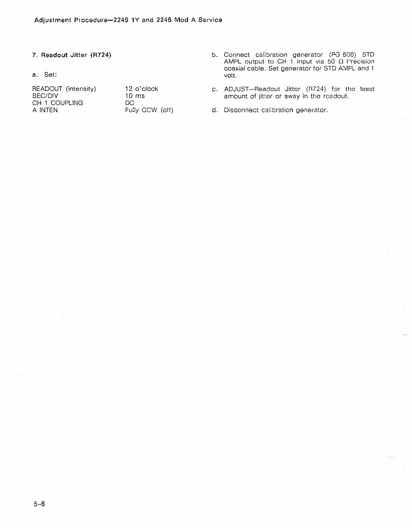
Adjustment Procedure-2246 1Y and 2246 Mod A Service
7 . Readout Jitter (R724)
a. Set:
READOUT (intensity) SECIDIV CH 1 COUPLING A INTEN
12 o'clock 10 ms DC Fully CCW (off)
b. Connect calibration generator (PG 506) STD AMPL output to CH 1 input via 50 Cl Precision coaxial cable. Set generator for STD AMPL and 1 volt.
c . ADJUST-Readout Jitter (R724) for the least amount of jitter or sway in the readout.
d. Disconnect calibration generator.

Adjustment Procedure-2246 1Y and 2246 Mod A Service
VERTICAL
Equipment Required (See Table 4-1):
Calibration Generator (PG506) 50 Cl Termination
Leveled Sine-Wave Generator Precision Normalizer (20 pF)
50 Cl Coaxial Cable
See the ADJUSTMENT LOCATIONS section
at the back of this manual for locations of test points and adjustments.
INITIAL CONTROL SETTINGS
1. Set:
Vertical MODE INPUT COUPLING VOLTS/DIV Vertical POSITION Controls Horizontal MODE A/B SELECT SECIDIV Trigger LEVEL HOLDOFF SLOPE Trigger MODE Trigger SOURCE Trigger COUPLING MEASUREMENTS MENU Displays A INTEN READOUT FOCUS
SCALE ILLUM
CH 1 and CH 2 DC 0.1 v
12 o'clock A A 0.1 ms 12 o'clock min (CCW) f AUTO LEVEL VERT DC OFF OFF 10 o'clock 12 o'clock for well defined display fully CCW
PROCEDURE
1. Vertical Output Gain (R703) and Readout Vertical Centering (R260)
a. Run ADJUST Vertical OUTPUT routine.
Select SERVICE MENU. Simultaneously press the top and bottom menu-item select buttons. Select
INTERNAL SETTINGS MENU. Press down-arrow button to underline selection, then press SELECT button. Run ADJUST Vertical OUTPUT routine. Press down-arrow button three times to underline selec- tion, then press RUN button.
NOTE
For this adjustment, the 2246 1Y or 2246 M o d A must be placed in the "normal" oper- ating position to avoid incorrect alignment due fo effects of the earth's magnetic field.
b. ADJUST-VO GAIN (R703) and RO VERT CENTERING (R260) alternately until dashed lines produced by the diagnostics are aligned with dotted lines on the graticule.
c. Press END button to end the ADJUST Vertical OUTPUT routine. Then press QUIT button to quit the Service Menu and return to the normal oscilloscope display.
2. CH 1 Step Balance (R12)
a. Set:
Vertical MODE CH 1 (CH 2 off) CH 1 COUPLING GND BW LIMIT 0 n
b. Position trace to center of screen.
c . ADJUST-R12 (CH 1 STEP BALANCE) so the trace does not move vertically while switching CH 1 VOLTSIDIV switch f rom 10 mV to 50 mV. ,
Adjustment Procedure - 2246 1Y and 2246 MOD A Service
3. CH 2 Step Balance (R22)
a. Set:
Vertical MODE CH 2 (CH 1 off) CH 2 COUPLING GND
b. Position trace to center of graticule.
c. ADJUST- R22 (CH 2 STEP BALANCE) so that trace does not move vertically while switching CH 2 VOLTSIDIV switch from 10 mV to 50 mV.
4. CH 3 Step Balance (R141)
a. Set Vertical MODE to CH 3 (CH 2 off).
b. Position trace to center of graticule.
c. ADJUST-R141 (CH 3 STEP BALANCE) so that trace does not move vertically while switching CH 3 VOLTSIDIV switch from 0.1 V to 0.5 V.
5. CH 4 Step Balance (R161)
a. Set Vertical MODE to CH 4 (CH 3 off).
b. Position trace to center of graticule.
c. ADJUST-RIG1 (CH 4 STEP BALANCE) so that trace does not move vertically while switching CH 4 VOLTSIDIV switch from 0.1 V to 0.5 V.
6. CH 1 MFILF Gain (R13) and Compensation (C1)
a. Set:
Vertical MODE CH 1 (CH 4 off) CH 1 VOLTS/DIV 50 mV CH 1 COUPLING DC SECIDIV 50 p.s
b. Connect calibration generator to CH 1 input via 50 Cl BNC coaxial cable and 50 fi BNC termination. Set generator for HIGH AMPL. Set Period to 10 kHz and adjust Pulse Amplitude for a 5-division display.
c. ADJUST-R13 (CH 1 MFILF GAIN) and C1 (CH 1 MFILF COMP) for the flattest response (within 0.25 division).
7. CH 1 lnput Capacitance (C114)
a. Set:
b. Add precision normalizer between termination and CH 1 input connector. Set calibration generator Pe- riod to l kHz and adjust Pulse Amplitude for 5-divi- sion display.
c. ADJUST-C114 (CH 1 INPUT CAPACITANCE) for best flat top.
d. Remove precision normalizer from the input cable.
8. CH 1 lnput Compensation X I 0 (C11)
a. Set:
CH 1 VOLTSIDIV SECIDIV
b. Set calibration generator Period to 10 kHz and adjust Pulse Amplitude for a 5-division display.
c. ADJUST-Cl1 (CH 1 INPUT COMP XI 0) for flattest response (within 0.25 division).
9. CH 1 lnput Compensation Xl00 (C10)
a. Set CH 1 VOLTSIDIV to 1 V.
b. Set calibration generator amplitude for a 5-division display.
c. ADJUST-C10 (CH 1 INPUTCOMP X100) forflattest response (within 0.25 division).
10. CH 1 Gain (R211)
a. Set calibration generator to STD AMPL and Ampli- tude to 50 mV. Remove 50 Cl termination from input cable.
b. Set:
CH 1 VOLTSIDIV 10 mV SECIDIV 0.2 ms
c. ADJUST-CH 1 GAIN (R211) for exactly a 5-division display amplitude.
11. CH 2 MFILF Gain (R23) and Compensation (C2)
a. Set:
Vertical MODE CH 2 (CH 1 off) CH 2 VOLTSIDIV 50 mV CH 2 COUPLING DC SECIDIV 50 FS
b. Move calibiation generator signal to CH 2 input. Add 50 Cl termination.
REV JUN 1991

Adjustment Procedure-2246 1Y and 2246 MOD A Service
c. Set calibration generator for HlGH AMPL. Set Period c. ADJUST-CH 2 GAlN (R221) for exactly a5-division to 10 kHz and adjust Pulse Amplitude for 5-division display amplitude. display.
d. ADJUST-R23 (CH 2 MFILF GAIN) and C2 (CH 2 16. CH 3 MFILF Compensation (C134)
MFILF COMP) for flattest response (within 0.25 divi- a. Set: sion).
Vertical MODE CH 3
12. CH 2 lnput Capacitance (C124)
a. Set:
CH 2 VOLTSIDIV SECIDIV
CH 3 VOLTSIDIV SECIDIV
b. Move calibration generator signal to CH 3 input. Add 50 R termination.
c. Set calibration aeneratorfor HlGH AMPL. Set Period to 10 kHz and &just Pulse Amplitude for a 5-divi-
b. Add precision normalizer between termination and sion display. CH 2 i n ~ u t connector. Set calibration aenerator Pe- riod to i HZ and adjust Pulse ~ m ~ l i t ; d e for 5-divi- d A D J U S T - C ~ ~ ~ (CH 3 MFlLF coMp) for flattest re- sion display. sponse.
c. ADJUST-C124 (CH 1 INPUT CAPACITANCE) for best flat top. 17. CH 3 Gain (R231)
d. Remove precision normalizer from the input cable. a- Set:
CH 3 VOLTS/DIV 0.5 V 13. CH 2 Input Compensation X I 0 (C21) SECIDIV 2 ms
a. Set: b. Set calibration generator for STD AMPL. Set ampli- tude to 2 V. Remove 50 R termination.
CH 2 VOLTS/DIV SECIDIV c. ADJUST-CH 3 GAlN (R231) for exactly 4-division
display amplitude.
b. Set calibration generator Period to 10 kHz and adjust Pulse amplitude for a 5-division display. 18. CH 4 MFILF Compensation (C154)
c. ADJUST-C21 (CH 2 INPUT COMP X10) for flattest a. Sf3 response (within 0.25 division).
Vertical MODE CH 4 VOLTS/DIV
14. CH 2 Input Compensation X I 00 (C20) SECIDIV
CH 4 (CH 3 off) 0.1 v 50 r*s
a. Set CH 2 VOLTSIDIV to 1 V. b. Move calibration generator signal to CH 4 input. Add 50 R termination.
b. ADJUST-C20 (CH 2 INPUT COMP X100) forflattest response (within 0.25 division). c. Set calibration generator for HIGH AMPL. Set Period
to 10 kHz and adiust Pulse Amplitude for a 5-divi-
15. CH 2 Gain (R221) sion display.
d. ADJUST-C154 (CH 4 MFILF COMP) for flattest re-
a. Set calibration generator to STD AMPL and Ampli- sponse.
tude to 50 mV. Remove 50 R termination from the in- put cable. 19. CH 4 Gain (R241)
b. Set:
CH 2 VOLTS/DIV SECIDIV
a. Set:
CH 4 VOLTS/DIV SECIDIV
REV JUN 1991
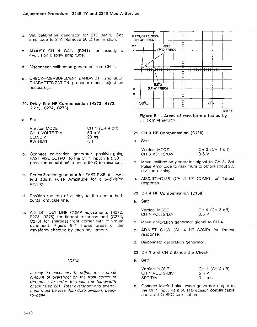
Adjustment Procedure-2246 1Y and 2246 Mod A Service
b. Set calibration generator for STD AMPL. Set I amplitude to 2 V. Remove 50 R termination.
f
c. ADJUST-CH 4 GAIN (R241) for exactly a I
4-division display amplitude.
d. Disconnect calibration generator from CH 4.
e. CHECK-MEASUREMENT BANDWIDTH and SELF CHARACTERIZATION procedure and adjust as necessary.
20. Delay-line HF Compensation (R272, R273, R275, C274, C273)
a. Set:
Vertical MODE CH 1 (CH 4 off) CH 1 VOLTSIDIV 50 mV SECIDIV 20 ns BW LIMIT Off
b. Connect calibration generator positive-going FAST RISE OUTPUT to the CH 1 input via a 50 R precision coaxial cable and a 50 .Q termination.
c. Set calibration generator for FAST RISE at 1 MHz and adjust Pulse Amplitude for a 5-division display.
d. Position the top of display to the center hori- zontal graticule line.
Figure 5-1. Areas of waveform affected by HF compensation.
21. CH 3 HF Compensation (C138)
a. Set:
Vertical MODE CH 3 (CH 1 off) CH 3 VOLTSIDIV 0.5 V
b. Move calibration generator signal to CH 3. Set Pulse Amplitude to maximum to obtain about 2.5 division display.
c. ADJUST-C138 (CH 3 HF COMP) for flattest response.
22. CH 4 HF Compensation (C158)
a. Set:
e. ADJUST-DLY LINE COMP adjustments (R272, Vertical MODE
R273, R275) for flattest response and (C274, CH 4 VOLTSIDIV
CH 4 (CH 3 off) 0.5 V
C273) for sharpest front Corner with minimum b, Move calibration generator signal to CH 4 . overshoot. Figure 5-1 shows areas of the waveform affected by each adjustment. c. ADJUST-C158 (CH 4 HF COMP) for flattest
response.
d. Disconnect calibration generator.
23. CH 1 and CH 2 Bandwidth Check
NOTE a. Set:
Vertical MODE CH 1 (CH 4 off) It may be necessary to adjust for a small CH 1 VOLTSIDIV 5 mV amount of overshoot on the front corner of SECIDIV 0.1 ms the pulse in order to meet the bandwidth check (step 23) . Total overshoot and aberra- b. Connect leveled sine-wave generator output to tions must be less than 0.25 division, peak- the CH 1 input via a 50 .Q precision coaxial cable to-peak. and a 50 R BNC termination.
Adjustment Procedure-2246 1Y and 2246 Mod A Service
c. Set leveled sine-wave generator output for a h. Repeat the complete bandwidth check pro- six-division signal amplitude at 50 kHz. cedure for Channel 2.
d. CHECK-the displayed signal amplitude is at least 4.2 divisions as the aenerator frequency is 24. CH 3 and CH 4 Bandwidth Check - increased to 100 MHz. a. Set:
NOTE
If the displayed signal amplitude drops below 4.2 divisions at any frequency below 100 MHz, readjust Delay-Line HF Compensation (step 20) with increased front-corner over- shoot.
e. Repeat the frequency setup and CHECK pro- cedure for VOLTSIDIV settings of 50 mV and 0.1 v.
Vertical MODE CH 3 (CH 2 off) CH 3 VOLTSIDIV 0.1 V
b. Move the leveled sine-wave generator signal to the CH 3 input.
c. Set the generator output for a six-division signal display at 50 kHz.
d. CHECK-the displayed signal amplitude is at least 4.2 divisions as the generator frequency is increased to 100 MHz.
e. Move the test signal to the CH 4 input.
f. Set:
f. Move the test signal to the CH 2 input. Vertical MODE CH 4 (CH 3 off) CH 4 VOLTSIDIV 0.1 V
g. Set: g. Repeat the procedure for CH 4.
Vertical MODE CH 2 (CH 1 off) CH 2 VOLTSIDIV 10 mV h. Disconnect leveled sine-wave generator.

Adjustment Procedure-2246 1Y and 2246 MOD A Service
HORIZONTAL
Equipment Required (See Table 4-1):
Time-Mark Generator 50 !2 Coaxial Cable
Calibration Generator 50 Cl Termination
See the ADJUSTMENT LOCATIONS section
at the back of this manual for locations of test points and adjustments.
INITIAL CONTROL SETTINGS
1. Set:
Vertical MODE INPUT COUPLING VOLTS/DIV Vertical POSITION Controls Horizontal MODE A/B SELECT SEC/DIV Trigger LEVEL HOLDOFF SLOPE Trigger MODE Trigger SOURCE Trigger COUPLING MEASUREMENTS MENU Displays A INTEN READOUT FOCUS
SCALE ILLUM
CH 1 and CH 2 DC 0.1 v
12 o'clock A A 0.1 ms 12 o'clock min (CCw) 1
PROCEDURE
AUTO LEVEL VERT DC OFF OFF 10 o'clock 12 o'clock for well defined display fully CCW
1. Horizontal X I Gain (Timing) (R826)
a. Set:
Vertical MODE CH 1 VOLTS/DIV
CH 1 (CH 2 off) 0.5 V
b. Connect time mark generator to CH 1 input via 50 Q BNC coaxial cable and 50 !2 BNC termination. Set generator for 0.1 ms time marks.
c. Position peaks of the time markers to the center hori- zontal graticule line.
d. ADJUST-HORIZONTAL 1X GAlN (R826) for one time mark per division over the center 8 divisions.
2. Horizontal X I 0 Gain (Timing) (R825)
a. Set XI 0 MAG to ON.
b. Set time mark generator for 10 ps time marks.
c. Position display about center screen.
d. ADJUST- HORIZONTAL X I0 GAlN (R825) for one time mark per division over the center 8 divisions.
3. Readout Horizontal Gain (R823) and MAG Registration (R809)
a. Set the time mark generator for 0.5 ms time marks.
b. Position the middle time marker to the centervertical graticule line using the Horizontal POSITION con- trol.
c. Set XI0 MAG to Off.
d. ADJUST-MAG REG (R809) to position the middle time marker to the center vertical graticule line.
e. Set XlO MAG to On.
f. CHECK-for no horizontal shift in the time marker.
g. Repeat parts b through f until no shift is noted.
5-1 2 REV JUN 1991

Adjustment Procedure - 2246 1 Y and 2246 MOD A Service
h. Set:
X10 MAG SECIDIV A INTEN
Off 50 ps CCW (off)
i. Select Time CURSORS. Press the TIME MEASURE- MENT button and select k SEC 4 from the menu.
j. Rotate theIt OR DELAY control to align the cursor to the second graticule line.
k. Rotate t h e 4 control so that the reading is 400.0 ps.
I. ADJUST- Both the It OR DELAY control and R823 so that the cursors are aligned exactly on the second and tenth graticule line.
m. Set A INTEN to 10 o'clock.
6. 2-5 ns Timing (C807, C814)
a. Set:
Horizontal MODE A SECIDIV 20 ns XI0 MAG On C H 1 50 mV CH 1 COUPLING AC
b. Set time mark generator for 5 ns time marks.
C. ADJUST-2 NSTlMlNG (C807, C814) for 1 cycle per each 2.5 divisions over the center 8 divisions. See Figure 5-2. Use the vertical transition of the sine wave instead of the peaks for better accuracy.
d. INTERACTION - between C807 and C814. Readjust as necessary to make the timing at 2.5, 5, and 7.5 divisions within -t 0.2 division (1 minor division).
e. Disconnect time mark generator.
4. A 0.5 ps Timing (C314)
a. Set:
XI0 MAG Off SECIDIV 0.5 ps B Trigger MODE RUNS AFTER B INTEN 10 o'clock
b. Set time mark generator for 0.5 ps time marks.
c. ADJUST-A0.5 pSTlMlNG (C314) for one time mark per division over the center 8 divisions.
Figure 5-2. 2-5 ns Timing.
5. B 0.5 p s Timing (C329)
a. Set:
Horizontal MODE B SECIDIV (B) 0.5 ps
b. Set time mark generator for 0.5 ps time marks.
c. Rotate the OR DELAY control counterclockwise until the readout displays "?0.000 ps".
d. ADJUST- B 0.5 pSTlMlNG (C329) for one time mark per division over the center 8 divisions.
7. X Gain (R827)
a. Set:
XI0 MAG Off Horizontal MODE X-Y Vertical MODE CH 2 CH 1 VOLTS/DIV 10 mV
b. Connect calibration generator STD AMPL output to CH 1 input via 50 !2 coaxial cable. Set generator for STD AMPL. Set Amplitude to 50 mV.
c. ADJUST-X GAIN (R827) for 5 divisions of horizon- tal signal.
d. Disconnect calibration generator.
REV JUN 1991

Adjustment Procedure-2246 1Y and 2246 Mod A Service
MEASUREMENT BANDWIDTH AND SELF CHARACTERIZATION
Equipment Required (See Table 4-1):
Digital Multimeter (DMM) 50 Coaxial Cable
Leveled Sine- Wave Generator
See the ADJUSTMENT LOCATIONS section
at the back of this manual for locations of test points and adjustments.
INITIAL CONTROL SETTINGS b. ADJUST-VOLTS CAL (R920) so the DMM reads 0.250 V.
1. Set:
Vertical MODE INPUT COUPLING VOLTSIDIV Vertical POSITION Controls SCOPE BW Horizontal MODE A/B SELECT SECIDIV Trigger LEVEL HOLDOFF SLOPE Trigger MODE Trigger SOURCE Trigger COUPLING MEASUREMENTS MENU Displays A INTEN READOUT FOCUS
SCALE ILLUM
2. B Trigger Bandwidth (R455)
CH 1 and CH 2 DC a. Set: 0.1 v
Vertical MODE CH 2 (CH 1 off) 12 o'clock CH 2 VOLTSIDIV 20 mV Off SECIDIV 50 ~s A
b. Preset potentiometer R455 to midrange.
12 o'clock c. Run the SELF CAL routine. Press CHIICH2 min (CCW) VOLTMETER button and select SELF CAL. f AUTO LEVEL VERT DC OFF OFF 10 o'clock 12 o'clock for well defined display fully CCW
d. Connect leveled sine-wave generator output to the CH 2 input connector via a 50 BNC pre- cision coaxial cable and a 50 l2 BNC termination. Set generator for a 5-division display at 50 kHz.
e. Set CHIICH2 VOLTMETER for PK-PK voltage measurement. Set output of Leveled Sine-Wave Generator for a peak-to-peak readout display of I 0 0 mV i 0 . 5 mV. Adjust generator to 11 5 MHz.
f . ADJUST-B TRIG BANDWIDTH (R455) for a peak- to-peak readout of 75 mV i 0 . 5 mV.
PROCEDURE 3. Self Characterization
1. Volts Cal (R920) a. Run the SELF CAL MEASUREMENTS routine.
a. Connect digital multimeter (DMM) LO lead to Press both top and bottom menu-item select chassis ground and the high lead to R921 pin 6. buttons. Select INTERNAL SETTINGS MENU, then

Adjustment Procedure-2246 1Y and 2246 Mod A Service
SELF CAL MEASUREMENTS. Press RUN to start SETTINGS MENU. Press SELECT, then press the the routine. When the routine is done, continue down-arrow button to select MAKE FACTORY with part b. or press QUIT to return to normal SETTINGS. Press RUN to start the routine. When oscillcscope mode. done, press QUIT to return to normal
oscilloscope mode. b. Run MAKE FACTORY SETTINGS routine. Press
the down-arrow button to select the INTERNAL

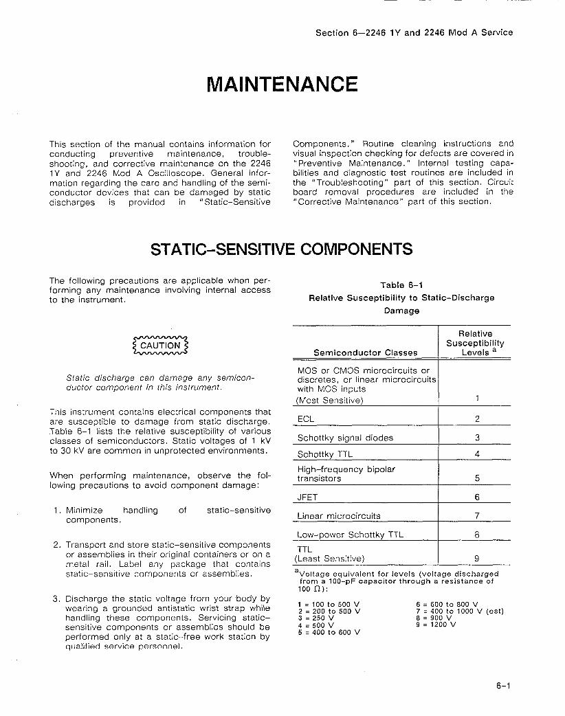
-- --
Section 6-2246 1Y and 2246 Mod A Service
MAINTENANCE
This section of the manual contains information for Components. " Routine cleaning instructions and conducting preventive maintenance, trouble- visual inspection checking for defects are covered in shooting, and corrective maintenance on the 2246 "Preventive Maintenance." Internal testing capa- 1Y and 2246 Mod A Oscilloscope. General infor- bilities and diagnostic test routines are included in mation regarding the care and handling of the semi- the "Troubleshooting" part of this section. Circuit conductor devices that can be damaged by static board removal procedures are included in the discharges is provided in "Static-Sensitive "Corrective Maintenance" part of this section.
STATIC-SENSITIVE COMPONENTS
The following precautions are applicable when per- forming any maintenance involving internal access Table 6-1
to the instrument. Relative Susceptibility to Static-Discharge
Damage
Static discharge can damage any semicon- ductor component in this instrument.
This instrument contains electrical components that are susceptible to damage from static discharge. Table 6-1 lists the relative susceptibility of various classes of semiconductors. Static voltages of 1 kV to 30 kV are common in unprotected environments.
ECL I 2
Semiconductor Classes
MOS or CMOS microcircuits or discretes, or linear microcircuits with MOS inputs (Most Sensitive)
Schottky sianal diodes I 3
Relative Susceptibility
Levels a
1
Schottkv TTL 1 4
High-frequency bipolar When performing maintenance, observe the fol- transistors lowing precautions to avoid component damage:
5
JFET 6
1 . Minimize handling of static-sensitive components. Linear microcircuits
3. Discharge the static voltage from your body by wearing a grounded antistatic wrist strap while 1 = 100 to 500 V 6 = 600 to 800 V
2 = 200 to 500 V 7 = 400 to 1000 V (est) handling these components. Servicing static- 3 = 250 v 8 = 900 v sensitive components or assemblies should be 4 = 500 v 9 = 1200 v performed only at a static-free work station by 5 = 400 to 600 V
qualified service personnel.
7
Low-power Schottky TTL 2. Transport and store static-sensitive components TTL
or assemblies in their original containers or on a (Least Sensitive)
8
metal rail. Label any package that contains 9
static-sensitive components or assemblies. a ~ o l t a g e equivalent for levels (voltage discharged from a 100-pF capacitor through a resistance of 100 R):

Maintenance-2246 1Y and 2246 Mod A Service
4. Keep anything capable of generating or holding 8. Avoid handling components in areas that have a a static charge off the work station surface. floor or work-surface covering capable of gen-
erating a static charge. 5. Keep the component leads shorted together
whenever possible. 9. Use a soldering iron that is connected to earth ground.
6. Pick up components by their bodies, never by their leads.
10. Use only approved antistatic, vacuum-type 7. Do not slide the components over any surface. desoldering tools for component removal.
PREVENTIVE MAINTENANCE
INTRODUCTION Exterior
Preventive maintenance consists of cleaning, visual inspection, and checking instrument performance. Preventive maintenance on a regular basis may pre- vent instrument malfunction and improve instrument reliability. The required frequency of maintenance depends on the severity of the environment in which the instrument is used. An appropriate time to do preventive maintenance is just before instrument adjustment.
INSPECTION. Inspect the external portions of the instrument for damage, wear, and missing parts; use Table 6-2 as a guide. Instruments that appear to have been dropped or otherwise abused should be checked thoroughly to verify correct operation and performance. Deficiencies that could cause per- sonal injury or could lead to further instrument damage should be repaired immediately.
INSPECTION AND CLEANING Do not allow moisture to get inside the instru- ment during external cleaning. Use only
Visually inspect and clean the 2246 1Y or 2246 enough liquid to dampen the cloth or Mod A as often as operating conditions require. applicator. Accumulation of dirt in the instrument can cause overheating and component breakdown. Dirt on components acts as an insulating blanket, pre- CLEANING. Loose dust on the outside of the instru-
venting efficient heat dissipation. it also provides an ment can be removed with a soft cloth or small soft-
electrical conduction path that could result in instru- bristle brush. The brush is particularly useful on and merit failure, especially under high-humidity around the controls and connectors. Remove
conditions. remaining dirt with a soft cloth dampened in a mild detergent-and-water solution. Do not use abrasive cleaners.
Do not use chemical cleaning agents which might damage the plastics used in this instru- ment. Use a nonresidue-type cleaner, preferably isopropyl alcohol or a solution of 7 % mild detergent with 99% water. Before using any other type of cleaner, consult your Tektronix Service Center or representative.
Clean the light filters and the crt face with a soft lint- free cloth dampened with either isopropyl alcohol or a mild detergent-and-water solution.
Interior
To access internal portions of the instrument for inspection and cleaning, refer to the Removal and Replacement Instructions in the Corrective Maintenance part of this section.
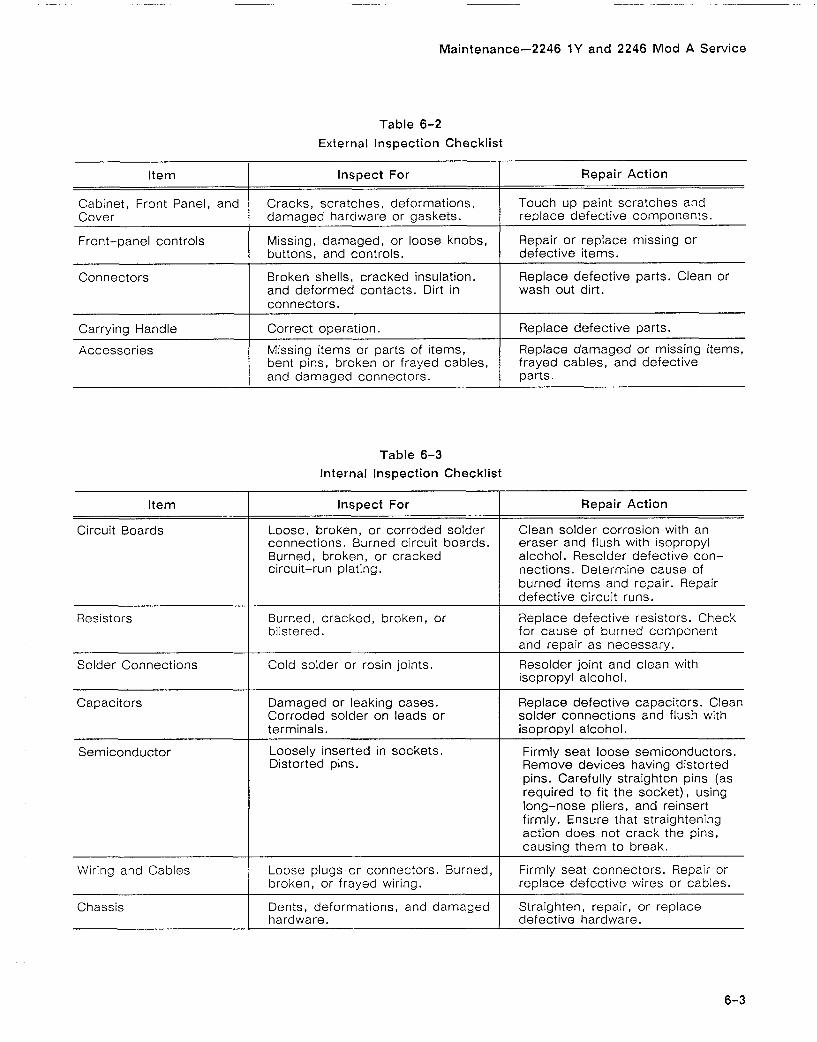
Maintenance-2246 1Y and 2246 Mod A Service
Table 6-2
External lnspection Checklist
Table 6-3 Internal lnspection Checklist
Repair Action
Touch up paint scratches and replace defective components.
Repair or replace missing or defective items.
Replace defective parts. Clean or wash out dirt.
Replace defective parts.
Replace damaged or missing items, frayed cables, and defective parts.
Item
Cabinet, Front Panel, and Cover
Front-panel controls
Connectors
Carrying Handle
Accessories
Inspect For
Cracks, scratches, deformations, damaged hardware or gaskets.
Missing, damaged, or loose knobs, buttons, and controls.
Broken shells, cracked insulation, and deformed contacts. Dirt in connectors.
Correct operation.
Missing items or parts of items, bent pins, broken or frayed cables, and damaged connectors.
Repair Action
Clean solder corrosion with an eraser and flush with isopropyl alcohol. Resolder defective con- nections. Determine cause of burned items and repair. Repair defective circuit runs.
Replace defective resistors. Check for cause of burned component and repair as necessary.
Resolder joint and clean with isopropyl alcohol.
Replace defective capacitors. Clean solder connections and flush with isopropyl alcohol.
Firmly seat loose semiconductors. Remove devices having distorted pins. Carefully straighten pins (as required to fit the socket), using long-nose pliers, and reinsert firmly. Ensure that straightening action does not crack the pins, causing them to break.
Firmly seat connectors. Repair or replace defective wires or cables.
Straighten, repair, or replace defective hardware.
Item
Circuit Boards
Resistors
Solder Connections
Capacitors
Semiconductor
Wiring and Cables
Chassis
Inspect For
Loose, broken, or corroded solder connections. Burned circuit boards. Burned, broken, or cracked circuit-run plating.
Burned, cracked, broken, or blistered.
Cold solder or rosin joints.
Damaged or leaking cases. Corroded solder on leads or terminals.
Loosely inserted in sockets. Distorted pins.
Loose plugs or connectors. Burned, broken, or frayed wiring.
Dents, deformations, and damaged hardware.

Maintenance-2246 1Y and 2246 Mod A Service
INSPECTION. Inspect the internal portions of the 2246 1Y or 2246 Mod A for damage and wear, using Table 6-3 as a guide. Repair deficiencies im- mediately. The corrective procedure for most visible defects is obvious; however, particular care must be taken if heat-damaged components are found. Since overheating usually indicates other trouble in the instrument, it is important that the cause of over- heating be corrected to prevent further damage.
If any electrical component is replaced, conduct a Performance Check for the affected circuit and for other closely related circuits (see Section 4 for the Performance Check). If repair or replacement work is done on any of the power supplies, conduct a complete Performance Check and, if so indicated, an instrument readjustment (see Section 5 for Adjustment Procedure).
SWITCH CONTACTS. Switch contacts are perma- nently treated when assembled. Neither cleaning nor other preventive maintenance is necessary, unless the switch board is replaced or the switch assembly has remained disassembled for a long period of time.
LUBRICATION
A regular periodic lubrication program for the instru- ment is not necessary. Most of the potentiometers used in this instrument are permanently sealed and generally do not require periodic lubrication. The backs of the front-panel knob guides have been lubricated when assembled and will require lubri- cation again only when the front panel assembly is replaced. Rotary switches are installed with proper lubrication when assembled and will require lubri- cation only when the rotor is replaced.
To prevent damage from electrical arcing, en- SEMICONDUCTOR CHECKS sure that circuit boards and components are dry before applying power to the instrument. Periodic checks of the transistors and other
semiconductors in the oscilloscope are not recom- mended. The best check of semiconductor per-
CLEANING. T~ clean the interior, blow off dust with formance is actual operation in the instrument.
dry, low-pressure air (approximately 9 psi). Remove any remaining dust with a soft brush or a cloth dampened with a solution of mild detergent and water. A cotton-tipped applicator is useful for PERIODIC READJUSTMENT cleanina in narrow maces and on circuit boards. If these methods do not remove all the dust or dirt,
To ensure accurate measurements, check the per- the instrument may be spray washed using a formance of this instrument every 2000 hours of solution of 1% mild detergent and 99% water as follows: operation, or if used infrequently, once each year. If
you replace any components, it may be necessary to readjust the affected circuits. The silver-oxide
1. Remove covers and shields to reach parts to be battery used in the 2246 1Y MUST be replaced cleaned (see Removal and Replacement annually. Refer to Corrective Maintenance in this Instructions). section for more information on battery
replacement.
2. Spray wash dirty parts with the detergent-and- water solution; then use clean water to Complete Performance Check instructions are given thoroughly rinse them. in Section 4 of this manual; adjustment instructions
are given in Section 5. The Performance Check
3. Dry all parts with low-pressure air. procedure can be helpful in localizing certain troubles in the instrument. In some cases, minor problems may be revealed or corrected by readjust-
4. Dry all components and assemblies in an oven ment. If only a partial adjustment is performed, see or drying compartment using low-temperature Table 5-1 (the interaction chart) for possible adjust- (1 25°F to 150°F) circulating air. ment interaction with other circuits.

Maintenance-2246 1Y and 2246 Mod A Service
TROUBLESHOOTING
INTRODUCTION
Preventive maintenance performed on a regular basis should reveal most potential problems before an instrument malfunctions. However, should troubleshooting be required, the following infor- mation is provided to aid in locating a fault. In addition, the material presented in the Theory of Operation and Diagrams sections of this manual may be helpful while troubleshooting.
TROUBLESHOOTING AIDS
Diagnostic Firmware
This instrument contains built-in diagnostic routines that can aid in localizing failures. An automatic power-up self test checks the system RAM and ROM and readout interface circuitry. If a failure is detected, this information is presented in either of two ways: a flashing code display on the Trigger LEDs or, if the instrument is capable of presenting a readout, error messages in the crt display. In addition to the power-on testing, various diagnostic routines can be run from the service mode using the SERVICE MENU. (See Internal Testing Capabilities in this subsection for the details.)
Schematic Diagrams
Complete schematic diagrams are located on tabbed foldout pages in the Diagrams section. Portions of circuitry mounted on each circuit board are enclosed by heavy black lines. The assembly number and name(s) of the circuit(s) are shown near the top or the bottom edge of each diagram.
Functional blocks on schematic diagrams are out- lined with a wide gray line. Components within the outlined area perform the function designated by the block label. The Theory of Operation uses these functional block names when describing circuit operation as an aid in cross-referencing between the circuit description and the schematic diagrams.
shown on each diagram. Waveform illustrations are located adjacent to their respective schematic diagram.
Circuit Board Illustrations
Circuit board illustrations showing the physical lo- cation of each component are provided for use in conjunction with each schematic diagram. Each board illustration is found in the Diagrams section on the back of a foldout page, preceding the first related schematic diagram (s) .
The locations of waveform test points are marked on the circuit board illustrations with hexagonal outlined numbers corresponding to the waveform numbers on both the schematic diagram and the waveform illustrations.
Circuit Board Locations
The location of a circuit board within the instrument is shown on each foldout page along with the circuit board illustration.
Circuit Board Interconnections
A circuit board interconnection diagram (schematic Diagram 16) is provided in the Diagrams section to aid in tracing a signal path or power source between boards. All wire, plug, and jack numbers are shown along with their associated wire or pin numbers and signal names.
Power Distribution
Two Power Distribution diagrams (schematic Diaarams 14 and 15) are orovided to aid in trouble- shooting power supbly p;oblems. These diagrams show the components that the various voltages are applied to and the jumper connections and de- coupling components used to apply the power to those circuits. Excessive loading on a power supply by a circuit fault may be isolated by disconnecting the appropriate jumpers.
Component numbers and electrical values of com- Grid Coordinate System ponents in this instrument are shown on the sche- matic diagrams. Refer to the first page of the Each schematic diagram and circuit board illus- Diagrams section for the reference designators and tration has a grid border along its left and top edges. symbols used to identify components. Important A table located next to each schematic diagram lists voltages and waveform reference numbers the grid coordinates of each component shown in (enclosed in hexagonal-shaped boxes) are also that diagram. To aid in physically locating

Maintenance-2246 1Y and 2246 Mod A Service
components on the circuit board, the table also lists the grid coordinates of each component in the circuit board illustration.
Near each circuit board illustration is an alpha- numeric listing of all components mounted on that board. The second column in each listing identifies the schematic diagram in which each component can be found. These component-locator tables are especially useful when more than one schematic diagram is associated with a particular circuit board.
Component Color Coding
Information regarding color codes and markings of resistors and capacitors is located in the color- coding illustration (Figure 9-1) at the beginning of the Diagrams section.
RESISTOR COLOR CODE. Resistors used in this instrument are carbon-film, composition, or pre- cision metal-film types. They are usually color coded with the EIA color code; however, some metal-film type resistors may have the value printed on the body. The color code is interpreted starting with the stripe nearest to one end of the resistor. Composition resistors have four stripes; these rep- resent two significant digits, a multiplier, and a tolerance value. Metal-film resistors have five stripes representing three significant digits, a multiplier, and a tolerance value.
Semiconductor Lead Configurations
Figure 9-2 in the Diagrams section shows the lead configurations for semiconductor devices used in the instrument. These lead configurations and case styles are typical of those used at completion of the instrument design. Vendor changes and per- formance improvement changes may result in changes of case styles or lead configurations. If the device in question does not appear to match the configuration shown in Figure 9-2, examine the associated circuitry or consult a manufacturer's data sheet.
Multipin Connections
This instrument uses two types of cable connectors. The main type is an etched-circuit ribbon cable with pin connectors crimped directly to the end of the cable. The number one pin is indicated by a mark on the ribbon cable. The other type of connector is a plastic holder containing connectors crimped to the ends of individual wires. Orientation, where important, is indicated by a triangle (arrow).
TROUBLESHOOTING EQUIPMENT
The equipment listed in Table 4-1 of this manual, or equivalent equipment, may be useful when trouble- shooting this instrument.
TROUBLESHOOTING TECHNIQUES
The followina ~rocedut-e is arranaed in an order that
CAPACITOR MARKINGS. Capacitance values of enables checking simple trouble-possibilities before
common disc capacitors and small electrolytics are requiring more extensive troubleshooting. The first two steps use diagnostic routines built into the marked on the side of the capacitor body. White
system of the instrument, ceramic capacitors are color coded in picofarads, using a modified EIA code. The next four procedures are check steps that
ensure proper control settings, connections, operation, and adjustment. If the trouble is not
Dipped capacit0rs are in located by these checks, the remaining steps will aid microfarads. The color dot indicates both the in locating the defective component. When the positive lead and the rating. Since these defective component is located, replace it using the capacitors are easily by reversed Or appropriate replacement procedure given under excessive voltage, be careful to observe the polarity Corrective Maintenance in this section. and voltage rating when replacing them.
DIODE COLOR CODE. The cathode end of each glass-encased diode is indicated by either a stripe, a series of stripes or a dot. For most diodes marked with a series of stripes, the color combination of the stripes identifies three digits of the Tektronix Part Number, using the resistor color-code system. The cathode and anode ends of a metal-encased diode may be identified by the diode symbol marked on its body.
Before using any test equipment to make measurements on static-sensitive, current- sensitive, or voltage-sensitive components or assemblies, ensure that any voltage or current supplied by the test equipment does not exceed the limits of the component to be tested.
Maintenance-2246 1Y and 2246 Mod A Service
1. Power-up Tests
When the instrument power is applied, self tests are automatically run to verify proper operation of the system RAM and ROM and readout interface circuitry. If the power-up test fails, failure codes appear in the Trigger Mode LEDs to identify the general location of the fault. (See Power-Up Testing later in this section for failure-code information.)
6. Check Instrument Performance and Adjustment
Check the performance of either those circuits where trouble appears to exist or the entire instru- ment. An apparent trouble may be the result of misadjustment. The complete performance check is given in Section 4 of this manual and adjustment instructions are given in Section 5.
2. Diagnostic Routines 7. Isolate Trouble to a Circuit
Various diagnostic routines can be run from the service mode. The routines can be run at any time by displaying the SERVICE MENU and selecting the desired item from the menu using front panel pushbuttons.
Entry into the SERVICE MENU and its uses are explained in the Diagnostic Routines discussion later in this section.
3. Check Control Settings
Incorrect control settings can give a false indication of instrument malfunction. If there is any question about the correct function or operation of any con- trol, refer to the Operating Information in the 2246 1Y and 2246 Mod A Operators Manual.
4. Check Associated Equipment
Before proceeding, ensure that any equipment used with the 2246 1Y or 2246 Mod A is operating cor- rectly. Verify that input signals are properly con- nected and that the interconnecting cables are not defective. Check that the ac-power-source voltage to all equipment is correct.
5. Visual Check
I WARNING I
To isolate problems, use any symptoms noticed when checking the instrument's operation to help localize the trouble to a particular circuit. For exam- ple, if the vertical deflection is incorrect on all chan- nels, the problem is most likely from the delay line driver to the vertical output; if deflection is bad only on one channel, the problem is from the attenuator of that channel to the input of the delay line driver. The detailed block diagram shown in the foldout section may be used as an aid in determining signal flow and control line dependency for correct circuit operation. Refer to the troubleshooting hints given in Table 6-6 for diagnostic routine failures. Trouble- shooting hints by diagram are given immediately fol- lowing Table 6-6, and Table 6-9 may be used to aid in locating a problem in the measurement system.
8. Check Power Supplies
I WARNING 1
For safety reasons, an isolation transformer must be used between the ac power main and the instrument's ac power input when- ever troubleshooting is done with the cabinet removed. This is especially important when working in the Preregulator and Inverter Power Supply sections of the instrument.
When trouble symptoms appear in more than one circuit, first check the power supplies; then check the affected circuits by taking voltage and waveform readings. Check first for the correct o u t ~ u t voltaae
To avoid electrical shock, disconnect the of each individual supply. These voitages are measured between J1204 (interface connector
instrument from the ac power source before between power supply and main board) and ground making a visual inspection of the infernal (J1204 pin 4 or 8) . See the associated circuit board circuitry. illustration and able 6-4.
Perform a visual inspection. This check may reveal Voltages levels may be measured either with a DMM broken connections or wires, damaged com- or with an oscilloscope. Voltage ripple amplitudes ponents, semiconductors not firmly mounted, must be measured using an oscilloscope. Use a 1X damaged circuit boards, or other clues to the cause probe with as short a ground lead as possible to of an instrument malfunction. minimize stray pickup.

Maintenance-2246 1Y and 2246 Mod A Service
NOTE
Use 20 MHz bandwidth limiting on the test oscilloscope. A higher bandwidth may pro- duce higher observed ripple levels.
If the power-supply voltages and ripple are within the listed ranges in Table 6-4, the supply can be assumed to be working correctly. If they are outside the range, the supply may be either misadjusted, operating incorrectly, or excessively loaded. The power supply adjustment procedure is given in the Power Supply, Display, and Z-Axis subsection of Section 5 (the Adjustment Procedure).
A defective component elsewhere in the instrument can create the appearance of a power-supply prob- lem and may also affect the operation of other circuits. Use the power distribution diagrams (schematic Diagrams 14 and 15 in the foldouts) to aid in localizing a loading problem to a particular circuit.
9. Check Circuit Board Interconnections
After the trouble has been isolated to a particular circuit, again check for loose or broken con- nections, improperly seated semiconductors, and heat-damaged components.
10. Check Voltages and Waveforms
Often the defective component can be located by checking circuit voltages or waveforms. Typical voltages are listed on the schematic diagrams. Waveforms indicated on the schematic diagrams by hexagonal-outlined numbers are shown adjacent to the diagrams. Waveform test points are shown in the circuit board illustrations.
NOTE
Voltages and waveforms indicated on the schematic diagrams are not absolute and may vary slightly between instruments. To establish operating conditions similar to those used to obtain these readings, see the Voltage and Waveform Setup Conditions pre- ceding the waveform illustrations in the Diagrams section.
Note the recommended test equipment, front-panel control settings, voltage and waveform conditions, and cable-connection instructions. Any special con- trol settings required to obtain a given waveform are noted under the waveform illustration. VoltsIDiv and SecIDiv settings of the test oscilloscope for a waveform are indicated in the waveform illustration.
Table 6-4
Power Supply Voltage and Ripple Limits
a At rated load.
Nominal supply Voltage
+I30
+58
+15
+7.5
i-5.0
-5.0
-7.5
-1 5 unreg
Test Point (+ lead)
Test Point (+ lead)
J1204-11
J 1 204-1 0
J 1 204-7
J1204-8
J1204-1,2
J 1 204-5
J1204-9
J 1 204-6
Limits (-1 0°C to 55OC)
Min
+I 27
+55
+14.6
+7.4
+5.0
-5.2
-7.5
-1 5.5
P-P Ripple a
Max
+I35
+59
+15.6
+7.6
+5.3
-5.4
-7.8
-1 6.6
60-150 Hz
70 mV
40 mV
8 mV
8 mV
30 mV
4 mV
4 mV
10 mV
20-40 kHz
70 mV
120 mV
4 mV
4 mV
20 mV
4 mV
4 mV
100 mV

Maintenance-2246 1Y and 2246 Mod A Service
11. Check Individual Components a sensitive voltmeter across the junction rather than comparing two voltages taken with respect to ground. If the former method is used, both leads of the voltmeter must be isolated from ground.
If voltage values measured are less that those just given, either the device is shorted or no current is
To avoid electric shock, always disconnect flowing in the external circuit. If values exceed the the instrument from the ac power source emitter-to-base values given, either the junction is
before removing or replacing components. reverse biased or the device is defective. Voltages exceeding those given for typical emitter-to- collector values could indicate either a nonsaturated
The following procedures describe methods of checking individual components. Two-lead com- ponents that are soldered in place are most accurately checked by first disconnecting one end from the circuit board. This isolates the measure- ment from the effects of the surroundina circuitrv. See Figure 9-1 for component value identificatidn and Figure 9-2 for semiconductor lead configurations.
When checking semiconductors, observe the static-sensitivity precautions given at the beginning of this section.
TRANSISTORS. A good check of a transistor is actual performance under operating conditions. A transistor can most effectively be checked by substi- tuting a known-good component. However, be sure that circuit conditions are not such that a replace- ment transistor might also be damaged. If substitute transistors are not available, use a dynamic-type transistor checker for testing. Static-type transistor checkers are not recommended, since they do not check operation under simulated operating conditions.
When troubleshooting transistors in the circuit with a voltmeter, measure both the emitter-to-base and emitter-to-collector voltages to determine whether they are consistent with normal circuit voltages. Voltages across a transistor may vary with the type of device and its circuit function.
Some of these voltages are predictable. The emitter-to-base voltage for a conducting silicon transistor will normally range from 0.6 V to 0.8 V. The emitter-to-collector voltage for a saturated transistor is about 0.2 V. Because these values are small, the best way to check them is by connecting
device operating normally or a defective (open- circuited) transistor. If the device is conducting, voltage will be developed across the resistors in series with it; if open, no voltage will be developed across the resistors unless current is being supplied by a parallel path.
When checking emitter-to-base junctions, do not use an ohmmeter range that has a high internal current. High current may damage the transistor. Reverse biasing the emitter- to-base junction with a high current may de- grade the current-transfer ratio (Beta) of the transistor.
A transistor emitter-to-base junction also can be checked for an open or shorted condition by measuring the resistance between terminals with an ohmmeter set to a range having a low internal source current, such as the R X 1 k f l range. The junction resistance should be very high in one direc- tion and much lower when the meter leads are reversed.
When troubleshooting a field-effect transistor (FET) , the voltage across its elements can be checked in the same manner as previously described for other transistors. However, remember that in the normal depletion mode of operation, the gate-to-source junction is reverse biased; in the enhanced mode, the junction is forward biased.
INTEGRATED CIRCUITS. An integrated circuit (IC) can be checked with a voltmeter, test oscilloscope, or by direct substitution. A good understanding of circuit operation is essential when troubleshooting a circuit having IC components. Use care when check- ing voltages and waveforms around the IC so that adjacent leads are not shorted together. An IC test clip provides a convenient means of clipping a test probe to an IC.

Maintenance-2246 1Y and 2246 Mod A Service
performance of the entire instrument should be checked if work has been done on the power sup- plies. Readjustment of the affected circuitry may be necessary. Refer to the Performance Check Pro-
When checking a diode, do not use an ohm- cedure and the Adjustment Procedure, (sections 4 meter scale that has a high internal current. and 5) and to Table 5-1 (Adjustment Interactions). High current may damage a diode. Checks on diodes can be performed in much the same manner as those on transistor emitter- to-base junctions. INTERNAL TESTING CAPABILITIES
The diagnostics built into the 2246 1Y and 2246 DIODES. A diode can be checked for either an open Mod A permit the technician to test much of the or a shorted condition by measuring the resistance digital circuitry and the digital-to-analog interface. between terminals with an ohmmeter set to a range The following text describes the testing capabilities having a low internal source current, such as the R X of the Measurement Processor and the firmware 1 kC2 range. The diode resistance should be very controlled circuitry. high in one direction and much lower when the meter leads are reversed.
Power-Up Testing
Silicon diodes should have 0.6 V to 0.8 V across their junctions when conducting; Schottky diodes about 0.2 V to 0.4 V. Higher readings indicate that they are either reverse biased or defective, de- pending on polarity.
RESISTORS. Check resistors with an ohmmeter. Refer to the Replaceable Electrical Parts list for the tolerances of resistors used in this instrument. A resistor normally does not require replacement unless its measured value varies widely from its specified value and tolerance.
INDUCTORS. Check for open inductors by checking continuity with an ohmmeter. Shorted or partially shorted inductors can usually be found by checking the waveform response when high-frequency sig- nals are passed through the circuit.
CAPACITORS. A leaky or shorted capacitor can best be detected by checking resistance with an ohm- meter set to one of the highest ranges. Do not exceed the voltage rating of the capacitor. The resistance reading should be high after the capacitor is charged to the output voltage of the ohmmeter. An open capacitor can be detected with a capaci- tance meter or by checking whether the capacitor passes ac signals.
The systems shown in Figure 6-1 are tested at power-on. Failure codes appear in the Trigger MODE LEDs, with ON being shown as " x " and OFF as " 0 " in the figure. In the event of a display failure where error message cannot be displayed on the crt, the codes indicate a failure area to begin troubleshooting.
(seen on t h e
Tests Run
Figure 6-1. Power-on test failure codes.
System RAM System ROM Readout I n t e r f a c e
Power-up tests performed are:
X O O O 0 0 O X 0 0 0 0 0 0 X 0 0 0
1. RAM diagnostics-failures indicated by flashing 12. Repair and Adjust the Circuit AUTO LEVEL lamp. Three diagnostics are run on
all locations in the RAM: If any defective parts are located, follow the replace- ment procedures given under Corrective Mainte- a. Store and read 00. nance in this section. After any electrical component has been replaced, the performance of that circuit b. Store and read FF. and any other closely related circuit should be checked. Since the power supplies affect all circuits, c. Store and read pseudo-random pattern.
6557-95

Maintenance-2246 1Y and 2246 Mod A Service
2. ROM diagnostics-failures indicated by flashing AUTO lamp. Tests all of ROM, except for ROM header. Runs proprietary version of CRCC test.
3. Readout interface diagnostics-failures indicated by flashing NORM lamp. Performs a marching- one test around the loop from D7-DO to R7-RO and back.
SERVICE MODE
The service mode driver menu is accessed by pressing the top and the bottom menu-item buttons at the same time. The initial SERVICE MENU will be displayed as shown in Figure 6-2. Each service menu display has two parts; the part to the left is the service menu, and the part to the right is the modifier menu.
r
SERVICE MENU/ ........................ DIAGNOSE T MENU
CONFIGURE .L
SELF CAL MEASUREMENTS
INTERNAL SETTINGS MENU/
EXERCISER MENU/ Q U I T
6555-23
Figure 6-2. Initial SERVICE MENU.
Each service menu has a title and a number of selectable items in the menu. The title appears in the top line of the crt display, and the selectable items appear under the title, indented (see Figure 6-2). Menu choices that are names of sub- menus have a following slash ( / ) , and when one is underlined, the word "SELECT" appears in the modifier menu list. When a choice with sub-menus is selected, the sub-menu choices are displayed on
the left side of the screen with the name of the selected sub-menu displayed in the top line.
A menu choice that has no following slash is an executable service routine. The routine may be run by underlining it and pressing the menu button next to the RUN label that appears in the modifier menu list. Executable servicing selections are: diagnostics that return either a pass message or a fail message along with service data; one-shot exercisers that carry out some service and immediately return to the menu; or regular exercisers that carry out a service while continuously displaying service data.
An underlined service-menu choice is available for selection. To select a menu item, use the buttons next to the up-arrow and down-arrow symbols to move the underline up or down in the SERVICE MENU. When the underline is below the sub-menu title, pressing the menu button next to up-arrow MENU label returns to the preceding menu con- taining that sub-menu (an up-menu operation).
Pressing the QUlT selection or CLEAR Display button at any time the choice is displayed will cause the scope to return to normal oscilloscope mode. If a service routine is operating that has an END menu selection displayed, pressing the button next to END exits the routine and returns to the selection menu (where QUlT is displayed). Routines that run once, return to the selection menu when finished.
The diagnostic tests in the SERVICE MENU may be run with a conditional setting that determines how many times the routine is done. The conditional MODE setting menu choice appears in the modifier menu when the DIAGNOSE choice in the SERVICE MENU is underlined (see Figure 6-3). One of the fol- lowing mode types will be displayed:
ONCE, CONTINUOUS, UNTlL PASS, or UNTlL FAlL
Change the mode type displayed in the bottom line by pressing the MODE button. When ONCE is the mode, the diagnostic is run once, and the result is displayed. When CONTINUOUS is the mode, the diagnostics are run continuously. When UNTIL PASS is the mode, the diagnostics are run until they pass. When UNTlL FAIL is the mode, the diagnostics are run until they fail. In order to stop a diagnostic that is looping in the CONTINUOUS, UNTlL PASS, or UNTlL FAlL mode, press the HALT button. The diagnostic will stop and display the current status. When the status is displayed, press END to return to the SERVICE MENU choices.

Maintenance-2246 1Y and 2246 Mod A Service
I SERVICE MENU/ I D IAGNO.SE.
CONFIGURE
/ INTERNAL SETTINGS MENU/ RUN 1 / FRONT PANEL MENU/
/ PROC BOARD MENU/ QUIT^ 1 MAIN BOARD MENU/ MODE:
ONCE
6555-24
Figure 6-3. SERVICE MENU with DIAGNOSE choice selected.
Service Routines
Descriptions of the available service routines are given in Table 6-5. The complete SERVICE MENU has this structure:
SERVICE MENU/ DIAGNOSE CONFIGURE SELF CAL MEASUREMENTS INTERNAL SETTINGS MENU/
MAKE FACTORY SETTINGS LOAD STOREIRECALL SETUPS ADJUST VERTICAL OUTPUT
EXERCISER MENU/ FRONT PANEL MENU/
EXERCISE POTS EXERCISE LEDS EXERCISE SWITCHES
PROC BOARD MENU/ A TO D MENU/
EXERCISE DACS EXERCISE PORTS
READOUT MENUI SHOW READOUT ROM HEADER EXERCISE RO INTERFACE
EXERCISE TIME REF SHOW SYSTEM ROM HEADER SHOW AUTO RESTARTS
MAIN BOARD MENUI SHIFT REGISTER MENU/
EXERCISE SR 0 EXERCISE SR 1 EXERCISE SR 2
EXERCISE VOLT REF
Table 6-5 SERVICE MENU Selections
Menu Item
DIAGNOSE
CONFIGURE
Action
Runs all diagnostics in sequence, stopping at the first failed diagnostic. (See Table 6-6 for a diagnostic test failure troubleshooting guide.) Diagnostics are:
RO (readout) INTERFACE ROM RAM SLlC CONTROL REG SHIFT REGISTERS (in SR2, SRO, SRI, SR3 order) D AC Triggers
Configures the scope-mode operation of the instrument according to the users' wishes. Configuration is done by answering yesfno questions. The questions are: KEEP MENU ON WHEN MEAS SELECTED? The menu remains displayed after a measurement function has been selected from one of the Measurements menus.
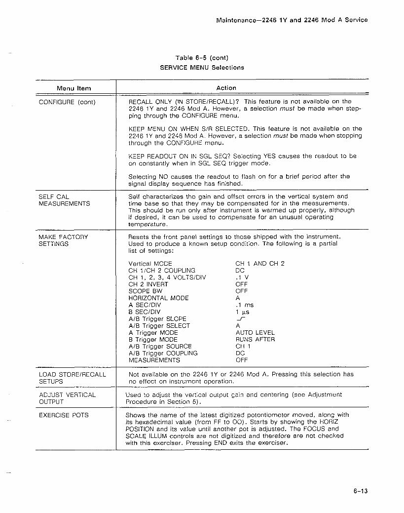
Maintenance-2246 1Y and 2246 Mod A Service
Table 6-5 (cont)
SERVICE MENU Selections
Menu Item
CONFIGURE (cont)
SELF CAL MEASUREMENTS
MAKE FACTORY SETTINGS
LOAD STOREIRECALL SETUPS
-
ADJUST VERTICAL OUTPUT
EXERCISE POTS
Action
RECALL ONLY (IN STOREIRECALL)? This feature is not available on the 2246 1Y and 2246 Mod A. However, a selection must be made when step- ping through the CONFIGURE menu.
KEEP MENU ON WHEN SIR SELECTED. This feature is not available on the 2246 1Y and 2246 Mod A. However, a selection must be made when stepping through the CONFIGURE menu.
KEEP READOUT ON IN SGL SEQ? Selecting YES causes the readout to be on constantly when in SGL SEQ trigger mode.
Selecting NO causes the readout to flash on for a brief period after the signal display sequence has finished.
Self characterizes the gain and offset errors in the vertical system and time base so that they may be compensated for in the measurements. This should be run only after instrument is warmed up properly, although if desired, it can be used to compensate for an unusual operating temperature.
Resets the front panel settings to those shipped with the instrument. Used to produce a known setup condition. The following is a partial list of settings:
Vertical MODE CH 1 ICH 2 COUPLING CH 1 , 2, 3, 4 VOLTS/DIV CH 2 INVERT SCOPE BW HORIZONTAL MODE A SECIDIV B SECIDIV AIB Trigger SLOPE AIB Trigger SELECT A Trigger MODE B Trigger MODE AIB Trigger SOURCE AIB Trigger COUPLING MEASUREMENTS
CH 1 AND CH 2 DC .I v OFF OFF A . I ms 1 PS J-
A AUTO LEVEL RUNS AFTER CH 1 DC OFF
Not available on the 2246 1Y or 2246 Mod A. Pressing this selection has no effect on instrument operation.
Used to adjust the vertical output gain and centering (see Adjustment Procedure in Section 5).
Shows the name of the latest digitized potentiometer moved, along with its hexadecimal value (from FF to 0 0 ) . Starts by showing the HORlZ POSITION and its value until another pot is adjusted. The FOCUS and SCALE ILLUM controls are not digitized and therefore are not checked with this exerciser. Pressing END exits the exerciser.
Maintenance-2246 1Y and 2246 Mod A Service
Table 6-5 (cont)
SERVICE MENU Selections
Menu Item
EXERCISE LEDS
Action
Uses the delay control to check for adjacent-row or adjacent-column shorts in the front panel board and for inoperative LEDs.The exerciser displays the circuit number and illuminates each LED as the control is rotated. Circuit numbers DS2016, DS2017, 05201 8, DS2019, DS2024, DS2040, and DS2049 do not correspond to any LEDs on the front panel. Pressing END exits the excerciser.
EXERCISE SWITCHES
EXERCISE DACS
Shows the circuit number of the latest momentary-contact button pressed, or the name and position of the latest rotary switch turned. Pressing END exits the exerciser; pressing CLEAR MEAS'MT terminates the Service Pro- gram.
Attaches the DAC (U2302, Diagram 11) to a single sample-and-hold channel (through U2303), and outputs a sawtooth waveform to that channel. Select the channel by pressing STEP. This excerciser may be used to trace a sample-hold value through the system, with the DAC system operating in a non-multiplexed mode. Pressing END exits the exerciser.
EXERCISE PORTS Continuously does analog-to-digital conversion on a single A-to-D port. Select the port by pressing STEP. The exerciser may be used to trace a single potentiometer wiper value or probe code value through the system by operating the A-to-D converter in a non-multiplexed mode. Pressing END exits the exerciser.
EXERCISE RO INTERFACE
SHOW READOUT ROM HEADER
Continuously echos a marching-bit value across the readout interface. This exerciser may be used to check the integrity of the Measurement- Processor-to-Readout-Processor communication system. Pressing END exits the exerciser.
Shows the Readout ROM part number (U2408, Diagram 9) and its expected and actual checksum.
SHOW SYSTEM ROM HEADER
EXERCISE TIME REF
Shows the system ROM part numbers (U2519, Diagram 8) and checksums of the installed firmware version.
Steps through the timing frequencies used to characterize the horizontal timing accuracy. Calibration periods are shown in the following table.
Time Test Period
5 PS 32 ps 10 ps 64 ps 20 ps 128 ps 50 LS 256 ps .1 ms 512 ps .2 ms 1.024 ms .5 ms 2.048 ms 1 ms 4.096 ms 2 ms 8.192 ms 5 ms 32.768 ms

Maintenance-2246 1Y and 2246 Mod A Service
Menu Item
SHOW AUTO RESTARTS
EXERCISE SR 0
EXERCISE SR 1
EXERCISE SR 2
EXERCISE VOLT REF
Table 6-5 (cont)
SERVICE MENU Selections
Action
Shows the address being executed if a software error occurs that causes execution out of normal memory space. This is for factory use only and is of no use in field servicing of the instrument. If an AUTO RESTART is ever seen, record the address displayed and report it to a service center; the error address is cleared from memory when SHOW AUTO RESTARTS is exited.
Shifts alternate zeros and ones through Shift Register 0 (U171, U172, and U173, Diagram 1). This shift register sets Attenuator and Input Coupling relay positions and Vertical Preamplifier gain settings.
Shifts alternate zeros and ones through Shift Register 1 (U302 and U303, Diagram 5; U1103, Diagram 3). This shift register sets sweep speeds and auxiliary trigger settings (TV Trigger, Scope Bandwidth, X I 0 magnifi- cation, and X-Y Mode).
Shift alternate zeros and ones through Shift Register 2 (U502, Diagram 4).
Steps through all settings of the Voltage Reference Generator (U931, Diagram 7) that are used to calibrate the Volts Measurement system. For each setting, Channels 1 and 2 are placed into the gain configuration (2 mV through 50 mV) that uses that setting. The voltage select lines (VOLTS CAL 2-0) may be checked for activity, and the generated VOLTS CAL SIGNAL may be measured to check its values.
VOLTSIDIV Cal voltage
Maintenance-2246 1Y and 2246 Mod A Service
DIAGNOSE Tests troubleshooting the instrument. Testing routines and troubleshooting information for use in the event of a
The complete DIAGNOSE routine may be called up failed test are given in Table 6-6. by the service technician as needed to aid in
Table 6-6
DIAGNOSE ROUTINES
Error Label
INTERFACE ERROR
RAM ERROR
(RO RAM)
Path, devices tested, and troubleshooting actions
Measurement Processor to Readout Processor Communications.
WROTE (hex number that was written, 2 characters).
READ (hex number that was read, 2 characters).
This test rotates a 1 through the byte on the bus lines. The difference between WROTE and READ indicates which bit is stuck.
Devices to troubleshoot:
U2401, U2402, U2417C and D, and bus lines between Measurement Proc- essor and Readout Processor.
Check U2501 pin 29 for enabling signal to U2402, and U2400 pin 22 for clock.
- -
Writes and reads test bytes from the Readout RAM (U2406).
ADDRESS (hex address of error location, 3 characters).
WROTE (hex data written, 2 characters).
READ (hex data read, 2 characters).
The difference between WROTE and READ data indicates a stuck bit.
PART NUM (Tektronix Part Number without dashes). EXPECTED CHECKSUM (hex number, 2 characters) ACTUAL CHECKSUM (hex number, 2 characters).
NOTE
Readout ROM is internal to the Readout Processor, U2400; a failure of this test may mean a bad Readout Processor.

Maintenance-2246 1Y and 2246 Mod A Service
Table 6-6 (cont)
DIAGNOSE ROUTINES
Error Label
REG SR 2
REG SR 0
REG SR 1
Path. devices tested, and troubleshootinn actions
Front Panel Potentiometer Multiplexer data path check.
WROTE (hex data written, 1 character).
READ (hex data read, 1 character).
Device Tested: U502, Diagram 4.
Troubleshooting checks:
Check pin 11 for correct clock. Check pin 2 for data. Check pin 12 for multiplexer output.
Attenuator and Preamplifier data path check.
WROTE (hex data written, 6 characters).
READ (hex data read,, 6 characters).
Devices Tested: U171, U172, and U173 on Diagram 1.
NOTE
U171 and U172 have +15 V clocks and data; U173 has +5 V clocks and data.
Troubleshooting checks:
Check pin 3 of each device for correct clock. Check pin 9 of each device for marching bit pattern. Attenuator relay latches are driven and a clacking sound is heard.
Sweeps and Auxiliary Trigger data path check.
WROTE (hex data written, 6 characters).
READ (hex data read, 6 characters).
Devices Tested:
U302 and U303 on Diagram 3; U1103 on Diagram 3. Clock and data levels for U302 and U303 are +15 V; they are +5 V for U1103.
Troubleshooting checks:
Check pin 3 of each device for correct clock. Check pin 9 of each device for marching bit pattern.

Maintenance-2246 1Y and 2246 Mod A Service
Table 6-6 (cont)
DIAGNOSE ROUTINES
Error Label
WROTE (hex data written, 4 characters).
READ (hex data read, 4 characters).
Path, devices tested, and troubleshooting actions
REG SR 3
NOTE
There is no exerciser for SR 3, but i t is included in "DIAGNOSE."
I
Switch board data path check.
I Devices Tested: U2001 and U2002, Diagram 10.
Troubleshooting Checks:
Check pin 10 for serial data in. Check pin 9 for serial data out. Check pin 2 for clock.
U2515 and U2517, Diagram 8; U2306, U2302, U2300, U2313, and U2314, Diagram 11; U506, Diagram 7
DAC ERROR 0
(Triggers)
The A-to-D system, Diagram 11, is not working correctly. Ground level was digitized out of the specified error limits.
Devices to troubleshoot:
The trigger diagnostic partially checks the Trigger SOURCE, Trigger CPLG, and Trigger SLOPE circuitry.
Error Messages:
TlME SIGNAL TOO SMALL AT A Trigger A Trigger circuitry failed amplitude test.
I TlME SIGNAL TOO SMALL AT B Trigger B Trigger circuitry failed amplitude test.
NO A Trigger FOR TIME CAL SIGNAL (2 digit code, see table)
Trigger never occurred.

Maintenance-2246 1Y and 2246 Mod A Service
Table 6-6 (cont)
DIAGNOSE ROUTINES
I Check U421, U431, U1106A. and associated circuitry, Diagram 3.
Error Label
SLlC (Display Logic IC, U600) and FLIC (Trigger Logic IC, U602) gate outputs and level shifters, Diagram 4.
Path, devices tested, and troubleshooting actions
Time Base Cal Signal Code
128 k s 0 8.192 ms 1
256 k s 2 4.096 ms 3 2.048 ms 4
512 ps 5 32.768 ms 6
1.024 ms 7 64 ps 13 32 k s 14
TROUBLESHOOTING HINTS BY DIAGRAM
Vertical SELF CAL-Checks Cursor and Preamplifier Outputs
The circuitry listed below must be operational for Vertical SELF CAL to work. Troubleshoot these cir- cuits if voltage measurements or tracking cursors are not correct.
1. DAC system (U2303, U2304, and U2305, Diagram 1 1 ) .
2. Trigger Level Comparators (U431 and U421, Diagram 3).
3. VERT COMP feedback (U702, Diagram 2)
4. ECL-to-CMOS translators (Q604, Q605, Q606, Q607, Q602, and Q603) between U600 and U602 (Diagram 4).
5. Data to Measurement Processor (data bus and bus transceivers, Diagram 8).
6. VOLTS CAL signal (U931, Diagram 7).
7. Vertical Preamps (U210, U220, U230, and U240), Delay Line Drivers (Q250, Q251, Q252, and Q253), and Vertical Position Switching circuitry (U203, U801B, U201, U202, U280, Q284 and Q285, Diagram 2).
HORIZONTAL SELF CAL-Checks Sweep Timing
1. Put the oscilloscope into Self Cal and check at U421A pin 4 (Diagram 3) for changing width calibration signals.
2. Run the "EXERCISE TIME REF" exerciser and check for correct TB CAL signal at U421A pin 4, Diagram 3 (see Table 6-5).
Schematic Diagram 1 -Vertical INPUTS
1. Run DIAGNOSE to check for shift register failure.
2. Run the shift register exerciser for Shift Register 0. Check for clock, data, and strobe signals. Check the shift register outputs.
NOTE
The outputs of U171 and U172 are at 15 V; the outputs from U173 are at 5 V .

Maintenance-2246 1Y and 2246 Mod A Service
3. Check the outputs of the relay driver transistor arrays (U174 and U175). When a transistor is blown in one of the arrays, the usual symptom is 8 V on its output.
Vertical output transistors Q701 and Q702 4. Go to a known setup and check the outputs for run extremely hot (in excess of 100°C). Use
correct levels (see Circuit Description in care when probing in those areas to not touch Section 3). The MAKE FACTORY SETTINGS the heat sinks or cases with bare fingers. selection under INTERNAL SETTINGS of the SERVICE MENU provides known control states.
5. Check relay contacts.
6 . Follow the signal path and check for correct sig- nal and gains. Put in a known signal for each attenuator setting and check at the Vertical Preamplifier inputs to determine if the signal path is ok. The front panel boards and the attenuator shield have to be removed to gain access to the solder side of the Main Board.
7. Check the channel input buffer amplifier (U112 or U122) output if the vertical deflection of either channel 1 or channel 2 is defective. If the buffer amplifier output is held at -6 V or a strange saw- tooth signal is present, replace that buffer amplifier.
8. Check gains and offsets of the CH 3 or CH 4 input buffers (Q131 or Q151).
Schematic Diagram 2-Vertical PREAMPLIFIERS, DELAY LINE DRIVERS and OUTPUT
Perform the following troubleshooting checks with no signal input.
1. Check both inputs of the delay line. If offset on either side, troubleshoot the offsetting side. Inputs to the bases of Q250 and Q251 should be at t7 .5 V.
2. Differential voltage across the delay line should be 0 V f 0.5 V.
3. Check signal gain through the Preamplifier ICs (U210, U220, U230, and U240). Gain is 10 mVIdivision of input signal.
4. Check INVERT operation.
5. Check the operation of U260 if the inputs to de- lay line driver are not at 7.5 V. This operational amplifier is the bias stabilization circuit that com- pares the average dc level to t7 .5 and moves the emitters (and therefore the bases) of (2250 and Q251 to return the inputs to 7.5 V.
The vertical output amplifier runs hot. DO NOT touch it with bare fingers.
The metal tab on top of the vertical output amplifier IC (U701) is NOT ground. Do not connect a ground lead to it. Doing so may cause the IC to fail and usually causes R733 from pin 14 of U701 to the -5 V supply to open.
6 . Avoid moving the package or flexing the leads of R708. If the resistor pack is moved excessively, its leads may break. The resistor pack will then have to be replaced.
NOTE
The heat sinks on Q701 and Q702 may be removed for short periods of time to permit access for a test probe around the close-in circuitry. DO NOTleave them off for extended periods. Check that they are on all the way when replaced.
7. If the heat sinks on the output transistors shake loose, the plastic grommet inserted in the top of the heat sink prevents the sink from touching the metal cabinet. If the grommet is left out, then the metal cabinet may come in contact with the heat sink; and the transistor, the vertical output amplifier IC, and R733 will usually fail. If the heat sinks are removed during maintenance, they must fit tightly when replaced and the grommet must be checked.
NOTE
The cases of Q701 and Q702 are the base leads of the transistors, not the collector as is usual for a TO5 case. Also, the tab marks the collector lead, not the emitter.
Maintenance-2246 1Y and 2246 Mod A Service
8. The vertical outputs to the crt may be momen- front-panel setup condition, such as changing tarily shorted together to check for offsets in the trigger mode, vertical mode, etc. crt. (This should center the vertical trace.)
7. Check TDI, U600, pin 10, for a CMOS-level 9. The output at pins 6 and 7 of U701 may be switching signal.
shorted together to check for offsets in the Ver- tical Preamplifier. (This should bring the trace to 8. Check T D o p U602f pin 301 an ECL-level within +I-0.5 division of center.) switching signal.
10. Pins 18 and 19 of U701 mav be shorted toaether 9. Check the A signal at U602 pin
to check for offsets from-the delay line.- (This Check the A GATE signal at U602 pin 14, Vary should bring the trace to within +/-I .5 divisions
of center.) the Holdoff control to see if the spacing between each A GATE pulse changes.
Shorting the bases of Q701 and Q702 11. Check the Holdoff oscillator output at U600 pin usually causes the vertical output circuit to 15. Vary the HOLDOFF control to see if the width oscillate. of the oscillator pulses varies.
12. Check the center lead of R708 for a voltage of about +60 V, and a common-mode voltage dif- Schematic Diagram 5-A AND B SWEEPS AND
ference (between the two deflection dates) of DELAY COMPARATORS
O v (when pins and Of 'u701 'are 1. Check that the baseline voltage (level that is shorted together). present during holdoff after retrace) of the A
Check the operation of Vertical Comparator U702 by noting if the TRACK MEASUREMENT cursors are off screen when called up. (The Vertical Comparator circuit is enabled only during a vertical Self Cal.)
Schematic Diagram 4-DISPLAY AND TRIGGER LOGIC AND PROCESSOR INTERFACE
and B ramp signals is -2 V. (The baseline level is referenced to the output of U309B and con- trolled by Q302, Q303, and Q304 for the A sweep and Q315, Q316, and Q317 for the B sweep).
2. Check the S w e e ~ End Com~arators. U316. for correct output. he sweep should end at a maxi- mum of 2.5 V. Check the outputs (pin 15 for the A Sweep and pin 2 for the B Sweep) for about
1. Put the oscilloscope into A Horizontal Display 3.8 V (the middle of ECL transitions).
mode with CH 1 and CH 2 Vertical modes on. 3. Place the osci l losco~e in delav and delta delav
2. Check U600 vertical enables (CH 1 EN, pin 39; and check the ~ e l a y ' Time ~ o h ~ a r a t o r s for co;-
CH 2 EN, pin 38) rect outputs (DLY END 1 and DLY END 0).
Probe U600 A TRIG selects (ATS 0, pin 31; ATS 1, pin 32; ATS 2, pin 33; A SLOPE, pin 30) and B TRIG selects (BTS 0, pin 27; BTS 1, pin 28; BTS 2, pin 29; B SLOPE, pin 26) while making trigger source and slope changes on the front panel. (Probe the A select lines for A tria- ger changes 'and the B select lines for B trigger changes.)
4. Check the 10 MHz clock at U600 pin 1 and U600 power sources. Check the 1 kHz clock at pin 2.
5. Check communication lines ( SLIC RD, pin 8; SLlC WR, pin 3; ADDRO through ADDR3, pins 4 through 7, respectively; and MB DATA, pin 9) for activity while making front panel trigger-mode changes.
6. Check THO line, pin 17. Signal should go to a logic high then low again for every new
4. Check U301 for correct switching and delay level transfer. Vary the Delay Time and the Delta Delay time and check for smooth signal change at pins 12 and 13 of U301C. If not correct, troubleshoot DAC system or front panel controls.
5. Run diagnostics to check for Shift Register 1 (U302 and U303) failure.
6. Exercise SR 1 and check switching of U307, U308, U310, and U311.
Schematic Diagram 6-HORIZONTAL OUTPUT AMPLIFIER
1. Turn off the READOUT and check the ramps for equal (but opposite) waveforms on each plate. (Run MAKE FACTORY SETTINGS under the INTERNAL SETTINGS MENU in the SERVICE MENU.)


Maintenance-2246 1Y and 2246 Mod A Service
Table 6-8
Measurement Processor 110 Memory Map
Address range (A19 - AO) I- Binary --W
01 10 0000 0000 OXXX XXXX
01 10 0000 0000 I XXX XXXX
01 10 0000 0001 OXXX XXXX
01 10 0000 0001 lXXX XXXX
0110 0000 0010 OXXX XOOO
01 10 0000 0010 OXXX XOOI
0110 0000 0010 OXXX XOlO
IOOX XXXX XXXX XXXX XOOO
IOOX 0000 XXXX XXXX XOOO
1 OOX XXXX XXXX XXXX XOOI
10OX XXXX XXXX XXXX XOlO
IOOX XXXX XXXX XXXX XO11
Signal name and description
LED CATH CLK -Latches cathode data to Front-Panel LEDs.
LED ANODE CLK-Latches anode data to Front-Panel LEDs.
RO BUF WR -Latches Readout Processor control datas.
RO BUF RD-Enables Readout RAM data onto bus DO-D7 (used for diag- nostics only).
DAC LSB CLK -Latches the least significant byte of data to the D-to-A Converter.
DAC MSB CLK -Latches the most significant byte of data to the D-to-A Converter.
POT MUX CLK -Latches channel selection code for pot multiplexer.
MB CNTL WR -Write enables Pro- cessor Interface circuitry (Diagram 4).
Sets BEAM FIND (U503 pin 7) high ON.
SW BD SR LOAD -Loads column data into switch board registers.
SW BD SR SHIFT -Shifts data in switch board registers to the SW BD DATA signal line.
SLlC WR -Write to SLIC, U600 Diagram 4.
Signal source
U2501 pin 25 (Diagram 8)
U2501 pin 27 (Diagram 8)
U2501 pin 28 (Diagram 8)
U2501 pin 29 (Diagram 8)
U2517 pin 14 (Diagram 8)
U2517 pin 14 (Diagram 8)
U2517 pin 13 (Diagram 8)
U2518 pin 15 (Diagram 8)
U503 pin 7 (Diagram 4)
U2518 pin 14 (Diagram 8)
U2518 pin 13 (Diagram 8)
U2518 pin 12 (Diagram 8)

Maintenance-2246 1Y and 2246 Mod A Service
Table 6-8 (cont)
Measurement Processor 110 Memory Map
Schematic Diaaram 9-READOUT SYSTEM value should chanae smoothlv as the ~ o t is ro- - 1. Run EXERCISE POTS (under the EXERCISER and tated. EXERCISE-POTS always displays the
FRONT PANEL menus) and check the digitized HORlZ POSITION pot when first called.The
front panel pots for proper operation. The name FOCUS and SCALE ILLUM controls are not digit-
of the exercised pot is displayed in the readout ized and therefore are not checked with this ex-
alona with its current hexadecimal value. The erciser. Pressing END exits the exerciser.
Signal source
U2518 pin 11 (Diagram 8)
U606F pin 12 (Diagram 4)
U606B pin 4 (Diagram 4)
U503 pin 7 (Diagram 4)
U503 pin 13 (Diagram 4)
U503 pin 13 (Diagram 4)
U606C pin 6 (Diagram 4)
U606C pin 6 (Diagram 4)
U2512 pin 5 (Diagram 8)
U2512 pin 5 (Diagram 8)
U600 pin 19 (Diagram 4)
U2501 pin 36 (Diagram 8)
Address range (A1 9 - AO) I- Binary -4
IOOX XXXX XXXX XXXX XI00
lOOX 0001 XXXX XXXX XOOO
IOOX 0010 XXXX XXXX XOOO
IOOX 001 1 XXXX XXXX XOOO
1OOX 001 1 XXXX XXXX XOOO
IOOX 0100 XXXX XXXX XOOO
1 OOX 0101 XXXX XXXX XOOO
1 OOX 01 10 XXXX XXXX XOOO
lOOX 01 11 XXXX XXXX XOOO
IOOX IXXX XXXX XXXX XOOO
IOOX 11 11 XXXX XXXX XO11
101 0 XXXX XXXX XXXX XXXX
value range from 00 to FF and the displayed
Signal name and description
FLlC WR -Write to FLIC, U602 Diagram 4.
SR 0 CLK-Clock Shift Register 0.
SR 1 CLK-Clock Shift Register 1.
Sets BEAM FIND (503 pin 7) low (OFF).
Sets MSEL (U602 pin 29) low (delta or long delay).
Sets MSEL (U602 pin 29) high reference or short delay).
Sets SR DATA signal line low.
Sets SR DATA signal line high.
Places SR 2 in shift mode (U502 pin 10, Diagram 4) .
A places SR 2 in load mode (U502 pin 10, Diagram 4).
TRIG CLK -Loads coupling data to triggers.
Chip enable for Measurement Processor RAM (U2521 pin 20).

Maintenance-2246 1Y and 2246 Mod A Service
2. Check Readout Request pulse (RO REQ, U2410 Schematic Diagram 12-POWER SUPPLY pin 14).
3. Check Readout Blanking signal ( RO BLANK, U2410 pin 16).
4. Check activity of Readout Processor (U2400).
5. Check outputs of Vertical and Horizontal Readout DACs (U2412 and U2413, respectively).
6. Check outputs of Vertical and Horizontal Readout Mixers (U2416A and U24168, re- spectively) and multiplexers (U2414 and U2415, respectively).
Schematic Diagram 10-SWITCH BOARD AND INTERFACE
1. Run the EXERCISE SWITCHES exerciser and check each of the front panel switches for cor- rect operation. The circuit number of the latest switch pressed is displayed in the readout. Pressing END exits the exerciser; pressing CLEAR MEAS'MT terminates the Service Program.
For safety reasons, an isolation transformer must be connected whenever troubleshooting is done in the Preregulator and Inverter Power Supply sections of the instrument.
1. If the fuse blows, check that Q2201 is not shorted. (If a variac is available, slowly increase the line voltage from 0 V until the voltage across C2202 is about 40 V. If the same voltage is across C2203, Q2201 is probably shorted.)
2. If the Preregulator fails to come up (44 V not present across C2203) :
a. Check +DC at the output of the line rectifier bridge (across C2202) for approximately ( VacRMS X 1.41 4).
b. Check the Start-up circuit. The voltage across C2204 should ramp up to about 20 V, at which point Q2204 and Q2211 turn on to supply voltage to pin 10 of U2201.
c . Check the Preregulator circuit. Voltage pulses with a repetition rate of about 25 ~s should be present on pin 8 of U2201 when- ever supply voltage is present on pin 10.
2. Run the EXERCISE LEDS exerciser and check 3. If the power supply is in the chirp mode (con- that each of the front panel LEDS may be turned tinually restarting and shutting down), excessive on. The circuit number of the lighted LED is dis- loading of the +44 V supply is probable. played in the readout. Circuit numbers DS2016, DS2017, ' DS2018, DS2019, DS2024, DS2040, and DS2049 do not correspond to any LEDs on the front panel. Pressing END exits the TROUBLESHOOTING MEASUREMENT excerciser. ERRORS
When certain measurement malfunctions occur, the Schematic Diagram 11 -ADC, DAC SYSTEM symptoms usually indicate the circuit components
that may be causing the problems. Read the following text to becot%e familiar with the terms used
1 Run EXERCISE DACS (under EXERCISER, PROC in describing a measurement failure problem and BOARD, and A TO D menus) and probe the the setup conditions needed to determine the demultiplexed outputs of U2303 (Diagram 11) symptoms. Then use Table 6-9 to check for and each of the sam~le-and-hold circuits for measurement malfunction symptoms and probable proper operation. causes.
2. Run EXERCISE PORTS (under EXERCISER, PROC 1. Verify all the following conditions and read the BOARD, and A TO D menus) and trace the signal definitions before attempting to use Table 6-9 path of any problems with the A-to-D for locating the source of measurement-error Converter. problems.

Maintenance-2246 1Y and 2246 Mod A Service
Conditions: +PEAK, -PEAK, PK-PK
All vertical channels can be successfully dis- played and positioned independently.
The A and B sweeps both free-run and trigger successfully.
Both A and B Trigger COUPLING and SOURCE operate properly.
Normal-appearing readout text and cursors can be displayed.
Definition of terms:
Type 1 volts measurements are:
I t VOLTS* and rf7 VOLTS*
Type 2 volts measurements are:
Type 3 volts measurements are:
Type 4 volts measurements are:
GATED +PEAK, GATED -PEAK, and GATED PK-PK
Measurement value accuracy is the accuracy of number displayed in top line of readout on the crt . Measurement cursor accuracy is the accuracy of the match between cursor position and the measurement value.
Trigger value accuracy is the accuracy of the number displayed on the trigger level cursor.
Trigger cursor accuracy is the accuracy of the match between cursor position the value dis- played on the cursor.
A TL is the A trigger level measurement system.
B TL is the B trigger level measurement system.
Table 6-9 Measurement Error Troubleshooting Hints
VERTICAL INPUTS (schematic Diagram 1)
Circuit Problem Symptoms
Ground relay stuck in signal position
Defective Xl0, X I 00, X I , X2, X5 Relays and Attenuators
ZERO HYST line stuck low (U173-13)
Gross value problems for Types 1-4 volts measurements.
Gross value problems A TL and B TL.
Test: Use "EXERCISE VOLT REF." Check that the ground relay is in ground position.
Gross value problems for affected channel for Types 1-4 volts measurements.
Gross value problems in A TL and B TL.
Test: Check channel accuracy at all VOLTS/DIV settings.
In Type 4 measurements, minor value problems for +PK cursors when gating interval is at negative end of waveform, and for -PK cursors when gating interval is at positive end of waveform.
Test: Turn off all measurements; use the A Horizontal Mode. U431 pin 28 should be -3.0 volts.
Switch to ALT Horizontal Mode. U431 pin 28 should be -0.7 volts.
Maintenance-2246 1Y and 2246 Mod A Service
Table 6-9, (cont)
Measurement Error Troubleshooting Hints
VERTICAL PREAMP AND OUTPUT AMPLIFIER (schematic Diagram 2)
Circuit Problem
RO FREEZE line stuck high (U173-11)
Symptoms
Gross cursor problems for Types 2, 3, and 4 measurements. Gross cursor problems for A TL and B TL. Gross valve problems with Type 1 measurements.
Test: Monitor during CH 1/CH 2 VOLTMETER menu SELF CAL. Signal line should reach TTL low.
Preamp Trig Outputs Bad
Preamp Vert Outputs or Enable Bad
VERT COMP output (U702-7)
Minor to gross value problems (depending on which source is stuck) with the A TL measurement.
Gross value problems for Types 2, 3, and 4 measurements for affected channel.
Test: Check B triggering on the affected channel.
Gross cursor problems for Types 2, 3, and 4 measurement for affected channel.
Gross value accuracy problems for Type 1 measurements for affected channel.
Test: With only the affected channel selected for display, check that channel is shown and check gain accuracy.
Gross value problems with Type 1 measurements.
Gross cursor problems with Types 2, 3, and 4 measurements.
Gross cursor problems with A TL and B TL.
Test: Lift W1101 and ground the base of Q703. VERT COMP should be toggling between TTL high and TTL low either with readout on or with two channels on (one at screen top, one at screen bottom).
A AND B TRIGGER SYSTEM (schematic Diagram 3)
I Test: Set A Trigger SOURCE to VERT.
A Trig Source Multiplexer (U421 A)
For each channel, display only that channel and check that the signal applied to the displayed channel appears at pin 25 of U421.
"SEARCH FAILED AT 5 ps" for "SELF CAL" on time measurements unless stuck in LINE.

Maintenance-2246 1Y and 2246 Mod A Service
Table 6-9, (cont)
Measurement Error Troubleshooting Hints
---
Circuit Problem
Minor to gross value problems with the A TL if coupling is I stuck in anv ~os i t ion exceDt DC.
Symptoms
A Trig Cplg Multiplexer (U42 1 B)
Test: Switch between all A Trigger COUPLING settings with a 10 kHz square wave connected to CH 1 input; use CH 1 for the A Trigger SOURCE and set A Trigger SLOPE to 7- .
May get "SEARCH FAILED at . . . " for "SELF CAL" on time measurements if coupling is stuck in HF REF coupling.
Check signal at U421 pin 25 (square edge for DC or NOISE REJ; rounded corner for HF REJ; spiked corner for LF REJ; signal center shifts to ground for AC).
A Trig line stuck high or low (U421 C-10)
"SEARCH FAILED AT 5 ps for SELF CAL" on time measurements. Gross value problems with A TL.
Test: Set the A Trigger mode to NORM. Check that the sweep can be triggered on the Channel 1 signal.
B Trig Source Multiplexer (U43 1 A)
Minor to gross value problems (depending on which bit is stuck) with types 2, 3, and 4 measurements.
Minor to gross value problems with B TL. "SEARCH RETURNED BAD VALUE AT . . . " on time measurements (unless stuck in LINE SOURCE) .
Test: Set B Trigger Source to VERT. For each channel, display only that channel and check that the signal applied to the displayed channel appears at U431 pin 25.
B Trig Cplg Multiplexer (U43 1 B)
B Trig BW Limit circuitry
Minor to gross value problems with Types 3 and 4 measurements (depending on which coupling bit is stuck).
Gross value problems with Type 2 measurements (unless stuck in measurement mode input).
Minor to gross value problems with B TL.
Minor value problems with Type 3 and 4 measurements if stuck in limited BW position.
Minor value problems with Type 2 measurements if stuck in full BW position.
BW FULL B line (U1103-14)
I See notes on "B Trig BW limiter."
I Test: Should be CMOS low when SCOPE BW button is lit.
Should be CMOS high when SCOPE BW button is not lit; use ALT I Horizontal Mode with B CPLG set to DC.

Maintenance-2246 1Y and 2246 Mod A Service
Table 6-9, (cont)
Measurement Error Troubleshooting Hints
DISPLAY AND TRIGGER LOGIC AND PROCESSOR INTERFACE (schematic Diagram 4)
Circuit Problem
B Trig (U43 1 C)
B TV TRIG EN line stuck high (U1103-4)
VERT COMP EN line stuck high (U1103-7)
LINEITIME BASE CAL signal Mux stuck in LINE position (U1106A)
DC Average circuit (U1101B
MB RETURN line (U502-12)
Symptoms
Gross value problems with Types 2, 3, and 4 measurements.
Gross value problems with B TL.
"SEARCH RETURNED BAD VALUE AT . . ." on time measurements.
Gross value problems with Type 2 measurements.
Test: Run CH I ICH 2 VOLTMETER DC measurement and check that the B TV TRIG EN signal is at TTL low.
See notes on "VERT COMP" (schematic Diagram 2).
Test: VERT COMP EN should be at CMOS high in normal use. Run "SELF CALM from the CH 1/CH 2 VOLTMETER menu and check that VERT COMP EN goes to a CMOS low.
"f3ETURNED BAD SEARCH VALUE AT . . . " from "SELF CAL" for time measurements.
Test: Run "EXERCISE TIME REF" diagnostic and check the output of U1106A (pin 1) for changing signal.
Gross value problems for Type 2 measurements (minor value problems with low frequencies if RC values in the filter are incorrect).
Test: Display only CH 1, run DC measurement. Apply to 50 Hz sine- wave signal with a DC offset to the CH 1 input. Check that only the dc value appears at output of the DC Average circuit.
I See notes on VERT COMP (schematic Diagram 2).
MP DLY SEL line (U503-13 or MP DLY SEL Interface (U602)
SR 0 CLK line (U606F-12)
"SEARCH RETURNED BAD VALUE AT 5 ps" on time measurements.
Test: Turn all measurements off. Use the A Horizontal mode. The MP DLY SEL signal should be at a TTL high.
SR DATA line (U606C-6)
I Effects are the same as those caused by malfunctions in SR 0.
Effects are the same as those caused by malfunctions in SR 0 and SR 1.
Test: The A Sweep rate changes when SECtDIV knob is rotated in the A Horizontal Display Mode.
Test: Channel 1 sensitivity changes when CH 1 VOLTSIDIV knob is rotated.
Maintenance-2246 1Y and 2246 Mod A Service
Table 6-9, (cont)
Measurement Error Troubleshooting Hints
SR 1 CLK line 1 Effects same as those caused by malfunctions in SR 1.
Circuit Problem
Test: Check that the A Sweep rate changes when SECIDIV knob is rotated in the A Horizontal Display Mode.
Symptoms
SR 1 CLK TTL line Effects same as those caused by malfunctions in auxiliary section of (U501-13) I SR 1 (U1103, Diagram 3).
Test: HF noise in trace reduces when SCOPE BW button is lit and increases when not lit.
-- -
Processor-to-Display- Sequencer lnterface (U600)
TDO Level Shifter (U603, Q603, Q602)
I Gross effects on all voltage and time measurements.
Test: Run DIAGNOSE and note results of SLlC CONTROL REG test; Set the A Trigger Mode to NORM; check that the ATS 0-2 signal lines (pins 31-33) change when the A Trigger SOURCE is changed. Check that no "LOW REP RATE" warning occurs with Type 4 measurements.
I Same as Processor-to-Display-Sequencer lnterface problem.
Test: Using NORM mode for both triggers, VERT source for both triggers, and CH 1 only displayed; apply a four-division, square- wave signal to the CH 1 input.
In the A Horizontal mode, check that the Trig'd LED light goes off and the sweep stops running with the Trigger LEVEL control at full CW rotation.
Change to AUTO mode for A trigger; check that sweep free runs with the Trigger LEVEL control at full CW rotation.
Check that the Trig'd LED can be lit and the sweep can be trig- gered when the Trigger Level is set to within the signal limits. Keep the A Sweep triggered for the next check.
In B Horizontal mode, check that the Trig'd LED goes off, and the sweep stops running with the Trigger LEVEL control set at full CW rotation.
Check that the Trig'd LED can be lit and the sweep made to trig- ger when Trigger Level is set to within the signal limits.
Change to RUNS AFTER Mode for the B Trigger. Check that the B Sweep free runs.
-- -
Maintenance-2246 1Y and 2246 Mod A Service
Table 6-9, (cont)
Measurement Error Troubleshooting Hints
A AND B SWEEP AND DELAY COMPARATORS (schematic Diagram 5)
Circuit Problem
DLY SEL line stuck low (U602-32)
DLY SEL line stuck high (U602-32)
ATS 0-2 (U600, pins 31-33) A Trig Source Multiplexer
BTS 0-2 (U600, pins 27-29) B Trig Source Multiplexer
B SLOPE line stuck high (U600-26)
TRIG CLK line (U600-19)
Symptoms
"SEARCH RETURNED BAD VALUE AT 5 ps" for "SELF CAL" on time measurements.
Test: Use settings given in previous test. Set the first delay zone to the start of the sweep with I t control. Check that the second delay zone can be positioned over the entire sweep length with the +I control.
"SEARCH RETURNED BAD VALUE AT 0.1 ms" for "SELF CAI.." on time measurements.
Test: Use settings given in previous test. Set the first delay zone to the start of the sweep with It control. Check that the second delay zone can be positioned over the entire sweep length with the +I control.
See notes on " A Trig Source Multiplexer" (schematic Diagram 4).
See notes on "B Trig Source Multiplexer" (schematic Diagram 3).
Gross problems with +PEAK value, Types 2, 3, and 4 measurements.
Gross value problems with the B TL measurement.
See notes on "A Trig Cplg Multiplexer" and "B Trig Cplg Multiplexer" (U421 and U431, Diagram 3).
Test: Run the k-TIME+[ measurement in ALT Horizontal Mode with the A SECIDIV at 1 msldiv and the B SECIDIV at 0.1 msldiv. Check that the first delay zone can be positioned over the length of sweep using the I t control.
DLY END 0 line stuck low or high (U315-15)
"SEARCH RETURNED BAD VALUE AT 5 ps" for "SELF CAL" on time measurements.
RefIDelta Delay Muxes stuck (U301A & C)
I Test: Use "EXERCISE VOLT REF" diagnostic.
See notes on DLY SEL (schematic Diagram 4).
A Sweep Control circuit (U302 & U303)
"SEARCH RETURNED BAD VALUE AT (affected SECIDIV setting)" for "SELF CAL" on time measurements.

Maintenance-2246 1Y and 2246 Mod A Service
Table 6-9, (cont)
Measurement Error Troubleshooting Hints
Test: Use "EXERCISE VOLT REF" diagnostic.
Z-AXIS, CRT, PROBE ADJUST, AND CONTROL MUX (schematic Diagram 7)
Circuit Problem
VOLT CAL 0-2 (U302 & U303)
Symptoms
Gross value problems with Types 1, 2, 3, and 4 measurements.
Gross value and cursor problems with A TL and B TL.
MEASUREMENT PROCESSOR (schematic Diagram 8)
VOLT CAL line (U93 1-3)
TB CAL line (U2501-22)
Gross value problems with types 1, 2, 3, and 4 measurements.
Gross value and cursor problems with A TL and B TL.
Test: Use "EXERCISE VOLT REF" diagnostic.
"SEARCH FAILED AT SWEEP SPEED . . . " in "SELF CAL" on time measurements.
I Test: Use "EXERCISE TIME REF" diagnostic.
FLlC WR (U2518-11)
SLlC WR (U2518-12)
SLlC RD (U2503C-8)
See notes and tests on "TDO Level Shifter" (schematic Diagram 4).
Check that TB CAL signal is correct and signal path is intact to U421A pin 4 (Diagram 3) through U1106A.
See notes on " Processor-to-Display-Sequencer Interface" (schematic Diagram 4).
See notes on "Processor-to-Display-Sequencer Interface" (schematic Diagram 4).
MB DATA (U2515-11)
See notes on " Processor-to-SLIC Interface" (schematic Diagram 4).
Field & Mixer Control I Gross cursor problems with Types 1, 2. 3. and 4 measurements. Latch or Readout Position Gross cursor ~ r o b l e m s with A TL and B TL. Mixer stuck (U2411, U2414, U2415) Test: Run k VOLTS+I CURSOR Measurement mode with
only CH 1 displayed.
Check that cursors move the CH 1 position control.
Check that I+ cursor moves with It control and -4 cursor moves with +I control.
Check that top and bottom line of readout do not move with any position control.
-- - -- --
Maintenance-2246 1Y and 2246 Mod A Service
Table 6-9, (cont)
Measurement Error Troubleshooting Hints
Circuit Problem Symptoms
A TRIG LVL (U2304C-8)
B REF TRIG LVL (U2304B-7)
REF DLY (U2305C-8)
DELTA DELAY (U2305B-7)
REF CURSOR (U2304D-14)
DELTA CURSOR (U2304A-1)
ADC, DAC SYSTEM (schematic Diagram 11)
See notes for " A TRIG" (schematic Diagram 3).
Test: Select A trigger, set A Trig mode to NORM.
Check that A TRlG LVL can be set to any value from -2.5 to +2.5 volts using the Trigger LEVEL control.
See notes for "B TRIG" (hints for schematic Diagram 3).
Test: Select B trigger, set B Trig mode to NORM, and select B Horizontal mode.
Check that B REF TRlG LVL can be set to any value from -2.5 to +2.5 volts with Trigger LEVEL pot.
"RETURNED BAD SEARCH VALUE AT . . . " for "SELF CAL" on time measurements.
Test: Run ItTIME+I measurement in ALT Horizontal mode; A at 1 msldiv, B at 0.1 msldiv.
Check that first delay zone can be positioned over length of sweep with the I t control.
"RETURNED BAD SEARCH VALUE AT . . . " for "SELF CAL" on on time measurements.
Test: Use the preceding REF DELAY settings, and set first delay zone to start of sweep with I t control.
Check that second delay zone can be positioned over length of sweep with +I control.
Gross value problems with Type 1 measurements.
Gross cursor problems with Types 2, 3, and 4 measurements.
Gross cursor problems with A TL and B TL.
Test: Run I+- VOLTS4 CURSOR Measurement Mode.
Check that I t cursor can be positioned 215 divisions around the trace ground.
Gross value problems with Type 1 measurements.
Gross cursor problems with Types 2, 3, and 4 measurements.
Gross cursor problems with A TL and B TL.
Test: Run I t VOLTS4 CURSOR Measurement Mode.
Check that 4 cursor can be positioned Z15 divisions around the trace ground level.

Maintenance-2246 1Y and 2246 Mod A Service
CORRECTIVE MAINTENANCE
INTRODUCTION WARNING ) Corrective maintenance consists of component Portions of the power supply are floating at replacement and instrument repair. This part of the the ac line voltage level and pose a shock manual describes special techniques and pro- cedures that are needed to replace components in hazard if not isolated from ground.
this instrument. If it is necessary to ship your instru- ment to a Tektronix Service Center for repair or 6. Use an isolation transformer to supply power
service, refer to the Repackaging for Shipment infor- the 2246 l Y or 2246 Mod A if you troubleshoot in
mation in this section. power supply with power applied to the instrument.
MAINTENANCE PRECAUTIONS OBTAINING REPLACEMENT PARTS
Electrical and mechanical replacement parts can be TO reduce the possibility of personal injury or instru- obtained through you,- local Tektronix Field Office or ment damage, observe the following precautions. representative. However, many of the standard
electronic components may usually be obtained 1 Disconnect the instrument from the ac-power from a local commercial source. Before purchasing
source before removing or installing 0' ordering a part from a source other than components. Tektronix, Inc., please check the Replaceable
Electrical Parts list for the proper value, rating, tol- erance, and description.
2. Verify that the line-rectifier filter capacitors are discharged prior to performing any servicing. NOTE
The physical size and shape of a component 3. Use care not to interconnect instrument grounds may affect instrument performance, par-
which may be at different potentials (cross ticularly at high frequencies. Always use grounding).
direct-replacement components, unless it is known that a substitute will not degrade
4. When soldering on circuit boards or small insu- instrument performance. Parts in the crt lated wires, use only a 15-watt, pencil-type high-voltage and Z-Axis circuits are safety- soldering iron. controlled-USE EXACT REPLACEMENTS in
these circuits.
Do not exceed 9 in-lb of torque when tighten- ing the 6-32 screws.
5. Use care not to overtighten screws into chassis. Threads that have been formed directly into aluminum components can be stripped out. If this occurs, use a 6-32 nut to secure the screw.
Special Parts
In addition to the standard electronic components, some special parts are used in the 2246 1Y and 2246 Mod A. These components are manufactured or selected by Tektronix, Inc. to meet specific per- formance requirements, or are manufactured for Tektronix, Inc. in accordance with our specifications. The various manufacturers can be identified by referring to the Cross Index-Manufacturer's Code number to Manufacturer at the beginning of the Replaceable Electrical Parts list (Section 8). Most of the mechanical parts for in this instrument are

Maintenance-2246 1Y and 2246 Mod A Service
manufactured by Tektronix, Inc. Order all special 5. Seal the shipping carton with an industrial stapler parts directly from your local Tektronix Field Office or strapping tape. or representative.
6. If the instrument was NOT ourchased under Air Force Contract No. F41 608-88-D-008, address the shipping carton to the nearest Tektronix
Ordering Parts Service Center. Please include your own return address on the shipping carton.
When ordering replacement parts from Tektronix, Inc., be sure to include all of the following NOTE information: Special instructions for instruments
purchased under Air Force Contract
1, lnstrument type (include modification or option numbers).
2 , lnstrument serial number
If the instrument IS under warranty, contact your local Tektronix Service Center for shipping instructions.
3. A description of the part (if electrical, include its If the instrument IS NOT under warranty, ad- full circuit component number). dress the shipping carton to the nearest
Tektronix Service Center. Please include your 4. Tektronix part number. own return address on the shipping carton.
REPACKAGING FOR SHIPMENT MAINTENANCE AIDS
The maintenance aids listed in Table 6-10 include It is recommended that the original carton and items required for performing most of the main- packing material be saved in the event it is tenance procedures in this instrument. Equivalent necessary for the instwnent to be reshipped using a products may be substituted for the examples given, commercial transport carrier. If the original materials provided their characteristics are similar. are unfit or not available, then repackage the instru- ment using the following procedure.
1. Use a corrugated cardboard shipping carton having a test strength of at least 275 pounds and
INTERCONNECTIONS
with an inside dimension at least six inches Several types of mating connectors are used for the greater than the instrument dimensions. interconnecting cable pins. The following information
provides the replacement procedures for the various type connectors.
2. If instrument is being shipped to a Tektronix Service Center, enclose the following infor- mation: show the owner's address, name and phone number of a contact person, type and End-Lead Pin Connectors serial number of the instrument, reason for returning, and a complete description of the Pin connectors used to connect the wires to the service required. interconnect pins are factory assembled. They con-
sist of machine-inserted in connectors mounted in plastic holders. If the connectors are faulty, the
3 . Completely wrap the instrument with ~ 0 1 ~ - entire wire assembly should be replaced. ethylene sheeting or equivalent to protect the outside finish a i d prevent entry o f foreign materials into the instrument.
Ribbon-Cable Connectors
4. Cushion the instrument on all sides using three The etch-ribbon cables have the connector pins inches of padding material or urethane foam, crimped onto the wire runs. If the connectors are tightly packed between the carton and the defective, the entire ribbon cable assembly must be instrument. replaced.

Maintenance-2246 1Y and 2246 Mod A Service
Table 6-10
Maintenance Aids
Example
Antex Precision Model C.
Tektronix Part Numbers: #T7 003-1 293-00 #T9 003-0965-00 #TI 0 003-081 4-00 #TI 5 003-0966-00 #T20 003-0866-00
Handles: 8 112 in. 003-0293-00 3 112 in. 003-0445-00
Xcelite #8, # I 0, # I 6 and # I 8.
Tektronix Part Numbers:
911 6) 003-0502-00. 112) 003-0822-00
Allen wrenches.
Diamalloy Model LN55-3.
Diamalloy Model M554-3.
Pace Model PC-10.
Tektronix Part Number 006-0442-02.
Tektronix Part Number 040-0542-01.
Augat T I 14-1.
2-lsopropanol.
Tektronix Part Number 006-5953-00.
TEKTRONIX P6101 A
Usage
General soldering and unsoldering.
Assembly and disassembly.
Assembly and disassembly.
Channel Input and Ext Trig BNC Connectors
Assembly and disassembly.
Component removal and replacement.
Component removal and replacement.
Unsoldering static sensitive devices and components on multi- layer boards.
Switch and pot cleaning.
Replace circuit board connector pins.
Removing DIP IC packages.
Cleaning attenuator and front-panel assemblies.
Isolate the instru- ment from the ac power source for safety.
Power supply ripple check.
Description
Soldering Iron
Torx Screwdriver Tips and Handle
Nutdrivers
Open-end Wrench
Hex Wrenches
Long-nose Pliers
Diagonal Cutters
Vacuum Solder Extractor.
Contact Cleaner
Pin-Replacement Kit
IC-removal Tool
lsopropyl Alcohol
Isolation Transformer
1X Probe
Specification
15 to 25 W.
Torx tips: #T7, #T9, #T10, #T15, and #T20.
Handle: 114 inch hex drive.
114 inch, 511 6 inch, 112 inch, and 9/16 inch.
9/16 inch and 1 I2 inch.
0.050 inch, 111 6 inch.
No Static Charge Retention.
No-Noise.@
Reagent grade.

Maintenance-2246 1Y and 2246 Mod A Service
BATTERY
The 2246 1Y instruments serial numbered B714999 and below use a pair of silver-oxide cells with an life expectancy of 1 year. Above this serial number, the
After replacing a power transistor, check that
2246 l Y uses a lithium battery. The 2246 Mod A uses the collector is not shorted to the chassis
a lithium battery. before applying power to the instrument.
The battery is used to supply backup Power to the To remove socketed dual-in-line packaged (DIP) System RAM and should last for at least 5 Years. integrated circuits, pull slowly and evenly on both W ~ e n it becomes necessary to replace the battery, ends of the device. Avoid disengaging one end of the be sure to observe the following general warning integrated circuit from the socket before the other, about disposal of lithium batteries. since this may damage the pins.
I WARNING 1
To avoid personal injury, observe proper pro- cedures for handling and disposal of lithium batteries. Improper handling may cause fire, explosion, or severe burns. Do not recharge, crush, disassemble, heat the battery above 212°F (lOO°C), incinerate, or expose con- tents of the battery to water. Dispose of battery in accordance with local, state, and national regulations.
Typically, smaN quantities (less than 20) can be safely disposed of with ordinary garbage in a sanitary landfill. Larger quantities must be sent by surface transport to a hazardous waste disposal facility. The batteries should be individually packaged to prevent shorting and packed in a sturdy container that is clearly labeled "Lithium Batteries-DO NOT OPEN."
TRANSISTORS AND INTEGRATED CIRCUITS
Transistors and integrated circuits should not be replaced unless they are actually defective. If one is removed from its socket or unsoldered from the circuit board during routine maintenance, return it to its original board location. Unnecessary replacement or transposing of semiconductor devices may affect the adjustment of the instrument. When a semi- conductor is replaced, check the performance of any circuit that may be affected.
Any replacement component should be of the original type or a direct replacement. Bend com- ponent leads to fit their circuit board holes, and cut the leads to the same length as the original com- ponent. See Figure 9-2 in the Diagrams section for the semiconductor lead-configurations.
To remove a soldered DIP IC when it is going to be replaced, clip all the leads of the device and remove the leads from the circuit board one at a time. If the device must be removed intact for possible reinstalla- tion, do not heat adjacent conductors consecutively. Apply heat to pins at alternate sides and ends of the IC as solder is removed. Allow a moment for the cir- cuit board to cool before proceeding to the next pin.
SOLDERING TECHNIQUES
The reliability and accuracy of this instrument can be maintained only if proper soldering techniques are used to remove or replace parts. General soldering techniques that apply to maintenance of any pre- cision electronic equipment should be used when working on this instrument.
To avoid an electric-shock hazard, observe the following precautions before attempting any soldering: turn the instrument off, discon- nect it from the ac power source, and wait at least three minutes for the line-rectifier filter capacitors to discharge.
Use rosin-core wire solder containing 63% tin and 37% lead. Contact your local Tektronix Field Office or representative to obtain the names of approved sol- der types.
When soldering on circuits boards or small insulated wires, use only a 15-watt, pencil-type soldering iron. A higher wattage soldering iron may cause etched circuit conductors to separate from the board base material and melt the insulation on small wires. Al- ways keep the soldering-iron tip properly tinned to ensure the best heat transfer from the tip to the sol- der joint. Apply only enough solder to make a firm joint. After soldering, clean the area around
REV OCT 1991

Maintenance-2246 1Y and 2246 Mod A Service
the solder connection with an approved flux- removing solvent (such as isopropyl alcohol) and allow it to air dry.
Only an experienced maintenance person, proficient in the use of vacuum-type de- soldering equipment should attempt repair of any circuit board in this instrument. Many in- tegrated circuits are static sensitive and may be damaged by solder extractors that gen- erate static charges. Perform work involving static-sensitive devices only at a static-free work station while wearing a grounded anti- static wrist strap. Use only an antistatic vacuum-type solder extractor approved by a Tektronix Service Center.
Attempts to unsolder, remove, and resolder leads from the component side of a circuit board may cause damage to the reverse side of the circuit board. The following techniques should be used to replace a component on a circuit board:
Excessive heat can cause the etched circuit conductors to separate from the circuit board. Never allow the solder extractor tip to remain at one place on the board for more than three seconds. Solder wick, spring- actuated or squeeze-bulb solder suckers, and heat blocks (for desoldering multipin components) must not be used. Damage caused by poor soldering techniques can void the instrument warranty.
3. Bend the leads of the replacement component to fit the holes in the circuit board. If the com- ponent is replaced while the board is installed in the instrument, cut the leads so they protrude only a small amount through the reverse side of the circuit board. Excess lead length may cause shorting to other conductive parts.
4. Insert the leads into the holes of the board so that the replacement component is positioned the same as the original component. Most com- ponents should be firmly seated against the circuit board.
5. Touch the soldering iron tip to the connection and apply enough solder to make a firm solder joint. Do not move the component while the solder hardens.
6. Cut off any excess lead protruding through the circuit board (if not clipped to the correct length in step 3).
1. Touch the vacuum desoldering tool tip to the 7. Clean the area around the solder connection lead at the solder connection. Never place the with an approved flux-removing solvent. Be tip directly on the board; doing so may damage careful not to remove any of the printed infor- the board. mation from the circuit board.
NOTE
Some components are difficult to remove from the circuit board due to a bend placed in the component leads during machine in- sertion. To make removal of machine- inserted components easier, straighten the component leads on the reverse side of the circuit board.
2. When removing a multipin component, especially an IC, do not heat adjacent pins con- secutively. Apply heat to the pins at alternate sides and ends of the IC as solder is removed. Allow a moment for the circuit board to cool before proceeding to the next pin.
REMOVAL AND REPLACEMENT INSTRUCTIONS
L WARNING 1 To avoid electric shock, disconnect the instru- ment from the power input source before removing or replacing any component or assembly.
The exploded view drawings in Replaceable Mechanical Parts list may be helpful during removal

Maintenance-2246 1Y and 2246 Mod A Service
and reinstallation of individual components or sub- 7 . Install the rear-panel. Secure it with four #15 assemblies. Circuit board and component locations Torx-head screws. are shown in Diagrams section.
8. Install a Torx-head screw in the right side of the
Read these instructions before attempting to remove cabinet.
or install any components. Crt Removal and Replacement
Cabinet
To remove the cabinet:
1. Unplug the power cord from its rear-panel connector.
2 . Place the instrument face down on a clean, flat surface.
3 . Remove the Torx-head screw from the right side near the rear of the cabinet.
4 . Remove the plastic rear cover, held with four Torx-head screws.
I WARNING )
Use care when handling a crt. Breaking the crt can cause high-velocity scattering of glass fragments. Protective clothing and safety glasses or safety face shield should be worn. Avoid striking the crt on any object which might cause it to crack or implode. When stor- ing a crt, either place it in a protective carton or set it face down on a smooth surface in a protected location with a soft mat under faceplate.
To remove the crt: 5. Slide the cabinet housing up and off the
instrument.
Potentially dangerous voltages exist at several points throughout this instrument. If it is oper- ated with the cabinet removed, do not touch exposed connections or components. Before replacing parts or cleaning, disconnect the ac-power source from the instrument and check that the line-rectifier filter capacitors have discharged. Also, check the low voltages at the Power-SupplylMain-Board interface connector (J1204). If any of the supply-volt- age or line-voltage filter capacitors remain charged for more that 20 seconds, discharge them to ground through a 1 kCl, 5- or 6-watt resistor.
I WARNING /
To avoid electrical shock, carefully discharge the crt anode lead directly to the metal chassis. To avoid static-discharge damage to electronic components, do not allow the an- ode lead to discharge into the adjacent circuitry.
1. Disconnect the high-voltage anode lead. Pull the anode-lead coupler apart slowly and carefully. DO NOT touch the exposed connector pin as it is withdrawn from coupler socket. Discharge the exposed anode pin to the metal chassis only. A hole is provided in the left side of the power sup- ply chassis for the purpose of holding the end of the lead to prevent a recharge while it is disconnected.
2 . Unplug the trace rotation cable (P27) from the Main board.
3 . Unplug the two vertical and the two horizontal de- To install the cabinet: flection leads from the crt neck. Grasp each lead
connector with long-nosed pliers and pull it 6 . Carefully slide the cabinet housing over the rear straight away from the crt neck pins. Be careful
of the instrument. Be careful not to snag any of not to bend the neck pins. the folded ribbon cables. Make sure the cabinet housing slides between the plastic front-panel 4 . Remove the crt implosion shield and bezel frame housing and the instrument chassis. (held with two screws at the lower side).
REV OCT 1991

Maintenance-2246 1Y and 2246 Mod A Service
5. Remove rear crt shield (held in place by 3 self- BNC Connectors (Vertical Inputs) tapping screws).
To replace BNC Connectors: 6. Place your left hand on crt neck shield and your
right hand over crt face. Move the crt and neck the Main board (see shield assembly forward to unplug the crt from removal procedure).
its socket and carefully withdraw it from the in- strument, feeding the trace rotation cable and anode lead through their respective access NOTE
holes in the crt front shield. Do not hold the crt assembly by the neck shield only. Do not disconnect the ends of the delay line
from board as indicated in the Main board
7. If it is necessary remove the metal neck shield removal procedure. It is not necessary for
from crt. Carefully slide the shield to rear of the replacing the input BNC connectors. crt. Be careful not to damage the neck pins.
To install the crt: 2. Unsolder the input lead of the defective BNC
connector (s) . 8. Install the metal shield over the neck of the crt. 3. Using a 911 6 open-end wrench, remove and
Make sure that the plastic grommet is in place replace the defective BNC connector(s) . over the front of the shield. Align the neck pins with the shield holes. 4. Resolder the input lead(s).
9. Check that the graticule scale-illumination light 5. Replace the Main board (see Main board instal- pipe is in place at bottom front of crt opening. lation procedure). Also make sure that the four crt corner cushions are in place in the crt opening of the subpanel.
10. Carefully guide the crt, anode lead, and trace Processor Board rotation cable into the instrument and through the access holes in the crt shield. Line up the crt base pins with base socket. Make sure that the ground clip above the rear of the crt shield goes outside of the shield. Hold in on the rear of the base socket with one hand and push on the face of the crt with the other hand to completely seat the crt base pins. If the crt will not go in all the way, check for bent pins. DO NOT FORCE this connection!
To remove the Processor board:
1. Unplug ribbon cables P2501, P2502, P2302, and P2304 from the the processor board. To aid the release of the ribbon-cable pins from con- nector, slide a thin-shafted, flat-bladed screw- driver between the ribbon cable (near the connector) and the etched-circuit board and pry gently upward.
11. Connect the trace rotation cable (P27) to the 2. Remove the six Torx-head attaching screws Main board. (one at each corner and two in the middle).
12. Connect the vertical and horizontal deflection 3. Unplug P2105 (17-pin) from the Potentiometer leads to the crt neck pins. The horizontal de- board and lift the Processor board out of the flection leads (going to bottom pins) should be instrument. crossed.
13. Connect the high-voltage anode lead.
14. Install the crt implosion shield and frame using two 718 in. Torx-head screws.
To install the Processor board:
15. Check that the graticule illumination light bulbs Do not exceed 9 in-16 of torque when tighten- are in place in the light pipe at the bottom of the ing the 6-32 screws that hold the circuit crt. board to the chassis-. Damage to the circuit
board andlor screw threads may result i f the 16. Reinstall rear crt shield. screws are overtightened.

Maintenance-2246 1Y and 2246 Mod A Service
4. Position the board to align the screw holes and install the six Torx-head attaching screws (two, 518 in. screws in the center and one, 7/16 in. screw at each corner).
The POWER switch must be in the OFF
5. Plug P2105 into the Potentiometer board. position to safely remove the shaft from the shaft of the switch in the following step. Pulling the shaft off with the POWER switch
6 . Plug in ribbon cables P2501, P2502, P2302, on may damage the switch shaft and spring P2304, and P2105. Press the ribbon cable pins assembly. firmly into the connector holes.
7. Remove the power-switch-extension shaft. Snap the extension shaft off the transitional pivot
A1 8 Power Supply Board assembly, then remove the shaft by prying from the switch actuator.
To remove the Power Supply board: 8. Remove the six screws that hold down the Power
1. Remove the Processor board (see Processor Supply board.
board removal procedure).
I WARNING )
To avoid electrical shock, carefully discharge the crt anode lead directly to the metal chassis. To avoid static-discharge damage to electronic components, do not allow the anode lead to discharge into the adjacent circuitry.
2. Disconnect the high-voltage anode lead. Pull the anode-lead coupler apart slowly and carefully. DO NOT touch the exposed connector pin as it is withdrawn from coupler socket. Discharge the exposed anode pin to the metal chassis only. A hole is provided in the left side of the power sup- ply chassis for the purpose of holding the end of the lead to prevent a recharge while it is disconnected.
3. Remove the eight screws holding the power sup- ply housing shield and remove the shield.
4. Disconnect the connectors from J2208 and J2225 and the two wires from ac-line filter. (Note the color stripes on the wires to the line filter for reinstallation.)
9. Unplug the Power Supply board from the Main board interface connector. Grasp the two heat sinks near the center of the board, one with each hand, and pull up to disconnect the inter- face connection.
10. Lift the front of Power Supply board and with- draw the board from the power-supply housing.
To install the Power Supply board:
11. Place the Power Supply board into power-supply housing. First, guide the fuse holder into the rear panel, then lower the front end of the board until the board interface pins touch the interface connector.
12. Plug the interface pins into the interface con- nector. With the Power Supply board against the rear panel, pull up on the large electrolytic capacitor (near the center of the board) with one hand and push down on HV multiplier module (at front of board) with the other hand. This action tends to align the pins with the con- nector. At the same time you will have to move the board around slightly so that the pins will easily slide into the connector holes. DO NOT FORCE this connection, otherwise you may bend the pins.
5. Pull the HV connector through the grommet in Do not exceed 9 in-lb of torque when tighten- the power supply housing and remove the HV ing the 6-32 screws that hold the circuit lead and P2208 cable from the retaining clip. board to the chassis. Damage to the circuit
board or screw threads may result if the 6. Set the POWER switch in the OFF (out) position. screws are overtightened.

Maintenance-2246 1Y and 2246 Mod A Service
13. Secure the circuit board with six screws.
14. lnstall the power-switch-extension shaft. Snap the shaft onto the switch, then onto the tran- sitional pivot assembly.
15. Insert the high-voltage lead through the power- supply-housing grommet and snap the connector shell into the clamp at the front of the power-supply housing.
16. Connect the leads to J2208, J2225, and the ac-line filter (observe the color coding noted when the filter leads were disconnected).
17. Route the HV lead and P2208 cable through the retaining clip.
18. lnstall the power-supply-housing shield with eight screws.
19. Connect the crt anode lead to the HV connector.
20. lnstall the Processor board (see Processor board installation instructions).
PotentiometerlSwitch board Assembly
To remove the PotentiometerlSwitch board assembly:
1. Unplug ribbon-cable connector P2501 from the Processor board and unplug ribbon-cable con- nector P2105 from the Potentiometer board.
2. Remove the CH 1 and CH 2 VOLTS/DIV VAR knobs and the SECIDIV VAR knob. (A 1/16 in. hexagonal wrench is needed for the set screws).
3. Pull out all the remaining front-panel knobs to the right of the crt. Grasp the knobs firmly and pull straight out from the front panel.
4. Pull out on the four captive plastic snap fasten- ers on the back of the switch board that hold the Switch board assembly to the front panel (not those that hold the Potentiometer board to the Switch board). Use long-nose pliers as necessary to reach the fasteners.
5. Unclip the high-voltage connector from the front of the power-supply housing. Remove the plas- tic retaining clip from the housing (it is pressed in). Move the high-voltage connector to the top of the power-supply housing to make room for removing the Potentiometer-/Switch board.
6. Move the PotentiometerlSwitch board assembly back away from the front panel and lift it out of the instrument.
To separate the A12 Potentiometer board from the Switch board:
7. Pull out on the three snap fasteners that hold the Potentiometer board to the Switch board.
8. Separate the Potentiometer board from the Switch board.
9. If necessary, unplug the VAR control shafts from their potentiometers.
To install the Potentiometer board:
10. Set the three snap fasteners on the board in the released (out) position.
11. Plug the three VAR control shafts onto the VAR potentiometers.
12. Set the Potentiometer board in place over the Switch board and press in on the snap fasteners.
To install the PotentiometerlSwitch board assembly:
13. Set the four snap fasteners (on the Switch board) in the released (out) position.
14. Guide the PotentiometerlSwitch board assembly into place behind the front panel and press in on the snap fasteners.
15, lnstall the control knobs. Push knobs in while rotating slightly until they align with the shaft and snap in place. The two knobs without a position- indicator rib go on the It and +I control shafts.
16. lnstall the three VAR control knobs, using 1/16 in. allen wrench. Make sure that VAR controls are in the detent (fully CW) position, then rotate the knobs so that the VAR label is horizontal before tightening the set screws.
17. lnstall the high-voltage connector clip to the front side of the power-supply housing and snap the connector shell into it.
18. Connect ribbon cable J2105 to the Potenti- ometer board and P2501 to the Processor board. Position the connector pins in the socket holes and push them fully into place.

Maintenance-2246 1Y and 2246 Mod A Service
A10 Main Board
NOTE
This procedure is infended for the complete replacement of the Main board. All repairs and component replacements (except BNC connectors) can be done without completely removing the Main board. When replacing BNC connectors, use the BNC Connector replacement procedure previously given in this section.
9. Unsolder the main delay-line wires from both sides of board (see Figures 6-4 and 6-5).
10. Unclip the delay line from both sides of the board and from the two clips at the lower side of the rear panel. Remove the two clips from the rear panel.
11. Remove the ten screws that hold the Main board to the chassis. Back out the three screws going through the rear panel enough to allow removal of Main board. See Figure 6-4.
12. Pull the three ribbon cables through to the bot- tom of the instrument.
To remove the Main board: 13. Lift the back of main board enough to dis- connect interface connection between Main
1. Remove the crt (see crt removal procedure). board and Power Supply board.
2. Pull out and remove the five crt-display control 14. Slide the Main board back away from front panel knobs. to completely remove the board from the
instrument.
3. Remove the P ~ o c ~ S S O ~ board (See P ~ o c ~ S S O ~ To install the Main board: board removal procedure).
15. Guide the BNC connectors at front of the Main
4. Remove the shield from the power-supply board into the holes in the front panel. Make
housing (held with eight screws). sure that you guide the PROBE ADJUST jack into the front panel as well as the BNC connectors.
5. Unplug the three-wire cable from J2208 on the Power Supply board. Pull the cable and con- nector through the plastic grommet.
6. Release the crt socket from its holder on the rear panel. Push the socket out the rear enough to turn it sideways and push it through to the inside of the instrument.
7. Remove the PotentiometerISwitch board assem- bly (see PotentiometerISwitch board assembly removal procedure).
8. Remove the top and bottom attenuator shields. The bottom shield is held with 5 screws and the top shield is held with one remaining screw. See Figure 6-4.
NOTE
If the Main board is being removed to replace or repair a component (such as a BNC con- nector), i t is not necessary to disconnect the delay line from the board as indicated in the following step.
16. Lower the rear of Main board while guiding the interface connector onto the power supply inter- face pins. DO NOT FORCE this connection; the pins may bend. Make sure that the grommet holding the crt and power supply wires is in place between the board and the rear panel.
Do not exceed 9 in-lb of torque when fighfen- ing the 6-32 screws that hold the circuit board to the chassis. Damage to the circuit board or screw threads may result i f the screws are overtightened.
17. Secure the Main board with ten screws. See Figure 6-4.
18. Solder both ends of delay line to Main board. Be sure to observe the polarity of the leads. See Figures 6-4 and 6-5. Press the ends of delay line into the clips on board.
19. Snap the two plastic clips into the lower edge of the rear panel and snap the delay line into them.

Maintenance-2246 1Y and 2246 Mod A Service
20. Connect the three-wire cable from the crt- 22. Install the inside attenuator shield (secure with socket cable assembly to J2208 on the Power one screw). Then install the outside attenuator Supply board, making sure it is routed through shield (secure with five screws). the clip in the power-supply housing.
23, Install the PotentiometerISwitch board assembly 21. Install the shield on the power-supply housing (see PotentiometerISwitch board assembly
(eight screws). installation procedure).
Figure 6-4. Main board removal.
r
1 I
-
6081-18
a
0 0 0 0
PLASTIC SHIELD
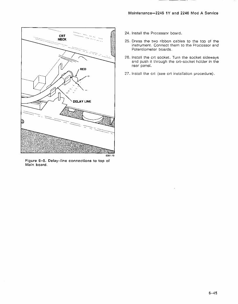
I , RED I
25'7 ' I \ DELAY LINE I
Maintenance-2246 1Y and 2246 Mod A Service
24. Install the Processor board.
25. Dress the two ribbon cables to the top of the instrument. Connect them to the Processor and Potentiometer boards.
26. Install the crt socket. Turn the socket sideways and push it through the crt-socket holder in the rear panel.
27 , Install the crt (see crt installation procedure).
6081-19
Figure 6-5. Delay-line connections t o top of Main board.


Section 7-2246 1Y and 2246 Mod A Service
OPTIONS
INTRODUCTION OPTION 1 R RACKMOUNTED INSTRUMENT This section contains a general description of the in- strument options and accessories available at the time of publication of this manual. Additional informa- tion about instrument options and other accessories can be obtained either by consulting the current Tektronix Product Catalog or by contacting your local Tektronix Field Office or representative.
INTERNATIONAL POWER CORDS Instruments are shipped with the detachable power- cord option ordered by the customer. Descriptive information about the international power-cord options is provided in Section 2 "Preparation for Use." The following list describes the power cords available for the 2246 1Y and 2246 Mod A.
Standard
Option A1
Option A2
Option A3
Option A4
Option A5
REV OCT 1991
--- - -
U. S. 120 V, 60 Hz, 74 in.
Universal Euro 220 V, 50 Hz, 2.5 m
UK 240 V, 50 Hz, 2.5 m
Australian 240 V, 50 Hz, 2.5 m
North American 240 V, 60 Hz, 2.5 m
Switzerland 220 V, 50 Hz, 2.5 m
When the 2246 1Y or 2246 Mod A Portable Oscil- loscope is ordered with Option 1 R, it is shipped in a configuration that permits easy installation into a 19-inch-wide equipment rack. Also, an optional rackmounting kit may be ordered to convert the stan- dard 2246 1 Y or 2246 Mod A to a rackmounted instru- ment. Installation instructions for rackmountina are providedin the documentation supplied with the;ack- mounting kit and the 1 R Option.


Section 8 - 2246 1Y/2246 MOD A
REPLACEABLE ELECTRICAL PARTS PARTS ORDERING INFORMATION
Replacement parts are available from or through your local Tektronix, Inc. F~eld Office or representative
Changes to Tektronix instruments are sometimes made to accommodate improved components as they become available, and to give you the benefit of the latest circuit improvements developed in our engineering department It is therefore impor- tant, when ordering parts, to Include the following information in your order Part number, Instrument type or number, serial
number, and modificat~on number if applicable.
If a part you have ordered has been replaced with a new or Improved part, your local Tektronix, Inc. Field Officeor represen- tative w ~ l l contact you concerning any change in part number.
Only the circuit number will appear on the diagrams and circuit board illustrations. Each diagram and circuit board
illustration is clearly marked with the assembly number. Assembly numbers are also marked on the mechanical exploded views located in the Mechanical Parts List. The component number is obtained by adding the assembly number prefix to the circuit number
The Electrical Parts List is divided and arranged by assemblies in numerical sequence (e.g.. assembly A1 with ~ t s subassemblies and parts, precedes assembly A2 with its sub- assemblies and parts)
Chassis-mounted parts have no assembly number prefix and are located at the end of the Electrical Parts List.
Change information, if any, is located at the rear of this manual.
LIST OF ASSEMBLIES TEKTRONIX PART NO. (column two of the Electrical Parts List)
A list of assemblies can be found at the beginning of the Electrical Parts L~st. The assembl~es arelistedin numerical order. Indicates part number to be used when ordering replace- When thecompletecomponent number of a part is known, this list ment part from Tektronix w ~ l l identify the assembly in which the part is located.
CROSS INDEX-MFR. CODE NUMBER TO MANUFACTURER
SERIAL/MODEL NO. (columns three and four of the Electrical Parts List)
'The Mfr. Code Number to Manufacturer index for the Column three (3) indicates the serial number at which the Electrical Parts Llst is located immediately after this page. The part was first used Column four (4) indicatestheserial numberat Cross Index provides codes, names and addresses of manufac- which the part was removed. No serial number entered indicates turers of components l~sted in the Electrical Parts List. part is good for all serial numbers.
Abbrev~at~ons conform to Amer~can Nat~onal Standard ~ 1 . 1 NAME & DESCFllPTlON (column five of the Electrical Parts List)
COMPONENT NUMBER (column one of the I n the Parts List, an Item Name is separated from the
Electrical Parts List) description by a colon (:). Because of space limitations, an ltem Name may sometimes appear as incomplete. For further ltem
A numbering method has been used to identify assemblies, Name identification, the U.S. Federal Cataloging Handbook H6-1
subassembl~es and parts Examples of this numbering method can be utilized where possible.
and typlcal expansions are illustrated by the following.
Example a. component number - A23R1234 A23 R1234
Assembly number Circuit number
Read: Resistor 1234 of Assembly 23
Example b. component number / h 4.
A23A2R1234 R1234 Assembly Subassembly Circuit number /?- x u m b e r
MFR. CODE (column six of the Electrical Parts List)
Indicates the code number of the actual manufacturer ofthe part. (Code to name and address cross reference can be found immediately after this page.)
MFR. PART NUMBER (column seven of the Electrical Parts List)
Read: Resistor 1234 af Subassembly 2 of Assembly 23 lndlcates actual manufacturers part number.
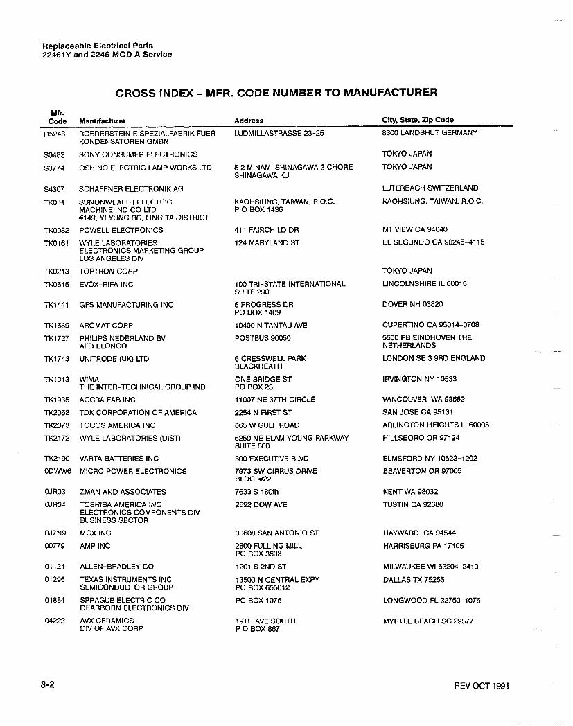
Replaceable Electrical Parts 22461Y and 2246 MOD A Service
CROSS INDEX - MFR. CODE NUMBER TO MANUFACTURER
Pflf?. Code
D5243
Manufacturer Address City, State, Zip Code
ROEDERSTEIN E SPEZIALFABRIK FUER LUDMILLASTRASSE 23-25 KONDENSATOREN GMBN
8300 LANDSHUT GERMANY
SONY CONSUMER ELECTRONICS
OSHINO ELECTRIC LAMP WORKS LTD
TOKYO JAPAN
TOKYO JAPAN 5 2 MlNAMl SHINAGAWA 2 CHORE SHINAGAWA KU
LUTERBACH SWITZERLAND
KAOHSIUNG, TAIWAN, R.O.C.
SCHAFFNER ELECTRONIK AG
SUNONWEALTH ELECTRIC KAOHSIUNG, TAIWAN, R.O.C. P 0 BOX 1436 MACHINE-IND co LTD
#149, YI YUNG RD, LING TA DISTRICT,
POWELL ELECTRONICS 411 FAIRCHILD DR
124 MARYLAND ST
MT VIEW CA 94040
EL SEGUNDO CA 90245-41 15 WYLE LABORATORIES ELECTRONICS MARKETING GROUP LOS ANGELES DIV
TOKYO JAPAN
LINCOLNSHIRE IL 60015
TOPTRON CORP
EVOX-RIFA INC 100 TRI-STATE INTERNATIONAL SUITE 290
GFS MANUFACTURING INC 6 PROGRESS DR PO BOX 1409
DOVER NH 03820
AROMAT CORP 10400 N TANTAU AVE
POSTBUS 90050
CUPERTINO CA 95014-0708
5600 PB EINDHOVEN THE NETHERLANDS
LONDON SE 3 9RD ENGLAND
PHILIPS NEDERLAND BV AFD ELONCO
UNITRODE (UK) LTD 6 CRESSWELL PARK BLACKHEATH
WlMA THE INTER-TECHNICAL GROUP IND
ACCRA FA6 INC
TDK CORPORATION OF AMERICA
TOCOS AMERICA INC
WYLE LABORATORIES (DIST)
ONE BRIDGE ST PO BOX 23
11007 NE 37TH CIRCLE VANCOUVER WA 98682
SAN JOSE CA 95131
ARLINGTON HEIGHTS IL 60005
HILLSBORO OR 97124
2254 N FIRST ST
565 W GULF ROAD
5250 NE ELAM YOUNG PARKWAY SUITE 600
VARTA BATTERIES INC 300 EXECUTIVE BLVD ELMSFORD NY 10523-1202
MICRO POWER ELECTRONICS 7973 SW CIRRUS DRIVE BEAVERTON OR 97005 BLDG. #22
ZMAN AND ASSOCIATES 7633 S 180th
2692 DOW AVE
KENT WA 98032
TUSTIN CA 92680 TOSHIBA AMERICA INC ELECTRONICS COMPONENTS DIV BUSINESS SECTOR
MCX INC
AMP INC
30608 SAN ANTONIO ST HAYWARD CA 94544
HARRISBURG PA 17105 2800 FULLING MILL PO BOX 3608
ALLEN-BRADLEY CO 1201 S 2ND ST
13500 N CENTRAL EXPY PO BOX 655012
MILWAUKEE WI 53204-2410
DALLAS TX 75265 TEXAS INSTRUMENTS INC SEMICONDUCTOR GROUP
SPRAGUE ELECTRIC CO PO BOX 1076 DEARBORN ELECTRONICS DIV
LONGWOOD FL 32750-1076
AVX CERAMICS DIV OF AVX CORP
19TH AVE SOUTH P 0 BOX 867
MYRTLE BEACH SC 29577
REV OCT 1991

Replaceable Electrical Parts 22461Y and 2246 MOD A Service
CROSS INDEX - MFR. CODE NUMBER TO MANUFACTURER
Mf r. Code Manufacturer Address City, State, l i p Code
MOTOROLA INC 5005 E MCDOWELL RD PHOENIX AZ 85008-4229 SEMICONDUCTOR PRODUCTS SECTOR
GENERAL INSTRUMENT CORP 600 W JOHN ST HlCKSVlLLE NY 11802 GOVERNMENT SYSTEMS DIV
BURNDY CORP RICHARDS AVE NORWALK CT 06852
UNITED CHEMI-CON INC 9801 W HlGGlNS SUITE 430
ROSEMONT IL 60018-4704
CTS CORP 406 PARR ROAD BERNE IN 4671 1-9506 BERNE DIV THICK FILM PRODUCTS GROUP
CLAROSTAT MFG CO INC LOWER WASHINGTON ST DOVER NH 03820
UNITRODE CORP 5 FORBES RD LEXINGTON MA 02173-7305
CAL-R INC 1601 OLYMPIC BLVD SANTA MONICA CA 90406 PO BOX 1397
MICROSEMI CORP 2830 S FAIRVIEW ST SANTA ANA CA 92704-5948
ELMWOOD SENSORS INC 500 NARRAGANSETT PARK DR PAWTUCKET RI 02861 -4325 SUB OF FASCO INDUSTRIES INC PO BOX 2325
GENERAL INSTRUMENT CORP 600 W JOHN ST HlCKSVlLLE NY 11802 DISCRETE SEMI CONDUCTOR DIV
KETEMA RODAN DIVISION
2900 BLUE STAR STREET ANAHEIM CA 92806-2591
AVX CORPORATION 3900 ELECTRONICS DR RALEIGH NC 27604-1620
SlGNETlCS CORP MILITARY PRODUCTS DIV
4130 S MARKET COURT SACRAMENTO CA 95834-1222
PHILIPS COMPONENTS DISCRETE PO BOX 760 PRODUCTS
MINERAL WELLS TX 76067-0760
DIV RESISTIVE PRODUCTS FACILITY AIRPORT ROAD
ALLEGRO MICROSYSTEMS INC 70 PEMBROKE ROAD CONCORD NH 03301 SEMICONDUCTOR DIVISION
SPRAGUE ELECTRIC CO 267 LOWELL ROAD HUDSON NH 03051
ANALOG DEVICES INC
CORNING GLASS WORKS
RT 1 INDUSTRIAL PK PO BOX 9106
550 HIGH ST
NORWOOD MA 02062
BRADFORD PA 16701 -3737
SPECIALTY CONNECTOR CO INC 2100 EARLYWOOD DR FRANKLIN IN 46131 PO BOX 547
NATIONAL SEMICONDUCTOR CORP 2900 SEMICONDUCTOR DR SANTA CLARA CA 95051-0606
MOLEX INC 2222 WELLINGTON COURT LISLE IL 60532-1613
KEMET ELECTRONICS CORP PO BOX 5928 NATIONAL SALES HEADQUARTERS
ITT SCHADOW INC 8081 WALLACE RD
BOURNS lNC 1200 COLUMBIA AVE TRIMPOT DIV
GREENVILLE SC 29606
EDEN PRAIRIE MN 55344-2224
RIVERSIDE CA 92507-21 14
ADVANCED MICRO DEVICES 901 THOMPSON PL
HARRIS CORP 200 PALM BAY BLVD HARRIS SEMICONDUCTOR PRODUCTS PO BOX 883 GROUP
SGS-THOMSON MICROELECTRONICS 1310 ELECTRONICS DR INC
SUNNYVALE CA 94086-4518
MELBOURNE FL 32919
CARROLLTON TX 75006-6905
REV OCT 1991
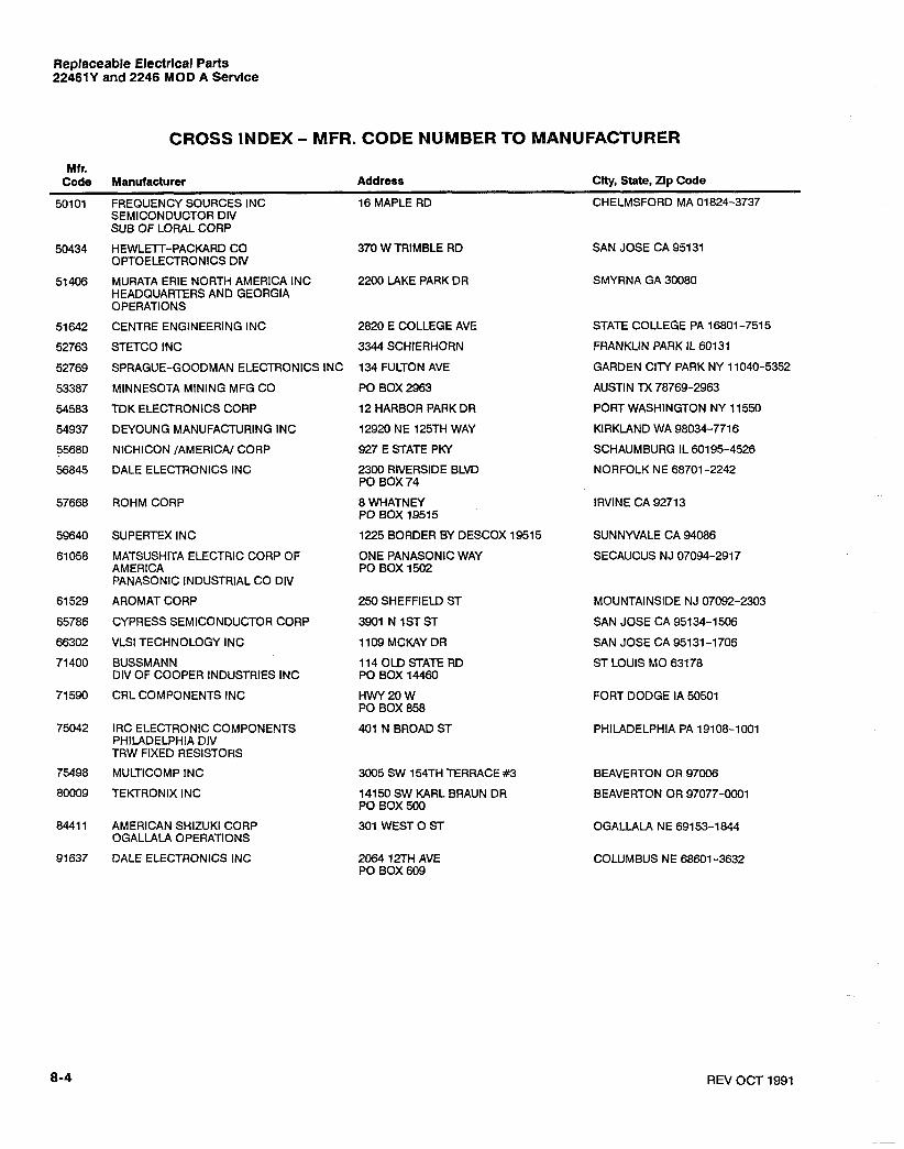
Replaceable Electrical Parts 22461Y and 2246 MOD A Servlce
CROSS INDEX - MFR. CODE NUMBER TO MANUFACTURER
Mf r. Code Manufacturer Address City, State, Zip Code
FREQUENCY SOURCES INC 16 MAPLE RD CHELMSFORD MA 01824-3737 SEMICONDUCTOR DIV SUB OF LORAL COUP
HEWLETT-PACKARD CO OPTOELECTRONICS DIV
SAN JOSE CA 95131
MURATA ERIE NORTH AMERICA INC HEADQUARTERS AND GEORGIA OPERATIONS
2200 LAKE PARK DR SMYRNA GA 30080
CENTRE ENGINEERING INC 2820 E COLLEGE AVE STATE COLLEGE PA 16801-7515
FRANKLIN PARK IL 60131
GARDEN CITY PARK NY 11040-5352
AUSTIN TX 78769-2963
PORT WASHINGTON NY 11550
KIRKLAND WA 98034-771 6
SCHAUMBURG IL 60195-4526
NORFOLK NE 68701-2242
3344 SCHIERHORN STETCO INC
SPRAGUE-GOODMAN ELECTRONICS INC
MINNESOTA MINING MFG CO
134 FULTON AVE
PO BOX 2963
12 HARBOR PARK DR TDK ELECTRONICS COUP
DEYOUNG MANUFACTURING INC
NlCHlCON /AMERICA/ CORP
12920 NE 125TH WAY
927 E STATE PKY
2300 RIVERSIDE BLVD PO BOX 74
8 WHATNEY PO BOX 19515
DALE ELECTRONICS INC
ROHM CORP
1225 BORDER BY DESCOX 19515
ONE PANASONIC WAY PO BOX 1502
SUPERTEX INC
MATSUSHITA ELECTRIC CORP OF AMERICA PANASONIC INDUSTRIAL CO DIV
AROMAT CORP
CYPRESS SEMICONDUCTOR COUP
SUNNWALE CA 94086
SECAUCUS NJ 07094-2917
250 SHEFFIELD ST MOUNTAINSIDE NJ 07092-2303
SAN JOSE CA 95134-1506
SAN JOSE CA 95131-1706
ST LOUIS MO 63178
VLSl TECHNOLOGY INC 1109 MCKAY DR
11 4 OLD STATE RD PO BOX 14460
BUSSMANN DIV OF COOPER INDUSTRIES INC
CRL COMPONENTS INC HWY 20 W FORT DODGE IA 50501 PO BOX 858
IRC ELECTRONIC COMPONENTS 401 N BROAD ST PHllADELPHlA PA 19108-1001 PHlIADELPHlA DIV TRW FIXED RESISTORS
MULTICOMP INC 3005 SW 154TH TERRACE #3 BEAVERTON OR 97006
TEKTRONIX INC 14150 SW KARL BRAUN DR BEAVERTON OR 97077-0001 PO BOX 500
AMERICAN SHlZUKl COUP OGALIALA OPERATIONS
301 WEST 0 ST OGALLAIA NE 69153-1844
DALE ELECTRONICS INC 2064 12TH AVE COLUMBUS NE 68601 -3632 PO BOX 609
REV OCT 1991

Replaceable Electrical Parts 22461Y and 2246 MOD A Service
Component Tektronlx Serlal No. Mfr. Number Part No. Effective Dscont Name & Description Code Mfr. Part No. A8 670-9783-01 CIRCUIT BD ASSYCRT CONTROL 80009 670978301 A9 671-0978-00 8700100 8710099 CIRCUIT BD ASSY2 MILLIVOLT BANDWIDTH 80009 671097800
(2246 1Y) A9 671-0978-08 BlOOlOO B1 10099 CIRCUIT BD ASSYP MILLIVOLT BANDWIDTH 80009 671097800
(2246 MOD A.2Y) A1 0 671-0875-00 B700100 8710099 CIRCUIT BD ASSYMAIN 80009 671087500
(2246 1Y) A10 671 -0875-01 871 01 00 871 0629 CIRCUIT BD ASSYMAIN 80009 671087501
(2246 1Y) A1 0 671 -0875-02 B710630 871 4999 CIRCUIT BD ASSYA10 MAIN
(2246 1Y) A1 0 671 -0875-03 8715000 CIRCUIT BD ASSYA10 MAIN
(2246 1Y) A1 0 671-0875-00 8100100 B110099 CIRCUITBDASSYMAIN
(2246 MOD A,2Y) A10 671 -0875-01 BllOl00 B111185 CIRCUIT BD ASSY:MAIN
(2246 MOD A.2Y) A1 0 671 -0875-02 B1 11 186 B1 19999 CIRCUIT BD ASSYA10 MAIN 80009 671087502
(2246 MOD A,2Y) A10 671-0875-03 B120000 CIRCUIT BD ASSYA10 MAIN
(2246 MOD A,2Y) A12 670-9402-01 CIRCUIT BD ASSYPOTENTIOMETER A1 4 670-9399-01 CIRCUIT BD ASSYSWITCH A16 672-1306-00 B700100 B711092 CIRCUIT BD ASSYPROCESSOR 80009 672130600
(2246 1W (WITH ~ 2 5 1 9 FIRMWARE)
A16 672-1306-01 B711093 CIRCUIT BD ASSYPROCESSOR,671-1086-XX 80009 672130601 WIRED (2246 1Y) (WITH U2519 FIRMWARE)
A1 6 672-0254-00 BlOOlOO B1 13797 CIRCUIT BD ASSY PROCESSOR 80009 672025400 (2246 MOD A,2Y) (WITH U2519 FIRMWARE)
A16 672-0254-01 8113798 CIRCUIT BD ASSY:PROCESSOR,671-1239-XX 80009 672025401 WIRED (2246 MOD A.2Y) (WITH U2519 FIRMWARE)
A16A1 671-1086-00 8700100 8711092 ClRCU1TBDASSY:PROCESSOR 80009 671108600 (2246 1Y) (WITHOUT U2519 FIRMWARE)
A16A1 671-1086-01 8711093 CIRCUIT 8D ASSYA16 PROCESSOR 80009 671108601 (2246 1Y) (WITHOUT U2519 FIRMWARE)
A16A1 671-0947-00 Bl00lOO B101981 CIRCUIT BD ASSYPROCESSOR 80009 671094700 (2246 MOD A.2W (WITHOUT ~ 2 5 1 9 FIRMWARE)
A16A1 671-1239-00 8101982 B1 13797 CIRCUIT BD ASSYPROCESSOR (2246 MOD A,2Y) (WITHOUT U2519 FIRMWARE)
A16A1 671 -1 239-01 B1 13798 CIRCUIT BD ASSY PROCESSOR 80009 671123901 (2246 MOD A.2Y) (WITHOUT U2519 FIRMWARE)
A1 8 670-9398-04 CIRCUIT BD ASSYLV POWER SUPPLY 80009 670939804
REV OCT 1991

Replaceable Electrical Parts 22461Y and 2246 MOD A Service
Component Tektronix Serial No. Number Part No. Effective Dscont A8 670-9783-01 A8R901 31 1-2344-00
Name & Description CIRCUIT BD ASSYCRT CONTROL RES,VAR.NONWW:CKT BD,4.7K OHM,20%,1.25WLINE AR RES,VAR,NONWW:CKT BD,4.7K OHM,20%,1.25WLINE AR RES,VAR,NONWW:CKT BD,4.7K OHM,20%,1.25WLINE AR RES,VAR,NONWWCKT BD.4.7K OHM,20%,1.25WLINE AR CONN.HDR::PCB,;MALE.RTANG,l X 8,O.l CTR,OP 95 MLG X 0.140 TAIL,TIN
Mf r. Code Mfr. Part No. 80009 670978301 71590 BA17140001
REV OCT 1991

Replaceable Electrical Parts 22461Y and 2246 MOD A Service
Component Tektronlx Serial No. Mf r. Number Part No. Effective Bscont Name & Description Code Mfr. Part No. A9 671-0978-00 8700100 8710099 CIRCUIT BD ASSY2 MILLIVOLT BANDWIDTH 80009 671 097800
(2246 1Y) A9 671-0978-00 BlOOlOO 8110099 CIRCUIT BD ASSY2 MILLIVOLT BANDWIDTH 80009 671097800
(2246 MOD A,2Y) A9C185 281 -0810-00 BlOOlOO 8110099 CAP,FXD,CER DI:5.6PF, + /-0.5PF,lOOVTUBULAR,MI 04222 SA102A5R6DAA
(2246 MOD A,2Y)
A9C186 281-0810-00 81 00100 8110099 CAF!FXD,CER DI:5.6PF, + 1-0.5PF.100VTUBULAR.MI 04222 SAl02A5R6DAA (2246 MOD A,2Y)
A9C186 281 -0810-00 8700100 8710099 CAI?FXD,CER DI:5.6PF, + /-0.5PF,100VTUBULBR,MI 04222 SA102A5R6DAA (2246 1Y)
A9C188 281-0909-00 BlOOlOO 5110099 CAf?FXD,CERDI:O.O22UF,20%,50V 04222 SA105C223MAA (2246 MOD A.2Y)
A9Q181 151-0712-00 8100100 8110099 TRANSISTOR.SIG:BIPOLARRPNP;20V,50MA,6O0MHZ 04713 MPSH81 AMPLIFIER (2246 MOD A.2Y)
A90181 151-0712-00 8700100 8710099 TRANSISTOR,SIG:BIPOLAR,PNP;20V,50MA,600MHZ 04713 MPSH81 AMPLIFIER (2246 1Y)
A9Q182 151-0712-00 BlOOlOO 8110099 TRANSISTOR,SIG:BIPOLAR,PNP;20V,50MA,600MHZ 04713 MPSH81 AMPLIFIER (2246 MOD A.2Y)
A9Q182 151-0712-00 8700100 8710099 TRANSISTOR,SIG:BIPOLAR,PNP;20V,50MA,600MHZ 04713 MPSH81 AMPLlFlER (2246 1Y)
A9R185 313-1512-00 8100100 8110099 RES,FXD,FILM:5.1 K OHM,5%,0.2W 91637 CCF50-2-51WJ (2246 MOD A,2Y)
A9R188 313-1512-00 8100100 8110099 RES,FXD.FILM:B.lK OHM,5%.0.2W (2246 MOD A.2Y)
A9R188 31 3-1512-00 8700100 8710099 RES,FXD.FILM:5.1 K OHM,5%,0.2W 91637 CCF50-2-51 OOOJ (2246 1Y)
A9R189 313-1271-00 8100100 81 10099 RES,FXD,FILM:270 OHM,5%,0.2W 91 637 CCF50-2-270ROJ (2246 MOD A,2Y)
A9VR101 152-0278-00 8100100 8110099 DlODE,ZENER:,;3V,5%,0,4W (2246 MOD A,2Y)
A9VR101 152-0278-00 8700100 8710099 DlODE,ZENER:.;3V,5%,0.4W (2246 1Y)
A9W105 131-0566-00 81 00100 8110099 BUS.CONDUCTOR:DUMMY RES,0.094 OD X 0.225L 24546 OMA 07 (2246 MOD A,2Y)
A9W105 131 -0566-00 8700100 81 10099 8US.CONDUCTOR:DUMMY RES,0.094 OD X 0.225L 24546 OMA 07 (2246 1Y)
A9W106 131-0566-00 8100100 81 10099 BUS,CONDUCTOR:DUMMY RES.0.094 OD X 0.225L 24546 OMA 07 (2246 MOD A,2Y)
A9W106 131-0566-00 8700100 8710099 BUS.CONDUCT0R:DUMMY RES,0.094 OD X 0.225L 24546 OMA 07 (2246 1Y)
A9W107 131-0566-00 BlOOlOO 8110099 BUS,CONDUCTOR:DUMMY RES,0.094ODX0.225L 24546 OMA07 (2246 MOD A.2Y)
REV OCT 1991

Replaceable' Electrical Parts 22461Y and 2246 MOD A Service
Component Tektronix Serial No. Mfr. Number Part No. Eftectlve Dscont Name & Descrlptlon Code Mfr. Part No. A9W107 131-0566-00 8700100 8710099 BU NDUCT0R:DUMMY RES,0.094 OD X 0.225L 24546 OMA 07
(22%CPY) A9W108 131-0566-00 BlOOlOO 81 10099 BUS,CONDUCTOR:DUMMY RES,0.094 OD X 0.225L 24546 OMA 07
(2246 MOD A,2Y) A9W108 131-0566-00 8700100 8710099 BUS,CONDUCTOR:DUMMY RES,0.094 OD X 0.225L 24546 OMA 07
(2246 1Y) A9W212 195-0970-00 8100100 8110099 LEAD,ELECTRICAL:26AWG,3.0L,O-N 80009 195097000
(2246 MOD A.2Y)
A9W222 195-0970-00 8100100 8110099 LEAD.ELECTRICAL26AWG.3.OL.O-N 80009 195097000 (2246 MOD A,2Y)
A9W222 195-0970-00 B700100 8710099 LEAD,ELECTRICAL:26 AWG,3.0 L.0-N 80009 195097000 (2246 1Y)
This scan is not authorized to be sold on eBay by other than it's creator. If you bought this scanned manual on eBay from any other than aa4df, then the vendor you bought it from is a thief who sold you stolen property. Please file a complaint with eBay and demand a refund. - --
REV OCT 1991

Replaceable Electrical Parts 22461Y and 2246 MOD A Service
Component Number A1 0
A1 OAT1 17
A1 OATl 17
A1 OATl 17
AlOAT117
A1 OAT1 17
A1 OAT127
A10ATl27
A1 OAT1 27
A10AT127
AlOClOl
Tektronix Serial No. Mfr. Part No. Effective Dscont Name & Description Code Mfr. Part No. 671-0875-00 8700100 8710099 CIRCUIT BD ASSYMAIN 80009 671087500
(2246 1Y)
671 -0875-01 871 0100 B710629 CIRCUIT BD ASSYMAIN 80009 671087501 (2246 1 Y)
671 -0875-02 8710630 B714999 CIRCUIT BD ASSYA10 MAIN 80009 671 087502 (2245 1Y)
671 -0875-03 871 5000 CIRCUIT BD ASSYA10 MAIN 80009 671087503 (2246 1Y)
671-0875-00 BlOOlOO 8110099 CIRCUIT BD ASSYMAIN 80009 671087500 (2246 MOD A,2Y)
671 -0875-01 BllOlOO 81 11 185 CIRCUIT BD ASSY:MAIN 80009 671087501 (2246 MOD A.2Y)
671 -0875-02 81 11 186 81 19999 CIRCUIT BD ASSYA10 MAlN (2246 MOD A.2Y)
671-0875-03 B120000 CIRCUIT BD ASSYA10 MAIN (2246 MOD A.2Y)
307-2135-00 B l 001 00 8101582 RES NTWK,FXD,FI:ATTENUATOR DIP PKG (2246 MOD A.2Y)
307-2135-01 B101583 81 13045 AlTENUAT0R:l M OHM AXENUATOR NETWORK 80009 307213501 (2246 MOD A, 2Y)
307-21 35-02 81 13046 B114266 AXENUAT0R:i M OHM AXENUATOR NETWORK 80009 307213502 (2246 MOD A,2Y)
307-2135-03 B114267 ATTENUAT0R:lMOHMATTENUATORNETWORK 80009 307213503 (2246 MOD A,2Y)
307-2135-00 8700100 B700493 RES NTWK,FXD,FI:AXENUATOR DIP PKG 80009 307213500 (2246 1Y)
307-2135-01 8700494 B711016 ATTENUAT0R:lM OHM ATTENUATOR NETWORK 80009 307213501 (2246 1Y)
307-2135-02 B711017 871 1094 ATTENUAT0R:IM OHM ATENUATOR NETWORK 80009 307213502 (2246 1Y)
307-21 35-03 871 1095 AlTENUAT0R:lM OHM ATTENUATOR NETWORK 80009 307213503 (2246 1Y)
307-2135-00 B100100 8101582 RES NTWK,FXD.FI:AlTENUATOR DIP PKG 80009 30721 3500 (2246 MOD A,2Y)
307-2135-01 8101583 B113045 ATTENUAT0R:l M OHM ATTENUATOR NETWORK 80009 307213501 (2246 MOD A,2Y)
307-2135-02 81 13046 81 14266 ATTENUAT0R:l M OHM ATTENUATOR NETWORK 80009 307213502 (2246 MOD A,2Y)
307-2135-03 B114267 ATTENUAT0R:l M OHM ATTENUATOR NETWORK 80009 307213503 (2246 MOD A,2Y)
307-2135-00 B700100 8700493 RES NTWK,FXD.FI:ATTENUATOR DIP PKG 80009 307213500 (2246 1Y)
307-2135-01 8700494 B711016 ATTENUAT0R:lM OHM ATTENUATOR NETWORK 80009 307213501 (2246 1 Y)
307-2135-02 671 1017 871 1094 ATTENUAT0R:l M OHM ATTENUATOR NETWORK 80009 307213502 (2246 1Y) ATTENUAT0R:lM OHM ATTENUATOR NETWORK 80009 307213503 (2246 1Y)
REV OCT 1991

Replaceable Electrical Parts 22461Y and 2246 MOD A Service
Component Tektronix Serial No. Number Part No. Effective Dscont Name 81 Description A10C107 281 -0909-00 CAP,FXD.CER DI:O.O22UF,20%,50V
A10C108 281 -0909-00 CAP,FXD,CER DI:O.O22UF,20%.50V
A lOCl l l 281-0909-00 CAP,FXD,CER DI:0.022UF,20°/o,50V A10C112 283-0414-01 CAP,FXD,CER DI:O.O22UF,20%,500V
A10C113 281 -0909-00 CARFXD,CER DI:O.O22UF,20%,50V
Mfr. Code 04222 04222 04222 04222 04222
Mfr. Part No. SA105C223MAA SA105C223MAA SA105C223MAA SR217C223MAATR SA105C223MAA
GKU 18000 SA105C223MAA SA105C223MAA SAl 06A15OKAA GKU 10000
GKU 18000 SA105C223MAA SA105C223MAA SA106A1 SOKAA GKU 10000
SA1 06A1 5OKAA KMC50VBlORM5Xll SA105C223MAA SAlOl C472KAA UMClOVB221 M8Xll
AlOC181 290-0944-01 CAP,FXD,ELCTLT220UF,20%,1 OV A1 0C185 281-0810-00 8110100 CAP,FXD,CER DI:5.6PF, + I-0.5PF,lOOVTUBULAR.MI
(2246 MOD A,2Y) A10C185 281-0810-00 B710100 CAP,FXD,CER DI:5.6PF, +I-0.5PF,lOOVTUBULAR,MI
(2246 1Y) A10C186 281-0810-00 BllOl00 CAP,FXD,CER DI:5.6PF,+/-O.5PF,lOOVTUBULAR,MI
(2246 MOD A,2Y) A10C186 281 -0810-00 8710100 CAP,FXD,CER DI:5.6PF, + /-0.5PF,100VTUBULAR,MI
(2246 1Y)
REV OCT 1991

Replaceable Electrical Parts 22461Y and 2246 MOD A Service
Component Tektronix Serial No. Mf r. Number Part No. Effective Dscont Name & Description Code Mfr. Part No. A1 0C188 281-0909-00 8110100 CARFXD,CER DI:O.O22UF,20%,50V 04222 SA105C223MAA
(2246 MOD A,2Y) A10C188 281-0909-00 8710100 CARFXD,CER DI:O.O22UF,20%,5OV 04222 ~ ~ 1 0 5 ~ 2 2 3 ~ ~ ~
(2246 1Y) A10C190 281-0797-00 CAP,FXD,CER DI:15PF,lO%,l00V,,TUBUlAR,MI 04222 SA106A150KAA A10C191 281-0797-00 CARFXD.CER DI:15PF,10%.100V,,TUBUlAR,MI 04222 SA106A150KAA A10C201 290-0974-01 CARFXD,ELCTLT:10UFF,20%,50V 1W344 KMC50VBlORM5Xll
A10C215 290-0974-01 CARFXD,ELCTLTlOUF,20%.50V A1 0C216 281-0909-00 8100100 8113468 CARFXD.CERDI:O.O22UF,20%,5OV
(2246 MOD A,2Y) A10C216 281-0775-01 8113469 CARFXD,CER D1:O.l UF,20%.50V
(2246 MOD A,2Y) A1 0C216 281-0909-00 8700100 B711092 CARFXD,CER DI:O.O22UF,20%.50V
(2246 1Y) A10C216 281 -0775-01 871 1093 CARFXD,CER DI:O.lUF,20%.50V
(2246 1Y)
A10C217 281-0909-00 8100100 8113468 CARFXD,CERDl:O.O22UF,20%.50V 04222 SA105C223MAA (2246 MOD A,2Y)
A1 0C217 281-0775-01 8113469 CARFXD,CER D1:O.l UF,20%.50V 04222 SA105E104MAA (2246 MOD A,2Y)
REV OCT 1991
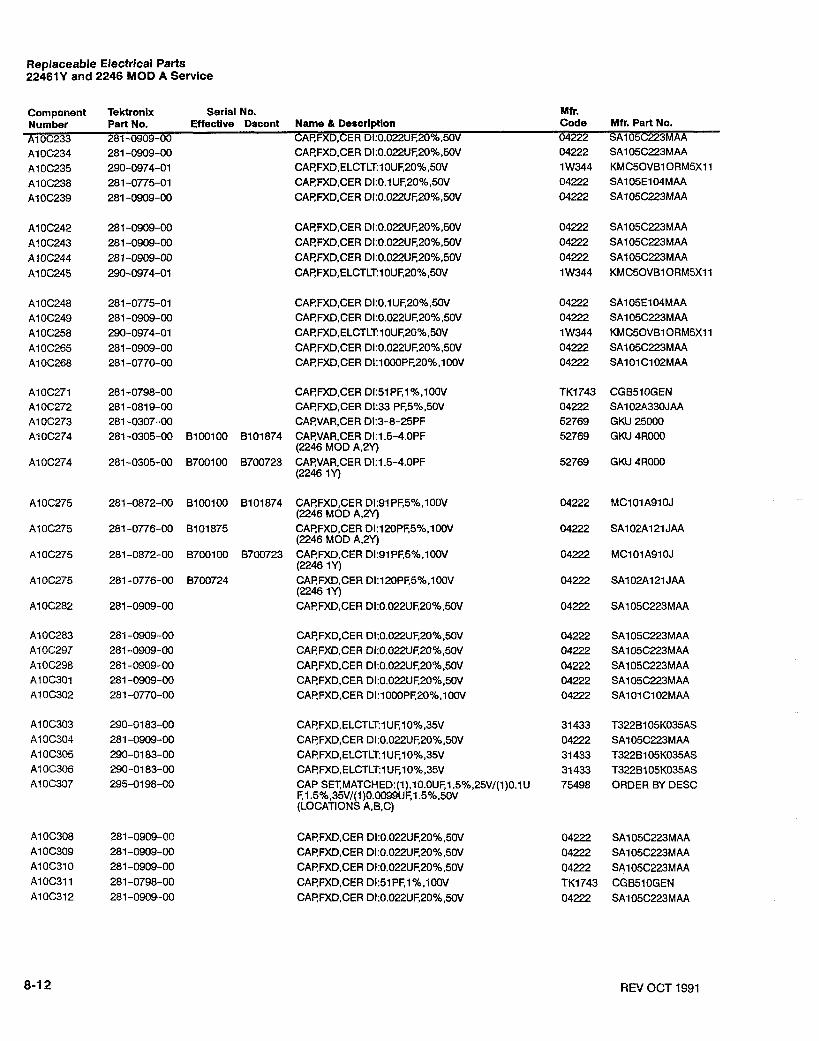
Replaceable Electrical Parts 22461Y and 2246 MOD A Service
Component Number A1 0C233 A1 0C234 A1 0C235 A1 0C238 A1 0C239
Tektronix Serial No. Mf r. Part No. Effective Dscont Name & Description Code 281-0909-00 CARFXD,CER DI:0.022UF,20%.50V 04222 281-0909-00 CARFXD,CER DI:0.022UF,20°h,50V 04222
290-0974-01 CAP,FXD,ELCTLT:lDUF,20%,50V 1 W344
281-0775-01 CAP,FXD,CER DI:O.lUF,20%,50V 04222
281 -0909-00 CAP,FXD,CER Dl:O.O22UF,20%,50V 04222
Mfr. Part No. SA105C223MAA SA105C223MAA KMC5OVBl ORM5X11 SA105E104MAA SA105C223MAA
281-0798-00 CAP,FXD,CER DI:51PF,1%,100V 281-0819-00 CAP,FXD,CER DL33 PF,5%,50V 281 -0307-00 CAi?VAR,CER DI:3-8-25PF 281 -0305-00 BlOOl00 B101874 CARVAR,CER DI:1.5-4.OPF
(2246 MOD A,2Y) 281-0305-00 B700100 B700723 CAP,VAR,CER DIZ1.5-4.OPF
(2246 1Y)
CGB5lOGEN SA102A330JAA GKU 25000 GKU 4R000
GKU 4R000
281 -0872-00 BlOOlOO B101874 CARFXD,CER DI:91 PF,5%,100V (2246 MOD A,2Y)
281 -0776-00 B1 01 875 CARFXD,CER DI:120PF,5%,100V (2246 MOD A,2Y)
281 -0872-00 B700100 8700723 CAP,FXD,CER DI:91 PF,5%,100V (2246 1Y)
SA102A121 JAA
SA102A121 JAA
T322Bl05K035AS SA105C223MAA T322B105K035AS T322B105K035AS ORDER BY DESC CAP S~MATCHED:(1),1O.OUF,1.5%,25V/(1)0.1U 75498
F,1.5%,35V/(l)O.0099UF,1.5%,50V (LOCATIONS A.B,C)
RE3 OCT 1991

Replaceable Electrical Pads 22461Y and 2246 MOD A Service
Component Tektronlx Serial No. Number Part No. Effective Dscont Name & Description A1 0C313 281-0909-00 CARFXD,CER DI:O.O22UF,20%,50V A10C314 281-0307-00 CARVAR,CER DI:3-8-25PF A1 0C315 281-0798-00 CASFXD,CER Dk51 PF,1%.100V A1 0C316 281-0909-00 CARFXD,CER DI:O.O22UF,20%,50V A10C317 281 -0909-00 CARFXD.CER DI:O.O22UF,20%,50V
A1 0C318 281-0909-00 CARFXD,CER DI:O.O22UF,20%,50V A1 0C319 281 -0909-00 CAP,FXD.CER DI:O.O22UF,20%,50V A1 0C320 281-0909-00 CAP,FXD.CER DI:O.O22UF,20%,50V A10C321 281 -0798-00 CASFXD,CER DL51 PF,l%.lOOV A1 0C322 281 -0909-00 B l 101 00 CAP,FXD,CER DI:O.O22UF,20%,50V
(2246 MOD A,2Y)
A1 0C425 281 -0820-00 B l 00100 81 10637 CARFXD,CER DI:680 PF,10%.50V (2246 MOD A.2Y)
A10C425 281-0861-00 B110638 81 19999 CARFXD,CER DI:270PF,5%,50V (2246 MOD A,2Y)
A10C425 283-0196-00 B120000 CAF!FXD,CER DI:270PF,10%,50V (2246 MOD A.2Y)
A1 0C442 281 -0909-00 B l 101 00 CARFXD.CER DI:O.O22UF,20%,50V (2246 MOD A.2Y)
A1 0C442 281 -0909-00 B710100 CAFiFXDGER DI:O.O22UF,20%.50V (2246 1Y)
A1 0C444 281-0765-00 CAF!FXD,CER DI:100PF,5°h,100V A1 0C445 290-0183-00 CARFXD,ELCTLT:lUF,10%,35V A1 0C447 281-0765-00 CARFXD,CER DI:100PF,5%,100V
Mlr. Code Mfr. Part No. 04222 SA105C223MAA 52769 GKU 25000 TK1743 CGB51OGEN 04222 SA105C223MAA 04222 SA105C223MAA
04222 SA105C223MAA 52769 GKU 25000 04222 SA101 A620GAA 04222 SA105C223MAA
04222 SA105C223MAA 04222 SA105C223MAA 04222 SA105C223MAA 04222 SA105E104MAA 04222 SAlOlA271 JAA
04222 SAlOlA431 JAA 31433 T322B105K035AS 04222 SAlOlC681KAA
04222 SA101 A271 JAA
16299 SR155C271 KAA
04222 SAlO1 C681 KAA
04222 SAlOlA271 JAA
16299 SR155C271 KAA
04222 SAlOlA431 JAA 04222 SA102C331 MAA
04222 SA102A101 JAA 31433 T3228105K035AS 04222 SA102A101 JAA
REV OCT 1991

Replaceable Electrical Parts 22461Y and 2246 MOD A Service
Mfr. Code Mfr. Part No. 04222 SA105El04MAA 04222 SAlOlA271 JAA 04222 SA101A431 JAA 31 433 T322B105K035AS 04222 SAlO1 C681 KAA
Component Tektronix Serial No. Number Part No. Effective Dscont Name L Description AlOC451 281 -0775-01 CApFXD.CER DI:O.lUF,20%,50V A1 OC452 281-0861-00 CAP,FXD,CER DI:270PF,5%,50V A1 0C453 281-0864-00 CAP,FXD,CER Dl:430PF,5%,100V A1 00454 290-01 83-00 CAP,FXD,ELCTLT:lUF,10%,35V A1 0C455 281-0820-00 8700100 8710290 CApFXD,CER DI:680 PF,10%,50V
(2246 1Y)
A1 0C455 281-0861-00 B710291 CApFXD.CER DI:270PF,5%,50V (2246 1Y)
A10C455 281-0820-00 BlOOlOO 8110637 CApFXD,CER DI:680 PF,10%,50V (2246 MOD A,2Y)
04222 SAlO1 A271 JAA
04222 SAlO1 C681 KAA
04222 SAlOlA271 JAA A1 0C455 281-0861-00 8110638 CApFXD.CER DI:270PF,5%,50V (2246 MOD A,2Y)
04222 SAlOlA431 JAA 04222 SA105E473MAA
A1 Om74 281-0776-00 CAPFXD,CER DI:120PF,590,100V A10C475 290-0183-00 CAP,FXD,ELCTLT:lUF,10%,35V A1 0C476 281 -0819-00 B l 10100 CApFXD,CER DL33 PF,5%,50V
(2246 MOD A,2Y) A1 0C476 281-0819-00 8710100 CARFXD,CER DL33 PF,5%,50V
(2246 1Y)
A1 0C477 281-0765-00 B100100 B110099 CAP,FXD,CERDI:100PF,5%,100V (2246 MOD A,2Y)
04222 SAlO2A121 JAA 31433 T322B105K035AS 04222 SA102A330JAA
04222 SA102A101 JAA
AlOC477 281-0872-00 BllOlOO CAP,FXD.CER DL91 PF,5%,100V (2246 MOD A.2Y)
04222 SA102A101 JAA
A1 0C478 281 -0864-00 81 101 00 CApFXD,CER DI:430PF,5%,100V (2246 MOD A,2Y)
04222 SAlOlA431 JAA
04222 SAlOlA431 JAA
A1 0C480 281-0909-00 8110100 CApFXD,CER DI:O.O22UF,20%,50V (2246 MOD A,2Y)
04222 SA105C223MAA 04222 SA105C223MAA 04222 SAlO1 C681 KAA
A1 0C484 281-0765-00 BlOOlOO 81 10099 CApFXD,CER DI:100PF,5%.100V (2246 MOD A,2Y)
A1 0C484 281-0861-00 B l 10100 CApFXD,CER DI:270PF,5%.50V (2246 MOD A,2Y)
04222 SA102A101 JAA
04222 SA101 A271 JAA
04222 SA102A101 JAA
A1 0C484 281 -0861 -00 871 01 00 CApFXD,CER DI:270PF,5%,50V (2246 1Y)
A1 0C485 281 -0765-00 8100100 81 10099 CApFXD,CER DI:lOOPF,5%.100V (2246 MOD A.2Y)
04222 SA101A271 JAA
04222 SA102A101 JAA
REV OCT 1991

Replaceable Electrical Parts 22461Y and 2246 MOD A Service
Component Tektronix Serial No. Number Part No. Effective Dscont Name & Description A10C485 281-0861-00 61 10100 61 19999 CAP,FXD,CER DI:270PF,5%.50V
(2246 MOD A,2Y) A10C485 283-0196-00 B120000 CApFXD,CER DI:270PF,10%,50V
(2246 MOD A,2Y) A1 0C485 281 -0765-00 B700100 8710099 CApFXD.CER DI:100PF,5%.100V
(2246 1Y) A10C485 281 -0861 -00 6710100 8714999 CApFXD,CER DI:270PF,5%.50V
(2246 1Y)
A1 0C486 281-0765-00 6100100 8110099 CAP,FXD,CERDI:100PF,5%,100V (2246 MOD A.2Y)
A1 0C486 281 -0765-00 6700100 8710099 CApFXD,CER DI:100PF,5%,100V (2246 1Y)
A10C487 281-0765-00 CApFXD,CER DI:lOOPF,5%,100V A1 00488 281-0765-00 BlOOlOO 8110099 CARFXD,CERDl:100PF,5%,100V
(2246 MOD A,2Y) A1 0C488 283-01 96-00 61 20000 CASFXD,CER DI:270PF,10%,50V
(2246 MOD A.2Y)
A1 0C496 281 -0864-00 61 10254 81 19999 CApFXD,CER DI:430PF,5%,100V (2246 MOD A.2Y)
A10C496 283-0196-00 6120000 CAP,FXD,CER DI:270PF,10°/o,50V (2246 MOD A,2Y)
Mf r. Code Mfr. Part No. 04222 SA101 A271 JAA
16299 SR155C271 KAA
04222 SA102A101 JAA
04222 SAlOlA271 JAA
16299 SR155C271 KAA
04222 SA102A101 JAA
04222 SA102A101 JAA
04222 SA102A101 JAA 04222 SA102A101 JAA
16299 SR155C271 KAA
16299 SR155C271 UAA
04222 SA102A101 JAA 04222 SA102A330JAA 04222 SA102A330JAA
04222 SA102A330JM 04222 SA102A330JAA 04222 SAlOlA431 JAA
16299 SR155C271 KAA
16299 SR155C271 KAA
04222 SAlOlA27l JAA 04222 SA101A271JM 04222 SA102A330JAA 04222 SA102A330JAA 04222 SA105C223MAA
04222 SA105C223MAA 04222 SA105C223MAA 04222 SA102A101 JAB 04222 SA102A101 JAA 04222 SA105C223MAA
REV OCT 1991
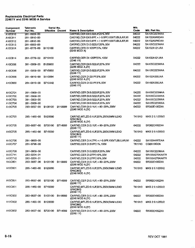
Replaceable Electrical Parts 22461Y and 2246 MOD A Service
Component Number A10C610 A1 OC611 A1 0C612 A1 OC613 A1 0C614
Tektronlx Serial No. Mfr. Part No. Effective Dscont Name & Description Code Mfr. Part No. 281 -0909-00 CARFXD,CER DI:O.O22UF,20%,5OV 04222 SA105C223MAA 281-0810-00 CARFXD.CER DI:5.6PF, + I-0.5PF,100VTUBULAR,MI 04222 SA102A5R6DAA 281-0810-00 CARFXD,CER DI:5.6PF,+I-O.5PF,lOOVTUBULAR,Ml 04222 SA102A5R6DAA 281 -0909-00 CApFXD.CER DI:O.O22UF,20%,50V 04222 SA105C223MAA 281 -0776-00 8110100 CA?FXD,CER DI:120PF,5%,100V 04222 SA102A121 JAA
(2246 MOD A)
CAI?FXD,CER DI:O.O22UF,20%,50\1 (2246 MOD A,2Y)
281-0909-00 8715000 CARFXD,CER DI:O.O22UF,20%,50V (2246 1Y)
281 -081 9-00 81 10994 CARFXD,CER DL33 PF,5°~.50V (2246 MOD A,2Y)
281-0819-00 8710442 CARFXD,CER Dk33 PF,5%,50V (2246 1Y)
04222 SA102A121 JAA
281-0909-00 CARFXD.CER DI:O.O22UF,20%,50V 04222 SA105C223MAA 281-0909-00 CARFXD,CER DI:O.O22UF,20%,50V 04222 SA105C223MAA 281 -0909-00 CAl?FXD,CER DI:O.O22UF,20%,50V 04222 SA105C223MAA 281 -0909-00 CARFXD,CER DI:O.O22UF,20%,50V 04222 SA105C223MAA 283-0057-00 8100100 81 19999 CARFXD,CER DI:O.IUF, + 80-20%,200V 04222 SR302E105ZAA
(2246 MOD A,2Y)
285-1460-00 8120000 CAP,FXD,MTLZD:O.l UF,20%,250V,5MM LEAD TK1913 MKS 2 0.1125012 SPACING (2246 MOD A.2Y)
283-0057-00 8700100 8714999 CARFXD,CER DI:O.lUF, +80-20%.200V 04222 SR302E105ZAA (2246 1Y)
285-1460-00 8715000 CARFXD.MTL2D:O.l UF,200/oo25OV,5MM LEAD TK1913 MKS 2 0.1125012 SPACING (2246 1Y)
283-0057-00 8100100 8119999 CAF!FXD,CERDI:0.1UF,+80-20%.200V 04222 SR302E105ZAA (2246 MOD A,2Y)
285-1 460-00 81 20000 CARFXD.MTL2D:O.l UF,20%,250V,5MM LEAD TK1913 MKS 2 0.1125012 SPACING (2246 MOD A.2Y)
283-0057-00 8700100 8714999 CARFXD,CERDI:O.lUF,+80-20%,200V 04222 SR302E105ZAA (2246 1Y)
285-1460-00 8715000 CARFXD.MTUD:O.lUF,20%,250V,5MM LEAD TK1913 MKS 2 0.1125012 SPACING (2246 1Y)
283-0057-00 BlOOlOO 81 19999 CARFXD,CER DI:O.lUF, + 80-20%,200V 04222 SR302E105ZAA (2246 MOD A,2Y)
285-1460-00 8120000 CARFXD,MTLZD:O.lUF,20%,250V,5MM LEAD TK1913 MKS 2 0.1 I25012 SPACING (2246 MOD A.2Y)
283-0057-00 8700100 8714999 CARFXD,CERDI:O.lUF,+80-20%.200V 04222 SR302E105ZAA (2246 1Y)
REV OCT 1991

Replaceable Electrical Parts 22461Y and 2246 MOD A Service
Component Tektronix Serial No. Mfr. Number Part No. Effective Dscont Name & Descriptlon Code Mfr. Part No. A1 0C802 285-1 460-00 8715000 CAF!FXD,MTUD:O.l UF,20%,250V,5MM LEAD TK1913 MKS 2 0.1125012
SPACING (2246 1Y)
A1 0C803 281 -0707-00 81 00100 81 10099 CARFXD,CER DI:15000PF,10%,200V 04222 MA302C153KAA (2246 MOD A,2Y)
A1 0C803 281-0909-00 8110100 CASFXD,CER DI:O.O22UF,20%,50V 04222 SA105C223MAA (2246 MOD A,2Y)
A1 0C803 281 -0707-00 87001 00 8710099 CASFXD,CER DI:15000PF,10%,200V 04222 MA302C153KAA (2246 1Y)
A10C803 281-0909-00 8710100 CAI?FXD.CER Dl:O.O22UF,20%,50V 04222 SA105C223MAA (2246 1Y)
A10C804 281-0909-00 8100100 8110099 CASFXD,CERDI:O.O22UF,20%,50V 04222 SA105C223MAA (2246 MOD A.2Y)
A1 OC804 283-0057-00 81 10100 81 19999 CASFXD,CER DI:O.lUF, + 80-20%.200V 04222 SR302E105ZAA (2246 MOD A.2Y)
A1 0C804 285-1460-00 8120000 CA~FXD,MTUD:0.1UF,200/o0250V,5MM LEAD TK1913 MKS 2 0.1125012 SPACING (2246 MOD A,2Y)
A1 OC804 281-0909-00 8700100 8710099 CASFXD,CER DI:O.O22UF,20%.50V 04222 SA105C223MAA (2246 1Y)
A10C804 283-0057-00 8710100 8714999 CAF!FXD,CER D1:O.l UF, +80-20%,200V 04222 S R302 E 105ZAA (2246 1Y)
A1 OC804 285-1460-00 8715000 CASFXD.MTL2D:O.l UF,200/oo25OV,5MM LEAD TK1913 MKS 2 0.1125012 SPACING (2246 1Y)
A1 0C805 281 -0909-00 CAP,FXD,CER DI:O.O22UF,20%,50V 04222 SA105C223MAA A1 0C806 281 -0909-00 CARFXD,CER DI:O.O22UF,20%,50V 04222 SA105C223MAA A1 OC807 281 -0064-00 81 00100 81 10099 CARVAR,PLASTIC:0.25-1.5PF.600V 52769 ER-530-013
(2246 MOD A,2Y)
A1 0C807 281-0214-00 8110100 CASVAR,CER DI:0.6-3PF,400V 52763 313613-140 (2246 MOD A,2Y)
A1 0C807 281 -0064-00 87001 00 871 0099 CAP,VAR.PLASTIC:0.25-1.5PF,600V 52769 ER-530-013 (2246 1Y)
A10C808 281-0765-00 CAP,FXD,CER DI:100PF,5°h.100V 04222 SA102A101 JAA A1 OC809 283-0057-00 8100100 8119999 CARFXD,CERDI:O.lUF,+80-20%,200V 04222 SR302E105ZAA
(2246 MOD A,2Y)
A1 0C809 285-1460-00 8120000 CARFXD,MTUD:O.l UF,20%,250V,5MM LEAD TK1913 MKS20.1125012 SPACING (2246 MOD A,2Y)
A10C809 283-0057-00 8700100 8714999 CARFXD,CERDl:O.lUF,+80-20%,200V 04222 SR302E105ZAA (2246 1'4
A1 0C809 285-1460-00 8715000 CARFXD.MTl2D:O.l UF,20%,250V,5MM LEAD TK1913 MKS 2 0.1 I25012 SPACING (2246 1Y)
A10C810 281 -0707-00 8100100 81 10099 CAf?FXD,CER DI:15000PF,10%,200V 04222 MA302C153KAA (2246 MOD A.2Y)
A10C810 281-0707-00 8700100 8710099 CARFXD,CER DI:15000PF,10°h,200V 04222 MA302C153KAA (2246 1Y)
REV OCT 1991

Replaceable Electrical Parts 22461Y and 2246 MOD A Service
Component Tektronix Serial No. Number Part No. Effective Dscont Name Q Description
A1 0C811 281-0909-00 CAP,FXD,CER DI:O.O22UF,20%,5OV
Mf r. Code Mfr. Part No. 04222 SA105C223MAA
CAP,VAR.PlASTIC:0.25-1.5PF.600V (2246 MOD A.2Y)
A10C814 281 -021 4-00 81 101 00 CAP,VAR,CER DI:0.6-3PF,400V (2246 MOD A.2Y)
8100100 8119999 CAF!FXD.CER DI:0.1UF, +80-20%.200V (2246 MOD A,2Y)
81 20000 CAP,R(D,MTLZD:O.lUF,20%,250V,5MM LEAD SPACING (2246 MOD A,2Y)
TK1913 MKS 2 0.1/250/2
8700100 8714999 CAP,FXD,CER D1:O.l UF, + 80-20%,200V (2246 1Y)
8715000 CAP,FXD,MTLZD:O.l UF,200/oO250V,5MM LEAD SPACING
TK1913 MKS 2 0.1/250/2
CAP,FXD,CER DI:100PF,5%,100V BllOl00 CAP,FXD,CER DI:O.O22UF,20%,50V
(2246 MOD A.2Y)
04222 SA102A101 JAA 04222 SA105C223MAA
A1 0C820 281-0909-00 8710100 CAP,FXD,CER DI:O.O22UF,20%.50V (2246 1Y)
A10C821 281 -0909-00 81 101 00 CAP,FXD,CER DI:O.O22UF,20%,50V (2246 MOD A.2Y)
A1 0C822 281-0909-00 8110100 CAP,FXD,CER DI:O.O22UF,20%,5OV (2246 MOD A,2Y)
A10C822 281-0909-00 8710100 CARFXD,CER DI:0.022UF.20%,50V (2246 1Y)
A1 0C860 281-0765-00 BllOl00 CAP,FXD,CER DI:100PF,5%,100V (2246 MOD A.2Y)
A1 OC860 281 -0765-00 871 01 00 CAP,FXD,CER DI:100PF,5%,100V (2246 1Y)
04222 SA102A101 JAA
04222 SA102A101 JAA
CARFXD,CER DL82 PF,5%,100V (2246 MOD A,2Y)
A1 0C880 281-0909-00 8110100 CAP,FXD,CER DI:O.O22UF,20%,50V (2246 MOD A.2Y)
REV OCT 1991
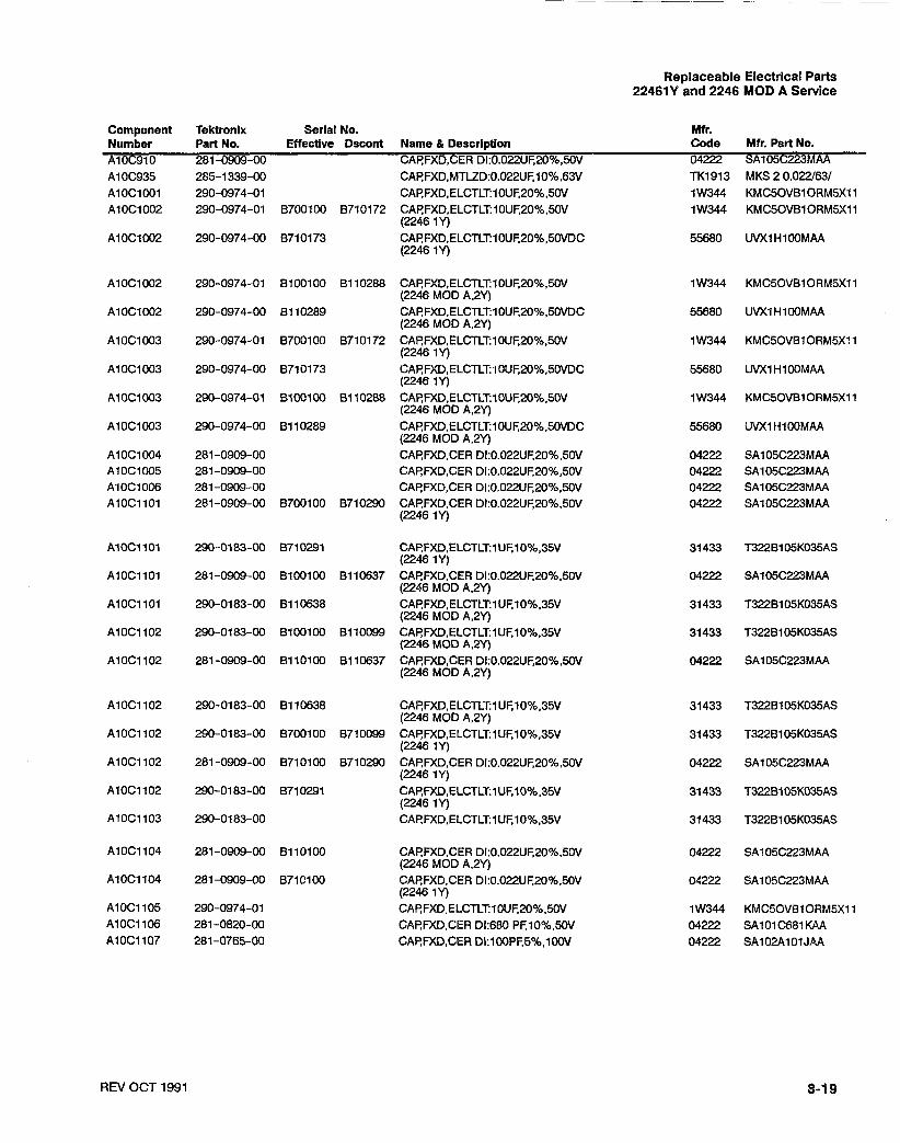
Replaceable Electrical Parts 2246111 and 2246 MOD A Service
Component Number A10C910 A1 0C935 AlOClOOl A1 0C1002
Tektronlx Serial No. Mfr. Part No. Effective Dscont Name & Description Code Mfr. Part No. 281-0909-00 CARFXD,CER DI:O.O22UF,20%,50V 04222 SA105C223MAA 285-1339-00 CAF!FXD,MTLZD:O.O22UF,10%.63V TK1913 MKS 2 0.022/63/ 290-0974-01 CAP,FXD,ELCTLTlOUF,20%,50V 1 W344 KMC50VB1 ORM5X1 1 290-0974-01 8700100 8710172 CARFXD,ELCTLTIOUF,20%,5OV 1 W344 KMC50VB1 ORM5X11
(2246 1Y) 290-0974-00 B710173 CARFXD,ELCTLT:I OUF,20%,50VDC 55680 UVXIH100MAA
(2246 1Y)
8100100 B110288 CARFXD,ELCTLT1OUF,20?4oo50V (2246 MOD A,2Y)
81 10289 CARFXD.ELCTLT1 OUF,20%,5OVDC (2246 MOD A.2Y)
8700100 8710172 CAP,FXD,ELCTLTIOUF,20%,50V (2246 1Y)
871 01 73 CAFIFXD,ELCTLTlOUF,20%,5OVDC (2246 1Y)
Bl00100 B1 10288 CAP,FXD,ELCTLT1OUF,2OO/oO5OV (2246 MOD A,2Y)
B110289 CA~FXD,ELCTLTlOUF,20%,50VDC (2246 MOD A.2Y)
A1 0C1004 A1 0C1005 A1 0C1006 AlOCllOl
AlOCllOl
AlOCllOl
290-0183-00 B710291 CAP,FXD,ELCTLTl UF. 1 0°A,35V (2246 1Y)
281-0909-00 8100100 81 10637 CARFXD,CER DI:O.O22UF,20%,50V (2246 MOD A,2Y)
290-0183-00 8110638 CARFXD,ELCTLTlUF,10%,35V (2246 MOD A,2Y)
290-0183-00 8100100 8110099 CAP,FXD,ELCTLT:l UF,10%,35V (2246 MOD A,2Y)
AlOCllOl
281-0909-00 8110100 81 10637 CARFXD,CER DI:O.O22UF,20%,50V (2246 MOD A,2Y)
290-0183-00 8110638 CARFXD,ELCTLT:lUF,l0%,35V 31 433 T3228105K035AS (2246 MOD A,2Y)
290-0183-00 8700100 8710099 CARFXD,ELCTLTlUF,10%,35V 31433 T3228105K035AS (2246 1Y)
281-0909-00 8710100 8710290 CARFXD,CERDl:O.O22UF,20%,50V 04222 SA105C223MAA (2246 1Y)
290-0183-00 8710291 CAP,FXD,ELCTLTlUF,lOYo,35V 31433 T322B105KO35AS (2246 1Y)
290-0183-00 CA~FXD,ELCTLTlUF,l0%,35V 31 433 T322B105KO35AS
281-0909-00 8110100 CARFXD.CER DI:O.O22UF,20%.50V (2246 MOD A,2Y)
281 -0909-00 871 01 00 CARFXD,CER DI:O.O22UF,20%.50V (2246 1Y)
290-0974-01 CARFXD,ELCTLTlOUF,20%,50V 281-0820-00 CARFXD,CER DI:680 PF,10%.50V 281-0765-00 CAP,FXD,CER DI:100PF,5%,100V
1W344 KMC50VB10RMSX11 04222 SA101 C681 KAA 04222 SA102At 01 JAA
REV OCT 1991

Replaceable Electrical Parts 22461Y and 2246 MOD A Service
Component Number A1 0C1108
Tektronix Serial No. M fr. Part No. Effective Dscont Name & Description Code 290-0183-00 B710630 CARFXD,ELCTLTlUF,l0%,35V 31433
(2246 1Y) 290-0183-00 B111186 CARFXD,ELCTLT:lUF,lO%,35V 31433
(2246 MOD A.2Y) 281 -0799-00 CARFXD,CER DI:62PF,2%,100V 04222 281-0799-00 CARFXD,CER DI:62PF,2%,100V 04222 290-0974-01 CAFFXD,ELCTLTl OUF,20%,50V 1 W344
Mfr. Part No. T322B105K035AS
AlOClllO AlOC1111 A10C1114
281 -0770-00 B111186 CARFXD,CER DI:1000PF,20%.100V 04222 (2246 MOD A,2Y)
CARFXD,CER DI:O.O22UF,20%,50V CARFXD,CER DI:O.O22UF,20%,50V
B110100 CARFXD,CER DI:O.O22UF,20%,50V (2246 MOD A)
B710100 CARFXD,CER DI:O.O22UF,20%,50V (2246 1Y)
81 20000 CApFXD,CER DI:2.2PF,200V (2246 MOD A,2Y)
8715000 CARFXD.CER DI:2.2PF,200V (2246 1Y)
B120000 CARFXD,CER DI:2.2PFS200V (2246 MOD A,2Y)
871 5000 CApFXD,CER DI:2.2PF,200V (2246 1Y)
281 -0909-00 CARFXD,CER DI:O.O22UF,20%,50V 04222 281 -0909-00 CARFXD,CER DI:O.O22UF,20%,50V 04222 281 -0064-00 BlOOl 00 B1 10099 CARVAR,PLASTIC:0.25-1.5PF,600V 52769
(2246 MOD A.2Y) 283-0348-00 B l 101 00 CARFXD,CER DI:O.SPF, + 1-0.1 PF.100V 51 642
(2246 MOD A.2Y) 281-0064-00 8700100 8710099 CAP,VAR.PLASTIC:0.25-1.5PF,600V 52769
(2246 1Y)
281-0771-00 CARFXD,CER DI:2200PF,20°h,200V 04222 281-0893-00 CARFXD,CER DI:4.7PF, +I-0.5PF,100VTUBULAR,MI 04222 281-0893-00 CARFXD,CER DI:4.7PF, + I-0.5PF.100VlllBULAR.Ml 04222 283-0057-00 B100100 81 19999 CARFXD,CER DI:O.lUF, + 80-20%,200V 04222
(2246 MOD A,2Y)
REV OCT 1991
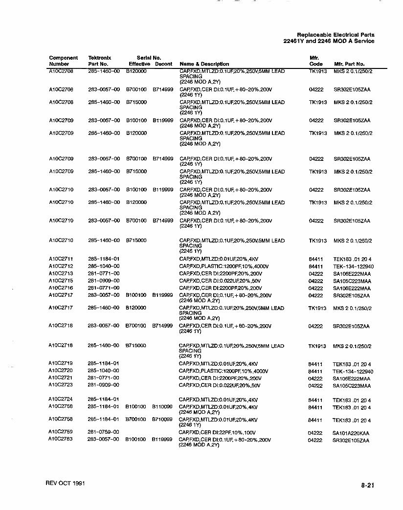
Replaceable Electrical Parts 2246111 and 2246 MOD A Service
Component Tektronix Serial No. Mtr. Number Part No. Effective Dscont Name & Description Code Mtr. Part No. A1 0C2708 285-1 460-00 81 20000 CARFXD,MTLZD:O.l UF,20%,250V,5MM LEAD TK1913 MKS 2 0.1/25012
SPACING (2246 MOD A.2Y)
A1 0C2708 283-0057-00 87001 00 871 4999 CARFXD.CER D1:O.l UF, + 80-20%,200V 04222 SR302E105ZAA (2246 1Y)
A1 0C2708 285-1 460-00 871 5000 CA~FXD,MTLZD:O.lUF,20%.25oV,5MM LEAD TK1913 MKS 2 0.1 125012 SPACING (2246 1Y)
AlOC2709 283-0057-00 BlOOlOO 81 19999 CARFXD,CER DI:O.lUF, + 80-20%,XH1V 04222 SR302E105ZAA (2246 MOD A,2Y)
A10C2709 285-1460-00 8120000 CARFXD,MTUD:O.I UF,20%,250V,5MM LEAD TK1913 MKS20.1/25012 SPACING (2246 MOD A,2Y)
A1 0C2709 285-1460-00 8715000 CARFXD,MTLZD:O.l UF,20%,250V,5MM LEAD TK1913 MKS 2 0.1 125012 SPACING (2246 1Y)
A10C2710 283-0057-00 8100100 8119999 CARFXD,CER DI:O.lUF, +80-20%,XX1V 04222 SR302E105ZAA (2246 MOD A,2Y)
A1 0'2271 0 285-1 460-00 61 20000 CARFXD,MTLZD:O.lUF,20%,250V,5MM LEAD TK1913 MKS20.1125012 SPACING (2246 MOD A,2Y)
A10C2710 283-0057-00 8700100 8714999 CARFXD.CER DI:O.lUF, + 80-20%,200V 04222 SR302E105ZAA (2246 1 Y)
871 5000 CARFXD,MTLZD:O.l UF.20%,250V,5MM LEAD SPACING (2246 1Y) CARFXD.MTLZD:O.O1UF,20%.4KV CAl?FXD,PIASTIC:1200PF,10%,4000V CAP,FXD.CER D1:2200PF,20%,200V CARFXD,CER DI:O.O22UF,20%,50V CARFXD,CER DI:2200PF,20%.200V
8100100 8119999 CARFXD,CER DI:O.lUF,+80-2O0h.200V (2246 MOD A,2Y) CAP,FXD,MTUD:O.l UF,20%,250V.5MM LEAD SPACING (2246 MOD A,2Y)
MKS 2 0.1 125012
MKS 2 0.1125012
A10C2718 285-1460-00 871 5000 CARFXD,MTLZD:0.lUF,209oO25oV,5MM LEAD TK1913 MKS20.1125012 SPACING
A1 0C2724 285-1 184-01 CARFXD,MTUD:O.OlUF,20%,4KV A10C2758 285-1 184-01 8100100 8110099 CARFXD,MTLZD:O.Ol UF,20°h,4W
(2246 MOD A,2Y) A10C2758 285-1 184-01 B700100 8710099 CARFXD.MTUD:O.Ol UF,2090,4W
(2246 1Y) A1 0C2759 281 -0759-00 CARFXD.CER DI:22PF,10%,110 04222 SAlOlA220KAA A10C2783 283-0057-00 8100100 81 19999 CARFXD,CER DI:O.lUF, + 80-20%.200V 04222 SR302E105ZAA
(2246 MOD A.2Y)
REV OCT 1991

Replaceable Eiectrical Parts 22461Y and 2246 MOD A Sewice
Component Number A1 0C2783
Tektronix Serial No. Part No. Effective Dscont Mame & Deocrlptiors
SPACING (2246 MOB A.2Y)
283-0057-00 87001 00 871 4999 CAEFXD,CEW D1:O.l UF, + 80-20%,20QV (2246 1Y)
285-1460-00 8715000 CAF!FXD,lWTLZD:O.l UF,20%,250V,5MM LEAD SPACING (2246 1 Y)
281 -0909-00 CARFXD,CER DI:O.O22UF,20%,50V
Mfr. Code Mtr. Part No. TK1913 MKS20.1125012
TK1913 MKS 2 0.1125012
283-0057-00 8100100 8119999 CAFIFXD,CER D1:O.f UE + 80-20%,200V (2246 MOD A.2Y)
285-1460-00 8120000 CAl?FXD,MTLZD:O.l UF,20O/o,250VV5MM LEAD SPAClNG (2246 MOD A,2Y)
283-0057-00 8700100 B714999 CAF!FXD,CERDI:O.lUF,+80-20%,20OV (2246 1Y)
285-1460-00 8715000 CAP,FXD,MTLZD:O.l UF,2OO/oO25OV,5MM LEAD SPACING (2246 1Y)
152-0246-00 SEMICOND DVC.DI:SW,S1.40V,20OMA,DO-7 152-0246-00 SEMICOND DVC,DI:SW,S1,40V,200MA,DO-7
04222 SR302E105ZAA
TK1913 MKS 2 0.1125012
152-0141-02 8100100 8119999 DIODE,SIG:.ULTRA FAST;40V,150MA,4NS,2PF (2246 MOD A,2\/E
152-1107-00 8120000 DIODE,SIG:SCHTKY;;40V,350MA,12PF (2246 MOD A,2Y)
152-0141-02 B700100 8714999 DIODE,SiG:,ULTRAFAST40V,l50MA,4NS,2PF (2246 1 Y)
152-1 107-00 8715000 D10DE,SlG:SCHTW,;40V,350MAA12PF (2246 1Y)
152-0141 -02 BlOOlOO B1 19999 DIODE.SIG:,ULTRA FAST;40V,150MA,4NS,2PF (2246 MOD A,2Y)
152-1107-00 8120000 DlOBE.SlG:SCHTKY;40V,35OMA,12PF (2246 MOD A,23
152-1107-00 8715000 DIODE,SiG:SCHTKY;;4OV,350MA,12PF (2246 1Y)
152-0066-00 DIODE,RECT,;400V,lA,30A IFSM
DIODE7RECT,;400V,1A,30A IFSM DIODE,SIG:,WC;30V,2.3PF@C25,C3/25 = 5.25 DIODE,SIG:,WC;30V,2.3PF@C25,C3125 = 5.25 DIODE,SIG:,ULTRA FAST;40V,150MA,4NS,2PF SEMICOND DVC,DI:SW,S1,40V,200MAADO-7
152-0061-00 8100100 8110099 SEMICOND DVC,DI:SW,S1,175V.OO1A,DO-35CD8393 (2245 MOD ~ , 2 3
152-0141-02 BllOl00 DIODE,SIG:,ULTRA FAST;40\1,150MA,4NS,2PF (2246 MOD A,2Y)
REV OCT 1991

Replaceable Electrical Parts 22461Y and 2246 MOD A Service
Component Number A1 0CR802
Tektronix Serial No. Mf r. Part No. Effective Dscont Name & Description Code Mfr. Part No. 152-0061 -00 B700100 B710099 SEMICOND DVC,DI:SW,S1,175V,O.1A,DO-35CD8393 12969 PV122
(2246 1Y) 152-01 41 -02 B710100 DIODE,SIG:,ULTRA FAST;40V,150MA,4NS,2PF 27014 FDH9427
(2246 1Y) 152-0141-02 B113047 DIODE.SIG:,ULTRA FAST;40V,150MA,4NS,2PF 27014 FDH9427
(2246 MOD A,2Y) 152-0141-02 B711085 DIODE,SIG:,ULTRA FAST;40V,15OMA,4NS,2PF 27014 FDH9427
(2246 1Y) 152-01 41 -02 81 13047 DIODE,SIG:,ULTRA FAST;40V,15OMA,4NS,2PF 27014 FDH9427
(2246 MOD A,2Y)
152-0141-02 8711085 DIODE,SIG:.ULTRA FAST;40V,150MA,4NS,2PF 27014 FDH9427 (2246 1 Y)
152-0061 -00 BlOOlOO B1 10099 SEMICOND DVC,DI:SW,S1,175V,O.lA,DO-35CD8393 12969 W122 (2246 MOD A,2Y)
152-0061-00 B700100 8710099 SEMICOND DVC.DI:SW,S1,175V,O.1A.DO-35CD8393 12969 W122 (2246 1Y)
152-0141-02 DIODE.SIG:,ULTRA FAST40V,150MA,4NS,2PF 2701 4 FDH9427 152-0141-02 DIODE,SIG:,ULTRA FAST40V,150MA,4NS,2PF 27014 FDH9427
DIODE,RECT.FAST RCVRY;400V,lA,200NS 14552 MB2501 DIODE,RECT,FAST RCVRY;400V,lA,200NS 14552 MB2501 DELAY LINE,ELEC: WlSTRAlNRELlEF 80009 119211901 LAMP,INCAND:14V,80MA,73E,WEDGE BASE S3774 0L-2182-01 LAMP,INCAND:14V,80MA,73E,WEDGE BASE 53774 0L-2182-01
LAMP,INCAND:14V,80MA,73E,WEDGE BASE S3774 OL-2182-01 LAMP,GLOW:90V MAX,0.3MA,AID-T.WIRE LD TKO21 3 JH00513011 JA LAMP,GLOW:WV MAX,0.3MA8AID-P.WIRE LD TKO21 3 JH00513011 JA LAMP,GLOW:WV MAX.O.3MA.AID-T,WIRE LD TKO213 JH085/3011JA LAMFIGLOW.WV MAX,0.3MA,AID-TWIRE LD TKO213 JH00513011JA
REV OCT 1991

Replaceable Electrical Parts 22461Y and 2246 MOD A Service
Component Number AlOJll
Tektronix Serial No. Mfr. Part No. Effective Dscont Name & Description Code Mfr. Part No.
131 -3731 -00 CONN,RF JACK:BNC,;SO 0HM.FEMALE.STR.SLDR 24931 28JR377-1 CUPIFRONT PNL,0.5-28 WID FLAT1.062 L X 0.188
131 -3731 -00 CONN,RF JACK:BNC,;50 OHM.FEMALE,STR,SLDR 24931 28JR377-1 CUPIFRONT PNL.0.5-28 W/D FLAT1.062 L X 0.188
131-3731-00 CONN,RF JACK:BNC,;5O OHM,FEMALE,STR,SLDR 24931 28JR377-1 CUPIFRONT PNL.0.5-28 W/D FLAT1.062 L X 0.188
CONN,RF JACK:BNC,;50 OHM,FEMALE,STR,SLDR 24931 28JR377-1 CUPIFRONT PNL,0.5-28 WID FLAT1.062 L X 0.188 C0NTACTELEC:BRASS TK1935 ORDER BY DESC
131-2921-00 Bl00lOO B1 10099 CONN,HDR:PCB,;MALE,RTANG,2 X 1.0.1 CTR, 00779 1-86479-3 0.318 MLG X 0.110 TAIL,0.238 H.30 GOLD (2246 MOD A.2Y)
131 -4546-00 B l 101 00 CONN,HDR:PCB,;MALE.STR.l X 2,O.l CTR,0.230 00779 103239-2 MLG X 0.120 TAIL30 GOLD (2246 MOD A,2Y)
131-2921-00 B700100 8710099 CONN,HDR:PCB,;MALE,RTANG,2 X 1.0.1 CTR, 00779 1-86479-3 0.318 MLG X 0.1 10 TAIL.0.238 H.30 GOLD (2246 1Y)
131 -4546-00 871 01 00 CONN,HDR:PCB,;MALE,STR,l X 2,O.l CTR,0.230 00779 103239-2 MLG X 0.120 TAIL.30 GOLD (2246 1Y)
CONN,BOX PWR:PCB,;FEMALE.STR,l X 13.0.156 27264 09-62-3132 CTR.0.450 H X 0.160 TAIL,BOlTOM ENTRY20 GOLD.0.156 X 0.125 CTR PCB
RELAY,ARMATURE:l FORM C,12VDC TK1689 DS1 EMDC12V-HI66 RELAY,ARMATURE:l FORM C.12VDC TK1689 DS1 EMDC12V-HI66 RELAY.ARMATURE:l FORM C,INSERT LOSS 0.3 TK1689 RK1 EDC12V DB@SOOMHZ,VSWR 1.5@900MHZ,COIL 12VDC 720 OHM,CONTACT 30VDC 0.5A 10W.PKG .795 X .441
RELAY,ARMATURE:l FORM C,INSERT LOSS 0.3 TK1689 RK1 EDC12V DB@SOOMHZ,VSWR 1.5@900MHZ,COIL 12VDC 720 OHM,CONTACT 30VDC 0.5A 10W.PKG .795 X .441
RELAY;ARMATURE:l FORM C,12VDC TK1689 DS1 EMDC12V-HI 66
RELAYARMATURE:l FORM C,12VDC RELAYARMATURE:l FORM C.12VDC RELAY,ARMATURE:l FORM C,12VDC REU4YARMATURE:l FORM C,INSERT LOSS 0.3 TK1689 RK1 EDC12V DB@900MHZ,VSWR 1.5@900MHZ,COIL 12VDC 720 OHM,CONTACT 3OVDC 0.5A 10W,PKG .795 X .441
AlOKllO RELAYARMATURE:l FORM C,INSERT LOSS 0.3 TK1689 RK1 EDC12V DB@SOOMHZ,VSWR 1.5@900MHZ,COIL 12VDC 720 OHM,CONTACT 3OVDC 0.5A 10W,PKG .795 X .441
RELAY,ARMATURE:l FORM C,12VDC RELAY,ARMATURE:l FORM C.12VDC INDUCTOR.FIXED:33UH,10%,1.8A INDUCTOR,FIXED:33UH.10%,1.8A COIL,RF:FIXED,6"IH
AlOKl l l A10K112 AlOLlOl A10L102 A1 OL130
OJR03 108-0682-00 54583 TSL1110-330K 1 R 91637 IR-2.330 MICRO 91637 IR-2.330 MICRO 54583 SPT0305-2R2K
REV OCT 1991
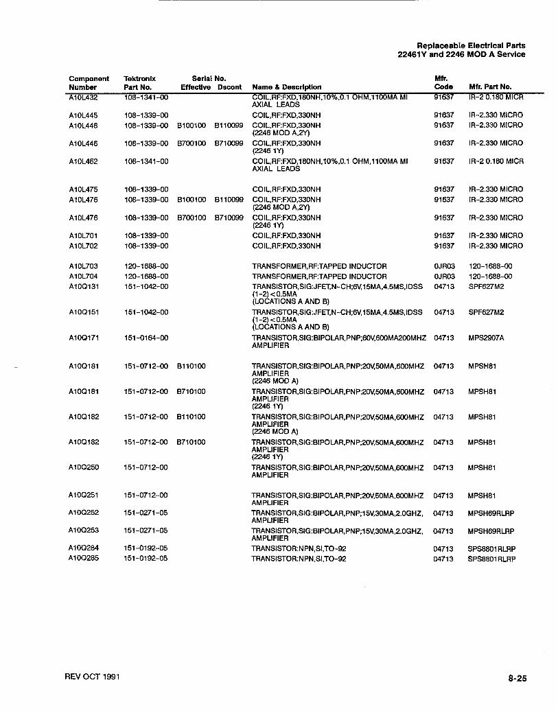
Replaceable Electrical Parts 22461Y and 2246 MOD A Service
Component Tektronlx Serial No. Mf r. Number Part No. Effective Dscont Name & Description Code Mfr. Pert No. A10L432 108-1341 -00 COIL,RF:FXD,18ONH,10~,OO1 OHM.1100MA MI 91637 IR-2 0.180 MlCR
AXIAL LEADS A10L445 108-1339-00 COIL,RF:FXD,33ONH 91637 IR-2.330 MICRO A1 0L446 108-1339-00 B100100 B110099 CQIL,RF:FXD,330NH 91637 IR-2.330 MICRO
(2246 MOD A.2Y) A10L446 108-1 339-00 87001 00 B710099 COIL,RF:FXD,33ONH 91637 IR-2.330 MICRO
(2246 1Y) A10L462 108-1341 -00 COIL,RF:FXD,180NH,10%,0.1 OHM,1100MA MI 91637 IR-2 0.180 MlCR
AXIAL LEADS
A1 0L475 108-1 339-00 COIL,RF:FXD,330NH A10L476 108-1339-00 BlOOlOO B110099 COIL,RF:FXD,330NH
(2246 MOD A,2Y) A10L476 108-1 339-00 B700100 871 0099 COIL,RF:FXD,33ONH
(2246 1Y) AlOL701 108-1339-00 COIL,RF:FXD,33ONH A1 OL702 108-1339-00 COIL,RF:FXD,33ONH
91637 IR-2.330 MlCRO 91637 IR-2.330 MlCRO
91637 IR-2.330 MlCRO
91637 IR-2.330 MlCRO 91637 IR-2.330 MlCRO
TRANSFORMER.RF:TAPPED INDUCTOR OJR03 120-1688-00 TRANSFORMER,RF:TAPPED INDUCTOR OJR03 120-1 688-00
A10Q131 151-1042-00 TRANSISTOR,SIG:JFET.N-CH;6V,15MA,4.5MS.IDSS 04713 SPF627M2 (1 -2) < 0.5MA (LOCATIONS A AND B)
A10Q171 151 -01 64-00 TRANSISTOR,SIG:BIPOlARRPNP;6oV,600MA200MHZ 04713 MPS2907A AMPLIFIER
A10Q181 151-0712-00 BllOl00 TRANSISTOR,SIG:BIPOlARRPNP;20V,50MA,600MHZ 04713 MPSH81 AMPLIFIER (2246 MOD A)
A10Q181 151 -071 2-00 871 01 00 TRANSISTOR,SIG:BIPOlAR,PNP;20V,50MA,600MHZ 04713 MPSH81 AMPLIFIER (224'3 1Y)
A10Q182 151-0712-00 B l lO l 00 TRANSISTOR,SIG:BIPOlAR,PNP;20V,50MA,600MHZ 04713 MPSH8l AMPLIFIER (2246 MOD A)
A10Q182 151-0712-00 B710100 TRANSISTOR.SIG:BIPOlARRPNP;20V.50MA,600MHZ 04713 MPSH8l AMPLIFIER (2246 1Y)
A1 0Q250 151 -071 2-00 TRANSISTOR,SIG:BIPOlAR,PNP;20V.50MA,600MHZ 04713 MPSH81 AMPLIFIER
A10Q251 151 -071 2-00 TRANSISTOR.SIG:BIPOLAR,PNP;20V.50MA,600MHZ 04713 MPSH81 AMPLIFIER
A1 0Q252 151-0271-05 TRANSISTOR,SIG:BIPOlARRPNP;15V,30MA,2.0GHZ, 04713 MPSH69RLRP AMPLIFIER TRANSISTOR,SIG:BIPOlAR,PNP;15V,30MA,2.OGHZ, 04713 MPSH69RLRP AMPLIFIER TRANSISTOR:NPN,SI,TO-92 04713 SPS8801 RLRP TRANSISTOR:NPN,SI,TO-92 04713 SPS8801 RLRP
REV OCT 1991

Replaceable Electrical Parts 22461Y and 2246 MOD A Service
Component Tektronix Serial No. Mfr. Number Part No. Effective Dscont Name & Description Code Mfr. Part No. A10Q301 151 -0254-03 TRANSISTOR.SIG:BIPOLARRNPN~30V.50OMA. OJR04 MPSA14. TPE2
125MHZ,AMPLIFIER,DARLlNGTON A10Q302 151 -01 88-00 TRANSISTOR,SIG:BIPOLARRPNP;40V,200MA, 04713 2N3906
250MHZ,AMPLIFIER
A10Q303 151-0188-00 TRANSISTOR.SIG:BIPOLARRPNP;40V,200MA, 04713 2N3906 250MHZ,AMPLIFIER
REV OCT 1991
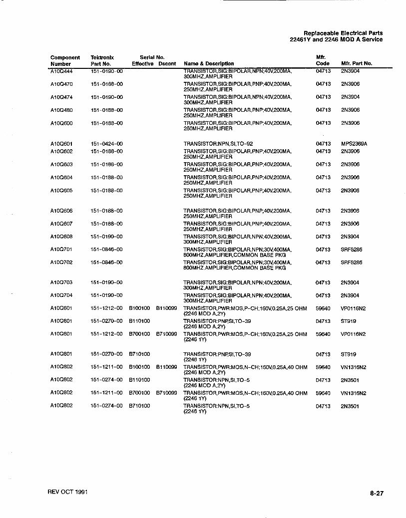
Replaceable Electrical Parts 22461Y and 2246 MOD A Service
Component Number A10Q444
Tektronix Serial No. Mf r. Part No. Effective Dscont Name & Description Code Mfr. Part No. 151 -01 90-00 TRANSISTOR,SIG:BIPOLAR,NPN~40V,2OOMA, 04713 2N3904
300MHZ,AMPLIFIER 151 -01 88-00 TRANSISTOR,SIG:BIPOLAR,PNP;40V,200MA, 04713 2N3906
25OMHZ,AMPLIFIER
151 -01 90-00 TRANSISTOR,SIG:BlPOLAR,NPN;40V,200MA, 04713 2N3904 300MHZ,AMPLIFIER
151-0188-00 TRANSISTOR,SIG:BIPOLAR,PNP;40V,2OOMA, 04713 2N3906 250MHZ.AMPLIFIER
151-0188-00 TRANSISTOR,SIG:BlPOLAR,PNP;40V,20OMA, 04713 2N3906 250MHZ,AMPLIFIER
151 -01 90-00 TRANSISTOR,SIG:BIPOLAR,NPN;40V,200MA, 04713 2N3904 300MHZ,AMPLIFIER
151 -0846-00 TRANSISTOR.SIG:BIPOLARRNPN;30V,400MA, 04713 SRF5286 800MHZ.AMPLIFIER.COMMON BASE PKG
151-0846-00 TRANSISTOR,SIG:BIPOLAR,NPN;30V,400MA, 04713 SRF5286 800MHZ,AMPLIFIER,COMMON BASE PKG
151 -0190-00 TRANSISTOR,SIG:BIPOLAR,NPN;40V,200MA, 04713 2N3904 300MHZ.AMPLIFIER
151-0190-00 TRANSISTOR,SIG:BIPOLARRNPN~40V,200MA. 04713 2N3904 300MHZ,AMPLIFIER
151 -1212-00 BlOOlOO B1 10099 TRANSISTOR,PWR:MOS,P-CH;16OVVO.25A,25 OHM 59640 VP0116N2 (2246 MOD A,2Y)
151-0270-00 BllOlOO TRANSISTOR:PNF!SI.TO-39 04713 ST919 (2246 MOD A,2Y)
151 -1212-00 8700100 8710099 TRANSISTOR,PWR:MOS,P-CH;160V,0.25A,25 OHM 59640 VP0116N2 (2246 1Y)
151 -121 1-00 BlOOlOO B1 10099 TRANSISTOR,PWR:MOS.N-CH;16OV,0.25A,40 OHM 59640 VN1316N2 (2246 MOD A,2Y)
151 -0274-00 B l 10100 TRANSISTOR:NPN,SI,TO-5 (2246 MOD A,2Y)
REV OCT 1991

Replaceable Electrical Parts 22461Y and 2246 MOD A Service
Component Tektronlx Serial No. Mf r. Number Part No. Effective Dscont Name & Description Code Mfr. Part No. A10Q803 151 -0736-00 81 001 00 81 10099 TRANSISTOR:NPN,SI,TO-92 OJR04 2N4401
(2246 MOD A,2Y) A1 0Q803 151-0190-00 8110100 TRANSISTOR,SIG:BIPOLAR,NPN;40V,200MA, 04713 2N3904
300MHZ.AMPLIFIER (2246 MOD A,2Y)
A1 0Q803 151 -0736-00 B700100 8710099 TRANSISTOR:NPN.SI,TO-92 OJR04 2N4401 (2246 1Y)
A1 0Q803 151-0190-00 8710100 TRANSISTOR,SIG:BIPOLARRNPN;40V,200MA. 04713 2N3904 300MHZ.AMPLIFIER (2246 1Y)
A1 0Q804 151-0712-00 8100100 8110099 TRANSISTOR,SIG:BIPOLAR,PNP;20V,50MA,600MHZ 04713 MPSH81 AMPLIFIER (2246 MOD A.2Y)
TRANSISTOR,SIG:BIPOLARRNPN;40V,200MA, 04713 2N3904 300MHZ,AMPLIFIER (2246 MOD A.2Y)
A1 0Q804 151-0712-00 8700100 8710099 TRANSISTOR,SIG:BIPOLAR,PNP;20V.50MA,600MHZ 04713 MPSH81 AMPLIFIER (2246 1Y)
(2246 1Y) A1 0Q805 151-1211-00 Bl00lOO 8110099 TRANSISTOR,PWR:MOS,N-CH;160V,O.25A,40OHM 59640 VN1316N2
(2246 MOD A,2Y) A10Q805 151 -0270-00 8110100 TRANSISTOR:PNP.SI,TO-39 04713 ST919
(2246 MOD A,2Y)
A1 0Q805 151-121 1-00 8700100 8710099 TRANSISTOR,PWR:MOS,N-CH;160V,0.25A,40 OHM 59640 VN1316N2 (2246 1Y)
A10Q805 151 -0270-00 871 01 00 TRANSISTOR:PNl?Sl,TO-39 04713 ST919 (2246 1Y)
A1 OQ806 151-1212-00 8100100 8110099 TRANSISTOR,PWR:MOS,P-CH;160VV0.25A,25OHM 59640 VP0116N2 (2246 MOD A,2Y)
A1 0Q806 151-0274-00 BllOlOO TRANSISTOR:NPN,SI,TO-5 04713 2N3501 (2246 MOD A,2Y)
A10Q806 151-1212-00 8700100 B710099 TRANSISTOR,PWR:MOS.P-CH;160V,0.25A,25 OHM 59640 VP0116N2 (2246 1Y)
A10Q808 151-0711-00 8100100 8110099 TRANSISTOR.SIG:BIPOLARRNPN;25V,50MA,650MHZ 04713 MPSHlO AMPLIFIER (2246 MOD A,2Y)
A10Q808 151-0711-00 8700100 B710G99 TRANSISTOR,SIG:BIPOLAR,NPN;25V,50MA,650MZ 04713 MPSHlO AMPLIFIER (2246 1Y)
A1 00809 151-0711-00 TRANSISTOR,SIG:BIPOLAR,NPN;25V,50MA,650MHZ 04713 MPSH10 AMPLIFIER
REV QCT 1991

Replaceable Electrical Parts 22461Y and 2246 MOD A Service
Component Tektronix Serial No. Mfr. Number Part No. Effective Dscont Name & Description Code Mfr. Part No. A1 0Q810 151 -071 1-00 TRANSISTOR,SIG:BIPOLAR,NPN;25V,50MA,650MHZ 04713 MPSHlO
AMPLIFIER
~ ~ ~ M H Z . A M P ~ I F I E R (2246 MOD A,2Y)
A10Q812 151 -0220-00 B l 101 00 TRANSISTOR,SIG:BlPOLAR,PNP;40V,200MA. 2D532 PTBTCl O5BK 400MHZ,AMPLIFIER (2246 MOD A.2Y)
A10Q812 151 -0220-00 8710100 TRANSISTOR,SIG:BIPOLAR,PNP;40V,200MA, 2D532 PTBTCl O5BK 400MHZ,AMPLIFIER (2246 1Y)
SPS8801 RLRP MPS6523RLRP
SPS8801 RLRP M PS6523RLRP
SPS8801 RLRP MPS2907A
2N4401 2N4401 SPS8801 RLRP 2N3904
TRANSISTOR,SIG:BIPOLAR,PNP;12V,80MA, SWITCHING
MPS3640
2N5551 RLRP (AM
TO BE ASSIGNED
REV OCT 1991

Replaceable Electrical Parts 22461Y and 2246 MOD A Servlce
Component Number A1 0Q2715
Tektronlx Serlal No. Part No. Etlectlve Dscont Name & DescrlpUon 151 -0190-00 TRANSISTOR.SIG:~IPOLAR,NPN;40V,20OMA,
300MHZ.AMPLIFIER 31 3-1822-00 RES,FXD,FILM:8.2K,OHM,5%,0.2W 313-1822-00 RES,FXD,FILM:8.2K,OHM,5%,0.2W 31 3-1 822-00 RES,FXD,FILM:8.2K,OHM,5%,0.2W 31 3-1 822-00 RES,FXD.FILM:8.2K,OHM,5%,0.2W
Mfr. Code 04713
Mtr. Part No. 2N3904
RES,FXD,FILM:20 OHM,5%,0.2W RES,FXD,FILM:lO OHM,5%,0.2W RES,FXD,FILM:75 OHM.1%,0.2W,TC =TO RES,FXD,FILM:62 OHM,5%,0.25W RES,FXD,FILM:20 OHM,5%,0.2W RES,FXD,FILM:lO OHM,5%.0.2W RES,FXD,FILM:75 OHM,1%,0.2W,TC = TO
6100100 6119999 RES,FXD,FlLM:39 OHM,5%,0.25W (2246 MOD A.2Y)
31 5-0620-00 61 20000 RES,FXD,FILM:62 OHM,5%.0.25W (2246 MOD A.2Y)
315-0390-00 6700100 6714999 RES,FXD,FILM:39OHM,5%,0.25W (2246 1Y)
31 1-2224-00 RES,VAR,NONWW:TRMR,20 OHM,20%.0.5W LINEAR
322-3056-00 RES,FXD,FILM:37.4 OHM.l%.0.2W,TC =TOMI 315-0390-00 6100100 6119999 RES,FXD,FILM:39 OHM,5%,0.25W
(2246 MOD A,2Y) 31 5-0620-00 81 20000 RES,FXD,FILM:62 OHM,5%,0.25W
(2246 MOD A.2Y) 315-0390-00 8700100 B714999 RES.FXD,FILM:39OHM,5%,0.25W
(2246 1Y)
R R I OCT 1991

Replaceable Electrical Parts 22461Y and 2246 MOD A Service
Component Number A10R151
TeMronix Serial No. Mf r. Part No. Effective Dscont Name IE Description Code Mfr. Part No. 31 5-0620-00 871 5000 RES,FXD,FILM:62 OHM,5%,0.25W TK1727 SFR252322-181-
(2246 1Y) 322-3443-00 RES,FXD,FILM:402K OHM,1%,0,2W,TC=TOMI 91 637 CCF5Ol G40202F 322-3443-00 RES,FXD,FILM:402K OHM,l0h,0.2W,TC=TOMl 91 637 CCF501 G40202F 322-341 4-00 RES,FXD,FILM:200K OHM,1%,0.2W,TC=TOMI 91 637 CCF501 G20002F 31 3-1 100-00 RES,FXD,FILM:lO OHM,5%,0.2W 91637 CCF50-2-10ROOJ
RES.FXD,FILM:8.87K OHM,I %.0.2W,TC =TOMI 91637 CCF501 G88700F RES,FXD,FILM:1.78K OHM,? %.0.2W,TC=TO 91637 CCF501G17800F RES,FXD,FILM:I.SK OHM,1%,0.2W,TC=TO 91637 CCF501 G15000F RES,FXD,FILM:75 OHM,1%,0.2W,TC=TO 91 637 CCFMl G75ROOF RES,FXD,FILM:75 OHM,1%,0.2W,TC=TO 91 637 CCF501 G75ROOF
RES,VAR,NONWW:TRMR,20 OHM.20%,0.5W TK2073 GF06UT2 200 M L LINEAR RES,FXD,FILM:37.4 OHM,1%,0,2W,TC=TOMI 91637 CCF50-2F37R40F RES,FXD,FILM:470 OHM,5%,0.2W 91637 CCF50-2-470ROJ RES.FXD,FILM:200K,5%,0.2W 91 637 CCF50-2-20002J RES,FXD,FILM:lOK OHM,5%,0.2W 91637 CCF50-2-10001 J
308-0058-00 RES.FXD,WW:I .5 OHM,lO%,I W 75042 SP-20-1 R500K 313-1512-00 BllOlOO RES,FXD,FILM:S.lK OHMS5%.0.2W 91 637 CCF50-2-51 000J
(2246 MOD A,2Y) 313-1 512-00 8710100 RES,FXD,FILM:S.l K OHMS5%,0.2W 91637 CCF50-2-5100OJ
(2246 1Y) 313-1512-00 8110100 RES.FXD,FILM:5.1 K OHM,5%,0.2W 91637 CCF50-2-51 OOOJ
(2246 MOD A,2Y) 313-1512-00 B710100 RES.FXD,FILM:5.1 K OHM,5%.0.2W 91637 CCF50-2-51000J
(2246 1Y)
31 1-2329-00 BlOOlOO 8110099 RES,VAR,NONWW:TRIMMER,5K OHM,10% 32997 3386R-EA5-502 (2246 MOD A,2Y)
31 1-2454-00 Bl 10100 81 19999 RES,VAR,NONW:TRMR,5K OHM,20%,0.5W,LOG 32997 3362U-EP6-502R (2246 MOD A,2Y)
311-2232-00 8120000 RES,VAR,NONW:TRMR,2K OHM.20%,0.5W TK2073 GF06UT2 202 M L LINEAR (2246 MOD A,2Y)
REV OCT 1994

Replaceable Electrical Parts 22461Y and 2246 MOD A Service
Component Tektronix Serial No. Number Part No. Effective Dscont Name & Descri~Uon
Mfr. Code Mfr. Part No. 32997 3386R-EA5-502
A10R211 31 1-2454-00 871 0100 871 4999 RES,VAR,NONWW:TRMR,5K OHM,20%,0.5W,LOG (2246 1Y)
A1 OR21 1 31 1-2232-00 871 5000 RES,VAR,NONW:TRMR,2K OHM,20%,0.5W LINEAR (2246 1Y)
A10R215 313-1821-00 RES,FXD,FILM:820 OHM,5%.0.2W A10R216 313-1103-00 8120000 RES,FXD.FILM:lOK OHMS5%,0.2W
(2246 MOD A,2Y)
A10R217 313-1472-00 8120000 RES,FXD,FILM:4.7K OHM,5%,0.2W (2246 MOD A,2Y)
A10R218 322-3237-00 RES,FXD,FILM:2.87K OHM,1%.0.2W,TC=TOMI A10R219 313-1103-00 RES,FXD,FILM:lOK OHM,5%.0.2W A10R220 313-1331-00 RES,FXD,FILM:330 OHM,5%,0.2W A1 OR221 31 1-2329-00 8100100 81 10099 RES,VAR,NONWTRIMMER,5K OHM,10%
(2246 MOD A.2Y)
A10R221 31 1-2454-00 81 10100 8119999 RES.VAR,NONWTRMR.5K OHM,20%,0.5W,LOG (2246 MOD A,2Y)
A10R221 311-2232-00 8120000 RES,VAR,NONWTRMR,2K OHM,20%,0.5W LINEAR (2246 MOD A,2Y)
A1 OR221 31 1-2232-00 871 5000 RES,VAR,NONW:TRMR,2K OHM,20%,0.5W LINEAR (2246 1Y)
RES,FXD,FILM:4.7K OHM,5%,0.2W RES.FXD,FILM:2.87K OHM,1%,0.2W.TC=TOMl RES,FXD,FILM:100K OHM,5Oh.0.2W RES,FXD,FILM:330 OHM,5%,0.2W
81 001 00 81 10099 RES,VAR,NONWW:TRIMMER,5K OHM.10% (2246 MOD A.2Y)
REV OCT 1991

Replaceable Electrical Parts 22461Y and 2246 MOD A Service
Component Tektronix Serial No. Number Part No. Effective Dscont Name & DescripUon
Mfr. Code Mfr. Part No.
A10R231 I (2246 MOD A,2Y)
AlOR231 311-2232-00 B120000 RES,VAR,NONW:TRMR,2K OHM,20%,0.5W TK2073 GF06UT2 202 M L LINEAR (2246 MOD A,2Y)
A10R231 31 1-2232-00 871 5000 RES,VAR,NONW:TRMR,2K OHM,20°/',0.5W TK2073 GF06UT2 202 M L LINEAR
A10R241 31 1-2329-00 B100100 B110099 RES,VAR,NONWW:TRIMMER,5K OHM,10% 32997 3386R-EA5-502 (2246 MOD A,2Y)
A10R241 311-2454-00 BllOl00 B119999 RES,VAR,NONW:TRMR,5KOHM,20%,0.5W.LOG 32997 3362U-EP6-502R (2246 MOD A,2Y)
A10R241 311-2232-00 8120000 RES,VAR,NONW:TRMR,2K OHM,20°h,0.5W TK2073 GF06UT2 202 M L LINEAR (2246 MOD A.2Y)
A10R241 311-2329-00 8700100 8710099 RES,VAR.NONW:TRIMMER,5K0HM,1O0/o 32997 3386R-EA5-502 (2246 1Y)
A1 OR241 311-2232-00 8715000 RES,VAR,NONWTRMR,2K OHM,20%,0.5W TK2073 GF06UT2 202 M L LINEAR (2246 1Y)
A10R242 313-151 1-00 RES,FXD,FILM:510 OHM,5%,0.2W 91637 CCF50-2-51OROJ A10R243 313-1 243-00 RES.FXD8FILM:24K OHM,5%.0.2W 57668 CCF50-1 -G2402J A10R244 322-3285-00 RES,FXD,FILM:9.09K OHM,1°/o,0.2W.TC =TOMI 91 637 CCF501 G90900F
A1 OR245 313-1027-00 RES.FXD,FILM:2.7 OHM,5%,0.2W 57668 TR20JE 02E7 A1 0 R248 322-3237-00 RES,FXD,FILM:2.87K OHM,1 %,0.2W,TC=TOMl 91 637 CCF501 G28700F A10R249 313-1027-00 B120000 RES,FXD,FILM:2.7 OHM,5%,0.2W 57668 TR20JE 02E7
(2246 MOD A,2Y)
A1 OR250 307-0792-00 BlOOlOO 8119999 RES NTWK,FXD,FI:7,82 OHM,2%,0.15W EACH 91637 MSW8A01820G OR (2246 MOD A,2Y)
A10R250 307-0792-00 B700100 8714999 RES NTWK,FXD,Fl:7,82 0HM,2%,0015W EACH 91637 MSP08A01820G OR (2246 1Y)
A10R251 307-0792-00 81001 00 B1 19999 RES NTWK,FXD,FI:7,82 OHM,2%,0.15W EACH 91637 MSP08A01820G OR (2246 MOD A,2Y)
A10R251 307-0792-00 8700100 8714999 RES NTWK,FXD,FI:7,82 OHM,2%,0.15W EACH 91637 MSP08A01820G OR (2246 1Y)
A10R254 322-331 8-00 RES,FXD,FILM:ZOK OHM,1%,0.2W,TC =TO 91 637 CCF5Ol G20001 F A10R255 322-3318-00 RES,FXD,FlLM:'K)K OHM,1°h,0.2W,TC =TO 91637 CCF501 G20001 F
REV OCT 1991
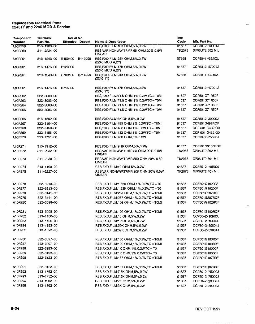
Replaceable Electrical Parts 22461Y and 2246 MOD A Service
Mfr. Code Mfr. Part No.
TK2073 GF06UT2 502 M L
Component Tektronix Serial No. Number Part No. Effective Dscont Name & Description A1 OR256 31 3-1 103-00 RES,FXD,FILM:lOK OHM85%,0.2W A10R260 311-2234-00 RES,VAR,NONWMI:TRMR,5K OHM,20%,0.5W
LINEAR A10R261 313-1243-00 8100100 81 19999 RES,FXD,FILM:24K OHM,5%,0.2W
(2246 MOD A,2Y) A10R261 313-1473-00 8120000 RES,FXD,FILM:47K OHM,5%,0.2W
(2246 MOD A,2Y) A10R261 313-1243-00 8700100 B714999 RES,FXD,FILM:24K OHM,5%,0.2W
(2246 1Y)
91637 CCF50-2-30000J 91637 CCF501 G499ROF 91637 CCF 501 G432 QO 91637 CCF 501 G432 QO 91637 CCF50-2-750ROJ
RES,FXD,FILM:9.1K OHM,5%,0.2W RES,VAR,NONWW:TRMR72K OHM,20%.0.5W LINEAR RES,VAR,NONWWTRMR,500 OHM,20%,0.50 LINEAR RES,FXD,FILM:lO OHM,5%,0.2W RES,VAR,NONWW:TRMR,100 OHM,20%.0.5W LINEAR
REV OCT 1991

Replaceable Electrical Parts 22461Y and 2246 MOD A Service
Component Number A10R296 A1 OR297 A10R298 A10R299 A10R301
Serial No. Mfr. Effective Dscont Name & Description Code Mfr. Part No.
RES,FXD,FILM:162 OHM,1%,0.2W,TC =TOMI 91637 CCF501 G162ROF RES,FXD,FILM:lO OHM,5%,0.2W 91637 CCF50-2-10R00J RES,FXD,FILM:2.7 O#M,5%,0.2W 57668 TR20JE 02E7 RES,FXD,FILM:~~~K,~YO,O.~W 91 637 CCF50-2-20002J RES.FXD,FILM:I K OHM,5%,0.2W 91 637 CCF50-2-1OOOOJ
RES,FXD.FILM:lO OHM,5%,0.2W 91 637 CCF50-2-1 OROOJ RES NTWK.FXD,FI:REF VOLTAGE DIVIDER 80009 307213200 RESSFXD,FILM:28.7K OHM,0.2W8.5% 91 637 CCF501 D28701 D RES,FXD,FILM:47 OHM,5%,0.2W 91637 CCF50-2-47R00J RES,FXD,FILM:27 OHM 5%,0.2W 91637 CCF50-2-27ROOJ
RES,FXD,FILM:100 OHM,5%,0.2W 91637 CCF50-2-100ROJ RES,FXD,FILM:680 OHM,5%,0.2W 91 637 CCF50-2-680ROJ RES,FXD,FILM:5.6K OHM,5%,0.2W 91 637 CCF50-2-5600OJ RES,FXD,FILM:47 OHM,5%,0.2W 91637 CCF50-2-47ROOJ RES NTWK,FXD,FI:RESISTOR NETWORK 80009 307213300

Replaceable Electrical Parts 22461 Y and 2246 MOD A Senrice
Component Tektronlx Serial No. Mfr. Number Part No. Eftectlve Dscont Name & Descrlptlon Code A1 0 R343 313-1162-00 RES.FXD,FILM:1.6K OHM,5%,0.2W 91 637 A1 OR344 313-1332-00 RES,FXD,FILM:3.3K OHM,5%,0.2W 91 637 A10R345 313-1 100-00 RES,R(D,FILM:lO OHM,5%,0.2W 91 637 A10R346 313-1101-00 RES,FXD,FILM:100 OHM,5%.0.2W 91 637 A10R347 31 3-1 202-00 RES,FXD,FILM:2K OHM,5%,0.2W 91637
A10R348 322-31 93-00 RES,FXD,FILM:lK OHM,1%.0.2W.TC=TO 91 637 A1 OR349 322-3193-00 RES,FXD,FILM:l K OHM,1 %,O.PW,TC= TO 91637 A10R350 307-0540-00 RES NTWK,FXD,FI:(5)1 K OHM,2%,0.7W 1 1236 A10R351 315-01 55-00 BlOOl00 B100823 RES,FXD,FILM:l.BM QHM,5%,0.25W TK1727
(2246 MOD A,2Y) A10R352 322-3193-00 RES,FXD,FILM:lK OHM,1%,0.2W,TC=TO 91 637
RES,FXD,FILM:1.5K OHM,5%,0.2W 91637 RES,FXD,FILM:100 OHM,5%,0.2W 91637 RES,FXD,FILM:680 OHM.5%,0.2W 91 637 RES,FXD,FILM:5.6K OHM,5%,0.2W 91 637 RES NTWK,FXD,FI:@)l K OHM.2%,0.7W 1 1236
RES.FXD,FILM:lK OHM,1%.0,2W,TC=TO 91 637 RES,FXD,FILM:82 OHM,5%,0.2W 91 637 RES,FXD,FILM:27 OHM 5%,0.2W 91637 RES,FXD,FILM:lK OHM,1°A,0.2W,TC=T0 91637 RES,FXD,FILM:150 OHM,5%,0.2W 91 637
Mfr. Part No. CCF50-2-160OOJ CCF50-2-33000J CCF50-2-1 OROOJ CCF50-2-100ROJ CCF50-2-20000J
CCF50-2-1 OROOJ CCF50-2-100ROJ CCF50-2-33000J CCF501G10000F CCF50-2-82ROOJ
REV OCT 1991
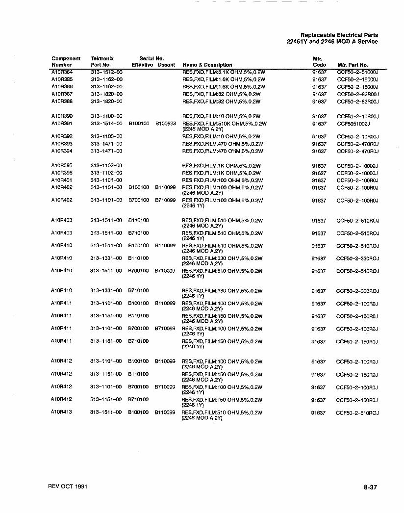
Replaceable Electrical Parts 22461Y and 2246 MOD A Service
Component Tektronix Serial No. Number Part No. Effective Dscont Name & Descrlptlon A1 OR384 313-1512-00 RES,FXD.FILM:5.1 K OHM,5%,0.2W
A10R390 313-1100-00 RES.FXD,FILM:lO OHM,5%,0.2W A1 OR391 313-1514-00 BlOOlOO 8100823 RES,FXD,FILM:510K OHM,5%,0.2W
(2246 MOD A,2Y) A10R392 313-1100-00 RES,FXD,FILM:lO OHM,5%,0.2W A10R393 313-1471 -00 RES,FXD,FlLM:470 OHM,5%,0.2W A10R394 313-1471-00 RES,FXD,FILM:470 OHMS59/o,0.2W
A10R396 313-1102-00 RES,FXD,FILM:l K OHM,5%,0.2W A10R401 313-1101-00 RES,FXD,FILM:100 OHM,5%,0.2W AlOR402 313-1101-00 Bl00100 8110099 RES,FXD,FILM:lOO OHM,5%,0.2W
(2246 MOD A,2Y) A10R402 313-1 101 -00 8700100 8710099 RES,FXD,FILM:lOO OHM,5%,0.2W
(2246 1Y)
A10R403 313-1511-00 8110100 RES,FXD,FILM:510 OHM,5%,0.2W (2246 MOD A,2Y)
A10R410 313-151 1-00 BlOOlOO 81 10099 RES,FXD,FILM:510 OHM,5%.0.2W (2246 MOD A.2Y)
A10R410 313-1331-00 B l 10100 RES,FXD,FlLM:330 OHM.5%,0.2W (2246 MOD A,2Y)
A10R410 313-1511-00 8700100 8710099 RES,FXD,FILM:510 OHM,5%,0.2W (2246 1Y)
A10R411 313-1101-00 8100100 8110099 RES,FXD,FILM:100 OHM,5%,0.2W (2246 MOD A.2Y)
A10R411 313-1151-00 8110100 RES,FXD,FILM:150 OHM85%,0.2W (2246 MOD A,2Y)
A10R412 313-1 101-00 8100100 61 10099 RES,FXD,FILM:lOO OHM.5%,0.2W (2246 MOD A,2Y)
A10R412 313-1151-00 8110100 RES,FXD,FILM:150 OHM,5%,0.2W (2246 MOD A,2Y)
A10R412 313-1101-00 8700100 8710099 RES,FXD,FILM:lOO OHM,5%,0.2W (2246 1Y)
A10R412 313-1151-00 8710100 RES,FXD,FILM:l50 OHM,5%,0.2W (2246 1Y)
313-151 1-00 8100100 81 10099 RES,FXD,FILM:510 OHMS5%,0.2W (2246 MOD A,2Y)
Mf r. Code Mfr. Part No. 91637 CCF50-2-51000J 91 637 CCF50-2-16000J 91 637 CCF50-2-16000J 91 637 CCF50-2-82ROOJ 91637 CCF50-2-82ROOJ
91637 CCF50-2-510ROJ
91637 CCF50-2-51OROJ
91 637 CCF50-2-51 OROJ
91637 CCF50-2-330ROJ
91637 CCF50-2-510ROJ
REV OCT 1991

Replaceable Electrical Parts 22461Y and 2246 MOD A Service
Component Number A10R413
Tektronlx Serlal No. Part No. Effective Dscont Name & Description 313-1331-00 BllOlOO RES,FXD,FILM:BSO OHM,5%,0.2W
(2246 MOD A,2Y) 313-151 1-00 8700100 8710099 RES,FXD,FILM:510 OHM,5%,0.2W
(2246 1Y) 313-1331 -00 B710100 RES,FXD,FILM:330 OHM,5%,0.2W
(2246 1Y)
Mfr. Code 91 637
Mfr. Part No. CCF50-2-330ROJ
CCF50-2-51 OROJ
81 10099 RES,FXD,FILM:510 OHM,5%,0.2W (2246 MOD A,2Y)
313-1331-00 BllOlOO RES,FXD,FILM:330 OHM,5%,0.2W (2246 MOD A,2Y)
313-1331 -00 B710100 RES,FXD,FILM:330 OHM,5%.0.2W (2246 1Y)
313-1101-00 BlOOlOO 81 10099 RES,FXD,FILM:100 OHM.596.0.2W (2246 MOD A,lY)
313-1151-00 BllOlOO RES,FXD,FILM:lM OHM,5%,0.2W (2246 MOD A,2Y)
313-1 101 -00 B100100 B1 10099 RES,FXD,FILM:100 OHM,59/o.0.2W (2246 MOD A,2Y)
CCF50-2-1 OOROJ
CCF50-2-150ROJ
CCF50-2-100ROJ
CCF50-2-150ROJ
313-1151-00 BllOlOO RES,FXD,FlLM:150 OHM.5%.0.2W (2246 MOD A.2Y)
313-1101-00 B700100 B710099 RES.FXD.FILM:100OHM,5%,0.2W (2246 1Y)
313-1151-00 B710100 RES,FXD,FILM:150 OHM.5%,0.2W (2246 1Y)
313-1511-00 BlOOlOO 81 10099 RES,FXD,FILM:510 OHM,5%,0.2W (2246 MOD A.29
313-1331 -00 B l 10100 RES,FXD,FILM:330 OHM,5%,0.2W (2246 MOD A,2Y)
313-151 1-00 B700100 8710099 RES,FXD,FILM:510 OHM,5%,0.2W (2246 1Y)
CCF50-2-51 OROJ
CCF50-2-330ROJ
REV OCT 1991

Replaceable Electrical Parts 22461Y and 2246 MOD A Servlce
Component Number AlOR441 A1 OR442 A10R443 A10R444 A10R445
Tektronix Serial No. Mtr. Part No. Effective Dscont Name 8 Description Code Mtr. Part No. 313-1621-00 RES,FXD,FILM:620 OHM,5%.0.2W 91 637 CCF50-2-620ROJ
313-1562-00 RES,FXDSFILM:5bK OHM,5°h,0.2W 91637 CCF50-2-56000J
31 3-1 562-00 RES,FXD,FILM:5.6K OHM85%,0.2W 91637 CCF50-2-56000J 31 3-1 561 -00 RES,FXD,FILM:560 OHM,5%,0.2W 91 637 CCF50-2-560ROJ
322-3143-00 RES,FXD,FILM:301 OHM.1%,0.2W,TC=TOMI 91637 CCF501G301 ROF
322-3285-00 8110100 RES,FXD,FILM:9.09K OHM,1%,0.2W,TC=TOMl 91637 CCF501G90900F (2246 MOD A,2Y)
322-3333-02 BllOlOO RES,FXD,FILM:28.7K OHM,0.2W,.5% 91 637 CCF501 D28701 D (2246 MOD A,2Y)
RES,VAR,NONWW:TRMR,500 OHM,20%,0.50 TK2073 GF06UT2 501 M L LINEAR
313-1103-00 RES,FXD,FILM:lOK OHM.5%,0.2W 313-1271-00 8100100 8113237 RES,FXD,FILM:270OHM,5%,0.2W
(2246 MOD A,2Y) 313-1681-00 8113238 RES,FXD,FILM:680 OHM.5%,0.2W
(2246 MOD A,2Y)
313-1101-00 8100100 B120199 RES,FXD,FILM:100 OHM,5%.0.2W 91637 CCF50-2-100ROJ (2246 MOD A,2Y)
322-3143-00 8120200 RES,FXD,FlLM:301 OHM,1%.0.2W,TC=TOMI 91637 CCF501G301 ROF (2246 MOD A,2Y)
313-1101-00 8700100 8714999 RES,FXD,FILM:100 OHM,5%.0.2W 91637 CCF50-2-100ROJ (2246 1Y)
322-31 43-00 871 5000 RES,FXD,FILM:301 OHM,1%.0.2W,TC =TOMI 91637 CCF501 G301 ROF (2246 1Y)
322-3074-00 RES.FXD,FILM:57.6 OHM,1%,0.2W,TC=TOMl 91 637 CCF501 G57R60F 31 3-1 120-00 RES,FXD,FILM:12 OHM,5%,0.2W 91 637 CCF50-2-12ROOJ 313-1104-00 RES,FXD,FILM:100K OHM,5%,0.2W 91637 CCF50-2-10002J 313-1621 -00 RES,FXD,FILM:620 OHM.5%.0.2W 91 637 CCF50-2-620ROJ
313-1562-00 RES,FXD,FILM:5.6K OHM.5%,0.2W 91637 CCF50-2-56000J 313-1562-00 RES,FXD,FILM:5,6K OHM,5%,0.2W 91637 CCF50-2-56000J 313-1561-00 RES,FXD,FILM:560 OHM,5%,0.2W 91 637 CCF50-2-560ROJ 322-3328-02 8110100 RES.FXD,FILM:25.5K OHM,0.5%,0.2W,TC =T2 91637 CCF501 D25501D
(2246 MOD A.2Y)
REV OCT 1991
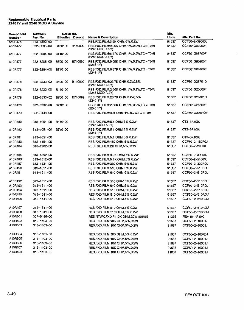
Replaceable Electrical Parts 22461Y and 2246 MOD A Service
Component Tektronlx Serial No. Number Part No. Effective Dscont Name & DescripUon A10R476 313-1392-00 RESSFXD,FILM:3.9K OHM.5%.0.2W
Mfr. Code Mfr. Part No. 91637 CCF50-2-3900OJ 91 637 CCF501 G90900F 322-3285-00 BlOOl00 81 10099 RES,FXD,FILM:9.09K OHM,1%,0.2W.TC = TOMI
(2246 MOD A,2Y)
A10R477 322-3284-00 BllOlOO RES.FXD.FILM:8.87K OHM,1%,0.2W,TC =TOMI (2246 MOD A,2Y)
A10R478 322-3333-02 BlOOlOO 8110099 RES,FXD,FILM:28.7KOHM.0.2W,.5% (2246 MOD A,2Y)
A10R478 322-3232-00 B1 101 00 RES,FXD,FILM:2.55K OHM,1%.0.2W,TC =TOMI (2246 MOD A,2Y)
A10R478 322-3333-02 B700100 8710099 RES,FXD,FILM:28.7K OHM,0.2W,.5% (2246 1Y)
A10R478 322-3232-00 B710100 RES,FXD,FILM:2.55K OHM,1%,0.2W,TC =TOMI (2246 1Y)
A10R479 322-3143-00 RES,FXD,FILM:301 OHM,1%,0.2W,TC=TOMI CCF501 G301 ROF
A1 OR480 313-1051-00 BllOlOO RES,FXD,FILM:5.1 OHM,5%,0.2W (2246 MOD A,2Y)
CT3-5R1 OOJ CCF50-2-150ROJ CCF50-2-20000J
CCF50-2-39000J CCF50-2-51 000J CCF50-2-330ROJ CCF50-2-510ROJ CCF50-2-51 OROJ
CCF50-2-510ROJ CCF50-2-510ROJ CCF50-2-51 OROJ CCF50-2-510ROJ CCF50-2-51 OROJ
RES,FXD,FILM:510 OHM,5%,0.2W RES,FXD,FILM:510 OHM,5%,0.2W RES NTWK,FXD,FI:lOK OHM,20%,(9)RES RES.FXD,FILM:lOK OHM85%,0.2W RES,FXD,FILM:lOK 0HM,59/0,0.2W
CCF50-2-510ROJ CCF50-2-51 OROJ 750-101-R10K CCF50-2-10001 J CCF50-2-10001 J
REV OCT 1991

Replaceable Electrical Parts 22461Y and 2246 MOB A Service
Component Tektronlx Serlal No. Mfr. Number Part No. Effective Dscont Name & Description Code Mfr. Par$ No. A10R510 313-1 103-00 RES.FXD,FILM:lOK OHM.5%,0.2W 91637 CCF50-2-10001 J
A10R512 313-1103-00 RES,FXD,FILM:lOK OHM,5%,0.2W 91637 CCF50-2-10001 J
A10R601 313-1102-00 RES,FXD,FILM:l K OHM,5%,0.2W 91 637 CCF50-2-1 OOOOJ
A10R602 322-3193-00 RES,FXD,FILM:lK OHM,1%,0.2W,TC=TO 91 637 CCF501 GI 0000F A10R603 322-3193-00 RES,FXD,FILM:lK OHM,I0/o,O.2W,TC=TO 91637 CCF501GlOM)OF
A10R604 322-3231 -00 RES,FXD,FILM:2.49K OHM,1%,0.2W,TC=TOMI 91637 CCF50-1 G24900F A10R605 322-3193-00 RES,FXD,FILM:l K OHM,1%,0.2W.TC=TO 91637 CCF501G10000F A10R606 313-1 102-00 RES,FXD,FILM:lK OHM,5%,0.2W 91637 CCF50-2-10000J A10R607 313-1510-00 BlOOlOO B110099 RES,FXD,FILM:51 OHM.5%,0.2W 91637 CCF501 G51 ROOJ
(2246 MOD A,2Y) A10R607 313-1510-00 B700100 8710099 RES,FXD,FILM:51 OHM,5%.0.2W 91637 CCF501 G51 ROBJ
(2246 1Y)
RES,FXD,FILM:lK OHM,5%,0.2W 91637 CCF50-2-10000J RES,FXD,FILM:200 OHM,5%,0.2W 91637 CCF50-2-200ROJ RES,FXD,FILM:39 OHM,5%,0.2W 91637 CCF50-2-39ROOJ RES,FXD,FILM:39 OHM,5%.0.2W 91637 CCF50-2-39ROOJ RES NTWK.FXD,FI:(g) 510 OHM,20%,0.125WTC = 50 11236 750-101-R510 OR PPMDEG C
REV OCT 1991

Replaceable Electrical Parts 22461Y and 2246 MOD A Service
Component Tektronix Serial No. Number Part No. Effective Dscont Name & Description A10R646 313-1562-00 RES.FXD,FILM:5.6K OHM.5%,0.2W A10R647 313-1821 -00 RES,FXD,FILM:820 OHM,5%,0.2W A10R648 313-1 471 -00 RES,FXD,FILM:470 OHM,5%,0.2W A10R649 31 3-1 302-00 RES,FXD,FILM:3K OHM,5%,0.2W A10R650 31 3-1751 -00 RES,FXD,FILM:750 OHM.5%,0.2W
A10R670 313-1511-00 RES,FXD,FILM:510 OHM,5%.0.2W A10R671 31 3-1 200-00 RES,FXD,FILM:20 OHM,5%.0.2W A1 OR672 313-1333-00 RES,FXD,FILM:33K OHM,5%,0.2W A10R673 313-1331-00 B1 10100 RES,FXD,FILM:330 OHM,5%.0.2W
(2246 MOD A,2Y) A10R673 313-1331-00 B710100 RES,FXD,FlLM:330 OHM,5%,0.2W
(2246 1Y)
A1 OR674 313-1201-00 BllOl00 RES,FXD,FlLM:200 OHM,5%,0.2W (2246 MOD A,2Y)
A10R686 313-1511-00 Bl lOl00 RES,FXD,FILM:510 OHM.5%,0.2W (2246 MOD A,2Y)
A10R686 313-1511-00 B71010C RES,FXD,FILM:510 OHM.5Oh.0.2W (2246 1Y)
A1 OR687 313-1511-00 BllOl00 RES,FXD,FILM:510 OHM,5%,0.2W (2246 MOD A,2Y)
AlOR688 313-1511-00 BllOl00 RES;FXD,FILM:510 OHM,5%,0.2W (2246 MOD A,2Y)
A10R688 313-151 1-00 B710100 RES,FXD,FILM:510 OHM,5%,0.2W (2246 1Y)
A10R689 313-1750-00 Bl lOl00 RES,FXD,FILM:75 OHMS5%.0.2W (2246 MOD A.2Y)
A10R689 313-1750-00 B710100 RES,FXD,FILM:75 OHM,5%,0.2W (2246 1Y)
Mfr. Code 91 637 91637 91 637 91 637 91637
Mfr. Part No. CCF50-2-56WJ CCF50-2-820ROJ CCF50-2-47OROJ CCF50-2-30000J CCF50-2-750ROJ
CCF50-2-39001 J CCF50-2-39001 J CCF50-2-39001 J CCF50-2-39001 J CCF50-2-51 OROJ
CCF50-2-51 OROJ CCF50-2-20ROOJ CCF50-2-33001 J CCF50-2-330ROJ
91637 CCF50-2-200ROJ
91637 CCF50-2-200ROJ
91637 CCF50-2-510ROJ
91 637 CCF50-2-51 OROJ
91 637 CCF50-2-510ROJ
91 637 CCF50-2-510ROJ
91637 CCF50-2-510ROJ
91 637 CCF50-2-51 OROJ
91637 CCF50-2-75ROOJ
91637 CCF50-2-75R00J
R N OCT 1991

Replaceable Electrical Parts 22461Y and 2246 MOD A Service
Tektronix Serial No. Mfr. Part No. Effective Dscont Name & Descriptlon Code Mfr. Part No. 313-1750-00 8110100 RES,FXD,FILM:75 OHM,5%,0.2W 91637 CCF50-2-75ROOJ
(2246 MOD A,2Y)
Component Number AlOR690
313-1750-00 8110100 RES,FXD,FILM:75 OHM,5%,0.2W 91637 CCF50-2-75ROOJ (2246 MOD A,2Y)
313-1750-00 8710100 RES,FXD,FILM:75 OHM.5%,0.2W (2246 1Y)
31 3-1750-00 8110100 RES,FXD,FILM:75 OHM,5%.0.2W (2246 MOD A,2Y)
313-1750-00 8710100 RES,FXD,FILM:75 OHM,5%,0.2W 91 637 CCF50-2-75ROOJ (2246 1Y)
313-1750-00 B110100 RES,FXD,FILM:75 OHM,5°h.0.2W 91637 CCF50-2-75ROOJ (2246 MOD A,2Y)
313-1750-00 B110100 RES,FXD,FILM:75 OHM,5%,0.2W (2246 MOD A.2Y)
313-1750-00 8710100 RES,FXD,FILM:75 OHM,5%.0.2W (2246 1Y)
31 1-2230-00 RES,VAR,NONWW:TRMR.500 OHM,20%.0.50 TK2073 GF06UT2 501 M L LINEAR
RES NTWK,FXD,FI:DUAL LOAD RESISTOR 80009 307213000 RES.FXD.FILM:2.7 OHM,5%.0.2W 57668 TR20JE 02E7 RES,FXD,FILM:130K OHM 5%,0.2W 91 637 CCF50-2-13OO2J RES.FXD,FILM:lO OHM,5%,0.2W 91637 CCF50-2-10ROOJ RES,FXD,FILM:lO OHM85%,0.2W 91637 CCF50-2-10R00J
RES,FXD,FILM:20 OHM,5%,0.2W 91 637 CCF50-2-20ROOJ RES,FXD,FILM:l30K OHM 5%,0.2W 91637 CCF50-2-13002J RES,FXD,FILM:130K OHM 5%,0.2W 91637 CCF50-2-13002J RES,FXD,FILM:2.7 OHM85%,0.2W 57668 TR20JE 02E7 RES,VAR,NONWTRMR,5K OHM,20%,0.5W TK2073 GF06UT2 502 M L LINEAR
313-1 102-00 6100100 8119999 RES,FXD,FILM:lK OHM,5%,0.2W (2246 MOD A,2Y)
313-1751-00 8120000 RES,FXD,FILM:750 OHM,5%,0.2W (2246 MOD A,2Y)
REV OCT 1991

Replaceable Electrical Parts 22461Y and 2246 MOD A Service
Component Tektronix Serial No. Mf r. Number Part No. Effective Dscont Name & DescrlpUon Code Mfr. Part No. A10R727 313-1 104-00 RES,FXDSFILM:100K OHM,5%,0.2W 91637 CCF50-2-10002J
A10R728 313-1824-00 RES,FXD,FILM:820K OHM,0.2W,5% 91 637 CCF50-2-82002J A10R729 313-1202-00 RES.FXD,FILM:PK OHMS5%,0.2W 91 637 CCF50-2-200OOJ A10R730 313-1 102-00 RES,FXD,FILM:l K OHM,5%.0.2W 91637 CCF50-2-10000J
A10R731 313-1750-00 RES,FXD,FILM:75 OHM,5%.0.2W 91637 CCF50-2-75ROOJ
A10R732 313-1750-00 RES,FXD,FILM:75 OHM.5%,0.2W A1 OR733 313-1027-00 RES,FXD,FILM:2.7 OHM.5%,0.2W A10R734 313-1120-00 RES,FXD,FILM:12 OHM,5%,0.2W A10R801 313-1431-00 8100100 81 10099 RES,FXD,FILM:430 OHM,5%,0.2W
(2246 MOD A.2Y) RES,FXD,FILM:680 OHM,5%.0.2W (2246 MOD A,2Y)
A10R802 31 3-1 750-00 RES,FXD,FILM:75 OHM,5%,0.2W 91 637 CCF50-2-75ROOJ A10R803 313-1 562-00 8100100 81 10099 RES,FXD,FILM:5.6K OHM,5%.0.2W 91637 CCF50-2-5600OJ
(2246 MOD A,2Y) A10R803 313-1272-00 8110100 RES.FXD,FILM:2.7K OHM,5%,0.2W 91 637 CCF50-2-27OOOJ
(2246 MOD A,2Y)
AlOR803 313-1562-00 8700100 8710099 RES,FXD,FlLM:5BK OHM.5%,0.2W (2246 1Y)
A10R803 31 3-1272-00 8710100 RES.FXD,FILM:2.7K OHM,5%,0.2W (2246 1Y)
A10R804 313-1 104-00 B100100 B1 10099 RES,FXD,FILM:lOOK OHM,5%.0.2W (2246 MOD A,2Y)
A10R804 313-1273-00 8110100 RES,FXD,FILM:27K OHM,5%.0.2W (2246 MOD A,2Y)
A1 OR804 313-1 273-00 8710100 RES,FXD,FILM:27K OHM,5%,0.2W (2246 1Y)
AlORBO5 313-1 162-00 8100100 81 10099 RES,FXD,FILM:I .6K OHM,5%,0.2W (2246 MOD A,2Y)
A10R805 313-1273-00 81 10100 RES,FXD,FILM:27K OHM,5%,0.2W (2246 MOD A,2Y)
RES.FXD,FILM:16.5K OHM.1%,0.5W,TC=TO 91 637 CMF65116G16501 F RES,FXD,FILM:75 OHM,5%,0.2W 91 637 CCF50-2-75ROOJ RES,FXD,FILM:2.7K OHM.5%.0.2W 91637 CCF50-2-27000J RES,VAR,NONWW:TRMR,5K OHM,20%,0.5W TK2073 GF06UT2 502 M L LINEAR RES,FXD,FILM:2.7K OHM,5%.0.2W 91637 CCF50-2-27000J
REV OCT 1991

Replaceable Electricas Parts 22461Y and 2246 MOD A Service
Component Tektronlx Serial No. Mfr. Number Part No. Effective Dscont Name & Descrlptlon Code Mfr. Part No. A1 OR81 1 322-3266-00 8100100 81 10099 RES.FXDSFILM:5.76K OHM,1%.0.2W,TC=TOMI 91637 CCF501 G57600F
(2246 MOD A.2Y) A1 OR81 1 322-3265-00 B1 10100 RES,FXD,FILM:5.62K OHM,l%.0.2W,TC =TOMI 91 637 CCF501 G56200F
(2246 MOD A,2Y)
A1 OR81 2 322-3266-00 8100100 81 10099 RES,FXD.FILM:5.76K OHM,1%.0.2W,TC=TOMI 91 637 CCF501 G57600F (2246 MOD A,2Y)
A10R812 322-3265-00 8110100 RES,FXD,FILM:5.62K OHM,1%,0.2W,TC =TOMI 91 637 CCF501 G56200F (2246 MOD A.2Y)
A10R812 322-3266-00 87001 00 871 0099 RES,FXD,FILM:5.76K OHM,1%,0.2W,TC =TOMI 91637 CCF501 G576cOF (2246 1Y)
A10R812 322-3265-00 8710100 RES,FXD,FILM:5.62K OHM,1%.0.2W,TC=TOMI 91637 CCF501 G56200F (2246 1Y)
A10R813 313-1431-00 8100100 8110099 RES,FXD,FILM:430 OHM,5%,0.2W 91 637 CCF50-2-430ROJ (2246 MOD A,2Y)
A10R813 313-1272-00 8110100 RES,FXD,FILM:2.7K OHM,5%,0.2W 91 637 CCF50-2-27000J (2246 MOD A,2Y)
A10R813 313-1431 -00 8700100 B710099 RES,FXD,FILM:430 OHM,5%,0.2W (2246 1Y)
A10R813 313-1272-00 8710100 RES,FXD,FILM:2.7K OHM,5%,0.2W (2246 1Y)
A10R814 313-1562-00 Bl00100 81 10099 RES,FXD,FILM:5.6K OHM,5%,0.2W (2246 MOD A,2Y)
A10R814 313-1272-00 8110100 RES,FXD,FILM:2.7K OHM,5%.0.2W (2246 MOD A.2Y)
A10R815 313-1104-00 8100100 8110099 RES,FXD,FILM:100KOHM,5%.0.2W 91 637 CCF50-2-10002J (2246 MOD A,2Y)
A10R815 313-1104-00 8700100 8710099 RES,FXD,FILM:100KOHM,5%,0.2W 91 637 CCF50-2-10002J (22% 1Y)
A10R816 323-0310-00 8100100 8110099 RES,FXD,FILM:16.5KOHM.1%.0.5W,TC=TO 91637 CMF65116G16501F (2246 MOD A,2Y)
A10R819 313-1750-00 8100100 8110099 RES,FXD,FILM:75 OHM,5%.0.2W (2246 MOD A.2Y)
A10R820 322-3402-00 B l 00100 81 19999 RES,FXD,FILM:150K OHM.1%,0.2W.TC =TOMI 91637 CCF50G15002F (2246 MOD A,2W
A10R820 322-0402-00 8120000 RES,FXD.FILM:lSOK OHM,1°/o,0.25W,TC=T0 91 637 CMF6042G1 W 2 F (2246 MOD A.2Y)
A10R820 322-3402-00 8700100 8714999 RES,FXD,FILM:150K OHM.1 %,O.2W,TC=TOMI 91 637 CCF50G15002F (2246 1Y)
REV OCT 1991

Replaceable Electrical Parts 22461Y and 2246 MOD A Service
Component Tektronix Serial No. Number Part No. Effective Dscont Name & Description A10R820 322-0402-00 871 5000 RES,FXD,FILM:lMK OHM,1%,0.25W,TC =TO
(2246 1Y) A10R821 322-3402-00 B100100 8119999 RES,FXD,FILM:150KOHM,1°h,0.2W,TC=TOMI
(2246 MOD A,2Y) RES,FXD,FILM:150K OHM,1°h,0.25W.TC =TO (2246 MOD A,2Y)
RES,FXD.FILM:5.62K OHM,1%,0.2W,TC=TOMI RES,VAR.NONWW:TRMR.500 OHM,20%,0.50 LINEAR RESSVAR,NONWW:TRMR,5K OHM,20%,0.5W LINEAR RES,VAR,NONWW:TRMR,5K OHM,20%,0.5W LINEAR RES,VAR,NONWW:TRMR,250 OHM,20%,0.5W Ll N EAR
A10R828 301 -0203-00 81 00100 61 10099 RESSFXD,FILM:20K OHM,5%.0.5W (2246 MOD A,2Y)
A10R828 313-1133-00 B110100 RES,FXD,FILM:13K,5%,0.2W (2246 MOD A,2Y)
A10R828 313-1133-00 8710100 RES,FXD,FILM:13K,5%,0.2W (2246 1Y)
A10R829 301-0203-00 BlOOlOO B110099 RES,FXD,FILM:20K OHM,5%.0.5W (2246 MOD A,2Y)
A10R829 313-1 133-00 B l 10100 RES,FXD.FILM:13K.5%,0.2W (2246 MOD A,2Y)
A10R829 301-0203-00 B700100 B710099 RES,FXD,FILM:20K OHM,5%,0.5W (2246 1Y)
A10R829 313-1 133-00 B710100 RES,FXD,FILM:13K,5%,0.2W (2246 1Y)
313-1133-00 BllOlOO RES,FXD,FILM:13K,5%.0.2W (2246 MOD A.2Y)
A10R831 313-1 133-00 BllOlOO RES,FXD,FILM:13K,5%,0.2W (2246 MOD A,2Y)
A10R831 313-1 133-00 B710100 RES,FXD,FILM:13K.5%,0.2W (2246 1Y)
A10R836 322-31 52-00 RES,FXD,FILM:374 OHM.1%,0.2W,TC =TOMI A10R837 313-1100-00 RES,FXD,FILM:lO OHM,5%,0.2W AlOR840 313-1470-00 BlOOl00 Bll0099 RES,FXD,FILM:47 OHM,5%,0.2W
(2246 MOD A.2Y)
Mf r. Code Mfr. Part No. 91637 CMF6042G15002F
REV OCT 1991

Replaceable Electrical Parts 22461Y and 2246 MOD A Service
Component Tektronlx Serial No. Mtr. Number Part No. EffecUve Dscont Name & Descrlptlon Code Mtr. Part No. A10R840 313-1470-00 8700100 8710099 R X .FILM:47 OHM.5%.0.2W 91637 CCF50-2-47ROOJ (E i iW A10R841 313-1 100-00 8100100 81 10099 RES,FXD.FILM:lO OHM,5%,0.2W 91 637 CCF50-2-10ROOJ
(2246 MOD A,2Y)
A10R842 313-1103-00 8100100 8110099 RES,FXD,FlLM:lOKOHM.5%,0.2W 91637 CCF50-2-10001 J (2246 MOD A.2Y)
A10R843 313-1751-00 8100100 8110099 RES,FXD,FILM:750 OHM.5%,0.2W (2246 MOD A,2Y)
A1 OR843 313-1751-00 8700100 8710099 RES,FXD,FILM:750 OHM,5%,0.2W (2246 1Y)
A10R844 313-1751 -00 8100100 81 10099 RES,FXD,FILM:750 OHM,5%.0.2W (2246 MOD A.2Y)
A10R844 313-1751-00 8700100 8710099 RES,FXD,FILM:750 OHM,5%,0.2W (2246 1Y)
A1 OR845 313-1100-00 8100100 8110099 RES,FXD.FILM:lOOHM.5%,0.2W (2246 MOD A.2Y)
A10R846 322-3058-00 8100100 8110099 RES,FXD,FILM:39.2 OHM.1%,0.2W,TC=TOMI 91637 CCF50-1 G39R20F (2246 MOD A.2Y)
A1 OR846 322-3058-00 8700100 8710099 RES,FXD.FILM:39.2OHM,1%.0.2W.TC=TOMI 91637 CCF50-1 G39R20F (2246 1Y)
A1 OR847 313-1 100-00 8100100 81 10099 RES.FXD.FILM:lO OHM,5%.0.2W 91637 CCF50-2-10ROOJ (2246 MOD A,2Y)
A1 OR847 313-1100-00 8700100 8710099 RES,FXD,FILM:10 OHM,5%,0.2W 91637 CCF50-2-10ROOJ (2246 1Y)
A10R848 301-0222-00 8100100 81 10099 RES,FXD,FILM:2.2K OHM,5%,0.5W (2246 MOD A,2Y)
A10R849 301-0222-00 8100100 81 10099 RES,FXD,FILM:2.2K OHM,5%,0.5W TK1727 SFR30 2322-1 82- (2246 MOD A,2Y)
A10R849 301-0222-00 8700100 8710099 RES.FXD,FILM:2.2K OHM,5%,0.5W (2246 1Y)
A10R850 313-1392-00 8100100 8110099 RES,FXD,FILM:89K OHM,5%.0.2W (2246 MOD A,2Y)
A10R850 313-1392-00 8700100 8710099 RES,FXD,FILM:3.9KOHM,5%,0.2W (2246 1Y)
A10R851 313-1100-00 8100100 8110099 RES,FXD,FILM:10 OHM.5%,0.2W (2246 MOD A,2Y)
AlOR851 313-1 100-00 8700100 8710099 RES,FXD.FILM:lO OHM,5%,0.2W (2246 1Y)
A10R852 322-3074-00 BlOOlOO B110099 RES,FXD,FILM:57.6 OHM.1%.0.2W,TC=TOMI 91 637 CCF501 G57R60F (2246 MOD A,2W
R N OCT 1991

Replaceable Electrlcal Parts 22461Y and 2246 MOD A Service
Component Tektronix Serial No. Number Part No. Effective Dscont Name & Description A10R853 313-1470-00 8100100 8110099 RES,FXDPFILM:47OHM,5%,0.2W
(2246 MOD A,2Y)
A10R853 313-1470-00 8700100 8710099 RES,FXD,FILM:47 OHM,5%,0.2W (2246 1Y)
A10R854 313-1201-00 RES,FXD,FILM:200 OHM,5%,0.2W
A1 OR855 313-1201 -00 RES,FXD,FILM:200 OHM,5%,0.2W A1 OR856 322-3289-00 RES.FXD,FILM:lOK OHM,1%,0.2W,TC=TO
A10R857 322-3265-00 RES,FXD,FILM:5.62K OHM,1%.0.2W,TC =TOMI A10R858 322-3143-00 8100100 81 10099 RES,FXD,FILM:301 OHM,1%,0.2W.TC =TOMI
(2246 MOD A,2Y)
A10R858 322-3143-00 8700100 B710099 RES,FXD,FILM:301 OHM,l Yo,0.2W,TC=TOMI (2246 1Y)
AlOR860 313-1 103-00 81 10100 RES,FXD,FILM:lOK OHM,5%,0.2W (2246 MOD A.2Y)
A10R860 313-1103-00 8710100 RES,FXD,FILM:lOK OHM.5%,0.2W (2246 1Y)
A10R861 313-1272-00 BllOl00 RES.FXD.FILM:2.7K OHM,5%,0.2W (2246 MOD A,2Y)
AIOR861 313-1272-00 8710100 RES.FXD,FILM:2.7K OHM,5%,0.2W (2246 1Y)
A1 OR862 322-3077-00 BllOl00 RES,FXD.FILM:61.9 OHM.1%,0.2W.TC =TOMI (2246 MOD A,2Y)
A1 OR862 322-3077-00 8710100 RES,FXD.FILM:61.9 OHM,l%,0.2W,TC=TOMl (2246 1Y) RES,FXD,FILM:270 OHM,5Yo,0.2W (2246 MOD A,2Y)
RES,FXD,FILM:lOK OHM,5%,0.2W (2246 MOD A.2Y)
A1 OR872 313-1510-00 8110100 RES.FXD.FILM:51 OHM,5%,0.2W (2246 MOD A,2Y)
A10R872 31 3-1510-00 8710100 RES,FXD,FILM:51 OHM,5%,0.2W (2246 1Y)
A10R873 313-1271-00 8110100 RES,FXD,FlLM:270 OHM,5%,0.2W (2246 MOD A,2Y)
A10R873 313-1271 -00 8710100 RES,FXD,FILM:270 OHM,5%,0.2W (2246 1Y)
A10R891 313-1681-00 BllOl00 RES,FXD,FILM:680 OHM,5%,0.2W (2246 MOD A,2Y)
A10R891 313-1681-00 B710100 RES,FXD,FILM:680 OHM,5%.0.2W (2246 1Y)
A1 OR892 313-1750-00 81 10100 RES,FXD,FILM:75 OHM,5%.0.2W (2246 MOD A,2Y)
Mf r. Code Mfr. Part No. 91637 CCF50-2-47ROOJ
91 637 CCF501 G56200F 91637 CCF501 G301 ROF
91637 CCF501 G301 ROF
91637 CCF50-2-10001 J
91 637 CCF50-2-10001 J
REV OCT 1991

Replaceable Electrical Parts 22461Y and 2246 MOD A Service
Component Tektronix Serial No. Mfr. Number Part No. Effective Dscont Name & Description Code Mfr. Part No. A1 OR892 313-1750-00 B710100 RES,FXD,FILM:75 OHM,5%,0.2W 91637 CCF50-2-75ROOJ
(2246 1Y)
A1 OR893 313-1391-00 BllOlOO RES,FXD,FILM:390 OHM,5%,0.2W 91637 CCF50-2-390ROJ (2246 MOD A,2Y)
A10R893 31 3-1 391 -00 871 01 00 RES,FXD,FILM:390 OHMS5%,0.2W 91 637 CCF50-2-390ROJ (2246 1Y)
A10R894 313-1100-00 BllOl00 RES,FXD,FILM:lO OHM85%,0.2W 91 637 CCF50-2-1 OROOJ (2246 MOD A,2Y)
A10R894 313-1 100-00 B710100 RES,FXD,FILM:lO OHM,5%,0.2W 91 637 CCF50-2-10R00J (2246 1Y)
A10R896 323-0310-00 BllOl00 RES,FXD.FILM:16.5K OHM,1%,0.5W,TC=TO 91637 CMF65116G16501 F (2246 MOD A,2Y)
A10R897 313-1100-00 BllOl00 RES,FXD,FILM:lO OHM,5%,0.2W (2246 MOD A,2Y)
A10R897 313-1100-00 B710100 RES,FXD,FILM:lO OHM,5%,0.2W (2246 1Y)
A10R898 313-1100-00 B110100 RES,FXD,FILM:lO OHM,5%,0.2W (2246 MOD A.2Y)
RES,FXD,FILM:100 OHM.5%,0.2W 91637 CCF50-2-1OOROJ RES,VAR,NONWW:TRMR,2.5K OHM,0.5W 32997 3386X-1-252 RES,FXD,FILM:lOK OHM,l%,O.2W.TC=TO 91637 CCF50G10001 F RES.FXD,FILM:lOK OHM.1%,0.2W,TC=TO 91637 CCF50G10001 F RES,VAR,NONWW:TRMR,200 OHM,20%,0.5W TK2073 GF06UT2 201 M L LINEAR
A10R921 307-21 31 -00 RES NTWK,FXD.FI:PRECESION VOLTAGE DIVIDER 80009 307213100 H2131
A1 OR924 313-1103-00 RES,FXD,FILM:lOK OHM,5%,0.2W A108925 313-1472-00 B120000 RESBFXD,FILM:4.7K OHM,5%,0.2W
(2246 MOD A.2Y)
REV OCT 1991
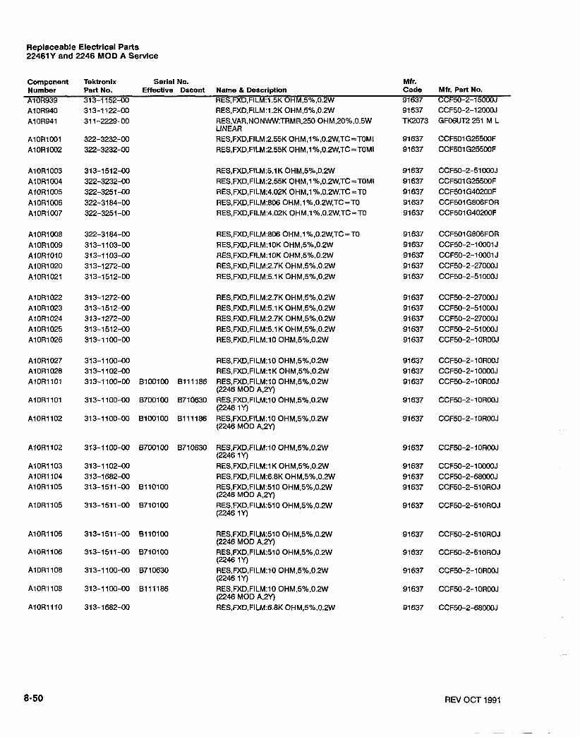
Replaceable Electrical Parts 22461Y and 2246 MOD A Service
Mf r. Code 91637
Component Tektronix Serial No. Number Part No. Effective Dscont Name & Description A10R939 313-1152-00 RES,FXD,FILM:1.5K OHM,5%,0.2W
Mfr. Part No. CCF50-2-15000J CCF50-2-12MMJ GF06UT2 251 M L
RES,FXD,FILM:1.2K OHM,5%,0.2W RES,VAR,NONWTRMR,250 OHM,20%.0.5W LINEAR
A10R1027 313-1 100-00 RES,FXD.FILM:lO OHM,5%,0.2W A1 OR1 028 313-1 102-00 RES,FXD,FILM:lK OHM,5%.0.2W AlORllOl 313-1 100-00 BlOOlOO B111186 RES,FXD,FILM:lO OHM,5%,0.2W
(2246 MOD A,2Y) AlORllOl 313-1 100-00 B700100 B710630 RES,FXD,FILM:lO OHM,5%,0.2W
(2246 1Y) AlOR1102 313-1 100-00 BlOOlOO 8111 186 RES,FXD,FILM:lO OHM,5%,0.2W
(2246 MOD A,2Y)
91 637 CCF50-2-1 OROOJ
91637 CCF50-2-10ROOJ
A10R1105 313-1511-00 BllOlOO RES,FXD,FILM:510 OHM,5%,0.2W (2246 MOD A,2Y)
A10R1105 313-151 1-00 8710100 RES,FXD,FILM:510 OHM,5%,0.2W (2246 1Y)
A10R1106 313-1511-00 BllOl00 RES,FXD,FILM:510 OHM,5%,0.2W (2246 MOD A,2Y)
A10R1108 313-1100-00 B111186 RES,FXD,FILM:lO OHM,5%,0.2W (2246 MOD A.2Y)
AlORlllO 313-1682-00 RES,FXD,FILM:6.8K OHM,5%,0.2W
REV OCT 1991

Replaceable Electrical Parts 22461Y and 2246 MOD A Service
Component Number AlORll 1 1 A10R1112 A10R1113 A10R1114 A10R1115
Tektronlx Serial No. Part NO. Effective Dscont Name & Description 31 3-1 303-00 RES,FXD,FILM:BOK OHM,5%,0.2W 313-1302-00 RES,FXD,FILM:3K OHM,5°h.0.2W 313-1101-00 RES,FXD,FILM:100 OHM,5%,0.2W 313-1103-00 RES,FXD,FILM:IOK OHM,5%,0.2W 31 3-1 682-00 RESBFXD,FILM:6.8K OHM.5%,0.2W
Mf r. Code Mfr. Part No. 91637 CCF50-2-30001 J 91637 CCF50-2-30000J 91637 CCF50-2-100ROJ 91637 CCF50-2-10091 J 91637 CCF50-2-68000J
313-1100-00 RES,FXD,FILM:lO OHM,5%,0.2W 313-1 100-00 RES,FXD.FILM:lO OHM.5%,0.2W 313-1100-00 BllOlOO RES,FXD.FILM:lO OHM,5%,0.2W
(2246 MOD A.2Y) 313-1100-00 B710100 RES,FXD,FILM:10 OHM,5%,0.2W
(2246 1Y) 313-1302-00 RES,FXD,FILM:3K OHM85%,0.2W
313-1152-00 RES.FXD,FILM:1.5K OHM,5%,0.2W 313-1152-00 RESSFXD,FILM:1.5K OHM,5%,0.2W 313-1101-00 B120000 RES,FXD,FILM:100 OHM85%,0.2W
(2246 MOD A,2Y) 313-1101-00 B715000 RES,FXD,FILM:100 OHM,5Oh,0.2W
(2246 1Y) RES,FXD,FILM:100 OHM,5%,0.2W (2246 MOD A.2Y)
REV OCT 1991

Replaceable Electrical Parts 22461Y and 2246 MOD A Service
Component Tektronix Serial No. Number Part No. Effective Dscont Name & Description A10R1211 313-1101-00 8715000 :I00 OHM,5%,0.2W
A10R1220 313-1 101-00 8120000 RES,FXD,FILM:100 OHM,5%.0.2W (2246 MOD A,2Y)
A10R1220 313-1101-00 8715000 RES,FXD,FILM:100 OHM,5%,0.2W (2246 1Y)
A10R1221 313-1 101-00 8120000 RES,FXD,FILM:100 OHM,5%.0.2W (2246 MOD A,2Y)
A10R1230 313-1101-00 8120000 RES,FXD,FILM:100 OHM.5%.0.2W (2246 MOD A,2Y)
A10R1230 313-1101-00 8715000 RES,FXD,FILM:100 OHM,5%.0.2W (2246 1Y)
A1 OR1 231 313-1 101-00 8120000 RES,FXD,FILM:lOO OHM,5%,0.2W (2246 MOD A,2Y)
A10R1231 313-1 101-00 8715000 RES,FXD,FILM:100 OHM.5%,0.2W (2246 1Y) RES,FXD,FILM:100 OHM,5%,0.2W (2246 MOD A.2Y)
A10R1241 31 3-1 101 -00 81 20000 RES,FXD,FILM:100 OHM,5%.0.2W (2246 MOD A,2Y)
A1 OR1 241 313-1101-00 6715000 RES.FXD.FILM:100 OHM,5%,0.2W (2246 1Y)
A1 OR1 250 322-3059-00 81 20000 RES.FXD,FILM:40.2 OHM,1%.0.2W,TC =TOMI (2246 MOD A,2Y)
A10R1251 322-3059-00 8120000 RES,FXD.FILM:40.2 OHM,1%,0.2W,TC =TOMI (2246 MOD A.2Y)
A1 OR1 251 322-3059-00 871 5000 RES,FXD.FILM:40.2 OHM.1%,0.2W,TC =TOMI (2246 1Y)
A10R1260 313-1 102-00 8120000 RES,FXD,FILM:lK OHM.5%.0.2W (2246 MOD A,2Y)
A10R1260 313-1102-00 8715000 RES,FXD,FILM:lK OHM,5%,0.2W (2246 1Y)
A10R1284 313-1820-00 8120000 RES,FXD,FILM:82 OHM,5%,0.2W (2246 MOD A,2Y)
A10R1285 313-1820-00 8120000 RES,FXD,FILM:82 OHM,5%.0.2W (2246 MOD A,2Y)
A10R2116 311-2329-00 8100100 81'10099 RES,VAR,NONWTRlMMER,5KOHM,lO% (2246 MOD A.2Y)
Mfr. Code Mtr. Part No. 91637 CCF50-2-100ROJ
REV OCT 1991

Replaceable Electrical Parts 22461Y and 2246 MOD A Service
Tektronix Serial No. Mf r. Part No. Effective Dscont Name 8 Description Code Mfr. Part No. 322-3112-00 RES,FXD,FILM:143 OHM,1%.0.2W,TC=TOMl 91637 CCF501 G143ROF 313-1393-00 RES,FXD,FILM:39K OHM,5%,0.2W 91 637 CCF50-2-39001 J 322-3282-00 RES,FXD,FILM:8.45K OHM,1%,0.2W,TC =TOM1 91637 CCF501 G84500F 322-3164-00 RES,FXD,FILM:499 OHM,1%.0.2W,TC=TOMI 91637 CCF501 G499ROF 313-1102-00 RES,FXD,FILM:IK OHMt5%,0.2W 91637 CCF50-2-10000J
Component Number A10R2701 A1 OR2702 A10R2703 A1 OR2704 A10R2705
RES,FXD,FILM:5.6K OHM,5%,0.2W 91637 CCF50-2-56000J RES,FXD,CMPSN:75 OHM.5%,0.17W 56845 CCF50-2-G68ROJ RES,VAR,NONWTRMR,20K OHM,20%,0.5W TK2073 GF06UT2 203 M L LINEAR RES,FXD,FILM:2OK OHM.5%,0.25W TK1727 SFR25 2322-181 - RES,FXD,FILM:4.7K OHM,5%,0.25W TK1727 SFR25 2322-181 -
REV OCT 1991

Replaceable Electrical Parts 22461Y and 2246 MOD A Servlce
Component Tektronlx Serlal No. Mf r. Number Part No. Effective Dscont Name & Description Code Mfr. Part No. A1 OR2751 31 5-0625-00 RES,FXD,FILM:6.2M OHM,5%.0.25W TK1727 SFR25 2322-181 - A10R2758 31 1-1933-00 RES.VAR,NONW.PNL,5M OHM.10%.0.5W 12697 23M909 A10R2760 307-2173-00 RES NTWK,FXD,FI:HIGH VOLTAGE,FINISHEDH2173 80009 307217300 A10R2765 322-3188-00 RES,FXD,FILM:887 OHM,1%.0.2W.TC=TOMI 91637 CCF501G887ROF A10R2783 313-1 101-00 RES,FXD,FILM:l00 OHM,5%.0.2W 91637 CCF50-2-100ROJ
A10R2784 31 1-2239-00 RES,VAR,NONWTRMR,lOOK OHM,20%,0.5W TK2073 GF06UT2 104 M L Ll N EAR RES,FXD,FILM:lK OHM,5%,0.2W 91 637 CCF50-2-1 OOOOJ RES.FXD.FILM:75K OHM.5%,0.2W 91637 CCF50-2-75001 J RES,FXD,FILM:33K OHM,5%,0.2W 91 637 CCF50-2-33001 J RES,VAR.NONWTRMR,lOOK OHM,20%,0.5W TK2073 GF06UT2 104 M L LINEAR
A10R2789 313-1 102-00 RES,FXD,FILM:lK OHM,5%.0.2W 91637 CCF50-2-10000J A10R2795 322-3268-00 RES.FXD,FILM:6.04K OHM,1%,0.2W,TC=TOMI 91 637 CCF501 G60400F A10R2796 313-1100-00 RES,FXD,FILM:lO OHM,5%,0.2W 91 637 CCF50-2-10R00J AlORT201 307-0181-00 RES,THERMAL:100K OHM.lO%,NTC 141 93 K10-10002K A10U112 165-2232-00 Bl00100 B101582 MICR0CKT.LINEAR:BUFFER AMPLIFIER 80009 165223200
(2246 MOD A,2Y)
A10U112 165-2232-01 8101583 MICROCKT,LINEAR:BUFFER AMPLIFIER W13 GAIN 80009 165223201 Sf3TINGS (2246 MOD A,2Y)
A10U112 165-2232-00 8700100 8700493 MICROCKT,LINEAR:BUFFER AMPLIFIER 80009 165223200 (2246 1Y)
A10U112 165-2232-01 B700494 MICROCKT,LINEAR:BUFFER AMPLIFIER W13 GAIN 80009 165223201 SElTlNGS (2246 1Y)
A10U122 165-2232-00 Bl00l 00 8101582 MICROCKT.LINEAR:BUFFER AMPLIFIER 80009 165223200 (2246 MOD A.2Y)
A10U122 165-2232-01 8101583 MICROCKT,LINEAR:BUFFER AMPLIFIER W13 GAIN 80009 165223201 SETTINGS (2246 MOD A,2Y)
A10U122 165-2232-00 87001 00 B700493 MICROCKT,LINEAR:BUFFER AMPLIFIER 80009 165223200 (2246 1Y)
A10U122 165-2232-01 8700494 MICROCKT,LINEAR:BUFFER AMPLIFIER W13 GAIN 80009 165223201 SETTINGS (2246 1Y)
A10U172 156-0796-00 IC,DIGITAL:CMOS,SHIFT REGISTER;8-STAGE 04713 MC14094BCP SHIFTISTORE, 3-STATE
A10U173 156-0796-00 Bl00100 8119999 IC,DIGITAL:CMOS,SHIFT REGISTER;8-STAGE 04713 MC14094BCP SHIFTISTORE, 3-STATE (2246 MOD A,2Y)
REV OCT 1991 7
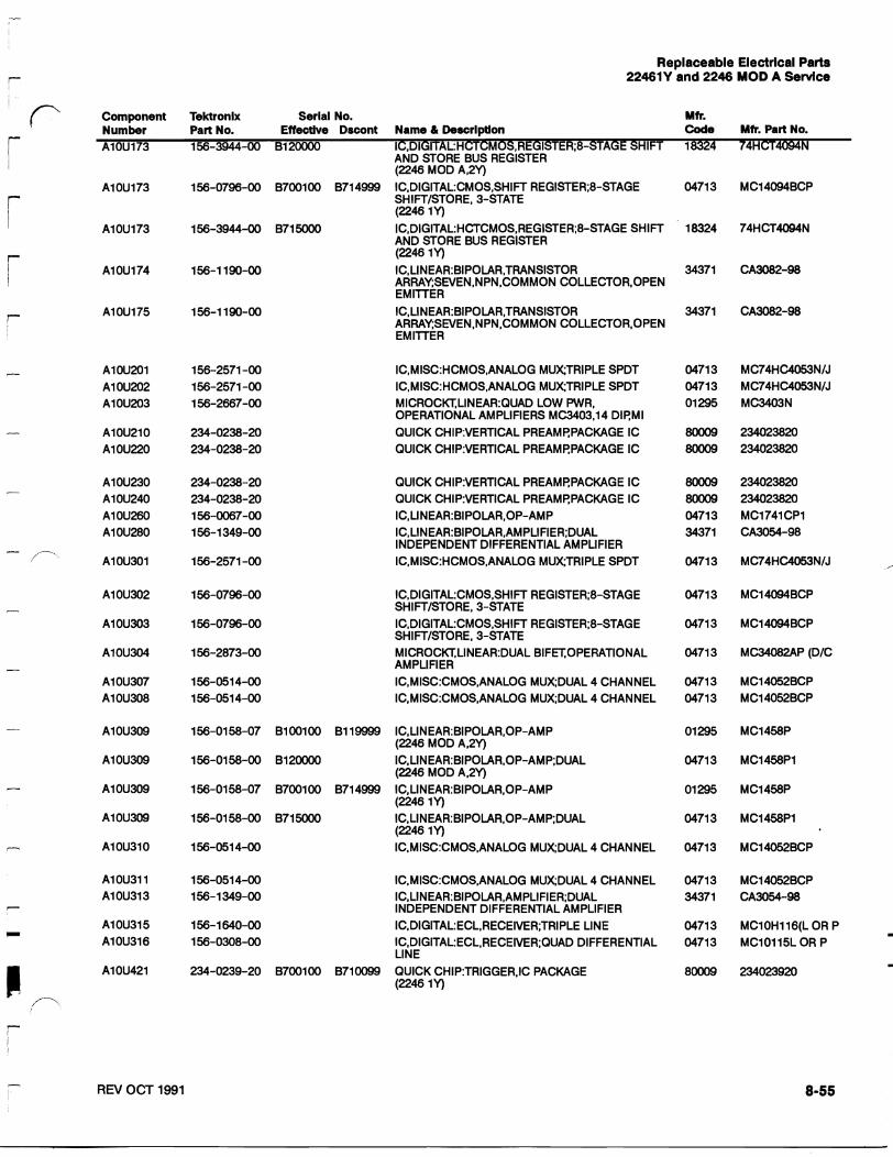
Replaceable Electrical Parts 22461Y and 2246 MOD A Senrlce
Component Tektronlx Serial No. Mfr. Number Part No. Effective Dscont Name & Dercrlption Code Mtr. Part No. A10U173 156-3944-00 B120000 IC,DIGITAL:HCTCMOS,REGIS~;~-STAGE SHIFT 18324 74HCT4094N
AND STORE BUS REGISTER (2246 MOD A,2Y)
A10U173 156-0796-00 8700100 8714999 IC,DIGITAL:CMOS,SHIFT REGISTERi8-STAGE 0471 3 MC14094BCP SHIFTISTORE, 3-STATE (2246 1Y)
A10U173 156-3944-00 871 5000 IC,DIGITAL:HCTCMOS,REGISTER;8-STAGE SHIFT 18324 74HCT4094N AND STORE BUS REGISTER (2246 1Y)
A1 0U174 156-1190-00 IC,LINEAR:BIPOLAR,TRANSISTOR 34371 CA3082-98 ARRAY;SEVEN,NPN,COMMON COLLECTOR,OPEN EMllTER
IC,MISC:HCMOS,ANALOG MUXTRIPLE SPDT 0471 3 MC74HC4053NlJ IC,MISC:HCMOS,ANALOG MUX;TRIPLE SPDT 0471 3 MC74HC4053NlJ MICROCKT,LINEAR:QUAD LOW PWR. 01295 MC3403N OPERATIONAL AMPLIFIERS MC3403,14 DIPMI QUICK CH1P:VERTICAL PREAMPPACKAGE IC 80009 234023820 QUICK CH1P:VERTICAL PREAMPPACKAGE IC 80009 234023820
QUICK CH1P:VERTICAL PREAMPPACKAGE IC 80009 234023820 QUICK CH1P:VERTICAL PREAMPPACKAGE IC 80009 234023820 IC,LINEAR:BIPOLAR,OP-AMP 04713 MC1741 CP1 IC,LINEAR:BIPOLAR,AMPLIFIER;DUAL 34371 CA3054-98 INDEPENDENT DIFFERENTIAL AMPLIFIER IC,MISC:HCMOS,ANALOG MUXTRIPLE SPDT 0471 3 MC74HC4053NN ,
IC,DIGITAL:CMOS,SHIFT REGISTER;8-STAGE 0471 3 MC14094BCP SHIFTISTORE, 3-STATE IC,DIGITAL:CMOS,SHIFT REGISTER;8-STAGE 04713 MC14094BCP SHIFTISTORE, 3-STATE MICROCICT,LINEAR:DUAL BIFET,OPERATIONAL 0471 3 MC34082AP (DIC AMPLIFIER IC,MISC:CMOS,ANALOG MUX;DUAL 4 CHANNEL 04713 MC14052BCP IC,MISC:CMOS,ANALOG MUX;DUAL 4 CHANNEL 04713 MC14052BCP
A10U309 156-0158-07 BlOOl00 8119999 IC.LINEAR:BIPOLAR,OP-AMP (2246 MOD A,2Y)
AlOU309 156-01 58-00 B1 20000 IC,LINEAR:BIPOLAR,OP-AMPiDUAL 04713 MC1458Pl (2246 MOD A,2Y)
A10U309 156-0158-07 B700100 871 4999 IC,LINEAR:BIPOLAR,OP-AMP 01295 MC1458P (2246 1 Y)
A1 0U309 156-0158-00 8715000 IC,LINEAR:BIPOLAR,OP-AMP;DUAL 04713 MC1458P1 (2246 1Y)
A10U310 156-051 4-00 IC,MISC:CMOS,ANALOG MUX;DUAL 4 CHANNEL 04713 MC14052BCP
IC,MISC:CMOS,ANALOG MUXDUAL 4 CHANNEL 04713 MC14052BCP IC,LINEAR:BIPOLAR,AMPLIFIER;DUAL 34371 CA3054-98 INDEPENDENT DIFFERENTIAL AMPLIFIER IC,DIGITAL:ECL,RECEIVER;TRIPLE LINE 04713 MClOH116(L OR P
I
IC,DIGITAL:ECL,RECEIVER;QUAD DIFFERENTIAL 04713 MClOl l5L OR P LlNE
A10U421 234-0239-20 8700100 8710099 QUICK CHIP:TRIGGER,IC PACKAGE 80009 234023920 -
(2246 1Y)
R N OCT 1991 8-55

Replaceable Electrical Parts 22461Y and 2246 MOD A Service
Component Tektronlx Serial No. Mtr. Number Part No. Etfectlve Dscont Name & Description Code Mtr. Part No. A1 0U421 234-0239-30 8710100 8710999 QUICK CH1P:TRIGGER lC PACKAGE 80009 234023930
(2246 1Y) 234-0239-31 8711000 QUICK CH1P:TRIGGER CIRCUIT,28PLCC WIAU 80009 234023931
LEAD (2246 1Y)
234-0239-20 8100100 8110099 QUlCK CHIP:TRIGGER,IC PACKAGE (2246 MOD A,2Y)
234-0239-30 BllOl00 81 12868 QUICK CHIPlTRIGGER IC PACKAGE 80009 234023930 (2246 MOD A.2Y) QUICK CH1P:TRIGGER CIRCUIT,28PLCC WIAU 80009 234023931 LEAD (2246 MOD A,2Y)
234-0239-20 8700100 8710099 QUICK CHIP:TRIGGER,IC PACKAGE 80009 234023920 (2246 1Y)
234-0239-30 B710100 8710999 QUICK CHIP:TRIGGER IC PACKAGE 80009 234023930 (2246 1Y)
234-0239-31 8711000 QUICK CHIP:TRIGGER CIRCUIT.28PLCC WIAU 80009 234023931 LEAD (2246 1Y)
234-0239-20 8100100 8110099 QUICK CHIP:TRIGGER,IC PACKAGE 80009 234023920 (2246 MOD A.2Y)
234-0239-30 8110100 8112868 QUICKCHIP:TRIGGERICPACKAGE 80009 234023930 (2246 MOD A,2Y)
234-0239-31 8112869 QUICK CH1P:TRIGGER CIRCUIT,28PLCC WIAU 80009 234023931 LEAD (2246 MOD A,2Y)
156-2027-00 IC,DIGITAL:HCMOS,GATE;HEX INV 27014 MM74HC04N 156-1 640-00 81 10100 IC.DIGITAL:ECL,RECEIVER;TRIPLE LINE 04713 MClOH116(L OR P
(2246 MOD A,2Y) 156-1640-00 8710100 IC,DIGITAL:ECL,RECEIVER;TRIPLE LINE 04713 MClOH116(L OR P
(2246 1Y) 156-0469-00 IC,DIGlTAL:LSlTL,DEMUWDECODER;3-TO-8 01295 SN74LS138 (N OR
DECODER
156-0768-00 IC,DIGITAL:LSlTL.SHIFT REGISTER;8-BIT 01295 SN74LS194AN BIDIRECTIONAL UNIVERSAL IC,DIGITAL:LSlTL,LATCH;QUADRUPLE S-R 01 295 SN74LS279AN IC.MISC:CMOS,ANALOG MUX;8 CHANNEL 04713 MC140518 (CP OR MICROCKT,DGTL:CMOS,SEMI CUSTOM,STD 66302 VF4247PC CCOOOl CELL,SLOW LOGIC
156-2654-00 MICROCKT,DGTL:ECL,SEMI CUSTOM.FAST LOGIC 04713 SC32205LB04 SCX32205LB04.40 DIPCERAMIC ONLY IC,DIGITAL:ECL,GATE;QUAD 2-INPUT ORINOR 04713 MC10101(L OR P) IC,DIGITAL:ECL,RECEIVER;TRIPLE LINE 04713 MClO116P IC,DIGITAL:lTL,BUFFER/DRIVER;HEX BUFFER. OC 01295 SN7417N MICROCKT,LINEAR:VERTlCAL OUTPUT 80009 155032200 AMPLIFIERM429
REV OCT 1991

Replaceable Electrical Parts 22461Y and 2246 MOD A Service
Component Tektronix Serlal No. Mfr. ~urnber Part No. Effective Dscont Name & Description Code Mfr. Part No. A1 0U702 156-1126-00 IC,LINEAR:BIPOLAR,COMPARATOR;OPEN 01295 LM3llP
COLLECTOR,2OONS A10U801 156-0158-07 BlOOl00 8119999 IC,LINEAR:BIPOlAR,OP-AMP
(2246 MOD A,2Y) A10U801 156-0158-00 Bi20000 IC,LINEAR:BIPOLAR,OP-AMPiDUAL
(2246 MOD A,2Y) A10U801 156-0158-07 B700100 B714999 IC,LINEAR:BIPOLAR,OP-AMP
(2246 1Y) A1 OU801 156-01 58-00 871 5000 IC,LINEAR:BIPOLAR,OP-AMPiDUAL
(2246 1Y)
QUICK CHIP:GPS HORlZ PREAMP 80009 234040121 IC,LINEAR:BIPOLAR,OP-AMP;DUAL,HIGH OUTPUT 57668 BA4560 CURRENT
A1 0U930 156-0158-07 BlOOl00 61 19999 IC,LINEAR:BIPOLAR,OP-AMP (2246 MOD A,2Y)
A1 0U930 156-0158-00 8120000 IC.LINEAR:BIPOLAR,OP-AMP;DUAL (2246 MOD A.2Y)
A1 0U930 156-0158-07 6700100 6714999 IC.LINEAR:BIPOLAR,OP-AMP (2246 1Y)
A1 0U930 156-0158-00 B715000 IC.LINEAR:BIPOLAR.OP-AMPiDUAL 04713 MC1458Pl (2246 1 Y)
A10U931 156-2605-00 IC,MISC:HCMOS,ANALOG MUX;8 CHANNEL 0471 3 MC74HC4051 NIJ
AlOUlOOl 156-0495-00 IC.LINEAR:BIPOLAR.OP-AMP;QUAD,SINGLE 01295 LM324N SUPPLY MICROCKT.LINEAR:DUAL BIFETOPERATIONAL 04713 MC34082AP (DIC AMPLIFIER
IC,MISC:CMOS,ANALOG MUX;TRIPLE SPDT 04713 MC14053BCP IC.MISC:CMOS,ANALOG MUX;TRIPLE SPDT 04713 MC140536CP
A1OVR801 152-0243-00 BlOOlOO B110099 DIODE,ZENER:,;15V,5°h,0.4W 0471 3 521 3203 (1 N965B (2246 MOD A,2Y)
A1 OVR801 152-0055-00 BllOl00 DlODE,ZENER:.;llV,5%,0.4W 0471 3 SZG35009Kl 1 N96 (2246 MOD A,2Y)
A1OVR801 152-0243-00 B700100 8710099 DIODE,ZENER:,;lSV,5%,0.4W 04713 SZ13203 (1 N965B (2246 1Y)
REV OCT 1991
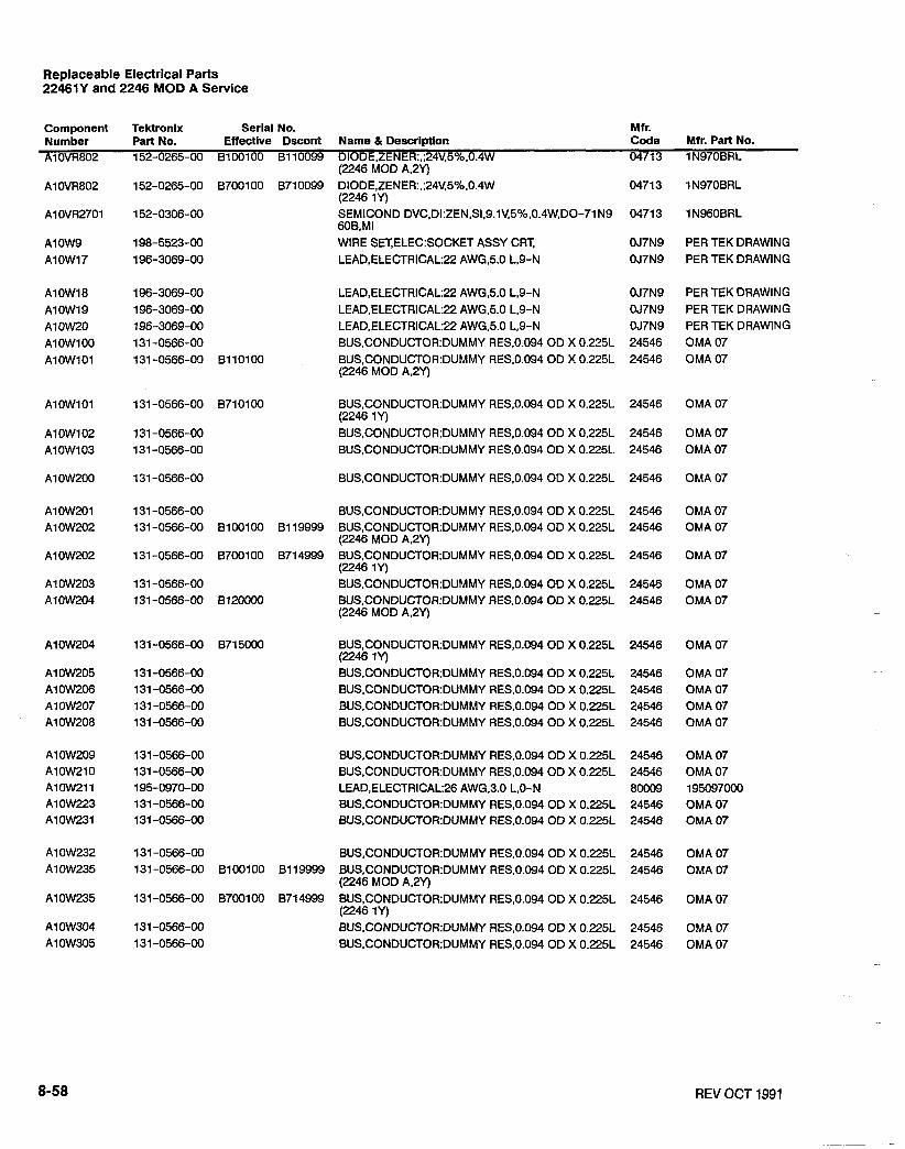
Replaceable Electrical Parts 22461Y and 2246 MOD A Service
Component Tektronlx Serial No. Number Part No. Effective Dscont Name & Description
Mf r. Code Mfr. Part No.
A10VR802 152-0265-00 BlOOlOO 8110099 DIODE,ZENER:.;24V,5%.0.4W 04713 1 N970BRL (2246 MOD A.2'4
A10VR802 152-0265-00 B700100 B710099 DIODE,ZENER:.;24V.5%,0.4W 04713 1 N970BRL (2246 1Y)
A1 0VR2701 152-0306-00 SEMICOND DVC.DI:ZEN,SI,9.1V,5%,0.4W,DO-71 N9 04713 1 N960BRL 60B,MI
A10W9 198-5523-00 WIRE SET,ELEC:SOCKET ASSY CRT, OJ7N9 PER TEK DRAWING A10W17 196-3069-00 LEAD,ELECTRICAL:22 AWG,5.O L,9-N OJ7N9 PER TEK DRAWING
A1 OW1 8 196-3069-00 LEAD,ELECTRICAL:22 AWG,S.O L,9-N OJ7N9 PER TEK DRAWING A10W19 196-3069-00 LEAD,ELECTRICAL:22 AWG,5.O L,9-N OJ7N9 PER TEK DRAWING A1 OW20 196-3069-00 LEAD,ELECTRICAL22 AWG,5.0 L.9-N OJ7N9 PER TEK DRAWING A10W100 131 -0566-00 BUS,CONDUCTOR:DUMMY RES.0.094 OD X 0.225L 24546 OMA 07 AlOWlOl 131 -0566-00 B l 10100 BUS,CONDUCTOR:DUMMY RES,0.094 OD X 0.225L 24546 OMA 07
(2246 MOD A,2Y)
AlOW101 131 -0566-00 B710100 BUS,CONDUCTOR:DUMMY RES,0.094 OD X 0.225L 24546 OMA 07 (2246 1Y)
A10W102 131 -0566-00 BUS,CONDUCTOR:DUMMY RES,0.094 OD X 0.225L 24546 OMA 07 A10W103 131-0566-00 BUS,CONDUCTOR:DUMMY RES.0.094 OD X 0.225L 24546 OMA 07
A1 OW200 131 -0566-00 BUS,CONDUCTOR:DUMMY RES.0.094 OD X 0.225L 24546 OMA 07
AlOW201 131-0566-00 BUS,CONDUCTOR:DUMMY RES.0.094 OD X 0.225L 24546 OMA 07 A1 OW202 131-0566-00 Bl00100 8119999 BUS.CONDUCTOR:DUMMY RES,0.094 OD X 0.225L 24546 OMA 07
(2246 MOD A,2Y) A1 OW202 131-0566-00 B700100 B714999 BUS,CONDUMOR:DUMMY RES,0.094 OD X 0.225L 24546 OMA 07
(2246 1Y) A1 OW203 131 -0566-00 BUS,CONDUCTOR:DUMMY RES0.094 OD X 0.225L 24546 OMA 07 A10W204 131-0566-00 8120000 BUS.CONDUCTOR:DUMMY RES.0.094 OD X 0.2251- 24546 OMA 07
(2246 MOD A,2Y)
A1 OW204 131-0566-00 B715000 BUS,CONDUCTOR:DUMMY RES.0.094 OD X 0.225L 24546 OMA 07 (2246 1Y)
A1 OW205 131 -0566-00 BUS.CONDUCTOR:DUMMY RES,0.094 OD X 0.225L 24546 OMA 07 A1 OW206 131-0566-00 BUS,CONDUCTOR:DUMMY RES,0.094 OD X 0.225L 24546 OMA 07 A10W207 131 -0566-00 BUS,CONDUCTOR:DUMMY RES,0.094 OD X 0.225L 24546 OMA 07 A10W208 131 -0566-00 BUS,CONDUCTOR:DUMMY RES,0.094 OD X 0.225L 24546 OMA 07
BUS,CONDUCTOR:DUMMY RES.0.094 OD X 0.225L 24546 OMA 07 BUS,CONDUCTOR:DUMMY RES,0.094 OD X 0.225L 24546 OMA 07 LEAD,ELEMRICAL:26 AWGB.0 L,O-N 80009 195097000 BUS,CONDUCTOR:DUMMY RES.0.094 OD X 0.225L 24546 OMA 07 BUS,CONDUCTOR:DUMMY RES,0.094 OD X 0.22511 24546 OMA 07
A10W232 131-0566-00 BUS,CONDUCTOR:DUMMY RES,0.094 OD X 0.225L 24546 OMA 07 A 1 OW235 131-0566-00 BlOOlOO B1 19999 BUS,CONDUCTOR:DUMMY RES.0.094 OD X O.225L 24546 OMA 07
(2246 MOD A,2Y) A1 OW235 131-0566-00 B700100 8714999 BUS,CONDUCTOR:DUMMY RES.0.094 OD X 0.225L 24546 OMA 07
(2246 1Y) BUS,CONDUCTOR:DUMMY RES,0.094 OD X 0.2251. 24546 OMA 07 BUS,CONDUCTOR:DUMMY RES.0.094 OD X 0.225L 24546 OMA 07
REV OCT 1991

Replaceable Electrical Parts 22461Y and 2246 MOD A Service
Component Tektronix Serial No. Mfr. Number Part No. Etfectlve Dscont Name & Descrlptlon Code Mfr. Part No. AlOW401 131-0566-00 BUS,CONDUCTOR:DUMMY RES.0.094 OD X 0.225L 24546 OMA 07 A1 OW403 131-0566-00 BlOOl00 B110099 BUS,CONDUCTOR:DUMMY RES.0.094ODX0.225L 24546 OMA07
(2246 MOD A,2Y) A10W403 131-0566-00 B700100 B710099 BUS,CONDUCTOR:DUMMY RES,0.094 OD X 0.2251 24546 OMA 07
(2246 1Y) A10W404 131-0566-00 BlOOlOO B110099 BUS.CONDUCT0R:DUMMY RES.0.094 OD X 0.225L 24546 OMA 07
(2246 MOD A,2Y) A1 OW404 131-0566-00 B700100 8710099 BUS,CONDUCTOR:DUMMY RES,0.094 OD X 0.225L 24546 OMA 07
(2246 1Y)
A1 OW405 131-0566-00 BlOOl00 B1 10099 BUS,CONDUCTOR:DUMMY RES,0.094 OD X 0.225L 24546 OMA 07 (2246 MOD A,2Y)
A1 OW405 131-0566-00 B700100 B710099 BUS,CONDUCTOR:DUMMY RES,0.094 OD X 0.225L 24546 OMA 07 (2246 1Y)
A10W406 131 -0566-00 BUS,CONDUCTOR:DUMMY RES,0.094 OD X 0.225L 24546 OMA 07 A1 OW407 131-0566-00 B100100 B110099 BUS,CONDUCTOR:DUMMY RES,0.094 OD X 0.225L 24546 OMA 07
(2246 MOD A,2Y) A1 OW407 131-0566-00 8700100 8710099 BUS,CONDUCTOR:DUMMY RES,0.094 OD X 0.225L 24546 OMA 07
(2246 1Y)
A10W408 131-0566-00 B100100 B1 10099 BUS.CONDUCTOR:DUMMY RES.0.094 OD X 0.225L 24546 OMA 07 (2246 MOD A,2Y)
A1 OW408 131-0566-00 B700100 8710099 BUS,CONDUCTOR:DUMMY RES,0.094 OD X 0.225L 24546 OMA 07 (2246 1Y)
A10W410 131 -0566-00 BlOOlOO B1 10099 BUS,CONDUCTOR:DUMMY RES.0.094 OD X 0.225L 24546 OMA 07 (2246 MOD A,2Y)
A10W410 131 -0566-00 B700100 8710099 BUS,CONDUCTOR:DUMMY RES,0.094 OD X 0.225L 24546 OMA 07 (2246 1Y)
A10W411 131-0566-00 Bl00100 B110099 BUS,CONDUCTOR:DUMMY RES.0.094 OD X 0.2251- 24546 OMA 07 (2246 MOD A,2Y)
A10W411 131-0566-00 B700100 8710099 BUS,CONDUCTOR:DUMMY RES.0.094 OD X 0.225L 24546 OMA 07 (2246 1Y)
AlOW412 131-0566-00 Bl00100 B1 10099 BUS,CONDUCTOR:DUMMY RES,0.094 OD X 0.225L 24546 OMA 07 (2246 MOD A.2Y)
AlOW412 131-0566-00 8700100 B710099 BUS,CONDUCTOR:DUMMY RES.0.094 OD X 0.225L 24546 OMA 07 (2246 1Y)
A10W413 131-0566-00 BUS,CONDUCTOR:DUMMY RES,0.094 OD X 0.225L 24546 OMA 07 A1 OW41 4 131-0566-00 BUS,CONDUCTOR:DUMMY RES.0.094 OD X 0.225L 24546 OMA 07
A1 OW41 5 174-0733-01 CA ASSY;SFIELEC:4,26 AWG.4.5 L,RIBBON OJ7N9 ORDER BY DESC A10W416 174-0732-01 CA ASSY;SF!ELEC:4.26 AWG,3.O L,RIBBON OJ7N9 ORDER BY DESC A10W501 131-0566-00 BllOl00 BUS,CONDUCTOR:DUMMY RES.0.094 OD X 0.225L 24546 OMA 07
(2246 MOD A,2Y) AlOW501 131 -0566-00 871 01 00 BUS,CONDUCTOR:DUMMY RES,0.094 OD X 0.225L 24546 OMA 07
(2246 1Y) A10W502 131 -0566-00 B l 101 00 BUS,CONDUCTOR:DUMMY RES,0.094 OD X 0.2251- 24546 OMA 07
(2246 MOD A,2Y)
A1 OW502 131-0566-00 B710100 BUS,CONDUCTOR:DUMMY RES,0.094 OD X 0.225L 24546 OMA 07 (2246 1Y)
A10W503 131 -0566-00 B110100 BUS,CONDUCTOR:DUMMY RES.0.094 OD X 0.225L 24546 OMA 07 (2246 MOD A,2Y)
A10W503 131-0566-00 B710100 BUS,CONDUCTOR:DUMMY RES,0.094 OD X 0.225L 24546 OMA 07 (2246 1Y)
A10W504 131-0566-00 BllOl00 BUS,CONDUCTOR:DUMMY RES,0.094 OD X 0.225L 24546 OMA 07 (2246 MOD A,2Y)
A1 OW504 131 -0566-00 871 01 00 BUS.CONDUCTOR:DUMMY RES.0.094 OD X 0.225L 24546 OMA 07 (2246 1Y)
REV OCT 1991

Replaceable Electrical Parts 22461Y and 2246 MOD A Service
Component Tektronix Serial No. Mf r. Number Part No. Effective Dscont Name & Description Code Mfr. Part No. A1 OW505 131 -0566-00 BUS.CONDUCTOR:DUMMY RES.0.094 OD X 0.225L 24546 OMA 07 A1 OW506 131-0566-00 Bl lOl00 BUS,CONDUCTOR:DUMMY RES,0.094 OD X 0.225L 24546 OMA 07
(2246 MOD A,2Y)
AlOW506 131 -0566-00 871 01 00 BUS,CONDUCTOR:DUMMY RES,0.094 OD X 0.225L 24546 OMA 07 (2246 1Y)
A1 OW507 131-0566-00 B l 10100 BUS,CONDUCTOR:DUMMY RES,0.094 OD X 0.225L 24546 OMA 07 (2246 MOD A,2Y) BUS,CONDUCTOR:DUMMY RES.0.094 OD X 0.22514 24546 OMA 07 (2246 1Y)
AlOW510 131 -0566-00 BUS,CONDUCTOR:DUMMY RES.0.094 OD X 0.225L 24546 OMA 07 A1 OW603 131 -0566-00 BUS,CONDUCTOR:DUMMY RES.0.094 OD X 0.225L 24546 OMA 07 A1 OW604 131 -0566-00 BUS.CONDUCTOR:DUMMY RES,0.094 OD X 0.225L 24546 OMA 07 A1 OW605 131 -0566-00 BUS,CONDUCTOR:DUMMY RES,0.094 OD X 0.225L 24546 OMA 07 A10W606 131-0566-00 B l 10100 BUS,CONDUCTOR:DUMMY RES.0.094 OD X 0.225L 24546 OMA 07
(2246 MOD A.2Y)
A1 OW606 131 -0566-00 B710100 BUS,CONDUCTOR:DUMMY RES,0.094 OD X 0.225L 24546 OMA 07 (2246 1Y)
A1 OW607 131-0566-00 B110100 BUS,CONDUCTOR:DUMMY RES0.094 OD X 0.225L 24546 OMA 07 (2246 MOD A,2Y)
A10W607 131 -0566-00 871 01 00 BUS,CONDUCTOR:DUMMY RES,0.094 OD X 0.225L 24546 OMA 07 (2246 1Y)
A1 OW61 0 131 -0566-00 BUS,CONDUCTOR:DUMMY RES,O.O94 OD X 0.225L 24546 OMA 07 A1 OW61 1 131 -0566-00 BUS,CONDUCTOR:DUMMY RES,0.094 OD X 0.225L 24546 OMA 07
A1 OW61 2 131-0566-00 Bl00100 B1 19999 BUS,CONDUCTOR:DUMMY RES,0.094 OD X 0.225L 24546 OMA 07 (2246 MOD A.2Y)
A1 OW61 2 131-0566-00 8700100 8714999 BUS,CONDUCTOR:DUMMY RES.0.094 OD X 0.225L 24546 OMA 07 (2246 1Y)
A1 OW802 131 -0566-00 BUS,CONDUCTOR:DUMMY RES,0.094 OD X 0.225L 24546 OMA 07 A1 OW805 131 -0566-00 5US.CONDUCTOR:DUMMY RES,0.094 OD X 0.225L 24546 OMA 07 A1 OW806 131 -0566-00 BUS,CONDUCTOR:DUMMY RES.0.094 OD X 0.225L 24546 OMA 07
BUS,CONDUCTOR:DUMMY RES.0.094 OD X 0.225L 24546 OMA 07 BUS.CONDUCTOR:DUMMY RES.0.094 OD X 0.225L 24546 OMA 07 BUS,CONDUCTOR:DUMMY RES.0.094 OD X 0.225L 24546 OMA 07 BUS,CONDUCTOR:DUMMY RES,0.094 OD X 0.225L 24546 OMA 07 BUS,CONDUCTOR:DUMMY RES,O.CN OD X 0.225L 24546 OMA 07
A1 OW820 131-0566-00 BllOl00 B1 19999 BUS,CONDUCTOR:DUMMY RES.0.094 OD X 0.225L 24546 OMA 07 (2246 MOD A.2Y)
A10W820 131-0566-00 5710100 8714999 BUS,CONDUCTOR:DUMMY RES.0.094 OD X 0.225L 24546 OMA 07 (2246 1Y)
AlOW821 131-0566-00 B l 10100 B1 19999 BUS,CONDUCTOR:DUMMY RES,0.094 OD X 0.225L 24546 OMA 07 (2246 MOD A,2Y)
AlOW821 131-0566-00 B710100 8714999 BUS.CONDUCTOR:DUMMY RES.0.094 OD X 0.225L 24546 OMA 07 (2246 1Y)
AlOW1 000 131 -0566-00 BUS,CONDUCTOR:DUMMY RES,0.094 OD X 0.225L 24546 OMA 07
A10W1010 131-0566-00 BlOOlOO B110099 BUS,CONDUCTOR:DUMMY RES.0.094 OD X 0.225L 24546 OMA 07 (2246 MOD A,2Y)
A10W1010 131-0566-00 B700100 8710099 BUS.CONDUCTOR:DUMMY RES,O.CN OD X 0.225L 24546 OMA 07 (2246 1Y)
A1 OW1 101 131 -0566-00 BUS,CONDUCTOR:DUMMY RES,0.094 OD X 0.225L 24546 OMA 07 BUS.CONDUCToR:DUMMY RES,0.094 OD X 0.225L 24546 OMA 07 BUS,CONDUCTOR:DUMMY RES,0.094 OD X 0.225L 24546 OMA 07
REV OCT 1991

Replaceable Electrical Parts 22461Y and 2246 MOD A Service
Component Tektronix Serial No. Mtr. Number Part No. Effective Dscont Name & Description Code Mfr. Part No. A10W1104 131-0566-00 8710630 BUS,CONDUCTOR:DUMMY RES,0.094 OD X 0.225L 24546 OMA 07
(2246 1Y) A10W1104 131 -0566-00 B111186 BUS,CONDUCTOR:DUMMY RES,0.094 OD X 0.225L 24546 OMA 07
(2246 MOD A.2Y) A1 OW1 105 131 -0566-00 B710630 BUS,CONDUCTOR:DUMMY RES,0.094 OD X 0.225L 24546 OMA 07
(2246 1Y) A10W1105 131 -0566-00 B111186 BUS,CONDUCTOR:DUMMY RES,0.094 OD X O.225L 24546 OMA 07
(2246 MOD A,2Y) A10W1106 131 -0566-00 BUS,CONDUCTOR:DUMMY RES0.094 OD X 0.225L 24546 OMA 07
AIOW1 107 131-0566-00 BlOOlOO B1 10099 BUS,CONDUCTOR:DUMMY RES,0.094 OD X 0.225L 24546 OMA 07 (2246 MOD A,2Y)
A10W1107 131-0566-00 B700100 8710099 BUS,CONDUCTOR:DUMMY RES.0.094 OD X 0.225L 24546 OMA 07 (2246 1Y)
A10W1108 131-0566-00 BllOlOO BUS.CONDUCTOR:DUMMY RES,0.094 OD X 0.225L 24546 OMA 07 (2246 MOD A.2Y)
A10W1108 131-0566-00 B710100 BUS,CONDUCTOR:DUMMY RES,0.094 OD X 0.225L 24546 OMA 07 (2246 1Y)
A1 OW1 120 131 -0566-Q0 Bl00100 81 10099 BUS,CONDUCTOR:DUMMY RES,0.094 OD X 0.225L 24546 OMA 07 (2246 MOD A.2Y)
A10W1120 131 -0566-00 B700100 B710099 BUS,CONDUCTOR:DUMMY RES.0.094 OD X 0.225L 24546 OMA 07 (2246 1Y)
A1 OW1 200 131 -0566-00 BUS,CONDUCTOR:DUMMY RES,0.094 OD X 0.225L 24546 OMA 07 A10W1201 131 -0566-00 BUS,CONDUCTOR:DUMMY RES,0.094 OD X 0.225L 24546 OMA 07 A1 OW1202 131 -0566-00 BUS,CONDUCTOR:DUMMY RES.0.094 OD X 0.225L 24546 OMA 07 A10W1203 131 -0566-00 B l 10100 BUS,CONDUCTOR:DUMMY RES.0.094 OD X 0.225L 24546 OMA 07
(2246 MOD A,2Y)
A10W1203 131 -0566-00 B710100 BUS.CONDUCTOR:DUMMY RES,0.094 OD X 0.225L 24546 OMA 07 (2246 1Y)
AlOW1204 131 -0566-00 BUS,CONDUCTOR:DUMMY RES.0.094 OD X 0.225L 24546 OMA 07 A10W1205 131 -0566-00 BUS.CONDUCTOR:DUMMY RES,0.094 OD X 0.225L 24546 OMA 07 A1 OW1 209 131 -0566-00 BUS,CONDUCTOR:DUMMY RES.0.094 OD X 0.225L 24546 OMA 07 A10W1210 131 -0566-00 BUS,CONDUCTOR:DUMMY RES,0.094 OD X 0.225L 24546 OMA 07
BUS,CONDUCTOR:DUMMY RES,0.094 OD X O.225L 24546 OMA 07 BUS.CONDUCTOR:DUMMY RES.0.094 OD X 0.225L 24546 OMA 07 BUS,CONDUCTOR:DUMMY RES,0.094 OD X 0.225L 24546 OMA 07 BUS,CONDUCTOR:DUMMY RES.0.094 OD X 0.225L 24546 OMA 07 BUS,CONDUCTOR:DUMMY RES,0.094 OD X 0.225L 24546 OMA 07
BUS,CONDUCTOR:DUMMY RES,0.094 OD X 0.225L 24546 OMA 07 BUS,CONDUCTOR:DUMMY RES,0.094 OD X 0.225L 24546 OMA 07 BUS,CONDUCTOR:DUMMY RES.0.094 OD X 0.225L 24546 OMA 07 BUS,CONDUCTOR:DUMMY RES,0.094 OD X 0.225L 24546 OMA 07 BUS.CONDUCTOR:DUMMY RES.0.094 OD X 0.225L 24546 OMA 07
BUS,CONDUCTOR:DUMMY RES.0.094 OD X 0.225L 24546 OMA 07 BUS,CONDUCTOR:DUMMY RES.0.094 OD X 0.225L 24546 OMA 07 BUS,CONDUCTOR:DUMMY RES,0.094 OD X 0.225L 24546 OMA 07 BUS,CONDUCTOR:DUMMY RES.0.094 OD X 0.225L 24546 OMA 07 BUS,CONDUCTOR:DUMMY RES.0.094 OD X 0.225L 24546 OMA 07
REV OCT 1991
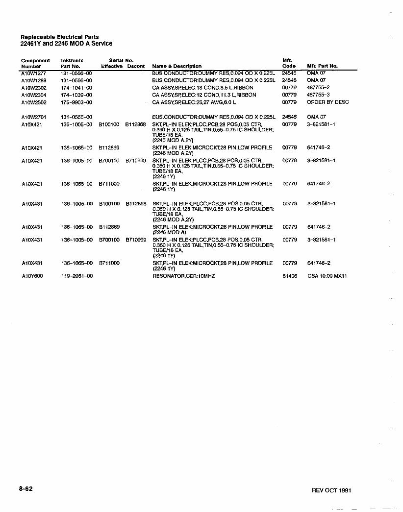
Replaceable Electrical Parts 22461Y and 2246 MOD A Service
Component Tektronix Serial No. Mf r. Number Part No. Effective Dscont Name & Description Code Mfr. Part No. A1 OW1 277 131 -0566-00 BUS,CONDUCTOR:DUMMY RES,0.094 OD X 0.225L 24546 OMA 07 A1 OW1 288 131 -0566-00 BUS,CONDUCTOR:DUMMY RES,0.094 OD X 0.225L 24546 OMA 07 A10W2302 174-1041 -00 CA ASSY,St?ELEC:18 COND.8.5 L,RIBBON 00779 487755-2 A1 OW2304 174-1 039-00 CA ASSY;SeELEC:12 COND,Tl.3 L.RIBBON 00779 487755-3 A1 OW2502 175-9903-00 CA ASSY,SP,ELEC:25,27 AWG.6.O L 00779 ORDER BY DESC
A1 OW2701 131 -0566-00 BUS.CONDUCT0R:DUMMY RES,0.094 OD X 0.225L 24546 OMA 07 A1 OX421 136-1005-00 Bl00lOO 8112868 SKT,PL-IN ELEK:PLCC,PCB,28 POS.0.05 CTR. 00779 3-821 581 -1
0.360 H X 0.125 TAIL.TIN.0.55-0.75 IC SHOULDER: TUBE118 EA, (2246 MOD A,2Y)
A1 OX421 136-1065-00 B1 12869 SKT,PL-IN ELEK:MICROCKT,28 PIN.LOW PROFILE 00779 641746-2 (2246 MOD A,2Y)
A10X421 136-1005-00 B700100 B710999 SKT,PL-IN ELEK:PLCC,PCB,28 POS,O.O5 CTR, 00779 3-821 581 -1 0.360 H X 0.125 TAlL,TIN,0.55-0.75 IC SHOULDER; TUBE118 EA. (2246 1Y)
A10X421 136-1 065-00 B711000 SKT,PL-IN ELEK:MICROCKT,28 PIN,LOW PROFILE 00779 641746-2 (2246 1Y)
A10X431 136-1005-00 BlOOl00 8112868 SKTPL-IN ELEK:PLCC,PCB.28 POS.0.05 CTR. 00779 3-821581-1 0.360 H X 0.125 TAIL.TIN.0.55-0.75 IC SHOULDER; TUBE118 EA. (2246 MOD A,2Y)
A10X431 136-1 065-00 B1 12869 SKT,PL-IN ELEK:MICROCKT.28 PIN.LOW PROFILE 00779 641746-2 (2246 MOD A)
A1 OX431 136-1 005-00 B700100 B710999 SKT.PL-IN ELEK:PLCC,PCB.28 POS.0.05 CTR. 00779 3-821 581 -1 0.360 H X 0.125 TAIL.TIN.0.55-0.75 IC SHOULDER; TUBE118 EA, (2246 1Y)
A10X431 136-1 065-00 B711000 SKT,PL-IN ELEK:MICROCKT,28 PIN,LOW PROFILE 00779 641746-2 (2246 1Y)
A1 0Y600 119-2051 -00 RESONATOR,CER:lOMHZ 51406 CSA 10:00 MXl l
REV OCT 1991

Replaceable Electrical Parts 2246 1Y and 2246 MOD A Service
Component Tektronix Serial No. Mfr. Number Part No. Etfectlve Dscont Name & Description Code Mfr. Part No. A1 2 670-9402-01 CIRCUIT BD ASSY:POTENTIOMETER 80009 670940201 A1 2J2105 131-3626-00 CONN,BOX:PCB,SIP;FEMALE,STR,l X 17.0.1 00779 2-643649-3
CTR,O.21 H X 0.120 TAIL,TIN.BECU,BD RETENTION RES,VAR.NONWW:CKT BD,5K OHM,20%,0.5W 32997 91ZlAZ45EA0119 LINEAR RES,VAR,NONWW:CKT BD 5K OHM,20%.0.5W 32997 91ZlAZ45EA0117 LINEAR RES,VAR,NONWW:CKT BD,BK OHM,20°h,0.5W 32997 91 Z l AZ45EA0119 LINEAR
RES,VAR,NONWW:CKT BD 5K OHM,20%,0.5W 32997 91ZlAZ45EA0117 LINEAR RES,VAR,NONWW:CKT BD 5K OHM,20%.0.5W 32997 91ZlAZ45EA0117 LINEAR
A12R2106 31 1-2345-00 RES,VAR.NONWCKT BD 5K OHM.20%,0.5W 32997 91ZlAZ45EA0117 LINEAR RES.VAR.NONWCKT BD,SK OHM,20%.0.5W 32997 91ZlAZ45EA0119 LINEAR RES,VAR,NONWWCKT BD 5K OHM,20%,0.5W 32997 91ZlAZ45EA0117 Ll N EAR
A12R2109 31 1-2345-00 RES.VAR,NONWW:CKT BD 5K OHM,20%,0.5W 32997 9iZlAZ45EA0117 LINEAR RES.VAR,NONWW:CKT BD 5K OHM,20%.0.5W 32997 91ZlAZ45EA0117 LINEAR RES,VAR,NONWW:LINEAR,5K OHM,30%,0,25W 32997 91 Z2D-245-EA002 RES,VAR,NONWCKT BD 5K OHM,20%,0.5W 32997 91ZlAZ45EA0117 LINEAR RES,VAR,NONWW:LINEAR,5K OHM,30%,0.25W 32997 91 Z2D-Z45-EA002
REV OCT 1991
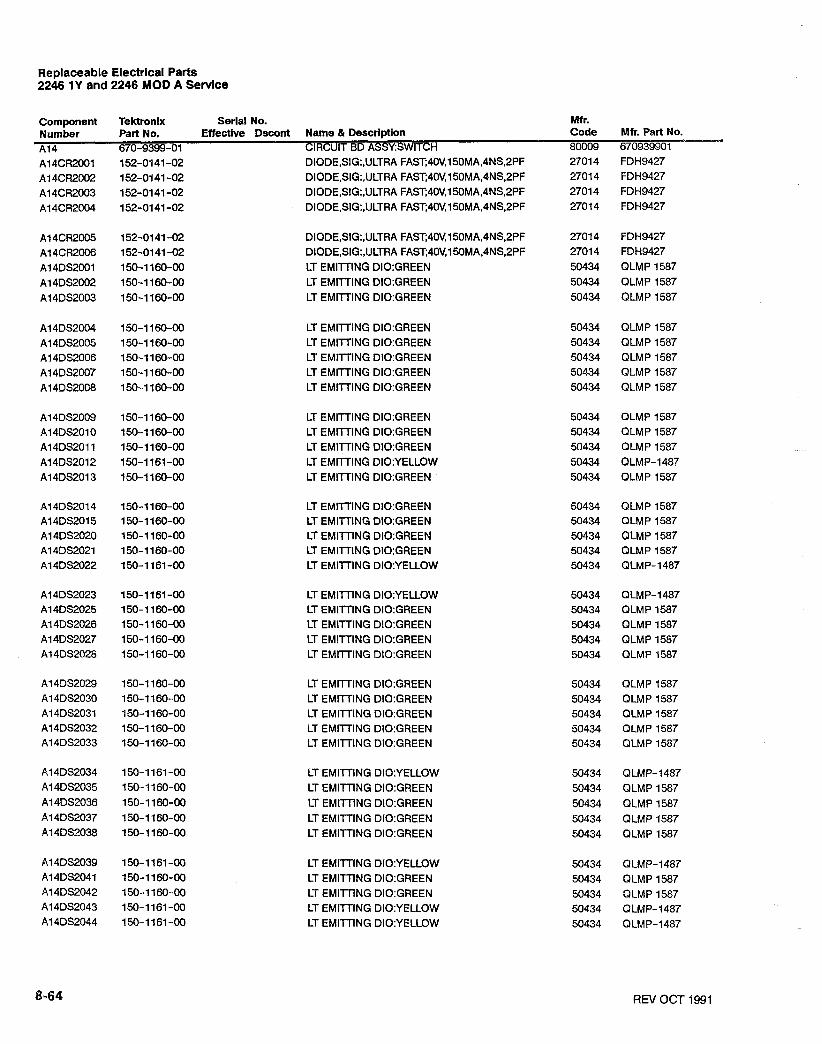
Replaceable Electrical Parts 2246 1Y and 2246 MOD A Service
Mf r. Code 80009 2701 4 2701 4 2701 4 27014
Component Tektronix Serial No. Number Part No. Effective Dscont Name & Description A1 4 670-9399-01 ClRCUlT BD ASSY:SWITCH A14CR2001 152-0141 -02 DIODE,SIG:,ULTRA FAST;40V,150MA,4NS,2PF A1 4CR2002 152-01 41 -02 DIODE,SIG:,ULTRA FAST;40V,150MA,4NS,2PF A1 4CR2003 152-01 41 -02 DIODE,SIG:.ULTRA FAST;40V,150MA,4NS,2PF A1 4CR2004 152-0141 -02 DIODE,SIG:.ULTRA FAST;40V,150MA,4NS,2PF
Mfr. Part No. 670939901 FDH9427 FDH9427 FDH9427 FDH9427
DIODE,SIG:.ULTRA FAST;40V,150MA,4NS,2PF DIODE,SIG:,ULTRA FAST;40V,150MA,4NS,2PF LT EMITTING DI0:GREEN LT EMITTING DI0:GREEN LT EMITTING DI0:GREEN
FDH9427 FDH9427 QLMP 1587 QLMP 1587 QLMP 1587
LT EMlTTlNG DI0:GREEN LT EMITTING DI0:GREEN LT EMITTING DI0:GREEN LT EMITTING DI0:GREEN LT EMITTING DI0:GREEN
QLMP 1587 QLMP 1587 QLMP 1587 QLMP 1587 QLMP 1587
LT EMITTING DI0:GREEN LT EMITTING DI0:GREEN LT EMITTING DI0:GREEN LT EMITTING DI0:YELLOW LT EMITTING DI0:GREEN
QLMP 1587 QLMP 1587 QLMP 1587 QLMP-1487 QLMP 1587
LT EMITTING DI0:GREEN LT EMlTTlNG DI0:GREEN LT EMITTING DI0:GREEN LT EMlTTlNG DI0:GREEN LT EMITTING DI0:YELLOW
QLMP 1587 QLMP 1587 QLMP 1587 QLMP 1587 QLMP-1487
LT EMITTING DI0:YELLOW LT EMITTING DI0:GREEN LT EMITTING DI0:GREEN LT EMITTING DI0:GREEN LT EMITTING DI0:GREEN
QLMP-1487 QLMP 1587 QLMP 1587 QLMP 1587 QLMP 1587
LT EMITTING DI0:GREEN LT EMITTING DI0:GREEN LT EMITTING DI0:GREEN LT EMITTING DI0:GREEN LT EMITTING DI0:GREEN
QLMP 1587 QLMP 1587 QLMP 1587 QLMP 1587 QLMP 1587
LT EMlmNG DI0:YELLOW LT EMITTING DI0:GREEN LT EMITTING DI0:GREEN LT EMITTING DI0:GREEN LT EMITTING DI0:GREEN
QLMP-1487 QLMP 1587 QLMP 1587 QLMP 1587 QLMP 1587
LT EMITTING DI0:YELLOW LT EMITTING DI0:GREEN LT EMITTING DI0:GREEN LT EMIlTlNG DI0:YELLOW LT EMITTING DI0:YELLOW
QLMP-1487 QLMP 1587 QLMP 1587 QLMP-1487 QLMP-1487
REV OCT 1991

Replaceable Electrical Parts 2246 1 Y and 2246 MOD A Service
Component Tektronix Serlal No. Mfr. Number Part No. Effective Dscont Name & Description Code Mfr. Part No. A1 4DS2045 150-1 161 -00 LT EMllTlNG DI0:YELLOW 50434 QLMP-1487 A14DS2046 150-1 161 -00 LT EMlTTlNG DI0:YELLOW 50434 QLMP-1487 A1 4DS2047 150-1 160-00 LT EMllTlNG DI0:GREEN 50434 QLMP1587 A1 4DS2048 150-1 160-00 LT EMllTlNG DI0:GREEN 50434 QLMP 1587 A14R2001 307-0675-00 RES NTWK,FXD,FI:(Q),lK OHM,2%,1.25W 91 637 CSCl OAO1-1 MG
RES NTWK,FXD.FI:(Q).lK OHM,2%.1.25W 91637 CSClOAOl-102G IC,DIGITAL:LSlTL,SHIFT REGISTER;8-BIT PIS0 01295 SN74LS165N IC,DIGITAL:LSTTL,SHIFT REGlSTER;8-BIT PIS0 01295 SN74LS165M CA ASSYSf?ELEC:20.27 AWG,8.05 L OJ7N9 PER TEK DRAWING
REV OCT 1991
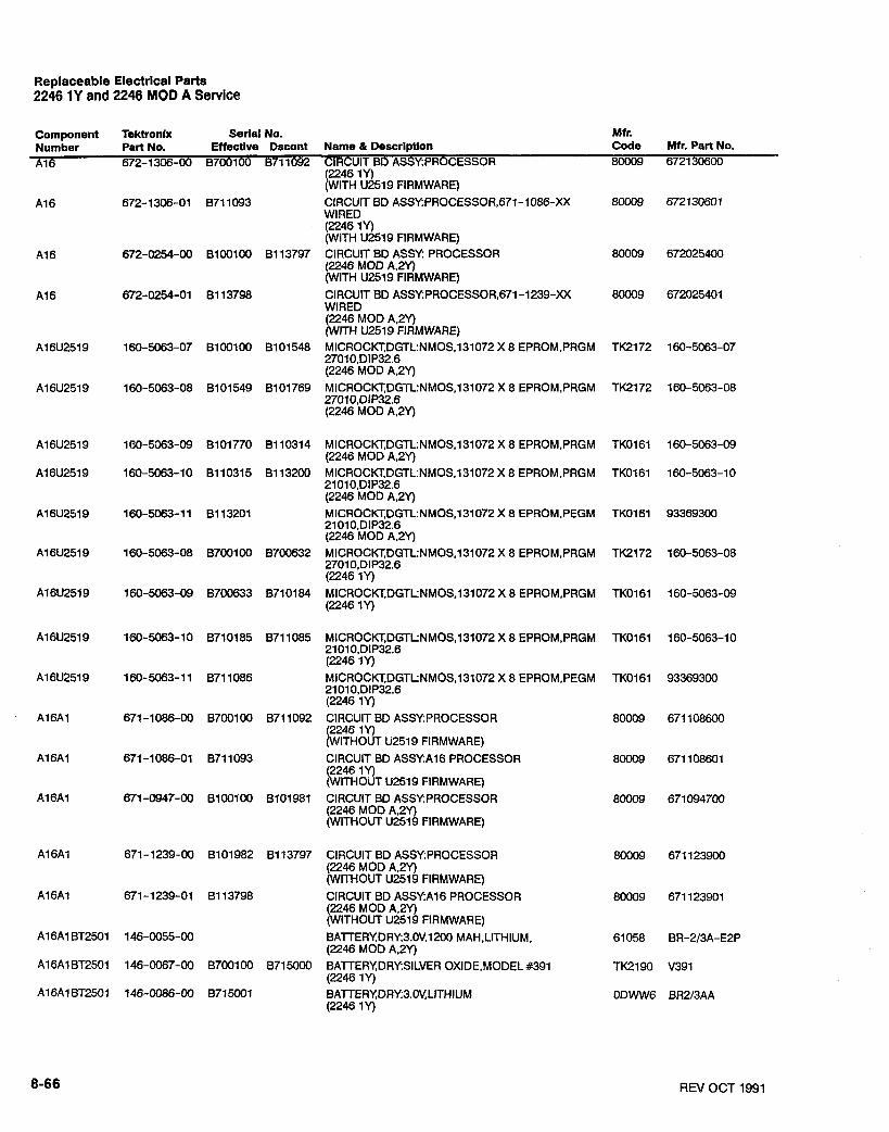
Replaceable Electrical Parts 2246 1Y and 2246 MOD A Service
Component Tektronlx Serial No. Mfr. Number Part No. Effective Dscont Name & Description Code Mfr. Part No. A1 6 672-1306-00 B700100 871 1092 CIRCUIT BD ASSYPROCESSOR 80009 672130600
(2246 1Y) (WITH U2519 FIRMWARE)
A1 6 672-1306-01 8711093 CIRCUIT BD ASSYPROCESSOR.671-1086-XX 80009 672130601 WIRED .... --
(2246 1Y) (WITH U2519 FIRMWARE)
A1 6 672-0254-00 8100100 B113797 CIRCUIT BD ASSY PROCESSOR 80009 672025400 (2246 MOD A,2Y) (WITH U2519 FIRMWARE)
A1 6 672-0254-01 8113798 CIRCUIT BD ASSYPROCESSOR,671-1239-XX 80009 672025401 WIRED (2246 MOD A,2Y) (WITH U2519 FIRMWARE)
A16U2519 160-5063-07 Bl00100 8101548 MICROCKT.DGTL:NMOS.131072 X 8 EPROM,PRGM TK2172 160-5063-07 27010.DIP32.6 (2246 MOD A,2Y)
A16U2519 160-5063-08 B101549 B101769 MICROCKT.DGTL:NMOS.131072 X 8 EPROM,PRGM TK2172 160-5063-08 27010.DIP32.6 (2246 MOD A.2Y)
A16U2519 160-5063-09 8101770 81 10314 MICROCKT;DGTL:NMOS.131072 X 8 EPROM.PRGM TKO161 160-5063-09 (2246 MOD A,2Y)
A16U2519 160-5063-10 B110315 81 13200 MICROCKT,DGTL:NMOS,131072 X 8 EPROM,PRGM TKO161 160-5063-10 21 01 0.DIP32.6 (2246 MOD A,2Y)
A16U2519 160-5063-1 1 81 13201 MICROCKT.DGTL:NMOS.131072 X 8 EPROM,PEGM TKO161 93369300 21 01 O.DIP32.6 (2246 MOD A,2Y)
A16A1 671-1086-00 8700100 871 1092 CIRCUIT BD ASSYPROCESSOR (2246 1Y) (WITHOUT U2519 FIRMWARE)
A16A1 671-1086-01 8711093 CIRCUIT BD ASSYA16 PROCESSOR 80009 671108601 (2246 1Y) (WITHOUT U2519 FIRMWARE)
A16A1 671-0947-00 Bl00100 8101981 CIRCUIT BD ASSYPROCESSOR (2246 MOD A,2Y) (WITHOUT U2519 FIRMWARE)
A16A1 671-1239-00 8101982 81 13797 CIRCUIT BD ASSY:PROCESSOR (2246 MOD A,2Y) (WITHOUT U2519 FIRMWARE) ClRCUlT BD ASSYA16 PROCESSOR - - (2246 MODA,~Y) (WITHOUT U2519 FIRMWARE)
A1 6A1 BT2501 146-0055-00 BATTERY,DRY3.0V,1200 MAH.LITHIUM, 61 058 BR-2/3A-E2P (2246 MOD A.2Y)
A16AlBT2501 146-0067-00 8700100 W15000 BATTERY,DRYSILVER OXIDE,MODEL#391 TK219O V391 (2246 1Y)
REV OCT 1991

Replaceable Electrical Parts 2246 I Y and 2246 MOD A Service
Component Tektronix Serlal No. Mfr. Number Part No. Effectlve Dscont Name & Description Code Mtr. Part No. A16A1 BT2502 146-0067-00 B700100 B715000 BATTERY,DRYSILVER OXIDE,MODEL #391 TK2190 V391
(2246 1Y) A1 6A1 C2300 281 -0759-00 CARFXD.CER DI:22PF,10%,100V 04222 SA101A220KAA A16A1 C2301 285-1300-01 CARFXD,MTLZD:O.lUF,10%,63V TK1913 MKS2 0.1/63/10 A1 6A1 C2302 285-1 300-01 CARFXD,MTLZD:O.1UF,10%,63V TK1913 MKS20.1/63/10 A1 6A1 C2303 285-1 300-01 CAF!FXD,MTLZD:O.lUF,10%,63V TK1913 MKS2 0.1/63/10
A1 6A1 C2319 281 -0909-00 CARFXD,CER DI:O.O22UF,20%,50V A16AlC2320 281-0798-00 8700100 8710099 CARFXD,CER DI:51 PF,1%.100V
(2246 1Y) A16A1 C2320 281 -0763-00 871 01 00 CARFXD,CER DI:47PF,10%,100V
(2246 1Y) A16AlC2320 281-0798-00 B100100 8110099 CARFXD.CER DI:51 PF,1%,100V
(2246 MOD A,2Y) A1 6A1 C2320 281 -0763-00 81 101 00 CARFXD,CER DI:47PF,10%,100V
(2246 MOD A,2Y)
A1 6A1 C2321 281 -0909-00 CAP.FXD,CER DI:O.O22UF,20%,50V A16A1 C2322 281 -0798-00 8700100 8710099 CARFXD.CER Dl151 PF,19/0,100V
(2246 1Y) A16A1 C2322 281 -0763-00 B710100 CAP.FXD,CER DI:47PF,10%.100V
(2246 1Y) A16AlC2322 281-0798-00 BlOOlOO 81 10099 CARFXD.CER DI:51 PF,1%.100V
(2246 MOD A,2Y) A16A1 C2322 281 -0763-00 B l 10100 CAF?FXD,CER DI:47PF,10%,100V
(2246 MOD A.2Y)
04222 SA105C223MAA TK1913 MKS2 0.1/63/10 TK1913 MKS2 0.1/63/10 TK1913 MKS 2.47150 OR TK1913 MKS20.22MFDl
TK1913 MKS 2.47/50 OR TK1913 MKS2 0.22 MFD 1 04222 SA105C223MAA 04222 SA105C223MAA 04222 SA105C223MAA
04222 SA105E104MAA 04222 SA105E104MAA 04222 SA105C223MAA 04222 SA105C223MAA 04222 SA101 A201 JAA
A16AlC2323 281-0798-00 BlOOl00 8110099 CAP.FXD,CER DI:51PF,1°~,100V (2246 MOD A,2Y)
A16A1 C2323 281-0763-00 B1 10100 CAl?FXD,CER DI:47PF,10%.100V (2246 MOD A.2Y)
REV OCT 1991
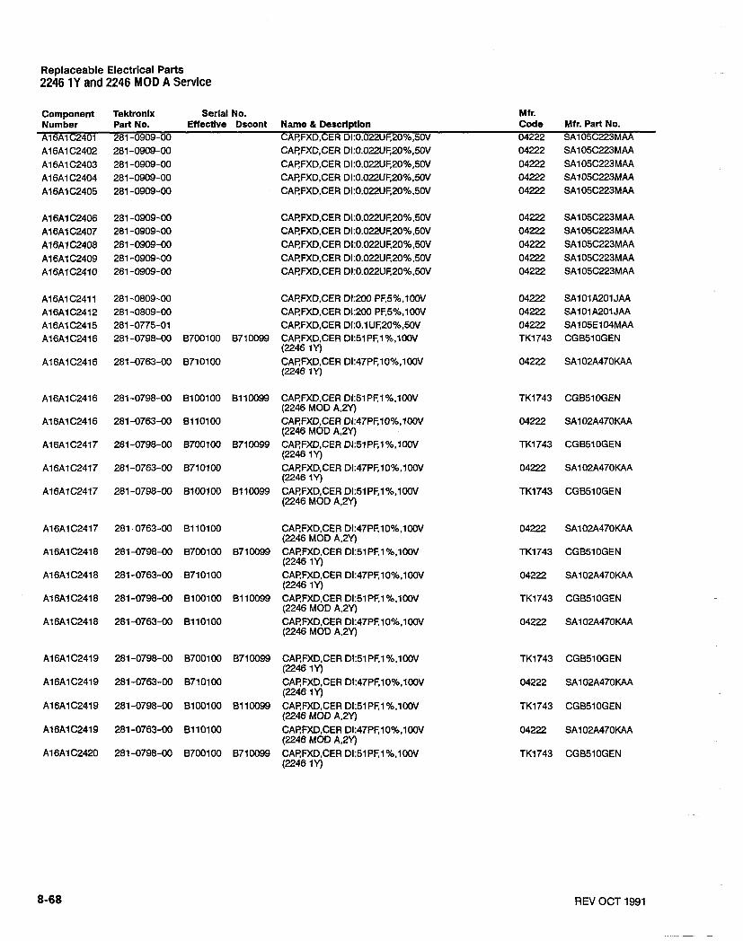
Replaceable Electrical Parts 2246 1Y and 2246 MOD A Service
Component Tektronlx Serlal No. Number Part No. Effective Dscont Name & Descrlptlon A1 6A1 C2401 281 -0909-00 CARFXD,CER DI:O.O22UF,20%,5OV A1 6A1 C2402 281 -0909-00 CARFXD,CER DI:O.O22UF,20%,50V A1 6A1 C2403 281 -0909-00 CAPFXD,CER DI:O.O22UF,20%,50V A1 6A1 C2404 281 -0909-00 CARFXD,CER DI:O.O22UF,20%.50V A16A1 C2405 281 -0909-00 CARFXD,CER DI:O.O22UF,20%,50V
A16AlC2416 281-0798-00 B100100 8110099 CARFXD,CER DI:51PF,1%,100V (2246 MOD A,2Y)
A16A1 C2416 281 -0763-00 BllOlOO CARFXD,CER DI:47PF,10%, 100V (2246 MOD A,2Y)
A16AlC2417 281-0798-00 8700100 8710099 CARFXD,CER DI:51 PF,1%,100V (2246 1Y)
A16AlC2417 281-0763-00 8710100 CARFXD,CER DI:47PE10%.100V (2246 1Y)
Al6AlC2417 281-0798-00 B100100 8110099 CARFXD,CER DI:51PF.1°h,100V (2246 MOD A,2Y)
A16A1 C2417 281 -0763-00 8110100 CARFXD,CER DI:47PF.l0%,100V (2246 MOD A,2Y)
A16AlC2418 281-0798-00 8700100 8710099 CARFXD,CER DI:51PF,1%,100V (2246 1Y)
A16A1 C2418 281 -0763-00 . 8710100 CARFXD,CER DI:47PF,10%,100V (2246 1Y)
A16AlC2418 281-0798-00 8100100 81 10099 CARFXD,CER DI:51PF,1%.100V (2246 MOD A,2Y)
A16A1 C2418 281 -0763-00 81 10100 CARFXD,CER DI:47PF,10%,100V (2246 MOD A,2Y)
A16AlC2419 281-0798-00 6100100 B1 10099 CARFXD,CER DI:51PF,1%,100V (2246 MOD A,2Y)
A16AlC2419 281 -0763-00 B1 10100 CARFXD,CER DI:47PF,10°h,100V (2246 MOD A,2Y)
Mf r. Code Mfr. Part No. 04222 SA105C223MAA 04222 SA105C223MAA 04222 SA105C223MAA 04222 SA105C223MAA 04222 SA105C223MAA
04222 SA101A201 JAA 04222 SA101 A201 JAA 04222 SA105E104MAA TK1743 CGB5lOGEN
REV OCT 1991

Replaceable Electrical Parts 2246 1Y and 2246 MOD A Service
Component Tektronix Serial No. Mf r. Number Part No. Effective Dscont Name & Descrlptlon Code Mfr. Part No. A1 6A1 C2420 281 -0763-00 B710100 CAP,FXD,CER DI:47PF,10%,100V 04222 SA102A470KAA
(2246 1 Y) A16AlC2420 281-0798-00 6100100 61 10099 CAP,FXD,CER DI:51PF,1%,100V TK1743 CGB51OGEN
(2246 MOD A,2Y) A1 6A1 C2420 281 -0763-00 61101 00 CAP,FXD,CER DI:47PF,10%.100V 04222 SA102A470KAA
(2246 MOD A,2Y) A16A1 C2501 281 -0909-00 CARFXD,CER Dl:O.O22UF,20%,50V 04222 SA105C223MAA A1 6A1 C2502 281 -0909-00 CARFXD,CER DI:O.O22UF,20%,50V 04222 SA105C223MAA
04222 SA101A220KAA TK1913 MKS 2.47150 OR 04222 SA105E104MAA TK1913 MKS 2 ,47150 OR 04222 SA101 C472KAA
CAP,FXD,CER DI:O.O22UE20%,50V 04222 SAI 05C223MAA CARFXD,CER DI:O.O22UF,20%,50V 04222 SA105C223MAA CAP,FXD,CER DI:O.O22UF,20%,50V 04222 SA105C223MAA CAP,FXD.ELCTLT:l OUF, + 50-20%,25WDC 7\1\1344 SME25TlORM5X12F CAP,FXD,CER DI:4700PF,10%.100V 04222 SA101 C472KAA
A16A1 C2551 281 -0763-00 671 0100 CARFXD,CER DI:47PF,10%,100V 04222 SA102A470KAA (2246 1Y)
A16AlC2551 281-0798-00 BlOOl00 6110099 CAP,FXD,CER DI:51PF,1%,100V TK1743 CG651OGEN (2246 MOD A,2Y)
REV OCT 1991
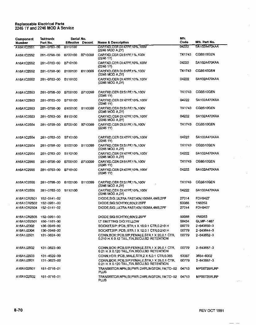
Replaceable Electrical Parts 2246 1Y and 2246 MOD A Service
Component Tektronix Serial No. Mf r. Number Part No. Effective Dscont Name & Description Code Mfr. Part No.
A16A1 C2551 281-0763-00 81 10100 CARFXD,CER DI:47PF,10%,100V 04222 SA102A470KAA (2246 MOD A,2Y)
A16A1 C2552 281 -0798-00 8700100 B710099 CARFXD,CER Dl151 PF,l%, 100V (2246 1Y)
A1 6A1 C2552 281 -0763-00 871 01 00 CARFXD,CER DI:47PF,10%,100V (2246 1Y)
A16A1 C2552 281-0798-00 BlOOlOO 8110099 CARFXD.CER DI:51 PF,lO/o.lOOV (2246 MOD A.2Y) CAP,FXD,CER DI:47PF,10%,100V (2246 MOD A,2Y)
A16AlC2553 281-0798-00 8700100 8710099 CAP,FXD,CER DI:51 PF,1%,100V (2246 1Y)
A16A1 C2553 281 -0763-00 87101 00 CARFXD,CER DI:47PF, 10%,100V (2246 1Y)
A16A1 C2553 281-0798-00 8100100 B110099 CAPFXD,CER DI:51 PF,1%,100V (2246 MOD A.2Y)
A1 6A1 C2553 281 -0763-00 81 10100 CAP,FXD,CER DI:47PF,10%,100V (2246 MOD A,2Y)
A1 6A1 C2554 281 -0763-00 871 01 00 CAP,FXD,CER DI:47PF,10%,100V (2246 1Y)
A16AlC2554 281-0798-00 B100100 B1 10099 CAP,FXD,CER DI:51 PF,1%,100V (2246 MOD A,2Y)
A16AlC2554 281-0763-00 B l 10100 CARFXD,CER Dl:47PF,10%,100V (2246 MOD A.2Y)
A16AlC2555 281-0798-00 8100100 8110099 CAP,FXD,CER DI:51 PF,l%.lOOV TK1743 CGB510GEN (2246 MOD A,2Y)
A1 6A1 C2555 281 -0763-00 B l 101 OO CARFXD,CER DI:47PF,10%,100V 04222 SA102A470KAA (2246 MOD A,2Y)
A16A1 CR2501 152-0141 -02 DIODE,SIG:,ULTRA FAST;40V.l50MA,4NS,2PF 27014 FDH9427 A16A1 CR2502 152-0951 -00 DIODE,SIG:SCHTKY,;60V,2.25PF 50088 IN6263 A16AlCR2504 152-0141-02 DIODE,SIG:,ULTRA FAST40V,150MA,4NS,2PF 27014 FDH9427
CONN,BOX::PCB,SIP;FEMALE,STR,~ x 20.0.1 CTR, o o n g 2-643652-3 0.210 H X 0.12 TAIL,TIN,BECU,BD RETENTION
CONN,BOX:PCB,SIP;FEMALE,STR,l X 25.0.1 CTR, 00779 2-643657-3 0.21 H X 0.120 TAIL,TIN,BECU.BD RETENTION
CONN,BOX:PCB,SIP;FEMALE,STR,l X 25,O.l CTR. 00779 2-643657-3 0.21 H X 0.120 TAIL,TIN,BECU.BD RETENTION TRANSISTOR:NPN,SI,PWR DARLINGTON.1W.TO-92 04713 MPS6725RLRP PLUS TRANSISTOR:NPN,SI,PWR DARLINGTON,lW,TO-92 04713 MPS6725RLRP PLUS
REV OCT 1991

Replaceable Electrical Parts 2246 1Y and 2246 MOD A Service
Com~onent Tektronix Serial No. Mfr. ~urnber Part No. Effective Dscont Name & DescrlpUon Code Mfr. Part No. A16A1 Q2503 151 -0716-01 TRANSISTOR:NPN,SI,PWR DARLINGTON.1 W,TO-92 0471 3 MPS6725RLRP
PLUS A16AlQ2504 151 -0716-01 TRANSISTOR:NPN,SI,PWR DARLINGTON,lW,TO-92 04713 MPS6725RLRP
PLUS A16A1 Q2505 151 -0716-01 TRANSISTOR:NPN,SI,PWR DARLINGTON,l W,TO-92 0471 3 MPS6725RLRP
PLUS A16A1 Q2506 151 -0716-01 TRANSISTOR:NPN,SI.PWR DARLINGTON,lW,TO-92 04713 MPS6725RLRP
PLUS
REV OCT 1991

Replaceable Electrical Parts 2246 1Y and 2246 MOD A Service
Mfr. Code 91 637 91 637 91 637 91 637 91637
Component Number A1 6A1 R2339 A1 6A1 R2340 A16A1 R2341 A1 6A1 R2342 A16A1 R2343
Tektronlx Part No. 313-1472-00 31 3-1 472-00 31 3-1 472-00 313-1472-00 31 3-1 472-00
Serlal No. Effective Dscont Name & Description
RES,FXDPFILM:4.7K OHM,5%,0.2W RES,FXD,FILM:4.7K OHM,5%,0.2W RES,FXDnFILM:4.7K OHM.5%,0.2W RES,FXD,FILM:4.7K OHM,5%,0.2W RES,FXD,FILM:4.7K OHM.5%,0.2W
Mfr. Part No. CCF50-2-4700OJ CCF50-2-470OOJ CCF50-2-470009 CCF50-2-4700OJ CCF50-2-47000J
CCF50-2-1 OOOOJ CCF50-2-1 OOOOJ CCF50-2-47OOOJ CCF50-2-4700OJ CCF50-2-47OOOJ
REV OCT 1991

Replaceable Electrical Parts 2246 1Y and 2246 MOD A Service
Component Tektronix Serial No. Mfr. Number Part No. Effective Dscont Name & Description Code Mfr. Part No. A16A1 R2503 313-1621 -00 RES,FXD,FiLM:620 OHM.5%,0.2W 91637 CCF50-2-620ROJ Al6A1 R2504 313-1 472-00 RES,FXD,FILM:4dK OHM,5%,0.2W 91 637 CCF50-2-47000J A16A1 R2505 313-1621 -00 RES,FXD,FILM:620 OHM.5°kr,0.2W 91637 CCF50-2-620ROJ A16AlR2506 313-1621-00 RES,FXD,FILM:620 OHM,5%,0.2W 91637 CCF50-2-620ROJ A16AlR2507 313-1101-00 RES,FXD,FILM:100 OHM,5%,0.2W 91637 CCF50-2-100ROJ
RES,FXD,FILM:l K OHM,5%,0.2W 91 637 CCF50-2-10000J RES,FXD,FILM:620 OHM.5%,0.2W 91637 CCF50-2-620ROJ RES,FXD,FILM:Q,lOOK OHM,5%,0.125WTC =200 11236 750-101-R100K 0 PPMIDEG C RES,FXD,FILM:9,100K OHM,5%,0.125WC=200 11236 750-101-R100K 0 PPMDEG C
A16AlR2522 307-0499-00 RES,FXD,FILM:9,100K OHM,5%,0.125WTC=200 11236 750-101-R100K 0 PPMDEG C
RES,FXD,FILM:lK OHM,5%,0.2W RES,FXD,FILM:lK OHM,5%,0.2W RES,FXD,FILM:lK OHM,5%,0.2W
61 13798 RES,FXD,FILM:22 OHM,5%,0.2W (2246 MOD A,2Y)
B711093 RES,FXD,FILM:22 OHM,5%,0.2W (2246 1Y) RES,FXD,FILM:22 OHM,5%,0.2W RES,FXD,FILM:22 OHM,5%,0.2W RES,FXD,FILM:22 OHM,5%,0.2W RES,FXD,FILM:22 OHM,5%.0.2W RES,FXD,FILM:22 OHM,5%,0.2W
REV OCT 1991

Replaceable Electrical Parts 2246 1Y and 2246 MOD A Sewice
Component Tektronlx Serial No. Number Part No. Effective Dscont Name & Description A1 6A1 R2551 31 3-1220-00 RES,FXD,FILM:22 OHM,5%,0.2W
A1 6A1 R2552 313-1 220-00 RES,FXD,FILM:22 OHM.5%,0.2W
A16A1 R2553 313-1220-00 RES,FXD,FILM:22 OHM,5%.0.2W
A1 6A1 R2554 31 3-1 102-00 RES,FXD,FILM:lK OHM,5%,0.2W A16AlR2555 313-1101-00 RES,FXD,FILM:100 OHM,5%,0.2W
A1 6A1 R2565 31 3-1 621 -00 B1 13798 RES,FXD,FILM:620 OHM85%,0.2W (2246 MOD A.2Y)
A16A1 R2565 313-1621-00 871 1093 RES,FXD,FlLM:620 OHM.5%,0.2W (2246 1Y)
A1 6A1 U2300 156-1646-00 IC,DIGITAL:HCTCMOS,FLIP FL0P;OCTAL D-TYPE,3-STATE
A16A1 U2301 156-1646-00 IC.DIGITAL:HCTCMOS.FLIP FL0P;OCTAL D-TYPE,3-STATE
A1 6A1 U2302 156-1 589-00 IC,CONVERTER:BIPOLAR,D/A;12 BIT,CURRENT OUTMULTIPLYING
IC,MISC:CMOS,ANALOG MUX;8 CHANNEL IC,LINEAR:BIFET,OP-AMP;QUAD IC,LINEAR:BIFET.OP-AMP;QUAD IC.LINEAR:BIPOLAR,COMPARATOR;OPEN COLLECTOR,POONS IC.MISC:CMOS,ANALOG MUX;8 CHANNEL
A1 6A1 U2309 156-0513-00 IC,MISC:CMOS.ANALOG MUX;8 CHANNEL A1 6A1 U2313 156-1 646-00 IC,DIGITAL:HCTCMOS.FLIP FL0P;OCTAL
D-TYPE.3-STATE A16AlU2314 156-1 149-00 iC,LINEAR:BIFET,OP-AMP; A1 6A1 U2400 160-3493-00 MICROCKT,DGTL:8 BIT MICROCOMPUTER,
MASKED FOR READOUT SYSTEM A1 6A1 U2401 156-1 646-00 IC,DIGITAL:HCTCMOS,FLIP FL0P;OCTAL
D-TYPE>-STATE
IC,DIGITAL:LSTTL.COUNTER;SYNCH 4-BIT UP/DOWN BINARY IC.DIGITAL:LSTTL,COUNTER;SYNCH 4-BIT UPIDOWN BINARY
A16A1 U2406 156-1594-00 BlOOl00 8102625 IC,MEMORY:NMOS,SRAM;2K X 8,150NS (2246 MOD A,2Y)
Mfr. Code Mfr. Part No. 91637 CCF50-2-22ROOJ 91637 CCF50-2-22ROOJ 91 637 CCF50-2-22ROOJ 91637 CCF50-2-1OOOOJ 91637 CCF50-2-100ROJ
91637 CCF50-2-100ROJ 91637 CCF50-2-100ROJ 91 637 CCF50-2-1 OOROJ 91637 CCF50-2-100ROJ 91637 CCF50-2-100ROJ
24355 DAC312-040P (ST
04713 MC14051B (CP OR
04713 MC14051 B (CP OR 18324 74HCT374N
REV OCT 1991
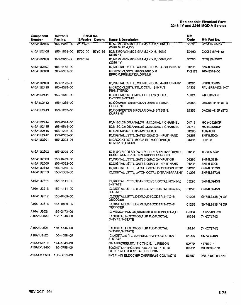
Replaceable Electrical Parts 2246 1Y and 2246 MOD A Service
Component Tektronix Serial No. Mfr. Number Part No. Effective Dscont Name & Descrlptlon Code Mfr. Part No. A16AlU2406 156-2016-00 8102626 IC,MEMORYNMOS,SRAM;2K X 8,100NS.OE 65786 CY6116-55PC
(2246 MOD A,2Y) A1 6A1 U2406 156-1594-00 B700100 8710186 IC,MEMORY:NMOS,SRAM;2K X 8,150NS SO482 CXK5816PN-12
(2246 1Y)
IC,DIGITAL:LSTTL,COUNTER;DUAL 4-BIT BINARY 01295 SN74LS393N MICROCKT.DGTL:NMOS,4096 X 8 TK2172 160-5391 -00 EPROM.PRGM2732A.DIP24.6
IC.DIGITAL:LSTTL,COUNTER;DUAL 4-BIT BINARY 01295 SN74LS393N MICROCW,DGTL:TTL,OCTAL 16 INPUT 34335 PAL1 6R8A4CN H07 REGISTERED IC,DIGITAL:HCTCMOS,FLIP FL0P;OCTAL 18324 74HCT374N D-TYPE,3-STATE
IC,CONVERTER:BIPOLAR,D/A;8 BIT,85NS, 24355 DAC08-415P (ST0 CURRENT
A16A1 U2413 156-1255-00 IC,CONVERTER:BIPOLAR,D/A;8 BIT,85NS, 24355 DAC08-415P (STD CURRENT
IC,MISC:CMOS.ANALOG MUX;DUAL 4 CHANNEL 04713 MC14052BCP IC.MISC:CMOS,ANALOG MUX;DUAL 4 CHANNEL 04713 MC14052BCP IC,LINEAR:BIFET,OP-AMP;QUAD 01295 TL074CN IC,DIGITAL:LSTTL,GATES;QUAD 2-INPUT NAND 01295 SN74LSOON MICROCW,DGTL:MOS.8 BIT MICROPRC,8 34335 R80188 MHz801 88.LCC68
IC.MISC:BIPOLAR,PWR SUPPLY SUPERVIS0R;MPU 01295 TL7705 ACP RESET GENERATOR.5V SUPPLY SENSING
IC,DIGITAL:LSTTL.GATES;QUAD 2-INPUT OR 01295 SN74LS32N IC,DIGITAL:LSTTL,GATES;QUAD 2-INPUT NAND 01295 SN74LSOON IC,DIGITAL:LSTTL,LATCH;OCTAL D TRANSPARENT 01295 SN74LS373N IC,DIGITAL:LSlTL,LATCH;OCTAL D TRANSPARENT 01295 SN74LS373N
A16AlU2514 156-1111-00 IC,DIGITAL:LSlTL,TRANSCEIVER;OCTAL NONINV, 01295 SN74LS245N 3-STATE
A16AlU2515 156-1 111-00 IC,DIGITAL:LSTTL,TRANSCElVER;OCTAL NONINV, 01295 SN74LS245N 3-STATE
A16AlU2517 156-0469-00 IC,DIGITAL:LSTTL,DEMUWDECODER;3-TO-8 01295 SN74LS138 (N OR DECODER
A1 6A1 U2518 156-0469-00 IC,DIGITAL:LSTTL,DEMUX/DECODER;3-TO-8 01295 SN74LS138 (N OR DECODER
A1 6/41 U2524 156-1 646-00 IC,DIGITAL:HCTCMOS,FLIP FL0P;OCTAL 18324 74HCT374N D-TYPE.3-STATE
A16A1 U2525 156-1058-00 IC,DIGITAL:STTL,BUFFER/DRIVER;OCTAL INV, 01295 SN74S240N 3-STATE CA ASS'(Sl?ELEC:17 COND.5.1 L,RIBBON 00779 487839-1 SOCKE7;DIP::PCB.;28 POS,2 X 14,O.l X 0.6 09922 DILB28P-108 CTR0.175 H X 0.13 TAIL,BECU.TIN SKT,PL-IN ELEK:CHIP CARRIER,68 CONTACTS 53387 268-5400-00-1 10
REV OCT 1991

Replaceable Electrical Parts 2246 1Y and 2246 MOD A Service
Component Tektronlx Serial No. Mf r. Number Part No. Effective Dscont Name & Description Code Mfr. Part No. A1 6A1 XU251 9 136-0963-00 SOCKET,DiP:PCB,;STR X 16.32 POS.O.l X 0.6 00779 2-64401 8-3
M 0.008-0.014 THK IC LEAD A16AlY2501 119-2936-00 BlOOlOO 81 13058 RESONATOR:16MHZ,CER 51406 CSA 16.00MXll
(2246 MOD A,2Y)
A1 6AlY2501 11 9-2936-01 B1 13059 RESONATOR:16MHZ,CER TK2058 82501009 (2246 MOD A,2Y)
A16AlY2501 119-2936-00 B700100 871 1085 RESONATOR:16MHZ,CER 51406 CSA 16.00MX11 (2246 1Y)
A16AlY2501 119-2936-01 B711086 RESONATOR:16MHZ,CER TK2058 82501009 (2246 1Y)
REV OCT 1991

Replaceable Electrical Parts 2246 1Y and 2246 MOD A Service
Component Number A18
Tektronix Serial No. Mfr. Part No. Effective Dscont Name & Descriptlon Code Mfr. Part No. 670-9398-04 CIRCUIT BD ASSYLV POWER SUPPLY 80009 670939804
(2246 1 Y) 670-9398-04 CIRCUIT BD ASSYLV POWER SUPPLY 80009 670939804
(2246 MOD A.2Y) CA~FXD,PLASTIC:1UF,10%,450V CAP FXD,ELCTLT270UF,20% ,450V,
290-0922-01 CAPFXD,ELCTLT:IOOOUF,4100% -10%,50V 01884 ORDER BY DESC
CAPFXD,ELCTLT100UF,20%,63V 55680 UEBl J l 01 MRAICA CAPFXD,CER DI:O.lUF,20%,50V 04222 SA105E104MAA CAPFXD,CER DI:O.lUF,20%,50V 04222 SA105E104MAA CA~FXD.ELCTLT:4.7UF.20%,1 OOV 1 W344 SM100VB4R7M6X11 CAPFXD,CER DI:O.O1UF,10%,100V.,TUBULAR,MI 04222 SA201 C103KAA
REV OCT 1991

Replaceable Electrical Parts 2246 1Y and 2246 MOD A Service
Component Tektronlx Serial No. Mtr. Number Part No. Effective Dscont Name & Description Code Mfr. Part No. A18C2249 281 -0773-00 CAF!FXD.CER DI:O.OlUF.l0%,100V,,TUBULAR,MI 04222 SA201 C103KAA A18CR2201 152-0661 -01 SEMICOND DVC,DI:RECT,S1,600V,3A 04713 MUR460RL A18CR2202 152-0400-00 DIODE,RECT,FAST RCVRY;400V,lA,200NS 14552 MB2501 A18CR2204 152-0400-00 DIODE,RECT,FAST RCVRY;400V,lA,200NS 14552 MB2501 A1 8CR2205 152-0400-00 DIODE,RECT:,FAST RCVRY;400V,lA,200NS 14552 MB2501
DIODE,RECTSCHTKY,;2OV,3A,.475VF,80A IFSM 04713 IN5820 DIODE,RECT:SCHTKY,;2OV,3A..475VF,80A IFSM 04713 IN5820 DIODE,RECT,FAST RCVRY;400V,lA,200NS 14552 MB2501 DIODE,RECT,FAST RCVRY;400V,lA,200NS 14552 MB2501
DIODE,RECT.FAST RCVRY;400V,lA,200NS 14552 MB2501 DIODE,RECT:,FAST RCVRY;400V,lA,200NS 14552 MB2501 DIODE,RECT.FAST RCVRY;400VS1A,200NS 14552 MB2501 DIODE.RECTSCHTKY,;20VV1A,.450VF,25A IFSM 04713 IN5817 DlODE,RECTSCHTKY,;2OV,lA,.450VF,25A IFSM 04713 IN5817
DIODE,RECT,FAST RCVRY;400V,lA,200NS 14552 MB2501 DIODE,RECT,FAST RCVRY;400V,lA,200NS 14552 MB2501 DlODE,RECT,;600V,lA,50A IFSM 14936 GP15J-069 DIODE,RECT,;600V,lA,50A IFSM 14936 GP15J-069 DIODE,RECT,;600V,lA,50A IFSM 14936 GP15J-069
DIODE,RECT,;600V,lA,50A IFSM 14936 GP15J-069 DIODE,RECT,FAST RCVRY;400V,lA,200NS 14552 MB2501 DIODE,RECT,FAST RCVRY;400V,lA,200NS 14552 MB2501 DIODE,SIG:.ULTRA FAST40V,150MA,4NS,2PF 27014 FDH9427 LAMRGLOWSOV MAX,OSMA,AID-T.WIRE LD TKO213 JH005/3011 JA
CONN,HDR:PCB,;MALE,STR,l X 3,O.l CTR,0.295 00779 644292-3 MLG X 0.140 TAIL,TIN CONN,HDR:PCB,;MALE,STR,l X 2.0.1 CTR.0.295 00779 644292-2 MLG X 0.140 TAIL,TIN COIL,RF:FXD,33UH,POWER 54583 OL1338-330K5RO INDUCTOR,FIXED:33UH,10~,1.8A ' 54583 TSLl110-330K l R INDUCTOR,FIXED:33UH,10%,1.8A 54583 TSL1110-330K 1R
A1 8L2204 108-1319-00 INDUCTOR,FIXED:33UH,10%.1.8A 54583 TSL1110-330K 1R A18L2205 108-1319-00 INDUCTOR,FIXED:33UH,10°/o,1 .8A 54583 TSL1110-330K 1R A1 812206 108-1396-00 B700100 871 1084 INDUCTOR,FIXED:150UH,10%,0.82 A, TK2058 TSL1110-151 KR82
RADIAL LEAD (2246 1Y)
A 1 8L2206 108-1319-00 8711085 INDUCTOR,FIXED:33UH,10%,1.8A 54583 TSL1110-330K 1R (2246 1Y)
A18L2206 108-1396-00 BlOOl00 B1 13046 INDUCTOR,FIXED:150UH,10°/o,0.82 A. TK2058 TSL1110-151 KR82 RADIAL LEAD (2246 MOD A,2Y)
REV OCT 1991

Replaceable Electrical Parts 2246 1Y and 2246 MOD A Service
Component Tektronlx Serial No. Mf r. Number Part No. Effective Dscont Name & Description Code Mtr. Part No. A1 8L2206 1 8-1319- 0 8113047 0
(2246 MOD A,2Y) A18L2207 108-1357-00 COIL,RF:FXD,POWER TK1441 86-343-2 A1 8L2208 108-1 357-00 COIL,RF:FXD,POWER TK1441 86-343-2 A18P2204 131 -3637-00 CONN,HDR PWR::PCB,;MALE,STR,l X 13,0.156 27264 A-41661 -A-13E50
CTR,0.953 MLG X 0.120 TAIL A18Q2201 151-1214-00 TRANSISTOR,PWR:MOS,N-CH;500V,4.5A,1.5 OHM 04713 STP4063
THYRISTOR,SCR:8A,200VVSENS GATE,TO-220 04713 SCR2117 WILEADFORM TRANSISTOR,SIG:BIPOLAR,NPN;40V,2OOMA, 04713 2N3904 300MHZ,AMPLIFIER
A1 8Q2212 151 -0276-01 TRANSISTOR,SIG:BIPOLARRPNP;50V,50MA,4OMHZ, OJR04 S1423-TPE2 (AMM AMPLIFIER
A1 80221 3 151 -0276-01 TRANSISTOR.SIG:BIPOLAR,PNP;50V,5OMA.40MHZ, OJR04 S1423-TPE2 (AMM AMPLIFIER
TRANSISTOR,PWR:MOS,N-CH;6OVV12A,O.25 OHM 04713 IRF533 WILEADFO RES,FXD,WW:O.l OHM,5%,2W 91637 CPF-2-RlOJ-TIR RES,FXD,FILM:180K OHM,5%.0.5W 57668 TR50J-E180K RES,FXD,FILM:180K OHM,5%,0.5W 57668 TR50J-E180K RES,FXD,FILM:lOOK OHM,5%,0.2W 91637 CCF50-2-10002J
A18R2215 313-1272-00 BlOOlOO B110219 RES.FXD,FILM:2.7K OHM,5%,0.2W 91637 CCF50-2-27000J (2246 MOD A.2Y)
A18R2215 313-1222-00 8110220 RES,FXD.FILM:2.2K OHM,5%,0.2W 91637 CCF50-2-22000J (2246 MOD A,2Y)
REV OCT 1991
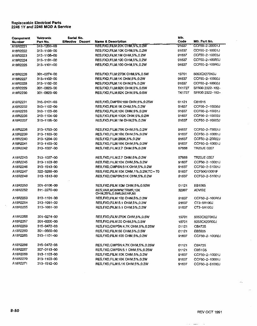
Replaceable Electrical Parts 2246 lY and 2246 MOD A Service
Component Tektronix Serial No. Mf r. Effective Dscont Name & Descrlption Code Mfr. Bart No. Number Part No.
A18R2221 313-1 3-00 rn F50-2-20001J
A1 8R2222 31 3-1 103-00 RES,FXD,FILM:lOK OHM,5%.0.2W 91637 CCF50-2-10001 J A1 8R2223 31 3-1 105-00 RES,FXD,FILM:lM OHM,5%,0.2W 91637 CCF50-2-10003J A1 8R2224 31 3-1 101 -00 RES,FXD,FILM:100 OHM,5%.0.2W 91 637 CCF50-2-100ROJ A18R2225 313-1101-00 RES,FXD,FILM:100 OHM.5%,0.2W 91637 CCF50-2-100ROJ
RES,FXD,CMPSN:100 OHM,5%,0.25W 01121 CB1015 RES,FXD.FILM:lK OHM,5%,0.2W 91 637 CCF50-2-1 OOOOJ RES,FXD,FILM:lOK OHM,5%,0.2W 91637 CCF50-2-10001 J RES,FXD,FILM:100K OHM,5%,0.2W 91 637 CCF50-2-10002J RES.FXD,FILM:lM OHM,5%,0.2W 91 637 CCF50-2-10003J
01121 EB1065 32997 ADVISE
REV OCT 1991

Replaceable Electrical Parts 2246 1Y and 2246 MOD A Service
Tektronlx Serial No. Mfr. Part No. Effective Dscont Name & Description Code Mfr. Part No. 313-1051-00 RES,FXD,FILM:5.1 OHM,5%,0.2W 91637 CT3-5R100J 313-1051-00 RES.FXD,FILM:5.1 OHM.5%,0.2W 91 637 CT3-5R100J 313-1103-00 RES,FXD,FILM:lOK OHM,5%,0.2M' 91637 CCF50-2-10001 J 301-0432-00 RES,FXD,FILM:4.3K OHM,5%,0.5W TK1727 SFR3O 2322-1 82- 313-1102-00 RES,FXD.FILM:l K OHM,5%.0.2W 91637 CCF50-2-10000J
Component Number A18R2272 A18R2273 A1 8R2274 A18R2275 A18R2276
307-0863-00 6100100 61 13898 RES,THERMAL:lO OHM,lO%,NTC 15454 SG-13s (2246 MOD A,2Y)
307-1551 -00 61 13899 RES,THERMAL:20 OHM,lO%,NTC, 91637 TECHNO (2246 MOD A,2Y) COMPONEN
307-1551-00 B711094 RES,THERMAL:20 OHM,lO%,NTC, 91637 TECHNO (2246 1Y) COMPONEN
260-2443-00 SWITCH,PUSH:POWER,DPST,6A,250VAC, 31918 130238
SWITCH,THRMSTC:NC.105 DEG C OPEN.80 DEG C 14604 24533-161-101 CLOSED,l OA,240VAC TRANSFORMER,RF:COUPLED INDUCTOR, 75498 ORDER BY DESC XFMR,PWR,STU:HIGH VOLTAGE, 75498 ORDER BY DESC TRANSFORMER.RF:DRIVER SATURATING 54583 BDT-001 XFMR,TRIGGER:LINE,l:l TURNS RATIO, 54937 DM1 500-2044
MICROCKT,LINEAR:BIPOLAR.PWM POWER 04713 MC34060AP SUPPLY,CONTROLLER SEMICOND DVC,DI:HIGH VOLTAGE 51406 MSL8523 MULTIPLIER,INPUT VOLTAGE 5.7KVAC PEAK TOPEAK.OUTPUT VOLTAGE 13750VDC
RES,V SENSITIVE:250VAC,20W,MEiAL OXIDE 34371 MOV-V250LA20A DIODE,ZENER:,;6.2V,5%,0.4W 04713 SZ11738RL DIODE,ZENER:,;30V.2%,0.4W 0471 3 1 N972CRL DIODE,ZENER:.;Z?OV,~~/O,O.~W 04713 lN968BRL LEAD,ELECTRICAL:18 AWG.3.3 L.8-9. OJ7N9 PER TEK DRAWING
LEAD,ELECTRICAL:18 AWG,3.3 L,8-0, OJ7N9 PER TEK DRAWING LEAD,ELECTRICAL:26 AWG.2.6 L,9-N OJ7N9 PER TEK DRAWING LEAD,ELECTRICAL:26 AWG.2.6 L.9-N OJ7N9 PER TEK DRAWING BUS,CONDUCTOR:DUMMY RES.0.094 OD X 0.2251- 24546 OMA 07
REV OCT 1991
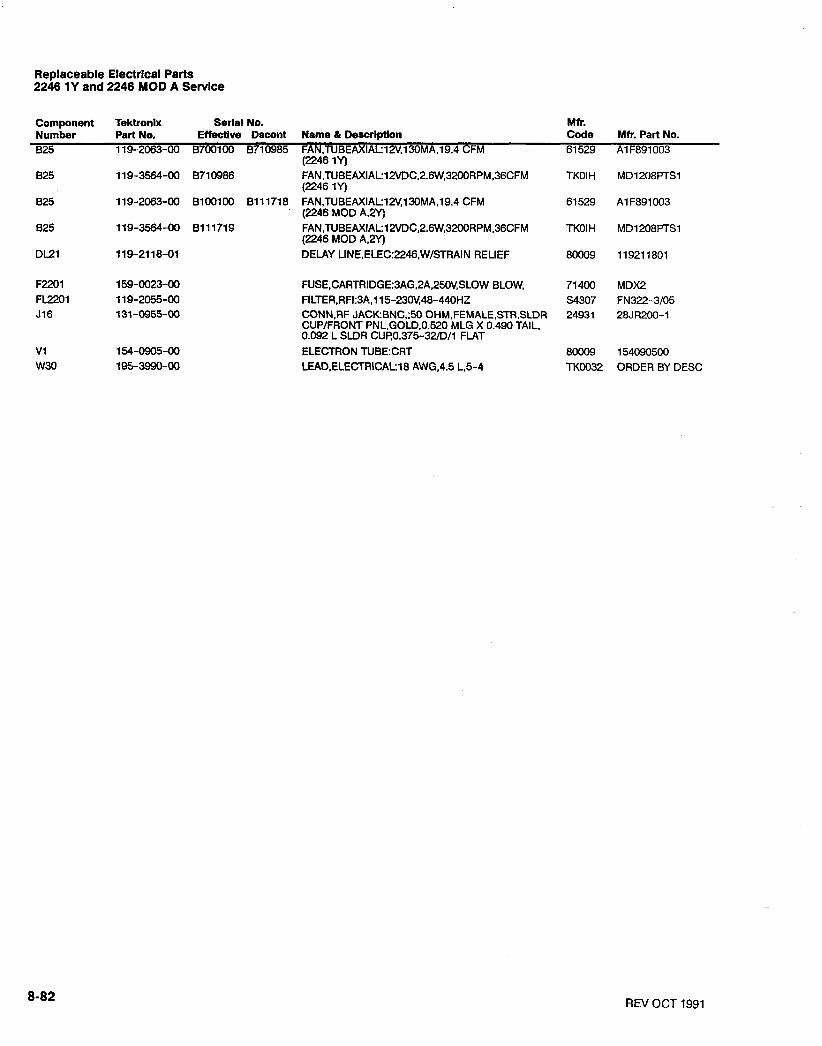
Replaceable Electrical Parts 2246 1Y and 2246 MOD A Service
Component Tektronlx Serlal No. Mtr. Number Part No. Effective Dscont Name 8 Description Code Mfr. Part No. 825 1 19-2063-00 8700100 871 0985 FAN,TUBEAXIAL:12V.13OMA,l9.4 CFM 61 529 A1 F891003
(2246 1Y) 825 1 19-3564-00 8710986 FAN,TUBEAXIAL:12VDC,2.6W,3200RPM,36CFM TKOlH MD1208PTSl
(2246 1Y) 825 119-2063-00 B l 00100 8111718 FAN,TUBEAXIAL:12V,13OMA,19.4 CFM 61529 A1 F891003
(2246 MOD A,2Y) 825 119-3564-00 8111719 FAN,TUBEAXIAL:12VDC,2.6W,3200RPM.36CFM TKOlH MD1208PTS1
(2246 MOD A,2Y) DL21 119-2118-01 DELAY LINE,ELEC:2246,WlSTRAIN RELIEF 80009 1 1921 1801
FUSE,CARTRIDGE:3AG,2A,250V,SLOW BLOW. 71400 MDX2 FILTER.RFI:3A,115-230V,48-440HZ S4307 FN322-3/05 CONN,RF JACK:BNC,;50 OHM,FEMALE,STR.SLDR 24931 28JR200-1 CUPIFRONT PNL.GOLD.O.520 MLG X 0.490 TAIL. 0.092 L SLDR CUP.0.375-32lD11 FLAT ELECTRON TUBE:CRT 80009 154090500 LEAD,ELECTRICAL:18 AWG,4.5 L,5-4 TK0032 ORDER BY DESC
REV OCT 1991

Section 9-2246 1Y and 2246 Mod A Service
DIAGRAMS AND CIRCUIT BOARD ILLUSTRATIONS Symbols
Graphic symbols and class designation letters are Y14.15-1966 Drafting Practices. based on ANSI Standard Y32.2-1975. Yl4.2M-1979 Line Conventions and Lettering.
ANSIIIEEE 280-1985 Letter Symbols for Quantities Used in Electrical Science
Logic symbology is based on ANSIIIEEE 91-1984. and Electrical Engineering. Logic symbols depict the logic function performed and may differ from the manufacturer's data. American National Standards Institute
1430 Broadway New York, New York 1001 8
The overline on a signal name indicates that the signal performs its intended function when it is in the LO state. Component Values
Abbreviations are based on ANSl Y1.l-1972. Electrical components shown on the diagrams are in
the following units unless noted otherwise:
Capacitors Values one or greater are in picofarads (pF). Other ANSI standards that are used in the preparation Values less than one are in microfarads (pF).
of diagrams by Tektronix, Inc., are: Resistors Ohms (R).
The information and special symbols below may appear in this manual.
Assembly Numbers and Grid Coordinates
Each assembly in the instrument is assigned an assembly number (e.g., A20). The assembly number appears on the circuit board outline on the diagram, in the title for the circuit board component location illustration, and in the lookup table for the schematic diagram and corresponding component locator illustration. The Replaceable Electrical Parts list is arranged by assemblies in numerical sequence; the components are listed by component number *(see following illustration for constructing a component number).
The schematic diagram and circuit board component location illustration have grids. A lookup table with the grid coordinates is provided for ease of locating the component. Only the components illustrated on thef acing diagram are listed in the lookup table. When more than one schematic diagram is used toillustratethecircuitry on a circuit board, the circuit board illustration may only appear opposite the first diagram on which it was il- lustrated; the lookup table will list the diagram number of other diagrams that the circuitry of the circuit board appears on.
A B C D M o d i f l e d C o m p o n e n t
Function Block Title I I
(Depicted in Grey, or With Grev Outline) See Pans hs t
Internal Screwdriver Adjustment
Cam Swltch Closure Chart (Dot indicates switch closure)
Etched Circuit Board Outlined In Black
Refer to Waveform
Function Block Out l~ne
IC type
Test Voltage
Heat Slnk
Board Name
P!O-Part of circult board
S t r a ~ or Link
Plug to E C Board
Coax~al connectors: male female
Plug Index; signifies pin No. 1
External Screwdriver Adj,
Shielding
Selected value, see Parts List and Maintenance Sect~on for Selection Criter~a
Assembly Number
Tektron~x Part No for clrcult boards
DeCOuDled or Filtered 6 7 0 - X X X X - X X R 3 3 0 @ Voltage
I * COMPONiXT I U Y B i R EXAMPLE Refer to D~agram Number
inmne Nunbe S Y N C G E N E R A T O R *
+ I S lmO Schematic Name and Number
a " "m . k**m h c. t e 0 R m * 4- , > ? a "
METAL-FILM RESISTORS
a@ and @ - lst , 2nd, and 3rd significant figures
@ -multiplier @ -tolerance
@ -temperature coefficient
@ -polarity and voltage rating
, 1 COLOR 1 SIGNIFICANT REsljToRs I MULTIPLIER TOLERANCE
BLACK
BROWN
RED
ORANGE
YELLOW
GREEN
BLUE
I WHITE I 9 ( --- I --- I
0
1
2
3
I VIOLET I 7
4
5
6
--- I f1/10%
(1 861-20A)6081-95
Figure 9-1. Color codes for resistors.
1
10
l o 2 or I 0 0
l o 3 or I K
GOLD
SILVER
NONE
---
f1 %
12%
%%
1 0 4 0 r 1 0 K
10' or 1 0 0 K
l o 6 o r 1 M
GRAY
%%
f%%
%A %
-
-
8 --- ---
10.' or 0.1
10-2 or 0.01
---
f 5%
f lo%
f 20%

16 Mod A Service
, 'IONS
8.
I and Lettering. I
or Quantities l Science glneering.
a Institute ,
he diagrams are in 1480:
In picofarads (pF). In microfarads (pF).
t board component ~ k u p table with the lee of locating the ~trated on the facing e. When more than tratethe circuitry on ustration may only In which it was il- diagram number of
f the circuit board
d Component In Grey, or With
M I - See Pans lrst
C Board
rntifles Panel , Connectors and a
I, aipnifles pln No. 1
crewdriver Adl.
'alue, see Parts L ~ s t anance Sect~on for Crlter~a
d or Filtered
)lagram Number
: Name mr
METAL-FILM RESISTORS
and @ - 1st. 2nd, and 3rd significant figures
@ -multiplier @ -tolerance
@ -temperature coefficient
@ -polarity and voltage rating
ORANGE 3
COLOR SIGN1 FICANT
YELLOW
GREEN
BLUE
I WHITE I 9 I _-- I --- I
RESISTORS
MULTIPLIER TOLERANCE '
VIOLET 7
4
5
6
--- 1 21110%
Q701 & (2801 (2802 Q806 (2807 ~ 7 0 2 MOS FET FET TO-92 ro-926
E G G D S C B E C E B
I METAL CASE 1 PLASTIC CASE I TRANSISTORS TRANSISTORS
TRANSISTOR SCR FET
C G CATHODE
IS FLAT
G S SIDE WITH
E SHORT LEAD
I FLAT PACK I LED 1
11 9
IND
7
1 1
I INTEGRATED CIRCUITS
LEAD CONFIGURATIONS AND CASE STYLES ARE TYPICAL BUT MAY VARY DUE TO VENDOR CHANGES OR INSTRUMENT MODIFICATIONS
GOLD
SILVER
NONE
Figure 9-1. Color codes for resistors.
l o 4 or 10 K
1 0 ~ 0 ~ 1 0 0 ~
l o 6 o r 1 M
GRAY I 8
Figure 9-2. Semiconductor lead configurations.
a% fx% *A%
--- ---
(1 861 -2OA)6081-95
-
-
l o - ' or 0.1
lo-* or 0.01
---
%%
*10%
+20%
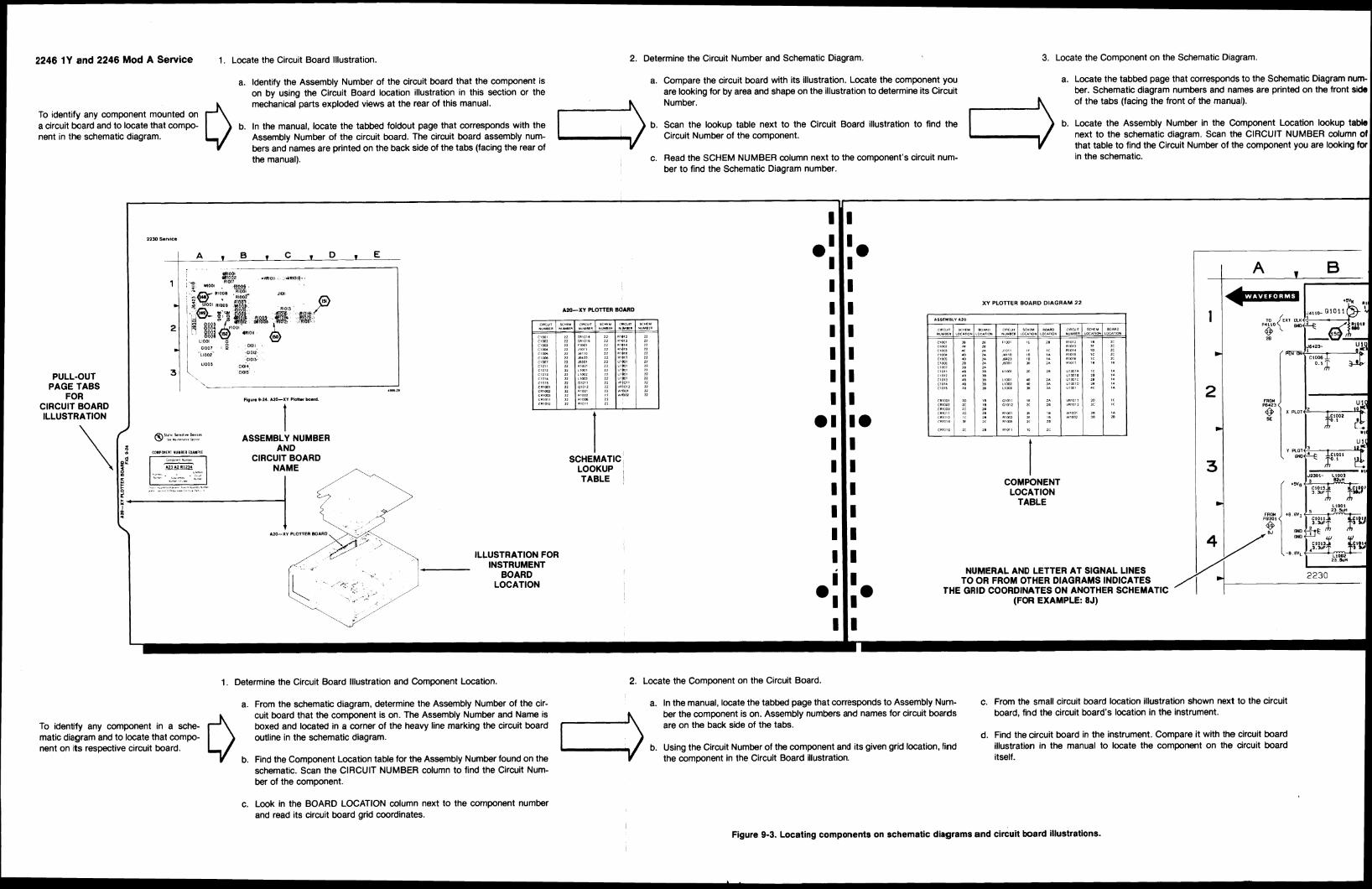
2246 1Y and 2246 Mod A Service 1. Locate the Circuit Board Illustration. 2. Determine the Circuit Number and Schematic Diagram. 3. Locate the Component on the Schematic Diagram.
a, Identify the Assembly Number of the circuit board that the component is a. Compare the circuit board with its illustration. Locate the component you a. Locate the tabbed page that corresponds to the Schematic Diagram nurn-
on by using the Circuit Board location illustration in this section or the are looking for by area and shape on the illustration to determine its Circuit ber. Schematic diagram numbers and names are printed on the front side
mechanical parts exploded views at the rear of this manual. Number. of the tabs (facing the front of the manual). To identify any component mounted on a circuit board and to locate that compo- b. In the manual, locate the tabbed foldout page that corresponds with the b. Scan the lookup table next to the Circuit Board illustration to find the b. Locate the Assembly Number in the Component Location lookup table nent in the schematic diagram. Assembly Number of the circuit board. The circuit board assembly num- Circuit Number of the component. next to the schematic diagram. Scan the CIRCUIT NUMBER column of
bers and names are ~rinted on the back side of the tabs (facina the rear of that table to find the Circuit Number of the component you are looking for .. -
the manual). c. Read the SCHEM NUMBER column next to the component's circuit num- ber to find the Schematic Diagram number.
in the schematic.
PULL-OUT PAGE TABS
FOR CIRCUIT BOARD ILLUSTRATION
@,,,,, .",!.. b.G.8
*, e"s * ASSEMBLY NUMBER
AZO-XY PLOTTER BOARD
SCHEMATIC LOOKUP TABLE
ILLUSTRATION FOR INSTRUMENT
BOARD LOCATION
XY PLOTTER BOARD DIAGRAM 22
ASSEMBLY A 2 0 1
COMPONENT LOCATION
TABLE
NUMERAL AND LETTER AT SIGNAL LINES TO OR FROM OTHER DIAGRAMS INDICATES
THE GRID COORDINATES ON ANOTHER SCHEMATIC (FOR EXAMPLE: 8J)
1. Determine the Circuit Board Illustration and Component Location. 2. Locate the Component on the Circuit Board.
a. From the schematic diagram, determine the Assembly Number of the cir- a. In the manual, locate the tabbed page that corresponds to Assembly Num- c. From the small circuit board location illustration shown next to the circuit
cuit board that the component is on. The Assembly Number and Name is ber the component is on. Assembly numbers and names for circuit boards board, find the circuit board's location in the instrument.
To identify any component in a sche- boxed and located in a corner of the heavy line marking the circuit board are on the back side of the tabs. matic diagram and to locate that compo- outline in the schematic diagram. d. Find the circuit board in the instrument. Compare it with the circuit board nent on its respective circuit board. b. Using the Circuit Number of the component and its given grid location, find illustration in the manual to locate the component on the circuit board
b. Find the Component Location table for the Assembly Number found on the the component in the Circuit Board illustration. itself.
schematic. Scan the CIRCUIT NUMBER column to find the Circuit Num- ber of the component.
c. Look in the BOARD LOCATION column next to the component number and read its circuit board grid coordinates.
Figure 9-3. Locating components on schematic diagrams and circuit board illustrations.

I 2. Determine the Circuit Number and Schematic Diagram. 3. Locale the Component on the Schematic Diagram.
a. Compare the circuit board with its illustration. Locate the component you
! are looking for by area and shape on the illustration to determine its Circuit ! Number. I
b. Scan the lookup table next to the Circuit Board illustrat~on to find the Circuit Number of the component.
c. Read the SCHEM NUMBER column next to the component's circuit num- ber to find the Schematic Diagram number.
a. Locate the tabbed page that corresponds to the Schematic Diagram num- c. In the SCHEM LOCATION column next to the component, read the grid ber. Schematic diagram numbers and names are printed on the front side coordinates of the component in the schematic. of the tabs (facing the front of the manual).
d. Using the grid coordinates given, find the component in the schematic b. Locate the Assembly Number in the Component Location lookup table diagram.
next to the schematic diagram. Scan the CIRCUIT NUMBER column of that table to find the Circuit Number of the component you are looking for in the schematic.
SCHEMATIC LOOKUP TABLE
XY PLOTTER BOARD DIAGRAM 22
A51EUBLI Pi20
c > m 3 c>m .D 2A >4>>0 I n a o c r
C l D O S LO 21 ,Mi, ( 8 I & R . 0 1 6 c>om 28 2a ,9,0> 33 >* R , " > 7 , B c>oo7 3B >a C l O l ' I B 2B L , iO l 10 28 "lrnl' I C C 1 0 1 2 18 18 " > r n > 8 $8 < > c > , AB 38 L>m> SB > A " , X > C 2B C o l a dB 3s L1m2 " 3s" ".Coil ,B ,A <.>,l 3s 1 LIDO, 3s , I' "lrnl r r . A
COMPONENT LOCATION
TABLE
NUMERAL AND LET---
I - - h -
2 CIRCUIT
SIG GNO
FROM l l l n n a r -
LIOOI
+a 6VpTO CRlOl2 SHIELD G
RLOll
. .. I
23 5uH A 20 XY ROTTER BOARD
static Sensitive Devices @ See Halntenance Sect lon
TTER AT SIGNAL LINES 2230 4999-71 X Y PLOTTER BOARD / PULL-OUT
TO OR FROM OTHER DIAGRAMS INDICATES PAGE TABS THE GRID COORDINATES ON ANOTHER SCHEMATIC FOR - / I -
(FOR EXAMPLE: 8J) A S S F M R I V N l l M R F R SCHFMATIC - . - - - - - - - . I SCHEMATIC ,---...--. ..-...--.. AND NAME
--..-.-..-. .- DIAGRAM NAME DIAGRAMS
AND NUMBER
2. Locate the Component on the Circuit Board.
a. In the manual, locate the tabbed page that corresponds to Assembly Num- c. From the small circuit board location illustration shown next to the circuit ber the component is on. Assembly numbers and names for circuit boards board, find the circuit board's location in the instrument. are on the back side of the tabs.
d. Find the circuit board in the instrument. Compare it with the circuit board b. Using the Circuit Number of the component and its given grid location, find illustration in the manual to locate the component on the circuit board
the component in the Circuit Board illustration. itself.
Figure 9-3. Locating components on schematic diagrams and circuit board illustrations.

2246 1Y and 2246 Mod A Service
VERTICAL PREAMPS
HORIZONTAL
EXT Z-AXIS INPUT
I
INTERFACE
I
MEASUREMENT PROCESSOR
ADC. DAC SYSTEM
REV JUN 1991 Figure 9-4. Simplified 2246 1Y or 2246 Mod A block diagram.


Figure 9-5b. Detailed 2246 1Y or 2246 Mod A block diagram-part 2. REV JUN 1991
2246 1Y and 2246 Mod A Service
5
RO VERT
RO HORIZ
NOTE
CD A m LED A ~ O SWITCH . I
RO RE0
RO BLANK - EOCH
CLK BM 4 DOT CLOCKS - -N 1 - - CLOCK -- + RO POSITION
DOT OIVIDER/COUNTER - RO-R4j ENABLE RO POS ENABLES
A
U2409A. 8. -
Q EOCH REFRESHER
U2410 LATCH U2417A. B U2403
POS STB I + I L
- CHARACTER CHARACTER
DOT - DOT iL RO RUN COUNTER > DOTO-DOT4 POSITION
CLK 4M U2407A. B ROM U2408
i SWITCH . > COLUH4 DRIVERS ASO-ASS ICQISTER m 2 3
REQUEST POSITION PROCESSOR a
0 0 4 7 00-07 LATCH ADDRESS
4
LED CATHODE
SWITCH DATA , *
l6
- READOUT
POSITION MIXER
U24 14. U2415,
U2416A. 8. C. 0
J
COMMUNICATION FIELD
6 MIXER 4 LATCHES RO-R7 CONTROLS > CONTROL
U2401. U2402 - '
LATCH It OR DELAY
J SEC/OIV VAR SYS RESET TRIG LEVEL
AD COUP TRIG HOLOOFF - - 1 CH 1 VAR CH 2 POS
r .I CH 4 POS
- SWITCH BOARD
SHIFT REGISTERS
U2001. U2002 J
?
RO INTR A - - d RO-R7 RO-R6
DDO-DD~ > READOUT DACS
I r. - U2412. a CHO-CW INTERRUPT CHARACTER - r 2 U2413
READOUT o
A
PI o 0 0
I
5 o 0
3 W J
1 7 I \ ? - - D O 4 7
POT5 - POT7 ( PROBE MUX
FRONT-PANEL CONTROLS \
(SEE NOTE)
DO-D7
- -
I- a
-+
*
1
A -
\ A D ~ - A O ~ < 4 I
V ROM RAM
U2519 < > U2521
3-07
'n 2 2
AND DRIVER U2524. U2525
U2717C. D U2400 COUNTER I -
U2404. U2405 A
RO B W WR V-
RO BUF RD 1
- . ? CHARACTER
A 3 CODES I RAM
U2406
$
- - ' POT TRACE SEP
,' 8
\ A - \ADDO-ADD34 -
1
\ FRONT-PANEL CONTROL VOLTAGES / \
- LEDS DS2001-DS2048
8 o a J2503
I
- -
I
A
DATA BUFFERS U2503A. 8.
U2506D. U2514. U2515
>. *
b o 0 0
DO-D3
CH 4 POS
CH 3 POS
CH 2 POS
CH 1 POS
TRACE SEP
FRONT PANEL
2
4
1L
Y J 0
iL
--
- -
DO-D7 < > 1
!o-&
V REGISTER
0 m I V)
\
t-
I
AOR
-
A
2,
I-
k I V) \
9 0
MUX LATCH
U2313
RD BUF WR ' - - RD BUF RD
A
m 0
0 o
' \ BSO-BS7
A -
A -
* 9,
POT MUX CLK
A O - A I ~ I ADO-AD7 ) I
> A8-A17
ALE - I
ADDRESS DECODERS
U2517. U2518
- CH 2 VAR
CH 1 VAR
TIME VAR
P0T0-P0T4 >
4
ADDRESS LATCHES U25l2. U2513
OAC CLOCKS 2 - POT MUX CLK -
A -
HOLDOFF
U2306. U2308. U2309
J
2 0 m P V)
AO-A12
I-ON
FRONT-PANEL CONTROL MUX
"t
SYS RESET
CH 2 VAR
4
INPUT > D A T A LATCHES 12
REF CURSOR
OELTA CURSOR
S A ~ L E 6
HOLD U2303.
U2304A. 8. C. D. D/ A
CONVERTER
E l 07 lW8C
DIG HORIZ POS - REF DELAY
2, DELTA DELAY
A TRIG LVL
t e A - AO-A17
2 DAC CLOCKS U2300 -tt U2305A. 8. C. 0
U2302 U23 14
- B REF TRIG LVL \ 3. B OELTA TRIG LVL /
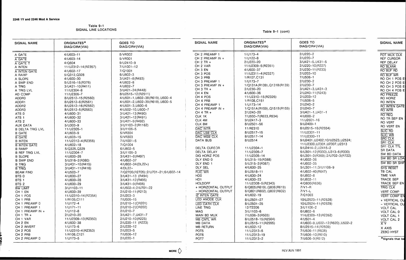
2246 1Y and 2246 Mod A Service
Table 9-1 SIGNAL LlNE LOCATIONS Table 9-1 (cont)
SIGNAL NAME I A GATE AE A GATE T A INTEN A INTEN GATE A RAMP A SLOPE A SWP END A TRlG A TRlG LVL AD COMP ADDRO ADDRl ADDR2 ADDR3 ATS 0 ATS 1 ATS 2 AUX DATA B DELTA TRlG LVL B GATE m B INTEN B INTEN GATE B RAMP B REF TRlG LVL B SLOPE B SWP END B TRlG BG BEAM FIND BTS 0 BTS 1 BTS 2 BW LIMIT CH 1 EN CH 1 POS CH 1 PRB CH 1 PREAMP 0 CH 1 PREAMP 1 CH 1 PREAMP IN + CH 1 TR + CH 1 VAR CH 2 EN CH 2 INVERT CH 2 POS CH 2 PRB CH 2 PREAMP 0 i u +
MORE 0
ORIGINATESa DIAGICIR# (VIA)
4lU603-11 4lU603-14 4lQ604 11 lU2312-14(R2357) 4lU602-17 5/Q312,Q328 4lU600-30 5lU316-15(R378) 3lU421-lO(R411) 11 lU2304-8 1 1 lU2306-7 8lU2512-15(R2560) 8lU2512-6(R2561) 8lU2512-16(R2562) 8lU2512-5 (R2563) 4lU600-3 1 4lU600-32 4lU600-33 5lU303-9 11 lU2305-1 4lU603-9 4lU603-15 11 lU2312-4(R2356) 4lU602-18 5lQ325, Q329 11 lU2304-7 41U600-26 5lU3 16-2 (R380) 3lU431-lO(R415) 3lU431-11 (R416) 4lU503-7 4lU600-27 4lU600-28 4lU600-29 3lU1103-11 4lU600-39 1 1 lU2310-14 (R2354) 1 lR105 ;C l l l 1 lU172-4 1lU171-11 1lU112-8 2lU210-20 11 lU2309-13 (R2350) 4lU600-38 1 lU173-6 1 1 lU2310-4(R2353) 1 /R106,C121 1 lU173-5
GOES TO DIAGICIR#(VIA)
5lVR302 5lVR301 9lU2410-9 7lU1001-12 7lQ1001 6lU802-3 3lU421-8 (R493) 4lU602-8 4/U602-7 3lU421-24 (R448) 8lU2515-1 Z(R2511) 4lU501-I, U602-38(R619) ,U600-4 4/U501-2,U602-39(R618) ,U600-5 4lU501-3,U600-6 4lU502-1 O,U600-7 3lU421-13 (R490) 3iU421-lZ(R491) 3lU421-9 (R492) 3lU1103-2 (R1162) 3lU1106-5 5lVR304 5lVR303 7lU1001-5 7lQ1004 6lU802-5 3lU1106-3 3lU431-8 (R497) 4/U602-37 4lU602-34 (DL22+) 4lDL22- 7/Q2706 (R2705) ;2/U701-21~61U802-14 3lU431-13 (R494) 3lU431-12 (R495) 3lU43 1-9 (R496) 4lU502-4;2/U701-22 21U210-11 (R213) 2lU203-3 7lU506-15 21U210-1 (CR201) 2IU210-2 (CR202) 2lU210-7 3lU421-7,U431-7 2lU210-1 O(R225) 2lU220-11 (R223) 2111220-12 21U203-5 7lU506-12 2lU220-1
REV JUN 1991
SIGNAL NAME GOES TO DIAGICIR# (VIA)
2lU220-2 2lU220-7 3/U421-5,U431-5 2lU220-10 (R227) 2lU230-11 (R233) 2lU203-10 7lU506-1 2IU23O-2 2111230-7 3lU421-3,U431-3 2lU240-11 (R243) 2lU203-12 7lU506-5 2lU240-2 2lU240-7 3lU421-1 ,U431-1 4lU600-2 1 1 lJ2601-16 9/U2409- 1 8lU2515-16 (R2554) 11 lU2301-11 1 1 lU2300- 1 1 9lU2401 ,U2402; 1 O/U2523,U2524; 11 /U23OO,U2301 ,U2307,U2313 9lU2414-2,U2415-2 5lU301-1 Z(R330) ,U313-6(R330) 6lU301-3 (R369) ;2/U702-3 (R722) 4lU602-36 4lU602-35 5lU301-11;3IU1106-9 4lU602-40 (R647) 6lU802-8 6111802-1 1 41Q600 (R636) 7lV1 -R 7lV1 -L 71Q1003 10lU2523-11 (R2528) 10lU2524-11 (R2529) 31U1106-2 6lU802-6 1 1 iU2309-12 (R2352) 4lU501-4 4lU600-9, U602-12 (R620), U502-2 8lU2515-14 (R2509) 7lU506-11 (R508) 7lU506- 10 (R510) 7IU506-9 (R512)
SIGNAL NAME
CH 2 PREAMP 1 CH 2 PREAMP IN + CH 2 TR + CH 2 VAR CH 3 EN CH 3 POS CH 3 PRB CH 3 PREAMP 1 CH 3 PREAMP IN + CH 3 TR + CH 4 EN CH 4 POS CH 4 PRB CH 4 PREAMP 1 CH 4 PREAMP IN + CH 4 TR + CLK 1 K CLK 4M CLK 8M DAC INTR DAC LSB CLK DAC MSB CLK DATA BUS
DELTA CURI3R DELTA DELAY DIG HORlZ POS DLY END 0 DLY END 1 DLY SEL FLlC WR HDO HD1 HOLDOFF + HORIZONTAL OUTPUT - HORIZONTAL OUTPUT IZ INTEN GATE LED ANODE CLK
LED CATH CLK LlNE TRlG MAG MAIN BD MUX MB CNTL WR MB DATA MB RETURN POT5 POT6 POT7
POT MUX CLK REF CURSOR REF DELAY RO BLANK RO BUF RD RO BUF WR RO CH 1 POS El RO CH 2 POS El RO CH 3 POS El RO CH 4 POS El RO FREEZE RO HORlZ RO INTEN
ORIGINATESa DIAGICIR#(VIA)
1 lU173-4 1 lU122-8 2lU220-20 1 1 lU2309-5(R2351) 4lU600-37 1 1 lU2311-4(R2327) 1 /R107,C131 1 lU173-7 l lQ131A(R139),Q131B(R139) 2lU230-20 4lU600-36 11 lU2310-15(R2326) 1 /R108,C151 1lU173-14 l /Ql51A(R159) ,Ql51 B(R159) 2lU240-20 71U930-7 (R933 ,R934) 9lU2417-3 8lU2501-56 11 lR2310 8lU2517-15 8lU25 1 7- 14 8lU2514
1 1 lU2304-1 1 1 lU2305-7 1 1 lU2305-14 5lU315-15(R388) 5lU315-2 (R387) 4111600-25 8lU2518-11 4lU600-24 4lU600-23 11lU2308-5(R2343) 6/Q805(R819) ,0806 (R819) 610801 (R802) ,Q802 (R802) 4lU602-19
8lU2501-27 8lU2501-25 12lT2206 3lU1103-6 7lU506-3 (R503) 8lU2518-15 (R2564) 8lU2515-11 (R2555) 4lU502-12 11 111231 3-5 11fU2313-19 11 fU2313-2
RO INTEN GATE RO INTR
RO REQ RO TR SEP EN RO VERT RO VERT EN SLlC RD SLlC WR SRO CLK SR1 CLK SR1 CLK TTL SR DATA SW BD DATA SW BD SR LOA
SW BD SR SHlF
SYS RESET TB CAL TIME VAR TRACE SEP TRACE SEP EN TRlG CLK VERT COMP VERT COMP EN + VERTICAL OU - VERTICAL OU VOLT CAL VOLT CAL 0 VOLT CAL 1 VOLT CAL 2 - X Y X AXIS ZERO HYST
a~ igna l s that bc
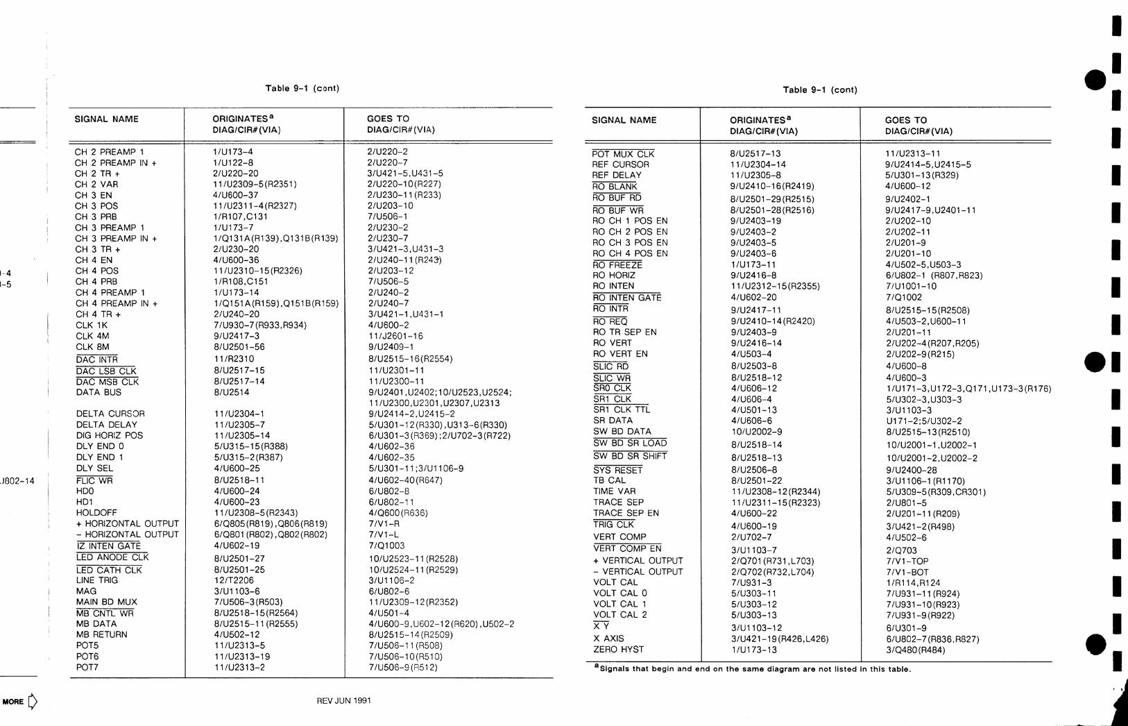
Table 9-1 (cont) Table 9-1 (cont)
MORE 0 REV JUN 1991
SIGNAL NAME GOES TO DIAGICIR#(VIA)
2lU220-2 2lU220-7 3lU421-5,U431-5 2lU220-1 O(R227) 2lU230-11 (R233) 2lU203-10 7lU506-1 2lU230-2 2lU230-7 3lU421-3,U431-3 2lU240-11 (R243) 2lU203-12 7lU506-5 2lU240-2 2lU240-7 3lU421-1 ,U431-1 4lU600-2 11 lJ2601-16 9lU2409-1 81U2515-16(R2554) 11 lU2301-11 11 lU2300-11 9lU2401 ,U2402; 1 OlU2523 ,U2524; 11 /U23OO,U2301 ,U2307,U2313 9lU2414-2,U2415-2 51U301-12 (R330) ,U313-6(R330) 6lU301-3 (R369) ; 2lU702-3 (R722) 4lU602-36 4lU602-35 5lU301-11;31U1106-9 4lU602-40 (R647) 6lU802-8 6lU802-11 4lQ600 (R636) 7lV1 -R 7lV1 -L 7lQ1003 10lU2523-11 (R2528) 10lU2524-11 (R2529) 3lU1106-2 6lU802-6 11 lU2309-12 (R2352) 4lU501-4 4lU600-9, U602-12 (R620) ,U502-2 8lU2515-14 (R2509) 7lU506-11 (R508) 7lU506-10 (R510) 7lU506-9 (R512)
SIGNAL NAME
CH 2 PREAMP 1 CH 2 PREAMP IN + CH 2 TR + CH 2 VAR CH 3 EN CH 3 POS CH 3 PRB CH 3 PREAMP 1 CH 3 PREAMP IN + CH 3 TR + CH 4 EN CH 4 POS CH 4 PRB CH 4 PREAMP 1 CH 4 PREAMP IN + CH 4 TR + CLK 1K CLK 4M CLK 8M DAC INTR DAC LSB CLK DAC MSB CLK DATA BUS
DELTA CURS3R DELTA DELAY DIG HORlZ POS DLY END 0 DLY END 1 DLY SEL FLlC WR HDO HD1 HOLDOFF + HORIZONTAL OUTPUT - HORIZONTAL OUTPUT IZ INTEN GATE LED ANODE CLK
LED CATH CLK LINE TRIG MAG MAIN BD MUX MB CNTL WR MB DATA MB RETURN POT5 POT6 POT7
POT MUX CLK REF CURSOR REF DELAY RO BLANK RO BUF RD RO BUF WR RO CH 1 POS EN RO CH 2 POS EN RO CH 3 POS EN RO CH 4 POS EN RO FREEZE RO HORlZ RO INTEN RO INTEN GATE RO INTR
RO REQ RO TR SEP EN RO VERT RO VERT EN SLlC RD
ORIGINATES a
DIAGICIR#(VIA)
1 lU173-4 1 lU122-8 2lU220-20 1 1 lU2309-5(R2351) 4lU600-37 11 lU2311-4(R2327) 1 /R107,C131 1 lU173-7 l/Q131A(R139),Q131 B(R139) 2lU230-20 4lU600-36 11 lU2310-15(R2326) 1 /R108,C151 1 lU173-14 l/Q151A(R159),Q151B(R159) 2lU240-20 7/U930-7(R933,R934) 9lU2417-3 8lU2501-56 11lR2310 8lU2517-15 8lU2517-14 8lU2514
11 lU2304-1 11 lU2305-7 1 1 IU2305-14 5lU315-15 (R388) 5lU315-2 (R387) 4lU600-25 8lU2518-11 4lU600-24 4lU600-23 1 1 lU2308-5 (R2343) 6/Q805(R819) ,Q806(R819) 6lQ801 (R802), (2802 (R802) 4lU602-19
8lU2501-27 8lU2501-25 12lT2206 3 lU 1 103-6 7lU506-3 (R503) 8lU2518-15 (R2564) 8lU2515-11 (R2555) 4lU502-12 1 1 lU2313-5 11 lU2313-19 11 lU2313-2
SLlC WR SRO CLK SR1 CLK SR1 CLK TTL SR DATA SW BD DATA SW BD SR LOAD
SW BD SR SHIFT
SYS RESET TB CAL TIME VAR TRACE SEP TRACE SEP EN TRIG CLK
ORIGINATES a DIAGICIR#(VIA)
8lU2517-13 1 1 lU2304-14 1 1 lU2305-8 9lU2410-16(R2419)
8lU2501-29 (R2515) 8lU2501-28 (R2516) 9lU2403-19 9lU2403-2 9lU2403-5 9lU2403-6 1 lU173-11 9lU2416-8 1 1 lU2312-15(R2355) 4lU602-20 9lU2417-11 9lU2410-14(R2420) 9lU2403-9 9lU2416-14 4lU503-4 8lU2503-8 8lU2518-12 4lU606-12 4lU606-4 4lU501-13 4lU606-6 1 OlU2002-9 8lU2518-14
8lU2518-13 8lU2506-8 8lU2501-22 1 1 lU2308-12 (R2344) 1 1 lU2311-15 (R2323) 4lU600-22 4lU600-19
GOES TO DIAGICIR# (VIA)
11 lU2313-11 9lU2414-5,U2415-5 5lU301-13 (R329) 4lU600-12
9lU2402-1 9lU2417-9,U2401-11 2lU202-10 2lU202-11 2lU201-9 2lU201-10 4lU502-5,U503-3 6lU802-1 (R807,R823) 7lU1001-10 7lQ1002
8lU2515-15(R2508) 4lU503-2,U600-11 2lU201-11 2lU202-4 (R207,R205) 2lU202-9 (R215) 4lU600-8 4lU600-3 l/Ul71-3,U172-3,Q171 ,U173-3(R176) 5lU302-3 ,U303-3 3lU1103-3 U171-2;5/U302-2 8lU2515-13(R2510)
1 o/u2001-1 ,U2002-1
1 O/U2001-2, U2002-2 9lU2400-28 3lU1106-1 (R1170) 5lU309-5 (R309 ,CR301) 2lU801-5 2lU201-11 (R209) 3lU421-2 (R498)
VERT COMP VERT COMP EN + VERTICAL OUTPUT - VERTICAL OUTPUT VOLT CAL VOLT CAL 0 VOLT CAL 1 VOLT CAL 2 - X Y X AXIS ZERO HYST
2lU702-7
3lU1103-7 2lQ701 (R731 ,L703)
4lU502-6
2lQ703 71Vl -TOP
a ~ i g n a l s that begin and end on the same diagram are not listed in this table.
2 1 ~ 7 0 2 ( ~ 7 3 2 , ~ 7 0 4 j 7lU931-3 5lU303-11 5lU303-12 5lU303-13 3/U1103-12 3lU421-19 (R426,L426) 1 lU173-13
71v1 -BOT l/R114,R124 7lU931-11 (R924) 7lU931-1 O(R923)
I 7lU931-9 (R922) 6lU301-9 6lU802-7 (R836, R827) 3lQ480 (R484)

REV JUN I!
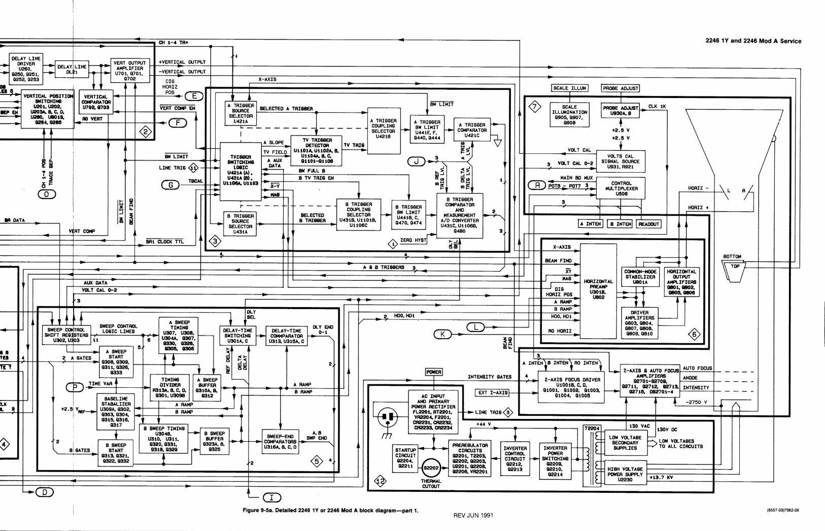

VOLTAGWAVEFORM SETUP CONDITIONS
WAVEFORMS
Test waveforms are shown on a page just before the schematic diagram to which they apply. Normal con- trol settings for the test oscilloscope are given in the readouts shown in each waveform illustration. Unless otherwise indicated near the waveform, setup conditions for the oscilloscope under test are as follows:
1. Set up the 2246 1Y or 2246 Mod A front-panel controls as follows:
VERTICAL MODE
CH 1 COUPLING CH 1 VOLTSIDIV VERTICAL POSITION Controls SCOPE BW HORIZONTAL MODE AIB SELECT SECIDIV Trigger LEVEL HOLDOFF SLOPE Trigger MODE Trigger SOURCE Trigger COUPLING MEASUREMENTS MENU Displays A INTEN READOUT FOCUS
SCALE ILLUM
CH 1 (other channels off) DC 0.1 v 12 o'clock On A A 0.1 ms 12 o'clock min (CCW) J-
AUTO LEVEL VERT DC OFF OFF 10 o'clock 12 o'clock for well de- fined display fully CCW
2. Connect the front panel PROBE ADJUST output to the channel 1 input connector.
3. For all waveforms, except those obtained from the Low-Voltage Power Supply, connect the test oscilloscope probe ground wire to the chassis. When obtaining waveforms from the power
supply, first connect the power cord of the 2246 1Y or 2246 Mod A under test through an isolation transformer, then connect probe ground wire to ground "P" (rear side of R2256). See Figure 9-1 2 to locate ground "Po.
WARNING
To avoid electric shock and instrument damage, always connect the power cord of the instrument under test through an isolation transformer when viewing waveforms or measuring voltages in the low-voltage power supply.
DC VOLTAGES
Dc voltages shown the schematic diagrams are typi- cal of a normally operating instrument. Voltages are referenced to chassis ground, except in the isolated portion of the Low Voltage Power Supply where they are referenced to ground "P" (at R2256 as shown in Figure 9-12). Make sure that the DMM leads are floating (isolated from chassis ground) when measuring voltages in this section.
TEST EQUIPMENT
The following test equipment is recommended for obtaining waveforms and voltages from the 2246 1Y and 2246 Mod A Oscilloscopes. Other similar equip- ment types can also be used.
1 . Test Oscilloscope with 1 OX probe(s) - TEKTRONIX 2246 1Y or 2246 Mod A.
2. Digital Voltmeter-TEKTRONIX DM 501 A.
3. Power-Line Isolation Transformer-Tektronix Part NO. 006-5953-00.

2246 1Y and 2246 Mod A Service fl 1 B 1 C 7 D 1 E 1 F 7 G 1 H 1 J 1 K 1 L 1 M 1 N
Static Sensitive Dev~ces See Maintenance Sect~on
COMPONENT NUMBER EXAMPLE
Cornpanen! Number I 1 s e b 1 L Number Subassembly c"C"lt
Number (if used) Number I I I
Chassis mounted comwnents havenoksembly Number prefix-see end of Replaceable Electrtcal Parts List
ADD JUN 1991
1 1 I Figure 9-6a. A10-Main board for SN B715000 and above (2246 lY) , and B1@000 and above (2246 MOD A).

I OTHER PARTS I
Static Sensitive Devices See Ma~ntenance Sect~on
COMPONENT NUMBER EXAMPLE
I Assembly J - SCi:E:" Number Suhlssembly
Number 11f used1 I 1 I
Charsls mounted commnentr have no ksembly Number prefix-see end of Replaceable Electrcal Parts L~st
ADD JUN 1991 6 IY), and B120000 and above (2246 MOD A).

A1 0- MAIN BOARD
ADD J UN 1991
CIRCUIT NUMBER
AT1 17 AT127
C1 C2 C10 C11 C20 C2 1 C101 C102 C103 C104 C105 C106 C107 C108 C l l l C112 C113 C114 C121 C122 C123 C124 C125 C126 C131 C132 C133 C134 C135 C136 C137 C138 C139 C140 C151 C152 C153 C154 C155 C156 C157 C158 C159 C171 C172 C173 C180 C181 C185 C186 C188 C190 C191 C201 C202 C203 C204 C205 C206 C210 C211 C212 C213 C214 C215 C216 C217 C218 C219 C220 C221 C222
A1 0 -MAIN BOARD (cont)
CIRCUIT NUMBER
CR802 CR803 CAB07 CR935 CR936 CRlOOI CR1002 CR1003 CR1004 CR1005 CR2701 CR2702 CR2703 CR2704 CR2705 CR2707 CR2713 CR2714 CR2715 CR2716 CR2717 CR2718
DL21 DL2 1 DL22 DL22
DS901 DS902 DS903 DS2701 DS2702 DS2703 DS2704
J11 J12 J13 J14 J15 J927 J 1204
K l 00 KlOl K102 K103 K104 K105 K107 K108 K109 K l lO K111 K112
LlOl L102 L130 L140 L20 1 L216 L217 L426 L432 L445 L462 L475 L70 1 L702 L703 L704
P8
SCHEM NUMBER
1 1
1 1 I 1 1 1 1 1 1 1 1 1 1 1 1 1 1 1 1 1 1 1 1 1 1 1 1 1 13 13 1 1 2 13 1 1 1 1 13 13 1 1 2 13 13 1 13 13 1 1 1 1 1 2 2 2 2 13 13 2 2 2 2 13 13 13 13 2 13 2 2 2
SCHEM NUMBER
6 6 6 7 7 7 7 7 7 7 7 7 7 7 7 7 7 7 7 7 7 7
2 2 3 3
7 7 7 7 7 7 7
1 1 1 1 7 7 13
1 1 1 1 1 1 1 1 1 1 1 I
13 13 1 1 13 13 13 3 3 13 3 13 2 2 2 2
7
BOARD LOCATION
68 48
6C 4C 68 6B 48 58 6A 4A 3A 1 A 68 6A 58 4A 1 OC 6A 5A 5C 1 OC 5A 4A 4C 1C 1 D 1 OC 2A 28 28 28 28 2C 2C 2C 2C 1 OC 2A 1 B 1 B 28 1 B 1C 1C 1C 28 3C 38 3D 6D 6D 4D 6D 2C 1C 4G 4H 4H 5H 11H 1 OH 6E 5E 5E 5E 5E 5D 5G 5G 10G 5D 5D 4E 4E
(SN 8715000 AND ABOVE, 2246 1Y SN
CIRCUIT NUMBER
C223 C224 C225 C228 C229 C232 C233 C234 C235 C238 C239 C242 C243 C244 C245 C248 C249 C258 C265 C268 C271 C272 C273 C274 C275 C282 C283 C297 C298 C301 C302 C303 C304 C305 C306 C307A C3078 C307C C308 C309 C310 C311 C312 C313 C314 C315 C316 C317 C318 C319 C320 C321 C322 C326 C329 C330 C337 C338 C339 C351 C421 C422 C423 C424 C425 C426 C432 C442 C444 C445 C447 C451 C452 C453 C454
BOARD LOCATION
4M aJ aJ 7A 7A 5L 5L 8L 7L 3L 9M 9M 8N 6N 6M 7L 1 OL 11L 9L 9M 9M 8L
3F 1 OK 2H 3K
8B 98 118 9N 9M 9M 9M
6A 5A 3A 1 A 7A l l B Y
6A 5A 58 78 5D 6D 4A 4A 48 58 4D 4D
2C 2C 2C 1C 6E 4H 5H 3H 2G 3J 1 G 1J 9J 10J 9H 1 OH
1 ON
SN
CIRCUIT NUMBER
P9 P9 PI7 PI8 PI9 P20 P2302 P2302 P2304 P2502 P2502
0131A 01318 0151A 01518 0171 0181 0182 0250 0251 0252 0253 0284 0285 0301 0302 0303 0304 0305 0306 0307 0308 0309 0310A 03108 031 1 0312 0313 0315 0316 0317 0318 0320 0321 0322 0323A 03238 0325 0326 0328 Q329 0330 0331 0332 0333 0440 0444 0470 0474 0480 0600 (1601 0602 0603 0604 0605 0606 0607 0608 0701 0702 Q703 0704 0601
(SN 8120000
SCHEM NUMBER
2 13 13 2 13 2 2 13 13 2 13 2 2 13 13 2 13 2 13 2 2 2 2 2 2 13 13 13 13 5 5 5 13 5 5 5 5 5 5 13 5 5 5 5 5 5 13 13 13 6 13 5 13 5 5 5 13 13 13 13 3 3 3 3 3 3 3 13 3 13 3 3 3 3 3
B715000 AND AND
BOARD LOCATION
4E 3D 30 10G 4D 2E 2E 30 2D 10G 3D 1 E 1 E 2D 2 0 11G 20 4G 5F 9G 4F 4F 4F 4F 4F 4F 6F 6F 3F 8F 9F 8C 7D 9D 7C 7E 7E 1 OF 7E 7H 7E 7F 9E 9E 7F 7G 8E BE 9E 7F 8F 1 OF 9D 10E 1 OF 10G 10E 8G 9G 8C 3G 3G 3G 3G 2G 3H 2G 2H 2F 3F 2F 2G 2G 2G 2G
ABOVE, ABOVE,
CIRCUIT NUMBER
C455 C462 C463 C474 C475 C476 C477 C478 C480 C481 C482 C483 C484 C485 C487 C488 C489 C491 C492 C493 C494 C496 C501 C502 C503 C505 C600 C601 C602 C603 C604 C605 C606 C607 C608 C609 C610 C611 C612 C613 C614 C636 C666 C701 C702 C703 C704 C705 C706 C707 C708 C711 C712 CEO1 CEO2 C803 C804 C805 C806 CEO7 CEO8 C809 C811 C814 C815 C816 C817 C818 C819 C820 C821 C822 C860 C870
B120000
SCHEM NUMBER
7 7 6 6 2 2 13 7 7 13 4
1 1 1 1 1 1 I 2 2 2 2 2 2 5 5 5 5 5 5 5 5 5 5 5 5 5 5 5 5 5 5 5 5 5 5 5 5 5 5 5 5 5 5 5 3 3 3 3 3 4 4 4 4 4 4 4 4 4 2 2 2 2 6
2246 2246 MOD
SCHEM NUMBER
3 3 3 3 13 3 3 3 13 13 13 3 3 3 3 3 3 2 2 2 2 3 13 13 13 13 4 4 4 4 13 13 13 4 4 13 13 4 4 13 4 4 4 13 13 13 13 13 2 2 13 2 2 13 6 6 6 6 13 6 6 6 2 6 13 13 6 13 6 6 13 13 6 6
AND
BOARD LOCATION
8N 9N 7K 8K 1 OH 9H 1 OD 1 OD 1 I D 1 L 1 L
28 28 1 B 18 28 6D 4D 4E 4F 4E 4F 6E 5E 7C 8E 8F 8F 7E 7E BD 8 F 8F BE BE 8F BE 9F 9E 9F 9F 10E 9E 9F 9F 9E 9 E 10E BF BE 9 E 8 F 9F 9 F 8 F 2H 3F 1H 2F 1 F 3N 3N 2K 2K 3K 3K 2K 2K 2L 9J 10J 9K 11H iK
1Y A)
BOARD LOCATION
1 G 1 G I F I F 1 F 1 E I F 1E 1J 3F 2F 2F 3G 2G 3F 2G 3G 2F 2F 2E 2F 2G 4M 4N 4N 9C 3N 3N 4L 3L 3M 2M 3L 3L 3M 2J 2L 4K 3K 1 N 5M 6N 4M 10J 9J 1 OK 9K 9H 10J 9J 9J 1 aJ 1 aJ 8K 7J 7K 8K 9H 8H 7J 9G 8K 7J aJ 7H 8H 6G 8.J 7J 8J 8J 8J 7J aJ
ABOVE,
CIRCUIT NUMBER
0802 0803 0804 0805 0806 0807 0809 0810 081 1 0812 0905 0907 0908 01001 0 1002 01003 01004 01005 01101 01 102 01103 01104 01105 01106 02701 02702 02703 02704 02705 02706 02707 02708 02709 0271 1 02712 02713 02715
R12 R13 A22 R23 RlOl R102 R103 R104 A105 R106 R107 R108 R111 R113 R114 R115 R121 R123 R124 R125 R131 R132 R133 R134 R135 R136 R137 R138 R139 R140 R141 R142 R151 R152 R153 R154 R155
CIRCUIT NUMBER
C880 C901 C902 C903 C904 C910 C935 ClOOl C1002 C1003 C1004 C1005 C1006 C l l O l C1102 C1103 C1104 C1105 C1106 C1107 C1108 C l l l O C l l l l C1114 C1130 C1143 C1154 C1155 C1158 C1159 C1160 C1250 C1251 C2701 C2702 C2703 C2704 C2705 C2706 C2707 C2708 C2709 C2710 C2711 C2712 C2713 C2715 C2716 C2717 C2719 C2720 C2721 C2723 C2724 C2759 C2783 C2784 C2785
CR131 CR151 CR171 CR201 CR202 CR260 CR261 CR262 CR263 CR301 CR432 CR462 CR603 CR612 CR8Ol
2246 MOD
SCHEM NUMBER
6 6 6 6 6 6 6 6 6 6 7 7 7 7 7 7 7 7 3 3 3 3 3 3 7 7 7 7 7 7 7 7 7 7 7 7 7
1 1 1 1 1 1 1 1 1 1 1 1 1 1 1 2 1 1 1 2 1 1 1 1 1 1 1 2 I 2 1 1 1 1 1 1 1
SCHEM NUMBER
6 13 13 13 13 7 7 7 7 7 7 13 13 13 13 3 13 3 3 3 13 3 3 3 3 3 3 3 13 13 13 2 2 13 13 7 7 7 7 7 7 13 7 7 7 7 7 7 7 7 7 7 7 7 7 7 7 7
1 1 1 2 2 2 2 2 2 5 3 3 4 4 6
A)
BOARD LOCATION
7K 7J 7J 8K 8K aJ 8H 7H 7J aJ 10A 10A 10A 4L 4L 4L 4L 7L 5J 5J 5J 5J 5J 5J 7N 7M 7N 6N 7M 7M 6M 6L 6L 1 OL 1 OL 11L 6M
6C 6C 5C 4C 7A 7A 7A 7A 7A 78 78 78 6A 5A 5A 5D 5A 4A 3A 4D 2A 2A 2A 2A 28 2C 2C 2C 2C 2C 28 28 2A 2A 1 A 2A 18
BOARD LOCATION
aJ 98 8A 9A 98 108 78 7L 8M 8M 7L 7M 8L 3H 3G 4 4H 5K 4G 4G 4G 3G 4H 4J 4G 4H 4G 4G 5L 5L 5K 5F 5F 7M 6L 7M 7M 7N 6N 7M 7N 7M 7N 8M 8N 6N 1 OL 1OL 11L 1 OM 8L 6K 7L 10M 7M 8N 6N 8N
28 1 8 38 5C 5C 4F 4F 4F 4F 7C 2G 1 G 4M 6N 5M
CIRCUIT NUMBER
R156 R157 R158 R159 R160 R161 R162 R171 R175 R176 R177 R178 R179 R180 R l 8 l R182 R185 R188 R201 R202 R203 R204 R205 R206 R207 R208 R209 R210 R211 R212 R213 R214 R215 R216 R217 R218 R219 R220 R221 R222 R223 R224 R225 R226 R227 R228 R229 R230 R231 R232 R233 R234 R235 R238 R240 R241 R242 R243 R244 6'245 R248 R249 R254 R255 R256 R260 R261 R262 R263 R264 R265 R266 R267 R268 R269
SCHEM NUMBER
1 1 2 1 2 1 1 1 1 1 1 1 1 1 1 13 1 1 2 2 2 2 2 2 2 13 2 2 2 2 2 2 2 2 2 2 2 2 2 2 2 2 2 13 2 2 2 2 2 2 2 2 2 2 2 2 2 2 2 13 2 2 2 2 2 2 2 2 2 2 2 2 2 2 2
BOARD LOCATION
1 C 1 C 1C 1C 1C 18 18 38 38 3C 3C 3C 3C 28 18 6D 6D 3D 5G 5G 5G 5G 6H 5G 9G 11H 1 M 6E 6E 2L 2M 6H 6N 8G 7G 5E 5C 4E 4E 21 2M 6H 8C 6E 8C 4E 5D 3E 3E I L 2M 6H 3E 2D 2E 2E 1 L 2M 6H 3D 2E 5G 5F 5F 6F 5E 5E 5F 5F 5F 5F 4F 4F 5F 5F

2246 1Y and 2246 Mod A Service
SCHEM NUMBER
1
6 13 13 13 13 7 7 7 7 7 7 13 13 13 13 3 13 3 3 3 13 3 3 3 3 3 3 3 13 13 13 2 2 13 13 7 7 7 7 7 7 13 7 7 7 7 7 7 7 7 7 7 7 7 7 7 7 7
1 1 1 2 2 2 2 2 2 5 3 3 4 4 6
BOARD LOCATION
aJ 96 8A 9A 9B 100 70 7L 8M 8M 7L 7M 8L 3H 3G 4.J 4H 5K 4G 4G 4G 3G 4H 4J 4G 4H 4G 4G 5L 5L 5K 5F 5F 7M 6L 7M 7M 7N 6N 7M 7N 7M 7N 8M 8N 6N 1 OL 1 OL 11L 1 OM 8L 6K 7L 10M 7M 8N 6N 8N
28 1 B 38 5C 5C 4F 4F 4F 4F 7C 2G 1G 4M 6N 5M
A1 0 -MAIN BOARD (cont)
ADD JUN 1991
A1 0 -MAIN BOARD (cont)
BOARD LOCATION
2K 2N 3L 6N 3N 3N 3L 3L 4M 4M 3M 3M 3M 3M 1J 3K 3K 3M 4M 4M 3K 3L 3L 4K 4K 4K 4M 21 3K 3K 4M 4K 3L 4K 3M 3M 4M 4M 9J 9J 11J 9K 1 OK 10H 9J 1 OK 10J I 0J 1 OK 1 OK 9K 9K 1 OH 1 OH 9K 9K 9J 9K 9K 11J 1 OK 1 OH 1 OH 9K 9H 1 OH 1 OK 1 OH 8K 7K 8K 8K 8J 7J
CIRCUIT NUMBER
R156 R157 R158 R159 R160 R161 R162 A171 R175 R176 R177 A178 R179 R180 R181 R182 R185 R188 R201 R202 R203 R204 R205 R206 R207 R208 R209 R210 R211 R212 R213 R214 R215 R216 R217 R218 R219 R220 R221 R222 R223 R224 R225 R226 R227 R228 R229 R230 R231 R232 R233 R234 R235 R238 R240 R241 R242 R243 R244 R245 R248 R249 R254 R255 R256 R260 R261 17262 R263 R264 R265 R266 R267 R268 R269
(SN 8715000 AND ABOVE, (SN B715000 AND ABOVE, 2246 2246 MOD
SCHEM NUMBER
6 6 6 6 6 6 6 6 6 6 7 7 7 7 7 7 7 7 3 3 3 3 3 3 7 7 7 7 7 7 7 7 7 7 7 7 7
1 1 1 1 1 1 1 1 1 1 1 1 1 1 1 2 1 1 1 2 1 1 1 1 1 1 1 2 1 2 1 1 1 1 1 1 1
2246 2246 MOD
SCHEM NUMBER
3 3 3 3 3 3 3 3 3 3 3 3 3 3 3 3 3 3 3 3 3 3 3 13 13 3 3 3 3 3 3 3 3 3 3 3 3 3 3 4 4 7 13 7 7 7 7 7 7 4 4 4 4 4 4 4 4 4 4 4 4 4 4 4 4 4 4 4 4 4 4 4 4 4
SCHEM NUMBER
1 1 2 1 2 1 1 1 1 1 1 1 1 1 1 13 1 1 2 2 2 2 2 2 2 13 2 2 2 2 2 2 2 2 2 2 2 2 2 2 2 2 2 13 2 2 2 2 2 2 2 2 2 2 2 2 2 2 2 73 2 2 2 2 2 2 2 2 2 2 2 2 2 2 2
1Y A)
BOARD LOCATION
7K 7J 7J 8K 8K 8J 8H 7H 7J 8J 10A 1 OA 10A 4L 4L 4L 4L 7L 5J 5J 5J 5J 5J 5J 7N 7M 7N 6N 7M 7M 6M 6L 6L 1 OL 1 OL l l L 6M
6C 6C 5C 4C 7A 7A 7A 7A 7A 70 78 7B 6A 5A 5A 5D 5A 4A 3A 4D 2A 2A 2A 2A 28 2C 2C 2C 2C 2C 2B 28 2A 2A 1A 2A 1B
BOARD LOCATION
1 C 1C 1 C 1 C 1C 18 10 30 30 3C 3C 3C 3C 20 16 60 6D 3D 5G 5G 5G 5G 6H 5G 9G 11H 1M 6E 6E 2L 2M 6H 6N 8G 7G 5E 5C 4E 4E 2L 2M 6H 8C 6E 8C 4E 5D 3E 3E 1L 2M 6H 3E 2D 2E 2E 1L 2M 6H 30 2E 5G 5F 5F 6F 5E 5E SF 5F 5F 5F 4F 4F 5F 5F
B120000
SCHEM NUMBER
7 7 6 6 2 2 13 7 7 13 4
1 1 I 1 1 1 1 2 2 2 2 2 2 5 5 5 5 5 5 5 5 5 5 5 5 5 5 5 5 5 5 5 5 5 5 5 5 5 5 5 5 5 5 5 3 3 3 3 3 4 4 4 4 4 4 4 4 4 2 2 2 2 6
CIRCUIT NUMBER
CR802 CR803 CR807 CR935 CR936 CRIOOl CR1002 CR1003 CR1004 CR1005 CR2701 CR2702 CR2703 CR2704 CR2705 CR2707 CR2713 CR2714 CR2715 CR2716 CR2717 CR2718
DL21 DL21 DL22 DL22
DS901 DS902 DS903 DS2701 DS2702 DS2703 DS2704
J11 J12 J13 J14 J15 J927 J1204
K l 00 KlOI K102 K103 K104 K105 K107 K108 K109 K l lO K111 K112
LlOl L102 L130 L140 L201 L216 L217 L426 L432 L445 L462 L475 L701 L702 L703 L704
P8
1Y A)
BOARD LOCATION
2F 3F 1 H 1 G 1G 2G 2G 2H 1G 1G 1G 1G I F 1 G 1H 1H 1H 1 H 1 F 1 F 1 F 1 F 1 F 4F 1J 3F 1 E 1 E 1 E 1 E 3J 3J 3J 2J 2J 2J 2J 2J 3J 1L 5N 1 OC 9C 9C 9C 9C 1 OC 1 OC 1 OC 3N 2N 1 N 1 N I N 3N 2K 2K 3K 3M 2K 3L 4L 3K 3K 3M 3M 4M 4L 3K 3K 2L 2L 4L 3L
AND
BOARD LOCATION
8E 8H 7H 7H 7H 9D 9E 9E 9F 8F 9D 8F 9F 8G 8F 9F 9G 10E 8C 9C 8D 9G 9G 9G 10G 10E 10E IOE 8H 6.J 7G 6J 1 OF 7G 9G 8D 9F 9F 8F 8F 8F 7C 1 OF 1 OF 8E 10E 3F 3F 3J 3G 3G 3G 3G 3H 2G 2G 2H 3H 3G 3G 3G 3G 3G 3H 2G 2F 2G 2G 3H 3H 2H 3H 2F 3F 2F
CIRCUIT NUMBER
R270 R271 R272 R273 R274 R275 R276 R277 R278 R279 R280 R281 R282 R283 R284 R285 R286 R287 R288 R289 R290 R291 R292 R293 R294 R295 R296 R297 R298 R299 R301 R302 R303 R304 R305 R306 R307 R308 R309 R310 R311 R312 R313 R314 R315 R316 R317 A318 R319 R320 R321 R322 R323 R325 R326 R327 R328 R329 R330 R331 R332 R333 R334 R335 R336 R337 R338 R339 R340 R341 R342 R343 R344 R345 R346
BOARD LOCATION
4M aJ 8J 7A 7A 5L 5L 8L 7L 3L 9M 9M 8N 6N 6M 7L 1OL 11L 9L 9M 9M 8L
3F 1 OK 2H 3K
80 9B 110 9N 9M 9M 9M
6A 5A 3A 1 A 7A 116 5J
6A 5A 56 76 5D 6D 4A 4A 48 56 4D 4D
2C 2C 2C 1C 6E 4H 5H 3H 2G 3J 1G 1J 9J 1@J 9H I OH
1 ON
SCHEM NUMBER
6 6 6 7 7 7 7 7 7 7 7 7 7 7 7 7 7 7 7 7 7 7
2 2 3 3
7 7 7 7 7 7 7
1 1 1 1 7 7 13
1 1 1 1 1 1 1 1 1 1 1 1
13 13 1 1 13 13 13 3 3 13 3 13 2 2 2 2
7
ABOVE,
CIRCUIT NUMBER
R448 R449 R450 R451 R452 R453 R454 R455 R456 R460 R461 R462 R463 R470 R471 R472 R473 R474 R475 R476 R477 R478 R479 R480 R481 R483 R484 R485 R486 R487 R490 R491 R492 R493 R494 R495 R496 R497 R498 R501 R502 R503 R504 R505 R506 R507 R508 R510 R512 R601 R602 R603 R604 R605 R606 R609 R610 R611 R612 R613 R614 R615 R616 R617 R618 R619 R620 R621 R622 R623 R624 R625 R626 R627
BOARD LOCATION
4F 4F 4F 4G 3E 4F 4F 4F 3F 3F 3F 3F 4F 6G 6F 6E 5G 5F 6F 5F 6F 5F 5F 5F 5G 5G 6F 6F 3F 4F 9E 7E 8F 8F 8G 7C 7C 7C 9C 7C 8C 7D 7D 7C 10E 7F 8E 8E 8F 8E 8D 7H 7G 7D 7D 9F 8E 9E 9E 8E 7G 8G 8G 9F 9F 8E 9E 9E 7G 9F 9E 9F 8E BE 8E
SCHEM NUMBER
2 2 2 2 2 2 2 2 2 2 2 2 13 13 2 2 2 2 2 2 2 2 2 2 2 2 2 13 13 2 5 5 5 5 5 5 5 5 5 5 5 13 5 5 5 5 5 5 5 5 5 5 5 5 5 5 5 5 5 5 5 5 5 5 5 5 5 13 5 5 5 5 5 13 5
AND
BOARD LOCATION
8N 9N 7K 8K I OH 9H 10D 1 OD 11D 1L 1 L
26 28 16 16 26 6D 4D 4E 4F 4E 4F 6E 5E 7C 8E 8F 8F 7E 7E 8D 8F 8F 8E 8E 8F 8E 9F 9E 9F 9F 10E 9E 9F 9F 9E 9E 10E 8F 8E 9E 8F 9F 9F 8F 2H 3F 1H 2F I F 3N 3N 2K 2K 3K 3K 2K 2K 2L 9J 10J 9K 11H 7K
SN
CIRCUIT NUMBER
P9 P9 P I 7 PI8 P I 9 P20 P2302 P2302 P2304 P2502 P2502
0131A 01318 0151A 01518 0171 0181 0182 0250 0251 0252 0253 0284 0285 030 1 0302 0303 0304 0305 0306 0307 0308 0309 0310A 03108 031 1 0312 0313 0315 0316 0317 031 8 0320 0321 0322 0323A 03238 0325 0326 0328 0329 0330 0331 0332 0333 0440 0444 0470 0474 0480 0600 060 1 0602 0603 0604 0605 0606 0607 0608 0701 0702 0703 0704 0801
CIRCUIT NUMBER
R628 R630 R631 R636 A637 R638 R639 R640 R641 R642 R643 R644 R645 R646 R647 R648 R649 R650 R651 R652 R653 R654 R655 A656 R657 R658 R659 R662 R663 R664 R665 R666 R669 R670 R671 R672 A673 R674 R701 R702 R703 R706 R707 R708 R709 R710 R711 R712 R715 R716 R717 R718 R719 R720 R721 R722 R723 R724 R725 R726 R727 R728 R729 R730 R731 R732 R733 R734 R801 R802 RE03 R804 R805 R806
ABOVE,
CIRCUIT NUMBER
0802 0803 0804 0805 0806 0807 0809 0810 081 1 0812 0905 0907 0908 01001 01002 01003 01004 01 005 01101 01102 0 1 103 01 104 01 105 01106 02701 02702 02703 02704 02705 02706 02707 02708 02709 0271 1 02712 027 13 02715
R12 R13 R22 R23 RlOl R102 R103 R104 R105 R106 R107 RlO8 R111 R113 R114 R115 R121 R123 R124 R125 R131 R132 R133 R134 R135 R136 R137 R138 R139 R140 R141 R142 R151 R152 R153 R154 R155
SCHEM NUMBER
4 4 4 4 4 4 4 4 4 4 4 4 4 4 4 4 4 4 4 4 4 4 4 4 4 4 4 4 4 4 4 4 4 4 4 4 4 4 13 2 2 2 2 2 13 2 2 2 2 2 2 2 2 2 2 2 13 2 2 2 2 2 2 2 2 2 13 13 6 6 6 6 6 6
SN
CIRCUIT NUMBER
R347 R348 R349 R350 R352 R353 R354 R355 R356 R357 R358 R359 R360 R361 R362 R363 R364 R365 R366 R367 R369 R370 R371 R372 R373 R374 R375 R376 R377 R378 R379 R380 A381 A382 R383 R384 R385 R386 R387 R388 R390 R392 R393 R394 R395 R396 R401 R402 R403 R410 R411 R412 R413 R414 R415 R416 R417 R420 R421 R422 R423 R424 R425 R426 R430 R431 R432 R440 ,5441 R442 R443 R444 R445 R446 R447
B120000
SCHEM NUMBER
5 5 5 5 5 5 5 5 5 5 6 5 5 5 5 5 5 5 5 5 6 5 5 5 5 13 5 5 5 5 5 5 5 5 5 5 5 5 5 5 13 13 5 5 5 5 3 3 3 3 3 3 3 3 3 3 3 3 3 3 3 3 3 3 3 3 3 3 3 3 3 3 3 3 3
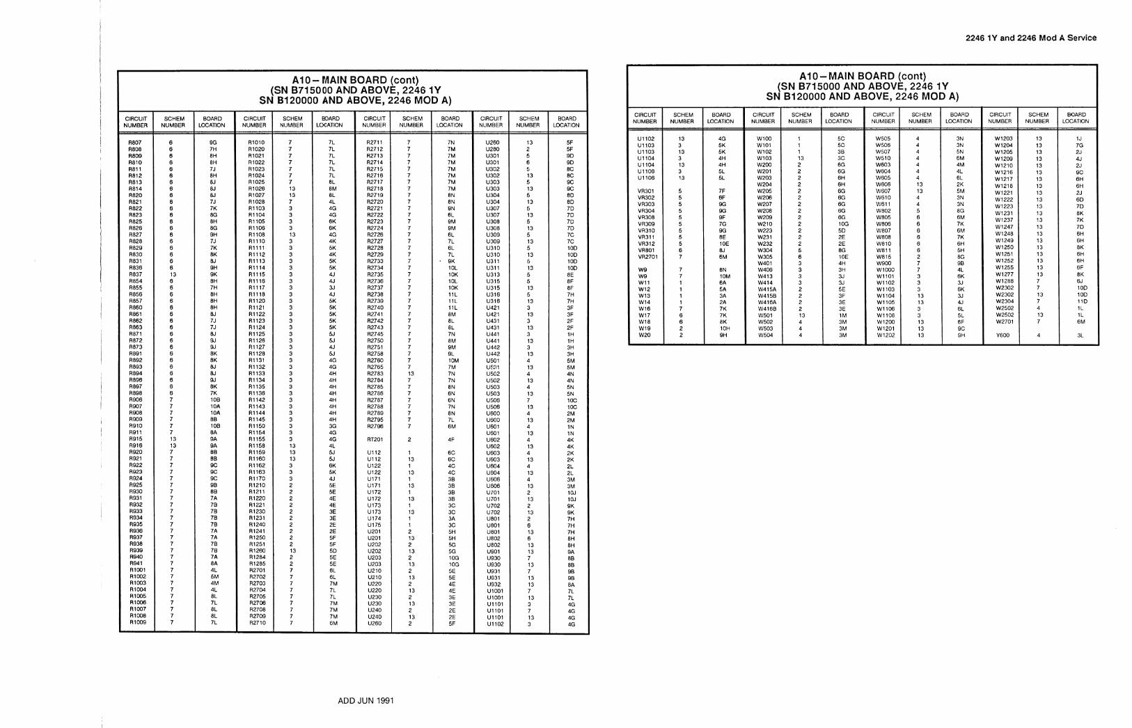
2246 1Y and 2246 Mod A Service
A1 0 - MAIN BOARD (cont)
ADD JUN 1991
A1 0 -MAIN BOARD (cont) (SN B715000 AND ABOVE, 2246 1Y
SN B120000 AND ABOVE, 2246 MOD A)
CIRCUIT NUMBER
U1102 U1103 U1103 U1104 U1104 U1106 U1106
VR301 VR302 VR303 VR304 VR308 VR309 VR310 VR311 VR312 VR801 VR2701
W9 W9 W11 W12 W13 W14 W16 W17 W18 W19 W20
CIRCUIT NUMBER
R807 R808 R809 R810 R81 1 RE12 R813 R814 R820 RE21 A822 R823 R825 R826 RE27 RE28 R829 R830 RE31 R836 R837 R854 RE55 R856 RE57 R860 R861 RE62 R863 R871 R872 R873 RE91 R892 R893 R894 R896 R897 RE98 R906 R907 R908 R909 R910 R911 R915 R916 R920 R921 R922 R923 R924 R925 R930 R931 R932 R933 R934 R935 R936 R937 R938 R939 R940 R941 RlOOl R1002 R I m 3 R1004 R1005 R1006 R1007 R1008 R1009
BOARD LOCATION
5C 5C 30 3C 6G 6G 6H 6H 6G 6G 6G 6G 6G 10G 5D 2E 2E 8G 10E 4H 3H 3J 3J 5E 3F 3E 3E 1M 3M 3M 3M
SN
CIRCUIT NUMBER
RlOlO A1020 R1021 R1022 R1023 R1024 R 1025 R1026 R1027 R1028 R1103 R1104 R1105 R1106 R1108 R1110 R l l l l R1112 R1113 R1114 R1116 R1116 R1117 R1118 R1120 R1121 R1122 R1123 R1124 R1125 R1126 R1127 R1128 R1131 R1132 R1133 R1134 R1135 R1136 R1142 R1143 R1144 R1146 R1150 R1154 R1155 R1158 R1159 R1160 A1162 R1163 R1170 R1210 R1211 R1220 R1221 R1230 R1231 R1240 R1241 R1250 R1251 R1260 R1284 R1285 R2701 R2702 R2703 R2704 R2705 A2706 R2708 R2709 R2710
ABOVE, ABOVE,
CIRCUIT NUMBER
R2711 R27 12 R2713 R2714 R27 15 R27 16 R2717 R2718 R27 19 R2720 R2721 R2722 R2723 R2724 R2726 R2727 R2728 R2729 R2733 R2734 R2735 R2736 132737 R2738 R2739 R2740 R2741 R2742 R2743 R2745 132750 R2751 R2758 R2760 R2765 R2783 R2784 R2785 R2786 R2787 R2788 R2789 R2795 R2796
RT201
U112 U112 U122 U122 U171 U171 U172 U172 U173 U173 U174 U175 U201 U201 U202 U202 U203 U203 U210 U210 U220 U220 U230 U230 U240 U240 U260
SCHEM NUMBER
13 3 13 3 13 3 13
5 5 5 5 5 5 5 5 5 6 7
7 7 1 1 1 1 7 6 6 2 2
CIRCUIT NUMBER
U260 U280 U301 U301 U302 U302 U303 U303 U304 U304 U307 U307 U308 U308 U309 U309 U310 U310 U311 U311 U313 U315 U315 U316 U316 U421 U421 U431 U431 U441 U441 U442 U442 U501 UEDl U502 U502 U503 U503 U506 U506 U600 U600 U601 U601 U602 U602 U603 U603 U604 U604 U606 U606 U701 U701 U702 U702 U801 U801 U801 U802 U802 US01 U930 U930 U931 U931 U932 UlOOl UlOOl U l l O l U l l O l U l l O l U1102
SCHEM NUMBER
6 6 6 6 6 6 6 6 6 6 6 6 6 6 6 6 6 6 6 6 13 6 6 6 6 6 6 6 6 6 6 6 6 6 6 6 6 6 6 7 7 7 7 7 7 13 13 7 7 7 7 7 7 7 7 7 7 7 7 7 7 7 7 7 7 7 7 7 7 7 7 7 7 7
CIRCUIT NUMBER
W505 W506 W507 W510 W603 W604 W605 W606 W607 W610 W611 WE02 WE05 WE06 We07 W808 WE10 W8l 1 W815 W900 W 1000 W l l O l W1102 W1103 W1104 W1105 W1106 W1108 W 1200 VJ1201 W 1202
(SN 871 8120000
SCHEM NUMBER
7 7 7 7 7 7 7 13 13 7 3 3 3 3 13 3 3 3 3 3 3 3 3 3 3 3 3 3 3 3 3 3 3 3 3 3 3 3 3 3 3 3 3 3 3 3 13 13 13 3 3 3 2 2 2 2 2 2 2 2 2 2 13 2 2 7 7 7 7 7 7 7 7 7
2246 2246 MOD
SCHEM NUMBER
7 7 7 7 7 7 7 7 7 7 7 7 7 7 7 7 7 7 7 7 7 7 7 7 7 7 7 7 7 7 7 7 7 7 7 13 7 7 7 7 7 7 7 7
2
1 13 1 13 1 13 1 13 1 13 1 1 2 13 2 13 2 13 2 13 2 13 2 13 2 13 2
BOARD LOCATION
9G 7H 8H 8H 7J 8H 8J 8J 8J 7J 7K 8G 8H 8G 9H 7J 7K 8K aJ 9H 9K 8H 7H 8H 8H 8H aJ 7J 7J 8J 9J 9J 8K 8K aJ 8J 9J 8K 7K 108 10A 10A 8B 108 8A 9A 9A 85 88 9C 9C 9C 98 88 7A 7 8 7 8 78 78 7A 7A 78 78 7A 8A 4L 5M 4M 4L 8L 7L 8L 8L 7L
BOARD LOCATION
4G 5K 5K 4H 4H 5L 5L
7F 6F 9G 9G 9F 7G 9G 8E 10E 8J 6M
8N 10M 6A 5A 3A 2A 7K 7K 8K 1 OH 9H
5000 AND AND
BOARD LOCATION
7L 7L 7L 7L 7L 7L 8L 8M 8L 4L 4G 4G 6K 6K 4G 4K 5K 4K 5K 5K 4J 4J 3J 41 5K 5K 5K 5K 5K 5J 5J 4J 5J 4G 4G 4H 4H 4H 4H 4H 4H 4H 4H 3G 4G 4G 4L 5J 5J 6K 5K 4J 5E 5E 4E 4E 3E 3E 2E 2E 5F 5F 5D 5E 5E 6L 6L 7M 7L 7L 7M 7M 7M 6M
1Y A) BOARD
LOCATION
7N 7M 7M 7M 7M 7M 7M 7M 8N 8N 9N 6L 9M 9M 6L 7L 6L 7L 9K 1 OL 1 OK 1 OL 1 OK 1 l L 11L 11L 8M 8L 8L 7N 8M 9M 9L 1 OM 7M 7N 7N 8N 6N 6N 7N 8N 7L 6M
4F
6C 6C 4C 4C 3B 38 38 30 3C 3C 3A 3C 5H 5H 5G 5G 10G 10G 5E 5E 4E 4E 3E 3E 2E 2E 5F
SCHEM NUMBER
13 2 5 6 5 13 5 13 5 13 5 13 5 13 5 13 5 13 5 13 5 5 13 5 13 3 13 3 13 3 13 3 13 4 13 4 13 4 13 7 13 4 13 4 13 4 13 4 13 4 13 4 13 2 13 2 13 2 6 13 6 13 13 7 13 7 13 13 7 13 3 7 13 3
SCHEM NUMBER
4 4 4 4 4 4 4 13 13 4 4 5 6 6 6 6 6 6 2 7 7 3 3 3 13 13 3 3 13 13 13
BOARD LOCATION
5F 5F 9D 9D 8C 8C 9C 9C 8D 8D 7 0 7 0 7D 7 0 7C 7C 10D 10D 1 OD 10D 8E 8F 8F 7H 7H 3F 3F 2F 2F 1 H 1 H 3H 3H 5M 5M 4N 4N 5N 5N 1 OC 1 OC 2M 2M 1 N 1 N 4K 4K 2K 2K 2L 2L 3M 3M 10J 10J 9K 9K 7H 7H 7H 8H 8H 9A 86 8B 9B 95 8A 7L 7L 4G 4G 4G 4G
CIRCUIT NUMBER
WlOO WlOI W102 W103 W200 W201 W203 W204 W205 W206 W207 W208 W209 W210 W223 W231 W232 W304 W305 W401 W406 W413 W414 W415A W415B W416A W416B W501 W502 W503 W504
BOARD LOCATION
3N 3N 5N 6M 4M 4L 6L 2K 5M 3N 3N 8G 6M 7K 6M 7K 6H 5H 8G 90 4L 6K 3J 6K 3J 41 6L 5L 6F 9C 9H
SCHEM NUMBER
1 1 1 13 2 2 2 2 2 2 2 2 2 2 2 2 2 5 6 3 3 3 3 2 2 2 2 13 4 4 4
CIRCUIT NUMBER
W 1203 W 1204 W 1205 W 1209 W1210 W1216 W1217 W1218 W1221 W1222 W1223 W1231 W 1237 W 1247 W1248 W 1249 W1250 W1251 W 1252 W1255 W 1277 W 1288 W2302 W2302 W2304 W2502 W2502 W2701
Y600
SCHEM NUMBER
13 13 13 13 13 13 13 13 13 13 13 13 13 13 13 13 13 13 13 13 13 7 7 13 7 4 13 7
4
BOARD LOCATION
1J 7G 2J 4J 2J 9C 6H 6H 2J 6D 7D 8K 7K 7 0 6H 6H 8K 6H 6H 6F 8K 6J 1 OD 1 OD 11D 1 L 1 L 6M
3L

2246 1Y and 2246 Mod A Service f2 1 B 7 C v D 1 E 1 F 1 G v H v J v K 1 L 1 ri 1 N
I
i 1 Figure 9-6b. A10-Main board for SN B710100 to 8714999 (2246 lY ) , and SN B110100 to B119999 (2246 MOD A). ADD JUN 1991

2246 lY), and SN B110100 to 8 1 19999 (2246 MOD A). ADD JUN 1991
A1 0 -MAIN BOARD
BOARD LOCATION
8M 8M 7L 7M 8L 3H 4G 41 4H 5K 4G 4G 3G 4G 41 4G 4G 4G 5L 5L 5K 7M 6L 7M 7M 7N 6N 7M 7N 7M 7N 8M 8N 6N 1 OL 1OL 1 OL 1 OM 8L 6K 7L 10M 7M 8N 6N 8N
28 18 5D 5D 4F 4F 4F 4F 38 7C 2G I G 4M 5N 5K 4M 7A 7A 4L 4L 8L 7L 3L 9N 9N 8N 6N 6M 7L
SCHEM NUMBER
7 7 7 13 13 13 13 3 13 3 3 3 3 3 3 3 3 3 13 13 13 13 13 7 7 7 7 7 7 13 7 7 7 7 7 7 7 7 7 7 7 7 7 7 7 7
1 1 2 2 2 2 2 2 1 5 3 3 4 4 6 6 7 7 7 7 7 7 7 7 7 7 7 7 7
CIRCUIT NUMBER
C1002 C1003 C1004 C 1005 C1006 C l l O l C1102 C1103 C1104 C1105 CllDB C1107 C l l l O C1111 C1114 C1130 C1154 C1155 C1158 C1159 C1160 C2701 C2702 C2703 C2704 C2705 C2706 C2707 C2708 C2709 C2710 C2711 C2712 C27 13 C2715 C2716 C2717 C2719 C2720 C2721 C2723 C2724 C2759 C2783 C2784 C2785
CR131 CR151 CR201 CR202 CR260 CR261 CR262 CR263 CR171 CR301 CR432 CR462 CR603 CR612 CR801 CR802 CR935 CR936 CR1001 CR1002 CR1003 CR1004 CR1005 CR2701 CR2702 CR2703 CR2704 CR2705 CR2707
A) BOARD
LOCATION
I F I F 1 F I F I F 1 E 1J 3F 2F 2F 3G 2H 3F 3G 2E 2F 2E 2F 4N 4N 4N 9C 3N 3N 4L 3L 3N 2M 3L 2L 3M 2J 2L 4K 3K I N 4M I aJ 9J 1 OK 9K 9G I &I SJ %I 9J 1 aJ 8K 7J 7K 8K 8H 8H 7J 9G 8K 7J aJ 7H 8H 6G aJ 7J aJ 7J BJ 7J aJ aJ 9B 8 A 8A 98 1 OB 78 7L
1Y MOD
SCHEM NUMBER
3 3 13 3 3 3 13 13 13 3 3 3 3 3 2 2 2 2 13 13 13 13 4 4 4 4 13 13 13 4 4 13 13 4 4 13 4 13 13 13 13 13 2 2 13 2 2 13 6 6 6 6 13 6 6 6 2 6 13 13 6 13 6 6 13 13 6 6 6 13 13 13 13 7 7 7
8714999,2246 19999,2246
CIRCUIT NUMBER
C463 C474 C475 C476 C477 C476 C480 C481 C482 C483 C484 C485 C487 C489 C491 C492 C493 C494 C501 C502 C503 C505 C600 C601 C602 C603 C604 CEQ5 C606 C607 C608 C609 C610 C611 C612 C613 C614 C701 C702 C703 C704 C705 C706 C707 C708 C711 C712 CEO1 CEO2 CEO3 C804 C805 C806 CEO7 CEO8 CBOQ C811 C814 C815 C816 C817 C818 C819 C820 C821 C822 C880 C870 C880 C901 C902 C903 C904 C910 C935 ClOOl
to to 8 1
BOARD LOCATION
3D 3D 1% 4D 2E 2E 2D 2D 10G 2D 1E 1E I D 1 D 10G 2D 4H 5F 9G 4F 4F 4F 4F 4F 4F 6G 5F 3F 8F 9F 8C 7D 9D 7C 7E 7E 1 OF 7E 7H 7E 7F 9E 9E 7F 7G BE BE 9E 7F 8G 9F 9 0 10E 10G 1 OG QE 8G 9G 8C 2G 3H 2G 3G 2G 3H 2G 2H 2F 3F 2F 1 G 2H 1G 1 G 1 G 1 G
SN
CIRCUIT NUMBER
C224 C225 C228 C229 C232 C233 C234 C235 C238 C239 C242 C243 C244 C245 C248 C249 C258 C265 C268 C271 C272 C273 C274 C275 C282 C283 C297 C298 C301 C302 C303 C304 C305 C306 C307A C307B C307C C308 C309 C310 C311 C312 C313 C314 C315 C316 C317 C318 C319 C320 C321 C322 C326 C329 C330 C337 C338 C339 C351 C421 C422 C423 C424 C425 C426 C432 C442 C444 C445 C447 C451 C452 C453 C454 C455 C462
BOARD LOCATION
68 48
6C 4C 68 6C 48 4C 6A 4A 3A 1 A 68 5A 58 4A 1 OC 6A 5A 5C 1 OC 4A 4A 4C I D 1 D 1 OC 2A 28 28 28 28 2C 2C 2C 2C 1 OC 2A 18 1B 28 1 B 1 C 1 C 1C 28 3C 38 3D 6D 6D 4D 6D 2C 1 C 4G 4H 4H 5H 10H 1 OH 6E 5E 5E 5E 4E 5D 5G 5G 10G 5D 5D 4E 4E 4E
CIRCUIT NUMBER
AT117 AT127
C1 C2 C10 C l I C20 C2 1 ClOl C102 C103 C104 C105 C106 C107 C108 C l I I C112 C113 C114 C121 C122 C123 C124 C125 C126 C131 C132 C133 C134 C135 C136 C137 C138 C139 C140 C151 C152 C153 C154 C155 C156 C157 C158 C159 C171 C172 C173 C180 C181 C185 C186 C188 C190 C191 C201 C202 C203 C204 C205 C206 C210 C211 C212 C213 C214 C215 C216 C217 C218 C219 C220 C221 C222 C223
*
(SN B710100 8 1 10100
SCHEM NUMBER
13 13 2 13 2 2 13 13 2 13 2 2 13 13 2 13 2 13 2 2 2 2 2 2 13 13 13 13 5 5 5 13 5 5 5 5 5 5 13 5 5 5 5 5 5 13 13 13 6 13 5 13 5 5 5 13 13 13 13 3 3 3 3 3 3 3 13 3 13 3 3 3 3 3 3 3
SCHEM NUMBER
1 1
1 1 1 1 1 1 1 1 1 1 1 1 1 1 1 1 1 1 1 1 1 1 I 1 1 1 1 1 13 13 1 1 2 13 1 1 1 1 13 13 1 1 2 13 13 1 13 13 1 1 1 1 1 2 2 2 2 13 13 2 2 2 2 13 13 13 13 2 13 2 2 2 2


2246 1Y and 2246 Mod A Service
ADD J U N 1991
A1 0 -MAIN BOARD (cont) (SN B710100 to B714999,2246 1Y
SN B110100 to B119999,2246 MOD A)
SCHEM NUMBER
6 3 3 3 3 2 2 2 2 13 4 4 4 4 4 4 4 4 4 4 13 13 4 4 5 6 6 6 6 6 6 2 6 6 13 7 3 3 3
CIRCUIT NUMBER
U702 U801 B U801 U802 U901A U9Ol B U901 U930A U930B U930 U931 U932 U931 UlOOlA UlOOlB UlOOlC U1001D UlOOl U1101A U1101B U1101 U1t02A U1102B U1102 U1103 U1103 U1104A U1104B U1104C U1104 U1106A U l l 0 6 B U1106C U1106
VR301 VR302 VR303 VR304
SCHEM NUMBER
5 5 5 5 5 6 7
7 7 7 1 1 1 1 7 6 6 2 2 1 1 1 13 2 2 2 2 2 2 2 2 2 2 2 2 2 13 5
BOARD LOCATION
10E 4H 3H 3J 3J 5E 3F 3E 3E 1 M 3M 3M 3M 3N 3N 5N 6M 4M 3L 5L 1 K 5M 3N 3N 8G 6M 7K 6M 7K 6H 5H 8G 5K 4M 9B 3L 5K 3.J 5K
SCHEM NUMBER
13 2 13 13 13 13 13 7 7 13 13 13 7 7 7 7 7 13 3 3 13 3 3 13 3 13 3 3 3 13 3 3 3 13
5 5 5 5
BOARD LOCATION
SF 7G QG 8E 10E @,I 6M
8N 1 ON 1 ON 6A 5A 3A 2A 7L 7K 8K 1 OH 9H 5C 5C 38 3D 6G 6G 5G 6H 6G 6G 6G 6G 6G 1 OH 5E 2E 2E 5E 8G
CIRCUIT NUMBER
W1106 W1108 W1200 W1201 W1202 W1203 W 1 204 W 1 205 W 1 209 W1210 W1216 W1217 W1218 W1221 W 1222 W1223 W1231 W1237 W1247 W1248 W1249 W 1250 W1251 W1252 W1255 W1277 W1288 W2302 W2302 W2502 W2304 W2502 W2502 W2701
Y600
CIRCUIT NUMBER
W305 W401 W406 W413 W414 W415A W415B W416A W416B W501 W502 W503 W504 W505 W506 W507 W510 W603 W604 W605 W606 W607 W610 W611 WE02 W805 W806 W807 W808 W810 W811 W815 WE20 W821 W900 WlOOO W l l O l W1102 W1103
BOARD LOCATION
9K 7H 7H 8H 9A 9A 9A 88 88 8B 98 8 A 98 7L 7L 7L 7L 7L 4G 4G 4G 4G 4G 4G 5K 5K 4H 4H 4H 4H 5L 5L 5L 5L
6G 6G 8G 8G
CIRCUIT NUMBER
VR308 VR309 VR310 VR311 VR312 VR801 VR2701
W9 W9 W9 W11 W12 W13 W14 W16 W17 W18 W19 W20 WlOO WlOl W102 W103 W200 W201 W202 W203 W205 W206 W207 W208 W209 W210 W223 W231 W232 W235 W304
SCHEM NUMBER
3 3 13 13 13 13 13 13 13 13 13 13 13 13 13 13 13 13 13 13 13 13 13 13 13 13 7 7 13 13 7 4 4 7
4
BOARD LOCATION
5L 5L 6F 9C 9H 1J 7G 2J 4J 2J 8C 6H 5H 1J 6D 7D 8K 7L 7D 6H 5H 8K 6H 5H 6F 8K 6J 1 OD 1 OD 1 OD 1 OD 1L 1L 6M
3M

Figure 9-6c. AlO-Main board for SN 8710099 and below (2246 1Y). and BllOO99 and below (2246 MOD A).
REV JUN 1991
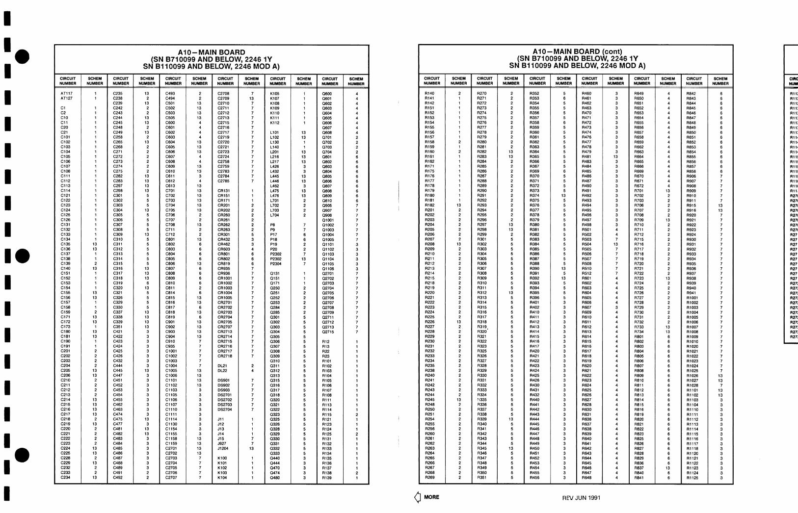


2246 1Y and 2246 Mod A Service
WAVEFORMS FOR DIAGRAM 1
Figure 9-7. A9-2 mV Bandwidth board for SN B700100 to 6714999 (2246 lY), and SN B100100 to 8119999 (2246 MOD A).
A9-2 mV BANDWIDTH BOARD I
Static Sens~t tve Devices See Maintenance Section
CIRCUIT NUMBER
COMPONENT NUMBER EXAMPLE
Component Number I
I I
SCHEM NUMBER
I Schematic
Number Subassembly Number (if used) I
CIRCUIT SCHEM CIRCUIT SCHEM NUMBER NUMBER NUMBER NUMBER
I I C h a i s s mounted components have no Assembly Number prelx-see end of Replaceable EIectr8ca Parts L~s t
Figure 9-7. A9-2 mV Bandwidth board for SN 8700100 to 8714999 (2246 lY), and SN B100100 to B119999 (2246 MOD A ) .
I A9-2 mV BANDWIDTH BOARD I
Static Sensitive Dev~ces See Marntenance Section
COMPONENT NUMBER EXAMPLE
CIRCUIT NUMBER
C185 C186 C188
Component Number
Figure 9-8. Hybrid pin identifiers. SCHEM NUMBER
1 1 1
I Assembiv _ _ I Number Sobassembly
L Circuit
Number ( r i used) Number I I I
Chaiis mounted components have no Assembly Number plef~x-see end of Replaceable EIectr8cal Parts Llst
CIRCUIT NUMBER
R185 R188 R189
REV JUN 1991
SCHEM NUMBER
1 1 1
VERTICAL INPUTS DIAGRAM 1 (SN B710100 AND ABOVE, 2246 1Y
SN B110100 AND ABOVE, 2246 MOD A)
1 PARTIAL A 10 WAIN BOARD I 2246 1 Y AND 2246 MOD A REV JUNE 1991 7062-39
ASSEMBLY
CIRCUIT NUMBER
AT1 17 AT127
C1 C2 C10 C11 C20 C21 C lO l C102 C103 C104 C105 C106 C107 C108 C l l l C112 C113 C114 C121 C122 C123 C124 C125 C126 C131 C132 C133 C134 C137 C138 C151 C152 C153 C154
Pamal A10
A10
SCHEM LOCATION
1J 3H
1K 4K 2H 2J 4H 5J 18 38 78 88 1 F 2G 4F 5G 18 I F 1F 2J 38 4F 4F 41 48 7F 78 7H 7J 7J 7L 7K 8B 8H aJ aJ
also shown on
BOARD LOCATION
68 48
6C 4C 6C 6C 4C 4C 6A 4A 3A 1 A 68 5A 58 4A 1 OC 6A 5A 5C 1 OC 4A 4A 4C I D I D 1 OC 2A 28 28 2C 2C 1 OC 2A 18 1 B
dlagrams 2, 3, 4,
CIRCUIT NUMBER
R151 R152 C157 C158 C173 C185 C186 C188 C190 C191
CR131 CR151 CR171
J l l J12 J13 J14
K1W KlOl K102 K103 K104 K105 K107 K108 K109 K110 K111 K112
L130 L140 0131A 01318
5, 6, 7and 13.
SCHEM LOCATION
8A 8H 8L 8K 5C 3M 6L 3M 7L 8L
6H 8H 5B
1 A 4A 7A 8A
1F 1 G 1 G 1H 2L 2K 4F 4G 4G 4H 5L 5K
7L 8L 7K 7J
BOARD LOCATION
1A 2A 1 C 1C 38 1 C 1A 18 2C 1C
28 18 38
6A 4A 3A 1A
6A 5A 5B 68 5D 6D 4A 4A 48 5B 4D 4D
2C 1 C 28 28
CIRCUIT NUMBER
0151A 01518 0171 0181 a182
R12 R13 R22 R23 RlOl R102 R103 R104 R105 R106 R107 RlO8 R111 R113 R114 R121 R123 R124 R131 A132 R133 R134 R135 R136 R137 R13Q R141 R142
R153 R154 R155
SCHEM LOCATION
8K aJ 5C 3M 6L
2K 2K 4K 4K 18 38 78 78 18 38 78 88 1 A 1G I F 3A 3G 3F 7A 6H 6H 7H 7J 7K 7K 7L 7J 7J 8H 8H 8J
BOARD LOCATION
18 18 28 1 C I A
6C 6C 5C 4C 78 78 7A 7A 7A 78 78 78 6A 5A 5A 4A 4A 3A 2A 2A 2A 2A 2B 2C X 2C 28 28
1 A 1 A 18
C I R C U ~ ~ NUMBER
R156 R157 R15Q R l 6 l R162 R171 R175 R176 R177 R178 R179 R18O R181 R185 R188
U112 U122 U171 U172 U173 U174 U175
W11 W12 W13 W14 WlOO 'MI01 W102
SCHEM LOCATION
8K 8K 8L aJ aJ 5B 58 6C 6C 6E 6E 6J 8J 3L 6L
1L 4L 4C 5D 6E 1E 4E
18 3A 7A 7A 4F 5G 5 0
BOARD LOCATION
1 C 1C 1 C 18 18 38 38 3C 2C X 3C 28 18 1 C 1 A
6C 4C 38 38 3C 3A 3C
6A 5A 3A 2A 5C 5C 38
2246 1 Y AND 2246 MOD A REV JUNE 1991 7062-33 SN B ~ ~ O ~ O O AND ABOVE 12246 MOD A) V E R T I C A L INPUTS @ SN 0710100 AND ABOVE 2246 1Yl
A A A 1. A A A A A
18 6A 3A 5A 7A 3A 7A 2A 4F 5C 5G 5C 50 38
SCHEM LCCATION -
8K 8K BL 8J 8J 58 58 6c 6c 6E 6E W 8J 3L 6L
1L 4L 4C 5D 6E 1E 4E
BOARD LOCATION
1 C 1 C 1 C 18 18 38 38 3C 2C 2C 3C 2B 1B 1 C 1 A
6C 4C 38 38 3C 3A 3C

VERTICAL INPUTS DIAGRAM 1 (SN 8710099 AND BELOW, 2246 1Y
SN B110099 AND BELOW, 2246 MOD A)
2" 'Nr C113.
KlOO 1 t n l 7
ASSEMBLY A9
cibs 16 -- 1 022 -
CH 1 ON0
12 CH 1 X ~ O 1 022 7 1 n L U
CIRCUIT NUMBER
C185 C186 C188
0181 1 1 I MI 2 CH 1 XlO 2
P A R T I A L A 10 WAIN BOAR0 1 2246 1 Y A AND 2246 MOD A A A h A REV JUNE 1991 A 7062.14
SCHEM LOCATION
3M 6L 3M
3M
ASSEMBLY
CIRCUIT NUMBER
AT1 17 AT1 27
C1 C2 C10 C11 C20 C2 1 C101 C102 C103 C104 C105 C106 C107 C108 C l l l C112 C113 C114 C121 C122 C123 C124 C125 C126 C131 C132 C133 C134 C137 C138 C151
BOARD LOCATION
1C 1 A 18
1C
Partlal A10 also shown on dlagrams 2.3 4.5, 6.7 and 13
A10
SCHEM LOCATION
1J 3H
1 K 4K 2H 2J 4H 5.J 10 30 78 80 I F 2G 4F 5G 10 1F I F 2J 38 4F 4F 4J 40 7F 70 7H 7J 7J 7L 7K 80
CIRCUIT NUMBER
0182
R185 R188 R189
BOARD LOCATION
68 40
6C 4C 68 68 48 4B 6A 4A 3A 1 A 6A 5A 5A 4A gC 6A 5A 5C 10C 4A 3A 4C 1 C 1D 100 2A 2A 28 1 C 2C 1DC
SCHEM LOCATION
6L
3L 6L 3M
CIRCUIT NUMBER
C152 C153 C154 C157 C158 C173 C190 C l 9 l
CR131 CR151 CR171
J11 J12 J13 J14
K l OO K101 K102 K103 K104 K105 K107 K108 K109 K110 K111 K112
L130 L140
BOARD LOCATION
1A
1 C 1A 10
SCHEM LOCATION
8H aJ 8J 8L 8K 5C 7L 8L
6H 8H 50
1 A 4A 7A 8A
I F 1G 1G 1H 2L 2K 4F 4G 4G 4H 5L 5K
7L 8L
CIRCUIT NUMBER
VRlOl
W105 W106
BOARD LOCATION
1 A 1A 10 1 C 1 C 30 2C 1 C
20 10 30
6A 4A 3A 1 A
6A 5A 58 68 5D 5D 4A 4A 40 50 40 4D
2C 1 C
SCHEM LOCATION
3M
6L 3N
,
CIRCUIT NUMBER
0131A 01310 0151A 01510 0171
R12 R13 R22 R23 RlOl R102 R103 R104 R1O5 R106 R107 R108 R111 R113 R114 R121 R123 R124 R131 R132 R133 R134 R135 R136 R137 R139 R141 R142
BOARD LOCATION
10
1A 10
SCHEM LOCATION
7K 7J 8K aJ 5C
2K 2K 4K 4K 10 30 78 70 10 30 70 80 1 A 1G 1F 3A 3G 3F 7A 6H 6H 7H 7J 7K 7K 7L 7J 7J
CIRCUIT NUMBER
W107 W108 W212 W222
BOARD LOCATION
28 28 1 B 10 20
6c 6c 4C 4C 6A 7A 7A 7A 7A 7A 78 78 6A 5A 5A 4A 3A 3A 2A 2A 2A 2A 28 2C 2C 2C 20 20
SCHEM LOCATION
3M 3M 3L 6L
BOARD LOCATION
18 1 C 10 10
CIRCUIT NUMBER
R151 R152 R153 R154 R155 A156 R157 R159 R161 R162 R171 R175 R176 R177 R178 R179 R180 R181
U112 U122 U171 U172 U173 U174 U175
W l l W12 W13 W14 WlOO WlOl W102
SCHEM LOCATION
8A 8H 8H 8H aJ 8K 8K 8L gl
aJ 50 50 6C 6C 6E 6E 8J aJ
1L 4L 4C 5D 6E 1E 4E
10 3A 7A 7A 4F 5G 5G
BOARD LOCATION
2A 1 A 1 A 1 A 10 1C 1 C 1 C 10 10 30 38 3C 2C 2C X 28 10
6C 4C 38 38 X 3A 3C
6A 4A 3A 1 A 5C 5C 38
PARTIAL A I 0 MAIN BOARD 1 I
SN B7100SQ AND BELOW 12246 1V1 REV JUNE l Q 9 1 7062-14 N B l l O Q A N O B E L 2 6 O O A INPUTS A 0 1
2246 1 Y AND 2246 MOD A 1.
A A A A A A A

2246 1Y and 2246 Mod A Service
WAVEFORMS FOR DIAGRAM 2
SET READOUT CONTROL CCW (OFF).
SET READOUT CONTROL CCW (OFF). SET READOUT CONTROL CCW (OFF).
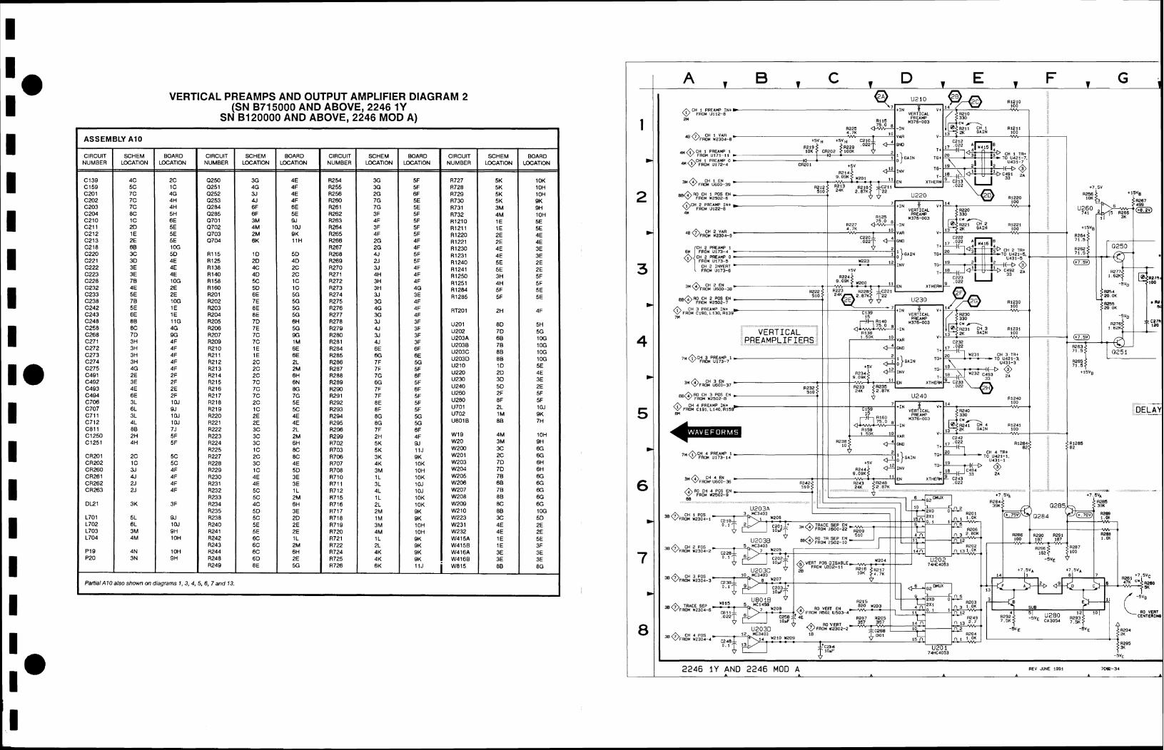
VERTICAL PREAMPS AND OUTPUT AMPLIFIER DIAGRAM 2 (SN B715000 AND ABOVE, 2246 1Y
SN B120000 AND ABOVE, 2246 MOD A)
I 2246 1 Y AND 2246 MOD A REV JUNE 1991 7c.z-34
h A A A A A A
ASSEMBLY
CIRCUIT NUMBER
C139 C159 C201 C202 C203 C204 C210 C211 C212 C213 C218 C220 C221 C222 C223 C228 C232 C233 C238 C242 C243 C248 C258 C268 C271 C272 C273 C274 C275 C491 C492 C493 C494 C706 C707 C711 C712 C811 C1250 C1251
CR201 CR202 CR260 CR261 CR262 CR263
DL21
L701 L702 L703 L704
P I 9 P20
Part~alAlO
A10
SCHEM LOCATION
4C 5C 7C 7C 7C 8C 1 C 2 0 1 E 2E 68 3C 3 0 3E 3E 78 4E 5E 78 5E 6E 88 8C 7D 3H 3H 3H 3H 4G 2E 3E 4E 6E 3L 6L 3L 4L 86 2H 4H
2C 1C 3J 4J 2J 2J
3K
5L 6L 3M 4M
4N 3N
also shown on
BOARD LOCATION
2C 1C 4G 4H 4H 5H 6E 5E 5E 5E 10G 5D 4E 4E 4E 10G 2E 2E 10G 1 E 1E 11G 4G 9G 4F 4F 4F 4F 4F 2F 2F 2E 2F 1 QJ QJ la 10J 7J 5F 5F
5C 5C 4F 4F 4F 4F
3F
9J l W 9H 10H
I OH 9H
dlagrarns 1 , 3, 4,
CIRCUIT NUMBER
0250 0251 0252 0253 0284 0285 0701 0702 0703 0704
R115 R125 R138 R140 R158 R160 R201 R202 R203 R204 R205 R205 R207 R209 R210 R211 R212 R213 R214 R215 R216 R217 R218 R219 R220 R221 R222 R223 R224 R225 R227 R228 R229 R230 R231 R232 R233 R234 R235 R238 R240 R241 R242 R243 R244 R248 R249
5, 6, 7 and 13.
SCHEM LOCATION
3G 4G 3J 4J 6F 6F 3M 4M 2M 6K
1 D 2D 4C 4D 5C 5D 6E 7E BE BE 7 0 7E 7C 7C 1 E 1 E 2C 2C 2C 7C 7C 7C 2C 1 C 2E 2E 3C 3C 3C 1C 2C 3C 1 C 4E 4E 5C 5C 4C 5D 5C 5E 5E 6C 6C 6C 6D 8E
BOARD LOCATION
4E 4F 4E 4F 6E 5E 9J 1 aJ 9K 11H
5D 4D 2C 2C 1 C 1 C 5G 5G 5G 5G 6H 5G 9G 1 M 6E 6E 2L 2M 6H 6N 8G 7G 5E 5C 4E 4E 2L 2M 6H 8C 8C 4E 5D 3E 3E 1L 2M 6H 3E 2D 2E 2E 1L 2M 6H 2E 5G
BOARD LOCATION
5F 5F 6F 5E 5E 5F 5F 5F 5F 4F 4F 5F 5F 4F 4F 4F 4G 3E 4F 4F 4F 3F 3F 3F 3F 6F 6E 5G 5F 6F 5F 6F 5F 5F 5F 5G 5G 6F 4F 9J 11J 9K 10K 1 OH 1 OK 1 0J 10J 1 OK 1 OK 9K 9K 1 OH 1 OH 9K 9K 9K 9K 11J
CIRCUIT NUMBER
R254 R255 R256 R260 R261 R262 R263 R264 R265 R266 R267 R268 R269 R270 R271 R272 R273 R274 R275 R276 R277 R278 R279 R280 R281 R284 R285 R286 R287 R288 R289 R290 R291 R292 R293 R294 R295 R296 R299 R702 R703 R706 R707 R708 R710 R711 R712 R715 R716 R717 R718 R719 R720 R721 R722 A724 R725 R726
SCHEM LOCATION
3G 3G 2G 7G 7G 3F 4F 3F 4F 2G 2G 4J 2J 3J 4H 3H 3H 3J 3G 4G 3G 3J 41 3J 4J 6E 6G 7F 7F 7G 6G 7F 7F 8E 8F 8G 8G 7F 2H 5K 5K 3K 4K 3M 1 L 3L 4L 1 L 2L 2M 1M 3M 4M 1L 2L 4K 4K 6K
CIRCUIT NUMBER
R727 R728 R729 R730 R731 A732 A1210 R1211 R1220 R1221 R1230 R1231 R1240 A1241 A1250 R1251 R1284 R1285
RT201
U201 U202 U203A U203B U203C U203D U210 U220 U230 U240 U260 U280 U701 U702 U801B
W19 W20 W200 W201 W203 W204 W205 W206 W207 W208 W209 W210 W223 W231 W232 W415A W415B W416A W416B . W815
SCHEM LOCATION
5K 5K 5K 5K 3M 4M 1 E 1E 2E 2E 4E 4E 5E 5E 3H 4H 5F SF
2H
8D 7 0 68 78 BB 88 1 D 2D 3D 5D 2F 8F 2L 1M 86
4M 3M 3C 2C 7D 7D 78 66 78 88 8C 88 3C 4E 4E 1 E 1E 3E 3E 88
BOARD LOCATION
1 OK 1 OH 1 OH 9K 9H 1 OH 5E 5E 4E 4E 3E 3E 2E 2E 5F 5F 5E 5E
4F
5H 5G 1 0G 10G 10G 1 OG 5E 4E 3E 2E 5F 5F 10J 9K 7H
1 OH 9H 6G 6G 6H 6H 6G 6G 6G 6G 6G 10G 5D 2E 2E 5E 3F 3E 3E 8G

Static Sensitive Devices @ See Maintenance Section

VERTICAL PREAMPS AND OUTPUT AMPLIFIER DIAGRAM 2 (SN 8714999 AND BELOW, 2246 1Y
SN B119999 AND BELOW, 2246 MOD A)
*See Parts List for serial number ranges.
2246 1 Y AND 2246 MOD A REV JUNE 1991 7062-15 d 1 A A A 4
CIRCUIT NUMBER
R712 R715 13716 R717 R718 R719 R720 R721 R722 R724 R725 R726 R727 R728 R729 R730 R731 R732
RT201
U201 U202 U203A U203B U203C U203D U210 U220 U230 U240 U260 U280 U701 U702 U8OlB
W19 W20 W200 W201 W202 W203 W205 W206 W207 W208 W209 W210 W223 W231 W232 W415A W415B W416A W4166 W815
CIRCUIT NUMBER
R250D R250E R250F R250G R251A R251 B R251C R251D R251 E R251F R251G R254 R255 R256 R260 R261 R262 R263 R264 R265 R266 R267 R268 R269 R270 R271 R272 R273 R274 R275 R276 R277 R278 R279 R280 R281 R284 R285 R286 R287 R288 R289 R290 R291 R292 R293 R294 R295 R296 R299 R702 R703 R706 17707 R708 R710 R711
BOARD LOCATION
4F 4E 4F 5E 5E 9H 1 OH 9K 1 OH
5D 4D 2C 2C 1C 1 C 5G 5G 5G 5G 5G 5G 9G 5H 5E 5E 3L 4M 5H 6M 5E 5C 4E 4E 3M 4M 5H 8C 8C 4E 50 3E 3E 3L 4M 5H 3E 2 0 2E 2E 3M 4L 5H 2E 5E 5E 5E
SCHEM LOCATION
4L 1 L 2L 2M 1 M 3M 4M 1L 2L 4K 4K 6K 5K 5K 5K 5K 3M 4M
2H
8 0 7 0 68 78 78 86 1 D 2D 3D 50 2F 8F 2L 1M 88
4M 3M 3C 2C 7E 7 0 78 68 78 88 8C 88 3C 4E 4E 1 E 1E 3E 3E 86
ASSEMBLY
CIRCUIT NUMBER
C139 C159 C201 C202 C203 C204 C210 C211 C212 C213 C218 C220 C221 C222 C223 C228 C232 C233 C238 C242 C243 C248 C258 C268 C271 C272 C273 C274' C275 C491 C492 C493 C494 C706 C707 C711 C712 C811
CR201 CR202 CR260 CR261 CR262 CR263
DL21
L701 L702 L703 L704
P I 9 P20
0250
Panlal A10
BOARD LOCATION
1 111 1 OK 9K QK QK 9H 10H 9K 9K QK QK 1 111 1111 1 OH 1 OH 9K 9H 1 OH
6G
5H 5G 1 OG 1OG 1 OG 1 OG 50 40 3E 2E 5F 5F 9J QK 7H
1 OH 9H 5G 5G 4G 5H 5G 5G 5G 5G 5G 1 OG 40 2E 2E 4E 2F 3E 2E 8G
SCHEM LOCATION
3E 2E 1 E 5F 4H 5H 5E 4E 2E 1E 5F 3G 3G 2G 7G 7G 3F 4F 3F 4F 2G 2G 41 2J 3J 4H 3H 3H 3J 3G 4G 3G 3J 41 3J 41 6E 6G 7F 7F 7G 6G 7F 7F BE 8F 8G 8G 7F 2H 5K 5K 3K 4K 3M 1L 3L
CIRCUIT NUMBER
0251 0252 0253 0284 0285 0701 0702 0703 0704
R115 R125 R138 R140 R158 R160 R201 R202 R203 R204 R205 R206 R207 R209 R210 R211 R212 R213 R214 R215 R218 R219 R220 R221 R222 R223 A224 R225 R227 R228 R229 R230 R231 R232 R233 R234 R235 R238 R240 R241 R242 R243 R244 R248 R250A R250B R 2 5 X
4, 5, 6, 7 and
BOARD LOCATION
5E 5E 5E 5E 5F 5F 5F 5F 5F 5F 5F 5F 5F 6F 5E 5E 5F 5F 5F 5F 4F 4F 5F 5F 4F 3F 4F 4F 3E 4E 4F 3F 3E 3F 3F 3F 6E 5E 5G 5F 6F 5F 5F 5F 5F 5F 4F SF 5F 6F 9J 1111 9K 1 OK 9H 1 OK 9J
SCHEM LOCATION
4G 3J 41 6F 6F 3M 4M 2M 6K
1 0 2D 4C 4 0 5C 5D 6E 7E BE 8E 7 0 8E 7C 7C 1E 1 E 2C 2C 2C 7C X 1 C 2E 2E 3C 3C 3C 1 C 2C 3C 1 C 4E 4E 5C 5C 4C 5D 5C 5E 5E 6c 6C 6c 6 0 2H 3H 5E
13.
A10
SCHEM LOCATION
4C 5C 7C 7C 7C 8C 1 C 20 1 E 2E 68 3C 3 0 3E 3E 78 4E 5E 78 5E 6E 86 8C 7 0 3H 3H 3H 3H 4G 2E 3E 4E 6E 3L 6L 3L 4L 86
2C 1C 3J 41 2J 2J
3K
5L 6L 3M 4M
4N 3N
3G
also shown on
BOARD LOCATION
2C 1C 4G 4G 4H 5H 6D 5E 5E 5E 9G 4D 4E 4E 4E 1 OG 2E 2E 1 OG 1E 1E 1OG 4H 9G 3F 4F 4F 4F 4F 2F 2F 2F 2F 1 OH 9J 9J 1 111 W
5C 5C 4F 4F 4F 4F
3F
9J 1111 9H 1 OH
1 OH 9H
4E
dlagrarns 1. 3.

S t a t i c S e n s i t i v e Devices @ See Maintenance Secllon
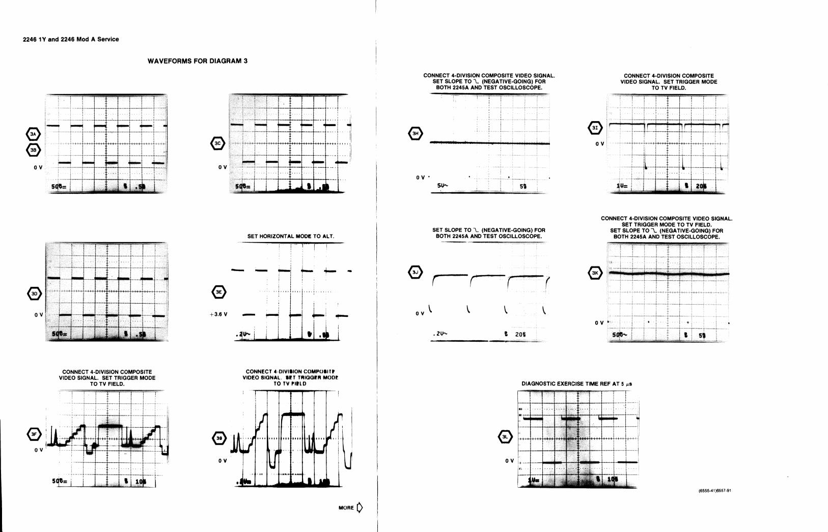
2246 1Y and 2246 Mod A Service
WAVEFORMS FOR DIAGRAM 3
CONNECT 4-DIVISION COMPOSITE VlDEO SIGNAL. SET SLOPE TO 1 (NEGATIVE-GOING) FOR
BOTH 2245A AND TEST OSCILLOSCOPE.
r- - --- -- IT--- - -
CONNECT 4-DIVISION COMPOSITE VlDEO SIGNAL. SET TRIGGER MODE
TO TV FIELD. - - r 1 i t /
I / $ " 1
CONNECT 4-DIVISION COMPOSITE VlDEO SIGNAL. SET TRIGGER MODE TO TV FIELD.
SET SLOPE TO 1 (NEGATIVE-GOING) FOR BOTH 2245A AND TEST OSCILLOSCOPE.
-I--"-' r ' --- I ?-a --i-
SET SLOPE TO 1 (NEGATIVE-GOING) FOR BOTH 2245A AND TEST OSCILLOSCOPE.
--- - w w ~ v w A m * - ~
SET HORIZONTAL MODE TO ALT.
' l T 1 '
CONNECT 4-DIVIIION COMPO8ltF I VlDEO 81ONAL 8LT TWIOOLW MOB€
TO T V r l w 1
CONNECT 4-DIVISION COMPOSITE VlDEO SIGNAL. SET TRIGGER MODE
TO TV FIELD.
i i i i t r
DIAGNOSTIC EXERCISE TIME REF AT 5 ps
I MORE 0 1

A AND B TRIGGER SYSTEM DIAGRAM 3 (SN B710100 AND ABOVE, 2246 1Y
SN B1 10100 AND ABOVE, 2246 MOD A)
*See Parts List for serial number ranges.
k
1 1 2246 1 Y AND 2246 MOD A REV JUNE 1991 7062-36
ASSEMBLY
CIRCUIT NUMBER
C421 C422 C423 C424 C425 C426 C432 C444 C447 C451 C452 C453 C454 C455 C462 C463 C474 C476 C477 C478 C483 C484 C485 C487 C488' C489 C496* C1103 C1105 C1106 C1107 C l l l O C1111 C1114 C1130 C1143' C1154 C1155
CR432 CR462
DL22 DL22
L426 L432 L462
0440 0444
PaR~al A10
A10
SCHEM LOCATION
1H 2H 2H 2H 2J 2D 1 L 2L 3L 6G 7H 8G 7G 6H 6L 6L 6K 7K 7L 8K 38 48 8B 38 88 48 88 3A 3E 3H 3H 3D 3H 5E 4G 4H 6F 6G
1 K 6K
6M 6M
2D 2L 6K
1L 2L
also shown on
BOARD LOCATION
2G 3H 2G 3G 2G 3H 2G 2F 2F 1G 2H 1G 1G 1G 1G 1 F 1 F 1 F 1 F 1 E 2F 3G 2H 3F 2G 3G 2G 4. 5K 4G 4G 3G 4G 4. 4G 4H 4G 4G
2G 1G
2K 2H
3H 2G 1 G
2H 2F
dlagrams 1, 2, 4,
CIRCUIT NUMBER
0473 0474 0480 01101 0 1 102 0 1 103 0 1 104 0 1 105 0 1 106
R401 R402 R403 R410 R411 R412 R413 R414 R415 R416 R417 R420 A421 R422 R423 R424 R425 R426 R430 R431 R432 R440 R441 R442 R443 R444 R445 R446 R447 R448 A449 R450 R451 R452 R453 R454 R455 R456 R460 R461 R462
5, 6, 7 and 13.
SCHEM LOCATION
5K 7K 8L 5E 4E 5F 3E 3E 3F
2C 2C 3L I M 1M 2M 2M 6M 6L 6L 6M 2E 1 H 2H 2H 2H 2H 2D 2K 1 K 2L 1 L 1L 1K 1K 2K 2L 2M 3L 3L 2M 6E 7G 7G 8H 7H 6D 6F 6K 6K 6L
BOARD LOCATION
1 H 1 F 1 F 5J 5J 5J 5J 5J 5J
3F 3F 3J 3G 3G 3G 3G 3H 2G 2G 2H 2G 2G 2G 3G 3G 2G 2H 2G 2F 2G 2G 2H 2H 2H 3H 2F 3F 2F 2F 3F 1G 1G 1G 2G 2G 1 H 1G 1 G 1 G 1 G
CIRCUIT NUMBER
R463 R470 R471 R472 R473 R474 R475 R476 R477 R478 R479 R483 R484 R485 R486 R487 R490 R491 R492 R493 R494 R495 R496 R497 R498 R1103 R1104 R1105 R1106 R l l l O R1111 R1112 R1113 R1114 R1115 R1116 R1117 R1118 R1120 R1121 R1122 R1123 R1124 R1125 R1126 R1127 R1128 R1131 R1132 R1133 R1134
SCHEM LOCATION
6L 6L 5K 5K 6K 6K 8K 8L 8L 7L 7L 38 8K 8L 8L 8L 38 48 48 48 78 78 88 88 38 3D 3 0 al al 5E 4E 4E 4E 4F 4F 5F 4F 5F 3E 4E 3E 4E 4F 3F 3F 4F 3F 3G 3H 3H 3J
BOARD LOCATION
I F 1G 1 H 1 H 1 H 1 H 1 F 1 F 1 F 1 F 1 F 3F 1 E 1 F 1 E 1 F 2J 3J 3J 2J 2J 2J 2J 2J 3J 3G 4G 5K 5K 4K 5K 4K 5K 5K 4. 4. 3J 4. 5K 5K 5K 5K 5K 5J 5J 3J 5J 4G 4G 4H 4H
CIRCUIT NUMBER
R1135 R1136 R1142 R1143 R1144 R1145 R1150 R1154 R1155 R1162 R1163 R1170
U421A U421B U421C U431A U431 B U431C U441A U441 B U441C U441D U441E U441F U442A U442B U442C U l l O l A U l l O l B U1102A U1102B U1103 U1104A U1104B U1104C U1106A U1106B U1106C
W401 W406 W413 W414 W l l O l W1102 W1103 W1106 W1108
SCHEM LOCATION
4F 4F 3G 4G 3H 3H 2D 6F 6F 5A 5A 3A
1C I K 1L 7D 6J 6L 4K 5K 7K 4K 2K 1 K 6M 4K 1 M 2E 6G 3G 3H 58 3J 4G 6H 28 al 4.
2D 3J 1M 2M 5C 3D 6C al 3K
BOARD LOCATION
4H 4H 4G 4H 4H 4H 3G 4G 4G 5K 5K 4.
3F 3F 3F 2F 2F 2F 1 H 1 H I H 1 H 1 H 1 H 2H 2H 2H 4G 4G 4G 4G 5K 4H 4H 4H 5L 5L 5L
4H 3H 3J 3J 5K 3. 5K 5L 5K

I
3K
SCHEM LOCATION
4F 4F 3G 4G 3H 3H 2 0 6F 6F 5A 5A 3A
1 I) 1K 1L 7D LU BL 4K 5K 7K 4K 2K 1 K 6M 4K 1M 2E 6G 3G 3H 50 3J 4G 6H 20 LU 41
2D
BOARD LOCATION
4H 4H 4G 4H 4H 4H 3G 4G 4G 5K 5K 41
3F 3F 3F 2F 2F 2F 1 H 1 H 1 H 1H 1H 1H 2H 2H 2H 4G 4G 4G 4G 5K 4H 4H 4H 5L 5L 5L
4H
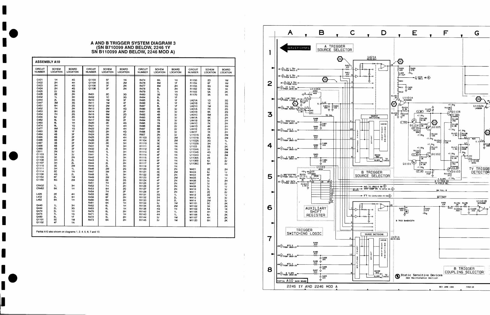


2246 1Y and 2246 Mod A Service
WAVEFORMS FOR DIAGRAM 4
-
SET A & B SECIDIV TO 0.1 rns, READOUT CONTROL CCW (OFF), AND HORIZONTAL
MODE TO ALT. ---
i T - T T
SET SECIDIV TO 20 ps. WAVEFORM VARIES WITH SETTING OF TRIGGER
HOLDOFF CONTROL.
6555-33
MORE 0

DISPLAY AND TIRGGER LOGIC AND PROCESSOR INTERFACE DIAGRAM 4 (SN B710100 AND ABOVE, 2246 1Y
SN B110100 AND ABOVE, 2246 MOD A)
*See Parts List for serial number ranges.
r
4
D
5 TO/ FROM
J2502<
'0 I* 3Y
0 6
1M
D
7 >
LOGIC
Partla1 A10 also shown on diagrams 1, 2, 3, 5, 6, 7, 18 and 21.
BOARD LOCATION
3M 4M 4M 3K 3L 3L 4K 4K 4K 4M 2L 3K 3K 4M 4K 3L 4K 3M 3M 4M 4M 3L 3L 3L 2K 2L 2L 2L 2L 2L
5M 4N 5N
2N@FgE:rl~ TRIG A G A T E L
6Y @FR:YT:?:2+ 34 0 TRIG BOARD
LOCATION
3K 3M 2K 3L 4L 3K 3K 3M 3M 4M 4L 3K 3K 2L 2L 4L 3L 2K 2N 3L 6N 3N 3N 3L 3L 4M 4M 3M 3M 3M 3M 1J 3K 3K
Assembly A10
RO CH 1 POS EN TO R212. U202-10 2 1 RO CH 2 PO5 EN TO R222. U202-11 , CH 3 , EN TO ,, ,,-, }::o
RO CH 4 PO5 EN RO CH 4 POS EN TO R242. U201-10 6A
CIRCUIT NUMBER
U600 U601 U602 U603A U603B U603C U603D U604A U6048 U604C UBOGA UBOGB U606C UBOGD U W E UBOGF
W502 W503 W504 W505 W506 W507 W510 W603 W604 W605 W610 W611 W612* W2502 W2502
YBM)
CIRCUIT NUMBER
RBI 1 RBI2 R613 R614 R615 R616 R617 R618 A619 R620 R621 R622 R623 R624 R625 R626 R627 R628 R630 R631 R636 R637 Re38 R639 R640 R641 R642 R643 R644 R645 R646 R647 R648 R649
CIRCUIT NUMBER
CeOO C601 C602 C603 C607 C608 C611 C612 C614 C636. C666'
CR603 CR612
0600 0601 0602 W 3 0604 0605 0606 0607 0608
R501 R502 REQI Re02 R603 R604 R605 R606 R609 R610
RO TR SEP EN TO "201-1j @BC
10 CAL TO R1170 0 3 1
CIRCUIT NUMBER
R650 R651 R652 R653 R654 R655 R656 R657 R658 R659 R662 R663 R664 R665 R666 R669 R670 R671 R672 R673 R674 R686 R687 R688 R689 R690 R691 R692 Re93 R694
U501 U502 U503
SCHEM LOCATION
2K 2K 3J 3J 5F 6F 6F 6F 6F 5F 5F 6F 6F 41 41 1G X 4H 6L 41 8H 8H eJ 1 H 2H 5H 5J 5H 5J 6H 4K 5F 5F 5F
2246 1Y AND 2246 MOD A REV JUM 1991 7062-36 1
A A h A A A
SCHEM LOCATION
3L 8K 1 G 3H 3H I H 2H 4J 2H 8F 5 0 3E 4E 4E 2L 3E
4C 7C 5C 4C 3E 4C 4E 1G 41 6L 3K 2L 8H 3M 8A
6K
SCHEM LOCATION
6K 2L 5E 4F 4F 4F 5H 41 5H 5J 4K 6H 6J 5H 5J 3H 4J 6K 61 5D 5D 2H 2J 2J I L 1L 1L 1 L 2L 2L
3C 5D 3D
SCHEM LOCATION
eJ eJ 1 G 1G 6J 6K 1L 2F 5D 8H 5J
5J 8H
eJ eJ 3K 3K X 2K U U 6K
66 4E 7J 8K 7K 7K 8L eJ 3K 3K
BOARD LOCATION
2M I N 4K 2K 2K 2K 2K 2L 2L 2L 3M 3M 3M 3M 3M 3M
3M 3M 3M 3N 3N 5N 6M 4M 4L EL 3N 3N 6N 1 L 1L
3L
BOARD LOCATION
3N 3N 4L 3L 3L 3M 4K 3K 5M 6N 4M
4M 6N
3N 3N 2K 2K 3K 3K 2K 2K 2L
1L 5N 3N 2N 1N I N I N 3N 2K 2K

RAM 4
--
Parts List for al number ranges.
2 2 4 6 1Y AND 2 2 4 6 MOD A REV JUNE 1991 7062-36 2: 8::8:88 :% 1:::; fb A, DISPLAY AND TRIGGER LOGIC AND PROCESSOR INTERFACE @ A A A A A A A A A A A

DISPLAY AND TIRGGER LOGIC AND PROCESSOR INTERFACE DIAGRAM 4 (SN B710099 AND BELOW, 2246 1Y
SN B1 10099 AND BELOW, 2246 MOD A)
PROCESSOR INTERFACE
B TRIG
8 TRIG FROM R416
B TRIG b
F
Partlal A10 also s h o w n on dlagrams 1. 2. 3, 5, 6. 7 and 13
SCHEM LOCATION
3L 8K 1G 2H 3H 1H 2H 4K 7F 8F 5E 3D 4E 2L 2L 2 0
4E 4E 1H 41 5G 3L 3L 8H 2M 8A
6K
CIRCUIT NUMBER
U6W U601 U602 U603A U603B U603C U603D U604A U604B U604C U606A U606B U606C U606D U606E U606F
Wm5 W510 W603 W604 W605 W610 W611 W612 W2502 W2502
Y 6 W
ASSEMBLY A10
EOAS
13p.12 SRO CLK
L/
BOARD LOCATION
4L 5K 3K 3M 3M 3M 3M 5M 5M 5M 5M 5M 5M 5M 5M 5M
5N 6M 3M 3L 3K 4M 5M 5K 1K 1K
4L
- SRl CLK - TO R367. 2A @ U302-3. U303-3
U606B
RO CH 1 POS EN TO R232. U202-10 28 cn 2 pos w Ro cH 2 w EN To R222. m2-11} , + CH 3 POS EN RO CH 3 POS EN TO R252. U201-9 CH 4 POS EN RO CH 4 POS EN TO ,7242. U201-10 68
I RO TR SEP EN ' RO TR S W W TO U 2 0 j - I 1 BC @ , TB CAL TO Rj.70 3A $
CIRCUIT NUMBER
R644 R645 R646 R647 R648 R649 R650 R651 R652 R653 R654 R655 R656 R657 R658 R659 R662 R663 R664 R665 R666 R669 R670 R671 Re72
U501 U502 U503
BOARD LOCATION
4M 4M 4M 4M 4M 4M 4K 4K 4K 4K 4L 4K 4L 5K 5K 5N 5N 3L 2L 4N 5M 6N 5K 4J 4J 3N 3N 4J 4K 3J
I PARTIAL A 1 0 MAIN 80AW I 2246 1 Y AND 2246 MOD A REV JUNE 1991 7062-17 0
CIRCUIT NUMBER
CBOO C601 C602 C603 C607 C608 C612
CR603
DL22
0600 0601 0602 0603 0604 0605 0608 0607 Q608
R501 R502 R601 R602 R603 R604 R605 R6C6
SCHEM LOCATION
5J 6H 4K 5F 5F 5G 6K 2L 2L 3F 4G 4F 5H 41 5H 5J 4K 6H 61 5H 5J 3H 4J 6K 6J
3C 4D 3D
CIRCUIT NUMBER
RM)9 R610 R611 R612 R613 R614 R615 R616 R617 R618 R619 R620 R621 R622 R623 R624 R625 R626 R627 R628 R630 R631 R636 R637 R638 R639 R640 Re41 R642 R643
BOARD LOCATION
2K 2K 5M 1K 2J 2J 4K 5M 5M 4N 5N 5N 41 4K 41 3K 4M 2K 2K 3J 3J 3M 5M 4L 4K
3N 3N 5N
SCHEM LOCATION
3K 3K 2K 2K 2K 3K 5F 6F 6F 6F 6F 5F 5G 6G 6G 4K 4K 1H 1H 4H 6L 4K 8H 8H 8J 1 H 2H 5H 5J 5H
SCHEM LOCATION
8J 8J 1 H 1 H 6J 6K 2G
5J
2F
8J aJ 3K 3K 2K 2K 2K 2K 6K
68 4E 7J 8K 7K 7K 8L aJ
BOARD LOCATION
4K 5K 3K 2K 4L 4L 2K
3J
2G
5J 5K 4M 4M 4M 4M 4M 4M 4L
3M 5N 4J 5L 5L 5L 5L 5K
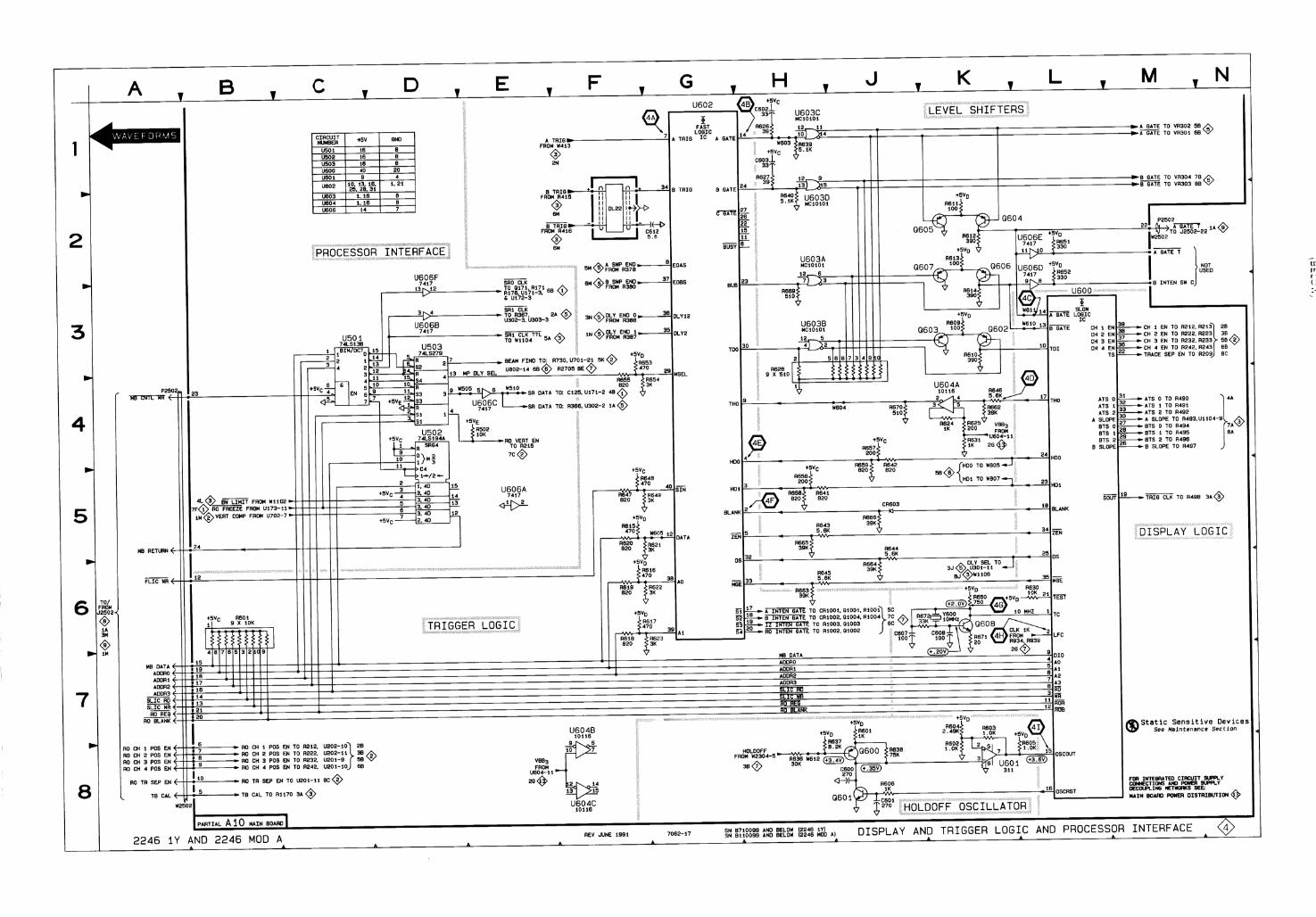

2246 lY and 2246 Mod A Service
WAVEFORMS FOR DIAGRAM 5
SET A SECIDIV TO 2 rns.
(3 -6.3 V
HORIZ MODE A, A SECIDIV 2 p s , HOLDOFF MIN (CCW)
HORIZ MODE ALT, A SECIDIV 2 , ~ s , B SECIDIV .5ps, HOLDOFF MIN,
DELAY-INTENSIFIED ZONE STARTS MIDSCREEN
MORE

A AND B SWEEPS AND DELAY COMPARATORS DIAGRAM 5
*See Parts List for serial number ranges.
SR DATA FROM
U606-6
ASSEMBLY
CIRCUIT NUMBER
C301 C302 C303 C305 C306 C307A C307B C307C C308 C310 C311 C312 C313 C314 C315 C321 C326 C329 C330
CR301
0301 0302 0303 0304 0305 0306 0307 0308 0309 0310A 03108 031 1 0312 0313 0315 0316 0317 0318 0320 0321 0322 0323A 03238 0325 0326
Panlal
VERT POSnDISABLE I I I I
J
BOARD LOCATION
8F 8F BE 8E 7G 9F 9E 9F 8E 8 0 BE 8H 7G 7H 7H 7H 7H 8F 7G 9E 9E 9F 8F 8F 8F 8F 8F 8F 8G 8F 9F 9G 10E 8C 8C 9G 9G 90 9G 10E 9E 8G 61 7G 6J 9F
VR304
B BATE FROM
U603-9
(-5.6V) IY 0313
R383
-7 .5v 6 .2V
A10
SCHEM LOCATION
40 7 0 3D 48 4A 5J 5J 7J 4H 41 5C U 2J 5J 5J 7C 7H 7J 7J
3C
3 0 48 4C 4 0 41 41 3H 5 0 5C 5J 5J 5C 5K 8D 68 7C 7D 7J 6H 7D 7C 7J BJ 7K 5 0
A10 also shown on
I
2246 1 Y AND 2246 MOD A REV JUNE 1999 7062-38 A A . A 4 A
BOARD LOCATION
7G 90 80 8F 9F 8F 8F 8D 10E 10E 7E 9E
80 80 8C 9C 80 80 7 0 7 0 7C 7C 9 0 9 0 8E 8F 8F 8F 7H 7H 7H 7H
80 6G 8G 8G 9F 6G 9G 8E 10E
8G 8G
BOARD LOCATION
8F 9F 7C 9 0 7C 7E 7E 1 OF 7 0 7 0 7F 9E 9E 7F 7G 9F 10E 10F 9G
7C
7C BE 8E 8F 7E 7 0 80 7F 7F 7E 7E 8F 7E 9F 9E 9E 9F 10E 9 0 9F 9F 9E 9E 9E 7F
dlagrams 1, 2.
CIRCUIT NUMBER
R382 R383 R384 R385 R386 R387 R388 R391" R393 R394 R395 R396
U301A U301C U302 U303 U304A U304B U307 U308 U309A U309B U310 U311 U313 U315A U315B U315C U316A U316B U316C U316D
VR301 VR302 VR303 VR304 VR308 VR309 VR310 VR311 VR312
W304 W802
SCHEM LOCATION
6L 8B 5E 1M 1 M 1 M 3M 5E 4H 6H 5J 7J
1K 2K 1B 2C 3H 6H 2F 2G 4A 30 5F 5G 3M 1 M 4M 2M 6M 6L 6L 6M
68 58 88 78 7C 5C 8C 6K 8K
7K 5K
C I R C U ~ ~ NUMBER
0328 0329 0330 0331 0332 0333
R301 R302 R303 R304 R305 R306 R307 R308 R309 R310 R311 R313A A3138 R313C R313D R314 R315 R316 R317 R318 R319 R320 R32 1 A R321B R321C R321 D R321 E R321 F R322 R323 R325 R326 R327 R328 R329 R330 R331 R332 R333 R334
3, 4, 6, 7 and
SCHEM LOCATION
4K 6K 4H 6H 78 58
6C 41 4C 5C 5C 48 4A 4A 3C 3C 3 0 4 0 30 3D 3 0 30 8K 50 4B 4C 58 5K 6F 6F 6F 3F 3F 3F 5L 7L 4H 41 7C 3M U 2J 3K 5C 50 58
13
BOARD LOCATION
7E 9E 7E 9E 9F 8F
9E 7E 8F 8F 7G 7C 7C 7C 9C 7C 8C 7C 7C 7C 7C 7C 10E 7F 8E 8E 8F 8E 8 0 8 0 8D 8 0 8D 8 0 7H 7G 7 0 7 0 9F 8E 9E 9E 8E 7G 7G 8G
CIRCUIT NUMBER
R335 R336 R337 R338 R340 R341 R342 R343 R344 R346 R347 R348 R349 R350A R350B R350C R350E R351 R352 R354 R355 R356 R357B R357C R357D R357E R359 R360 R361 R362 R363 R364 R365 R368 R367 R370 R371 R372 R373 R375 R376 R377 A378 R379 A380 R381
SCHEM LOCATION
3L 3L 2M 4L 6C 1L 2L 1L 4K 6K 5K 5L 5L 6M 7M 6L 5L 5E 6L 68 6C 78 1M 1M 3M 3M 2M 3M 60 4C 7C 8C 7H 1 A 214 8C 80 80 8C 8K 7K 6L 5M 6L 8M 7 0
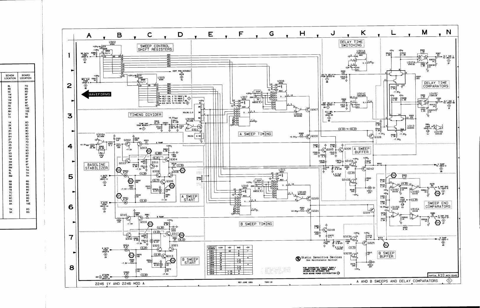
5G QD I : : : I : I

2246 1Y and 2246 Mod A Service
WAVEFORMS FOR DIAGRAM 6

HORIZONTAL OUTPUT AMPLIFIER DIAGRAM 6 (SN B710100 AND ABOVE, 2246 1Y
SN B1 101 00 AND ABOVE, 2246 MOD A)
*See Parts List for serial number ranges.
ASSEMBLY A10
C I ' C ~ ' t15V *75V +5V GNO NUMBER U301 16 8 UBOl 0 U802 16 4
I
2246 1 Y AND 2246 MOD A REV JUNE 1991 7062-37
A A A A A A
CIRCUIT NUMBER
C319 C802 C803 C804 C805 CEO7 CEO8 C8GQ C814 C817 C819 C82U C860 C870 C880
CR801' CR802'
P I 7 P I 8
0801 0802 0803
PartialAlO also shown on diagrams 1, 2, 3, 4, 5, 7 and 13.
>
CIRCUIT NUMBER
0804 0805 0806 0807 0809 0810 0811 0812
R353 R358 R369 R801 R802 R803 RE04 R805 RE06 R807 RE08 RE09 R810 R811 R812 R813
SCHEM LOCATION
78 3J 41 4J 4E 2J 58 61 6J 6C 7L 5H 3G 5G 4 0
58 68
3M 5M
3K 3J 3H
BOARD LOCATION
7F 7J 7K 8K 8H 7J 9G 8J 8J 6G 7J 8J 7J 8J 8J
5K 4M
7K 8K
7K 7K 7J
SCHEM LOCATION
4H 5K 5J 5H 5F 3F 3G 5G
68 6B 68 3K 3L 41 41 41 2J 48 4D 4D 5D 7D 7D 3G
BOARD LOCATION
7J 8K 8K 8J 8H 7H 7J 8J
9D 9D 8D 8K 7K 8K 8K 8J 7J 9G 7H 8H 8H 7H 8H 8J
CIRCUIT NUMBER
R814 R820 R821 R822 R823 R825 R826 R827 R828 R829 R830 R831 R836 R854 R855 RE56 R857 R860 R861 R862 R863 R871 RE72 RE73 R891
BOARD LOCATION
8J 8J 7J 7K 8G 8H 8G 9H 7J 7K 8K 8J 8H 8H 7H 8H 8H 8H 7J 7J 7J 8J 8J 8J 8K
SCHEM LOCATION
3G 7L 7L 7L 4C 7C 7C 4C 3K 3K 5K 5K 4C 5F 4F 4E 4E 5C 3F 3G 4F 5F 5G 5F 6K
CIRCUIT NUMBER
R892 R893 R894 R896 R897 RE98
U301B U801A U802
VR801
W17 W18 W305 W805 W806 W807 W808 WE10 W81 1 W820' W82lS
SCHEM LOCATION
5L 5H 5H 61 5J 41
68 7H 3C
4H
3M 5M 68 5B 5C 58 5C 48 48 5C 68
BOARD LOCATION
8K 8J 8J SJ 8K 7K
9D 7H 8H
8J
7K 8K 1 OD 6M 6K 6M 7K 6H 5H 5K 4M
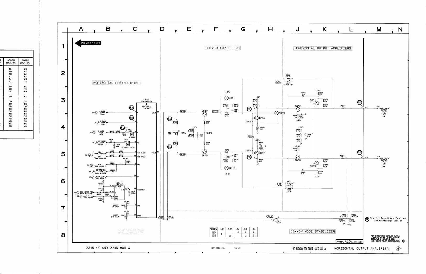
FW CWECTIDNS INTEGRATED A N l CIRCUIT W*ER S C P R V S I P R Y
DECOUPLIffi N T W a K S SEE:
) PARTIAL A 10 MAIN BOARD MAIN 80AW PW€U DISTRIBUTION '@
T R C
I h
2246 1 Y AND 2246 MOD A REV JUNE 1991 7082-37 SN B~ IO IOO B n o i o o AND AND ABOVE ABOVE 1 2 2 r 2246 ~ Y I HORIZONTAL OUTPUT AMPLIFIER @ A A A A A A A A A A A A
SCHEM LOCATION
5L 5H 5H 6 J 5.l 41
60 7H 3C
4H
3M 5M 6B 5 8 5C 58 5C 48 48 5C 60
BOARD LOCATION
BK @.I @.I 9J BK 7K
9D 7H 8H
8J
7K BK 1 OD 6M 6K 6M 7K 6H 5H 5K 4M

HORIZONTAL OUTPUT AMPLIFIER DIAGRAM 6 (SN B710099 AND BELOW, 2246 1Y
SN B110099 AND BELOW, 2246 MOD A)
U802 234-0401-21
mF LOUl - I
* HORIZCNTAL
P R E W
LOUl
BOARD LOCATION
8K 8J 8H 7H 8H 8H 7J
8D 7H 8H
BJ 8J
7K 8K 1 OD 6L 6K 6L 6K 5G 5H
A R A W FROM YB02
SCHEM LOCATION
5K 61 5E 4E 4E 4E 3K
68 7H 3C
4K 3G
3M 5M 6B 58 5C 5B 5C 48 48
X GAIN
CIRCUIT NUMBER
R852 R853 R854 R855 R856 R857 R858
U301B U801A U802
VR8Ol VR802
W17 W18 W305 W805 W8OB W807 WE08 WE10 W811
ROU'
BOARD LOCATION
8J 8K 8K 7K 7K 8G 8H 7G 8H 7K 8K 8H 7J 7J 7J 7K 7K 7J 7J 8J 8K 8K 8J 8J
C * MA6 RB09' REG 5K?-t15VG
1
SCHEM LOCATION
7H 5L 7L 7L 7L 4C 7C 7C 4C 3K 6K 4C 2K 4F 3F 2G X 3H 4K 5G 5H 5H 5G 5H
ASSEMBLY A1 0
loo RO H W I Z G A I N loo RO H W I Z G A I N
CIRCUIT NUMBER
R816 R819 R820 R821 R822 R823 R825 R826 R827 R828 R829 R836 R840 R841 R842 R843 R844 R845 R846 R847 R848 R849 R850 R851
Gem 0809
BOARD LOCATION
8J 8J 8J 8H 7H
8D 8D 8D 7K 7K 7J 7J 7J 7J OG 7H 8H 8H 7H 8H 8K 8J 8J
Parilal A10 also shown on dlagrams 1. 2. 3. 4. 5. 7 and 13 I I
SCHEM LOCATION
6K 5H 5H 5E 3E
6B 68 6B 2K 3L 2J 2.l 4H 2H 58 4D 4D 5E 70 7D 6K 6J 8J
HOO LLSBl ROU'
HD1 WI
CIRCUIT NUMBER
0806 0807 0808 0809 0810
R353 A358 R369 R801 R802 R803 R8M R805 R806 R807 R808 R809 RBI0 R81 1 R812 R813 R814 R815
' MAG
BOARD LOCATION
6F 7K 7J 8J 8J 7J 9G 8K 8J 8.l 6G 7J
9H 7K 8J
7K 8K
75 7J 75 7J 8J
CIRCUIT NUMBER
C319 C802 C803 C8M C805 '2807 C808 C809 C810 C814 C817 C819
CR8Ol CR802 CR819
PI7 PI8
0801 Q802 0803 0804 0805
A BEAM FINO - 14(BF I I
SCHEM LOCATION
6B 3K 3J 3G 4K 2H 58 5K 55 7H 6C 7L
48 3L 6L
3M 5M
2K 3K 3H 3G 5K
I 2246 1 Y AND 2246 MOD A REV JUNE 1 9 9 1 , 7062-19
A A A A A .

;CHEM CATION
5K 6J 5E 4E 4E 4E 3K
60 7H 3C
4K 3G
3M 5M 60 50 5C 50 5C 40 48
BOARD LOCATION
8K 8.J 6H 7H 6H 8H 7J
8D 7H 8H
8.J @J
7K 8K 1 OD 6L 6K 8L 6K 5G 5H

2246 1Y and 2246 Mod A Service
Static Sensitive Devices S e e Marntenance Sectron
COMPONENT NUMBER EXAMPLE
1 1 Schematic Assembly ,' t , clrcult Number Subassembly ~~~b~~
Number f r i used1
Figure 9-9. A8-CRT Control board.
. ~
I ,aisls mounted comw~ents have no hsembly Number ell,-see end of Replaceable Electr~cal Parts Llsl-
I A8-CRT CONTROL BOARD I
WAVEFORMS FOR DIAGRAM 7
SET READOUT CONTROL CCW (OFF) AND A INTEN CONTROL CW (FULLY ON).
BET READOUT CONTROL CCW (OFF) AND A INTEN CONTROL CW (FULLY ON).
SET READOUT CONTROL CCW (OFF) AND A INTEN CONTROL CW (FULLY ON).
SET A

WAVEFORMS FOR DIAGRAM 7
SET READOUT CONTROL CCW (OFF), SET READOUT CONTROL CCW (OFF) AND A INTEN CCW (OFF), B ENTEN CW (FULLY
A INTEN CONTROL CW (FULLY ON). ON), AND HORIZONTAL MODE TO ALT.
I I
.I Q
0 v 0 v I
SET READOUT CONTROL CCW (OFF) AND A INTEN CONTROL CW (FULLY ON).
-- -- -- i r- -
SET READOUT CONTROL CCW (OFF), A INTEN CCW (OFF), B ENTEN CW (FULLY
ON), AND HORIZONTAL MODE TO ALT. SET READOUT CONTROL CCW (OFF) AND
A INTEN CONTROL CW (FULLY ON).
0 v
SET READOUT CONTROL CCW (OFF) AND A INTEN CONTROL CW (FULLY ON).

Z-AXIS, CRT, PROBE ADJUST AND CONTROL MUX DIAGRAM 7 (SN B715000 AND ABOVE, 2246 1Y
SN 8120000 AND ABOVE, 2246 MOD A) P2302 1 1 RO HORIZ TO R807 50 6 RO VERT TO R207 7C @
A TRIG LVL A TRIG LVL TO W410 B REF TRIG LVL TO RiiOS
TO R925 3H
US'
t15V
I I ='='dr~ I r A t i t 1 s ' c ' ~ l l ~ MI I1 I A REV JUNE 1991 TW lo
h A L A A A 4

FOR I H T E W T E D CIRCUIT WPPLY CDEECTIDNS Am W*ER SIPPLY DECRPLIrn HET*OR(9 SEE. MAIN w*RO W*ER DISTRIBUTION

Z-AXIS, CRT, PROBE ADJUST AND CONTROL MUX DIAGRAM 7 (SN B714999 AND BELOW, 2246 1Y
SN B1 19999 AND BELOW, 2246 MOD A)
2246 1 Y AND 2246 MOD A REV JUNE 1991 7062-20 b & A b A
ASSEMBLY A8
*See Parts List for serial number ranges.
BOARD LOCATION
Pai-la1 A8 also shown on diagram 13.
SCHEM LOCATION
BOARD LOCATION
1E
BOARD LOCATION
1 F 1H
CIRCUIT NUMBER
W9M)
CIRCUIT NUMBER
SCHEM LOCATION
4A
CIRCUIT NUMBER
R903 R905
BOARD LOCATION
1 A 1C
CIRCUIT NUMBER
R901 R902
BOARD LOCATION
9C 8A 7A 7A 78 78 70 7A 7A 78 78 7A 8A 3K 3K 3L 3K 7L 7L 8L 7L 7K 7K 7L 7L 7L 7L 7L 7L 4K 6L 6L 7L 7L 7L 7M 7M 7M 6M 6N 6M 7M 7M 7M 7M 7M 7M 7N 8N 9N 6L 9M
SCHEM LOCATION
6A 4A
SCHEM LOCATION
5A 6A
BOARD LOCATION
9M 6L 7L 6L 7L 9L 9L 9L 1 OL 1 OK 1 OL 1 OL 1 OL 8M 8L 8L 7N 8M 9M 9L 10M 7M 7N 8N 6N 6N 6N 8N 7L 6M
9C 78 78 90 7L 7L 7L 2M
6M
7K 7K 7K 7K 3L 4K 61 1 OD 10D 5K
CIRCUIT NUMBER
R2724 R2726 R2727 R2728 R2729 R2733 R2734 R2735 R2736 R2737 R2738 R2739 R2740 R2741 R2742 R2743 R2745 R2750 R2751 R2758 R2760 R2765 R2784 R2785 R2786 R2787 R2788 R2789 R2795 R2796
U506 U930A U930B U931 U l00 lB UlOOlC UlOOlD U l l O l A
VR2701
W9 W9 W9 W16 W 1000 W1010' W1288 W2302 W2304 W2701
OTHER PARTS
SCHEM LOCATION
7K 5E 5E 5E 6E 6F 6F 5G 5G 5G 5G 4H 5J 5J 6J 6H 7J 61 6K 6L 6L 7F 3L 3L 4L 5L 5L 5L 7E 6F
2E 1H 2H 3H 68 6B 58 78
7G
3M 8A 8M 8A 5D 7D BJ 3A 4A 7E
CIRCUIT NUMBER
R924 R930 R931 R932 R933 R934 R935 R936 R937 R938 R939 R940 R941 RI001 R1002 R1003 R1004 R1005 R 1 006 R1007 R1008 R1009 RlOlO R1020 R1021 R 1022 R1023 R1024 R 1025 R 1028 R2701 R2702 R2703 R2704 R2705 R2706 R2708 R2709 R2710 R2711 R2712 R2713 R2714 R2715 R2716 R2717 R2718 R2719 A2720 R2721 R2722 R2723
SCHEM LOCATION
2H 1H 1 H 1 H 1H 2G 2H 1J 2J 1 G X 2J 1H 5C 6C 6C 7C 5C 6D 7D 7D 8C 8B 58 50 60 6B 70 78 5D 7E 7E 6E 6E 7F 7F 6G 6G 8G 7G 7G 7G 7G 7G 6G 6H 7J 7J 7J 7K 7K 7K
BOARD LOCATION
1 OB 78 7L 7M 8M 7L 6M 7M 7N 6N 7M 7N 7N 8M 8N 6N 1OL 1 OL 1 OL 1 OM 8L 6K 7L 8M 1 OL 7M 8N 6N 8N
7A 7A 4K 4K 7L 7L 5M 9M 9M 8N 6N 6M 7L 1 OL 1 OL 9L 8M 9M 8L
8A 9A 10A
dlagrams 1. 2.
ASSEMBLY
CIRCUIT NUMBER
C910 C935 ClOOl C1002 C1003 C1004 C2703 C2704 C2705 C2706 C2707 C2708 C27 10 C2711 C2712 C2713 C2715 C2716 C2717 C2719 C2720 C2721 C2723 C2724 C2758' C2759 C2783 C2784 C2785
CR935 CR936 CR1001 CR1002 CR1003 CR1004 CR1005 CR2701 CR2702 CR2703 CR2704 CR2705 CR2707 CR2713 CR2714 CR2715 CR2716 CR2717 CR2718
DS901 DS902 DS903
Paltial A10
BOARD LOCATION
9N 9M 9M 9M
6A 10A
1 OM 8N 8N 1 OD 10D
10A 10A 10A 3K 3K 3L 3K 7L 7N 7M 6M 6N 6M 7M 6M 6L 6L 1 OL 1 OL 1 OL 6M
lo€ 9C 92 9C 10C 10C 1 CC 108 10A 10A 60 100 8A 8B 80 9C 9C
CIRCUIT NUMBER
DS2701 DS2702 DS2703 DS2704
J15 J927
P8 W F9 P2302 P2304
0905 0907 0908 01001 01002 01003 01004 01005 02701 02702 02703 02704 02705 02708 02707 02708 02709 0271 1 02712 02713 027 15
R503 R505 A506 R507 R508 R510 R512 R906 R907 R908 R909 R910 R911 R920 R921 R922 R923
3. 4, 5. 6 and
A10
SCHEM LOCATION
2L 2H 5C 6C 6C 7C 7G 6G 7G 7H 7H 6H 7J 7K 7K BK 6G 5H 5H 5J 6J 61 6E 8K 6K 7F 3L 5L 5L
2J 2J 5D 7D 8C 7C 5D 7K 8K 7K 7K 8G 7F 6H 5H 5J 5K 6K 5J
4E 4F 4F
also shown on
SCHEM LOCATION
8L 7L 5K 6K
2K 2L
8 A 3M 4M 1 A 3A
4E 4E 4F 5D 6D 6D 7D 8D 7H 7H 7H 8H 7G 8F 7F 5E 5F 5G 5H 5H 7F
28 50 68 68 28 20 30 4E 4E 4F 5D 2L 2L 3G 3G 3H 3H
13
BOARD LOCATION
CHASSIS
BOARD LOCATION
CHASSIS
CIRCUIT NUMBER
V1
CIRCUIT NUMBER
J16
SCHEM LOCATION
1 M
BOARD LOCATION
CHASSIS
SCHEM LOCATION
7A
CIRCUIT NUMBER
P27
CIRCUIT NUMBER
P26
SCHEM LOCATION
2L
SCHEM LOCATION
1L
BOARD LOCATION
CHASSIS
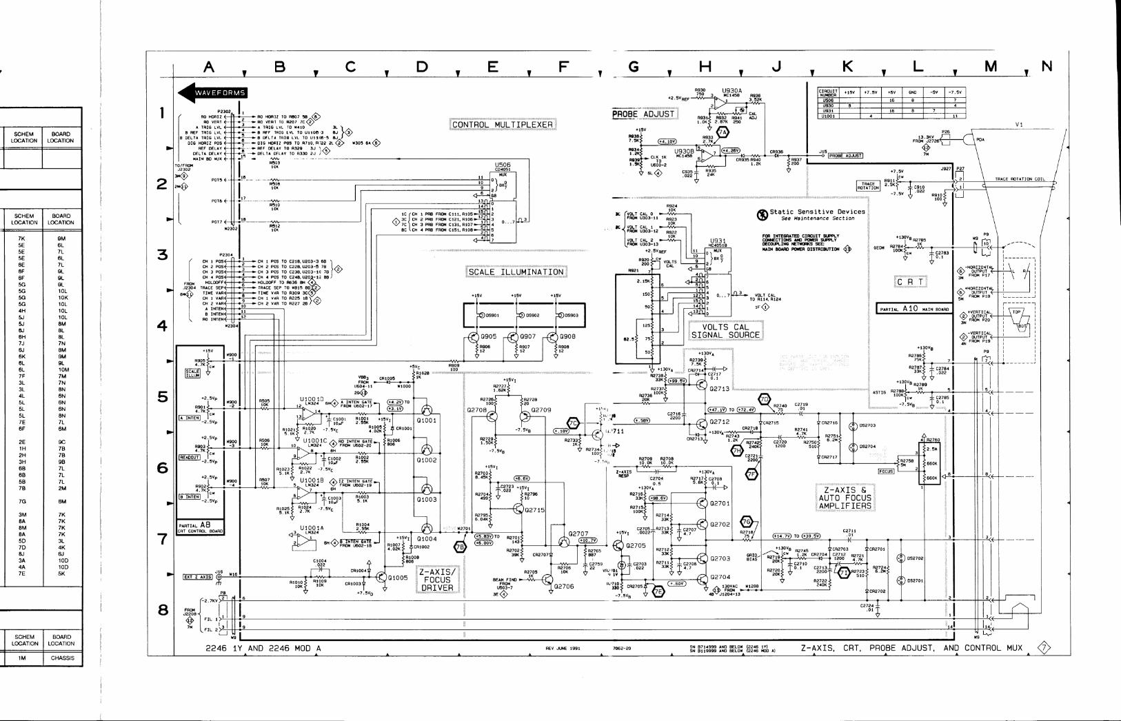
LOCATION BOARD
LOCATION
0 REF T R l G L V L 0 DELTA T R l G LVL
DIG H O R I Z PO5
S t a t i c Sens i t i ve Device d
FW INTEGWTED CIRCUIT m Y CmwECTIONS UO PMR m v OECWPLIffi HET*(FKS SEE. MAIN 8 0 M PO*ER DISTRIBUTION @
d
4
d
4
2246 1 Y AND 2246 MOD A REV JUNE 1991 7062-20 SN 8 1 1 ~ 9 9 AND BELOW 12246 MOD AI Z -AXIS , CRT, PROBE ADJUST, AND CONTROL MUX @ SN 8714999 AND BELOW 2246 IYI
I A A A A A A A

' and 2246 Mod A Service I
. * B O . ? c P C _ w l c l * * d a * ~ ~ * ~ ) r a * a IS : 2 * 7 2 U2403 N N N N N U V C J W W e g s * * l'i r a t B I B * * *
B a n d s mounted on md.c .ld. ot ehm b o d .
Figure 9-10. Ale-Procersor board.
Static Sensitive Devices See Ma~ntenance Sect~on
COMPONENT NUMBER EXAMPLE
(7 - Number I 'A23 A ~ 1 2 3 4 '
Assemtdv ~f~'chemat!c c,rcai Number Number Subassembly Of usedl Number I
1 I Charsls mounted components have no Assembly Number pelix-see end 01 Replaceable Electr~cal Parts List
REV JUN 1991
CIRCUIT NUMBER
ST2501 BT2502
C2300 C2301 C2302 C2303 C2304 C2305 C2306 C2307 C2308 C2309 C2310 C2311 C2312 C2313 C2314 C2315 C2316 C2317 C2318 C2319 C2320 C2321 C2322 C2323 C2324 C2401 C24M C2403 C2404 C2405 C2406 C2407 C2408 C2409 C2410 C2411 C2412 C2415 C2416 C2417 C2418 C2419 C2420 C2501 C2502 C2503 C2504 C2505 C2506 C2507 C2508 C2509 C2510 C2511
I N

Static Sensitive Devices See M a i n t e n a n c e S e c t ~ o o
COMPONENT NUMBER EXAMPLE
A16-PROCESSOR BOARD
C o m p o n e n t N u m b e r
A23A2 R1234 I --=. I I Schematic
Asiembk + ! I L clrcu,t Number Subassembly Number
Number id used] I I 1
Chassi mounted cornpanentr have no Assembly Numbel prefx-see end of Replaceable Electrtcal Parts 1s t
SCHEM NUMBER
11 11 11 9 9 9 9 9 9 9 9 9 9 9
14 9 9 9 9 9 9 9 9 9 8 8 8 8 8 8 8 8 8 8 8 8 8 8 8 8 8 8 8 8 8 8 8 8
10 8 8
10 10 10 10 10 10
CIRCUIT NUMBER
R2363 R2364 R2365 R2400 R2401 R2402 R2404 R2405 R2406 R2407 R2408 R2409 R2410 R2411 R2412 R2413 R2414 R2415 R2416 R2417 R2418 R2419 R2420 R2421 R2501 R2502 R2503 R2504 R2505 R2506 R2507 R2508 R2509 R2510 R2511 R2512 R2513 R2514 R2515 R2516 R2517 R2518 R2519 R2520 R2521 R2522 R2523 R2524 R2525 R2526 R2527 R2528 R2529 R2532 R2534 R2536 R2538
board.
CIRCUIT NUMBER
BT2501 BT2502
C2300 C2301 C2302 C2303 C2304 C2305 C2306 C2307 C2308 C2309 C2310 C2311 C2312 C2313 C2314 C2315 C2316 C2317 C2318 C2319 C2320 C2321 C2322 C2323 C2324 C2401 C2402 C2403 C2404 C2405 C2406 C2407 C2408 C2409 C2410 C2411 C2412 C2415 C2416 C2417 C2418 C2419 C2420 C2501 C2502 C2503 C2504 C2505 C2506 C2507 C2508 C2509 C2510 C2511
REV JUN 1991
CIRCUIT NUMBER
R2540 R2542 R2546 R2547 R2548 R2549 R2550 R2551 R2552 R2553 R2554 R2555 R2560 R2561 R2562 R2563 R2564
U2300 U2300 U2301 U2301 U2302 U2302 U2303 U2303 U2304 U2304 U2305 U2305 U2306 U2306 U2308 U2308 U2309 U2309 U2313 U2313 U2314 U2314 U2400 U2400 U2401 U2401 U2402 U2402 U2403 U2403 U2404 U2404 U2405 U2405 U2406 U2406 U2407 U2407 U2408
SCHEM NUMBER
8 8
11 11 11 11 14 11 11 11 11 11 11 14 14 14 14 14 14 14 11 14 11 14 11 11 11 14 14 14 14 14 14 14 14 14 14 9 9
14 9 9 9 9 9
14 14 14 14 14 14 14 14 14 14 14
CIRCUIT NUMBER
C2514 C2515 C2516 C2517 C2518 C2521 C2522 C2523 C2524 C2525 C2526 C2530 C2531 C2532 C2541 C2543 C2544 C2545 C2546 C2547 C2548 C2549 C2550 C2551 C2552 C2553 C2554 C2555
CR2501 CR2502 CR2504 CR2505
DS2501
J2302 J2302 J2302 J2304 J2501 J2501 J2502 J2502 J2502 J2503 J2601 J2601
P2105 P2105
02501 02502 Q2503 Q2504 02505
SCHEM NUMBER
10
10 lo 10 lo
lo 10 10 10 10 8 8 8 8 8 8 8
11 14 11 14 11 14 11 14 11 14 11 14 11 14 11 14 11 14 11 14 11 14 9
14 9
14 9
14 9
14 9
14 9
14 9
14 9
14 9
CIRCUIT NUMBER
Q2506 02507
R2301 R2302 R2303 R2304 R2305 R2306 R2307 R2308 R2309 R2310 R2311 R2312 R2313 R2314 R2315 R2316 R2317 R2318 R2319 R2320 R2321 R2322 R2324 R2325 R2328 R2329 R2330 R2331 R2332 R2333 R2334 R2335 R2336 R2337 R2338 R2339 R2340 R2341 R2342 R2343 R2344 R2345 R2346 R2347 R2348 R2349 R2350 R2351 R2352 R2355 R2356 R2357 R2361 R2362
SCHEM NUMBER
8 8 8 8 8
10 10 10 10 10 10 14 14 14 14 10 10 10 10 10 10 10 10 8 8 8 8 8
8 8 8 8
8
9 11 14 11 10 14 8 9
14
11 14
11 14
10
lo 10
10
SCHEM NUMBER
10 8
11 11 11 11 11 11 11 11 14 11 11 11 11 11 11 11 11 11 11 11 11 11 11 11 11 11 11 11 11 11 11 11 11 11 11 I 1 11 11 11 11 11 11 11 11 11 11 11 11 11 11 11 11 11 11
CIRCUIT NUMBER
U2408 U2409 U2409 U2410 U2410 U2411 U2411 U2412 U2412 U2413 U2413 U2414 U2414 U2415 U2415 U2416 U2416 U2417 U2417 U2501 U2501 U2502 U2502 U2503 U2503 U2506 U2506 U2512 U2512 U2513 U2513 U2514 U2514 U2515 U2515 U2517 U2517 U2518 U2518 U2519 U2519 U2521 U2523 U2523 U2524 U2524 U2525 U2525
W2105 W2105
Y2501
SCHEM NUMBER
14 9
14 9
14 9
14 9
14 9
14 9
14 9
14 9
14 9
14 8
14 8
14 8
14 8
14 8
14 8
14 8
14 8
14 8
14 8
14 8
14 8
10 14 10 14 10 14
11 14
8
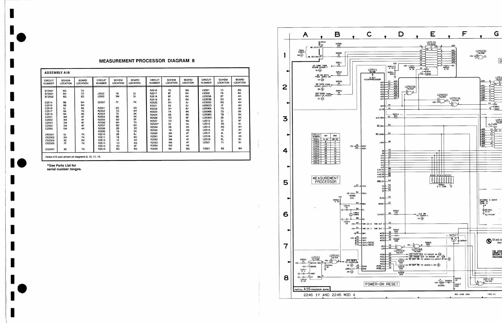
MEASUREMENT PROCESSOR DIAGRAM 8
*See Parts List for serial number ranges.
ASSEMBLY A16 FROM J2501-20
FROM
SROY 4ROY
ALE1050
- YR/OSl
LOCK
Partla1 A16 also shown on diagrams 9, 10, 11, 14.
SCHEM LOCATION
1 C 7A 2F 2 0 8G I F 7 0
7D . 78 2E 3J 3G X 1E 4L SL 6L 7J
6B
CIRCUIT NUMBER
U2501 U2502 U2503A U2503B U2503C U2503D U2506A U2506B U2506C U2506D U2512 U2513 U2514 U2515 U2517 U2518 U2519 U2521
Y2501
--- 415
A16/S3 417/S4 AIE/SS A19/S6
m / s 7
TEST SO S1 52
HOLD
HLO4 715001 6 ABOVE
RES RESET
BOARD LOCATION
60 6K 4H 4H 4H 4H 5K 5K 5K 5K 4F 41 5H 4H 5F 4K 61 5J
6H
U,z2%= ,6 ;5vg RESIN RES
SCHEM LOCATION
7D 8F 8F 6J 5H 5E 3H 7A 8B 7 0 7 0 5J 28 1B 3M 3M 3M 4M 5M 6B
CIRCUIT NUMBER
R2516 R2517 R2518 R2519 R2520 R2521 R2522 R2523 R2524 R2526 R2527 R2545' R2554 R2555 A2560 R2561 R2562 R2563 R2564 R2565
I N 1 TYR OUT 1 R2527 +
(32507
BOARD LOCATION
6G 6K 6K 6K 41 5J &I 6K 6K 6F 6G 7K 2A 4G 4F 4F 4F 4F 4K 6G
BOARD LOCATION
3.J 3.J
7K
4G 4H 5K 5K 5F 7C 6H 3 0 5K 8J 8C 4H 4G 5F 6G
U2506B 1 I I I I
SCHEM LOCATION
1B 3M
7F
2D 1 0 7E 68 8 0 6H 6 0 28 1 B 28 18 1E I D 3 0 8 0
J f ~ ~ , 6 O A 74LS00 LED CATH CLK TO R2529 4A @
&NOD CLK TO R252B 24 9 1 1 1 1 1 d TO U2401-11. U2417- 24 @ 7 R??!6
CIRCUIT NUMBER
J2502 J2502
02507
R2501 R2502 R2503 R2504 R2505 R2506 R2507 R2508 R2509 R2510 R2511 R2512 R2513 R2514 R2515
RO BUF RD TO U2402-1 6~ I I I I
BOARD LOCATION
7 0 7 0 8 0
6H 6H 8K 7K 8K 4F 4F 4F 4F 4K
7K 7K 6K 7K
7K
CIRCUIT NUMBER
BT2501 BT2501 BT2502
C2514 C2515 C2516 C2517 C2518 C2551 C2552 C2553 C2554 C2555
CR2501 CR2502 CR2504 CR2505
DS2501
FOR I r n C W C T I O E C R R I PROCESS
SCHEM LOCATION
6G 6H 6G
68 68 5J 8A 8A 4M 4M 3M 3M 5M
5J 5H 8E 7F
8E
~ 2246 1 Y AND 2246 MOD A REV JUNE 1991 7062-21
A A Ir A k A

SCHEM BOARD I 1 LCUTION I LCCATION
R2308. U2306-7
Static Sensitive Oevlces @ See Halntenance s e c t l o "
FOR INTEWTEO CIRCUIT SIPPLY C W C T I C N S UCI WKR SIPPLY OECOCRIW HET*OR(S YE: PRWESSOR BO*R) WKR DISTRIBUTION @
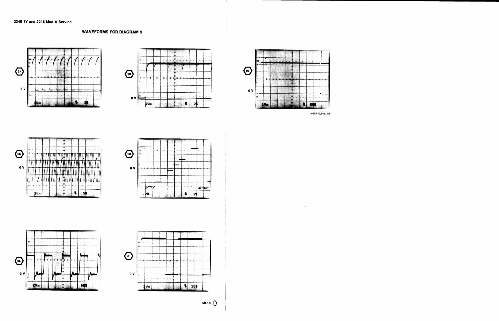
2246 1Y and 2246 Mod A Service
WAVEFORMS FOR DIAGRAM 9
I
MORE 0

READOUT SYSTEM DIAGRAM 9
I ASSEMBLY A16 I I CIRCUIT I SCHEM I BOARD I CIRCUIT I SCHEM I BOARD I CIRCUIT I SCCHEM I BOARD I CIRCUIT I S W E M I BOARD I NUMBER LOCATION LOCATION NUMBER LOCATION LOCATION NUMBER LOCATION LOCATION NUMBER LOCATION LOCATION
Paitlal A16 also shown on dlagrams 8, 10. 11 and 14. I
RO BUF A0 FROM R2515
0 00
REV JUNE 5991 7062-22
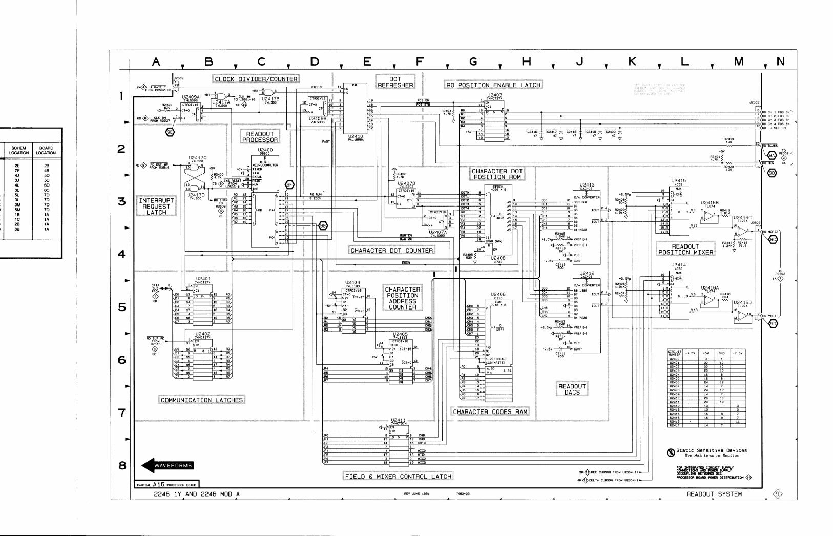
11 LOCATION LOCATION
R O CH 1 POS E N \ RO CH 2 POS EN RO CH 3 POS EN RO CH 4 POS EN
86 IOUT
83 IOUT
t 7 5V i 5 V GNU - 7 . 5 V
3 1 20 10 20 10 20 10 16 8 16 8 24 12 14 7 24 12 14 7 20 10
16 B 7
14 7
Static Sensitive Devices @ See Maintenance section
FOR COmECTIOs INTEWATED *N1 CIRCUIT PO*ER SUPPLY S U P R Y
O E C a R I W N E T M S SEe PROCESSOR B O N W*ER OISTRIWTION @
2 2 4 6 1Y AND 2246 MOD A REV JUNE 1991 7062-22 READOUT SYSTEM
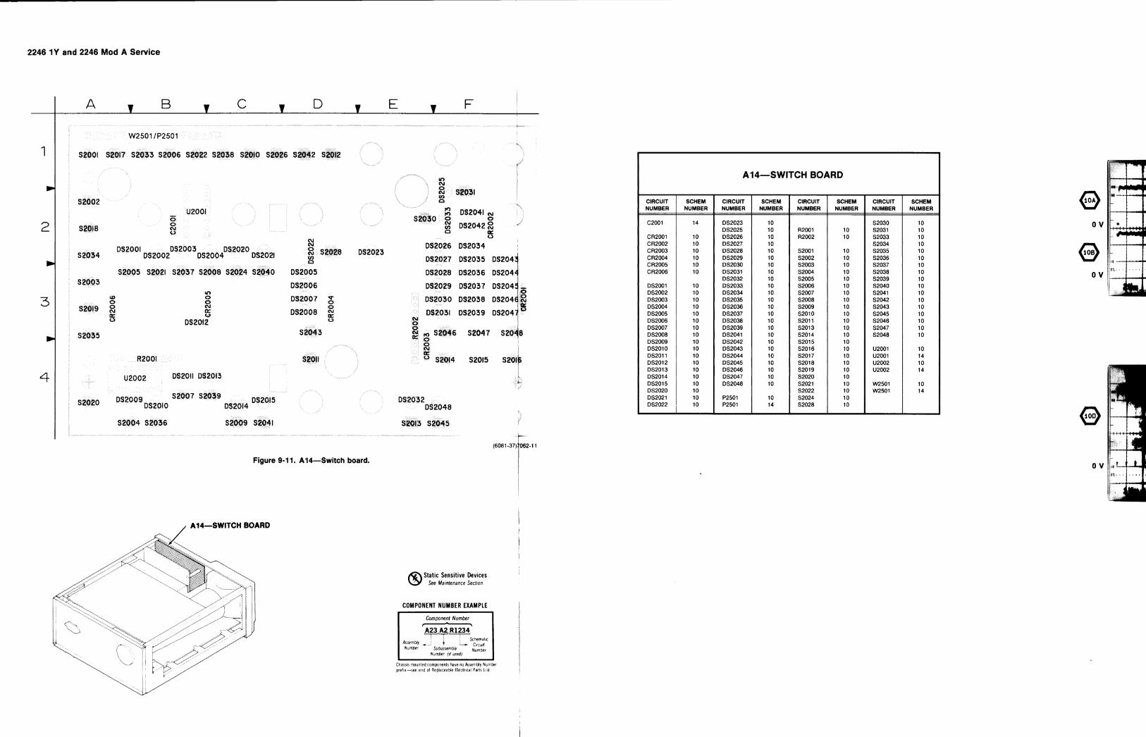
2246 1Y and 2246 Mod A Service
Figure 9-1 1. A14-Switch board.
A14-SWITCH BOARD
Static Sensitive Devices See Maintenance Sectloo
COMPONENT NUMBER EXAMPLE
A14-SWITCH BOARD
CIRCUIT SCHEM CIRCUIT SCHEM CIRCUIT SCHEM CIRCUIT SCHEM NUMBER NUMBER NUMBER NUMBER NUMBER NUMBER NUMBER NUMBER
: 1
Component Number I A23A2R1234 -T ~ r h e m a l l c
Arrernbiy _ Ciirui! Number Subassembly
Number ill used1 I I
C h a i i r mounted components have no ksernbly Nurnkr prel~r-see end of Replaceable Electr ial P a r k L s !
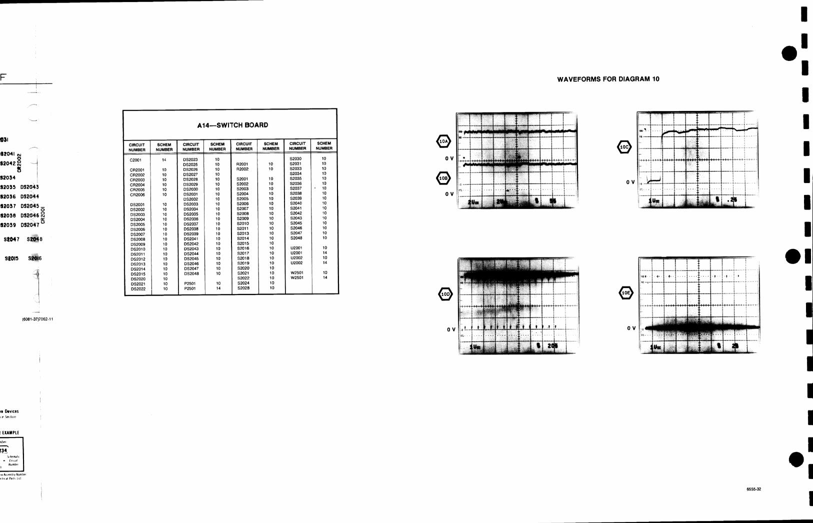

SWITCH BOARD AND INTERFACE DIAGRAM 10
r 1
Partial A14 also shown on dragram 14.
ASSEMBLY A16
Partla1 ~ 1 6 also show0 on diagrams 8. 9. 11 and 14 I
DATA BUS
FROM @ 2,
1 1
BOARD LOCATION
7J 7J 7J 7J 7J 7K 8.l
7H 6J 7J
LED 6 SWITCH COLUMN DRIVERS
SCHEM LOCATION
4C 4C 50 60 70 70 80
1A 3A 38
LED ANODE CLK
U2501-27
CIRCUIT NUMBER
R2547 R2548 R2549 R2550 R2551 R2552 R2553
U2523 U2524 U2525
BOARD LOCATION
7H
8.l 6H 6H 7H 7H 7H 7H 7H 7G 7J
SCHEM LOCATION
1K
1M 2A 4A I F 1 G 1 H 1H 1J 1J 30
CIRCUIT NUMBER
02508
R2525 R2528 R2529 R2532 R2534 R2536 R2538 R2540 R2542 R2546
BOARD LOCATION
7J 8J
8H 8H 7K
7J 7J 7H 7H 7H
SCHEM LOCATION
70 88
2F 3C 1M
X 1H 1H 1J 1J
CIRCUIT NUMBER
C2549 C2550
J2501 J2501 J2503
02501 02502 02503 02504 02505
BOARD LOCATION
7H 7H 7H 7H 7H 7 0 7H 7J 7J 7J 7J 7J
CIRCUIT NUMBER
C2521 C2522 C2523 C2524 C2525 C2526 C2543 C2544 C2545 C2546 C2547 C2548
SCHEM LOCATION
2F 1 G 1H 1J 1J 1K 3C 4C 4C 50 60 7 0
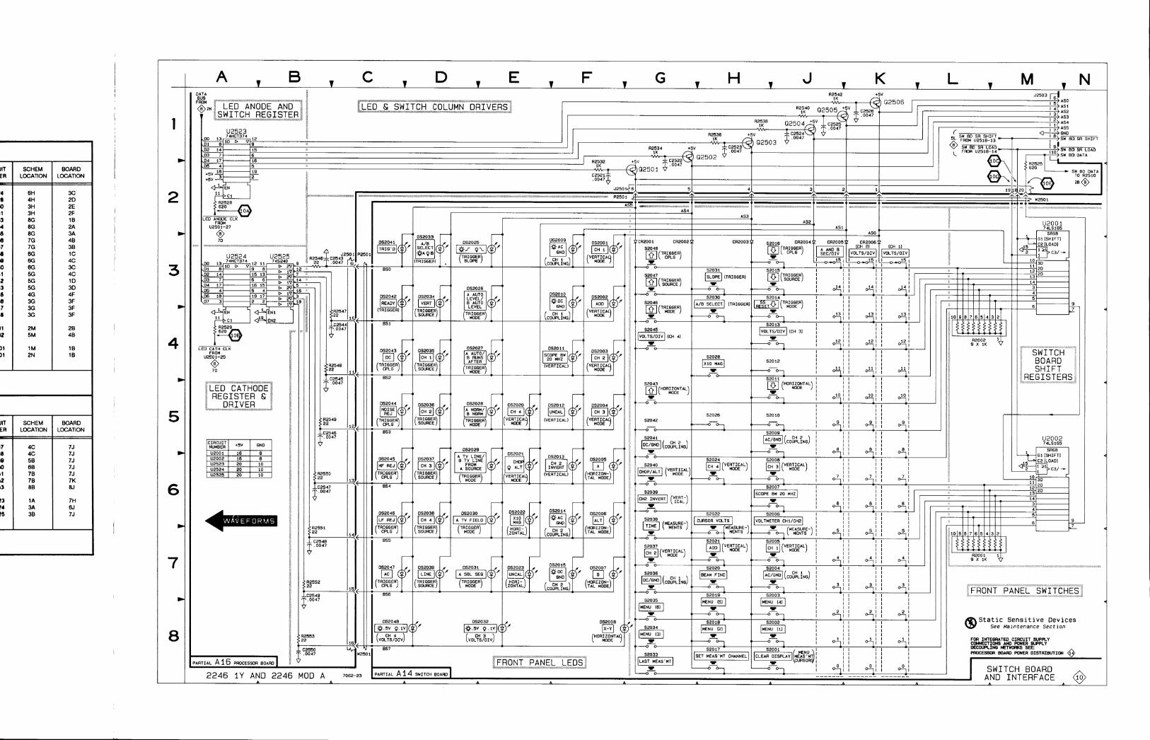
qGq-TE-1 ER LOCATION LOCATION
JIT ER F
7 18 10 0 11 12 13
13 14 I5
SCHEM LOCATION
4C 4C 58 68 78 78 68
1A 3A 38
BOARD LOCATION
7J 7J 7J 7J 7J 7K 6.J
7H 6J 7J

2246 1Y and 2246 Mod A Service
Figure 9-12. A12-Potentiometer board.
I l r l l ~ kntlllvo I h v l ~ ar 8 *.* u, .......... * . I....
I A12-POTENTIOMETER BOARD I
BOARD
1 CIRCUIT SCHEM CIRCUIT SCHEM CIRCUIT SCHEM
NUMBER
J2105 J2105
R2101 R2102 R2103
NUMBER
11 14
11 11 11
NUMBER
R2104 R2105 R2106 R2107 R2108 R2109
NUMBER
11 11 11 11 11 11
NUMBER
R2110 R2111 R2112 R2113
NUMBER
11 11 11 11

I A12-POTENTIOMETER BOARD
BOARD
CIRCUIT NUMBER
WAVEFORMS FOR DIAGRAM 11
SCHEM NUMBER
CIRCUIT NUMBER
SCHEM NUMBER
CIRCUIT NUMBER
SCHEM NUMBER
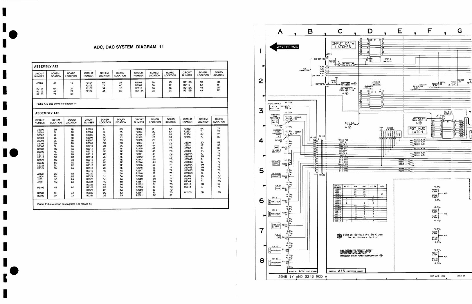
ADC, DAC SYSTEM DIAGRAM 11
CONNECTED WUX2 UUX3
OAC WUX OUT
J
ASSEMBLY A12
7 [CH 21 * 2 5vp S t a t l c Sensitive Devices
R2104
-2 5v0
FOR IHTEBR*TEO CIWJIT SUIPLY C M C T I D H S AKI POWER S U P R Y DECOlRINE NmaKS SEC
-2 5Vp PRXTSSOR 80A.W PO*ER DISTRIBUTION @ +2 5vp
8
BOARD LOCATION
2D 1F 2D 2E
-2 '5Vp
I PARTIAL A 12 POT BOARD PARTIAL A 16 PROCESSOR BOARD ( 2246 1 Y AND 2246 MOD A REV JUNE 1991 7062-24
A A A A A A
CIRCUIT NUMBER
R21110 R2112 R2113A R21130
BOARD LOCATION
4D 4F 1E 2C
Panlal A12 also shown on dlagram 14
ASSEMBLY A16
SCHEM LOCATION
30 5A 45 4A
I
SCHEM LOCATION
8A 6A 5A 3A
CIRCUIT NUMBER
R2108 R2109 R2110 R2111A
BOARD LOCATION
20 4C 1 D 3D
Partlal A16 also shown on dlagrams 8. 9. 10 and 14.
SCHEM LOCATION
6K 7L 6K 7L
2D 1E 3 1K 4L 2M 3L 3L 5M 4M 3M 2L 5K 5J 61 3G 2J
58
CIRCUIT NUMBER
R2362 R2363 R2364 R2365
U2300 U2301 U2302 U2303 U2304A U23040 U2304C U2304D U2305A U2305B U2305C U2305D U2306 U2308 U2309 U2313 U2314
W2105
SCHEM LOCATION
6A 7A 3A 4A
BOARD LOCATION
7F 7F 7F BE
50 50 60 7A 70 70 70 70 70 70 78 70 7C 7G 7G 6E 70
8G
BOARD LOCATION
5A 5A 5A 5A 70 7G 7G 7G 7G 7G 7G 7G 7G 7F 7F 7F 7F 7F 7F 7F 7D 7D 7D 7D 8F
CIRCUIT NUMBER
R2104 R2105 R2106 R2107
SCHEM LOCATION
2H X 2F 2F 2K 4F 4F 4F 4F 4F 4F 5H 4H 5E 5E 5E 5E 5E 5H 5H 6L 8L 8L 8L 7K
BOARD LOCATION
10
3A 2A 30
CIRCUIT NUMBER
J2105
R2101 R2102 R2103
CIRCUIT NUMBER
R2332 R2333 R2334 R2335 R2336 R2337 R2338 R2339 R2340 A2341 R2342 R2343 R2344 R2345 R2346 132347 R2348 R2349 R2350 R235 1 R2352 R2355 R2356 R2357 R2361
SCHEM LOCATION
48
6A 8A 7A
WARD LOCATION
6C 7A 70 7C 7C 7C 2A 7F 7E 7E 7E 7E 7E 7E 7E 4A 3A 5A 5A 50 8G 6A 6A 6A 6A
SCHEM LOCATION
2J 3L 4L 6K 5K 5K X 6F 6F 7E 7E 7F 7F 7E 7E 1K 1J 1J 1J 1 C 4E 2F 2F X 2G
CIRCUIT NUMBER
R2303 R2304 R2305 R2308 R2307 R2308 R2310 R2311 R2312 R2313 R2314 R2315 R2316 R23 17 R2318 R2319 R2320 R2321 R2322 R2324 A2325 R2328 R2329 R2330 R2331
CIRCUIT NUMBER
C23W C2301 C2302 C2303 C2305 C2306 C2307 C2308 C2309 C2310 C2318 C2320 C2322 '2.2323 C2324
J2302 J2304 J2601 J2601
P2105
R2301 R2302
SCHEM LOCATION
3H 3L 4L 3L 2L 2M 3L 3M 4L 4M 6K 5M 5M 5L 5M
2M 6M 1C 1M
40
3H 3H
BOARD LOCATION
70 7C 70 78 70 70 7A 7A 7A 76 7C 7D 7D 7 0 7A
88 8E 2A 2A
8G
7A 7A

78 I I : : I
D I G HORIZ PO5
0 REF TRIG L V L
B DELTA T R I G L V L
MAIN 00 MUX J
Static Sensitive Devices @ See Maintenance Section
FOR INTEBR*TED CIWJIT S L P R Y C W C T I O ( S U10 W*ER S L P R Y
-2.5vp
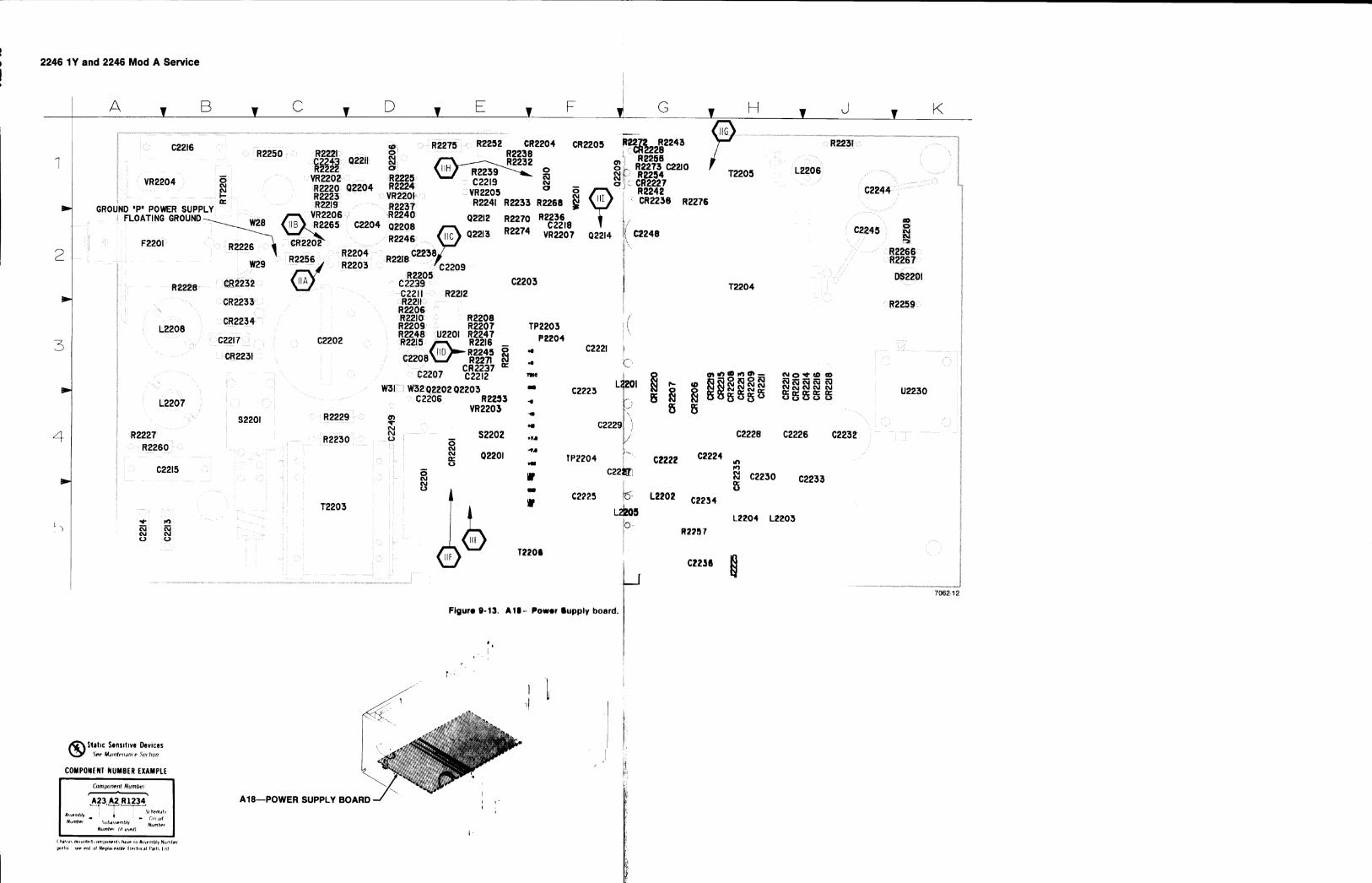
2246 1Y and 2246 Mod A Service
Flgure 9-13. A 18- Bowmr 8upply board.
'. 1
S t t l ~ c S e n s ~ l l v e Devlcss \#r ~~J!IIII~~I.IIII P \ t * r !!on
COMPONENT NUMBER EXAMPLE
A18-POWER SUPPLY BOARD --/

Bupply board.
A18-POWER SUPPLY BOARD
CIRCUIT NUMBER
C2201 C2202 C2203 C2204 C2206 C2207 C2208 C2209 C2210 C2211 C2212 C2213 C2214 C2215 C2216 C2217 C2218 C2219 C2221 C2222 C2223 C2224 C2225 C2226 C2227 C2228 C2229 C2230 C2232 C2233 C2234 C2236 C2238 C2239 C2243 C2244 C2245 C2248 C2249
CR2201 CR2202 CR2204 CR2205 CR2206 CR2207 CR2208
SCHEM NUMBER
12 12 12 12 12 12 12 12 12 12 12 12 12 12 12 12 12 12 12 12
12
12
12 12
12 12 12 12 12 12 12 12
12
12 12 12 12 12 12 12 12
SCHEM NUMBER
12 12 12 12 12 12 12 12 12 12 12 12 12 12 12 12 12 12 12 12 12 12 12 12 12 12 12 12 12 12 12 12 12 12 12 12 12 12 12
12 12 12 12 12 12 12
CIRCUIT NUMBER
CR2209 CR2210 CR2211 CR2212 CR2213 CR2214 CR2215 CR2216 CR2218 CR2219 CR2220 CR2227 CR2228 CR2231 CR2232 CR2233 CR2234 CR2235 CR2236 CR2237
DS2201
F2201
J2208 J2225
L2201 L2202 L2203 L2204 L2205 L2206 L2207 L2208
P2204
02201 (32202 Q2203 Q2204 Q2206 Q2208 Q2209 0221 0
CIRCUIT NUMBER
Q2211 Q2212 (22213 Q2214
R2201 R2203 R2204 R2205 R2206 R2207 R2208 132209 R2210 R2211 R2212 R2215 R2216 R2218 R2219 R2220 R2221 R2222 R2223 R2224 R2225 R2226 R2227 R2228 R2229 R2230 R2231 R2232 R2233 R2236 R2237 R2238 R2239 R2240 R2241 R2242 R2243 R2245 R2246 R2247 R2248 R2250
SCHEM NUMBER
12 12 12 12
12 12 12 12 12 12 12 12 12 12 12 12 12 12 12 12 12 12 12 12 12 12 12 12 12 12 12 12 12 12 12 12 12 12 12 12 12 12 12 12 12 12
CIRCUIT NUMBER
R2252 R2253 R2254 R2255 R2256 R2257 R2259 R2260 R2265 R2266 R2267 R2268 R2270 R2271 R2272 R2273 R2274 R2275 R2276
RT2201
52201 S2202
T2203 T2204 T2205 T2206
U2201 U2230
VR2201 VR2202 VR2203 VR2204 VR2205 VR2206 VR2207
W28 W29 W31 W32 W2201
SCHEM NUMBER
12 12 12 12 12 12 12 12 12 12 12 12 12 12 12 12 12 12 12
12
12 12
12 12 12 12
12 12
12 12 12 12 12 12 12
12 12 12 12 12

2246 1Y and 2246 Mod A Service
WAVEFORMS FOR DIAGRAM 12
(6555-47)6557-87
MORE 0

2246 1Y and 2246 Mod A Service
WAVEFORMS FOR DIAGRAM 12 (cont)
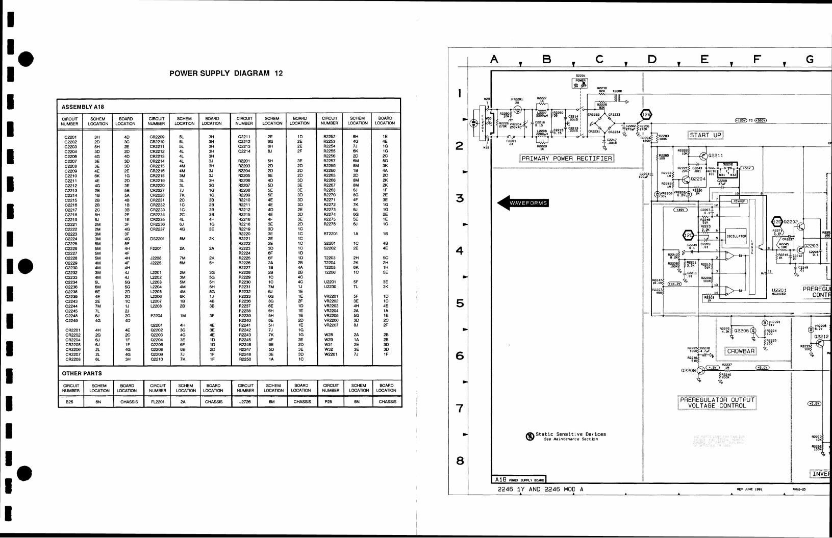
POWER SUPPLY DIAGRAM 12
Static Sensitive Devices @ S e e M a i n t e n a n c e S e c t j o n
2246 1 Y AND 2246 MOD A REV JUNE 1991 7062.25
CIRCUIT NUMBER
R2252 R2253 R2254 R2255 R2256 R2257 R2259 R2260 R2265 R2266 R2267 R2268 R2270 R2271 R2272 R2273 R2274 R2275 R2276
RT2201
S2201 52202
T2203 T2204 T2205 T2208
U2201 U2230
VR2201 VR2202 VR2203 VR2204 VR2205 VR2206 VR2207
W28 W29 W31 W32 W2201
CIRCUIT NUMBER
0221 1 02212 02213 02214
R2201 R2203 R2204 R2205 R2ZX R2207 R2208 R2209 R2210 R2211 R2212 R2215 R2216 R2218 R2219 R2220 R2221 R2222 R2223 R2224 R2225 R2226 R2227 R2228 R2229 R2230 R2231 R2232 R2233 R2236 R2237 172238 R2239 R2240 R2241 R2242 R2243 R2245 R2246 R2247 R2248 R2250
SCHEM LOCATION
6H 4G 7J 6K 2 0 6M 8M 1B 2 0 8M 8M 6J 8G 4F 7K 6. 6G 5E W
1A
1 C 2E
2H 2K 6K 1 C
SF 7L
5F 3E 4H 2A 5G 3 0 8J
2A 1 A 2E 3E 7J
SCHEM LOCATION
5L 5L 5L 4L 4L 4L 4M 4M 3M 3L 3L 7J 7K 2C 1C 1C 2C 4L 6J 4G
8M
2A
7M 6M
2M 3M 5M 4M 4M 6K 18 28
1M
4H 3G 4G 3E 6F 6E 7J 7K
CIRCUIT NUMBER
CR2209 CR2210 CR2211 CR2212 CR2213 CR2214 CR2215 CR2216 CR2218 CR2219 CR2220 CR2227 CR2228 CR2231 CR2232 CR2233 CR2234 CR2235 CR2236 CR2237
DS2201
F2201
J2208 J2225
L2201 L2202 L2203 L2204 L2205 12206 L2207 L2208
P2204
02201 02202 02203 02204 02206 02208 02209 02210
ASSEMBLY
CIRCUIT NUMBER
C2201 C2202 C2203 C2204 C2206 C2207 C2208 C2209 C2210 C2211 C2212 C2213 C2214 C2215 C2216 C2217 C2218 C2219 C2221 C2222 C2223 C2224 C2225 C2226 C2227 C2228 C2229 C2230 C2232 C2233 C2234 C2236 C2238 C2239 C2243 C2244 C2245 C2248 C2249
CR220 1 CR2202 CR22M CR2205 CR2206 CR2207 CR2208
OTHERPARTS
CIRCUIT NUMBER
825
BOARD LOCATION
1E 4E 1 G 1 G X 5G 3K 4A 2C 2K 2K 1 F 2E 3E 1 G 1G 2E 1E 1 G
18
48 4E
5C 2H 1H 5E
3E 3K
1 D 1 C 4E 1 A 1E 2C 2F
28 28 3 0 3 0 I F
SCHEM LOCATION
2E 6G 6H 8J
5H 2 0 2 0 6E 4D 5D 5E 5E 4E 4E 4 0 4E 4F 3E 3 0 3E 2E 2E 3 0 6F 6F 2A 1 B 28 1 C 1 C 7M 6J 6G 6G 6E 6H 5H 6E 5H 7J 7K 4F 6E 5 0 3E 1 A
BOARD LOCATION
3H 3H 3H 3H 3H 3J 3H 3.l 3J 3H 3G 1G 1 G 38 28 38 38 4H 1 G 3E
2K
2 A
2K 5H
3G 5G 5H 5H 5G 1J 48 38
3F
4E 3E 4E 1 0 1 0 2D I F I F
SCHEM LOCATION
2A
BOARD LOCATION
1 D 2E 2E 2F
3E 2 0 2 0 2 0 3 0 3E 3E 3 0 3 0 3 0 2E 3D 3E 2 0 1 C 1 C 1C 1 C 1 C I D 1 0 28 4A 28 4C 4C 1J 1E 1 E 2F 1D 1E 1E 2 0 1E 1 G 1 G 3E 2D 3E 3 0 1 C
A18
SCHEM LOCATION
3H 2 0 5H 3 0 4G 3E 3E 4E 6K 4E 4G 28 1 8 28 28 2C 8H 6J 2M 2M 3M 3M 5M 5M 5M 5M 4M 4M 3M 4M 5L 6M 6E 4E 2E 7M 7L 6J 4G
4H 2G 6. 6J 2L 2L 6L
SCHEM LOCATION
6N
BOARD LOCATION
40 3C 2E 2 0 4D 3 0 3 0 2E 1G 2 0 3E 58 5A 48 1B 38 2F 1E 3F 4G 3F 4G 5F 4H 4F 4H 4F 4H 41 Al 5G 5G 2 0 2 0 1 C 1J 2J X 4 0
4E 2C 1 F I F 4G 4G 3H
BOARD LOCATION
CHASSIS
BOARD LOCATION
CHASSIS
CIRCUIT NUMBER
J2726
CIRCUIT NUMBER
FL2201
SCHEM LOCATION
6M
BOARD LOCATION
CHASSIS
CIRCUIT NUMBER
P25
SCHEM LOCATION
6N
BOARD LOCATION
CHASSIS

Static Sensitive Devices @ SeeHa in tenanceSect ion

MAIN BOARD POWER DISTRIBUTION DIAGRAM 13 (SN B710100 AND ABOVE, 2246 1Y
SN B110100 AND ABOVE, 2246 MOD A) i i E E L I N E TRIG TO C1103, UllO6-2 9 2 .
ASSEMBLY A8
+5v TO: "73-1, 1 5 0 "14
8%; 0
C282 ,022 -+ Y
-5V TO' R276 ' R277 R282
10 - 5 v ~ TO: R292 11221 11218 11217 - 5 v ~ T 0 J601-17
U280-5
* 130VAC TO 11288 @ 0H L
W1277
R2739 +15V TO: 05901 05902 +130Vg TO: R2719 05903
P2204 R2784 R 2 7 , O
R938
R2788 0 11255
R312 10 Ill14
CIRCUIT NUMBER
t15Vc TO: 0362
CIRCUIT NUMBER
Pafl~al A8 also shown on dlagrarn 7.
t15Vo TO: t 1 5 V ~ TO: 0 3 2 3 " R376
R347
SCHEM LOCATION
SCHEM LOCATION
CIRCUIT NUMBER
W900
2246 1 Y AND 2246 MOD A REV JN 199% 7062-39 A A A A
BOARD LOCATION
SCHEM LOCATION
BOARD LOCATION
BOARD LOCATION
1E
SCHEM LOCATION
5M
BOARD LOCATION
CIRCUIT NUMBER
8F 7C 4F 1J 9C SJ 9J 9.J 1 OK 9H 9K 9A 9A 7M 8L 3J 41 4G 4L 5J 5J 5E 7N
6C 4C 38 38 3C 5H 5G 1 OG 5E 4E 3E 2E 5F 9D 8C 9C 8D 7 0 7D 7C 1 OD 1 OD 8F 7H 3F 2F I H 2H 5M 4N 5N 10C
R390 R392 R480 R481 R504 A701 R709 R723 R733 R734 R837 R915 R916 R1026 R1027 R1101' R1102' R1108' R1158 R1159 R1160 R1260' R2783
U112 U122 U171 U172 U173 U201 U202 U203 U210 U220 U230 U240 U260 U301 U302 U303 U304 U307 U308 U309 U310 U311 U315 U316 U421 U431 U441 U442 U501 U502 U503 U506
ASSEMBLY
C135 C136 C140 C155 C156 C171 C172 C180 CIS1 C205 C206 C214 C215 C216 C217 C219 C224 C225 C229 C234 C235 C239 C244 C245 C249 C265 C282 C283 C297 C298 C304 C309 C316 C317 C318 C320 C322 C337 C338 C339 C351 C442 C445 C475 C480 C481 C482 C501 C502 C503 C505 C604 C605 C606 C609 C610
Partla1 A10
U6CQ U601 U602 U603 U604 U606 U701 U702 U801 U802 UW1A U W l B Us01 U930 U931 U932 UlOOl U l l O l U1102 U1103 U1104 U1106
W103 W235. W501 W606 W607 W900 W1104' W1105' W l m W1201 W1202 W 1203 W 1204 W 1205 W1209 W1210 W1216 W1217 W1218 W1221 W1222 W 1223 W1231 W1237 W1247 W1248 W1249 W1250 W1251 W1252 W1255 W1277 W2302 W2502
1L 8F 20 2D 1 M 3J 2K 5H 3K 40 7H 5L 5L 8F 6F 6H 8G 7J 1 F 2G 6K 7E 4D
7D 7D 5A 6A 1 A 10 10 3J 70 70 7C 7C 50 1L 5E 5E 5F 5E 5E 5F 5E 5E 1J 2J 20 2D I D 3G 3E 3E 3E 2M
C613 C701 C702 C703 C704 C705 C708 C801 C606 C815 C816 C818 C821 C822 C901 C902 C903 C904 C1005 C1006 CI lO l C1102 C1104 C1108' C1158 C1159 C1160 C2701 C2702 C2709
J 1204
LlOl L102 UO 1 L216 L217 L445 L475
P2302 P2502
A182 R208 R226 R245 R282 R283 R297 R298 R312 R339 R345 R374
4, 5, 6 and 7.
A10
7D 8E 8D 7E 8E 5A 1 A 8D 7A 3J 3J 70 78 20 10 70 7 0 7 0 70 7C 7C 7C 7D 7C 7D 58 30 6B 3C 30 5D 2J 5C 1 L aJ 1J 2M 5D 8A 80 SF 3G 10 I D 2 0 2C 2D 3E 3E 3E 2M 3F 1H 1E 2H 2H
also shown on
X 2H 1E 2G 2H 3F 3K 3K 5H 6H 5K 5L 5J 5J 3M 5K 7F 7H 7H 2F 2C 2G
1 G 7E 1 H I E 2E 5M 6H 8H 1J 3M 2J 1G 1J 2G 1E 3G 3M 3G 3G 3E 80 3L 6F 8F 5C 5H 5H 5H 8A 8A 50 4D 8M 1M
1H %I 3K 3K 3L 4A %I 4A 5H 6H 7H 40 5H 6E 5K 5K 5M 5M 7F 6G 6H 8G 2C 7J 1 F 2G 6K 6H 8G 4E
1 A
5A 8D 6A 28 10 10 I D
8M I N
8D 3J 70 7C 38 60 3C 30 5D Rl 5C 5D
20 28 2C 28 10 20 3C 3D 6D I OH 1 OH 4E 5D 5G 5G 5D 3D 3D 4 0 2D 2D 2D 1 D I D 2D 5F 4F 6G 5F 3F 7D 7H 8E 8E 9E 8G 9D 9E 8G 9G 8C 2H 3F I F 1J 3F 2F 4M 4N 4N 9C 3M 2M 3L 2J 2L
dragrarns 1, 2, 3,
2M 1 N 3K 2K 2L 3M I OJ 9K 7H 8H 9A 9A 9A 88 90 8A 7L 4G 4G 5K 4H 5L
3D 5E 1 M 1K 5M 90 3J 41 6F 9C 9H 1J 7G 21 41 2.l 8C 6H 5H 1J 6 0 6D 8K 6L 6D 6H 5H 8% 8H 5H 6F 8K 1 OD 1L
I N l W W 10K 9K 9G W 8K 8H 7H 8H aJ 7J aJ 98 8A 8A 98 7M 8L 3H 4G 4H 4G 5L 5L 5K 7M 6L 7M
5J
2C 2C 6E 4H 5H 3J 1J
1 OD I L
6D 1 OH 6E 3D 3F 6G 6F 3F 7D 9E 8E I OE

L I N TRIG 10 C1103. U1106-2 @PA
P 7 C505 022
1 6 ' l - [DN~
7Jh-b C322 022
D
4
022 IS N/C
W796
C815 022
16 - +7 5Vg TO CR1003 10
P
U1001-LM324
H
-7 5vc TO C1001
EiSS: 0 cl,02 f+ -7 5Vs TO 02709 -7 5Vc TO R1136 -7 SVo T@ R338
0 0 SiE-, Static Sensitive Devices
2 2 4 6 1 Y AND 2 2 4 6 MOD A REV JUX 1991 7062-39 sn ~lloioo Am reova la2* mo A, MAIN BOARD POWER DISTRIBUTION @ SN 8710100 A N ) ABOVE 2246 lY1
A . . A . A
8393 R39.0
R1160 10
C1160 +7 5VtT0 R1111
R1113 R1115
02,T R1120 R1126
0 *
4 P2302
TO
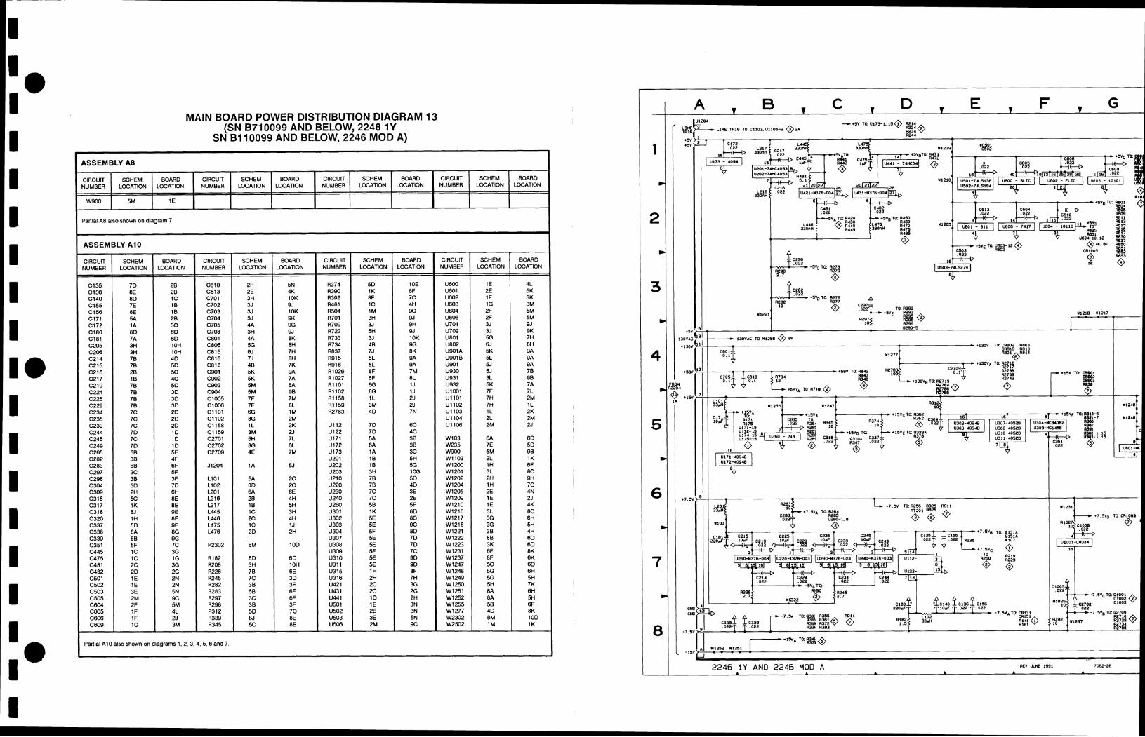
MAIN BOARD POWER DISTRIBUTION DIAGRAM 13 (SN B710099 AND BELOW, 2246 1Y
SN B110099 AND BELOW, 2246 MOD A)
J1204
LINE TRIG TO Cl lO3. l l l lO6-2 @ 2 ~
- +lMV TO: CRB02 ,3803
4 CR819 R013
R801@R814 - r +130VA TO: 132716
R2717 R2738
R2739 +15V TO: O!lSOl R2743 05902
+ 1 5 V ~ TO: 0323A
A
L
ASSEMBLY A8
L +7.5V TO: R256 W 2 5 R911 +7.5Vh TO: R284 RT201 Re26
C283 R205 UZBO-1.0
TO: 0131A 0151A U107
0 R219 R229
- - - lSVA TO: R346 R375 6
2246 1 Y AND 2246 MOD A REV JM 1991 7052-26 . A & . A
CIRCUIT NUMBER
BOARD LOCATION
Parllal A8 also shown on dlagram 7.
SCHEM LOCATION
CIRCUK NUMBER
BOARD LOCATION
SCHEM LOCATION
=HEM LOCATION
C IRCU~~ NUMBER
BOARD LOCATION
BOARD LOCATION
1 E
CIRCUK NUMBER
WSM)
CIRCUIT NUMBER
U600 U601 U602 U603 U604 U606 U701 U702 U801 U802 U901A U901B U901 U930 U931 U932 UlOOl U1101 U1102 U1103 U1104 U1106
W103 W235 W900 W1103 W1200 W1201 W1202 W1204 W1205 W1209 W1210 W1216 W1217 W1218 W1221 W1222 W1223 W1231 W1237 W 1247 W1248 W1249 W1250 W1251 W1252 W1255 W1277 W2302 W2502
BOARD LOCATION
10E 8F 7C 4H 9C W 9H 9.J 1 OK 9G 8K 9A 9A 7M 8L 1J 1J 2.l 2J 7N
6C 4C 38 38 3C 5H 5G 10G 5 0 4 0 3E 2E 5F 80 8C 9C 80 7 0 7 0 7C 9 0 9 0 8F 7H 3G 2G 2H 3N 3N 5N 9C
SCHEM LOCATION
5M
SCHEM LOCATION
5 0 1K 8F 1 C 1M 3H 3J 5H 3J 48 75 5L 5L 8F 6F 6G 8G 1 L 3M 4 0
7 0 7 0 5A 6A 1 A 18 18 3H 78 78 7C 7C 58 1K 5E 5E 5F 5E 5E 5F 5E 5E 1H 2H X 2C 1 D 1E 2E 3E 2M
SCHEM LOCATION
1E 2E 1F 1 G 2F 2F 3J 3J 5G 6J 5K 5L 5J 5J 3L 5K 7F 7H 7H 1L 2L 2M
6A 7E 5M 2L 1 H 3L 2H 1H 2E 1 E 1 E 3L 3G 3G 38 8B 3K 6F 8F 5C 5G 5G 5H 8A 8A 58 4 0 8M 1M
BOARD LOCATION
4L 5K 3K 3M 5M 5M 9.J 9K 7H 8H 9A Q A 9A 78 9B 7A 7L 2M 1L 2K 2M 2J
6 0 5 0 98 1 K 6F 8C 9H 7G 4N 2J 4K 8C 6H 5H 4H 6 0 6 0 8K 6K 6 0 6H 5H 7K 6H 5H 6F 8K 1 OD 1 K
SCHEM LOCATION
2F 2E 3H 3J 3J 3J 4A 3H 4A 5G 6J 7J 4B 5K 5K 5M 5M 7F 7F 6G 8G 1L 3M 5H 8G 4E
1A
5A 8 0 6A 28 1 B 1 C X 1 C 2 0
8M
8D 3H 78 7C 38 68 3C 38 5 0 aJ 5C
CIRCUIT NUMBER
C6lO C613 C701 C702 C703 C704 C705 C708 C801 C806 C815 C816 C818 C901 C902 C903 C904 C1005 C1006 C l l O l C1102 C1158 C1159 C2701 C2702 C2709
J1204
L101 L102 UD1 L216 L217 L445 L446 L475 L476
P2302
R182 R208 R226 R245 R282 R283 R297 R298 R312 R339 R345
4, 5, 6 and 7.
BOARD LOCATION
2 8 28 1C 1B 1 B 28 3C 6 0 6 0 1 OH 1 OH 4 0 5 0 5G 4G 5 0 3D 3 0 3D 2 0 2 0 2D 1 0 1 0 1 0 5F 4F 6F 5F 3F 7 0 6H 8E BE 9E 8F 9E 8G 9G 7C 3G 1G 3G 2G 2N 2N 5N 9C 5M 4L 2J 3M
dlagrams 1. 2. 3,
ASSEMBLY
CIRCUIT NUMBER
C135 C138 C140 C155 C156 C171 C172 C l80 C181 C205 C206 C214 C215 C216 C217 C219 C224 C225 C22Q C234 C235 C239 C244 C245 C249 C265 C282 C283 C297 C298 C304 C309 C316 C317 C318 C320 C337 C338 C339 C351 C445 C475 C481 C482 C501 C502 C503 C505 C604 C605 C606 CEG9
Parllal A10
BOARD LOCATION
5N 4K 1 OK 0.l 1 OK 9K 9G 9.J 8K 8H 7H 8H 7K 9A 7A 8A 98 7M 8L 1M 2M 2K 2J 7L 6L 7M
5J
2C 2C 6E 4H 5H 3H 4H 1J 2H
1 OD
6 0 10H 6E 3 0 3F 6F 6F 3F 7C BE 8E
A10
SCHEM LOCATION
7D 8E 8 0 7E 8E 5A 1A 8D ?A 3H 3H 78 78 28 1 B 78 7B 78 78 7C 7C 7C 7 0 7C 7 0 58 38 68 3C 38 5 0 2H 5C 1K 8J 1 H 5 0 8A 88 5F 1 C 1 C X 2 0 1 E 1E 3E 2M 2F 1 F 1F 1G
also shown on
CIRCUIT NUMBER
R374 R390 R392 R481 R504 R701 R709 R723 A733 R734 R837 R915 R916 R 1028 R1027 R1101 R1102 R1158 R1159 R2783
U112 U122 U171 U172 U173 U201 U202 U203 U210 U220 U230 U240 U260 U301 U302 U303 U304 U307 U308 U309 U310 U311 U315 U316 U421 U431 U441 U501 U502 U503 U5C8


PROCESSOR BOARD POWER DISTRIBUTION DIAGRAM 14
- - 7 . 5 V TO. C2411 C2412
ASSEMBLY A12
2246 1 Y AND 2246 MOD A 7062-2i
1 -15"
CIRCUIT NUMBER
J2105
- 1 5 V TO' C2300 0 ?j
CIRCUIT NUMBER
CIRCUIT NUMBER
Partlal AI 2 also shown on dlagram 11.
ASSEMBLY A14
BOARD LOCATION
SCHEM LOCATION
SCHEM LOCATION
3L
SCHEM LOCATION
BOARD LOCATION
10
CIRCUIT NUMBER
BOARD LOCATION
BOARD LOCATION
20 40
CIRCUIT NUMBER
C2001
CIRCUIT NUMBER
P2501
Partlal A14 also shown on dlagram 10.
ASSEMBLY A16
SCHEM LOCATION
CIRCUIT NUMBER
W2501
SCHEM LOCATION
1M
BOARD LOCATION
SCHEM LOCATION
1L
BOARD LOCATION
20
SCHEM LOCATION
1L
Partlal A16 also shown on dlagrams 8, 9. 10 and 11.
BOARD LOCATION
50 50 60 7A 78 70 7C 7G 7G 6E 78 3C SF 5F 1 C 40 38 4C 5E 5C 30 28
CIRCUIT NUMBER
C2304 C2311 C2312 C2313 C2314 C2315 C2316 C2317 C2319 C2321 C2401 C2402 C2403 C2404 C2405 C2406 C2407 C2408 C2409 C2410 C2415 C2501 C2502
BOARD LOCATION
10
BOARD LOCATION
1B
CIRCUIT NUMBER
C2503 C2504 C2505 C2506 C2507 C2508 C2509 C2510 C2511 C2530 C2531 C2532 C2541
J2302 J2501 J2502 J2601
P2105
R2309 R2412
CIRCUIT NUMBER
U2411 U2412 U2413 U2414 U2415 U2416 U2417 U2501 U2502 U2503 U2506 U2512 U2513 U2514 U2515 U2517 U2518 U2519 U2523 U2524 U2525
W2 105
SCHEM LOCATION
38 1 C 1 C 1 C 60 78 1J 6G 1 C 1 C 1 C 1 C 1 C 1 C 1 C 1C X X 2C 2C 6H 2C 2C
CIRCUIT NUMBER
U2001 U2002
SCHEM LOCATION
X X 2C 2C 2C 2C 2C 2C 2C 2C 2C 2C 10
38 1L 10 5L
3L
6G 6H
BOARD LOCATION
8A 58 5B 60 8A 70 70 7C 6F 6F 38 40 1 C 5E 2A 4A 4D 5D 3D 20 7D 4K 4F
SCHEM LOCATION
1L 1L
SCHEM LOCATION
2E 6G 7G 6H 7H 7C 1 F 1C 1G I F 2F 2E 2E 2E 2E I F 1 F I D 2E 2E 2E
3L
BOARD LOCATION
4F 5G 5K 5H 4G 4G 6F 6J 4H 6H 6H 7H 6K
80 8H 3.J 2A
8G
7C 7D
BOARD LOCATION
40 5D 5C 6D 6C 7D 1 A 6G 6K 4H 5K 4F 41 5H 4H 5F 4K 6J 7H &I 7J
8G
CIRCUIT NUMBER
U2300 U2301 U2302 U2303 U2304 U2305 U2306 U2308 U2309 U2313 U2314 U2400 U2401 U2402 U2403 U2404 U2405 U2406 U2407 U2406 U2409 U2410
SCHEM LOCATION
1 E 1E 1H 6G 6C 7C 6E 6F 7F 1E 6C 1 G 2E 2E 2E I F I F 1 D I F 1 D I F 2E
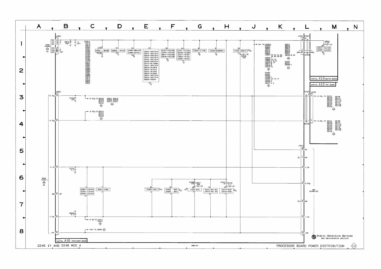

CH 1 PREAMP 0 CH 2 PREAMP 0
TRACE ROTATION
6 REF T R I G L V L 6 DELTA T R I G LVL
D I G H O R I Z POS
-HORIZONTAL OUTPUT
+HORIZONTAL OUTPUT
RO CH 1 POS E N RO CH 2 POS EN RO CH 3 POS E N
-VERTICAL OUTPUT
+VERTICAL OUTPUT
SW m SA LOAD
2 2 4 6 1 Y AND 2 2 4 6 MOD A 7 0 6 2 - 2 8 I N T E R C O N N E C T I O N D I A G R A M

DELAY HF COMP LINE
R231 R241 A R455 CH 3 GAIN CH 4 GAIN ' R275 C274 C273 R272 R273 ' B TRIG BANDWIDTH
2246 1Y and 2246 Mod A Service
Figure 9-14. AlO-Main board adjustment locations.
Section 10 - 2246 1Yl2246 MOD A
REPLACEABLE MECHANICAL PARTS
PARTS ORDERING INFORMATION
Replacement parts are available from or through your lo- cal Tektronix, Inc. Field Office or representative.
Changes to Tektronix instruments are sometimes made to accommodate improved components as they become available, and to give you the benefit of the latest circuit im- provements developed in our engineering department. It is therefore important, when ordering parts, to include the fol- lowing information in your order: Part number, instrument type or number, serial number, and modification number if applicable.
If a part you have ordered has been replaced with a new or improved part, your local Tektronix, Inc. Field Office or representative will contact you concerning any change in part number.
Change information, if any, is located at the rear of this manual.
ITEM NAME
In the Parts List, an item Name is separated from the description by a colon(:). Because of space limitations, an ltem Name may sometimes appear as incomplete. For fur- ther ltem Name identification, the U.S. Federal Cataloging Handbook H6-1 can be utilized where possible.
FIGURE AND INDEX NUMBERS
Items in this section are referenced by figure and index numbers to the illustrations.
INDENTATION SYSTEM
This mechanical parts list is indented to indicate item re- lationships. Following is an example of the indentation sys- tem used in the description column.
1 2 3 4 5 Name & Description
Assembly and/or Component Attaching parts for Assembly and/or Component
END ATTACHING PARTS
Detail Part of Assembly and/or Component Attaching parts for Detail Part
END ATTACHING PARTS
Parts of Detail Part Attaching parts for Parts of Detail Part
END ATTACHING PARTS
Attaching Parts always appear in the same indentation as the item it mounts, while the detail parts are indented to the right. Indented items are part of, and included with, the next higher indentation.
Attaching parts must be purchased separately, un- less othemise specified.
ABBREVIATIONS
Abbreviations conform to American National Standards Institute Y1.I

Replaceable Mechanical Parts 2246 1Y and 2246 MOD A Service
CROSS INDEX - MFR. CODE NUMBER TO MANUFACTURER M fr. Code
-??mr Manufacturer
FELLER
Address
72 Veronica Ave Unit 4 2015 SECOND STREET
City, State, Zip Code
Summerset NJ 08873
BERKELEY CA 94170 SCHURTERAGH C/O PANEL COMPONENTS CORP LEWIS SCREW CO LABEL GRAPHICS GEROME CORP
4300 S RACINE AVE 6700 SW BRADBURY CT OLIVER RD PO BOX 1089 9898 SW TIGARD ST 18224 SW l00TH CT 97 THORNWOOD RD 1385 HOWARD ST 821 S THIRD 195 ALGONQUIN RD 4336 SO ADAMS 1181 NORTH 4TH ST 1 1007 NE 3TTH CIRCLE 37399 CENTRAL MONT PLACE PO BOX 1127 14831 SPRING AVE 15lFX1. FU-SHING N. ROAD 1620 NE ARGYLE 3000 LEWIS AND CLARK HWY PO BOX 4200
CHICAGO IL 60609-3320 PORTLAND OR 97224 UNIONTOWN PA 15041
POLYCAST INC NORTHWEST FOURSLIDE INC AMLAN INC STUCKEL R J CO SEA LECT PRODUCTS INC FASTEX PLASTIC MOLDED PRODUCTS SHIN-ETSU POLYMER AMERICA INC ACCRA FAB INC GALGON INDUSTRIES LARSCO WALKER SPRING & STAMPING CORP UNION ELECTRIC BADGLEY MFG CO TRIQUEST CORP COMTEK MANUFACTURING OF OREGON (METALS) GEROME MFG CO INC MORELLIS Q & D PLASTICS STAUFFER SUPPLY BEARINGS INC
TIGARD OR 97223 TUALATIN OR 97062 STAMFORD CT 06903-2617 ELK GROVE VILLAGE IL 60007-2213 KENT WA 98032-61 29 DES PLAlNES IL 60016 TACOMA WA 98409 SAN JOSE CA 951 12 VANCOUVER WA 98682 FREMONT CA 94536 CLACKAMAS OR 97015 SANTA FE SPRINGS CA 90670-5109 TAIPEI, TAIWAN ROC PORTLAND OR 9721 1 VANCOUVER WA 98661-2999 BEAVERTON OR 97076-4200
OJ9P9 OKBZ5 OKBOl 05469
PO BOX 737 181 2 16TH AVE 810 SE SHERMAN 3634 EUCLID P 0 BOX 6925 5825 N TRlPP AVE 3191 CASITAS 9301 ALLEN DR 2021 W VALLEY VIEW LN PO BOX 810839 n DRAGON COURT 6136 NE 87th AVE PO BOX 20038 750 BOULEVARD P O BOX160 ONE KOOL PATH PO BOX 400 50 SPRING STREET PO BOX 575
NEWBERG OR 97132 FOREST GROVE OR 971 16 PORTLAND OR 97214 CLEVELAND OH 44101
RICHCO PLASTIC CO NELSON NAME PLATE CO FREEWAY CORP THERMALLOY CO INC
CHICAGO IL 60646-6013 LOS ANGELES CA 90039-2410 CLEVELAND OH 44125-4632 DALLAS TX 75381
CHOMERICS INC BOYD CORP
WOBURN MA 01801-1039 PORTLAND OR 97220
HEYCO MOLDED PRODUCTS KENILWORTH NJ 07033-1721
AAVlD ENGINEERING INC
BOGEN COMMUNICATIONS INC RAMSEY NJ 07446
COOPER BELDEN ELECTRONICS WIRE AND CABLE SUB OF COOPER INDUSTRIES INC BUSSMANN DIV OF COOPER INDUSTRIES INC FISCHER SPECIAL MFG CO LITELFUSE INC SUB TRACOR INC
ST LOUIS MO 63178 11 4 OLD STATE RD PO BOX 14460 11 1 INDUSTRIAL RD 800 E NORTHWEST HWY
COLD SPRING KY 41076-9749 DES PLAINES IL 60016-3049
REV OCT 1991

Replaceable Mechanical Parts 2246 1Y and 2246 MOD A Service
CROSS INDEX - MFR. CODE NUMBER TO MANUFACTURER Mlr. Code Manufacturer Address City, State, Zip Code
81 ILLIN T IN I SHAKEPROOF DIV
80009 TEKTRONIX INC 14150 SW KARL BRAUN DR BEAVERTON OR 97077-0001 PO BOX 500
83014 HARTWELL CORP 950 S RICHFIELD RD PLACENTIA CA 92670-6732 LOCKWELL DIVISION
REV OCT 1991
Replaceable Mechanical Parts 2246 1Y and 2246 MOD A Servlce
Flg. & Index Rktronlx Serlai No. Mfr. No. Part No. Effective D~oont Qty 12345 Name & Descrlptlon Code Mfr. Part No.
1-1 334-6445-00 1 MA A :MKD E -2 437-0390-00 1 CABINET ASSY:390-1057-00 WIFEET & HANDLE TK1935 ORDER BY DESC -3 337-2395-00 2 .SHIELD,ELEC:HANDLE TK1614 ORDER BY DESC
ATTACHING PARTS -4 213-0138-00 4 .SCREW,TPG,TF:4-24 X 0.188,TYPE B,PNH,STL TKO435 ORDER BY DESC
END ATTACHING PARTS -5 367-0289-00 1 .HANDLE,CARRYING:l3.855,SST, 80009 367028900
ATTACHING PARTS -6 212-0144-00 2 .SCREW,TPG,TF:8-16 X 0.562 L,PLASTITE,SPCL OKBOl ORDER BY DESC
.HD END ATTACHING PARTS
-7 390-1057-01 1 .CABINFT,SCOPE:EMI VERSION,ALUMINUM 80009 390105701 -8 348-0659-00 2 .FOOT,CABINETBLACK POLYURETHANE OJR05 ORDER BY DESC -9 348-0764-04 1 SHLD GSKTELEK:O.l25 X 0.188,WIRE MESH,P 18565 ORDER BY DESC
.LAYERS,37.0 L -10 200-3680-00 1 COVER,AUTO CAL:POLYCARBONATE TK1163 ORDER BY DESC -12 200-3233-02 1 COVER,REAR:PLASTIC,W/LABELS 80009 200323302
ATTACHING PARTS -13 211-0691-00 B l 00100 B1 14168 4 SCREW,MACHINE:6-32 X 0.625,PNH.STL OKBOl ORDER BY DESC
(2246 MOD A,2Y) 213-0942-00 8114169 4 SCREW,TPG,TR:6-32 X 0.75,TYPE TT,PNH,STL OKBOl ORDER BY DESC
(2246 MOD A,2Y) 21 1-0691-00 87001 00 B711094 4 SCREW,MACHINE:6-32 X 0.625,PNH,STL OKBO1 ORDER BY DESC
(2246 1Y) 213-0942-00 8711095 4 SCREW,TPG,TR:6-32 X 0.75,TYPE TT,PNH,STL OKBOl ORDER BY DESC
(2246 1Y) END ATTACHING PARTS
-14 ----------- 2 (PART OF FIG 1-12) -1 5 334-6707-00 1 MARKERJDENTMKD CAUTION 07416 ORDER BY DESC -16 334-6708-00 1 MARKER,IDENTMKD REAR PANEL Z-AXIS, 07416 ORDER BY DESC
REV OCT 1991
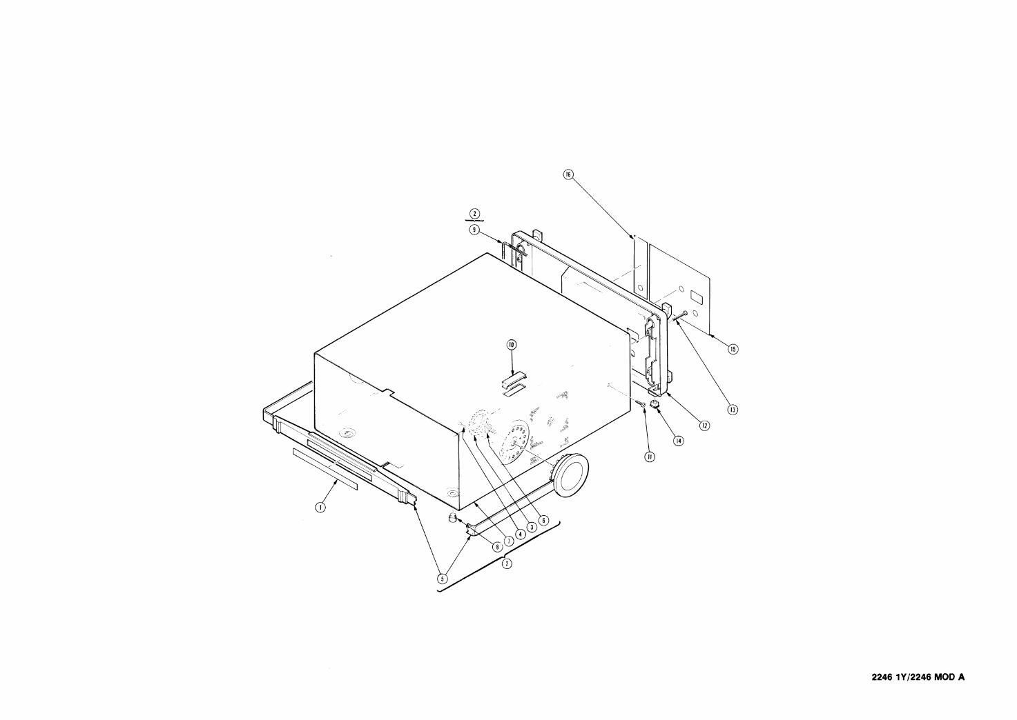
2246 1Y12246 MOD A
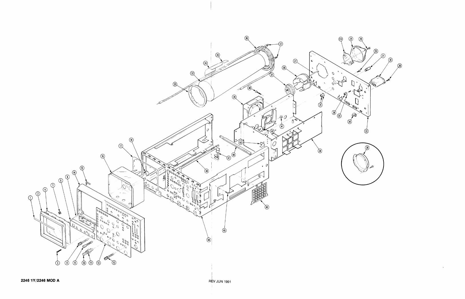

Replaceable Uechanlcal Parts 2246 1Y and 2246 MOD A Service
Fig. & Index Tektronlx No. Part No.
2-1 334-6446-00 -2 426-1765-02
Serial No. Effective Dscont
M fr. Code -
07416 OJR05
12345 Name & Description
MARKER.IDENTMKD TEKTRONIX 2246 FRAME,CRTPOLYCARBONATE,GRAY
ATTACH 1 NG PARTS SCREW,MACHINE:6-32 X 0.875 PNH,SST
END AlTACHING PARTS SHLD,IMPLOSION:FILTER,BLUE PANEL,FRONT GUIDE,LIGHTACRYLIC GRATICULE CUSHION,CRTPOLYURETHANE KN0B:GRAYPUSH ON,0.185 ID X 0.392 OD X 0.495 H KN0B:DOVE GRAY0.235 ID X 0.36 OD X 0.495H WISHAFT PUSHON WIO INDEX KN0B:DOVE GRAY,VAR,O.127 ID X 0.392 OD X 0.466 H KNOB:GRAY,VAR,0.2 ID X 0.546 ODX 0.69 H KN0B:GRAYPUSH ON,0.185 ID X 0.392 OD X 0.495 H PANEL.FRONT SUBPANEL,FRONT SHLD GSR,ELEK:2 IAYER,0.094 X 0.188 X 37 SHIELD,ELEC:CRT,MAGNETlC FRONT GASKET,CRT SHLD:CU BE (2246 MOD A,2Y) SHLD GSR,ELEK:EMI,SST (2246 MOD A,2Y) GASKRCRT SHLD:CU BE (2246 1Y) SHLD GSKT,ELEK:EMI,SST (2246 1Y) GROMMET,PLASTIC:BLACK,ROUND,O.625 ID FILTER,RFI: (SEE FL2201 REPL)
AlTACHING PARTS SCREW,TPG,TR:6-32 X 0.437 TAPTITE,PNH,STL
END ATTACHING PARTS CONN,RCPT,ELEC:BNC (SEE J16 REPL) CHASSIS,REAR: (2246 MOD A,2Y) CHASSIS,REAR:EMI VERSION (2246 MOD A,2Y) CHASSIS,REAR: (2246 1Y) CHASSIS,REAR:EMI VERSION (2246 1Y)
ATTACHING PARTS SCREW,TPG,TR:6-32 X 0.437 TAIJTITE.PNH,STL
END ATTACHING PARTS CLAMRCABLE:0.25 ID,NYLON LEAD.ELECTRICAL: (SEE W30 REPL)
AlTACHING PARTS NUT,PL,ASSEM WA:6-32 X 0.312,STL CD PL WASHER,LOCK:XG INTL,0.018 THK,STL
END ATTACHING PARTS SPRING,GROUND:CRT SHIELD CAF?CRT S0CKET:NATURAL LEXAN. (2246 MOD A,2Y) CACCRT S0CKET:NAWRAL LEXAN. (2246 1Y)
Mlr. Part No.
ORDER BY DESC ORDER BY DESC
OKBOl ORDER BY DESC
ORDER BY DESC ORDER BY DESC PER TEK DRAWING 348066000 PER TEK DRAWING
PER TEK DRAWING
ORDER BY DESC
PER TEK DRAWING PER TEK DRAWING
ORDER BY DESC PER TEK DRAWING ORDER BY DESC ORDER BY DESC 348101500
ORDER BY DESC
ORDER BY DESC
OKBOl ORDER BY DESC
ORDER BY DESC
ORDER BY DESC
ORDER BY DESC
ORDER BY DESC
OKBOl ORDER BY DESC
ORDER BY DESC 1206-00-00-0541
ORDER BY DESC 200251 900
REV OCT 1991

Replaceable Mechanical Parts 2246 1Y and 2246 MOD A Sewlce
Fig. & Index Tektronix Serial No. No. Part No. Effective Dscont Oty
-28 337-3411-00 Bl00100 B114611 1
Mf r. 12345 Name & Description Code Mfr. Part No.
SHIELD.ELEC:CRT.REAR OJ9P9 ORDER BY DESC (2246 MOD A.2Y) C0VER.CRT:REAR.ALUMlNUM TKI 692 76280-000 (2246 MOD A.2Y) SHIELD.ELEC:CRT.REAR OJ9P9 ORDER BY DESC (2246 1Y) COVER.CRTREAR.ALUMINUM TK1692 76280-000 (2246 1Y)
ATTACHING PARTS
SCREW,TPG,TR:6-32 X 0.437 TAPTITE,PNH,STL OK601 ORDER BY DESC (2246 MOD A.2Y) SCREW.TPG.TR:6-32 X 0.437 TAPTITE,PNH.STL OKBOl ORDER BY DESC (2246 MOD A.2Y) SCREW,TPG,TR:6-32 X 0.437 TAPTITE.PNH.STL OKBOl ORDER BY DESC (2246 1Y) SCREW,TPG,TR:6-32 X 0.437 TAPTITE.PNH.STL OKBOl ORDER BY DESC (2246 IY)
END ATTACHING PARTS
M0UNTRESILIENT:CRTREAR. 80009 426176600 WIRE SET,ELEC:CRT SOCKET (SEE A10W9 REPL) SHIELD,ELEC:CRT,STEEL TKO892 ORDER BY DESC (2246 MOD A.2Y) SHIELD.ELEC:CRTSTL OJ9P9 337-3487-00 (2246 MOD A.2Y) SHIELD.ELEC:CRT.STEEL TKO892 ORDER BY DESC (2246 1Y) SHIELD.ELEC:CRT.STL OJ9P9 337-3487-00 (2246 1 Y)
SUPPORT.SHIELD:CRT,FRONT.PLASTIC 80009 386444300 MARKER,IDENTMKD WARNING.CRT VOLTAGES TKO860 ORDER BY DESC MARKER,IDENTMKD HI VACUUM 07416 ORDER BY DESC DELAY LINE: (SEE DL21 REPL) STRAP.TIEDOWN.E:0.098 W X 4.0 L . M E L TKI 499 HW-047 CHAS.PWR SUPPLY:GPSB OJ260 ORDER BY DESC FAN.TUBAXIAL: (SEE 825 REPL)
ATTACHING PARTS SCREW,TPG,TC:6-32 X 1.25 L.TYPE T.PNH.STL OKBOl ORDER BY DESC
END ATTACHING PARTS CLEWIRE SADDLE:0.437 ID-NYLON TK2120 ORDER BY DESC GROMMET,PLASTIC:BLACK,ROUND.0.625 ID 28520 2096 CLIP.ELECTRICAL:ANODE,0.72 0D.NYLON OJR05 ORDER BY DESC CHASSIS.MAIN:ALUMiNUM OJ9P9 ORDER BY DESC
ATTACHING PARTS
SCREW,TPG,TR:6-32 X 0.437 TAPTITE.PNH.STL OKBOl ORDER BY DESC END ATTACHING PARTS
GRILLE.AIR DUCTALUMINUM OJ260 ORDER BY DESC ARM.PIVOTPOWER SWITCH TK1908 PER TEK DRAWING EXTENSION SHAm6.25 L X 0.285 0D.NYLON TK1908 PER TEK DRAWING EXTENSION SHAFT12.2 L X 0.285 OD,NYLON TK1908 PER TEK DRAWING (2246 MOD A.2Y) EXTENSION SHAFT:13.341 L X 0.285 OD,PC TK1908 ORDER BY DESC (2246 MOD A.2Y) EXTENSION SHAm13.341 L X 0.285 OD.PC TK1908 ORDER BY DESC (2246 1 Y)
REV OCT 1991
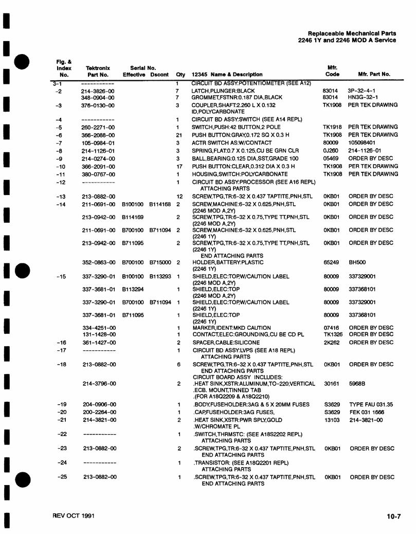
Replaceable Mechanical Parts 2246 1Y and 2246 MOD A Sewlce
Flg. & Index No.
3-1 -2
-3
-4 -5 -6 -7 -8 -9 -10 -1 1 -12
-13 -14
-1 5
-16 -17
-18
-1 9 -20 -21
-22
-23
-24
-25
Tektronlx Part No.
----------- 214-3826-00 348-0904-00 376-0130-00
Serlal No. Effectlve Dacont 12345 Name & Descrlptlon
CIRCUIT BD ASSYPOTENTIOME~ER (SEE A12) LATCH,PLUNGER:BLACK GROMMET,FSTNR:0.187 DIA,BLACK COUPLER,SHAR2.260 L X 0.132 ID,POLYCARBONATE CIRCUIT BD ASSYSWITCH (SEE A14 REPL) SWITCH,PUSH:42 BUlTON,2 POLE PUSH BUlTON:GRAY0.172 SQ X 0.3 H ACTR SWITCH AS:W/CONTAM SPRING,FLAT0.7 X 0.125,CU BE GRN CLR BALL,BEARING:O.125 DIA,SST,GRADE 100 PUSH BUlTON:CLEAR,0.312 DIA X 0.3 H HOUSING,SWITCH:POLYCARBONATE CIRCUIT BD ASSYPROCESSOR (SEE A16 REPL)
ATACHl NG PARTS SCREW,TPG,TR:6-32 X 0.437 TAPTITE,PNH,STL SCREW,MACHINE:6-32 X 0.625,PNH,STL (2246 MOD A,2Y) SCREW,TPG,TR:6-32 X 0.75,TYPE T,PNH,STL (2246 MOD A,2Y) SCREW,MACHINE:6-32 X 0.625,PNH,STL (2246 1Y) SCREW,TPG,TR:6-32 X 0.75,TYPE TT,PNH,STL (2246 1Y)
END ATACHING PARTS HOLDER,BATTERYPLASTIC (2246 1Y) SHIELD,ELEC:TOl?W/CAUTlON LABEL (2246 MOD A,2Y) SHIELD,ELEC:TOP (2246 MOD A,2Y) SHIELD,ELEC:TORW/CAUTlON LABEL (2246 1Y) SHIELD,ELEC:TOP (2246 1Y) MARKER,IDENTMKD CAUTION CONTACT,ELEC:GROUNDING,CU BE CD PL SPACER,CABLE:SILICONE CIRCUIT BD ASSYLVPS (SEE A18 REPL)
ATACHING PARTS SCREW,TPG,TR:6-32 X 0.437 TAPTITE,PNH,STL
END ATACHING PARTS CIRCUIT BOARD ASSY INCLUDES: .HEAT SINK,XSTR:ALUMINUM,TO-220;VERTICAL .ECB. MOUNT,TINNED TAB .(FOR A1802209 & A1802210) .BODYFUSEHOLDER:3AG & 5 X 20MM FUSES .CARFUSEHOLDER:3AG FUSES, .HEAT SINK,XSTR:PWR SPLYGOLD .W/CHROMATE PL .SWITCH,THRMSTC: (SEE Alas2202 REPL)
ATTACHING PARTS .SCREW,TPG,TR:6-32 X 0.437 TAPTITE,PNH,STL
END ATTACHING PARTS .TRANSISTOR: (SEE A1802201 REPL)
ATACHING PARTS .SCREW,TPG,TR:6-32 X 0.437 TAPTITE,PNH,STL
END ATACHING PARTS
Mtr. Code Mtr. Part No.
8301 4 8301 4 TK1908
TK1918 TK1908 80009 OJ260 05469 TK1908 TK1908
OKBOl OKBOl
OKBOl
OKBOl
OKBOl
65249
80009
80009
80009
80009
07416 TK1326 2K262
OKBOl
30161
S3629 S3629 131 03
OKBOl
OKBOl
3P-32-4-1 HN3G-32-1 PER TEK DRAWING
PER TEK DRAWING PER TEK DRAWING 105098401 214-1 126-01 ORDER BY DESC PER TEK DRAWING PER TEK DRAWING
ORDER BY DESC ORDER BY DESC
ORDER BY DESC
ORDER BY DESC
ORDER BY DESC
ORDER BY DESC ORDER BY DESC ORDER BY DESC
ORDER BY DESC
59686
TYPE FAU 031.35 FEK 031 1666 214-3821 -00
ORDER BY DESC
ORDER BY DESC
REV OCT 1991

Replaceable Mechanical Parts 2246 1Y and 2246 MOD A Service
Flg. & Index Rktronlx Serlal No. No. Part No. E M v e Dwont Qty
- ----------- 1
Mtr. Code 12345 Name & Descrlplon
TRANSISTOR: ( S t t A18Q2214 RtPL) ATTACHING PARTS
.SCREW,TPG,TR:6-32 X 0.437 TAPTITE,PNH,STL END ATTACHING PARTS
.CLIRCOIL SPRTl X 1.46,POLYCARBONATE
.(2246 1Y)
.CLIRCOIL SPRT1.O X 1.46.POLYCARBONATE
.(2246 1 Y)
.CLIP,COIL SPW.1 X 1.46,POLYCARBONATE
.(2246 MOD A,2Y)
.CLIRCOIL SPRTl .O X 1.46,POLYCARBONATE
.(2246 MOD A,2Y) INSUL,PWR SPLYPOLYCARBONATE CIRCUIT BD ASSYMAIN (SEE A10 REPL) .INSUlATOR,DISK:TRANSISTOR,NYLON .SHIELD,ELEC:HIGH VOLTAGE .SHIELD,ATTEN:FRONT,MAlN BD
ATTACHING PARTS .SCREW,MACHINE:6-32 X 0.875 PNH,SST
END ATACHING PARTS .SHIELD,ATTEN:ALUMINUM .(2246 MOD A,2Y) .SHIELD,ATTEN:FRONTMAlN BD .(2246 MOD A,2Y) .SHIELD,ATEN:ALUMINUM .(2246 1Y) .SHIELD,ATTEN:FRONT,MAlN BD .(2246 1Y)
ATTACHING PARTS .SCREW,TPG,TR:6-32 X 0.437 TAPTlTE,PNH,STL
END ATTACHING PARTS .CLIRELECTRICAL:FUSE,SPR BRS, .PLATE,ELEC SHLD:B SWEEP CKT BD .(2246 MOD A,2Y) .PlATE,ELEC SHLD:B SWEEP CKT BD .(2246 1Y) .CLAMRLOOP:O.25 ID,PLASTIC
ATTACHING PARTS .SCREW,TPG,TR:6-32 X 0.437 TAPTITE,PNH,STL .(2246 MOD A,2Y) .SCREW,TPG,TR:6-32 X 0.75,TYPE TT,PNH,STL .(2246 MOD A,2Y) .SCREW,TPG,TR:6-32 X 0.437 TAPTITE,PNH,STL .(2246 1Y) .SCREW,TPG,TR:6-32 X 0.75,TYPE T,PNH,STL .(2246 1Y) .WASHER,FLAT0.141 ID X 0.5 OD X 0.062,BRS .(2246 MOD A,2Y) .WASHER,FLAT0.141 ID X 0.5 OD X 0.062,BRS .(2246 1Y)
END ATACHING PARTS .BRACKET,ATTEN:BRASS .CONN,RCPT,ELEC:BNC(SEEAlWll ,J12,J13,J14)
ATTACHING PARTS .NVT,PLAIN,HW0.5-28 X 0.562 HEX,BRS CD PL .WASHER,LOCK:O.521 ID,INT,0.025 THK.SST
END ATTACHING PARTS
Mtr. Part No.
OKBOl
OKBZ5
TK1908
OKBZ5
TKl908
ORDER BY DESC
ORDER BY DESC
ORDER BY DESC
ORDER BY DESC
ORDER BY DESC
PER TEK DRAWING
7717-5N-BLUE ORDER BY DESC ORDER BY DESC
OKBOl ORDER BY DESC
ORDER BY DESC
ORDER BY DESC
ORDER BY DESC
ORDER BY DESC
OKBOl ORDER BY DESC
102074 ORDER BY DESC
ORDER BY DESC
0691 5
OKBOl
OKBOl
OKBOl
OKBOl
E4 CLEAR ROUND
ORDER BY DESC
ORDER BY DESC
ORDER BY DESC
ORDER BY DESC
ORDER BY DESC
ORDER BY DESC
ORDER BY DESC
73743 OKBOl
ORDER BY DESC 1224-02-00-0541
REV OCT 1991

Replaceable Mechanical Parts 2246 1Y and 2246 MOD A Service
Fig. & Index Tektronix Serial No. Mfr. No. Part No. Eifective D m n t Oty 12345 Name & Deacrlption Code Mfr. Part No.
131-3960-00 Bl00100 8110494 1 .CONTACT.ELEC:BNC GROUND,CU-BE ALLOY TK2147 ORDER BY DESC .(2246 MOD A,2Y)
131-4521-00 8110495 2 .CONTACT.ELEC:INPUT BNC GROUNDING,CU BE TK1326 ORDER BY DESC .ALLO.Y .(2246 MOD A.2Y)
131-3960-00 8700100 8710252 1 .CONTACT,ELEC:BN GROUND,CU-BE ALLOY TK2147 ORDER BY DESC ,12246 1Y1
. (2246 1Y)
2 .HEAT SINK.XSTR:TO-5,ALUMINUM 13103 2228B 2 .BUSHING,SNAP:0.25 ID X 0.234 THK,NYLON, 28520 2810
.0.375 OD 1 .EXTENSION SHAR9.97 L X 0.25,POLYMIDE TK1908 PER TEK DRAWING 1 .CIRCUIT BD ASSYCRT CONTROL (SEE A8
.REPL) 1 ..BUSHING.SNAP:0.25 ID X 0.234 THK.NYLON. 28520 2810
..0.375 OD 4 ..EXTENSION SHAFT0.918 L X 0.218 OD,PLASTIC TK1908 ORDER BY DESC 1 .CIRCUIT BD ASSY2 MILLIVOLT BANDWIDTH
.(SEE A9 REPL - NO LONGER REPLACEABLE)
REV OCT 1991

Replaceable Mechanical Parts 2246 1Y and 2246 MOD A Service
Flg. & Index Tektronix Serial No. Mfr. No. Part No. Effective Dscont Qty 12345 Name & Description Code Mir. Part No.
a' B
REV OCT 1991
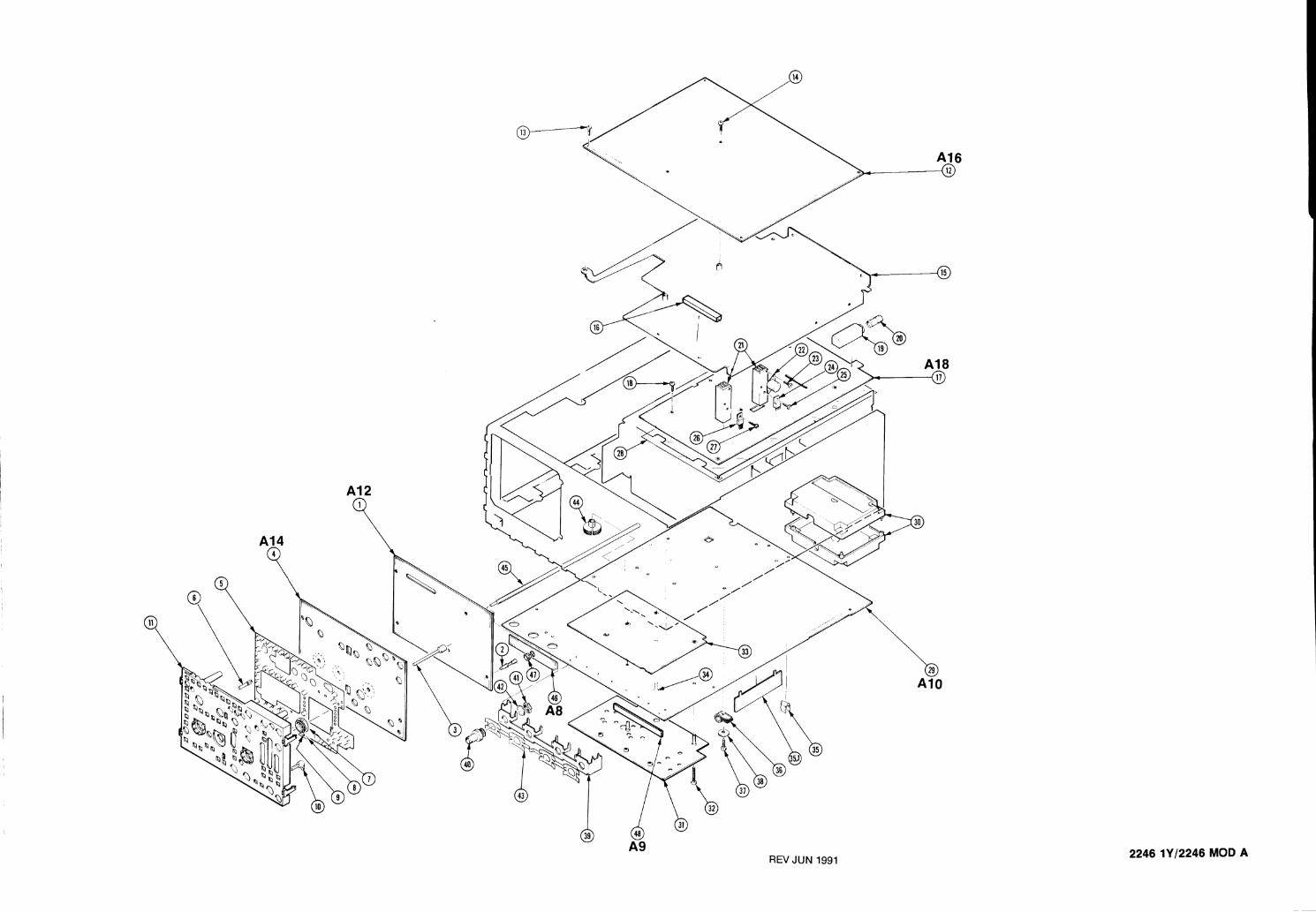
REV JUN 1991 2246 1Yl2246 MOD A
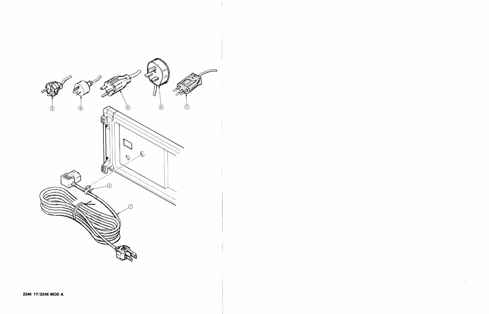
2246 1Yl2246 MOD A

Replaceable Mechanical Parts 2246 1Y and 2246 MOD A Service
Fig. & Index No.
4-
Tektronix Serial No. Part No. Ettectlve Dscont Oty
Mtr. Code Mfr. Part No. 12345 Name & Descrlptlon
STANDARD ACCESSORIES
ORDER BY DESC CABLE ASSYPWR,:3,18 AWG,92.0 L (STANDARD ONLY) CLAMRPWR C0RD:POLYMIDE ORDER BY DESC
COMPONENT KITEUROPEAN .CABLE ASSYPWR.:3 X 0.75MM SQ,220V,98.0 L .(OPTION A1 - EUROPEAN) .RTNR,CA TO CA:U/W 0.25 OD CABLES ORDER BY DESC
COMPONENT KITUNITED KINGDOM .CABLE ASSYPWR,:3 X 0.75MM SQ,240V,98.0 L .(OPTION A2 - UNITED KINGDOM) .RTNR,CA TO CA:U/W0.25 OD CABLES
020086000 ORDER BY DESC
ORDER BY DESC
COMPONENT KITAUSTRALIAN .CABLE ASSYPWR.:3.18 AWG,240V,98.0 L .(OPTION A3 - AUSTRALIAN) .RTNR,CA TO CA:U/W 0.25 OD CABLES ORDER BY DESC
COMPONENT KITNORTH AMERICAN .CABLE ASSYPWR.:3.18 AWG,240V,98.0 L .(OPTION A4 - NORTH AMERICAN) .RTNR,CA TO CA:U/W0.25 OD CABLES
020086200 ORDER BY DESC
ORDER BY DESC
COMPONENT KITSWISS .CABLE ASSY,PWR,:3.0 X 0.75.6A,240V,2.5M L .(OPTION A5 - SWITZERLAND) .RTNR,CA TO CA:U/W 0.25 OD CABLES ACCESSORY PKG:TWO P6109 PROBES,ONE P6101A PROBE,W/ACCESSORIES FUSE,CARTRIDGE:3AG.2A,25OVVSLOW BLOW ACCESSORY P0UCH:WlPLATE C0VER.FRONTAB.S MANUAL.TECH:OPERATOR (2246 MOD A,2Y) MANUAL,TECH:OPERATOR (2246 1Y) MANUAL,TECH:SERVICE (2246 1Y) CARD,INFO:REFERENCE (2246 MOD A,2Y) CARD.INFO:REFERENCE (2246 1Y)
020086300 ORDER BY DESC
ORDER BY DESC
MDX2 01 6085700 ORDER BY DESC PER TEK DRAWING 0707061 00
OPTIONAL ACCESSORIES
MANUAL,TECH:SERVICE (2246 MOD A,2Y)
REV OCT 1991

Re~laceable Mechanical Parts 2 2 h 1Y and 2246 MOD A Sewlce
Flg. & Index Tektronlx Serlal No. Mtr. No. Part No. E?fective D-nt Oly 12345 Name & lkrcrlptlon Code Mh: Part No.
REV OCT 1991

MANUAL CHANGE INFORMATION
At Tektronix, we continually strive to keep up with latest electronic developments by adding circuit and component i.mprovements to our instruments as soon as they are developed and tested.
Sometimes, due to printing and shipping requirements, we can't get these changes immediately into printed manuals. Hence, your manual may contain new change information on following pages.
A single change may affect several sections. Since the change information sheets are carried in the manual until all changes are permanently entered, some duplication may occur. If no such change pages appear following this page, your manual is correct as printed.
MANUAL CHANGE INFORMATION COMMITTEDTO EXCELLENCE Date: 5-1 3-91 Change Reference: M73903
Product: 2246 1Y and 2246 MOD A SERVICE MANUAL Manual Part Number: 070-7062-00
DESCRIPTION Product Group 46
EFFECTIVE SERIAL NUMBER: B715003 (IY, 2R) B120200 (MOD A, 2Y, 9X)
REPLACEABLE ELECTRICAL PARTS LIST CHANGES
CHANGE TO:
A10R113 313-1750-00 RES, FXD FILM:75 OHM,5%,0.2W A10R123 313-1750-00 RES, FXD FILM:75 OHM,5%,0.2W
DIAGRAM CHANGES
DIAGRAM 0 VERTICAL INPUTS
Change the value of resistor R113 (location 1G) to 75 a. Change the value of resistor R123 (location 3G) to 75 a.
Page 1 of 1

REPLACEABLE ELECTRICAL PARTS LIST CHANGES
Tkktronk MANUAL CHANGE INFORMATION COMMrrED TO EXCELLENCE Date: 5-1 5-91 Change Reference: M74238
Product: 2246 1Y & 2246 MOD A SERVICE MANUAL Manual Part Number: 070-7062-00
DESCRIPTION Product Group 46
EFFECTIVE SERIAL NUMBER: 8715476 (2246 IY , 2R) B121427 (2246 MOD A, 2Y, 9X)
CHANGE TO:
A18L2206 108-1501-00
DIAGRAM @ POWER SUPPLY
Change L2206 (location 6K) to 100~H.
Page 1 of 1

W r o n k MANUAL CHANGE INFORMATION COMMITTED TO EXCELLENCE Date: 9-23-91 Change Reference: C11/0991
Product: 2246ModAIlY SERVICE Manual Part Number: 070-7062-00
DESCRIPTION Product Group 46
EFFECTIVE ALL SERIAL NUMBERS
TEXT CHANGES
Page 4-25 Step 2e. DC Volts Normal Mode Rejection Ratio
Change spec to + 0.018V
Page 1 of 1

MANUAL CHANGE INFORMATION C O M M ~ D TO EXCELLENCE Date: 9-25-91 Change Reference: C12/0991
Product: 2246 Mod A / 1Y SERVICE Manual Part Number: 070-7062-00
DESCRIPTION Product Group 46
EFFECTIVE ALL SERIAL NUMBERS
TEXT CHANGES
Page 6-39 Removal and Replacement Instructions - 'WARNING"
The component number for the Power Supply/Main Board interface connector mentioned in the warning was incorrectly identified as J1024. The correct component number is 51 204.
The correct warning statement is given below:
Potentially dangerous voltages exist at several points throughout this instrument. If it is operated with the cabinet removed, do not touch exposed connections or components. Before replacing parts or cleaning, disconnect the ac power source from the instrument and check that the line rectifier filter capacitors have discharged. Also check the low voltages at the Power SupplylMain Board interface connector (J1204). If any of the supply voltage or line voltage filter capacitors remain charged for more than 20 seconds, discharge them to ground through a 1 kn, 5 or 6 watt resistor.
Page 1 of 1