TI ON MANUAL - xDevs.com
143
CHECK FOR CHANGE INFORMATION REAR O THIS MANUAL . Tektronix, Inc . P.O . Box 500 Beaverton, Oregon 97077 Serial Number COMMITTED TO EXCELLENCE UIRE CLOCK TI ON MANUAL 070-2788-00 First Printing APR 1980 Product Group 42 Revised JAN 1986
-
Upload
khangminh22 -
Category
Documents
-
view
3 -
download
0
Transcript of TI ON MANUAL - xDevs.com

CHECK FOR CHANGE INFORMATIONREAR O THIS MANUAL.
Tektronix, Inc .P.O . Box 500Beaverton, Oregon
97077
Serial Number
COMMITTED TO EXCELLENCE
UIRE CLOCK
TI ON MANUAL
070-2788-00
First Printing APR 1980Product Group 42
Revised JAN 1986

Copyright Ll~ 1980 Tektronix, Inc . All rights reserved .Contents of this publication may not be reproduced in anyform without the written permission of Tektronix, Inc .
Products of Tektronix, Inc . and its subsidiaries are coveredby U .S . and foreign patents and/or pending patents .
TEKTRONIX, TEK, SCOPE-MOBILE, and
19!!44
areregistered trademarks of "Tektronix, Inc . TELEOUIPMENTis a registered trademark of Tektronix U.K. Limited .
Printed in U.S.A . Specification and price change privilegesare reserved .
INSTRUMENT SERIAL NUMBERS
Each instrument has a serial number on a parlel insert, tag,or stamped on the chassis . The first number or letterdesignates the country of manufacture. The last five digitsof the serial number are assigned sequentially and areunique to each instrument . Those manufactured in theUnited States have six unique digits . The country ofmanufacture is identified as follows :
13000000
"Tektronix, Inc ., Beaverton, Oregon, USA100000
Tektronix Guernsey, Ltd ., Channel Islands200000
Tektronix United Kingdom, Ltd ., London300000
Sony/Tektronix, Japan700000
Tektronix Holland, NV, Heerenveen,The Netherlands

LIST OF ILLUSTRATIONS . . . . . . . . . . . . . . . . . . . . . . . . . . . . . . . . . iiiLIST OF TABLES . . . . . . . . . . . . . . . . . . . . . . . . . . . . . . . . . . . . . . . . . ivOPERATORS SAFETY SUMMARY . . . . . . . . . . . . . . . . . . . . . . . . . . vSERVICING SAFETY SUMMARY . . . . . . . . . . . . . . . . . . . . . . . . . . vii
SECTION 1----OPERATING INSTRUCTIONSINSTALLATION . . . . . . . . . . . . . . . . . . . . . . . . . . . . . . . . . . . 1-1CONTROLS, CONNECTORS, AND INDICATORS . . . . . . 1-1FUNCTIONAL CHECK . . . . . . . . . . . . . . . . . . . . . . . . . . . . . . 1-1
SETUP PROCEDURE . . . . . . . . . . . . . . . . . . . . . . . . . . ., 1-1SWEEP FUNCTIONS . . . . . . . . . . . . . . . . . . . . . . . . . . . . 1-4TRIGGERING FUNCTIONS . . . . . . . . . . . . . . . . . . . . . . 1-4PRETRIGGER ACQUIRE CLOCK FUNCTIONS . . . . . 1-5
GENERAL OPERATING INFORMATION . . . . . . . . . . . . . . 1-6TRIGGERING SWITCH LOGIC . . . . . . . . . . . . . . . . . . . 1-6TRIGGERING MODES . . . . . . . . . . . . . . . . . . . . . . . . . . 1-6TRIGGER COUPLING . . . . . . . . . . . . . . . . . . . . . . . . . . . 1-9TRIGGER SOURCE . . . . . . . . . . . . . . . . . . . . . . . . . . . . . 1-9TRIGGER SLOPE . . . . . . . . . . . . . . . . . . . . . . . . . . . . . . 1-11TRIGGER LEVEL. . . . . . . . . . . . . . . . . . . . . . . . . . . . . . . 1-11HORIZONTAL SWEEP RATES . . . . . . . . . . . . . . . . . . 1-11TIME MEASUREMENT . . . . . . . . . . . . . . . . . . . . . . ., . 1-11SWEEP MAGNIFICATION . . . . . . . . . . . . . . . . . . . . . . 1-11VARIABLE HOLD OFF . . . . . . . . . . . . . . . . . . . . . . . . . 1-12MAINFRAME OPERATING MODES . . . . . . . . . . . . . 1-12
APPLICATIONS . . . . . . . . . . . . . . . . . . . . . . . . . . . . . . . . . . . . . 1-12TIME INTERVAL MEASUREMENTS . . . . . . . . . . . . . . . . 1-12
PERIOD AND FREQUENCY MEASUREMENTS . . . 1-12RISE-TIME AND FALL-TIME MEASUREMENTS . .
1-13PULSE WIDTH MEASUREMENTS . . . . . . . . . . . . . . .
1-14
SECTION 2--SPECIFICATIONSTANDARD ACCESSORIES . . . . . . . . . . . . . . . . . . . . . . . . 2-4
------------WARNING
THE REMAINING PORTION OF THIS TABLE OF CONTENTSLISTS SERVICING INSTRUCTIONS . THESE SERVICINGINSTRUCTIONS ARE FOR USE BY QUALIFIED PERSONNELONLY . TO AVOID ELECTRICAL SHOCK, DO NOT PERFORMANY SERVICING OTHER THAN THAT CALLED OUT IN THEOPERATING INSTRUCTIONS UNLESS QUALIFIED TO DOSO .
SECTION 3---THEORY OF OPERATIONBLOCK DIAGRAM DESCRIPTION . . . . . . . . . . . . . . . . . . . . . . 3-1
TRIGGER GENERATOR . . . . . . . . . . . . . . . . . . . . . . . . . . . . 3-1SWEEP GENERATOR . . . . . . . . . . . . . . . . . . . . . . . . . . . . . . 3-1PICKOFF AMPLIFIER AND DELAY GATE
GENERATOR . . . . . . . . . . . . . . . . . . . . . . . . . . . . . . . . . . 3-1LOGIC . . . . . . . . . . . . . . . . . . . . . . . . . . . . . . . . . . . . . . . . . . . . 3-1DIGITAL VOLTMETER . . . . . . . . . . . . . . . . . . . . . . . . . . . . . 3-1CLOCK GENERATOR . . . . . . . . . . . . . . . . . . . . . . . . . . . . . . 3-1
REV JUN 1981
PAGE
71387 Instruction
PAGE
DETAILED CIRCUIT DESCRIPTION . . . . . . . . . . . . . . . . . . . . . 3-1FRONT-PANEL DISTRIBUTION . . . . . . . . . . . . . . . . . . . . . 3-3TRIGGER GENERATOR . . . . . . . . . . . . . . . . . . . . . . . . . . . . 3-3
EXTERNAL SOURCE . . . . . . . . . . . . . . . . . . . . . . . . . . . . 3-3INTERNAL AND LINE SOURCE . . . . . . . . . . . . . . . . . . 3-3TRIGGER SOURCE SELECTOR AND
AMPLIFIER . . . . . . . . . . . . . . . . . . . . . . . . . . . . . . . . . 3-3PEAK-TO-PEAK AUTO . . . . . . . . . . . . . . . . . . . . . . . . . . 3-3SLOPE SELECTOR AND TRIGGER
GENERATOR . . . . . . . . . . . . . . . . . . . . . . . . . . . . . . . 3-5GATE GENERATOR . . . . . . . . . . . . . . . . . . . . . . . . . . . . 3-5
LOGIC . . . . . . . . . . . . . . . . . . . . . . . . . . . . . . . . . . . . . . . . . . . . 3-5SWEEP MODES . . . . . . . . . . . . . .. . . . . . . . . . . . . . . . . . 3-5HOLD OFF TIMING . . . . . . . . . . . . . . . . . . . . . . . . . . . . . 3-6LOCKOUT BUFFER AMPLIFIER . . . . . . . . . . . . . . . . . . 3-7HOLD OFF OUTPUT AMPLIFIER . . . . . . . . . . . . . . . . . 3-7
SWEEP GENERATOR . . . . . . . . . . . . . . . . . . . . . . . . . . . . . . 3-7TIMING CURRENT SOURCE . . . . . . . . . . . . . . . . . . . . . 3-7RAMP GENERATOR . . . . . . . . . . . . . . . . . . . . . . . . . . . 3-10HORIZONTAL PREAMPLIFIER . . . . . . . . . . . . . . . . . . 3-10SWEEP GATE GENERATOR . . . . . . . . . . . . . . . . . . . . 3-10
DVM . . . . . . . . . . . . . . . . . . . . . . . . . . . . . . . . . . . . . . . . . . . . 3-10DELAY TIME COMPARATOR AND DELAY
GATE GENERATOR . . . . . . . . . . . . . . . . . . . . . . . . 3-10DIGITAL VOLTMETER . . . . . . . . . . . . . . . . . . . . . . . . . . . . 3-11
DELAY COMPARISON VOLTAGE-TO-RAMPCONVERTER . . . . . . . . . . . . . . . . . . . . . . . . . . . . . . . 3-12
COMPARATOR . . . . . . . . . . . . . . . . . . . . . . . . . . . . . . . 3-12REFERENCE CURRENT SOURCE . . . . . . . . . . . . . . . 3-12REFERENCE CURRENT INVERTER . . . . . . . . . . . . . . 3-12COUNTER AND ENCODER . . . . . . . . . . . . . . . . . . . . . 3-12
CLOCK GENERATOR . . . . . . . . . . . . . . . . . . . . . . . . . . . . . 3-12CONTROL LOGIC . . . . . . . . . . . . . . . . . . . . . . . . . . . . . 3-13OSCILLATOR . . . . . . . . . . . . . . . . . . . . . . . . . . . . . . . . . 3-13FIRST DIVIDER . . . . . . . . . . . . . . . . . . . . . . . . . . . . . . . . 3-15X1-X10MULTIPL-EXER . . . . . . . . . . . ., . . . . ��� .3-15DECADE DIVIDER . . . . . . . . . . . . . . . . . . . . . . . . . . . . . 3-15INTERNAL CLOCK MULTIPLEXER . . . . . . . . . . . . . . 3-15OUTPUT CLOCK MULTIPLEXER . . . . . . . . . . . . . . . . 3-15INTENSIFY CIRCUIT . . . . . . . . . . . . . . . . . . . . . . . . . . . 3-15
71387 IN A HORIZ PLUG-IN COMPARTMENT . . . . . . . 3-16IN] ERNAL BUTTON PRESSED . . . . . . . . . . . . . . . . . . 3-16
71387 IN B HORIZ PLUG-IN COMPARTMENT . . . . . . . 3-16INTERNAL BUTTON PRESSED . . . . . . . . . . . . . . . . . . 3-16
TIME/DIVISION AND READOUT SWITCHING . . . . . . . 3-17BASIC READOUT SYSTEM . . . . . . . . . . . . . . . . . . . . . 3-17TIME/DIVISION READOUT . . . . . . . . . . . . . . . . . . . . . 3-17ACQUIRE-STOP DELAY TIME READOUT . . . . . . . . 3-17
INTERFACE CONNECTIONS AND POWERSUPPLY . . . . . . . . . . . . . . . . . . . . . . . . . . . . . . . . . . . . . . 3-17
SEC'T'ION 4-MAINTENANCEPREVENTIVE MAINTENANCE . . . . . . . . . . . . . . . . . . . . . . . . . 4-1
CLEANING . . . . . . . . . . . . . . . . . . . . . . . . . . . . . . . . . . . . . . . . 4-1EXTERIOR . . . . . . . . . . . . . . . . . . . . . . . . . . . . . . . . . . . . . 4-1INTERIOR . . . . . . . . . . . . . . . . . . . . . . . . . . . . . . . . . . . . . . 4,1SWITCH CONTACTS . . . . . . . . . . . . . . . . . . . . . . . . . . . . 4-1

71387 Instruction
PAGE
VISUAL INSPECTION . . . . . . . . . . . . . . . . . . . . . . . . . . . . . . 4-1LUBRICATION . . . . . . . . . . . . . . . . . . . . . . . . . . . . . . . . . . . . 4-1CAM SWITCH LUBRICATION . . . . . . . . . . . . . . . . . . . . 4-2
SEMICONDUCTOR CHECKS . . . . . . . . . . . . . . . . . . . . . . . 4-2ADJUSTMENT AFTER REPAIR . . . . . . . . . . . . . . . . . . . . . 4-2
TROUBLESHOOTING . . . . . . . . . . . . . . . . . . . . . . . . . . . . . . . . . 4-2TROUBLESHOOTING AIDS . . . . . . . . . . . . . . . . . . . . . . . . . 4-2
DIAGRAMS . . . . . . . . . . . . . . . . . . . . . . . . . . . . . . . . . . . .
4-2VOLTAGES AND WAVEFORMS . . . . . . . . . . . . . . . . . 4-2CIRCUIT-BOARD ILLUSTRATIONS . . . . . . . . . . . . . . . 4-2SWITCH CAM IDENTIFICATION . . . . . . . . . . . . . . . . . 4-4DIODE COLOR CODE . . . . . . . . . . . . . . . . . . . . . . . . . . .
4-4WIRING COLOR CODE . . . . . . . . . . . . . . . . . . . . . . . . . 4-4SEMICONDUCTOR LEAD CONFIGURATIONS . . . . . 4-4INTER-BOARD PIN CONNECTOR
IDENTIFICATION . . . . . . . . . . . . . . . . . . . . . . . . . . . . 4-4MULTI-PIN CONNECTOR IDENTIFICATION . . . . . . . 4-4INTERFACE CONNECTOR PIN LOCATIONS . . . . . . . 4-5PERFORMANCE CHECK AND ADJUSTMENT . . . . . 4-5
STATIC SENSITIVE DEVICES . . . . . . . . . . . . . . . . . . . . . . . 4-5TROUBLESHOOTING EQUIPMENT . . . . . . . . . . . . . . . . . . 4-6TROUBLESHOOTING TECHNIQUES . . . . . . . . . . . . . . . . . 4-6
TROUBLESHOOTING PROCEDURE . . . . . . . . . . . . . . 4-6CORRECTIVE MAINTENANCE . . . . . . . . . . . . . . . . . . . . . . . . . 4-8
OBTAINING REPLACEABLE PARTS . . . . . . . . . . . . . . . . . 4-8SOLDERING TECHNIQUES . . . . . . . . . . . . . . . . . . . . . . . . . 4-9COMPONENT REMOVAL AND REPLACEMENT . . . . . 4-10
CIRCUIT BOARDS . . . . . . . . . . . . . . . . . . . . . . . . . . . . . 4-10SWITCHES . . . . . . . . . . . . . . . . . . . . . . . . . . . . . . . . . . . 4-12SEMICONDUCTORS . . . . . . . . . . . . . . . . . . . . . . . . . . . 4-15INTERCONNECTING PINS . . . . . . . . . . . . . . . . . . . . . . 4-15CIRCUIT-BOARD PINS . . . . . . . . . . . . . . . . . . . . . . . . . 4-15FRONT-PANEL LIGHTS . . . . . . . . . . . . . . . . . . . . . . . . 4-16
ADJUSTMENT AFTER REPAIR . . . . . . . . . . . . . . . . . . . . 4-16INSTRUMENT' REPACKAGING . . . . . . . . . . . . . . . . . . . . . 4-16
SECTION 5 .--.-PERFORMANCE CHECK ANDADJUSTMENT
PRELIMINARY INFORMATION . . . . . . . . . . . . . . . . . . . . . . 5-1ADJUSTMENT INTERVAL . . . . . . . . . . . . . . . . . . . . . . . 5-1TEKTRONIX FIELD SERVICE . . . . . . . . . . . . . . . . . . . . . 5-1USING THIS PROCEDURE . . . . . . . . . . . . . . . . . . . . . . 5-1
TEST EQUIPMENT REQUIRED . . . . . . . . . . . . . . . . . . . . . . 5-1SPECIAL FIXTURES . . . . . . . . . . . . . . . . . . . . . . . . . . . . 5-1TEST EQUIPMENT ALTERNATIVES . . . . . . . . . . . . . . 5-1
INDEX TO PERFORMANCE CHECK ANDADJUSTMENT PROCEDURE . . . . . . . . . . . . . . . . . . . . 5-4
PRELIMINARY PROCEDURE . . . . . . . . . . . . . . . . . . . . . . . . 5-4A . TRIGGERING SYSTEM . . . . . . . . . . . . . . . . . . . . . . . . . . . . . 5-5B . HORIZONTAL/AQS SYSTEM . . . . . . . . . . . . . . . . . . . . . . 5-10
SECTION &---INSTRUMENT OPTIONS
SECTION f --REPLACEABLE ELECTRICAL PARTS
SECTION 8--DIAGRAMS AND CIRCUIT BOARDILLUSTRATIONS
SECTION 9---REPLACEABLE MECHANICAL PARTS
CHANGE INFORMATION
PAGE
REV JUN 1981

FIG .NO .
Frontis-piece1-11-2
1-31-4
1-61-7
2-13-1
3-23-3
3-43-53-6
4-24-3
REV JUN 1981
71387 Features . . . . . . . . . . . . . . . . . . . . . . . . . . . . . . . ..Locationof release latch . . . . . . . . . . . . . . . . . . . . . . . .
Front-panel controls, connectors, andindicators . . . . . . . . . . . . . . . . . . . . . . . . . . . . . . . . . . . . .Single Sweep Acquisition . . . . . . . . . . . . . . . . . . . . . . .Effect of LEVEL control and SLOPE switchon crt display . . . . . . . . . . . . . . . . . . . . . . . . . . . . . . . . .
.Areaof graticule used for most accuratetime measurements . . . . . . . . . . . . . . . . . . . . . . . . . . .Operation of sweep magnifier . . . . . . . . . . . . . . . . . .Measuring the period and determining thefrequency of a displayed waveform . . . . . . . . . . . . .Measuring the rise time and fall time ofa displayed waveform . . . . . . . . . . . . . . . . . . . . . . . . . 1-14Measuring the pulse width of a displayedwaveform . . . . . . . . . . . . . . . . . . . . . . . . . . . . . . . . . . . . 1-1471387 dimensional drawing . . . . . . . . . . . . . . . . . � . . 2-5Basic block diagram of the 71387 DelayingTime Base Unit . . . . . . . . . . . . . . . . . . . . . . . . . . . . . . . . 3-2Detailed block diagram of Trigger Generator . . . . . 3-4Timing diagram for Gate Generator stage(092, Q96, 098) . . . . . . . . . . . . . . . . . . . . . . . . . . . . . . . 3-6Detailed block diagram of Logic circuit . . . . . . . . . . . 3-7Detailed block diagram of Sweep Generator . . . . . . 3-8Timing of events that form the DelayGate signal . . . . . . . . . . . . . . . . . . . . . . . . . . . . . . . . . . . 3-11Lubrication procedure for a typicalcam switch . . . . . . . . . . . . . . . . . . . . . . . . . . . . . . . . . . . . 4-2Semiconductor lead configuration . . . . . . . . . . . . . . . 4-3Inter-board multi-pin connector assembly . . . . . . . . 4-4
8-1
Semiconductor Lead Configurations .8-2
Locations of circuit boards in the 71387 .8-3
A2-Trigger circuit board assembly.8-4
A1-Interface circuit board assembly .8-5
A1-Interface circuit board assembly .8-6
A1-Interface circuit board assembly .8-7
A4-Clock circuit board assembly .8-8
A4-Clock circuit board assembly .8-9
A3-Readout circuit board assembly .8-10
A1-Interface circuit board assembly .8-11
Test Point and Adjustment Locations .
713£37 Instruction
The illustrations in Section 8 are located near their associateddiagrams on the foldout pages .
AGE FIG .NO .
PAGE
4-4 End-lead multi-pin connector assembly . . . . . . . . . . 4-4. viii 4-5 Location of pin numbers on Interface1 -1 connector . . . . . . . . . . . . . . . . . . . . . . . . . . . . . . . . . . . . . 4-5
4-6 71387 troubleshooting chart . . . . . . . . . . . . . . . . . . . . . 4-71-2 4-7 Readout board removal procedure . . . . . . . . . . . . . . 4-101-5 4-8 Coaxial end-lead connector assembly . . . . . . . . . . . 4-11
4-9 Location of securing screws and inter-board1-10 multi-pin connectors on clock circuit board . . . . . . 4-12
4-10 Cam switch removal procedure . . . . . . . . . . . . . . . . 4-131-11 4-11 Removal procedure for typical pushbutton1-12 switch . . . . . . . . . . . . . . . . . . . . . . . . . . . . . . . . . . . . . . . 4-14
4-12 Exploded view of circuit-board pin and1-13 ferrule . . . . . . . . . . . . . . . . . . . . . . . . . . . . . . . . . . . . . . . 4-16
4-13 Front-panel light socket assembly . . . . . . . . . . . . . . 4-16

TABLE
PAGENO.
1-1
TIME/DIV Setting Relationship To 7887Internal Acquire Clock Rep Rate . . . . . . . . . . . . . . . . . 1-7
2-1
Electrical Characteristics . . . . . . . . . . . . . . . . . . . . . . . 2-12-2
Mainframe Horizontal Compatibility . . . . . . . . . . . . . 2-32-3
Environmental Characteristics . . . . . . . . . . . . . . . . . . 2-42-4
Physical Characteristics . . . . . . . . . . . . . . . . . . . . . . . . 2-43-1
Truth Table, TIME/DIV Setting vs . Strobesfor U637 and U638 . . . . . . . . . . . . . . . . . . . . . . . . . . . 3-13
3-2
Selected Inputs or X1 and X10 Multiplexers . . . . . 3-143-3
Operation of Output Multiplexer U655 . . . . . . . . . . 3-153-4
Current in CH1 Readout Line vs . AcquireClock Mode, During TS10 . . . . . . . . . . . . . . . . . . . . . . 3-16
3-5
Readout Character Selection . . . . . . . . . . . . . . . . . . . 3-184-1
Relative Susceptibility . . . . . . . . . . . . . . . . . . . . . . . . . . 4-55-1
Test Equipment . . . . . . . . . . . . . . . . . . . . . . . . . . . . . . . . 5-25-2
Acquire Clock Repetition Rate Output . . . . . . . . . . . 5-115-3
Delay Time Linearity . . . . . . . . . . . . . . . . . . . . . . . . . . 5-125-4
Acquire-Stop Delay Accuracy . . . . . . . . . . . . . . . . . . 5-135-5
Sweep Timing . . . . . . . . . . . . . . . . . . . . . . . . . . . . . . . . 5-145-6
Magnified Sweep Timing . . . . . . . . . . . . . . . . . . . . . . 5-15

The general safety information in this part of the summary is for both operating and servicing personnel. Specificwarnings and cautions will be found throughout the manual where they apply, but may not appear in this summary.
IN THIS MANUALCAUTION statements identify conditions or practices that could result in damage to the equipment or other property .
WARNING statements identify conditions or practices that could result in personal injury or loss of life .
AS MARKED ON EQUIPMENT
CAUTION indicates a personal injury hazard not immediately accessible as one reads the marking, or a hazard toproperty including the equipment itself .
DANGER indicates a personal injury hazard immediately accessible as one reads the marking .
IN THIS MANUAL
Static-Sensitive Devces .
This symbol indicates where applicable cautionary or other information is to be found.
AS MARKED ON EQUIPMENT
DANGER----High voltage.
Protective ground (earth) terminal .
ATTENTION-----refer to manual .
POWER SOURCE
GROUNDING THE PRODUCT
TERMS
SYMBOLS
WARNINGS
7'1381 Instruction
This product is intended to operate in a mainframe connected to a power source that will not apply more than 250 voltsrms between the supply conductors or between either supply conductor and ground . A protective ground connection byway of the grounding conductor in the mainframe power cord is essential for safe operation .
This product is grounded through the grounding conductor of the mainframe power cord . To avoid electrical shock, plugthe mainframe power cord into a properly wired receptacle before connecting to the product input or output terminals . Aprotective ground connection by way of the grounding conductor in the mainframe power cord is essential for safeoperation.

71387 Instruction
DANGER ARISING FROM LOSS OF GROUND
Upon loss of the protective-ground connection, all accessible conductive parts (including knobs and controls that mayappear to be insulating), can render an electric shock.
DO NOT OPERATE IN EXPLOSIVE ATMOSPHERES
To avoid explosion, do not operate this product in an atmosphere of explosive gases unless it has been specificallycertified for such operation .
DO NOT OPERATE PLUG-IN UNIT WITHOUT COVERS
To avoid personal injury, do not operate this product without covers or panels installed . Do not apply power to the plug-inunit via a plug-in extender .

DO NOT SERVICE ALONE
FOR QUALIFIED SERVICE PERSONNEL ONLY
Refer also to the preceding Operators Safety Summary
Do not perform internal service or adjustment of this product unless another person capable of rendering first aid andresuscitation is present.
USE CARE WHEN SERVICING WITH POWER ON
POWER SOURCE
713$7 Instruction
Dangerous voltages exist at several points in this product. To avoid personal injury, do not touch exposed connectionsand components while power is on .
Disconnect power before removing protective panels, soldering, or replacing components .
This product is intended to operate in a mainframe connected to a power source that will not apply more than 250 voltsrms between the supply conductors or between either supply conductor and ground . A protective ground connection byway of the grounding conductor in the mainframe power cord is essential for safe operation .

71387 Instruction
VIII
FlitPoernow
aI ~' IAN
ACQUIRE STOP DELAY
71387 FEATURES
TRIGGERING
YoafF-P AU T0
AUTO
AC LF W
*OW
AC IF KJ
MAG
II '~ XIO~IrT
COMING
OCHOLDOFF
EXT CLOCK IN
SWIM CALIts IIh USX)
II + 1OUT+1!EXT TRIG IN
y
S2f4y
2788-1
The 71387 Time-Base unit Pretrigger Acquire Clock provides calibrated sweep rates from 5 seconds to 10 nanoseconds and triggering to400megahertz for 7000-Series Oscilloscopes. A X10 Magnifier increases each sweep rate by a factor of 10 and a VARIABLE TIME/ DIV controlprovides continuously-variable sweep rates between calibrated steps . Variable holdoff and alphanumeric readout are provided . Also, whenoperating in the AUTO TRIGGERING MODE, a bright baseline trace is displayed in the absence of a trigger signal . The 7887 can be operated
as an independent time base or as a delayed-sweep unit with a companion delaying time-base unit . Sweep mode is determined by thecompanion delaying time base .
The 71387 also features an internally-generated clock and an external clock input for sequential single sweep acquisition when operating in a7000-series digitizing oscilloscope . The frequency range of the internally generated clock is 20.48 mHz (millihertz) to 20.48 MHz asdetermined by the TIME/DIV, X10 MAG, and INT _ 1000 switches. Also, an ACQUIRE-STOP DELAY function varies delay pickoff, andtherefore pretrigger time, in compatible digitizing plug-in oscilloscopes . The portion of the oscilloscope real-time display between thetriggering event and the end of delay time is intensified . The exact delay time is displayed on the crt readout .

INSTALLATION
The time-base unit operates in the horizontal plug-incompartment of the mainframe . When used for singlesweep acquisition with a Tektronix 7000-series digitizingoscilloscope (7854) the 71387 must be installed in the Bhorizontal compartment of the mainframe . Thisinstrument can also be installed in a vertical plug-incompartment to provide a vertical sweep on the crt .However, when used in this manner, there are nointernal triggering or retrace blanking provisions, and theunit may not meet the specifications given in Section 2,Specification .
To install the unit in a plug-in compartment, push it inuntil it fits firmly into the compartment . The front panelof the unit should be flush with the front panel of themainframe . Even though the gain of the mainframe isstandardized, the sweep calibration of the unit should bechecked when installed . The procedure for checking theunit is given under Sweep Functions in the FunctionalCheck procedure in this section .
To remove the unit, first turn the power off, then pull therelease latch (see Fig . 1 -1) to disengage the unit from themainframe, and pull it out of the plug-in compartment .
CONTROLS, CONNECTORS, ANDINDICATORS
All controls, connectors, and indicators required for theoperation of the time-base unit are located on the frontpanel . Figure 1-2 shows and provides a brief descriptionof all front-panel controls, connectors, and indicators .More detailed information is given in the GeneralOperating Instructions .
FUNCTIONAL CHECK
The following procedures are provided for checking basicinstrument functions . Refer to the description of thecontrols, connectors, and indicators while performingthis procedure . If performing the functional checkprocedure reveals a malfunction or possible improperadjustment, first check the operation of the associatedplug-in units, then refer to the instruction manual formaintenance and adjustment procedures .
The 71387 Time-Base unit operates with a Tektronix 7700-, 7800-, or 7900-series oscilloscope mainframe and a 7A-series amplifier unit to form a complete oscilloscope system . This section describes the operation of the front-panelcontrols and connectors, provides general operating information, a functional check procedure, and basic applications forthis instrument .
SETUP PROCEDURE1 . Install the time-base unit in the A horizontalcompartment of the mainframe .
2 . Install an amplifier plug-in unit in a verticalcompartment .
3 . Set the time-base unit controls as follows :
SLOPE . . . . . . . . . . . . . . . . . . . . . . . . . . . . . . . . . . . . . . . (+)MODE . . . . . . . . . . . . . . . . . . . . . . . . . . . . . . . P-P AUTOCOUPLING . . . . . . . . . . . . . . . . . . . . . . . . . . . . . . . . . . ACSOURCE . . . . . . . . . . . . . . . . . . . . . . . . . . . . . . . . . . . . INTPOSITION . . . . . . . . . . . . . . . . . . . . . . . . . . . . . Midrange.TIME/DIV . . . . . . . . . . . . . . . . . . . . . . . . . . . . . . . . . 1 msVARIABLE (CAL IN) . . . . . . Calibrated (Pushed in)HOLD OFF . . . . . . . . . . MIN (fully counterclockwise)MAG . . . . . . . . . . . . . . . . . . . . . . . . . . . X1 (pushed in)
Section 1--71387
Figure 1-1 . Location of release latch .

Operating Instructions� 7B87
TIME BASE
uwnW/PRETRIGGER ACQUIRE CLOCK
Figure 1-2 . Front-panel controls, connectors, and indicators .

TRIGGERING
LEVEL Control---Selects a point on the trigger signal where triggering occurs .
SLOPE Switch Permits sweep to be triggered on negative- or positive-going portions of the trigger signal .
READY Indicator--Illuminates when sweep circuit is armed (SINGLE SWEEP Mode) .
TRIG'D Indicator
Illuminates when the display is triggered .
MODE Pushbuttons---Selects the operating mode of the triggering circuit .
COUPLING Pushbuttons---Selects the method of coupling the trigger signal to triggering circuit .
SOURCE
Selects source of the trigger signal .
SWEEP
POSITION Control---Provides horizontal positioning .
FINE Control-----Provides precise horizontal positioning .
@MAG Pushbutton---Selects magnified X10 or unmagnified sweep .
@ HOLD OFF Control----Permits hold off period to be varied to improve trigger stability on repetitive, complex waveforms .
@) TIME/DIV Selector-Selects the sweep rate of the sweep generator .
VARIABLE Control and CAL Switch---Selects calibrated or uncalibrated sweep rates . Uncalibrated sweep rates can becontinuously reduced to at least the sweep rate of the next slower position .
SWP CAL Adjustment---Compensates for basic timing changes due to the differences in sensitivity of mainframes .
EXTERNAL TRIGGER INPUT
EXT TRIG ATTENUATOR--Selects attenuation factor for external trigger signals .
@EXT TRIG IN Connector---Connector (BNC type) provides input for external trigger signals .
PRETRIGGER ACQUIRE CLOCK
EXT CLOCK IN Connector--Provides input for external TTL clock signals .
Figure 1-2 (cont) . Front-panel controls, connectors, and indicators .
Operating Instructions---71387
~~
AQS (acquire single-shot) CLOCK/AQR (acquire repetitive)---Selects the source of clock pulses from the 71387 tothe 7854 digitizing plug-in oscilloscope (71387 must be installed in B horizontal compartment of companionoscilloscope mainframe) .
18
ACQUIRE-STOP DELAY Control---A variabledelaygatefunctionthatallowspretriggertimetobevariedincompatible7000-series digitizing oscilloscopes . Exact delay time is displayed on oscilloscope crt readout .
2788 38

Operating Instructions--713187
4. Turn on the mainframe and allow at least 20 minuteswarmup .
5 . Set the mainframe vertical and horizontal modes todisplay the plug-in units used and adjust the intensityand focus for a well-defined display . See the oscilloscopemainframe and amplifier unit instruction manuals fordetailed operating instructions .
SWEEP FUNCTIONS
NORMAL SWEEP. Perform the following procedure toobtain a normal sweep and to demonstrate the functionof the related controls :
1 . Perform the preceding Setup Procedure .
2 . Connect a 0 .4-volt, 1-kilohertz signal from themainframe calibrator to the amplifier unit input .
3 . Set the amplifier unit deflection factor for 4 divisionsof display .
4 . Adjust the LEVEL control for a stable display .
5 . Turn the POSITION control and note that the tracemoves horizontally .
6 . Turn the FINE control and note that the display can beprecisely positioned horizontally .
7 . Check the display for one complete cycle per division .If necessary, adjust the front-panel SWP CAL screwdriveradjustment for one complete cycle per division over thecenter 8 graticule divisions . Be sure that the timing of themainframe calibrator signal is accurate to within 0.25%(+20° to +30° C) .
8 . Press to release the VARIABLE (CAL IN) control . Turnthe VARIABLE (CAL IN) control fully counterclockwiseand note that the displayed sweep rate changes to atleast the next slower TIME/DIV switch setting (i .e ., 2milliseconds/division) . Press the VARIABLE (CAL IN)knob in (to the calibrated position) .
MAGNIFIED SWEEP. Perform the following procedureto obtain a X10 magnified display and to demonstrate thefunction of the related controls :
1 . Obtain a one cycle per division display as described inthe preceding Normal Sweep procedure .
2 . Press to release the MAG button (X10) . Note that theunmagnified display within the center division of thegraticule is magnified to about 10 divisions .
3 . Press the MAG button (X1) .
TRIGGERING FUNCTIONS
Perform the following procedure to obtain a triggeredsweep and to demonstrate the functions of the relatedcontrols :
1 . Obtain a display as described in the preceding NormalSweep procedure .
2 . Press the AUTO MODE button and turn the LEVELcontrol fully counterclockwise to obtain a free-runningsweep .
3 . Slowly turn the HOLD OFF control clockwise and notethat a stable display can be obtained at several positionsof the HOLD OFF control . Return the HOLD OFF controlto the fully counterclockwise (MIN) position .
NOTEThe HOLD OFF control varies the sweep hold-off time which effectively changes therepetition-rate of the horizontal sweep signal.However, its primary function is to obtain astable display of complex waveforms whichare otherwise difficult to trigger.
4 . Press the AC, AC HF REJ, and DC COUPLING buttonsfor both the + and - positions of the SLOPE switch andcheck for a stable display (LEVEL control may beadjusted, if necessary, to obtain a stable display) .
5 . Apply the 0.4-volt, 1-kilohertz signal from themainframe calibrator to the amplifier unit and to the EXTTRIG IN connector .
6 . Press the EXT SOURCE button and set the amplifierunit deflection factor for a 4-division display .
7 . Press the AC, AC HF REJ, and DC COUPLING buttonsfor both the + and - positions of the SLOPE switch andcheck for a stable display (LEVEL control may beadjusted, if necessary, for a stable display) .
8 . Press the AC COUPLING, INT SOURCE, and NORMMODE buttons . Adjust the LEVEL control for a stabledisplay .
9 . Press the AUTO MODE button and adjust the LEVELcontrol for a free-running display .
10 . Press the NORM MODE button and check for nodisplay .
11 . Adjust the LEVEL control for a stable display andpress the SINGLE SWP MODE button .
12 . Note that one trace occurs when the RESET MODEbutton is pressed .
13 . Disconnect the mainframe calibrator signal from theamplifier unit input and press the RESET MODE button .Check for no display and note that the READY indicator islit .

14 . Note that one trace occurs and that the READYindicator extinguishes when the mainframe calibratorsignal is reconnected to the amplifier unit input.
PRETRIGGER ACQUIRE CLOCK FUNCTIONS
NOTEThe following procedure must be performedwith the 71387 installed in the B horizontalcompartment of a Tektronix 7854Oscilloscope.
1 . Install the 71387 in the 7854 Oscilloscope B horizontalcompartment and install an amplifier unit in themainframe left vertical compartment . Turn onoscilloscope power. See Tektronix 7854 OscilloscopeOperators Manual for detailed operating information .
2. Set the time-base unit controls as follows:
SLOPE . . . . . . . . . . . . . . . . . . . . . . . . . . . . . . . . . . . . . . . (+)MODE . . . . . . . . . . . . . . . . . . . . . . . . . . . . . . . . . . . AUTOCOUPLING . . . . . . . . . . . . . . . . . . . . . . . . . . . . . . . . . . ACSOURCE . . . . . . . . . . . . . . . . . . . . . . . . . . . . . . . . . . . . INTPOSITION . . . . . . . . . . . . . . . . . . . . . . . . . . . . . MidrangeTIME/DIV . . . . . . . . . . . . . . . . . . . . . . . . . . . . . . . . . 1 msVARIABLE . . . . . . . . . . . . . . . . . . Calibrated (CAL IN)HOLDOFF . . . . . . . . . . . MIN (fully counterclockwise)MAG . . . . . . . . . . . . . . . . . . . . . . . . . . . X1 (pushed in)AQS CLOCK/AQR . . . . . . . . . . . . . . . . . . . . INTERNALACQUIRE STOP DELAY . . . . . . . . . . . . . . . . Midrange
3. Set the 7854 vertical and horizontal modes to displaythe plug-in units and set WFM ACQUISITION to SCOPE.Set the intensity and focus for a well-defined, intensifieddisplay.
4. Connect the 0.4-volt, 1-kilohertz signal from themainframe calibrator to the amplifier unit input .
5. Set the amplifier unit deflection factor for 4 divisionsof display.
6. Set the TRIGGERING MODE to NORM and adjust theLEVEL control for a stable display (TRIG'D light on).
7. Rotate the ACQUIRE-STOP DELAY control fullycounterclockwise . Notice that delay-time readout (locatedin the lower right-hand corner of the crt) is near 0.2 ms .(Zero delay time means that the acquired signal occurredprior to the triggering event .)
8. Rotate the ACQUIRE-STOP DELAY control until thedelay-time readout is approximately 4 ms . Notice that thefirst four divisions of squarewave display are intensified .The 4 ms intensified display relates to four divisions ofpost-trigger in the subsequent single-sweep display.Therefore, the remaining 6 divisions in the subsequentdisplay would be pre-trigger (see Fig. 1-3) .
Operating Instructions-71387
NOTEFour divisions of intensified display at 1msldiv relates to delay-time readout ofapproximately 4 ms.
9. Set the amplifier unit input coupling switch to off orground . Set the 71387 to SINGLE SWEEP MODE andpress the RESET pushbutton so that READY light is on .
10 . Set the 7854 to Stored CRT Display and then toAcquire Single-Shot Waveform Acquisition (AQS) .
INTENSIFIED ZONEPOST-TRIGGER
SCOPE (REAL-TIME) MODETIME
SWEEP SPEEDr
\1
MEMOMEmmaENMEMMOMMMMEMEMME
V
_TRIGGERPOINT
ACQUIRE. STOP
No fr
ACQUIRE-STOP DELAY TIME-L.-1-- (POST-TRIGGER TIME)
(A) 7854 REAL-TIME DISPLAY (SCOPE MODE)
PRE-TRIGGER TIME IN
POSTTRIGGERTHE 71387 INTERNAL
TIMEAQS CLOCK MODE
OPW " V2R~" 1"w
SINGLE SWEEPTRIGGER POINT
(B) 7854 STORED SINGLE SWEEP DISPLAY.
2788 6
Figure 1-3 . Single Sweep Acquisition .

Operating Instructions---7887
11 . To trigger the single-sweep display, set the amplifierunit input coupling to dc . Triggering occurs when theamplifier coupling switch is set to dc . The first sixmilliseconds of the display is pretrigger . (Noise in theStored Single Sweep may be displayed at the SingleSweep Trigger Point as a result of the coupling switchcontact closure .)
TRIGGERING SWITCH LOGIC
The MODE, COUPLING, and SOURCE pushbuttons of theTRIGGERING switches are arranged in a sequence whichplaces the most-often used position at the top of eachseries of pushbuttons . With this arrangement, a stabledisplay can usually be obtained by pressing the toppushbuttons : P-P AUTO, AC, INT . When an adequatetrigger signal is applied and the LEVEL control is correctlyset, the unit is triggered as indicated by the illuminatedTRIG'D light . If the TRIG'D light is not on, the LEVELcontrol is either at a setting outside the range of thetrigger signal applied to this unit from the vertical unit,the trigger signal amplitude is inadequate, or itsfrequency is below the lower frequency limit of the ACCOUPLING switch position . If the desired display is notobtained with these buttons pushed in, other selectionsmust be made . Refer to the following discussions or theinstruction manuals for the associated oscilloscopemainframe and vertical unit(s) for more information .
TRIGGERING MODES
The MODE pushbutton switches select the mode inwhich the sweep is triggered .
P-P AUTO . The P-P AUTO MODE provides a triggereddisplay at any setting of the LEVEL control whenever anadequate trigger signal is applied . The range of theLEVEL control in the P-P AUTO MODE is betweenapproximately 10% and 90% of the peak-to-peakamplitude of the trigger signal . The LEVEL control can beset so that the displayed waveform starts at any pointwithin this range on either slope . 'The trigger circuitsautomatically compensate for a change in trigger signalamplitude . Therefore, if the LEVEL control is set to startthe waveform display at a certain percentage point on theleading edge of a low-amplitude signal, it also triggers atthe same percentage point on the leading edge of a high-amplitude signal, if the LEVEL control is not changed .When the trigger repetition rate is outside the parametergiven in the Specification section, or when the triggersignal is inadequate, the sweep free runs at the rateindicated by the TIME/DIV switch to produce a brightbase-line, reference trace (TRIG'D light off) . When anadequate trigger signal is again applied, the free-runningcondition ends and a triggered display is presented .
The P-P AUTO MODE is particularly useful whenobserving a series of waveforms, since it is not necessaryto reset the LEVEL control for each observation . The P-PAUTO MODE is used for most applications because of the
GENERAL. OPERATINGINFORMATION
ease of obtaining a triggered display . The AUTO, NORM,and SINGLE-SWP MODE settings may be used forspecial applications .
AUTO . The AUTO MODE provides a triggered displaywith the correct setting of the LEVEL control wheneveran adequate trigger signal is applied (see Trigger Leveldiscussions) . The TRIG'D light indicates when the displayis triggered .
When the trigger repetition rate is outside the frequencyrange selected by the COUPLING switch or the triggersignal is inadequate, the sweep free runs at the rateindicated by the TIME/DIV switch (TRIG'D indicator off) .An adequate trigger signal ends the free-runningcondition and a triggered display is presented . The sweepalso free runs at the rate indicated by the TIME/DIVswitch when the LEVEL control is at a setting outside theamplitude range of the trigger signal . This type of free-running display is useful when it is desired to measureonly the peak-to-peak amplitude of a signal without
TRIG'D light indicates when the display is triggered .
The normal trigger mode must be used to producetriggered displays with trigger repetition rates belowabout 30 hertz . When the TRIG'D light is off, no trace isdisplayed .
SINGLE-SWEEP OPERATION . The 71387 single-sweepfunction can be used with both digitizing and non-digitizing oscilloscopes . A discussion of each follows :
Non-Digitizing Oscilloscope Single Sweep . When thesignal to be displayed is not repetitive or varies inamplitude, waveshape, or repetition rate, a conventionalrepetitive type display may produce an unstablepresentation . Under these circumstances, a stabledisplay can often be obtained by using the single-sweepfeature of this unit . The single-sweep mode is useful tophotgraph non-repetitive or unstable displays .
To obtain a single-sweep display of a repetitive signal,first obtain the best possible display in the NORM MODE .Then, without changing the other TRIGGERING controls,press the SINGLE SWP RESET button . A single trace ispresented each time this button is pressed . Furthersweeps cannot be presented until the SINGLE SWPRESET button is pressed again . If the display signal is acomplex waveform composed of varying amplitudepulses, successive single-sweep displays may not start atthe same point on the waveform . To avoid confusion dueto the crt persistance, allow the display to disappearbefore pressing the SINGLE SWP RESET button again . Atfast sweep rates, it may be difficult to view the single-sweep display . The apparent trace intensity can beincreased by reducing the ambient light level or by usinga viewing hood as recommended in the mainframeinstruction manual .
observing the waveshapemeasurements) .
(such as bandwidth
NORMAL . The NORM MODE provides a triggereddisplay with the correct setting of the LEVEL controlwhenever an adequate trigger signal is applied . The

When using the single-sweep mode to photographwaveforms, the graticule may have to be photographedseparately in the normal manner to prevent overexposing the film . Be sure the camera system is wellprotected against stray light, or operate the system in adarkened room . For repetitive waveforms, press theSINGLE SWP RESET button only once for each waveformunless the signal is completely symmetrical . Otherwise,multiple waveforms may appear on the film . For randomsignals, the camera shutter can be left open until thesignal triggers the unit . Further information onphotographic techniques is given in the appropriatecamera instruction manual .
Single-Sweep Acquisition Using a 7854 Oscilloscope ."The ACQUIRE-STOP DELAY control and AQS CLOCKswitches function only with the 71387 installed in the7854 Oscilloscope B Horiz compartment . The 7854requires a sequential clock signal to acquire a single-sweep display : this is provided by the 71387 time-baseunit with the AQS CLOCK/AQR clock switch in theINTERNAL or INI - 1000 positions or externally throughthe EX1- CLOCK IN, when in the EXT/AQR position .
Table 1-1 shows the internal clock frequencies atdifferent TIME/DIV switch settings, at X10 MAG settingsand at the INTERNAL and INT = 1000 settings of the AQSCLOCK/AQR switches .
The AQS CLOCK/AQR switches select three clockoperating modes :
2 ms
.5 ms
1 ms
50 pS__20NS
10 pS
REV A MAR 1981
1 .024 kHz
2.048 kHz
5.12 kHz __
20 .48 kHz
51 .2 kHz
102.4 kHz
204.8 kHz
1 .024 MHz
2.048 MHz
TABLE 1-1TIME/DIV Setting Relationship To
7887 Internal Acquire Clock Rep Rate
1 . INTERNAL----The clock is generated internally, with theclock frequency determined by the TIME/DIV and MAGsettings (see Table 1-1) .
The ACQUIRE-STOP DELAY control varies the allocationof pretrigger and post-trigger time in the subsequentstored single-sweep display . The post-trigger portion isintensified in the real-time display and the exact time isdisplayed by CRT readout (see Fig . 1-3) .
Operating Instructions---7887
NOTE
Occasionally, when using the 7B87l7854, the firstpoint of single-shot acquired (AOS) waveform will bedisplayed at the end of the trace (extreme right) andwill appear that the waveform has made a transitionon the last point. To determine if the last point iserroneous, check that the first and last points havenearly the same vertical value at any setting of the71387 ACQUIRE-STOP DELAY control.
2 . IN1 - 1000----In this AQS CLOCK mode the internalclock frequency is divided by 1,000 (see Table 1-1) . Thereal-time display is the same as the internal mode withthe intensified zone and associated ACQUIRE-STOPDELAY readout corresponding to post-trigger time in thesubsequent stored single-sweep display .
X10 - 1000
2 .048 kHz
5 .12 kHz.10.24 _-kHz
20.48 kHz

Operating Instructions--71387
The AQS stored single-sweep display is effectively 1000times slower than the real-time display; however, theACQUIRE-STOP DELAY time (post-trigger time) remainsunchanged and becomes insignificant compared to thedigitized sweep . Therefore, the stored single-sweepdisplay is for practical purposes all pretrigger .
During single-shot acquisition with an external clockinput the 7854 may not necessarily sample one datapoint for each clock pulse, as shown below.-
NOTE
3 . EXT/AQR (EXT CLOCK IN)----This mode connects theexternal TTL compatible clock signal, applied to the front-panel EXT CLOCK IN connector, to the companiondigitizing oscilloscope mainframe (7854) .
The real-time display is the same as the internal modewith the intensified zone and associated ACQUIRE-STOPDELAY readout corresponding to post-trigger time in thesubsequent stored single-sweep display. When the AQS(acquire single-shot) display is stored, the ACQUIRE-STOP DELAY time is as displayed on the readout but theeffective TIME/DIV of the display changes at a ratedetermined by the frequency of the external clock signal .The resulting TIME/DIV for the stored single-sweepdisplay acquired in the external clock mode can bedetermined by the following formula:
or
EXT TIME/DIV = 102.4 x External Clock Period
_102.4 x -EXT CLOCK
11FREQUENCY
NOTE
The 7854 maynotreturn from the acquire single-shot(AQS) mode if the acquire-stop occurs before thememory is filled once. This is most noticeable at slowsweep speeds, especially in the internal : 1000 clockmode . When the 7854 AQS button is pressed, the7854 begins to sample the waveform and fill thememory. The acquire-stop signal occurs at a setinterval after the 7887 is triggered,- thisinterval is theacquire-stop delay time. if the acquire-stop isgenerated before the 7854 has filled the memoryonce (one digital sweep) the 7854 will not recognizeit, and the system will keep on digitizing.
When the 7854 is used for non-single-sweep acquisition(AQR), the 71387 clock should be disabled by selecting theEXT/AQR pushbutton and removing any connection fromthe EXT CLOCK IN connector. This prevents the 71387clock signal from interfering with the 7854 acquisitionmode .
To obtain a stored single-sweep display of a repetitivesignal with a 7854 digitizing oscilloscope, first obtain areal-time display (7854 set to Scope CRT Display Mode)in the NORM TRIGGERING MODE . Then select theportion of pretrigger and post-trigger desired for thesubsequent stored single-sweep display with theACQUIRE-STOP DELAY control . The displayed intensifiedzone relates to the portion of the single-sweep displayedafter the single-sweep trigger event (post-trigger) and thenon-intensified zone relates to the portion of single-sweep displayed before the single-sweep trigger event
REV A MAR 1981

occurs (pretrigger---see Fig . 1-3) . The exact amount of thepost-trigger display is indicated by the CRT readout.Then, without changing other triggering controls, selectthe single-sweep mode by pressing the SINGLE SWPRESET pushbutton . Set the 7854 to the Stored CRTDisplay mode and to the AQS (acquire single-shot) WFIVIAcquisition mode . When the AQ.S button is presed, the7854 will respond by lighting the "Busy" LED andblanking the entire screen . Arm the single-sweepfunction by pressing the SINGLE SWP RESET pushbuttonagain. After the trigger event occurs, the storedwaveform will be displayed on screen . A single storedtrace is displayed each time the 7854 AQS function isselected and the 71387 SINGLE SWP RESET pushbuttonis pressed .
If an Error message is displayed at the bottom of the CRT,the 71387 clock is running faster than the 7854 candigitize, and the single sweep will not be acquired . Toremedy this error condition, select a slower TIME/DIVsetting and re-acquire the single-sweep display until theError message disappears and the single-sweep displayis stored . If the 7854 does not return from the "Busy"state or if it is desired to abort the AQS before the triggerevent has occurred, press Stop Ext Acquire button on the7854 rear panel.
TRIGGER COUPLINGThe TRIGGERING COUPLING pushbuttons select themethod in which the trigger signal is connected to thetrigger circuits . Each position permits selection orrejection of some frequency components of the signalwhich triggers the sweep .
AC . AC COUPLING blocks the do component of thetrigger signal . Signals with low-frequency componentsbelow about 30 hertz are attenuated . In general, ACCOUPLING can be used for most applications . However,if the signal contains unwanted frequency components orif the sweep is to be triggered at a low repetition rate or ado level, one of the other COUPLING switch positions willprovide a better display.
REV A MAR 1981
Operating Instructions--7887
AC LF REJ . AC LF REJ COUPLING rejects dc, andattenuates low-frequency trigger signals below about 30kilohertz . Therefore, the sweep is triggered only by thehigher-frequency components of the trigger signal . Thisposition is particularly useful for providing stabletriggering if the trigger signal contains line-frequencycomponents . Also, the AC LF REJ position provides thebest alternate-mode vertical displays at fast sweep rateswhen comparing two or more unrelated signals.
AC HF REJ . AC HE REJ COUPLING passes all low-frequency signals between about 30 hertz and 50kilohertz . Dc is rejected and signals outside the aboverange are attenuated . When triggering from complexwaveforms, this position is useful to provide a stabledisplay of the low-frequency components .
DC . DC COUPLING can be used to provide stabletriggering from low-frequency signals which would beattenuated in other COUPLING switch positions. DCCOUPLING can be used to trigger the sweep when thetrigger signal reaches a do level set by the LEVEL control.When using internal triggering, the setting of the verticalunit position control affects the triggering point.
TRIGGER SOURCE
The TRIGGERING SOURCE pushbuttons select thesource of the trigger signal which is connected to thetrigger circuits .
INTERNAL . The INT position causes the 71387 to triggeron the trigger signal from the vertical plug-in unit .Further selection of the internal trigger signal may beprovided by the vertical plug-in unit or by the mainframe;see the instruction manuals for these instruments formore information . For most applications, the internalsource can be used . However, some applications requirespecial triggering which cannot be obtained in the INTposition . In such cases, the LINE or EXT positions of theSOURCE switches must be used .

Operating Instructions---71387
1-10
CRT DISPLAYOBTAINED WITHSLOPE SWITCHSET TO POSITIVE(+)
(LEVEL)
CRT DISPLAYOBTAINED WITHSLOPE SWITCHSET TO NEGATIVE (-)
TRIG'D@dOPLLEVEL
TRIGVgLC-D[E ;:LEVEL0- +
TRIG'D&dOO FCi ; ;LEVEL
- -0- +
(SLOPE)
0000
0000
0000
090
POSITIVE(+) SLOPE
Figure 1-4 . Effect of LEVEL control and SLOPE switch on crt display .
C19588-7 1
REV A MAR 1981

LINE . The LINE position connects a sample of the power-line voltage from the mainframe to the trigger circuit .Line triggering is useful when the input signal is time-related (multiple or submultiple) to the line frequency . Itis also useful for providing a stable display of a line-frequency component in a complex waveform .
EXTERNAL. The EXT position connects the signal fromthe EXT TRIG IN connector to the trigger circuit . Theexternal signal must be time-related to the displayedwaveform for a stable display . An external trigger signalcan be used to provide a triggered display when theinternal signal is either too low in amplitude for correcttriggering or contains signal components on whichtriggering is not desired . It is also useful when signaltracing in amplifiers, phase-shift networks, wave-shapingcircuits, etc . The signal from a single point in the circuitcan be connected to the EXT TRIG IN connector through aprobe or cable . The sweep is then triggered by the samesignal at all times and allows amplitude, timerelationship, or waveshape changes of signals at variouspoints in the circuit to be examined without resetting theTRIGGERING controls .
The - 10 pushbutton attenuates the external triggersignal by a factor of 10 . Attenuation of high-amplitudeexternal trigger signals is desirable to increase theeffective range of the LEVEL control .
TRIGGER SLOPEThe TRIGGERING SLOPE switch (concentric with theTRIGGERING LEVEL control) determines whether thetrigger circuit responds on the positive- or negative-goingportion of the trigger signal . When the SLOPE switch isin the (+) (positive-going) position, the display starts onthe positive--going portion of the waveform (see Fig . 1-4) .When several cycles of a signal appear in the display, thesetting of the SLOPE switch is often unimportant .However, if only a certain portion of a cycle is to bedisplayed, correct setting of the SLOPE switch isnecessary to provide a display that starts on the desiredslope of the input signal .
TRIGGER LEVELThe TRIGGERING LEVEL control determines the voltagelevel on the trigger signal at which the sweep istriggered . When the LEVEL control is set in the + region,the trigger circuit responds at a more positive point onthe trigger signal . When the LEVEL control is set in the -region, the trigger circuit responds at a more negativepoint on the trigger signal . Figure 1-4 illustrates thiseffect with different settings of the SLOPE switch .
To set the LEVEL control, first select the TRIGGERINGMODE, COUPLING, SOURCE, and SLOPE . Then set theLEVEL control fully counterclockwise and rotate itclockwise until the display starts at the desired point .
HORIZONTAL SWEEP RATESThe TIME/DIV switch provides calibrated sweep ratesfrom 5 seconds/division to 10 nanoseconds/division in a1-2-5 sequence . The VARIABLE TIME/DIV control must
REV A MAR 1981
be in the calibrated position and the MAG switch set toX1 to obtain the sweep rate indicated by the TIME/DIVswitch . However, the mainframe CRT readout will displaythe appropriate sweep rate .
The VARIABLE TIME/DIV control includes a two-positionswitch to determine if the sweep rate is calibrated, oruncalibrated . When the VARIABLE control is pressed in,it is inoperative and the sweep rate is calibrated . Whenpressed and released outward, the VARIABLE control isactivated for uncalibrated sweep rates, to at least thesweep rate of the next slower position .
A calibrated sweep rate can be obtained in any positionof the VARIABLE control by pressing the VARIABLEcontrol . This feature is particularly useful when a specificuncalibrated sweep rate has been obtained and it isdesired to switch between calibrated and uncalibrateddisplays .
TIME MEASUREMENTWhen making time measurements from the graticule, thearea between the second and tenth vertical lines of thegraticule provides the most linear time measurements(see Fig . 1-5) . Position the start of the timing area to thesecond vertical line and adjust the TIME/DIV switch sothe end of the timing area falls between the second andtenth vertical lines .
SECOND-VERTICAL
TENTH-VERTICALLINE
LINEtv
SWEEP MAGNIFICATION
-TIME MEASUREMENTAREA
Operating Instructions-71387
+44-+-
C1752-06
Figure 1-5 . Area of graticule used for most accurate timemeasurements .
The sweep magnifier can be used to expand the displayby a factor of 10 . 'The center division of the unmagnifieddisplay is the portion visible on the crt in the magnifiedform (see Fig . 1-6) . The equivalent length of the

Operating Instructions----7387
Figure 1-6 . Operation of sweep magnifier.
TIME-INTERVAL MEASUREMENTS
Since the sweep rate and the horizontal distance (indivisions) that the sweep travels across the graticule in acalibrated-sweep oscilloscope system is a function oftime, the time interval between any two points on awaveform can be accurately measured . The followingprocedures provide methods to measure some of themore common time-related definable characteristics of awaveform such as period, frequency, rise time, fall time,and pulse width. The procedure for each of thesemeasurements is essentially the same, except for thepoints between which the measurements are made . Thetime interval between any two selected points on adisplayed waveform can be measured with basically thesame technique .
magnified sweep is more than 100 divisions; any 10-division portion can be viewed by adjusting the POSITIONand FINE POSITION controls to bring the desired portioninto the viewing area .
When the MAG switch is set to X10 (OUT), theequivalent magnified sweep rate can be determined bydividing the TIME/DIV setting by 10 ; the equivalentmagnified sweep rate is displayed on the crt readout.
VARIABLE HOLD OFF
The HOLD OFF control improves triggering stability onrepetitive complex waveforms by effectively changing therepetition rate of the horizontal sweep signal . The HOLDOFF control should normally be set to its minimumsetting. When a stable display cannot be obtained withthe TRIGGERING LEVEL control, the HOLD OFF controlcan be varied for an improved display. If a stable displaycannot be obtained at any setting of the LEVEL and HOLDOFF controls, check the TRIGGERING COUPLING andSOURCE switch settings .
MAINFRAME OPERATING MODES
The time-base unit can be operated either as anindependent time base in any Tektronix 1700-, 7800-, or7900-series oscilloscope mainframe, or as a delayed-sweep unit in those mainframes that have two horizontalcompartments . A companion delaying time-base unit isrequired for delayed-sweep operation . Refer to thedelaying tirne-base unit instruction manual for additionalinformation .
The following information describes procedures and techniques for making basic time measurements with the time-baseunit installed in a Tektronix 7700-, 7800-, or 7900-series oscilloscope . These procedures provide enough detail to enablethe operator to adapt them to other related time measurements . Contact your Tektronix Field Office or representative forassistance in making measurements that are not described in this manual .
PERIOD AND FREQUENCY MEASUREMENTS
Perform the following procedure to measure the periodand determine the frequency of a displayed waveform :
1 . Install the time-base unit in a mainframe horizontalcompartment (either A or B Horiz in a four-compartmentmainframe) .
2 . Connect the signal to be measured to the vertical unitinput .
3 . Set the mainframe Horizontal and Vertical Modeswitches to display the time base and vertical units.(Check that the time base VARIABLE (CAL IN) control ispushed in and the HOLD OFF control is in the MINposition .)
REV A MAR 1981

4. Set the TRIGGERING switches and LEVEL control for astable display (see General Operating Information forselecting proper triggering) .
5 . Set the vertical deflection factor and position controlfor about a 5-division display, vertically centered on thegraticule.
6. Set the TIME/DIV switch and POSITION control for 1complete cycle displayed within the center 8 graticuledivisions as shown in Figure 1-7 .
7 . Measure the horizontal distance in divisions over 1complete cycle of the displayed waveform (see Fig . 1-7) .
8. Multiply the horizontal distance measured in step 7 bythe TIME/DIV switch setting. (Divide the answer by 10 ifsweep magnification is used .)
Example: Assume that the horizontal distance over 1complete cycle is 7 divisions, and the TIME/DIV switchsetting is 0.1 ms (see Fig. 1-7) .
Using the formula:
Period =
Substituting values :
Horizontal distance x TIME/DIV(divisions) setting
7 x 0.1 ms_Period = - ----- ----
-- 0.7 millisecond
9. Determine the frequency of the displayed waveformobtained in steps 1 through 8 by taking the reciprocal ofthe period of 1 cycle .
Figure 1-7. Measuring the period and determining thefrequency of a displayed waveform .
REV A MAR 1981
Example: Assume that the period of the displayedwaveform is 0.7 millisecond .
Using the formula:
Frequency = - ~-- _Period
Substituting values :
Frequency
ms-= 1 .43 kilohertz
Operating Instructions---71387
RISE-TIME AND FALL-TIME MEASUREMENTSPerform the following procedure to measure the rise timeand fall time of a displayed waveform :
1 . Install the time-base unit in a mainframe horizontalcompartment (either A or B Horiz in a four-compartmentmainframe) .
2 . Connect the signal to be measured to the vertical unitinput .
3 . Set the mainframe Horizontal and Vertical Modeswitches to display the time base and the vertical unit .(Check that the time base VARIABLE (CAL IN) control ispushed in and the HOLD OFF control is in the MINposition .)
4. Set the TRIGGERING switches and LEVEL control for astable display (see General Operating Information forselecting proper triggering) .
5 . Set the vertical deflection factor and position controlfor a vertically-centered display with an exact number ofdivisions of amplitude.
6. Set the TIME/DIV switch and POSITION control todisplay the rising or falling portion of the waveformwithin the center 8 graticule divisions as shown in Figure1-8 (see General Operating Information in this section fordiscussion of timing measurment accuracy).
7. Determine rise time or fall time by measuring thehorizontal distance in divisions between the point on therising or falling portion of the waveform that is 10% andthe point that is 90% of the total display amplitude (seeFig . 1-8) .
NOTEThe left edge of the oscilloscope graticule isscribed with 0, 10, 90, and 100% lines forconvenience when measuring rise time or falltime. To use this feature, adjust the verticaldeflection factor andposition control to fit thedisplay between the 0 and 100% graticulelines. Then measure the horizontal distancebetween the points where the waveformcrosses the 10% and 90% graticule lines.
1- 1 3

Operating Instructions---711387
1- 1 4
MEASURE HORIZONTAL DISTANCE FROM!A TO B (10% TO 90%)
FALL TIME
MEASURE HORIZONTAL DISTANCE FROMA TO B (90% TO 10%)
Figure 1-8 . Measuring the rise time and fall time of adisplayed waveform .
8. Multiply the horizontal distance measured in step 7 bythe TIME/DIV switch setting. (Divide the answer by 10 ifsweep magnification is used .)
Example : Assume that the horizontal distance from the10 to 90% points is 2.5 divisions and the TIME/DIVswitch setting is .1 us (see Fig. 1-8) .
Using the formula :
Rise Time
Substituting values :
Horizontal distance x TIME/DIV(divisions) setting- ..-- Magnification
- -,_ .
C1985 11A
0 . 1Rise Time = 2. :5-'`--
--E-is -
0.25 microsecond
PULSE WIDTH MEASUREMENTSPerform the following procedure to measure the pulsewidth of a displayed waveform :
1 . Install the time-base unit in a mainframe horizontalcompartment (either A or B Horiz in a four-compartmentmainframe) .
2. Connect the signal to be measured to the vertical unitinput .
3. Set the mainframe horizontal- and vertical-modeswitches to display the time base and vertical unit .(Check that the time base VARIABLE (CAL IN) control ispushed in and the HOLD OFF control is in the MINposition .)
4. Set the 1RIGGERING switches and LEVEL control for astable display (see General Operating Information forselecting proper triggering) .
5 . Set the vertical deflection factor and position controlfor about a 5-division pulse, vertically centered on thegraticule .
6 . Set the i"IME/DIV switch and POSrriON control for 1complete pulse displayed within the center 8 graticuledivisions as shown in Figure 1-9.
7 . Measure the horizontal distance in divisions betweenthe 50% amplitude points of the displayed pulse (see Fig.1-9) .
8. Multiply the horizontal distance measured in step 7 bythe TIME/DIV switch setting . (Divide the answer by 10 ifsweep magnification is used).
MEASURE HORIZONTAL DISTANCE FROM
Figure 1-9 . Measuring the pulse width of a displayedwaveform .
C1985-12
REV A MAR 1981

Example : Assume that the horizontal distance betweenthe 50% amplitude points is 3 divisions, and theTIME/DIV switch setting is 0 .1 ms (see Fig . 1-9) .
Using the formula :
Horizontal distance x TIME/DIV
Pulse Width = -------(divisions )
__ _-s__ett_in _^~Ma4nification
MAR 1981
Operating Instructions--7887
Substituting values :
Pulse Width = -3-X-1' -ms- = 0.3 millisecond
1- 1 5

Sweep Rates
Calibrated Range
Variable Range
Over^-Center -8 Div
5 s/Div to 1 s/Div
0.5 s/Div to 0.1 us/Div
50 ns/Div to 10 ns/Div
Excluded Portions of Sweep
Start of Sweep
End of Sweep
MAG Registration
Position Range
Sweep Length (Unmagnified)
This instrument will meet the electrical characteristics listed in Table 2-1, following complete adjustment . The followingelectrical characteristics apply over an ambient temperature range of 0° to +50° C, except as otherwise indicated .Warmup time for given accuracy is 20 minutes.
SweepMAccuracy' s(With 7700, 7800, Yore7900-Series Mainframes)
POSITION Controls Fully Clockwise
POSITION Controls Fully Counterclockwise
IFI
TABLE 2-1Electrical Characteristics
SWEEP GENERATOR
'The fastest calibrated sweep rate is limited by some mainframes .
5 s/div to 10 ns/div in 27 steps. X10 Magnifier extendsfastest calibrated sweep rate to 1 ns/div .
Continuously variable uncalibrated sweep rate to at least2.5 times the calibrated sweep rate setting .
~TM With SWP^ CAL adjusted at 1 ms/div within the temperaturerange of +200 to +30° C to a timing reference of 0.25% orbetter .
Performance Requirement
Section 2--7887
First 10 ns in 7100, 7800, and 7900-series mainframes .First 20 ns in 7700-series mainframes .First 50 ns in all other 7000-series mainframes .
Beyond 10th div unmagnified.Beyond 100th div magnified .
At least 10.2 div yat all sweep rates.^__
0.5 div or less from graticule center when changing fromMAG X10 to MAG X1 .
Start of sweep must be to the right of graticule center at
End of sweep must be to the left of graticule center at1 ms/div .

Specification---71387
Trigger Holdoff Time
Minimum Holdoff Setting
5 s/Div to 1 us/Div
0.5 u/Div to 10 ns/Div
Triggering Sensitivity from Repetitive Signal(Auto, Norm and Single Sweep Modes)
Coupling
AC
AC LF REJ3
AC HF REJ
DC4
Internal Trigger Jitter
External Trigger Input
Maximum Input Voltage
EXT _ 10
Input R and C
Level Range (Excluding P-P AUTO)
EXT~-~1
P-P AUTO Operation Sensitivity (AC orDC Coupling)
Low Frequency Response
TABLE 2-1 (CONT)Electrical Characteristics
Performance Requirement
SWEEP GENERATOR (CON
2 times TIME/DIV setting or less .
2.0 Ns or less .
Extends holdoff time through at least 2 sweep lengths forsweep rates of 20 ms/div or faster .
TRIGGERING
TriggeringFrequencyRange2
30 Hz to50MHz50 MHz to 400 MHz
30 kHz to 50 MHz50 MHz to400MHz
30 Hz to 50 kHz
Dc to 50 MHz
0.3 div50 - MHzTto ^ 400- MHz
1 .5 div
0.1 ns or less at 400 MHz.
250 V (dc plus peak ac) .
1 MQ within 5%, 20 pF within 10%.
(Checked on 1 kHz sine wave .)
At least + and -1 .5 volts.__
At least + and -15 volts.
Minimum TriggeringSignal Required
External
50 mV250 mV
50 mV250 mV
2The triggering frequency ranges given here are limited to the -3 de frequency of the oscilloscope vertical system (mainframe and amplifier unit)when operating from an internal source .'Will not trigger on sine waves at or below 60 Hz when amplitudes are less than 8 divisions internal or 3 volts external .'The Triggering Frequency Range for DC COUPLING applies to frequencies above 30 Hz when operating in the AUTO TRIGGERING MODE .
Triggering IFrequencyRange
MinimumSignal
TriggeringRequired
Internal I External
200 Hz to 50 MHz 0.5 div 125 mV
50 MHz to 400 MHzmm 1 .5 div 375 mV
- At least 50 a Hz~~~M -2.0 div 500 mV

Internal Acquire (AQS) Clock Frequency
Accuracy (INTERNAL and- INT
1-000)
Range
INTERNAL (X1 MAG)
INTERNAL (X10 MAG)
INT _ 1000 (X1 MAG)
TNT _ 1000 (X10 MAG)
External_
_
_Clock Input (EXT/AQR)
Maximum~lnput Voltage
Input Characteristic
Maximum Input Frequency
BNC to Interface Delay
-Acquire Stop Delay
Range
Jitter (5 s/div to 10 Ns/div)
Delay Accuracy (+15° C to +35° C)
Mainframe
7844
1844Option 21
Threshold Voltage
When
Characteristic
0.5 s/Div to 10 ,us/Div
TABLE 2-2Mainframe Horizontal Compatibility
g________._ .OperatinConditions
the B Horizontalcompartment is displayedby both Beam 1 andBeam 2, a 71387 in theA Horizontal compartmentwill terminate theB sweep display at theend of the A sweep.
TABLE 2-1 (CONT)Electrical Characteristics
PR TRIGGER ACQUIRE CLOCK20.48 mHz (millihertz) to 20.48 MHz as determined bythe TIME/DIV X10 MAG, and INT _ 1000 switches .
18 steps in a 1-2-5 sequence from 20 .48 Hz to 10.24 MHz.
X10 magnifier increases frequency by a factor of 10 toa maximum of 20 .48 MHz (16 steps to 50 /is/Div setting) .
18 steps in a 1-2-5 sequence from 20.48 mHz (millihertz)to 10.24 kHz.
X10 magnifier increases frequency by a factor of 10 toa maximum of 20.48 kHz (16 steps to 50 Ns/Div setting) .
Front-panel- b~nc connector...._ .__
._~-~~_
-1W%_____
00 kf2 within5.
fTLcompatible .~_10 MHz.
0.5 Ns~or less.-_... _ .
0.2 or less to at least 9.9 times TIME/DIV setting .
0.02% of TIME/DIV setting or less .
Within 0.5% of measurement plus 5% of TIME/DIV setting .
Symptom
The B sweep display maybe shortened or disappearas determined by the 71387ACQUIRE-STOP DELAYcontrol .
Fully ~Compatible
Performance Requirement
Cause
7000-Series Mainframes withfour plug-in compartments haveinterface connection A16 HIin the A Horizontal compartmentand A16 LO in the B Horizontalcompartment. In the 7844, thestate of A16 is switchableas determined by the selectionof Beam 1 or Beam 2 display.
Specification--71387

TABLE 2.3Environmental Characteristics
Red*, to the Specification section of the associated mainframe manual .
Characteristic
Net Weight
Dimensions
TABLE 2-4Physical Characteristics
Approximately 2 .6 pounds <1 .3 kilogram) .
See Figure 2'1 ' dimensional drawing .
STANDARD ACCESSORIES
1 oo . . . . . . . . . . . . . . . . . . . . . . . . . . . . . . . . . . . . . . . . . . . . . . . . . . . . . . . . . . . . . . . . . . . . . . . . . . . . . . Instruction Manual
Information

F-_Z
U) 0z
0-
0:_
J F-
W W
QW
Figure 2-1 . 7887 dimensional drawing .
dO
3 0
N O Nc c UOIn .c cC O ON v
.2) .m.o-.
WH
Specification--71387
arN
2-J


TRIGGER GENERATOR
The Trigger Generator provides a stable crt display bystarting each sweep at the same point on the waveform .Circuitry is included for selection of trigger-mode,coupling, and source . The output of the Trigger Generatoris a fast-rise gate which enables the Sweep Generator .
SWEEP GENERATOR
The sweep sawtooth signal is initiated when the TriggerGenerator output is applied to the Sweep Generator . Therate of change (slope) of the sawtooth signal isdetermined by the TIME/DIV switch setting . Thesawtooth signal provides horizontal deflection for themainframe (oscilloscope) and is used by the PickoffAmplifier and the Delay Gate Generator in the 71387 . TheSweep Generator also generates a Sweep Gate pulsewhich unblanks the mainframe crt .
PICKOFF AMPLIFIER AND DELAYGATE GENERATOR
The Pickoff Amplifier and Delay Gate Generator circuitsproduce a delay gate when the sawtooth signal from thesweep generator reaches the level set by the ACQUIRE-STOP DELAY control . The ACQUIRE-STOP DELAY control
TAILED
This section of the manual describes the circuitry used in the 71387 Time-Base . The description begins with a discussionof the instrument, using the block diagram shown in Figure 3-1 . Next, each circuit is described in detail with a blockdiagram provided to show the major interconnections between circuits, and the relationship of the front-panel controls toeach circuit . Detailed schematic diagrams of each circuit are located in the diagrams foldout section at the back of thismanual . Refer to these diagrams throughout the following discussions for specific electrical values and relationships .
LOCK DIAGRAM DESCRIPTIONThe following discussion is provided to aid in understanding the overall concept of the 7B87 before the individual circuitsare discussed in detail . A basic block diagram is shown in Figure 3-1 . The numbered diamond in each block refers to thecorresponding circuit diagram at the rear of this manual .
determines where the intensified zone ends . The DelayGate signal enables the companion delayed time-baseunit .
LOGIC
`The Logic circuit determines the acquire mode (acquiresingle-shot, AQS; or acquire repetitive, AQR) of the71387 . The 71387 can operate independently or as adelayed time base . The Logic circuit also determines thetrigger mode and generates the holdoff signal for themainframe
DIGITAL VOLTMETER
The Digital Voltmeter circuit converts the delaycomparison voltage, from the ACQUIRE-STOP DELAYcontrol, to a calibrated delay time readout on the crt . Thereadout indicates the time between the start of thesweep and the end of the intensified zone .
CLOCK GENERATOR
The Clock Generator produces three signals for themainframe : (1) the Clock pulse, (2) the channel 1 RowData for the 7854 mainframe, and (3) the Aux Z-Axissignal which intensifies the display .
CRI 'TI N
Section 3---7887
The operation of circuits unique to this instrument is described in detail in this discussion . Circuits commonly used in theelectronics industry are not described in detail .
The following circuit analysis, with supporting illustrations, names the individual stages and shows how they areconnected to form major circuits . These illustrations show the inputs and outputs for each circuit and the relationship ofthe front-panel controls to the individual stages . The detailed circuit diagrams from which the illustrations are derivedare shown in the Diagrams section .

Theory of Operation---71387
(INT) A20TRIGGER IN
~ 1320
TRIGGER '44LINE
HOLD OFF
3- 2
_-(AUTO) --
A16--B7-
Figure 3-1 . Basic block diagram of the 71387 Delaying Time Base Unit .
1311
ROW & COLUMNDATA
TIME/DIVREADOUT
CH 1ROW DATA
B37B5 CLOCK
SIGNAL(SWEEP)OUTPUT
SWEEP GATE(UNBLANKING)
A17 AUX Z-AXIS
B16 AUX Y-AXIS
~4 B4 HOLD OFF
CH 2 COLUMNrA38
DATADELAY TIME
( READOUT
B9
DELAY GATE
C1961-1

FRONT-PANEL DISTRIBUTION
The Front-Panel Distribution diagram shows theinterconnections between front-panel functions (controls,connectors, and indicators) and circuit boards in the7887 .
TRIGGER GENERATOR
The Trigger Generator provides a stable display bystarting the Sweep Generator (diagram 4) at a selectedpoint on the input waveform . The triggering point can bevaried by the LEVEL control and may occur on either thepositive or negative slope of the waveform . The triggeringsignal source may come from the signal being displayed(INT), and external source (EXT), or a sample of thepower-line voltage (LINE) . Figure 3-2 is a block diagramof the Trigger Generator.
EXTERNAL SOURCE
The external trigger signal is connected to the TriggerGenerator through EXT TRIG IN connector J2 . Whenreleased, push-button switch S10 provides 10 timesattenuation of the external trigger input signal .
When SOURCE switch (S50) is set to EXT and theCOUPLING control set to AC, external signals belowapproximately 16 kilohertz are coupled through R15, C15and R20 to Q22. Triggering signals above 16 kilohertz arecoupled through C20 to the gate of Q22A .
Field-effect transistors Q22A and Q22B form a unity-gainsource follower, which couples the external trigger signalto the Trigger Source Selector and Amplifier stage (U65pin 4) . Diodes CR23 and CR24 protect the input byclamping it within a diode drop of ground (approximately0.7 volt).
INTERNAL AND LINE SOURCE
The internal trigger signal from the vertical channel(s) ofthe mainframe is connected to the Internal TriggerAmplifier stage (U35) differentially via interfaceconnector pins A20 and B20.
Internal trigger signals with frequencies above 16kilohertz are coupled through C37 directly into theTrigger Source Selector and Amplifier stage (U65 pin 8) .Internal trigger signals with frequencies below 16kilohertz are coupled differentially through R31 and R33to U35 pins 2 and 3 . The single-ended output at U35 pin6 is coupled, along with the offset from LEVEL controlR60, to U65 pin 10 . Ac coupling is provided by C43 .
A sample of the line voltage is connected to the triggercircuits via interface connector pin A4 . The line signalconnects to the Trigger Source Selector and Amplifierstage at U65 pin 2 .
TRIGGER SOURCE SELECTOR AND AMPLIFIERThe Trigger Source Selector and Amplifier stage (partialU65) selects the triggering signal source from the signalbeing displayed (INT), an external source (EXT), or asample of the power line voltage (LINE) .
The trigger source is selected by SOURCE switch S50.The voltage offset from LEVEL control R60 is coupled toU65 pin 10 . The differential trigger output signal fromU65 pins 16 and 17 is coupled to the Slope Selector andTrigger Generator stage (U85).
High-frequency reject coupling is provided in the TriggerSource Selector stage . When the AC HF REJ push buttonis pressed, R68, C68 and components internal to U65 pin9 form a high-frequency rejection filter . Only low-frequency ac triggering signals are accepted .
PEAK-TO-PEAK AUTO
The Peak-to-Peak Auto function can be divided into 3distinct blocks . First, the Peak Detector determines signalsize and do positioning . Second, a DC Centering loopcenters the peak-detected output regardless of the doinput and off-set voltages . "Third, the Peak-to-Peak LevelRange output voltage is automatically adjusted until thetrigger output reaches the clamp level set by theAutomatic Gain Control to achieve full level range (referto the Specification section in this manual for level rangeparameters).
Peak Detector
Peak-to-Peak Level Range
Theory of Operation---7B87
The peak detector outputs from U65 pins 14 and 15,rectified within U65, are externally filtered by C73 andC74. Secondary stages of peak detection for the positiveand negative detector signals are provided by U75A-CR71-C72 and U75B-CR75-C76 . Outputs from the PeakDetector stage are coupled to the Peak-to-Peak LevelRange and DC Centering stages .
DC CenteringOperational amplifier U55B adjusts the input level at U65pin 10 to null the do input voltage and accumulated dooffsets. This allows the trigger outputs at U65 pins 16and 17 to balance when LEVEL control R60 is set to zero .DC Balance adjustment R85 provides centering for offsetvoltages due to U85 .
The Peak-to Peak Level Range stage amplifies the peakDetector signals to provide constant-amplitude triggersignals and to establish the range of the front-panelLEVEL control . Peak Detector signal amplitude dependson triggering (input) signal amplitude.
Peak Detector signals from R58-R59 are coupled to U55Apin 3 of the Peak-to-Peak Level Range stage. The gain of
3-3

v
CD .C L
O07C
TRIGGER INa
- 820
PEAK-TO-PEAK AUTO
sio
S50
S20
9
SLOPEBALANCE
RSO
AUTO NABLs.GATEDIAG
TRIGGERDISABLEDIAG
DELAY MODECONTROLMAINFRAME
DIAG
TRIGGER GENERATOR .
AUTOSENSEDIAG
Z-AXISGATEDIAG
C1986-61
Tm0
0
O
CDd
0
s
Wco
01
TRIGGER SOURCE
PEAK-TO-PEAKLEVEL RANGE
R60 ANDAUTOMATIC GAIN
CONTROLf9 U55A
PARTIALU65
7fD
G1
O
TRIGGER -131 1 GATE~
LINE TRIGGER A4 E-. TRIGGER GATESOURCE GENERATORSELECTOR 088, 092AND 096, 098
AMPLIFIER+ A20
E-- U65

the feedback amplifier (consisting of_ U55A and pins 1and 20 of U65) increases as the Peak Detector signalamplitude is reduced, thereby producing a constanttrigger signal level at U65 pins 16 and 17 .
The range of the front-panel LEVEL control is zero atminimum triggering signal amplitude . The LEVEL rangeincreases as triggering signal amplitude increases, untilit reaches maximum level range at the Automatic GainControl threshold . Refer to the Specification section inthis manual for triggering sensitivity and triggeringLEVEL range parameters .
Automatic Gain ControlThe Automatic Gain Control stage limits the triggersignal amplitude to approximately 450 millivolts peak-to-peak (at U65 pins 16 and 17) regardless of the triggerinput signal amplitude . The level of the peak-detectedsignal from R58-59 is sensed by a feedback amplifierstage (U55A and pins 1 and 20 of U65) . When the peakdetected signal is above the Automatic Gain Controlthreshold (resulting from approximately 2 divisions ofinternal trigger signal or approximately 50 millivolts ofexternal trigger signal), the Automatic Gain Control stagelimits the output trigger signal amplitude at U65 pins 16and 17 . Current into U65 pin 3 (established by R51)determines the current reference that sets the AutomaticGain Control threshold.
SLOPE SELECTOR AND TRIGGER GENERATORIntegrated circuit U85 converts the differential triggersignal from the Trigger Source Selector and Amplifierblock to a differential gate waveform for use by the GateGenerator stage.
SLOPE switch S60 is connected to U85 pin 1 todetermine whether the trigger occurs on the positive- ornegative-going slope . When the SLOPE switch is set to +,a positive going signal on pin 13 produces a positive-going gate on pin 3 and a negative-going gate on pin 4.When the SLOPE switch is set to -, a negative-goingsignal on pin 13 produces a positive-going gate on pin 3and a negative-going gate on pin 4. Slope Balanceadjustment R80 provides optimum input balance for both+ and - SLOPE operation.
The Delay Mode In signal (to U85 pin 16) functions onlywhen the unit is operating as a delayed sweep in the BHorizontal compartment of a mainframe with 2 horizontalcompartments . When the unit is operating in the"independent" or "triggerable after delay" modes (asdetermined by the delaying sweep time-base unit in theA horizontal compartment), there is no effect on theTrigger Generator circuits . However, when the unit isoperating in the "B starts after delay" mode, a high levelat U85 pin 16 supplies a trigger gate pulse to U85 pins 3and 4 in the absence of a trigger disable pulse at theemitter of 0242 .
At the end of each sweep, the Logic circuits (diagram 3)supply a trigger disable pulse through Q242 to U85 pins
GATE GENERATOR
Theory of Operation-71387
6 and 10 . A high level disables the Trigger Generator toallow enough time for the sweep generator to stabilizebefore another trigger pulse starts the next sweep .
The Gate Generator stage provides an auto enable gateand Z-axis gate (unblanking) to the Sweep Generatorcircuit (diagram 4) . Figure 3-3 shows the timing of theGate Generator Functions.
When an adequate trigger signal is applied to U85 pins13 and 14, it produces high and low levels, respectively,at its pin 3 and pin 4 outputs.
The high level from U85 pin 3 is coupled through emitterfollower Q88 and J200-2 into the Logic circuit (diagram3) to indicate that a triggering signal has been received .The Logic circuit (diagram 3) sets the Auto Sense line atJ200-3 high, turning off Q98. Simultaneously, the lowlevel at U85 pin 4 gates comparator 096-092. Thecollector of Q92 rises high to provide a Sweep Start Gateat J200-5 and the collector of Q96 falls low to provide aZ-Axis Gate (unblanking) at J200-4 .
In the absence of a trigger output at U85 pins 13 and 14,pin 3 is set low and pin 4 is set high . The low level fromU85 pin 3 is coupled through J200-2 to the Logic circuit(diagram 3) to indicate the lack of a triggering signal . TheLogic circuit provides a low-level Auto Sense pulsethrough J200-3 to the base of Q98 . The low level gatesthe comparator (098 and Q96) . The collector of Q98 ofQ96 falls low to provide a Z-Axis Gate (unblanking) atJ200-4 .
LOGIC
The Logic circuit controls the sweep modes andassociated functions of the time-base unit (e .g ., sweepdisplay, hold off, auto sweep, single sweep, etc.) . TheLogic circuit also generates control signals for themainframe. Figure 3-4 is a block diagram for the Logiccircuit .
SWEEP MODES
Integrated circuit U220 controls the Norm, Auto, andSingle Sweep Modes and also generates control signals.P-P Auto operation is described in the Trigger Generatorcircuit description (diagram 2) .
Normal ModeThe Norm Mode is provided when U220 pin 12 is low. Inthe Norm Mode, only an appropriate trigger signal caninitiate a sweep gate to the Sweep Generator (diagram4) . Sweep Control integrated circuit U220 controls sweeplockout and hold-off functions.

Theory of Operation--7887
Auto Mode
Single Sweep Mode
3-6
AUTO MODE OPERATIONWITH TRIGGER SIGNAL
The Auto Control stage produces a free-runningreference trace (bright base line) in the absence of atrigger signal .
A high level from MODE switch S230 is inverted byQ230 to set U220 pin 19 low, which selects AUTOMODE operation. In the presence of a trigger pulse fromthe Trigger Generator (diagram 2), a high level at U220pin 1 discharges the auto stage which inhibits the AutoSense signal from U220 pin 3. In the absence of a triggerpulse, the low level at U220 pin 1 enables the AutoControl stage. After a time delay determined by R228,C228, and circuitry internal to U220 pin 6, an AutoSense signal is initiated from U220 pin 3 to the TriggerGenerator (diagram 2) .
Single Sweep operation provides display of only onesweep . After one sweep has run the sweep is inhibiteduntil the SINGLE SWP RESET button is pressed . TheREADY light indicates that the sweep is ready to accept atrigger .
AUTO MODE OPERATIONWITHOUT TRIGGER SIGNAL
HOLD OFF TIMING
Figure 3-3. Timing diagram for Gate Generator stage (Q92, Q96, Q98) .
After completion of one sweep, the Holdoff Start pulse atU220 pin 16 causes the Swp Disable Out at pin 17 to risehigh . A high level at U220 pin 12 initiates single sweepoperation and holds the sweep disable out at U220 pin17 after completion of the sweep . Momentary contact ofthe RESET push button places a low at U220 pins 14 and15, which removes the sweep disable out from pin 17and allows the Sweep Generator (diagram 4) to accept atrigger . Interface connector B15 provides a remoteSingle-Sweep Reset input from compatible mainframes .
The hold off stages prevent the Sweep Generator(diagram 4 from being retriggered until the sweep timingcapacitors are discharged .
At the end of each sawtooth waveform from the SweepGenerator (diagram 4), a Holdoff Start pulse (high) iscoupled to U220 pin 16 . This pulse enables the hold offtiming circuits at U220 pin 8, which sets the sweepdisable out at U220 pin 17 high and the Hold Off signalat pin 10 low for the duration of the hold-off cycle. Hold-off timing (U220 pin 8) is provided by capacitors C211through C215, and resistors R212 through R214 .Transistors Q203 and 0204 prevent the Swp Disable Out

pulse at U220 pin 17 from falling low until the timingcapacitors have discharged . Transistors Q212 and Q214and front-panel HOLD OFF control R210 provide variablecurrent to the timing components to change the hold-offtime period .
LOCKOUT BUFFER AMPLIFIER
A Sweep Lockout pulse (high) may be initiated atinterface connector pin B8 by mainframe switchingfunctions. A high level, coupled from interface connectorB8 through the Lockout Buffer Amplifier Q202 and Q206to the Lockout input at U220 pin 18, initiates a SwpDisable pulse at U220 pin 17, thereby disabling thesweep. The Lockout pulse (high) is also applied throughQ358 (diagram 4) to the hold off start input at U220 pin16 to enable the hold off cycle.
HOLD OFF OUTPUT AMPLIFIER
The Hold Off Output Amplifier inverts and amplifies theHold Off signal from U220 for the mainframe.
Transistor 0272 inverts the Hold Off signal from U220 toprovide a high level when hold off is present. Theinverted signal is coupled through emitter follower 0274to interface connector B4 .
AQC5645
AQR
- . ..m._
INHs~
Figure 3-4. Detailed block diagram of Logic circuit .
Theory of Operation---7B87
SWEEP GENERATOR
The Sweep Generator produces a linear ramp waveformfor the mainframe when gated by the Trigger Generator.The sweep trace is displayed either independently or asthe intensified sweep (when used with a companiondelayed time base unit) of an alternate display. Thesweep ramp is also used as a time reference for the delaypickoff comparator (diagram 5) . A sweep gate(unblanking) is also generated in this circuit block .
The linear sweep ramp waveform is produced bycharging a capacitor from a constant-current source . Theslope of the ramp determines the sweep rate of thedisplayed trace. Figure 3-5 is a block diagram of theSweep Generator .
TIMING CURRENT SOURCEThe Timing Current Source stages generate a constantcurrent for the Ramp Generator stages (see Figure 3-5) .
DELAY GATEINHIBITDIAG
DELAY MODE- -'---~ R2 CONTROL OUT
DIAG
01961-4
3-7

Theory of Operation---71387
3- 8
SWPCAL
--4-jREFERENCE
VOLTAGE SOURCER710-R715,R717
SOURCECURRENT GENERATOR
U722,0732
TIMINGCAPACITORSC330, C331C332, C334
C336
R705
TIMING CURRENT SOURCE
SWEEPSTARTGATEDIAG
S800
SWP CALREFERENCEVOLTAGETO DIAG
Figure 3-5 . Detailed block diagram of Sweep Generator .
RAMPVOLTAGE FOLLOWER
Q334A,0334BQ338
(1961-5)2788-105A
REV JUN 1981
III VARIABLE
IIII
III TIMING RESISTORS
R725IIIIIIIII
R'741-R749

SWEEPLOCKOUT'DIAG
SWEEPRAMP
REV JUN 1981
SWEEP GATE GENERA - OR
AUXILIARY SWEEPPREAMPLIFIER0344 0346
HORIZONTALPREAMPLIFIER
Q424,04280448,Q4340438, 0458
S435MAG
Z-AXISGATE °
IDIAG
SWEEP GATEGENERATORQ362,0372
0382
ASWEEP
SWEEP
OU -fPUI PREAMPLIFIER
(1961--5)2788-107
Figure 3-5 (cont) . Detailed block diagram of Sweep Generator .
Theory of Operation.----7B57
A1
SWEEP GATE(UNBLANKING)
AUX~~ SAWTOOTH
B OUT
COLUMNANALOGDATA
(READOUT MAGSTATUS)DIAG
3-9

Theory of Operation--711387
A Reference Voltage Source is established by the -+50volt supply and R710, R711, and R705 (front-panel SWPCAL adjustment) .
The reference voltage is applied to the Source CurrentGenerator stage . Operational amplifier U722 providesunity voltage gain and low output impedance. The outputof U722 is connected through Q732 to the TimingResistors (R741 through R749). Timing current is theresult of the voltage across the Timing Resistors andflows through the collector of Q732 to the RampGenerator stages .
RAMP GENERATORThe Ramp Generator stages produce a linear positivegoing ramp for the Output Preamplifier and Sweep GateGenerator stages, and for delay pickoff in the Logic DVM(diagram 5). Refer to Figure 3-5.
Upon the arrival of a high-level Sweep Start Gate at theCurrent Switch stage, Q322 turns on and Q324 turns off .The source current from Q732 charges the TimingCapacitors (C332, C334, C336) in a positive ramp . Fieldeffect transistors 0334A, Q334B, and transistor 0338form a unity-gain Ramp Voltage Follower for the sweepramp . The output of 0338 is connected to the HorizontalPreamplifier, Sweep Stop Comparator, Delay-TimeComparator, and Baseline Stabilizer stages .
When the Sweep Start Gate is low, Q322 turns off andQ324 turns on causing the Timing Capacitors (C332,C334, and C336) to discharge . The Baseline Stabilizerstage (Q304, 0314) maintains a constant level fromwhich the ramp begins . The output of Q338 is compared(via Q304A) with the reference level at the base of0304B. If the output of Q338 is less than the reference,Q314 will charge the timing capacitors through CR323until the output and reference voltages are equal . If theoutput of Q338 is greater than the reference, Q314conducts more and CR323 conducts less causing theTiming Capacitors to discharge through 0324 and R322 .When the output and reference voltages are equal, thecurrent through CR323 and Q732 equal the currentthrough Q324 .
HORIZONTAL PREAMPLIFIERThe Horizontal Preamplifier stages connect thedifferential sweep signal to the mainframe and providean offset voltage for trace positioning . Provisions aremade in these stages for sweep magnification, and anegative-going sawtooth signal is supplied to themainframe for sawtooth output and special plug-in unitfunctions. Refer to Figure 3-5 .
The sweep ramp voltage from Q338 is coupled to theHorizontal Preamplifier stage at the base of Q424.Transistors Q424 and Q434 form a single-ended to push-pull converter with Q428 and 0438 as current followerstages for the push-pull signal . Output Q448 and Q458provide final amplification and connect the sweep signalto the mainframe .
3-1 0
1 he
MAG
switch,
S435,
increases
the
HorizontalPreamplifier gain ten times by connecting R431 andR430 in parallel with R442 .
The Position Voltage Source stage combines the dovoltages of the FINE and POSITION controls to produce aposition voltage level at the output of operationalamplifier U416 . This voltage level on the base of Q434provides a ramp-waveform-offset voltage to horizontallyposition the displayed trace.
The Auxiliary Sweep Preamplifier stage provides anegative-going sweep ramp to the mainframe (viainterface connector pins A3 and 133) for sawtooth outputand special plug-in unit functions. Transistors Q344 andQ346 form a unity-gain inverting amplifier for thesawtooth signal from the Ramp Voltage Follower Stage .Diode CR344 provides emitter-base compensation .
SWEEP GATE GENERATORThe Sweep Gate Generator produces an unblanking gate,at interface pin A1, for the Z-Axis system of themainframe. When the sweep is displayed, the crt isunblanked (gate level high). The sweep is blanked (gatelevel low) between sweeps . Refer to Figure 3-5.
The sweep ramp is applied to the Sweep StopComparator stage. A reference voltage is set at the baseof 0356 . When the ramp voltage exceeds the referencevoltage, Q352 turns off and Q356 couples a high levelthrough common-base transistor Q358 . The Sweep StopComparator output is coupled to the Sweep GateGenerator stage and to the Logic circuit (diagram 3) toinitiate hold off .
The Z-Axis gate from the Trigger Generator circuit(diagram 2) is low at the start of the sweep. This low levelturns off Q372 . The resultant high-level sweep gatepulse at the collector of Q372 is coupled through emitterfollower Q382 to the mainframe for sweep unblanking .At the end of the sweep, the high level from the SweepStop Comparator stage turns Q362 off and Q372 on . Theresultant low is coupled through emitter follower Q382to the mainframe for sweep blanking .
DVM
DELAY TIME COMPARATOR AND DELAYGATE GENERATORThe Delay Time Comparator (DTC) produces a signal thatgoes positive when the sweep voltage is more positivethan the delay comparison voltage from the ACO.U1RE-STOP DELAY control. The DTC consists of Q51 2B andQ522A. (Q512A and 0522E are not used because +5Vturns off Q528 via R529 .) The DTC operates at sweepspeeds from 5 s to 10 Ns/Div. At sweep speeds above 10ps/Div, a low level from 0607 (diagram 6) turns Q518off . When Q518 is turned off, the DTC does not function,

and no Delay Gate occurs . Unity-gain buffer U535Acouples the voltage from the ACQUIRE-STOP DELAYcontrol to the comparator . When the Sweep Rampvoltage at the base of Q522A exceeds the referencevoltage from U535A, Q522A shuts off and 0512B turnson . Because Q522A is turned off, the low level at itscollector turns off Q564, the input of Schmitt trigger pairQ564-Q568 . With Q564 turned off, Q568 conducts agreater current through 0574 .
The Delay Gate Generator (DGG) produces the DelayGate signal in response to the output of the Delay TimeComparator and the Z-Axis Gate line . The DGG consistsof Q572 and Q574 .
The Delay Gate starts when a low-logic level on the Z-Axis Gate line turns Q572 off . When Q572 is shut off,0574 conducts all the current from Q568, which is offbecause the Sweep Ramp voltage is lower than thevoltage from the ACQUIRE-STOP DELAY control . Thiscauses Q574's collector voltage to produce a positivetransition, which is the leading edge of the Delay Gate .When the Sweep Ramp voltage exceeds the voltage fromthe ACQUIRE-STOP DELAY control, Q522A turns off andQ512B turns on . This causes the Schmitt triggertransistor Q568 to conduct a greater current through
Figure 3-6 . Timing of events that form the Delay Gate signal .
Theory of Operation--71387
Q574, whose collector voltage falls and forms the trailingedge of the Delay Gate . Emitter-follower Q578 appliesthe Delay Gate to pin B9 of the Interface Board's edgeconnector . Figure 3-6 shows the timing of the events thatform the Delay Gate Signal .
If the 71387 is in the A Horiz plug-in compartment and theINTERNAL AQS CLOCK/AQR button is pressed, S645grounds the Delay Mode line . The Delay Mode line turnson 0576, which saturates and removes the collectorvoltage from 0574 . In this situation the Delay Gate linestays at a low-logic level . This permits a time base in theB Horiz plug-in compartment to operate independently .
IGITAL VOLTMETER
The Digital Voltmeter circuit converts the DelayComparison Voltage, determined by the ACQUIRE-STOPDELAY front-panel control, to an accurate timemeasurement which is displayed on the crt by themainframe readout system . The schematic for the DigitalVoltmeter circuit is shown on diagram 5 .
SWEEP
TRIGGER EVENT
2788-106
3- 1 1
Z-AXIS GATE
IIII
IIII
IIII
I
III11
Q568 COLLECTOR I I III I I II11 I I II
DELAY GATE11 IQ574 COLLECTORII I I II
(I I I IIII I II
BRIEF
I DELAY"ACQUIRE STOP"
I I VOLTAGE FROMACQUIRE-$1 OP
I IDELAY CONTROL

Theory of Operation � 71387
DELAY COMPARISON VOLTAGE-'TO-RAMPCONVERTERThe Delay Comparison Voltage-to-Ramp Converter,U547, develops a negative-going ramp at CR552's anode .The current that flows through R537 and R539 (delaycomparison current, determined by the ACQUIRE-STOPDELAY front-panel control) is integrated by U547 andC547 to form a negative-going ramp with a slopeproportional to the delay comparison voltage .Consequently, the more positive the delay comparisonvoltage, the more negative the ramp will run .
After a period of time (determined by U590) diode CR547turns on and adds reference current to the delaycomparison current . This reference current polarity isopposite to the delay comparison current and at least 10times greater . Therefore, the output of U547 becomes apositive-going ramp . When the positive-going rampreaches about 7 volts, the Comparator stage switchesand the Ramp control turns off CR547 . The output ofU547 becomes a negative-going ramp, completing thecycle .
The DVM Zero adjustment, R550, provides a do offsetcurrent to set the quiescent operating level of the DelayComparison . Voltage to Ramp Converter . Scalingadjustment R538 allows for calibration of the delaycomparison current .
COMPARATORThe Comparator circuitry drives the comparator input ofU590 . When the output of U547 rises to about 7 volts, itforward biases CR552, which turns on 0552- . InvertersU556B and U566D provide rapid latchup of the positive-going signal from Q552 and U556C applies it to thecomparator input of U590 .
REFERENCE CURRENT SOURCEThe Reference Current Source determines the amount ofcurrent to be used for cornparison with the delaycomparison current . The front-panel SWP CAL controldetermines the absolute value of reference current . TheSwp Cal reference input, on pin 1 of J100, changes thereference current value to compensate for different front-panel SWP CAL settings .
REFERENCE CURRENT INVERTERThe Reference Current Inverter acts as a current "mirror"to produce an equivalent current in opposite polarity .Thus, current flowing through R546 is reversed as itflows through R547 . Reversing current flow allows U547to sum the reference current with the delay comparisoncurrent .
The ramp control output of U590 controls the referencecurrent switching . A high on pin 16 of U590 causes alow at U556A's output, which reverse biases CR555 .This causes U535 to forward-bias CR547 and allowsreference current to flow from the summing node at pin2 of U547 . A low at pin 16 of U590 forward-biasesCR555, turning off CR547 and routing the referencecurrent away from U547's summing node .
3- 1 2
COUNTER AND ENCODERThe Counter and Encoder circuit consists essentially of afour-decade counter with a multiplexer and associatedcircuitry.
An integration cycle of 100,000 counts begins with theramp control (pin 16) going high and starting a shortinternal delay . During the delay, the counters are clearedand set to their initial state . After the delay, the countersare enabled and increment until a transition occurs onthe comparison input (pin 8) signaling that the counterscontain the desired digital output which is a directfunction of the delay comparison voltage . At this pointclock pulses to the counters are disabled, the rampcontrol is set low, and the contents of the counter arelatched . The counter then resumes operation .
Each decade counter counts synchronously with dataread out by sequentially strobing U590's select lines,pins 3, 4, 5, and 6 . The output appears at pin 18 as acurrent which varies from 0 ma to 1 ma in 100/ja steps .
Integrated circuit U590 uses S800 cam-switch controlvoltages at pins 10 and 11 for accurate 1, 2, and 5sweep-speed scaling . The presence of voltages at pins 10or 1 1 allows U590 to determine if it should be dividing bytwo or by five . An absence of voltage at both pins isinterpreted as "divide by one."
CLOCK GENERATOR
The Clock board generates a Clock signal for digitizingmainframes such as the 7854 . Diagram 6 depicts thecircuitry on the Clock board . There are 10 groups ofcircuitry on diagram 6, as follows :
1 . Control Logic . The Control Logic generates the signalsthat operate the X1-X10 Multiplexer .
2 . Oscillator . The Oscillator produces a 20.48-MHz signalthat serves as the reference for the Clock Generator .
3 . First Divider . The First Divider produces outputs of10.24, 5.12, 2. .048, and 1 .024 MHz and 512 kHz for theX1-X10 multiplexer .
4 . X1-X10 Multiplexer . The X1-X10 Multiplexer selectsits output based on the position of the MAG X1-X10control .
5 . Decade Divider . The Decade Divider furnishes fiveinputs to the Internal Clock Multiplexer . It produces thefive inputs by dividing the output of the X1-X10Multiplexer by 10, 100, 1,000, and 100,000 .
6 . Internal Clock Multiplexer . The Internal ClockMultiplexer selects one of the outputs of the DecadeDivider as the input to the Output Clock Multiplexer .

7 . Output Clock Multiplexer . The Output ClockMultiplexer selects the output of the Internal ClockMultiplexer, the Internal Clock divided by 1000, or thesignal from the EXT CLOCK IN connector to be the"acquire clock" signal .
8 . Intensify Circuit . The Intensify Circuit causes themainframe to intensify the display between sweep startand the point selected by the ACQUIRE-STOP DELAYcontrol .
9 . External Clock Buffer . The External Clock Buffer is ahigh-impedance source follower which ensures that the71387 will not load the external signal source .
10 . AQS CLOCK/AQR Switches . The AQS CLOCK/AQRswitches control the Output Clock Multiplexer and theIntensify circuit .
CONTROL LOGICThe Control Logic (CL) circuit produces a select input forOutput Multiplexer U660, and enable inputs for X1multiplexer U638 and X10 multiplexer U637 . The CLcircuit consists of U621A, U622A, B, C and D, andU623B, C and D .
When section 18 or 35 of TIME/DIV switch S800 isclosed, U621A will be active and apply a high-logic levelto multiplexer U660's pin 15 input . One or both ofsections 18 and 35 is closed from 5s to 50 /us/div, andfrorn 2 us to 50 us/div . Because of this, U621 A applies ahigh-logic level to U660's pin 15 input at all TIME/DIVsettings except 20, 10, and 5 us, and 20 and 10 ns .
'Operates from 5s to 10us/div, in X1 MAG .2 0perates from 5s to 50us/div, in X10 MAG .
TABLE 3-1Truth Table, TIME/DIV Setting vs . Strobes for U637 and U638
Gates U622A, B, C and D and U623B, C and D are wiredso that they provide low-logic levels to the enable inputsof : a) X1 multiplexer U638 from 5s to 10 ,us/div whenthe MAG button is set to X1, and b) X10 multiplexerU637 from 5s to 50 us/div when the MAG button is setto X10 . Table 3-1 is a truth table that gives details of thisoperation .
When the TIME/DIV switch is set between 5 s and 10us/Div, section 1 of S800 turns Q607 off . The high leveloutput of Q607 permits the Delay Time Comparator(diagram 5) to operate . At settings between 5 us and 10ns/Div, Q607 is turned on, producing a low output levelthat disables the Delay Time Comparator .
OSCILLATORThe Oscillator generates a 20.48-MHz signal that servesas the reference for the clock-generating circuitry . GatesU621 B and C and crystal Y626 form the Oscillator .
the Oscillator has two enable inputs, which areconnected to the TIME/DIV switch, via U622D, and to theAOS CLOCK/AQR switch . Both enable inputs must be athigh-logic levels to allow oscillation .
When the TIME/DIV switch (S800) is set from 5 s to 10/us/Div, section 11 is closed . The ground from S800section 11 causes U622D to assert a high-logic level toU621 B's pin 5 input, which enables the oscillator .
When the AQS CLOCK/AQR control is set to INTERNALor INT - 1000, R646 applies a high-logic level to U621 C'spin 10 input . When the AQS CLOCK/AQR control is set
Theory of Operation---.7B87
Strobe forU638
(U623B)
3- 13
MAG
5s to 50us
20 & 10Ns L
L
2jis to 50ns L
20ns, 10ns L
5s to 50us
20/is, 10us------- -------- H5us H2us to 50ns H__20ns, 10 ns H

TABLE 3-2Selected inputs or X1 and X10 Multiplexers
-4m
0.h
0
0
00.4
X1 MAG il X30 SAG
Selected Multiplexer Input Selected Multiplexer Input
U638 ii U660 U637 II U660
U)to LO NCq m Ln T- UJ
to LOm LO Nr- WSetting of Frequency of oa N
13a . r- LU LUN w w X Frequency of i Ln M . W- W , W
N LU LUTIME/DIV Clock (pin B5) 0 0 0
w 0 -V 00 0 .V 0 0 Clock (pin 85) 1 , , ,
0 X 00 0 0 0N.1. V I--.1. +
NI .
I+ T- T- T- W-I . I . + 7 7I . I. I r- N+ I . ,t+ V- r- I--I . I . + + + +
5 s 20.48 Hz X 204.8 Hz X2 s 51 .2 Hz X X
X512 Hz X
1 s 102.4 Hz X X 1 .024 kHz X XX
.5 s 204.8 Hz X X 2.048 kH z X X
.2 s 512 Hz X X 5.12 kHz X X
.1 s 1 .024 kHz X X 10 .24 kHz X X50 ms 2 .048 kHz X X 20 .48 kH z X X20 ms 5 .12 kHz X X 51 .2 kHz X X10 ms 10.24k z X X 102.4 kHz X X5 ms 20.48 kHz X X 204.8 kHz X X2 ms 512 kHz X X 512 kHz X X1 ms 102.4 kHz X X 1 .024 MHz X X.5 ms 204.8 kHz X X 2.048 MHz X X.2 ms 512 kHz X 5 .12 MHz X X.1 ms 1 .024 MHz X 10.24 MHz X X50 Ps 2 .048
MHzX )X 20.48 MHz X X
20 Ns 5.12 MHz X X10 Ps 10.24 MHz X X
5 ps2 ps1 Ps.5 /is.2 us The acquire Clock does not run above 10 /is in X1 MAG, or above 50 /is in X10 MAG ..1 Ps50 ns20 ns10 ns

to EXT/AQR, S645 grounds the enable line and stops theoscillator .
FIRST DIVIDER
The First Divider (FD) receives the reference frequencyfrom the oscillator and divides it to form five sub-frequencies (10 .24, 5.12, 2 .56, and 1 .28 MHz, and 512kHz) . The FD consists of U635 and U636 .
Counter U635 receives the 20.48-MHz referencefrequency on its A input and produces a half-frequencyoutput (10.24 MHz) . The 10.24-MHz signal clockscounter U636, which provides signals at one-half (5.12MHz) and one-fifth (2 .048 MHz) the 10.24-MHz inputfrequency.
The 2 .048-MHz output from U636 clocks U635's B input,and U635 provides signals at one-half (1 .024 MHz) andone-fourth (512 kHz) the 2.048-MHz input.
X1-X10 MULTIPLEXER
The X1-X10 Multiplexer selects the input frequencydesignated by the levels on its A, B and C inputs . Thecircuit consists of X1 multiplexer U638, X10 multiplexerU637 and gate U621 D. Table 3-2 shows which inputs theX1, X10 and Internal Clock multiplexers select for eachsetting of the TIME/DIV control .
DECADE DIVIDER
The Decade Divider (DD) receives the output of the X1-X10 Multiplexer, and from it provides five submultiplefrequencies to the Internal Clock Multiplexer . The DDconsists of counters U651, U652, U653 and U654 .
Counters U651, 0652 and U653 divide the output of theX1-X10 Multiplexer and furnish the - 10, - 100, - 1 k,10 k and = 100 k signals to the Internal Clock Multiplexer .
Counter U654 receives the - 10 signal from U653, anddivides it by 100 to form the Int _ 1000 input for theoutput Clock Multiplexer .
S645AQS CLOCK/AQR
INTERNAL__IN,T
.._-1000
EXT/AQR .
TABLE 3-3Operation of Output Multiplexer U655
INTERNAL CLOCK MULTIPLEXERThe Internal Clock Multiplexer receives the outputs of theDecade Divider, and selects the one designated by theoutputs of the TIME/DIV switch as the Internal Clock.One-of-sixteen multiplexer U660 is the Output ClockMultiplexer . Table 3-2 shows which inputs U660 selectsfor each setting of the TIME/DIV control .
OUTPUT CLOCK MULTIPLEXER
The Output Clock Multiplexer receives the Internal Clock,the Int - 1000 clock, and the Ext Clock signals andselects one of them to be the output Clock signal .Multiplexer U655, Q663, Q667 and 0671 form theOutput Multiplexer .
The AQS CLOCK/AQR switch, S645, controls pins 10and 11 of U655, and causes U655 to select one of itsthree inputs . Table 3-3 shows the three positions ofS645 and the resulting output of multiplexer U655 .
Transistors Q663, 0667 convert the TTL output of U655to a level suitable for the mainframe.
INTENSIFY CIRCUIT
The Intensify circuit produces the Aux Z Axis signal,which intensifies the display via the mainframe's z-axisamplifier, when :
a. The '71387 is in the B Horiz plug-in compartment,and
b. The Display B (pin 137) line is at a high-logic level .
If the Display B line is at a low-logic level when the 71387is in the B Horiz plug-in compartment, or if the 71387 is inthe A Horiz plug-in compartment, the Intensify circuitdoes not produce the Aux Z-Axis signal .
Although the 71387 is not called a "delaying" time base,its "acquire stop" signal is identical to the Delay Gate ina delaying time base, and its delay-mode operation is thesame . That is, the Delay Gate in the 71387 has twofunctions- it sets the boundaries of the acquisition timein a digitizing mainframe, such as the 7854, and operates
Internal Clock
Internal Clock = 1000
v External Clock
Theory of Operation.--7138'7
Output of U655
3- 1 5

Theory of Operation---71387
like the Delay Gate of a delaying time base . By setting thevoltage on the Delay Mode line, the three AQSCLOCK/AQR pushbuttons, INTERNAL, INT - 1000, andEXT/AQR, cause operating modes that correspond toIndependent, B Starts After Dly, and B Triggerable AfterDly, respectively (if the 71387 is in the A Horiz plug-incompartment) . The Delay Mode line controls Q576 andQ574 . The voltage on the Delay Mode line, that goes topin B2, is 0 V, +5 .0 V, and +3 .6 V, respectively, when theINTERNAL, INT divided by 1000, or EXT/AQR button ispressed.
7887 IN A HORIZ PLUG-INCOMPARTMENT
INTERNAL BUTTON PRESSED
A low-logic level on the Delay Mode line turns on Q576(refer to diagram 5), which saturates and removes thecollector voltage from Q574 . Without collector voltage,0574 produces no Delay Gate signal . Transistor 0678controls intensification in response to the voltage on pinA16. When the 71387 is in the A Horiz plug-incompartment pin Al 6 will be at +5 V. Intensification thencannot occur because Q678 and Q680 keep Q681 turnedoff . When 0681 is off, its output turns off Q687, whichprevents Q574 (diagram 5) from producing the DelayGate . Either of these events will prevent a Delay Gatefrom occurring in the A Horiz compartment with theINTERNAL button pressed; one would be sufficient .When there is no Delay Gate there is no Aux Z-Axissignal and no intensification.
71387 IN B HORI PLUG-INCOMPARTMENT
INTERNAL BUTTON PRESSEDA low-logic level on the Delay Mode line turns off Q576(refer to diagram 5) . The pin A16 input is at ground,which turns off Q680 via Q678, and Q680 turns onQ681 . The output of Q681 turns on Q687, which has twoeffects:
a . It supplies collector voltage for Q574 via R687, and
b. If the Display B line is at a high-logic level, it turnson Q691 via R688 .
Transistor Q691 conducts current from the mainframe,which intensifies the display .
When the TIME/DIV control is set to 10 Ns or faster, +5 Vturns on CR677 via R611 . This clamps the emitter ofQ691 to about +3 .4 V, which turns it off and preventsintensification .
External Clock Buffer
The External Clock Buffer receives the signal from theEXT CLOCK IN connector, buffers it, and applies it to theOutput Clock Multiplexer . The External Clock Bufferconsists of Q642, Q643 and U623A.
3-16
Source-follower 0642 and current source Q643 presenta high impedance to the input signal . Inverter U623Aapplies an inverted, TTL version of the Ext Clock In signalto multiplexer U655 . Diodes CR641 and CR642 limit thevoltage at Q642's gate to the -0.6 V to +5.6 V range.
AQS CLOCK/AQR Switches
the AQS CLOCK/AQR Switches control the Output ClockMultiplexer, activate the Delay Mode line for the Intensifycircuit, and insert different resistances in the Ch 1,Analog Data Row line .
Two sections of S645, operated by the INTERNAL andEXT/AQR buttons, control the select lines for multiplexerU655 . When a button is released, that switch's outputline will be at a high-logic level ; and when a button ispressed that switch's output line will be at a low-logiclevel . When the EXT/AQR line is pressed, the low-logiclevel on the output line stops the Oscillator .
Two sections of S645 select the voltages on the DelayMode line, which are :
Acquire Clock Mode
AcquireClock Mode
External
INTERNAL,-,-
INT _ 1000
+5 V
EXT/AQR
TABLE 3-4Current in CH1 Readout Line vs
Acquire Clock Mode, During TS10
Internal - 1000
0.2 mA
When the 71387 is in the B Horiz plug-in compartment,the current in the TS10 line indicates the Acquire ClockMode, as follows :
_CurrentCH 1 Row m~ CH 2 Column
When the 71387 is installed in the B Horiz plug-incompartment, the information during TS10 is used by adigitizing mainframe (such as the 7854) to sense the7B87's clock mode .

TIME/DIVISION AND READOUTSWITCHING;
The Readout Switching circuits provide sweep rate anddelay time information to the mainframe readout system .Readout circuitry appears on the Time/Division andReadout Switching diagram (7) at the rear of this manual .
BASIC READOUT SYSTEM
The readout system in 7000-series mainframes providesalpha-numeric display of information encoded by theplug-in units . This display is presented on the crt, and iswritten by the crt beam on a time-shared basis with theanalog waveform display .
The readout system produces a pulse train consisting often negative-going pulses called time-slots . Each pulserepresents a possible character in a readout word, and isassigned a time-slot number corresponding to its positionin the word . Each time-slot pulse is directed to one of tenoutput lines, labeled fS 1 through TS 10 (time slots onethrough ten), which are connected to the vertical andhorizontal plug-in compartments . Two output lines, rowand column, are connected from each channel (twochannels per plug-in compartment) back to the readoutsystem .
Data is encoded on these output lines either byconnecting resistors between them and the time-slotinput lines or by generating equivalent currents . Theresultant output is a sequence of analog current levels onthe row and column output lines . The row and columncurrent levels are decoded by the readout system toaddress a character matrix during each time slot, thusselecting a character to be displayed or a specialinstruction to be followed .
TIME/DIVISION READOUT
Theory of Operation--71387
Time/Division readout is displayed on channel 1 (top ofthe graticule) corresponding to the plug-in compartmentin which the time-base unit is installed . The sweep rateis selected by TIME/DIV switch S800, which also selectsthe resistors that determine the various readoutcharacters shown in Table 3-5 .
ACQUIRE-STOP DELAY TIME READOUT
The Acquire-Stop delay time is displayed on Channel 2(bottom of graticule) corresponding to the plug-incompartment where the 71387 is installed . The Acquire-Stop delay time is selected by the ACQUIRE-STOP DELAYcontrol, R535, as explained in the Delay Line Comparatorand Delay Gate Generator description (diagram 5) .
The resistors that control the various delay time readoutfunctions are shown in the channel 2 portions of Table 3-5 . Numerical scaling for delay time readout (1, 2, 5sequence) is explained in the Digital Voltmeterdescription (diagram 3) .
INTERFACE CONNECTIONS ANDPOWER SUPPLY
The Interface Connectors connect control signals andpower supply voltages between the mainframe and thetime-base .
The Power Supply derives supply voltages from themainframe supplies for power requirements unique tothis instrument . Additional voltage regulation is alsoprovided within the 71387 .

00
0O
TABLE 3-5Readout Character Selection
.°+o'
Characters Time-Slot DescriptionChannel l
(Time/Division)
Encoded By
Channel 2(Delay Time)
Decimal TS-1 Determines decimal magnitude 13751, 13752, j 13753, 13754,l (number of zeros displayed 13756 i R754, 8757
or prefix change information)
Uncalibrated i TS-3 Indicates calibrated or ' 13761, 13764 S280, 13762,(>) uncalibrated sweep rates 13763
i and delay times . d
2, 5 TS-4 Scaling (TIME/DIV) . 13771, 8772,13773
0 through 9 1 TS-4 Scaling (Delay Time) ; U686i TS-5 il TS-6 s 6' TS-7 i
m, u, n TS-8 Defines the prefix which i 13781, 13782 R785,13786modifies the units of 13783, 8784 I 8787measurement.
s (seconds) 3 TS-9 Defines the unit of R793,13794 13791, 8792measurement. i ?
TS-2 ; Indicates differential delay- j 8542, 8543time measurement. i
5
blank space TS-10r73 Indicates Acquire Clock 13645, 8647
Mode by magnitude ofnow current" . (Used by7854 mainframe.)

CLEANING
This instrument should be cleaned as often as operatingconditions require . Accumulation of dirt on componentsacts as an insulating blanket and prevents efficient heatdissipation which can cause overheating and componentbreakdown .
CAUTION
Avoid the use of chemical cleaning agentswhich might damage the plastics used in thisinstrument. In particular, avoid chemicals thatcontain benzene, toluene, xylene, acetone, orsimilar solvents.
EXTERIOR
Loose dust accumulated on the front panel can beremoved with a soft cloth or small brush . Dirt thatremains can be removed with a soft cloth dampened witha mild detergent and water solution . Abrasive cleanersshould not be used .
INTERIOR
Dust in the interior of the instrument should occasionallybe removed due to its electrical conductivity under high-humidity conditions . The best way to clean the interior isto blow off the accumulated dust with dry, low-pressureair . Remove any dirt which remains with a soft brush or acloth dampened with a mild detergent and watersolution . A cotton-tipped applicator is useful for cleaningin narrow spaces .
This section of the manual contains information for performing preventive maintenance, troubleshooting, and correctivemaintenance for this instrument .
NTIV
M
INTNANC
SWITCH CONTACTS
Preventive maintenance consists of cleaning, visual inspection, lubrication, etc . Preventive maintenance performed on aregular basis may prevent instrument breakdown and will improve the reliability of the instrument . The severity of theenvironment to which this instrument is subjected determines the frequency of maintenance . A convenient time toperform preventive maintenance is preceding adjustment of the instrument .
Switch contacts and pads are designed to operate dry forthe life of the switch . However, as the switches are notsealed, dust attracted to the contact area may causeswitch contacts to become electrically noisy . Cleaningmay be accomplished by flushing the contact area withisopropl alcohol or kelite (1 part kelite to 20 parts water) .Do not use chemical cleaning agents that leave a film orthat might damage plastic parts . Do not use cotton swabsor similar applicators to apply cleaning agents, as theytend to snag and leave strands of cotton on switchcontacts . Should it become necessary to remove a switchfor replacement or cleaning, refer to Component Removaland Replacement in this section .
VISUAL INSPECTION
Section 4---71387
This instrument should be inspected occasionally forsuch defects as broken connections, improperly seatedsemiconductors, damaged circuit boards, and heat-damaged parts .
The corrective procedure for most visible defects isobvious ; however, particular care must be taken if heat-damaged components are found . Overheating usuallyindicates other trouble in the instrument ; therefore, it isimportant that the cause of overheating be corrected toprevent recurrence of the damage .
LUBRICATION
Generally, there are no components in this instrumentthat require a regular lubrication program during the lifeof the instrument .

Maintenance----7B87
CAM SWITCH LUBRICATION
In most cases, factory lubrication should be adequate forthe life of the instrument . However, if the switch hasbeen disassembled for replacement of switch sub-parts,a lubrication kit containing the necessary lubricatingmaterials and instructions is available through anyTektronix Field Office . Order Tektronix Part 003-0342-01 .General Electric Versilube? silicone grease should beapplied sparingly so that the lubricant does not get on thecontacts . Refer to Figure 4-1 for lubrication instructions .
SEMICONDUCTOR CHECKSPeriodic checks of the semiconductors in this instrumentare not recommended. The best check of semiconductorperformance is actual operation in the instrument . Moredetails on checking semiconductor operation are givenunder Troubleshooting.
ADJUSTMENT AFTER REPAIR
After any electrical component has been replaced, theadjustment of that particular circuit should be checked,as well as the adjustment of other closely related circuits .The Performance Check and Adjustment procedure inthis manual provides a quick and convenient means ofchecking instrument operation. In some cases, minortroubles may be revealed or corrected by adjustment .
TROUBLESHOOTING AIDS
DIAGRAMS
VOLTAGES AND WAVEFORMS
4-2
TROU
Circuit diagrams are given on foldout pages in section 8 .The component number and electrical value of eachcomponent in this instrument is shown on the diagrams .Components that are mounted on circuit boards areoutlined on the diagrams with a heavy black line .
Typical operating voltages are shown on the diagrams .Voltage conditions given on the diagrams page indicatethe test equipment used and the front-panel controlstatus necessary to obtain the given voltages .
Apply lubricant to the drum journals andmating surface in the mounting bearings .
Apply lubricant to the wear surface of theindex wheel .
Apply lubricant to the index roller and rollerguide in the front bearing. A thin film shouldbe applied to the inner face of the detentsprings if more than one spring is replaced .
Ensure that some lubricant is present at theinterface between the bearing and retainer clip .
Figure 4-1 . Lubrication procedure for a typical cam switch .
IN
The following information is provided to help troubleshoot this instrument . Information contained in other sections ofthis manual should be used along with the following information to aid in locating the defective component. Anunderstanding of the circuit operation is very helpful in locating troubles, particularly where integrated circuits are used .
Typical operating waveforms are shown next to thediagram where they were measured . Each waveform isnumbered to locate on the diagram the point where thewaveform was taken. Waveform Conditions given on thediagram page list the test equipment used and the front-panel control status necessary to obtain the givenwaveform .
CIRCUIT-BOARD ILLUSTRATIONS
Circuit-board illustrations are shown on the foldout pagepreceding the associated diagram . Each board-mountedelectrical component is identified by its circuit number,as are interconnecting wires and connectors .

C
REV SEP 1981
L- SIGNAL DIODE
E
LIGHT EMITTINGDIODE (II
G S
SINGLE
Figure 4-2 . Semiconductor lead configuration .
B
ti~il nip~l
I(~ '1
fGj.1
dlS
D
NOTELEAD CONFIGURATIONS AND CASE STYLES ARE TYPICAL, BUT MAYVARY DUE TO VENDOR CHANGES OR INSTRUMENT MODIFICATIONS .
Maintenance--7881
DUAL
METAL CASE
, a.
.e. ... .._.-..,...aTRANSISTORS
PLASTIC CASE,CASE FETTRANSISTORS
FE7S--
PLASTIC CASE w.Y
i
L-, DUAL METAL _j
(1986-66)2788-51 B

Maintenance---71387
Figure 8-2, in the front of the diagrams section, showsthe location and assembly number of each circuit boardin this instrument .
SWITCH CAM IDENTIFICATION
Switch cam numbers shown on diagrams indicate theposition of each cam in the complete switch assembly .The switch cams are numbered from front to rear .
DIODE COLOR CODE
The cathode end of each glass-encased diode is indicatedby a stripe, a series of stripes, or a dot. The cathode andanode ends of metal-encased diodes are identified by thediode symbol marked on the case . For most silicon orgermanium diodes with a series of stripes, the color codeidentifies the four significant digits of the JEDEC orvendor number using the resistor color-code system (e .g .,a diode color-coded yellow-brown-green-red indicates a1N-4152 diode).
Figure 4-3 . Inter-board multi-pin connector assembly .
WIRING COLOR CODEInsulated wire and cable used in this instrument is color-coded to facilitate circuit tracing .
SEMICONDUCTOR LEAD CONFIGURATIONSFigure 4-2 illustrates the lead configurations for allsemiconductors used in this instrument . Some plastic-case transistors have lead configurations that do notagree with those shown here . If a replacement transistoris made by a different manufacturer than the original,check the manufacturer's lead configuration diagram. Alltransistor sockets in this instrument are wired for thestandard lead configuration used for metal-casetransistors .
INTER-BOARD PIN CONNECTORIDENTIFICATION
The inter-board pin connector sockets are installed oncircuit boards, in groups of 5 sockets (as in Fig. 4-3) .Socket number 1 is indexed on the circuit board witheither a triangular mark or the number 1 . Each group ofsockets is identified by its J (jack) number etched on thecircuit board . The J numbers correlate to the J (jack) andP (plug) circuit numbers on the schematic diagrams.
MULTI-PIN CONNECTOR IDENTIFICATION
Multi-pin connectors mate with groups of pins solderedto circuit boards . Pin number 1 is indexed with atriangular mark on the circuit board and molded on theholder of the multi-pin connector, as shown in Figure 4-4. Each group of pins is identified by its corresponding J
END-LEADMULTI-PINCONNECTOR
INDEX
END-LEADMULTI-PIN
CONNECTOR
Figure 4-4 . End-lead multi-pin connector assembly .

number etched on the circuit board . The J numbers, onthe circuit boards, correlate to the J and P componentnumbers on the schematic diagrams .
INTERFACE CONNECTOR PIN LOCATIONSThe Interface circuit board couples the plug-in unit to theassociated mainframe (oscilloscope) . Figure 4-5 identifiesthe pins on the interface connector as shown onInterface Connectors and Power Supply diagram 8 in thediagrams section .
PERFORMANCE CHECK AND ADJUSTMENTThe Performance Check and Adjustment procedure,given in section 5 of this manual, provides a quick andconvenient means of checking instrument operation . Insome cases, minor troubles may be revealed or correctedby adjustment .
STATIC-SENSITIVE DEVICES
Static discharge can damage anysemiconductor component in this instrument .
This instrument contains electrical components that aresusceptible to damage from static discharge . See Table4-1 for relative susceptibility of various classes ofsemiconductors . Static voltage of 1 kV to 30 kV arecommon in unprotected environments .
Observe the following precautions to avoid damage .
TABLE 4-1Relative Susceptibility to Static Discharge Damage
RelativeSusceptibility
Levels'Semiconductor Classes
MOS or CMOS microcircuits ordiscretes, or linear microcircuitswith MOS inputs . (Most sensitive)
Schottktl diodes -_Schottky TTL
High-frequency bipolar transistors
JFETs
Linear Microcircuits
Low-power Schotttt_ky TTL
1`iL (Least sensitive) ^~~
'Voltage equivalent for levels :
100 ohms .)
1 = 100 to 500 V 4 = 500 V
7 = 400 to 1000 V (est .)2 = 200 to 500 V 5 = 400 to 600 V 8 = 900 V3=250V
6=600to800V 9=1200V
(Voltage discharged from a 100 pF capacitor through a resistance of
Maintenance----71387
Figure 4-5 . Location of pin numbers on Interface connector .
1 . Minimize handling of static-sensitive components .
2 . Transport and store static-sensitive components orassemblies in their original containers, on a metal rail oron conductive foam . Label any package that containsstatic-sensitive assemblies or components .
3 . Discharge the static voltage from your body by wearinga wrist strap while handling these components . Servicingstatic-sensitive assemblies or components should beperformed only at a static-free work station by qualifiedservice personnel .
4 . Nothing capable of generating or holding a staticcharge should be allowed on the work station surface .
5 . Keep the component leads shorted together wheneverpossible .
6 . Pick up components by the body, never by the leads .
7 . Do not slide the components over any surface .
8 . Avoid handling components in areas that have a flooror work-surface covering capable of generating a staticcharge .
a 4-5

Maintenance--7[387
9. Use a soldering iron that is connected to earth ground .
10 . Use only special anti-static suction type or wick typedesoldering tools.
TROUBLESHOOTING EQUIPMENT
The following equipment, in addition to that listed in thePerformance Check and Adjustment section, is useful fortroubleshooting.
Transistor Tester
Description : Dynamic-type tester .
Purpose: Test semiconductors .
Recommended Tektronix types: 576 Curve Tracer,577/177 Curve bracer system, 7CT1 N Curve Tracerunit and a 7000-series oscilloscope system, or a5CT1 N Curve Tracer unit and a 5000-seriesoscilloscope .
Multimeter
Description : Voltmeter, 10 megohm input impedanceand a range from 0 to at least 50 volts dc ; accuracy,within 0.1%. Ohmmeter, 0 to 20 megohms. Testprobes should be insulated to prevent accidentalshorting .
Purpose: Check voltage and resistance .
Test Oscilloscope
Description : Frequency response, do to 100megahertz minimum; deflection factor, 5 millivolts to 5volts/division . A 10X, 10 megohm voltage probeshould be used to reduce circuit loading .
Purpose: Check operating waveforms.
TROUBLESHOOTING TECHNIQUES
The following troubleshooting procedure is arranged tocheck the simple trouble possibilities before proceedingwith extensive troubleshooting . The first few checksensure proper connection, operation, and adjustment . Ifthe trouble is not located by these checks, the remainingsteps aid in locating the defective component. When thedefective component is located, it should be replacedusing the replacement procedure given under CorrectiveMaintenance.
TROUBLESHOOTING PROCEDURE1 . CHECK CONTROL SETTINGS . Incorrect controlsettings can indicate a trouble that does not exist. If thereis any question about the correct function or operation ofany control, see Operating Instructions, Section 2.
2 . CHECK ASSOCIATED EQUIPMENT . Beforetroubleshooting, check that the equipment used with thisinstrument is operating correctly. Check that the signal isproperly connected and that the interconnecting cablesare not defective . Also, check the power source . If thetrouble persists, the time-base unit is probably at fault .
3. VISUAL CHECK. Visually check the portion of theinstrument in which the trouble is located . Many troublescan be located by visible indications such as unsolderedconnections, broken wires, damaged circuit boards,damaged components, etc.
4. CHECK INSTRUMENT ADJUSTMENT . Check theadjustment of this instrument, or the affected circuit ifthe trouble appears in one circuit . The apparent troublemay be the result of misadjustment . Completeadjustment instructions are given in the PerformanceCheck and Adjustment, Section 5 .
5. ISOLATE TROUBLE TO A CIRCUIT. To isolatetrouble to a circuit, note the trouble symptom. Thesymptom often identifies the circuit in which the troubleis located. When trouble symptoms appear in more thanone circuit, check the affected circuits by taking voltageand waveform readings . Incorrect operation of all circuitsoften indicates trouble in the power supply . Check firstfor correct voltages of the individual supplies . However, adefective component elsewhere in the instrument canappear as a power-supply trouble and may also affect theoperation of other circuits .
Figure 4-6 provides a guide for locating a defectivecircuit . Start at the top of the chart and perform thechecks given on the left side of the page until a step isfound that does not produce the indicated results.Further checks, or the circuit in which the trouble isprobably located, are listed to the right of the step . Theshaded blocks on the Troubleshooting Chart indicatecircuit(s) that may cause instrument malfunction . Thecircuit(s) listed in shaded blocks are discussed in detail inthe Theory of Operation section of this manual . Thischart does not include checks for all possible defects; usesteps 6 and 7 in such cases.
After the defective circuit has been located, proceed withsteps 6 and 7 to locate the defective component(s) .
6. CHECK VOLTAGES AND WAVEFORMS . Often thedefective component can be located by checking for thecorrect voltages and waveforms in the circuit . Refer tothe diagrams section at the rear of the manual for typicalvoltages and waveforms.
Voltages and waveforms given on thediagrams are not absolute and may varyslightly between instruments. To obtainoperating conditions similar to those used totake these readings, see the voltage andwaveforms page adjacent to each schematicdiagram. Note the recommended testequipment, front-panel control settings,voltage and waveform conditions, and testequipment cable connection instructions .
NOTE

CCD
JW
O
00
C!TCDNSOO
7f0nS>y1M
Connect oscilloscope to be used (7700,7800 or 7900 series Tektronixoscilloscope) to correct power source .Turn poweron . Set vertical mode switchto left- Set horizontal mode switch to B.Set B trigger source switch to left vent .Install 7887 in B horiz compartment.Install 7000-series amplifier unit in theleft vert compartment . Set 71387triggering for P-P AUTO, with ACcoupling from the internal source . Set7887 MAG to IN and TIME/DIV switchtto
1 ms .
Trace displayed
Connect the calibrator output to the
Unstable displayamplifier input . Set calibrator andamplifier controls for a 2 division cnt TRIG'D Indicatordisplay. Rotate 71387 trigger LEVEL,knob .
~.. off
¬ TRIG'D indicatoron and display
I stable
Timing correctApply time marks to the input of the~; --amplifierunit andchecktiming at several
isettings of the 71387 TIME/DIV switchCheck TIME/DIV readout display .
Readout incorrect
Timing andreadout display
correct
Rotate ACQUIRE-STOP DELAY controlclockwise . The intensified zone shouldbegin at left edge of screen and move tothe right.
71387 n 7854 mainframe B Horizcompartment .
No stored displaybusy light remainson (ADS doesn't
Display BOTH stored and realtime . Set'
complete(AQS Clock/AQR mode switch to~-internal , Press ADS.
,
Iftroublestill persists aftercompletion oftees in chart, see steps 6 and 7
Troubleshooting Techniques in thissection.
No tracei displayed TRIG'D
Press oscilloscopeo
ederandroute
indicator onB intensity
control Rotatetrigger LEVEL
knob
TROUBLESHOOTING CHART INSTRUCTIONS :
1 Proceed down the left side of chart until the instrument does not perform as indicated . Then proceed to the right as thesymptom(s) indicates.
2 . Follow thepath(s) of symptoms until a shaded block is reached . Theshaded blockindicatesthecircuit(s) that maycause instrumentmalfunction. Refer to the Theory of Operation section for a detailed discussion of the circuit(s) .
NOTE
The upper case titles in shaded blocks are the same titles as used in the Theory of Operation section and ontabs in the diagrams section.
2788-55
G17.rt(D7
n(D
V0000

Maintenance---71387
7 . CHECK INDIVIDUAL COMPONENTS . The followingprocedures describe methods for checking individualcomponents . Two-lead components that are soldered inplace are best checked by first disconnecting one end ."this isolates the measurement from the effects ofsurrounding circuitry .
To avoid component damage, disconnect thepower source before removing or replacingsemiconductors .
Transistors . The best check of transistor operation isactual performance under operating conditions . Atransistor can be most effectively checked by substitutinga new component or one that has been checkedpreviously . However, be sure that circuit conditions arenot such that a replacement transistor might also bedamaged . If substitute transistors are not available, use adynamic tester . Static-type testers are not recommended,since they do not check operation under simulatedoperating conditions .
Integrated Circuits . IC's can be checked with avoltmeter, test oscilloscope, or by direct substitution . Agood understanding of circuit operation is desirable whentroubleshooting circuits using IC's . Use care whenchecking voltages and waveforms around the IC's so thatadjacent leads are not shorted together . A convenientmeans of clipping a test probe to the 14- and 16-pin IC'sis with an IC test clip . This device also serves as anextraction tool . The lead configuration for thesemiconductors used in this instrument are shown inFigure 4-2, and also on a pullout page in the front of thediagrams section .
4-8
Do not use an ohmmeter scale that has ahigh internal current. High currents maydamage the diode.
OBTAINING REPLACEMENT PARTS
All electrical and mechanical part replacervrents can beobtained through your Tektronix Field Office orrepresentative . However, many of the standard electroniccomponents can be obtained locally in less time than isrequired to order them from Tektronix, Inc . Beforepurchasing or ordering replacement parts check the partslist for value, tolerance, rating, and description .
Diodes . A diode can be checked for an open or shortedcondition by measuring the resistance between terminalswith an ohmmeter having a low internal source current,such as the R X 1 K scale . The resistance should be veryhigh in one direction and very low when the meter leadsare reversed .
The cathode end of each glass-encased diode is indicatedby a stripe, a series of stripes, or a dot . The cathode andanode ends of a metal-encased diode are identified bythe diode symbol marked on the case . For most silicon orgermanium diodes with a series of stripes, the color codeidentifies the four significant digits of the JEDEC orvendor number using the resistor color-code system (e .g .,a diode color-coded yellow-brown-green-red indicates a1N-4152 diode) .
Resistors . Check resistors with an ohmmeter . See theReplaceable Electrical Parts list for the tolerance of theresistors used in this instrument . Resistors normally donot need to be replaced unless the measured value varieswidely from that specified .
Inductors . Check for open inductors by checkingcontinuity with an ohmmeter . Shorted or partially shortedinductors can usually be found by checking the waveformresponse when high-frequency signals are passedthrough the circuit . Partial shorting often reduces high-frequency response .
Capacitors . A leaky or shorted capacitor can usually bedetected by checking resistance with an ohmmeter onthe highest scale . Do not exceed the voltage rating of thecapacitor . The resistance reading should be high afterinitial charge of the capacitor . An open capacitor can bestbe detected with a capacitance meter or by checking thatthe capacitor passes ac signals .
8 . REPAIR AND ADJUSTMENT. If any defective partsare located, follow the replacement procedures given inCorrective Maintenance . Be sure to check theperformance of any circuit that has been repaired or hadany electrical components replaced .
MAINT NAN
Corrective maintenance consists of component replacement and instrument repair . Special techniques required toreplace components in this instrument are given here .
When selecting replacement parts, rememberthat the physical size and shape of acomponent may affect the performance of theinstrument, particularly at high frequenies.All parts should be direct replacementsunless a different component will notadversely affect instrument performance .
NOTE

Some parts are manufactured or selected by Tektronix,Inc . to satisfy particular requirements, or aremanufactured to specifications for Tektronix, Inc . Most ofthe mechanical parts used in this instrument have beenmanufactured by Tektronix, Inc . To determine themanufacturer of parts, first refer to parts list, then to theCross Index---Mfr . Code Number to Manufacturer .
When ordering replacement parts from Tektronix, Inc .,include the following information :
1 . Instrument type .
2 . Instrument serial number .
3 . A description of the part (if electrical, include circuitnumber) .
4 . Tektronix part number .
SOLDERING TECHNIQUES
To avoid electrical shock, disconnect theinstrument from the power source beforesoldering.
The reliability and accuracy of this instrument can bemaintained only if proper soldering techniques are usedwhen repairing or replacing parts . General solderingtechniques, which apply to maintenance of any precisionelectronic equipment, should be used when working onthis instrument . Use only 60/40 rosin-core, electronic-grade solder . The choice of soldering iron is determinedby the repair to be made . When soldering on circuitboards, use a 15- to 40-watt pencil-type soldering ironwith a 1/8-inch wide, wedge-shaped tip . A higherwattage soldering iron may separate the printed wiringfrom its base material . Keep the tip properly tinned forbest heat transfer to the solder joint . Avoid excessiveheat ; apply only enough heat to remove the componentor to make a good solder joint . Also, apply only enoughsolder to make a firm solder joint ; do not apply too muchsolder .
All circuit boards, except the readout circuitboard, in this instrument are multilayer typeboards with a conductive path(s) laminatedbetween the top and bottom board layers . Allsoldering on these boards should be donewith extreme care to prevent breaking theconnections to the center conductor(s), onlyexperienced maintenance personnel shouldattempt repair of these boards.
Maintenance--7B87
For metal terminals (e .g ., switch terminals,potentiometers, etc .) a higher wattage-rating solderingiron may be required . Match the soldering iron to thework being done . For example, if the component isconnected to the chassis or other large heat-radiatingsurface, it will require a 75-watt or larger soldering iron .
The following techniques should be used to replace acomponent on a circuit board :
1 . Grip the component lead with long-nose pliers . Touchthe soldering iron to the lead at the solder connection . Donot lay the iron directly on the board, as it may damagethe board .
2 . When the solder begins to melt, gently pull the leadout . If unable to pull out the lead without using force, tryremoving the other end of the component as it may bemore easily removed .
NOTE
The reason some component leads aretroublesome to remove is due to a bendplaced on each lead during the manufacturingprocess . The bent leads hold components inplace during a process that solders manycomponents at one time .
If a component lead is extremely difficult to remove, itmay be helpful to straighten the leads on the back side ofthe board with a small screwdriver or pliers whileheating the soldered connection .
Use only enough heat to remove the component leadwithout removing the solder from the board . If it isdesired to remove solder from a circuit-board hole foreasier installation of a new component, a solder-removing wick should be used .
3 . Bend the leads of the new component to fit the holesin the board . If the component is replaced while theboard is mounted in the instrument, cut the leads so theywill just protrude through the board . Insert the leads intothe holes so the component is firmly seated against theboard (or as positioned originally) . If it does not seatproperly, heat the solder and gently press the componentinto place .
4 . Touch the iron to the connection and apply a smallamount of solder to make a firm solder-joint . To protectheat-sensitive components, hold the lead between thecomponent body and the solder joint with a pair of long-nose pliers or other heat sink .
5 . Clip any excess lead protruding through the board (ifnot clipped in step 3) .
6 . Clean the area around the solder connection with aflux-removing solvent . Be careful not to removeinformation printed on the board .
4-9

Maintenance--7B87
COMPONENT REMOVAL ANDREPLACEMENT
To avoid electrical shock, disconnect theinstrument from the power source beforereplacing components.
The exploded-view drawing associated with theReplaceable Mechanical Parts list may be helpful in the
4- 1 0
CIRCUIT" BOARDS
REMOVE READOUT BOARD AS FOLLOWS :
1 . Note index of multi-pin connector attached to board and disconnect cable .
2 .
3 .
4 .
5 .
TO REPLACE READOUT BOARD, REVERSE THE ORDER OF REMOVAL .
Loosen set screw on variable switch assembly .
Remove VARIABLE (CAL IN) TIME/DIV knob and attached shaft out the front of the instrument .
Remove the 8 securing screws from board .
Lift board away from cam switch assembly .
Figure 4-7 . Readout board removal procedure .
removal or disassembly of individual components orsubassemblies . Component location and circuit boardlocations are shown in the diagrams section .
If a circuit board is damaged beyond repair, replace theentire board assembly . Part numbers for completelywired boards are given in the Replaceable Electrical Partslist .
A3-READOUT CIRCUIT BOARD. To remove the circuitboard, follow the procedure given in Figure 4-7 .
C1986-70I

A2-TRIGGER CIRCUIT BOARD . To remove the circuitboard :
1 . Remove 3 inter-board multi-pin connectors (see Fig . 4-3 for identification) .
2 . Remove 2 screws from circuit board .
3 . Lift rear of circuit board away from frame and slideboard to the rear until pushbutton switches are clear ofthe front panel .
4 . Note wire color on single-conductor shielded cables(see Fig . 4-8) and connector to which each is attached .
5 . Disconnect cables from back of circuit board .
To replace the circuit board, reverse the order of removal .
Figure 4-8 . Coaxial end-lead connector assembly .
Maintenance-- 71387
A4-CLOCK CIRCUIT BOARD. To remove the circuitboard :
1 . Note color of multi-pin connectors (see F ig
4-4 foridentification) and P numbers to which each attach .Disconnect all multi-pin connectors from board .
2 . Remove 4 inter-board multi-pin connectors shown inFigure 4-9 . See Figure 4-3 for identification .
3 . Remove 4 screws that secure circuit board as shownin Figure 4-9 .
4 . Lift rear of circuit board away from the frame and slideboard to the rear until pushbutton switches are clear offront panel .
5 . Disconnect coaxial end-lead connector from bottom ofboard (see Fig . 4-8 for identification) . Remove board frominstrument .
6 . Remove remaining 5 screws to detach aluminiumshield .
7 . To replace circuit board, reverse order of removal .
Al-INTERFACE CIRCUIT BOARD . To remove circuitboard :
1 . Remove Trigger and Clock circuit boards usingprocedures given previously .
2 . Set TIME/DIV knob to 2 ms position and VARIABLETIME/DIV knob to expose the set screw .
3 . With hex-key wrench, loosen set screws in both knobs .Remove knobs from shafts .
4 . Note color of multi-pin connectors (see Fig 4-4 foridentification) and P numbers to which each connect .Disconnect all multi-pin connectors from board .
5 . Remove 4 screws that secure gray plastic rear panel toinstrument frame .
6 . Remove 6 screws that secure perimeter of board toinstrument frame
7 . Remove Interface circuit board through rear ofinstrument .
To install the Interface circuit board :
1 . Guide TIME/DIV switch shaft through hole in front-panel .
2 . Install 6 screws that secure perimeter of board toinstrument frame .

Maintenance-788°7
SWITCHES
4- 1 2
Figure 4-9 . Location of securing screws and inter-board multi-pin connectors on clock circuit board .
3 . Install gray plastic rear panel with 4 securing screws .
4 . Replace TIME/DIV knob on shaft . Align knob indexwith 2 ms position ; then, tighten 2 set screws on knob .
5 . Replace VARIABLE knob and tighten set screw .
6 . Replace all cables as noted during removal procedure .
7 . Replace Trigger and Clock circuit boards .
Two types of switches are used in this instrument .Contact alignment and spacing are critical to theoperation of the pushbutton and cam switches .Therefore, defective switches should either be replacedas a unit or repaired only by personnel experienced withthese types of switches . Your local Tektronix Field Officeor representative can provide additional repairinformation . The following special maintenanceinformation is provided for switch replacement .
INTER-BOARDMULTI-PIN
CONNECTORS
CAM SWITCHES . Cam switches consist of a rotatingcam that mates with contacts on the adjacent circuitboard . These contacts are activated by lobes on the careas the switch is rotated . A cam switch can bedisassembled for inspection, cleaning, repair, orreplacement ; however, it is recommended that the switchbe removed and replaced as a unit . Refer to Figure 4-10for special instructions on cam switch removal .
Repair of a cam switch should be undertakenonly by experienced maintenance personnel.Switch alignment and contact spacing mustbe carefully maintained for proper operation .A cam switch repair kit is available (Tektronixpart 040-0541-00) which contains specialalignment tools for use in repairing orreplacing the switch contacts. For informationor assistance on maintenance of camswitches, contact your local Tektronix FieldOffice or representative .
2788-62

Remove Trigger circuit board as follows :
a . Remove the 3 inter-board multi-pin connectors .
b . Remove 2 screws from circuit board .c . Lift rear of board away from frame and slide toward rear of instrument.
d . Note wire color of single-conductor shielded cables and connector towhich each attach . Then, disconnect cables .
3 . Remove the TIME/DIV and VARIABLE (CAL IN) knobs as follows :
a . Set the TIME/DIV switch to the 2 ms position and the VARIABLE (CAL IN)to expose set screw .
4 . Remove 8 screws securing cam-type switch to the Interface circuit board .
5 . Disconnect multi-pin connector from Readout circuit board .
To reinstall the cam-type switch, reverse the order of removal .
b . With a hex key wrench loosen the set screws in both knobs . Remove knobs from shaft .
Figure 4-10 . Cam switch removal procedure .
Maintenance---7887
4- 1 3

Maintenance----7'11387"
4- 1 4
6-INCH STEEL RULE(OR EQUIVALENT)
CD Make sure that all switch shafts are in the OUT position to clear the rear clip .
Place the long edge of a six-inch rule or similar thin straight edge between the top edge of the rear clipand the switch body .
Carefully pry the rear clap back just far enough to push the steel rule down between the clip and switchbody .
CAUTION
When the switch is removed, the contacts may drop free and be damaged or lost.Body salts or acids can contaminate the switch contacts. Wear cotton gloves toprevent touching the contacts in the switch or on the board with bare hands.
Pull the rear of the switch up, remove the steel rule, and pull the switch out of the front clip .
To replace the ew,tch, first check that the slide contacts are properly installed in the carrier . Then,place the front of the switch into the front clip and push the rear of the switch down until the rear clipcatches and holds the switch in place .
Figure 4-11 . Removal procedure for typical pushbutton switch .
- ci ss7-3

PUSHBUTTON SWITCHES . Removal and replacementinstructions for pushbutton switches are shown in Figure4-11 .
SEMICONDUCTORS
To avoid component damage, power must beturned off before removing or replacingsemiconductors .
Semiconductors should not be replaced unless actuallydefective . If semiconductors are removed during routinemaintenance, return them to their original sockets .Unnecessary replacement of semiconductors may affectthe adjustment of this instrument . When semiconductorsare replaced, check the operation of that part of theinstrument which may be affected .
Handle silicone grease with care. Avoidgetting silicone grease in eyes . Wash handsthroroughly after use .
Replacement devices should be of the original type or adirect replacement . Figure 4-2 shows the leadconfigurations of the semiconductor devices used in thisinstrument . Some plastic-case transistors have leadconfigurations that do not agree with those shown here .When replacing, check the manufacturer's leadconfiguration diagram . All transistor sockets in thisinstrument are wired for the standard lead configurationused for metal-case transistors . Semiconductors thathave heat radiators use silicone grease to increase heattransfer . Replace the silicone grease when replacingthese semiconductors .
An extraction tool should be used to remove the 14- and16-pin integrated circuits to prevent damage to the pins .This tool is available from Tektronix, Inc . Order Tektronixpart 003-0619-00 . If an extraction tool is not availablewhen removing one of these integrated circuits, pullslowly and evenly on both ends of the device . Try to avoidhaving one end of the integrated circuit disengage fromthe socket before the other, as the pins may be damaged .
INTERCONNECTING PINS
Three methods of interconnection are used to connectthe circuit boards with other boards and components .When the interconnection is made with a coaxial cable, aspecial end-lead connector plugs into a socket on theboard (Fig . 4-8) . When the interconnection is made witha wire lead, an end-lead connector is used which mateswith the interconnecting pin soldered into the board (Fig .4-4) . When the interconnection is made betweenadjacent boards, an inter-board multi-pin connector isused (Fig . 4-3) . The following informaton provides theremoval and replacement procedure for the various typesof interconnection methods .
CIRCUIT-BOARD PINS
AC
UTION
Maintenance---71387
COAXIAL END-LEAD CONNECTORS. Replacement ofthe coaxial-type end-lead connectors requires specialtools and techniques; only experienced maintenancepersonnel should attempt to remove and replace theseconnectors . It is recommended that the cable be replacedas a unit . For cable part numbers see the ReplaceableMechanical Parts list . An alternative solution is to referthe replacement of the defective connector to your localTektronix Field Office or representative .
END-LEAD CONNECTORS. The pin connectors used toconnect the wires to the interconnecting pins areclamped to the ends of the associated leads . To removeand replace damaged end-lead pin connectors, removethe old pin connector from the end of the lead and clampthe replacement connector to the lead .
Some of the pin connectors are grouped together andmounted in a plastic holder ; the overall result is thatthese connectors are removed and installed as a multi-pin connector (see Fig . 4-4) . To provide correctorientation of this multi-pin connector when it isreplaced, an arrow is marked on the circuit board and amatching arrow is molded into the plastic holder of themulti-pin connector . Be sure these arrows are aligned asthe multi-pin connector is replaced . If the individual end-lead pin connectors are removed from the plastic holder,note the color of the individual wires for replacement .
INTER-BOARD MULTI-PIN CONNECTOR . The inter-board multi-pin connector pin-holder is not repairableand should be replaced as a unit (see Fig . 4-3) . Refer tothe Replaceable Mechanical Parts list for part number .Inter-board multi-pin connector pin-sockets are solderedto circuit boards (see Fig . 4-3) . To replace a socket, firstremove the guide . Then, remove the old socket usingsoldering techniques previously described . Solder thenew socket in place, making sure it will align properlywith the inter-board connector pins .
All circuit boards in this instrument, exceptthe Readout circuit board, are multilayer typeboards with a conductive path(s) laminatedbetween the top and bottom board layers. Allsoldering on these boards should be donewith extreme care to prevent breaking theconnection to the center conductor(s), onlyexperienced maintenance personnel shouldattempt repair on these boards.
A circuit-board pin replacement kit including thenecessary tools, instructions, and replacement pins isavailable from Tektronix, Inc . Order Tektronix part 040-0542-00 . Replacement of circuit-board pins on multi-layer boards is not recommended ; refer such repairs toyour local Tektronix Field Office or representative .
To replace a damaged pin which is mounted on a single-layer circuit board, first disconnect any pin connectors .
4- 1 5

Maintenance-7887
Then (using Soldering Techniques given earlier in thissection), unsolder the damaged pin and pull it from theboard with a pair of pliers, leaving the ferrule (see Fig . 4-12) in the hole, if possible . If the ferrule remains in thecircuit board, remove the spare ferrule from thereplacement pin and press the new pin into the hole inthe circuit board . If the ferrule is removed with thedamaged pin, clean out the hole, using a solder-removingwick and a scribe . Then, press the replacement pin withattached spare ferrule into the hole . Position thereplacement pin in the same manner as the damagedpin . Solder the pin to the circuit board on each side of theboard . If the old pin was bent at an angle to mate with aconnector, carefully bend the new pin to the same angle .Replace the pin connector .
FRONT-PANEL LIGHTSThis instrument uses LED's (light-emitting diodes) andincandescent lamps for front-panel lights .
LED's are used to illuminate the TRIG'D and SINGLESWP READY lights . To replace LED's, remove the capfrom the sleeve as in Figure 4-13 . Note lead wire colorcoding and LED lead configuration . Unsolder wire leadsand remove LED from the cap . Solder the replacementLED and lead wires to the socket cap as noted previously .Install the cap in the sleeve .
4-16
PROPERPLACEMENT OFFERRULES INCIRCUIT BOARD
C1967-5
Figure 4-12 . Exploded view of circuit-board pin and ferrule .
Figure 4-13 . Front-panel light socket assembly .
Incandescent lamps are used to illuminate thetransparent pushbutton switches . To replaceincandescent lamps unsolder the lead wires from therear of the cap (see Fig . 4-13), pull the cap and bulb outof the sleeve . Solder the replacement lamp and leadwires to the cap . Install the assembly in the sub-panelsleeve .
ADJUSTMENT AFTER REPAIR
After any electrical component has been replaced, theadjustment of that particular circuit should be checked,as well as other closely related circuits . See section 5 fora complete adjustment procedure .
INSTRUMENT REPACKAGING
If the Tektronix instrument is to be shipped to a TektronixService Center for service or repair, attach a tag showing :owner (with address) and the name of an individual atyour firm that can be contacted, complete instrumentserial number and a description of the service required .
Save and re-use the package in which your instrumentwas shipped . If the original packaging is unfit for use ornot available, repackage the instrument as follows :
1 . Obtain a corrugated cardboard carton having insidedimensions of no less than six inches more than theinstrument dimensions ; this will allow for cushioning .The shipping carton test strength for this instrument is200 lbs .
2 . Surround the instrument with polyethylene sheeting toprotect the finish of the instrument .
3 . Cushion the instrument on all sides by tightly packingdunnage or urethane foam between carton andinstrument, allowing three inches on all sides .
4 . Seal carton with shipping tape or industrial stapler .

TEKTRONIX FIELD SERVICE
USING THIS PROCEDURE
Index
Performance Check
Adjustment
PRELIMINARY INFORMATION
ADJUSTMENT INTERVALTo maintain instrument accuracy, check the performanceof the 71387 every 1000 hours of operation, or every 6months if used infrequently . Before complete adjustment,thoroughly clean and inspect this instrument as outlinedin Section 4, Maintenance .
Tektronix Field Service Centers and the Factory ServiceCenter provide instrument repair and adjustmentservices . Contact your Tektronix Field Office orrepresentative for further information .
This Performance Check and Adjustment procedure canbe used either for complete adjustment or as a check ofinstrument performance . Completion of each step in theprocedure ensures that the instrument is correctlyadjusted and operating within specified limits . Refer tothe following discussion for instructions on a complete orpartial check and adjustment .
An index precedes the procedure to aid in locatingPerformance Check and Adjustment steps .
Instrument performance can be checked by performingthe complete Performance Check and Adjustmentprocedure and omitting only the ADJUST parts of thesteps . A check mark J preceding a CHECK indicates thatthe limit given is a performance requirement specified inSection 2, Specification .
Completion of each step in the Performance Check andAdjustment procedure ensures that the instrument iscorrectly adjusted and performing within specified limits .Where possible, instrument performance is checkedbefore an adjustment is made . For best overallperformance when performing the complete adjustmentprocedure, make each adjustment to the exact settingindicated .
This section contains information necessary to perform a complete instrument performance check and adjustment .Limits given in the procedure are adjustment guides and should not be interpreted as performance requirements unlesspreceeded by a check mark J . Where possible, instrument performance is checked before an adjustment is made .
Partial Procedures
Section 5----71387
The following procedure is written to completely checkand adjust the instrument to the PerformanceRequirements listed in Section 2, Specification . If theapplications for which the instrument is used do notrequire the full available performance, the proceduresand the required equipment list can be shortenedaccordingly .
A partial performance check and adjustment may bedesirable after replacing components, or to touch up theadjustment of a portion of the instrument . To check oradjust only part of the instrument, refer to the EquipmentRequired list which precedes that portion of theprocedure to be performed . To avoid unnecessaryadjustment of other parts, adjust only if the tolerancegiven in each CHECK is not met .
TEST EQUIPMENT REQUIRED
The test equipment listed in Table 5-1 is required for acomplete performance check and adjustment of thisinstrument . The specifications given in Table 5-1 for testequipment are the minimum required to meet thePerformance Requirements listed in Section 2,Specification . Detailed operating instructions for testequipment are omitted in this procedure . Refer to the testequipment instruction manual if more information isneeded .
SPECIAL FIXTURESSpecial fixtures are used only where they facilitateinstrument adjustment . These fixtures are available fromTektronix, Inc . Order by part number from Tektronix FieldOffices or representatives .
TEST EQUIPMENT ALTERNATIVESThe test equipment listed in the Examples of ApplicableTest Equipment column, Table 5-1, is required to checkand adjust this instrument . The Performance Check andAdjustment procedure is based on the first item ofequipment given as an example . If other equipment issubstituted, control settings or setups may need to bealtered . If the exact item of equipment given as anexample is not available, refer to the MinimumSpecifications column to determine if other equipmentmay be substituted . Then check the Purpose column . Ifyou determine that your measurement requirements willnot be affected, the item and corresponding step(s) canbe deleted .

Performance Check and Adjustment--7887
Description
1 . Oscilloscope -`Mainframe
2. Amplifier Plug-in Units
3. Time-Base Plug-in Unit
4 . Test Oscilloscope
5 . FrequencyCounter
6. Pulse Generator
7. High-FrequencySignal Generator
_.8 .Medium-Frequency
Signal Generator
9 . Low-FrequencySine-Wave Gen-erator
10 . Time-MarkGenerator
TABLE 5-1Test Equipment
Minimum Specifications
ektronix 7000-series;bandwidth, 400 MHzwith 2 horizontal plug-in compartments .
Tektronix 7A-series;bandwidth, 400 MHz;deflection factor, 10 mVto 0.5 V.
Sweep rate, 5 ps/division .
Bandwidth, dc to 50 MHz;minimum deflectionfactor, 1 volt/division ;
Range, 20.00 Hz to20 .48 MHz; accuracy,within 0.02% .
Frequency, 10 MHz;output, square wave ;Amplitude, 5 V (0 topeak) into 100 KQ.
Frequency, 400 MHz;output amplitude,variable from 50 mVto 0.5 V into 50 0.
Frequency, 50 MHz;output amplitude range,50 mV to 125 mV.
Frequency, 30 Hz to50 kHz; output ampli-tude, variable from50 mV to 3 V into500.
Marker outputs, 2 nsto 5 s; accuracywithin 0 .1 %.
Purpose
Provides a display forunit under test .
Provides vertical inputto oscilloscope main-frame .
Provides a delayed tracefor the Delay TimeAccuracy check andadjustments.
Provides a means tocheck the internal andand external clocksignal amplitudes .
Provides a means tocheck the internaland external clockfrequencies.
External clock inputcheck.
High-frequency trigger-ing checks .
Medium-frequencytriggering checks .
Low-frequency trigger-ing checks and adjust-ments.
Examples of ApplicableTest Equipment
a . TEKTRONIX7854Oscilloscope system .
a . TEKTRONIX 7A1 6AAmplifier and 7A19Amplifier plug-in units.
a. TEKTRONIX 71380Time Base plug-in unit .
b . TEKTRONIX 71385Delaying Time Baseplug-in unit .
a. TEKTRONIX 465Oscilloscope with P6105probe.
a. TEKTRONIX DC 504Counter/Timer, withpower module .
a . TEKTRONIX PG 501Pulse Generator withpower module .
a . TEKTRONIX SG 504Leveled Sine WaveGenerator .
b. Wavetek 1002 Sweep/Signal Generator.
a . TEKTRONIX SG 503Leveled Sine WaveGenerator.
a . TEKTRONIX FG 503Function Generator withpower module .
b. General Radio 1310-BOscillator .
a . TEKTRONIX TG 501Time Mark Generatorwith power module .
b. TEKTRONIX 2901Time-Mark Generator.
c. TEKTRONIX 184Time-Mark Generator .

14 . Coaxial Cables<2 required)
15 . T Connector
Minimum Specifications
Ranges, 200 K and2IVID; accuracy,within 1% .
Compatible with freq-uency ooumorboingused (see item 5,frequency counter) .
Toot Equipment
Tektronix 7000-seriesextender .
Impedance, 50 D; typeRG 58/U ; length, 18inches ; connectors,
Impedance, 50( ;accuracy, within 2% ;connectors, 8NC .
TABLE 5-1 (CONT)
Purpose
Special readout en-coding check.
Provides signalconnection from freq-uency Counto,.
Provides access tointernal adjustmentsand test points .
Provides signal inter-connections .
Performance Check and Adjustment-711387
Exump!ou of Apn!inab!oTest Equipment
a. TEKTRON!x Did 5O1Digital Multimeter, withpower module .
a. TEKTRONIX P6028probe .
b. TEKTRONIX P6101
aTnhvnnixPat067-0589-00 CalibrationFixture.
a . Tektronix Part012'0057'01
a. Tektronix Part103-0030'00.
a . Tektronix Part011-0069-02 (2X)Tektronix Part011-0058-)2(10X) .
a . TeMronix Part011-0048-01 .
o . Xoo!hvR3323 .

Performance Check and Adjustment--71387
INDEX TO PERFORMANCE CHECKAND ADJUSTMENT PROCEDURE
PAGEA. TRIGGERING SYSTEM
1 . Adjust DC Balance and Slope Balance
B. HORIZONTAL/AQS SYSTEM1 . Set Basic Sweep Calibration . . . . . . . . . . . . . . . 5-10
J 2 . Check Sweep Length and PositioningRange . . . . . . . . . . . . . . . . . . . . . . . . . . . . . . . . . . . . . . . 5-10
J 3 . Check/Adjust Magnifier Gain andRegistration (R430,R445) . . . . . . . . . . . . . . . . . . . . . 5-11
V 4. Check Variable Time/Division and Variable
J Performance Requirement check; see introductory information.
5-4
PRELIMINARY PROCEDURE
1 . Install a 7A16A Amplifier unit in the left verticalcompartment, and a 7A19 Amplifier unit in the rightvertical compartment of the oscilloscope mainframe .
2. Install the 067-0580-00 plug-in extender in the Bhorizontal compartment of the mainframe. Remove theside covers and install the 71387 in the plug-in extender .
3 . Set the mainframe vertical mode switch to display theleft vertical unit and the horizontal mode switch todisplay the B horizonal unit . Set the mainframe intensitycontrols fully counterclockwise and set the trigger sourceswitches to vertical mode .
4. Turn on the mainframe and allow at least 20 minuteswarmup before beginning the procedure.
NOTEThe performance of this instrument can bechecked at any ambient temperature withinthe 0° to +50° C range unless statedotherwise. This instrument must be adjustedat an ambient temperature of +20° to +30° Cfor quoted accuracy .
Hold Off . . . . . . . . . . . . . . . . . . . . . . . . . . . . . . . . . . . . . 5-115 . Adjust 50 ns Sweep Timing (C330) . . . . . . . 5-11
V 6. Check Internal Clock Frequency Ranges . . . 5-11J 7 . Check External Clock Input . . . . . . . . . . . . . . . . 5-12
8. Adjust Delay Start and Pickoff Bias(R305,R530) . . . . . . . . . . . . . . . . . . . . . . . . . . . . . . . . . . 5-129 . Adjust DVM Zero and Scaling(R550,R538) . . . . . . . . . . . . . . . . . . . . . . . . . . . . . . . . . . 5-1210 . Adjust 10 ps and 10 ms Sweep Timing(R710,R715) . . . . . . .
. . .. . . . . . . . . . . . . . . . . . . . . . . . 5-13
V 11 . Check Delay Time Accuracy . . . . . . . . . . . . . . 5-13J 12 . Check Sweep Timing . . . . . . . . . . . . . . . . . . . . . 5-14V 13 . Check Magnified Sweep Timing . . . . . . . . . . 5-14J 14 . Check Special Readout Encoding . . . . . . . . . 5-15
(R85,R80) . . . . . . . . . . . . . . . . . . . . . . . . . . . . . . . . . . . . . 5-5J 2. Check Triggering Modes . . . . . . . . . . . . . . . . . . . . 5-5V 3. Check External Level Range . . . . . . . . . . . . . . . . 5-6
4. Adjust Trigger Sensitivity (R49) . . . . . . . . . . . . . 5-6J 5 . Check External Triggering Sensitivity . . . . . . . . 5-6J 6. Check Internal Triggering Sensitivity . . . . . . . . 5-7J 7 . Check Internal Trigger Jitter . . . . . . . . . . . . . . . . 5-9V 8. Check Line Triggering . . . . . . . . . . . . . . . . . . . . . . 5-9

BEFORE YOU BEGIN, see
CONTROL SETTINGSSet the 7887 controls as follows:
Equipment Required : (Refer to Table 5-1, Test Equipment.)
1 . Oscilloscope mainframe.
2. Amplifier plug-in units.
3. Low-frequency sine-wave generator.
4. Medium-frequency signal generator .
5 . High-frequency signal generator.
6. Plug-in extender .
TRIGGERINGMODE . . . . . . . . . . . . . . . . . . . . . . . . . . . . P-P AUTOCOUPLING . . . . . . . . . . . . . . . . . . . . . . . . . . . . . . . ACSOURCE . . . . . . . . . . . . . . . . . . . . . . . . . . . . . . . . .INT
SWEEPPOSITION . . . . . . . . . . . . . . . . . . . . . . . . . . MidrangeTIME/DIV . . . . . . . . . . . . . . . . . . . . . . . . . . . . . 20 NsVARIABLE . . . . . . . . . . . . . . . . . . . . . . IN (calibrated)MAG . . . . . . . . . . . . . . . . . . . . . . . . . . . . . . . . . . . . . X1HOLD OFF . . . . . . . . . . . . . . . . . . . . . . . . . . . . . . MIN
Al . ADJUST' DC BALANCE AND SLOPEBALANCE (R85, R80)a . Connect the low-frequency sine-wave generator tothe amplifier unit input with a 50-ohm cable.
b. Set the oscilloscope mainframe intensity and focuscontrols for the desired display.
c. Set the low-frequency sine-wave generator and theamplifier unit deflection factor for a 0.3-divisiondisplay at 50 kilohertz . Center the display vertically .
d . Set the TRIGGERING LEVEL control toapproximately 0 (midrange) and TRIGGERING SLOPEto (+) .
J Performance Requirement check; see introductory information .
Performance Check and Adjustment--7B87
7 . 50-ohm cables (2) .
8. BNC T connector.
9. 2X attenuator .
10 . 10X attenuator .
in the Diagrams section.
e. Check for a stable display with TRIG'D light on .
f . ADJUST---1385 (DC Balance) for a stable crt display.
g . Set the SLOPE switch to (-) and check for a stabledisplay.
h. ADJUST--1380 (Slope Balance) for a stable display.
i . Check for a stable display when the SLOPE switch isset to (+) and (-) .
j . INTERACTION--Repeat the adjustment of R85 (DCBalance) and R80 (Slope Balance) until a stabledisplay is obtained while changing TRIGGERINGSLOPE.
NOTEIf any of the CHECK parts in the followingsteps cannot be met, repeat step Al .
V A2. CHECK TRIGGERING MODESa. Set the low-frequency sine--wave generator and theamplifier unit deflection factor for approximately a 2-division display.
V b. CHECK---For a stable display at all LEVEL controlsettings (P-P AUTO MODE).
c. Set the TRIGGERING MODE to AUTO .
5-5

Performance Check and Adjustment�711387
V d. CHECK---Set the TRIGGERING LEVEL control for astable display (TRIG'D light on).
J e. CHECK---For a free-running display with TRIG'Dlight off when the TRIGGERING LEVEL control is setfully clockwise and fully counterclockwise .
f. Set the TRIGGERING MODE to NORM .
J g. CHECK---Set the TRIGGERING LEVEL control for astable display (TRIG'D light on).
J h . CHECK-For no display (TRIG'D light off) when theTRIGGERING LEVEL control is set fully clockwise andfully counterclockwise .
i . Set the TRIGGERING LEVEL control for a stabledisplay (TRIG'D light on).
j . Set the TRIGGERING MODE to SINGLE SWP and theSOURCE to EXT.
J k . CHECK-Press the SINGLE SWP RESETpushbutton and check that the READY light is on .
,/ I . CHECK---Rotate the oscilloscope intensity controlclockwise slightly and check for one sweep and thatthe READY light is out after completion of that sweepwhen the INT SOURCE push button is pressed.
m. Remove signal connection .
V A3 . CHECK EXTERNAL LEVEL RANGE
5-6
a. Connect the low-frequency sine-wave generator tothe EXT TRIG IN connector with a 42-inch 50-ohmcable and T connector. Connect the output of the TConnector to the amplifier unit input with an 18-inch50-ohm cable.
b. Set the TRIGGERING MODE to AUTO, SLOPE to (+),and SOURCE to EXT. SET the TIME/DIV switch to 0.5ms and the EXT TRIG IN attenuator to IN - 1 .
c. Set the amplifier unit deflection factor for 0.5volts/division . Set the low-frequency sine-wavegenerator for a 6-division display (3 volts) at 1kilohertz .
V d . CHECK--That all levels of the positive slope maybe selected for the sweep starting point as theTRIGGERING LEVEL control is rotated throughout itsrange (indicates an external level range of at least plusand minus 1 .5 volts) . Check that the display is nottriggered at either end of the LEVEL control rotation .
J e. CHECK----Change the TRIGGERING LEVEL to (-)and repeat part d for the negative slope of thewaveform .
J Performance Requirement check; see introductory information .
A4 . ADJUST TRIGGERING SENSITIVITY(R49)
a . Set the TRIGGERING LEVEL control to 0. Set theTRIGGERING MODE to NORM, and SOURCE to INT.
b. Set the amplifier unit deflection factor to 50millivolts/division. Set the low-frequency sine-wavegenerator for a 5-division display (250 millivolts) at 1kilohertz .
c. Set the amplifier unit deflection factor to 1volt/division (0.25 division). Set the TRIGGERINGLEVEL control for a stable display.
d . ADJUST----R49 (Trigger Sensitivity) for a stable crtdisplay .
e. Set the amplifier unit deflection factor to 2volts/division (0.125 division). Set the TRIGGERINGLEVEL control for a stable display (stable display maynot be possible).
f . ADJUST---R49 (Trigger Sensitivity) to a setting thatprovides a visible trace, but the display remainsunstable .
g. Repeat part c of this step .
h . Set the amplifier unit deflection factor to 5volts/division (0.05 division) .
J i . CHECK----rotate the TRIGGERING LEVEL controlthroughout its range and check for no trace (onedisplayed sweep will occur when control passes themidrange point) .
V A5. CHECK EXTERNAL TRIGGERINGSENSITIVITY
a. Remove the 7887 and plug-in extender; then installthe 7B87 directly into the B horizontal compartment.Set the amplifier unit deflection factor for 10millivolts/division . Set the low-frequency sine-wavegenerator for a 5-division display (50 millivolts) at 30hertz.
b. Set TRIGGERING SLOPE to (+) MODE to NORM,TIME/DIV to 20 ms, and set the LEVEL control for astable display.
V c. CHECK----Set the TRIGGERING MODE to AUTO andcheck for a stable display (TRIG'D light on) with theCOUPLING pushbutton set to :
1 . AC2. AC HF REJ3. DC
(Set TRIGGERING LEVEL control as necessary) .

J d. CHECK---Change the TRIGGERING SLOPE to (-)and repeat part c.
e. Set the TRIGGERING MODE to P-P AUTO andCOUPLING to AC .
f. Set the amplifier unit deflection factor for 0.1volt/division and the low-frequency sine-wavegenerator for a 5-division display (500 millivolts) at 50hertz.
J g. CHECK---For a stable display (TRIG'D light on) atall settings of the LEVEL control with COUPLING setto :
1 . AC2. DC
J h . CHECK---Set the SLOPE to (+) and repeat part g .
i . Set the amplifier unit deflection factor for 50mill ivolts/division and the low-frequency sine-wavegenerator for a 2.5-division display (125 millivolts) at200 hertz. Set the TIME/DIV switch to 5 ms .
J j . CHECK---Repeat part g for both the (+) and (-)SLOPE .
k. Disconnect the low-frequency sine-wave generatorfrom the T connector and connect the medium-frequency signal generator to the T connector .
I . Set the TRIGGERING MODE to AUTO and theSLOPE to (+) . Set the TIME/DIV switch to 20 ns .
m . Set the amplifier unit deflection factor to 10millivolts/division and the medium-frequency signalgenerator for a 5 division display (50 millivolts) at 50megahertz.
J n . CHECK----For a stable display (TRIG'D light on) withthe COUPLING switch set to :
1 . AC2 . AC LF REJ3 . DC
(Set the TRIGGERING LEVEL control as necessary.)
J o . CHECK----Set the SLOPE switch to (-) and repeatpart n .
p. Set the amplifier unit deflection factor to 50millivolts/division and set the medium-frequencysignal generator for a 2 .5-division display (125millivolts) .
J Performance Requirement check; see introductory information .
1 . AC2. DC
Performance Check and Adjustment----713$7
J q . CHECK--Set the TRIGGERING MODE to P-P AUTOand check for a stable display (TRIG'D light on) at allsettings of the LEVEL control with the COUPLINGswitch set to :
J r . CHECK----Set the SLOPE to (+) and repeat part q .
s . Disconnect the medium-frequency sine-wavegenerator and T-connector from the left vertical plug-in unit . Connect the high-frequency signal generatorthrough the T-connector to the right vertical plug-inunit .
t . Set the mainframe vertical mode switch to displaythe right vertical plug-in unit .
u . Set the high-frequency signal generator for a 7 .5-division display (375 millivolts) at 400 megahertz . Setthe TIME/DIV switch to 10 ns and the MAG switch toX10.
J v. CHECK---Set the TRIGGERING MODE to P-P AUTOand check for a stable display (TRIG'D light on) whenthe LEVEL control setting is within the ends of thearrows on the front panel. Repeat for both the (+) and(-) SLOPE.
w. Set the high-frequency signal generator for a 5-division display (250 millivolts) at 400 megahertz. Setthe -TRIGGERING MODE to AUTO and the SLOPE to(+) .
V x. CHECK----For a stable display (TRIG'D light on) withthe COUPLING switch set to :
1 . AC2. AC LF REJ3. DC
(Set TRIGGERING LEVEL control as necessary .)
J y. CHECK--Set the SLOPE to (-) and repeat part x.
,/ A6. CHECK INTERNAL TRIGGERINGSENSITIVITYa . Remove all signal connections, then connect thelow-frequency sine-wave generator to the amplifierunit input .
b. Set the TIME/DIV switch to 20 ms and the MAGswitch to X1 .

Performance Check and Adjustment----7887
J e. CHECK---Set the TRIGGERING MODE to AUTO andcheck for a stable display (TRIG'D light on) with theCOUPLING switch set to :
J f. CHECK---Change the TRIGGERING SLOPE to (--)and repeat part e .
J i . CHECK---For a stable display (TRIG'D light on) at allsettings of the LEVEL control with the COUPLINGswitch set to :
J j . CHECK----Set the SLOPE to (+) and repeat part i .
J I . CHECK--Repeat part i for both the (+) and (-)SLOPE.
J Performance Requirement check; see introductory information .
5-8
c. Set the low-frequency sine-wave generator and theamplifier unit deflection factor for a 0.3-divisiondisplay at 30 hertz.
d. Set TRIGGERING for (+) SLOPE, NORM MODE, ACCOUPLING, INT SOURCE, and set the LEVEL controlfor a stable display (TRIG'D light on).
1 . AC2 . AC HFREJ3. DC
(Set TRIGGERING LEVEL control as necessary.)
g . Set the TRIGGERING MODE to P-P AUTO andCOUPLING to AC .
h . Set the low-frequency sine-wave generator and theamplifier unit deflection factor for a 2-division displayat 50 hertz.
1 . AC2. DC
k. Set the low-frequency sine-wave generator and theamplifier unit deflection factor for a 0.5-divisiondisplay at 200 hertz. Set the TIME/DIV switch to 5 ms .
m. Disconnect the low-frequency sine-wave generatorand connect the medium-frequency signal generatorto the amplifier unit input.
n . Set the TRIGGERING MODE to AUTO and theSLOPE to (+) . Set the TIME/DIV switch to 20 ns .
o. Set the medium-frequency signal generator and theamplifier unit deflection factor for a 0.3-divisiondisplay at 50 megahertz .
J p. CHECK--For a stable display (TRIG'D light on) withthe COUPLING switch set to :
1 . AC2. AC LF REJ3. DC
(Set TRIGGERING LEVEL control as necessary.)
J q. CHECK---Set the SLOPE to (-) and repeat part p.
r. Set the medium-frequency signal generator and theamplifier unit deflection factor for a 0.5 divisiondisplay.
J s. CHECK---Set the TRIGGERING MODE to P-P AUTOand check for a stable display at all settings of theLEVEL control (TRIG'D light on) with the COUPLINGswitch set to :
1 . AC2 . DC
J t. CHECK-----Set the SLOPE to (+) and repeat part s.
u . Disconnect the medium-frequency sine-wavegenerator and connect the high-frequency signalgenerator to the amplifier unit input.
v. Set the high-frequency signal generator and theamplifier unit deflection factor for a 1 .5-divisiondisplay at 400 megahertz. Set the TIME/DIV switch to10 ns and the MAG switch to X10.
J w. CHECK----Set the TRIGGERING MODE to P-PAUTO and check for a stable display (TRIG'D light on)when the LEVEL control setting is within the ends ofthe arrows on the front panel . Repeat for both the (+)and (-) SLOPE.
x. Set the TRIGGERING MODE to AUTO and SLOPE to(+),
J y. CHECK---For a stable display (TRIG'D light on) withthe COUPLING switch set to :
1 . AC2. AC LF REJ3. DC
(Set TRIGGERING LEVEL control as necessary.)
J z. CHECK---Set the SLOPE to (-) and repeat part y.

V A°7. CHECK INTERNAL TRIGGER JITTER
b. Set the TRIGGERING SOURCE to LINE, theTIME/DIV switch to 1 ms, and the MAG switch to X1 .
a. Set TRIGGERING COUPLING to AC and set theLEVEL control for a stable display (TRIG'D light on).
,/ b. CHECK---For a stable display with no more than0.1 division (0 .1 nanosecond) of jitter .
,/ A8. CHECK LINE TRIGGERING V d. CHECK--That the display is not triggered (TRIG'Da . Remove all signal connections .
light off) at either end of the LEVEL control rotation .
J Performance Requirement check; see introductory information .
Performance Check and Adjustment---71387
V c. CHECK---Set the TRIGGERING LEVEL to approx-imately midrange and check that the TRIG'D light ison .
5- 9

Performance Check and Adjustment----7887
HORIZON
Equipment Required : (Refer to Table 5-1, Test Equipment.)
CONTROL SETTINGS
Set the 71387 controls as follows:
`TRIGGERINGMODE . . . . . . . . . . . . . . . . . . . . . . . . . . . . . . . . AUTOSLOPE . . . . . . . . . . . . . . . . . . . . . . . . . . . . . . . . . . . . . +COUPLING . . . . . . . . . . . . . . . . . . . . . . . . . . . . . . . ACSOURCE . . . . . . . . . . . . . . . . . . . . . . . . . . . . . . . . .INT
SWEEPPOSITION . . . . . . . . . . . . . . . . . . . . . . . . . . MidrangeTIME/DIV . . . . . . . . . . . . . . . . . . . . . . . . . . . . . . 1 msVARIABLE . . . . . . . . . . . . . . . . . . . . . . IN (calibrated)MAG . . . . . . . . . . . . . . . . . . . . . . . . . . . . . . . . . . . . . X1HOLD OFF . . . . . . . . . . . . . . . . . . . . . . . . . . . . . . MIN
5- 1 0
1 . Oscilloscope mainframe.
2. Test oscilloscope .
3. Amplifier plug-in units.
4. Time-base plug-in unit .
5 . Time-mark generator.
6 . Frequency counter.
7 . Pulse generator.
BEFORE YOU BEGIN, see
E z ; i
"x lN
in the Diagrams section .
B1 . SET BASIC SWEEP CALIBRATION
a . Remove the 71387 from the oscilloscope mainframeand install the plug-in extender in the A horizontalcompartment . Then, install the 71387 in the plug-inextender . Install a time base in the B horizontalcompartment . Set the horizontal mode switch todisplay the A horizontal plug-in compartment.
b. Connect the time-mark generator to the amplifierunit input with a 50-ohm cable. Set the time-markgenerator for 1-millisecond markers . Set themainframe intensity and focus for the desired display.
J Performance Requirement check; see introductory information .
8. Digital multimeter .
9. Plug-in extender .
10 .
1 X probe.
11 . 50-ohm cables (2) .
12 . 50-ohm termination .
c. Set the LEVEL control for a stable display (TRIG'Dlight on). Set the amplifier unit for approximately a 2-division display centered vertically on the graticule .
d . Set the front-panel SWP CAL adjustment for exactly1 marker/ division over the center 8 divisions (positionas necessary) .
./ B2. CHECK SWEEP LENGTH ANDPOSITIONING RANGE
a . Horizontally position the display to place the secondtime marker to the first graticule line .
J b. CHECK----That the end of sweep is beyond 9.2graticule divisions (indicates sweep length of at least10.2 divisions) .
c . Set the POSrriON and FINE controls fully clockwise.
J d. CHECK---The start of sweep must be to the right ofgraticule center .
e. Set the POSITION and FINE controls fullycounterclockwise .
J f . CHECK---The end of sweep must be to the left ofgraticule center .

J B3. CHECK/ADJUST MAGNIFIER GAINAND REGISTRATION (R430,R445)
a. Set the time-mark generator for 0.1-millisecondmarkers.
b. Set the MAG switch to X10 and set the POSITIONcontrols to midrange . Set the mainframe intensitycontrols for the desired display .
c . Check for 1 marker/division over the center 8divisions of display (position as necessary) .
d. ADJUST---13430 (Mag Gain) for 1 marker/divisionover the center 8 divisions of display.
e. Set the time-mark generator for 0.5-millisecondmarkers. Align the center time marker with graticulecenter .
J f. CHECK----Set the MAG switch to X1 and check thatthe center time marker is at graticule center within0.5 division .
g . ADJUST-----13445 (Mag Reg) to align the center timemarker with graticule center .
h . INTERACTION---Set the MAG switch to X10 andrepeat parts e, f, and g as necessary.
J B4. CHECK VARIABLE TIME/DIVISIONAND VARIABLE HOLD OFF
a . Press and release the VARIABLE TIME/DIV controlfor uncalibrated sweep rates . Set the VARIABLEcontrol fully clockwise and note 3 time markers in 10graticule divisions.
J b . CHECK---Set the VARIABLE control fully counter-clockwise and check for 2 divisions or less between 5-millisecond markers .
c. Press the VARIABLE control in for calibrated sweeprates .
d. Set the LEVEL control for a free-running display(TRIG'D light off) .
e. Set the HOLD OFF control fully counterclockwise .
V f . CHECK----Rotate the HOLD OFF control slowlyclockwise throughout its range and check that thedisplay (3 time markers in 10 divisions) will stabalizeat least 3 times throughout the range of the HOLDOFF control (disregard any slow drift) .
g. Set the HOLD OFF control counterclockwise to MINand set the LEVEL control for a stable display.
J Performance Requirement check; see introductory information .
Performance Check and Adjustment---71387
B5 . ADJUST 50 ns SWEEP TIMING (C330)a. Set the TIME/DIV switch to 50 ns and set the timemark generator for 50-nanosecond markers.
b. Check for 1 marker/division over the center 8divisions of display (position as necessary) .
c. ADJUST---C330 (50 ns Timing) for 1 marker/division over the center 8 divisions of display (positionas necessary) .
V B6. CHECK INTERNAL CLOCK FREQUENCYRANGES
a . Set the 71381 TIME/DIV switch to 10 ,us .
b. Connect the frequency counter IIX probe tip toTP673 and the ground lead to the GND test point.
V c. CHECK----That the clock frequency is 10.240 MHz,within the limits of 10.230 to 10.250 MHz. Check thatthe repetition rate output for each TIME/DIV switchsetting is approximately the same as that shown inTable 5-2 .
d. Set the AQS CLOCK/AQR switch to I NT = 1000, theTIME/DIV switch to 50 ors, and the MAG switch to X1(in) .
TIME/DIV
TABLE 5-2Acquire Clock Repetition Rate Output
MAG X10(Button Out)
5 ms
~~~10 ms
20 ms__
50 ms
.1 s
.5 s1 s----------------2 s
5_S
MAG X1
.1 ms
2 ms
5 ms
1 ms
2.048 MHz
20.48 MHzT1`.024^M-Hz ~ 10.24 MHz_L. . ..m- ._ .-_----------512.0 kHz
204.8 kHz
102.4 kHz
5.12 MHz-------------2.048 MHz
1 .024 MHz ' _^vW
5- 1 1
51 .2 kHz20.48 kHz
0.24Hz-k-__.__.__
-------512.0 ~kHz__ _.__..~204.8 kHz
_-' 102- .4 -_kHz_5
.12...kHz_.. ..._-.5_1_.2_
._kHz_
2.048 kHz 20.48 kHz- . ._ __ ._
1 -.024 kHz -__...__.._
10.24WkHz
512.0 Hz--5
.12.-------- _ ._.
kHz
W204�8-. Hz 2.048 kHz -11 _ _
102.4 Hz 1 .024 kHz
512H? 512.0 Hz_ -_.
20 : 48_.H?-
T ._._._.- ..__._ _. ._ ..--------- __-204.8 Hz

Performance Check and Adjustment--"71387
V. e. CHECK--That the repetition rate is 2.048 kHz,within the limits of 2 .045 to 2.050 kHz.
V B7. CHECK EXTERNAL CLOCK INPUT
a. Set the AQS CLOCK/AQR switch to EXT/AQR.
b. Connect a +5 volt (0 to peak), 10 MHz signal fromthe pulse generator to the 71387 EXT CLOCK INconnector. The frequency counter probe and groundlead must remain on TP673 and TP644.
J c. CHECK--That the external clock output repetitionrate is 10 MHz.
B8 . ADJUST DELAY START AND PICKOFFBIAS (8305, R530)
a . Set the B horizontal time-base unit time/div switchto 5 ps/div, and the triggering to + slope, auto, ac , int .Set the AQS CLOCK/AQR switch to INT _ 1000, andthe TIME/DIV switch to 1 ms .
b. Connect the time-mark generator to the amplifier unitinput with a 50-ohm cable. Set the time-mark generator todisplay 0.2 millisecond markers with an amplitude of about1-division . Align every fifth marker with the verticalgraticule lines using the 71387 POSITION control.
c. Set the mainframe horizontal mode to alternate, andadjust the intensity and focus for the desired display.
d. Position the start of the B horizontal trace to the leftgraticule edge . Rotate the ACQUIRE-STOP DELAYcontrol fully counterclockwise .
e. Check that the intensified zone is on the secondtime marker, and the rising edge of the delayed sweepmarker is at the start of the delayed sweep trace.
f. ADJUST---R305 (Delay Start) to position theintensified zone to the 2nd time marker on thedelaying sweep trace and the rising edge of thedelayed sweep marker to the start of the delayedsweep trace.
g. Rotate the ACQUIRE-STOP DELAY control fullyclockwise.
h . Set the time-mark generator for 1 millisecondmarkers.
i . Check that the intensified zone is on the 11th timemarker .
j . ADJUST----R530 (Pickoff Bias) to position theintensified zone to the 11th marker and the risingedge of the delayed sweep marker to 5 divisions (25/is) from the start of the delayed sweep.
J Performance Requirement check; see introductory information.
5- 12
k. INTERACTION--Repeat parts b through j until theintensified zone is on the 2nd (0.2 ms) and 11th (1 ms)markers when the ACQUIRE-STOP DELAY is rotatedfully counterclockwise and fully clockwise.
B9 . ADJUST DVM ZERO AND SCALING(R550, R538)
a . Set the ACQUIRE-STOP DELAY control fullycounterclockwise .
b. Check that the channel 2 readout indicates 0.200Ms .
c. ADJUST----R550 (DVM Zero) for a channel 2readout display of exactly 0.200 ms .
d . Rotate the ACQUIRE-STOP DELAY control fullyclockwise .
e. Check that the channel 2 readout indicates 9.995 ms .
f . ADJUST-8538 (Scaling) for a channel 2 readout ofexactly 9 .995 ms .
g. INTERACTION�Repeat parts a through f until thechannel 2 readout indicates 0.200 ms (ACQUIRE-STOPDELAY control fully counterclockwise), and 9.995 ms(ACQUIRE-STOP control fully clockwise) .
h. Rotate the ACQUIRE-STOP DELAY control to posi-tion the instensified zone on the 2nd time marker andposition horizontally the rising edge of the delayed timemarker (reference point) to the first graticule line .
i . Progressively check each time marker using the abovereference point and note the readout count display asshown in Table 5-3 .
TABLE 5-3Delay Time Linearity
Within
0.990-1 .010
1 .985-2.015
2.980-3.020
3 .975-4.025
4.970-5.030
5 .975-6.025
7 .985-8.015
8.990-9.010
REV SEP 1983

1310 . ADJUST 10 /is AND 10
s SWEEPTIMING (R710, 13715)
NOTEThe 50 ns timing has been previouslychecked or adjusted in step B5.
a . Set the time mark generator for 10ps time markers.
b. Set the TIME/DIV switch to 10 ps, and the delayedtime base sweep rate for 50 ns .
c. Rotate the ACQUIRE-STOP DELAY control for achannel 2 readout of approximately 9.7 ps ; furtheradjust the control to align the rising portion of thedelayed sweep marker with the center verticalgraticule line . Note the exact channel 2 readout valueand add 80.00 to that amount .
d. Rotate the ACQUIRE-STOP DELAY controlclockwise to the amount calculated in part c.
e. ADJUST--13710 (10 ps Timing) to align the risingportion of the delayed sweep marker with the centervertical graticule line .
f . INTERACTION---Repeat parts c through e untilinteraction is eliminated .
--.._.1 s
ms
s
TABLE 5-4Acquire-Stop Delay Accuracy
Channel 2 Readout Display
.5s
5ms
J Performance Requirement check; see introductory information .
.5 s
g. Set the time mark generator for 10 ms markers.
h . Set the TIME/DIV switch to 10 ms, the delayed timebase sweep rate to 50 ps/div, and the oscilloscopemainframe horizontal mode to chop .
i . Rotate the ACQUIRE-STOP DELAY control to displaya channel 2 readout of approximately 9.7 ms; furtheradjust the control to align the rising portion of thedelayed sweep marker with the center verticalgraticule line . Note the exact channel 2 readout valueand add 80.000 to that amount .
j . Rotate the ACQUIRE-STOP DELAY control clockwiseto the amount calculated in part i .
k. ADJUST--13715 (10 ms Timing) to align the risingportion of the delayed sweep marker with the centervertical graticule line .
I . INTERACTION----Repeat parts i through k untilinteraction is eliminated .
V B11 . CHECK DELAY TIME ACCURACYa . Remove the 7887 and plug-in extender from the Ahorizontal compartment. Then, install the 7B87directly in the A horizontal compartment.
2nd Delayed"rime Marker
^
47.2-52._8_ V_94_5-1.05.50.189-0.211
Performance Check and Adjustment---71387
1 .782-1 .818.__ ._4.455-4.545
891 .0-909.0 ~`
1 .782-1 .818^ 4.455-4.545
_Differential
_ _
Time Delay
79 ._57-80.43^Y158 .9-1611 -_-~
397 .7-402.3
__795:_7-,804 . .3
__1...589 .. .1.:_6113.977-4.023 .̂_
-7 .9-57-8.043-,-
15 .89-16.11�39.77-40.23
79.57-80.43
158.9-161 .1
397.7-40_2.3
795. 7-804. 3
1 .589-1 .611
3.977-4.023 _~.
5- 1 3
7138071387 Time Base
ITime Mark
TIME/)IV Sweep Rate Generator
10 us 1 us 10 ps__2o_ps2 ps 20 ps
50 ps 5 /is 50,as.1 ms
__ _1 N__
.2 ms 2 Ns 1 .2 ms
.5 ms 5 ps 5 ms1 ms-. Y 10 /IS 1 ms
5 ms 50 Ps 5 ms10 ms .1 ms 10 ms
20 ms .2 ms 20 ms
50 ms 5 ms 50 ms

Performance Check and Adjustment---7887
b . Set the time-mark generator for 10 ps markers . Setthe TIME/DIV switch to 10 ps and the companiontime-base unit for a 0.1 /is/division sweep rate(unmagnified) .
c . Position the display for 1 marker/division over thecenter 8 divisions of intensified display .
d . Position the start of the delayed sweep to the leftgraticule edge . Then set the ACQUIRE-STOP DELAYcontrol to start the first intensified zone on the secondtime marker, and the rising portion of the delayed timemarker to the start of the delayed sweep .
e . CHECK--That the channel 2 readout indicates 10.00ps within 09.45 to 10.55 ps .
J
f . Rotate the ACQUIRE-STOP DELAY control toposition the intensified zone on the 10th marker and therising portion of the delayed time marker to the start ofthe delayed sweep .
g . CHECK----That the channel 2 readout indicates 90.00us within 89.10 to 90.90 ws .
V h . CHECK----Follow the procedure outlined in parts cthrough g and check the ACQUIRE-STOP DELAYaccuracy as given in Table 5-4 .
,/ 1312 . CHECK SWEEP TIMINGNOTE
The tolerances given in Table 5-5 are for anambient temperature range of +15° to +35° C.If outside this range, see the Specificationsection for applicable tolerances .
a . Remove the 7887 and plug-in extender from themainframe ; then install the 7887 directly into the Bhorizontal compartment .
b . Set the POSITION controls to midrange andTRIGGERING MODE to NORM.
V c . CHECK---Using the TIME/DIV setting and time-mark generator settings from Table 5-5, check sweepaccuracy for 1 time mark/division over the center 8divisions within the tolerance given in Table 5-5 . Setthe POSITION controls and TRIGGERING LEVELcontrol as necessary for a stable display aligned withthe vertical graticule lines .
NOTE
If the time-mark generator used does nothave 1-2-5 sequence markers, apply 1 unitmarkers in place of 2 unit markers and checkfor 2 markers/division, over the center eightdivisions of display, to the tolerances given inTable 5-5 .
J Performance Requirement check; see introductory information.
5- 1 4
_ 10 ns
Within 0.2 div
20VnS_..- ...
Within 0.2 div
- 10ns~
_._20_ns . ._ .__50 ns
1 /is---- --------- ---2 /is
5 ps
5 s
TABLE 5-5
Within 0.12 div
Within 0.12 div
10 /is
10 ps
Within 0.12 div__.._.__-.._ .___.__.__.__.__-..__ .__ ..._
50 ps
50 ps
Within 0.12 div
.1 ms
1 ms
Within 0.12 div
Within 0.12 div
50 ms
Within 0.12 div
.2 s
Within 0.12 div
.5 s
Within 0.12 div--.-W ^ .~.ithin 0.32 div
-2~ s____..^ ~-
eWithin 0.32 div---Within 0.32 div
J 1313. CHECK MAGNIFIED SWEEP TIMINGNOTE
The tolerances in Table 5-6 are for anambient temperature range of +15° to +35 ° C.If outside this range, see the Specificationsection for applicable tolerances.
a . Center the display horizontally on the graticule . Setthe MAG switch to X10 and the SOURCE switch toEXT.
b. Connect the time-mark generator trigger output tothe EXT TRIG IN connector with a 50-ohm cable and50-ohm termination .
REV AUG 1982

5s
REV APR 1985
TABLE 5-6Magnified Sweep Timing
Tolerance(+-150 to 35 0 C)
Within 0.32 div
Within 0.2 div
Within 0 .2 div
Within 0 .2 div
Within 0.2 div
Within 0.2 div
Within 0.2 div
Within 0.2 div
Within 0.2 div
Within 0.2 div
Within 0.2 div
Within 0.2 div
Within 0.2 div
Within 0.2 div
Within 0.2 div
Within 0.2 div
Within 0.2 div
Within 0.2 div
Within 0.2 div
Within 0 .2 div
Within 0.4 div
Within 0.4 div
Within 0.4 div
Check for 1 time-marker in 2 divisions over the center eight divisions .
v Performance Requirement check; see introductory information .
Performance Check and Adjustment-71387
v B14. CHECK SPECIAL READOUT ENCODING
a. Remove the 71387 from the oscilloscope mainframe.
b. Set the AQS CLOCK/AQR switch to INTERNAL .
c. Connect the digital multimeter between pins A29 andB37 on the plug-in rear interface connector. Refer to Fig-ure 4-5 in the Maintenance section for the location of pinnumbers on the interface connector.
v d. CHECK-The
resistance
should
measure
150 ko,within the limits of 142.5 to 172.5 kQ .
e. Set the AQS CLOCK/AQR switch to INT :-- 1000 .
f . CHECK-The resistance should measure 75 kQ, withinthe limits of 71 .25 to 78 .75 k52 .
g . Set the AQS CLOCK/AQR switch to EXTERNAL .
v h. CHECK-The resistance should measure 50 kQ, withinthe limits of 47.5 to 54.1 ko .
This completes the Performance Check and Adjustmentprocedure.
5- 1 5

No options were available for this instrument at the time of this printing .
Information on any subsequent options may be found in the CHANGE INFORMATION section in the back of this manual .
Section 6---7887

Replacement parts are available from or through your localTektronix, Inc. Field Office or representative .
Changes to Tektronix instruments are sometimes made toaccommodate improved components as they become available,and to give you the benefit of the latest circuit improvementsdeveloped in our engineering department . It is therefore impor-tant, when ordering parts, to include the following information inyour order: Part number, instrument type or number, serialnumber, and modification number if applicable .
If a part you have ordered has been replaced with a new orimproved part, your local Tektronix, Inc. Field Officeor represen-tative will contact you concerning any change in part number.
Change information, if any, is located at the rear of thismanual .
A list of assemblies can be found at the beginning of theElectrical Parts List . The assemblies are listed in numerical order.When the complete component number of a part is known, this listwill identify the assembly in which the part is located.
CROSS INDEX-MFR. CODE NUMBER TOMANUFACTURER
The Mfr . Code Number to Manufacturer index for theElectrical Parts List is located immediately after this page . TheCross Index provides codes, names and addresses of manufac-turers of components listed in the Electrical Parts List .
LIST OF ASSEMBLIES
ABBREVIATIONSAbbreviations conform to American National Standard Y1 .1 .
COMPONENT NUMBER (column one of theElectrical Parts List)
A numbering method has been used to identify assemblies,subassemblies and parts. Examples of this numbering methodand typical expansions are illustrated by the following:
Example a.
component number
A23R1234 A23 R1234
Assembly number
Read : Resistor 1234 of Assembly 23
Example b.
component number
A23A2R1234 A23 A2 R1234Assemblynumber
Read: Resistor 1234 of Subassembly 2 of Assembly 23
PARTS ORDERING INFORMATION
Section 7--7887
Only the circuit number will appear on the diagrams andcircuit board illustrations . Each diagram and circuit boardillustration is clearly marked with the assembly number.Assembly numbers are also marked on the mechanical explodedviews located in the Mechanical Parts List . The componentnumber is obtained by adding the assembly number prefix to thecircuit number .
The Electrical Parts List is divided and arranged byassemblies in numerical sequence (e .g ., assembly A1 with itssubassemblies and parts, precedes assembly A2 with its sub-assemblies and parts) .
Chassis-mounted parts have no assembly number prefixand are located at the end of the Electrical Parts List .
TEKTRONIX PART NO. (column two of theElectrical Parts List)
Indicates part number to be used when ordering replace-ment part from Tektronix.
SERIAL/MODEL NO . (columns three and fourof the Electrical Parts List)
Column three (3) indicates the serial number at which thepart was first used . Column four (4) indicates the serial number atwhich the part wasremoved. No serial number entered indicatespart is good for all serial numbers.
NAME & DESCRIPTION (column five of theElectrical Parts List)
In the Parts List, an Item Name is separated from thedescription by a colon ( :) . Because of space limitations, an ItemName may sometimes appear as incomplete . For further ItemName identification, the U.S . Federal Cataloging Handbook H6-1can be utilized where possible .
MFR . CODE (column six of the Electrical PartsList)
Indicates the code number of the actual manufacturer ofthepart . (Code to name and address cross reference can be foundimmediately after this page .)
MFR . PART NUMBER (column seven of theElectrical Parts List)
Indicates actual manufacturers part number .

Replaceable Electrical Farts - 7887
7-2 REV AUG 1985
CROSS INDEX MFR . CODE NUMBER TO MANUFACTURERMfr .Code, Manufacturer___, - Address City,- State, � Z_ �~Code.~_..
00853 SANGAMO HESTON INC SANGAMO RO PICKENS SC 29671SANGAMO CAPACITOR DIV P 0 BOX 128
01121 ALLEN-BRADLEY CO 1201 SOUTH 2ND ST MILWAUKEE WI 5320401295 TEXAS INSTRUMENTS INC 13500 N CENTRAL EXPRESSWAY DALLAS TX 75265
SEMICONDUCTOR GROUP P 0 BOX 225012 M/S 4902111 SPECTROL ELECTRONICS CORP 17070 E GALE AVE CITY OF INDUSTRY CA 91749
SUB OF CARRIER CORP P 0 BOX 122002114 AMPEREX ELECTRONIC CORP 5083 KINGS HWY SAUGERTIES NY 12477
FERROXCUBE DIV02735 RCA CORP ROUTE 202 SOMERVILLE NJ 08876
SOLID STATE DIVISION03508 GENERAL ELECTRIC CO W GENESEE ST AUBURN NY 13021
SEMI-CONDUCTOR PRODUCTS DEPT04222 AVX CERAMICS DIV OF AVX CORP 19TH AVE SOUTH MYRTLE BEACH SC 29577
P 0 BOX 86704713 MOTOROLA INC 5005 E MCOOMELL RO PHOENIX AZ 85008
SEMICONDUCTOR GROUP05397 UNION CARBIDE CORP MATERIALS SYSTEMS 11901 MADISON AVE CLEVELAND OH 44101
DIV07263 FAIRCHILD CAMERA AND INSTRUMENT CORP 464 ELLIS ST MOUNTAIN VIEW CA 94042
SEMICONDUCTOR DIV07716 TRW INC 2850 MT PLEASANT AVE BURLINGTON IA 52601
TRW ELECTRONICS COMPONENTSTRW IRC FIXED RESISTORS/BURLINGTON
12697 CLAROSTAT MFG CO INC LOWER WASHINGTON ST DOVER NH 0382014301 ANDERSON ELECTRONICS INC 310 PENN ST HOLLIDAYSBURG PA 1664814552 MICRO/SEMICONDUCTOR CORP 2830 S FAIRVIEW ST SANTA ANA CA 9270418324 SIGNETICS CORP 811 E ARQUES SUNNYVALE CA 9408619396 ILLINOIS TOOL WORKS INC 900 FOLLIN LANE S E VIENNA VA 22180
PAKTRON DIVISION19701 MEPCO/ELECTRA INC P 0 BOX 760 MINERAL WELLS TX 76067
A NORTH AMERICAN PHILIPS CO21847 TRW MICROWAVE INC 825 STEWART OR S"YVALE CA 94086
SUB OF TRW INC24546 CORNING GLASS WORKS 550 HIGH ST BRADFORD PA 1670127014 NATIONAL SEMICONDUCTOR CORP 2900 SEMICONDUCTOR OR SANTA CLARA CA 9505131918 ITT SCHADOW INC 8081 WALLACE RO EDEN PRAIRIE MN 5534332293 INTERSIL INC 10900 N TANTAU AVE CUPERTINO CA 9501432997 BOURNS INC 1200 COLUMBIA AVE RIVERSIDE CA 92507
TRIMPOT DIV50434 HEWLETT-PACKARD CO OPTOELECTRONICS 640 PAGE MILL RO PALO ALTO CA 94304
DIV51642 CENTRE ENGINEERING INC 2820 E COLLEGE AVE STATE COLLEGE PA 1680151984 NEC AMERICA INC 2741 PROSPERITY AVE FAIRFAX VA 2203154473 MATSUSHITA ELECTRIC CORP OF AMERICA ONE PANASONIC WAY SECAUCUS NJ 0709456289 SPRAGUE ELECTRIC CO 87 MARSHALL ST NORTH ADAMS MA 0124757668 ROHN CORP 16931 MILLIKEN AVE IRVINE CA 9271358361 GENERAL INSTRUMENT CORP 3400 HILLVIEW AVE PALO ALTO CA 94304
OPTOELECTRONICS DIV58854 GTE PRODUCTS CORP 60 BOSTON ST SALEM MA 01970
LIGHTING PRODUCTS GROUP59660 TUSONIX INC 2155 N FORBES BLVD TUCSON, ARIZONA 8570574970 JOHNSON E F CO 299 10TH AVE S M WASECA MN 5609375042 TRW INC 401 N BROAD ST PHILADELPHIA PA 19108
TRW ELECTRONIC COMPONENTSIRC FIXED RESISTORS PHILADELPHIA DIV
80009 TEKTRONIX INC 4900 S M GRIFFITH OR BEAVERTON OR 97077P 0 BOX 500
91637 BALE ELECTRONICS INC P 0 BOX 609 COLUMBUS NE 68601

o
REV AUG 1985
7- 3
Replaceable Electrical Parts - 713®7
C9. . .,_-mpanent,Tektronix
No------Part No .-Serial/AssemblyEffective
No .Dscont Name 8 Description
Mfr .Code MfrA_,Part
A1 CKT BOARD ASSYANTERFACE(REPLACEABLE AS A UNIT KITH 672-0829-XX)
A2 670-4181-01 CIRCUIT BO ASSY:TRIGGER 009 670-4181-01A3 670-4183-00 CIRCUIT BO ASSY:READOUT 80009 670-4183-00A4 670-6184-00 B010100 B023314 CIRCUIT BD ASSY:CLOCK 80009 670-6184-00A4 670-6184-01 B023315 CIRCUIT BO ASSY:CLOCK 80009 670-6184-01

Replaceable Electrical Parts - 71387
7-4
REV AUG 1985
Component No .TektronixPart No,,
Serial/AssemblyEffective,
No ., Dscont_ Name & Description
Mfr .Code Mfr . Part No .
Q1 _---- -~-_° CKT BOARD ASSY :INTERFACE(REPLACEABLE AS A UNIT WITH 672-0829-XX)
A1C99 281-0786-00 CAP,IXO,CER OI :150PF,10%,100V 04222 MAIOI4151KAA41C204 281-0772-00 CAP,FXO,CER 01 :4700PF,10%,100V 04222 MA201C47209AlC211 283-06'72-00 CAP,FXO,MICA DI :200PF,1X,500V 00853 0155F2010FOA1C212 283-0555-00 CAP,FXO,MICA OI :2000PF,1X,500V 00853 0195F202FOAIC213 285-0683-00 CAP,FXO,PLASTIC :0 .022UF,5X,100V 19396 223JOlPT485
AIC214 290-0269-00 CAP,FXO,ELCTLT :0 .22UF,5X,35V 05397 T3204224JO35ASAIC221 281-0775-00 CAP,FXO,CER DI :0 .1UF,20%,50V 04222 MA205E104MAA41C222 281-0772-00 CAP,FXO,CER 01 :4700PF,10%,100V 04222 MA201C472KAAOIC225 290-0536-00 CAP,FXD,ELCTLT:10UF,20%,25V TANTALUM 05397 T3688106NO25ASA1C228 290-0534-00 CAP,FXO,ELCTLT:1UF,20%,35V 05397 T368A105M035AZ41C273 281-0815-00 CAP,FXO,CER 01 :0.027UF,20%,50V 04222 MA205C273M4A
41012 283-0691-00 CAP,FXD,MICA 01 :650PF,1%,300V 00853 0153F651FOA1024 281-0775-00 CAP,FXO,CER 01 :0.1UF,20%,50V 04222 M4205E1004A41033 281-0775-00 CAP,FXD,CER DI :0.1UF,20%,50V 04272 MA205E104144AA1035 281-0775-00 CAP,FXD,CER 01 :0,1UF,20%,50V 04222 MA205E104MAA41053 281-0763-00 CAP,FXO,CER 01 :47PF,10%,100V 04222 MA101A470KAAA1C356 283-0616-00 CAP,FXD,MICA OI :75PF,5%,500V 00853 0155E750JO
A1C416 290-0534-00 CAP,FXD,ELCTLT:1UF,20%,35V 05397 T3684105MO359LOIC432 281-0775-00 CAP,FXD,CER OI :0.1UF,20%,50V 04222 M4205EI04HOAA1C440 281-0616-00 CAP,FXO,CER 01 :6.8PF,+/-0.5PF,200V 59660 374-018-COH0689041C441 281-0592-00 CAP,FXO,CER 0I :4.7PF,+/-0.5PF,500V 59660 301-OOOCOHO-4790131C522 283-0119-00 CAP,FXD,CER 01 :2200PF,5%,200V 59660 855-XXXY5EO222JAIC523 290-0527-00 CAP,FXD,ELCTLT:15UF,20X,20V 05397 T368BI56MO209S
41C526 290-0527-00 CAP,FXO,ELCTLT:15UF,20%,20V 05397 T3688156MO20AS41073 290-0527-00 CAP,FXO,ELCTLT:15UF,20%,20V 05397 T3680156MO20ASAIC576 281-0775-00 CAP,FXD,CER OI :0.1UF,20%,50V 04222 MA205E104MAAA1C712 290-0420-00 CAP,FXO,ELCTLT :0.68UF,20%,75V 05397 T110A684M075ASAIC730 281-0772-00 CAP,FXO,CER OI :4700PF,10X,100V 04222 MA20lC4?2KA441C731 281-0772-00 CAP,FXO,CER 01 :4700PF,10%,100V 04222 M9201C47209
41C810 281-0775-00 8010100 8023285 CAP,FXO,CER 01 :0.1UF,20%,SOV 04222 MA205E1041,199AlCO10 283-0167-00 8023286 CAP,FXD,CE7R 01 :0.1UF,10%,100V 04222 3430-1000-104KAlCB20 290-0745-00 CAP,FXO,ELCTLT :22UF,+50-10%,25V 54473 ECE-A25V22LAIC822 281-0815-00 CAP,FXD,CER 01 :0.027UF,20%,50V 04222 MA205C273MAAA1C830 290-0745-00 CAP,FXD,ELCTLT :22UF,+50-10%,25V 54473 ECE-A25V22LA1C840 290-0745-00 CAP,FXO,ELCTLT :22UF,+50-10%,25V 54473 ECE-A25V22L
A1C844 281-0815-00 CAP,FXD,CER DI :0 .027UF,20%,50V 04222 MA205C273MAAA1CR202 152-0153-00 SEMICONO OVC,OI :SM,SI,10V,50MA, .00-7 07263 FO7003PICR206 152-0141-02 SE41CONO DVC,01 :SM,SI,30V,150MA,30V,00-35 03508 092527 (1144152)A1CR208 152-0141-02 SEMICOND OVC,01 :SM,SI,30V,150MA,30V,00-35 03508 092527 (1144152)MOM 152-0141-02 SEMICONO OVC,DI :SM,SI,30V,150MA,30V,DO-35 03508 DA2527 (1144152)A1CR225 152-0141-02 SEMICONO DVC,0I :SM,SI,30V,150MA,30V,00-35 03508 DA2527 (1144152)
AICR226 152-0141-02 SEMICONO OVC,01 :SW,SI,30V,150MA,30V,00-35 03508 D42527 (1144152)AICR273 152-0141-02 SEMICONO OVC,DI :SW,S1,30V,150MA,30V,00-35 03508 DA2527 (1144152)AICR301 152-0141-02 SEMICONO OVC,OI :SW,S1,30V,15OMA,30V,00-35 03508 DA2527 (1144152)91CR302 152-0141-02 SEMICONO DVC,DI :SW,S1,30V,150MA,30V,D0-35 03508 DA2527 (1144152)41CR314 152-0141-02 SEMICONO DVC,01 :SW,SI,30V,150MA,30V,00-35 03508 DA2527 (1144152)41CR323 152-0322-00 SEMICONO DVC,DI :SCHOTTKY BARRIER,SI,15V 21847 92X600
AICR324 152-0141-02 SEMICONO DVC,DI:SM,SI,30V,150MA,30V,00-35 03508 DA2527 (1144152)A1CR334 152-0141-02 SEMICONO DVC,01:SW,SI,30V,150MA,30V,00-35 03508 092527 (1144152)AICR344 152-0141-02 SEMICONO DVC,DI:SW,SI,30V,150MA,30V,00-35 03508 DA2527 (1144152)AICR356 152-0141-02 SEMICONO OVC,01:SW,SI,30V,150NA,30V,00-35 03508 092527 (1144152)AICR362 152-0141-02 SE}IICONO DVC,OI :SM,SI,30V,150MA,30V,00-35 03508 042527 (1144152)AlCR372 152-0322-00 SEMICONO OVC,DI :SCHOTTKY BARRIER,SI,15V 21847 92X600
AlCR423 152-0141-02 SEMICONO DVC,DI :SM,SI,30V,150MA,30V,00-35 03508 DA2527 (1144152)41CR433 152-0141-02 SEMICONO DVC,01 :SM,SI,30V,150MA,30V,00-35 03508 092527 (1144152)91CR435 152-0141-02 SEMICONO OVC,DI :SM,SI,30V,150MA,30V,00-35 03508 DA2527 (1144152)41CR526 152-0141-02 SEMICOND OVC,DI :SM,SI,30V,150MA,30V,00-35 03508 DA2527 (1144152)

Replaceable Electrical Parts - 71387
REV AUG 1985 7-5
Comnponent No,TektronixPart No,__.
Serial/Assemblyffecbye
No .Oscont � Name 8 Description-~. p, .
Mfr .Cocie-,Mfr . ParNo. _
41CR567 152-0141-02 SEMICOND DVC,D1 :SK,SI,30V,150MA,30V,DO-35 03508 DA2527 (1N4152)01CR578 152-0141-02 SENICOND DVC,DI :SN,SI,30V,150MA,30V,DO-35 03508 042527 (1N4152)AlCR579 152-0141-02 SEMICOND DVC,DI :SN,SI,30V,15OMA,30V,D0-35 03508 DA2527 (1N4152)A1CR717 152-0141-02 SFMICOND DVC,DI :SN,SI,30V,150MA,30V,D0-35 03508 DA2527 (1N4152)AICR718 152-0141-02 SEMICOND DVC,DI :SN,SI,30V,150MA,30V,DO-35 03508 DA2527 (1N4152)AICR723 152-0141-02 SEMICOND DVC,DI :SN,S1,30V,150MA,30V,D0-35 03508 DA2527 (1N4152)
A1CR724 152-0141-02 SEMICOND DVC,DI :SH,S1,30V,150MA,30V,D0-35 03508 DA2527 (1N4152)A1CR844 152-0141-02 SEMICOND DVC,DI :SN,SI,30V,150MA,30V,D0-35 03508 DA2527 (1N4152)A1E274 276-0507-00 SHLD BEAD,ELEK:FERRITE 02114 56-590-658/38AIE382 276-0507-00 SHLD BEAD,ELEK:FERRITE 02114 56-590-658/38A1E578 276-0507-00 SHLD BEAD,ELEK:FERRITE 02114 56-590-658/3BA1LRB10 108-0537-00 COIL,RF:FIXED,2000H 80009 106-0537-00
A1LRB20 108-0537-00 COIL,RF:FIXED,2000H 80009 108-0537-00AlLR830 108-0537-00 COIL,RF:FIXED,2000H 80009 108-0537-00A1LR840 108-0537-00 COIL,RF:FIXED,2000N 80009 108-0537-00A10201 151-0221-00 TRANSISTOR:PNP,SI,TO-92 04713 SPS246A10202 151-0325-00 TRANSISTOR:PNP,SI,TO-92,SEL 80009 151-0325-00A10203 151-0220-00 8010100 8011049 TRANSISTOR:PNP,SI,TO-92 04713 SPS8867A1Q203 151-0216-00 8011050 TRANSISTOR :1305I,TO-92 04713 SPS8803
410204 151-0223-00 TRANSISTOR:NPN,SI,TO-92 04713 SPS8026A10206 151-0223-00 TRANSISTOR:NPN,SI,TO-92 04713 SPS8026A10210 151-0273-00 TRANSISTOR:SELECTED 03508 X1613616AIQ214 151-0220-00 TRANSISTOR:PNP,SI,T0-92 04713 SPS8867A1Q230 151-0302-00 TRANSISTOR:NPN,SI,TO-18 04713 ST899AlQ234 151-0301-00 TRANSISTOR:PNP,S1,TO-18 04713 ST898
AlQ242 151-0223-00 TRANSISTOR:NPN,SI,TO-92 04713 SPS8026A10272 151-0223-00 TRANSISTORMN5I,TO-92 04713 SPS8026A1Q274 151-0223-00 TRANSISTORMN,SI,TO-92 04713 SPS8026410304 151-0354-00 TRANSISTOR :PNP,SI,TO-78 32293 ITS-1200-9A1Q314 151-0220-00 TRANSISTOR :PNP,SI,TO-92 04713 SPS8867A1Q322 151-0367-00 TRANSISTOR:NPN,SI,X-55 04713 SPS 8811
A1Q324 151-0367-00 TRANSISTOR:NPN,Sl,X-55 04713 SPS 8811IIIQ334 151-1036-00 TRANSISTOR:FET,N-CHAN,SI,TO-71 80009 151-1036-00AIQ338 151-0437-00 8010100 8011049 TRANSISTOR :SELECTED 07263 5038704A1Q338 151-0127-00 8011050 TRANSISTOR :NPN,SI,TO-18 04713 SL60734A10344 151-0220-00 TRANSISTOR :PNP,SI,TO-92 04713 SPS8867A10346 151-0220-00 TRANSISTOR :PNP,SI,TO-92 04713 SPS8867
A10352 151-0221-00 TRANSISTOR :PNP,SI,TO-92 04713 SPS246410356 151-0221-00 TRANSISTOR:PNP,SI,TO-92 04713 SPS246AlQ358 151-0223-00 TRANSISTORMN,SI,TO-92 04713 SPS8026A1Q362 151-0221-00 TRANSISTOR:PNP,SI,TO-92 04713 SPS246A1Q372 151-0223-00 TRANSISTOR:NPN,SI,TO-92 04713 SPS6026A1Q382 151-0367-00 TRANSISTOR:NPN,SI,X-55 04713 SPS 8811
A10424 151-0220-00 TRANSISTOR :PNP,SI,TO-92 04713 SPS8867A10428 151-0325-00 TRANSISTOR :PNP,SI,TO-92,SEL 80009 151-0325-00A10434 151-0220-00 TRANSISTOR :PNP,SI,TO-92 04713 SPS8867410438 151-0325-00 TRANSISTOR:PNP,SI,TO-92,SEL 80009 151-0325-00A10448 151-0472-00 TRANSISTOR:NPN,SI,TO-92 51984 NE41632B410458 151-0472-00 TRANSISTOR:NPN,SI,TO-92 51984 NE41632B
A10512 151-0354-00 TRANSISTOR:PNP,SI,TO-78 32293 ITS-1200-AA1Q518 151-0410-00 TRANSISTOR:PNP,SI,TO-92 04713 SPS6765AlQ522 151-0354-00 TRANSISTOR:PNP,SI,TO-78 32293 ITS-1200-AAIQ528 151-0410-00 TRANSISTOR:PNP,S1,TO-92 04713 SPS6765A1Q562 151-0223-00 TRANSISTOR :NPN,SI,TO-92 04713 SP58026A1Q564 151-0223-00 TRANSISTORMN,SI,TO-92 04713 SPS8026
A1Q568 151-0223-00 TRANSISTORMN,SI,TO-92 04713 SPS8026A1Q572 151-0223-00 TRANSISTOR:NPN,SI,TO-92 04713 SPS8026A1Q574 151-0223-00 TRANSISTOR:NPN,SI,TO-92 04713 SPS8026A1Q576 151-0223-00 TRANSISTOR:NPN,SI,TO-92 04713 SPS8026

Replaceable Electrical Parts - 71387
7°"6
REV AUG 1985
Com_ .._ ...._ .. .onent No...m~..--._Tektronix Serial/Assembly No .Part N.-o Effective Dscont..a . ._. ..._._.�_._ . Name 8 Descri.__.- .._.,. ~_. ._tion.
Mfr .Code Mfr . Part No .
AIQ578 151-0190-00 TR4NSISTOR:NPN,SI,TO-92 80009 151-0190-00
410844 151-0301-00 TR4NSISTOR:PNP,S1,TO-18 04713 ST898
AIR28 315-0822-00 RES,FXD,CMPSN :8.2K OHM,5%,0 .25H 19701 5043CX8K200J
A1R88 315-0100-00 RES,FXO,CMPSN :10 OHM,5%,0.25M 19701 5043CX10RROOJAIR99 315-0911-00 RES,FXD,CMPSN :910 OHM,SX,0.25M 57668 NTR25J-E910E
A1R201 315--0223-00 RES,FXD,CNPSN :22K OHN,5X,0.25M 19701 5043CX22KOOJ92U
418202 315-0202-00 RES,FXO,CMPSN :2K OHM,S,0.25M 57668 NTR25J-E 2KA1R203 315-0391-00 RES,FXD,CMPSN :390 OHM,S%,0.25H 57658 NTR25J-E390EA1R204 315-0392-00 RES,FXO,CMPSN :3.9K OHM,5%,0.25H 57668 NTR25J-E03K9418205 315-0471-00 RES,FXD,CMPSN :470 OHM,5%,0.75N 57668 NTR25J-E470EA1R206 321-0219-00 RES,FXD,FILM:1 .87K OHM,1%,0.125M,TC=TO 07716 CEAD1870OFAlR207 321-0173-00 RES,FXD,FILM:619 OHM,1X,0.125N,TC=TO 07716 CEAD619ROF
A1R208 315-0102-00 RES,FXD,CMPSN :IK OHM,5%,0 .25H 57668 NTR25JE01KO418209 321-0274-00 RES,FXD,FILM :6.98K OHM,I%,0.125K,TC=TO 19701 5043ED6K980F418211 301-0752-00 RES,FXD,CMPSN :7.5K OHM,SX,0.5M 19701 5053CX7K500JA1R212 321-0373-00 RES,FXD,FILM :75.OK OHM,I%,0.125M,TC=TO 19701 5033E075KOOFAlR213 321-0373-00 RES,FXD,FILM :75.OK OHM,1%,0.125M,TC=TO 19701 5033EO75KOOFA1R214 321-0689-00 RES,FXO,FILM :24 .9K OHM,0 .5%,0.125M,TC=TO 91637 MFF18166249010
91R215 315-0101-00 RES,FXO,CMPSN :100 OHM,5%,0 .25H 57668 NTR25J-E 100EAIR216 321-0689-00 RES,FXD,FILM:24 .9K OHN,0 .5%,0.125M,TC=TO 91637 MFF1816G249010418217 321-0291-00 RES,FXO,FILM :10 .5K OHM,I%,0 .125M,TC=TO 80009 321-0291-00418218 321-0267-00 RES,FXO,FILM :5 .90K OHM,1%,0 .125-,TC=TO 19701 5033ED5K900F4182;1.2 315-0472-00 RES,FXO,CMPSN :4 .7K OHM,SX,0 .25M 57668 NTR25J-E04K?418224 315-0622-00 RES,FXO,CMPSN :6 .2K OHM,5%,0 .25H 19701 5043CX6K200J
AIR225 315-0103-00 RES,FXO,CMPSN :IOK OHM,5%,0 .25M 19701 5043CXIOKOOJA1R226 315-0393-00 RES,FXD,CMPSN :39K OHM,5%,0 .25H 57668 NTR25J-E39KOA1R227 315-0121-00 RES,FXO,CMPSN :120 OHM,5%,0 .25H 19701 5043CX120ROJ418228 315-0184-00 RES,FXO,CMPSN :180K OHM,5%,0 .25H 19701 5043CX180KOJAlR231 315-0432-00 RES,FXD,CMPSN :4 .3K OHM,5%,0 .25H 57668 NTR25J-E04K3AIR232 315-0121-00 RES,FXO,CMPSN :120 OHM,5%,0 .25H 19701 5043CX120ROJ
A1R233 315-0561-00 RES,FXD,CMPSN :560 OHM,S%,0.25H 19701 5043CX560ROJA1R234 315-0430-00 RES,FXO,CMPSN :43 OHM,5%,0.25H 19701 5043CX43ROOJAlR240 315-0471-00 RES,FXD,CMPSN :470 OHM,5X,0.25M 57668 NTR25J-E470EAlR241 315-0241-00 RES,FXD,CMPSN :240 OHM,5%,0.25M 19701 5043CX240ROJ418242 315-0332-00 RES,FXD,CMPSN :3.3K OHM,5%,0.25H 57668 NTR25J-E03K3A1R243 315-0821-00 RES,FXD,CMPSN :820 OHM,5%,0.25H 19701 5043CX820ROJ
AIR244 315-0432-00 RES,FXD,CNPSN :4.3K OHM,5%,0.25H 57668 NTR25J-EO4K3AlR271 315-0222-00 RES,FXD,CMPSN :2.2K OHM,5X,0.25M 57668 NTR25J-EO2K2418272 315-0472-00 RES,FXO,CMPSN :4.7K OHM,5%,0.25H 57668 NTR25J-E04K?A1R274 315-0302-00 RES,F'XO,CMPSN:3K OHM,5%,0.25M 57668 NTR25J-E03KOA1R275 315-0510-00 RES,FXD,CMPSN :51 OHM,5%,0.25H 19701 5043CX51ROOJA1R301 315-0221-00 RES,FXD,CMPSN :220 OHM,5X,0 .25H 57668 NTR25J-E220E
4IR303 315-0470-00 RES,FXO,CMPSN :47 OHM,5%,0.25M 57668 NTR25J-E47EOAIR304 315-0103-00 RES,FXO,CMPSN :10K OHM,5%,0 .25H 19701 5043CXIOKOOJA1R305 311-1228-00 RES,VAR,NO :TRMR,10K OHM,0.5M 32997 3386F-704-103A1R307 321-0301-00 RES,FXO,FILM .13 .3K OHM,1X,0 .125N,TC=TO 07716 CE4013301FA1R308 321-0275-00 RES,FXD,FILM :7 .15K OHM,1X,0 .125M,TC=TO 07716 CE907150OFAlR312 315-0201-00 RES,FXD,CMPSN :200 OHM,SG,0 .25M 57668 NTR25J-E200E
AIR313 315-0101-00 RES,FXO,CMPSN :100 OHM,5%,0 .25H 57668 NTR25J-E 100EA1R314 315-0101-00 RES,FXD,CMPSN :100 OHM,5%,0 .25H 57668 NTR25J-E 100EAIR315 315-0112-00 RES,FXO,CMPSN :1 .1K OHM,5%,0 .25H 19701 5043CXlKlOOJ418321 315°-0101-00 RES,FXD,CMPSN :100 OHM,5%,0 .25H 57668 NTR25J-E 100EA1R322 323-0175-00 RES,FXD,FILM:649 OHM,1X,0.5N,TC=TO 75042 CECTO-649OFA1R323 315-0101-00 RES,FXD,CNPSN :100 OHM,5%,0 .25N 57668 NTR25J-E 100E
A1R324 315-0100-00 RES,FXO,CMPSN :10 OHM,5X,0.25M 19701 5043CX10RROOJA1R325 315-0221-00 RES,FXO,CMPSN :220 OHM,5%,0.25H 57668 NTR25J-E220EAlR326 315-0227.-00 RES,FXD,CMPSN :2.2K OHM,5%,0 .25H 57668 NTR25J-EO2K2AlR333 315-0470-00 RES,FXO,CMPSN :47 OHM,5%,0.25H 57668 NTR25J-E47EOAIR334 315-0101-00 RES,FXO,CMPSN :100 OHM,5Z,0.25M 57668 NTR25J-E 100E

Replaceable Electrical Parts - 71387
ComponentNo .Tektronix Serial/Assembly No.Fart No, _ Effective .-Dscont Name &DescriRtion
Mfr .
A1R335 315-0470-00 RES,FXD,CMPSN :47 OHM,5%,0.25M 57668 NTR25J-E47EOA1R336 315-0101-00 RES,FXD,CMPSN :100 OHM,5X,0 .25H 57668 NTR25J-E 100EAlR337 315-0272-00 RES,FXD,CNPSN :2 .7K OHM,5%,0 .25H 57668 NTR25J-E02K7A1R338 315-0120-00 RES,FXD,CNPSN :12 OHM,5%,0.25H 57668 NTR25J-R12A1R339 315-0470-00 RES,FXD,CMPSN :47 OHM,5%,0.25H 57668 NTR25J-E47EOA1R341 321-0260-00 RES,FXD,FILM:4.99K OHM,1X,0 .125N,TC=TO 19701 5033E04K990F
A1R342 315-0474-00 RES,FXD,CMPSN :470K OHH,5%,0.25N 19701 5043CX470KOJ92UAIR343 321-0263-00 RES,FXD,FILM:5.36K OHM,1%,0.125N,TC=TO 07716 CEA05360OFAIR344 315-0431-00 RES,FXD,CMPSN :430 OHM,5%,0.25H 19701 5043CX430RDJAIR345 315-0242-00 RES,FXD,CMPSN :2.4K OHM,5%,0.25H 57668 NTR25J-E02K4A1R346 315-0472-00 RES,FXD,CMPSN :4 .7K OHM,5%,0.25N 57668 NTR25J-EO4K7AlR347 315-0510-00 RES,FXD,CMPSN :51 OHM,5%,0 .25H 19701 5043CX51ROOJ
A1R350 315-0751-00 RES,FXD,CMPSN :750 OID#,5%,0 .25H 57668 NTR25J-E750EA1R351 315-0161-00 RES,FXD,CMPSN :160 01 ,5X,0 .25H 57668 NTR25J-E 160EA1R352 315-0222-00 RES,FXD,CNPSN :2 .2K OHM,5%,0 .25H 57668 NTR25J-EO2K2AIR353 321-0222-07 RES,FXD,FILM:2 .OK OHN,0.1X,0 .125N,TC=T9 19701 5033RE2K0008A1R354 321-0196-00 RES,FXD,FILM:1 .07K OHM,1X,0.125N,TC=TO 07716 CE401070OFA1R355 315-0162-00 RES,FXD,CMPSN :1 .6K OHM,5%,0.25H 19701 5043CX1KSOOJ
A1R356 321-0229-00 RES,FXD,FILM:2.37K OHM,1%,0.125N,TC=TO 19701 5043ED2K37FA1R358 321-0185-00 RES,FXD,FILM:825 OHM,1%,0.125N,TC=TO 07716 CEAD825ROFA1R362 315-0122-00 RES,FXD,CMPSN :1 .2K OHM,5%,0.25H 57668 NTR25J-E01K2A1R371 315-0121-00 RES,FXD,CMPSN :120 OHM,5%,0.25H 19701 5043CX120RDJA1R372 315-0102-00 RES,FXD,CMPSN :IK OHM,5%,0.25H 57668 NTR25JEOIKO11111373 321-0173-00 RES,FXD,FILM :619 OHM,1%,0.125M,TC=TO 07716 CE40619ROF
A1R381 315-0202-00 RES,FXD,CMPSN :2K OHM,5%,0 .25H 57668 NTR25J-E 2KA1R383 315-0510-00 RES,FXD,CMPSN :51 OHM,5X,0 .25H 19701 5043CX51ROOJA1R412 315-0513-00 RES,FXD,CMPSN :51K OHM,5%,0 .25H 57668 NTR25J-E51KOA1R413 315-0105-00 RES,FXD,CMPSN :IM OHM,5%,0 .25H 19701 5043CXINDOOJA1R414 321-0362-00 RES,FXD,FILM:57 .6K OHM,1X,0 .125N,TC=TO 19701 5043ED57K60FA1R416 321-0289-03 RES,FXD,FILM:10 .OK OHM,0.25%,0.125N,TC=T2 07716 CEAC10001C
AIR422 315-0680-00 RES,FXD,CMPSN :68 CHM,5%,0.25H 57668 NTR25J-E68EOAlR424 323-0285-00 RES,FXD,FILM:9.09K OHM,1%,0.5N,TC=TO 19701 5053RD9KO90FA1R426 315-0180-00 RES,FXD,CMPSN :18 OHM,5%,0.25H 19701 5043CX18RCOJA1R427 315-0103-00 RES,FXD,CMPSN :10K OHM,5%,0.25H 19701 5043CXIOKOOJAlR428 315-0473-00 RES,FXD,CMPSN :47K OHM,5%,0.25H 57668 NTR25J-E47KOA1R430 311-1423-00 RES,VAR,N :TRMR,20 OHM,0.5N 32997 3386F-704-200
AIR431 321-0122-00 RES,FXD,FILM :182 OHM,1X,0.125N,TC=TO 19701 5033ED182ROFAlR432 315-0180-00 RES,FXD,CMPSN :18 OHM,5%,0 .25H 19701 5043CX18ROOJA1R433 315-0820-00 RES,FXD,CMPSN :82 OHM,5%,0 .25N 57668 NTR25J-E82EOA1R434 323-0285-00 RES,FXD,FILM:9 .09K OHM,1%,0.5N,TC=TO 19701 5053RD9KC90FA1R435 321-0400-00 RES,FXD,FILM:143K OHM,1%,0 .125N,TC=TO 19701 5043ED143KOFA1R436 315-0180-00 RES,FXD,CMPSN :18 OHM,5%,0 .25H 19701 5043CX18ROOJ
AlR437 315-0103-00 RES,FXD,CMPSN :10K OHM,5%,0 .25H 19701 5043CX10KOOJAIR438 315-0473-00 RES,FXD,CMPSN :47K OHM,5%,0 .25H 57668 NTR25J-E47KOA1R439 315-0151-00 RES,FXD,CMPSN :150 OHM,5%,0.25H 57668 NTR25J-E150EA1R440 315-0470-00 RES,FXD,CMPSN :47 OlfM,5%,0 .25N 57668 NTR25J-E47EOAIR441 315-0682-00 RES,FXD,CMPSN :6.8K OHH,5X,0 .25H 57668 NTR25J-EO6K8A1R442 321-0225-06 RES,FXD,FILM:2.15K OHM,0.25X,0 .125N,T=TgkI 07716 CEAE21500C
A1R444 322-0210-00 RES,FXD,FILM:1 .50K OHM,1X,0 .25N,TC=TO 75042 CEBTO-1501FA1R"5 311-1226-00 RES,VAR,N :TRMR,2 .5K OHM,0 .5N 32997 3386F-TO4-252A1R446 315-0682-00 RES,FXD,CMPSN :6.8K OHM,5%,0.25H 57668 NTR25J-E06K8AIR447 321-0928-00 RES,FXD,FILM :250 OHM,1%,0 .125N,TC=TO 91637 MFF18160250ROCAlR448 322-0218-00 RES,FXD,FILM :1 .82K OHM,1X,0.25N,TC=TO 75042 CERTO-1821FA1R449 322-0224-00 RES,FXO,FILM :2.10K OHM,1X,0.25N,TC=TO 19701 5043RD2K100F
A1R454 322-0210-00 RES,FXD,FILM:1 .50K OHM,1X,0 .25N,TC=TO 75042 CERTO-1501FA1R455 321-0124-00 RES,FXD,FILM:191 OHM,1%,0 .125M, TC=TO 07716 CFAD191ROFAIR456 315-0682-00 RES,FXD,CMPSN :6 .BK OHM,5%,0 .25H 57668 NTR25J-E06K8AIR457 321-0928-03 RES,FXD,FILM:250 OHM,0 .25%,0 .125H,TC=T2 91637 MFF18160250ROCA1R458 322-0218-DO RES,FXD,FILM:1 .82K OHM,1X,0 .25N,TC=TO 75042 CENTO-1821F
REV AUG 1985 7-7

Replaceable Electrical Parts - 7887
ComponentTektronix
No ._Part NoSerial/Assembly No,Effective Dscont __Namem& Description-
Mfr .Code Mfr . Part No .
AlR459 322-0224-00 RES,FXD,FILM:2.10K OHM,1X,0 .25H,TC=TO 19701 5043RO2K100FAlR514 315-0221-00 RES,FXD,CMPSN :220 OHM,5%,0.25H 57668 NTR25J-F220EAIR518 321-0260-00 RES,FXD,FILM:4 .99K OHM,1X,0.125H,TC=TO 19701 5033ED4K990FAIR522 315-0331-00 RES,FXD,CMPSN :330 OHM,5%,0.25H 57668 NTR25J-E330E41R524 315-0221-00 RES,FXD,CMPSN :220 OHM,5%,0 .25H 57668 NTR25J-E220EAIR526 321-0260-00 RES,FXO,FILM :4 .99K OHM,1%,0 .125H,TC=TO 19701 5033ED4K990F
A1R527 321-0285-00 RES,FXO,FILM :9 .09K OHM,1%,0 .125H,TC=TO 07716 CEA09090OFA1R528 321-0260-00 RES,FXD,FILM:4 .99K OHM,1X,0 .125W,TC=TO 19701 5033ED4K99OFA1R560 321-0196-00 RES,FXO,FILH:1 .07K OHM,1X,0 .125H,TC=TO 07716 CEAD1070OFAlR561 321-0302-00 RES,FXD,FILM:13 .7K OHM,1X,0 .125H,TC=TO 07716 CEAD 13701EA1R562 315-0242-00 RES,FXD,CMPSN :2 .4K OHM,5%,0 .25H 57668 NTR25J-EO2K4A1R563 315-0102-00 RES,FXO,CMPSN :IK OHM,5X,0.25H 57668 NTR25JEOIKO
A1R564 315-0510-00 RES,FXD,CMPSN :51 OHM,SX,0.25H 19701 5043CX51ROOJA1R567 315-0242-00 RES,FXO,CMPSN :2.4K OHM,5%,0.25H 57668 NTR25J-EO2K4AIR569 315-0223-00 RES,FXD,CMPSN :22K OHM,5X,0.25H 19701 5043CX22KOOJ92UAIR570 315-0511-00 RES,FXO,CMPSN :510 OHM,5%,0,25H 19701 5043CX510ROJA1R571 315-0153-00 RES,FXD,CMPSN :15K OHM,5%,0.25H 19701 5043CX15KOOJAlR572 315-0270-00 RES,FXD,CMPSN :27 OHM,5X,0 .25H 19701 5043CX27ROOJ
41R573 315-0153-00 RES,FXD,CMPSN :15K OHM,5%,0 .25H 19701 5043CX15KOOJA1R574 315-0242-00 RES,FXD,CMPSN :2 .4K OHM,5`X,0 .25H 57668 NTR25J-EO2K4A1R575 315-0392-00 RES,FXD,CMPSN :3 .9K OHM,5%,0 .25H 57668 NTR25J-EO3K9A1R576 315-0112-00 RES,FXO,CMPSN :1 .1K OHM,5X,0 .25H 19701 5043CXlKlOOJA1R577 315-0302-00 RES,FXD,CMPSN :3K OHM,5X,0,25H 57668 NTR25J-EO3KOAIR578 315-0510-00 RES,FXD,CMPSN :51 OHM,5X,0 .25H 19701 5043CX51ROOJ
AIR579 315-0122-00 RES,FXO,CMPSN :1 .2K OHM,5"%,0 .25H 57668 NTR25J-E01K2AlR706 321-0438-00 RES,FXD,FILM:357K OHM,1%,0 .125H,TC=TO 07716 CE9035702FAlR710 311-1232-00 RES,VAR,NONHH :TRMR,50K OHM,0.5H 32997 3386F-704-503AIR711 321-0458-00 RES,FXD,FILM:576K OHM,1x,0.125H,TC=TO 07716 CE9057602FAIR712 315-0273-00 RES,FXD,CMPSN :27K OHM,5X,0,25H 57668 NTR25J-E27KOA1R713 315-0273-00 RES,FXD,CMPSN :27K OHM,5%,0.25H 57668 NTR25J-E27KO
A1R714 321-0363-00 RES,FXD,FILM :59 .OK OHM,1X,0 .125H,TC=TO 07716 CE4059001FAlR715 311-1232-00 RES,VAR,NONHH :TRMR,50K OHM,0.5H 32997 3386F-704-503A1R717 321-0360-00 RES,FXD,FILM:54 .9K OHM,1%,0 .125H,TC=TO 19701 5033ED54K90FAlR721 315-0121-00 RES,FXO,CMPSN :120 OHM,5%,0 .25H 19701 5043CX120ROJA1R722 321-0225-06 RES,FXO,FILM:2 .15K OHM,0 .25%,0 .125H,T=T9MI 07716 CEAE21500041R723 321-0642-00 RES,FXD,FILM:20 .3K OHM,0 .25%,0 .125H,T=T9 91637 MFF1816C20301C
A1R724 315-0682-00 RES,FXO,CMPSN :6.SK OHM,5X,0 .25H 57668 NTR25J-EO6KBA1R728 301-0432-00 RES,FXO,CMPSN :4.3K OHM,5%,0 .5H 19701 5053CX4K300JAIR729 315-0101-00 RES,FXO,CMPSN :100 OHM,5%,0.25H 57668 NTR25J-E 100EA1R731 315-0221-00 RES,FXD,CMPSN :220 OHM,5%,0.25H 57668 NTR25J-E2.20EA1R741 323°0810-07 RES,FXD,FILM:4 MEG OHM,0 .1%,0 .5H,TC=T9 24546 NE65E4004BAlR742 323-0809-07 RES,FXO,FILH:2.667ME6 OHM,0.1%,0 .5H,TC=T9 19701 5053REM667B
A1R743 323-1500-07 RES,FXD,FILM:1 .6MEG OHM,0.1%,0.5H,TC=T2 24546 NE65E1604BA1R744 323-0620-07 RES,FXO,FILM:BOOK OHM,0 .1%,0.5H,TC=T9 24546 NE65E8003BAIR745 323-0806-07 RES,FXO,FILM :266.7K OHM,0 .1%,0.5H,TC=T9 24546 ADVISEAIR746 323-1404-07 RES,FXO,FILM:160K OHM,0 .1%,0.5H,TC=T9 24546 NE65E16038AIR747 323-0805-07 RES,FXD,FILM:80 .OK OHM,0 .1%,0.5H,TC=T9 24546 NE65E00028AlR748 323-0802-07 RES,FXD,FILA:26 .67K OHM,0 .1%,0 .5H,TC=T9 07716 CECE266718
A1R749 323-1308-07 RES,FXO,FILM:16 .OK OHM,0.1%,0 .5H,TC=T9 24546 NE65E1602841R803 321-0308-00 RES,FXD,FIU4:15.8K OHM,1%,0.125H,TC=TO 07716 CE90 15801EAIR806 315-0154-00 RES,FXO,CMPSN :150K OHM,5%,0.25H 57668 NTR25J-E150KAIR821 315-0510-00 RES,FXD,CMPSN :51 OHM,5X,0.25H 19701 5043CX51ROOJ4IR832 315-0150-00 RES,FXD,CMPSN :15 OHM,5%,0.25H 19701 5043CX15ROOJAIR841 321-0260-00 RES,FXO,FILM:4.99K OHM,1%,0.125H,TC=TO 19701 5033E04K990F
A1R842 321-0289-03 RES,FXD,FILM:10.OK OHM,0.25%,0.125H,TC=T2 07716 CEAC10001C41R844 315-0241-00 RES,FXD,CMPSN :240 OHM,5%,0 .25H 19701 5043CX240ROJA1S435 260-1771-00 SHITCH,PUSH:1 BUTTON,2 POLE,SLOPE 31918 OROLR BY OESCRAIT35 120-0444-00 XFMR,TOROID : 80009 120-0444-00AIU220 155-0049-02 MICROCKT,DGTL:SHEEP CONTROL,N/LOCKOUT 80009 155-0049-02
7-8REV AUG 1985

REV AUG 1985
Replaceable Electrical Parts - 71387
Component, No.Tektronix Serial/Assembly No .-P-qtNo . , Effective -__Dscont Name-8, Qesc tion,_
Mfr .,Code -Mfr. Part No,v_
A1U416 156-0067-02 MICROCKT,LINEAR :OPNL AMPL,SELECTED 02735 85147A1U722 156-1149-00 MICROCKT,LINEAR :OPERATIONAL AMP,JFET INPUT 27014 LF351N/GLEA134A1U842 156-0067-02 MICROCKT,LINEAR :OPNL AMPL,SELECTED 02735 85147A1VR314 152-0168-00 SEMICOND DVC,01 :ZEN,S1,12V,5X,0 .4M,DO-7638 14552 T033168941VR728 152-0226-00 SEMICOND DVC,DI :ZEN,SI,5.1V,5%,0.4M,DO-7 04713 SZ12262RLAIM 131-0566-00 BUS,COND :DUMMY RES,0 .094 00 X 0 .225 L 24546 ONA 07
AIM2 131-0566-00 BUS,COND:DUMMY RES,0 .094 OD X 0 .225 L 24546 OMA 07AM 131-0566-00 BUS,COND:DUMMY RES,0 .094 OD X 0 .225 L 24546 OMA 07A1M4 131-0566-00 BUS,COND :DUMMY RES,0 .094 OD X 0.225 L 24546 OMA 07AIM5 131-0566-00 BUS,COND :DUMMY RES,0.094 OD X 0.225 L 24546 OMA 07
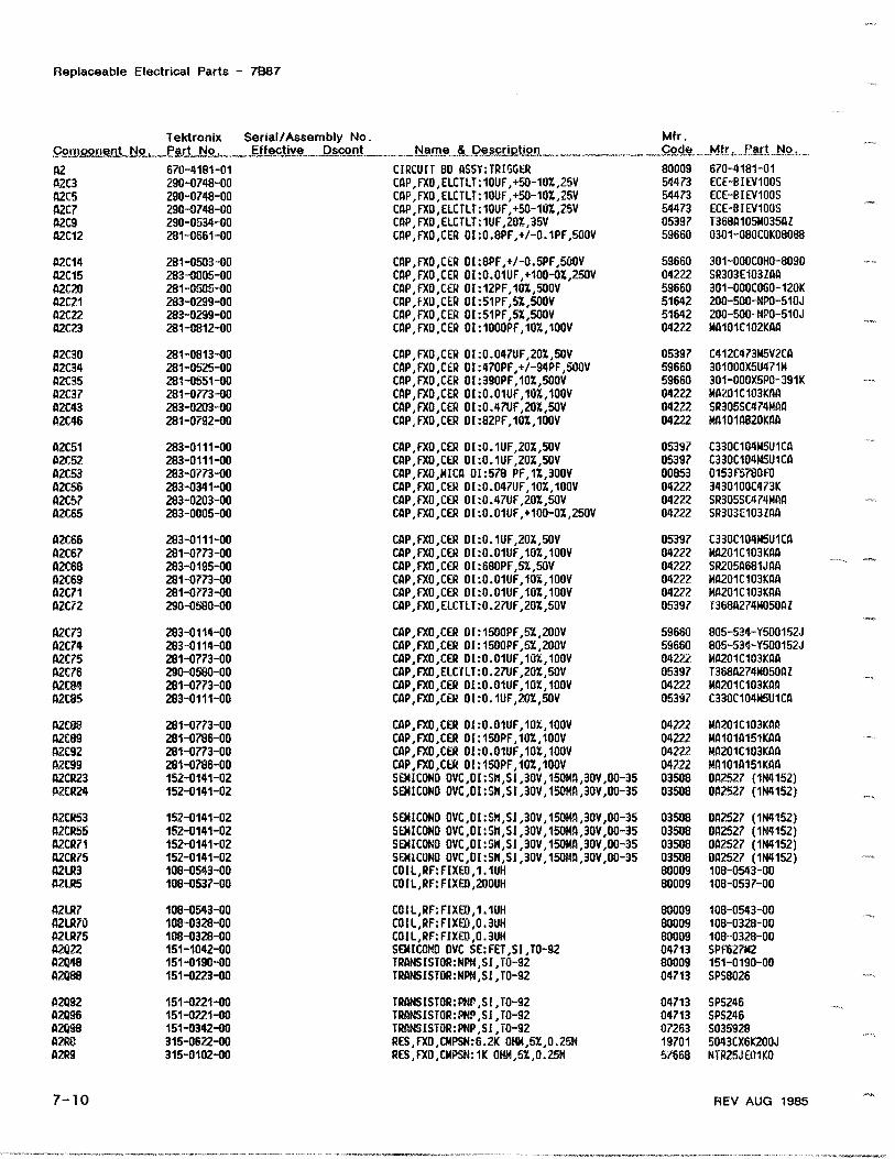
Replaceable Electrical Parts - 71387
7-10 REV AUG 1985
Comd ponent No .Tektronix Serial/Assembly No .
Dscont_ Part Effective_ _ Name,8,. Description__ ��Mfr .Code� _Mfr . _Part No .
A2 670-4181-01 CIRCUIT BO ASSY:TRISGER 80009 670-4181-01
A2C3 290-0748-00 CAP,FXO,ELCTL1 :10UF,+50-10%,25V 54473 ECE-BIEV100S
A2C5 290-0748-00 CAP,FXD,ELCTLT :10UF,+50-10%,25V 54473 ECE°°BIEV1OOS
A2C7 290-0748-00 CAP,FXD,ELCTLT :10UF,+50-10%,25V 54473 ECE-BIEVIOOS
AM 290-0534-00 CAP,FXD,ELCTLT :IUF,20%,35V 05397 T36BA105M035AZ
A2C12 281-0661-00 CAP,FXD,CER OI :0.8PF,+/-0.1PF,500V 59660 0301-08000K08088
42C14 281-0503°00 CAP,FXO,CER OI :BPF,+/-0.5PF,500V 59660 301-OOOCOHO-8090
42C15 283-0005-00 CAP,FXD,CER OI :0.01UF,+100-0%,250V 04222 SR303E103ZAA
A2C20 281-0505-00 CAP,FXO,CER OI :12PF,10%,500V 59660 301-OOOCOGO-120K
42C21 283-0299-00 CAP,FXD,CER 01 :51PF,5%,SDOV 51642 200-500-NPO-510J
92C22 283-0299-00 CAP,FXD,CER 01 :51PF,5%,500V 51642 200-500--NPO-510J
42023 281-0812-00 CAP,FXO,CER 01 :1000PF,10%,100V 04222 M9101C102KAA
A2C30 281-0813-00 CAP,FXD,CER DI :0.047UF,20%,50V 05397 C412C473M5V2CA
A2C34 281-0525-00 CAP,FXD,CER DI :470PF,+/-94PF,5OOV 59660 301000X5U471M
42035 281-0551-00 CAP,FXO,CER 01 :390PF,10%,500V 59660 301-00OX5PO-391K
A2C37 281-0773-00 CAP,FXD,CER OI :0.01UF,10%,100V 04222 MA201C103KAA
A2C43 283-0203°00 CAP,FXD,CER DI :0.47UF,20%,50V 04222 SR305SC474MAA
A2C46 281-0792-00 CAP,FXD,CER DI :82PF,10X,100V 04222 MAIOI4820KAA
A2C51 283-0111-00 CAP,FXD,CER DI :0.1UF,20%,50V 05397 C330C104M5UICA
42052 283-0111-00 CAP,FXD,CER 01 :0.1UF,20%,50V 05397 C330C1O4M5U1CAA2C53 283-0773-00 CAP,FXD,MIC4 01 :578 PF,1%,300V 00853 0153F5780FO42056 283-0341-00 CAP,FXD,CER DI :0.047UF,10%,100V 04222 34301000473KA2C57 283-0203-00 CAP,FXO,CER OI :0.47UF,20%,50V 04222 SR305SC474MAAA2C65 283-0005-00 CAP,FXD,CER DI :0.01UF,+100-OX,250V 04222 SR303E1031AA
42066 283-0111-00 CAP,FXD,CER DI :0.1UF,20%,50V 05397 C330C1O4M5U1CAA2C67 281-0773-00 CAP,FXO,CER DI :0.01UF,10%,100V 04222 M4201C103KAA92068 283-0195-00 CAP,FXO,CER OI :680PF,5X,50V 04222 SR2054681JAA
42069 281-0773-00 CAP,FXO,CER OI :0.01UF,10%,100V 0427..2 MA201C1O3K4AA2C71 281-0773-00 CAP,FXO,CER DI :0.01UF,10%,100V 04222 MA201C103KAA
A2C72 290-0580-00 CAP,FXO,ELCTLT :0.27UF,20%,50V 05397 T3689274MO50A1
02C73 283-0114-00 CAP,FXO,CER DI :1500PF,5%,200V 59660 805-534-Y500152J
A2C74 283-0114-00 CAP,FXD,CER DI :1500PF,5%,200V 59660 805-534-Y500152J
A2C75 281-0773-00 CAP,FXO,CER 01 :0.01UF,10%,100V 04222 M4201003011
02C76 290-0580-00 CAP,FXD,ELCTLT :0.27UF,20X,50V 05397 T3689274NO50OZ
A2C84 281-0773-00 CAP,FXD,CER OI :0.01UF,10%,100V 04222 MA201C103KAR
A2C85 283-0111-00 CAP,FXD,CER DI :0.1UF,20%,50V 05397 C330C104M5U1CA
92COO 281-0773-00 CAP,FXD,CER DI :0.01UF,10%,100V 04222 MA20IC103KAA
92C89 281-0786-00 CAP,FXD,CER OI :150PF,10%,100V 04222 M41010151KAAA2C92 281-0773-00 CAP,FXD,CER OI :0.01UF,10%,100V 04222 MA201C103KAA42C99 281-0786-00 CAP,FXD,CER OI :150PF,10%,100V 04222 MA101A151KAA92CR23 152-0141-02 SEMICONO OVC,DI :SN,SI,30V,150MA,30V,00-35 03508 002527 (1N4152)02CR24 152-0141-02 SEMICOND DVC,01 :SN,SI,30V,150MA,30V,00-35 03508 042527 (1N4152)
A2CR53 152-0141-02 SEMICOND DVC,D[ :S49,SI,30V,150MA,30V,00-35 03508 D42527 (1N4152)42CR55 152-0141-02 SEMICOND DVC,OI :SM,SI,30V,150MA,30V,00-35 03508 DA2527 (1N4152)92CR71 152-0141-02 SEMICOND DVC,01 :SN,SI,30V,150MA,30V,00-35 03508 042527 (1N4152)A2CR75 152-0141-02 SEMICONO DVC,01 :SM,SI,30V,150MA,30V,00-35 03508 042527 (1N4152)42LR3 108-0543-00 COIL,RF:FIXEU,1 .1UH 80009 108-0543-00A2LR5 108-0537-00 COIL,RF:FIXED,2000H 80009 108-0537-00
A2LR7 108-0543-00 COIL,RF:FIXED,1 .1UH 80009 108-0543-0042LR70 108°-0328-00 COIL,RF:FIXEIO,0 .3UH 80009 108-0328-0042LR75 108-0328-DO COIL,RF:FIXE0,0 .3UH 80009 108--328-0042422 151-1042-00 SEMICONO OVC SE:FET,SI,TO-92 04713 SPf627M202448 151-0190-00 TRANSISTOR:NPN,SI,TO-92 80009 151-0190-0002488 151-0223-00 TRANSISTOR:NPN,SI,TO-92 04713 SPS8026
42092 151-0221-00 TRANSISTOR:PNP,S1,TO-92 04713 SPS24602496 151-0221-00 TRANSISTOR:PNP,SI,TO-92 04713 SPS24602498 151-0342-00 TR4NSISTOR:PNP,SI,TO-92 07263 8035928A2RB 315-0622-00 RES,FXD,CMPSN :6 .2K OHM,5%,0 .25N 19701 5043CX6K200JA2R9 315-0102-00 RES,FXO,CNPSN :IK OHM,SX,0 .25H 57668 NTR25JEOIKO

Replaceable Electrical Parts - 71387
Component No, .Tektronix
- Part NoSerial/Assembly No .Effective ~-Dscont 88 i n- - NameDes-�cry
Mfr .
A2R12 315-0915-00 RES,FXD,CMPSN :9 .1M CHM,5X,0 .25H 01121 CB9155A2R13 317-0470-00 RES,FXD,CMPSN :47 OIAi,5%,0 .125H 01121 BB4705A2R14 315-0105-00 RES,FXD,CMPSN :IM OHM,5X,0 .25N 19701 5043CXIMDOGJA2R15 315-0824-00 RES,FXD,CMPSN :820K OHM,5%,0 .25N 19701 5043CX820KOJA2R16 315-0274-00 RES,FXD,CMPSN :270K OHM,5%,0.25H 57668 NTR25J-E270K42R19 315-0274-00 RES,FXD,CMPSN :270K OHM,5%,0.25H 576 NTR25J-E270K
A2R20 315-0103-00 RES,FXD,CMPSN :10K OHN,5%,0.25H 19701 5043CX10KOOJA2R21 315-0510-00 RES,FXD,CMPSN :51 OHM,5%,0.25M 19701 5043CX51RDOJA2R22 315-0272-00 RES,FXD,CNPSN :2.7K OHN,5%,0.25H 57668 NTR25J-E02K7A2R23 315-0751-DO RES,FXD,CMPSN :750 OHN,5%,0.25N 57668 NTR75J- EA2R29 315-0222-00 RES,FXD,CMPSN :2.2K OHM,5%,0.25H 57668 NTR25J-ED2K2A2R30 315-0104-00 RES,FXD,CMPSN :100K OHN,5%,0.25M 57668 NTR25J-E100K
A2R31 315-0202-00 RES,FXD,CMPSN :2K ,5%,0.25H 57668 NTR25J-E 2KA2R32 315-0510-00 RES,FXD,CMPSN :51 ONM,5X,0.25H 19701 5043CX51ROOJA2R33 315-0202-00 RES,FXD,CMPSN :2K OHM,5%,0.25M 57668 NTR25J-E 2KA2R34 315-0203-00 RES,FXD,CMPSN :20K OHM,5%,0.25H 57668 NTR25J-E 2OKA2R35 315-0203-00 RES,FXD,CMPSN :20K OHM,5%,0 .25M 57668 NTR25J-E 20KA2R36 315-0203-00 RES,FXD,CMPSN :20K 0194,5%,0 .25H 57668 NTR25J-E 2OK
A2R37 315-0560-00 RES,FXD,CMPSN :56 0194,5%,0 .25N 57668 NTR25J-E56EO02R38 317-0101-00 RES,FXD,CMPSN :100 OHM,5%,0 .125H 01121 BB1015A2R41 315-0102-00 RES,FXD,CMPSN :IK OHM,5%,0 .25H 57668 UTR25JEOIKOA2R42 315-0473-00 RES,FXD,CMPSN :47K 04N,5%,0 .25M 57668 NTR25J-E47KOA2R43 315-0752-00 RES,FXD,CMPSN :7.5K OIR4,5X,0 .25H 57668 NTR25J-EO7K5A2R44 315-0103-00 RES,FXD,CMPSN :10K DIg4,5X,0 .25H 19701 5043CXIOKOOJ
A2R45 315-0102-00 RES,FXD,CMPSN :1K OHM,5%,0.254 57668 NTR25JE01KOAM? 315-0101-00 RES,FXD,CMPSN :100 04 ,5%,0.25M 57668 NT -E 100EA2R48 315-0682-00 RES,FXD,CNPSN :6.8K OHM,5%,0 .25N 57668 NTR25J-EO6K8A2R49 311-1564-00 RES,VAR,NO JRMR,500 0491,0 .5N 32997 3352T-CKS°501A2R50 315-0133-00 RES,FXD,CHPSN :13K OHN,5%,0.25H 19701 5043CX13KOOJA2R51 321-0274-00 RES,FXD,FILM :6.98K OHM,1%,0.125N,TC=TO 19701 5043ED6K980F
A2R52 321-0431-00 RES,FXD,FILM :301K 0191,I%,0.125M,TC=TO 07716 CE4030102FA2R53 315-0124-00 RES,FXD,CMPSN :120K OHM,5%,0.25H 19701 5043CX120KOJ92R54 315-0622-00 RES,FXD,CMPSN :6 .2K OHM,5%,0.25N 19701 5043CX6K200JA2R55 315-0202-00 RES,FXD,CMPSN :2K OHM,5%,0 .25H 57668 NTR25J-E 2KA2R56 315-0104-00 RES,FXD,CMPSN :100K OHM,5%,0.25H 57668 NTR25J-E100KA2R57 315-0104-00 RES,FXD,CMPSN :100K OHM,5%,0.25M 57668 NTR25J-E100K
A2R58 321-0443-00 RES,FXD,FILM:402K OHM,1X,0 .125N,TC=TO 19701 5043ED402KOFA2R59 321-0443-00 RES,FXD,FILM:402K OHM,1X,0 .125N,TC=TO 19701 5043ED402KOFA2R61 315-0203-00 RES,FXD,CMPSN :20K OHM,5X,0 .25N 57668 N'IR25J-E 20KA2R62 315-0512-DO RES,FXD,CMPSN :5 .IK OHM,5%,0 .25H 57668 NTR25J-E05KIA2R63 315-0152-00 RES,FXD,CMPSN :1 .5K OHM,5X,0 .25H 57668 NTR25J-E01K5A2R64 315-0123-00 RES,FXD,CMPSN :12K OHM,5X,0.25N 57668 NTR25J-E12KO
AZR65 315-0511-00 RES,FXD,CMPSN :510 OHM,5X,0.25N 19701 5043CX510ROJA2R67 323-0155-00 RES,FXD,FILM:402 OHM,1X,0.5N,TC=TO 75042 CECTO-402OFA2R6O 315-0162-00 RES,FXD,CMPSN :1 .6K OHM,5X,0 .25M 19701 5043CXIK600JA2R69 315-0820-00 RES,FXD,CNPSN :82 OHN,5%,0.25H 57668 NTR25J-E82E0A2R72 315-0205-00 RES,FXD,CMPSN :2M OHM,5%,0.25M 01121 CB205.SA2R73 315-0514-00 RES,FXD,CMPSN :510K OHM,5%,0.25H 19701 5043CX510KOJ
A2R74 315-0514-00 RES,FXD,CMPSN :510K OHN,5%,0.25H 19701 5043CX510KOJA2R76 315-0205-00 RES,FXD,CMPSN :2M OHM,5X,0.25M 01121 082055A2R80 311-1228-00 RES,VAR,NO :TRNR,IOK OHM,0.5N 32997 3386F-TO4-103A2R83 315-0470-00 RES,FXD,CMPSN :47 OHM,5%,0 .25N 57668 NTR25J-E47EOA2R84 315-0680-00 RES,FXD,CMPSN :68 OHN,5%,0 .25H 57668 NTR25J-E68EOA2R85 311-1594-00 RES,VAR,NO :TRNR,10 OHM,0.5H 32997 3352T-1-100
A2R86 315-0470-00 RES,FXD,CMPSN :47 OHH,5%,0 .25M 57668 NT -E47EOA2R89 315--0103-00 RES,FXD,CMPSN :10K OM,5%,0 .25H 19701 5043CXIOKOOJA2R90 315-0102-00 RES,FXD,CNPSN :1K OHM,5%,0 .25H 57668 NTR25JE01KOA2R91 315-0470-00 RES,FXD,CMPSN :47 OHM,5%,0 .25H 57668 NTR25J-E47EOA2R92 315-0102-00 RES,FXD,CMPSN :IK OHM,5%,0 .25N 57668 NTR25JE01KO
REV AUG 1985 T-11

Replaceable Electrical Parts - 71381
CoTektronix Serial/Assembly No .
vent_ Nos Part No . �- Etfective ,Dscon Name 8 . Description_Mfr,Code . _Mfrs_Part _No ._ ,_
A2R93 321-0260-00 RES,FXO,FILM :4.99K OHM,1%,0.125W,TC=TO 19701 5033EO4K990FA2R94 321-0202-00 RES,FXD,FILM :1 .24K OHM,1%,0.125W,TC=TO 24546 N45501241FA2R95 315-0470-00 RES,FXD,CMPSN:47 OHM,5%,0 .25W 57668 NTR25J-E47EOA2R96 315-0470-00 RES,FXO,CMPSN:47 OHM,5%,0 .25W 57668 N'IR25J-E47EOA2R97 315-0221-00 RES,FXO,CMPSN:22O OHM,5%,0 .25W 57668 NTR25J-F220EAn10 263-0010-01 SWITCH P8 ASSY:1 PUSH,7 .5 MM,1 CONTACT 80009 263-0010-01
A2S20 263-0016-00 SWITCH f4; ASSY:4 LATCHING,7.5 MM,5 CONTACT 80009 263-0016-00SAFETY CONTROLLED
A2S50 263-0015-00 SWITCH P® ASSY:3 LATCHING,7.5 MM 80009 263-0015-00A2U35 156-0067-02 MICROCKT,LINEAR :OPNL AMPL,SELECTE0 02735 85147421155 156-0158-00 MICROCKT,LINF-QR :OUAL OPNL AMPL 04713 MC1458P1/MC1458U421165 155-0126-00 MICROCKT,LINEAR :TRIGGER AMPLIFIER 80009 155-0126-00
921175 156-0158-00 MICROCKT,LINFAR :OUAL OPNL AMPL 04713 MC1458P1/MC1458UA2U85 155-0109-01 MICROCKT,LINEAR :MONOLITHIC TRIG 80009 155-0109-01
7-12 REV AUG 1985

Replaceable Electrical Parts - 713187
REV AUG 1985
7-13
Com onent_,NoTektronix Serial/Assembly No .
. _Part,No. ._,- Effective Dscont -_Name&_"iestionMfr .
Mfr Pa NoA3 670-4183-00 CIRCUIT BO ASSY :READOUT 9 670-4183-00A3CR725 152-0141-02 SENIC DVC,DI :SN,SI,30V,150NA,30V,00-35 03508 DA2527 (1N4152)A3CR751 152-0141-02 SENICOND DVC,DI :SM,SI,30V,150NA,30V,D0-35 03508 DA2527 (1N4152)A3CR752 152-0141-02 SEMICOND DVC,DI :SN,SI,30V,150NA,30V,DO-35 03508 DA2527 (1N4152)43CR753 152-0141-02 SENICOND DVC,DI:SN,SI,30V,150NA,30V,DO-35 03508 DA2527 (1N4152)A3CR754 152-0141-02 SENICOND DVC,DI :SN,SI,30V,150NA,30V,00-35 03508 042527 (1N4152)
A3CR763 152-0141-02 SENICOND DVC,DI :SN,SI,30V,1 ,30V,DO-35 03508 DA2527 (1N4152)A3CR772 152-0141-02 SENICOND DVC,DI :SH,SI,30V,150NA,30V,D0-35 03508 DA2527 (1N4152)A3CR773 152-0141-02 SEMICOND DVC,DI :SN,SI,30V,150NA,30V,DO-35 03508 002527 (1M4152)A3CR782 152-0141-02 SEMICOND DVC,DI :SN,SI,30V,150MA,30V,DO-35 03508 DA2527 (1N415a2)A3CR783 152-0141-02 SENICOND DVC,DI :SN,SI,30V,150MA,30V,00-35 03508 DA2527 (1N4152)A3CR785 152-0141-02 SFMICOND DVC,D1 :SN,SI,30V,150NA,30V,DO-35 03508 DA2527 (1N4152)
A3CR786 152-0141-02 SENICOND DVC,D1 :SN,S1,30V,150NA,30V,DO-35 03508 DA2527 (1N4152)A3R751 315-0154-00 RES,FXD,CMPSN :150K O141,5%,0 .25H 57668 NTR25J-E150KA3R752 315-0154-00 RES,FXD,CNPSN :150K O191,5%,0 .25N 57668 NTR25J-E150KA3R753 315-0154-00 RES,FXD,CNPSN :150K OM,5%,0 .25H 57668 NTR25J-E150KA3R754 315-0154-00 RES,FXD,CNPSN :150K OHN,5%,0 .25N 5`1668 NTR25J-E150KA3R755 321-0344-00 RES,FXD,FILN:37.4K CM,1X,0 .125N,TC=TO 19701 5033ED 37K40F
A3R756 315-0753-00 RES,FXO,CNPSN :75K OHN,5%,0.25H 57668 NTR25J-E75KOA3R757 321-0327-00 RES,FXD,FILN:24.9K OHN,1%,0.125M,TC=TO 07716 CEAD24901FA3R761 315-0154-00 RES,FXD,CNPSN :150K OHN,5%,0 .25H 57668 NTR25J-EI50KA3R762 315-0154-00 RES,FXD,CNPSN :150K OHN,5%,0.25H 57668 NTR25J-E150KA3R763 315-0133-00 RES,FXD,CNPSN :13K OHM,5%,0.25M 19701 5043CX13KOOJA3R764 315-0133-00 RES,FXD,CMPSN :13K 0146,5X,0 .25H 19701 5043CX13KOOJ
A3R771 315-0753-00 RES,FXD,CNPSN :75K O101,5%,0 .25H 57668 NTR25J-E75KOA3R772 321-0356-00 RES,FXD,FILN :49 .9K OHN,1%,0.125N,TC=TO 19701 5033ED49K90FA3R773 315-0154-00 RES,FXD,CNPSN :150K OHN,5X,0.25H 57668 NTR25J-E150KA3R779 315-0151-00 RES,FXD,CMPSN :150 OHN,5%,0 .25M 57668 NTR25J-E150EA3R781 315-0154-00 RES,FXD,CMPSN :150K ONN,5X,0.25H 57668 NTR25J-E150KA3R782 315-0753-00 RES,FXD,CNPSN :75K 0161,5X,0 .25N 57668 NT -E75KO
A3R783 315-0154-00 RES,FXD,CNPSN :150K OPM,5%,0.25H 57668 NTR25J-E150KA3R784 32.1-0356-00 RES,FXD,FILN:49.9K ONM,1%,0 .125N,TC=TO 19701 5033ED49K90FA3R785 315-0154-00 RES,FXD,CNPSN :150K OlfN,5X,0 .25H 57668 NTR25J-E15OKA3R786 315-0753-00 RES,FXD,CNPSN :75K OHM,5X,0.25N 57668 NTR25J-E75KOA3R787 321-0356-00 RES,FXD,FILN :49.9K OHN,1X,0.125N,TC=TO 19701 5033ED49K90FA3R791 321-0344-00 RES,FXD,FILN :37.4K OHN,1%,0.125H,TC=T0 19701 5033ED 37K40F
A3Rl92 315-0154-00 RES,FXD,CNPSN :150K OHN,5X,0.25N 57668 NTR25J-E150KA3R793 321-0344-00 RES,FXD,FILN:37.4K 0101,1%,0 .125N,TC=TO 19701 5033ET1 37K40FA3R794 315-0154-00 RES,FXD,CNPSN :150K OHN,5X,0.25H 57668 NTR25J-E150K

Replaceable Electrical Parts - 7E387
7-14 REV AUG 1985
Component No .TektronixPart No . _
Serial/AssemblyEffective
No._Dscont .,_ Name 8 Description
Mfr .Code -- Mfr . Part _No ._
44 670-6184-00 6010100 8023314 CIRCUIT 00 ASSY:CLOCK 80009 670-6184-00A4 670-6184-01 6023315 CIRCUIT 80 ASSY:CLOCK 80009 670-6184-01A4C535 281-0775-00 CAP,FXO,CER OI :0.1UF,20X,50V 04222 MA205EI04MAAA4C536 283-0211-00 CAP,FXO,CER DI :O.IUF,10%,200V 042.22 SR406C104KA4A4C540 281-0775-00 CAP,FXO,CER OI :0.1UF,20X,50V 04222 MA205EI04MOA44C541 281-0775-00 CAP,FXO,CER 01 :0.1UF,20%,50V 04222 MA205E10044
A4C547 285-0809-00 CAP,FXO,PLASTIC :IUF,10%,50V 56289 LP66AIA105KA4C552 281-0762-00 8010100 8023314 CAP,FXO,CER 01 :27PF,20%,100V 04222 M41019270MA9A4C556 281-0775-00 CAP,FXO,CER OI :0 .1UF,20X,50V 04222 MA205E104MAA94C559 281-0773-00 C4P,FXD,CER 01 :0 .01UF,10%,100V 04222 MA201003KA494C583 283-0691-00 CAP,FXO,MICA 01:650PF,1X,300V 00853 0153F651FOA4C622 281-0775-00 CAP,FXO,CER OI :0 .1UF,20X,50V 04222 M9205E10099
94C625 281-0775-00 8010121 C4P,FXO,CER OI :0 .1UF,20X,50V 04222 MA205E1041,19944C626 281-0811-00 8010100 8010120 CAP,FXO,CER 01 :10PF,10%,100V 04222 MA1019100KOA44C627 281-0762-00 8010100 6010120 CAP,FXO,CER 01 :27PF,20%,100V 04222 M910111270MAAA4C631 290-0748-00 CAP,FXD,ELCTLT :IOUF,+50-10%,25V 54473 ECE-BIEV100SA4C632 281-0775-00 CAP,FXO,CER OI :0.1UF,20X,50V 04722 M9205EI04HAA44C633 290-0748-00 CAP,FXD,ELCTLT :10UF,+50-10%,25V 54473 ECE-BIEVIOOS
A4C634 290-0748-00 CAP,FXD,ELCTLT :10UF,+50-10%,25V 54473 ECE-BIEV100SA4C641 281-0770-DO CAP,FXO,CER OI :1000PF,20%,100V 04222 MAIOIC102MAA44C642 281-0775-00 CAP,FXO,CER OI :0 .1UF,20X,50V 04222 M4205EI04MAA44C643 281-0775-00 CAP,FXO,CER OI :0 .1UF,20X,50V 042,22 MA20SE104HAA94C655 281-0775-00 CAP,FXO,CER 01 :0 .1UF,20%,50V 04222 M4205E104MA904C660 281-0775-00 CAP,FXD,CER 01 :0 .1UF,20%,50V 04222 MA205E1O4MAA
114C661 281-0775-00 C4P,FXO,CER 01 :0 .1UF,20%,50V 04222 MA205EI04MAAA4C663 281-0775-00 CAP,FXO,CER OI :0.1UF,20X,50V 0427. .2 MA205E104MAA44C668 281-0775-00 C4P,FXO,CER 01 :0.1UF,20%,50V 04222 MA205E104MAAA4CR544 152-0141-02 SEMICOND DVC,01 :SN,SI,30V,150M4,30V,00-35 03508 092527 (1N4152)44CR547 152-0141-02 SE?IICOND OVC,DI :SW,SI,30V,150MA,30V,00-35 03508 DA2527 (1N4152)A4CR552 152-0141-02 SEHICONO OVC,01 :SH,SI,30V,150MA,30V,00-35 03508 092527 (1N4152)
44CR554 152-0141-02 SEMICOND DVC,01 :SH,SI,30V,150MA,30V,00-35 03508 0112527 (1N4152)44CR555 152-0141-02 SE}IICONO OVC,01 :SN,SI,30V,150MA,30V,00-35 03508 042527 (1N4152)44CR640 152-0141-02 SEMICONO DVC,01 :SH,SI,30V,150MA,30V,00-35 03508 042527 (1N4152)44CR641 152-0141-02 SEMICQNO DVC,01 :SM,SI,30V,150MA,30V,00-35 03508 042527 (1N4152)A4CR677 152-0141-02 SEMICOND DVC,DI :SH,SI,30V,150MA,30V,00-35 03508 DA2527 (1N4152)94CR678 152-0141-02 SEMICONO DVC,01 :SN,SI,30V,150MA,30V,00-35 03508 092527 (1N4152)
MCR679 152-0141-02 SEMICOND DVC,DI :SN,SI,30V,150MA,30V,00-35 03508 002527 (1N4152)A4CR680 152-0141-02 SEMICOND DVC,DI :SH,SI,30V,150MA,30V,00-35 03508 OA2527 (1N4152)44CR691 152-0322-00 SEMICONO OVC,DI :SCHOTTKY BARRIER,SI,15V 21847 92X60094CR695 152-0141-02 SEMICOND DVC,01 :SH,SI,30V,150MA,30V,00-35 03508 092527 (1N4152)1141-631 108-0543-00 COIL,RF:FIXED,1 .1UH 80009 108-0543-00941-632 108-0537-00 COIL,RF:FIXED,2000H 80009 108-0537-00
94L634 108-0543-00 COIL,RF:FIXE9,1 .1UH 80009 108-0543-00A4LR626 108-0797-00 6010121 COIL,RF:FIXED,2.45UH 80009 108-0797-00940531 151-0410-00 TRANSISTOR:PNP,S1,TO-92 04713 SPS6765A40545 151-0410-00 TRANSISTOR:PNP,S1,TO-92 04713 SPS6765440552 151-0301-00 TRANSISTOR:PNP,S1,TO-18 04713 ST898A4Q607 151-0190-00 TRANSISTOR:NPN,SI,TO-92 80009 151-0190-00
440642 151-1042-00 SEMICONO OVC SE:FET,S1,TO-92 04713 SPF62792440643 ___-- -°~-- (PART OF 0642)940663 151-0192-00 TR4NSISTOR :SELECTED 04713 SPS8801A4Q667 151-0192-00 TRANSISTOR :SELECTED 04713 SPS8801940671 151-0192-00 TRANSISTOR :SELECTED 04713 SPS8801440678 151-0192-00 TRANSISTOR :SELECTED 04713 SPS8801
440680 151-0192-00 TRANSISTOR:SELECTEO 04713 SPS8801440681 151-0192-00 TRANSISTOR:SELECTED 04713 SPS8801A4Q687 151-0168-00 TRANSISTOR:PNP,SI,TO-92 80009 151-0188-00440691 151-0192-00 TRANSISTOMELECTED 04713 SPS8801940695 151-0192-00 TRANSISTOMELECTED 04713 SPS8801

REV AUG 1985
Replaceable Electrical Parts - 71387
7-15
ComponentTektronix
No�;_. Part _NoSerial/AssemblyEffective
No .,_ Dscont _, _.� Name& Description
Mfr .Code_ Mfr. ,�Part No. .
A4R523 315-0101-00 RES,FXD,CMPSN :100 OHM,57,0 .25H 57668 NTR25J-E 100EA4R529 315-0102-00 RES,FXD,CMPSN :1K OHM,5%,0.25H 57668 NTR25JE01KOWHO 311-1560-00 RES,VAR,NONNN :TRMR,5K OHM,0.5N 32997 3352T-1-502A4R531 321-0340-00 RES,FXD,FIL14 :34 .OK OHM,17,0.125N,TC=TO 19701 5043ED34KOOFA4R532 315°-0511-00 RES,FXD,CMPSN :510 OHM,5X,0 .25M 19701 5043CX510ROJA4R533 315-0512-00 RES,FXD,CMPSN :5 .1K OHM,5%,0.25H 57668 NTR25J-EO5K1
A4R536 315-0101-00 RES,FXD,CMPSN :100 OHM,57,0 .25H 57668 NTR25J-E 100EA4R537 321-0360-00 RES,FXD,FILM:54.9K OHM,17,0 .125N,TC=TO 19701 5033EO54K90FA4R538 311-1336-00 RES,VAR,NO :TRMR,100K OHM,0 .5H 02111 43P104T67244R539 321-0995-00 RES,FXD,FILM:549K OHM,17,0.125N,TC=TO 24546 N45505493FA4R540 315-0100-00 RES,FXD,CMPSN :10 OHM,54,0.25H 19701 5043CXIORROOJA4R541 315-0100-00 RES,FXD,CMPSN :10 OHM,5%,0.25H 19701 5043CXIORROOJ
A4R544 321-0820-06 RES,FXD,FILM :42K OHM,0 .257,0.125H,TC=T9 19701 5033RE42K000A4R545 321-0259-00 RES,FXD,FILM:4.87K OHM,17,0 .125N,TC=TO 07716 CE404870OFA4R546 321-0289-00 RES,FXD,FILM:10.OK OHM,17,0 .125N,TC=TO 19701 5033ED10KOFA4R547 321-0289-00 RES,FXD,FILM:10.OK OHM,17,0 .125N,TC=TO 19701 5033EDIOKOFA4R548 315-0513-00 RES,FXD,CMPSN :51K OHM,57,0.25H 57668 NTR25J-E51KO110549 315-0101-00 RES,FXD,CMPSN :100 OHM,5%,0.25H 57668 NTR25J-E 100E
A4R550 311-1230-00 RES,VAR,NO :TRMR,20K OHH,0.5N 32997 3386F-TO4-203A4R551 315-0104-00 8010100 8023314 RES,FXO,CMPSN :100K OHM,5%,0.25H 57668 NTR25J-E100KA4R551 315-0823-00 8023315 RES,FXD,CHPSN :82K OHM,57,0.25H 57668 NTR25J-E82KA4R552 315-0182-00 RES,FXD,CMPSN :1 .8K OHM,5%,0 .25H 57668 NTR25J-ElK8A4R553 315-0391-00 RES,FXD,CMPSN :390 OHM,57,0 .25H 57668 NTR25J-E390EA4R554 315-0392-00 RES,FXD,CNPSN :3 .9K OHM,57,0 .25H 57668 NTR25J-EO3K9
A4R555 315-0222-00 RES,FXD,CMPSN :2.2K OHM,57,0 .25H 57668 NTR25J-EO2K2A4R556 315-0563-00 RES,FXD,CMPSN :56K OHM,57,0.25H 19701 5043CX56KOOJA4R557 315-0103-00 RES,FXO,CMPSN :10K OHM,5%,0.25H 19701 5043CXIOKOOJ94R558 315-0331-00 RES,FXD,CMPSN :330 OHM,57,0.25H 57668 NTR25J-E330EA4R559 321-1651-04 RES,FXD,FILM:37 .5K OHM,0 .17,0.125N,TC=T2 91637 MFF1816037501BA4R581 315-0202-00 RES,FXO,CMPSN :2K OHM,57,0 .25H 57668 NTR25J-E 2K
A4R582 315-0332-00 RES,FXD,CMPSN :3 .3K OHM,57,0 .25H 57668 NTR25J-E03K3A4R591 315-0101-00 RES,FXD,CMPSN :100 OHM,5%,0 .25H 57668 NTR25J-E 100EA4R606 307-0542-00 RES NTNK,FXD,FI :(5)10K OHM,57,0 .125H 01121 1064103OR706AI03A4R607 315-0103-00 RES,FXD,CMPSN :10K OHM,5%,0.25H 19701 5043CXIOKOOJA4R608 315-0512-00 RES,FXD,CMPSN :5.1K OHM,5%,0.25H 57668 NTR25J-EO5K1A4R611 315-0102-00 RES,FXD,CMPSN :1K OHM,57,0.25H 57668 NTR25JEOIKO
A4R621 315-0473-00 RES,FXD,CMPSN :47K OHM,5X,0 .25H 57668 NTR25J-E47KOA4R622 315-0203-00 RES,FXD,CMPSN :20K OHM,5%,0 .25H 57668 NTR25J-E 20KA4R623 315-0473-00 RES,FXD,CMPSN :47K OHM,5%,0 .25H 57668 NTR25J-E47KOA4R624 315-0203-00 RES,FXD,CMPSN :20K OHM,57,0 .25H 57668 NTR25J-E 20KA4R626 315-0751-00 RES,FXD,CNPSN :750 OHM,5%,0 .25H 57668 NTR25J-E750EA4R627 315-0751-00 RES,FXD,CMPSN :750 OHM,5%,0 .25H 57668 NTR25J-E750E
A4R640 315-0104-00 RES,FXD,CMPSN :100K OHM,57,0.25H 57668 NTR25J-E100KA4R641 315-0104-00 RES,FXD,CMPSN :100K OHM,5%,0.25H 57668 NTR25J-E100KA4R642 315-0100-00 RES,FXD,CMPSN :10 OHM,57,0 .25H 19701 5043CX10RROOJA4R643 315-0100-00 RES,FXD,CMPSN :10 OHM,57,0 .25N 19701 5043CXIORROOJA4R644 315-0103-00 RES,FXD,CMPSN :10K OHM,57,0 .25N 19701 5043CXIOKOOJA4R645 315-0154-00 RES,FXD,CMPSN :150K OHM,5%,0 .25H 57668 NTR25J-E150K
A4R646 315-0103-00 RES,FXD,CMPSN :10K OHM,5%,0.25H 19701 5043CX10KOOJA4R647 315-0753-00 RES,FXD,CMPSN :75K OHM,57,0.25H 57668 NTR25J-E75KOA4R648A4R649
315-0820-00 RES,FXD,CMPSN :82 OHM,57,0.25H 57668 NTR25J-E82E0
A4R660315-0201-00 RES,FXD,CMPSN :200 OHM,57,0.25N 57668 NTR25J-E200E
44R663315-0471-00 RES,FXD,CMPSN :470 OHM,5%,0 .25H 57668 NTR25J-E470E315-0510-00 RES,FXD,CMPSN :51 OHM,5%,0 .25H 19701 5043CX51ROOJ
A4R664 321-0169-00 RES,FXD,FILM:562 OHM,17,0 .125N,TC=TO 07716 CEAD562ROF14R667 321-0239-00 RES,FXD,FILM:3.01K OHM,17,0 .125N,TC=TO 19701 5043ED3KO10FA4R668A4R669
321-0237-00 RES,FXD,FILM:2.87K OHM,17,0 .125N,TC=TO 07716 CEAD 2870OF
44R671321-0218-00 RES,FXD,FILM:1 .82K OHM,17,0.125N,TC=TO 19701 5033FD1K82F315-0510-00 RES,FXD,CMPSN :51 OHM,5%,0 .2514 19701 5043CX51ROOJ

Replaceable Electrical Parts - 7Ei87
7- 1 6
REV AUG 1985
Tektronix Serial/Assembly No . Mfr .Component Nq -. Part No .a ffective ,Dscont m __ a ____�,_Name 8 Description-, Code Mfr. Part No .
40672 301-0102-00 RES,FXO,CMPSN:IK OHM,5X,0 .50H 01121 E3B1025
40673 315-0510-00 RES,FXD,CMPSN:51 OHM,SX,0 .25N 19701 5043CX51ROOJ
A4R677 315-0102-00 RES,FXD,CMPSN:IK OHM,5%,0 .25H 57668 NTR25JEOIKO40678 315-0202-00 RES,FXD,CMPSN:2K OHM,S%,0 .25N 57668 NTR25J-E 2K
A4R680 315-0103-00 RES,FXD,CMPSN:10K OHM,5%,0 .25H 19701 5043CXIOKOOJA4R681 315-0153°-00 RES,FXO,CMPSN:15K OHM,5%,0 .25N 19701 5043CX15KOOJ
A4R682 315-0302-00 RES,FXD,CMPSN:3K OHM,5%,0 .25H 57668 NTR25J-E03KOA4R683 315-0302-00 RES,FXO,CNPSN:3K OHM,5X,0 .25M 57668 NTR25J-E03KOA4R684 315-0102-00 RES,FXO,CMPSN:IK OHN,SX,0 .25H 57668 NTR25JEOIKOA4R687 315-0162-00 RES,FXO,CMPSN:1 .6K OHN,5%,0.25h 19701 5043CX1K6OOJ
1106 315-0203-00 RES,FXO,CNPSN:20K OHM,5%,0 .25H 57668 NTR25J-E 20KA4R689 315-0154-00 RES,FXO,CMPSN:150K OHM,5%,0 .25H 57668 NTR25J-E150K
A4R692 315-0104-00 RES,FXO,CMPSN:100K OHM,S%,0 .25H 57668 NTR25J-E100KA4R694 315-0102-00 RES,FXO,CMPSN:IK OHM,5X,0.25N 57668 NTR25JE01KOA4R695 315-0103-00 RES,FXD,CMPSN:10K OHM,S%,0 .25N 19701 5043CXIOKOOJ94S645 263-0015-02 SNITCH P8 ASSY:3 LCH,7.5MM,6 CONTACTS 80009 263-0015-02A4U535 156-0158--00 MICROCKT,LINEAR:DUAL OPNL AMPL 04713 MC1458P1/MC1458U40545 156-1149-01 MICROCKT,LINF.nR:OPERATION AMP JFET INPUT 27014 AL160307
44U547 156-0105-02 8010100 8023314 MICROCKT,LINEAR:OPNL AMPL,SELECTEO 01295 LM301AJ64
A4U547 156-1149-01 8023315 MICROCKT,LINEAR:OPL72ATION AMP JFET INPUT 27014 AL160307
A4U556 156-°0382-02 MICROCKT,OGTL:QUAO 2 INP NANO GATE BURN 18324 N74LSOOND
94US90 155-0185-00 MICROCKT,INTFC :ML 4 OECAOE OGTL VOLTMETER 80009 155-0185-00
A4U621 156-0180-04 MICROCKT,OGTL:QUAO 2 INP NANO GATE, 18324 N74S00(NB OR FO)A4U622 156-0382-02 MICROCKT,OGTL:QUAD 2 INP NANO GATE BURN 18324 N74LSOONB
A4U623 156-0721-02 MICROCKT,OGTL:QUAD ST 2-INP NANO GATES,SCRN 01295 SN74LS132NP3
A4U635 156-0646-02 MICROCKT,OGTL:4°BIT BINARY CNTR,SCRN 04713 SN74LS93NDSA4U636 156-0656-02 MICROCKT,OGTL:OECAOE COUNTER,SCRN 01295 SN74L590NP3
A4U637 156-0994-00 NICROCKT,OGTL:8 INPUT OATH SEUMUX 04713 74LS151(N OR J)A4U638 156-0994-00 NICROCKT,OGTL:8 INPUT OATA SEUMUX 04713 74LS151(N OR J)A4U651 156-0910-02 MICROCKT,OGTL:OUAL DECADE COUNTER,SCRN 01295 SN74LS390N3
A4U652 156-0910-02 MICROCKT,OGTL:OUAL DECADE COUNTER,SCRN 01295 SN74LS390N3A4U653 156-0910-02 MICROCKT,OGTL:OUAL OECAOE COUNTER,SCRN 01295 SN74LS390N3
A4U654 156-°0910-02 MICROCKT,OGTL:OUAL OECAOE COUNTER,SCRN 01295 SN74LS390N3A4U655 156-0994-00 MICROCKT,OGTL:8 INPUT OATA SEUMUX 04713 74LS151(N OR J)
A4U660 156-0299-02 MICROCKT,DGTL:TTL,16°BIT DATA SELECTOR 18324 N74150(NB OR F8)
A4YR552 152-0217-00 SENICONO OVC,DI :ZEN,SI,8 .2V,5'X,0 .4N,00-7 04713 SZG20
4414627 131-0566-00 8010121 BUS,CON0 :OUMMY RES,0 .094 00 X 0 .225 L 24546 OMA 07A4Y626 158-0203-00 XTAL UNIT,QTZ :20.48MH1,0 .01%,SERIES 14301 X#1943

Replaceable Electrical Parts - 78187
REV AUG 1985
7- 1 7
ComeonentTektronix Serial/Assembly No .
No-Part,No. Effective Dscont Name&Descr,DescriptionMfr .Code Mfr PmtNo._-
C211 283-0672-00 CAP,FXO,MICA D1 :200PF,1%,500V 00853 D155F2010FO0215 290-0523-00 CAP,FXD,ELCTLT :2 .2UF,20%,20V 05397 T3684225MO20ASC330 281-0166-00 CAP,V4R,AIR 01 :1.9-15.7 PF,250V 74970 187-0109-0550331 283-0633-00 CAP,FXO,MICA D1 :77PF,1%,100V 00853 D155E770FOC332 295-0172-00 CAP SET,MATCHED:O .1UF,10UF,898PF,MATCHED 80009 295-0172-00C334 295-0172-00 CAP SET,MATCHED:0 .1UF,10UF,898PF,MATCHED 80009 295-0172-00
C336 ----- ------ (PART OF C332)
US2220 150-1029-00 LT EMITTING D10:GREEN, ,35MA 58361 06480/MV5274CUS232 150-1033-00 LT EMITTING DIO : ER, ,40MA MAX 50434 HLMP 1401
DS810 150-0048-01 LAMP,INCAND:5V,0.O6A,4683,AGEO 8 SEL 54 683AS1505820 150-0048-01 LAMP,INCANO:5V,0.06A,"683,AGEO 8 SEL 54 683AS15
J2 131-1315-01 COW,RCPT,ELEC:BNC,FEMALE 80009 131-1315-01
J640 131-1315-01 CONN,RCPT,ELEC :BNC,F LE 80009 131-1315-01L326 108-0271-00 COIL,RF:FIXEO,235NH 80009 108-0271-00
0732 151-0410-00 TRANSISTOR:PNP,S1,TO-92 04713 SPS6765R60 311-1192-00 RES,VAR,NO :PNL,10K 01 ,1M,M/SM 12697 381-CM39695
R210 311-0467-00 RES,VAR, :PNL,100K OHM,0 .5M 01121 11177058R330 315-0330-00 RES,FXD,CMPSN :33 0161,5X,0.251 19701 5043CX33RDDJ
8331 315-0330-00 RES,FXD,CMPSN :33 OIR4,5%,0.251 19701 5043CX33RDDJR332 315-0560-00 RES,FXD,CMPSN :56 OHM,5X,0.25M 57668 NTR25J-E56EOR410 311-1781-00 RES,VAR,N :PNL,10K OHN,10%,0 .5N 12697 388CM40913R534 321-0193-00 RES,FXD,FILM :IK OHM,I%,0.125M,TC=TO 19701 5033®1KOOFR535 311-1889-00 RES,VAR,MM:PNL,50K OHM,2M 32997 3541S-458-5038705 311-0467-00 RES,VAR,NO :PNL,100K OHM,0.5M 01121 N7705B
R725 311-1590-00 RES,VAR,NO :PNL,10K 0191,1M,COMPOSITION 12697 CM40256R732 315-0104-00 RES,FXD,CMPSN :100K OHN,5%,0.25M 57668 NTR25J-E100KS60 ----- (PART OF R60)5230 263-0016-01 SMITCH PB ASSY :3 LCH & 1 CANC,7 . ,5 CONT 80009 263-0016-01S725 214-1136-00 ACTUATOR,51. SM :VARIABLE CAL 80009 214-1136-005800 263-1181-00 SM CAN ACTR AS :TIME/CM 80009 263-1181-00

Symbols and Reference Designators
Electrical components shown on the diagrams are in the following units unless noted otherwise :
Capacitors =
Resistors =Graphic symbols and class designation letters are based on ANSI Standard Y32.2-1975 .
Logic symbology is based on ANSI Y32 .14-1973 in terms of positive logic . Logic symbols depict the logicfunction performed and may differ from the manufacturer's data .The overline on a signal name indicates that the signal performs its intended function when it goes to theAbbreviations are based on ANSI Y1 .1-1972 .Other ANSI standards that are used in the preparation of diagrams by Tektronix, Inc . are :
Y14 .15, 1966Y14 .2, 1973Y10.5, 1968
Drafting Practices .Line Conventions and Lettering .Letter Symbols for Quantities Used inElectrical Engineering .
The following prefix letters are used as reference designators to identify components or
The following special symbols may appear on the diagrams :
Strap or Link �,~*�
Cam SwitchClosure Chart(Dot indicatesswitch closure)
Values one or greater are in picofarads (pF) .Values less than one are in microfarads (pF) .Ohms (S2) .
Electrical Science and
VERTICAL_ AMPLIFIER
low state .
assemblies on the diagrams .
Plug to E.C . Board
CB- x] Identifies PanelControls, Connectors and�.<Indicators
Modified Component(Depicted in Greys, or withGrey Outline)-see PartsListPlug Index
J l4 Coaxial Connector,
�� Decoupled or FilteredVoltage
Etched Circuit BoardOutlined in Black
A Assembly, separable or repairable H Heat dissipating device (heat sink, S Switch or contactor(circuit board, etc) heat radiator, etc) T Transformer
AT Attenuator. fixed or variable HR Heater TC ThermocoupleB Motor HY Hybrid circuit TP Test pointBT Battery Connector, stationary portion u Assembly, inseparable or non-repairableC Capacitor, fixed or variable I( Relay (integrated circuit, etc .)CB Circuit breaker L Inductor, fixed or variable V Electron tubeCR Diode, signal or rectifier M Meter VR Voltage regulator (zener diode, etc .)DL Delay line P Connector, movable portion W Wirestrap or cableDS Indicating device (lamp) p Transistor or silicon-controlled Y CrystalE Spark Gap, Ferrite bead rectifier z Phase shifterF Fuse R Resistor, fixed or variableFL Filter RI Thermistor

L- SIGNAL DIODE ._-J
B
E
NOTELEAD CONFIGURATIONS AND CASE STYLES ARE TYPICAL, BUT MAYVARY DUE TO VENDOR CHANGES OR INSTRUMENT MODIFICATIONS .
PLASTIC CASETRANSISTORS
LIGHT EMITTINGDIODE (L.E.D .)
._ ,
PLASTIC CASE ..
,~
DUAL METALFETE
CASE FET
G
D
INTEGRATED CIRCUITS
Figure 8-1 . Semiconductor Lead Configurations .
REV SEP 1981
METAL CASETRANSISTORS
10
J
Maintenance-- 7B87
DUAL
(1986-66)2788---51B~

A4CLOCK
Shown on dings1,3,5,6 & 7
A2TRIGGER
Shown on dings1 & 2
Figure 8-2. Locations of circuit boards in the 7(387.
A1INTERFACE
Shown on dings1,2,3.4.5 .6 .7 & 8
A3READOUT
Shown on drags .1, 4 & 7
Section 8 ---7587
2 788 75

s~~~~
~
/T~~_

18-zooV SEP 1981
FROM' PANEL
ODISTRIBUTION

Figure 8-3 . A2-Trigger circuit board assembly .
REV SEP 1981
CKlNO
C3C5C7C9CIiC 1~CIEC2(C21C2iC2 ;C3(C3~C3EC3,C4 ;C4(C51C5 :C5 :C5(C5 -,C6(C6 :C6(C6SC7'C73C7 .C7~C7EC7(C8dCBE
C8(CSQ
A 0 C D E F
S50 :FRONT J200S20 BACK R63 R93
R29 R94 C88RIB
ROOR1
096 098R45 R97
R44 R90 R96C85 R91 088 R89
'l R61 C89uR62 85 092
R9 8C92
C15 C5 7 J300 R86 R4B
C53C52
CR53R56
RBfi R83 048 R49
R55 R50 A84R64 U55 R59 R43
R51 R58 R72P60 R57 CR71
R53 R52 R65 1870 R74CR 55 C69 R69 C66 C74 C71R54R68 C72C51 U6 s m
U75R8C30 C76R30
C9R92
939A 022 8
C68
LR37C75CR15
R41R76
fl20 CR23 ~' C31 fl36R13
R22 CR24 C67 R31C73
_ S10 315 C35
U35R35 C5
R15 C12 R14C20 R12 C14 R13 C34
J400 LR5
J12R21 C22 R33 LR7
C21 R19 J16 R32 C7
5 R67 R34 LR3_
2788-10

CKT rtNO
C3 5E C92C5 4EC7 5E CR23C9 4A CR24C12 4B CR53C14 5C CR55C15 2B CR71C20 5B CR75C21 5BC22 5C J12C23 4C J15C30 4B J16C34 5D J200C35 4D J300C37 4C J400C43 2CC46 3C LR3C51 3B LR5C52 2B LR7C53 2B LR70C56 2C LR75C57 2CC66 3C P60C67 4CC68 4C Q22C69 3B Q48C71 3D Q88C72 3D Q92C73 4D Q96C74 3D Q98C75 4DC'76 4D RSC84 2D R9C85 2D R12C88 1E R13C89 2E R14
GRID CKT GRID CKl' GRIDCOORD NO COORD NO COORD
2E R15 4B R62 2DR16 1D R63 1D
4B R19 5C R64 3B4B R20 4B R65 3C2C R21 58 R67 5B38 R22 4B R68 3B3D R23 4C R69 3C4D R29 1D R72 3D
R30 4B R73 4D5B R31 4D R74 3D4C R32 5D R76 4D5C R33 5D R80 1D1E R34 5D R83 2D2C R35 40 R84 3D5D R36 4D R85 2D
R37 4D R86 2D5D R38 4B R89 2E5E R41 4C R90 2E5E R42 4B R91 2E3C R43 3D R92 2E4D R44 2D R93 1E
R45 1D R94 1E3B R47 3C R95 1E
R48 2E R96 2E4B R49 2E R97 1E2E R50 3C R98 2E2E R51 3B2E R52 3B S10 4B1E R53 3B S20 1C1E R54 3B S50 1C
R55 3B3B R56 2C U35 4C4B R57 3C U55 3C5B R58 3C U65 3C5C R59 3C U75 3D4C U85 2.D

VOLTAGE AND WAVEFORM CONDITIONS
The voltages and waveforms shown were obtained with the 71387 installed in the B HORIZ compartment and controls set as follows .
TIME /DIV, 1 ms ; VARIABLE (CAL IN), knob in ; MAX, X1 (button in), HOLD OFF, fully counterclockwise ; SWP CAL, midranged ;POSITION, midranged; TRIGGERING : LEVEL, midranged ; MODE, P-P AUTO ; COUPLING, AC ; SOURCE, LINE ; SLOPE, + ; ACQUIRESTOP DELAY, counterclockwise .
Voltage Conditions . The voltages shown on the diagram were obtained using a digital multimeter with a 10 Mfg input impedance(Tektronix DM 501 Digital Multimeter or Tektronix 7D13 Digital Multimeter used with readout equipped, 7000-series oscilloscope) .
Waveform Conditions . The waveforms shown below were obtained using a test oscilloscope system with 10 Mfg input impedanceand at least 60 MHz bandwidth (Tektronix 7603 Oscilloscope, 7853A Time Base, and 7A13 Differential Comparator equipped with1OX probe),
0v
" 35
200 � ,v
s ~,s
50
2788-11

2788-2017481
REV SEP 1981

-15V
, -11 R,AI \) sbk ' a114r""I `T,3 50~
2788-201REV SEP 1981
u 65
PARTIAL $20COUPLINf_~.."O HP ¢EJT
LR 10m,w
DELAY MODE INcR0
SLOGE BALEV
507E SELECTORANO
TRIygERCIENERATOP.
FREE RUN
TRICaGIER CIENERATOR
Q99cot
I
I J200 1
AUTO ENABLE GATE
241
_.__._ .......__i.2
u210TOISO 6.511,
-ISV
t ~RC991
II
910 ~
10
099
T
AUTO SENSEFROM
3
I
UT10-1
hsv

7B87
m. ~c
T35
J5
R21
W3
\Q372N-2 'M9
°9m °`°2 Q3f2sa
E382
8106
Rt03
P373
CR314 8345834!346 Q344 Q346Pt
Rl7
P2
P3 R3TP10 R343
8342CR4]58435 8341
TP345
LRNO
C$40~~C810R426R"21
18120 CON 8441
R<41Q441
8424 _ L33S2202 5
R44fAU1g0
Rl410440 8440R459
s
C 0 A0130
454 ,Q451
R45118130
8__ ._ I ._ .
R434
Rl37
/p439
Q434
R432
!
C314
C332W4 9! Rl31W5
CR4338430
011fTP26
R435
0:R433 C432
Q572 Q574w
2 a aca
~crasaa Q272Q5M Q576
^'ZE274aaE578 \
C822
Q274u
C576J700
J600
8414 CR7248723
e~ eF722
n s x x
a s ame a ac
°c
C
Figure 8-4 . A1-Interface circuit board assembly .
0573 C523
CR526R710 R71S If 8713
8714$712
8510 R52t8561
Q562 8511 C524C3538564 QS12 8514 8355 Q352 Q356 R314
CR567 C522 0511 0351 8353R7
8562 as" 8522 R3058352 8350 VR314 RM
R563 8524830! 8354 R7 I1
R567Q522 8521 Q521 8303
CR356C324 CR71
857] Q561 85218301 8315
831'8422
R337 a331 Q314 CR3K832
I 8307 Q30! 8321
8441 R439 CR301 CR302 R313R339 R]21
8"26 C313 8301CR33"
8325CR423 C312 R335 VA 7:
8446Q421 0424
S435 833! Q33!Q324 Q321 CR7i
8335 CR323731~
CR3~
8445 8333 8312 0 t 871

R713 R706R7u
^�~
z
3a R
s m c
s s x W1C336
J600
circuit board assembly .
Na
Nis e
aN
JSOe
U220
CR362
8271
C213 C212
R233CR202
03f2
0203
\8234
R225205 8201 P410
A4CLOCK
Shown on diags1,3,5,6 & 7
R2431112"82408242
P820 PRO
AlINTERFACE
Shown on drags.1,2.3.4.5,6,7,& 8 '
J300
(1242 0204
R204
n10R207
R241 8358CR2ae CR206R202 R206C3568231
0358 (1206
REV OCT 1984
CKT GRIDNO COORD
C99 3JC204 4KC211 31C212 51C213 51C214 5JC215 41C221 3.1C222 51C225 3JC228 3JC273 5DC312 3FC324 2GC330 2GC331 213C332 4FC333 3EC334 4FC335 3EC336 5HC353 2HC356 4KC416 4DC432 4DC440 3CC441 3DC522 2EC523 1DC526 2EC573 1DC576 5DC712 2HC730 3HC731 2GC810 3CC820 3BC822 5DC830 3BC840 3BC844 2 .1C4206 3KC4301 3ECR202 4KCR206 3KCR208 3KCR224 3 .1CR225 3JCR226 3JCR273 5DCR301 3ECR302 3FCR314 2GCR323 2GCR324 3HCR334 3FCR344 20CR356 2GCR362 41CR372 5BCR423 3CCR433 4CCR435 2BCR526 2ECR567 2CCR578 5ACR579 5CCR717 2HCR718 2HCR723 3HCR724 4E
CKT fNO 1
CR044E274E278E382
J5J6J100J200J300J400J500J600J700
LR326LR810LR820LR830LR840
P1P2P3P8P10P210P230P410 EP705P810P820
Q201Q2020203 '.Q204G206Q210Q214Q230Q234Q242Q272 E0274 '.0304Q3140322Q324Q334Q338Q3440346G3520356Q358Q362Q372G382Q424Q428Q434 40438 4Q448Q458 4Q512 iQ518 iQ522 2Q528 iQ562 2Q564 i
C730
352 (1356 R314C353
R72t
712 ilea J206
R353 R11
R832
8350 VRM 8711 C712g218 C11344
R354 R711 CRM 8641
CR356C324
CR711 R721R216 R842
R315 R209 116441331 (13u ca3u R
24R32624
8729Re17 11842 C844
R323R313 :321 R322 0210 0214 C225
0844R339 R25 C2288335 VR729 R213 CR224 CR225
0]24 0322 CR727 R214 R226 R224
CR324U722
R212 CR226 R88
C731 R731 " ; R22t C992 °r J0330 J\ 8215 iP644 R99

- '- ----- 'T GRID__,
CKT GRID CKI GRID CKT GIF CKT GRID CKTNO COORD NO COORD NO COORD NO COORD NO COORD
C99 3.1 CR844 21 Q568 2D R337 2F R567 2CC204 4K E274 5D Q572 5C R338 5F R569 5CC211 31 E278 5C 0574 5C R339 2G R570 5BC212 51 E382 5B Q576 5C R341 2C R571 5cC213 51 0578 5C R342 2C R572 4BC214 5J J5 3A 0732 2G R343 2C R573 2CC215 41 J6 3A Q844 2J R344 2B R574 5CC221 3J i100 1H R345 2C R575 5DC222 51 J200 11 R28 48 R346 2B R576 5DC225 3J J300 3K R88 3J R347 2B R577 5CC228 3J J400 5J R99 3J R350 2G R578 5BC273 5D J500 5J R201 5K R351 2F R579 5DC312 3F J600 5G R202 4K R352 2F R706 1HC324 2G J700 5E R203 4K R353 2G R710 1FC330 2G R204 3K R354 2G R711 2HC331 2G LR326 2G R205 5K R355 2F R712 1HC332 4F LR810 3B R206 3K R356 4K R713 1HC333 3E LR820 3B R207 3K R358 3K R714 1HC334 4F LR830 4B R208 3K R362 5 .1 R715 1FC335 3E LR840 3B R209 21 R371 5B R717 2HC336 5H R211 21 R372 58 R721 2HC353 2H P1 2A R212 31 R373 4C R722 5EC356 4K P2 2B R213 31 R381 5B R723 5EC416 4D P3 2B R214 31 R383 5A R724 4EC432 4D P8 4A R215 31 R412 5E R728 2HC440 3C P10 3B R216 21 R413 5E R729 5FC441 3D P210 3L R217 21 R414 4E R731 3HC522 2E P230 4L R218 21 R416 4D R732 4HC523 1D P410 5L R222 51 R422 2E R741 51C526 2E P705 4L R224 3J R424 3D R742 5HC573 1D P810 1K R225 5K R426 3C R743 5HC576 5D P820 1K R226 3J R427 3C R744 5HC02 2H R227 4K R428 3C R745 5GC730 3H 0201 4K R228 3J R430 4D R746 5GC731 2G Q202 4K R231 4K R431 3D R747 5GC810 3C Q203 5J R232 4K R432 4D R748 5GC820 3B 0204 3K R233 4K R433 4C R749 5FC822 5D 0206 4K R234 5K R434 4D R803 1BC830 3B 0210 21 R240 3K R435 28 R806 18C840 3B 0214 21 R241 3K R436 4C R821 5BC844 2J Q230 4J R242 3K R437 4C R832 2JC4206 3K Q234 4K R243 3K R438 4C R841 2 .1C4301 3E 0242 3J R244 3K R439 3D R842 2JCR202 4K 0272 5D R255 5K R440 3C R844 2JCR206 3K 0274 5D R271 4J R441 3C 5230 2KCR208 3K 0304 2F R272 5D R442 3D S435 3DCR224 3J 0314 2G R274 5E R444 3C S800 4GCR225 3J 0322 2G R275 5A R445 3DCR226 3J 0324 2G R301 3F R446 3C T35 3ACR273 5D 0334 3F R303 2F R447 3CCR301 3E 0338 2F R304 2F R448 3D TP10 2BCR302 3F Q344 2C R305 2F R449 3C TP26 4CCR314 2G Q346 2C R307 2F R454 4C TP345 2CCR323 2G 0.352 2F R308 2F R455 3C TP844 3JCR324 3H 0.356 2G R312 3F R456 4CCR334 3F 0358 4K R313 2G R457 4C U220 4JCR344 2B 0362 5J R314 2G R458 4D U416 4DCR356 2G G372 5B R05 2G R459 3C U722 3HCR362 41 0382 5B R321 2G R514 2E U842 21CR372 5B 0424 3D R322 2H R518 2ECR423 3C Q428 3C R323 2G R522 2E VR314 2GCR433 4C Q434 4D R324 2H R524 2E VR728 3HCR435 2B 0438 4C R325 2G R526 2ECR526 2E 0448 3C R326 2H R527 2E w1 51CR567 2C 0458 4C R330 2G R528 2E W3 4BCR578 5A 0512 2D R331 3F R560 2C W4 4BCR579 5C Q518 2E R332 3F R561 2C W5 4BCR717 2H 0522 2D R333 3E R562 2CCR718 2H G528 2E R334 3F R563 2CCR723 3H Q562 2D R335 2G R564 2CCR724 4E 0564 2D R336 3F

The voltages and waveforms shown were obtained with the 71387 installed in the B HORIZ compartment and controls set as follows :
TIME ; DIV, 1 ms ; VARIABLE (CAL IN), knob in ; MAG, X1 (button in) ; HOLD OFF, fully counterclockwise ; SWP CAL, midranged ;POSITION, midranged ; TRIGGERING : LEVEL, midranged ; MODE, P-P AUTO ; COUPLING, AC ; SOURCE, LINE ; SLOPE, + ; ACOUIRE-STOP DELAY, counterclockwise
Voltage Conditions . The voltages shown on the diagram were obtained using a digital multimeter with a 10 MO input impedance(Tektronix DM 501 Digital Multimeter or Tektronix 7D1 3 Digital Multimeter used with readout equipped, 7000-series oscilloscopel .
Waveform Conditions . The waveforms shown below were obtained using a test oscilloscope system with 10 M0 input impedanceand at least 60 MHz bandwidth (Tektronix 7603 Oscilloscope, 71353A Time Base, and 7A13 Differential Comparator equipped with10X probe) .
Some voltages and waveforms were measured with the Clock board removed .
ov
VOLTAGE AND WAVEFORM CONDITIONS
0v
NOTE
0v
is
a0v
2788-13
"20

7687
-ISV
TOIFROM J200-2,9I
AENABLE UTOENABLEf,ATE SENSE
RESETSTART
_5_nrv~LE SWEEP_
T T
MF-
-~-y
3 DELAY MODE0a222~ 1C222 CED READYI �4 .1V T.0047
LIIHT
'-. _ .-. .. .+15V
Bt5 IAIS
0230 R231,IG1 Oak
TUaly D T -(p,' '~yHT ~-
PARTIAL 5230
_ _TMP-PE ~51NyLE SWP RESET
NORM
2788-202REV OCTI°.

PAItTIAL 5230
5CE ALSO
7788-202msvCT.~a+ LOW

The voltages and waveforms shown weir obtained with the 7B87 installed to tIic , B HORIZ compartment and controls set as follows
TIME DIV, 1 ms . VARIABLE (CAL IN), knob in, MAG, X1 (button in), HOLD OFF . fully counterclockwise ; SWP CAL, midranged,POSITION, midranged . TRIGGERING LEVEL, midranged, MODE P-P AUTO, COUPLING, AC, SOURCE, LINE, SLOPE, -, ACQUIRE-STOP DELAY . counterclockwise .
Voltage Conditions . The voltages shown on the diagram were obtained using a digital multimeter with a 10 MO input impedance(Tektronix DM 501 Digital Multimeter or Tektronix 7D1 3 Digital Multimeter used with readout equipped . 7000-series oscilloscope(
Waveform Conditions . The waveforms shown below were obtained using a test oscilloscope system with 10 Mfg input impedanceand at least 60 MHz bandwidth (Tektronix 7603 Oscilloscope, 7B53A Time Base, and 7A13 Differential Comparator equipped with10X probe)
Some voltages and waveforms were measured with the Clock hoard removed
-20
" 20
VOLTAGE AND WAVEFORM CONDITIONS
1 V
NOTE
t u s
" 20
Ov
"20
30
0v
'»q9 ",

L~4SWP_4705leak
78al
" ASV
-15~
TSIF "OM
P�yO
2788-203REV SEP 1981
-ISY
F417
R4

2788-203REV 5EP 1991 SWEEP GENERATOR

7B87
LR631R692R607CR678CR691R688R689CR695
U654
C631 0667
C663R663 0671
R672P68
0695 R673 0678R695
0691
R694TP645 TP673
J700 T0644 CR677
R660
~ toN N¢ ¢G
U621
U636U
R621U652
R622R623R624
U660 8611
J600
Ik
R531 ~}.R530
CR552X8552
U547 VR552-R546 ,;%.
TP636
C552
R547 �-C547 CR547
8537
U535 ,R539
TP627R548R549
U R551R536
U638 U637
C633
o
R550
R608
R668 U
R646C634 Q663 C668
C655
CR554
0680 CR555
R671
R681
R55R556 U623
R667
R684R669
R683 0681 CR679
0R678
R606
U622 NU655
8687
R680R677
w
R682 0687
R642
R643U
C642
Figure 8-5. A4-Clock circuit board assembly.
J500
R538
Q642
J641
REV AUG 1985

1kC552
-547 CR547R537R539R548R549
U R551R536
U535R541C541R540C540
J500 J641 TP643
REV AUG 1985
R647R645
R649R648R644CR641CR640R641C641eau
Q642 06430613
'See Parts List forserial number ranges .
"Located on back of board .
CKTNO
GRIDCOORD
CKTNO
GRIDCOORD
CKTNO
GRIDCOORD
CKTNO
GRIDCOORD
P11 1A R591 1A U535 2GC535 1H P32 2A R606 4D U545 2HC536' 2F P33 3A R607 4B U547 2GC540 2H P68 4A R608 3B U556 2BC541 2H P530 1H R611 3E U590 2AC547 2F R621 3E U621 2EC552' 2G 0522 2H R622 3E U622 4EC556 2B 0531 2H R623 3E U623 4GC559 1B 0545 2H R624 3E U635 2DC583 2A 0607 4A R626 2E U636 2EC622 4E 0642 5G R627 2E U637 3FC625' 1E 0643 5H R630 1F U638 3FC626 1D 0663 3C R640 4HC627' 1D 0667 4C R641 4H U651 2CC631 4B 0671 4C R642 4G U652 3CC632 3B 0678 4C R643 4H U653 2CC633 3B 0680 4F R644 4H U654 3BC634 4B 0681 4F R645 3H U655 4EC641 4H 0687 4F R646 3G U660 3DC642 4G t]691 5A R647 3HC643 5H Q695 4B R648 4H VR552 2GC655 4E R649 4HC660 3D R523 1D R660 2D Y626 2DC661 2E R529 3A R663 4BC663 4B R530 1F R664 3C W627' 1DC668 4C R531 1G R667 4C
R532 1H R668 3CCR547 2G R533 1H R669 4CCR552 1G R536 3G R671 4CCR554 4G R537 2G R672 4BCR555 4G R538 3G R673 4BCR640 4H R539 2G R677 4CCR641 4H R540 2H R678 4CCR647 2G R541 2H R680 4GCR677 5C R544 1H R681 4FCR678 4B R545 1H R682 4FCR679 4G R546 2G R683 4FCR680 4G R547 2G R684 4FCR691 4B R548 2G R687 4FCR695 4B R549 2G R688 4B
R550 3F R689 4BJ100 1E R551 2G R692 4AJ500 5F R552 1G R694 5BJ600 5D R553 2B R695 4BJ641 5G R554 2BJ700 5A R555 4G S645 3H
R556 4GL632 3A R557 3A TP627 2FLR626 " R558 2A TP636 2F
R559 1B TP643 5HLR631 4A R581 3B TP644 5BLR634 4A R582 3B TP645 5A
TP673 5B
8550
R538
R646CR554CR555Q680 P555R556 U623
0681 CR679CR680R680
0687 R642 R643C642
C5358533 P530
R531 R532CR552 R544R552 R545
U547 V R552R546 Q552 0545 0531R547

VOLTAGE AND WAVEFORM CONDITIONS
The voltages and waveforms shown were obtained with the 71387 installed in the B HORIZ compartment and controls set as follows :
TIME/DIV, 1 ms ; VARIABLE (CAL IN), knob in ; MAG X1 (button in) ; HOLD OFF, fully counterclockwise; SWP CAL, midranged,POSITION, midranged, TRIGGERING LEVEL, midranged ; MODE, AUTO, COUPLING, AC, SOURCE, EXT; SLOPE, + : EXT TRIG IN, IN (1Mfg) ; ACQUIRE-STOP DELAY, counterclockwise .
Voltage Conditions. The voltages shown on the diagram were obtained using a digital multimeter with a 1 Mfg input impedance(Tektronix DM 501 Digital Multimeter or Tektronix 7D13 Digital Multimeter used with readout equpped, 7000-series oscilloscope).
Waveform Conditions . The waveforms shown below were obtained using a test oscilloscope system with 10 Mfg input impedanceand at least 60 MHz bandwidth (Tektronix 7603 Oscilloscope, 7853A Time Base, and 7A1 3 Differential Comparator equipped with10X probe) . A 4 volt, 1 kHz square wave signal was fed to the EXT TRIG IN connector .
""""""N""""""""""""N1""W
50 ms
MEMENME
N""""//IM"II""M
CJ"G"d""""WFR
. 9.37 V offset
26V 0.66 V
1 .8 V
N"""W"0W"""l~SS""""I"""""
2788-18
0v

FROM R608
+SV
PARTIAL A4CLOCK BOARD
T54
T55
T56
T57
7087
RS284.ggk
Q5229
SWEEP RAMPFROM Q3384~
t15VR526 z4 .99k +ISV5
+10526CRS26 7 -1^ IS,uF
ti~ J
;R527'9 .Ogk7
C522.0022
R522330
Q522A
IINS
Q528
a15V
R5184.99k
Q518
R514220
C573
R53754 .9k
LF351
T!I : ET"f-I_L"Z_T_L-1:11"51.T":
:1w.F"TSIKII".IZ :I"LL~LC_LT.lwi"I~~Il~ [~ .Ili N~
N2wN-N
- ~OONN_ N N-NNO.__.._ ...5_., . . .__n .._..,._ms_~_.... .._ .._ ..r.~.,. ._...
ms ~s
-`PARTIAL 5800
2788-204REVAU& 1`905
R56922k

150V
P32754 ._._
1
.1
l'9 I
19",
TS6
SI I8 TS7
2788-204REV Au& 1905
+15V
i15V
-15V
TYPE
LM301LF351
DELAY MODECONTROL OUT
NOTE * SHOWN ALSO ON
J500
qINT=1000
5VI J100 I
DELAY
_GATE
"
3,>---.
TO
1
~AQS CLOCK/AQRR687,R688© a5V
x R648
~
PARTIAL 5645
82
~ 6._.L4 EXT/AQR) (SEE©)
* R649
DELAYGATE
DELAY MODE_ OUTmTO CR679
-15V
-ISV
^4
CURRENT 8_._ . ..OUT
v~R591100
PARTIAL AIINTERFACE
..,~ A38
CH2 COLUMNANALOG DATA

A29 .;.. ._.._ .?SIO
7887
~LU~"~sr~T"z"~~r_ ~zczzz~rrw
(PARTIAL 5800)
-
. ._.
TIME /DIVSHOWN IN ImS POSITION
~INDICA"rF.S SWITCHCLOSEO
A16
.MAM ,FRAME , MODE - INFO_. ,
R435143K }R439 ft
ISO+f PARTIAL -
O5435
IN : x_I_OUT:' K)
+SVI 6066r 16 ---~
I
4 IOk
2I 5S R606A35-___.~
2zI0k
-
s
sv
U621A
GR606E
746
500
E%T CLOCK IN
MAIN FRAME CHANNEL SWITCHSIGNAL (DISPLAY 8)
J700
PB P68
ANALOG GNDUPPER AND LOWER"-'~ I TP643FRONT MOUNTING HOLE
LOWER REARMOUNTING HOLE
PTP64477L GND
+SVR611Ik
5VR'O'D
IOk
U6221:74L5001~
R62147k
8622
To US90-p]O
V0kII5_I5
sTO 0590--- .
___ .___-R623 8624471, 20k
-ISv
x11 _
U622A74LSOO
U621B74500
TPG36
+ISv
-ISv
(SHOWN IN INTERNAL)INTERNAL
56_45_AOS CLOCK/AOR] INT+1000
R606
6 9,I-Or~,~~~w
U623CU622B 74L513274LSOO
FROM 5205I0
6 R646
R626'7'27m _ . ._.._- ... .iyy~_..
Y626 VJ~Z.7i 20 .48MHZ U621C?
74500r40
`CAPACITANCE)
74L5132
U623D13, . 74 L5132
20.48M"4TP627
U63574LS93
U63674L590
EN
EXT/AOR
DPDIDxD3
Q607
TO P33-3-- R608R607 5 " IkIOk
1
2~ SEL4
U63874LS151
7413
NOTE : * SHOWN ALSO ONx 5 BYPASSING CAPACITO
2788-205REVOGT 1984

NAL
000
.5V R645
NOTE : * SHOWN ALSO ON+
5 BYPASSING CAPAC170R5 (O.q : C622,C632,C655,C660,C66I
2788-205REV CDC71984
CR677
.SVR687
R683
$1 .bk
DELAY GATE
' J7003k
TP645
1
DELAY WE-°.-°-y-<
-."'PROM Q574'3 ,
.15V
P_33 P3
+50VLR
II7
.ISV
_--.-wCE.-.m_aISV
10�F~ L632 I2.. 1 41 4"5V .m,-."--I_.t._.
j.,._..._ ._..~~(.-.m._t5V.r C
c633
1
~
~
I 1
5x0.1 CJ a10,FLR634
Coj4.~ 1 .1 u HF
-ISV ~a..--.-
TYPE
74500m --74L50074L59074LS974L51327415074LSIS174L5390
F15V
R672R664 I.Ok
8668 -ISV562 2.87k
06680.1
-ISV
"SV b
14 75
101014 724 12Ib 816 B
©Static Sensitive Devices
See Maintenance Sect-
Q691
CLOCK GENERATOR
-ISV
POWERFROM
Q671 CLOCK
I J700TP673
pU% SWEEP 6ATER673
"
FROM PI-4/,\~
CHI ROWANALO(,DATA
~B37
DELAY MODE OUTTO Q576/
,\
----> 82

a
r~
a
~v ,̂o~oem~ais~~^
sic^"'r~".
¢m^ocw~srmsm~ tis~s
sr°.' oc~
¢sssU U U U
U U
¢ U U U U
Figure 8-6. A3-Readout circuit board assembly.
A B
CKTNO
GRIDCOORD
CKTNO
GRIDCOORD
CR725 1G R757 1CCR751 2B R761 1FCR752 28 R763 1HCR753 2B R764 1FCR754 2B R771 1DCR763 1F R772 1DCR772 2D R773 1DCR773 2D R779 2DCR782 2D R781 1CCR783 2D R782 1DCR785 2A R783 1DCR786 2A R784 1C
R785 1AP21 1H R786 1A
R787 1CR725 1H R791 1ER751 1B R792 1ER752 18 R793 1ER752 1F R794 1ER753 18R754 1B S725 1GR755 1C S800 1CR756 1C

board assembly .
CKT GRIDNO COORD
R757 1CR761 1FR763 1HR764 1FR771 1DR772 1DR773 1DR779 2DR781 1CR782 1DR783 1DR784 1 CR785 1AR786 1AR787 1CR791 1ER792 1ER793 1ER794 1E
S725 1G5800 1C
I SEP 1981
2788-16
A4CLOCK
Shown on diags1, 3.5,6 & 7
A1INTERFACE
Shown on diags .1,2.3,4,5.6 .7. & 8

PI P21IF -1
T5 9
531~°-...~- ._.~. ®.de.~
_.w.,
..
...Y ._y,~.._. .(1
TS I
633(-I
Tsa
A32,1
m. fI6
1 I
I 1TS S
A10;°--°-~
."'°
E"°"°"".'®'°;lob 6,TS
m5
n5
7887
S
PARTIAL AI INTrkr^I-E so*RO
i IYI
o 's
;11
91 1 1.2,5
7.788-206REV OCT1984
976313 k
5800
9 829 '.
SHOWN IN 1°M-6 POS.]INDICATED SWITCH CLOSE

5800TIME /DIYI N 1N
17x.4 POs .%TED SWITCH CLOSED
TIMVDIVISION AND READOUT SWITCHING
m -+
obc-1

COLUMNANALOCA DATA
+SV LIgHTS s
+SY POWER 5
INTENSITY LIMIT l
6
3
LINE TRIC-4~~9.
4
A SWEEP
3
2
SWEEPWE I
38 <-
FROM P2-2 5O
136 <
135 <
134 <
133 r
TS4 32 <-
ITS6
31 F--4° TS b~I
TSS SO <--
TSSTO PI-q
TS10
29 <I,
Ts 101
TO PIO-Z©
<28
21
26
25
24
23I
22 <
1<1<I<I
121 <
* TRIG, 1N
20
I
To T33
TS 4SEE
,~+sy
2788-207REV STEP 1981
Q844

FROM R5T8
iTO CR226, 5230 °-" 16
SINC;LE 5WEEP RESET
FROM ri5
6
FROM J70©2
aI AUX SWEEP GATE
FROM R2'15 -0--> 4
HOLD OFF
II
FROM QS76,
_~ 1
OUTJ500-I
©
I
DELAY MODETO U220-I3
.j I
IN
CONTROL
I NTERFACE
CONNECTORSAND
a8I
POWER SUPPLY
3 b SWEEP
II
® ! 14
Is
~--~ I 1
. ___ ._. ._.__........._. .~.,._..__..>j, I I
II
- SIGNAL
NC ----> IO X-Y COMPENSATION
9 DELAY GATE
'9O gZOI -,*-) S SWEEP LOCKOUT.4> 1
TO PS-2 --> I MAIN FRAME CHANNEL. SWITCH© ' SI4NAL (DISPLAY 6)

R445 \ R710 R71510 Ns TIMING
10 ms TIMINGMAG REG
R430 C330MAG GAIN
50 ns TIMING
R80SLOPE BAL
R305DELAY START
Figure 8-7 . Test Point and Adjustment Loc;
REV SEP 1981

oint and Adjustment Locations .
REV SEP 1981
TP673 GND
R550DVIV ZERO
R538SCALING
2788-22
7B87

PARTS ORDERING INFORMATION
Replacement parts are available from or through your localTektronix. Inc. Field Office or representative .
Changes to Tektronix instruments are sometimes made toaccommodate improved components as they become available,and to give you the benefit of the latest circuit improvementsdeveloped in our engineering department . It is thereforeimportant . when ordering parts, to include the followinginformation in your order: Part number, instrument type ornumber, serial number, and modification number if applicable .
If a part you have ordered has been replaced with a new orimproved part, your local Tektronix, Inc. Field Office orrepresentative will contact you concerning any change in partnumber .
Change information, if any. i s located at the rear of thismanual .
SPECIAL NOTES AND SYMBOLSX000
00X
Part first added at this serial number
Part removed after this serial number
FIGURE AND INDEX NUMBERSItems in this section are referenced by figure and index
numbers to the illustrations .
INDENTATION SYSTEMThis mechanical parts list is indented to indicate item
relationships. Following is an example of the indentation systemused in the description column .
VIATIONS
1 2 3 4 5
Name & Description
Assembly and/or ComponentAttaching parts for Assembly and/or Component
Detail Part of Assembly and/or ComponentAttaching parts for Detail Part
Parts of Detail PartAttaching parts for Parts o1 Detail Part
Attaching Parts always appear in the same indentation asthe item it mounts, while the detail parts are indented to the right.Indented items are part of, and included with, the next higherindentation . The separation symbol ---' --- indicates the end ofattaching parts.
Attaching parts must be purchased separately, unless otherwisespecified.
ITEM NAME
Section 9-7B87
In the Parts List, an Item Name is separated from thedescription by a colon ( :) . Because of space limitations, an ItemName may sometimes appear as incomplete . For further ItemName identification, the U.S . Federal Cataloging Handbook H6-1can be utilized where possible .
INCH ELCTRN ELECTRON++ NUMBER SIZE ELEC ELECTRICALACTR ACTUATOR ELCTLT ELECTROLYTICADPTR ADAPTER ELEM ELEMENTALIGN ALIGNMENT EPL ELECTRICAL PARTS LISTAL ALUMINUM EQPT EQUIPMENTASSEM ASSEMBLED EXT EXTERNALASSY ASSEMBLY FIL FILLISTER HEADATTEN ATTENUATOR FLEX FLEXIBLEAWG AMERICAN WIRE GAGE FLH FLAT HEADBD BOARD FLTR FILTERBRKT BRACKET FR FRAME or FRONTBRS BRASS FSTNR FASTENERBRZ BRONZE FT FOOTBSHG BUSHING FXD FIXEDCAB CABINET GSKT GASKETCAP CAPACITOR HDL HANDLECER CERAMIC HEX HEXAGONCHAS CHASSIS HEX HD HEXAGONAL HEADCKT CIRCUIT HEX SOC HEXAGONAL SOCKETCOMP COMPOSITION HLCPS HELICAL COMPRESSIONCONN CONNECTOR HLEXT HELICAL EXTENSIONCOV COVER HV HIGH VOLTAGECPLG COUPLING IC INTEGRATED CIRCUITCRT CATHODE RAY TUBE ID INSIDE DIAMETERDEG DEGREE IDENT IDENTIFICATIONDWR DRAWER IMPLR IMPELLER
IN INCH SE SINGLE ENDINCAND INCANDESCENT SECT SECTIONINSUL INSULATOR SEMICOND SEMICONDUCTORINTL INTERNAL SHLO SHIELDLPHLDR LAMPHOLDER SHLDR SHOULDEREDMACH MACHINE SKT SOCKETMECH MECHANICAL SL SLIDEMTG MOUNTING SLFLKG SELF-LOCKINGNIP NIPPLE SLVG SLEEVINGNON WIRE NOT WIRE WOUND SPR SPRINGOBD ORDER BY DESCRIPTION SO SQUAREOD OUTSIDE DIAMETER SST STAINI...ESS STEELOVH OVALHEAD STL STEELPH BRZ PHOSPHOR BRONZE SW SWITCHPL PLAIN or PLATE T TUBEPLSTC PLASTIC TERM TERMINALPN PART NUMBER THD THREADPNH PAN HEAD THK THICKPWR POWER TNSN TENSIONRCPT RECEPTACLE TPG TAPPINGRES RESISTOR TRH TRUSS HEADRGD RIGID V VOLTAGERLF RELIEF VAR VARIABLERTNR RETAINER Wi WITHSCH SOCKET HEAD WSHR WASHERSCOPE OSCILLOSCOPE XFMR TRANSFORMERSCR SCREW XSTR TRANSISTOR

Replaceable Mechanical Parts - 7B87
9"2
REV AUG 1985
CROSS INDEX --- MFR . CODE NUMBER TO MANUFACTURERMfr .Code, Manufacturer____., .__ Addressw. __ n _ . City,_ State.ZiD� Code
01536 TEXTRON INC ROCKFORD IL 61108CAMCAR DIV 1818 CHRISTINA STSEWS PRODUCTS UNIT
07707 USM CORP 510 RIVER RD SHELTON CT 06484SUB OF EMHART INDUSTRIES INCUSN FASTENER DIV
08261 SPECTRA-STRIP AN ELTRA CO 7100 LAMPSON AVE GARDEN GROVE CA 9264209922 BURNOY CORP RICHARDS AVE NORNALK CT 0685222526 OU PONT E I DE NEMOURS AND CO INC 30 HUNTER LANE CAMP HILL PA 17011
OU PONT CONNECTOR SYSTEMS22599 ANERACE CORP ESNA DIV 15201 BURBANK BLVD SUITE C VAN NUYS CA 9141124546 CORNING GLASS HORKS 550 HIGH ST BRADFORD PA 1670127238 BRISTOL INDUSTRIES 630 E ERT RD BREA CA 92621
P 0 BOX 63071159 BRISTOL SOCKET SCRElf CO WATERBURY CT73743 FISCHER SPECIAL MFG CO 446 MORGAN ST CINCINNATI OH 4520674445 HOLD-KRONE CO 31 BROOK ST NEST HARTFORD CT 0611077900 SHAKEPROOF SAINT CHARLES RD ELGIN IL 60120
DIV OF ILLINOIS TOOL HORKS78189 ILLINOIS TOOL HORKS INC ST CHARLES ROAD ELGIN IL 60120
SHAKEPROOF DIVISION79136 HALOES KOHINOOR INC 47-16 AUSTEL PLACE LONG ISLAND CITY NY 1110180009 TEKTRONIX INC 4900 S H GRIFFITH OR BEAVERTON OR 97077
P 0 BOX 50083385 MICROOOT MANUFACTURING INC 3221 H BIG BEAVER RD TROY MI 48098
GREER-CENTRAL DIV83486 ELCO INDUSTRIES INC 1101 SAMUELSON RD ROCKFORD IL 6110185471 BOYD INDUSTRIAL RUBBER 2527 GRANT AVE SAN LEANDRO CA 94579
DIV OF A 8 BOYD CO87308 N L INDUSTRIES INC BARKLEY RD STATESVILLE NC 28677
N L FASTENERS P 0 BOX 136093907 TEXTRON INC 600 18TH AVE ROCKFORD IL 61101
CARCAR DIVTKO507 0 MARA METAL PRODUCTS CO 542 BR N ST SAN FRANCISCO CA 94107

Replaceable Mechanical Parts - 7887
REV AUG 1985 9w-3
Fig . 8Index Tektronix Serial/Assembly No . Mfr .No Part_- �No Effective__Dscont ,_QQty. .,_.-12345Name8Descriotion Code Mfr,, Part No.__1-1 337-1064-04 8010100 8022299 2 SHIELD,ELEC :SIDE FOR PLUG-IN UNIT 80009 337-1064-04
337-1064-12 8022300 2 SHIELO,ELEC:SIDE FOR PLUG-IN UNIT 80009 337-1064-12-2 366-1391-02 1 KNOB :LT GY,0 .081 10 X 0 .28 00 X 0 .32 H 80009 366-1391-02
213-0075--00 1 .SETSCREH:4-40 X 0 .094,STL 74445 ORDER BY DESCR-3 366-1077-00 2 KN08 :GRAY H/SETSCREH 80009 366-1077-00
213-0246-00 2 .SETSCREN:5-40 X 0 .094,STL 71159 ORDER BY DESCR-4 366-1319-02 1 KN08 :GY,0 .079 10 X 0 .28 00 X 0.32 H 80009 366-1319-02
213-0075-00 1 .SETSCRETI :4-40 X 0 .094,STL 74445 ORDER BY DESCR-5 426-0681-00 1 FRAME,PUSH 8TN: 80009 426-0681-00-6 366°1189-00 1 KNOB:GY,0 .127 10 X 0 .5 00 X 0 .531 80009 366-1189-00
213-0246-00 1 .SETSCREM :5-40 X 0 .094,STL 71159 ORDER BY DESCR-7 366-1023-01 1 KNOB:GY,0 .127 10 X 0 .392 00 X 0 .531 H 80009 366-1023-01
213-0246-00 1 .SETSCREN :5-40 X 0 .094,STL 71159 ORDER BY DESCR-8 366-1166-00 1 KNOB :RED,0 .127 10 X 0 .392 00 X 0 .4 H 80009 366-1166-00
213-0246-00 1 .SETSCREM:5-40 X 0.094,STL 71159 ORDER BY DESCR-9 366-1103-00 1 KN08 :GY,0 .252 10 X 1.095 00 X 0 .79 H 80009 366-1103-00
213-0153-00 2 .SETSCREH:5-40 X 0.125,STL BK OXD,HEX SKT 27236 ORDER BY DESCR-10 426-1072-00 1 FRAME,PUSH BTN:SILVER GRAY PLSTC 80009 426-1072-00-11 366-1058-79 1 KNOB :GRAY,7887 80009 366-1058-79
(ATTACHING PARTS)-12 214-1095-00 1 PIN,SPRING:0.187 L X 0.094 OD,STL,CO PL 22599 52-022-094-0187-13 105-0076-02 8010100 8021475 1 RELEASE BAR,LCH :PLUG-IN UNIT 80009 105-0076-02
105-0076-04 8021476 1 RELEASE BAR,LCH:PLUG-IN UNIT 80009 105-0076-04-14 214-1280-00 1 SPRING,HLCPS :0.14 00 X 1 .126 L,THIST LOOP, 80009 214-1280-00
MUSIC HIRE(ENO ATTACHING PARTS)
-15 333-1213-17 1 PANEL,FRONT : 80009 333-1213-17(ATTACHING PARTS)
-16 358-0342-00 1 BSHG,MACH TH0 : .25-32X .159 10,9L AND1, .352 80009 358-0342-00(END ATTACHING PARTS)
-17 352-0157-00 2 LAMPHOLDER:(1)T-2 UNBASED,HHITE 80009 352-0157-00-18 351-0469-00 2 GUIDE,PUSH ETNA BUTTON 80009 351-0469--00-19 351-0469-01 2 GUIDE,PUSH BTN :3 BUTTON 80009 351-0469-01-20 ,__ ...-- ----- 2 COM,RCPT,ELEC :BNC,FENALE(SEE J2,J640 REPL)-21 348-0235-00 2 SHLO GSKT,ELEK :FINGER TYPE,4 .734 L 92101 ORDER BY DESCR-22 ----- -- -_ 1 RESISTOR,VAR :(SEE 8705 REPL)-23 129-0290-00 1 SPACER,POST:0.635 L,0.25-32 THRU,AL,0 .312 80009 129-0290-00-24 210-0046-00 2 HASHER,LOCK:0,261 [O,INTL,0 .018 THK,STL 77900 1214-05-00-0541C-25 348-0067-00 1 GR E1°,PLASTIC:GRAY,ROUNO,0 .252 10 80009 348-0067-00-26 --°°-- ----- 1 RESISTOR,VAR :(SEE R210 REPL)
(ATTACHING PARTS)-27 210-0583-00 2 NUT,PLAIN,HEX:0 .25-32 X 0.312,BRS CO PL 73743 2X-20319-402-28 210-0046-00 3 NASHER,LOCK :0 .261 I0,INTL,0.018 THK,STL 77900 1214-05-DO-0541C
(ENO ATTACHING PARTS)-29 366-1257-93 1 PUSH BUTTON:SIL GY,X1 X10 80009 366-1257-93-30 384--1292-00 1 EXTENSION SHAFT :2.417 L,GL FILLED NYLON 80009 384-1292-00-31 384-1100-00 1 EXTENSION SHAFT :6 .215 L X 0.187 SQ,PLASTIC 80009 384-1100-00_32 1 RESISTOR,VAR : (SEE R535 REPL)
(ATTACHING PARTS)-33 210-0583-00 2 NUT,PLAIN,HEX:0 .25-32 X 0 .312,BR5 CO PL 73743 2X-20319-402-34 210-0046-00 1 HASHER,LOCK:0.261 10,INTL,0 .018 THK,STL 77900 1214-05-00-0541C
(ENO ATTACHING PARTS)-35 386-3440-00 1 LT CNDCT,PB ILL:3 BUTTON,7 .SHM SPACING 80009 386-3440-00-36 386-3439-00 1 LT CNOCT,P8 ILL:10 BUTTON,7 .5MM SPACING 80009 386°-3439-00-37 200-0935-00 4 BASE,I-AMPHOLDER :0,29 00 X 0 .19 L,BK PLSTC 80009 200-0935--00-38 1 RESISTOR,VAR : (SEE R415 REPL)
(ATTACHING PARTS)-39 210-0583-00 2 NUT,PLAIN,HEX :0 .25-32 X 0.312,BRS CO PL 73743 2X-20319°402-40 210-0046-00 1 HASHER,LOCK:0 .261 10,INTL,0.018 THK,STL 77900 1214-05-00-0541C
(ENO ATTACHING PARTS)-41 1 RESISTOR,VAR : (SEE R410 REPL)
(ATTACHING PARTS)-42 210-0583-00 1 NUT,PLAIN,HEX :0 .25-32 X 0 .312,BRS CO PL 73743 2X-20319-402-43 210-0046-00 1 HASHER,LOCK:0 .261 IO,INTL,0 .016 THK,STL 77900 1214-05°00-0541C
(ENO ATTACHING PARTS)-44 386-4181-00 1 SUBPANEL,FRONT : 80009 386-4181-00
(ATTACHING PARTS)

Replaceable Mechanical Parts - 7B87
9_4
REV AUG 1985
Fig, &IndexNo .
TektronixPart No . Effective.
Serial/Assembly No .Dscont _Qom., 12345 rName & Descrir)tion
Mfr,Code Mfr . Part No .
1-45 213-0192-00 8010100 8010389 4 SCREW,TPG,TF :6-32 X 0 .5,SPCL TYPE,FILH,STL 87308 ORDER BY DESCR213-0793-00 8010390 4 SCREW,TPG,TF :6-32 X O.4375,TAPTITE,FILH 83486 239-006-406043
(END ATTACHING PARTS)-46 378-0074-00 7 REFLECTOR,LIGHT:PUSH BUTTON 80009 378-0074-00-47 366-1650-00 14 PUSH BUTTON:CLEAR,0 .184 X 0 .214 X 8.0 80009 366-1650-00-48 131-1820-00 7 CONN,PLUG,ELEC:CKT 80,5 CONTACT MALE 22526 65306-002-49 384-1382-00 7 EXTENSION SHAF-f :1 .09 L,OFFFSET,MLO PLSTC 80009 384-1382-00-50 ---- ------ 1 CKT BOARD ASSY:CLOCK(SEE 44 REPL)
(ATTACHING PARTS)-51 211-0008-DO 9 SCREW,MACHINEA-40 X O .25,PNH,STL 93907 ORDER BY DESCR
(END ATTACHING PARTS)CKT BOARD ASSY INCLUDES :
-52 ---- 1 SWITCH PB ASSY:(SEE 5205 REPL)-53 343-0495-03 1 .CLIP,SHITCH :FRONT,7 .5MM X 3 UNIT 80009 343-0495-03
.(ATTACHING PARTS)-54 210-3033-00 3 .EYELET,METALLIC :0.059 00 X 0.156 L,BRS 07707 SE-25
.(END ATTACHING PARTS)-55 343-0499-03 1 .CLIP,SHITCH :REAR,7 .5MM X 3 UNIT 80009 343-0499-03
.(ATTACHING PARTS)-56 210-3033-00 3 .EYELCT,ML-TALLIC :0 .059 00 X 0 .156 L,BRS 07707 SE-25
.(ENO ATTACHING PARTS)-57 136-0252-07 37 SOCKET,PIN CONN:W/O DIMPLE 22526 75060-012-58 131-0566-00 1 .8US,CONO :OUMMY RES,0 .094 00 X 0 .225 L 24546 DMA 07--59 136-0263-04 20 SOCKET,PIN TERM:U/W 0 .025 SO PIN 22526 75377-001-60 253-0176-00 1 JAPE,PRESS SENS:VINYL FOAM,0 .5 X 0.062, 85471 ORDER BY DESCR-61 214-0579-00 6 TERM,TEST POINT: 80009 214-0579-00-62 136-0634-00 8010100 8021627 1 .SKT,PL-IN ELEK:MICROCIRCUIT,20 DIP 09922 OIL820P-108
136-0752-00 8021628 1 .SKT,PL-IN ELEK:MICROCIRCUIT,20 DIP 09922 DIL82OP-108-63 131-0589-00 22 .TERMINAL,PIN:0 .46L X 0 .025 SO BRI GLO PL 22526 48283-029-64 131-1003-00 1 .CONN,RCPT,ELEC :CKT BO MT,3 PRONG 80009 131-1003-00
131-0566-00 8010121 2 .8US,CONO:DUMMY RES,0 .094 00 X 0.225 L 24546 DNA 07-65 337-2671-00 8010100 8010575 1 SHIELD,ELEC:CLOCK 80009 337-2671-00
337-2671-01 6010576 1 SHIEt.O,ELEC:CLOCK 80009 337-2671-01-66 366-1559-00 1 PUSH BUTTON:SIL GY,0.18 SO X 0.43 80009 3669-1559-00-67 °--°- -_---- 1 CKT BOARD ASSY :TRIGGER(SEE 42 REPL)
(ATTACHING PARTS)-68 211-0008-00 2 SCREW,MACHINE:4-40 X O.25,PNH,STL 93907 ORDER BY DESCR
(END ATTACHING PARTS)CKT BOARD ASSY INCLUDES :
-69 ---°-~ -----°-- 1 SWITCH P8 ASSY:(SEE S20 REPL)-70 ----- --__- 1 SWITCH PB ASSY:(SEE S50 REPL)-71 343-0495-04 1 .CLIP,SHITCH :FRONT,7 .5MN X 4 UNIT 80009 343-0495-04
.(ATTACHING PARTS)-72 210-3050-00 3 .EYELET,METALLIC :0.059 00 X 0 .218 L,BRS 07707 SE-27-73 210-3033-00 1 .EYELET,METALLIC :0.059 00 X 0 .156 L,BRS 07707 SE-25
.(ENO ATTACHING PARTS)-74 343-0495-03 1 .CLIP,SKITCH :FRONT,7.5MM X 3 UNIT 80009 343-0495-03-75 343-0499-04 8010100 8010599 1 .CLIP,SHITCH :REAR,7.5MM X 4 UNIT 80009 343-0499-04
343-0499-13 8010600 1 .CLIP,SHITCH:7 .5KM X 4 UNIT 80009 343-0499-13.(ATTACHING PARTS)
-76 210-3050-00 3 .EYELET,METALLIC :0 .059 00 X 0 .218 L,BRS 07707 SE-27-77 210-3033-00 8010100 8010599 1 .EYELET,NETALLIC :0 .059 00 X 0 .156 L,BRS 07707 SE-25
343-0499-12 8010600 1 .CLIP,SHITCH:FRONT,7.5MM X 3 UNIT 80009 343-0499-12.(END ATTACHING PARTS)
-78 343-0499-03 8010100 8010599 1 .CLIP,SHITCH:REAR,7 .5MM X 3 UNIT 80009 343-0499-03343-0499-12 8010600 1 .CLIP,SKITCH:FRONT,7 .5MM X 3 UNIT 80009 343-0499-12
-79 136°-0263-04 15 SOCKET,PIN TERM:U/W 0 .025 SO PIN 22526 75377-001-80 136-0260-02 8010100 8021627 1 .SKT,PL-IN ELEK:MICROCKT,16 OIP,LOW CL 09922 DIlB16P-108T
136-0729-00 8021626 1 .SKT,PL-IN ELEK:MICROCKT,16 CONTACT 09922 OILB16P-108T-81 136-0514-00 8010100 8021627 3 .SKT,PL-IN ELEK:MICROCIRCUIT,8 DIP 09922 BILBSP-108
136-0727-00 8021628 3 .SKT,PL-IN ELEK :MICROCKT,8 CONTACT 09922 DILBOP-108-82 136-0634-00 8010100 8021627 1 .SKT,PL-IN ELEK:MICROCIRCUIT,20 DIP 09922 DIL82OP-108
136-0752-00 8021626 1 .SKT,PL-IN ELEK :MICROCIRCUIT,20 DIP 09922 DILB20P-108-83 214-0579-00 2 TERM,TEST POINT : 80009 214-0579-00-84 ----- °-°--- 1 SWITCH PS ASSY:(SEE S10 REPL)-85 343-0499-01 1 .CLIP,SWITCH:REAR,7.5MM X 1 UNIT 80009 343-0499-01
.(ATTACHING PARTS)

Fig . 8Index
Tektronix
Serial/Assembly No .
Mfr ._
REV AUG 1985
Replaceable Mechanical Parts - 7138'%
9-_-5
No. .__ .__, ._Part_-No_:Effective. .. . ..._Dscont_._. -.-Qtr.--- .?2.345, . . .--._Name ._$._DescriptionCodeMfr..__... ... Part No .1-86 210-3033-00 1 .EYELEI,METALLIC :0 .059 00 X 0 .156 L,BRS 07707 SE-25
.(END ATTACHING PARTS)-87 214-0973-00 1 HEAT SINK,XSTR:TO-92,CU BE CO PL 80009 214-0973-00--88 343-0495-01 1 .CLIP,SNITCH :FRONT,7.5MM X 1 UNIT 80009 343-0495-01
.(ATTACHING PARTS)-89 210-3033-00 1 .EYELET,MET4LLIC :0.059 00 X 0.156 L,BRS 07707 SE-25
.(ENO ATTACHING PARTS)-90 136-0252-07 24 SOCKET,PIN CONNWO DIMPLE 22526 75060-012-91 131-1003-00 3 .CONN,RCPT,ELEC :CKT 80 MT,3 PRONG 80009 131-1003-00-92 131-0608-00 5 .TUMINAL,PIN :0 .365 L X 0 .025 BRZ GLO PL 22526 48283-036-93 129-0198-00 4 SPACER,POST:0.75 L,4-40 EA END,BRS,0 .188 80009 129-0198-00
(ATTACHING PARTS)-94 211-0008-00 4 SCREW,MACHINE:4-40 X 0 .25,PNH,STL 93907 ORDER BY DESCR
(ENO ATTACHING PARTS)-95 204-0683-00 7 CONN BOOY,RCPT :5 FEMALE PV CONTACTS 22526 65058-001-96 386-1402-00 1 PANEL,REAR : 80009 386-1402-00
(ATTACHING PARTS)-97 213-0192-00 0010100 8010389 4 SCRETI,TPG,TF:6-32 X O .5,SPCL TYPE,FILH,STL 87308 ORDER BY DESCR
213-0793-00 8010390 4 SCREK,TPG,TF :6-32 X 0.4375,TAPTITE,FILH 83486 239-006-406043(END ATTACHING PARTS)
672-0829-00 8010100 8023285 1 CIRCUIT 80 ASSY:TIME/CM 80009 672-0829-00672-0829-01 8023286 1 CIRCUIT 80 9SSY:TIME/CM 80009 672-0829-01
(ATTACHING PARTS)-98 211-0008-00 6 SCREW,MACHINE:4-40 X 0.25,PNH,STL 93907 ORDER BY DESCR
(ENO ATTACHING PARTS)CKT BOARD ASSY INCLUDES :
-99 200-1362-00 2 COVER,CAM SW :30 ELEMENTS 80009 200-1362-00.(ATTACHING PARTS)
-100 211-0244-00 8010100 8010670 6 SCR,ASSEM NSHR :4-40 X 0 .312,PNH STL 01536 ORDER BY DESCR211-0292-00 8010671 6 SCR,ASSEM NSHR :4-40 X 0 .29,PNH,BRS 78189 51-040445-01-101 210-0406-00 6 .NUT,PLAIN,HEX:4-40 X 0.188,BRS CO PL 73743 12161-50
.(END ATTACHING PARTS)-102 -°--- ---°-- 1 CKT BOARD ASSY:READOUT(SEE A3 REPL)
.(ATTACHING PARTS)-103 211-0008-00 1 .SCREN,MACHINE:4-40 X 0 .25,PNH,STL 93907 ORDER BY DESCR-104 211-0244-00 8010100 8010670 7 SCR,ASSEM WSHR:4-40 X 0 .312,PNH STL 01536 ORDER BY DESCR
211-0292-00 8010671 7 SCR,ASSEM NSHR:4-40 X O .29,PNH,8RS 78189 51-040445-01.(ENO ATTACHING PARTS).CKT BOARD ASSY INCLUDES :
-105 131-0604-00 13 . .CONTACT,ELEC:CKT BO SW,SPR,CU BE 80009 131-0604-00-106 131-0589-00 10 . .TERMINAL,PIN:0 .46L X 0.025 SO BRZ GLO PL 22526 48283-029-107 136-0263-04 3 . .SOCKET,PIN TERM :U/W 0.025 SO PIN 22526 75377-001-108 ----- 1 .RESISTOR,VAR :(SEE R725 REPL).(ATTACHING PARTS)
-109 210-0583-DO 1 .NUT,PLAIN,HEX :0 .25-32 X 0.312,BRS CO PL 73743 2X-20319-402-110 210-0046-00 1 MASHER,LOCK :0 .261 10,INTL,0.018 THK,STL 77900 1214-05-00-0541C.(END ATTACHING PARTS)
-111 407-0803-00 1 BRACKET,ELEC SW :BRASS 80009 407-0803-00-112 351-0180-00 1 GUIDE,SLIDE SN :SKITCH ACTUATOR 80009 351-0180-00-113 214-1136-00 1 .ACTUATOR,SL SW :VARIABLE CAL 80009 214-1136-00-114 214-1190-00 1 .CPLG,SHAFT,RGD:0 .125 00 TO 0 .125 OO,AL 80009 214-1190-00-115 129-0570-00 1 .SPACER,POST :0.976 L,4-40 INT EA END,0 .188 80009 129-0570-00
.(ATTACHING PARTS)-116 211-0008-00 1 .SCREW,MACHINE:4-40 X O .25,PNH,STL 93907 ORDER BY DESCR
.(END ATTACHING PARTS)-117 131-0593-00 3 .TERMINAL,PfN :1 .15 L X 0 .025 SO BRS TIN 22526 47354-118 352-0274-00 1 .HOLDER,TERMINAL:8 SQUARE PINS 80009 352-0274-00-119 ------~ ------- 1 .SHITCH,PUSH : (SEE R435 REPL)-120 361-0411-00 2 .SP4CER,PUSH SW :0 .109 L,BLUE POLYCARBONATE 80009 361-0411-00-121 136-0252-07 5 SOCKET,PIN CONN :W/0 DIMPLE 22526 75060-012
.ACTR ASSY,CAM S:(SEE 5800 REPL)
.(ATTACHING PARTS)-122 211-0244-00 8010100 8010670 4 SCR,ASSEM NSHR:4-40 X 0.312,PNH STL 01536 ORDER BY DESCR211-0292-00 8010671 4 SCR,ASSEM 14SHR:4-40 X 0 .29,PNH,BRS 78189 51-040445-01
.(ENO ATTACHING PARTS)
.ACTUATOR ASSY INCLUDES :-123 210-0406-00 7 . .NUT,PLAIN,HEX :4-40 X 0 .1 ,BRS CO PL 73743 12161-50
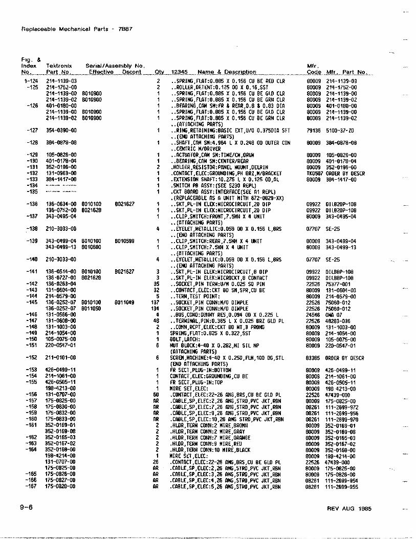
Replaceable Mechanical Parts - 7887
9--6 REV AUG 1985
Fig . &IndexNo.,
TektronixPart dNo, Effective
Serial/Assembly No .Dscont, _ Qtv, 12345 __. Name &.-DescriDtion
Mfr .Code Mfr,� Part No,__
1-124 214-1139-03 2 . .SPRING,FLAT:0.885 X 0 .156 CU BE RED CLR 80009 214-1139-03-125 214-1752-00 2 . .ROLLER,OETENT :0.125 00 X 0.16,SST 80009 214-1752-00
214-1139-00 8010900 1 . .SPRING,FLAT :0.885 X 0 .156 CU BE GLO CLR 80009 214-1139-00214-1139-02 8010900 1 . .SPRING,FLAT :0.885 X 0 .156 CU BE GRN CLR 80009 214-1139-02
-126 401-0180-00 1 . .BEARING,CAM SW:FR & REAR,0.8 & 0 .83 OIA 80009 401-0180-00214-1139-00 8010900 1 . .SPRING,FLAT :0.885 X 0 .156 CU BE GLO CLR 80009 214-1139-00214-1139-02 8010900 1 . .SPRING,FLAT:0.885 X 0 .156 CU BE GRN CL .R 80009 214-1139-02
. .(ATTACHING PARTS)-127 354-0390-00 1 . .RING,RETAINING:BASIC EXT,U/O 0 .3750IA SFT 79136 5100-37-ZO
. .(END ATTACHING PARTS)-128 384-0878-08 1 . .SHAFT,CAM SW :4 .964 L X 0 .248 OD OUTER CON 80009 384-0878-08
. .CENTRIC W/DRIVER-129 105-0826-00 1 . .ACTUATOR,CAM SK:TIME/CM,ORUM 80009 105-0826-00-130 401-0178-04 1 . .BEARING,CAM SW:CENTER/REAR 80009 401-0178-04-131 352-0196-00 2 .HOLDER,RESISTOR:PANEL MOUNT,OELRIN 80009 352-0196-00-132 131-0963-00 1 .CONTACT,ELEC :GROUNOING,PH BRZ,W/BRACKE'T TKO507 ORDER BY DESCR-133 384-1417-00 1 EXTENSION SHAFT :10.275 L X 0 .125 OO,AL 80009 384-1417-00-134 ------ ----- 1 SWITCH PB ASSY:(SEE S230 REPL)-135 1 CKT BOARD ASSY:INTERFACE(SEE A1 RLPL)
.(REPLACEABLE AS A UNIT WITH 672-0829-XX)-136 136-0634-00 6010100 8021627 1 . .SKT,PL-IN ELEK :MICROCIRCUIT,20 DIP 09922 OIL82OP-108
136-0752-00 8021628 1 . .SKT,PL-IN ELEK :MICROCIRCUIT,20 DIP 09922 OIL82OP-108-137 343-0495-04 1 . .CLIP,SHITCH:FRONT,7 . X 4 UNIT 80009 343-0495-04
. .(ATTACHING PARTS)-138 210-3033-00 4 . .EYELET,METALLIC :0 .059 00 X 0 .156 L,BRS 07707 SE-25
. .(END ATTACHING PARTS)-139 343-0499-04 8010100 8010599 1 . .CLIP,SWITCH:REAR,7 .5MM X 4 UNIT 80009 343-0499-04
343-0499-13 8010600 1 . .CLIP,SWITCH:7 . X 4 UNIT 80009 343-0499-13. .(ATTACHING PARTS)
-140 210-3033-00 4 . .EYELET,METALLIC :0 .059 OD X 0 .156 L,BRS 07707 SE-25. .(END ATTACHING PARTS)
-141 136-0514-00 8010100 8021627 3 . .SKT,PL-IN ELEK:MICROCIRCUIT,8 DIP 09922 OILB8P-108136-0727-00 8021628 3 . .SKT,PL-IN ELEK:MICROCKT,S CONTACT 09922 BILBBP-108
-142 136-0263-04 35 . .SOCKET,PIN TERM:U/W 0 .025 SO PIN 22526 75377-001-143 131-0604-00 32 . .CONTACT,ELEC :CKT 80 SW,SPR,CU BE 80009 131-0604-00-144 214-0579-00 5 . .TERM,TEST POINT : 80009 214-0579-00-145 136-0252-07 8010100 8011049 137 . .SOCKET,PIN CONN:W/O DIMPLE 22526 75060-012
136-0252-07 8011050 134 . .SOCKE"f,PIN CONN:W/O DIMPLE 22526 75060-012-146 131-0566-00 4 . .BUS,COND :D Y RES,0 .094 OD X 0 .225 L 24546 DNA 07-147 131-0608-00 48 . .TERMINAL,PIN :0.365 L X 0 .025 BRI GLD PL 22526 48283-036-148 131-1003-00 2 . .CONN,RCPT,ELEC:CKT BO MT,3 PRONG 80009 131-1003-00-149 214-1054-00 1 SPRING,FLAT:0 .825 X 0.322,SST 80009 214-1054-00-150 105-0075-00 1 BOLT,LATCH : 80009 105-0075-00-151 220-0547-01 6 NUT BLOCK:4-40 X O.282,NI SIL NP 80009 220-0547-01
(ATTACHING PARTS)-152 211-0101-00 6 SCREW,MACHINE :4-40 X 0.250,FLH,100 OG,STL 83385 ORDER BY DESCR
(END ATTACHING PARTS)-153 426-0499-11 1 FR SECT,PLUG-IN :BOT1'OM 80009 426°-0499-11-154 214-1061-00 1 CONTACT,ELEC:6ROUNDING,CU BE 80009 214-1061-00-155 426-0505-11 1 FR SECT,PLUG-IN :TOP 80009 426-0505-11
198--4213-00 1 WIRE SET,ELEC : 80009 198-4213-00-156 131-0707-00 60 .CONTACT,ELEC:22-26 AWG,BRS,CU BE GLD PL 22526 47439-000-157 175-0825-00 AR .CA8LE,SP,ELEC:2,26 ANG,STRO,PVC JKT,RBN 80009 175-0825-00-158 175-0830-00 AR .CABLE,SP,ELEC:7,26 AWG,STRO,PVC JKT,RBN 08261 111-2699-972-159 175-0832-00 AR .CABLE,SP,ELEC.9,26 AWG,STRO,PVC JKT,RBN 08261 111-2699-956-160 175-0833-00 AR .CABLE,SP,ELEC:10,26 ANG STRD,PVC JKT,RBN 08261 111-2699-970-161 352-0169-01 2 HLOR,TERN CONN:2 HIRE,BROHN 80009 352-0169-01
352-0169-08 2 HLOR,TERW CONN:2 HIRE,GRAY 80009 352-0169-08-162 352-0165-03 2 .HLOR,TE'RN CONN:7 WIRE,ORANGE 80009 352-0165-03-163 352-0167-02 2 HLOR,TERW CONN:9 WIRE,RFD 80009 352-0167-02-164 352-0168-00 2 HLOR,TERM CONN:10 NIRE,BLACK 80009 352-0168-00
198-4214-00 1 WIRE SET,ELEC : 80009 198-4214-00131-0707-00 26 .CONTACT,ELEC :22-26 AWG,BRS,CU BE GLO PL 22526 47439-000175-0825-00 AR .CABLE,SP,ELEC:2,26 AWG,STRD,PVC JKT,RBN 80009 175-0825-00
-165 175-0826-00 AR .CABLE,SP,ELEC:3,26 AWG,STRO,PVC JKT,RBN 80009 175-0826-00-166 175-0827-00 AR .CABLE,SP,ELEC:4,26 AWG,STRO,PVC JKT,RBN 08261 111-2699-954-167 175-0828-00 AR .CABLE,SP,ELEC:5,26 AWG,STRO,PVC JKT,RBN 08261 111-2699-955

REV AUG 1985
Replaceable Mechanical Parts - 71387
9- 7
Fig . 8IndexNo,.
Tektronix Serial/Assembly No .Part_ Dscont_No . .-,..--, Effective _ TQtv 12345 Name 8Description
Mtr .Code Mfr Part No.
1- 352-0163-06 1 HLOR,TERN CONN:5 HIRE,BLUE 80009 352-0163-06352-0169-00 2 .HL)R,TERM COiN:2 KIRE,BLACK 80009 352-0169-00
-168 352-0161-00 1 HLOR,TERM CONN:3 HIRE,BLACK 80009 352-0161-00352-0161-05 1 HLOR,TERN CONN:3 WIRE,GREEN 80009 352-0161-05352-0161-07 1 HLOR,TERM CONN:3 HIRE,VIOLET 80009 352-0161-07
-169 352-0162-00 1 .HU)R,TERK CONN:4 HIRE,BLACK 80009 352-0162-00352-0162-04 1 .HLf)R,TERN CONN :4 HIRE,YELLOH 80009 352-0162-04
STAMOARO ACCESSORIES
070-2788-00 1 L,TECH:INSTR 80009 070-2 -00

OO
s
IT
&M20 -
WASOFLei
5l
Ill~y®'"vzo
-,19
51
m
01
MOM
P
re,
Lal
9
98
u
13

--- 61
7B87 TIME BASE

MANUAL CHANGE INFORMATION
At Tektronix, we continually strive to keep up with latest electronic developmentsby adding circuit and component improvements to our instruments as soon as theyare developed and tested .
Sometimes, due to printing and shipping requirements, we can't get thesechanges immediately into printed manuals. Hence, your manual may contain newchange information on following pages.
A single change may affect several sections . Since the change information sheetsare carried in the manual until all changes are permanently entered, someduplication may occur. If no such change pages appear following this page, yourmanual is correct as printed .

Product:_ 7887 Time Base
These changes are effective at serial number 8023665.
MCOMMITTED TO EXCEtLErvce
Date : .._..___2/10/1986___
Change Reference: ., .,_. . . .__M57812
NUAL CHANGE INFORMATION
DESCRIPTION
Manual Insert for Product Group 42
DIAGRAM CHANG
Manual Part No . : -
070-22788800
SECTION 8 DIAGRAMS AND CIRCUIT BOARD ILLUSTRATIONS
LOGIC
Change R227 from 120 to 200. R227 is located in the center-right portion of the schematic.
CHANGE TO:
RS LAC CT ICAL PARTS LIST CHANGES
A1 ----- ----- CKT BOARD ASSY :INTERFACE(REPLACEABLE AS A UNIT WITH 672-0829-02)
A1 R227 315-0201-00 RES.,FXD,FILM:200 OHM,5%,0.25W
DS220 150-1078-00 LT EMITTING DIO:GREEN,565NM,20MA