Presentation Title Here - TI training
43
隔離式閘極驅動器概論 張巍, 系統工程師 德州儀器 1
-
Upload
khangminh22 -
Category
Documents
-
view
5 -
download
0
Transcript of Presentation Title Here - TI training

隔離式閘極驅動器概論
張巍, 系統工程師
德州儀器
1

What will you get out of this session?
PURPOSES:
What are the gate driver application
What are the differences: low-side, high-side and low-side, and isolated gate driver?
How to maximize the gate driver performance – from basic to details
Parasitics in the gate driver
Hard/soft switching
High dV/dt and di/dt
Isolated gate driver
• Part numbers mentioned: Low side: UCC27511A, UCC27524A
H-/L- Side: UCC27282, LMG1210, UCC27710
Isolated: UCC21540, UCC23513, UCC21710,
• Relevant End Equipment:
Telecom, servers, solar inverters, motor drive, EV/HEV, UPS
2

Where are gate driver ICs used?
Electric vehicles
class D audio
Renewables Solid state lighting
(SSL)
Adaptors and
chargers Server/telecom/UPS
Gate driver
applications
Motor drive (VFD)
Li-ion battery
portables
3
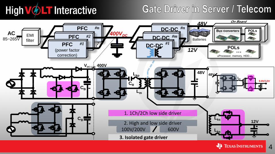
AC 85~265V
400VDC EMI
filter
PFC (Power Factor
Correction)
#n
PFC (Power Factor
Correction)
#2
PFC (power factor
correction)
#1
DC-DC
#n
DC-DC
#m
DC-DC #1
48V
Batteries
POLs 12V …
uProcessor, memory, HDD…
POLs Bus converters
VDC-Link 400V
48V
Lm
CR
Lkp Lk
9.6V/12V
48V
CB
CB Lks
Lks
12V 2. High and low side driver
1. 1Ch/2Ch low side driver
600V 100V/200V
3. Isolated gate driver
4

Si-MOSFET IGBT SiC-MOSFET GaN
Nom-ON Nom-OFF
20~650V ≥650V ≥650V ≤650V Voltage ratings
Optimal VGS 0~15V -10~15V -5~20V -5~10V -4~6V
(±20V) (±20V) (-10~25V) (±18V) (-10~7V) Max.limit
5V
4V
3V
2V
GaN
- I-V curves are from datasheets of Infineon, Fairchild, ST, Wolfspeed, EPC
10V 12V Si-MOSFET IGBT SiC-MOSFET
20V
16V
18V
5

Si-MOSFET IGBT SiC-MOSFET GaN
Nom-ON Nom-OFF
IF
VSD
Si
VDS
IDS
SiC
VSD
ISD
GaN
6

48V
Lm
CR
Lkp Lk
9.6V/12V
48V
CB
- Reduces BOM component
count
- Reduces PCB space
- Protects from spurious signals
during power up (such as
UVLO)
- Improves reliability
Now
3.3V/5V
PWM signal from
microcontroller or
DSP
Level shifted
12V signal
NPN/PNP totem pole Level shift circuit
12V with high peak
source/sink current
Micro/DSP
+
- UCC27511A - Single
- UCC27524A - Dual
- UCC27531 – SiC or IGBT
7

48V
Lm
CR
Lkp Lk
9.6V/12V
48V
CB
SGND
DBoot RBoot
HV(100~700V) VBias
GND
Q2
Q1
HS
VDD
VDD VDD PWM2 LI
LI HI
HS
HO
High
side
Similar as low
side driver
LO
UCC27712 (650V), UCC27282 (120V)
CBoot
HV (100~680V)
GND
HI
PWM1
Level Shift
Nois
e
Can
cell
er
HO
LO
GND
GND
HB
HS
VDD-VF
8

Si-MOSFET IGBT SiC-MOSFET GaN
Nom-ON Nom-OFF
IF
VSD
Si
VDS
IDS
SiC
VSD
ISD
GaN
9

Lm
CR
Lkp
12/48V VDC-Link 400V
85V~265V
EMI filter
L
N
PE
Isolation
feedback,
controller Half/full bridge
gate driver
Primary Secondary
CB
Working voltage V, peak or
DC
Test voltage for electric strength based on peak working voltage
Functional Isolation
(VRMS)
Basic Isolation
(VRMS)
Reinforced Isolation
(VRMS)
≤210 1000 1000 1500
≤420 1500 1500 3000
IEC 60950-1 ed. 2.0, Table 5B
10

Isolation Definition Featured Drivers
Functional Isolation that is necessary only for the correct functioning of the
equipment UCC21220A, UCC21222
Basic Isolation to provide basic protection against electric shock UCC21220A, UCC21222
Reinforced
Single Isolation system that provides a degree of protection against
electric shock equivalent to DOUBLE isolation under the conditions
specified in this standard
UCC21540, UCC21520
11

48V DC link
9.6V/12V
VDC-Link 400V
AC/DC-DC/DC Telecom BMP
EMI
&
PFC
L
N
PE
μ-controller
UCC21230
(≥200V and Ground bouncing)
ISOLATION BARRIER
ISO driver
Functional 2× ISO Driver
ISOLATION BARRIER
ISO driver
Reinforced ISOLATION BARRIER ISOLATION BARRIER
(36V~75V)
2×
μ-controller
UCC21230
(≥200V and Ground bouncing)
ISOLATION BARRIER
Low side
driver 1× ISO Driver
ISOLATION BARRIER
ISO driver
Basic ISOLATION BARRIER 2×
According to Figure 2H of IEC60950-1
12

9.6V/12V
VDC-Link 400V
AC/DC-DC/DC Telecom BMP
EMI
&
PFC
L
N
PE
μ-controller
UCC21230
(≥200V and Ground bouncing)
ISOLATION BARRIER
ISO driver
Functional 2× ISO Driver
ISOLATION BARRIER
ISO driver
Basic ISOLATION BARRIER ISOLATION BARRIER
(36V~60V)
2×
μ-controller
UCC21230
(≥200V and Ground bouncing)
ISOLATION BARRIER
Low side
driver 1× ISO Driver
ISOLATION BARRIER
ISO driver
Functional ISOLATION BARRIER 2×
According to Figure 2H of IEC60950-1
48V DC link
13

Con
tro
ller
VSS
VCC
HV
PWM2
PGND
Q1
Q2
CByp
SGND
PWM1
Low
Side
Driver
VCC
TYPE A
LDO
Con
tro
ller
VSS
VCC
HV
PWM2
PGND
Q1
Q2
CByp
SGND
PWM1
TYPE B
HI
LI
VSS
EN/NC
VCC
HB
HO
HS
LO
COM
DBoot VBias
High side
and
Low side
Gate driver
Isolator
Type A Type B
TProp ≈20ns ≈100ns
Bias power NO Yes
CIO ≥10pF <1pF
Parasitics Large (LLK) Very small
Overshoot Large Small
Size Bulky Small
CIO
CIO
14

CMTI>100V/ns
5kVrms reinforced isolation
TProp: 19ns typ.
Match./TPWD < 5ns
110mm2
Con
tro
ller
VSS
VCC
HV
PWM2
PGND
Q1
Q2
CByp
SGND
PWM1
Low
side
driver
VCC
TYPE A
Con
tro
ller
VSS
VCC
HV
PWM2
PGND
Q1
Q2
CByp
SGND
PWM1
TYPE B
HI
LI
VSS
EN/NC
VCC
HB
HO
HS
LO
COM
DBoot VBias
High side
and
Low side
Gate driver
Isolator
Type B ISO7520C 10.5 10.6 2.65 111.3 295
UCC27714 8.75 6.2 1.75 54.25 95
MURS360 8.1 6.1 2.4 49.41 119
SUM 215 509
W (mm) L (mm) H (mm) Area
(mm2) Vol
(mm3)
Type A UCC27324 5 6.2 1.75 31 54.25
GA3550-BL 17.4 24.13 10 420 4200
SUM 451 4254
TYPE C: ISO driver
LDO
15

• A) Optocoupler • Signal transfer between two isolated circuits
using light – LED + phototransistor, ~1970s
• B) Transformer • Integrated micro-transformer and electronic
circuitry, ~2001
• C) Capacitor • Signal transmission through capacitive isolation
with on-off-keying (OOK) modulation, ~2004
16

TI Reinforced Isolation Technology
• Reinforced Isolation is realized by thick SiO2 capacitors combined in series – Each channel uses high voltage isolation capacitors on both die
• Combined Isolation capacitor thickness is >21um
• 12.8kV surge voltage, 8kVpeak transient over-voltage, 1.5kVrms working voltage
Package
Leadframe Leadframe Left Die Right Die 600um
Series Capacitors
17
UCC2x52x, UCC2154x, UCC2351x
ModulatorIN OUTDemodulator

• The main Isolation electrical lifetime test is TDDB: Qualification Test – Standard methodology for determining the lifetime of a dielectric as a function of Voltage
• TDDB is accelerated lifetime
testing of the isolation barrier
– Weibull statistics at each voltage
First technology to certify to
VDE 0884-11
VIOTM
Foundation of Quality – Qualification & Reliability

TI Capacitive Isolation uses SiO2 as the Isolation Dielectric.
– SiO2 advantages compared to competing HV isolative material are: reliability and dielectric strength
Table 1: Commonly used materials for High-Voltage isolation (SiO2 has the highest dielectric strength and best reliability)
Dielectric Thickness (SiO2) Fabrication Process Control & Monitor:
– Repeatability and Reproducibility – SiO2 thickness monitored using two methods:
• Oxide thickness sample measured in the wafer fab for each of the layers of the dielectric stack
• Tox by capacitance measurement on test structures on every production wafer after fabrication
– Thickness is tracked on all wafers for each fabrication lot as required by UL standard
Foundation of Quality – SiO2 Insulation
Insulator Materials Dielectric Strength, 1 sec Dielectric Strength, 40yr reliability
Air ~1 Vrms/um
Epoxies ~20 Vrms/um
Silica filled Mold compounds ~100 Vrms/um
Polyimide ~300 Vrms/um ~20 Vrms/um
SiO2 ~500 Vrms/um ~100 Vrms/um

UCC21220A, UCC21540: 2-ch. Isolated Gate Driver
Functional
Isolation
20
Input Die – takes inputs from µController,
modulates and transmits across isolation
barrier using on-off-keying
SiO2 Capacitors – provides high voltage basic
or reinforced isolation, with excellent noise
immunity and lifetime
Output Die – demodulates signal and drives
outputs on or off depending on logic inputs

UCC21220A, UCC21540: 2-ch. Isolated Gate Driver
• 6A/4A sink/source
• 28ns propagation delay
• >100V/ns CMTI
• Up to 3~5V input range and 6~18V wide output voltage range
• Programmable overlap, and interlock/delay time from 0ns~5µs
• Output fail safe low with active pull down
• UVLO options: 5V, 8V
• 3.0kV, 5.7kV basic/functional and reinforced isolation
• Pin-2-pin compatible to industry standard
• UL, VDE, CQC certified
Functional
Isolation
21

Fe
atu
res &
In
teg
rati
on
Time
Isolated Gate Driver Portfolio
UCC21540
• Dual driver
• 4A source/6A sink OR
2A/3A
• Pin-to-pin with 21520
• 5V or 8V UVLO
• VCC=3-5.5V
• 5KVrms Viso
• 16-pin SOIC (8mm) DW
or DWK (missing pins)
ISO=5.0kV WV=1.4kV
• Dual driver
• 5V or 8V UVLO, DIS
• Dead-time (DT)
• 4A source/6A sink
• VCC=3-5.5V & Vdd= 4.8-18V
• 25ns prop delay (typ)
• 16-pin SOIC (4mm)
• AUTO
UCC21220/A
UCC21222-Q1 ISO=3.0kV WV=990V
• Dual driver
• 4A source/6A sink
• CMTI > 100V/ns
• 19ns prop delay (typ)
• 5ns match (max)
• VCC=3-18V&Vdd=9-25V
• 16-pin SOIC (8mm)
• OPTIONS:
• 5, 8, 12V UVLO
• EN or DIS
• Dual IN or PWM
• AUTO
• Single driver (8V
UVLO)
• 3KVrms Viso
• 8.5A source/10A sink
• VCC=3-15V & Vdd=10-
33V
• 8-pin SOIC (4mm)
UCC2152x/A/C
UCC5350SB
• Dual driver
• 4A source/6A sink
• CMTI > 100V/ns
• 19ns prop delay (typ)
w/ 5ns match
(max)
• PWM (UCC20x) or dual
input (UCC21x)
w/disable
• 5V or 8V UVLO
• 13-pin LGA (5x5mm)
UCC2x225/A
• Single driver (12V UVLO)
• 2A source/2A sink
• M = Miller clamp (5310)
• S = Split output
• VCC=3-15V & Vdd=10-33V
• 8-pin SOIC (4mm)
UCC5320SC/EC
UCC5310MC
UCC5390SC/EC
UCC5350MC • 10A source/10A
sink
M = Miller clamp
UCC5310MC
UCC5390EC
UCC5320SC • 1A,2A &10A
• 8-pin SOIC (8mm)
• Single IGBT driver with
protection
• DeSAT, clamp, fault
output , UVLO OK
• 2.5A source/5A sink
• CMTI = 100V/ns
• 76ns prop delay (typ)
• Vdd=15-30V
• 16-pin SOIC (8mm)
• AUTO
ISO585x/ISO545x
ISO=5.7kV
WV=1.4kV
ISO=5.7kV
WV=2.1kV
ISO=5.7kV
ISO=3kV WV=990V
ISO=2.5kV
ISO=5.0kV WV=2.1kV
UCC21530-Q1
• 12V UVLO
• AUTO
• 16-pin SOIC DWK (8mm)
w/ 3.3mm HS to LS
(missing pins)
WV=2.1kV WV=2.1kV ISO=5.7kV
WV=790V
Re
info
rce
d
Fu
nc
tio
na
l / B
as
ic
End Equipment:
• Server PSU Isolated DC/DC
• Telecom Rectifiers Isolated DC/DC
• Industrial AC-DC
• Solar Inverters
• AC Motor Drives
End Equipment:
• Server PSU PFC, SR
• Telecom Rectifiers PFC, SR
• Brick Power Modules
• Solar Inverter & Solar Optimizers
• Motor Drives & Robotics
22
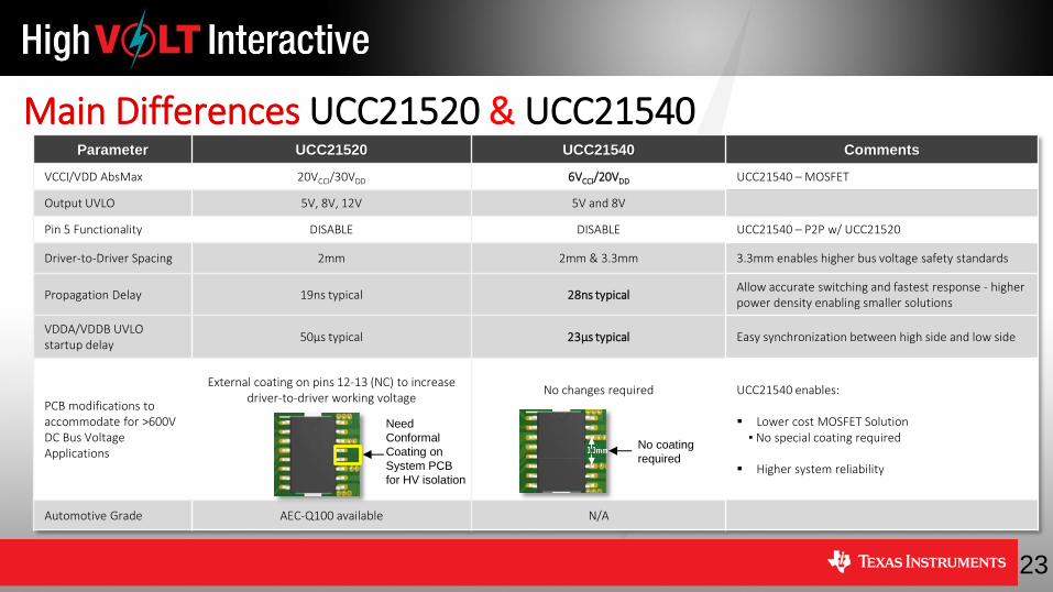
Main Differences UCC21520 & UCC21540 Parameter UCC21520 UCC21540 Comments
VCCI/VDD AbsMax 20VCCI/30VDD 6VCCI/20VDD UCC21540 – MOSFET
Output UVLO 5V, 8V, 12V 5V and 8V
Pin 5 Functionality DISABLE DISABLE UCC21540 – P2P w/ UCC21520
Driver-to-Driver Spacing 2mm 2mm & 3.3mm 3.3mm enables higher bus voltage safety standards
Propagation Delay 19ns typical 28ns typical Allow accurate switching and fastest response - higher power density enabling smaller solutions
VDDA/VDDB UVLO startup delay
50µs typical 23µs typical Easy synchronization between high side and low side
PCB modifications to accommodate for >600V DC Bus Voltage Applications
External coating on pins 12-13 (NC) to increase driver-to-driver working voltage
No changes required
UCC21540 enables: Lower cost MOSFET Solution ▪ No special coating required Higher system reliability
Automotive Grade AEC-Q100 available N/A
No coating
required
Need
Conformal
Coating on
System PCB
for HV isolation
23

UCC23513 Specifications
• Opto-compatible input, isolated Gate driver for IGBT/MOSFET/SiCs
• SiO2 based capacitive isolation technology
• Pin compatible, drop-in upgrade for ACPL-W341, W346, TLP5752
• 4A peak output drive current
• 35V max output drive (VCC – VEE)
• SO6 (6 pin wide lead, smt), NiPdAu lead finish, material group I
• > 8.5mm Cr & Clr; 5kVRMS reinforced isolation
• 105ns propagation delay with 25ns part-to-part delay matching
• 100 kV/us Common Mode Transient Integrity (CMTI)
• 12V Under Voltage Lockout (UVLO)
• Input stage can be reverse-biased for interlock
• Wide operating temperature range (Tj): -40°C to 150°C
UCC23513 is a 4A, 5kVRMS opto-compatible gate driver available in stretched SO-6.
Using capacitive isolation technology to simulate opto-isolation, this solution is more
robust, longer-lasting, and exhibits exemplary propagation delay and Common Mode
Transient Integrity specifications. With UCC23513, TI is providing customers with a
pin-to-pin replacement for opto-isolated gate drivers to offer a better performing and
longer-lasting solution that requires minimal effort to design in.
1
2
3
6
5
4
e
UVLO
ISOLA
TIO
N B
AR
RIE
R
VOUT
VCC
VEE
NC
Anode
Cathode
SO6
Body Size
7.5 mm x 4.68mm
• Higher common mode transient integrity
• Smaller propagation delay and tighter part-to-part delay matching
• Lower pulse width distortion
• Higher reliability, resistant to temperature and aging
• No long term aging of input stage
• Very tight tolerance of cap oxide since oxide is a controlled fab process
• Long lifetime (> 40 yrs)
• Less variation in forward current due to tighter VF
7.5mm
4A, 5kVRMS, Opto-Compatible Input Gate Driver in Stretched SO-6 Overview
Features
Benefits
http://www.ti.com/product/UCC23513

New Features in UCC217XX Key System Challenge Solved …
System Benefits IGBT SiC
±10A peak drive strength (throughout drive voltage range)
>10kW systems use discrete buffers (e.g., NPN+PNP) to increase drive strength: Reliability, drive supply & cost challenges
▪ Higher System Reliability + Higher Efficiency ▪ Lower System Cost + Smaller PCB Area
>150V/ns CMTI (Min) (Typically <50V/ns) SiC switches fast to reduce switching
loss ▪ Enhanced System Robustness ▪ Higher System Efficiency
200ns Over-Current Detection + 650ns Isolated Fault Reporting
Programmable DESAT threshold voltage
SiC has <3µs short-circuit capability
▪ Fast System Protection ▪ Enhanced System Robustness
2-Level Turn OFF (Option)
Significantly reduced VCE / VDS Overshoot during System Shutdown ▪ Safe System Shutdown ▪ Enhanced System Robustness ▪ Improved Switch Lifetime
Integrated Isolated Accurate Analog-to-PWM Sensor
Eliminate all discrete components used for bus voltage sensing / switch temperature sensing / sec-to-primary feedback / isolated alarm / …
▪ Lower System Cost ▪ Smaller PCB Area
VEE UVLO (Option)
Eliminate discrete circuitry for VEE monitoring (voltage sensor + isolator) ▪ Lower System Cost ▪ Smaller PCB Area
External Miller Clamp (Option)
More effective technique than internal miller clamp for high-power switch modules
▪ Enhanced System Robustness ▪ Lower System Noise (Ringing + EM)
Standard SOIC-16 DW Package Small package size, 1mm pad pitch, pin-to-pin compatibility with better specs ▪ Lower System Cost ▪ Smaller PCB Area
25

Fast (200ns) Over-Current Detection: Important for fast switch protection, especially SiC
MOSFETs Allows for flexible DESAT threshold setting for SiC
MOSFET or IGBT Applicable to IGBT modules with SenseFET
Internal Miller Clamp: Suited for lower power levels (<50kW) or tighter layouts (driver to switch)
Soft Turn-OFF: Preferred method for safe shutdown of SiC or IGBT switch
Fast (200ns) Over-Current Detection: Important for fast switch protection, especially
SiC MOSFETs
Allows for flexible DESAT threshold setting for
SiC MOSFET or IGBT
Applicable to IGBT modules with SenseFET
External Miller Clamp: Ideal for high-power IGBT/SiC modules (reduce clamp-to-gate parasitics)
2-Level Turn-OFF: Preferred for high-power modules for higher power applications
Standard 9V DESAT: Exactly what typical IGBTs need (same specs as
ISO58XX) 9V DESAT might be high for SiC MOSFETs (depends
on SiC MOSFET supplier)
Internal Miller Clamp: Suited for lower power levels (<50kW) or tighter layouts (driver to switch)
Soft Turn-OFF: Preferred method for safe shutdown of IGBT or SiC switch
JOLT: UCC21732
[Delphi] UCC21710 UCC21732 / 36 UCC21750 : AEC-Q100 : AEC-Q100 : AEC-Q100
[Disclaimer: Specs, features & pinouts subject to change without prior notice.]
[NOTE: Pins in Black have same pin locations as in ISO5852S or ISO5452. Pin in Blue are new pin definitions.]
26

Isolated Switch Temperature Sensing: NTC/PTC
[Disclaimer: Specs, features & pinouts subject to change without prior notice.]
Isolated Switch Temperature Sensing: Thermal Diode Isolated Digital Signal: Alarm / Shutdown
COM
VDD
CFLT
AIN
+
SawTooth
Gen
MOD
In Module or
External
AIN Range: 0.5V to 4.5V
AIN Bandwidth: 50kHz
APWM: 90% to 10%
APWM Frequency: 400kHz
AIN-APWM Accuracy:
±1%: System-level cal.
±3%: Without cal.
IAIN: 0.2mA (±3%) COM
VDD
CFLT
AIN
+
SawTooth
Gen
MODVDC_BUS
RS1
RS2
RS3
COM
VDD
CFLT
AIN
+
SawTooth
Gen
MOD
In Module or
External
HV Bus Sensing
Secondary-to-Primary Bus
Voltage Feedback
Driver-side Supply Voltage
Monitoring (Redundant /
Additional UVLO)
Digital Alarm
Emergency Shutdown signal
COM
VDD
CFLT
AIN
+
SawTooth
Gen
MODVDC_BUS
RS1
RS2
RS3
Digital
Alarm
Switch Over-temperature Detection: System Protection
System performance optimization based on Switch Temperature Sensing
Switch temp-cycling / lifetime monitoring
Isolated Analog Signal Sensing: HV Bus / Power Supply / …
Back to
Portfolio 27

Driver
Gate driver deep dive Very critical role in converter efficiency and reliability
1. Parasitics in gate driver?
2. Common mode transient immunity(CMTI), dv/dt and
di/dt through parasitics L and C?
3. Gate driver soft/hard switching difference?
4. Strong gate driver and MOSFET nonlinear COSS?
5. Power supply for isolated gate driver in UPS, server
and Telecom system
28

SW-node
VCC
Driver
PWM
P
N
Turn-ON
Turn-OFF
𝑪𝑰𝑺𝑺 = 𝑪𝑮𝑺 + 𝑪𝑮𝑫
𝑪𝑹𝑺𝑺 = 𝑪𝑮𝑫
𝑪𝑶𝑺𝑺 = 𝑪𝑮𝑫 + 𝑪𝑫𝑺
CGD
CGS
CDS
29

VTH
VGS
VDS
ID
t0 t1 t2 t3 t4
CGD
CGS CDS
VCC SW-node
P
N
t0~t2
CGD
CGS CDS
VCC SW-node
P
N
t2~t3
CGD
CGS CDS
VCC SW-node
P
N
t3~t4
t4
Turn-ON
𝑽𝑫𝑺 𝒕 ∙ 𝑰𝑫 𝒕 𝒅𝒕𝒕𝟑
𝒕𝟏
+ 𝐸𝑂𝑆𝑆
Switching on loss
𝒕𝟏~𝟑 ∝ 𝟏
𝑰𝑫𝒓𝒗
Stronger driver lower
switching loss PON
t0 t1 t2 t3
Turn-OFF
POFF
30

𝐼𝑑𝑠
VDS
VGS
𝟖𝟎𝒏𝒔/𝒅𝒊𝒗
20𝐴/𝑑𝑖𝑣
15V/div
100V/div
𝐼𝐶
VCE
VGE
10𝐴/𝑑𝑖𝑣
10V/div
100V/div
𝟐𝟎𝒏𝒔/𝒅𝒊𝒗
SW
VIN
SJ-MOSFET
SW
VIN
IGBT
Parasitic
diode Anti-parallel diode
(co-package)
QRR
IF
VF
Diode reverse
recovery
VTH
VGS
VDS
ID
t0 t1 t2a t2b t4 t3
ID_pk
Turn-on w/
QRR
IL IL
QRR
31

Lm
CR
LR
VDC-Link
400V 85V~
265V
EMI filter
Lks
Lks
12V
LLC converter + center-tap rectifier
IL
S1
S2
VDS
ILr
ILm
ZVS
CRM totem pole PFC
VGS
IL
…
…
ZVS
VDS (V)
IL (A)
VGS
32

CGD
CGS CDS
VCC SW-Node
P
N
CGD
CGS CDS
VCC SW-Node
P
N
VTH
VGS
VDS
ID
a b
CGD
CGS CDS
VCC SW-node
P
N
c
Hard-switching VGS
VDS
Soft-switching
VTH
ID
t0 t1 t2 t3
Current slope
decided by inductor
Coss discharge
a b c c
33
Qgate[nc]
AHS_ON
AHS_OFF
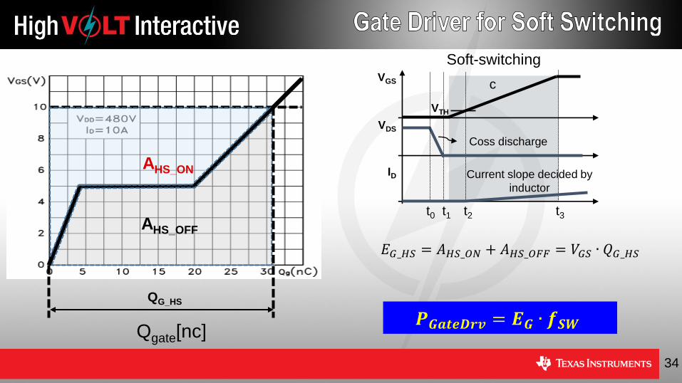
𝐸𝐺_𝐻𝑆 = 𝐴𝐻𝑆_𝑂𝑁 + 𝐴𝐻𝑆_𝑂𝐹𝐹 = 𝑉𝐺𝑆 ∙ 𝑄𝐺_𝐻𝑆
QG_HS
𝑷𝑮𝒂𝒕𝒆𝑫𝒓𝒗 = 𝑬𝑮 ∙ 𝒇𝑺𝑾
VGS
VDS
Soft-switching
VTH
ID
t0 t1 t2 t3
Current slope decided by
inductor
Coss discharge
c
34

Qgate[nc]
𝐸𝐺_𝐻𝑆 = 𝐴𝐻𝑆_𝑂𝑁 + 𝐴𝐻𝑆_𝑂𝐹𝐹 = 𝑉𝐺𝑆 ∙ 𝑄𝐺_𝐻𝑆
𝐸𝐺_𝑍𝑉𝑆 = 𝐴𝑍𝑉𝑆_𝑂𝑁 + 𝐴𝑍𝑉𝑆_𝑂𝐹𝐹 ≈ 𝑉𝐺𝑆 ∙ 𝑄𝐺_𝑍𝑉𝑆
QG_HS
QG_ZVS
𝑷𝑮𝒂𝒕𝒆𝑫𝒓𝒗 = 𝑬𝑮 ∙ 𝒇𝑺𝑾
VGS
VDS
Soft-switching
VTH
ID
t0 t1 t2 t3
Current slope decided by
inductor
Coss discharge
c
AZVS_ON
AZVS_OFF
35

• Switching behavior is not controlled by gate current,
but by COSS and load current
• Large COSS at low voltage performs as natural snubber
• Small COSS at high voltage shortens V-I overlap
• Fast dv/dt and di/dt, other bad things
t0 t1 t2 t3 t4
w/ Weak driver
COSS(0V)
=6nF
COSS(400V)
<30pF
VTH
VGS
VDS
ID
t0 t1 t3
w/ Strong driver
t2
VGS
VDS
ID
t0
w/ Strong driver w/
nonlinear COSS
t1 t2 t3
VGS
VDS
ID
36

200ns/div
15A
VDS
(100V/div)
IDS
(10A/div)
VGS
(10V/div)
VDS
(5V/div)
IDS
(5A/div)
VGS
(5V/div)
Zoom IN
20ns/div
37

ID_CH
ID_Coss
t
t
t
t
VGS_S1
VDS_S1
VGS(plt)
VGS(th)
IM
IM
Vin
I II III IV
tfi
Lm
S2
S1
Im
Vin
ID_Coss1ID_CH
T
Coss2
Coss1
ID_Coss2I
Lm
S2
S1
Im
Vin
ID_Coss1ID_CH
T
Coss2
Coss1
ID_Coss2
II
Lm
S2
S1
Im
Vin
ID_Coss1
T
Coss2
Coss1
III
Lm
S2
S1
Im
Vin
T
Coss2
Coss1
IV
In period II, High dv/dt, di/dt
COSS
charge
(EOSS)
Recovered
at turn-on
1_2_1__
212_1_
CossDCossDCossDCossD
ossossSDSSDS
IIII
CCVV
;
38

159
145
130
102
90
52.7
37.429.5
23.7 19.8
0
20
40
60
80
100
120
140
160
180
0 5 10 15 20
109
87.4
6.75
1.02 0.65 0.55 0.5 0.4
0
2
4
6
8
10
12
0 5 10 15 20
GaN GaN
SJ-MOSFET
SJ-MOSFET
dv/dt (V/ns) di/dt (A/ns)
(a) (b)
159
145
130
102
90
52.7
37.429.5
23.7 19.8
0
20
40
60
80
100
120
140
160
180
0 5 10 15 20
109
87.4
6.75
1.02 0.65 0.55 0.5 0.4
0
2
4
6
8
10
12
0 5 10 15 20
GaN GaN
SJ-MOSFET
SJ-MOSFET
dv/dt (V/ns) di/dt (A/ns)
(a) (b)
A/n
s
RG-EXT(Ω)
di/dt (IOFF=15A)
V/n
s
dv/dt (IOFF=15A)
RG-EXT(Ω)
39

0
50
100
150
200
250
300
-50 0 50 100 150
Positive-ChA
Positive-ChB
Negative-ChA
Negative-ChB
CMTI (V/ns)
Temperature
(°C)
Lf
IL
VChg COSS
CD VCMT
VChg Lf IL
COSS CD
VCMT
CMT
rising
CMT
falling
VClamp
VClamp
40

41
Gate Driver Portfolio: Selection Tree
UCC21520/1(A)
5V or 8V UVLO,
Dual Input
AEC-Q100 Qualified
RTM’d/APL’d in last 4
Quarters
Gate Drivers
Low-Side Half-Bridge Isolated
Single Channel Dual Channel
VDD ≤18V VDD >18V
UCC27517(A) 4A/4A High-Speed,
Negative Voltage
Handling Option
UCC27537 2.5A/5A
35 VMAX
<250V ≥250V
UCC27712 8-SOIC
UCC27714 14-SOIC
UCC27710 8-SOIC
UCC27212 5V UVLO
1A 2.8A 4A <4A >4A
LM5109B PWM or Dual
Inputs
Single Channel Dual Channel
UCC21220(A) Narrow Body
UCC5350 5A
Miller Clamp/ Split
Output
4A 5A
UCC27424 Non-Inverting with
Enable
UCC27524(A) Multiple
Configurations,
Negative Voltage
Handling Option
<5kVrms ≥5kVrms
UCC21222 Deadtime, Narrow
Body
Basic
Production
UCC27511(A) 4A/8A High-Speed,
Negative Voltage
Handling Option,
Split Output
UCC5390EDWV
10A, Emitter
Wide Body
Cost-Competitive Part
Premium Part
UCC27611 4A/6A GaN Driver,
Low Roh,
5V LDO
LMG1210 GaN Driver, WQFN
Package
Reinforced
UCC21530 12V UVLO,
3.3-mm Output
Spacing
UCC21540 8V UVLO, DW or
3.3mm Output
Spacing
UCC27282 5V UVLO
Half-Bridge Drivers Isolated Drivers Low-Side Drivers
ISO5451 5A SiC Driver, 12V
UVLO
UCC217xx 5A SiC Driver, 12V
UVLO, AIN/APWM
UCC23513 IGBT Driver, Opto
input, 12V UVLO
41

Gate driver fundamentals and in-system consideration
Low side, high- and low side, isolated gate driver
Parasitics in gate driver?
Gate driver soft/hard switching difference?
Strong gate driver and MOSFET nonlinear COSS?
Common mode transient immunity(CMTI), dV/dt and di/dt through parasitics
Power supply for isolated gate driver in UPS, server and Telecom
Sample TI’s New Isolated Gate Drivers: UCC21540: http://www.ti.com/product/UCC21540/samplebuy UCC21220A: http://www.ti.com/product/UCC21220A/samplebuy UCC21710-Q1: http://www.ti.com/product/UCC21710-Q1/samplebuy UCC23513: http://www.ti.com/product/UCC23513/samplebuy
42

43