
CLOSED-FORM DESIGN METHOD OF AN N-WAY DUAL ...
18
Progress In Electromagnetics Research, PIER 101, 97–114, 2010 CLOSED-FORM DESIGN METHOD OF AN N-WAY DUAL-BAND WILKINSON HYBRID POWER DIVIDER Y. L. Wu, Y. A. Liu, S. L. Li, C. P. Yu, and X. Liu School of Electronic Engineering Beijing University of Posts and Telecommunications China Abstract—In this paper, the closed-form design method of an N- way dual-band Wilkinson hybrid power divider is proposed. This symmetric structure including N groups of two sections of transmission lines and two isolated resistors is described which can split a signal into N equiphase equiamplitude parts at two arbitrary frequencies (dual-band) simultaneously, where N can be odd or even. Based on the rigorous even- and odd-mode analysis, the closed-form design equations are derived. For verification, various numerical examples are designed, calculated and compared while two practical examples including two ways and three ways dual-band microstrip power dividers are fabricated and measured. It is very interesting that this generalized power divider with analytical design equations can be designed for wideband applications when the frequency-ratio is relatively small. In addition, it is found that the conventional N-way hybrid Wilkinson power divider for single-band applications is a special case (the frequency-ratio equals to 3) of this generalized power divider. 1. INTRODUCTION In microwave and millimeter-wave circuits, power dividers are widely used as key passive components. As is well known, the first complete design method for N-way power dividers was developed by Wilkinson [1] in 1960. And then, the appearance of Wilkinson power dividers has lead to further researches on bandwidth enhancement [2] and planar circuit’s applications [3, 4] of N-way power dividers. In addition, extending from equal and symmetric N-way power dividers, Corresponding author: Y. L. Wu ([email protected]).
-
Upload
khangminh22 -
Category
Documents
-
view
1 -
download
0
Transcript of CLOSED-FORM DESIGN METHOD OF AN N-WAY DUAL ...

Progress In Electromagnetics Research, PIER 101, 97–114, 2010
CLOSED-FORM DESIGN METHOD OF AN N-WAYDUAL-BAND WILKINSON HYBRID POWER DIVIDER
Y. L. Wu, Y. A. Liu, S. L. Li, C. P. Yu, and X. Liu
School of Electronic EngineeringBeijing University of Posts and TelecommunicationsChina
Abstract—In this paper, the closed-form design method of an N-way dual-band Wilkinson hybrid power divider is proposed. Thissymmetric structure including N groups of two sections of transmissionlines and two isolated resistors is described which can split a signalinto N equiphase equiamplitude parts at two arbitrary frequencies(dual-band) simultaneously, where N can be odd or even. Basedon the rigorous even- and odd-mode analysis, the closed-form designequations are derived. For verification, various numerical examplesare designed, calculated and compared while two practical examplesincluding two ways and three ways dual-band microstrip power dividersare fabricated and measured. It is very interesting that this generalizedpower divider with analytical design equations can be designed forwideband applications when the frequency-ratio is relatively small. Inaddition, it is found that the conventional N-way hybrid Wilkinsonpower divider for single-band applications is a special case (thefrequency-ratio equals to 3) of this generalized power divider.
1. INTRODUCTION
In microwave and millimeter-wave circuits, power dividers are widelyused as key passive components. As is well known, the firstcomplete design method for N-way power dividers was developed byWilkinson [1] in 1960. And then, the appearance of Wilkinson powerdividers has lead to further researches on bandwidth enhancement [2]and planar circuit’s applications [3, 4] of N-way power dividers. Inaddition, extending from equal and symmetric N-way power dividers,
Corresponding author: Y. L. Wu ([email protected]).

98 Wu et al.
general design equations of N-way power dividers with arbitrarypower dividing ratios were presented in [5]. Recently, novel N-waymicrowave power dividers are developed based on meta-materialsin [6, 7] while full-wave analysis of N-way power dividers by eigenvaluedecomposition is reported in [8]. However, these N-way powerdividers discussed in [1–8] and unequal lumped-elements power dividersanalyzed in [9] are proposed only for single-band (or wideband)applications. To satisfy dual-band or multi-band applications, noveldual-band transformers [10–13], equal dual-band power dividers [14–24], and unequal dual-band modified power dividers [25–30] withclosed-form design equations are developed. Although the powerdividers presented in [14–30] can operate at two bands, only two-way structures are considered. As the extension of the three-waysingle-band power divider in [3], the paper [31] introduces a planarthree-way dual-frequency power divider, however, the design methodis only considered for this special three-way case. More recently, theconcept of N-way dual-frequency power dividers is discussed and thecorresponding numerical design method is based on genetic algorithm[32]. In addition, the developments of new Wilkinson power dividerswith small size [33, 34], harmonic suppression [35] or 6 : 1 unequalpower division [36] are new research topics.
In this paper, we analyze a generalized equal Wilkinson hybridpower divider, which includes N-way and can operate at two arbitraryfrequencies (dual-band) simultaneously, namely, a multi-way dual-band power divider. The analyzed structure consists of N groupsof two-section transmission lines and two isolated resistors, which issimilar with the design structure in [32]. Different from the designmethod of [32], the values of design parameters in this paper can becalculated by closed-form design equations, in other words, the designmethod of the N-way dual-band power divider is analytical. In thisgeneralized power divider, there are two important characteristics. Oneis that it can be used in wideband applications when the frequency-ratio (the center frequency-ratio of dual-band) is relatively small (forexample, it is smaller than two). The other is that the analyzed N-way dual-band Wilkinson hybrid power divider is an extension of theN-way single-band power divider developed by Wilkinson [1] when thefrequency-ratio v equals to three.
2. CIRCUIT STRUCTURES AND DESIGN EQUATIONS
Figure 1 illustrates the basic circuit structure of the analyzed N-waydual-band Wilkinson hybrid power divider. As shown in Fig. 1, thetotal structure includes N groups of two-section of transmission lines

Progress In Electromagnetics Research, PIER 101, 2010 99
Figure 1. The analyzed circuit of N-way dual-band Wilkinson hybridpower divider.
(Z1 and Z2) with the same electrical length θ and two isolated resistors(R1 and R2). N symmetric parallel dual-frequency transformers [10]can achieve the ideal input matching at the input Port 1. At the outputports (such as Port 2, . . . , (N +1) in Fig. 1), the ideal output matchingand isolation between two arbitrary output ports can be obtained byN groups of two separated isolated resistors R1 and R2. In particular,when N equals to two, this generalized power divider can be simplifiedto a new kind of two-way dual-band power divider with bandwidthenhancement [24]. Actually, this simple case, which will be discussed insection 4, is very suitable for distributed circuit implementation. Whenthe value of N is larger than three, the planar circuit implementationbecomes difficult. Therefore, the three-dimensional (3D) structureincluding splines and coaxial lines [1] should be used to implementdual-band Wilkinson hybrid power divider with N (N > 3) outputports. The analytical design equations can be derived with the aid ofthe conventional even- and odd-mode analysis [14], and the completeprocess is given in the rest of this chapter.
2.1. The Even-mode Analysis
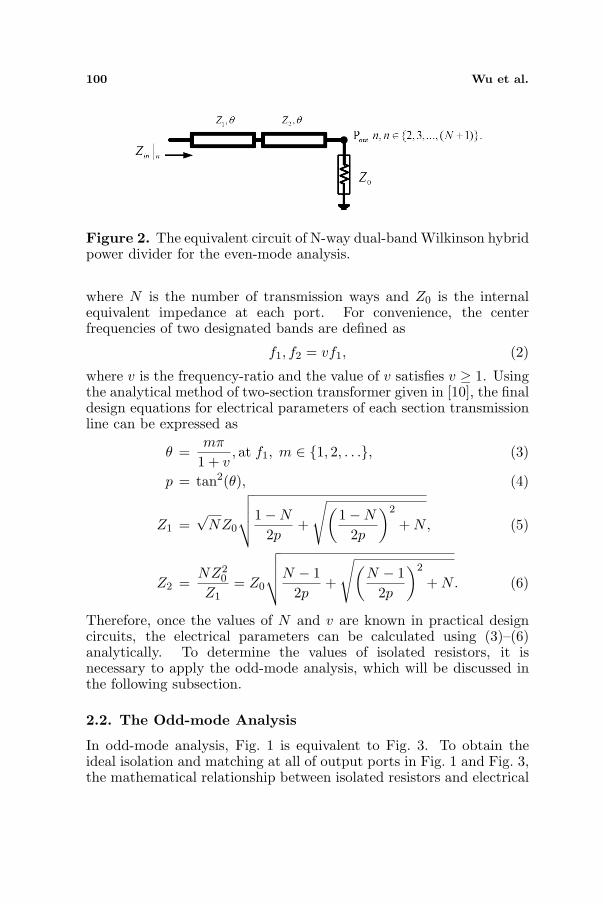
In even-mode analysis, Fig. 1 is simplified to Fig. 2. From Fig. 2, tomatch the input Port 1, the value of input equivalent impedance onarbitrary way n ∈ 2, 3, . . . , (N + 1) should be calculated by
Zin |n = NZ0, (1)
100 Wu et al.
Figure 2. The equivalent circuit of N-way dual-band Wilkinson hybridpower divider for the even-mode analysis.
where N is the number of transmission ways and Z0 is the internalequivalent impedance at each port. For convenience, the centerfrequencies of two designated bands are defined as
f1, f2 = vf1, (2)
where v is the frequency-ratio and the value of v satisfies v ≥ 1. Usingthe analytical method of two-section transformer given in [10], the finaldesign equations for electrical parameters of each section transmissionline can be expressed as
θ =mπ
1 + v, at f1, m ∈ 1, 2, . . ., (3)
p = tan2(θ), (4)
Z1 =√
NZ0
√√√√1−N
2p+
√(1−N
2p
)2
+ N, (5)
Z2 =NZ2
0
Z1= Z0
√√√√N − 12p
+
√(N − 1
2p
)2
+ N. (6)
Therefore, once the values of N and v are known in practical designcircuits, the electrical parameters can be calculated using (3)–(6)analytically. To determine the values of isolated resistors, it isnecessary to apply the odd-mode analysis, which will be discussed inthe following subsection.
2.2. The Odd-mode Analysis
In odd-mode analysis, Fig. 1 is equivalent to Fig. 3. To obtain theideal isolation and matching at all of output ports in Fig. 1 and Fig. 3,the mathematical relationship between isolated resistors and electrical

Progress In Electromagnetics Research, PIER 101, 2010 101
parameters of transmission lines can be written as
ZTemp =jZ1R1 tan(θ)
jZ1 tan(θ) + R1, (7)
1Z0
=Z2 + jZTemp tan(θ)
Z2[ZTemp + jZ2 tan(θ)]+
1R2
, (8)
where ZTemp is the internal input impedance shown in Fig. 3. Aftercombining (7) with (8) and separating the real and imaginary part, wecan obtain the following equations:(
1Z0
− 1R2
)Z1Z
22 tan2(θ) = R1[Z1 tan2(θ)− Z2], (9)
(1Z0
− 1R2
)R1(Z1 + Z2) = Z1. (10)
Solving (9) and (10) simultaneously, the final analytical solutions ofisolated resistors are obtained as follows (The Equation (4) is used.),
R1 =
√Z2
1Z22p
(Z1 + Z2)(Z1p− Z2), (11)
R2 =Z0Z2
√p(Z1 + Z2)
Z2
√p(Z1 + Z2)− Z0
√pZ1 − Z2
. (12)
Obviously, according to (3)–(6), (11) and (12), the values of electricalparameters of transmission lines, isolated resistors R1 and R2 can becalculated directly. Consequently, when the first frequency f1, thefrequency-ratio v, and the number of ways N are fixed, based on thestructure shown in Fig. 1 and the above closed-form design equations,this generalized and flexible N-way dual-band power divider can bedesigned easily. Additionally, the implemented structures of this N-way dual-band power divider depend on special technologies, such asmicrostrip, strip-line, spline, coaxial cable, etc.
Figure 3. The equivalent circuit of N-way dual-band Wilkinson hybridpower divider for the odd-mode analysis.

102 Wu et al.
2.3. The Available Scope of the Frequency-ratio for Realand Positive Resistors
Here, the available scope of the frequency-ratio in this generalized N-way dual-band power divider is discussed. To assure that the values ofisolated resistors R1 and R2 are real and positive, from (11) and (12),the following condition should be satisfied simultaneously:
Z1 tan2(θ)− Z2 ≥ 0, (13)
Z2
√tan2(θ)(Z1 + Z2)− Z0
√Z1 tan2(θ)− Z2 ≥ 0. (14)
Substituting (5) and (6) into (13) and (14) at the same time, theconstraint situation can be rewritten and simplified as,
p2 ≥ 1, (15)
N − 12p
≥ −√(
N − 12p
)2
+ N. (16)
Because N > 1, the inequality (16) will be satisfied unconditionally.Therefore, the final constraint condition is only inequality (15). Tobegin with, tan(θ) > 0 is considered. Thus, using (3) and (4), theaccurate condition tan(θ) > 1 is obtained and the correspondingcondition including initial parameters (such as the frequency-ratio vand the defined positive integer m) can be expressed as
k +14≤ m
1 + v<
12
+ k, k ∈ 0, 1, 2, . . .. (17)
And then, tan(θ) < 0 is considered. Obviously, the values of (11)and (12) must be real and positive when the inequality (15) is satisfied.Similarly, tan(θ) < −1 can be obtained directly and the correspondingcondition is written as
k +12
<m
1 + v≤ 3
4+ k, k ∈ 0, 1, 2, . . .. (18)
After analyzing the internal and special case that m/(1 + v) = 0.5(The simplified results of this case are Z1 =
√N√
NZ0, Z2 =√√NZ0, R1 =
√NZ0/(
√1 +
√N), R2 =
√1 +
√N(
√1 +
√N +
1)Z0/√
N.) and combining (17) and (18), the final total situation canbe summarized as
k +14≤ m
1 + v≤ 3
4+ k, k ∈ 0, 1, 2, . . .. (19)
Therefore, once the values of m and v satisfy the inequality (19), allof the final design parameters are real and positive. Thus, the designprocedure will be practical.

Progress In Electromagnetics Research, PIER 101, 2010 103
2.4. Design Charts for Normalized CharacteristicImpedances of Transmission Lines and Resistors
When the values of N and port impedance Z0 change, the values ofcharacteristic impedances of transmission lines and isolated resistorswill change accordingly. For convenience in designing common multi-way dual-band power dividers, Fig. 4 and Fig. 5 give the designcharts for normalized characteristic impedances and resistors. Themathematical definitions of normalized parameters are as follows:z1 = Z1/Z0, z2 = Z2/Z0, r1 = R1/Z0, and r2 = R2/Z0. In addition,
(a) (b)
Figure 4. The normalized characteristic impedances (z1 and z2)against the frequency-ratio v for various values of N when (a) m = 1,and (b) m = 2.
(a) (b)
Figure 5. The normalized resistances (r1 and r2) against thefrequency-ratio v for various values of N when (a) m = 1, and (b)m = 2.

104 Wu et al.
as shown in both Fig. 4(a) and Fig. 4(b), the larger the N valueis, the larger the corresponding values of normalized characteristicimpedances are. The value of z1 decreases as v is increased from 1to 3 while the value of z2 increases as v is increased from 1 to 3 inFig. 4(a). Note that the monotonic properties cannot be observedfrom Fig. 4(b) when m = 2 is adopted. Fig. 5(a) and Fig. 5(b) plot,respectively, the normalized resistances of two isolated resistors withm = 1 and m = 2 when N = 2, 3, 4, 5 are considered. Fortunately,the values of isolated resistors are in the available range of practicallumped-elements when the standard 50-Ω transmission line is used.
2.5. Special Case of the Generalized N-way Dual-bandPower Divider
A special case is discussed in this subsection. When v = 3 and m = 1,tan(θ) = 1 can be obtained. Thus, from (5), (6), (11) and (12), thefollowing simplest results can be obtained:
Z1 = Z2 =√
NZ0, (20)R1 = +∞, R2 = Z0. (21)
Actually, the Equations (20) and (21) are the same with the resultsgiven in [1]. In other words, this paper can be considered asthe extension of the N-way single-band power divider developed byWilkinson in 1960.
3. NUMERICAL EXAMPLES
For theoretical verification, twelve examples are designed using theclosed-form design equations (3)–(6), (11), and (12). Numerical resultsof these examples are based on the lossless transmission line and idealresistor models. The power dividers with different ways are presentedbelow in details.
3.1. Two-way Dual-band Power Dividers
In two-way dual-band power dividers, four cases (Case 1–Case 4)with different frequency-ratios are designed and the detailed designparameters are listed in Table 1. The amplitude responses of S-parameters over different frequency ranges are shown in Fig. 6.Obviously, ideal return loss of each port and isolation between outputports are attained with insertion loss of 3 dB at two desired frequenciessimultaneously in these four cases.

Progress In Electromagnetics Research, PIER 101, 2010 105
Table 1. Final parameters of four cases in two-way dual-band powerdivider.
f1 = 1GHz, Z0 = 50 Ω, N = 2.Case 1v = 1.4m = 1
Case 2v = 2m = 1
Case 3v = 2.4m = 1
Case 4v = 4m = 2
θ(rad)f1 1.3090 1.0472 0.9240 1.2566Z1(Ω) 83.0292 79.2885 76.0768 82.5352Z2(Ω) 60.2198 63.0608 65.7231 60.5802R1(Ω) 47.0892 54.9005 67.5861 47.8985R2(Ω) 130.0199 101.4777 82.9060 125.6302
(Case 3) (Case 4)
(Case 1) (Case 2)
Figure 6. The amplitude responses of S-parameters of Case 1–Case4 in two-way dual-band power dividers.

106 Wu et al.
Table 2. Final parameters of four cases in three-way dual-band powerdivider.
f1 = 1GHz, Z0 = 50 Ω, N = 3.Case 5v = 1.4m = 1
Case 6v = 2m = 1
Case 7v = 2.4m = 1
Case 8v = 4m = 2
θ(rad)f1 1.3090 1.0472 0.9240 1.2566Z1(Ω) 111.6381 103.5797 96.9501 110.5563Z2(Ω) 67.1814 72.4080 77.3594 67.8387R1(Ω) 54.2673 63.4294 78.1527 55.2232R2(Ω) 117.7062 93.2750 77.6203 113.9242
(Case 7) (Case 8)
(Case 5) (Case 6)
Figure 7. The amplitude responses of S-parameters of Case 5–Case8 in three-way dual-band power dividers.

Progress In Electromagnetics Research, PIER 101, 2010 107
Table 3. Final parameters of four cases in four-way dual-band powerdivider.
f1 = 1GHz, Z0 = 50 Ω, N = 4.Case 9v = 1.4m = 1
Case 10v = 2m = 1
Case 11v = 2.4m = 1
Case 12v = 4m = 2
θ(rad)f1 1.3090 1.0472 0.9240 1.2566Z1(Ω) 137.6663 124.9621 114.8844 135.9375Z2(Ω) 72.6394 80.0243 87.0440 73.5632R1(Ω) 59.9165 70.4512 87.1217 61.0256R2(Ω) 110.1954 88.1287 74.2411 106.7539
(Case 11) (Case 12)
(Case 9) (Case 10)
Figure 8. The amplitude responses of S-parameters of Case 9–Case12 in four-way dual-band power dividers.

108 Wu et al.
3.2. Three-way Dual-band Power Dividers
Similarly, in three-way dual-band power dividers, four cases (Case 5–Case 8) with different frequency-ratios are designed and the detaileddesign parameters are listed in Table 2. The amplitude responses of S-parameters over different frequency ranges are shown in Fig. 7. In thesecases, ideal matching of each port, isolation between output ports,and insertion loss of 4.77 dB are satisfied at two desired frequenciessimultaneously.
3.3. Four-way Dual-band Power Dividers
Finally, in four-way dual-band power dividers, four cases (Case 9–Case 12) with different frequency-ratios are designed and the detaileddesign parameters are listed in Table 3. The amplitude responses ofS-parameters over different frequency ranges are shown in Fig. 8. Asillustrated in Fig. 8, the matching of both the input port 1 and outputports at two frequencies is ideal, isolation between output ports attwo frequencies is perfect, and the insertion loss equals to 6 dB at twodesired frequencies simultaneously.
It is necessary to point out that the values of transmissionparameters Si1,i=2,3,..., isolation parameters Sij,i=2,3,...,j=2,3,...,i 6=j ,and output matching Sii,i=2,3,... maintain the same when locationsof ports change in these ideal calculations. Therefore, Fig. 6, Fig. 7,and Fig. 8 only show four different S-parameters including S21, S11,S22, and S32. In addition, when the frequency-ratio is relatively small,these generalized power dividers can be used as wideband ones withN-way, such as Case 1, Case 5, and Case 9. It can be also observedfrom Case 4, Case 8, and Case 12 that these power dividers have twoseparated bands with bandwidth enhancement.
4. MICROSTRIP EXAMPLES
In this section, for experimental verification, a two-way power divideroperating at 1 GHz and 2.4 GHz and a three-way power divideroperating at 1 GHz and 2 GHz are fabricated in microstrip technology.The design parameters are obtained from Case 3 in Table 1 and Case 6in Table 2, which is given in Section 3. In these two examples, the F4Bsubstrate with a dielectric constant of 2.65 and a thickness of 0.8 mmis chosen. Photographs of the two-way fabricated power divider andthe three-way one are shown in Fig. 9 and Fig. 10, respectively. Inaddition, the area sizes of the two-way fabricated power divider andthe three-way one are 71× 36mm2 and 86× 44 mm2, respectively. All

Progress In Electromagnetics Research, PIER 101, 2010 109
Figure 9. Photograph ofthe two-way dual-band fabricatedpower divider (Case 3).
Figure 10. Photograph of thethree-way dual-band fabricatedpower divider (Case 6).
(a) (b)
Figure 11. The measured S-parameters of the two-way dual-bandpower divider (Case 3): (a) Magnitude; (b) Phase difference includingcalculated results (Ang (S31)–Ang (S21)).
the measured results shown in Fig. 11 and Fig. 12 are collected fromAgilent N5230C network analyzer.
From Fig. 11(a), in this microstrip two-way dual-band powerdivider, the absolute value of transmission parameters S21(S21
∼= S31)is approximately −3.1 dB while all of the input and output portsmatching and isolation are below −15 dB at both 1 GHz and 2.4GHz.As shown in Fig. 11(b), the phase difference between the output port3 and the output port 2 is in the range of ±0.8 at both 1 GHz and2.4GHz. Therefore, according to calculated results shown in Fig. 6(Case 3), there is a good agreement between our design goals andpractical measurements.
In the microstrip three-way dual-band power divider, as shown inFig. 12(a), all of the input matching |S11| and the output matchingincluding |S22|, |S33|, and |S44| are below −15 dB at both 1 GHz and2GHz. From Fig. 12(b), all of measured transmission parameters |S21|,

110 Wu et al.
(e)
(d)(c)
(b)(a)
Figure 12. The measured S-parameters of the three-way dual-bandfabricated power divider (Case 6): (a) Matching; (b) Transmission(Magnitude); (c) Isolation; (d) Transmission (Phase); (e) Transmission(Phase difference).
|S31| and |S41| are approximately equal and the corresponding valuesare in the range of−4.9 dB to−5.0 dB at 1 GHz and−5.2 dB to−5.5 dBat 2 GHz. The good isolation between the output ports (such as theport 2, 3, and 4) can be observed from Fig. 12(c). Moreover, the phaseinformation is shown in Fig. 12(d) and Fig. 12(e). The electrical length

Progress In Electromagnetics Research, PIER 101, 2010 111
at the port 3 is shorter than other output ports in actual circuit shownin Fig. 10, thus, it is indicated in Fig. 12(e) that the phase differencebetween the port 4 and the port 3 decreases linearly as the operatingfrequency increases. Meanwhile, because path electrical lengths at theport 2 and the port 4 are equal, the phase difference between thesetwo output ports is in the range of ±1.2 at 1 GHz and 2 GHz. Infact, a few disagreements between calculation and measurement maybe caused by the loss characteristic of the substrate and two jumperwires connecting isolated resistors as the common junctions in thisplanar structure (shown in Fig. 10). In a word, the measurements ofthis three-way fabricated power divider operating at 1 GHz and 2GHzcan satisfy the requirement of common dual-band systems.
In summary, there are good agreements between the measuredresults and the desired performances in these two microstrip examples,in other words, these examples effectively verify the analyticalapproach for the generalized N-way dual-band power divider as typicalsamples. Furthermore, the four or more ways dual-band power dividersare not suitable for planar implementations, thus, a three-dimensionalstructure including splines and coaxial lines should be applied like theoriginal Wilkinson power divider [1].
5. CONCLUSIONS
An N-way Wilkinson dual-band power divider with simple structureand without reactive components is analyzed in this paper. The finalanalytical (closed-form) design equations are obtained and the designcharts of normalized parameters are given. The generalized structureand analytical design method are verified by twelve numerical examplesbased on ideal models and two practical examples in microstriptechnology. Actually, this N-way dual-band power divider may beused as an N-way wideband power divider when the frequency-ratio is relatively small and can be considered as the extensionof the conventional N-way Wilkinson power divider for single-bandapplications. The N-way (Multi-way) unequal dual-band powerdividers will need in-depth study.
ACKNOWLEDGMENT
This work was supported in part by National High Technol-ogy Research and Development Program of China (863 Pro-gram, No. 2008AA01Z211), Sino-Swedish IMT-Advanced CooperationProject (No. 2008DFA11780), and BUPT Excellent Ph.D. StudentsFoundation (CX200901).

112 Wu et al.
REFERENCES
1. Wilkinson, E., “An N-way hybrid power divider,” IRE Trans.Microw. Theory Tech., Vol. 8, No. 1, 116–118, 1960.
2. Yee, H. Y., F.-C. Chang, and N. F. Audeh, “N-way TEM-modebroad-band power dividers,” IEEE Trans. Microw. Theory Tech.,Vol. 18, No. 10, 682–688, 1970.
3. Nagai, N., E. Maekawa, and K. Ono, “New N-way hybrid powerdividers,” IEEE Trans. Microw. Theory Tech., Vol. 25, No. 12,1008–1012, 1977.
4. Saleh, A. A. M., “Planar electrically symmetric N-way hybridpower dividers/combiners,” IEEE Trans. Microw. Theory Tech.,Vol. 28, No. 6, 555–563, 1980.
5. Ahn, H.-R., K. Lee, and N.-H. Myung, “General design equationsof N-way arbitrary power dividers,” IEEE MTT-S InternationalMicrowave Symposium Digest, Vol. 1, 65–68, Jun. 6–11, 2004.
6. Eccleston, K. W., “N-way microwave power divider using two-dimensional meta-materials,” Electron. Lett., Vol. 42, No. 15, 863–864, 2006.
7. Eccleston, K. W. and J. Zong, “Implementation of a microstripsquare planar N-way metamaterial power divider,” IEEE Trans.Microw. Theory Tech., Vol. 57, No. 1, 189–195, 2009.
8. Rozzi, T., A. Morini, G. Venanzoni, and M. Farina, “Full-waveanalysis of N-way power dividers by eigenvalue decomposition,”IEEE Trans. Microw. Theory Tech., Vol. 57, No. 5, 1156–1162,2009.
9. Wu, Y. and Y. Liu, “Closed-form design method for unequallumped-elements wilkinson power dividers,” Microwave andOptical Technology Letters, Vol. 51, No. 5, 1320–1324, 2009.
10. Monzon, C., “A small dual-frequency transformer in twosections,” IEEE Trans. Microw. Theory Tech., Vol. 51, No. 4,1157–1161, 2003.
11. Wu, Y., Y. Liu, and S. Li, “A compact Pi-structure dual bandtransformer,” Progress In Electromagnetics Research, PIER 88,121–134, 2008.
12. Wu, Y., Y. Liu, and S. Li, “A dual-frequency transformer forcomplex impedances with two unequal sections,” IEEE Microw.Wireless Compon. Lett., Vol. 19, No. 2, 77–79, 2009.
13. Wu, Y., Y. Liu, S. Li, C. Yu, and X. Liu, “A generalizeddual-frequency transformer for two arbitrary complex frequency-dependent impedances,” IEEE Microw. Wireless Compon. Lett.,

Progress In Electromagnetics Research, PIER 101, 2010 113
Vol. 19, No. 12, 792–794, 2009.14. Wu, L., Z. Sun, H. Yilmaz, and M. Berroth, “A dual-frequency
Wilkinson power divider,” IEEE Trans. Microw. Theory Tech.,Vol. 54, No. 1, 278–284, 2006.
15. Cheng, K.-K. M. and C. Law, “A novel approach to the designand implementation of dual-band power divider,” IEEE Trans.Microw. Theory Tech., Vol. 56, No. 2, 487–492, 2008.
16. Park, M. J. and B. Lee, “A dual-band Wilkinson power divider,”IEEE Microw. Wireless Compon. Lett., Vol. 18, No. 2, 85–87,2008.
17. Yang, T., J.-X. Chen, X. Y. Zhang, and Q. Xue, “A dual-band out-of-phase power divider,” IEEE Microw. Wireless Compon. Lett.,Vol.18, No. 3, 188–190, 2008.
18. Wu, Y., Y. Liu, and X. Liu, “Dual-frequency power divider withisolation stubs,” Electron. Lett., Vol. 44, No. 24, 1407–1408, 2008.
19. Wu, Y., Y. Liu, and S. Li, “A new dual-frequency Wilkinson powerdivider,” Journal of Electromagnetic Waves and Applications,Vol. 23, No. 4, 483–492, 2009.
20. Wu, Y., Y. Liu, and S. Li, “Dual-band modified Wilkinson powerdivider without transmission line stubs and reactive components,”Progress In Electromagnetics Research, PIER 96, 9–20, 2009.
21. Wu, Y., Y. Liu, S. Li, and H. Zhou, “Compact dual-bandequal power divider circuit for large frequency-ratio applications,”Journal of Infrared Millimeter and Terahertz Waves, in press,2009.
22. Wu, Y., Y. Liu, S. Li, and C. Yu, “A new symmetric modifiedWilkinson power divider using L-type dual-band impedancematching structure,” Journal of Electromagnetic Waves andApplications, Vol. 23, No. 17/18, 2351–2362, 2009.
23. Li, X., S.-X. Gong, L. Yang, and Y.-J. Yang, “A novelwilkinson power divider for dual-band operation,” Journal ofElectromagnetic Waves and Applications, Vol. 23, No. 2–3, 395–404, 2009.
24. Law, C. and K.-K. M. Cheng, “Compact dual-band powerdivider design using branch-lines and resistors only,” Asia-PacificMicrowave Conference (APMC) 2008, 1–4, Dec. 16–20, 2008.
25. Wu, Y., H. Zhou, Y. Zhang, and Y. Liu, “An unequal Wilkinsonpower divider for a frequency and its first harmonic,” IEEEMicrow. Wireless Compon. Lett., Vol. 18, No. 11, 737–739, 2008.
26. Wu, Y., Y. Liu, Y. Zhang, J. Gao, and H. Zhou, “A dual bandunequal wilkinson power divider without reactive components,”

114 Wu et al.
IEEE Trans. Microw. Theory Tech., Vol. 57, No. 1, 216–222, 2009.27. Wu, Y., Y. Liu, and S. Li, “Unequal dual-frequency Wilkinson
power divider including series resistor-inductor-capacitor isolationstructure,” IET Microwaves, Antennas & Propagation, Vol. 3,No. 7, 1079–1085, 2009.
28. Wu, Y., Y. Liu, and S. Li, “An unequal dual-frequency Wilkinsonpower divider with optional isolation structure,” Progress InElectromagnetics Research, PIER 91, 393–411, 2009.
29. Wu, Y., Y. Liu, S. Li, and X. Liu, “A novel dual-frequency Wilkinson power divider with unequal power division,”Electromagnetics, Vol. 29, No. 8, 627–640, 2009.
30. Wu, Y., Y. Liu, S. Li, and C. Yu, “A new design methodfor unequal dual-band modified Wilkinson power divider,”Electromagnetics, accepted after revisions, 2010.
31. Feng, C., G. Zhao, X.-F. Liu, and F.-S, Zhang, “Planar three-waydual-frequency power divider,” Electron. Lett., Vol. 44, No. 2, 133–134, 2008.
32. Wang, W., W. Li, and D. Chen, “Design of N-way dual-frequencypower divider base on genetic algorithm,” 2009 InternationalConference on Networks Security, Wireless Communications andTrusted Computing (NSWCTC’09), Vol. 1, 274–277, Apr. 25–26,2009.
33. Shamsinejad, S., M. Soleimani, and N. Komjani, “Novelminiaturized Wilkinson power divider for 3G mobile receivers,”Progress In Electromagnetics Research Letters, Vol. 3, 9–16, 2008.
34. Oraizi, H. and M. S. Esfahlan, “Miniaturization of Wilkinsonpower dividers by using defected ground structures,” Progress InElectromagnetics Research Letters, Vol. 4, 113–120, 2008.
35. Fan, F., Z.-H. Yan, and J.-B. Jiang, “Design of a novelcompact power divider with harmonic suppression,” Progress InElectromagnetics Research Letters, Vol. 5, 151–157, 2008.
36. Chang, C.-P., C.-C. Su, S.-H. Hung, Y.-H. Wang, and J.-H. Chen,“A 6 : 1 unequal wilkinson power divider with EBG CPW,”Progress In Electromagnetics Research Letters, Vol. 8, 151–159,2009.