επιταξιζ - Page closed
12
EPITAXY 2005-04-17 August Yurgens 1 extended single-crystal film formation on top of a crystalline substrate Epitaxy strained relaxed matched substrate • Homoepitaxy (Si on Si) • Heteroepitaxy (AlAs on GaAs) homoepitaxy heteroepitaxy • optoelectronic devices (GaInN) • high-frequency wireless communication devices (GeSi) • high device packing densities • nanoscale quantum electronic and optical devices • magnetooptics and ferroelectrics Misfit = [a 0 (s)-a 0 (f)]/a 0 (f)
-
Upload
khangminh22 -
Category
Documents
-
view
1 -
download
0
Transcript of επιταξιζ - Page closed

EPITAXY 2005-04-17
August Yurgens 1
��������
extended single-crystal film formation on top of a crystalline
substrate
Epitaxy
strained relaxedmatched
substrate
• Homoepitaxy (Si on Si)• Heteroepitaxy (AlAs on GaAs)
homoepitaxy
heteroepitaxy
• optoelectronic devices (GaInN)• high-frequency wireless communication devices (GeSi)• high device packing densities• nanoscale quantum electronic and optical devices• magnetooptics and ferroelectrics
Misfit � = [a0(s)-a0(f)]/a0(f)

EPITAXY 2005-04-17
August Yurgens 2
Epitaxy Graphoepitaxy: films can be oriented even in the presense of a large misfit strain and absence of any bonding between the film and substrate
Graphoepitaxy of germanium on gratings with square-wave and sawtooth profiles M. W. Geis, B-Y. Tsaur, and D. C. Flanders
Applied Physics Letters Vol 41(6) pp. 526-529. September 15, 1982
Epitaxy Heteroepitaxy: coupled orientations of the thinfilm and substrate
Si: a0=5.431 ÅCoSi2: a0=5.365 ÅNiSi2: a0=5.406 Å
a)
GaAs: a0=5.654 ÅFe: a0=2.866 Å(110)Fe // (110)GaAs:[200]Fe // [100]GaAs
b)
Notation: (001)Ni // (001)Cu: [100]Ni // [100]Cu
thin film substrate
SrRuO3: a0=5.567 Å;b0=5.530 Å
YBa2Cu3O7: a0=3.82 Åb0=3.88 Å
(001)YBCO // (001)SRO:[100]YBCO // [110]SRO
c)

EPITAXY 2005-04-17
August Yurgens 3
Epitaxy Tilted-Layer: growth on vicinal-cut substrates
film
substrate
Epitaxy Lattice Misfitand Defects in Epitaxial Films
)S-�(14)/ln(2
1)/( 22
T νβµ
νϕ bdbSbYd
E +−−=
elastic dislocations
( ) 0/d
d T =Sb
E
��
���
�
+=�
�
���
�=bdb
bd
Yb
d ccc
βϕν
βϕ
µln
)�(18ln
�4
)1(2 νµ
+= Y
Critical thickness
minimum

EPITAXY 2005-04-17
August Yurgens 4
Epitaxy Lattice Misfitand Defects in Epitaxial Films
Epitaxy Dislocation Typesin Epitaxial Films
1: threading-edge dislocations
2: interfacial misfit dislocations3: threading screw dislocation
4: growth spiral 5: stacking fault in film
6: stacking fault in substrate
7: oval defects
8: hillock
9: precipitate or void

EPITAXY 2005-04-17
August Yurgens 5
Epitaxy Dislocation Typesin Epitaxial Films
Edge dislocation
Screw dislocation
Dislocation motion (plasticity)
tensile
compression
Epitaxy Dislocation Typesin Epitaxial Films
Stacking faults as translation boundaries between the crystals with parallel orientationTwin boundaries with a certain difference in the orientation between the crystalsGrain boundaries between regions of the crystal with arbitrary orientationsPhase boundaries between regions of different structure
From: Hartmut S. Leipner : Structure of imperfect crystals

EPITAXY 2005-04-17
August Yurgens 6
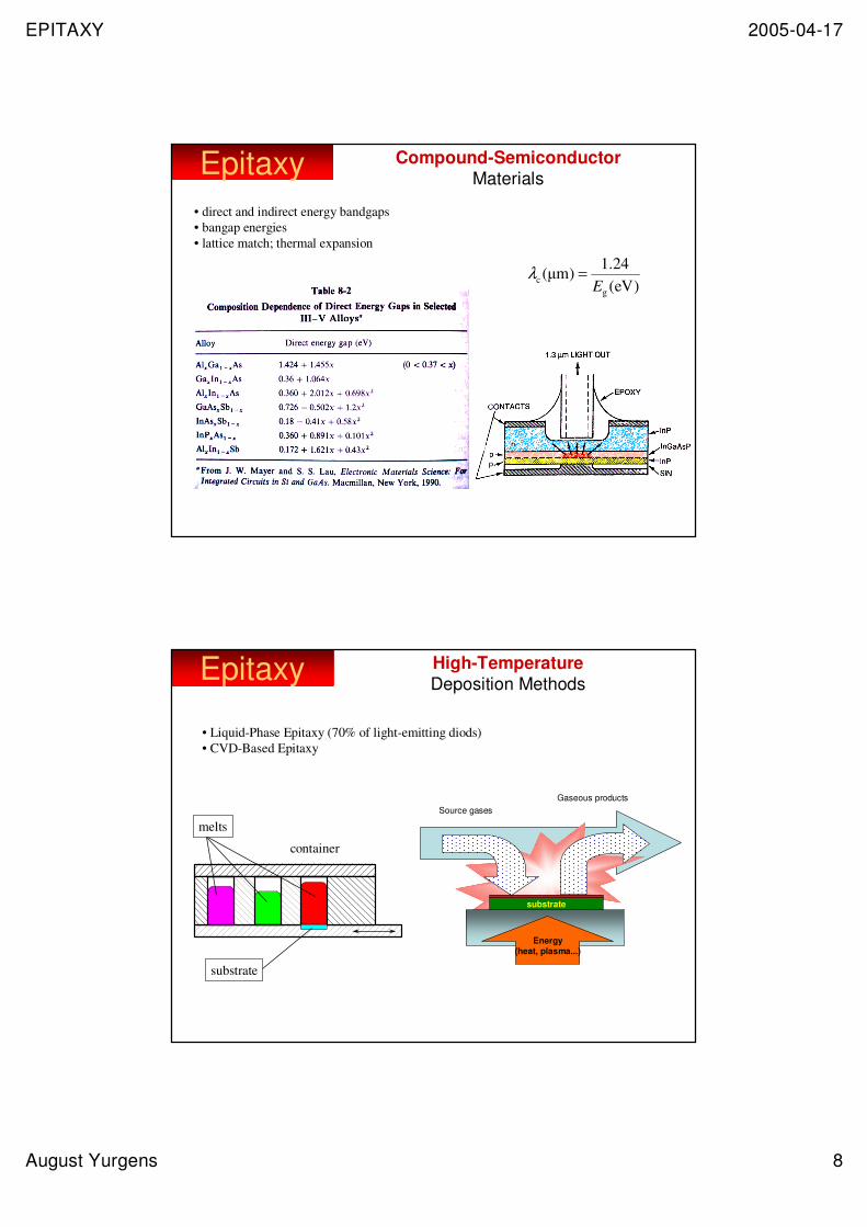
Epitaxy Compound-SemiconductorMaterials:
Designing Film-Substrate Match• direct and indirect energy bandgaps• bangap energies• lattice match; thermal expansion
http://rleweb.mit.edu/Publications/pr143/chapter14-web.pdf
http://www.hhi.fraunhofer.de
Epitaxy Compound-SemiconductorMaterials:
Designing Film-Substrate Match
In direct gap semiconductors such as GaAs the top of the valence band and the bottom of the conduction band occur at the same k-vector.
k = 0

EPITAXY 2005-04-17
August Yurgens 7
Epitaxy Compound-SemiconductorMaterials:
Designing Film-Substrate Match
from Britney Spears Guide to Semiconductor Physics: Indirect-gap ... : http://britneyspears.ac/physics/indirect/indirect.htm
Indirect Bandgap SemiconductorsNot all semiconductor materials have the minimum of the conduction band above the top of the valence band in the E-k bandstructure. These materials are known as indirect semiconductors. Examples include Si, Ge and AlAs. For indirect bad gap semiconductors, the conduction band can be crudely approximated by the following equation near the conduction band minimum.
E(k)=Eg+h2(k-k0)2/(2me)
where k0 is the offset in the conduction band minimum. For light emitting devices, indirect band gap semiconductors are not at all promising.
To see why, consider the band edge diagram of an indirect band gap semiconductor. The momentum of an electron in the conductionband is different from a hole in the valence band.
For a transition to occur, requires both a photon of frequency � and also a phonon of frequency �.Clearly, the probability of these two events happening is less likely than an electron making a single direct transition, as occurs in direct bandgap semiconductors.
Epitaxy Compound-SemiconductorMaterials:
Designing Film-Substrate Match• direct and indirect energy bandgaps• bangap energies• lattice match; thermal expansion
Relationship between energy gaps and lattice constants of representative semiconductors. Energy gap of GaNAs is shown in this figure as a representative of III-V-N nitrides. The solid line is an extrapolation of the experimental results close to GaAs and cubic GaN based on the dielectric model, and negative energy gap is expected in-between from this extrapolation. http://opmac06.es.hokudai.ac.jp/opres/resthe/r2/res2e.html#res2_1
EPITAXY 2005-04-17
August Yurgens 8
Epitaxy Compound-SemiconductorMaterials
• direct and indirect energy bandgaps• bangap energies• lattice match; thermal expansion
)eV(24.1
)�m(g
c E=λ
Epitaxy High-TemperatureDeposition Methods
• Liquid-Phase Epitaxy (70% of light-emitting diods)• CVD-Based Epitaxy
substrate
melts
container
Energy(heat, plasma...)
substrate
Source gasesGaseous products
EPITAXY 2005-04-17
August Yurgens 9
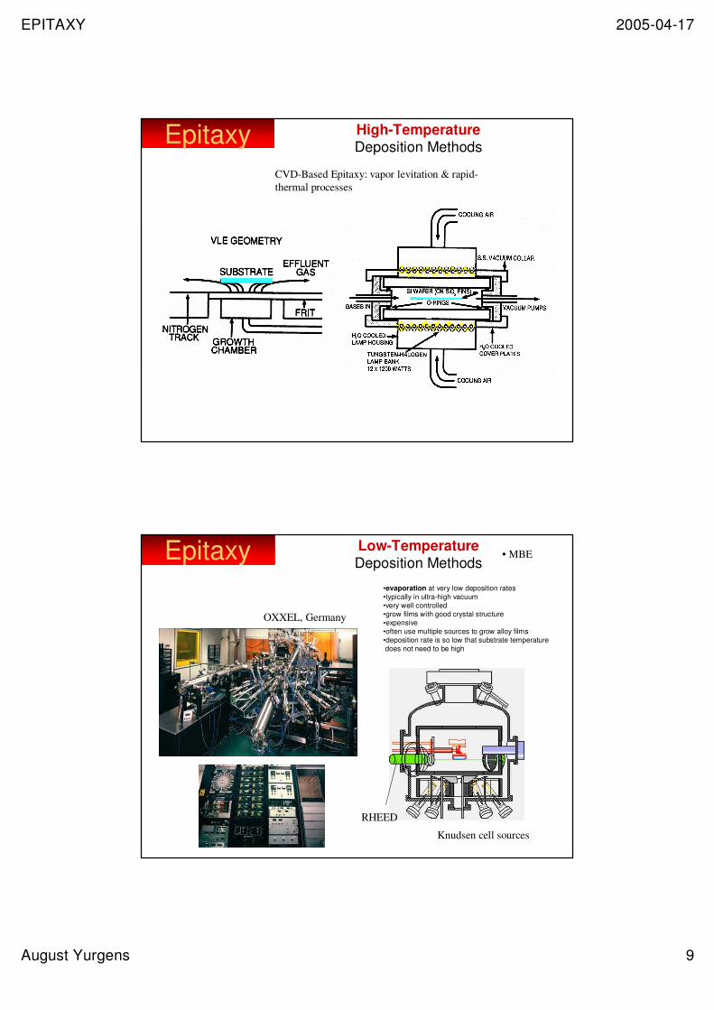
Epitaxy High-TemperatureDeposition Methods
CVD-Based Epitaxy: vapor levitation & rapid-thermal processes
Epitaxy Low-TemperatureDeposition Methods
• MBE
OXXEL, Germany
Knudsen cell sources
RHEED
•evaporation at very low deposition rates •typically in ultra-high vacuum •very well controlled •grow films with good crystal structure •expensive •often use multiple sources to grow alloy films •deposition rate is so low that substrate temperature does not need to be high
EPITAXY 2005-04-17
August Yurgens 10
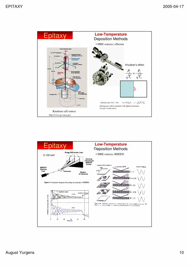
Epitaxy Low-TemperatureDeposition Methods
• MBE sources; effusion
Knudsen cell sourcehttp://www.grc.nasa.gov
2
2
1
1
TP
TP =
Knudsen’s effect
effusion rate (1/s) ~ Snv 0BB /~ , mTkvTkPn =effusing gas will be enriched with lighter molecules(isotope rectification)
Epitaxy Low-TemperatureDeposition Methods
• MBE sources; RHEED5-100 keV

EPITAXY 2005-04-17
August Yurgens 11
Epitaxy Less Common Epitaxy Processes
• MBE Allotaxy• Mesotaxy
J. Phys. D: Appl. Phys. 31 (7 January 1998) 1-17Molecular beam allotaxy: a new approach to epitaxial heterostructuresSiegfried Mantl
Si
2x1017 cm-2 200 keV Co+
after annealing at ~1000 C
CoSi2
Epitaxy Less Common Epitaxy Processes
• van der Waals epitaxy
Se/Te; [(Mo,Nb,)(S,Te,Se)2]/(mica,SbS2,S-GaAs);GaSe/Se-GaAs; GaSe/H-Si
• large lattice mismatch• still an epitaxial growth

EPITAXY 2005-04-17
August Yurgens 12
Epitaxy Less Common Epitaxy Processes
Solid particles in a liquid->colloid (paint, ketchup). The particles are usually very small, often less than 10�m in diameter.
• Colloidal epitaxy