Chemical Aspects of Electronic Ceramics Processing - DTIC
461
Chemical Aspects of Electronic Ceramics Processing
-
Upload
khangminh22 -
Category
Documents
-
view
0 -
download
0
Transcript of Chemical Aspects of Electronic Ceramics Processing - DTIC

Chemical Aspects of Electronic Ceramics Processing

MATERIALS RESEARCH SOCIETY
SYMPOSIUM PROCEEDINGS VOLUME 495
Chemical Aspects of Electronic Ceramics Processing
Symposium held November 30-December 4,1997, Boston, Massachusetts, U.S.A.
EDITORS:
Prashant N. Kumta Carnegie Mellon University
Pittsburgh, Pennsylvania, U.S.A.
Aloysius F. Hepp ^ NASA Lewis Research Center H <5 Cleveland, Ohio, U.S.A.
1U ST3 5 a> © David B. Beach UJ DC "E Oak Ridge National Laboratory ho- Oak Ridge, Tennessee, U.S.A.
l2 6? c Barry Arkles Jic fc- #Q Gelest, Inc. 25 5 ""5 Tullytown, Pennsylvania, U.S.A.
S £ to John J. Sullivan —" ' "- MKS Instruments, inc.
CO 5 H" o Andover, Massachusetts, U.S.A. 22<
IMJRISI Materials Research Society
Warrendale, Pennsylvania

This work relates to Department of Navy Grant N00014-98-1-002 issued by the Office of Naval Research. The United States Government has a royalty-free license throughout the world in all copyrightable material contained herein.
Single article reprints from this publication are available through University Microfilms Inc., 300 North Zeeb Road, Ann Arbor, Michigan 48106
CODEN: MRSPDH
Copyright 1998 by Materials Research Society. All rights reserved.
This book has been registered with Copyright Clearance Center, Inc. For further information, please contact the Copyright Clearance Center, Salem, Massachusetts.
Published by:
Materials Research Society _ '"'' 506 Keystone Drive ¥? J:1 Warrendale, PA 15086 .:- Telephone (724) 779-3003 TT Fax (724) 779-8313 Website: http://www.mrs.org/ s
Library of Congress Cataloging in Publication Data \- , ■
Chemical aspects of electronic ceramics processing : symposium held -' '2 November 30-December 4, 1997, Boston, Massachusetts, U.S.A. / editors ■ ^ Prashant N. Kumta, Aloysius F. Hepp, David B. Beach, Barry Arkles, ; •; John J. Sullivan. ; r
p. cm. - (Materials Research Society symposium proceedings, ; 'r ISSN-0272-9172 ; v. 495) '„:;
Includes bibliographical references and indexes. ' '; ': ISBN 1-55899-400-9
1. Ceramics-Congresses. 2. Electronic ceramics-Chemistry-CongressesV * 3. Vapor-plating-Congresses. I. Kumta, Prashant N., II. Hepp, Aloysius F! ,- HI. Beach, David B., IV. Arkles, Barry, V. Sullivan, John J., VI. Series "
TP786.C485 1998 98-21858 620.1'4-dc21 CIP
Manufactured in the United States of America

CONTENTS
Preface xi
Acknowledgments xiii
Materials Research Society Symposium Proceedings xiv
PARTI: CHEMICAL VAPOR DEPOSITION OF OXIDE CERAMICS
"Metalorganic-Chemical-Vapor-Deposition Routes to Films of Transparent Conducting Oxides 3
A. Wang, S.C. Cheng, J.A. Belot, R.J. McNeely, J. Cheng, B. Marcordes, T.J. Marks, J.Y. Dal, R.P.ti. Chang, J.L. Schindler, M.P. Chudzik, and C.R. Kannewurf
"Control of Growth Dynamics by Molecular Design in the MOCVD of Electronic Ceramics 11
A.C. Jones, T.J. Leedham, P.J. Wright, M.J. Crosbie, D.J. Williams, P.A. Lane, and P. O'Brien
'Epitaxial Ferroelectric Oxides for Electro-Optic and Nonlinear Optical Applications 23
B.W. Wesseis
*Room-Temperature Magnetoresistance in LaxCayMn03 Thin Films Deposited by Liquid Delivery Chemical vapor Deposition 31
D. Studebaker, M. Todd, Q. Doubinina, C. Seegal, and T.H. Baum
Microstructural and Photoluminescence Studies on Europium-Doped Yttrium Oxide Films Synthesized by Metalorganic Vapor Deposition 39
O.A. tlirata, J. McKittrick, J. Yi, S.d. Pattillo, K.V. Salazar, and M. Trkula
Low-Temperature Chemical Vapor Deposition of Titanium Dioxide Thin Films Using Tetranitratotitanium (IV) 45
D.C. Qilmer, W.L. Oladfelter, D.O. Colombo, C.J. Taylor, J. Roberts, S.A. Campbell, H-S. Kim, Q.D.^ Wilk, and M.A. Oribelyuk
Chemical Vapor Deposition of Strontium Ruthenate Thin Films from BIS(2,4-Dimethylpentadienyl)Ruthenium and Bis(Tetramethylheptanedionato)Strontium 51
Richard Breitkopf, Lamartine J. Meda, Terry Haas, and Rein U. Kirss
Spectroscopic and Structural Studies of Some Precursors for the Deposition of PZT and Related Materials by MOCVD 57
Kirsty A. Fleeting, Tony C. Jones, Tim Leedham, M. Azad Malik, Paul O'Brien, and David J. Otway
*lnvited Paper

New Liquid Precursors for Chemical Vapor Deposition 63 Roy G. Gordon, Feng Chen, Nicholas J. Diceglie, Jr., Amos Kenigsberg, Xinye Liu, Daniel J. Teff, and John Thornton
Single-Source CVD of UAI02 69 Wonyong Koh, Su-Jin Ku, and Yunsoo Kim
Chemical Vapor Deposition of Ruthenium Dioxide Thin Films from BIS(2, 4-Dimethylpentadienyl)Ruthenium 75
Lamartine Meda, Richard C. Breitkopf, Terry E. Haas, and Rein U. Kirss
PART II: CHEMICAL VAPOR DEPOSITION OF NONOXIDE CERAMICS
"Precursors for Vapor Deposition of Blue Phosphors for Electroluminescent Flat-Panel Displays 83
William S. Rees, Jr., Oliver Just, Henry A. Luten, and David J. Otway
•Precursors for the Chemical Vapor Deposition of Titanium Nitride and Titanium Aluminum Nitride Films 95
Charles H. Winter, Peggy J. McKarns, and Joseph T. Scheper
•Silicon Nitride Films Deposited by Atmospheric Pressure Chemical Vapor Deposition 107
Xian Lin, Denis Endisch, Xiaomeng Chen, Alain Kaloyeros, and Barry Arkles
Novel Antimony Precursors for Low-Temperature CVD of Anfimonide Thin Films 113
Michael A. Todd, Qautam Bhandari, and T.tl. Baum
Preparation of Boron Nitride Thin Films by MOCVD 119 Sang-Yeol Lee, Yong-Qi Jin, Young-Woo Nam, Joong Kee Lee, and Dalkeun Park
Kinetics of Reactions Relevant to the Chemical Vapor Deposition of Indium Compounds 125
M.D. Allendorf and AM. NcDaniel
Growth of Highly Transparent Nanocrystalline Diamond Films by Microwave CVD 131
D.M. Bhusari, H.H. Chen, J.R. Yang, S.T. Lin, T.Y. Wang, and L.C. Chen
Investigation of Low-Molecular-Weight Carbosilanes as Potential Single-Source Precursors to Silicon Carbide 139
M.A. Lienhard, L. V. Interrante, and D.J. Larkin
New Magnesium Precursors for Doping Semiconductor Films 147
Charles H. Winter, Jennifer L. Sebestl, and Mary Jane lieeg
*lnvited Paper
VI

Temperature-Dependent Studies of a-SiC:H Growth by Remote Plasma CVD Using Methylsilanes 153
Moon-Sook Lee, Pratik Lai, and Stacey F. Bent
PECVD of Amorphous Silicon Carbide From Trimethylsilane 159 J.T. Kelliher, M. Massuda, P.A. DiFonzo, and T.R. Heal
Low-Pressure CVD Growth of AlxTh.xN Films With Tetrakis-(Dimethylamido)Titanium(TDMAT) and Dimethylaluminumhydride (DMAH) Precursors 165
Y-M. Sun, J. Endle, J.Q. Ekerdt, n.M. Russell, M.D. Healy, andJ.M. White
Spray Chemical Vapor Deposition of CulnS2 Thin Films for Application in Solar Cell Devices 171
Jennifer A. Holiingsworth, William E. Buhro, Aloysius F. Hepp, Philip P. Jenkins, and Mark A. Stan
Deposition of Ti(C,N) Thick Films by ILPCVD Starting From TDMAT 177
S. Oilles, N. Bourhila, J.P. Senateur, R. Madar, R.A. Levy, and E. Bianquet
PART III: SOLUTION ROUTES TO CERAMIC MATERIALS \
•Chemically Prepared Lead Magnesium Niobate Dielectrics 185 B.A. Tuttle, J.A. Voigt, D.L. Sipola, W.R. Olson, and D.M. Qoy
Low-Temperature, Solution-Based Routes to Nanocrystalline InS Powders and Thin Films 197
Jennifer A. Holiingsworth and William E. Buhro
Solution Processing of YBa2Cu307.x Thin Films 203 A. Singhal, M. Paranthaman, E.D. Specht, R.D. Hunt, D.B. Beach, P.M. Martin, and D.F. Lee
Room-Temperature Phase-Selective Synthesis of Metastable Lead Chromium Oxides 209
Kenneth M. Doxsee and Meehae Jang
Synthesis and Photoresponse of Rare-Earth-Doped Phosphosilicates 215
Z. Cao, B.I. Lee, W.D. Samuels, Q.J. Exarhos, and L. Wang
Structural Characterization of a Series of New Ternary K-Nitride Compounds 221
K.S. Weil and P.n. Kumta
The Spray Deposition of Transition-Metal Nitride Thin Films Using Alcohol Based Precursor Solutions 227
K.S. Weil and P.n. Kumta
*lnvited Paper
VII

A Comparison of Ferroelectric Thin Films Prepared by Sol-Gel, Metalorganic Deposition, and Photochemical Methods 233
Y. Shi, S.L. Blair, I. Yaroslavsky, and R.H. Hill
Preparation of Ti-Based Ferroelectric Thin Films From Heterometallic Coordination Compounds 239
V.T. Moshnyaga, I.V. Khoroshun, P.A. Petrenko, D.O. Shaban, and L.L. Kuliuk
Effect of Precursors and Stacking Structures on Crystallization of Multilayered Lead Zirconate Titanate Thin Films by Sol-Gel Method 245
fi. Suzuki, Y. Hondo, S. Kaneko, T. Tsutsumi, T. Miura, and T. Hayashii
Effects of Reaction Conditions on Deposition of Ferrites from Alkaline Metal Hydroxide Gels 251
Karl F. Schoch, Jr. and Theodore R. Vasilow
Synthesis and Electro-optical Properties of Potassium Titanyl Phosphate Thin Films by Sol-Gel Method 257
Jianping Zhang, Burtrand I. Lee, Feiling Wang, and Melvin A. Leitheiser
Sol-Gel Synthesis of Rare-Earth Aluminate Films as Buffer Layers for High Tc Superconducting Films 263
David B. Beach, Catherine E. Vallet, Mariappan Paranthaman, Eliot D. Specht, Jonathan S. Morrell, and Ziling B. Xue
Sol-Gel Synthesis of Epitaxial Films of (Sr,Ba)Bi2(Nb,Ta)209 and Bi4Ti3012 on (100)SrTiO3 271
Jonathan S. Morrell, Ziling B. Xue, Eliot D. Specht, and David B. Beach
PART IV: CHARACTERIZATION AND APPLICATION OF CERAMIC MATERIALS
'Nanoporous Silica for Low K Dielectrics 279 Teresa Ramos, Steve Wallace, and Douglas M. Smith
"Automotive Applications of Materials Prepared by Ceramic Precursor and Sol-Gel Routes 287
C.K. liarula, A. Varshney, M.P. Everson, P. Schmitz, L.F. Allard, A. Qandopadhyay, T. Suren Lewkbandara, C.H. Winter, P. Czubarow, and D. Seyferth
'Morphology and Electron Emission Properties of Nanocrystalline CVD Diamond Thin Films 299
Alan R. Krauss, Dieter M. Qruen, Daniel Zhou, Thomas Q. McCauley, Lu Chang Qin, Timothy Corrigan, Orlando Auciello, and R.P.H. Chang
"Invited Paper
VIII

MOCVD of Field-Emission Phosphors Using a Liquid Delivery System 311
T.S. Moss, B.F. Espinoza, U.V. Salazar, andR.C. Dye
Properties of TiN and TiN Deposited by CVD on Graphite for Pyrochemical Applications 317
P.S. Maiya and B.M. Moon
Sol-Gel Derived Ferroelectric YMn03 Films 327 O. Teowee, K.C. McCarthy, F.S. McCarthy, B.H. Dietz, D.O. Davis, Jr., and D.R. Uhlmann
Colossal Magnetroresistive Thin Films of (Lai.xPrx)o.7Cao.3Mn03 Prepared by Aerosol MOCVD 333
O.Yu. Gorbenko, A.A. Bosak, A.R. Kaul, H.A. Babushkina, and L.M. Belova
One- and Two-Color Photorefractive Processes in Sputtered W03 Films 339
Rebecca Bussjager, Joseph M. Osman, and J. Chaiken
Removal of Titanium Oxide Grown on Titanium Nitride and Reduction of Via Contact Resistance Using a Modern Plasma Asher 345
Mohamed Boumerzoug, Han Xu, Richard Bersin, Peter Mascher, and Oinutis Balcaitis
Epitaxial ZnO Piezoelectric Films for RF Filters 353 liuri W. Emanetoglu, Yicheng Lu, Chandrasekhar Oorla, Ying Liu, Shaohua Liang, and William Mayo
Boron Nitride Materials for Tribological and High- Temperature, High-Power Devices 359
N. Badi, A. Tempez, D. Starikov, N. Medelci, A. Bensaoula, J. Kulik, S.M. Klimentov, S.V. Qarnov, V.P. Ageev, M.V. Ugarov, S. Lee, S.S. Perry, K. Waters, and A. Shultz
PARTV: NOVEL PROCESSING OF CERAMIC MATERIALS: PROCESS CHARACTERIZATION
'Materials Chemistry and Bulk Crystal Growth of Group Ill- Nitrides in Supercritical Ammonia 367
Joseph W. Kolis, Steven Wilcenski, and Robert A. Laudise
*Four Revolutions in Diamond Synthesis: The Vindication of Edisonian Chemistry 373
Rustum Roy
Electrodeposited CulnSe2 Thin-Film Junctions 383 R.P. Raffaelie, J.O. Mantovani, S.O. Bailey, A.F. tlepp, E.M. Gordon, and R. Haraway
'Invited Paper

Preparation of YBCO Superconducting Thin Film by Pulsed Thermal Decomposition of Ultrasonic-Misted Nitrate Solution 389
Junichi Kinugasa, Akimitsu Hatta, and Toshimichi /to
Surface Characterization of Calcium-Stabilized Zirconia Film by X-ray Photoelectron Spectroscopy 395
E.O. Bensadon, P.A.P. Nascente, L.O.S. Buihöes, and E.C. Pereira
Formation of Transparent Si02 Thin Film at Room Temperature With Excimer Lamp Irradiation 401
T. Okamoto, li. lizuka, S. Ito, and M. Murahara
Photochemical Pattern Etching of Single-Crystalline 3C-SiC 407
T. Mori, K. tiatao, and M. Murahara
A Surface Raman and Scanning-Tunneling-Microscopy Study of the Spatial Distribution of Corner-Sharing and Edge-Sharing Octahedra on Thermally Oxidized Tungsten 413
Matthew J. Cöte, Corey Radloff, Joseph M. Osman, Rebecca Bussjager, R. Martin Villarica, Fazio Nash, and J. Chaiken
Chemical Etching of Diamond Revisited: Past Basic Research as Guide to New Processing Technologies 419
K.A. Cherian, J. Litster, V. Rudolph, and E.T. White
Composite Films of Nickel/Silicon Carbide 425 Maria tlepel
Thick Films of Pb(Mg,Nb)TiO by Aerosol Combustion 433 A.C. Qreenwald, A. Kussmaul, T.F. Morse, and CM. Wei
Chemical and Sonochemical Approaches to the Formation of V02 Films and V02-Impregnated Materials 439
V. Keppens, D. Mandrus, and L.A. Boatner
Low-Temperature Remote-Plasma-Assisted Jet Vapor Deposition of Silicon Nitride 445
J. Veteran, C. tlobbs, R. tlegde, P. Tobin, V. Wang, ti. Tseng, Q. Kenig, M. Hartig, T. Tamagawa, R. Doran, P. Makowicz, J. Schmitt, B. fiaipem, and J.Z. Zhang
Microstructures in Thin BaTi03 Films by Hydrothermal Method 451
T. Hoffmann and V.M. Fuenzalida
Investigation on the Growth Mechanism of Zinc Oxide Film Prepared by Electrochemical Method 457
Jaeyoung Lee and Yongsug Tak
Author Index 463
Subject Index 467

Preface
This volume contains 65 papers from a symposium entitled "Chemical Aspects of Electronic Ceramics Processing," held over four days at the 1997 MRS Fall Meeting in Boston. This symposium is the "merger" of two previously held symposia, Tton- Oxide Ceramics" and "Metal Organic Chemical Vapor Deposition of Electronic Ceramics," both held twice before in the Fall of 1993 and the Fall of 1995. The considerable overlap, between the two symposia, especially in the area of chemical vapor deposition of non-oxide electronic ceramics, suggested that combining the two would attract a wider audience without unduly sacrificing the focus of the symposium. The common themes in all of the research presented in this volume are the creative use of chemistry principles for ceramic fabrication and a multidisciplinary approach to materials research. Inorganic chemistry, solid-state chemistry, chemical engineering, materials science and engineering, and electrical engineering have all been skillfully combined to produce materials which will play an increasingly more important part in our lives.
As in prior years, chemical vapor deposition (CVD) continues to be a popular area of research and was the subject of approximately half of the papers in this volume. Particularly "hot" areas of research are new and improved precursors, delivery systems for low-vapor pressure precursors, and improved processing and materials properties. Papers are evenly divided between oxide ceramics and non- oxide ceramics.
Another major theme in this volume is solution processing of films. Using several techniques and chemistries, a wide range of materials were deposited with excellent properties. This technique holds the promise of replacing many expensive high-vacuum techniques with simpler and cheaper solution chemistry routes. In addition to sol-gel and metal-organic decomposition (MOD) techniques, newer solution chemistry based techniques such as hydrothermal synthesis, electrochemical synthesis, synthesis in liquified gases, and electrospray synthesis are presented.
The types of materials described and the range of applications of ceramic materials to the field of electronics continues to increase. Highlights of these developments in electronic ceramics include: ferroelectric ceramic capacitors for ferroelectric nonvolatile random access memory (FRAM); high-dielectric capacitors for dynamic random access memory (DRAM); low-dielectric aerogels and mesoporous materials; electro-optical materials for waveguides, filters, and switches; electronic packaging and interconnects for microelectronics; wide-bandgap materials for blue LEDs and high temperature electronic devices.
The symposium consisted of eleven sessions that spanned four days, including a poster session and a joint session with the symposium entitled "Intelligent Processing of Electronic Ceramics." A tutorial was also organized on "Chemical Processing and Applications of Electronic Ceramics: Chemical Vapor Deposition and Sol-Gel Processing" that was well attended. Another unique feature of this symposium was a panel discussion on "Future Directions in Electronic Ceramics" that was very successful. It is the sincere hope of the symposium organizers that this volume will prove to be a valuable reference in the field of electronic ceramic processing.
Prashant N. Kumta Aloysius F. Hepp David B. Beach Barry Arkle John J. Sullivan
April, 1998
xi

Acknowledgments
The success of this symposium could not have been achieved without the support and contributions of the sponsors. In addition, the symposium organizers would also like to thank the session chairs, invited speakers, and the participants for preparing and reviewing the manuscripts. Finally, the organizers would like to express their appreciation to the MRS officials for their support and assistance in handling all the details before, during, and after the meeting, and for helping to produce this proceedings volume.
Invited Speakers and Session Chairs
Barry Arkles, Gelest, Inc. Thomas H. Baum, ATM, Inc. David Beach, Oak Ridge national Laboratory Amar S. Bhalla, Pennsylvania State University C. Jeffrey Brinker, Sandia national Laboratory William E. Buhro, Washington University Robert F. Davis, north Carolina State University Sandwip K. Dey, Arizona State University Aloysius F. Hepp, nASA Lewis Research Center Anthony C. Jones, Inorgtech Ltd. Alain Kaloyeros, SUMY-Albany Thomas F. Keuch, University of Wisconsin Joseph W. Kolis, Clemson University Alan R. Krauss, Argonne national Laboratory Frashant n. Kumta, Carnegie Mellon University Fred F Lange, University of California, Santa Barbara Subhash Mahajan, Arizona State University Tobin Marks, northwestern University Gary L. Messing, Pennsylvania State University David Payne, University of Illinois, Urbana William S. Rees, Jr., Georgia Institute of Technology Rustum Roy, Pennsylvania State University David Smith, nanoglass LLC John J. Sullivan, MKS Instruments Bruce A. Tuttle, Sandia national Laboratory Bruce W. Wessels, northwestern University Charles H. Winter, Wayne State University
Financial Support:
Ballistic Missile Defense Organization (BMDO) CVC Products, Inc. Elsevier Science, Ltd. Gelest Inc. Inorgtech Ltd. Materials Research Society MKS Instruments Inc. nanoPore Inc. nASA Lewis Research Center Oak Ridge national Laboratory Office of naval Research
XIII

MATERIALS RESEARCH SOCIETY SYMPOSIUM PROCEEDINGS
Volume 467—Amorphous and Microcrystalline Silicon Technology—1997, M. Hack, E.A. Schiff, S. Wagner, R. Schropp, 1. Shimizu, 1997, ISBN: 1-55899-371-1
Volume 468— Gallium nitride and Related Materials II, C.R. Abemathy, H. Amano, J.C. Zolper, 1997, ISBM: 1-55899-372-X
Volume 469— Defects and Diffusion in Silicon Processing, T. Diaz de la Rubia, S. Coffa, P.A. Stolk, C.S. Rafferty, 1997, ISBM: 1-55899-373-8
Volume 470— Rapid Thermal and Integrated Processing VI, T.J. Riley, J.C. Qelpey, F. Roozeboom, S. Saito, 1998, ISBN: 1-55899-374-6
Volume 471— Flat Panel Display Materials III, R.T. Fulks, Q.N. Parsons, D.E. Slobodin, T.H. Yuzuriha, 1997, ISBN: 1-55899-375-4
Volume 472— Polycrystalline Thin Films—Structure, Texture, Properties and Applications III, S.M. Yalisove, B.L. Adams, J.S. Im, Y. Zhu, F-R. Chen, 1997, ISBN: 1-55899-376-2
Volume 473— Materials Reliability in Microelectronics VII, J.J. Clement, R.R. Keller, K.S. Krisch, J.E. Sanchez, Jr., Z. Suo, 1997, ISBN: 1-55899-377-0
Volume 474— Epitaxial Oxide Thin Films III, D.O. Schlom, C-B. Eom, M.E. Hawley, CM. Foster, J.S. Speck, 1997, ISBN: 1-55899-378-9
Volume 475— Magnetic Ultrathin Films, Multilayers and Surfaces—1997, J.Q. Tobin, D.D. Chambliss, D. Kubinski, K. Barmak, P. Dederichs, W.J.M. de Jonge, T. Katayama, A. Schuhl, 1997, ISBN: 1-55899-379-7
Volume 476— Low-Dielectric Constant Materials III, C. Case, P. Kohl, T. Kikkawa, W.W. Lee, 1998, ISBN: 1-55899-380-0
Volume 477— Science and Technology of Semiconductor Surface Preparation, Q.S. Higashi, M. Hirose, S. Raghavan, S. Verhaverbeke, 1997, ISBN: 1-55899-381-9
Volume 478— Thermoelectric Materials—New Directions and Approaches, T.M. Tritt, M.a. Kanatzidis, H.B. Lyon, Jr., Q.D. Mahan, 1997, ISBN: 1-55899-382-7
Volume 479— Materials for Optical Limiting II, R. Sutherland, R. Pachter, P. Hood, D. Hagan, K. Lewis, J. Perry, 1997, ISBN: 1-55899- 383-5
Volume 480— Specimen Preparation for Transmission Electron Microscopy of Materials IV, R.M. Anderson, S.D. Walck, 1997, ISBN: 1-55899-384-3
Volume 481— Phase Transformation and Systems Driven Far From Equilibrium, E. Ma, P. Bellon, M. Atzmon, R. Trivedi, 1998, ISBN: 1-55899-386-X
Volume 482— Nitride Semiconductors, F.A. Ponce, S.P. DenBaars, B.K. Meyer, S. Nakamura, S. Suite, 1998, ISBN: 1-55899-387-8
Volume 483— Power Semiconductor Materials and Devices, S.J. Pearton, R.J. Shul, E. Wolfgang, F. Ren, S. Tenconi, 1998, ISBN: 1-55899-388-6
Volume 484— Infrared Applications of Semiconductors II, S. Sivananthan, M.O. Manasreh, R.H. Miles, D.L. McDaniel, Jr., 1998, ISBN: 1-55899-389-4
Volume 485— Thin-Film Structures for Photovoltaics, E.D. Jones, R. Noufi, B.L. Sopori, J. Kalejs, 1998, ISBN: 1-55899-390-8
Volume 486— Materials and Devices for Silicon-Based Optoelectronics, J.E. Cunningham, S. Coffa, A. Polman, R. Soref, 1998, ISBN: 1-55899-391-6
Volume 487— Semiconductors for Room-Temperature Radiation Detector Applications II, R.B. James, T.E. Schlesinger, P. Siffert, M. Cuzin, M. Squillante, W. Dusi, 1998, ISBN: 1-55899-392-4

MATERIALS RESEARCH SOCIETY SYMPOSIUM PROCEEDINGS
Volume 488— Electrical, Optical, and Magnetic Properties of Organic Solid-State Materials IV, J.R. Reynolds, A. K-Y. Jen, L.R. Dalton, M.F. Rubner, L.Y. Chiang, 1998, ISBN: 1-55899-393-2
Volume 489— Materials Science of the Cell, B. Mulder, V. Vogel, C. Schmidt, 1998, ISBN: 1-55899-394-0
Volume 490— Semiconductor Process and Device Performance Modeling, J.S. Nelson, CD. Wilson, S.T. Dunham, 1998, ISBN: 1-55899-395-9
Volume 491— Tight-Binding Approach to Computational Materials Science, P.E.A. Turchi, A. Qonis, L. Colombo, 1998, ISBN: 1-55899-396-7
Volume 492—■ Microscopic Simulation of Interfacial Phenomena in Solids and Liquids, S.R. Phillpot, P.D. Bristowe, D.O. Stroud, J.R. Smith, 1998, ISBN: 1-55899-397-5
Volume 493— Ferroelectric Thin Films VI, R.E. Treece, R.E. Jones, S.B. Desu, CM. Foster, I.K. Yoo, 1998, ISBN: 1-55899-398-3
Volume 494— Science and Technology of Magnetic Oxides, M. Hundley, J. Nickel, R. Ramesh, Y. Tokura, 1998, ISBN: 1-55899-399-1
Volume 495— Chemical Aspects of Electronic Ceramics Processing, P.N. Kumta, A.F. fiepp, D.N. Beach, J.J. Sullivan, B. Arkles, 1998, ISBN: 1-55899-400-9
Volume 496— Materials for Electrochemical Energy Storage and Conversion II—Batteries, Capacitors and Fuel Cells, D.S. Qinley, D.H. Doughty, T. Takamura, Z. Zhang, B. Scrosati, 1998, ISBN: 1-55899-401-7
Volume 497— Recent Advances in Catalytic Materials, N.M. Rodriguez, S.L. Soled, J. Hrbek, 1998, ISBN: 1-55899-402-5
Volume 498— Covalently Bonded Disordered Thin-Film Materials, M.P. Siegal, J.E. Jaskie, W. Milne, D. McKenzie, 1998, ISBN: 1-55899-403-3
Volume 499— High-Pressure Materials Research, R.M. Wentzocovitch, R.J. Hemley, W.J. Nellis, P.Y. Yu, 1998, ISBN: 1-55899-404-1
Volume 500— Electrically Based Microstructural Characterization II, R.A. Gerhardt, M.A. Alim, S.R. Taylor, 1998, ISBN: 1-55899-405-X
Volume 501— Surface-Controlled Nanoscale Materials for High-Added-Value Applications, K.E. Qonsalves, M-I. Baraton, J.X. Chen, J.A. Akkara, 1998, ISBN: 1-55899-406-8
Volume 502— In Situ Process Diagnostics and Intelligent Materials Processing, P.A. Rosenthal, W.M. Duncan, J.A. Woollam, 1998, ISBN: 1-55899-407-6
Volume 503— Nondestructive Characterization of Materials in Aging Systems, R.L. Crane, S.P. Shah, R. Qilmore, J.D. Achenbach, P.T. Khuri-Yakub, T.E. Matikas, 1998, ISBN: 1-55899-408-4
Volume 504— Atomistic Mechanisms in Beam Synthesis and Irradiation of Materials, J.C. Barbour, S. Roorda, D. Ila, 1998, ISBN: 1-55899-409-2
Volume 505—■ Thin-Films—Stresses and Mechanical Properties VII, R.C. Cammarata, E.P. Busso, M. Nastasi, W.C. Oliver, 1998, ISBN: 1-55899-410-6
Prior Materials Research Society Symposium Proceedings available by contacting Materials Research Society

Part I
Chemical Vapor Deposition of Oxide Ceramics

METAL-ORGANIC CHEMICAL VAPOR DEPOSITION ROUTES TO FILMS OF TRANSPARENT CONDUCTING OXIDES
A. WANG*, S.C. CHENG*, J.A. BELOT*, R.J. MCNEELY*, J. CHENG*, B. MARCORDES*, T.J. MARKS*, J.Y. DAT, R.P.H. CHANG*, J.L. SCHINDLER*, M.P. CHUDZK*, C.R. KANNEWURF* ♦Department of Chemistry, [email protected] + Department of Materials Science and Engineering * Department of Electrical and Computer Engineering Materials Research Center, Northwestern University, Evanston, IL 60208
ABSTRACT
This contribution reports the in situ growth of transparent, conducting GaJn^Oj and ZnkIn20M films by MOCVD (metal-organic chemical vapor deposition) techniques using m(dpm)3, Ga(dpm)3, and Zn(dpm)2 (dpm = dipivaloylmethanate) as volatile precursors. In the former series, film microstructure in the x = 0.4 - 1.0 range is predominantly cubic with 25° C electrical conductivities as high as 1300 S/cm (n-type; carrier density = 1.2 x 1020 cm"3, mobility = 68 cm2/Vs) and optical transparency in the visible region greater than that of ITO. In the latter series, films in the composition range k = 0.16 - 3.60 were studied; the microstructural systematics are rather complex. Electrical conductivities (25° C) as high as 1000 S/cm (n-type; carrier density = 3.7 x 1020 cm'3, mobility = 18.6 cm2/Vs) for k = 0.66 were measured. The optical transparency window is significantly broader than that of ITO.
INTRODUCTION
Transparent conducting electrodes are key components of numerous display technologies. At present, coatings of ln203 doped with Sn ("ITO") are employed on a massive scale for this purpose [1,2], although neither the electrical conductivity nor optical transparency window are truly optimum for current or envisaged device technologies. Improved materials as well as a better fundamental understanding of film growth - processing - microstructure - charge transport relationships would greatly benefit this field, as would improved film growth techniques.
A recent major advance was the report by researchers at AT&T Bell Laboratories that the layered compound Galn03 (monoclinic ß-Ga^ structure) can be doped with Sn and Ge to yield, after film growth by reactive sputtering or pulsed laser deposition (PLD), films having transparencies exceeding those of typical ITO films and conductivities only slightly less [3,4]. In related work, the same researchers reported the growth by reactive sputtering and PLD of essentially amorphous, Sn-doped Zn3In206 films having broader optical transparency windows than ITO and comparable conductivities [5]. Subsequent detailed studies at Northwestern of phase equilibria, structure, and charge transport in bulk samples reveals that the Ga203-In203-Sn02 system is far richer than previously thought and that the conductive family Ga^In^S^ 016 (0.20 s x 1.6) prepared at 1250°C has a tetragonal crystal structure [6,7]. Complementary bulk structural, optical, and electrical studies of phase relationships in the ln203 - ZnO system [8] revealed nine homologous layered compounds of composition ZnkIn2Ok+3 (k = 3,4,5,6,7,9,11,13 and 15; prepared at 1300°C), with both resistivity and band gap increasing with k.
3
Mat. Res. Soc. Symp. Proc. Vol. 495 ® 1998 Materials Research Society

For oxide film deposition, MOCVD (metal-organic chemical vapor deposition) processes offer the attraction of in situ growth under a variety of atmospheres, amenability to large area coverage with high throughput, conformal coverage (MOCVD is not a line- of-site deposition process), and the possibility of creating metastable phases. In the present contribution, we describe the first application of MOCVD to the aforementioned transparent conducting oxide systems, with the goals of defining appropriate growth conditions, the role/necessity of dopants, and the relationship of film processing and microstructure to what has been learned from the bulk studies.
EXPERIMENTAL
The horizontal, low-pressure reactor design described previously was used in these studies [9]. The volatile metal-organic precursors Ga(dpm)3, In(dpm)3, and Zn(dpm)2 (dpm = dipivaloylmethanate) were prepared from high-purity metal nitrates and were triply vacuum-sublimed. For Ga,ln2.x03 film growth, precursor temperatures/Ar carrier gas flow rates were: Ga(dpm)3, 95°C/32 seem; In(dpm)3, 110°C/32 seem, with 200 seem flowing 02
as the oxidizer gas. The system pressure was 3.5 Torr and substrate temperature, 500° C. Under these conditions, film growth rates were - 0.3nm/h. For ZnkIn2Ot+3 film growth, all parameters were identical except the Zn(dpm)2 temperature was 80° C/32 seem and the substrate temperature 400-500° C. Films were grown on clean quartz substrates and were characterized using the microstructural and charge transport analysis instrumentation described previously [10]. Film patterning for van der Pauw and Hall effect measurements employed standard photolithographic techniques and concentrated HC1 as the etchant. For the latter, B = 4000 G with a dc current of 1.0 mA. Composition analysis by EDX was calibrated using inductively coupled plasma (ICP) spectrometry, and optical transparency measurements were carried out with Cary 14 (uv-vis-nir) and Mattson (ir) spectrometers. Film thicknesses were measured with a Tencor P-10 profilometer after etching a step in the film.
RESULTS AND DISCUSSION
G&Mi XQJ Film Qrpwth by MQCVD
Gajn2.x03 films were grown in situ (without post-annealing) on quartz substrates at 500° C using a horizontal hot-wall reactor. Film compositions were in the range Gao4ln1603 - Ga, „In, 0O3 as determined by ICP-calibrated EDX. X-ray diffraction 0-20 scans of these films (e.g., Figure 1) are all consistent with a cubic microstructure similar to that of ln203 [6], with any crystalline monoclinic constituents (as in PVD-derived, Sn- doped films [3,4]) below the detection limit. Scanning electron microscopy of the present films (e.g., Figure 2) reveals polycrystalline surface morphologies with grain sizes dependent upon the exact film growth parameters.
The electrical properties of the Gajn2.x03 films were characterized by 4-probe dc resistivity and Hall effect techniques. The most conductive compositions were in the region x = 0.6 - 0.7, with a (25° C) = 1300 S/cm for a Ga^In, 3603 sample. The conduction is n-type with a carrier density of 1.2 x 1020 cm"3 and a mobility of 68 cm2/Vs. The temperature dependence of a is weakly "metal-like" (da/dT < 0). These results can be compared to o(25°C) = 365 S/cm for the most conductive PVD (physical vapor deposition)-derived, H2/N2-annealed, Sn-doped Galn03 film (GamoIno^SnoosOj) having a

<0 c ID
CM CM CM
O O
o
^**MF N»*¥*ii|«i»iliW>VfiffWiM>«W
20 40
28
50
Figure 1. X-ray diffraction 0-29 scan of an MOCVD-derived Gag.e7I1i1.33O3 film grown on quartz.
gmi H
WIM l£)im ^^B
Figure 2. Scanning electron micrograph of an Gao.67In1.33O3 film. The scale is 1.5|im.
reported carrier density of 4 x 10²° cm3 and a mobility of 10 cm2/Vs[4]. In comparison, typical ITO films on glass exhibit a(25°C) = 2500-5000 S/cm. Figure 3 shows a transmission optical spectrum of a Ga^Li! 3603 film. The transmission window is considerably broader than that of commercial ITO on glass [5], especially in the long wavelength region. These results present an interesting contrast to the PVD results in that neither annealing nor Sn doping are required to achieve Ga^A films with significantly greater conductivities and comparable transparencies.

3 1 0.8 0.6 0.4
A. (um) Figure 3. Transmission optical spectrum of an MOCVD-derived Ga,, 67ln13303 film.
Zn„In,(V» Film Growth bv MOCVD
ZnkIn2Ot+3 films were grown in situ on quartz at substrate temperatures of 450- 500° C with compositions in the range k = 0.16 - 3.60. Unlike the Ga^C^ system, x-ray diffraction reveals a poorly crystalline film microstructure, with broad reflections and features assignable to cubic ln203 [6,8] at low Zn levels and to ZnO [6,8] at low In levels. More detailed studies by TEM of a film having the nominal composition Zn2In2Os show a polycrystalline microstructure with 100-200 nm polycrystaliine grains (Figure 4), while electron diffraction is consistent with a disordered, cubic, homogeneously Zn-doped ln203
structure (confirmed by microdiffraction (Figure 5), and EDX with a 5 nm electron beam).
Figure 4. Plan-view bright field image of a ZnjI^Oj film.
Figure 5. Micro-diffraction image of a Zn2In205 film grain along the [110] zone axis of cubic ln203.
HRTEM additionally reveals the presence of a layered phase precipitated in the In203:Zn matrix (Figure 6). This is assigned from the lattice parameters to the k = 3 member of the ZnkIn2Ok+3 family, the structures of which consist of alternating (ZnO)k and ln203 layers [8,11,12].

Figure 6. High resolution electron micrograph of the modulated Zn3In206
precipitate structure within the cubic ln203 matrix of a Zrijh^Os film. Inset: corresponding electron diffraction pattern showing the super diffraction points (003) of Zn3In206 and (222) of ln203.
Figure 7 shows the sheet resistance for a series of Znkln203+k films as a function of
3000 -
2500 -
2000 -
Zn.1°>°l
s 1 1 !
1500 •
1000 -
500 J ■\
0 - 1 1 1 ,,....,....,...- , ... 1 1
0 0.5 1 1.5 2 2.5 3 3.5 x/y
Figure 7. Sheet resistance of Znkln203tl films as a function of the Zn/In ratio.
Zn/In atomic ratio. It can be seen that the resistance is minimized at x/y = 0.33, which is similar to results for Sn-doped, PVD-derived films where p is rninimized at x = 0.5 - 0.6[5]. The 25°C conductivity of the x = 0.33 MOCVD-derived film (Zn066In20O366) is - 1000 S/cm, with n-type transport, a carrier concentration of 3.7 x 1020 cm"3, and a mobility of 18.6 cm2/Vs. These results can be compared with maximum a(25°C) values of -2500 S/cm for Sn-doped films grown by reactive sputtering [5], -1800 S/cm for Ga-doped films grown by rf magnetron sputtering [13], and -2900 S/cm for Sn-doped films also prepared by rf magnetron sputtering [14]. These doped systems have roughly comparable mobilities and carrier concentrations versus the present films. Figure 8 illustrates the metal-like

150 200 Temperature (K)
Figure 8. Variable-temperature charge transport data for a Zr^«^^ film.
charge transport characteristics of the MOCVD-derived films, while Figure 9 shows the optical transmission characteristics of this film. It can be seen that the transparency
3.00 1.00 0.60 0.40
Hllm)
Figure 9. Optical transmission spectrum of an MOCVD-derived Zrio ^Inj.oOj film.
window is considerably greater than that of typical ITO films and comparable to that of PVD-derived ZnkIn20O3 films [5].
CONCLUSIONS
This study demonstrates the utility of MOCVD as an efficient film growth process for transparent conducting oxides. For Gajn2.x03 films (x = 0.4 - 1.0), conductivities of undoped films grown in situ exceed those of doped films grown by PVD, while optical transparencies are comparable. The MOCVD- and PVD-derived films have significantly different microstructures. The MOCVD-derived ZnkIn2Ok+3 films (k = 0.08-1.34) are

somewhat less conductive at optimum stoichiometries than doped films grown by PVD techniques, with roughly comparable carrier concentrations, nubilities, and transparencies. The film microstructural systematics of this phase family are rather complex and illustrate the caution that should be excercised in drawing structure-charge transport correlations.
ACKNOWLEDGMENTS
We thank the NSF-MRSEC Program (Grant DMR-9632472) through the Northwestern University Materials Research Center and ONR/NSF ARPA (N00014-95-1- 0717/CHE-9421910) for support of this research. We thank our colleagues T O. Mason, K. R. Poepplemeier, and their students for stimulating discussions and interchange of information.
REFERENCES
1. Z. M. Jarzebski, Phvs. Status Solidi A. 71, p. 13 (1982).
2. C. G. Granqvist, Appl. Phvs. A. 52, p. 83 (1991).
3. J. M. Phillips, J. Kwo, G. A. Thomas, S. A. Carter, R.J. Cava, S. Y. Hou, J. J. Krajewski, Jr., J. H. Marshall, W. F. Peck, D. H. Rapkine and R. B. van Dover, Appl. Phvs. Lett. 65, p. 115 (1994).
4. R. J. Cava, J. M. Phillips, J. Kwo, G. A. Thomas, R. B. van Dover, S. A. Carter, J. J. Krajewski, W. F. Peck, Jr., J. H. Marshall and D.H. Rapkine, Appl. Phvs. Lett. 64, p. 2071 (1994).
5. J. M. Phillips, R.J. Cava, G.A. Thomas, S. A. Carter, T. Siegrist, J. J. Krajewski, J. H. Marshall, W. F. Peck, Jr. and D. H. Rapkine, Appl. Phvs. Lett. 67, p. 2246 (1995).
6. D. D. Edwards, P. E. Folkins, and T. O. Mason, J. Amer. Ceram. Soc.. 80, p. 253 (1997).
7. D. D. Edwards, T.O. Mason, F. Goutenoire, and K.R. Peoppelmeier, Appl. Phvs. Lett.. 70, p. 1706 (1997).
8. T. Moriga, D. D. Edwards, T.O. Mason, G.B. Polmer, K.R. Poeppelmeier, J.L. Schindler, C. R. Kannewurf, and I. Nakabayashi, J. Am. Ceram. Soc.. in press.
9. B. Han, D. A. Neumayer, D. L. Schulz, B. J. Hinds, T. J. Marks, H. Zhang, and V. P. Dravid, Chem. Mater.. 6, p. 18 (1994).
10. B. H. Hinds, R. J. McNeely, D. B. Studebaker, T. J. Marks, T. P. Hogan, J. L. Schindler, C. R. Kannewurf, X. F. Zhang, and D. J. Miller, J. Mater. Res.. 12, p. 1214 (1997).
11. N. Kimizuka, M. Isobe, and M. Nakamura, J. Solid State Chem.. 116, p. 170 (1994).

12. P. J. Cannard and R. J. D. Tilley, J. Solid State Chem.. 73, p. 418 (1988).
13. R. Wang, L. L. H. King, and A. W. Sleight, J. Mater. Res.. 11, p. 1659 (1997).
14. T. Minami, T. Kokumu, and S. Takata, J. Vac. Sei. Technol. A. 14, p. 1704 (1996).
10
CONTROL OF GROWTH DYNAMICS BY MOLECULAR DESIGN IN THE MOCVD OF ELECTRONIC CERAMICS
A.C. JONES*, T.J. LEEDHAM*, P.J.WRIGHT**, MJ.CROSBIE**, D.J. WILLIAMS** , P.A. LANE** AND P.O'BRIEN*** * Inorgtech Ltd., 25 James Carter Road, Mildenhall, Suffolk, IP28 7DE, UK. **DRA Malvern, St. Andrews Road, Malvern, Worcs. WR14 3PS, UK. ♦♦♦Department of Chemistry, Imperial College of Science, Technology and Medicine, London,
SW7 2BP, UK.
ABSTRACT
The MOCVD technique is being used increasingly for the deposition of electronic ceramics such as PrXZr,Ti)03, Ta205 and Ti02. For the full potential of MOCVD to be realised, it is sometimes necessary to modify existing precursors so that process parameters in the MOCVD process are optimised. In this paper we describe our approach to "molecular design" and discuss how the substitution of simple alkoxide groups by ß-diketonates or donor-functionalised ligands can result in precursors with improved physical properties and optimum MOCVD characteristics.
INTRODUCTION
MOCVD is an attractive technique for the growth of electronic ceramics such as tantalum oxide, niobium oxide, lead zirconate titanate and lead magnesium niobate [1]. However, for the full potential of MOCVD to be realised it is necessary to develop precursors with the appropriate physical properties and decomposition behaviour.
It is important that there is an adequate temperature window between precursor vaporisation and decomposition and for the majority of electronic applications the deposition temperature must be limited to a little over 500°C, to prevent degradation of the underlying silicon circuits and interconnect technology. Other important requirements are that the precursors should be compatible and not pre-react, and should pyrolyze to deposit the metal oxide in the same temperature region. The available precursors are generally metal alkoxides or ß-diketonates and many of the problems associated with the transport of low vapour pressure species can be solved by the use of liquid delivery MOCVD [2]. However, in order to ensure that the precursors do not pre-react and also pyrolyze in the desired temperature regime, it is necessary to consider the molecular structure of the precursor. For instance, during the deposition of lead zirconate titanate and lead magnesium niobate using thd-based precursors, uniformity problems can arise due to the high thermal stability of the Zr and Nb sources relative to Pb(thd)2. Alternative sources are therefore required, and in this paper we discuss how Zr, Nb ,Ta and Ti oxide precursors containing both alkoxide and ß-diketonate ligands demonstrate improved physical properties as well as allowing oxide growth in the optimum temperature regime.
11
Mat. Res. Soc. Symp. Proc. Vol. 495 ® 1998 Materials Research Society

GROWTH OF ZK)2 AND Pb(Zr,Ti)03
Thin films of zirconia, Zr02) have a variety of applications such as protective coatings [3], sensors [4] and dielectric layers in microelectronics [5]. The related ferroelectric oxide Pb(Zr,Ti)03 also has a large potential application in non-volatile computer memories [6]. The MOCVD of Zr02 and related metal oxides has traditionally been carried out using Zirconium ß-diketonates [ 7 ] fluorinated ß-diketonates [8 ] or zirconium alkoxides [ 9 ], however, there are a number of problems associated with their use. For instance, the use of Zr(acac)2 or Zr(tfoc)2 leads to high levels of carbon and/or fluorine contamination [5]. Although pure Zr02 can be deposited from Zr(thd)4 [ 7,10], the high thermal stability of the precursor only allows diffiision controlled growth at high substrate temperatures (>600°C) [ 10 ]. Whilst suitable for the deposition of protective coatings, such high deposition temperatures are incompatible with the low growth temperatures (< 500°C) required for microelectronics applications.
The problems of using the high thermal stability Zr(thd)4 source are exemplified by preliminary studies into the MOCVD of Pb(Zr,Ti)03 by liquid injection, using Pb(thd)2, Zr(thd)4
and Ti(0Prj)2(thd)2 [1 l].For reasons of toxicity and ambient stability, Pb(thd)2 was chosen as the lead precursor. However this source has a significantly lower thermal stability than Zr(thd)4 . At the high substrate temperatures required to optimise oxide deposition from Zr(thd)4 loss of lead occurs by desorption. Alternatively, the use of higher Zr precursor flow rates, or increased evaporator temperatures in order to increase Zr incorporation leads either to the blocking of reactor lines by unreacted Zr(thd)4, or the decomposition of Pb(thd)2 in the evaporator.
Alternative Zr precursors are therefore required which are more volatile than Zr(thd)4 and which also have a lower thermal stability, more compatible with Pb(thd)2. Although zirconium alkoxides Zr(OR)4 (R = Pr', Bu') are significantly less thermally stable than Zr(thd)4, they contain an unsaturated 4-coordinate Zr(I V) centre, rendering them highly sensitive to air and moisture and susceptible to pre-reaction, especially in solution-based liquid injection MOCVD. This prompted us to investigate the six-co-ordinate mixed alkoxide/ß-diketonate compounds Zr(OR)2(thd)2 (R = Pr', Bu') as precursors for the MOCVD of Zr02 [ 12 ]. This "molecular design" approach aims to combine the advantages of high ambient stability, associated with co-ordinatively saturated zirconium ß-diketonates, with the lower thermal stability and increased volatility of Zr(OR)4
precursors. The most successful alternative source was found to be Zr(OPr')2(thd)2 which allowed the
diffusion-controlled deposition of Zr02 films some 100°C lower than Zr(thd)4 [ 12 ], see Fig. 1, in a similar temperature regime to the deposition of PbO from Pb(thd)2. This can be readily attributed to the reduced thermal stability of Zr(OPr')2(thd)2 relative to Zr(thd)4, making Zr(OPr')2(thd)2 more suited to the growth of electronic ceramics on thermally sensitive substrates.
Moreover, it was found that Zr(OPr')2(thd)2 transported more readily than Zr(thd)4 during liquid injection MOCVD, with much less tendency to block reactor inlet lines at high carrier gas flows. The Zr02 films grown from Zr(OPri)2(thd)2 were of similar purity to those grown from Zr(thd)4, with carbon levels of ca. 2 atom %. Overall, Zr(OPr')2(thd)2 displays many of the characteristics of an ideal MOCVD precursor and offers the potential for the growth of Pb(Zr,Ti)03
with improved uniformity.
12

Another way of achieving saturation of the highly electropositive Zr(IV) centre is to insert a "donor-functionalised" alkoxide group such as dimethylamino propoxide, OCH(CH3)CH2NMe2 (DMAP). However, reaction between Zr(OPr')4 and the DMAP ligand resulted in a complex with the stoichiometry Zr2(OPri)6(DMAP)2. Compounds such as this, and the related dimethylamino- ethoxide complex, proved unsuitable as precursors to Zr02 as they underwent severe pre-reaction with oxygen during the MOCVD process, indicative of unsaturated Zr(IV) species in the vapour phase. In the absence of oxygen only dark, heavily carbon contaminated Zr02 films could be grown [13].
.14
550 600
Substrate Temperature °C Figure 1. Variation in metal oxide growth rate with substrate temperature
for the precursors ; Zr(OPr')2(thd)2, Zr(thd)4 and Pb(thd)2
Explanations for the marked difference in MOCVD behaviour between Zr(OPr')2(thd)2 and Zr2(OPr')6(DMAP)2 lie in the difference in the species generated in the vapour phase on volatilisation of the precursor. In this context it is interesting to note that single crystal X-ray diffraction studies have shown that Zr2(OPr')6(DMAP)2 exists in solid form as two alkoxide - bridged units Zr(OPri)4 and Zr(OPrj)2(DMAP)2 [14]. On vaporisation, the [Zr - 0 - Zr] bridging bonds will cleave, and the molecule is likely to disproportionate to give a six co-ordinate species, Zr(OPr')2(DMAP)2 in the vapour phase as well as the unsaturated four co-ordinate species, Zr(OPr')4, which then undergoes severe pre-reaction with oxygen (see Fig. 2). Also, the long and relatively weak [Zr-N] bonds in the Zr(OPr')2(DMAP)2 fragment (see ref.[14] for detailed crystal
13

structure) make these complexes reactive and susceptible to pre-reaction with O2
OPr1
Pr'O -'zr-^-'-Q .-^Zr —-OPr1
PHO w \
y OPr1
P*//\ Pr'O 0Pr'
OPr1
Figure 2. Proposed gas-phase dissociation of Zr2(OPr')6(DMAP)2
In the case of Zr(OPri)2(thd)2, !H and 13C studies indicate that Zr(OPr')2(thd)2 exists as an
equilibrium mixture of monomeric and dimeric species in benzene solution. The alkoxide bridged compound Zr2(OPr')<j(thd)2 has recently been isolated from such solutions and its structure is reported elsewhere in these proceedings[14]. However, the marked lack of pre-reaction with oxygen, together with the volatility and reproducible evaporation behaviour, indicate that the precursor is transported as a saturated Zr(IV) species, such as the monomer shown below in Fig. 3.
Figure 3. Proposed structure of Zr(OPr')2(thd)2 in the gas-phase.
PRECURSORS FOR THE GROWTH OF TANTALUM OXIDE AND NIOBIUM OXIDE.
Tantalum oxide, Ta205, and niobium oxide, Nl^Os, are important materials with a range of potential applications. Ta205 displays high chemical and thermal stability, and has high dielectric and optical constants. Therefore, thin films of Ta205 have been used in dielectric capacitor layers in DRAM's [ 15-17 ], optical waveguides [18 ] and filters [19 ] and as corrosion - resistant coatings
14

[20 ]. Although less well investigated, niobium oxide is a major component of the important ferroelectric material Pb(Mg,Nb)03, used in infra-red detectors [21 ].
Ta205 thin films have been deposited by low pressure CVD using Ta(OEt)5 in the presence of oxygen, at substrate temperatures of 340°-400°C [16] and 470-650°C [22 ]. Although pure films can be grown, future device applications may require lower growth temperatures. In addition, Ta(OEt)5 in an alkoxy-bridged dimeric molecule with a very low vapour pressure (0.27 Torr at 127°C), which necessitates the use of high source temperatures and heated reactor inlet lines to achieve acceptable growth rates. Although Ta(OMe)5 has been investigated as an alternative source [ 17 ], the resulting Ta20s films were heavily contaminated with carbon.
The growth of Nr^Os by MOCVD has been achieved using the low vapour pressure dimer Nb(OEt)5 and oxygen [23 ], whilst Nb - thd sources have a significantly higher thermal stability than the lead co-precursor, Pb(thd)2 which may lead to uniformity and compositional problems in the resulting Pb(Mg,Nb)03 films.
There is clearly scope for the development of alternative Ta and Nb sources which have higher vapour pressures than Ta(OEt)5, or Nb(OEt)5, and which also allow the growth of pure Ta205 and Nl^Os at low substrate temperature. For the growth of Pb(Mg,Nb)03, it would also be desirable to develop a Nb source with a comparable thermal stability to Pb(thd)2.
Dimerisation of Ta(OEt)5 and Nb(OEt)5 occurs because the electropositive Ta(V) and Nb(V) centres require six co-ordination for saturation, and this is achieved by co-ordination to an alkoxy group from a neighbouring M(OEt)5 unit as shown schematically in Fig. 4.
R R ? R ?
RO /OR /I
^*OR RO / R
) ( \ 1
C F
Dimer Monomer
Figure 4. Structures of [M(OEt)5]2 and M(OEt)4(OCH2CH2NMe2) [M = Nb,Ta]
In order to prevent dimerisation, we have inserted the "donor-functionalised" alkoxide group dimethyl - aminoethoxide, OCH2CH2NMe2(DMAE). This allows the Ta or Nb metal centre
15

to achieve saturated six co-ordination within a monomeric unit, M(OR)4(OCH2CH2NMe2), (see Fig. 4), leading in turn to an increase in precursor vapour pressure.
Vapour pressure data [ 24 ], shown in Fig. 5, confirms that Ta(OEt)4(DMAE) is significantly more volatile than the conventional Ta(OEt)5 precursor, and Ta(OEt)4(DMAE) has been successfully used in bubbler-based MOCVD to deposit high purity Ta205 films (no detectable C or N by Auger electron spectroscopy) [24]. Ta(OEt)4(DMAE) can also be used to deposit Ta205
films by liquid injection MOCVD (10% solution in tetrahydrofuran) with the highest growth rates being achieved at substrate temperatures below 400°C, (Fig. 6), fully compatible with the requirements of the microelectronics industry.
2.0
1.0-
0.5.
,_ 0.25
ß c g 0.1-
g 0.05 a» ^ 0.025 3 s. CO
0.01
0.005'
0.O025
0.001
Ta(OEt)4 (DMAE)
[Ta(OEt)5]2
■ i 2.25
i i i
2.50 2.75 3.00 3.25 3.50
Inverse Temp : 1000/T°K
Figure 5. Comparison of the vapour pressures of [Ta(OEt)5]2 and Ta(OEt)4(DMAE)
16

450 500 550
Substrate Temperature °C
Figure 6. Variation in Growth rate of Ta205 with substrate temperature using Ta(OEt)4(DMAE) in liquid injection MOCVD [ Reactor pressure: 200 mbar; precursor injection rate S.Scrn'hr"1]
Similarly, Nb(OEt)4(DMAE) can also be used successfully to deposit Nb205 films by liquid injection MOCVD (10% solution in n-hexane), in a suitable temperature range for microelectronics applications, see Fig. 7. Maximum growth rates occur at temperatures of 400-450°C, considerably lower than those achievable with a Nb-thd based precursors (prepared from the stoichiometric reaction between Nb(OEt)5 and thdH and used without isolation ). Growth of NbzOs from Nb(OEt)4(DMAE) occurs in a similar temperature regime to the deposition of PbO from Pb(thd)2 (c.f. Fig. 1). Therefore, in addition to the growth of niobium oxide dielectric films, Nb(OEt)4(DMAE) may be useful for the deposition of Pb(Mg,Nb)03 films with improved uniformity.
17

0.35-
0.30- / ^"^^NbfOEtJ^DMAE)
C 0.25 ■ / * ^^^i
1 0.20 -
Gro
wth
Rat
i p
p
/ Nb-th<i^I ^^
0.05-
0.00 - 1—± ~~^—. . . , , ,—1
300 350 400 450 500 550 Substrate Temperature °C
600
Figure 7. Variation of NIJ2O5 growth rate with substrate temperature for Nb(OEt)4(DMAE) and a Nb-thd based precursor in liquid injection MOCVD
PRECURSORS FOR THE GROWTH OF Ti02
Thin films of Ti02 find application as high permitivity gate dielectrics [25] and as a component of Pb(Zr,Ti)03 and related ferroelectric materials [26 ]. Although the conventional Ti alkoxide precursors Ti(OR)4 (R = Pr', Bu') are suitable for the deposition of pure Ti02 films at low temperatures (<500°C) [27 ] they suffer from the drawbacks of high air and moisture sensitivity, and the unsaturated Ti(IV) centre renders them susceptible to prereaction during liquid injection MOCVD.
Therefore, modified Ti alkoxide precursors, such as Ti(OPr')2(thd)2 which contain a saturated six co-ordinate Ti(IV) centre, have been investigated in liquid injection MOCVD processes [28,29 ]. NMR studies have shown that Ti(0Pr')2(thd)2 does not undergo pre-reactions with co-precursors Pb(thd)2 and Zr(thd)4 in solution [2 ]. We have therefore extended our approach using donor-functionalised alkoxides to titanium precursor chemistry and we have recently used Ti(0Pri)2(DMAE)2 for the deposition of Ti02 by liquid injection MOCVD[30]. The new Ti(OPr')2(DMAE)2 precursor is considerably less air / moisture sensitive than Ti(OPr')4 and allows the growth of Ti02 films at low substrate temperatures, see Fig. 8. These films were of comparable purity (N not detected; C ~3 atom %) to those grown from conventional Ti(OR)4
precursors [31], therefore Ti(0Pr')2(DMAE)2 represents a viable alternative precursor to Ti(OPr')4
and Ti(OPr')2(thd)2.
18

.9
.8 -I
— .7 ■l. £
i .6 a> CO .5
DC ■C 4 % O .3 Ö
.2 ■
0 ^' 250 300 350 400 450 500
Substrate Temperature °C 550 600
Figure 8. Variation of Ti02 growth rate with temperature in liquid injection MOCVD using Ti(OPr')2(DMAE)2
CONCLUSIONS
The use of ß-diketonate or donor-functionalised ligands in the modification of Zr, Ta, Nb and Ti Alkoxides leads to precursors with improved physical properties and improved MOCVD performance. In particular, the ß-diketonate or donor-functionalised groups allow the steric requirement of highly electropositive metal centres to be satisfied whilst minimizing molecularity and inhibiting the formation of alkoxide bridged dimers or polymers. Consequently high vapour pressures are maintained, prereactions are minimized and optimum deposition characteristics are obtained.
ACKNOWLEDGEMENTS
We are pleased to acknowledge the significant experimental contribution of Miss K. A. Fleeting and Dr. D J. Otway (Imperial College, London).

REFERENCES
1. Mat.Res.Soc. Symp.Proc.335,1994 and references therein.
2. R.A. Gardiner, P.C. Van Buskirk and P.S. Kirlin, Mat.Res. Soc. Proc, 335,221, (1994)
3. R.D. Veltri and F.S. Galasso, Ger. Offen, DE 3,427,911, Jan. 1986.
4. V.K. Khanna and R.K. Nahar, Appl. Surf.Sci., 28,247 (1987).
5. S.B.Desu, T.Shi and C.K. Kwok, in: Chemical Vapor Deposition of Refractory Metals and Ceramics, Mat. Res. Soc. Symp. Proc.,168,349 (1990) (eds.Th.M.Besman and B.M.Gallois).
6. J.C. Crawford and F.L. English, IEEE Trans. Electron Devices,ED-16,525 (1969).
7. J.Si, S.B. Desu and C.Y. Tsai, J. Mater. Res., 9,1721 (1994).
8. C.S. Hwang, and H.J. Kim, J.Mater. Res., 8,1361 (1993).
9. Z. Xue, B.A. Vaartstra, K.G. Caulton, M.H. Chisholm,and D.L. Jones, Eur. J. Solid State Inorg. Chem.,29,213 (19920.
10. M. Pulver and G. Wahl, in : Chemical Vapor Deposition, Proc. 14th Int. Conf. And Euro CVD 11, Electrochem Soc. Proc, 97-25, 960 (1997).
11. D.J. Williams, DERA Malvern (UK), unpublished work (1997).
12. AC. Jones, T.J. Leedham, P.J. Wright, M.J. Crosbie, P.A. Lane, DJ. Williams, K.A. Fleeting, D.J. Otway and P.O'Brien, Chem. Vapor Deposition, in press.
13. M.J. Crosbie and P.J. Wright, DERA Malvern, unpublished work (1997).
14. K.A. Fleeting, D.J. Otway, P.O'Brien, A.C. Jones and T.J. Leedham, These Proceedings, abstract No. W 7.4.
15. W.R Hitchens, W.C. Krusell, and D.M. Dobkin, J. Electrochem. Soc, 190,2615 (1993).
16. S. Zaima, T. Furuta, Y. Yasuda and M. Iida, J. Electrochem. Soc, 137,1297(1990)
17. H. Treichel, A. Mitwalsky, G Tempel, G. Zorn, W. Kern, N. Sandier and A.P. Lane, Mat. Res. Soc. Symp. Proc 282, 557 (1993).
18. W. M. Paulson, F.S. Hickernell and R.L. Davis, J. Vac. Sei. Technol., 16, 307, (1979).
19. S.B. Desu, Mat, Chem. Phys., 31,341 (1992).
20. C.H. An and K. Sugimoto, J. Electrochem. Soc, 139,1956 (1992).
21. Y. Takeshima, K. Shiratsuyu, H. Takagi and K. Tomono, Jpn. J. Appl. Phys. 34, 5083 (1995).
22. H. Treichel, A. Mitwalsky, N.P. Sandier, D. Tribula, W. Kern and A.P. Lane, Adv. Mater.
Optics Electron., 1,299 (1992).
20

23. C.C. Wang, K.H. Zaainger and M.T. Duffy, RCA Rev., 31,723 (1970).
24. Data courtesy of J.C. Schumacher Inc. Carlsbad, USA.
25. S.A. Campbell, D.C. Gilmer, X-C. Wang, M-ta Hsieh, H-S Kim, W.L. Gladfelter and J. Yan,
IEEE Trans. Electron Devices, 44,104 (1997)
26. 26. C.H. Peng and S.B. Desu, J. Am. Ceram. Soc.,77,1799 (1994).
27. M. Yokozawa, H. Iwasa and I. Teramoto, Jpn. J. Appl. Phys., 7,96 (1968).
28. D. B. Beach and C.E. Vallet, Mater. Res. Soc. Symp. Proc. 415,225 (1996).
29. J.F. Roeder, B.A. Vaartstra, P.C. Van Buskirk and H.R. Beratan, Mat. Res. Soc. Symp. Proc,
415,123 (1996)
30. A.C. Jones, T.J. Leedham, P.J. Wright, M.J. Crosbie, M.E. Pemble, K.A. Fleeting, P. O'Brien,
Chem. Vap. Deposition, submitted for publication.
31. T.Won, S.Yoon and H.Kim, J. Electrochem. Soc, 139, 3284 (1992).
21

EPITAXIAL FERROELECTRIC OXIDES FOR ELECTRO-OPTIC AND NON-LINEAR OPTICAL APPLICATIONS
B. W. Wessels Materials Science and Engineering Department and Materials Research Center, Northwestern University, Evanston, IL, 60208
ABSTRACT
Ferroelectric oxide epitaxial thin films are potentially important for a variety of guided- wave electro-optic and non-linear optical applications. Metalorganic chemical vapor deposition has been used to synthesize epitaxial thin films of a number of ferroelectric oxides. The films now have sufficient optical quality to enable the fabrication of waveguide devices including electro-optic modulators and optical amplifiers for 1.54 microns.
INTRODUCTION
The next generation of optoelectronics will require optical devices that can process information at bandwidths of greater than 100 GHz. New materials and new ways to use existing materials need to be developed. Furthermore integration of these devices will be necessary. One approach to obtain a high level of device integration is to utilize thin films of materials with excellent non-linear optical and electro-optic properties.(l) By using a thin film deposited on a substrate with a low refractive index, highly confining optical waveguides, much higher than that obtained for diffused bulk devices, can be fabricated. As a result optical integrated circuits (OIC) with high levels of integration can be potentially designed and fabricated. For a viable OIC technology, different types of devices are needed including planar waveguides, high speed electro- optic modulators, optical amplifiers, lasers and frequency conversion devices. To date most of the effort has been centered on developing semiconductor based OICs. This, of course, is a result of the relative maturity of epitaxial techniques for semiconductors. Other potential materials are non- linear optical polymers which have been actively researched for more than a decade but still suffer from large optical absoiption losses and chemical stability problems. A promising alternative class of materials is inorganic ferroelectrics. These materials have been widely used in bulk form for a variety of electro-optic and non-linear optical applications. However only until recently have thin film ferroelectrics with sufficient crystalline perfection and optical quality become available as a result of the application of physical vapor deposition or metal-organic vapor phase epitaxy for their formation.(2-5)
Ferroelectric oxides have a number of advantages including large electro-optic and non- linear optical coefficients. Ferroelectric oxides of potential use as thin films for OICs include the perovskites BaTi03, BaSrTi03, KNb03, PbTi03, (PbZr)Ti03 as well as related tungsten bronze structure in which (SrBa)Nb206 is a promising compound. For high speed electro-optic modulators, the electro-optic figure of merit n3r is relevant. The figure of merit ranges from 715 pm/V for KNb03 to more than 16300 pm/V for (SrBa)Nb206. In order to realize these applications there are a number of stringent materials requirements for the ferroelectric oxide thin films. First they should have a low optical loss. An optical loss of the order of 1 dB/cm is nominally required for most applications. Secondly they should be epitaxial in order to have bulk-like electro-optic and non-linear optical coefficients. To date, these requirements have presented a long-standing, major obstacle towards the realization of thin film devices and optical integrated circuits.
23
Mat. Res. Soc. Symp. Proc. Vol. 495 ® 1998 Materials Research Society

METAL-ORGANIC CHEMICAL VAPOR DEPOSITION
While previous approaches to the synthesis of thin films for electro-optic applications have centered on physical vapor deposition such as sputtering and molecular beam epitaxy, recently metal-organic chemical vapor deposition (MOCVD) has been shown to yield films with the requisite structural and optical properties. Central to the success of the MOCVD process for ferroelectric oxide thin films is the availability of volatile precursors. Since many of the compounds of interest contain alkali and alkaline earths, this has been problematic. Precursor requirements include good volatility with vapor pressure in excess of 10" torr at 100° C, good long term stability, non reactivity in the vapor phase, and minimal incorporation of the precursor components in the deposit, especially carbon.
A variety of precursors have been used for the deposition of ferroelectric oxides. These include: beta-diketonates both fluorinated and non-fluorinated, organometallics such as metal cyclopentadienyls, and alkoxides. An approach we have taken to realize alkaline-earth precursors with sufficient volatility is to use metal beta-diketonates substituted with fluorine and subsequently encapsulated with lariat compounds. One such example is M(hfa)2L beta-diketonate where L is a triglyme or a tetraglyme.(6)
As to the overall requirements for MOCVD of ferroelectrics, in addition to the availability of volatile precursors with long-term stability, the compound to be deposited must be stable at sub- atmospheric pressure at the deposition temperature. Furthermore suitable substrates must be available that do not chemically react with the deposited layer. Preferably the substrate should be nearly lattice matched to the layer. This requirement is not readily met for oxides since many of the potential substrates have high melting points and as a consequence difficult to grow as bulk single crystals. Since structural imperfections such as twins, cracks and surface roughness severely limit light propogation through the film it is especially important to minimize their formation.(7) Thus, it is advantageous to have substrates that are isomorphous with the layer thereby promoting layer by layer growth and minimizing structural defects that nucleate at the interface.
Table I. summarizes the ferroelectric oxides deposited by MOCVD at Northwestern. These include perovskites such as BaTi03, SrTi03, KNb03 as well as compounds with the tungsten bronze structure such as (SrBa)Nb206. While all these compounds have been successfully deposited as epitaxial films, their structural perfection differs. To date BaTi03 is the most highly developed system for waveguide applications.(5) Epitaxial layers that are untwinned have been deposited with thicknesses of the order of 0.5 microns. In contrast, KNbÜ3 often has two variants present.(8) Presumably the dissimilarity results in part from differences in the tetragonality for BaTi03 and KNb03. The c/a ratio is 1.01 for BaTi03 whereas it isl.04 for KNb03. Upon undergoing the ferroelectric transition, considerable strain results leading to variant formation upon cooling after deposition.
Table I. Ferroelectric Materials Figures of Merit
Dielectric Constant n3r (pm/V)
BaTiOs 2300 11300
SrTi03 300 —
(BaSr)Ti03 600 2460
Sro.75Bao.2sNb206 3400 16300
KNbOa 55 715
24

Thus in choosing systems for utilization in optical integrated circuits, one must also consider ease in synthesis of low defect density thin films. It is interesting to note that although LiNbCb is the most widely used bulk ferroelectric material for electro-optic applications, it has not been deposited as films by MOCVD at thicknesses of greater than 0.1 micron due to problems in cracking.(9) This may be due to the lower symmetry of the LiNbC>3 trigonal structure. The predominant strain relief mechanism is through cracking.
DEPENDENCE OF OPTICAL PROPERTIES ON STRUCTURE
Table II summarizes the factors that must be considered when developing ferroelectric oxide thin films for electro-optic applications. In the area of deposition, factors include precursor choice, substrate and process variables. In order to get the requisite properties, composition, microstructure, epitaxy, domain structure and surface morphology must be controlled. Properties to be optimized include dielectric constant, resistivity, polarizability, optical loss, and non-linear optical coefficients.
Table n. Non-linear optical thin film design
Processing (MOCVD)
Structure Properties
Precursors Temperature Pressure Reactant Composition Substrate
Composition Domain Structure Epitaxy Thickness Texture
Dielectric Constant Optical absorption 2nd order NLOCoeff. Resistivity Curie Temperature Polarizability
The importance of optical loss in the thin films can be seen from the absorption equation given by:
I = Lexp-otz (1)
where z is the distance along the thin film waveguide, a is the nominal absorption coefficent, L is the incident light intensity and I is the measured intensity. The nominal absorption coefficient consists of two components:
a=Oa + Os (2)
where ota is the linear optical absorption coefficent involving electronic transitions. For propogation of subbandgap light, this term is dominated by impurity absorption. In order to achieve losses of less than 1 dB/cm, impurity concentrations of less than 1 ppm are required. The second term o(s results from optical scattering, which involves scattering by surfaces and interfaces. For thin films scattering by surfaces can dominate optical loss. For a film with an rms surface roughness of 2 nm an optical loss of 10 dB/cm has been predicted using Tien's model for optical scattering in guides from surfaces of thin films as shown in Figure 1. Our recent measurements on BaTiÜ3 thin film waveguides, however, have shown that the roughness requirements may not be as stringent(5). Nevertheless surface roughness should be limited to less than 2nm.
25

For most ferroelectric thin films a surface roughness well in excess of 2nm rms is observed for films of 500 nm in thickness.(7) The factors which determine the surface roughness of the oxide thin films have not been well-established. Nevertheless since films are grown heteroepitaxially, roughening may result from a number of factors. These include:
1. Strain due to differences in the lattice constants between substrate and film
2. Differences between surface energies of the film and the substrate.
3. Growth parameters (temperature and reactant partial pressure)
4. Layer plasticity 5. Layer thickness
One mechanism that has been shown previously to be important in surface roughening during deposition is island formation. Differences in either the surface energies of the film and substrate or the lattice constants can lead to island formation. Upon island coalition the surface becomes rough.
To minimize island formation, substrates that are isomorphous with the epitaxial layer are desired. Furthermore differences in the lattice constant between film and substrate should be minimized. For the case of BaTiC>3 thin films, the commonly used substrates such as MgO and LaA103 have a mismatch of the order of 5 %, which is certainly less than ideal. Although epitaxial films have been obtained on both substrates, the films typically have a surface roughness of greater than 5 nm rms.
3 o J 60
00
• —n.— Experimental Data // Uncoated Waveguide /r
T Experimental Data /r SOG Coated // %.
100 Tien's model Air Cladding —»- ->.
Jy Tien's Model " JY SOG Cladding :
m-2 - m=l.l jf
10 [ /
BaTi03 Waveguide
1 on MgO <—
1 10 Surface Roughness (nm)
Figure 1 Theoretical and experimental results of surface roughness induced optical scattering loss in BaTiÜ3 waveguide on MgO.
600
Film Thickness (nm)
Figure 2 Surface roughness vs. film thickness for various BaTiOj films grown on MgO.
Typical surface roughness values for BaTiC>3 thin films are shown in Figure 2 as a function of thickness.(5) It can been seen that films often have roughness in excess of 10 nm which would lead to unacceptable optical losses.
To attain films with non-linear optical coefficients comparable to that of the bulk, epitaxial films are required. While, epitaxy of a number of ferroelectrics have been obtained by MOCVD by our group, BaTiÜ3 epitaxial films were attained early on and are the most highly developed.(6) Table HI summarizes the x-ray diffraction rocking curves for BaTiC>3 grown on both MgO and LaA103. Rocking curve widths as low as 0.22 degrees have been achieved.(lO) This is quite low for oxide thin films but is much larger than that measured for epitaxial semiconductors. It is noted that films have a broader rocking curve width when grown on MgO.
26

(100) LaAlOs (100)
(100) MgO (100)
(110) MgO (110)
(100) SrTiOs (001)
Table in. Rocking curves for doped BaTiC>3 films on various substrates after Ref. 10.
Substrate Film Orientation FWHM of Rocking Curve __
0.72°
0.80° 02£
EPITAXIAL WAVEGUIDES AND THEIR PROPERTIES
BaTi03 thin films have been used to fabricate waveguides. For waveguide formation the substrates were MgO. While MgO has a large lattice mismatch with BaTi03, its low refractive index of 1.6 makes it desirable for forming highly confining waveguides. Moreover the lack of twins within the substrate leads to waveguides with good continuity. This is in contrast to LaA103 substrates that are often heavily twinned. Twin formation precludes their use as a substrate even though films with narrow rocking curves have been obtained. For epitaxial BaTiÜ3 films on MgO, ridge waveguides have been fabricated using photolithography on mechanically planarized thin films, planarized to a requisite rms roughness of 2 nm. Propagation losses were measured on cleaved waveguides and end-fired. The throughput was subsequently measured for several different wavelengths of light. The lowest loss measured was 4 dB/cm +/- 2dB/cm at 1.55 microns.(5) However as the wavelength decreased to 1.06 microns the throughput decreased by a factor of one hundred.
The electro-optic properties of the BaTKb epitaxial layers were determined using polarization measurements on the waveguides.(ll) Coplanar Al electrodes with a spacing of 20 microns were used. Voltages of up to 100 V were applied and the electro-optic response measured. For linearly polarized light at 45 degrees to the vertical, amplitude modulation was achieved by placing a polarizer at the output of the waveguide. An effective electro-optic coefficient reff of 50 pm/V was measured. This corresponds to an electro-optic figure of merit n r of 690 pm/V. For comparison the figure of merit for LiNb03 is 380.
The frequency dependence of the electro-optic coefficient for the waveguides have been measured over the frequency range of .01 Hz to 100 MHz. A low frequency drop-off from 50 to 37 pm/V was measured. Subsequently only a weak decrease was observed up to 1 MHz. Recent measurements on the frequency dependence out to 100 MHz have shown that the response is weakly dependent on frequency. For these waveguides VL products of 1.35 V cm at DC and 2.7 V cm at 1 MHz have been calculated.
Ferroelectric oxide thin films are also being considered as an optical gain media for applications as integrated optical amplifiers and lasers. In order to attain optical amplification the ferroelectrics need to be doped with optically active ions. Rare-earth ions including Nd and Er have been shown to läse in LiNb03 bulk waveguides. Strong characteristic 4f luminescence at 1.55 microns has been observed in Er-doped BaTi03 thin films.(12)
In order to obtain materials that show appreciable gain, it is necessary to incorporate high concentrations of optically active rare-earth ions. BaTiÜ3 has been shown to have a high solubility for rare-earths and concentrations in excess of 2 x 10 cm" have been incorporated into the thin films grown by MOCVD.(12) In addition it is necessary that strong 4f characteristic luminescence should be observable at room temperature with minimal thermal quenching. This is indeed the case for Er ions in BaTi03 where the emission intensity is independent of temperature. In order to obtain high gain, concentration in excess of 1020 cm"3 is desired. At these concentrations, however, there
27

a.
j 1111 111111 11 i i 11 i i 11
Er .3+ Er: BaTi03
T=16K
-1 l.Wi'1 'i <■«.!■ I» .n I- ii liy
is the possibility of concentration quenching as a result of resonant energy transfer or up- conversion. In addition upon rare-earth doping the optical quality of the thin films must be maintained in order that waveguiding is maintained. Thus scattering by surfaces and optical absorption by defects must be minimized.
Figure 3 shows the photoluminescence emission spectrum for epitaxial Er-doped BaTiCb at 16 K using Ar ion laser excitation. Strong 4f emission at 0.7 0.9 1.1 1.3 1.5 1.7 1.9 2.1 0.80 eV (1.55 microns) is observed.(12) In Emission Energy (eV) addition there are no competing radiative transitions evident. The radiative lifetime is Figure 3 PL emission spectrum from Er:BaTi03. The strong of the order of 7 msec which is comparable luminescence at 0.80 eV is attributed to the intra-4f shell . »«..v. J ■ u ii T3 J J T-XTU<~> transition from the Ii3/2tothe I15/2 level of the Er ion. to that observed in bulk Er doped LiNbC>3 indicating that non-radiative processes are relatively unimportant in quenching of the excited Er centers in the thin film host. Thus provided the doped thin films have sufficiently low loss, stimulated emission should be observable. Indeed recently using Er-doped BaTi03 thin film waveguides, stimulated emission at 1.55 microns was observed under optical excitation using a 1.45 micron pump.(13)
FUTURE CHALLENGES
As to future challenges for MOCVD ferroelectrics for non-linear and electro-optic applications, further reduction in their optical loss is required. To minimize losses due to surface scattering, a basic understanding of the factors that influence formation of surface roughness during heteroepitaxial growth of ferroelectrics is needed. Ideally a surface roughness of the order of atomic dimensions is required. In addition to scattering losses, losses due to optical absorption by both impurities and native defects need to be lowered. Thus improvements in film purity are required. This will necessitate precursors with a higher purity than is now available, especially for alkali and alkaline earth metals. Furthermore, to minimize absorption due to native defects better control of gas phase stoichiometry during growth is required. This will again require improvements in precursor stability as well as better control of gas phase transport. To improve the optical gain in the material rare-earth doping of the thin films need to be optimized with respect to rare-earth concentration.
In order for ferroelectric thin film electro-optic and non-linear optical devices to be widely accepted, it will be necessary to integrate these devices on large area substrates to achieve the economy of scale. Here oxide substrates such as MgO, or AI2O3 are possibilities since they are available in large areas. Alternatively, the ferroelectric oxides can be deposited on Si or GaAs substrates using low index oxide buffer layers in order to obtain the requisite epitaxy and optical waveguiding.
ACKNOWLEDGEMENTS
This work was carried out by members of the Electronic and Photonic Materials group at Northwestern University. Alkaline earth precursors were synthesized by Prof. T. Marks and his research group. Electro-optic measurements were performed by the Optics group under Prof. S.
28

Ho. MOCVD studies have benefited from support by the DOE Materials Science and NSF- MRSEC programs. Ferroelectric electro-optic thin film studies are supported by AFOSR/DARPA through the MURI program.
REFERENCES
1. D. K. Fork, F. Armani-Lepilingard, J. J. Kingston, and G. B. Anderson, MRS Proa, 392 189 (1996).
2. J. A. Agostinelli, G. H. Braunstein, T. N. Blanton, Appl. Phys. Lett., 63 123 (1993).
3. R. A. McKee, F. J. Walker, E. D. Specht and K. B. Alexander, MRS Proa, 341 309 (1994).
4. S. Zhu, Y Zhu,J Liu, Z. Zhang, H. Shu, J. Hong, Z. Lin, Optics Lett., 20 291 (1995).
5. D. M. Gill, B. A. Block, C. W. Conrad, B. W. Weasels and S. T. Ho, Appl. Phys. Lett., 69 2968 (1996).
6. L. A. Wills, B. W. Wessels, D. S. Richeson, and T. J.Marks, Appl. Phys. Lett., 60 41 (1992).
7. D. K. Fork, F. Armani-Leplingard and J. J. Kingston, MRS Proa, 3611785 (1995).
8. M.J. Nystrom, B. W. Wessels, J. Chen and T. J. Marks, Appl. Phys. Lett., 68 761 (1996).
9. R. S. Feigelson, J. of Cryst. Growth, 166 1 (1996).
10. B. A. Block, PhD Thesis, Northwestern University 1996.
11. D. M. Gill, C. W. Conrad, G. M. Ford, B. W. Wessels, and S. T. Ho, Appl. Phys. Lett., 711783 (1997).
12. B. A. Block and B. W. Wessels, Appl. Phys. Lett., 65 25 (1994).
13. D. M. Gill, G. M. Ford, B. A. Block, B. W. Wessels and S. T. Ho, MRS Proa, 486 (1997) in press.
29

ROOM TEMPERATURE MAGNETORESISTANCE IN LaxCaYMn03 THIN-FILMS DEPOSITED BY LIQUID DELIVERY CHEMICAL VAPOR DEPOSITION
D. STUDEBAKER, M. TODD, G. DOUBININA, C. SEEGAL, and T. H. BAUM* Advanced Technology Materials Inc., 7 Commerce Drive, Danbury, CT 06810.
ABSTRACT Liquid delivery, metal-organic chemical vapor deposition (MOCVD) was used to deposit high quality, A-site deficient crystalline films of LaxCayMnOi where x + y < 1. The properties of the deposited thin-films are strongly dependent upon the film stoichiometry and display magnetoresistance repsonses at or above room temperature. Using Ca doped A-site deficient thin-films, we can shift the metal to insulator transition (Tc) in a controlled manner to temperatures that are useful for commercial applications. Further, these films exhibit useful magnetoresistance at room temperature in relatively small applied magnetic fields.
INTRODUCTION Current magnetic sensors and thin-film recording heads are fabricated using either permalloy or multilayer giant magnetoresistant (GMR) metallic structures. Permalloy (Nio.80Feo.2o) exhibits a 2% change in small magnetic fields, while the GMR multilayer FeMn/Co/Cu/NiFe exhibits a 4% change in a 10-20 Oe field.[l] GMR responses near 10% have been achieved using spin-valve technology. The observation of large magnetoresistance changes in perovskite manganites (LaxAyMn03 where A = Ca, Sr, Ba) has generated substantial interest in using these materials in future magnetic sensors. [2] Colossal magnetoresistance (CMR) changes (100,000%) have been noted in bulk crystalline manganites at low temperatures and in large magnetic fields (>1 Tesla). Since CMR materials display significantly larger magnetoresistance changes than GMR materials, they may provide improved detection sensitivity and increased signal-to-noise ratios in magnetic sensors. The ideal material for commercial sensor applications and magnetic random access memories (MRAM) would posssess a large magnetoresistance response at room temperature in small magnetic fields.
Historically, doped manganites exhibit large MR responses in large magnetic fields and at temperatures near 250 K.[3] The MR response increases with increasing magnetic field strengths up to 14 Tesla, the highest fields typically used in the measurements. The MR response, however, is strongly temperature dependent and is maximized at a specific temperature known as the Curie temperature (Tc). At this temperature, the material changes from a metallic-like ferromagnet to an insulating paramagnet. In Lao.67Cao.33Mn03, the Tc is observed at 250 K and large applied fields are necessary to induce the magnetoresistance changes; both of these physical properties severely limit the commercial viability of the doped manganite materials.
Our current research has focused on shifting the Tc of manganite thin-films to room temperature and improving the MR response towards small magnetic fields. Common methods for changing the magnetic response involve doping the A site of the manganite with a Group II cation. [4] Recently, the Curie temperature was altered in off-stoichiometric LaMnÜ3 films. [5] For instance, a LaMn03 film with a La:Mn ratio of 0.75 displayed a Curie temperature of 240 K, compared to a similar film with a La:Mn ratio of 1.0 and a Tc of 115 K. Thus, A deficient manganite films
31
Mat. Res. Soc. Symp. Proc. Vol. 495 ° 1998 Materials Research Society

were observed to exhibit varying Tc values. By altering the film stoichiometry in LCMO, through variations in the precursor ratios in solution, the CVD film growth conditions and utilizing a post-deposition annealing process, we may provide manganite materials with unique physical and electronic properties.
In this work, we report the liquid delivery metal organic chemical vapor deposition (MOCVD) [6] of A site (A site = (La + Ca)) deficient thin-films of single crystal LaxCaYMn03 (LCMO) on LaA103. Films were deposited by varying the ratios of (La + Ca):Mn and La:Ca. The film stoichiometry was determined by inductively coupled plasma mass-spectroscopy (ICP-MS) and cross-referenced to energy dispersive x-ray analysis (EDX) of films deposited onto MgO substrates. The Tc of the LCMO films was obtained by measuring the electrical resistance as a function of temperature, in both as-deposited and thermally annealed samples (O2). Characterization of the magnetoresistance was also explored in fixed applied magnetic fields. The thin-film stoichiometry - magnetoresistance property relationship in LCMO films deposited by liquid delivery CVD was studied .
RESULTS The precursors used for film growth were tris (2,2,6,6-tetramethyl-3,5-heptanedionato) lanthanum, La(thd)3, tris (2,2,6,6-tetramethyl-3,5-heptanedionato) manganese, Mn(thd)3 and bis (2,2,6,6-tetramethyl-3,5-heptanedionato) calcium, Ca(thd)2, prepared and purified at ATMI. The precursors were analyzed by simultaneous thermogravimetric analysis (TGA) and differential scanning calorimetry (DSC) to determine crystalline phase changes, melting points, vaporization and decomposition properties in various environments. The simultaneous thermal analyses are shown in Figures 1-3, both in argon and oxygen atmospheres and may be used as a guide for thermal transport (argon) and oxidative decomposition (oxygen) of the precursors during CVD film growth of the doped manganite films. Upon thermal analysis (10 °C/min) in atmospheric argon, the weight loss was determined as a function of increasing temperature. In oxygen, all of the precursors exhibit a large exotherm related to oxidative decomposition; the formation of La2Ü3 and CaC03 has been confirmed using x-ray diffraction of the powders and calculated residual weights. CaCÜ3 was also found to convert to CaO in oxygen at temperatures above 650 °C.
Figure 1. Simultaneous thermal gravimetric analysis (TGA) and differential scanning calorimetry (DSC) of La(thd)3 in argon (left) and oxygen (right). Two exotherms are visible in an oxygen atmosphere and are indicative of oxidative decomposition (175 °C) and combustion (405 °C).
32

Thin-films were deposited in an inverted vertical MOCVD reactor described previously.[6a] An organic solution containing the metal precursors was transported to the reactor at ~ 7 mmol/hour using a liquid delivery system. The solution was injected into a hot zone, vaporized, and transported to the substrate using a nitrogen carrier gas flowing at 100 seem. Oxidizer gases were
Figure 2. Simultaneous thermal gravimetric analysis (TGA) and differential scanning calorimetry (DSC) of Ca(thd)2 in argon (left) and oxygen (right). Two exotherms are observed in an oxygen atmosphere and are indicative of oxidative decomposition (280 °C) and combustion (413 °C). CaCC-3 was detected below 650 °C and converts to CaO at temperatures above 650 °C in oxygen, as determined by x-ray powder diffraction.
a v A :
yr ^
Figure 3. Simultaneous thermal gravimetric analysis (TGA) and differential scanning calorimetry (DSC) of Mn(thd)3 in argon (left) and oxygen (right). Two large exotherms are noted in oxygen and are indicative of oxidative decomposition beginning near 240 °C and oxidation of the residue.
introduced in the region of the substrate at rates of 100-300 seem for oxygen and 100-350 seem for nitrous oxide. The reactor base pressure was maintained at 1.5 Torr by using- a throttle valve on a vacuum pump inlet. Films were grown on [100] polished LaA103 and cleaved MgO substrates. The films were deposited at susceptor temperatures between 500 and 800 °C. Films were deposited for one hour and yielded -0.3 |im thick films on LaAlC>3. Following the deposition, the precursor solution delivery was halted, the chamber was backfilled with oxygen to atmospheric pressure, and the susceptor temperature was reduced by 15 °C/min to room temperature.
33

For efficient precursor transport during liquid delivery, the precursor residence time in the heated zone (Tvap = 225 °C) should be minimized; precursor decomposition and/or ligand exchange reactions between the metal precursors or solvents must be avoided. Optimization of the precuror transport during "flash" vaporization can increase vaporizer lifetime, transport efficiency and manufacturability. Chemical modification of the precursor molecular structure can be used to enhance precursor transport and volatility. Oxidative decomposition and hydrolytic instability must be minimized to prevent premature precursor decomposition, leading to gas- phase particle formation. In this study, a liquid delivery system (LDS) and vaporizer were used to transport the precursors into the CVD reactor. [7] Repeatable transport and delivery are required for the reproducible, full fabrication of thin-film devices. Careful control of the deposited film stoichiometry can be realized directly, via concentration changes to the precursors in solution, provided reproducible delivery and transport of the reactants can be achieved. In this study, the precursor concentrations were varied to produce A-deficient, Ca doped manganite thin-films of varying Ca/La and (La+Ca)/Mn stoichiometries. The film stoichiometry was altered specifically to increase the Curie transition temperature to room temperature and to optimize the small magnetic field response.
The as-deposited CVD films displayed transition temperatures (Tc), commensurate with the film composition, ranging from 150 - 294 K. It has previously been reported that annealing CMR films in oxygen increases the Tc.[8] The increased transition temperature may result from improved crystallinity and/or oxygen content which alters the film stoichiometry. An increase in the transition temperature is observed when the as-deposited CVD films are annealed at 1000 °C in oxygen for four hours. The change in transition temperature (ATc) observed after annealing, ranged from 17 to 50 °C. The as-deposited films, which exhibited high transition temperatures before annealing, displayed the smallest ATc after annealing. Films which were annealed in argon exhibited a decrease in the Tc, corresponding to a loss of oxygen, and possibly a decrease in Mn+4 ionic concentration. [9]
LAO (I(X»
LCMO
LAO (2(H))
LCMO
I 15. 20. 25. 30.
I'l'jM'l
35. 40. 45. 50. 55. 60
Figure 4. X-ray diffraction (XRD) pattern for an A-deficient LCMO film after thermal annealing in oxygen.
X-ray diffraction measurements were made on as-deposited and thermally annealed films to determine if there was a significant change in crystallinity after annealing (Figure 4). 9-26
34

measurements showed that a single phase was present and the intensity of the LCMO [100] and [200] reflections increased after annealing, relative to the [100] LaAIO.-) reflections; the increased peak intensity may result from an increase in film crystallinity. In most films, the position of the [200] reflection also shifted to higher 9-26 values corresponding to a shrinking of the c-axis. For
films annealed in argon, the [200] reflection shifted to lower 20 values corresponding to an increase in the c-axis. Since Mn+4 has a smaller ionic radius than that of Mn+3 these observations were believed to indicate a gain (loss) of Mn+4 ions upon oxygen (argon) annealing.
Solutions with differing metal-organic precursor concentrations were used to produce a series of films with varying film stoichiometries. The focus of the study was to vary the (La + Ca):Mn ratio and the Ca:La ratio with respect to the often reported' La().67Caoj3MnC>3 system. The Lao.67Cao 33M11O3 stoichiometry was thought to afford the best CMR properties between the closely related anti-ferromagnetic insulators LaMnC>3 and CaMnO3.[10] The doping of Ca+2 ions into La+3 (A) sites creates a charge imbalance which is offset by the creation of Mn+4 sites. The mixture of Mn+3 and Mn+4 sites creates charge carriers leading to electron exchange between Mn+3 and Mn+4 sites known as "double exchange".[8,9] Other theories have postulated that crystalline defects and/or strain induced upon the lattice can drastcially alter the magnetoresistive transtitions.[l 1]
The Mn+3:Mn+4 ratio is also heavily dependent upon the oxygen content of the sample; the oxygen content has not been quantified in this study. Although the general formula for perovskite structured films calls for three oxygens, non-stoichiometric materials can easily be formed with varying film growth conditions. [12] In order to maintain a constant oxygen concentration in each film, the processing conditions were held constant during all film growths, and annealing treatments. As a result, the Mn+3:Mn+4 ratio should be predominantly affected by the La:Ca and (La + Ca):Mn ratios in these films.
The shift in the transition temperature for A site deficient, (La+Ca):Mn films are exemplified by the data shown in Figure 5 (left). This same film was examined in high magnetic fields as shown in Figure 5 (right). This film consisted of a (La+Ca):Mn ratio of 0.73 and has a measured Tc of 317 K after thermal annealing in oxygen. Similar results have been obtained for films deposited under identical conditions, but with varying film stoichiometries. CVD films with a stoichiometry of Lao.67Cao.33Mn03 exhibited a Tc of 251 K, in agreement with the literature. However, when the (La+Ca):Mn ratio was reduced, the as-deposited films exhibited Tcs as high as 295 K. These same films exhibited increased Tcs after thermal annealing in oxygen. This data indicates the possibility of a hole dependence towards the conduction mechanism. If conduction were only dependent on the Mn+3:Mn+4 ratio, then higher Tcs would be expected in the Lao.67Cao.33Mn03 system; however, this has not been observed. [12] In further support of our hypothesis, new experimental results demonstrate that the variation in the (La+Ca):Mn ratio has a greater influence towards the observed Tc than does the Ca:La ratio.
The magnetoresistance response to small magnetic fields was measured for an A-site deficient LCMO film to determine the effect of temperature. The MR response is defined as the percentage change in film resistivity in the presence of an applied magnetic field relative to no applied field. The CVD film has a stoichiometry of LaiuyCao 24M11O3 and an MR ratio of 5%
35

measured at 28 °C in a 700 Oe field. A strong temperature dependence to the measured MR respsonse was also observed. This MR response is the highest reported to date in small magnetic fields at room temperature.fi 3] Alternately, a film that was a Mn-deficient composition was also examined, but displayed no MR response in a 700 Oe field at room temperature.
(LCMO #70)
500
a E
(LCMO #70)
—■—i—i—i—i—l—■—c—■—1 ' 1 ■
\ \ : ■ \ >v J
\ ^V 1 \ ^^\
N. ^"^^ - ^^-^^^ ■—~__; 320 K
^ —~————— 300 K
250 K 200 K 100 K
6 8
Figure 5. Film resistivity (p) measured versus temperature (K) (left) for Lao49Cao.24Mn03. The sample exhibited a Tmax of 317 K after thermal annealing in oxygen to 1000 °C. Film resistivity (p) measured versus the applied magnetic field (Tesla) at several temperatures (K) for the same film (right). The steepest resistivity change was noted at 300 K and is indicative of the approxiamte Curie temperature for this film.
CONCLUSION Metal (ß-diketonato) complexes were used for the liquid delivery CVD film growth of LaxCayMn03 thin-films of variable stoichiometry. Curie temperatures at or above room temperature were observed in A deficient, Ca doped manganite thin-films. After annealing in oxygen, the Tc increases, the intensity of the [200] reflection increases and shifts to larger angles, and an MR response is observed at room temperature in small magnetic fields. These Curie temperatures and low field MR ratios are the highest reported to date in LCMO and were obtained in (La+Ca) deficient thin-films. Thus far, films composed of a (La+Ca):Mn ratio between 0.6 and 0.9 and a Ca/La ratio of 0.3 to 0.5 exhibited the highest Tcs and MR ratios. These results suggest that hole conduction may be important to both the electrical conduction and magnetic response observed in these thin-films. Clearly, LCMO and the liquid delivery MOCVD film growth process are promising for future sensor device fabrication and integrated thin-film sensor applications.
ACKNOWLEDGMENTS The authors thank the Ballistic Missile Defense Organization for financial support and also acknowledge Dr. R. C. O'Handley at Massachusetts Institute of Technology and Drs. H. Wan, and B. Pant of the Honeywell Corporation for their experimental input and cooperation. The LabView interface code was written by J. Schindler of Northwestern University. A special thanks is also extended to E. Clark of the NASA Lewis Research Center.
36

REFERENCES
1. K. Derbyshire and E. Korczynski, "Giant Magnetoresistance for Tomorrow's Hard Drives", Solid State Technology, September, 57 (1995).
2. P. Singer, "Read/Write Heads: The MR Revolution", Semiconductor International, February, 71 (1997).
3. R. von Helmont, J. Wecker, B. Holzapfel, L. Schulz and K.Samwer, Phys. Rev Lett.,11,2331 (1993).
4. H.Y. Hwang, S-W. Cheong, P.G. Radaelli, M. Marezio, and B. Batlogg, Phys. Rev. Lett. 75, 914(1995).
5. A. Gupta, T. R. McGuire, P. R. Duncombe, M. Rupp, J. Z. Sun, W. J. Gallagher and G. Wang, Appl. Phys. Lett., 67 (23), 3494 (1995); J.Z. Sun, L. Krusin-Elbaum, A. Gupta, G. Xiao, and S.S.P. Farkin, Appl. Phys. Lett., 69, 1002 (1997).
6. Y.Q. Li, J. Zhang, S. Pombrick, S. DiMascio, W. Stevens, Y.F. Yan, and N.P. Ong, J. Mater. Res. 10, 2166 (1995). K. H. Dahmen and M.W. Carris, Chcm. Vup. Deposition, 3(1), p. 27 (1997).
7. J. Zhang, R.A. Gardiner, P.S. Kirlin, R.W. Boerstler, and J. Steinbeck, Appl. Phys. Lett. 61, 2882(1992).
8. S.S. Manoharen, N.Y. Vasanthacharya, M.S. Hegde, K.M. Satyalakshmi, V. Prasad, and S.V. Subramanyam, J.Appl. Phys., 76, 3923 (1994); S. Jin, M. McCormack, T.H. Tiefel, and R. Ramesh, J. Appl. Phys, 76, 6929 (1994).
9. M.F. Hundley, M. Hawley, R.H. Heffner, Q.X. Jia, J..I. Neumeier, J. Tesmer, J.D. Thompson, and X.D. Wu,A^P4iysHbettr67; 860 (1995).
10. J.Z. Liu, I.C. Chang, S. Irons, P. Klavins, R.N. Shelton, K. Song, and S.R. Wasserman, Appl. Phys. Lett., 66, 3218 (1995).
11. N. D. Mather, G. Burnell, S. P. Issac, T. F. Jackson, B.-S. Teo, J. L. McManus-Driscoll, L. F. Cohen, J. E. Evetts, M. G. Blamire, Nature, 387, 266 (1997).
12. E.O. Wollan, and W.C. Koehler, Phys. Rev., 100, 545 (1955). 13. Z. Trajanovic, C. Kwon, M. C. Robson, K. -C. Kim, M. Rajeswari, R. Ramesh, T.
Venkatensan, S. E. Lofland, S. M. Bhagat and D. Fork, Appl. Phys. Lett., 69, 1005 (1996).
37

MICROSTRUCTURAL AND PHOTOLUMINESCENCE STUDIES ON EUROPIUM DOPED YTTRIUM OXIDE FILMS SYNTHESIZED BY
METALLORGANIC VAPOR DEPOSITION
G.A. HIRATA*. J. McKITTRICK*, J. Yi*. S.G. PATTILLO**, K.V. SALAZAR** AND M. TRKULA** *Dept. of Applied Mechanics and Engineering Sciences and Materials Science Program, University of California at San Diego, La Jolla, CA 92093-0411, [email protected] "Materials Science and Technology Division, Los Alamos National Laboratory, Los Alamos, NM 87545
ABSTRACT
The microstructural and luminescence properties of europium doped yttrium oxide (Y203:Eu) thin films deposited by metallorganic chemical vapor deposition are presented in this work. It was found that surface morphology, crystallinity and photoluminescent emission properties are strongly dependent on substrate temperature during deposition. The depositions were carried out in a stainless steel chamber using yttrium and europium 2,2,6,6,-tetramethyl-3,5- heptanedionates as volatile precursors and O2 as the reactant gas. Post-annealing increased the crystallite size and decreased the lattice parameter, resulting in an increased photoluminescent emission intensity.
INTRODUCTION
Europium doped yttrium oxide (Y203:Eu3+) is a high photo- and cathodoluminescent efficient material used as the red-emitting component in cathode-ray tubes and fluorescent lighting devices [1], and is currently being investigated for use in new emissive flat panel displays. Flat panel display applications require thinner luminescent screens in order to increase light transmission (to the viewer), improve spatial resolution, reduce saturation effects and reduce cost. Y203:Eu3+ thin films have been prepared by rf sputtering, pulsed laser deposition, spray pyrolysis and metallorganic chemical vapor deposition (MOCVD) [2-4]. MOCVD is the most promising deposition technique for the preparation of large area screens since high deposition rates with controllable stoichiometry, thickness uniformity and cleanliness can be achieved at low substrate temperatures. In this work we report the microstructural development and properties of thin film Y203:Eu3+ deposited by MOCVD and report on the parameters that influence the composition, structure and luminescent properties.
EXPERIMENT
Y203:Eu films were grown in a low-pressure stainless steel reactor with the same configuration as previously reported [4]. A series of samples were deposited following the experimental conditions listed in Table I.
Table I. MOCVD experimental conditions used to deposit Y:>O^Eu3+. substrate sapphire substrate temperature 400, 500, 600, 700°C carrier gas argon metallorganic precursors Y- or Eu tris (2,2,6,6-tetramethyl-3,5-heptanedionate) Y carrier gas flow rate 100 seem Eu carrier gas flow rate 5-20 seem precursor bubbler temperature 140-150" C oxygen carrier flow rate 100 seem chamber pressure 3-5 Torr deposition time 1, 2, 4 or 8 hours
39
Mat. Res. Soc. Symp. Proc. Vol. 495 c 1998 Materials Research Society

X-ray diffractometry (XRD) with Co Ka radiation (k = 0.17902 nm) was used to identify the phase and crystallite size of the films. The crystallite size was measured by using the Scherrer's line broadening formula [5]. The surface morphology of the Y203:Eu samples was analyzed with a scanning electron microscope (SEM) operated at 10 kV. A chemical binding energy analysis was also performed at the surface using x-ray photoelectron spectroscopy (XPS) operated with an Al Ka (1486.6 eV) x-ray source with a resolution of 1 at%. Photoluminescence was induced with an ultraviolet Hg hand lamp (254 nm) and the emission spectra were collected with a CCD array. The film thickness was determined with a surface profilometer.
RESULTS
The influence on morphology with changes in substrate temperature during deposition is shown in the SEM micrographs (Figure 1). At 500"C, well-defined grains (-2-3 nm) are observed and have grown slightly larger at the 600°C deposition. At 700°C, the oriented growth of the films is clearly evident. The as-deposited films were luminescent and the emission intensity was found to increase with increasing substrate temperature.
(a) (b) (c)
Figure 1. SEM micrographs of Y203:Eu films grown for 2 hours at substrate temperatures: (a) 5009C, (b) 600QC, and (c) 7009C
Figure 2 shows the XPS spectra for films grown at 700°C for 4 hours with two different Eu ß-diketonate carrier gas flows. As can be seen, clean films were obtained as there is no detectable carbon peak present (270 eV). Additionally, there is substantial difference in Eu concentration for the two flow rates. This indicates that the ß-dikeatonates are excellent precursors for depositing ultra-clean materials with a high degree of compositional control. The ease of stoichiometric control is attractive for compositions which require tightly controlled dopant concentrations, since this processing flexibility is absent for deposition methods using single composition targets, such as physical vapor deposition techniques.
To analyze the influence of crystallite size on luminescent properties, a sample deposited at 6009C for 8 hours was post-annealed at 850*C for 24 or 108 hours to promote crystallite growth. The thickness of these films were 1.47 nm. Figure 3 shows an increase of the diffraction peak intensity is induced with the longer annealing treatments. Sharper peaks are also observed along with a slight shift in peak location. The sharpening of the peaks indicates an increase in crystallite size and the shift in the peak location indicates a decrease in the lattice parameter.
40

CO c 0)
- Eu 3d .
ji;
■ o j . £ y*"""
. 0 1s .:' 20 seem
_ Y4d Y3p *>*..»•*'
.JL--'- "■""IL—. ^_*~—~* 10 seem
|Jt'""
i i i i i i i i i i . i . i . i . 1 1
0 100 200 300 400 500 600 700 800 900 1000 1100 1200
Binding Energy (eV)
Figure 2. XPS spectra of films deposited at two different Eu ß-diketonate flow rates.
5000-
850'C, 108 hours
850'C, 24 hours as-synthesized
I 39
I 40
I I 41 42 2-theta
I 43
I 44
I 45 38
Figure 3. XRD spectra for the film grown at 600SC for 8 hours and post-annealed at 850^ for 24 and 108 hours. The (400) and (420) reflections are shown.
Photoluminescence (PL) measurements taken on the same films as shown in Figure 3 are presented in Figure 4. The PL intensity increases along with an increase in crystallite size.
Table II summarizes the structural and luminescent data taken on the as-deposited and annealed samples. The area under the PL spectra was integrated between 550-650 nm to obtain the integrated intensity. Comparing the as-deposited sample with the 108 hour annealed sample, the crystallite size increased by 26%, which is closely correlated with the increase in PL integrated intensity (20%). The change in lattice parameter was only 0.12%, indicating that this had less of
41

an influence on the PL emission behavior than the change in crystallite size. Thermal effects (diffusion, sublimation of volatile species, grain growth) have been shown previously to improve luminescent emission intensity in powders [6] and films [3,4]. However, these new results show that the increased crystallite size, whether induced by an increase in temperature or an increase in annealing time, is the dominant mechanism for improved PL emission intensity. This can be attributed to a reduction in the grain boundary area, a region with a high density of defects that could quench luminescence emission.
55-,
850'C, 108
850"C, 24 hours
as-deposited
1 T 580 590 600 610 620
Wavelength (nm) 630 640
Figure 4. PL spectra of Y203:Eu3+ films deposited for 8 hours at 600°C and annealed at 850*C for 24 and 108 hours.
Table II. Summary of data taken on Y?OrEu3+ films deposited for 8 hours at 600'C (1.47 urn), condition lattice parameter crystallite size normalized PL (nm) (nm) integrated intensity
as-synthesized 850°C, 24 hours 850°C, 108 hours
1.0632 1.0624 1.0619
17 20 23
1.0 1.1 1.2
CONCLUSIONS
Metallorganic vapor deposition of crystalline, photoluminescent europium doped Y2O3 was achieved with Y- or Eu tris (2,2,6,6-tetramethyl-3,5-heptanedionate) precursors on sapphire substrates held between 400-700'C. The as-deposited films had high purity and contained only Y, Eu and O peaks in the XPS spectra. The photoluminescent emission intensity of the films increased with increasing deposition temperature and with isothermal post-annealing time. Both were correlated with an increase in crystallite size. Although PL emission intensity has been found previously to be related to high temperature treatments, this work shows that the major effect on PL intensity is the increase in crystallite size and not other thermal mechanisms.
42
ACKNOWLEDGMENTS
This work was conducted under the auspices of the US Department of Energy, supported (in part) by funds provided by the University of California for the conduct of discretionary research by Los Alamos National Laboratory under project CULAR and the Visiting Scholar Program. Technical assistance by I. Gradilla, E. Aparicio and A. Tiznado is gratefully acknowledged.
REFERENCES
1. K. A. Franz, W. G. Kehr, A. Siggel, J. Wieczoreck, in Ullmann's Encyclopedia of Industrial Chemistry, eds. B. Elvers, S. Hawkins, and G. Schulz, A15, VCH Publishers, Weinheim, Germany 1985.
2. H.P. Maruska, T. Parodos, N.M. Kalkhouraud and W.D. Halverson, MRS Symp. Proc. 345 269 (1994).
3. G.A. West and K.W. Beeson, J. Mater. Res. 5, 1573 (1990).
4. G.A. Hirata, J. McKittrick, M. Avalos-Borja, J. M. Siqueiros and D. Devlin, Appl. Surf. Sei. 113/114 509 (1997).
5. Handbook of X-Ray Photoelectron Spectroscopy. edited by Perkin-Elmer, Eden-Prairie, MN (1990).
6. L.E. Shea, J. McKittrick, O.A. Lopez, E. Sluzky, J. Am. Ceram. Soc. 79 3257 (1996).
43

LOW TEMPERATURE CHEMICAL VAPOR DEPOSITION OF TITANIUM DIOXIDE THIN FILMS USING TETRANITRATOTITANIUM (IV)
D. C. Gilmer, W. L. Gladfelter, D. G. Colombo, C. J. Taylor, J. Roberts*, S. A. Campbell, H.-S. Kim**, G. D. Wilk, M. A. Gribelyuk*** *Department of Chemistry, University of Minnesota, Minneapolis, MN 55455, **Department of Electrical Engineering, University of Minnesota, Minneapolis, MN 55455 ***Texas Instruments, 13588 N. Central Expressway, Dallas, TX 75243
ABSTRACT
Crystalline titanium dioxide films were deposited on silicon (100) at temperatures as low as 184°C using the volatile molecular precursor, tetranitratotitanium(IV). Deposition rates in a low pressure chemical vapor deposition (LPCVD) reactor operated at 230 - 500°C with a precursor vessel temperature at 22°C were typically 4 nm/min. The effect of deposition temperature and annealing conditions on morphology are shown. Following post-deposition annealing in oxygen and hydrogen, Pt/TiCVSi/Al capacitors were fabricated and exhibited dielectric constants in the range of 19 - 30 and leakage current densities as low as 10"8 Amp/cm2.
INTRODUCTION
The continuing push to decrease the size of microelectronic devices is hampered by some of the physical properties of silicon dioxide. Silicon dioxide is currently used as the gate dielectric in metal oxide semiconductor field effect transistors (MOSFETs), and operation of this device requires that the thickness of the dielectric be scaled along with the length of the gate between the source and drain. As the gate lengths approach 0.1 urn, the required SiC>2 thickness will drop to 15 - 20 Ä, and leakage current through the dielectric will rise to unacceptable limits.[1] One alternative is to replace SiÜ2 (dielectric constant, K, = 3.9) with a material having a higher dielectric constant that will allow the use of thicker, less leaky, films. Towards this end compounds such as Ta2Ü5 (K = 20 - 25) have been evaluated.[2] We have recently reported on the first well-behaved metal insulating semiconductor field effect transistor (MISFET) using TiÜ2 (K = 25 - 30) grown from titanium tetrakis-isopropoxide (TTIP) as the gate dielectric. [3-5]
Titanium dioxide has been deposited from single source precursors, such as Ti(OR)4, or from TiCU where the latter requires a source of oxygen (i.e. O2 or H20).[6-33] With few exceptions,[32] depositions at temperatures below approximately 250°C lead to amorphous films which typically exhibit lower dielectric constants. Depending on the source and conditions, carbon or chlorine impurities can be present in the films.[21, 25, 29, 32, 33] In addition, the presence of O2 and/or H2O (a TTIP thermolysis byproduct) in the reactor can lead to unwanted oxidation of the silicon wafer before TiC>2 is formed. To surmount these problems it was desirable to have a precursor that can deposit pure, crystalline TiÜ2 at low temperature without requiring oxygen as an additional precursor or producing water as a thermolysis byproduct.
Anhydrous metal nitrates vary widely in their properties, however, some have been shown to be volatile and to form metal oxides upon thermolysis.[34, 35] The structure of tetranitratotitanium(IV), TNT, which was synthesized using a literature procedure, [36] consists of four bidentate nitrato ligands arranged in a slightly flattened tetrahedral pattern around the central titanium atom and is shown below. [37] It is a white, crystalline solid, purified by distillation, that has a melting point of 58CC and that readily sublimes at 50°C and 0.2 torr.
Figure 1. Ti(N03)4 (TNT)
45
Mat. Res. Soc. Symp. Proc. Vol. 495 • 1998 Materials Research Society

EXPERIMENT
Low pressure chemical vapor depositions (LPCVD) using TNT were accomplished in a vertical cold wall impinging jet reactor equipped with loadlock wafer transfer capability and a resistively heated ceramic directly below the substrate. The 2", circular substrates were hydrogen-terminated, single crystalline p-Si(lOO), maintained at temperatures ranging from 230- 500 °C. The TNT bubbler was maintained at 22°C, and the 0.5 meter of precursor line between the bubbler and reactor was maintained at 40°C. Ultra high purity (99.998%) Ar was used as the carrier gas at a flow rate of 60 seem. The reactor pressure was 1 torr, and the deposition rate was about 4 nm/min. Films were also deposited in a UHV-CVD reactor operating at 2xl05 torr of TNT and at substrate temperatures between 184 and 300°C. Above ~250°C the deposition rate in this reactor was > 8 nm/min, however, at 184°C the growth rate dropped to 1.1 nm/min. Film thickness was measured using Rutherford backscattering spectrometry (RBS), ellipsometry, and/or stylus profilometry.
RESULTS
The composition of all films was Ti02.o±o.l as measured by RBS. No evidence for the presence of nitrogen was found using particle-induced X-ray emission (PIXE) or Auger electron spectroscopy. X-ray diffraction (XRD) established that even the TiC>2 films grown at 184°C by UHV-CVD were polycrystalline anatase (Figure 2A). Figure 2B shows similar results observed at the lowest temperatures studied thus far for LPCVD (260°C). Atomic force microscopy (AFM) indicated the rms roughness for as-deposited, LPCVD-grown, 10 - 35 nm thick films was 0.12 - 0.15 nm and the average grain diameter for a 35 nm-thick film was approximately 500 nm.
Scanning electron microscopy (SEM) of films deposited at 184°C display well-defined grains of TiC>2 (Figure 3). As the growth temperature increases to 208°C, individual grains appear to subdivide along a common crystallographic direction. At higher temperatures this change increases to the point where the originally small subgrains have evolved into the primary grains of the film.
Figure 4 compares Ti02 films grown in the identical LPCVD reactor under similar conditions using TNT and TTIP. The SEM of films grown from TNT at 340°C reveal large grain domains with distinct boundaries which are not observed in films grown at similar temperatures using TTIP (Figure 4A, B). Increasing the temperature towards 500°C, the difference in morphology of Ti02 films grown from TNT vs. TTIP significantly decreases (Figure 4C, D) suggesting that at high temperatures, the chemistry of the precursor becomes less important in directing film morphology.
200
400
B
£•300
C
£ 200
100
l#™ W+WhwMWi«M«^>«««l»»J, \UM^M WwJ
20 25 30 35 40 45 50 55 60 Two Theta
20 25 30 35 40 45 50 55 60 Two Theta
Figure 2. X-ray diffraction pattern for (A) 150 nm Ti02 film on Si (100) deposited at 184°C using TNT in a UHV-CVD reactor, and (B) 230 nm Ti02 film on Si (100) deposited at 260°C using TNT in a LPCVD reactor. The XRD peaks (Cu Koc) at 25.3°, 48.0°, and 55.1° correspond to anatase (101), (200), and (211), respectively.
46

600 nm Figure 3. Scanning electron micrographs of approximately 200 nm thick Ti02 films on
Si (100) deposited from TNT in a UHV-CVD reactor at the substrate temperature: A) 184°C, B) 208°C, C) 230°C, and D) 300°C. (600 nm scale fits all images).
47

600 nm Figure 4. Scanning electron micrographs of approximately 50 nm thick Ti02 films on Si (100)
deposited in a LPCVD reactor using the precursor and substrate temperature: A) TNT, 340°C, B) TTIP, 340°C, C) TNT, 500°C, and D) TTIP, 465°C. (600 nm scale fits all images).
48

The large-grain morphology, especially evident in the UHV-CVD-grown films, was further verified by cross-sectional transmission electron microscopy (TEM). Also evident is an amorphous region, approximately 2 nm in thickness, at the interface between silicon and the TiC>2. This appears to be silicon oxide or a mixture of silicon and titanium oxide, but attempts to determine its exact composition using energy dispersive X-ray analysis and RBS were precluded by its limited thickness. The film used for the TEM was grown at 270°C in the UHV-CVD reactor on a silicon (100) surface cleaned by thermal annealing to 820°C. Before depositing the TiC>2, reflection high energy electron diffraction displayed a pattern expected for a clean Si(100) surface. The presence of an interfacial oxide layer apparently arises from TNT oxidation of the silicon. A similar layer forms upon deposition of TiC>2 using TTIP.[5]
The electrical properties of the LPCVD TiÜ2 films grown from TNT (substrate deposition temperature = 280°C; thickness = 30-35 nm) were measured by fabricating an array of 450 x 600 urn capacitors [Pt/TiO2/p-Si(100)/Al] where the platinum gate metal and aluminum backside contact were deposited by dc magnetron sputtering. Figure 5 shows the low (100 Hz) and high (1 MHz) frequency capacitance-voltage (C-V) characteristics of a typical capacitor after annealing at 750°C in O2 for 30 minutes followed by 450°C in H2 for 30 minutes. These TiC>2 capacitors exhibited dielectric constants in the range of 19 - 30 and leakage current densities as low as 10"8 Amp/cm2. Previous results with TTIP-grown films established that post-deposition annealing in oxygen was able to reduce the leakage current density.[5] While some reduction in leakage current density of the films grown using TNT was seen with 30 minute oxygen anneals, a much more dramatic effect was seen upon following this with a 30 minute H2 anneal at 450°C with the gate electrode in place (Figure 6). Leakage currents were found to decrease by as much as six orders of magnitude. Increasing the 02-annealing temperature decreased the dielectric constant, presumably due to the formation of a thicker interfacial oxide layer.
-1.5 -1 -0.5 0 0.5 1 Gate Voltage (V)
1.5
Figure 5. The capacitance-voltage characteristic for a Pt/Ti02/p-Si (100)/A1 capacitor at 100 Hz (dashed line) and 1 MHz (solid line).
CONCLUSION
650 700 750 800 850 900 O2 Annealing Temperature (°C)
Figure 6. Effective dielectric constant (A) after 30 min. post-deposition O2 annealing and the leakage currrent density with, ■, or without, •, a subsequent 30 min. H2 anneal at450°C.
Ti(NÜ3)4 produces highly crystalline TiÜ2 films of the anatase phase at temperatures as low as 184°C. Growth temperature influences film morphology with lower temperatures leading to distinct grain domains and higher temperatures resulting in grains without any distinct domains. Following post-deposition annealing in oxygen and hydrogen, capacitors (with 30 - 35 nm thick TiÜ2 films) constructed with Pt gate electrodes exhibited dielectric constants in the range of 19 - 30 and leakage current densities as low as 10-8 Amp/cm2. Promising electrical properties of these capacitors has encouraged us to probe the details of the deposition chemistry and the fabrication of more complex test devices. These results will be presented in future publications.
49

ACKNOWLEDGMENTS
This research was supported by a grant from the Semiconductor Research Corporation.
REFERENCES
[I] B. Brar, G. D. Wilk and A. C. Seabaugh, Appl. Phys. Lett. 69, 2728 (1996). [2] S.-O. Kim and H. J. Kim, J. Vac. Sei. Technol. B 12, 3006 (1994). [3] S. A. Campbell, D. C. Gilmer, X.-C. Wang, M.-T. Hsieh, H.-S. Kim, W. L. Gladfelter and J.
Yan, IEEE Trans. Electron Devices 44, 104 (1997). [4] H.-S. Kim, D. C. Gilmer, S. A. Campbell and D. L. Polla, Appl. Phys. Lett. 69, 3860 (1996). [5] J. Yan, D. C. Gilmer, S. A. Campbell, W. L. Gladfelter and P. G. Schmid, J. Vac. Sei.
Technol. B 14, 1706(1996). [6] G. Hass, Vacuum 2, 331 (1952). [7] A. E. Feuersanger, Proc. IEEE 52, 1463 (1964). [8] R. N. Ghoshtagore and A. J. Norieka, J. Electrochem. Soc. 117, 1310 (1970). [9] R. N. Ghoshtagore, J. Electrochem. Soc. 117, 529 (1970). [10] E. T. Fitzgibbons, K. J. Sladek and W. H. Hartwig, J. Electrochem. Soc. 119, 735 (1972). [II] M. Balog, M. Schieber, S. Patai and M. Michman, J. Crystal Growth 17, 298 (1972). [12] Y. Takahashi, K. Tsuda, K. Sugiyama, H. Minoura, D. Makino and M. Tsuiki, J. Chem.
Soc, Faraday Trans. 1 77, 1051 (1981). [13] T. Fuyuki and H. Matsunami, Jpn. J. Appl. Phys. 25, 1288 (1986). [14] T. Fuyuki, T. Kobayashi and H. Matsnami, J. Electrochem. Soc. 135, 248 (1988). [15] K. L. Siefering and G. L. Griffin, J. Electrochem. Soc 137, 814 (1990). [16] K. L. Siefering and G. L. Griffin, J. Electrochem. Soc. 137, 1206 (1990). [17] K. Kamata, K. Maruyama, S. Amano and H. Fukazawa, J. Mater. Sei. Lett. 9, 316 (1990). [18] J. Lu and R. Raj, J. Mater. Res. 6, 1913 (1991). [19] H. L. M. Chang, H. You, J. Guo and D. J. Lam, Appl. Surf. Sei. 48/49, 12 (1991). [20] E.-L. Lakomaa, S. Haukka and T. Suntola, Appl. Surf. Sei 60/61, 742 (1992). [21] T. Won, S. Yoon and H. Kim, J. Electrochem. Soc. 139, 3284 (1992). [22] H. L. M. Chang, H. You, Y. Gao, J. Guo, C. M. Foster, R. P. Chiarello, T. J. Zhang and D.
J. Lam, J. Mater. Res. 7, 2495 (1992). [23] M. Ritala, M. Leskelä, L. Niinistö and P. Haussalo, Chem. Mater. 5, 1174 (1993). [24] Y. Wu, D. C. Bradley and R. M. Nix, Appl. Surf. Sei. 64, 21 (1993). [25] M. Ritala, M. Leskelä, E. Nykänen, P. Soininen and L. Niinistö, Thin Solid Films 225, 288
(1993). [26] N. Rausch and E. P. Burte, J. Electrochem. Soc. 140, 145 (1993). [27] S. Chen, M. G. Masen, H. J. Gysling, G. R. Paz-Pujalt, T. N. Blanton, T. Castro, K. M.
Chen, C. P. Fictorie, W. L. Gladfelter, A. Franciosi, P. I. Cohen and J. F. Evans, J. Vac. Sei. Technol. A 11, 2419 (1993).
[28] H. L. M. Chang, T. J. Zhang, H. Zhang, J. Guo, H. K. Kim and D. J. Lam, J. Mater. Res. 8, 2634 (1993).
[29] Y. S. Yoon, W. N. Kang, S. S. Yom, T. W. Kim, M. Jung, T. H. Park, K. Y. Seo and J. Y. Lee, Thin Solid Films 238, 12 (1994).
[30] T. W. Kim, M. Jung, H. J. Kim, T. H. Park, Y. S. Yoon, W. N. Kang, S. S. Yom and H. K. Na, Appl. Phys. Lett. 64, 1407 (1994).
[31] C. P. Fictore, J. F. Evans and W. L. Gladfelter, J. Vac. Sei. Technol. A 12, 1108 (1994). [32] J. Aarik, A. Aidla, T. Uustare and V. Sammelselg, J. Crystal Growth 148, 268 (1995). [33] V. A. Versteeg, T. C. Avedisian and R. Raj, J. Am. Ceram. Soc. 78, 2763 (1995). [34] M. Schmeisser, Angew. Chem. 67, 493 (1955). [35] C. C. Addison, Chem. Rev. 80, 21 (1980). [36] B. O. Field and C. J. Hardy, J. Chem. Soc. 5278 (1963). [37] C. D. Garner and S. C. Wallwork, J. Chem. Soc. (A) 1496 (1966).
50

CHEMICAL VAPOR DEPOSITION OF STRONTIUM RUTHENATE THIN FILMS FROM BIS(2,4-
DIMETHYLPENTADIENYL) RUTHENIUM AND BIS(TETRAMETHYLHEPTANEDIONATO) STRONTIUM
Richard Breitkopf**, Lamartine J. Meda*, Terry Haas**, and Rein U. Kirss*
'Department of Chemistry, Northeastern University, Boston, MA 02115.
** Department of Chemistry, W. M. Keck Materials Chemistry Laboratory.Tufts University, Medford, MA 02155
ABSTRACT
Adherent, polycrystalline films containing mixtures of SrRu03, Sr2Ru04 and Ru02 were deposited on
silicon and alumina substrates by hot wall chemical vapor deposition from bis(2, 4-dimethylpentadienyl)
ruthenium and Sr(thd)2 between 650 and 700°C. The as-deposited mixed phase films, which contained
polycrystalline phases of Ru02 and amorphous phases of the mixed oxide exhibited resistivities between 6.5
and 20 mQcm. Rims were annealed at 1000°C under oxygen/argon ambient. The annealed films exhibited
higher resistivities than their as-deposited counterparts and a substrate dependence of phases present was
observed. The decrease in conductivity upon annealing for films on both substrates is attributed to the
formation of volatile ruthenium oxides. The higher conductivity of post-annealed samples on alumina
(compared to samples prepared and annealed on Si) is attributed to Sr uptake by the substrate and thus a
suppression of Sr2Ru04 formation.
INTRODUCTION
Complex transition metal oxides with perovskite structures behave as ferroelectric materials (e. g.
SrTi03) and as high temperature superconductors (YBa2Cu307). Strontium ruthenate, SrRu03 , is an
electrically conductive complex metal oxide with a pseudo-perovskite structure. The room temperature
resistivity of single crystal SrRu03 is reported to be 280 /jQ-cm. Strontium ruthenate also undergoes a
ferromagnetic transition between 150 and 160 K (1).
Thin layers of strontium ruthenate have attracted attention as buffer layers for growth of
superconductors on perovskite substrates (2) and as lattice matched ferroelectric capacitor electrodes (3). Thin
films of SrRu03 have been deposited principally by pulsed laser deposition (2-4,16). We have been able to
locate only one reference to chemical vapor deposition (CVD) of SrRu03 films (5). CVD of SrRu03 requires
volatile precursors for two metals. Strontium compounds have notoriously low vapor pressures with substituted
fj-diketonate derivatives representing the most volatile and stable precursors in use (6). Our recent success in
using bis(2, 4-dimethylpentadienyi)nrthenium , 1, in the low temperature deposition of Ru02 led to the present
investigation of CVD of SrRu03 using 1 (7).
51
Mat. Res. Soc. Symp. Proc. Vol. 495 e 1998 Materials Research Society

EXPERIMENTAL
Bis(2, 4-dimethylpentadienyl ruthenium was prepared by reaction of RuCl3- XH2O with 2, 4-
pentadiene and zinc powder by literature procedures (8) and purified by sublimation. Bis(2, 2, 6, 6-tetramethyl-
3, 5-heptanedionato)strontium (Sr(TMHD)2) was purchased from Strem Chemical Co. and used as received.
The deposition apparatus consisted of a 3" O. D. pyrex or quartz tube placed in a Lindbergh tube
furnace with three heating zones. The ruthenium precursor was sublimed into a stainless steel premix zone
kept at 210-230°C where 100-200 mg of Sr precursor was contained in a ceramic boat. The mixed precursors
entered the reaction chamber through a series of 1 mm holes whose total cross sectional area equaled that of
the incoming precursor lines. The ruthenium source bubbler was heated to 70°C with an oil bath and all lines
leading from the bubbler to the furnace were warmed to 100-115°C with heating tape. Sr(TMHD)2 was
maintained at temperatures ranging from 210-230°C inside the premix zone where it was entrained by 100 seem
of ultra-high purity (Northeast Airgas) argon and all other transported gases. Oxygen diluted with argon was
admitted as the oxidant. Gas flows were controlled with mass flow controllers. A summary of the deposition
conditions is found in Table 1.
Substrates (<111>silicon and a-alumina) were cleaned by sequential washing with hexane, acetone, sonication in hexane, washing with 1% H2SO4, water and dried in air. Substrates were loaded into the middle
of the first heating zone and supported on a 304 stainless steel substrate holder. The chamber was evacuated
to 20 mTorr using a mechanical pump. Pressure was measured with a capacitance manometer.
Table 1: Deposition Conditions For SrRuC>3 Rims Grown from 1
1 Sr(tmhd)2 Precursor Color pale yellow white Sublimation Temp. 70 "C 210-230 °C
Substrate Temp. 650-700°C Carrier gas (Ar) 30 socm 100 seem Oxidant Flow (OJ 210 seem Diluent Flow (Ar) 500 seem Deposition Time 600 s Total Pressure 2.90 torr Annealing Temp. 1000°C Annealing Gas 50:50 O2 + Ar Oxidant Flow (OJ 300 socm Diluent flow (Ar) 200 seem Total Pressure 1.84 torr
The films were characterized by scanning electron microscopy on a Jeol JSM 6100 Scanning Electron
Microscope, a JEOL JXA-840 scanning microanalyzer (EDS) and by x-ray diffraction using a Siemens D-500
Diffractometer (Cu-Ka radiation, X = 1.5406A). Rim resistivity was measured using standard four point probe
techniques.
52

RESULTS
Transition metal complexes containing pentadienyl ligands or "open metaliocenes" show greater
reactivity than the corresponding metallocene compounds (9) suggesting that bis(2, 4-
dimethylpentadienyl)ruthenium , 1, might be a useful precursor for the deposition of SrRu03.
>M< Sr(tmhd^
Volatile strontium precursors are more difficult to identify. Bis(2, 2, 6, 6-tetramethyl-3, 5-
heptanedionato)strontium (Sr(TMHD)2) was selected for this work as it is a readily available precursor subliming
at 230°C but decomposing at 250°C. Other strontium derivatives like Sr(acetylacetonate)2 offer no advantages
in volatility or thermal stability (6). Partially fluorinated ß-diketonate derivatives are more volatile but are also more
expensive and introduce the potential for fluorine contamination (11).
Adherent films ranging in thickness from 0.1 to 1 /y were deposited on silicon and alumina substrates
between 650 and 700°C under a steady flow of 210 seem of oxygen. The films were annealed under oxygen at
1000°Cfor2hours.
X-ray diffraction patterns (Figure 1) of annealed films grown from 1 reveal the presence of a mixture of polycrystalline SrRu03 and Ru02 phases on a-alumina. Strontium aluminate, Sr12 AI-) 1 O 33, is also present
through reactions with the substrate. A mixture of polycrystalline SrRuC>3, Sr2Ru04 and Ru02 is observed for
films grown on silicon. We are aware of only one published report on the deposition of polycrystalline SrRu03
films (16). Comparison of the x-ray diffraction patterns in Figure 2 with these literature data allow fitting of
reflections at 32°, 46° and 57° to the (112), (004) and (132) Miller indices of SrRuC-3, respectively on both silicon
and alumina substrates (12). Reflections at 31°, 33°, 47 and 57° (13) index to Sr2RuÜ4. Reflections indexed to
Ru02 are (14) observed at 28° (110), 35° (101), 40° (200), and 55° (211). EDX studies confirm the presence of
strontium, oxygen and ruthenium in these films.
53

in aO 3D
1 ' Fill: I0SS94.FMH
J8
Sconr 10-90/.02/ -1/moot. A"°t»
a* b)
Figure 1: X-ray diffraction patterns of annealed films on a. silicon and b. alumina
The presence of SrRu03, Sr2RuC>4 and R11O2 phases is not surprising given the large difference in
vapor pressure for the strontium and ruthenium precursors. Bis(2, 4-dimethylpentadienyl)ruthenium readily
deposits Ru02 films under oxygen at temperatures well below (= 200°C) those used for SrRu03 deposition (9).
Furthermore, strontium ruthenate decomposes to Sr2RuC>4 and Ru02 above 950°C (15) and Ru02 is volatile
at these temperatures.
The as-deposited films exhibit resistivities ranging from 6.5 to 20 m£2cm. In general, resistivities
increases upon annealing, consistent with the formation of the less conductive Sr2Ru04 phase.
Polycrystalline Sr-RuO« exhibits a bulk resistivity on the order of 51 mQ cm (10). The annealed films on alumina
show lower resistivities than their silicon counterparts, consistent with the absence of Sr2Ru04. Table II shows
resistivity data for both as-deposited and annealed films on both substrates. A resistivity of 529 /jß-cm at 300K is reported for polycrystalline SrRuC>3 prepared by pulsed laser deposition (16), significantly higher than p
values of 280 /iO-cm for epitaxially grown SrRu03 films using the same technique (17). While it has been shown
that the choice of substrate influences both crystal structure and conductivity of the films, it is possible that the
presence of multiple phases and grain sizes (16) as well as the polycrystalline nature of the films have a
substrate independent contribution to the increased resistivity of films deposited from 1 and Sr(tmhd)2- In
54

addition, the higher resistivities reported here may be due to oxygen deficiencies which have shown to
increase film resistivities greater than ten orders of magnitude from their stoichiometric (3,16) values. Further
characterization is required to determine whether this is responsible for the high resistivities obtained.
Substrate status thickness Resistivity crystalline phases present
o-alumina as-deposited 300 nm 6.5 mQcm Ru02
(111) Si as-deposited 400 nm 20mQcm RuC>2
a-alumina annealed 300 nm 90 mQcm SrRu03, Ru02
(111) Si annealed 400 nm 120 mQcm SrRu03, Sr2Ru04, R11O2
Table II: Resistivity data for as-deposited and annealed films on both substrates.
CONCLUSIONS
Rims containing strontium, ruthenium and oxygen were successfully deposited from bis(2, 4- dimethylpentadienyl)ruthenium and Sr(tmhd)2- The films consisted of three phases: SrRu03, Sr2Ru04 and
RUO2. Although the films were adherent, the resistivity of the films was significantly higher than those prepared
by pulsed laser deposition. Use of alternate Sr precursors is under investigation to try to achieve better
stoichiometric control. This is believed to be crucial to the phase purity of the as-deposited films. In addition,
further work to examine the effect of oxygen stoichiometry on film resistivity is planned.
REFERENCES
1. M. Shikano, T-K Huang, Y. Inaguma, M. Itoh and T. Nakamura Solid State Commun. 9 0, p. 116 (1991). 2. M. Hiratani, C. Okazaki, K. Imagawa, and K. Takagi Jpn. J. Appl. Phys. 3 5, p. 6212 (1996). 3a. R. Domel, C. J. Lia, G. Ockenfuss, and A. I. Braginski Supercond. Sei. Technol. 7, p. 277 (1994).
b. C. B. Eom, R. B. Van Dover, J. M. Phillips, D. J. Werder, J. H. Marshall, C. H. Chen., R. J. Cava, and R. M. Fleming, Appl. Phys. Lett. 6 3, p. 2570 (1993). 4a. A. Gupta, B. W. Hussey, andT. M. Shaw Mater. Res. Bull. 3 1, p. 1463 (1996).
b. C. L Chen, Y. Cao, Z J. Huang, Q. D. Jiang, Z Zhang, Y. Y. Sun, W. N. Kang, L M. Dezaneti, W. K. Chu, and C. W Chu Appl. Phys. Lett. 7 1, p. 1047 (1997).
c. Q. X. Jia, S. R. Foltyn, M. Hawley, X. D. Wu J. Vac. Sei. Tech. A. 1 5, p. 1080 (1997). 5. C. M. Foster, Z U, S. Rozeveld, L. A. Wills, and RT. Hiskes Abstr. MRS Fall Meeting. Boston. MA Nov 27; Dec. 2. 1994. Abstr. No. 12-4.18. 6. W. A. Feil, B. W. Wessels, L. M. Tonge, and T. J. Marks, J. Appl. Phys. 6 7, p. 3858 (1990). 7. L J. Meda, R. Breitkopf, T. Haas and R. U. Kirss Abstr. MRS Fall Meeting. Boston. MA. Nov. 30 - Dec 4. 1997. Abstr. No. W2.8 8. L Stahl and R. D. Ernst. Organometallics 2, p. 1229 (1983). 9. R. D. Ernst Chem. Rev. 8 8, p. 1255 (1988). 10. J.J. Neumeier, M.F. Hundley, M.G. Smith, J.D. Thompson. C. Allegier. H. Xie, W. Yelon, J.S. Kim, Physical Rev. B, 50, 24, 17910-916 (1994). 11. Strem Catalog, 1997. 12. ASTM Card 43-472. 13. F. Lichtenberg, A. Castana, J. Mannhart, and D. G. Schlom, Appl. Phys. Lett. 6 0, p. 113 (1992). 14. ASTM Card 43-217. 15. ASTM Card 43-1027. 16. K. Wattanabe, M. Ami and M. Tanaka, Mater. Res. Bull. 3 2, p. 83 (1997). 17. Q.X. Jia, F. Chu, CD. Adams, X.D. Wu et a!, J. Mater. Res. 11, 9, p. 2263 (1996).
55

SPECTROSCOPIC AND STRUCTURAL STUDIES OF SOME PRECURSORS FOR THE DEPOSITION OF PZT AND RELATED MATERIALS BY MOCVD
KIRSTY A. FLEETING," TONY C. JONES," TIM LEEDHAM," M. AZAD MALIK," PAUL O'BRIEN,"* and DAVID J. OTWAY* a. Department of Chemistry, Imperial College of Science, Technology and Medicine, Exhibition Road, London, SW7 2AZ, UK b. Inorgtech Ltd., 25 James Carter Rd, Mildenhall, Suffolk, IP28 IDE, UK. Email: [email protected]; [email protected]; [email protected]
ABSTRACT
MOCVD is a useful method for the deposition of thin films of lead zirconium titanate, PZT, because of its good step coverage and control of composition. Results are herein presented on a number of novel compounds which are potential MOCVD precursors. The compounds studied include Pb(tmhd)2, Zr(OBu')4 and Ti(OPr')4. Another commonly utilized precursor Zr(tmhd)4, is not ideal, in that it is a high melting point solid, and hence requires high substrate temperatures. We have sought to modify Zr precursors through chemical methods and have synthesized a number of novel, more volatile, and less intrinsically thermally stable MOCVD precursors. Full chemical characterization of the Zr precursors (NMR, IR, MS, CHN, TGA/DSC, Single Crystal X-ray diffraction) has been undertaken. We also present structural results on some related lead precursors.
INTRODUCTION
There has been recent interest in lead zirconate titanate (PZT) because of its ferroelectric properties, which makes it a useful material for devices such as dynamic random access memories (DRAM).1 In order to meet charge storage requirements for DRAM with increasing cell density, manufacturers are searching for new dielectric materials to reduce the capacitors geometrical complexity and consequently to ease manufacture.2 It is in this area that PZT is thought to be a promising material3 because of its ferroelectric, piezoelectric and pyroelectric properties, and its high dielectric constant (up to 1000).4 The high dielectric constant indicates a large capacitance which is obviously a very desirable property in DRAM applications. The synthesis of PZT using a variety of techniques have been investigated e.g. sol-gel, hydrothermal RF sputtering, laser ablation and metal-organic chemical vapour deposition (MOCVD).5 It has been shown that the MOCVD process for growing PZT is capable of producing uniform reproducible films on large area wafers (up to 8"),6 and that composition, stoichiometry 4 and structure 6 can be controlled. MOCVD grown PZT material exhibits good ferroelectric, piezoelectric and pyroelectric properties, and a high dielectric constant.1
Another advantage is that the step coverage of PZT films from MOCVD is significantly better than that of films produced by other techniques.7 However, there are some disadvantages to MOCVD. In conventional MOCVD, it is difficult to completely rule out the possibility of unwanted vapour phase reactions between the metal precursors and gases above the substrate, which presumably generate undesirably large Pb/Zr/Ti intermediates and oxide complexes. Thus, it is difficult to deposit PZT thin films at low temperatures by conventional MOCVD.8
Many methods have been tried in attempts to lower the growth temperature of PZT. For example, several researchers have grown lanthanum doped PZT (PLZT).9" 2 Lee et. al. have grown films at 500 °C, but their films are poorer than those grown by Dey et. al.14 by a sol-gel
57
Mat. Res. Soc. Symp. Proc. Vol. 495 ® 1998 Materials Research Society

process. Atomic layer epitaxy (ALE) has also been used to deposit PZT and it is claimed that ALE reduces the vapour phase reactions, and that surface reactions on the substrate are predominant, allowing greater composition control.8 Another method utilized has been direct liquid injection (DLI) MOCVD to improve control of the stoichiometry of films grown.15
EXPERIMENTAL
All reagents were obtained from Aldrich Chemical Co. and Inorgtech Ltd. and all solvents from B.D.H. Melting points were measured in sealed tubes with an electrothermal melting point apparatus and are uncorrected. Elemental analysis was performed by the Imperial College Chemistry Departmental Service.
Synthesis of IZrftmhdMOPr'h] (la). Zr(OPri)4.(PriOH) (3.64 g, 9.38 mmol) was dissolved in n- hexane (30 cm3) and tmhd-H (3.91 cm3,18.78 mmol) was added. The solution was stirred at reflux for 1 hour, after which time all volatiles were removed in vacuo to yield a white solid. This was redissolved in a minimum of hot w-hexane (ca. 8 cm3), and left to stand at 0 °C overnight. Colorless crystals of (1) were filtered off. Yield: 3.12 g, 74 %. Melting Point: 110-111 °C. Microanalysis: Found, C, 56.86; H, 8.30; Calc. for Zr06C28H52; C, 58.43; H, 9.04 %. Note: Both the *H and 13C{*H} NMR spectra show that there is mixture of dimers and monomers in solution (see discussion for details). One of the dimers was crystallized and found to be [Z^tmhd^OPr1^] (lb).
Synthesis of [Z^tmhdMOPr')«] (lb). Zr(OPr')4. (Pr'OH) (2.93 g, 7.56 mmol) was dissolved in n- hexane (30 cm3) and tmhd-H (1.51 cm3, 7.56 mmol) was added. The reaction conditions and workup were as for (la). Colorless crystals of (lb) were filtered off. Yield: 3.31 g, 97 %. Melting Point: 160-163 °C.
Synthesis of [Zr(tmhd)2(OBu')2] (2). Zirconium terf-butoxide (2.68 g, 7 mmol) was dissolved in M-hexane (30 cm3) and tmhd-H (2.92 cm3,14 mmol) was added. The reaction conditions and workup were as for (la). Colorless crystals of (2) were filtered off. Yield: 3.55 g, 84 %. Melting Point: 261-263 °C. Micro: Found, C, 58.66; H,8.70; Calc for Zr06C3oH56; C 59.70; H, 9.40 %.
Synthesis of [Zr(dmae)2(OPr')2]„ (3). ZrtOPrVPr'OH) (1.55 g, 4 mmol) was dissolved in n- hexane (30 cm3) and dmae-H (8.02 cm3, 8 mmol) was added. The solution was stirred at reflux for 1 hour, after which time all volatiles were removed in vacuo to yield a white viscous liquid. Yield: 1.08 g, 70 %. Micro: Found, C, 43.08; H, 8.64; N, 7.24; Calc forZr04Ci4H34N2; C, 43.41; H, 8.79; N, 7.24 %.
Synthesis of [Zr(dmae)2(OBu,)2]n (4). Zirconium /-butoxide (1.33 g, 3.47 mmol) was dissolved in w-hexane (30 cm3) and dmae-H (0.70 cm3, 6.95 mmol) was added. The reaction conditions and workup were as for (la). Opaque crystals of (4) were filtered off. Yield: 1.27g, 89 %. Melting Point: 93-97 °C. Micro: Found, C, 47.2; H, 9.32; N, 7.18; Calc. for Zr04Ci6H38N2; C, 46.3; H, 9.2, N, 6.8 %.
Synthesis of [Zr2(dmap)2(OPri)6] (5). ZrtOPrVtPr'OH) (3.76 g, 9.70 mmol) was dissolved in n- hexane (30 cm3) and dmap-H (2.36 cm3,19.4 mmol) was added. The reaction conditions and workup were as for (la). Colourless crystals of (5) were filtered off. Yield: 4.37 g, 61 %. Melting
58
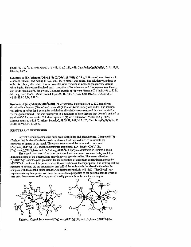
point: 107-110 °C. Micro: Found, C, 37.43, H, 6.71, N, 3.68; Calc forZr2C28N208H64; C, 45.52, H, 8.65, N, 3.79%.
Synthesis of [Zr^bdmapMOPr')«] (6). ZrCOPr^.^OH) (3.25 g, 8.38 mmol) was dissolved in n-hexane (30 cm3) and bdmap-H (2.73 cm3,16.76 mmol) was added. The solution was stirred at reflux for 1 hour, after which time all volatiles were removed in vacuo to yield a very viscous white liquid. This was redissolved in a 1:1 solution of hot w-hexane and wo-propanol (ca. 8 cm3), and left to stand at 0 °C for a week. Colorless crystals of (6) were filtered off. Yield: 3.95 g, 57 %. Melting point: 176 °C. Micro: Found, C, 40.45, H, 7.88, N, 8.26; Calc forZrzCsiNÄflta; C, 46.49, H, 9.20, N, 6.78%.
Synthesis of [Zr2(bdmap)4(OBu')30H] (7). Zirconium f-butoxide (8.51 g, 22.2 mmol) was dissolved in n-hexane (50 cm3) and bdmap-H (7.23 cm3,44.35 mmol) was added. The solution was stirred at reflux for 1 hour, after which time all volatiles were removed in vacuo to yield a viscous yellow liquid. This was redissolved in a minimum of hot n-hexane (ca. 20 cm3), and left to stand at 0 °C for two weeks. Colorless crystals of (7) were filtered off. Yield: 19.5 g, 88 %. Melting point: 120-124 °C. Micro: Found, C, 48.09, H, 8.41, N, 11.26; Calc forZ^GtoNgOsHge; C, 48.10, H, 9.62, N, 11.22%.
RESULTS AND DISCUSSION
Several zirconium complexes have been synthesized and characterized. Compounds (1) - (7) show that Zr alkoxide/chelate materials have a tendency to dimerize to saturate the coordination sphere of the metal. The crystal structures of the symmetric compound [Zr2(tmhd)2(OPr')6] (lb), and the asymmetric compounds [Zr2(dmap)2(OPr')6] (5), [Zr2(bdmap)2(OPri)6] (6), and [Zr2(bdmap)4(OBut)3OH] (7) are illustrated in Figures 1 and 2.
The crystal structures of the compounds we have determined are remarkably useful in discussing some of the observations made in crystal growth studies. The parent alkoxide "[Zr(OPr')4]" is itself a poor precursor for the deposition of zirconium containing materials by MOCVD, in particular it is prone to adventitious reactions in the vapor phase. It is striking that the structure of (5) and (6) are asymmetric, one half of the molecule is the alkoxide the other the complex with the second ligand (dmap). On heating thermolysis will yield "[Zr(OPr')4]" any vapor containing this species will have the unfortunate properties of the parent alkoxide which is very sensitive to water and/or oxygen and readily pre-reacts in the reactor leading to
Figure 1: Crystal Structures of [Z^tmhdMOPrVl (lb) and [Zr^dmapMOPOe] (5)
59

Figure 2: Crystal Structures of [Zr2(bdmap)2(OPri)6] (6) and [Zr2(bdmap)4(OBu,)3OH] (7).
homogeneous precipitation ('snow'). Growth results at DRA Malvern, which are described elsewhere in these proceedings 16 support this conjecture.
The situation is quite different from the complexes derived from alkoxides and tmhd. It is possible to isolate compounds with the stoichiometry [Zr(OR)2(tmhd)2] with f-butanol or iso- propoxide. The /-butoxide is a poor precursor 17 however the wo-propoxides are excellent precursors for the deposition of zirconium containing oxides. The compound isolated from the stoichiometric reaction of tmhd with the alkoxide has the stoichiometry Zr(OR)2(tmhd)2, however the compound has a very interesting *H NMR spectrum at room temperature. There are four distinct methyne proton environments between 5.88 and 5.97 ppm, and a similarly "busy" methyl region. Variable concentration and variable temperature *H NMR were undertaken to further discern the structures evolving from (1) in solution. These results show that there is a mixture of dimers and monomers in solution (CöDö). One important species in these solutions is the dimer [Zr2(tmhd)2(OPr')6] (lb) which has been obtained from exhaustive «crystallizations of solutions of 'Zr(OPr')2(tmhd)2' or by stoichiometric reaction, and has had its structure determined. Pure crystalline samples of (lb) show two CH resonances in the *H NMR which are probably due to geometric isomers in which the tmhd ligands are eis and trans in the dimer.
The 'H NMR spectrum of (1) is shown (Figure 3) in the region of the methyne protons together with a scheme which may explain the species forming in solution (Scheme 1). The chemistry of the wo-propoxide system is interesting, this alkoxide has a great propensity to form dimeric complexes. Our results suggest that the simple dimerization of [Zr(OPr')2(tmhd)2] is not a particularly favorable reaction the explanations for this may lie in the steric crowding of the dimer which would have a 'low-symmetry' and high coordination compound. As mentioned above, exhaustive crystallization of the parent compound leads to the isolation of the simple dimer [Zr2(OPr')6(tmhd)2] which is highly symmetrical.
60
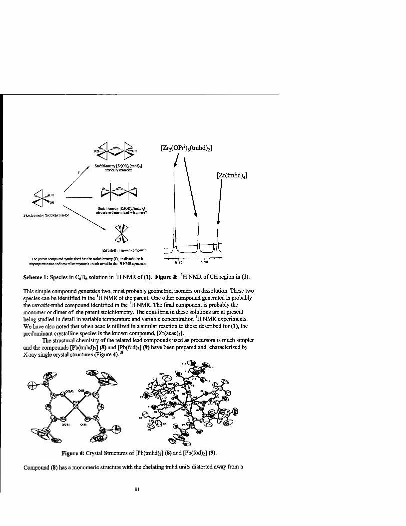
W/,. ..»A***/,. ..rt^
Stoichiometry [Zi(OR)2{tmhd)2] stoically crowded
[Zr2(OW)6(tmhd)2]
I
»OR
Stoichiometry '»(ORMtmhdV
Stoichiometry [Zr(0R)6(tmhd)J structure determined + isomers?
[Zr(tmhd)4]
[Zr(tmhd)4 ] known compound
The parent compound synthesised has the stoichiometry (1); on dissolution it —\—<—i—'—' '~~l I ' ' ■" disproportionates and several compounds are observed in the 'HNMR spectrum. 5-95
Scheme 1: Species in C6D6 solution in 'H NMR of (1). Figure 3: *H NMR of CH region in (1).
This simple compound generates two, most probably geometric, isomers on dissolution. These two species can be identified in the *H NMR of the parent. One other compound generated is probably the tetrakis-tmhd compound identified in the *H NMR. The final component is probably the monomer or dimer of the parent stoichiometry. The equilibria in these solutions are at present being studied in detail in variable temperature and variable concentration *H NMR experiments. We have also noted that when acac is utilized in a similar reaction to those described for (1), the predominant crystalline species is the known compound, [Zr(acac)<t].
The structural chemistry of the related lead compounds used as precursors is much simpler and the compounds [Pb(tmhd)2] (8) and [Pb(fod)2] (9) have been prepared and characterized by X-ray single crystal structures (Figure 4).18
Figure 4: Crystal Structures of [Pb(tmhd)2] (8) and [Pb(fod)2] (9).
Compound (8) has a monomeric structure with the chelating tmhd units distorted away from a
61

stereochemically active lone pair of electrons at the lead(II) center. The structure of compound (9) is based on unusual dimers where seven coordinate lead units are bridged by the fluorine atoms of the ligand.
CONCLUSIONS
We have studied the structural chemistry and the species present in solutions of some novel and known precursors for ferroelectric materials. It is clear that understanding the details of this chemistry is important in developing effective precursors. In the case of the dmap complexes of zirconium, a direct correlation between structure and the behavior observed in MOCVD experiments has been possible. Studies of the species present in solution are similarly important especially if liquid injection procedures are used for the volatilization of precursors. The compound [Zr2(OPr')6(tmhd)2] has been prepared and characterized and is potentially a well defined precursor for zirconates which should not be susceptible to adventitious gas phase reactions.
ACKNOWLEDEMENTS
We would like to thank the EPSRC and DTI for support of collaborations between ICSTM and Inorgtech. KAF thanks the EPSRC and Inorgtech Ltd. for a CASE award. We thank Inorgtech Ltd. for the gifts of chemicals used in this study. POB is the Royal Society Amersham International Research Fellow and the Sumitomo/STS Professor of Materials Chemistry. We would also like to thank Dick Sheppard and Paul Hammerton for VC and VT NMR studies.
REFERENCES
1. Y. Sotome, J. Senzaki, S.-I. Morita, S. Tanimoto, T. Hirai, T. Ueno, K. Kuroiwa and Y. Tarui, Jpn. J. Appl. Phys.,33,p.4066(1994).
2. S.-S. Lee and H.-G. Kim, J. Elect. Mat, 24, p.1023 (1995). 3. T. Hase, T. Sakuma, Y. Miyasaka, K.Hirata andN. Hosokawa, Jpn. J. Appl. Phys., 32, p.4061 (1993). 4. C. M. Foster, G-R. Bai, R. Csencsits, J, Vetrame, R Jammy, L. A. Wells, E. Carr, and J. Amano, J. Appl. Phys.,
81, p.2349 (1997). 5. T. Shiosaki, M. Fujimoto, M. Shimizu, M. Fkagawa and K. Nakaya, Int. Ferroelect., 5, p.39 (1994). 6. D. Kim, T.-Y. Kim, J. K. Lee, W. Tao and S. B. Desu, Mat. Res. Soc. Symp. Proc., 433, p.213 (1996). 7. M. Shimizu, S. Hyodo, H. Fujisawa, H. Niu and T. Shiosaki, Mat. Res. Soc. Symp. Proc, 433, p.201 (1996). 8. T. Hirai, K. Teramoto, T. Goto and Y. Tarui, Jpn. J. Appl. Phys., 34, p.539 (1995). 9. J. F. Scott and C. A. Paz de Araujo, Science, 246, p.1400 (1989). 10. R. Moazzami, P. D. Manier, R. E. Jones Jr., A. C. Campbell and C. J. Mogato, VLSI Technology Symposium
Digest, p.87 (1993). 11. P. K. Larsen, R. Cuppens and G. A. C. M. Spierings, Ferroelect, 128, p.265 (1992). 12. D. J. Taylor, P. K. Larsen, G. J. M. Dormans and A. E. M. De Veirman, Int. Ferroelect, 7, p.123 (1995). 13. S.-S. Lee and H.-G. Kim, J. Elect. Mat., 24, p.1023 (1995). 14. J.-J. Lee and S. K. Dey, Ceram. Trans. (Ferroelectric Thin Films), 25, p.235 (1992). 15. W. Tao, S. B. Desu, and T. K. Li, Mat. Lett., 23, p.177 (1995). 16. A. C. Jones, T. J. Leedham, P. Wright, M. J. Crosbie, P. A. Lane, and D. Williams, these proceedings. 17. A. C. Jones, T. J. Leedham, P. J. Wright, M. J. Crosbie, P. A. Lane, D. Williams, K. A. Fleeting, D. J. Otway and
P. O'Brien, Adv. Mater., Chem. Vap. Dep., accepted for publication (1997). 18. M. A. Malik, M. Motevalli and P. O'Brien, J. Chem. Soc, Chem. Commun, p.1257 (1992).
62
NEW LIQUID PRECURSORS FOR CHEMICAL VAPOR DEPOSITION
ROY G. GORDON, FENG CHEN, NICHOLAS J. DICEGLIE JR., AMOS KENIGSBERG, XINYE LIU, DANIEL J. TEFF AND JOHN THORNTON Harvard University Chemical Laboratories, Cambridge, Massachusetts 02138
ABSTRACT
New precursors have been found for chemical vapor deposition (CVD) of many metal oxides. Each precursor is a mixture formed by randomly attaching a selected set of organic groups, such as the isomers of the butyl group, to a metal 2,4-pentanedionate (also known as acetylacetonate) in place of the methyl groups of the 2,4-pentanedionate ligand. Most of these new mixed metal beta-diketonates are liquids at room temperature, whereas the corresponding metal 2,4- pentanedionates are solids. In the cases where they were solids or viscous liquids, small amounts of organic solvents were added to reduce the viscosity. We have so far prepared mixed beta- diketonate precursors for barium, strontium, calcium, magnesium, aluminum, indium, tin, lead, bismuth, titanium, zirconium, vanadium, niobium, tantalum, chromium, molybdenum, manganese, iron, ruthenium, cobalt, nickel, copper, zinc, yttrium, lanthanum and cerium.
Liquid sources are much more convenient for CVD than solid sources. These liquid mixtures or solutions were vaporized by ultrasonically nebulizing the liquid into a flow of hot nitrogen carrier gas preheated to 150-250 °C. These vapor mixtures were mixed with air or oxygen and flowed over substrates heated typically to 350-450 °C. Films of the corresponding metal oxide (or carbonate, in the case of barium, strontium and calcium) were deposited on substrates of silicon or glass. Gas pressures from 20-760 Torr were used.
Because a common set of ligands is used for each of these metal precursors, they can be mixed as liquids or vapors without any precipitation due to ligand exchange reactions. To demonstrate their use in forming mixed metal oxides, we have prepared films of ferroelectric barium titanate. This method should be applicable to other mixed metal oxides of current interest, such as high dielectric constant strontium titanate, ferroelectric bismuth strontium tantalate, superconducting yttrium barium copper oxide, refractory yttrium zirconium oxide, second-harmonic generating barium borate, metallic lanthanum strontium cobalt oxide and magnetoresistive lanthanum strontium manganate.
INTRODUCTION
Chemical vapor deposition (CVD) is a versatile method for preparing a wide variety of materials. An effective CVD process needs to have a reproducible supply of a gas containing the elements to be deposited. If the reactant chemicals are gases, they can be directly metered into the apparatus. Liquid reactants can generally be vaporized reproducibly. Sufficiently volatile and thermally stable liquids can be vaporized by bubbling a carrier gas through the liquid. Even liquids with relatively low vapor pressures and limited thermal stability can be successfully vaporized by direct liquid injection or by nebulization into a heated carrier gas.
Solid materials are not so easily used to generate reactant vapors. The rates of sublimation from solid surfaces are often low and not very reproducible. Sintering and evaporation can change the available surface area, and decomposition or contamination of the solid surface can change the rate of evaporation. Unfortunately, many potentially useful CVD precursors are solids. In particular, the beta-diketonates of many metals have been tried as CVD precursors, despite the difficulties inherent in the fact that they are solids.
63
Mat. Res. Soc. Symp. Proc. Vol. 495 s 1998 Materials Research Society

We have now found that liquid beta-diketonates can be prepared for the majority of metals, by combining them with a mixture of beta-diketonate ligands which prevents their crystallization. The ligands in the mixture may be considered to be derived from 2,4-pentanedione by substituting various isomeric butyl and propyl groups for terminal hydrogens. The disorder introduced by the different shapes and sizes of these alkyl groups prevents crystallization, so that the resulting mixture of metal beta-diketonates remains either as a liquid or a solid glass at room temperature. Those that are glasses are extremely soluble in organic solvents, so in these cases highly concentrated liquid solutions can be formed by adding a small proportion of solvent. Then the liquid or solution can be vaporized by direct liquid injection or by nebulization, and used in a CVD process. In this way, we have so far prepared 21 liquid mixtures and 7 solutions of glasses, and used each of them for the CVD of metal oxides.
PREPARATION OF LIQUID METAL BETA-DIKETONATES
The beta-diketone ligands were prepared by the Claisen condensation of an ethyl ester and a methyl ketone in the presence of a strong base, such as sodium hydride, followed by acid hydrolysis and distillation of the crude product.
+ H2 + NaCl + CftOH
R2
The alkyl groups R1 and R2 are randomly selected from tert-butyl, sec-butyl, iso-butyl and isopropyl. The exact proportions do not appear to be critical, and we have generally used equal molar proportions of the alkyl groups. The individual beta-diketones may be prepared separately and then mixed before combining them with the metal. A simpler procedure is to condense simultaneously a mixture of methyl ketones, such as tert-butyl methyl ketone, sec- butyl methyl ketone, isobutyl methyl ketone and methyl isopropyl ketone, along with a mixture of ethyl esters, such as ethyl isobutyrate, ethyl isovalerate, ethyl 2-methylbutyrate and ethyl trimethylacetate.
Compounds can be formed between these ligands and most metals. Many different reactions can be used to bind beta-diketonate ligands to metals.[l] Additional ligands, besides the beta- diketonate mixtures, may also be bound to the metal. For example, the barium, strontium and calcium mixed beta-diketonates may be complexed with donor solvents, such as ethers or amines. Metals in higher oxidation states, such as titanium(IV) or tantalum(V), may contain other ligands, such as alkoxides or halides, in addition to the mixed beta-diketonate ligands.
Synthetic Techniques and Reagents.
All manipulations were carried out using standard Schlenk techniques under dry nitrogen either in a drybox or on a Schlenk line unless otherwise stated. Hexane, EtOH, MeOH, benzene, N,N,N',N',N"-pentamethyldiethylenetriamine (pmdeta) and THF were distilled from appropriate drying agents and stored under nitrogen over molecular sieves prior to use. Et3N, Ti(0'Pr)4 and Zn(OAc)2 were purchased from Aldrich and used as received. YCI3, LaCl3, Ba and Sr were purchased from Cerac and used as received. Zr(acac)4, Ta(OEt)s, Cu(OAc)2-H20
64

and TiO(acac)2 were purchased from Alfa and used as received. RuCl3-H20 was purchased from Strem and used as received.
Synthesis of the Beta-Diketonate Ligand Mixture.
The ketone mixture was added slowly and steadily over 3 hours to a rapidly-stirred mixture of the esters, sodium hydride and toluene heated to 90 °C, using a syringe pump. After cooling and stirring overnight, the mixture was neutralized with aqueous hydrochloric acid and the organic layer was separated. The product mixture was distilled from the crude organic layer at 30 mbar from about 70-110 °C, and dried over molecular sieves.
Yields were around 80%. By proton-decoupled carbon-13 NMR analysis in deutero- chloroform, the resulting reaction product was found to be a mixture containing ten of the beta- diketone ligands. Table 1 gives the chemical shifts of the central carbon between ketone groups, in the major (enol) forms of these compounds, as identified by separate syntheses of the pure compounds. This single resonance line is easily resolved for each compound in this mixture, making it useful for analysis, whereas other lines in the proton and C-13 NMR spectra are badly overlapped. Table 1 also gives the numbers assigned by Chemical Abstracts to eight previously known compounds in this mixture. The general formula is written R'C(=0)CHR3C(=0)R2, where R3 = H in all these examples.
Table 1. NMR data for the beta-diketone ligands
Name
2,6-dimethyl-3,5-heptanedione 2,7-dimethyl-3,5-octanedione 2,6-dimethyl-3,5-octanedione 2,2,6-trimethyl-3,5-heptanedione 2,8-dimethyl-4,6-nonanedione 2,7-dimethyl-4,6-nonanedione 2,2,7-trimethyl-3,5-octanedione 3,7-dimethyl-4,6-nonanedione 2,2,6-trimethyl-3,5-octanedione 2,2,6,6-tetramethyl-3,5-heptanedione
R1 R2 Chemical Shift Chemical C13 NMR, ppm Abstracts No
iso-Pr iso-Pr 94.9 57733-60-5 iso-Pr iso-Bu 97.8 7307-07-5 iso-Pr sec-Bu 96.0 not reported iso-Pr tert-Bu 92.9 7333-23-5 iso-Bu iso-Bu 100.6 7307-08-6 iso-Bu sec-Bu 98.8 not reported iso-Bu tert-Bu 95.7 69725-37-7 sec-Bu sec-Bu 97.0 43865-74-2 sec-Bu tert-Bu 94.0 34865-71-9 tert-Bu tert-Bu 90.6 1118-71-4
Synthesis of Metal Jj-diketonates
Synthesis of Ba(beta-diketonate)?. Ba (0.878 g, 6.39 mmol) and pmdeta (2.22 g, 12.8 mmol) were placed together in a flask and 7 mL of THF was added. Bubbles were evolved slowly upon addition of a beta -diketone mixture (2.26 g, 12.8 mmol) diluted with 7 mL of THF. The reaction, more intense after passing NH3 through the solution for 5 minutes, continued for 20 minutes until there was very little metal. The NH3 flow was continued for another 5 minutes followed by 15 minutes of stirring until only flecks of metal remained. On addition of NH3 to the solution the second time, a light green gel, perhaps Ba(beta-diketonate)2(NFi3)x, formed but slowly disappeared on stirring under flowing N2. The solution was then filtered through celite and the solvent was removed in vacuo to leave a light yellow liquid (4.16 g, 78%). On exposing this liquid to air, a white solid material formed. A similar preparation was used for strontium.
65

Synthesis of TKO'PrMß-diketonate)?. A ß-diketone mixture (6.84 g, 38.8 mmol) diluted
with 10 mL of THF was added to Ti(OiPr)4 (5.50 g, 19.4 mmol) in 10 mL of THF. This gave an amber solution which was stirred for 2 hr. The solvent was removed in vacuo and the resulting brown, viscous liquid was pumped on for 2 hr at 40 °C (9.25 g, 93%). Due to the presence of O'Pr groups, this species is air sensitive.
Synthesis of TiO(ß-diketonate)?. A ß-diketone mixture (8.51 g, 48.2 mmol) diluted with 10
mL of Et20 was cannula-transferred to Ti(0'Pr)4 (6.85 g, 24.1 mmol) diluted with 10 mL of Et2Ü. The reaction produced heat and resulted in an amber-colored solution. After complete addition, the solvent was removed in vacuo leaving an orange-brown liquid. This was heated to 90 °C for 1 min under static vacuum and then stirred under dynamic vacuum for 5 min. The process was repeated twice resulting in a very dark brown liquid. Then, 50 mL of THF was added and the reaction was stirred under air for 5 min. The solution gradually began to turn red upon dropwise addition of H2O (0.66 mL, 36.7 mmol) and was very dark red after stirring 12 hr. After heating to 50 °C for 30 min, the solvent was removed in vacuo and the resulting viscous liquid was pumped on for 4 hr (both done at 50 °C). On cooling, the liquid eventually became a solid, very dark brown glass (9.47 g, 94%).
Synthesis of Zr(ß-diketonate)4. Zr(acac)4 (7.50 g, 15.4 mmol) and a beta-diketone mixture (13.5 g, 76.9 mmol) were added together to a flask neat. The flask was fitted with a reflux column and the yellow mixture was heated to 130 °C when a colorless liquid (acacH) began to reflux. After heating for 12 hours and the solution had become clear, the acacH and excess b- diketones were removed in vacuo at 130 °C leaving a slightly viscous yellow liquid (11.43 g, 94%). Exposure to air resulted in formation of crystalline plates.
Synthesis of Ruflj-diketonate)-;. RuC^-H^O (1.81 g, 8.01 mmol) was suspended in 15 mL of EtOH and a beta-diketone mixture (4.23 g, 24.1 mmol) diluted with 7 mL of EtOH was added. Smoke was evolved upon dropwise addition of Et3N (2.45 g, 24.2 mmol) diluted with 15 mL of EtOH. The solution was refluxed at 98 °C for 26 hours, the solvent was removed in vacuo and 30 mL of hexane was added. After filtration, the solvent was removed leaving a very dark red/brown, viscous liquid (4.07 g, 81.4%). This liquid was taken up in 3.20 g of mesitylene giving a 56% w/w solution. The product did not show any appreciable change on exposure to air.
Synthesis of Znflü-diketonate)?, Zn(OAc)2 (10.52 g, 57.4 mmol) was suspended in 25 mL of
EtOH and a ß-diketone mixture (24.98 g, 142.3 mmol) was added. The solution was refluxed at 110 °C for 12 hours giving a slightly turbid solution. The solution was filtered and the solvent was removed in vacuo giving a viscous, yellow liquid (18.96 g, 80%). This liquid formed some white solid on exposure to air.
Synthesis of Y(j3-diketonate)3, A beta -diketone mixture (16.85 g, 96.0 mmol) was diluted in 30 mL of EtOH and added to YCI3 (5.01 g, 25.7 mmol) dissolved in 75 mL of EtOH. Some smoke was evolved upon dropwise addition of Et3N (7.80 g, 77.1 mmol) diluted with 15 mL of EtOH and the solution eventually became yellow and cloudy. After stirring for hours, the EtOH was removed in vacuo at ambient temperature to leave white solid suspended in a yellow oil. To this was added 60 mL of hexane. After filtration, removal of the solvent in vacuo and further evacuation at 90 °C to remove excess ß-diketone, a viscous yellow liquid (11.19 g, 71%) remained. This product formed some white solid upon exposure to air.
Synthesis of Laflj-diketonateK A beta-diketone mixture (13.51 g, 77.0 mmol) was diluted in 30 mL of EtOH and added to LaCl3 (5.00 g, 20.4 mmol) dissolved in 100 mL of EtOH. Some smoke was evolved upon dropwise addition of Et3N (6.19 g, 61.2 mmol) diluted with 20 mL of
66

EtOH and the solution eventually became yellow. After stirring 12 hours, the EtOH was removed in vacuo at ambient temperature to leave white solid suspended in a yellow oil. To this was added 50 mL of hexane. After filtration, removal of the solvent in vacuo and further evacuation at 90 °C to remove excess ß-diketone, a very viscous yellow liquid (8.22 g, 61%) remained. This was dissolved in 12.58 g of pmdeta to give a 40% w/w solution. This solution formed some white solid upon exposure to air.
CVD USING THE NEW LIQUID PRECURSORS
The liquid mixtures were vaporized in a well-controlled, reproducible manner by ultrasonic nebulization. The liquids were pumped at the desired rate (typically about 0.05 cc/min) by a syringe pump onto the surface of a horizontal quartz plate driven by a piezoelectric transducer at 1.44 Mhz. [2] This quartz plate formed the bottom of a home-made stainless steel housing, through which the mist was carried upward by a low flow (0.2 to 1 L/m) of nitrogen carrier gas. During this upward flow, all large droplets having a terminal velocity faster than the upward gas flow velocity fell back to the quartz plate, where they were broken down again into smaller droplets. In this way, the mist reaching the top of the housing consisted of droplets all of which are smaller than a predetermined size, typically set to 20 microns. There small droplets met preheated (typically to 250 C) nitrogen carrier gas and were vaporized very quickly as they were carried into the reactor. Pressures from 20 Torr to atmospheric pressure were used.
Silicon and glass substrates were used. Film composition and thickness were determined by Rutherford Backscattering Spectroscopy (RBS). Sheet resistance was measured by 4-point probe.
H substrate
S heater
precursor
Figure 1. Schematic cross section of the CVD reactor.
RESULTS OF THE CVD EXPERIMENTS
Deposition of films from the barium liquid precursor yielded barium carbonate films. Addition of oxygen or nitrous oxide to the deposition atmosphere did not reduce the carbon content. Similar results were obtained from the strontium and calcium precursors. The
67

magnesium precursor yielded carbon-free magnesium oxide films. Deposition from both of the titanium precursors yielded carbon-free titanium dioxide films.
Mixed solutions of titanium and barium precursors in the absence of added oxygen gas yielded films with Ba/Ti ratios constant along the gas flow direction, but with considerable carbon contamination, about 30 atomic per cent. Adding nitrous oxide did not decrease the carbon content. Adding oxygen reduced the carbon content considerably, to below 10 atomic per cent, but then the Ba/Ti ratio decreased along gas flow direction. The mixed titanium/barium precursor solutions are stable in the absence of moisture, and have been stored for months with no change or precipitation.
In the presence of oxygen, the ruthenium precursor yielded metallic ruthenium dioxide films with resistivities about 1 AxlO'4 ohm-cm. In the absence of oxygen, the films had a composition RuOo.5- Carbon was not detected in the ruthenium oxide films.
The copper beta-diketonate was a solid glass at room temperature. It is highly soluble in organic solvents. For example, a diglyme solution with concentration of 1.6 mole/liter was prepared. This solubility is 17 times larger than the solubility of commonly used precursor copper(thd)2 (Hthd=2,2,6,6-tetramethylheptanedione).[3] A mesitylene solution of the copper beta-diketonate mixture was used for CVD of copper oxide films. The stoichiometry of the films depended on the oxygen content of the deposition atmosphere, varying from Cu20 with no oxygen to CuO for 20% oxygen.
Oxide films were also prepared from the liquid beta-diketonate precursors for aluminum, indium, tin, bismuth, zirconium, niobium, tantalum, molybdenum, iron, zinc, yttrium, lanthanum and cerium, and from solutions of the glassy beta-diketonate precursors for lead, vanadium, chromium, manganese, cobalt and nickel.
CONCLUSIONS
Liquid precursors were prepared for all types of metals, including main group, transition and lanthanide metals. They have been vaporized by ultrasonic nebulization and used for the CVD of metal oxides and mixed metal oxides, such as barium strontium titanate. Because the same ligand mixture can be used for all of the metals, the different metal precursors can be mixed, either in the liquid or vapor states, without the precipitation of non-volatile products of ligand exchange, that are often observed when attempts are made for CVD of mixed metal oxides.
ACKNOWLEDGMENTS
This work was supported in part by the U. S. National Science Foundation, and the National Renewable Energy Laboratory under a subcontract from the U. S. Department of Energy.
REFERENCES
1. Specific examples of preparative procedures for similar ligands are given in Inorganic Syntheses, for chromium(III) in 5, pp. 130-131 (1957) and 24, pp. 183-184 (1986); for cobalt(III) in 5, pp. 188-189 (1957); for rare earth metals in 11, pp. 94-98 (1968); for cerium(IV) in 12, pp. 77-78 (1970) and 23, pp. 147-8 (1985); for manganese(III) in 23, pp. 148-149 (1985); for iron(II) in 31, pp. 267-269 (1997); for copper(II) in 23, pp. 146-147 (1985); for beryllium in 2, pp. 17-20 (1946); and for calcium, strontium and barium in 31, pp. 1-7 (1997). 2. The power supply and transducer were manufactured by Cetac, Inc., Omaha, NE. 3. L. G. Hubert-Pfalzgraf, Electrochem. Soc. Proc. 97-25, 824 (1997).
68

SINGLE SOURCE CVD OF LiA102
Wonyong Koh, Su-Jin Ku, Yunsoo Kim*
Advanced Materials Division, KRICT, 100 Chang-dong, Yusong-gu, Taejon 305-343, SOUTH
KOREA,[email protected]
ABSTRACT
We successfully deposited LiA102 films on Si substrates at 400-600 °C by single source chemical
vapor deposition using a heterometallic compound, Li(0'Pr)2Al(CH3)2, which contains Li, Al,
and O at the same 1:1:2 ratio as LiA102. Li(0'Pr)2Al(CH3)2 is sufficiently volatile to be vapor-
transported at 50 °C. Elastic recoil detection and Rutherford backscattering spectroscopy
analyses of a deposited film indicate that the film is stoichiometric (Li:Al:0 = 1.0:1.0:2.0) and
contains a few atomic percent hydrogen (5 %) and carbon (2 %). Depth profile analysis of X-ray
photoelectron spectroscopy also confirms the 1:1 ratio of metal contents in the films. As-
deposited films were amorphous, however, crystallized to ß- or y-LiA102 after annealing at 950
°C.
INTRODUCTION
High-quality GaN films are difficult to grow on sapphire, the most commonly used
substrate for GaN film growth, due to its large lattice mismatch (14%). ZnO, LiA102, and
LiGa02 are the most closely lattice-matched materials with GaN (lattice mismatch < 2%). ZnO is
an isomorphic material with GaN. LiA102 and LiGa02 are closely related with ZnO where two
Zn atoms are replaced with one Li and one Al/Ga atom. A lattice-matched buffer layer can
enhance epitaxial film growth. Akasaki et al. successfully deposited thick monocrystalline GaN
films on sapphire using thick ZnO buffer layers [1]. Xiao et al. demonstrated that a [0001]-
oriented thin ZnO buffer layer enabled epitaxial growth of GaN films over fused silica,
monocrystalline Si, and sapphire [2]. Only few years ago LiGa02 and LiA102 were suggested as
lattice-matched substrates for GaN [3]. Already structurally-high-quality GaN film growths were
reported on monocrystalline ß-LiGa02 [4] and y-LiA102 [5]. Therefore it should be worthwhile
to explore the possibility of LiGa02 and LiA102 as a buffer layer for GaN film growth, however,
there has been no report of the film growth of these materials to the best of our knowledge.
Stoichiometric control is much more difficult for the deposition of a double metal oxide
(MM'xOy) compared to that of a simple oxide (MOx). Chemical vapor deposition (CVD) using a
single source, which contains all the necessary elements, can be an answer to the problem [6].
We prepared a volatile precursor Li(0'Pr)2Al(CH3)2, which contains Li, Al, and O in the same
1:1:2 ratio as LiA102, and deposited LiA102 films on Si by CVD using it as a single source.
69 Mat. Res. Soc. Symp. Proc. Vol. 495 ® 1998 Materials Research Society

EXPERIMENT
The precursor was prepared from lithium isopropoxide and dimethylaluminum
isopropoxide. Lithium isopropoxide was slowly added to a diethyl ether solution of
dimethylaluminum isopropoxide and the resulting solution was stirred for several hours under
inert atmosphere. The product was quantitatively obtained (93-96 % yield) in the form of a
colorless solid after drying and vacuum sublimation at 110 °C under 0.05 torr.
A simple apparatus was used for CVD, in which borosilicate glass tubing, quartz tubing,
and stainless steel bodies were connected through O-ring joints. Si substrates were degreased
with trichloroethylene and rinsed with acetone, methanol, and deionized water. They were then
treated with a 36 % HC1 solution, rinsed with deionized water, and immediately introduced into
the CVD apparatus. The substrates were placed on a graphite heating block. Substrate
temperature was monitored by a thermocouple inserted in the graphite block. The deposition
temperature was maintained in the range 400-600 °C. No carrier gas was used and the source
was vaporized at 50 °C. The base pressure of the CVD apparatus was 2-5 mPa and the pressure
increased to 50-200 mPa after introducing the source into the CVD apparatus. Interference colors
appeared on the substrate within half an hour and the deposition continued for several hours.
The deposited films were characterized by X-ray photoelectron spectroscopy (XPS), X-
ray diffractometry, elastic recoil detection (ERD), Rutherford backscattering spectroscopy (RBS),
and scanning electron microscopy (SEM).
RESULTS
Figure 1 shows ERD and Rutherford backscattering spectra of a film deposited on
Si(lll) at 400 °C for 5 hours. The atomic composition of the film was determined from these
data: 24 % Li, 24 % Al, 45 % O, 2 % C, and 5 % H. The film thickness, 0.31 um, calculated
from the areal density, 3.0 x 10¹⁸ atoms/cm2, is in good agreement with the thickness, 0.28 urn,
measured on the cross-sectional SEM image of the film. Deposited films were also analyzed by
XPS after the film growth. X-ray photoelectron spectra of all deposited films display peaks
associated with only Li, Al, O, and C (Figure 2a) and indicate the surface Li:Al ratio between
1.0:0.9 and 1.0:1.1. XPS depth profile analysis also shows that the metal ratio is nearly 1:1
(Figure 2b). These results indicate that the film is stoichiometric LiA102 with C incorporation
less than 10 % and the 1:1:2 atomic ratio of Li, Al, and O in the precursor is preserved in the film.
Figure 3 shows the SEM images of the films deposited at 400 °C and 600 °C, as-
deposited and after annealing at 950 °C. The columnar structure of the film grown at 600 °C
indicates that surface diffusion is negligible at 600 °C and the film was grown three-
dimensionally, which is understandable considering LiA102's melting point 1700 °C. The films
are shrunk and presumably densified after annealing. The deposition rates are estimated as 0.06
70

um/hr at 400 °C and 0.30 um/hr at 600 °C.
All films deposited on Si(lll) and Si(100) at 400-600 °C display no peaks other than
those of substrates in X-ray diffraction (XRD) patterns, indicating that the films are amorphous.
XRD patterns of LiA102 films after annealing at 950 °C for 5 hours, however, displays peaks
associated with ß- and y-LiA102 (Figure 4). Interestingly a film deposited on Si(lll) at 400 °C
displays only a peak diffracted from the ß-LiA102 (002) plane (Figure 4a) whereas a film
deposited on Si(lll) at 600 °C displays two major peaks, diffracted from the y-LiA102(110) and
y-LiA102(200) planes, and other smaller ones (Figure 4b). The former result suggests that solid
phase epitaxy occurred during the annealing process. The cause of different crystallization
behaviors of the two films is not clear yet.
400 450 500 550 600
Channel
0 100 200 300 400 500 0 100 200 300 400 500
Channel Channel
Figure 1. The TOF-ERD spectra for the five masses, (a) 'H, (b) 'Li, (c) 7Li, (d) 12C, and (e) 160
with a 9.6 MeV 35C1 probe beam, and (f) the 4.2 MeV 4He Rutherford backscattering spectrum of
a LiA102 film deposited on Si(l 11) at 400 °C for 5 hours.
100
A BO t
B c 8
60
40
20
1200 1000 800 600 400
Binding Energy (eV)
. Peak Area (b)-
■
_ <L-^_^— ■^ ^
■
■
Li__^
/ — Al . ^^C .
0 1000 2000 3000 4000 5000 6000 7000 8000 Etch Time (Seconds)
Figure 2. (a) X-ray photoelectron spectrum of a film deposited on Si(100) at 600 °C and (b) XPS
depth profile of a film deposited on Si(l 11) at 400 °C.
71

SUMMARY
Li(OiPr)2Al(CH3)2 deposited stoichiometric LiA102 films with a few atomic percent carbon by
single source CVD. A well-oriented ß-LiA102 film was obtained on Si(lll) after annealing at
950 °C. A LiA102 film can be a preferable buffer layer for GaN growth considering its good
thermal stability and close match of the lattice constant and thermal expansion coefficient with
GaN.
ACKNOWLEDGMENTS
The authors gratefully acknowledge the financial support of the Ministry of Science and
Technology of Korea.
Figure 3. SEM images of (a) a film deposited on Si(lll) at 400 °C for 5 hours and (b) a film
deposited on Si(100) at 600 °C for 20 hours, (c) and (d) are the SEM images of (a) and (b) films
after annealing at 950 °C for 5 hours, respectively.
72

Si(111) (b)
(110
)
(200
)
d" cT Sj 1 ±- ^
JJ , A. 20 30 40 50 60
29
70 80 90
Figure 4. X-ray diffraction patterns, after annealing at 950 °C for 5 hours, of (a) the film of
which SEM image is shown in Figure 3c and (b) a film deposited on Si(lll) at 600 °C.
REFERENCES
l.T. Detchprohm, H. Amano, K. Hiramatsu, and I. Akasaki, J. Cryst. Growth 128, 384-390
(1993)
2. R. F. Xiao, X. W. Sun, Z. F. Li, N. Cue, H. S. Kwok, Q. Z. Liu, and S. S. Lau, J. Vac. Sei.
Technol. A 15, 2207-2213 (1997)
3. J. F. H. Nicholls, H. Gallapher, B. Henderson, C. Trager-Cowan, P. G. Middleton, K. P.
O'Donnell, T. S. Cheng, C. T. Foxon, and B. H. T. Chai in Gallium Nitride and Related
Materials, edited by F. A. Ponce, R. D. Dupuis, S. Nakamura, and J. A. Edmond (Mater. Res.
Soc. Proc. 395, Pittsburgh, PA, 1996), pp. 535-539.
4. O. M. Kryliouk, T. W. Dann, T. J. Anderson, H. P. Maruska, L. D. Zhu, J. T. Daly, M. Lin, P.
Norris, H. T. Chai, D. W. Kisker, J. H. Li, and K. S. Jones in III-V Nitrides, edited by F. A.
Ponce, T. D. Moustakas, I. Akasaki, and B. A. Monemar (Mater. Res. Soc. Proc. 449,
Pittsburgh, PA, 1997), pp. 123-128.
5. E. S. Hellman, Z. Liliental-Weber, and D. N. E. Buchanan, MRS Internet J. Nitride Semicond.
Res. 2, 30 (1997).
6. A. A. Wernberg, H. J. Gysling, A. J. Filo, and T. N. Blanton, Appl. Phys. Lett. 62, 946-948
(1993).
73

CHEMICAL VAPOR DEPOSITION OF RUTHENIUM DIOXIDE THIN FILMS FROM BIS(2,4-
DIMETHYLPENTADIENYL)RUTHENIUM
Lamartine Meda*, Richard C. Breitkopf," Terry E. Haas**, and Rein U. Wrss*
'Department of Chemistry, Northeastern University, Boston, MA 02115
"Department of Chemistry, Tufts University, Medford, MA 02155
ABSTRACT
Thin films of polycrystalline Ru02 were deposited from bis(2,4-dimethylpentadienyl)
ruthenium, (TI5-2, 4-Me2C5Hs)2Ru (1) and ruthenocene (2) on quartz and silicon substrates
between 200 and 500°C under Ar/02 or 02- Films deposited from 1 were more adherent than those
grown from 2 under the same conditions, however, none of the films were particularly adherent when
O2 was used as a carrier gas. SEM revealed a columnar structure for both precursors with grain size
ranging from 0.15- 15/;. Crystallinity increased after annealing the films to 800°C. Resistivity
decreased as the annealing temperature increased.
INTRODUCTION
Ruthenium dioxide, Ru02, belongs to a class of metal oxide with rutile structures and
relatively low resistivity (p = 46 /jO-cm). Thin films of ruthenium dioxide are attracting attention as
diffusion barriers in VLSI circuits and in DRAM devices.1 -2-3 In contrast to materials like titanium
nitride, ruthenium dioxide is inert toward further air oxidation. Thin films of Ru02 have been
deposited from ruthenium tris(acetylacetonate) and ruthenocene, rrMCsHsteRu.1 • * Films
deposited from ruthenium tris(acetylacetonate) under vacuum contained predominantly ruthenium
metal.1 Ruthenium dioxide was deposited only in the presence of oxygen. Ruthenium metal was
also observed from CVD using Ru3(CO)-|2 even under 1 Torr of oxygen. Both Ru3(CO)-|2 and
ruthenium tris(acetylacetonate) suffer from low vapor pressure. The deposition of ruthenium dioxide
from ruthenocene 3 between 500 and 600°C and 1 to 5 Torr of oxygen yielded Ru02 on SiQ2 but
produced films containing both Ru and Ru02 on silicon substrates even after annealing at 900°C. 1
Optimization of the deposition conditions 4 led to pure Ru02 films on quartz, Si02 and silicon at
550°C and 1000 seem of O2. Deviation from these conditions led to pure ruthenium or mixed
Ru/Ru02 films.
75 Mat. Res. Soc. Symp. Proc. Vol. 495 ° 1998 Materials Research Society

Transition metal complexes containing pentadienyl ligands or "open metallocenes" show
greater sensitivity toward oxygen than the corresponding metallocene compounds 6 suggesting that
bis(2, 4-dimethylpentadienyl)ruthenium , 1, might be a better precursor for the deposition of Ru02-
In particular, the greater air-sensitivity of 1 had potential for lowering the growth temperature. During
the course of the present work, it was reported that RuQ2 films could be deposited from Rufa5-
C5H5)2 as low as 200°C on SiCfc/Si substrates. 7 In this paper we report on the characterization of
ruthenium dioxide films grown from RU(TI5-2, 4-Me2CsH5)2 and compare the results with Ru02 films
prepared from ruthenocene under identical conditions.
EXPERIMENTAL
Bis(2, 4-dimethylpentadienyl) ruthenium was prepared by reaction of RuCfe- x H2O with 2, 4-
pentadiene and zinc powder by literature procedures5 and purified by sublimation. Ruthenocene was
also prepared by literature procedures.6
The deposition apparatus consisted of a 3" O. D. quartz tube placed in a Lindbergh tube
furnace with three heating zones. The precursor (15 to 200 mg) was placed in a 304 stainless steel
bubbler attached to the tube. The bubbler was heated to 70 - 85°C with an oil bath and all lines
leading from the bubbler to the furnace were warmed between 100-115°C with heating tapes to
prevent condensation.
Substrates (glass, quartz, and Si) were cleaned by sequential washing with hexane, acetone,
sonication in hexane, washing with 1% H2SO4 and H2O2, rinsed with water, and dried in air.
Substrates were loaded into the middle of the second heating zone and supported on 304 stainless
steel substrate holders. The chamber was evacuated to approximately 20 mTorr before each run.
Total pressure was measured with a capacitance manometer.
Precursors were delivered into the hot zone using argon as a carrier gas. Oxygen diluted with
argon was admitted as the oxidant. Gas flows were controlled with mass flow controllers. The films
were annealed for 5 h at 100° intervals between 400 and 800"C under oxygen. A summary of the
deposition conditions is found in Table 1.
Rims were also deposited in an apparatus similar to that described by Green et. al.1 The
substrates were loaded into the tube in an inert atmosphere glove box. The precursor was
transported through the furnace using oxygen as the carrier gas but without accurate control of the
oxygen flow rate.
The films were characterized by scanning electron microscopy on a Jeol JSM 6100 Scanning
Electron Micrograph and by x-ray diffraction using a Siemens D-5000 Diffractometer (Cu-Ka radiation,
\ = 1.5406Ä). Rim resistivity was measured using the standard four point probe technique.
76

RESULTS
Bis(2, 4-dimethylpentadienyl) ruthenium, 1, is a volatile, pale yellow solid which can be
handled briefly in air without decomposition. Prolonged exposure of the solid to air leads to a black
material. In the absence of oxygen, 1 is thermally stable up to 400°C whereupon it undergoes
sequential cyclization reactions to form bis(1, 3-dimethylcyclopentadienyl)ruthenium. 9-10 In the
presence of oxygen, decomposition of 1 occurs below 200°C and deposits transparent dark reflective
films on glass and silicon substrates. Water (H2O) was the only volatile by-products observed by1H
NMR. The absence of hydrocarbons by-products suggests that combustion of the ligand is nearly
complete.
Conditions for film growth using both reagents are summarized in Table 1. Films ranging from
100 to 500 nm in thickness were grown from ruthenocene between 300 and 400°C. A columnar
structure is observed by SEM. Reflections at 26 = 28,35, 40,55 and 67.5 ° in the x-ray diffraction
pattern (Fig. 1) correspond to the (110), (101), (200), (211), and (112) planes respectively of RuC-2
reported in the literature. 4 The relative intensities depend on the orientation of the silicon substrate.
The resistivity of the as-deposited films was measured as 1300 isQ-cm, much greater than the values
reported earlier.4-5 Numerous factors such as thickness and poor adhesion contribute to the high
resistivity of the films.
Deposition of Ru02 films from 1 under similar conditions (Table 1) is rapid. Rims ranging in
thickness from 0.1 - 1/J films are deposited after 10 minutes. Scanning electron microscopy indicates
microstructural nonuniformity with an average grain size of 150 nm (Fig.2). SEM studies show high
stress in films deposited at 500 °C. Cracking is more apparent after annealing at high temperatures.
X-ray powder patterns for as-deposited films are consistent with those shown in Fig 1. The resistivity of
the films grown from 1 decrease from 1300 to 157 |*Q- cm upon annealing under O2 (Fig.3)
Table 1: Deposition Conditions For Ru02 Rims
Ru(r£-Csrteb RufT.5-2. 4-C7H11)9(1)
Precursor Color white pale yellow
Sublimation Temp. 85 °C 70 °C
Substrate Temp. 350-400°C 250-500°C
Precursor Line Temp. 100-115°C 100-115°C
Carrier gas (Ar) 50SCCM 30SCCM
Oxidant Row 110-210SCCM 110-210SCCM
Deposition Time 10-20 min 10 min
Total Pressure 1.92 Torr 2.87 Torr
Annealing (O2) 400-800°C 300-800°C
77

m^ ■^4^/wvH
W' ""Ay^v^J W*W-, .vAv\*VA y.wWy y ^.v^wvA^«^\^.^\j,nj-ftj_jjy«v.
ffirafcWwi* iälr. V^WWWMMV^VI,>'
Rgure 1: XRD Pattern of Ru02film Deposited From a) Ruthenocence at 300 -400 °C b) Bis(2,4-
pentadienyl )Ru when argon is used as a carrier gas c) When part b is annealed at 800 °C
and crystallinity improves. The potential for carbon contamination from the 2, 4-pentadiene ligand as a
contributing factor to the high resistivity for the as-deposited films is under investigation.
Ruthenium dioxide films are also deposited on glass from both ruthenocene and 1 using
oxygen as a earner gas at a total pressure of 1 -2 Torr. In these as-deposited films, a columnar structure
is observed by SEM (Rg. 4). Under these conditions, the films are of uniform thickness and = 1 fj
average grain size. The resistivity of the as-deposited films is 200//O-cm. A columnar structure is
reported to correlate with low resistivity in Ru02 films. 3 The x-ray diffraction pattern (Rg. 5) is
consistent with the presence of both RuC>2 and Ru (26 = 42 and 44.5°) for low pressure deposition.
When the total pressure is increased to - 2 Torr the films show very little crystallinity and poor
adhesion.
1500-,
9 1000-
Sd 500' as ■*■
OS f) .
4( )0 600
Temp
800
Rg. 2: SEM of Ru02 Rim Deposited From 1
when Ar is used as a carrier gas at 400°C
Rg.3: Resistivity vs annealing Temperature.
78

JN-~. \:Z*mill**'*m»^/...^**^y^^^;ll*it^, „-Wte ,.,.*. ....
® sot JF™ ' * "• " r*$ »^
Figui e 4: a. SEM of Ru/Ru02 Rim Deposited Froml at 1-2 Torr 02 at 300 - 400°C
CONCLUSIONS
Thin films of polycrystalline ruthenium dioxide, Ru02, can be deposited from bis(2, 4-dimethyl-
pentadienyl ruthenium at low temperature. Control over microstructure and resistivity of the film appear to
be highly dependent on oxygen pressure, deposition conditions, growth rate, and reactor design as
observed by others.2
79

ACKNOWLEDGMENTS
The authors would like to thank Prof D. Budil for the use of the four point probe instrument and the
entire X-ray group for their time.
REFERENCES
1. M. L Green, M. E. Gross, L E. Papa, K. J. Schnoes and D. Brasen, J. Electrochem. Soc. 132,
2677 (1985).
2 L Krusin-Elbaum and M. Wittmer, J. Electrochem. Soc. 135, 2610 (1988)
3 E. Kolawa, F. T. C. So, W. Hick, X-A. Zhao and M-A. Nicolet, Appl. Phys. Lett. 50, 854 (1987).
4. J. Si and S. B. Desu, J. Mater. Res. 8, 2644 (1993).
5. W-C. Shin and S-G Yoon, J. Electrochem. Soc. 144, 1055 (1997).
6. R. D. Ernst, Chem. Rev.88, 1255 (1988).
7. L. Stahl and R. D. Ernst, Organometallics 2,1229 (1983).
8. P. Partici and Vituli, in Inorganic Synthesis, S.L Holt (ed.) 22,180, (1983).
9. R. U. Kirss, A. Quazi, C. H. Lake, and M. R. Churchill, Organometallics 12, 4145 (1993).
10. R. U. Kirss, Organometallics 11, 497 (1992).
80

Part II
Chemical Vapor Deposition of Nonoxide Ceramics

PRECURSORS FOR VAPOR DEPOSITION OF BLUE PHOSPHORS FOR
ELECTROLUMINESCENT FLAT PANEL DISPLAYS
WILLIAM S. REES, JR.*, OLIVER JUST, HENRY A. LUTEN AND DAVID J. OTWAY
Georgia Institute of Technology, School of Chemistry and Biochemistry and School of Materials
Science and Engineering and Molecular Design Institute, Atlanta, GA 30332-0400
ABSTRACT
New strontium (host lattice constituent) and cerium (doping element) precursor sources
have been developed and evaluated for deposition of blue color emitting SrS:Ce thin films by
ALE (Atomic Layer Epitaxy). In the case of strontium, the monomeric derivative
[Sr(hfac)2]-triglyme has been synthesized and structurally characterized, whereas, for cerium, the
utilization of its homoleptic tris amide derivative Ce{N[Si(CH3)3]2}3 has led to a blue color
emitting SrS:Ce. In a further effort, emission characteristics of SrS:Ce doped with the ß-
diketonate-related Ce(tmhd)4 derivative have been weighed against data obtained employing the
cerium tris amide composition.
INTRODUCTION
The electroluminescent phenomenon (EL)1'2 - non-thermal conversion of electrical into
luminous energy - was first observed as high-field electroluminescence of ZnS by Destriau in
1936. Nearly half a century later mass production of TFEL devices began based on ZnS:Mn, a
yellow light emitting phosphor.3 Multicolor displays have been constructed, since, though the
production of full-color arrays has been hampered by complications in fabricating a material
83
Mat. Res. Soc. Symp. Proc. Vol. 495 c 1998 Materials Research Society

producing efficient blue light luminescence. Two main approaches have been pursued in this
regard: dual-substrate (red and green phosphors are linked with a material emitting a
monochrome "blue" light) and color-by-white concept (the three principal colors are achieved by
filtering a broadband phosphor) (Figure l).4
a.)
Transparent Electrodes
Insulator
R and G Phosphors
Insulator
Transparent Electrodes
Transparent Electrodes Insulator
Blue Phosphor Insulator
Electrodes
b.) Color Filter Substrate
RGB Color Filters
Transparent Electrodes
Insulator SrS:Ce/ZnS:Mn
Insulator Metal Electrodes
TFEL Panel Substrate
Figure 1: Schematic illustration of a.) color-by-white and b.) dual-substrate EL-devices.
ALE5 emerged almost two decades ago as a most promising modification of the
conventional MOCVD technique for fabrication of EL thin-films on diversely shaped structures
utilized in numerous light emitting devices as liquid crystal displays (LCD's) and laser diodes.
The principle of the ALE process6 (Figure 2) is based on sequential interactions of the deposition
surface with desired reactants, resulting in digitally controlled consecutive deposition of strictly
defined single atomic layers at a time. Moderate deposition rates and increased contamination
effects, giving rise to film defects, however constitute certain limitations of this growth method.
Key to note here is the difference between CVD and ALE. In CVD, the dominant growth process
is thermally activated, whereas in ALE, it is primarily a protolytic effect.
84

H,S
® ® ® ® I I I I
® ® ® ®
1[Sr(tmhd)2]3-Htmhd - Htmhd
(Sr) (Sr) H,S D-21
® ®@ ® (si) (Sr)
,s) (s) (sj Csj [SrCtmhd^lyHtmhd - Htmhd
Figure 2: Schematic representation of the atomic layer epitaxy (ALE) process.
BACKGROUND
Strontium sulfide thin films typically are grown by ALE or MOCVD techniques
combining hydrogen sulfide and chelating ß-diketonate complexes of strontium. However,
several major drawbacks are associated with the use of "Sr(tmhd)2", the most commonly utilized
representative of the Sr(ß-diketonate)2 class of compounds. Rapid quality deterioration has been
observed at room temperature, which prompted in some instances an inside the reactor "in situ"
synthesis of "Sr(tmhd)2" using Sr metal, Sr(OH)2, SrC03 or SrO.7 Furthermore, because of
insufficient stabilization of the metal center, "Sr(tmhd)2" does not exist in monomeric form. Its
structure in the solid state has been shown by single crystal X-ray diffraction technique to consist
rather of {Sr(trriid)2}3-trimers8 with one additionally coordinated free Htmhd-ligand, which has
been previously demonstrated to detrimentally influence the dissociation of the metal atom
during the thermal decomposition process.9 Also in the gas-phase this compound has been shown
85

to form undesirable oligomeric aggregations. The resulting disadvantageous size mismatch
between the H2S molecule and [Sr(trnhd)2]3-Htmhd (Figure 3), as well as the fully encapsulated
nature of strontium atoms, presumably are responsible for the poor quality growth of SrS films.
In addition, the presence of water molecules coordinated to the metal center in an alternative
strontium precursor [Sr(hfac)2(H20)]-triglyme has been surmised to initiate the aging
phenomenon.11
Figure 3: Size comparison of space-filling representations of H2S and [Sr(tmhd)2]3,Htmhd.
From earlier work on monomeric Sr(hfac)2,(glyme)12 complexes it was concluded that
strontium requires the coordination number of 9 to satisfy its coordination domain. Although
lower coordinated strontium compounds are represented in the literature13, it appears that a
sufficient stabilization of any Sr(ß-diketonate)2 complex necessitates the association of at least
nine oxygen atoms. Sr09-cores present in [Sr(hfac)2(H20)]-triglyme and [Sr(hfac)2]-tetraglyme
(Figure 4) clearly demonstrate not only that a formation of an adequately stabilized compound
with a 8-coordinate Sr-center would create a docking pocket for attachment of a H2S molecule,
86
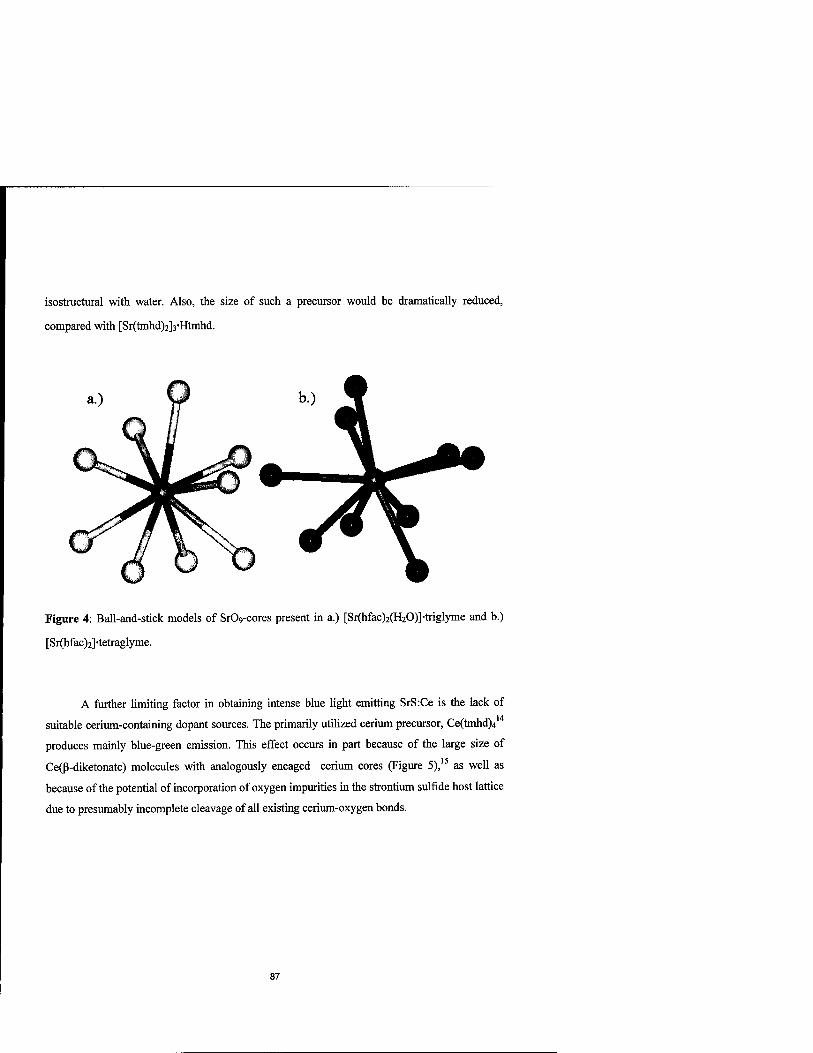
isostractural with water. Also, the size of such a precursor would be dramatically reduced,
compared with [Sr(tmhd)2]3,Htmhd.
Figure 4: Ball-and-stick models of Sr09-cores present in a.) [Sr(hfac)2(H20)]-triglyme and b.)
[Sr(hfac)2]-tetraglyme.
A further limiting factor in obtaining intense blue light emitting SrS:Ce is the lack of
suitable cerium-containing dopant sources. The primarily utilized cerium precursor, Ce(tmhd)4
produces mainly blue-green emission. This effect occurs in part because of the large size of
Ce(ß-diketonate) molecules with analogously encaged cerium cores (Figure 5),15 as well as
because of the potential of incorporation of oxygen impurities in the strontium sulfide host lattice
due to presumably incomplete cleavage of all existing cerium-oxygen bonds.
87

Figure 5: The space-filling portrayal of Ce(tmhd)4.
RESULTS AND DISCUSSION
The synthesis of [Sr(hfac)2]-triglyme was accomplished by reacting strontium ethoxide
with two equivalents of the Hhfac-ligand and one equivalent of triglyme (eq. 1) in hexane under
strictly anaerobic and aqueous-free conditions, which otherwise inevitably leads to the formation
of a solvated derivative.
[Sr(OEt)2(EtOH)4]„ + 2 Hhfac + triglyme -> [Sr(hfac)2(tri)] + 6 EtOH (1)
88

Single crystals suitable for X-ray structure determination were obtained from a
concetrated hexane solution at 0°C (monoclinic, C2/c, a = 22.3695 Ä, b = 9.4900 Ä, c = 15.7232
A, ß = 128.9540°, Z = 4, V = 2595.66 Ä3, R = 3.61 %). The proportions comparison between the
unsolvated [Sr(hfac)2]-triglyme and the trimeric agglomerate [Sr(tmhd)2]3*htmhd (Figure 6)
manifests distinctly the vast reduction in size, as well as the creation of an opening for potential
H2S-linkage. The "molecular radius" has been decreased from -7.5Ä for [Sr(tmhd)2]3*htmhd to
2.9 Ä in the axial and 2.2 A in the equatorial direction for [Sr(hfac)2]-triglyme.
Figure 6: Space-filling models of and [Sr(hfac)2]-triglyme and [Sr(tmhd)2]3-htmhd.
Ce{N[Si(CH3)3]2}3 has been secured according to existing procedures16 by reacting
cerium(III)chloride and lithium hexamethyldisilylamide in THF (eq. 2).
CeCl3 + 3 LiN[Si(CH3)3]2 -> Ce{N[Si(CH3)3]2}3 + 3 LiCl (2)
Multiple sublimations yielded an extremely air- and moisture-sensitive yellow powder. It
represents a highly volatile cerium compound, which was shown by thermogravimetric analysis
to stay intact in the vapor phase (Figure 7).
89

120
0 50 100 150 200 250 300 350 400
Temperature
Figure 7: TGA plot of Ce{N[Si(CH3)3]2}3.
Ce{N[Si(CH3)3]2}3 has been employed along with Ce(tmhd)4 in ALE experiments as a
dopant source of SrS. Preliminary results are compiled in Table 1.
Item Ce(tmhd)4 Ce(tmsa)3
^max (nm) 518 -480
cd/m2 28 9
X .30 .20
y .52 .40
[lcd/m2 + 50v]Bon 23-61 -12 - 22
[lcd/m2]Vthr 81 + 2 75 -112
[Ce]XRF(wt%) 0.91 - 1.19 0.20 - 2.40
x1/2(ns) 11-14 15-20
Table 1: Emission characteristics of SrS:Ce obtained employing Ce(tmhd)4 and Ce(tmsa)3
[Ce{N[Si(CH3)3]2}3] as cerium dopant sources.
90

As can be viewed from Table 1, compared with cerium diketonates, cerium amide doped
SrS films emit visible electromagnetic radiation at a wavelength shifted almost 40 nm towards
the blue region of spectrum (Figure 8). Additional efforts to improve emissions intensity are
underway and will be reported in due course.
§ B.
5
400
SPECTRAL RADIANCE PEAK (ffi 484 nm
§ P. <» W »
Figure 8: Comparison of wavelength emissions for SrS:Ce doped with a.) Ce(tmhd)4 and b.)
Ce{N[Si(CH3)3]2}3.
91

A possible explanation for this wavelength shift lies in the discrepancy of cerium-
nitrogen and -oxygen bond strengths. Contrary to relatively stable Ce-0 bonds, the extremely
sensitive Ce-N-linkage should ensure complete dissociation of the lanthanide core upon contact
with hot substrate surfaces (Figure 9).
R R I I r\
R-N N-R 9 9 ^
777777 777777 Figure 9: Schematic substrate-dopant interactions for cerium amide and ß-diketonate molecules.
CONCLUSIONS
New strontium and cerium precursors for deposition of blue light emitting SrS:Ce have
been developed. In contrast to the clustered species [Sr(tmhd)2]3-Htmhd, the newly synthesized
[Sr(hfac)2]-triglyme represents a vastly size-diminished monomeric precursor with a pocket for
potential H2S-attachment. In the case of cerium, the utilization of Ce{N[Si(CH3)3]2}3 has
produced a substantial blue shift in the emission wavelength, compared with originally employed
Ce(tmhd)4 representative.
92

REFERENCES
1. C.N. King, J. Vac. Sei. Technol. A14,1729 (1996).
2. P.D. Rack, P.H. Holloway, L. Pham, J. Wager, S.-S. Sun, E. Dickey and C.N. King, SID
95 Digest 1995,480.
3. M. Takeda, Y. Kanatani, H. Kishishita and H. Uede, Adv. Disp. Technol. 3, SPIE Proc.
Int. Soc. Opt. Eng. 34, 386 (1983).
4. M. Tiitta and L. Niinistö, Chem. Vap. Deposition 3 (4), 167 (1997).
5. T. Suntola, J. Antson, A. Pakkala and S. Lindfors, SID 80 Digest 1980,108.
6. W.S. Rees, Jr., CVD of Nonmetals, 1st ed. (Wiley-VCH Verlagsgesellschaft mbH, D-
69469 Weinheim, 1997), p. 254.
7. P. Soininen, E. Nykänen, L. Niinistö and M. Leskelä, Chem. Vap. Deposition 2 (2), 69
(1996).
8. S.R. Drake, M.B. Hursthouse, DJ. Otway and K.M.A. Malik, J. Chem. Soc, Dalton
Trans. 1993,2883.
9. P.H. Dickinson, T.H. Geballe, A. Sanjurjo., D. Hildenbrand, G. Craig, M. Zisk, J.
Collman, S.A. Banning and R.E. Sievers, J. Appl. Phys. 66,444 (1989).
10. M. Leskelä, L. Niinistö, E. Nykänen, P. Soininen and M. Tiitta, Thermochim. Acta 175,
91 (1991).
11. G.S. Hammond, D.C. Nonhebel and C.-H.S. Wu, Inorg. Chem. 2,73 (1963).
12. D.J. Otway, H.A. Luten, K.M.A. Malik, M.B. Hursthouse and W.S. Rees, Jr., in Metal-
Organic Chemical Vapor Deposition of Electronic Materials II, edited by S.B. Desu, D.B.
Beach and P.C. Van Buskirk (Mater. Res. Soc. Symp. Proc, 415, Pittsburgh, PA, 1996)
pp. 105-110.
13. a. S.R. Drake, W.E. Streib, M.H. Chisholm and K.G. Caulton, Inorg. Chem. 29, 2707
(1990).
b. S.R. Drake, D.J. Otway, M.B. Hursthouse and K.A.M. Malik, Polyhedron 11, 1995
(1992).
14. M. Becht, T. Gerfin and K.-H. Dahmen, Chem. Mater. 5,137 (1993).
15. M. Leskelä, R. Silanpää, L. Niinistö and M. Tiitta, Acta Chem. Scand. 45, 1006 (1991).
16. D.C. Bradley, J.S. Ghotra and F.A. Hart, J. Chem. Soc, Dalton Trans. 1073,1021.
93

PRECURSORS FOR THE CHEMICAL VAPOR DEPOSITION OF TITANIUM NITRIDE AND TITANIUM ALUMINUM NITRIDE FILMS
CHARLES H. WINTER,* PEGGY J. MCKARNS, AND JOSEPH T. SCHEPER
Department of Chemistry, Wayne State University, Detroit, Michigan 48202, [email protected]
ABSTRACT
Titanium nitride and ternary alloys thereof are of significant interest due to their hardness,. chemical resistance, and good electrical conductivity. We report the synthesis, structure, and properties of several new precursors to titanium nitride that are based upon hydrazine-derived ligands. Application of these complexes in titanium nitride film depositions is overviewed. Film properties and characterization are presented. We also describe a new process for the preparation of titanium aluminum nitride films, and focus on how the presence of small amounts of aluminum change the properties of the material.
INTRODUCTION
Titanium nitride (TiN) has been the subject of considerable attention in recent years due to its wide range of applications. TiN is nearly as hard as diamond, which has led to its use as a hard coating for steel cutting tools [1]. TiN films are widely used as decorative gold-colored coatings due to the similarity of the optical spectrum of TiN to that of gold [2]. TiN is an excellent candidate material for solar control coatings in automotive and architectural glass [3]. TiN has also found applications in the microelectronics industry as a contact material [4] and as a barrier layer material [5].
Fabrication of TiN thin films has been reported using various physical vapor deposition (PVD) [6] and chemical vapor deposition (CVD) techniques. CVD processes generally lead to films with better density, step coverage, and growth rates than those produced by physical vapor deposition routes. The reaction of titanium (IV) chloride with nitrogen and hydrogen results in TiN films at temperatures of 915 °C or higher ([7], eq 1). The high temperature, however, limits possible substrate materials. Using ammonia as the nitrogen source was found to afford TiN films at temperatures as low as 550 °C ([8], eq 2). Treatmentof titanium(IV)chloride with alkylamines yields high quality TiN films at or above 475 °C ([9], eq 3). Low temperature (200-450 °C) deposition of TiN films from tetrakis(dialkylamido)titanium(IV) complexes and ammonia has been described as well ([10], eq 4). Recently, it has been demonstrated that the reaction of titanium(F/) iodide with ammonia affords TiN films at deposition temperatures below 450 °C ([11], eq 5).
2TiCl4 + N2 + H2 2 TiN 8HC1 (1)
6TiCl4 + 8NH3
TiCl4 + excess (CH3)3CNH2
Ti(NR2)4 + excess NH3
6 Til, + 8NH3
6 TiN + 24HC1 + N2 (2)
-*- TiN + organic products (3)
-*- TiN + organic products (4)
-*- 6TiN + 24 HI + N2 (5)
95
Mat. Res. Soc. Symp. Proc. Vol. 495 ® 1998 Materials Research Society

In addition to the multi-component precursor methods, several single-source precursors have been reported for the chemical vapor deposition of TiN. The use of a single-source precursor eliminates the problem of mixing gas phase reactants in the CVD system, because all necessary elements are contained in one complex. TiN has been deposited from TitNR^, between 250 and 450 °C, however, the films contain significant amounts of carbon [12,13]. Titanocene diazide was found to afford TiN films, although the films contained significant graphitic carbon contamination [14]. Recently, Cowley, Roesky, Jones, and coworkers have reported a precursor (TifNMe^fN^yj) with an all nitrogen coordination sphere [15]. However, films derived from this precursor contained 10% carbon. Our previous work in this field has yielded several single- source precursors, including [TiCljCNtBuXNHjtBuJJ,, [16] and [TiCl4(NH3)J [17].
Titanium nitride is not without its shortcomings, however. The columnar structure of polycrystallineTiN provides grain boundaries that limit its barrier performance, especially when very thin layers are used [18]. TiN is readily oxidized by ambient oxygen at high temperatures (> 500 °C) [19-21]. Oxidation at higher temperatures can reduce the usefulness of TiN coatings in many applications. Certain properties of TiN films can be improved by inclusion of varying amounts of a second metal or metalloid in the film. For example, amorphous Ti-Si-N films have been offered as an improved barrier layer for microelectronics applications [18]. TiBN, TiZrN, TiNbN are harder than TiN itself [21]. Titanium aluminum nitride (Ti^ALN) is the best studied of the ternary titanium nitride materials. Ti.,ALN is harder and more resistant to oxidation than TiN [19-21]. Both properties make it a desirable materialfor applications as wear-resistant coatings. The attractive violet black color of Ti! „ALN has led to its use as a durable, decorative coating in jewelry [22]. Ti. ALN films with low aluminum content have also been shown to be an effective barrier layer in microelectronics devices [23]. Ti,, ALN films have been produced by various PVD methods [19,21]. The only CVD route that has been reported is the plasma-assisted reaction of titanium(I V) chloride with aluminum trichloride, ammonia, and hydrogen [20].
Herein we report the reaction of titanium(IV) chloride with 1,1-disubstituted hydrazines. The resulting complexes constitute a new class of single-source precursors to TiN films. Deposition studies using [rip4(NNMe,)2(HjNNMe2)2] are described. High quality TiN films were obtained at temperatures above 400 °C. We also report the first thermal CVD route to Ti. Al N films using a ternary precursor system consisting of titanium(IV) chloride, trimethylaluminum, and tert-butylamine. Finally, high temperature oxidation studies are described comparing resistance of TiN and Ti,.,, ALN toward degradation by ambient atmosphere.
RESULTS
Precursors to TiN Films. Treatment of titanium(IV) chloride with four equivalents of 1 l-dimethylhydrazineorl-aminopiperidineindichloromethaneat23 °C, followed by removal of volatiles and extraction with benzene, afforded [Tiaq4(NH2N(ayjIöirNN(Ciy JJ (1, 95%) and [Tip^NHjNCCH^jOi-NNfCH^s).,] (2,91%), respectively, as red solids (eq 1). Red rods
R2NNH2 Nr NR2
2TiCU + 8H2NNR2 <gg» » £>« T<° (6)
-4R2NNH3C1 R2^V_>NR2
1,R = CH3,95% 2,R2 = (CH2)5,91%
of 2 crystallized from a benzene solution layered with hexane. The 'H NMR spectra of 1 and 2 revealed the presence of hydrazide(2-) and hydrazine ligands. For example, the C{ H) NMR spectrum' of 1 in chloroform-d showed two broad peaks that arise from the methyl groups of the dimethylhydrazido(2-) (51.50 ppm) and the dimethylhydrazine (49.27 ppm) functionalities. For comparison, the methyl groups in free 1,1-dimethylhydrazine show a resonance in the C{ H}
96
NMR at 5130 ppm. The ER spectrum of 1 exhibited N-H stretches at 3237 and 3127 cm"1, while the corresponding stretches in complex 2 were found at 3293,3213,3154, and 3096 cm". These values imply hydrogen bonded hydrazine groups. The N-H bends were observed at 1621 cm' for 1 and at 1581 and 1565 cm"' for 2. The molecular geometry of 2 was determined by X-ray crystallography. .
Treatmentoftitanium(rV) chloride with 1-aminohomopiperidine in dichloromethaneat 23 °C, followed by crystallizationfrom a dichloromethane solution layered with hexanes, afforded ^NNCCH^JM [Ti^CNNCCH^J^-CDj}" (3, 76 %) as dark red crystals (eq 2). Complex 3 was fully characterized by spectroscopic and analytical techniques. The carbons directly attached to nitrogens in the hydrazide(2-) and the hydrazinium ligands in complex 3 had resonances in the 13C{'H} NMR at 62.25 ppm and 60.69 ppm, respectively. For comparison, the analogous carbon resonance in free aminohomopiperidinewas observed at 62.72 ppm. The IR spectrum displayed N-H stretches at 3287,3157, and 3106 cm"1 while N-H bends were found at 1598 and 1573 cm". An X-ray crystal structure determination established the molecular geometry of 3.
4 TiCl4
H3NNR2
12 H2NNR2 CH?Ch
23 °C, 18 h -7 R2NNH3C1
RaNr—A 9 9 Nr-}™
^ Ti T£- Cl—Ti TijC :"7\/^c,/\/v R2N N N N
Cl
R
(7)
3,R2 = (CH2)6,76%
Complexes 1-3 sublime slowly at 140-150 °C (0.1 mmHg), and do not leave residues (qualitatively < 5% decomposition). The fact that 3 possesses similar volatility as 1 and 2 suggests that it readily reverts to two equivalents of ^^^(NN^Hj)^ J and one equivalent of (CH^6NNH3C1 upon heating. Obviously, (CH^NNHjCl also sublimes, since it was not left behind as a residue.
The X-ray crystal structures of 2 and 3 were determined in order to establish their molecular geometries. Perspective views are presented in Figures 1 and 2, along with selected bond lengths and angles. Complex 2 exists as a dimer held together by bridging hydrazide(2-) ligands. Both titanium centers are six coordinate, but Ti(l) is bonded to two hydrazine ligands, two chlorides, and is terminally bonded to the hydrazide(2-) ligands. Ti(2) is side-bonded to the two hydrazide(2-) ligands and is bonded to two terminal chlorides. The Ti(2)-N(7) and Ti(2)-N(5) bond distances (1.932(3) and 1.926(3) A) are slightly longer than that of Ti(l)-N(7) and Ti(l)- N(5) (1.858(3) and 1.832(3) A). The average Ti(2)-N(6) and Ti(2)-N(8) bond distance (2.184 A) is shorter than that of the average bond distance (2.274 A) of Ti(l)-N(l) and Ti(l)-N(3). The chlorines attached to Ti(2) are approximately trans to the hydrazide(2-) ligands. These bonds are distinctly shorter (Ti(2)-Cl(3) 2.287(1) A, Ti(2)-Cl(4) 2.277(2) A versus Ti(l)-Cl(l) 2.411(1) A, Ti(l)-Cl(2) 2.427(1) A) than the Ti(l)-Cl bonds where the chlorine atoms are eis to each other. This anomaly could be attributed to differences in trans effect of the hydrazide(2-) and chloride ligands and to N-H"«C1 hydrogen bonding associated only with chlorides attached to Ti(l).
97

C(12)
CK3I
C(32)
Figure 1. Perspective View of 2 with Selected Bond Lengths (A) and Angles (°): Ti(l)-N(l) 2.285(3), Ti(l)-N(3) 2.262(3), Ti(2)-N(5) 1.926(3), Ti(2)-N(6) 2.207(3), Ti(2)-N(7) 1.858(3), Ti(l)-Cl(l) 2.411(1), Ti(l)-Cl(2) 2.427(1), Ti(2)-Cl(3) 2.287(1), Ti(2)-Cl(4) 2.277(2), Ti(l)- Ti(2) 2.740, N(l)-Ti(l)-N(3) 75.6(1), N(5)-Ti(l)-N(7) 89.3(1), Cl(l)-Ti(l)-Cl(2) 165.3(1), N(5)-Ti(2)-N(7) 84.5(1), N(6)-Ti(2)-N(8) 161.1(1), Cl(3)-Ti(2)-Cl(4) 117.0(1).
Complex 3 crystallized in an ionic fashion. The cation is a 1-aminohomopiperidinium ion. The anion is a tetranuclear species comprised of two hydrazide(2-)-bridged dinuclear moieties connected by three chloride bridges. For the anion, only the data for the coordination spheres of Ti( 1) and Ti(2) are presented, since the analogous values for Ti(3) and Ti(4) are identical within the limits of the experiment. The 1-aminohomopiperidinium cation has a nitrogen-nitrogen bond length of 1.434(9) A (N(9)-N(10)), which is ca. 0.07 A longer than the nitrogen-nitrogen bonds found in the hydrazide(2-) ligands of the anion (N(l)-N(2) 1.372(9) A, N(3)-N(4) 1.357(9) A). There are three types of chloride ligands in the anion. The first type bridges the two dinuclear moieties and has an average titanium-chlorine bond length of 2.540 A (range 2.514(3)-2.566(2) A). The second type is a terminal chloride trans to a bridging chloride (Cl(3)-Ti(2)-Cl(6) 163.07(10)°) and has a significantly shorter titanium-chlorine bond (Ti(2)-Cl(3) 2.342(3) A). The third type is a terminal chloride on the titanium bearing both nitrogens of each hydrazide(2-) moiety, and has an average titanium-chlorine bond length of 2.268 A (Ti(l)-Cl(l) 2.264(3) A, Ti(l)-Cl(2) 2.272(3) A). The bridging hydrazide(2-) ligand is asymmetrically bonded to both titanium atoms, with Ti(l)-N(l) (1.916(7) A) and Ti(l)-N(3) (1.928(7) A) bond distances that are slightly longer than that of Ti(2)-N(l) (1.829(7) A) and Ti(2)-N(3) (1.848(7) A). Each titanium atom has a distorted octahedral coordination sphere. The nitrogen-titanium-nitrogen angles for the titanium bearing both nitrogens of the hydrazide(2-) species are 37.8(2)° (N(l)-Ti(l)-N(2)) and 37.8(3)° (N(3)-Ti(l)-N(4)). On the same titanium, the angle of a chlorine to a hydrazide(2-) nitrogen averages 113.78° (range 112.2(2)-115.1(2)°). The chlorine-titanium-homopiperidine nitrogen angles average 95.6° (range 95.0(2)-96.0(2)°). About Ti(2), the terminal chlorine- titanium-nitrogen angles are 98.7(2)° (Cl(3)-Ti(2)-N(l)) and 96.9(2)° (Cl(3)-Ti(2)-N(3)). Each hydrazide(2-) nitrogen is trans to a bridging chloride (N(l)-Ti(2)-Cl(4), 169.0(2)°; N(3)-Ti(2)- Cl(5), 174.0(2)°). The deviation from linearity demonstrates the octahedral distortion.
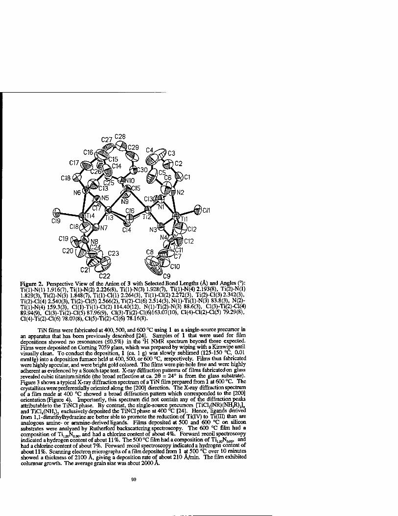
C27 C28
C22 ^*C9 Figure 2. Perspective View of the Anion of 3 with Selected Bond Lengths (Ä) and Angles (°): Ti(l)-N(l) 1.916(7), Ti(l)-N(2) 2.226(8), Ti(l)-N(3) 1.928(7), Ti(l)-N(4) 2.193(8), Ti(2)-N(l) 1.829(3), Ti(2)-N(3) 1.848(7), Ti(l)-Cl(l) 2.264(3), Ti(l)-Cl(2) 2.272(3), Ti(2)-Cl(3) 2.342(3), Ti(2)-Cl(4) 2.540(3), Ti(2)-Cl(5) 2.566(2), Ti(2)-Cl(6) 2.514(3), N(l)-Ti(l)-N(3) 83.8(3), N(2)- Ti(l)-N(4) 159.3(3), Cl(l)-Ti(l)-Cl(2) 114.40(12), N(l)-Ti(2)-N(3) 88.6(3), Cl(3)-Ti(2)-Cl(4) 89.94(9), Cl(3)-Ti(2)-Cl(5) 87.96(9), Cl(3)-Ti(2)-Cl(6)163.07(10), C1(4)-C1(2)-C1(5) 79.29(8), Cl(4)-Ti(2)-Cl(6) 78.07(8), Cl(5)-Ti(2)-Cl(6) 78.16(8).
TiN films were fabricated at 400,500, and 600 °C using 1 as a single-source precursor in an apparatus that has been previously described [24]. Samples of 1 that were used for film depositions showed no resonances (<0.5%) in the 'H NMR spectrum beyond those expected. Films were deposited on Coming 7059 glass, which was prepared by wiping with a Kimwipe until visually clean. To conduct the deposition, 1 (ca. 1 g) was slowly sublimed (125-150 °C, 0.01 mmHg) into a deposition furnace held at 400,500, or 600 °C, respectively. Films thus fabricated were highly specular, and were bright gold colored. The films were pin-hole free and were highly adherent as evidenced by a Scotch tape test. X-ray diffraction patterns of films fabricated on glass revealed cubic titanium nitride (the broad reflection at ca. 29 = 24° is from the glass substrate). Figure 3 shows a typical X-ray diffraction spectrum of a TiN film prepared from 1 at 600 °C. The crystallites were preferentially oriented along the [200] direction. The X-ray diffraction spectrum of a film made at 400 °C showed a broad diffraction pattern which corresponded to the [200] orientation (Figure 4). Importantly, this spectrum did not contain any of the diffraction peaks attributable to the TiNCl phase. By contrast, the single-source precursors [TiCl2(NR)(NHjR)Jn and TiCl4(NH3)2 exclusively deposited the TiNCl phase at 400 °C [24]. Hence, ligands derived from 1,1-dimethylhydrazine are better able to promote the reduction of Ti(IV) to Ti(rfl) than are analogous amine- or ammine-derived ligands. Films deposited at 500 and 600 °C on silicon substrates were analyzed by Rutherford backscattering spectroscopy. The 600 °C film had a composition of Ti100N096, and had a chlorine content of about 4%. Forward recoil spectroscopy indicated a hydrogen content of about 11%. The 500 °C film had a composition of T^^oN^s, and had a chlorine content of about 7%. Forward recoil spectroscopy indicated a hydrogen content of about 11%. Scanning electron micrographs of a film deposited from 1 at 500 °C over 10 minutes showed a thickness of 2100 A, giving a deposition rate of about 210 AAnin. The film exhibited columnar growth. The average grain size was about 2000 A.
99

T'HjTU 11 i'fnii"»Ti|m IT rrn firm i n i j i i i'i iirrip 11 M m i |TH 111 n i ] in u 11 T I [ i m j i ri i; n 11
10. 20. 30. 40. 50. 60. 70. 80. 90. 100.
Figure 3. X-Ray Diffraction Spectrum of a TiN Film Deposited from 1 at 600 °C.
10. 20. 30. 40. 50. 60. 70. BO. 90. 100. Figure 4. X-Ray Diffraction Spectrum of a TiN Film Deposited from 1 at 400 °C.
Deposition of Ti^A^N Films. T^ AljN films were deposited in a horizontal hot walled reactor according to eq 8. Details of the reactor configuration have been previously described [9]. Coming 7059 glass, silicon, and mica substrates were used. The glass substrates
100

were wiped with a Kimwipe until visually clean, the silicon substrates were used as received, and the mica substrates were cleaved just prior to placement in the reactor. The precursors were loaded into bubblers and were delivered to the deposition zone by a flow of nitrogen carrier gas. Bubblers were kept at ambient temperature. The inlet to the deposition tube consisted of three concentric stainless steel tubes. Titanium(IV) chloride was introduced through the innermost tube. The outermost tube was used to deliver the tert-butylamine. For TiN depositions, pure nitrogen gas was passed through the center tube to act as a separation between the reactants. In Ti, AJjN depositions the separation flow was seeded with trimethylaluminum. The concentration of each reactant in the total flow was controlled by flow meters regulating the amount of carrier gas passing through the bubblers. Substrates were held at 600 °C during depositions.
TiCU + A12(CH3)6 + (CH3)3CNH2 C^ffigaCg
(8) Tii.xAljiN films + organic products
TiN films were first grown in the reactor as a test of the system, by reacting titanium(IV) chloride with tert-butylamine at 600 °C as previously described [9]. The resultant films were highly specular and were rose-gold colored. Next, a separate flow of carrier gas was passed through a trimethylaluminum bubbler and was added to the separation flow emanating from the middle concentric tube. The amount of trimethylaluminum was varied by changing the flow of carrier gas through the bubbler, but the total flow of carrier gas through the middle tube was kept constant by adjusting the separation flow. In this fashion Ti^ALN was deposited on the various substrates. The resultant films were specular, smooth, highly adherent (scotch tape test), violet- black in color, and qualitatively hard (not scratched by a straight pin). Rutherford backscattering spectroscopy was used to determine the composition of the films. Films fabricated using three different flow rates of trimethylaluminum analyzed as TiogjAl^Nog,, (0.019 mmolAninAl, 0.40 mmolAninTi,4.3 mmol/mintBuNH2), T^^Al^N,,; (0.055 mmolAninAl, 0.40 mmol/minTi, 4.3 mmolAnin tBuNH2), and Ti^Al^N^ (0.090 mmol/min Al, 0.40 mmol/minTi, 5.3 mmol/min tBuNH2). The first two films were slightly nitrogen deficient, while the third was slightly nitrogen rich. Forward recoil spectroscopy of the TioejAloaiNogj film indicated a hydrogen content of about 5%. Attempts to deposit films with aluminum contents greater than in TiojjAlo^Nu, led to rough, poorly adherent coatings. The X-ray diffraction spectra of pure TiN films prepared as described above exhibited preferred (200) orientations. The X-ray diffraction spectra of the Ti^AL, 17N0.89, Tia^Al^N^, and Ti<,.52Alo^N,.„ films exhibited the same preferred orientation. As seen in Figure 5, however, there was significant broadening of the reflection as the aluminum content increased. Line broadening can be attributed to either a decrease in grain size or an increase in non uniform stress within the grains [25]. Atomic force microscopy and scanning electron microscopy of the films clearly show the columnar structure characteristicof TiN. The average grain size of a Ti^Al^N^,, film was about 730 Ä, as determined by atomic force microscopy. This can be compared with an average grain size of about 1900 A from atomic force microscopy for a TiN film deposited at 600 °C from titanium(IV) chloride and tert- butylamine. A decrease in the grain size is generally associated with an increase in hardness [25]. No A1N reflections were observed. The absence of any reflections that can be assigned to AlN suggests that the aluminum atoms are substituted for titanium atoms in the TiN lattice. The growth rate of a Ti„ «Al^N,,.,, film at 600 °C was 2700 A/min.
The resistance of the films to oxidation by ambient atmosphere was evaluated. Films were placed on a steel stage in a quartz tube open to air at both ends. The tube was placed in a furnace and was heated for 3 h at 550, 625, and 700 °C. The films were analyzed by X-ray diffraction before and after heating. As shown in Figure 6, TiN started to show reflections arising from Ti02 (rutile) after 3 h at 550 °C. After 3 h at 625 °C, the TiN film had been completely oxidized to Ti02. A TiosyAl^Noss film, however, showed no signs of Ti02 even after 3 h at 700 °C. Hence, Ti^ALN films deposited using our methodology exhibit significantly enhanced oxidation resistance, compared to TiN films.
101

(a)
(b)
(c)
wmf^WVK *«n<-.nV<WWVT^V ■V^V-^M-—, ■■—^ ■„« J, ^^f im»i^
1-K+V+**•*•**J+#* *
•*»*'»««**•»*•-*»« ■riiir
39. 40. 41. 42. 43. 44. 45. 46. Figure 5. Expansion of the (200) Reflection in the X-ray Diffraction Spectra of (a) TW^NM». (b> TwHutNass. and (c) Ti^AI^N,.,, Films.
(a)
\
(b)
.
(c)
__J__ A h '"!"
1111111 |Ti .,,. J 1 | 1 1 1 11 1 j 1J |
10. 20. 30. 40. 50. 60. 70. 80. 90. 100.
Figure 6. X-ray Diffraction Spectra of a TiN Film Deposited from Titanium(IV) Chloride and tert-Butylamine Under the Following Conditions (a) As Deposited (b) Exposed to Ambient Air at 550 °C for 3 h (c) Exposed to Ambient Air at 625 °C for 3 h. The Reflections in (c) Correspond to Those of Rutile.
102

DISCUSSION
Development of New Precursors to TiN Films. The precursors 1-3 represent improved source compounds for TiN, relative to our previously described precursors [TiCl^tBuKNHjtBuy,, [16] and [TiCl4(NH3)J [17]. Sources 1-3 afford highly specular TiN films, and give more uniform substrate coverage than is possible with our earlier precursors. Unfortunately, complex 3 is ionic and tetranuclear, and therefore should have a low vapor pressure. Curiously, 1-3 all sublime at ca. 150 °C (0.1 mmHg), suggesting that the molecular species 1 and 2 have similar vapor pressures to 3. This similarity in volatility could have several origins. Complex 3 may dissociate to two equivalents of Ti2Cl4(NN(CHj)6)4 and one equivalent of aminohomopiperidinium chloride at temperatures below where sublimation of T^C^CNNCCHj)^ begins. Alternatively, 1 and 2 may exist predominantly as ionic species with formulations similar to that of 3. Therefore, the sublimation temperatures of 1-3 may reflect the energy required for the complexes to revert to neutral titanium species. This point has been difficult to establish unambiguously. Complex 2 is difficult to crystallize, and only small amounts of crystals can be obtained in a given crystallization. For film depositions, microcrystalline 1 was used due to the difficulty in producing enough crystalline material. It is difficult to distinguish between coordinated hydrazine ligands and a hydrazinium ion, since both show complex N-H stretching modes at similar energies in the IR spectra. 'H NMR has not been able to distinguish between coordinated hydrazine ligands and a hydrazinium ion, since the protons in both resonate at similar frequencies. Furthermore, microanalyses on Ti-N-Cl species are generally not useful, due to the formation of refractory compounds (e.g., TiN, TiC, TiNC) upon combustion. We are continuing to define the structures of 1-3 in more detail. However, the present state of structural ambiguity does not limit the use of 1 -3 as excellent TiN precursors.
A significant finding in this work is the observation that complexes 1-3 lead to the deposition of TiN films at ca. 75 °C lower than is possible with our previously reported chloride- based single-source precursors [TiCl2(NtBu)(NH2tBu),]„ [16] and rTiCl4(NH3)2] [17]. By comparison, [TiCl2(NtBu)(NH2tBuU and [TiCl4(NH3)2] give TiNCl films at 400 °C, demonstrating that reduction from Ti(IV) to Ti(III) does not proceed at this temperature. Therefore, ligands derived from 1,1 -dialkylhydrazines must be better reducing agents than ligands derived from alkyl amines or ammonia. It is well known that hydrazine derivatives are substantially more electron rich than related amines. For example, tert-butylamine has an oxidation potential (EJ of 1.22 V versus Ag/Ag+, while 1,1-dimethylhydrazinehas an oxidation potential (EJ of 0.50 V under similar conditions [26]. Therefore, dialkylhydrazine-derivedligands should be better able to promote the reduction of Ti(IV) to Ti(HI), compared to alkylamine-derived ligands. The successful use of 1 as a single-source precursor to TiN films implies that hydrazine- derived ligands are also good nitrogen sources. We propose that the hydrazide(2-) nitrogens that bridge the two metals in 1-3 (e.g., N(7) and N(5) in 2) are the nitrogens that end up in the TiN films, since strong bonds are already formed to both titaniums and nitrogen-nitrogen bonds are relatively weak (ca. 54 kcal/mol in hydrazine). I5N labeling experiments are in progress to explore this issue.
Our long term goal is to develop ligands for early transition metal source compounds that are extremely efficient in promoting the reduction from the high oxidation states typically found in volatile metal complexes to the M(III) oxidation state required for MN phases. Ligands that promote such reductions should lead to lower temperatures for film depositions. While TiN films can be deposited a relatively low temperatures by several different CVD processes, low temperature processes for ZrN, HfN, and TaN films have yet to be described due to the difficulty in reducing these metals to the M(m) state. Hydrazine-derived ligands represent potentially useful ligands for the development of general processes for the low temperature deposition of MN phases. We are presently working on the development of new precursors that take advantage of the properties embodied by 1-3. The first goal has been to prepare halide-free precursors. We have examined the preparation of Ti(N(CH3)N(CH?),)4 by treatment of titanium(IV) chloride with lithium trimethylhydrazide(l-),but only two chlorides are replaced under all conditions that have been examined, affording TiCl2(N(CH,)N(CH3)2)2 [27]. TiCL(N(CH3)N(CH3)2)2 serves as an excellent precursor to TiN films, but still it contains chlorine. We have also prepared monomeric 8-coordinatepyrazolato complexes of the formula Ti(3,5-R2C3HN2)4 [28,29] but these complexes
103

give amorphous films of approximate composition Tilj0N, 0C50 in deposition processes. We are continuing our ligand development efforts.
Development of Processes for the CVD of Ternary Nitride Films. We chose to explore the development of CVD processes to Ti, ALN films, since a thermal CVD process for this ternary material has not been reported. General advantages of CVD processes over physical deposition techniques include potentially lower deposition temperatures through optimization of the chemistry, the possibility of excellent conformal coverage due to the chemical nature of the process, the feasibility of large area depositions, excellent control over film stoichiometry, and control over film purity by careful purification of the source compounds. Plasma CVD processes entail more expensive and complicated deposition equipment than required for thermal CVD processes, and can lead to substrate damage by the plasma. Furthermore, Ti^ALN is a prototypical ternary nitride, and properties described in the literature should serve as valuable benchmarks against which to compare the characteristics of our films. The process described herein is the first thermal CVD process for Ti,.,,ALN films. The maximum aluminum content that was possible in our system occurred in TiOJ2ALl4gNU8; attempts to produce films with greater aluminum incorporation led to poorly adherent films with rough morphology. Therefore, our process can easily produce Ti^ALN films with 0 < x < 0.50. By contrast, it is more problematic to control the aluminum content in sputtered films, due to difficulties in fabrication of the Ti-Al target with varying composition [19]. The average grain size in our Ti, XALN films is slightly smaller than that of TiN films prepared in an analogous fashion, as determined by scanning electron microscopy and atomic force microscopy. Reduced grain size in Ti, ALN films has been correlated with increased hardness [19-21]. While we have not yet measured the hardness of our films, it is likely that they are harder than TiN films. The oxidation of Ti,.„ALN films is substantially slower than TiN films prepared under similar conditions. TiN films were completely oxidized to rutile after 3 h at 625 °C in ambient air. By contrast, a film of the composition Tio^ÜojjNojj was completely stable toward oxidation to Ti02 after 3 h at 700 °C. It has been proposed that Ti, „ALN forms a thin protective layer of alumina on the surface of the film, which protects the bulk material from atmospheric degradation [19,20]. The surface analysis of a Ti,, 5^3,^85 film by X-ray photoelectron spectroscopy suggests that this proposal is true in material produced by our methodology. The A12p binding energy, 74.72 eV, is consistent with that of ALOj. For comparison, the A12p binding energy of an A1203 sample has been reported to be 74.7 ev [30]. The Ti2p3/2 binding energy showed at least two titanium species to be present, with the major ionization centered at 459 eV. This is close to the reference binding energy of Ti02 (458.5 eV, [30]). The bulk of the film, however, is crystalline with no evidence of Ti02 or A\p3 in the X-ray diffraction spectrum.
In summary, the properties of the Ti1„AlxN films produced by our method are very similar to those of films prepared by physical deposition methods and plasma-enhanced CVD. The simplicity of the process makes it attractive for the industrial fabrication of Ti^Al N films. The facile formation of Ti, ALN films suggests that other ternary titanium nitride films should be easily deposited by substituting other metal or metalloid source compounds for the aluminum source. These processes are being investigated in our laboratory.
ACKNOWLEDGMENTS
We thank the National Science Foundation for support of this work, Dr. Victor Rotberg of the Michigan Ion Beam Laboratory for RBS spectra, Professor Arnold L. Rheingold, Dr. Glenn P.A. Yap, and Dr. Mary Jane Heeg for single-crystal X-ray structural analyses, Professor Gang-yu Liu and Kapila Wadu Mesthrige for performing the atomic force microscopy, and Dr. James W. Proscia of Ford Motor Company, Glass Division for help with scanning electron microscopy and for comments on the manuscript.
REFERENCES
1. For leading references, see: W.D. Münz, D. Hofmann and K. Hartig, Thin Solid Films, 96, p. 79 (1982).
2. R. Buhl, H.K. Pulker and E. Moll, Thin Solid Films 80, p. 265 (1981).
104

3. For leading references, see: M. Erola, J. Keinonen, A. Anttila and J. Koskinen, Solar Energy Mater. 12, p. 353 (1985). A. Schlegel, P. Wachtere, J.J. Nickl and H.Lingg, J. Phys. C: Solid State Phys. 10, p. 4,889 (1977).
4. For leading references, see: C. Emsberger, J. Nickerson, A. Miller and D. Banks, J. Vac. Sei. Technol. A 3,2303 (1985). M. Wittmer, B. Studer and H. Melchior, J.Appl. Phys. 52, p. 5,722 (1981).
5. For example, see: IJ. Raaijmakers, Thin Solid Films 247, p. 85 (1994). M.-A. Nicolet, Thin Solid Films 54, p. 415 (1978).
6. For example, see: M. Wittmer, J. Vac. Sei. Technol. A 3, p 1,797 (1985). 7. W. Schintlmeister, O. Pacher, K. Pfaffinger and T. Raines, J. Electrochem. Soc. 123, p.
924 (1976). 8. S.R. Kurtz and R.G. Gordon, Thin Solid Films 140, p. 277 (1986). 9. K.B. Williams, O. Stewart, G.P. Reck and J.W. Proscia, Mater. Res. Soc. Symp. Proc.
327, p. 121 (1993). 10. R. Fix, R.G. Gordon and D.M. Hoffman, Chem. Mater. 3, p. 1138 (1991). D.M.
Hoffman, Polyhedron 13, p. 1169 (1994). 11. C. Faltermeier, C. Goldberg, M. Jones, A. Upham, D. Manger, G. Peterson, J. Lau, A.E.
Kaloyeros, B. Arkles and A. Paranjpe, J. Electrochem. Soc. 144, p. 1002 (1997). 12. K. Sugiyama, S. Pac, Y. Takahashi and S. Motojima, J. Electrochem. Soc. 122, p.
1,545 (1975). 13. R. Fix, R.G. Gordon and D.M. Hoffman, Chem. Mater. 2, p. 235 (1990). 14. G.M. Brown, Inorg. Chem. 28, 3028 (1989). K. Ikeda, M. Maeda and Y. Arita, Proc.
Symp. VLSI Technol. p. 61 (1990). 15. CJ. Carmalt, A.H. Cowley, R.D. Culp, R.A. Jones, Y.-M. Sun, B. Fitts, S. Whaley
and H.W. Roesky, Inorg. Chem. 36, p. 3,108 (1997). 16. C.H. Winter, P.H. Sheridan, T.S. Lewkebandara, M.J. Heeg and J.W. Proscia, J. Am.
Chem. Soc. 114, p. 1,095 (1992). T.S. Lewkebandara, P.H. Sheridan, M.J. Heeg, A.L. Rheingold and C.H. Winter, Inorg. Chem. 33, p. 5,879 (1994).
17. C.H. Winter, T.S. Lewkebandara, J.W. Proscia and A.L. Rheingold, Inorg. Chem. 33, p. 1,227 (1994).
18. For leading references, see: P.M. Smith and J.S. Custer, Appl. Phys. Lett. 70, p. 3,116 (1997). J.S. Reid, X. Sun, E. Kolawa and M.-A. Nicolet, IEEE Electron Device Lett. 15, p. 298 (1994). J.S. Reid, E. Kolawa, R.P. Ruiz and M.-A. Nicolet, Thin Solid Films 236, p. 319 (1993). E. Kolawa, J.S. Chen, J.S. Reid, PJ. Pokela and M.-A. Nicolet, J. Appl. Phys. 70, p. 1,369 (1991).
19. For leading references, see: C.-T. Huang and J.-G. Duh, Surf. Coatings Technol. 71, p. 259 (1995). Y. Tanaka, T.M. Giir, M Kelly, S.B. Hagstrom and T. Ikeda, Thin Solid Films 228, p. 238 (1993). W.-D. Münz, T. Hurkmans, G. Keiren and T. Trinh, J. Vac. Sei. Technol. A 11, p. 2,583 (1993). D. Mclntyre, J.E. Greene, G. Hakansson, J.-E. Sundgren and W.-D. Münz, J. Appl. Phys. 67, p. 1,542 (1990). H. Randhawa, P.D. Johnson and R. Cunningham, J. Vac. Sei. Technol. A 6, p. 2,136 (1988). G. Hakansson, J.-E. Sundgren, D. Mclntyre, J.E. Greene and W.D. Münz, Thin Solid Films 153, p. 55 (1987).
20. B.-J. Kim, S.-H. Lee and J.-J. Lee, J. Mater. Sei. Lett. 16, p. 1,597 (1997). K.H. Kim and S.H. Lee, Thin Solid Films 283, p. 165 (1996).
21. E. Vancoille, J.P. Celis and J.R. Roos, Thin Solid Films 224, p. 168 (1993). J.R. Roos, J.P. Celis, E. Vancoille, H. Veltrop, S. Boelens, F. Jungblut, J. Ebberink and H. Homberg, Thin Solid Films 193/194, p. 547 (1990). W. Gissler, Surf. Coatings Technol. 68/69, p. 556 (1994).
22. W.D. Sproul, J. Vac. Sei. Technol. A 12, p. 1,595 (1994). 23. I. Petrov, E. Mojab, F. Adibi, J.E. Greene, L. Hultman and J.-E. Sundgren, J. Vac. Sei.
Technol. A 11,11(1993). 24. C.H. Winter, T.S. Lewkebandara, P.H. Sheridan and J.W. Proscia, Mat. Res. Soc.
Symp. Proc. 282, p. 293 (1993). 25. B.D. Cullity, Elements of X-Ray Diffraction, Addison-Wesley, New York, 1978, pp. 99-
106, p. 281.
105

26. We thank Mr. Ariel Macatangay of our department for measuring these oxidation potentials.
27. J.T. Scheper and C.H. Winter, unpublished results. 28. I.A. Guzei, A.G. Baboul, G.P.A. Yap, A.L. Rheingold, H.B. Schlegel and C.H. Winter,
J. Am. Chem. Soc. 119, p. 3,387 (1997) 29. I.A. Guzei and C.H. Winter, unpublished work. 30. CD. Wagner, W.M. Riggs, L.E. Davis, J.F. Moulder, and G.E. Murlenberg, Handbook of
X-Ray Photoelectron Spectroscopy, Perkin Elmer Corp., Physical Electronics Division: Eden Prairie, Minnesota, 1979, pp 42, 68.
106

SILICON NITRIDE FILMS DEPOSITED BY ATMOSPHERIC PRESSURE CHEMICAL VAPOR DEPOSITION
Xian Lin, Denis Endisch, Xiaomeng Chen, and Alain Kaloyeros, Center for Advanced Thin Film Technology and Physics Department, The University at Albany-SUNY, Albany, New York 12222 Barry Afkles, Gelest Inc., Tullytown, Pennsylvania 19007
ABSTRACT
Films of silicon nitride are widely used in semiconductor technologies for very large scale integration (VLSI), thin film transistor (TFT), and solar cell applications. Current production technologies for silicon nitride use low pressure chemical vapor deposition (LPCVD) at temperatures > 700 °C or plasma enhanced chemical vapor deposition (PECVD) at temperatures below 450 °C. In this report, successful deposition of silicon nitride films by the low temperature thermal atmospheric pressure chemical vapor deposition (APCVD) method is described. Using a novel precursor tetraiodosilane (SiLt), deposition of silicon nitride has been achieved at temperature as low as 400 °C. Data pertaining to the dependence of film properties on deposition temperature are presented, along with a evaluation of the deposition rate, composition, chemical structure, and conformality of the resulting films.
INTRODUCTION
Increasing semiconductor device integration by feature size reduction results in a higher number of interconnect levels and enhanced dependence on the properties and performance of dielectric materials [1]. Silicon nitride is of significant technical interest due to its extensive use in microelectronic device fabrication as passivation layer, as oxidation or diffusion barrier, and as interlevel isolation layer[2]. LPCVD is extensively used to deposit silicon nitride thin films at high temperatures range [3]. Excellent uniformity and high throughput can be achieved by using reaction of dichlorosilane and ammonia at a temperature of 700-800 °C. But the requirement of high deposition temperature of the LPCVD process has serious limitations for some advanced VLSI applications when low processing temperatures are required. For TFT applications, all the processing temperatures should be lower than 400 °C if low cost glass substrates are used [4]. PECVD is an established alternative for deposition of silicon nitride at low substrate temperatures (<450°C) [5]. Silicon nitride films prepared by PECVD tend to be nonstoichiometric, and contain substantial quantities of atomic H (10-30%). However, the plasma process can cause ion bombardment damage of the underlying device structures. The high H concentration in the PECVD film is found to be related to the film instability and device degradation [6]. Deposition of low stress, low hydrogen content silicon nitride films with low surface damage at low temperature has been achieved by using microwave electron cyclotron resonance (ECR) deposition approach [7].
Atmospheric pressure thermal CVD using (TEOS/O3) chemistry is a proven technology for depositing high quality silicon dioxide films at low temperatures . Thus,
107
Mat. Res. Soc. Symp. Proc. Vol. 495 ° 1998 Materials Research Society

it was the initial motivation of the research to apply the same technique for deposition of silicon nitride films at low temperatures by testing various precursor chemistries and deposition conditions. The obvious advantage of the APCVD technique over the conventional PECVD process is cost effectiveness due to the simpler tool design. This paper will focus on the development of APCVD process for low temperature deposition of silicon nitride films using SiLt as silicon precursor. The reaction of iodosilane and ammonia has been studied and supports the concept of a relatively stable intermediate monosilylamine. Although not explicity directed toward CVD, the study indicates that at higher pressures trisilylamine and not silicon nitride is formed [8]. Recent recalculations of the bond dissociation energies of iodine and hydrogen bound to silicon [9], indicate that a preferred path to silicon nitride should avoid intermediates in which hydrogen is bound to silicon. Correlation between film properties and process parameters are presented, along with a evaluation of the deposition rate, composition, chemical structure, and conformality of the resulting films.
EXPERIMENT
Depositions were performed in a custom-designed rectangular CVD reactor system which incorporated a specialized Watkins Johnson monoblock injector (Figl.). The wafer was seated on a quartz plate holder heated by resistance heating. The Substrate temperature was monitored by the thermocouple near the back surface of the quartz holder. Depositions were carried out on silicon at substrate temperatures of 300-550°C. All the deposition runs were performed at the fixed chamber pressure of 750 Torr.
Atmospheric Pressure CVD System
SeperotorGas-»- Reacrant Gas -*-^
Heat Bath
Figl. Schematic of experimental set up.
SiLt was used as silicon precursor, and NH3 as nitrogen precursor. High purity N2
gas was used as carrier gas, and was also served as dilution and separator gas. Carrier gas and precursor flow to the inner zone of the injector; ammonia and dilution gas flow to the outzone of the injector, while the separator gas flows in between. Such an injector design can effectively prevent the gas phase reaction. All the gas flow rates were regulated by mass flow controllers. Typical temperature for the SiLt bubbler was 170°C, carrier gas flow was used to control the precursor deliver rate. The precursor deliver line was heated to a temperature up to 20°C higher than the bubbler temperature to avoid recondensation.
108

Composition analysis was performed using Rutherford backscattering spectroseopy (RBS). Thickness and composition were determined by comparing measured spectra with simulations using the analysis program RUMP. Fourier transform infared spectroseopy (FTIR) was used to determine the chemical bonding and H concentration in the films. Structure analysis was performed using x-ray diffraction(XRD). Conformality of the deposition was analyzed by scanning electron microscopy (SEM).
RESULTS AND DISCUSSION
Under the optimized processing window, series of runs were done in the temperature range from 350~550°C. RBS was performed for thickness and compositional analysis. The results are summarized in Table I. RBS spectrum of silicon nitride deposited at 400°C is shown at Fig2. The deposition of the silicon nitride film has been achieved at temperature as low as 350°C. The films are nitrogen rich at deposition temperatures below 550°C. There appears to be a trend toward stoichiometric deposition when the substrate temperature increases above 550°C. Unfortunately, due to the limitation of the sealing o-rings , the temperature could not be increased further. The iodine impurity concentration decreases dramatically when the substrate temperature increases from 350 to 400°C, and then decreases slowly with the further increase of the temperature. It was not clear why the growth rates increase greatly with the decrease of the deposition temperatures in the range between 350-450°C. The film obtained at 400°C has much lower impurity concentration than the film prepared at 350°C, and has film properties similar to the other high temperature runs. Accordingly, 400°C is considered to be a conservative minimum deposition temperature in this particular process window.
Table I. Temperature series runs Bubbler temperature =170°C Injector temperature=200°C Flow rate: N2 carrier=0.1slm, NH3=1.0slm, N2 outzone=3.0slm, N2 innerzone=1.9slm N2 separator=1.9slm
Run# Temperature Growth N/Si Iodine content (°C) Rate(A/min) ratio (at.%)
243 350 1375 1.8 4.2 242 400 950 1.9 2.3 230 450 750 1.9 1.2 241 500 800 1.9 0.9 244 550 850 1.33 0.8
109

Energy (Me V) 0.5 1.0 1.5
30
i i
1 G24497 w1#242 SiN/Sim green 3L Simulation of Si-N-I/Si
I
Ijk 1-S En«w _,
2 25 a>
>~ ~ N/*n "1 n -
aliz
ed
01
O
W* , :L jjjiiii i h 1 10 I ■Hi ML L
Ttosa "° Channel
5 NO 3i 1 l" i
I I I 1 200 400 600
Channel 800 1000
Fig.2 RBS spectrum of silicon nitride deposited on silicon at 400°C.
The infrared spectra for three silicon nitride films deposited at temperatures of 1) 350°C, 2). 400°C , and 3) 550°C are shown at Fig.3. All the deposited films showed strong N-H stretching mode at 3360 cm"1 and bending mode at 1200 cm"1. Si-N stretching mode is at 880 cm"1. The weak features near 2300 cm"1 were resulted from an incomplete subtraction of the absorption due to C02 in the spectrophotometer sample chamber. It is interesting that for our specific process, no Si-H bonding configuration (at 2180 cm") has been observed in the FTIR spectra. The Asymmetry of the N-H stretching mode peaks is due to the hydrogen bonding between the H atoms in the N-H bonds and long-pair electrons on nearby N atoms[10]. The temperature dependence of the N-H concentration is shown in Fig.4. The N-H concentration is calculated based on the calibration results from W.A.Lanford [11] and H.Efstathiadis [12]. The typical N-H concentration for films deposited at temperature >400 °C is around 4.0 x 10²²/cm3, Since there is no Si-H bonding in the film, the N-H bonding concentration could be used to indicate the H concentration in the film assuming a weak concentration of unbonded hydrogen. The films have absolute H concentrations around 30% , which are similar to the typical PECVD deposited silicon nitride films. The positions of the Si-N and N-H stretching modes are found to be sensitive to the hydrogen content in the films. The Si-N stretching mode will shift to the high wavenumber direction, and N-H stretching mode shift to the low wavenumber direction as the H content in the film increases.
110

—400 deg C — 350 deg C —550 deg C
dbwj A » OtP 2000 MOO
Wavenumber (cm'1)
2800 3200 365H T4C H>
Fig.3 Infrared absorbance spectra for three silicon nitride films deposited at different substrate temperature
XRD diffraction measurements showed that the deposited films were amorphous. Scanning electron microscopy showed a conformal deposition of silicon nitride over a 1x1.6 micrometer feature size trench structure with 10 nm TiN (Fig.5) on top, the step coverage is better than 85%. Comparing SEM thickness measurement with the results from the RBS, the film density of the moderate temperature (450°C) runs is calculated to be 2.4g/cm"', which is comparable to typical PECVD results.
M-H Concentration vt Tomporatura
Fig.4 FTIR N-H concentration versus substrate temperature.
Fig.5 Cross section-SEM of 380 nm SiN grown on top of TiN trench structure with feature size 1x1.6 nm.
111

CONCLUSIONS
It has been demonstrated that silicon nitride films can be grown by thermal APCVD at temperature as low as 400°C using SiLt and NH3 chemistry. The film properties such as stoichiometry, impurity and H concentration, and growth rate are strongly dependent on the deposition temperature. No Si-H bonding configuration exists in the deposited films. Under moderate deposition temperature film density is about 2.4g/cm"3. and H concentration is around 30%. These properties are comparable to the film prepared by PECVD process. Further investigation will be conducted to optimize the processing parameters to lower the impurity and H concentration, and increase the density of the film.
REFERENCES
1. Y.S. Obeng, K.G. Steiner, A.N.Velaga and C-S Pai AT&T Tech. J. May/June (1994) 94
2. B. El-Kareh Fundementals of Semiconductor Processing Technologies (Kluwer Academic Publishers 1995)
3. J.A. Gregory et.al Thin Solid Films 206 (1991) 11 4. Y. Kuo J.Electrochem. Soc. 142 (1995) 186 5. TJ. Cotler and J. Chapple-Sokol J.Electrochem. Soc. 140 (1993) 2071 6. G.N. Parson, J.H.Souk and J. Batey J. Appl. Phys. 70 (1991) 1553 7. C.Apblett, M.F. Gonzales, J.C.Barbour, L.G Pettersen, M.Kovacs and B. Huhr Nov.
Solid State Technology (1995) 73 8. D. Beach, Inorg. Chem., 31 (1992) 4174 9. R. Walsh in " Silicon, Germanium, Tin and Lead Compounds- A Survey of
Properties and Chemistry," ed. B. Arkles, Gelest 1998. Relevent bond dissociation energies in this reference: H3Si-H = 91.8 kcal/mole; H3Si-SiH3 = 76.7 kcal/mole; H3Si-I = 71 kcal/mole; I3Si-I = 68 kcal/mole.
10. Z.Yin and F.W.Smith Physical Review B 42 (1990) 3666 11. W.A. Lanford and M.J.Rand J. Appl. Phys. 49 (1978) 2473 12. H. Efstathiadis, Z.Akkerman, and F.W. Smith, Mat. Res. Soc. Symp. Proc. 415
(1995)51
112

NOVEL ANTIMONY PRECURSORS FOR LOW- TEMPERATURE CVD OF ANTIMONIDE THIN FILMS
MICHAEL A. TODD, GAUTAM BHANDARI AND T.H. BAUM Advanced Technology Materials, Inc, ADCS Division 7 Commerce Dr., Danbury, CT 06810, USA
ABSTRACT
Volatile antimony precursors were synthesized for the low temperature chemical vapor deposition (CVD) of antimony thin films. The molecules synthesized include tris (trifluoromethyl)stibine, Sb(CF3)3, Lewis base adducts of Sb(CF3)3, and antimony trihydride (stibine), SbH3. Isotopic substitution of stibine with deuterium leads to a more thermally stable, carbon-free antimony source. Similarly, deuterium substitution of trimethylsilylmethyl antimony dihydride leads to a stabilized liquid antimony precursor. The molecules were characterized using FTIR, NMR and DSC / TGA. Pure antimony films were deposited at temperatures below 300 °C with growth rates approaching 170 Ä / min using a low pressure hot-wall CVD reactor. The films were characterized using XRD, EDS, SEM and AFM.
INTRODUCTION
Processing of sophisticated microelctronic device heterostructures is the primary motivation behind the development and commercialization of volatile CVD precursors. At present, many III-V compound semiconductor and semiconductor alloy devices based upon complex heterostructures, such as strained layer superlattices and multiple quantum wells (MQW), are processed using molecular beam epitaxy (MBE) techniques. MBE is unattractive for commercial production because of its low throughput and high cost relative to other processing techniques. However, a lack of suitable, low temperature, low-cost precursors has hindered the development of CVD processing of many of these materials [1-2]. This is particularly true for many III-V heterostructures containing antimony, Sb.
Antimonide-based heterostructures are employed in both microelectronics and optoelectronics because of the wide range of bandgaps which are accessible by a variety of HI-V alloy compositions. Bandgaps from 1.6 eV (AlSb) to 0.2 eV (InSb) can be achieved by the growth of films having the proper stoichiometry. Currently, the materials of greatest interest incude InSbBi and InAsSbBi[3] for long wavelength infrared detectors (8-12 iim), InAsSb[4] and InGaSb[5] for mid-infrared military applications and InSb/Ini_xAlxSb[6] light emitting diodes (LEDs) for mid- infrared chemical sensor applications. Many of these materials are metastable and thus require volatile CVD precursors that decompose at low temperature to produce high quality, impurity- free thin films.
Antimonides are important in the development of quantum cascade (QC) lasers based on intersubband transitions in complex III-V compound semiconductor multiple quantum well (MQW) heterostructures [7-9]. MQW heterostructures can produce high-power lasers for applications including military trace monitoring, low-loss fiberoptic communications and mid- infrared chemical sensing of common pollutants such as methane (3.3 u.m) and carbon dioxide (4.2 Jim). These lasers are ideal candidates for the replacement of commercially available IV-VI based compound semiconductor lasers whose maximum power output is on the order of one mW.[10] These type-II QW lasers employ a variety of antimonide thin film regions including GalnSb [11], InAsSb [12] and InPAsSb[13]. The fabrication of these advanced heterostructures requires the deposition of elemental aluminum, antimony, gallium and indium to produce both
113
Mat. Res. Soc. Symp. Proc. Vol. 495 ® 1998 Materials Research Society

the active regions and the confinement / injection regions, a task which presents a significant technological challenge. The inherent physical properties of Ga, In and Sb necessitate low processing temperatures to prevent interdiffusion, melting and evaporation of elemental In and Ga (eg. InSb melts at 525 °C). Unfortunately, current alkyl-antimony precursors such as trimethyl antimony require processing temperatures in excess of 460 °C to achieve precursor decomposition and meaningful film growth rates.
In this work we describe the synthesis and decomposition of several novel antimony precursors which are suitable for the CVD growth of III-V compound semiconductors. These include Sb(CF3)3 and Lewis base Sb(CF3)3 adducts which decompose at 300 °C to yield antimony thin films, and antimony hydrides, including SbD3 and (CH3)3SiCH2SbD2, which decompose cleanly at substrate temperatures below 200 °C. These precursor molecules offer the possibility for the development of new low-temperature CVD processes for the growth of exciting III-V antimonide heterostructures.
EXPERIMENT
Tris(trifluoromethyl)stibine, Sb(CF3)3, compound 1, was synthesized in 40% yield via the high pressure stainless steel autoclave reaction of antimony and trifluoromethyl iodide, ICF3 [14]. It is a thermally stable, mobile, colorless liquid (mp. - 58 °C) with a room temperature vapor pressure in excess of 50 Torr. (Caution: it reacts explosively on contact with oxygen). The molecule was characterized by l3C NMR and vapor phase FTIR. Compound 1 was reacted with ammonia by condensing gaseous ammonia into a flask containing Sb(CF3)3 at -196 "C. The resulting Lewis base adduct, H3N:Sb(CF3)3, compound 2, was formed in nearly quantitative yield upon warming to room temperature. 2 is a mobile colorless liquid with a room temperature vapor pressure of 31 Torr, that is markedly less reactive toward oxygen than compound 1 (it only fumes on contact with air). 2 was characterized via l3C NMR, 'H NMR and vapor phase FTIR. Compound 1 was also reacted with pyridine, C5H5N, by condensing a stoichiometric amount of pyridine into a flask containing Sb(CF3)3 held at -196 °C. The resulting Lewis adduct, HsC5N:Sb(CF3)3, 3, is a white solid with a room temperature vapor pressure of nearly 2 Torr. Compound 3 transports readily, without heating, under reduced pressure and is less reactive toward oxygen than compound 1, merely fuming on contact with air. An attempt to characterize 3 by single crystal x- ray analysis was unsuccessful, a result of the exceptionally high molecular symmetry of the adduct. All of the molecules described above are useful CVD precursors and were used to deposit thin films of antimony, as detailed below.
Antimony trihydride (stibine), SbH3, 4, was synthesized in high yield via the reaction of SbCl3
and LiAlH4 in tetraethyleneglycol dimethylether ('tetraglyme'). Stibine is a toxic gas (mp. -88 °C, b.p. -18 °C) and is reportedly unstable at temperatures as low as -65 °C. Other reductants such as LiH and NaBH4 were also successfully employed in the synthesis of SbH3, but the use of LiAIH4 resulted in the highest yields. 4 was collected in a trap held at -130 °C, while a trap at -20 °C was employed to separate any solvent coming from the reaction flask.
We investigated the stabilization of SbH3, in order to circumvent the low temperature storage required for SbH3. The synthesis of the deuterium analog of stibine, antimony trideuteride, SbD3, 5, was investigated. SbD3 was synthesized via the identical reaction used to synthesize 4 by employing LiAlD4 as the reductant. 5, like SbH3 is a gas, but with considerably greater thermal stability that can be stored on suitable adsorbents. Loadings of 30 weight % of 5 were achieved on carbon at approximately 0 °C. Minimal decomposition of SbD3 was observed over a period of several weeks. 5 can be removed from the adsorbent under reduced pressure and used immediately or at a later date. Recovery rates of desorbed 5 as high as 85 % (by weight) have
114

been observed. Compounds 4 and 5 were used to deposit very pure thin antimony fims. The details of its CVD decomposition to antimony thin films are presented below.
Trimthylsilylmethyl antimony dideuteride, (CHj)3SiCH2SbD2, compound 6, was synthesized by the reaction of trimethylsilylmethylantimony dibromide and lithium aluminum deuteride in diethyl ether. 6 is a colorless mobile liquid with a room temperature vapor pressure of approximately 10 Torr. It shows considerable thermal stability relative to the dihydride compound, a result of the isotope effect which leads to bond stabilization. 6 was characterized by NMR and FTIR spectroscopy, and by comparison of its vapor phase FTIR spectrum to that reported for (CH3)3SiCH2SbH2 in the literature[15]. The enhanced stability displayed by the dideuteride makes it a more desirable source for the CVD of antimonide thin films.
A majority of the antimony precursors described above, compounds 1-5, were thermally decomposed in a horizontal, hot-wall 1.5" quartz CVD reactor. The reactor was connected to a diffusion pump which provided a base vacuum of 4.0 X 10 "5 Torr. Precursors were introduced neat or diluted in hydrogen via mass flow controller. Heating was accomplished using a tube furnace controlled by a Eurotherm temperature controller. The reaction byproducts were collected in a glass trap held at -196 °C and analyzed via FTIR and NMR, whenever possible. The Sb films were characterized using EDS, XRD, AFM and SEM analysis. Film thickness was determined using a Dektak IIA profilometer.
RESULTS
Thermal decomposition of compound 1 at 325 °C yielded films with an average thickness of 1500 Ä for a 30 minute deposition time. This corresponds to an average growth rate of 50 Ä / min, for direct feed of the precursor into the reactor system. Films were deposited on Si, Pt / Si, glass (pyrex) and SiCh substrates. Good adherence was observed on pyrex and Pt / Si, but poor adherence was observed on Si and SiÜ2. An AFM image of a 1500 Ä thick antimony film deposited on Pt / Si at 325 °C is shown in Figure 1. The image reveals that the film is relatively flat with the exception of islands which appear as white dots on the surface of the film. Due to the presence of the islands, the film exhibits a mean roughness of approximately 8 nm. Analysis
HanoScope Tapping AFM Scan size 14.96 UM Setpoint 1.474 U Scan rate 1.001 Hz NiiMber of sanples 512
view angle
- Iight angle
*
Figure 1: AFM image of a 1500 A thick Sb film deposited on Pt / Si at 325 °C. The surface of the film is covered in separated islands, which result in the films ~ 8 nm RMS roughness.
115

of the byproducts produced during the decomposition of compound 1 revealed the presence of tetrafluoroethylene, hexafluoroethane and unreacted 1, as well as a white solid residue which exhibited strong C-F stretches at 1165 - 1050 cm"'. This white solid was found outside the hot zone of the reactor and is likely a mixture of C-F polymers formed from CF3 and CF2 radicals formed during the thermal decomposition of 1.
Thermal decomposition of compound 2 at 320 °C yielded films with an average thickness of 1200 Ä, for a 30 minute growth time. This corresponds to an average growth rate of 40 A / min for direct feed of the precursor into the reactor system. Figure 2 shows an X-ray diffraction pattern of a 1400 Ä thick film deposited on Pt / Si at 375 °C. The pattern matches that of an antimony-platinum alloy, Geversite, PtSb2. The EDS spectrum (inset) reveals the presence of Sb and Pt, but shows no evidence for carbon, nitrogen or oxygen. Analysis of the decomposition byproducts collected in the liquid nitrogen cold trap revealed the presence of tetrafluoroethylene, hexafluoroethane and unreacted 2, as well as ammonia. This suggests that the adduct bond between Sb(CF3)3 and NH3 is labile and does not survive thermal decomposition. The decomposition yields free ammonia, a very stable byproduct and Sb(CF3)3, which further decomposes to yield Sb. A white solid containing C-F bonds, similar to that observed during the decomposition of 1, was also observed.
Thermal decomposition of compound 3 at 330 °C yielded thin films of antimony with average thickness 1000 Ä, for a 30 minute deposition. This corresponds to an average growth rate of 35 Ä / min for direct introduction of the precursor into the reactor system. Analysis of the decompo- sition byproducts revealed the presence of fluorocarbon gases and unreacted starting material, similar to that observed for compounds 1 and 2. However, peaks for pyridine were not observed by vapor phase FTIR because the partial pressure of pyridine was too small relative to C-F species. XRD and EDS analysis of films deposited using compound 3 did not show elevated
L ■fpTrTriTTir|rfT7[i II'IJTI rmiTrfniTirr'nji 11 rrr-TT
49. 50. 51. 52. 53. 54. 55.
Figure 2: X-ray diffraction pattern from a 1400 Ä thick Sb film deposited on Pt / Si at 375 °C using H3N:Sb(CF3)3. The pattern matches that of Geversite, PtSb2. The EDS spectrum (inset) reveals the presence of Sb and Pt, but shows no evidence for the presence of C, N or O. None of these contaminants is visible within the XRD pattern.
116

levels of carbon or nitrogen when compared to those obtained using compounds 1 and 2. The best results for antimony film deposition were obtained using deuterated stibine,
compound 5. Film growth at 300 °C from a dilute mixture of SbD3 and H2 (1 : 40) yielded a 5000 Ä thick film for a 30 min growth time at a flow rate of 100 seem. This corresponds to a growth rate of nearly 170 Ä / min. Analysis of the contents of the liquid nitrogen cold trap revealed the presence of unreacted 5. Based upon the weight of the deuterated stibine recovered from the cold trap, the decomposition at 300 °C was nearly 50 % efficient. The films were examined by XRD and EDS analysis. As shown in Figure 3, the XRD pattern matches those of Pt, Sb and Sb203. The EDS analysis shows only Pt and Sb within the film, indicating that the oxygen visible within the XRD is probably a surface layer which formed subsequent to the removal of the wafers from the reactor. AFM analysis of the films reveals pinholes in the very rough surfaces of the films. The pinholes occur at positions on the wafer where no Pt is present, perhaps indicative of chemical selectivity of SbD3 for Pt surfaces, probably a result of the formation of stable alloys.
Z1267B.RAW
50. 55. 60. 65.
Figure 3: XRD pattern of a 5000 Ä thick antimony / Pt film deposited using SbD3 at 300 °C. The pattern reveals the presence of Sb, Pt, Sb203 and Pt2Sb3. The EDS analysis (inset) reveals only the presence of Sb and Pt. This indicates that the Sb203 observed in the XRD pattern is most likely a surface layer that formed after the wafers were removed from the reactor.
CONCLUSIONS
We have demonstrated the low temperature CVD decomposition of several novel antimony precursors to yield elemental antimony. Tris(trifIuoromethyl)stibine and its ammonia and pyridine adducts were decomposed at 300 - 330 °C to yield antimony films with growth rates of 35 Ä / min to 50 Ä / min. Deuterated stibine, a thermaly stabilized antimony hydride gas, was diluted in H2 and decomposed at 300 °C to yield antimony films at a growth rate of nearly 170 kl min. The results demonstrated here clearly indicate that these precursors are suitable candidates for the low temperature CVD growth of III-V compound semiconductors. We are presently pursuing low-temperature III-V compound semiconductor growth using these sources.
117

ACKNOWLEDGEMENTS
The authors would like to acknowledge the funding support and fruitful discussions provided by Karl Olander, Senior Vice President, NovaSource, Advanced Technology Materials, Inc.
REFERENCES
1. R.Q. Yang, B.H. Yang, D. Zhang, C.H. Lin, S.J. Murry, H. Wu, and S.S. Pei. Appl. Phys. Lett. 71(17), p. 2409(1997).
2. C. Bocci, A. Bosacchi, S. Franchi, S. Gennari, R. Magnanini and A.V. Drigo. Appl. Phys. Lett. 71(11), p. 1549(1997).
3. K.T. Huang, C.T. Chiu, R.M. Cohen, and G.B. Stringfellow. J. Appl. Phys. 75, 2857 (1997).
4. J.D. kim, D. Wu, J. Wojkowski, J. Piotrowski, E. Bigan and M. Razeghi. Appl. Phys. Lett. 68, p. 99(1996).
5. R.Q. Yang and S.S. Pei. J. Appl. Phys. 79, 8197 (1996).
6. A.D. Johnson. 1996 Electronic Materials Conference, Session U: Antimonide Based Infrared Materials, Paper U4.
7. A. Rybaltowski, Y. Xiao, D. Wu, B. Lane, H. Yi, H. Feng, J. Diaz and M. Razeghi. Appl. Phys. Lett. 71(17), p. 2430 (1997).
8. M. Razeghi, H. Yi, and V. Litvinov. (unpublished results).
9. C.H. Lin, P.C. Chang, S.J. Murray, D. Zhang, R.Q. Yang, and S.S. Pei. 1996 Electronic Materials Conference, Session U: Antimonide Based Infrared Materials, Paper U2.
10. A. Rybaltowski, Y. Xiao, D. Wu, B. Lane, H. Yi, H. Feng, J. Diaz and M. Razeghi. Appl. Phys. Lett. 71(17), p. 2430 (1997).
11. R.Q. Yang, B.H. Yang, D. Zhang, C.H. Lin, S.J. Murry, H. Wu, and S.S. Pei. Appl. Phys. Lett. 71(17), p. 2409(1997).
12. B. Lane, D. Wu, A. Rybaltowski, H. Yi, J. Diaz and M. Razeghi, Appl. Phys. Lett. 70, p. 443 (1997).
13. A. Rybaltowski, Y. Xiao, D. Wu, B. Lane, H. Yi, H. Feng, J. Diaz and M. Razeghi. Appl. Phys. Lett. 71(17), p. 2430 (1997).
14. J.W. Dale, H.J. Emelius, R.N. Hazeldine and J.H. Moss. J. Am. Chem. Soc. 730, p. 3708 (1957).
15. D.G. Hendershot and A.D. Berry. J. Organomet. Chem. 119, p. 119 (1993).
118

PREPARATION OF BORON NITRIDE THIN FILMS BY MOCVD
Sang-Yeol Lee*, Yong-Gi Jin**, Young-Woo Nam*, Joong Kee Lee*** and Dalkeun Park*" * Soong-sil University, Seoul, KOREA "Hong Ik University, Seoul, KOREA *** Division of Chem. Eng., KIST, PO Box 131, Cheongryang, Seoul, KOREA
ABSTRACT
Boron nitride thin films were prepared on Si(100) substrate by CVD. Triethylboron and ammonia were employed as precursors and various operating parameters such as reactor pressure, temperature, feed rates of gases were varied to investigate their effects on deposition rate and film characteristics. Total gas pressure in the reactor was varied from atmospheric to 1 torr. Deposition temperature was in the range 850 - 1,050 "C. Deposition rate increased with partial pressure of TEB but decreased with total pressure in the reactor. Deposited films were examined with SEM, FTIR, XPS, AES, XRD. Prepared films were BN of turbostratic structure.
INTRODUCTION
Boron nitride (BN) is a man-made material with outstanding properties such as optical transparency, chemical inertness, hardness, high electrical resistivity, high thermal conductivity, low dielectric loss, etc. [1]. Recently many investigators have studied on the BN thin films prepared by various physical vapor deposition (PVD) and chemical vapor deposition (CVD) methods[2,3,4,5]. BN films can crystallize in various phases. Hexagonal BN (h-BN) is similar to graphite in structure showing analogous properties. But cubic BN (c-BN) receives much attention as its structure is similar to diamond. Both PVD and CVD can be used to grow c-BN, and it is known that growth of c-BN is possible only when film growing surface is bombarded with energetic ions. Therefore stress build-up is inevitable and adhesion of the film is very poor. Although thermal energy alone does not seem to conduce to the deposition of c-BN, CVD can be used for the deposition of versatile BN thin films.
In CVD various physical and chemical parameters are involved in the formation of thin films. For example, in deposition of Ill-nitrides such as GaN and A1N metalorganic(MO) precursors and ammonia are usually used. But MO and ammonia readily combine to form adducts making chemistry very complicated. Epitaxy of GaN is possible by atmospheric pressure MOCVD, but epitaxy of A1N requires reduced pressure MOCVD due to parasitic reactions[6].
Compared to MOCVD of GaN and A1N thin films, little work was reported on CVD of BN with alkyl boron. In this study we investigated effects of deposition conditions on the deposition rate and characteristics of BN thin films using triethyl boron (TEB) as a precursor. Nakamura reported results of CVD using the same precursor but pressure was fixed at atmospheric pressure [7]. Here we present experimental results including effects of pressure on BN film deposition.
EXPERIMENT
The CVD system used in this study is schematically shown in Figure 1. Reactor was made of quartz tube and substrate was put upon graphite substrate holder. The reactor was heated by a three zone electrical heater and a K-type thermocouple was inserted into the substrate holder. The reactor was jacketed with a bigger quartz tube and air was supplied in the annulus for the
119
Mat. Res. Soc. Symp. Proc. Vol. 495 ® 1998 Materials Research Society

NH,
TEB bubbler
cooling air
PID temperature controller
1
Ar chiller
thermocouple
suceptor
heater throttle? valve T
pressure controller
Vent
Figure 1. Schematic view of CVD apparatus for the growth of BN
cooling of the reactor wall thereby reducing deposition on the inner wall of the reactor. Hydrogen was used as a carrier gas to transport triethylboron (TEB) into the reactor. Feed rate of TEB was controlled by adjusting bubbler temperature and carrier gas flow rate through it. TEB inlet tube was positioned along the axis of the reactor and the distance between the tip of the inlet tube and substrate could be varied. Ammonia and argon were fed into the reactor through a separate line to avoid formation of adducts in the gas feed line. All the gases were fed into the reactor through mass flow controllers and traps to remove moisture and oxygen were installed in the gas lines from cylinders. Working pressure of the reactor could be regulated through a control loop consisting of a throttling valve in the gas exhaust and vacuum pump. Exhaust gas from the reactor was passed through a scrubbing unit before discharge.
Single crystal silicon (100) wafers were cut into 10x10x0.53 mm chips and used as substrates for the deposition of BN thin film. Substrate was put in boiling solution of H2SO4/H2O2/H2O for ten minutes to remove organic material and then cleaned of oxides with HF/H20 solution. After drying with nitrogen gas it was placed into the reactor. It was baked at 600 °C for ten minutes under vacuum. Then argon was introduced to adjust reactor pressure to the desired value and reactor temperature was raised at the rate of 6.7 "C/min to the deposition temperature. Deposition was carried out by feeding reactant gases. Conditions for the deposition are summarized in Table 1. Substrates were weighed before and after deposition and deposited films were examined with FTIR, XPS, SEM, AES, and XRD.
Table I. Deposition conditions for CVD of BN thin films.
Deposition temperature 850- 1100 °C Reactor pressure 7.4 ~ 740 torr Feed rate of TEB 0.06- 1.5ml/min Feed rate of NH3 10-300 ml/min Feed rate of Ar 0 ~ 700 ml/min Feed rate of H2 9-50 ml/min
Bubbler pressure 100- 760 torr Bubbler temperature -18.5--1.25 °C
120

RESULTS and DISCUSSION
Deposition rate was highest for a certain value of the distance between the inlet of TEB and substrate. Distance for maximum deposition rate varied with deposition pressure. When the distance is short, gases do not have enough time for good mixing before reaching to the substrate. Then probability of forming adducts is low, and deposition rate of BN is thus low. On the other hand adducts formed in the reactor have high probability of moving toward reactor wall instead of deposition on the substrate when the distance from the TEB inlet to the substrate is longer (thus surface area of reactor wall is much larger than substrate). In the former case gases continue to mix downstream of the substrate and solid phase can be formed over there. A sizable amount of particles were indeed found there when the reactor was opened at the end of deposition experiment. In the latter case deposition of films on the reactor wall between the tip of TEB inlet tube and substrate should occur. This was also confirmed as there was film deposition in that region of the reactor wall.
Deposition rate increased with increase of total gas flow rate but not by much within the experimental ranges of the study. To investigate effects of partial pressure of individual gases on the deposition rate feed rate of each gas was varied by adjusting flow rate of argon to maintain total gas feed rate constant. It was found that effects of hydrogen and ammonia partial pressures are insignificant. This is as expected because feed rate of ammonia was much in excess as is usual with CVD of III-V compounds. Ratio of ammonia to TEB feed rate was 20 or larger in this study. When total gas feed rate was constant, deposition rate increased with increase of TEB feed rate. At the constant reactor pressure of 740 torr deposition rate was proportional to the 0.7 power of TEB inlet partial pressure. On the other hand partial pressures of hydrogen and ammonia had insignificant effects on the deposition rate.
However, effects of total reactor pressure turned out to be very significant. Figure 2 shows variation of deposition rate with total reactor pressure at constant TEB partial pressure. Flow rate of argon was adjusted to control partial pressures of reactant gases and total gas flow rates.
c E
& 2 c o
+^ 'w o Q. (U
T3
'1
TEB partial pressure
- • • 1.63 torr ■ 0.41 torr
- •
■ •
- ■ ■ • • ■
10 100
pressure(torr) 1000
Figure 2. Effect of reaction pressure on the deposition rate at constant TEB partial pressure
121

11UU
♦ 1200 - ■
• 91sccm 182sccm
£ 1000 ♦ 273sccm
♦
•
t • < 800 0) 2 600 c
£ 400 ■ ■
depo
s
o 8
■ * •
■
0 1 1 10 100 10
pressure (torr)
Figure 3. Effect of reaction pressure on the deposition rate at 1000°C at the various total gas flow rate
Deposition rate increased dramatically with decrease of total reactor pressure. With reduced pressure in the reactor diffusivity of gases increase thereby increasing transport rate of film forming precursors materials toward substrate surface. Notice that molar fraction of TEB in the gas increased with decrease of total pressure as partial pressure of TEB was kept constant. If we vary total reactor pressure while keeping molar fraction of TEB constant, partial pressure of TEB is proportional to total pressure. Effects of total reactor pressure in this case are shown in Figure 3. Here flow rates of all the gases were kept constant and only the total pressure of the reactor was varied thereby keeping molar fraction of each gases constant. From near atmospheric pressure to about 70 torr deposition rate either decreased or increased slightly depending on total gas flow rate. In this regime deposition rate was insensitive to partial pressure of TEB, though it was a little bit higher at larger total gas flow rate. At the reactor pressure of 740 torr powders were formed in downstream of the substrate in the reactor. Formation of particles depleted reactants which could reach substrate surface thus obstructing formation of thin film. Thus deposition rate did not increase with reactor pressure despite of increase in partial pressure of reactant gases in the feed. However, deposition rate decreased dramatically as reactor pressure decreased further below 70 torr showing dependency of deposition rate on partial pressure of TEB. Below 20 torr of the reactor pressure deposition rate became very small and below 1 ton- deposition hardly occurred. When the deposition rate was very small deposition on the reactor wall near the tip of TEB inlet tube was significant. As the reactor pressure decreased diffusion became active, but residence time of gases in the bed decreased and adduct formation rate decreased. Note that concentrations of both TEB and ammonia decrease with decrease of reactor pressure.
Arrhenius plot is shown in Figure 4. Deposition rate increased with increase of deposition temperature up to 1,000 °C, but decreased with further increase of temperature. This is not unusual in CVD. Activation energy for the temperature range of 850 to 1,000 °C was calculated from the slope to be 313kJ/mol. SEM photographs of the surfaces of deposited BN thin films showed pebble-like structure.
122

Films deposited at low pressure having more surface uniformity compared to those deposited at atmospheric pressure. But morphology of the film depended also on the ratio ammonia to TEB feed rate: for ammonia to TEB ratio of equal to or more than 180 flaky type films were deposited. Density of flaky films was 1.8 g/cm3 compared to 2.1 g/cm3 of pebble-like films. Density of the film was determined from the film thickness measured by cross-sectional SEM photography and weight change of substrate from deposition. Measured density of the film was in the range of 1.88 - 2.15 g/cm3. This was comparable to the results of 1.99 - 2.20 g/cm3 from CVD with BCI3-NH3 at 1,850 - 2,200 °C .
Figure 5 and Figure 6 show typical FTIR spectra of deposited BN thin film. B-N stretching mode at wave number 1,380 - 1,400 cm"1 comes from in-plane vibration
100000
<n o D.
a
10000 -
1000
100
Figure 4. Arrhenius plot of deposition
It is construed that the film is of h-BN structure with sp2 orbital. B-N-B bending mode shown up at wave number 790 - 800 cm"1 is the result of out-of-plane vibration. In this study B-N-B bending was not found when deposition rate was lower than 960 mg/m2hr. This suggests that deposition rate influences B-N-B bonding in deposition. And similar deposition rate, deposition
CO
400 800 1200 1600 2000
wave number (cm-1) Figure 5. FT-IR transmission spectra of BN films deposited at different temperature :(a) at 1100°C (b) at 1050°C (c) at 1000°C
400 B00 1200 1600 2000
wave number (cm1) Figure 6. FT-IR transmission spectra of BN films deposited at different total reaction pressure :(a) at 740torr (b) at 23.4torr (c) at 7.4torr
123

temperature also influences B-N-B bonding. Trial of RBS for the determination of film composition was not successful due to the poor resolution between BN thin film and silicon substrate. Wide scanning XPS spectra showed peaks for B, N, C and O. AES also confirmed deposited films were made of boron and nitrogen. Depth profile showed constant B/N composition across film thickness. Values of N/B ratio in film were in the range of 0.83 - 1.06 . This indicates that deposited films were nearly stoichiometric BN. From AES and narrow scanning XPS of the film deposited at 740torr total reactor pressure, no bonding other than B-N could be found between B and N. Carbon was concentrated near film surface suggesting that it came from contamination after deposition. But at low total reactor pressure formation of carbide could not be excluded. XRD showed (002), (004), (001), (110) planes of h-BN. Peaks were shifted toward lower angles and broadened thus indicating that film is of turbostratic structure (t- BN) having irregular stacking of hexagonal network layers of B and N in c-axis.
CONCLUSIONS
Thin films of BN were deposited flowing TEB, ammonia, hydrogen and argon through a CVD reactor. Deposition parameters such as pressure, temperature, flow rate of each gas were varied to investigate their effects on deposition rate and film characteristics. It was found that deposition rate increased with partial pressure of TEB to the power of 0.7 at total reactor pressure of 740 torr. Partial pressures of other gases showed negligible effects on deposition rate within the experimental range of this study. At 740 torr activation energy was estimated to be 313 kJ/mol for temperatures from 850 to 1,050 °C .
Effects of total pressure in the reactor on the deposition rate was significant. When total pressure was varied while partial pressures of TEB and ammonia were kept constant deposition rate increased with decrease in total pressure. Increase of gas diffusivity with decrease of pressure might be a cause of deposition rate increase. When total pressure in the reactor was varied while keeping feed rates of all the gases constant two distinct regimes were observed. From atmospheric pressure to about 70 torr deposition rate did not vary much. As pressure decreases mass transfer of depositing material increases due to increased diffusivity. On the other hand partial pressures of reactants decrease in proportion to the total pressure. Thus these two effects cancel each other out resulting insignificant effects of total pressure in this regime. For total reactor pressure less than 70 torr deposition rate decreased dramatically with decrease of total pressure. Decrease of film forming precursors outweighed increase in transport rate resulting rapid decrease in deposition rate with decrease of total pressure. SEM showed morphology and density of deposited thin films were influenced by deposition conditions. XPS and AES confirmed deposited films were nearly stoichiometric BN.
REFERENCES
1. L. Kempfer, Material Engineering 1990 November, 41. 2. S. P. S. Arya and A. D'Amico, Thin Solid Films, 157 (1988) 267. 3. D.J. Kester, K.S. Ailey, D. Lichtenwalner and R.F. Davis, J. Vac. Sei. Technol. A.12 (6), 3073-3081 (1994). 4. M. Kuhr, S. Reinke and W. Kulisch, Surf. Coat. Technol. 74-75 (1995) 806. 5. T. Ichiki, S. Amagi and T. Yoshida, J. Appl. Phys. 79 (8) 4381-4387 (1996). 6. C. H. Chen, H. Liu, D. Steigerwald, W. Imler, C.P. Kuo, M. G. Craford, M. Ludowise, S. Lester and J. Amano, J. Electronics Materials, 25 (1996) 1004. 7. K. Nakamura, J. Electrochem. Soc, 133 (1986) 1120.
124

KINETICS OF REACTIONS RELEVANT TO THE CHEMICAL VAPOR DEPOSITION OF INDIUM COMPOUNDS
M. D. ALLENDORF, A. H. McDANIEL Sandia National Laboratories, Livermore, CA 94551-0969, [email protected]
ABSTRACT
The kinetics of trimethylindium pyrolysis are investigated in a flow reactor equipped with a molecular-beam mass-spectrometric sampling system. Data are analyzed using a new computational approach that accounts for heat and mass transport in the reactor. The measured activation energy, 46.2 kcal moH, is in good agreement with previously reported values.
INTRODUCTION
Compounds containing indium are of interest for electronic and optical applications. These compounds include m-V semiconductors such as InP and InAs, which are used in electronic devices and solar cells, and indium tin oxide, which can be used for optical memory and antireflection coatings. Chemical vapor deposition (CVD) techniques can be used to deposit these materials on a variety of substrates. At the temperatures typically employed (550 - 900 K), gas-phase chemical reactions involving the indium-containing precursor can occur. These reactions can be of two types: 1) pyrolysis of the original precursor, and 2) bimolecular reactions between the precursor or its decomposition products and other source gases, such as water, oxygen, ammonia, or phosphine. The rates of these reactions determine the identity of the molecules interacting with the substrate and, consequently, the deposition rate. They may also determine the extent to which impurities such as carbon are incorporated into the film. It is thus desirable to gain a more fundamental understanding of these reactions to provide data for detailed models used to simulate the growth process.
One commonly used indium-containing precursor is trimethylindium (TMI). The chemistry of this compound is a useful starting point for probing the reactivity of organometallic indium compounds for several reasons. First, its relatively high vapor pressure makes it easy to deliver to experimental apparatus. Second, although other precursors have been developed, their more complex structure adds to the difficulty of interpreting kinetic data. Third, the widespread use of TMI in the CVD of electronic materials makes the results of an investigation of its reactions of interest to a broad community. Finally, several investigators have studied TMI pyrolysis and their results are quite valuable in guiding the design of new experiments.
The kinetics of TMI pyrolysis are not well understood. The earliest experiments were reported by Jacko and Price (JP) [1], who observed the decomposition of TMI in a toluene carrier gas at pressures from 6 to 33.5 Torr and temperatures from 550 to 781 K. Their results suggest a mechanism in which methyl groups are sequentially lost from TMI in homogeneous gas-phase reactions:
In(CH3)3 <-> In(CH3)2 + CH3 (1) In(CH3)2 <-> InCH3 + CH3 (2) InCH3 <-> In + CH3 (3)
At temperatures above 673 K, Reaction 2 is thought to be fast, resulting in rapid conversion of TMI to InCH3. The measured rate constants for Reactions 1 and 3 each contain a small contribution from surface reactions. The JP results were later used to determine heats of formation and bond energies for the In(CH3)n species [2]. Buchan and Jasinski used these values to perform RRKM calculations predicting the fall-off behavior of Reaction 1 [3].
Larsen and Stringfellow (LS) measured the TMI decomposition rate by measuring weight gains in a tube [4]. An activation barrier of 40.5 kcal mol"1 was obtained in nitrogen carrier gas, which is lower than the 47 kcal mol"1 found by JP in toluene gas. A later investigation by Buchan, Larsen, and Stringfellow (BLS) produced an activation barrier in helium carrier gas of 54.0 kcal mol"1 [5]. Like JP, these investigators determined that heterogeneous processes had a
125
Mat. Res. Soc. Symp. Proc. Vol. 495 ° 1998 Materials Research Society

small effect on their measured rates, but did not correct for this. More recently, Sugiyama et al. measured TMI decomposition in hydrogen [6]. Their rate constant is a factor of two slower than BLS rate in hydrogen; however, they detected only methane in the products, while BLS detected both ethane and methane.
These results indicate that the details of TMI pyrolysis are still unclear. In particular, the variation in the measured activation energies, which range from 40.5 to 54.0 kcal moT1, is problematic, especially since these data are the only information available that can be used to estimate heats of formation for methyl-indium compounds. In addition, the effects of radical scavengers in an inert carrier gas have not been explored (JP conducted their experiment in toluene vapor without additional carrier gas). Finally, the relative contributions of heterogeneous and homogeneous processes have not been fully resolved.
In this paper, we describe a high-temperature flow reactor equipped with a molecular-beam mass-sampling apparatus that can be used to characterize the reactions of CVD precursors. We also discuss a new numerical method for analyzing flow-reactor data that accounts for non- uniform radial and axial concentration and temperature profiles in the reactor. These methods are used to conduct an initial investigation of the pyrolyis of TMI in helium. Because of the high sensitivity of our detection system, we are able to use lower TMI concentrations (300 ppm) than were accessible to previous investigators, thus minimizing the impact of secondary reactions. Finally, the TMI decomposition rate was measured with and without an excess of toluene to determine the importance of radical-chain mechanisms.
EXPERIMENT
The experimental apparatus is shown schematically in Figure 1 and consists of a high- temperature flow reactor (HTFR) interfaced to a molecular-beam mass spectrometer. The HTFR is a water-jacketed steel chamber that contains alumina- and graphite-felt insulation (not shown), heating elements, a flow tube, a ceramic heat-exchanger, and a translating injector. The flow tube is constructed of quartz and has an internal diameter of 6.4 cm and an overall length of 112 cm. Three independently controlled graphite heating elements control the temperature of the tube. A movable injector, constructed of stainless steel and surrounded by a water jacket to prevent decomposition of thermally sensitive reactants, allows the residence time of the injected gas(es) to be changed. Residence times up to 2000 ms can be achieved by adjusting the injector position, gas flow rate, pressure, and temperature. Mass-flow controllers are used to meter all gas feed rates. The reactor exhaust is throttled, allowing for feedback control of the reactor pressure to any desired setpoint within the range 1 to 700 Torr.
Gases exiting the flow tube are sampled using a modulated molecular-beam mass spectrometer, shown in Figure 1. Expansion through the 125-^m sampling nozzle is supersonic and under-expanded so that, within 2-5 nozzle diameters, the flow becomes rotationally and vibrationally cold and collisionless, "freezing" the chemical composition of the mixture. This allows transient or short-lived species to be detected as well as stable compounds. The molecular beam thus formed is chopped with a resonant modulator driven at 200 Hz. The chopper reference and analog multiplier signals are routed through a lock-in amplifier where the modulated ion signals are extracted from the DC baseline. This allows for discrimination between beam gases and quiescent gases that are present in the mass-spectrometer chamber. Phase-sensitive detection reduces the ultimate detection limit to less than 1 ppm at reactor pressures above 5 Torr in a helium carrier gas. The quadrupole mass-spectrometer (Extrel C50) has a unit resolution up to 500 AMU.
The pyrolysis of TMI was investigated at temperatures between 523 and 698 K in He carrier gas at a reactor pressures of 10.0, 15.0, and 20.0 (± 0.2) Torr. TMI (Epichem; electronic grade) was fed by passing helium (100 - 300 seem) through a manufacturer-supplied container that was maintained at a temperature of 298 K to yield a vapor pressure of 2.5 Torr. It was used without further purification. Conditions for the various experiments performed are given in Table I. Toluene vapor was delivered by using the vapor pressure of the liquid at 333 K to drive a mass-flow controller. A typical experiment involved recording the intensity of the desired ion signals at 5 to 10 injector positions, ranging from 225 to 425 mm from the sampling nozzle. The decay of TMI and formation of products was observed by monitoring the
126

Signal at the following mass/charge ratios (m/e): 145 (In(CH3)2+), 115 (In+), 26-30 (C2
+
hydrocarbons), 16 (CH4+), and 15 (CH3
+). The parent ion of TMI was never observed.
Mass Spectrometer Nozzle Chamber Furnace Section Injector
\ TMI inlet
Moveable \ Cooled \
Injector Carrier Gas Inlet
Mass Filter Gate Skimmer Sampling (0-500 amu) Valve Nozzle and
Chopper Nozzle
Figure 1. Schematic of the high-temperature flow reactor (HTFR).
Table I. Experimental conditions
P,„, (torr) ß.o, (seem)"
Temp. (K) AT (s)b [TMI] (ppm)
[Toluene] (ppm)
IE (eV)c
20.0 15.0 10.0
1200 2000 2000
523 - 698 523 - 698
648
0 - 0.60 0-0.15 0-0.15
300 300 750
0 2x10"
0 or 2 x 10⁴
70 70 24
a Total flow rate. Average relative gas residence time, based on furnace set-point temperature. c Ionization energy.
RESULTS
Figure 2 shows the time-dependence of the m/e 145 signal corresponding to the In(CH3)2+
ion as a function of reactor temperature. The reaction is a strong function of temperature, as observed by all previous investigators [1,4-6]. The only products that can be conclusively identified are methane (CH4) and ethane (C2H6).
Plots of the type shown in Figure 2 should be linear in the ideal case of a single first-order or pseudo-first-order reaction in an isothermal reactor. Under these conditions, the rate constant for the reaction is equivalent to the slope of the line. As can be clearly seen from these data, however, there is a substantial amount of curvature in these plots, making a straightforward analysis of the data impossible. Figure 3, in fact, shows an attempt to'fit a line to the data at 648 K; the agreement is quite poor. Several factors could contribute to this behavior: 1) the mass signal may have contributions from more than one species; 2) more than one reaction may be occurring in the reactor; and 3) the temperature profile of the reactor may be non-uniform. Since it is possible that all three factors are involved, we address each one in detail below.
As discussed in the introduction, evidence of previous investigations suggests that TMI undergoes sequential loss of methyl radicals. The mass of the initial product, In(CH3)2, is the same as the mass of the primary ion fragment of TMI formed in the mass spectrometer. As a consequence, m/e 145 could have contributions from both the reactant and product. Since the mass spectrum of In(CH3)2 is unknown, it is not possible to determine the individual contributions to the m/e 145 from In(CH3)2 and TMI. Unfortunately, all other TMI fragments
127

are affected in the same manner. Evidence presented by JP suggests, however, that the In(CH3)2 molecule rapidly decomposes unimolecularly to form InCH3. Thus, its steady-state concentration is likely to be very small. For this reason, we assume here that the only contribution to m/e 145 comes from TM.
5
5
0*00 0.05 0.10 0.15 0.20 Relative Residence Time (T - tj (s)
Figure 2. Temperature dependence of TMI concentration as a function of residence time.
-i 1 1 r 0.05r
0.00-
-0.05 -
-0.10-
-0.15-
-0.20 -
-0.25 -
"°'3(20 25 30 35 40 45 50
Injector-Nozzle Distance (cm)
Figure 3. 648 K data from Fig. 2 fit by linear least-squares method using the CRESLAF model.
_l I L.
Since the products of Reaction 1 are both radicals, the possibility exists for radical-chain mechanisms to accelerate the decomposition of TMI. In particular, CH3 could extract a hydrogen atom form TMI to from CH4:
In(CH3)3 + CH3 o In(CH3)2CH2 + CH4 (4)
This is suggested by our observation of methane in the product gases in the absence of toluene. The resulting indium radical, In(CH3)2CH2, could then react with other TMI molecules or radicals to form low-volatility polymers that would be lost to the reactor walls. Although the rate of this abstraction is unknown, it is reasonable to assume, based on the bond energies of other Group HI alkyls [5], that the C-H bond strength is essentially unaffected by the bonding of the carbon with indium. Thus, the rate of hydrogen abstraction from TMI should be similar to that for hydrocarbons, such as ethane. Under this assumption, we estimate a rate constant for Reaction 4 of ~ 2 x 10» cm3 moH s-1 at 648 K (which is in the middle of our experimental temperature range). Whether or not this reaction affects the rate of TMI decomposition depends on the rate of recombination of methyl radicals to form ethane (C2H6), which is also an observed product. Since the rate constant for this reaction is well known [7], we can compare its rate with that of Reaction 4. At 648 K and 10 torr, the rate of methyl radical recombination is nearly 7 x 10⁴ times faster than Reaction 4. Thus, Reaction 4 should have little impact on the observed rate. As will be seen below, this is further supported by the lack an effect of toluene, a radical scavenger, on the rate constant.
The third and remaining possibility is that the non-linearity in Fig. 2 is caused by temperature non-uniformities in the HTFR. Fig. 4 shows the centerline temperature profile, measured with a type-K thermocouple, for two different positions of the water-cooled injector. The temperature profile is far from flat as a result of heat losses induced by the water-cooled injector and in the unheated portion of the flow tube at its downstream end. At locations near the injector (for example, 190-230 mm for an injector-sampling nozzle distance of 225 mm), the temperature is as much as 38 K below the setpoint. Between 0 and 100 mm, the temperature drops as the gases flow through an unheated section of the reactor. These variations change the
128

rate of TM pyrolysis as a function of residence time, thereby inducing curvature in the ln(concentration) vs. residence time plots.
650
600
.o> 550
500. 0 100 200 300 400
Iniector-Nozzle Distance (mml
Figure 4. Measured and predicted (by the CRESLAF model) axial temperature profiles in the HTFR.
Je c
-2
^J 1 1— 1 1
— This Work ^-. — JP (Ref. 2) "
v. ---LS(Ref. 5) \^ \^ - - BLS (Ref. 6)
_ s "^■x ^\.
, 1 1 1 li. 1.45 1.50 1.55 1.60
1000/T (K1)
1.65
Figure 5. Comparison of literature rate expressions for TMI pyrolysis with results of this work.
To extract an accurate rate constant for TMI pyrolysis, we developed a new approach to the analysis of flow-reactor data by combining the non-linear least-squares fitting program TJMAR [8] with the CRESLAF two-dimensional boundary-layer model of the reactor. CRESLAF includes both gas-phase and surface chemical reactions [9], as well as radial diffusion, axial convection, and heat transfer. We must assume that the injected gases, which represent only 10- 15% of the total flow, mix and reach the temperature of the preheated carrier gas instantaneously. This is necessary because the CRESLAF code simulates only the flow of premixed gases through a tube. Under the low-pressures used here and using a helium carrier gas, diffusion rates are sufficiently high to make this a reasonable assumption. The axial temperature profile predicted by the model for two different injector positions is compared in Figure 4 with the measured profile; good agreement is achieved.
To determine the rate for Reaction 1, a 21-step gas-phase reaction mechanism was used that includes Reactions 1 and 2 as well as eighteen other reactions involving only hydrocarbon species. (Due to space constraints, the full mechanism is not presented here.) The latter include methyl-radical recombination, hydrogen abstraction from toluene by methyl, and formation of methane, ethane, ethylene, and ethylbenzene products. Rate constants and thermochemistry for the hydrocarbon reactions are well known and were taken from standard sources [7]. Reaction 2 was assumed to be very fast relative to Reaction 1 (fc2 = l.OxlO16 s-1 at all temperatures). Reaction 3 was not included, since results of JP indicate that it is very slow under the conditions of our experiments. Thus, only the rate constant of Reaction 1 was fitted by the model.
The fit to the measured TMI concentration (based on the signal at m/e 145) is shown in Figure 3 and is quite good. The rate constant obtained by fitting data measured at a single furnace setpoint of 648 K is it, (s1) = 7.00xl015exp(-46,170/RT). This can be compared with k (s'1) = 2.8xl016exp (-47,700/RT) obtained from a simple linear least-squares fit (dotted line, Fig. 3). At 648 K, the linear fit yields a rate that is 22% higher than the one predicted by the detailed model. Realistically, this difference may be within the systematic experimental uncertainty. However, the magnitude of the effects caused by temperature gradients in the reactor increases as the furnace setpoint increases. This can be seen in Fig. 2; the curves obtained at higher temperatures curve more than those obtained at lower temperatures. Thus, the CRESLAF analysis will provide more accurate results when data are obtained over a broad range of temperatures.
129

Comparison of this work with the literature indicates that the activation energy obtained, 46.2 kcal mol-1, is in the middle of the range of reported values (40-54 kcal moH) and agrees well with the earlier measurement of JP. However, the decomposition rate is higher than those reported previously. The available rate expressions are plotted in Figure 5 along with the one derived here. At 648 K, the rate we obtain is almost a factor of three faster than JP and a factor of four faster than BLS. The reason for this is unclear. A heterogeneous component to the reaction is one possible cause. However, experiments by other investigators in which S/V was varied [1,5,6] or the chemical properties of the surface were changed [6] exhibited little or no effect on the rate. This would seem to rule out surface reactions. Our reactor also has the lowest surface/volume (S/V) ratio of those reported (S/V this work = 0.63; JP is unknown; BLS = 10; Sugiyama et al. = 2.5), so surface processes should be even less of a factor.
Experiments in which 20,000 ppm of toluene, a radical scavenger, were added to the reactant gases indicate that reactions involving product species such as CH3 (e.g., Reaction 4) do not contribute significantly to the observed rate of TMI decomposition. No effect, within experimental error, was observed upon addition of toluene. This result is is consistent with the use of low TMI concentrations in our experiments (300 ppm) to rninimize the impact of secondary reactions on the observed rate. Given these low concentrations and the fact that, like all previous studies of TMI decomposition, we used a flow reactor, there is no reason to believe that radical reactions should be any more important in our experiments than the previous investigations. Thus, such processes cannot be invoked to explain the faster rates of TMI decomposition that we observe.
To summarize, we have developed new experimental and analytical techniques that should lead to improved understanding of the chemistry of organometallic compounds such as TMI. A valuable feature of the new approach to flow-reactor data analysis is that it enables one to measure a reaction's temperature dependence by conducting a single experiment, rather than a series of experiments at different temperatures. This is possible because the gases are exposed to a range of temperatures as they travel through the HTFR and the analysis does not assume that the temperature profile is uniform. Thus, when one would like to obtain a broad picture of a molecule's reactivity, activation energies for a series of related reactions could obtained (e.g., TMI + NH3, PH3, or AsH3) with a relatively small number of experiments.
Although the limited extent of our TMI pyrolysis data is sufficient to demonstrate only the capabilities of our methods, investigations underway will provide the data required to resolve outstanding questions associated with TMI pyrolysis. We are also developing ab initio methods to predict heats of formation for indium-containing compounds, which will provide insight into the energetics of possible gas-phase reactions.
ACKNOWLEDGMENTS
The authors are grateful for the support of this research provided by Libbey-Owens-Ford Co. (Toledo, OH) and the U.S. Dept. of Energy, Office of Industrial Technologies.
REFERENCES
1. M. G. Jacko, S. J. W. Price Can. J. Chem. 42, 1198 (1964). 2. W. D. Clark, S. J. W. Price Can. J. Chem. 46, 1634 (1968). 3. N. I. Buchan, J. M. Jasinski J. Cryst. Growth 106, 227 (1990). 4. C. A. Larsen, G. B. Stringfellow J. Cryst. Growth 75, 247 (1986). 5. N. I. Buchan, C. A. Larsen, G. B. Stringfellow J. Cryst. Growth 92, 591 (1988). 6. M. Sugiyama, et al. Appl. Surf. Sei. 117/118, 746 (1997). 7. NIST Chemical Kinetics Database, Version 6.0. 8. T. H. Jefferson, "TJMAR1-A Fortran Subroutine for Nonlinear Least Squares Prameter
Estimation," Sandia National Laboratories Report, SLL-73-0305,1973. 9. M. E. Coltrin, et al, "CRESLAF (Version 4.0): A Fortran Program for Modeling
Laminar, Chemically Reacting, Boundary-Layer Flow in Cylindrical or Planar Channels," Sandia National Laboratories Report, SAND93-0478 UC-401, 1996.
130

GROWTH OF HIGHLY TRANSPARENT NANO-CRYSTALLINE DIAMOND FILMS BY MICROWAVE CVD
D.M.Bhusari*, K.H.Chen*, J.R.Yang", S.T.Lin", T.Y.Wang*" and L.C.Chen*** * Institute of Atomic and Molecular Sciences, Acadcmia Sinica, Taipei, Taiwan. ** Department of Mechanical Engineering, National Taiwan Institute of Technology,
Taipei, Taiwan. *** Center for Condensed Matter Sciences, National Taiwan University, Taipei, Taiwan.
ABSTRACT
We report here growth of highly transparent nano-crystalline diamond films on quartz substrates by microwave plasma enhanced CVD. Optical transmittance of greater than 84% beyond 700 nm has been obtained for films as thick as 1 um. Such high optical transparency of these films is primarily attributed to the high smoothness of their surface (average roughness of about 60-65 A) as well as the high content of sp* bonded carbon therein. The effects of methane fraction in the source gas, substrate temperature and grain size of the diamond powder used for substrate pretrcalmcnt on the structural and optical properties of these films are also studied.
INTRODUCTION
Diamond films are attractive for several applications due to their unusual physical properties such as high optical band gap, high hardness, high thermal conductivity and low electrical conductivity. As a result of the intense research efforts over the past decade, high quality diamond films can now be grown on Si and some other substrates1. However, the surface of these films is often very rough, owing to their polycrystallinc nature with crystallite sizes of the order of few microns. This severely limits their important applications as optical coatings and wear-resistant coatings, since for the former application there is excessive light scattering from the rough surface which in-lurn reduces their transparency drastically; while for the later application the rough surface causes the friction coefficient to increase beyond acceptable limits. On the other hand, any attempts to compromise the crystallinity of these films, in order to obtain smoother surface, inadvertently result in a considerable increase in their sp2 content, and the ensuing opacity and softness of the films precludes their said applications. Therefore, for these two particular applications, diamond films with smooth surface but with very high sp* content are highly desirable.
Towards this end, the recent development of nano-crystalline diamond films is very promising2-6. Nano-crystalline diamond films with surface roughness as low as 200-300 Ä and optical transmittance (Tr) of greater than 60% beyond 700 nm have been reported2-3. The key parameter to obtain smooth nano-crystalline films is the primary nucleation density of diamond nuclcii.on the substrate2. Nucleation densities exceeding 1010 cm-2, which can be achieved by ultrasonically scratching the substrate surface with fine grained diamond powder, are well known to yield very smooth nano-crystalline diamond films2-4. Accordingly, a direct relationship between the grain size of diamond powder and primary nucleation density on the substrates, and consequently the optical transparency, has been observed2. Finer the diamond powder, larger is the nucleation density and more transparent are the films. The other parameters that can be exploited to further control the growth of crystallites arc CH4 concentration in the source gas and the substrate temperature (Ts). By optimizing the first two parameters, i.e. the nucleation density
and mclhane fraction, Erz et al.2 have been able to obtain lixm thick nano-crystalline diamond films with Tr greater than 60% beyond 700 nm and surface roughness of 300 Ä. Ong et al? have also reported 0.92 iim thick films with 60% Tr at 700 nm and surface roughness of 200 Ä, while Wu et
al.4 have reported 1.0 p.m thick films with 60% Tr at 2500nm. However, these previous studies have only focused on the variations in grain size of the diamond powder, keeping the methane concentration in the source gas cither constant or varying it over only a small range2. In the present study, we have investigated the effects of both the grain size of diamond powder as well as
131 Mat. Res. Soc. Symp. Proc. Vol. 495 e 1998 Materials Research Society

methane content of the source gas on the optical transparency and roughness of these films. The results reveal that contrary to the prevailing knowledge, nano-crystalline diamond films grown on substrates scratched with coarser diamond powder can be more transparent than those on substrates scratched with finer diamond powder. Moreover, the observation by Erz et al.1 of film transparency not being dependent on Ts below 800C is also found to be incorrect, as films transparency increases rapidly for reduction in the Ts below 800C. This is as expected, since Ts primarily dictates the surface mobility of the deposited atoms, which in-turn determines the degree of crystallinity in the film, and consequently the surface roughness and transparency of the film.
EXPERIMENTAL
The diamond films were deposited on quartz substrates in an AsTex 5 KW microwave reactor. A mixture of semiconductor grade CH4, H2 and O2 was used as a source gas, wherein the fraction of methane was varied between 4% and 42%, while O2 was always kept constant at 0.1%. The total flow rate was 200 seem, the chamber pressure was 22 Torr, the microwave power was 1 KW and the substrate temperature was maintained at 590-600C for all the depositions. The substrate temperature was controlled by an independent rf heater and a single color optical pyrometer was used to read the temperature. The substrate pre-trcatment involved ultrasonic polishing of the substrates with diamond powders of two different grain sizes, 4 nm and O.lfim, for 8 hr, after standard chemical cleaning with acetone and deionized water. We will denote hereafter the substrates treated with 4 nm powder as nm-scralchcd and those treatcdwith 0.1 \im
powder as p-m-scratched. Notably, for no ultrasonic polishing at all or polishing for less than 8 hr with cither of the powders, the resulting films were not continuous, indicating that the substrates were not uniformly and entirely scratched for less than 8 hr of treatment. The substrates were also cleaned in a pure hydrogen plasma at 1.5 KW for 30 min. before the depositions.
Film thickness as well as surface rough-ncss were measured on a Dcktak profilomctcr (model no. 3030 ST). The optical transmission spectra of the films were recorded in the range 850-190 nm on Hitachi UV-VIS spectro-photomcter (model no. U- 3200). An identically pre-treated but uncoated piece of quartz was used as reference. The Raman spectra were recorded on a Rcnishaw system 2000 micro-Raman spectrometer with a 25 mW He-Ne laser (632 nm wavelength) as an excitation source. With 5 p.m opening of the exit slit, the spectral resolution was better than +1 cnr1.
RESULTS AND DISCUSSION
The transmission spectra of nano- crystalline diamond films deposited on nm- and iim-scratched substrates at various methane concentrations, but at same Ts of about 590-600C and having similar thickness of about 0.55 (+0.05) (im, are presented in Fig.l. Whereas, variations in the optical transmittance (Tr) at 700 nm of these films arc plotted in Fig.2 as a function of methane content of the source gas. Note that a wavelength of 700 nm is chosen to compare the Tr of these films since it reflects the
200 300 400 500 600 700 800
Wavelength (nm)
Fig. 1: Optical (ransmittancc spcclra of nano-crysta- lline diamond films grown on (a) nm-scralchcd and (b) um-scratclicd substrates at various CH4 concentrations.
132

£90 ¥80 §70
"> 8 50
I 40 E30
§20
600 Substrate Temperature ( C)
650 700 750 800
••S ° 0 o x»":o 0 0 0
10 20 30 Methane Fraction (%)
40
Fig.2: Variations in optical Iransmiltancc at 700nm as a function of mcliiance concentration for nano-crysta- Ilinc diamond films grown on nm-scratched (•) and |im-scralclicd (O) substrates, and as a function of substrate temperature (X).
suitability of these films as optical coating in the near-ir region. It can be seen from Figs.l and 2 that at lower methane fractions, the films grown on nm-scratched substrates are considerably more transparent than those grown on |im-scratched substrates. However, as the methane content of the source gas increases, the difference between the Tr of these two films goes on reducing and actually reverses at the methane fraction of 13%, such that beyond this methane fraction, the films grown on u.m-scratchcd substrates arc more transparent than those on nm-scratched substrates. Again, the difference between these two films continuously increases with further increase in methane fraction of the source gas. The films grown on jim-scralchcd substrates remain highly transparent until CH4 fraction of 42%, while those on nm-scratched substrates become fairly opaque for CH4 fractions beyond 25%. As also shown in Fig.2, the substrate temperature also has a pronounced effect on the Tr of these films, such that for a film deposited on nm-scratched substrates with 4% CH4, the Tr at 700 nm reduces from 78% at 600C to 32% at 715C and to only 4% at 780C-,
The two major factors that dictate the Tr of diamond films arc the fraction of ap2-bondcd graphitic carbon in the films and surface roughness (Ra). The surface roughness, in turn, depends on the degree of crystallinity in the film, such that for films containing fine grained crystallites and large fractions of amorphous phase, Ra will be lower. This readily explains the observed rapid reduction in Tr with increase in Ts, since increased Ts
facilitates growth of larger crystallites, consequently increasing the Ra of films and reducing the Tr. This has been confirmed from the corresponding surface profiles and Raman spectra, but not presented here. Further, in order to understand the reasons for the: observed variations in Tr of these films with CH4 fraction, their Raman spectra and surface profiles were measured. The Raman spectra in Fig.3 show that none of the films contain large diamond crystallites, as indicated by the absence of 1332 env1
diamond peak in all the spectra. These spectra also show that these films do not contain any significant fraction of graphitic carbon either, as evidenced by the absence of any noticeable peak in the range of 1500-1600 cm-1. Therefore, the possibility of incorporation of sp2-bonded carbon in the films at high CH4 fractions in the source gas being responsible for the observed reduction in Tr can be ruled out. From these spectra, the phase of these films can be considered to be predominantly
1100 1200 1300 1400 1500 1600 1700
Raman shift (cm"')
Fig.3: Raman spectra of nanc-crystaline diamond films grown at (a and b) 4% CH4, nm- and u,m- scratched substrates rcspeclivcly, (c and d) 13% CH4, nm- and ijm-scratcucd substrates respectively, (e and f) 20% CH4, nm- and |im-scratchcd substrates respectively
133

10 20 30 40 Methane Fraction (%)
Fig.4: Variations in the slope of optical absorption edge as a function of mclbancc concentration for nano- crysla-llinc diamond films grown on nm-scralchcd (•) and uin-scratchcd (O) substrates.
amorphous but sp3 bonded. Therefore, another factor, viz. structural disorder of the amorphous phase, now comes into picture which would also affect the Tr. However, the present Raman spectra do not lead to any conclusion regarding the structural disorder, since the correlations between the parameters of structural ordering and various features in the Raman spectra are still to be established for this phase of carbon. In fact, studies on Raman scattering from purely amorphous tetrahedral carbon are still very preliminary7.
Nevertheless, one another parameter that also qualitatively reflects the variations in structural disorder of the amorphous materials, is the slope of absorption edge in the optical transmission spectra. It has to be noted here that although an optical absorption edge can not be defined in a strict sense for amorphous materials as for crystals, variations in structural disorder arc well known to modify the width of the band tails8, which consequently reflect in variation in the corresponding optical absorption8'9. Thus, the slope of the steepest part in the transmission spectrum can be considered as a parameter that qualitatively reflects the variations in structural ordering in the amorphous phase. Fig.4 presents the variations in this slope as a function of CH4
fraction in the source gas for films with similar thickness deposited on nm- and |im-scratched substrates. The results in this figure can be seen to correlate with those in Fig.2 to some extent, although there is no one-to-one correspondence. Notably, the magnitude of variation in the slope of absorption edge for films grown on nm-scratched substrates at methane contents between 4% and 20% is much sharper than the corresponding variation in Tr, and for films grown on p.m- scralchcd substrates, the slight decline in slope beyond 13% CH4 does not show a corresponding reduction in Tr. In regard of this inconsistency, it has to be noted here that the absorption edge for these samples occurs in the wavelength region of 200-300nm, while the energy of radiation at 700nm is much lower. Hence, slight changes in the width of band tails, corresponding to the slight variations in structural ordering, may not affect the absorption of 700nm radiation as much as it would for 250nm. Hence Tr at 700nm docs not show a one-to-one correspondence with the variations in structural disorder of the amorphous phase. Nevertheless, the overall trend of variation in structural ordering agrees well with the observed variations in Tr at 700nm. It can be concluded from Fig.4 that the films deposited on nm-scralched at 13% CH4 possess the highest structural ordering, which rapidly declines with variation in CH4 on cither side. The structural disorder in the films grown on fim-scratchcd substrates, on the other hand, also shows a similar trend but with much gradual variations. Consequently, it may be argued fromthis result that structural disorder alone in the amorphous
g 10 12 14 Length (nm)
Fig.5: Surface profiles of nano-cryslalinc diamond films grown at (a and b) 4% CH4, nm- and nm- scralchcd substrates respectively, (c and d) 31% CH4, nm- and urn-scratched substrates respectively.
134

0 10 20 30 40
Methane Fraction (%)
Fig.6: Variations in the average surface roughness of nano-crystalliiic diamond films as a function of mclhancc concentration for films grown on nm- scratched (•) and um-scratched (O) substrates.
g» 90
80
V. 70
60
50
40
M 30
O
—, r—i • f—i 1—>—I—i—r-
1
o
0.«s. •• »■■■ °°
but predominantly tctrahcdral carbon phase does not widen the band tails to that extent to affect its transparency in the infrared region.
However, since the results in Fig.4 do not adequately explain the observed variations in Tr at 700nm, we now need to consider the remaining factor, viz. surface roughness. Fig.5 presents the surface profiles of some rcpresen-tative films grown on nm- and jim-scratchcd substrates at various methane concentrations, while variations in Ra of these films as a function of CH4 content of the source gas are plotted in Fig.6. The result in this figure can be seen to correlate very well with the corresponding variations in Tr (Fig.2). High Ra of the films grown on nm-scratched substrates at methane fractions lower than 13% impart them a low magnitude of Tr, while the films grown on nm-scratched substrates at similar methane fractions are much smoother and correspon- dingly exhibit higher Tr. However, most interestingly, as the CH4 fraction is increased beyond 13%, Ra of the films grown on nm- scratched substrates increases almost exponentially, resulting in drastic reduction in their Tr; while the films grown on nm- scratched substrates continue being smoother and smoother with increasing CH4 fractions, correspondingly exhibiting higher Tr. In fact, the plot between Tr and 1/Ra, as plotted in Fig.7, clearly reveals the existence of two different regions, one showing a linear relationship between Tr and 1/Ra and the other showing saturation of Tr with respect to Ra, irrespective of the substrate pretreatment. Thus, in the region of linear relationship, it is the surface roughness which primarily dictates the optical transparency of the films in the ir region, with content of s/>2-bondcd carbon being very low and structural disorder of the amorphous sp3-bonded carbon phase being less effective in modifying the absorption in this region. In the second region, saturation of Tr of the films grown on jim-scratched substrates to 80% despite continuing reduction in their Ra with increasing CH4 fraction may be attributed to the ensuing slight increase in structural disorder of the amorphous phase, as can be seen from Fig.4. However, the reason for the observed difference in Ra of the films grown on differently scratched substrates as a function of CH4 content of the source gas is unclear at present, but is speculated to be related to the difference in the rate of two types of substrates. Nevertheless, these results clearly demonstrate that highly transparent nano-crystalline/amorphous diamond films can be achieved even by substrate pretreatment with coarser diamond powder.
Although the reason behind the behavior discussed above is still not properly understood and is being investigated, nevertheless, the knowledge that at low methane fractions the films grown on nm-scratched substrates arc very smooth, while at higher methane fractions those on (xm-scralched substrates are smooth can be used to achieve a smooth interface layer by varying the CH4 concentration in the source gas, depending on substrate pretreatment. This smooth interface
10 12 14 16 18
1/Ra(xl0 )
Fig.7: Correlation between optical transmillancc at 700nm and average surface roughness for nano- cryslallinc diamond films grown on nm-scratched (•) and fun-scratched (O) substrates.
135

layer can then be used for subsequent growth of nano-crystalline phase. If the crystallinity of this later phase is kept low and simultaneously if the growth of *p2-bonded graphitic carbon phase is avoided, the resulting films are likely to be very smooth and highly transparent. The stage of growing the interface layer may be considered as a nucleation stage, while the second stage may be considered as growth stage. Several films were thus deposited in this study following the above strategy. The crystallinity of the nano-crystalline phase was kept low by using high CH4 fractions in the source gas and by using low substrate temperature, while the growth of graphitic carbon was avoided in-situ by mixing a small quantity of oxygen in the source gas.
Fig.8 presents the transmission spectra of two representative films grown by this two-stage method on nm- and itm- scratched substrates. The thickness of both these films is 1 11m. The trans-mission spectra of 1 11m thick films grown on similarly prctrcaled substrates but under optimized single-stage growth conditions is also presented for comparison. The films grown by two-stage method clearly exhibit much superior transmittancc, i.e. of about 80-84%, at 700nm. The film on nm- scratched substrate was grown with 4% CH4 in the nucleation stage for 2hr, followed by 20% CH4 in the growth stage for 2hr; while the film on iim-scratched substrate was grown with 13% CH4 in the nucleation stage for 30 min, followed by 41% CH4 in the growth stage for 3.5hr. Notably, the average surface roughness of these films is as low as 60-65Ä.
c *S
'i C
Q. o
CONCLUSION 400 500 600
Wavelength (nm)
Fig.8: Oplical transmiltancc spectra of"nano- crystalline diamond films grown on (A) nm-scratched and (B) urn-scratched substralres by two-stage method (curves 'a') and under optimized single-stage conditions (curves V).
In conclusion, highly transparent and smooth nano-crystalline/amorphous diamond films arc grown on quartz substrates by micro-wave CVD. The dependence of structural and optical properties of these films on various growth parameter are studied. It is found that the films grown at 13%CH4 possess the best structural ordering, which however, declines very rapidly with variation in CH4 on either side forfilms grown on substrates prctreated with finer diamond powder, while for the films grown on substrates pretrcated with coarser diamond powder, this variation is much gentler. A novel two-stage method for growth of these films is subsequently developed, which affords 1 Urn thick films with optical transmittancc at 700nm as high as 80-84% and surface roughness as low as 60-65Ä.
ACKNOWLEDGEMENT
This project was supported by the National Science Council, Taipei, Taiwan, under contract No. NSC 86-2113-M-002-024. One of the authors (D.M.B.) acknowledges the post- doctoral fellowship awarded also by the NSC.
136
REFERENCES
1. K.H.Chcn, Y.L.Lai, L.C.Chen, J.Y.Wu and F.J.Kao, Thin Solid Films 270, p.143 (1995). 2. R.Erz, W.Dotter, K.Jung and H.Erhardt, Diam. Rclat. Mater. 2, p.449 (1993). 3. T.P.Ong and R.P.H.Chang, Appl. Phys. Lett. 55, p.2063 (1989). 4. R.L.C.WU, A.K.Rai, A.Garscadden, P.Lec, H.D.Desai and K.Miyoshi, J. Appl. Phys. 72,
p. 110 (1992). 5. V.LKonov, A.A.Smolin, V.G.Ralchenco, S.M.Pimenov, E.D.Obraztsova, E.N.Loubmin,
S.M.Mctev and G.Sepold, Diam. Relat. Mater. 4, p. 1073 (1995). 6. J.Lee, B.Hong, R.Messier and R.W.Collins, Appl. Phys. Lett 69, p.1716 (1996). 7. V.I.Merkulov, J.S.Lannin, C.H.Munro, S.A.Asher, V.S.Veerasamy and W.I.Milnc,
Phys. Rev. Lett. 78, p.4869 (1997). 8. N.F.Mott, Adv. Phys. 16, p.49 (1967). 9. J.Tauc, in Amorphous and Liquid Semiconductors. Ed. by J.Tauc (Plenum Press, 1974),
p. 159.
137
INVESTIGATION OF LOW MOLECULAR WEIGHT CARBOSILANES AS POTENTIAL SINGLE-SOURCE PRECURSORS TO SILICON CARBIDE
M. A. Lienhard*, L.V. Interrante*, and D. J. Larkin** * Dept of Chemistry, R.P.I., Troy, NY 12180 ** NASA LeRC, MS-77-1, Cleveland, OH. 44135
ABSTRACT
Several volatile, low molecular weight, linear and cyclic carbosilanes containing a 1:1 Si:C ratio were studied as single-source CVD precursors to SiC. A comparison of methylsilane, 1,3-disilacyclobutane, 1,3-disila-n-butane, and 1,3,5-trisilacyclohexane in terms of both their pyrolysis chemistry (decomposition onset temperatures and gaseous by-products) and resulting film characterization (growth rate, stoichiometry, crystallinity and morphology) is presented. Polycrystalline ß-SiC films were deposited by LPCVD on Si (100) substrates at temperatures ranging from 800°C to 1100°C by using each of these single-source precursors.
INTRODUCTION
SiC is currently being developed as a semiconducting material for use in high temperature, high power electronic device applications1. With the commercial availability of single crystal SiC wafers2 along with the rapid progress in high quality, low defect, epitaxial growth3, improved doping techniques4, and the demonstration of various SiC devices1, the commercial viability of SiC devices seems likely. However, there still exists a need for improved fundamental chemical insights leading to alternative methods to many of the various processes involved in SiC device fabrication.
The current route to epitaxial SiC is achieved by a CVD process which employs separate molecular sources of both silicon (silane) and carbon (typically propane) and additionally requires hydrogen as a co-reactant/carrier gas. Although this approach will likely remain the dominant process for SiC epitaxy because of the high quality epitaxial films and reliable doping methods developed using this technique, alternate routes may ultimately be needed to resolve issues such as the etching of graphite reactor parts and unintentional introduction of impurities due to the hydrogen gas and the high temperatures required (>1500°C) for this process. One such alternate route involves the use of single-source molecular precursors, which contain both Si and C in the same molecule, potentially alleviating the need for careful control of the flow of the multiple reagents used in the current process, thus simplifying the CVD process.
Several classes of compounds have been studied as single-source precursors including halogenated silanes (chloro and bromosilanes)5, organosilanes (molecules containing Si-Si backbone bonds)6 and carbosilanes (molecules containing Si-C backbone bonds)7"9. The halogenated silane precursors have the disadvantage of producing acidic byproducts (e.g. HC1), which act as both an unwanted impurity and etchant in CVD processes. The silanes typically contain a C:Si ratio exceeding 1, and the deposited material is therefore usually C-rich. Of all the single-source precursors studied to date the low molecular weight carbosilanes containing a "built-in" 1:1 ratio of Si:C have provided the most promising results. Studies of 1,3- disilacyclobutane have yielded stoichiometric, polycrystalline, ß-SiC at temperatures as low as 800°C7. Methylsilane, in the presence of large amounts of hydrogen, has been used to produce epitaxial ß-SiC on Si substrates8. Most recently, ß-SiC epitaxial growth on carbonized Si substrates was achieved using only 1,3-disila-n-butane9.
139 Mat. Res. Soc. Symp. Proc. Vol. 495 ® 1998 Materials Research Society

Due to the success of carbosilane precursors containing a 1:1 Si:C ratio as single-source precursors to SiC, we have been investigating how the chemical structure of these molecules effects the CVD process. In particular, four low molecular weight carbosilanes containing a 1:1 Si:C ratio are being studied as SiC precursors and include: the linear molecules methylsilane (MeSiH3) and 1,3-disila-n-butane (n-DSB), and the cyclic molecules 1,3-disilacyclobutane (DSCB) and 1,3,5-trisilacyclohexane (TSCH). Their pyrolysis chemistry (decomposition onset temperature and gaseous by-products) and characterization of the solid deposits produced (growth rate, stoichiometry, crystallinity and morphology) by these precursors are being compared in order to gain a fundamental understanding of the deposition process with these compounds and to determine which structures are most suitable for SiC CVD processes.
EXPERIMENTAL
All growth and pyrolysis experiments were carried out in a low pressure, stainless steel CVD system (LPCVD) with a main reactor base pressure of 10"8 Torr. Single crystal Si (100) wafers (p-type, 0.005-0.020 fi cm.) were cleaved into 6.5 x 0.8 cm. rectangles for use as substrates. The Si substrates were prepared for introduction into the LPCVD apparatus by scrubbing with a soap solution for several minutes, rinsing in deionized water, dip etching in 10% HF for 30 seconds, re-rinsing in deionized water, and then drying under N2. The samples were then immediately placed into the sample holder and inserted into the loadlock portion of the system which was evacuated to 10"3 torr and backfilled with Ar several times. The sample holder held two Si substrate pieces side by side which were heated resistively using a voltage limited DC power supply, and a third unheated piece (held ca. 1 cm. along the vector normal to the heated pieces). The third unheated piece was designed to allow a cool surface for active gas molecules emanating from the heated substrate surfaces to deposit on. A vapor source mass flow controller (MFC) [MKS, Andover, MA] was used to meter the flow of precursor (except for MeSiH3 which was controlled using a standard MFC) into the system. The liquid precursors were loaded into teflon lined stainless steel bublers in an Ar glovebox and after attachment to the LP- CVD were freeze-pump-thaw degassed. DSCB and TSCH were chemically synthesized10 and purified by distillation (to >99% purity by GC) while MeSiH3 and n-DSB were obtained commercially and used as received .
To compare the thermal stability of and lowest temperature at which CVD can be performed using these precursors, the decomposition onset temperature (TD) for each was determined by monitoring the amount of hydrogen (the major gaseous pyrolysis byproduct) produced as a function of Si substrate temperature (Ts). This was accomplished by using a quadrupole mass spectrometer (QMS) to sample the gaseous reactor byproducts. A type S thermocouple was tungsten-clipped to the Si surface to monitor Ts. The thermocouple temperature measurements were calibrated between 700° C and 1000° C against an optical pyrometer corrected for the emissivity of Si. The Ar carrier gas and the reaction mixture were pumped through a series of two cold traps (-76°C and liq N2) before being sampled by the attached QMS. The cold traps allowed separation of the non-condensable byproducts from both the condensable by-products and undecomposed precursor thus ensuring an accurate H2 signal unaffected by fragments produced during ionization of other byproduct and precursor fragments. The main reactor was initially backfilled with 0.5 torr Ar and then a 10 seem Ar flow into the system was maintained. Isobaric conditions were maintained throughout the experiment using a capacitance manometer/butterfly valve pressure control system . The Ar signal was allowed to stabilize prior to introducing a 1 seem flow of precursor into the reaction chamber for 3 minutes while monitoring the QMS- H2 signal. The signals of other possible non-condensable byproducts
140

(CHU, SiH4, C2Hx) were also monitored concurrently. Between precursor doses the H2 signal was monitored to ensure that it returned to the unheated baseline value and then Ts was changed and allowed to equilibrate. After the decomposition onset experiment was completed, the traps were allowed to warm slowly to room temperature while monitoring the attached QMS signal from 0- 100 AMU in an attempt to determine the condensable byproducts.
Deposition runs for each precursor were performed for 1 hour at Ts = 700° C (740° C for MeSiHs), 800° C, 900° C, and 1100° C for each precursor using a 1 seem precursor flow rate while maintaining a reactor pressure of 5 mTorr. Additionally, in order to study the effect of partial pressure (precursor mean free path and residence time) on the deposited material, selected growth experiments were run with a constant precursor flow (ca. 1 seem) and reactor pressure (0.5 Torr), with and without the addition of a 10 seem Ar flow.
The film thicknesses were determined by using cross-sectional SEM on cleaved substrate pieces from each growth run. The SEM thickness values were consistent with those also determined using profilometry. Profilometry was performed following SIMS analysis, by sputtering through the deposited film to the silicon substrate and then probing the depth of the sputtered crater. The morphology of the films was examined by SEM and optical microscopy.
The stoichiometry of the deposited films were determined using ESC A (VG ESCALAB MKII, Al Kcc X-rays, 1mm. spot size, 90° take-off angle, AE=0.3eV). All samples were sputtered for equal time periods using 2.5 KeV Ar+ ions (to remove surface contamination) followed by a survey scan from 0-1400 eV. The only detectable elements present were Si, C and O. The Si (2p), C (Is), and O (Is) were quantified using single crystal SiC as a comparative standard. The peak positions of the films were compared to Si (100), highly oriented pyrolytic graphite, and single crystal SiC to ensure that carbidic carbon could be resolved from free carbon as well as the Si in SiC from free silicon. Powder XRD was run for 20 values of 25 to 90° using Al Ka X-rays to examine the crystallinity of the deposited films.
RESULTS AND DISCUSSION:
The decomposition onset temperature (To) for the precursors ranged from 650°C to 720°C, significantly less than conventional SiC CVD temperatures (>1500°C)3 (Table I). Each TD was determined by monitoring the H2 signal intensity with the QMS which typically remained at background levels with increasing temperature (while Ts < TD) and then increased exponentially when Ts > To with continued stepwise increases in Ts (Figure 1). Although there is uncertainty in the exact TD values due to the uncertainty in the actual surface temperature, the relative trend was confirmed by setting Ts to the lowest TD of all the precursors, verifying a H2 signal above baseline for that precursor, and then flushing the system and introducing the next highest TD precursor without altering Ts and monitoring the H2 signal to ensure it remained at baseline. Unexpectedly, n-DSB was found to have the lowest TD while MeSiH3 was found to have the highest TD of all the precursors investigated. Since both of these molecules contain a Si atom with three terminal H's the second Si atom in n-DSB seems to be important in the decomposition pathway possibly providing a second site for attachment to the heated substrate surface thus increasing its sticking probability and aiding in the release of hydrogen. As expected for the cyclic precursors, DSCB with its significant ring strain12 was found to have a lower TD
than the relatively more stable six-membered ring structure of TSCH. In addition to H2, the other non-condensable pyrolysis byproducts detected include small
amounts of CH4 and SiH4 at Ts > 800°C. While the amounts of CH4 and SiH4 were not quantified, the qualitative amounts of both CH4 and SiH4 relative to H2 reached a maximum at
141

Precursor Decomposition Onset Temperature
MeSiH, 720° C
DSCB 670° C
n-DSB 650° C
TSCH 680° C
8 I
II
1 ' -«-m/e=2 (up)
■ m/e=2 (down) I
QM
S S
ign
al I
nte
nsi
ty
(X10
"1°Am
ps)
o
-
»
h
i
W
Ä
Ü
1
. i ■»»!!■» I < III ■ *V^ ,
Table 1: Precursor decomposition onset temperature (TD).
550 600 650 700
Temperature (°C) Figure 1: Plot of H2 signal Vs. Ts for DSCB.
ca.l000°C and then decreased thereafter. Following the decomposition onset experiments for each precursor, the cold traps were slowly warmed while monitoring the evolved gases using the QMS. In the liquid nitrogen cooled trap, small amounts of C2HX and Si(CH3)xH4-x (x =1-3) were detected whereas large quantities of undecomposed precursor was found in the upstream (-76°C) trap.
The thickness of a series of films grown from ca. 20-50°C above TD to ca. 1100°C using each carbosilane precursor, at a reactor pressure of 5 mTorr for 1 hour, was determined using cross sectional SEM. As expected for equivalent mass flows, the heaviest of the precursors TSCH, containing three SiC units produced the thickest SiC deposits while MeSiH3, which contains only one SiC unit produces the thinnest films. If the relative number of SiC units in each molecule is considered the film thickness is generally the same per SiC unit (ca. 3:2:2:1 thickness ratio for TSCH:n-DSB:DSCB:MeSiH3) for a similar Ts from each TD to ca. 1000°C. However, a difference in deposition rate as a function of precursor molecular structure becomes apparent at Ts >1000°C. The deposition rate for the cyclic precursors (DSCB and TSCH) increases nearly linearly with Ts over the range studied. Conversely, the films produced from the linear precursors (MeSiH3 and n-DSB) reach a maximum film thickness at Ts = 1000°C and then decreases at Ts =1080°C . This difference, between the linear and cyclic precursor results, may be due to the increased amount of hydrogen per SiC unit in the linear precursors relative to that of the cyclic precursors. Decomposition of the precursor molecules leads to chemically active SiHx, CHX, and SiHxCHx species which can migrate to low energy areas and form bonds at the surface producing the solid deposit or react with hydrogen and desorb into the gas phase. The relatively larger amount of hydrogen per SiC unit in the linear precursors could result in decreased growth rates by quenching active gas phase species and also assisting in desorption of adsorbed surface species.
The majority of the films, including those produced using MeSiH3, were determined to be stoichiometric SiC, within the experimental uncertainty (3%) for ESCA. This result is somewhat surprising. For example, previous pyrolysis studies of MeSiH3 have yielded Si-rich deposits and large quantities of CH4 in the gas phase with no evidence of SiH4. These previous results for MeSiH3 support the occurrence of a 1,1-H2 elimination mechanism as the initial decomposition route followed by a 1,2-H shift to eliminate CH4, resulting in Si-rich films.13 However, these studies were performed at higher pressures where gas phase reactions are dominant. In our study, surface reactions on the heated substrate are expected to dominate over gas phase reactions under
142

140
120
100
. 80
60
40
20
0
-♦-MeSKä
-•-DSCB
-*-n-DSB
-♦-TSCH
750 950 1050 850
Temperature
Figure 2: Precursor deposition rate versus temperature for 5mTorr reactor pressure, 1 seem precursor flow and 1 hour growth.
Figure 3: Effect of Ts on deposit morphology; T on right edge ca. 1080°C while T on left edge <900°C.
the conditions employed, indicating that the decomposition mechanisms of the current precursors produces nearly stoichiometric SiC. The only deviation from stoichiometry occurs for the carbon- rich films produced by the cyclic precursors at Ts =1080°C. This suggests that the gaseous byproducts should consist of Si-rich species; however this was not detected in the films produced on the unheated piece (produced from reactive precursor molecules emanating from the heated substrate surface) nor is it supported by any observation of Si-rich gas phase pyrolysis byproducts (both condensable and non-condensable).
Powder XRD characterization of the SiC films revealed polycrystalline ß-SiC at Ts > 800°C for each of the precursors. The film morphology was specular for all of the films produced on the unheated piece as well as the films grown in the low temperature range (i.e. To < Ts < 800°C) for all precursors. In the higher temperature range (Ts > 800°C), hillock features were observed which predominantly occupy the edges of the substrates, presumably due to the decreased surface mobility encountered at the relatively cooler substrate edges. Whisker structures were another morphological feature that was observed, growing roughly perpendicular to the surface. At the highest temperature employed (ca. 1080°C) all the films exhibited a rough surface morphology consisting of micrometer sized, randomly oriented crystalline platelets. Notable is the effect of the temperature gradient along the surface of the wafer (resulting from the heat sink of the metal contacts/substrate holder) which exhibited a sharp transition from a hillock morphology to a platelet morphology (Figure 3).
The films produced using n-DSB from Ts = 900° to 1000°C at 5 mTorr and 1 seem show a unique surface morphology that consists of small shell like structures (Figure 4) produced only when the growth occurred for at least 1 hour. In contrast, these features were not produced using identical conditions but a shorter growth period (20 min.) or when the pressure of the reactor and residence time of n-DSB was altered by adding Ar and maintaining the reactor pressure at 0.5 Torr. Finally there is also a difference between the linear and cyclic precursors at the highest temperature examined. The general morphology of films produced from both linear and cyclic precursors is identical to that seen on the right of Figure 3. However, both of the linear precursors produced films additionally containing hillock features, which increased in density near the substrate edges (Figure 5).
143

Figure 4: Shell like structures produced on deposits grown from n-DSB at 5mTorr and 900°C for > 1 hr. Figure 5: Hillock feature observed on MeSi3 at growth. 1080°C.
CONCLUSION
Several carbosilanes containing a 1:1 Si:C ratio have been studied and compared as single-source LPCVD precursors to SiC. All of the precursors examined produced polycrystalline, stoichiometric, ß-SiC at Si(100) substrate temperatures from 800°C to 1000°C and a reactor pressure of 5 mTorr. Several differences were revealed between the linear and cyclic precursors at the highest temperature studied (1080°C). At Ts > 1080°C, the cyclic precursors growth rate/thickness continues to increase linearly while the films become C-rich, whereas the growth rate of the linear precursors decreases, the film stoichiometry remains 1:1, and several interesting morphological features are produced. Because these precursors show promise as single source CVD precursors to SiC, further studies are underway to determine the detailed pyrolysis mechanisms that may ultimately lead to superior SiC epitaxial layers.
ACKNOWLEDGMENTS
This work was supported through a grant from NASA Lewis (Grant # NAG3-1856).
REFERENCES
1. P. G Neudeck, J. Electron. Mater. 24 (4), 283-288 (1995). 2. Cree Research, Inc., Durham, NC 27713 3. (a) J. A. Powell, D. J. Larkin, and P. B. Abel, J. Electron. Mater. 24 (4), 295-303 (1995). (b)
D. J. Larkin, "An Overview of SiC Epitaxial Growth," MRS Bulletin. 22 (3), 36-41 (1997). 4. (a) D. J. Larkin, P. G. Neudeck, J. A. Powell, and L. G. Matus, Appl. Phys. Lett. 65 (13),
1659-1661 (1994). (b) D. J. Larkin, SiC Dopant Incorporation Control Using Site- Competition CVD , in Silicon Carbide: A Review of Fundamental Questions and Applications to Current Device Technology, W.J. Choyke, H. Matsunami, and G Pensl, Editors. (Wiley-VCH Verlag GmbH, Weinheim, Germany, 1997) pp. 305-320.
5. Th. Kunstmann, H. Angerer, J. Knetch, S. Veprek, N.W. Mitzel and H. Schmidbaur, Chem. Mater. 7(9), 1675-9(1995).
144

6. N. Nordell, S. Nishino, J.-W. Yang, C. Jacob, and P. Pirouz, J. Electrochem. Soc. 142 (2), 565-571 (1995).
7. D.J. Larkin and L.V. Interrante, Chem. Mater. 4 (1), 22-4 (1992). 8. I. Golecki, F. Reidinger, and J. Marti, Appl. Phys. Lett. 60 , (1992). 9. K.W. Lee, K.S. Yu, J.H. Boo, Y. Kim, T Hatayama, T. Kimoto, and H.Matsunami, J.
Electrochem. Soc. 144 (4), 1474-6 (1997). 10. Q. Shen, PhD thesis, Rensselaer Polytechnic Institute, 1995. 11. MeSiH3: UHP Grade >99.96% pure, Voltaix, Inc. N. Branch, NJ 08876.
n-DSB: Purity >99.9% by GC, Gelest, Inc. Tullytown, PA 19007. 12. H.E. O'Neal and M.A. Ring, J. Organomet. Chem. 213,419 (1981). 13. A.D. Johnson, J.Perrin, J.A. Mucha, and D.E. Ibbotson, J. Phys. Chem. 97(49), 12937-12950
(1993).
145

NEW MAGNESIUM PRECURSORS FOR DOPING SEMICONDUCTOR FILMS
CHARLES H. WINTER,* JENNIFER L. SEBESTL, AND MARY JANE HEEG
Department of Chemistry, Wayne State University, Detroit, Michigan 48202, [email protected]
ABSTRACT
Magnesium-doped semiconductors have existing and anticipated applications in the fabrication of blue and green light-emitting diodes, blue and green laser diodes, and in microelectronics devices. At present, the area is limited by the precursor characteristics of bis(cyclopentadienyl)magnesium and substituted derivatives. We will describe our efforts to identify new magnesium source compounds that are potentially superior to magnesocenes and can be used in chemical vapor deposition processes. Monomeric three- and four-coordinate amides have been synthesized and totally characterized. These complexes are low-melting solids and are significantly more volatile than magnesocene derivatives. We will also describe the synthesis and characterization of several other classes of volatile magnesium compounds that might be useful in chemical vapor deposition processes.
INTRODUCTION
Magnesium-doped group 13 nitrides rank among the leading candidate materials for the fabrication of stable, high-luminosity blue and green photonic devices [1]. Useful attributes of magnesium include a low diffusion constant in common semiconductor matrices, desirable acceptor energy level, and low toxicity of its compounds [2]. Bis(cyclopentadienyl)magnesium (1) [3] and substituted derivatives [4] are almost universally used as the magnesium source in film depositions by metal organic chemical vapor deposition (MOCVD), chemical beam epitaxy (CBE), and related techniques using molecular sources. However, 1 is a solid with a high melting point and low vapor pressure. Moreover, cyclopentadienyl ligands bond strongly to metals; their cleavage from metals may not be efficient [5]. The low vapor pressure and low reactivity of 1 lead to the so-called "memory effect," where 1 adsorbs to the walls of the reactor during doped film growth and then slowly desorbs after the dopant precursor flow is ceased [6]. The "memory effect" engenders broad doping profiles and represents a severe impediment to device performance where abrupt doping profiles are required. In view of the well-documented problems associated with 1, it is surprising that there has been very little work reported on alternate source compounds. The complex Mg(Al(CH3)„)2 (2) has been used to dope G^Al^As films [7], and affords high doping levels and nearly flat doping profiles (virtually no "memory effect"). While 2 is probably unsuitable for general use due to the aluminum content and its reversion to the constituent alkyls, it demonstrates that more volatile source compounds can significantly affect film characteristics. With these issues in mind, we report the synthesis, structure, and properties of several three- and four-coordinate magnesium amides. These compounds are substantially more volatile than Cp2Mg and are potentially superior source compounds. Furthermore, we describe the crystal structures of the first neutral, monomeric, three-coordinate magnesium compounds.
H3 H3 c c
(CHsljAI^ MgT ;AI(C^)Z
H3 H3
147
Mat. Res. Soc. Symp. Proc. Vol. 495 ° 1998 Materials Research Society

RESULTS
The amide-based synthetic chemistry is outlined in Scheme 1. Treatment of bis(bis(trimethylsilyl)amido)bis(tetrahydrofuran)magnesium[8] with either 2,3,5-collidine (2 equivalents) or 2-picoline (2 equivalents) in benzene at room temperature for 18 h afforded bis(bis(trimethylsilyl)amido)bis(2,3,5-collidine)magnesium (3, 66%) and bis(bis(trimethylsilyl)- amido)bis(2-picoline)magnesium(4,70%), respectively. The structures of 3 and 4 were assigned based upon spectral and analytical data, and by an X-ray crystal structure determination of 3.
Scheme 1. Preparation and Reactions of 3-6
((CH^i)2N «CH^SO-N H&K_J*
•Lr/s + 2 TT C6H6'23°°- jk O .CfeS)*!' \\J ^NACH3
18h «H3C)3Si)2N' V V^ ((HjCbSiJjN
O H3C—(' y-R
3, R = CH3, 66% 4, R = H, 70%
sublime, 90-115 °C 0.1 mmHg
XX. N CH3
((CH3)3Si)2N H3<\. /CH3 crystallize from «CH^3Si)d .! / \ hexane M0""N /) ■" """"'"' „Mg
«HsOjSiJsN^ V ^J R = CH3 ((H3C)3Si)2N^ N^,
H^-tP&> 14% H^' VR
H3C R
5, R = CH3, 53% 6, R = H, 46%
Sublimation of 3 (90 °C, 0.1 mmHg) and 4 (115 °C, 0.1 mmHg) afforded colorless crystals of bis(bis(trimethylsilyl)amido)(2,3,5-collidine)magnesium (5, 53%) and bis(bis(tri- methylsilyl)amido)(2-picoline)magnesium (6, 46%), respectively. The presence of only one substituted pyridine ligand in 5 and 6 was evident from the 'H and 13C{ 'H} NMR spectra and the microanalysis data. Themonomericnatureof5 and 6 in the solid state was established by an X- ray crystal structure determination of 6. The reactivity of 5 was probed, since 3 could be easily isolated by crystallization from hexane. Treatmentof 5 with 2,3,5-collidine (1 equiv) in hexane afforded 3 (46% crystallized yield), demonstrating that 5 is unsaturated with respect to ligand addition. Attempted crystallization of 5 from hexane afforded colorless crystals of 3 (14%), which indicates the highly labile nature of 5. Thus, a redistribution equilibrium is accessible in hexane, and is driven by crystallization of 3. Complexes 5 and 6 can be resublimed at 90 °C (0.1 mmHg) and 115 °C (0.1 mmHg), respectively, without any evidence of thermal decomposition. By comparison, bis(bis(trimethylsilyl)amido)bis(tetrahydrofuran)magnesium [8] and bis(bis(trimethylsilyl)amido)magnesiumdimer [9] sublime at about 140 °C under the same conditions. Thus, the three-coordinate complexes 5 and 6 are significantly more volatile than even related monomeric and dimeric structures.
In order to delineate the bonding involved in 3 and 6, their X-ray crystal structures were determined. Complex 3 crystallized as a distorted tetrahedral monomer with two bis(trimethylsilyl)amido and two 2,3,5-collidine ligands (Figure 1). The approximate tetrahedral geometry was characterized by N(l)-Mg-N(l)' and N(2)-Mg-N(2)' angles of 120.95(10)° and
148

87.93(8)°, respectively. These angles emphasize the extremely bulky nature of the bis(trimethylsilyl)amido ligands. The magnesium-nitrogen bond distance was 2.0467(14) Ä for the bis(trimethylsilyl)amido ligand and 2.259(2) A for the 2,3,5-collidine ligand.
Figure 1. Perspective View of 3. Selected Bond Lengths (A) and Angles (°): Mg-N(l) 2.0467(14), Mg-N(2) 2.259(2), N(l)-Mg-N(l)' 120.95(10), N(l)-Mg-N(2)' 102.20(5), N(l)- Mg-N(2) 119.87(6), N(2)-Mg-N(2)' 87.93(8).
Complex 6 crystallized in trigonal planar geometry with two bis(trimethylsilyl)amido ligands and one 2-picoline ligand (Figure 2). The sum of the angles about magnesium was 359.5°, indicating almost perfect planarity. The N(l)-Mg-N(2) angle was 137.3(2)°, consistent with the steric bulk of the bis(trimethylsilyl)amido ligands. The plane of the 2-picoline ligand was approximately perpendicular to the plane of the three nitrogens, probably to avoid steric interactions with the silyl methyl groups. The magnesium-nitrogen bond distances for the bis(trimethylsilyl)amido ligands were 1.969(3) (Mg-N(l)) and 1.959(4) A (Mg-N(2)), while the value forthe 2-picoline ligand was 2.098(4) A (Mg-N(3)). These values are substantially shorter than the analogous values for 3, and reflect the diminished steric interactions and increased electronic unsaturation present in 6.
Figure 2. Perspective View of 6. Selected Bond Lengths (A) and Angles (°): Mg-N(l) 1.969(3), Mg-N(2) 1.959(4), Mg-N(3) 2.098(4), N(l)-Mg-N(2) 137.3(2), N(l)-Mg-N(3) 110.3(2), N(2)-Mg-N(3) 111.9(2).
149

Bis(neopentyl)magnesium is one of the few volatile dialkyl magnesium compounds that has been reported (sublimes 120 °C, 0.1 mmHg) [10]. It is trimeric in benzene solution [10], but is monomeric in the gas phase [11]. Bis(neopentyl)magnesium is an attractive source structure, since it contains only Mg, C, and H. However, its probable oligomeric structure in the solid state may limit volatility. Accordingly, we have sought to prepare monomeric derivatives of bis(neopentyl)magnesium by reacting it with nitrogen donor ligands. Treatment of neopentylmagnesium bromide 7 with excess tetramethylethylenediamine (TMEDA) in diethyl ether solvent leads to the precipitation of MgBr2«TMEDA and formation of bis(neopentyl)magnesium as a TMEDA adduct (eq 1). 'H and 13C{'H} NMR analysis of this adduct suggests a formulation of Mg(CH2C(CH3)3)2(TMEDA)3 8. Complex 8 is a white crystalline solid with a melting point of 119.5 °C. It sublimes without visible residue at 120 °C (0.1 mmHg). The ratio of neopentyl resonances to TMEDA resonances in the 'H NMR spectrum did not change in the sublimed material, demonstrating that 8 does not react upon sublimation. Complex 8 is a promising source compound for magnesium doping, since it does not contain extraneous elements that could act as undesired dopants for semiconductor films. The relatively high sublimation temperature and unusual stoichiometry of 8 argue that it is not a monomeric species, but is probably dimeric or a higher oligomer in the solid state. We are continuing to develop the chemistry of 8 and related structures. However, the documentation of 8 as a volatile and stable species suggests that magnesium dialkyl adducts with nitrogen donors could be developed into useful source compounds.
Et2Q > 2 (CH3)3CCH2MgBr + excess(CH3)2NCH2CH2N(CH3)2- 23 °C
18 h
-MgBr2-TMEDA (1)
Mg(CH2C(CH3)3)2(TMEDA)3
8, 78%
CONCLUSIONS
Complex 6 is the first structurally characterized neutral, three-coordinate, monomeric magnesium compound. Three-coordinate magnesium centers have been structurally documented in polynuclear complexes [12] and in several ionic complexes [13]. As revealed in the structures of 3 and 6, the extremely bulky nature of the bis(trimethylsilyl)amido ligand is probably the dominant contribution to the kinetic stability of 5 and 6. The compounds described herein, especially 3, represent promising source compounds for doping semiconductor films. Compounds 3 and 4 (sublime 90-115 °C, 0.1 mmHg) are substantially more volatile than 1 (melting point 176 °C, sublimes at 160 °C in the same apparatus used to sublime 3 and 4). Furthermore, 3 has a melting point of 94 °C and can be readily maintained in the liquid state for steady transport. While 3 and 4 contain silicon (an n-type dopant for group 13-15 semiconductors), the large excesses of ammonia that are typically used in the deposition of magnesium-doped semiconductor films [3] should remove the trimethylsilylamide ligands as volatile and unreactive compounds that are swept away from the growth ambient. The identification of three-coordinate magnesium amides as stable, volatile species should allow the synthesis of analogs that do not contain silicon or other potential dopants. We are continuing to pursue both the synthesis of improved magnesium source compounds, as well the evaluation of these compounds for doping GaAs and GaN films [14].
ACKNOWLEDGMENTS
We thank the Wayne State University Graduate School for a fellowship to J.L.S. and the National Science Foundation for support of this work.
150
REFERENCES
1. For recent overviews, see: S.N. Mohamad, A.A. Salvador and H. Morkoc, Proc. IEEE 83, p. 1,306 (1995). H. Morkoc and S.N. Mohamad, Science 267, p. 1 (1995). R.L. Gunshor and A.V. Nurmikko, MRS Bulletin 20, p. 15 (1995).
2. For a discussion, see: A. Kozen, S. Nojima, J. Tenmyo and H. Asahi, J. Appl. Phys. 59, p. 1156 (1986). K. Tamamura, T. Ohhata, H. Kawai and C. Kojima, C. J. Appl. Phys. 59, p. 3549 (1986).
3. S. Nakamura, T. Mukai, M. Senoh and N. Iwasa, Jpn. J. Appl. Phys. 31, p. L139 (1993). S. Nakamura, N. Iwasa, M. Senoh and T. Mukai, T. Jpn. J. Appl. Phys. 31, p. 1258 (1992). S. Nakamura, M. Senoh and T. Mukai, Jpn. J. Appl. Phys. 30, p. L1708 (1991). H. Amano, M. Kitoh, K. Hiramatsu and I. Akasaki, J. Electrochem. Soc. 137, p. 1639 (1990). H. Amano, M. Kitoh, K. Hiramatsu and I. Akasaki, I. Jpn. J. Appl. Phys. 28, p. L2112 (1989). R.J. Molnar, R. Singh and T.D. Moustakas, Appl. Phys. Lett. 66, p. 268 (1995). C. Wang and R.F. Davis, Appl. Phys. Lett. 63, p. 990 (1993). G. Landgren, M. Rask, S.G. Andersson and A. Lundberg, J. Cryst. Growth 93, p. 646 (1988). M. Rask, G Landgren, S.G. Andersson and A. Lundberg, J. Electron. Mater. 17, p. 311 (1988). F. Dildey, M. Shier and G Ebbinghaus, J. Electrochem. Soc. 139, p. 1193 (1992). H. Tews, R. Neumann, T. Humer-Hager and R. Treichler, J. Appl. Phys. 68, p. 1318 (1990). A. Kozen, S. Nojima, J. Tenmyo and H. Asahi, J. Appl. Phys. 59, p. 1156 (1986). K. Tamamura, T. Ohhata, H. Kawai and C. Kojima, J. Appl. Phys. 59, p. 3549 (1986).
4. M. Ohkubo, J. Osabe, T. Shiojima, T. Yamaguchi and T. Ninomiya, J. Cryst. Growth 170, p. 177 (1997). M.L. Timmons, P.K. Chiang and S.V. Hattangady, J. Cryst. Growth 77, p. 37 (1986).
5. G.-Y. Yi and B.W. Wessels, Appl. Phys. Lett. 70, p. 357 (1997). See also: J.M. Redwing, T.F. Kuech, D.C. Gordon, B.A. Vaarstra and S.S. Lau, J. Appl. Phys. 76, p. 1585 (1994).
6. (a) T.F. Kuech, P.-J. Wang, M.A. Tischler, R. Potemski, G.J. Scilla and F. Cardone, J. Cryst. Growth 93, p. 624 (1988). (b) M. Kondo, C. Anayama, H. Sekiguchi and T. Tanahashi, J. Cryst. Growth 141, p. 1 (1994). (c) S. Courmont, P. Maurel, C. Grattepain and J.C. Garcia, Appl. Phys. Lett. 64, p. 1371 (1994). (d) C.R. Abernathy, P.W. Wisk, S.J. Pearton, and F. Ren, Appl. Phys. Lett. 62, p. 258 (1993).
7. A. Hatano, T. Izumiya and Y. Ohba, Appl. Phys. Lett. 58, p. 1488 (1991). J. Cryst. Growth 115, p. 455 (1991).
8. D.C. Bradley, M.B. Hursthouse, A.A. Ibrahim, K.M.A. Malik, M. Motevalli, R. Moseler, H. Powell, J.D. Runnacles and A.C. Sullivan, Polyhedron 9, p. 2959 (1990).
9. U. Wannagat and H. Kuckertz, Angew. Chem., Int. Ed. Engl. 2, p. 47 (1963). U. Wannagat, H. Autzen, H. Kuckertz and H.-J. Wismar, Z. Anorg. Allg. Chem. 394, p. 254 (1972).
10. R.A. Andersen and G. Wilkinson, J. Chem. Soc, Dalton Trans, p. 809 (1977). 11. E.C. Ashby, L. Fernholt, A. Haaland, R. Seip and R.S. Smith, Acta. Chem. Scand. A
34, p. 213 (1980). 12. Polynuclear complexes with three-coordinate magnesium: C.-C. Chang, T.-H. Her, M.-
D. Li, R. Williamson, G.-H. Lee, S.-M. Peng and Y. Wang, Inorg. Chem. 34, p. 4296 (1995). K. Ruhlandt-Senge, Inorg. Chem. 34, p. 3499 (1995). W. Clegg, K.W. Henderson, R.E. Mulvey and P.A. O'Neil, J. Chem. Soc, Chem. Commun. p. 769 (1994). T.-Y. Her, C.-C. Chang, G.-H. Lee, S.-M. Peng and Y. Wang, Inorg. Chem. 33, p. 99 (1994). M. Veith, A. Spaniol, J. Pöhlmann, F. Gross and V. Huch, Chem. Ber. 126, p. 2625 (1993). A.J. Arduengo III, H.V.R. Dias, F. Davidson and R.L. Harlow, J. Organomet. Chem. 462, p. 13 (1993). T.-Y. Her, C.-C. Chang and L.-K. Liu, Inorg. Chem. 31, p. 2291 (1992). M. Westerhausen and W. Schwarz, Z. Anorg. Allg. Chem. 609, p. 39 (1992). L.M. Engelhardt, B.S. Jolly, P.C. Junk, C.L. Raston, B.W. Skelton and A.H. White, Aust. J. Chem. 39, p. 1337 (1986). J.L. Atwood and K.D. Smith, J. Am. Chem. Soc. 96, p. 994 (1974).
151

13. Ionic compounds containing three-coordinate magnesium: K.M. Waggoner and P.P. Power, Organometallics 11, p. 3209 (1992). E.P. Squiller, R.R. Whittle and H.G. Richey Jr., J. Am. Chem. Soc. 107, p. 432 (1985).
14. J.G. Cederberg, J.L. Sebestl, C.H. Winter and T.F. Kuech, work in progress.
152

TEMPERATURE-DEPENDENT STUDIES OF a-SiC:H GROWTH BY REMOTE PLASMA CVD USING METHYLSILANES
MOON-SOOK LEE, PRATIK LAL, AND STACEY F. BENT Department of Chemistry, New York University, 100 Washington Square East, New York, NY 10003, [email protected]
ABSTRACT
Thin hydrogenated amorphous silicon carbide (a-SiC:H) films were grown at substrate temperatures ranging from 200 K to 600 K by remote ECR plasma-enhanced CVD. Mono- and trimethylsilane were used as single source precursors. The films grown using both precursors were compared as a function of temperature by in situ multiple internal reflection Fourier transform infrared (MIR-FTIR) spectroscopy. The difference in growth temperature leads to changes in both the hydrogen content and the composition of the film. At low growth temperature, films incorporate high concentrations of intact methyl group and a mixture of SiHx (X=i-3) groups, with a polysilane-like structure. At higher temperatures, the hydrogen content decreases. This decrease is observed in two different ways: (1) a loss of highly hydrogenated SiHx groups (SiH3 or S1H2); and (2) a shift from methyl groups to CH2 and CH bonding. However, the temperature dependence of each functional group is found to be different for the two precursors.
INTRODUCTION
SiC-based materials are valued for their mechanical, thermal and electrooptical properties [1,2]. One important application is in SiC ceramics, which are typically produced by liquid-phase catalytic polymerization to generate poly(methylsilane) chains, followed by thermal treatment to form SiC [3]. Recent studies have reported successful use of methylsilane gases as single source precursors for growing various SiC-based materials (such as c-SiC and a-SiC:H) by chemical vapor deposition (CVD) [4-6]. By using CVD techniques, the hydrogen content in deposited films can be widely varied by modifying growth conditions such as temperature. For example, plasma-enhanced CVD at low temperature is shown to produce poly(methylsilane) films [7], while thermal CVD above 1000 K generates almost hydrogen-free crystalline SiC [5]. In general, the hydrogen content of hydrogenated silicon-based materials decreases with increasing substrate temperature [8].
The purpose of this study is to investigate the temperature dependence of a-SiC:H film growth using methylsilane precursors in the range of 200 K - 600 K. Understanding the temperature dependence is important, for example, in the development of low temperature growth methods for applications requiring plastic substrates, e.g. for flat panel displays. At the lower limit studied, 200 K, the hydrogen content can be maximized without forming unstable physisorbed multilayers. The upper value, 600 K, is the temperature at which the least stable functional groups (e.g. -S1H3, -SiH2(CH3)) in the films begin to decompose, leading to evolution of silane and methylsilanes [9,10].
Previous studies have investigated the temperature dependence of the growth rate, the film density, and the binding energies of Si and C (by XPS) in a-SiC:H [4]. In this paper, we focus on the effect of growth temperature on the detailed hydrogen bonding in the form of SiHx and CHX groups incorporated into the films. This information is important in defining the structure, and ultimately the mechanical or optoelectronic properties, of the SiC-based material. From a thermodynamic standpoint, the most stable coordination number of hydrogen bonded to Si and to C in Si-C alloy systems can be predicted based on the different nature of Si-H and C- H bonds, such as their strength and atomic size [11,12]. However, during growth, a number of complex factors, including kinetics of gas-surface reactions and relative thermodynamic stabilities of different functional groups, influence the hydride bonding. We have found in our previous studies that the thermal stabilities of functional groups in thin films follows SiH3 (-600 K) < SiH2 (-670 K) < CH3 (-700 K) < SiH (-780 K)[9]. It is expected that these stabilities may influence the film growth as a function of the growth temperature.
153
Mat. Res. Soc. Symp. Proc. Vol. 495 • 1998 Materials Research Society

In order to investigate the detailed hydrogen bonding of SiHx and CHX groups, multiple internal reflection Fourier transform infrared (MIR-FTIR) spectroscopy was used. Two different methylsilane precursors - monomethylsilane and trimethylsilane - were compared.
EXPERIMENT
The a-SiC-H films were grown by remote plasma-enhanced (PE) CVD using an electron cyclotron resonance (ECR) plasma source (Astex). A hydrogen/argon plasma was formed by the ECR source, and either monomethylsilane or trimethylsilane was introduced downstream near the substrate. Hydrogen and argon gases entered the plasma source through mass flow controllers (MKS), while the methylsilane gases were introduced through a leak valve in the chamber, where their pressure was monitored by ion gauge or capacitance manometer. Monomethylsilane (Voltaix, 99% purity), and trimethylsilane (Strem, 97%) were used as obtained without further purification. The vacuum system is described in detail elsewhere [9]. The reactor maintained a base pressure of 2-5xl0"9 torr between experiments. Typical deposition conditions are summarized in Table I.
Trapezoidally shaped Si(100) crystals (Harrick) permitting approximately 25 internal reflections of the infrared (IR) beam were used as substrates for the multiple internal reflection FTIR absorption measurements. For the IR measurements, a Mattson Galaxy 4020 FTIR spectrometer was coupled to the vacuum chamber. All spectra shown are the average of 500 scans recorded at 4 cm"1 resolution at 200 or 300 K, and are ratioed to the surface spectrum taken before growth at that same temperature. The substrate temperature was monitored using one of two chromel-alumel thermocouples attached to the crystal. Films were grown on the previously deposited silicon carbide films after annealing to 850 K.
Table I. Growth Conditions Growth Temperature 200 K - 600 K
Methylsilanes 4 x 10"4 Torr Hydrogen 20 seem
Argon 25 seem Total chamber pressure 2 x 10⁻³ Torr
Growth Time 30 minutes
RESULTS
Figures 1 and 2 show the MIR-FTIR spectra obtained over the Si-H and C-H stretching regions for a-SiC:H films grown at different substrate temperatures, using mono- and trimethylsilane, respectively. The Si-H and C-H bending region could not be probed due to absorption by the silicon substrate below 1400 cm"1. In this study, the relative amount of hydrogen contained in each functional group (SiHx, CHX) is determined by the absorption frequencies and by the integrated absorption intensity. Although this method yields only an estimate of the concentrations, it is expected to be sufficient for revealing trends as a function of temperature.
A comparison of the spectra indicates that both mono- and trimethylsilane precursors produce films containing similar functional groups, based on the assigned vibrational frequencies: SiHx groups (v ~ 2100 cm"1), CH3 (va = 2955 cm"1, vs = 2895 cm"1), CH2 (va = 2920 cm"1, vs = 2855 cm"1), and CH (v = 2920 cm"1) [3,9]. Predictably, trimethylsilane, which has three methyl groups and only one Si-H bond, produces a higher concentration of CHX groups relative to SiHx than does monomethylsilane.
Based on the width and frequency of the silicon hydride stretching feature, the films grown at 200 K contain a distribution of SiHx (x=i-3) species. However, a significant portion of the CHX concentration is present as intact methyl groups. The spectral analysis suggests that the film is networked primarily through the silicon atoms, and has characteristics therefore of
154
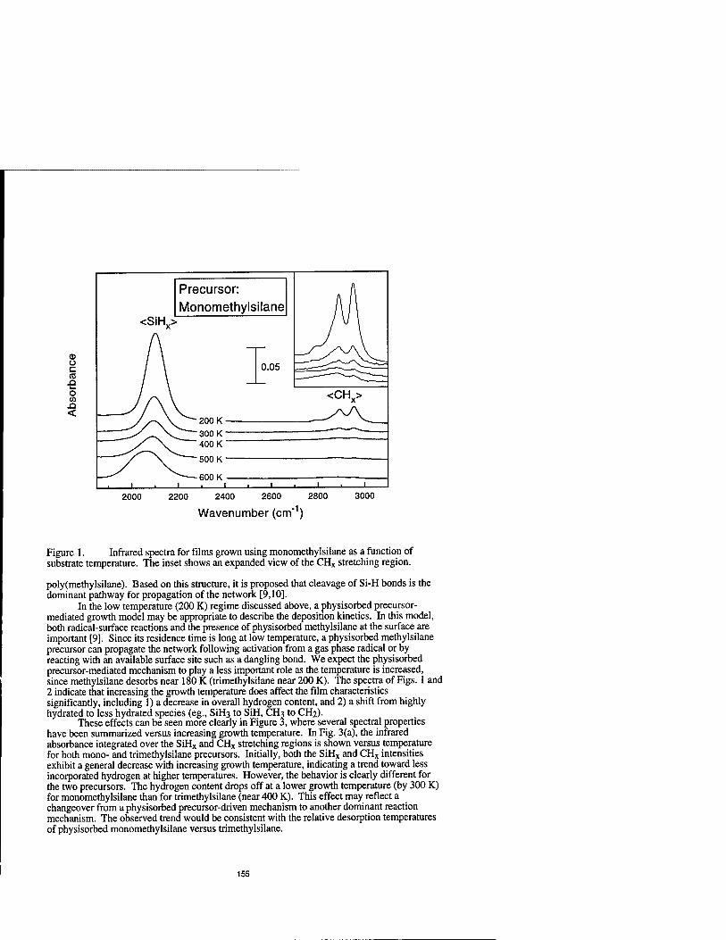
<u o c CO A o W
<
2000 2200 2400 2600 2800 3000
Wavenumber (cm )
Figure 1. Infrared spectra for films grown using monomethylsilane as a function of substrate temperature. The inset shows an expanded view of the CHX stretching region.
poly(methylsilane). Based on this structure, it is proposed that cleavage of Si-H bonds is the dominant pathway for propagation of the network [9,10].
In the low temperature (200 K) regime discussed above, a physisorbed precursor- mediated growth model may be appropriate to describe the deposition kinetics. In this model, both radical-surface reactions and the presence of physisorbed methylsilane at the surface are important [9]. Since its residence time is long at low temperature, a physisorbed methylsilane precursor can propagate the network following activation from a gas phase radical or by reacting with an available surface site such as a dangling bond. We expect the physisorbed precursor-mediated mechanism to play a less important role as the temperature is increased, since methylsilane desorbs near 180 K (trimethylsilane near 200 K). The spectra of Figs. 1 and 2 indicate that increasing the growth temperature does affect the film characteristics significantly, including 1) a decrease in overall hydrogen content, and 2) a shift from highly hydrated to less hydrated species (eg., SiH3 to SiH, CH3 to CH2).
These effects can be seen more clearly in Figure 3, where several spectral properties have been summarized versus increasing growth temperature. In Fig. 3(a), the infrared absorbance integrated over the SiHx and CHX stretching regions is shown versus temperature for both mono- and trimethylsilane precursors. Initially, both the SiHx and CHX intensities exhibit a general decrease with increasing growth temperature, indicating a trend toward less incorporated hydrogen at higher temperatures. However, the behavior is clearly different for the two precursors. The hydrogen content drops off at a lower growth temperature (by 300 K) for monomethylsilane than for trimethylsilane (near 400 K). This effect may reflect a changeover from a physisorbed precursor-driven mechanism to another dominant reaction mechanism. The observed trend would be consistent with the relative desorption temperatures of physisorbed monomethylsilane versus trimethylsilane.
155

o c co i— o (/> £1 <
2000 3000 2200 2400 2600 2800
Wavenumber (cm"1) Figure 2. Infrared spectra for films grown using trimethylsilane as a function of substrate temperature. The inset shows a typical deconvolution for the CHX stretching region (300 K).
Interestingly, for the case of monomethylsilane, the downward trend in SiHx concentration reverses, and actually increases with growth temperature above 400 K. The effect is most significant at 600 K. Inspection of the infrared spectrum in Fig. 1 shows that the character of the SiHx peak has changed at this temperature. In particular, there is new spectral intensity near 2000 cnr1. In a-Si:H films, this frequency is associated with the silicon monohydride stretch, and is thought to originate from hydrogen at clusters (or voids) [13,14]. We do not fully understand the observed result in a-SiC:H; however, we note that silane evolution becomes thermally active just at 600 K, and that the onset of this new reaction may be responsible for the observed changes.
In Fig. 3(b), the peak of the SiHx absorbance in wavenumbers is plotted versus temperature for both mono- and trimethylsilane. This value decreases monotonically, and based on established assignments [9], indicates that the silicon hydrides are shifting from tri- and dihydrides to monohydride. Fig. 3(c) shows the estimated ratio of CH3 groups to CHi,2 groups. This value was calculated by deconvoluting the CHX absorbance peaks into the component contributions, as shown in the inset to Fig. 2. Again, the data show a clear shift from the more highly hydrogenated form of carbon (CH3) to lower forms such as CH2 and CH.
The infrared spectroscopy results show that as the growth temperature is raised, less hydrogen is incorporated into the films, and that the hydrogen that does remain is bonded in lower coordination number on both silicon and carbon atoms. Similar effects have been observed in a-Si:H growth from silanes. In the present case of a-SiC:H, these results indicate that at higher growth temperatures, carbon becomes more involved in network bonding, since whereas CH3 species are effectively terminating groups, CH2 and CH species can contribute to networking. In other words, the structure changes from polysilane-like to polycarbosilane-like. By the same reasoning, the data in Fig. 3(a) showing a shift from higher to lower silicon
156

(0
B 0
0) c
Monomethylsilane
200 300 400 500 600 700
Growth Temperature (K)
2140
T 2120
—■— Monomethylsilane —x— Trimethylsilane
200 300 400 500 600 Growth Temperature (K)
0) cs £
^- S x a o a> 5T £ -^ 1 x
,o ■-' «5 x
3 - \\
■ Monomethylsilane x Trimethylsilane
■
••* .^TVv.
■ (c)
1
■N
200 300 400 500 600
Growth Temperature (K)
Figure 3. The analysis of the IR spectra of films grown at different temperatures using mono- and trimethylsilane (a) the integrated absorbance for SiHx and CHX groups (b) wavenumbers of the SiHx peaks (c) the ratio of integrated areas for CH3 to CHi,2.
hydrides also suggest that the film becomes more highly networked through the silicon atoms at higher growth temperatures. These conclusions are consistent with previous reports showing that increased growth temperatures lead to films that are denser, contain lower hydrogen content, and consist of a more compact Si-C network. Clearly, network bonding, such as Si-C, Si-Si, or C-C bonds, is formed at the expense of -S1H3 and -CH3 terminal groups.
There is clearly a strong dependence of the film structure on surface temperature. At the lowest temperatures studied, this dependence may reflect the decreasing role of physisorbed methylsilane in the growth process with increasing temperature. Another possible explanation is that the radical- surface reactions which drive the film growth are temperature- dependent. While many direct radical-surface reactions, such as abstraction, only exhibit a weak temperature dependence, radical induced etching was shown to exhibit a significant temperature dependence in the a- Si:H system [15].
One model that has been used to describe the temperature dependence of a-Si:H growth suggests that the deposition is controlled by diffusion of physisorbed SiH3 radicals (the reactive precursor) over the
157

surface [8]. Similarly, in a-SiC:H growth, the temperature dependence may stem from a thermally-activated diffusion process of reactive species at the surface.
Another possible explanation for the temperature dependence is that the change in structure reflects changes in functional group stability in the presence of dangling bond sites (surface radicals). This model has been previously proposed to explain similar behavior in a- Si:H growth [15]. It is known that for SiHx groups, thermally-activated decomposition of higher hydrides occurs in the presence of silicon dangling bonds, i.e., SiH2 + -» 2 SiH. A similar reaction may occur for methyl groups. Hence as the substrate temperature is increased, methyl and SiH3 groups that are incorporated in the films can decompose once a site is available nearby for decomposition. Sites are likely generated continuously by abstraction or etching reactions with the incoming radicals. This model may explain why films grown at moderate temperatures are composed primarily of lower hydrides.
CONCLUSIONS
We have shown that the hydrogen content and network structure of a-SiC:H films can be varied by increasing the growth temperature using methylsilane PE-CVD. As the temperature increases, films change from a polysilane (Si-backbone) structure to a polycarbosilane (Si-C backbone) structure. The total H content decreases; this occurs by a shift from higher hydrides such as SiH2, SiH3, or CH3 to lower hydrides such as SiH and CH2.
ACKNOWLEDGMENTS
Support for this work was provided by a National Science Foundation CAREER award (Grant No. DMR-9501774) and by the Donors of The Petroleum Research Fund, administered by the American Chemical Society. S.F.B. gratefully acknowledges the Beckman Foundation for support through the Young Investigator program.
REFERENCES
1. W. Luft and Y. S. Tsuo, Hydrogenated Amorphous Silicon Alloy Deposition Processes. Vol. 1 (Marcel Dekker, Inc., New York, 1993). 2. S. Furukawa, in Amorphous and Crystalline Silicon Carbide and Related Materials. Vol. 34, edited by G. L. Harris and C. Y.-W. Yang (Springer-Verlag, Heidelberg, 1987), p. 58-65. 3. F. I. Hurwitz, T. A. Kacik, X.-Y. Bu, J. Masnovi, P. J. Heimann, and K. Beyene, J. Mater. Sei. 30, p. 3,130 (1995). 4. M. P. Delplancke, J. M. Powers, G. J. Vandentop, M. Salmeron, and G. A. Somorjai, J. Vac. Sei. Technol. A9, p. 450 (1991). 5. I. Golecki, F. Reidinger, and J. Marti, Appl. Phys. Lett. 60, p. 1,703 (1992). 6. A. D. Johnson, J. Perrin, J. A. Mucha, and D. E. Ibbotson, J. Phys. Chem. 97, p. 12,937 (1993). 7. I. Solomon, M. P. Schmidt, and H. Tran-Quoc, Phys. Rev. B 38, p. 9,895 (1988). 8. R. J. Severens, M. C. M. Van De Sanden, H. J. M. Verhoeven, J. Bastiaanssen, and D. C. Schräm, Mat. Res. Soc. Symp. Proc. 420, p. 341 (1996), and references therein. 9. M.-S. Lee and S. F. Bent, J. Phys. Chem. 101, p. 9,195 (1997), and references therein. 10. M.-S. Lee and S. F. Bent, J. Vac. Sei. Technol. A, submitted. H.H. Efstathiadis, Z. Yin, and F. W. Smith, Phys. Rev. B 46, p. 13,119 (1992). 12. G. Lucovsky, Solid State Comunications 29, p. 571 (1979). 13. M. Kondo, T. Nishimiya, K. Saitoh, T. Ohe, and A. Matsuda, Mat. Res. Soc. Symp. Proc, submitted. 14. H. Meiling, J. Bezemer, R. E. I. Schropp, and W. F. Van Der Weg, Mat. Res. Soc. Symp. Proc, submitted. 15. C.-M. Chiang, S. M. Gates, S. S. Lee, M. J. Kong, and S. F. Bent, J. Phys. Chem., in press (1997).
158

PECVD OF AMORPHOUS SILICON CARBIDE FROM TRIMETHYLSILANE
J. T. Kelliher, M. Massuda, P. A. DiFonzo and T. R. Neal Microelectronics Research Lab, Columbia, MD, 21045
ABSTRACT
Amorphous silicon carbide (SiC) was deposited by plasma enhanced chemical vapor deposition (PECVD) in an Applied Materials (AMT5000) tool from sources of trimethylsilane (3MS) and either argon or nitrogen. A deposition rate of = 800 nm/min on a 150 mm silicon wafer was achieved at 350°C. Process conditions investigated were temperature (200-400°C), power (100-600W), pressure (2-8 torr), gas flow rates, and spacing. Various process condition regimes generated a high particle count that was eliminated by controlling parameters of pressure and spacing. Ellipsometry and n&k Analyzer techniques determined the index of refraction. The index of refraction was in agreement between both tools and range from 1.79-2.36 depending on the 3MS flow (25-100 seem) and carrier gas. A Prometrix FT500 with a fixed index of refraction measured 49 points of thickness determined the uniformity. The SiC films stoichiometric composition was measured by X-ray Photoelectron Spectroscopy (XPS). Small quantities of oxygen or nitrogen were found. Additional properties examined were crystallinity, stress, and pinhole density. Dielectric constant was measured by CV techniques.
INTRODUCTION
Amorphous silicon carbide films grants a wide variety of controllable film properties such as stress, hardness, chemical stability, and thermal expansion and have been used in active area formation1 and passivation2. Integration of SiC films into IC fabrication requires that the thermal budget must be considered. Our choice for a low temperature option for SiC deposition is Plasma Enhanced Chemical Vapor Deposition (PECVD). Another consideration was safety and to use an alternative silane source. Various organosilicon precursors3- 4>5 are being explored for PECVD of amorphous SiC. The candidate for this work is trimethylsilane6 {3MS, (CH3)3SiH} from Dow Corning (9-5170). This work is the first reported results of depositing low temperature PECVD amorphous SiC films using 3MS as the source gas in an Applied Materials AMT 5000 tool.
EXPERIMENT
Initially, a 1000 seem nitrogen mass flow controller (MFC) was installed in an Applied Materials (AMT5000) PECVD nitride chamber to deliver the 3MS gas. The correction factor for 3MS through a nitrogen MFC was 0.256. Optical properties of the films were determined with a single wavelength Gaertner Ellipsometer Model L 119 and n&k Analyzer 1200. The n&k Analyzer analytically determines the n and k spectrum from reflectance measurements between 190-900 nm. A Prometrix FT500 with a fixed index of refraction measured thickness and film uniformity (49 points). A Flexus F2320 measured the film stress. An ex situ VG Instruments X-ray Photoelectron Spectroscopy (XPS) determined the stoichiometry composition on 150 mm wafers from sources of 3MS and Ar (or N2). All XPS data was taken as received and after a
159 Mat. Res. Soc. Symp. Proc. Vol. 495 e 1998 Materials Research Society

minimum 20 minute argon sputter etch to eliminate surface contamination. Early results indicated lower flows of 3MS gave the better results (uniformity control) thus we installed a smaller MFC of 500 seem nitrogen. Initial work examined a wide range of process conditions. A high deposition rate (above 5000 Ä/min) with good uniformity (less than 5% standard deviation) targeted the process parameters. Other process conditions varied were spacing between showerhead and susceptor, power, pressure, and temperature. The density for SiC films from various 3MS flows were calculated from the linear slope of film thickness vs. weight gain due to deposition7. Various SiC thick films (=2500 Ä to «1 um) deposited on 1 ^m aluminum films were used to determine pinhole density. Samples were submerged in an aluminum etch solution (16:1:1:2 by volume of phosphoric acid: nitric acid: acetic acid: water) at 34°C for 10 minutes and at room temperature for 24 hours. The normal aluminum etch rate is 8000 Ä/min at 34°C. X-ray diffraction analysis was done at the David Sarnoff Research Center. MIS capacitors were formed by evaporating 8000 Ä of Al on 2400 A of SiC deposited at various 3MS and Ar (or N2) flows, followed by photolithography and etching 500 tim x 500 urn structures.
RESULTS
The deposition rate versus 3MS flow is shown in Figure 1 with the remaining process conditions fixed. Table I contains initial results for the index of refraction as determined by the ellipsometer and n&k tool plus the calculated density and dielectric constant of films deposited at 25, 50 and 100 seem 3MS flow from either Ar or N2. The SiC film thickness was confirmed by step height measurements on patterned SiC films. The results of XPS qualitative analysis after a 20 minute argon sputter etch for various 3MS flow are presented in Table II. The as received SiC films revealed higher oxygen content at the surface. Figure 2 shows the effect of Ar flow on the deposition rate of SiC with all the other parameters remaining constant. The SiC films become less uniform across the wafer with an increase in Ar flow. Process conditions of 3MS flow with no Ar flow produced a very high particle count in the chamber.
_14000
|12000
~10000
g 8000
| 6000 E-
55 4000 b
a. 2000 D nl j_
0 50 100 150 200 250 3MS (seem)
Figure 1. Deposition rate of SiC as a function of 3MS gas flow.
160

Table I - Index of Refraction, Density and Dielectric Constant as a Function of 3MS Flow
Ar/N2 3MS n&k Ellipsometer Uniformity Density Dielectric
(seem) index index % Std Dev g/cm Constant
Ar 25 2.37 2.36 2.68 2.58 6.28
Ar 50 2.22 2.29 4.89 1.91 6.09
Ar 100 1.91 1.89 9.15 1.44 4.57
N2 25 1.99 1.95 1.83 ... ...
N2 50 1.91 1.90 6.47 1.73 4.47
N2 100 1.79 1.81 7.09 1.48 4.13
*' «5000 A SiC film. *2 «2000 Ä SiC film. Other process conditions are fixed: power (500 W), temperature (350°C), pressure (8 Torr), spacing (200 mils) and Ar or N2 flow (85 seem).
Table II - XPS Qualitative Analysis of SiC Films Obtained from Different 3MS Flow
Ar/N2 3MS (seem) % Oxygen % Nitrogen % Silicon % Carbon
Ar 25 1.9 — 39.6 58.5 Ar 50 2.9 ... 46.0 51.1
Ar 100 12.2 — 37.2 44.9 Ar 150 13.3 — 42.1 44.6 Ar 200 11.4 — 44.2 44.4
N7 25 4.4 20.8 37.8 37.0 N? 50 6.2 10.6 41.1 42.1
N2 100 13.2 3.3 40.8 42.7 Other process conditions are fixed: power (500W), temperature (350°C), pressure (8 Torr), spacing (200 mils) and Ar or N2 flow (85 seem).
14000
I «.
12000:
loooor
8000 \
6000:
4000 :
2000 :
o E- I I I I I I I I I I I I I I I I I I I I I I L.
0 200 400 600 800 1000 1200 Ar (seem)
Figure 2. Deposition rate of SiC as a function of Ar gas flow.
161

Figure 3 presents the results of deposition rate versus power. The effect of temperature is shown in Figure 4. Films deposited at 200°C flaked off the wafer. Increasing the chamber pressure increases the deposition rate of the SiC film. The process condition which had the greatest effect on controlling the uniformity of the SiC film was the spacing between the showerhead and susceptor. A small spacing achieves the best uniformity with a high deposition rate.
Ill I-
i Z o F v> o 0. LU Q
14000 -
12000 '-
10000
8000
6000
4000
2000
0 1^| 1 ■ ■ ■ I ■ ' ■ I ■ ■ ' I ■ » ■ I ■
0 100 200 300 400 500 600 700 POWER (W)
Figure 3. Deposition rate of SiC as a function of power.
HI H
i z o F v> o a. UK Q
14000
12000
10000
8000
6000
4000
2000
I i t i » I j * *' « I ■ ■ i i I i i i I |
150 200 250 300 350 400 450 TEMPERATURE (°C)
Figure 4. Deposition rate of SiC as a function of temperature.
162
The SiC films were amorphous from X-ray diffraction results. All the films had a compressive stress in the range of 2E9 to 5E10 dyne/cm2 and showed no temperature-stress hysteresis effects. Various process conditions for 2500Ä SiC films all produced no pinholes.
DISCUSSION
Figure 1 shows the SiC deposition rate rising with increasing 3MS flow until 150 seem and then starts to decrease at higher 3MS flows. As can be seen from Table I, the index of refraction, density, and dielectric constant are effected by 3MS flow. The density and dielectric constant both decrease at higher 3MS flow which indicates a more porous film. The oxygen content of the SiC films increases dramatically at 3MS above 50 seem. The deposition chamber is leak tight and routinely deposits a PECVD Si3N4 film. Si3N4 is very sensitive to oxygen incorporation and we do not observe oxygen in our SisNi films. Also, the impurity specification on 3MS cylinder has an oxygen concentration of less than 0.01 ppm.
A comparison of SiC films grown with either argon or nitrogen exhibits the same trends. Films grown with nitrogen and lower 3MS flow incorporate more nitrogen and less oxygen. Nitrogen is not observed in films grown with argon. The films deposited at the higher 3MS flow have a lower index of refraction, density, and dielectric constant.
Combining Figure 1 with Table I and II, we offer this possible explanation for the increase in the oxygen content at 3MS flows above 100 seem. The SiC films are less dense at higher 3MS flows, this allows oxygen to absorb into the film when exposed to atmosphere and are transported to the XPS system. Experiments are underway using FTIR to determine if the oxygen (nitrogen) is bonded and to characterize the hydrogen content in the SiC films.
As expected, the effects of higher argon flows and lower power (Figure 2 and 3, respectively) decrease the deposition rate. Figure 4 shows a higher deposition rate for lower temperatures which indicates that the deposition rate is a mass flow limited process.
Future work will be evaluation on the properties of SiC films deposited by PECVD using 3MS. How the properties are effected by process conditions, stoichiometric composition, and the incorporation of oxygen or nitrogen in the film.
CONCLUSION
Amorphous SiC has been deposited from a trimethylsilane source by PECVD. A higher deposition rate (above 5000 A/minute) is achieved at low temperatures. Optimization and determination of film properties still need to be investigated from various process conditions.
ACKNOWLEDGMENTS
We would like to thank Dr. Pramod Karulkar, Dr. Eric McDaniel and Mr. Wayne Waltman for processing, analysis and equipment discussions.
163

REFERENCES
1. W. -J. Lu, A. J. Steckl, T. P. Chow, and W. Katz, J. Electrochem. Soc. 131 (8), 1907 (1984).
2. J. M. Eldridge, J. O. Moore, G. Olive, and V. Dunton, J. Electrochem. Soc. 137 (7), 2266 (1990).
3. S. W. Rynders, A. Scheeline, and P. W. Bohn, J. Appl. Phys. 69 (5), 2951 (1991).
4. M. P. Delplancke, J. M. Powers, G. J. Vandentop, M. Salmeron, and G. A. Somorjai, J. Vac. Sei. Technol. A 9 (3), 450 (1991).
5. M. J. Loboda, J. A. Seifferly, and F. C. Dill, J. Vac. Sei. Technol. A 12 (1), 90 (1994).
6. M. J. Loboda, J. A. Seifferly, C. M. Grove, and R. F. Schneider, MRS. Sym., (1996).
7. J. M. Grow, R. A. Levy, Y. T. Shi, and R. L. Pfeffer, J. Electrochem. Soc. 140 (3), 851 (1993).
164

LOW PRESSURE CVD GROWTH OF AlxTii.xN FILMS WITH TETRAKIS- (DIMETHYLAMIDO)TITANIUM (TDMAT) AND DIMETHYL ALUMINUM
HYDRIDE (DMAH) PRECURSORS
Y.-M. Sun, J. Endle*, J. G. Ekerdt*, N. M. Russell**, M.D. Healy*** and J. M. White Department of Chemistry and Biochemistry, *Department of Chemical Engineering, The University of Texas at Austin, Austin, TX 78712 **Semiconductor Process and Device Center, Texas Instruments, Dallas, TX 75265 ***Schumacher R&D, 1969 Palomar Oaks Way, Carlsbad, California 92009_1307.
ABSTRACT
AlxTii-xN film growth has been studied by a organometallic chemical vapor deposition and in-situ X-ray photoelectron spectroscopy . Terakis(dimethylamido)titanium (TDMAT) and dimethyl aluminum hydride (DMAH) were used as the Ti, N and Al precursors. AlTiN film growth was observed on SiO2/Si(100) with substrate temperatures between 200 and 400 °C. The Al content in the film is controlled by the ratio of partial pressures of the two precursors in the gas phase. The metal to C to N ratio is approximately constant at 1:1:1 for most conditions studied. The chemical states of Ti, C, and N in A^Ti^N and titanium-carbo-nitride (TiCN) films are identical, while the Al chemical state is nitride at low, but increasingly carbidic at high Al concentration. The initial growth rate on Si02 was significantly suppressed by the presence of DMAH. At lower growth temperatures, the DMAH effect is more severe. Good step coverage was observed for AlxTil-xN on 0.3 \xm vias with a 3:1 aspect ratio.
INTRODUCTION
TiN has been widely used as a barrier layer between metals and silicon or silicon dioxide in microelectronic devices [1-2]. Although chemical vapor deposition (CVD) TiN provides good step coverage, TiN does not provide a barrier to diffusion of Al for annealing temperatures greater than 550 °C [3]. The TiN barrier layer fails due to the interdiffusion of Ti into the Al layer [4], where it tends to form a Ti rich Ti/Al intermetallic phase. Petrov [4] and coworkers demonstrate there is a marked reduction of the interfacial reaction kinetics of the Al/TWo.sAlo.i-oaN system compared to Al/TiN. Mclntyre et al. [5] have shown no phase decomposition in TiN/Ti0.8-o.9Alo.i-o.2N for one hour annealing at temperatures up to 900 °C. They also found that AlTiN has four orders of magnitude higher oxidation resistance than TiN. This increase is due to the formation of an aluminum oxide layer on top of the AlTiN which prevents further oxidation. Ti^A^N films have been deposited using thermal CVD [6] and plasma enhanced CVD (PECVD) with TiCl4, A1C13, NH3 as precursors and H2 and Ar as plasma gases [7]. Although the deposition was successful, NH3 caused a gas phase reaction resulting in particle formation, and Cl was present in the bulk film. Furthermore, the inherently poor step-coverage of plasma-enhanced processes makes this chemistry a poor choice for many applications. Recently, Winter et al. has reported AlTiN film growth using single source precursors [8].
Here, we report the first thermal CVD of AlTiN, using dimethylaluminum hydride (DMAH) and tetrakis(dimethylamido)titanium (TDMAT). AlxTii.xN films were successfully deposited on Si02 at temperatures ranging from 200 to 400°C. The initial film growth rate was found to be very sensitive to the ratio of the partial pressures of the two precursors, and the Al chemical state strongly depends on its concentration in the film.
EXPERIMENT
CVD and film analysis were carried out in a UHV system consisting of load lock, growth and analysis chamber which is equipped with a mass spectrometer and X-ray photoelectron spectrometer (VG ESCALab). The detailed discription of the system can be found in reference [9].
165 Mat. Res. Soc. Symp. Proc. Vol. 495 ® 1998 Materials Research Society

The Al and Ti precursors were > 99% pure. The dosing system was designed for use with or without carrier gas. Two dosing devices have been used for the film growth. The first introduces the two precursors to the chamber separately, in order to avoid gas phase reactions between the precursors. The second dosing device allows the precursors to mix in a shower head before they enter the chamber. During film growth, the chamber was operated at pressures < 1 x 10⁻³ torr without carrier gas, and at 1 torr with the N2 carrier gas. Films were grown on SiO2/Si(100) substrates.
X-ray photoelectron spectra using a Mg anode source were taken at pass energies of 50 eV for all elements. XP binding energies (BE) were referenced to the Si2p peak of Si02 at 103.4 eV. All concentrations mentioned in the text are atomic concentrations.
RESULTS
Al and TiCN Film Growth with DMAH and TDMAT
Figs. 1 (a) and 1 (b) show the Al films grown with DMAH at various temperatures between 200 and 350 °C. At 200 °C, the XP spectrum (a) shows a pure Al film with a C content < 3 %. The C content increases from 12 % to 48 % as the growth temperature increases from 280 to 350 °C, as shown in spectrum (b) and (c). The Cls and A12p binding energies for the film grown at 350 °C are 281.5 and 74.2 eV, respectively. From the literature [10], we assign the film grown at 350 °C film as A1C. In addition, the full widths at half maximum (FWHM) of the Al 2p peak for films grown at 200 and 350 °C are identical, indicating that Al has a single chemical state in both films. For reference, the chemical state of Al in an AlTiN film was also examined, spectrum (d). The A12p of the nitride is at 73.6 eV, which is about 0.4 eV higher than that of carbide.
A TiCN film grown with TDMAT at substrate temperatures between 250 and 350 °C is shown in Fig. 1 (c). The chemical composition is shown in the Table 1. The Ti, C, and N concentrations vary less than 5 % with the growth temperatures and maintain an approximately constant ratio of 1: 1: 1, which is consistent with the literature[ll]. The binding energy of Ti2p at 455.3 eV indicates that Ti was reduced from Ti4+ (in the parent molecule) to Ti3+. The Nls peak is located at 396.7 eV, consistent with the presence of nitride. The Cls peak
111> 11 i i i| 11 IT i> i r i | 11| i | i i i i
Ti2p
200 200 ■' ■ •
70 80 Binding Energy, eV
Fig. 1, (a) XPS of Al film grown on TiCN at a. 200 C, b. 280 C, c. 350 C d. AlTiN film (b) A12p XPS of Al film grown at a. 200 C, b. 280 C, c. 350 C and d. of AlTiN film (c) XPS of TiCN film grown at a. 250 C, b. 300 C and c. 350 C. with TDMAT alone
at 284.3 eV with a shoulder on the lower binding energy side is assigned to aliphatic and carbidic carbon respectively [11]. Above 300 °C, there are no changes in the binding energies of any elements. Below 300 °C, the Ti2p, Nls, and Cls peaks shift to higher binding energies of 456,
166
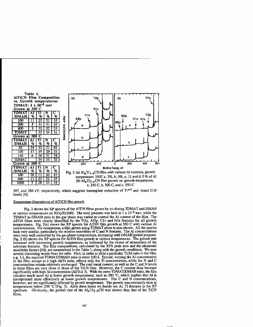
Table 1. AlTiCN Film Composition vs. Growth temperatures: TDMAT: 1 x 10"4 torr Grown at 350 C TDMAT /DMAH
Al %
Ti %
N %
C %
100 11 25 31 33 200 5 31 31 32 400 3 32 32 33
1DMAT 35 34 31 Grown at 30( \C TDMAT /DMAH
Al %
Ti %
N %
C %
50 24 12 21 42 100 17 19 29 35 140 6 28 31 34
TDMAT 34 33 32 Grown at 20C 1 C TDMAT /DMAH
Al %
Ti %
N %
C %
100 26 11 20 43 500 11 23 32 33 1000 5 28 33 34
■e
i 11i I i i ii 1111 i I i iii | i i
(a) Ti2p
\
N1s
C1s AI2p \
/ ^
^.J- i d J—~'
Jr'"f i r>i i i i i i
-i—r
(b)
J--ÜJ
-i—i—i—i—i—r Ols
\
Si2p Ti2P I C1s N1s I
alt ' i-
200
397, and 286 eV, respectively, bonds [9].
400 0 200
Binding Energy, eV
Fig. 2 (a) AlxTii_xCN film with various Al contents, growth temperature: 350C a. 3%, b. 5%, c. 11 and d. 0 % of Al (b) AlxTii-xCN film growth vs. growth temperature,
a. 250 C, b. 300 C, and c. 350 C
which suggests incomplete reduction of Ti+4 and intact C-N
Temperature Dependence of AlTiCN film growth
Fig. 2 shows the XP spectra of the AlTiN films grown by co-dosing TDMAT and DMAH at various temperatures on SiO2/Si(100). The total pressure was held at 1 x 10⁻⁴ torr, while the TDMAT to DMAH ratio in the gas phase was varied to control the Al content of the film. The AlTiN films were clearly identified by the Ti2p, A12p, Cls and Nls features for all growth temperatures. Fig. 2(a) shows the XP spectra for AlTiN film growth at 350 C with various Al concentrations. For comparison, a film grown using TDMAT alone is also shown. All the spectra look very similar, particularly the relative intensities of C and N features. The Al concentrations were very well controlled by the gas phase compositions, increasing with DMAH partial pressure. Fig. 2 (b) shows the XP spectra for AlTiN film growth at various temperatures. The growth rate increases with increasing growth temperature, as indicated by the extent of attenuation of the substrate features. The film compositions, calculated by the XPS peak area and the elemental sensitivity factors [10], are summarized in the Table 1, along with the growth conditions. We note several interesting trends from the table. First, in order to yield a particular Ti/Al ratio in the film, e.g. 1:1, the required TDMAT/DMAH ratio is about 100:1. Second, varying the Al concentration in the film, except at a high Al/Ti ratio, affects only the Ti concentration, while the N and C concentrations remain relatively unchanged. The total metal content, as well as the C and N levels in these films are very close to those of the TiCN film. However, the C content does increase significantly with high Al concentration (Al/Ti 2 3). With the same TDMAT/DMAH ratio, the film contains much more Al at lower growth temperatures, such as 200 °C, which implies that Al is incorporated more effectively at lower growth temperatures. The C and N concentrations, however, are not significantly affected by growth temperature. The growth was extremely slow at temperatures below 250 °C (Fig. 3). After three hours we barely see Al, Ti features in the XP spectrum. Obviously, the growth rate of the AlxTii-xCN was slower than that of the TiCN films.
167
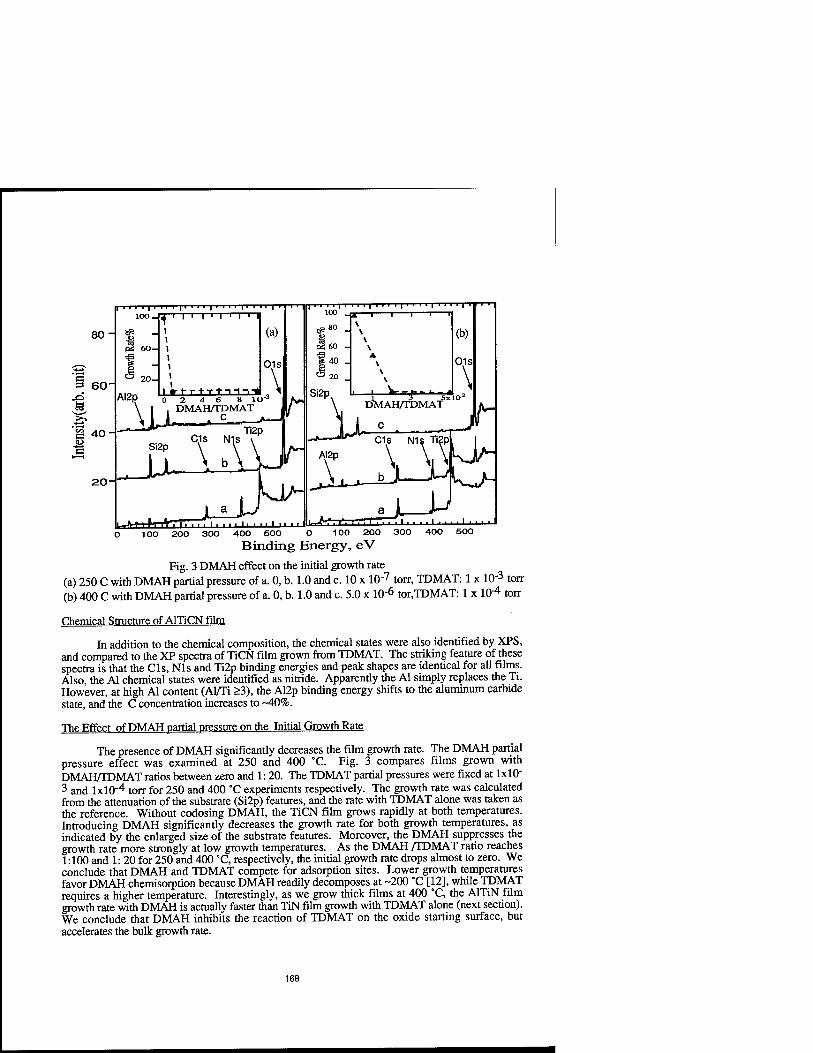
80-
60-
"§
es 40' M
20-
400 500 0 100 200 Binding Energy, eV
Fig. 3 DMAH effect on the initial growth rate (a) 250 C with DMAH partial pressure of a. 0, b. 1.0 and c. 10 x 10"7 torr, TDMAT: 1 x 10"3 torr (b) 400 C with DMAH partial pressure of a. 0, b. 1.0 and c. 5.0 x 10"6 tor,TDMAT: 1 x 10"4 torr
Chemical Structure of AlTiCN film
In addition to the chemical composition, the chemical states were also identified by XPS, and compared to the XP spectra of TiCN film grown from TDMAT. The striking feature of these spectra is that the Cls, Nls and Ti2p binding energies and peak shapes are identical for all films. Also, the Al chemical states were identified as nitride. Apparently the Al simply replaces the Ti. However, at high Al content (Al/Ti >3), the A12p binding energy shifts to the aluminum carbide state, and the C concentration increases to ~40%.
The Effect of DMAH partial pressure on the Initial Growth Rate
The presence of DMAH significantly decreases the film growth rate. The DMAH partial pressure effect was examined at 250 and 400 °C. Fig. 3 compares films grown with DMAH/TDMAT ratios between zero and 1: 20. The TDMAT partial pressures were fixed at 1x10" 3 and lxlO"4 torr for 250 and 400 *C experiments respectively. The growth rate was calculated from the attenuation of the substrate (Si2p) features, and the rate with TDMAT alone was taken as the reference. Without codosing DMAH, the TiCN film grows rapidly at both temperatures. Introducing DMAH significantly decreases the growth rate for both growth temperatures, as indicated by the enlarged size of the substrate features. Moreover, the DMAH suppresses the growth rate more strongly at low growth temperatures. As the DMAH /TDMAT ratio reaches 1:100 and 1: 20 for 250 and 400 °C, respectively, the initial growth rate drops almost to zero. We conclude that DMAH and TDMAT compete for adsorption sites. Lower growth temperatures favor DMAH chemisorption because DMAH readily decomposes at -200 °C [12], while TDMAT requires a higher temperature. Interestingly, as we grow thick films at 400 "C, the AlTiN film growth rate with DMAH is actually faster than TiN film growth with TDMAT alone (next section). We conclude that DMAH inhibits the reaction of TDMAT on the oxide starting surface, but accelerates the bulk growth rate.
168

Step Coverage Measurement
Fig. 4 shows the SEM images for step coverage measurements on a patterned wafer with 0.3 |xm diameter 3:1 contacts at various deposition temperatures. For comparison, the films deposited by TDMAT alone were also examined. At 300 °C, the step coverage approaches -100%, while at 400 °C, the step coverage becomes poor. The step coverage of the Ti^AljCN film grown at 350 °C was comparable to the TiCN film grown at the same temperature. From the film thickness at the top of the contact hole, the growth rate of Ti^AlxCN film at 400 °C is about two times higher than that of the TiCN film grown under equivalent conditions. This increased growth rate was sufficient to shift the growth regime from kinetic control to mass transport control, as noted by the poor step coverage for Ti^Al^CN at 400 °C and 1 Torr. We can conclude, contrary to the observed effect of DMAH in the initial stages of growth, that the reaction of DMAH serves to accelerate the TDMAT decomposition during steady-state growth.
DISCUSSION We have demonstrated that AlTiCN films can be deposited by codosing DMAH and
TDMAT onto SiÜ2 between 200 and 400 °C. Two observations are interesting. First, DMAH has a significant influence on the growth rate. Its role varies with the growth temperature and substrates; it slows down the initial growth rate on a Si02 surface, but increases the rate on AlTiCN at 400 °C. Second, the C and N content of the films remains approximately constant, regardless of the Al concentration in the films. Moreover, XPS shows that Al forms the nitride, rather than a carbide. This is surprising because at temperatures > 350 °C, DMAH alone yields A1C . Given previous studies showing that DMAH and TDMAT react in the liquid phase and form Al(NMe2)Me2 [13], we speculate that ligand exchange between the two precursors may occur during deposition. This results in the formation of A1(N(CH3) containing species, and subsequently, to A1N formation. Note that increasing Al content in the film is accompanied by a decrease of Ti concentration, we propose that the ligand exchange may also alter the TDMAT decomposition pathway, more likely desorption instead of deposition, thereby reducing Ti film content.
When the Al species surface concentration is much greater than that of Ti species, too few metallacycle species are available for A1N formation, and DMAH simply decomposes and forms A1C at high growth temperatures. That is, in fact, what we observed when the film's Al content was much higher than the Ti content. The Al chemical state switches to A1C, and the carbon concentration of the film increases. The ligand exchange also alters the decomposition pathway of TDMAT, and most likely, leads to desorption instead of decomposition. The fact that 1% DMAH in the reaction gas can shut off the film deposition strongly indicates that the DMAH, or its
wm
mm» MM'iMMMik ;lee34.15KU «sö-eee maMis ■. ^ j«^ m,m mm mi®
Fig. 4. Step coverage of AlTiN film Grown at a. 400 °C, b. 350 °C and C. 300 °C Step coverage of TiCN film grown at d. 400 °C and e. 350 °C.

decomposed products, block the chemisorption sites on Si02- It is not surprising that this mechanism changes as the growth temperature and substrate change.
CONCLUSIONS
Using TDMAT and DMAH as precursors, AlxTii-xN films were grown at temperatures from 200 to 400 °C. The Al content was well controlled and the metal to C to N ratio remained approximately constant. The initial Tii.xAl„CN film growth rate was significantly suppressed by the presence of DMAH, especially at lower temperatures. Conversely, the steady state growth rate increased dramatically with increasing DMAH, indicating a significant difference between the kinetics on Si02 and on the growing Ti^A^CN surface. Good step coverage was observed for Tii.xAlxCN films deposited in 0.3 um, 3:1 contacts at growth temperatures below 300 °C. A ligand exchange model is proposed for the film growth mechanism.
ACKNOWLEDGMENTS
This work is supported by the National Science Foundation, Science and Technology Center Program (CHE8920120), Texas Instruments and Schumacher R&D.
REFERENCES
1. R. I. Hegde, R. W. Flordalice, E. O. Travis, and P. J. Tobin, J. Vac. Sei. Technol. Bll p. 1287(1993)
2. J. A. Prybyla, C.-M. Chiang, and L. H. Dubois, J. Electrochem. Soc., 140, p 2695 (1993)
3 K.-H. Bather and H. Schreibe, Thin Solid Film, 200, p 93 (1991)
4.1. Petrov, E. Mojab, J. E. Greene, L. Hultman, J.-E. Sundgren, J. Vac. Sei. Technol. All, pll (1993).
5. D. Mclntyre, J. E. Greene, G. Hakansson, J.-E. Sundgren and W.-D. Munz, J. Appl. Phys. 67, pl542 (1990).
6. R. Madar, A. Rouault, E. Blanquet, C. Bernard and A.-M. Dutron, PCT International Patent, No. WO9732057, (4 September, 1997).
7. K.-H. Kim and S.-H. Lee, Thin Solid Films, 283, p 165 (1996)
8. C. H. Winter, P. J. McKarns, and J. T. Scheper, to be published in 1997 MRS Proceedings.
9. Sun, Y.-M., Fitts, B., Whaley, S., Sweeney, C, White, J.M., Carmalt, C.J., Culp, R.D., Jones, R.A., and Cowly, A.H., 1996 MRS Proceedings, "Advanced Metallization and Interconnect Systems for ULSI", p. 373
10. CD. Wagner, W.M. Riggs, L.E. Davis, and J.F. Moulder.X-rav Photoelectron Spectroscopy". Physical Electronics, edited by G.E. Muilenberg (Physical Electronics, Eden Paririe, MN 1978) p. 38, 40, 50, 68.
11. M. Eizenberg, K. Littau, S. Ghanayem, M. Liao, R. Mosely, and A. K. Sinha, J. Vac. Sei. Technol. A13, p590 (1995)
12. E. Kondoh, and T. Ohta, J. Vac. Sei. Technol. A 13, p.2863 (1995)
13.M. D. Healy, unpublished results.
170

SPRAY CHEMICAL VAPOR DEPOSITION OF CuInS2 THIN FILMS FOR APPLICATION IN SOLAR CELL DEVICES
JENNIFER A. HOLLINGSWORTH*, WILLIAM E. BUHRO*, ALOYSIUS F. HEPP**, PHILIP P. JENKINS**, and MARK A. STAN** *Dept. of Chemistry, Washington University, Box 1134, St. Louis, MO 63130 **Photovoltaic Branch, NASA Lewis Research Center, MS 302-1, Cleveland, OH 44135
ABSTRACT
Chalcopyrite CuInS2 is a direct band gap semiconductor (1.5 eV) that has potential applications in photovoltaic thin film and photoelectrochemical devices. We have successfully employed spray chemical vapor deposition using the previously known, single-source, metalorganic precursor, (Ph3P)2CuIn(SEt)4, to deposit CuInS2 thin films. Stoichiometric, polycrystalline films were deposited onto fused silica over a range of temperatures (300-400 °C). Morphology was observed to vary with temperature: spheroidal features were obtained at lower temperatures and angular features at 400 °C. At even higher temperatures (500 °C), a Cu- deficient phase, CuInsSg, was obtained as a single phase. The CuInS2 films were determined to have a direct band gap of ca. 1.4 eV.
INTRODUCTION
CuInS2 is a candidate material for application as the absorber layer in solar-cell devices. It has a high absorption coefficient1 enabling its use in thin-film applications, and its direct band- gap (1.5 eV) is near the optimum value for most efficient utilization of solar radiation.2 In addition, CuInS2 can be doped both usefully n- and p-type,3 and thereby provides for the possibility of constructing p-n homojunctions.
We have undertaken a film-deposition study of CuInS2 using spray chemical vapor deposition (spray CVD). Spray CVD maintains the most desirable features of MOCVD and spray pyrolysis while avoiding the major difficulties of each. The technique we employ is a modification of that developed by Gysling, et at which is a variation on an earlier spray pyrolysis apparatus.5 Spray CVD combines the inert atmosphere environment, the large-area deposition capability, and laminar gas-phase flow of traditional MOCVD with the low- temperature precursor reservoir of spray pyrolysis. The latter prevents premature decomposition of thermally-sensitive precursors. Furthermore, the volatility requirements for an aerosol-based delivery system such as this are less stringent than for traditional methods.
We have employed a single-source metalorganic precursor in our study. In general, single-source precursors are of interest because they offer the potential for easy control of stoichiometry from the vapor phase. Furthermore, their use avoids the application of more toxic and corrosive materials, such as H2S and CS2, and may eliminate the need for precise control of flowrates as in multiple-source MOCVD and reactant-gas vapor pressures as in evaporation and sputtering systems, thereby simplifying processing.
Single-source precursors to the ternary semiconductor CuInS2 are rare. Nomura, et al. have reported several related precursors: Bu2In(SiPr)Cu(S2CNBu2), BuIn(SiPr2)Cu(S2CNBu2), Bu2In(SPr)Cu(S2CNBu2),BuIn(SiPr)2Cu(S2CNiPr2), and Bu2In(SiPr)Cu(S2CNiPr2).
6'7 However, only Bu2ln(S'Pr)Cu(S2CN'Pr2) has been successfully used to deposit phase-pure CuInS2 by MOCVD.7'8 Hirpo, et al, reported two CuInS2 precursors, (Ph3P)2CuIn(SiPr)4 and (Ph3P)2CuIn(SEt)4, but neither has been tested in a film-deposition study until now.9 We chose
171 Mat. Res. Soc. Symp. Proc. Vol. 495 e 1998 Materials Research Society

to focus on (Ph3P)2CuIn(SEt)4 because it was fully-characterized having a structure determined by single-crystal X-ray analysis, was shown to decompose to the desired phase at temperatures near (or less than) 400 °C, and was soluble in common organic solvents.
Herein, we report the preliminary results from our deposition study. We have successfully employed spray CVD to deposit stoichiometric films of CuInS2 at 300-400 °C and have helped to demonstrate the potential utility of the literature single-source precursor.
EXPERIMENTAL PROCEDURES
All ambient-pressure procedures were carried out under dry N2(g) using standard inert- atmosphere techniques. (Ph3P)2CuIn(SEt)4 was synthesized according to the literature procedure9
with the following exceptions: 1) after all reactants were mixed and allowed to react, the mixture was not filtered prior to removal of solvent under reduced pressure and extraction of the residue and 2) after filtering the extracted residue, methanol was added to the the filtrate to help precipitate product and to improve yield. Toluene, methylene chloride, methanol, acetonitrile, hexane, and diethyl ether were dried, deoxygenated, and purified according to standard procedures10 and stored over 4A molecular sieves.
Films were deposited using a spray chemical vapor deposition apparatus similar to one reported in the literature.4 Toluene or methylene chloride was employed as the carrier solvent. The zone-2 (deposition-zone) temperature was varied from run to run: 505 °C + 5 °C (zone 1: 135 °C + 10 °C), 405 °C ± 5 °C (zone 1: 135 °C ± 10 °C), 350 °C ± 5 °C (zone 1: 155 °C ± 10 °C), and 300 °C ± 5 °C (zone 1: 155 °C + 10 °C). The carrier-gas flowrate was maintained at 4.0 SLPM.
XRD patterns were recorded on a Rigaku DmaxA diffractometer using Cu Ka radiation (^.=1.541845 Ä) and Materials Data Inc. (MDI) software. Experimental powder patterns were compared to the JCPDS reference patterns for CuInS2 (27-0159 and 38-0777) and CuIn5S8 (24- 0361). Average coherence lengths were estimated by the JADE X-ray powder data processing program, which uses the Scherrer formula. Koc2 features and background counts were stripped from the data, and fwhm values were determined by peak integration; a term correcting for instrumental broadening was included. The reported coherence lengths were obtained from the (1 1 2) CuInS2 and the (3 1 1) CuIn5S8 reflections.
SEM analysis was performed on a Hitachi S-4500 field-emission instrument. Associated EDS was performed using Noran Instruments Voyager U X-ray Quantitative Microanalysis System with Digital Imaging.
The film composition and thickness were determined by Rutherford Backscattering Analysis (RBS) with a 1.7 MV tandem Pelletron accelerator. A beam-defining aperture of 2 mm was used with a He beam current of approximately 15 nA. The data were obtained at a scattering angle of 170 degrees. A He-beam energy of 1.5 MeV was utilized to provide a depth resolution of the order of 20 nm. The film composition and thickness were determined using a computer simulation package (RUMP) in order to reproduce the major features obtained in the experimental backscatter spectrum.11
XPS depth profiling was performed on a Physical Electronics Model 5600 instrument equipped with a hemispherical analyzer. The sputtering (50 A/min) was performed with a 4kV Ar ion beam and a raster size of 4mm x 3mm. The XPS sampling size is ca. 0.8mm. K-alpha X- rays were used from an Al anode source. The composition accuracy is ± 1%.
172

The band gap was determined from photoluminescence measurements which were taken at room temperature using a 1.24 meter spectrometer and a N2O) cooled silicon CCD array detector. The excitation was provided by a 514 nm argon ion laser.
RESULTS AND DISCUSSION
CU&1S2 films were deposited at 300-400 °C, while a Cu-deficient phase resulted when a higher temperature was used. Deposition parameters and results are summarized in Table 1. As determined by XRD (Figure 1), only phase-pure films were deposited, CuInS2 or CuftisSg,
Table I Temperature dependence of phase identity and average coherence length as calculated from XRD line broadening
Run* Deposition Phase Average Coherence Temperature (°C) Length
(nm ± 3 nm) A 500 CuIn5S8 >100 B 400 CuInS2 35 C 400 CuInS2 30 D 350 CuInS2 15 E 300 CuInS2 15
* Toluene was the carrier solvent in runs A, C, D, and E; methylene chloride was used in run B.
with the exception of an unidentified minor line in the CuInS2 pattern. Our CuInS2 films do not appear to contain the second phases often observed in non-stoichiometric depositions, such as InöS7, In2S3, Q12S, and CuftisSs. Film composition was determined by RBS analysis for films B, D and E to be Cu1.0In1.0S20 (Figure 2); depth profiling indicated that composition was approximately uniform with depth. In addition, B was analyzed for impurity content by XPS; no evidence for C, O, N, or P was found (composition accuracy: ± 1%). EDS on D also showed no detectable contribution from P. More comprehensive compositional analyses are in progress.
Morphology varied with temperature. The films deposited at 300 and 350 °C comprised rounded regions (400-800 nm) on top of and themselves composed of finer-grained particles (-50-200 nm) (Figure 3a). The 400 °C CurnS2 film (C) comprised more-angular and uniform particles (-200-400 nm) (Figure 3b) compared to the lower- temperature runs. These particle sizes are larger than have been obtained by spray pyrolysis12 or solution pyrolysis,13 and comparable to those from traditional MOCVD.8 The feature sizes observed by SEM are substantially larger than the average coherence lengths calculated from XRD line broadening. Future efforts will entail TEM analyses to obtain a more accurate estimate of crystalline domain size.
The carrier solvent also influenced film growth and morphology. The 400 °C film deposited using methylene chloride as the carrier solvent, B, exhibited greater surface roughness and less-uniform feature sizes compared to that from C. The difference in the two runs is apparently related to the relative volatilities of the respective carrier solvents. Methylene chloride boils at 40 °C, whereas toluene boils at 111 °C. The run time (time to nebulize and transport -150 mL of precursor solution through the CVD apparatus) for the CH2C12 solvent
173

20 30 SO 60 40
2Theta
Fig. 1. X-ray diffraction patterns of Run C CuInS2 and Run A CuInsS8 films.
1.0 1.5 2.0 25
2.5 —I—
Energy (MeV)
900
Fig. 2. Representative RBS spectrum (Run B).
system was observed to be -1/3 the time required for the toluene run: -25 min vs. -75 min. Furthermore, the resulting film thickness appeared to be substantially less for the faster run. Thickness for B was estimated to be -300 nm from RBS measurements assuming 100% density so the true thickness is likely even less. C was optically thick and similar in appearance to D, the thickness of which was determined by RBS to be -1000 nm.
PL data confirmed that the CuInS2 films are direct bandgap semiconductors with an energy gap of approximately 1.35-1.40 eV (Figure 4). These values are somewhat low compared to the bandgaps obtained for single-crystal bulk CuInS2 (1.5 eV)3 and for films deposited by solution pyrolysis13 and MOCVD8 (1.43 and 1.48 eV, respectively). However, the values for the latter two films were obtained by optical absorption measurements, not PL.
174

CIS4NA le.ekv xie. ek''3; e'eViii eise ls.Bkv xie. ak''3; aiaViii
(a) (b)
Fig. 3. SEM micrographs of CuInS2 films for (a) deposition at 400 °C (C) and (b) deposition at 350 °C (D).
By using optical transmission measurements, we obtained somewhat higher bandgap values, 1.40-1.45 eV (e.g. B: maximum in the derivative plot = 1.43 eV). In addition to the expected spectral feature in the PL spectra, a small peak was present at -1.7 eV. The source of this peak has yet to be determined.
28000
a HJ 8000 DM
~I 1 r
1.2 1.3 1.4 1.5 1.6 1.7 1.8 Electron Volts
Fig . 4. Photoluminescence Spectrum of B
175

CONCLUSIONS
The growth of stoichiometric CuInS2 thin films is readily achieved by spray chemical vapor deposition of the single-source, metalorganic precursor, (Ph3P)2CuIn(SEt)4. The morphology, particle size, and phase obtained are sensitive to deposition parameters, including deposition temperature and deposition chemistry (solvent effect). Additional parameters that may influence film quality and optical and electrical properties are currently under investigation. These include carrier-gas flowrate, nebulization efficiency, substrate composition and crystallinity, among others, and will be presented in subsequent publications. This system should ultimately allow substantial control of film characteristics beyond phase and compositional purity.
ACKNOWLEDGEMENTS
Funding was provided by a NSF Presidential Young Investigator Award (Grant CHE- 9158369). J.A.H. was supported by a NASA Graduate Student Researchers Program Fellowship.
REFERENCES
1. C. Dzionk, H. Metzner, S.Hessler, and H.-E. Mahnke, Thin Solid Films 299, 38 (1997). 2. Hans Joachim Möller, Semiconductors for Solar Cells. (Artech House, Boston, 1993), pp. 35
-36. 3. J.L. Shay and J. Warnick, Ternary Chalcopvrite Semiconductors: Growth. Electronic
Properties and Applications, (Pergamon, Oxford, 1975), pp. 187-188. 4. Henry J. Gysling, Alex A. Wernberg, and Thomas N. Blanton, Chem. Mater. 4, 900 (1992). 5. Y.-M. Gao, P. Wu, R. Kershaw, K. Dwight, and A. Wold, Mater. Res. Bull. 25, 871 (1990). 6. Ryoki Nomura, Satoru Fujii, Kouichi Kanaya, and Haruo Matsuda, Polyhedron 9, 361
(1990). 7. Ryoki Nomura, Yasuharu Seki, Kazuhisa Konishi, and Haruo Matsuda, Applied
Organometallic Chemistry 6, 685 (1992). 8. Ryoki Nomura, Yasuharu Seki, and Haruo Matsuda, J. Mater. Chem. 2, 765 (1992). 9. Wakgari Hirpo, Sandeep Dhingra, Anthony C. Sutorik, and Mercouri G. Kanatzidis, J. Am.
Chem. Soc. 115, 1597 (1993). 10. D.D. Perrin, W.L.F. Armarego, and Dawn R. Perrin, Purification of Laboratory Chemicals,
2nd ed. (Pergamon Press, Oxford, 1980). 11. L.R. Doolittle, Nucl. Instr. and Meth. B9, 344 (1985). 12. P. Rajaram, R. Thangraj, A.K. Sharma, A. Raza, and O.P. Agnihotri, Thin Solid Films 100,
111(1983). 13. Ryoki Nomura, Kouichi Kanaya, and Haruo Matsuda, Chemistry Letters, 1849 (1988).
176
DEPOSITION OF Ti(C,N) THICK FILMS BY ILPCVD STARTING FROM TDMAT
S. Gilles, N. Bourhila, J. P. Senateur, R. Madar. INPG-LMGP, UMR 5628 CNRS, BP 46, 38402 St Martin d'Heres (France); R.A. Levy NJIT, University Heights, Newark, New Jersey 07102 (USA); and E. Blanquet INPG-LTPCM, UMR 5614 CNRS, BP 75, 38402 St Martin d'Heres (France).
ABSTRACT
Ti(C,N) films have been deposited from tetrakis(dimethylamido)titanium (TDMAT) and ammonia by CVD at low pressure using pulsed Injection technique (ILPCVD). This procedure allows us to easily deposit Ti(C,N) films with a good reproducibility. It is an efficient technique to control growth rates and composition of coatings. The liquid TDMAT undergoes no degradation during deposition since it is kept at room temperature. Ti(C,N) films, with fee structure and fine grains were deposited at substrate temperature varying from 200 to 500 °C. Composition of films is controlled by substrate temperature and ammonia flow rate. Growth rates as high as 2 /<m/min are reached for deposition of Ti(C,N) films at low temperature (350 °C).
INTRODUCTION
Titanium-containing coatings and particularly titanium nitride (TiN) coatings are typically used on high speed steel cutting tools since they present high hardness and low friction coefficient characteristics [1]. Early, Chemical Vapor Deposition (CVD) has been tested to coat cutting tools. Compared to Physical Vapor Deposition, CVD allows to deposit on complicated shaped tools. The requirements for the process at low temperature and low halide contamination have prompted workers to move from the classical CVD method starting from TiCl4 and NH3 [2] to new processes using organometallic precursors. Indeed, a more reactive set of precursors would lower the deposition temperature. Fix et al. [3] and Bae et al.[4] demonstrated the potential of a low temperature process to deposit TiN from tetrakis(dimethylamido)titanium (Ti(N(CH3)2)4 or TDMAT) and ammonia. Different processes using TDMAT have been studied since: atmospheric pressure CVD using TDMAT and NH3 [5], plasma assisted CVD using thermal decomposition of TDMAT [6], and low pressure CVD using TDMAT and NH3 [7,8]. In this last case, it appeared very hard to obtain reproducible deposition and to control the quantities of TDMAT introduced into the reactor. In order to solve this problem, we have used a new-experimental set up to deposit TiN from TDMAT and NH3: our procedure consists in CVD at Low Pressure using Injection Technique (ILPCVD). The principle of this method is based on a computer-controlled injection of micro quantities of liquid precursor inside an evaporator. This technique has been already used in our laboratory to deposit different materials such as oxides [9,10] and superconductor films [11].
The parameters investigated in this study are : injection frequency, deposition temperature and ammonia flow rate. Their influence on growth rate, composition, morphology, and structure will be discussed.
EXPERIMENTAL PROCEDURE
The experiments were performed in a prototype LPCVD single wafer reactor 100 mm "JIPELEC PCU4 SYSTEM" described elsewhere [12]. A new system for injection of the liquid precursor is adapted to this reactor. The modified reactor scheme is presented on the figure 1. The pure liquid precursor of TDMAT is contained in a hermetically closed vessel pressurized under 1.5 105 Pa of Argon, connected to the injector, which is a high speed electro valve. The nozzle of the injector is introduced into an evaporator (a quartz tube heated by heating tape) which is held at 60 CC and connected to the top of the reaction chamber. The pressure inside die reactor is fixed at 20 Pa. The droplets injected are flash volatilized and the vapor is carried toward the heated substrate by argon which is used as vector gas. NH3 is introduced by small apertures located all around the reactor chamber walls just at the level of the substrate. The gaseous mixture of argon
177
Mat. Res. Soc. Symp. Proc. Vol. 495 ® 1998 Materials Research Society

Figure 1: Schematic of the modified LPCVD reactor JIPELEC PCU4 SYSTEM.
and precursor is introduced at the top of the reaction chamber. Total gaseous flow rate was maintained constant at 300 seem.
Experimental parameters are reported in table I.
Titanium
Precursor
Deposition
temperature
Ammonia
flow rate
Total
flow rate
(Ar+NH3)
Total
pressure
Injection
frequency
Injection
opening
time
Droplet
volume
TDMAT 200-500 0-200
seem
300
seem
20
Pa
0.2-1.5
Hz
1
ms
2.25
A<1
Table I
Films were deposited on Si (100), previously cleaned by a HF solution. The morphology was examined by scanning electron microscopy. The use of microprobe analysis allowed to determine films composition and density. Structure analysis were made by x-ray diffraction measurements
using Fe-Ka radiation in a 9-28 standard mode.
RESULTS AND DISCUSSION
Growth rate
The injection frequency of precursor was studied in order to see its influence on growth rate. In this case, the deposition was made by thermal decomposition (without ammonia) of the same quantity of TDMAT for each experiment. The figure 2 shows that there is no evolution of the thickness as a function of frequency for the same quantity of precursor injected.
This means that the increase of frequency is an easy and efficient way to increase the film growth rate and to control the thickness of deposited Ti(C,N).
In figure 3 is presented an Arrhenius plot of the growth rate of Ti(C,N) thin film as a function of substrate temperature. In the temperature range 200 - 500 °C, the growth rate behavior is indicative of a feed rate limited process, with 2 apparent activation energies of 1.9 kJ/mole between 350 - 500 °C and 7.7 kJ/mole between 200 and 350 °C.
178

•3, 560 o 2
T CC) 350 280
"gl.9 B
w 1.7
■S
o Of) 1.5
1.«
J 1.4
III 1 1 1 1 ' ■ ' 1 ' ■"■'I ' ' ' . ij/molj
" 1 T
irq
m: X.
; 1 Eä'STLT"'kj/ffl"öT~
: | \. :
Injection frequency (hz)
Figure 2 : Thickness and growth rate versus injection frequency. Ts = 450 °C; P10tal = 20 Pa t = 60 droplets; NH3 flow rate = 0 seem.
1.6 1.8 2 1000/T (K-l)
Figure 3: Growth rate as a function of substrate temperature. f=l Hz; PIota] = 20 Pa; t = 60 droplets; NH3 flow rate = 0 seem.
Temperature and ammonia flow rate influence on composition
As can be seen on figure 4, the substrate temperature has an influence on film composition. The titanium proportion presents no significant evolution with temperature: its average value is 31 at.%. The nitrogen quantity decrease from 44 to 33 at.% when temperature increase from 200 to 500 °C. This decrease is compensated by an increase of the carbon incorporation from 11 to 24 at.%. No effect of temperature on the oxygen incorporation is observed: its average value is about 15 at.%.
The figure 5 shows the evolution of the composition as a function of the quantity of ammonia injected during the process. When ammonia flow rate increases from 0 to 200 seem, the carbon level decreases noticeably from 42 to 15 at.%. The quantity of oxygen remains stable at a value of 18 at.%. Nitrogen content increases twice from 18 to 34 at.% and those of titanium increases from 25 to 33 at.%. For ammonia flow rate from 0 to 100 seem, N/Ti ratio is lower than 1, when ammonia flow rate is above 100 seem, N/Ti ratio is more than 1. By varying both parameters: temperature and ammonia flow rate, we can control the composition of Ti(C,N) coatings. According to thermodynamical calculations, the carbon content may come from an incomplete decomposition of precursors [8].
150200250300350400450500550 Deposition temperature (°C)
Figure 4: Composition as a function of temperature; Injection frequency =lHz, NH3 flow rate =150 seem, t=60 s.
-■-at Ti 9, -B-at N %
\ —•—at O % I l\ 1 -*-at C %
i- | \Ar^fa^^:^r -.
L i/^T^ J
45
40
35
# 30
« 25
20
15
10 -50 0 50 100 150 200 250
Ammonia flow rate (seem)
Figure 5 : Composition as a function of NH3 flow rate; Injection frequency = 1Hz, TS = 450°C, t = 60s
179

The oxygen incorporation is very high and can be attributed to two origins: coming from carrier and reactant gases and incorporated during the deposition, or after the run deposition, during the exposure to air. In this last case the incorporation of oxygen can be the consequence of a high porosity of Ti(C,N) coatings. This hypothesis is enforced by resistivity measurements and density values, which are reported in table II.
Ammonia flow rate (seem)
Resistivity after 1 month (mQ.cm)
Density (g.cm-3)
0 4.5 2.9 50 14 3 100 18.3 3.5 150 12.7 3.2 200 8.9 4.6
Table II
Resistivity values were measured within 5 minutes after the substrate has been removed from the reaction chamber, and were repeated after 1 hour and 1 month. The evolution of film resistivity as a function of time is noticeable. It is ten times higher 1 hour after the deposition, and 40 times after one month. This increase is presumably due to oxidation. The density is also lower than those for bulk TiN (5.4 g.cm 3), which underlines the porous character of the coatings.
Morphology and structure
The dependence of the microstructure of Ti (C,N) coatings on substrate temperature was investigated in the temperature range of 200 - 500 °C at a constant total pressure of 20 Pa and a constant ammonia flow rate of 100 seem.
SEM micrographs revealed that the films deposited at 500 and 300 °C have columnar structure, fine grains with a smooth surface (Figure 6). The films deposited at 200 °C present a far more compact aspect (no more visible columnar structure) but cracks are apparent on a very smooth surface, probably due to important film constraint.
On figure 7 is presented the evolution of x-ray diffraction spectra as a function of temperature; they reveal a fee structure with a preferred (111) orientation. Consistent with SEM results, the broadening of the XRD peaks observed at low deposition temperature (200°Q reflects the fine grains characteristic of these films. An increase of substrate temperature gives a refinement of the (111) peak and the (200) peak appears at 500 °C.
The lattice parameter (a) increases with increasing substrate temperature from 4.18 A at 200 °C to 4.22 A at 500 °C. This variation can be attributed to the increase of carbon content (cf. Fig. 4).
CONCLUSION
Deposition of Ti(C,N) films have been demonstrated using Injection LPCVD technique from TDMAT and ammonia. High growth rate (> l/«m/min.) and good film reproducibility and composition control have been achieved in the temperature range of 200-500°C. The film composition seems to be controlled by ammonia flow rate and substrate temperature.
The deposit films contain a large amount of carbon and oxygen in relation with incomplete chemical reactions and film porosity (3g/cm3). Low roughness and fine grains with fee structure films have been obtained at low substrate temperature
This novel technique allows a good control of injected quantity of precursor in the reaction chamber and has the advantage of allowing the use of unstable precursors because the liquid is kept at room temperature.
180

Ts= 500°C
Ts= 300°C
Ts= 200°C
Figure 6: SEM micrographs of coatings deposited at 500, 300 and 200 CC Injection frequency =lHz, ammonia flow rate = 150 seem, t = 60 s.
a 1000
Figure 7: Evolution of X-ray spectra with substrate temperature. Injection frequency = 1 Hz, NH3 flow rate =150 seem, t = 60 sec.
181

REFERENCES
I. A. Bendavid, P. J. Martin, R. P. Netterfield and T. J. Kinder, Sur. Coat. Technol., 70, p. 97(1994). c L 2 S. Anderbouhr, E. Blanquet, V. Ghetta and C. Bernard, Electrochem. Soc. Proc. of the XVIth Intern. Conf. and EUROCVD-11, Paris, 97-25, p. 356 (1997). 3. R. Fix, R. G. Gordon and D. M. Hoffman, Chem. Mater., 2, p. 1138 (1991). 4 Y W. Bae, W. Y. Lee, T. M. Besmann, P. J. Blau and L. Riester, Mater. Res. Soc. Symp. Proc. Vol. 363, p. 245 (1995). 5. Joshua N. Musher and Roy G. Gordon, J. Mater. Res., 11, N°4, p. 989 (1996). 6. C. Marcadal, E. Richard, J. Torres, J. Palleau, L. Ulmer and L. Perroud, in European Workshop Materials for Advanced Metallization (Villard-de-Lans, France), p. 54 (1997) 7. C. Jimenez, S. Gilles, C. Bernard and R. Madar, Sur. Coat. Technol., 76-77, p. 237 (1995) 8. S. Gilles, PhD Thesis, National Polytechnic Institut of Grenoble France (1997) 9 N. Bourhila, F. Feiten, J. P. Senateur, F. Schuster, R. Madar and A. Abrutis,, Electrochem. Soc. Proc. of the XVIth Intern. Conf. and EUROCVD-11, Paris, 97-25, p. 417 (1997). 10. F. Feiten, J. P. Senateur, F.Weiss, R. Madar and A. Abrutis, Journal de Physique IV, Colloque C5, supplement au Journal de Physique II, Vol. 5, p. C5-1079 (1995) II. J. P. Senateur, F. Feiten, S. Pignard, F.Weiss, A. Abrutis, V. Bigelyte, A. Teiserskis and Z. Saltyle. To be published in J. of Alloys and Compounds. 12. N. Bourhila, N. Thomas, J. Palleau, J. Torres, C. Bernard and R. Madar, Appl. Surf. Sei. 91, p. 175(1995).
182

Part III
Solution Routes to Ceramic Materials

CHEMICALLY PREPARED LEAD MAGNESIUM NIOBATE DIELECTRICS
B.A. TUTTLE, J.A. VOIGT, D.L. SIPOLA, W.R. OLSON and D.M. Goy Sandia National Laboratories, Albuquerque, NM 87185
ABSTRACT
A chemical solution powder synthesis technique has been developed that produces fine, uniform powders of lead magnesium niobate (PMN) with 60 to 80 nm crystallite size. The synthesis technique was based on the dissolution of lead acetate and alkoxide precursors in acetic acid followed by precipitation with oxalic acid/propanol solutions. Lead magnesium niobate ceramics fabricated from these chemically derived powders had smaller, more uniform grain size and higher dielectric constants than ceramics fabricated from mixed oxide powders that were processed under similar thermal conditions. Chem-prep PMN dielectrics with peak dielectric constants greater than 22,000 and polarizations in excess of 29 (iC/cm2 were obtained for 1100°C firing treatments. Substantial decreases in dielectric constant and polarization were measured for chemically prepared PMN ceramics fired at lower temperatures, consistent with previous work on mixed oxide materials.
INTRODUCTION
Lead magnesium niobate (PMN) dielectrics are of great interest for high strain, low hysteresis microacuators, high dielectric constant capacitors and sensors. Greater mechanical strength, improved phase purity and more uniform grain size are desired for bulk actuator, micropositioner and thin multilayer capacitor applications. The decrease in strength of PMN mixed oxide ceramics compared to conventional lead zirconate titanate materials is in part due to the large, nonuniform grain size that accompanies the thermal treatments necessary to produce high dielectric constant, high electrostrictive coefficient PMN ceramics. Enhanced chemical homogeneity on the submicrometer scale via chemical preparation techniques is expected to lead to improved phase purity and more uniform grain size PMN ceramics. Specific issues associated with improvement of phase purity are the elimination of low dielectric constant pyrochlore phases and PbO rich grain boundary phases to produce high dielectric constant, single phase perovskite ceramics. For these reasons, we have investigated the chemical preparation of PMN powders. We have demonstrated that PMN ceramics with fine, uniform grain size and enhanced chemical homogeneity can be fabricated. These microstructural improvements should lead to better mechanical and electrical properties than those obtained by conventional mixed oxide processing.
The most widely accepted process for fabrication of mixed oxide PMN ceramics was developed by Swartz and coworkers. [1] A critical step in this process was the mixing and thermal reaction of MgO and Nb205 powder precursors to form powders of a magnesium/niobium solid solution columbite phase. Enhanced perovskite formation was obtained by combining these prereacted columbite powders with PbO powders, compared to mixing powders of individual components. Papet, Dougherty and Shrout [2] fabricated a series of PMN ceramics using fine, submicron, mixed oxide powders. Firing temperature was found to have a substantial effect on dielectric properties. While PMN dielectrics hot pressed at 810°C developed a 0.3 |J,m grain size and had a peak dielectric constant of 4600, dielectrics conventionally fired at 1100°C possessed a 6.2 u,m grain size had a peak dielectric constant of 17,300. These dielectric constants were measured at a frequency of 1 kHz. Although substantial changes in grain size occurred for the different firing temperatures, a series dielectric mixing model was developed from TEM analyses, similar to the work of Wang and Schulze, [3] that indicated nanoscale dimension grain boundary phases were the primary cause for the dilution in dielectric constant for grain sizes greater than 1 u.m. Dielectric behavior of PMN ceramics with grain size below 1 |im did not fit the series dielectric mixing model.
185
Mat. Res. Soc. Symp. Proc. Vol. 495 e 1998 Materials Research Society

A number of attempts have been previously made to synthesize chemically prepared PMN powders. Two different methodologies will be discussed. Chaput and coworkers [4] have fabricated fine powders from translucent gels of PMN using alkoxide precursors and hypercritical drying (250°C and 6.3 MPa). A B-site deficient pyrochlore phase was formed for temperatures below 700°C, with a major percentage of perovskite phase being obtained by a 700°C thermal treatment. After an 800°C thermal treatment, the powders were single phase perovskite by X-ray diffraction; however, no electrical results were given. Jeng and coworkers[5] have developed a process for PMN powder synthesis based on the coprecipitation of niobium oxalate, magnesium nitrate and lead nitrate. A 2 Jim to 4 (xm grain size material was developed at 900°C, with a dielectric constant of 11,000 measured at ambient. The maximum dielectric constant measured in their study was 18,000 at 100 Hz at an unspecified lower temperature.
EXPERIMENT
Chem-prep PMN and PMN/PT 94/6 powders with 0.6 mol% Cu addition were synthesized using an acetate / alkoxide / oxalic acid technique (Figure 1). [6] This powder synthesis technique minimizes waste and produces a readily filterable co-precipitate unlike many other chemical preparation techniques for lead based ferroelectrics.[7] In addition, a very uniform, weakly agglomerated, free flowing powder was obtained. While individual particles were on the order of 60 nm, weak agglomerates of these fine particles in the form of 5 u.m to 10 (im spheroids facilitated handling and green body formation. At least 99% of all of the original metal cation constituents were precipitated as determined by ICP analyses mass balance.
The metal cation containing solution was synthesized by first preparing a lead-magnesium- copper acetate/acetic acid solution that was formed by dissolving lead oxide, magnesium acetate, and copper acetate in glatial acetic acid. This solution was mixed with a niobium-titanium butoxide/acetic acid solution to form the metal cation solution. An exothermic mixing reaction raised the solution temperature to about 40°C. Moisture sensitivity and undesirable hydrolysis reactions were minimized by the use of titanium and niobium n-butoxides. The metal solution was then pumped into an oxalic acid / n-propanol precipitant solution to form a readily filterable oxalate coprecipitate. Advantages of the oxalic acid / n-proponal precipitant were the stoichiometric removal of constituent metal species and minimized agglomeration. While 1500 gram lots of PZT 95/5 powder have been synthesized for other DOE programs using this process, 100 to 500 gram lots were synthesized for this development project.
A 400°C thermal treatment of the PMN powders to pyrolyze residual organics, followed by ball milling the pyrolyzed powders with Zr02 media for 2 hours were critical process improvements that increased the densities of fired PMN materials compared to chem-prep PMN/PT 94/46 ceramics fabricated in the early stages of our study. Densities for PMN/PT ceramics fabricated without using these process steps were on the order of 90% of theoretical, while densities of PMN ceramics with the improved process were in excess of 96%. While low field dielectric constants were 15% lower than mixed oxide materials for the unimproved process, the improved process resulted in dielectric constants that exceeded those of mixed oxide materials reported in the literature. [2]
Green body processing for the PMN based materials in this study, consisted of uniaxial pressing chem-prep PMN powder at 2 ksi (13.7 MPa) and then isopressing the resultant compact at 30 ksi (206 MPa). Green densities on the order of 59% were obtained. While no atmosphere powder was used for the 900°C /l hour and 1100°C/3 hour PMN firings, a combination of bubbled alumina and mixed oxide PMN/PT 94/6 powder was used to minimize weight loss during the 1000°C/2 hour firing. Typically, the weight loss was less than 1.3% for the PMN powders that contained 3 mol% (1.90 weight % ) excess Pb.
186
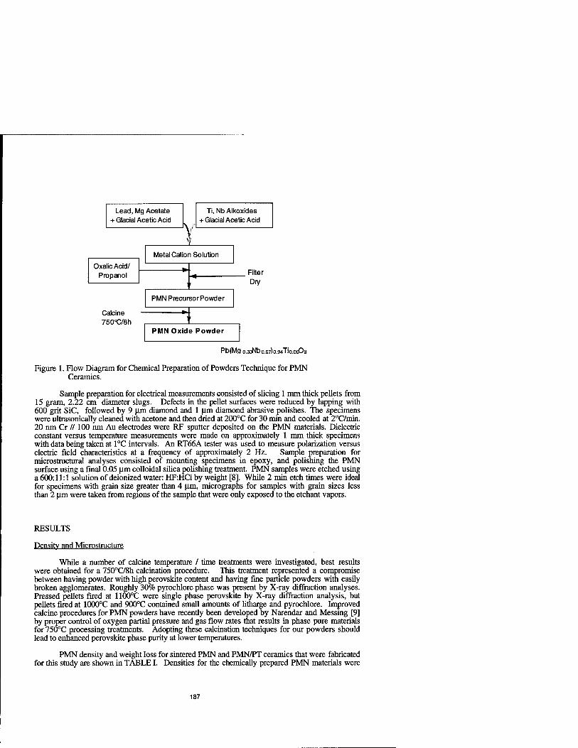
Lead, Mg Acetate + Glacial Acetic Acid
Ti, Nb Alkoxides + Glacial Acetic Acid
Oxalic Acid/ Propanol
Metal Cation Solution
■ ' PMN PrecursorPowder
' ' PMN Oxide Powder
. Filter Dry
Calcine 75(W8h
Pb(Mg o.33Nbo.67)o.94Tio.orf33
Figure 1. Flow Diagram for Chemical Preparation of Powders Technique for PMN Ceramics.
Sample preparation for electrical measurements consisted of slicing 1 mm thick pellets from 15 gram, 2.22 cm diameter slugs. Defects in the pellet surfaces were reduced by lapping with 600 grit SiC, followed by 9 |im diamond and 1 |im diamond abrasive polishes. The specimens were ultrasonically cleaned with acetone and then dried at 200°C for 30 min and cooled at 2°C/min. 20 nm Cr //100 nm Au electrodes were RF sputter deposited on the PMN materials. Dielectric constant versus temperature measurements were made on approximately 1 mm thick specimens with data being taken at 1°C intervals. An RT66A tester was used to measure polarization versus electric field characteristics at a frequency of approximately 2 Hz. Sample preparation for microstructural analyses consisted of mounting specimens in epoxy, and polishing the PMN surface using a final 0.05 (im colloidal silica polishing treatment. PMN samples were etched using a 600:11:1 solution of deionized water: HF:HC1 by weight [8]. While 2 min etch times were ideal for specimens with grain size greater than 4 (im, micrographs for samples with grain sizes less than 2 (im were taken from regions of the sample that were only exposed to the etchant vapors.
RESULTS
Density and Microstructure
While a number of calcine temperature / time treatments were investigated, best results were obtained for a 750°C/8h calcination procedure. This treatment represented a compromise between having powder with high perovskite content and having fine particle powders with easily broken agglomerates. Roughly 30% pyrochlore phase was present by X-ray diffraction analyses. Pressed pellets fired at 1100°C were single phase perovskite by X-ray diffraction analysis, but pellets fired at 1000°C and 900°C contained small amounts of litharge and pyrochlore. Improved calcine procedures for PMN powders have recently been developed by Narendar and Messing [9] by proper control of oxygen partial pressure and gas flow rates that results in phase pure materials for 750°C processing treatments. Adopting these calcination techniques for our powders should lead to enhanced perovskite phase purity at lower temperatures.
PMN density and weight loss for sintered PMN and PMN/PT ceramics that were fabricated for this study are shown in TABLE I. Densities for the chemically prepared PMN materials were
187

comparable to commercial mixed oxide ceramics (TAM Ceramics 52639). Samples fabricated without the 400°C pyrolysis treatment followed by ball milling had densities that were approximately 6% to 8% lower than the commercial mixed oxide ceramics. No atmosphere powder was used for the firing treatments at 900°C and 1100°C shown in TABLE I. All chemically prepared ceramics had a nominal 3 mol% (1.95 wt%) excess Pb addition, while no Pb excess was assumed for the mixed oxide PMN/PT material. All weight losses during firing are attributed to the loss of PbO, a standard assumption for Pb based dielectric processing. The weight losses given in TABLE I are with respect to the stoichiometric value of PbO for the composition. If the calculated value of PbO in the compact is in excess of the stoichiometric value, then this value is denoted by a parentheses. For example, for the chem-prep PMN 1100°C firing a weight loss compared to the PbO stoichiometric value of 1.15% was obtained, 3.05% total weight loss, which corresponds to a weight loss of 3.05% of the fired sample compared to the bisque fired pellet. Because of the weight loss measured for the 1100°C firing, atmosphere powder consisting of PMN powder and bubbled alumina was used for the subsequent 1000°C firing. The fired weight of the 1000°C fired pellet was within 0.6% of the expected stoichiometric level. It should be noted that weight losses beyond that to maintain stoichiometry - similar to that observed for the 1100°C firing - may be advantageous to the removal of nanoscale dimension, low dielectric constant grain boundary phases. The presence of grain boundary phases can lower measured dielectric constants substantially. This dielectric constant dilution mechanism is covered in more detail in the excellent work by Pappet, Dougherty and Shrout [2].
TABLE I. Density and Weight Loss For PMN Dielectrics
Composition Firing Treatment Density (% Theory) Weight Loss (Gain)
PMN 900°C/1 hour 89.9 ( 1.2%) PMN 1000°C/2 hours 96.4 (+0.6%) PMN 1100°C/3 hours 96.4 1.15% PMN/PT 94/6 1100°C/1.5hours 90.0 1.15% PMN/PT 94/6 Mixed Oxide
1100°C/3 hours 96.5 0.5%
Microstructures of a chemically prepared PMN ceramic and a mixed oxide PMN/PT 94/6 ceramic are shown in Figure 2. Both materials were fired at 1100°C. Previous work in our laboratory on mixed oxide PMN/PT ceramics showed a montonic trend of decreasing grain size with increasing Ti content, over the range of 0% to 100% Ti substitution. From this work, the slight difference in chemical composition between the two materials shown in Figure 2 has little effect on grain size. The chemically prepared material has substantially smaller grains (approximately 6.9 urn grain size) than the mixed oxide material. Further the chem-prep PMN material is equiaxed, and has a relatively uniform grain size distribution. Grain size (GS) was determined using a lineal intercept technique with no multiplicative multiplier for three dimensional shape equivalence, as shown in equation 1,
GS = L/N*M (1)
where L is the total distance of measurement, N = the number of grain boundary intersections and M is the magnification. The mixed oxide material shows very nonuniform grain growth, with grain sizes varying from 1 urn to 34 (im. Smaller, uniform grain size should result in smaller, more uniform flaw sizes which can lead to higher mechanical strength and more robust dielectric breakdown behavior. The chem-prep microstrucure is also typified by dense grains with far fewer entrapped pores than the similarly processed mixed oxide material.

m (A)
(B)
Figure 2. Microstructure of PMN based ceramics fired at 1100°C: A) chemically prepared PMN and B) mixed oxide PMN/PT 94/6.
189

The evolution of microstructure of chemically prepared PMN materials is shown in Figure 3, for two chem-prep PMN ceramics fired at 900°C and 1000°C, respectively. An extremely fine grain size is observed for the 900°C sample with a majority of grains being less than 0.1 urn. Some nonuniformity in growth is also evidenced, as clusters of grains on the order of 0.6 urn are present. An average grain size of 0.3 urn was measured using the lineal intercept technique. With increased firing temperature the microstructure coarsens, an average grain size of 0.82 um was measured using the lineal intercept technique. However, the chem-prep PMN ceramics fired at this temperature still have extremely fine grain size compared to conventional mixed oxide materials. A bimodal distribution of grain size is observed for the sample fired at 1000°C with the group of smaller grains being on the order of 0.3 um and the set of larger grains having an average grain size on the order of 1.0 urn. The larger grains may be attributed to micron scale regions of Pb enhancement. Polished sections of the chem-prep PMN powder after calcination indicated Pb inhomgeneities at this scale for the powder subjected to 750°C for 8 hours. Nonetheless, this appears to be a much finer inhomogeneity scale than that observed for mixing mixed oxide powders on the order of several microns. Based on the improved dielectric constant results obtained for the chemically prepared materials, the chemical uniformity may be better than that of submicron, mixed oxide powders.
Dielectric Properties: Comparison of Chem-Prep and Mixed Oxide Ceramics
Dielectric constants greater than 22,000 were obtained for chemically prepared PMN ceramics fired at 1100°C, as shown in Figure 4. Conventional relaxor behavior, similar to that for mixed oxide materials,[2] is observed for the chem-prep PMN ceramics. As the measurement frequency increases, the magnitude of the peak dielectric constant, Kmax, decreases and the temperature at which the dielectric constant maximum occurs, Tmax, increases. This unusual dielectric relaxation behavior is the origin of the term relaxor ferroelectrics and is caused by the unique assemblages of polar nanoclusters within the material.[10] The values of Tmax for the frequencies of 100 Hz, 1 kHz, and 10 kHz were -7.9°C, -5.5°C and 0°C. These values agree with mixed oxide measurements [2] to within one degree centigrade, which is within our experimental measurement error. The dielectric constant maxima are somewhat larger, on the order of 15%, than the values previously measured for mixed oxide materials. Improved homogeneity of material, greater ordering of nanoclusters, and less nanodimension second phase at grain boundaries are among the factors that could be the cause of this property improvement.
190

fW
1 (A)
(B)
Figure 3. Microstructures of PMN ceramics fired at (A) 900°C and (B) 1000°C.
191

c CO *-* CO c o o o 'k. +■* Ü 0 0 b
25000
20000
15000
10000
5000
0
T-i- ' I i T-T- T Tf I-r- ' I ' '
F= 100 Hz, Kmax = 22,500, Tmax = - 9.9°C F =1 kHz, Kmax = 21,270, Tmax = - 5.9°C F = 10 kHz, Kmax = 19,962, Tmax = 0°C
i i i i i i i i i i i
-80 -60 -40 -20 0 20 40
Temperature (°C)
60 80
Figure 4 Dielectric constant versus temperature for chemically prepared PMN dielectrics fired at 1100°C for 3 hours.
Dielectric constants of the chemically prepared PMN ceramics in this study were a strong function of grain size, similar to that previously reported [2] for mixed oxide materials. For these PMN materials, the larger the grain size, the greater the dielectric constant. Peak dielectric constants of 21,270, 3,900 and 2500 were measured at 1 kHz for chemically prepared PMN materials fired at 1100°C, 1000°C and 900°C, respectively. The aforementioned firing treatments resulted in the following average lineal intercept grain sizes: 6.9 u.m, 0.82 urn and 0.3 u.m. Dielectric constant versus temperature characteristics for the chem-prep PMN ceramics fired at 1100°C and 1000°C are shown in Figure 5. The data is quantitatively quite similar to that of Pappet, Shrout, and Dougherty for mixed oxide PMN materials. [2] They measured peak dielectric constants of 18,000, 11,000 and 4,600 at 1 kHz, for PMN ceramics with grain sizes of 6.2 |im, 1.1 urn and 0.3 ixm. While Pappet and coworkers attributed the dielectric constant dilution with grain size (down to 1 u.m) to the presence of a grain boundary phase, other factors may affect our data. One factor is phase purity, evidence of second phases of both litharge and pyrochlore are detected in the X-ray patterns of the smaller grain size 900°C and 1000°C samples. Consideration of dielectric mixing rules would suggest that while the distribution of second phase pyrochlore would not be a major factor, a PbO-rich grain boundary phase could lead to series dilution of the dielectric constant, as previously demonstrated. [2,3] Recent work by Samara [11] has demonstrated that relaxor behavior can be observed in some normal ferroelectrics by application of hydrostatic pressure. Further, as pressure is increased, the relaxor transition becomes more diffuse and the peak dielectric constant is lowered. Thus, the enhanced stress of fine grain, individual crystallites may reduce the peak of the dielectric constant for both mixed oxide and chem-prep materials.
192

25000
20000 -
CO ■**
CO
§ 15000 Ü
o 10000
Hi b
5000
-i—i—i—i—i—r-T—r
1 kHz 971106
T i I i -1—r -i—i—i—i—r
1100°C/3h Kmax = 21,270 Tmax = -5.9°C
Kmax = 3910 Tmax = -4.9°C
>u o o o o a y e
_L I i I ■
-80 -60 -40 -20 20 40 60 80
Temperature (°C)
Figure 5. Dielectric Constant versus temperature for Chem-prep PMN ceramics fired at 1000°C andllOO°C.
Polarization versus electric field behavior is shown in Figure 6 for the chemically prepared PMN ceramic fired at 1100°C. An applied field of 30 kV/cm was used to obtain the polarization vs. field characteristic. The dielectric hysteresis characteristic is indicative of the slim loop, limited hysteresis, ferroelectric behavior common to relaxor materials. Maximum polarizations of 21, 25 and 29 |iC/cm2 were obtained for field strengths of 20, 30 and 40 kV/cm, respectively. The samples fired at 900°C and 1000°C had substantially lower maximum polarizations than the larger grain size 1100°C sample. Maximum polarizations of 6.9 nC/cm2 and 11.4 nC/cm2 were obtained for applied fields of 40 kV/cm for the 900°C and 1000°C samples, respectively. Maximum polarizations of 5.4 and 9.4 |J.C/cm2 were obtained for applied fields of 30 kV/cm for the 900°C and 1000°C samples, respectively. Internal stress and the presence of a low dielectric constant second phase at the grain boundaries may be responsible for the substantial lower polarizations measured for the samples fired at 900°C and 1000°C.
193

30 -|—i—i—i—i—|—i—i—i—i—|—i—i—i—i—|—i—i—i—i—|—i—i—i—r
CPPMN 1100°C/3h
-30 * * ' * ' ' • * ' ' • ' • ' ' * ' * * ' * * ' ' ' * * * ' -30 -20 -10 0 10 20 30
Electric Field (kV/cm) Figure 6. Polarization vs. Electric Field for Chemically Prepared PMN ceramic
fired at 1100°Cfor 3 hours.
SUMMARY
A chemical powder synthesis technique was developed for PMN based powders using acetate / alkoxide precursors with an oxalic acid / propanol solution as the precipitating agent. Highly filterable powders were obtained from this nonaqueous process with minimal chemical waste. After calcination at 750°C for 8 hours, a particle size of approximately 60 nm and weak agglomerates of approximately 10 iim dimension were obtained. PMN ceramics fabricated from these chemically derived powders had a finer, more uniform grain size than mixed oxide ceramics processed using similar thermal treatments. The more uniform, fine grain chem-prep PMN microstructure should be conducive to higher mechanical and dielectric breakdown strengths than those obtained from conventional mixed oxide PMN dielectrics. Peak dielectric constants (K^J in excess of 21,000 at 1 kHz were obtained from the chemically prepared ceramics, compared to peak dielectric constants of 18,000 previously reported for highly reactive, mixed oxide powder PMN ceramics processed under similar conditions.
194

ACKNOWLEDGMENTS
The authors acknowledge the fine technical efforts of Gary Zender and Alice Kilgo for SEM analysis and sample preparation. Further, technical discussions with Bob Brooks, Curtis King and Pat Smith with regard to electrical measurements and sample preparation were greatly appreciated. Sandia is a multiprogram laboratory operated by Sandia Corporation, a Lockheed Martin Company, for the United States Department of Energy under contract DE-AC04- 94AL85000.
REFERENCES
1. S. L. Swartz and T.R. Shrout, Mater. Res. Bull. XXVII, p.1245 (1982).
2. P. Papet, J.P. Dougherty, and T.R. Shrout, J. Mater. Res. 5, p.2902 (1990).
3. H.C. Wang and W.R. Schulze, J. Am. Cer. Soc. 73, p.825 (1990).
4. F. Chaput, J-P. Boilot, M. Lejeune, R. Papiernik, L.G. Huber-Pfalzgraf, J. Am. Ceram. Soc. 72, p. 1355 (1989).
5. D-Y. Jeng, C-J. Chen, S. R. Chaudhuri, Proceedings of the Eighth US-Japan Seminar on Dielectric and Piezoelectric Ceramics, p. 227 (1997).
6. JA. Voigt, D.L. Sipola, B.A. Turtle and M.T. Anderson, Sandia Technical Disclosure, SD- 6106 (1997).
7. G.H. Haertling and C.E. Land, Ferroelectrics, 3,p.269 (1972).
8. T. Hatanaka and H. Hasegawa, Jpn. J. Appl. Phys. 31 p.3245 (1992).
9. Y. Narendar and G.L. Messing, J. Amer. Ceram. Soc. 80, p.915 (1997).
10. L.E. Cross, Ferroelectrics 76, p.241 (1987).
11. G. A. Samara, Phys. Rev. 77, p.314 (1996).
195

LOW-TEMPERATURE, SOLUTION-BASED ROUTES TO NANOCRYSTALLINE InS POWDERS AND THIN FILMS
JENNIFER A. HOLLINGSWORTH AND WILLIAM E. BUHRO Dept. of Chemistry, Washington University, St. Louis, MO 63130
ABSTRACT
We have developed several solution-based preparations for nanocrystalline orthorhombic InS, which is a mid band gap semiconductor (2.44 eV) with potential applications in photovoltaics. Various reagents were used as indium (?-Bu3ln, f-Bu2lnCl) and sulfur (H2S, (TMS)2S) sources. Growth of crystalline powders was dependent upon the addition or in-situ generation of indium metal. These reactions represent the first reported use of a Solution-Liquid- Solid (SLS) mechanism by which semiconductors are grown from a molten metal flux for a system other than the IH-V family of semiconductors. The studies on powder preparations were used to develop a new, low-temperature (185 °C) chemical-bath process for depositing a polycrystalline InS thin film. The film was deposited from a solution of f-Bußln and elemental sulfur onto an indium-coated fused-silica substrate; the indium film acted as the crystallization medium.
INTRODUCTION
Indium monosulfide is structurally unique amongst HI-VI semiconductors. The more typical compounds, e.g. GaS and InSe, share a layered structure comprising S3-In-In-S3 units that stack along the c-axis and are separated by van der Waals interactions between chalcogenides of neighboring units.1 These crystallize in hexagonal or rhombohedral crystal systems. InS also contains S3-In-In-S3 units but the van der Waals interlayer gaps are absent resulting in a denser orthorhombic structure.2
InS has been employed as source material for growth of conductive oxide films at relatively low temperatures (< 400 °C) by thermal oxidation of an InS film.3 In addition, InS may be useful as a passivation layer on InP devices.4,5 InS has a direct bandgap at 2.44 eV, and single crystals of n-type conductivity have been grown, which have demonstrated a photovoltaic response in a Au-InS Schottky barrier. Interestingly, InS shows enhanced conductivity in the plane perpendicular to the c-axis; InS shares this resistivity anisotropy with the layered HI-VI compounds.2
Herein, we provide a preliminary report of several new solution-based reactions that have yielded nanocrystalline InS at the relatively low temperature of 203 °C. Nanocrystalline InS powders have not previously been reported.6 The successful growth of crystalline material was found to be dependent upon the presence of a non-molecular catalyst, or facilitator, molten indium metal. We propose that the mechanism for crystallization is related to the solution- liquid-solid (SLS) mechanism employed previously in the growth of HI-V semiconductor whiskers and polycrystalline fibers.7
In SLS growth organometallic precursors are dissolved in a high-boiling solvent and are decomposed at 164-238 °C at the interface between the solvent and a metal flux droplet (e.g. indium, mp 157 °C). The constituent elements dissolve into the molten metal flux until supersaturation produces nucleation and growth of crystalline semiconductor from the flux. The metal flux allows for reversible deposition of constituent atoms of the solid thereby resulting in growth of a crystalline phase at low temperatures compared to those used in traditional methods
197
Mat. Res. Soc. Symp. Proc. Vol. 495 ® 1998 Materials Research Society

(analogous to VLS growth).7 By extending SLS growth to the HI-VI system, we have begun to demonstrate its general utility in low-temperature growth of non-molecular solids.
Additionally, we report a promising result in our attempt to grow InS thin films at low temperature utilizing the SLS mechanism to localize crystalline growth to a targeted substrate. An InS film was grown on an indium-metal-coated substrate at 185 °C.
EXPERIMENTAL PROCEDURES
General Methods All ambient-pressure procedures were carried out under dry N2(g) using standard inert-
atmosphere techniques.8 r-Bu3ln and /-Bu2InCl were synthesized according the literature procedures.9 PhSH (Aldrich) and PhOH (Aldrich) were used as received. Indium metal powder with - 1% Mg as anticaking agent (Aldrich) was stored in an inert-atmosphere glove box and otherwise used as received. Sulfur powder (Aldrich, S8, 99.98%) was used as received. Bis(trimethylsilyl) sulfide ((TMS)2S) was prepared according to the literature procedure.10 Caution! Extreme stench. Hexane was distilled from sodium benzophenone ketyl and stored over 4Ä molecular sieves. 1,3- diisopropylbenzene was sequentially washed with concentrated H2SO4, de-ionized H2O, dilute NaOH, and de-ionized H20, then sequentially dried over CaH2(s) and KOH(s), and finally sparged with N2(g) and stored over 4Ä molecular sieves. H2S(g) was used as received from Matheson. Caution! Hydrogen sulfide (H2S) is highly toxic and must be handled in accordance with proper safety measures." All reactions were heated for -24 h using a hot oil bath.
Substrates were prepared by evaporating indium metal (Rocky Mountain Research, Inc. indium metal shot, 99.99%) from a SI 005 Mo boat onto precleaned (organic-solvent and acid washed) ground and polished fused-silica plates (Quartz Scientific, Inc.) to a thickness of 580 nm. The substrates were subsequently stored in an inert-atmosphere glovebox.
XRD patterns of powders and film were recorded on a Rigaku DmaxA diffractometer using Cu Ka radiation (X= 1.541845 Ä) and Materials Data Inc. (MDI) software. Experimental powder patterns were compared to the JCPDS reference patterns for InS (19-0588) and indium (05-0642). Average coherence lengths were estimated by the JADE X-ray powder data processing program, which uses the Scherrer formula. K^ features and background counts were stripped from the data, and FWHM values were determined by peak integration; a term correcting for instrumental broadening was included. The reported coherence lengths are averages of the values obtained from the (0 1 2), (1 1 0), and (1 1 4) InS reflections, or the 100% reflection of indium metal.
Specimens for TEM analyses were prepared by applying pyridine suspensions of the product powders to substrates of holey, amorphous-carbon films on Cu or Ni grids. The analyses were performed on a JEOL 2000 FX transmission electron microscope, equipped with a Noran Voyager X-ray Spectrometer for energy-dispersive spectroscopic (EDS) elemental analysis.
SEM of the film was performed on a Hitachi S-4500 field-emission instrument. Associated EDS was performed using Noran Instruments Voyager II X-ray Quantitative Microanalysis System with Digital Imaging.
Solution-based preparations of InS powders at 203 °C using t-Bu Jn and H?S(g) A solution of r-Bu3In in diisopropylbenzene (-0.07 M) was prepared at room temperature. In
some cases indium metal (20 mole % ± 5 mole %) was added to the ?-Bu3In prior to addition of the high-boiling solvent. In a well-ventilated hood, excess H2S(g) was then bubbled into the solution, and effluent gas was passed through aqueous sodium hypochlorite to oxidize unreacted H2S. The clear, yellow f-Bu3In solution almost immediately became clear and colorless. Excess H2S was removed by sparging the solution with N2(g) for 1-2 hours, and then the solution was refluxed to yield a black powder. In some reactions, phenol (10 mole %) was added prior to reflux.
198

Solution-based preparations of InS powders at 203 °C using f-Bu?InCl and (TMS)?S A solution of f-Bu2InCl in diisopropylbenzene (-0.05 M) was prepared at room temperature
(solid did not completely dissolve). In some cases indium metal (20 mole % + 5 mole %) was added to the r-Bu2InCl prior to addition of the high-boiling solvent. Bis(trimethylsilyl) sulfide was weighed into a separate flask and diluted with diisopropylbenzene. The (TMS)2S solution was cannulated into the In-reaction flask. No reaction was apparent at room temperature. The solution was then refluxed to yield a black powder. In some reactions, thiophenol (10 mole %) was added prior to reflux.
Solution-based preparation of an InS thin film at 185 °C on an indium-metal-coated fused silica substrate using f-Bu Jn and S«
A solution of f-Bu3In in diisopropylbenzene was prepared (-0.05 M) at room temperature. An indium-coated (580 nm) fused silica substrate was suspended above the f-Bu3In using nichrome wire. A solution of Sg in diisopropylbenzene was prepared (-0.015 M) at room temperature (dissolution was not immediate and was aided by swirling). Thiophenol (10 mole %) was added to the Sg solution, and the mixture was then cannulated into the reaction vessel submerging the substrate (reaction solution: -0.010 M). The still clear, yellow solution was warmed to 185 °C and allowed to react for 24 hours to yield an orange powder in the flask and a golden-yellow film on the substrate.
RESULTS AND DISCUSSION
Results for several reactions employed to generate nanocrystalline InS powders are summarized in Table I. In all successful reactions indium must be added to the reaction solution, or generated in situ, in order to obtain the crystalline product. The presence of the metal flux is not sufficient, however, to promote the growth of the indium sulfide product phase; the In- and S-source materials must be sufficiently reactive or no InS is obtained as in reaction E. Bis(trimethylsilyl) sulfide can function as a sufficiently reactive S-source if f-Bu2InCl is used as the In-source rather than f-Bu3In, and as a liquid it is more easily measured providing greater control over reactant stoichiometry. Significantly, f-Bu2InCl is not entirely consumed by reaction with (TMS)2S prior to thermal decomposition of some of the ?-Bu2InCl to generate indium metal.
Table I Influence of reaction conditions on product phase and average coherence length
Reaction In S Flux Protic Phase Average Source source Reagent Coherence
Length of InS
A f-Bu3In H2S — — amorphous — B f-Bu3In H2S — phenol amorphous —
C J-Bu3In H2S In° — ß-InS, In° + amorphous
45 nm ± 5 nm
D f-Bu3In H2S In° phenol ß-InS, In° 45 nm + 5 nm E f-Bu3In TMS2S In0 thiophenol In° — F f-Bu2InCl TMS2S In° generated
in situ — ß-InS, M° 75 nm + 5 nm
G f-Bu2InCl TMS2S In° — ß-InS, In° 45 nm + 5 nm H f-Bu2InCl TMS2S In° thiophenol ß-InS, In0 50 nm + 5 nm
199

For this reason, this system can "self-catalyze" by generating in situ sufficient In for crystallization of InS product.
The average coherence length was found to be greater for InS obtained from this self- catalyzed system compared to that obtained from similar ones in which granular indium metal was added to the reaction mixture (G and H). In general, particle size may be enhanced by limiting the number of sites for heterogeneous nucleation, and this result suggests that manipulating the flux source might offer an opportunity for controlling nucleation sites. A molecular source differs from a granular source in two ways: 1) the former must first thermally decompose to generate the metal (higher decomposition temperatures delay introduction into the system) and 2) initial average particle size of the flux droplets obtained from the molecular source should be smaller (being derived from a molecular precursor, dissociated in solution) compared to droplet sizes derived from the commercial powder. Future reactions are planned to further investigate the possible influence of flux source on crystalline quality.
The dependence of the successful generation of crystalline product on the presence of a molten-metal flux supports the supposition that an SLS-type process is functioning. In addition, microstructural evidence was obtained from TEM. Powders from reactions F and H exhibited structures typical of an SLS process: indium or indium-rich regions with associated polycrystalline InS fibers (Figure 1). However, powders from other reactions showed, instead, complex, dense, relatively large features apparently due to an intimate mixture of InS and indium metal. The microstructural correlation to an SLS process was less clear in such cases.
The effect of the protic catalyst, phenol, is subtle. The primary difference noted between a phenol-catalyzed reaction (D) and a non-phenol catalyzed reaction (C) is the absence of amorphous rises in the baseline of the XRD pattern of the former (Figure 2). More phase-pure product was, therefore, obtained when phenol was added. The effect on average coherence length of the crystalline product, however, is negligible. In addition, elemental analysis (Galbraith Laboratories, Inc.) of either amorphous product (A or B) found only minimal residual carbon content (0.92% C + < 0.5%H; 0.91% C + <0.5%H, respectively), suggesting that thermally-activated alkyl elimination without phenol added is as complete as that in the presence
Fig. 1. TEM image depicting SLS growth morphology of powder H
<L IAJJL^MJJIKX
Reaction D
. I Keacuun ^ Reaction C
20 30 40 2Theta
50 60
Fig. 2. X-ray diffraction patterns of two powders: marked peaks are In°; remaining peaks are InS
200

of the protic reagent. Solid-state annealing (500 °C, 6 h, N2(g)) of the amorphous product from a type-B reaction yielded phase-pure ß-InS.
The ultimate goal of the chemical bath method is to adapt the syntheses of nanocrystalline powders by an SLS-mechanism to the synthesis of thin films. We report here the first, promising step in this process — the growth of a well-adhered (scotch-tape test), crystalline film from solution and localized to a targeted substrate. The ß-InS film on indium-coated fused silica substrate (Figure 3) was grown at low-temperature (185 °C) compared to solution pyrolysis11
(250 °C) and MOCVD4 (300-350 °C). The surface morphology (Figure 4) appears to comprise a polycrystalline InS crust coating the underlying indium layer which apparently buckled during reaction resulting in an undulating, "bubbled" appearance. SEM feature sizes of 50-70 nm for the ß-InS compare well to Scherrer coherence lengths and appear similar in size to the literature MOCVD film features produced at higher temperatures. The thickness of the InS film may be limited by the apparent "smothering" of the metal growth surface by the InS coating. The film deposition process has yet to be optimized; a thinner indium film will be employed to avoid buckling of the metal layer.
3 S t 2
20 30 50 60 40
2Theta
Fig. 3. X-ray diffraction pattern of InS film on In-coated fused silica substrate
6um Fig. 4. SEM images of the InS fdm
l|jm
201

CONCLUSIONS
Nanocrystalline powders were successfully grown from solution at relatively low temperatures from a molten metal flux, dispersed or as a film. An SLS process has successfully been extended to a non-Hi-V system, and the potential generality of the SLS mechanism has been shown. Several reactions were employed in an attempt to exercise control over particle size; a subtle influence of the non-molecular indium metal "catalyst" and the molecular protic reagent, phenol, on particle size and phase purity, respectively, was observed. Further, by growing a polycrystalline InS film on an indium-coated fused-silica substrate, the possibility to target SLS- growth to a substrate was demonstrated. Further experiments to optimize film growth and to exert further control over particle size and phase formation under these mild, low-temperature growth conditions are currently under investigation.
ACKNOWLEDGEMENTS
We are grateful to Professor Patrick Gibbons (Department of Physics, Washington University) for assistance with indium metal evaporation and to Dr. Subhash Goel for providing (TMS)2S. Funding was provided by a NSF Presidential Young Investigator Award (Grant CHE-9158369), the Eastman Kodak Co., the Emerson Electric Co., the Exxon Education Foundation, and the Monsanto Co. J.A.H. was supported by a NASA Graduate Student Researchers Program Fellowship.
REFERENCES
1. L. I. Man, R. M. Imamov, and S. A. Semiletov, Sov. Phys. Crystallogr. 21, 355 (1976). 2. Taneo Nishino and Yoshihiro Hamakawa, Japanese Journal of Applied Physics 16, 1291
(1977). 3. Ryoki Nomura, Akiko Moritake, Kouichi Kanaya, and Haruo Matsuda, Thin Solid Films 167,
L27 (1988). 4. Andrew N. Maclnnes, Michael B. Power, Aloysius F. Hepp, and Andrew R. Barron, Journal
of Organometallic Chemistry 449, 95 (1993). 5. R. Iyer, R. R. Chang, and D.L. Lile, Appl. Phys. Lett. 53, 134 (1988). 6. Sarah L. Stoll, Edward G. Gillan, and Andrew R. Barron, Chemical Vapor Deposition 2, 182
(1996). 7. Timothy J. Trentler, Kathleen M. Hickman, Subhash C. Goel, Ann M. Viano, Patrick C.
Gibbons, and William E. Buhro, Science 270,1791 (1995). 8. D. F. Shriver and M. A. Drezdzon, The Manipulation of Air-Sensitive Compounds. 2nd ed.
(Wiley-Interscience Publication, New York, 1986). 9. Donald C. Bradley, Dario M. Frigo, Michael B. Hursthouse, and Bilquis Hussain,
Organometallics 7,1112 (1988). 10. Michael R. Detty and Mark D. Seidler, J. Org. Chem. 47,1354 (1982). 11. William Braker and Allen L. Mossman, Gas Data Book, 6th ed. (Matheson, Lyndhurst,
1980), pp. 408-415. 12. Ryoki Nomura, Satoru Fujii, Kouichi Kanaya, and Haruo Matsuda, Polyhedron 9, 361
(1990).
202

Solution Processing of YBa2Cii307.x Thin Films
A. Singhaf, M. Paranthaman*, E. D. Specht*, R. D. Hunt*, D. B. Beach*, P. M. Martin* and D. F. Lee+
'Chemical and Analytical Sciences Division, +Metals and Ceramic Division, *Chemical Technology Division, Oak Ridge National Laboratory, Oak Ridge, Tennessee - 37831
Abstract The aim of this work was to develop a non-vacuum chemical deposition technique for YBa2Cu307.x (YBCO) coated conductors on rolling-assisted biaxially textured substrates (RABiTS). We have chosen the metal-organic decomposition (MOD) and sol-gel precursor routes to grow textured YBCO films. In the MOD process, yttrium 2-ethylhexonate, barium neodecanoate, copper 2-ethylhexonate and toluene were used as the starting reagents. YBCO films processed by the MOD method on SrTiÜ3 (100) single crystal substrates were predominately epitaxial and consisted of c and a-axis oriented material. Films have a Tc,0„Set of 89K and the best superconducting transition temperature of 63K. Films pyrolyzed at 525 °C and subsequently annealed at 780 °C in a p(02) of 3.5 x 10"4 atm contained YBCO phase predominately in a-axis orientation. In the sol-gel route, yttrium-isopropoxide, barium metal, copper methoxide and 2-methoxyethanol were used as the starting reagents. Sol-gel YBCO films on SrTiÜ3 substrates were epitaxial and c-axis oriented.
Introduction:
It has been observed that randomly oriented polycrystalline high-temperature superconducting (HTS) materials have poor critical current densities (Jc's) < 500 A/cm2. On the other hand, oriented YBa2Cu307.x (YBCO) films grown epitaxially on single crystal oxide substrates, such as SrTi03 (100), exhibit Jc values > 1 MA/cm2 at 77K[1]. The aim of this work was to develop a non-vacuum chemical deposition technique for YBCO coated conductors on rolling-assisted biaxially textured substrate (RABiTS)[2]. The RABiTS approach developed at Oak Ridge gives a new approach for the fabrication of long lengths conductors for high temperature, high field applications.
We are presently using a metal-organic precursor route [3-7]. The most commonly used solution techniques may be grouped into three categories: (1) Sol-gel process that has 2- methoxyethanol as a reactant and solvent (2) hybrid processes that use chealeating agents such as acetylacetonate or diethanolamine to reduce alkoxide reactivity and (3) metal-organic decomposition (MOD) technique that uses high molecular weight precursors, and water insensitive carboxylates, 2-ethylhexonates, etc. [8].
Recently several group of workers [4-6] have prepared high-Jc YBCO films on single crystal substrates using solution processing routes. Mclntyre et al. used trifluoracetate method to prepare YBCO superconducting films with Tc (R = 0)> 92 K and Jc (T = 77 K, Happ = 0) > 106
A/cm2 in films of 70-80 nm nominal thickness [5]. In the present study, we focus on developing YBCO thin films on SrTi03 single crystal substrates using MOD and sol-gel precursor routes. The chemistry used in both precursor routes is different from the literature work.
203
Mat. Res. Soc. Symp. Proc. Vol. 495 ® 1998 Materials Research Society

Experimental Procedure:
The MOD precursor solution was prepared by mixing yttrium 2-ethylhexonate (STREM Chemicals, 98.5%), barium neodecanoate (STREM Chemicals, 95%) and copper 2- ethylhexonate (STREM Chemicals, 98.2%) in a molar ratio of 1: 2: 3, respectively. Solutions were heated to on hot plate (< 100 °C) to prepare a homogenous solution but on cooling solution became very viscous. A solution suitable for spin coating was prepared by adding a small amount of 2- ethylhexonaic acid into this viscous precursor solution. The total cation concentration was 0.32 M. MOD solutions were spin coated on SrTI03 single crystals at 4000 rpm for 40 sec and heated in air for an hour at 275 °C or 195 °C at a rate of 2 °C/min. This procedure was repeated several times to adjust the thickness of the prefired films on the substrate. It has been found that the low temperature heating is an important step to achieve the continuous film. For example, films pyrolyzed rapidly at 500 °C became discontinuous. These prefired films were heat treated at two different p(02): 2 x 10"2 and 3.5 x 10"4 atm. Film A prepared at a p(02) of 2 x 10"2 atm was heated at 450 °C at a rate of 5 °C/min. while the film B synthesized at 3.5 x 10"4 atm was heated at 450 °C at a rater of 15 °C/min to burn off the carbon. Finally both films, A and B, were annealed at 870 and 800 °C, respectively, in different partial pressures of oxygens. Films were furnace cooled in 100% oxygen to 500 °C and were oxygenated at this temperature for one hour and subsequently cooled down at a rate of 1 °C/min to the room temperature.
Results and Discussion:
A. MOD Solution:
The DTA and TGA data were obtained on yttrium, barium and copper precursor powders in a p(02) equal to 2 x 10"4 atm. The TGA scans are shown in Figure 1. All three precursors have
1.0
0.8 -
"§> 0.6
0.4 -
0.2
-
■
1 1 1 -
v\ — barium neodecanoate • • • • copper ethylhexonate — yttrium ethylhexonate
l\
l\
\
1 \
-
1 " T H—-
200 400 600 800
Temperature (°C) Figure 1: Thermal gravimeteric analysis (TGA) plots of barium, copper and yttrium precursor materials in a p(02) of 2.0 x 10"4 atm.
204

sharp thermal decomposition events. Copper precursor has two thermal events at 262.5 and 275 °C while yttrium and barium precursors have only single thermal events at 475 and 487.5 °C, respectively. The differences in thermal decomposition temperatures can cause inhomogenities in films.
Figure 2 shows the XRD pattern for the film A (t = 4000 A) formed on the SrTi03 (100) substrate by heating at 870 °C for 4 hours. This pattern exhibits YBCO as the predominant phase with small amounts of CuO and Y2BaCu05 impurities. XRD pattern of film A shows both (001) and (hOO) peaks of YBCO indicating the presence of both c and a-axis perpendicular orientations to the substrate and also some amount of random phase.
XRD results from the o and § scans for films grown on SrTi03 substrate revealed a (100) cubic texture. The full-width-at-half maximum (FWHM) values for YBCO films on SrTi03 substrates in case of c-axis orientation were 0.45° (out-of-plane epitaxy) and 0.5° (in-plane epitaxy). The typical phi scan for the (102) planes are shown in Figure 3. The FWHM value for in-plane crystallographic alignment of a-axis orientated material was 2°.
0J
Figure 2: The room temperature powder X-ray diffraction pattern of YBCO films on (001) SrTiÜ3 substrates.
As shown in Figure 4, scanning electron micrograph of film A surface that indicates the presence of a smooth microstructure. The microstructure is composed of YBCO platelets in both c and a-axis orientations. This microstructure also contain few secondary particles which are presumed to be primarily Y2BaCuOs and CuO. Figure 5 shows the dc-resistance measurements on film A. The TCi onset is 88K while film became superconducting at 63K. XRD pattern (Figure 2) on film B (t ~ 1 urn) shows that this film has more YBCO in c-axis orientation in compared to the film A. The Tc,onsei of film B is 89K while the superconducting transition
205

5ÜÜ -1 1 YBCO (102)
1 1 1-
400 - A<}) = 0.5° -
u 300 _ £
1 200
~ 100 : „]
-40 -20 0 20 40 <i> (deg.)
Figure 3: A typical <|> scan featuring the epitaxial nature of c-axis oriented YBCO films on SrTiÜ3 substrates. — —m
Figure 4: SEM photomicrograph of film A.
es
1.0
11 111 111 i [ 11 i 11 1 1 1 1 | 1 1 1 1 | UU Ii | 1 1 1 1 | ■
f Film B -
0.8 - If Film A
-
0.6 —
0.4 - -
0.2
M Ml IMl 111 I..J mt 111111111111111111 ■ ' '
40 60 80 100 Temperature (K)
120
Figure 5: Temperature dependence of resistance for films A and B.
206

occurs at 63K as shown in Figure 5. To improve the surface finish of YBCO films processed at a p(02) of 3.5 x 10"4 atm, it was decided that it might be better if films are heated to 525 °C to complete the decomposition of precursor materials (Figure 1) before annealing to high temperatures. Therefore, a film was heated to 525 °C at a rate of 15 °C/min and kept at that temperature for 20 min. after every coat. To avoid the carbon contamination in the film, films were heat treated in a 100% oxygen atmosphere at 525 °C for 8 hrs. One film was heated to 780 °C at a rate of 20-25 °C/min. in a p(02) of 3.5 x 10"4 atm and hold it for 3 hours at that temperature. The film surface was shiny and smooth. XRD pattern of this film showed the YBCO phase present predominately in the a-axis orientation. The Tc of this film was only 46K. An another film was heated rapidly to 780 °C but YBCO phase still existed predominately in the a-axis orientation. This appears from these data that low temperature treatment (< 525 °C) to the film is important for the crystal structure and properties of YBCO films prepared from MOD precursors.
B. Sol-Gel Route:
YBCO films were also prepared by the alkoxide precursors. Copper methoxide (Alfa), barium metal (Alfa, 99.99%), triethanolamine and 2-methoxyethanol (Alfa, Spectrometeric grade) were used without further purification. The yttrium iso-propoxide was synthesized in our laboratory. The final YBCO precursor solution was prepared by mixing the yttrium and barium methoxyethanolate/ 2 - methoxyethanol solution with the copper methoxide/triethanolamine solution at the room temperature. A similar procedure has been used to prepare TlBa2Ca2Cu309_ y superconducting films [2]. The precursor solution was partially hydrolyzed for spin coating by adding approximately 1 equivalent of water per cation equivalent. The film was dried on the hot plate before the high temperature annealing. The film was first heat treated at 450 °C for 1.5 hrs and subsequently heated at 860 °C for 20 hrs in a p(02) of 2 x 10"2 atm.
XRD pattern of this film is shown in Figure 6. The film is completely c-axis oriented and epitaxial. The typical phi scan for the (102) planes are shown in Figure 6 (inset). The FWHM values for sol-gel YBCO films on SrTiÜ3 substrates were 0.45° (in-plane epitaxy) and 0.69° (out- of-plane epitaxy).
In summary, we have developed MOD and sol-gel solutions for preparing YBCO films. Films prepared on SrTi03 single crystals from MOD solutions were predominately epitaxial and having a mixture of c and a-axis orientations. On processing the film at a low p(02) and at a lower-low temperature treatment, the amount of c-axis orientation increases. These films also contain some amount of random phase. The Tc,onset of films is 89K while the best superconducting transition temperature is 63K. The sol-gel YBCO films on SrTiÜ3 single crystals were epitaxial and c-axis oriented.
Acknowledgements:
We are thankful to Dr. D. Kroeger and Dr. A. Goyal for their helpful discussions. The research was sponsored by the Divisions of Materials Sciences, Office of Basic Energy Sciences and Office of Energy Efficiency and Renewable Energy, Office of Utility Technology- Superconductivity Program. The research was performed at the Oak Ridge National Laboratory, ORNL, managed by Lockheed Martin Energy Research Corporation for the U.S. Department of
207
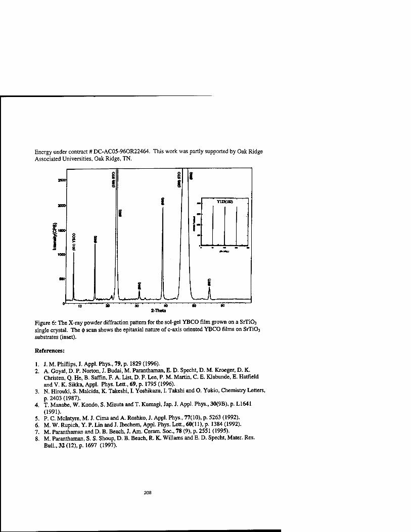
Energy under contract # DC-AC05-96OR22464. This work was partly supported by Oak Ridge Associated Universities, Oak Ridge, TN.
Figure 6: The X-ray powder diffraction pattern for the sol-gel YBCO film grown on a SrTi03
single crystal. The $ scan shows the epitaxial nature of c-axis oriented YBCO films on SrTi03
substrates (inset).
References:
J. M. Phillips, J. Appl. Phys., 79, p. 1829 (1996). A. Goyal, D. P. Norton, J. Budai, M. Paranthaman, E. D. Specht, D. M. Kroeger, D. K. Christen, Q. He, B. Saffin, F. A. List, D. F. Lee, P. M. Martin, C. E. Klabunde, E. Hatfield and V. K. Sikka, Appl. Phys. Lett., 69, p. 1795 (1996). N. Hirouki, S. Malcida, K. Takeshi, I. Yoshikazu, I. Takshi and O. Yukio, Chemistry Letters, p. 2403 (1987). T. Manabe, W. Kondo, S. Mizuta and T. Kumagi, Jap. J. Appl. Phys., 30(9B), p. L1641 (1991). P. C. Mclntyre, M. J. Cima and A. Roshko, J. Appl. Phys., 77(10), p. 5263 (1992). M. W. Rupich, Y. P. Lin and J. Ibechem, Appl. Phys. Lett., 60(11), p. 1384 (1992). M. Paranthaman and D. B. Beach, J. Am. Ceram. Soc., 78 (9), p. 2551 (1995). M. Paranthaman, S. S. Shoup, D. B. Beach, R. K. Willams and E. D. Specht, Mater. Res. Bull., 32 (12), p. 1697 (1997).
208

ROOM TEMPERATURE PHASE-SELECTIVE SYNTHESIS OF METASTABLE LEAD CHROMIUM OXIDES
KENNETH M. DOXSEE, MEEHAE JANG Department of Chemistry, University of Oregon, Eugene, OR 97403
ABSTRACT
The salt metathesis reaction between lead(II) salts and potassium chromate in methanolic solution, mediated by the formation of a soluble complex of potassium chromate with a cyclic polyether, affords orthorhombic PbCr04 rather than the monoclinic modification formed in aqueous solution. When the aqueous metathesis reaction is carried out in the presence of tertiary amines, a lead oxide-rich phase, PbO*PbCr04 (Pb2Cr05), is selectively formed.
INTRODUCTION
The solution-phase salt metathesis reaction, wherein two soluble salts react to produce an in- soluble phase, represents one of the simplest procedures for the synthesis of solid-state materials. Although allowing for the preparation of a wide variety of materials, however, it provides some- what limited options for control of crystal properties. In particular, given the negligible solubility often displayed by one or both reactant salts in organic solvents, salt metathesis reactions are generally carried out in aqueous solution, excluding the ability to examine nonaqueous solvent effects. As solvents are known to exert powerful effects on the crystal form of organic compounds [1], we have initiated a program of study [2,3] wherein we translate simple salt metathesis reactions to the realm of nonaqueous solvents through the intermediate formation of soluble complexes of the reactants [4]. This technique of "complexation-mediated crystallization" permits the exploitation of solvent effects on the crystallization of a wide range of inorganic materials, including, as we report herein, binary metal oxides, as typified by the lead chromium oxides.
Three phases of PbCr04 have been identified: a monoclinic phase (the naturally occurring mineral crocoite) [5], a comparatively poorly studied orthorhombic phase [6, 7], and a tetragonal phase which displays stability only at high temperatures (above 783 °C) [8] or when cocrystallized with the isomorphous PbS04 [9]. Only the monoclinic phase has been firmly placed on the lead- chromium-oxygen phase diagram, which also contains a series of compounds with progressively higher lead oxide content, nPbO«PbCr04 (n = 1,2,4,5) [8, 9, 10,11], of which one, PbO«PbCr04 (Pb2Cr05) is naturally occurring (phoenicochroite) [12]. Several of these phases have received attention in a variety of technological applications, ranging from the use of orthorhombic PbCrQt as an anticorrosive coating [13], specialty pigment [14], and catalyst for photochemical water splitting [15] to the study of the photoconductivity and photovoltaic properties of Pb2Cr0s [16]. Monoclinic PbCr04 is obtained through salt metathesis reactions in aqueous solution under ambient conditions, while the orthorhombic modification is reported to be formed under carefully controlled conditions of temperature, concentration, and counterions [6,7]. The other lead- chromium-oxygen phases have been prepared only through traditional high-temperature solid-state syntheses from the constituent element oxides.
• We now report the application of complexation-mediated crystallization to the facile preparation of orthorhombic PbCr04 through a simple salt metathesis reaction carried out in methanolic solution, as well as a simple modification of the aqueous metathesis reaction which affords access to Pb2Cr05 under ambient conditions of temperature and pressure.
EXPERIMENT
Materials
1,4,7,10,13,16-Hexaoxacyclooctadecane (18-crown-6) (Jansen), (CH3C02)2Pb*3H20 (Baker), Pb(N03)2 (EM Science), K2&04 (Baker), tris[2-(2-methoxyethoxy)ethyl]amine (MEEA, Aldrich), and poly(vinyl alcohol) (MW 13,000-23,000, 87-89% hydrolyzed, Aldrich) were obtained from the indicated commercial sources and used without further purification.
209 Mat. Res. Soc. Symp. Proc. Vol. 495 ® 1998 Materials Research Society

Crystallization from Aqueous Solution - Preparation of Monoclinic PbCrOa
A test tube (2 cm diameter, 30 mL volume) was charged with 5 mL of a 0.05 M solution of K2GO4 in water. A glass microfiber filter paper (Whatman, 2.5 cm diameter) was placed in contact with the surface of the solution. Pure water (5 mL) was then introduced, followed by a second glass fiber filter paper and, finally, 5 mL of a 0.05 M solution of (CH3C02)2Pb*3H20 or Pb(N03)2 in water. The tube was capped with a rubber septum and allowed to stand under ambient laboratory conditions (ca. 22 °C) until crystallization appeared complete (typically 2-7 days). The precipitated solid (typical yield >95%) was then isolated by filtration, washed well with water, then acetone, air-dried, and analyzed by x-ray powder diffraction and scanning electron microscopy coupled with energy dispersive x-ray (EDX) analysis. Crystallizations incorporating 18-crown-6 in either the lead solution or the chromate solution were carried out analogously, with additional washing with diethyl ether and acetone to ensure removal of the chelating agents.
Analogous crystallizations were also carried out in a u-tube configuration. Water (15 mL) was placed in the u-tube (1.8 cm diameter, 40 mL volume), and glass fiber filter papers were inserted to cover each solvent surface. The side arms were then carefully charged with 5 mL of 0.05 M solutions of K2Cr04 and (CH3C02)2Pb*3H20 or Pb(N03)2 in water. Isolation and analysis proceeded as described above.
Crystallization from Alkaline Aqueous Solution - Preparation of PtoCrOs Analogous crystallizations to those described above were carried out in the presence of one or
more equivalents of tris(methoxyethoxyethyl)amine or triethylamine in either the lead(II) solution or the chromate solution. Isolation and analysis proceeded as described above. When either MEEA or triethylamine was added to the aqueous lead(IT) soultion, initial formation of a white precipitate was observed. Isolation by filtration and washing with water afforded an analytical sample. Anal. Pb, 82.83; C.0.17; H.0.33; O, 16.67 (by difference).
Crystallization in Aqueous Gels
Poly(vinyl alcohol) (20 g) was dissolved in 100 mL of water at 80 °C. Approximately 15 mL of the hot solution was poured into a glass u-tube (1.8 cm diameter, 40 mL volume) and allowed to cool to room temperature. Aqueous solutions of K2CrC"4 and (CH3C02)2Pb«3H20 or Pb(NC>3)2 were layered into the side arms of the tube. After 2-4 weeks, needle-like crystals were apparent at the bottom of the u-tube. After removal of the supernatant solutions and most of the gel from the tube, warm water was added to the remaining mixture of crystals in gel to remove the gel. The product was isolated by filtration on a 0.05 um nylon filter, followed by repeated washing with water and with acetone and air drying (typical yield ca. 30%), and analyzed by x-ray powder diffraction and scanning electron microscopy coupled with energy dispersive x-ray (EDX) analysis.
Analogous crystallizations were also carried out in a two-phase configuration. A mixture of K2CrÜ4 (0.05 g, 0.26 mmol) and poly (vinyl alcohol) (0.5 g) in 5 mL of water was heated at ca. 80 °C until a homogeneous solution was obtained (ca. 30 min). The hot solution was poured into a test tube and allowed to cool to room temperature. A glass fiber filter paper was inserted, then 5 mL of a 0.05 M solution of (CH3C02)2Pb'3H20 or Pb(N03)2 in water was added. After ca. 2 weeks, the product was isolated as described above (typical yield ca. 13%).
Crystallization from Methanol - Preparation of Orthorhombic PbCrCXi
A solution of 0.05 g of K2G-O4 (0.26 mmol) in 5 mL of methanol was prepared through addition of 0.14 g of 18-crown-6 (0.52 mmol, 2 equiv) and ultrasonication. This was allowed to react with a 0.05 M solution of (CH3C02)2Pb'3H20 or Pb(NC>3)2 in methanol in both the test tube and the u-tube configurations, as described above. The precipitated solid (typical yield >95%) was then isolated by filtration, washed well with methanol, water, diethyl ether, and acetone, air-dried, and analyzed by x-ray powder diffraction and scanning electron microscopy coupled with energy dispersive x-ray (EDX) analysis. Crystallizations incorporating 18-crown-6 or MEEA in the lead solution were carried out analogously. MEEA was less effective at solubilizing K2C1O4 in
210

methanol, but afforded a ca. 0.02 M solution, which was correspondingly layered with a 0.02 M solution of (CH3C02)2Pb'3H20 or Pb(NC>3)2 in methanol.
RESULTS
The metathesis reaction between K^CrCH and (CH3C02)2Pb#3H20 or Pb(N03>2 in aqueous solution cleanly affords the monoclinic modification of PbCrO,*. Particularly under the slower approach to supersaturation afforded by a u-tube arrangement for crystallization, the crystallinity of the precipitated PbCr04 is quite high (Figure 1).
Figure 1. Monoclinic PbCr04 as obtained from aqueous solution. Bar = 1 um.
Crystallization within gels often offers access to well-formed single crystals [17], and we have recently reported the modification of traditional gel growth procedures to permit the study of crystallization in nonaqueous solvent-swollen polymer "gels" [18]. Translation of the salt metathesis reaction between K2CrÜ4 and (CH3C02)2Pb,3H20 or Pb(N03)2 to an aqueous poly(vinyl alcohol) gel affords the monoclinic modification of PbCr04, showing the gel matrix to have no impact on the phase selectivity of this reaction. As in the liquid-liquid diffusion approach, the degree of crystal perfection is quite high.
Although (CH3C02)2Pb*3H20 and Pb(N03)2 is quite soluble in methanol, K2Cr04 is completely insoluble in this solvent. However, with the addition of two equivalents of 18-crown- 6, a well-known potassium binding agent [19], 0.05 M solutions of K2Cr04 in methanol may be readily obtained. In dramatic contrast to the results from aqueous solution, the reaction between (CH3C02)2Pb«3H20 or Pb(N03>2 and 18-crown-6 solubilized K2CrC>4 in methanol affords not monoclinic PbCr04, but rather the orthorhombic modification. This phase, which has received scant literature attention and has not yet been placed on the Pb-Cr-0 phase diagram, was originally reported to be formed from lead(II) nitrate and potassium chromate [6] or dichromate [7] under carefully controlled conditions of pH, temperature, and concentration. While we have no reasons to doubt these early reports, we have been unable to reproduce them, finding only the monoclinic modification to be formed despite the best of our abilities to replicate the (sketchy) experimental procedures reported. In contrast, formation of the orthorhombic modification from methanol is readily reproducible and requires no particular care in the control of experimental conditions.
An earlier report also noted the facile conversion of the orthorhombic phase to the monoclinic phase upon heating or after prolonged storage (> 30 days) at room temperature [7]. However, we find this phase, as prepared via complexation-mediated crystallization from methanolic solution, to be apparently indefinitely stable under ambient conditions, with no detectable formation of the monoclinic phase after more than eight months of storage as a dry microcrystalline solid. Although the reasons for this enhanced kinetic phase stability are not clear, a higher degree of crystallinity and/or the avoidance of prolonged exposure to aqueous media may be responsible. We have seen no evidence thus far for the formation of the metastable tetragonal phase of PbCrÜ4 under the conditions of complexation-mediated crystallization.
The orthorhombic phase is obtained as a microcrystalline powder, affording sharp x-ray powder diffraction lines but displaying no clear crystal form (Figure 2).
211

Figure 2. Orthorhombic PbCr04 as obtained from methanol solution. Bar = 1 urn.
Figure 3. Orthorhombic PbCrC>4 as obtained from methanol solutions of K2Cr04«2(18-crown-6) andPb(OAc)2,3H20,l[tris(methoxyethoxyethyl)amine]. Bar= 1 um.
In an attempt to reduce the nucleation rate and thereby access larger single crystals, the crystallization from methanol was repeated in the presence of various concentrations of tris(methoxyethoxyethyl)amine (MEEA), a well-known chelating agent for lead [20]. Although the effect of this chelating agent is under continuing study, initial observations are not inconsistent with expectations, and in some cases samples displaying good crystallinity have been obtained (Figure 3) Addition of an equivalent of 18-crown-6 to the lead acetate solution gives rise to a similar modification of crystal form to that expressed by MEEA, although in this case a preference is displayed for clustered aggregates of the orthorhombic phase in the form of rosettes (Figure 4).
Figure 4. Orthorhombic PbCr04 as obtained from methanol solutions of K2Cr04«2(18-crown-6) andPb(OAc)2*3H20«l[18-crown-6]. Bar= 1 um.
212

Surprisingly, addition of MEEA to aqueous metathesis mixtures affords neither the orthorhombic nor the monoclinic modification of PbCr04, but rather Pb2CrOs. Although MEEA could potentially serve in some way to facilitate the nucleation of this lead oxide-rich phase, use of triethylamine in place of MEEA again provides Pb2CrC>5, suggesting that MEEA simply acts as a base under these reaction conditions. It was noted that addition of either MEEA or triethylamine to aqueous solutions of (CHsCC^Pb'SI^O results in the formation of a white precipitate which is consumed upon subsequent addition of potassium chromate. Elemental analysis of this precipitate is consistent with its formulation as hydrated lead(II) oxide [21]. Since this precipitate is not formed in methanolic solution, it seems plausible that its formation is responsible for nucleation of the lead oxide-rich phase in the aqueous preparations.
Consistent with this hypothesis, seeding of aqueous salt metathesis reactions in the absence of either MEEA or triethylamine (reactions shown above to produce monoclinic PbCr04) with the white precipitate does indeed result in the selective formation of Pb2CrOs. Equally dramatically, seeding of methanolic preparations with the white precipitate [as obtained from aqueous (CH3C02)2Pb*3H20] also affords Pb2CrOs, whereas all other preparations from methanol afford only orthorhombic PbCrCy. The impact of this crystallization procedure on the crystal morphology of the resulting Pb2CrOs are under ongoing investigation.
Initial efforts to place orthorhombic PbCr04 on the lead-chromium-oxygen phase diagram through thermal analysis have been inconclusive, although it appears clear that it is metastable with respect to the monoclinic form under ambient conditions. Both phases undergo irreversible conversion to Pb2Cr05 when heated under a nitrogen atmosphere. The monoclinic phase displays an exotherm at 753 °C leading directly to Pb2CrOs, consistent with earlier literature reports [9]. The orthorhombic modification exhibits a broad endotherm at 150-320 °C, apparently corresponding to the direct formation of Pb2CrOs without intermediate formation of monoclinic PbCr04, consistent with our observations regarding the thermal stability of this phase but contrasting with earlier reports of its facile thermal conversion to the monoclinic phase.
CONCLUSIONS
Through appropriate choice of precursor salts, the technique of complexation-mediated crystallization from nonaqueous solvents may be applied to the crystallization of binary metal oxides, as typified by the lead chromium oxides. The technique offers the opportunity for phase- selective synthesis of a variety of both stable and metastable phases under ambient conditions, with monoclinic PbCr04 obtained from water and orthorhombic PbCr04 from methanol. In addition to the powerful solvent effects, other variables may be adjusted in order to further tune both the phase selectivity of the metathesis reaction and the morphology of its products. Thus, addition of tertiary amines permits the preparation of metastable Pb2CrOs from aqueous solution, while the use of a nucleation inhibitor in methanolic solution, coupled with appropriate seeding, allows adjustment of the crystal morphology of this Pb2CrOs phase.
ACKNOWLEDGMENT
Support of this work by the Office of Naval Research is gratefully acknowledged.
REFERENCES
1. R. M. Hooper, B. J. McArdle, R S. Narang, and J. N. Sherwood, in Crystal Growth, 2nd Edition, edited by B. R. Pamplin (Pergamon Press, New York, 1980), p. 395.
2. K. M. Doxsee, D. S. Keegan, H. R. Wierman, J. Hagadorn, M. Arimura, Pure Appl. Chem. 65, 429 (1993).
3. K. M. Doxsee, U.S. Patent 5,545,394, 13 August, 1996. 4. Crystallization of inorganic materials through the intermediacy of inorganic coordination
complexes has been reported, but is to be distinguished from the use of molecular organic species (e.g., crown ethers) as solubilizing agents. For example, Hgl2 may be recrystallized through the intermediacy of Hgl3_ and/or HgL;2- from solutions containing excess iodide: I. F. Nicolau, J. Cryst. Growth 48, 51-60 (1980). Similarly, cinnabar (HgS) has been
213

recrystallized from aqueous sulfide solutions: A. F. Armington and J. J. O'Connor, /. Cryst. Growth 6, 278-280 (1970); P. Anizon, Mater. Res. Bull. 6, 1277 (1971).
5. B. Gossner and F. Mussgnug, Z. Krist. 75, 410-420 (1930); R. Brill, Z Krist. 77, 506 (1931); H. Effenberger and F. Pertlik, Z. Krist. 176, 75-83 (1986).
6. L. Conti and M. Zocchi, Acta Cryst. 12,416 (1959). 7. F. Quittner, J. Sapgir, and N. Rassudowa, Z. anorg. allgem. Chem. 204, 315-317 (1932). 8. F. M. Jäger, H. C. Germs, Z. anorg. allgem. Chem. 119, 145 (1921). 9. H. Wagner, R. Haug, M. Zipfel, Z. anorg. allgem. Chem. 208, 249-254 (1932). 10. T. Negas, /. Am. Ceram. Soc. 51, 716-719 (1968). 11. A. M. Gadalla and M. F. Abadir, Trans. J. Brit. Ceram. Soc. 76, 22-26 (1977). Additional
phases identified in this system are PbCr03 and Pb7Cr20i3. 12. S. A. Williams, W. J. McLean, J. W. Anthony, Amer. Mineral. 55,784-792 (1970); J. C.
Ruckman, R. T. W. Morrison, R. H. Buck, /. Chem. Soc, Dalton Trans., 426-427 (1971). 13. See, e.g.: H. Hanabatake and S. Ikeda, Jpn. Kokai Tokkyo Koho JP 03,110,144,10 May
1991 [Chem Abstr. 117, 53371n (1992)]; H. Kashiwase, K. Sano, N. Tagaki, and M. Yokoyama, Jpn. Kokai Tokkyo Koho JP 04,110,354, 10 April 1992 [Chem. Abstr. 117, 193649J (1992)].
14. See, e.g.: G. N. Savastenko and I. N. Ermolenko, Vestsi Akad. Navuk BSSR, Ser. Khim. Navuk, 15-19 (1991) [Chem Abstr. 115, 146496f (1991)].
15. A. Kudo, M. Steinberg, A. J. Bard, A. Campion, M. A. Fox, T. E. Mallouk, S. E. Webber, and J. M. White, Catal. Lett. 5, 61-66 (1990).
16. K. Toda, S. Morita, Appl. Physics 33, 231-233 (1984); K. Toda, S. Morita, /. Appl. Physics 57, 5325-5329 (1985); S. Morita, K. Toda, J. Appl. Physics 55, 2733-2737 (1984); S. Yoshida, K. Toda J. Appl. Physics 65, 3300-3302 (1989).
17. H. K. Henisch, Crystals in Gels and Liesegang Rings (Cambridge University Press, Cambridge, 1988).
18. Solvent-swollen polymers are technically not true gels, but do serve as gelatinous media for crystal growth: K. M. Doxsee, R. C. Chang, E. Chen, A. S. Myerson, and D. Huang, submitted for publication.
19. Y. Li, G. Gokel, J. Hernandez, L. Echegoyen, J. Am. Chem. Soc. 116, 3087-3096 (1994). 20. G. Soula, /. Org. Chem. 50, 3717-3721 (1985). 21. F. A. Cotton and G. Wilkinson, Advanced Inorganic Chemistry, Fifth edition (J. Wiley and
Sons, New York, 1988), p. 298.
214

Synthesis and photoresponse of rare earth doped phosphosilicates
Z. Cao, B. I. Lee, W. D. Samuels*, G. J. Exarhos** L. Wang*
Gilbert C. Robinson Department of Ceramic and Materials Engineering, Clemson University, Clemson, South Carolina 29634-0907 *Battelle Pacific Northwest National Laboratory, Richland, Washington 99352
ABSTRACT
Phosphate ceramics doped with Sm3+ and Tb-*+ ions were synthesized through sol-gel process. Thin films of T\ß+ doped phosphosilicates were fabricated by spin coating of the phosphosilicate sols on SiOx/indium-tin-oxide/glass substrates. The gels synthesized by reaction of P2O5 with tetraethoxy silane (TEOS) were fired in air at a temperature range of 200°C - 900°C. The crystal structure was examined by x-ray diffractometry. Si50(P04)g was the only crystalline phase. The fluorescence spectra of Sm3+ as a function of firing temperature, composition and structure of the matrices were investigated. The intensity of Snfi+ emission increased with increasing firing temperatures and greater proportion of phosphorus. The photocurrent of the films at 355 nm laser excitation was observed. The photoresponse as a function of laser energy was linear and showed no sign of saturation. The films exhibited stable photoresponse under a high number of laser shots.
INTRODUCTION
Ceramics containing rare earth elements such as Nd-5"1", Er3+, Sm3+, Eu^+and Tb^+ have attracted great attention as potential materials for optical devices. 1_4 Crichton et alß reported that non-silicate glasses such as phosphates offer several potential advantages over borosilicate systems, including low glass transition temperatures and reduced water absorption. Dong et alß produced gratings in rare earth doped phosphosilicate optical fibers. Marion and Weber? presented the superiority of a phosphate system to silicates for laser host matrices.
The mechanical and optical properties of crystalline phosphates made by conventional techniques are generally poor due to large grain size and residual porosity, and effective sintering requires very high temperatures and pressures. Guo et alß reported the preparation and characterization of rare earth orthophosphates through a sol-gel process, but no fluorescence property was investigated. The rare earth doped phosphates are obviously more economical for many applications than rare earth phosphates.
The sol-gel technique is suitable for preparation of rare earth doped phosphates due to the simplicity and the homogeneity of the dopant distribution at the molecular level. The work described here was intended to combine the advantageous properties of rare earth doped phosphates for a luminescent material and the advantages of the sol-gel technique. All samples in this paper were prepared by a sol-gel process developed in our laboratory9.10.
EXPERIMENTAL
The sol-gel preparation of phosphosilicate (PSi) ceramics are described in our previous paper10. Different compositions of phosphosilicate sols were prepared by reaction of P2O5 and tetraethoxy silane (TEOS). A calculated amount of one molar stock solution of samarium chloride (SmCl3) or terbium chloride (TbCl3) was added to the phosphosilicate sols. The homogeneous sols were cast
into Teflon® containers before being placed into a convection oven at 60°C to gel. For Tb3+ doped PSi films, the Tb3+ doped phosphosilicate sols were spun coated on SiOx/indium-tin-oxide/glass
215
Mat. Res. Soc. Symp. Proc. Vol. 495 ®1998 Materials Research Society

Substrates. The detailed procedure is described in Ref. 4. Dried gels were fired in air at 100°C- 900°C for x-ray diffraction (XRD) and fluorescence spectra. The thin films were fired at 650°C for photoresponse measurements. XRD patterns were obtained by using a Philips Model PN3550 generator with Cu K-a anode at 40 kV and 45 mA and wide-range vertical goniometer with an incident beam 20-compensating slit. Nominal semiquantitative estimation of the crystalline- amorphous ratio in mixed phase samples was calculated by comparing the integrated total diffracted intensity with the integrated background. Thermogravimetric analysis (TGA) was carried out on a Seiko 5200H TGA/DTA with 20°C/min heating rate. The solid-state nuclear magnetic resonance (NMR) spectra were obtained from a Chemagnetic Spectrometer of 300 MHz, 89 mm widebore Oxford magnet using a CP-MAS probe at frequency 120.77 MHz for 31 p. The fluorescence spectra of Sm3+ doped phosphates were taken at room temperature with a SPEX Model 1877 Triple Spectrophotometer. The excitation source was the Ar ion laser 488.0 nm line generated by Spectra Physics Model 164. The slit was set at 100 nm for a resolution of il nm. The photocurrent of Tb^+doped phosphosilicate thin films was recorded by a LeCroy 9350 digital oscilloscope under excitation of a Nd:YAG 5 ns, 3 Hz pulse laser of 355 nm.
RESULTS AND DISCUSSION
A. Characterization of Sm3+ and Tb^+doped phosphosilicates
All the samples in this paper were doped with 1 at.% Sm^+ or Tb^4" with respect to phosphorus. Solid state NMR of 31p was carried out to examine the molecular structure of Snß+ doped P-Si gels and fired samples. 31p spectrum of the dried gel (Fig. 1(a)) showed that only one kind of P-0 bond existed, while the spectrum of the sample fired at 900°C (Fig. 1(b)) showed clearly the existence of P-O-Si linkage (-38.3 ppm)9. An XRD pattern for a P-Si (1:1) gel is shown in Fig. 2. The dried gels remained amorphous up to 600°C, and crystallized to phase Si50(P04)6 above that
2500
10 20 30 40 50 60 70 2-Theta
Fig. 1. 3 lp solid state NMR ofP-Si (1:1) gel after (a) dried at 60°C and (b) fired at 900°C.
Fig. 2. X-ray diffraction pattern of P-Si (1:1) gel fired at (a) 500°C, (b) 700°C, (c) 900°C.
216

temperature. No obvious changes were observed in XRD when Srrß+ was doped into the matrix. Szu et al. 11 and Poojary et dl. *2 reported that the structure of silicon phosphate compound is Si50(PC>4)6, no matter what the starting compositions were. Our experiment agrees with the result that the x-ray pattern did not change with the variation of P:Si molar ratio.
The TGA showing the weight loss of P-Si (1:1) gel upon firing is given in Fig. 3. It shows that most of the weight losses occurred below 300°C, mostly due to the elimination of alkyl organic groups. The -30% weight loss is close to the theoretical weight loss due to the ethoxy group decomposition. After burning out the organic groups, the weight loss was less than 3% from 300°C to 1000°C. This is different from the results reported by Poojary et alX2-. Their samples had a substantial phosphorus loss at high temperatures from 300°C to 1000°C, but the phosphosilicate samples we prepared in our study showed no obvious phosphorus loss in the same temperature range.
B. Fluorescence spectra of Sm^4" in phosphosilicate
The electronic configuration of Sm3+ is 4f5. The ground state of Srn^4" is 6H5/2 , and the lowest excited state energy level of 4f is ^65/2- Fluorescence spectra of Sm3+ in a phosphosilicate (P:Si=l :1 in molar ratio) fired at different temperatures are shown in Fig. 4. The XRD results showed that P-Si system remained amorphous below 600°C, and the amounts of crystalline phases increased as the firing temperatures increased up to 900°C. The emission intensities increased with higher firing temperatures. No emission wavelength changes caused by the firing temperatures were observed. This is because the emissions are due to the transitions of 4f-4f, i. e., ^G5/2-"Hj, j=5/2, 7/2, 9/2, 11/2, and the f-orbital electrons are well shielded by the outer electrons. Thus the emission positions originated from f-f transitions are hardly affected by external factors such as composition, structure, temperature , crystal field and so on. However, as shown in Fig. 4, the emission intensity can be affected by external variables. When P-Si was doped with Sm3+, one can reasonably assume that Sm^+ ions substituted Si^+ cations, then oxygen vacancies would be created to compensate for the charge imbalance. Obviously the higher the firing temperatures, the
Temperature(°C)
Fig. 3. TGA curve of P-Si (1:1) gel.
550 600 650 Wavelength(nm)
Fig. 4. Fluorescence spectra of SirP"1" in P-Si (1:1) gels fired at different temperatures, (a) 100°C, (b) 500°C, (c) 900°C.
217

easier the formation of the oxygen vacancies which is a result of Sm3+ of substitution. Moreover, after being fired at higher temperatures, fewer OH groups would remain. The presence of OH groups in the first coordination sphere of Sm3+ ions would mediate the de-excitation from the excited state to the lower energy levels via an effective pathway for radiationless decay. Thus the emission intensity increased with more oxygen vacancies and less OH, i. e., higher firing temperatures.
The emission intensity of Sm3+ as a function of the composition of the matrix was investigated by spectral analysis of Sm3+ at 1 at. % in P-Si after firing at 900°C. Fig. 5 shows the emission spectra of Sm3+ doped P-Si of different molar compositions of P:Si. The emission intensity increased as the proportion of phosphorus increased. This indicates that, with respect to the emission intensity, phosphate is superior to silicate as the matrix. Since Si50(P04>6 is the only crystalline phase, regardless of the starting composition, when the molar ratio of P to Si changed closer to the stoichiometric ratio of 6:5, the degree of the crystallinity increased accordingly.
C. Photoresponse of Tb3+ doped phosphosilicate thin films
Due to the variable valence state of Tb ion (3+ and 4+), Tb3+ can become an electron donor under UV excitation. The photo-induced electron can be promoted to the conduction band, exhibiting the photoconductivity observed in Tb3+/PSi thin films. Fig. 6 shows a transient voltage
-30 (c)
-20 CPS X103
-10 #bM i^a)\^
0
1
1.70E-2
> 9.00E-3
1.00E-3
550 600 650 Wavelength(nm)
-3.00E-5 1.00E-5 5.00E-5 Time (seconds)
Fig. 5. Fluorescence spectra of Sm3+ in P-Si gel fired at 900°C as a function of composition of P-Si matrix. (a)P:Si=l:2,(b)P:Si=l:1.5,(c)P:Si=l:l.
Fig. 6. A transient voltage pulse of Tb/PSi thin film under 355 nm laser excitation.
signal of Tb3+/PSi thin films under 355 nm laser excitation. The photoresponse dependence on laser power is shown in Fig. 7. It is a linear relation in the range of 1.4-4.4 mJ pulse-1. This means no power saturation exists in the range. Fig. 8 shows the photoresponse dependence on the number of laser shots. The photoresponse stayed constant up to 15,300 laser pulses. There were no signs of fatigue or visible damage to the thin films, indicating the stability of the material.
218

o 1.90E-7
c o 1.80E-7.
.70E-7 1.1 2.1 3.1 4.1 5.1
Laser Power (mJ/Pulse)
•34.00E-7 >
|2.00E-7
o
£ O.OOEO 0 4000 8000 12000
No. of Laser Shots (355nm)
Fig. 7. Plot of photoresponse vs. laser power.
IV. CONCLUSIONS
Fig. 8. Plot of photoresponse vs. number of laser shots.
The emission intensity of Sm3+ doped phosphosilicates prepared by a sol-gel process increased with higher firing temperatures and greater amount of phosphorus. Tb/PSi thin films coated on SiOx/indium-tin-oxide/glass substrates exhibited photoresponse by 355 nm laser excitation. Photoresponse as a function of laser power was linear and showed no sign of saturation. The films exhibited stable photoresponse under a high number of laser shots.
ACKNOWLEDGMENTS This project was supported by the U. S. Department of Energy under contract DE-AC06-76RL
through Pacific Northwest National Laboratory operated by Battelle Memorial Institute. The authors would like to thank Dr. W. Sisk for photoresponse measurements.
References 1. H. Takebe, K. Morinaga, T. Izumitani, J. Non-Cryst. Solids, 178, 58 (1994). 2. W. Xu, S. Dai, L. M. Toth, G. D. Del Cul, J. R. Peterson, J. Non-Cryst. Solids, 194, 235 (1996). 3. Z. Cao, B. I. Lee, W. D. Samuels, G. J. Exarhos, J. Applied Physics, in press. 4. B. I. Lee, Z. Cao, W. N. Sisk, J. Hudak, W. D. Samuels, G. J. Exarhos, Mater. Res. Bull., 32, 9 (1997). 5. S. Crichton, H. Yamanaka, J. Matsuoka, and E. Wakabayashi, in Ceramic Trans. Solid-State Optical Materials, edited by A. J. Bruce and B. V. Hiremath, (Am. Ceram. Soc., Westerville, OH 1992), p493. 6. L. Dong, J. L. Cruz, J. A. Tucknott, L. Reekie, and D.N. Payne, Optical Letters, 20, 1982 (1995). 7. J. E. Marion and M. J. Weber, Smr. J. Solid State Inorg. Chem. 28, 271 (1991). 8. Y. Guo, P. Woznicki, A. Barkatt, E. E. Saad, and I. G. Talmy, J. Mat. Res. 11, 3 (1996). 9. B. I. Lee, W. D. Samuels, L. Wang, and G. J. Exarhos, J. Mater. Res. 11, 1 (1996). 10. Z. Cao, B. I. Lee, W. D. Samuels, G. J. Exarhos, L. Wang, J. Mater. Res., in press. 11. S. P. Szu, L. C. Klein, and M. Greenblatt, J. Non-Cryst. Solids, 143, 21 (1992). 12. D. M. Poojary, R. B. Borade, and A. Clearfield, Inorganic Chimica Acta, 23, 208 (1993).
219
STRUCTURAL CHARACTERIZATION OF A SERIES OF NEW TERNARY TI-NITRIDE COMPOUNDS
K.S. WEIL AND P.N. KUMTA Department of Materials Science and Engineering, Carnegie Mellon University, Pittsburgh, PA 15213
ABSTRACT
The structures of four new tungsten based, ternary nitride compounds, Fe3W3N, Ni6W6N, Ni2W4N, and Fe4W2N, each prepared using a complexed precursor synthesis route, have been determined by Rietveld analyses of the respective powder x-ray diffraction (PXRD) data. Each compound crystallizes in a relatively complex cubic structure which is in general isostructural with the r|-carbide structure. However, subtle structural differences which are compositionally dependent do exist between each nitride and these will be examined in detail in this paper.
INTRODUCTION
Over the past ten years interest in the synthesis of ternary transition metal-transition metal nitrides has intensified. The motivation for studying multicomponent nitrides is fueled by two important expectations: 1) these higher order nitride compounds are anticipated to display different, more complex crystal structures and more exotic magnetic, optical, and electrical properties in comparison to their binary counterparts and 2) to date, the preparation of this type of ternary nitride using traditional approaches has proven to be quite challenging and may require the development of new chemical synthesis techniques, which could eventually be generally applicable for discovering other new compounds. Thus far, the crystal structures of these ternaries seem to fall predominantly into one of three categories, either: 1) layered hexagonal or rhombohedral structures such as MnMoN2 (1) and CrWN2 (2), 2) cubic, r|-carbide structures such as Fe3Mo3N and Co3Mo3N (3), and 3) cubic, anti- perovskite structures such as Fe3NiN and Cu3MnN (4). Our interests in the r|-nitride compounds lie in further characterizing their crystal structures and determining their structure sensitive properties.
Historically, compounds exhibiting the ri-carbide structure began to attract attention with the advent of high speed steels used in the manufacture of cutting tools. Iron-carbon alloys containing molybdenum and/or tungsten were known to form fine ternary carbide precipitates such as Fe3Mo3C and Fe3W3C, which were suspected to be responsible for the high strength, hardness, and toughness characteristics attributed to this class of tool steels. Since the initial discovery of Fe3W3C by Westgren and Phragmen (5) in 1928, a large number of ternary carbides and oxides, and to a lesser extent nitrides, exhibiting the T|- carbide structure have been identified. The structural details of four new ternary transition metal nitride compounds, namely Fe3W3N, Ni6W6N, Ni2W4N, and Fe4W2N, will be described here. Each crystallizes in the ri-carbide structure, but with small compositionally induced structural differences.
EXPERIMENTAL PROCEDURE
Materials Synthesis
Each of the nitride compounds discussed in this work was synthesized by the ammonolysis of a complexed mixed-metal precursor, using an approach similar to that
221
Mat. Res. Soc. Symp. Proc. Vol. 495 e 1998 Materials Research Society
previously reported by us (6). The anhydrous chlorides of the two species of interest were dissolved in anhydrous HPLC grade acetonitrile in the molar ratio necessary to achieve the final stoichiometry of interest. For example, in synthesizing Fe4W2N, anhydrous ferric chloride and tungsten hexachloride were dissolved in a 2:1 molar ratio. The two metal species were then simultaneously complexed with triethylamine, forming a viscous liquid. This liquid was heated to ~90°C to evaporate off the acetonitrile and leave behind a waxy solid precursor. Each of the precursors was heated at 2K/min in ammonia to a final soak temperature of 850°C for 4 - 8 hours and furnace cooled to form the single phase ternary nitride.
Materials Characterization
Quantitative chemical assay on two samples of each ammonolyzed powder product was conducted by Galbraith Laboratories (Knoxville, Tennessee). They employed a wet chemical analysis technique to determine the concentration of the metal species and combustion analyses to evaluate the nitrogen and carbon contents. In preparing samples for x-ray analysis, each nitride powder was slurried in acetone and ground with an agate mortar and pestle for five to ten minutes. The samples were then loaded into standard brass sample holders for PXRD analysis. These measurements were conducted on a Rigaku theta-theta diffractometer employing graphite monochromated Cu Ka radiation under the following step scan settings: 10 -120° range, 0.02° step size, and 15 second collection time. Prior to the diffraction experiments, the diffractometer was aligned using a (100) oriented silicon single crystal for accurate peak positions.
An initial estimate of the lattice parameters for each compound was obtained by a least-squares refinement of the angular positions of the reflections obtained in the two-theta range of 20°< 26 < 80°. Rietveld refinements were then carried out using the RlETAN-94 (7) program over the entire 10 -120° range of the x-ray diffraction data. The profile shape was represented by the modified pseudo-Voigt function (8), with profile asymmetry introduced by employing a multi-term Simpson's rule integration (9). In addition to the profile, lattice, thermal displacement, and structure parameters, the zero-point shift, nine background parameters, and the scale factor were refined without correction for preferred orientation. Thermal vibrations were assumed to be isotropic. Crystal structure graphics and geometric measurements were prepared using the Ca.R.Ine crystallographic software package (10).
RESULTS AND DISCUSSION
Results from the chemical analyses, shown in Table 1, verify the target
Table 1. Chemical Composition
Compound at%W at% Ni or Fe at%N at%C
Fe3W3N 43.03 43.14 13.76 0.06
Ni.WjN 46.21 46.26 7.33 0.16
Ni2W4N 28.98 57.09 13.87 0.04
Fe4W2N 56.99 28.85 14.04 0.11
stoichiometries of the ammonolyzed mixed-metal precursors as Fe3W3N, Ni6W6N, Fe4W2N, and Ni2W4N, respectively. Carbon impurities were found to be present in relatively insignificant concentrations in all four compounds. As seen in other ternary transition metal- transition metal nitrides (1-3), the nitrogen content of these compounds are slightly substoichiometric. Each compound was indexed as cubic, with the lattice parameter given in Table 2. Systematic absences in the indexing, along with Rietveld refinement of the PXRD
222

patterns indicate that each new nitride crystallizes in the space group Fd3m (227), but that the atomic parameters of the constituent transition metal and nitrogen atoms vary with the compound stoichiometry. Given below in Table 2 are the Wyckoff positions of the constituent atoms in each of the four new nitrides, displaying the compositionally induced structural variations.
Table 2. Lattice Parameter. Site Occupancies, and Atomic Parameters
Compound a (A)
FejW3N 11.106(7) Ni6W6N 10.890(2)
Ni2W4N 11.254(5)
Fe4W2N 11.081(1)
im
N
N
16ftn
Fe Ni
W Fe
32feVx2 48fflx1
Fe/0.418(7) W/0.196(0) Ni/0.421(8) W/0.197(4)
Ni/0.416(3) W/0.191(5) Fe/0.426(8) V3Fe & V3W/0.194(1)
The atomic arrangement of the prototype n-carbide unit cell, seen in Figure 1(a), is based on a filled version of the Ti2Ni structure (11). As shown in Figures 1(b) - (d), separate clusters of T (titanium) and M (nickel) atoms in this intermetallic structure essentially define two interpenetrating diamond cubic lattices. The T atoms cluster in regular octahedra on the first diamond cubic lattice, while the M atoms can be found in groups of four as tetrahedra on a second diamond lattice which interpenetrates the first through a V2, V2, V2 unit cell translation. Sixteen additional metal atoms, either T- or M-type depending on the T:M ratio, tetrahedrally coordinate the M tetrahedra. In filled versions of Ti2Ni, depending on the metal- to-non-metal ratio, eight or more non-metal atoms surround the T octahedra in tetrahedral coordination. These non-metal atoms are located centrally between two neighboring T octahedra, producing a six-fold trigonal antiprismatic, or distorted octahedral, environment of T atoms around each non-metal atom.
(0 (d)
Figure 1. Schematic representation of the T4M2X unit cell [adapted from reference (11)]. Figure (a) displays the unit cell where the dark gray, large spheres represent the T atoms, the light gray, medium size spheres represent the M atoms, and the small, light gray spheres represent the interstitial X atoms. Although T4M2X has a large fee unit cell, its structure can be visualized as two subcells, (b) and (c), alternately stacked in a cubic array (d), where the dark gray spheres represent T atoms in addition to those in the octahedra and the light gray spheres represent interstitial, X, atoms such as carbon. The patterns in the subcells assume a diamond cubic-type of arrangement in which the T octahedra or the M tetrahedra are centered at the corners and center of these small cubic cells.
223

Alternative views of the filled Ti2Ni structure can be visualized using XT6 octahedra (where X is an interstitial atom) and polyhedral clusters of the remaining atoms. For example, in T4MjX the non-metal X atoms are octahedrally coordinated by T atoms forming slightly distorted XT6 octahedra, shown in Figures 2(c) and (d). On the other hand, the M atoms and remaining T atoms cluster into groups of eight, M4T4, arranged into four tetrahedra each which share a face with a fifth central tetrahedron, thus forming a Stella quadrangula (12). The M4T4 stellae quadrangulae are displayed in Figures 2(a) and (b). These octahedral and tetrahedral arrangements are related. The first can be viewed as a set of octahedra ordered such that a central unfilled, regular T octahedron is bounded on four faces (two opposing pairs) by filled, slightly distorted XT6 octahedra, as shown in Figure 2(d). In fact, Figure 2(d) directly demonstrates the spatial relationship between the unfilled regular T6 octahedra in this structure, shown in Figures 1(b) and (c) and the filled distorted XT6 octahedra seen in Figure 2(c).The second, tetrahedral, arrangement of the M atoms and remaining T atoms can be viewed as a central tetrahedron, M4, capped on all four faces by additional tetrahedra, M3T, in which the T atoms are at the far most vertex of each outer tetrahedron, as shown in Figure 2(b). Thus, the XT6 octahedra corner share in a manner which is similar to that seen in the pyrochlore structure, while the M4T4 stellae quadrangulae also corner share, but on a structural lattice separate from that formed by the XT6 octahedra. Because these two lattices interpenetrate, each occupying the interstices of the other, their unit cell edges are identical in size.
* »';« m im (a)
¥mJä (c)
(b)
(d)
Figure 2. Polyhedral representation of T4M2X: In Figure (a) clusters of four M atoms and four T atoms are arranged into four tetrahedra, M3T, each which share a face with a fifth central tetrahedron, M4 (outlined in white), forming the star-shaped Stella quadrangula. As shown in Figure (b), the stellae quadrangulae corner share and the T atoms can be found on the four corner-shared vertices of each Stella quadrangula. In Figure (c), each X atom is coordinated by six T atoms, forming slightly distorted XT6 octahedra. The octahedra share corners in a manner similar to that seen in the pyrochlore structure. Figure (d) displays the octahedral arrangement of the pyrochlore-like lattice in ti-carbide structures. Shown sharing corners are four dark gray, slightly distorted XT6 octahedra. Centered within the XT6 octahedra is a regular unfilled T6 octahedron, shaded lighter gray.
224
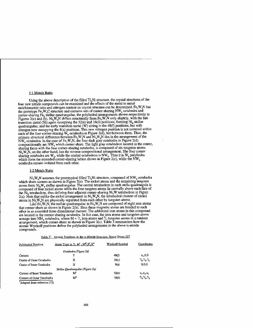
1:1 Metals Ratio
Using the above description of the filled Ti2Ni structure, the crystal structures of the four new nitride compounds can be examined and the effects of the metal to metal stoichiometric ratio and nitrogen content on crystal structure can be determined. Fe3W3N has the prototype Fe3W3C structure and contains sets of corner-sharing NW6 octahedra and corner-sharing Fe8 stellae quadrangulae, the polyhedral arrangements shown respectively in Figures 2(c) and (b). Ni6W6N differs structurally from Fe3W3N only slightly, with the late transition metal (Ni) again occupying the 32(e) and 16(d) positions, forming Ni8 stellae quadrangulae, and the early transition metal (W) sitting in the 48(f) positions, but with nitrogen now occupying the 8(a) positions. This new nitrogen position is not centered within each of the four corner-sharing W8 octahedra in Figure 2(d), but between them. Thus, the primary structural difference between Fe3W3N and Ni6W6N lies in the arrangement of the NW6 octahedra. In the case of Fe3W3N, the four dark gray octahedra in Figure 2(d) compositionally are NW6 which corner-share. The light gray octahedron located in the center, sharing faces with the four corner-sharing octahedra, is composed of six tungsten atoms. Ni6W6N, on the other hand, has the reverse compositional arrangement. The four corner sharing octahedra are W6, while the central octahedron is NW6. Thus it is W6 polyhedra which form the extended corner-sharing lattice shown in Figure 2(c), while the NW6
octahedra remain isolated from each other.
1:2 Metals Ratio
Ni2W4N assumes the prototypical filled Ti2Ni structure, composed of NW6 octahedra which share corners as shown in Figure 2(c). The nickel atoms and the remaining tungsten atoms form Ni4W4 stellae quadrangulae. The central tetrahedron in each Stella quadrangula is composed of four nickel atoms while the four tungsten atoms lie centrally above each face of the Ni4 tetrahedron, thus defining four adjacent corner-sharing Ni3W tetrahedron in Figure 2(a). Note that unlike the nickel arrangement in Ni6W6N, the tetrahedral clusters of nickel atoms in Ni2W4N are physically separated from each other by tungsten atoms.
Like Fe3W3N, the stellae quadrangulae in Fe4W2N are composed of eight iron atoms that corner-share as shown in Figure 2(b). Thus these magnetic atoms are bonded to each other in an extended three-dimensional manner. The additional iron atoms in this compound are located in the corner-sharing octahedra. In this case, the iron atoms and tungsten atoms arrange into NM6 octahedra, where M = V3 iron atoms and 2/3 tungsten atoms in a random arrangement, which corner-share as shown in Figure 2(c). Table 3 summarizes how the atomic Wyckoff positions define the polyhedral arrangements in the above Ti-nitride compounds.
Table 3'. Atomic Positions in the n-Nitride Structure. Space Group 227
Polvhedral Position Atom Type in Tt M1^ M",X',X" WvckoffSvmbol Coordinates
Comers
Octahedra (Figure 2d)
T 48(f) x„0,0
Center of Outer Octahedra X 16(c) '/ '/ '/ '8, '8» '8
Center of Inner Octahedra X 8(a) 0,0,0
Corners of Inner Tetrahedra
Stellae Quadrangulae (Figure 2a)
M' 32(e) ^2' 2' 2
Corners of Outer Tetrahedra M" 16(d) 5/ 5/ 5/ '8> '8> '8
"Adapted from reference (12).
225

Interatomic Bonding
Bond distances and angles between the constituent atoms in each of these structures were calculated from the refined unit cell data. The metal-nitrogen bond distances in the NM6 octahedra of each compound were found to be significantly longer in comparison to M-N bond lengths existing in the alkali- and alkaline-earth-transition metal nitrides. For example, the W-N bond distances in NajWNj (13) and Ba,WN4 (14) range from 1.78(1) -1.93(1) A, nearly 10 - 20 % shorter than the M-N bonds in Fe4W2N and Ni6W6N. The longer metal- nitrogen bond lengths imply that the bonding in Fe4W2N is at least partially covalent. Similarly, comparisons of the metallic bond lengths in the NM6 octahedra with those in metallic tungsten, iron, and nickel suggest that the longer metallic bonds in the n-nitrides are due to covalent bonding in the octahedra. On the other hand, the metal to metal bond lengths within the M8 stellae quadrangulae clusters of each compound are nearly equivalent to those found in the respective pure metal structures, suggesting that within the stellae quadrangulae clusters, the constituent atoms form metallic bonds.
CONCLUSIONS
We have synthesized four new ternary tungsten-transition metal nitrides, Fe3W3N, Ni6W6N, Fe4W2N, and Ni2W4N, by the ammonolysis of complexed mixed-metal precursors at a soak temperature of 850°C. Each nitride was found to be isostructural with the n-carbide structure, crystallizing in face-centered cubic structures. However, differences in the compositions of these compounds predicate structural differences between each in terms of spatial arrangement of the nitrogen atoms and the crystallographic relationship of the metal atoms within the polyhedral description of the n-carbide structure.
ACKNOWLEDGMENTS
This work is supported by the National Science Foundation under Grant No. CTS 9700343. One of the authors (KSW) would also like to acknowledge the award of a Fellowship by NASA.
REFERENCES
1. D. S. Bern, C. M. Lampe-Onnerud, H. P. Olsen, and H-C zur Loye, Inorg. Chem. 35, p. 581 (1996). 2. K. S. Weil and P. N. Kumta, J. Solid State Chem. 128, p. 2 (1997). 3. J. D. Houmes, D. S. Bern, and H-C zur Loye, in Covalent Ceramics II: Non-Oxides, edited by A. R.
Barron, G. S. Fischman, M. A. Fury, and A. F. Hepp (Mater. Res. Soc. Proc. 327, Pittsburgh, PA 1993), p. 153-164.
4. H. H. Stadelmaier. in Developments in the Structural Chemistry of Alloy Phases, edited bv B. C. Giessen (Plenum Press, New York, NY 1969), p. 141-180.
5. A. Westgren and G Phragmen, Trans. Amer. Soc. Steel Treat. 13, p. 539 (1928). 6. K. S. Weil and P. N. Kumta, Mat. Sei. and Eng. B 38, p. 109 (1996). 7. F. Izumi, in The Rietveld Method, edited by R. A. Young (Oxford University Press, Oxford, 1993),
Chap. 13.. 8. P. Thompson, D. E. Cox, and J. B. Hastings, J Appl. Cryst. 20, p. 79 (1987). 9. C. J. Howard, J. Appl. Cryst. IS, p. 615 (1982). 10. C. Boudias and D. Monceau, Ca.R.Ine Cristallographie, version 3.0 (1989). 11. M. H. Mueller and H. W. Knott, Trans. Met. Soc. AIME 227, p. 674 (1963). 12. B. G. Hyde and S. Andersson, Inorganic Crystal Structures. John Wiley & Sons, New York, 1989,
pp. 347-350. 13. E. Parthe, W. Jeitschko, and V. Sadagopan, Acta Cryst. 19, p. 1031 (1965). 14. A. Gudat, P. Hohn, R. Kniep, and A. Rabenau, Z. Naturforsch. B 46, p. 566 (1991).
226

THE SPRAY DEPOSITION OF TRANSITION METAL NITRIDE THIN FILMS USING ALCOHOL BASED PRECURSOR SOLUTIONS
K.S. WEIL AND P.N. KUMTA Department of Materials Science and Engineering, Carnegie Mellon University, Pittsburgh, PA 15213
ABSTRACT
A new alcohol solution based approach has been developed for preparing transition metal nitride thin films and coatings. In this technique, the metal of interest is dissolved as a chloride in acetonitrile, then chelated with triethanolamine to form a highly viscous solution which settles out of the solvent phase. The acetonitrile is then evaporated off and the remaining thick liquid precursor is easily diluted with water or methanol, yielding a semi- viscous liquid which can be used directly to coat various substrates. When heat treated under the appropriate conditions in ammonia, the precursor coating transforms to yield the corresponding nitride. This approach is currently being considered for preparing nitride- based thin film electrical components and has been successfully used thus far to spray deposit TaN and NbN nitride films onto silicon substrates. Results of the preliminary study on these two nitride films are discussed in this paper.
INTRODUCTION
Transition metal nitride materials, such as TiN, ZrN, and Fe4N are important in a wide range of applications including wear and corrosion resistant coatings, high-temperature structural components, and magnetic storage devices. However, the most immediate use of transition metal nitrides may depend on their electrical properties. Thin tantalum nitride and niobium nitride films are of particular interest. Tantalum nitride films are used extensively in microelectronic applications such as in resistors and capacitors because of their low thermal coefficients of resistance and stable resistance values under long term operating conditions (1). The 8 phase of NbN is a type II superconductor with a useful Tc of 17.3 K and high breakdown current value, and it has found important applications in devices such as dc- superconducting quantum interference devices, Josephson junctions, and switches for pulsed power applications (2).
In recent years, a number of synthesis techniques have been developed for preparing transition metal nitride coatings and films. These include: reaction sputtering (3), laser ablation (4), the ammonolysis of sol-gel derived spin coated films (5), and thermal decomposition of [(CH3)3Si] 2NH based compounds (6). Synthetic approaches based on liquid precursor techniques may offer several advantages over line of sight physical film deposition methods, such as sputtering, including the opportunity to better control the stoichiometry and microstructure of nitride thin films. We have recently demonstrated a new solution based approach which offers the potential to synthesize a number of ternary transition metal nitride powders (7,8). The focus of the present study is to demonstrate the utility of this approach in preparing nitride thin films for electronic device applications. The process involves dissolving a metal chloride in acetonitrile and chelating the metal species with an alkanolamine complexing agent to form a liquid precursor. Depending on the choice of the alkanolamine, this liquid can be further modified to prepare precursors for generating a nitride powder or coating. Precursors for the powders, for example, are prepared using a low molecular weight bidentate chelating agent, such as ethanolamine, followed by subsequent hydrolysis to form a metallo-organic hydroxide precipitate which can be filtered and dried. Thin film precursors, on the other hand, can be prepared by chelating the transition metal chloride species with a higher molecular weight alkanolamine, such as triethanolamine. The
227
Mat. Res. Soc. Symp. Proc. Vol. 495 e 1998 Materials Research Society

resulting complexed liquid is quite resistant to hydrolysis and can be dissolved in polar solvents so that the viscosity of the solution can be accordingly modified for spray, dip, or spin coating. Additionally, we have found that upon reacting with or dissolving in water or methanol, the precursors for both powders and films can be handled in air without concern of further reaction, eliminating the need for constant glovebox containment throughout the entire synthesis process. To date, nitride films of zirconium, tantalum, molybdenum, niobium, and iron have been prepared by spray coating using the above solution precursor scheme. This paper will describe our initial results on the synthesis of tantalum and niobium nitride thin films.
EXPERIMENTAL PROCEDURE
1. Chemicals
The metal chlorides, TaCl5 (99.9%, Aldrich) and NbCl5 (99.9%, Aldrich); the solvents, HPLC grade acetonitrile (Fisher Scientific) and ACS grade methanol (Fisher Scientific); and the chelating agent, triethanolamine (98%, Fisher Scientific) were all used without further purification. Boron-doped, p-type semiconductor grade silicon chips (V2" x 72" x VI6") were used as substrates for the formation of the thin-film coatings. These were washed sequentially with trichloroethylene, acetone, and methanol, then oven dried prior to coating. Electronic grade ammonia (Matheson Gas) was used for the pyrolysis and ammonolysis treatments. All chemical manipulations were conducted in an argon filled glovebox (02 and H20 < 5ppm; Vacuum Atmospheres) or under a protective stream of ultra high purity (UHP) nitrogen (Matheson Gas) unless otherwise noted. All glassware used was acid washed with NoChromix and oven dried prior to use.
2. Materials Characterization
Crystalline phases in the as-heat treated thin films were characterized by X-ray diffraction (XRD). The samples were fixed in brass holders and analyzed with a Rigaku (Theta-Theta) diffractometer using graphite filtered monochromated CuKot radiation. The XRD data was collected using a scan rate of 1.57min and a step size of 0.05°, over a 20 range of 20° -100°. The microstructure of the nitride films were characterized using an AMRAY 1810 scanning electron microscope (SEM) equipped with a Robinson backscatter detector and a windowless ED AX, DX-4 analyzer.
3. Materials Synthesis
The chelated tantalum and niobium precursors were prepared using the following technique. The metal chloride was weighed in a glovebox, typically using a 2 - 6g sample, and loaded into a 500ml, three necked round bottom flask along with a Teflon coated magnetic stir bar and approximately 200ml of acetonitrile. After appropriately sealing the flask with rubber septa, it was transferred to a fume hood and connected to the ultra high purity (UHP) nitrogen line. Once the chloride had thoroughly dissolved in the solvent, triethanolamine was added to the solution through the central septum using a syringe and needle. The amount of triethanolamine used in each experiment was determined assuming complete reaction of the chlorine species by the chelating reagent.
Since the chelation reaction with triethanolamine is slightly exothermic and some hydrogen chloride gas does evolve, it was added at a moderately slow rate of approximately 10 ml/min. For both tantalum and niobium, the chelation reaction occurred nearly instantaneously as evidenced by color changes in the acetonitrile solution and by the formation of a syrupy, yellow colored liquid which settled out of the acetonitrile phase. After reacting the dissolved metal chloride with triethanolamine, the parent liquor was heated to approximately 85°C for four hours to drive off the acetonitrile. The remaining viscous liquid
228

was dissolved in methanol, allowing the concentration of the solution to be adjusted to -0.1M on a metals basis by adding or evaporating methanol.
In this particular study, the precursor was being tested for its applicability in preparing thin films by using a spray deposition technique. The spray deposition apparatus was enclosed within a bell jar which could be evacuated and backfilled with UHP nitrogen. This was done three times prior to spray coating to avoid forming an oxide during the deposition process. Spray deposition was conducted by pressurizing a preheated (~60°C) precursor solution with UHP nitrogen and forcing it through a fine nozzle, forming a mist which settled onto a substrate heated to approximately 700°C. Once spraying was completed, the coated substrate was allowed to remain on the heater for five additional minutes before further processing. The substrates were then placed into an aluminum nitride boat which was transferred to a 2% inch diameter quartz flow-through tube furnace. The back end of the tube furnace was connected to a mineral oil bubbler and the front end was connected to the gas line. Prior to initiating the heat treatment, the tube was purged for twenty minutes with pre- pure nitrogen, then purged for another ten minutes with ammonia gas. The samples were fired in flowing ammonia (120ml/min) at a ramp rate of 3°C/min to a soak temperature of 700°C and held at that temperature for four hours, then allowed to furnace cool.
RESULTS AND DISCUSSION
1. Formation of the Chelated Precursor
Both of the metal chlorides used in this study dissolve readily in acetonitrile. Also in both cases, the chelation reaction occurs immediately upon the addition of triethanolamine to the acetonitrile solution, with each droplet of triethanolamine forming two products: 1) a yellow colored, sticky liquid droplet, which eventually settled to the bottom of the flask or smeared along the inside wall of the vessel, and 2) a cloudy white material which eventually seemed to dissolve in the acetonitrile phase. The addition of the first 10-20 drops of triethanolamine resulted in the formation of hydrogen chloride gas in the empty volume above the acetonitrile solution. Even after the gas evidently cleared from inside the flask, white fumes of a low pH gas continued to evolve from the bubbler for several minutes thereafter.
It is well known that the transition metal chlorides behave as Lewis acids and tend to form adducts with electron donating bases such as hydrazine and alkylamines (9). The presence of three strong nucleophilic hydroxyl groups on triethanolamine and the unpaired electrons on the nitrogen center make it a strong chelating agent. In view of this, it is suspected that in the absence of a solvent, the transition metal chlorides will react directly with triethanolamine by replacing one or more chlorine species from the metal chloride to form HC1 gas and a solid or liquid chelated product. This reaction could be written in the case of tantalum chloride, for example, as follows:
2+3HCI
Cl CH2CH2OH I I
C| —Ta ~.a + OHCH2CH2- N
Cl Cl CH2CH2OH Cl
Cl CH2CH20-TaCCI
<V I Nc,cl
ft-OCH2CH2-N +3HCI Cl'/ | /CI
Cl ~HjCH2C - -™ (1)
Cl CH2CH20-Ta'-Cl
C-CI Cl
229

The products from reaction (1) can continue to react with triethanolamine. However, the extent of the subsequent reactions will depend on the kinetics of the replacement reaction, which in part depends upon steric and electrostatic interactions between the attached and unattached triethanolamine groups. The fact that the resulting precursor is a viscous liquid indicates that it is composed of a highly linked or bridged structure. Therefore, we can assume that further reaction of either product in reaction (1) with triethanolamine should result in the formation of a bridged oligomer such as (2) or (3):
(2)
'N ->Ta - OCH
Cl OHCHoCHo I CH2CH2OH
NCH2CH20-Ta-OCH2CH2N W / / \ V.
OHCH2CH2 /-»I /->i Crl2CH2OH
This neat reaction between TaCl5 and triethanolamine has been observed (10) and results in the exothermic evolution of hydrogen chloride gas and the formation of a very viscous, tar- like yellow product. Heat treatment of this viscous liquid precursor in ammonia at 850°C yields TajN5. Similar reactions have been reported for the complexes obtained from the reaction between ethanolamine and chromium, nickel, or cobalt halides (11).
In acetonitrile, it is expected that the transition metal chlorides will form soluble complexes with the solvent. For example, in the case of MoCl5, it is known that acetonitrile forms both an end-on and a side-on coordinated adduct, depending on the manner in which Mo is linked to the polar nitrile species of CH3CN (12). The end-on adducts can be replaced by weak bases such as hydrazine. Thus, with respect to tantalum chloride, it is possible that triethanolamine could replace the adduct of TaCl5 formed in acetonitrile and yield products very similar to those speculated above for the neat reaction. Detailed analysis of the molecular processes in solution are currently being conducted to determine the exact mechanism of formation of the viscous precursor.
2. The Addition of Methanol
The coating precursors were prepared by evaporating off the majority of the acetonitrile and dissolving the remaining thick liquid in methanol. Both the tantalum and niobium chelated phases dissolve readily in methanol, forming a slightly viscous, straw
230

colored solution. No precipitation appeared to occur with either liquid precursor during heating or after storage of these solutions in polyethylene bottles for several months. Thus, it is assumed that only simple dissolution occurs unaccompanied by any significant extent of hydrolysis. These solutions can be either concentrated or diluted by the evaporation or the addition of methanol. Thus, we expect that they should be suitable for the deposition of thin films not only by spray coating, but also by spin- or dip-coating.
3. Spray Deposition and Ammonolysis of the Thin Film Precursor
As mentioned previously, the precursor solutions were deposited onto heated silicon substrates in an UHP nitrogen atmosphere using standard spray deposition equipment. When sprayed onto the 700°C silicon surface, each straw-colored precursor darkened noticeably to a black color and proceeded to develop into a hard waxy film during the deposition process. XRD analysis of both the tantalum and niobium pre-ammonolyzed films indicated that they were non-crystalline. It is likely that this waxy film is a partially decomposed form of the chelated precursor, although this warrants further verification by chemical analysis. After ammonolysis at 700°C, XRD analysis demonstrated that each of the spray coated precursor films convert to the corresponding single phase mononitride, either cubic TaN (13) or 8-NbN (14), respectively. On average, both films are approximately 0.5 -1 um thick and adherent, as observed qualitatively by a simple scotch tape peel test. At an SEM magnification of 2000x, the TaN and NbN films seemingly display virtually no cracks and few pores as revealed by their planar images, shown in Figures 1 (a) and (c), respectively. At much higher magnifications, submicron porosity and microcracking are apparent as seen in Figures 1 (b) and (d).
10 um Figure 1. SEM micrographs showing the microstructures of the nitride films obtained after heat treating the coated silicon substrates at 700°C for 4 hours in flowing ammonia: (a) TaN (2000x), (b)TaN (20,000x), (c) NbN (2000x), and (d) NbN (20,000x).
231

Initial estimates of the carbon, oxygen, and chlorine levels in both films using windowless EDAX indicate that contamination is low (< 5%), but additional characterization will be conducted in the future to confirm these measurements. Although we have established the feasibility of using these alkanolamine based solutions as nitride film precursors, we expect that improvements in the uniformity of the atomized spray (i.e. minimizing large droplet formation and reducing the deposition rate) should reduce both microcrack and micropore formation. Additionally, these may be controlled by introducing ammonia gas directly in the deposition process (in place of the UHP nitrogen), thereby initiating the ammonolysis reaction during deposition, not after. These revisions will be incorporated and studied in future experiments.
CONCLUSIONS
We have succeeded in developing methanol soluble tantalum and niobium based precursor solutions which can be used to spray deposit 0.5 - lum thick films of tantalum nitride (TaN) and niobium nitride (8-NbN) on silicon substrates. The precursor solutions were prepared by dissolving the metal chloride of interest in acetonitrile, then chelating with triethanolamine. Upon evaporation of the acetonitrile, the resulting liquid was dissolved in methanol and spray deposited in an UHP nitrogen atmosphere onto heated silicon substrates. During deposition, the precursor solution seems to partially decompose, forming a hard, waxy film over the substrate. When heat treated in flowing ammonia at 700°C, this precursor film converts to the corresponding mononitride, namely TaN and NbN.
ACKNOWLEDGMENTS
This work is supported by the National Science Foundation under Grant No. CTS-9700343. One of the authors (KSW) would also like to acknowledge the award of a Fellowship by NASA.
REFERENCES
1. J. R. Adams and D. K. Kramer, Surface Science 56, p. 482 (1976). 2. G.-I. Oya and T. Onodera, J. Appl. Phys. 45, p. 1389 (1974). 3. L. E. Toth, Transition Metal Carbides and Nitrides. Academic Press, New York, 1971, pp. 18-22. 4. O. Auciello, T. Barnes, S. Chevacharoenkul, A. F. Schreiner, and G. E. McGuire, Thin Solid Films
181, p. 65-73 (1989). 5. J. L. Keddie, J. Li, J. W. Mayer, and E. P. Giannelis, J. Am. Ceram. Soc. 74, p. 2937 (1991). 6. C. K. Narula, B. G. Demczyk, P. Czubarow, and D. Seyferth, J. Am. Ceram. Soc. 78, p. 1247
(1995). 7. K. S. Weil and P. N. Kumta, Mat. Sei. and Eng. B 38, p. 109 (1996). 8. K. S. Weil and P. N. Kumta, J. Sol. St. Chem. 128, p. 2 (1997). 9. F. A. Cotton and G. Wilkinson, Advanced Inorganic Chemistry. John Wiley & Sons, New York
1988, pp. 776-954. 10. K. S. Weil and P. N. Kumta, unpublished data. 11. V.V. Udovenko and O.N. Stepanenko, Russ. J. of Inorg. Chem. 14, p. 91 (1969). 12. M. A. Sriram, P. N. Kumta, and E. I. Ko, Chem. Mater. 7, p. 859 (1995). 13. Powder Diffraction File #32-1283. 14. Powder Diffraction File #38-1155.
232

A COMPARISON OF FERROELECTRIC THIN FILMS PREPARED BY SOL-GEL, METAL- ORGANIC DEPOSITION AND PHOTOCHEMICAL METHODS
Y. SHI, S. L. BLAIR, I. YAROSLAVSKY, and R. H. HILL Department of Chemistry, Simon Fräser University, Burnaby, BC, V5A 1S6 Canada
ABSTRACT
The process for generating films of Bao 5 Sr05TiO3, and PbZr0 48Ti0 5203 by photochemical deposition from metal-organic thin films has been investigated. Films have also been prepared by metal-organic and sol-gel deposition for comparison with the photochemical method. All three methods could produce crystalline films of the target materials. Studies of the heating of the amorphous films prepared by each of the methods indicated that similar crystalline films could be prepared by the different methods. Under some conditions the photochemical methods gave the highest degree of orientation of the crystalline films.
INTRODUCTION
In this contribution we describe our studies of the formation of both lead zirconate titanate (PZT) and barium strontium titanate (BST) using photochemical metal-organic deposition (PMOD), metal-organic deposition (MOD), and sol-gel deposition. Both PZT and BST are ferroelectric materials with high dielectric constants. There is interest in the deposition of thin films of these materials for use in capacitors as dielectric materials and in nonvolatile memory devices.1'2 The deposition of these materials by metal organic deposition (MOD)1,2 and sol-gel deposition ' has been demonstrated previously. Since the direct patterning of these materials would provide an advantageous process for the construction of these devices we decided to explore the use of a photochemical method to directly pattern these materials.
Our research has involved the development of a photochemical method for deposition of thin films of materials.5*10 In this process a thin precursor film of an inorganic or organometallic precursor is deposited on a surface. The precursor is designed such that the film formed of good optical quality and photosensitive. The optical quality is necessary for photopatterning. This film is then photolysed resulting in the loss of the organic components from the film leaving the metal in the exposed areas. In the presence of air a metal oxide is formed in this process. In many instances the metal oxide formed in this, room temperature, process is amorphous. Surprisingly the metal oxide formed often has no apparent organic contamination from the precursors.5, "'' The heating of the film can lead to the formation of a crystalline film without the necessity of diffusion to remove impurities from the film. '
A related method, MOD uses precursor films similar to those used in the photochemical deposition. The film is then heated to bake out the organic components and thermally decompose the metal complexes. The resultant film often contains contaminants formed by the decomposition of the organic materials. The resultant film is then heated at higher temperatures to yield crystalline films. In the sol-gel process the bulk of the organic components of the precursors are lost during the initial processing and this loss may be completed with a pre-bake. This preliminary bake out step is followed by a high temperature cycle.
It has been reported that the impurities remaining in the amorphous metal oxide film effect the crystallization process in these films. ' ' Since PMOD, MOD and sol-gel each generate an amorphous metal oxide film by a different route these amorphous films may have
233
Mat. Res. Soc. Symp. Proc. Vol. 495 e 1998 Materials Research Society

different amounts and types of impurities present. If this is the case we may expect that these three methods may yield films with different propensities for crystallization. This difference may show up either in the temperatures of crystallization or in the texturing of the films formed. In this contribution we explore crystallization of films formed by PMOD, MOD and the sol-gel processes. For this comparison we use the same precursors for PMOD and MOD depositions although different precursors are used for the sol-gel process.
EXPERIMENTAL
The silicon substrates used for this study were obtained from Wafernet Inc. and were the (100) or (111) face. The other substrate used for PZT deposition and for the capacitor construction was a Si(l 11) wafer coated with 100 nm of titanium and 200 nm of platinum. Both substrates were cut to approximate dimensions 1 x 1 cm in house. The X-ray diffraction was recorded with a Siemens D5000 diffractometer using a Cu Ka source.
The precursors used for the photochemical production of the BST films were the 2- ethylhexanoates of barium (II) and strontium (II) and titanium bisacetylacetonate di- isopropoxide. The precursors for the photochemical production of the PZT films were the 2- ethylhexanoates of lead (II) and zirconium (IV) and titanium bisacetylacetonate di-isopropoxide. In a typical process a methylene chloride solution containing a stoichiometric mixture of the precursors was spin coated onto a substrate. For the photochemical treatment the film was then exposed to the 254 nm output of a low pressure mercury lamp. For the MOD deposition the precursor films constructed as above were heated in air as described in the text.
For the sol-gel processing of these BST a mixture of the isopropoxides of barium (II) strontium (II) and titanium (IV) were used as precursors. These chemicals were dissolved together in a 2-methoxyethanol solvent. An excess of water in acetic acid was added to the solution and the resultant sol used to spin coat the substrate. The film deposited in this way was pyrolized at 400 °C. This procedure could be repeated to build up thick films. The resultant film was then heated as described in the text to yield crystalline films. The sol-gel processing of PZT was done with a mixture of the isopropoxides of zirconium (IV) and titanium (IV) and lead (II) acetate trihydrate. These precursors were processed analogously to the BST precursors.
The dielectric properties of the PZT films were investigated by constructing a simple capacitor. The material was deposited onto a platinum electrode supported on silicon. Gold electrodes 0.28 mm square were deposited by evaporation onto the ferroelectric material by shadow masking. The measured capacitance and film thickness were used to calculate the dielectric constants for films deposited by sol-gel and the photochemical methods.
RESULTS
Spectroscopv of the precursors
The PMOD precursors used in this study were spin coated onto silicon surfaces and the FTIR and electronic spectroscopy investigated. The results are shown in Table 1. All of the complexes have been characterized under these conditions previously except the strontium precursor.9,10 This complex exhibits bands similar to the barium precursor. The separation between the symmetric and antisymmetric stretching of the carbonyl groups allows one to identify the coordination modes as bridging, chelating or monodentate. In the case of the strontium precursor the observed bands are consistent with the presence of bridging, chelating
234

and unidentate modes of coordination being present in the films. Similar mixed modes of bonding have been observed for films of other precursors previously.10'11 All of the individual 2- ethylhexanoate complexes used here exhibit mixed bonding modes.
The presence of different bonding modes increases the structural complexity of the amorphous films lowering the tendency for crystallization. In the PMOD process the presence of crystalline materials within the film may result in lower efficiencies of reaction and poor optical properties. The lower photoefficiencies result from inefficient diffusion apart of the primary photoproducts resulting in thermal recombination of these fragments. The poor optical properties would limit the use of these films for lithography. These complex films with little tendency to crystallize are ideal for the photochemical processing.
Table 1. Selected spectroscopic data for relevant complexes. Complex FTIR (cm"') Assignment UV(nm)
(relative intensity) Sr(02CC7H15)2 1688, 1296 v(CO) unidentate 205 (sh)
1558,1416 v(CO) bridging 1558, 1458 v(CO) bidentate
Ba(02CC7H15)2 1687,1290 v(CO) unidentate 200 (sh) (4) 1543, 1460 v(CO) bridging 235 (sh) (1) 1543, 1416 v(CO) bidentate
Zr(02CC7H15)4 1701, 1321 v(CO) unidentate 246 (1) 1578, 1425 v(CO) bridging 296 (5) 1551, 1462 v(CO) bidentate
Pb(02CC7H15)2 1518,1414 v(CO) bridging 246(1) 1518,1458 v(CO) bidentate 206(1.4)
Ti(0'Pr)2(acac)2 1013,993 v(CO) isopropoxide 234(1.9) 930 v(CO)+(CC) isopropoxide 330(1)
1589,1524 v(CO)+(CC) acac
The spin coated films of the BST precursors were of good optical quality and the FTIR of the film is shown in Figure 1. The general features of the spectrum of the precursor mixture is as expected for the sum of the spectra of each component of the mixture. Detailed analyses of the ratios of the components indicate an increase in the amount of bridging barium and strontium 2- ethylhexanoate and a decrease in the amount of unidentate coordination. A previous study found no change in coordination relative to the components for films of the PZT precursors.'
The electronic spectroscopy of the precursors is summarized in Table 1. The electronic transitions listed in the table are presumably associated with both intraligand and metal to ligand charge transfer transitions. The absorption bands of the barium and strontium precursors do not overlap well with the 254 nm irradiation wavelength used to initiate the
1BOO 1600 1400 1200 Wavemimbers (cnf-*)
Figure 1. Spectral changes associated with the photolysis of the metal-organic precursors to BST.
photochemistry in this study. In each case only weak absorption from the higher energy bands is
235

evident in this region. In the remaining complexes significant absorption is found at 254 nm and these transitions are most likely charge transfer in nature. This is the region that will be exploited to initiate the photochemical reactions of these molecules.
Preparation of the Amorphous Films by PMOD
The spectral changes associated with the photolysis of a spin coated film of the BST precursors is shown in Figure 1. Photolysis results in the loss of absorption associated with the starting materials and a change in the appearance of the absorption bands. Short photolysis times appear to result in the loss of unidentate carboxylate groups most efficiently. A shift in both peak position and relative intensity occurs and the remaining bands decay in intensity. Over the course of two hours of photolysis bands at 1560 and 1390 cm'1 increase in intensity. The peaks associated with C-H modes near 3000 cm'1 are barely visible at this point. As photolysis is continued these two bands shift to lower energy and decrease in intensity. Interestingly, no evidence for either barium or strontium carbonate was observed in the IR spectra associated with the decomposition under photochemical conditions. Both of these have been observed to accompany the thermal decomposition of these precursors.13'14 The FTIR appears to be consistent with the loss of all carbon containing species from the film and the formation of the amorphous metal oxides.
The photochemistry of the mixture appears to be more efficient than the photochemistry of any individual component. This is at least in part a result of the low optical absorption of the barium and strontium precursors at the irradiation wavelength. The titanium complex, which absorbs the light more efficiently is expected to decompose by the production of radicals. The titanium is presumed to react by a mechanism analogous to that seen previously for acetylacetonate complexes and has been discussed previously.6 Presumably, these radicals thermally react with the barium and strontium complexes leading to their decomposition. A second plausible mode for this enhanced reactivity is via electron transfer reactions from the excited titanium complex to the barium and strontium precursors. Either of these reactions may initiate chain reactions leading to the decomposition of these precursors. Similar results have been reported previously for the photolytic deposition of the PZT precursors.
The above process was used to generate films of the mixed metal oxides for heating to generate BST and PZT as described below. Examination of the films by X-ray diffraction indicated that the films produced photochemically were amorphous.
Preparation of the amorphous films by MOD and sol-gel
For comparison purposes amorphous films of the metal oxides were prepared by both the MOD and sol-gel methods. For MOD films of the BST precursors were made by the above process and subjected to heat treatment. Pyrolysis of the film at 400°C resulted in the loss of all absorption bands associated with the starting material in 12 min. An attempt was made to determine if BaC03 or SrC03 was present but no definitive spectroscopic evidence for its presence could be obtained from these films. This is in contrast to previous reports of the formation of MC03 resulting from pyrolysis of the metal 2-ethylhexanoates.1 'l This difference may be associated with the different process conditions. In this work we heated the samples rapidly on a temperature controlled hot plate while the reference used an oven. Extended heating of the sample for an additional hour did not result in any new spectral features.
Solutions of the sol-gel precursors to BST films when first mixed formed a non-viscous
236

solution at room temperature. By adding a water/acetic acid solution to this mixture the viscosity increases. This mixture can be cast as film by spin coating. These films were pyrolysed at 400°C to produce an amorphous film. In order to form thick films the spin coat/pyrolize sequence can be repeated multiple times.
Similar experiments were performed on the PZT precursors to produce thin amorphous films by both the MOD and the sol-gel process. The observations were similar to those found using the BST precursors.
Studies of the crystallization of the amorphous films prepared photochemicallv and thermally
c 3 si w a
Films of the amorphous BST generated from the photochemical deposition method were heated. The film could be made to crystallize by heating at temperatures of 550°C or greater but did not crystallize as a result of heating at 500°C. The diffraction pattern result did not indicate the formation of a highly oriented film. One estimate of the orientation can be obtained by the ratio of the intensity associated with different reflections. The ratio of the intensity of the (110):(111):(200) reflections was 6:1:2.
Similarly films made from the MOD process were heated under identical conditions and the ratio of the intensity of the (110):(111):(200) reflections was 6:1:2. Similar processing of the sol-gel produced amorphous films resulted in an intensity ratio of 4.5:1:1 for the (110):(111):(200) reflections. These results do not indicate a simple change in the orientation as a result of the deposition method however it is clear that the orientation observed is dependent upon the history of the sample. A similar study was done on the amorphous precursors to PZT.
Amorphous films of PZT produced photochemically were heated and the temperature for crystallization of the PZT was found to lie between 500 and 550CC. The pyrochlore phase was apparent in samples heated from 500 to 650°C and was present in only trace amounts in samples heated to 700°C. The relative orientation of the PZT crystals did not appear to change as a result of the different process conditions. The orientation of the films is evident in Figure 2. The films produced were much more oriented than observed for the BST although this was only observed on Pt coated surfaces. This has been noted previously.15 The intensity ratio of the reflections from the (100):(110) planes was found to be 8.7:1.
Samples prepared by MOD and the sol-gel process were analyzed in a similar manner and the XRD patterns are presented in Figure 2. Once again temperatures of 550°C or higher resulted in the crystallization of the films of PZT. In contrast neither films produced by MOD or sol-gel gave as high an orientation. The MOD films yielded a ratio of the (100):(110) reflections 1:3.7 while the sol gel produced films exhibited an intensity ratio of 6:1. While we note that the PMOD process has produced the highest ratio of the (100):(110) this should not be taken to indicate that this process is inherently superior. It has been demonstrated that the processing parameters can have a large influence on the orientation.15 As a result it is probable that different conditions would yield superior orientation of the material processed by sol-gel or MOD.
14000
12000 (100)
■ \
•
10000
8000
6000
: \ T ,(200)
r : 4000 • . J H™ yU: 2000
0 ," r* . JLJJ ^— , - 10 20 30 40 GO 60
angle 26
Figure 2. Figure showing the XRD for PMOD (middle), MOD (lower) and sol-gel (upper) deposited films.
237

The two most highly oriented films were used to construct simple capacitors and the dielectric constants of the films were measured. The highest relative dielectric constant measured was 950 for the sol-gel produced film. The film produced by the PMOD gave a relative dielectric constant of 700. Both of these exhibit reasonably high values however they should be viewed with caution. Measurements of different film indicated a large variation in relative dielectric constants probably associated with the defects in the film rather than the material. The differences in these measurements are probably associated more with the films quality than the materials and we hope to optimize the PMOD process over time.
CONCLUSIONS
Previously it has been reported that the crystal growth in thin films of perovskite structure materials is effected by the presence of organic contamination within the films. Our results suggest that films formed by the photochemical method have at least the same potential to serve as precursors for these materials and have the advantage that the PMOD process can be used lithographically. We have demonstrated that the photochemical deposition process can be used to generate polycrystalline films of BST and oriented films of PZT. These results demonstrate the potential of the photochemical deposition method to produce textured thin film materials.
ACKNOWLEDGMENTS
We wish to thank Nortel for the donation of the platinum titanium wafers. Financial support from Natural Sciences and Engineering Research Council (Canada) is gratefully acknowledged.
REFERENCES
1. M. S. Mohammed, R. Naik, J. V. Mantese, N. W. Schubring, A. L. Micheli and A. B. Catalan, J. Mater. Res. 11,2588(1996). 2. J.-F. Chang and S. B. Desu, J. Mater. Res. 9, 955 (1994). 3. K. K. Deb, M. D. Hill, and J. F. Kelly, J. Mater. Res. 7, 3296 (1992). 4. E. M. Griswald, L. Weaver, M. Sayer, and I. D. Calder, J. Mater. Res. 10, 3149 (1995). 5. A. A. Avey and R. H. Hill, J. Am. Chem. Soc. 118, 237 (1996). 6. M. Gao and R. H. Hill, J. Photochem. Photobiol., A: Chem. 97, 73 (1996). 7. C. W. Chu and R. H. Hill, Mater. Chem. and Phys. 43,135 (1996). 8. R. H. Hill, A. A. Avey, S. L. Blair, M. Gao, and B. J. Palmer, Mater. Chem. and Phys. 43, 233 (1996). 9. S. L. Blair, C. W. Chu, R. R. Dammel, and R. H. Hill in Advances in Resist Technology and Processing XIV, edited by R. G. Terascon-Auriol (Proceedings of SPIE 3049,1997) p. 829-837. 10. S. L. Blair and R. H. Hill, ACS Symposium Series, accepted for publication. 11. W. L. Law and R. H. Hill, Mat. Res. Bull, in press. 12. K. Nakamoto, Infrared and Raman Spectra of Inorganic and Organometallic Compounds, 4th ed., John Wiley & Sons, New York 1986, pp. 231-233. 13. W. Ousi-Benomar, S. S. Xue, R. A. Lessard, A. Singh, Z. L. Wu, and P. K. Kuo, J. Mater. Res. 9, 970 (1994). 14. G. Braunstein, G. R. Paz-Pujalt, M. G. Mason, T. Blanton, C. L. Barnes and D. Margevich, J.Appl. Phys. 73,961(1993). 15. C. J. Kim, D. S. Yoon, Z.-T. Jiang and K. No, Journal of Materials Science 32,1213 (1997).
238

PREPARATION OF Ti-BASED FERROELECTRIC THIN FILMS FROM HETEROMETALLIC COORDINATION COMPOUNDS
V.T.MOSHNYAGA, I.V.KHOROSHUN, P.A.PETRENKO, D.G.SHABAN, L.L.KULIUK,
Institute of Applied Physics, Moldavian Academy of Sciences, str. Academiei 5, MD- 2028 Kishinev, MOLDOVA, [email protected]
ABSTRACT
Novel binary (Pb,Ti) coordination compound were synthesized and used as precursor for the preparation of PbTi03 films by means of aerosol deposition and spin coating. Single-phased textured thin films of perovskite structure were fabricated on MgO(lOO) substrate at T=380°C.
INTRODUCTION
Sol-gel technology [1-6] is a simple and inexpensive method, alternative to the physical vapor deposition and MOCVD, for preparation of ferroelectric metal-oxide thin films due to the possibilities of precise control of the chemical composition, potential for lowering of the processing temperature and ability to obtain thin films on large area substrates. However, being an ex-situ deposition process it has some problems in preparation of ferroelectric thin films with high degree of crystalline orientation. Few data [4,5] report about the possibility of preparation of highly oriented PbTi03 on the SrTi03 and A1203 substrates after the heat treatment at about 700-750°C for 2h.
Another problem consists of the choice of metalorganic precursors. Commonly used alkyl and/ or alkoxide precursors tend to hydrolyze with subsequent precipitation even in the presence of small concentrations of water. Therefore preparation of precursors, thin films and handling requires the using of dry and inert atmosphere. Moreover these precursors tend to the formation of polymeric compounds of variable composition that can lead to the break-down of the stoichiometry of oxide perovskite compound.
The main goal of this article is to present a novel metal-organic decomposition route based on the use of specially designed binary (Pb,Ti)-contained heterometallic coordination compounds, in which the required metal ratio 1:1 is realized on the molecular level. Chemical stability, namely increased water resistance, and availability for the preparation of PbTi03 thin films at substrate temperatures as low as 350-380° C by means of aerosol deposition and spin coating techniques were shown also.
PREPARATION OF PRECURSORS
We report here about the methods of synthesis, characterization of chemical composition and some properties of the following metal-chelate coordination compounds - TiO(H2L)(OH)Cl (I), Pb(acac)(OH)(H20)2 (II) and PbOTi(H2L)(OH)3Cl(H20) (III). Semicarbazone of salicylaldehyde H2L=C8H9N302 and acetylacetone Hacac= C5H802 were used as chelating ligands. Interaction of these organic molecules in the forms of 0,N-bi- or 0,N,0-tridentate (H2L) and O-mono- or 0,0-bidentate (Hacac) ligands with metal ions leads to the formation of various coordination compounds of monomer as well as of polymer types. Moreover, the ability for coordination is characteristic for any dentateness of ligands.
Ti-precursor - TiO(H,LVOmCl <T) (I) have been prepared by means of the following chemical reactions: l).TiCLt+HOH->
Ti(OH)Cl3+HClt; 2).Ti(OH)Cl3 -> TiOCl2 + HClt; 3).TiOCl2+ +H2L->TiO(H2L)(OH)Cl + HC1.
239
Mat. Res. Soc. Symp. Proc. Vol. 495 e 1998 Materials Research Society

The obtained product, a powder of red-brown color, does not dissolve in acetone, benzene, CCL, CHC13, but it is soluble in methanol, ethanol, dimethylformamide (DMFA), dimethylsulphoxide (DMSO). Remarkable feature of the prepared Ti-complex is the solubility in water up to the concentrations of about 10"2 M and moreover its solutions in alcohols and dimethylformamide are stable even when diluted by 10-fold excess of water. According to the data of elementary chemical analysis the following ratio of elements in (I), was established: Ti: C : H : N : Cl = 1 : 8 : 10 : 3 : 1 (see Table 1).
Table 1. Chemical analysis data and some physico-chemical characteristics of the
Precursor brutto-formula
M, g/mole
Ti, % meas/cal- culated
Pb, % C,% H,% N,% Cl, %
TiO(H2L)(OH)Cl TiCHioNjC^Cl T=500°C ->Ti02
295,5 16.19 16.21
32.40 32.52
3.30 3.38
14.10 14.21
11.90 12.01
Pb(acac)(OH)(H20)2
PbC5Hi205
T=450°C-»PbO 359.2
57.42 57.68
16.53 16.70
3.20 3.34
PbOTi(H2L)(OH)3Cl(H20) PbTiC8Hi4N307Cl 380°C->PbTiO3
554.6 8.49 8.64
37.20 37.39
17.30 17.31
2.43 2.52
7.46 7.57
6.23 6.40
To obtain the information on the chemical structure (way of coordination) and to determine the chemical formula of the prepared complex there were carried out measurements of IR-spectra of I in the spectral range of v=4000 cm"'-200 cm"1 in comparison with those of coordinating ligand H2L. IR-spectra of I (Tab.2) showed absorption lines at frequencies, corresponding to vibrations of v(NH2) =3400-2800 cm"1; v(C=O)=1680 cm"1; v(C=N)=1600 cm"1; 6(NH)=1580 cm"1, 1320 cm"1; 5(OH)=1280-1220 cm"1p(NH)=1030 cm"1 v(Ti-N)=570 cm"1 and v(Ti-O)=530 cm"1. Thus, according to [7-9], we can conclude that in (I) H2L works as 0,N- bidentate neutral ligand, coordinating with Ti-atom by means of O atom from carbonyl and N from hydrazine, forming the five-member metallocycle. Moreover coordination sphere of Ti-atom is supplemented to the octahedral by means of the OH-group (v=1140 cm'1, 1120 cm"1 [9]), Cl- atom (v(Ti-Cl)=370 cm"1 [10]) and u-O-atom from «bridge» bond of Ti-O-Ti (v(Ti-O-Ti)=820 cm"1 [9,11]) due to which the dimer structure has been realized.
Pb-precursor - Pb(acac)(OH)(H20)2 (ID Chemical reactions leading to the formation of II are: 1) Pb2+ + HOH -> [Pb(OH)]+ + ET;
2) Hacac + OH" -> (acac)" + HOH; 3) [Pb(OH)f + (acac)" + 2HOH -> Pb(OH)(acac)(H20)2. The obtained product does not dissolve in alcohols, acetone, CC14, CHC13, benzene, H20 and possess poor solubility in DMFA and DMSO. According to the data of IR-spectroscopy (Tab.2) there were revealed spectral lines, characteristic for the complex with single 0,0-bidentate acetylacetonate ion coordinated to Pb and forming the metal-chelate cycle similar to that of [Pt(acac)Cl2]" [7,12,13]. Besides of the (acac)-ion there were found coordinating water, characterized by vibrations at 750, 720, and 680 cm"1, as well as bridge OH-group (8(OH)=900 cm"1) due to which II can form the dimeric structure probably.
(Pb(Ti) binary coordination compound (III) To prepare the heterometallic (Pb,Ti)-containing complex there have been realized
240

chemical reaction between TiO(H2L)(OH)Cl (I) and Pb(A)(OH)(H20)2 (II) taken in molar ratio 1:1 in methanol or or dimethylformamide: Table 2. Characteristic lines in the IR-spectra of synthesized coordination compounds« Compound V vC=0, 8NH, V pH20 v M- vM-O,
NH2 vC=N, vC.O + vCC
pNH 8 OH Mi-O-
M2
coord. N vM-Cl
TiO(H2L)Cl« 3420 1680, 1520 1280 820 570 530, (OH) 3320
3280 3220 3160 3070
1600, 1320, 1030
1250 1220, 1140 1110
370
Pb(acac)(OH) 3080 1570 900 810 750 680 • 2730 1520 720 450
(H20)2 1380 1340
250
PbOTi(H2I> 3510 1670, 1520, 1280 850 750 570 620 (0H)3C1(H20 3480 1600 1030 1260 720 540 ) 3320
3180 3070 2740
1220, 950 940 910
445 240, 380
H2L 3510 3360 3300 3250 3160 3070 2740
1690, 1580
1520 1350 1310, 1090 1020 1005
TiO(H2L)(OH)C 1 + Pb( A)(OH)(H2 0)2 ->P bOTi(H 2L)(OH)3C (H20) + HA,wr lere A' = C5H7O2- , CH3COO. As a result the yellow-colored crystalline powders have been obtained and analyzed (Tab.l).
IR-spectra of these products were identical as well as the data of chemical analysis according to which it was found (Tab.l): Pb:Ti:C:H:N:Cl=l:l:8:16:3:l. These results allow us to conclude that irrespective of the solvent and Pb-precursor nature interaction of the initial coordination compounds leads to the formation of the same ixeterometallic (Pb,Ti)-complex. Analysis of IR-spectra of HI in comparison with those of Ti- and Pb- precursors reveals the absence of coordinating acac-group (Tab.2) in the former. Frequency lines of v(C—O)=1570-1520 cm1 and v(C—Q=1380-1340 cm -1 do disappear in (Pb,Ti)-complex. In the same time H2L plays the role of 0,N-bidentate neutral ligand, similar to the case of the described above Ti-precursor. The presence of v(C=O)=1660 cm-'; v(C=N)=1600 cm1; 8(OH)=1280-1220) cm-i; v(Ti-N)=570 cm' and v(Ti-O)=540 cm1 confirms such conclusion.
241

MgO(200)
(110) I (2i
PREPARATION OF FILMS AND THEIR CHARACTERIZATION. Thin films of PbTi03 have been fabricated from the solutions of (Pb.Ti) complex (III) by
means of aerosol deposition technique used by us earlier [17-19] for the deposition of various oxide thin films, including High-Tc superconducting YBa2Cu307-x and by spin coating.
For this purpose 0.1 M solution of (III) in DMFA have been prepared for the aerosol deposition. Preparation of the solution for spin coating includes the evaporation of solvent at T~80°C leading to the increase of the concentration of solution up to the 0.4-0.5 M and transforming it to the state of viscous transparent liquid. Films were formed by spinning the substrates (freshly cleaved 15»15 mm2 MgO(lOO) plates) at 4000 rpm for 20 sec. Resulted precursor films revealed a smooth and homogeneous glass-like surface under the optic microscopy observation. The thickness of the precursor film after one spin cycle was about 500 nm. Drying of the precursor film and subsequent annealing were carried in air by means of plate heater provided with Pt/Pt-Rh thermocouple.
To determine the conditions for the obtaining of perovskite phased PbTi03 (PTO) films we studied the process of thermal transformation of precursor film in the temperature range up to 500°C. By aerosol technique the
20.dcg precursor films were deposited onto the «cold» (T,=50°C) Fig. 1. X-ray diffraction spectra of the substrate and then were drove to different temperatures precursor films at different temperatures. ftom tne mentioned above range.
X-ray 9-20 diffraction spectra measured on the films at different temperatures are shown in Fig. 1. It is clearly seen that the initial precursor film demonstrates well defined crystalline but not amorph structure if compared with that characteristic for sol-gel method. Our precursor remains quite stable in the temperature interval 50-300°C and drastically changes at T,~350°C crystallizing into the PTO perovskite material. Measured crystal lattice parameters were slightly different from those of standard PTO and consist of a-0.392 nm and c=0.412 nm, showing tetragonal character of film material
(100)
Fig. 2. Thermal analysis data of the (Pb,Ti) complex.
J L_Jt. 3« d«S
Fig. 3. X-ray diffraction spectra of a PTO thin film deposited at 380C.
One should point out that there were not detected any Pb-, and Ti-oxides as well as pyrochlore phase in final PTO film and during the thermal transformation of the precursor film. This fact was confirmed by the data of DTA and DTG analysis of the (Pb.Ti) precursor powder shown in Fig.2, where oJy one abrupt exothermic effect with maximum at T~350°C was observed, accompanying with formation of PTO perovskite phase. In low-temperature (T<300°C) region there was only gradual mass loss due to release of some chemical groups like coordinating water, HC1 without any pronounced thermal effects.
242

According to the data on thermal behavior of (Pb,Ti)-precursor we have been fabricated PTO thin films in-situ by deposition of aerosols at T,~380-400oC. Fig.3 shows that in this case the textured films can be prepared at low substrate temperature in comparison with sol-gel and physical vapor deposition techniques. Although we cannot distinguish between c- and a-texturing by our XRD analysis, the effect of texturing expressed by the ratio I(100)/I(100)+I(101)=87% is clearly seen (theoretic ratio for isotropic powder is 33%).
By means of the second harmonic generation (SHG) W1*' method [19] it was observed that spin coated precursor(**™)
films as well as resulting PTO films posses nonlinear optic susceptibility. At Fig.4, where the temperature dependence of SH signal monitored during the heating (3-5°C/min) of a precursor film up to the T~500°C is shown, one can see that thermal transformation of «low-temperature» metalorganic phase to «high-temperature» PTO accompanies with the increasing of the SHG intensity only. So that one can make a conclusion that precursor do not transforms to any intermediate oxide phases (PbO, Ti02) which are not SHG- Fig. 4. SH signal vs. temperature active. These data confirm the results of X-ray, DTA and dependance in spin coated precursor DTG measurements. fllm'
According to' the determined chemical composition (Tab.l) and basing on the principles of coordination chemistry we propose a model of the structure of the (Pb.Ti) complex. This structure consists of Pb and Ti atoms linked together by u-O- and u-OH groups; as well as coordinated to metals H2L, H20 and Cl, forming a three-dimensional framework (Fig. 5) in which the octahedral mainly oxygen environment of metal atoms, namely PbOs and TiOtNCl is realized. Stability of the metal- oxygen framework is determined by the fact that bond's lengths of the n-O-M (0.160-0.180 nm) and u-OH-M (-0.190 nm) are essentially smaller than those of M-N (-0.210 nm) and M-Cl (-0.240 nm) bonds in such type of complexes [18-21]. Consequently at the first stage of thermolysis the release of HC1 and H2L will be preferable remaining Pb-O-Ti framework practically unchanged, preven-
ting its decomposition to single oxide phases as well as the formation of pyrochlore. Similarity of the proposed metal-oxygen fragment to that of PbTi03 may be a probable cause for the low (350°C) temperature of PTO crystallization observed by us.
Fig. 5. Proposed structure of (Pb,Ti) ' coordination compound.
O =Pb; •=ri;©=0; • =H; (^__N) = H2L
O
CONCLUSIONS
We prepared a novel heterometallic (Pb.Ti) precursor suitable for the preparation of thin films as well as for bulk PbTi03. It was determined its composition, some chemical properties, thermal behavior and the suitability of the precursor for processing and handling in ambient atmosphere conditions was demonstrated. By means of the aerosol deposition technique the textured PbTi03/MgO thin films were fabricated at substrate temperature as low as 380°C.
243

REFERENCES
1. T.Hase and T.Shiosaki, J.Appl.Phys. 30, p. 2,159 (1991).
2. H.Zhang, H.Moilanen, A.Uusimaki,.S.Leppavuori and R.Rautioaho, J.Electron.Mater. 22, p.
1,176(1993).
3. G.Yi, Z.Wu, and M.Sayer, J.Appl.Phys. 65, p.2717 (1988).
4. G.Guzman, P.Barboux, and J.Perriere, J.Appl.Phys. 77 p.635 (1995).
5. 5.M.D.Carper and P.P.Phule, Appl.Phys.Lett, 63 p.153 (1993).
6. F.Wang, AUusimaki, and S.Leppavuori, Appl.Phys.Lett. 67 p.1,692 (1995).
7. K.Nakamoto. Infrared and Raman Spectra of Inorganic and Coordination Compounds, by
John Willey and Sons, Inc, New York, 1986.
8. L.Bellami. Infrared Spectra of Complex Molecules. 1962.
9. RFeld. P.L.Cowe The Organic Chemistry of Titanium. London, Butterworth, 1965.
lO.N.Seprone, P.H.Bird, and D.G.Bickley, J.Chem.Soc.Chem.Commun. 3, p.217 (1972).
11.M.C0X, J.Lewis, and R.S.Nyholm, J.Chem.Soc. 4, p.2840 (1965).
12.G.T.Behnke, K.Nakamoto J.Inorg.Chem. 6, p.433 (1967).
13.M.Mikami, J.Nakagawa, T.Shimanouchi Spectrochim. Acta23A, p. 1037 (1967).
14.Y.Nakamura, N.Kanehisa, S.Kawaguchi Bull.Chem.Soc.Jap. 45, p.485 (1972).
lS.Khoroshun, E.V.Karyaev, V.T.Moshnyaga et al Supercond.Sci.& Techn. 3, p.493 (1990).
16L.L.Kuliuk, V.T.Moshnyaga, I.V.Khoroshun et al Non-Ninear Optics of Low-Dimen.
Struct.&Mat., SPIE, 2801, p. 135 (1996).
17.AI.Ivashchenko, I.V.Khoroshun, V.T.Moshnyaga et al, Thin Solid Films, 263, p. 122 (1995).
18.Smith D.G., Cauglan C.N., and Campbell D. Inorg. Chem. 11, p.2989, (1972).
19.Poray-Koshitz M. A Crvstallochem. Inorg & Org. Comp.. Kishinev. «Stiinta», p. 132, 1982.
20.Simonov Yu.A, Malinovsky T.I. et al.Dokl. AN SSSR (Sov.), 246, p.609, (1979).
21.Chumakov Yu.M., Tsapkov V.l., Biyushkin V.N. Cristallography (Rus.), 41, p.873, (1996).
244

EFFECT OF PRECURSORS AND STACKING STRUCTURES ON CRYSTALLIZATION OF MULTI-LAYERED LEAD ZIRCONATE
TITANATE THIN FILMS BY SOL-GEL METHOD
H. SUZUKI*, Y. KONDO*, S. KANEKO*, T. TSUTSUM**, T. MIURA**, T. HAYASHII***
♦Shizuoka University, Dept. of Materials Science and Tech., Hamamatsu, 432 JAPAN, [email protected]
**Hamamatsu Koden Ltd, Hamamatsu, 432 JAPAN
*** Department of Materials Science and Technology, Shonan Institute of Technology, 1-1-25 Tsujido-Nishikaigan Fujisawa, Kanagawa 251, JAPAN
ABSTRACT
Ferroelectritrtead zirconate titanate, Pb(Zrx Ti,.x)03 (hereafter abbreviated as PZT), thin films were prepared by annealing precursor films of multilayered structures composed of alternating layers of PZT ancL lead titanate (hereafter abbreviated as PT). This method (which we refer to as multi- seeding) was used in order to-lower the processing temperature of PZT. The precursor films were prepared from alkoxide precursor solutions. Effects of zirconium to titanium ratios and stacking structures of the multi-layered precursor films on crystallization behavior were studied to improve the electrical properties of the resultant PZT thin films. Layers of PT were inserted between every PZT layer in order to seed the crystallization of the desired perovskite phase. PT has previously been shown to crystallize with a pure perovskite structure at temperatures as low as 450 °C. Precursor layers of PZT with different compositions, ranging from x = 1 to x = 0.53 were prepared. In this process, the compositions of the PZT precursors and/or the stacking structure, as well as the heating schedule, had a large effect on the crystallization behavior. Nucleation control of the PT seeding layer by changing the heating schedules played an important role in preparing perovskite PZT thin films at low temperatures. Dielectric properties of the resultant films depended on the compositions and annealing temperatures. It was demonstrated that the composition of the resultant PZT film was controllable in the multi-seeding process, and that dielectric properties of the resultant films were improved.
INTRODUCTION
Ferroelectric lead zirconate titanate, Pb(ZrxTi,.x)03 commonly referred to as PZT, thin films have been attracting wide interest due to their potential use for various applications including optical modulators, non-volatile semiconductor memories, and high-frequency surface acoustic wave (SAW) devfces[f-3J. PZT thin films are prepared by several techniques such as chemical vapor deposition, sputtering and wet chemical processing. Among wet chemical processes, the sol-gel method is one of the most promising techniques for processing high-performance ceramic thin films because it offers precise control of composition and intimate mixing on a molecular scale can result in low processing temperatures. However, a sophisticated sol-gel method can be very hard to realize. An alkoxide route is expected to be the best route for the development of a sophisticated sol-gel process. In a previous paper, perovskite PZT thin films with multi-layered structures were prepared at low temperatures by
245
Mat. Res. Soc. Symp. Proc. Vol. 495 ° 1998 Materials Research Society

the dip-coating method from alkoxide precursor solutions [4, 5]. In this paper we describe a multi- seeding process using PT layers as seed layers. Lead titanate is known to form the desired perovskite phase at low temeratures. Since the composition and hence the properties of the resultant PZT thin film will be modified by this process, this paper focuses on the effects of the stacking structures of the multi-layered thin films, including the compositional control of the PZT precursors, as well as the heating schedules and the substrates. The crystallization behavior of the alkoxide-derived precursor thin films are known to be affected by composition, precursor structures, homogeneity, initial nucleation, heating schedule and seeding layers. Initially, we attempted to prepare PZT thin films by annealing multi-layered precursor films of lead titanate (PT) and lead zirconate (PZ) which inter- diffused to form a solid solution of PZT. Later we prepared PZT from precursor layers of PT and PZT with zirconium fraction higher than the final film. The detailed study on the crystallization behavior for the multi-layered precursor films will show the formation mechanism for the PZT thin film prepared by the multi-seeding process, leading to the control of the compositions of the resultant films.
EXPERIMENTAL PROCEDURE
PT.PZT.PZ precursor solution
repeating ( dipping )' repeating
(drying at 115°C) (drying at 115°C)
pyrolysis at ) 350 or 400°C
The molecular design of the precursor solutions of lead titanate and lead zirconium titanate with a composition along the morphotropic phase boundary were described in the previous papers [4, 5]. PT, PZ or PZT precursor layers were dip-coated on a Si02 glass or a silicon wafer with platinum electrode and titanium under-coat. Several heating schedules were used as shown in the Figure 1. Heating rate used in this study was usually 400 °C/h to study the crystallization behavior. The crystalline phases in the resultant films were identified by the X-ray diffraction (XRD) technique.
At first, crystallization behavior of the precursor film with alternative stacking of PT and PZ layers, which corresponds to the composition of x = 1, was studied in details. Next, PZT thin films were prepared from precursor films of PT and PZT layers with different composition and thickness to investigate the effect of stacking structure and composition on the dielectric properties of the resultant PZT thin films. Relative permittivity of the resultant film was measured using an LCR meter (HP-4284A).
( annealing at 500 or 600°C in O; flow J
(fpZT Im)
Figure 1. Schematic diagram for the preparation of multi-layered PZT thin films.
246
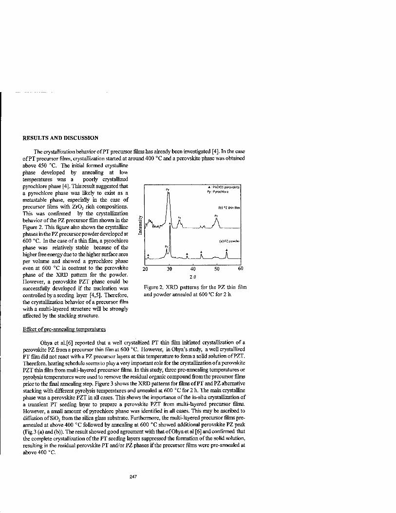
A : PbZr03 perovskite Py: Pyrochlore
(b) PZ thin film
RESULTS AND DISCUSSION
The crystallization behavior of PT precursor films has already been investigated [4]. In the case of PT precursor films, crystallization started at around 400 °C and a perovskite phase was obtained above 450 °C. The initial formed crystalline phase developed by annealing at low temperatures was a poorly crystallized pyrochlore phase [4]. This result suggested that a pyrochlore phase was likely to exist as a metastable phase, especially in the case of precursor films with Zr02 rich compositions. This was confirmed by the crystallization behavior of the PZ precursor film shown in the Figure 2. This figure also shows the crystalline phases in the PZ precursor powder developed at 600 °C. In the case of a thin film, a pyrochlore phase was relatively stable because of the higher free energy due to the higher surface area per volume and showed a pyrochlore phase even at 600 °C in contrast to the perovskite phase of the XRD pattern for the powder. However, a perovskite PZT phase could be successfully developed if the nucleation was controlled by a seeding layer [4,5]. Therefore, the crystallization behavior of a precursor film with a multi-layered structure will be strongly affected by the stacking structure.
(a) PZ powder
20 30 40
20
50 60
Figure 2. XRD patterns for the PZ thin film and powder annealed at 600 °C for 2 h.
Effect of pre-annealing temperatures
Ohya et al.[6] reported that a well crystallized PT thin film initiated crystallization of a perovskite PZ from a precursor thin film at 600 °C. However, in Ohya's study, a well crystallized PT film did not react with a PZ precursor layers at this temperature to form a solid solution of PZT. Therefore, heating schedule seems to play a very important role for the crystallization of a perovskite PZT thin film from multi-layered precursor films. In this study, three pre-annealing temperatures or pyrolysis temperatures were used to remove the residual organic compound from the precursor films prior to the final annealing step. Figure 3 shows the XRD patterns for films of PT and PZ alternative stacking with different pyrolysis temperatures and annealed at 600 °C for 2 h. The main crystalline phase was a perovskite PZT in all cases. This shows the importance of the in-situ crystallization of a transient PT seeding layer to prepare a perovskite PZT from multi-layered precursor films. However, a small amount of pyrochlore phase was identified in all cases. This may be ascribed to diffusion of Si02 from the silica glass substrate. Furthermore, the multi-layered precursor films pre- annealed at above 400 °C followed by annealing at 600 °C showed additional perovskite PZ peak (Fig.3 (a) and (b)). The result showed good agreement with that of Ohya et al [6] and confirmed that the complete crystallization of the PT seeding layers suppressed the formation of the solid solution, resulting in the residual perovskite PT and/or PZ phases if the precursor films were pre-annealed at above 400 °C.
247

Effect of substrate
In the previous section, the importance of the pre-annealing temperature was discussed. As a result, it was concluded that the multi- layered precursor film should be pre- annealed below 350 °C to suppress the crystallization of the PT seeding layer. Therefore, the pre-annealing was carried out at 350 °C for the rest of the experiments described in this paper. In this section, the effect of the substrate on the crystallization behavior of the multilayered precursor films was studied. Because PZT thin films are usually prepared on a silicon wafer with a platinum electrode for applications in memory or sensor devices, the effect of substrates on the crystallization of the multi-layered precursor films on this technologically important substrate be investigated.
Figure 4 shows the XRD patterns of the multi-layered precursor films annealed at 600 °C for 2 h on different substrates. Obvious differences are observed. A considerable quantity of a perovskite PZ phase was identified if the multi- layered precursor film was prepared on Si wafer with Pt electrode. This may be ascribed to the accelerated nucleation of a PT precursor layers by the platinum electrode to lower the crystallization of a perovskite PT phase. To avoid this, rapid thermal annealing (RTA) may prove to be effective. The other method is to change the order of the stacking layers. If the PZ precursor was used as a first layer on the Si wafer, this may be avoided. In the next section, the PZT films were prepared from multi- layered films of PT and PZT precursor layers to obtain perovskite PZT thin films.
Figure 3. XRD patterns for the multi-layered films with different pre-annealing temperatures
(221)A< ► pt ♦: Pb(Zr,Ti)03 perovskite ▲: PbZr03 perovskite Py: Pyrochlore Pt: platinum
l\ ? 1 (b) (PT-PZ)5 substrate: Pt/Ti/Si02/Si
• ►
A 1 (a)(PT-PZ)S substrate: Si02
A j A _^v
20 30 40 50 60
Figure 4. Effect of the substrates on the crystallization of multi-layered PZT films.
248

Dielectric properties of PZT thin films with different compositions
The results described above showed that the PZT precursors of composition less than x = 1 should be stacked together with the transient seeding layers in the multi-seeding process to obtain a perovskite type thin film. In this section, PZT thin films with different compositions were prepared on a silicon wafer from multi-layered precursors of PT and PZT with x less than 1 to control the composition of the resultant PZT film. Thickness of the each layer was also controlled to change the nominal composition of the multi-layered films. As a result, single phase perovskite thin films were successfully deposited at above 500 °C even on a silicon wafer (Fig. 5). The relative permittivities of the resultant films with thickness of about 500 nm were measured and shown in Figure 6. The relative permittivity of the resultant film increased with annealing temperature. Distinct effect of the heating rate on the dielectric property were not observed in this study. However, the nominal composition of the resultant thin film exhibited considerable affect, especially at the higher annealing temperature of 600 °C. The maximum of the relative permittivity was obtained at a composition at a morphotropic phase boundary (nominal composition of x = 0.53). This result indicated that the composition of the resultant film was controllable in the multi-seeding process.
A
♦ : Pb(Zr,Ti)03 perovskite
(c) substrate: Pt/Ti/SiOZ/S< annealing temperature: 60013
A (a) substrate : pyrex glass
annealing temperature: SOOt
20 30
Fig. 5 An example of the XRD patterns for the PZT films with a multi-seeding process deposited on a silicon wafer or a silica glass substrate. The thickness and the composition of the films after annealing are about 500 nm and X=0.53, respectively.
Nominal composition of multi-layered PZT films (X) after annealing
0.35 0.53 0.67
0.5 0.6 0.7 0.8 0.9 Composition of PZT precursor layers
(X)'in multi-layered films
Fig.6 Relative permittivity of the resultant PZT thin films with different compositions. ■: annealed at 600X3 with heating rate of 100X3/h, #: annealed at 600X3 with heating rateof600X3/h, A: annealed at 600 X3with heating rate of 3000X3/h, D: annealed at 500X3with heating rate of 100X3/h, O: annealed at 500 X3 with heating rate of 600X3/h, A: annealed at 500X3with heating rateof3000X3/h.
249

The dotted line in the Figure 6 shows the relative permittivity of a highly oriented PZT film with a composition of x = 0.31 and a thickness of about 700 nm, annealed at 500°C[5]. Therefore, the relative permittivity of the films annealed at 500 °C in this study (which will increase with increasing film thickness) is comparable to that of the highly oriented PZT films with a composition of about X = 0.3.
CONCLUSIONS
The effects of the stacking structure and pre-annealing temperature on the crystallization of the multi-layered precursor films of PT and PZ were examined in detail and the following was concluded:
(1) A lead titanate thin film crystallized at low temperature of 450 °C into the perovskite phase. On the other hand, a lead zirconate thin film did not crystallize into perovskite phase at low temperatures. Therefore, a lead titanate layer seemed to act as transient seeding layer at lower temperatures depending upon the heating schedule. (2) Pre-annealing temperature played an important role in the multi-seeding process to lower the processing temperature. Well-crystallized lead titanate seeding layer restricted the interdiffusion, leading to the residual perovskite phase of PT and PZ.
Consequently, perovskite PZT thin films could be deposited on a silicon wafer from alkoxide precursor thin films with multi-layered structure of PT and PZT by choosing the suitable pyrolysis conditions before annealing. The resultant PZT thin films by a multiseeding process showed following characteristics:
(1) The composition of the film could be controlled by changing the thickness and the compositions of the PZT precursor films. (2) The dielectric properties of the resultant film were also controlled by changing the nominal composition of the film.
Further investigation will be carried out to improve the electrical properties of the resultant films annealed at lower temperatures.
REFERENCES
1. J.F.Scott, L.Kammerdiner, M.Parris, S.Traynor, V.Ottenbacher, A.~hawabkeh and W. F. Oliver, J. Appl. Phys. 64, p.787 (1989).
2. S.G.Vamado and W.E.Smith, IEEE J. Quantum Electron 8, p.88 (1972).
3. R.N.Castellane and L.G.Feinstein, J. Appl. Physs. 50, p.4406(1979).
4. H.Suzuki, M.B.Othman, K.Murakami, S.Kaneko and T.Hayashi, Jpn. J. Appl. Phys. 35 , p.4896(1996).
5. H.Suzuki, K.Murakami, S.Kaneko and T.Hayashi, Jpn. J. Appl. Phys. 36, p.5803 (1997).
6. Y.Ohya, T.Ito and Y.Takahashi, Jpn. J. Appl. Phys. 33 , p.5272 (1994).
250

EFFECTS OF REACTION CONDITIONS ON DEPOSITION OF FERRITES FROM ALKALINE METAL HYDROXIDE GELS
KARL F. SCHOCH, JR. and THEODORE R. VASILOW Northrop Grumman Electronic Sensors and Systems Division, Science and Technology Center, 1350 Beulah Rd., Pittsburgh, PA 15235
ABSTRACT
Formation of ferrites from aqueous solution of metal salts is a well known process involving precipitation of metal hydroxides followed by oxidation of the resulting gel. The purpose of the present work was to determine the effects oxygen flow rate on the progress of the reaction and on the structure and properties of the resulting precipitate. The reaction was carried out at 70°C with pH of 10.5 and oxygen flow rate of 2,4, or 8 standard liters per hour. The progress of the reaction was monitored by following the oxidation-reduction potential of the solution, which changes dramatically after the Fe(II) is consumed. The reaction rate increased with increasing oxygen flow rate. The Mg content of the precipitate was lower than that of the reaction mixture, possibly because of the pH of the reaction mixture. X-ray diffraction and infrared spectroscopy confirmed formation of a ferrite under these conditions.
INTRODUCTION
Traditional synthesis of ferrites involves mixing and grinding metal oxide powders, sintering at high temperature, grinding, pressing, and sintering again to the final form. In the course of this process, it is difficult to control the composition, grain size, and porosity on a microscopic scale. In some applications, it is important to have consistent properties from part to part, which requires labor-intensive preparation and sorting of parts made using these processes.
Coprecipitation of ferrites from aqueous solution offers the possibility of producing a product having more uniform composition and microstructure than is available by the high temperature methods. This approach (Figure 1) typically involves dissolving the appropriate metal salts in water, deaerating, adding a ferrous salt, raising the pH to precipitate the metal hydroxides, and then oxidizing the Fe(II) to Fe(III). The product is a finely divided ferrite powder. This process is well documented in the literature for a wide variety of ferrites starting with various classes of metal salts, including halides, sulfates, and nitrates, and using air or oxygen as the oxidizing agent.[l] The pH at which complete precipitation occurs depends on the metals present and temperature. Typically air or oxygen are used as the oxidizing agent, although we have determined that other oxidizers are also effective.[2] The objective of the present work is to determine the effect of reaction conditions, particularly oxygen flow rate, on the reaction kinetics, composition, and magnetic properties of a manganese-doped magnesium ferrite.
251
Mat. Res. Soc. Symp. Proc. Vol. 495 c 1998 Materials Research Society

Dissolve Metal Salts and Deaerate
Add Fe(II) Salt Precipitate Metal Hydroxides
Figure 1. Precipitation of Ferrites in Aqueous Solution.
EXPERIMENT
Preparation
The reaction solutions were prepared by dissolving Fe(S04)«7H20 (47.88 g), Mg(S04>7H20 (32.16 g), and Mn(S04)«H20 (2.36 g) in 193 ml of deaerated, deionized water at room temperature under nitrogen in a PFA beaker. Sulfate salts were ACS reagent grade, used as supplied by Aldrich Chemical Co. After mixing, the solution was heated to 70°C with continued nitrogen flow. The reaction solution was monitored using electrodes for pH, and Pt and saturated calomel electrodes for oxidation-reduction potential (ORP). When the sulfates were dissolved, the pH was raised to 10.5 by addition of deaerated 25% aqueous tetramethylammonium hydroxide (TMAH). When the ORP reached a stable value, and the temperature had stabilized, the nitrogen bubbling was discontinued and oxygen was bubbled through the solution at a rate of 2, 4, or 8 standard liters per hour SLPH using a dispersion stone. Additional aliquots of TMAH or 2 M H2S04 were added to maintain the pH within 0.2 pH units of the desired value during the reaction. When the ORP reached a stable value (typically after 1-2 hours) the reaction was terminated. The product was collected by filtration and washed with 5% aqueous TMAH.
Characterization
The product was characterized by X-ray powder diffraction, IR spectroscopy, elemental analysis, and magnetic susceptibility. In order to determine the lattice parameter accurately, samples for X-ray powder diffraction were mixed with a Si standard. IR spectra were recorded on KBr pellets using a Perking-Elmer 883 spectrophotometer. The magnetic susceptibility was determined by the Faraday method. Elemental analysis was performed by ICP-AES.
RESULTS AND DISCUSSION
Precipitation
The choice of pH in this process was governed by the solubility of the metal hydroxides. Quantitative precipitation of the metal hydroxides is required in order to achieve the desired composition reproducibly. In this particular case, Mg(OH)2 is known to precipitate at pH above
252

10.5, Mn(OH)2 precipitates above 8.5 and Fe(OH)2 precipitates above 5.5.[3] Thus we chose to use a pH of 10.5 in this study.
The oxidation-reduction potential (ORP) of the solution has been to shown to signal completion of the oxidation of Fe(II) to Fe(III) in a mixed metal hydroxide gel.[4,5] These workers have shown that the sudden change in ORP at the end of the reaction coincides with the depletion of Fe(II) in the reaction mixture by oxidation to Fe(III). Typically the ORP starts at approximately -0.9 V vs. SCE and ends at approximately -0.1 V vs. SCE when the reaction is complete. The consumption of Fe(II) in these processes is essentially first order with respect to 02 pressure and Fe(II) concentration, and second order with respect to hydroxide concentration: [6]
-d[Fe(II)]/dt = k [Fe(II)] PQ2 [OH"]2 (1)
Others have shown that the anion plays a key role in the reaction kinetics, [7] with sulfate, the anion used in the present work, being slower than others such as perchlorate or nitrate. The previous studies were carried out in reaction mixtures having fewer cations and at pH of 8 or less.
The ORP curves obtained in this study are shown in Figure 2. Taking the endpoint of the reaction as the time at which the ORP stabilized, we have observed that time to completion of the reaction is apparently directly proportional to oxygen flow rate. Assuming that the consumption of Fe(II) is linear with time, as reported by others,[5,6,7] this observation implies that the average reaction rate is also proportional to oxygen flow rate. Using
4Fe2+ + 02 + 2H20-»4Fe3+ + 4 0H" (2)
as the reaction occurring in this process, we can calculate that 0.0430 mol 02 is required to complete conversion of Fe(II) to Fe (III). That volume of gas would have been delivered before the observed end point of the reaction, even at 2 SLPH. The solubility of oxygen in water at 70°C is 0.0037 L.[8] Unless the solubility is dramatically different in this reaction medium, there was an appreciable excess of oygen present under all the conditions used in this study.
Characterization
These compounds form in the spinel crystal structure having the general form AB204, with the A ions occupying tetrahedral sites and B ions occupying octahedral sites in the crystal lattice. Depending on the relative size of the A and B ions, in some cases ferrites may form inverse spinels in which the site occupancy is reversed. Typically the spin of the ions in the tetrahedral sites is opposite to that of ions in the octahedral sites. Thus the overall magnetic properties of the ferrite are determined by the relative population of the sites and the oxidation state of the metal ions on those sites. In the case of mixed magnesium-manganese ferrites, the Mn(III) typically prefers the tetrahedral site, and the Mg(II) prefers the octahedral site.[9] Thus the addition of Mn(III) to a magnesium ferrite composition displaces Fe(III) from the tetrahedral site to the octahedral site thereby increasing the net magnetic moment of the material.
Infrared spectroscopy has been used to determine the location of metal ions in the crystal lattice and composition of many classes of ferrites. Typically four absorptions are observed: strong v, (500 - 600 cm"1) and v2 (350-420 cm"1), attributed to the M-0 stretch from the metal ions on the tetrahedral sites, and on the octahedral sites, respectively;[10] and weaker v3 (300-
253
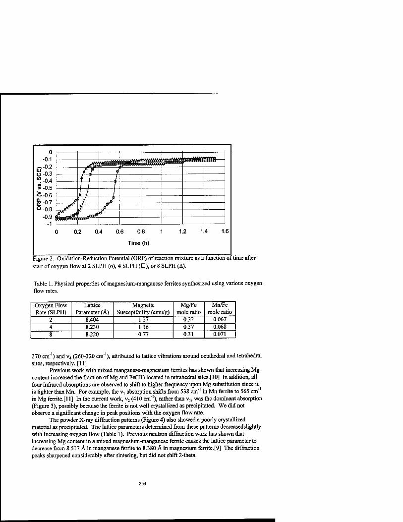
0 -0.1
—0.2 LLI O-0.3 »-0.4 §-0.5 £■-0.6 £-0.7 O-0.8
-0 9 J
i I. w
-1 ( ) 0.2 0.4 0.6 0.8 1 1.2 1.4 1.6
Time (h)
Figure 2. Oxidation-Reduction Potential (ORP) of reaction mixture as a function of time after start of oxygen flow at 2 SLPH (o), 4 SLPH (D), or 8 SLPH (A).
Table 1. Physical properties of magnesium-manganese ferrites synthesized using various oxygen flow rates.
Oxygen Flow Rate (SLPH)
Lattice Parameter (Ä)
Magnetic Susceptibility (emu/g)
Mg/Fe mole ratio
Mn/Fe mole ratio
2 8.404 1.27 0.32 0.067 4 8.230 1.16 0.37 0.068 8 8.220 0.77 0.31 0.071
370 cm'1) and v4 (260-320 cm"1), attributed to lattice vibrations around octahedral and tetrahedral sites, respectively. [11]
Previous work with mixed manganese-magnesium ferrites has shown that increasing Mg content increased the fraction of Mg and Fe(III) located in tetrahedral sites. [10] In addition, all four infrared absorptions are observed to shift to higher frequency upon Mg substitution since it is lighter than Mn. For example, the V! absorption shifts from 538 cm'1 in Mn ferrite to 565 cm" in Mg ferrite.[l 1] In the current work, v2 (410 cm"'), rather than v,, was the dominant absorption (Figure 3), possibly because the ferrite is not well crystallized as precipitated. We did not observe a significant change in peak positions with the oxygen flow rate.
The powder X-ray diffraction patterns (Figure 4) also showed a poorly crystallized material as precipitated. The lattice parameters determined from these patterns decreasedslightly with increasing oxygen flow (Table 1). Previous neutron diffraction work has shown that increasing Mg content in a mixed magnesium-manganese ferrite causes the lattice parameter to decrease from 8.517 A in manganese ferrite to 8.380 Ä in magnesium ferrite.[9] The diffraction peaks sharpened considerably after sintering, but did not shift 2-theta.
254

i E
S.
1000 900 800 700 600 500 400 300 200
Wavenumbers (cm-1)
Figure 3. Infrared spectra of ferrites as precipitated at oxygen flow rates of 4 SLPH and 8 SLPH.
«V C 3 c 0
i n
& ^^^TxJ^M <~*~**V/\A^
[V-mj( Jpj N^^n * l-J(^
k.
10 20 30 40 SO 60
2-Theta
70 80
Figure 4. X-ray diffraction patterns of ferrites as precipitated at oxygen flow rates of 2 SLPH (—), 4 SLPH ( ), and 8 SLPH (—). Each sample included a Si internal standard.
255

Magnetic susceptibility of these materials as precipitated were all relatively low, as shown in Table 1. To the extent that these values are changing, they suggest that the magnesium content was decreasing with increasing oxygen flow rate.
Elemental analysis showed that the magnesium content of the materials as precipitated (Table 1) deviated somewhat from the ratio in the starting materials, which are Mg/Fe = 0.76 and Mn/Fe = 0.08. The Mg content, in particular, was low, possibly because the pH was just at the point at which Mg(OH)2 is reported to precipitate, as mentioned above.
CONCLUSIONS
The oxygen flow rate was a key variable in the precipitation of ferrites from aqueous alkaline metal hydroxide gels. The reaction rate increased with increasing oxgyen flow rate over the range of 2 to 8 SLPH. As precipitated the material was a ferrite, but not highly crystalline, as shown by the X-ray diffraction patterns and infrared spectra. Elemental analysis of the material as precipitated showed that the composition deviated somewhat from the ratio of elements in the starting materials, which may be due the pH of the reaction mixture. There was not a consistent trend in variation in composition of the materials with oxygen flow rate.
ACKNOWLEDGEMENTS
Technical assistance of D. V. Stough, A. M. Stewart, V. A. Toth, and J. A. Kerestes during this work is gratefully acknowledged.
REFERENCES
1. G. Economos, J. Am. Ceram. Soc. 38, pp. 241-244 (1955). 2. K. F. Schoch, Jr., T. R. Vasilow, and D. V. Stough, U. S. Patent 5,662,879 (Sept. 2,1997). 3.1. M. Kolthoff, P. J. Elving, and E. B. Sandell, eds. Treatise on Analytical Chemistry, part 1,
vol. 1, The Interscience Encyclopedia, Inc., New York, 1959, p. 806. 4. K. Kaneko and T. Katsura, Bull. Chem. Soc. Japan 52, pp. 747-752 (1979). 5. Y. Tamaura, C. Kameshima, and T. Katsura, J. Electrochem. Soc. 128, pp. 1447-1451 (1981). 6. W. Stumm and G. F. Lee, Ind. Engg. Chem. 53, pp. 143-146 (1961). 7. H. Tamura, K. Goto, and M. Nagayma, J. Inorg. Nucl. Chem. 38, pp. 113-117 (1976). 8. D. R. Lide, ed., Handbook of Chemistry and Physics, 75th edition, CRC Press, Boca Raton,
FL, p. 6-4. 9. R. Nathans, S. J. Pickart, S. E. Harrison, and C. J. Friessman, Proc. IEE B 104, pp. 217-220
(1955). 10. R. D. Waldron, Phys. Rev. 99, pp.1727-1735 (1955). 11. P. V. Reddy and M. Salagram, Phys. Stat. Sol. A 100, pp. 639-643 (1987).
256

SYNTHESIS AND ELECTRO-OPTICAL PROPERTIES OF POTASSIUM TITANYL PHOSPHATE THIN FILMS BY SOL-GEL METHOD
Jianping Zhang, Burtrand I. Lee, Feiling Wang* and Melvin A. Leitheiser** Dept. of Ceramic & Materials Eng., Clemson University, Clemson, SC 29634 *NZ Applied Technologies, Woburn, MA 01801 **Ceramic Technology Center, 3M Co., St. Paul, MN 55144
ABSTRACT
Potassium titanyl phosphate, KTiOP04 (KTP), thin films were prepared by sol-gel process. The structural evolution of KTP thin films was investigated by means of DTA/TGA, XRD, and FT-IR. The electro-optical results show that KTP thin films have a refractive index of 1.8 and large quadratic electro-optical coefficient of R=2.50643*10"16 and have potential applications for electro-optical devices.
INTRODUCTION
Potassium titanyl phosphate (KTiOP04/KTP) single crystal is currently used for frequency doubling of Nd:YAG laser because of its high nonlinear-optical coefficient, high optical damage threshold, wide acceptance angles and thermally stable phase- matching properties [1]. Its large linear electro-optic coefficient and low dielectric constant also make it promising for some electro-optics applications such as modulators and Q switches [1]. However, these potential applications such as frequency modulators, Q-switches, and electro-optic waveguide modulators are limited by its several drawbacks such as high cost, inclusion of impurities and difficulty for patterning and shaping.
Sol-gel derived KTP thin films appear to be an alternative choice because the sol-gel processing can offer high purity and easy control of stoichiometry of the resulting thin films. The simplicity of the patterning and shaping of sol-gel thin film deposition also makes KTP thin films possible for integrated-optic fabrication.
Barbe et al. [2] reported the sol-gel process and microstructure of KTP thin films. Hirano et al. [3] also investigated the relationship between the preferred orientation of KTP grains on single crystal substrates and obtained a weak second harmonic generation signal from the KTP thin films on a glass substrate. However, no electro-optical properties were reported. The present work focuses on the synthesis and preparation of sol-gel derived KTP thin films, the evolution of the structure as well as the electro- optical properties.
EXPERIMENT
(1) Synthesis of KTP precursor solution
Potassium ethoxide and titanium isopropoxide were used as starting precursors for K and Ti. Phosphate precursor was synthesized by dissolving P205 in absolute ethanol. The KTP sol was prepared by mixing the equimolar proportion of the above three precursors
257
Mat. Res. Soc. Symp. Proc. Vol. 495 e 1998 Materials Research Society

and refluxing for 6 hours. A clear light brown solution was obtained for thin film deposition.
(2) KTP thin film deposition
A spin coater was used to prepare KTP thin film. Soda-lime glasses were used as substrates. The above KTP stock sol was diluted with ethanol and then was dropped onto the substrate fixed on the spin coater for spin coating. The spinning speed was 4000 rpm, spinning time of 30 second. The above procedure was repeated five times to achieve a thickness of -0.6 um. The final KTP thin films were dried at the room temperature before heat treatment was carried out. The entire flow chart of the sol-gel synthesis of KTP thin films is shown in Fig.l.
PA C,H5OH
Ti(OC3H7>4
KOC,H,
Stirring for 30 minutes
Refluxing for 6 hours
KTP precursor
Spin-coating at 4000 rpm for 30 seconds
KTP thin films
Heat treatment at 600-700 °C
Final KTP thin films
Fig. 1. Flow chart of the sol-gel synthesis of KTP thin film
(3) Heat treatment of KTP thin films
A gradient temperature heat treatment technique is employed to promote the crystalline-oriented growth. The as-deposited KTP thin films were placed on a hot plate at 300 °C for organic decomposition. Due to the existence of a gradient temperature along the vertical direction of the samples, small KTiOP04 crystallites will begin to nucleate and grow along the direction of gradient temperature from the initial amorphous state. However, the KTiOP04 crystallites are small and immature at this stage. Hence a high temperature crystallization stage was still needed to promote the existing nucleus and small crystallites to grow into fully crystallized KTiOP04 polycrystalline structure with grain-orientation along the direction perpendicular to the substrate plane. This stage could be achieved by firing the thin films at 650 °C for 1 hour.
258

(4) Characterization of KTP powders and thin films
The crystallization behavior of KTP powders was analyzed by differential thermal analysis (DTA), thermogravimetric analysis (TGA) and x-ray diffractometry (XRD). A FT-IR spectrum of a dried gel was obtained by Mattson Infinity FT-IRspectrophotometer with a diffuse reflectance technique. The dielectric constant and dissipation factor were measured by HP 4194A Impedance/Gain-Phase Analyzer. The refractive indices and electro-optic coefficients were determined by differential ellipsometry measurements.
RESULTS
(1) Structural evolution of KTP polycrystalline phase
1000
Temperature ( °C)
Fig. 2. Thermal analysis of the KTP gel dried at 100 °C.
Fig. 2 is the TGA and DTA curves of KTP dried gels. The TGA curve shows two decomposition steps during the pyrolysis . This means that there are two reaction for the weights losses. The first weight loss at 250-300 °C corresponds to the oxidation reaction of the solvents and alkyl groups from the KTP solution. The second weight loss at 600- 700 °C is an exothermic reaction which can be attributed to the removal of residual carbonaceous material or free carbon. This reaction also can be confirmed by the DTA curve which shows an exothermic peak at 600-700 °C.
XRD patterns of KTP powders and thin films fired at different temperature are shown in Figs.3 and 4. These powders were prepared by firing the dried KTP gel at 550, 600, 650 °C respectively in air. The XRD patterns show that the KTP powders fired at 550 °C is amorphous. It begins to crystallize at 600 °C. It is obvious that all the peaks are attributed to the single KTiOP04 phase. Fig. 4 is the XRD patterns of KTP thin films of thickness of 0.6 (im on a glass substrate fired at 550 and 650 °C respectively. They show that KTiOP04 phase exist in the KTP thin film fired at 650 °C. The weak intensity is due
259

to the small amount of material on the substrate. Nevertheless, it shows the structure transformation of the KTP thin film from amorphous state to polycrystalline state.
650'C
600" C
550 C
10 30 50 70 90
2-Theta (degree)
Fig. 3. XRD powder diffraction patterns of the KTP powders fired at 550,600,650 °C
2-Theta (degree)
Fig. 4. XRD diffraction patterns of KTP thin films fired at 550,650 °C for 1 hour
Fig. 5 is the FT-IR spectrum of dried KTP gel. The peak at -1050 Cm"1 may be attributed to P-O-Ti bond. The peak at 1237cm"1 which corresponds to P=0 absorption band of KTP precursor suggests that the KTP structure may already exist even when the sample was dried only at 100 °C. The-OH absorption peak at ~3400cm"' indicates that the KTP sample still has much alcohol and water after dried at 100°C. The absorption peaks at ~2987 cm"1 is due to -CH3 and C-H group.
4000 3000 2000 1000 Wavenumber (cm"1 )
Fig. 5. FT-IR spectrum of the KTP dried gel.
260

(2) Electro-optical properties of KTP thin films
A reflection differential ellisometer [4] was used to characterize the electro-optical properties of KTP thin film of a thickness of 0.46(im. The incident laser wavelength was 633nm. When the voltage of 380V was applied, the field strength on the film was 1.52 volts/micron and the relative phase shift in radian was 0.01382 and the field-induced birefringence was 0.00309. Some electro-optical properties are listed in Table I.
Table I Electro-optical Properties of KTP Thin Films Properties KTP thin film Films thickness (|am) 0.45 Dielectric constant (1 kHz) 5.81 Dissipation factor (1 kHz) 0.133 Refractive index 1.8 Electro-optical Coefficient (R*10 16) 2.5
Table I shows that KTP thin film has low dielectric constant,high refractive index and high quadratic electro-optical coefficient R.
Fig. 6 shows the field-induced birefringence vs electric-field strength loop of the KTP thin film. This curve indicates that KTP thin film is an electro-optical material and has potential applications for light modulation.
27.2 ■
£ 13.8 ■
.S
-1.92 -0.96
Electric field strength (volt/micron)
Fig. 6. Field-induced birefringence vs electric field strength loop of KTP thin film of 0.46nm on a glass substrate.
CONCLUSIONS
KTP thin films were successfully prepared by sol-gel process from P2Os, potassium ethoxide and titanium isopropoxide. Polycrystalline structural evolution at 650 °C has
261

been confirmed by DTA/TGA and XRD. The electro-optical measurements show that KTP thin films have large quadratic electro-optic coefficient R, low dielectric constant and have potential applications for electro-optical devices. Further research is being carried out to improve the process including poling the KTP thin films to overcome the current problems.
ACKNOWLEDGEMENT
We would like to thank 3M Company to support this work.
REFERENCES
1. J. D. Bierlein and H. Vanherzeele, J. Opt.Soc. Am. 6, 622 (1989). 2. C. J. Barbe, M. A. Harmer, G. W. Scherer, J. Am. Ceram. Soc, 78 (8) 2033-44 (1995) 3. S. I. Hirano, T. Yogo, K.I. Kikuta, K.I. Noda, M.Ichida. and A.Nakamura; J. Am.
Ceram. Soc, 78 (11) 2956-60 (1995) 4. F. L. Wang, E. Furman, and G. H. Haertling, J. Appl. Phys. 78(1), 9-15 (1995)
262
SOL-GEL SYNTHESIS OF RARE EARTH ALUMINATE FILMS AS BUFFER LAYERS FOR HIGH Tc SUPERCONDUCTING FILMS
DAVID B. BEACH,* CATHERINE E. VALLET,* MARIAPPAN PARANTHAMAN,* ELIOT D. SPECHT,** JONATHAN S. MORRELL,*** AND ZILING B. XUE*** * Chemical and Analytical Sciences Division, Oak Ridge National Laboratory, Oak Ridge, TN 37831-6197, [email protected] **Metals and Ceramics Division, Oak Ridge National Laboaratory »♦♦Department of Chemistry, University of Tennessee, Knoxville, TN
ABSTRACT
Cubic rare-earth aluminate perovskites of the general form REA103 have been identified as possible buffer layers for high current carrying cuprate superconductors deposited on roll-textured metals. This paper describes on-going research to develop solution routes which would avoid the use of slow and costly vacuum processing. Our research plan includes the development of an appropriate solution chemistry, studies of the crystallization behavior of powders under reducing and oxidizing conditions, deposition of polycrystalline films on silver substrates, deposition of epitaxial films on single-crystal oxide substrates, and deposition on roll textured nickel. The method is illustrated with the example of PrA103.
INTRODUCTION
In the past two year, significant progress has been made in the synthesis and processing of practical coated conductors using YBajCufi,, (YBCO) as the current conducting layer. The use of YBCO is particularly important because of the high performance of YBCO in strong magnetic fields at 77K relative to bismuth and thallium containing superconducting materials, even though these materials have substantially higher superconducting transitions.1 The use of YBCO coated conductors offers at least an order of magnitude increase in current carrying ability of superconducting wires relative to the best available current technology (bismuth-strontium-calcium-copper oxide (BSSCO) in silver powder-in-tube conductors) and may enable the construction of high-field magnets operating at 77 K.
To use YBCO as a high current carrying layer, it is necessary to achieve both out-of-plane (c-axis) orientation and a fair degree of in-plane (a and b-axis) orientation.2 In superconducting devices, this alignment is achieved by deposition on single-crystal substrates. In practical, long- length conductors it will be necessary to prepare substrates which are chemically inert, textured, and lattice matched to YBCO, as well as flexible and mechanically robust. The mechanical requirements are best met by a metal substrate, but metal substrates will require a ceramic buffer layer to achieve the other requirements. To produce a textured buffer layer, two main approaches have been developed; texturing of the buffer layer with ion beams (IB AD)3 and deposition of an epitaxial buffer layer on a roll-textured metal substrate (called RABiTS for Rolling Assisted Biaxially Textures Substrates).4
Our research has been concerned with the development of solution techniques for the deposition of epitaxial buffer layers on roll-textured metals.
Solution techniques hold the promise of low-cost, high-speed deposition of buffer layers using a continuous process. Figure 1 depicts a possible process using simple, non-vacuum equipment:
263
Mat. Res. Soc. Symp. Proc. Vol. 495 e 1998 Materials Research Society

0 Q
~Q Annealing oven, (Quartz lamp heated, entrance and exit with multiple gas purge
Q. 4
Metal tape
Figure 1. Continuous process for coating roll- textured tapes with a textured rare-earth aluminate layer.
Previous work on buffer layers for RABiTS has used pulsed laser ablation4 and e-beam evaporation5
to prepare epitaxial buffer layers. The most successful structure to date used cerium oxide and yttrium stabilized zirconia on roll-textured nickel. To prevent oxidation of nickel (which would lead to the loss of epitaxy), the oxide layers were deposited under reducing conditions. In developing a solution process for buffer layer deposition, it was necessary to consider only ceramic materials which do not reduce under hydrogen at temperatures as high as 1200 °C. This consideration lead us to investigate rare-earth aluminates as candidates for solution deposited layers. Single-crystal substrates of the rare earth aluminates have been shown to be excellent substrates for YBCO. These materials are extremely difficult to deposit by sputtering or even pulsed-laser ablations because of preferential sputtering or ablation. A successful solution route to these highly versatile perovskite materials would have a number of possible uses. We have previously reported on our initial work with lanthanum aluminate and the epitaxial growth of lanthanum aluminate on strontium titanate.6
This paper describes our experimental method and illustrates the method using PrA103 as an example.
EXPERIMENTAL
Solution preparation
All manipulations were carried out under argon using standard Schlenk techniques. Solid transfers were done using an inert atmosphere dry-box. Aluminum isopropoxide, 2-methoxyethanol, and praseodymiur* were used as received. Isopropanol was dried over aluminum isopropoxide. Praseodymium isopropoxide was prepared by the direct reaction of isopropanol and the element in the presence of a mercuric chloride/mercuric acetate catalyst. A 25 ml of a 0.25 M solution of praseodymium methoxyethoxide in 2-methoxyethanol was prepared by reacting the isopropoxide with excess 2-methoxyethanol and distilling off the isopropanol formed in the reaction. In a similar manner, 25 ml of a 0.25 M aluminum methoxyethoxide in 2-methoxyethanol was prepared by the reaction of aluminum isopropoxide with 2-methoxyethanol. The two solution were mixed, refluxed, and the concentration was adjusted to form a 0.25 M stock solution. To form powders, the stock
264

solution was mixed 1 part stock solution to 2 parts IM H20 in 2-methoxyethanol (excess water), allowed to gel over a period of 15 to 20 minutes, dried at 150 °C, crushed and fired under various conditions of time, temperature and atmosphere. To form films, the stock solution was hydrolyzed with 1 part of IM H20 in 2-methoxyethanol to 3 parts of stock solution (less than stoichiometric amount of water). Films were spin-coated by flooding the substrate with solution and then spinning for 30 sec at 2000 rpm. Annealing conditions are discussed in the next section.
X-ray diffraction (XRD) data was obtained using Phillips equipment for scans and a Picker 4-circle diffractometer for texture measurements. Out-of-plane orientation was determined from 6-20 scans, and the mosaic character of the out-of-plane texture was determined by the full-width at half- maximum (fwhm) of u-scans. In-plane texture was determined by pole figures and the mosaic character of the in-plane texture was determined from the fwhm of (J> scans.
RESULTS AND DISCUSSION
Powder Studies- In evaluating new precursors, we first study the annealing behavior of powders under both oxidizing and reducing conditions. Figure 2 shows XRD data at several temperatures of powders annealed for four hours in air. Figure 3 shows XRD data at several temperatures of powders annealed for four hours in 4% hydrogen in argon.
1850°C
JLLLLJUJU.
750 °C
10 20 30 40 50 60 70 80 90
2-Theta
I 1 1050 °C
". A A t ' A A A A,
(A *^ 'c
1 I 950 °C
n <
in 850 °C
c 750 °C
650 °C
10 20 30 40 50 60 70 80 90
2-Theta
Figure 2. PrAl03 powders annealed in air Figure 3. PrA103 powders annealed in 4%H2/Ar.
265

The data shows that the onset of crystallization occurs at about 100 °C higher under reducing conditions. (The patterns have been indexed as a cubic structure because we were unable to discern any rhombohedral splitting, even though the samples appear to be well crystallized.)
Poly crystalline Films on Silver- In order to determine the coating characteristics of our solutions, we deposit films on silver sheets using spin-coating. Solution concentrations of- 0.15 M give films which are continuous, crack-free, and uniform. Each layer was annealed at 850 °C for 20 minutes in air. Thicker films were built up by deposition of successive layers. A single layer was found to have an annealed thickness of 600 to 700 Ä by etching a step in the films and measuring the step height with a profilometer. Figure 4 shows XRD data for a polycrystalline PrAlO, film on silver. The pattern of intensities is similar to the powder data and no secondary phases are observed.
It)
[200
] o CM CM CO
E | O) < £ < .a <
JUL § o S.
JLJLU Uw^ 10 20 30 40 50 60 70 80 90
2-Theta
Figure 4. Polycrystalline film of PrA103 on silver sheet.
Epitaxial Films on Strontium Titanate- In order to study epitaxial growth, we have grown epitaxial films of PrA103 on single crystal strontium titanate substrates with a [100] orientation. Again, each layer was annealed at 850 °C for 20 minutes in air. Figure 5 shows a 6-20 scan of a 2000 Ä PrA103
film on SrTi03. Only the [hOO] reflections of the film and the substrate are observed, demonstrating a high degree of out-of-plane alignment. A rocking curve (w scan) about the [300] reflection had a full-width-at half-maximum (fwhm) of 0.9°, indicative of a high degree of crystallinity. In order to determine in-plane alignment, a pole figure (Figure 6) about the [202] plane (% = 45°) was obtained. The four-fold symmetry of the substrate is clearly observed, demonstrating a high degree of in-plane texture. In addition, a (j>-scan of this reflection showed a fwhm of 1.0°, again indicative of a highly crystalline layer. These results demonstrate that praseodymium aluminate grows on strontium titanate with a single cube-on-cube epitaxy.
266

CO
>r» "c/5 CD
"1 o o o o 1 S o o o o 1 a o
^L cd I w CO
o" o" o o o V- < 1- < t w Q. w Q. OT o o
to m
O i
, . .
a.
■A , ,
10 20 30 40 50 60 70 80 90 2-Theta
Figure 5. 6-26 XRD of an epitaxial film of PrAl03 on [100] SrTiQ3.
■tiuo litun I IB« I «oxo liaco IIJOJOO ltiuo |iauo
mat n.« »oo neo saoo «M 30.00 20.00
lOOt 0X0
Figure 6. Pole figure about the [220] reflection of PrA103 on [100] SrTi03.
Epitaxial Films on Roll-Textured Nickel- Films on roll textured nickel were annealed at 1150 °C for 1 hour in flowing 4%hydrogen in argon. A typical 6-26 scan is shown in Figure 7. Only the [hOO] peaks of the film are prominent, although a small [110] peak can be observed. A rocking curve (w scan) about the [200] reflection had a fwhm of 7.2°. Although this is significantly greater than the than the film deposited on single crystal strontium titanate, this value of fwhm is similar to the fwhm of the rocking curve of the nickel substrate about the [200] reflection. To determine the degree of
267

<0
"c
.□ i_ <
o o s
—iv, »A—
20 30 60 40 50 2-Theta
Figure 7. 6-26 XRD of PrA103 deposited on roll-textured nickel.
70
of the rocking curve of the nickel substrate about the [200] reflection. To determine the degree of in-plane alignment, a pole figure about the [110] plane was obtained (Figure 8). The eight-fold symmetry of the pattern indicates that there are two in-plane epitaxies. The major epitaxy is
2.60
2.40
2.20
2.00
1.80
1.60
1.40
1.20
1.00
0.80
0.60
0.40
0.20
0.00
Figure 8. Pole figure about the [110] reflection of PrA103 on roll-textured nickel.
268

PrAlO,[100] II Ni[100] and the minor epitaxy is PrAlO3[110]| |Ni[100]. The [110] epitaxy is rotated 45° from the [100] cube-on-cube epitaxy. A 90° portion of the (|>-scan (Figure 9) shows that the peak corresponding to the [110] epitaxy is about half the intensity of the peak corresponding to the [100] epitaxy. The fwhm of the phi scan of the peak corresponding to [100] epitaxy is 12°. Work is continuing on obtaining a single in-plane epitaxy.
20 30 40 50 60 70 80 90 100110
Phi
Figure 9. Phi scan of PrA103 on Ni showing two in-plane epitaxies
CONCLUSIONS
Sol-gel solution techniques have been used to prepare praseodymium aluminate powders, polycrystalline films and epitaxial films on both ceramic and metal substrates. This technique clearly has both great utility and versatility.
ACKNOWLEDGMENT
This work was sponsored by U.S. Department of Energy, Office of Basic Energy Science, Division of Materials Sciences, under contract DE-AC05-96OR22464 with the Oak Ridge National Laboratory, managed by the Lockheed Martin Energy Research Corp.
REFERENCES
1. H.R. Kirchner, D. P. Norton, A. Goyal, J. D. Budai, D. K. Christen, D. M. Kroeger, E. D. Specht, Q. He, M. Paranthaman, D. F. Lee, B. C. Sales, F.A. List, and R. Feenstra, Appl. Phys. Lett., 71, 2029 (1997).
2. D. Dimos, P. Chaudhari, and J. Mannhart, Phys. Rev. B, 41,4038 (1990).
269

X.D. Wu, S.R. Foltyn, P.N. Arendt, W.R. Blumenthal, I.H. Campbell, J.D. Cotton, J.Y. Coulter, W.L. Hults, M.P. Malley, H.F. Safar, and J.L. Smith, Appl. Phys. Lett., 67, 2397 (1995).
D.P. Norton, A. Goyal, J.D. Budai, D.K. Christen, D.M. Kroeger, E.D. Specht, Q. He, B. Saffian, M. Paranthaman, C.E. Klabunde, D.F. Lee, B. C. Sales, and F.A. List, Science 274, 755 (1996).
M. Paranthaman, A. Goyal, F.A. List, E.D. Specht, D.F. Lee, P.M. Martin, Q. He, D.K. Christen D. P. Norton, J.D. Budai, and D.M. Kroeger, Physica C, 275, 266 (1997).
S.S. Shoup, M. Paranthaman, D.B. Beach, E.D. Specht, R.K. Williams, J. Mater. Res. 12, 1017
270

SOL-GEL SYNTHESIS OF EPITAXIAL FILMS OF (Sr.BaJBijCNb.Ta^O, AND Bi4Ti3012
ON [100] SrTi03
JONATHAN S. MORRELL,* ZILING B. XUE,* ELIOT D. SPECHT,** and DAVID B. BEACH*** ♦Department of Chemistry, University of Tennessee, Knoxville, TN **Metals and Ceramics Division, Oak Ridge National Laboratory, Oak Ridge, TN ***Chemical and Analytical Sciences Division, Oak Ridge National Laboratory, Oak Ridge, TN 37831-6197, [email protected]
ABSTRACT
An all-alkoxide sol-gel process utilizing methoxyethoxide complexes in 2-methoxyethanol was used to prepare epitaxial films of SrBi2Nb209, SrBi2Taj09, BaBi2Nb209, BaBijTajO,, and Bi4Ti3012 on [100] oriented SrTi03 single crystals. Films were prepared by spin coating strontium titanate substrates with partially hydrolyzed alkoxide solutions and firing in air at 850 °C for 20 minutes. Out-of-plane orientation was confirmed by 6-26 scans which showed only [0021] reflections. In- plane orientation was determined by pole figures and phi-scans about the [105] plane in the case of the (Sr,Ba)Bi2(Nb,Ta)209 complexes and the [117] plane in the case of Bi,Ti3012. Lattice constants and full-width at half-maximum (fwhm) values for both in-plane and out-of-plane reflections are reported.
INTRODUCTION
Layered perovskites containing bismuth (Aurivillius compounds or Aurivillius phases, after B. Aurivillius1 who first prepared these compounds in 1949) have attracted considerable attention from researchers engaged in work on non-volatile semiconductor memory because these materials have been shown to undergo more than 1012 polarization reversals using platinum electrodes without degradation.2 These fatigue-free materials hold the promise of replacing main-memory in a variety of electronic applications. The growth of highly-oriented or epitaxial films is of special interest because of the highly anisotropic nature of the dielectric response of the materials.3 For example, these materials are predicted to show ferroelectric behavior only in the a-b plane. Indeed, Desu and co-workers4 have shown that c-axis oriented films show drastically reduced remnant polarization and coercive field compared to randomly oriented polycrystalline films.
Deposition techniques used to prepare films of these materials include physical deposition methods such as sputtering5 and pulsed laser ablation,6'7 and chemical methods such as chemical vapor deposition.8,9 All of these methods require vacuum processing, expensive equipment and skilled operators, and each technique has specific advantages and disadvantages. Another deposition technique which has recently become viable is the use of solution chemistry to produce precursor films which can then be annealed to produce films.10 The advantages of using solution techniques are low capital cost of deposition equipment, great flexibility in coating technique (spin coating, dip coating or spraying), precise composition control and low temperature crystallization. This technique has been used primarily for electronic and optoelectronic materials such as lithium niobate and lead zirconium titanate.10 In the case of the Aurivillius compounds, most solution preparations have made use of metal containing soaps in an organic solvent. This technique is known as Metal- Organic Decomposition or MOD1'and can produce films of excellent quality, but suffers from the drawbacks that the soaps have a high content of organic material which may lead to shrinkage and
271
Mat. Res. Soc. Symp. Proc. Vol. 495 ® 1998 Materials Research Society

cracking, and that intimate mixing, a requirement for low temperature processing, may not occur. In an effort to improve film quality and lower processing temperatures, sol-gel routes to these materials have been developed.12
In a previous publication,13 we reported on the chemistry of all-alkoxide solutions for the preparation of powders and polycrystalline films of SrBi2Nb20, (SBN), SrBijTaA (SBT), BaBi.NbA (BBN), BaBiJaA (BBT), and Bi,Ti3012 (BT). In this paper, we report the synthesis of epitaxial films of these materials on single-crystal strontium titanate. Physical techniques have recently been used to produce SBT4 and BT14 films on SrTi03, but, to our knowledge, this is the first report of solution synthesis of epitaxial films of the Aurivillius compounds.
EXPERIMENTAL
All manipulations were carried out under argon using standard Schlenk techniques. Solid transfers were done using an inert atmosphere dry-box. Solvents were dried by standard methods. Strontium metal, barium metal, bismuth bromide, tantalum ethoxide, niobium ethoxide and titanium isopropoxide were used as received. Strontium titanate [100] substrates were cleaned using organic solvents and prepared for coating by heating at 1000 °C for 1 hour in oxygen.15
Bismuth titanate solution - (Details of the preparation of this solution have appeared elsewhere.16) Briefly, bismuth t-butoxide (prepared from the reaction of bismuth tribromide with soidum t- butoxide and purified by sublimation) was reacted with excess 2-methoxyethanol to prepare a
. bismuth methoxyethoxide solution in 2-methoxyethanol. Similarly, titanium isopropoxide was reacted with 2-methoxyethanol to prepare a titanium methoxyethoxide solution in 2-methoxyethanol. The two solutions were mixed and refluxed and the concentration was adjusted to 0.25 M to prepare a stock solution. A coating solution was prepared by mixing 1 part 1 M H20 in 2-methoxyethanol 2 parts of the stock solution.
(Strontium, barium) bismuth (niobate, tantalate) solution - (Details of the preparation of these solutions has appeared elsewhere.13) Strontium and barium methoxyethoxide solutions in 2- methoxyethanol were prepared by the direct reaction of the elements with 2-methoxyethanol. Niobium and tantalum methoxyethoxide solutions were prepared by the reaction of the ethoxides of these elements with 2-methoxyethanol. The bismuth solution was prepared as described above. Stock solutions were prepared by mixing the appropriate metal containing solutions, refluxing and adjusting the concentration to 0.25 M. A coating solution was prepared by mixing 1 part 1 M H20 in 2-methoxyethanol 2 parts of the stock solution
Film coating-Films 0.2 /^m thick were prepared by spin-coating strontium titanate substrates with 3 layers of the coating solution. The films were fired layer-by-layer at 850°C for 20 minutes in air.
X-ray structure characterization-Füms were characterized by x-ray diffraction to determine both in- plane and out-of-plane orientation. Out-of-plane orientation was determined from 6-26 scans and the full-width-at-half maximum (fwhm) of the [008] (in the case SBN, SBT, BBN, and BBT) and the [006] (in the case of BT) reflections were determined by Q scans. In-plane orientation was determined from pole figures and the fwhm of the [105] (in the case SBN, SBT, BBN, and BBT) and the [107] (in the case of BT) reflections were determined by ((> scans. The lattice parameters for SBN, SBT, BBN, and BBT were determined by first measuring the c-axis lattice constant from 6-26 scans. The [00Q reflections of the film were calibrated against the SrTi03 [M)0] substrate peaks and
272

corrected values of d were plotted against (l/l). The slope of this line is the c-axis lattice constant. The a-axis lattice constant was measured by measuring the [105] reflection of the films and calibrating these reflections against the [110] reflection of the substrate. The corrected d value and the c-axis lattice constant were used in the following formula17 to determine a:
a= /72+/C2
1 I2
RESULTS AND DISCUSSION
The films were characterized primarily by X-ray diffraction. The 0-20 X-ray diffraction (XRD) patterns of SBT, SBN, BBN, and BBT epitaxial films on SrTi03 are shown in Figure 1. All of the films show only [001] peaks, indicating a high degree of out-of-plane alignment. The 0-20 XRD of BT also shows only [001] peaks (Figure 2). C-axis lattice constants determined from these spectra are reported in Table I, as well a full-width-at-half maximum (fwhm) values for omega scans of out- of-plane reflections.
Table I. Lattice constants and fwhm from X-rav data.
Film a(A) c(A) out-of-plane fwhmO
in-plane fwhm(°)
SBN 3.82(1)* 25.0(1) 0.49(5) 0.52(5)
SBT 3.85(1) 25.0(1) 0.46(5) 0.47(5)
BBN 3.92(1) 25.6(1) 0.90(5) 0.86(5)
BBT 3.96(1) 25.5(1) 0.86(5) 0.78(5)
BT - - 1.15(5) 1.15(5)
♦Uncertainty in the last digit indicated parenthetically.
In-plane texture was determined by obtaining pole figures and phi scans about in-plane reflections. A representative pole figure (Figure 3, bismuth titanate on strontium titanate about the [117] plane) shows the expected four-fold symmetry and the extremely sharp texture characteristic of all of these films. Phi scans (Figure 4, strontium bismuth niobate on strontium titantate, [105] plane) also show the four-fold symmetry and the width of these phi scan peaks gives a measure of the mosaic character of the film. The fwhms of the phi scans are reported in Table I.
CONCLUSIONS
Solution growth of good quality epitaxial films of Aurivillius compounds on single crystal strontium titanate has been demonstrated. The results demonstrate the relative ease and versatility of this
273

CO
'c Z) .Q
1—
<
c
(d)
_A^_A_W\ U VJL
(c)
il
(b)
LL üV CO o o
o o
LLJ h L L_Li u
VJL
o o
i_
K
o o
o o
_a io_
10 20 30 40 50 60 70 80
2-Theta
90
Figure 1. XRD of epitaxial films of (a) SBN, (b) SBT, (c) BBN, and (d) BBT films on strontium titanate. Peaks at 22.8, 46.5 and 72.5 degrees are due to the [hOO] reflections of the substrate.
274

\LJ LJ jJU ILLJUL I i 10 20 30 40 SO 60 70 80 90
2-Tneta
Figure 2. XRD of an epitaxial film of BT on strontium titanate. Peaks at 22.8, 46.5 and 72.5 are due to the [hOO] reflections of the substrate.
J
Figure 3. Pole figure about the [117] plane of BT on strontium titanate.
Figure 4. Phi scan about the [105] plane of SBN on strontium titanate.
technique.
ACKNOWLEDGMENT
This work was supported by the U.S. Department of Energy, Division of Materials Sciences, Office of Basic Energy Sciences, under contract DE-AC05-96OR22464 with Oak Ridge National
275

Laboratory, managed by Lockheed Martin Energy Research Corp.
REFERENCES
1. B. Aurivillius, Arkiv. for Kemi., 1, 463 (1949).
2. C. A. Aruajo, J. D. Cuchiaro, L. D. McMillan, M. C. Scott, and J. F. Scott, Nature, 374, 627 (1995).
3. F. Jona and G. Shirane, Ferroelectric Crystals, Dover, New York, 1960.
4. S. B. Desu, D. P. Vijay, X. Zhang, and B. He, Appl. Phys. Lett., 69,1719 (1996).
5. T. K. Song, J. K. Lee, and H. J. Jung, Appl. Phys. Lett., 69, 3839 (1996).
6. Y. Oishi, W. Wu, K. Fumato, M Okuyama, and Y. Hamakawa, Jpn. J. of Appl. Phys. Part I, 35,1242(1996).
7. H. Tabata, H. Tanaka, and T. Kawai, Jpn. J. of Appl. Phys. Part I, 34, 5146 (1995).
8. J. Zhu, S. B. Desu, T. Li, S. Ramanthan, and M. Nagata, J. Mater. Res., 12, 783 (1997).
9. N. J. Seong, S. G. Yoon, S. S. Lee Appl. Phys. Lett., 71, 81 (1997).
10. F. F. Lange, Science, 273, 903 (1996).
U.K. Amanuma, T. Hase, and Y. Miyasaka, Appl. Phys. Lett., 66, 221 (1995).
12. T. J. Boyle, C. D. Bucheut, M. A. Rodriguez, H. N. Al-Shareet, B. A. Hernandez, B. Scott, and J. W. Ziller, J. Mater. Res., 11, 2274 (1996).
13. J. S. Morrell, Z. Xue, E. D. Specht, and D. B. Beach, Chem. of Materials, in press.
14. S. Choopun, T. Matusmoto, and T. Kawai, Appl. Phys. Lett., 67, 1072 (1995).
15. I. Kawaya, M. Kanai, and T. Kawai, Jpn. J. Appl. Phys. Part II, 35, 929 (1996).
16. D. B. Beach, C. E. Vallet and M. Paranthaman, Mat. Res. Soc. Symp. Proc, 446, 309 (1997).
17. A. J. C. Wilson, Elements of X-ray Crystallography, Addison-Wesley, Menlo-Park, 1970.
276

Part IV
Characterization and Application of Ceramic Materials

NANOPOROUS SILICA FOR LOW K DIELECTRICS
Teresa Ramos, Steve Wallace, and Douglas M. Smith Nanoglass LLC, 1349 Moffet Park Dr., Sunnyvale, CA 94089, USA
ABSTRACT
As integrated circuit sizes decrease below 0.25 microns, device performance will no longer improve at the same rate as for past generations because of RC interconnect delay which becomes significant as compared to the intrinsic gate delay. The parallel approaches to partially address this fundamental problem are to use a lower resistance metal (i.e., copper instead of aluminum) and to use a dielectric material with a dielectric constant significantly below that of dense silica (~4). Recently, considerable progress has been made in development of thin films of nanoporous silica (also known as aerogels or low density xerogels) for these ILD and IMD applications. Advantages of these materials include high thermal stability, small pore size, and similarity to conventional spin-on deposition processes, spin-on glass precursors and final material (silica). The dielectric constant of nanoporous silica can be tailored between ~1 and 3 which allows its' implementation at multiple technology nodes in integrated circuit manufacture starting with the 0.18 micron node.
Research and development efforts at Nanoglass over the last several years have focused on; 1) simpler and more reproducible deposition processes, 2) a more complete understanding of processing-property relationships for this material, 3) scale-up of manufacturing to yield a range of precursor products with stability for at least six months and very high purity, and 4) working with customers to integrate this material into both aluminum/gapfill and copper/damascene process flows. Nanoglass has now developed a new process which considerably reduces the number of process steps and allows independent control of both film thickness and porosity. The current status of process and precursor development and device integration efforts for nanoporous silica is discussed.
INTRODUCTION
As feature sizes in integrated circuits approach 0.18 urn and below, problems with interconnect RC delay, power consumption and cross talk all become more urgent1'2. These problems are compounded by an accelerating trend that indicates that the time between each technology node is now decreasing from the historic 3 year per technology node predicted by Moore's law. One approach is to use increasing numbers of metallization layers but this solution has significant costs and is reaching limitations in performance gain as the number of layers exceeds 5-7. Switching to copper as a replacement for aluminum yields lower resistance and thus partially solves the problem but a lower dielectric constant insulator is also required. Integration of low dielectric constant (K) materials will helps but each of the material candidates with K significantly lower than currently employed dense silica (K~4) suffer from disadvantages. Current low K materials development emphasizes spin-on-glasses (SOG's) and fluorinated plasma CVD Si02 with K of >3. A number of polymers (organic/inorganic) are under development with K in the range of 2.2 to 3.5 however these may suffer from a number of potential problems including low thermal stability, poor mechanical properties including low Tg and poor adhesion, sample outgassing, and long term reliability questions. The major problem with those solutions is that they are only useful for one technology node. Therefore, after making large investments in integrating a new material into a process flow and determining performance and device reliability metrics, the IC manufacturer only has several years in which
279
Mat. Res. Soc. Symp. Proc. Vol. 495 ° 1998 Materials Research Society

he can use that material. Another approach is to employ nanoporous silica which can have dielectric constants in the range of 1 to 33 and is therefore scaleable over multiple technology generations. There have now been a significant number of reports of the use nanoporous silica films for use in interlevel and intermetal dielectric applications4,5,6,7.
Nanoporous silica is attractive for semiconductor manufacturers because it employs similar precursors (i.e. TEOS) as used for SOG's and CVD Si02, is the same material as conventional dielectrics (silica) which means that well-established processes such as etch may be used with minor changes, and because of the ability to carefully control pore size and size distribution. Nanoporous silica has been historically classified as an aerogel (dried supercritically) or a xerogel (dried by solvent evaporation). However, we use the term nanoporous silica since it captures the material's key properties which may be independent of how the films are processed. It is important to note that unlike very low density aerogels reported in the popular literature which have very low density and strength, nanoporous silica is of higher density and has the appearance of a dense glass. In addition to low dielectric constant, nanoporous silica offers other advantages for microelectronics including: 1) thermal stability up to 800 °C, 2) small pore size («microelectronics features), 3) a material, silica, and precursors (i.e. TEOS) that are widely used in the semiconductor industry, 4) deposition using similar tools as employed for conventional SOG processing, 5) the ability to "tune" dielectric constant over a wide range, and 6) the ability to migrate the same dielectric material and integration scheme for multiple semiconductor technology nodes by tuning the dielectric constant to lower values. From a practical viewpoint, since related precursors (SOG) are already employed in the microelectronics industry, issues related to precursor purity, production scale-up, technical support, deposition tool development and product cost can be easily addressed.
Although porosity leads to a lower dielectric constant than the corresponding dense material, additional materials and processing issues may be introduced as compared to a dense material. Materials issues include the necessity of having all pores significantly smaller than circuit feature sizes, the strength decrease associated with porosity, and the role of surface chemistry on dielectric constant, environmental stability and thermal conductivity. Density (or the inverse, porosity) and surface chemistry are the key nanoporous silica parameters controlling properties of importance for dielectrics7.
Electrical properties of interest include; 1) dielectric constant, 2) dielectric loss, and 3) breakdown voltage. The dielectric constant may be varied over a continuous spectrum from the extremes of an air gap at a porosity of 100% to dense silica with a porosity of 0%. The role of density/porosity on dielectric constant is shown in Figure 1. Hrubesh and co-workers3 measured K at 1-40 GHz for bulk aerogels of different densities which had been prepared using supercritical drying and showed that a parallel 2-phase model adequately predicted the role of porosity on the dielectric constant. Samples were equilibrated with air (40% humidity) or baked at 700 K for 10 hours under vacuum. Only a ~7% increase in K was noted if samples were not dried. Loss values were in the range of 0.0005 to 0.07 and a dramatic effect of adsorbed water on loss was noted (no effort was made to passivate the surface). For silica density values less than 1 g/cm3 (porosity > 55%), the dielectric constant is predicted to be always less than 2.4. The parallel model and Hrubesh's result are only correct for nanoporous silica which does not adsorb significant water or is capped with a barrier layer because even small amounts of water will affect dielectric constant and loss. Also, even without adsorbed water, the measured dielectric constant may differ from the model's predictions because of the presence of silanol (SiOH) or other species on the internal surface of the film. Thus, dielectric constant and loss are intrinsically coupled with surface chemistry. In a similar fashion, the breakdown voltage depends upon both pore size/size distribution and surface chemistry. The presence of pores with dimensions smaller than the mean free path of air is what yields breakdown voltages significantly above those expected for air and above the value of 2 MV/cm which is typically taken as the required value for high performance semiconductors.
280

Density |^cm) 0.8 0.6 0.4
I 2.0
1.0
"■~— Parallel model I EB Hrabesh et. al.[
0.5 H y 0.6
I1111!1
0.9 0.7 0.8 Porosity
Figure 1. Variation of predicted dielectric constant and measured values3 as a function of porosity/density.
In addition to electrical properties, it is well- established that mechanical properties vary with density. Generally, a power-law relationship between mechanical properties, such as the bulk modulus, and density exist for these materials. The exponent is in the range of 3 to 4 so that a doubling of density yields a dramatic (8-16x) improvement in film mechanical stability. However, at a given density/dielectric constant, the strength can also be changed by several orders of magnitude by controlling the microstructure during synthesis8. For successful integration into commercial semiconductors, it is anticipated that the mechanical properties of nanoporous silica will be critical in post- deposition steps such as CMP.
Nanoporous silica or aerogels are well-known as excellent thermal insulators and this has been the main focus of large-scale commercialization activities'. However, this is only true for low densities of 0.05-0.15 g/cm3 (porosity of 93- 98%) and when infrared opacifiers have been added to lower thermal radiation penetration
distances to less than the film thickness. For thin film densities yielding a dielectric constant of 1.6-2.0, the thermal conductivity of nanoporous silica is greater than polymeric materials.
Although the material properties of nanoporous silica are ideally suited for solving the RC delay problems in future semiconductor generations, a number of other issues are important for this material to be a commercially viable solution. These include; 1) Development of a deposition process which enables high within wafer and wafer to wafer
reproducibility (o<l%) of both thickness and dielectric constant. 2) Availability of commercial deposition tools which allow production rates on the order of 60
wafers per hour. 3) Availability of nanoporous silica precursor with ultra high purity (impurities measured at ppt
levels) and which is stable (as measured by thickness/dielectric constant) over a 6 month time period.
4) The ability to be integrated into both aluminum/gapfill and copper/damascene process flows. 5) Controlled organic content for both water adsorption protection and to minimize problems
with via poisoning. 6) A low cost-of-ownership for the integrated circuit manufacturers.
FILM PROCESSING
Processing of nanoporous silica films requires process considerations different from conventional spin-on materials in order to control both film thickness and porosity independently. This is particularly problematic for integrated circuit manufacture because of the stringent requirements for variability and reproducibility. Although the initial deposition of nanoporous silica films is very similar to other spin-on materials such as SOG's and some polymer dielectrics, post-processing steps may be important to the properties of the nanoporous silica thin film. The processing complexity and ability to control film properties is a strong function of the precursor and processing conditions employed. After precursor deposition, if the film is immediately dried under conditions such that an insufficient number of bonds form to enable gelation, the material is unconstrained during drying and will yield a planarized, dense
281

film. The process is similar to that employed for SOG's and is shown on the left hand side of Figure 2. Depending upon precursor rheology, reaction chemistry and processing conditions, the film thickness may be limited to approximately one micron or the film will crack during drying. For SOG's, processing on 200 mm wafers using commercial spin-tracks (i.e. deposit, spin, edge-bead removal, and bake) is routine although film appearance, particle formation and uniformity may be sensitive to issues such as drying kinetics, humidity control, post-deposition hot plate temperature profile, etc..
As-deposited liquid precursor film
High density
Low density but pullout and cracks, poor control of density
Drying w/o shrinkaz
Low density, no defects, excellent control of density
Figure 2. Deposition and drying of spin-on low dielectric constant films showing drying and gelation stages.
For nanoporous silica, the film must gel (i.e. cross-link to yield a continuous solid network spanning the entire fluid) before it dries. Gelation occurs after precursor deposition either as a result of changes in the precursor immediately before deposition (temperature, pH, catalyst, etc.), as a result of a catalyst added after deposition, or by evaporation after deposition. When the film is deposited on a patterned wafer, one must be careful that shrinkage after the gel point is minimized/eliminated in order to prevent cracking, pull-out, poor adhesive strength, and delamination (see middle example, Fig. 2). This precludes the use of the Ambient Pressure Aerogel (APA) approach which uses surface modification to allow gel shrinkage during drying but enables springback to yield a final low density10. The best approach is to control the solvent concentration at the gel point and to eliminate all shrinkage after gelation. The density/dielectric constant is fixed by the solvent concentration at the gel point. Shrinkage before gelation as a result of solvent evaporation allows deposition at lower solids content to yield better gap filling and penalization as well as independent control over the thickness and porosity (see right example, Fig. 2). By measuring the thickness and refractive index after each process step, one can develop an understanding of the physics of gelation and shrinkage. A typical shrinkage curve is shown in Figure 3. Upon deposition, the film is relatively thick as solvent is evaporating. The pores are completely filled with solvent so the refractive index is high. During aging, solvent evaporates further yielding a thinner film which is still saturated. After 1-2 minutes, the wafer is placed on a 220 °C hot plate for one minutes and the refractive decreases dramatically as the fluid leaves the pores. A subsequent one minute on a 400 °C hot plate yields a lower refractive index as the pores empty completely. The final refractive index for this film yields an estimated dielectric constant of 1.54 by interpolating between a dielectric constant of 1 for a refractive index of 1 and a dielectric constant of 4 for a refractive index of 1.46 (i.e., dense silica). In order to achieve this controlled deposition, both the precursor and
282

20,000 l l
15,000
-
a 10,000 o -
5,000
i
^ •"• > d -£]
K=1.54 (from n)
i
1.5 processing conditions are important. By employing the proper precursor" (i.e., which eliminates requirements for a catalyst, solvent atmosphere
M control, and which has high strength and negligible drying shrinkage), the deposition and post-processing of nanoporous silica films is greatly simplified as shown in Figure 4. The remainder of this paper describes critical chemical and process condition considerations necessary to achieve this process flow as well as typical properties of the film which are produced.
PRECURSOR CHEMISTRY
13 S
1.2 8-
"O > o as FT
y- K
Figure 3 Variation on film thickness and refractive index during film processing.
Time
Deposit and spin <30s
♦ Edge bead removal <15s
1 Reaction <120
♦
Dry and bake <120
* Furnace cure
(optional)
Figure 4 Nanoglass process flow.
The precursors employed in the synthesis of nanoporous silica are similar or the same as those used for SOG's and may include alkoxysilanes such as tetraethoxysilane (TEOS) and
alkylalkoxysilanes such as methyltriethoxysilane (MTEOS). For use in the semiconductor industry, a stable solution of partially reacted silane must be available which can be deposited on the wafer in a process flow similar to Figure 3. Ideally, this can be accomplished without mixing any additional ingredients (i.e. catalysts) or changing temperature. Since gel times are required to be short as compared to the overall process time (~5 minutes), one must be able to manipulate the reactions which govern the conversion of the precursor into silica. Key reactions are of four types as shown below for an alkylalkoxysilane. These are only example reactions since the extent of hydrolysis and transesterification can vary from 0 to x.
1) Hydrolysis: R'xSi(OR)4.x+H20 o
R'xSi(OR)3.xOH + ROH
2) Transesterification: R'xSi(OR)4.x + R"OH o
R'xSi(OR)3.xOR" + ROH
3) H20 condensation: R'xSi(OR)3.xOH +
R'xSi(OR)3.xOH o R'xSi(OR)3.xOR'xSi(OR)3.x
4) Alcohol condensation: R'xSi(OR)3.xOH + R'xSi(OR)4.x <-» R'xSi(OR)3.sOR'xSi(OR)3.x + ROH
Often in sol-gel processing, an alcohol is used as the solvent which is the same as the alkoxy group on the silane. However, to modify reactivity of the silane, transesterification may be
283
employed to replace some of the alkoxy groups with a more or less labile group. The extent of this replacement depends upon the relative concentrations of the two groups and their reactivity.
The microstructure of silica gel produced using reactions #1-4 is a complex function of the concentrations of each reaction species, as well as the reaction conditions. It is important to note that the reactions listed above are all reversible although the equilibrium constants can vary over a wide range. For thin films, the problem is complicated because of the dramatic changes in relative concentrations of the various species that rapidly occur after deposition because of evaporation. Thus, although bulk gel experiments are often used to mimic thin film, the timescales and rate-controlling processes that occur in a bulk experiment are quite different.
For semiconductor processing, the gel time must be reduced to less than one minute for practical purposes. However, gel times on the order of minutes, hours, or even days are common in sol- gel processing. In order to accelerate gelation, a number of process variables exist including the solids content of the solution, the catalyst concentration(if any), temperature, water concentration, and/or the alkoxy group(s).
Since limited shrinkage after gelation is absolutely essential for most dielectric applications, the solids content at the gel point is essentially fixed by the desired K value. The silica concentration in the precursor solution will always increase during and immediately after deposition as a result of solvent evaporation (note: low initial solids contents are required to yield good planarization, thickness uniformity and gapfill). This decreases the time required for gelation. Changing the precursor deposition temperature or the temperature of the wafer after deposition also significantly changes the rate of gelation. Of course, increasing the temperature increases the problems associated with controlling solvent evaporation. However, it must be remembered that the wafer and precursor temperature may decrease upon deposition as a result of evaporative cooling.
The discussion above assumes a precursor solution made using TEOS, water and ethanol. If some of the ethanol is replaced with another alcohol, transesterification can occur (reaction #2) and yield a more or less labile alkoxy group which depends upon both the type of alcohol (primary, secondary, tertiary), the molecular weight, and types of substitution on the alcohol. Of course, any solvent replacement must be conducted taken a number of factors into consideration including the vapor pressure, heat of vaporization, boiling point, viscosity, miscibility, as well as the reactivity of the alkoxy group. Ultimately, both the cost and purity (which are related) of both the solvent system and the silane are important and provide a strong motivation for the use of TEOS as a starting material.
SOLVENT EVAPORATION
The processing of thin films with controlled porosity is complicated by the very high solvent evaporation rates in the films. These high evaporation rates arise from several factors including; 1) the very high heat and mass transfer coefficients between the film and the surrounding atmosphere because of the high spin speeds, 2) the film thickness which precludes heat and mass transfer resistance in the film, 3) the continual flow of fresh air pass the wafer during and after deposition (necessary to prevent explosive concentrations of solvent in the surrounding air, to prevent particle contamination, and to insure uniform drying), 4) the practical necessity of performing deposition at ambient temperatures, and 5) the relative volatility and high diffusion constants of common solvents in air. Even if one is attempting to make low density thin films via supercritical processing, the solvent can easily evaporate after deposition and before gelation/drying if precautions are not taken. The concept of spinning the films onto a wafer in a solvent-controlled chamber is not practical on a commercial scale because of concerns with temperature changes during spinning, particle generation, and explosion hazards.
284

Previously, we have reported on the development of a mass transfer model to predict the evaporation rate of solvents from a wafer8. Using this model, we can predict the rate of evaporation of various solvents as a function of temperature and the solvent concentration in the atmosphere around the wafer. Figure 5 shows the evaporation rate in nanometers per second as a function of the relative saturation for several common solvents commonly employed in sol-gel processing at ambient temperature. The saturation ratio is defined as the ratio of the solvent's partial pressure in the gas phase above the wafer to the equilibrium saturation pressure of the solvent at ambient temperature. For reference, the initial film thickness will be on the order of 1,000-3,000 nm and the timescales of gelation and aging should be on the order of minutes. For solvents such as ethanol and water and with no control of the solvent concentration in the atmosphere above the wafer (saturation ratio equal to zero), the film will quickly evaporate in timescales faster than aging/gelation for all common solvents. This would result in a film with fairly high density and dielectric constant as well as large thickness and dielectric constant variations across the wafer. In contrast, if the atmosphere is controlled, the evaporation rate can be reduced by over two orders of magnitude but still yields unacceptable shrinkage before subsequent processing. Increasing the temperature, which is desirable for reaction kinetics, only complicates the problem further. This is because of the higher solvent vapor pressure and larger diffusion coefficient in the ambient air. One approach is to use solvents other than primary alcohols and which have higher boiling points but which still participate in sol-gel reactions. This is illustrated in Figure 5 for ethylene glycol12. For that solvent, the total amount of evaporation (-60 nm) over a minute time period starts to become on the same order as the desired final film thickness for gapfill (100-500 nm) and Damascene (500-2,000 nm) processes. These estimates are conservative since they ignore evaporative cooling which will tend to lower the film temperature/evaporation rate and the presence porosity which will reduce the superficial area of the solvent and result in vapor pressure depression from the Kelvin effect in small pores.
1
o •■c .10-' e a «
io-J
methanol ■ - ♦ - ■ butanol -A- - ethanol pentanol
P ~€]" — propanol ■ -• - hexanol : - -O- - water - - ■ — ethylene glycol
lr -____^^ -
~ =-- r- -
: ♦- ■. --> \\= - —-— -";---:^ n - - _ .
r •-----. \-:i - "■- A
II "^ E ' -■--.. ^ : ^ ^. \: - "\ « = \ : - V
i i i 1 , , , 1 , "
10 J -El - propanol ■ -• - hexanol DRYING SHRINKAGE
One of the historical problems in 10 fe- J7 ~~ ——-_ -4 making low density silica for bulk or
thin films is related to the large drying _ _ __ stresses rising from the capillary
10 v '"--._ _~ ~-=-->- ^\-J pressures associated small pores. During drying, gels shrink until the
u _. __ _ ^^ ... matrix is strong enough to resist the 10b- "•---_ ~"~ -^ M capillary pressure. As described earlier,
this strength change follows a power law with an exponent of 3-4. One solution is to employ supercritical processing to eliminate the vapor-liquid menisci which cause shrinkage. However, supercritical drying requires high pressures (>60 bar) and often requires solvent exchanges before drying which are very difficult to
1 perform on a thin film in semiconductor processing. Another approach to
room solving this problem is to reduce drying as a stress by making the pores large but
leads to defects in a semiconductor device. A better approach is to develop
a gel which is strong enough to resist the capillary pressure that results from drying directly from the pore solvent. This implies both increasing strength in a very short time and decreasing capillary pressure by minimizing surface tension.
0 0.2 0.8 0.4 0.6 Saturation ratio
Figure 5 Solvent evaporation rates at temperature for common sol-gel solvents function of atmosphere saturation.
285
INTEGRATION OF NANOPOROUS SILICA
Many of the basic properties of nanoporous silica such as electrical properties, gapfill, ability to be capped with a dense oxide layer, ability to be processed with CMP, and mechanical integrity during overpressures typical of aluminum reflow have been shown by Jin and coworkers7. The breakdown strength was greater than 2 MV/cm which greatly exceeds the breakdown voltage of air and exceeds IC requirements. Gaps of 0.15 micron width and an aspect ratio of 6:1 could be completely filled. Capping with a dense oxide was demonstrated with neglible penetration into the porosity of the nanoporous silica. The integration of nanoporous silica into aluminum gapfill structures has been clearly demonstrated by the Texas Instruments group13 . A nanoporous silica with a nominal dielectric constant of 1.8 was deposited using an older generation Nanoglass process. Films were deposited on aluminum in a double level metal structure and the electrical performance of both etchback and nonetchback process flows was compared to both HDP oxide and a commercial hydrogen silsesquioxane (HSQ). Capacitance reductions of 17% compared to HSQ and 35% to HDP oxide were observed. Via resistance values were similar for all four structures and the electromigration behavior of the nanoporous silica was actually significantly better than the HSQ.
CONCLUSIONS
Nanoporous silica films may be reproducibly produced with typical SOG spin-on processing conditions and the dielectric constant of these films is significantly less than competing materials and may be tuned over a wide range. In order to produce films, careful consideration of precursor chemistry, solvent evaporation, aging and drying shrinkage is required but which can now be achieved. This suggests that nanoporous silica is a solution for many interlevel and intermetal dielectrics problems in the near term if a precursor is employed which meets the many commercial constraints such as long-term stability, ultrahigh purity, and high wafer to wafer and within wafer reproducibility of thickness and refractive index.
ACKNOWLEDGMENTS
The authors thank K. Roderick and L. Weber of NanoPore, R.H. Havemann, CM. Jin, S. List, J.D. Luttmer, and M. Anthony of Texas Instruments, and Nanoglass LLC. Technical assistance has been provided by N. Hendricks, N. Rutherford, J. Drage and many others at Nanoglass.
REFERENCES
The National Technology Roadmap for Semiconductors, SIA, San Jose, CA (1997) 2 W.W. Lee and P.S. Ho, MRS Bulletin, 22, 19, (1997). 3 L.W. Hrubesh, L.E. Keene, and V.R. Latorre, J. Mater.Res., 8, 1736, (1993). 4 D.M Smith, J.M. Anderson, C.C. Cho and B.E. Gnade, Advances in Porous Materials, edited by S. Komareni, D.M. Smith and J.S. Beck, Mater.Res.Soc. 371,261, Pittsburgh, PA, 1995. 5 D.M. Smith, J. M. Anderson, C.C. Cho, G.P.Johnston, and S.P. Jeng, Low Dielectric Constant Materials. Mater.Res.Soc. 381,261, Pittsburgh, PA, 1995. 6 C.C. Cho, B. Gnade, D.M. Smith, US patents #5,470,802, #5,494,858, #5,504,042, #5,523,615 (1995) »C. Jin, J.D. Luttmer, D.M. Smith, and T. Ramos, MRS Bulletin, 22, 39, (1997). 8 T. Ramos, K. Roderick, A. Maskara, and D.M. Smith, Advanced Metallization and Interconnect Systems for ULSI Applications. 1996. MRS, in press. »D.M. Smith, U. Boes, and A. Maskara, J.Non-Crystalline Solids, in press. 10 R. Desphande, D. M. Smith, C.J. Brinker, U.S. Patent 5,565,142, (1996) " Patents pending a D.M. Smith, G. Johnston, A. Maskara, T. Ramos, S.P. Jeng, B.E. Gnade, and CM. Jin, WTC Patent Application, (1996) » List, S. and co-workers, 1997 VLSI meeting, Kyoto, Japan.
286

AUTOMOTIVE APPLICATIONS OF MATEMALS PREPARED BY CERAMIC PRECURSOR AND SOL-GEL ROUTES
C.K. NARULA1*, A. VARSHNEY1, M.P. EVERSON1, P. SCHMITZ1, L.F. ALLARD2, A. GANDOPADHYAY3,T. SUREN LEWKBANDARA4, C.H. WINTER4, P. CZUBAROW5, D.SEYFERTH5
* [email protected] 1 Department of Chemistry, Ford Motor Co., MD 3083, P.O. Box 2053, Dearborn, MI 48121. 2 HTML, Oak Ridge National Laboratory, Oak Ridge, TN 37831. 3 Engine and Processes Department, Ford Motor Co., P.O. Box 2053, Dearborn, MI 48121. 4 Department of Chemistry, Wayne State University, Detroit, MI 48202. 5 Department of Chemistry, Massachusetts Institute of Technology, Cambridge, MA 02139.
ABSTRACT
The promise of new applications continues to drive research on ceramic precursor and sol- gel routes to materials preparation. These routes offer flexibility in the fabrication of materials in forms such as films, coatings, fibers, foams, and powders, etc. Our interest in ceramic precursors stems from their potential in the low cost fabrication of films. Such films can be employed in a variety of new automotive applications. In this article, we summarize our efforts to prepare soluble ceramic precursors and their conversion to group IV metal nitrides. A comparison of some properties of electrically conducting titanium nitride films prepared by dipcoat-fire cycle and low pressure CVD is presented. We also describe the fabrication of indium tin oxide films by a sol-gel process. These films are candidates in the low cost fabrication of electrically heatable catalyst devices.
INTRODUCTION
There has been an extensive effort to employ ceramic precursors to fabricate advanced materials during the last 10-15 years [1]. The driving force for this research has been the desire to economically fabricate materials in controlled shapes and forms. In principle, ceramic precursors can be used to prepare powders, films, fibers, preforms, etc., but the demonstrated examples are rare. The successful use of ceramic precursor routes is limited to fiber production [2]. It is unlikely that ceramic precursors will provide an economical alternate to classical methods employed to manufacture ceramic powders. Ceramic bodies made from ceramic precursor preforms contain defects and pores due to shrinkage and gas evolution during processing [3]. Film fabrication employing ceramic precursors can be economical because it can be carried out by essentially using the manufacturing systems available for mass scale production of coatings on glass by a sol-gel process [4]. However, there are not many demonstrated examples of film fabrication by the dipcoat-fire cycle employing ceramic precursors [1].
Film fabrication employing ceramic precursors is attractive to the automotive industry since it can be easily integrated into the existing manufacturing systems. Since the solubility of the precursors is an important criteria, we initiated our work on group IV nitrides by preparing precursors that are soluble in common organic solvents and can be easily converted to nitrides at relatively low temperatures [5]. We employed these precursors to demonstrate the feasibility of the fabrication of group IV metal nitride films [6]. Furthermore, we investigated the sol-gel process for indium tin oxide to obtain conducting films. The impetus for this work comes from our work on prototype electrically heatable catalyst (EHC) devices [7]. A brief description of the
287 Mat. Res. Soc. Sytnp. Proc. Vol. 495 • 1998 Materials Research Society

automotive catalyst and the need for an electrically heatable catalyst is presented in subsequent paragraphs. A detailed discussion can be found in references 8 and 9.
The automotive exhaust reduction catalyst on a modern vehicle is also known as a three way catalyst (TWC) because it oxidizes hydrocarbons and CO and simultaneously reduces NOx. The catalyst comprises a cordierite honeycomb substrate with a cell density of 400 cells/in . The alumina based washcoat contains the platinum group metals (PGMs) and is coated on the walls of these channels. This catalyst has a light-off temperature of 350°C and generally operates at 600CC under normal urban driving conditions. It takes about 120 seconds to reach lightoff conditions. During this period untreated hydrocarbons and CO are released through the tailpipe and account for about 70% of all hydrocarbon and CO released during a normal urban driving cycle. It is important to point out that a reduction in HC and CO emissions is necessary to meet the goals of ultralow emission vehicles.
Electrically heating the catalyst is one of several approaches being investigated to reduce emissions during cold start. A feasible EHC needs to attain light-off temperatures within 10 seconds and should require less than 1 kW of power. Although commercially available for more than ten years, EHCs have not been incorporated into vehicles because of high power requirements, durability, and cost issues. For EHCs that rely on heating the whole catalyst, the power requirements can be reduced only by shrinking the size of the catalyst thereby reducing the available surface area. We reasoned that it is not necessary to heat the whole catalyst because only the gas molecules being treated and the PGMs need to be at the light off temperature. Since it is not possible to selectively heat the PGMs, our prototype [Fig. 1] relies on heating the washcoat by placing a conducting layer underneath the washcoat.
Conductive Leads Catalyst and washcoat
Conductive Leads
Substrate
Fig.l. A Prototype Electrically Heatable Catalyst Device
We fabricated the prototype on a glass coupon coated with a fluoride doped tin oxide film [7]. The titania washcoat was deposited by dipcoating from a titania sol. The palladium was impregnated from Pd(DBA)2. Tests show that the prototype can attain light-off temperatures, instantaneously. The power estimates show that a full scale device will need less than 1 kW power.
The fabrication of a full scale device based on our prototype requires only one additional step, namely the deposition of a conducting layer. The simplicity of dipcoat-fire cycle based methods employing ceramic precursors allows for easy integration with the existing catalyst manufacturing process. The conducting films of interest are doped silicon carbide, molybdenum silicide, titanium and zirconium nitride, doped tin oxide, and doped indium oxide. Here, we review our studies on ceramic precursors for titanium and zirconium nitrides. We have
288
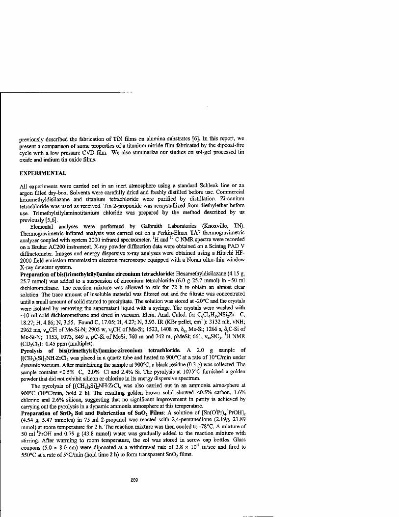
previously described the fabrication of TiN films on alumina substrates [6]. In this report, we present a comparison of some properties of a titanium nitride film fabricated by the dipcoat-fire cycle with a low pressure CVD film. We also summarize our studies on sol-gel processed tin oxide and indium tin oxide films.
EXPERIMENTAL
All experiments were carried out in an inert atmosphere using a standard Schlenk line or an argon filled dry-box. Solvents were carefully dried and freshly distilled before use. Commercial hexamethyldisilazane and titanium tetrachloride were purified by distillation. Zirconium tetrachloride was used as received. Tin 2-propoxide was recrystallized from diethylether before use. Trimethylsilylaminotitanium chloride was prepared by the method described by us previously [5,6].
Elemental analyses were performed by Galbraith Laboratories (Knoxville, TN). Thermogravimetric-infrared analysis was carried out on a Perkin-Elmer TA7 thermogravimetric analyzer coupled with system 2000 infrared spectrometer, 'H and 13 C NMR spectra were recorded on a Bruker AC200 instrument. X-ray powder diffraction data were obtained on a Scintag PAD V diffractometer. Images and energy dispersive x-ray analyses were obtained using a Hitachi HF- 2000 field emission transmission electron microscope equipped with a Noran ultra-thin-window X-ray detector system. Preparation of bis(trimethylsilyl)aminezirconium tetrachloride: Hexamethyldisilazane (4.15 g, 25.7 mmol) was added to a suspension of zirconium tetrachloride (6.0 g 25.7 mmol) in -50 ml dichloromethane. The reaction mixture was allowed to stir for 72 h to obtain an almost clear solution. The trace amount of insoluble material was filtered out and the filtrate was concentrated until a small amount of solid started to precipitate. The solution was stored at -20°C and the crystals were isolated by removing the supernatant liquid with a syringe. The crystals were washed with -10 ml cold dichloromethane and dried in vacuum. Elem. Anal. Calcd. for C6Cl4H19NSi2Zr: C, 18.27; H, 4.86; N, 3.55. Found C, 17.05; H, 4.27; N, 3.93. IR (KBr pellet, cm"1): 3132 mb, vNH; 2962 ms, v^CH of Me-Si-N; 2905 w, vsCH of Me-Si; 1523,1408 m, 0as Me-Si; 1266 s, 5SC-Si of Me-Si-N; 1153, 1073, 849 s, pC-Si of MeSi; 760 m and 742 m, pMeSi; 661, v^SiCj. *H NMR (CD2C12): 0.45 ppm (multiplet). Pyrolysis of bis(trimethylsilyl)aminezirconium tetrachloride. A 2.0 g sample of [(CHj^SiljNH-ZrCLt was placed in a quartz tube and heated to 900°C at a rate of 10°C/min under dynamic vacuum. After maintaining the sample at 900°C, a black residue (0.3 g) was collected. The sample contains <0.5% C, 2.0% Cl and 2.4% Si. The pyrolysis at 1075°C furnished a golden powder that did not exhibit silicon or chlorine in its energy dispersive spectrum.
The pyrolysis of [(CHj^Si^NH-ZrCL, was also carried out in an ammonia atmosphere at 900°C (10°C/min, hold 2 h). The resulting golden brown solid showed <0.5% carbon, 1.6% chlorine and 2.6% silicon, suggesting that no significant improvement in purity is achieved by carrying out the pyrolysis in a dynamic ammonia atmosphere at this temperature. Preparation of Sn02 Sol and Fabrication of Sn02 Films: A solution of [Sn(0'Pr)4.'PrOH]2
(4.54 g, 5.47 mmoles) in 75 ml 2-propanol was reacted with 2,4-pentanedione (2.19g, 21.89 mmol) at room temperature for 2 h. The reaction mixture was then cooled to -78°C. A mixture of 50 ml 'PrOH and 0.79 g (43.8 mmol) water was gradually added to the reaction mixture with stirring. After warming to room temperature, the sol was stored in screw cap bottles. Glass coupons (5.0 x 8.0 cm) were dipcoated at a withdrawal rate of 3.8 x 10'3 m/sec and fired to 550°C at a rate of 5°C/min (hold time 2 h) to form transparent Sn02 films.
289

Preparation of Indium Tin Oxide Films: A solution of [Sn(0,Pr)4.,PrOH]2 (0.5 g, mmoles) in 5 ml THF was reacted with 2,4-pentanedione (2.19g, mmol) at room temperature for 2 h. The reaction mixture was added to a solution of In(acac)3 (3.6 g) in 10 ml THF. Glass coupons (1.0 x 2.5 cm) were dipcoated at a withdrawal rate of 1.5 x 10"3 m/sec and fired to 500°C at a rate of 5°C/min (hold time lh). The process was repeated two times to obtain a film of thickness 1000 Ä and resistivity 16 |xQ cm.
RESULTS AND DISCUSSION
Group IV metal Nitrides
We previously reported a high yield preparation of trimehylsilylaminotitanium trichloride, (CH3)3SiNHTiCl3, from a reaction of titanium tetrachloride with hexamethyldisilazane [5]. In continuation, we carried out the reaction of hexamethyldisilazane with zirconium tetrachloride.
[(CH3)3Si]2NH + ZrCLj »■ [(CH3)3Si]2NH.ZrCl4
Unlike the instantaneous reaction with titanium tetrachloride, hexamethyldisilazane reacted slowly with zirconium tetrachloride. The reaction furnished an adduct, [(CH3)3Si]2NH-ZrCl4 instead of an analogue of trimethylsilylaminotitanium trichloride [10]. The crystals of [(CH3)3Si]2NH-ZrCl4
turn into a powder upon drying. This suggests that the solvent is a constituent of the crystals. Efforts to grow single crystals of [(CH3)3Si]2NH-ZrCl4 were unsuccessful. The dry powder has very poor solubility in deuterated dichloromethane and is thermally unstable at ambient temperatures which makes its structural characterization difficult. Polar solvents (e.g., THF) can not be used since they replace the hexamethyldisilazane in [(CH3)3Si]2NHZrCl4. The infrared spectrum of this powder shows the expected absorptions for (CH3)3Si [11] and ZrCl groups [12]. The ]H NMR of a saturated solution of [(CH3)3Si]2NHZrCl4 in deuterated dichloromethane shows a multiplet centered at 0.45 ppm suggesting a complex structure.
Proposed Pathway for the Decomposition of [(CHi^SiKNHZrCli Thermogravimetric-infrared spectral analysis (TGA-ER) provides information on the decomposition pathway for [(CH3)3Si]2NH-ZrCl4. This arrangement of the instrument allows for simultaneous infrared analysis of evolved species during thermogravimetric analysis. The sample was heated at a rate of 40°C/min from 30°C to 600°C following a one minute initialization delay. Weight losses (Fig. 2a) of 30.0,13.9, and 23.3% are observed in the 30-190,190-270, and 270-440°C temperature ranges, respectively. A gradual weight loss of 4% also occurs in the 440-600°C range. Simultaneous infrared spectra of the evolved species are shown in Fig. 2b. From the spectra, trimethylchlorosilane can be identified in gases evolving in the 30-420°C temperature range. The elimination of hydrogen chloride initiates at 320°C and is complete at 420°C. These two species account for 61.8% of the weight loss from [(CH3)3Si]2NH-ZrCl4. The residual weight loss is assigned to chlorine and can not be identified by infrared spectroscopy.
The TGA-IR data also suggests that the elimination of trimethylchlorosilane in the second temperature begins before the complete elimination of trimethylcholorosilane in the first temperature range (30-190°C). This is based on the observed weight loss of 30% in the 30-190°C range while the first step requires weight loss of 27.4%. The observed total weight loss of 71% is less than the theoretical weight loss (73.3%) required for the complete conversion of precursor to
290

zirconium nitride. This suggests that the resulting sample can be expected to contain some residual impurities if pyrolysis is carried out under a dynamic flow of inert gases.
100 200 300 400 MO
Temperature (°C)
Fig. 2a. Thermogravimetric Analysis of [(CHj^SikNH.ZrC^
* Me3SiCl
4000.0 3000 £000 1500
Wavenumber cm-1
Fig. 2b. Infrared spectrum of Evolved Species
Considering the TGA-ER data, we propose the following mechanism for the thermal decomposition of[(CH3)3Si]2NHZrCl4:
-(CH3)3SiCI -(CH3)3SiCI [(CH3)3Si]2NHZrCl4 »► (CH3)3SiNHZrCl3
HCI
-*► NZrCI ZrN
291

Pvrolvsis of [fCH2>2Sil2NH-ZrCl| Since the TGA of [(CHj^Si^NH-ZrCL, showed that the weight loss is complete at 440°C, we pyrolyzed the sample at three temperatures - 600, 900, and 1075°C to study the evolution of the zirconium nitride structure. The pyrolysis conditions (dynamic vacuum vs. ammonia) at 600 or 900°C do not improve the quality of the zirconium nitride since samples contained silicon and chlorine impurities and were susceptible to oxidation under ambient conditions. Pyrolysis of the precursor and subsequent sintering at 1075°C in a dynamic vacuum furnished a sample that did not show O, Si or C\ in its energy dispersive spectrum and did not oxidize under ambient conditions. The characterization of all zirconium nitride samples by X-ray powder diffraction (XRD) and transmission electron microscopy (TEM) is presented in the following paragraphs.
The gray-black powder, formed on pyrolysis of the precursor in a dynamic vacuum at 600°C, is amorphous as determined by XRD and is highly sensitive to atmospheric humidity.
The XRD of the golden black powder, obtained at 900°C in a dynamic vacuum, matches the pattern reported for crystalline zirconium nitride (JCPDS # 35-753) and there is no indication of zirconium oxide contamination. The TEM of the material shows that the particle size varies in the 70 to 150 nm range. The particles have a uniform coating that varies in thickness from 5 to 10 nm. Energy dispersive spectra (EDS) of the particles show zirconium, nitrogen and oxygen while that of the coatings show only Zr and O. This suggest a pure oxide structure for the coating and primarily ZrN for the core. The high resolution micrograph of Fig. 3 shows lattice fringes within the coating corresponding to tetragonal Zr02 (111) (JCPDS Card #17-0923).
Fig. 3. TEM of Zirconium Nitride Prepared at 900°C.
The lattice is highly oriented, suggesting that the coating is essentially a single crystal over the core ZrN particle. The fringes seen at the outer edges of the coating were also observed to continue through the core particle structure. This is further evidence that the coating is a single crystal on a given particle. Thus the coating formed due to a heterogeneous nucleation in which the oxide film nucleated at a single point on the particle surface and grew epitactically from that point to form the complete film. Alternatively, a uniform, amorphous coating crystallized heterogeneously forms the final single crystal structure. The FFT from the core shows the ZrN
292

(Ill) lattice. These data suggest that the samples prepared at 900°C are susceptible to oxidation due to the presence of amorphous zirconium nitride materials.
The gold colored powder, obtained at 1075°C in a dynamic vacuum, shows sharp peaks at 29 (in degrees) = 33.8, 39.3, 56.8, 67.8,71.3, 84.7 in its XRD due to crystalline zirconium nitride. The lattice parameter, a, calculated from (111) and (200) is 4.59 A which is close to stoichiometric zirconium nitride (4.577 A) films [13]. It is important to point out that the magnitude of increase in the lattice parameter associated with the nitrogen rich ZrN films will be lower for the bulk powder as compared to a stressed film. In our samples, the increase in the lattice parameter calculated from either (111) or (200) diffraction peaks is negligible, suggesting that our samples are stoichiometric zirconium nitride. The particle size of the 1075°C material ranges from 30 to 150 nm and the EDS from the particles show only Zr and N. The high resolution micrograph [Fig. 4] shows lattice fringes corresponding to ZrN (111) as measured from FFT.
Fig. 4. TEM of Zirconium Nitride Prepared at 1075°C.
These results suggest that sintering at 1075°C is necessary to stabilize our ZrN powders towards oxidation.
Group IV Nitride Films Titanium nitride films can be easily fabricated on an alumina substrate by the dipcoat fire cycle as described previously [6]. Efforts to fabricate zirconium nitride films by a dipcoat-fire cycle employing [(CHj^Si^NH-ZrCL, are in progress and will be presented in a future report. Here we present a comparison of some of the properties of TiN films prepared by the dipcoat method with those of CVD films [14]. TiN films on alumina substrates were fabricated by low pressure CVD [15] employing a single source precursor [TiCl4(NH3)2] with a substrate temperature of 600CC and a sublimation temperature of 120°C.
The XPS of the dipcoated films show a titanium to nitrogen ratio of 1:1.08, whereas for the low pressure CVD films the Ti:N ratio is exactly 1:1. The resistivity of dipcoat film is 2.5 x 10 [iCl
293

cm and that of the LPCVD film is 962 |iQ cm. The resistivity difference between the dip-coated film that is slightly nitrogen rich, and the stoichiometric low pressure CVD film can be explained on the basis of nitrogen content.
Scanning tunneling microscopy (STM) was used to compare the surfaces of the TiN films made by the dipcoat process with those generated by the conventional low pressure CVD process. Three to five arbitrarily selected regions of each sample were measured.
Fig. 5. STM of TiN films from (a,c) dipcoat method and (b,d) low pressure CVD method.
Images were obtained with tip biases in the range VB = +0.6 to +3.4 V and currents of approximately 2.2 nA. Cut Pt/Ir tips were used. There was substantial evidence for rounding of the tip shape with time. Presumably the specimens had small patches with poor conductivity that caused minor tip crashes. A bias voltage between +1.0 and +1.5 V was the best for reducing the frequency of tip crashes, but no range of bias voltage and tunneling current was found where Ulis problem was eliminated. The images presented here were taken with new tips, before the rounding became severe.
Figure 5 shows two pieces of data from each type of sample. Figures a and c are images of dipcoated film surfaces, figure b and d are low pressure CVD films. Both films have roughly similar grain structures. The apparent grain diameters for the dipcoated films are in the 3-10um range while the low pressure CVD films are 2-8um range. The images in the figure were chosen to illustrate the range of grain sizes present in the different areas of each sample. As can be seen, the grain size shown in figure 5a is approximately twice that shown in Figure 5b. However, in other
294

areas the films prepared by the two methods look quite similar, as observed in c) and d). Apart from some subtle differences, the films are quite similar.
Smaller-scale images of each type of film also show some evidence of faceting. This is seen as
flat planar regions of up to 5|xm in both types of films. Such facets are relatively uncommon for the measured areas, accounting for only a few percentages or less of the examined sample area.
The surface roughness of the films was evaluated using a stylus and the mechanical properties of the films suggest that they are similar. The center-line average roughness and peak-to-valley roughness parameters of both TiN film types are comparable as shown in Table I. This is not surprising since the surface roughness of the films is dictated by the surface roughness of the substrate (center-line average roughness 0.59 urn, peak-to-valley roughness 5.2 um).
Table I: Some Mechanical Properties of TiN Films
Dipcoat Film LPCVD Film Steel
Surface Roughness (urn) Center-line average 0.57 Peak-to-valley 5.2
Friction and Wear Characteristics friction coefficient 0.95
ball wear volume (mm3) 2.33 x ball wear rate, mm3/m 3.45 x
io-2
10^
0.55 4.7
0.65 2.307 x 3.404 x
IO"2
IO"4
0.02 0.1
0.61
5.4 x IO"6
The friction and wear properties were evaluated using a ball-on-disk contact geometry in which a 6.35 mm diameter AISI 52100 steel ball was pressed against the film on the alumina substrate. Due to their small size only one test could be performed on each sample. The tests were conducted without any lubricant for 30 minutes at room temperature under a normal load of 4.9 N and sliding velocity of 3.77 mm/s. The friction coefficient for both films increased for the first few minutes before reaching steady state. The coatings were found to be intact at the end of the test on examining the wear area under optical microscope. The dipcoated films exhibited a higher friction coefficient against a steel ball than the low pressure CVD films. For comparison, the friction coefficient obtained for a steel ball sliding against a polished steel disk is also shown in Table I.
The wear track contained wear debris from the steel counterface and a flat wear scar was produced on the steel balls. The size of the wear scar was measured, and used to calculate the ball wear volume and average ball wear rates. The average wear rate was calculated by dividing the ball wear volume by the total sliding distance. The ball wear volume, the average ball wear rate and the steady state friction coefficients for the two films are comparable.
The friction coefficients of the dipcoated and low pressure CVD TiN films are also comparable to those deposited by other techniques for tests conducted under similar conditions. Although both films appeared wear resistant, the wear rates of the balls were high. In a tribological system, it is necessary to consider that the wear on the opposing surface is not increased by the use of a hard coating. The high wear rates of the steel balls could be due to the high surface roughness of the coating. The friction coefficients and ball wear rates could be reduced by better surface finish
strategies. Thus, the films prepared by our dipcoat method and the low pressure CVD method are quite
comparable in both mechanical properties and surface morphology. It is important to point out that
295

the dipcoated films, at the current stage of development, are only suitable for mechanical applications provided they can be deposited at low temperature. For practical applications, methods that permit deposition at temperatures below 400°C (high speed steel cutting tools) or 600°C (aluminum alloy based engine components) need to be developed. For electronic applications, the films should contain extremely low levels of contaminants.
Tin Oxide and Indium Tin Oxide Films
There are practical limitation of using tin oxide sols due to the short shelf life. Here we describe a tin oxide sol which can be stored for two months in a screw cap bottle. Since tin alkoxides hydrolyze rapidly, it is necessary to modify them for the preparation of stable sol. We found that addition of two equivalents of acetylacetone to a solution of tin 2-propoxide prior to hydrolysis leads to a clear sol. This is due to the reaction of acetylacetone with tin 2-propoxide to form cis- Sn[CH3C(:0)CHC(:0)CH3]2(O
iC3H7)2.
[SntO'CalWCjHyOHk + 4 CH3C(:0)CH:C(OH)CH3->2 Sn[CH3C(:0)CHC(:0)CH3]2(OiC3H7)2
The intermediate can be isolated from either a 2-propanol or THF solution. The IR of the intermediate shows strong vC=0 bands at 1583 and 1689 cm"1 for coordinated acetylacetone and none for the uncoordinated one expected at 1725 cm"1. The 'H NMR shows peaks at 2.0, 2.11 (CH3); 5.5 (CH); 1.14-1.2 m (CH3); and 4.27 (CH). These spectroscopic data match those previously reported for the cis-isomer [16].
The tin oxide sol can be stored in screw cap bottles for two months. The films of tin oxide were prepared by the dipcoat-fire cycle (550°C, hold 2 h) from the sol after aging for 2-3 weeks. A single dipcoat-fire cycle furnished films of thickness 234 Ä at a withdrawal rate of 10" m/sec and 365 A at a withdrawal rate of 3.8 x 10"3 m/sec. The refractive index is in 1.72-1.75 range. XRD of the films show them to be amorphous. The XPS shows peaks corresponding to Na,C,Sn and O. After ion milling (50 Ä), the carbon Is peak is not seen. The ratio of Sn/Na is 50/1 which increases to 49/2 after ion milling by another 150 Ä. Sodium diffusion in tin oxide films has been previously noted (Sn/Na =1) by Osaka et al. in films prepared from a tin oxalate solution [17]. They attributed this process to a hydronium-sodium ion exchange due to the highly acidic tin oxalate solution. Thus the low levels of sodium in our films are due to the low acidity of the sol [pH of sol = 4.5, pH of 'C3H7OH = 5.35]. The reflectance of the films is 10-22% in the visible region.
Addition of this sol to an indium acetylacetonate, In(CH3C(:0)CH:C(OH)CH3)3, solution leads to a stock solution that can be used to deposit indium tin oxide films. We selected indium acetylacetonate as a source of indium, despite its hydrolytic stability, due to its high solubility in organic solvents as compared with indium alkoxides. The indium tin oxide films were deposited on microscope slides by dipcoating and firing at 500°C. XRD of the films showed (222), (400), and (440) diffraction peaks due to indium oxide (JCPD # 06-0416). The tin oxide diffraction peaks were not observed due to dilution effects. XRD of a powder prepared by drying a portion of the stock solution and firing at 500°C shows 110 and 101 diffraction peaks due to tin oxide (JCPDS # 41-1445) in addition to those of indium oxide (Fig. 6). The tin oxide diffraction peaks are weak due to dilution. The rest of the diffraction peaks are either too weak to be observed at this dilution or overlap with indium oxide peaks. The XPS of the film showed peaks due to In, Sn, O, and C. The carbon Is peak is due to adventitious carbon and is removed by ion milling a few Angstroms of the film. The depth profile of the film while monitoring the In 3d and Sn 3d windows shows a good
296

distribution of tin in the indium oxide matrix. The Na Is peak is observed close to the interface of the film suggesting outward diffusion of sodium atoms from the glass substrate.
'VnJbi1 IU^WVAX 20 25 30 35 40 45 50 55 60 65 70 75 80 85 90
26
Fig. 6. XRD of indium tin oxide powder
Thus the sol derived from acetlyacetone modified tin 2-propoxide can be used in preparation of indium tin oxide films. The sheet resistance of the film (1600 Dsquare) is higher than those fabricated from reactive electron bean evaporation methods (250-500 Qsquare). Studies are in progress to optimize the film fabrication conditions to improve the electrical properties.
CONCLUSION
We have made progress toward the low cost fabrication of electrically conducting films of titanium nitride and indium tin oxide. The properties of titanium nitride films are close to those of LPCVD films. The simplicity of the process makes it attractive for large scale application on components. We have also prepared a new precursor for zirconium nitride that is soluble in dichoromethane when freshly prepared. Efforts to fabricate ZrN films from this precursor are in progress.
At this stage of development, the dipcoat films show some limitations. For example, the crystallization of films requires high temperature treatment that can damage the substrates. Residual trace impurities from the pyrolysis of precursor can also limit the applications of these films in electronics. Further work is necessary to overcome these limitations.
REFERENCES
1. C.K. Narula, Ceramic Precursor Technology & Its Applications. Marcel Dekker, Inc., New York, 1995.
2. S. Yajima, J. Hayasi, M. Omori, Chem. Lett., p. 931 (1975). 3. PJ. Greil, J. Am. Ceram. Soc, 78, p. 835 (1995). 4. H. Dislich, in Sol-Gel Technology for Thin Films. Fibers. Preforms. Electronics, and
Specialty Shapes. Ed. L.C. Klein, Noyes, park Ridge, NJ, 1988, p. 50.
297
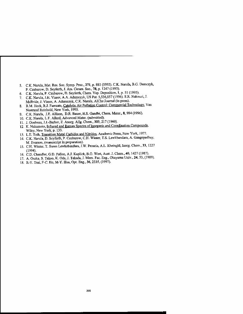
5. C.K. Narula, Mat. Res. Soc. Symp. Proa, 271, p. 881 (1992). C.K. Narula, B.G. Demczyk, P. Czubarow, D. Seyferth, J. Am. Ceram. Soc, 78, p. 1247 (1993).
6. C.K. Narula, P. Czubarow, D. Seyferth, Chem. Vap. Deposition, 1, p. 51 (1995). 7. C.K. Narula, J.H. Visser, A.A. Adamczyk, US Pat. 5,536,857 (1996). S.R. Nakouzi, J.
McBride, J. Visser, A. Adamczyk, C.K. Narula, AlChe Journal (in press). 8. R.M. Heck, R.J. Farrauto, Catalytic Air Pollution Control: Commercial Technology. Van
Nostrand Reinhold, New York, 1995. 9. C.K. Narula, J.E. Allison, D.R. Bauer, H.S. Gandhi, Chem. Mater., 8,984 (1996). 10. C.K. Narula, L.F. Allard, Advanced Mater, (submitted). 11. J. Goubeau, J.J.-Barber, Z. Anorg. Allg. Chem., 303,217 (1960). 12. K Nakamoto. Infrared and Raman Spectra of Inorganic and Coordination Compounds,
Wiley, New York, p. 133. 13. L.E. Toth, Transition Metal Carbides and Nitrides. Academic Press, New York, 1977. 14. C.K. Narula, D. Seyferth, P. Czubarow, C.H. Winter, T.S. Lewkbandara, A. Gangopadhay,
M. Everson, (manuscript in preparation). 15. C.H. Winter, T. Suren Lewkebandara, J.W. Proscia, A.L. Rheingld, Inorg. Chem., 33, 1227
(1994). 16. CD. Chandler, G.D. Fallon, A.J. Koplick, B.O. West, Aust. J. Chem., 40,1427 (1987). 17. A. Osaka, S. Takao, K. Oda, J. Takada, J. Mem. Fac. Eng., Okayama Univ., 24, 53, (1989). 18. R-Y. Tsai, F-C. Ho, M-Y. Hua, Opt. Eng., 36, 2335, (1997).
298

MORPHOLOGY AND ELECTRON EMISSION PROPERTIES OF NANOCRYSTALLINE CVD DIAMOND THIN FILMS
ALAN R. KRAUSS, DIETER M. GRUEN, DANIEL ZHOU, THOMAS G. McCAULEY, LU CHANG QIN, TIMOTHY CORRIGAN*, ORLANDO AUCIELLO**, R. P. H. CHANG*** ♦Materials Science and Chemistry Divisions, Argonne National Laboratory, Argonne IL 60439 ♦♦Materials Science Division, Argonne National Laboratory, Argonne IL 60439 ♦♦♦Materials Science Dept., Northwestern University, Evanston IL 60208
ABSTRACT
Nanocrystalline diamond thin films have been produced by microwave plasma-enhanced chemical vapor deposition (MPECVD) using C<5(vAr/H2 or CH4/Ar/H2 plasmas. Films grown with H2 concentration < 20% are nanocrystalline, with atomically abrupt grain boundaries and without observable graphitic or amorphous carbon phases. The growth and morphology of these films are controlled via a high nucleation rate resulting from low hydrogen concentration in the plasma. Initial growth is in the form of diamond, which is the thermodynamic equilibrium phase for grains < 5 nm in diameter. Once formed, the diamond phase persists for grains up to at least 15-20 nm in diameter. The renucleation rate in the near-absence of atomic hydrogen is very high (~1010 cm-2
sec-1), limiting the average grain size to a nearly constant value as the film thickness increases, although the average grain size increases as hydrogen is added to the plasma. For hydrogen concentrations less than -20%, the growth species is believed to be the carbon dimer, C2, rather than the CH3* growth species associated with diamond film growth at higher hydrogen concentrations. For very thin films grown from the COO precursor, the threshold field (2 to -60 volts/micron) for cold cathode electron emission depends on the electrical conductivity and on the surface topography, which in turn depends on the hydrogen concentration in the plasma. A model of electron emission, based on quantum well effects at the grain boundaries is presented. This model predicts promotion of the electrons at the grain boundary to the conduction band of diamond for a grain boundary width -3-4 Ä, a value within the range observed by TEM.
INTRODUCTION
Diamond Film Growth
Bulk diamond is unstable relative to graphite except at extremely high pressures and temperatures. Therefore, the growth of diamond films via low pressure chemical vapor deposition (CVD) requires a means of kinetically allowing the growth of the diamond phase while suppressing the formation of the graphitic phase. This is typically achieved by using atomic hydrogen to preferentially etch the graphitic phase and stabilize the diamond surface structure via hydrogen termination of the carbon dangling bonds. Additionally, since the growth species in this process is the CH3* radical, it is necessary to both prepare a carbon atom insertion site at the surface, and to remove the extra hydrogen atoms from the growth species in order to permit migration of the adsorbed carbon to the diamond lattice site. These functions are accomplished through atomic hydrogen abstraction reactions [1]. The presence of a large excess of atomic hydrogen is therefore considered essential to the conventional method of low pressure growth of diamond films, which is restricted to a region of the C-H-0 phase diagram (Fig. 1) close to the line extending from the hydrogen corner to the middle of the C-O line [2]. The region below this line corresponds to a net etching of the diamond, and therefore no growth is observed. The region above this line corresponds to the growth of non-diamond phases. By growing close to the H-CO line, phase pure, large grain, textured diamond films may be produced.
These films however, generally make poor electron emitters [3], and changes in the growth conditions which result in improved electron emission properties generally result in the
299
Mat. Res. Soc. Symp. Proc. Vol. 495 c 1998 Materials Research Society

simultaneous variation of a number of film properties. Increasing the carbon/hydrogen ratio in the CVD plasma tends to enhance the electron emission, but it can be seen by referring to Figure 1, that the result will be to enhance the growth of non-diamond phases, typically as intergranular graphitic or amorphous carbon inclusions. Additionally, the grain size decreases, preferred orientation is lost, and a larger number of atoms are located along grain boundaries. Consequently, there is an intrinsic linkage between grain size, growth rate, surface morphology, and the presence of intergranular non-diamond phases which makes it very difficult to either sort out the basic physics of the electron emission process or to significantly improve the performance of carbon- based cold cathode electron emission materials in a systematic manner.
"C2" Diamond Growth Region
Methyl Radical Diamond Grovith Region
Figure 1. The H-C-O phase diagram showing the predicted [1] region of diamond film growth as the solid line connecting the H corner to the middle of the C-O line, the experimentally observed region of film growth [2] as the shaded area surrounding the theoretical line, and the growth method reported here [4], located at the carbon apex and extending along the C-H leg of the triangle as hydrogen is added to the plasma.
We have developed a new method of diamond film deposition based on direct insertion of gas phase carbon dimers (C2) into the diamond lattice without the assistance of atomic hydrogen abstraction reactions. The relation between the morphological, compositional and electronic properties of these films differs significantly from that of conventionally grown diamond films. It is possible to control the ratio of C2 / CH3* growth species and the resulting character of the dominant growth process by tailoring the amount of H2 in the plasma. Films grown by this new method display a correlation between readily identifiable topographic, electrical, and morphological properties which are predictive of the electron emission properties of the films.
The growth process involves either C60 or CH4 precursors in an argon microwave plasma [4] with little or no added atomic hydrogen [5], and permits growth of equiaxed, nanocrystalline diamond films [6]. It has been predicted [7], and experimental results indicate [8] that the growth species is the carbon dimer, and atomic hydrogen abstraction reactions do not seem to play a role in the film growth. Diamond growth by the new method occurs in the region indicated by the shaded area near the carbon vertex of Figure 1. Both x-ray photoabsorption spectroscopy [9] and UV excitation Raman spectroscopy [10] show that the electronic bonding character is almost entirely sp3. High resolution TEM studies [11] reveal equiaxed nanocrystalline diamond grains with atomically abrupt grain boundaries and no trace of inter-granular non-diamond phases. Because of the relative absence of atomic hydrogen in the plasma, there is little etching of the nascent diamond grains, and continuous renucleation occurs, resulting in an average grain size of -15 nm [11], and surface roughness of 20-40 nm, regardless of film thickness [12]. For very small grains, there is evidence [13, 14] that the grain boundary energy is sufficient to make the diamond phase stable relative to graphite, and we conclude that the dimer growth species gives rise to a high nucleation rate which limits the grain size, and grows diamond as the thermodynamically stable phase of carbon.
300

If the ambient hydrogen pressure is low, the C2 growth species can be produced via two possible routes using either a Cßo gas phase precursor;
CßO-» nC2 + fragments [15] (1)
or a hydrocarbon precursor such as CH4;
2CH4 -» C2H2 +3H2 -» C2 +4H2. (2)
By increasing the amount of hydrogen in the plasma, reactions 1 and 2 can be shifted to the left;
C2 + 3H2 -> 2CH3* (3)
eo y 1 1 _-^T 1
I O
s 0
2% H 2 s ^V
/ C hem Kin Calculation: 0 100 Torr
§ 10* 1XCH in Ar vs. % [HI 4 2 —
T =2500 K O vik
ß LL V[C1 \^2 0 O
2 m-7 . 1 1 1 1 -— 20 40 60
Mole % H 80 100
Figure 2. ChemKin Calculation at 100 Torr,l% CH4 in Ar vs. % H2) Tvib = 2500 K
Equations 1 and 2 correspond to the growth of diamond via direct insertion of the carbon dimer into the diamond lattice site [7], whereas equation 3 corresponds to diamond film growth from the CH3 species [1, 2]. If thermodynamic equilibrium conditions are assumed, it is possible to calculate the C2/CH3* ratio using the Chemkin code [16]. The calculated C2 and CH3* concentrations in the plasma are shown in Figure 2 for a plasma in thermodynamic equilibrium at 2500 K. In reality however, the plasma is not in thermodynamic equilibrium, and preliminary optical absorption measurements [17,18] indicate that the effective temperature may be lower than 2500 K. However, the general result that the C2 concentration decreases and the CH3* concentration increases as the plasma hydrogen concentration increases remains valid. Since these two growth species give rise to films with very different properties with regard to grain size and orientation, surface morphology, and the formation of inter-granular non-diamond phases, it is possible to controllably produce films with a wide range of morphological and electronic characteristics by varying the plasma hydrogen concentration.
Cold Cathode Electron Emission
Some diamond and diamond-like carbon thin films exhibit cold cathode electron emission [19] for moderately low applied voltages. This requires a means for (I) transferring electrons from the substrate into the diamond, (II) transferring charge through the diamond layer to the surface, and (in) ejecting electrons into the vacuum. The experimentally observed current-voltage relation fits the Fowler-Nordheim expression (Eq. 4) corresponding to tunneling through a barrier [20].
301

However, it is not clear whether the tunneling occurs at the interface between the substrate and the diamond [21,22], or between the diamond and the vacuum [23]. There is additional disagreement as to whether the electrons tunnel from the valence band [24], the conduction band [23], or from interband [25] states either associated with graphitic or DLC phases, or induced by damage or dopants [3], intentional or otherwise. Assuming that the electron mechanism consists of tunneling through a barrier associated with an effective work function <|>, the emission current density can be expressed in the form [21]
J=154E2F/<t> exp{-6830<|>3/2/E} (4)
where J is the current density in amps/cm2, E is the electric field in volts/micron, § is measured in eV, and F is the effective fraction of the free surface area which gives rise to electron emission. In general, E=ß x Eft,, where Eft, is the field corresponding to a parallel flat plate geometry, and the quantity ß reflects the geometric enhancement of the electric field, presumably by surface asperities. The effective work function and emission area can be determined from the slope and intercept, respectively, of a plot of ln(J/E2) vs 1/E, assuming a known value of ß. The value of the effective work function tends to be quite low [26], typically less than 0.1 eV, and the emission comes from isolated, discrete sites [20] which are often very low in density.
It has been demonstrated via ultra-violet photoelectron spectroscopy [20, 27] that under certain circumstances, diamond is a negative electron affinity (NEA) material (i. e., the bottom of the conduction band lies above the vacuum level) with a 5.5 eV band gap. Consequently, conduction electrons which reach the surface would experience little or no barrier to emission into the vacuum. A back-injection model has been hypothesized [21, 22] in which the observed current-voltage characteristic relates to tunneling through a barrier between the substrate and the diamond film, followed by transport to the NEA surface and ejection without further energy loss. The voltage drop across the diamond film results in a shift of the conduction and valence bands such that tunneling through the substrate-diamond interface barrier may result in injection of substrate electrons into the conduction band [21, 23]. Recent studies of the kinetic energy distributions of electrons emitted from Mo tips cataphoretically coated with diamond powder confirm this picture, although the energy distribution of electrons emitted from natural p-type diamond suggests that emission occurs from the diamond valence band [28], and there may not be a single tunneling mechanism [29].
However, diamond is an insulator with a large band gap, and the transport mechanism through the film is not clear. The best electron emitting thin film materials are usually either a highly damaged polycrystalline diamond [3], or various forms of diamond-like carbon (DLC) [4] (amorphous carbon with a high degree of sp3 bonding), and almost certainly do not meet the conditions under which NEA has been observed. It is not clear at this point what role NEA has in the electron emission process in diamond and diamond-like carbon films. If the barrier is at the diamond-vacuum interface, then damage may be required simply to provide conductive paths through the film, although Xu, Tzeng, and Latham [20] argue that such conducting paths are inconsistent with the observed low density of emitting sites. They have proposed a model in which the intergranular regions of graphite which typically form between diamond grains act as antennas which give rise to a local field enhancement sufficient to form conducting channels within the diamond matrix. The emission sites are conjectured to be a "triple-point" at which a diamond grain and graphitic inclusion intersect at the vacuum interface.
The "triple point" model however, does not seem plausible for the more uniform DLC films. A model proposed by Robertson [30] describes both the observed low effective work function values and the low effective emission area in DLC films. Eq. 4 yields the quantity <|)3/2 /E as the slope of the Fowler-Nordheim (F-N) plot (In J/E2 vs 1/E). In general, it is not possible to separate the effect of the work function from that of the local electric field, which is very sensitive to surface structures with small radii of curvature. The effective low work function of conventionally grown diamond films could be attributed to field enhancement at surface asperities and/or sharp-edged crystalline facets associated with these typically very rough surfaces. However, DLC films are
302

quite smooth, and it is therefore difficult to explain low effective work function values in topographic terras. A "patch effect" model based on a largely hydrogen-terminated surface with small bare patches at defect sites has been proposed [30]. Hydrogen is an electropositive adsorbate, which results in the formation of surface dipoles with the positive end pointing outward. Small regions of the surface which are hydrogen-deficient experience the effects of the adjacent negative image charge, resulting in a lowering of the electron affinity and a large normal component of the electric field, i. e. a non-topographic field enhancement effect. The key ingredients of this model are a high density of very small hydrogen-depleted surface defect sites.
There are still a number of issues which remain to be resolved before the cold cathode electron emission mechanism in diamond and DLC films is understood. The complexity of the process and variability of materials properties leads to poor reproducibility which has hindered the development of applications based on cold cathode electron emission from diamond films. In particular, it has not been possible to provide definitive morphological or electronic bonding criteria which would make it possible to predict whether a given diamond or diamond-like carbon film will emit electrons, except by direct testing. We have developed a class of phase-pure nanocrystalline diamond which has properties characteristic of both microcrystalline diamond and DLC, and therefore provides a new means of examining the electron emission process.
EXPERIMENTAL
Nanocrystalline diamond films were grown on <100> n-type Si substrates with resistivity in the range 0.01-1.0 ohm-cm, using an ASTeX PDS-17 microwave (2.45 GHz) CVD reactor. Diamond nucleation was accomplished by applying a 100-200 volt negative bias to the substrate in a 10% CH4 / 90% H2 plasma with a total pressure of 5 Torr. The substrate temperature was maintained at 800 °C, and the microwave power level was 500 watts. Laser interferometry [31] was used to determine when diamond film growth begins, with an estimated reproducibility of 300-400 Ä. Once the initial growth has begun, the gas composition and pressure are altered to grow the films using the desired processes corresponding to equations 1, 2, or 3. For growth using the dimer insertion process (Eqs. 1 or 2), Ar is introduced at a pressure of 98-100 Torr at a flow rate of 100 seem, with carbon provided via either 1-2 seem of CH4, or by turning on the COO sublimation source described elsewhere [5]. In most cases, at least 1-2 seem of H2 was required to reduce the electron density and stabilize the predominantly Ar plasma, which otherwise tends to form at the quartz microwave window, rather than wetting the substrate. The hydrogen flow rate was varied up to 20 seem by connecting two of the system's flowmeters in parallel. The growth rate at a microwave power level of 800 watts is in the range 0.4-0.6 ixm/hr.
Electron emission was measured using an anode 1.89 mm in diameter with rounded edges to prevent spurious emission at anode asperities. The initial anode-cathode spacing was measured using a high magnification CCD camera. A series of current-voltage measurements were made at various distances, set by computer control of a calibrated micro-step motor. The cathode voltage was increased under computer control until the emission current reached 10 |JA, and then decreased to zero. The sequence was typically repeated three times to verify reproducibility. The gap was then increased, typically in five micron steps, and the whole sequence was repeated until the distance was so large that a current of 0.1 |iA could not be obtained with an applied voltage of 3 kV. The samples were also analyzed by atomic force microscopy (AFM) using a Burleigh ARIS 3300 microscope. Transmission electron microscopy was performed using a JEOL 4000 EX. Electrical conductivity measurements were made using a two-point probe, and are intended for comparison purposes only.
RESULTS
The surface morphology as a function of plasma composition is shown in the SEM images of Fig. 3 for four films grown in a plasma containing 1% CH4 and various amounts of Ar and H2. For high H2/Ar ratio (Fig. 3(a)), the growth species is CH3*, and the resulting film consists of large, faceted diamond grains. Total gas pressure was 100 Torr, with a gas flow rate of 100 seem.
303

The microwave power was 800 watts, and the substrate temperature was 800 °C. As the H2 concentration drops toward -20%, a new morphology, consisting of equiaxed, very small, non- faceted grains develops, as show in Fig. 3 (b-d). X-ray photoabsorption measurements at the Cis edge [9] have been used to characterize the relative amounts of diamond vs graphitic material in the films, showing that for both CH4 and COO precursors, the films grown with the smallest amount of hydrogen are indistinguishable from single crystal natural diamond, with a well defined diamond a* exciton at 289 eV, as shown in Fig. 4. As the hydrogen content of the plasma increases, the diamond exciton becomes less well-defined, and there is evidence of H-C localized bonding, although diamond remains the predominant phase.
Fig 3 Scanning electron micrograph images of diamond films grown in a microwave plasma consisting of 1% CH4 and (a) 2% Ar, 97% H2, (b) 80% Ar, 19% H2,(c) 90% Ar, 9% H2,(d) 97% Ar, 2% H2.
285 290 295 300 305 Photon Energy (eV)
Figure 4. Cls x-ray photoabsorption spectra of a single crystal diamond and graphite reference samples, and nanocrystalline diamond films grown from Cßo and CH4 precursors in an Ar microwave plasma containing either 2% or 10% added hydrogen.
304

The electron emission properties for twelve 60 and 120 nm thick samples, as well as that of a lUm thick reference film deposited using a 2% CH4-98% Ar microwave plasma are listed in Table I. The conventionally grown film has an rms roughness value > 500 nm, very high electrical resistance as measured by a two point probe, and a high threshold field (defined as the flat plate field at which an emission current of 0.1 ^A was measured). The films made using the Ar-CH4-H2 plasma exhibited increasing roughness as the plasma hydrogen concentration increased, but there was little change in electrical resistivity, and none of these films emitted at fields up to 60 V/|J.m (assuming ß=l). The films derived from the Cßo precursor exhibited very different behavior. The rms roughness, electrical resistance and threshold field were strong functions of the plasma hydrogen content, with threshold fields ranging from 2 V/\im to more than 60 V/|0.m.
Table I: Electron Emission Properties of Diamond Films Grown in H2-CH4, Ar-CH4-H2, and Ar-C60-H2 Microwave Plasmas Sample Carbon % H2 Thickness Resistance Turn-on roughness
Precursor (nm) (Kilohms) Field (V/um) (nm rms) 950111 CH4 98 1000 250-400 60-70 >500 950707c CH4* 2 60 0.8 NE 950707a CH4* 2 120 5.0 NE 65 950724 CH4* 10 60 0.8 NE 15 950725b CH4* 10 120 0.8 NE 70 950725d CH4* 20 60 -- NE 26 950725c CH4* 20 120 2.7 NE 153 950726a Ceo* 2 60 - NE 950726b ceo* 2 120 400 50-65 28 950727b c6o* 10 60 13.0 30 16 950727a c6o* 10 120 1.8 12-35 70 950731 C60* 20 60 186 10 15 960807 Ceo* 20 120 500 2 140
* Balance of the gas is argon
16flml apTfini; 45 am Mmmm^>
Figure 5. Plan view and line scan AFM image of two 120 nm thick diamond films grown in a CH4(1%)-Ar plasma with (a) 2% added H2, and (b) 20% added H2.
Figure 5 shows the atomic force microscope (AFM) images for films corresponding to (a) growth in a 2% H2 - CH4 (1%) - Ar plasma, and (b) growth in a 20% H2 - CH4 (1%) - Ar plasma. Both films exhibit a faceted topography with a 5-10 ixm lateral modulation distance. Neither film emitted electrons at fields up to 70 V/ixm
305

Figure 6 shows the atomic force microscope (AFM) images for films corresponding to (a) growth in a 2% H2 - Cßo ü%) - Ar plasma, and (b) growth in a 20% H2 - COO (1%) - Ar plasma. The rms roughness values are similar to those of Figs. 5(a) and 5(b), but there is no well-defined crystallinity, and the lateral modulation length is much shorter, varying from roughly 1.5 to 2 |^m with little change as the plasma hydrogen concentration varies, although the rms roughness varies significantly as shown in Table I. The origin of this lateral modulation is not known but it superficially resembles stress relief-related topography observed in strained epilayer growth of [SiGe/Ge]. The modulated structure which appears in Figs. 6a and 6b seems to be closely correlated to field electron emission in these films.
1 (a)
■ '-^■Qääjjimr
B :> '0,3^im^
I ,;;--:;.(l'xii*r£~
■ OflOum 22 5i>» 45um
i (b)
H ,V^V VHvA AJV I\ ^ggfi [■■■■&Atm~ V . ^ Vy \ ' V .' \ 1
am f5um .■: 30um ,45(»m :: «Own : 75iim
Figure 6. plan view and line scan AFM image of (a) a film grown in a plasma containing 2% H2 in a CöO-Ar plasma, (b) a film grown in a plasma containing 20% H2 in a CöO-Ar plasma.
The effect of increasing plasma hydrogen content on grain morphology of 120 nm thick nanocrystalline diamond films grown from CH4 and COO precursors is shown in Figs. 7 and 8. A TEM image of a film grown using the CH4 precursor in an Ar plasma with 2% H2 added (Fig. 7a) shows very small grains with extremely low defect density, consisting almost entirely of twinning. Increasing the plasma hydrogen content (Fig. 7b and 7c) to 20% results in a relatively small degree of grain coarsening resulting from etching by atomic hydrogen, but there is no detectable formation of intergranular graphitic phase in this range of hydrogen concentration. 120 nm thick films grown from an Ar-H2 plasma into which COO has been sublimed (Fig. 8) show for low plasma hydrogen concentration (Fig. 8a), a structure similar to that of Fig. 7a. However, as the plasma hydrogen content increases, there is a considerable increase in both the defect density and grain size, which reaches a diameter of ~1 11m for 20% added H2. It should be emphasized that the lateral topographic modulation observed in Figs. 5 and 6 do not correspond to the individual diamond grains, although for the film corresponding to Fig. 8c, the defect density has become so high that it is difficult to identify individual grains.
UV Raman spectroscopy [10] has shown that the films grown from COO precursors in an Ar microwave plasma with relatively low added hydrogen have electronic bonding character which is -2-3% sp2 in character. However, atomic resolution TEM has failed to reveal any significant presence of non-diamond phase in these films. Generally, non-diamond phases in diamond films occur as intergranular inclusions of sp2-bonded amorphous carbon or graphite. Figure 9 shows a boundary between 2 grains of a diamond film grown under the same conditions as that of Fig. 7(a). The individual grains are found to be nearly defect-free, with extremely narrow grain boundaries, estimated to be 0.25-0.4 nm in width [11]. As the hydrogen in the plasma is varied
306

over the range 2-20%, there is no evidence of the formation of non-diamond intergranular phases, and the grain boundary width remains near-atomic in sharpness.
Fig. 7 TEM images of diamond films grown from CH4 in (a) Ar-2% H2, (b) Ar-10% H2, and (c) Ar-20% H2 plasmas.
Fig. 8 TEM images of diamond films grown from C6o in (a) Ar-2% H2, (b) Ar-10% H2, and (c) Ar-20% H2 plasmas.
Figure 9. High resolution TEM image of the grain boundary in a nanocrystalline diamond film grown from a Cßo precursor in an Ar microwave plasma with 2% added hydrogen.
Figure 10 shows the current density vs flat plate electric field for two films grown from the COO precursor in an Ar plasma using 2% and 20% added H2. There is a considerable difference in both the threshold field and the abruptness of the current rise with electric field. Both films however, show a smooth turn-on, with little apparent need for conditioning [32], little or no hysteresis, and excellent reprodurability from one cycle to the next. Plotting the same data in "Fowler-Nordheim (FN) units" (In [J/E2] vs 1/E) as shown in Figure 11, results in a straight line plot in which the slope can be interpreted in terms of the effective work function. For the film grown using 2% added H2, the corresponding value of <bis0.17 eV, assuming ß=l. According to the x-ray photoabsorption data of Fig. 4, this sample has a near-edge electronic structure virtually
307

indistinguishable from that of single crystal diamond, and it would therefore be reasonable to expect the work function to be close to that of pure diamond, namely 5.5 eV. If this value is assumed, the corresponding field enhancement factor turns out to be ß=185. This value is consistent with that of microtip arrays such as reported by McCauley et. al. [33] in these proceedings, but is not consistent with AFM images of Fig. 6(a). The FN plot for the sample grown using 20% added H2 yields even more extreme values. If it is assumed that ß=l, the corresponding value for 4» is 0.02 eV. It must be assumed that such a low value is unphysical since such a material would result in room temperature thermionic emission. If a value of 5.5 eV is assumed for <[>, the requisite field enhancement factor is ß=530O. This value is totally inconsistent with AFM image Fig. 6b.
a. E -2.S
FN*M7MlM0r)*.4tf
■ - ■ C --80%Ar-201tHI
. SS0TO8
/ -
. / :
■
C -S8%Ar-2*/.H *
SS0726b '
/ j /' :
/ : 1 1-^ .
« .0.02 s» =1) (♦ =5.5 «V? =5300)
(* = 0.17e)fl =1) j ♦ =5.5 eV.ß =185)
Electric Field (VottsAim)
Fig. 11 "FN" plot of nanocrystalline diamond films grown in an Ar plasma with 2% and 20% added hydrogen.
Fig. 10 J vs E plot of nanocrystalline diamond films grown in an Ar plasma with 2% and 20% added hydrogen.
DISCUSSION
A recent model [34], based on a psuedopotential method for describing grain boundaries in silicon, has been extended to diamond. Starting from the two assumptions of a nanocrystalline microstructure and randomly oriented grain boundaries, and by observing that unlike silicon, the grain boundary energy for carbon can be minimized either by forming disordered 4-fold bonds, or 3-fold bonds with a lower degree of disorder, it is predicted that the grain boundary width will be typically less than one lattice parameter (0.36 nm), and that approximately 80% of the atoms at the grain boundary will be locally sp2-bonded in the sense that bonds across the boundary are 3-fold coordinated, but there is no long range connectivity along the grain boundary unless some impurity such as hydrogen is present in the grain boundary. This result both agrees well with experimentally observed properties of the Cßo nanocrystalline diamond, and provides a basis for a model of electron emission from these films. As noted previously, the grain boundary width has been determined to be 0.25-0.4 nm UV Raman spectroscopy has determined that 2-3% of the carbon atoms are sp2 in character, and the mean grain size has been determined to be [11] 10-15 nm, with the result that 2-3% of the carbon atoms are located at the grain boundary, we have seen that both the electrical conductivity and the electron emission properties are strongly dependent on plasma hydrogen concentration, and it may therefore be postulated that the presence of hydrogen at the grain boundaries is necessary to provide conducting paths to the surface. Band bending associated with the IR drop in the film may then be responsible for tunneling into the conduction band.
A recent model proposed by Robertson [30] attempts to describe field emission from DLC as the result of a non-uniform image dipole distribution associated with adsorbed hydrogen covering most of the surface except for a few very small surface defects of unspecified origin. Since hydrogen is an electropositive adsorbate on carbon, hydrogen termination of the surface results in a dipole layer with the positive end pointing into the vacuum, and an induced accumulation of negative image charge just below the surface. At sites which are denuded of hydrogen, the
308

neighboring image charge results in an enhanced electric field and a focusing mechanism for electrons ejected from the surface. We note in this context, that the grain boundaries in the phase- pure nanocrystalline films described here constitute a sink for hydrogen which may give rise to the hydrogen-depleted surface sites required by Robertson's model.
Ulli 0.32 0.34
Well Width (nm)
Figure 12. The allowed energy levels in a one dimensional quantum well 26.5 eV deep as a function of well width for a particle with effective mass equal to that of the free electron.
It should also be noted that a conducting region 0.25-0.4 nm in width but unbounded in the other two dimensions constitutes a one dimensional quantum well. A simple calculation of the allowed energy wells for such a system as a function of grain boundary width is presented in Fig. 12. For a width of 0.36 nm or less, it is not possible to accommodate the four valence electrons of carbon since the highest state lies in the continuum. For a well width of 0.36 nm, all four valence electrons are in bound states, but the highest lying state is at the bottom of the conduction band, which, depending on the crystal face and adsorbed gas, is within a few tenths of an eV of the vacuum level. Finally, we note that a very thin conducting sheet between insulating media gives rise to a very high field enhancement factor without the need for surface asperities.
SUMMARY
Previous attempts to find correlations between the physical properties of diamond and diamond-like carbon films and their electron emission behavior have been largely unsuccessful. The films studied in this work are not typical of either conventionally grown CVD diamond or diamond-like carbon. They show a clear correlation between film morphology and field-induced electron emission. This grain morphology is associated with a characteristic non-faceted surface topography. Several mechanisms have been presented which are expected to increase the electric field, lower the tunneling barrier, and provide a means for enhancing the interband density of electronic states at the grain boundaries, making the intersection of the grain boundaries with the surface a likely candidate for the electron emission site in these materials.
ACKNOWLEDGMENT
This work was funded by the United States Department of Energy Office of Basic Energy Sciences under contract W-31-109-ENG-38 and ER-LTR CRADA No. C9404901
REFERENCES
1. D. N. Belton and S. J. Harris, J. Chem. Phys. 96, 2371 (1992); S. J. Harris and D. G. Goodwin, J. Phys. Chem 97, 23 (1993)
309

2. P. K. Bachmann, H. J. Hagemann, H. Lade, D. Leers, D. U. Weichert, H. Wilson, D. Fournier, and K. Plamann, Diamond and Related Materials, 4, 820 (1995)
3. W. Zhu, G. P. Kochanski, S. Jin, L. Seibles, D. C. Jacobson, M. McCormack, and A. E. White Applied Phys. Lett., 67, 1157, 1995
4. D. M. Gruen, S. Liu, A. R. Krauss, J. Luo, and X. Pan, Appl. Phys. Lett. 64, 1502 (1994) 5. D. M. Gruen, S. Liu, A. R. Krauss and X. Pan, J. Appl. Phys. 75,1758 (1994) 6. R. Csencsits, D.M. Gruen, A.R. Krauss and C. Zuiker, Mat. Res. Soc. Symp. Proc. 403,291
(1996) 7. P.C. Redfern, D.A. Homer, L.A.Curtiss and D.M. Gruen, J. Phys. Chem. 100, 11654 (1996) 8. D.M. Gruen, CD. Zuiker, A.R. Krauss, and X. Pan, J. Vac. Sei. Technol. A13, 1628 (1995) 9. D. M. Gruen, A. R. Krauss, C. D. Zuiker, L. Terminello, J. A. Carlisle, I. Jiminez, D. G. J.
Sutherland, D. K. Shuh, W. Tong, and F. J. Himpsel, Appl. Phys. Lett. 68, 1640 (1996) 10. C. D. Zuiker, A. R. Krauss, D. M. Gruen, J. A. Carlisle, L. J. Terminello, S. A. Asher, and
R. W. Bormett. Mat. Res. Soc. Proc. 437, 211 (1996) 11. R. Csencsits, CD. Zuiker, D.M. Gruen, A. R. Krauss, Sol. St. Phenom. 51-52, 261 (1996) 12. CD. Zuiker, D.M. Gruen and A.R. Krauss, Proc. 187th Symp. Electrochem Soc, Reno
Nevada, May 21-26,1995 13.Y. Bar-Yam and T. D. Moustakas, Nature 342,786 (1989) 14. J. Bernholc, A. Antonelli, T. M. Sel-Sole, Y. Bar-Yam, and S. T. Pantelides, Phys. Rev. B
61, 2689 (1988) 15. K. R. Lykke, Phys. rev. A 52, 1354 (1995) 16. R. J. Kee, F. M. Rupley, and J. A. Miller, Sandia National Laboratories Report No. SAND-
8215B and SAND 89-8009B 17. A. N. Goyette, J. E. Lawler, L W. Anderson, D. M. Gruen, T. G. McCauley, D. Zhou, and
A. R. Krauss, submitted to Plasma Sources Science and Technology, in press 18. A. N. Goyette, J. E. Lawler, L. W. Anderson, D. M. Gruen, T. G. McCauley, D. Zhou, and
A. R. Krauss, submitted to J. Phys. D 19. C. Wang, A. Garcia, DC. Ingram, M. Lake, and M.E. Kordesch, Electron Lett. 27,1459
(1991) 20. N. S. Xu, Y. Tzeng, and R. V. Latham, J. Phys. D26, 1776 (1993) 21. M. W. Geis, J. C. Twichell, N. N. Efremov, K. Krohn, and T. M. Lyszcarsz, Appl. Phys.
Lett. 68, 2294 (1996) 22. E. I. Givargizov, V. V. Shirnov, A. N. Stepanova, E. V. Rakova, A. N. Kiselev, and P. S.
Plekhanov, Appl. Surf. Sei. 87/88, 24 (1995) 23. R. Schlesser, M.T McClure, W.B. Choi, JJ. Hren, and Z.Sitar, Appl. Phys. Lett. 70, 1596
(1997) 24. C. Nützenadel, O.M. Küttel, O. Gröning, and L. Schlapbach, Appl. Phys. Lett. 69,2662,
(1996) 25. J. Bruley, D. B. Williams, J. J. Cuomo and D. P. Pappas, J. Microscopy 180, 22 (1995) 26. J. Robertson amd W. I. Milne, Mat. Res. Soc. Symp 424, 381 (1997) 27. F.J. Himpsel, J.A. Knapp, J.A. Van Vechten and D.E. Eastman, Phys. rev. B20, 624 (1979) 28. C. Bandis and B.B. Pate, Appl. Phys. Lett. 69, 366 (1996)] 29. W.B. Choi, M.T. McClure, R. Schlesser, Z. Sitar and J.J. Hren, J. de Physique IV 6, C5-97
(1996) 30. J. Robertson, Phys. Rev. B, in press 31. C. D. Zuiker, D. M. Gruen and A. R. Krauss, J. Appl. Phys. 79, 3541 (1996) 32. O. Gröning, O.M. Küttel, E. Schaller, P. Gröning, and L. Schlapbach, Applied Physics
Letters, 69, 476 (1996) 33. T.G. McCauley, T.D. Corrigan, A.R. Krauss, O. Auciello, D. Zhou. D.M. Gruen, D.
Temple, R.P.H. Chang, S. English, and R. Nemanich, In press: Proc. Mater. Res. Soc. 1997 Fall Meeting, Boston, MA Dec. 1-5,1997
34. P. Keblinsky, D. Wolf, S. Philpott, and H. Gleiter, J. Mater. Resch., in press
310

MOCVD OF FIELD EMISSION PHOSPHORS USING A LIQUID DELIVERY SYSTEM
T.S. MOSS, B.F. ESPINOZA, K.V. SALAZAR, AND R.C. DYE M.S. E549, Los Alamos National Laboratory, Los Alamos, NM 87545
ABSTRACT
Thin film phosphors for field emission displays show the potential to overcome the life- limiting problems that traditional powders face because of their high surface areas. By depositing a fully dense thin film, the surface area can be dramatically reduced, while the electrical and thermal conductivity is increased. Metal organic chemical vapor deposition offers the ability to deposit high quality, dense films that are crystalline-as-deposited and at temperatures low enough to allow for inexpensive glass. Deposition has been produced from mixtures of Y(tmhd)3, TEOS, Tb(tmhd)3, and 02 using a liquid delivery system. Coatings were shown to be composed of Y, Si, and Tb by x-ray fluorescence, but x-ray diffraction did not show any crystallinity. Excitation using radioluminescence produced a peak in the visible green at approximately 540 nm, indicative of the excitation of Tb3+. The morphology of the deposition was smooth, with surface features on the order of one micron and below. Some limited microcrackingwas also observed in the morphology because of the thermal expansion mismatch.
INTRODUCTION
The concept of a field emission display (FED), where a visible emission is produced from the interaction of a rare earth dopant in a host lattice with an electron beam, has been proposed for many years. It is in fact very similar in structure to that of a cathode ray tube or a television set. Cathodoluminescent (CL) phosphors have been well developed and have been used for the last 30 years in full color CRT and TV sets. However, the requirements for the phosphor and phosphor environment are much different for field emission displays, and the CL phosphors for CRTs and TVs are not applicable to FEDs. Primarily, because CRTs are operated at high accelerating voltages, on the order of 13 to 30 kV, significant spacing is required between the anode and cathode to prevent a vacuum breakdown and arcing. Reducing this distance between the anode and cathode is one of the main driving forces for flat panel displays and has led to the development of new phosphors that can be operated at lower voltages, allowing a spacing on the order of 1 mm while operating at 2 to 4 kV.1,2
To date, most of the work in phosphors for field emission displays has been in the area of powders. While powders do present some attractive advantages in terms of simplicity of synthesis, several problems with the performance have been noted. The largest of these is the degradation mechanism that phosphors undergo while being excited by an electron beam. This electron-stimulated surface chemical reaction leads to the formation of a dead layer at the surface of the particle, reducing the luminance of the phosphor, and to the formation of gaseous components, eroding the vacuum between the anode and cathode.3 However, by producing a thin film instead of a powder, the surface area can be reduced because the material would be fully dense. A thin film would also have the advantage of improved thermal and electrical
311
Mat. Res. Soc. Symp. Proc. Vol. 495 c 1998 Materials Research Society

conductivity, and the adherence would be improved in the event of arcing from the cathode and rough handling from usage.
The choice of phosphor to be deposited for this program was terbium-doped yttrium silicate (Y2Si05:Tb) because of its bright green color and, most importantly, low luminance saturation at high current densities.4 The process of metal organic chemical vapor deposition (MOCVD) was selected because it is well suited to produce these low voltage phosphors in a thin film form at a low deposition temperature. These depositions are typically high quality and crystalline-as-deposited with high densities obtainable. Further, by working at reduced temperatures, inexpensive glass can be used, an important advantage from a manufacturing perspective.
EXPERIMENT
The deposition of Y2Si05:Tb was accomplished in a hot wall reactor using a liquid delivery system purchased from MKS Instruments (Model DLI-25B). This system is shown schematically in Figure 1. The choice of reagents was Y(tmhd)3, TEOS, and Tb(tmhd)3, where (tmhd) refers to 2,2,6,6-tetramethyl-3,5-heptadionate or CnH1902 and TEOS is tetraethyl orthosilicate or Si(C2H50)4. The oxygen source was from 02 gas, and Ar gas was used as a carrier and diluent. Deposition reactions were accomplished at a system pressure of 30 torr and at temperatures below 650CC. Samples were held in place on a boron nitride sample holder cut at a 45° angle to the reagent flow. The reaction tube was 2 inches (I.D.) in diameter and had the provision to move the sample position relative to the reagent injector. Quartz slides and silicon wafers were used as the substrates, but both caused some difficulty in the analysis of the deposition using x-ray fluorescence because the Si peak was convoluted with signal from the substrate.
Vaporizer
a y Three Zone Furnace y f r * .*■ M ., * * .»■ j, > .- ^ .- - >- f
Liquid Pump
I Cocktail ■
\ To Vacuum Pump
Reagent Cocktail
Figure 1. Schematic of the MOCVD system.
312

The reagents were combined into a single source, or reagent cocktail, for use in the liquid delivery system. This process involved the determination of a single solvent that was capable of dissolving all three reagents. However, because TEOS is a liquid at room, either the Y(tmhd)3 or the Tb(tmhd)3 had the limiting solubility. Toluene (C7H8) was found to be an acceptable solvent, capable of dissolving all the reagents to some amount. All reagent cocktails were mixed in a glove box using dry toluene and loaded into the liquid source container before being attached to the system. In the liquid delivery system, this reagent cocktail was pumped to a remote vaporizer, located just prior to the deposition system. The vaporizer was kept at approximately 150°C so that the liquid would be converted into a gas which could then be transported into the reactor using an Ar flow. The substrate was supported on a boron nitride holder within the closest zone of a three zone furnace. By-products of the reaction were removed from the end of the reaction tube. A vacuum pump was used to operate at reduced pressures.
However, the addition of additional hydrocarbons to the reagent stream is the cause of some concern because it could provide a source for carbon and hydrogen in the films. Such inclusions can have a negative impact on the luminescent properties of the material. As a result, additional oxygen was critical to ensure that all of the hydrocarbon molecules were combusted in the gas phase. Significant amounts of carbon are typically detectable as a brownish color in the normally translucent film and are visible to the naked eye. No browning was observed in any of the deposition.
RESULTS
Deposition from the MOCVD reactor was, in general, of good quality. Chemical characterization of the deposition using x-ray fluorescence (XRF) showed that Y, Si, and Tb were present on the surface. The results were not calibrated to an absolute molar amount that could be used to determine the ratio of Y to Si and the doping amount of Tb. However, future plans are under way to develop those relationships by calibrating against information from Rutherford Backscatter Spectroscopy. Notwithstanding, the relative numbers from the XRF are still valid in an attempt to understand the performance of the deposition reaction.
Of interest in the deposition system is the positioning of the sample in the reactor relative to the reagent injector. This is an important parameter because of the high reactivity of the TEOS in the hot wall environment. In an early design of the system, the reagents were not kept separate prior to entering the reactor, and the TEOS was found to have completely depleted before reaching the sample, usually in the form of a spiderweb of SiOx. A redesign was made to keep the Y(tmhd)3, TEOS, and Tb(tmhd)3 separate from the 02 flow until well inside of the furnace. In keeping with the design, an optimum distance from this injector had to determined relative to the maximum deposition rate. For this a series of four experiments were performed, each positioning the sample at a different distance from the injector. The results of these runs is shown in Figure 2 as the Y XRF counts against the distance; in this figure the 0" point refers to the background Y XRF counts taken from an uncoated sample. The Y peak was used because it was completely resolved and had a strong intensity while the Si peak was convoluted with counts from the glass slide beneath it and the Tb peak was relatively small and did not have good counting statistics. Based on the information, a distance of 3" was determined to be the best distance from the injector. This position gave the maximum distance to allow for proper heating of the reagents in the reactor with the minimum depletion to the walls of the reactor.
313

u
X >■
I ' ' f ■ Samples from this
system were also examined using x-ray diffraction (XRD) for their crystallinity. XRD did not show the presence of any crystalline material, just the amorphous hump from the quartz substrate. This observation was a surprise because the samples did show emission when excited using a 254 nm UV lamp. Typically, amorphous materials do not show PL emissions because the crystal structure of the host lattice is important to the local
environment of the dopant. A possible explanation is that the pattern from the deposition was obscured by the broad quartz peak because the thickness was not sufficient to produce a strong pattern.
Selected samples were also examined using radioluminescence(RL), a process where the material is excited using x-rays and the resulting luminescence is characterized. The RL data for two samples, along with a blank quartz slide is shown in Figure 3. Both samples show an emission peak in the visible green at around 540 nm as would be expected for the excitation of a Tb3+ dopant. The absolute intensity is not calibrated for this system, but the relative intensity for Sample 187 is slightly higher than 188, presumably due to a thicker deposition.
0 | i 11 i | 11 i i j 11 i 11 i i i 11 i 11 11 i 11 i j 11 I 11 11 I 11 11 I I 0 12 3 4
Distance from Reagent Inlet (Inches) Figure 2. The optimum distance from the reagent injector was 3".
800 -
c O 600 ■
I 8 <L>
400 -
■ " I ii t ti i ii 11 i it i i i ii 11 i
Sample 187
i i ■ ii 111 ii J i ii i
Sample 188|
Blank Quartz
»I I | I 11 I j 11 I 11 i 11 i i i 11 i | i 11 I I I 11 I 11 11 i I i 11 i | i i f I I I
200 300 400 500 600 700 800 Wavelength (nm)
Figure 3. Radioluminescence shows emission in the visible green due to the Tb3+ excitation.
314

Sample 187, which showed a good emission spectrum, was also analyzed using scanning electron microscopy (SEM) to determine the surface morphology. This micrograph is shown in Figure 4. The surface has a smooth and rounded characteristic to it, with surface features on the order of one micron or less. That size range is a smaller than optimum. Previous experience in the deposition of thin films for electroluminescent displays has shown that larger grain sizes give enhanced brightnesses. However, due to the relatively low deposition temperature and relative stability of the Y(tmhd)3 and Tb(tmhd)3, enhanced grain growth may not be possible without a significant post deposition anneal. Also seen in Figure 4 is a slight amount of microcrackingon the surface. This is attributed to the difference in the thermal expansion of the deposition and the quartz. Such a difference may be moderated by the presence of an indium tin oxide layer, necessary to act as a transparent conductor, and/or by changing the type of glass away from quartz, which has little or no thermal expansion.
;-'.*jf>....... C*?
y -«Hv>-"i, ■"'
l'- J , ,A..S .;.« -\ v,;'°''"', >"'. i
... ■<' ** -" '. ;'
it * ." Jf »•*, •'"»
r*^.'' '»i,
008751 5.0 kV ' ' ' '3 . 0 0," m
Figure 4. Surface morphology of the Y2SiO?:Tb deposition shows smooth features with some limited microcracking of the surface.
CONCLUSIONS
The MOCVD of Y2Si05:Tb films from a mixture of Y(tmhd)3, TEOS, Tb(tmhd)4, and 02
has been accomplished for the production of thin film field emission phosphors. The reagent flows in this system were controlled using a liquid delivery system from a single source reagent cocktail. These coatings have deposited on quartz slides and silicon wafers at temperatures below 650°C and pressures below 30 torr. The deposition has shown the presence of Y, Si, and Tb by x-ray fluorescence, but the deposition has not been shown to be crystalline based on XRD. Radioluminescenceof the deposition revealed an emission peak in the visible green at around 540 nm, as would be expected from the excitation of a Tb3+ dopant. SEM micrographs of the surface morphology showed a relatively smooth surface with features below one micron in
315

size. A limited amount of microcracking was also observed on the surface, presumably due to the difference in thermal expansion between the deposition and the quartz substrate.
ACKNOWLEDGMENTS
The authors wish to acknowledge the work of Norm Elliot for the SEM micrographs and Wayne Cooke for the RL spectra, both of Los Alamos National Laboratory.
REFERENCES
1. S. Yeng, F. Zhang, C. Stoffers, S.M. Jacobsen, C.J. Summers, P.N. Yocom, and S. McCelland, Liquid Crystal Materials, Devices and Displays (Proc. SPIE-Int. Soc. Opt. Eng. 2408, 1995) p. 194.
2. C.E. Hunt and A.G. Chakhovskoi, J. Vac. Sei. Technol. B, 15, p. 516 (1997). 3. P.H. Holloway, T.A. Trottier, J. Sebastian, S. Jones, X.-M. Zhang, J.-S. Bang, B. Abrams,
W.J. Thomes, and T.-J. Kim, Extended Abstracts of the Third International Conference on the Science and Technology of Display Phosphors, p. 7 (1997).
4. C.R. Ronda, J. of Alloys and Compounds, 225, p. 534 (1995).
316

PROPERTIES OF TiN AND TiN DEPOSITED BY CVD ON GRAPHITE FOR PYROCHEMICAL APPLICATIONS P. S. Maiya* and B. M. Moon** *Energy Technology Division, Argonne National Laboratory, Argonne, IL 60439, [email protected] **SGL Carbon Corporation, Dallas, 75247
ABSTRACT
High-density TiN (>98% of theoretical) has been prepared by hot pressing TiN powder with 2-4 wt.% Li2C03 at temperatures between 1150-1550°C and pressures of «40-50 MPa. The Li2CÜ3 served as a fugitive sintering aid, enabling attainment of high density at low temperatures without adversely affecting the inherently good properties. Variation in processing variables and TiN powder characteristics resulted in material with various porosities. Measurement of mechanical properties such as flexural strength and fracture toughness showed that the high- density material has mechanical properties that are superior to those of several oxide ceramics. We have also quantified the effects of porosity on mechanical properties. In addition, adhesion and chemical stability tests were used to investigate graphite coated with TiN by chemical vapor deposition (CVD). Pin-pull tests were used to determine coating adhesion and failure stresses were analyzed by Weibull statistics. All pin-pull tests resulted in fracture of the graphite substrate, rather than separation at the TiN/graphite interface. The data showed a good fit to the two- parameter Weibull expression, with a failure strength of 16.4 MPa and Weibull modulus of 9.3. Both the high-density TiN and the TiN coating on the graphite were exposed to a corrosive molten salt CaCl2-7 wt.% CaO and a liquid metal alloy (Zn-10 wt.% Mg) at 800°C for 168 h to determine chemical interactions. No reaction was detected by scanning electron microscopy (SEM) or energy-dispersive X-ray (EDX) analysis. Thus, graphite coated with TiN by CVD combines the fhermodynamic stability of TiN when exposed to reactive molten metals and salts, with the excellent machinability of graphite, and hence is promising for use in container vessels for pyrochemical processing of certain rare-earth and nuclear metals, where chemical inertness and good matching of thermal expansion coefficients are required.
INTRODUCTION
Pyrochemical processing of certain nuclear metals is based on the use of highly corrosive molten CaCl2 and liquid metal alloys of Zn and Mg at temperatures of 500-900°C [1]. Moreover, certain rare-earth metals are produced commercially by electrolysis of chlorides [2]. TiN is considered an attractive container material for these applications due to its good thermodynamic stability. Although preparation of high-density bulk TiN by sintering with fugitive sintering aids such as Li2C03 and LiF is possible (as this study shows), fabrication of large process vessels requires considerable developmental work. However, the chemical inertness of TiN to reactive molten metals and salts can be utilized by coating graphite with TiN by chemical vapor deposition (CVD). Graphite can be easily fabricated into containers and is stable in molten salts, but reacts with nuclear metals to form insoluble carbides and hence needs protection. The thermal expansion coefficients of TiN and graphite are similar, resulting in good thermal shock resistance.
Considerations of both thermodynamic stability and thermal shock resistance show that TiN is a promising container material for pyrochemical applications. The standard free energies of formation of selected oxides, carbides, and nitrides can be found in standard references [3,4]. Oxides are not acceptable because of dissolution and reduction reactions [5,6], but TiN and TiC are more stable than the corresponding transuranic compounds and calcium and lithium compounds. In addition, both TiN and TiC are attractive because of their superior thermal shock resistance, compared to several oxide ceramics. Thermal shock resistance is related to several mechanical and physical properties; e.g., materials should have high fracture strength so that thermal stress does not exceed fracture strength. High fracture strength also requires that the material not be too porous because higher porosity results in lower strength and also makes the material unsuitable for containing molten salt and liquid metal alloys. In addition, we require the material to have high fracture strength in order to sustain a large number of thermal cycles before cracks become critical; the material should also have a low elastic modulus to minimize thermal stress.
317
Mat. Res. Soc. Symp. Proc. Vol. 495<s 1998 Materials Research Society

Several oxides can be fabricated from powder to nearly theoretical densities by hot pressing with small amounts of fugitive sintering aids such as IJ2CO3 or LiF [7,8].
This paper is concerned with the preparation and properties of TiN disks by hot pressing with and without U2CO3 together with the coating of graphite by TiN through CVD and evaluation of mechanical properties. The chemical stability of high-density TiN and graphite coated with TiN by CVD was investigated by exposure to reactive molten salt and liquid metal alloys.
EXPERIMENTAL PROCEDURE
TiN Disks: Hot pressing of TiN powder containing controlled amounts of LJ2Ü3 was hot pressed to determine the optimal quantity of the sintering aid required for densification. To establish the appropriate amount of sintering aid, TiN powder was prepared by mixing 20% of fine TiN powder (99.8% purity with particle sizes of 2-5 urn obtained from Johnson Matthey Catalog Co.) with 80% of coarser (>25-30 |4.m) TiN powder (obtained from Atomergic Chemetals Corp.). The mixture was then processed with a known amount of Li2CC>3 (Baker analyzed grade reagent) in stearic acid and xylene. The mixture was stirred continuously on a hot plate until all xylene was evaporated. The mixture was then dried in an oven at 80°C for 20 h, followed by crushing in an agate mortar and pestle until all the powder passed through a 100-mesh screen. Several batches of powder were prepared with 0, 0.5, 2, and 4 wt.% of L12CO3 and hot pressed in a graphite die at elevated temperatures.
The die assembly for pressing the powder was lubricated with boron-nitride slip. The bottom punch was inserted into the die, and a piece of paper (same diameter as that of the punch =40.6 mm) was placed on the top of punch. TiN powder, with or without the sintering aid, was poured, followed by a graphite spacer, another paper, and a graphite spacer. This procedure was repeated to obtain four TiN disks, as shown schematically in Fig. 1 (paper separating the spacer and powder is not shown). The powder in the die was then cold pressed to 40 MPa in increments of 10 MPa. The assembly was removed from the hydraulic press, wrapped in carbon felt, and placed inside the hot press. Hot pressing was done at 1260°C for 1 h and a pressure of 50 MPa in continuously flowing N2. After the chamber was cooled, the disks were removed from the die assembly and several rectangular bar specimens (=35 mm length x 5 mm width x 4 mm thickness)
Graphite Punch
■ Direction of Applied Forces
Graphite Die
TiN Powdei
Supports
Graphite Spacers
Graphite Punch
Figure 1. Schematic Diagram of Hot Press and Die Assembly.
318

were cut from the disks for characterization of physical and mechanical properties. Hot pressing of TiN with various amounts of L12CO3 was also done at 1520°C to determine the effect of temperature on densification.
Density measurements were made by the conventional methods. Flexural strength was measured in a four-point-bending mode with an outer span of 19 mm, and inner loading span of 9.5 mm, and crosshead speed of 0.13 cm/min in an Instron machine. Elastic properties such as Young's modulus, shear modulus, and Poisson ratio were determined from measurements of the longitudinal and shear sound velocities by the pulse-echo technique [9]. Fracture toughness was measured by a single-edge notch method [10]. Single-edge notches (=0.73-mm depth) was produced on several rectangular specimens (34 x 4.6 x 3.6 mm) by an electrical discharge machine that used a copper wire.
Several of the rectangular bar specimens were used to study thermal-shock behavior. Approximately four specimens were heated in an air furnace for 30 min at an elevated temperature (100-600°C) to achieve steady state. The bars were then quenched in water at room temperature, removed from the water, dried, and tested for flexural strength.
In this study, various porosities were achieved by varying the hot-pressing parameters such as temperature and pressure, and by hot pressing with and without sintering aids. The various properties of specimens with different porosities were measured to establish correlations.
TiN-Coated Graphite: Fabrication of high-density TiN crucibles for pyrochemical applications requires considerable development work to identify the optimal processing variables and sintering conditions. Attempts to prepare TiN crucibles by cold pressing TiN powder with sintering aid (Li2C03) and sintering based on procedures described earlier [11] and by slip casting followed by sintering, were not successful. Graphite crucibles, however, can be fabricated into intricate large shapes but need protective coatings when used with certain carbide-forming nuclear metals. Therefore, in our initial study, graphite plates coated with TiN by CVD were considered for evaluation of adhesion and strength.
High-purity (AI6) isostatically pressed fine-grained graphite plates (51 x 25.4 x 6.4 mm) were used for CVD coating with TiN. The thermal expansion coefficient of graphite is comparable to that of TiN. Fabrication and coating were done at SGL Carbon Corporation, Dallas, TX. In CVD, precursor gases decompose upon contact with a heated specimen, leaving behind a coating of the desired compound. For the TiN coating, an N2/H2 carrier gas mixture was used with a TiCU precursor. The gas was allowed to react with the plates at 1000°C at atmospheric pressure; coating times were typically 45 min to 1 h, after a 30 min preannealing in H2. Coating thickness of TiN was =10 \im. Prior to coating, the graphite was purified by annealing in flowing N2 at 2000°C for 1 h, followed by addition of flowing CI2 to the gas stream for 10 h.
Adhesion studies of TiN to graphite used the pin-pull method [12]. Aluminum pins or studs were bonded with epoxy to the coating to be tested. The cured epoxy has a strength of =70 MPa, significantly greater than the graphite strength of =39 MPa. The pins were pulled with increasing force normal to the substrate until separation occurred (Fig. 2). The failure stress is taken to be the force required to pull the coating from the substrate divided by the area of the pin.
The pin-pull tests were performed with a commercial pull-testing machine (Sebastian V). Before testing, the specimen was cleaned with a 9:1 hexane/toluene mixture in an ultrasonic bath for 1 h followed by rinsing in hexane and final cleaning with acetone. Aluminum pins (2.69 mm head diameter) were bonded to the TiN surface with an epoxy that was cured for =30 min at 150°C.
Chemical Stability Tests: The chemical stability of the high-density TiN and the TiN-coated graphite was studied in two corrosive environments: molten salt (CaCl2 -7 wt.% CaO) and molten salt saturated with Ca to which was added an equal amount of Zn-10 wt.% Mg melt. The liquid
319

Zn-10 wt.% Mg formed a bimetallic melt with the salt. Specimens were placed in graphite
Force 1 Pin
Support
TiN Coating
Epoxy
ISSÖ3SSSSS
Support
Graphite Substrate
Fig. 1. Schematic Diagram of Pin-Pull Geometry
crucibles (graphite is inert to both molten salt and Zn-10 wt.% Mg), and appropriate quantities of molten salt, or molten salt + liquid metal, were loaded into the crucible so that at least 2/3 of the specimen was immersed. The crucible was then sealed under helium in a stainless steel specimen bomb and annealed in a muffle furnace at 800°C for 168 h. After exposure, the specimens were weighed and cross-sectioned for examination by scanning electron microscopy (SEM) and energy- dispersive X-ray (EDX) analysis.
RESULTS AND DISCUSSION
The effect of the quantity of U2CO3 added to the powder (before hot pressing) on the density of TiN at two temperatures is shown in Fig. 3. The sintering aid has a more pronounced effect at the lower temperature than at the higher. In both cases, the amount of sintering aid in excess of 2 wt.% does not appear to significantly affect densification. Analysis of TiN by inductively coupled plasma-atomic emission spectroscopy (ICP-AES) indicated that most of the sintering aid evaporated during hot pressing at elevated temperatures. The influence of sintering aid quantity on microstructure at 1260°C, as examined by SEM, is shown in Fig. 3. Density close to 99% of theoretical can be achieved by addition of sintering aid and hot pressing at appropriate temperature and pressure.
Measurement of elastic and mechanical properties of TiN with various porosities show that lowering the porosity of the material results in higher strength and higher elastic moduli. Porosity dependence of strength and elastic properties is generally represented by several empirical equations. The dependence of Young's modulus E, shear modulus G, and strength a are represented by the following relationships [13]:
E = E,(l-p)- (1)
G = G.(l-p)" (2)
CT = o0(l-pf (3)
320

100
& 90
80
70
I I '—■——*
-
—•—1520°C ■
—*—1260°C
I i i
2 3 Wt.%of Li CO.
Figure 3. Effect of U2CO3 on Density of TiN.
where E0, G0, a0, ml, m2, and m3 are constants. These correlations satisfy the boundary conditions E = 0, G = 0, and 0 = 0 at p = 1. When p = 0, we obtain properties of the material with 100% of theoretical density. Figures 4-6 show that our data on dependence of Young's modulus, shear modulus, and flexural strength on porosity are represented by Eqs. 1-3 and these relationships, although empirical, are useful in predicting the properties of porous and dense ceramics.
500
0.3
Porosity (p)
Figure 4. Young's Modulus vs. Porosity in TiN.
321

Fracture toughness, Kjc, value for the high-density material (96% of theoretical density) is 4.3 + 0.34 MPa.m1'2, approximately a factor of 2 higher than the values we have measured for some dense oxide ceramics such as MgO, Y2O3, and Ca3Ti2C>7.
Thermal-shock resistance is related to several mechanical and physical properties. Hasselman [14] has proposed thermal-shock resistance parameters for various conditions. One simplified parameter, a measure of resistance to crack initiation, is R', which equals OK/Ea, where a is fracture strength, K is thermal conductivity, E is Young's modulus, and a is the coefficient of thermal expansion. Higher values of R' are associated with greater resistance to crack initiation under thermal shock. Using the properties published in the literature [15-19], together with properties we measured, we computed R' for several selected materials at 1000 K. These calculations showed that the materials in order of decreasing thermal-shock resistance are TiC, 532N, TiN, A1N, BeO, NbC, ZrC, TaC, and MgO. In this list, the material designated 532N is a nitrided Nb-based alloy containing 30 wt.% Ti and 20 wt.% W (TRIBOCOR 532N) [19]. However, despite its good thermal shock resistance, 532N is not chemically stable in molten salt/metal environments and hence both TiC and TiN appear to have the best thermal shock resistance of the materials we considered.
300
a* O O
3 •a o
J3 CO
200
100
0.1 0.2 Porosity (p)
0.3
Figure 5. Shear Modulus vs. Porosity in TiN.
Thermal-shock resistance of TiN was investigated by the water-quench method and showed that degradation in flexural strength occurred at AT (quenching temperature difference) =125 K, which is similar to that of several oxide ceramics such as Ca3Ti207 [6], but greater strength is retained by TiN than by Ca3Ti2Ü7 in these water-quench experiments. Also, the remaining strength at AT > 150 K remained nearly constant for TiN, whereas the strength of Ca3Ti207 decreased rapidly to values approaching zero, suggesting a higher thermal shock resistance for TiN. Note that in this type of severe testing, only significant differences in thermal shock resistance can be determined.
The pin-pull tests performed on TiN-coated graphite showed that failure occurred in the bulk graphite in all cases; the coating/graphite interface remained intact. Failure stress data from the TiN-coated graphite exhibited scatter. It is therefore meaningful to analyze such data in the manner of Weibull [20,21], a common method used extensively to analyze fracture behavior of engineering ceramics. If P(c) is the probability that a tested graphite coating will support a stress O, for multiple tests the probability of failure can be estimated as
322

0.1 0.2
Porosity (p)
0.3
Figure 6. Strength vs. Porosity in TiN.
P(o) = na/(N + l), (4)
where na is the rank of a specimen that failed at stress a when the data are sorted in increasing order of o, and N is the total number of tests. The Weibull equation is then written as
P(c) = l-exp{-[(a-au)/a0]m}, (5)
where an can be considered the threshold stress below which fracture does not occur, a0 is a characteristic stress that is a measure of the strength of the system, and m is the Weibull modulus that indicates the variability of measured strength. The lower the modulus, the greater the variability of strength. For brittle fracture, ou is usually taken to be zero. Thus, a0 is the stress at which the probability of failure is 63.2%. The characteristic stress CT0 and Weibull modulus m were determined by performing a computer fit of the values of P(0) and o to the Weibull equation (Eq. 5) with the assumption that <7U is zero.
Figure 7 shows a plot of the probability of failure vs. failure stress for TiN-coated graphite; a good fit of the data to the Weibull equation was found. Characteristic stress is 17.6 MPa and the Weibull modulus is 9.3. Instead of using Eq. 3, some investigators [22] have proposed P(o) = (no-0.5)/N to estimate the probability of failure. No significant differences were obtained when this expression was used.
Thermal cycling experiments were not performed on TiN-coated graphite in our study. Other investigators [23] have shown that CVD coatings of TiC and Til$2 on graphite have performed well under thermally cycled conditions. The good thermal-shock resistance is attributed to the good match of the thermal expansion coefficients of graphite and TiC or T1B2.
After 168 h exposure at 800°C, visual examination of both TiN (high-density) and TiN- coated graphite, showed that coatings reacted neither with the molten salt nor liquid metal. These observations are substantiated by ICP-AES analysis of the salt and metal environments. Weight measurements before and after exposure indicated negligible weight change (±0.01%). The specimens were then cross-sectioned, mounted, and metallographically prepared by grinding on
323
1.0
0.8
s •a 0.6 n, o & 04 X> a J3
£ 0.2
0.0
1" 1 1 1 J-^~« '
- f a = 17.6 MPa
V m = 9.3
: ,./, i i i
10 12 14 16 18 20 Failure Stress (MPa)
22 24
Figure 7. Probability of Failure vs. Pull Stress for TiN-Coated Graphite.
silicon carbide paper and polishing on diamond paper (the latter is preferred to paste in order to retain the coating edges) for examination by SEM and EDX analysis. SEM examination of the cross-sectioned TiN-coated graphite did not show any evidence of chemical interactions between the TiN coating and molten salt, nor was Ca detected in the coating (Fig. 8a). Figure 8b shows
Figure 8. Cross-sectional SEM Photomicrographs of Graphite-coated with TiN Exposed to (a) CaCh-7 wt.% CaO and (b) CaCl2-7 wt.% CaO saturated with Ca + Zn-10 wt.% Mg. Exposure was at 800°C for 168 h.
324

similar results in molten salt + Zn-10 wt.% Mg. Figure 8 shows that the coating adhered well to the substrate even in the rounded edges of the specimen. No discontinuity of coating was seen along the interface at either low or high magnification. Thus, TIN coating on graphite, in addition to displaying good adherence, is chemically stable in corrosive and reducing molten salt and liquid metal alloy baths. These results are consistent with the chemical analysis of salt by ICP-AES.
SUMMARY AND CONCLUSIONS
TiN has been identified as a good container material for pyrochemical processing, based on its thermodynamic stability and thermal shock resistance. Density > 96% of theoretical has been achieved in TiN prepared by hot pressing with the use of the sintering aid Li2CC>3. An optimal amount of 2 wt.% of sintering aid was found to promote densification at 1260°C during hot pressing. Properties have been determined for several porous and high-density TiN disks prepared with different processing variables, and correlations have been described between properties and porosity. These relationships, although empirical, facilitate prediction of strength and elastic modulus of TiN with different porosities. The TiN has better thermal-shock resistance than the oxides previously investigated by water-quench experiments.
Adhesion testing was used to investigate graphite coated with TiN by chemical vapor deposition; the coatings adhered strongly to the graphite and fracture occurred only in the bulk graphite, not at the TiN/graphite interface. The data showed a good fit to the two-parameter Weibull expression, with failure strength of 16.4 MPa and Weibull modulus of 9.3.
No reaction of TiN or TiN coating on graphite with the aggressive molten salt CaCl2-7 wt.% CaO or with molten salt saturated with Ca + liquid Zn-10 wt.% Mg, at 800°C/168 h could be detected by either scanning electron microscopy and energy-dispersive X-ray analysis or by chemical analysis.
ACKNOWLEDGMENTS
We are grateful to D. E. Busch, S. F. Zentack, and S. M. McDeavitt for their assistance with experiments. This work was supported by the U.S. Department of Energy, Nuclear Energy Research and Development Program, under Contract W-31-109-Eng-38.
REFERENCES
1. R. D. Pierce, T. R. Johnson, C. C. McPheeters, and J. J. Laidler, J. Metals, 45, p. 40 (1993).
2. I. N. Ross, The Metallurgical and Materials Technologist, p. 311 (July 1974).
3. JANF Thermochemical Tables, J. of Physical and Chemical Reference Data, 14, Parts I and n (1986).
4. L. B. Pankratz, Thermodynamic Properties of Elements and Oxides, U.S. Bureau of Mines, Bulletin 672 (1982).
5. I. Johnson and P. S. Maiya, J. Mater. Res., 9 (3), p. 1337 (1994).
6. P. S. Maiya, R. Rüssel, D. S. Rao, A. S. Wagh, and R. B. Poeppel, J. Mater. Res., 8 (6), p. 1337 (1993).
7. S. Y. Cheng, S. L. Fu and C. C. Wei, Ceramics International, 15, p. 231 (1989).
8. M. W. Benecke, N. Olson, and J. A. Pask, J. Am. Ceram. Soc., 50 (7), p. 365 (1967).
9. J. Krautkramer and H. Krautkramer, Ultrasonic Testing of Materials. Springer-Verlag, New York (1983).
325
10. W. F. Brown, Jr. and J. E. Srawley, Plane Strain Crack Toughness Testing of High Strength Metallic Materials. Am. Soc. for Testing and Materials, STP 410, Philadelphia (Dec. 1967).
11. P. S. Maiya, S. M. Sweeney, L. A. Carroll, and J. T. Dusek, in Advances in Porous Materials, eds. S. Komarneni, D. M. Smith, and J. S. Beck, Materials Research Soc. Symp Proa, 371, p. 337 (1995).
12. R. Erck, J. Adhesion Sei. Technol., 8 (3), p. 885 (1994).
13. S. K. Dutta, A. K. Mukhopadhyay, and D. Chakraborty, J. Am. Ceram. Soc, 71 (11), p. 942 (1988).
14. D. P. H. Hasselman, Bull. Am. Ceram. Soc, 49, p. 1033 (1970).
15. S. R. Witek, G. A. Miller, and M. P. Harmer, J. Am. Ceram. Soc, 72 (3), p. 469 (1989).
16. A. G. Evans, D. Giling, and and R. W. Davidge, J. of Mater. Sei., 5, p. 187 (1970).
17. D. W. Richerson, Modern Ceramic Engineering. Marcel Dekker, Inc., New York (1982).
18. Thermophysical Properties of High Temperature Solid Materials, ed. V. S. Touloukian,
Purdue Research Foundation, Purdue U., 5 (1967).
19. P. F. Ziegler and J. J. Rausch, J. Mater, for Energy Systems, 8 (1), p. 49 (1986).
20. W. Weibull, J. Appl. Mech. 18, p. 293 (1951).
21. R. Sadananda, J. Mater. Res., 6 (1), p. 202 ) (1991).
22. K. Trustrum and A. De S. Jayatilaka, J. Mater. Soc, 14, p. 1080 (1979).
23. A. W. Mullendore and J. F. Smatana, TFTR Limited Study: Coating Adhesion Testing and Graphite Surface Preparation, Sandia National Laboratories, SAND85-1514 (Nov. 1985).
326

SOL-GEL DERIVED FERROELECTRIC YMnOj FILMS
GTEOWEE3, K.C.McCARTHYa, F.S.McCARTHYa, B.H. DIETZ", D.G.DAVIS, Jr." and D.R.UHLMANN"
"Donnelly Corporation, 4545 East Fort Lowell Road, Tucson, AZ 85712; bDepartment of Materials Science and Engineering, University of Arizona, Tucson, AZ 85721.
ABSTRACT
Sol-gel derived YMn03 films have been prepared on platinized Si wafers. Crystallization took place at firing temperatures above about 750C. The crystallized films were very conductive. YMn03 films exhibited a dielectric constant of 23, a remanent polarization of 1.0 uC/cm2 and a coercive field of 12 kV/cm, all measured at -33C. The FE loop was lossy and elliptical at room temperature but became more distinct at lower measuring temperatures or at higher measuring frequencies.
INTRODUCTION
There has been intense interest in the use of layered perovskite films, notably SrBi2Ta209
(SBT) [1] and PZT - Ru02 [2] for applications in non-volatile memories. These films exhibit minimal fatigue; but they contain volatile species, i.e., Bi and Pb, which can lead to non- stoichiometry and heterogeneity problems during processing, especially at elevated temperatures. Hence there is a need to explore other FE materials which are fatigue-free and also processing-friendly.
YMn03 is a hexagonal FE with a Tc of 650C [3], exhibiting a unipolar axis along the (0001) direction [4] with 180° domain walls [5]. It is also an anti-ferromagnetic compound with Neel temperature, TN, of 42K [6,7]. An orthorhombic perovskite modification of YMn03 at high pressure (35-40 kbar) has been reported [8]. YMn03 also exists in a metastable form at normal temperature and pressure [9]. Its conductivity is quite high, and is classified as a p-type semiconductor [10]. The spontaneous polarization, coercive field, and dielectric constant (see Table I) are fairly low, being 2.5 - 5.5 uC/cm2, 15- 20 kV/cm and 20, respectively. The unipolar domains, low dielectric constant and satisfactory polarization (at least for bulk) would make YMn03 a potential candidate for non-volatile ferroelectric DRAMs.
Recently there have been a few reports of YMn03 thin films obtained using sputtered and pulse laser deposition techniques. Their properties are shown in Table II. The dielectric constant of the films (~8.2) is typically lower than that found in bulk (~20).
327
Mat. Res. Soc. Sytnp. Proc. Vol. 495 ° 1998 Materials Research Society

Table I. Ferroelectric and dielectric properties of bulk single crystals YMnQ3, Ps (uC/cm2) Ec(kV/cm) er
Reference
2.5-5.0 15-20 20 8
4-5 15-20 20 6 2.5 5
5.0 3
5.5 11 5.0 20 30 12
Table II. Ferroelectric and dielectric properties of YMn03 thin films. Ps(uC/cm2) Er Method Reference
6.7-12.1* 8.2 Rf Sputtering 13 8.2 Rf Sputtering 13 8.2 Pulsed Laser
Deposition 14
* measured by force method.
EXPERIMENTAL PROCEDURES
The yttrium manganate solution was produced using yttrium acetate, manganese acetate, and methanol. The relative amounts of Y and Mn were varied to ascertain the effect of film stoichiometry on properties. The substrates used for electrical characterization were platinized Si wafers. The 0.25 molar yttrium manganate solution was spincoated onto the platinum surface, using a Headway Spinner. To prevent paniculate contamination of the precursor, a 0.2um filter was added to the syringe. The films were spincoated at 2000 rpm for 30 sec, and fired at 400C between coats. To vary the degree of crystallization, the films were subjected to a range of temperatures, 450C-800C, for lA hour. All firing was performed in an oxygen atmosphere. Electrical characterization was performed to determine the dielectric properties. An HP4192A impedance analyzer was used to measure capacitance and dissipation factors at 1MHz and a 1 volt rms oscillation voltage. Leakage currents were obtained from 0-2 volts at 0.2 volt intervals at 60 sec. delay times using a Keithley 617 programmable electrometer interfaced to a computer. The phase development of the films was determined by X-ray diffraction (XRD), using a Scintag Diffractometer with a Cu-K a wavelength from 26=20°-50°, performed at a scan rate of 10°/min. The microstructures were observed using optical microscopy, namely Nikon Microphot FXA. The ferroelectric loops were obtained using a Sawyer- Tower circuit with an integration capacitor and an oscilloscope.
RESULTS AND DISSCUSSION
The XRD scans of YMn03 films indicated that the films were amorphous below 750C. The amorphous - hexagonal phase transformation initiated at 750C; and above 800C, the films became completely crystallized. No extraneous phase of Mn02, Y203 or orthorhombic YMn03
was detected during phase development. The microstructures of the films fired at 800C consisted of a very fine grain size (< 100 nm).
328

The dielectric constants of the YMn03 films fired at various temperatures are shown in Fig. 1. The dielectric constant increased from 16 for films fired below 600C to 23 when fired to 700C, and decreased slightly above 750C, indicative of reactions with the Pt substrates. The dielectric constants of these films are higher than reported for sputtered or pulsed laser deposited films, i.e., 8.2 (see Table II), and are comparable to bulk values (Table I). The dissipation factors are high(> 1.0), especially for films fired above 750C due to the high conductivity of the films.
30 u +*
400 500 600 700
Firing Temperature(C)
800
Figure 1. Dielectric constants of YMn03 films as a function of various firing temperatures.
The leakage characteristics of the films fired to 400C and 800C are shown in Fig. 2. The leakage currents followed typical Schottky emission. Even in amorphous films, the leakage currents are already high (10"7 A/cm2) compared to other FE films, e.g., PZT films with leakage currents of lO-8 - 10"9 A/cm2 [15].
1.E-03
3S- 1E-05 c
t 1.E-07 Ü
1.E-09 -+-
-400C
-800C
1 1 2
Voltage(V)
Figure 2.1-V characteristics of YMn03 films fired to 400C and 800C.
The leakage currents measured at 2V in the YMn03 films fired at various temperatures are shown in Fig. 3. The leakage currents generally increased at higher firing temperatures especially when fired above 800C. The high conductivity of the films is attributed to Mn3+ - Mn4+ intervalence electron transfer [13] and the small grain size of the films, which facilitates intergrain boundary conduction. Bulk single crystal YMn03has also been reported to exhibit enhanced conductivity, especially at high temperatures [4].
329

5" 1.E-02 £ 1.E-04 £ 1.E-06 R 1.E-08
400 600 800
Firing Temperature(C)
1000
Figure 3. Leakage currents of YMn03 films at 2V as a function of firing temperatures.
The dielectric constants of YxMn03 films, where x was varied from 0.9 to 1.1, and fairly independent of Y203 content except at x = 0.9 where it falls to 16, but appears to influence the leakage current strongly. Stoichiometric YMn03has the lowest leakage current. This is indicative of enhanced conductivity resulting from incomplete charge compensation in the non- stoichiometric films. The effect of measuring temperature on the normalized dielectric constants in a YMn03 film fired to 750C was also studied. It is fairly constant except near 0C, and above 230C, where it increases dramatically. These observations can be associated with an a-axis lattice parameter shift at 0C and a phase transition near 230C which were reported in bulk YMn03 [4].
The dielectric relaxation of a sol-gel derived YMn03 film fired to 750C is shown in Fig. 4. There is a large degree of dielectric dispersion (< 10 kHz), which was also reported for sputtered YMn03 films [13]. This dispersion, which is not accompanied by any peak in the dissipation factor, is due to dc conductivity in the film.
c a 1200 w c o 800 u Ü 40U
o 0 a a O
Frequency(Hz)
Figure 4. Dielectric dispersion in a YMn03 film fired to 750C.
The ferroelectric loop obtained at room temperature is quite lossy and elliptical in all the films due to the conductive nature of the films (see Fig. 5). Sputtered films [13] and single crystals [6] also yielded very lossy loops. Even in single crystal samples, such loops are also lossy and distorted [6]. At higher frequencies, the loop became less lossy, because the conductance component in the loop was lower.
330

R ^^ CM E 4, o O a^-^T S_
^"^ b C o
■^^^ »~~* ff'"
"■5 -2 r"*"~ioo> ̂ ?i in co N BS5^""*""" -1. w n o Q.
R
Field (kV/cm)
Figure 5. Hysteresis loops of a YMn03 films fired to 700C obtained at room temperature at different measuring frequencies; a) 5kHz, b) 15 kHz and c) 25 kHz.
At low temperatures, the FE loops at 1 kHz became more distinct (see Fig. 6) since the films are less conducting, but the polarization values are quite small. For example, at a measurement temperature of-33C and -45C, the polarizations were only about 1.0 and 0.5 HC/cm2, respectively. At lower temperatures (e.g., -70C), the domain walls are not as mobile, resulting in low values of Prand Ec. These values are much lower than those found in PZT or even SBT, an observation which points to a thermally activated conduction process in the
o 0.
CM
E o O J3 C O
"■5 -3)0 -201 10 200 3110
Coercive Field (kV/cm)
Figure 6. Hysteresis loops measured at 1kHz and a)-33C, b)-45C and c) -70C of a sol-gel derived YMn03 film fired to 750C.
CONCLUSIONS
Sol-gel derived YMn03 films were prepared on platinized Si wafers. The films were quite refractory and were amorphous when fired at temperatures below 750C. At higher firing temperatures, the films became crystalline and appeared quite conductive. A dielectric constant of 23 was obtained. This is higher than reported literature values for thin films and comparable to the bulk value. Any deviation from stoichiometry appeared to increase the leakage current.
331

There is a sizable conductivity contribution to the hysteresis loop. The FE loop was lossy and elliptical at room temperature but became more distinct at lower measuring temperatures or at higher measuring frequencies. The remanent polarization and coercive field were 1.0 uC/cm2
and 120 kV/cm, respectively, when measured at -33C. Due to the low polarization and high leakage current characteristics which distort the ferroelectric properties, these films do not appear attractive for application in non-volatile memories.
ACKNOWLEDGMENTS
The financial support of the Donnelly Corporation and the Air Force Office of Scientific Research is greatly appreciated.
REFERENCES
1. CD. Gutleben, MRS Symp. Proc, 433, 109 (1996). 2. B.A. Turtle, T.J. Headley, H.N. Al-Shareef, JA. Voigt, M. Rodriguez, J. Michael and W.L.
Warren, J. Mater. Res., 11, 2309 (1996). 3. I. Ismailzade, Phys. Stat. Sol., 46, K39 (1971). 4. I. Ismailzade, and Kizhaev, Soviet Phys. - Sol. Stat., 7, 236 (1965). 5. E. Betraut, F. Forrat, and P. Fang, Bull. American Physical Society, 8, 61 (1963). 6. V. Bokov, G. Smolenskii, S. Kizhaev, and E. Myl'nikova, Soviet Physics Solid State, 5,
2646 (1964). 7. G.A.Smolenskii and V.A.Bokov, J.Appl. Phys., 35, 915 (1964). 8. Landolt, and Borstein, Numerical Data and Functional Relationships in Science and
Technology, 16,164(1981). 9. H. Brinks, H. Fjellvag, and A. Kjekshus, J. of Sol. Stat. Chem., 129, 334 (1997). 10. V.E.Wood, A.E.Austin, E.W.Collins and K.C.Brog, J.Phys. Chem. Solids, 34, 859 (1973). 11. F. Lissalde and J. Puezin, Ferroelectrics, 4,159 (1972). 12. H.Tamura, E.Sawaguchi and A.Kikuchi, Jpn. J.Appl. Phys., 4, 621 (1965). 13. N. Fujimura, T. Ishida, T. Yoshimura, and T. Ito, Appl. Phys. Lett., 69,1011(1996); Mat.
Res. Soc. Symp. Proc. 433, 119 (1996). 14. N. Fujimura, S. Azuma, N. Aoki, and T. Yoshimura, T. Ito, J. Appl. Phys., 80, 7084 (1996). 15. G.Teowee, unpublished results.
332

COLOSSAL MAGNETORESISTTVE THIN FILMS OF (LanPr^CadMiiO. PREPARED BY AEROSOL MOCVD
O.YU.GORBENKO*, AABOSAK*, ARKAUL*, N.ABABUSHKINA**, L.M.BELOVA** * Chemistry Department, Moscow State University, 119899, Russia ** RRC Kurchatov Institute, Moscow, 123182 Russia
ABSTRACT
Thin epitaxial films of (Ui.xPrx)o.7Cao.3Mn03 (x=0,0.25,0.5,0.75,l) were grown on LaA103, SrTi03
and Zr02(Y203) by aerosol MOCVD at 750°C Variation of x greatly influences the electrical properties of material by changing of the tolerance factor t. The tensile strain in the films on perovskite substrates produces the effect on the maximum resistivity temperature Tp comparable with the effect of chemical pressure nearby critical value of t ~ 0.91. By variation of x the colossal magnetoresistance in very low magnetic fields was achieved in the thin films: an applied field of 0.3 T was enough for 32 times decrease of the resistivity of Lao.35Pio.35Cao.3Mn03 film on LaA103 at 155 K. The charge ordering starting in (Lai.xPrx)o.7Cao.3Mn03 at 160-210 K leads to the switching from Arrhenius law (lgp ~ T1) to Mott law (lgp ~ TM) of resistivity. Large-angle boundaries dominating the structure of the films on Zr02(Y2O3) increase the resistivity both above and below Tp.
INTRODUCTION
Ri.xMxMn03 perovskites, where R3+ is a rare earth cation, M is a doubly charged cation of large radius with both R and M populating A sites of ABO3 perovskite lattice, are a subject of renewed interest due to the recent discovery of colossal magnetoresistance (CMR) in such compounds.1 The CMR is normally observed in the temperature range of the diversified phase transitions resulting in the formation of a metal-like ferromagnetic phase. The appearance of the ferromagnetic state on doping RMn03 was explained by the mechanism of the double exchange.2 But double exchange alone doesn't explain the magnitude and temperature dependence of the colossal magnetoresistance. Millis at el.3
have theorized that trapping of the itinerant electrons by phonohs related to the dynamic Jahn-Teller distortion happens simultaneously with ferromagnetic transition. Formed small polarons are able to conduct by hopping only. This supposition was experimentally verified just recently by the discovery of the colossal isotopic effect on the electrical and magnetic properties of Ri.xMxMn03.4
Therefore, it is meaningful to test the temperature dependence of the electrical resistivity of Ri. xMxMn03 for the mechanism proposed by Millis et al.3,5 A variety of solid solutions (Lai- xPfx)o.7Cao.3Mn03 (x=O,0.25,0.5,0.75,l) was chosen for the study. There are numerous indications that the real structure of the CMR materials (oxygen stoichiometry, grain size, large-angle boundaries, tensile strain etc.) influences the electronic and magnetic properties.6"9 This contribution was set off in our work by the comparison of the results for random ceramics and oriented thin films both with and without large-angle boundaries.
EXPERIMENT
Aerosol MOCVD used to prepare thin films consists of deposition from precursor vapors produced by the evaporation of their organic solution nebulized in the carrier gas flow.10 Volatile precursors were as follows: La(thd>3, Pr(thd)3, Sr(thd>2, Ca(thd)2 and Mn(thd)3, where thd is 2,2,6,6- tetramethylheptane-3,5-dionate. Single crystalline (001) ZrC^YaQs), (001) LaA103 (pseudocubic cell) and (001) SrTi03 were used as substrates. Films prepared were ~ 300 nm thick. Directly after the
333
Mat. Res. Soc. Symp. Proc. Vol. 495 e 1998 Materials Research Society

deposition at 750°C the rector was filled with oxygen up to the pressure of 1 bar and films were annealed for 0.5h at the deposition temperature. On this point the procedure differs from one used earlier,11 when the annealing in oxygen was accomplished separately. This variation of the post- deposition treatment was found to result in 30-60 K increase of the maximum resistivity temperature Tp (the ATP grows gradually with the increase of Pr/La ratio). SEM was accomplished by CAMSCAN equipped with ED AX system.
The ceramics was prepared as follows: ash-free paper filters were soaked with the water solution of the metal nitrates, then the ashes formed by burning of the dried paper were pressed in pellets and sintered in air at 1200°C for 12h. XRD with four circle diffractometer Siemens D5000 with secondary graphite monochromator (Gu K« radiation) was applied to determine phase composition, orientation and lattice parameters. 0-29 (including measurements of the tilted samples over the reflection poles found by <p- and /-scanning), cp scans and out-of-plane rocking curve measurements were used. Reflections of the substrates were used as inner standard with reference to the lattice constants 0.3905 nm (SrTi03), 0.3792 nm (LaA103) and 0.5415 nm for Zr02(Y203). Resistivity measurements were carried out with a conventional four-point probe configuration using 3x8 mm bars cut out of the 10x10 mm2 specimens of the thin films and 1x1x8 mm3 bars cut out of the ceramic pellets.
RESULTS AND DISCUSSION
Crystal structure peculiarities
Perovskite substrates (LaA103, SrTi03) permit deposition of layers showing the epitaxy of the 'cube-on-cube' type.11 The rocking curves for (00/)p reflections were rather narrow (FWHM 0.17- 0.25°). For the whole series, d-values for pseudocubic (00/), reflections were different for the films on LaA103 and SrTi03 (Fig. 1). By measurements of 0-20 scans under the tilting we have found that the symmetry of the cell is close to the tetragonal one. Thus, thin films (Lai.xPrx)o.7Cao.3Mn03 reveal different structure as compared to that of ceramics.
The tetragonal distortion has opposite direction for the films on LaA103 and SrTi03 in agreement with the mismatch between lattice constants of the substrates and pseudocubic (marked by index p) lattice constant for the films ap. The lattice constant of SrTi03 is larger, hence the tensile strain in the film demands in-plane expansion. The deformation of the lattice normal to the substrate is proportional to the in-plane strain components. The films on SrTi03 are contracted along the normal. The opposite is valid for the films on LaA103.
What is the mechanism of the deformation? Buckling of Mn06 octahedra array and cooperative Jahn-Teller distortion could provide the deformation, as was assumed earlier.12 The Jahn- Teller distortion, which is small in the presence of Mn4+ in perovskite structure,13 can't cancel the orthorhombic symmetry determined by the buckling but only changes the ratio a 421c. The transition from orthorhombic (symmetry group Pbnm) to the tetragonal symmetry proceeds by a change-over of a rotation around [100]p or [010]p axes from antiphase to the in-phase for the consequent octahedra. The increase of the cell volume is eliminated by additional rotation around [001]p axis (film on LaA103) or around [100]p and [010],, axes (film on SrTi03) providing distortion in accordance with the film- substrate lattice mismatch. The number of the antiphase rotations can be deduced by the observation of the difference reflections referred to the unit cell with lattice constant 2ap by XRD.14 In-phase rotation produces (hkl)dP reflections of (odd-odd-even),!,, type, antiphase rotation produces reflections of (odd- odd-odd)dP type. Using cp-scans for (103)dp and (113)dp reflections we have found that both were present for the films on LaA103 and SrTi03 resulting in the tetragonal symmetry.
334

3.87
'S 3.84 ,3
3.8ß
3.87
3.86
3.85
3.84 -
1^rT1.rrT^.rTTT,r,|,TTrrT1, 0.0 0.2 0.4 0.6 0.8 1.0
3.83 ~*I—i—T—i—j—i—i—i—i—i—r—i—r-r--T—T-i—r-i—i—r* 0.0 0.2 0.4 0.6 0.8 1.0
X X
Figure 1, Lattice parameters of (Lai-xPr^.TCaajMnCk thin films: a) on LaAlC>3 (dashed lines) and on SrTiOj (solid lines), b) on Zr02(Y203).
(Lai.xPrxV7Cao.3Mn03 films on Zr02(Y2C)3) had orientation (110)p//(001)YSz. The best films on Zr02(Y203) showed the rocking curves widths like that of the films on perovskite substrates. Due to the difference in the symmetry of the matching atomic planes, structural variants are generated in the film (index s means substrate): i) [l-i \yi [i lot [-1 i2]p// [-1 io]s, 2) [l-i \yi [i io]s> [-i i2]p// [i-io]s, 3) [1-1 \yi [-110]S) [-112]p// [110k 4) [1-11 yi [-110k [-112]p// [-l-10]s
Thus, the diagonal in-plane alignment with Zr02(Y203) (apVJ to 5.14* ■>/■?) takes place. The main peculiarity of the films is the domination of the large-angle boundaries (19.5°, 70.5° and 90°) between the in-plane variants. We don't possess direct HREM evidence of the lateral size of the structural variants domains in our films but comprehensive data for related materials imply the value of tens to few hundreds angstroms.15'10 Indexing of the reflections observed for the films on ZrChO^Os) in the term of the orthorhombic lattice allows the best fit to the experimental d-values (Fig. 1). The compositions with x=0-0.25 are nearly cubic. For x = 0.5-1 (112)„//(001)Ysz orientation of the film (index or is referred to the orthorhombic cell) was registered. The choice of the orientation is determined by minimization of the area mismatch of the nearly coincident site lattices. Orthorhombic lattice parameters of (Lai.xPrx)0.7Cao.3Mn03 films on ZrO^Os) follow the dependence on x similar to that of the ceramics, but with lower orthorhombic distortion at any x. This tendency to the pseudocubic form was observed for many other perovskite films grown on Zr02(Y203).
17
Electrical properties
The tolerance factor *=d(A-0)/ V2 d(Mn-0), where d denotes a interatomic distance, is related to the bending of Mn-O-Mn chains and respectively determines the appearance of ferromagnetic metal- like phase.18 In this series of (Lai.xPrx)0.7Cao.3Mn03 solid solutions t passes through its critical value 0.91 for x ~ 0.75. Starting with -260 K for Lao.7Cao.3Mn03, Tp decreases rapidly with increasing Pr content (Fig.2). ProjCao.sMhQs isn't a metal-like ferromagnet. As buckling of the MnO« octahedra array changes with the variation of the material type, we could expect the correlated behavior near the critical t value. Tp values actually become scattered approaching critical t value. In doing so, Tp varies from the highest value for the film on SrTi03 to the lowest value for the film on Zr02(Y203).
335
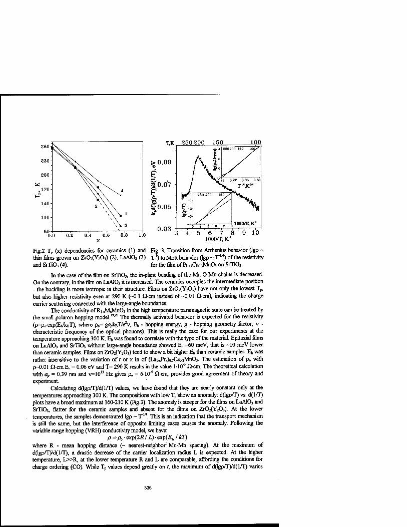
T,K 250 200 150 100
1000/T, K"
Fig.2 Tp (x) dependencies for ceramics (1) and Fig. 3. Transition from Arrhenius behavior (lgp ~ thin films grown on ZrCfeOfA) (2), LaA103 (3) T1) to Mott behavior (lgp ~ T""4) of the resistivity and SrTiOs (4). for the film of PrwCaosMnOs on SrTi03.
In the case of the film on SrTi03, the in-plane bending of the Mn-O-Mn chains is decreased. On the contrary, in the film on LaAlCfe it is increased. The ceramics occupies the intermediate position - the buckling is more isotropic in their structure. Films on Zr02(Y203) have not only the lowest Tp, but also higher resistivity even at 290 K (-0.1 il-cm instead of -0.01 Qcm), indicating the charge carrier scattering connected with the large-angle boundaries.
The conductivity of Ri.xMxMh03 in the high temperature paramagnetic state can be treated by the smafl polaron hopping model.'9,20 The thermally activated behavior is expected for the resistivity (p=p0-exp(Eh/kBT), where p„= ga^T/eS-, Eh - hopping energy, g - hopping geometry factor, v - characteristic frequency of the optical phonons). This is really the case for our experiments at the temperature approaching 300 K. Eh was found to correlate with the type of the material. Epitaxial films on LaA103 and SrTiOs without large-angle boundaries showed Eh -60 meV, that is -10 meV lower than ceramic samples. Films on Zr02(Y203) tend to show a bit higher Eh than ceramic samples. Eh was rather insensitive to the variation of t or x in of (Lai.xPrx)o.7Cao.3Mn03. The estimation of p„ with p~0.01 fi-cm Eh = 0.06 eV and T= 290 K results in the value MO'312-cm. The theoretical calculation with ap = 0.39 nm and v=1013 Hz gives p„ = 6-10"* ficm, provides good agreement of theory and experiment.
Calculating d(\gp/T)/d(l/T) values, we have found that they are nearly constant only at the temperatures approaching 300 K. The compositions with low Tp show an anomaly: d(lgp/T) vs. d(l/T) plots have a broad maximum at 160-210 K (Fig.3). The anomaly is steeper for the films on LaA103 and SrTiCb, flatter for the ceramic samples and absent for the films on Zr02(Y203). At the lower temperatures, the samples demonstrated lgp - T"w. This is an indication that the transport mechanism is still the same, but the interference of opposite limiting cases causes the anomaly. Following the variable range hopping (VRH) conductivity model, we have:
p = p0- exp(2Ä / L) ■ exp(Eh I kT) where R - mean hopping distance (~ nearestaeighbor'Mn-Mn spacing). At the maximum of d(lgpflT)yd(l/T), a drastic decrease of the carrier localization radius L is expected. At the higher temperature, L»R, at the lower temperature R and L are comparable, affording the conditions for charge ordering (CO). While Tp values depend greatly on /, the maximum of d(lgp/T)/d(l/T) varies
336

insignificantly with the change of x. The absence of the maximum of d(lgp/T)/d(l/T) for the films on Zr02(Y203) can be understood upon taking into account that the large-angle boundaries dominate their structure. The higher resistivity of the films as compared to the films on the perovskite substrates (including p„ values) means limitation of L by such boundaries. The effect conceals the point of crossover. Nevertheless, lgp ~ T""4 dependence is valid at the lower temperature.
Below Tp, Ri.xMxMnQs doesn't obey the law p ~ T as expected for normal metals. Some attempts were made to approximate the experimental data by the parabolic law p ~ T, which implies the electron-electron interaction as the predominant scattering mechanism.21 Unfortunately, without additional suppositions, the approximation is valid only for a narrow temperature range. We have found that the function p ~ exp(aT°) fits experimental data in wide temperature range below Tp and is valid for (Lai.xPrx)o.7Cao.3Mn03 in either bulk or thin film form, as well as for other Ri.xMxMn03
compositions studied. The n value correlates with Tp. For Tp > 200 K n approaches 1, while for values of Tp< 200 K, n increases up to 3-4. The only exclusion occurs in films on Zr02(Y203) which have n~2 independent of x (and consequently Tp). At Tp, the sharp maximum in resistivity was observed (Fig.4). The effect is characteristic for the ceramics and films on LaA103 and SrTi03. Films on Zr02(Y203) don't reveal such an effect. The experimental data probably can be fitted by the model of the thermally activated trapping of the itinerant electrons with the temperature dependent activation energy.
0.6
0.4
<T 0.2 -
Q. "M 0.0
^-0.2
-0.4
-0.6
50000
40000
O Q 30000 B 'g 20000
Pi 10000
ing
/V1 3000 Ö
o \ H/2Jk B O ' <ZJ a »/v\. 2000 p
O k j ij Iz ^t -1000 gj
\i\\U heating^** 03
2.1 2.2 2.3 log(T.K)
2.5 140 ^ 160 180T^ Temperature, K
200
Fig.4 Fit of the resistivity below Tp by p
1)
Fig.5 Magnetoresistance of Lao.35Pro.3sCao.3Mn03 film on LaA103:1) zero magnetic field; 2) 0.3 T. exp(aT°) for (Lai.xPrxX7Cao.3Mn03 ceramics:
x=0,2) x=0.25,3) x=0.5 4) x=0.75.
Antiferromagnetic ordering, taken alone, is metastable when compared to the ferromagnetic one. The CO stabilizes the antiferromagnetic state. (Lai.xPrx)o.7Cao.3MnC)3 with t > 0.91 are found between two extremes depending on the temperature. The presence of two potential minima manifests itself by the hysteresis of resistivity of (Lai-xPrx)o.7Cao.3Mn03 samples and high sensitivity to the magnetic field stabilizing the ferromagnetic state (Fig.5). The magnetic field of 0.3 T was enough for 32 times decrease of the resistivity for a Lao.35Pro.3sCaojMn03 film on LaA103 at 155 K.
CONCLUSIONS
The CO starting in (Lai-xPr^.TCaosMnOs at 160-210 K leads to the drastic variation of the localization radius of the small polaron resulting in the switching from Arrhenius behavior (lgp ~ T1) to Mott behavior (lgp ~ T""4) of the resistivity. Tp is controlled by tolerance factor t, which determines
337

the mean bending of Mn-O-Mn chains. The tensile strain in the thin epitaxial films on perovskite substrates results in the bending of such chains in and out of the film plane producing an effect on Tp
comparable with the effect of chemical pressure near to the critical value t ~ 0.91. Large-angle boundaries dominating the structure of the films on ZrOatYA) increase the resistivity both above and below Tp, but the mechanism of conductivity is still retained. The most profound variation of resistivity around Tp is characteristic for thin epitaxial films on perovskite substrates providing higher sensitivity to the magnetic field.
ACKNOWLEDGEMENTS
This study was partly supported by Copernicus Program (grant No. PL 96-4292) and RFBR (grant No. 97-03-32979a).
REFERENCES
1. CNR. Rao, A.K. Cheetham and R. Mahesh, Chem. Mater. 8, p.2421 (1996). 2. C.Zener, Phys. Rev. 82, p.403 (1951). 3. A.J. Millis, P.B. Littlewood and B.I. Shraiman, Phys. Rev. Lett. 74, p.5144 (1995). 4.G.M. Zhao, K. Conder, H. Keller and K.A. Mueller, Nature 381, p.676 (1996). 5. AJ. Millis, Phys. Rev. B 53, p.8434 (1996). 6. R. Mahesh, R. Mahendiran, AK. Raychaudhuri and C.N.R.Rao, Appl. Phys. Lett. 68, p.2291 (1996). 7. H.Y. Hwang, S.W. Cheong, N.P. Ong and B. Batlogg, Phys. Rev. Lett. 77, p.2041 (1996). 8.K.M. Krishnan, AR. Modak, C.A Lucas, R. Michel and H.B. Cherry, J. Appl. Phys. 79, p.5169 (1996). 9.S. Jin, T.H. Tiefel, M. McCormack, R.A Fastnacht, R. Ramesh and L.H. Chen, Science 264, p.413 (1994). 10. O.Yu. Gorbenko, V.N Fuflyigin, Y.Y. Erokhin, I.E. Graboy, AR. Kaul, Yu.D. Tretyakov, G.Wahl and L.Klippe, J. Mater. Chem. 4, p.1585 (1994). 11. O.Yu. Gorbenko, AR. Kaul, NA Babushkina and L.M. Belova, J. Mater. Chem. 7, p.747 (1997). 12.0.Yii. Gorbenko, NA Babushkina, L.M. Belova, AA Bosak, V.A Amelichev, AR. Kaul and G Wahl, in XTV International Conference on CVD and EuroCVD-11. edited by M.D. Allendorf and C. Bernard (Electrochem. Soc. Proc. 97-25, Pennington, 1997), p.l 101-1108. 13. J.L. Garcia-Munos, M. Suaidi, J. Fontcuberta and J. Rodriguez-Carvajal, Phys. Rev. B 55, p.34 (1997). 14. AM. Gazer, Acta. Cryst. A 31, 756 (1975). 15. D. Liu, Q. Wang, H.L.M. Chang and H. Chen, J. Mater. Res. 10, p.1516 (1995). 16. W. Ito, A Oishi, S. Mahajan, Y Yoshida and T. Morishita, J. Mater. Res. 10, p.803 (1995). 17. O.Yu. Gorbenko, AR. Kaul, V.N. Fuflyigin, AAMoIodyk, M.A Novozhilov, A.A. Bosak, V. Amelichev, G. Wahl and U. Krause, J. Alloys & Comp. 251, p.337 (1997). 18. H.Y. Hwang, S.W. Cheong, P.G Radaelli, M. Marezio and B. Batlogg, Phys. Rev. Lett. 75, p.914 (1995). 19. J.S. Zhou, W. Archibald and IB. Goodenough, Nature 381, p.770 (1996). 20. MJaime, H.T. Hardner, M.B. Salamon, M. Rubinstein, P. Dorsey and D. Emin, Phys. Rev. Lett. 78,p.951(1997). 21. A Urushibara, Y. Moritomo, T. Arima, A Asamitsu, G. Kido and Y. Tokura, Phys. Rev. B 51, p.14103 (1995).
338

ONE AND TWO COLOR PHOTOREFRAC1TVE PROCESSES IN SPUTTERED WO3 FILMS
Rebecca Bussjager*, Joseph M. Osman*, J. Chaiken&
*Rome Laboratory, Griffiss AFB, New York 13441-4515 §Laser Chemical Corporation, 302 Edwards Dr., Fayetteville, New York 13066 and Department of Chemistry, Syracuse University, Syracuse, New York 13244-4100, jchaiken@syr.
Abstract
As-deposited and derivatized W03_x films of various stoichiometry were examined in a "nonlinear interface" configuration. The optical properties of the films at 632 ran were modulated using 850 nm and 488 nm CW lasers either separately or simultaneously, Some films were modified by electrochemical reduction. Purely photoinduced changes were interpreted in the context of photoinduced chemistry involving water and/or oxygen exchange with the ambient atmosphere. Both reversible and irreversible changes were observed. Applications as either all-optical switches or logic devices are discussed.
Introduction
Monoclinic tungsten oxide1, m-WC>3, exists under normal ambient conditions as an assembly of edge and corner sharing WOß octahedra which can be identified by vibrational spectroscopy2. The tungsten is present in both W+5 and W+6 oxidation states with the presence of W+5 being associated with the degree of edge sharing. Coalescence growth of edge sharing octahedra into so-called crystallographic shear planes(CS)3. The formation of CS planes allows the lattice to compensate for the loss of oxygen.The color of the oxide becomes progressively more blue with the loss of oxygen. This change in the spectroscopic properties with varying W+5/W+6 ratio or, equivalently, the net oxygen deficiency is the basis for many proposed1 photo and/or electrochromic applications for WO3.
The oxygen deficency and W+5/W+6 ratio can be manipulated either photo or electrochemically. Ambient conditions for prospective applications generally includes water to some extent. During sputtered film preparation, water is often introduced into the sputtering mix as a convenient means for introducing hydrogen into the lattice. Hydrogen, i.e. protons, are thought to stabilize the W+5 which may be present in the lattice, with or without the loss of oxygen. We suggest that, for all practical purposes, during either electrochemical or photochemical processing, or some combination of the two, more than one chemical process usually occurs. Sequential reactions occur as well as reactions which occur in parallel and, with regard to applications, these processes may or may not reinforce each other's positive or negative effect(s). We performed the experiments described in this paper in order to study these effects and to test WO3 in a different type of device configuration.
The concept of a nonlinear interface optical switch, NIOS, was first proposed in 1976 by Kaplan4'5. As shown in Figure 1, the basic idea is that light is made to contact an interface between two media having carefully chosen optical properties. There is a reflection at the interface because the two media have different indices of refraction. One medium is chosen so that it's nonlinear optical response is such that at some incident laser power, its index of refraction becomes equal to that of the other medium. At this power the reflection at the interface vanishes and switching occurs. This situation can be set up to be a zero background measurement and so becomes a very sensitive probe of index of refraction changes6.
In this paper we describe the results of experiments in which we study the photoinduced index change of WO3-X films using both a NIOS configuration. We have also used a collinear normal incidence configuration but those results will not be presented here. For the type of sample
339
Mat. Res. Soc. Symp. Proc. Vol. 495 ° 1998 Materials Research Society

studied and our particular choices of processing conditions, these results show the relative extent of water induced chemistry and oxygen exchange chemistry. We begin with a very brief review of
Totally Internally Reflected (TIR) light
transmitted data light 632.8 nm ~"
Figure 1.
wo3_x
NIOS configuration as used in this study
the known photochromic and electrochromic chemistry of W03_x. We then describe experimental methods of some one and two color experiments and the results obtained. Finally, we discuss these results and their ramnifications with regard to certain applications in optical memory and signal processing.
Background
Deb published the first paper7 describing the photochromic properties of W03.x. Since then there have been many papers1 relating both to the photo and the electrochromic properties of this material. We and others8 have emphasized the role of oxygen exchange in the photochromism. Equations la-lc summarize this chemistry where it is clear that the oxygen deficient products contain the aforementioned CS planes. Others9 have emphasized the role of electron and
4W03(s) = 2W205(s) + 02(g) 8W03(s) = 2W4Oi i(s) + 02(g) nW03(s) = 2W„03n.i(s) + 02(g)
(la) (lb) (lc)
proton injection in the so-called "double-injection" model of the electrochromic effect. This process is actually quite complicated and equations 2-4 summarize the situation as we view it. Given sufficent energy input, either by photon absorption or by external field induced charge carrier motion, it is possible to convert some portion of the W+6 in the WO3 lattice to W+5.
W205 + H20 —> 2e- + 2W03 + 2H+ 2H20 + 2e- -—> H2 + 20H-
W205 + 3H20 - > H2 + 20H- + 2W03 + 2H+
(2) (3)
(4)
The photochromic process was thought7'8 to be possible only using superbandgap excitation but we found that decidedly subbandgap photons were quite capable of driving the oxygen exchange. Given the energetics of process (4) the same is probably true for some of the processes we have attributed to electrochromic response as well.
340

The characteristics of the various processes may provide some handle on sorting out their various contributions to the net effect for a given set of processing conditions. The pure photochromic process, as we have written it in (1) would seem to be most prevalent near the gas solid interface and may involve oxygen atom/vacancy migration while the processes represented in (2)-(4) require bulk diffusion of protons and hydroxy species in the lattice. It is not altogether clear which of these processes would be the faster. We note that Yoshiike10 has claimed that using superbandgap excitation it is possible to observe the photochromic effect in 200 psec although we cannot say whether the color change occurs during that period or whether such an exposure is sufficient to cause a color change which actually occurs later.
Experimental
We briely describe our methods and materials here since they have been described in detail elsewhere11. We have used DC magnetron sputtering with a tungsten oxide target to produce films having 102 -103 nm thickness on a wide variety of substrates. In this study substrates ranging from quartz to ZnS were employed and the films studies were all =200 nm thick. Thicknesses were measured using a Tencor Alpha Step profilimeter. UV visible and infrared spectroscopy were used on these films to insure their identity. Depending on the oxygen/argon/water proportions in the sputtering atmosphere, the stoichiometry of the films could be varied over a wide range of W+5/W+6
stoichiometries. The results presented in this study were common to all the films with the main differences being between films which were mostly W+6, i.e. yellow, and films which contained appreciable amounts of W+5, i.e. blue. We12 and others have reported earlier that ESCA spectra confirm that the blue/yellow color can be atributed to the presence of W+5 and W+6 and not to the presence of W+4. In some experiments, yellow films (W+6)were chemically reduced using IN H2SO4 and Sn metal as described in the literature.
One apparatus used to laser process the films is shown below in Figure 2. This apparatus have been described in detail elsewhere so only a very brief description is given here. To mimic the properties of commercially available CW lasers, blue light from an Ar+ ion laser, 488 nm, red light from a HeNe laser, 633 nm, and infrared light from either a MOPA diode laser(SDL, Inc), =978 nm, or a simple single element laser diode was employed. Unlike the situtation depicted in Figure 1, in these experiments the control light was brought to the interaction zone from the backside of the prism. An Olympus 80x objective with a .8 NA was used to focus the Ar+ beam and the infrared beam in the same plane yielding spot sizes of=10-15 urn in diameter as measured with a reticle under a microscope. A Vincent Associates Uniblitz mechanical shutter was used to modulate the blue light.
Results
In our earlier published work12-13 we emphasized the laser chemical processing of yellow as-deposited films such that they could be cycled between yellow and blue states. While yellow films could allow reversible optical data storage functions we focused our attention more on blue
I WCCD ! Power Meier
l/2waveplatc |— Jt fanrtnim' T 488laser
■ Pellicles* ObjWiVe \j\
ShutterPBS W Filmx-T W Cj on prism| -+- 632.8 ];,£„
white tight ■ ■ |incfilier
source ; Power Mclcr
Figure 2 Schematic of NIOS test apparatus.
341

Switched HeNe Light at Three Incident Angles for a W205 Film
...—HeNe switched at 50.479 degrees
—— HeNe switched at 53.878 degrees
HeNe switched at 57.573 degrees
Ar laser power into objective (mW)
Figure 3 Switching of W03_x films at three different angles of incidence
as-deposited films in the present study. Figure 3 shows the reflectivity of red light sensed at a 200 nm blue WC>3_X film on a quartz right angle prism in an NIOS configuration. Blue 488 nm light, no infrared, was brought to a focus within the region illuminated on the hypotenuse by the HeNe probe(data) beam. When the light impacts the hypotenuse in a NIOS configuration, the illuminated region must be elongated in one direction. It was therefore possible to change the amount of spatial overlap between the red data light and the blue control light. As the power of the 488 control light was ramped up, the amount of detected red light always showed a discontinuous change at the power which caused switching. Decreasing the laser power did not completely restore the original optical properties of the films. The percentage of the incident light which "switched" involved the spatial overlap of the control and data light as well as the angle of incidence of the two beams. When starting with a yellow film, qualitatively similar results to those we published earlier were obtained.
In the same configuration it was possible to also bring in the light from one of the infrared sources. Figure 4 shows a sequence of experiments on different spots which summarizes the observed results. The red light was always clearly switched by combined blue and infrared light acting together. After switching occured, the infrared light alone caused a relatively small but reproducible change. It was possible to choose a set of levels which caused no switching unless both infrared and blue light were present simultaneously.
Contrast of HeNe with Response to Control Light for a W205 Film
Hi No control light, HeNe only F^l 358mWAr + HeNe Hg] 35 8mWAr + 375mWIR + HeNe
r—1375 mWIR* HeNe
Sets of Switching
Figure 4 Variation in reflected HeNe (data) power under different laser exposures
342

nnj^noirinji ,*TvJ
shutter output
Lar^emodulation
'J*V**HvT:
of He$Ie switching profile -fr-H-i-H- i i j i +-f ■ ! ■ ■
Small modulation of HeNe sjwitehihg profile
'••■I : W : VÜ :1*J
Figure 5 Oscilloscope trace showing switching of HeNe with Ar+ modulation
Figure 5 shows modulated reflected HeNe light as a function of the using a shutter to modulate the 488 nm control light. By synchronizing the oscilloscope trace to the initiation of the first exposure of the blue film to 488 it is possible to observe the complete overall effect without any infrared light being present. On the first exposure of the film to 50 mW of 488 nm light, a large modulation in the reflected HeNe light is observed. After the initial exposure each successive exposure causes a completely reversible modulation which we have observed for thousands of cycles.
Although not shown here14, there is a distinct color change which accompanies each switching regime. The initial switching event causes a nearly complete decoloration of the film. The later modulation involves no obvious color change. Observing the films using various color combinations of front and backlighting suggests the films are clear.
Discussion
The results on as-deposited blue films show that distinct all optical, reversible, switching can be implemented using tungsten oxide films in a NIOS configuration. The use of two colors increases the switching contrast although the improvement is not large. The results also show that there are two regimes of switching. We shall discuss each of these observations in the context of the known photo and electrochromism of tungsten oxide and in the context of possible applications.
An important result of this study is that two regimes of switching were observed. The initial switching is much less reversible than is the second regime. On this basis we suggest that the first regime of switching is associated with the gas-solid, oxygen incorporation chemistry represented by reaction la-c. The second regime would appear to be associated with the water mediated oxidation- reduction chemistry associated with the reaction 4. The amount of W+6 to W+5 interconversion would seem to be much less than that associated with the oxygen transfer chemistry since there is no apparent color change.
Another possibility is that the small index of refraction change associated with the observed switching could be simply due to the motion of water. Water is present in the tungsten oxide lattice and can move in the channels created by the packing of the WOö octahedra. The motion of water would seem to be driven thermally in that case and the amount of modulation is approximately the same as was observed using either the 488 nm light as for the 978 nm light. However, given the
343

variablility in contrast obtained due to spatial overlap and power density variation, we cannot unequivocably eliminate either of these possibilities at this time. We note that many attempts to discern a surface morphology change, i.e. a "crater", on the surface of the films after the various regimes of switching had been visited, all failed. Thus, the observed optical changes are due to chemical changes of the material and not thickness or other physical changes.
The appearance of a distinct threshold for optical switching allows for the possibility of using the NIOS switches in a "latching" application. In this case, once the switch has opened, or closed, it stays in that state. The timescale of these measurements was not ideal for testing the reversibility of these changes but given our eariler experience with such films, we suspect that all of the changes can be made reversible to some extent. The reversible regime is quite interesting particularly since, given appropriate choice of spatial overlap and laser power density considerations, an all optical switch with extreme versatility seems possible. The huge change in refractive index with the initial switching event appears to be ideal for WORM type optical memory applications. Research into this and other possible applications is on-going.
Conclusions
We have observed two regimes of all optical switching using m-W03_x films. The first is much less reversible than the second and involves a much larger index of refraction change. This regime would seem to correspond to oxygen incorporation into the film from the surrounding gas phase. The second regime is fully reversible, quite robust and would seem to be associated with water incorporation. Neither explantion is unequivocal at this point but both effects suggest a variety of all optical switching and memory applications.
Acknowledgements
This research was supported in part by Laser Chemical Corporation. All thin film fabrication took place at the Cornell Nanofabrication Facility.
References
1 C. G. Granquist, "Handbook of Inorganic Electrochromic Materials"(EIsevier, Amsterdam, 1995) 2 M. F. Daniel, B. Desbat, and J. C. Lassagues, J. Solid State Chem. 73, 127-139(1988), J. Solid State Chem. 67, 235-247(1987) 3 see for example M. Sundberg and R. J. D. Tilley, J. Solid State Chem. 11, 150- 160(1974) 4 see Alexander E. Kaplan, Soviet Physics JETP, 45, 896-9045(1977), Appl. Phys. Lett. 38, 67-69(1981) and references therein 5 J. M. Osman, R. Martin Villarica, J. Chaiken, Proc. SPIE 1626, 217-225(1992) 6 for example see S. Henon and J. Meunier, Rev. Sei. Instrum. 62, 936-939(1991) 7 S. K. Deb, Philos. Mag. 27, 801(1973) 8 C. Bechinger, G. Oefinger, S. Herminghaus and P. Leiderer, J. Appl. Phys. 74, 4527-4533(1993) and later references 9 R. S. Crandall and B. W. Faughnan, Appl. Phys. Lett. 26, 120(1975) 10 Yoshiike, et al. U.S. Patent 4,711,815 1 1 Rebecca Bussjager, J. M. Osman, R. Martin Villarica, J. Chaiken, Proc. SPIE 3075,34-46(1997) 1 2 R. Martin Villarica, J. Chaiken, Fazio Nash, J. M. Osman, Rebecca Bussjager, Proc. Mat. Res. Soc. 397, 347-352(1996) 13 J. M. Osman, Rebecca Bussjager, Fazio Nash, R. Martin Villarica, J. Chaiken, Appl Phys A. in press 1 4 Matthew J. Coti, Corey Radloff, J. M. Osman, Rebecca Bussjager, Fazio Nash, R. Martin Villarica, J. Chaiken, J. Appl Phys. Manuscript in preparation
344

REMOVAL OF TITANIUM OXIDE GROWN ON TITANIUM NITRIDE AND REDUCTION OF VIA CONTACT RESISTANCE
USING A MODERN PLASMA ASHER
Mohamed Boumerzoug, Han Xu, Richard Bersin, Ulvac Technologies Inc., Methuen, MA; Peter Mascher, Ginutis Balcaitis, Department of Engineering Physics, McMaster University, Hamilton, ON, Canada.
ABSTRACT
In making multi-level interconnects, a via layer is generally made of a dielectric layer grown on a TiN/AlSiCu/TiN metal stack. The via contact hole to the lower level metal is first etched after metal patterning and intermetal oxide deposition, then the resist mask for via etch is stripped in an oxygen plasma at high temperature before filling the via with tungsten or aluminum. However, during the resist stripping process, the titanium nitride (TiN) is exposed to oxygen radicals and becomes oxidized. This oxidized surface leads to high via resistance and may cause yield loss and poor adhesion of the subsequently deposited metal. Thus, the oxide layer must be removed completely before filling the via hole.
Utilizing a modern asher and combining microwave downstream plasma and low damage RIE we have successfully developed an integral process to strip the resist and to remove any oxidized TiN film. This process also gives clean vias that are free of polymer residues from the etching process.
Samples were characterized using Auger electron spectroscopy (AES), scanning electron microscopy (SEM), ellipsometry and via resistance measurements. The AES depth profile measurements and ellipsometry show clearly that a titanium oxide has grown onto TiN during the oxygen downstream ashing and is completely removed when adding the RIE step. The electrical measurements show that the resistance of vias cleaned with this two step process in a single tool is comparable to that of vias cleaned with Ar sputtering using a separate tool after the oxygen ashing process.
INTRODUCTION
The removal of photoresist and polymer residues after etching process using plasma techniques has gained considerable technological prominence [1,2]. Both microwave plasma and RF plasma have been applied to photoresist stripping and post etch residue removal [3,4]. Plasma assisted ashing is influenced by a number of parameters such as total pressure, gas flow rates and power. The goal of the good ashing process is to remove from the wafer surface photoresist, residual organics, residual polymer containing metals and oxides from the etching process, or native oxide or oxides formed on the surface during the ashing process itself.
TiN films are well known for their combination of desirable properties, such as high melting point, good thermal stability and low resistivity. Due to these good characteristics TiN, is used as a diffusion barrier and antireflect coating over metal for aluminum interconnect metallization in silicon device technology [5,6]. For such applications it is
345 Mat. Res. Soc. Symp. Proc. Vol. 495 c 1998 Materials Research Society

Figure 1: SEM picture of via sample after etching process.
very important to know the effect of different processing conditions on the TiN characteristics.
In order to stop the lateral etching during the via etching, the gas mixture is chosen to enhance the polymer growth on the sidewall. A typical mixture uses CF4/CHF3, usually in combination with a noble gas such as Ar and He [7]. Figure 1 shows a cross section of via after RIE etching process. It shows that a thick polymer was grown on the via sidewall. This sidewall polymer must be removed with the ashing process to ensure a good adhesion of the subsequent deposited material. The presence of TiN at the bottom of the via make the removal of post etch residues difficult. During the via etch, an overetch is often required to compensate for the non-uniformity of the topography over the wafer. During the overetch sputtered material form the bottom and side of the via is deposited on the sidewall. The sputtered Si02 and TiN get incorporated into the side wall polymer. TiN forms Ti-0 bonds when it react with oxygen. Thus, the formed polymer will be hardened. For wet cleaning technique, hydroxylamine based solvent has been found to be effective solution for removing this type of hardened polymer. However, there are raising concerns about the attack of the bottom metal layer and the stability of the solvent due to the water evaporation. For Dry only processes the ashing gas mixture should be chosen to make the Ti -O and Si-0 containing residues volatile or water soluble. In order to break the strong Si-0 and Ti-0 bonds during the ashing process, a high surface energy is needed which can be supplied by ion bombardment, a raised wafer temperature, or a combination of the two.
The Phoenix ashing tool has the capability of using ion-assisted processes using RIE plasma; neutral free-radical processes through remote microwave plasma; or running microwave downstream and RIE simultaneously. Pure oxygen plasma or fluorine /oxygel plasma that can render the post ash residue water soluble can be used. Using this capability, a two step process was developed. The first step is a downstream oxygen (O2) and forming gas (N2/H2, H2 = 3%) mixture microwave plasma and is for the photoresist bulk removal. Oxygen plasma is widely used for etching polymeric materials. The oxygen radicals and ions in the plasma react with the polymer to form CO, C02 and H20 as a volatile product. The second step is an CF4/N2/H2 RIE plasma that render the sidewall polymer residue soluble and remove the oxide grown on the TiN.
346

There are reports on via cleaning using fluorine based chemistry [8,9]. To our knowledge there have been no reports on using a single ashing tool for the photoresist ashing, residue removal, and native oxide or oxide grown removal by the ashing process itself. By combining the removal of resist residue and native or process grown oxide in a single tool, a more cost effective process can be achieved.
EXPERIMENT DETAILS
Eight inch wafers were used for these experiments. The vias were etched using RIE plasma with Ar/N2/CHF3/CF4 gas mixtures. The resist and residue removal experiments were performed with the Phoenix asher from Ulvac Technologies Inc.. Microwave energy with frequency of 2.45 GHz propagate from the microwave power supply to the plasma source through a wave guide. The tool is equipped with a load-lock. This configuration will ensure process reproducibility, excellent wafer temperature control; and rninimize the contamination due to exposition to atmosphere. The dependence of the Ti02 growth rate during the O2/N2/H2 stripping was measured as a function of the process time. The dependence of the Ti02 etch rate during the CF4/N2/H2 RIE step was measured as a function of the applied RF power, CF4 content and the wafer temperature. The wafer temperature was varied from 140 to 220 °C. The CF4 content in the RIE step was varied from 0 to 25%. To confirm that a Ti02 film is grown on TiN due to the oxygen plasma exposure, a set of experiments were conducted
Figure 2: SEM picture of via sample that was ashed using two-step process: A) top view and B) cross section.
347

30 60 90 120 O2/N2H2 Plasma Time [sec]
with a single step O2/N2/H2 downstream plasma using blanket TiN wafers. The film optical index and thickness were measured by an ex-situ ellipsometer (Rudolph Research) assuming a thin layer of TiÜ2 on TiN. For all experiments the input microwave power was set to 2kW and the pressure was kept constant. The wafers were washed with dionized water for 5 min. after being processed. To evaluate the cleanliness, vias with different opening size and aspect ratio were observed with the SEM. Pictures of top view and cross section were taken from the center and edge of the wafer. Via resistance measurements were performed on via of size 0.45 Urn.
RESULTS AND DISCUSSION
Figure 2 shows SEM photographs of via sample that was dry ashed using two-step process and dionized water rinsed. A) top surface view B) cross section view. It shows clearly that the polymer residue on the sidewall of the via was completely removed. There is no visible undercut of the TiN. Since the TiN is used to promote the adhesion of the subsequent metal filling, it is very important to avoid undercutting and insulating layer deposition on its surface. The top view shows that the surface is free of any residues. It is also important to keep high selectivity to the exposed SiC>2 layer. A major loss of the oxide will change the aspect ratio and the size of the via. Under our processing conditions The oxide loss is below 20 Ä as measured with ellipsometry.
Figure 3 : Ti02 growth vs. O2/N2H2 plasma time.
_ 7dn .5 e 200 -
-160
1 120 ♦/
/4 ♦/
JS a so -
s 4°- P 0 V^- h— 1
50 100 150 200 250 300
RF Power [Watts]
Figure 4: TiÜ2 etch rate vs applied RF power.
348

.—. " '^—^——__
.3 Jl20- tan«
V •*» £ 80- ■a + / o 4« W 40 IS
O /• H 0' *-—I 1 1 1 1
0 5 10 15 20 25
CF4/(CF4 + N2H2)[%] Figure 5: TiCfe etch rate vs. CF4 content.
30
240
Figure 3 shows the effect of the downstream O2/N2/H2 plasma time on the oxidation of the TiN. As stated before raising the temperature will lead to high surface energy and thus enhance the reactions at the surface. The understanding of the effect of Downstream O2/N2/H2 plasma on the growth of TiC>2 oxide is very important for various reasons. The TiÜ2 that is formed during the ashing step can be removed with plasma RIE. However, the RIE step has to run long enough to remove the oxide. A short RIE would leave some residues and lead to higher contact resistance. Overetching might also leave some topography and thus affect the adhesion of the subsequent deposited film.
The energy of particles bombarding the sample will also affect the etching rate of TiC>2. At very low pressure an ion is accelerated across the sheath and strikes the substrate with an energy similar to the sheath voltage. At relatively high pressure, comparable to our processing pressure, above 0.4 Torr, the ions will collide with neutrals in the sheath area . The ion energy will be attenuated thus reducing the damage due to ion bombardment. Forming gas is added to provide hydrogen active species. It was reported that hydrogen plasma causes a significant decrease of the oxidized species and increased TiN component in the XPS spectrum [10]. The etch rate of TiÜ2 is reported to increase linearly with the bias voltage. CFX is also reported to deposit at the bottom of high aspect ratio vias but is removed with RIE step [11].
The relation between TiC>2 etch rate and the applied RF power is showed in figure 4. As power is increased, there is an increase in reactive species generation, ion bombardment, and the etch rate of Ti02. In a CF» plasma the following positive ions: CF3
+, CF2+, CF+, C+ and C2F5
+ were detected [12]. Negative F ions were also detected
a
I es « JB
w «>« o
H 160
220-
200-
180-
140 160 180 200 220 Wafer Temperature [°q
Figure 6: TiQ2 etch rate vs. wafer temperature.
240
349
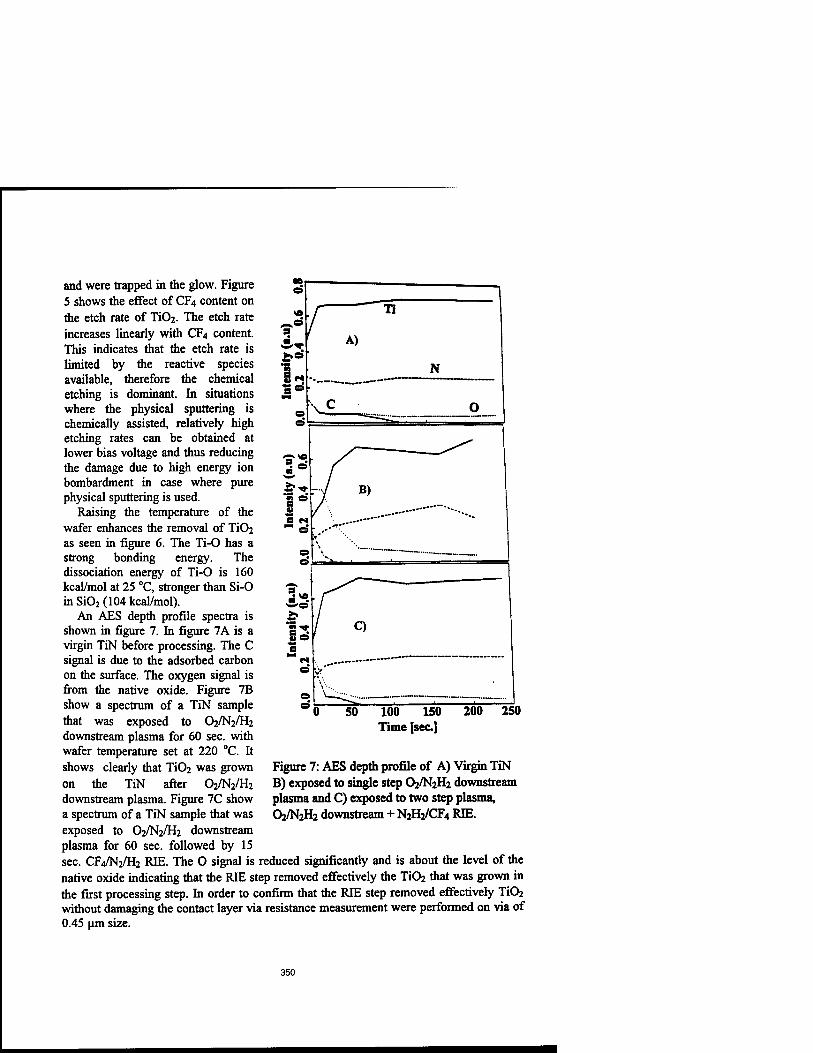
and were trapped in the glow. Figure 5 shows the effect of CF4 content on the etch rate of Ti02. The etch rate increases linearly with CF4 content. This indicates that the etch rate is limited by the reactive species available, therefore the chemical etching is dominant. In situations where the physical sputtering is chemically assisted, relatively high etching rates can be obtained at lower bias voltage and thus reducing the damage due to high energy ion bombardment in case where pure physical sputtering is used.
Raising the temperature of the wafer enhances the removal of Ti02
as seen in figure 6. The Ti-0 has a strong bonding energy. The dissociation energy of Ti-0 is 160 kcal/mol at 25 °C, stronger than Si-0 in Si02 (104 kcal/mol).
An AES depth profile spectra is shown in figure 7. In figure 7A is a virgin TiN before processing. The C signal is due to the adsorbed carbon on the surface. The oxygen signal is from the native oxide. Figure 7B show a spectrum of a TiN sample that was exposed to O2/N2/H2 downstream plasma for 60 sec. with wafer temperature set at 220 °C. It shows clearly that Ti02 was grown on the TiN after 02/N2/H2
downstream plasma. Figure 7C show a spectrum of a TiN sample that was exposed to 02/N2/H2 downstream plasma for 60 sec. followed by 15 sec. CF4/N2/H2 RIE. The O signal is reduced significantly and is about the level of the native oxide indicating that the RIE step removed effectively the Ti02 that was grown in the first processing step. In order to confirm that the RIE step removed effectively Ti02
without damaging the contact layer via resistance measurement were performed on via of 0.45 urn size.
100 150 Time [sec]
Figure 7: AES depth profile of A) Virgin TiN B) exposed to single step O2/N2H2 downstream plasma and C) exposed to two step plasma, O2/N2H2 downstream + N2H2/CF4 RIE.
350

Table 1 shows the comparison of via resistance values using the two-step dry process followed by (lionized water rinse and via that was cleaned using a single O2/N2/H2 step process followed by Ar sputtering. Typically, argon sputtering is used to clean the oxidized surface in a separate process. Beside the need for another process chamber or even a separate tool for the removal of the oxide, there has been concern regarding the plasma damage due to this Ar sputter clean. In Ar sputtering high ion energy is needed since the removal of the oxide is purely physical. Obviously, it is beneficial to remove the oxide layer in the resist stripping tool using a process that is chemically assisted . The contact resistance improvement is in agreement with the AES and SEM observations .
Tablel: Normalized to the argon sputtering via resistance for 0.45 [im via.
Current Process Argon sputtering Positive Overplug 0.92 1.0 Zero Overplug 0.64 1.0 Negative Overplug 1.0 1.0
The results in table 1 show clearly that the resistance of the vias cleaned in the Phoenix asher using a two-step process is better or comparable to that of vias cleaned with argon sputtering.
CONCLUSION
The use of combination of microwave downstream and low damage RIE was demonstrated as an effective post via etch cleaning. The combination of the two step eliminate the need for high ion energy Ar sputtering to remove the grown oxide on TiN.
ACKNOWLEDGMENTS
The authors would like to thank Dr. David Feiler of Rockwell International for providing the via electrical data and Michael Salmon of Ulvac Technologies for assisting in SEM characterization of the samples.
REFERENCES
1. R. L. Bersin, M. Boumerzoug, Q. Geng, I. Nakayama, H. Xu, Semiconductor Fabtech 6, 341(1997) 2. P. Singer, Semiconductor International, 9 , 83 (1996) 3. A. Usujima, M. Yasui, M. Aoyama, Y. Shioya, J. Electrochem. Soc. 141, 2487 (1994) 4 . J. A. G. Baggerman, R. J. Visser, E. J. H. Collart, J. Appl. Phys., 75, 758 (1994) 5. K. Ramkumar, S. K. Ghosh, A. N. Saxena in Handbook of Multilevel Metallization for Integrated Circuits. Edited by S. R. Wilson, C. J. Tracy, J. L. Freeman Jr. (Noyes Publications, New Jersey, 1993), pp. 97. 6. D. Pramanik, V. Jain, Solid State Technol. 26, 131 (1991).
351

7. Y. Wang, S. W. Graham, L. Chan, S. Loong, J. Electrochem. Soc, 144, 1522 (1997). 8. S. Jimbo, K. Shimomura, T. Ohiwa, M. Sekine, H. Mori, K. Horioka, H. Okano, Jpn. J. Appl. Phys. 32, 3045 (1993). 9. S. Marks, S. W. Graham, T. Uk, C. C. Chang, C. Geller, C. Tse, Electrochem. Soc. Proc, 95-20, 214 (1996). 10. F. Fracassi, R. d'Agostino, R. Lamendola and I. Mangieri, J. Vac. Sei. Technol. A13, 335 (1995) 11. F. D. Eggito, F. Emmi, R. S. Horwath, and V. Vukanivic, J. Vac. Sei. Technol., B3, 893 (1985). 12. R. J. M. M. Snijkers, M. J. M. Van Sambeek, M. B. Hoppenbouwers, G. M. W. Kroesen and F. J. deHoog, J. Appl. Phys. 79, 8982 (1996)
352
EPITAXIAL ZnO PIEZOELECTRIC FILMS FOR RF FILTERS
NURIW. EMANETOGLU*, YICHENG LU*, CHANDRASEKHAR GORLA**, YING LIU*, SHAOHUA LIANG*, WILLIAM MAYO** * ECE Department, Rutgers University, Piscataway, NJ 08855-0909, *[email protected] **Ceramics Department, Rutgers University, Piscataway, NJ 08855-0909
ABSTRACT
ZnO has high piezoelectric coupling coefficient and acoustic velocity; therefore, it is an attractive material candidate for high frequency and low loss filters. Piezoelectric ZnO thin film based RF devices offer the advantages such as low power consumption, circuit miniaturization and cost reduction through integration with main stream MMIC technology. We report CVD growth of epitaxial ZnO thin films on R-sapphire substrates. X-ray diffraction techniques have been used to study the crystallinity and orientation of the films, as well as the epitaxial relationship between the films and the substrate. High-resolution cross-sectional TEM reveals the atomically sharp interface structure. As grown ZnO films exhibit dominant n-type conductivity due to the oxygen vacancies. Excellent piezoelectricity has been achieved through a multi-step Li diffusion under oxygen ambient. Surface Acoustic Wave (SAW) filters with 10- micron wavelength have been fabricated. Low insertion loss and high piezoelectric coupling coefficient have been observed.
I. INTRODUCTION
Over the past decade there has been an explosive growth of wireless communication products. The next generation of wireless communication systems with expanded multimedia capabilities are likely to be deployed at much higher frequencies than current systems, which operate up to 900 MHz. At higher frequencies, 1.5 GHz and higher, practical systems will rely increasingly on the interaction of advances in materials and components. High frequency filters with low loss will be the key elements for the performance of transceivers in communication systems. As operating frequencies move higher, it becomes increasingly difficult to fabricate filters with small critical geometry. In developing high frequency, low loss filters, high quality piezoelectric films lead to low power consumption, cost reduction and circuit miniaturization through integration with mainstream MMIC technology.
ZnO is a piezoelectric oxide with a high coupling coefficient, which makes it attractive for Surface Acoustic Wave (SAW) device applications. ZnO thin films can be deposited on high velocity substrates such as diamond [1] and sapphire [2,3,4,5] for low loss, high frequency SAW filters. Recently, state of the art ZnO based SAW filters operating at 2.5 GHz [2,4] and BAW filters operating in the 1 to 3 GHz band [6] have been reported. Many growth techniques have been employed for ZnO film deposition [2,3,4,5]. Among them sputtering [4] is the most common growth method for polycrystalline ZnO films in acoustic applications. However, it is expected that single-crystal ZnO will provide the highest coupling coefficient. MOCVD technique has been used for high quality epitaxial growth of various semiconductors and oxide materials, including ZnO thin films [3].
In this paper, we present characterization results of MOCVD grown ZnO thin films. Microstructural and electrical characterization will be discussed in detail.
353
Mat. Res. Soc. Symp. Proc. Vol. 495 ®1998 Materials Research Society

ü. EXPERIMENTAL
(1120) oriented ZnO epitaxial films were grown on (1102) A1203 (R-plane sapphire) using a rotating disc MOCVD system, shown in Figure 1. Diethylzinc (DEZ) is the Zn precursor and oxygen (02) is the oxidizer gas. Growth conditions were varied as given in Table 1. The substrates used for the experiment were 3" R-plane sapphire substrates. Resulting film thickness ranged from 0.2 um. to 2.0 urn. and the growth rate of the ZnO film varied from 1.0
um./hour to 10 um./hour. Growth process conditions for the (1120) orientated ZnO epitaxial films on (0ll2) sapphire (R- plane) have been optimized at substrate temperature of 400°C, reactor pressure of
50 Torr, and total flow of 19 Liters per Table 1. Variation range of process variables minute, for ZnO growth using the MOCVD system shown in Figure 1.
Growth Variable Variation Range Temperature 300° C- 600° C Pressure range 20 - 200 Torr Substrate rotation 200 - 600 RPM Total gas flow 10-25 liters/minute
Oa —o C3>~
N, —O—ip CZ>
Coplanar Probe
Figure 1. MOCVD system used for ZnO film growth
Figure 2. SAW Filter and Network analyzer for test setup
The microstructure of the ZnO film after growth was characterized using X-ray diffraction (XRD), Scanning Electron Microscopy (SEM) and Transmission Electron Microscopy (TEM). SAW filters were then fabricated on the ZnO/Al203 system. Lithium diffusion was carried out to compensate for the high conductivity of the MOCVD grown film [3]. Resistivity of the Li-diffused ZnO film was characterized using Transmission Line Model configuration [7,8]. Image reversal photolithography, e-beam evaporation of Al and lift-off processes were used for generating the test device patterns. Aluminum thickness is 2000Ä. Shown in Figure 2 are the SAW device and the test setup. A HP 8753D network analyzer is used to characterize the filters, with Cascade Microtech Air CoPlanar Probes used for on-wafer testing. The test pattern consists of interdigitated transducers, which induce surface acoustic waves. Periodicity of the interdigitated pattern determines the acoustic wavelength of the SAW filter at center frequency. The wavelength of the test devices range from 2um. to 16um. The
354

IDT design is a "solid finger" design, where electrode width and inter-electrode spacing is A/4. The results presented in this paper were obtained with 10|xm. wavelength devices.
^ Sapphire (0 2 4)
s - fc a
JO
A r*
ZnO (1 1 0) c a> c
—j ,IIII
32 36 40 44 48 52 56 60 64 68 72
2-8 (degrees)
Figure 3a. X-ray diffraction 6-20 scan of ZnO film on R-plane sapphire.
ZnO grown on R-plane Sapphire
\FWHM = 900 arc second
-1000 0 1000
<B (arc second)
Figure 3b. Rocking curve of double crystal diffraction for ZnO film. FWHM is approximately 900 arc seconds.
m. RESULTS AND DISCUSSIONS
Microstructural Characterization ä!7S«!'-^iä»ii-rk.'äJSJiS5?i|!
X-ray diffraction 9-26 measurements, double crystal rocking curve measurements, and phi-scan measurements were made to determine the epitaxial relationship of the ZnO film with the R- plane sapphire substrate. From Figure 3a it can be seen that the film has a (110) orientation. From (|)-scan measurements [9] the films were shown to have a single epitaxial relationship with the substrate, this relationship being (1120) ZnO// (1102) A1203 and [ llOO ] ZnO// [ 1120 ] A1203. The full width half maximum (FWHM) of the rocking curve measurements, seen in Figure 3b, is about 0.25°, among the best reported to date. Figure 4 shows a SEM picture of the grown film. The white region in the picture corresponds to the sapphire substrate, due to the charging effect. The film is seen to be dense with a smooth surface. TEM of the ZnO/sapphire interface revealed an atomically sharp interface, as explained in [10]. These properties are crucial for high piezoelectric coupling coefficient and low loss SAW characteristics. Surface acoustic waves extend one wavelength into the material system. The main purpose of using a multilayer structure is to utilize the coupling coefficient of the film and the acoustic velocity of the substrate, thus the film thickness will be less than wavelength at the center frequency. This requires a smooth interface to reduce loss.
Figure 4. SEM picture of ZnO on R-plane sapphire.
355

SAW Characteristics
The as-grown ZnO film is highly conductive, with resistivity in the range of 1 to 100 ßxm. Low resistivity results in electrical conduction in the ZnO film, rather than piezoelectric characteristics. This conductivity is due to oxygen vacancies [11,12]. Cu, Ni and Li are known to compensate for this conductivity. Li diffusion was carried out in this experiment. Resistivity of the Li-diffused ZnO film was characterized using TLM configuration and the resistivity was found to be above 107 ß.cm., which is necessary for SAW applications.
0.2 0.4 0.6 0.8 1.0 1.2 1.4 1.e
Frequency [GHz]
Figure 5a. Frequency spectrum of 10 urn. wavelength device, from 300 MHz to 1.7 GHz. Main SAW response at 406 MHz.
" 370 380 390 400 410
Frequency [MHz]
Figure 5b. Frequency spectrum of the same device device, from 370 MHz to 470 MHz. More detailed view of the main peak.
Frequency spectrum of a sample 10 um. wavelength device is shown in Figures 5a and 5b. Figure 5a. is the frequency spectrum from 300 MHz to 1.7 GHz. The Rayleigh wave response is seen to be at 406 MHz, and peaks corresponding to Bulk Acoustic Waves, harmonic SAWs and the first-order-Rayleigh wave known as the Sezawa wave are also seen in the figure. Figure 5b presents the frequency spectrum between 370 MHz and 430 MHz. A minimum insertion loss of 9.5 dB is observed at this frequency. We found a maximum piezoelectric coupling coefficient, fc2, of 6% has been achieved, dependent on the hA. ratio [1]. The effective acoustic velocity is a function of the acoustic velocities of the ZnO film and the A1203 substrate, as well as the film thickness to wavelength ratio, h/X. Higher acoustic velocities are obtained for lower h/X ratios. Detailed theoretical analysis of multilayer structures can be found in [1,13,14]. For the 1.5 um. thick ZnO film SAW velocity at the center frequency is 4060 m/s., while for 0.5 urn. thick ZnO film on sapphire, the SAW velocity was found to be 5600 m/s.
rv. CONCLUSION
High quality ZnO epitaxial films were grown on 3" diameter R-plane sapphire substrates using MOCVD technique. Epitaxial quality of the film was verified using X-ray diffraction, SEM and TEM measurements. The test SAW filter devices exhibit strong SAW characteristics, including high piezoelectric coupling coefficient and low loss, due to excellent epitaxial quality of ZnO epitaxial films. The achieved results are promising for fabrication of low-loss SAW filters at gigahertz frequency range.
356

References
1. A. Hachigo, D.C. Malocha, S.M. Richie, "ZnO/ Diamond/Si SAW Filter Properties Including Velocity Dispersion", Proc. Of the 1995 IEEE Ultrasonics Symposium, pp. 371- 374, 1995
2. H. Ieki, H. Tanaka, J. Koike, T. Nishikawa, "Microwave Low Insertion Loss SAW Filter by Using ZnO/Sapphire Substrate with Ni Dopant", 1996 IEEE MTT-S Digest, pp. 409-412, 1996
3. C.K. Lau, S.K. Tiku, K.M. Lakin, "Growth of epitaxial ZnO thin films by organometallic chemical vapor deposition", J. Electrochem. Soc: Solid-State Sei. & Tech., vol.127, no.8, pp. 1843-1847,1980
4. J. Koike, H. Tanaka, H. Ieki, "Quasi-Microwave band longitudinally coupled surface acoustic wave resonator filters using ZnO/Sapphire substrate", Jpn. J. Appl. Phys., vol. 34, pp. 2678-2682, 1995
5. T. Mitsuyu, S. Ono, K. Wasa, "Structures and SAW properties of rf-sputtered single crystal films of ZnO on sapphire", J. Appl. Phys., vol. 51, no. 5, pp. 2464-2470, May 1980
6. C.W. Seabury, P.H. Kobrin, R. Addison, D.P. Havens, "Thin film ZnO based bulk acoustic mode filters", 1997 IEEE MTT-S Digest, pp. 181-184
7. Berger, "Models for contacts to planar devices", Solid State Electronics, v. 15, p. 145, 1972 8. Berger, "Contact resistance and contact resistivity", J. Electrochem. Soc, v. 119, n.4, p.
507, 1972 9. C. Gorla, S. Liang, N. W. Emanetoglu, W. Mayo, Y. Lu, "Microstructural evaluation of
ZnO thin films deposited by MOCVD", Proc. of the MRS 1997 Fall Meeting, to be published
10. N.W. Emanetoglu, S. Liang, C. Gorla, Y. Lu, S. Jen, R. Subramanian, "Epitaxial Growth and Characterization of High Quality ZnO Films for Surface Acoustic Wave Applications", Proc. Of the 1997 IEEE Ultrasonics Symposium, to be published.
11. G. Mandel, "Self-compensation limited conductivity in binary semiconductors. I. Theory", Physical Review, v. 134, no.4A, pp. A1073-A1079, May 1964
12. G. Mandel, F.F. Morehead, P.R. Wagner, ""Self-compensation limited conductivity in binary semiconductors. III. Expected correlations with fundamental parameters", Physical Review, vol. 136, no.3A, pp. A826-A832, Nov. 1964
13. W. Ruile, H. Meier, "Determination of Eleastic Constants of Thin Films for Improved CAD Modeling of SAW Filters and Resonators", Proc. Of the 1992 IEEE Ultrasonics Symposium, pp. 437-440, 1992
14. E.L. Adler, "Matrix Methods Applied to Acoustic Waves in Multilayers", IEEE Trans. On Ultrasonics, Ferroelectrics and Frequency Control, v. 37, no.6, pp. 485-490, Nov. 1990
357

BORON NITRIDE MATERIALS FOR TRIBOLOGICAL AND HIGH TEMPERATURE HIGH POWER DEVICES
N BADI0', A. TEMPEZ(1), D. STARIKOV(1), N. MEDELCI*0 , A. BENSAOULA(1)
J. KULK(2), S.M. KLMENTOV(3), S.V. GARNOV(3), V.P.AGEEV(3), M.V. UGAROV(3), S. LEE(4), S. S. PERRY<4), K. WATERS®, A. SHULTZ(5)
(1) Space Vacuum Epitaxy Center, University of Houston, Houston, Texas 77204-5507 (2) Texas Center for Superconductivity, University of Houston, Houston, Texas 77204-5932 (3) General Physics Institute, Moscow -Russia (4) Department of Chemistry, University of Houston, Houston, Texas 77204-5641 (5) Ionwerks, 2472 Bolsover suite 255, Houston, Texas 77005
ABSTRACT
Boron nitride thin films on sapphire substrates were investigated for their tribological and optoelectronic applications. A gridless end Hall gun source and an electron cyclotron resonance (ECR) source were used for nitrogen species delivery while pure boron was evaporated at a rate of 0.2 A/s. The surface stability of these thin films was investigated by high temperature annealing. Atomic force microscopy (AFM), friction force microscopy (FFM), and Knoop microhardness measurements were performed on the materials in order to assess their merits as tribological coatings. Finally, BN thin films were subjected to laser transient photoconductivity (TPC) experiments to determine both their optical laser damage threshold as well as their photoconductivity characteristics. For both single-pulse shot and multiple-pulse irradiation regimes, preliminary tests showed the higher the ion beam current used during growth (70-150 mA), the higher the optical damage threshold. The lower damage threshold was typical of BN films grown using an ECR plasma source and was measured to be in the range of ~50 MW/cm2. Optical damage of films grown at ion beam currents above 100 mA was not observed at laser intensities up to few hundreds MW/cm2. A multiphoton excitation technique was utilized to obtain PC signals from this wide band gap material and preliminary results show that unusual PC voltage amplitudes as high as 0.5 V were observed.
INTRODUCTION
The need for devices which reliably operate in extreme and hostile environments such as high temperatures (> 500 °C), corrosive atmospheres (strong acids, solvents, and bases), and high radiation environments (space, nuclear reactors, etc.) requires the development of novel materials with appropriate properties. Amongst the currently known compounds, IH-V nitrides (GaN, A1N, InN, and BN) are the most promising candidate material systems. The research activity has been mainly confined to "traditional" nitride materials such as GaN, A1N, and InN. As a result, high quality GaN-based LEDs have been realized by a number of groups and
359
Mat. Res. Soc. Symp. Proc. Vol. 495 s1998 Materials Research Society
recently continuous operation GaN lasers [1] have also been demonstrated. Despite the extraordinary properties of BN [2] (high bulk modulus, high thermal conductivity, low density, high electric breakdown field strength, resistance to radiation damage, and large band gap), the research activity on this material is low. There is, however, a renewed interest in this compound as a hard coating material, competing comparatively with diamond like thin film products as UV optoelectronic devices for ranges not accessible with GaN or SiC alloys, and for super high temperature devices.
In this paper we report on the morphology, friction, hardness, thermal stability, and optical resistance of as-grown boron nitride films. Preliminary results are encouraging as far as the application of this material in tribological fields and to high temperature, high power optoelectronic systems.
EXPERIMENTAL
In our laboratory, nitrogen species were delivered by a gridless end Hall ion gun (Commonwealth MARK H) and an electron cyclotron resonance (CECR -ASTEX) plasma source. The former delivered to the substrate ions with energies between 40 and 60 eV and ion beam currents ranging from 70 mA to 150 mA. The ECR source allowed the delivery of nitrogen species with energies varying between 4 and 20 eV. The boron was obtained by electron beam evaporation of pure boron (99.9999 %) at a rate of ~ 0.2 A/s. Films were deposited on 1 inch diameter sapphire (0001) oriented substrates. The growth temperature was 450 °C and the background pressure in the growth chamber was ~ 10"8 Torr which rose to 10" Torr during deposition.
The surface composition of the films was measured by in-situ Auger spectroscopy. The microscopic surface morphology and tribological properties of the BN films were measured with atomic force microscopy (AFM). These measurements made use of a single tube sample scanner and a four-quadrant photodetection scheme. All measurements were made using a S13N4 microfabricated cantilever-tip assembly (Park Scientific, tip F) employing the manufacturer's value for the normal force constant and the results of mechanical modeling for the lateral force constant [3]. Topographic images were generated by plotting the piezo voltage, required to maintain a fixed lever deflection, as a function of sample location. Frictional properties were investigated by simultaneously monitoring applied loads between the tip and the sample, and the lateral force while sliding. The slope of the plot of the frictional force versus normal force (load) is defined as the coefficient of friction. The hardness of our films was investigated using a standard microhardness tester and a Knoop indentor that ran over samples super glued to a flat block of stainless steel. In the transient laser photoconductivity (TPC) measurements [4-6], the sample of interest was positioned inside a flat capacitor of a photoconductive cell, and a high voltage pulse (30us, 4 kV) was applied synchronously with exciting radiation. The motion of the free carriers excited into the conduction band of the material by laser radiation creates a transient current through the load resistor and is registered by a high speed oscilloscope as a transient photoconductivity signal.
In the case of a laser pulse-width shorter than the carrier recombination time, the amplitude of the measured TPC signal IPC can be described by the simple equations:
Ipc=«/zE0NKT(t) (1)
NK*ßKqK (2)
360

where q is a laser radiation intensity, E0 is an applied voltage, (land NK are the drift mobility and the total number of charge carriers excited into the conduction band, and a is a geometrical factor characterizing the deviation from a planar geometry. Here NK values are proportional to the k-photon absorption coefficient ßK and to the k-power of excitation intensity q. The signals' peak value in our experiments were digitized along with the laser pulse energy signals and recorded by a calibrated p-i-n photo diode or pyro-electric energy meter. The temporal resolution of the whole system (without amplifier) was limited to about 200 ps.
The TPC measurements were performed on BN samples for laser induced damage threshold (LIDT) and TPC characteristics evaluation. The 2nd and 3rd harmonics of a pulsed YAG:Nd laser (532 ran, 355 nm; pulsewidth of 2 ns at the 1/e level) were applied for photo-excitation. The spot diameter on the surface of the samples was ~ 3.5 mm and the maximum laser pulse intensity was ~ 250 MW/cm . The intensity of the laser radiation was chosen below the value which leads to visible alteration of the film surface.
RESULTS
The deposition of BN thin films on sapphire using both nitrogen sources was investigated for various growth conditions. The growth rate was ~ 0.1 um/h and the average thickness was around 4000 A. Our results show that BN (N/B = 0.59 -1.17) films can be easily achieved with either source. The films were uniform, smooth, and consisted of a mixed c-BN/h-BN phase with highly insulating properties. The effect of vacuum annealing on the surface stability of BN samples, at temperatures up to 900 °C, was investigated by in-situ Auger spectroscopy. The results indicate a good thermal stability. This material is expected to remain stable beyond 900 °C. Currently the maximum temperature was only limited by our present equipment set up.
Atomic force microscopy (AFM) measurements have indicated that our films have relatively low rms roughness. Fig 1. presents an AFM image of a 1 um x 1 urn area of a BN film deposited on a sapphire substrate.
Figure 1. AFM topographic image of BN film deposited on a A1203 substrate.
The surface roughness of this region, calculated as the rms deviation in the surface height for each pixel of the image from the height of a best fit plane, is 10.5 A. Other regions across this and other samples displayed slightly higher roughness value (up to 20.5 A rms). These results compare favorably with the best diamond thin films deposited by CVD methods [7]. Friction
361
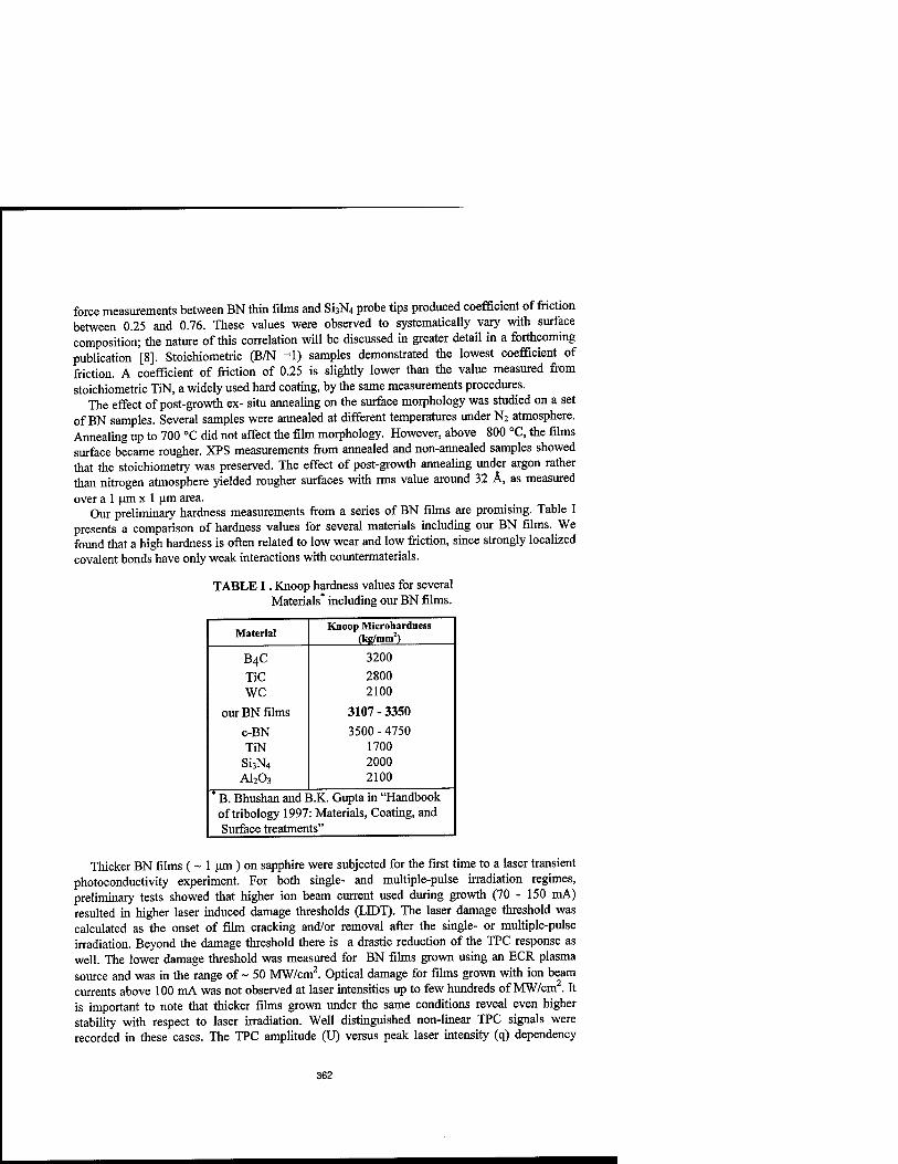
force measurements between BN thin films and Si3N4 probe tips produced coefficient of friction between 0.25 and 0.76. These values were observed to systematically vary with surface composition; the nature of this correlation will be discussed in greater detail in a forthcoming publication [8]. Stoichiometric (B/N =1) samples demonstrated the lowest coefficient of friction. A coefficient of friction of 0.25 is slightly lower than the value measured from stoichiometric TiN, a widely used hard coating, by the same measurements procedures.
The effect of post-growth ex- situ annealing on the surface morphology was studied on a set of BN samples. Several samples were annealed at different temperatures under N2 atmosphere. Annealing up to 700 °C did not affect the film morphology. However, above 800 °C, the films surface became rougher. XPS measurements from annealed and non-annealed samples showed that the stoichiometry was preserved. The effect of post-growth annealing under argon rather than nitrogen atmosphere yielded rougher surfaces with rms value around 32 A, as measured over a 1 urn x 1 um area.
Our preliminary hardness measurements from a series of BN films are promising. Table I presents a comparison of hardness values for several materials including our BN films. We found that a high hardness is often related to low wear and low friction, since strongly localized covalent bonds have only weak interactions with countermaterials.
TABLE I. Knoop hardness values for several Materials* including our BN films.
Material Knoop Microhardness
(kg/mm2)
B4C
TiC WC
our BN films
c-BN TiN
Si3N4
AI2O3
3200
2800 2100
3107 - 3350
3500 - 4750 1700 2000 2100
* B. Bhushan and B.K. Gupta in "Handbook of tribology 1997: Materials, Coating, and Surface treatments"
Thicker BN films ( ~ 1 um ) on sapphire were subjected for the first time to a laser transient photoconductivity experiment. For both single- and multiple-pulse irradiation regimes, preliminary tests showed that higher ion beam current used during growth (70 - 150 mA) resulted in higher laser induced damage thresholds (LIDT). The laser damage threshold was calculated as the onset of film cracking and/or removal after the single- or multiple-pulse irradiation. Beyond the damage threshold there is a drastic reduction of the TPC response as well. The lower damage threshold was measured for BN films grown using an ECR plasma source and was in the range of- 50 MW/cm2. Optical damage for films grown with ion beam currents above 100 mA was not observed at laser intensities up to few hundreds of MW/cm . It is important to note that thicker films grown under the same conditions reveal even higher stability with respect to laser irradiation. Well distinguished non-linear TPC signals were recorded in these cases. The TPC amplitude (U) versus peak laser intensity (q) dependency
362

obeys the scaling law: U cc qn , where the power degree n is as high as 3 to 4 for X = 532 nm and 2 for X = 355 nm . Typical dependency of the non-linear TPC response as a function of laser intensity is presented in Fig 2. A maximal PC signal amplitude of 400 mV was reached in these experiments with a corresponding maximum current density level of 1.5 kA/cm2. This is a very unusual result for sub-micron film thickness. Hence, further studies of carrier generation mechanism by intense laser pulses become of principal importance.
1000
1 100
>
Figure 2. TPC response on laser intensity at % = 532 nm (near to the forth power U-vs-q scaling law is realized).
108 109 Intensity, W/cm2
CONCLUSIONS
The surface morphology, tribological properties, and the optical resistance of our boron nitride films were investigated. The combined smoothness with respectable friction and hardness properties make this material a good candidate for coating applications (including corrosive and high temperature environments). Our results are very promising since this is the first time a thin film combines the four critical characteristics for a coating material: (i) high hardness, (ii) smooth topography, (iii) high temperature stability, and (iv) low friction properties. Our challenge is to incorporate BN into coating technologies either as a single layer or as a multilayered or composite coating in combination with other nitrides. As far as device applications are concerned, this material is a good candidate for thin insulating layers in high temperature metal-insulator-semiconductor (MS) structures. Finally, results obtained from laser photoconductivity measurements from boron nitride films are encouraging for incorporation of this material in high voltage, high speed optoelectronic switching applications.
ACKNOWLEDGMENTS
This work is supported by funds from a NASA cooperative agreement, # NCC8-127, to SVEC. This material is based upon work supported by the U.S. Civilian Research and Development Foundation under Award No.REI-247. Ionwerks would like to acknowledge support from U. S. Air Force SBIR contact # F33615-97-C-1035 monitored by Dr. J. E. VanNostrand; and a NASA phase II SBIR # NASA-9701 trough MSFC monitored by Dr. Jerry Watkins. SL and SSP wish to acknowledge the support by the MRSEC Program of the National science Foundation under Award No. DMR-99632667 and the Texas Center for Superconductivity at the University of Houston.
363

REFERENCES
1. S. Nakamura, M. Senoh, and S. Nagahama, Appl. Phys. Lett. 68, p.3,269 (1996).
2. S.P.S. Arya and A.D'Amico, Thin Solid Films. 5, p.267 (1988).
3. D. F. Ogletree, R. W. Carpick, and M. Salmeron, Rev. Sei. Instrum. 67, p.3,298 (1996).
4. S.V. Gamov, A.S. Epifanov, S.M. Klimentov, A.A. Manenkov, A.M.Prokhorov, Optical Engineering. 28, p. 1,069 (1989).
5. S.V. Gamov, S.M. Pimenov, V.G Ralchenko, S.M. Klimentov, V.l. Konov, K.G. Korotoushenko, E.D. Obraztsova, S.P.Plotnikova, D.M. Sagatelyan, S.Holly, in Laser-Induced Damage in Optical Materials: (26 Ann. Symp. on materials for high power lasers), Proc. SPIE, 1994, 2428, pp. 134-143.
6. Klimentov S.M., Garnov S.V., Epifanov A.S., Manenkov A.A., Sagatelian D.M., in Book of abstracts of DC Int. Conf. "Nonresonant Laser-Matter Interaction" (NLMI-9), St.Peterburg, 1996, p. 26.
7. D. M. Gruen, X. Pan, A. R. Krauss, S. Liu, J. Luo, and C. M. Foster, J. Vac. Sei. Technol. A 12,p.l,491(1994).
8. S. Lee, S. Imaduddin, N. Badi, A. Tempez, A. Bensaoula, and S. S. Perry, to be published.
364

Part V
Novel Processing of Ceramic Materials; Process Characterization

MATERIALS CHEMISTRY AND BULK CRYSTAL GROWTH OF GROUP III NITRIDES IN SUPERCRITICAL AMMONIA
Joseph W. Kolis,* Steven Wilcenski*, Robert A. Laudise ** * Department of Chemistry Clemson University, Clemson SC 29634 [email protected] ** Bell Laboratories Lucent Technologies Murray Hill NJ. 07974
ABSTRACT
Reasonably sized crystals of aluminum and gallium nitrides can be grown in supercritical ammonia using chloride and amide as the mineralizer. Best growth was achieved at 380°C in ammonia at 40,000 psi (270 MPa). Under these conditions crystals as large as 0.4 mm could be grown over several days. Attempts to optimize the identity and concentration of the mineralizer, and the acidity of the solution, led to several new products including A1F3(NH3)2.
INTRODUCTION
The synthesis of high quality single crystals of group in nitrides is an important goal for a variety of reasons. The development of a number of advanced technological devices, such as blue lasers, are based on wide bandgap semiconductors.fi] Solid state blue lasers are desirable for a number of applications particularly optical storage applications where the shorter wavelength light leads to dramatically increased storage capacity. The nitrides of group HI metals, especially aluminum and gallium, are particularly attractive for these applications. They exhibit wide, direct bandgaps, and are chemically and thermally durable.[2] The bandgap of A1N is 6.2 eV but this can be reduced by alloy ing with Ga or IN. Recently it has been demonstrated that, with proper doping, high quality thin films of MN can emit intense blue light. [3] The preparation and doping of epitaxial thin films, while not trivial, is advancing at a steady pace. Substantial progress in the area, however, is hindered by the demands for high quality substrates. This is especially so for the production of solid state blue lasers. Typically the epitaxial group IE nitride films are deposited on the surface of sapphire or, less commonly, silicon carbide. Both of these materials have substantial lattice mismatches with the group m nitride films, which leads to fairly high defect densities. Surprisingly these high defect densities do not seem to have deleterious effect upon the blue LED devices entering the commercial markets. However, the situation is somewhat different for diode lasers. The higher energy output for continuous blue laser emission, demands considerably lower defect density, as well as excellent thermal expansion coefficients.[4] Naturally the best matches for group HI nitride films are group in nitride substrates. Thus there is a growing demand for high quality single crystals of group III nitrides.
The growth of single crystals of group III nitrides is a particularly challenging synthetic problem. Several methods have been investigated as routes to single crystals of group III nitrides. The fundamental problem with traditional crystal growth methods involving either sublimation or melt growth is rooted in the very high lattice energy of group HI metal nitrides. The nitrides do not melt congruently and only liquefy at temperatures above 2000°C , where they decompose to gaseous nitrogen and the molten metal. [5]
367
Mat. Res. Soc. Symp. Proc. Vol. 495 ° 1998 Materials Research Society

Similarly sublimation is problematical because the compounds vaporize as metal atoms and atomic nitrogen. Several years ago Slack and McNelly were able to grow some crystals via sublimation but found that very high pressures of nitrogen were needed. [6] At such high temperatures (typically >2000'C), the only containers found suitable were single crystals of tungsten. Probably the steadiest improvement in this field has involved high pressure techniques, whereby reasonably high quality crystals have been grown from liquid gallium at ca. 1500°C under very high pressures of nitrogen (>10kbar).[7] The high pressures of nitrogen are required because of the low solubility of nitrogen in liquid gallium. The crystals grown by this method are good quality hexagonal plates and are currently approaching one centimeter in size. However, the size of the crystals seem to limited by the size of the high pressure chamber. Most recently good quality single crystals of GaN were grown from liquid sodium at 700°C.[8] These methods all work with varying degrees of success, but scale up to workable quantities of larger crystals is somewhat problematical in each case. The experimental demands of the various techniques are all indicative of the extraordinary difficulty of the problem. Indeed it is unlikely that any traditional melt techniques will ever be successful in the growth of high quality crystals.
We have been attempting to grow good quality single crystals of both GaN and A1N in supercritical ammonia. The method is an extrapolation of that used to prepare single crystals of quartz and other oxides in supercritical water. [9] It depends on the fact that high pressure fluids often can solubilize normally intractable solids to a degree that, while not high, is sufficient to lead to crystallization at a reasonable rate. The very high mobility of the supercritical fluid means that even modest solubility leads to reasonable crystallization rates. Thus quartz crystal as large as one kilogram can be grown in under 30 days in supercritical water. This method is employed on a large scale, and over one million pounds of electronic grade quartz crystals are grown each year. [10] The key ingredient in this method is the mineralizer. The mineralizer is a small molecule which attacks the bulk feedstock to create a soluble molecular species which can migrate through the fluid to the growing crystal site. With the proper thermal gradient, a supersaturation is created at the growing seed crystal site. In the case of quartz synthesis, hydroxide is the mineralizer which attacks silica feedstock leading to a soluble polysilicate.
3Si02+ 20H- > Si3072' + H20 > a-quartz + 20H- (1)
We postulated that this method could be extended to the nitrides using an appropriate mineralizer in supercritical ammonia. Supercritical NH3 has been used previously to prepare a number of new metal nitrogen compounds including nitrides.[l 1] The most direct mineralizer analog is amide, which could conceivably attack a bulk nitride feedstock to form a soluble molecular species which could migrate to the growing crystal site by reactions such as (2). A1N + NH2- + 3NH3 > [A1(NH2)4]- > A1N + NH2" + 3NH3 (2)
We are encouraged by reports that gallium metal becomes mineralized in the presence of potassium metal in supercritical ammonia to form GaN.[12,13] Such a technique has numerous potential advantages if it could be satisfactorily developed. The reaction temperatures will be relatively low by necessity because of the onset of the Haber equilibrium above 550°C. The reaction pressures will also be reasonably low, probably not exceeding 3 kbar, making the synthetic conditions accessible by fairly conventional commercially available equipment. Furthermore, the relatively low temperatures, and the ability to purify the ammonia and the starting materials, should minimize the presence of oxide impurities, which are the primary cause of defects in crystal prepared at high temperatures. Finally, if conditions can be determined for transport at a reasonable rate, efficient scaleup should be possible using many of the techniques developed for commercial quartz production.
368

EXPERIMENTAL
All reactions were done in Morey autoclaves lined with Ag or Pt, or in Tem Pres vessels made from Rene alloy with Tuttle style cold seals [9,10]. The Morey vessels possess the advantage that truly clean experiments can be performed completely enclosed in an inert metal container. However, they are designed such that they cannot contain more than about 12-15,000 psi of pressure before they begin to leak. The Rene vessels can easily contain pressures up to 50,000 psi at very high temperatures, but the Rene alloy is directly exposed to the solution and the alloy is susceptible to some attack by mineralizers, especially chloride. The amorphous starting materials were prepared by refluxing A1C13 in ammonia for several hours. After the evaporation of ammonia, the white solid was washed with fresh ammonia using a custom made Sohxlet extractor to remove the NH4C1. The resultant insoluble free flowing white powders were completely amorphous to x-rays.
Solubility studies were performed by using chips of microcrystalline A1N sintered by hot isostatic pressing. Individual chips were weighed and placed in TemPres vessels with 10ml volume. An appropriate amount of mineralizer was added and the vessel charged with ammonia, via distillation on a vacuum line. The vessel was placed in a tube furnace for 3 days at 375°C. After cooling and release of NH3, the contents of the vessel were examined. The chip is washed with water and weighed, and the difference taken is a rough approximation of solubility. This protocol is similar to that used to determine the appropriate mineralization conditions for the growth of a variety of crystals such as KTiOP04. [14]
Synthesis of AlFj/NHjV,
A silver lined Morey vessel was charged with 200 mg A1N and 160 mg NH4F. The vessels was filled to 50% with ammonia and capped with a silver disk. The vessel was sealed and heated at 400°C for three days. The large white crystalline polyhedra were isolated and washed with water and characterized by x-ray diffraction.
Growth of MN crystals CM = Al. Ga^
In a typical preparation, a Tem Pres vessel was charged with 250 mg of the amorphous "MN" starting material and 125 mg NaNH2. Ammonia was distilled using a solid C02 acetone bath to a fill level of 80%. The vessel was heated to 380°C for three days. After isolation and washing with water, the product mostly consists of crystalline white powder which is entirely MN as indicated by x-ray powder diffraction. Within the microcrystalline white powder is some longer needles which are single crystals of the metal nitrides.
RESULTS AND DISCUSSION
We found that when our amorphous starting material was reacted with NaNH2 in ammonia at 380°C at 40,000 psi pressure, reasonably high quality crystals of MN as large as 0.4 mm in length can be formed. The amorphous material was prepared by refluxing the metal halides in ammonia followed by extensive washing. It was felt that the amorphous material would be more reactive than microcrystalline materials as it is less dense, less interconnected and more susceptible to attack by mineralizer. Indeed we found that NaNH2 does not appear to attack crystalline MN in any reasonable concentrations under our experimental conditions. We postulated that the NaNH2 is not soluble enough in the fluid, and prepared some KNH2 which is substantially more soluble in liquid ammonia, but found that it did not attack bulk MN under these experimental conditions either.
The reactions conditions were varied systematically particularly with regard to pressure and temperature. The optimum reaction conditions are listed in Table 1. In our
369

hands, it appears that little if any mineralization or transport occurs below 300°C. Reactions above 500°C in supercritical ammonia become less feasible because of the onset of the Haber equilibrium. This results in catastrophic increases in pressures due to N2 formation and potential embrittlement of the alloy due to hydrogen formation. The pressure is a reflection of the density of the fluid. It appears that the highest solubility and transport is achieved at the highest possible density of ammonia. Our current techniques restrict our_ density to an 80% fill of liquid ammonia which leads to a pressure of 40,000 psi at 400"C. Nevertheless we found that sufficient solubilization and transport occurs for crystal formation of several hundred microns over 3-4 days. However, mineralization only occurred in the presence of the homemade amorphous metal nitrides as feedstock. Mineralization or transport was never observed using commercial microcrystalline or bulk MN feedstock.
Table 1. Typical Reaction Parameters for AIN and GaN Crystal Growth
Staring Materials Amorphous "MN"
Mineralizer NaNH2, KNH2
Time 3-4 days
Temperature 380'C
Temperature Gradient 40°
Pressure 30-40,000 psi (80% fill)
Since no apparent attack took place upon bulk metal nitrides even in the presence of excess amide, the role of the amorphous feedstock was reexamined more closely. Upon further investigation it was found that this material always contains some residual chloride, despite repeated washings. Thus in an attempt to optimize the mineralization conditions, we began to systematically alter the identity and concentration of mineralizer. We found that chloride was indeed a key ingredient and that addition of a mixture of KCl and KNH2 to commercial MN leads to substantial dissolution of bulk AIN and GaN, as determiend by weight loss of bulk pieces. The concentration of chloride was found to be significant in that reduced concentration of chloride lead to reduced solubilization of nitride. An equimolar amount of MN, Cl" and KNH2 leads to complete solubility of the bulk feedstock. Clear crystals are obtained upon slow removal of the ammonia, which are extremely reactive and completely soluble in water. Characterization of these species is underway. It was hoped that a mixture of fluoride and amide would also lead to solubilization, but thus far fluoride has not proven to be an effective mineralizer in the presence of amide ion. It should be noted that in the presence of chloride and amide we also observed the formation of A1(NH- 2)4" ion, which is a possible but not confirmed intermediate in the transport of MN. This suggests that, under the proper conditions, the chloride could act as a catalyst solubilizing the MN feedstock, but getting displaced in solution by amide, leading to formation of Al(NH2)4", which may be the predominant mobile species in solution.
AIN + 2NH3 + Cl" > [Al(NH2)3Cl]- (3)
370

[A1(NH2)3C1]- + NH2- -> AI(NH2)4- + cr (4)
A1(NH2); > A1N + NH2' +2NH3 (5)
We also investigated the role of acidity in mineralization. In contrast to the basic regime where amide was added, the addition of ammonium fluoride and ammonium chloride leads to substantially different chemistry. Reaction of ammonium fluoride with an equimolar amount of bulk A1N leads to isolation of large clear insoluble crystals of A1F3(NH3)2. The compound was characterized by single crystal x-ray diffraction and was shown to have an unusual structure in the orthorhombic space group Immm. It contains octahedrally coordinated aluminum cations coordinated by two ammonia ligands in the trans positions (See Figure 1). The octahedral coordination is completed by two very interesting linear bridging fluorides. Strong hydrogen bonding between the hydrogen atoms of the coordinated ammonia ligands and the non bridging fluoride ligands also helps link the three dimensional structure together. Reaction of GaN with equimolar amounts of ammonium fluoride also leads to formation of similar looking colorless insoluble crystals. Powder diffraction indicates that they are not isostructural to the aluminum complex, but probably have similar sized unit cells. The reaction of ammonium chloride with A1N leads to formation of red-orange crystals which extremely water sensitive. No MN crystals were observed in any reactions in the acidic regime. The result of these investigations do indicate however, that the halides play a substantial role in mineralization of the bulk nitrides and that the identity of the mineralizer and acidity of solvent alter the chemistry significantly.
F1<
[AH N1
Figure 1. Thermal Ellipsoid View of the Unit Cell of A1F3(NH3)2
371

CONCLUSIONS
We have demonstrated that reasonably sized single crystals (up to 0.4 mm) can be grown in supercritical ammonia at reasonable temperatures and pressures. Although the crystals are not large enough to be useful, they are of good quality and are large enough to prove that mineralization and transport are definitely taking place. The role of mineralizer is very important and it appears that simple alkali metal amides are not sufficient. Rather another co-mineralizer, such as chloride is needed to solubilize the metal nitride. However, the proper concentration and relative ratios of mineralizers have not yet been fully elucidated. Reaction of halides in acidic solvent leads to formation of several new products including AIF3(NH3)2, which indicate that the solution chemistry is extremely rich.
ACKNOWLEDGMENTS
This work was supported by the National Science Foundation, the Office of Naval Research and Bell Laboratories. JWK is indebted to Tony Caporaso for considerable technical assistance.
REFERENCES
1. S. Nakamura, Mat. Res. Soc. Bull., 22, no. 2, 29 (1997).
2. F.A. Ponce, D.P. Bour Nature, 386, 351 (1997).
3. S. Nakamura, T. Mukui, M. Senoh, Appl. Phys. Lets., 64, 1687 (1994).
4. F.A. Ponce, Mat. Res. Soc. Bull., 22, no. 2, 51 (1997).
5. D.A. Neumayer, J.G. Ekerdt, Chem.Mater., 8, 9 (1996).
6. G. A. Slack, T.F. McNelly, J. Cryst. Growth, 34, 263 (1976)
7. S. Porowski, J. Cryst. Growth, 166 583 (1996)
8. H.Yamane, M. Shimada, S.J. Clarke, F. J. DiSalvo, Chem. Mater., 9, 413 (1997).
9. R.A. Laudise, Prog. Inorg. Chem., 3, 1 (1962).
10. R.A. Laudise, J.W. Nielsen Solid State Phys., 12, 149, (1961).
H.H. Jacobs, D. Schmidt, Curr. Top. in Mater. Sei., 8, 381 (1982).
12. D. Peters, J. Cryst. Growth, 104, 411 (1990).
13. R. Dwilinski, J.M. Baranowski, M.Kaminski, R. Doradzinski, J. Garczynski, L. Sierzputowski, Acta Phys. Polonica A, 90, 763 (1996).
14. R. A. Laudise, R.J. Cava, A.J. Caporaso, J. Cryst. Growth, 74, 275 (1986).
372

FOUR REVOLUTIONS IN DIAMOND SYNTHESIS: THE VINDICATION OF EDISONIAN CHEMISTRY
Rustum Roy, Materials Research Laboratory, The Pennsylvania State University, University Park, PA 16802 USA; Fax: 814 863 7039; e-mail: [email protected]
ABSTRACT
Careless claims by scientists are often expanded further by journalists and grossly distort the scientific "truths" passed on to the public and policy maker. Recently, such overclaims have invaded the field of materials synthesis.
The real first principles of materials synthesis, based on the work of V.M. Goldschmidt (and Linus Pauling), have proved to be, and continue to be, very successful. By combining such principles with Edison's methodology of careful observation, precise experimentation and rapid feedback, thousands of new (inorganic) phases have been, and continue to be made (since 1948, several hundred from our own laboratory), producing dozens of useful, widely commercialized materials.
In contrast, in spite of seventy years of trying, the so-called "first principles" calculations (from the quantum mechanics of cores and electrons) have utterly failed to actually predict and synthesize a single new material or add anything to the deep and reliable insights of well known chemical theories. It is clear that what students and researchers in contemporary materials synthesis need most is a thorough grounding in crystal chemistry and phase equilibria (including metastable equilibria).
The history of the "C3N4" failure, as a harder than diamond candidate, is prototypical of the"calculating" approach to synthesis. It is contrasted with short summaries on four recent real advances into completely new processes for diamond synthesis.
INTRODUCTION
Truth in Advertising Materials Science
I open this analysis of how materials scientists should go about synthesizing materials by quoting two impressions that we as scientists, supported by those great distorters of science — the media — have managed to convey to the "attentives," (i.e. the decision making public). Here is one, Paula Borsook, a reporter writing in the Whole Earth Review (a very solid respectable source on other technical matters):
Computational chemists are on the verge of being able to create, on demand, materials that have specific properties, whether of flexibility, durability or the ability to turn an alluring shade of lavender when the late-afternoon light strikes them at a certain angle.
Dirac, one of the fathers of quantum mechanics, said in 1929 that "The underlying physical laws necessary..for a large part of physics and the whole of chemistry are completely known, and the difficulty is only that the exact applications of laws lead to equations much too complicated to be solvable. "No chemist has had the time or the means to perform the calculations, so no chemical engineer has been able to use the solutions to build new materials. It is turning out that advances in computer hardware and software may prove Dirac wrong: Supercomputers andnew ways to use them may finally be able to solve the equations that explain and describe the material universe.
373
Mat. Res. Soc. Symp. Proc. Vol. 495 e 1998 Materials Research Society

That was written in 1992. In 70 years, computational power available to physicists and chemists alike has gone up by 106 to 1010. Yet Dirac's heirs have made no progress in helping anyone "build a new material.'' Computational power has probably followed Moore's law since, and the number of new materials made by calculations from the "underlying physical laws" remains at zero. Clearly, the theory was inadequate. The report gets worse:
Along with nanotechnology, computational chemistry is fundamentally changing the relationship of humans to materials. Throughout history designers have built things with the materials that were available. While new materials, such as plastics, certainly were invented over time, those new compositions were often, if not always, the result of trial and error and broad experimentation. Sometimes even mistakes yielded unintended materials with practical value.
As Borsook said, computers are changing all that. Today, a designer working on a bridge looks up the characteristics of the materials that are available, and computes how much of it is required to handle the loads that are anticipated. We are approaching the time when the designer of a bridge may compute the characteristics of the structural material required to meet her needs (flexibility, abrasion resistance, color, strength and other), and order the mill to manufacture the material in the configurations she desires.
Surely every materials scientist should shudder at such nonsense being palmed off on a defenseless public. The facts are that the real sciences have improved steel, aluminum, cement by orders of magnitude and made million of tons of totally new products, e.g. in the polymer world. No one has seen one of these computed materials. And worse, in the Fall 1997 issue of one of the most sophisticated journals written for and by world leaders "New Perspectives Quarterly," here is what Peter Schwartz, one of the most enlightened U.S. business analysts, writes about our future:
Beyond this, further waves of development are underway in biotechnology, nanotechnology (molecular scale engineering) and alternative energy... Nanotechnology will be able to produce micromachines to perform functions once only imagined in science fiction —for example, tiny sensors released in our circulatory system to report on the composition of the bloodstream. By 2018, micromachines will be able to perform basic cell repair.
Clearly, someone has misled the American and world public into a Star Trek version of materials synthesis. Pure rhetoric has displaced reality and even scientists, including agency managers, now act on the basis of the virtual world. My opening point is this: We the scientists, here the computational physicists and chemists, must take 100% of the responsibility for this state of affairs. It is our careless statements, hints of future "breakthroughs," often hedged about by maybe's and if s (which we know will be lost in the reporting) which lead to this fantasy world for policy makers.
The damage we do to truth, to science, to the reputation of scientists is incalculable. The damage we do to national science policies is enormous. The national leaders are looking for easy fixes. Science has been the pinch-hitter for decades, called upon to excite and, if all else fails, to mystify the voter. Remember the "war on cancer" and the "nuclear plane" funded for several years! Or read with shame what was said about the SSC and what it would do for the country (cure AIDS, find oil, fix radioactive waste, etc.).
What then are the facts? No, we will not "compute" and design 99.99% of the material world around us. The vast majority of our buildings will be made of steel, concrete and glass, each getting
374

steadily better because of excellent materials engineering at the usual macro- and micro levels with possible minor improvements at the nanoscale. Recall that much of the large volume nanoscale engineering in metals and ceramics is very old fashioned, indeed 40 years old. It will be a very long time — in ceramics — before any other nano synthesis as significant to the public as zeolite synthesis, or glass ceramics appears. These are billion dollar industries based on exquisite nano engineering. Amazingly, most of the rhetorical champions of nano-x are unaware of these major successes.
There are two simple rules which the Materials Community should enforce upon its members: Scientific reports or claims should only be made about what has been done, and established and confirmed - never, never, about what will be done or what may happen! That is science fiction. It should be labeled as such and published in Sci-fi venues. Real materials science - i.e. that of significance to the public — should be about real materials which can be perceived by the 5 human senses: If you cannot show the world a piece of it, perhaps aided with an instrument or two, by all means report it to your colleagues in science, but never discuss it in public for fear that you may mislead your fellow citizens.
Chemistry or Physics for Synthesis?
There are two radically different approaches to making new materials. Synthesis is the domain of the chemist. For nearly one hundred years, chemical science has succeeded admirably in creating tens of thousands of new organic (and thousands of new inorganic) materials. Some of these materials are produced in millions of lbs/year (various polymers including Teflon, superalloys, ferrites, BaTi03, etc., etc.), some have exquisitely tailored properties, as in any semiconductor circuit or GaN diode. The other approach is a more recent attempt by theoretical physicists to "calculate" the structure of a phase of a given composition - usually extremely simple compositions and hope or guess that it has certain desirable properties. We compare these approaches below.
EXPERIMENT
The Chemists' Approach
This approach, different in every case, is a combination of the approaches by Edison, Sherlock Holmes and Prince Serendip. It is based on reliable data, clever inductive reasoning (highly perceptive observations from very different sources) and a large number of simple, cheap experiments which allow repeatability. For inorganic or ceramic materials, the 1926 textbook by V.M. Goldschmidt, entitled "Geochemische Verteilungsgesetze der Elemente"(l), is an absolutely essential and nearly sufficient guide. Recently, Ian Ross, a former President of Bell Labs, described (2), in detail, this very process as it was applied to the transistor: applications pulled basic research with new ideas translated into simple, albeit crude, experiments. The synthesis of diamond by: (a) High Pressure, High Temp; (b) CVD; (c) Laser-fluxes; and, (d) Liquid Metal Low Pressure Processes, is another outstanding example. The author has relied on such approaches and probably synthesized perhaps several hundred totally new phases including dozens in each of the following areas:
•Perovskites and related structures •ABX4, ABX3 and A2BX4 phases (see O. Müller and R. Roy (3) for a summary) •Synthetic clays •Synthetic zeolites quenchable (hence, usable), high pressure phases •New complex phosphates such as NZP and apatites.
375

Spectacular and defining examples of the scientific success of Goldschmidt principles are the ability to predict and make, for example, BeF2 in the coesite structure; or Na2BeF4 in the larnite structure. Ironically, the inability to predict the appearance of coesite in p-t space for the Si02
composition itself, illustrates the limitations of inductive reasoning (of course, no theoretical approach could possibly have predicted that such a structure would appear).
The theoretical reason why subatomic theory can add so little is very simple: chaos applies. The typical material in a very complex assemblage of cores and electrons, the number of potential wells of more or less stable configuration is essentially infinite and many are separated by only a few kcals in the G function. Bigger computers cannot help select among these, even if all the interactions could be calculated, because the kT noise is so large.
The "First Principles" or Physicists' Approach
We have already quoted Dirac's hopes in 1929. Yet, the total failure of the so-called "first principles" approach to predicting the structure of even the simplest composition, under given thermodynamic constraints, continues (even though computational power has increased by many orders of magnitude). Rigorous calculations can reach the H2 molecule, but consider the quandary for such calculators with the very simplest larger "molecules" or crystalline 'solids.' Will theory predict graphite, diamond, buckyballs or glassy carbon as the structure of carbon? Another monatomic solid such as sulfur has a dozen crystalline and several noncrystalline structures with radically different properties as a function of modest p-t changes. To which of these structures will the calculations point? Water, H20, is a simple diatomic solid also with a half dozen crystalline and some non-crystalline forms. Yet, we have seen no papers purporting to predict or explain all this variety, in even simple cases, from physical theories.
One may take as the paradigmatic example of the current state-of-the-art of "first principles" calculations the work of Cohen (4), which claimed to predict new materials and illustrate its application by the example of "C3N4". To start with, undergraduate crystal chemistry principles allow one to "predict" that it is conceivable that such a phase.may. be formed at high pressures (approx. lOOkb range) and if so, one of the candidate structures would be that of Si3N4. The principle of parsimony, or Occam's razor, demands that new theories not be constructed unless they can do better than existing theory. No mention is made in any of these papers by physicists of the highly developed chemical theories. Si3N4 is modestly hard, C3N4 could be expected to be harder, if it is not more anisodesmic. a very possible occurrence. However, the banner of "harder than diamond" was the rhetorical flourish without any basis in data that attracted the attention only of inexperienced materials synthesizers to C3N4. In the six years since the first prediction of this obvious guess, a most extraordinary phenomenon has occurred. First, it is fairly certain that no one, so far, has prepared even a few milligrams of a crystalline phase with the composition of C3N4. Certainly, no two lab reports agree on reproducing the composition of the claimed phase. The structure of any phase(s) reported is obviously even less certain. The claim by Niu et al. (5), to have prepared a "harder than diamond" phase in the predicted composition and structure, has been essentially discredited and not confirmed by the original authors' own later work. Yet, probably misled by the repeated allusions to "harder than diamond" in the original papers and expanded on in popular magazines — based on no hardness data whatsoever — a worldwide flurry of research on this non-existent C3N4 phase began (6). Up to August 1997, DeVries (7) has catalogued over 400 papers on "C3N4," into a half dozen categories, from claimed synthesis to outright discrediting (see Table 1). Sociological analysis of this phenomenon will reveal a great deal about the status of contemporary materials synthesis. DeVries notes that a very high percentage of the authors are Chinese: why? If the authors were really interested in materials that are putatively harder than
376

diamond, why would some not have studied, or even mentioned, "B220," where clear evidence of scratching [111] diamond faces have been shown (8-9) by two independent laboratories. DeVries points out that this futile research has employed possibly some 1200 scientists, who presumably could find no more significant problems to study. Clearly, some theorists were also unaware that bulk modulus, bond length, and bond strength are not, by themselves, indicators of bulk hardness, since it is the shear modulus that is critical to hardness, as Oilman has pointed out (10). It is also very well known to experimentalists that bond length, by itself, is meaningless since the C-C bond in graphite (in the plane) is shorter than in diamond.
Table I (from Ref. 7) IJn»r«ti.r» Analysis of Paner* on "ClN4»
1. Reviews 30 2. Theory (synthesis, structure, properties) 30 3. Claimed synthesis 65 4. Highly skeptical or negative on synthesis IS 5. C-N (other phases than C3N4) 28
6. Synthesis, properties of CNX not C3N4 194
7. C-N-H 27 8. CN x in a composite (e.g., metal nitrides) 13
Total 402
Since this paper was submitted to the Journal; DeVries (personal communication) reports that another 98 papers have appeared (in less than six months) with no more success, and asymptotically diminishing significance.
Comparison with Four Real Revolutions in Diamond Synthesis
In sharp contrast to these major expenditures of effort (and of course, money) which have yielded zero in new materials, I present below some rather remarkable developments in roughly the same field in the same time frame. Four new processes for synthesis have been discovered to make diamonds by methods that theory had ruled out, i.e. at 1 atm pressure. One thousand labs have duplicated one of them; many labs are just catching on to the others. All make real diamonds, everytime, in any lab. None has yet been explained in terms of the most basic thermodynamic theory of stability of diamond and graphite. So much for the value of theory in the world of real materials synthesis.
1) CVD Diamond Synthesis
More or less contemporaneous with the C3N4 failure, the entire world of diamond synthesis has been revolutionized by four real syntheses. In the mid 1950's, GE, Norton, ASEA, etc., succeeded in reproducibly synthesizing diamond by the high pressure, high temperature (HPHT) route, in what was taken to be its thermodynamic stability field. This became a worldwide industry. The success
377

of the HPHT route, however, tended to discourage support for alternative synthesis routes explicitly excluding any at low pressures - because it was theoretically forbidden. The Russians, however, persisted and the story has been told in detailed reviews (11-13) how Spitsyn and Dejaguin (14) reproducibly produced diamonds at 1 atm in the presence of atomic hydrogen. Setaka et al. (15) made it a simple engineering process, which was transferred by Roy (16) to the U.S. and the rest of the world. Today, perhaps 1000 labs have successfully made CVD diamonds below 1 atm, where it is not supposed to form. So much for the value of theoretical guidance, including my own.
2) LESSS
Once CVD was established by 1987-1988, all other methods, in turn, were viewed skeptically, as for example in 1992 when we first described our low pressure solid state source (LPSSS) process. Nevertheless, our two dozen publications describe the simple process of mixing graphite (or other solid carbon form) with a fine metal powder (Cu, Ni, Au, Ag, Fe, Pt) and by merely exposing the mixture to atomic hydrogen (17-18) producing copious diamonds. The mechanism is quite clear. A metal-carbon-H° liquid alloy is produced with very high (50+) content of carbon. This carbon subsequently precipitates out as diamond (and only diamond in nearly 1000 runs). A variant of this process which does not use a hydrogen plasma at all, but uses metal hydride dissociation to give nascent hydrogen, also appears to produce diamonds at 1 atm, merely by heating the mixture seeded with diamonds to about 1000°C.
3) Hydrothermal
The synthesis of diamonds in nature under the thermodynamically stable p-t conditions has never been fully satisfactory for all diamonds. In meteorites, and recently in a variety of metamorphic rocks, the occurrence of very fine diamond is proving to be quite common. This author started on the hydrothermal route to diamond synthesis forty years ago. However, in the last few years by introducing metal powders into the carbon, water and diamond seed mix, at 1 kbar H20 800 °C, we have accumulated excellent evidence (19) for the synthesis of diamond under these conditions.
4) Laser Synthesis in Air at 1 atm
The totally skeptical response by most of the diamond research community to the report on the production of real world products - 30/^m diamond coatings on WC cutting tools which can be held in one's hand, examined by Raman, XRD, SEM and its cutting performance determined - stands in mind-boggling contrast to the acceptance on the basis of no evidence of the "harder than diamond C3N4."
Thus, the discovery by P. Mistry and M. Turchan of the QQC Company (20), of the multiplexed-lasers process to make diamonds in the open air at 1 jan per second, was announced at the NIST Diamond Conference in 1995, and published in 1996. Roy and Badzian (21) have since provided great detail on these products made by QQC. The skeptics had also ignored the fact fully established in the literature of the conversion of graphite to diamond in the air with a 50 watt laser. This had been easily achieved by Dejaguin in 1982 (22), and confirmed and extended by Alam, Debroy and Roy (23) in the U.S.
378

CONCLUSIONS
Policy Analysis
What is most striking about the comparison of the successful chemists' approaches to diamond synthesis and the unsuccessful physicists' approach is the incredibly different response of the community. Only a half-dozen (the most experienced ones) labs have moved in on, for example, the LPSSS approach. Even fewer have followed the hydrothermal or non-plasma approaches. This is in contrast to the several hundreds worldwide chasing what R.W. Cahn, founding editor of the Journal of Materials Science, calls the C3N4 "will-of-the-wisp" (24).
Of course, sociologists and policy makers, observing such data, might infer that there is too much money chasing too few problems and that materials scientists and their supporting government agencies choose problems largely when they become scientific fads in the media, such as superconductors, buckyballs, and diamonds. But the later, at least, were all based on real discoveries, albeit they were soon over subscribed, possibly by an order of magnitude. "C3N4" (and metallic hydrogen) are unique. They are "hypothetical" materials, almost certainly with no particular use or significance, and hence, their research is an example of extremely poor management of personal and national resources and strategic directions of research. Consider: one thousand papers will be written on C3N4 before even the existence of a material, of "no particular value," is confirmed or denied. Note also that U.S. industry wastes no time on it.
The Rational Approach to Ceramic Material Synthesis
At the turn of the millennium, it is now certain that the fundamental assumption or paradigm on which American post W.W.II research is based was completely incorrect. This is the so-called "linear model."
Basic science -> applied science -> technology ->products -> prosperity
Shapley and Roy (25) were first to sharply pointed out the absurdity of this model, in their 1985 book. In 1997, Stokes (26), writing from the Brookings Institution (where our work was also done), completed the demolition of the linear model. Worldwide high-tech industry has completely vindicated the Shapley and Roy analysis. They have acted to abolish their immense ivory tower laboratories, built on that absurd proposition. All "real world" research in major industry has returned to the successful, time tested applications-driven, discovery-following model. Unfortunately, the governments of the U.S., now followed by Japan and W. Europe, have not yet been able to change their policies, partly because of the outcries from many of their constituents who have known no other reality.
Very clear and simple guidelines exist for successful contemporary materials synthesis. The following algorithm has been followed in the author's lab for 50 years with substantial success in making new materials and new processes (sol-gel, hydrothermal, microwave) widely used for synthesis worldwide:
(1) The synthesis should have a specific goal or application. (A new ferroelectric, or ferrimagnet, or hard, or photoconducting material).
(2) The classical "textbook" literature, starting with Goldschmidt, Mellor, Partington, Pauling, Eitel, etc should be thoroughly assimilated before turning to contemporary
379

literature. (3) The whole range of synthesis tools converting p-t space, including hydrothermal, high
pressure, plasma, ultrasound, microwave and laser hydrothermal, highpressure, assisted, should be available.
(4) XRD, SEM, and chemical composition characterization of all samples is essential. (5) Repeatability must be assured, before any publication. (6) Overclaim or exaggeration of the significance of any discovery, specifically to the public,
must be absolutely abjured.
ACKNOWLEDGMENTS
Research in new materials synthesis is currently supported by the Office of Naval Research, Materials Science program.
REFERENCES
1. V.M. Goldschmidt, "Geochemische Veneilungsgesetze der Elemente," Dybwad, Oslo, Vols. 5,7,8 (1925).
2. Ian Ross, "Physics Today," p. 34 (December, 1997). 3. O. Müller and R. Roy, "The Major Ternary Structural Families," Springer-Verlag.
Heidelberg (1974). 4. M.L. Cohen, etal.,/'/-oc.i?o)'Soc.,London,334A,501 (1991), see also Phys. Rev., 38B, 9488
(1988). 5. C. Niu, Y.Z. Liu and CM. Lieber, Science, 261,334 (1993). 6. A. Badzian, et. al., Yut. J. of Refractory Metals and Hard Materials, 15,3 (1997). 7. R.C. DeVries, Materials Res. Innovations, Vol. 1:3 (1997)(in press). 8. A. Badzian, Appl. Phys. Lett., 53,2495 (1988) 9. V. Srikanth, et al., J. Am. Cer. Soc, 74,3145 (1991). 10. J.J. Oilman, Mat. Sei. Engg., A209, 74 (1996). 11. R.C. DeVries, Annu. Rev. Mater. Sei., 17, 161 (1987). 12. A. Badzian and R.C. DeVries, "Crystallization of Diamond From the Gas Phase (Part 1)",
Mat. Res. Bull.. 23(3), 385-400 (1988). 13. J. Angus, et. al., J. Appl. Phys, 39,2915 (1968). 14. B. Spitsyn and B.V. Dejaguin, J. Crystal Growth, 52, 219 (1981). 15. Matsumoto, et. al., Jpn. J. Appl. Phys. Part 2, 21, L183 (1982). 16. R.C. DeVries, A. Badzian and R. Roy, "Diamond Synthesis: The Russian Connection," MRS
Bulletin 21,65 (1996). 17a. R. Roy, H.S. Dewan and P. Ravindranathan, "Crystallization of Diamond at 1 arm From
Carbon-Metal Mixtures," J. Mat Chem. 3(6), 685 (1993). 17b. R. Roy, H.S. Dewan and P. Ravindranathan, "Diamond Synthsis Via the Low Pressure Solid
State Source (LPSSS) Process," Materials Research Bulletin 28(9), 861 (1993). 18. R.C. DeVries, R. Poy, S. Somiya and S. Yamada, "A Review of Liquid Phase Systems
Pertinent to Diamond Synthesis," Proceedings of IUMRs-ICAM 93, S. Somiya, M. Doyama, M. Hasegawa and S. Yamada (eds.), Tokyo, Japan (August 31-September 4,1993).
19. X-Z. ZhaoR. Roy, K.A. Cherian and A. Badzian, Nature 385, 513 (1997). 20. P. Mistry, et al., Innov. Mater. Res. 1,193 (1996). 21. R. Boy, A. Badzian, P. Mistry and M.C. Turchan, "Physics of Diamond," Proc. of the
International School of Physics, Enrico Fermi, A. Paoletti and A. Tucciaronce (eds.), IOS
380

Press, Amsterdam, p. 195 (1997). 22. D.V. Fedoseev and B. Derjaguin, et. al, Carbon 21,237 (1983). 23. M. Alam, T. Debroy, R. Poy and E. Breval, "Diamond Formation in Air by the
FedoseevDejaguin Laser Process," Carbon 27(2), 289-294 (1989). 24. R.W. Cahn, quoted by Phillip Ball in "Made to Measure," Princeton U. Press, p. 342 (1997). 25. D. Shapley and R. Poy, "Lost at the Frontier," ISI Ress, Philadelphia (1985). 26. D.E. Stokes, "Pasteur's Quadrant; Basic Science and Technological Innovation," Brookings
Institution Press, Washington D.C. (1997).
381
ELECTRODEPOSITED CuInSe2 THIN FILM JUNCTIONS
R.P. RAFFAELLE*, J.G. MANTOVANP, S.G BAILEY**, A.F. HEPP**, E.M. GORDON***, and R. HARAWAY*** *Florida Institute of Technology, Melbourne, FL 32901, [email protected] **NASA Lewis Research Center, Cleveland, OH 44135 ***Wilberforce University, Wilberforce, OH 45384
ABSTRACT
We have investigated thin films and junctions based on copper indium diselenide (CIS) which have been grown by electrochemical deposition. CIS is a leading candidate for use in polycrystalline thin film photovoltaic solar cells. Electrodeposition is a cost-effective method for producing thin-film CIS. We have produced both p and n type CIS thin films from the same aqueous solution by simply varying the deposition potential. A CIS pn junction was deposited using a step-function potential. Stoichiometry of the single layer films was determined by energy dispersive spectroscopy. Carrier densities of these films increased with deviation from stoichiometry, as determined by the capacitance versus voltage dependence of Schottky contacts. Optical bandgaps for the single layer films as determined by transmission spectrocopy were also found to increase with deviation from stoichiometry. Rectifying current versus voltage characteristics were demonstrated for the Schottky barriers and for the pn junction.
INTRODUCTION
Copper indium diselenide (CIS) is one of the best optical absorber materials used in poly- crystalline thin film photovoltaic solar cells [1]. This is due to its favorable electrical and optical properties, stability, and inexpensive means of production. Conversion efficiencies of 17.8% have been achieved for a vapor deposited CIS based solar cell [2]. Electrochemical deposition is an inexpensive alternative to the standard vapor deposition techniques for producing thin-film CIS [3].
Stoichiometric variation in polycrystalline CIS leads to a high concentration of electrically active native defects. Small variations from a Cu-to-In ratio of unity have been shown to result in large changes in the carrier density [4]. In fact, the semiconductor type changes from n to p as the Cu to In ratio changes from less than one to greater than one. However, CIS has been shown to be electrically and structurally stable over a wide range of stoichiometries and their associated native defect concentrations [5]. This behavior has been recently explained in terms of electrically inactive and ordered defect pairs [6].
The stoichiometry of our electrodeposited thin films is potentiostatically controlled. We have previously shown that the Cu-to-In ratio will demonstrate a linear dependance with deposition potential over a fairly wide range [7]. Therefore, we are able to deposit thin films with different electrical, optical properties, and semiconductor type from the same aqueous solution by simply changing the deposition voltage [8].
The optical band gap of CIS can be calculated from its absorption spectrum assuming a direct energy gap [9]. CIS has been shown to have a low electron effective mass (m *=0.09 m) [10]. Therefore, these materials become degenerate at low electron carrier densities
e e and we would expect a Burstein-Moss shift in the optical bandgap [11]. This effect has been observed in CIS single crystals grown by the vertical Bridgman method [12].
The current versus voltage (I-V) characteristics can be used to determine the barrier heights of metal to CIS junctions. For an ideal Schottky contact with an n-type semiconductor, the barrier height q<j>B is the difference in the metal work function q<pm and the semiconductor electron affinity IX-
383
Mat. Res. Soc. Symp. Proc. Vol. 495 ® 1998 Materials Research Society

q<pB = q(ä>m-x) (!)
When the metal work function is comparable to or smaller than the semiconductor's electron affinity we would expect an ohmic contact for an n-type semiconductor. In the case of a p-type semiconductor, the barrier height is the difference between the metal work function and the sum of the electron affinity and the bandgap. Assuming ideal junctions and an Al work function of 4.28 eV [13], electron affinity of 4.48 eV and a CIS bandgap of leV [14], we would expect Al to make an ohmic contact on n-type CIS and a Schottky contact to p-type CIS, with a barrier height of around 1.2 eV. However, if there is a large density of surface states, the barrier height is determined by the semiconductor surface and is independent of the metal work function [13]. Schottky barrier junctions have been produced on both n and p type CIS (Au and Al, respectively) [14].
The current density versus voltage for a Schottky barrier can be expressed as
J~Jse(qVtnkT) forV»kT/q (2)
where Js is the saturation current density and n is the ideality factor. The ideality factor is very close to unity at low dopings and high temperature. However, it can depart substantially from unity when doping is increased or the temperature is lowered [15]. The barrier height can be determined using
kT. —In q
A**r) (3)
where A" is the effective Richardson constant which can be estimated based on the effective mass [13].
The capacitance of an ideal Schottky barrier as a function of reverse bias voltage can be expressed as
C = A '^/^-[T)-V %
(4)
where A is the junction area, e„ is the dielectric constant, Ni is the semiconductor doping density, and Vhi is the built-in voltage [13]. Therefore, the slope of 1/C2 vs. V can be used to determine the doping density.
The Shockley ideal pn junction diode equation follows the same form as equation (2) above. The ideality factor is determined for the forward bias current and equals 2 when the recombination current dominates and equals 1 when the diffusion current dominates. When both currents are comparable, n has a value between 1 and 2 [13].
EXPERIMENT
A series of one micron thick films were electrodeposited on mechanically polished Mo substrates using deposition potentials ranging from -1.0 to -1.4 V versus a saturated calomel electrode (SCE). An analogous set of films was also deposited on indium tin oxide (ITO) coated glass. The deposition solutions consisted of ImM CuSO , 10 mM In (SO )v 5 mM Se02, and 25 mM Na-citrate.
The deposition potentials used to deposit our thin films were based upon the results of cyclic voltammetry. These cyclic voltammograms and depositions were generated and monitored by a
384

Keithley 236 Source/Measure Unit interfaced to a personal computer and a EG&G 362 Scanning Potentiostat. The composition of the resulting films were characterized by energy dispersive spectroscopy (EDS).
The thickness of the films was calculated using the following equation based on Faraday's law
1 ( i t M T = n FA\ p J (5)
where n is the number of electrons transferred, F is Faraday's number, A is the electrode area, i is the applied current, t is the deposition time, M is the formula weight, and p is the density [16]. For our calculations, we used the formula weight (336.28 g/mol) and density (5.77 g/cm ) of intrinsic CIS [17]. This is an approximation, since the formula weight and density vary with composition. The number of electrons transferred was taken as 13 according to the total electrode reaction:
Cu2++ In3* + 2SeO\-+12H+ +13e~ -> CulnSe, + 6W20 (6)
The absorption coefficient versus photon energy of the films deposited on ITO was determined from transmittance measurements in a Perkin Elmer Lambda 19 spectrophotometer. Optical bandgaps were detemined from the absorption coefficient data using linear least-squares analysis and assuming a direct bandgap dependence [9].
Schottky barriers were made on the series of films on Mo by thermal evaporation of aluminum using a positive photo-resist mask of 0.00095 cm2 pads. Current versus voltage (I-V) measurements were performed on these junctions to determine their barrier heights. Capacitance versus voltage (C-V) measurements were used to determine the carrier density of the films.
Based on our EDS results, we attempted to deposit pn junction from a single aqueous solution using a step-function potential. A -1.0 V vs. SCE potential was applied for 900 s and then changed to -1.3 V for 90 s. This was done in an attempt to produce an approximately 0.1 um n- type CIS layer on a 1.0 |J.m p-type CIS layer. A similar procedure was used to grow a injunction with slightly different characteristics (e.g., majority carrier densities) using voltages of-1.1 and -1.3 V vs. SCE. Ohmic contacts were made to the top n-side of the junctions using thermal evaporation of aluminum and a shadow mask.
The I-V characteristics of the Schottky barriers and pn junctions were measured using a signatone wafer probing station and a Keithley 236 Source/Measure Unit interfaced to a 486 PC. The Keithley 236 is replaced by a Keithley 590 CV Analyzer in this setup to measure the C-V behavior of the Schottky barriers. The C-V measurements were performed at 1kHz.
RESULTS
The cyclic voltammogram of the deposition bath identified the deposition potentials for the various atomic constituents. These atomic deposition potentials are indicated by the increases in the deposition current: Cu @ -0.4 V, Se @ -0.8 V, In @ -1.0 V (see Fig. 1). Therefore, films deposited at less negative potentials should have a larger Cu to In ratio. Comparing cyclic voltammetry of ITO working electrodes to those of Mo showed a shift of -1.0V.
SEM micrographs show that the series of thin films on Mo were polycrystalline and dense with a sub-micron grain size and a uniform thickness (see Fig. 2). However, surface roughness increased with more negative deposition potentials.
385

EDS analysis showed that the atomic percent of Se was between 50 and 53% for deposition potentials from-1.0 to-1.4 V vs. SCE. However, there is a large degree of variation in the Cu to In ratio in the films as a function of deposition potential (see Fig. 3). Based on these results, we would expect that those films deposited at potentials less negative than -1.2 V vs. SCE would be p-type, and those deposited at more negative potentials would be n-type [15].
6.0 r
5.0 ■
3 4.0 ■
& 3.0 I 2.0
Ö 10
0.0 -1.00 B— 0.5 1.0 1.5 -2.0
Voltage (-V vs. SCE)
Figure 1. Cyclic voltammogram of the deposition solution used in this study.
Figure 2. SEM micrograph of an -1.2 V as-deposited 1.0 u,m thick CIS film.
Analysis of the transmission spectra of the series of films deposited on ITO revealed a linear dependence of (othv) versus photon energy, indicating a direct energy gap. Non-linear behavior occurred below 0.95 eV and was attributed to phonon related mechanisms. For the films on ITO, the optical band gap was found to increase for potentials less than and greater than -2.2 V vs. SCE corresponding to the potential producing a Cu/In ratio of 1 (see Fig. 4). This change in optical bandgap is consistent with a Burstein-Moss shift, and indicates an increasing carrier density with deviation from stoichiometry. However, the linearity of (ahv) versus hv was also reduced as the Cu/In ratio deviated from unity, most likely due to the introduction of second phases.
1.5 >
a 1 ♦ ♦ o. • ♦ c "§ 0.5 * U
0 1 1.2 1.4 1.6
Deposition Voltage (-V vs. SCE)
1.2 r > *L1 »
1 i • • CO S0.9 ♦ • a. , ,
0.8
0.7 0.8 0.9 1.0 1.1 Cu to In Ratio
1.2 U
Figure 3. Cu to In ratio versus deposition voltage of the as-deposited CIS films as determined by EDS.
Figure 4. Optical bandgap versus deposition potential.
The I-V behavior of the Al contacts on CIS films deposited at less negative potentials than -1.2 V vs. SCE showed the rectifying behavior of a Shottky barrier. This implies that these films were p-type. Al contacts on the films deposited at more negative potential that -1.2 V vs. SCE showed ohmic behavior indicative of n-type films. The semilog plots of current density versus voltage showed the anticipated linear behavior and yielded barrier heights between 0.55 and 0.64 eV, with ideality factors much greater than one (see Table I). A value for the hole effective mass
386

of 0.71 was used in our calculations [1). The measured barrier heights are much smaller than the theoretical prediction of 1.2 eV. The measured barrier heights of the Schottky barriers were found to decrease with increasing carrier density.
The capacitance versus voltage measurements of the Schottky barriers demonstrated linear 1/C2 vs. V behavior. The doping densities based on the least-square slopes were in good agreement with previous studies and our EDS results (see Table I). A value of 8.1 was used for the high frequency dielectric constant in our calculations [1].
Table I. Measured material properties versus deposition voltage based on I-V and C-V results using Al contacts
Deposition Voltage
(-V vs. SCE)
Semiconductor Type
Barrier Height (eV)
Carrier Density
1.00 P 0.56 l.lxlO21
1.05 P 0.60 7.3x102" 1.10 P 0.64 2.8xl020
1.20 N 0.0 - 1.30 N 0.0 - 1.40 N 0.0 -
The I-V results of the (-1.0/-1.3 V) /injunction showed the anticipated rectifying behavior (see Figure 5). The immediate flow of current in the reverse bias direction is indicative of a "backward" diode [14]. This current is due to tunneling between degenerate or nearly degenerate semiconductors. This degeneracy is consistent with the above optical and Schottky barrier results. The (-l.l/-1.3V)pn junction showed less degeneracy as expected, with a more characteristic Schockley diode behavior [13].
25.0
20.0
15.0 ■
10.0
5.0 . /
Voltage (V
15.0
10.0 H
5.0
-3.0 -2.0 -1.0 op -5.0
Voltage (V
1.0 20 3.0
Figure 5. I-V behavior of a -1.0/-1.3 V CIS-based pn junction
CONCLUSIONS
Figure 6. I-V behavior of a —1.1/-1.3 V CIS-based pn junction.
The electrodeposited Cu In Se thin films were shown to have stoichiometries which varied r * 2-x 2 linearly with the range of deposition potentials used in this study. The optical band gaps were found to be between 0.88 and 0.98 eV and increase with deviation from stoichiometry. Schottky barrier behavior was observed for Al contacts to films deposited at potentials less negative than -1.2 V. The results are in agreement with these films being p-type as indicated by our EDS results and previous studies on native defects in CIS. Current versus voltage measurements confirmed the ability to deposit a pn junction from a single aqueous solution using a step-function potential.
387

ACKNOWLEDGMENTS
We wish to thank F. Montegani, the Ohio Aerospace Institute (OAI), and the NASA-ASEE program for their support of R.P. Raffaelle; NASA Cooperative Agreement NCC3-535 for support of E.M. Gordon; and National Renewable Energy Laboratory's HBCU Photovoltaic Research Associates Program for support of R. Haraway.
REFERENCES
1. A. Rockett and R.W. Birkmire, J. Appl. Phys. 70, R81(1991). 2. K. Zweibel, H. Ullal, and B. von Roedern, 25th IEEE PVSC (IEEE, New York, 1996). 3. FJ. Pern, J. Goral, R.J. Matson, TA. Gessert, and R. Noufi, Solar Cells 24, 81 (1988) 4. S.P. Grindle, A.H. Clark, S. Rezaie-Serej, E. Falconer, J. Mcneily, and L.L. Kazmerski, J.
Appl. Phys. 51, 5464 (1980). 5. Copper Indium Diselenide for Photovoltaic Applications, edited by T.J. Couts,
L.L. Kazmerski, and S. Wagner (Elsevier, Amsterdam, 1986). 6. S.B. Zhang, S.H. Wei, A. Zunger, Phys. Rev. Lett. 78, 21 (1997). 7. R.P. Raffaelle, J.G. Mantovani, and R.B. Friedfeld, Sol.Ener.Mat. & Sol.Cells 46, 201 (1997). 8. R.P. Raffaelle, J.G. Mantovani, R.B. Friedfeld, S.G. Bailey, and S.M. Hubbard, 26,h IEEE
Photovolt. Spec. Conf. (IEEE, New York, 1997). 9. E.J. Johnson, Semicond. and Semimet. 3, 153 (1967).
10. T. Irie, S. Endo, and S. Kimura, Jpn. J. Appl. Phys. 18, 1303 (1979). 11. E. Burstein, Phys. Rev. 93, 632 (1954); S. Moss, Proc. Phys. Soc. B 67, 775 (1954). 12. C. Rincon and G. Sanchez Perez, Solar Cells 16, 363 (1986). 13. S.M. Sze, Phvsics of Semiconductor Devices (John Wiley & Sons, Inc., New York, 1981). 14. H.M. Möller, Semiconductors for Solar Cells (Artech House, Boston, 1993). 15. C.Y. Chang and S.M. Sze, Solid State Electron., 13, 727 (1970). 16. D.S. Lashmore and M.P. Dariel, J. Electrochem. Soc. 135, 1218 (1988). 17. R.C. Weast, ed., CRC Handbook of Chem. and Phys. (CRC, Boca Raton, FL, 1980).
388

PREPARATION OF YBCO SUPERCONDUCTING THIN FILM
BY PULSED THERMAL DECOMPOSITION OF ULTRASONIC-MISTED
NITRATE SOLUTION
Junichi. KINUGASA, Akimitsu. HATTA, and Toshimichi. ITO
Department of Electrical Engineering, Osaka University, 2-1 Yamadaoka, Suita,
Osaka 565, Japan
ABSTRACT
YBa2Cu307.x superconducting thin films have been prepared by a new material preparation method, namely pulsed thermal decomposition of ultrasonic-misted nitrate solution. The prepared films have been studied by using powder X-ray diffraction method, scanning electron microscopy and Rutherford backscattering spectrometry. The results obtained indicate (1) that by local heating of the substrate with an infrared lamp, c-axis oriented YE^CujCVx films can be deposited without segregation of impurity phases, (2) that a high decomposition temperature is necessary to increase flatness of thin YBa2Cu307.x films although a sufficient margin temperature is required to obtain impurity-phase-free films, and (3) that the efficiency of the process increases if the adhesion is large between the deposited film and the substrate.
1. INTRODUCTION
Superconducting YBCO with a high critical temperature above 90K has been investigated because of the possibility for practical applications at liquid nitrogen temperature. One of the technological challenges in superconducting electronics is to fabricate thin film devices such as Josephson junctions with oxide superconductors[l-5]. Obtaining thin homogeneous films with smooth surfaces is one of the key technologies to develop high quality junctions. So far, various techniques such as sputtering [6], laser ablation [7], reactive co-evaporation [8] and chemical vapor deposition [9] have been employed in the preparation of high quality YBCO films. For these techniques, however, the costs are rather expensive to control the desired compositions of multi-component materials, and often the oxygen amounts in films deposited should be well controlled under a sufficiently good vacuum. Thus, as one of the material preparation methods using a liquid source containing multi components, we have developed a pulsed thermal decomposition method where a nitrate solution is sprayed to prepare fine homogeneous drops and is intermittently decomposed in atmosphere environment. Because the size of sprayed drops is not sufficiently small, however, it is indispensable how to control the thermal segregation and morphology of the films deposited. By employing pulsed thermal decomposition of ultrasonic-misted nitrate solution, we have succeeded the preparation of thin YBCO films.
389
Mat. Res. Soc. Symp. Proc. Vol. 495 e 1998 Materials Research Society
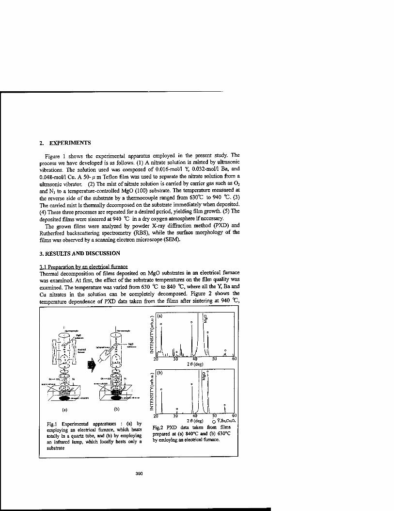
2. EXPERIMENTS
Figure 1 shows the experimental apparatus employed in the present study. The process we have developed is as follows. (1) A nitrate solution is misted by ultrasonic vibrations. The solution used was composed of 0.016-mol/l Y, 0.032-mol/l Ba, and 0.048-mol/l Cu. A 50- ß m Teflon film was used to separate the nitrate solution from a ultrasonic vibrator. (2) The mist of nitrate solution is carried by carrier gas such as 02
and N2 to a temperature-controlled MgO (100) substrate. The temperature measured at the reverse side of the substrate by a thermocouple ranged from 630t to 940 CC. (3) The carried mist is thermally decomposed on the substrate immediately when deposited. (4) These three processes are repeated for a desired period, yielding film growth. (5) The deposited films were sintered at 940 X^ in a dry oxygen atmosphere if necessary.
The grown films were analyzed by powder X-ray diffraction method (PXD) and Rutherford backscattering spectrometry (RBS), while the surface morphology of the films was observed by a scanning electron microscope (SEM).
3. RESULTS AND DISCUSSION
3.1 Preparation by an electrical furnace Thermal decomposition of films deposited on MgO substrates in an electrical furnace was examined. At first, the effect of the substrate temperatures on the film quality was examined. The temperature was varied from 630 t to 840 °C, where all the Y, Ba and Cu nitrates in the solution can be completely decomposed. Figure 2 shows the temperature dependence of PXD data taken from the films after sintering at 940 t,
(a) (b)
Fig.l Experimental apparatuses : (a) by employing an electrical furnace, which heats totally in a quartz tube, and (b) by employing an infrared lamp, which locally heats only a substrate
(a)
20 \i. jiL \J
30 40 2 9(deg)
50 A >
60
(b
c
CO
2
c
o J V . . 0
20 30 40 50 6 2 6 (deg) o Y,Ba,Cu,0,
Fig.2 PXD data taken from films prepared at (a) 840°C and (b) 630°C by emloying an electrical furnace.
390
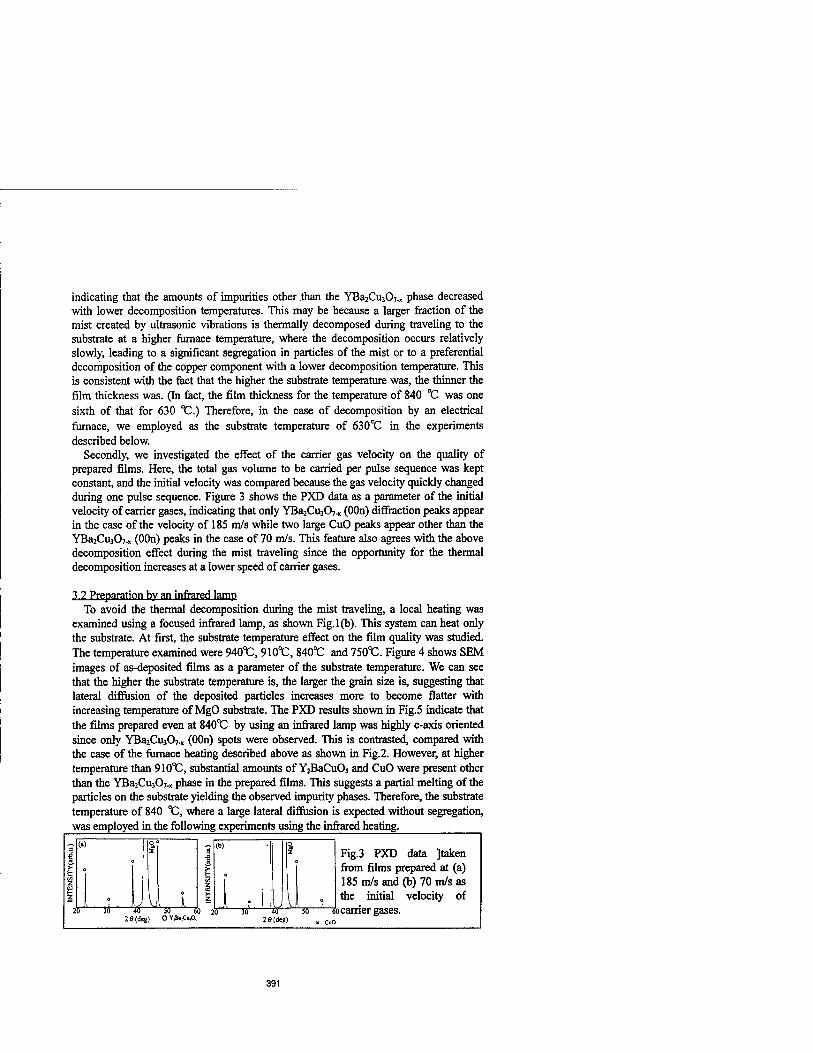
indicating that the amounts of impurities other than the YBa2Cu307.x phase decreased with lower decomposition temperatures. This may be because a larger fraction of the mist created by ultrasonic vibrations is thermally decomposed during traveling to the substrate at a higher furnace temperature, where the decomposition occurs relatively slowly, leading to a significant segregation in particles of the mist or to a preferential decomposition of the copper component with a lower decomposition temperature. This is consistent with the fact that the higher the substrate temperature was, the thinner the film thickness was. (In fact, the film thickness for the temperature of 840 t was one sixth of that for 630 t.) Therefore, in the case of decomposition by an electrical furnace, we employed as the substrate temperature of 630CC in the experiments described below.
Secondly, we investigated the effect of the carrier gas velocity on the quality of prepared films. Here, the total gas volume to be carried per pulse sequence was kept constant, and the initial velocity was compared because the gas velocity quickly changed during one pulse sequence. Figure 3 shows the PXD data as a parameter of the initial velocity of carrier gases, indicating that only YBa2Cu307.x (OOn) diffraction peaks appear in the case of the velocity of 185 m/s while two large CuO peaks appear other than the YBa2Cu307.x (OOn) peaks in the case of 70 m/s. This feature also agrees with the above decomposition effect during the mist traveling since the opportunity for the thermal decomposition increases at a lower speed of carrier gases.
3.2 Preparation by an infrared lamp To avoid the thermal decomposition during the mist traveling, a local heating was
examined using a focused infrared lamp, as shown Fig. 1(b). This system can heat only the substrate. At first, the substrate temperature effect on the film quality was studied. The temperature examined were 940t, 910t;, 840t and 750t:. Figure 4 shows SEM images of as-deposited films as a parameter of the substrate temperature. We can see that the higher the substrate temperature is, the larger the grain size is, suggesting that lateral diffusion of the deposited particles increases more to become flatter with increasing temperature of MgO substrate. The PXD results shown in Fig.5 indicate that the films prepared even at 840t by using an infrared lamp was highly c-axis oriented since only YBa2Cu307.x (OOn) spots were observed. This is contrasted, compared with the case of the furnace heating described above as shown in Fig.2. However, at higher temperature than 910t), substantial amounts of Y2BaCuOs and CuO were present other than the YBa2Cu307., phase in the prepared films. This suggests a partial melting of the particles on the substrate yielding the observed impurity phases. Therefore, the substrate temperature of 840 °C, where a large lateral diffusion is expected without segregation, was employed in the following experiments using the infrared heating. _^
2 9 (dtg) O Y,Ba,Cu,0. 4<T '
2 9(dcg)
Fig.3 PXD data ]taken from films prepared at (a) 185 m/s and (b) 70 m/s as the initial velocity of
So earner gases. CuO
391
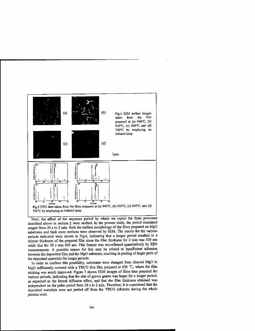
Fig.4 SEM surface images taken from the film prepared at (a) 940°C, (b) 910°C, (c) 840°C and (d) 750°C by employing an infrared lamp
lum
n I
-J- 2 8(dcj)
Fig.5 PXD data taken from the films prepared at (a) 940°C, (b) 910°C, (c) 840°C, and (d) 750°C by employing an infrared lamp
Next, the effect of the sequence period by which we repeat the three processes described above in section 2 were studied. In the present study, the period examined ranged from 20 s to 2 min. Both the surface morphology of the films prepared on MgO substrates and their cross sections were observed by SEM. The results for the various periods indicated were shown in Fig.6, indicating that a longer period resulted in a thinner thickness of the prepared film since the film thickness for 2 min was 300 nm while that for 20 s was 600 nm. This feature was reconfirmed quantitatively by RBS measurements. A possible reason for this may be related to insufficient adhesion between the deposited film and the MgO substrate, resulting in peeling of larger parts of the deposited materials for longer periods.
In order to confirm this possibility, substrates were changed from cleaved MgO to MgO sufficiently covered with a YBCO thin film prepared at 630 °C, where the film sticking was much improved. Figure 7 shows SEM images of films thus prepared for various periods, indicating that the size of grown grains was larger for a longer period, as expected as the lateral diffusion effect, and that the film thickness obtained was independent on the pulse period from 20 s to 2 min. Therefore, it is considered that the deposited materials were not peeled off from the YBCO substrate during the whole process used.
392

Fig.6 The cross-se substrates : the seq surface images are
(a)
(d)
ctional 5 jence pe >hown in
EM images taken fi riodsof(a)20s,(b) 1 (d), (e) and (f), respe
(b)
(<0
rom the min and ctively.
films prepared on c (c) 2min. The corres
(c)
(0
lum
leaved MgO ponding top-
(a)
(d)
^^S
(b)
(e)
(c)
(0
lum
ower panels, on the buffer
Fig.7 Cross-section, respectively: YBC( layerat sequence pe
il and to D buffer ■iods of 'i
3-surface SEM image ayer on MgO ((a),(d 0 s ((b),(e)) and 2 mi
s are sho ), Y,Ba2
n((c),(f))
wn in the upper and Cu307.x films grown
The amounts of the deposited materials were measured using RBS. Figure 8 shows RBS spectra of the films prepared for various periods. It is estimated from the RBS data that the areal densities of Ba atoms were 8.2 x 10¹³ atoms/cm2 and 1.4 x 10¹⁵ atoms/cm2
for the films on bare MgO and the YBCO, respectively. Since the mists consumed for the deposition corresponded to a value of 1.9 x 10¹⁷ atoms/cm2 if all of them were deposited on the substrate used, the deposition efficiencies were 0.04 % for the MgO substrate and 0.8 % for the YBCO substrate, the latter of which is sufficiently larger than the former. It is necessary to improve theprocess efficiency.
393

300 J5Ü TO Channel Number
Fig.8 The RBS spectra taken from (a) the films on cleaved MgO substrates and (b)the films on YBCO buffer layers, as a parameter of the sequence periods shown.
Channel Number
Thus, it is indicated that the adhesive property between the substrate and the deposited products is very important in the present process proposed. However, the film quality of the present preparation process should be improved using more suitable experimental parameters such as the mist size, the amounts of the mist per pulsed sequence and the solution concentration, which have not been examined in the present
study.
4. CONCLUSIONS
We have investigated YBaiCxiiO^ films prepared by means of pulsed thermal decomposition of mists intermittently created from a nitrate solution using PXD, RBS and SEM, and have obtained the following results. (1) In the case of films prepared by an electrical furnace, a low temperature of MgO substrate (630^) is required to grow c- axis oriented YBa2Cu307.x without segregation of impurities. (2) In the case of films prepared by an electrical furnace, a high initial speed of the carrier gas (185 m/s) is necessary to obtain a pure YBa2Cu307.x film. (3) A local heating is important to prepare c-axis oriented YBa2Cu307.x films at a substrate temperature of 840^ on cleaved MgO
substrates without impurity segregation. However, the temperature higher than 910t induced impurities such as Y2BaiCu,05 and CuO. (4) A sufficient adhesion between the deposited material and the substrate is required to obtain the YBCO films without peeling of the materials during the growth. The efficiency of 0.8 % was attained when YBCO-covered MgO substrates were used.
REFERENCES
1. Y. Enomoto and T. Murakami, J. Appl. Phys. 11 807 (1986). 2. P.G. Quincey, Appl. Phys. Lett. 64 517 (1994). 3. E.M. Jackson, B.D. Weaver and G.P. Summers, Appl. Phys. Lett. 64 511 (1994). 4. Y.M. Zhang, D. Winkler, P.A. Nilsson and T. Cleason, Appl. Phys. Lett. 64 1153 (1994). 5. R.Gross, P. Chaudhari, M, Kawasaki and A. Gupta, IEEE Trans. Magn. 27 3227 (1991). 6. C.B. Eom, J.Z. Sun, B.M. Lairson, S.K. Streiffer, A.F. Marshall, K. Yamamoto, S.M. Anlage,
J.C. Bravman, T.H. Geballe, Physica C171354 (1990). 7. D.K. Fork, D.B. Fenner, R.W. Barton, J.M. Phillips, G.A.N. Connell, J.B. Boyce,
T.H. Geballe, Appl. Phys. Lett. 57 1161 (1990). 8. T. Terashima, K. Iijima, K. Yamamoto, Y. Bando, H. Mazaki, Jpn. J. Appl. Phys. 27 L91
(1988). 9. I.M. Watson, Chem. Vap. Deposition 3 9 (1997).
394

SURFACE CHARACTERIZATION OF CALCIUM-STABILIZED ZIRCONIA FILM BY
X-RAY PHOTOELECTRON SPECTROSCOPY
E. 0. Bensadon*, P. A. P. Nascente", L.O.S. Bulhöes*, E.C. Pereira* * Laboratörio Interdisciplinar de Eletroquimica e Cerämica, Departamento de Quimica, Universidade Federal de Säo Carlos, 13565-905 Säo Carlos, SP, Brazil; [email protected] ** Centro de Caracterizacäo e Desenvolvimento de Materials, Departamento de Engenharia de Materials, Universidade Federal de Säo Carlos, 13565-905 Säo Carlos, SP, Brazil; [email protected]
ABSTRACT
A new methodology was developed to stabilized zirconia films at room temperature. The zirconium oxide films were prepared electrochemically by anodic oxidation of metallic zirconium at constant current density. X-ray diffraction (XRD) revealed the partial stabilization of the cubic phase in the Zr02 films obtained in the presence of calcium. On the other hand, the films obtained in H3PO4 presented monoclinic phase. Scanning electron microscopy (SEM) showed that the oxide films obtained in calcium medium were porous, while the films obtained in H3PO4 were compact. X-ray photoelectron spectroscopy (XPS) identified Zr02 and the intercalation of Na, N, P and CaO, as well as adventitious carbon. Using depth profiling, we observed that the concentrations of Zr02, P and CaO increased with sputtering time.
INTRODUCTION
Zirconia is widely employed in industry due to its refractory properties and its ability as oxygen sensors [1]. The control of its crystalline structure is fundamental in any application. At room temperature pure zirconia exists in the monoclinic phase. At 1270°C the material changes to tetragonal phase. At temperatures near to 2370 °C the tetragonal zirconia becomes cubic, and it melts at 2680 °C. The tetragonal to cubic transformation is reversible. However, the tetragonal to monoclinic transformation occurs through cooling, with thermal hysteresis at 950 °C. During the transformation from tetragonal to the monoclinic phase it undergoes a mechanical degradation due to the greater molar volume of the tetragonal phase (3-5%). Since high temperatures are normally used in ceramic processing, it is important to avoid the tetragonal to monoclinic transformation during cooling of zirconia. The preparation of stabilized zirconia films in either tetragonal or cubic phase can be done by different methods, such as a solid state reaction or by a chemical method [2]. Another method used is doping the oxide with CaO, MnO, MgO, Nb205 or Y203, which yields a solid solutions with Zr02. These dopants inhibit the tetragonal (or cubic) to monoclinic phase transformation during cooling [3, 4],
Zirconia obtained by electrochemical methods crystallizes during the film growth into the monoclinic phase. At very high fields, dielectric breakdown occurs, resulting in fracture of oxide film. The film is quickly reformed generating high local current densities in the pore. Considering the conditions of the breakdown and regrowth, we decided to investigate the effect of addition of Ca2+ ions in the solution since these ions migrate into the film during the breakdown process and could be incorporated into the oxide film. This process can generate solid solutions in Zr02, allowing the tetragonal (or cubic) phase stabilization. In this paper we present a new electrochemical method for preparing stabilized zirconia film, as well as the results of the film characterization by XRD, SEM and XPS.
395
Mat. Res. Soc. Symp. Proc. Vol. 495 ° 1998 Materials Research Society
EXPERIMENT
We grew the oxide films anodicaly on a zirconium substrate using 0.1 mol/L phosphoric acid aqueous solution at a constant current density. Initially, we studied the oxide films prepared in acid aqueous solution with no dopant ions. Then, we investigated the oxide films formed in 0.1 mol/L phosphoric acid solution containing Na2[Ca(EDTA)] at different concentrations. The experiments were carried out at temperatures between 5 °C and 25 °C. We used as work electrode 0.5 and 2.0 cm2 zirconium plates and, as auxiliary electrode, a 21 cm2 semicircular platinum sheet.
We followed the oxide grown kinetics by potential-time curves using a home made current power supply.
The crystalline structure of the oxide films was determined by XRD using a D5000 Siemens diffractometer. The morphology of the oxide films and the presence of dopants were characterized by SEM using a Zeiss 950 instrument.
The surface analysis by XPS was performed using a XSAM HS spectrometer from Kratos Analytical. The radiation source used to excite the photoelectrons was Mg Koc (power given by 15 kV and 15 mA). The pressure at the analysis chamber was in the low 10'9 Torr range. The samples were flooded with low energy electrons from a flood gun to avoid charging effects. The spectra were referenced to the adventitious carbon C Is line, set at 284.8 eV. Argon ion bombardment (3 kV, 20 mA) was employed to clean the surface.
RESULTS AND DISCUSSION
Figure 1 presents a typical potential-time curve for the oxide film grown in phosphoric acid aqueous solutions. This curve is characterized by two regions: the initial region presents a linear increase of the potential, and almost no change in the average potential in the second region is observed, although it shows an oscillation of approximately 20 V. This behavior can be described in the following way: an electric field applied to an oxide film causes electric charge transport though the film. The charges can be transported by ions or electrons.
In the region of linear potential increase, the main contribution to the charge flux is the ionic transport, if, which leads to an oxide film growth. On the other hand, the constant potential region is characterized by electronic transport through the film from the solution interface due to the water oxidation reaction.
In the intermediate region observed in figure 1, the curve levels off, indicating that the values of id and ie became important. The second region indicates that the oxide film suffers rupture by electronic [5] or mechanical mechanism [6].
For the film grown in phosphoric acid solution containing Na2[Ca(EDTA)] complex, the potential curve as a function of time presents the same characteristics examined previously, although the potential breakdown occurs at lower values, indicating the presence of defects in the oxide film.
The morphology of the oxide films prepared in pure H3P04 is completely different than the morphology of the oxide films grown in the presence of Na2[Ca(EDTA)] complex. The oxide films prepared in pure 0.1 mol/L H3P04 solution showed a compact and uniform crystallites, while the ones prepared in the presence of calcium complex were porous, as shown in figure 2.
396

Figure 1. Chronopotentiogram obtained during the Zr02 film growth in 0.1 mol/L H3P04 solution, i = 36 mA/cm2, T = 5 °C.
H&
W* 0 'S?*
Itil !# *
Figure 2. SEM micrographs of the Zr02 film grown in: (left) 0.1 mol/L H3P04 solution (x 2000); (right) 0.1 mol/L H3P04 plus 0.1 mol/L Na2[Ca(EDTA)] solution (x 5000).
We employed XPS to characterize the oxide film surfaces to identify the chemical states and determine the amounts of the elements. The Zr 3d spectra are shown in figure 3 for the Zr02 films prepared in: (a) aqueous H3P04 and (b) the presence of 0.1 mol/L calcium complex. The shapes of the Zr 3d photoelectron doublets differ, as well as their binding energies, indicating that the calcia-doped film, with a binding energy of 182.3 eV, is consistent with Zr02, while the film grown in the H3P04 solution, with a binding energy of 183.3 eV, could be related to the formation of a Zr-OH species [7]. Table I presents the quantification (atomic %) measured by XPS for different ion sputtering times for the Zr02 film grown in phosphoric acid solution containing Na2[Ca(EDTA)] complex.
The XRD spectrum shows that the oxide films grown on aqueous phosphoric acid solutions without the Ca complex are crystalline and have monoclinic structure (figure 4). The peaks corresponding to the metal substrate are also present. The oxide film prepared in aqueous phosphoric acid solutions in the presence of the Ca complex presents a completely different XRD spectrum (figure 5).
397

Figure 3. Zr 3d spectra obtained by XPS for the Zr02 films prepared in: (a) aqueous H3PO4 and (b) the presence of 0.1 mol/L calcium complex.
Table I. Quantification (atomic %) measured by XPS for different ion sputtering times for the Zr02 film grown in phosphoric acid solution containing Na2[Ca(EDTA)] complex.
Element Quantification (atomic %) for different ion sputtering times No ion sputtering 60 min 120 min 240 min
0 47.3 41.5 38.1 39.1 C 40.7 41.2 38.4 36.5 N 2.0 3.0 5.3 2.3 Na 0.8 1.8 1.1 1.0 P 3.2 3.9 8.3 5.4 Ca 4.5 6.2 6.2 10.2 Zr 1.5 2.5 2.5 5.5
The conventional method of zirconia stabilization is based on mixing oxide phases followed by sintering at high temperatures. A possible mechanism for the zirconia stabilization by the electrochemical method is associated with the breakdown phenomena of the oxide film. The electric field applied leads to the water oxidation in the oxide-solution interface, which in turn generates electrons. These electrons collide with the oxide molecules causing ionization processes, initiating the electron avalanche phenomenon, which initiates the film destruction locally. As a consequence, the electrolytic solution penetrates into the oxide film carrying away the ions present in this phase. Corroborating with this statement, the results of the quantification of these ions obtained by the combination of XPS and ion sputtering presented in table I indicate that the concentration of calcia is higher in the bulk of the film (accordingly to longer sputtering
398
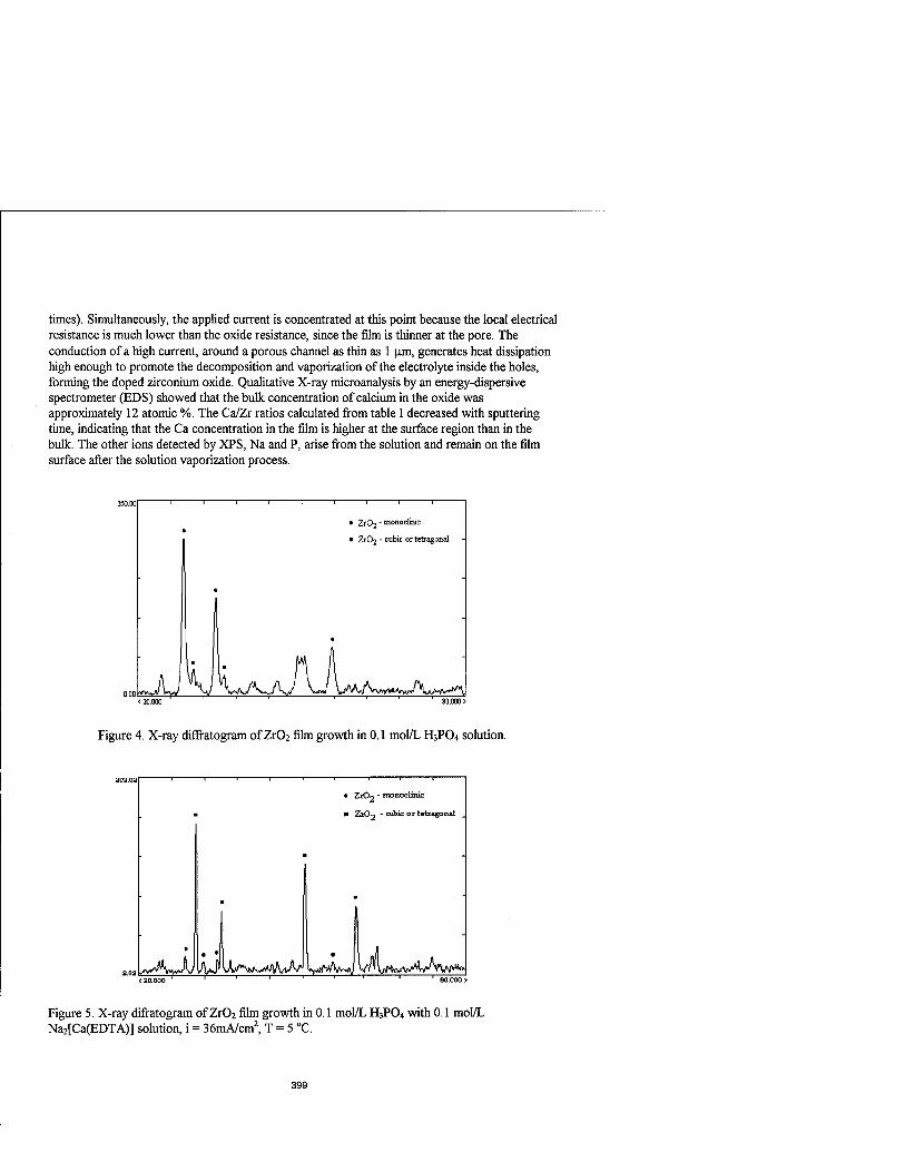
times). Simultaneously, the applied current is concentrated at this point because the local electrical resistance is much lower than the oxide resistance, since the film is thinner at the pore. The conduction of a high current, around a porous channel as thin as 1 urn, generates heat dissipation high enough to promote the decomposition and vaporization of the electrolyte inside the holes, forming the doped zirconium oxide. Qualitative X-ray microanalysis by an energy-dispersive spectrometer (EDS) showed that the bulk concentration of calcium in the oxide was approximately 12 atomic %. The Ca/Zr ratios calculated from table I decreased with sputtering time, indicating that the Ca concentration in the film is higher at the surface region than in the bulk. The other ions detected by XPS, Na and P, arise from the solution and remain on the film surface after the solution vaporization process.
muu
1
■ ZrO? ■ mono clinic
■ Zr02 - cubic or tetragonal
nnn "/W^N Wv* V •
Figure 4. X-ray diffratogram of Zr02 film growth in 0.1 mol/L H3PO4 solution.
1 1 1
* ZJOO - monoclinic
■ ZxOn - cubic or tatragorul
■/V-A-vJl/ IWW^r^tJ^fyAA ^LV%!^AAV^V. T r-
Figure 5. X-ray difratogram of Zr(>2 film growth in 0.1 mol/L H3PO4 with 0.1 mol/L Na2[Ca(EDTA)] solution, i = 36mA/cm2, T = 5 °C.
399

CONCLUSIONS
We have demonstrated the possibility of preparing stabilized zirconia films at room temperature using electrochemical methods. The electrochemical oxide growth was characterized by an initial linear potential increase, which was related only to the oxide growth. A second region, with an oscillatory potential behavior of the potential, was associated with the breakdown phenomenon. We proposed that the local destruction and rebuilding of the oxide film leads to the intercalation of the solution ions. These ions migrate into the oxide during the film rebuilding as the electric current flows through the pores created by the local film destruction. Surface enrichment of CaO was observed by XPS. Considering the results here presented, we can affirm that we have developed a new method to introduce large quantities of dopants in oxide films which is economical and simple to use.
ACKNOWLEDGMENTS
This work was supported by CNPq, FAPESP and PADCT II of Brazil. The authors would like to thank H.A. Carmona for their assistance in some of the experiments.
REFERENCES
1. G. Fisher; Ceramic. Bull. 65, p. 1,355 (1986). 2. D. F. Shriver and G. C. Farrington, Chem. Eng. News 63, p. 42 (1985). 3. P. Duwez, F. Odell and F.H. Brown; J. Am. Ceramic Soc. 35, p. 107 (1952). 4. T.K. Gupta, J.H. Bechtold, R.C. Kuznicki, L.H. Cadoff and B.R. Rossing; J. Mater. Sei. 12, p. 2,421 (1977). 5. S. Ikonopisov; Electrochim. Acta 22, p. 1,077 (1977). 6. N. Sato and M. Cohen; J. Electrochem. Soc. Ill, p. 512 (1964). 7. Y.S. Li, P.C. Wong and K.A.R. Mitchell; Appl. Surf. Sei. 89, p. 263 (1995).
400
FORMATION OF TRANSPARENT Si02 THIN FILM AT ROOM TEMPERATURE WITH EXCIMER LAMP IRRADIATION
T.Okamoto, H.Iizuka, S.Ito and M.Murahara Faculty of Electrical Engineering, Tokai University 1117 Kitakaname, Hiratsuka, Kanagawa, 259-1292, JAPAN
ABSTRACT A transparent Si02 thin film was grown with Xe2* excimer lamp and NF3, 02 mixed
gases at room temperature. Unlike the conventional methods such as atomic layer epitaxy (ALE) at low temperature, this method requires only a few minutes for deposition without changing material gases. A Si substrate was placed in a reaction chamber, which was filled with NF3 and 02 gases. The gases were exposed to the Xe2* excimer lamp light, and SiF4
and N02 were produced by photochemical reaction. The S1F4 was adsorbed on the substrate; which reacted with N02 in gas ambient and was oxidized to form Si02. The molecular layer was produced per reaction, and by voluntarily repeated reaction, the transparent Si02 thin film was grown. As a result, the Si02 film thickness of about 2200Ä was achieved for 15 minutes at room temperature. By annealing the formed Si02 film, the surface current density of the formed Si02 decreased; the higher the annealing temperature became, the more the surface density decreased.
INTRODUCTION Si02 insulator is generally fabricated by a thermal oxidation of silicon wafer. Such
high temperature processes, however, have many disadvantages such as dopant diffusion, material interaction and stress in films. To solve these problems, a low temperature process is required. There are many reports on Si02 deposition by photochemical vapor deposition (photo-CVD) or plasma CVD at low temperature [1, 2]; nevertheless, they still require a temperature of approximately 200 *C for processing. Recently, formation of Si02 thin films by using TEOS have been extensively investigated [3, 4]. These methods present difficulties in controlling deposition rates and in forming high-density Si02 films because an oxidation reaction takes place not only on the surface but also in gas phase. As one of a few techniques to fabricate thin films at low temperature, atomic layer epitaxy (ALE) has been reported [5, 6]. In ALE process, two kinds of material gases are alternately sealed and exhausted in a reaction chamber, being photo- or thermal-dissociated by laser light irradiation to be adsorbed on a substrate [7, 8]. One complete atomic or molecular layer is produced per operational cycle, with a greater thickness being obtained by repeated cycling. Therefore, we have studied a new simpler method named Self-laminating Atomic Layer Epitaxy (SALE), which is distinguished from the ALE, to solve the above-mentioned problems. By this new method, a transparent Si02 thin film was successfully fabricated on a silicon substrate. In the process, adsorption of S1F4 and oxidation were repeated spontaneously without changing reaction gases in a reaction chamber, and a monolayer was grown intermittently one after another to form the transparent Si02 film of greater thickness. The silicon substrate, which was a silicon wafer, was used as a source of Si; NF3 and 02 mixed gas was employed as a reaction gas. The mixed gas was photodissociated by Xe2* excimer lamp (A= 172 nm)
401
Mat. Res. Soc. Symp. Proc. Vol. 495 e 1998 Materials Research Society

irradiation to react with the silicon substrate; SiF4 and NO2 gases were produced. The SiF4 gas was adsorbed on the etched Si substrate, which pulled the oxygen out of the N02 to form a Si02 molecular layer. Thus, the transparent thin film was grown at room temperature [9-11]. The reaction mechanism was investigated by FTTR and UV spectroscopes. Moreover, the trial surface roughness, I-V, e r-f characteristics and refractive index were measured to evaluate the characteristics of the formed Si02.
PHOTOCHEMICAL REACTIONS As in Fig. 1 and Fig. 2, NF3 and O2 gases have a strong absorption band in the
wavelength of the Xe2* excimer lamplight (A= 172 nm). They, therefore, are efficiently photo-decompose by the Xe2* excimer lamp. The chemical reactions are given in the following equations:
i) Photo-decomposition of reaction gases: NF3 + 02 + h v ■ NFO + nF2 + N02
ii) Etching of native oxide of silicon substrate: NFO + Si02 (native oxide) + h v N02 + SiF4
iii) Etching of silicon substrate: Si + nF2 + hv S1F4
iv) Oxidation reaction between adsorbed SiF4 of Si substrate and N02 gas: SiR, + 2N02 3- Si02 + 2NO
(eq.-l)
(eq.-2)
(eq.-3)
(eq.-4)
N-F: 72kcal/mol
/Xe2*lamp Photon energy : 165.5kcal/mol
170 180 190 200 210 Wavelength (nm)
Fig. 1 VUV and UV spectrum of NF3
02: 30Torr
180 190 200 21 Wavelength (nm)
Fig. 2 VUV and UV spectrum of 02
The NF3 and 02 gases were photo-dissociated with the Xe2* excimer lamp irradiation to generate NFO, N02 and F2 (eq.-l). The NFO, an intermediate product that has a strong reductive character, etched the native oxide of the silicon substrate surface (eq.-2) [12].
402
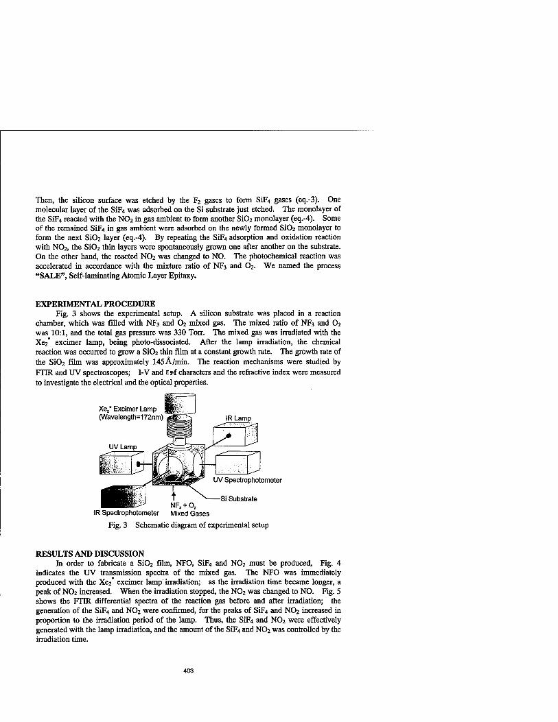
Then, the silicon surface was etched by the F2 gases to form S1F4 gases (eq.-3). One molecular layer of the SiF4 was adsorbed on the Si substrate just etched. The monolayer of the SiF4 reacted with the NO2 in gas ambient to form another SiC>2 monolayer (eq.-4). Some of the remained S1F4 in gas ambient were adsorbed on the newly formed Si02 monolayer to form the next Si02 layer (eq.-4). By repeating the S1F4 adsorption and oxidation reaction with NO2, the SiC>2 thin layers were spontaneously grown one after another on the substrate. On the other hand, the reacted N02 was changed to NO. The photochemical reaction was accelerated in accordance with the mixture ratio of NF3 and O2. We named the process "SALE", Self-laminating Atomic Layer Epitaxy.
EXPERIMENTAL PROCEDURE Fig. 3 shows the experimental setup. A silicon substrate was placed in a reaction
chamber, which was filled with NF3 and O2 mixed gas. The mixed ratio of NF3 and O2 was 10:1, and the total gas pressure was 330 Torr. The mixed gas was irradiated with the Xe2* excimer lamp, being photo-dissociated. After the lamp irradiation, the chemical reaction was occurred to grow a SiÜ2 thin film at a constant growth rate. The growth rate of the SiÜ2 film was approximately 145Ä/min. The reaction mechanisms were studied by FTIR and UV spectroscopes; I-V and erf characters and the refractive index were measured to investigate the electrical and the optical properties.
Xe2* Excimer Lamp (Wavelength=172nm) IR Lamp
^**~-- ■ ■ V';\ '***^i
> '■'[■ ■■-:}
^r**' **^
■^
UV Spectrophotometer
Si Substrate
IR Spectrophotometer Mixed Gases
Fig. 3 Schematic diagram of experimental setup
RESULTS AND DISCUSSION In order to fabricate a Si02 film, NFO, SiF4 and NO2 must be produced. Fig. 4
indicates the UV transmission spectra of the mixed gas. The NFO was immediately produced with the Xe2* excimer lamp irradiation; as the irradiation time became longer, a peak of NO2 increased. When the irradiation stopped, the NO2 was changed to NO. Fig. 5 shows the FTIR differential spectra of the reaction gas before and after irradiation; the generation of the S1F4 and NO2 were confirmed, for the peaks of S1F4 and NO2 increased in proportion to the irradiation period of the lamp. Thus, the SiEt and NO2 were effectively generated with the lamp irradiation, and the amount of the S1F4 and NO2 was controlled by the irradiation time.
403

^100
1 50
NO, V V NFO
-before irradiation -1 min. irradiation - 3 min. irradiation -5 min. after irradiation
200 250 300 Wavelength (nm)
350
Fig. 4 UV transmittance of reaction gas before and after lamp irradiation
0.50
"E
I °
-0.571
NO,
Irradiation Time 3 min. 9 min. 12 min.
NF^IO:! (Total: 330 Torr)
J L 1900 r ,-, 95(
Wavenumber [cm J
Fig. 5 FITR differential spectra of reaction gas before and after lamp irradiation
Fig. 6 exhabits the FITR differential spectra of the reaction gas after lamp irradiation. The peak of NO increased, but N02 decreased with the self-reaction time after irradiation, which is clearly shown in Fig. 4. The color of the gas in the reaction chamber changed from brown to colorless as the self-reaction advanced. As a result, by repetitional adsorption of the SiF4 on the silicon surface and oxidation with the N02, a transparent Si02 monolayer was intermittently and spontaneously grown on the etched silicon surface. Fig. 7 shows the dependence of irradiation time and film thickness in the case of 15-minute self chemical reaction after irradiation. The film thickness increased until the irradiation time reached 12 minutes, but decreased after that. This decrement resulted from the over-production of SiF4
and N02; the oxidation reaction occurred not only on the surface but also in the gas phase, producing Si02 powder. In this mechanism, the Si02 thin film was grown with the repetition of the SiF, adsorption and N02 oxidation reaction. The visible color of the Si02 film changed from blue to yellow, as the film was grown.
0.35
-0.10 1900
Fig. 6
Wavenumber [cm' ]
FITR differential spectra of reaction gas after lamp irradiation
1400
Total pressure: 330 Torr. Self reaction time: 15 min
"0 5 . .10 , . 15 Irradiation time (min.)
Fig. 7 Dependence of lamp irradiation time and formed Si02 thickness
404

Fig. 8 displays the three-dimensional image of the fabricated Si02 surface measured by the interference roughness meter. When the photo-dissociation time was 12 minutes and the self chemical reaction time, 15 minutes, the fabricated Si02 film thickness was approximately 2200Ä.
Fabricated Si02 film surface Si surface
2200
0.363
(mm) o.329 ° v
Fig. 8 3-D image of the formed Si02 surface
In general, the characterization of a fabricated thin film is advanced with the improvement of crystallization by annealing [13]. Fig. 9 shows the comparison of the I-V characteristics of the samples unannealed or annealed: a is unannealed; b, annealed at 100 "C; c, annealed at 250 *C: d, the commercial thermal oxide film heated at 1100 V.. The higher the annealing temperature of the sample was, the lower the surface current density of the film became. With the increase of annealing temperature, the characteristics of the annealed sample improved and became similar to that of the thermal oxide film. This implies that the insulation characteristic of the surface was improved by annealing.
E 10"'
10"
C10"'
1 a:
b:
c:
i j^jj^jiiiifflmlinrililiiiilll1!"'1"'1"1111"": -
■mjniimiiiiiiiiiiiiiiiiiii11111 IIIMI111111"""" f
o non annealing
x annealing: 100 "C :
+ annealing: 250 °C s
i d: • Thermal oxide: 1100 *C |
! i , i _J—i—.—i—■—3
■a -b
£-5
2 4 6 8 Potential (Volt)
10
Fig.9 I-V characteristics of the formed Si02 surface
■ 11iiMi—'—' 'i,M,I—'—' ' i""
a: e no annealing c: o annealing: 250 °C d: • Thermal oxide: 1100"C
103 104
Frequency (Hz)
Fig.10 Interdependence of relative permittivity and frequency
405

At the same time, the interdependence between the relative permittivity of the films and the frequency was measured, as in Fig. 10. The relative permittivity of the c declined by annealing, and became closer to that of the d in characteristics. While the relative permittivity of the d was maintained constant as the frequency increased, the relative permittivity of the sample was remarkably high at a low frequency, especially f<103 Hz. These results revealed that the insulation characteristic of the surface was improved by annealing at 250 *C,
Furthermore, the refractive index of the a was compared to that of the d. The refractive index of the a before annealing was 1.366 against that of the thermal oxide of 1.472. The indexes of the b at 100 "C and the c at 250 V, were improved by annealing to 1.371 and 1.394, respectively. From these results, it is obvious that the annealing temperature contributed to the improvement of the refractive index of the sample Si02 film; it is considered that a film structure was improved by the annealing temperature.
CONCLUSION The transparent Si02 thin film was successfully fabricated by Self-laminating Atomic
Layer Epitaxy (SALE) at room temperature. This fabrication process was carried out in the manner that the NF3 and O2 mixed gas was photo-dissociated by the Xe2* excimer lamp to produce NFO, S1F4 and NO2 gases, which were intermittently allowed to react themselves. The formed transparent Si02 thin film had the evenly yellow interference color at room temperature, because the film was grown intermittently and spontaneously layer by layer. The chemical reaction changes in a state from the etching to the deposition at a certain oxygen concentration in the mixed gas. Moreover, it was proved that the surface insulation and the refractive index of the formed SiÜ2 film have improved by annealing.
REFERENCES 1) C.Licoppe, C.Meriadec, Y.I.Nissim and J.M.Moison; Appl. Surf. Sei., 54, pp.445-452
(1992) 2) R. M. Levin and K.Evans-Luterodt; J.Vac. Sei. Technol., Bl, 54 (1983) 3) K. Fujino, Y.Nishimoto, N.Tokumasu, and K.Maeda; J. Electrochem. Soc, Vol.137,
No.9, pp.2883-2887 (1990) 4) Y.Ikeda, Y.Numasawa and M.Sakamoto; J. Electro. Mat., 19, 45 (1990) 5) Colin H. L. Goodman, and Markus V. Pessa: J. Appl. Phys. 60, (3), R65 (1986) 6) T.Suntola: Mater. Sei. Rep., 4, 261 (1989) 7) Y.Aoyagi, A.Doi, S.Iwai, and S.Namba: J. Vac. Sei. Technol., B5,1460 (1987) 8) S.Iwai, T.Meguro, and Y.Aoyagi: J. Cryst. Growth, 107,136 (1991) 9) S.Aomori and M.Murahara; Mat. Res. Soc. Symp.Proc, Vol.236, pp.9-14 (1992) 10) M.Murahara and S.Aomori; CLEO (Conference on Lasers and Electro-Optics),
CThI50, pp.488-491, Anaheim, CA (1992) 11) T.Suzuki and M.Murahara; Mat. Res. Soc. Symp. Proa, Vol.446, pp.285-290 (1997) 12) K.Kitamura and M.Murahara; Mat. Res. Soc. Symp. Proa, Vol.334, pp.439-444 (1994) 13) H.Nagasawa, H.Kitajima, D.Kitayama, Y.Okamoto and H.Ikoma; Jap. J. Appl. Phys.,
Vol.34, pp.L1103-L1106 (1995)
406

PHOTOCHEMICAL PATTERN ETCHING OF SINGLE-CRYSTALLINE 3C-SiC
T. MORI, K. HATAO and M. MURAHARA Faculty of Engineering, Tokai University, 1117 Kitakaname, Hiratsuka, Kanagawa, 259-12, JAPAN
Abstract. A single-crystalline 3C-SiC is very difficult to etch compared with a polycrystalline SiC. Thus, a photochemical pattern etching of the SiC was demonstrated by using Xe2* excimer lamp and ArF or KrF excimer laser. To promote the surface reaction, a Xe2* excimer lamp was employed to produce many radicals on the sample surface; simultaneously, ArF or KrF laser light irradiated the surface via a circuit pattern to dissociate the Si-C bonds. The Si and C reacted with the F and N radicals photo-dissociated from NF3 gas to form SiF4, CFn and CN, which diffused in the reaction cell. As a result, the single-crystalline 3C-SiC was photo-chemically etched effectively. With the NF3 gas of 200Torr, the Xe2' excimer lamp of 7mW/cm2, and the KrF excimer laser of 650mJ/cm2, 20Hz and 10,000shots, the etch depth of 700 A was
successfully achieved.
Introduction Silicon-carbide (SiC) has excellent properties such as a high melting point (2830"C), a
wide band gap (3C-SiC; 2.2eV) and a high resistance to vacuum ultra violet (VUV) or X-ray radiation. SiC is a promising material for structural applications in optical and electronics industries owing to its attractive properties. Deposition of SiC, accordingly, has been studied extensively. However, there are little reports on pattern etching of SiC except our reports. SiC has so high reflectance on the soft X-ray range that it has been expected as a material for mirror or grating of SR light. Moreover, due to the high melting point and wide band gap, IC, which works at high temperatures, can be fabricated if a circuit pattern minute process is made possible. Today, there are diamond etching and laser ablation in physical methods, and reactive ion etching (RIE)1"13 and photo-electrochemical (PEC)14'15 method in chemical methods. In chemical methods, RIE requires a more chemically stable resist than SiC for pattern etching, but PEC requires no resist. PEC, however, has disadvantages in terms of process time and precision because of the direct drawing method. Thus, we have studied a resistless pattern etching of SiC by using excimer laser1"0; in which NF3 was employed as an etchant gas and ArF excimer laser or Xe2* excimer lamp, as a light source to etch patterns on SiC by radicals
being produced. In this study, we have tried a resistless pattern etching of single-crystalline 3C-SiC by
using two light sources, Xe2* excimer lamp light for dissociating NF3 and ArF or KrF excimer laser light for excitation of the sample surface, in order to investigate the relationship between the laser wavelength and photochemical reaction. A single-crystalline 3C-SiC substrate was placed in NF3 gas ambient and was irradiated by Xe/ excimer lamp (172nm) horizontally to
407
Mat. Res. Soc. Symp. Proc. Vol. 495 ® 1998 Materials Research Society

photo-decompose NF3; which was simultaneously irradiated by ArF excimer laser (193nm) or KrF excimer laser (248nm) light via a circuit pattern. The surface etching was performed effectively by exciting the substrate surface and promoting photochemical reaction on the surface. To clarify the reaction mechanism, the etchant gas was analyzed by the Fourier- transformation infrared (FT-IR) spectrometer before and after etching. The etched SiC surface was evaluated by the interference roughness meter (ZYGO).
Photo Etching Mechanism Photochemical etching requires two reactions as stated below.
1) Photo-dissociation of etchant gas to produce active radicals on SiC surface 2) Photo-excitation of substrate surface to dissociate Si-C bond
Fig.l illustrates the photo etching mechanism of single-crystalline 3C-SiC. A Xe2" excimer lamp light (172nm) was used to photo-dissociate the etchant gas (NF3); a circuit patterned ArF excimer laser (193nm) or KrF excimer laser (248nm), to excite the SiC surface. Photon energy of Xe2* excimer lamp is 165kcal/mol and bonding energy of N-F is 62.6kcal/mol. Accordingly, the lamp easily dissociates the N-F bond to produce an active F or N radical near the substrate (eq.-l). On the other hand, SiC has an absorption band of approximately 50% and 70% at the ArF excimer laser wavelength of 193nm and at the KrF excimer laser wavelength of 248nm, respectively. Photon energies of ArF and KrF lasers are 147kcal/mol and 115kcal/mol, respectively, so they can dissociate the Si-C bond, whose bonding energy is 107kcal/mol, to be free (eq.-2). The Si and C react with the F and N radicals photo-dissociated by the excimer lamp to form volatile gases such as SiF4, CF4 and CN, which will diffuse in the chamber (eq.-3). Etching progresses by repeating the reaction. Furthermore, a pattern etching is possible because this etching reaction takes place on the exposed area only.
KrF excimer laser (liskcai/moi) or
ArF excimer laser (N7kcaumei)
NF3
SiC (■Si + ■C)
Fig. 1 Diagram of Photochemical Etching
•N* + -F* (eq.-l)
•Si + -C (eq.-2) + (-N*+ -F*) -»• Si + 4F -* SiF4~
-»• C + 4F -+ CF4
C + N CN (eq.-3)
408

Experiment
Fig.2 shows the experimental setup. A single-crystalline 3C-SiC that had been fabricated on Si substrate by CVD was used as a sample. The SiC substrate was placed in a teflon reaction chamber; which was vacuumed, was purged of the residual gases by He, and was filled with NF3 gas. The gas pressure was fixed at 200Torr. The substrate was irradiated with the Xe2" excimer lamp (172nm, TmW/cm2) horizontally to photo-dissociate the NF3. There was a gap (20mm) between the lamp and the fused silica glass window; therefore, it was covered and filled with nitrogen in order to reduce the light absorption by oxygen in the air. Simultaneously, the ArF or KrF excimer laser irradiated the substrate surface through the minute circuit pattern.
193nra ArFExdnttr Lucr (1471uafy
MSnm KrF Eidmer Laser (llikot)
Fig. 2 Experimental setup of photo etching
Results and Discuxxinn
Fig.3 exhibits the measurement of the reaction gas by FT-IR before and after etching. The ArF excimer laser light irradiated the substrate surface vertically at the laser fluence of 275mJ/cm2, the frequency of 10Hz and 10,000 shots. After etching, the peaks of SiF„, CFn and C=N were observed in the vicinity of 1280cm"1, 1250cm"1 and 1600-1650cm"\ respectively. The results revealed that the F and N radicals photo-dissociated from NF3 reacted with the Si and C from SiC to produce the volatile gases. Accordingly, it was confirmed that the single- crystalline 3C-SiC was photo-chemically etched.
C=N
- Before etching iiF^tmorr -After etching ArF2JSmJ/an',10Hil»,XKhhM
2300.00 Wavenumberfcm J
Fig. 3 The absorption chart of the etchant gas by FT-IR spectrometer
800 • KrFexcimer later (24tnitQ A ArFeteimtr later (193nm)
/ ~f600 ' 6S0mJ/enf, 20Ht, lMOtokots
^400 - //
200 ^- NF,:209Terr
' ' 20 40 60 80 100
Xej excimer lamp intensity (%)
Fig. 4 Dependence of etch depth of Xej' excimer lamp intensity
409
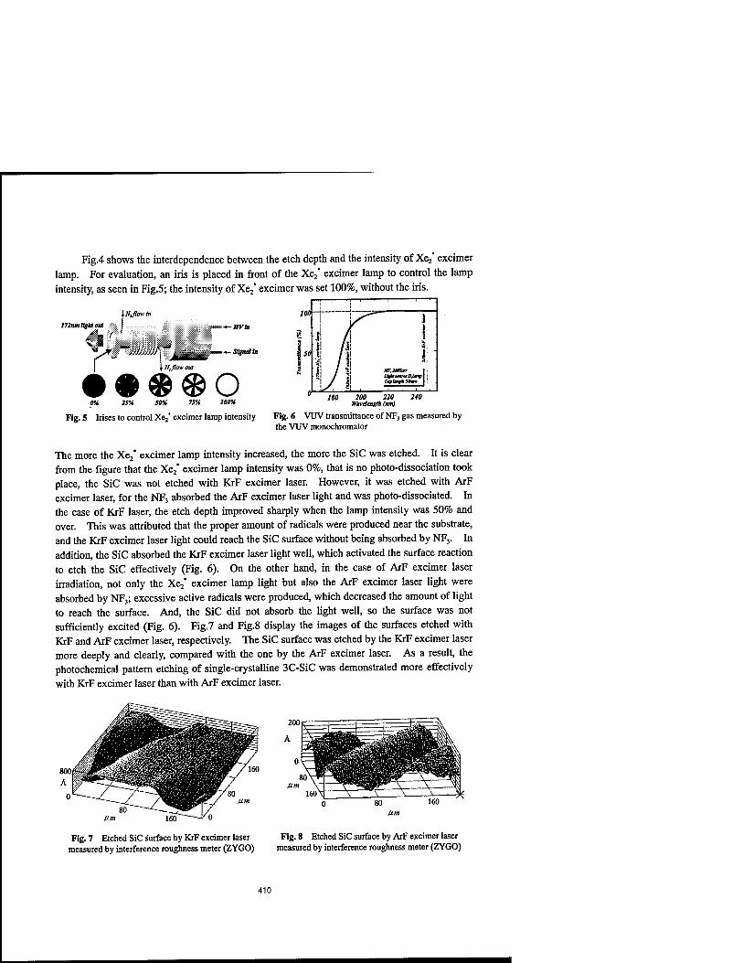
Fig.4 shows the interdependence between the etch depth and the intensity of Xe2" excimer lamp. For evaluation, an iris is placed in front of the Xe2* excimer lamp to control the lamp intensity, as seen in Fig.5; the intensity of Xe2' excimer was set 100%, without the iris.
\N,flow in
mmtliglaout
u I _. wmm +-Signal tit
I N,flow out
6% 2S% SOU 75X 1MX
Fig. 5 Irises to control Xe/ excimer lamp intensity Fig. 6 VUV transmittance of NF3 gas measured by the VUV monochromator
The more the Xe2* excimer lamp intensity increased, the more the SiC was etched. It is clear from the figure that the Xe2* excimer lamp intensity was 0%, that is no photo-dissociation took place, the SiC was not etched with KrF excimer laser. However, it was etched with ArF excimer laser, for the NF3 absorbed the ArF excimer laser light and was photo-dissociated. In the case of KrF laser, the etch depth improved sharply when the lamp intensity was 50% and over. This was attributed that the proper amount of radicals were produced near the substrate, and the KrF excimer laser light could reach the SiC surface without being absorbed by NF3. In addition, the SiC absorbed the KrF excimer laser light well, which activated the surface reaction to etch the SiC effectively (Fig. 6). On the other hand, in the case of ArF excimer laser irradiation, not only the Xe2* excimer lamp light but also the ArF excimer laser light were absorbed by NF3; excessive active radicals were produced, which decreased the amount of light to reach the surface. And, the SiC did not absorb the light well, so the surface was not sufficiently excited (Fig. 6). Fig.7 and Fig.8 display the images of the surfaces etched with KrF and ArF excimer laser, respectively. The SiC surface was etched by the KrF excimer laser more deeply and clearly, compared with the one by the ArF excimer laser. As a result, the photochemical pattern etching of single-crystalline 3C-SiC was demonstrated more effectively with KrF excimer laser than with ArF excimer laser.
Fig. 7 Etched SiC surface by KrF excimer laser measured by interference roughness meter (ZYGO)
Fig. 8 Etched SiC surface by ArF excimer laser measured by interference roughness meter (ZYGO)
410

Conclusion
The FT-IR measurements of the reaction gas before and after etching depicted the peaks
of SiF4, CFn and CN after etching which had not been observed before. These peaks were the
reaction products of the SiC and the radicals, and it is clear that the SiC was etched.
Furthermore, from the interdependence of etch depth and Xe2* excimer lamp intensity, it was
confirmed that the more the intensity of irradiation increased, the more the radicals were
produced. Consequently, the surface reaction became active, and etching progressed. In the
case of KrF laser, the etch depth remarkably improved when the lamp intensity was 50% and
over. This resulted from two things: the amount of the radicals produced was sufficient for
etching, and the KrF laser absorption by the sample was high. In addition, the KrF laser light
was not absorbed by the NF3 so that it could reach and etch the surface effectively. On the
contrary, the ArF laser light was absorbed by the NF3; accordingly, the radicals, were produced
excessively, so its laser fluence was lowered. As a result, the single-crystalline 3C-SiC was
photo-chemically etched by KrF excimer laser more effectively compared with ArF excimer
laser.
References
1. S. Domae, K Shibahara, S. Nishino, and H. Matsunami, J. Appl. Phys. 2, L873 (1985)
2. J. W. Palmour, R. G. Davis, T. M. Wallet, and K. B. Bhasin, J. Vac. Sei. Technol. A 4,590 (1986) 3. J. Sugiura, W. J. Lu, K. C. Cadien, and A. J. Steckl, J. Vac. Sei. Technol. B4,349 (1986)
4. J. W. Palmour, R. G. Davis, P. Astell-Burt and P. Blackbolow, Mater. Res. Soc.Symp. Proc. 76,185 (1987)
5. G. Keiner, S. C. Binari and P. H. Klein, J. Electrochem. Soc. 134,253 (1987)
6. M. M. Carrabba, J. Li, J. P. Hachey, R. D. Rauhand Y. Wang, Electrochem. Soc. Extended Abstracts, 89-2 727(1989)
7. W. S. Pan and A. J. Steckl and P. H. Kelein, J. Electrochem. Soc. 137,212 (1990)
8. A. J. Steckl and P. H. Yih, Appl. Phys. Lett. 60,1966 (1992)
9. M. Ghezzo, D. M. Brown, E. Downey, J. Kretchmer, W. Hennessy, D. L Polla and H. Bakhrh, IEEE Electron Devices Lett. 13,639 (1992)
10. D. M. Brown, E. T. Downey, M. Ghezzo, J. Kretchner, R. J. Saia, Y. S. Liu, J. A. Edmond, G. Gati, H. M. Pimbley and W. E. Sschneider, IEEE Trans. Electron Devices ED-40,325 (1993)
11. B. P. Luther, J. Ruzyllo and D. L Miller, Appl. Phys. Lett. 63,171 (1993) 12. J. R. Flemish, K Xie, and J. H. Zhao, Appl. Phys Lett. 64,2314 (1994)
13. F. Bounasri, M. Moisan, L. St-Onge, J. Margot, M. Caker, J. Pelletier, M. A. Khakani and E. Gat, J. Appl. Phys. 77,4030 (1995)
14. J. S. Shor, R. M. Osgood and A D. Kartz, Appl. Phys. Lett. 60 (8), 24 February (1992) 15. J. S. Shor, X. Zhang, M. N. Ruberto, D. V. Potlesik and R. M. Osgood, CLEO'90, CWH2 (1990) 16. M. Murahara, H. Arai and T. Matsumura, Mater. Res Soc. Symp. Proc. 129,315 (1993) 17. M. Murahara, M. Yonekawa and YL Shirakawa, Mater. Res. Soc. Symp. Proc. 158,295 (1989) 18. M. Murahara, SPIE, Laser / Optical Proc. Of Electro. Mater. 1190,136 (1989) 19. K Shirakawa and M. Murahara, Springer. Proc. In Phys. 71,328 (1992) 20. K Hasegawa and M. Murahara, Mat. Res. Soc. Symp. Proc. Vol. 397 (1996)
411

A SURFACE RAMAN AND SCANNING TUNNELING MICROSCOPY STUDY OF THE SPATIAL DISTRIBUTION OF CORNER-SHARING AND EDGE-
SHARING OCTAHEDRA ON THERMALLY OXIDIZED TUNGSTEN
Matthew J. Cote*, Corey Radloff*, Joseph M. Osman§, Rebecca Bussjager§, R. Martin Villaricat, Fazio Nash¥, J. Chaiken¥
*Department of Chemistry, Bates College, Lewiston, Maine 04240 §Rome Laboratory, Rome, New York 13441-4515 tLaser Chemical Corporation, 302 Edwards Dr., Fayetteville, New York 13066,[email protected] ¥Department of Chemistry, Syracuse University, Syracuse, New York 13244-4100
Abstract
We have measured the dependence of the strength of Raman activity of polycrystalline m-W03 on spot size at constant laser power density. These data are compared to surface area scaling measurements obtained using scanning tunneling microscopy. We argue that the spatial distribution of scattering centers is the complement of the spatial distribution of crystallographic shear (CS) structures on or near the oxide surface. Our results are consistent with there being an essentially uniform spatial distribution of scattering sites which implies the spatial distribution of defect sites is also uniform. At the laser power density involved and at the defect densities studied, we found no evidence suggesting a large amount of cooperativity in the formation of CS structures. These results suggest a qualitative description of the structure of common oxide surfaces in agreement with a basic assumption of the JMAK theory of first order phase transformations.
Introduction
It has been known for some time1 that absorption of a single photon with energy equal to or greater than the bandgap can drive the photochromic response of monoclinic tungsten oxide (m- WO3). We recently reported new results2-3 demonstrating the use of sub band-gap laser excitation to manipulate the oxidation states, and the associated photochromic response, of the metal oxide. In our view3, sub band-gap excitation, involves surface or near-surface localized defect states and results in the formation of oxygen atoms. Mobility of oxygen atoms and oxygen vacancies leads to coalescence growth of structures known as crystallographic shear (CS) planes4. CS structures can be of varying sizes and orientations with respect to the gas-solid interface across which laser driven oxygen exchange occurs. ESCA spectra of oxygen deficient samples we have prepared, show only the presence of W+6 and W+5 species with the W+5 species being associated with the blue, edge- sharing material.
The structure of IT1-WO3 surfaces that exist in equilibrium with ambient air have been studied extensively5. The vibrational spectroscopy6 of m-W03 has been studied by many groups and most features have been assigned unambiguously. There are two particularly strong and important features at 716 and 805 cm-1 which are associated with the presence of corner sharing octahedra comprising the lattice of the idealized m-W03 structure. In the idealized structure it is thought that perfect m-WÜ3 possesses a distorted ReC>3 type structure. The oxygen deficient material, m-W03_x, accommodates the associated oxygen vacancies by a partial shift to edge sharing between the octahedra. The edge sharing octahedra do not give rise to any Raman features at or near 716 and 805 cm-' so that the strength of these features is a measure of the defect number density within the scattering volume. We have published3 the O2 pressure dependence of the Raman activity which strongly suggests that the edge and comer sharing octahedra are in a binary equilibrium.
We are interested in the earliest example of an exactly solvable, although phenomenological and stochastic, kinetic model of a first order phase transformation: the Kolmogorov7-Johnson- Mehl8-Avrami9 (JMAK) theory. The JMAK model makes the assumption that macroscopic scale transformations begin at surface defect sites, presumably like those associated with surface defect sites in WO3. It is further assumed that the chemical transformation(s) associated with the phase
413
Mat. Res. Soc. Symp. Proc. Vol. 495 ® 1998 Materials Research Society
transition spread outward from each defect until regions of transformed phase originating from adjacent defects contact and terminate each other. This model allows the calculation of grain size distributions if the initial defect density and the rate at which the transformation spreads outward are known. This JMAK theory is often applied although there seems to be little experimental evidence refuting or supporting the idea.
Recently, there has been much work on the use of scanning probe microscopy10'11>12, in particular scanning tunneling microscopy (STM), to study CS structures on m-WC>3. Allowing the possibility of atomic scale imaging, STM is a powerful tool for the study of conducting or semiconducting surfaces. STM data can give a direct measure of surface area on angstrom to micron spatial scales. In this study we compare the scaling of the surface area measured by STM to the size of the region scanned. Rough surfaces have greater surface area for a given projection along the x and y axes than would a perfectly flat surface with equal extent along the x and y axes.
To complement STM probing of the m-WC>3 surface, we have also used the Raman spectrum to assess the presence of corner sharing octahedra. We seek to test the validity of considering the entire surface to be composed of only corner-sharing, Raman active octahedra or edge-sharing, Raman inactive octahedra. If this picture is valid then the spatial distribution of defect centers and the spatial distribution of scattering centers are complementary. STM provides a measure of topographical area. If the total Raman intensity scales differently with increasing spot size than does the topographical area with the size of the scanned region, then the spatial distribution of scattering centers is not uniform within the scattering volume. Given the complexity of oxide surfaces, particularly those in contact with a crude ambient atmosphere, this comparison represents an unusual and possibly useful approach for characterizing the surfaces of metal oxides.
Experimental
The Raman spectrometer has been described in detail elsewhere2. The excitation source was an Ar+ ion laser operating on the 488 nm line. Spot size measurements were made using the moving knife edge-based technique implemented in the Spot Scan instrument (Photon, Inc.). For the present experiments, optics were added so that it was possible to view the laser irradiated region from which Raman shifted photons were be collected. The small depth of focus employed in our experiments could be viewed directly on the active surface. This ensured that the focus size we measured using the Spot Scan was identical to the focus size that was employed in obtaining the Raman measurements of the W03 surface. Throughout our work, the spot shape was circular to visual examination and always easily fit using a Gaussian profile. The spot size for our purposes is defined arbitrarily as the 1/e point of the circularly symmetric spots.
The STM used for the surface area measurements comprises two horizontally oriented concentric piezo tubes both with outer electrodes separated into quadrants, as introduced by Binnig and Smith13. The inner piezo tube (6.4 mm diameter, 12.7 mm length) is used to scan the tip. The outer piezo tube (12.7 mm diameter, 12.7 mm length) is used to position the sample relative to the tip scanner. Identical cycloid shaped pulses applied to all quadrants of the outer piezo tube, relative to its grounded inner electrode, induce a "stick-slip"14 motion of the sample holder toward or away from the STM tip, depending on the pulses' polarity. Applying pulses of opposite polarity to the left and right quadrants induces the stick-slip motion in the plane of the sample. Reproducible steps as small as 7 nm can be taken along either axis. Also, DC voltage offsets applied to the outer piezo tube quadrants can be used for fine positioning of the sample along x, y, and z. Tip height images were typically obtained using a scan speed of 4 lines per second.
The samples of m-W03 used for this study were obtained by thermal oxidation of tungsten foils. Tungsten metal foils of varying thickness (0.025 cm, 0.050 cm, 0.10 cm) were obtained from Aldrich Chemical and were used as received. The foil was cut into a roughly 1 cm x 1 cm square and put into a quartz boat which was placed into a tube furnace at 600 °C in ambient air. The foil became coated with a strongly adherent bright yellow oxide coat on the order of=102 urn thick after =20-25 minutes. Reflectance IR spectra of these oxidized foils are essentially identical to the spectra obtained from powder WO3 also obtained from Aldrich Chemical. By direct comparison with powder samples, precession x-ray photographs of the oxidized foil also showed only the presence of W metal and WO3. The tungsten metal could only be detected by x-ray if the foil had not been oxidized thoroughly. Profilimetry was performed using a Tencor Alpha-Step 500.
414

Results
The Raman spectrum of the oxidized metal foils is identical to those published earlier3 for W03 powder (10 u,m particle size). Figure 1 shows the dependence of the peak Raman signal at the 805 cm-1 peak as a function of spot size for an essentially constant, 1.91 mW/|xm2, power density. To obtain these data, a spot was chosen on the oxidized surface of a foil and the Raman spectrum was obtained successively until there was no change, typically one or two seconds total exposure. The spectrum lost about 5-10% of the initial scattered intensity during this equilibration process. At this point, the oxide sample was equilibrated with the excitation at the ambient temperature and air pressure. By equilibrated, we mean that the net proportion of WO3 present compared with all non-Raman scattering WOx type species was considered constant while the light was on.
Having established an equilibrated spot on the oxide, the spot size was measured and power density was calculated. By changing the distance between the focusing objective and the sample surface, the spot size was varied. The spot size was re-measured each time the sample to objective distance was changed to ensure accuracy. Using the calculated power density from the previous measurement, the power of the laser was varied so as to keep the power density constant. In this way, successive Raman spectra were obtained in which the laser power density impinging on the sample surface was constant while the spot size was varied.
To avoid systematic error, the spot size was varied such that no two successive measurements were made which varied in the same magnitude or sign. However, the spot size was always varied by moving the focusing objective closer to the sample surface than the position which obtains the smallest spot. The uncertainty, 1 standard deviation, in the least squares slope for each of these plots, without including any uncertainty in the raw Raman counts, was such that each slope was 2.0. Thus, Figure 1 clearly shows that the variation in Raman signal, corresponding to a factor of three variation in spot size, is accounted for in terms of a quadratic variation.
Samples of oxidized foil were imaged using the STM at various degrees of spatial resolution and scan size. Representative images are displayed in Figure 2. Similar scan parameters modes were employed for all images. Profilimetry showed that over any randomly chosen region on the surface in the range of 10 |im to 1 mm, there are vertical excursions in the range given by
T
1.0 1.2
Figure 1.
0.6 0.8
In diameter (u.m)
Dependance of Raman counts on spot size at constant laser power density
415

Figure 2 Typical STM images of a thermally oxidized tungsten foil sample. (0.5 V tip bias and current set point of 0.5 nA) (a) 1.8 urn square, (b) 380 nm square
the RMS corrugation. The STM images reveal a rich diversity of topographies on all scales, however, for our present purposes, we are concerned only with how the oxide surface area scales with the lateral extent of the region imaged.
To obtain the topographical surface area from a particular STM image we recognize that the raw data is a collection of (x, y, z) points which comprise the location of the surface detected by the scanning probe. Each surface area calculation was based on an STM image that consisted of 65536 height(z) measurements taken on a square 256 x 256 (x,y) grid. The STM images take the form of height measurements which we stored as a 256 x 256 array, I. From I, a 255 x 255 element surface array A was computed as follows:
Am,n = i-AxV(Ii,j+1 -Ii,jF + (Ii+i,j -IijP + Ax2 +
V(Ii,j+,-Ii+i,j+i)2 + (Ii+i,j- Ii+i,j+i)2 + Ax2
where Ax is ihe horizontal distance between neighboring measurement sites, and {Ii,j} are height measurements. Surface area array element An,o, for example, was obtained by summing the surface areas of the two triangular regions corresponding to In,i, Io,0> Ii.O and Io,l> *1,1> 11,0. taking into account each region's angle of inclination. The total surface area of the scanned area is the sum of the elements in A.
To study a sample's surface area as a function of projected area, a log-log plot of the surface area lying within a circle of radius r, was created as a function of r. The slope of the resulting line is the surface fractal dimension. Mild smoothing of images was used to reduce high frequency noise before surface areas were computed. Neither the computed surface areas nor the computed surface fractal dimension was found to depend significantly upon the extent or type (convolution or median) of filtering employed
Using this algorithm, we measured the surface area as a function of projected area for several regions of several samples. The variation of the calculated surface area with the size of the x,y range for four such images can be seen in Figure 3. Despite the wide variation in appearance, every region examined showed that the surface area scales as the square of the lateral extent of the image. In the language of the fractal literature, the surface fractal dimension of oxide surfaces prepared using our procedure is 2.
416

107F
1000
10"
105
10"
103
10z
101
i i i ui) 1—r i i i ■ ■ 11
y=4.29x1-96
10 100
radius (nm)
1000
Figure 3 Surface area calculated from topographic data (see text) (a) and (b) are calculated from images 2a and 2b respectively
Discussion
We performed these Raman experiments at constant power density for two reasons. First, we wanted to have a constant penetration depth of the light into the oxide surface so that whatever variation in Raman strength was observed could be interpreted in terms of the increasing lateral extent of the exposed region. Second, from our earlier work, we knew that the degree of oxygen substoichiometry, as will be discussed below, would be a function of the applied power density. If the power density was not constant then the degree of substoichiometry would have varied.
The Raman scattering and STM imaging results show that both the density of Raman scatterers and the topographical area vary as the square of the lateral extent of the region examined. The STM images define the surface of constant tunneling current indicated by the z coordinates. This would be expected if the Raman scattering centers were uniformly distributed across the oxide surface. Since we presume that the regions of edge sharing octahedra and corner sharing octahedra are complementary, this finding also suggests that the density of defects varies as if their spatial distribution were isotropic across the oxide surface.
The Raman experiments probed a region which is very large compared to the largest expected dimension of the CS planes so that we do not expect to be able to discern any structural features of individual CS planes. We assume that a large number always tended to be completely enveloped by the observation process. Since the Raman intensity varies quadratically with the spot size, we conclude that the spatial distribution of CS structures is uniform.
It should be noted that we have attempted to characterize the most common type of tungsten oxide one can prepare. Because of the inherent anisotropy or extremely small grain size of columnar sputtered films or highly amorphous evaporated films respectively, we do not know if the results presented here are applicable to such materials. Since defect centers are apparently being formed and destroyed constantly while illuminated and in contact with either adsorbed or, equivalently, gas phase oxygen, we suggest the formation/destruction process also occurs isotropically.
At the defect densities studied, we found no evidence suggesting a large amount of cooperativity in the formation of CS structures. However, any degree of cooperativity would probably be a function of the laser power density involved. Since we are using sub band-gap irradiation to drive the photochemistry, the actual absorbing centers seem to be the defects themselves and the net absorption crossection would not be expected to be very large. If some processes are only significant at high densities of "excited" defect centers, then the initial density of defects and the proportion of them which are excited at any instant in time will be expected to have a significant effect on what kind of photochemistry ensues. By "excited" defects we mean defect structures which have just participated in photon absorption. It is possible that we conducted our experiments at defect densities which are too low to allow observation of cooperative effects.
417

Conclusions
The distribution of Raman scattering centers, i.e. corner-sharing octahedra, on the surface of common WO3 is spatially uniform. The density of defects, i.e. edge-sharing, oxygen deficient octahedra, scales as the square of the lateral extent of the observed region as does the topographical surface area. This finding supports the basic assumption of the JMAK theory of first order phase transitions in metal oxide systems. At the power densities employed and the amount of oxygen substoichiometry employed, there appears to be little cooperativity between the chemistry occurring at different defect centers.
Acknowledgments
This research was supported by Rome Laboratory, the Research Corporation, a grant to Bates College from the Howard Hughes Medical Institute, and Laser Chemical Corporation. The authors gratefully acknowledge Professor John Rhodes (Bates College) for assistance with the surface area algorithm. Conversations with Professor Jerry Goodisman were also helpful.
References
1. S. K. Deb, Appl. Opt. 801(1972), Philos. Mag. 27, 801(1973) 2. Joseph M. Osman, Rebecca J. Bussjager, Fazio Nash, R. M. Villarica, J. Chaiken, Appl. Phys. A. in press 3. R. M. Villarica, Fazio Nash, Joseph M. Osman, Rebecca J. Bussjager, J. Chaiken, Proc. Mat. Res. Soc. 397, 347(1996) 4. M. Sundberg, R. J. D. Tilley, J. Solid State Chem. 11, 150-160(1974) 5. C. G. Granquist, "Handbook of Inorganic Electrochromic Materials"(Elsevier, Amsterdam, 1995) 6. M. F. Daniel, B. Desbat and J. C. Lassegues, J. Solid State Chem. 73, 127-139(1988), J. Solid State Chem. 67, 235-247(1987) 7. A. N. Kolmogorov, Izv. Akad. Nauk SSSR, Ser. Matem No. 3, 355-359(1937) 8. W. Johnson and R. F. Mehl, TAIME 135, 416-442, Discussion 442-458(1939); unpublished details of the derivations in Appendices A-E deposited as ADI number 1182 with the American Society for Information Science (ISIS), 8720 Georgia Avenue, Silver Spring, MD 20910-3603. 9. Melvin Avrami, J. Chem. Phys. 7, 1103-1112(1939), J. Chem. Phys. 8, 212-224(1940), J. Chem. Phys. 9, 177-184(1941) 10. F. H. Jones, K. Rawlings, J. S. Foord, R. G. Egdell, J. B. Pethica, B. M. R. Wanklyn, S. C. Parker, P. M. Oliver, Surf. Sei. 359, 107-121(1996) 11. F. H. Jones, K. Rawlings, J. S. Foord, P. A. Cox, R. G. Egdell, J. B. Pethica, B. M. R. Wanklyn, Phys. Rev. B. 52, R14 392-R14 395(1995-11) 12. F. H. Jones, R. A. Dixon, A. Brown, Surf. Sei. 369, 343-350(1996) 13. G. Binnig and D. P. E. Smith, Rev. Sei. Instrum. 57, 1688(1986). 14. "stick-slip", or "inertial drive", translator first described by D. W. Pohl, Rev. Sei. Instrum. 58, 54(1987).
418

CHEMICAL ETCHING OF DIAMOND REVISITED: PAST BASIC RESEARCH AS GUIDE TO NEW PROCESSING TECHNOLOGIES
K.A. CHERIAN, J. LITSTER, V. RUDOLPH, E.T. WHITE Department of Chemical Engineering, University of Queensland, Brisbane 4072, Australia, [email protected]
ABSTRACT
Increased rate of material removal and a high degree of surface finish during the polishing of diamond is desirable not only in the technology of gem diamond processing, but also for the tribological, optical, electronic and thermal management applications of chemical vapor deposited (CVD) diamond films. Conventional mechanical abrasion techniques, though with comparatively larger material removal rates, have limitations to the surface finish attainable due to the inherent nature of the material removal process - predominantly micro-chipping. Chemical etching of diamond, on the other hand is understood to involve atom by atom material removal preferentially from defect sites, but with lower overall material removal rates. It has been realized mat a combination of these two processes, leading to chemi-mechanical polishing, may therefore provide better overall results, in terms of material removal and surface finish.
In recent work on chemi-mechanical polishing of diamond, KNO3 - an oxidizing agent shown to be a dislocation etchant for diamond by Tolansky and Patel in the 1950s - has been employed. Dislocation etchants usually lead to the formation of block patterns on diamond surfaces under the usual etching conditions because of the normal and tangential etch rates (Vn and Vt) of comparable magnitude. KN03 therefore would impose a limitation on the degree of surface finish attainable when used for chemi-mechanical polishing. However, if a chemical etchant and conditions for which Vn« V, could be established for diamond surfaces, better chemical polishing effects may be achieved. Experimental investigations in this direction have provided encouraging results and some aspects of the new results are presented.
EMTRODUCTION
The establishment of diamond film deposition techniques, in addition to the availability of the bulk material in natural and synthetic forms, make various applications exploiting its unique properties possible. However, obtaining a high surface finish is equally important for many of the applications. In the case of bulk diamond crystal applications such as gems and microtone knives, a higher degree of surface finish is not only desirable but a necessity. In the case of thin film diamond applications too, such as in optical, thermal management and tribological applications, a high degree of surface finish is necessary.
Most of diamond gem polishing has been done using traditional mechanical methods; but, specific modern technological requirements have led to the development of new polishing techniques, each with its advantages and limitations [1]. These could be physical or chemical based, and include thermochemical, chemi-mechanical, ion-beam, plasma and laser processing techniques. Of these, chemical-based processes involving atom by atom removal is thought to be helpful for obtaining a very high degree of surface finish. We have therefore examined past basic research in the chemical etching of diamond, and these have provided guidelines for developing new processing technologies.
419
Mat. Res. Soc. Symp. Proc. Vol. 495 ® 1998 Materials Research Society

PHYSICO-CHEMICAL ASPECTS OF DIAMOND MATERIAL REMOVAL
Physical Aspects
In the case of material removal by physical methods, the anisotropy of hardness of diamond surfaces has to be taken into account. It is known [2,3] that considering cubic, octahedral and dodecahedral faces, the hardest to softest directions for diamond are:
1. Cube 45 ° to axis
2. Dodecahedron 90° to axis 3. Octahedron towards cube 4. Octahedron towards dodecahedron 5. Cube parallel to crystal axis 6. Dodecahedron parallel to crystal axis Therefore orienting the crystal with the polishing direction being one of the softer directions is necessary for the mechanical polishing process to be effective.
Chemical Aspects
In the case of material removal involving chemical methods, systematic and detailed basic research investigations on chemical etching of diamond has been reported in the literature. Tolansky et.al. [4,5] at the University of London in the 1950s, have reported etch patterns on different crystallographic faces of diamond, and established KN03to be a dislocation etchant. Patel et.al. [6,7], at the Sardar Patel University from 1960s onwards, have studied and reported KN03 and several other high temperature oxidation systems, such as KCIO3 & NaC104 and also KOH & NaOH, as etchants for natural and synthetic diamond. Chemical environments such as molten KNO3 exhibit preferential etching characteristics, leading to etch pit formation at crystal defect sites such as dislocation outcrop sites, point defects, etc. The nature of such pits on the various diamond faces are: Cube face: Square pits, corners towards face corners i.e., 45 to axis Octahedral face: Triangular pits, corners towards cube
Dodecahedral face: Boat shaped pits length 90 to axis The longer dimensions of the pits may be considered to indicate the resultant easier directions of material removal, chemically, on each of these faces.
APPLICATION TO DIAMOND POLISHING
The above facts of chemical etching of diamond, resulting from the systematic investigations by the earlier workers, would be helpful in understanding how chemical etching effects could contribute to improving the surface finish during diamond polishing, and how an improved technology could be developed further.
Wilks et.al.[8], at the University of Oxford in the 1970s, have reported the exploitation of this high temperature oxidation property of diamond, with cast iron laps and KNO3 (or KCIO3) to obtain a higher degree of surface finish, in comparison to conventional polishing, for bulk diamond. More recently, Bhushan et.al. [9], at the Ohio State University, have adopted an approach similar to Wilks' for establishing a polishing technique for diamond films. Adopting a two step process for diamond films, surface roughness has been found to be reduced from ~500nm to -lOOnm in 5 hours; better values for material removal rates and surface roughness values are clearly desirable.
Considering the octahedral (111) face as representative, the physical and chemical easier directions for material removal, as discussed above, may be represented as in Fig. l(a&b). This schematic representation shows that the "physically difficult direction of material removal"
420

corresponds to the "chemically easier direction of material removal", and vice versa. Therefore, if the chemical effects could be made to operate simultaneously in conjunction with the physical process of material removal, a degree of surface finish better than that obtainable by a mechanical (essentially physical) process alone should be attainable. This probably is a reason for the better surface finish obtained by the chemi-mechanical polishing processes reported using KNO3.
To further improve the process, one has again to look into the fundamental aspects of etchant-diamond surface interaction leading to etch pitting. Under normal etching conditions, the effects observed may be considered to be the resulting from normal and tangential etching rate components, adopting a simplified view. Dislocation etchants usually lead to the formation of etch pits on diamond surfaces under the usual etching conditions because of the normal and tangential etch rates (V„ and Vt) being of comparable magnitude. Continued etching would only lead to the interaction of the individual pits leading to block patterns. KN03 therefore would impose a limitation on the degree of surface finish attainable when used for chemi-mechanical polishing. However, if a chemical etchant and conditions for which Vn« V, could be established for diamond surfaces, better chemical polishing effects may be achieved.
It is known that there are several etch rate varying parameters for various inorganic crystals. These could include pressure, temperature and presence of etch inhibitors [10]. In the case of natural diamond, Evans and Sauter [11] have studied the temperature dependence of etch pit shapes. In the case of synthetic diamond, Patel et.al. [12] have reported evidence for impurity segregation along dislocations affecting etch rates in specific crystallographic directions; the metallic catalyst solvent-metal(s) used and/or their oxides are thought to be involved. This insight was used to try to modify the etchants and find polishing conditions for diamond. Experimental investigations in this direction have provided encouraging results.
Diamond Etching/Polishing Studies
Experiments based on the insight provided by the earlier workers were conducted. Alkali Nitrates and Hydroxides were investigated, with additives which were considered to be possible etch inhibitors in specific crystallographic directions. The procedure followed were basically similar to that adopted by Tolansky and co-workers: selected diamond crystals (HPHT synthetic) were introduced into the selected etchant, with or without additives as the particular case may be, in a nickel crucible preheated to a predetermined temperature in a muffle furnace. After the specific processing time decided for the particular run, the crucible with contents were removed from the furnace and cooled rapidly to room temperature. The crystals in the solidified melt were then leached out and readied for surface topographical examination.
The reported etchants for diamond usually lead to the formation of "positively oriented" etch pits associated with crystal defects such as vacancies and dislocation outcrops; continued etching under the same conditions usually lead to the enlargement and mutual interaction of these pits, and result in the formation of etch block patterns. Figs. 2(a&b) represents a general representative case, for temperatures 600-800C. It is clear that such conditions would not result in highly smooth surfaces and therefore are not conducive to improving chemical polishing effects. The effects of possible normal etch inhibitors were examined next, to decrease the normal etch rate Vn. Of the numerous additives tried, ferrous metal oxides in alkali hydroxide melts were found to provide encouraging results. Figs 3(a&b) show an example of the normal etch inhibitor becoming effective: more of flat bottomed pits are formed, indicative of retardation of normal etching effects. Further processing leads to better polishing effects, as shown in Figs. 4(a&b); this clearly shows the possibility of a chemical polishing process being operative for diamond.
Investigations currently being undertaken include quantification of these results and experimentation for even better control of the normal etch component by varying the parameters; the results would be reported in detain later. Adoption and suitable application of these results to a chemi-mechanical polishing set up should provide a higher degree of surface finish than what has
421

(a) (b)
Fig. 1 (a&b): Easier directions of material removal, on a diamond (111) face: a) by physical (abrasive) process b) by chemical (normal etching) process.
M "-*, ^ '■ ''■ 0* *%
s^' ^ ''if* "':IÜt
-«5 ^^^^H kf -~~ *i* -c^Sffli bif^^^^H H( ti^rjBft'^THH KK^B
|] Kl
HKT h .... v ^^H Bfc» * JBtEShiflF ^' "i^B ^■Blli*. . «■"* i ßrt^' K'HJ-.J ^MBffHB»^fct.'."iB
* A f
(a) (b) Fig. 2(a&b): A general example of a (111) synthetic diamond surface, before (a) and
after (b) high temperature processing under normal etching conditions.
422

(a) (b) Fig. 3(a&b): An example of a (111) synthetic diamond surface, before (a) and after (b)
high temperature processing under conditions favoring transition from normal etching to polishing effects.
(a) (b) Fig. 4(a&b): An example of a (111) synthetic diamond surface, before (a) and after (b)
high temperature processing under conditions favoring polishing effects.
423

been achieved so far.
CONCLUSIONS
Past basic research on chemical etching of diamond has provided insights into the possibility of new chemical processing technology for diamond. Chemical polishing conditions for diamond has thus been developed. Extension of these to suitably modified lapping set-ups should provide more efficient chemi-mechanical polishing technologies for diamond in the bulk crystal as well as thin film forms.
ACKNOWLEDGMENTS
The financial support of the Australian Research Council is gratefully acknowledged.
REFERENCES
1. B. Bhushan, V.V. Subramaniam and B.K. Gupta, Diam. Films & Tech., 4, p. 71 (1994).
2. M. Tolkowsky, D.Sc. Thesis, University of London (1920).
3. J. Wilks and E. Wilks, Properties and Applications of Diamond, Butterworth-Heinemann, 1991, pp. 234-239.
4. N.S. Pandya and S. Tolansky, Proc. Roy. Soc, A 225, p. 40 (1954).
5. A.R. Patel and S. Tolansky, Proc. Roy. Soc, A 243, p. 41 (1957).
6. A.R. Patel and S. Ramanathan, Phil. Mag., 7, p. 1305 (1962).
7. A.R. Patel and S. Ramanathan, Physica, 30, p. 2003 (1964).
8. A.G. Thornton and J. Wilks, Diamond Research 1974, supplement to Industrial Diamond Review (1974), pp. 39-42.
9. B. Bhushan, V.V. Subramaniam, A. Malshe, B.K. Gupta and J. Ruan, J. Appl. Phys., 74, p. 4174 (1993).
10. K. Sangwal, Etching of Crystals, Theory, Experiment and Application, Elsevier, 1987.
11. T. Evans and D.H. Sauter, Phil. Mag., 6, p. 429 (1961).
12. A.R. Patel and T.C. Patel, Mat. Res. Bull., 5, p. 1039 (1970).
424
COMPOSITE FILMS OF NICKEL / SILICON CARBIDE
MARIA HEPEL Department of Chemistry, State University of New York at Potsdam Potsdam, New York 13676
ABSTRACT
The electrodeposition of nickel/silicon carbide (Ni/SiC) composite films formed from modified Watt's bath solutions under potentiostatic conditions on steel substrates was investigated. The effects of deposition potential, pH, variable concentration of SiC in suspension, and additives, such as coumarin and EDTA, on the nickel nucleation and growth transients, as well as on the composition and morphology of Ni/SiC films are described. Improved Vickers microhardness and corrosion resistance of these composite films were found in comparison to those of particle-free deposits.
INTRODUCTION
Composite coatings obtained by plating in an electrolyte having suspended inert particles such as carbides, nitrides, or oxides are promising materials with good corrosion, oxidation, and wear resistance [1-5]. The effect of SiC particles on the current efficiency of nickel electrodeposition and on the catalysis of Hads and enhancement of hydrogen evolution at pH < 2.0 have been reported [1,4].
EXPERIMENTAL
Chemicals. All chemicals were of reagent grade purity (Aldrich) and were used without further purification. SiC particles were obtained from Johnson-Matthey Company. Procedures. The Ni/SiC films were obtained by potentiostatic electrodeposition from the suspension of silicon carbide particles in modified Watt's bath solutions containing 0.85 M NiS04
and 0.15 M NiCl2. The average size of the SiC particles was 0.5 u,m. Films were deposited on C-1018 carbon steel disk substrates (A = 1.2 cm2). They were degreased with propanol, polished with 0.05 u.m alumina powder, rinsed with distilled water and ethanol, and assembled in the demountable working electrode located in the bottom of the electrolytic cell. The depositions were caried out from deoxygenated, stirred (600 r.p.m.) suspensions, at 22 °C. Instrumentation. A Model PS-605 Precision Potentiostat/Galvanostat (ELCHEMA, Potsdam, NY) was used in measurements. The program waveform was generated by VOLTSCAN Real- Time Data Acquisition System (ELCHEMA). Scanning Electron Micrographs were taken using a Model JSM-6300 SEM (JEOL) equipped with an Energy Dispersive X-ray unit for elemental analysis and a Noran Voyager X-Ray Microanalyzer. Vickers microhardness was measured using a Microhardness Tester, Model M-400 (LECO), with a standard 50 mN load.
RESULTS AND DISCUSSION
The electrodeposition of Ni from Watt's bath solution in the presence and absence of silicon carbide particles in the solution was investigated under various conditions. Typical current-time transients recorded for the electrodeposition of bare nickel and composite Ni/SiC
425
Mat. Res. Soc. Symp. Proc. Vol. 495 ® 1998 Materials Research Society

films under the same macro-hydrodynamic conditions are presented in Figure 1. In this Figure, the effect of the deposition potential and concentration of SiC in a
suspension on the current-time transients are presented. Curves 2 and 4 were obtained for a Watt's bath solution (pH = 4), without SiC, at two different deposition potentials E = - 1100 mV and E = - 1300 mV, respectively. Curves 1 and 3 were obtained for a Watt's bath solution (pH = 4), with 30 g/L SiC in a suspension, at two different deposition potentials: E = -1100 mV and E = -1300 mV, respectively.
o.o
< -0.5
¥ -1.0 O
Ü -1-5
-2.5
0 20 40 60 ÖU 1UU tai
Time (s)
Figure 1. Chronoamperometric current-time transients for cathodic deposition of Ni/SiC films from Watt's bath solution containing a suspension of 30 g/L SiC (1,3) and without SiC (2,4), obtained at £[mV vs. SCE]: (1,2) -1100, (3,4) -1300.
An increase of the deposition potential caused an increase in the deposition current in the absence as well as in the presence of SiC particles in the suspension. However, a substantial decrease in the deposition current was observed at both potentials after addition of 30 g/L SiC particles to Watt's bath solution. The decrease in the Ni deposition current in curves 1 and 3 can be attributed to the blocking affect of the SiC particles, which when adsorbed on the electrode provide less active surface for Ni electrodeposition. The effect of other concentrations of SiC in suspension, pH, and temperature, on the current-time transients were reported elsewhere [5]. The configuration of our electrochemical cell with a cathode positioned at the bottom of this cell helps SiC particles to be embedded into the Ni film because of gravity forces playing an important role in spite of the continuous stirring of the solution at a constant rate of 600 r.p.m.
Microhardness
The effect of the concentration of SiC on the microhardness of Ni/SiC films is presented in Table I. Significant increase in the microhardness of these films was observed when the concentration of SiC in suspension was increased from 5 g/L to 60 g/L.
The effect of temperature on the microhardness of Ni/SiC films deposited at a constant potential E = -1200 mV from Watt's bath solution containing 30 g/L SiC is presented in Table II. When the temperature was changed from 22 °C to 40 °C, the microhardness of Ni/SiC films increased by 45%.
426

TABLE I TABLE II Effect of SiC Content on Effect of Temperature on Microhardness
Microhardness of Ni/SiC Films of Ni/SiC Films
SiC suspension Microhardness Temperature Microhardness density (g/L) (VHN50) (°C) (Vickers VHN50)
0 302.3 22 334.8 5 350.3 35 341.1 30 464.9 40 486.7 60 524.2
Effect of Additives on the Nucleation and Growth Processes
In Figure 2, an inhibition of nucleation and growth processes upon addition of 10 mM coumarin to the Watt's bath solution (pH = 4) containing 30 g/L SiC when electrodeposition of Ni/SiC was carried out at low overvoltage E = -1100 mV (curves 1 and 2) and at high overvoltage E = -1300 mV (curves 3 and 4) is presented. The presence of coumarin makes the growth of the deposit more difficult as a consequence of its interactions with the electrode surface. The fall in the current after the maxima corresponds to the inhibition of the Ni deposition process due to the adsorption of coumarin on the surface of Ni deposit since the evolution of H2 is delayed by the presence of coumarin. The inhibition of H2 evolution in the presence of coumarin was observed on CV curves.
An inhibiting effect similar to that of coumarin on the nucleation and growth transients for Ni/SiC films was also observed upon addition of 10 mM EDTA to the Watt's bath solution (pH = 4) containing 30 g/L SiC. It is illustrated in Figure 3. The decrease of the current upon addition of EDTA was observed when electrodeposition was performed at E = -1100 mV (curves 1 and 2) and at E = -1300 mV (curves 3 and 4). The decrease of the saturation current in the presence of 10 mM EDTA was much smaller than in the presence of 10 mM coumarin. Also, differences in the shape of the nucleation spikes for both additives were observed. In the presence of 10 mM EDTA, the current decay occurred at a slower rate.
The EDTA anions form complexes with Ni+2 ions and affect the potential of nickel ion reduction. The role of EDTA is primarily as a complexing agent for Ni+2 ions and differs from that of coumarin acting as a strongly adsorbing agent.
Effect ofpH and Additives on the Morphology ofNVSiC Films
The effect of pH on the amount of embedded SiC particles into a nickel film electrodeposited at E = -1200 mV from Watt's bath solution containing 10 mM EDTA and 30 g/L SiC is presented in Figures 4a and b, respectively. The electrodeposition of Ni/SiC film from a solution of pH = 4 (Figure Ab) in the presence of 10 mM EDTA resulted in more SiC particles embedded into nickel film than when electrodeposition was carried out at pH = 1.25. (Figure 4a). The complexing ability of EDTA ligand increases when pH increases, because more of this ligand exist in a dissociated form. At pH = 4, SiC particles are negatively charged and the negatively charged EDTA ligands do not adsorb on their surface, but rather adsorption of positive Ni+2 ions will occur facilitating the incorporation of SiC particles into the Ni film. At pH = 1, SiC particles are positively charged. Since the amount of negatively charged EDTA ligands is strongly diminished, the electrolyte anions adsorb preferentially on SiC particles
427

0.5
0.0
< e ^r -0.5 c
3 o
< E c Q)
-1.0
-1.5
-2.0 20 40 60
Time (s)
80 100 120
Figure 2. Chronoamperometric current-time transients for cathodic deposition of Ni/SiC films from a modified Watt's bath containing a suspension of 30 g/L SiC, in the presence of 10 mM coumarine (1,3) and without coumarine (2,4), obtained at E[mV vs. SCE]: (1,2) -1100, (3,4) -1300.
0.0 -
-0.5 -
O -I"
-1.5 -
-2.0
-
- 1
' f^~-~ 1 " " r-~-~ ____ 3
i . i ■ i ■ i ■ i -■—i—
20 40 60 80 100 120
Time (s)
Figure 3. Chronoamperometric current-time transients for cathodic deposition of Ni/SiC films from a modified Watt's bath solution containing a suspension of 30 g/L SiC, in the presence of 10 mM EDTA (1,3) and without EDTA (2,4), obtained at E[mV vs. SCE]: (1,2) -1100, (3,4) -1300.
428

B
Figure 4. SEM image of the surface of a composite Ni/SiC film electrodeposited potentiostatically at E = -1200 mV on a C-1018 carbon steel substrate from Watt's bath solution containing 10 mM EDTA and suspension of 30 g/L SiC; pH: (a) 1.25, (b) 4.00.
429

B
Figure 5. SEM image of the surface of a composite Ni/SiC film electrodeposited potentiostatically at E = -1200 mV on a C-1018 carbon steel substrate from Watt's bath solution containing 10 mM coumarin and suspension of 30 g/L SiC; pH: (a) 1.25, (b) 4.00.
430
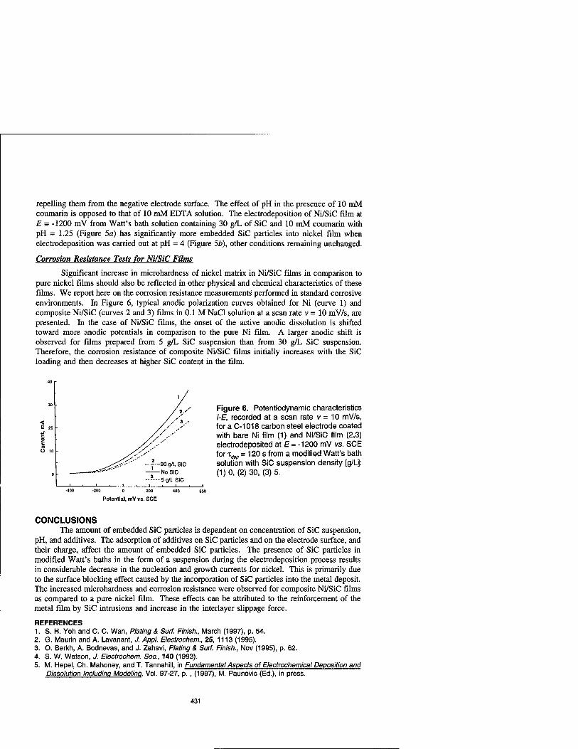
repelling them from the negative electrode surface. The effect of pH in the presence of 10 mM coumarin is opposed to that of 10 mM EDTA solution. The electrodeposition of Ni/SiC film at E = -1200 mV from Watt's bath solution containing 30 g/L of SiC and 10 mM coumarin with pH = 1.25 (Figure 5a) has significantly more embedded SiC particles into nickel film when electrodeposition was carried out at pH = 4 (Figure 5b), other conditions remaining unchanged.
Corrosion Resistance Tests for Ni/SiC Films
Significant increase in microhardness of nickel matrix in Ni/SiC films in comparison to pure nickel films should also be reflected in other physical and chemical characteristics of these films. We report here on the corrosion resistance measurements performed in standard corrosive environments. In Figure 6, typical anodic polarization curves obtained for Ni (curve 1) and composite Ni/SiC (curves 2 and 3) films in 0.1 M NaCl solution at a scan rate v = 10 mV/s, are presented. In the case of Ni/SiC films, the onset of the active anodic dissolution is shifted toward more anodic potentials in comparison to the pure Ni film. A larger anodic shift is observed for films prepared from 5 g/L SiC suspension than from 30 g/L SiC suspension. Therefore, the corrosion resistance of composite Ni/SiC films initially increases with the SiC loading and then decreases at higher SiC content in the film.
Figure 6. Potentiodynamic characteristics /-£, recorded at a scan rate v = 10 mV/s, for a C-1018 carbon steel electrode coated with bare Ni film (1) and Ni/SiC film (2,3) electrodeposited at £= -1200 mV vs. SCE for xaep = 120 s from a modified Watt's bath solution with SiC suspension density [g/L]: (1) 0, (2) 30, (3) 5.
-200 0 200
Potential, mV vs. SCE
CONCLUSIONS The amount of embedded SiC particles is dependent on concentration of SiC suspension,
pH, and additives. The adsorption of additives on SiC particles and on the electrode surface, and their charge, affect the amount of embedded SiC particles. The presence of SiC particles in modified Watt's baths in the form of a suspension during the electrodeposition process results in considerable decrease in the nucleation and growth currents for nickel. This is primarily due to the surface blocking effect caused by the incorporation of SiC particles into the metal deposit. The increased microhardness and corrosion resistance were observed for composite Ni/SiC films as compared to a pure nickel film. These effects can be attributed to the reinforcement of the metal film by SiC intrusions and increase in the interlayer slippage force.
REFERENCES 1. S. H. Yeh and C. C. Wan, Plating & Surf. Finish., March (1997), p. 54. 2. G. Maurin and A. Lavanant, J. Appl. Electrochem., 25, 1113 (1995). 3. O. Berkh, A. Bodnevas, and J. Zahavi, Plating & Surf. Finish., Nov (1995), p. 62. 4. S. W. Watson, J. Electrochem. Soc, 140 (1993). 5. M. Hepel, Ch. Mahoney, and T. Tannahill, in Fundamental Aspects of Electrochemical Deposition and
Dissolution Including Modeling, Vol. 97-27, p., (1997), M. Paunovic (Ed.), in press.
431

THICK FILMS OF Pb(Mg,Nb)TiO BY AEROSOL COMBUSTION
A.C. Greenwald , A. Kussmaul , T.F. Morse , C.H. Wei * Spire Corporation, Bedford, MA 01730-2396
Brown Univ. Providence, RI.
ABSTRACT
Thick films of solid solutions of lead-mägnesium-niobium-oxide (PMN) and lead-titanate (PTO) were deposited by aerosol combustion. Films consisted of submicron ceramic particles synthesized by combustion of a metalorganic solution in a methane-oxygen flame. The particulate material was deposited on heated substrates (200°C) and subsequently sintered at elevated temperatures. Results varied with starting chemistry and sintering conditions. As- deposited materials were mixed perovskite-pyrochlore phase. Sintering at low temperatures produced pure perovskite material that was not completely dense. Sintering at high temperatures produced dense ceramics of pyrochlore material. This technique requires further optimization for direct deposition of continuous films, but is immediately suitable for producing fine powders for tape casting of capacitors, etc.
INTRODUCTION
The use of aerosol processes to produce fine oxide powders with narrow size distribution and high chemical purity has received a great deal of attention in the last few years [1,2], due to the increasing technological importance of complex oxide materials such as superconductors and ferroelectrics. One variant of the technique is to use a flame to provide a high temperature, oxidizing, short residence-time reaction environment for the mist. The resulting powder can then be collected by thermophoresis on a substrate held close to the flame.
The goal of this project is to determine if aerosol combustion can be used as an economical technique to produce high quality, thick film (10 to 100 urn) ferroelectric materials with electrical properties comparable to those of thin films deposited by chemical vapor deposition [3] or sol-gel [4] techniques. The key criteria are high density {i.e., low porosity), pure perovskite phase (high dielectric constant), and dielectric breakdown strength exceeding 100 MV/m. We previously reported studies on (Ba,Sr)Ti03 where the properties of the as- deposited powder were superior, but sintering temperatures required to achieve high density were too high [5]. Materials were changed to lead based ferroelectric compositions to reduce sintering temperatures in this work.
EXPERIMENTAL DESCRIPTION AND RESULTS
A diagram of the apparatus is shown in Figure 1 and in reference [5]. The metal containing solution is kept in a small flask with a Teflon sheet as the bottom seal, separating this solution from a water bath. An ultrasonic vibration source in the water bath, through transmission of sonic vibrations, created an aerosol or mist of fine droplets above the metalorganic solution which is carried to the torch by an inert gas flow (He).
433
Mat. Res. Soc. Symp. Proc. Vol. 495 ° 1998 Materials Research Society

Entire Facility Installed in Vented Cabinet
Figure 1 Schematic diagram of Aerosol Deposition apparatus.
The torch consists of five concentric cylinders numbered 1 to 5 from the inside. Methane is injected through cylinder number 4 at 290 seem. Oxygen is injected through cylinders 1 and 3 at equal flows of 1 slpm. An inert gas is sometimes injected into cylinder number 2 for added dilution. The aerosol is carried into the innermost cylinder (number 1) with a helium flow rate of 360 seem. The torch is normally run in an oxygen rich condition. If there is insufficient oxygen to oxidize the methane and the organic solvent, a mixture of soot and metallic oxides results, The flows indicated typically produce powders with less than 1% carbon prior to sintering. Content was measured by IR absorption on inductively carbon heated sample with comparison to standards.[7]
434

The substrate to be coated was mounted on a steel plate which could be scanned in a plane normal to the torch axis to give a uniform coating over a large area. The mounting plate also had a separate heating element. However, we found that the temperature of the sample was more sensitive to the sample-torch distance, typically 5 cm, than it was to power in the supplemental heater. Nominal substrate temperature was 200°C.
The precursor solution consisting of a mixture of Pb(NC>3)2, Mg(NC>3)2, and Nb-ethoxide in a solution of water, ethanol, nitric acid and hydrogen peroxide was prepared in two steps. First, the lead and magnesium compounds were mixed with dilute nitric acid to form a 1.5N solution, followed by addition of H2O2. Second, a 6% molar solution was prepared with niobium ethoxide diluted in ethanol. The solutions were mixed with vigorous stirring of the liquid just prior to use. We added peroxide to retard precipitation of Nb2Os XH2O, but his was not completely successful. Separated, these two solutions were stable for many days. After mixing, the solution was stable for only a few hours.
The torch was run for one hour for each test, and the substrate was held stationary. All tests deposited a fine crystalline powder which was loosely adherent to the substrate; it did not come off when the substrate was held upside down, but was pulled off by the tape test. Samples were analyzed by scanning electron microscopy (SEM) and by X-ray diffraction (XRD). Material deposited in the center of the film had a grain size between 0.5 and 0.7 urn. Material deposited near the periphery had a grain size less than 0.1 um.
The key variables in our experiments were the composition of the original solution and the sintering temperature. The stoichiometric composition of PMN has a metals ratio of 1.0:0.33:0.67 for Pb:Mg:Nb. PbO is known to have a high vapor pressure above 800°C, and excess lead was added to this composition in molar ratio 10%, 25%, 50%, 80% 85%, and 100% above the stoichiometric value. Some papers [6] have suggested that excess Mg would promote formation of the perovskite phase over the pyrochlore phase, so some samples also contained 5% excess Mg relative to the stoichiometric molar ratio.
Figure 2 shows a typical XRD pattern obtained from our samples. The ratio of perovskite formation to pyrochlore formation (volume fraction) was obtained from XRD data using the formula:
% Perovskite = I<no>/(I<iio> + I<222>)x 100 (1)
from reference [8] where I<n0> and I<222> are the intensities of the perovskite and pyrochlore peaks for the given reflections shown in Figure 2.
From this analysis, samples with less than 50% excess lead were mostly pyrochlore as- deposited and after sintering at all temperatures. With at least 50% excess lead, the as-deposited powder was almost pure perovskite phase, and maintained this structure when heated up to 750°C - but was not sintered. The structure of the powdered material did not change either on the microscopic scale (crystal structure) or the macroscopic scale (agglomeration of grains) until the sintering temperature was raised above 800°C. At higher temperatures, the material was fully sintered but the crystal structure changed, and was predominantly the pyrochlore phase. Quantitative data are shown in Table 1 for high lead content materials.
435

4000 1 * * ' ' » I i ■ » ' ' ■ ' '
PMN(80mole% excessPbO, 5 mole% excess MgO)
o perovskite A pyrochlore
As-deposited powder
A A o A A
3000
6
pt
A A ( ,{',■!■■ flA-/ 20 25 30
A Pt A T-r^T ^r-,'>-l
45
i I i i i
50 55 60
3000
U
35
i .... I ■
40
e perovskite A pyrochlore
650°C for 40 min
A A ° A 4 45 50 55 60
(B)
IS o
Pt
0
4 Ofn-t'r 20
A » I ' ■ 1*1 \~i
25 30
A PtA A
I ■ ■ ■ ' ' ' ■ * ■ ' ' * ■ '
o perovskite A pyrochlore
g00°C for 40 min
35
| A. A A I'l I I i"|' I I 1*1 |"> i l ' |*r i*0 r \0 45 50 55 60 40
29
(C)
Figure 2 X-ray diffraction (XRD) patterns of PMNpowders synthesized by aerosol combustion with 80% excess lead and 5% excess magnesium content in the solution as-deposited (A) and after sintering (B), (C). Note ratio of<110> and <222> peaks.
436

Table 1 Volume fraction ofPerovskite material.
Temperature (C) Excess Lead (mole %) + 5% extra Mg 80 85 100
as-deposited 92 68 46 650 91 71 38 750 94 800 78 78 820 3** 40 850 2" A**
900 <J**
All sintering times were 40 minutes ** were fully dense films - see text.
Sintering results to form a fully dense compact (** in Table 1) is illustrated in Figure 3. At sufficiently high temperatures, the material appears to have been melted. Electrical measurements were taken on the fully dense samples. The dielectric constant was approximately 100, corresponding to the pyrochlore phase material. Dielectric breakdown voltages were low because mismatched thermal expansion coefficients led to cracks in the fully dense medium. Dielectric constants of the sintered (but still not fully agglomerated powder) were very high, equal to the best ceramic capacitors available commercially.
Thermal heating for shorter times, 10 minutes, resulted in nearly pure perovskite material for samples with excess lead. However, these samples were not completely sintered and were unsuited for device fabrication. We also tested the addition of barium and extra titanium to the solution before powder formation. Perovskite formation was increased, but the powder required higher sintering temperatures than the pure PMN specimens.
CONCLUSIONS
We synthesized high purity, lead-magnesium-niobium-oxide powders by heating an aqueous solution of metalorganics in a torch. Typical grain sizes were between 0.1 and 1.0 microns. The material could be deposited upon a substrate, compressed cold, and sintered to produce a fully dense, thick film coating. Sintering temperatures (820°C) were significantly lower than those required for barium-titanate based materials (1450°C). The technique may be a cost effective method for producing fine, high purity powders of ceramics for tape casting or hot pressing parts.
ACKNOWLEDGEMENTS
This work was supported by NASA grant number NAS7-1385, monitored by the Jet Propulsion Laboratory, CA.
437

650°C 750°C
•^«■i^^f»*^/.<,
820°C 850°C
Figure 3 Scanning electron microphotographs ofPMN with 85% excess Pb and 5% excess Mg sintered at (A) 650°C (B) 750°C, (C) 820°C, and (D) 850°Cfor 40 minutes.
REFERENCES
1. K. Nonaka, et. al, J. Mater. 6, 1750 (1991). 2. M.R. Zacharia and S. Huarewicz, J. Mater. Res., 6, 264 (1991). 3. J. Zhang et. al, Mat. Res. Soc. Symp. Proc. 275, 419 (1992). 4. R. Tsu, et. al.,Mat. Res. Soc. Symp. Proc. 275, 361 (1992). 5. A. Kussmaul, et. al., Mat. Res. Soc. Symp. Proc. 433, 39 (1996). 6. S.M. Gupta and A.R.Kulkarni, Mater. Chem. AndPhys., 39, 98 (1991). 7. LECO Corporation, St. Joseph, MI. 8. D. Saha et al, J. Mater. Res., 11, 932 1996).
438
CHEMICAL AND SONOCHEMICAL APPROACHES TO THE FORMATION OF V02 FILMS AND VOj-IMPREGNATED MATERIALS
V. KEPPENS, D. MANDRUS, AND L. A. BOATNER Oak Ridge National Laboratory, Solid State Division, P.O.Box 2008, Oak Ridge TN 37831-6056
ABSTRACT
A new chemical and chemical/ultrasonic approach to the preparation of VO2 films and V02-impregnated bulk materials has been developed. In this approach, a V205 sol prepared by quenching is used to coat SiÜ2 substrates. The resulting gel-film is heat treated in a reducing atmosphere to form a film identified as V02 from the results of X-ray diffraction and both optical and resistivity measurements, which reveal the phase transition characteristic of vanadium dioxide. The advantage of this approach to the formation of V02 is that the V205 sol can be used to impregnate porous materials, which are then heat treated to form an optically active composite material. The switching properties of the V02 films are investigated using optical and resistivity measurements, and the results are compared to those obtained for V02-films prepared by more- conventional methods.
INTRODUCTION
Vanadium dioxide, both in single-crystal form and as a thin film, has been the subject of a number of previous investigations. These prior studies were motivated by the large variations in the electronic and optical properties of V02 that occur as the material undergoes a structural phase transition [1]. This transition is also accompanied by a semiconductor-to-metal transition that is characterized by a change in the V02 electrical conductivity of over two orders of magnitude. The phase-transition temperature of ~68°C is sufficiently close to ambient temperature to make this material suitable for a variety of practical applications, including thermally activated optical switching and data storage devices [2,3], modulators and polarizers of submillimeter wave radiation [4], and energy-conserving coatings for windows and walls [5], Single crystals were found to disintegrate upon cycling through the transition temperature; thin films, however, appear to survive the stresses during repetitive cycles and are, therefore, considered much more practical for applications. High-quality V02 films have been obtained using vapor deposition [6], metal oxidation and reactive evaporation [7], reactive sputtering [8], pulsed laser deposition [9], and both organic and inorganic sol-gel methods [10,11,12]. Recently, optically active switchable surfaces have been produced by ion-implantation: by co-implanting vanadium and oxygen into a sapphire substrate and annealing under the proper conditions, it was possible to form buried precipitates of V02 [13]. The advantage of this type of active composite surface arises from the fact that the active components are an integral part of the near-surface region of the host material and are, therefore, protected from potential environmental degradation effects.
In this work, a new chemical and chemical/ultrasonic approach to the preparation of V02
films and V02-impregnated bulk materials has been developed. In this approach, a V205 sol prepared by quenching is used to coat Si02 substrates. The resulting gel-film is heat treated in a reducing atmosphere to form a film identified as V02, revealing the switching behavior characteristic of vanadium dioxide. The fact that this approach is a relatively simple and inexpensive way to form V02 films makes it very valuable. Its main benefit, however, may lie in
439
Mat. Res. Soc. Symp. Proc. Vol. 495 ° 1998 Materials Research Society

the possibility of using the V2O5 sol to impregnate porous materials, which can then be heat treated to form an optically active composite material, consisting of V02 nanocrystals embedded in the host matrix. Potential candidates for host materials can be found among the so-called sonogels. In contrast to "classic" sol-gels, a sonogel is made without the addition of a solvent. Instead, the different compounds are mixed using ultrasonic energy. Ultrasonic waves propagating through a liquid can generate locally a large amount of energy through the collapse of cavitation bubbles [14]. It has been demonstrated that homogeneous solutions can be formed when 2 immiscible liquids are simultaneously subjected to ultrasound radiation, as a result of the forces acting at their interface. The sonicated water-TEOS solutions quickly gel, giving rise to the so-called sonogels with a superior short gelation time, high density, and a fine, uniform porosity [15]. The surface:volume ratio is typically twice as large as that for gels prepared in an alcoholic solution, which permits sintering at lower temperatures [16]. Sonogels are considered to be superior hosts for nanoparticles and dyes, producing materials with nonlinear optical applications, as well as ceramic composites [17]. The objective of the research effort reported in this paper is to form an optically active composite material, consisting of V02 nanocrystals embedded in a silica sonogel.
EXPERIMENTAL DETAILS
In the subject synthesis process, 15 grams of V205 powder (99.995%, Alfa Aesar, Puratronic) were put in a platinum crucible and melted in air at 1100 °C for 20 minutes. The melt was then poured in 500 ml of distilled water and vigorously stirred. After discarding the residue on the bottom of the jar, a brown sol with approximately 1.6 wt.% V2O5 was obtained. Thin films of V205 were deposited on amorphous Si02 substrates (25 x 10 x 2 mm) by dipping the substrates in the sol. A 2-step recipe was used to reduce the V205 film to V02. The first step consists of reducing the V205 film at 500 °C in Ar, containing 4 % H2. Under these conditions, the brown film turns gray and converts to mainly V203. In order to obtain V02, a second heat treatment is carried out at 450 °C in argon gas, bubbling through water. The water vapor treatment provides a slightly oxidizing atmosphere, which leads to the formation of a stable blue-colored V02 film.
The preparation of the silica sonogels is based on the method of De La Rosa-Fox et al. [15]. In this approach, sonogels are obtained by submitting mixtures of Si(OC2H5)4 (TEOS), H20 (pH=l) and formamide in a molar ratio 1:10:7 to ultrasonic radiation, produced by a sonifier (Misonix, Model XL2015). Gelling and aging took place at 40 °C.
RESULTS AND DISCUSSION
Figure 1 shows an X-ray 6-29 scan (using Cu Ka radiation) of a vanadium oxide film formed on a Si02 substrate, after being reduced under the conditions described above. The intense peak observed at 27.86° is characteristic of the (011) reflection of V02 [18], and suggests, together with the reflections at higher angles, that the film consists mainly of vanadium dioxide. There is, however, at least one impurity phase present, which is difficult to identify because of the large number of nonstoichiometric vanadium oxides that can be formed. Since these oxides could have reflections close to the reflections expected for vanadium dioxide, resistance measurements as well as optical transmission measurements have been performed in order to confirm unambiguously the presence of V02. Figure 2 shows the resistance as a function of temperature for the V02 film on the Si02 substrate, as the temperature is cycled from room temperature to 100 °C. This figure clearly shows a drastic change in the resistance of the film upon heating and cooling in the 65°-70° C region, i.e. the temperature region where the characteristic V02-phase
440

^ 3000
ijj 2500 " V02—^
(011)
f 2000 -
| 1500 -
1000 -
500 - u? (012) VO, (021) y 2
vo2 . (022)
20 30 40
26 (deg)
50 60
FIGURE 1: X-ray diffraction pattern of a V02 film obtained by heat treatment of a V205 gel-film.
10°
a cc
10°
+: Heating
O: Cooling
j L j L
40 50 60 70 80 90 100
Temperature (°C) FIGURE 2: Resistance as a function of temperature for a V02 film obtained by
heat treatment of a V205 gel-film.
441

60
c g w
£ c CO
-4-*
a:
+: Heating
O: Cooling
40 50 60 70 80 90
Temperature (°C)
FIGURE 3: Infrared transmission (X = 3.4um) as a function of temperature for a V02 film obtained by heat treatment of a V205 gel-film. The thickness of the film
is approximately 4500 Ä.
transition takes place. A change of more than 2 orders of magnitude is observed in our film at a transition temperature of 68 °C, which is typical for films deposited on glass substrates. Although the magnitude of resistive switching has been reported to be between 3 to 5 orders of magnitude for single crystals or thin films on crystalline substrates, it is no more than 2 to 3 orders of magnitude for films on glass substrates [19]. Figure 3 shows the optical transmission for the film, measured at a fixed wavelength of 3.4 urn. It clearly illustrates the drastic change in transmission as the film is cycled through the transition region. Not only is the switching contrast comparable to values reported for "standard" films [20,21], the transition is also remarkably sharp.
The results of this sol-gel approach, as established by the properties of the resulting films, are extremely promising and indicate that superior switching properties may be obtained when the coating-procedure is optimized and the influence of the film-thickness and length of the heat treatments is determined. It will also be interesting to investigate the properties of films deposited on crystalline substrates. However, as noted above, the main benefit of this approach may be the possibility of using a V205 sol to impregnate porous materials and form thereby "switchable" composite materials. To investigate these possibilities, we have originated a study of silica
442

sonogels as possible hosts for V02 nanocrystals. Sonogels were preferred over conventional gels because of their short gelation time and their excellent properties as a host matrix for nanoparticles [17]. One possible way of making such a Si02/V02 composite is an "in situ" impregnation, where that the V2O5 sol can be directly used as one of the compounds to make the sonogel. We were, in fact, able to form homogeneous monolithic gels by adding a V205 sol to the TEOS-water-formamide mixture. However, in this approach, one has to deal with the fact that V205 dissolves in formamide, which is used as a drying-control chemical additive (DCCA). Currently, attempts are being made to form homogeneous V205-containing gels omitting the DCCA or by using another drying-control agent. A second approach to the formation of Si02/V02 composites consists of "infiltrating" the Si02 after gelling. In order to avoid having the V205 go into solution, the gel-glass has to be sufficiently dry, such that most of the formamide has been removed. Successful infiltration was obtained by soaking the gels, which had been dried at 250 °C, in a diluted V2O5 sol. These gels have been subjected to the heat treatments that were found to give the proper reducing condition for the V02-films. The first heat treatment, at 500 °C in an Ar/4%H2 atmosphere changes the color of the film from yellow to gray. This color and the observation that parts of the gel are conducting indicate that the V2Os in the gel has, like the V02
films, been reduced to V2O3. The second heat treatment, carried out at 450 °C in Ar bubbling through H20, returns the gel to its original yellowish color, and no indication of a phase transition around 68 °C could be observed. It is likely that the slightly oxidizing atmosphere, provided by the water vapor, does not supply the right atmosphere for the gel/V203 system, probably because of the water that is still retained or absorbed by the Si02 gel. As a result, a higher oxide is obtained instead of the intended V02. Heat treatments under different conditions are currently being carried out in order to find the proper conditions to form a stable Si02/V02 composite.
CONCLUSIONS
A new chemical and chemical/ultrasonic approach to the preparation of V02 films and V02-impregnated bulk materials has been developed. In this approach a V205 sol prepared by quenching is used to coat Si02 substrates. The resulting gel-film is heat treated in a reducing atmosphere to form a film identified as V02. Resistance and infrared transmission measurements as a function of temperature reveal the switching behavior characteristic of vanadium dioxide and indicate that superior switching characteristics may be obtained when the method is optimized. The possibility of using the V2O5 sol to impregnate porous materials, which can then be heat treated to form an optically active composite material, has been investigated using silica sonogels as the host matrix. Partially dried gels have been infiltrated with the V2Os sol; however, the heat treatment conditions used to reduce V205 gel films to V02 do not seem to be adequate for the Si02 gel/ V2O5 system. Future investigations will, therefore, focus on finding the proper reducing atmosphere to form a stable Si02/V02 composite. Attention will also be paid to the formation and reduction of stable and homogeneous silica/ V2O5 composite gels, using the V2Os sol as one of the starting compounds for the sonogel.
ACKNOWLEDGEMENTS
This research was sponsored by the U.S. Department of energy, Division of Materials Sciences. Oak Ridge National Laboratory is managed by Lockheed Martin energy research Corp. for the U.S. Department of Energy under contract number DE-AC05-96OR22464.
443

REFERENCES
1. F. J. Morin, Phys. Rev. Lett. 3, 34 (1959). 2. A. W. Smith, Appl. Phys. Lett. 23, 437 (1973). 3. I. Balberg and S. Trokman, J. Appl. Phys. 46, 2111 (1975). 4. J. C. C. Fan, H, R. Fetterman, F. J. Bachner, P. M. Zavracky, and C. D. Parker, Appl. Phys.
Lett. 31, 1 (1977). 5. C. V. Jorgenson and J. C. Lee, Solar energy Materials 14, 205 (1986). 6. J. B. MacChesney, J. F. potter, and H. J. Guggenheim, J. Electrochem. Soc 115, 52 (1968). 7. F. C. Case, Applied Optics 28, 2731 (1989). 8. A. Razavi, T. Hughes, J. Antinovitch, and J. Hoffman, J. Vac. Sei. Technol. A 7, 1310 (1989). 9. H. S. Choi, J. S. Ahn, J. H. Jung, T. W. Noh, and D. H. Kim, Phys. Rev. B 54, 4621 (1996). 10. K. R. Speck, H. S.-W. Hu, M. E. Sherwin, and R. S. Potember, Thin Solid Films 165, 317
(1988). 11. D. P. Partlow, S. R. Gurkovich, K. C. Radford, and L. J. Denes, J. Appl. Phys. 70, 443
(1991). 12. Y. Dachuan, X. Niankan, Z. Jingyu, and Z. Xiulin, Mat. Res. Bull, 31, 335 (1996); J. Phys. D
29, 1051 (1996). 13. L. A. Gea and L. A. Boatner, Appl. Phys. Lett. 68, 3081 (1996); L. A. Gea, L. A. Boatner, J.
D. Budai, and R. A. Zuhr, in Ion-Solid Interactions for Materials Modification and Processing, edited by D. B. Poker, D. Ila, Y.-T. Cheng, L. R. Harriott, and T. W. Sigmon (Mat. Res. Soc. Proc. 396, Pittsburgh, PA 1996) pp. 215-220.
14. H. G. Flynn in Physical acoustics, edited by W. P. Mason (Academic Press, New York. 1964) IB, p57.
15. N. De La Rosa-Fox, L. Esquivias, and J. Zarzycki, J. Mater. Sei. Lett. 10, 1237 (1991). 16. M. Pinero, M. Atik, and J. Zarzycki, J. Non-Cryst. Solids 174&148, 523 (1992). 17. D. Levy and L. Esquivias, Adv. Mater. 7, 120 (1995). 18. JCPDS-ICDD, 12 Campus Boulevard, Newton Square, PA 19073-3273. 19. C. B. Greenberg, Thin Solid Films, 110, 73 (1982). 20. F. C. Case, J. Vac. Sei. Technol. A8, 1395 (1990). 21. E. E. Chain, Applied Optics 30, 2782 (1991).
444

LOW TEMPERATURE REMOTE PLASMA ASSISTED JET VAPOR DEPOSITION OF SILICON NITRIDE
J.VETERAN,* C.HOBBS,* R.HEGDE,* P.TOBIN,* V.WANG,* H.TSENG,* G.KENIG,* M.HARTIG,* T.TAMAGAWA,** R.DORAN,** P.MAKOWICZ,** J.SCHMTT,** B.HALPERN, and ** J.Z.ZHANG** »Motorola APRDL, Austin TX, 78721 **Jet Process Corp., New Haven CT 06511
ABSTRACT:
As MOSFET dimensions are aggressively scaled, minimizing the thermal budget becomes critical for limiting the diffusion of channel profiles. Unfortunately, high quality dielectrics with low deposition temperatures have not been readily available. Typical room temperature dielectrics are porous and electrically leaky. A promising technique for low temperature dielectric deposition is Jet Vapor Deposition (JVD). [ 1 ] Two coaxial quartz nozzles spray the process gases to the substrate surface at super-sonic speeds while a microwave cavity generates a plasma in the nozzle. [2] We have successfully deposited silicon nitride films using SiHVHe and N2/He gas mixtures. These are the first reported JVD results on 200 mm wafers.
INTRODUCTION:
Thermal oxide processes have been moving to lower temperature regimes with the reduction of device dimensions. Current state of the art furnace oxidation processes are operating at or below temperatures, that of standard 700-800°C CVD processes, and the desire is to reduce the time at temperature even more. With the room temperature processing provided with the JVD processing, the thermal budget is not impacted, thus JVD is a promising technique for low temperature processing.
The JVD process was studied in this investigation for the purpose of silicon nitride deposition. [3] Additional work is underway to apply this process to other insulator and metal depositions. The low temperature JVD process has applications in both the front end and back end processes. MOSFET devices with JVD Nitride have been demonstrated to be a viable high-K dielectric replacement for Si02. [4,5,6] In order for this process to meet the future needs of the semiconductor industry, tools capable of running 200 mm and larger, wafers will be required. To satisfy this requirement, an experimental JVD system was designed to accommodate 200 mm wafers. This work characterizes the JVD process variables on 200 mm wafers and their resultant effects on JVD deposited silicon nitride films. Film thickness, uniformity, refractive index and film composition were studied by means of ellipsometry, AES, TXRF, SIMS and TEM.
EXPERIMENT:
The JVD Nitride tool used for this work was developed for maximum experimental flexibility. A schematic of the system is illustrated in Figure 1. The process chamber is rectangular and the jet port is mounted on the side wall. The wafer is mounted vertically on a wafer chuck and the chuck movement was programmable with the scanning profile recipe. Any size wafer (200 mm and smaller) can be accommodated by changing the wafer chuck. The wafer scanning movement was left/right for a fixed distance from the jet, and with a fixed rotational rate of the wafer, to create the scan profile. The chamber was evacuated by a slow pump bypass, followed by an unthrottled Roots
445
Mat. Res. Soc. Symp. Proc. Vol. 495 ° 1998 Materials Research Society

blower/mechanical pump combination, and then pumped down to the high vacuum range by a cryogenic pump.
Bectronic Controller MFCs valves
Rot at.
Motor
^ X-Axis Motor
J
-0 -©
Figure 1: Schematic drawing of the Jet Vapor Deposition System
Thickness uniformity is dictated by the scan profile and rotation rate in combination. The unit area per rotational angle increases as the larger diameter portions of the wafer move in front of the jet, thus the time of deposition for the outer wafer diameters must be longer. Therefore, it is the scanning profile that dictates the thickness of film, and thus the thickness uniformity. The scan speed becomes the critical factor in achieving a uniformly thick film, particularly for larger wafer diameter wafers.
A diagram of the jet nozzle is shown in Figure 2. It consists of two concentric quartz tubes. The diameter of the outer nozzle, at a constant flow rate, defines the jet velocity. It is the supersonic velocity of the gases that provide the unique characteristics of the JVD process. [2] Larger diameter tubing reduces the jet velocity, given that the Velocity = (Flow Rate)/Area. The source gases for the nitride deposition flow separately through these nozzles, with the outer nozzle carrying the nitrogen source in the form of nitrogen gas mixed with a helium carrier gas in a 4.6% mixture, and the inner nozzle carrying silane with a He carrier gas in a 0.0004% mixture. A microwave cavity mounted around the outer nozzle is
D=&He/SiH4
le/N2
Plasma
Scanning Substrate Figure 2. Schematic of the Jet Vapor
Deposition system.
446

used to generate the plasma, operated at a nominal 100 W. Each wafer was prepared with an ex-situ 10:1 HF dip to remove the native oxide, followed by
a DI water rinse to insure repeatability in the pre-deposition surface conditions. The wafers were immediately loaded into the deposition chamber and pumped down to a base pressure of 2xl0"7
Torr. Deposition was started after reaching base pressure. The independent process parameters of the JVD system include gas flows, nozzle distance,
microwave power, scanning speed and rotational rate. The pumps were run at maximum capacity to rapidly remove reactants from the chamber. The system pressure was controlled by adjusting the gas flow rates.
RESULTS:
We studied various scanning profiles to optimize the thickness uniformity. Figure 3 depicts the digitized scan profile used for two conditions. Figure 4 shows the wafer thickness uniformity patterns obtained with the two scan profiles indicated. Improvement across wafer uniformity is possible with improved scanning profiles, however, a 200 mm across wafer uniformity of 3% (3 sigma) were quickly obtained in this study.
0.25
g.0.20
< £"0.15 '3 _o "3 >• o.io u
CM es £ 0.05
0.00
Scan Profile 2: Modified 1/R
Scan Profile 1: Triangular
0 50 100 150 Wafer Position (mm)
Figure 3: Scanning speed profile from the center to the edge of the wafer
-100 -50 0 50 100
Position from Center (mm) Figure 4: Thickness uniformity across a
200 mm wafer
The wafer rotational rate was varied from 10 to 60 rpm, and was found to have no significant effect on deposition rate, thickness uniformity or refractive index as depicted in Figure 5. Thickness, and thus wafer uniformity, was studied for both a variety of scanning profiles and as a function of microwave power settings.
Microwave power to the jet nozzle assembly was studied for its effect on thickness as well as film uniformity and refractive index (RI), as shown in Figure 6. Increases in the power did not increase the deposition rate of the film, or change the thickness uniformity across the wafer. However, the index of refraction was observed to increase as the plasma power was increased. This
447

1000
25 50 Rotation Rate (RPM)
.90
■a e .86 f*
.82, m&
100 120 0 20 40 60 80 Plasma Power (W)
Figure 5: Wafer rotational rate vs Thickness and Figure 6: Microwave Power vs Thickness Refractive Index. and Refractive Index
is most likely due to increased nitrogen incorporation, and reduced hydrogen incorporation, in the film. Some heating of the wafer occurred during the deposition. This heating was related to the microwave power, but in all cases the wafer temperature remained below 50CC, as measured by an infrared pyrometer.
The effect of the relative nozzle positions was studied, with respect to both thickness and refractive index (RI), as shown in Figure 7. The inner nozzle was moved 1.5x further from the wafer from its standard position, while the outer nozzle remained stationary. Increasing the distance between the wafer and the inner jet decreased both the deposition rate and the refractive index. This is most likely due to the film becoming more silicon rich as the silane source gas opening of the nozzle is moved closer to the microwave cavity.
Auger depth profiling of the as-deposited films has shown the JVD nitride films to be uniform in composition both in depth and across the wafer. The oxygen level measured in several samples was found to be 8-20%, (Figure 8). One source of oxygen was determined to be the purity of the source gases. An upgrade to semiconductor level quality gases reduced the oxygen incorporation by 50% of their original amounts. It is believed that the remaining oxygen source is due to the
InnerNozzle
Outer Nozzle
Position (
Wafer Figure 7A: Inner/Outer Nozzle positions relative
to the wafer. (Not to scale)
2
a, 1.9
WO M S3 1.7
Pi 1.6
1.5
Standard Position [i
7 1.5 X Standard Position
0 200 400 600 800 Thickness (A)
Figure 7B: Thickness and Refractive Index relative to two different inner nozzle positions
448

outgassing of the system walls. Each time the chamber is opened for the loading process, the chamber walls are exposed to the moist room air, and absorb the ambient oxygen. Secondary Ion Mass Spectroscopy (SMS) analysis also showed lower hydrogen content in the JVD Nitride film, vs. the standard CVD furnace nitride film. Reduction in hydrogen incorporation reduces the number of bulk traps in the film.
Total X-ray Reflection Flourescence (TXRF) was used to study the surface contamination of the wafer surface. Many elements were detected, including K, Ca, and metallics such as Ti, Fe and Zn. All of the metallics seen are components of stainless steel, and were seen at levels as high as lxlO13
atoms/cm2, as is shown in Figure 9. There is no radial symmetry in the contamination pattern, thus factors in addition to the jet scanning process are likely contributing to the contamination.
TEM micrographs were taken of the deposited film as part of the study of the film composition. Figure 10 depicts a TEM cross section of a polysilicon/JVD Nitride/ silicon structure. The JVD silicon nitride film was found to be non-porous and smooth at the interface.
CONCLUSION:
We have successfully deposited silicon nitride films on 200 mm wafers, at near room temperature, using the Jet Vapor Deposition technique. A thickness uniformity of 3% (3 sigma) was achieved and can be improved with further refinement of the scan profile. We have characterized the process parameters of wafer thickness uniformity and refractive index, in terms of the effects of scanning profiles, rotational rates, nozzle position, plasma power and film composition. We produced non-porous films with compositional uniformity throughout the film.
The JVD Nitride deposition process has been studied with an eye towards future CMOS applications. The JVD nitride process has great
-L. 10 20 30 40
DEPTH (MI)
Figure 8: Auger depth profile of JVD Nitride
50
.K ■ Ca
Ti *Cr
■ • «Fe
* 1 1
*
.Co + Ni .Cu
4 0 -Zn 20 Position from Center (mm)
Figure 9: Surface contamination as determined by TXRF
Figure 10: TEM Photo on 50A JVD Nitride on a silicon wafer with a polysilicon cap.
449

potential for future device application, especially where thermal budget is of concern. Further work will be required to achieve a suitable tool for 200 mm and beyond, in a manufacturing environment.
REFERENCES:
1) J.Schmitt, B.Halpern U.S.Patent 4788082 (1988).
2) J.Schmitt, B.Halpern U.S. Patent 5256205 (1993).
3) F.Burshah, (ed.) "Handbook of Deposition Technologies and Coatings"- Chapter 16,"Jet Vapor Deposition", B.Halpern. J.Schmitt, Noyes Publications, Park Ridge NJ, 1994.
4) X.Wang,T.P.Ma,G.Cui,T.Tamagawa,J.Golz,S .Karecki,B .Halpern,J.Schmitt, "Highly Reliable Silicon Nitride Films Made by Jet Vapor Deposition" 1994 Int'l Conf. on Solid State Devices, p. 856.
5)H.Tseng,P.Tsui,P.Tobin,J.Mogab,M.Khare,XJ.Veteran,M.Hartig,G.Kenig,V.Wang,R.Blum B.Halpern,G.Cui,J.Schmitt "Application of JVD Nitride Gate Dielectric to a 0.35 Micron CMOS Process for Reduction of Gate Leakage Current and Boron Penetration" 1997 EDM
6) M.Khare,X.Guo,X .Wang,T.P.Ma, "Ultra-thin Silicon Nitride Gate Dielectric for DeepSub-Micro CMOS Devices" 1997 VLSI Tech.Digest p 51.
450

MICROSTRUCTURES IN THIN BaTiOj FILMS BY HYDROTHERMAL METHOD
T. HOFFMANN*, V.M. FUENZALIDA Departamento de Fisica, Universidad de Chile, Casilla 487-3, Santiago, Chile present address: Institut für Materialwissenschaften, Universität Wuppertal, Gauss-Str. 20,
42097 Wuppertal
ABSTRACT
Barium titanate microstructures are fabricated on silicon(100)/platinum substrates coated with photoresist and titanium by a combination of hydrothermal and lift-off techniques. The microstructures of lOum width are well defined. The barium titanate films grow in its cubic phase. Analysis by means of x-ray diffraction and scanning electron microscopy shows that only a part of the titanium layer is affected by the hydrothermal reaction. This limitation may be overcome by application of electrochemistry.
INTRODUCTION
Technological applications of ferroelectric materials as nonvolatile memories [1], dynamic random access memory [2], electro-optic devices [3] and electro-mechanic devices [4] have stimulated work on barium titanate thin films in the last years. Even in the case of the non-ferroelectric cubic phase of BaTiÜ3 the comparatively high dielectric constant makes it a prospective material for volatile memories and capacitors. Recently the hydrothermal growth method or its extension to the hydrothermal-electrochemical method has been applied successfully to grow crystalline thin films at rather low temperatures (55- 300°C) [5-7] compared to other processing methods (450-800°C) [8]. Some efforts have been made to grow BaTi03 thin films on titanium-coated silicon substrates by the hydrothermal method [8-13] in order to explore the compatibility of hydrothermal processing with silicon technology. However, none of these works were concerned with the patterning of BaTi03 layer. We succeeded in the fabrication of BaTi03 microstructures (10 um x 10 mm) at low temperatures by combining the hydrothermal method with the lift-off technique.
EXPERIMENT
Substrates were prepared by sputtering thin layers of Ti-W (~30nm) and Pt (~300nm) on Si(100) wafers. The Ti-W layer promotes adhesion of Pt to the Si substrate. The Pt layer was coated with approximately 450-500 nm photoresist (Waycoat 200, Hunt Chemicals), and subsequently exposed for 60 s to an energy of radiation (40 mJ/cm2). The pattern was developed in a solution of KOH (electronic grade, 2%) for 40 s. Thin layers of titanium with thickness' of 80 and 120 nanometers were sputtered on top of the structured photoresist. Subsequently the substrates were immersed in aqueous solution of Ba(OH)2 at concentrations between 0.25 and 0.5 M. The hydrothermal treatment was carried out at 90°C and under atmospheric pressure. The treatment time was varied from 30 to 120 minutes. After the treatment the samples were immediately submerged into hot distilled water in order to clean the surface from contamination with barium carbonate. The deposit was lifted off by dissolving the remaining photoresist in hot acetone for more than 4 hours
451
Mat. Res. Soc. Symp. Proc. Vol. 495 ® 1998 Materials Research Society

leading to a negative pattern of the original structure. The lift-off process was applied to an untreated sample in order to obtain microstructures of untreated titanium, which served as a reference for the original height of the line profiles. Further reference samples were prepared by sputtering titanium directly on top of the platinum layer without an intermediate photoresist layer. The unstructured samples facilitated analysis by means of x- ray diffraction (XRD). Both reference and structured samples were treated simultaneously. The samples were characterized by means of scanning electron microscopy (SEM), surface profilometry (TENCOR ALPHA STEP 500), and XRD (SIEMENS D5000).
RESULTS
Microstructures and Thickness
The lift-off was easier carried out in samples treated for one hour rather than two hours. This may indicate that some chemical reaction of the resist during the hydrothermal treatment has taken place. No differences in the success of the lift-off step were observed between the two concentrations of the solution, 0.25M and 0.5M, respectively. Figure 1 shows a SEM micrograph of the microstructure after hydrothermal treatment at 90°C for 1 hour and subsequent lift-off. The line structure stands out from the smooth platinum surface which can be seen on both sides of it. The peel-off of the structure at the edge is due to cutting the sample with a diamond scriber after the hydrothermal treatment.
Fig. 1: Micrograph of a line profile after hydrothermal treatment (lh, 90°C, 0.5M Ba2+) and subsequent lift-off. The line corresponds to the hydrothermally treated Ti layer and the smooth surface is that of the Pt layer.
Fig. 2 depicts profiles taken from scans across differently prepared single line structures. The curvature of the profiles is introduced by the profile of the photoresist pattern with slightly inclined sidewalls. Sputtering of titanium on top of this profile leads to a coverage of the sidewalls and the application of the lift-off process results in a variation of thickness across the stripes, being thicker at the edges. A proper measurement of the film thickness was difficult to achieve at the fine lines. However, for broader stripes (1 mm) than those which are shown in Fig. 2 (10 urn) the thickness can be measured away from the edge of the structure. Scans were taken at different sample positions and the measured values agree well with the values obtained by SEM.
452
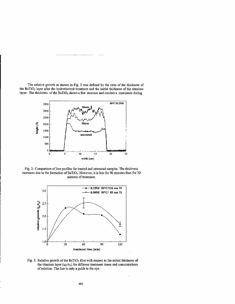
The relative growth as shown in Fig. 3 was defined by the ratio of the thickness of the BaTi03 layer after the hydrothermal treatment and the initial thickness of the titanium layer. The thickness of the BaTiC>3 shows a fast increase and reaches a maximum during
3500 - . jiA 30min l ^
90°C/0.25M
3000 K 2500
2000 90m in
1500
1000 untreated
500
0 10 15
width (urn)
20 25
Fig. 2: Comparison of line profiles for treated and untreated samples. The thickness increases due to the formation of BaTiÜ3. However, it is less for 90 minutes than for 30
minutes of treatment.
3.0 -•— 0.25M/ 90°C/126 nm Ti -A— 0.50M/ 90°C/ 85 nm Ti
60 90 treatment time (min)
120
Fig. 3: Relative growth of the BaTiC>3 film with respect to the initial thickness of the titanium layer (tai/tri) for different treatment times and concentrations of solution. The line is only a guide to the eye.
453

short treatment times of 30 to 60 minutes. After reaching this maximum the thickness decreases continuously with longer treatment times. Despite the differences in solution concentration and initial thickness both sets of samples show the same trend.
Crvstallinitv and Morphology
XRD-spectra of all samples showed the presence of only the cubic phase of barium titanate without traces of barium carbonate. Fig. 4 shows the changes of the Ti (002) and the BaTi03 (111) peak with hydrothermal treatment time. Both peaks decrease with increasing treatment time. This trend was observed independent of solution concentration and initial thickness of the Ti layer. In the case of the BaTi03 film the obtained result indicates that the crystallinity decreases after a fast crystallization process. This structural result correlates well with the observed decrease in thickness. The decrease in the intensity of the Ti peak at short times can be related to the formation of barium titanate as well as to the oxidation of Ti. The further decrease in intensity after 2 hours of treatment may be due to oxidation of the titanium layer or the formation of a non-crystalline barium titanate phase with a composition which differs from that of BaTiC>3.
- 30min 60min 90min
120min
Ti(002) BT(lll)
37.5 38.0 38.5
2 theta (°)
Fig. 4: XRD spectra of the Ti (002) and the BaTi03 (111) peaks for different treatment times. The spectra show the changes in intensity due to the formation of BaTi03.
The micrographs (see Fig. 5) reveal that only a small part of the Ti layer was consumed during the hydrothermal treatment. It can be seen that grown BaTi03 layer consists of grains with diameters between 0.1 and 0.7 urn. The layer roughness decreases notably with treatment time and the distribution of grain sizes becomes more uniform.. The grain-like appearance of the film suggests that the growth of the deposit occurs most likely by nucleation on top of the titanium layer and proceeds by grain growth. At later stages of the formation process grains with larger diameter disappear most likely due to a
454

dissolution-crystallization equilibrium between the BaTi03 layer and the alkaline solution. This would lead to thinner films with less roughness.
Fig. 5: Micrographs of layer structure as obtained after 1 hour (left) and 2 hours (right) treatment in 0.5M solution and at 90°C. Both samples were cutted after hydrothermal treatment, the smooth foreground corresponds to the Pt layer.
CONCLUSIONS
Our results show that a well defined barium titanate microstructures can be obtained by the combination of lift-off techniques and hydrothermal growth. Problems due to the incomplete reaction of the titanium layer must be addressed in further work in order to obtain well defined interfaces. An alternative approach can make use of electrochemical and lift-off techniques. It is now accepted that the combination of hydrothermal and electrochemical methods leads to thicker barium titanate films [6-7]. An insulating photoresist below the titanium layer would have the advantage that the charge has to pass through the titanium layer during reaction. This would not be the case if the titanium layer were already structured, as the charge could be transferred through the underlying substrate in contact with the solution.
ACKNOWLEDGEMENTS
This work was supported by grants Fondecyt 3950004 and Fundacion Andes C- 12776 and C-12510. The authors wish to acknowledge Mrs. Judit G. Lisoni, U. de Chile, for her help in XRD, Mr. Jose Morillas, PUC, and Mr. Michael Schlüter both for their help in SEM. We also acknowledge Solvay-Sabed, Italy for providing us with high purity Ba(OH)2 powder.
REFERENCES
1. J.F. Scott, F.M. Ross, CA. Paz de Araujo , M.C. Scott, and M. Huffman, MRS Bulletin, 21(7), 33 (1996).
2. A.I. Kingon, S.K. Streiffer, C. Basceri, and S.R. Summerfelt, MRS Bulletin, 21(7), 46(1996).
455

3. D.K. Fork, F. Armani-Leplingrad, and J.J. Kingston, MRS Bulletin, 21(7), 53 (1996).
4. D.L. Polla, and L.F. Francis, MRS Bulletin, 21(7), 59 (1996).
5. M. Yoshimura, S.E. Yoo, M. Hayashi, and N. Ishizawa, Jpn. J. Appl. Phys., 28(11), L2007 (1989).
6. R.R. Bacsa, G. Rutsch, and J.P. Dougherty, J. Mater. Res., 11(1), 194 (1996).
7. S. Venigalla, P. Bendale, and J.H. Adair, J. Electrochem. Soc, 142(6) 2101 (1995).
8. see MRS Bulletin 21(6) 21-58 (1996): Electroceramic thin films. Part I: Processing.
9. M.E. Pilleux, and V.M. Fuenzalida, J. Appl. Phys., 74[7], 4664 (1993).
10. R.R Bacsa, J.P. Dougherty, and LJ. Pilione, Appl. Phys. Lett., 63(8), 1053 (1993).
11. E. Shi, C.R. Cho, M.S. Jang, S.Y. Jeong, and H. Kim, J. Mater. Res., 9(11) 2914 (1994).
12. C.R. Cho, E. Shi, M.S. Jang, S.Y. Jeong, and S.C. Kim, Jpn. J. Appl. Phys., 33, 4984 (1994).
13. W. Xu, L. Zheng, C. Lin, and M. Okuyama, J. Electrochem. Soc, 143(3), 1133 (1996).
456

INVESTIGATION ON THE GROWTH MECHANISM OF ZINC OXIDE FILM PREPARED BY ELECTROCHEMICAL METHOD
Jaeyoung Lee and Yongsug Tak Department of Chemical Engineering, Inha University, Inchon 402-751, Korea,
ABSTRACT
ZnO thin films were potentiostatically deposited on ITO electrode in 0.1 M Zn(N03)2and the film growth mechanism was investigated by using FTIR and electrochemical quartz crystal microbalance(EQCM). Intermediates formed in the initial stage were identified as soluble zinc hydroxides and a critical concentration of OH" was required for the ZnO to be deposited. A rapid growth rate of ZnO film observed in the presence of 02 was attributed to the higher cathodic current which produces OH"
INTRODUCTION
Electrochemical preparation of ceramic thin films on substrates has several advantages over conventional methods such as CVD, sputtering and sol-gel processes[l-3]. ZnO particles or films, which have potential applications in sensors and electronic devices, have been deposited on a cathode substrate by electrolysis in solutions containing Zn2+. Izaki et al. [4,5] and Lincot et al. [6] prepared ZnO films on NESA glass potentiostatically and discussed the reaction schemes. Kitano et al. worked on the electrochemical reaction of Zn in water and, found that both ZnO and Zn(OH)2 structures are formed simultaneously on Pt cathodes[7]. Authors suggested the growth mechanisms in the ZnO film formation, however the experimental evidences are not sufficient and the mechanism of ZnO film growth remains still unclear.
This work is intended to investigate the electrochemical growth mechanism of the ZnO film by using FTIR, EQCM and potential pulse method.
EXPERIMENTAL
A transparent ZnO film was cathodically formed on the ITO electrode. Prior to the electrodeposition, the ITO cathode coated on 9MHz quartz crystal was thermally treated at 773K to lower the resistance and then rinsed with acetone in an ultrasonic cleaner. The area of the electrode during electrolysis was 0.196cnf. A Zn plate as a counter electrode was used to supply Zn2+ ions and a saturated calomel electrode(SCE) was used as a reference electrode. Solutions used for the experiments were prepared using reagent grade Zn(N03)2 and deionized water. In the process of ZnO formation, N2 or 02 was bubbled through the solution to investigate the effect of cathodic reduction of dissolved oxygen. With 02 bubbling, it was assumed that the electrolyte was saturated with 02. The electrolysis temperature was maintained at 60 °C.
Electrodeposition was executed by modulating potential(EG&G PAR273) and the initial reaction products were studied with FTIR(Bruker, IFS48). Mass changes of the ITO cathode due to the film formation were measured in-situ with the electrochemical quartz crystal microbalance (EQCM, Seiko EG&G QCA917). The morphology and crystal structure of the film were observed with SEM(Hitachi S-4200) and XRD(Phillips DY616), and the optical transmission data were obtained with a UV-vis spectrophotometer(HP 8452A).
457
Mat. Res. Soc. Symp. Proc. Vol. 495 e 1998 Materials Research Society

RESULTS AND DISCUSSION
Fig. 1(a) shows the X- ray diffractogram of the potentiostatically electrodeposited ZnO films on ITO electrode after 10 min of electrolysis. The only crystalline phase formed was ZnO and the other phases were not detected and, UV transmission spectra showed that the optical bandgap energy of 3.3 eV represented by ZnO is obtained, as has been observed previously[4]. The formation process of zinc oxide film was studied with the variation of electrolysis time. When the electrolysis was terminated after 30 s, the initially formed materials on the electrode were viscous and transparent liquids, which can be washed out with water very easily. Liquid phase materials were collected with the iteration of the same experiments and the FTIR spectrum in Fig. 2 was obtained after the evaporation of water. Both a strong peak found at 3500cm"1 and peaks in the 625-1100cm'1 are attributed to -OH and Zn-OH vibrations[6], and the small peak at 500cm"1
represents ZnO. Since the strong band at 1350cm"1 is due to the presence of -N03, which is an electrolyte solution(Zn(N03)2), the spectrum indicates that the soluble zinc hydroxide is present in the initially formed liquid products. As electrolysis continues, XRD analysis shows that zinc hydroxide is not precipitated as a crystalline phase. This result suggested that zinc hydroxide is a soluble intermediate species(Zn(OH)4 "2)[8], which can be dehydrated into zinc oxide.
During the cathodic deposition at constant potential -0.72 V, the possible cathodic reductions
02 +2H20 + 4e NO,- + H,0 + 2e
40H", N02- + 20H\
E° = 0.401V (1) E° = 0.01V (2)
Fig. 3 shows that the presence of 02 in 0.1M zinc nitrate solution affects greatly the electrochemical formation of ZnO films and these films have more uniform deposition and higher growth rate. It tells that dissolved oxygen plays a major role in synthesizing ZnO films. The potential was scanned from an open circuit potential, 0.05 V, to -1.1 V at 20 mV/s;
c (a
> ra
40 50 60
2-6 (degrees)
£0.4 / V^
r c 1 o CO CO
E 0.2 CO c to
0.0 I.I.I.
4000 3000 2000 1000
Wave numbers, k/cm*1
Fig. 1. XRD of ZnO formed by potential pulse experiments, total cathodic time=10min. E,=0.3V, EC=-0.72V. (a) cathodic only, (b) t,=ls, V=5s, and (c) t,=5s, tt=5s.
Fig. 2. FTIR spectrum for liquid phase products obtained after 30s of electrolysis at -0.72V (water was evaporated).
458
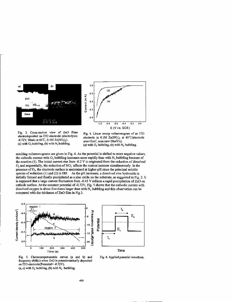
Fig. 3. Cross-section view of ZnO films electrodeposited on ITO electrode (electrolysis; -0.72V, 30min at 60°C, 0.1M Zn(N03)2). (a) with 02 bubbling, (b) with N2 bubbling.
r^rzi^ -0 5 I jiitfr
< / Mr E / \1r ^^ -1.0 ■ j Ji (a) c / p 01
3 -1 5 A
o
-2.0
Ely vs. SCE)
Fig. 4. Linear sweep voltammogram of an ITO electrode in 0.1M Zn(N03)2 at 60 t; (electrode area=2cm2, scan rate=20mV/s). (a) with 02 bubbling, (b) with N2 bubbling.
resulting voltammograms are given in Fig. 4. As the potential is shifted to more negative values, the cathodic current with 02 bubbling increases more rapidly than with N2 bubbling because of the reaction (1). The initial current rise from -0.2 V is originated from the reduction of dissolved 02 and sequentially, the reduction of N03" affects the current increase simultaneously. In the presence of 02, the electrode surface is maintained at higher pH since the principal soluble species of reduction (1) and (2) is OH". As the pH increases, a dissolved zinc hydroxide is initially formed and finally precipitated as a zinc oxide on the substrate, as suggested in Fig. 2. It is supposed that a large current fluctuation from -0.45 V reflects a rapid precipitation of ZnO on cathode surface. At the constant potential of-0.72V, Fig. 5 shows that the cathodic current with dissolved oxygen is about five times larger than with N2 bubbling and this observation can be compared with the thickness of ZnO film in Fig.3.
5 E
O
region 1
-0.6 ■ Vij, ilHJlwU. a
0.4 .— ^^£
h region l*^^.^ i 0.2 iü.,,.1 iU.L.,1-,1 lui^htiL-lJ
•"— b N.—-■
0.0
0 Tl
.2 c a o Q.
ta
Ea CD * C
3 -10,3
(A 3" Er
-15 5
;*■
-20 I N
to
200
Time (s) 400 500
Fig. 5. Chronoamperometric curves (a and b) and frequency shift(c) when ZnO is potentiostatically deposited on ITO electrode(Potential= -0.72V). (a, c) with 02 bubbling, (b) withN2 bubbling.
Time
Fig. 6. Applied potential waveform.
459

The effect of OH" on the ZnO formation was tested by using a potential pulse of Fig. 6. Anodic potential was 0.3V and ta was fixed at 5s, and cathodic potential was -0.72V and tc was varied. Differently from the XRD of Fig. 1(a) with the cathodic only depostion, pulse experiments bring the different results depending upon the cathodic time, tc. Since the possible anodic reactions are the reverse of reaction (2) and
2H,0 O, + 4H* + 4e (3)
the pH of the electrode surface is expected to be decreased during anodic period. Fig. 1 (b) shows that, though the total cathodic time is the same with Fig. 1(a), the potential pulse deposition with tc=ls does not result in the ZnO formation. On the other hand, Fig. 1(c) shows the formation of ZnO film when tc=5s. The formation of ZnO is heavily dependent on the cathodic charging during a single cycle. Since the cathodic charging means the concentration of OH', the concentration increase of OH" during tc=ls is too low for the ZnO to be formed and they are consumed again by the following oxidation. When tc=5s, the local sites of the electrode which has above critical pH induced the ZnO formation. However, part of OH" produced during tc=5s is oxidized during anodic time and therefore, the faradaic efficiency decreased significantly. It suggests that the pH of the electrode surface must be maintained at higher value, in order for the ZnO film to be formed.
When the electrolysis was carried out at -0.72V, Fig. 7 shows that ZnO nucleates on isolated sites at early times and, both the density and size of ZnO increases as the electrolysis time increases. The correlation of surface morphology with the current measurement in Fig. 5(a) represents that the initial current increase is due to both the nucleation and growth of ZnO. At about 5 min of electrolysis time, the electrode surface was completely covered with ZnO films and the steady-state current was reached. This observation tells that ZnO has a layer-type growth and the electrode area was maintained constant with further electrolysis. This can be explained evidently with the real-time measurement of the electrode mass by EQCM.
(a) K3Ei£] " %
„ at
9 ■*«^-. ^a». ^/f¥>:
(c) ■
1 *"'. if- a »> .• .'. <"* .A ■■■- -■■ \
1 - * - "\
* ~ «» •
y - . - ">■ -'i '
Fig. 7. Scanning electron micrographs of cathodically deposited ZnO for different electrolysis time(electrolysis ; -0.72V, 60 "C, 0.1M Zn(N03)2). (a) lmin, (b) 2min, and (c) 5min.
Fig. 5(c) shows the frequency(f)-time(t) response obtained with the ITO EQCM electrode in Zn(N03)2 during potentiostatic deposition. Since the surface mass change of the electrode, 4M, is described by frequency shift, Jf, (Sauerbrey equation)[7],
460

4/"= ■Cf -z/M, where Cr= 935.7 Hz//zg (3)
f-t curve represents an in-situ mass increase with electrolysis time. This curve can be divided into two regions, I and II, at around 20s of electrolysis time which shows an abrupt change of frequency shift rate. For region I which shows a rapid mass increase, AM/AQ obtained from f-t and i-t relationship is 2.12 mg/C and the value is about 3 times larger than the theoretical value of 0.69 mg/C expected for the formation of Zn(OH)4"2. Since FTIR spectra and potential pulse experiments indicate the existence of a soluble zinc hydroxides which can be dehydrated, it suggests that, in the initial stage of cathodic reduction, Zn+2 existing as Zn(H20)4
+2 in aqueous solutions[8] approaches to the cathode as a hydrate state and participate in the reaction with OH" generated by the reductions. The increase of soluble and viscous intermediate species on the electrode surface induce a higher value of AM/AQ obtained in region I. When intermediate species are reached at critical concentration over the electrode surface, the zinc ions from the solution are deposited in the form of ZnO via intermediate. It resulted in the substantial decrease of mass increase rate(between region I and region II) because the concentration(i.e., viscosity) is constant.
In entire region II, the rate of mass change becomes slow and AM/AQ obtained from f-t relationship is 0.41 mg/C and the value is in a good agreement with the theoretical value of 0.42 mg/C expected for pure ZnO. However, a detailed observation of frequency shift with time revealed two different frequency decreasing patterns in region II. As shown in Fig. 8(a), a stairwise decrease of frequency is dominant in the early period of region II. In spite of the evident mass decrease by dehydration during the deposition of ZnO, the plateaus(T) of frequency which means the invariant mass changes with time are observed. The cathodic current increase in this time range can be explained by the active nucleation and growth of ZnO crystallites which require the fast formation of intermediate species. The mass increase by these compensates for the mass decrease by dehydration.
▼
Ay
(a)
-4600 \y
~^T
,—. T -4700
* -4800
-4900
^y
>^
14700 "\P (b)
14800 • \fr
14900 \
15000 ^l 15100 \ T
15200 ^
55 60
Time (s)
65 360 365
Time (s)
Fig. 8. Two different decreasing patterns of frequency observed in the process of ZnO formation(extracted from region II of Fig. 5(c)). (T ; plateau part, O ; increasing part). Around electrolysis time of (a) 60s, (b) 360s.
On the other hand, Fig. 8(b) shows that the continuing frequency decrease with fluctuations
461

becomes more evident in the later period of region II, i.e., frequency increase«» is observed more often than Fig. 8(a). Since the ITO surface is completely covered with ZnO films at this time period, ZnO formation occurs on the pre-formed ZnO layer with the constant cathodic current. It is supposed that the current fluctuations observed represent the equilibrated condition for the formation of intermediate and dehydration of hydroxide into oxide. Different decreasing patterns observed in region II are the results of different growth steps of ZnO film.
CONCLUSIONS
In the electrochemical formation of zinc oxide on ITO glass, a soluble zinc hydroxide, Zn(OH)4'
2, was initially formed as a reaction intermediate. Controlled potential pulse experiments and in situ mass changes suggested that the critical concentration of OH" is required for the ZnO formation. ZnO crystals were nucleated at isolated sites and their growth was directly related with both the cathodic production of OH" and dehydration of intermediate species. With the dissolution of 02, the higher cathodic current observed was due to the production of OH" and it resulted in the rapid growth of ZnO films.
ACKNOWLEDGEMENT
This work was supported under 1997 Inha University Research Support Program.
REFERENCES
1. L. Gal-Or, I. Silberman, and R. Chaim, J. Electrochem. Soc, 138,1939(1991).
2. J. A. Switzer,^m. Ceram. Soc. Bull., 66, 1521(1987).
3. K. Kajiyoshi, M. Yoshimura, Y. Hamaji, K. Tomono, and T. Kasanami, J. Mater. Res., 11, 169(1996).
4. M. Izaki and T. Omi, J. Electrochem. Soc, 143, L53(1996).
5. M. Izaki and T. Omi, J. Electrochem. Soc, 144, L3(1997).
6. S. Peulon and D. Lincot, Advanced Materials, 8,169(1996).
7. M. Kitano and M. Shiojiri, J. Electrochem. Soc, 143, 809(1996).
8. R. J. Brodd and V. E. Leger, in Encyclopedia of Electrochemistry of the Elements, edited by A. J. Bard(Marcel Dekker Publishers, New York, 1992), Vol. 5, p. 4.
9. D. A. Buttery and M. D. Ward, Chem. Rev., 92,1037(1992).
462

AUTHOR INDEX
Ageev, V.P., 359 Ekerdt, J.Q., 165 Allard, L.F., 287 Emanetoglu, Nuri W., 353 Allendorf, M.D., 125 Endisch, Denis, 107 Arkles, Barry, 107 Endle, J., 165 Auciello, Orlando, 299 Espinoza, B.F., 311
Everson, M.P., 287 Babushkina, N.A., 333 Exarhos, Q.J., 215 Badi, M., 359 Bailey, S.O., 383 Fleeting, Kirsty A., 57 Balcaitis, Qinutis, 345 Fuenzalida, V.M., 451 Baum,T.H., 31, 113 Beach, David B., 203, 263, 271 Qandopadhyay, A., 287 Belot, J.A., 3 Qarnov, S.V., 359 Belova, L.M., 333 Gilles, S., 177 Bensadon, E.O., 395 Gilmer, D.C., 45 Bensaoula, A., 359 Gladfelter, W.L., 45 Bent, Stacey F., 153 Gorbenko, O.Yu., 333 Bersin, Richard, 345 Gordon, E.M., 383 Bhandari, Gautam, 113 Gordon, Roy G., 63 Bhusari, D.M., 131 Gorla, Chandrasekhar, 353 Blair, S.L., 233 Goy, D.M., 185 Blanquet, E., 177 Greenwald, A.C., 433 Boatner, L.A., 439 Gribelyuk, M.A., 45 Bosak, A.A., 333 Gruen, Dieter M., 299 Boumerzoug, Mohamed, 345 Bourhila, N„ 177 Haas, Terry E., 51, 75 Breitkopf, Richard C, 51, 75 Halpern, B., 445 Buhro, William E., 171, 197 Haraway, R., 383 Bulhöes, L.O.S., 395 Hartig, M., 445 Bussjager, Rebecca, 339, 413 Hatao, K., 407
Hatta, Akimitsu, 389 Campbell, S.A., 45 Hayashii, T, 245 Cao, Z., 215 Healy, M.D., 165 Chaiken,J., 339, 413 Heeg, Mary Jane, 147 Chang, R.F.H., 3, 299 Hegde, R., 445 Chen, Feng, 63 Hepel, Maria, 425 Chen, K.H., 131 Hepp, Aloysius F., 171, 383 Chen, L.C., 131 Hill, R.H., 233 Chen, Xiaomeng, 107 Hirata, G.A., 39 Cheng, J., 3 Hobbs, C, 445 Cheng, S.C., 3 Hoffmann, T., 451 Cherian, K.A., 419 Hollingsworth, Jennifer A., 171, 197 Chudzik, M.P., 3 Hunt, R.D., 203 Colombo, D.d., 45 Corrigan, Timothy, 299 Iizuka, H., 401 Cöte, Matthew J., 413 Interrante, L.V., 139 Crosbie, M.J., 11 Ito, S., 401 Czubarow, P., 287 Ito, Toshimichi, 389
Dai, J.Y., 3 Jang, Meehae, 209 Davis, Jr., D.Q., 327 Jenkins, Philip P., 171 Diceglie, Jr., Nicholas J., 63 Jin, Yong-Gi, 119 Dietz, B.H., 327 Jones, Tony C, 11, 57 DiFonzo, P.A., 159 Just, Oliver, 83 Doran, R., 445 Doubinina, G., 31 Doxsee, Kenneth M., 209 Dye, R.C., 311
Kaloyeros, Alain, 107 Kaneko, S., 245 Kannewurf, C.R., 3
463

Kaul, A.R., 333 Kelliher, J.T., 159 Kenig, Q., 445 Kenigsberg, Amos, 63 Keppens, V., 439 Khoroshun, I.V., 239 Kim, H-S., 45 Kim, Yunsoo, 69 Kinugasa, Junichi, 389 Kirss, Rein U., 51, 75 Klimentov, S.M., 359 Koh, Wonyong, 69 Kolis, Joseph W., 367 Kondo, Y., 245 Krauss, Alan R., 299 Ku, Su-Jin, 69 Kulik, J„ 359 Kuliuk, L.L., 239 Kumta, P.n., 221, 227 Kussmaul, A., 433
Lai, Pratik, 153 Lane, P.A., 11 Larkin, D.J., 139 Laudise, Robert A., 367 Lee, Burtrand I., 215, 257 Lee, D.F., 203 Lee, Jaeyoung, 457 Lee, Joong Kee, 119 Lee, Moon-Sook, 153 Lee, S., 359 Lee, Sang-Yeol, 119 Leedham, Tim J., 11,57 Leitheiser, Melvin A., 257 Levy, R.A., 177 Lewkbandara, T. Suren, 287 Liang, Shaohua, 353 Lienhard, M.A., 139 Lin, S.T., 131 Lin, Xian, 107 Litster, J., 419 Liu, Xinye, 63 Liu, Ying, 353 Lu, Yicheng, 353 Luten, Henry A., 83
Madar, R., 177 Maiya, P.S., 317 Makowicz, P., 445 Malik, M. Azad, 57 Mandrus, D., 439 Mantovani, J.Q., 383 Marcordes, B., 3 Marks, T.J., 3 Martin, P.M., 203 Mascher, Peter, 345 Massuda, M., 159 Mayo, William, 353 McCarthy, F.S., 327 McCarthy, K.C., 327 McCauley, Thomas Q., 299 McDaniel, A.H., 125
McKarns, Peggy J., 95 McKittrick, J., 39 McMeely, R.J., 3 Meda, Lamartine J., 51, 75 Medelci, M., 359 Miura, T., 245 Moon, B.M., 317 Mori, T., 407 Morrell, Jonathan S., 263, 271 Morse, T.F., 433 Moshnyaga, V.T., 239 Moss, T.S., 311 Murahara, M., 401, 407
Mam, Young-Woo, 119 Marula, C.K., 287 Mascente, P.A.P., 395 Mash, Fazio, 413 Meal, T.R., 159
O'Brien, Paul, 11, 57 Okamoto, T., 401 Olson, W.R., 185 Osman, Joseph M., 339, 413 Otway, David J., 57, 83
Paranthaman, Mariappan, 203, 263 Park, Dalkeun, 119 Pattillo, S.Q., 39 Pereira, E.C., 395 Perry, S.S., 359 Petrenko, P.A., 239
Qin, Lu Chang, 299
Radloff, Corey, 413 Raffaelle, R.P., 383 Ramos, Teresa, 279 Rees, Jr., William S., 83 Roberts, J., 45 Roy, Rustum, 373 Rudolph, V., 419 Russell, M.M., 165
Salazar, K.V., 39, 311 Samuels, W.D., 215 Scheper, Joseph T., 95 Schindler, J.L., 3 Schmitt, J., 445 Schmitz, P., 287 Schoch, Jr., Karl F., 251 Sebestl, Jennifer L., 147 Seegal, C, 31 Senateur, J.P., 177 Seyferth, D., 287 Shaban, D.O., 239 Shi, Y., 233 Shultz, A., 359 Singhal, A., 203 Sipola, D.L., 185 Smith, Douglas M., 279 Specht, Eliot D., 203, 263, 271
464

Stan, Mark A., 171 Starikov, D., 359 Studebaker, D., 31 Sun, Y-M., 165 Suzuki, H., 245
Tak, Yongsug, 457 Tamagawa, T., 445 Taylor, C.J., 45 Teff, Daniel J., 63 Tempez, A., 359 Teowee, Q., 327 Thornton, John, 63 Tobin, P., 445 Todd, Michael A., 31, 113 Trkula, M., 39 Tseng, H., 445 Tsutsumi, T., 245 Tuttle, B.A., 185
Ugarov, M.V., 359 Uhlmann, D.R., 327
Vallet, Catherine E., 263 Varshney, A., 287 Vasilow, Theodore R„ 251 Veteran, J., 445 Villarica, R. Martin, 413 Voigt, J.A., 185
Wallace, Steve, 279 Wang, A., 3 Wang, Feiling, 257 Wang, L., 215 Wang,T.Y., 131 Wang, V., 445 Waters, K., 359 Wei, C.H., 433 Weil, K.S., 221, 227 Wessels, B.W., 23 White, E.T., 419 White, J.M., 165 Wilcenski, Steven, 367 Wilk, Q.D., 45 Williams, D.J., 11 Winter, Charles H., 95, 147, 287 Wright, P.J., 11
Xu, Han, 345 Xue, ZilingB., 263, 271
Yang,J.R., 131 Yaroslavsky, I., 233 Yi, J., 39
Zhang, J.Z., 445 Zhang, Jianping, 257 Zhou, Daniel, 299
465

SUBJECT INDEX
ri-carbide, 221 adhesion, 317, 389 aerosol
combustion, 433 metalorganic chemical vapor
deposition, 333 alkaline metal hydroxide gels, 251 all-optical switches, 339 AlxTii.xM films, 165 aluminum
hydride, 165 nitride, 367
amorphous SiC, 159 silicon carbide (a-SiC:H) films, 153
anodic oxidation, 395 antimony, 113 ArF, 407
excimer laser, 407 atmospheric pressure chemical vapor
deposition, 107 atomic layer epitaxy, 83
BaBi2Nb2Og, 271 BaBi2Ta209,271 barium titanate, 63, 451 barrier layer, 95 (Ba,Sr)Ti03, 433 beta-diketonates, 63 bis(cyclopentadienyl)magnesium, 147 bis(2, 4-dimethylpentadienyl)ruthenium,
51,75 bis(tetramethylheptanedionato) strontium,
51 Bi4Ti3012,271 blue and green
laser diodes, 147 light-emitting diodes, 147
blue light, 83 boron nitride, 119, 359 buffer layer, 69, 263
calcium-stabilized zirconia, 395 carbosilane, 139 Ce{ri(Si(CH3)3)2)3,83 chelated, 227 chemical
bath, 197 etchant, 419 mechanical polishing, 419 preparation, 185 stability, 317 vapor deposition, 23, 63, 75, 95
CIS, 383 coercive field, 327 complexation-mediated crystallization, 209 complexed precursor, 221 computational chemistry, 373
copper indium diselenide, 383 corrosion, 425 crocoite, 209 crystal growth, 367 crystallite size, 39 crystallization, 245 CuInS2, 171 CVD, 45, 51, 113, 119, 131, 139, 317, 353
deposition rate, 119, 159 diamond, 131, 299, 419 dielectric(s), 185
constant, 279, 327 properties, 245
Edisonian chemistry, 373 electrically heatable catalysts, 287 electrochemical
preparation, 457 quartz-crystal microbalance (EQCM), 457
electrodeposition, 383, 425 electronic ceramics, 11 electro-optical devices, 257 epitaxial, 23
films, 271 piezoelectric films, 353
europium-doped yttrium oxide (Y2Q5:Eu3+), 39 excimer laser, 407
ferrites, 251 ferroelectric, 63
films, 233 materials, 433 oxides, 23 thin films, 239
field-emission display, 311 filters, 353 fluorescence spectra, 215
Qaln03, 3 gallium nitride, 367 QaM, 69 Qa205-In203-Sn02, 3 gas-phase chemical reaction, 125 Qroup-IV metal nitrides, 287 growth mechanism, 457
high decomposition temperature, 389 Tc superconducting films, 263 temperature flow, 125
hydrogenated films, 153 hydrothermal thin films, 451
indium compounds, 125 tin oxide, 287
InS, 197 1TO electrode, 457
467

jet vapor deposition (JVD), 445
kinetics, 12 KrF, 407
excimer laser, 407
LaxCayMn03, 31 (Lai.xPrx)0.7Cao.3Mn03, 333 laser, 359 lead(-)
chromium oxides, 209 magnesium(-)
niobate, 185 niobium-oxide, 433
zirconate titantate thin films, 245 zirconium titanate, 57
LiA102,69 lift-off, 451 liquid delivery
chemical vapor deposition, 31 system, 311
local heating, 389 low K
dielectric, 279 temperature, solution-based
preparation, 197 luminescence, 39
magnesium(-) chemical vapor deposition, 147 doped semiconductor, 147
magnetoresistance, 31, 333 magnetoresistive, 63 mass-sampling apparatus, 125 metal oxides, 63 metal organic, 233
chemical vapor deposition, 311 decomposition, 203
metastable phases, 209 methylsilane(s), 139, 153 MgO(100) substrate, 239 microhardness, 425 microstructues, 451 microwave plasma-enhanced
chemical vapor deposition, 131, 299 MOCVD, 3, 11,39,57 modulators, 23 molecular beam, 125 morphology, 171,299 MOSFET, 45 multi-seeding process, 245 multiple internal reflection Fourier
transform infrared (MIR-FTIR) spectroscopy, 153
nanocrystalline, 131, 197, 299 nanoporous silica, 279 riF3,401,407 nickel/silicon carbide, 425 nitride(s), 359, 367 M02, 401
nonlinear interface, 339
1,3-disilacyclobutane, 139 1,3-disila-n-butane, 139 1,3,5,-trisilacyciohexane, 139 optical properties, 131 optically active composite, 439 orthorhombic, 197
Pb(Mg,Nb)TiO, 433 (Pb,Ti) coordination compound, 239 Fb(Zr,Ti)03, 11 PECVD, 159 phoenicochroite, 209 phosphors, 311 photochemical, 233
pattern etching, 407 photoconductivity, 359 photoresponse, 215 photovoltaic, 171 PMN, 185 p-n junction, 383 polymer residues, 345 potassium titanyl phosphate, 257 powder synthesis, 185 precursor, 11, 139,239 processing, 419 pulsed injection technique, 177 PZT, 57
Raman, 413 rare-earth
aluminate, 263 phosphosilicates, 215
reactor, 125 pressure, 119
refractory, 63 remnant polarization, 327 remote plasma, 153 resist stripping, 345 Ru02, 75 ruthenocene, 75
salt metathesis, 209 scanning tunneling microscopy, 413 Schottky barrier, 383 self-laminating atomic layer epitaxy (SALE),
401 SiC, 139, 159 SiF4,401 Sil*, 107 silicon,
nitride, 107, 445 Si3N4,445 single(-)
crystals, 367 source
chemical vapor deposition, 69 precursor, 95, 139
Si02 thin films, 401 solar cells, 383
468

sol-gel, 203, 233, 245, 327 process, 257 synthesis, 263, 271
solution(-) liquid-solid (SLS) mechanism, 197 processing, 203
sonogels, 439 spectroscopic studies, 57 spray chemical vapor deposition, 171 SrBi2rib209,271 SrBi2Ta209,271 (Sr(hfac)2.)triglyme, 83 SrS:Ce thin films, 83 stabilized zirconia films, 395 stibine, 113 strontium ruthenate, 51 structural studies, 57 submicron ceramic particles, 433 superconducting, 63, 389 supercritical ammonia, 367 surface
characterization, 395 finish, 419
synthesis, 221
Ta2Os, 11 ternary nitride, 221 tetraiodosilane, 107 tetrakis(dimethyIamido)titanium, 165, 177 tetranitratotitanium (IV), 45 textured thin films, 239 thermal decomposition, 389 thermally oxidized tungsten, 413 thin films, 23, 39, 171, 227, 257 3C-SiC, 407
Ti(C,ri) films, 177 TiN, 317 Ti02/ 11,45 titanium
aluminum nitride, 95 dioxide, 45 nitride, 345
films, 287 transition-metal nitride, 227 transparent conducting, 3 tribology, 359 triethylboron, 119 trimethylindium, 125 trimethylsilane, 159 tris(trifluoromethyl)stibine, 113
ultrasonic-misted nitrates, 389
via etch, 345 VCh films, 439 V2Os sol, 439
W03 films, 339
Xe2* excimerlamp, 401, 407 x-ray photoelectron spectroscopy, 395
YBa2Cu307.x, 203, 389 YMn03, 327
zirconium oxide films, 395 Znkln2OK+3', 3 ZnO, 353
thin films, 457
469