CHARACTERIZATION OF NON-NORMAL OPERATING ...
95
CHARACTERIZATION OF NON-NORMAL OPERATING CONDITIONS OF OUTDOOR PHOTOVOLTAIC (PV) POWER GENERATOR MODULES: GLOBAL AND A NEPAL CASE-STUDY Dinesh Rai Thesis to obtain the Master of Science Degree in Electrical and Computer Engineering Supervisor: Prof. Paulo José da Costa Branco Prof. João Filipe Pereira Fernandes Jury Chairperson: Prof. Rui Manuel Gameiro de Castro Supervisor: Prof. Paulo José da Costa Branco Members of the Committee: Prof. Carlos Alberto Ferreira Fernandes December 2017
-
Upload
khangminh22 -
Category
Documents
-
view
0 -
download
0
Transcript of CHARACTERIZATION OF NON-NORMAL OPERATING ...
CHARACTERIZATION OF NON-NORMAL
OPERATING CONDITIONS OF OUTDOOR
PHOTOVOLTAIC (PV) POWER GENERATOR
MODULES: GLOBAL AND A NEPAL CASE-STUDY
Dinesh Rai
Thesis to obtain the Master of Science Degree in Electrical and Computer Engineering
Supervisor: Prof. Paulo José da Costa Branco
Prof. João Filipe Pereira Fernandes
Jury
Chairperson: Prof. Rui Manuel Gameiro de Castro
Supervisor: Prof. Paulo José da Costa Branco
Members of the Committee: Prof. Carlos Alberto Ferreira Fernandes
December 2017

i
ABSTRACT
The energy consumption is increasing day by day. We are marching towards the renewable energy
sources for the healthy environment issues. Among the various renewable sources, the solar energy is
one of the most abundant. PV cell is a technology that generates direct electrical power from
semiconductors when they are subject to illumination. The PV cell technology has enhanced the usage
of solar energy primarily due to the manufacturing cost reduction and improvement in the power
conversion.
The purpose of this work is to study the operating characteristics of PV system in the case of the
non-normal operation conditions. The installed PV system has to operate in abnormal environmental
conditions which lead to adverse effects on the PV system performance, so there is the need of
systematics study of those conditions. The systematic study includes the detail analysis of the variation
in the output characteristics, i.e., current, voltage and power. The waveform of current and voltage of
the PV cell, module and panel are measured and recorded. The waveforms are recorded for normal
operating condition, as well as the abnormal conditions. The obtained curves are then compared and the
problem is associated with the PV system is identified. An algorithm has been presented for detection
of faults.
Nepal is a country with huge potential of solar energy. There is an increasing of the PV installation,
but they lack the monitoring and management of the installed system, so it is required to study about it.
Keywords: Renewable energy, PV systems, Solar cells, PV faults, Operation and
maintenance

ii
iii
RESUMO
Por questões ambientais, as fontes de energia renováveis ganham um peso cada vez maior no
domínio da produção e consumo de energia. Entre as fontes de energia renováveis destaca-se a energia
solar fotovoltaica (PV). Esta tem tido um grande incremento devido à diminuição dos custos envolvidos
e ao aumento das eficiências dos processos de conversão energética envolvidos.
As análises de falhas do sistema PV é uma tarefa fundamental para garantir a confiança e eficiência
do sistema. O objetivo deste trabalho é o estudo das características de funcionamento do sistema PV
em condições anormais. Danos físicos, sombreamento, envelhecimento, estragos nos díodos de
contorno, são alguns exemplos de condições referidas como anormais. É importante um controlo
sistemático do sistema. Esse estudo inclui a análise pormenorizada da variação das características de
saída (corrente, tensão e potência). Cada falha tem associado um dado sintoma, que permite a sua
caracterização. É apresentado um algoritmo para a deteção de falhas. Várias simulações foram levadas
a cabo para as diferentes falhas e as respetivas comparações com os resultados experimentais foram
realizadas para validar os módulos PV.
É apresentado o caso de estudo do Nepal, país com um grande potencial fotovoltaico, embora ainda
não totalmente aproveitado. Existe um aumento da instalação de sistemas PV, mas com uma
monitorização e gestão do sistema já instalado incipientes. O presente trabalho tenta identificar as falhas
frequentes e as causas de degradação, recomendando soluções para os problemas encontrados.

iv

v
ACKNOWLEDGEMENT
First, I would like to express my sincere gratitude to my supervisor Associate Professor Doctor Paulo
José da Costa Branco and invited Professor. João Fernandes for their continuous support of my thesis,
for their motivation, guidance, and enthusiasm. They were always ready to help and steered me in the
right direction whenever I needed it.
I would also like to thank Mr. Luis Marques who actively involved with me for the various
experimental works and assisted me to deduce the significant results. He is very helpful hardworking
person, without his help the validation of the experimental work could not have been successfully
conducted.
My sincere thank also goes to my lab mate, Mr Nabin Khadka and other colleges, they were
supporting and were always ready to help me. They actively created learning environment between us
and shared the knowledge with each other.
Last not the least, I would like to extend my thanks to my friends Mr. Manish Adhikari, Mr. Durga
Khatri, Mr. Anil Poudel, Miss. Monika Rai, Miss. Anamika Thapa, for their unfailing support and
continuous encouragement throughout my years of study and through the process of researching and
writing this thesis.

vi

vii
TABLE OF CONTENTS Abstract.................................................................................................................................................................... i
resumo ................................................................................................................................................................... iii
Acknowledgement .................................................................................................................................................. v
List of figures ........................................................................................................................................................ ix
List of Tables ......................................................................................................................................................... xi
List of Acronyms ................................................................................................................................................. xiii
List of symbols .................................................................................................................................................... xv
1. INTRODUCTION ..................................................................................................................................... 1
1.1. Motivation......................................................................................................................................... 1
1.2. Objectives ......................................................................................................................................... 2
1.3. State of art ......................................................................................................................................... 2
1.4. Development of PV Technology ...................................................................................................... 4
2. SOLAR CELL MODEL ............................................................................................................................ 7
2.1. Current-Voltage Curve of a Solar Cell and Module ......................................................................... 7
2.2. Determining I-V and P-V characteristics of solar cells..................................................................... 9
2.3. Solar cell materials............................................................................................................................ 9
3. ABNORMAL CONDITION IN PHOTO-VOLTAIC SYSTEMS .......................................................... 11
3.1. Faults in PV Systems ...................................................................................................................... 11
3.2. Faults in a cell ................................................................................................................................. 13
3.3. Fault on bypass diodes on a group of cells ..................................................................................... 15
3.4. Faults in a PV Module .................................................................................................................... 16
3.5. Faults on a String ............................................................................................................................ 16
3.6. Aging .............................................................................................................................................. 17
4. EXPERIMENTAL TESTS TO DETERMINE THE CELL PARAMETER ........................................... 19
4.1. The IV characteristics of cell in dark condition .............................................................................. 19
4.2. Methodology ................................................................................................................................... 19
4.3. Current-Voltage characteristics of an experimental cell ................................................................. 20
4.4. Determination of parameters for computational analysis ............................................................... 20
4.5. Limitation and conclusion of Dark Condition ................................................................................ 23
4.6. Calculation of cell parameters using a fitting function ................................................................... 25
4.7. Comparison of the obtained results ................................................................................................. 25
5. EXPERIMENTAL ACTIVITIES AND SIMULATIONS ...................................................................... 27
5.2. Effect of shading on a group of a solar cell .................................................................................... 36
5.3. Faults on group of cells (string) module ......................................................................................... 41
5.4. Fault on a String of modules ........................................................................................................... 48
6. ALGORITHM FOR FAULT DETECTION ........................................................................................... 53
6.1. Symptoms for detection of fault ..................................................................................................... 53
6.2. Identification of symptoms ............................................................................................................. 54
6.3. Evolution of symptoms as the function of the severity of faults ..................................................... 56
6.4. Qualitative analysis of detection and localization capacity of defects ............................................ 59
viii
7. CASE STUDY OF NEPAL ..................................................................................................................... 63
7.1. Current situation and opportunity of PV technology ...................................................................... 63
7.2. Faults and Maintenance compare with global scenario .................................................................. 64
7.3. Case study ....................................................................................................................................... 65
7.4. Case- II: Degradation of the system ................................................................................................ 66
8. CONCLUSION AND RECOMMENDATION....................................................................................... 69
9. FUTURE WORK .................................................................................................................................... 71
References ............................................................................................................................................................ 73
10. Appendix I........................................................................................................................................... 77

ix
LIST OF FIGURES
Fig. 1- 1 A PV system [2] ...................................................................................................................................... 3 Fig. 1- 2 Global solar PV market scenario [6] ........................................................................................................ 4 Fig. 1- 3. Top 10 countries in 2015 based on total PV installed capacity (MW) [7] .............................................. 5 Fig. 2- 1. A single diode model of a solar cell. [10] ............................................................................................... 7 Fig. 2- 2 IV and PV curves of a solar cell [11] ....................................................................................................... 8 Fig. 2- 3 Current voltage characteristics [13] ......................................................................................................... 9 Fig. 3- 1 Dust [15] ................................................................................................................................................ 12 Fig. 3- 2 Burnt cells [16] ...................................................................................................................................... 12 Fig. 3- 3 Damage PV modules[17] ....................................................................................................................... 12 Fig. 3- 4 Crack on PV cells [15] ........................................................................................................................... 12 Fig. 3- 5 Hotspots [18] .......................................................................................................................................... 12 Fig. 3- 6 Snow on PV modules [19] ..................................................................................................................... 12 Fig. 3- 7 Shading on cells [21] .............................................................................................................................. 13 Fig. 3- 8 Solar cell in different operation conditions. ........................................................................................... 14 Fig. 3- 9 Shading on a cell [13] ............................................................................................................................ 15 Fig. 3- 10 Fault on bypass diode[13] .................................................................................................................... 15 Fig. 3- 11 Degradation of performance due to aging of a solar panel [14] ........................................................... 17 Fig. 4- 1 Experimental setup for measurement ..................................................................................................... 19 Fig. 4- 2 A Solar Cell ............................................................................................................................................ 19 Fig. 4- 3 Experimental IV characteristics of a solar cell ....................................................................................... 20 Fig. 4- 4 The equivalent circuit of a cell 1 diode model [10] ............................................................................... 20 Fig. 4- 5 Measurement of Shunt resistance [17] ................................................................................................... 21 Fig. 4- 6 Voltage and inverted currents in linear region. ...................................................................................... 22 Fig. 4- 7 Equivalent circuit in P-spice .................................................................................................................. 26 Fig. 4- 8 characteristics obtained from Pspice ...................................................................................................... 26 Fig. 5- 1 Modelling of a Solar Cell in Matlab....................................................................................................... 27 Fig. 5- 2 IV curve of a solar cell ........................................................................................................................... 28 Fig. 5- 3 PV curve of a solar cell .......................................................................................................................... 28 Fig. 5- 4 IV curve of a solar cell in different irradiances ...................................................................................... 29 Fig. 5- 5 PV curve of a solar cell in different irradiance ...................................................................................... 29 Fig. 5- 6 The effect of series resistance in a solar cell .......................................................................................... 31 Fig. 5- 7 Effect of irradiance in a solar cell .......................................................................................................... 32 Fig. 5- 8 Effect of temperature on IV curve of a solar cell ................................................................................... 33 Fig. 5- 9 Effect of Temperature on PV curve of a solar cell ................................................................................. 33 Fig. 5- 10 IV curve of two series connected cells ................................................................................................. 33 Fig. 5- 11 PV curve of a two series connected cells ............................................................................................. 34 Fig. 5- 12 IV curve of two cells in series ............................................................................................................. 34 Fig. 5- 13 PV curve of two cells in series ............................................................................................................. 35 Fig. 5- 14 Effect of mismatch current ................................................................................................................... 36 Fig. 5- 15 Schematic model of two cells in series ................................................................................................ 37 Fig. 5- 16Three cells in series connection ............................................................................................................ 37 Fig. 5- 17 The effect of shading on three cells ..................................................................................................... 38 Fig. 5- 18 Shading case I ...................................................................................................................................... 38 Fig. 5- 19 IV curve of group of solar cells presented in fig. 5-18 ......................................................................... 39 Fig. 5- 20 PV curve of group of solar cells presented in fig. 5-18 ........................................................................ 39 Fig. 5- 21 Shading case II ..................................................................................................................................... 39 Fig. 5- 22 IV curve of shading case II .................................................................................................................. 40 Fig. 5- 23 PV curve of shading case II ................................................................................................................. 40 Fig. 5- 24 Shading case III .................................................................................................................................... 40 Fig. 5- 25 IV curve of shading case III ................................................................................................................. 41 Fig. 5- 26 PV curve of shading case III ................................................................................................................ 41 Fig. 5- 27 Schematic design of a PV module........................................................................................................ 42 Fig. 5- 28 Effect of short circuit of bypass diode ................................................................................................. 43 Fig. 5- 29 Effect of resistance of bypass diode ..................................................................................................... 43 Fig. 5- 30 Reversal of a bypass diode ................................................................................................................... 44 Fig. 5- 31 IV curves of PV panel in different working conditions ....................................................................... 44 Fig. 5- 32 Schematic and Setup of IV measurement on IST roof ......................................................................... 45

x
Fig. 5- 33 Curves measured on a solar panel under different scenarios................................................................ 47 Fig. 5- 34 Effect of shading on IV and PV curve ................................................................................................. 48 Fig. 5- 35 Simulation configuration for partial shading ........................................................................................ 49 Fig. 5- 36 IV and PV curves of 3 modules connected in series ............................................................................ 49 Fig. 5- 37 String of PV modules ........................................................................................................................... 50 Fig. 5- 38 IV curve of string of PV ....................................................................................................................... 50 Fig. 5- 39 PV curve of a PV string ....................................................................................................................... 50 Fig. 5- 40 Strings of PV modules ......................................................................................................................... 51 Fig. 5- 41 IV curve of a string .............................................................................................................................. 51 Fig. 5- 42 PV curve of a string ............................................................................................................................. 51 Fig. 6- 1 Characteristics IV curves of PV modules in different scenarios ............................................................ 55 Fig. 6- 2 Effect of resistance ................................................................................................................................. 56 Fig. 6- 3 Effect of temperature ............................................................................................................................. 57 Fig. 6- 4 Short circuit of bypass diode .................................................................................................................. 57 Fig. 6- 5 Influence of irradiance in the IV curve of PV cell ................................................................................. 58 Fig. 6- 6 Fault in module and transformed to string ............................................................................................. 58 Fig. 6- 7 Fault in module and transferred to string ............................................................................................... 58 Fig. 6- 8 Flow chart .............................................................................................................................................. 61 Fig. 7- 1 Solar energy potential of Nepal [35] ...................................................................................................... 63 Fig. 7- 2 Generated voltage from PV module ....................................................................................................... 65 Fig. 7- 3 Generated current from PV module ....................................................................................................... 66 Fig. 7- 4 Percentage changes in data parameter .................................................................................................... 66 Fig. 7- 5 IV curve of PV module with degradation over a time............................................................................ 67 Fig. 7- 6 PV curve of a PV module with degradation over a time ........................................................................ 67
xi
LIST OF TABLES
Table 2-1 – Different methods for determining the IV curve of a PV module ...................................................... 9 Table 3-1 – Non-normal operating conditions of PV system .............................................................................. 12 Table 3-2 – Variation of IV curve of a solar cell in different conditions .............................................................. 13 Table 4-1 – Experimental IV curve obtained. ....................................................................................................... 25 Table 4-2 – Simulation Results ............................................................................................................................. 25 Table 4-3 – Comparison of values ........................................................................................................................ 26 Table 5-1 – The parameters of solar cell .............................................................................................................. 28 Table 5-2 – Data parameter of a solar cell from experiment ................................................................................ 30 Table 5-3 – Parameter of the two cells in series from experiment........................................................................ 35 Table 5-4 – Solar cell data ................................................................................................................................... 36 Table 5-5 – Simulation of 3 cells .......................................................................................................................... 37 Table 5-6 – Shading data ...................................................................................................................................... 40 Table 5-7 – Parameters of model .......................................................................................................................... 42 Table 5-8 – Datasheet of a PV String ................................................................................................................... 44 Table 5-9 – Power available in the different non-normal conditions .................................................................... 44 Table 5-10 – Conditions tested on the solar panel ................................................................................................ 45 Table 5-11 – Datasheet of a PV module ............................................................................................................... 48 Table 5-12 – Comparison of power between normal and open voltage fault case ............................................... 50 Table 5-13 – Comparison of power before and after degradation of PV panel .................................................... 52 Table 6-1 – List of types of faults and its consequences ...................................................................................... 54 Table 6-2 – Symptoms of the faults and its occurring zones ................................................................................ 55 Table 6-3 – Module faults..................................................................................................................................... 59 Table 6-4 – String faults ....................................................................................................................................... 60 Table 7-1 – Comparison of power generation over a time with degraded PV module ......................................... 67

xii

xiii
LIST OF ACRONYMS
AEPC Alternative Energy Promotion Centre
Imp Current at maximum power
INGO International Non-Governmental Organisation
MPP Maximum Power Point
MPPT Maximum Power Point Tracker
NGO Non-Governmental Organisation
NOCT Normal Operating Condition
PV Photovoltaic
PVT Photovoltaic thermal
STC Standard Test Condition

xiv
xv
LIST OF SYMBOLS
A Ampere
AC Alternating Current
Eg Energy band eV
eV Electron volt 1.602 × 10⁻¹⁹ joules
G Irradiance (W/m2)
GW Giga Watt
ID Diode current
IL Photo current
Imp Current at maximum power
IO Inverse saturation current
Isc Short circuit current
Isc_r Short circuit current in reference condition
Ish Parallel loss current
IV Current-Voltage
k Boltzmann constant 1.380 × 10⁻²³ m2 kg s-2 K-1
K Kelvin degree
mA Milliampere
MW Mega Watt
PV Photovoltaic
q Charge of electron modulus 1.16*10-19 Coulombs
Rp Shunt Resistance
Rs Series Resistance
T Temperature in Kelvin
V Voltage
Vmp Voltage at maximum power
Voc Open Circuit Voltage
VT Thermal Voltage 25.85 mV

xvi

1
1. INTRODUCTION
The generation of energy from the fossil fuels emit greenhouse gases, result in global warming which
is unfavourable for the environment and ecosystem. These problems lead to the use of the environment-
friendly renewable energy resources like wind, solar, geothermal, tidal, and so on. Among these
renewable resources, PV solar energy is gaining its global popularity. Nevertheless, the advancement
of technology the bottlenecks is still associated with high cost and low efficiency. In addition to the
high capital cost, it’s maintenance cost is high because they are installed outside so they are prone to
various mechanical and electrical faults. These faults results increase in the power loss and decrease the
efficiency as well as the reliability of the system. There is five level of faults that can occur in the PV
system i.e. cell level, group of cell level, module level, string level and array level. Each level faults
have its own characterizes so a proper model has to be made to identify the location of faults. Each level
also has different types of faults so the modelling should be done promptly and should include all the
probable modelling of the system.
The analysis of different faults is very useful to characterize the faults which are very for the
recognition of faults for the whole system. The probable faults in the PV system are partial shading,
open circuit, short circuit, hotspots, mismatch, aging. The simulation of these faults conditions eases
the analysis behaviour of the faults. Modelling and design calculation of PV system requires the
knowledge of the parameter which describes the non-linear characters of PV cell. These parameters are
calculated with the Dark current-voltage measurement method. After determining these parameters, it
is easy to characterize the system and easy to model of the system. Modelling must be done from each
level and should measure the quantity for the future reference.
Nepal is a developing country struggling with the energy crisis. The government of Nepal is
concerning about the meeting the demand of energy through the renewable resources. The solar PV
system has been a good source of energy for the off-grid population of Nepal since all the population is
not connected to the grid. Nowadays not only the remote areas, a solar PV system has gaining its
popularity in the cities areas too and many business firms, normal people have installed this system to
their business house, home etc, so there is need of study of the non-operating conditions and faults in
Nepal. This thesis work focus study of the potentiality of the solar PV system and its status. The measure
problem has been identified and its measurement and recommendation have been made.
1.1. Motivation
As the demand for clean energy is increasing due to the global warming and pollution issues, PV
solar power generation has an important role in the clean energy. Now all the developed countries are
focusing on this renewable source of energy. The capital cost and maintenance cost for PV power

2
generation is very high. It is necessary to supervise and monitor the unfavorable operating condition to
ensure they are working correctly. It is required to have high efficiency and long-life span of PV system.
Since the PV panel must mount on the open place so it is always prone to various defects. This kind of
unfavorable conditions can degrade the efficiency of the solar panel. The decrease in the efficiency of
PV panel can cause heavy loss to the owner because the cost of the panel is very high as compared to
other energy sources. To save the money and environment it is necessary to monitor and supervise the
condition of the PV system. The one of the method to monitor faults on the system is the supervision
of output current-voltage characteristics, the analysis of current-voltage curve for each unfavorable
condition characterize its pattern, so this characteristics pattern is the very important tool in future for
the monitoring and fault analysis of the system.
Nepal is a small developing country, focusing on the renewable solar energy to meet the energy
demand. Nepal has a huge potential of solar PV energy due to its geographical advantage, and there is
increasing demand for the solar PV system though there are only the off-grid system exits. Till now
there is collectively not more than few megawatts has installed but now the government is focusing on
the flourishing the PV power. In this condition, it is necessary to be updated with the various faults and
non-operating conditions in Nepal. A systematic study of the faults and maintenance of PV system in
Nepal has not been done yet, so it’s a great chance to have such opportunity of doing something that
has not been done
1.2. Objectives
PV system must withstand the various environmental conditions. The output power of PV system is
highly dependent on the operating conditions. The objective of this thesis is to study the current and
voltage characteristics of the PV system for the different unfavourable conditions. The waveform of
current and voltage changes with the operating conditions and plays vital role in determining the faults.
These changes presented by waveforms are studied and identify the characteristics of faults. This
characteristic is then used to determine the fault associated with the system.
Finally, this thesis work finally improves the reliability of the PV system. This thesis work also
focuses on the condition of PV system in Nepal and try to identify the problems associated with the PV
system and their remedies. This thesis work can be a reference to the people who are interested in PV
system in Nepal.
1.3. State of art
The demand for clean energy is increasing day by day as the global warming and climate change
have been a serious problem for the world. Most of the countries are developing the technology to

3
harness the renewable energy that is environmentally friendly. They utmost try to avoid the use of Fossil
fuel. Thinking about the renewable energy resources, there are different types of renewable resources
like wind energy, solar energy, geothermal energy tidal energy etc. Among these different kinds of
renewable energy solar energy is the major energy source. Solar energy can be harnessed in different
ways choosing the appropriate technology. Among them, the most common are solar PV (PV), solar
thermal and hybrid solar PV/thermal (PVT) [1]. Electricity is the most versatile form of energy. It can
be transformed into various forms of energy as it is required it to be. The PV effect is a technology that
transforms a solar energy into electricity (dc) with the help of semiconductor device. In the last decade,
solar power generation from PV cells has had a large increase. The fig 1-1 shows the basic level of the
solar cell to the PV system, its formation along the various levels.
Fig. 1- 1 A PV system [2]
A recent development involves the makeup of solar cells to increase its efficiency. The most efficient
type of solar cell to date is a multi-junction concentrator solar cell with an efficiency of 46% [3]. The
highest efficiencies achieved without concertation include a material by “Sharp corporation” at 35.8 %
[3] using a proprietary triple-junction manufacture technology. There is an ongoing effort to increase
the conversion efficiency of PV cells and modules. Recent developments in Organic PV cells have
made significant advancement in power conversion efficiency. The other recent development includes
the discoveries of Light-Sensitive Nanoparticles, Gallium Arsenide new material that could make three
times more efficient than existing products on the market [3]. There has been a study to the solar panel
with built-in battery and other manufacturing material.
4
1.4. Development of PV Technology
The history of PV begins with the nineteenth century, the first fictional, intentionally made PV
device was by Fritts [3]. The modern era of PVs started in 1954 when researchers at Bell Labs in the
USA accidentally discovered that p-n junction diodes generated a voltage when the room lights on [3].
Then there has been a start of the study of the PV system and its development, In the 1980s the industries
began to give emphasis on the manufacture of PV cells [3]. Initially, the cost of manufacture of PV cells
are expensive but along with the time the cost has been decreasing and the efficiency has increased.
Solar PV technology has evolved a lot since it has been discovered. Solar PVs are taken as a thing
of today and future. The development of material technology, monocrystalline silicon and multi-
crystalline silicon are now economically viable to produce in large quantity [4]. However, their energy
conversion efficiency from solar to electricity is still low Researchers have long looked-for ways to
improve the efficiency and cost-effectiveness of solar-cells. The average solar cell is approximately 15
% efficient which means nearly 85% [5] of the sunlight is not converted into electricity.
Solar PV is growing rapidly and worldwide installed capacity reached at least 177 gigawatts (GW)
by the end of 2014 [3]. The total power output of the world’s PV capacity in a calendar year is now
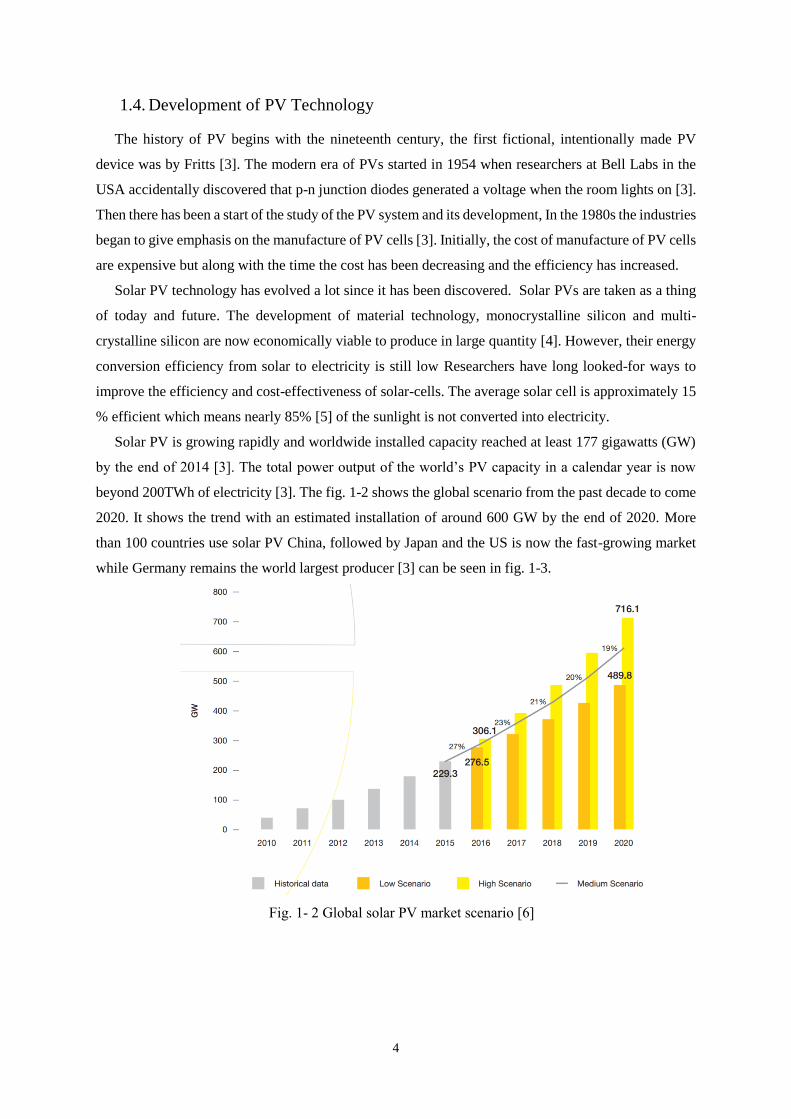
beyond 200TWh of electricity [3]. The fig. 1-2 shows the global scenario from the past decade to come
2020. It shows the trend with an estimated installation of around 600 GW by the end of 2020. More
than 100 countries use solar PV China, followed by Japan and the US is now the fast-growing market
while Germany remains the world largest producer [3] can be seen in fig. 1-3.
Fig. 1- 2 Global solar PV market scenario [6]

5
Fig. 1- 3. Top 10 countries in 2015 based on total PV installed capacity (MW) [7]

6

7
2. SOLAR CELL MODEL The solar cell is a basic unit block of a solar PV system which is made of two layers of semiconductor
materials. When the photon with sufficient energy strikes the surface of the solar cell, electron and hole
pairs are released which causes to a generation of electricity. A solar cell works on the principle of PV
effect. Basically, the silicon is doped with pentavalent and trivalent impurities to increase the charge
carrier concentration and these oppositely doped layers are brought together to form a junction. In the
junction after the photons are absorbed the free electron of n region try to move to p-region and holes
of p-region try to move to the n-region to compensate for their respective deficiencies. If electrical
contacts are made with the two semiconductor materials, the free electrons will flow from the n-type
through the external path to the p-type material. The flow of electrons through the external circuit will
continue as long as more free electrons and holes are formed by the solar radiation[3].
There are various electrical circuit models of PV cells which have been widely described in the
literature [8] [9] . A most commonly used model is the one-diode model (Ideal model) as shown in the
fig. 2-1. In one diode model, a cell is represented by a current source IL in parallel with a diode and a
resistance (Rsh) with and a series resistance (Rs).
Fig. 2- 1. A single diode model of a solar cell. [10]
The governing equations for this model is given as:
𝐼𝑠ℎ =𝑉+𝐼𝑅𝑠
𝑅𝑠ℎ (2-1)
𝐼 = 𝐼𝐿 − 𝐼𝐷 − 𝐼𝑠ℎ (2-2)
𝐼 = 𝐼𝐿 − 𝐼0𝑒(𝑉+𝐼𝑅𝑠
𝑉𝑡) −
𝑉+𝐼𝑅𝑠
𝑅𝑠ℎ (2-3)
2.1. Current-Voltage Curve of a Solar Cell and Module
The current-voltage curve of a PV panel describes its energy conversion capability at the existing
conditions of irradiance and temperature. The IV curve provides a quick and effective means of
accessing the true performance of solar cell. As shown in the fig. 2-2, the curve represents the
combinations of current and voltage at which the string could be operated or ‘loaded’, if the irradiance
and cell temperature could be held constant. The current-voltage curve of a PV panel is non-linear
graph. The curve is highly dependent on the irradiance as well as the temperature of the cell and with
the local weather condition too. Since the different solar panel has a different parameter so it will result

8
in the different IV curves. The behaviour of the current of a solar cell is nonlinear described by above
equations (2-3). The typical IV and PV curve of a solar cell is shown in fig 2-2.
Fig. 2- 2 IV and PV curves of a solar cell [11]
The important parameters of IV and PV curve are the following
• Short circuit current (Isc): Maximum value of current generated by a solar cell when the
voltage is zero;
• Open circuit voltage (Voc): Maximum value of voltage generated across cell when there is
open circuit of cell;
• Maximum power point: The maximum value of power that can be extracted from a
cell/module;
• Imp: The value of current of a cell at MPP.
• Vmp: the value of voltage of a cell at MPP.
• Fill factor (FF): It’s a ratio of the maximum power from the solar cell to the product of Voc
and Isc.
𝐹𝐹 =𝐼𝑚𝑝∗𝑉𝑚𝑝
𝐼𝑠𝑐∗𝑉𝑠𝑐 (2-4)
The IV curve of a PV module is shown in the fig 2-3. The IV curve changes with irradiance [3] and
operating temperature of a panel. The study of the current-voltage characteristics of the PV panel is
done with comparing the standard current-voltage curve versus the measured curve of the panel.
Occasionally the measured IV curve deviates substantially with the standard IV curves [11]. The
changes in the curve are the results of various reasons, probable damages, or defects and aging etc. The
deviation in the curve can provide the information of the performance of the panel. The study of the IV
characteristics curve provides the following deviations in the PV panel according to the various defects
and aging.

9
Fig. 2- 3 Current voltage characteristics [12]
2.2. Determining I-V and P-V characteristics of solar cells
Theoretically, the IV characteristic of a solar cell is determined by changing the voltage applied to
the cell in progressive steps from zero to infinite resistance. In practice, to obtain this curve are used 6
distinct methods. These methods consist in using a variable resistor, capacitive load, electronic load,
bipolar power amplifier, four-quadrant power supply or a DC to DC converter as shown in table 2-1. A
comparison between these 6 methods can be seen in figure. In this thesis, a variable resistor is used, so
it was not much convenient to obtain all the data from the experiment.
Table 2-1 – Different methods for determining the IV curve of a PV module
Types Flexibility Modularity Fidelity Fast
Response
Direct display Cost
Variable
resistor
Medium Medium Medium Low No low
Capacitive
load
Low Low Medium Low No High
Electronic
load
High High Medium Medium Yes High
Bipolar
Power
Amplifier
High High high Medium Yes High
4-quadrant
power
Supply
Low Low high High Yes High
Dc-Dc
converter
High High High High Yes Low
2.3. Solar cell materials
Silicon is the most used semiconductor for the manufacture of the solar cell. Pure silicon is
crystalline in structure which is necessary for solar cells. Silicon can be arranged into either a
monocrystalline structure or a polycrystalline structure. Polycrystalline shells are made by using various
10
silicon crystal together and are less expensive in cost than monocrystalline. Once the silicon has been
properly prepared, it is doped with phosphorous (donor dopant) and boron (acceptor dopant) to for a
semiconductor. The electrical properties of silicon depend on the amount of the dopant materials. There
are other semiconductor materials, choice of the material depends upon the energy gap, efficiency, and
the cost.

11
3. ABNORMAL CONDITION IN PHOTO-VOLTAIC SYSTEMS
Since the PV panels are operated in outdoor conditions, they are exposed to various environmental
and sometimes harsh conditions as, dirt and dust, partial shading, rain, snow, corrosion which can lead
to a faster aging [4]. A very basic approach to detect an abnormal condition is to compare the output
power of the panel with the reference power and get notified when there is a difference more than some
tolerance. The approach that we are going to adopt in this thesis work will be to analyze the IV curves
(one or for an array of panels) for the most common abnormal conditions [11]. The study of the IV
curves includes the analysis and measurement of characteristics of the current, voltage and power for
the most frequent abnormal conditions. The measured curves are then compared with the characteristic
ones of the healthy panel (or healthy arrays) or their initial condition to ensure the system has no
significant abnormalities.
3.1. Faults in PV Systems
There are four levels of the components to form a PV system: the PV cell unit, cell groups, the PV
module and a PV string. These components are always exposed to some defects that can affect the
performance of the whole system[13]. The main task for this thesis is to figure out the probable faults
for each of the components and its influence in the IV curve of the system. Table 3-1 lists the most
probable defects as well as the non-normal operating conditions associated with the PV system in the
real world.

12
Table 3-1 – Non-normal operating conditions of PV system
Fig. 3- 1 Dust [14]
Fig. 3- 2 Burnt cells [15]
Fig. 3- 3 Damage PV modules[16]
Fig. 3- 4 Crack on PV cells [14]
Fig. 3- 5 Hotspots [17]
Fig. 3- 6 Snow on PV modules [18]
13
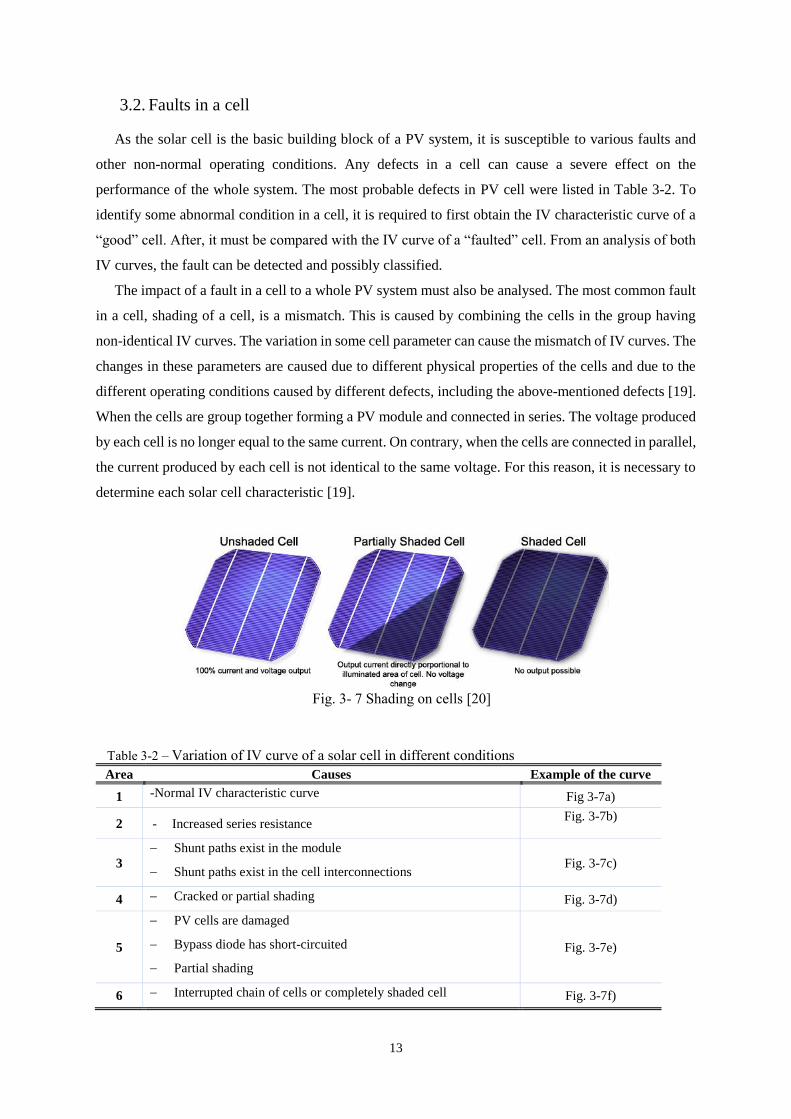
3.2. Faults in a cell
As the solar cell is the basic building block of a PV system, it is susceptible to various faults and
other non-normal operating conditions. Any defects in a cell can cause a severe effect on the
performance of the whole system. The most probable defects in PV cell were listed in Table 3-2. To
identify some abnormal condition in a cell, it is required to first obtain the IV characteristic curve of a
“good” cell. After, it must be compared with the IV curve of a “faulted” cell. From an analysis of both
IV curves, the fault can be detected and possibly classified.
The impact of a fault in a cell to a whole PV system must also be analysed. The most common fault
in a cell, shading of a cell, is a mismatch. This is caused by combining the cells in the group having
non-identical IV curves. The variation in some cell parameter can cause the mismatch of IV curves. The
changes in these parameters are caused due to different physical properties of the cells and due to the
different operating conditions caused by different defects, including the above-mentioned defects [19].
When the cells are group together forming a PV module and connected in series. The voltage produced
by each cell is no longer equal to the same current. On contrary, when the cells are connected in parallel,
the current produced by each cell is not identical to the same voltage. For this reason, it is necessary to
determine each solar cell characteristic [19].
Fig. 3- 7 Shading on cells [20]
Table 3-2 – Variation of IV curve of a solar cell in different conditions
Area Causes Example of the curve
1 -Normal IV characteristic curve Fig 3-7a)
2 - Increased series resistance Fig. 3-7b)
3
Shunt paths exist in the module
Shunt paths exist in the cell interconnections Fig. 3-7c)
4 Cracked or partial shading Fig. 3-7d)
5
PV cells are damaged
Bypass diode has short-circuited
Partial shading
Fig. 3-7e)
6 Interrupted chain of cells or completely shaded cell Fig. 3-7f)

14
a) b)
c) d)
e) f)
Fig. 3- 8 Solar cell in different operation conditions.
Partial shading is one of the most frequent situations that can induce abnormal conditions, occurring
when some module of the PV array is shaded. This is a regular phenomenon mainly caused by clouds
and/or nearby obstacles. Due to the nature of shading, it will show its influence on the IV characteristics
[5]. The study of the nature of defects and its influences in the IV curves (either in a single solar cell
and in a module), has found that module was broken, degradation, cracking, sand and snow effects,
corrosion, and shading, all have in common will result in the variation of its fill factor. There can be
also heating of the cells due to some defects, hotspots may occur due to the rise in cell’s temperature
[9]. There may be degradation of the interconnection between the modules, corrosion in the inter-cell
bonds, all this will give rise to the variation of series resistance.
15
3.3. Fault on bypass diodes on a group of cells
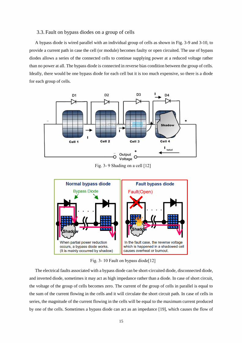
A bypass diode is wired parallel with an individual group of cells as shown in Fig. 3-9 and 3-10, to
provide a current path in case the cell (or module) becomes faulty or open circuited. The use of bypass
diodes allows a series of the connected cells to continue supplying power at a reduced voltage rather
than no power at all. The bypass diode is connected in reverse bias condition between the group of cells.
Ideally, there would be one bypass diode for each cell but it is too much expensive, so there is a diode
for each group of cells.
Fig. 3- 9 Shading on a cell [12]
Fig. 3- 10 Fault on bypass diode[12]
The electrical faults associated with a bypass diode can be short-circuited diode, disconnected diode,
and inverted diode, sometimes it may act as high impedance rather than a diode. In case of short circuit,
the voltage of the group of cells becomes zero. The current of the group of cells in parallel is equal to
the sum of the current flowing in the cells and it will circulate the short circuit path. In case of cells in
series, the magnitude of the current flowing in the cells will be equal to the maximum current produced
by one of the cells. Sometimes a bypass diode can act as an impedance [19], which causes the flow of
16
current through it causing some power losses in that diode [8]. In case of an open circuit, there is no
path for the current if there is a fault in a cell. In the case of reverse polarity, the diode starts to conduct
when the sum of the voltage is greater than the voltage required to turn on the diode
Different studies [19] have been done on defects of the bypass diode. They show that there are some
significant changes in the characteristic curve of the module. For the short circuit case, the overall
voltage of the module decreases and so the power. In a case where a bypass diode acts as an impedance
[19], the overall power decreases as the value of resistance increases and vice-versa. In the open-circuit
case, the characteristics curve has drastic changes as in this condition another type of fault like shading
plays a vital role in the modification of the curve. In case of reverse polarity, case the output power
decreases as the reversal of polarity of the diode in the group can bypass the power when there is a
greater voltage across the diode.
3.4. Faults in a PV Module
The PV module is prone to different faults. Since the module is the combination of series and parallel
connection of numbers of cells with help of bypass diode. The electrical faults associated with the failure
of a module of a PV system are short-circuiting of a bypass diode, reversal in the polarity of the bypass
diode. The short-circuit of a diode causes the output voltage decrease. One reversal direction of a bypass
diode also decreases the output voltage of group of cells. These faults can make significant changes in
the IV characteristics of the system. The simulation of these faults is simulated in following simulation
part.
3.5. Faults on a String
The PV array is the combination of series and parallel connection of the number of PV modules.
The fault in a string is the fault associated with the PV module and non-return diode. The non-return
diode may be short circuited or reverse biased. The short circuit of non-return diode may sometimes
lead to the reverse flow of the current during non-normal condition. The reverse bias diode can oppose
the flow of the current and lead to significant power losses. Sometimes the diode can act as the resistance
this also lead to power loss. Apart from the fault in the bypass diode there may be opposite polarity
connection of a PV panel within the string. there may chance of short circuit of the PV panel.
Mismatches are also likely to occur in the string. Mismatch in modules occur when the parameter of
one modules is significantly changed from others. They are also likely to occur due to different
environmental conditions [21] (i.e irradiance or temperature ). Mismatch losses may lead to a serious
problem causing drastic change in power generation.
The PV array can have some mismatch losses, these losses are caused because of change in electrical
parameter in one module than others [11]. The difference environmental condition of module in a same
string give such mismatch cases. The environmental conditions are irradiance, operating temperature
17
[18]. A manufacture faults may also lead to mismatch losses. Mismatch losses may cause serious
problem. There are two kind of mismatch faults [11]:
3.5.1. Temporary mismatch:
Partial shading/ non- uniform temperature of PV system results the temporary mismatch in string.
The shading caused by the position of the cloud is very common in large centralized PV system [22].
The consequences of this temporary fault have been already discussed in above sections.
3.5.2. Permanent mismatch:
Open circuit faults, aging, degradation, hot spots caused by the defects on the bypass diode, these
are the general causes of the permanent mismatch [23]..
3.6. Aging
The solar panels are always exposed to open environment so they must bear harsh environmental
conditions snow, dust, wind, temperature variations etc. The dust, soil, shading, water corrosion for
long period can lead to aging of PV module [23][24]. Due to these environmental conditions, there is
degradation of the performance of the PV systems. This degradation can be termed as the aging of a PV
panel. The degradation may due to anti-reflective coating delamination, microcracks, encapsulation
faults discolouring, delamination, and hot spots. There is no proper knowledge how the aging can be
studied for PV cells but it has found that it can reduce the efficiency 13-25 % [13] of the solar panel in
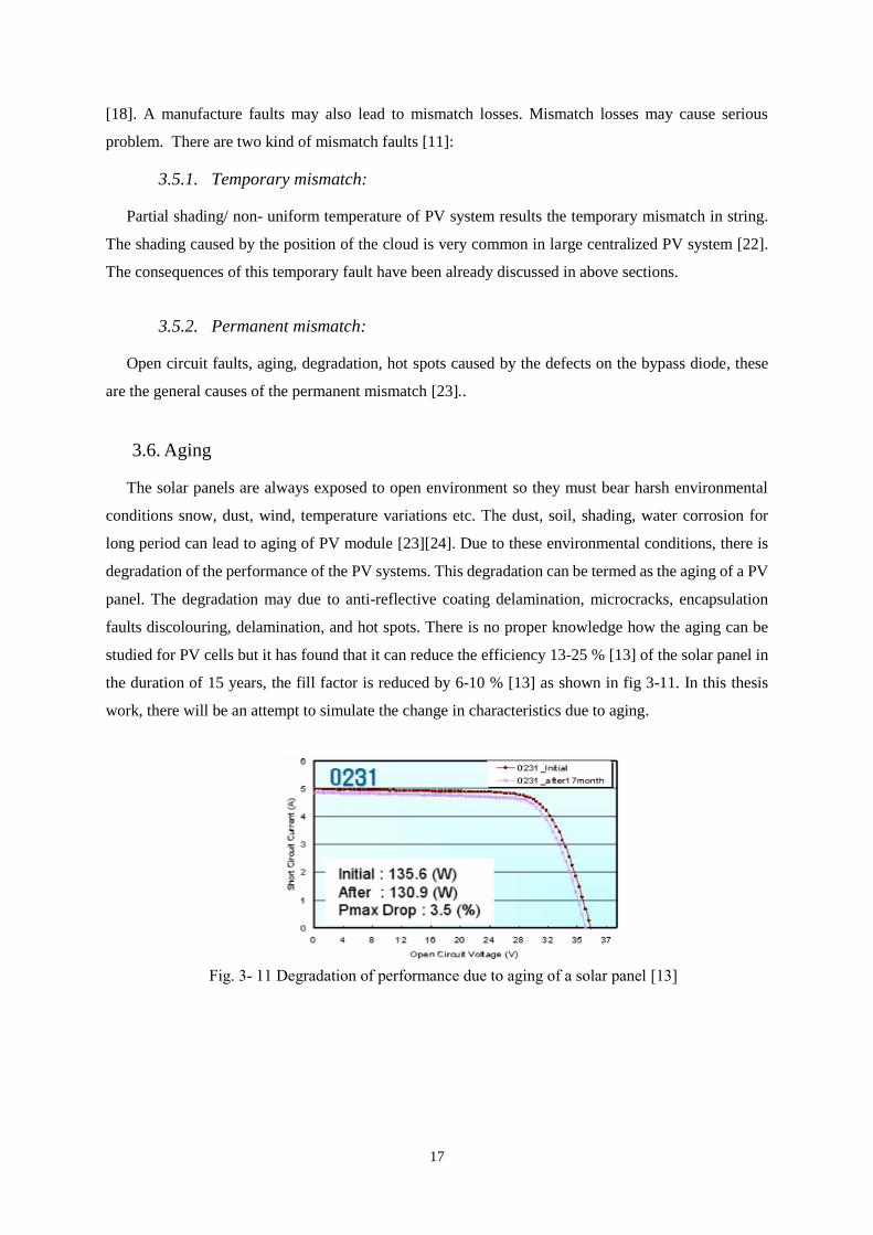
the duration of 15 years, the fill factor is reduced by 6-10 % [13] as shown in fig 3-11. In this thesis
work, there will be an attempt to simulate the change in characteristics due to aging.
Fig. 3- 11 Degradation of performance due to aging of a solar panel [13]

18
19
4. EXPERIMENTAL TESTS TO DETERMINE THE CELL
PARAMETER
4.1. The IV characteristics of cell in dark condition
All the solar cells have some parasitic resistances. To determine these parasitic shunt and series
resistances an experiment is carried out known as dark current-voltage experiments [25]. Since it is
done in the dark condition, so it is termed as a dark current-voltage experiment. The dark current-voltage
experiment is commonly used to analyse the electrical characteristics of solar cells. It provides an
effective way to determine parasitic parameters without the need of a solar simulator. The dark IV
measurement technique provides such a diagnostic tool for module manufacturers.
4.2. Methodology
For the experiment the cell was covered with some objects so that it cannot receive any illumination
and measurements were taken.
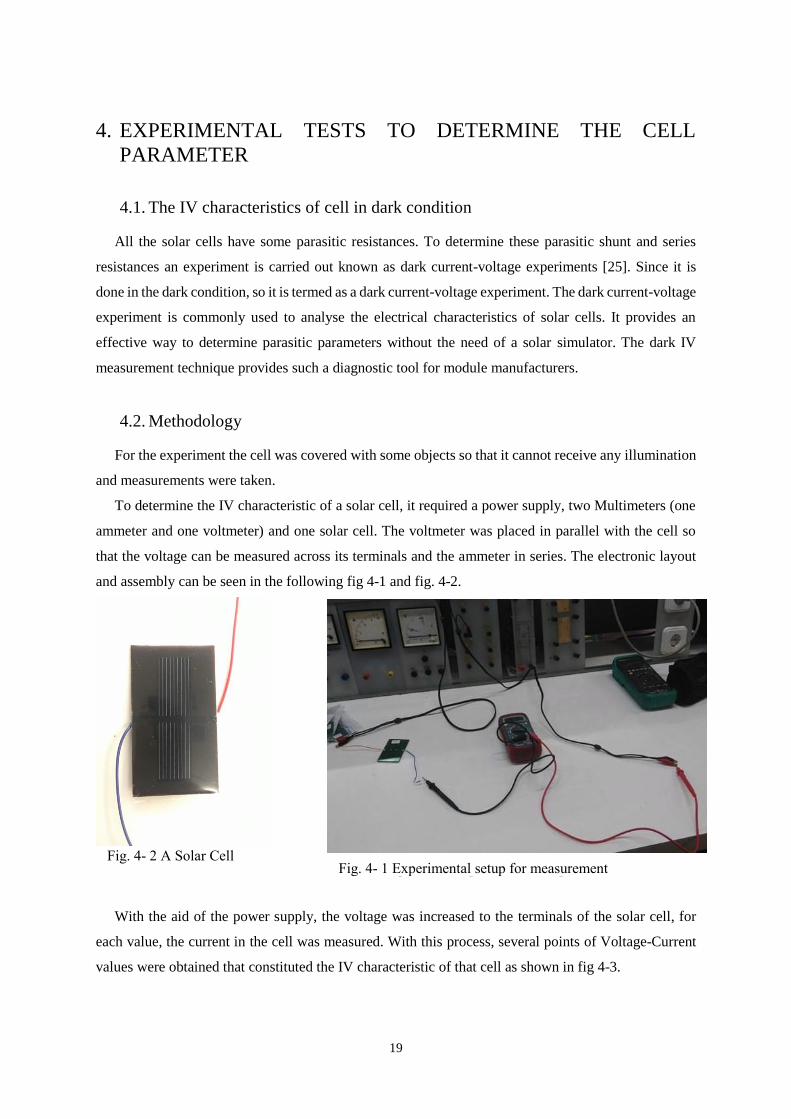
To determine the IV characteristic of a solar cell, it required a power supply, two Multimeters (one
ammeter and one voltmeter) and one solar cell. The voltmeter was placed in parallel with the cell so
that the voltage can be measured across its terminals and the ammeter in series. The electronic layout
and assembly can be seen in the following fig 4-1 and fig. 4-2.
Fig. 4- 2 A Solar Cell
With the aid of the power supply, the voltage was increased to the terminals of the solar cell, for
each value, the current in the cell was measured. With this process, several points of Voltage-Current
values were obtained that constituted the IV characteristic of that cell as shown in fig 4-3.
Figure 4- 1 Experimental setup for measurement Fig. 4- 1 Experimental setup for measurement
20
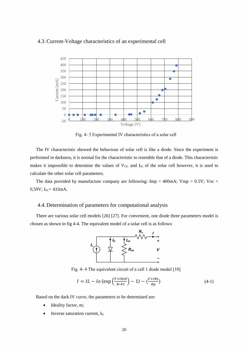
4.3. Current-Voltage characteristics of an experimental cell
Fig. 4- 3 Experimental IV characteristics of a solar cell
The IV characteristic showed the behaviour of solar cell is like a diode. Since the experiment is
performed in darkness, it is normal for the characteristic to resemble that of a diode. This characteristic
makes it impossible to determine the values of VOC and ISC of the solar cell however, it is used to
calculate the other solar cell parameters.
The data provided by manufacture company are following: Imp = 400mA; Vmp = 0.5V; Voc =
0,59V; ISC= 433mA.
4.4. Determination of parameters for computational analysis
There are various solar cell models [26] [27]. For convenient, one diode three parameters model is
chosen as shown in fig 4-4. The equivalent model of a solar cell is as follows:
Fig. 4- 4 The equivalent circuit of a cell 1 diode model [10]
𝐼 = 𝐼𝐿 − 𝐼𝑜 ⟨exp (𝑉+𝐼𝑅𝑠ℎ
𝑁∗𝑉𝑡) − 1⟩ − (
𝑉+𝐼𝑅𝑠
𝑅𝑝) (4-1)
Based on the dark IV curve, the parameters to be determined are:
• Ideality factor, m;
• Inverse saturation current, I0;
0 100 200 300 400 500 600 700 800 900-50
0
50
100
150
200
250
300
350
400
450
Voltage [V]
Curr
ent
[mA
]
21
• Series resistance, RS;
• Shunt resistance, Rsh.
4.4.1. Ideal factor (m)
The ideality factor of a diode is a measure of how closely the diode follows the ideal diode equation.
The ideal factor of a solar cell is calculated from the following formula (4-2) and obtained the value of
1.333.
𝑚 =𝑉𝑚𝑝𝑟−𝐼𝑚𝑝_𝑟
𝑉𝑡𝑟∗ln(1−𝐼𝑚𝑝𝑟𝐼𝑠𝑐𝑟
) (4-2)
4.4.2. Inverse Saturation current at STC (Io)
The inverse saturation current of a solar cell is calculated using the following formula and obtained
the value 2.9104e-8 A.
𝐼𝑜 =𝐼𝑐𝑐𝑟
𝑒𝑉𝑜𝑐𝑟𝑚∗𝑉𝑡𝑟−1
(4-3)
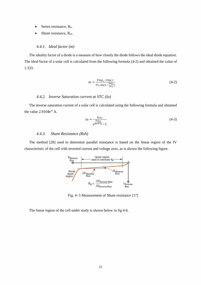
4.4.3. Shunt Resistance (Rsh)
The method [28] used to determine parallel resistance is based on the linear region of the IV
characteristic of the cell with inverted current and voltage axes, as is shown the following figure.
Fig. 4- 5 Measurement of Shunt resistance [17]
The linear region of the cell under study is shown below in fig 4-6.
22
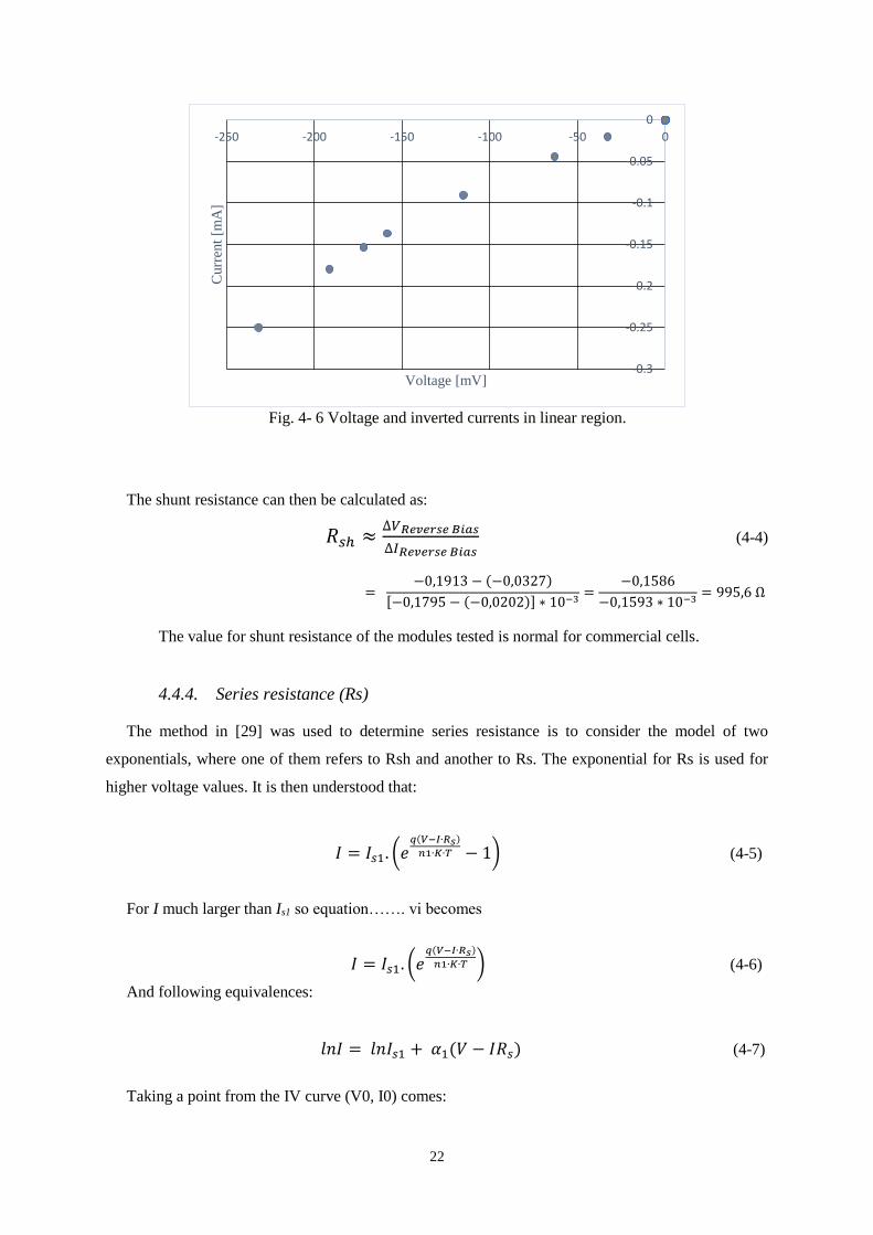
Fig. 4- 6 Voltage and inverted currents in linear region.
The shunt resistance can then be calculated as:
𝑅𝑠ℎ ≈∆𝑉𝑅𝑒𝑣𝑒𝑟𝑠𝑒𝐵𝑖𝑎𝑠
∆𝐼𝑅𝑒𝑣𝑒𝑟𝑠𝑒𝐵𝑖𝑎𝑠 (4-4)
=−0,1913 − (−0,0327)
[−0,1795 − (−0,0202)] ∗ 10−3=
−0,1586
−0,1593 ∗ 10−3= 995,6Ω
The value for shunt resistance of the modules tested is normal for commercial cells.
4.4.4. Series resistance (Rs)
The method in [29] was used to determine series resistance is to consider the model of two
exponentials, where one of them refers to Rsh and another to Rs. The exponential for Rs is used for
higher voltage values. It is then understood that:
𝐼 = 𝐼𝑠1. (𝑒𝑞(𝑉−𝐼∙𝑅𝑠)
𝑛1∙𝐾∙𝑇 − 1) (4-5)
For I much larger than Is1 so equation……. vi becomes
𝐼 = 𝐼𝑠1. (𝑒𝑞(𝑉−𝐼∙𝑅𝑠)
𝑛1∙𝐾∙𝑇 ) (4-6)
And following equivalences:
𝑙𝑛𝐼 = 𝑙𝑛𝐼𝑠1 +𝛼1(𝑉 − 𝐼𝑅𝑠) (4-7)
Taking a point from the IV curve (V0, I0) comes:
-250 -200 -150 -100 -50 0
-0.3
-0.25
-0.2
-0.15
-0.1
-0.05
0
Voltage [mV]
Curr
ent
[mA
]

23
𝐼𝑛𝐼 − 𝐼𝑛0 = 𝛼1(𝑉 − 𝐼𝑅𝑠) − 𝛼1(𝑉0 − 𝐼0𝑅𝑠) (4-8)
Being X = 𝑉−𝑉0
𝐼−𝐼0 and Y =
ln(𝐼
𝐼0)
𝐼−𝐼0, this gives a straight line:𝑌 = 𝛼1(−𝑅𝑠 + 𝑋)
Next, the values of the IV curve of cell 10 were used, with voltages and currents starting at V = 0.34
V. X and Y were calculated, giving 24 pairs of values. Subsequently, with a fitting the line was obtained:
Y = 13.82 * (1.104 + X). That is Rs = 1.104 Ω
The values that obtained are for the parasitic elements of a diode are higher than the real values. The
calculated value for shunt resistance is 995.6 Ω which is as normal value for commercial cells. The
series resistance is 1.04 which is too high, it should be less than 0.1 Ω for commercial purpose. The
reason for the high value of series resistance may be the calculating method is not accurate as it converts
the non-linear curve to linear form, this results in a chance of some error. It is required to adopt another
way of to determine this parameter described in section 4.6
4.5. Limitation and conclusion of Dark Condition
A problem consists of the measurements of the IV curve in the darkness: the current flows in the
opposite direction and the current paths are different. The change in the path of the current causes a
lower series resistance in the measurements in the darkness in relation to the measurements with light.
The equation of the equivalent scheme of a solar cell makes it impossible to perform a fitting with
exactness, even knowing the pairs of voltage and current values. Approximate methods could be used
if one knew the VOC voltage and the ISC current, but for the characteristic, both values are unknown and
do not apply. As such, the only parameter that was calculated was the parallel resistance, through an
approximate method, which resulted in 995.6Ω.
But there is a research work that says that it is possible to calculate the values VOC, Imp and VMP
very close to the real ones, knowing only the parameters calculated by dark IV: "Using the cell
parameters determined from dark IV analysis, it is possible to calculate a module's expected Light IV
performance by prescribing a value for Isc and inserting the parameters in a two-diode electrical model
[30].
In general case, the average ISC of cells is typically a well-known quantity since manufacture
company provides it. Work by others has shown that for individual cells, the Rs parameter determined
from dark IV measurements differs, and is usually lower than the value determined from light IV
measurements [25]. This work has demonstrated the same difference for dark IV measurements on
modules. The cause for the difference in calculated Rs is that the imposed voltage distributions and
consequently the current flow patterns are different in dark IV versus light IV measurements.

24
Nonetheless, dark IV measurements provide a valuable method for analysing module performance
parameters

25
4.6. Calculation of cell parameters using a fitting function
Using a numerical software, a fitting of the IV curve was done with a non-linear regression. This
function, eq. (4-9) was used to fit the curve and help to determine the cell parameters. The equation 4-
1 represents a behaviour of non-linear equation where the data from the table 4-1 is provided.
𝑓(𝑥) = 𝐼 −𝐼𝑃𝑉 +𝐼𝑠. (𝑒𝑞(𝑉+𝐼∙𝑅𝑠)
𝑛∙𝐾∙𝑇 − 1) +𝑉+𝐼∙𝑅𝑠
𝑅𝑠ℎ∗ [1 + 𝑘 (1 −
𝑉+𝑅𝑠𝐼
𝑉𝑏)−𝑛
] (4.9)
Table 4-1 – Experimental IV curve obtained.
Voltage [V] Current [mA]
0.439 2.26
0.4980 5.94
0.523 10.61
0.546 19.43
0.553 23.65
0561 29.47
0.569 36.84
0.577 46.6
0.584 55.9
0.587 61.6
0.59 66.8
0.594 75.2
0.599 85.2
0.603 95
The obtained results from the theoretical calculation in section 4.4 and from this fitting method are
quite different, this is the fact that the fitting was done using the non-linear IV curve and the theoretical
calculation was done with the linearization of the equation.
Using the initial points x0 = [Iph0 I00 Rs0 Rsh0 Vt0] = [0 10-8 0.015 5 0.0308], the parameters for
which the function converges are: x = [0.0034 -4.2357e-10 0.0504 31.4961 0.0306].
Table 4-2 – Simulation Results
Iph I0 Rs Rsh Vt
0.0034 4.2357e-10 0.0504 31.4961 0.0306
4.7. Comparison of the obtained results
The previous obtained parameters were used in the P-Spice, a software program, and plotted an I-V
curve of a diode. The equivalent circuit model for simulation in P-Spice is shown in figure 4-7. The
obtained IV curve is shown in figure 4-8. The table 4-3 shows the data from dark current experimental
work and from P-spice simulation. This table shows that the obtained parameters are quite near the
exact value. The data obtained for high voltage values are relevant. The relative error has decreased as
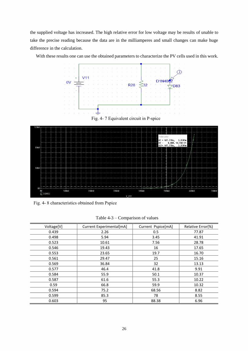
26
the supplied voltage has increased. The high relative error for low voltage may be results of unable to
take the precise reading because the data are in the milliamperes and small changes can make huge
difference in the calculation.
With these results one can use the obtained parameters to characterize the PV cells used in this work.
Fig. 4- 7 Equivalent circuit in P-spice
Fig. 4- 8 characteristics obtained from Pspice
Table 4-3 – Comparison of values
Voltage[V] Current Experimental[mA] Current Pspice[mA] Relative Error(%)
0.439 2.26 0.5 77.87
0.498 5.94 3.45 41.91
0.523 10.61 7.56 28.78
0.546 19.43 16 17.65
0.553 23.65 19.7 16.70
0.561 29.47 25 15.16
0.569 36.84 32 13.13
0.577 46.4 41.8 9.91
0.584 55.9 50.1 10.37
0.587 61.6 55.3 10.22
0.59 66.8 59.9 10.32
0.594 75.2 68.56 8.82
0.599 85.3 78 8.55
0.603 95 88.38 6.96

27
5. EXPERIMENTAL ACTIVITIES AND SIMULATIONS
A simulation work was done using Simulink tool of Matlab to simulate the behaviour of solar cell
under different non-normal conditions. The fig. 5-1 shows the model of one solar cell used in the
simulation.
Fig. 5- 1 Modelling of a Solar Cell in Matlab
The governing equation for this model is given as:
𝐼 = 𝐼𝑝ℎ − 𝐼𝑠 ⟨exp (𝑉+𝐼𝑅𝑠
𝑁∗𝑉𝑡) − 1⟩ − 𝐼𝑠2 ⟨exp (
𝑉+𝐼𝑅𝑠
𝑁2∗𝑉𝑡) − 1⟩ − (
𝑉+𝐼𝑅𝑠
𝑅𝑝) (5-1)
where:
• Is is the saturation current of the first diode.
• Is2 is the saturation current of the second diode.
• Vt is the thermal voltage, kT/q, where:
• k is the Boltzmann constant.
• T is the Device simulation temperature parameter value.
• q is the elementary charge on an electron.
• N is the quality factor (diode emission coefficient) of the first diode.
• N2 is the quality factor (diode emission coefficient) of the second diode.
• V is the voltage across the solar cell electrical ports.
• The quality factor varies for amorphous cells, and is typically 2 for polycrystalline cells.
In this work, the used model is “Short circuit current and open circuit voltage, 5 parameters” whose
parameters values are given in the table below. This model assumes the following simplification in the
8- parameter model
• The inverse saturation current of second diode is zero
• The impedance of the parallel resistor is infinite
28
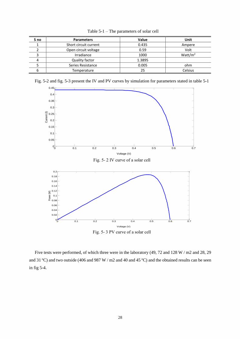
Table 5-1 – The parameters of solar cell
S no Parameters Value Unit
1 Short circuit current 0.435 Ampere
2 Open circuit voltage 0.59 Volt
3 Irradiance 1000 Watt/m2
4 Quality factor 1.3895
5 Series Resistance 0.005 ohm
6 Temperature 25 Celsius
Fig. 5-2 and fig. 5-3 present the IV and PV curves by simulation for parameters stated in table 5-1
Fig. 5- 2 IV curve of a solar cell
Fig. 5- 3 PV curve of a solar cell
Five tests were performed, of which three were in the laboratory (49, 72 and 128 W / m2 and 28, 29
and 31 ºC) and two outside (406 and 987 W / m2 and 40 and 45 ºC) and the obtained results can be seen
in fig 5-4.
0 0.1 0.2 0.3 0.4 0.5 0.6 0.70
0.05
0.1
0.15
0.2
0.25
0.3
0.35
0.4
0.45
Voltage (V)
Curr
ent (I
)
0 0.1 0.2 0.3 0.4 0.5 0.6 0.70
0.02
0.04
0.06
0.08
0.1
0.12
0.14
0.16
0.18
0.2
Voltage (V)
Pow
er (W
)
29
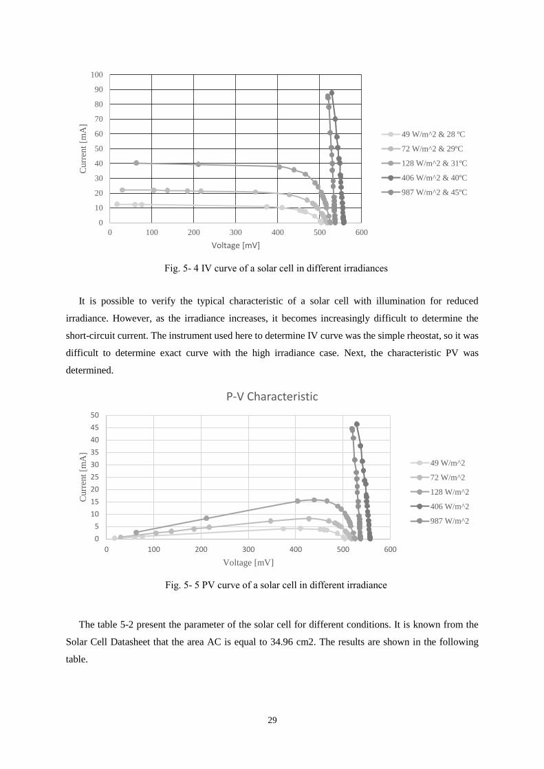
Fig. 5- 4 IV curve of a solar cell in different irradiances
It is possible to verify the typical characteristic of a solar cell with illumination for reduced
irradiance. However, as the irradiance increases, it becomes increasingly difficult to determine the
short-circuit current. The instrument used here to determine IV curve was the simple rheostat, so it was
difficult to determine exact curve with the high irradiance case. Next, the characteristic PV was
determined.
Fig. 5- 5 PV curve of a solar cell in different irradiance
The table 5-2 present the parameter of the solar cell for different conditions. It is known from the
Solar Cell Datasheet that the area AC is equal to 34.96 cm2. The results are shown in the following
table.
0
10
20
30
40
50
60
70
80
90
100
0 100 200 300 400 500 600
Curr
ent
[mA
]
Voltage [mV]
49 W/m^2 & 28 ºC
72 W/m^2 & 29ºC
128 W/m^2 & 31ºC
406 W/m^2 & 40ºC
987 W/m^2 & 45ºC
0
5
10
15
20
25
30
35
40
45
50
0 100 200 300 400 500 600
Curr
ent
[mA
]
Voltage [mV]
P-V Characteristic
49 W/m^2
72 W/m^2
128 W/m^2
406 W/m^2
987 W/m^2
30
Table 5-2 – Data parameter of a solar cell from experiment
Irradiance[W/m2] 49 72 128 406 987
Cell temperature [ºC] 27,5 29,1 31,4 40 45
ISC [mA] 12,5 22,3 40,6
VOC [mV] 504 519 526 557 537
Imp [mA] 10,2 18,9 35,7
Vmp [mV] 410 428 439
Pmp [mW] 4,2 8,1 15,7
FF = 𝑰𝒎𝒑𝒑𝑽𝒎𝒑𝒑
𝑰𝒔𝒄𝑽𝑶𝑪 [%] 66,4 70,4 72,1
𝜼𝟏 = 𝑰𝒎𝒑𝒑𝑽𝒎𝒑𝒑
𝑮∗𝑨𝑪∗𝑵 [%] 0,7 0,7 0,9
5.1.1. Effect of series resistance of a solar cell
A general solar cell shows some series resistances. This is due the fact that current must flow through
the emitter and base, the contact resistance between the metal contact and silicon and the resistance
between the top and rear metal contacts.
The current equation of solar cell is given as:
𝐼 = 𝐼𝑝ℎ − 𝐼𝑜 exp (𝑉+𝐼𝑅𝑠
𝑁∗𝑉𝑡) − 1 (5-2)
Study of the effect of series resistance of the solar cell is done by keeping all the parameters constant
and only the series resistance is changed. The obtained result from simulation is shown in the fig. 5-6.
From the above equation as the value of the series resistance is increased, there is decreased in the
output current from the solar cell, this will result in the decrease in the output power. The open circuit
voltage is independent of current flowing through the series resistance so it constant nevertheless there
is variation in the series resistances.

31
Fig. 5- 6 The effect of series resistance in a solar cell
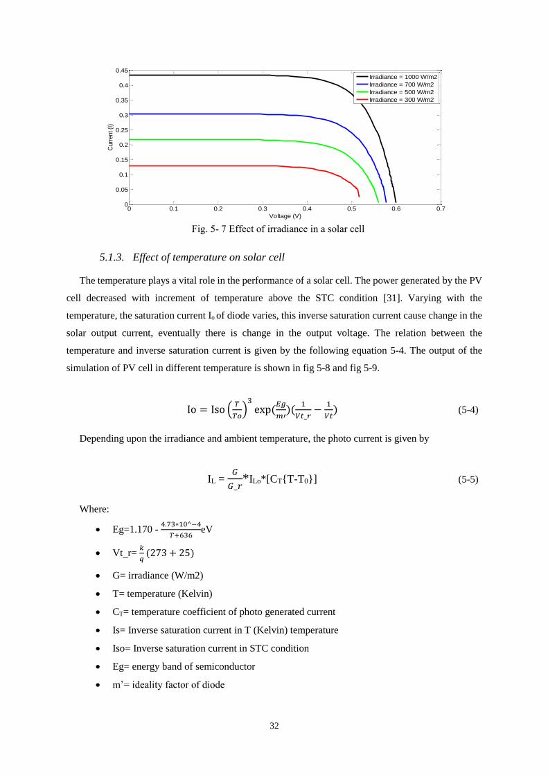
5.1.2. Effect of irradiance in the IV characteristics of the solar cell
The generation of photocurrent from the solar cell is dependent of the solar radiation. The radiation
having a certain range of frequency knot out the electron from the bond to the conduction band to form
an electron-hole pair [3]. The formation of electron-hole pair is depending upon the intensity of the light
i.e. more irradiance more generation of hole pair so this is why the irradiance plays a vital role in the
magnitude of generated current.
The relation of the irradiance and the generated current is given as
𝐼𝑠𝑐 =𝐺
𝐺𝑟∗ 𝐼𝑠𝑐_𝑟 (5-3)
Where
• Isc=Short circuit of a solar cell in a irradiance equal to G
• G= Value of Irradiance at short circuit equal to Isc
• Gr=Value of irradiance at reference condition i.e. 1000 W/m2
• Isc_r=Value of short circuit current in the reference condition
The effect of the variation in the irradiance is shown in the fig. 5-7. The value of the short circuit
current is given by the above equation, but the open circuit voltage is almost independent to the
irradiance, it is more dependent on the operating temperature of the cell.
0 0.1 0.2 0.3 0.4 0.5 0.6 0.70
0.05
0.1
0.15
0.2
0.25
0.3
0.35
0.4
0.45The effect of series resistance in a solar cell
Voltage (V)
Curr
ent (I
)
Rs=0.1 ohm
Rs=0.5 ohm
Rs=0.005 ohm
32
Fig. 5- 7 Effect of irradiance in a solar cell
5.1.3. Effect of temperature on solar cell
The temperature plays a vital role in the performance of a solar cell. The power generated by the PV
cell decreased with increment of temperature above the STC condition [31]. Varying with the
temperature, the saturation current Io of diode varies, this inverse saturation current cause change in the
solar output current, eventually there is change in the output voltage. The relation between the
temperature and inverse saturation current is given by the following equation 5-4. The output of the
simulation of PV cell in different temperature is shown in fig 5-8 and fig 5-9.
Io = Iso (𝑇
𝑇𝑜)3
exp(𝐸𝑔
𝑚′)(
1
𝑉𝑡_𝑟−
1
𝑉𝑡) (5-4)
Depending upon the irradiance and ambient temperature, the photo current is given by
IL =𝐺
𝐺_𝑟*ILo*[CTT-T0] (5-5)
Where:
• Eg=1.170 - 4.73∗10^−4
𝑇+636eV
• Vt_r= 𝑘
𝑞(273 + 25)
• G= irradiance (W/m2)
• T= temperature (Kelvin)
• CT= temperature coefficient of photo generated current
• Is= Inverse saturation current in T (Kelvin) temperature
• Iso= Inverse saturation current in STC condition
• Eg= energy band of semiconductor
• m’= ideality factor of diode
0 0.1 0.2 0.3 0.4 0.5 0.6 0.70
0.05
0.1
0.15
0.2
0.25
0.3
0.35
0.4
0.45
Voltage (V)
Curr
ent (I
)
Irradiance = 1000 W/m2
Irradiance = 700 W/m2
Irradiance = 500 W/m2
Irradiance = 300 W/m2

33
Fig. 5- 8 Effect of temperature on IV curve of a solar cell
Fig. 5- 9 Effect of Temperature on PV curve of a solar cell
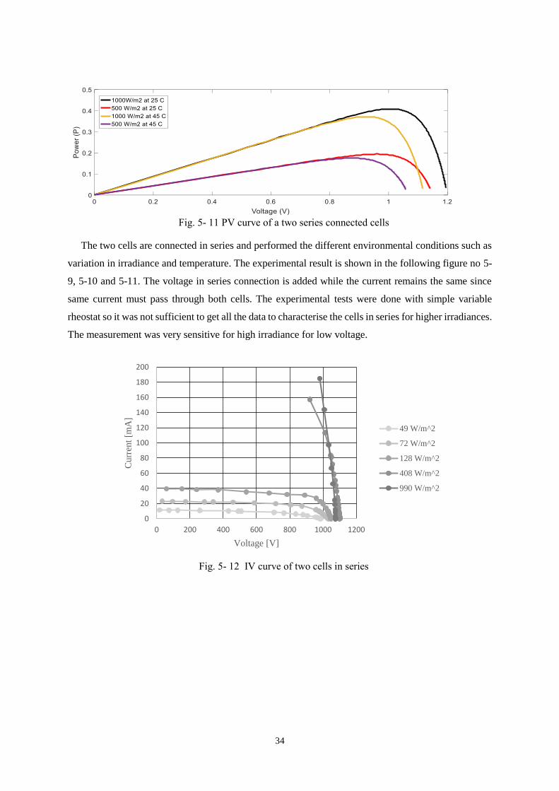
5.1.4. Two cells connected in series
The IV and PV characteristics for two cells connected in series with respect to different irradiance
and temperature are shown in the fig. 5-10 and 5-11. From the simulation results it can be concluded
that the temperature affects the open-circuit voltage whereas the irradiance affects the short circuit
current.
Fig. 5- 10 IV curve of two series connected cells
34
Fig. 5- 11 PV curve of a two series connected cells
The two cells are connected in series and performed the different environmental conditions such as
variation in irradiance and temperature. The experimental result is shown in the following figure no 5-
9, 5-10 and 5-11. The voltage in series connection is added while the current remains the same since
same current must pass through both cells. The experimental tests were done with simple variable
rheostat so it was not sufficient to get all the data to characterise the cells in series for higher irradiances.
The measurement was very sensitive for high irradiance for low voltage.
Fig. 5- 12 IV curve of two cells in series
0
20
40
60
80
100
120
140
160
180
200
0 200 400 600 800 1000 1200
Curr
ent
[mA
]
Voltage [V]
49 W/m^2
72 W/m^2
128 W/m^2
408 W/m^2
990 W/m^2

35
Fig. 5- 13 PV curve of two cells in series
The experiment shows that the short circuit current is highly dependent with the irradiance while the
voltage is not so much influence with the temperature. As the irradiance increases the current produced
by solar cell increases which can be seen in the table no 5-3. The higher the irradiance, higher the power
generation and higher the fill factor of a cell. Due to the inability of the experimental instrument all the
required data are not available here.
Table 5-3 – Parameter of the two cells in series from experiment
Irradiância [W/m2] 49 72 128 408 990
Cell temperature [ºC] 27,8 28,8 31,8 40 45
ISC [mA] 11,6 22,9 39,6
VOC [mV] 986 1031 1047 1101 1075
Imp [mA] 8,3 18,5 31,3
Vmp [mV] 705 805 890
Pmp [mW] 5,8
14,9 27,9
FF = 𝐼𝑚𝑝𝑝𝑉𝑚𝑝𝑝
𝐼𝑠𝑐𝑉𝑂𝐶 [%] 51,1 63,1 67,2
𝜂1 = 𝐼𝑚𝑝𝑝𝑉𝑚𝑝𝑝
𝐺∗𝐴𝐶∗𝑁 [%] 0,5 0,6 0,8
5.1.5. Effect of mismatch of the current
Mismatch of the current, produced by different cells in series makes adverse effect in the overall
generation of the power. It causes the current produced by the one cell having large current is limited
by another cell producing the less current. It doesn’t have significant effect on the voltage.The reason
0
5
10
15
20
25
30
0 200 400 600 800 1000 1200
Po
wer
[m
W]
Voltage [V]
P-V Characteristic
175 W/m^2
332 W/m^2
477 W/m^2
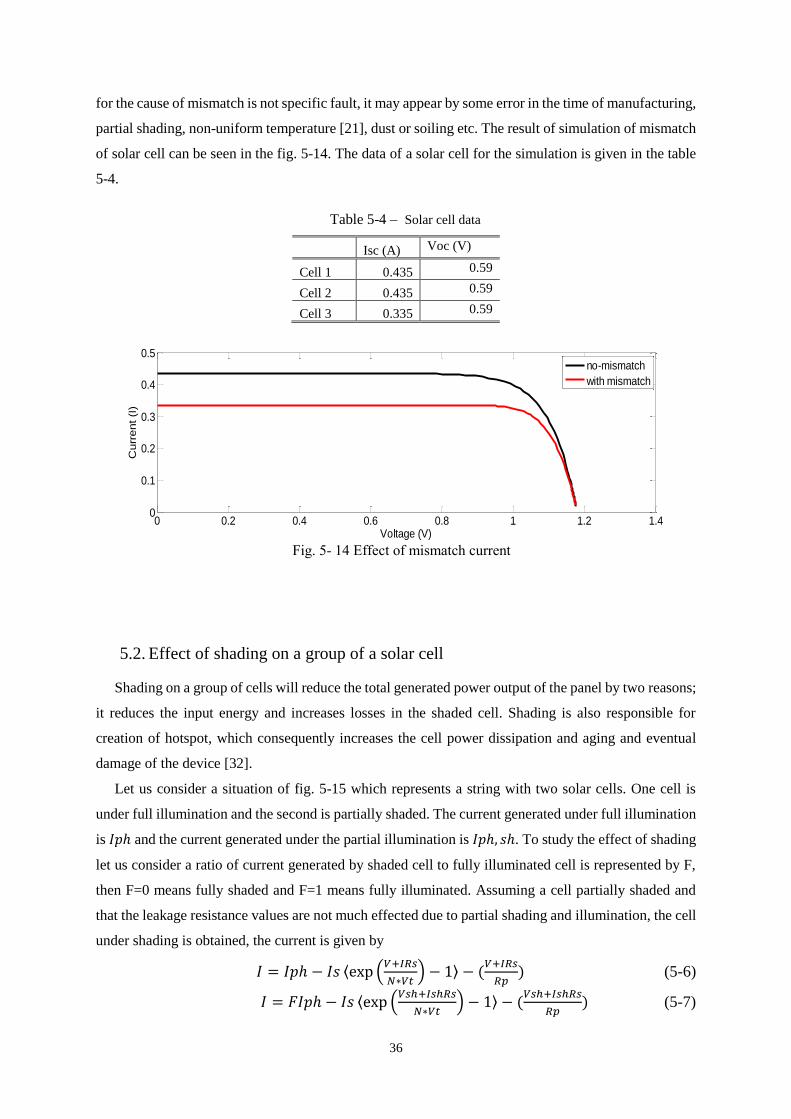
36
for the cause of mismatch is not specific fault, it may appear by some error in the time of manufacturing,
partial shading, non-uniform temperature [21], dust or soiling etc. The result of simulation of mismatch
of solar cell can be seen in the fig. 5-14. The data of a solar cell for the simulation is given in the table
5-4.
Table 5-4 – Solar cell data
Isc (A) Voc (V)
Cell 1 0.435 0.59
Cell 2 0.435 0.59
Cell 3 0.335 0.59
Fig. 5- 14 Effect of mismatch current
5.2. Effect of shading on a group of a solar cell
Shading on a group of cells will reduce the total generated power output of the panel by two reasons;
it reduces the input energy and increases losses in the shaded cell. Shading is also responsible for
creation of hotspot, which consequently increases the cell power dissipation and aging and eventual
damage of the device [32].
Let us consider a situation of fig. 5-15 which represents a string with two solar cells. One cell is
under full illumination and the second is partially shaded. The current generated under full illumination
is 𝐼𝑝ℎ and the current generated under the partial illumination is 𝐼𝑝ℎ, 𝑠ℎ. To study the effect of shading
let us consider a ratio of current generated by shaded cell to fully illuminated cell is represented by F,
then F=0 means fully shaded and F=1 means fully illuminated. Assuming a cell partially shaded and
that the leakage resistance values are not much effected due to partial shading and illumination, the cell
under shading is obtained, the current is given by
𝐼 = 𝐼𝑝ℎ − 𝐼𝑠 ⟨exp (𝑉+𝐼𝑅𝑠
𝑁∗𝑉𝑡) − 1⟩ − (
𝑉+𝐼𝑅𝑠
𝑅𝑝) (5-6)
𝐼 = 𝐹𝐼𝑝ℎ − 𝐼𝑠 ⟨exp (𝑉𝑠ℎ+𝐼𝑠ℎ𝑅𝑠
𝑁∗𝑉𝑡) − 1⟩ − (
𝑉𝑠ℎ+𝐼𝑠ℎ𝑅𝑠
𝑅𝑝) (5-7)
0 0.2 0.4 0.6 0.8 1 1.2 1.40
0.1
0.2
0.3
0.4
0.5
Voltage (V)
Curr
ent (I
)
no-mismatch
with mismatch

37
Fig. 5- 15 Schematic model of two cells in series
As the extent of shading increases, the exponential term tends to zero [32] and hence the shaded cell
voltage and voltage across string can be approximated as
𝑉𝑠ℎ = (𝐹𝑙𝑝ℎ, 𝑠ℎ − 𝐼) + 𝐼𝑅𝑠 (5-8)
𝑉 = 𝑉𝑖 + 𝑉𝑠ℎ (5-9)
Finally, the power dissipated by the shaded cell may be obtained as
𝑃𝑑𝑖𝑠 = 𝐼(𝐹𝑙𝑝ℎ, 𝑠ℎ − 𝐼) + 𝐼𝑅𝑠 (5-10)
The effect of shading is studied with the help of three solar cells, they are connected in series and
performed different simulation to study of the shading effect on the output IV curve of the group of a
cell. In this simulation, the first case is the normal uniform irradiance in all cell of 1000W/m2. In the
second case, the irradiance is kept constant for two outsider’s cells and the middle one was given
700W/m2, without bypass diode, and in final case the bypass diode is used as shown in the fig. 5-16
Fig. 5- 16Three cells in series connection
Table 5-5 – Simulation of 3 cells
Case Irradiance
Cell A Cell B Cell C
Case A (normal) 1000 1000 1000
Case B 1000 700 1000
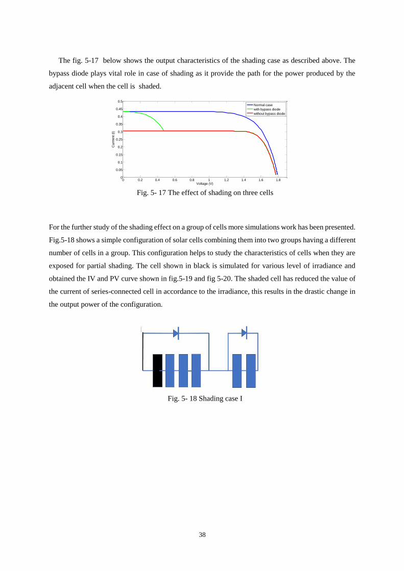
38
The fig. 5-17 below shows the output characteristics of the shading case as described above. The
bypass diode plays vital role in case of shading as it provide the path for the power produced by the
adjacent cell when the cell is shaded.
Fig. 5- 17 The effect of shading on three cells
For the further study of the shading effect on a group of cells more simulations work has been presented.
Fig.5-18 shows a simple configuration of solar cells combining them into two groups having a different
number of cells in a group. This configuration helps to study the characteristics of cells when they are
exposed for partial shading. The cell shown in black is simulated for various level of irradiance and
obtained the IV and PV curve shown in fig.5-19 and fig 5-20. The shaded cell has reduced the value of
the current of series-connected cell in accordance to the irradiance, this results in the drastic change in
the output power of the configuration.
Fig. 5- 18 Shading case I
0 0.2 0.4 0.6 0.8 1 1.2 1.4 1.6 1.80
0.05
0.1
0.15
0.2
0.25
0.3
0.35
0.4
0.45
0.5
Voltage (V)
Curr
rent (I
)
Normal case
with bypass diode
without bypass diode
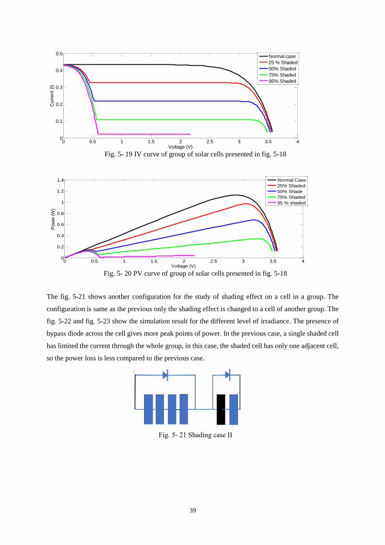
39
Fig. 5- 19 IV curve of group of solar cells presented in fig. 5-18
Fig. 5- 20 PV curve of group of solar cells presented in fig. 5-18
The fig. 5-21 shows another configuration for the study of shading effect on a cell in a group. The
configuration is same as the previous only the shading effect is changed to a cell of another group. The
fig. 5-22 and fig. 5-23 show the simulation result for the different level of irradiance. The presence of
bypass diode across the cell gives more peak points of power. In the previous case, a single shaded cell
has limited the current through the whole group, in this case, the shaded cell has only one adjacent cell,
so the power loss is less compared to the previous case.
Fig. 5- 21 Shading case II
0 0.5 1 1.5 2 2.5 3 3.5 40
0.1
0.2
0.3
0.4
0.5
Voltage (V)
Curr
ent (I
)
Normal case
25 % Shaded
50% Shaded
75% Shaded
95% Shaded
0 0.5 1 1.5 2 2.5 3 3.5 40
0.2
0.4
0.6
0.8
1
1.2
1.4
Voltage (V)
Pow
er
(W)
Normal Case
25% Shaded
50% Shade
75% Shaded
95 % shaded
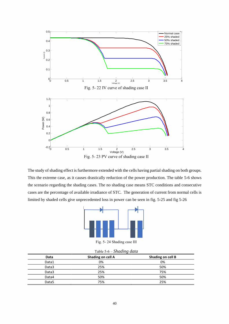
40
Fig. 5- 22 IV curve of shading case II
Fig. 5- 23 PV curve of shading case II
The study of shading effect is furthermore extended with the cells having partial shading on both groups.
This the extreme case, as it causes drastically reduction of the power production. The table 5-6 shows
the scenario regarding the shading cases. The no shading case means STC conditions and consecutive
cases are the percentage of available irradiance of STC. The generation of current from normal cells is
limited by shaded cells give unprecedented loss in power can be seen in fig. 5-25 and fig 5-26
Fig. 5- 24 Shading case III
Table 5-6 – Shading data
Data Shading on cell A Shading on cell B
Data1 0% 0%
Data3 25% 50%
Data3 25% 75%
Data4 50% 50%
Data5 75% 25%
0 0.5 1 1.5 2 2.5 3 3.5 40
0.1
0.2
0.3
0.4
0.5
Voltage (V)
Curr
ent
(I)
Normal case
25% shaded
50% shaded
75% shaded
0 0.5 1 1.5 2 2.5 3 3.5 4-0.2
0
0.2
0.4
0.6
0.8
1
1.2
Voltage (V)
Pow
er
(W)
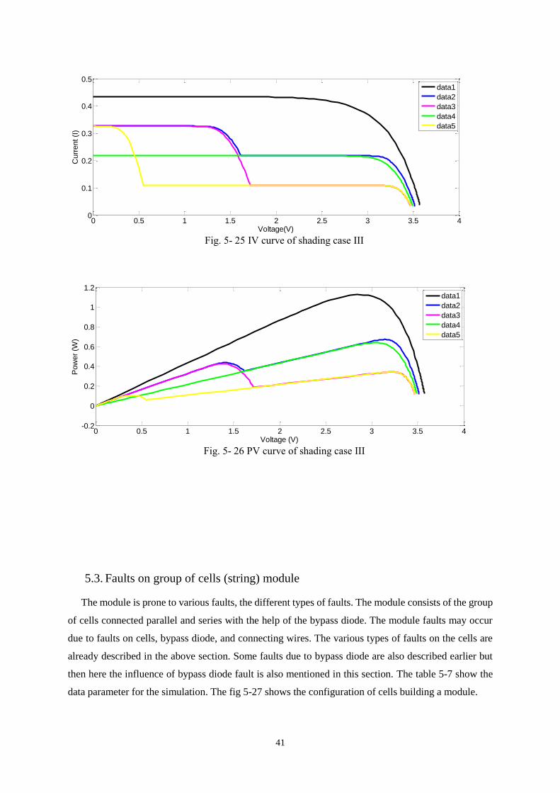
41
Fig. 5- 25 IV curve of shading case III
Fig. 5- 26 PV curve of shading case III
5.3. Faults on group of cells (string) module
The module is prone to various faults, the different types of faults. The module consists of the group
of cells connected parallel and series with the help of the bypass diode. The module faults may occur
due to faults on cells, bypass diode, and connecting wires. The various types of faults on the cells are
already described in the above section. Some faults due to bypass diode are also described earlier but
then here the influence of bypass diode fault is also mentioned in this section. The table 5-7 show the
data parameter for the simulation. The fig 5-27 shows the configuration of cells building a module.
0 0.5 1 1.5 2 2.5 3 3.5 40
0.1
0.2
0.3
0.4
0.5
Voltage(V)
Curr
ent (I
)
data1
data2
data3
data4
data5
0 0.5 1 1.5 2 2.5 3 3.5 4-0.2
0
0.2
0.4
0.6
0.8
1
1.2
Voltage (V)
Pow
er
(W)
data1
data2
data3
data4
data5
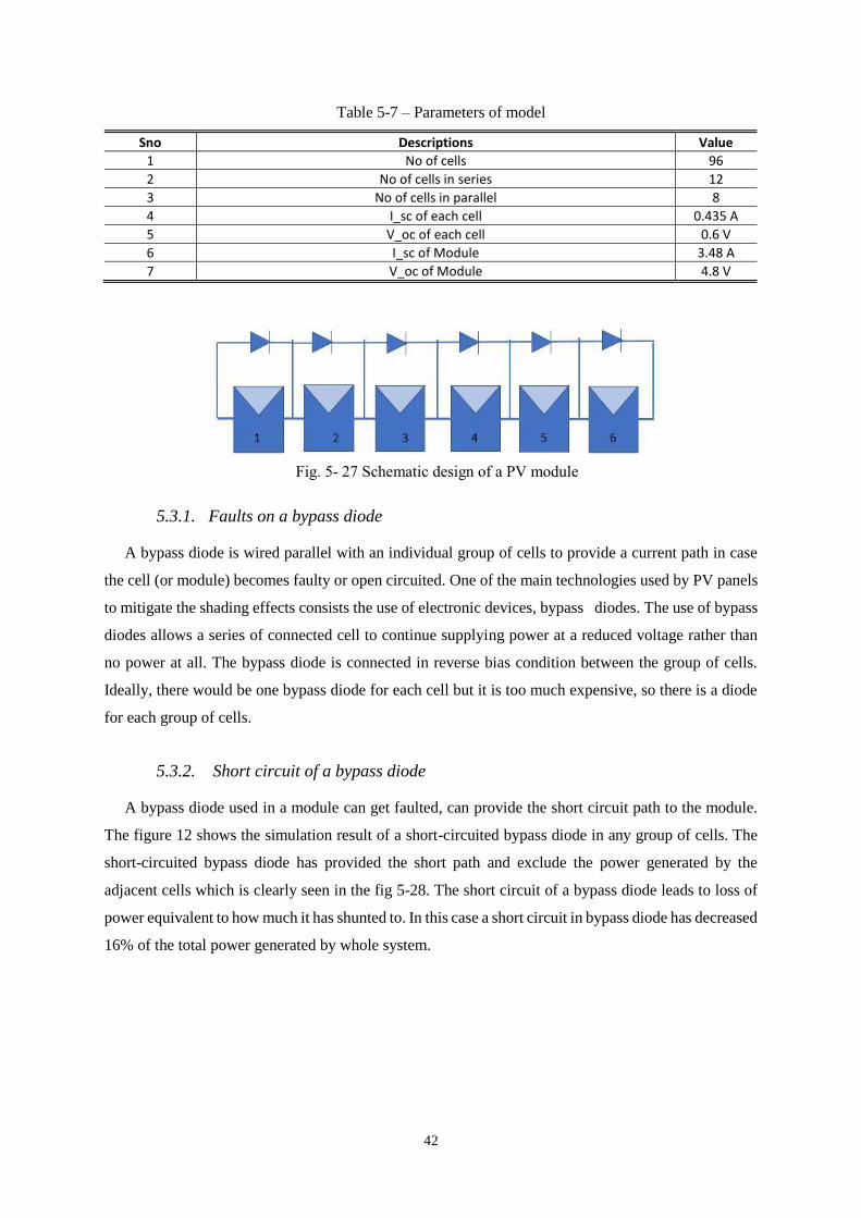
42
Table 5-7 – Parameters of model
Sno Descriptions Value
1 No of cells 96
2 No of cells in series 12
3 No of cells in parallel 8
4 I_sc of each cell 0.435 A
5 V_oc of each cell 0.6 V
6 I_sc of Module 3.48 A
7 V_oc of Module 4.8 V
Fig. 5- 27 Schematic design of a PV module
5.3.1. Faults on a bypass diode
A bypass diode is wired parallel with an individual group of cells to provide a current path in case
the cell (or module) becomes faulty or open circuited. One of the main technologies used by PV panels
to mitigate the shading effects consists the use of electronic devices, bypass diodes. The use of bypass
diodes allows a series of connected cell to continue supplying power at a reduced voltage rather than
no power at all. The bypass diode is connected in reverse bias condition between the group of cells.
Ideally, there would be one bypass diode for each cell but it is too much expensive, so there is a diode
for each group of cells.
5.3.2. Short circuit of a bypass diode
A bypass diode used in a module can get faulted, can provide the short circuit path to the module.
The figure 12 shows the simulation result of a short-circuited bypass diode in any group of cells. The
short-circuited bypass diode has provided the short path and exclude the power generated by the
adjacent cells which is clearly seen in the fig 5-28. The short circuit of a bypass diode leads to loss of
power equivalent to how much it has shunted to. In this case a short circuit in bypass diode has decreased
16% of the total power generated by whole system.
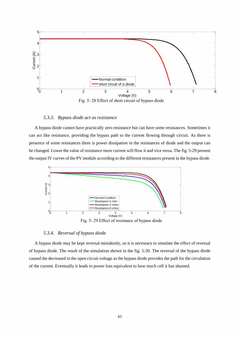
43
Fig. 5- 28 Effect of short circuit of bypass diode
5.3.3. Bypass diode act as resistance
A bypass diode cannot have practically zero resistance but can have some resistances. Sometimes it
can act like resistance, providing the bypass path to the current flowing through circuit. As there is
presence of some resistances there is power dissipation in the resistances of diode and the output can
be changed. Lower the value of resistance more current will flow it and vice versa. The fig. 5-29 present
the output IV curves of the PV module according to the different resistances present in the bypass diode.
Fig. 5- 29 Effect of resistance of bypass diode
5.3.4. Reversal of bypass diode
A bypass diode may be kept reversal mistakenly, so it is necessary to simulate the effect of reversal
of bypass diode. The result of the simulation shown in the fig. 5-30. The reversal of the bypass diode
caused the decreased in the open circuit voltage as the bypass diode provides the path for the circulation
of the current. Eventually it leads to power loss equivalent to how much cell it has shunted.
0 1 2 3 4 5 6 7 80
1
2
3
4
5
Voltage (V)
Curr
ent (A
)
Normal condition
short circuit of a diode
0 1 2 3 4 5 6 7 80
1
2
3
4
5
Voltage (V)
Curr
ent (I
)
Normal Condition
Resistance=1 ohm
Resistance=2 ohms
Resistance=5 ohms

44
Fig. 5- 30 Reversal of a bypass diode
5.3.5. Simulation of module of three group of cells
The data for the following PV modules are present in the below table 5-8 and output curve can be
seen in fig. 5-31. The table 5-9 presents power available in the different non-normal conditions. The
major power loss occurs during shading followed by fault in bypass diode and increase in series
resistance.
Table 5-8 – Datasheet of a PV String
Sno Description Value
1 Open circuit voltage (Voc) 38.5 V
2 Short ciruit current (Isc) 9.43 A
3 Voltage at maximum power (Vmp) 31.5 V
4 Current at maximum power (Imp) 8.89 A
5 Temperature coeffcient of Voc -0.31 V/K
6 Temperature coefficient of Isc -0.053 A/K
Fig. 5- 31 IV curves of PV panel in different working conditions
Table 5-9 – Power available in the different non-normal conditions
Sno Condition Power Available (W) Power avaliable (%) Power lost (%)
1 STC 271.7 100 0
2 50% Shading 138.8 51.11 48.8
3 Series resistance (0.5 Ω) 204.1 75.13 24.8
4 Effect of temp (60 °C) 250.7 92.27 7.7
5 Short circuit of 1 BP diode 178.6 65.74 34.2
0 1 2 3 4 5 6 7 80
1
2
3
4
5
Voltage (V)
Curr
ent (I
)
Normal Condition
Reversal of one bypass diode
Reversal of one bypass diode and shading on other cells
0
2
4
6
8
10
12
0 5 10 15 20 25 30 35 40 45
STC
50% shading
With series resistance
Effect of temp
short_ckt_of 1byapass
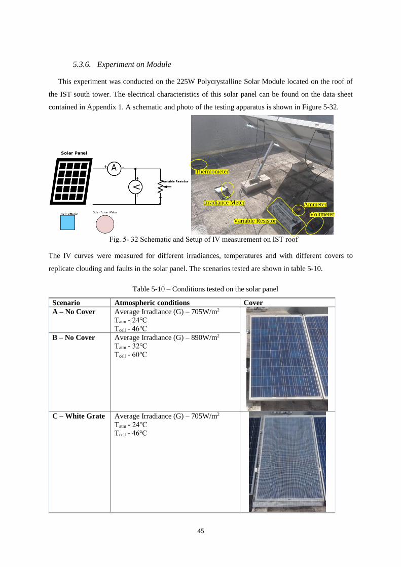
45
5.3.6. Experiment on Module
This experiment was conducted on the 225W Polycrystalline Solar Module located on the roof of
the IST south tower. The electrical characteristics of this solar panel can be found on the data sheet
contained in Appendix 1. A schematic and photo of the testing apparatus is shown in Figure 5-32.
Fig. 5- 32 Schematic and Setup of IV measurement on IST roof
The IV curves were measured for different irradiances, temperatures and with different covers to
replicate clouding and faults in the solar panel. The scenarios tested are shown in table 5-10.
Table 5-10 – Conditions tested on the solar panel
Scenario Atmospheric conditions Cover
A – No Cover Average Irradiance (G) – 705W/m2
Tatm - 24
Tcell - 46
B – No Cover Average Irradiance (G) – 890W/m2
Tatm - 32
Tcell - 60
C – White Grate Average Irradiance (G) – 705W/m2
Tatm - 24
Tcell - 46
Thermometer
Irradiance Meter
Variable Resistor
Ammeter
Voltmeter

46
D – Bubble
Wrap
Average Irradiance (G) – 875W/m2
Tatm – 31.5
Tcell - 59
E – 2/3rds
covered
Average Irradiance (G) – 820W/m2
Tatm - 25
Tcell - 51
F – 2/3rds
covered
Average Irradiance (G) – 900W/m2
Tatm - 32
Tcell - 60
G – 1/3rd
covered
Average Irradiance (G) – 800W/m2
Tatm - 26
Tcell - 51
H – 1 Square
covered
Average Irradiance (G) – 810W/m2
Tatm – 24.5
Tcell - 50

47
I – Bottom half
covered
Average Irradiance (G) – 770W/m2
Tatm – 24.5
Tcell - 49
The different experimental scenario shows different IV characteristic of the panel. The first
experiment was done for normal (No cover) case with different in temperature and irradiance, it gives
the normal IV curve but higher short circuit in higher irradiance which can be seen in the figure 6-30.
Similarly, in the case C and D a transparent sheet is used to covet the panel but with different manner
once with fine wrap and another with bubble wrap, in this scenario there is no such significant difference
in these two scenarios. The case E, F and G present the case of the shading (1/3 and 2/3), the shading
cause the evolution of notches in the IV curves, higher the shading region, lower will be the power. The
case H represents where only one cell is shaded completely, this give the IV curve as in the case G, this
is the that this cell is connected series with other cell and there no way for current to flow from its group
of cells. The last case, I is the case where shading is done for bottom part of the panel, since the cell of
the panel are connected series (upside-down), there no way for the flow of the current, so this gives the
no power to output of the system which can be seen in the fig 5-33. [Source:**]
Fig. 5- 33 Curves measured on a solar panel under different scenarios
0
1
2
3
4
5
6
7
8
9
0 5 10 15 20 25 30 35 40
Curr
ent
[I]
Voltage [V]
A B C
D E F
G H I

48
5.4. Fault on a String of modules
5.4.1. Effect of Partial shading
The major fault or non-operating condition of PV string is the partial shading. Simulaton clearly
shows how the different irradiance effects the output of characteristics of a system. Here, the three
number of panels are connected in series and they are exposed to different irradiance but each panel has
uniform irradiance, this gives the condition of partial shading. The output IV and PV graph are presented
below. The partial shading causes high output power reduction in the operation of MPPT.
A bypass diode used in a module can get faulted and provide the short circuit path to the module.
Fig 5-28 shows the simulation result of a short-circuited bypass diode in any group of cells. The short-
circuited bypass diode has provided the short path and exclude the power generated by the adjacent
cells which are clearly seen in the fig 5-34.
Fig. 5- 34 Effect of shading on IV and PV curve
For the further study of the partial shading and other expected faults, a model is designed for the
simulations and experiments. The data parameter of module is given in table 5-11. The data presented
in the table 5-10 is the overall value of system not of a single module. The different faults are simulated
individually and graphs has presented. The fig 5-35 shows the simulation configuration for Matlab
where three modules are connected in series and fig. 5-36 shows the output of IV and PV curve of
simulation.
Table 5-11 – Datasheet of a PV module
Sno Description Value
1 Open circuit voltage (Voc) 38.5 V
2 Short ciruit current (Isc) 9.43 A
3 Voltage at maximum power (Vmp) 31.5 V
4 Current at maximum power (Imp) 8.89 A
5 Temperature coeff of Voc -0.31 V/K
6 Temperature of Isc -0.053 A/K

49
Fig. 5- 35 Simulation configuration for partial shading
Fig. 5- 36 IV and PV curves of 3 modules connected in series
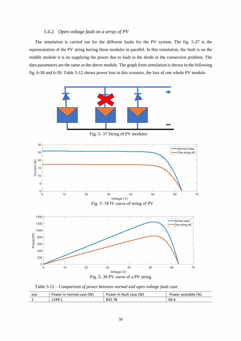
50
5.4.2. Open voltage fault on a array of PV
The simulation is carried out for the different faults for the PV system. The fig. 5-37 is the
representation of the PV string having three modules in parallel. In this simulation, the fault is on the
middle module it is no supplying the power due to fault in the diode or the connection problem. The
data parameters are the same as the above module. The graph from simulation is shown in the following
fig. 6-38 and 6-39. Table 5-12 shows power loss in this scenario, the loss of one whole PV module.
Fig. 5- 38 IV curve of string of PV
Fig. 5- 39 PV curve of a PV string
Table 5-12 – Comparison of power between normal and open voltage fault case
sno Power in normal case (W) Power in fault case (W) Power available (%)
1 1249.1 832.78 66.6
Fig. 5- 37 String of PV modules

51
5.4.3. Degradation of PV string
The degradation of the PV module occurs because of the continues exposers in the various
environmental conditions. It has to withstands the rains, hailstone, dust particles, ultra violet rays [21]
etc. This kind of degradation leads to the increase in the series resistances as shown in figure 5-40. The
degradation is simulated as the increment of the series resistance (0.5 Ω in 10 years) in a module and
simulation is carried out. From the simulation, the power degradation of PV module can be calculated.
The comparison of IV and PV curves between this time interval can be seen in fig 5-41 and 5-42. From
this simulation the power decrement for 10 years of time is 7.75%. This is not the precise value but it
can be taken as reference. The value is given in the table below 5-13.
Fig. 5- 41 IV curve of a string
Fig. 5- 42 PV curve of a string
Fig. 5- 40 Strings of PV modules

52
Table 5-13 – Comparison of power before and after degradation of PV panel
sno Power in Normal condition (W) Power with degradion (W) Power available (%)
1 1249.18 1152.3 92.
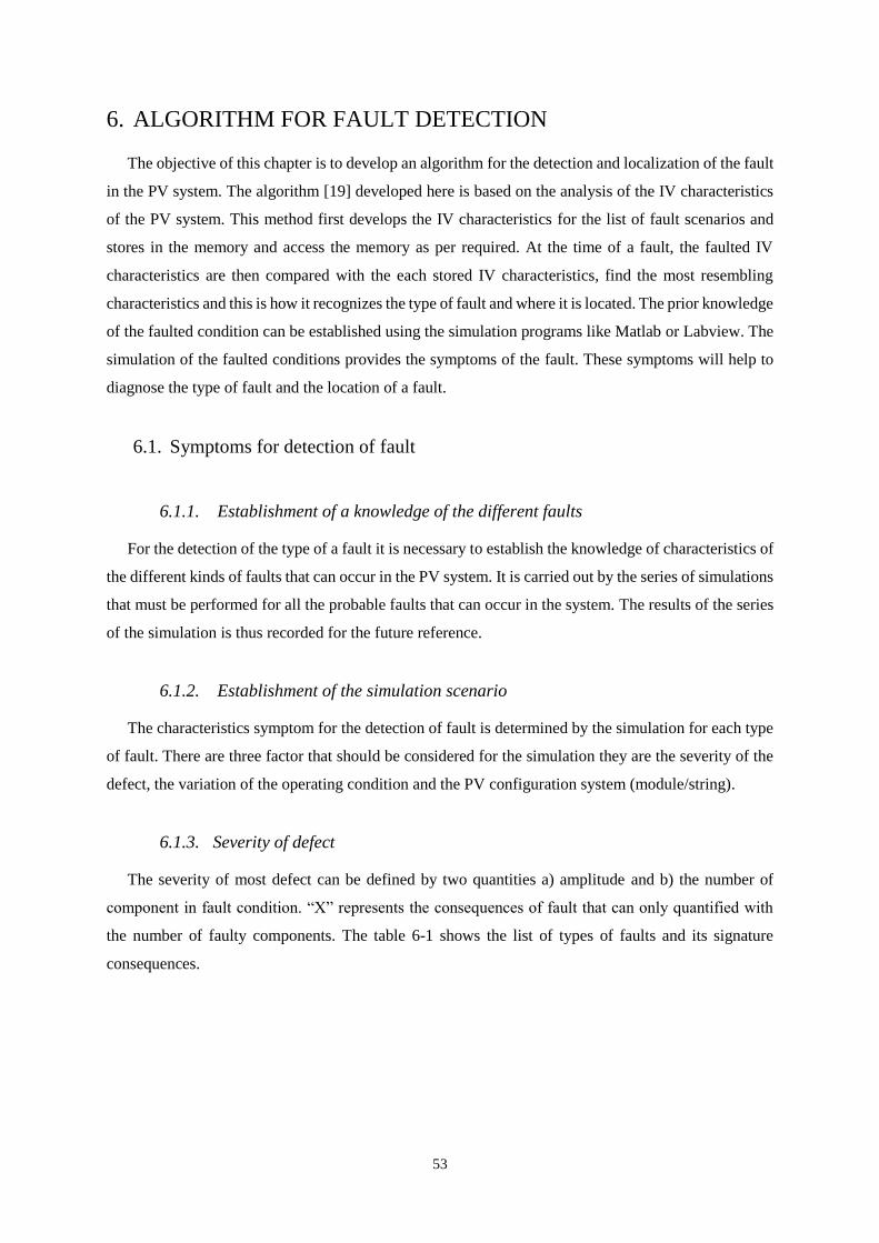
53
6. ALGORITHM FOR FAULT DETECTION
The objective of this chapter is to develop an algorithm for the detection and localization of the fault
in the PV system. The algorithm [19] developed here is based on the analysis of the IV characteristics
of the PV system. This method first develops the IV characteristics for the list of fault scenarios and
stores in the memory and access the memory as per required. At the time of a fault, the faulted IV
characteristics are then compared with the each stored IV characteristics, find the most resembling
characteristics and this is how it recognizes the type of fault and where it is located. The prior knowledge
of the faulted condition can be established using the simulation programs like Matlab or Labview. The
simulation of the faulted conditions provides the symptoms of the fault. These symptoms will help to
diagnose the type of fault and the location of a fault.
6.1. Symptoms for detection of fault
6.1.1. Establishment of a knowledge of the different faults
For the detection of the type of a fault it is necessary to establish the knowledge of characteristics of
the different kinds of faults that can occur in the PV system. It is carried out by the series of simulations
that must be performed for all the probable faults that can occur in the system. The results of the series
of the simulation is thus recorded for the future reference.
6.1.2. Establishment of the simulation scenario
The characteristics symptom for the detection of fault is determined by the simulation for each type
of fault. There are three factor that should be considered for the simulation they are the severity of the
defect, the variation of the operating condition and the PV configuration system (module/string).
6.1.3. Severity of defect
The severity of most defect can be defined by two quantities a) amplitude and b) the number of
component in fault condition. “X” represents the consequences of fault that can only quantified with
the number of faulty components. The table 6-1 shows the list of types of faults and its signature
consequences.
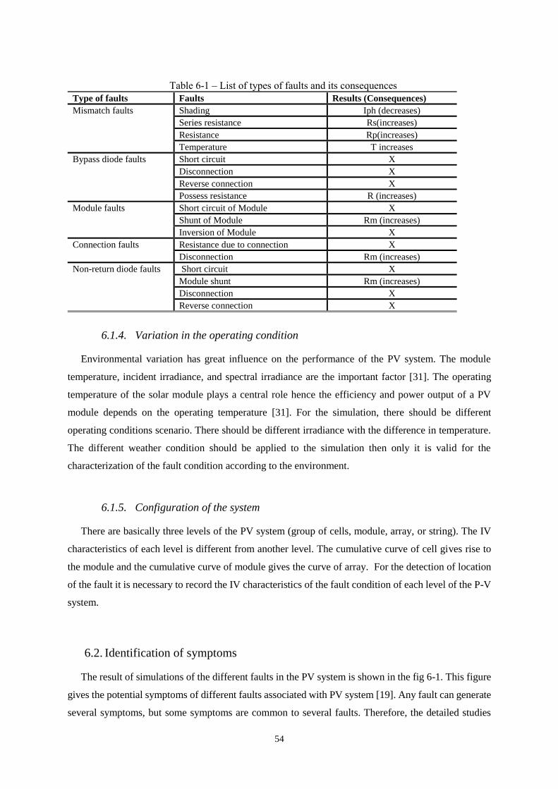
54
Table 6-1 – List of types of faults and its consequences
Type of faults Faults Results (Consequences)
Mismatch faults Shading Iph (decreases)
Series resistance Rs(increases)
Resistance Rp(increases)
Temperature T increases
Bypass diode faults Short circuit X
Disconnection X
Reverse connection X
Possess resistance R (increases)
Module faults Short circuit of Module X
Shunt of Module Rm (increases)
Inversion of Module X
Connection faults Resistance due to connection X
Disconnection Rm (increases)
Non-return diode faults Short circuit X
Module shunt Rm (increases)
Disconnection X
Reverse connection X
6.1.4. Variation in the operating condition
Environmental variation has great influence on the performance of the PV system. The module
temperature, incident irradiance, and spectral irradiance are the important factor [31]. The operating
temperature of the solar module plays a central role hence the efficiency and power output of a PV
module depends on the operating temperature [31]. For the simulation, there should be different
operating conditions scenario. There should be different irradiance with the difference in temperature.
The different weather condition should be applied to the simulation then only it is valid for the
characterization of the fault condition according to the environment.
6.1.5. Configuration of the system
There are basically three levels of the PV system (group of cells, module, array, or string). The IV
characteristics of each level is different from another level. The cumulative curve of cell gives rise to
the module and the cumulative curve of module gives the curve of array. For the detection of location
of the fault it is necessary to record the IV characteristics of the fault condition of each level of the P-V
system.
6.2. Identification of symptoms
The result of simulations of the different faults in the PV system is shown in the fig 6-1. This figure
gives the potential symptoms of different faults associated with PV system [19]. Any fault can generate
several symptoms, but some symptoms are common to several faults. Therefore, the detailed studies

55
should be carried out to figure out the exact fault in the system. Basically, there are four zones that can
be affected by the fault in the PV system. The first zone is the zone 1, is a zone of the open circuit
voltage. Zone 2 is the zone of the short circuit current. Similarly, zone 3 is the zone of in between the
open circuit voltage and short circuit current. Finally, zone 4 represent the slope of either short-circuit
current or open circuit voltage. Table 6-2 presents the symptoms, its effecting area and its consequences.
Fig. 6- 1 Characteristics IV curves of PV modules in different scenarios
Table 6-2 – Symptoms of the faults and its occurring zones
Symptom Area of Characteristic IV Symptom Name
S1 Reduction of maximum power
S2 Zone1 Reduction of the open circuit voltage
S3 Zone2 Reduction of short-circuit current
S4 Zone3 Presence of one or more inflection points
S5 Zone4 Deviation of the slope
The symptom “S1” is the first symptom that can be identified from the comparison because it is
obvious that any fault will lead to a loss of the power produced. The main difference is the magnitude
of power loss. On the other hand, this observation is not always true because certain faults do not lead
to any loss of power e.g. disconnection of bypass diode.

56
The symptom “S2” is the difference between the open circuit voltage of the PV system in normal
operation condition and the faulty condition. This symptom helps to figure out the problem with the
open circuit voltage faults. In the following part, the types of faults associated with open circuit voltage
has been described.
The symptom “S3” is the difference between the short circuit current of the PV system in normal
operating condition and faulty condition. This symptom helps to identify the problem with the short
circuit current faults. In the following part, the types of faults associated with open circuit voltage has
been described.
The symptom “S4” is based on the presence of one or more inflection points. These inflection points
are results from the conduction of one or more bypass diode in case of shading. Partial shading is the
major cause for this kind of fault.
The symptom “S5” refers to deviation of the slope of IV curve at the faulty condition as compared
to the normal operating condition. This deviation is caused by the parasitic resistance appeared in the
solar cell and other external wire resistances.
6.3. Evolution of symptoms as the function of the severity of faults
Symptoms are generated by comparing the IV characteristics of a PV system in normal operating
condition with the faulty condition. Some examples are presented here.
6.3.1. Evolution of symptom as a function of the severity of faults
The IV characteristic of a faulty PV system will change with severity of the faults. The evolution of
the symptom depends upon the magnitude of fault and the number of the components in the faults
condition as shown in fig. 6-2 to 6-4.
Fig. 6- 2 Effect of resistance
0 0.1 0.2 0.3 0.4 0.5 0.6 0.70
0.05
0.1
0.15
0.2
0.25
0.3
0.35
0.4
0.45The effect of series resistance in a solar cell
Voltage (V)
Curr
ent (I
)
Rs=0.1 ohm
Rs=0.5 ohm
Rs=0.005 ohm

57
Fig. 6- 3 Effect of temperature
Fig. 6- 4 Short circuit of bypass diode
6.3.2. Evolution of symptom as a function of the operating condition
The fig. 6-5 shows the influence of the irradiance in the IV curve of the PV cell. Irradiance primarily
affects the short-circuit current of the solar cell. The relation between the short circuit current and the
irradiance is given by equation (6-1).
Isc=G/Gr*Isc_r (6-1)
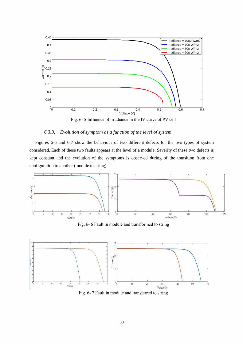
58
Fig. 6- 5 Influence of irradiance in the IV curve of PV cell
6.3.3. Evolution of symptom as a function of the level of system
Figures 6-6 and 6-7 show the behaviour of two different defects for the two types of system
considered. Each of these two faults appears at the level of a module. Severity of these two defects is
kept constant and the evolution of the symptoms is observed during of the transition from one
configuration to another (module to string).
Fig. 6- 6 Fault in module and transformed to string
Fig. 6- 7 Fault in module and transferred to string
0 0.1 0.2 0.3 0.4 0.5 0.6 0.70
0.05
0.1
0.15
0.2
0.25
0.3
0.35
0.4
0.45
Voltage (V)
Curr
ent (I
)
Irradiance = 1000 W/m2
Irradiance = 700 W/m2
Irradiance = 500 W/m2
Irradiance = 300 W/m2
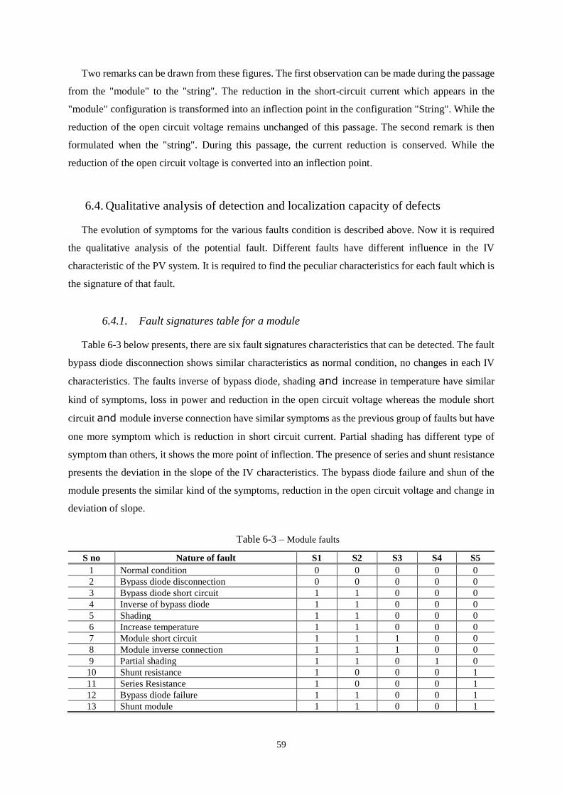
59
Two remarks can be drawn from these figures. The first observation can be made during the passage
from the "module" to the "string". The reduction in the short-circuit current which appears in the
"module" configuration is transformed into an inflection point in the configuration "String". While the
reduction of the open circuit voltage remains unchanged of this passage. The second remark is then
formulated when the "string". During this passage, the current reduction is conserved. While the
reduction of the open circuit voltage is converted into an inflection point.
6.4. Qualitative analysis of detection and localization capacity of defects
The evolution of symptoms for the various faults condition is described above. Now it is required
the qualitative analysis of the potential fault. Different faults have different influence in the IV
characteristic of the PV system. It is required to find the peculiar characteristics for each fault which is
the signature of that fault.
6.4.1. Fault signatures table for a module
Table 6-3 below presents, there are six fault signatures characteristics that can be detected. The fault
bypass diode disconnection shows similar characteristics as normal condition, no changes in each IV
characteristics. The faults inverse of bypass diode, shading and increase in temperature have similar
kind of symptoms, loss in power and reduction in the open circuit voltage whereas the module short
circuit and module inverse connection have similar symptoms as the previous group of faults but have
one more symptom which is reduction in short circuit current. Partial shading has different type of
symptom than others, it shows the more point of inflection. The presence of series and shunt resistance
presents the deviation in the slope of the IV characteristics. The bypass diode failure and shun of the
module presents the similar kind of the symptoms, reduction in the open circuit voltage and change in
deviation of slope.
Table 6-3 – Module faults
S no Nature of fault S1 S2 S3 S4 S5
1 Normal condition 0 0 0 0 0
2 Bypass diode disconnection 0 0 0 0 0
3 Bypass diode short circuit 1 1 0 0 0
4 Inverse of bypass diode 1 1 0 0 0
5 Shading 1 1 0 0 0
6 Increase temperature 1 1 0 0 0
7 Module short circuit 1 1 1 0 0
8 Module inverse connection 1 1 1 0 0
9 Partial shading 1 1 0 1 0
10 Shunt resistance 1 0 0 0 1
11 Series Resistance 1 0 0 0 1
12 Bypass diode failure 1 1 0 0 1
13 Shunt module 1 1 0 0 1

60
6.4.2. Fault signatures table for a string
The following table 6-4 shows the signature characteristics for a string. The concept of construction
of the table is same as it is done for module. The faults (connection fault) are introduced in this case.
Table 6-4 – String faults
Nature of fault S1 S2 S3 S4 S5
Normal condition 0 0 0 0 0
Bypass diode disconnection 0 0 0 0 0
Bypass diode short circuit 1 1 0 0 0
Inverse of bypass diode 1 1 0 0 0
Shading 1 1 0 0 0
Increase temperature 1 1 0 0 0
Module short circuit 1 1 1 0 0
Module inverse connection 1 1 1 0 0
Partial shading 1 1 0 1 0
Shunt resistance 1 0 0 0 1
Series Resistance 1 0 0 0 1
Bypass diode failure 1 1 0 0 1
Shunt module 1 1 0 0 1
The qualitative analysis of the faults detection is required for the determining the fault and its
location. The characteristics of each fault remains the same when the fault is at module or at the string.
The symptom “S1” appears for all the defects so this symptom doesn’t contribute to identify the fault.
Therefore, it is necessary to exclude this symptom and examine the symptom “S2 to S5”. When these
symptoms were identified, the signature table is constructed for the diagnosis of the faults. This analysis
is done with the comparison of the healthy and faulted P-V system.
6.4.3. Flow chart
The flow chart for the above algorithm is shown in the fig. 6-8. The flow chart has two starting
process as there are two different scenarios. First flow chart follows the storing of all non-normal
operating conditions associated with PV system, it follows the storing of different symptoms while
another measure the physical parameters that has influence the PV system in real time. After storing of
all the non-normal conditions, it is used to compare with the real-time data. The comparison of the data
acquired in real time by microcontroller gives the fault that occurred.

61
Fig. 6- 8 Flow chart

62
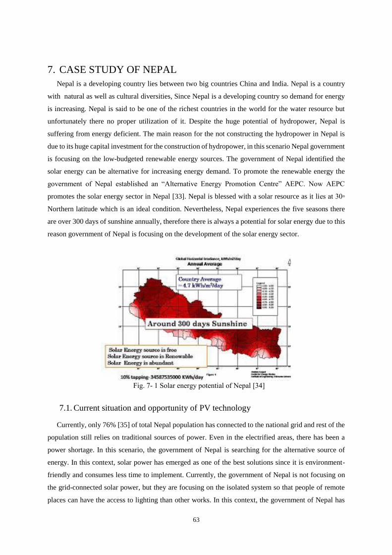
63
7. CASE STUDY OF NEPAL
Nepal is a developing country lies between two big countries China and India. Nepal is a country
with natural as well as cultural diversities, Since Nepal is a developing country so demand for energy
is increasing. Nepal is said to be one of the richest countries in the world for the water resource but
unfortunately there no proper utilization of it. Despite the huge potential of hydropower, Nepal is
suffering from energy deficient. The main reason for the not constructing the hydropower in Nepal is
due to its huge capital investment for the construction of hydropower, in this scenario Nepal government
is focusing on the low-budgeted renewable energy sources. The government of Nepal identified the
solar energy can be alternative for increasing energy demand. To promote the renewable energy the
government of Nepal established an “Alternative Energy Promotion Centre” AEPC. Now AEPC
promotes the solar energy sector in Nepal [33]. Nepal is blessed with a solar resource as it lies at 30
Northern latitude which is an ideal condition. Nevertheless, Nepal experiences the five seasons there
are over 300 days of sunshine annually, therefore there is always a potential for solar energy due to this
reason government of Nepal is focusing on the development of the solar energy sector.
Fig. 7- 1 Solar energy potential of Nepal [34]
7.1. Current situation and opportunity of PV technology
Currently, only 76% [35] of total Nepal population has connected to the national grid and rest of the
population still relies on traditional sources of power. Even in the electrified areas, there has been a
power shortage. In this scenario, the government of Nepal is searching for the alternative source of
energy. In this context, solar power has emerged as one of the best solutions since it is environment-
friendly and consumes less time to implement. Currently, the government of Nepal is not focusing on
the grid-connected solar power, but they are focusing on the isolated system so that people of remote
places can have the access to lighting than other works. In this context, the government of Nepal has
64
been actively promoting the utilization of solar PV energy. The government of Nepal has been
presenting their plans and policies to address the utilization of solar energy. In Nepal, along with the
AEPC other INGOs, NGOs collects the fund from different donor [36] and gives subsidies to the public
for installation of the PV system [36]. Previously the subsidies were only given to the public of remote
areas but now the policies have changed and now the subsidies are also given to the public of urban
areas. The way that government agencies are giving the subsidies are the optimistic part for the
promotion of clean energy, but also this is the fact that to make the balance between energy demand
and supply government is promoting this kind of policies. From this scenario, we can conclude that
there is huge potential for the solar PV system and Nepalese people are getting privilege from the solar
technology.
7.2. Faults and Maintenance compare with global scenario
As already stated, Nepal is increasing the utilization of PV energy. There are more than hundred
solar companies working in the field of PV technology [22]. The solar companies basically provide the
installation facilities and some maintenance work. Generally, in Nepal, a solar company gives the
guarantee/warranty for the certain period. In that period, any malfunction, the companies maintain or
monitors defects. The most maintenance work done is Nepal is checking the battery conditions and
checking of connections during the warranty period. After the completion of the guarantee period, the
maintains of fault monitoring case is very rare. Only a few people or stakeholder are concerned about
the monitoring and maintenance of faults, so we can almost say there is no maintenance of a solar PV
system. So, due to this reason there no proper idea regarding the most frequent faults in Nepal. It is said
that the major problem for the PV system is unaware of cleanliness of the panel and shading. Due to
improper cleanliness problems, the solar panels have dust, dirt, sand, clay etc. the deposition of this
kind of material not decrease the efficiency of the panel but also causes effective aging, corrosion in
the metallic connection. Unlike in other countries the owner of solar panel is more careless, they are
not using the solar energy inefficient ways.
There are not such systematic studies about the fault and maintenance of PV system in Nepal, but
then measure problems associated with the PV panel of Nepal are recognised as following
• Shading
• Inappropriate position of panel (hit and trial method)
• Dust, dirt, soiling, poor cleanliness, careless
• Corrosion of cable, joints
• Poor connections
• No monitoring body, use it until it works after some malfunctions then only alert
• No budget for maintenance work
• Solar company are more focus on quantity than quality
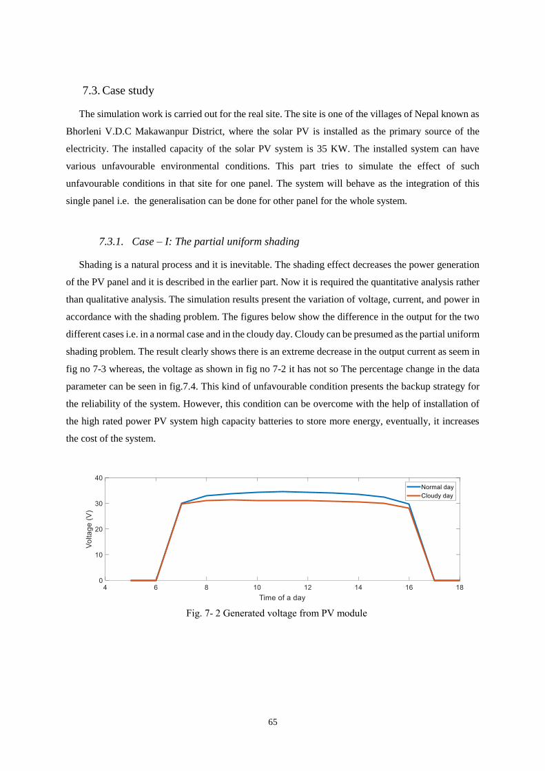
65
7.3. Case study
The simulation work is carried out for the real site. The site is one of the villages of Nepal known as
Bhorleni V.D.C Makawanpur District, where the solar PV is installed as the primary source of the
electricity. The installed capacity of the solar PV system is 35 KW. The installed system can have
various unfavourable environmental conditions. This part tries to simulate the effect of such
unfavourable conditions in that site for one panel. The system will behave as the integration of this
single panel i.e. the generalisation can be done for other panel for the whole system.
7.3.1. Case – I: The partial uniform shading
Shading is a natural process and it is inevitable. The shading effect decreases the power generation
of the PV panel and it is described in the earlier part. Now it is required the quantitative analysis rather
than qualitative analysis. The simulation results present the variation of voltage, current, and power in
accordance with the shading problem. The figures below show the difference in the output for the two
different cases i.e. in a normal case and in the cloudy day. Cloudy can be presumed as the partial uniform
shading problem. The result clearly shows there is an extreme decrease in the output current as seem in
fig no 7-3 whereas, the voltage as shown in fig no 7-2 it has not so The percentage change in the data
parameter can be seen in fig.7.4. This kind of unfavourable condition presents the backup strategy for
the reliability of the system. However, this condition can be overcome with the help of installation of
the high rated power PV system high capacity batteries to store more energy, eventually, it increases
the cost of the system.
Fig. 7- 2 Generated voltage from PV module
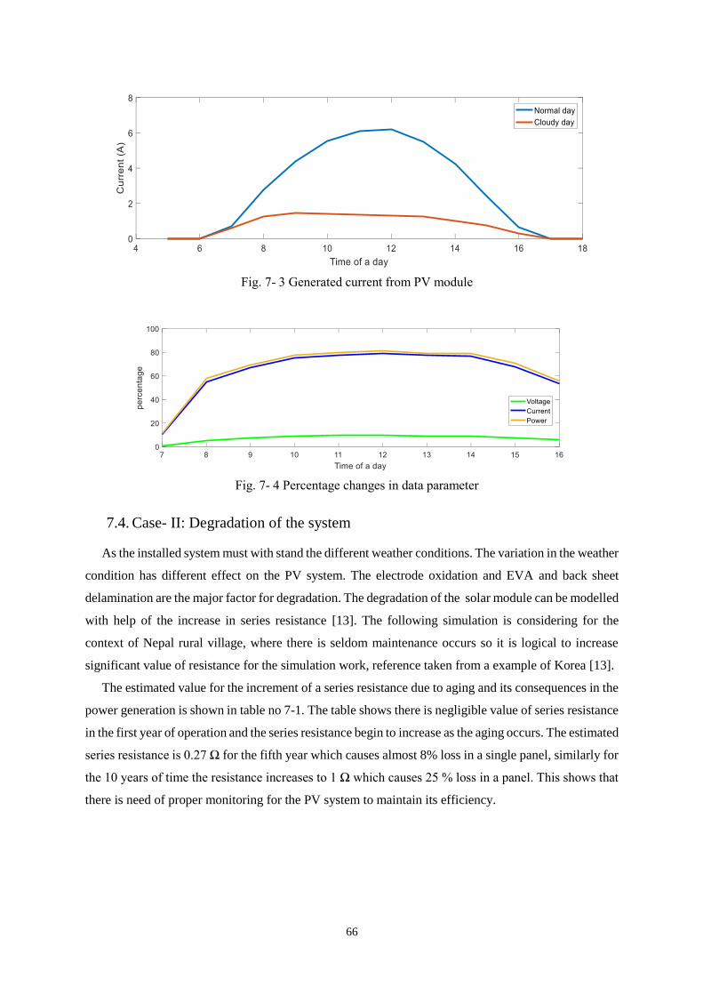
66
Fig. 7- 3 Generated current from PV module
Fig. 7- 4 Percentage changes in data parameter
7.4. Case- II: Degradation of the system
As the installed system must with stand the different weather conditions. The variation in the weather
condition has different effect on the PV system. The electrode oxidation and EVA and back sheet
delamination are the major factor for degradation. The degradation of the solar module can be modelled
with help of the increase in series resistance [13]. The following simulation is considering for the
context of Nepal rural village, where there is seldom maintenance occurs so it is logical to increase
significant value of resistance for the simulation work, reference taken from a example of Korea [13].
The estimated value for the increment of a series resistance due to aging and its consequences in the
power generation is shown in table no 7-1. The table shows there is negligible value of series resistance
in the first year of operation and the series resistance begin to increase as the aging occurs. The estimated
series resistance is 0.27 Ω for the fifth year which causes almost 8% loss in a single panel, similarly for
the 10 years of time the resistance increases to 1 Ω which causes 25 % loss in a panel. This shows that
there is need of proper monitoring for the PV system to maintain its efficiency.

67
Fig. 7- 5 IV curve of PV module with degradation over a time
Fig. 7- 6 PV curve of a PV module with degradation over a time
Table 7-1 – Comparison of power generation over a time with degraded PV module
Sno Years Resistance Power generated (W) Power available (%)
1 1st negligible 249.8356 100
2 5th 0.27Ω 232.56 92.86
3 10th 1Ω 187.245 74.95

68
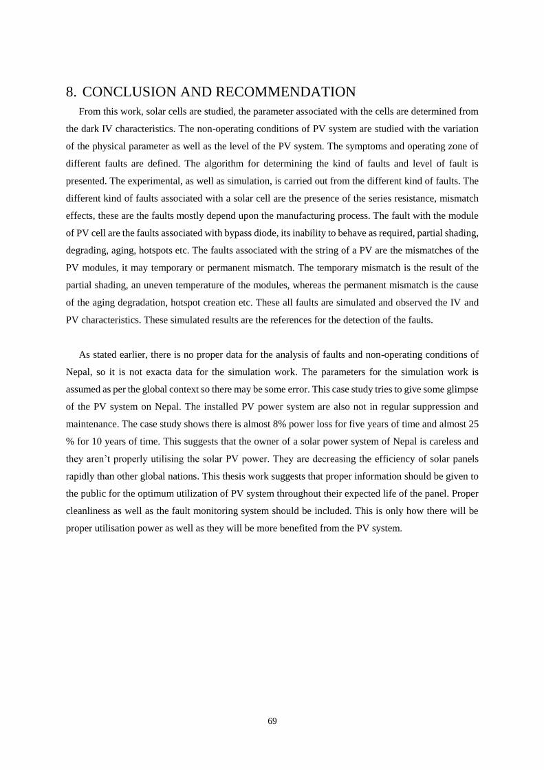
69
8. CONCLUSION AND RECOMMENDATION
From this work, solar cells are studied, the parameter associated with the cells are determined from
the dark IV characteristics. The non-operating conditions of PV system are studied with the variation
of the physical parameter as well as the level of the PV system. The symptoms and operating zone of
different faults are defined. The algorithm for determining the kind of faults and level of fault is
presented. The experimental, as well as simulation, is carried out from the different kind of faults. The
different kind of faults associated with a solar cell are the presence of the series resistance, mismatch
effects, these are the faults mostly depend upon the manufacturing process. The fault with the module
of PV cell are the faults associated with bypass diode, its inability to behave as required, partial shading,
degrading, aging, hotspots etc. The faults associated with the string of a PV are the mismatches of the
PV modules, it may temporary or permanent mismatch. The temporary mismatch is the result of the
partial shading, an uneven temperature of the modules, whereas the permanent mismatch is the cause
of the aging degradation, hotspot creation etc. These all faults are simulated and observed the IV and
PV characteristics. These simulated results are the references for the detection of the faults.
As stated earlier, there is no proper data for the analysis of faults and non-operating conditions of
Nepal, so it is not exacta data for the simulation work. The parameters for the simulation work is
assumed as per the global context so there may be some error. This case study tries to give some glimpse
of the PV system on Nepal. The installed PV power system are also not in regular suppression and
maintenance. The case study shows there is almost 8% power loss for five years of time and almost 25
% for 10 years of time. This suggests that the owner of a solar power system of Nepal is careless and
they aren’t properly utilising the solar PV power. They are decreasing the efficiency of solar panels
rapidly than other global nations. This thesis work suggests that proper information should be given to
the public for the optimum utilization of PV system throughout their expected life of the panel. Proper
cleanliness as well as the fault monitoring system should be included. This is only how there will be
proper utilisation power as well as they will be more benefited from the PV system.

70

71
9. FUTURE WORK
The simulation work to carried out in the Matlab for all the non-operating condition is not possible.
The modelling in the simulation works sometimes do not work as in the practical field. Though Matlab
provides much flexible for modelling it is not sufficient to model and simulate all the faults associated
with PV panel. However, in the future, the modelling of each fault which is unable to simulate can be a
model with great precision. In this thesis, only the theoretical simulation is carried out, the validity of
simulation work should be performed in the practical field, this provides the future work. After only the
practical experiments this work will be a reference to the others, so it is important to execute the
experimental setup to validate this work.

72
73
REFERENCES
[1] S. Silvestre and A. Chouder, “Effects of shadowing on photovoltaic module
performance,” Prog. Photovoltaics Res. Appl., vol. 16, no. 2, pp. 141–149, 2008.
[2] E. Engineering, “Pv System,” Focus, no. February. pp. 38–42, 2004.
[3] A. Luque and S. Hegedus, Handbook of Photovoltaic Science. .
[4] Y. Hu, J. Zhang, J. Wu, W. Cao, G. Y. Tian, and J. L. Kirtley, “Efficiency
Improvement of Nonuniformly Aged PV Arrays,” IEEE Trans. Power Electron., vol.
32, no. 2, pp. 1124–1137, 2017.
[5] “_ Europe-Solar.” .
[6]
“global_annual_PV_market_scenario_SolarPower_Europe_2016_report_750_564_s.p
ng (750×564).” [Online]. Available: https://www.pv-
tech.org/images/made/assets/images/editorial/global_annual_PV_market_scenario_Sol
arPower_Europe_2016_report_750_564_s.png. [Accessed: 12-Oct-2017].
[7] C. Besche-Richard, C. Passerieux, M. C. Hardy-Baylé, S. Nicolas, and J. P. Laurent,
“http://upload.wikimedia.org/wikipedia/he/thumb/1/14/Nissim.jpg/250px-Nissim.jpg,”
Brain Cogn., 1999.
[8] R. C. Campbell, “A circuit-based photovoltaic array model for power system studies,”
in 2007 39th North American Power Symposium, NAPS, 2007, pp. 97–101.
[9] J. C. H. Phang, D. S. H. Chan, and J. R. Phillips, “Accurate analytical method for the
extraction of solar cell model parameters,” Electron. Lett., vol. 20, no. 10, p. 406,
1984.
[10] “Single-Diode-EC2.png (590×310).” [Online]. Available:
https://pvpmc.sandia.gov/wp-content/uploads/2012/04/Single-Diode-EC2.png.
[Accessed: 12-Oct-2017].
[11] Solmetric Corporation, “Guide To Interpreting I-V Curve Measurements of PV
Arrays,” Appl. Note, vol. PVA-600-1, pp. p5–p6, 2011.
[12] “20_3.jpg (401×301).” [Online]. Available:
http://www.savanasolar.com/media/wysiwyg/20_3.jpg. [Accessed: 12-Oct-2017].
[13] G.-H. Kang et al., “Current-Voltage Characteristics With Degradation of Field-Aged
Silicon Photovoltaic Modules,” 21st Eur. Photovolt. Sol. Energy Conf., no. September,
pp. 2–5, 2006.
[14] “IMG_1032.jpg (3264×2448).” [Online]. Available: https://c1cleantechnicacom-
wpengine.netdna-ssl.com/files/2014/03/IMG_1032.jpg. [Accessed: 15-Oct-2017].
[15] “burned.jpg (482×230).” [Online]. Available:
https://www.homepower.com/sites/default/files/styles/article_gallery_active/public/arti
cles/images/burned.jpg?itok=NSW5L8ff. [Accessed: 15-Oct-2017].
[16] “IMG_4067-e1478227381833.jpg (2448×3263).” [Online]. Available:
http://www.acsolarwarehouse.com/wp-content/uploads/2016/11/IMG_4067-
e1478227381833.jpg. [Accessed: 15-Oct-2017].
[17] “Infrarotbild-Luftaufnahme-defekte-Solaranlage-in-Sachsen.jpg (800×600).” [Online].
Available: http://www.kitawa.de/images/IR-Bilder/FLIR-T-620/Infrarotbild-

74
Luftaufnahme-defekte-Solaranlage-in-Sachsen.jpg. [Accessed: 15-Oct-2017].
[18] “iStock_000012366395_Large.jpg (700×527).” [Online]. Available:
http://www.webberenergygroup.com/test/html/iii-renewable-energy/chapter-14-INDD-
web-resources/image/iStock_000012366395_Large.jpg. [Accessed: 15-Oct-2017].
[19] L. Bun, “D’etection et localisation de d ´ efauts dans un syst ` eme Détection et
Localisation de Défauts pour un Système PV,” 2011.
[20] “Be wary of solar panels with multiple circuits!” [Online]. Available:
https://www.coastalclimatecontrol.com/index.php/blog/124-be-wary-of-solar-panels-
with-multiple-circuits.html. [Accessed: 15-Oct-2017].
[21] Y. Zhao, “Fault Analysis in Solar Photovoltaic Arrays,” p. 137, 2010.
[22] M. Sabbaghpur Arani and M. A. Hejazi, “The comprehensive study of electrical faults
in PV arrays,” J. Electr. Comput. Eng., vol. 2016, 2016.
[23] E. L. Meyer and E. E. Van Dyk, “Assessing the reliability and degradation of
photovoltaic module performance parameters,” IEEE Trans. Reliab., vol. 53, no. 1, pp.
83–92, 2004.
[24] S. Djordjevic, D. Parlevliet, and P. Jennings, “Detectable faults on recently installed
solar modules in Western Australia,” Renew. Energy, vol. 67, pp. 215–221, 2014.
[25] A. A. El Tayyan, “A New Method to Extract the Electrical Parameters from Dark I-V :
T Experimental Data of Cds / Cu ( In , Ga ) Se 2 Interface,” Interface, vol. 2, no. 8, pp.
11–20, 2015.
[26] M. Villalva, J. Gazoli, and E. Filho, “Comprehensive Approach to Modeling and
Simulation of Photovoltaic Arrays,” IEEE Trans. Power Electron., vol. 24, no. 5, pp.
1198–1208, 2009.
[27] J. A. Gow and C. D. Manning, “Development of a photovoltaic array model for use in
power-electronics simulation studies,” IEE Proc. - Electr. Power Appl., vol. 146, no. 2,
p. 193, 1999.
[28] “Keysight N6700 Series DC Sources for Dark I-V Solar Cell Testing _ Keysight
(formerly Agilent’s Electronic Measurement).” .
[29] a. Kaminski, J. J. Marchand, a. Fave, and a. Laugier, “New method of parameters
extraction from dark I-V curve,” Conf. Rec. Twenty Sixth IEEE Photovolt. Spec. Conf.
- 1997, pp. 203–206, 1997.
[30] J.-M. Wagner, S. Rißland, A. Schütt, J. Carstensen, and R. Adelung, “Distributed
series resistance in a one-dimensional two-diode model revisited,” Energy Procedia,
vol. 124, no. September, pp. 197–206, 2017.
[31] E. Skoplaki, A. G. Boudouvis, and J. A. Palyvos, “A simple correlation for the
operating temperature of photovoltaic modules of arbitrary mounting,” Sol. Energy
Mater. Sol. Cells, vol. 92, no. 11, pp. 1393–1402, 2008.
[32] J. P. N. Torres, S. K. Nashih, C. A. F. Fernandes, and J. C. Leite, “The effect of
shading on photovoltaic solar panels,” Energy Syst., pp. 1–14, 2016.
[33] S. Abhiyan, “Socio-economic impact study of the users of Solar Home Systems,”
2010.
[34] “» Why Solar.” [Online]. Available: http://nationalintra.com/why-solar/. [Accessed:
13-Oct-2017].

75
[35] “Nepal Energy Situation - energypedia.info.” [Online]. Available:
https://energypedia.info/wiki/Nepal_Energy_Situation. [Accessed: 13-Oct-2017].
[36] “Nepal Energy Situation - energypedia.” .

76
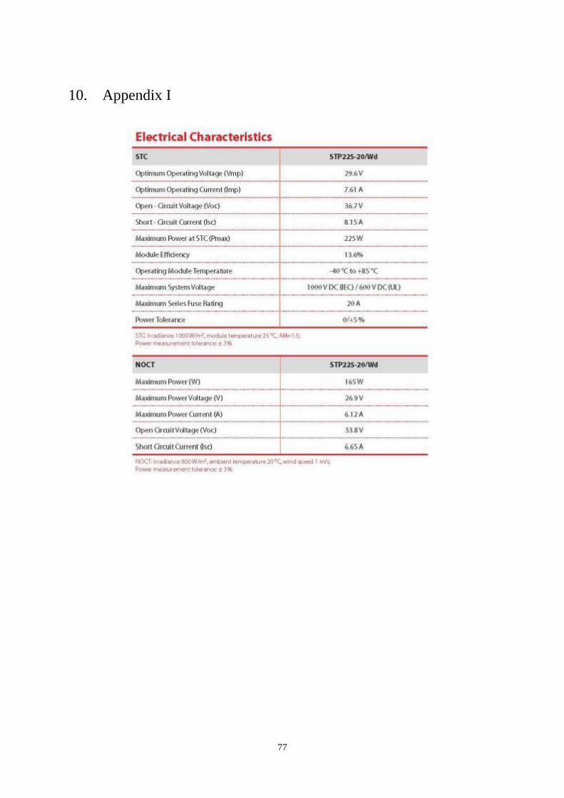
77
10. Appendix I