
CHARACTERIZATION OF NANO MATERIALS...
19
UNIT 5 CHARACTERIZATION OF NANO MATERIALS Introduction to Nanometrology Nanometrology is a subfield of metrology, concerned with the science of measurement at thenanoscale level. Nanometrology has a crucial role in order to produce nanomaterials and devices with a high degree of accuracy and reliability innanomanufacturing. A challenge in this field is to develop or create new measurement techniques and standards to meet the needs of next-generation advanced manufacturing, which will rely on nanometer scale materials and technologies. The needs for measurement and characterization of new sample structures and characteristics far exceed the capabilities of current measurement science. Control of the critical dimensions are the most important factors in anotechnology. Nanometrology today, is to a large extent based on the development insemiconductortechnology. Nanometrology is the science ofmeasurementat the nanoscale level. In Nanotechnology accurate control of dimensions of objects is important. Typical dimensions of nanosystems vary from 10nm to a few hundred nm and while fabricating such systems measurement up to 0.1nm is required. In the last 70 years various techniques for measuring at nanoscale have been developed most of them based on some physical phenomena observed on particle interactions or forces at nanoscale. Some of the most commonly used techniques are Atomic Force Microscopy, X-Ray Diffraction, Scanning Electron Microscopy, Transmission Electron Microscopy, High Resolution Transmission Electron Microscopy, and Field Emission Scanning Electron Microscopy. The full list of nanomeasuring systems are: (i) Atomic Force Microscopy (ii) X-ray absorption Spectroscopy (iii) X- Ray Diffraction (iv) Small Angle X-Ray Scattering (v) Scanning Tunneling Microscopy (vi) Transmission Electron Microscopy (vii) Scanning Tunneling Microscopy (viii) Capacitance Spectroscopy (ix) Polarization Spectroscopy (x) Auger Electron Spectroscopy (xi) Raman Spectroscopy (xii) Small Angle Neutron Scattering (xiii) Scanning Electron Microscopy (xiv) Cyclic Voltammetry (xv) Linear Sweep Voltammetry (xvi) Nuclear Magnetic Resonance (xvii) Mössbauer Spectroscopy (xviii) Fouier Transform Infrared Spectroscopy (xix) Photoluminescence Spectroscopy
Transcript of CHARACTERIZATION OF NANO MATERIALS...
UNIT 5 CHARACTERIZATION OF NANO MATERIALS
Introduction to Nanometrology
Nanometrology is a subfield of metrology, concerned with the science of measurement at
thenanoscale level. Nanometrology has a crucial role in order to produce nanomaterials and
devices with a high degree of accuracy and reliability innanomanufacturing.
A challenge in this field is to develop or create new measurement techniques and standards to
meet the needs of next-generation advanced manufacturing, which will rely on nanometer
scale materials and technologies.
The needs for measurement and characterization of new sample structures and characteristics
far exceed the capabilities of current measurement science.
Control of the critical dimensions are the most important factors in anotechnology.
Nanometrology today, is to a large extent based on the development
insemiconductortechnology. Nanometrology is the science ofmeasurementat the nanoscale
level.
In Nanotechnology accurate control of dimensions of objects is important. Typical dimensions
of nanosystems vary from 10nm to a few hundred nm and while fabricating such systems
measurement up to 0.1nm is required.
In the last 70 years various techniques for measuring at nanoscale have been developed most
of them based on some physical phenomena observed on particle interactions or forces at
nanoscale. Some of the most commonly used techniques are
Atomic Force Microscopy, X-Ray Diffraction, Scanning Electron Microscopy,
Transmission Electron Microscopy, High Resolution Transmission Electron Microscopy, and
Field Emission Scanning Electron Microscopy.
The full list of nanomeasuring systems are:
(i) Atomic Force Microscopy
(ii) X-ray absorption Spectroscopy
(iii) X- Ray Diffraction
(iv) Small Angle X-Ray Scattering
(v) Scanning Tunneling Microscopy
(vi) Transmission Electron Microscopy
(vii) Scanning Tunneling Microscopy
(viii) Capacitance Spectroscopy
(ix) Polarization Spectroscopy
(x) Auger Electron Spectroscopy
(xi) Raman Spectroscopy
(xii) Small Angle Neutron Scattering
(xiii) Scanning Electron Microscopy
(xiv) Cyclic Voltammetry
(xv) Linear Sweep Voltammetry
(xvi) Nuclear Magnetic Resonance
(xvii) Mössbauer Spectroscopy
(xviii) Fouier Transform Infrared Spectroscopy
(xix) Photoluminescence Spectroscopy
VELAMMAL COLLEGE OF ENGG & TECH,MADURAIMANUFACTURING ENGG (2014-2016)
VIGNESHWARAN.S
(xx) Electroluminescence Spectroscopy
(xxi) Differential Scanning Calorimetry
(xxii) Secondary Ion Mass Spectrometry
(xxiii) Cathodoluminescence Spectroscopy
(xxiv) Electron Energy Loss Spectroscopy
(xxv) EnergyDispersiveX-RaySpectroscopy
(xxvi) Four point probe and I-V technique
(xxvii) X-Ray Photoelectron Spectroscopy
(xxviii) Scanning Near-field Optical Microscopy
(xxix) Single-molecule Spectroscopy
(xxx) Neutron Diffraction
Analytical Imaging
The fundamental of nanotechnology lies in the fact that properties of materials change
dramatically when their size is reduced to the nanometer range. But measuring this nano
dimension is not a very easy task.
Although research is going on to synthesise nanostructured and nanophasic materials,
characterizing these nano sized materials is also an emerging field posing lot of challenges
to scientists and technonologists.
Thus, nanotechnology has motivated the upsurge in research activities on the discovery and
invention of sophisticated nano characterization techniques to allow a better control of
morphology, size and dimensions of materials in nano range.
Nanomaterials to be thoroughly characterized as much as possible using a combination of
experimental techniques due to the intrinsic complex nature of nanomaterials. For example,
two of the most basic characteristics are size and shape of nanostructures.
Another important property is the surface of nanomaterials due to their extremely large
surface-to-volume ratio. Furthermore, it is often important to know the crystal structures of
the nanomaterials. To study these different properties requires many other experimental
methods, besides optical spectroscopy.
Nanotechnology was mostly a dream until the invention of the Scanning Tunneling
Microscope and the Atomic Force Microscope. In addition, all other existing facilities are
used to characterize nanomaterials. List of nanocharacterisation techniques
Image Analysis
Surface Analysis
Structural Analysis
Organic
Optical microscopy
Confocal microscopy
SEM/EDX – Scanning Electron Microscopy with Energy Dispersive
X-Ray detector
SPM – Scanning Probe Microscopy
AFM – Atomic Force Microscopy
TEM – Transmission Electron Microscopy
AES – Auger Electron Spectroscopy
XPS – X-Ray Photoelectron Spectroscopy
TOFSSIMS-Time of Flight Static Secondary Ion Mass Spectra LEED – Low Energy Electron
Diffraction
XRD – X-Ray Diffraction
XAX/EXAFS - X-ray Absorption Spectroscopy and Extended
X-Ray Absorption Fine Structure Raman spectroscopy
TEM – Transmission Electron Microscopy
EELS – Electron Energy Loss Spectroscopy (typically combined with TEM)
FTIR – Fourier Transform Infrared Spectroscopy
Analysis
Elemental Analysis
GC/MS – Gas Chromatography with Mass Spectroscopy (detector) HPLC – High Performance
Liquid Chromatography Raman
spectroscopy (structural organic)
ICP – Inductively Coupled Plasma
XRF – X-Ray Fluorescence
PIXE - Particle-Induced X-ray Emission
Optical atomic spectroscopy - CHN (Carbon / Hydrogen / Nitrogen)
–-----------------------------------------------------------------------------------------------------------------------
Microscopy
Structural determination is essential for nanomaterials research. Since the nanostructures are usually
too small to be visualized with conventional optical microscopes, it is important to use appropriate
tools to adequately characterize their structure and surface in detail at the molecular or atomic level.
This is important not only for understanding their fundamental properties but also for exploring
their functional and technical performance in technological applications.
There are several experimental techniques that can be used to characterize structural and surface
properties of nanomaterials either directly or indirectly, e.g. XRD, STM (scanning tunneling
microscopy), AFM (atomic force microscopy), SEM (scanning electron microscopy), TEM
(transmission electron microscopy), XAS (X-ray absorption spectroscopy), EXAFS, XANES (X-
ray absorption near edge structure), EDX (energy dispersive X-ray), XPS, IR (infrared), Raman,
and DLS (dynamic light scattering).
Some of these techniques are more surface sensitive than others. Some techniques are directly
element-specific while others are not. The choice of techniques depends strongly on the information
being sought about the material.
–-----------------------------------------------------------------------------------------------------------------------
Electron microscopy
Optical microscopes have limited spatial resolution, usually on the order of a few hundred nm in the
best case scenario due to the diffraction limit of light. Higher resolution, a few nm or even sub nm,
is needed for many applications, especially in the study of nanomaterials.
The trend toward nanoscience and nanotechnology is mainly motivated by the fact that the
underlying physical laws change from macroscopic to microscopic.
As we move to smaller and smaller length scales, new characterization techniques have to be
developed to probe the properties of novel nanostructures. There is a continuing demand for new
measurement methods that will be positioned to meet emerging measurement challenges.
Electon microscopes help to see nanocrystals and atomic arrangement in nanocrystals.
DIFFRACTION TECHNIQUE
Introduction
X-rays are electromagnetic radiation similar to light, but with a much shorter wavelength
(few Angstrom). They are produced when electrically charged particles of sufficient energy are
decelerated. In an X-ray tube, the high voltage maintained across the electrodes draws electrons
toward a metal target (the anode). X-rays are produced at the point of impact, and radiate in all
directions
Basic Principle
If an incident X-ray beam encounters a crystal lattice, general scattering occurs. Although most
scattering interferes with itself and is eliminated (destructive interference), diffraction occurs when
scattering in a certain direction is in phase with scattered rays from other atomic planes. Under this
condition the reflections combine to form new enhanced wave fronts that mutually reinforce each
other (constructive interference). The relation by which diffraction occurs is known as the Bragg’s
law or equation
nλ = d sinθ
where n is order of reflection, λ is wavelength of the x-ray, d is interplanar spscing and θ is Bragg’s
angle.
The method of X-ray diffraction is quantitative, in general, but it is also used for qualitative
analysis. This form of analysis extends to all crystalline solids including ceramics, metals,
insulators, organics, polymers, thin films, powders, etc.
X-ray diffractometers can be used either for single crystals or for powders, with both using
significantly different infrastructure.
While single crystal diffractometers are used for the study of molecular structure, powder
diffractometers are used for the analysis of phases, though the latter can also be used to
derive molecu lar information. X-rays corresponds to electromagnetic radiation in the
wavelength range of 1 ?. The wavelength range is below that of ultraviolet light and above
that of gamma rays.
This radiation is produced when charged particles are decelerated by metals, thus producing
a continuum called Bremsstrauhlung radiation.
X-rays are generally produced when electrons of several thousands of electron volts are
decelerated or stopped by metals. This will produce a white radiation up to a threshold
frequency corresponding to the kinetic energy of the particle. This threshold corresponds to
a wavelength (in angstroms), λ = 12399/V where V is the accelerating voltage of the
electrons.
When particles such as electrons fall on matter with high energy, electrons can be ejected
from various energy levels. Electron ejection from the core orbital is also accompanied by
the emission of characteristic X-rays. In the case of electron from the 1s orbital an outer
electron from the 2 p or 3p orbital can fall down to occupy the vacant 1s orbital. This 2 p →
1s transitions leads to the emission of Kα radiation.
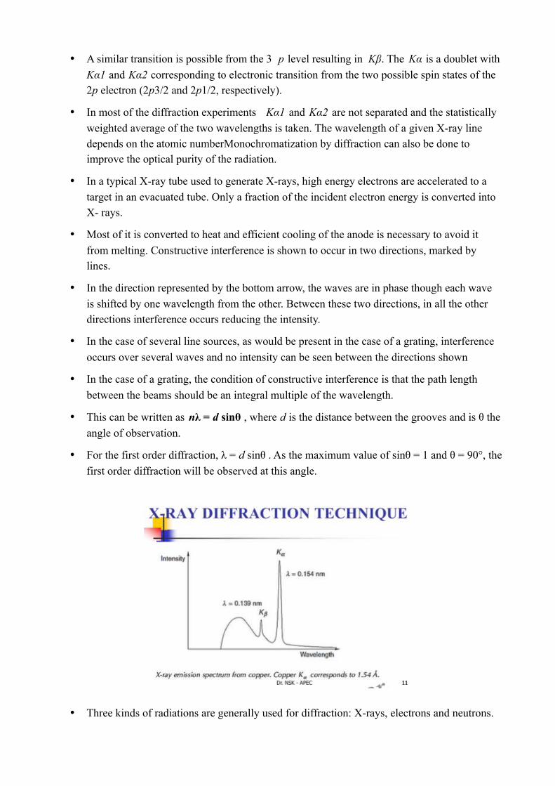
A similar transition is possible from the 3 p level resulting in Kβ. The Kα is a doublet with
Kα1 and Kα2 corresponding to electronic transition from the two possible spin states of the
2p electron (2p3/2 and 2p1/2, respectively).
In most of the diffraction experiments Kα1 and Kα2 are not separated and the statistically
weighted average of the two wavelengths is taken. The wavelength of a given X-ray line
depends on the atomic numberMonochromatization by diffraction can also be done to
improve the optical purity of the radiation.
In a typical X-ray tube used to generate X-rays, high energy electrons are accelerated to a
target in an evacuated tube. Only a fraction of the incident electron energy is converted into
X- rays.
Most of it is converted to heat and efficient cooling of the anode is necessary to avoid it
from melting. Constructive interference is shown to occur in two directions, marked by
lines.
In the direction represented by the bottom arrow, the waves are in phase though each wave
is shifted by one wavelength from the other. Between these two directions, in all the other
directions interference occurs reducing the intensity.
In the case of several line sources, as would be present in the case of a grating, interference
occurs over several waves and no intensity can be seen between the directions shown
In the case of a grating, the condition of constructive interference is that the path length
between the beams should be an integral multiple of the wavelength.
This can be written as nλ = d sinθ , where d is the distance between the grooves and is θ the
angle of observation.
For the first order diffraction, λ = d sinθ . As the maximum value of sinθ = 1 and θ = 90°, the
first order diffraction will be observed at this angle.
Three kinds of radiations are generally used for diffraction: X-rays, electrons and neutrons.
Commonly, the characteristic X-ray used for diffraction is the copper Kα radiation at 1.5418
? wavelength.
Two approaches are generally used for the analysis of X-ray diffraction data.
These are the Laue equations and the Bragg’s law.In the Laue equations, diffraction from
a one-dimensional crystal may be treated in the same way as the diffraction by an optical
grating.
Upon projection, the grating is like an array of points similar to a crystal. The diffraction
condition is again, nλ = d sinθ. In a crystal arrangement of atoms is periodic in all the three
directions and three independent Laue equations can be written.
The three equations have to be satisfied simultaneously for diffraction to occur.
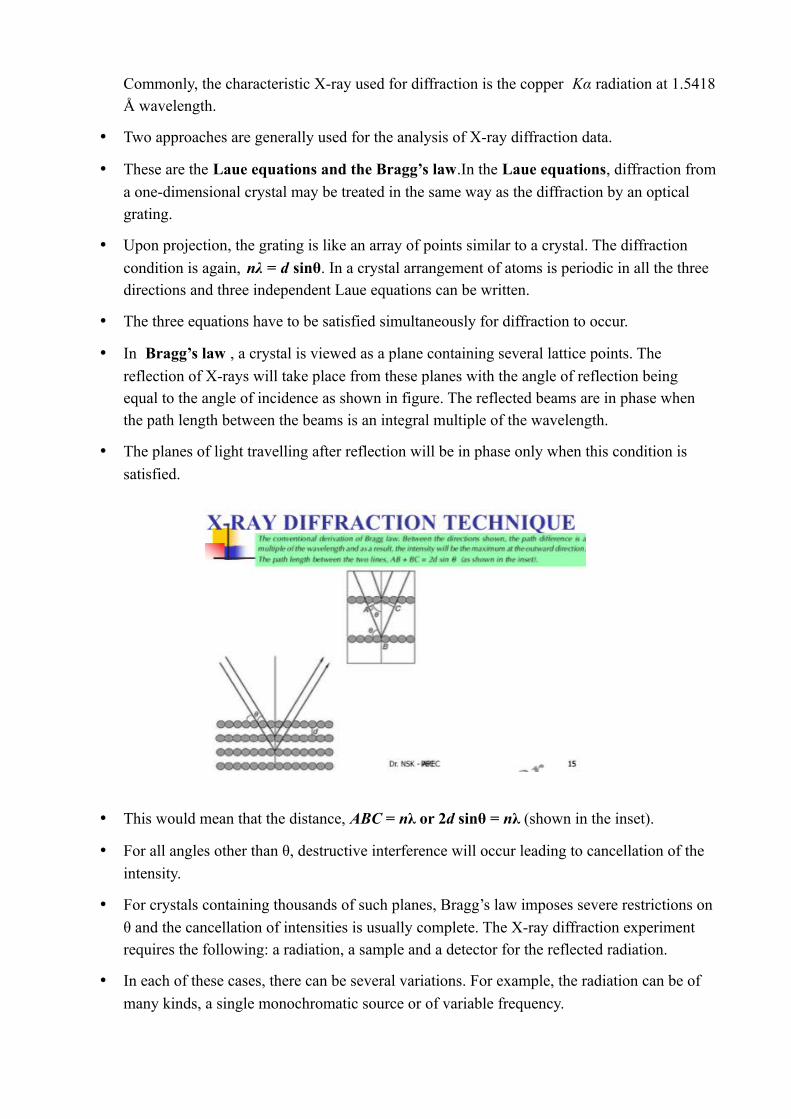
In Bragg’s law , a crystal is viewed as a plane containing several lattice points. The
reflection of X-rays will take place from these planes with the angle of reflection being
equal to the angle of incidence as shown in figure. The reflected beams are in phase when
the path length between the beams is an integral multiple of the wavelength.
The planes of light travelling after reflection will be in phase only when this condition is
satisfied.
This would mean that the distance, ABC = nλ or 2d sinθ = nλ (shown in the inset).
For all angles other than θ, destructive interference will occur leading to cancellation of the
intensity.
For crystals containing thousands of such planes, Bragg’s law imposes severe restrictions on
θ and the cancellation of intensities is usually complete. The X-ray diffraction experiment
requires the following: a radiation, a sample and a detector for the reflected radiation.
In each of these cases, there can be several variations. For example, the radiation can be of
many kinds, a single monochromatic source or of variable frequency.
The sample can be powder, single crystal, solid piece or a thin film. The detector can be of
several kinds, ranging from a simple photographic plate to a sophisticated counter or an area
detector. In a powder diffraction experiment, there are crystals arranged in all possible
orientations in a finely powdered sample.
The various lattice planes are also arranged in all possible orientations. For each crystal
plane, there will be a number of orientations. The reflected X-rays may be collected on a
photographic plate or by using a counter that is suitably connected to a recorder.
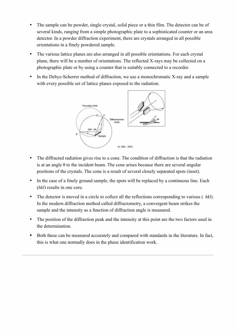
In the Debye-Scherrer method of diffraction, we use a monochromatic X-ray and a sample
with every possible set of lattice planes exposed to the radiation.
The diffracted radiation gives rise to a cone. The condition of diffraction is that the radiation
is at an angle θ to the incident beam. The cone arises because there are several angular
positions of the crystals. The cone is a result of several closely separated spots (inset).
In the case of a finely ground sample, the spots will be replaced by a continuous line. Each
(hkl) results in one core.
The detector is moved in a circle to collect all the reflections corresponding to various ( hkl).
In the modern diffraction method called diffractometry, a convergent beam strikes the
sample and the intensity as a function of diffraction angle is measured.
The position of the diffraction peak and the intensity at this point are the two factors used in
the determination.
Both these can be measured accurately and compared with standards in the literature. In fact,
this is what one normally does in the phase identification work.
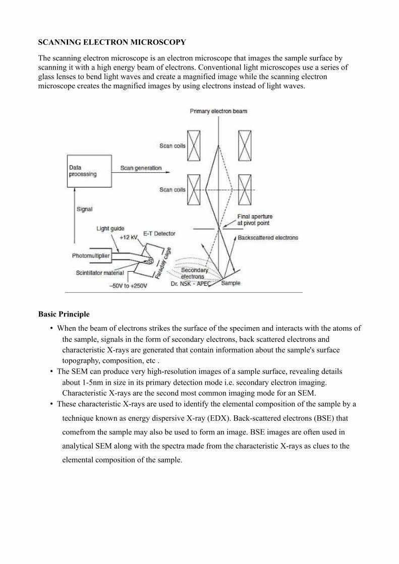
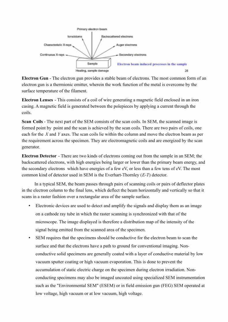
SCANNING ELECTRON MICROSCOPY
The scanning electron microscope is an electron microscope that images the sample surface byscanning it with a high energy beam of electrons. Conventional light microscopes use a series ofglass lenses to bend light waves and create a magnified image while the scanning electronmicroscope creates the magnified images by using electrons instead of light waves.
Basic Principle
• When the beam of electrons strikes the surface of the specimen and interacts with the atoms of
the sample, signals in the form of secondary electrons, back scattered electrons and
characteristic X-rays are generated that contain information about the sample's surface
topography, composition, etc .
• The SEM can produce very high-resolution images of a sample surface, revealing details
about 1-5nm in size in its primary detection mode i.e. secondary electron imaging.
Characteristic X-rays are the second most common imaging mode for an SEM.
• These characteristic X-rays are used to identify the elemental composition of the sample by a
technique known as energy dispersive X-ray (EDX). Back-scattered electrons (BSE) that
comefrom the sample may also be used to form an image. BSE images are often used in
analytical SEM along with the spectra made from the characteristic X-rays as clues to the
elemental composition of the sample.
Electron Gun - The electron gun provides a stable beam of electrons. The most common form of an
electron gun is a thermionic emitter, wherein the work function of the metal is overcome by the
surface temperature of the filament.
Electron Lenses - This consists of a coil of wire generating a magnetic field enclosed in an iron
casing. A magnetic field is generated between the polepieces by applying a current through the
coils.
Scan Coils - The next part of the SEM consists of the scan coils. In SEM, the scanned image is
formed point by point and the scan is achieved by the scan coils. There are two pairs of coils, one
each for the X and Y axes. The scan coils lie within the column and move the electron beam as per
the requirement across the specimen. They are electromagnetic coils and are energized by the scan
generator.
Electron Detector - There are two kinds of electrons coming out from the sample in an SEM; the
backscattered electrons, with high energies being larger or lower than the primary beam energy, and
the secondary electrons which have energies of a few eV, or less than a few tens of eV. The most
common kind of detector used in SEM is the Everhart-Thornley (E-T) detector.
In a typical SEM, the beam passes through pairs of scanning coils or pairs of deflector plates
in the electron column to the final lens, which deflect the beam horizontally and vertically so that it
scans in a raster fashion over a rectangular area of the sample surface.
• Electronic devices are used to detect and amplify the signals and display them as an image
on a cathode ray tube in which the raster scanning is synchronized with that of the
microscope. The image displayed is therefore a distribution map of the intensity of the
signal being emitted from the scanned area of the specimen.
• SEM requires that the specimens should be conductive for the electron beam to scan the
surface and that the electrons have a path to ground for conventional imaging. Non-
conductive solid specimens are generally coated with a layer of conductive material by low
vacuum sputter coating or high vacuum evaporation. This is done to prevent the
accumulation of static electric charge on the specimen during electron irradiation. Non-
conducting specimens may also be imaged uncoated using specialized SEM instrumentation
such as the "Environmental SEM" (ESEM) or in field emission gun (FEG) SEM operated at
low voltage, high vacuum or at low vacuum, high voltage.
.
Applications
• The SEM shows very detailed three dimensional images at much high magnifications (up to
×300000) as compared to light microscope (up to × 10000). But as the images are created
without light waves, they are black and white.
• The surface structure of polymer nanocomposites, fracture surfaces, nanofibres, nanoparticles
and nanocoating can be imaged through SEM with great clarity. As very high resolution
images of the dimension 1-5nm can be obtained, SEM is the most suitable process to study
the surface of nanostrutures.
• Electrospun nanofibres are extensively studied in biomedical, environmental and other
technical textile applications for their huge surface area. Electrospun nylon 6 nanofibres
decorated with surface bound silver nanoparticles used for antibacterial air purifier can be
characterized using SEM (Figure 39.3-39.7).
• In tissue engineering or cell culture applications, the SEM image is the prime characterization
technique for scaffold construction, cell development and growth. SEM technique is used to
observe the plied CNT yarns in 3D braided structures.
• The SEM technique can also be used to view dispersion of nanoparticles such as carbon
nanotubes, nanoclays and nanofillers in the bulk and on the surface of nanocomposite
samples.
------------------------------------------------------------------------------------------------------------------------
TRANSMISSION ELECTRON MICROSCOPY
• Transmission electron microscopy is a microscopy technique whereby a beam of electrons is
transmitted through an ultra thin specimen and interacts as passes through the sample. An
image is formed from the electrons transmitted through the specimen, magnified and
focused by an objective lens and appears on an imaging screen.
• In TEM, the transmitted electrons are used to create an image of the sample. Scattering
occurs when the electron beam interacts with matter.
• Scattering can be elastic (no energy change) or inelastic (energy change). Elastic scattering
can be both coherent and incoherent (with and without phase relationship). Elastic scattering
occurring from well-ordered arrangements of atoms as in a crystal, results in coherent
scattering, giving spot patterns.
This can be in the form of rings in the case of a polycrystalline material. However, inelastic
scattering also occurs, which also gives regular patterns as in the case of Kikuchi patterns.
Inelastic processes give characteristic absorption or emission, specific to the compound or element
or chemical structure.
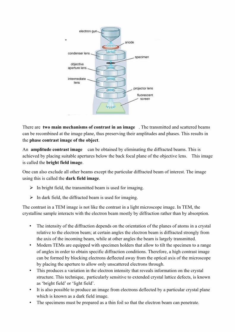
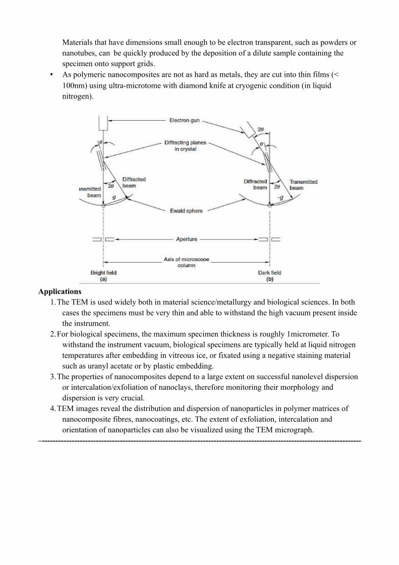
There are two main mechanisms of contrast in an image . The transmitted and scattered beams
can be recombined at the image plane, thus preserving their amplitudes and phases. This results in
the phase contrast image of the object.
An amplitude contrast image can be obtained by eliminating the diffracted beams. This is
achieved by placing suitable apertures below the back focal plane of the objective lens. This image
is called the bright field image.
One can also exclude all other beams except the particular diffracted beam of interest. The image
using this is called the dark field image.
➢ In bright field, the transmitted beam is used for imaging.
➢ In dark field, the diffracted beam is used for imaging.
The contrast in a TEM image is not like the contrast in a light microscope image. In TEM, the
crystalline sample interacts with the electron beam mostly by diffraction rather than by absorption.
• The intensity of the diffraction depends on the orientation of the planes of atoms in a crystal
relative to the electron beam; at certain angles the electron beam is diffracted strongly from
the axis of the incoming beam, while at other angles the beam is largely transmitted.
• Modern TEMs are equipped with specimen holders that allow to tilt the specimen to a range
of angles in order to obtain specific diffraction conditions. Therefore, a high contrast image
can be formed by blocking electrons deflected away from the optical axis of the microscope
by placing the aperture to allow only unscattered electrons through.
• This produces a variation in the electron intensity that reveals information on the crystal
structure. This technique, particularly sensitive to extended crystal lattice defects, is known
as ‘bright field’ or ‘light field’.
• It is also possible to produce an image from electrons deflected by a particular crystal plane
which is known as a dark field image.
• The specimens must be prepared as a thin foil so that the electron beam can penetrate.
Materials that have dimensions small enough to be electron transparent, such as powders or
nanotubes, can be quickly produced by the deposition of a dilute sample containing the
specimen onto support grids.
• As polymeric nanocomposites are not as hard as metals, they are cut into thin films (<
100nm) using ultra-microtome with diamond knife at cryogenic condition (in liquid
nitrogen).
Applications
1.The TEM is used widely both in material science/metallurgy and biological sciences. In both
cases the specimens must be very thin and able to withstand the high vacuum present inside
the instrument.
2.For biological specimens, the maximum specimen thickness is roughly 1micrometer. To
withstand the instrument vacuum, biological specimens are typically held at liquid nitrogen
temperatures after embedding in vitreous ice, or fixated using a negative staining material
such as uranyl acetate or by plastic embedding.
3.The properties of nanocomposites depend to a large extent on successful nanolevel dispersion
or intercalation/exfoliation of nanoclays, therefore monitoring their morphology and
dispersion is very crucial.
4.TEM images reveal the distribution and dispersion of nanoparticles in polymer matrices of
nanocomposite fibres, nanocoatings, etc. The extent of exfoliation, intercalation and
orientation of nanoparticles can also be visualized using the TEM micrograph.
–-----------------------------------------------------------------------------------------------------------------------
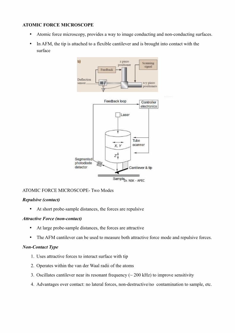
ATOMIC FORCE MICROSCOPE
Atomic force microscopy, provides a way to image conducting and non-conducting surfaces.
In AFM, the tip is attached to a flexible cantilever and is brought into contact with the
surface
ATOMIC FORCE MICROSCOPE- Two Modes
Repulsive (contact)
At short probe-sample distances, the forces are repulsive
Attractive Force (non-contact)
At large probe-sample distances, the forces are attractive
The AFM cantilever can be used to measure both attractive force mode and repulsive forces.
Non-Contact Type
1. Uses attractive forces to interact surface with tip
2. Operates within the van der Waal radii of the atoms
3. Oscillates cantilever near its resonant frequency (~ 200 kHz) to improve sensitivity
4. Advantages over contact: no lateral forces, non-destructive/no contamination to sample, etc.
Contact Type
1. Contact mode operates in the repulsive regime of the van der Waals curve
2. Tip attached to cantilever with low spring constant.
3. In ambient conditions there is also a capillary force exerted by the thin water layer present
(2-50 nm thick).
The force between the tip and the surface is detected by sensing the cantilever deflection. A
topographic image of the surface is obtained by plotting the deflection as a function of the X-Y
position. In a more common mode of operation, a feedback loop is used to maintain a constant
deflection while the topographic information is obtained from the vertical displacement of the
cantilever.
Some scanning probe systems use a combination of AFM and STM modes: the tip is mounted in a
cantilever with electrical connection so that both the surface force and the tunneling current are
controlled or monitored.
1. STM systems can be operated in ultrahigh vacuum (UHV STM) or in air, whereas AFM
systems are typically operated in air.
2. When a scanning probe system is operated in air, water adsorbed onto the sample surface
accumulates underneath the tip, forming a meniscus between the tip and the surface.
–------------------------------------------------------------------------------------------------------------------
Scanning tunneling microscopy
The principle of operation of Scanning Tunneling Microscope is based on marvelous quantum
phenomenon known as the tunnel effect.
Scanning tunneling microscopy (Figure 41. 1) is an instrument for producing surface images with atomic-scale lateral resolution, in which a fine probe tip is scanned over the surface of a conducting specimen, with the help of a piezoelectric crystal at a distance of 0.5–1nm, and the resulting tunneling current or the position of the tip required to maintain a constant tunneling current is monitored.
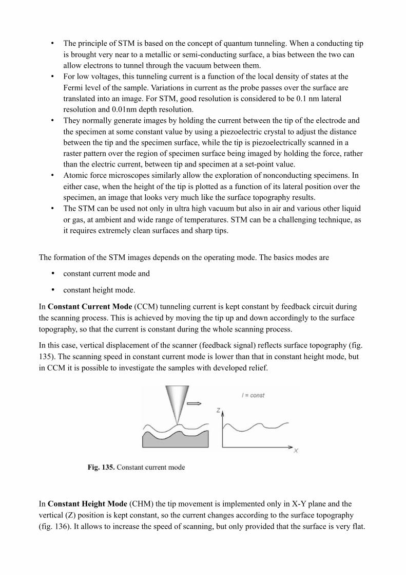
• The principle of STM is based on the concept of quantum tunneling. When a conducting tip
is brought very near to a metallic or semi-conducting surface, a bias between the two can
allow electrons to tunnel through the vacuum between them.
• For low voltages, this tunneling current is a function of the local density of states at the
Fermi level of the sample. Variations in current as the probe passes over the surface are
translated into an image. For STM, good resolution is considered to be 0.1 nm lateral
resolution and 0.01nm depth resolution.
• They normally generate images by holding the current between the tip of the electrode and
the specimen at some constant value by using a piezoelectric crystal to adjust the distance
between the tip and the specimen surface, while the tip is piezoelectrically scanned in a
raster pattern over the region of specimen surface being imaged by holding the force, rather
than the electric current, between tip and specimen at a set-point value.
• Atomic force microscopes similarly allow the exploration of nonconducting specimens. In
either case, when the height of the tip is plotted as a function of its lateral position over the
specimen, an image that looks very much like the surface topography results.
• The STM can be used not only in ultra high vacuum but also in air and various other liquid
or gas, at ambient and wide range of temperatures. STM can be a challenging technique, as
it requires extremely clean surfaces and sharp tips.
The formation of the STM images depends on the operating mode. The basics modes are
constant current mode and
constant height mode.
In Constant Current Mode (CCM) tunneling current is kept constant by feedback circuit during
the scanning process. This is achieved by moving the tip up and down accordingly to the surface
topography, so that the current is constant during the whole scanning process.
In this case, vertical displacement of the scanner (feedback signal) reflects surface topography (fig.
135). The scanning speed in constant current mode is lower than that in constant height mode, but
in CCM it is possible to investigate the samples with developed relief.
In Constant Height Mode (CHM) the tip movement is implemented only in X-Y plane and the
vertical (Z) position is kept constant, so the current changes according to the surface topography
(fig. 136). It allows to increase the speed of scanning, but only provided that the surface is very flat.
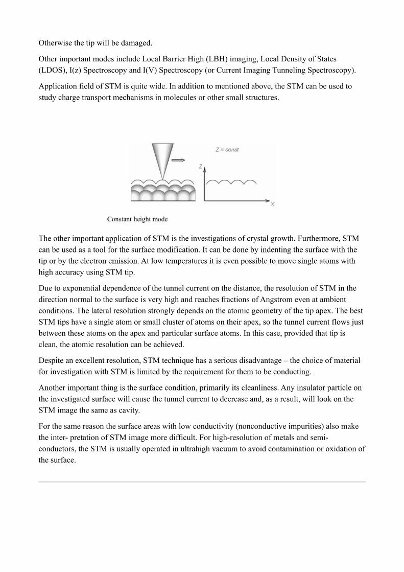
Otherwise the tip will be damaged.
Other important modes include Local Barrier High (LBH) imaging, Local Density of States
(LDOS), I(z) Spectroscopy and I(V) Spectroscopy (or Current Imaging Tunneling Spectroscopy).
Application field of STM is quite wide. In addition to mentioned above, the STM can be used to
study charge transport mechanisms in molecules or other small structures.
The other important application of STM is the investigations of crystal growth. Furthermore, STM
can be used as a tool for the surface modification. It can be done by indenting the surface with the
tip or by the electron emission. At low temperatures it is even possible to move single atoms with
high accuracy using STM tip.
Due to exponential dependence of the tunnel current on the distance, the resolution of STM in the
direction normal to the surface is very high and reaches fractions of Angstrom even at ambient
conditions. The lateral resolution strongly depends on the atomic geometry of the tip apex. The best
STM tips have a single atom or small cluster of atoms on their apex, so the tunnel current flows just
between these atoms on the apex and particular surface atoms. In this case, provided that tip is
clean, the atomic resolution can be achieved.
Despite an excellent resolution, STM technique has a serious disadvantage – the choice of material
for investigation with STM is limited by the requirement for them to be conducting.
Another important thing is the surface condition, primarily its cleanliness. Any insulator particle on
the investigated surface will cause the tunnel current to decrease and, as a result, will look on the
STM image the same as cavity.
For the same reason the surface areas with low conductivity (nonconductive impurities) also make
the inter- pretation of STM image more difficult. For high-resolution of metals and semi-
conductors, the STM is usually operated in ultrahigh vacuum to avoid contamination or oxidation of
the surface.
Raman Spectroscopy
Introduction
Raman spectroscopy is a spectroscopic technique used in condensed matter physics and chemistry
to study vibrational, rotational, and other low- frequency modes in a system. It relies on inelastic
scattering, or Raman scattering of monochromatic laser light. The laser light interacts with phonons
or other excitations in the system, resulting in the energy of the laser photons being shifted up or
down. The shift in energy gives information about the phonon modes in the system.
Basic Principle
The Raman effect occurs when light impinges upon a molecule, interacts with the electron cloud of
the bonds of that molecule and incident photon excites one of the electrons into a virtual state. For
the spontaneous Raman effect, the molecule will be excited from the ground state to a virtual energy
state, and relax into a vibrational excited state, which generates stokes Raman scattering. If the
molecule was already in an elevated vibrational energy state, the Raman scattering is then called
anti-stokes Raman scattering. A molecular polarizability change or amount of deformation of the
electron cloud, with respect to the vibrational coordinate is required for the molecule to exhibit the
Raman effect. The amount of the polarizability change will determine the Raman scattering
intensity, whereas the Raman shift is equal to the vibrational level that is involved.
When light is scattered from a molecule or crystal, most photons are elastically scattered. The
scattered photons have the same energy (frequency) and, therefore, wavelength, as the incident
photons. However, a small fraction of light (approximately 1 in 107 photons) is scattered at opti- cal
frequencies different from, and usually lower than, the frequency of the incident photons. The
process leading to this inelastic scatter is termed the Raman effect. Raman scattering can occur with
a change in vibrational, rotational or electronic energy of a molecule. If the scattering is elastic, the
process is called Rayleigh scattering. If it’s not elastic, the process is called Raman scattering.
If the substance being studied is illuminated by monochromatic light, for example from a laser, the
spectrum of the scattered light consists of a strong line (the exciting line) of the same frequency as
the incident illumination together with weaker lines on either side shifted from the strong line by
frequencies ranging from a few to about 3500 cm-1. The lines of frequency less than the exciting
lines are called Stokes lines, the others anti-Stokes lines.
The Raman effect arises when a photon is incident on a molecule and interacts with the electric
dipole of the molecule. In quantum mechanics the scattering is described as an ex- citation to a
virtual state lower in energy than a real electronic transition with nearly coinci- dent de-excitation
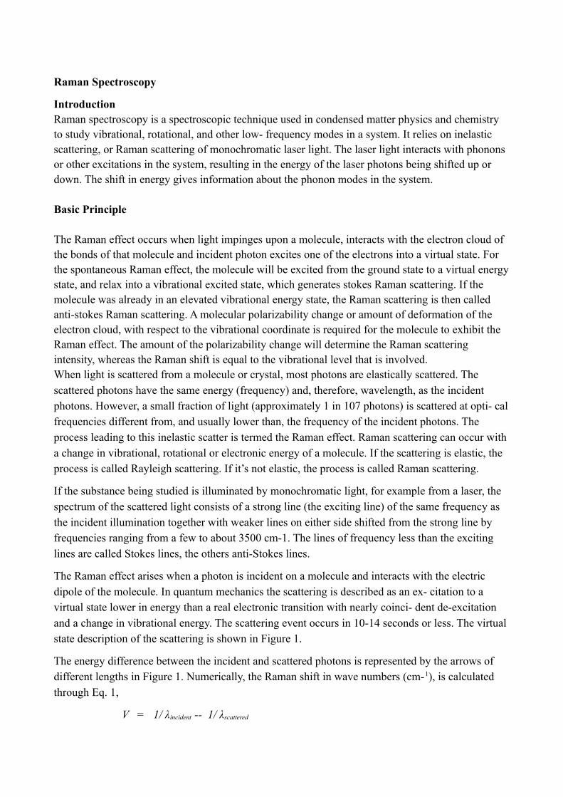
and a change in vibrational energy. The scattering event occurs in 10-14 seconds or less. The virtual
state description of the scattering is shown in Figure 1.
The energy difference between the incident and scattered photons is represented by the arrows of
different lengths in Figure 1. Numerically, the Raman shift in wave numbers (cm-1), is calculated
through Eq. 1,
V = 1/ λincident -- 1/ λscattered
in which the λ’s are the wavelengths (in cm) of the incident and Raman scattered photons, respec-
tively.
At room temperature the thermal population of vibrational excited states is low, although not zero.
Therefore, the initial state is the ground state, and the scattered photon will have lower energy
(longer wavelength) than the exciting photon. This Stokes shifted scatter is what is usually ob-
served in Raman spectroscopy. Figure 1(a) depicts Raman Stokes scattering.
A small fraction of the molecules are in vibrationally excited states. Raman scattering from vibra-
tionally excited molecules leaves the molecule in the ground state. The scattered photon appears at
higher energy, as shown in Figure 1(b). This anti-Stokes-shifted Raman spectrum is always weaker
than the Stokes-shifted spectrum, but at room temperature it is strong enough to be useful for
vibrational frequencies less than about 1500 cm-1. The Stokes and anti-Stokes spectra contain the
same frequency information. The anti-Stokes spectrum can be used when the Stokes spectrum is not
directly observable, for example, because of poor detector response at lower frequencies.
–-----------------------------------------------------------------------------------------------------------------------
3-D Surface Analysis
Surface metrology methods can be divided into “contact” and “noncontact”.
Noncontact (Optical) Methods
Microscopically, there is little ambiguity about the notion of contact but in the nanoscale one
is aware that the Born repulsion prevents atoms from moving arbitrarily close to each other.
In the atomic force microscope (AFM), nanoscale stylus scans over a sample.
The repulsion between the atoms of the AFM tip and sample asperity is actually action at a
distance, hence the method could equally well be classified as noncontact.

Noncontact (Optical) Methods
Optical profilers are analogous to the mechanical stylus instruments but use focused beams to
detect the location of the surface.
They are therefore unlikely to have the resolution required to characterize nanotexture.