Mechanical properties of nano-silver joints as die attach materials
14
Click here to load reader
Transcript of Mechanical properties of nano-silver joints as die attach materials

R
M
KP
a
ARRAA
KMSAL
C
0d
Journal of Alloys and Compounds 514 (2012) 6– 19
Contents lists available at SciVerse ScienceDirect
Journal of Alloys and Compounds
j our na l ho me p ag e: www.elsev ier .com/ locate / ja l l com
eview
echanical properties of nano-silver joints as die attach materials
im S. Siow ∗
ackage Innovation Development Centre, On Semiconductor SCG Industries Malaysia Sdn Bhd, Lot 122 Senawang Industrial Estate, 70450 Seremban, Negeri Sembilan, Malaysia
r t i c l e i n f o
rticle history:eceived 15 July 2011eceived in revised form 25 October 2011ccepted 28 October 2011
a b s t r a c t
This review traces the development of silver (Ag) as a die attach bonding material in the microelectronicpackaging industry from its’ early days as micron-scale silver flakes to the recent nanoscale Ag pasteand other derivatives. Basic materials properties include the composition of Ag pastes, the methods ofproducing Ag nanoparticles, and product applications will be presented. Key processing conditions will
vailable online 7 November 2011
eywords:echanical properties
interingg nanoparticles
be discussed to elucidate different factors which influence the mechanical properties of nano-Ag joints,principally the tensile and shear strength as well as thermal fatigue properties. Success in implementingnano-scale Ag pastes could only have been possible by deriving a fundamental understanding developedin the field of processing and using ceramic and metallic nano-powders.
© 2011 Elsevier B.V. All rights reserved.
ead free die attachontents
1. Introduction . . . . . . . . . . . . . . . . . . . . . . . . . . . . . . . . . . . . . . . . . . . . . . . . . . . . . . . . . . . . . . . . . . . . . . . . . . . . . . . . . . . . . . . . . . . . . . . . . . . . . . . . . . . . . . . . . . . . . . . . . . . . . . . . . . . . . . . . . . 62. Micron-scale Ag flakes . . . . . . . . . . . . . . . . . . . . . . . . . . . . . . . . . . . . . . . . . . . . . . . . . . . . . . . . . . . . . . . . . . . . . . . . . . . . . . . . . . . . . . . . . . . . . . . . . . . . . . . . . . . . . . . . . . . . . . . . . . . . . . . 73. Nano-scale Ag paste . . . . . . . . . . . . . . . . . . . . . . . . . . . . . . . . . . . . . . . . . . . . . . . . . . . . . . . . . . . . . . . . . . . . . . . . . . . . . . . . . . . . . . . . . . . . . . . . . . . . . . . . . . . . . . . . . . . . . . . . . . . . . . . . . . 8
3.1. Synthesis of Ag nanoparticles . . . . . . . . . . . . . . . . . . . . . . . . . . . . . . . . . . . . . . . . . . . . . . . . . . . . . . . . . . . . . . . . . . . . . . . . . . . . . . . . . . . . . . . . . . . . . . . . . . . . . . . . . . . . . . . . 83.2. Composition of nanoscale Ag paste . . . . . . . . . . . . . . . . . . . . . . . . . . . . . . . . . . . . . . . . . . . . . . . . . . . . . . . . . . . . . . . . . . . . . . . . . . . . . . . . . . . . . . . . . . . . . . . . . . . . . . . . . . 9
4. Mechanical properties . . . . . . . . . . . . . . . . . . . . . . . . . . . . . . . . . . . . . . . . . . . . . . . . . . . . . . . . . . . . . . . . . . . . . . . . . . . . . . . . . . . . . . . . . . . . . . . . . . . . . . . . . . . . . . . . . . . . . . . . . . . . . . . 104.1. Elastic modulus . . . . . . . . . . . . . . . . . . . . . . . . . . . . . . . . . . . . . . . . . . . . . . . . . . . . . . . . . . . . . . . . . . . . . . . . . . . . . . . . . . . . . . . . . . . . . . . . . . . . . . . . . . . . . . . . . . . . . . . . . . . . . . . 104.2. Strength. . . . . . . . . . . . . . . . . . . . . . . . . . . . . . . . . . . . . . . . . . . . . . . . . . . . . . . . . . . . . . . . . . . . . . . . . . . . . . . . . . . . . . . . . . . . . . . . . . . . . . . . . . . . . . . . . . . . . . . . . . . . . . . . . . . . . . . 11
4.2.1. Tensile strength . . . . . . . . . . . . . . . . . . . . . . . . . . . . . . . . . . . . . . . . . . . . . . . . . . . . . . . . . . . . . . . . . . . . . . . . . . . . . . . . . . . . . . . . . . . . . . . . . . . . . . . . . . . . . . . . . . . . . 114.2.2. Shear strength . . . . . . . . . . . . . . . . . . . . . . . . . . . . . . . . . . . . . . . . . . . . . . . . . . . . . . . . . . . . . . . . . . . . . . . . . . . . . . . . . . . . . . . . . . . . . . . . . . . . . . . . . . . . . . . . . . . . . . 12
4.3. Factors affecting the bonding strength of nano-Ag joints . . . . . . . . . . . . . . . . . . . . . . . . . . . . . . . . . . . . . . . . . . . . . . . . . . . . . . . . . . . . . . . . . . . . . . . . . . . . . . . . . . . 124.3.1. Bonding pressure . . . . . . . . . . . . . . . . . . . . . . . . . . . . . . . . . . . . . . . . . . . . . . . . . . . . . . . . . . . . . . . . . . . . . . . . . . . . . . . . . . . . . . . . . . . . . . . . . . . . . . . . . . . . . . . . . . . 124.3.2. Sintering temperature . . . . . . . . . . . . . . . . . . . . . . . . . . . . . . . . . . . . . . . . . . . . . . . . . . . . . . . . . . . . . . . . . . . . . . . . . . . . . . . . . . . . . . . . . . . . . . . . . . . . . . . . . . . . . . 134.3.3. Nanoparticle size, distribution and morphology . . . . . . . . . . . . . . . . . . . . . . . . . . . . . . . . . . . . . . . . . . . . . . . . . . . . . . . . . . . . . . . . . . . . . . . . . . . . . . . . . . . 134.3.4. Heating rate . . . . . . . . . . . . . . . . . . . . . . . . . . . . . . . . . . . . . . . . . . . . . . . . . . . . . . . . . . . . . . . . . . . . . . . . . . . . . . . . . . . . . . . . . . . . . . . . . . . . . . . . . . . . . . . . . . . . . . . . . 144.3.5. Dimension of bonding area . . . . . . . . . . . . . . . . . . . . . . . . . . . . . . . . . . . . . . . . . . . . . . . . . . . . . . . . . . . . . . . . . . . . . . . . . . . . . . . . . . . . . . . . . . . . . . . . . . . . . . . . . 144.3.6. Bonding substrate . . . . . . . . . . . . . . . . . . . . . . . . . . . . . . . . . . . . . . . . . . . . . . . . . . . . . . . . . . . . . . . . . . . . . . . . . . . . . . . . . . . . . . . . . . . . . . . . . . . . . . . . . . . . . . . . . . 144.3.7. Sintering time. . . . . . . . . . . . . . . . . . . . . . . . . . . . . . . . . . . . . . . . . . . . . . . . . . . . . . . . . . . . . . . . . . . . . . . . . . . . . . . . . . . . . . . . . . . . . . . . . . . . . . . . . . . . . . . . . . . . . . . 15
4.4. Thermal fatigue properties . . . . . . . . . . . . . . . . . . . . . . . . . . . . . . . . . . . . . . . . . . . . . . . . . . . . . . . . . . . . . . . . . . . . . . . . . . . . . . . . . . . . . . . . . . . . . . . . . . . . . . . . . . . . . . . . . . . 164.5. Recent innovations in LTJT . . . . . . . . . . . . . . . . . . . . . . . . . . . . . . . . . . . . . . . . . . . . . . . . . . . . . . . . . . . . . . . . . . . . . . . . . . . . . . . . . . . . . . . . . . . . . . . . . . . . . . . . . . . . . . . . . . . 164.6. Future challenges in LTJT . . . . . . . . . . . . . . . . . . . . . . . . . . . . . . . . . . . . . . . . . . . . . . . . . . . . . . . . . . . . . . . . . . . . . . . . . . . . . . . . . . . . . . . . . . . . . . . . . . . . . . . . . . . . . . . . . . . . . 17
5. Conclusions . . . . . . . . . . . . . . . . . . . . . . . . . . . . . . . . . . . . . . . . . . . . . . . . . . . . . . . . . . . . . . . . . . . . . . . . . . . . . . . . . . . . . . . . . . . . . . . . . . . . . . . . . . . . . . . . . . . . . . . . . . . . . . . . . . . . . . . . . . 17Acknowledgements . . . . . . . . . . . . . . . . . . . . . . . . . . . . . . . . . . . . . . . . . . . . . . . . . . . . . . . . . . . . . . . . . . . . . . . . . . . . . . . . . . . . . . . . . . . . . . . . . . . . . . . . . . . . . . . . . . . . . . . . . . . . . . . . . . 17References . . . . . . . . . . . . . . . . . . . . . . . . . . . . . . . . . . . . . . . . . . . . . . . . . . . . . . . . . . . . . . . . . . . . . . . . . . . . . . . . . . . . . . . . . . . . . . . . . . . . . . . . . . . . . . . . . . . . . . . . . . . . . . . . . . . . . . . . . . . 17
∗ Tel.: +60 6 671 2155; fax: +60 6 678 0725.E-mail addresses: [email protected], [email protected]
925-8388/$ – see front matter © 2011 Elsevier B.V. All rights reserved.oi:10.1016/j.jallcom.2011.10.092
1. Introduction
There are several European Union directives which aim toreduce and eventually remove lead from electronic materialsbecause of its hazardous effect on human health. Examples of

K.S. Siow / Journal of Alloys and Co
1000oC
800oC
600oC
400oC
200oC
0oC
-100oC
Steam Injec� on
Combu s�onSensing
Engine ControlEBS
AEROSPACE
Geothermal
Oil & Gas
WELLLOGG ING
AUTOMOTIVE
WheelMountedOn Engine
Combu s�on FlameMoni toring
SPACE &MILITARY
R
t2tetcma[
athtmsSt
phpfldb2
ptjmt(dTjapcc
tpsmc
Fig. 1. Indicative temperature range [5].eprinted with permission; ©1999 IEEE
hese directives are Restriction of Hazardous Substance (ROHS)002/95/EC, End of Life Vehicle (ELV) and Waste Electrical & Elec-ronic Equipment (WEEE) 2002/96/EC. Pb–Sn die attach materials isxempted from these directives until 2014, but no efforts are sparedo find Pb-free replacements for the die attach material. Currentandidate solders like Bi-alloys, Zn-alloys, and Au–Sn alloys haveany limitations like poor processability, poor corrosion resistance
nd high costs. These issues are comprehensively reviewed here1–3].
Besides lead-free applications, another driver for evaluatinglternative die attach strategies is the emergence of silicon carbideechnologies to replace silicon technologies. In order to achieveigher performance, the former operates at significantly higheremperatures, power, and voltages than the latter [4]. Different seg-
ents of industries which utilize high temperature electronics areummarized in Fig. 1 with their operating temperature ranges [5].uch high temperature applications require a new form of joininghe dies to the chip-carrier or leadframe.
The low temperature joining technique (LTJT) has been pro-osed as a possible alternative to lead-free die attach materials andigh temperature application mentioned above. LTJT is a techniqueioneered by Schwarzbauer and others to produce die attach jointsrom micron-scale Ag paste for power electronics packaging in theate 1980s [6]. Since then, LTJT technology has garnered a greateal of interests amongst the academia as well as industry playersased on more than 40 publications in this area for the period of010–2011.
There are numerous benefits associated with the use of Agarticles in LTJT. Silver has better thermal and electrical conduc-ivities than the commonly used Sn–Pb or Pb-free joints. Nano-Agoints are sintered at temperatures significantly lower than the
elting temperature of Ag, typically 0.2–0.4 Tm [7]. Once sinteredhe Ag joint will have a melting temperature similar to bulk Ag961 ◦C). This property will avoid the remelting problem in theownstream microelectronic packaging and assembly processes.hermal impedance measurement also confirmed that nano-Agoint perform better than Sn–3Ag–0.5Cu alloy or Sn–Cu–Ni–Gelloy (better known as trade name “SN100C”) [8]. Based on theseroperties, nano-Ag has been listed in recent literature as leadingandidate for lead free die attach as well as die-attach for siliconarbide technologies [4,9–11].
Due to micron scale Ag flakes, the pressure required to affecthis bonding in LTJT can be as large as 80 MPa [12] though lower
ressures of ∼10 MPa have also been demonstrated [6]. “Pressureintering” is also a term commonly used to describe sintering oficron-scale Ag particles [13]. Pressure sintering is similar to theommonly used sinter-forging used in the ceramic industry but of
mpounds 514 (2012) 6– 19 7
even higher pressures in the range of more than 100 MPa [14]. Inthe semiconductor industry, pressure sintering was initially usedin semiconductor components like diodes, thyristors, and insulatedgate bipolar transistors (IGBT) that are more robust than the silicontrench technologies. Hence, there are various efforts to reduce thestresses impressed by the sintering conditions.
One viable approach for reducing the pressure requirement inLTJT is to reduce the size of Ag particles to the nanometer range[15,16]. When Ag particles are reduced to such a dimension theeffective surface area, which in turn implies the number of Ag sur-face atoms increase several fold. The surface area may be as highas 23.81 m2/g for Ag nanoparticles of 26 nm diameter [17]. Thesechanges in surface area and concomitant increase in surface cur-vature provides the driving forces to sinter with neighbouring Agatoms at temperatures 0.2–0.4 of the melting point (Tm) [7]. Dueto the use of nano-size particles LTJT is also known as nanocrystal-enabled solid state bonding [18].
This review traces the early development of LTJT with micron-scale Ag flakes. Early lessons from the formulation of themicron-scale Ag paste and processing routes eventually led to thedevelopment of nanoscale Ag pastes. Different processing parame-ters affecting the mechanical properties like shear strength, tensilestrength, elastic modulus, fatigue properties of nano-Ag jointsare discussed. Key lessons are drawn from results related to Agnanoparticles used in LTJT and guiding principles are also takenfrom related fields like Ag nano-ink of printed electronics and othermetallic or ceramic nanoparticles. This review is expected to beuseful to researchers who are exploring nano-scale Ag pastes asoptions for lead-free die attach materials.
2. Micron-scale Ag flakes
Early effort in the use of micron-scale Ag flakes as joining mate-rials is led by Schwarzbauer and his team. Several patents have beenfiled in the area of process, materials applications and componentlevel joining with the micron-scale Ag paste [13,19]. In general, theprocessing steps are [13,20–22]:
1. Print the micron-scale Ag paste (Ag flakes, carrier and solvent)on the board.
2. Preheat the micron-scale Ag paste to drive out the solvent.3. Place the die on the dried Ag paste.4. Sinter the die under pressure (9 MPa) and high temperature
(150–250 ◦C) to form the Ag bond.
Other researchers have applied and preheated this micron-scaleAg paste on the wafer backside before the sawing and die-bondingstage [23]. Another approach for applying micron-scale Ag pastewas to create the microscopic Ag particles in situ for bonding byreducing the Ag oxide chemically prior to die-bonding [24].
However, there were claims that the preheating stage can beeliminated if a slow heating rate of less than 2 ◦C/min was main-tained to reach the sintering temperature of ∼180 ◦C [25]. Thisnon-pre-heating approach was based on the sintering of Ag flakesat their edges to form an extended network of metal flakes in theabsence of applied pressure [25]. Others also removed the preheat-ing stage but sintered the micron-scale Ag paste in an oxidizingenvironment at 300 ◦C [26]. Other used pre-sintered micron-scaleAg laminates to enable bonding of electronic component at lowertemperature (150 ◦C) and pressure (30 MPa) [27].
These micron-scale Ag pastes consist of two main components
namely Ag flakes (diameters of ∼15 �m)[13,27] and solvents likecyclohexanol [12,13], butanol [25], terpineol [28], or an ethyleneglycol ether [28] mixture of cyclohexanol–methanol [27]. In theprinted electronics industry metal-organic compounds like silver
8 and Co
stafl
lsarseem
3
sbwm
aabhultriw
qamtdobdaet
si
tpaodcsmbedwns
12
K.S. Siow / Journal of Alloys
tearate or silver oxalate are often added to be decomposed to formhe silver bridge linking the micron-scale silver flakes [29]. Such anpproach can also be used in the formulation of micron-scale Agakes as bonding materials but is not found in the literature.
Since this early success of micron scale Ag paste in componentevel mounting, there is an interest to use Ag paste to bond otherilicon technology die to the substrate materials; aptly termeds “die-bonding”. A good “die bonding” step must fulfil certainequirements such as not transmitting destructive stress to theilicon dies during bonding and operation, ability to withstandxtreme temperature without degradation in bonding quality, goodlectrical and thermal contact between the silicon die and substrateaterials.
. Nano-scale Ag paste
In the development of ceramic or metallic nanoparticles, con-olidation or compaction was always carried out before sinteringut this processing route was only meant for making bulk materialsith desired thermo-mechanical properties [14], not for bondingaterials as described here.Adaptation of this approach in nanoscale Ag paste is limited
nd may result in undesirable effects. Compaction of these driednd porous nano-Ag pastes before sintering may not be a feasi-le approach to achieve higher densities because Ag nanoparticlesave a large number of particle–particle contacts per unit vol-me which creates high internal stress [30]. This residual strain is
ikely to cause delamination between the dried nano-Ag paste andhe frame. On the other hand, foams of dried Ag paste have beeneported to adhere easily to smooth surfaces like silicon and poly-mide [28] though the bonding requires other processing conditions
hich will be discussed later.In general, the process steps of using nanoscale Ag paste were
uite similar to that of micron-scale Ag paste [31–34]. There werelso some reports which describe a different approach compared toicron-scale Ag sintering-eliminating the preheating stage before
he die attachment step [35–42]. The heating rate is very critical torive out the solvent and promote sintering simultaneously, detailsf which will be discussed in later sections. Others applied andaked this nanoscale Ag paste on the backside of the wafer beforeie bonding on the leadframe [43]. Another variation is to applynd dry the nanoscale Ag paste on the wafer and the leadframe tonsure metallurgical bonding and mechanically stable anchoring ofhe porous dried nanoscale Ag paste during die bonding [40,43].
Typically, nanoscale Ag paste is transferred to the substrate bypray coating, foil transfer, dispensing [44], stencil or screen print-ng [31] and dipping [43].
Each variation of the process steps mentioned earlier is expectedo influence the sintering mechanism and the final mechanicalroperties of the nano-Ag joint. These variations are expected toffect the two primary stages of joint formation namely the evap-ration of solvent and the accessibility of oxygen to remove theispersant on the Ag nanoparticles to allow the sintering pro-ess to proceed [35,45,46]. Some researchers introduced a thirdtage in the process flow, adding a final burn-off of the higherolecular weight binder system [47]. These different stages will
e discussed in detail in the subsequent section on factors influ-ncing shear strength of nano-Ag joints. Depending on the type ofispersant used in the Ag nanoparticle materials, exothermic peaksere detected between ∼220 ◦C and ∼280 ◦C during sintering of Aganoparticles. These peaks could be attributed to thermal events
uch as [48]:. Crystallization and consolidation of the metal particles.
. Recrystallization of strained metal particles.
mpounds 514 (2012) 6– 19
3. Diffusion between unstable surface atoms on the nanoparticleswhich leads to surface sintering.
4. Gas phase formation/evolution from the nanoparticles.5. Oxidation of chemisorbed fatty acids (carriers or solvents) [31].
While each of these thermal events has equal probability tocause the sintering of nanoscale Ag paste, its intensity may differdepending on the bonding routes described earlier, the materialsand physical properties of the Ag nanoparticles and type of disper-sants.
Generally, there are three stages of sintering for nanopowdersalthough the morphological transition from one stage to anotheris not always well defined [14,16,49]. In the initial stage of sin-tering the adhesion mechanism, like surface diffusion, dominatesto produce necking at adjacent Ag nanoparticles [50] with a cor-responding increase in mechanical strength [14]. At this stageof sintering, the ratio of X/D is less than ∼0.3 where X is theparticle–particle neck size and D is the particle (grain) size [49].
In the intermediate stage the networks of interpenetrating poresare shrinking in the radial direction with a concomitant increasein density up to 90–92% of theoretical [14,49]. The “X/D” is morethan ∼0.3 at this stage of sintering [49]. In the final stage therewill be collapse of tubular pores to spherical pores [49]. Under theright sintering conditions, all pores are eliminated [14]. For metallicnanoparticles, the large shear stress at the curved neck regions alsogenerates dislocations which induce grain rotation which aids indensifying the sintered nanoparticles [51].
3.1. Synthesis of Ag nanoparticles
The earliest record of producing unpassivated Ag nanoparti-cles or colloidal Ag, as they were known, was documented byFrens and Overbeek in 1969 based on the Carey Lea’s approachof 1889 [52]. Since then, there have been numerous reviews onthe synthesis of Ag nanoparticles for diverse applications like elec-tronics, green technologies, biomedical needs, etc. [53–55]. Thisreview gives a short summary of available techniques with empha-sis on synthesis of Ag nanoparticles to formulate Ag paste for dieattach application. Generally, the Ag nanoparticles of sizes lessthan 20 nm are precipitated from Ag salts to form agglomerateswith sizes ranging from 800 to 3500 nm [31]. Reducing agents likeascorbic acid [40,56], hydrazine monohydrate [57], sodium citrate[58] or sodium citrate dihydrate [59], polyvinylpyrollidone [50],ethylenediaminetetraacetic acid (EDTA) [60], sodium sulfite [61]and sodium borohydride [62] were added into Ag salts like nitrates,sulphates or chlorates or Ag–ammonia complexes [62]. The reduc-ing reaction occurred in a polar solvent such as ethanol, methanol,acetonitrile or tetrahydrofurane [40]. Condensation with a cen-trifuge might be carried out after the reduction steps to increasethe concentration of the Ag nanoparticles [58].
Besides precipitation techniques, combustion chemical vapourcondensation (CCVC) also produced unpassivated Ag nanoparti-cles from AgNO3 [48]. In the CCVC process, precursor containingAg-bearing chemical were dissolved in combustible fuel. TheNanomiser® Device atomized this precursor into microscopicdroplets in an oxygen stream which were then combusted to pro-duce the Ag nanoparticles. Others used a thermal decompositionmethod to produce a passivating layer in situ by mixing and heat-ing AgNO3 with fatty acids like oleic acid, stearic acid and myristicacid in a nitrogen atmosphere [63]. Monodispersed Ag nanoparti-cles could also be produced by reacting silver myristate or silvertetradecanoate (C13H27CO2Ag) with a tertiary alkylamine like tri-
ethylamine [64] or trioctylamine [65]. This technique used thecarboxylate ligand precursor to prevent aggregation and controlthe size distribution while the amine reduced amine-coordinatedintermediates to Ag nanoparticles [65]. The oxidation of long chain
K.S. Siow / Journal of Alloys and Compounds 514 (2012) 6– 19 9
Ag
Ag
Ag
Aghead
H-Bond
tail
O-H
H-O CO
Binder
Thinner
- - --
- - --
- - --
- - --
- - --
- - --
- - --
- - --
- - --
- - --
- - --
- - --
- - --
- - --
- - --
- - --
- - --
- - --
- - --
- - --
- - --
- - --
- - --
- - --
- - --
- - --
----
- - --
Dispersant
- - -- - -
- - --
hinner
a[
3
pofif
ptudoSedT
aasn
“r1tIcaitt
bbw
dtbv
to be unsuitable because of its’ high temperature stability up to andabove ∼300 ◦C [45].
131211109876543210
100
150
200
250
300
Boilin
g Po
int (
o C)
--
Fig. 2. Functions of the dispersant, binder and t
lcohols with Ag2CO3 also produced passivated Ag nanoparticles35].
.2. Composition of nanoscale Ag paste
The weight percentage of Ag nanoparticles in the nanoscale Agaste is normally above 50% with percentages as high as ∼70% [38]r ∼80% [40]. This percentage will ensure its viscosity is suitableor applying the die attach materials via screen printing or dispens-ng methods. Unlike highly conductive epoxies, nanoscale Ag pasteorms an interconnect material of “100% Ag”.
Besides Ag nanoparticles, the main additives of nanoscale Agaste are dispersants, binders and solvents [16]. Most literaturereats the dispersant and binder as having the same functions andses the two terminologies somewhat interchangeably. Besidesispersing the nanoparticles, binders have the additional functionf preventing cracking of the dried Ag paste during handling [16].olvent is also added to the nanoscale Ag paste to adjust viscosity forasy printing after the initial blend of Ag nanoparticles and binders-ispersants are made. Examples of these additives are shown inable 1 [66–68].
Dispersants, as shown in Fig. 2, consists of polar acids whichnchors on the Ag nanoparticles while the hydrophobic tails acts spacers from adjacent particles [16]. This dispersant providesteric resistance and decreases the system energy to prevent theanoparticles from melting and self-sintering [69].
Experimentally, self-sintering of Ag nanoparticles (known assubmicron Ag”) at room temperature had been deduced witheduction of surface area using BET adsorption isotherm as early as984 [70]. However, aggregation or agglomeration of Ag nanopar-icles can also contribute to the reduction of the total surface area.n recent times, the emerging interest of printing electronic cir-uits at room temperature spurred microanalytical activities in thisrea. HR-SEM (high resolution scanning electron microscopy) andn situ TEM (transmission electron microscopy) analyses were ableo demonstrate self-coalescence of Ag nano-particle at ambientemperature [71,72].
Aggregates and agglomerates of nanoparticles are differentiatedy the strength of the interparticle bonding [14]. Agglomerates cane reverted to nanoparticles by ultrasonic or mechanical agitationhile the same cannot be carried out for Ag aggregates.
The selection of a dispersant depends on the effectiveness in
ispersing Ag nanoparticles and reaching the desired sinteringemperature in the shortest time possible. Dispersants constituteetween ∼1 and ∼15 weight percent of the total weight of passi-ated Ag nanoparticles [33] although the percentage of all organicsin the formulation of nanoscale Ag pastes [16].
in the paste could be as high as 22 weight percent [16]. It isimportant to adequately protect these Ag nanoparticles from self-coalescence until the sintering temperature is reached becauseagglomeration or aggregation at lower temperatures will reducethe driving force for densification during the sintering step.
Some dispersants like fatty acids with longer hydrocarbonagents could disperse the Ag nanoparticles better than those withshorter hydrocarbon chains [16]. Others specified the dispersantfrom the perspective of molecular weight to be less than ∼250 gwhich is a relatively long hydrocarbon [40]. Longer chain disper-sants increase the steric repulsion because of unfavourable entropyin the confined, highly curved spaces between Ag nanoparticles[73]. The magnitude of steric repulsion was also affected by thesolvent used in the paste which influenced the radius of gyrationof these dispersant and other binders in the paste [73].
The targeted burnout temperature of the dispersant is directlyrelated to its boiling temperature. As shown in Fig. 3, the boilingpoint of the dispersant is related to the number of carbons in the dis-persant [16]. Hence, it is possible to choose a dispersant which willdecompose just below the sintering temperature of the nanoscaleAg paste. In this respect, polyvinylpyrollidone (PVP) had been found
Number of Carbon Atoms
Fig. 3. The relationship of the boiling point of fatty acid versus their number ofcarbon atoms.
Adapted from the Sigma–Aldrich websites [16].

10 K.S. Siow / Journal of Alloys and Compounds 514 (2012) 6– 19
Table 1Main additives of nanoscale Ag paste.
No Component Example
1 Dispersant/passivatinglayer/organic shell/cappingagent
Menhaden fish oils [16,67], poly(diallydimethyl ammonium chloride) (PDDA) [16,67], polyacrylic acid (PAA)[16,67], polystyrene sulfonate (PSS) [16,67], triethylene glycol [32], methyloctylamine [40,56], dodecylamine[66], hexadecylamine [33], myristyl alcohol [46], 1-dodecanol [35], 1-decanol [35] stearic acid, oleic acid,palmitic acid [31], dodecanethiol [33]
yvinyl(IBCH], phe
Aiddoii
a[wia
tniAalm
p[irirv2
pala[drs
t1csptit
4
p∼
2 Binder Ethyl cellulose [68], pol3 Solvents/thinner Isobornyl cyclohexanol
xylene [40], ethanol [40
Therefore, an ideal dispersant possesses low binding energies tog nanoparticles surfaces and a low boiling temperature to ensure
ts easy evolution. At the same time this dispersant must be stableuring extended room-temperature storage. This dispersant ideallyecomposes in a relatively narrow temperature band in a non-xidizing environment below 300 ◦C. A non-oxidizing environments also preferred to avoid oxidizing the substrates and surfaces usedn die bonding.
In certain circumstances, additional surfactants such as BYK163nd Dysperbyk 163 were added to disperse the Ag nanoparticles33]. Then the mixture of different additives and Ag nanoparticlesere mixed in a high speed mixer before ball-mill or 3-roll mill
nto a homogeneous phase [33]. Others used ultrasonic agitationnd vacuum evaporation to mix the nanoscale Ag paste [16].
Besides blending nanoscale Ag paste, others used Ag nanopar-icles inks from printed electronics as bonding materials to formano-Ag joints [18]. Although nano-Ag inks have some similarities
n selection of dispersants and solvent vehicles with the nanoscaleg paste their final compositions are dissimilar [74]. In the liter-ture, the nano-Ag ink is typically used to fabricate conductiveines under pressureless sintering and seldom reported as die attach
aterials.Due to oxidation, and in certain cases by formulation, Ag oxide
articles will be present in Ag nano-ink or nanoscale Ag paste18,75,76]. Their effect on the bonding qualities will be discussedn subsequent sections. Others include Ag2CO3 or silver lactate aseactive materials to be decomposed to reactive Ag to fill the poros-ty in the nano-scale Ag paste [41,76]. Such approaches have beeneported earlier to bind adjacent micron-scale silver flakes with sil-er decomposed from metal-organic silver compounds like silver-ethylhexanoate or silver oxalate [29].
Alternatively, Ag pastes containing exclusively silver com-ounds like silver lactate or Ag2CO3 have been claimed to be a betterpproach to form interconnects than Ag paste mixtures of metal-ic silver nanoparticles because the former has less problems ofgglomeration which generally increases the sintering temperature76]. Compounds of Ag2CO3 have also been detected as residualsuring processing of nano-Ag paste from AgNO3 and sodium cit-ate [58] or even in the colloidal Ag particles produced from electricpark discharge technique [77].
Other impurities like copper, potassium and sodium are alsoypically found in the nanoscale Ag paste in the range of less than000 ppm, although it has been reported on rare occasion that theopper content may rise to ∼2700 ppm [31]. Sodium or potassiumalts of the fatty acids which were used as lubricants for the millingrocess, were also detected in the Ag paste [31]. These impuri-ies did not appear to interfere with the bonding process [31] butnstead it had been shown to improve bondability of the Ag pasteo the copper substrate [38].
. Mechanical properties
Unlike Sn–Pb solders, Ag joints do not suffer from room tem-erature ageing because of the low homologous temperature of0.3Tm. Sintered nano-Ag joints assume the melting temperature
alcohol [16], polyvinyl butyral (PVB) [16,67], wax [16,67]) [36], texanol [16,67], terpineol [16,40,41,67], butyl carbitol [33], toluene [33],nol [40].
of bulk Ag (961 ◦C) after formation. Its low homologous tempera-ture also results in insensitivity to strain rate and hence, creep is notexpected to have a marked influence on the mechanical propertiesof the joint material at room temperature. However, reduction oftensile strength for sintered bulk nano-Ag has been reported to besignificant at strain rate of 0.001%s−1 and testing temperature ofmore than 120 ◦C [78].
4.1. Elastic modulus
Elastic modulus is the ratio of stress to strain in the elastic regionduring a tensile loading. Elastic modulus is essentially independentof small compositional or microstructural differences because itdepends predominantly on forces between atoms in the crystal lat-tice. In the case of sintered Ag nanoparticles the microstructure andcomposition is almost homogeneous except for residual dispersant.
In the literature, the elastic modulus (E) of free-standing sin-tered Ag nanoparticles, as measured by tensile testing and dynamicmechanical analyser, was reported to be ∼9 GPa [15] and ∼ 6–7 GPa[78,79] respectively at room temperature. By comparison the elas-tic modulus for sintered Ag nano-ink and sputtered Ag were118 GPa [80] and 148 GPa [81] respectively (N.B. Elastic constantof a typical bulk silver is 82.7 GPa [82].) The latter measurementswere carried out with a nano-indenter in compression mode. In thecase of free-standing sintered Ag nanoparticles, the sintering wascarried out when the nanoscale Ag paste was constrained by a sub-strate [15]. Hence, the test piece was likely to be more porous thanusual which further lowered the elastic modulus.
Besides the density of pores the ratio of “annular flaw size/poreradius” also influences the elastic modulus of nanomaterial primar-ily in compacted nanoparticles [83]. This concept can be traced tothe stress distribution at the sharp pore tip. A larger ratio impliesthat the crack is longer and sharper resulting in a higher stress con-centration. The joint will experience brittle failure in the absence ofany stress relaxation mechanism. However, a close examination ofpublished stress–strain curves of nano-Ag joints [84] showed theminimum macroscopic yield before failure and localized yield asexemplified by dimple formation on the fracture surfaces.
In the case of the shear modulus (G), values ranging from 0.4 to0.6 GPa were derived from published shear stress–strain graphs ofnano-Ag sintered joints [84]. In a related study, if the sound wavevelocity measurement method was used to measure compactedAg nanoparticles (97% density), the effective elastic constant wasapproximately 20% lower than those reported for polycrystallineAg ≈ 66 GPa (E) and ≈24 GPa (G) [30]. The researchers’ analysisattributed the cause of this observation to the indirect influence ofinternal stress in the Ag compact while dismissing the influence ofdisordered interfacial structure and intergrain sliding in this com-pacted Ag nanoparticle material. It should be mentioned that thisAg compact was not sintered but merely compacted at 2.3 GPa.
In summary the modulus of printed and sintered Ag nanopar-ticles (6–9 GPa) [15,78,79], which are lower than moduli of typicalPb–Sn, or Pb-free, solder joints provides good thermo-mechanicalproperties during thermal cycling [85]. This low modulus is entirely

and Compounds 514 (2012) 6– 19 11
fc
pbslamhpg
4
aatoo2gwys
ttf[th
4
pvsiafmswttcpn
jrfpaucattsb[ea
4003503002502001501000
10
20
30
40
50
60
70
80
Tens
ile S
treng
th (M
Pa)
Sintering Temperature (oC)
Au (Hirose, 2009) Au (Akada, 2008) Cu (Akada, 2008) Cu (Hu , 2 010)
followed by phase identification with X-ray diffractometer (XRD),Raman spectroscopy or Fourier transform infra-red (FTIR) spec-troscopy [93].
1210864200
10
20
30
40
50
60
Shea
r Stre
ngth
(MPa
)
Bonding Pressure (MPa)
250oC (Morisada, 2010) 250oC (Tobita, 2010)300oC (Morisada, 2010) 300oC (Ide, 2005) 300 oC(Ide, 2006)350oC (Morisada, 2010)
K.S. Siow / Journal of Alloys
ortuitous and a result of sintering of un-compacted Ag nanoparti-les.
It is neither practical nor the aim of current research trends toroduce a nano-Ag joint of 100% density because of the need toalance the elastic modulus and other mechanical properties liketrength and fatigue properties [85]. High density Ag nanoparticlesike those in compacted Ag achieving densities from 85% to 97%re also likely to face grain-growth issues which reduce the goodechanical properties of nanocrystalline Ag [30,86]. Elsewhere, it
as been reported that nanomaterials with 90% density and openores morphology is the most convenient way to control grainrowth in nanomaterials [7].
.2. Strength
There are two types of strengths: bulk sintered Ag nanoparticlesnd nano-Ag joint strength. Two possible loadings namely shearnd tensile, are possible. Bulk sintered Ag nanoparticles can only beested in tension. This bulk strength forms the minimum strengthf the joints if the interfacial bonding with the substrate is high. Inne study, the bulk tensile strength for Ag nanoparticles sintered at80–300 ◦C was −43 MPa [15]. Based on the published stress–strainraph there was minimal strain hardening and the yield strengthas estimated to be 30 MPa (0.02% offset) [15]. These tensile and
ield strengths are comparable to the tensile strength of Pb-freeolders reported in the literature [87].
However, the yield strength of sintered nano-Ag was compara-ively lower than compacted Ag nanoparticles based on hardnessesting converted yield strength of about 200 MPa, based on theollowing formula: yield strength is ∼1/3 of the hardness (in GPa)30]. This result is to be expected because of the higher porosity inhe sintered nano-Ag joint versus the compressive loading in theardness tester which tends to close the pores.
.2.1. Tensile strengthDuring tensile loading of a joint, the cross-section of the sam-
le contracts to maintain the volume of the Ag nanoparticles, andoid volumes alter their shape accordingly. This contraction is con-trained by the substrate which transfers the uniaxial tensile stressnto triaxial stress within the joints [88]. The adjacent substratesre still stressed within elastic range. As a result the joints will onlyail when they reach the brittle fracture stress point of the bonding
aterial. This transfer of stress will elevate the measured tensiletrength above bulk values of the bonding materials. Surprisingly,hen the tensile strength of a nano-Ag joint [32] was compared to
hat of bulk sintered Ag nanoparticles [15], the tensile strength ofhe former was lower than the latter. This difference is likely to beaused by the efficient transfer of stress in brazed joints [88] com-ared to the poorer transfer in the relatively low density sinteredano-Ag joint.
As shown in Fig. 4, a higher sintering temperature produces aoint of higher tensile strength [32,89]. A similar observation wasecorded for the shear strength in Fig. 5 for joints which have beenabricated under similar bonding pressures [37,38,46,56]. A higherercentage of dispersant on the Ag nanoparticles will decomposet a higher sintering temperature. This decomposition exposed thenpassivated Ag nanoparticles to neighbouring nanoparticles foroalescence [32]. The resulting nano-Ag joint formed strong bondsnd the fracture interfaces were reported to be cohesive failurehrough the sintered Ag nanoparticles [32]. As shown in Fig. 4,he joint design also influences the increase of tensile strength atimilar sintering temperatures [58]. Hu’s design of using Cu wire
onding to Cu pad design resembled mixed “tensile-shear” stress58] instead of the relatively “pure” tensile stress used by Akadat al. [32] and Hirose et al. [89]. Their dispersant chemistries arelso likely to be different and its influence on the tensile strengthFig. 4. Tensile strength of Ag nanoparticles joints on copper (Cu) and gold (Au)-plated substrates at 5 MPa, 5 min [32,58,89].
will be discussed later. It should be noted here that when the sinter-ing temperature of nano-Ag paste, used by Hu et al., was increasedto 250 ◦C, the failure interface shifted to substrate breakage insteadof joint failure [58].
There is some speculation that the decomposition of Ag oxidesto Ag also contributes to the sintering process at higher bondingtemperatures. Different decomposition temperatures of Ag oxidessuch as 210 ◦C [75], 250 ◦C [86,90], 280 ◦C [18], 330 ◦C [91], 385 ◦C[92], 454 ◦C [93] have been reported in the literature. The exactdecomposition temperature and mechanism of Ag oxides to Agdepends on several factors like the preparation method of theAg oxide particles, different analysis methods, mechanical ageingconditions, partial pressure of gases like oxygen or CO2 [92–94].Regarding testing methods, dynamic heating methods with differ-ential scanning calorimetry (DSC) and thermo-gravimetric analyser(TGA) normally produces a higher decomposition temperature, asmuch as 50 ◦C more than isothermal heating methods, which is
Fig. 5. Shear strength of Ag nanoparticles joints for bonding in ambient atmospherefor Ag nano-particle size between 8–11 nm using “double-copper disc” configuration[37,38,46,56]. Note: “250 ◦C”, “300 ◦C” and “350 ◦C” refer to the sintering tempera-ture for this joint.

1 and Co
nd∼ott∼
4
dmwortrlp
sdoicrtwstp6a
ttpualtsbs
4
4
ttfh[A
stoicitrf
which showed that nanoparticles will assume the melting temper-ature of bulk Ag properties at sizes larger than approximately 85 nm[50].
50403020100-200
0
200
400
600
800
1000
Mel
ting
Tem
pera
ture
(o C)
Dominquez et al. Classical Thermodynamics Classical Sintering Prediction
2 K.S. Siow / Journal of Alloys
An examination of published DSC and TGA data of Aganoparticles did not reveal any thermal activity related to theecomposition of Ag oxides in the temperature range above350 ◦C [31,48,56,68,89]. Hence, the influence of decompositionf Ag oxides, if any, on the sintering of Ag nanoparticles is likelyo be minimal. Silver nanoparticles, per se, had also been reportedo reduce the burnout temperature of the binder to a range below350 ◦C [68].
.2.2. Shear strengthThe loading for die attach application is often in shear mode
uring thermal cycling. Microscopically, yielding mechanism of aetallic system like sintered Ag nanoparticles is crystal planes sliphich is controlled by shear stress. In shear loading, deformation
ccurs within the bonding material which is likely to produce moreepeatable results. However, deformation during sample prepara-ion could introduce a tensile mode into the pure shear loadingesulting in a saturation of the maximum shear strength at valuesower than the actual strength, to approximately 40 MPa for onearticular joint design reported in [95].
The most common approach adopted to measure the sheartrength of nano-Ag joint is to use a fixture similar to a commercialie shear tester to shear a “square/rectangle” bonded onto a frame,r two coins with “face to face” bonding. This tester consists of annstrument to apply the load with a contact tool to shear the “sili-on die” at lift-off offset from the joining substrate. This approachequires the contact tool and dies to be kept parallel to each othero avoid cracking the dies before shearing occur. Another concernith such a die shear tester is the lift-off offset from the joining
ubstrate. Current approach normally uses this joining substrate ashe datum but uneven thickness of the nano-Ag joint can result ineeling of the die attach materials. Several standards like IPC-TM-50 and MIL-STD 883 provide some guidelines for die shear testingnd loading.
A single lap shear joint has also been reported to measurehe shear stress of nano-Ag joints [44,68], but it suffers fromhe addition of a bending component. The bending introduces aeeling stress into the total stress measurement which therebynderestimates the actual shear stress. The length of joint overlaplso influenced the measured shear strength [88]. With increasingength of overlap, the shear strength was found to decrease becausehe central portion of the joint sustained little or no stress, whiletress was concentrated at both ends. Such geometric factors muste taken into consideration when comparing results from differentources.
.3. Factors affecting the bonding strength of nano-Ag joints
.3.1. Bonding pressureThe influence of bonding pressure on the shear strength is illus-
rated in Fig. 5 for shear testing on copper substrates. Besideshe results for a sintering temperature of 250 ◦C, it is apparentrom Fig. 5 that increasing the bonding pressure will result inigher shear strength for nano-Ag bonded with copper substrates37,38,46,56]. A similar trend was reported for joints formed ong-plated substrates [68].
When pressure is applied during sintering, the hydrostatic pres-ure and shear stress build-up in the nano-Ag joint is similar tohat built-up in sinter forging of nanocrystalline ceramics with-ut die (no lateral constraints) [49]. The hydrostatic componentncreases the average number of contacts between Ag nanoparti-les to increase the sintering rate [68,95]. If the amount of pressure
s sufficiently high, the induced shear strain will also tend to closehe pores and align the grains similar to those reported in nanoce-amics [49]. As a result the path for diffusion and the driving forceor sintering also increase concomitantly [68,95].mpounds 514 (2012) 6– 19
However, most published results in literature, including thosereviewed here, show extensive porosity suggesting that pressureand other sintering conditions like temperature and time werenot consolidating the nano-Ag to a high density. Earlier in Section4.1, the author has discussed the need to have a porous nano-Agjoint with lower elastic modulus for enhanced reliability in ther-mal cycling application. In this section, sufficiently high density isneeded to achieve reasonable strength to meet the loading require-ment of the nano-Ag joint. Hence, a balance must be struck betweenthese two objectives.
In Fig. 5, the sintering pressure for various bonding experimentswas applied for duration of 150–300 s. During this time it is likelythat the higher pressure is only effective if an elevated temper-ature, higher than 250 ◦C to oxidize the dispersants, is achieved.Similar observations of “high temperature to achieve better sinter-ing properties” have been reported for nano-ceramic system liketrialuminides [96].
In order to ease the automation of die-bonding, there havebeen several attempts to sinter the nanoscale Ag paste withoutthe addition of pressure [35,39,68]. Such approaches are knownas “pressureless sintering” in the field of nanocrystalline ceramicswhich typically control sintering schedules like sintering/heatingrate and combined-stage sintering [49]. Some of these approacheshave been adopted in forming nano-Ag joints, and will be discussedlater [39,68].
Although the shear strengths for pressureless sintering wereadequate, i.e. 11–12 MPa, the fracture surface suggested unevenbonding with weak spots scattered on the joining areas [35]. In theabsence of applied pressure the sintering mechanism was likely tobe assisted by liquid capillary pressure from the “molten” surface ofthe nanoparticles [36]. The melting temperature of Ag nanoparti-cles with a dimension of 2.3 nm can be as low as ∼360 ◦C [97] whileits surface may melt at lower temperatures [98]. In situ TEM studyshowed that melting occurs between adjacent Ag nanoparticles atdimensions of between 15 and 40 nm at temperature of 400 ◦C [99].In a related study when Ag nanoparticle sintering was treated as aliquid-state phenomena based on a Debye model with Lindemann’sLaw, the theoretical melting temperature was modelled as shownin Fig. 6 [50]. This model agreed with the experimental results
Particle Radius (nm)
Fig. 6. Theoretical prediction of size-sintering relationships for Ag nanoparticles[50].
Reprinted with permission.

and Co
tttsi(
F
wrt
vfnfdn
tp[pbai[
iais[
mpw
F(baanc
K.S. Siow / Journal of Alloys
In pressureless sintering, van der Waals force also play a role inhe adhesion of nanoscale Ag paste to the substrate at the nanome-er scale [75]. Van der Waals forces attracted the Ag nanoparticleso the substrate which resulted in deformation and an increase ofurface areas [75]. Based on the assumption of similar elementsn nanoparticles and contacting surfaces, the van der Waals forceFvdW) can be calculated with the following equation [73]:
vdW = − AR
6D2
here A is the Hamaker constant (1 × 10⁻¹⁹ J); R is the nanoparticleadius (20 × 10−9 m); and D is the distance between the nanopar-icle and the surface (0.2 × 10⁻⁹ m).
Based on the above typical values to simulate close contact, thean der Waals force comes to 8 × 10⁻⁹ N per nanoparticle. Thisorce is quite sizable although this calculation has not taken theanoparticle-to-nanoparticle interactions and the applied pressure
rom sintering into consideration. Additional surface area from thiseformation increases the van der Waals force to attract more Aganoparticles to the surface for the sintering process [75].
In another study, applied pressures as low as 5 MPa were foundo increase the shear strength as much as fourfold compared toressureless sintering for a typical sintering temperature of 275 ◦C68]. In this case, it is likely that “5 MPa” is the threshold stress forarticle size of ∼30 nm [68] although this can only be confirmedy the measurement of density in the sintered nano-Ag joint. Thepplied pressure for a nano-Ag joint is typically less than that usedn sintering of micron-scale Ag particles which requires 10–40 MPa6].
Threshold stress depends on the particle size because of thencreasing contribution from the surface curvature of the particles it becomes smaller as shown in Fig. 7 [100]. It is likely that theres a change of the diffusion mechanism to the more particle-sizeensitive, diffusional creep, when sintering pressure is increased101].
Besides the curvature of nanoparticles other processes which
ay contribute to the densification are stress-assisted diffusion,ore curvature driven diffusion and strain controlled pore closure,hich have been reported for other nanoparticles [14]. However,
10001001010.01
0.1
1
Contribution from Applied Pressure
Contribution from Curvature
Total Driving Force
Driv
ing
Forc
e (a
rb. u
nits
)
Grain Size (nm)
ig. 7. Driving forces for nanopowder consolidation as a function of grain size [100]reprinted with permission). Note: It should be noted that grain and particle size cane used interchangeably in Fig. 7 for the understanding of driving force to sinteringlthough they do not refer to the same concept in the larger embodiment of liter-ture. In general, there are two types of nanocrsytalline materials: single grains ofanometer size also known as ‘nanoparticles” or “crystallites” [14], or larger particlesontaining grain sizes of nanometer dimension.
mpounds 514 (2012) 6– 19 13
such mechanistic study is lacking in the literature for Ag nanopar-ticles and deserves further attention.
4.3.2. Sintering temperatureAs discussed earlier in Section 4.2.1 on “tensile strength”, an
increase of sintering temperature will also increase the bondingstrength because of increased decomposition of the dispersantwhich allows coalescence of Ag nanoparticles. Hence, the stabil-ity of dispersant plays a critical role in joint formation [45,56]. Inone study, the bonding process of nano-Ag paste is modelled intotwo steps:
1. Detachment of dispersant which is related to the binding ener-gies of functional groups facing the Ag surfaces (Eb).
2. Evaporation of the detached dispersant which is related to boil-ing point of the molecules forming the dispersant (Ev).
The total energy to remove the dispersants depends on themultiplicative sum of two factors (Eb + Ev) and the density of themolecules on the Ag surface (D) [56]. These factors were inves-tigated experimentally with primary and secondary amines ofdifferent chain length as dispersants.
These researchers found that secondary amine-passivated Agnanoparticles with shorter chain lengths produced higher die shearstrength than with primary amine-passivated Ag nanoparticles inagreement with its quantum chemical prediction [56]. This quan-tum chemical calculation further postulated that dispersants withfunctional groups like thiol and carboxylic acids possess higherbinding energies on Ag nanoparticles than those amine groupswhich would hamper their detachment during sintering [56]. How-ever, comparison of shear strengths between carboxylate [35] andamine passivated [56] Ag nanoparticles from different researchersshowed otherwise. This difference between theoretical and experi-mental results can be attributed to the higher sintering temperatureof carboxylate-passivated Ag nanoparticles at 300 ◦C [35] versus250 ◦C [56] for amine-passivated Ag nanoparticles of equal size.
4.3.3. Nanoparticle size, distribution and morphologyBesides the sintering temperature and pressure, effective sin-
tering of Ag nanoparticles also depends on the particle size asshown in Fig. 8 for sintering at 300 ◦C [18,39,46]. As shown in Fig. 8,Ag nanoparticles of 11 nm have a shear strength six times largerthan those produced from Ag particles of ∼100 nm dimensions
100806040200
0
5
10
15
20
25
30
35
40
Shea
r Stre
ngth
(MPa
)
Nanoparticle Size (nm)
1 MPa, Cu (Holm, 2010) 1 MPa, Cu (Ide, 2005) 5 MPa. Cu (Ide, 2005)0 MPa, Ag (Wang, 2007) 1 MPa, Ag (Holm, 2010) 5 MPa, Ag (Holm, 2010)
Fig. 8. Shear strength of Ag nanoparticles joints for bonding Ag or copper (Cu) sub-strates in ambient atmosphere for Ag nano-particle size ranging from 8 to 100 nmat sintering temperatures of 300 ◦C [18,39,46]. Holm et al. used Ag nano-ink in theirwork.

1 and Co
[(t(a
thfg
wsstsaaewTsto
ja[ugpr
tdttddbpasr
∼snt
4
oAdditmhapdban
4 K.S. Siow / Journal of Alloys
46]. The reason was attributed to bonding interfaces: Ag particles∼100 nm) were merely anchored without chemically bonding tohe copper substrates. On the other hand, Ag nanoparticle joints11 nm) fractured cohesively within the Ag joints instead of generaldhesive failure at the Ag–Cu interface [46].
This trend is also supported by a study which showed thathe densification rate of 30 nm Ag nanoparticles was substantiallyigher than those of 100 nm Ag nanoparticles [47]. The driving force
or sintering can be significant for smaller diameter particles withreater curvature as discussed earlier in Fig. 7.
If the influence of sintering temperature is considered togetherith particle size the results may not be straightforward. In one
tudy, room temperature sintering has been demonstrated with ahear strength of more than 8 MPa for diameters of Ag nanopar-icles of 8 nm [84]. In another study Ag nanoparticles of 20 nmhowed sintering behaviour at temperatures as low as 150 ◦C [48]lthough detectable bonding strength required sintering temper-tures of 250 ◦C [32]. Others reported shear strengths of Ag jointsxceeded the substrate strength when Ag nanoparticles of 50 nmere sintered at 160 ◦C for 30 min under pressure of 5 MPa [59].
here are many differences between these results including theensitivity of the equipment to detect the bonding strength andesting configuration of the joints which overwhelm the influencef Ag nanoparticle size in the joint formation.
The measurement of grain (particle) size has also been a sub-ect of controversy because of different methods (TEM versus XRD)nd XRD protocols such as Scherrer and Warren Averbach used7,102]. Good agreement can be found between these methodsnder certain circumstances like monodispersed and strain-freerain (particle) size. This important issue is often overlooked inublished results and may hamper comparison between differentesearchers.
Besides particle size, other physical properties of Ag nanopar-icles which influence the bonding properties are particle sizeistribution and particle morphology [31,103]. These factors affecthe packing density of Ag nanoparticles which thereby affectshe final density and strength of the nano-Ag joint. A largeristribution of particle sizes and different particle morphologiesemonstrates better sintering properties which results in higheronding strength [31]. Many researchers mixed micron-scale Agarticles with nano-Ag to produce denser joints [35,36,50,104]. Inddition, micron-scale Ag particles have lesser amounts of disper-ant and solvent associated with the lower surface-area-to-volumeatio compared to Ag nanoparticles.
In the context of particle morphology Ag nanorods (length8 �m and diameters of 70 nm) produced joints with lower shear
trengths than that of Ag nanoparticles [103]. The researchers didot postulate any possible reasons but it was likely to be caused byhe inability of the nanorods to form a compact and dense joint.
.3.4. Heating rateClosely related to sintering temperature is the heating rate
f the nanoscale Ag paste up to the final sintering temperature. fast heating rate to a high sintering temperature promoted aense structure [39]. It should be mentioned here that surfaceiffusion is the dominant mechanism for low temperature sinter-
ng while grain boundary or lattice diffusion dominates the highemperature sintering of nanopowders [14]. A high heating rate
inimized aggregation of nanoparticles during the ramp-up to theigh sintering temperature [68]. When nanoparticles aggregated orgglomerated into a larger effective radius, higher sintering tem-eratures were required to reach the equivalent higher relative
ensity [105]. The latter example is based on titania nanoparticlesut the same principle is expected to govern the sintering mech-nism of Ag nanoparticles. Unlike sintering of bulk ceramics, Aganoparticles did not face the issue of low heat transfer duringmpounds 514 (2012) 6– 19
high heating rate because of its high thermal conductivity whichheated the entire printed/dispensed area almost instantaneously(phonon-limited transfer).
On the other hand, the heating rate should be low enoughto allow the adequate outgassing of the solvent without disrupt-ing the bond line thickness of the nanoscale Ag paste. A rate of∼10–20 ◦C/min appears to be the optimum heating rate for someresearchers [39] although others have used higher heating ratesof 60 ◦C/min [46]. The latter investigation imposed a constantpressure of 1–5 MPa during the bonding process to ensure theoutgassing solvent did not lift the dies during sintering [46]. In amixture of Ag micron-sized and nanoparticles, liquefaction of Agnanoparticles was observed near the contact areas of adjacent par-ticles when the heating rate was carried out at 10 ◦C/min [50]. Suchthermal transition stress induced macroscopic cracks [50] whichcould delaminate the nano-Ag from the surfaces.
Another approach to reduce the heating rate for sintering is tointroduce a separate drying profile, e.g. sequentially higher temper-atures of 50 ◦C, 100 ◦C and 180 ◦C, before the sintering step [106]. Inthe case of large bonding areas, e.g. 25 mm2, a double-print processwas used which involved an interim step of drying the nanoscale Agpaste before applying a second layer of nanoscale Ag paste beforefinal steps of die attaching [106]. This variation in process stepswould ensure complete outgassing of the solvents from the pastewhich might otherwise disrupt the sintering process.
4.3.5. Dimension of bonding areaBesides the heating rate, the bonding area dimensions also
influenced the nano-Ag joint shear strength. Using a die-shear con-figuration, it was reported that the shear strength decreased asmuch as 30% for an increase of bonding area from 3.9 mm2 to5.4 mm2 [107]. There is an increased risk of solvents unable toescape from inner areas of the bonding interfaces with an increaseof bonding area. Subsequent sintering temperature, which is typ-ically higher than the preheating temperature, will cause violentoutgassing which interferes with the sintering process. Oxygentakes a longer diffusion path to inner die area to oxidize the dis-persant. Such lack of sintering at centre of the bonding areas hasbeen reported elsewhere [18].
Microstructure studies of sintered nano-Ag joints also sup-ported these proposed mechanisms [95]. An air-sintered nano-scale Ag paste under a chip looked similar to the surface of anexposed nano-Ag sintered under a nitrogen environment [95]. Thisdiscussion on “out-diffusion of solvent and in-diffusion of oxygen”suggests that the thickness of the nanoscale Ag paste in the man-ufacture of the bond is also likely to play a role in controlling thestrength of the joints though this factor is not actively researchedin the literature. The main reason for lack of interest in this areabecause die attach thickness is governed by other electrical andthermal conductivity consideration.
As mentioned earlier oxygen is needed during sintering ofnanoscale Ag paste to fully oxidize the dispersant derived fromfatty acids on the Ag nanoparticles [35,45,46]. Hence, it is expectedthat nano-Ag joints produced in an ambient environment possessconsistently higher strength than those produced in a nitrogenatmosphere.
4.3.6. Bonding substrateThe foregoing discussion has been primarily dealing with intra-
particle cohesion via various mechanisms of sintering. An equallyimportant aspect to determine the strength of the joint is the adhe-sion strength of the Ag nanoparticles on the bonding substrate
surface. One group of researchers demonstrated that the ambientenvironment sintering of nanoscale Ag paste produced lower dieshear strength than those sintered in a nitrogen atmosphere [35].They attributed this result to the oxidation of the copper substrate.
and Compounds 514 (2012) 6– 19 15
Otseo
sppotant
isboobbtcici
bf[nTdb
ffs(ccseaaTbmdsf[popnos
ltoslc
10000100010010105
101520253035404550
She
ar S
treng
th (M
Pa)
Sintering Time (s)
0 MPa , Ag (Wang, 2007) 5 MPa, Ag (Kno err , 20 10) 5 MP a, Ag (Eg elkraut, 2010)0 MP a, Ag-Ni (Wang, 2007 ) 0 MP a, Ag-Ni (Lei, 2010)1 MP a, Ag-Ni (L ei, 2010) 3 MPa, Ag-Ni (L ei, 2010 ) 5 MPa , Ag-Ni (L ei, 2010 )
Fig. 9. Shear strength of Ag nanoparticles joints for bonding Ag plated substrates fordifferent sintering time in ambient atmosphere for Ag nano-particle size between30 and 50 nm at sintering temperatures between 275 ◦C and 285 ◦C [39,68,95,113].“Ni” refers to a diffusion barrier nickel plating layer on the copper substrate before
bouring Ag nanoparticles [58]. In prolonged sintering times, the
K.S. Siow / Journal of Alloys
thers reported that this oxidized copper layer did not interfere inhe formation of Cu–Ag inter-diffusion layer which is the key to atrong joint [75]. A partial oxygen pressure of 0.08 atm was consid-red optimum to oxidize the dispersant while preventing excessivexidation of the copper substrate [108].
As demonstrated in Figs. 4, 5, 8 and 9, Ag nanoparticles have beenuccessfully used as bonding materials on different surfaces like Au-lated copper, Ag plated with and without nickel diffusion barrierlating, and bare copper. As expected, nano-Ag paste bonds easilyn Ag-plated substrate because the chemistry is the same acrosshe interface, and the lattice constant is similar between substratend paste. Due to similar atoms between paste and substrate, it isot possible to track the diffusion of Ag atoms from Ag paste intohe Ag plated substrate.
In the case of a sputtered Au coating the diffusion distance of Aunto Ag joint reached a distance of 300 nm [37]. The oxidation-freeurfaces and comparable lattice constants of Au and Ag eased theonding process with Ag nanoparticles [32]. The crystal orientationf Ag atoms and Au atoms suggested quasi-epitaxial growth of Agn the Au substrate [32,109]; silver and gold are completely misci-le couple. Epitaxial growth will reduce the overall energy of thisonding process. Others reported that higher sintering tempera-ures are required for bonding on Au-plated substrates to achieve aomparable strength to a Ag plated substrate [110]. A likely reasons the need to have additional energy, i.e. thermal energy, to over-ome the higher activation energy for inter-diffusion of Ag atomsn dissimilar materials.
Good bonding results for copper substrate were generally aidedy the surface preparation methods which removed copper oxidesrom the substrate with diluted nitric acid [84] or hydrochloric acid37,38,46,63] prior to applying nanoscale Ag paste. The thickness ofaturally occurring copper oxides varied from 23 to 147 nm [111].here were also some speculations that the decomposition of theispersant deoxidized the oxide film on the copper surfaces for theonding process [37,38,46].
Compared with a Au plated substrate, the Cu–Ag diffusion layerrom Ag nanoparticles, on the copper substrate lacked the epitaxialormation in Ag–Au surfaces because of difference in lattice con-tants and electrochemical differences; copper (0.3615 nm), gold0.4079 nm) and Ag (0.4086 nm) [32]. The percentage of diffusingopper in Ag joints were found to be less than 4 weight per-ent at 10 nm from the Ag–Cu interface [32]. Other researchershowed that these Ag nanoparticles wet the Cu substrate and formpitaxially oriented islands by grain boundary migration uponnnealing at 100 ◦C [112]. A contrast belt of less than one nm waslso reported in the bonding interface of Ag–Cu substrate [58].hese observations suggested that a metallic bond was formedetween silver atoms on copper substrates despite the lattice mis-atch between Cu and Ag [58]. These researchers attributed the
ifferences in interfacial properties to the thickness and compo-ition of dispersant [58]. There was also some success reportedor bonding of nano-Ag with bare nickel as a joining substrate37]. Less success was reported for the bonding of nanoscale Agaste on aluminium and titanium because of their stable surfacexides which could not be reduced by decomposition of the dis-ersants on Ag nanoparticles [37]. The shear strength results ofano-Ag bonding with nickel substrates were better than thosef Al and Ti, but only ∼50% of the copper substrate bondingtrength [37].
Amongst the different substrates, bonding on copper substrate isikely to be gaining more interest in the future because many elec-ronic packaging schemes tend to favour bare copper leadframever Ag plated leadframe. Consistent bonding results on copperubstrate are still lacking but one notable approach reported in
iterature will be exploiting on the decomposition of organic Agompounds like Ag2CO3 to bond on copper surfaces [76]plating Ag layer.
4.3.7. Sintering timeAnother factor which strongly influenced the shear strength is
the sintering time. Based on Fig. 9, an increase of sintering timeleads to an increase in shear strength regardless of the joint design[39,68,95,113]. The mechanism is likely to be similar to an increaseof sintering temperature which exposes more unpassivated Agnanoparticles for sintering with adjacent nanoparticles with anincrease in time. Sintering is a diffusion-controlled mechanismwhich depends on time for progress. In the presence of appliedpressure as shown in Fig. 9, the trend of increasing shear strengthwith increase of sintering time remains but the absolute valuesof those with pressure are higher than those without pressure.Applied pressure increases the number of contact surfaces betweenadjacent Ag nanoparticles to form strong bond.
The influence of sintering time must also be taken togetherwithin the context of the targeted sintering temperature. Athigher sintering temperatures the densifying mechanisms likegrain boundary and lattice diffusion will be operating to densifythe nano-Ag joint [47]. If the sintering temperature is too low, fur-ther heating will only result in grain growth instead of densificationwhich naturally leads to lower shear strength.
However, the optimum duration of sintering varies betweendifferent nanoscale Ag pastes and joint design. In one study, theoptimum shear strength of 17–18 MPa was reported after 60 min ofsintering time [39]. Using similar nanoscale Ag pastes, an increaseof 30% in shear strength to 40 MPa was measured when the sinter-ing time was increased from 5 to 60 s [95]. During this period thedensity of the nano-Ag joint increased from 68% to 75%. By compar-ison, the initial 5 s of sintering was sufficient to increase the densityfrom 45% to 68% with a corresponding increase of shear strengthfrom 23 MPa to 30 MPa [95]. This rapid sintering within the firstfew seconds suggested that the coalescence of Ag nanoparticlesoccurred as soon as the dispersants were oxidized under heat andpressure [95]. This fast sintering has also been predicted by MonteCarlo simulation methods with tight binding many-body potentialsfor sintering of two Ag nanoparticles [58].
Even short duration heating of less than a minute during testingwas also found to increase the tensile strength of the nano-Ag jointbecause of continuing coalescence of Ag nanoparticles to neigh-
concentration of crystal defects was reduced and the macroscopicflow of materials increased the nano-Ag density [39].

1 and Compounds 514 (2012) 6– 19
wssbta[
c[flrimnrtp
jtgopts8nis
btoe
4
rtsmpti
ocamttgnep
fbmtsCo
300025002000150010005000
1.0
1.1
1.2a
b
N2
Air
Ele
ctric
al R
esis
tanc
e V F (a
rb. u
nits
)
Number of thermal cycles
C10Ag (N2)C12Ag (N2)Pb-5Sn (N2)C10Ag (air )C12Ag (air )
300025002000150010005000
1.0
1.1
1.2
Air
N2
Ther
mal
resi
stan
ce V
F (arb
. uni
ts)
Number of thermal cycles
C10Ag (N2)C12Ag (N2)Pb-5Sn (N2)C10Ag (air )C12Ag (air )
Fig. 10. Graphs of (a) electrical resistances VF (b) thermal resistances VF of diodepackages made from each paste. Circles: C10Ag paste. Triangles: C12Ag. Open: sin-tered in air. Solid: sintered in N2. Diamonds: high temperature Pb–5Sn solder paste.
6 K.S. Siow / Journal of Alloys
High temperature storage testing of sintered nano-Ag jointsith Ni–Ag plated substrate at 200 ◦C also resulted in an increase of
hear strength up to 500 h [113]. When these nano-Ag joints weretored for another 500 h at 200 ◦C, the shear strength remained sta-le. The researchers speculated on several possibilities includinghe diffusion of the nickel layer into the porous Ag layer to reduceny further increase of shear strength with prolonged ageing time113].
In their report, the microstructure of nano-Ag joint showedoarser structure and larger pores with increasing ageing time113]. The authors did not comment on the ratio of “annularaw size/pore radius” but annealing at 200 ◦C could reduce thisatio to improve the mechanical properties. A likely mechanisms surface diffusion which has been reported to be the dominant
ass transport mechanism for grain growth in sputter-depositedanocrystalline Ag [114]. Such an annealing approach has been car-ied out on compacted nanocrystalline copper albeit at a loweremperature of 150 ◦C for nine hours to improve its mechanicalroperties [115].
An important aspect which is seldom mentioned in the nano-Agoint is the grain growth during sintering. Compacted Ag nanopar-icles of different density from 85 to 95% exhibited abnormal grainrowth at 190–210 ◦C when investigated by dynamic heating meth-ds such as DSC [86]. High temperature annealing studies of 30 minut the grain growth temperature for this compacted Ag nanopar-icles (density of 97%) at 150 ◦C [30]. The range of densities werelightly higher than those reported for sintered nano-Ag joint at5–90% density [95]. Examination of sintered nano-Ag joints didot reveal any well-delineated grain size. It is likely that the poros-
ty played a critical role in preventing any grain growth for thisintered nano-Ag.
Inherently the joints made from Ag nanoparticles are more sta-le than lead-free or Sn–Pb solder because the former assumes thehermal stability of Ag which has a low homologous temperaturef 0.3. This thermal stability was also demonstrated by a stablelectrical resistivity when operating at above 500 ◦C [15].
.4. Thermal fatigue properties
In the public literature, there are some limited thermal cyclingesults of microelectronic packages produced with Ag nanopar-icles as the die bonding materials [35,36,85,116]. These limitedtudies demonstrated the ability of nano-Ag joint to operate in ther-al cycling application, often multiple times better than typically
rocessed Sn–Pb solder joint. The following paragraphs describehese experiments in greater details and different factors influenc-ng its performance in thermal cycling environment.
In one study, nano-Ag joints with passive dies passed 800 cyclesf temperature cycling (TC) (−40 to 125 ◦C) without any significanthanges in the microstructure and/or cracks [85]. The researchersttributed these good mechanical properties to the plastic defor-ation of the porous sintered Ag nanoparticles which absorbed
he thermal stresses. Although porosity is not mentioned as con-ributing factor by the author [85], pores are known to minimizerain growth which is detrimental to the mechanical properties ofanomaterials [101]. However, it should be mentioned that thisxperiment used a less stringent temperature cycling test com-ared to those described in the following TC test (−55 ◦C to 175 ◦C).
In separate study with similar nanoscale Ag paste but with dif-erent processing parameters, sintered nano-Ag joints proved toe more reliable than Sn–Ag–Cu alloy and Pb–5Sn alloy in ther-al and power cycling tests [116]. These researchers attributed
he good property of sintered joints to the high density, high jointtrength and high elastic strain which led to slower failure as per theoffin–Mason law. According to this model and Suhir’s, the lifetimef Ag sintered joints was 4000× longer than typical solder joints.
The values for VF and �VF are normalized by thermal resistance for Pb–5Sn solderat zero thermal cycle [35].
Reprinted with permission.
In another Ag sintered nano-joint study with live devices asshown in Fig. 10, there was no changes in the electrical resistance(VF) for joints sintered in N2 after 3000 cycles [35]. Air-sinterednano-Ag joints appeared to be less reliable with a sharper increasein thermal and electrical resistance for joints made from C10Ag buta more moderate increase in the C12Ag paste. It was suggested thatthe beneficial effect of sintering in air which involved rapid oxida-tion of dispersant was offset by oxidation of the copper substrate.Another possible reason which was not raised in the paper is thecomposition of the Ag paste. C10Ag andC12Ag had weight percent-ages of 84% and 60% of 0.4 �m-scale Ag particles. The beneficialeffect of sintering in air may not be substantial because of the highpercentages of micron-scale Ag particles in these pastes.
4.5. Recent innovations in LTJT
In recent times, there are many innovations in LTJT to improvethe adoption by industry such as in the area of applying the nano-Agon designated area and the materials properties.

and Co
aArpnwicardfb
ttw1tnvt
litjtnc
bicta[dspjatp
4
fntrct
tsctmoTmtt
K.S. Siow / Journal of Alloys
In the area of applying Ag nanoparticles in the joint area, therere some recent innovations. Similar to reactive inkjet printing,g nanoparticles can be formed in situ in the joining area by theeduction of Ag2O with triethylene glycol at a decomposition tem-erature between 130 ◦C and 160 ◦C [89]. These newly formed Aganoparticles sintered and the joint strength improved to ∼60 MPahen further heated up to 250 ◦C [89]. In reactive inkjet print-
ng, AgNO3 and reducing agents like ascorbic acid are printedonsecutively for in situ formation of Ag nanoparticles to buildn interconnect structure [117]. Such approaches provide anotheroute for forming nano-Ag joints without resorting to printing orispensing of nanoscale Ag pastes. In the absence of heat used toorm the Ag joints, dispersants like dodecylamine could be removedy methanol to affect the coalescence of Ag nanoparticles [84,118].
In another approach, Ag nanoparticles are precipitated onhe joint area via vaporization and condensation in a precipita-ion chamber filled with helium [119]. Then, these nanoparticlesere pre-sintered at 120–350 ◦C before bonding at 9 MPa and
80–250 ◦C. Some processing details may be missing fromhis disclosure because self-coalescence would increase the Aganoparticle size to the micron range in the absence of a passi-ation step which would surely increase the sintering temperatureo more than 250 ◦C.
In the area of materials development different core–shell alloysike Cu–Ag [120] or Ni–Ag are used to form the nano-Ag jointnstead of pure Ag nanoparticles [34]. This approach is expectedo further improve the mechanical and electrical properties of theoints. A similar objective could be achieved by mixing copper par-icles, as much as 2700 ppm, into nanoscale Ag pastes [31]. Copperanoparticles improved the bondability of nano-scale Ag paste toopper surfaces by forming a nanostructural solute solution [38].
Others added diamond particles into the Ag nanoparticles toetter match the coefficient of thermal expansion (CTE) with sil-
con die and improve the thermal conductivities [28,121]. Siliconarbide particles were also added to the nanoscale Ag paste forhe same reason [28,122]. The linear CTEs of silicon, silicon carbidend diamonds at 20 ◦C are 3.0, 4.4 and 1.0 (10−6/◦C), respectively123,124]. In the presence of these different nanoscale materials,ifferent intermolecular forces like van der Waals, electrostatic,teric, etc., are expected to play a role in the formulation of theaste and eventually affecting the mechanical properties of the
oints. Although unlikely to happen attention should be paid tony detrimental phase transformations which might occur withinhe operating temperature range to reduce the good thermal orhysical properties of these additives.
.6. Future challenges in LTJT
LTJT using nano-Ag has achieved great strides in the materialsormulation and application but wide spread adoption of this tech-ology is likely to face environmental challenges. Nano-Ag is toxico many micro-organisms including those which are ecologicallyelevant species [125]. The use of Ag nanoparticles will be severelyurtailed if these studies show that they are indeed detrimental tohe environment [126].
The commercialization of nano-Ag as LTJT material also faceshe challenges of escalating price of Ag flakes and powders becauseuppliers typically include the Ag base metal price as part of theirosting. This trend prompts the development of mixed nanopar-icles like Cu–Ag to reduce the percentage of Ag loading [38] or
ixing with micron-scale Ag particles which cost only one tenthf Ag nanoparticles [35,36,50,104] or alloying with other elements.
he alloying approach has the added advantage of reducing silverigration reported in the literature recently [90,127]. The litera-ure on these mixed Ag particles is less widely available. Althoughhese initial studies on mixed Ag particles are encouraging, more
mpounds 514 (2012) 6– 19 17
confirmatory work is needed to fully understand the sinteringmechanism and formation of additional phases for mixed elementswhich may occur under an applied pressure.
Even in the pure Ag nanoparticle, there is still some knowledgegaps in the area of mechanical properties of nano-Ag joint suchas thermal fatigue properties with only four studies found by theauthor in the literature. Theoretical understanding of microstruc-tural evolution (such as coarsening and closure of porosity) duringformation of nano-Ag joint is somewhat lacking though theyare expected to be the same as sinter forging of other metal-lic nanoparticles. These densification mechanisms are differentfrom pressureless sintering. Currently, most studies are directedat demonstrating the feasibility of using nano-Ag as interconnectmaterials, as opposed to the long-term behaviours in the field.
Another challenge facing the nano-Ag is the lack of produc-tion equipment which can demonstrate the good properties ofnano-Ag as bonding materials without compromising the pro-duction throughput. Company like Semikron developed bondingequipment for their internal use to bond component [128]. Otherequipment manufacturers have jumped into bandwagon by filingpatents in this area [42] but commercial prototypes are lacking.Most microelectronic packaging companies are relatively new tosintering technology and hence, their reluctance to invest in newtechnology without definite return of investment.
5. Conclusions
In conclusion, this review discusses at length, the various factorswhich influence the formation of nano-Ag joints such as sinteringpressure, sintering temperature, sintering time, sintering environ-ment, heating rate, type of substrates and physical properties ofAg nanoparticles like sizes, particle size distribution and morphol-ogy. The purpose of this discussion is to demonstrate the bulk ofknowledge in this area and its close relationship to the field ofprocessing and using ceramic and metallic nano-powders albeit inunconstrained manner for the latter.
LTJT using Ag paste has a long history of development andimplementation since the late 1980s. While long term mechanicalproperties of joints made from micron-scale Ag are acknowledgedand widely available, the same cannot be said for the die attachjoints made from Ag nanoparticles. Besides the knowledge gap inthis area, LTJT using nano-Ag needs to overcome several hurdlessuch as environmental challenges, escalating silver price and wideravailability of production-type die bonding equipment. Neverthe-less, this area of research is currently attracting the best brains ofmicroelectronic industry to solve these issues with new bondingconcepts and materials composition.
Acknowledgements
The author would like to express his heartfelt gratitude to hiscolleagues, relatives, friends, suppliers and reviewers of this jour-nal for suggestions, discussions and help rendered throughout thepublication of this review. Special thanks to J. Parsey (On Semicon-ductor), Lam Y.M. (NTU) and Chen Z. (NTU) for critically reviewingthis paper. The author would also to thank his managers at OnSemiconductor, Shutesh Krishnan and C.H. Chew, for supportinghis work.
References
[1] K. Suganuma, S.J. Kim, K.S. Kim, JOM 61 (2009) 64–71.[2] Y. Takaku, I. Ohnuma, Y. Yantada, Y. Yagi, I. Nakagawa, T. Atsumi, M. Shirai, K.
Ishida, ASTM Spec. Tech. Publ. 1530 (2011) 27–49.[3] V. Chidambaram, J. Hattel, J. Hald, Microelectron. Eng 88 (2011) 981–989.
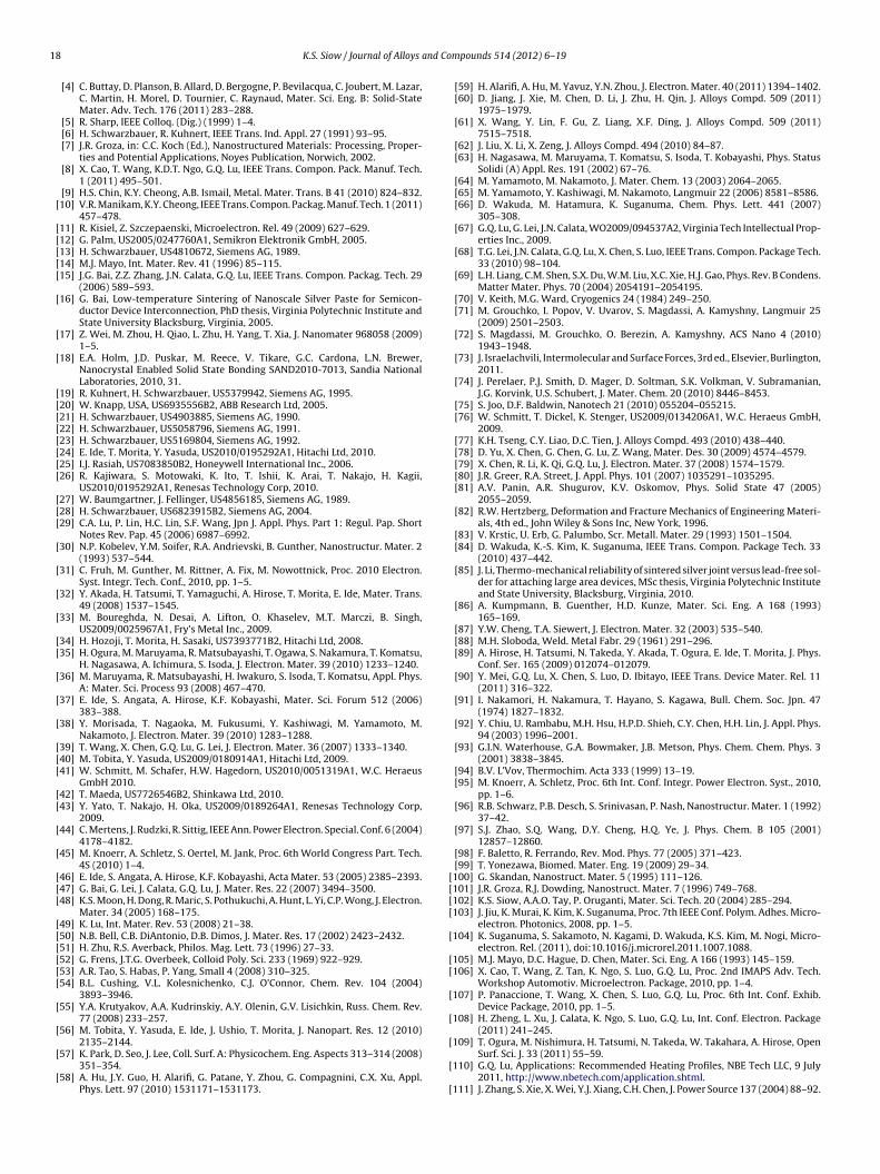
1 and Co
8 K.S. Siow / Journal of Alloys[4] C. Buttay, D. Planson, B. Allard, D. Bergogne, P. Bevilacqua, C. Joubert, M. Lazar,C. Martin, H. Morel, D. Tournier, C. Raynaud, Mater. Sci. Eng. B: Solid-StateMater. Adv. Tech. 176 (2011) 283–288.
[5] R. Sharp, IEEE Colloq. (Dig.) (1999) 1–4.[6] H. Schwarzbauer, R. Kuhnert, IEEE Trans. Ind. Appl. 27 (1991) 93–95.[7] J.R. Groza, in: C.C. Koch (Ed.), Nanostructured Materials: Processing, Proper-
ties and Potential Applications, Noyes Publication, Norwich, 2002.[8] X. Cao, T. Wang, K.D.T. Ngo, G.Q. Lu, IEEE Trans. Compon. Pack. Manuf. Tech.
1 (2011) 495–501.[9] H.S. Chin, K.Y. Cheong, A.B. Ismail, Metal. Mater. Trans. B 41 (2010) 824–832.
[10] V.R. Manikam, K.Y. Cheong, IEEE Trans. Compon. Packag. Manuf. Tech. 1 (2011)457–478.
[11] R. Kisiel, Z. Szczepaenski, Microelectron. Rel. 49 (2009) 627–629.[12] G. Palm, US2005/0247760A1, Semikron Elektronik GmbH, 2005.[13] H. Schwarzbauer, US4810672, Siemens AG, 1989.[14] M.J. Mayo, Int. Mater. Rev. 41 (1996) 85–115.[15] J.G. Bai, Z.Z. Zhang, J.N. Calata, G.Q. Lu, IEEE Trans. Compon. Packag. Tech. 29
(2006) 589–593.[16] G. Bai, Low-temperature Sintering of Nanoscale Silver Paste for Semicon-
ductor Device Interconnection, PhD thesis, Virginia Polytechnic Institute andState University Blacksburg, Virginia, 2005.
[17] Z. Wei, M. Zhou, H. Qiao, L. Zhu, H. Yang, T. Xia, J. Nanomater 968058 (2009)1–5.
[18] E.A. Holm, J.D. Puskar, M. Reece, V. Tikare, G.C. Cardona, L.N. Brewer,Nanocrystal Enabled Solid State Bonding SAND2010-7013, Sandia NationalLaboratories, 2010, 31.
[19] R. Kuhnert, H. Schwarzbauer, US5379942, Siemens AG, 1995.[20] W. Knapp, USA, US6935556B2, ABB Research Ltd, 2005.[21] H. Schwarzbauer, US4903885, Siemens AG, 1990.[22] H. Schwarzbauer, US5058796, Siemens AG, 1991.[23] H. Schwarzbauer, US5169804, Siemens AG, 1992.[24] E. Ide, T. Morita, Y. Yasuda, US2010/0195292A1, Hitachi Ltd, 2010.[25] I.J. Rasiah, US7083850B2, Honeywell International Inc., 2006.[26] R. Kajiwara, S. Motowaki, K. Ito, T. Ishii, K. Arai, T. Nakajo, H. Kagii,
US2010/0195292A1, Renesas Technology Corp, 2010.[27] W. Baumgartner, J. Fellinger, US4856185, Siemens AG, 1989.[28] H. Schwarzbauer, US6823915B2, Siemens AG, 2004.[29] C.A. Lu, P. Lin, H.C. Lin, S.F. Wang, Jpn J. Appl. Phys. Part 1: Regul. Pap. Short
Notes Rev. Pap. 45 (2006) 6987–6992.[30] N.P. Kobelev, Y.M. Soifer, R.A. Andrievski, B. Gunther, Nanostructur. Mater. 2
(1993) 537–544.[31] C. Fruh, M. Gunther, M. Rittner, A. Fix, M. Nowottnick, Proc. 2010 Electron.
Syst. Integr. Tech. Conf., 2010, pp. 1–5.[32] Y. Akada, H. Tatsumi, T. Yamaguchi, A. Hirose, T. Morita, E. Ide, Mater. Trans.
49 (2008) 1537–1545.[33] M. Boureghda, N. Desai, A. Lifton, O. Khaselev, M.T. Marczi, B. Singh,
US2009/0025967A1, Fry’s Metal Inc., 2009.[34] H. Hozoji, T. Morita, H. Sasaki, US7393771B2, Hitachi Ltd, 2008.[35] H. Ogura, M. Maruyama, R. Matsubayashi, T. Ogawa, S. Nakamura, T. Komatsu,
H. Nagasawa, A. Ichimura, S. Isoda, J. Electron. Mater. 39 (2010) 1233–1240.[36] M. Maruyama, R. Matsubayashi, H. Iwakuro, S. Isoda, T. Komatsu, Appl. Phys.
A: Mater. Sci. Process 93 (2008) 467–470.[37] E. Ide, S. Angata, A. Hirose, K.F. Kobayashi, Mater. Sci. Forum 512 (2006)
383–388.[38] Y. Morisada, T. Nagaoka, M. Fukusumi, Y. Kashiwagi, M. Yamamoto, M.
Nakamoto, J. Electron. Mater. 39 (2010) 1283–1288.[39] T. Wang, X. Chen, G.Q. Lu, G. Lei, J. Electron. Mater. 36 (2007) 1333–1340.[40] M. Tobita, Y. Yasuda, US2009/0180914A1, Hitachi Ltd, 2009.[41] W. Schmitt, M. Schafer, H.W. Hagedorn, US2010/0051319A1, W.C. Heraeus
GmbH 2010.[42] T. Maeda, US7726546B2, Shinkawa Ltd, 2010.[43] Y. Yato, T. Nakajo, H. Oka, US2009/0189264A1, Renesas Technology Corp,
2009.[44] C. Mertens, J. Rudzki, R. Sittig, IEEE Ann. Power Electron. Special. Conf. 6 (2004)
4178–4182.[45] M. Knoerr, A. Schletz, S. Oertel, M. Jank, Proc. 6th World Congress Part. Tech.
4S (2010) 1–4.[46] E. Ide, S. Angata, A. Hirose, K.F. Kobayashi, Acta Mater. 53 (2005) 2385–2393.[47] G. Bai, G. Lei, J. Calata, G.Q. Lu, J. Mater. Res. 22 (2007) 3494–3500.[48] K.S. Moon, H. Dong, R. Maric, S. Pothukuchi, A. Hunt, L. Yi, C.P. Wong, J. Electron.
Mater. 34 (2005) 168–175.[49] K. Lu, Int. Mater. Rev. 53 (2008) 21–38.[50] N.B. Bell, C.B. DiAntonio, D.B. Dimos, J. Mater. Res. 17 (2002) 2423–2432.[51] H. Zhu, R.S. Averback, Philos. Mag. Lett. 73 (1996) 27–33.[52] G. Frens, J.T.G. Overbeek, Colloid Poly. Sci. 233 (1969) 922–929.[53] A.R. Tao, S. Habas, P. Yang, Small 4 (2008) 310–325.[54] B.L. Cushing, V.L. Kolesnichenko, C.J. O’Connor, Chem. Rev. 104 (2004)
3893–3946.[55] Y.A. Krutyakov, A.A. Kudrinskiy, A.Y. Olenin, G.V. Lisichkin, Russ. Chem. Rev.
77 (2008) 233–257.[56] M. Tobita, Y. Yasuda, E. Ide, J. Ushio, T. Morita, J. Nanopart. Res. 12 (2010)
2135–2144.[57] K. Park, D. Seo, J. Lee, Coll. Surf. A: Physicochem. Eng. Aspects 313–314 (2008)
351–354.[58] A. Hu, J.Y. Guo, H. Alarifi, G. Patane, Y. Zhou, G. Compagnini, C.X. Xu, Appl.
Phys. Lett. 97 (2010) 1531171–1531173.
mpounds 514 (2012) 6– 19
[59] H. Alarifi, A. Hu, M. Yavuz, Y.N. Zhou, J. Electron. Mater. 40 (2011) 1394–1402.[60] D. Jiang, J. Xie, M. Chen, D. Li, J. Zhu, H. Qin, J. Alloys Compd. 509 (2011)
1975–1979.[61] X. Wang, Y. Lin, F. Gu, Z. Liang, X.F. Ding, J. Alloys Compd. 509 (2011)
7515–7518.[62] J. Liu, X. Li, X. Zeng, J. Alloys Compd. 494 (2010) 84–87.[63] H. Nagasawa, M. Maruyama, T. Komatsu, S. Isoda, T. Kobayashi, Phys. Status
Solidi (A) Appl. Res. 191 (2002) 67–76.[64] M. Yamamoto, M. Nakamoto, J. Mater. Chem. 13 (2003) 2064–2065.[65] M. Yamamoto, Y. Kashiwagi, M. Nakamoto, Langmuir 22 (2006) 8581–8586.[66] D. Wakuda, M. Hatamura, K. Suganuma, Chem. Phys. Lett. 441 (2007)
305–308.[67] G.Q. Lu, G. Lei, J.N. Calata, WO2009/094537A2, Virginia Tech Intellectual Prop-
erties Inc., 2009.[68] T.G. Lei, J.N. Calata, G.Q. Lu, X. Chen, S. Luo, IEEE Trans. Compon. Package Tech.
33 (2010) 98–104.[69] L.H. Liang, C.M. Shen, S.X. Du, W.M. Liu, X.C. Xie, H.J. Gao, Phys. Rev. B Condens.
Matter Mater. Phys. 70 (2004) 2054191–2054195.[70] V. Keith, M.G. Ward, Cryogenics 24 (1984) 249–250.[71] M. Grouchko, I. Popov, V. Uvarov, S. Magdassi, A. Kamyshny, Langmuir 25
(2009) 2501–2503.[72] S. Magdassi, M. Grouchko, O. Berezin, A. Kamyshny, ACS Nano 4 (2010)
1943–1948.[73] J. Israelachvili, Intermolecular and Surface Forces, 3rd ed., Elsevier, Burlington,
2011.[74] J. Perelaer, P.J. Smith, D. Mager, D. Soltman, S.K. Volkman, V. Subramanian,
J.G. Korvink, U.S. Schubert, J. Mater. Chem. 20 (2010) 8446–8453.[75] S. Joo, D.F. Baldwin, Nanotech 21 (2010) 055204–055215.[76] W. Schmitt, T. Dickel, K. Stenger, US2009/0134206A1, W.C. Heraeus GmbH,
2009.[77] K.H. Tseng, C.Y. Liao, D.C. Tien, J. Alloys Compd. 493 (2010) 438–440.[78] D. Yu, X. Chen, G. Chen, G. Lu, Z. Wang, Mater. Des. 30 (2009) 4574–4579.[79] X. Chen, R. Li, K. Qi, G.Q. Lu, J. Electron. Mater. 37 (2008) 1574–1579.[80] J.R. Greer, R.A. Street, J. Appl. Phys. 101 (2007) 1035291–1035295.[81] A.V. Panin, A.R. Shugurov, K.V. Oskomov, Phys. Solid State 47 (2005)
2055–2059.[82] R.W. Hertzberg, Deformation and Fracture Mechanics of Engineering Materi-
als, 4th ed., John Wiley & Sons Inc, New York, 1996.[83] V. Krstic, U. Erb, G. Palumbo, Scr. Metall. Mater. 29 (1993) 1501–1504.[84] D. Wakuda, K.-S. Kim, K. Suganuma, IEEE Trans. Compon. Package Tech. 33
(2010) 437–442.[85] J. Li, Thermo-mechanical reliability of sintered silver joint versus lead-free sol-
der for attaching large area devices, MSc thesis, Virginia Polytechnic Instituteand State University, Blacksburg, Virginia, 2010.
[86] A. Kumpmann, B. Guenther, H.D. Kunze, Mater. Sci. Eng. A 168 (1993)165–169.
[87] Y.W. Cheng, T.A. Siewert, J. Electron. Mater. 32 (2003) 535–540.[88] M.H. Sloboda, Weld. Metal Fabr. 29 (1961) 291–296.[89] A. Hirose, H. Tatsumi, N. Takeda, Y. Akada, T. Ogura, E. Ide, T. Morita, J. Phys.
Conf. Ser. 165 (2009) 012074–012079.[90] Y. Mei, G.Q. Lu, X. Chen, S. Luo, D. Ibitayo, IEEE Trans. Device Mater. Rel. 11
(2011) 316–322.[91] I. Nakamori, H. Nakamura, T. Hayano, S. Kagawa, Bull. Chem. Soc. Jpn. 47
(1974) 1827–1832.[92] Y. Chiu, U. Rambabu, M.H. Hsu, H.P.D. Shieh, C.Y. Chen, H.H. Lin, J. Appl. Phys.
94 (2003) 1996–2001.[93] G.I.N. Waterhouse, G.A. Bowmaker, J.B. Metson, Phys. Chem. Chem. Phys. 3
(2001) 3838–3845.[94] B.V. L’Vov, Thermochim. Acta 333 (1999) 13–19.[95] M. Knoerr, A. Schletz, Proc. 6th Int. Conf. Integr. Power Electron. Syst., 2010,
pp. 1–6.[96] R.B. Schwarz, P.B. Desch, S. Srinivasan, P. Nash, Nanostructur. Mater. 1 (1992)
37–42.[97] S.J. Zhao, S.Q. Wang, D.Y. Cheng, H.Q. Ye, J. Phys. Chem. B 105 (2001)
12857–12860.[98] F. Baletto, R. Ferrando, Rev. Mod. Phys. 77 (2005) 371–423.[99] T. Yonezawa, Biomed. Mater. Eng. 19 (2009) 29–34.
[100] G. Skandan, Nanostruct. Mater. 5 (1995) 111–126.[101] J.R. Groza, R.J. Dowding, Nanostruct. Mater. 7 (1996) 749–768.[102] K.S. Siow, A.A.O. Tay, P. Oruganti, Mater. Sci. Tech. 20 (2004) 285–294.[103] J. Jiu, K. Murai, K. Kim, K. Suganuma, Proc. 7th IEEE Conf. Polym. Adhes. Micro-
electron. Photonics, 2008, pp. 1–5.[104] K. Suganuma, S. Sakamoto, N. Kagami, D. Wakuda, K.S. Kim, M. Nogi, Micro-
electron. Rel. (2011), doi:10.1016/j.microrel.2011.1007.1088.[105] M.J. Mayo, D.C. Hague, D. Chen, Mater. Sci. Eng. A 166 (1993) 145–159.[106] X. Cao, T. Wang, Z. Tan, K. Ngo, S. Luo, G.Q. Lu, Proc. 2nd IMAPS Adv. Tech.
Workshop Automotiv. Microelectron. Package, 2010, pp. 1–4.[107] P. Panaccione, T. Wang, X. Chen, S. Luo, G.Q. Lu, Proc. 6th Int. Conf. Exhib.
Device Package, 2010, pp. 1–5.[108] H. Zheng, L. Xu, J. Calata, K. Ngo, S. Luo, G.Q. Lu, Int. Conf. Electron. Package
(2011) 241–245.
[109] T. Ogura, M. Nishimura, H. Tatsumi, N. Takeda, W. Takahara, A. Hirose, OpenSurf. Sci. J. 33 (2011) 55–59.[110] G.Q. Lu, Applications: Recommended Heating Profiles, NBE Tech LLC, 9 July
2011, http://www.nbetech.com/application.shtml.[111] J. Zhang, S. Xie, X. Wei, Y.J. Xiang, C.H. Chen, J. Power Source 137 (2004) 88–92.

and Co
K.S. Siow / Journal of Alloys[112] M. Yeadon, J.C. Yang, R.S. Averback, J.W. Bullard, J.M. Gibson, Nanostruct.Mater. 10 (1998) 731–739.
[113] S. Egelkraut, L. Frey, M. Knoerr, A. Schletz, Proc. 12th Electron. Package Tech.Conf., 2010, pp. 660–667.
[114] R. Dannenberg, E. Stach, J.R. Groza, B.J. Dresser, Thin Solid Films 379 (2000)133–138.
[115] P.G. Sanders, J.R. Weertman, J.G. Barker, J. Mater. Res. 11 (1996) 3110–3120.[116] M. Knoerr, S. Kraft, A. Schletz, Proc. 12th Electron. Package Tech. Conf., 2010,
pp. 56–61.[117] S.M. Bidoki, D.M. Lewis, M. Clark, A. Vakorov, P.A. Millner, D. McGorman, J.
Micromech. Microeng. 17 (2007) 967–974.
[118] D. Wakuda, M. Hatamura, K. Suganuma, Proc. 6th Int. IEEE Conf. Polym. Adhes.Microelectron. Photonics, 2007, pp. 110–113.[119] H. Schwarzbauer, US5893511, Siemens AG, 1999.[120] A. Muza, Lead-free Solutions for High and Low Temperature Solder Intercon-
nects, MSc thesis, Purdue University, 2009.
mpounds 514 (2012) 6– 19 19
[121] J. Nadler, Taking the Heat: Silver–Diamond Composite Offers Unique Capa-bilities for Cooling Powerful Defense Microelectronics, Georgia TechnologyResearch Institute, 9th July 2011, http://www.gtri.gatech.edu/casestudy/silver-diamond-composite-cooling-microelectronics.
[122] N. Heuck, G. Palm, T. Sauerberg, A. Stranz, A. Waag, A. Bakin, Mater. Sci. Forum645/648 (2010) 741–744.
[123] D.E. Gray, American Institute of Physics Handbook, Thermal Expansion ofCu and Diamond, 9 July, 2011, http://www.calstatela.edu/academic/nuclearphysics/99012/thermal expansion.htm.
[124] R.G. Munro, J. Phys. Chem. Ref. Data 26 (1997) 1195–1203.[125] M.C. Stensberg, Q. Wei, E.S. McLamore, D.M. Porterfield, A. Wei, M.S.
Sepuelveda, Nanomed 6 (2011) 879–898.[126] B. Nowack, H.F. Krug, M. Height, Environ. Sci. Tech. 45 (2011) 1177–1183.[127] Y. Mei, G.Q. Lu, X. Chen, S. Luo, D. Ibitayo, IEEE Trans. Device Mater. Rel. 11
(2011) 312–315.[128] C. Gobl, US2007/0131353A1, Semikron Elektronik GmbH, 2007.