Highly Selective Detection of Nitro Explosives by a Luminescent Metal-Organic Framework
www.elsevier.com/locate/sab
Spectrochimica Acta Part B
Cathodoluminescence study of the activator distribution
in SrS:Cu,Ag thin luminescent filmsB
D. Poelmana,*, J. Doerschelb, P.F. Smeta
aDepartment of Solid State Sciences, Ghent University, Krijgslaan 281 S1, B-9000 Gent, BelgiumbInstitut fur Kristallzuchtung (IKZ), Max-Born-Strasse 2, D-12489 Berlin (Adlershof), Germany
Received 1 November 2003; accepted 30 April 2004
Available online 1 September 2004
Abstract
The lateral distribution of the CL (cathodoluminescent) emission of electron beam deposited SrS:Cu,Ag thin films was studied using
SEM-CL (CL in a scanning electron microscope) spectroscopy. Both CL spectra and CL images at different wavelengths were acquired at
room temperature and at low temperature (80 K). Using this technique together with a deconvolution of the CL spectra, the contributions of
Cu and Ag activators to the overall emission could be separated. Differences in emission spectra between samples, annealed under different
conditions, could be interpreted from the different distribution of activators.
D 2004 Elsevier B.V. All rights reserved.
Keywords: Cathodoluminescence; Thin films; SrS:Cu,Ag; Activator distribution
1. Introduction
During the last few years, there has been extensive
interest in SrS:Cu,Ag as a blue electroluminescent emitter
for flat panel display applications [1]. While there have been
several efforts to find a model explaining the emission
process in this phosphor, there is still quite some uncertainty
on the role played by the copper and silver activators and
their location in the SrS host. Recently, the lateral
distribution of the luminescent emission from such a
phosphor layer was monitored, using SEM-CL (cathodolu-
minescence using a scanning electron microscope) [2,3].
With this technique, it was shown that the light distribution,
usually seen from these layers (light mainly coming from
the grain boundaries) is due to optical outcoupling effects
and that the emission mainly originates from the bulk of the
phosphor grains.
0584-8547/$ - see front matter D 2004 Elsevier B.V. All rights reserved.
doi:10.1016/j.sab.2004.04.016
B This paper was presented at the International Congress on X-Ray
Optics and Microanalysis (ICXOM XVII), held in Chamonix, Mont Blanc,
France, 22-26 September 2003, and is published in the special issue of
Spectrochimica Acta Part B, dedicated to that conference.
* Corresponding author. Tel.: +32 9 264 43 67; fax: +32 9 264 4996.
E-mail address: [email protected] (D. Poelman).
In the present work, spectroscopic SEM-CL was used in
order to separate the contributions due to Cu and Ag
emission. CL spectra and CL mappings at selected wave-
lengths were measured on electron beam deposited
SrS:Cu,Ag layers. Both layers annealed in N2 and in H2S
were studied. Since the thermal quenching of the lumines-
cence in these materials is considerable, room temperature
as well as low temperature (80 K) measurements were
performed. The penetration depth and the attainable lateral
resolution were estimated using CASINO Monte-Carlo
simulations [4].
2. Experimental
Thin films SrS:Cu [0.4 mol%], Ag [0.6 mol%] (activator
concentrations in the starting materials) were deposited by
electron beam deposition under a H2S atmosphere (partial
pressure of 5�10�3 Pa), at a substrate temperature of 500
8C. A Leybold Univex 450 vacuum system with a base
pressure of about 2�10�4 Pa was used. Sintered powder
was used as source material: appropriate amounts of SrS
(Cerac, Milwaukee, 99.99%), metallic Cu and Ag2S were
59 (2004) 1775–1780
D. Poelman et al. / Spectrochimica Acta Part B 59 (2004) 1775–17801776
thoroughly mixed. This powder was sintered in a H2S
atmosphere during 1 h at 1000 8C, which yielded material
that could be used as the electron beam evaporation source
without further treatment or pressing [5]. Films with a
thickness of about 1000 nm were deposited on Vycor
(Corning 7913) substrates.
Since these as-deposited SrS:Cu,Ag films are not
luminescent [1], they were subjected to a post-deposition
annealing treatment. Two types of annealing were per-
formed, which had already proven to yield good results for
this kind of samples [1,3]. A first type of post-deposition
annealing (further called specimens type A) consisted of a
rapid thermal anneal (RTA) in a nitrogen atmosphere at
atmospheric pressure during 30 s at 800 8C, using an AST
Super Heat System 1000. A second type of annealing
(specimens type B) was performed at 680 8C during 30 min
in a quartz tube furnace, in a pure H2S flow at atmospheric
pressure. Both kinds of annealing treatment closely repre-
sent maximum annealing times and temperatures for
common flat panel display substrates (typically Corning
borosilicate glass 7059 or 1737). Unfortunately, it is not
possible to perform annealing experiments in H2S in the
RTA equipment for technical reasons.
3. Results and discussion
On the subject of the exact location of the Cu and Ag
activator ions in luminescent SrS:Cu,Ag films, different
results have been published: Xin et al. [6] expected Cu-
diffusion into crystallite grains in SrS:Cu upon annealing for
thermodynamic reasons and also found experimental evi-
dence for this behaviour [7]. Vdovenkov et al. [8] reported
increased activator concentrations at the grain boundaries in
annealed layers, based on EDX mappings. In the present
work, it turned out to be that the activator concentrations
were below the detection limit of our EDX equipment.
However, luminescence measurements can be orders of
magnitude more sensitive for the detection of defects than
X-ray microanalysis [9]. Therefore, the optical emission
characteristics of the layers were used to study the activator
distribution.
Over the last decades, numerous articles have been
published, discussing the luminescent emission spectrum
(mainly photoluminescence and electroluminescence) of
SrS:Cu and SrS:Cu,Ag powders and thin films. At first,
the emission mechanism in SrS:Cu was thought to be the
same as in ZnS:Cu, namely the recombination of a donor
level to the Cu acceptor level [10]. Soon, however, it was
realised that a different kind of transition was responsible
for the luminescence in SrS:Cu [11], an internal transition in
the Cu+ ion (4s3d9Y3d10).
Part of the problem in identifying the peaks in the SrS:Cu
emission stems from its irreproducibility [12]: the spectrum
is strongly dependent on the preparation conditions of the
powders and the thin films [13] and on the activator
concentration. The latter effect was studied in detail on
SrS:Cu powders by Yamashita et al. [14]. These authors
distinguished the emission from Cu monomers, dimers,
aggregates and large aggregates, at 513, 543, 558 nm and at
higher wavelengths respectively (photoluminescence at
80 K). At room temperature, an additional peak in the
blue region is seen, and at moderate Cu concentrations,
two peaks are usually described, at 460 and 520 nm
[5,13,15]. These are attributed to emission from Cu-ions
in different site symmetries.
In 1997, SrS:Cu was proposed for the first time as the
blue emitter in AC thin film electroluminescent (ACTFEL)
display devices [16]. While quite high luminance could be
obtained from these devices, most of them could not provide
the saturated blue emission, necessary for full colour display
applications. SrS:Cu,Ag was then proposed (Ag acting as a
co-activator) to shift the emission spectrum to shorter
wavelengths and to obtain pure blue emission [17].
While improved colour purity and luminance could be
obtained using SrS:Cu,Ag, the interpretation of the emis-
sion spectrum and the interactions of the activators is much
more difficult than in SrS:Cu. SrS:Ag in itself only shows
weak luminescence (at about 360 nm—in the UV—and at
420 nm [17]), which is strongly quenched at room
temperature. The 360 nm peak has been attributed to
emission from single Ag-ions (monomers), while it was
thought that the 420 nm peak is correlated with Ag
dimers [17]. The photoluminescent emission spectrum of
SrS:Cu,Ag at low temperature shows both the peaks due to
Ag (360 and 420 nm) and a broad peak due to Cu at about
520 nm [18,19]. At room temperature, the 360 nm peak is
consistently quenched; the spectrum then consists of peaks
at about 420, 460–490 and 500–520 nm, again very much
dependent on preparation conditions [5]. While the peak
around 420 nm is clearly due to Ag and the one around
500–520 nm due to copper, there is some uncertainty about
the origin (being Ag-or Cu-related) of the 460–490 nm
emission [13].
When the photoluminescent, electroluminescent or cath-
odoluminescent emission of thin films is observed on a
microscopic scale, the observed light distribution is usually
entirely governed by optical outcoupling effects. In a
previous publication [3], these effects were studied in detail
and, at the same time, SEM-CL was proven to be a suitable
technique to avoid these optical outcoupling effects. There-
fore, SEM-CL allows observing the optical emission where
it is generated in the layer, not where it exits the layer after
(possibly) multiple reflections. The aim of the present work
was to separate the contributions of the Cu- and Ag-related
emission in SrS:Cu,Ag thin films, in order to improve on
our understanding of their interactions.
CL emission spectra and CL images were acquired using
a Zeiss DSM 962 scanning electron microscope, equipped
with an Oxford monoCL cathodoluminescence extension.
The acceleration voltage was 10 kV for all experiments,
while the beam current was chosen between 5 and 200 pA

Fig. 2. Cathodoluminescence emission spectra from the SrS:Cu,Ag layers
for both types of samples, at 80 K and at room temperature. Gaussian fits
were performed when the spectra were plotted on an energy scale.
D. Poelman et al. / Spectrochimica Acta Part B 59 (2004) 1775–1780 1777
as a function of the CL brightness at the wavelength
selected. In all cases, the beam diameter was well below
100 nm.
In order to get an estimate of the CL image resolution
under these experimental conditions, the beam penetration
in the SrS sample was calculated using a CASINO [4]
Monte-Carlo simulation. Fig. 1 shows the resulting energy
distribution of the incident electron beam. For primary
electron energies of the order of 10 kV, the phosphor
efficiency (in lumen per watt) is usually independent of
electron energy, while it rapidly decreases towards lower
energy [20]. From this fact, and from Fig. 1, it was
estimated that at least half of the CL emission emerges from
an apparent beam spot of 250 nm wide. Therefore, 250 nm
can also be used as an upper limit of the attainable CL
lateral image resolution.
The CL emission spectra, obtained at both low temper-
ature (80 K) and room temperature, are shown in Fig. 2, for
a specimen type A (rapid annealing in N2) and for type B
(slow annealing in H2S). In all cases, multiple Gaussian fits,
using a minimum number of peaks to get a decent match,
were performed on the spectra. In order to perform this
fitting, spectra were plotted on an energy scale [10].
At low temperature, four emission peaks can be
distinguished, at about 485, 440, 425 and 360 nm. At room
temperature, the UV emission (360 nm) is completely
quenched and the other peaks are somewhat shifted,
yielding peaks at about 450, 500–510 and 520–530 nm.
These spectra, both at low temperature and at room
temperature, are remarkably similar to the PL spectra of
sputtered films SrS:Ag,Cu,Ga from Li et al. [13]. We
tentatively ascribe the low temperature peaks to Ag (360
and 425 nm) and Cu (440 and 485 nm), the latter peaks
being clearly influenced by the presence of Ag. At room
temperature, only one Ag-peak remains (at 450 nm),
together with very broad peaks for Cu. As can be seen in
Fig. 2, there is so much overlap between the peaks at room
temperature that the peak fitting and the corresponding
identification becomes quite difficult.
Fig. 1. CASINO [4] Monte-Carlo simulation of the penetration of a 100 nm
wide electron beam (primary energy 10 kV) in SrS (density q=3.7 g/cm3).
Numbers indicate the average electron energy relative to the primary
energy.
The complete set of all fitted peaks is listed in Table 1,
together with the intensity ratio of Ag- to Cu-related
emission.
The corresponding CL-mappings (recorded at low
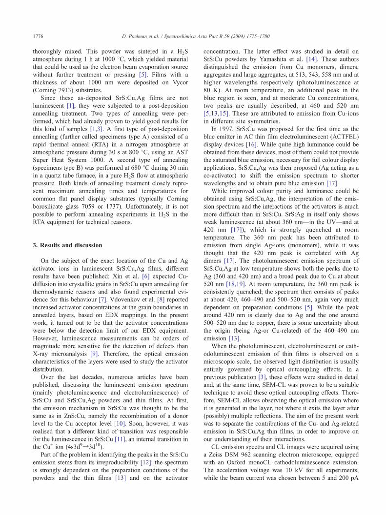
temperature) are depicted in Figs. 3 and 4, for specimens
A and B, respectively. Room temperature mappings are
not shown, since they essentially provide the same
information. Moreover, the overlap between different
emission peaks increases at higher temperature due to
an increase of the line width with temperature, making it
difficult to distinguish different peaks on single-wave-
length CL mappings. Secondary electron (SE) images
were added to show the actual surface morphology of
the films. As observed earlier [2,21], the type of
annealing has a marked influence on the morphology:
rapid thermal annealing (type A) leads to a cracked surface,
while slow annealing (type B) yields well-developed
grains.
Table 1
Emission peaks of both type A and type B films, at low temperature and at
room temperature (RT)
Specimen T (K) Cu-
peaks
(eV)
Ag-
peaks
(eV)
Cu-
peaks
(nm)
Ag-
peaks
(nm)
IAg/ICuratio
A (N2-anneal) 80 K 2.50 2.93 481 424 0.54
2.80 3.46 442 358
A (N2-anneal) RT 2.33 2.72 531 454 0.61
2.36 499
B (H2S-anneal) 80 K 2.52 2.91 486 425 1.00
2.78 3.45 444 360
B (H2S-anneal) RT 2.25 2.78 519 444 1.99
2.36 510
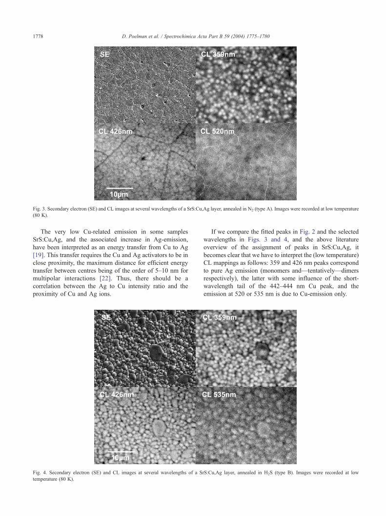
Fig. 3. Secondary electron (SE) and CL images at several wavelengths of a SrS:Cu,Ag layer, annealed in N2 (type A). Images were recorded at low temperature
(80 K).
D. Poelman et al. / Spectrochimica Acta Part B 59 (2004) 1775–17801778
The very low Cu-related emission in some samples
SrS:Cu,Ag, and the associated increase in Ag-emission,
have been interpreted as an energy transfer from Cu to Ag
[19]. This transfer requires the Cu and Ag activators to be in
close proximity, the maximum distance for efficient energy
transfer between centres being of the order of 5–10 nm for
multipolar interactions [22]. Thus, there should be a
correlation between the Ag to Cu intensity ratio and the
proximity of Cu and Ag ions.
Fig. 4. Secondary electron (SE) and CL images at several wavelengths of a S
temperature (80 K).
If we compare the fitted peaks in Fig. 2 and the selected
wavelengths in Figs. 3 and 4, and the above literature
overview of the assignment of peaks in SrS:Cu,Ag, it
becomes clear that we have to interpret the (low temperature)
CL mappings as follows: 359 and 426 nm peaks correspond
to pure Ag emission (monomers and—tentatively—dimers
respectively), the latter with some influence of the short-
wavelength tail of the 442–444 nm Cu peak, and the
emission at 520 or 535 nm is due to Cu-emission only.
rS:Cu,Ag layer, annealed in H2S (type B). Images were recorded at low
D. Poelman et al. / Spectrochimica Acta Part B 59 (2004) 1775–1780 1779
In samples annealed in H2S (type B), there is little
difference between the lateral distribution of the different
emission peaks. In samples, annealed using RTA (rapid
thermal annealing, type A) in N2, the emission due to Ag
is seen to emerge from the bulk of the crystallite grains,
while Cu emission is also coming from the grain
boundaries. The latter effect indicates Cu migrates to grain
boundaries upon annealing in N2. This observation is
consistent with the relative decrease of the Ag-related
emission to the Cu emission, as seen in the last column of
Table 1.
From the results of Figs. 3 and 4, one could interpret the
difference in lateral distribution between the 359 nm and the
426 nm emission as an experimental indication of the fact
that these peaks should arise from Ag monomers and dimers
respectively. While the Ag dimers and monomers could
indeed be located on slightly different positions in the
grains, this interpretation should be handled with caution,
especially since the emission at 426 nm also partly results
from Cu.
4. Conclusions
It has been argued that a strong energetic coupling exists
between Cu- and Ag-ions in SrS:Cu,Ag [23], based on the
fact that the emission in SrS:Ag (without Cu doping) is very
weak. Therefore, the proximity of Cu- and Ag-ions should
be crucial for the efficient luminescent emission from Ag-
ions and distributions of Ag and Cu should virtually overlap
in order to have high luminance from the Ag centres. This
interpretation is supported by the current results, since
migration of Cu towards the grain boundaries leads to a
physical separation of Cu and Ag ions and thus to a decrease
of the Ag-related emission. The latter effect is only observed
in specimens of type A, using rapid annealing in N2. In this
case, the cracks that are formed upon annealing, become
decorated with Cu. In specimens of type B, no outdiffusion
of Cu seems to take place.
Using SEM-CL spectroscopy, the lateral distribution of
Cu- and Ag-activators in SrS:Cu,Ag luminescent layers
could be determined. It was observed that the type of
post-deposition annealing of the layers has a marked
influence on the emission spectra and the diffusion of Cu.
This effect can in part explain the differences in emission
spectrum, found for SrS:Cu,Ag layers, produced by
different research groups. While the present results do
not allow to give a definitive answer to the problems with
the interpretation of the emission spectra of SrS:Cu,Ag, it
has been shown that SEM-CL spectroscopy is a powerful
technique to distribution of luminescent activators in such
complex systems. Future work will include the measure-
ment and analysis of photoluminescent excitation and
emission spectra of SrS:Cu,Ag layers as a function of
activator concentrations, in order to confirm and complete
the present results.
Acknowledgments
One of the authors (P.F.S.) is research assistant for FWO-
Vlaanderen (Fund for scientific research Flanders).
References
[1] D. Poelman, D. Wauters, R.L. Van Meirhaeghe, F. Cardon, Photo-
luminescence of SrS:Cu,Ag and SrS1-xSex:Cu, Ag thin films, Solid
State Commun. 113 (2000) 405–410.
[2] D. Poelman, D. Wauters, R.L. Van Meirhaeghe, Analytical study of
phosphor films based on SrS and CaS, 10th Int. Workshop on
Inorganic and Organic Electroluminescence, Hamamatsu, Japan,
December 4–7, 2000, pp. 437–442.
[3] D. Poelman, D. Wauters, J. Versluys, R.L. Van Meirhaeghe, Micro-
optical characterization of electroluminescent SrS:Cu,Ag thin films by
photo- and cathodoluminescence observations, J. Appl. Phys. 90
(2001) 248–251.
[4] http://www.gel.usherb.ca/casino/index.html.
[5] P. Smet, D. Wauters, D. Poelman, R.L. Van Meirhaeghe, Influence of
sintering on PL emission of SrS:Cu,Ag powders and e-beam
evaporated phosphor layers, Solid State Commun. 118 (2001) 59–62.
[6] Y.B. Xin, W. Tong, W. Park, M. Chaichimansour, C.J. Summers,
Effect of annealing on the grain growth and luminescent properties of
SrS:Cu blue phosphors, J. Appl. Phys. 85 (1999) 3999–4002.
[7] Y.B. Xin, W. Tong, Z.L. Wang, W. Park, C.J. Summers, Oxidation and
diffusion of Cu in SrS : Cu grown by MBE for blue phosphors,
Displays 21 (2000) 89–92.
[8] A. Vdovenkov, E. Soininen, T. Vdovenkova, Microanalytical Study of
ALE TFEL Devices Based on SrS, Proc. 8th International Symposium
on Advanced Display Technologies, Novy Svit, Crimea, Ukraine,
October 10–14, 1999, p. 142.
[9] D.B. Holt, B.G. Yacobi, in: D.B. Holt, D.C. Joy (Eds.), SEM Micro-
characterization of Semiconductors, Academic Press, London, 1989,
pp. 373–423.
[10] G. Blasse, B.C. Grabmaier, Luminescent Materials, Springer, Berlin,
1994.
[11] W. Lehmann, Alkaline earth sulphide phosphors activated by copper,
silver, and gold, J. Electrochem. Soc. 117 (1970) 1389–1393.
[12] K. Barth, J. Lau, H. Efstathiadis, R.T. Tuenge, C.N. King, A.E.
Kaloyeros, Metal-organic chemical vapour deposition (MOCVD) of
SrS:Cu for applications in electroluminescent devices, Proc. 4th Int.
Conf. on the Science and technology of Display Phosphors, Bend,
Oregon, September 14–17, 1998, pp. 303–306.
[13] W.-M. Li, M. Ritala, M. Leskel7, L. Niinistf, E. Soininen, S.-S.
Sun, W. Tong, C.J. Summers, Photo- and electroluminescence of
SrS:Cu and SrS:Ag,Cu,Ga thin films, J. Appl. Phys. 86 (1999)
5017–5025.
[14] N. Yamashita, K. Ebisumori, K. Nakamura, Luminescence from the
aggregated Cu+ centers in SrS:Cu+, Jpn. J. Appl. Phys. 32 (1993)
3846–3850.
[15] D. Poelman, D. Wauters, R.L. Van Meirhaeghe, F. Cardon, Photo-
luminescence study of SrS:Cu,Ag and SrS1�xSex:Cu,Ag thin films,
Proc. 19th Int. Display Research Conference, Berlin, Germany,
September 6–9, 1999, pp. 233–236.
[16] S.-S. Sun, E. Dickey, J. Kane, P.N. Yocom, A bright and efficient
new blue TFEL phosphor, Proc. 17th Int. Display Research Confer-
ence, edited by J. Morreale (SID, Santa Ana), September 15–17, 1997,
p. 301.
[17] U. Troppenz, B. Hqttl, U. Storz, P. Kratzert, K.-O. Velthaus,
Photoluminescence and electroluminescence studies on Cu and Ag
doped SrS ACTFEL devices, Proc. 4th Int. Conf. On the Science and
technology of Display Phosphors, Bend, Oregon, September 14–17,
1998, pp. 187–190.

D. Poelman et al. / Spectrochimica Acta Part B 59 (2004) 1775–17801780
[18] W. Park, T.C. Jones, C.J. Summers, A spectroscopic study on SrS:Cu,
Ag two-component electroluminescent phosphors, J. Lumin. 87–89
(2000) 1267–1270.
[19] C.J. Summers, B.K. Wagner, W. Tong, W. Park, M. Chaichimansour,
Y.B. Xin, Recent progress in the development of full color SrS-
based electroluminescent phosphors, J. Cryst. Growth 214–215 (2000)
918–925.
[20] H. Bechtel, W. Czarnojan, M. Haase, W. Mayr, H. Nikol,
Phosphor screens for flat cathode ray tubes, Philips J. Res. 50
(1996) 433–462.
[21] D. Wauters, D. Poelman, R.L. Van Meirhaeghe, Optical and structural
effects of annealing on blue emitting EL phosphors, 21st Int. Display
Research Conference and 8th Int. Display Workshops, Nagoya, Japan,
October 16–19, 2001, pp. 1127–1130.
[22] G. Blasse, Luminescent centres in insulators, in: A.H. Kitai (Ed.),
Solid State Luminescence, Chapman and Hall, London, 1993, p. 37.
[23] W. Park, T.C. Jones, E. Mohammed, C. Summers, Luminescence
properties of SrS:Cu,Ag thin film electroluminescent phosphors, 4th
Conf. on the Science and Technology of Display Phosphors, Bend,
Oregon, September 14–17, 1998, pp. 215–218.
Copyright © 2022 FDOKUMEN