
Applications of depth-resolved cathodoluminescence spectroscopy
28
Applications of depth-resolved cathodoluminescence spectroscopy This article has been downloaded from IOPscience. Please scroll down to see the full text article. 2012 J. Phys. D: Appl. Phys. 45 183001 (http://iopscience.iop.org/0022-3727/45/18/183001) Download details: IP Address: 164.107.166.141 The article was downloaded on 24/04/2013 at 17:10 Please note that terms and conditions apply. View the table of contents for this issue, or go to the journal homepage for more Home Search Collections Journals About Contact us My IOPscience
-
Upload
independent -
Category
Documents
-
view
5 -
download
0
Transcript of Applications of depth-resolved cathodoluminescence spectroscopy

Applications of depth-resolved cathodoluminescence spectroscopy
This article has been downloaded from IOPscience. Please scroll down to see the full text article.
2012 J. Phys. D: Appl. Phys. 45 183001
(http://iopscience.iop.org/0022-3727/45/18/183001)
Download details:
IP Address: 164.107.166.141
The article was downloaded on 24/04/2013 at 17:10
Please note that terms and conditions apply.
View the table of contents for this issue, or go to the journal homepage for more
Home Search Collections Journals About Contact us My IOPscience
IOP PUBLISHING JOURNAL OF PHYSICS D: APPLIED PHYSICS
J. Phys. D: Appl. Phys. 45 (2012) 183001 (27pp) doi:10.1088/0022-3727/45/18/183001
TOPICAL REVIEW
Applications of depth-resolvedcathodoluminescence spectroscopyL J Brillson
The Ohio State University, Columbus, OH 43210, USA
E-mail: [email protected]
Received 31 January 2012, in final form 14 March 2012Published 12 April 2012Online at stacks.iop.org/JPhysD/45/183001
AbstractDepth-resolved cathodoluminescence spectroscopy (DRCLS) has developed over the past fewdecades into a powerful technique for characterizing electronic properties of advancedmaterials structures and devices on a nanoscale. The lateral and depth-resolved capabilities ofDRCLS enable researchers to probe native defects, impurities, chemical changes and localband structure inside state-of-the-art device structures on an unprecedented scale. A keystrength of DRCLS is its ability to distinguish electronic features at buried interfaces withinmultilayer device structures, interfaces whose microscopic physical features can determinemacroscopic electronic properties. This review provides a general overview of DRCLS andillustrates the wide array of applications now available using this technique.
(Some figures may appear in colour only in the online journal)
1. Historical overview
With the development of advanced electronic materialsstructure and devices on a nanoscale, depth-resolvedcathodoluminescence spectroscopy (DRCLS) has proven tobe a useful technique in a wide range of applications.Historically, luminescence spectroscopy has been a widelyused tool to characterize the nature of excitons, impuritiesand native point defects in electronic materials. The highenergy resolution of this optical technique coupled withits sensitivity to excitations at orders-of-magnitude higherlevels than other techniques provides a wealth of physicalinformation. Cathodoluminescence spectroscopy retainsthese advantages and adds the capability to probe electronicproperties on a nanometre scale both laterally and depth-wise. This capability has proven especially useful in studyingthe electronic structure of semiconductor, insulator and metalheterointerfaces and DRCLS applications extend to probingstate-of-the-art electronic devices.
The cathodoluminescence spectroscopy technique isrelatively old and is used conventionally with a scanningelectron microscope (SEM) to identify compounds andphases of minerals [1–3]. In their book, Yacobi and Holtreview early applications of cathodoluminescence microscopy
centred on defect contrast and spectroscopy. These includedmeasurement of dislocation densities, carrier concentration,minority diffusion length and chemical composition. Earlywork by Norris et al showed that depth sensitivity was possible,applying CLS to the detection of shallow implanted ionsin GaAs, ZnS and CdS by reducing the energy of theirincident electron beam into the low kilovolt range [4, 5]. Suchenergies are much lower than are typically used in SEMstudies. In 1985, Brillson et al showed that CLS could beextended to probe buried interfaces within electronic materialsby varying the incident beam energy [6–8]. Motivating thiswork was the study of local electronic properties at metal–semiconductor interfaces and their role in Schottky barrierformation. Such studies revealed the presence of defects,impurities and chemical bonding localized on a nanometrescale. Further developments extended the DRCLS techniquefurther to probe buried ultrathin films and even the outer atomiclayers of free surfaces. Researchers have now extended theirelectron beam capabilities to probe a wide array of electronicdevices.
While techniques such as electron paramagnetic reso-nance (EPR), positron annihilation spectroscopy (PAS) andluminescence have traditionally provided some of the mostvaluable information on the fundamental properties of bulk
0022-3727/12/183001+27$33.00 1 © 2012 IOP Publishing Ltd Printed in the UK & the USA

J. Phys. D: Appl. Phys. 45 (2012) 183001 Topical Review
Figure 1. (a) Energy loss versus depth profile for low incident electron EB according to equation (1). (b) Depth of maximum energy loss U0
and Bohr–Bethe range RB versus EB. Reprinted with permission from [22] Copyright 2001, American Institute of Physics.
defects, it has been the DRCLS technique that has revealedkey electronic features of solid state interfaces and ultrathinfilms. The impact of such work on our knowledge of defects,chemical and structural interactions at interfaces can be seenat several levels—the choice of growth methods and process-ing conditions used by researchers to build electronic materialsstructures and devices, the ‘reactive’ versus ‘unreactive’ inter-face context of choosing interface constituents, and the use of‘interlayers’ at heterojunctions to modify interface bonding,composition and thereby electronic properties. The challengenow is to extend these techniques even further as electronicmaterials and devices shrink further into the nanoscale regime.This review aims to introduce the DRCLS technique to a gen-eral audience, provide a historical perspective and offer rep-resentative examples of DRCLS applications that illustrate itsutility for probing physical properties and mechanisms insideelectronic devices.
2. The DRCLS technique
Cathodoluminescence is one of several processes that occurwith electron irradiation of solids. A primary electron beamimpinging on a solid surface produces: (i) Auger electrons[9] within the first few angstroms of the free surface; (ii)secondary electrons due to ionization of impacted atoms atnanometre or higher depths that depend on the incident beamenergy; (iii) backscattered electrons at greater depths due torandom collisions of electrons that have lost significant kineticenergy; (iv) x-rays characteristic of specific atomic transitions;(v) a continuum of x-rays resulting from secondary x-rayexcitation; (vi) fluorescent x-rays, that is, optical emissiondue to low-energy electrons initially excited by x-rays and
(vii) the creation of electron–hole pairs resulting from theelectron beam–solid interaction at any incident beam energy[10]. Below incident beam energies of a few keV, x-raygeneration decreases strongly so that the dominant energy lossmechanism is via plasmon generation and subsequently byimpact ionization—the creation of free electrons and holes.It is the recombination of these free carriers that produces thecathodoluminescence.
The rate of energy loss due to electron–hole pair creationversus penetration depth reflects the profile of excitationresulting in cathodoluminescence. Figure 1(a) illustrates anexcitation profile for electrons in the low keV range versusdepth for GaN based on an analytic expression developed byEverhart and Hoff [11] for gauging electron beam penetration.The incident electron produces a cascade of secondaryelectrons that produce more electrons at lower energy untilthese energies are too low to cause impact ionization. Theresultant profile has a maximum energy loss rate at a depthU0 and a maximum range RB, the Bohr–Bethe range. At lowkeV energies, these profiles are strongly peaked on a scale ofnanometres. Figure 1(b) illustrates how U0 and RB vary withincident beam energy. The electron kinetic energy E changesalong a path s as
− dE/ds = (2πNAe4)(Zρ/A)[E−1 ln(aE/I)], (1)
where NA is Avogadro’s number, Z is the atomic number, ρ isthe density, A is the atomic weight, I is the mean excitation lossenergy, equal to (9.76 + 58.8Z−1.19)Z (eV) and a = 1.1658 isa material-independent constant. The Bohr–Bethe range
RB =∫ ∞
E
dE/(dE/d(ρs)) =∫ ξ(EB)
0ξ dξ/ ln(ξ), (2)
2

J. Phys. D: Appl. Phys. 45 (2012) 183001 Topical Review
Figure 2. (a) With increasing electron energies, incident beams can excite above, at, and below interfaces, respectively. (b) Luminescenceenergies correspond to band-to-band, band–to-defect and near-surface electronic material transitions. Reprinted with permission from [22]Copyright 2001, American Institute of Physics.
where ξ = aE/I and EB = incident beam energy. A usefulEverhart–Hoff approximation that provides a ‘universal’ fit toexperimental data is
RB = Cξa, (3)
where C is a material-dependent constant = 9.40 ×10⁻¹²I 2(A/Z)c′/ρ, a = 1.29 and material-independentconstant c′ = 1.48, both for ξ < 10. These expressionsare useful above the kiloelectronvolt region and for solidswith uniform composition. The kinetic energy changealong a path s corresponds to the Bethe’s stopping powerapproximation of continuous slowing down [12], which is nolonger valid below kiloelectronvolt energies. The Everhart–Hoff analytical depth–dose function is valid for low Z
materials. Other analytic expressions are useful for higherZ materials. However, these models can yield significantlydifferent results for the same material. Thus the penetrationdepths derived by Kanaya and Okayama [13] based on asimple atomic potential model with empirical values, diffusionassociated with multiple scattering, and a modified energyretardation model are similar to those of Wu and Wittry[14] based on a modified Gaussian of the energy dissipationfunction. However, these are significantly higher than thoseof Gruen [15], expressions for which depend only on thebeam energy and material density and from which the aboveEverhart and Hoff expressions were modified [16]. This isa challenge at the sub-kiloelectronvolt energies often usedin nanoscale DRCLS, where penetration depths need to bedetermined very precisely. Multiple layers of material withdifferent densities, atomic weights, scattering cross-sectionsand thicknesses present even greater challenges for analyticexpressions.
Monte Carlo simulations based on the random collisionsof the secondary electrons generated by an ensemble ofincident electrons can more accurately model the rate ofelectron–hole pair creation versus depth [17]. They areadvantaged over analytic expressions in that they can simulateelectron scattering and energy loss in structures comprised ofmultiple layers with different densities and atomic weights,which together with incident beam energy and primaryloss mechanisms determine scattering cross-sections. Suchsimulations are analogous to SRIM, i.e. stopping and range of
ions in matter, calculations used in high energy physics [18].However, the penetration depth derived from Monte Carlosimulations will depend on the scattering cross-sections usedand may not be well adapted to low electron beam energies,particularly for materials with high atomic number [19].Theprecision of cathodoluminescence excitation depth will alsodepend on the diffusion of minority carriers required forrecombination, the velocity of which will depend on the spatialdistribution, cross-section and density of recombination sites.The experimental results of the electronic material systemspresented here provide evidence that Monte Carlo simulationssuch as CASINO can provide remarkably precise maximumdepth values for cathodoluminescence, typically on a scale ofa few nm or less at sub-kiloelectronvolt energies for both lowand high atomic numbers. Examples include nitrided Si/SiO2
interfaces [10, 20] for low-Z materials, GaAs, GaN and HfO2
discussed below for intermediate-Z materials, and LaLuO3 forhigh-Z materials [21]. This precision appears to be in large partdue to the high recombination velocities of minority carrierswith electronically active defects at surfaces and interfaces, theprimary subject of DRCLS studies.
The peaked nature of the energy loss profile and itsvariation with incident beam energy enables the study ofbulk, surface and interface regions of a solid selectively, asfigure 2(a) illustrates schematically in a real-space cross-sectional view [22]. Figure 2(b) shows schematically theoptical emissions excited by this incident electron beam inan energy level versus depth picture. These emissions areprimarily from (i) near band edge (NBE) transitions betweenstates at or near the conduction and valence band edges,(ii) transitions between deep levels and states near eitherconduction or valence band and (iii) transitions associated withnew electronic levels or band structure localized at a buriedsolid state interface. The NBE emissions identify the materialbeing probed, including new phases formed at interfaces. Thedeep-level transitions are fingerprints of specific impurities orlattice defects. The spatial location of these NBE and deep-level transitions coupled with their variation with depth provideinformation on the physical processes, e.g., local bonding,chemical reaction, diffusion and defect formation, which occuron a nanometre scale.
Figure 3 illustrates two experimental arrangements forcathodoluminescence spectroscopy. Figure 3(a) shows an
3

J. Phys. D: Appl. Phys. 45 (2012) 183001 Topical Review
Figure 3. (a) Schematic cross-section of DRCLS optical train, reprinted with permission from [22] (Copyright 2001, American Institute ofPhysics. (b) UHV SEM-based DRCLS, courtesy JEOL Corp.
ultrahigh vacuum (UHV) chamber in cross-section, with aglancing incidence electron gun and beam that impinges ona specimen attached to a manipulator. The light emitted bythe specimen is collected by a quartz lens and passed througha sapphire window into a monochromator and photoelectrondetector. The UHV environment prevents buildup ofcarbon contamination that would otherwise accumulate withdecomposition of residual air molecules by the electronbeam. Such carbon deposits act as recombination centres thatquench the optical luminescence for excitation close to thesurface. This configuration provides point spectra but not two-dimensional images. Figure 3(b) provides a cross-sectionalview of a 25 keV UHV field emission SEM (JEOL 7800F) withcorresponding monochromator and photodetection of lightgathered by a parabolic mirror inside the analysis chamber.A typical spot size in figure 3(a) is ∼0.5 mm at an incidentbeam current of 1–3 µA. In figure 3(b), spot sizes of <5 nmare achievable at currents >nA at high keV and ∼10 nm atlow keV energies. This configuration can provide both CLspectra and two-dimensional images. Both analytic chamberscan contain equipment for surface science techniques such asAuger electron spectroscopy (AES) and x-ray photoemissionspectroscopy (XPS).
3. Early work
Figure 4 illustrates early work by Norris et al that demonstratedthe use of keV electron energies to detect lattice damageand impurities introduced by ion implantation in subsurfaceregions [4]. This work reflected technology interests inassessing and improving the activation of implanted impuritiesfor semiconductor doping. Here Norris et al used a 1–20 keVmagnetically focused electron gun in an oil-pumped vacuumof ∼10−9 Torr to minimize hydrocarbon contamination. Thedepth-dependent CL spectra show how the ratio of 1.24 eVCu+ implant emission relative to the 1.49 eV GaAs NBEpeak intensity increases as EB decreases from 20 to 5 keV,corresponding to excitation depths decreasing from 1.6 to0.14 µm. Norris et al also first pointed out the importance ofenergy density in these studies, illustrating the dependence of
Figure 4. Cathodoluminescence spectra excited from various depthsin GaAs. With decreasing beam voltage, the quenching of the NBEpeak increases due to the shallow Cu+ implantation and latticedamage. Reprinted with permission from [4] Copyright 1973,American Institute of Physics.
4

J. Phys. D: Appl. Phys. 45 (2012) 183001 Topical Review
Figure 5. CL spectra of UHV-cleaved CdS(1 l 2 0) after in situ deposition of 50 Å Al (a), (b) versus Cu (c) plus in situ laser annealing withenergy densities shown. For Al, EB = 0.5 and 2 keV correspond to RB = 110 and 600 Å, respectively. For Cu, EB = 0.5, 1, 1.5 and 2 keVcorrespond to RB = 50, 170, 350 and 520 Å, respectively. In addition to the 2.5 eV CdS NBE emission in all spectra, the 1.3 and 1.7 eVpeaks in (a) and (b) are attributed to native point defects, while the 1.28 eV peak in (c) is attributed to Cu2S formation. Reprinted withpermission from [6] Copyright 1985, American Institute of Physics.
relative luminescence intensities on incident current densities[5]. Thus he showed how the band-to-band versus defectintensity ratio increased for unimplanted GaAs with increasingcurrent density as carrier recombination from the limiteddensity of defects saturated [4].
In 1985, Brillson et al showed for the first time thatCLS could be extended to probe buried interfaces withinelectronic materials [6]. Motivating interface studies in thelate 1970s and 1980s for the solid state community was thesearch for physical mechanisms to understand Fermi levelEF stabilization/pinning and Schottky barrier formation atsemiconductor interfaces with metals and insulators [23],given the central importance of these effects for the operationof semiconductor devices. Various theoretical modelssought to interpret these phenomena in terms of localizedelectronic states, but they differed dramatically in terms oftheir basic physical mechanisms [24]. Experimental studiesrelied heavily on surface science techniques that were notsensitive to interfaces below the free surface. On theother hand, local electronic probes revealed the importanceof chemical interactions at metal–semiconductor interfaces[25, 26]. Figure 5 illustrates the use of DRCLS to probe
interface specific reactions at metal-CdS interfaces [6]. Infigure 5(c), CdS cleaved in UHV, overcoated with Cu 5 nmthick, and laser-annealed exhibits an additional emission at1.35 eV due to Cu–S reaction. With decreasing EB from2 to 0.5 keV, the I(defect)/I(NBE) intensity ratio increasesdramatically and emission from CdS disappears at depthsbelow a few nm. Figures 5(a) and (b) illustrate differentbehaviour for laser-annealed Al on UHV-cleaved CdS. Herea second emission appears at 1.55 eV, with both gap stateemissions again dominating the CL spectra at near-surfaceexcitation. The common 1.35 eV for both Cu and Al suggeststhat a common lattice defect is created. The 1.35 and1.55 eV peaks have a different depth and laser annealing powerdependence, indicating different defects or alloy formationwithin the same nanometre-scale subsurface region.
Directly relevant to Schottky barrier formation, DRCLSstudies then showed that the deposition of metals onsemiconductors induced the formation of localized electronicstates. Figure 6 shows the absence of gap states for UHV-cleaved InP and their appearance with the deposition of evensubmonolayer amounts of Au, Cu Al and Pd [27]. For eachmetal, new emissions appear at 0.8 and ∼1 eV. However, their
5

J. Phys. D: Appl. Phys. 45 (2012) 183001 Topical Review
Figure 6. Cathodoluminescence spectra of (a) Au, (b) Cu and (c)Al on clean, mirror-like InP(1 1 0) and (d) Pd on clean, mirror-likep-InP (1 1 0) as a function of metal deposition. Reprinted withpermission from [27] Copyright 1986, American Physical Society.
amplitudes, energies and depth dependence evolve differentlywith metal thickness, highlighting differences in metal–semiconductor interaction. Metals on GaAs also displaymetal-induced gap states [27]. Significantly, the energies ofthese states within the semiconductor band gap correspondto EF positions of the macroscopic Schottky barrier heights.The CL results can be related to the origin of Schottky barrierformation since the metal-induced states form at energiesor ‘pinning’ levels corresponding to the range of Fermilevel movement at compound semiconductor–metal interfaces[28]. These Schottky barriers exhibit behaviour intermediatebetween Schottky-like and Bardeen-like models, depending onthe density of interface states. Thus for Czochralski-grownbulk GaAs with high densities of As antisites, Fermi level‘pinning’ is much more pronounced than in InP, where bulktrap densities are much lower [29]. For several representativesemiconductors, the interface states can be associated withnative point defects that are found to segregate to the interfaces,again measured by DRCLS [30].
Quantum wells studied with DRCLS offer another earlyexample of probing buried interfaces. Here non-radiative
recombination pathways and scattering centres introduced bylattice imperfections are of high concern for the efficiency ofoptoelectronic devices. For a GaN/2 nm In0.28Ga0.72N/30 nmGaN quantum well, figure 7 shows a series of DRCL spectrawith EB from 0.75 to 2 keV and NBE emissions correspondingto GaN and InGaN [31, 32]. With increasing EB, the ratioof InGaN to GaN NBE increases as excitation depth RB
approaches the upper quantum well interface. As EB andRB increase further, a third peak emerges at 3.25 eV thatreaches a maximum at a depth corresponding to the deeperquantum well interface, then decreases with higher EB atcorresponding depths within the GaN buffer layer. The energyand phonon replicas of this feature identify it as a cubic GaNlayer. This structural change is known to occur because ofstacking faults introduced by the reduced growth temperatureat the growth transition from GaN to InGaN. DRCLS spectraof a GaN/2 nm In0.14Ga0.86N/30 nm GaN quantum well do notexhibit this cubic feature due to the lower lattice mismatchat the heterointerfaces. By modelling the quantum wellemission increase with increasing EB starting as low as0.1 keV in terms of the integrated excitation volume and itsproximity to the quantum well, one obtains a minority carrierdiffusion length λ ∼ 27 nm, much shorter than typical bulksemiconductor diffusion lengths but consistent with valuesobtained by other techniques on similar material and with thehigh depth resolution of the DRCLS technique [32]. Herequantum well intensity reflects the change in minority carrierdensity with excitation proximity. An alternative methodof determining diffusion lengths using cathodoluminescence,albeit on a micrometre scale, is lateral detection of intensity byan optical fibre versus distance from an excited volume [33].
Further emphasizing the multilayer capabilities ofDRCLS, Hasegawa et al used DRCLS to measure native pointdefects at buried InP/GaAs heterojunctions and quantum wells[34]. Here the variation of optical emission from the variouslayers was compared with a theoretical analysis developed forphotoluminescence but coupled with an excitation versus depthdependence based on Everhart–Hoff energy loss. Using an EB
range 5–30 keV, they reported the appearance of a 1.7 eV defectemission attributed to P vacancies [35] in gas source molecularbeam epitaxy (GSMBE) versus organometallic vapour phaseepitaxy (MOVPE). This defect emission also appeared inGaAs/InP/GaAs quantum wells due to incomplete Group Vvapour substitution during growth. The decrease in CLsignal at 5 keV and below is attributed to quenching of theoptical recombination by surface carbon buildup in the non-UHV SEM.
4. Near-surface studies
DRCLS with relatively low EB enables the study ofelectronic properties associated with near-surface structural,i.e. morphological, defects. A notable example is thestudy of surface stress in AlGaN films with microcracksby combined DRCLS-micro-Raman spectroscopies. HereProfessor Christen’s Magdeburg group mapped the NBEfeatures of GaN as a function of lateral distance from AlGaNmicrocracks on a sub-micrometre scale [36]. Mechanical
6

J. Phys. D: Appl. Phys. 45 (2012) 183001 Topical Review
1.0 1.5 2.0 2.5 3.0 3.5 4.0 4.5
GaN/In0.28
Ga0.72
N/GaN Quantum Well
x 10 0.75 keV
Photon Energy (eV)
x 4
x 2
Lum
ines
cent
Inte
nsi
ty (
arbit
rary
)
1.0 keV
1.25 keV
1.5 keV
1.75 keV
2.0 keV
T = 90 K
2.4 eV
3.25 eV
3.5 eV
Energy
2.25 keV
1.0 1.5 2.0 2.5 3.0 3.5 4.0 4.5
x 22.0 keV
Photon Energy (eV)
x 2
L
um
ines
cent
Inte
nsi
ty (
arbit
rary
)
2.25 keV
x 2
2.5 keV
3.25 eV
3.0 keV
3.5 keV
2.4 eV 3.5 eV
4.0 keV
T = 90 K
Energy
GaN/In0.28
Ga0.72
N/GaN Quantum Well
4.5 keV
Figure 7. Depth-dependent cathodoluminescence spectra of a GaN/In0.28Ga0.72N quantum well for beam voltages from 0.75 to 5.0 keV. Inaddition to the 3.5 eV NBE and 2.4 eV quantum well peaks, a sharp new peak appears at 3.25 eV at intermediate beam voltages, indicatingemission from states localized near the quantum well. Reprinted with permission from [31] Copyright 1999, American Institute of Physics.
stress on a scale of GPa causes semiconductor bandgap to shift in energy, typically by tens of meV. Asshown in figure 8, high energy resolution NBE shiftsassociated with strain are revealed by hyperspectral analysis,termed cathodoluminescence wavelength imaging (CLWI), i.e.mapping of CL intensity at single energies extracted from fullspectra acquired at each and every pixel of the probed area.Advantages of this hyperspectral analysis include minimizing(i) electron beam damage due to the focused electron beamat a given pixel, (ii) beam drift during data acquisition thatwould otherwise degrade image resolution, (iii) charging thatcan deflect the incident beam and prevent analysis. Figure 8(a)exhibits regular and well-defined patterns in the underlyingGaN buffer layer even though the NBE wavelength shiftsby only 3 nm at most. In figure 8(b), the stresses measuredby DRCLS are compared with stresses from finite elementcalculations using the shifts of Raman peaks. These plotsdemonstrate that DRCLS is capable of measuring local stressand, in this case, that stress extends several micrometres awayfrom the microcracks. While cracks relieve the tensile stressof the AlGaN/GaN junction, nevertheless figure 8 reveals thepresence of microcracks and extensive variations in biaxialstress on a GPa scale laterally. These features diminish withhigher EB excitation as expected due to the near-surface natureof the interface stress.
Near-surface DRCLS studies have established that surfaceasperities such as step edges, pits, and mounds on asemiconductor surface are electrically active with states in theband gap that act as recombination centres for free charge.
Based on studies of a wide variety of ZnO single crystals, Douttet al demonstrated that the intensity ratio I(NBE)/I(defect) nearthe free surface increased monotonically as surface roughnessdecreased [37]. The highest NBE emission intensity and hencethe lowest non-radiative recombination occurred for surfaceswith root mean square (rms) roughness of 0.5 nm, that is, unitcell dimensions. This DRCLS application demonstrates that:(i) localized states exist at sites of surface roughness that act asrecombination centres and (ii) optoelectronic applications ofthin films achieve optimal efficiency when surface roughness isminimized on a unit cell dimension. Hence near-surface CLSreveals both a roughness figure of merit for semiconductorpolishing and etching as well as its physical basis.
DRCLS coupled with Kelvin probe force microscopy(KPFM) and surface photovoltage spectroscopy (SPS) furtherextend the ability to probe electronic states near the surface.Here low EB micro-CLS spectra localized to atomic steps orpit edges display gap state emissions that increase in intensitywith lateral proximity to the surface asperity [38]. Thesestudies also show that gap states due to lattice vacancies areassociated with nanostructures on ZnO surfaces and that theselattice vacancies increase with proximity to the nanostructure.DRCLS lends itself to probing the formation of these near-surface defects in three dimensions as the nanostructures grow.Early DRCLS studies of GaAs surface reconstructions showeda correspondence between gap states and Ga versus As surfacecomposition [39]. Researchers have also used a strongly biasedscanning tunnelling microscope (STM) tip to stimulate CLspectra with ZnO [40]. Together with earlier STM CL studies
7

J. Phys. D: Appl. Phys. 45 (2012) 183001 Topical Review
Figure 8. Stress analysis of AlGaN films with microcracks. (a) CL wavelength-specific map of the GaN buffer layer and (b) line scanenergy versus position relative to cracks. Corresponding finite element (FE) map (c) and analysis (d) comparing stresses along the line scanswith calculated stresses (solid lines). Reprinted with permission from [36] Copyright 2003, American Institute of Physics.
[41–43], their results suggest alternative avenues to identifysurface lattice structures and elements with specific gap stateenergies.
5. Extended depth studies
DRCLS studies on an extended depth scale provide a widevariety of additional information on semiconductor multilayerstructures. Weakly coupled superlattices used for negativedifferential resistance (NDR) can develop multiple domainswith different electric field strengths with applied bias.Cathodoluminescence spectra of heavily doped GaAs–AlAssuperlattices under applied bias can gauge the strength of thesefields from band edge shifts in energy [44]. The energy ofband-to-band luminescence decreases with increasing field dueto the Franz–Keldysh effect [45, 46]. Figure 9 illustrates thespatial variation of miniband energies inside the superlatticeunder an applied bias of 3.2 V over the superlattice thicknessof ∼1600 nm—a 20 KV cm−1 average field—versus proximityto the anode. Figure 9(a) inset illustrates the variation ofconduction miniband and its wavelength dependence on EB
and probe depth. As probe depth increases toward the anode,the dominant emission peak shifts from 789 (peak I) to 792 nm(peak II). This bimodal shift indicates that the superlatticeelectric field breaks into two distinct domains with differentelectric field strengths. Significantly, a higher applied biasof 8.2 V does not create additional domains. Again, onlytwo domains are present, as indicated by peaks II and III,which are shifted to longer wavelength than in figure 9(a)due the higher overall fields. The Ploog Group modelled
the energy dissipation of the incident beam coupled with theincident beam penetration in order to extract the depth of thedomain boundary. Their results were consistent with the depth-dependent variation of high- versus low-field peak emissionintensity. A best fit for the 8.2 V bias spectra yielded 17 and 21well widths for the low- and high-field domains, respectively.Thus DRCLS provides not only the number of electric fielddomains within the superlattice but also the position of thedomain boundary and its excess charge required to producethe electric field difference.
Another application of subsurface and bulk DRCLS is thedetermination of crystal quality versus distance from a growthsubstrate. Carrier concentrations and mobilities of GaN grownby various techniques are known to depend sensitively on filmthickness. Coleman et al used a 5–25 keV electron beam,corresponding to an RB of 0.2–3.3 µm according a Kanaya–Okayama model of excitation depth [13], to probe the NBEand defect emissions inside a 3 µm thick GaN films grownon sapphire by organometallic chemical vapour deposition(MOCVD) [47]. Taking into account the excitation powerdependence of the emission intensities, the Coleman groupfound that the MOCVD films exhibit a strong decrease indefect emissions toward the free surface, indicating that crystalquality increases with film thickness. This represents thefirst systematic study of optical quality as a function of filmthickness. The results are consistent with the decreasingdensity of morphological imperfections commonly observedin cross-sectional transmission electron microscope (TEM)studies of thick GaN films.
Pereiera et al used DRCLS to measure alloy compositionversus depth within InGaN films grown on GaN/Al2O3(0 0 0 1)
8

J. Phys. D: Appl. Phys. 45 (2012) 183001 Topical Review
Figure 9. Depth-dependent band edge shift revealing spatial arrangement of electric field domains in heavily doped GaAs-AlAssuperlattices. Peaks labelled I and II denote domains with different electric field strength. The domain peaks vary with excitation depth,providing the location, width and number of domains within the superlattice. Reprinted with permission from [44] Copyright 1995,American Institute of Physics.
substrates [48]. They observed variations in NBE energiescorresponding to continuous changes in alloy compositionfrom 14% to 20% In over a nominal 75 nm thick film. Bydistinguishing between energy shifts due to strain versuscomposition, they showed an increasing In mole fractionalong the growth direction that scaled with the degree ofstrain relaxation. In atoms are excluded from the intimateInGaN/GaN junction in order to minimize strain. Withincreasing thickness, the InGaN film begins to relax, allowingincorporation of additional In. Hence, DRCLS reveals thatstrain can be a major driving force for composition variationsduring epitaxial growth.
Another extended depth application of DRCLS is thevariation of defects with depth associated with different growthmodes. Ong and Du combined DRCLS with Rutherfordbackscattering spectrometry (RBS) and AES to study theevolution of defects versus depth in ZnO thin films grownby pulsed laser deposition (PLD) on Al2O3(0 0 0 1) underO-deficient and Zn-deficient conditions [49]. This workrevealed that several types of defects are present in thesefilms whose type and spatial distribution depend strongly onfilm stoichiometry. Previous work suggested that initial ZnOgrowth can nucleate with different defect distributions witheither columnar or as two-dimensional layers. The DRCLSwork shows that crystal uniformity and quality depend oncontrol of the initial growth mode.
Each of the bulk crystal studies is careful to take intoaccount the effect of self-absorption on the relative NBEand defect intensities. Self-absorption of light from depthsmore than a few hundred nm below the free surface canshift the NBE emission to lower energies, i.e. ‘red shift’, by
absorbing the higher energy photons preferentially. Gelhausenet al highlight the importance of self-absorption for thicksamples in analysing composition from band edge shifts [50].They compared the depth-resolved NBE peak shift usingMonte Carlo simulations to those observed experimentally.Differences between calculated and measured peak shifts wereattributed to strain, near-edge defects and alloy variations.
Cross-sectional studies provide an alternative methodto avoid self-absorption effects and to measure materialproperties at depths otherwise limited by electron microscopeenergies. With this technique, Zaldivar et al found enhanceddefect emission near the interface of an 8 µm thick GaNepilayer on Al2O3(0 0 0 1) [51]. They attributed enhancedmid-gap emission near this junction to stacking faults anddislocations dressed with point defects. Likewise, electronbeam-induced current (EBIC) measurements performed incross-section at various depths show strong decreases inminority carrier lifetime and diffusion length with proximity toGaN/Al2O3 interfaces. These transport effects were attributedto scattering at threading dislocations [52].
Cross-sectional CLS can also establish the presence ofatomic interdiffusion between electronically active layers.Such interdiffusion can strongly affect carrier transportthroughout thin epitaxial films. At GaN junctions withsapphire, the most common substrate for device development,degenerate doping can occur due to native point defects,morphological defects such as stacking faults or dislocations,impurities, the initial growth surface, or complexes generatedfrom the substrate. A conductive channel created by sucheffects can act to ‘short-circuit’ devices fabricated on the outerfilm surface. In order to determine the physical nature of these
9

J. Phys. D: Appl. Phys. 45 (2012) 183001 Topical Review
defects, Goss et al obtained high resolution, low-temperatureCL spectra from 70 µm thick GaN grown hydrothermally onAl2O3 [53]. They correlated the intensities of a donor-boundexciton strongly associated with O shallow donors by Hallmeasurements with the density of oxygen impurities extendingaway from the GaN/Al2O3 interface measured by SIMS. Theoutdiffusion of oxygen is consistent with the high (>1000 C)temperatures involved with hydrothermal vapour phase epitaxy(HVPE). The cross-sectional CLS measurements providedirect evidence to identify the donor responsible for theinterface doping.
6. Applications for device materials and structures
As devices shrink into the nanometre regime, non-destructiveevaluation of the physical properties inside semiconductordevices on that scale has become increasingly important. Therelevance of DRCLS to optoelectronic devices is natural,given the direct impact of parasitic emissions and non-radiative recombination on light-emitting efficiency. Inaddition to the quantum well and superlattice applicationsalready described, the non-destructive detection and control ofdefects and inhomogeneities in small volumes is important forphotodetectors, solar cells, semiconductor optical amplifiers,erbium-doped optical fibre amplifiers, as well as many otherhigh-speed and photonic applications [54]. The extension tomicroelectronic devices finds many applications, including (i)the identification of defects, atomic diffusion, and chemicalcomposition changes during device growth and processingand their impact on device properties; (ii) the identificationof degradation mechanisms inside devices under operatingconditions and their use in models that can predict devicelifetime. Such predictions are especially timely for next-generation device materials and structures that are evolvingtoo rapidly for extended life tests to be relevant.
A key challenge is to perform studies on actual devicestructures, whose dimensions may be in the sub-micrometrerange, a regime in which diffraction limits typical opticaldiagnostic techniques such as photoluminescence, absorptionor Raman spectroscopy. Furthermore, it is desirable to probedevices under actual operating conditions in order to identifythe effects of temperature, mechanical strain and electricalstress on such microstructures. The following sectionsdescribe DRCLS applications to both materials structures withnanoscale dimensions prior to device fabrication as well asactual electronic devices under operating conditions.
7. Application to Schottky diodes
DRCLS provides the capability to probe electronic featuresat intimate metal–semiconductor interfaces. By the 1980s,researchers using surface-sensitive electron energy loss andsoft x-ray photoemission spectroscopy (SXPS) had alreadyobserved interface reactions, interdiffusion and Fermi levelmovements that occurred with less than a few atomic layerthicknesses of metals on semiconductors and even near roomtemperature [55]. Electronic changes over these limitedthicknesses nevertheless could introduce localized electronic
Figure 10. Metal-induced defect formation at buried (a)Al-ZnO(0 0 0 1) interface indicating Al-oxygen reaction versus (b)Au–ZnO(0 0 0 1) interface showing Au–Zn eutectic formation.Reprinted with permission from [58, 59] Copyright 2007, AmericanInstitute of Physics.
states that alter Schottky barrier heights [56]. DRCLSmeasurements of actual diodes now allow researchers to relateelectronic features at these local interfaces and below the freesurface directly to electrical transport measurements.
The application of DRCLS to metal–ZnO Schottkybarriers provides numerous examples relating nanoscaleinterface features to macroscopic electrical measurements.The inset of figure 10(a) illustrates the cross-sectionalgeometry of electron beam excitation both through the metaldiode and at its periphery. Metal thicknesses of 30–50 nmsatisfy two main requirements: (i) the overlayer is thick enoughto be characteristic of the bulk metal and (ii) the overlayer isthin enough to pass cathodoluminescence from the interfacethrough the metal with negligible attenuation. Typically,EB = 5 keV through the diode and 2 keV at its peripheryenable a direct comparison of the semiconductor at the samedepth, so that any spectral changes must be due to effectsof the metal rather than any semiconductor artifacts. ZnOsingle crystals and films grown and processed by different
10
J. Phys. D: Appl. Phys. 45 (2012) 183001 Topical Review
methods often contain widely varying levels of defect andimpurity emissions [57], so that unambiguous comparisonsrequire spectra from the same crystal and as close together inthree dimensions as possible. In addition, it is desirable for theZnO under test to have relatively low-defect levels so that anymetal-induced changes at the interface are not masked by bulkemissions.
In the case of a 500 µm diameter Al diode deposited onZnO at room temperature, the DRCL spectrum under versusnext to the metal in figure 10(a) shows the 3.36 eV NBEfeature in both and a broad deep-level emission centred at2.45 eV that increases by an order of magnitude [58]. Incontrast, a Au diode deposited on the same ZnO surfaceshows no spectral changes at room temperature. The current–voltage (I–V ) characteristics of the Al diode are ohmic withhigh forward and reverse currents. I–V curves for Au showrectifying characteristics instead [59, 60]. The Al–ZnO dioderemains ohmic with annealing. Similarly, the Au–ZnO dioderemains rectifying until a temperature of 650 C, at whichthe I–V characteristic becomes ohmic. DRCL spectra infigure 10(b) show that a new defect emission appears at∼2 eV at this temperature. The depth sensitivity of DRCLSenables detection of these additional luminescence featureseven though they extend only nanometres beyond the metalinterface. The intensity of these interface features rapidlydecreases with increasing excitation depth. Hence techniquessuch as photoluminescence whose excitation depth is typicallymuch larger than buried interface widths will be proportionallyless sensitive to local interfaces below the free surface.
The nature of the defects created by these metal contacts isrelated to chemical interactions at the metal–ZnO interfaces.The ∼2 eV feature appears when the annealing temperatureexceeds that of the Au–Zn eutectic, at which point the metalextracts Zn atoms from the adjoining ZnO lattice, leavingbehind zinc vacancies VZn. Figure 10(b) inset representsthis mechanism of defect creation schematically. Thisidentification is confirmed by a correlation of the 2 eV emissionintensity with the density of VZn measured by PAS [61].The 2.45 eV feature reflects the Al bonding with O at theintimate Al–ZnO interface and can be identified with oxygenvacancies VO or their complexes as suggested by previousstudies [62]. DRCLS studies support this identification aswell. This 2.45 eV emission decreases in the near-surfaceregion with exposure to a remote oxygen plasma (ROP),suggesting the filling of vacancy sites with oxygen atoms [63].Indeed, I–V characteristics for a Au–ZnO transform fromohmic to rectifying with this ROP treatment, and 1/C2–V
measurements reveal a corresponding decrease in dopingdensity within 50–100 nm of the metal–ZnO interface [64].The higher carrier density associated with the 2.45 eV emissionwithin the surface space charge region can account for lowerSchottky barriers due to increased tunnelling through thebarrier [65].
There is ample evidence for chemical reactions at diodeinterfaces as measured by DRCLS. One of the most dramaticexamples is the Ta–ZnO diode interface. Figure 11 showsEB = 5 keV DRCL spectra for Ta–ZnO(0 0 0 1) interfacesand their corresponding I–V characteristics on two different
crystals. In figure 11(a), mid-gap defect and NBE emissionintensities are comparable after annealing, which reducesthe 2 eV emission by orders of magnitude. At annealingtemperatures of 550 and 650 C, figure 11(b) shows both theforward and reverse currents decrease by orders of magnitude,representative of a blocking contact [66]. In addition, theI–V for the interface annealed to 450 C is offset by −0.5 eV,indicative of an interface dipole that alters the effectiveelectric field across the diode. Figure 11(c) shows anotherTa–ZnO(0 0 0 1) interface for a crystal with lower initialmid-gap defects. Here again defect densities increase withannealing, but much less than for the higher bulk defectdensity crystal. Whereas the I–V for the high-defect ZnObecomes more conductive at 550 C, the low-defect ZnOcontact changes from ohmic to blocking but remains blockingfor all anneal temperatures in figure 11(d). The leakagecurrent increase for the high-defect ZnO contact indicates thatthe presence of high-defect concentrations promotes interfacealloying and reactions that produce additional defects. In turn,these defects degrade Schottky barriers and blocking layers.Also, figure 11(c) inset shows the appearance of a new emissionat ∼4.1 eV with a 550 C anneal. This energy agrees well withthe ∼4.2 eV band gap energy of Ta2O5 [67] and demonstratesthe ability of DRCLS to measure optical transitions within nm-thick reaction products at metal–semiconductor interfaces.
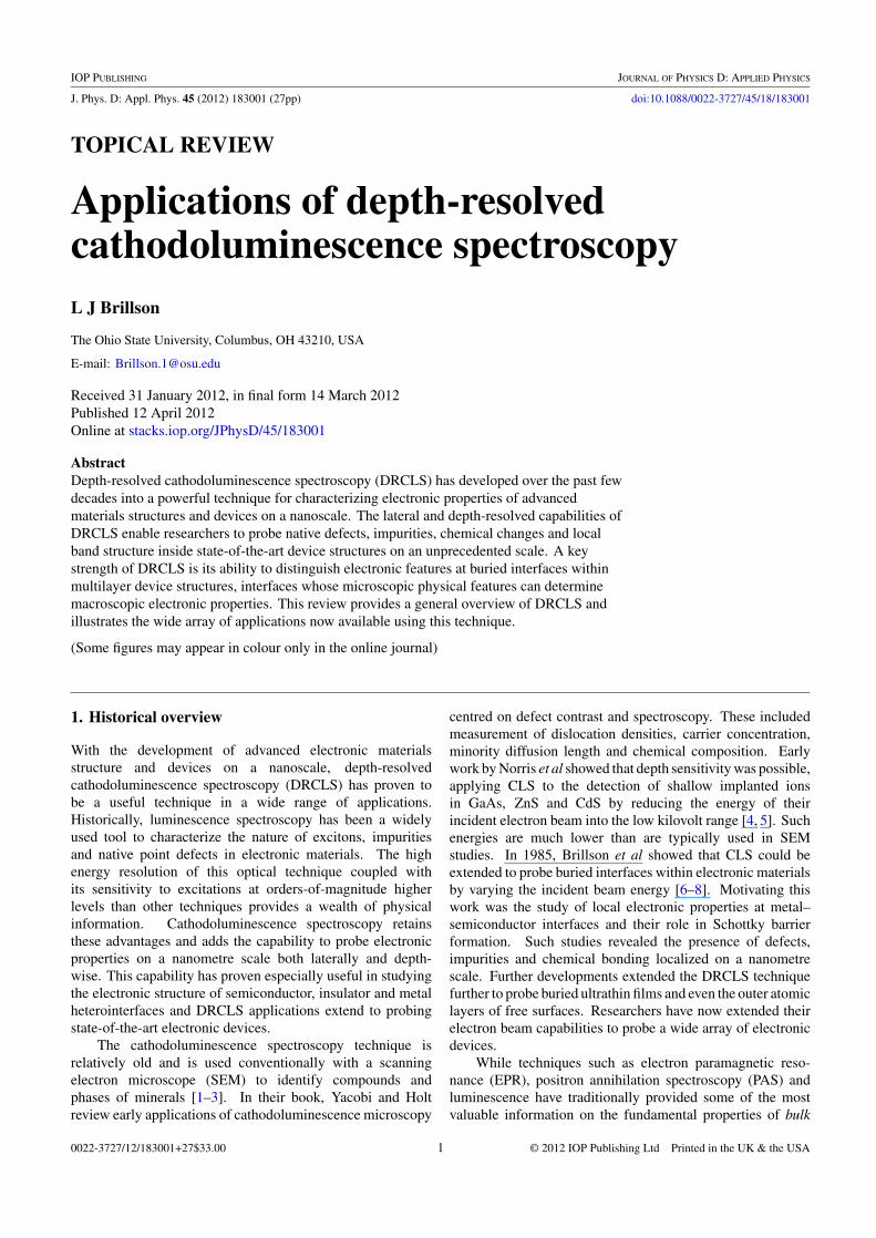
The application of DRCLS to metal–semiconductordiodes reveals the importance of resident native point defectsin: (i) promoting reaction, (ii) forming and degradinginterfacial layers, as well as (iii) introducing defects thatcan increasing doping densities or enable hopping transportthrough Schottky barriers. These effects are magnified bythe segregation of high densities of defects to surfaces andinterfaces at concentrations comparable to those of bulkcarriers [30]. Processing steps that alter the distribution ofthese defects as monitored by DRCLS can produce majorchanges in diode I–V characteristics. For example, figure 12illustrates the effect of ROP treatment on diodes of the samemetal on the same ZnO surface [68]. The schematic diagramillustrates the sequence of measurements. First, Au diodestermed Au I are deposited on as-received/chemically cleanedZn- or O-terminated surfaces. These surfaces then receive anROP treatment. Finally, Au diodes termed Au II are depositedon the ROP-treated surfaces.
The effect of ROP treatment on the DRCL interfacespectra and the free carrier densities measured from 1/C2–V plots are shown in figures 12(a) and (b). For both Zn-and O-polar surfaces, ROP treatment decreases the 2.5 eVemission associated with new donors. For the Zn-polar surfaceonly, ROP treatment also introduces 2.1 eV emission due to Znvacancies, which act as acceptors to reduce carrier densities.Indeed, figure 12(a) inset shows a 2× decrease within 200 nmof the free Zn-polar surface. Significantly, O-face carrierdensities for Au II diodes are twice as high at Zn-polar surfacesthan at Au I diodes before ROP treatment. Carrier densities forAu I diodes could not be measured on O-polar surfaces becausethey are even higher. Consistent with these measurements,Au II diodes are rectifying while Au I diodes are ohmic. Hereagain, DRCLS provides a microscopic physical basis for
11

J. Phys. D: Appl. Phys. 45 (2012) 183001 Topical Review
-2 -1 0 1 2
1E-13
1E-12
1E-11
1E-10
1E-9
1E-8
1E-7
1E-6
1E-5
1E-4
1E-3
As-Received
1 Hr O-Plasma
1 Hr O-Plasma 350
1 Hr O-Plasma 450
1 Hr O-Plasma 550
I (A
mp
ere
s)
I (A
mp
ere
s)
V (Volts)
V (Volts)
-3 -2 -1 0 1 2 3
1E-13
1E-12
1E-11
1E-10
1E-9
1E-8
1E-7
1E-6
1E-5
1E-4
1E-3
0.01
1E-13
1E-12
1E-11
1E-10
1E-9
1E-8
1E-7
1E-6
1E-5
1E-4
1E-3
0.01
O2 Plasma
350 Anneal O2 Plasma
450 Anneal O2 Plasma
550 Anneal O2 Plasma
1.5 2.0 2.5
Energy (eV)
3.0 3.5 4.0
10
100
1000
10000
100000
3.0 eV
2.5 eV
2.10 eV
CL
In
ten
sit
y (
a.u
)
(5kV) AR
(5kV) O2 Plasma
(5kV) O2 350 Anneal
(5kV) O2 450 Anneal
(5kV) O2 550 Anneal
(5kV) O2 650 Anneal
(c)
(d)
(a)
Figure 11. 5 keV DRCLS of 30 nm Ta on (a) high and (b) low-defect ZnO(0 0 0 1). The 2.5 eV intensity increases with Ta deposition andsubsequent annealing up to 550 C. The inset shows 4.1 eV peak associated with Ta oxide that appears only at 550 C. High-defectI–V characteristics show (c) annealed Ta contacts blocking and stability up to 450 C. Low-defect I–V characteristics show (d) stability upto 550 C. Both show I–V voltage offset due to dipole formation. Reprinted with permission from [59] Copyright 2007, American Instituteof Physics.
the carrier densities and barrier heights measured electricallybecause of its capability to probe within nanometres of themetal–semiconductor interface.
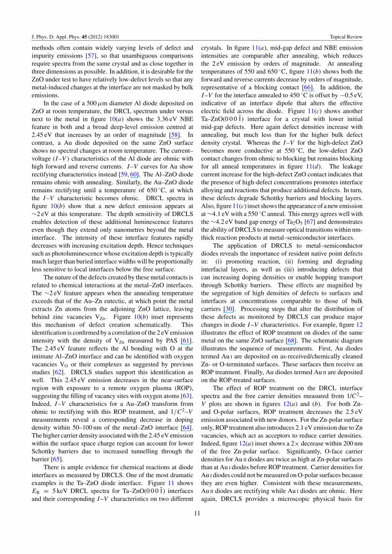
Interface-specific DRCLS can uncover the physical natureand spatial distribution of nonuniformities commonly observedin the I–V characteristics of single diodes. In the caseof an array of Ni diodes patterned on a 4H–SiC surface,DRCLS reveals a striking correspondence between deep-leveldefects and electrical transport measurements on a diode-by-diode basis. These diodes exhibit both ideal and non-idealdiode characteristics due to multiple barriers within individualcontacts [69]. Ideal diodes displayed current characteristicsthat increased exponentially with forward bias, whereas non-ideal diodes exhibited excess current at low voltages that couldbe modelled using thermionic emission theory [70] as twoSchottky barriers in parallel [71]. Figure 13 illustrates thediode pattern, the CL spectrum of the full 500 µm diameterdiode, and the CL spectra from two areas within that diode.The full diode spectrum exhibits the NBE emission at 3.2 eV
as well as broad emissions extending from 1.8 to 2.8 eVdue to gap states. By subtracting out the broad 2.45 eVemission commonly observed for most diodes, one findstwo additional gap state emissions at 2.2 and 2.65 eV whoseintensities vary between diodes. The Area 1 spectrum displaysstrong emission entirely for the 2.65 eV emission, while the2.2 eV emission is stronger in the Area 2 spectrum. Hencethe DRCL spectrum of the entire diode area represents aweighted average of the two more localized spectra. The2.2, 2.45 and 2.65 eV emissions are complementary totransitions from states 1.07, 0.82 and 0.62 eV below theconduction band EC of the 3.27 eV 4H–SiC band gap. Theseenergies agree with multi-component Schottky barriers of 1.05,0,87 and 0.6 eV typically observed in pronounced doublebarrier diodes. The 2.65 eV peak was observed only indiodes that exhibited double barrier behaviour. The lowerof the dual Schottky barrier heights obtained from I–V
measurements was ∼0.6–0.8 eV, in agreement with deep-leveltransient spectroscopy (DLTS) measurements of a companion
12
J. Phys. D: Appl. Phys. 45 (2012) 183001 Topical Review
1.8 2.0 2.2 2.4 2.6 2.8 3.0 3.2 3.4
101
102
103
104
105
80 120 160 200 240
0.4
0.6
0.8
N
d (
10
17 c
m-3)
Depth (nm)
Au II
CL I
nte
nsity (
a.
u.)
Photon Energy (eV)
(b) O face(a) Zn face Au I
Au II
2.1 eV
as-received
Au I ROP Au I
1.8 2.0 2.2 2.4 2.6 2.8 3.0 3.2 3.4
80 100 120 140 160 1800.4
0.8
1.2
1.6
Nd (
10
17 c
m-3)
Depth (nm)
Au I
Au II
2.5 eV2.5 eV
Figure 12. Comparison of CL spectra for Au I and Au II diodes on Zn and O faces. The corresponding CV carrier profiles appear in theinset. Near-interface carrier densities and 2.5 eV DRCLS peak intensities are higher for O- versus Zn-polar surfaces and lower forROP-treated surfaces. Reprinted with permission from [68] Copyright 2010, American Institute of Physics.
1.8 2.0 2.2 2.4 2.6 2.8 3.0 3.2 3.4
0
200
400
600
800
1000
1200
1400
3.2 eV
2.65 eV2.2 eV
5 keV500 µm Full Diode
Energy (eV)
CL
In
ten
sit
y (
a.u
.)
1.8 2.0 2.2 2.4 2.6 2.8 3.0 3.2 3.4
-100
0
100
200
300
400
500
600
700
800 2.2 eV 2.65 eV
3.2 eV
5 keV
Area 2
Energy (eV)
CL
In
ten
sit
y (
a.u
.)
1 .8 2.0 2.2 2.4 2.6 2.8 3.0 3.2 3.4-200
0
200
400
600
800
1000
1200
1400
1600
1800
3.2 eV
2.65 eVArea 1
5 keV
Energy (eV)
CL
In
ten
sit
y (
a.u
.)
Figure 13. SEM micrograph of etched Ni-SiC diodes and DRCLS of corresponding areas within a single, strongly non-ideal diode.Subtraction of broad 2.45 eV feature reveals additional 2.2 and 2.65 eV peaks whose intensities vary between areas and whose energiescorrespond to band gap energies of Fermi level pinning. Reprinted with permission from [69] Copyright 2005, American Institute of Physics.
13
J. Phys. D: Appl. Phys. 45 (2012) 183001 Topical Review
CVD-grown 4H–SiC epilayer that measured deep levels atEC-0.62 eV. The 2.2 and 2.65 eV emissions can be associatedwith specific defect complex and polytype inclusions. Thebroad 2.45 eV luminescence is usually assigned to B-relateddefects. While screw dislocations and micropipes aredetected in these diodes, there was no correlation betweenthe ideality factors, barrier heights or reverse leakage currentsand the numbers of these morphological imperfections undereach diode. Thus the spatial distributions of point defectsmeasured by DRCLS among and within individual diodesrather than any morphological features can account for thediode barrier inhomogeneities measured electrically. Theseresults suggest that surface and interface-specific DRCLS hasthe potential to predict diode uniformity nondestructively priorto metallization.
8. Application to solar cells
The depth profiling capability of DRCLS provides a newavenue to probe multilayer solar cell structures. In additionto the intrinsic properties of the absorption layers, theefficiency of solar cells is limited by defects and interfacialchemistry introduced during fabrication. CLS provides auseful tool to probe electronic and chemical properties ofpolycrystalline grains and grain boundaries. These changescan have a major effect on charge separation and transportwithin the generation layers, which are critical to solar cellefficiency. For example, AES measurements of copperindium gallium diselenide (CIGS) films cleaved in UHVreveal a decrease in grain boundary copper content relativeto the bulk [72, 73], confirming theoretical predictions [74] ofcompositional and band structure changes which can reduceelectron–hole recombination. In addition to CL imagingof dislocations [75, 76], most CLS measurements have beenin plan view [77–80] or in cross-section [81]. DRCLSstudies of solar cell layers reveal defect distributions extendingaway from the free surface [82] and their relation to surfacemorphology [80]. However, these plan-view features of solarcell materials convey only a partial view of the properties insidethe assembled multilayer structure.
DRCLS can also probe electronic properties inside actualsolar cells and relate the defect and band structure featuresto real solar cell performance. As various semiconductor-based technologies move from the lab to manufacturing, newdiagnostic techniques are needed to assess the electronicproperties of the assembled multilayer solar cell structureson a microscopic scale. DRCLS measurements throughoutthe various layers within the solar cells can reveal localspatial variations in the semiconductor band structures, evenwithin a single grain [73, 83]. For solar cells consisting ofa CIGS absorber, a CdS/ZnO heterojunction, and an indiumtin oxide (ITO) transparent conducting oxide (TCO) coverelectrode, band gap and defect correlations to the efficiency,open circuit voltage and short circuit current characteristicsshow evidence for alloying or intermixing between the CdS andZnO layers that degrade solar cell performance. These solarcells were manufactured by Ascent Solar and intentionallyselected to exhibit a range of electrical properties. DRCL
spectra within each of the layers and at their interfaces showedthat: (1) open circuit voltage VOC decreased as ZnO NBE peakenergy increased, indicating a detrimental effect of ZnO/CdSinterfacial alloying; (2) short circuit current JSC quantumefficiency (QE) increased by nearly 10% as ZnO NBE peakintensity increased, showing that reduced defect density withinthe ZnO improved solar efficiency by >10%; and (3) JSC QEalso increased with ITO NBE intensity, showing that reduceddefect density inside the ITO layer improved cell efficiencyas well. These effects may reflect the movement of minorityhole carriers from the ZnO and ITO layers into the CdS/CIGSjunction region, where they recombine at deep levels observedwithin the ZnO, CdS, CIGS and interfacial layers. Thesignificant variations in VOC and JSC QE of operating solarcells with their local electronic structure highlight the roleof DRCLS as a diagnostic tool to assess and guide theimprovement of solar cell structures.
9. Application to oxide–semiconductor interfaces
With the scaling down of complementary metal-oxide-semiconductor (CMOS) devices into the nanoscale regime,there is an urgent need for high permittivity, i.e.high-k dielectrics to maintain threshold capacitances despiteshrinking dimensions. Candidate materials that can substitutefor SiO2 include HfO2, ZrO2 and their alloys. A primarychallenge in incorporating these new materials is to minimizethe electronic traps within the dielectric and at its interfaces.The traps in high-k dielectrics and at their interface with Si aresubstantially higher than for SiO2 on Si. These cause trapping,Fermi level pinning, degradation of Si carrier mobility andtransient threshold voltage shifts that degrade MOS field-effect transistor (MOSFET) performance [84]. However, thesetraps depend sensitively on growth and processing, and theirelectronic effects are apparent only after device fabrication. Inaddition to electrical measurements, diagnostic tools such asEPR on transistor structures have been effective in detectingand characterizing the nature of these states. DRCLS hasproven valuable in assessing these traps electronically both inultrathin deposited films as well as in assembled metal–oxide–Si device layers.
Early DRCLS work examined PECVD-deposited, ultra-thin SiO2/Si interfaces processed under various thermal andambient conditions. Figure 14 illustrates the evolution of de-fect emissions versus annealing treatment at 5 nm thick SiO2
on Si interfaces using EB = 2 keV to probe the interfacial re-gion preferentially [85]. Each curve is a composite of S-20phototube and Ge photodiode spectra spanning infrared to theultraviolet energies. The as-deposited interface displays de-fect emissions at 0.8 and 1 eV that are related to interfacialSi-atom dangling bond defects with different numbers of Siand O atoms back bonded to the Si atom with the danglingbond. The broad emission peaked at 1.9 eV is assigned to lu-minescent transitions involving a suboxide bonding defect inthe transition region near the grown interface. A forming gas(FG) anneal lowers the 1.9 eV defect intensity, partially passi-vating these defects in the transition region. A rapid thermalanneal (RTA) at 900 C known to produce atomically abrupt
14

J. Phys. D: Appl. Phys. 45 (2012) 183001 Topical Review
Figure 14. Interface-specific 2.0 keV DRCLS spectra showing theprogression of defect reduction from as-deposited 5 nm SiO2 on Sias a function of post-growth processing. A dramatic decrease indefect density is observed at 1.9 eV upon annealing at 900 C.Post-hydrogenation at 400 C induces an additional decrease at0.8 eV. Reprinted with permission from [85] Copyright 1998,American Institute of Physics.
SiO2/Si interfaces eliminates these transition region defectsbut leaves the Si dangling bond defects. Finally, a FG annealat 400 C following the 900 C RTA passivates the Si danglingbond defects, reducing interface state densities measured elec-trically down to at the least the mid 1010 cm−2 eV−1 range [86].This value also indicates a meaningful lower limit on the detec-tion of defects using DRCLS. The ability to monitor successivereduction of defects at the SiO2/Si interface in multiple processsteps demonstrates how DRCLS can be useful in optimizingprocess steps for other oxide–semiconductor interfaces with-out the need to fabricate device structures.
DRCLS is able to detect defects inside metal/high-Kdielectric/Si MOS structures. Figure 15 displays DRCLspectra measured inside 4 nm thick HfO2 deposited filmssandwiched between Si and a 10 nm Mo gate metal before andafter a FG anneal [87]. These heterostructures are representedschematically as insets in figure 15. They were fabricatedat Motorola with a variety of conventional process sequencesin order to identify optimal conditions that minimize HfO2
defect densities. With increasing EB, DRCLS first detectsdefect emissions at 3.35, 3.9 and 4.3 eV that increase as theelectron cascade extends past the metal into the HfO2. Theseenergies correspond to the three charge state transition energiespredicted theoretically for oxygen vacancies in HfO2 [88].Deeper penetration introduces defects at 2 and 2.5 eV thatcorrespond to the HfO2/Si interface. These states increasestrongly with a FG anneal. Their energies are close to thoseof native defects in SiO2, namely, the non-bonding oxygenhole centre (NBOHC) at 1.9 eV, i.e. a hole trapped in a pure
2pπ orbital of a single O bonded to a single Si bonded tothree O atoms in the SiO2 structure, denoted ≡Si–O· [89]and E’ oxygen vacancy, i.e. an unpaired spin in a danglingtetrahedral orbital of an undercoordinated Si atom, denoted≡Si· (positively charged O vacancy) [90]. Both are illustratedin figure 15. The emergence of these SiO2-like emissionsindicates the formation of a Hf silicate, HfSiO4, with similardefects. Their presence mirrors a 0.8 nm SiO2-like interfaciallayer known to form after HfO2 deposition, typically growinga few Å after RTA with a Mo electrode. Hence DRCLSis capable of detecting interface features inside and at theinterfaces of films only 4 nm thick even when covered witha metal overlayer. Furthermore these defect states varydramatically between process sequences and can be understoodin terms of known reactions at HfO2–Si interfaces.
More recent work on ultrathin oxides at buried interfacesincludes the properties of interfacial layers at high-k dielectricMOS interfaces. For the promising dielectric LaLuO3,DRCLS is used to measure trap energies and relative densitiesin metal/LaLuO3/Si stacks, defects produced by LaLuO3–Siinterdiffusion, and suppression of these defects by monolayer-thick Al2O3 interlayers [21, 91]. DRCLS detects a set ofthree deep levels at energies above the valence band that areconsistent with LaLuO3 oxygen vacancies predicted by theory[92] as well as a 5.5 eV band gap. Oxygen annealing meantto reduce oxygen vacancies instead introduces an interfaciallayer between LaLuO3 and the Si substrate that leads to anincrease in effective oxide thickness (EOT) and deformedC–V curves. New traps are measured by temperaturedependent I–V of leakage conduction at 0.66 eV below theconduction band that DRCLS also detects. In order to isolatethe LaLuO3/Si interface, Shen et al introduce a differentialDRCLS technique that further enhances depth resolution [21].The Al2O3 monolayer acts as a diffusion barrier to suppressthe LaLuO3–Si reaction and the associated trap states. DRCLSconfirms the central role of the barrier layer in removing trapsin the LaLuO3 gate stacks with oxygen annealing withoutsignificantly degrading dielectric EOT.
10. Application to TCOs
TCOs have many opto- and microelectronic applicationsincluding electrodes for photovoltaic cells and flat paneldisplays, LEDs and laser diodes. DRCLS can provideinformation on doping density, doping uniformity and thenature of dopants for highly degenerate n-type, Ga-doped ZnO[93], now becoming a useful replacement for ITO. Large scaleproduction of ZnO-based TCOs attractive for several reasons:(i) ZnO is environmentally compatible, as opposed to the heavymetal In in ITO, which is not. Only a very low fraction ofthe heavy metal Ga is required; (ii) Zn ore from mines isreadily available so that cost is relatively low [94]. Figure 16shows DRCL spectra of thin Ga-doped ZnO (GZO) grown byPLD that exhibit characteristic features of degenerately dopedsemiconductors [95], e.g., a broad asymmetric free-electronrecombination band extending to energies above the band gap[96] . DRCL spectra display luminescence involving filledconduction band states which provide the Fermi level cutoff
15

J. Phys. D: Appl. Phys. 45 (2012) 183001 Topical Review
4.35 eV
3.89 eV
3.53 eV3.35 eV
2.55 eV1.97 eV
Inte
nsit
y (
A.U
.)
1.5 keV
2.0 keV
3.0 keV
4.0 keV
5.0 keV
~ 5.9 eV
PVD 10 nm Mo
4 nm HfO2
Si
No FG Anneal x 1 Scale
(a)
2 3 4 5 6
In
ten
sit
y (
A.U
.)
~ 5.9 eV
4.3 eV
3.9 eV
3.5 eV
2.5 eV2.0 eV
Photon Energy (eV)
1.5 keV
2.0 keV
3.0 keV
4.0 keV
5.0 keV
PVD 10 nm Mo
4nm HfO2
Si
FG Annealx 1/4 Scale
(b)
ET
Figure 15. DRCLS of (a) PVD-deposited 10 nm 4 nm Mo on HfO2/Si without anneals showing mutiple deep levels below 5.5 eV band gap.The 2–2.5 eV features increase relative to the dominant 3.35.3.53 eV doublet with increasing excitation depth. (b) After annealing in FG, 2and 2.5 eV intensities increase. Reprinted with permission from [87] Copyright 2007, American Institute of Physics.
Figure 16. TCO VZn-related defect emission intensity versus Hallcarrier density indicating that Ga fills vacant Zn sites to increase(decrease) donor (acceptor) concentration. Data point labels aregrowth temperatures. After [95].
and an integrated area, both of which provide a measure of freecarrier density. This carrier density tracks with measured Halldensity and with optical absorption threshold, which dependson the Burstein–Moss effect [97, 98]. Figure 16 inset shows notonly filled conduction band-to-valence band emission but alsodefects within the band gap. Peaks at 1.6–2.1 eV correspond
to Zn vacancies and Zn vacancy complexes established bycorrelation with PAS [61]. Figure 16 includes measurementsof GZO films grown under both Ar and FG atmosphere andwith a range of degenerate doping extending over nearly anorder of magnitude. The NBE-normalized Zn vacancy-relatedemission intensity I (VZn − R)/I (NBE) exhibits a systematicdecrease with increasing free carrier density determined fromHall measurements [99]. This indicates that these native pointdefects are directly involved in the doping process, either at orbelow the free surface as the crystal is growing. As Zn sitesare filled with Ga, VZn sites are removed that would otherwiseact as doubly charged acceptors and GaZn sites are created thatact as donors. This trend is reflected in the decreasing VZn-Remission with increasing free carrier density.
This decrease in VZn-R emission with increasing dopantincorporation is also evident in studies of ZnO doped withLi [100]. Here the formation of Li on Zn sites, LiZn, presentsa distinct optical signature that increases as VZn-R emissiondecreases. The LiZn intensity measured by DRCLS as afunction of depth matches the Li incorporation concentrationversus depth measured by SIMS, thereby confirming the Linature of the defect. Likewise, scanning spreading resistancemeasurements (SSRM) matching the SIMS [Li] profile confirmthe acceptor nature of the LiZn emission. Hence the depth-resolved capability of DRCLS to measure electronic structureversus depth enables (i) the identification of the LiZn lattice siteemission, (ii) the acceptor nature of this optical emission and(iii) the central role of Zn vacancies in the Li incorporation asa p-type dopant.
16

J. Phys. D: Appl. Phys. 45 (2012) 183001 Topical Review
Figure 17. Anticorrelation of VZn-related defects and carrierdensity nCL versus probe depth of degenerately doped ZnO : Ga.Electron carrier density decreases at depths where VZn acceptorsincrease. The variation on a scale of 5–10 nm can affect electricalmeasurements. After [95].
The Fermi level cutoff feature in these spectra enablemeasurements of free carrier density as a function of depth,even in films only a few tens of nm thick. For example,figure 17 shows that a film grown by PLD under FG at 600 Cexhibits oscillations in carrier density with depth. Using adifferential technique to improve depth resolution, Doutt et alfound that such oscillations can occur on a scale of only a fewnanometres [96]. Significantly, the VZn-R intensities fromthe same spectra anti-correlate with the free carrier densitydetermined from the Fermi level cutoff. This is consistentwith the acceptor nature of VZn sites, which act to decreasethe otherwise n-type doping density. This is consistent withthe correlation of VZn-R defects to carrier density shownin figure 16. These DRCLS results raise the possibility ofcontrolling vacancy defects during and following the growthprocess to assist doping in semiconductors such as ZnO.
11. Application to transistors
DRCLS has provided a wide range of information on state-of-the-art transistors, in particular, the AlGaN/GaN highelectron mobility transistors (HEMTs) now widely used forhigh frequency, high power applications. These devicesrely on a high carrier density, high mobility channel layerat the AlGaN/GaN heterojunction. Both the carrier densityand the mobility are extremely sensitive to the quality ofthe semiconductors and their interface. Large variations inquality within the same crystal wafer can occur that determinecarrier mobilities and whether or not channels exist at theresultant HEMTs.
Lateral DRCLS obtained from specific depths providesinformation on composition and defects to account for thevariations in HEMT properties. Figures 18(a) and (b) depictthe lateral and cross-sections geometries of this application,respectively [101–106]. Figure 18(a) shows how DRCLspectra are acquired at increasing radial distances of the wafer.For a wafer of GaN with a 50 nm AlGaN barrier layer and
a 2 nm GaN overlayer, depicted in figure 18(b), an incidentelectron beam with EB = 2 keV provides spectra that aresensitive primarily to the two dimensional electron gas (2DEG)at the AlGaN/GaN interface. Figure 18(c) shows spectraversus radial position that include emissions from AlGaN andGaN NBE as well as defects within their band gaps. TheAlGaN NBE energy is a function of Al alloy composition.With increasing radius, the AlGaN NBE energy increasesfrom 3.72 to 3.92 eV, indicating an increase in Al content.This variation alters the AlGaN barrier layer band gap andband offset with GaN. In addition, the intensity of mid-gapdefects at 2.34 eV increase then decrease with radial position,reaching a maximum at intermediate radii. Such defects areassociated with transitions termed yellow luminescence (YL)at this energy from a shallow donor, e.g., a N vacancy, to a deepacceptor level, e.g., a Ga vacancy [107–109]. These deep-level defects promote free carrier recombination, loweringcarrier density and hence the ultimate current density of devicesfabricated at these wafer locations. These variations areapparent in the DRCL spectra at the 2DEG heterojunctiondepth but not for excitations extending beyond this layer.
AES depth profiling of the regions with high-defectdensity provided elemental composition versus depth, whichrevealed significant interdiffusion between AlGaN and GaNat these radial positions that could account for the increaseddefect densities. The ability to observe such imperfectionswithout ablating the wafer surface using DRCLS representsan attractive alternative to AES sputter depth profiling. At therelatively low beam energies, current densities and fluencesused here, no induced defect changes or interdiffusion areobserved. Furthermore, DRCLS can rapidly identify processconditions, e.g., temperature and flux uniformity across thewafer, informing growth conditions that can improve quality.
The charged nature of the defects act to disrupt theAlGaN/GaN 2DEG. Comparison of AlGaN/GaN wafersections that form high quality 2DEGs versus those for which a2DEG is absent reveal strong differences in DRCLS emissions.Figure 19(a) shows DRCL spectra of AlGaN/GaN HEMTlayers used to fabricate transistor structures that had noelectrically measured 2DEG channel. These layers exhibitstrong defect emission at energies of 2.34 eV at 2DEG depths.In contrast, figure 19(b) shows almost no defect emissionsat this energy for the same range of depths, increasing onlyfor excitation into the GaN layer below the 2DEG. A Poissonsolver analysis of the 2DEG well simulates the band bendingand charge accumulation at the AlGaN/GaN interfaces underHEMT operating conditions, and it shows that additionalacceptor states within the AlGaN layer can decrease the welldepth. At high enough acceptor densities, the 2DEG isabsent. These results not only account for the absence of2DEG channels in high-defect HEMTs but also provide arough calibration of the DRCLS defect density, in this case,I(defect)/I(GaN NBE) of ∼5 corresponds to defect densitiesof ∼1018 cm−3. Here band bending changes due to electronbeam injection are independent of the device measurements.
DRCLS can detect defect formation at buried transistorchannels of high mobility semiconductors such as InAlAs.Figure 20(a) illustrates a cross-sectional schematic inside an
17

J. Phys. D: Appl. Phys. 45 (2012) 183001 Topical Review
1.5 2.0 2.5 3.0 3.5 4.0
6.0 mm
7.2 mm
0.0 mm
Photon Energy (eV)
2.32 eV
2.15 eV
3.72 eV9.2 mmx10
x5
Lu
min
esce
nce
In
ten
sity
(re
l. u
nit
s)
16 mm
3.80 eV
x20
21 mm
18 mm
x20
3.40 eV3.92 eVx100
x50
(a)
(b)
(c)
Figure 18. Radial variation of AlGaN composition and heterojunction defects across AlGaN/GaN wafer. 2 keV spectra probe the 2DEGAlGaN/GaN heterojunction as shown in the cross-section. Defect emissions at 2.15 and 2.32 eV are strongest at intermediate radii.Reprinted with permission from [101] Copyright 2001, IEEE.
1.5 2.0 2.5 3.0 3.5 4.0
2.34 eV
0.7 keV
0.5 keV
Photon Energy (eV)
1.2 keV
1.0 keV
Lu
min
esce
nt
Inte
nsi
ty (
Rel
. U
nit
s)
3.28 eV
2.0 keV
1.5 keV
3.31 eV
x2
x2
x2
x2
x2
x2
(a) 3.82 eV
3.32 eV
1.5 2.0 2.5 3.0 3.5 4.0
3.27 eV
x2
x2
x2
x2
x2
x2
0.7 keV
0.5 keV
Photon Energy (eV)
1.0 keV
1.2 keV
1.5 keV
(b)2.18 eV
3.42 eV3.95 eV
2.0 keV
Figure 19. DRCL spectra of AlGaN/GaN HEMT layers with (a) and without (b) 2DEG carrier densities. Increased defect densities in (a)alter heterojunction band bending, removing the 2DEG. Reprinted with permission from [90] Copyright 2001, IEEE.
InP-based lattice matched InAlAs HEMT. Here, gate length,gate width and InAlAs layer thickness are 0.1 µm, 1 µm and20 nm, respectively, with the channel located hundreds ofnm below the free surface [110]. Salviati et al measured
the formation of defects in this buried channel layer withelectrical stress, i.e. hot electrons forming defects within thegate-drain region of the stressed device [111]. Figure 20(b)shows the changes in DRCLS lineshape at 1523, 1358 and
18

J. Phys. D: Appl. Phys. 45 (2012) 183001 Topical Review
Figure 20. Defect formation at buried channel layers of InAlAs inside quantum well. (a) InGaAs NBE-related depth resolved anddeconvolved cathodoluminescence from the stressed gate-drain region. (b) Features assigned to band bending within the InGaAs quantumwell and to defects within the AlGaN layers above and below the InGaAs. Reprinted with permission from [111] Copyright 2001 Elsevier(c) Schematic cross-section of the HEMT. Reprinted with permission from [110] Copyright 1998, IEEE.
1428 wavelength attributed to, respectively, the NBE in theupper n-doped InGaAs cap layer, and band bending of thequantum well forming the undoped InGaAs channel belowthe InAlAs layer. The latter exhibit changes in lineshape asEB is decreased to 8 keV to emphasize the quantum well.In figure 20(c), a peak at 846 nm observed at EB = 8 keVincreases with electrical stress, suggesting formation of a deeplevel within the InAlAs layers.
In the case of heterojunction bipolar transistors (HBT’s),Borgarino et al used DRCLS to detect the base-dopantoutdiffusion of Be induced by electrical stress in a realAlGaAs/GaAs Be-doped device [112]. Such outdiffusionof the p-type dopant into the emitter layer during thedevice operation can significantly degrade device reliability.DRCL spectra in the 10–14 keV range showed pronouncednew emission appearing after electrical stress at 10 keVthat diminishes at 14 keV. Single scattering Monte Carlosimulations show that the EB = 10 keV beam excites onlythe shallower emitter layer, whereas EB = 14 keV excitesdeeper past the AlGaAs/Be-doped base layer interface. Thenew emission is assigned to a Be-related transition in AlGaAs
emitter layer. SIMS measurements show the presence of Bewithin the emitter layer, confirming these DRCLS results.
DRCLS measurements at energies tuned to theAlGaN/GaN depth can provide defect information specificto the 2DEG region of state-of-the-art transistors withinan actual die layout. Jessen et al used a UHV SEM toprobe Ti/Al/Ni/Au ohmic contact resistances in transmissionline measurement (TLM) structures within dies patterned onthe same AlGaN/GaN wafer [113]. DRCLS enabled theassignment of defect emissions to particular layers and theirinterfaces. Thus DRCLS could distinguish defect emissionsfound near the surface from those associated with high sheetresistance found within the AlGaN layer itself. They found astatistical correlation of YL intensity with contact resistanceρc extending across TLM structures on the same wafer as wellas within wafers with different Al mole fraction. Such defectscan alter the Fermi level position at the metal–semiconductorinterface, reducing the 2DEG carrier density and increasing ρc.Furthermore, they showed a correlation of sheet resistance withAlGaN NBE energy and thereby the Al mole fraction. Withdecreasing Al mole fraction, channel carrier density decreases,consistent with an increasing sheet resistance.
19

J. Phys. D: Appl. Phys. 45 (2012) 183001 Topical Review
Figure 21. DRCLS defect peak intensity ratio versus AlGaN/GaNHEMT contact resistivity across the same wafer and comparisonbetween HEMTs grown on different substrates. Inset showscorresponding fT. Increasing DAP/YL increases ρc and reduced fT.Reprinted with permission from [114] Copyright 2003, AmericanInstitute of Physics.
Extending this work, Jessen et al showed a correlationbetween the ratio of GaN donor acceptor pair (DAP) versusYL emission intensities DAP/YL. Figure 21 shows that ρc
increases with DAP/YL across arrays of high frequencyHEMT’s on SiC (DU14) and Al2O3 (AB06) substrates [114].Furthermore, figure 21 inset shows that the average unity-current gain frequency fT decreases with increasing DAP/YLfor these same HEMT’s, consistent with increasing ρc.DAP and YL alone do not correlate with ρc, indicating aninterplay between these defects that an effective barrier heightscattering model involving dislocations can explain. TheseDRCLS studies provided information useful to predict howthese HEMT structures would perform electronically prior tofabrication.
Walker et al correlated near-2DEG defects andAlGaN/GaN HEMT fT as a function of UHV processingconditions used to prepare the GaN gate surface prior tometallization [115]. They combined DRCLS with in situUHV surface science techniques, gate mask fabrication andprocessing to demonstrate improvements in fT comparedwith standard processing. DRCL spectra revealed that a Gareflux and anneal process intended to reduce Ga vacancydefects at the GaN surface doubled fT and reduced bothYL and blue luminescence (BL) substantially compared withstandard processing. For HEMT’s fabricated on the samewafer with either annealing alone or Ar+ sputter cleaningfollowed by annealing, defect reduction at the 2DEG layerand improvements over standard processing were both smaller.These measurements served to demonstrate the importanceof the gate surface quality and the effect of surface damageon the final device performance. They also showed thatimproved surface cleaning, annealing and chemical treatmentthat remove defects as gauged by DRCLS can improve devicequality significantly.
Figure 22. DRCLS spectra at 10 K versus EB for MBE-grownHFET samples before irradiation (thin black curves) and after10 protons cm−1 fluence (thick gray curves). All intensities arenormalized to the GaN NBE emission. Irradiation reducespiezoelectric strain and electric fields, shifting AlGaN NBE peakenergies higher. The higher energy NBE peak is strongest atEB = 2 keV, where excitation of the AlGaN/GaN 2DEGheterojunction is strongest. Reprinted with permission from [117]Copyright 2002, IEEE.
AlGaN/GaN HEMT’s are the major driver for next-generation communication technology, particularly forsatellites and other aerospace applications. However, thesedevices are subject to high energy radiation that can also createdefects. For example, such defects act to quench NBE emissionin GaN layers bombarded with light ions [116]. Figure 22shows that DRCLS can monitor the changes in electronicstructure introduced by radiation at the 2DEG interfacialregion [117]. Before 1.8 MeV proton irradiation, spectradisplay features at 3.42 and 3.73 eV due to AlGaN and GaNNBEs, respectively. After irradiation, these peaks shift upin energy to 3.49 and 3.8 eV, suggesting that strain-inducedelectric fields that lower the NBE emission energy due to aFranz–Keldysh effect have decreased due to the introductionof defects that lower the strain at the heterojunction. Thiseffect is most pronounced at 2 keV, as evidenced by the AlGaNpeak intensity, at which depth the electron beam excites the2DEG interface region preferentially. In addition, a newpeak at 3.19 eV appears that increases with increasing energy,indicating its location primarily in the GaN. As in figure 19earlier, the presence of acceptor-like trap states near theAlGaN/GaN heterojunction can disrupt the 2DEG. This workillustrates how DRCLS detects both the introduction of newdefects and the relaxation of strain in this region.
Micro-DRCLS applications now extend to transistorsduring actual operation. These studies are aimed at identifyingthe physical cause of device degradation mechanisms on a
20

J. Phys. D: Appl. Phys. 45 (2012) 183001 Topical Review
microscopic scale. Early work showed that AlGaN/GaNHEMTs experience large increases in temperature and strainunder operating conditions. However, because these effectscombine with piezoelectric strain and occur in highly localizedregions of the transistor, device failure is hard to interpret andpredict. Unlike optical measurements, the spatial resolutionof DRCLS is not limited by diffraction. Also, DRCLS canprobe selectively at 2DEG depths versus deeper into the GaNbuffer layer and beyond. Lin et al used DRCLS to measureand map the temperature distribution and defect generationinside state-of-the-art AlGaN/GaN HEMT’s on a scale of tensof nanometres [118, 119]. Figure 23(a) shows a scaled cross-sectional schematic of a gated HEMT structure. The GaN NBEenergy provides a measure of temperature, precise to withinan accuracy of ±3 within an excitation radius of <50 nm.A previous CL study shows a close correspondence withliterature, decreasing with increasing temperature up to 900 C[120]. Figure 23(c) shows measurements across the transistorfrom the drain to the gate termed ‘extrinsic drain’ and fromthe gate to the source termed ‘extrinsic source.’ Temperatureincreases during ‘on-state’ operation toward the gate primarilyin the extrinsic drain, reaching a maximum at the drain-sidegate. Figure 23(a) shows these temperature variations acrossthe extrinsic regions and in depth within the AlGaN and GaNlayers. These are all obtained by acquiring CL spectra in planview along the drain-source direction as in figure 23(c) butat different excitation depths [121]. An expanded drain-sidegate region is illustrated in figure 23(b). The magnitude andspatial dimensions of the temperature contours are in goodagreement with those calculated for similar HEMT structures[122]. Furthermore, temperature inhomogeneities hundredsof nanometres below the AlGaN/GaN interface are evidentthat could relate to morphological defects. In principle, thesecontours could be extended into the third dimension parallelto the gate length.
DRCLS can also measure mechanical strain inside theHEMT structure on a nanometre scale. The NBE energyshifts to higher energy at a rate of 26 meV Pa−1 [123].Since temperature shifts the NBE energy as well, the strainmeasurements were carried out under ‘OFF-state’ conditions,where a negative bias on the gate ‘pinches off’ the source–drain current, preventing any heating. Figure 24(a) shows thedc output characteristics and normalized off-state gate currentIG-off as a function of off-state stress voltage VDG betweengate and drain. Very little change in IG-off is evident until VDG
exceeds a threshold voltage of 28 V. Figure 24(b) presents thecorresponding increase in stress at the edge of the gate on thedrain side within the 2DEG channel after an off-state stress.For a 28 V critical VDG, the corresponding stress is ∼0.25 GPacompared with this transistor before stress.
Figure 24(c) presents a representative DRCL spectrumfrom the 2DEG channel of an off-state-stressed transistorthat shows YB and BB emissions present within the bandgap at the drain-side gate foot that reveals large voltagedifferences in these regions. Figure 25(a) illustrates surfacepotential maps of the extrinsic source, drain and gate regionsin this transistor obtained by Kelvin force probe microscopy(KPFM). The different potential regions labelled numerically
Figure 23. Temperature profiles versus depth. (a) (top) 2D verticalmap of source-gate-drain areas across which temperatures weremeasured. (b) Expanded cross-section of 2DEG region showingtemperature variation at the drain-side gate foot. (consistent withmodelling) at EB = 10 keV. (c) Transistor SEM showing top view ofextrinsic source and drain. (d) Temperature is highest and increasesmonotonically from drain to gate overhand edge. Reprinted withpermission from [119] Copyright 2009, American Institute ofPhysics.
show large variations, while the YB/NBE intensity ratioplotted in figure 25(b) show that decreasing off-state surfacepotential correlates with increasing YB/NBE. A self-consistentelectrostatic model [124] with near-surface dipoles that dependon acceptor level EA and EF positions in the band gap provides
21

J. Phys. D: Appl. Phys. 45 (2012) 183001 Topical Review
Figure 24. (a) DC output characteristics and IG−off as a function ofoff-state stress. (b) External stress caused by applied voltage underan off-state stress. Reprinted with permission from [121] Copyright2010, American Institute of Physics (c) DRCLS at one of lowestpotential areas(inset) within the extrinsic drain region after off-statestress showing 2.2 eV YB, 2.8–2.9 eV BB and 3.45 eV NBE peaks.
the defect densities required to produce these potentialchanges. Figure 25(c) shows good agreement of the potentialchanges with dipole widths of 7 to 9 nm, indicating the locationof acceptor states extending from the surface to just beyond the2DEG interface, that is, largely within the AlGaN layer.
The off-state stress results provide strong support forthe inverse piezoelectric mechanism of AlGaN/GaN HEMT
degradation [125, 126]. This model is based on lattice defectsforming between gate and drain by an off-state field-inducedstress normal to the surface that, added to lattice-mismatchstrain already present, exceeds the crystal’s critical elasticenergy density. Consistent with this model are (1) the thresholdbehaviour shown in figure 24(b), (2) the appearance of nativepoint defects detected by DRCLS near the 2DEG interface,(3) their increase with decreasing surface potential and (4)and the dipole location required to produce these potentialchanges. Hence, with its ability to probe electronic structureselectively within multilayer structures and their interfaces,DRCLS provides a tool to identify device failure mechanismsin transistors and related electronic devices. Furthermore, thecorrelation of defect emissions with device failure supportsa physical model of degradation that can provide acceleratedlife tests as well as that can pinpoint specific locations withintransistors where failure is likely to occur first.
12. New directions
New materials structures and devices are constantly beingdeveloped with electronic features that depend sensitivelyon their surface and interface properties. DRCLS canprovide spatially resolved electronic information within thesestructures, particularly as they shrink into the nanoscaleregime. One largely unexplored area is with the surfaces andinterfaces of complex oxides. The remarkable ferroelectric andferromagnetic properties of these materials depend strongly oncharge transfer at their interfaces as well as on the distributionand movement of electrically active defects common tosuch oxides. Movement of defects under applied electricfields plays a significant role in new device phenomenasuch as memristors [127] and tip-induced conductivity [128].Likewise, defects at magnetic tunnel junctions scatter spin-polarized electronics, reducing the polarization of transferredcharge. Furthermore, chemical reaction, phase changes, orlattice distortion can produce local changes in electronicstructure that DRCLS can detect. Initial DRCLS studies[129–131] show that high densities of native point defectsare present in these materials, often segregating to theirsurfaces and interfaces. DRCLS studies now show thatdefects within ferroelectrics such as SrTiO3 correlate directlywith RF dielectric loss and permittivity [132]. Furthermore,DRCLS studies can extend to superconducting oxides suchas YBCO, whose defects can have significant effects on itselectronic properties. Surface studies achieved with growthand analysis chambers linked under UHV conditions willenable identification of near-surface defects measured byDRCLS with specific elemental composition and bondingmeasured by photoemission spectroscopies.
High-k dielectrics represent an area of solid stateelectronics where DRCLS can also make significanttechnology contributions. The ability to probe withinultrathin dielectric films, even when sandwiched betweenmetals and semiconductors, enables DRCLS to measurenondestructively the presence of chemical reactions, the natureand location of electronically active defects in the nm-scale‘bulk’ and its interfaces, and the energies of defects relative
22

J. Phys. D: Appl. Phys. 45 (2012) 183001 Topical Review
Figure 25. (a) KPFM maps from two representative transistor areas along its width show surface potential distribution and averaged defectemission after off- state stress. (b) With decreasing potential, ratio YB/NBE increases. In general, regions with lower potential correlatewith higher YB or BB defect emission. (c) Decreasing potential corresponds to higher defect density deep within the GaN band gap thatintroduces surface dipoles and Fermi level pinning. After [121].
to the band structure of the metal–dielectric–semiconductorcomposite. This capability can be of particular valuewhen evaluating optimal dielectric compositions, growth anddeposition methods, and subsequent processing to minimizeeffects due to electronic trapping.
DRCLS at very low energies permits studies at depthsof only a few atomic layers. Studies using incidentbeam energies of only 50–100 eV generate secondaries withminimum inelastic mean free paths (IMFP) of only 2–10 Å[133, 134]. Plasmons dominate electron energy loss at theseenergies [135] followed by impact ionization and creationof free electron–hole pairs. Hence for plasmon energiesof ∼15–20 eV, only a few such material-dependent lossescan occur per IMFP before energies fall below the multipleband gap ionization energies needed to generate electron–holepairs in semiconductors [136]. DRCLS studies at these lowenergies with ∼100 µm lateral dimensions on surfaces withsingle monolayer roughness are now underway to examinethe distribution of defects normal to superlattices and otherheterointerfaces on a nanometre scale. The ability to restrictexcitation on this scale also offers the possibility of probingthe differences in electronic structure at nanostructures andespecially at their interfaces. A complication to such studiesat very low energies is the buildup of carbon at sample surfacesdue to decomposition of residual gases within the analysischamber. This is not of high concern for CLS using electron
guns within UHV chambers. Furthermore, with the advent ofUHV SEMs, this difficulty can be largely avoided.
The combination of DRCLS with other depth-resolved anddefect-sensitive techniques can not only enable identificationof defect transition energies with specific defects, but it can alsobe used to calibrate DRCLS emissions. One notable exampleto date has been DRCLS combined with PAS to identify the1.6–2.1 eV luminescence energies with VZn and VZn clusters aswell to calibrate the emission intensities with defect densities[61, 100]. Another technique that has already complementedDRCLS is SPS, which provides information on the filling andunfilling of trap states at and near free semiconductor surfaces,thereby identifying the conduction or valence band natureof the defect transition within the band gap [61, 100] SIMShas already proven effective in correlating DRCLS emissionswith a particular defect [61]. Defect densities measured withC–V techniques at the edge of a semiconductor’s surfacespace charge region calibrate DRCLS intensities, that can thenprovide defect densities for shallower depths otherwise limitedin C–V measurements by forward bias leakage currents.Similarly, DRCLS can be combined with EPR, anotherpowerful technique for characterizing point defects. EPRinformation includes the nearest neighbour coordination andcharge state. A related technique is optically detected magneticresonance (ODMR), which used the changes in charge stateof defect levels to determine their energies within the bandgap [137, 138]. A challenge for EPR and ODMR is that a
23
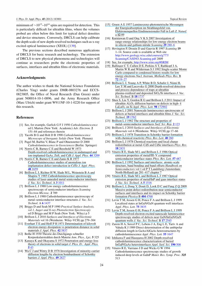
J. Phys. D: Appl. Phys. 45 (2012) 183001 Topical Review
minimum of ∼1013–1014 spins are required for detection. Thisis particularly difficult for ultrathin films, where the volumesprobed are often below this limit for typical defect densitiesand device structures. Conversely, DRCLS can help calibratethe depth scale of new depth-resolved techniques such as x-rayexcited optical luminescence (XEOL) [139].
The previous sections described numerous applicationsof DRCLS for basic research and technology. The extensionof DRCLS to new physical phenomena and technologies willcontinue as researchers probe the electronic properties ofsurfaces, interfaces and ultrathin films of electronic materials.
Acknowledgments
The author wishes to thank the National Science Foundation(Charles Ying) under grants DMR-0803276 and ECCS-0823805, the Office of Naval Research (Dan Green) undergrant N00014-10-1-0896, and the Army Research Office(Marc Ulrich) under grant W911NF-10-1-0220 for support ofthis research.
References
[1] See, for example, Garlick G F J 1950 Cathodoluminescenceed L Marton (New York: Academic) Adv. Electron. 2151–84 and references therein
[2] Yacobi B G and Holt D B 1990 CathodoluminescenceMicroscopy of Inorganic Solids (New York: Plenum)
[3] Pagel M, Barbin V, Blanc P and Ohnenstetter D 2000Cathodoluminescence in Geosciences (Berlin: Springer)
[4] Norris C B, Barnes C E and Beezhold W 1973Depth-resolved cathodoluminescence in undamaged andion-implanted GaAs, ZnS, and CdS J. Appl. Phys. 44 3209
[5] Norris C B, Barnes C E and Zanio K R 1977Cathodoluminescence studies of anomalous ionimplantation defect introduction in CdTe J. Appl. Phys.48 1659
[6] Brillson L J, Richter H W, Slade M L, Weinstein B A andShapira Y 1985 Cathodoluminescence spectroscopystudies of laser-annealed metal semiconductor interfacesJ. Vac. Sci. Technol. A 3 1011
[7] Brillson L J 1988 Low energy cathodoluminescencespectroscopy of semiconductor interfaces ScanningElectron Microsc. 2 789
[8] Brillson L J 1988 Cathodoluminescence spectroscopy ofmetal–semiconductor interface structures J. Vac. Sci.Technol. A 6 1437
[9] Briggs D and Seah M P 1990 Practical Surface Analysis,vol 1, Auger and X-ray Photoelectron Spectroscopyed D Briggs and M P Seah (New York: Wiley) p 5
[10] Brillson L J 2010 Surfaces and Interfaces of ElectronicMaterials vol 16 (Weinheim: Wiley-VCH) pp 279–304
[11] Everhart T E and Hoff P H 1971 Determination of kilovoltelectron energy dissipation vs penetration distance in solidmaterials J. Appl. Phys. 42 5837
[12] Bethe H 1930 Theorie des Durchgangs schnellerKorpuskularstrahlen durch Materie Ann. Phys., Lpz. 5 325
[13] Kanaya K and Okayama S 1972 Penetration and energy-losstheory of electrons in solid target J. Phys. D.: Appl. Phys.5 43
[14] Wu C J and Wittry D B 1978 Investigation of minority-carrierdiffusion lengths by electron bombardment of Schottkybarriers J. Appl. Phys. 49 2827
[15] Gruen A E 1957 Lumineszenz-photometrische Messungender Energieabsorption im Strahlungsfeld von.Elektronenquellen Eindimensionaler Fall in Luft Z. Naturf.a 12 89
[16] Kurniawan O and Ong V K S 2007 Investigation ofrange-energy relationships for low-energy electron beamsin silicon and gallium nitride Scanning 29 280–6
[17] Hovington P, Drouin D and Gauvin R 1997 Scanning 191–14. Source code is available at Web sitehttp://www.geology.wisc.edu/courses/g777/Scanning/CASINO Scanning.pdf 2009
[18] See, for example, http://www.srim.org/#SRIM[19] Ballinger C T, Cullen D E, Perkins S T, Rathkopf J A,
Martin W R and Wilderman S J 1992 Single-scatter MonteCarlo compared to condensed history results for lowenergy electrons Nucl. Instrum. Methods Phys. Res. B72 19–27
[20] Brillson L J, Young A P, White B D, Schafer J, Niimi H,Lee Y M and Lucovsky G 2000 Depth-resolved detectionand process dependence of traps at ultrathinplasma-oxidized and deposited SiO2/Si interfaces J. Vac.Sci. Technol. B 18 1737
[21] Shen S, Liu Y, Gordon R G and Brillson L J 2011 Impact ofultrathin Al2O3 diffusion barriers on defects in high- kLaLuO3 on Si Appl. Phys. Lett. 98 172902
[22] Brillson L J 2001 Nanoscale luminescence spectroscopy ofdefects at buried interfaces and ultrathin films J. Vac. Sci.Technol. 19 1762
[23] Brillson L J 1982 The structure and properties ofmetal–semiconductor interfaces Surf. Sci. Rep. 2 123
[24] Brillson L J 2010 Surfaces and Interfaces of ElectronicMaterials vol 4 (Weinheim: Wiley-VCH) pp 17–66
[25] Brillson L J 1978 Transition in Schottky barrier formationwith chemical reactivity Phys. Rev. Lett. 40 260
[26] Brillson L J 1978 Chemical reactions and local chargeredistribution at metal–CdS and CdSe interfaces Phys. Rev.18 2431
[27] Viturro R E, Slade M L and Brillson L J 1986 Opticalemission properties of metal/III–V compoundsemiconductor interface states Phys. Rev. Lett. 57 487
[28] Brillson L J 1992 Surfaces and interfaces: atomic-scalestructure, band bending and band offsets Handbook onSemiconductors vol 1 ed P T Landsberg (Amsterdam:North-Holland) pp 281–417 chapter 7
[29] Viturro R E, Slade M L and Brillson L J 1987 Opticalemission properties of metal/InP and gaas interface statesJ. Vac. Sci. Technol. A 5 1516
[30] Brillson L J, Dong Y, Doutt D, Look D C and Fang Z Q 2009Massive point defect redistribution near semiconductorsurfaces and interfaces and its impact on Schottky barrierformation Physica B 404 4768
[31] Levin T M, Jessen G H, Ponce F A and Brillson L J 1999Localized states at InGaN/GaN quantum well interfacesAppl. Phys. Lett. 75 3835
[32] Levin T M, Jessen G H, Ponce F A and Brillson L J 1999Depth-resolved electron-excited nanoscale luminescencespectroscopy studies of defects near GaN/InGaN/GaNquantum wells J. Vac. Sci. Technol. B 17 2545
[33] Zarem H A, Sercel P C, Lebens J A, Eng L E, Yariv A andVahala K J 1989 Direct determination of the ambipolardiffusion length in GaAs/AlGaAs heterostructures bycathodoluminescence Appl. Phys. Lett. 55 1647
[34] Ishikawa F and Hasegawa H 2002 Depth-resolvedcathodoluminescence characterization of buriedInGaP/GaAs heterointerfaces Appl. Surf. Sci. 190 508
[35] Viturro R E, Varriano J D and Wicks G W 1994Cathodoluminescence spectroscopy studies of growthinduced deep levels at GaInP Mater. Res. Symp. Proc. 325513
24

J. Phys. D: Appl. Phys. 45 (2012) 183001 Topical Review
[36] Rudloff D et al 2003 Stress analysis of AlxGa1−xN films withmicrocracks Appl. Phys. Lett. 82 367
[37] Doutt D, Mosbacker H L, Cantwell G, Zhang J, Song J J andBrillson L J 2009 Impact of near-surface defects andmorphology on ZnO luminescence Appl. Phys. Lett.94 042111
[38] Merz T A, Doutt D R, Bolton T, Dong Y and Brillson L J2011 Native defect formation with zno nanostructuregrowth Surf. Sci. Lett. 605 L20
[39] Vitomirov I M, Raisanen A D, Viturro R E, Chang S,Brillson L J, Kirchner P D, Pettit G D and Woodall J M1992 Surface and interface states for GaAs(100) (1 × 1)and (4 × 2)- c(8 × 2) reconstructions J. Vac. Sci. Technol.A 10 749
[40] Likovich E M, Jaramillo R, Russell K J, Ramanathan S andNarayanamurti V 2011 Narrow band defect luminescencefrom Al-doped ZnO probed by scanning tunnelingcathodoluminescence Appl. Phys. Lett.99 151910
[41] Garni B, Ma J, Perkins N, Liu J, Kuech T F and Lagally M G1996 Scanning tunneling microscopy and tunnelingluminescence of the surface of GaN films grown by vaporphase epitaxy Appl. Phys. Lett. 68 1380
[42] Tsuruoka T, Ohizumi Y, Ushioda S, Ohno S Y and Ohno H1998 Light emission spectra of AlGaAs/GaAsmultiquantum wells induced by scanning tunnelingmicroscope Appl. Phys. Lett. 73 1544
[43] Samuelson L, Gustafsson A, Lindahl J, Montelius L,Pistol M-E, Vermeire J-O and Demeester P 1994 Scanningtunneling microscope and electron beam inducedluminescence in quantum wires J. Vac. Sci. Technol. B12 2521
[44] Kwok S H, Jahn U, Menniger J, Grahn H T and Ploog K1995 Spatial distribution of electric-field domains inn-doped semiconductor superlattices Appl. Phys. Lett.66 2113
[45] Franz W 1958 Einfluß eines elektrischen Feldes auf eineoptische Absorptionskante Z. Naturf. a 13 484
[46] Keldysh L V 1957 Behaviour of non-metallic crystals instrong electric fields J. Exp. Theor. Phys. (USSR) 33 994
Keldysh L V 1958 Sov. Phys.—JETP 6 763 (Engl. Transl.)[47] Li X and Coleman J J 1997 Depth-resolved and excitation
power dependent cathodoluminescence study of GaN filmsgrown by metalorganic chemical vapor deposition Appl.Phys. Lett. 70 438
[48] Pereira S, Correia M R, Pereira E, O’Donnell K P,Trager-Cowan C, Sweeney F and Alves E 2011Compositional pulling effects in InxGa1−xN/GaN layers: acombined depth-resolved cathodoluminescence andRutherford backscattering channeling study Phys. Rev. B64 205311
[49] Ong H C and Du G T 2004 The evolution of defect emissionsin oxygen-deficient and -surplus ZnO thin films: theimplication of different growth modes J. Cryst. Growth265 471
[50] Gelhausen O, Phillips M R and Toth M 2011 Depth-resolvedcathodoluminescence microanalysis of near-edge emissionin III-nitride thin films J. Appl. Phys. 89 3535
[51] Herrera Zaldivar M, Fernandez P and Piqueras J 1998 Studyof defects in GaN films by cross-sectionalcathodoluminescence J. Appl. Phys. 83 2796
[52] Chernyak L, Osinsky A, Nootz G, Schulte A, Jasinski J,Benamara M, Liliental-Weber Z, Look D C andMolnar R J 2000 Electron beam and optical profiling ofquasibulk GaN Appl. Phys. Lett. 77 2695
[53] Goss S H, Sun X L,Young A P, Brillson L J, Look D C andMolnar R J 2001 Microcathodoluminescence of impuritydoping at gallium nitride/sapphire interfaces Appl. Phys.Lett. 78 3630
[54] Zanotti Fregonara C, Salviati G, Borgarino M, Lazzarini Land Fantini F 2000 Low-temperature spectrally resolvedcathodoluminescence study of degradation inopto-electronic and microelectronic devices Micron 31 269
[55] Brillson L J 1982 Chemical and electronic structure ofcompound semiconductor–metal interfaces J. Vac. Sci.Technol. 20 652
[56] Brillson L J 1994 Metal–semiconductor interfaces Surf. Sci.299/300 909
[57] Brillson L J, Mosbacker H L, Doutt D, Kramer M, Fang Z L,Look D C, Cantwell G, Zhang J and Song J J 2009Nanoscale depth resolved cathodoluminescencespectroscopy of ZnO surfaces and metal interfacesSuperlatt. Microstruct. 45 206
[58] Mosbacker H L, El Hage S, Gonzalez M, Ringel S A,Hetzer M, Look D C, Cantwell G, Zhang J, Song J J andBrillson L J 2007 Role of subsurface defects inmetal-Zn(000-1) Schottky barrier formation J. Vac. Sci.Technol. B 25 1405
[59] Mosbacker H L, Zgrabik C, Swain A, El Hage S, Hetzer M,Look D C, Cantwell G, Zhang J, Song J J and Brillson L J2007 Thermally driven defect formation and blockinglayers at Metal–ZnO interfaces Appl. Phys. Lett.91 072102
[60] Brillson L J, Mosbacker H L, Hetzer M J, Strzhemechny Y,Jessen G H, Look D C, Cantwell G, Zhang J and Song J J,2007 Dominant effect of near-interface native point defectson ZnO Schottky barriers Appl. Phys. Lett. 90 102116
[61] Dong Y, Tuomisto F, Svensson B G, Kuznetsov A Yu andBrillson L J 2010 Vacancy defect and defect clusterenergetics in ion-implanted ZnO Phys. Rev. B81 081201(R)
[62] Vanheusden L, Seager C J, Warren W L, Tallant D R andVoigt J A 1996 Correlation between photoluminescenceand oxygen vacancies in ZnO phosphors Appl. Phys. Lett.68 403
[63] Strzhemechny Y M, Mosbacker H L, Look D C,Reynolds D C, Litton C W, Garces N Y, Giles N C,Halliburton L E, Niki S and Brillson L J 2004 Remotehydrogen plasma doping of single crystal ZnO Appl. Phys.Lett. 84 2545
[64] Fang Z Q, Claflin B, Look D C, Dong Y F, Mosbacker H Land Brillson L J 2008 Surface traps in vapor-phase-grownbulk ZnO studied by deep level transient spectroscopyJ. Appl. Phys. 104 063707
[65] Brillson L J and Lu Y 2011 ZnO Schottky barriers and ohmiccontacts J. Appl. Phys. 109 121301
[66] Brillson L J 2008 Surface and near-surface passivation,chemical reaction, and Schottky barrier formation at ZnOsurfaces and interfaces Appl. Surf. Sci. 254 8000
[67] Chaneliere C, Autran J L, Devine R A B and Balland B 1998Tantalum Pentoxide (Ta2O5) thin films for advanceddielectric applications Mater. Sci. Eng. R 22 269
[68] Dong Y, Fang Z Q, Look D C, Doutt D R, Cantwell G,Zhang J, Song J J and Brillson L J 2010 Defects at oxygenplasma cleaned ZnO polar surfaces J. Appl. Phys.108 103718
[69] Tumakha S, Ewing D J, Porter L M, Wahab Q, Ma X,Sudharshan T S and Brillson L J 2005 Defect-driveninhomogeneities in Ni/4H–SiC Schottky barriers Appl.Phys. Lett. 87 242106
[70] Sze S M 1985 Semiconductor Devices: Physics andTechnology (New York: Wiley) chapter 7
[71] Skromme B J, Luckowski E L, Moore K, Bhatnagar M,Weitzel C E, Gehoski T and Ganser D 2000 Electricalcharacteristics of Schottky barriers on 4H–SiC: the effectsof barrier height nonuniformity J. Electron. Mater. 29 376
[72] Hetzer M J, Strzhemechny Y M, Gao M, Contreras M A,Zunger A and Brillson L J 2005 Direct observation of
25

J. Phys. D: Appl. Phys. 45 (2012) 183001 Topical Review
copper depletion and potential changes at copper indiumgallium diselenide grain boundaries Appl. Phys. Lett.86 162105
[73] Hetzer M J, Strzhemechny Y M, Gao M, Contreras M A,Zunger A and Brillson L J 2006 On microscopiccompositional and electrostatic properties of grainboundaries in polycrystalline CuIn1−xGaxSe2 J. Vac. Sci.Technol. B 24 1739
[74] Persson C and Zunger A 2003 Anomalous grain boundaryphysics in polycrystalline CuInSe2: the existence of a holebarrier Phys. Rev. Lett. 91 266401
[75] For example, Geisz J F, Friedman D J, Ward J S, Duda AOlavarria W J, Moriarty T E, Kiehl J T, Romero M J,Norman A G and Jones K M 2008 40.8% efficient invertedtriple-junction solar cell with two independentlymetamorphic junctions Appl. Phys. Lett. 93 123505
[76] Durose K, Edwards P R and Halliday D P 1999 Materialsaspects of CdTe/CdS solar cells J. Cryst. Growth197 733
[77] Romero M J, Ramanathan K, Contreras M A,Al-Jassim M M, Noufi R and Sheldon P 2003Cathodoluminescence of Cu(In,Ga)Se2 thin films used inhigh-efficiency solar cells Appl. Phys. Lett. 83 4770
[78] Romero M J, Albin D S, Al-Jassim M M, Wu X,Moutinho H R and Dhere R G 2002 Cathodoluminescenceof Cu diffusion in CdTe thin films for CdTe/CdS solar cellsAppl. Phys. Lett. 81 2962
[79] Ott N, Hanna G, Rau U, Werner J H and Strunk H P 2004Texture of Cu(In, Ga)Se2 thin films and nanoscalecathodoluminescence J. Phys.: Condens. Matter16 S85
[80] Strzhemechny Y M, Smith P E, Bradley S T, Liao D X,Rockett A A, Ramanathan K and Brillson L J 2002Near-surface electronic defects and morphology ofCuIn1−xGaxSe2 J. Vac. Sci. Technol. 20 2441
[81] Jahn U, Okamoto T, Yamada A and Konagai M 2001 Dopingand intermixing in CdS/CdTe solar cells fabricated underdifferent conditions J. Appl. Phys. 90 2553
[82] Rockett A, Liao D, Heath J T, Cohen J D,Strzhemechny Y M, Brillson L J, Ramanathan K andShafarman W N 2003 Near-surface defect distributions inCu(In,Ga)Se2 Thin Solid Films 431–433 301
[83] Hetzer M J, Brillson L J and Jensen D G 2009 Interfacialalloying and defect formation inside operations CIGS solarcells Proc. 34th Int. Photovoltaic Specialists Conf. (PVSC)002061
[84] Lee B H, Oh J, Tseng H H, Jammy R and Huff H 2006 Gatestack technology for nanoscale devices Mater. Today 9 32
[85] Schafer J, Young A P, Brillson L J, Niimi H and Lucovsky G1998 Depth-dependent spectroscopic defectcharacterization of the interface between plasma-depositedSiO2 and Si Appl. Phys. Lett. 73 791
[86] Lee D R, Parker C, Hauser J R and Lucovsky G 1995Reliability of nitrided Si–SiO2 interfaces formed by a new,low-temperature, remote-plasma process J. Vac. Sci.Technol. B 13 1788
[87] Walsh S, Fang L, Schaeffer J K, Weisbrod E and Brillson L J2007 Process-dependent defects in Si/HfO2/Mo gate oxideheterostructures Appl. Phys. Lett. 90 052901
[88] Xiong K, Robertson J and Clark S J 2005 Defect energylevels in HfO2 high-dielectric-constant gate oxide Appl.Phys. Lett. 87 183505
[89] Stevens Kalceff M A and Phillips M R 1995Cathodoluminescence microcharacterization of the defectstructure of quartz Phys. Rev. B 52 3122 and referencestherein
[90] Skuja L 1998 Optically active oxygen-deficiency-relatedcentres in amorphous silicon dioxide J. Non-Cryst. Solids239 16 and references therein
[91] Liu Y, Shen S, Brillson L J and Gordon R G 2011 Impact ofultrathin Al2O3 barrier layer on electrical properties ofLaLuO3 metal–oxide–semiconductor devices Appl. Phys.Lett. 98 122907
[92] Xiong K and Robertson J 2009 Oxygen vacancies in highdielectric constant oxides La2O3, Lu2O3, and LaLuO3
Appl. Phys. Lett. 95 022903[93] Scott R C, Leedy K D, Bayraktaroglu B, Look D C and
Zhang Y H 2010 Highly conductive ZnO grown bypulsed laser deposition in pure Ar Appl. Phys. Lett.97 072113
[94] Look D C, Leedy K D, Tomich D H and Bayraktaroglu B2010 Mobility analysis of highly conducting thin films:Application to ZnO Appl. Phys. Lett. 96 062102
[95] Doutt D R, Isabella L, Leedy K D, Look D C and Brillson L JRole of native point defects in degenerately doped ZnOfilms, unpublished
[96] Arnaudov B, Paskova T, Goldys E M, Yakimova R,Evtimova S, Ivanov I G, Henry A and Monemar B 1999Contribution of free-electron recombination to theluminescence spectra of thick GaN films grown by hydridevapor phase epitaxy J. Appl. Phys. 85 7888
[97] Burstein E 1954 Anoma1ous optical absorption limit in InSbPhys. Rev. 93 632
[98] Moss T S 1954 The interpretation of the properties of indiumantimonide Proc. R. Soc. B 67 775
[99] Look D C, Leedy K D, Vines L, Svensson B G, Zubiaga A,Tuomisto F, Doutt D R and Brillson L J 2011Self-compensation in semiconductors: the Zn vacancy inGa-doped ZnO Phys. Rev. B 84 115202
[100] Zhang Z, Merz T, Knutsen K E, Kuznetsov A Yu,Svensson B G and Brillson L J 2012 Thermal processdependence of Li configuration and electrical properties ofLi-doped ZnO Appl. Phys. Lett. 100 042107
[101] Bradley S T, Young A P, Brillson L J, Murphy M J andSchaff W J 2000 Role of barrier and buffer layer defectstates in AlGaN/GaN 2DEG HEMT structures J. Electron.Mater. 30 123
[102] Bradley S T, Young A P, Brillson L J, Murphy M J,Schaff W J and Eastman L F 2001 Influence of AlGaNdeep level defects on AlGaN/GaN 2DEG carrierconfinement IEEE Trans. Electron. Devices48 412
[103] Brillson L J, Young A P, Jessen G H, Levin T M, Bradley S T,Goss S H and Bae J 2001 Low energy electron-excitednano-luminescence spectroscopy of GaN surfaces andinterfaces Appl. Surf. Sci. 175–176 442
[104] Brillson L J et al 2002 Low energy excitednano-luminescence studies of GaN and related materialsAppl. Surf. Sci. 190 498
[105] Bradley S T, Goss S H and Brillson L J 2003 deep leveldefects and doping in high Al mole fraction AlGaN J. Vac.Sci. Technol. B 21 2558
[106] Brillson L J, Bradley S T, Tumakha S J, Goss S H, Sun X L,Okojie R S, Hwang J and Schaff W J 2005 Localelectronic and chemical structure at GaN, AlGaN and SiCheterointerfaces Appl. Surf. Sci. 244 257
[107] Okino T and Aoki M 1980 Mechanism of yellowluminescence in GaN Japan. J. Appl. Phys. 12 2395
[108] Brown S, Reeves R, Haase C, Cheung R, Kirchner C andKamp M 1999 Reactive-ion-etched gallium nitide:metastable defects and yellow luminescence Appl. Phys.Lett. 75 3285
[109] Subba R K, Su Y, Chang S, Juang F and Chen C 2000Photoluminescence characteristics of Mg-and Si-dopedGaN thin films grown by MOCVD technique J. Cryst.Growth 220 405
[110] Meneghesso G, Buttari D, Perin E, Canali C and Zanoni E1998 Improvement of DC, low frequency and reliability
26

J. Phys. D: Appl. Phys. 45 (2012) 183001 Topical Review
properties on InAlAs/InGaAs InP-based HEMT’s bymeans of an InP etch stop layer IEDM Tech. Dig. 98 227
[111] Salviati G, Armani N, Cova P, Meneghesso G and Zanoni E2001 Correlation between hot-electron-stress-induceddegradation and cathodoluminescence in InP-basedHEMTs Mater. Sci. Eng. B 80 289
[112] Borgarino M, Salviati G, Cattani L, Lazzarini L,Fregonara C Z, Fantini F and Carnera A 1998Cathodoluminescence evidence of stress-inducedoutdiffusion of beryllium in AlGaAs/GaAs heterojunctionbipolar transistors J. Phys. D: Appl. Phys. 31 3004
[113] Jessen G H, White B D, Bradley S T, Smith P E, Brillson L J,Van Nostrand J E, Fitch R, Via G D, Gillespie J K,Dettmer R W and Sewell J S 2002 Ohmic contactcharacterization of AlGaN/GaN device layers withspatially localized LEEN spectroscopy Solid-StateElectron. 46 1427
[114] Jessen G H, Fitch R C, Gillespie J K, Via G D, White B D,Bradley S T, Smith P E, Walker D E Jr and Brillson L J2003 Effects of deep-level defects on ohmic contact andfrequency performance of AlGaN/GaNhigh-electron-mobility transistors Appl. Phys. Lett.83 485
[115] Walker D E Jr, Fitch R C Jr, Gillespie J K, Jessen G H,Cassity P D, Breedlove J R and Brillson L J 2006Controlled gate surface processing of AlGaN/GaN highelectron mobility transistors Appl. Phys. Lett. 89 183523
[116] Kucheyev S O, Toth M, Phillips M R, Williams J S,Jagadish C and Li G 2001 Cathodoluminescence profilingof ion-implanted GaN Appl. Phys. Lett. 78 34
[117] White B D et al 2002 Characterization of 1.8-MeVproton-irradiated AlGaN/GaN field-effect transistorstructures by nanoscale depth-resolved luminescencespectroscopy IEEE Trans. Nucl Sci. 49 2695
[118] Lin C H, Merz T A, Doutt D R, Hetzer M J, Joh J,del Alamo J A, Mishra U K and Brillson L J 2009Nanoscale mapping of temperature and defect evolutioninside operating AlGaN/GaN high electron mobilitytransistors Appl. Phys. Lett. 95 033510
[119] Lin C H, Merz T A, Doutt D R, Joh J, del Alamo J A,Mishra U K and Brillson L J 2011 Strain and temperaturedependence of defect formation at AlGaN/GaN highelectron mobility transistors on a nanometer scale IEEETrans. Electron Devices at press
[120] Young A P and Brillson L J 2000 Luminescencespectroscopy of GaN in the high temperature regime fromroom temperature to 900C Appl. Phys. Lett. 77 699
[121] Lin C H, Doutt D R, Mishra U K, Merz T A and Brillson L J2010 Field-induced strain degradation of AlGaN/GaNhigh electron mobility transistors on a nanometer scaleAppl. Phys. Lett. 97 223502
[122] Heller E R and Crespo A 2008 Electro-thermal modeling ofmultifinger AlGaN/GaN HEMT device operationincluding thermal substrate effects Microelectron. Reliab.48 45
[123] Wan K, Porporati A A, Geng G, Yang H and Pezzotti G 2006Biaxial stress dependence of the electrostimulated
near-band-gap spectrum of GaN epitaxial film grown on(0 0 0 1) sapphire substrate Appl. Phys. Lett. 88 251910
[124] Duke C B and Mailhiot C 1985 A microscopic model ofmetal–semiconductor contacts J. Vac. Sci. Technol. B3 1170
[125] Joh J, del Alamo J A, Langworthy K, Xie S and Zheleva T2011 Role of stress voltage on structural degradation ofGaN high-electron mobility transistors Microelectron.Reliab. 51 201
[126] del Alamo J A and Joh J 2009 GaN HEMT reliabilityMicroelectron. Reliab. 49 1200
[127] Strukov D B, Snider G S, Stewart D R and Williams R S2008 The missing memristor found Nature 453 80
[128] Thiel S, Hammerl G, Schmehl, A, Schneider C W andMannhart J 2006 Tunable quasi-two-dimensional electrongases in oxide heterostructures Science 313 1942
[129] Zhang J, Doutt D R, Merz T A, Chakhalian J, Kareev M, Liu Jand Brillson L J 2009 Depth-resolved subsurface defectsin chemically etched SrTiO3 Appl. Phys. Lett. 94 092904
[130] Zhang J, Rutkowski M, Martin L W, Conry T, Ramesh R,Ihlefeld J F, Melville A, Schlom D G and Brillson L J2009 Surface, bulk, and interface electronic states ofepitaxial BiFeO3 films J. Vac. Sci. Technol. B 27 2012
[131] Hauser A J, Zhang J, Mier L, Ricciardo R A,Woodward P M,Gustafson T L, Brillson L J and Yang F Y 2008Characterization of electronic structure and defect states ofthin epitaxial BiFeO3 films by UV–visible absorption andcathodoluminescence spectroscopies Appl. Phys. Lett.92 222901
[132] Shen S, Schlom D, Chang W, Pond J and Brillson L J 2012Impact of native point defects on SrTiO3 permittivity andloss, unpublished
[133] Seah M P and Dench W P 1979 Quantitative electronspectroscopy of surfaces: a standard data base for electroninelastic mean free paths in solids Surf. Int. Anal. 1 2
[134] Powell C J and Jablonski A 2009 Elasticphotoelectron-scattering effects in quantitative x-rayphotoelectron Spectroscopy Nucl. Instrum. Methods Phys.Res. A 601 54
[135] Rose A 1966 Electron losses by hot electrons RCA Rev. 27600
[136] Klein C A 1968 Band gap dependence and related features ofradiation ionization energies in semiconductors J. Appl.Phys. 39 2029
[137] Glaser, E R, Bennett B R, Shanabrook B V and Magno R1996 Recombination processes in InxGa1−xNlight-emitting diodes studied through optically detectedmagnetic resonance Appl. Phys. Lett. 73 3123
[138] Yang S, Halliburton L E, Manivannan A, Bunton P H,Baker D B, Klemm M, Horn S and Fujishima A 2009Photoinduced electron paramagnetic resonance study ofelectron traps in TiO2 crystals: oxygen vacancies and Ti3+
ions Appl. Phys. Lett. 94 162114[139] Rosenberg R A, Choi Y, Vijayalakshmi, Kareev M,
Tchakhalian J, Balaz S and Brillson L J 2012 Depthresolved x-ray excited optical luminescence studies ofSrTiO3, unpublished
27