Time dependence of the ground-state population statistics of condensed microcavity polaritons
Upload
stanfordrejectCategory
view
0download
0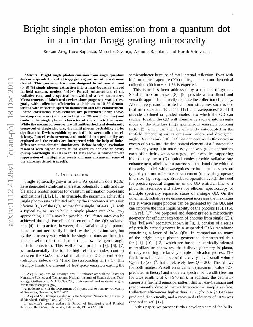
arX
iv:1
112.
4126
v1 [
quan
t-ph
] 18
Dec
201
11
Bright single photon emission from a quantum dotin a circular Bragg grating microcavity
Serkan Ates, Luca Sapienza, Marcelo Davanco, Antonio Badolato, and Kartik Srinivasan
Abstract—Bright single photon emission from single quantumdots in suspended circular Bragg grating microcavities is demon-strated. This geometry has been designed to achieve efficient(> 50 %) single photon extraction into a near-Gaussian shapedfar-field pattern, modest (≈10x) Purcell enhancement of theradiative rate, and a spectral bandwidth of a few nanometers.Measurements of fabricated devices show progress towards thesegoals, with collection efficiencies as high as≈ 10 % demon-strated with moderate spectral bandwidth and rate enhancement.Photon correlation measurements are performed under above-bandgap excitation (pump wavelength =780 nm to 820 nm) andconfirm the single photon character of the collected emission.While the measured sources are all antibunched and dominantlycomposed of single photons, the multi-photon probability variessignificantly. Devices exhibiting tradeoffs between collection ef-ficiency, Purcell enhancement, and multi-photon probability areexplored and the results are interpreted with the help of finite-difference time-domain simulations. Below-bandgap excitationresonant with higher states of the quantum dot and/or cavity(pump wavelength = 860nm to 900nm) shows a near-completesuppression of multi-photon events and may circumvent someofthe aforementioned tradeoffs.
I. I NTRODUCTION
Single epitaxially-grown InxGa1−xAs quantum dots (QDs)have generated significant interest as potentially bright and sta-ble single photon sources for quantum information processingapplications [1], [2], [3]. In principle, the maximum achievablesingle photon rate is limited only by the spontaneous emissionlifetime (τsp) of the QD, so that for a single InGaAs QD witha typical τsp ≈1 ns in bulk, a single photon rateR≈ 1/τsp
approaching 1 GHz may be possible. Still faster rates can beachieved through Purcell enhancement of the QD radiativerate [4]. In practice, however, the available single photonrates are not necessarily limited by the generation rate, butby the efficiency with which the single photons are funneledinto a useful collection channel (e.g., low divergence anglefar-field emission). This well-known problem [5], [6], [7]is fundamentally due to the high-refractive index contrastbetween the GaAs material in which the QD is embedded(refractive indexn≈ 3.4) and the surrounding air (n=1). Thisstrongly limits the amount of free-space emission exiting the
S. Ates, L. Sapienza, M. Davanco, and K. Srinivasan are with the Center forNanoscale Science and Technology, National Institute of Standards and Tech-nology, Gaithersburg, MD 20899-6203, USA (e-mail: [email protected];[email protected])
A. Badolato is with the Department of Physics and Astronomy,Universityof Rochester, Rochester, NY 14627
S. Ates and M. Davanco are also with the Maryland Nanocenter, Universityof Maryland, College Park, MD 20742
L. Sapienza’s present address is School of Engineering and PhysicalSciences, Heriot-Watt University, Edinburgh, EH14 4AS, UK
semiconductor because of total internal reflection. Even withhigh numerical aperture (NA) optics, a maximum theoreticalcollection efficiency< 1 % is expected.
This issue has been addressed by a number of groups.Solid immersion lenses [8], [9] provide a broadband andversatile approach to directly increase the collection efficiency.Alternatively, nanofabricated photonic structures such as op-tical microcavities [10], [11], [12] and waveguides[13], [14]provide confined or guided modes into which the QD canradiate. Ideally, the QD will dominantly radiate into a singlemode of the structure (high spontaneous emission couplingfactor β), which can then be efficiently out-coupled in thefar-field depending on its emission pattern and divergenceangle. Recent work [10], [13] has demonstrated efficienciesinexcess of 50 % into the first optical element of a fluorescencemicroscopy setup. The microcavity and waveguide approacheseach offer their own advantages - microcavities supportinghigh quality factor (Q) optical modes provide radiative rateenhancement, albeit over a narrow spectral band (the width ofthe cavity mode), while waveguides are broadband devices buttypically do not offer rate enhancement (unless they operatein a slow-light regime). Broadband operation avoids the needfor precise spectral alignment of the QD emission line to aphotonic resonance and allows for efficient spectroscopy ofmultiple spectrally separated states of a single QD. On theother hand, radiative rate enhancement increases the maximumrate at which single photons can be generated by the QD, andcan improve the indistinguishability of the photons [15], [16].
In ref. [17], we proposed and demonstrated a microcavitygeometry for efficient extraction of photons from single QDs.This ’bullseye’ geometry, shown in Fig. 1, consists of a seriesof partially etched grooves in a suspended GaAs membranecontaining a layer of InAs QDs. In comparison to manyof the bright single photon geometries demonstrated thusfar [11], [10], [13], which are based on vertically-orientedmicropillars or nanowires, the bullseye geometry is planar,thereby requiring a relatively simple fabrication process. Thefundamental optical mode of this cavity has a small volumeVeff ≈ 1.3(λ/n)3, but a relatively lowQ = 200. This allowsfor both modest Purcell enhancement (maximum value 12×predicted in theory) and moderate spectral bandwidth (few nmfor QDs emitting atλ ≈ 940 nm). In addition, the geometrysupports a far-field emission pattern that is near-Gaussianandpredominantly directed vertically above the sample surface.Collection efficiencies higher than 50 % (for NA& 0.42) arepredicted theoretically, and a measured efficiency of 10 % wasreported in ref. [17].
In this paper, we present further developments of the bulls-

2
Fig. 1. (a) Top view and (b) angled view scanning electron microscope (SEM)images of the bullseye cavities with different undercut access geometries. (c)-(e) Cross-sectional SEM images of the bullseye cavities after the GaAs dryetch but before the HF undercut. The grating trenches are etched to a depthd that is below the QD-containing layer (located att/2) but smaller than theGaAs thickness (t). In comparison, the access areas outside of the grating arefully etched through the GaAs layer, allowing the devices tobe undercut. (f)Optical microscope image of a fully processed device.
eye cavity, with a focus on better understanding its potentialin single photon source applications. A key question leftunanswered in ref. [17] is the degree to which multi-photonprobability is suppressed in the out-coupled emission fromthe device, given the fact that the QD lines are situated ontop of a broad cavity mode which also effectively out-couplesother (non single photon) emission from multi-excitonic andhybridized QD-wetting layer states [18], [19]. Through photoncorrelation measurements of a series of devices under above-bandgap excitation (pump wavelength = 780 nm to 820 nm),we observe tradeoffs between collection efficiency, Purcell en-hancement, and multi-photon probability. These tradeoffs, andthe reduction in collection efficiency and Purcell enhancementrelative to the maximum predicted values, are interpreted withthe help of finite-difference time-domain simulations whichfocus on the role of variations in the grating geometry and QDposition and orientation in influencing device performance.The results indicate that if adequate control of the QD posi-tion [20] and grating dimensions can be exercised, the devicebehavior may be tuned according to the application at hand(for example, limiting Purcell enhancement in exchange forsingle photon purity). Ideally, such tradeoffs would not benecessary, and as a first step towards improving this, wepursue below-bandgap excitation resonant with higher statesof the QD and/or cavity (pump wavelength = 860 nm to 890nm). These measurements show a near-complete suppressionof multi-photon events and may circumvent some of theaforementioned limitations.
II. D EVICE DESIGN
Our nanophotonic structure (Fig. 1) consists of a circulardielectric grating with radial periodΛ surrounding a centralregion of radiusR =2Λ, produced on a suspended GaAsmembrane. The GaAs slab of thicknesst supports single TEand TM polarized modes (electric or magnetic field parallelto the slab, respectively) at wavelengths near 980 nm. Thegrating is composed of partially etched circular trenches thathave widthw, depthd (t/2< d < t), and are radially spacedby a periodΛ. Quantum dots are grown at the center of theGaAs membrane (z= 0), and are located randomly in thexyplane.
This ’bullseye’ geometry favors extraction of emission fromQDs in the central circular region, which would otherwise betrapped inside the GaAs membrane. Indeed, a QD locatedin the central region radiates dominantly into slab-guidedwaves due to total internal reflection at the semiconductor-air interface. The role of the circular grating is to scattersuch guided waves into free-space, preferentially upwards,towards the collection optic. Effective light extraction canbe achieved via a second order Bragg grating for the slabmodes (with period equal to the guided wave wavelength),which provides a first order diffraction perpendicular to theslab plane [21], [22]. In [22], linear gratings were developedto provide efficient coupling between free-space beams andplanar waveguides modes. In our case, a circular gratinggeometry was a more natural choice because QD emission inthe GaAs slab was expected to be cylindrically symmetric. Wepoint out that similar circular geometries have been employedfor enhanced light extraction from light emitting diodes [23],and for demonstrating annular Bragg lasers [24].
The grating periodΛ was chosen to approximately satisfythe second-order Bragg condition,Λ= λQD/nTE, wherenTE isthe GaAs slab TE mode effective index. Because this formulais valid in the limit of a weak grating, which is not the casehere (as the grating’s etch depth is a considerable fractionof the slab thickness), we use it as a starting point in anoptimization procedure which determines the correct period.
Partial reflections at the grating towards the center of thegeometry lead to the formation of cavity resonances such asshown in Fig. 2(a), where the particular orientation of thecavity mode is determined by the orientation of the radiatingdipole (x direction in this case). The large index contrast atthe trenches leads to strong reflections and out-of-slab-planescattering at the semiconductor-air interfaces, as apparent inFig. 2(b). Resonances are centered at wavelengths determinedby the radius of the central region and the grating geometryitself, which determines the overall phase of the reflectedwaves. Figure 2(c) shows the evolution of the resonance centerwavelength for three varying grating periodsΛ. In addition tothe trench spacing, large differences in propagation constantsin the semiconductor and air regions of the grating producesignificant resonance spectral shifts with small variations intrench width and depth.
The trench depthd has a strong influence on the qualityfactor (Q) and vertical light extraction, as incomplete spatialoverlap between a trench and an incident slab-bound wave

3
Fig. 2. Electric field intensity in the (a)xy and (b)xz planes (log scale). (c)Calculated vertically extracted power as a function of wavelength, normalizedto the homogeneous medium electric dipole powerPhom for d = 0.70t.Continuous lines: upwards (+z) extraction; dotted: downwards (−z). (d) Far-field polar plot for the cavity mode withΛ = 360 nm.
leads to both coupling to radiating waves and lower modal re-flectivity. Preferential upwards vertical extraction results fromthe grating asymmetry, as evidenced in Fig. 2(c). This trade-off between the quality factorQ, power extraction and powerextraction asymmetry, and far-field collimation due to variationin the trench depth is discussed further in Section IV-A. Wenote that our suspended, asymmetric grating approach limitsradiation into the substrate without the need to oxidize theAlGaAs, bond the grating to a low index layer[24], or utilizea deeply etched geometry [10], [13].
In Fig. 2(c), the maximum upwards extracted powers are≈ 10× Phom (Phom is the emitted power for an electricdipole in a homogeneous GaAs medium), an indication ofPurcell radiation rate enhancement due to the cavity [25],[26]. Indeed, for theΛ = 360 nm structure the enhancementFp at the maximum extraction wavelength (λc = 948.9 nm)is Fp = Ptot/PHom = 11.0, where Ptot is the total radiatedpower in all directions. This resonance hasQ= 200, and itseffective mode volume, calculated from the field distribution,isVeff =1.3(λc/n)3 (n is the GaAs refractive index) [17]. Thus,despite the relatively low quality factor, the mode volume canbe sufficiently small to produce a significant Purcell factor.
Finally, the far-field of the emitted radiation is highlydirectional, as evidenced in Fig. 2(d). Here, the emitted fieldfor a dipole located at the bullseye center is nearly gaussian,and mostly contained within a 20◦ half-angle. Indeed, in [17],we show that≈ 53 % of the total emission can be collectedwith a NA=0.42 optic, while collection superior to 80 % ofthe total emission can be achieved with NA> 0.7. The depen-dence of the emitted field’s spatial distribution on geometricparameters is non-trivial, however, and is discussed further inSection IV-A.
Design Procedure
The design process used to generate Fig. 2 above and theresults to be discussed in Section IV-A consisted of a series
of finite-difference time-domain simulations that sought tomaximize vertical light extraction near the QD’s expected s-shell emission (λQD ≈ 940 nm), by varyingΛ, t, andw. Thestructures were excited with a horizontally oriented electricdipole at the bullseye center(x= 0,y= 0), representing an op-timally placed QD. Total radiated power, steady-state upwardsand downwards emission, and electromagnetic fields were thenrecorded at several wavelengths. The dipole orientation wasassumed to be aligned along thexy plane, exciting only TEslab waves (self-assembled InAs QDs are expected to haveelectric dipole on the GaAs slab plane).
Steady-state fields at a surface just above the GaAs slabwere used to calculate far-field patterns as in Fig. 2(d).The powerPcoll collected by an optic of numerical apertureNA was calculated by integrating the far-field pattern overthe appropriate angular range, and multiplying by the powerradiated upwards.
III. E XPERIMENTAL RESULTSUNDER ABOVE-BAND
EXCITATION
A. Experimental Setup
Figure 3 shows a detailed schematic view of several ex-perimental setups used within this work. The sample wasmounted on a cold finger and placed in a continuous flowliquid He cryostat that sits on a two-axis nano-positioningstage. Two different excitation sources were used to opticallyexcite the QDs: (i) a CW laser diode (780 nm) for above-band excitation, (ii) a tunable pulsed fiber laser (820 nmto 950 nm) for quasi-resonant excitation. Spectral propertiesof the QD emission were investigated via a low-temperaturemicro-photoluminescence (µ-PL) setup (Fig.3(a)), where asingle microscope objective (NA = 0.42) was used for both theillumination of the sample and the collection of the emission.The collected signal is directed to a 500 mm focal lengthspectrometer either to record an emission spectrum with a SiCharge-Coupled Device (CCD) or to filter a single emissionline for further investigations. For the second-order correlationfunctiong(2)(τ) measurements, the spectrally filtered emission(with a linewidth ≈ 70 pm ≈100 µeV) is directed to aHanbury-Brown and Twiss (HBT) type interferometer thatconsists of a 50/50 non-polarizing beamsplitter (NPBS) andtwo high quantum efficiency (QE) single-photon countingavalanche diodes (SPADs), as shown in Fig. 3(b). The SPADs(peak QE = 73 % at 700 nm and QE = 28 % at 980 nm) wereconnected to a time-correlated single-photon counting moduleto create a histogram of photon detection events. The dynamicsof a single QD emission was measured by using a time-correlated single-photon counting (TCSPC) technique, whichrelies on measuring the time delay between an excitation pulseand detection of an emitted photon by using a fast SPAD(Fig. 3(c), timing jitter = 50 ps, QE = 3 % at 940 nm). Finally,for first-order field correlation functiong(1)(τ) measurements,a Michelson interferometer was attached to the output ofthe spectrometer. As shown in Fig. 3(d), the setup consistsof a 50/50 NPBS and two retro-reflectors, one of which ismounted on a linear stage to provide a coarse tunable opticaldelay up to 4 ns and the other retro-reflector is attached on a
4
Fig. 3. Schematic of theexperimental setup: (a) Confo-cal µ-PL, (b) Hanbury-Brownand Twiss photon correlationsetup, (c) time-resolved PL,and (d) Michelson interferom-eter. SMF: single mode fiber,LPF: long pass filter
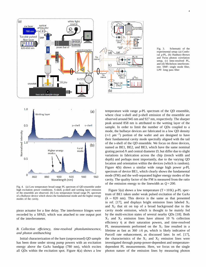
Fig. 4. (a) Low temperature broad range PL spectrum of QD-ensemble underhigh excitation power conditions. S-shell, p-shell and wetting layer emissionof the ensemble are observed. (b) Low temperature broad range PL spectrumof a Bullseye device which shows the fundamental mode and thehigher energymodes of the cavity.
piezo actuator for a fine delay. The interference fringes wererecorded by a SPAD, which was attached to one output portof the interferometer.
B. Collection efficiency, time-resolved photoluminescence,and photon antibunching
Initial characterization of the bare (unprocessed) QD samplehas been done under strong pump powers with an excitationenergy above the GaAs bandgap (780 nm), which excitesall QDs within the excitation spot. Figure 4(a) shows a low
temperature wide rangeµ-PL spectrum of the QD ensemble,where clear s-shell and p-shell emission of the ensemble areobserved around 945 nm and 927 nm, respectively. The sharperpeak around 858 nm is attributed to the wetting layer of thesample. In order to limit the number of QDs coupled to amode, the bullseye devices are fabricated in a low QD density(≈1 µm−2) portion of the wafer and are designed to havetheir fundamental cavity mode spectrally aligned with the tailof the s-shell of the QD ensemble. We focus on three devices,named as BE1, BE2, and BE3, which have the same nominalgrating periodΛ and central diameterD, but differ due to slightvariations in fabrication across the chip (trench width anddepth) and perhaps most importantly, due to the varying QDlocation and orientation within the devices (which is random).Figure 4(b) shows a similar wide range high powerµ-PLspectrum of device BE1, which clearly shows the fundamentalmode (FM) and the well-separated higher energy modes of thecavity. The quality factor of the FM is measured from the ratioof the emission energy to the linewidth asQ= 200.
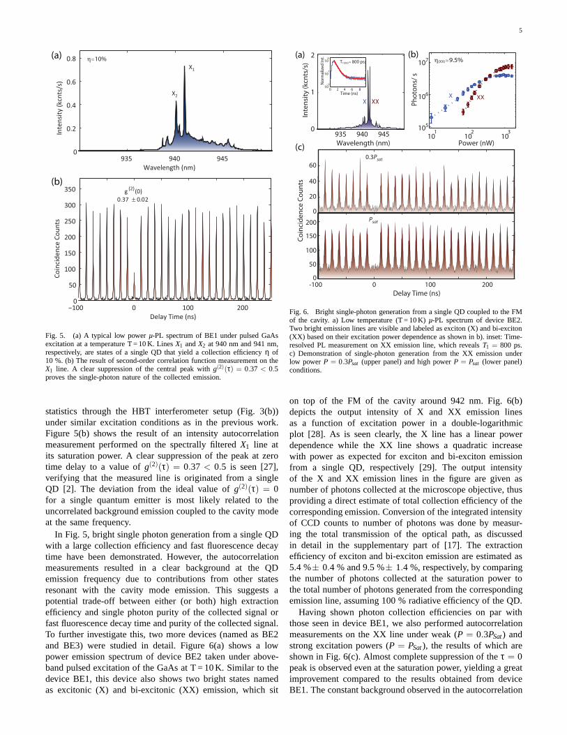
Figure 5(a) shows a low temperature (T = 10 K)µ-PL spec-trum of BE1 taken under weak pulsed excitation of the GaAs(λ = 820 nm). This device is the same as that presentedin ref. [17], and displays bright emission lines labeled X1
and X2 that sit on top of a broad background due to thecavity mode emission, which is thought to be mainly fedby the multi-exciton states of several nearby QDs [18]. BothX1 and X2 emission lines have almost 10 % collectionefficiency η at their saturation powers, and time-resolvedPL measurements performed on the X1 line resulted in alifetime as fast as 360±6 ps, which is likely indicative ofPurcell rate enhancement, as discussed later. In ref. [17],the characteristics of the X1 and X2 emission lines wereinvestigated through pump-power-dependent and temperature-dependent PL measurements. Here, we focus on the singlephoton nature of the emission lines by measuring photon
5
935 940 9450
0.2
0.4
0.6
0.8
Wavelength (nm)
Inte
nsi
ty (
kcn
ts/s
)
−100 0 100 2000
50
100
150
200
250
300
350
Delay Time (ns)
Co
inci
de
nce
Co
un
ts
g(2)
(0)
0.37 ± 0.02
X1
X2
η≈10%(a)
(b)
Fig. 5. (a) A typical low powerµ-PL spectrum of BE1 under pulsed GaAsexcitation at a temperature T = 10 K. LinesX1 andX2 at 940 nm and 941 nm,respectively, are states of a single QD that yield a collection efficiencyη of10 %. (b) The result of second-order correlation function measurement on theX1 line. A clear suppression of the central peak withg(2)(τ) = 0.37 < 0.5proves the single-photon nature of the collected emission.
statistics through the HBT interferometer setup (Fig. 3(b))under similar excitation conditions as in the previous work.Figure 5(b) shows the result of an intensity autocorrelationmeasurement performed on the spectrally filteredX1 line atits saturation power. A clear suppression of the peak at zerotime delay to a value ofg(2)(τ) = 0.37 < 0.5 is seen [27],verifying that the measured line is originated from a singleQD [2]. The deviation from the ideal value ofg(2)(τ) = 0for a single quantum emitter is most likely related to theuncorrelated background emission coupled to the cavity modeat the same frequency.
In Fig. 5, bright single photon generation from a single QDwith a large collection efficiency and fast fluorescence decaytime have been demonstrated. However, the autocorrelationmeasurements resulted in a clear background at the QDemission frequency due to contributions from other statesresonant with the cavity mode emission. This suggests apotential trade-off between either (or both) high extractionefficiency and single photon purity of the collected signal orfast fluorescence decay time and purity of the collected signal.To further investigate this, two more devices (named as BE2and BE3) were studied in detail. Figure 6(a) shows a lowpower emission spectrum of device BE2 taken under above-band pulsed excitation of the GaAs at T = 10 K. Similar to thedevice BE1, this device also shows two bright states namedas excitonic (X) and bi-excitonic (XX) emission, which sit
935 940 9450
1
2
Wavelength (nm)
Inte
nsi
ty (
kcn
ts/s
)
101
102
103
105
106
107
Power (nW)
Ph
oto
ns/
s
XXXXXX
0
50
20
0
100
200
Co
inci
de
nce
Co
un
ts
0 200
Delay Time (ns)
-100 100
(a) (b)
(c)
0 2 4 6 810
−2
10−1
100
No
rmal
ize
d In
t.
Time (ns)
T1(XX) = 800 ps
η(XX)≈9.5%
150
40
60
0.3Psat
Psat
Fig. 6. Bright single-photon generation from a single QD coupled to the FMof the cavity. a) Low temperature (T = 10 K)µ-PL spectrum of device BE2.Two bright emission lines are visible and labeled as exciton(X) and bi-exciton(XX) based on their excitation power dependence as shown in b). inset: Time-resolved PL measurement on XX emission line, which revealsT1 = 800 ps.c) Demonstration of single-photon generation from the XX emission underlow powerP = 0.3Psat (upper panel) and high powerP = Psat (lower panel)conditions.
on top of the FM of the cavity around 942 nm. Fig. 6(b)depicts the output intensity of X and XX emission linesas a function of excitation power in a double-logarithmicplot [28]. As is seen clearly, the X line has a linear powerdependence while the XX line shows a quadratic increasewith power as expected for exciton and bi-exciton emissionfrom a single QD, respectively [29]. The output intensityof the X and XX emission lines in the figure are given asnumber of photons collected at the microscope objective, thusproviding a direct estimate of total collection efficiency of thecorresponding emission. Conversion of the integrated intensityof CCD counts to number of photons was done by measur-ing the total transmission of the optical path, as discussedin detail in the supplementary part of [17]. The extractionefficiency of exciton and bi-exciton emission are estimatedas5.4 %± 0.4 % and 9.5 %± 1.4 %, respectively, by comparingthe number of photons collected at the saturation power tothe total number of photons generated from the correspondingemission line, assuming 100 % radiative efficiency of the QD.
Having shown photon collection efficiencies on par withthose seen in device BE1, we also performed autocorrelationmeasurements on the XX line under weak (P = 0.3PSat) andstrong excitation powers (P = PSat), the results of which areshown in Fig. 6(c). Almost complete suppression of theτ = 0peak is observed even at the saturation power, yielding a greatimprovement compared to the results obtained from deviceBE1. The constant background observed in the autocorrelation

6
935 940 9450
0.2
0.4
0.6
Wavelength (nm)
Inte
nsi
ty (
kcn
ts/s
)
−100 0 100 2000
100
200
300
Delay Time (ns)
Co
inci
de
nce
Co
un
ts
g(2)
(0)
0.17 ± 0.02
0 2 4 6 8 10 1210
−2
10−1
100
Time (ns)
No
rma
lize
d In
t.
η≈5.6 %(a)
(b)
T1 = 390 ps XX
Fig. 7. Purcell-enhanced bright single-photon generationfrom a singleQD. (a) Low temperature (T = 10 K)µ-PL spectrum of device BE3, whichshows sharp emission lines around 936 nm within the spectralwidth of thefundamental mode of the bullseye. inset: Time-resolved PL on QD emissionat 937 nm. (b) The result of an autocorrelation measurement performed onXX line under close-to-saturation excitation power.
measurements is mainly due to the overlap of broad correlationpeaks indicating long lifetime of the measured emission. Theinset of figure 6 (a) shows a direct measure of the lifetime ofthe XX emission through time-resolved PL setup. Applying anexponential fit to the measured decay curve gives the radiativelifetime asT1 = 800± 70 ps, slightly more than a factor oftwo larger than that measured for device BE1.
The results obtained from BE2 showed a clear improvementin the purity of the single photons generated from a singleQD, with a cost of a longer radiative lifetime. A compro-mise between these two important parameters can also beachieved. Figure 7(a) shows a low temperatureµ-PL spectrumof another device, named BE3, under weak pulsed excitation(λExc. = 820 nm). Like the other devices, bright emissionlines are visible on top of the cavity mode around 936 nm,and are collected with an efficiency of 5.6 %± 0.4 % atsaturation (not shown). The inset of Fig.7(a) depicts the resultof a time-revolved PL measurement performed on the XXline, which dominates the spectrum at elevated powers, anda radiative lifetime of about 390±15 ps is estimated fromthe bi-exponential fit. This radiative lifetime is close to thatmeasured for device BE1 and about a factor of two faster thanthat for BE2. In order to verify the single-photon nature ofthe measured emission line, an autocorrelation measurementwas performed, the result of which is shown in Fig. 7(b). Thereduced area of the peak at zero time delay indicates a clear
photon antibunching with a value ofg(2)(τ) = 0.17 < 0.5,thus proving that the source is dominantly composed of singlephotons with a multi-photon probability in-between that ofdevices BE1 and BE2.
Devices BE1, BE2, and BE3 show radiative lifetimes of360 ps, 800 ps, and 390 ps, indicating that the relative levelof Purcell enhancement varies by a factor of 2.2 betweenthe different devices. An estimate of the absolute Purcellenhancement factorFp requires a measurement of the QDlifetime without modification by the cavity. Unfortunately,the broad spectral bandwidth of the bullseye eliminates thepotential for using temperature tuning to shift the QD linesoff-resonance from the cavity. We instead measured the lifetimeof QDs within suspended waveguides [14] made from thesame wafer, where we saw characteristic lifetimes between1.4 ns and 1.6 ns for the neutral exciton (X) state (noPurcell enhancement is expected in these devices). However,as described above, the lifetime andg(2)(τ) measurements forthe bullseye devices were typically performed on the biexciton(XX) state, though we note that the collection efficiency ofthe exciton state was often equally as high. While the XXlifetime is in principle a factor of two times shorter than theX lifetime, other works [30], [31] have suggested that quantumconfinement properties specific to the particular QD geometrymay limit this reduction to a factor closer to 1.4. Taking thisinto account, we roughly estimate that a Purcell factor as highas≈3 has been demonstrated in these devices.
C. Coherence time
For quantum information processing applications, it is im-portant not only to suppress multi-photon events but also tohave the single photon wavepackets be indistinguishable [32],[16]. For an ideal transform-limited QD line, the coherencetimeT2 would be twice the lifetimeT1, and values approachingthis limit have been demonstrated [33], [34]. In practice,achieving such coherence times depends strongly on parame-ters such as temperature and the method by which the QD isoptically excited (e.g., above-band vs. resonant excitation).
We investigate the coherence properties of the bright emis-sion lines from all three bullseye devices by measuring thefirst-order field correlation functiong(1)(τ), which provides adirect access to the coherence time of the emission through[35]:
τc =
∫ ∞
−∞|g(1)(τ)|2dτ (1)
Experimentally, theg(1)(τ) function is measured from thevisibility of the interference fringes observed at the output portof the Michelson interferometer (Fig. 3(d)) according to:
V(τ) =(Imax − Imin)
(Imax + Imin)=
∣
∣
∣g(1)(τ)
∣
∣
∣(2)
for equal intensities of interfered light. The inset to figure 8shows an example of high-resolution interference fringes of the

7
−100 −50 0 50 1000
0.1
0.2
0.3
0.4
0.5
0.6
0.7
0.8
0.9
1
Delay Time (ps)
g(1
) (τ) 0 25 50 75
0
1
Time (s)
No
rma
lize
d In
ten
sity
BE2 data
BE2 !t
BE1 data
BE1 !t
BE3 data
BE3 !t
Fig. 8. The results of first-order field correlation functionmeasurements onall three devices under low power above-band excitation conditions. The insetshows an example of the interference fringes produced at a position close tozero delay line in the Michelson interferometer.
XX emission line from device BE1 obtained under above-bandexcitation conditions (λExc. = 780 nm, CW). The visibility ofthe fringes at each systematically varied time delay betweenthe interferometer arms are calculated according to Eqn. 2,and plotted in Fig. 8 for all devices [36]. The visibility ofthe interference fringes decreases with an increase in delayas a result of the limited coherence timeτc of the emission.Applying a Gaussian fit to the visibility data revealsτc = 27 ps(Γ = 100µeV) for BE1 and 17 ps (160µeV) for BE2 and BE3.The emission linewidth estimated fromg(1)(τ) measurementsis in full agreement with the linewidth obtained from thecorrespondingµ-PL spectrum for BE2 and BE3. However,the emission spectrum of device BE1 revealed a linewidthof 130µeV, which is broader than the linewidth obtainedfrom g(1)(τ) measurement (100µeV). The difference mainlyarises from the limited spectral resolution of theµ-PL setupestimated as 80µeV by measuring a narrow CW laser. Themeasured linewidths of emission from all devices are muchbroader than the reported homogenous linewidth of QDs thatare nearly transform-limited (≈ 1µeV to 2µeV) [33], [34]. Themain reason for this is thought to be the incoherent nature ofthe above-band excitation process, which excites several QDswithin the excitation spot and thus enhances the dephasingprocesses due to the carrier-carrier interactions. In additionto that, spectral diffusion of the emission frequency due tofluctuating charges in the vicinity of the QDs may result in abroadening of the emission [37].
IV. D ISCUSSION
The results presented above can be further interpreted withthe help of numerical simulations. In particular, we try tounderstand how the specific device geometry influences theaforementioned trade-offs in different performance character-istics, as well as the reduced collection efficiency and rateenhancement observed in experiments relative to the maximumpredicted theoretical values in ref. [17].
Fig. 9. (a) Purcell enhancement factorFp as a function of wavelength forvarious normalized trench depthsd/t. (b) Ratio of the vertically emittedpower in the±z direction (Pz±) to the total emitted power of a dipole inbulk GaAs (Phom), as a function of wavelength for various values ofd/t. (c)Fp as a function ofd/t. (d) percentage of total power emitted upwards anddownwards, as a function ofd/t. (e) percentage of upwards emitted powercollected by NA = 0.42 NA = 0.7 lenses. (f) percentage of totalemitted powercollected by NA = 0.42 NA = 0.7 lenses.
A. Tradeoffs in Purcell enhancement and collection efficiency
We next illustrate the effects of varying trench depths onemission properties of the circular dielectric grating. The firstkey quantity of interest is the Purcell enhancement factorFp. It is determined from simulation by the quantitiesPtot
and Phom. Ptot is the total power emitted by a dipole in thebullseye structure, whilePhom is the power emitted by adipole in a homogenous GaAs medium, so thatFp is givenby their ratio Ptot/Phom [25]. Figures 9(a) and (c) showFp
as a function of wavelength and normalized trench depthd/t.Fp increases asd/t approaches unity, with deeper trenchesproviding increased field confinement and higher cavityQ.This is a consequence of better overlap of the guided fieldinside the slab and the etched region, which leads to increasedguided wave reflectivity and reduces coupling to out-of-planeradiation. The higher cavityQ with increasing trench depth isseen in the decreasing resonance width in Fig. 9(a); in addition,a strong blueshift of the cavity mode is observed.
The increase inFp with trench depth comes at a cost,however, as the fraction of light emitted above the structure(+z direction) is reduced. Intuitively, this makes sense inthat, once the grating is completely symmetric (d/t=1, forwhich Fp is maximized), equal emission in the+z and −zdirections should be expected. Figures 9(b) and (d) showthe upwards (Pz+) and downwards (Pz-) extracted powers asa function of wavelength and normalized trench depthd/t.Asymmetric and preferential upwards emission (determinedby the ratioPz+/Pz−) is maximized withd/t = 0.6, for whichPz+/Pz− = 7.1, but comes at the expense of a significantlyreducedFp of 6.9 in comparison to its peak value of nearly20.
For useful single photon emission, preferential upwardsemission alone is not sufficient. We also require the emissionto be directed within a relatively narrow divergence angle far-field pattern, so that the majority of this emission can becollected by a standard focusing optic. Figure 9(e) shows the
8
fraction of upwards emission that is collected (Pcoll/Pz+) byNA=0.42 and NA=0.7 optics, at the peak emission wavelengthfor each d/t (see Fig. 9(a)). We note that this value isclose to unity for the NA=0.7 optic, indicating a strong levelof directionality, which we also expect based on the far-field emission pattern in Fig. 2(d). In addition, we see thatthe collection of the upwards-emitted power can vary by asmuch as 33 % for the trench depth range considered. Finally,Fig. 9(f) shows the overall collection efficiencyη (=Pcoll/Ptot)as a function of trench depth, which is the quantity that isactually measured in the experiments of the previous section.η peaks at a value of≈80 % for a NA=0.7 optic, while for theNA=0.42 optic used in our experiments, this value is≈50 %.
It is evident from these results that sufficiently accuratecontrol of the trench depth is a necessity, not only for optimalspectral alignment, but also for optimal extraction efficiency.For instance, for a trench depthd = 0.8t, the collectionefficiency into a 0.42 NA objective drops to approximately34 % from the 53 % ford = 0.6t. As t = 190 nm, a 40 nmdifference in trench depth, which we might expect to observebased on the tolerances of our fabrication process, can lowerthe maximum extraction efficiency significantly.
Along with radiative lifetime (determined byFp) and col-lection efficiency, the third key characteristic of the devicesmeasured in the previous section is the single photon purity(i.e., the value ofg(2)(0)). Our simulations do not directlyaddress the effects which causeg(2)(0) > 0. However, manyworks [18], [19] have attributed this to cavity-enhanced out-coupling of multi-excitonic and hybridized QD-wetting layerstates that are spectrally resonant with the QD state of interest.In such a scenario, strongly Purcell-enhanced devices arelikely to haveg(2)(0) levels that significantly differ from zero,while devices lacking Purcell enhancement can showg(2)(0)≈0 even under above-band pumping near saturation [13]. Fromthis, we speculate that shallower grating depths (0.5< d/t <0.6), which lead to smallerFp in Fig. 10(c), may also leadto enhanced emission purity. Furthermore, this benefit wouldcome together with increased collection efficiency (Fig. 10(f))as a consequence of improved vertical extraction and emissionasymmetry (Fig. 10(d)).
B. Influence of Dipole Position and Orientation
Other important factors affecting both the achieved Purcellradiative rate enhancement and overall photon collection effi-ciency are dipole position and orientation within the nanostruc-ture. Considering the fundamental mode of the BE cavity inFig. 2 (shown also in Fig. 10(b) and (c)), which we label asM0,we note that due to the circular symmetry of the nanostructure,both modeM0 and a degenerate, 90◦ version of it (henceforthreferred to asE1 and E2, respectively) are simultaneouslysupported. ModeE1 is exclusively excited by azimuthallyoriented dipoles along the radial direction (r ), while modeE2 is exclusively excited by radially oriented dipoles alongr . The specific instances of the modes excited byx-polarizedandy-polarized dipoles are shown in Fig. 10(b) and (c), and adipole oriented at an arbitrary angle in the plane would thenbe expected to radiate into both of these modes.
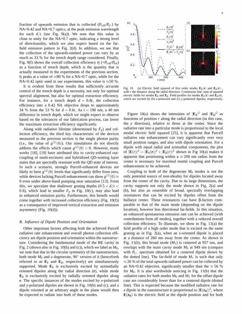
Fig. 10. (a) Electric field squared of first order modesE1(r) and E2(r) ,with r the distance along the radial direction. Continuous line: sum of squaredelectric fields for modesE1 andE2. Field profiles for modesE1(r) andE2(r),which are excited by (b)x-polarized and (c)y-polarized dipoles, respectively.
Figure 10(a) shows the intensities of|E1|2 and |E2|
2 asfunctions of positionr along the radial direction (in this case,the y direction), relative to those at the center. Since theradiative rate into a particular mode is proportional to thelocalmodal electric field squared [25], it is apparent that Purcellradiative rate enhancement can vary significantly over verysmall position ranges, and also with dipole orientation. For adipole with equal radial and azimuthal components, the plotof |E(r)|2 = |E1(r)|2+ |E2(r)|2 shown in Fig 10(a) makes itapparent that positioning within a≈ 200 nm radius from thecenter is necessary for maximal modal coupling and Purcellenhancement to be achieved.
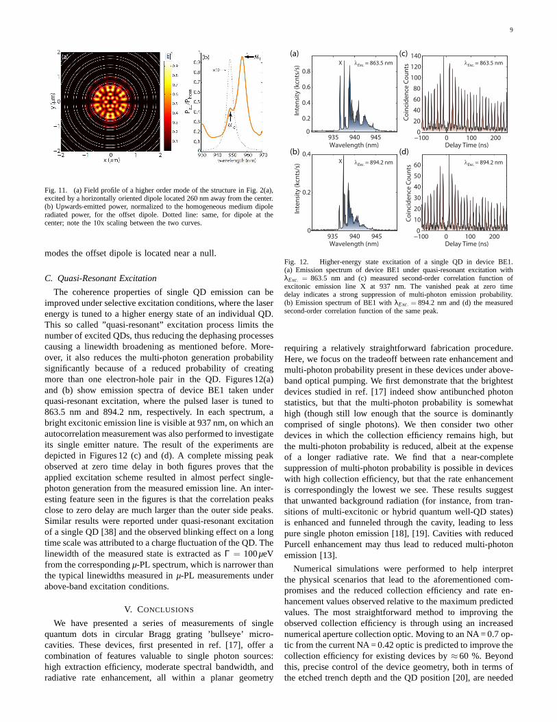
Coupling to both of the degenerateM0 modes is not theonly potential source of non-ideality for dipoles located awayfrom the center of the cavity. Due to its large dimensions, thecavity supports not only the mode shown in Fig. 2(a) and(b), but also an ensemble of broad, spectrally overlappingresonances that can be excited by dipoles offset from thebullseye center. These resonances can haveβ-factors com-parable to that of the main mode (depending on the dipolelocation), however less directional far-fields. In this situation,an enhanced spontaneous emission rate can be achieved (withcontributions from all modes), together with a reduced overallcollection efficiency. To illustrate, we show in Fig. 11(a) thefield profile of a high order mode that is excited on the samegrating as in Fig. 2(a), when anx-oriented dipole is placedat a distance of 260 nm away from the center. As shown inFig. 11(b), this broad mode (M1) is centered at 957 nm, andoverlaps with the main cavity modeM0 at 949 nm (comparewith Pz+ spectrum obtained for a centered dipole shown bythe dotted line). The far-field of modeM1 is such that only≈26 % of the total upwards radiated power can be collected byan NA=0.42 objective, significantly smaller than the≈ 56 %for M0. It is also worthwhile noticing in Fig. 11(b) that theradiative rates for both modes M0 and M1 for the offset dipolecase are considerably lower than for a centered dipole (dottedline). This is expected because the modified radiative rate fora dipole in the nanostructure is proportional to|E(r0)|
2, whereE(r0) is the electric field at the dipole position and for both
9
Fig. 11. (a) Field profile of a higher order mode of the structure in Fig. 2(a),excited by a horizontally oriented dipole located 260 nm away from the center.(b) Upwards-emitted power, normalized to the homogeneous medium dipoleradiated power, for the offset dipole. Dotted line: same, for dipole at thecenter; note the 10x scaling between the two curves.
modes the offset dipole is located near a null.
C. Quasi-Resonant Excitation
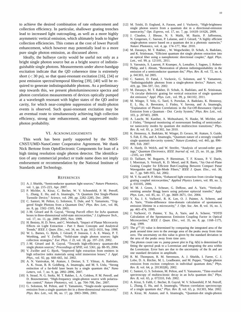
The coherence properties of single QD emission can beimproved under selective excitation conditions, where thelaserenergy is tuned to a higher energy state of an individual QD.This so called ”quasi-resonant” excitation process limitsthenumber of excited QDs, thus reducing the dephasing processescausing a linewidth broadening as mentioned before. More-over, it also reduces the multi-photon generation probabilitysignificantly because of a reduced probability of creatingmore than one electron-hole pair in the QD. Figures 12(a)and (b) show emission spectra of device BE1 taken underquasi-resonant excitation, where the pulsed laser is tunedto863.5 nm and 894.2 nm, respectively. In each spectrum, abright excitonic emission line is visible at 937 nm, on whichanautocorrelation measurement was also performed to investigateits single emitter nature. The result of the experiments aredepicted in Figures 12 (c) and (d). A complete missing peakobserved at zero time delay in both figures proves that theapplied excitation scheme resulted in almost perfect single-photon generation from the measured emission line. An inter-esting feature seen in the figures is that the correlation peaksclose to zero delay are much larger than the outer side peaks.Similar results were reported under quasi-resonant excitationof a single QD [38] and the observed blinking effect on a longtime scale was attributed to a charge fluctuation of the QD. Thelinewidth of the measured state is extracted asΓ = 100µeVfrom the correspondingµ-PL spectrum, which is narrower thanthe typical linewidths measured inµ-PL measurements underabove-band excitation conditions.
V. CONCLUSIONS
We have presented a series of measurements of singlequantum dots in circular Bragg grating ’bullseye’ micro-cavities. These devices, first presented in ref. [17], offeracombination of features valuable to single photon sources:high extraction efficiency, moderate spectral bandwidth, andradiative rate enhancement, all within a planar geometry
935 940 9450
0.2
0.4
Wavelength (nm)
Inte
nsi
ty (
kcn
ts/s
)
−100 0 100 2000
10
20
30
40
50
60
Delay Time (ns)
Co
inci
de
nce
Co
un
ts
935 940 9450
0.2
0.4
0.6
0.8
Wavelength (nm)
Inte
nsi
ty (
kcn
ts/s
)
−100 0 100 2000
20
40
60
80
100
120
140
Delay Time (ns)
Co
inci
de
nce
Co
un
ts
(a)
(b)
(c)
(d)
λExc.
= 863.5 nm
λExc.
= 894.2 nm
λExc.
= 863.5 nm
λExc.
= 894.2 nm
X
X
Fig. 12. Higher-energy state excitation of a single QD in device BE1.(a) Emission spectrum of device BE1 under quasi-resonant excitation withλExc. = 863.5 nm and (c) measured second-order correlation function ofexcitonic emission line X at 937 nm. The vanished peak at zerotimedelay indicates a strong suppression of multi-photon emission probability.(b) Emission spectrum of BE1 withλExc. = 894.2 nm and (d) the measuredsecond-order correlation function of the same peak.
requiring a relatively straightforward fabrication procedure.Here, we focus on the tradeoff between rate enhancement andmulti-photon probability present in these devices under above-band optical pumping. We first demonstrate that the brightestdevices studied in ref. [17] indeed show antibunched photonstatistics, but that the multi-photon probability is somewhathigh (though still low enough that the source is dominantlycomprised of single photons). We then consider two otherdevices in which the collection efficiency remains high, butthe multi-photon probability is reduced, albeit at the expenseof a longer radiative rate. We find that a near-completesuppression of multi-photon probability is possible in deviceswith high collection efficiency, but that the rate enhancementis correspondingly the lowest we see. These results suggestthat unwanted background radiation (for instance, from tran-sitions of multi-excitonic or hybrid quantum well-QD states)is enhanced and funneled through the cavity, leading to lesspure single photon emission [18], [19]. Cavities with reducedPurcell enhancement may thus lead to reduced multi-photonemission [13].
Numerical simulations were performed to help interpretthe physical scenarios that lead to the aforementioned com-promises and the reduced collection efficiency and rate en-hancement values observed relative to the maximum predictedvalues. The most straightforward method to improving theobserved collection efficiency is through using an increasednumerical aperture collection optic. Moving to an NA = 0.7 op-tic from the current NA = 0.42 optic is predicted to improve thecollection efficiency for existing devices by≈60 %. Beyondthis, precise control of the device geometry, both in terms ofthe etched trench depth and the QD position [20], are needed
10
to achieve the desired combination of rate enhancement andcollection efficiency. In particular, shallower grating trencheslead to increased light outcoupling, as well as a more highlyasymmetric vertical emission, which ultimately leads to highercollection efficiencies. This comes at the cost of lower Purcellenhancement, which however may potentially lead to a morepure single photon emission, as discussed above.
Ideally, the bullseye cavity would be useful not only as abright single photon source but as a bright source of indistin-guishable single photons. Measurements under above-bandgapexcitation indicate that the QD coherence time is extremelyshort (<30 ps), so that quasi-resonant excitation [16], [34] orpost emission spectral/temporal filtering [39], [40] will be re-quired to generate indistinguishable photons. As a preliminarystep towards this, we present photoluminescence spectra andphoton correlation measurements of devices optically pumpedat a wavelength resonant with higher states of the QD and/orcavity, for which near-complete suppression of multi-photonevents is observed. Such quasi-resonant excitation may bean eventual route to simultaneously achieving high collectionefficiency, strong rate enhancement, and suppressed multi-photon probability.
VI. A CKNOWLEDGEMENTS
This work has been partly supported by the NIST-CNST/UMD-NanoCenter Cooperative Agreement. We thankNick Bertone from OptoElectronic Components for loan of ahigh timing resolution single photon detector. The identifica-tion of any commercial product or trade name does not implyendorsement or recommendation by the National Institute ofStandards and Technology.
REFERENCES
[1] A. J. Shields, “Semiconductor quantum light sources,”Nature Photonics,vol. 1, pp. 215–223, Apr. 2007.
[2] P. Michler, A. Kiraz, C. Becher, W. V. Schoenfeld, P. M. Petroff,L. Zhang, E. Hu, and A. Imamoglu, “A Quantum Dot Single-PhotonTurnstile Device,”Science, vol. 290, pp. 2282–2285, Dec. 2000.
[3] C. Santori, M. Pelton, G. Solomon, Y. Dale, and Y. Yamamoto, “Trig-gered Single Photons from a Quantum Dot,”Phys. Rev. Lett., vol. 86,no. 8, pp. 1502–1505, Feb. 2001.
[4] J.-M. Gerard and B. Gayral, “Strong Purcell effect for InAs quantumboxes in three-dimensional solid-state microcavities,”J. Lightwave Tech.,vol. 17, no. 11, pp. 2089–2095, Nov. 1999.
[5] H. Benisty, H. D. Neve, and C. Weisbuch, “Impact of PlanarMicrocavityEffects on Light Extraction - Part I: Basic Concepts and AnalyticalTrends,”IEEE J. Quan. Elec., vol. 34, no. 9, pp. 1612–1631, Sep. 1998.
[6] W. L. Barnes, G. Bjork, J. Gerard, P. Jonsson, J. A. E. Wasey, P. T.Worthing, and V. Zwiller, “Solid-state single photon sources: lightcollection strategies,”Eur. Phys. J. D, vol. 18, pp. 197–210, 2002.
[7] J.-M. Gerard and B. Gayral, “Towards high-efficiency quantum-dotsingle photon sources,”Proceedings of SPIE, vol. 5361, pp. 88–95, 2004.
[8] V. Zwiller and G. Bjork, “Improved light extraction fromemitters inhigh refractive index materials using solid immersion lenses,” J. Appl.Phys., vol. 92, pp. 660–665, Jul. 2002.
[9] A. N. Vamivakas, M. Atature, J. Dreiser, S. T. Yilmaz, A. Badolato,A. K. Swan, B. B. Goldberg, A. Imamoglu, and M. S. Unlu, “Strongextinction of a far-field laser beam by a single quantum dot,”NanoLetters, vol. 7, no. 9, pp. 2892–2896, 2007.
[10] S. Strauf, N. G. Stoltz, M. T. Rakher, L. A. Coldren, P. M.Petroff, andD. Bouwmeester, “High-frequency single-photon source with polariza-tion control,” Nature Photonics, vol. 1, pp. 704–708, Dec. 2007.
[11] G. Solomon, M. Pelton, and Y. Yamamoto, “Single-mode spontaneousemission from a single quantum dot in a three-dimensional microcavity,”Phys. Rev. Lett., vol. 86, no. 17, pp. 3903–3906, 2001.
[12] M. Toishi, D. Englund, A. Faraon, and J. Vuckovic, “High-brightnesssingle photon source from a quantum dot in a directional-emissionnanocavity,”Opt. Express, vol. 17, no. 7, pp. 14 618–14 626, 2009.
[13] J. Claudon, J. Bleuse, N. S. Malik, M. Bazin, P. Jaffrennou,N. Gregersen, C. Sauvan, P. Lalanne, and J. Gerard, “A highly efficientsingle-photon source based on a quantum dot in a photonic nanowire,”Nature Photonics, vol. 4, pp. 174–177, Mar. 2010.
[14] M. Davanco, M. T. Rakher, , W. Wegscheider, D. Schuh, A.Badolato,and K. Srinivasan, “Efficient quantum dot single photon extraction intoan optical fiber using a nanophotonic directional coupler,”Appl. Phys.Lett., vol. 99, p. 121101, 2011.
[15] S. Varoutsis, S. Laurent, P. Kramper, A. Lemaıtre, I. Sagnes, I. Robert-Philip, and I. Abram, “Restoration of photon indistinguishability in theemission of a semiconductor quantum dot,”Phys. Rev. B, vol. 72, no. 4,p. 041303, Jul 2005.
[16] C. Santori, D. Fattal, J. Vuckovic, G. Solomon, and Y. Yamamoto,“Indistinguishable photons from a single-photon device,”Nature, vol.419, pp. 594–597, Oct. 2002.
[17] M. Davanco, M. T. Rakher, D. Schuh, A. Badolato, and K. Srinivasan,“A circular dielectric grating for vertical extraction of single quantumdot emission,”Appl. Phys. Lett., vol. 99, p. 041102, 2011.
[18] M. Winger, T. Volz, G. Tarel, S. Portolan, A. Badolato, K. Hennessy,E. L. Hu, A. Beveratos, J. Finley, V. Savona, and A. Imamoglu,“Explanation of Photon Correlations in the Far-Off-Resonance OpticalEmission from a Quantum - Dot Cavity System,”Phys. Rev. Lett., vol.103, p. 207403, 2009.
[19] A. Laucht, M. Kaniber, A. Mohtashami, N. Hauke, M. Michler, andJ. Finley, “Temporal monitoring of nonresonant feeding of semiconduc-tor nanocavity modes by quantum dot multiexciton transitions,” Phys.Rev. B, vol. 81, p. 241302, Jun 2010.
[20] K. Hennessy, A. Badolato, M. Winger, D. Gerace, M. Atature, S. Guide,S. Falt, E. Hu, and A. Imamoglu, “Quantum nature of a stronglycoupledsingle quantum dot-cavity system,”Nature (London), vol. 445, pp. 896–899, Feb. 2007.
[21] A. Hardy, D. Welch, and W. Streifer, “Analysis of second-order grat-ings,” Quantum Electronics, IEEE Journal of, vol. 25, no. 10, pp. 2096–2105, oct 1989.
[22] D. Taillaert, W. Bogaerts, P. Bienstman, T. F. Krauss, P. V. Daele,I. Moerman, S. Vertuyft, K. D. Mesel, and R. Baets, “An Out-of-PlaneGrating Coupler for Efficient Butt-Coupling Between Compact PanarWaveguides and Single-Mode Fibers,”IEEE J. Quan. Elec., vol. 38,no. 7, pp. 949–955, Jul. 2002.
[23] M. Y. Su and R. P. Mirin, “Enhanced light extraction fromcircular bragggrating coupled microcavities,”Applied Physics Letters, vol. 89, no. 3,p. 033105, 2006.
[24] W. M. J. Green, J. Scheuer, G. DeRose, and A. Yariv, “Verticallyemitting annular Bragg lasers using polymer epitaxial transfer,” Appl.Phys. Lett., vol. 85, no. 17, pp. 3669–3671, Oct. 2004.
[25] Y. Xu, J. S. Vuckovic, R. K. Lee, O. J. Painter, A. Scherer, andA. Yariv, “Finite-difference time-domain calculation of spontaneousemission lifetime in a microcavity,”J. Opt. Soc. Am. B, vol. 16, no. 3,pp. 465–474, 1999.
[26] J. Vuckovic, O. Painter, Y. Xu, A. Yariv, and A. Scherer, “FDTDCalculation of the Spontaneous Emission Coupling Factor inOpticalMicrocavities,” IEEE J. Quan. Elec., vol. 35, no. 8, pp. 1168–1175,Aug. 1999.
[27] Theg(2)(0) value is determined by comparing the integrated area of thepeak around time zero to the average area of the peaks away from timezero. The uncertainty on this value is given by the standard deviation inthe area of the peaks away from time zero.
[28] The photon count rate vs. pump power plot in Fig. 6(b) is determined byfitting the spectral peak to a Lorentzian and integrating thearea withinthe Lorentzian. Error bars are due to the uncertainty of the fit and areone standard deviation in amplitude.
[29] R. M. Thompson, R. M. Stevenson, A. J. Shields, I. Farrer, C. J.Lobo, D. A. Ritchie, M. L. Leadbeater, and M. Pepper, “Single-photonemission from exciton complexes in individual quantum dots,” Phys.Rev. B, vol. 64, p. 201302(R), 2002.
[30] C. Santori, G. S. Solomon, M. Pelton, and Y. Yamamoto, “Time-resolvedspectroscopy of multiexcitonic decay in an InAs quantum dot,” Phys.Rev. B, vol. 65, p. 073310, Feb. 2002.
[31] A. Kiraz, S. Falth, C. Becher, B. Gayral, W. V. Schoenfeld, P. M. Petroff,L. Zhang, E. Hu, and A. Imamoglu, “Photon correlation spectroscopyof a single quantum dot,”Phys. Rev. B, vol. 65, p. 161303, Mar. 2002.
[32] A. Kiraz, M. Atature, and A. Imamoglu, “Quantum-dot single-photon
11
sources: Prospects for applications in linear optics quantum-informationprocessing,”Phys. Rev. A, vol. 69, p. 032305, 2004.
[33] M. Bayer and A. Forchel, “Temperature dependence of theexcitonhomogeneous linewidth in In0.60Ga0.40As/GaAs self-assembled quantumdots,” Phys. Rev. B, vol. 65, p. 041308(R), 2002.
[34] S. Ates, S. M. Ulrich, S. Reitzenstein, A. Loffler, A. Forchel, andP. Michler, “Post-selected indistinguishable photons from the resonancefluorescence of a single quantum dot in a microcavity,”Phys. Rev. Lett.,vol. 103, no. 16, p. 167402, Oct 2009.
[35] R. Loudon,The Quantum Theory of Light, 3rd ed. Oxford UniversityPress, 2000.
[36] The error bars in theg(1)(τ) data in Fig. 8 are determined by thefluctuations in the inteference contrast and are one standard deviationin amplitude.
[37] J. Seufert, R. Weigand, G. Bacher, T. Kummell, A. Forchel, K. Leonardi,and D. Hommel, “Spectral diffusion of the exciton transition in a singleself-organized quantum dot,”Appl. Phys. Lett., vol. 76, p. 1872, 2000.
[38] C. Santori, D. Fattal, J. Vuckovic, G. S. Solomon, E. Waks, andY. Yamamoto, “Submicrosecond correlations in photoluminescence fromInAs quantum dots,”Phys. Rev. B, vol. 69, p. 205324, May 2004.
[39] R. B. Patel, A. J. Bennett, K. Cooper, P. Atkinson, C. A. Nicoll, D. A.Ritchie, and A. J. Shields, “Postselective two-photon interference froma continuous nonclassical stream of photons emitted by a quantum dot,”Phys. Rev. Lett., vol. 100, no. 20, p. 207405, May 2008.
[40] M. T. Rakher and K. Srinivasan, “Subnanosecond electro-optic modula-tion of triggered single photons from a quantum dot,”Appl. Phys. Lett.,vol. 98, no. 21, p. 211103, May 2011.
Copyright © 2022 FDOKUMEN