Near-field characterization of Bragg mirrors engraved in surface plasmon waveguides
32
Near–field characterization of Bragg mirrors engraved in surface plasmon waveguides Jean-Claude Weeber, Yvon Lacroute, Alain Dereux Laboratoire de Physique de l’Universit´ e de Bourgogne, UMR CNRS 5027, 9 avenue Alain Savary, BP 47870, F-21078 Dijon, France Elo¨ ıse Devaux, Thomas Ebbesen Laboratoire des Nanostructures, ISIS, 8 all´ ee Gaspard Monge, BP 70028, F-67083 Strasbourg, France Christian Girard Centre d’Elaboration des Matriaux et d’Etudes Structurales, UPR CNRS 8011, 29 Rue J. Marvig, BP 4347, F-31055 Toulouse, France Mar´ ıa Uju´ e Gonz´alez, Anne–Laure Baudrion Laboratoire de Physique de l’Universit´ e de Bourgogne, UMR CNRS 5027, 9 avenue Alain Savary, BP 47870, F-21078 Dijon, France (April 12, 2010) Abstract Surface plasmon waveguides (SPW’s) are metal ridges featuring widths in the micrometre range and thicknesses of a few tens of nanometres. A focused ion beam (FIB) has been used to carve micro–scatterers into gold SPW’s and the near–field distributions around these micro-structures are observed by means of a Photon Scanning Tunneling Microscope (PSTM). On the basis of near-field images, we show that a finite length periodic arrangement of 1 hal-00472585, version 1 - 12 Apr 2010 Author manuscript, published in "Physical Review B 70, 23 (2004) 235406" DOI : 10.1103/PhysRevB.70.235406
-
Upload
independent -
Category
Documents
-
view
1 -
download
0
Transcript of Near-field characterization of Bragg mirrors engraved in surface plasmon waveguides

Near–field characterization of Bragg mirrors engraved in surface
plasmon waveguides
Jean-Claude Weeber, Yvon Lacroute, Alain Dereux
Laboratoire de Physique de l’Universite de Bourgogne, UMR CNRS 5027,
9 avenue Alain Savary, BP 47870, F-21078 Dijon, France
Eloıse Devaux, Thomas Ebbesen
Laboratoire des Nanostructures, ISIS,
8 allee Gaspard Monge, BP 70028, F-67083 Strasbourg, France
Christian Girard
Centre d’Elaboration des Matriaux et d’Etudes Structurales, UPR CNRS 8011,
29 Rue J. Marvig, BP 4347, F-31055 Toulouse, France
Marıa Ujue Gonzalez, Anne–Laure Baudrion
Laboratoire de Physique de l’Universite de Bourgogne, UMR CNRS 5027,
9 avenue Alain Savary, BP 47870, F-21078 Dijon, France
(April 12, 2010)
Abstract
Surface plasmon waveguides (SPW’s) are metal ridges featuring widths in
the micrometre range and thicknesses of a few tens of nanometres. A focused
ion beam (FIB) has been used to carve micro–scatterers into gold SPW’s
and the near–field distributions around these micro-structures are observed
by means of a Photon Scanning Tunneling Microscope (PSTM). On the basis
of near-field images, we show that a finite length periodic arrangement of
1
hal-0
0472
585,
ver
sion
1 -
12 A
pr 2
010
Author manuscript, published in "Physical Review B 70, 23 (2004) 235406" DOI : 10.1103/PhysRevB.70.235406
narrow slits can reflect a surface plasmon mode propagating along a SPW. The
reflection efficiency of the micro–grating is found to depend upon the number
of slits, the period of the grating and the incident wavelength. The optimum
reflection efficiency is obtained for a period of the micro-grating equal to half
the incident wavelength in vacuum. The PSTM images of the plasmon mirrors
taken at different wavelengths allow us to measure the experimental dispersion
curve of the SPW in the near–infrared. From this dispersion curve, we found
that, in analogy with a surface plasmon (SP) excited on extended thin films,
the group velocity of a SPW mode is close to the speed of light. For a given
frequency in the near–infrared, the effective index of the SP mode supported
by a 2.5 µm wide SPW is also found to be significantly larger than the effective
index of an extended thin film SP. Finally, we show that the optical properties
of micro–gratings engraved into a SPW can be qualitatively approached by a
standard Bragg mirror model.
07.79.Fc Near-field scanning optical microscopes
42.79.Gn Optical waveguides and couplers
73.20.Mf Collective excitations (including plasmons
and other charge-density excitations)
78.66.-w Optical properties of specific thin films,
surfaces, and low- dimensional structures
Typeset using REVTEX
2
hal-0
0472
585,
ver
sion
1 -
12 A
pr 2
010

I. INTRODUCTION
A polariton is an electromagnetic mode related to the oscillations of the polarization
density. At the interface between two media such that the real parts of their frequency
dependent dielectric functions have opposite signs, surface polariton featuring a field dis-
tribution that decays exponentially in both media may occur according to a well–known
dispersion relation [1]. In the case where the material displaying a negative real part of
the dielectric function is a metal, the polarization density oscillation corresponds to oscilla-
tions of the electron gas. The surface polariton is then called a Surface Plasmon Polariton
(SPP) [2,3]. The electromagnetic field associated with a SPP can propagate along the inter-
face to which it is bounded and decreases exponentially in the direction perpendicular to this
interface. This vertical confinement makes SPP’s appealing for the design of optical devices
integrated in coplanar geometry. Until now, two features have hindered the development of
SPP based integrated optics. First, the damping of the electron collective excitations limits
the propagation distances. Second, very little is known about systems able to control the
propagation of SPP.
In order to achieve efficient SPP guiding, two different approaches are currently investi-
gated. The first kind of systems relies on the propagation of SPP modes along finite width
thin metal films. When buried in an homogeneous dielectric medium, these surface plasmon
waveguides (SPW’s) allow the propagation of so-called “long-range” SPP’s over distances
of several millimeters at telecommunication frequencies [4–6] . Such a range of propagation
distances make SPW’s a possible alternative to high refractive index dielectric waveguides
for the fabrication of miniaturized passive optical components such as splitters, filters or
resonant cavities.
When deposited on a dielectric substrate, SPW’s support SPP modes with effective prop-
agation lengths of only few tens of microns in the near–infrared frequency range. Although
in this case the propagation lengths are probably too small to be directly useful for inte-
grated optical devices, this configuration offers the opportunity to observe SPP modes in
3
hal-0
0472
585,
ver
sion
1 -
12 A
pr 2
010

direct space by near–field optical microscopy. For example, a strong lateral field confinement
of SPP modes supported by silver SPW’s has been demonstrated on the basis of Photon
Scanning Tunneling Microscope (PSTM) images [7]. More recently, the PSTM images of
gold SPW have shown that the modal field distributions of SPW modes are created by the
coupling of finite width interface modes and boundary modes supported by the abrupt edges
of the metal strips [8].
The second kind of devices allowing both the lateral confinement and the propagation
control of SPP’s are based on the interaction of surface plasmon with gratings formed with
individual scatterers. Recently, SPP propagation along lines of defects created into a so–
called “plasmonic crystal”, such as an array of gold nano–particles deposited on a gold thin
film, has been reported [9]. Similarly, silica posts texturing an extended silver thin film
have been found to be very efficient to achieve the reflection of a locally launched surface
plasmon [10]. Most of the previous works dealing with the scattering of SPP by periodic
nano-structures have considered surface plasmons excited on extended thin films, i.e. thin
films with lateral dimensions much larger than the wavelength of the surface wave.
In this work, we consider metal strips with typical widths of only a few wavelengths of
the SPW modes and we study the interaction of these SPW modes with micro–structures
engraved by Focused Ion Beam (FIB) milling into the metal strips. Specifically, we consider
gratings made by a finite number of narrow slits texturing a 2.5 µm wide SPW to show that
these micro–gratings can be used as SPP mirrors. The paper is organized as follows. After
a brief description of the experimental setup and the sample fabrication process in section
II, we analyze in section III the PSTM images of a micro–grating recorded at different
observation distances. The back–reflection of a SPW mode by a micro–grating is then
discussed on the basis of these results. In section IV, we study the reflection efficiency of the
micro–gratings as a function of different structural parameters such as the number of slits or
the period of the gratings. Section V is dedicated to the measurement of the phase constant
and the group velocity of a 2.5 µm wide SPW using PSTM images obtained at different
incident wavelengths in the near–infrared frequency range. Finally, we show in section VI
4
hal-0
0472
585,
ver
sion
1 -
12 A
pr 2
010
that a standard Bragg mirror can model, at least qualitatively, the optical properties of the
micro–gratings acting on SPW. The parameters of the equivalent Bragg mirror are deduced
empirically from the experimental results of the previous sections.
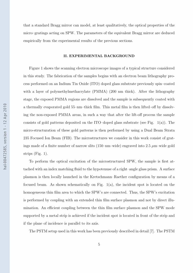
II. EXPERIMENTAL BACKGROUND
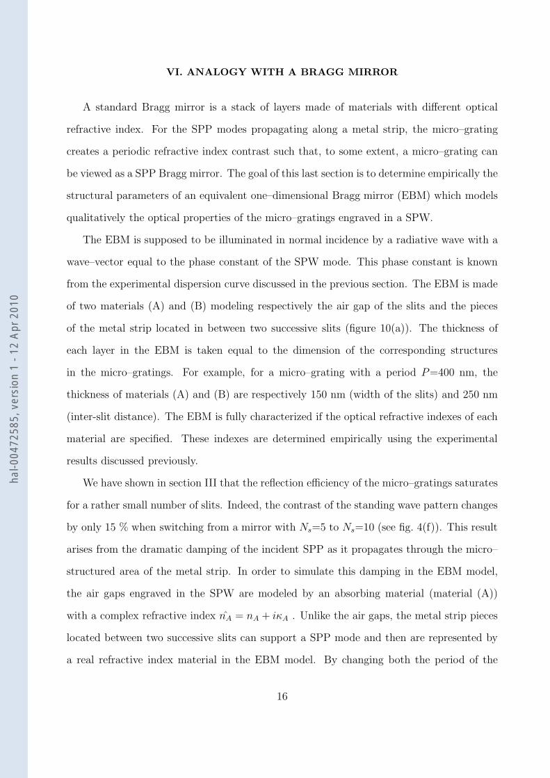
Figure 1 shows the scanning electron microscope images of a typical structure considered
in this study. The fabrication of the samples begins with an electron beam lithography pro-
cess performed on an Indium Tin Oxide (ITO) doped glass substrate previously spin–coated
with a layer of polymethylmethacrylate (PMMA) (200 nm thick). After the lithography
stage, the exposed PMMA regions are dissolved and the sample is subsequently coated with
a thermally evaporated gold 55–nm–thick film. This metal film is then lifted–off by dissolv-
ing the non-exposed PMMA areas, in such a way that after the lift-off process the sample
consists of gold patterns deposited on the ITO–doped glass substrate (see Fig. 1(a)). The
micro-structuration of these gold patterns is then performed by using a Dual Beam Strata
235 Focused Ion Beam (FIB). The microstructures we consider in this work consist of grat-
ings made of a finite number of narrow slits (150–nm–wide) engraved into 2.5 µm–wide gold
strips (Fig. 1).
To perform the optical excitation of the microstructured SPW, the sample is first at-
tached with an index matching fluid to the hypotenuse of a right–angle glass prism. A surface
plasmon is then locally launched in the Kretschmann–Raether configuration by means of a
focused beam. As shown schematically on Fig. 1(a), the incident spot is located on the
homogeneous thin film area to which the SPW’s are connected. Thus, the SPW’s excitation
is performed by coupling with an extended thin film surface plasmon and not by direct illu-
mination. An efficient coupling between the thin film surface plasmon and the SPW mode
supported by a metal strip is achieved if the incident spot is located in front of the strip and
if the plane of incidence is parallel to its axis.
The PSTM setup used in this work has been previously described in detail [7]. The PSTM
5
hal-0
0472
585,
ver
sion
1 -
12 A
pr 2
010

relies on the frustration of evanescent fields using a local probe attached to a piezo–tube
and scanned in the close vicinity of the sample surface [11]. In our device, the local probes
are multi–mode optical fiber tips coated with a thin layer of chromium (10 nm) in order to
prevent that a significant amount of radiative light enters the fiber and contributes to the
near–field optical signal [12]. The metal coating also allows the detection of a tunnel current
when a bias voltage is applied between the metal coated tip and the conductive surface
of the sample. The detection of such a tunnel current is used to define the origin for the
measurement of the absolute tip–sample distance since it occurs for the tip in quasi–contact
with the sample surface.
III. SPW MODE BACK-REFLECTION BY A MICRO–GRATING
Two recent experimental studies have shown that either the abrupt discontinuity ending
the extremity of a metal strip [7] or a single narrow groove engraved in an extended thin
silver film [13] can efficiently reflect a SPP. In order to show the effect of the presence of
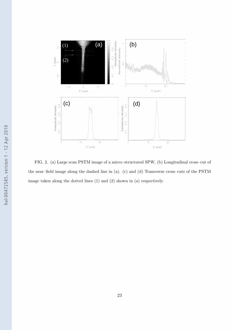
a micro–grating on the propagation of a SPW mode, we show in figure 2(a) a large scan
PSTM image recorded over a mirror consisting of ten slits milled in a 2.5 µm wide SPW.
The period of the micro-grating is 400nm and the incident light frequency corresponds to
a wavelength in vacuum of λ0=800nm. The micro–grating is located at a distance of 15
µm from the output end of the triangularly shaped area (named taper in the following)
connecting the strip to the extended thin film. Well pronounced interference fringes with
a period of roughly λ0
2are visible all along the SPW while a two–dimensional standing
wave pattern is observed over the taper. A longitudinal cross–cut of the optical image is
displayed in figure 2(b) and shows more in detail the near–field intensity distribution over
the the SPW. In analogy with a surface plasmon mode supported by an extended thin film
propagating towards positive values of y, the electromagnetic field associated with a SPW
mode is expected to depend upon y as exp (−α + iβ)y where α and β denote respectively
the attenuation and the phase constant of the surface plasmon. However, it can observed on
6
hal-0
0472
585,
ver
sion
1 -
12 A
pr 2
010

fig. 2(b) that the intensity of the SPW mode does not decrease exponentially as it propagates
along the metal strip. Indeed, the optical signal at the center of the SPW increases from
the end of the taper (corresponding to y=4.0 µm on fig. 2(b)) to y=11 µm. Furthermore,
the transverse intensity distribution changes dramatically with y over that range as shown
by the two optical profiles displayed respectively in fig. 2(c) and 2(d). Close to the SPW
input ( fig. 2(c)), the optical profile exhibits a three peaks structure while a large central
peak flanked by two shoulders is observed when the SPW mode has propagated over few
microns (fig. 2(d)). Since it has been shown in a previous study that the SPW modes
are hybrid modes, also called “super–modes”, resulting from the superposition of finite size
interface modes and boundary modes supported by the edges of the metal strip [8], we can
thus assume that the spatial transient we observe on the PSTM image is due to the fact
that these different modes must interact over a distance long enough in order to build–up
the SPW mode.
As shown in fig. 2(b), the near–field intensity vanishes after the micro-structures leading
to the conclusion that the incident SPW mode is mostly back–reflected and scattered by the
grating. The standing wave pattern visible on the PSTM image could then arise from the
interference of the incident SPP with either a back-reflected SPP or a scattered wave. In the
near–infrared frequency range, we can reasonably assume that, in analogy with an extended
thin film SPP, the phase constant of the SPW mode is close to the incident light wave–vector
modulus in vacuum, k0 = 2πλ0
. Therefore, from the momentum conservation law is derived
that the micro-mirror could generate a scattered field propagating at grazing incidence
regarding that in this experiment the period of the grating is equal to λ0
2. Moreover, taking
the phase constant of the incoming SPW mode close to k0, the interference of the incident
SPP with either a back–reflected SPP or a contra–propagating scattered wave traveling at
grazing incidence could create a standing wave pattern with a period close to λ0
2in agreement
with the rough estimate of the oscillations period observed on the PSTM image. In order
to discriminate the origin of the standing wave pattern, we consider successively this two
situations.
7
hal-0
0472
585,
ver
sion
1 -
12 A
pr 2
010
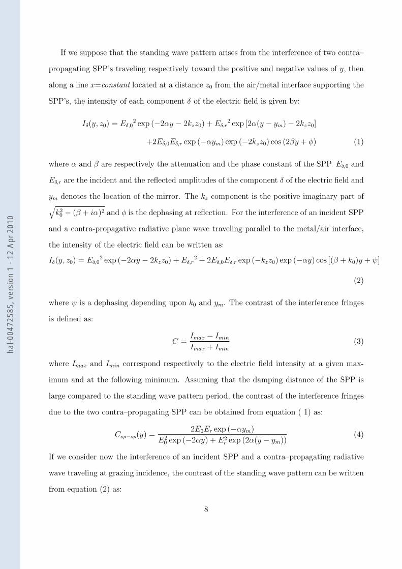
If we suppose that the standing wave pattern arises from the interference of two contra–
propagating SPP’s traveling respectively toward the positive and negative values of y, then
along a line x=constant located at a distance z0 from the air/metal interface supporting the
SPP’s, the intensity of each component δ of the electric field is given by:
Iδ(y, z0) = Eδ,02 exp (−2αy − 2kzz0) + Eδ,r
2 exp [2α(y − ym) − 2kzz0]
+2Eδ,0Eδ,r exp (−αym) exp (−2kzz0) cos (2βy + φ) (1)
where α and β are respectively the attenuation and the phase constant of the SPP. Eδ,0 and
Eδ,r are the incident and the reflected amplitudes of the component δ of the electric field and
ym denotes the location of the mirror. The kz component is the positive imaginary part of√
k20 − (β + iα)2 and φ is the dephasing at reflection. For the interference of an incident SPP
and a contra-propagative radiative plane wave traveling parallel to the metal/air interface,
the intensity of the electric field can be written as:
Iδ(y, z0) = Eδ,02 exp (−2αy − 2kzz0) + Eδ,r
2 + 2Eδ,0Eδ,r exp (−kzz0) exp (−αy) cos [(β + k0)y + ψ]
(2)
where ψ is a dephasing depending upon k0 and ym. The contrast of the interference fringes
is defined as:
C =Imax − Imin
Imax + Imin
(3)
where Imax and Imin correspond respectively to the electric field intensity at a given max-
imum and at the following minimum. Assuming that the damping distance of the SPP is
large compared to the standing wave pattern period, the contrast of the interference fringes
due to the two contra–propagating SPP can be obtained from equation ( 1) as:
Csp−sp(y) =2E0Er exp (−αym)
E20 exp (−2αy) + E2
r exp (2α(y − ym))(4)
If we consider now the interference of an incident SPP and a contra–propagating radiative
wave traveling at grazing incidence, the contrast of the standing wave pattern can be written
from equation (2) as:
8
hal-0
0472
585,
ver
sion
1 -
12 A
pr 2
010

Csp−rad(y, z0) =2E0Er exp (−kzz0) exp (−αy)
E20 exp (−2αy) exp (−2kzz0) + E2
r
(5)
Therefore, from (4) and (5), we can conclude that in the case of two contra–propagating
SPP the contrast of the standing wave pattern does not depend on z0 while this dependence
does exist for the interference of an incident SPP and a radiative wave traveling at grazing
incidence. In fact, if we assume that the reflected amplitude Er is small compared to the
term E20 exp (−2αy) exp (−2kzz0), then the contrast Csp−rad increases exponentially with z0.
So, to elucidate the origin of the standing wave pattern observed on the PSTM image, we
have recorded PSTM images of the micro–structured strip for different tip–sample distances.
The images corresponding to z0 =340 nm, 280 nm and 170 nm are shown respectively on
figures 3(b), (c) and (d). The transverse cross-cuts of each image are displayed in figure 3(e).
For the smallest tip–sample distance, the intensity distribution exhibits the three peaks
structure characteristic of a 2.5 µm-wide gold strip illuminated with an incident wavelength
in vacuum of 800 nm [8]. The longitudinal optical profiles corresponding to each value of
z0 are also shown in figure 3(f). By averaging the contrast of up to ten oscillations in each
profile, we have found that the average contrast Cavg equal to 0.30, 0.32 and 0.30 for z0 =
170 nm, 280 nm and 340 nm respectively. Thus, the experimental average contrast of the
standing wave pattern does not depend significantly on the tip–sample distance although
the near-field intensity at a given observation point is divided by a factor of about 5 when
increasing z0 from 170 nm to 340 nm (see figure 3(f)). From this result, we conclude that
the standing wave pattern observed on the PSTM images is created by the interference of
two contra–propagating SPP modes traveling along the metal strip.
IV. REFLECTION EFFICIENCY OF THE MICRO–MIRRORS
The results of the previous section demonstrate the ability of a micro–grating to reflect
a SPW mode. With the aim of characterizing the reflection process by such a mirror, we
investigate in this section the influence on the reflection efficiency of structural parameters
such as the number of slits or the period of the micro-gratings.
9
hal-0
0472
585,
ver
sion
1 -
12 A
pr 2
010

A. Influence of the number of slits
As mentioned above, a single slit engraved in a metal film can reflect a surface plas-
mon [13]. It is then possible that the reflection efficiency of the ten slits micro-grating
considered in the previous paragraph could be obtained as well with mirrors consisting of
a reduced number of slits (Ns). In order to study the evolution of the reflection efficiency
with Ns, we have designed samples with one, three, five and ten slits. For all these samples,
the mirrors are located at a distance of 15 µm from the input of the 2.5–µm–wide SPW,
the width of the slits and the period of the gratings being 150 nm and 400 nm respec-
tively. The optical profiles recorded along an observation line located over the center of each
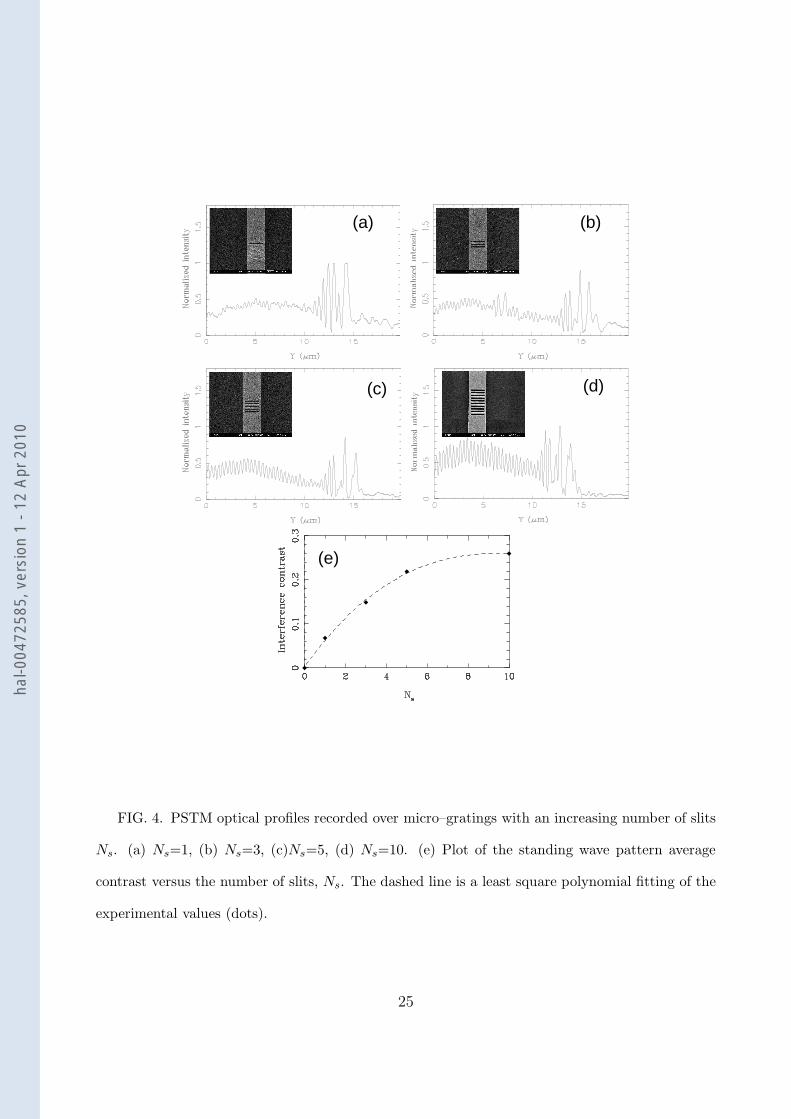
micro–structured SPW are displayed in figure 4. The interference of the incident SPW mode
with the field scattered by a single slit engraved into the metal strip (see fig. 4(a)) creates
a pattern of non–periodic large amplitude oscillations extending over a distance of more
than 4 µm. A very low contrast standing wave pattern which can be attributed to a weak
back-reflection of the incident SPP, is also visible on the left part of the optical profile. In
spite of the back-reflection and the scattering, the incident SPP is also transmitted through
the slit. Indeed, a rather large near–field intensity is still detected for the observation points
located after the slit (y > 15µm). Since the slit engraved into the SPW consists of an air
gap separating two parts of the metal strip and each part of the metal strip can support a
SPP while no SPP can propagate in air, the transmission of the SPW mode through the slit
can then be viewed as a kind of tunnel effect.
For an increasing number of slits, the amplitude of the SPP transmitted through the
micro–grating vanishes while conversely the contrast of the standing wave pattern increases.
The average contrast Cavg computed over more than 20 oscillations of the different standing
wave patterns is plotted in figure 4(e) as a function of the number of slits. The contrast
reaches an asymptotic value of about 0.26 for the micro-grating consisting of ten slits. Note
that the contrast increases between Ns = 5 and Ns = 10, leading to the conclusion that
the five last slits of the micro-grating with Ns=10 do contribute to the back–reflection of
10
hal-0
0472
585,
ver
sion
1 -
12 A
pr 2
010

the incident SPP. In other words, the hopping of the incident SPP over the successive slits
of the micro–grating is efficient enough to allow the propagation of the SPP through a
micro–structured area with a length of several microns.
The increase of the standing wave pattern contrast is obviously related to a corresponding
increase of the reflection efficiency of the mirror. However, without a reliable modeling of
the metal strip SPP modes, we can only roughly estimate these efficiency. Considering an
incident SPP propagating at a gold/air interface and a mirror located at 15 µm from the
launch site, we can compute the reflection coefficient of the mirror needed for matching
the value of the contrast of the theoretical standing wave pattern with the contrast of the
experimental optical profiles. We define the reflection coefficient of the mirror by r = Erδ/E
0δ
where Erδ and E0
δ denote respectively the amplitude of the reflected and the incident δ
component of the SPP electric field at the location of the mirror. Assuming a similar
reflection coefficient for the transverse and the longitudinal components of the SPP electric
field, a contrast for the computed standing wave pattern of 0.26 is obtained with r equal to
25%.
B. Influence the micro–grating period
Up to now, we have only considered micro-gratings with a period P = 400 nm. With
the aim of studying the influence of the period on the reflection efficiency, we consider now
mirrors with three different periods (350 nm, 400 nm and 500 nm) while keeping a fixed
number of ten slits engraved at a distance of 15 µm from the SPW input. The longitudinal
optical profiles shown in the right part of figure 5 have been recorded over these samples
for two incident wavelengths λ0 = 753 nm (solid line) and λ0 = 800 nm (dashed line) (The
PSTM images recorded with λ0=800nm are shown in the left part of figure 5). A neat
standing wave pattern is observed for the mirrors with P=350 nm and P=400 nm while
mainly the scattering on the mirror is visible when P=500 nm. The low contrast standing
wave patterns in figure 5(f) indicate that, for both wavelengths, the mirror with a period
11
hal-0
0472
585,
ver
sion
1 -
12 A
pr 2
010

of 500 nm reflects very poorly the incident SPW mode. The standing wave pattern being
much more pronounced for P=350 nm and P=400 nm, it is worth to notice that the highest
contrast is obtained for λ0=753 nm if P=350 nm and for λ0=800 nm if P=400 nm. In order
to investigate more in detail the efficiency of the mirror when the ratio P/λ0 is close to 0.5,
the micro–grating with a period P=400 nm has been imaged at six different wavelengths
while only two have been used for P=350 nm and P=500 nm. The average contrast of the
standing wave–pattern obtained for the different period–wavelengths combinations is plotted
as a function of the ratio P/λ0 in figure 6. The curve displayed in figure 6 shows that the
contrast reaches a maximum when the incident wavelength in vacuum is twice the period of
the micro-grating. The highest reflection efficiency of the mirror is expected for the SPP’s
back-reflected by each slit being in phase then we conclude that the effective wavelength of
the SPP mode traveling through in the micro–structured area is very close to λ0.
C. Influence of the incident wavelength
By changing the period of the micro–grating, we have found that the maximum reflection
efficiency of the mirror is obtained for P/λ0 equal to 0.5. To further confirm this result, we
have performed the PSTM imaging of a micro-grating with a fixed period of 400 nm by using
incident wavelengths distributed over the whole tunability range of our Titanium-sapphire
laser (750 nm - 830 nm). In this case, the mirror consists of ten slits engraved at a distance
of 25 µm from the input of the 2.5 µm wide SPW. A typical PSTM image of this mirror
obtained with λ0 = 800 nm is shown in figure 7(a). As expected, a well pronounced standing
wave pattern is visible on the near–field image. A cross–cut of this image taken along the axis
x = 0 is shown in figure 7(b) (solid line). Unlike the standing wave pattern resulting from
the interference of two contra–propagating SPP’s (see equation (1)), we observe that the
amplitude of the oscillations decreases dramatically when the observation point approaches
the mirror. In fact, according to equation (2), such a damping occurs when an incident
SPP interferes with a radiative wave. However, we have shown in section III that the
12
hal-0
0472
585,
ver
sion
1 -
12 A
pr 2
010

standing wave pattern in the PSTM images of the micro–gratings arises from surface–waves
interferences. Furthermore, unlike what is expected when a SPP interferes with a radiative
wave, the amplitude of the oscillations in figure 7(b) is not damped monotonically with the
propagation distance. Indeed, it is found to be rather constant for y < 5 µm (see dashed line
in figure 7(b)). From these observations, we deduce that the damping of the standing wave
pattern amplitude is not due to the interference of a SPP and a radiative wave but on the
other hand, such a damping is not expected for two contra–propagating SPP’s. To overcome
this apparent contradiction, it is worth to notice that in our case we are not considering
SPP excited on an extended thin film but the hybrid SPW modes. The damping could then
be related to the intrinsic properties of these modes, i.e the back–reflected hybrid SPW
mode has to propagate over a minimal “threshold” distance in order to arise as the result of
the reflection, produced by each slit of the mirror, of each SPP component involved in the
incident hybrid SPW. In the absence of a reliable modeling of these modes, this hypothesis
is difficult to verify. However, it is consistent with the fact that, at the input of the SPW,
such a spatial transient is necessary to operate the transition from the incident extended
thin film SPP and the SPW mode (see fig. 2). Note also that the damping of the standing
wave pattern is less pronounced when the mirror is engraved at a smaller distance from the
SPW input (see for example fig 4(d)) indicating that the field distribution of the incident
SPW mode at the location of the mirror influences the back–reflection process.
Although not fully understood, the damping of the standing wave pattern oscillations is
not an obstacle to the spectroscopic study of the mirror efficiency on the basis of the PSTM
images. Indeed, one can see on figure 7(c) that the contrast of the oscillations is rather
constant for observation points located at a distance large enough from the mirror. Thus,
by averaging this contrast over the five first micrometers (y < 5 µm) of each optical profile
recorded with different incident wavelength, we obtain the curve plotted in figure 8. The
fitting of the experimental data exhibits a parabolic shape with a maximum corresponding
to an incident wavelength in vacuum of λ0 =800 nm. Thus, in agreement with the previous
experiment, we find that the maximum reflection efficiency is obtained for the wavelength
13
hal-0
0472
585,
ver
sion
1 -
12 A
pr 2
010

λ0 equal to twice the period of the micro–grating. This result suggests once again that
the phase constant of the field traveling through the micro–structured area is very close to
k0 = 2πλ0
.
V. DISPERSION CURVE OF THE SPW MODE
The integration of micro–mirrors in SPW may have interest for SPP routing purposes
for example, but beyond these practical applications micro–mirrors can also be used to
characterize the fundamental physical properties of metal strip SPP. The general form of
the electric field of a SPW mode propagating along the y axis can be written as:
~E(x, y, z) = ~E0(x, z) exp (−α + iβ)y (6)
where α and β denote respectively the attenuation and the phase constant of the SPP. The
PSTM images of the micro–structured SPW’s allow the measurement of these two constants
simultaneously. Indeed by averaging up to 60 columns of a 512×512 pixels PSTM SPW
image (see for example figure 7(a)), a mean longitudinal optical profile can be obtained.
From such a profile, one can measure the period d of the standing wave pattern and the 1/e
damping distance Lsp of the background intensity and then compute the attenuation and
the phase constants according to the relations α = 1/(2Lsp) and β = π/d.
The reflection efficiency of the micro–mirror is large enough over the tunability range of
our laser to provide a well–defined standing wave pattern that allows an accurate measure-
ment of the period d and thus the computation of the phase constant β. The experimental
dispersion curve of the SPW mode phase constant is shown on figure 9. The light line defined
by β = ω/c and the dispersion curve of an extended gold/air interface surface plasmon are
also displayed on this figure. The phase constant of the surface plasmon has been computed
according to the well–known relation βSP = ℜ(ωc
√
ε(ω)ε(ω)+1
) where ℜ and ε(ω) denote respec-
tively the real part and the complex dielectric function of gold [3]. The values of ε(ω) used
for the computation of βSP are experimental values measured by ellipsometry. Over the
14
hal-0
0472
585,
ver
sion
1 -
12 A
pr 2
010

frequency range considered, the complex refractive index of gold has been found to be given
by n = 0.32+ i(8.66×λ0−2.05), where λ0 is the incident wavelength in vacuum expressed in
micrometer. It can be seen on figure 9 that, at a given frequency, the phase constant of the
SPW mode is significantly larger compared to the one of a SPP launched on an extended
thin film. Note that, in spite of the absence of crossing between the two dispersion curves,
an efficient coupling between the two kinds of surface plasmon is observed [8]. Such an
efficiency must be related to an overlap of the two kinds of surface plasmon resonance due
to their respective linewidths.
The group velocity, defined by vg = dω/dk, is commonly interpreted as the average
velocity of a pulse [14]. However, both the shape and the amplitude of a pulse can be affected
by the propagation into a dissipative and/or dispersive medium such that the concept of
group velocity may lose its physical significance in this situation [15]. Nevertheless, even for
a dispersive medium, the group velocity remains physically meaningful if the duration of the
pulse is sufficiently long such that its spectrum has a significant amplitude only over a very
narrow range of frequency. Thus, at a given frequency, the local slope of the dispersion curve
of a surface plasmon can still be interpret as a pulse velocity for long enough excitations.
With this restriction in mind, we can measure the average velocity of a pulse propagating
along a metal strip directly from the experimental dispersion curve shown in fig.(9). For
example, at a frequency corresponding to a wavelength of 800 nm in vacuum, we found a
group velocity of vg=2.9×10⁸ ms−1. For this range of frequency, the group velocity of a
plasmon polariton excited at the surface of an extended thin gold film is also very close to
the speed of light. It is then worth to notice that surprisingly, unlike what has been found for
the damping distance [16], the finite width of the metal strip (only three times the incident
wavelength) does not influence significantly the group velocity of the SPW mode.
15
hal-0
0472
585,
ver
sion
1 -
12 A
pr 2
010
VI. ANALOGY WITH A BRAGG MIRROR
A standard Bragg mirror is a stack of layers made of materials with different optical
refractive index. For the SPP modes propagating along a metal strip, the micro–grating
creates a periodic refractive index contrast such that, to some extent, a micro–grating can
be viewed as a SPP Bragg mirror. The goal of this last section is to determine empirically the
structural parameters of an equivalent one–dimensional Bragg mirror (EBM) which models
qualitatively the optical properties of the micro–gratings engraved in a SPW.
The EBM is supposed to be illuminated in normal incidence by a radiative wave with a
wave–vector equal to the phase constant of the SPW mode. This phase constant is known
from the experimental dispersion curve discussed in the previous section. The EBM is made
of two materials (A) and (B) modeling respectively the air gap of the slits and the pieces
of the metal strip located in between two successive slits (figure 10(a)). The thickness of
each layer in the EBM is taken equal to the dimension of the corresponding structures
in the micro–gratings. For example, for a micro–grating with a period P=400 nm, the
thickness of materials (A) and (B) are respectively 150 nm (width of the slits) and 250 nm
(inter-slit distance). The EBM is fully characterized if the optical refractive indexes of each
material are specified. These indexes are determined empirically using the experimental
results discussed previously.
We have shown in section III that the reflection efficiency of the micro–gratings saturates
for a rather small number of slits. Indeed, the contrast of the standing wave pattern changes
by only 15 % when switching from a mirror with Ns=5 to Ns=10 (see fig. 4(f)). This result
arises from the dramatic damping of the incident SPP as it propagates through the micro–
structured area of the metal strip. In order to simulate this damping in the EBM model,
the air gaps engraved in the SPW are modeled by an absorbing material (material (A))
with a complex refractive index nA = nA + iκA . Unlike the air gaps, the metal strip pieces
located between two successive slits can support a SPP mode and then are represented by
a real refractive index material in the EBM model. By changing both the period of the
16
hal-0
0472
585,
ver
sion
1 -
12 A
pr 2
010
micro–grating and/or the incident frequency, we have found that the maximum reflection
efficiency of the mirror is obtained for an incident wavelength in vacuum equal to two times
the period of the grating. As mentioned before, this suggests that the phase constant of the
SPP field traveling through the mirror is very close to k0. As a consequence, for the EBM
model, the real part of refractive index of both materials (A) and (B) should be chosen very
close to 1.0. Material (B) simulates a medium supporting a SPP. A SPP being an evanescent
wave, it’s phase constant β is larger than k0 leading to an effective index neff = β/k0 larger
than 1.0 for the medium supporting the SP. In order to satisfy the two aforementioned
conditions, we chose an optical refractive index for material (B) equal to nB=1.01. Since
material (A) models the air gaps in the SPW, nA is taken equal to 1.0. In order to estimate
the extinction coefficient of (A), the EBM reflectivity has been computed as a function of
the number of layers Ns of material (A) for a several values of κA. The curve plotted in
figure 10(a) has been obtained with κA=0.3. We found that, in qualitative agreement with
the experimental curve of fig. 4(f), the reflectivity of the EBM saturates at Ns=10. The
curve displayed in figure 10(b) shows the reflectivity of the EBM (Ns=10) computed for
frequencies corresponding to the tunability range of our laser. As expected, the maximum
reflectivity is obtained for a wavelength (λ0=803 nm) almost equal to double the period of
the EBM. The EBM reflectivity curve exhibits a parabolic shape which is one more time in
qualitative agreement with the experimental results (fig. 8). The calculation of the EBM
reflectivity has been performed with a refractive index of the input and output medium
equal to 1.07 which is the effective index corresponding to the SPW mode as computed
using the experimental dispersion curve shown in figure 9. It is then worth to notice that,
in order to obtain a qualitative agreement with the experimental results, the SPP traveling
inside the micro–structured area is modeled with an effective index (nB=1.01) different from
the effective index of the SPW mode propagating along the homogeneous (non–structured)
SPW although in both cases we consider SPP at a gold/air interface. A possible explanation
for such a difference could be that, in analogy with localized surface plasmon of metallic
nano–particles, the geometry of the system supporting the SPP plays a key role. For the
17
hal-0
0472
585,
ver
sion
1 -
12 A
pr 2
010

homogeneous SPW, the SPP mode propagates along a metal strip with a length much larger
that it’s width. On the contrary, inside the micro–structured area, the SPP is supported
by pieces of the metal strip with a dimension along the propagation direction much smaller
than the SPW width.
With the aim of checking the reliability of our empirical model, we consider finally the
influence of the period P on the reflectivity of the EBM. Similarly to the experimental
situation, we have simulated three different periods P = 350 nm, P = 400 nm and P = 500
nm, by taking the inter-slit distance respectively equal to 200 nm, 250 nm and 350 nm. The
reflectivity of the EBM computed for the wavelengths considered experimentally for each
period is plotted as a function of the ratio P/λ0 in figure 10(d). Although small differences
with the experimental curve (fig. 6) can be observed, we found that, qualitatively, the EBM
models accurately the influence of the period on the SPP back–reflection efficiency of the
micro–gratings.
VII. CONCLUSION
In summary, we have analyzed in detail the integration of micro–mirrors into surface
plasmon waveguides. A PSTM has been used to map the near–field optical intensity dis-
tribution of a SPP propagating along a metal strips with a width of 2.5µm where finite
length gratings of slits have been engraved by FIB milling. The PSTM images of the micro–
gratings show a well pronounced standing wave pattern. This standing wave pattern has
been found to arise from the interference of two contra–propagating SPP since the contrast
of the interference fringes does not depend upon the distance between the observation plane
and the surface of the sample.
By considering micro–gratings with an increasing number of periods, we have shown that
the reflection efficiency of the mirrors saturates for a rather low number of about ten slits.
This saturation is due to the dramatic damping of the incident SPW mode as it propagates
through the micro–grating. Using three different periods, we have found that the optimum
18
hal-0
0472
585,
ver
sion
1 -
12 A
pr 2
010
mirrors efficiency is obtained for an incident wavelength in vacuum equal to twice the period
of the grating. This result has been confirmed by the spectroscopic study of the reflection
efficiency performed over the whole tunability range of our laser (753 nm - 830 nm) for a
mirror with a period of 400 nm.
An accurate measurement of the standing wave pattern period has been used to obtain
the experimental dispersion curve of the SPW mode phase constant. On the basis of this
dispersion curve, we have found that, in the near–infrared, the effective index of the SPW
mode we consider is about neff =1.07 and that the group velocity is close to the speed of light
in vacuum. Finally, we have demonstrated that the optical properties of the micro–gratings
integrated into SPW can be modeled, at least qualitatively, by mean of an equivalent Bragg
mirror. From this analogy we conclude that, in principle, the micro–gratings implanted in
metal strips act on SPW modes as Bragg mirrors although the SPP Bragg mirrors studied
in this paper might have specific properties such as the influence of the micro–gratings
geometry on the effective index of SPP propagating through the zone where the slits are
engraved.
ACKNOWLEDGMENTS
This work was supported by the Regional Council of Burgundy (ARCEN project), by
the French CNRS (STIC: EPML 20) and, in its final phase, by the European Commission
(NoE contract FP6-IST-2002-1-507879). One of us (M. U. G.) acknowledges funding from
the Spanish Ministry of Education.
19
hal-0
0472
585,
ver
sion
1 -
12 A
pr 2
010

REFERENCES
[1] K. L. Kliewer and R. Fuchs, Adv. Chem. Phys. 27, 355 (1974).
[2] A. Otto, Zeit. fur Physik 216, 398 (1968).
[3] H. Raether, Surface Plasmons, Springer Tracts in Modern Physics, Vol. 111 (Springer,
Berlin, 1988).
[4] P. Berini, Phys. Rev. B 61, 10484 (2000).
[5] R. Charbonneau, P. Berini, E. Berolo, E. Lisicka-Shrzek, Optics Lett. 25, 844 (2000).
[6] T. Nikolajsen, K. Leosson, I. Salahutdinov, S. Bozhevolyi, Appl. Phys. Lett. 82, 668
(2003).
[7] J. C. Weeber, J. R. Krenn, A. Dereux, B. Lamprecht, Y. Lacroute, J.P. Goudonnet,
Phys. Rev. B 64, 045411 (2001).
[8] J. C. Weeber, Y. Lacroute, A. Dereux, Phys. Rev. B 68, 115401 (2003).
[9] S.I. Bozhevolnyi, J. E. Erland, P. M. W. Skovgaard, J. M. Hvam, Phys. Rev. Lett. 86,
3008 (2001).
[10] H. Ditlblacher, J.R. Krenn, G. Schider, A. Leitner, F. R. Aussenegg, Appl. Phys. Lett.
81, 1762 (2002).
[11] R. C. Reddick, R. J. Warmack, T. L. Ferrell, Phys. Rev. B 39, 767 (1989).
[12] C. Peeters, E. Fluck, A. M. Otter, M.L.M. Balistreri, J.P. Korterik, L. Kuipers, N.F.
van Hulst, Appl. Phys. Lett. 77, 142 (2000).
[13] J. Seidel, S. Grafstrom, L. Eng, L. Bischoff, Appl. Phys. Lett. 82, 1368 (2003)
[14] J. D. Jackson, Classical Electrodynamics, J. Wiley, New-York (1975).
[15] J. A. Stratton, Electromagnetic Theory, McGraw–Hill, New-York (1941).
20
hal-0
0472
585,
ver
sion
1 -
12 A
pr 2
010

[16] B. Lamprecht, J.R. Krenn, G. Schider, H. Ditlbacher, M. Salerno, N. Felidj, A. Leitner,
F.R. Aussenegg, J-C. Weeber, Appl. Phys. Lett. 79, 51 (2001).
21
hal-0
0472
585,
ver
sion
1 -
12 A
pr 2
010
FIGURES
µmµm 2.5 10
(a) (b)
FIG. 1. Scanning electron microscope (SEM) images of a typical structure used in this study.
(a) The sample consists of a gold pattern (thickness 55 nm) fabricated by electron–beam lithography
and deposited on an indium-tin oxide doped glass substrate. The black ellipse shows the location
of the totally reflected focused light beam (incident from the substrate) used for the excitation of
the surface plasmon. (b) A FIB is used to a engrave micro–gratings into each metal strips. The
micro–grating shown here consists of ten parallel slits of same width (150 nm). In this case, the
period of the pattern is 400 nm.
22
hal-0
0472
585,
ver
sion
1 -
12 A
pr 2
010
(b)
(c) (d)
(a)(1)
(2)
FIG. 2. (a) Large scan PSTM image of a micro–structured SPW. (b) Longitudinal cross–cut of
the near–field image along the dashed line in (a). (c) and (d) Transverse cross–cuts of the PSTM
image taken along the dotted lines (1) and (2) shown in (a) respectively.
23
hal-0
0472
585,
ver
sion
1 -
12 A
pr 2
010

(f)(e)
(c) (d)
(b)
k SP
(a)
FIG. 3. (a) SEM image of the sample used to investigate the influence of the tip–sample distance
on the standing wave pattern contrast. The incident wavelength is 800 nm and the period of the
grating is 400 nm. (b), (c), (d) Small scans PSTM images of the standing wave pattern obtained
for tip–sample distances of respectively 340 nm, 280 nm and 170 nm. The white dashed perimeter
in fig. 3(a) shows approximately the scanning area. (e) Transverse cross–cuts of the PSTM images
(solid: 170 nm, dashed: 280 nm, dashed-dotted:340 nm). (f) Longitudinal cross–cuts of the PSTM
images (solid: 170 nm, dashed: 280 nm, dashed-dotted: 340 nm).
24
hal-0
0472
585,
ver
sion
1 -
12 A
pr 2
010
(a) (b)
(c) (d)
(e)
FIG. 4. PSTM optical profiles recorded over micro–gratings with an increasing number of slits
Ns. (a) Ns=1, (b) Ns=3, (c)Ns=5, (d) Ns=10. (e) Plot of the standing wave pattern average
contrast versus the number of slits, Ns. The dashed line is a least square polynomial fitting of the
experimental values (dots).
25
hal-0
0472
585,
ver
sion
1 -
12 A
pr 2
010

λ 0
λ 0
λ 0
(a)
(c)
(e) (f)
(d)
(b)
P=350nm
P=400nm
P=500nm
= 800 nm
= 753 nm
= 800 nm
FIG. 5. (a), (c), (e) PSTM images of SPP propagating along a metal strip (width=2.5µm)
textured by micro-gratings with different periods, P=350nm, 400nm and 500nm. The incident
wavelength in vaccum is 800nm. (b) (resp. (d),(f)) Cross–cut of the PSTM images of the micro–
grating with P=350nm ( resp. P= 400 nm, P= 500nm). The dashed (resp. solid) line corresponds
to an incident wavelength of 800 nm (resp. 753 nm).
26
hal-0
0472
585,
ver
sion
1 -
12 A
pr 2
010
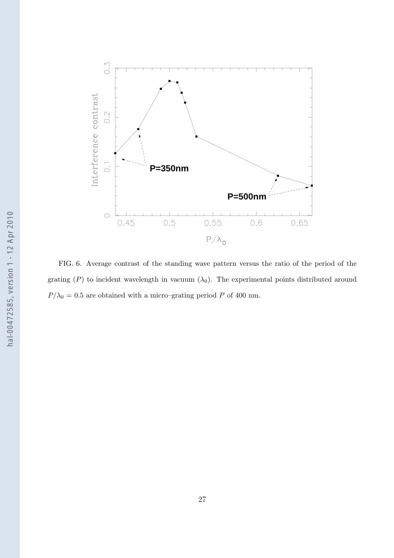
P=500nm
P=350nm
FIG. 6. Average contrast of the standing wave pattern versus the ratio of the period of the
grating (P ) to incident wavelength in vacuum (λ0). The experimental points distributed around
P/λ0 = 0.5 are obtained with a micro–grating period P of 400 nm.
27
hal-0
0472
585,
ver
sion
1 -
12 A
pr 2
010

kSP
(a)
(b) (c)
FIG. 7. (a) PSTM image of a ten slits micro–grating (P = 400 nm). The mirror is engraved
at a distance of 25 µm of the SPW input. The incident wavelength is λ0 = 800 nm. (b) (solid)
Longitudinal cross–cut of the PSTM image, (dashed) Amplitude of the standing wave pattern
oscillations. Note the damping of the amplitude as the observation point approaches the mirror.
(c) Contrast of the oscillations in the cross–cut shown in (b).
28
hal-0
0472
585,
ver
sion
1 -
12 A
pr 2
010
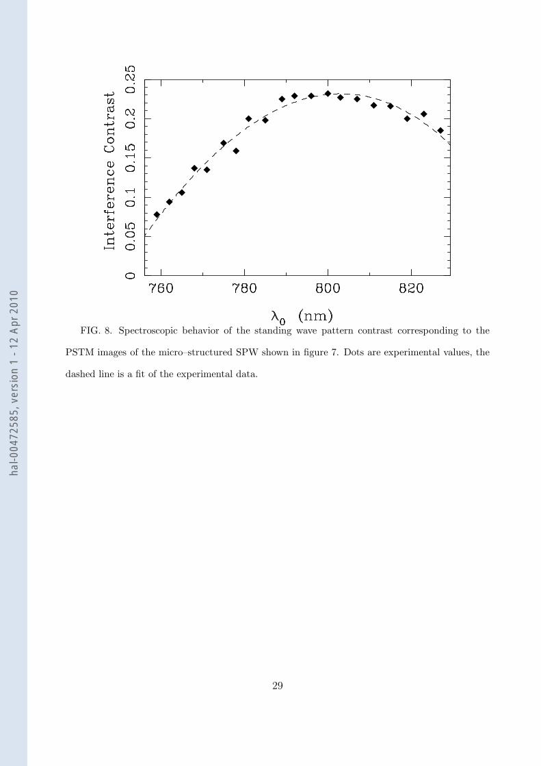
FIG. 8. Spectroscopic behavior of the standing wave pattern contrast corresponding to the
PSTM images of the micro–structured SPW shown in figure 7. Dots are experimental values, the
dashed line is a fit of the experimental data.
29
hal-0
0472
585,
ver
sion
1 -
12 A
pr 2
010

ω(1
0
Hz)
15
µ( m )−1β
2.4
2.45
2.5
2.35
2.3
LL
SP
FIG. 9. Experimental dispersion curve of the SPW mode phase constant. The reported fre-
quency range corresponds to wavelengths in vacuum varying from 760 nm to 830 nm . SP (dashed):
Computed dispersion curve of a surface plasmon excited at a gold/air interface. The dielectric func-
tion of gold used for the calculation of the dispersion curve has been measured by ellipsometry. LL
(Dashed–dotted): Light line in air.
30
hal-0
0472
585,
ver
sion
1 -
12 A
pr 2
010
kinc
(a) (b)
P=500nm
P=350nm
(c) (d)
A A B AB
31
hal-0
0472
585,
ver
sion
1 -
12 A
pr 2
010
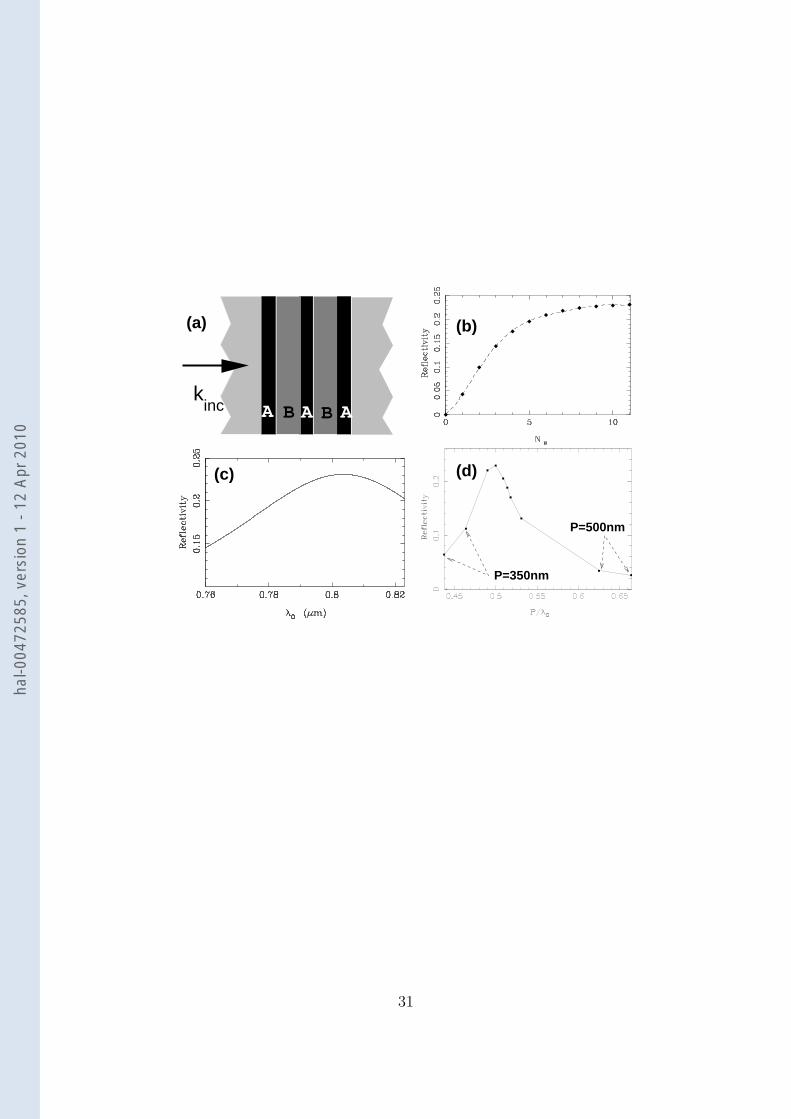
FIG. 10. (a) Scheme of equivalent Bragg Mirror (EBM) for modeling the optical properties of
the SPP mirrors integrated into SPW. The EBM is made of two materials (A) and (B) modeling
respectively the air gaps and the metallic parts of the micro–grating. Material (A) has been taken
as an absorbing material in order to simulate the scattering losses of the incident SPW mode on
the slits of the micro–grating. (b) Saturation of the EBM reflectivity for an increasing number of
layers Ns. The period of the EBM is 400 nm, the thickness of layers (A) and (B) are respectively
150 nm and 250 nm and the incident wavelength is 800 nm in vacuum. The indexes of the input
and out media are equal to the effective index of the SPW mode (1.07). The indexes of material
(A) and (B) are respectively (1.0+i0.3) and 1.01. (c) Evolution of the EBM reflectivity with the
incident wavelength. For this computation the EBM period is 400 nm and Ns=10. (d) Reflectivity
of the EBM as a function of the period P (Ns=10).
32
hal-0
0472
585,
ver
sion
1 -
12 A
pr 2
010