
Nano-gap grating devices with enhanced optical properties and methods of fabrication
20
US 20140226207A1 (12) Patent Application Publication (10) Pub. No.: US 2014/0226207 A1 (19) United States Gangopadhyay et al. (43) Pub. Date: Aug. 14, 2014 (54) NANO-GAP GRATING DEVICES WITH ENHANCED OPTICAL PROPERTIES AND METHODS OF FABRICATION (71) Applicant: The Curators of the University of Missouri, Columbia, MO (US) (72) Inventors: Shubhra Gangopadhyay, Columbia, MO (US); Venu Korampally, Aurora, IL (US); Sagnik Basuray, Columbia, MO (US); Kunal Bhatnagar, College Station, TX (US); Avinash Pathak, Columbia, MO (US); Arnab Ghosh, Columbia, MO (US); DreW Edwin Menke, Berger, MO (US); Joseph Mathai, Columbia, MO (US); Peter Cornish, Columbia, MO (US); Keshab Gangopadhyay, Columbia, MO (US); Aaron Wood, Columbia, MO (US) (73) Assignee: THE CURATORS OF THE UNIVERSITY OF MISSOURI, Columbia, MO (US) (21) App1.No.: 14/081,353 (22) Filed: Nov. 15, 2013 Related US. Application Data (60) Provisional application No. 61/850,232, ?led on Feb. 11, 2013. Publication Classi?cation (51) Int. Cl. G02B 5/18 (2006.01) (52) US. Cl. CPC .......... .. G02B 5/1842 (2013.01); G02B 5/1852 (2013.01) USPC ......................................... .. 359/566; 101/483 (57) ABSTRACT A method of producing a grating structure comprises the steps of forming a stamp from ?exible plastic material, the stamp including a negative of a periodic grating pattern on a ?rst surface; forming an ink by applying a polymer ?lm to the stamp, the ink including a ?rst surface and an opposing sec ond surface, Wherein the ?rst surface of the ink contacts the ?rst surface of the stamp such that the ink retains a positive of the periodic grating pattern; placing the ink and the stamp on a substrate such that the second surface of the ink contacts an upper surface of the substrate; and removing the stamp from the ink by applying a tensional force to one edge of the stamp.
Transcript of Nano-gap grating devices with enhanced optical properties and methods of fabrication
US 20140226207A1
(12) Patent Application Publication (10) Pub. No.: US 2014/0226207 A1 (19) United States
Gangopadhyay et al. (43) Pub. Date: Aug. 14, 2014
(54) NANO-GAP GRATING DEVICES WITH ENHANCED OPTICAL PROPERTIES AND METHODS OF FABRICATION
(71) Applicant: The Curators of the University of Missouri, Columbia, MO (US)
(72) Inventors: Shubhra Gangopadhyay, Columbia, MO (US); Venu Korampally, Aurora, IL (US); Sagnik Basuray, Columbia, MO (US); Kunal Bhatnagar, College Station, TX (US); Avinash Pathak, Columbia, MO (US); Arnab Ghosh, Columbia, MO (US); DreW Edwin Menke, Berger, MO (US); Joseph Mathai, Columbia, MO (US); Peter Cornish, Columbia, MO (US); Keshab Gangopadhyay, Columbia, MO (US); Aaron Wood, Columbia, MO (US)
(73) Assignee: THE CURATORS OF THE UNIVERSITY OF MISSOURI, Columbia, MO (US)
(21) App1.No.: 14/081,353
(22) Filed: Nov. 15, 2013
Related US. Application Data
(60) Provisional application No. 61/850,232, ?led on Feb. 11, 2013.
Publication Classi?cation
(51) Int. Cl. G02B 5/18 (2006.01)
(52) US. Cl. CPC .......... .. G02B 5/1842 (2013.01); G02B 5/1852
(2013.01) USPC ......................................... .. 359/566; 101/483
(57) ABSTRACT A method of producing a grating structure comprises the steps of forming a stamp from ?exible plastic material, the stamp including a negative of a periodic grating pattern on a ?rst surface; forming an ink by applying a polymer ?lm to the stamp, the ink including a ?rst surface and an opposing sec ond surface, Wherein the ?rst surface of the ink contacts the ?rst surface of the stamp such that the ink retains a positive of the periodic grating pattern; placing the ink and the stamp on a substrate such that the second surface of the ink contacts an upper surface of the substrate; and removing the stamp from the ink by applying a tensional force to one edge of the stamp.
Patent Application Publication Aug. 14, 2014 Sheet 1 0f 12 US 2014/0226207 A1
Patent Application Publication Aug. 14, 2014 Sheet 2 0f 12 US 2014/0226207 A1
Patent Application Publication Aug. 14, 2014 Sheet 3 0f 12 US 2014/0226207 A1
Patent Application Publication Aug. 14, 2014 Sheet 4 0f 12 US 2014/0226207 A1
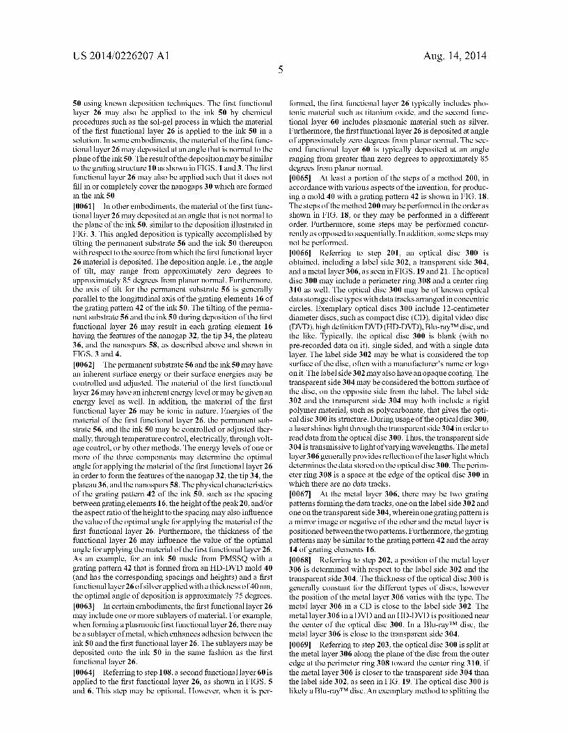
M
FORM A STAMP BY APPLYING A FLEXIBLE PLASTIC 101 /
PATTERN TO TRANSFER A MATERIAL TO A MOLD WHICH INCLUDES A GRATING
NEGATIVE OF THE GRATING PATTERN TO THE STAMP
II
REMOVE THE STAM P FROM THE MOLD
II
'/102
GRATING
FORM AN INK BY APPLYING A POLYMER FILM TO THE STAMP TO RECEIVE AND RETAIN A POSITIVE OF THE
PATTERN
II
PLACE THE STAMP AND THE INK ON A SUBSTRATE
II
CREATE NANOGAPS IN THE INK
II
REMOVE THE STAMP FROM THE INK
II
APPLY A FIRST FUNCTIONAL LAYER TO THE INK
II
APPLY A SECOND FUNCTIONAL LAYER TO ‘ THE FIRST FUNCTIONAL LAYER
?e? 7.
/-108
Patent Application Publication Aug. 14, 2014 Sheet 5 0f 12 US 2014/0226207 A1
40
Patent Application Publication Aug. 14, 2014 Sheet 6 0f 12 US 2014/0226207 A1
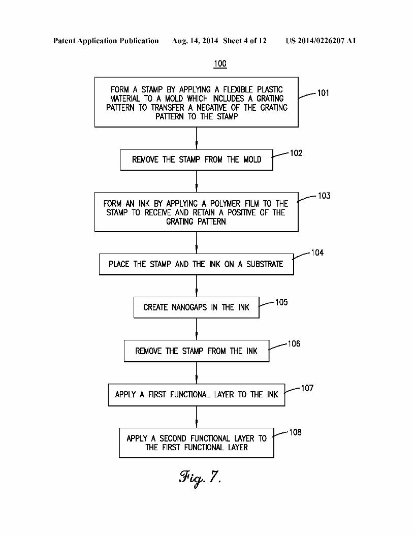
Patent Application Publication Aug. 14, 2014 Sheet 7 0f 12 US 2014/0226207 A1
Q
Patent Application Publication Aug. 14, 2014 Sheet 8 0f 12 US 2014/0226207 A1
Patent Application Publication Aug. 14, 2014 Sheet 9 0f 12 US 2014/0226207 A1

Patent Application Publication Aug. 14, 2014 Sheet 10 0f 12 US 2014/0226207 A1
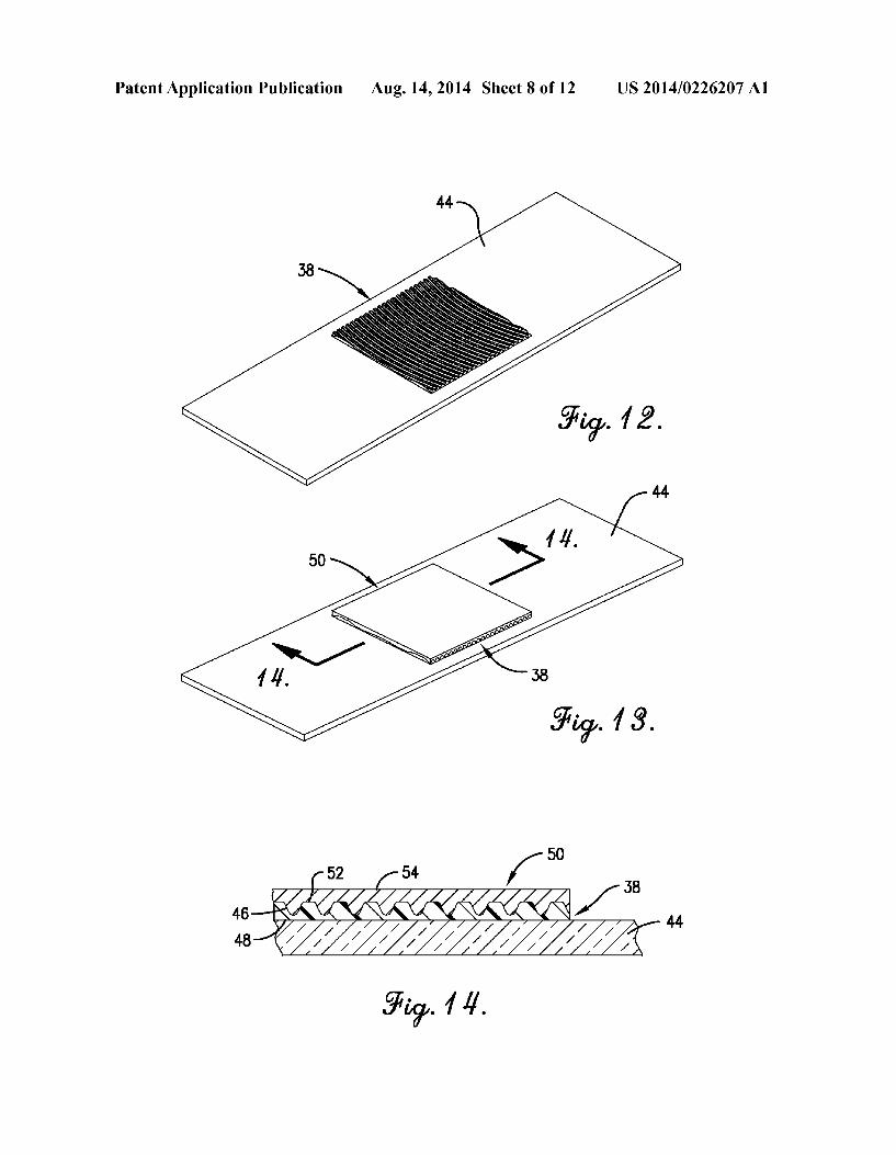
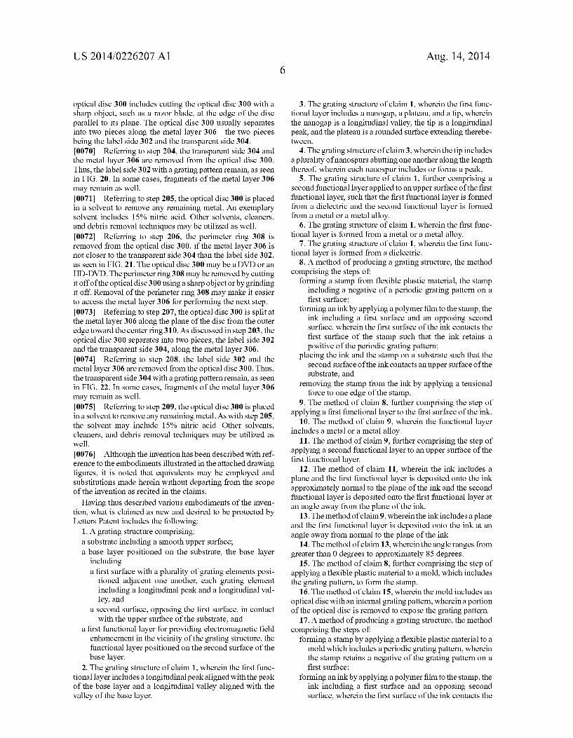
200
OBTAIN AN OPTICAL DISC INCLUDING A LABEL SIDE, A /201 TRANSPARENT SIDE, AND A METAL LAYER
I
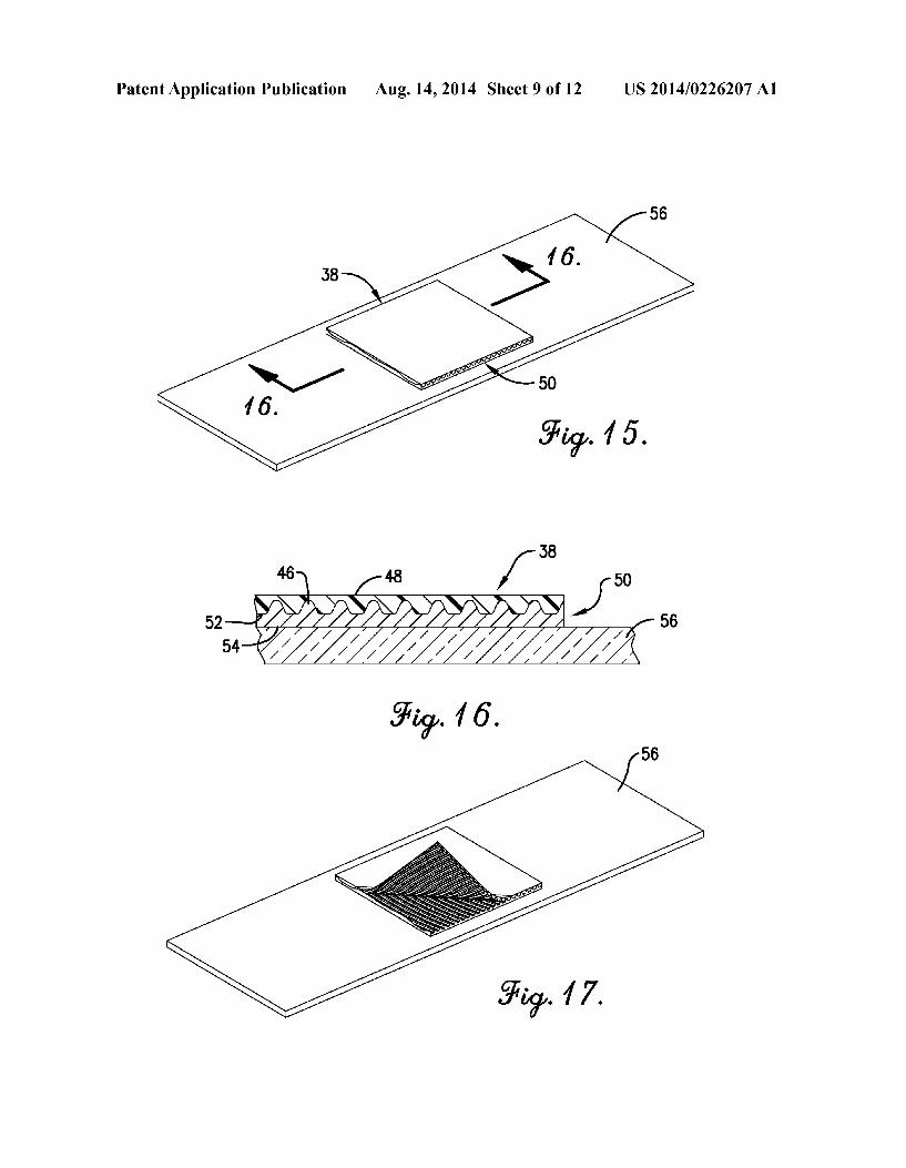
DETERMINE THE POSITION OF THE METAL LAYER WITH / 202 RESPECT TO THE LABEL SIDE AND THE TRANSPARENT SIDE
I
IF THE METAL LAYER IS CLOSER TO THE TRANSPARENT SIDE THAN THE LABEL SIDE THEN SPLIT THE OPTICAL DISC AT THE METAL LAYER ALONG THE PLANE OF THE DISC FROM THE OUTER EDGE TOWARD THE CENTER
/ 203
I
REMOVE THE TRANSPARENT SIDE AND THE METAL /204 LAYER FROM THE OPTICAL DIsc
I
PLACE THE OPTICAL DISC IN A SOLVENT TO REMOVE /205 ANY REMAINING METAL
I
IF THE METAL LAYER IS NOT CLOSER TO THE TRANSPARENT / 205 SIDE THAN THE LABEL SIDE THEN REMOVE A PERIMETER RING FROM THE OPTICAL DISC
I 207
SPLIT THE OPTICAL DISC AT THE METAL LAYER ALONG / THE PLANE OF THE DISC FROM THE OUTER EDGE
TOWARD THE CENTER
I
REMOVE THE LABEL SIDE AND THE METAL LAYER /2()8 FROM THE OPTICAL DISC
I
PLACE THE OPTICAL DISC IN A SOLVENT TO REMOVE ANY REMAINING METAL 1 8
Patent Application Publication Aug. 14, 2014 Sheet 11 0f 12 US 2014/0226207 A1
% > 302 /
95?. 19.
306 338
f. / l 302-]
308
?in.
310 \
Patent Application Publication Aug. 14, 2014 Sheet 12 0f 12 US 2014/0226207 A1
00 o I")
304 J 306
l
\302
304\ \ Pk? 21. WWW gay. 22.
310\\ 310\
US 2014/0226207 A1
NANO-GAP GRATING DEVICES WITH ENHANCED OPTICAL PROPERTIES AND
METHODS OF FABRICATION
RELATED APPLICATION
[0001] The present application is a non-provisional appli cation, and claims priority bene?t with regard to all common subject matter, of US. Provisional Application No. 61/850, 232, ?led Feb. 11, 2013, and entitled “NANO-GAP GRAT ING DEVICES WITH ENHANCED OPTICAL PROP ERTY AND FABRICATIONS THEREOF.” The identi?ed earlier-?led provisional application is hereby incorporated by reference in its entirety.
FEDERALLY SPONSORED RESEARCH OR DEVELOPMENT
[0002] This invention was made with Government support under Grant No. ECCS-1102070 awarded by the National Science Foundation and Grant No. W15QKN-ll-9-0001 RPPl-H awarded by the Nano Technology Enterprise Con sortium (NTEC). The Government has certain rights in the invention.
BACKGROUND
[0003] 1. Field [0004] Embodiments of the invention relate to structures for improving optical imaging and methods of their fabrica tion. [0005] 2. RelatedArt [0006] Microscopic imaging is utilized for studying small objects in ?elds such as medical development, biological research, cancer research, metallurgy, and others. Imaging of microscopic objects often encounters the diffraction limit when trying to image increasingly small objects. Fluores cence spectroscopy can be utilized in ultrasensitive chemical and biological threat sensors. But ?uorescence spectroscopy suffers from low image contrast and a limit on the detection capabilities. Uniform, periodic grating structures have been developed to offer improvement in microscopic imaging and ?uorescence spectroscopy. However, the improvements may be limited and the production of the grating structures may require the usage of costly fabrication equipment and com plex manufacturing techniques, leading to a high cost of the grating structures.
SUMMARY
[0007] Embodiments of the invention solve the above-men tioned problems and provide a distinct advance in the art of microscopic imaging and ?uorescence spectroscopy. More particularly, embodiments of the invention provide grating structures with enhanced optical properties and methods of their fabrication. [0008] A ?rst embodiment of the invention provides a grat ing structure comprising a substrate, a base layer, and a ?rst functional layer. The base layer is positioned on the substrate and includes a ?rst surface with a plurality of grating elements positioned adjacent one another and an opposing second sur face in contact with a surface of the substrate. The grating elements include a longitudinal peak and a longitudinal val ley. The functional layer is positioned on the second surface of the base layer and provides electromagnetic ?eld enhance ment in the vicinity of the grating structure.
Aug. 14, 2014
[0009] A second embodiment of the invention provides a method of producing a grating structure. The method com prises the steps of forming a stamp from ?exible plastic material, the stamp including a negative of a periodic grating pattern on a ?rst surface; forming an ink by applying a poly mer ?lm to the stamp, the ink including a ?rst surface and an opposing second surface, wherein the ?rst surface of the ink contacts the ?rst surface of the stamp such that the ink retains a positive of the periodic grating pattern; placing the ink and the stamp on a substrate such that the second surface of the ink contacts an upper surface of the substrate; and removing the stamp from the ink by applying a tensional force to one edge of the stamp. [0010] A third embodiment of the invention provides a method of producing a. The method comprises the steps of forming a stamp by applying a ?exible plastic material to a mold which includes a periodic grating pattern, wherein the stamp retains a negative of the grating pattern on a ?rst sur face; forrning an ink by applying a polymer ?lm to the stamp, the ink including a ?rst surface and an opposing second surface, wherein the ?rst surface of the ink contacts the ?rst surface of the stamp such that the ink retains a positive of the periodic grating pattern; placing the ink and the stamp on a substrate such that the second surface of the ink contacts an upper surface of the substrate; removing the stamp from the ink by applying a tensional force to one edge of the stamp; and applying a functional layer to the ?rst surface of the ink. [0011] This summary is provided to introduce a selection of concepts in a simpli?ed form that are further described below in the detailed description. This summary is not intended to identify key features or essential features of the claimed sub ject matter, nor is it intended to be used to limit the scope of the claimed subject matter. Other aspects and advantages of the invention will be apparent from the following detailed description of the embodiments and the accompanying draw ing ?gures.
BRIEF DESCRIPTION OF THE DRAWING FIGURES
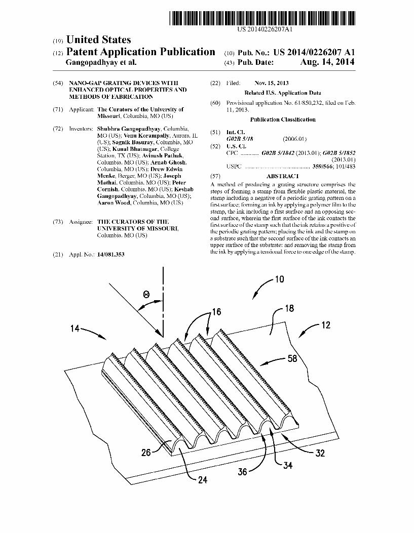
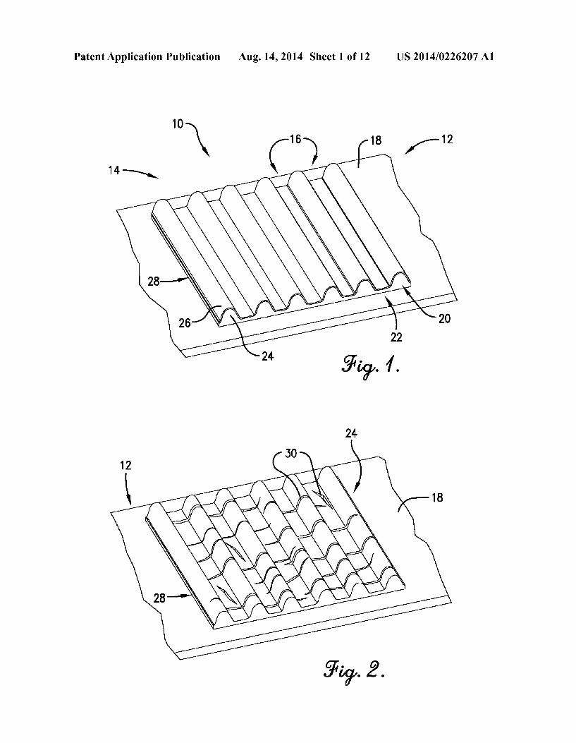
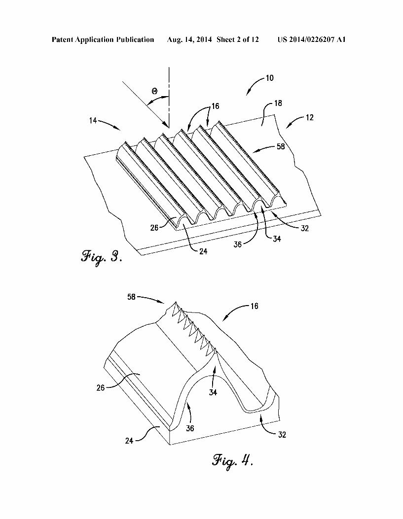
[0012] Embodiments of the invention are described in detail below with reference to the attached drawing ?gures, wherein: [0013] FIG. 1 is a perspective view of a grating structure including a ?rst functional layer, a base layer, and a substrate, constructed in accordance with various embodiments of the invention; [0014] FIG. 2 is a perspective view of the base layer and the substrate from the grating structure of FIG. 1, the base layer including a plurality of nanogaps; [0015] FIG. 3 is a perspective view of the grating structure with the ?rst functional layer being deposited at an angle away from normal to the plane of the grating structure; [0016] FIG. 4 is an enlarged view of a portion of the grating structure of FIG. 3; [0017] FIG. 5 is a perspective view of the grating structure with the ?rst functional layer being deposited normal to the plane of the grating structure and a second functional layer being deposited at an angle away from normal to the plane of the grating structure; [0018] FIG. 6 is an enlarged view of a portion of the grating structure of FIG. 5; [0019] FIG. 7 is a ?ow diagram of at least a portion of the steps of a method of producing a grating structure;
US 2014/0226207 A1
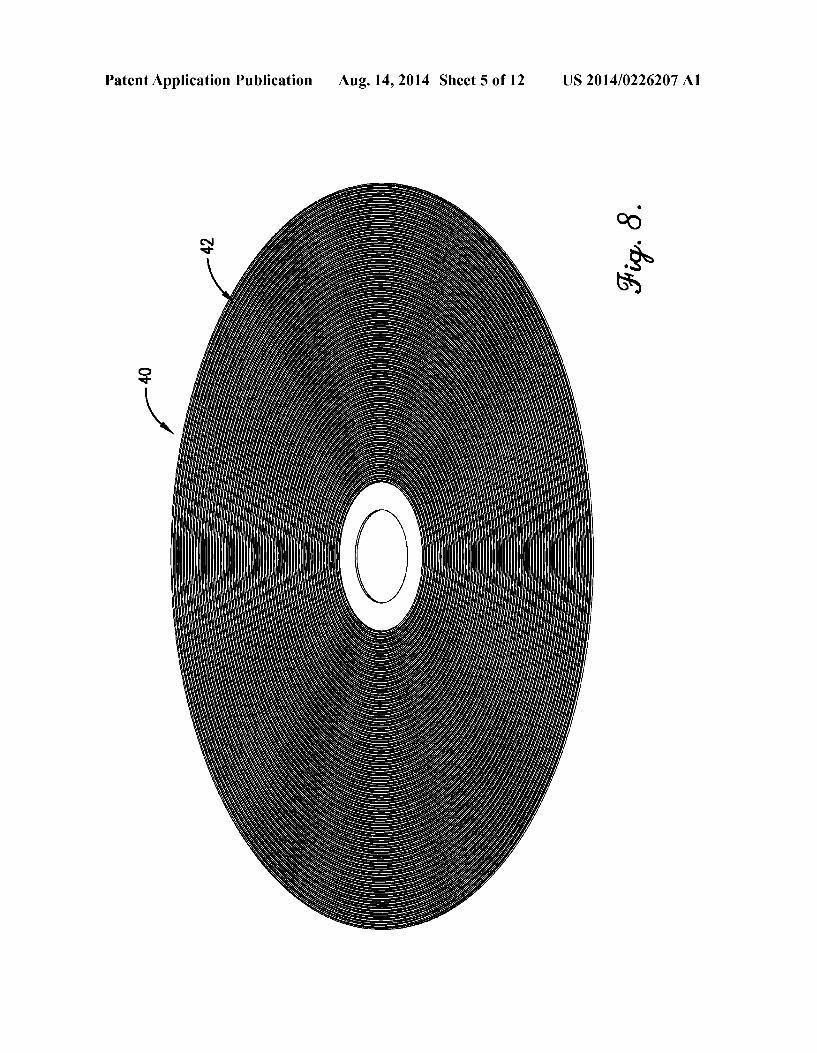
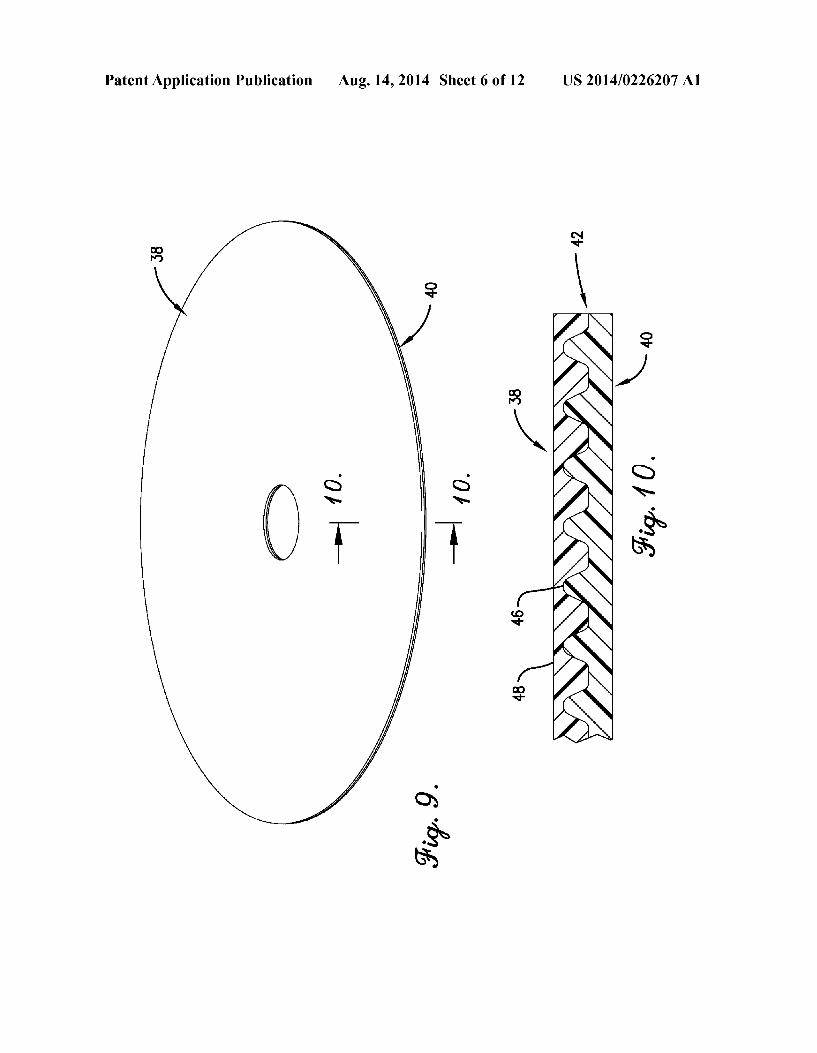
[0020] FIG. 8 is a perspective view of a mold created from a modi?ed optical disc; [0021] FIG. 9 is a perspective view of the mold coated with a plastic material to form a stamp; [0022] FIG. 10 is a sectional view of the mold and the stamp from FIG. 9 cut along the line 10-10; [0023] FIG. 11 is a perspective view of the mold and the stamp with a portion of the stamp removed to create a small stamp; [0024] FIG. 12 is a perspective view of the stamp placed on a temporary substrate; [0025] FIG. 13 is a perspective view of the stamp on the temporary substrate coated with a polymer ?lm to create an
ink; [0026] FIG. 14 is a sectional view ofthe stamp and the ink from FIG. 13 cut along the line 14-14; [0027] FIG. 15 is a perspective view of the stamp and the ink placed on a permanent substrate; [0028] FIG. 16 is a sectional view ofthe stamp and the ink from FIG. 15 cut along the line 16-16; [0029] FIG. 17 is a perspective view of the stamp and the ink on the permanent substrate depicting the stamp being removed from the ink; [0030] FIG. 18 is a ?ow diagram ofat least a portion ofthe steps of a method of producing a mold that includes a grating structure; [0031] FIG. 19 is a sectional view of a ?rst type of optical disc with a metal layer and a transparent side in which the metal layer is closer to the transparent side; [0032] FIG. 20 is a sectional view of the ?rst type of optical disc in which the metal layer and the transparent side have been removed; [0033] FIG. 21 is a sectional view of a second type of optical disc with a metal layer, a transparent side, and a label side in which the metal layer is not closer to the transparent side; and [0034] FIG. 22 is a sectional view of the second type of optical disc in which the metal layer and the label side have been removed. [0035] The drawing ?gures do not limit the invention to the speci?c embodiments disclosed and described herein. The drawings are not necessarily to scale, emphasis instead being placed upon clearly illustrating the principles of the inven tion.
DETAILED DESCRIPTION
[0036] The following detailed description of embodiments of the invention references the accompanying drawings that illustrate speci?c embodiments in which the invention can be practiced. The embodiments are intended to describe aspects of the invention in suf?cient detail to enable those skilled in the art to practice the invention. Other embodiments can be utilized and changes can be made without departing from the scope of the present invention. The following detailed description is, therefore, not to be taken in a limiting sense. The scope of the present invention is de?ned only by the appended claims, along with the full scope of equivalents to which such claims are entitled.
[0037] In this description, references to “one embodiment”, “an embodiment”, or “embodiments” mean that the feature or features being referred to are included in at least one embodi ment of the technology. Separate references to “one embodi ment”, “an embodiment”, or “embodiments” in this descrip tion do not necessarily refer to the same embodiment and are
Aug. 14,2014
also not mutually exclusive unless so stated and/or except as will be readily apparent to those skilled in the art from the description. For example, a feature, structure, act, etc. described in one embodiment may also be included in other embodiments, but is not necessarily included. Thus, the tech nology can include a variety of combinations and/ or integra tions of the embodiments described herein. [0038] A grating structure 10 with nanogap features, con structed in accordance with various embodiments of the invention, is shown in FIGS. 1, 3, and 4 and may broadly comprise a substrate 12 and an array 14 of grating elements 16. Various embodiments of the invention can provide optical wave guiding and imaging beyond the diffraction limit. The invention may be utilized in a sensing or imaging system which may improve the detection limits of harmful biological and chemical agents in food down to pico or femtomolar concentration levels. Similarly the invention may be used in anti-terrorism to detect any trace quantities of bio or chemi cally hazardous material. Embodiments of the invention may also be utilized in studying single molecule ?uorescence phe nomena in real time, enhancing surface-enhanced Raman spectroscopy (SERS), and the like. [0039] The substrate 12, as shown in FIGS. 1-3, generally provides a structural base or foundational support for the grating elements 16 and may be formed from silicon, glass, or combinations thereof. The substrate 12 may include an upper surface 18 that receives the grating elements 16. The upper surface 18 may be planar and smooth so as to easily bond with the grating elements 16. [0040] The array 14, as shown in FIGS. 1 and 3, is arranged on the substrate 12 so that the grating elements 16 are parallel and positioned abutting one another. Each grating element 16 is generally elongated, relatively narrow, and is formed with a longitudinal peak 20 positioned next to a longitudinal valley 22. In some embodiments, the longitudinal axis of the grating elements 16 may be straight, while in other embodiments, the longitudinal axis may be curved. In some embodiments, the peak 20 may have a constant and continuous height along the length of the grating element 1 6, while in other embodiments, the peak 20 may have a variable height along the length of the grating element 16. [0041] An exemplary grating element 16, as seen in FIG. 1, may have a cross-sectional pro?le that is a roughly half sine wave with the peak 20 having a generally rounded shape and the valley 22 being generally ?at. An exemplary grating ele ment 16 may have a width or pitch of approximately 400 nanometers (nm). The width of each grating element 16 may vary depending on the application for which the grating struc ture 10 is used. An exemplary peak 20 may have a height relative to the valley 22 of approximately 60 nm. In other embodiments, the grating element 16 may have a cross-sec tional pro?le that is a roughly sine wave shape, a roughly triangle wave shape, a roughly square wave shape, a roughly sawtooth shape, variations thereof, or combinations thereof. [0042] Each grating element 16 may include a base layer 24 and a ?rst functional layer 26. The base layer 24, as seen without the ?rst functional layer 26 in FIG. 2, may be posi tioned on the substrate 12 and may include a lower surface 28 which contacts and adheres to the upper surface 18 of the substrate 12. The base layer 24 may be formed from a poly mer material or a polymer ?lm such as polymethylsilsesqui oxane (PMSSQ) and may have the same cross-sectional pro ?le as the grating element 16 including the peak 20 and the valley 22. The base layer 24 may also be considered an ink.
US 2014/0226207 A1
[0043] The base layer 24 may further include a plurality of nanogaps 30, best seen in FIG. 2, wherein each nanogap 30 is an elongated, generally narrow gap or opening in the material of the base layer 24. Exemplary nanogaps 30 may have a width ranging from approximately 20 nm to approximately 30 nm, while the length of the nanogaps 30 may vary more greatly. In some embodiments, the nanogaps 30 may be ran domly oriented and randomly distributed primarily in prox imity to the edges of the array 14. In other embodiments, the nanogaps 30 may be more uniformly distributed across the array 14. In addition, the nanogaps 30 may generally be oriented or aligned with one another. In still other embodi ments, there may be a combination of randomly oriented and distributed nanogaps 30 and more uniformly oriented and distributed nano gaps 30.
[0044] The ?rst functional layer 26, as seen in FIGS. 1, 3, and 4, generally provides electromagnetic ?eld enhancement in the vicinity of the grating structure 10. The ?rst functional layer 26 may be applied or formed such that it does not ?ll in or completely cover the nanogaps 30 of the base layer 24. The ?rst functional layer 26 may include either a plasmonic com ponent or a photonic component. In embodiments of the ?rst functional layer 26 with plasmonics, the ?rst functional layer 26 primarily includes one or more layers of metal. An optional lower metal layer may provide improved adhesion between the base layer 24 and an upper layer of metal. An exemplary lower metal layer may include a thin layer of titanium, approximately 2 nm thick. A main upper layer of metal may provide plasmonic functionality. An exemplary metal for the upper metal layer is silver, approximately 100 nm thick, deposited on the ?rst lower layer of metal. Silver is often utilized as the plasmonic material because it may allow or promote ?uorescence in various applications of the grating structure 10 to a greater extent than other metals. In addition, silver may have a lower energy loss than other metals. Other metals can be used for either the ?rst lower adhesion layer or the second, upper metal layer including silver, titanium, gold, chromium, alloys, or combinations thereof. In some embodi ments, the plasmonic ?rst functional layer 26 may further include a thin layer of dielectric or insulating material, such as silicon dioxide, rhodamine-doped PMSSQ, or similar mate rials positioned on the metal. The layer of dielectric may have a thickness ranging from approximately 10 nm to approxi mately 30 nm.
[0045] In embodiments of the ?rst functional layer 26 with photonics (also referred to as photonic crystals), the ?rst functional layer 26 primarily includes one or more layers of dielectrics. An exemplary photonic ?rst functional layer may include titanium oxide (TiOZ), with a thickness ranging from approximately 100 nm to approximately 200 nm, deposited on the base layer 24. When the grating structure 10 is used for photonic applications, the thickness of the base layer 24 may be varied as well to provide different performance character istics.
[0046] The ?rst functional layer 26 may further include nanogaps 32 as well, seen in FIGS. 3 and 4, depending on the angle of deposition of the plasmonic or photonic material onto the base layer 24. If the plasmonic or photonic material of the ?rst functional layer 26 is deposited onto the base layer 24 at an angle that is roughly normal to the plane of the substrate 12 and the base layer 24, as shown in FIG. 1, then no nanogaps 32 in the ?rst functional layer 26 are formed. If the plasmonic or photonic material is deposited at an angle, such as 8 shown in FIG. 3, away from the normal, then nano gaps 32
Aug. 14, 2014
may be formed in parallel with the grating elements 16. The deposition angle may range from approximately zero degrees to approximately 85 degrees from planar normal, with a range from approximately 65 degrees to approximately 80 degrees providing optimal results. Typically, the plasmonic or photo nic material is also deposited in a direction that is transverse to the longitudinal axis of the grating elements 16. [0047] When the ?rst functional layer 26 is deposited at an angle other than planar normal, each grating element 16 may include three regions, as seen in FIGS. 3 and 4, instead of just the two discussed above. The regions may include the nan ogap 32, a tip 34, and a plateau 36. Furthermore, the tip 34 may include a plurality of nanospurs 58. When viewed in cross-sectional pro?le, the nanogap 32 may present a low point for the grating element 16, while the tip 34 may present a high point, with an angled, generally smooth surface ther ebetween. The plateau 36 may have a rounded shape that falls from the tip of one grating element 16 to the nanogap 32 of the adjacent grating element 16. In an exemplary embodiment in which the ?rst functional layer 26 was deposited at an angle of approximately 76 degrees away from planar normal, the nan ogap 32 has a width ranging from approximately 10 nm to approximately 30 nm, the tip 34 has a width ranging from approximately 10 nm to approximately 30 nm, and the pla teau 36 has a width of approximately 90 nm. The nanospurs 58 may include or may form a plurality of peaks abutting one another along the length of the tip 34, as shown in FIGS. 3-6. Each nanospur 58 may have a shape of roughly a triangle, roughly a sawtooth, roughly a half sine wave, variations thereof, or combinations thereof. At the edges of each nano spur 58, or where the nanospurs 58 join with one another, there may be a sharp point. [0048] The nanogap 32 and the tip 34 may behave like electromagnetic ?eld concentrators, wherein the nanogap 32 acts as a lightning rod and the tip 34 acts as a nano antenna. The plateau 36 experiences interference from the two distinct electromagnetic ?elds resulting in either constructive or destructive interference. The large electromagnetic ?elds produced in the nanogap 30, the tip 34, and the plateau 36 are a result of the localized electromagnetic ?eld enhancement. When the grating structure 10 is utilized in ?uorescence imaging, either the lightning rod, the nano antenna, or the constructive interference effect may cause any ?uorophore placed in the right region to ?uoresce with a several fold higher intensity in comparison to the other regions. In addi tion, the nanospurs 58 positioned along the tips 34 may enhance or amplify the electromagnetic ?eld to create regions along the grating structure 10 with an increased electromag netic ?eld known as hotspots.
[0049] In various embodiments, the grating structure 10 may further include a second functional layer 60, as seen in FIGS. 5 and 6, positioned on the upper surface of the ?rst functional layer 26. Generally, with such embodiments, the ?rst functional layer 26 is a photonic material functional layer 26 wherein the photonic material is a dielectric such as tita nium oxide. The ?rst functional layer 26 is deposited at angle of approximately zero degrees from planar normal, so that the ?rst functional layer 26 may have a shape as seen in FIG. 1. The second functional layer 60 typically includes plasmonic material such as silver that is deposited at an angle ranging from greater than zero degrees to approximately 85 degrees from planar normal. Alternatively, both the ?rst functional layer 26 and the second functional layer 60 may include plasmonic materials.
US 2014/0226207 A1
[0050] At least a portion of the steps of a method 100, in accordance with various aspects of the invention, for produc ing a grating structure 10 is shown in FIG. 7. The steps of the method 100 may be performed in the order as shown in FIG. 7, or they may be performed in a different order. Furthermore, some steps may be performed concurrently as opposed to sequentially. In addition, some steps may not be performed. [0051] Referring to step 101, a stamp 38 is formed by applying a ?exible plastic material to a mold 40, shown in FIG. 8, which includes a grating pattern 42 such that the plastic material receives and retains a negative of the grating pattern 42. The plastic material may include any ?exible, somewhat resilient polymer that can adapt to the shape of a mold and retain that shape. An exemplary plastic material is polydimethylsiloxane (PDMS). [0052] The mold 40 may be any solid object that includes the grating pattern 42 on one of its surfaces and may be constructed from materials such as metals, glass, silicon, or the like. The mold 40 may be produced by an exemplary process described below or by forming the grating pattern 42 in the mold 40 material using patterning and etching, e-beam lithography, reactive ion etching, machining, or the like. An exemplary mold 40 is an optical disc, such as a compact disc (CD), a digital video disc (DVD), a high de?nition DVD (HD-DVD), a Blu-rayTM disc, etc., which includes an internal data layer de?ned by a grating pattern, the same as or similar to the grating pattern 42, with a portion of the disc removed to expose the data layer and the grating pattern, as seen in FIG. 8.
[0053] The grating pattern 42 may be similar to the array 14, discussed above, wherein the grating pattern 42 includes a plurality of grating elements 16 with the characteristics mentioned above. The grating elements 16 of an exemplary grating pattern 42 may include a longitudinal peak 20 posi tioned next to a longitudinal valley 22 that in combination have a cross-sectional width of approximately 400 nm.
[0054] The plastic material that forms the stamp 38 may initially be in a liquid form and may be applied to the surface of the mold 40 that includes the grating pattern 42 by spin coating the plastic material onto the mold 40 in a known fashion, the result of which is shown in FIGS. 9 and 10. The plastic material may cure on the mold 40 until it hardens and is solid to the touchithereby forming the stamp 38. [0055] Referring to step 102, the stamp 38, or a portion thereof, is removed from the mold 40 and is placed on a temporary substrate 44. The temporary substrate 44 is gener ally a rigid body with at least one surface that is ?at and smooth. An exemplary temporary substrate 44 is a glass slide, a silicon wafer, or the like. After the stamp 38 is formed, as seen in FIGS. 9-11, it may include a ?rst surface 46 which includes the negative of the grating pattern 42 and an oppos ing second surface 48 which is generally ?at and smooth. The stamp 38 is placed on the temporary substrate 44 such that the second surface 48 contacts the temporary substrate 44 and the ?rst surface 46 is exposed and accessible, as seen in FIG. 12. [0056] Referring to step 103, an ink 50 is formed by apply ing a polymer ?lm to the stamp 38 to receive and retain a positive of the grating pattern 42. The polymer ?lm may include any ?exible, somewhat resilient polymer that can adapt to the shape of a mold and retain that shape. An exem plary polymer ?lm is polymethylsilsesquioxane (PMSSQ). In various embodiments, the PMSSQ may be mixed with etha nol. The polymer ?lm that forms the ink 50 may initially be in a liquid form and may be applied to the stamp 38 by spin
Aug. 14,2014
coating onto the exposed ?rst surface 46, the result of which is shown in FIGS. 13 and 14. The polymer ?lm may cure on the stamp 38 until it hardens and is solid to the touchi thereby forming the ink 50. After its formation, the ink 50 may include a ?rst surface 52 and an opposing second surface 54, as best seen in FIG. 14. The ?rst surface 52 includes the positive of the grating pattern 42 and is in contact with the ?rst surface 46 of the stamp 38. The second surface 54 is generally ?at and smooth.
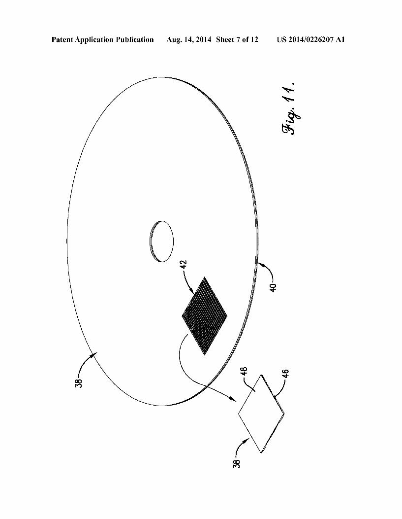
[0057] Referring to step 104, nanogaps 30 are created in the ink 50, similar to those of the base layer 24 seen in FIG. 2. The nanogaps 30 may include tears, openings, or gaps in the polymer material of the ink 50. Exemplary nanogaps 30 may have a width ranging from approximately 20 nm to approxi mately 30 nm, while the length of the nanogaps 30 may vary more greatly. The nanogaps 30 may be formed by applying a tensional force to opposing ends of the stamp 38 and the ink 50 while they are in contact with one another. The nanogaps 30 may also be formed by poking holes in the combination of the stamp 38 and the ink 50, by bending the combination of the stamp 38 and the ink 50, or by reverse bending the com bination of the stamp 38 and the ink 50. This step may be optional, it may be performed after the stamp 38 and ink 50 are removed from the temporary substrate 44, or it may be performed during or after step 105. [0058] Referring to step 105, the stamp 38 and the ink 50 are removed from the temporary substrate 44 and placed on a permanent substrate 56, as shown in FIGS. 15 and 16. The permanent substrate 56 may be similar to the temporary sub strate 44. An exemplary permanent substrate 56 is a glass slide, a silicon wafer, or the like. The stamp 38 and ink 50 may be removed from the temporary substrate 44 as a unit while still contacting one another. They may be removed manually by a technician or by an automated machine. The stamp 38 and ink 50 may be placed on the permanent substrate 56 with the second surface of the ink 50 contacting a surface of the permanent substrate 56 and the second surface of the stamp 38 facing away from the permanent substrate 56. The place ment may be performed manually or by automated machine. After the placement of the stamp 38 and ink 50, a period of time may elapse to allow the ink 50 to seal with the permanent substrate 56.
[0059] Referring to step 106, the stamp 38 is removed from the ink 50. In some embodiments, the stamp 38 may be peeled from the ink 50 by manually lifting one comer or edge of the stamp 38, as seen in FIG. 17, with a pair of tweezers. In other embodiments, the stamp 38 may be removed from the ink 50 by an automated machine. The process of removing the stamp 38 from the ink 50 may create nanogaps 30 in the stamp 38 which are transferred to the ink 50. Thus, after removing the stamp 38 from the ink 50, the ink 50 may a plurality of nanogaps 30 that are randomly oriented and generally posi tioned in proximity to the perimeter of the ink 50. Further more, after removing the stamp 38, the ?rst surface 52 of the ink 50 is exposed such that the positive of the grating pattern 42 is facing upwards. In addition, the ink 50 on the permanent substrate 56 generally forms the base layer 24 on the substrate 12 of the grating structure 10. [0060] Referring to step 107, a ?rst functional layer 26 is applied to the ink 50. The ?rst functional layer 26 is applied to the ?rst surface 52 on top of the grating pattern 42. The ?rst functional layer 26 may include plasmonic material, such as metals, or photonic material, such as dielectrics, as discussed above. The ?rst functional layer 26 may be applied to the ink
US 2014/0226207 A1
50 using known deposition techniques. The ?rst functional layer 26 may also be applied to the ink 50 by chemical procedures such as the sol-gel process in which the material of the ?rst functional layer 26 is applied to the ink 50 in a solution. In some embodiments, the material of the ?rst func tional layer 26 may deposited at an angle that is normal to the plane of the ink 50. The result of the deposition may be similar to the grating structure 10 as shown in FIGS. 1 and 3. The ?rst functional layer 26 may also be applied such that it does not ?ll in or completely cover the nanogaps 30 which are formed in the ink 50.
[0061] In other embodiments, the material of the ?rst func tional layer 26 may deposited at an angle that is not normal to the plane of the ink 50, similar to the deposition illustrated in FIG. 3. This angled deposition is typically accomplished by tilting the permanent substrate 56 and the ink 50 thereupon with respect to the source from which the ?rst functional layer 26 material is deposited. The deposition angle, i.e., the angle of tilt, may range from approximately zero degrees to approximately 85 degrees from planar normal. Furthermore, the axis of tilt for the permanent substrate 56 is generally parallel to the longitudinal axis of the grating elements 16 of the grating pattern 42 of the ink 50. The tilting of the perma nent substrate 56 and the ink 50 during deposition of the ?rst functional layer 26 may result in each grating element 16 having the features of the nanogap 32, the tip 34, the plateau 36, and the nanospurs 58, as described above and shown in FIGS. 3 and 4.
[0062] The permanent substrate 56 and the ink 50 may have an inherent surface energy or their surface energies may be controlled and adjusted. The material of the ?rst functional layer 26 may have an inherent energy level or may be given an energy level as well. In addition, the material of the ?rst functional layer 26 may be ionic in nature. Energies of the material of the ?rst functional layer 26, the permanent sub strate 56, and the ink 50 may be controlled or adjusted ther mally, through temperature control, electrically, through volt age control, or by other methods. The energy levels of one or more of the three components may determine the optimal angle for applying the material of the ?rst functional layer 26 in order to form the features of the nanogap 32, the tip 34, the plateau 36, and the nanospurs 58. The physical characteristics of the grating pattern 42 of the ink 50, such as the spacing between grating elements 1 6, the height of the peak 20, and/ or the aspect ratio of the height to the spacing may also in?uence the value of the optimal angle for applying the material of the ?rst functional layer 26. Furthermore, the thickness of the functional layer 26 may in?uence the value of the optimal angle for applying the material of the ?rst functional layer 26. As an example, for an ink 50 made from PMSSQ with a grating pattern 42 that is formed from an HD-DVD mold 40 (and has the corresponding spacings and heights) and a ?rst functional layer 26 of silver applied with a thickness of 40 nm, the optimal angle of deposition is approximately 75 degrees. [0063] In certain embodiments, the ?rst functional layer 26 may include one or more sublayers of material. For example, when forming a plasmonic ?rst functional layer 26, there may be a sublayer of metal, which enhances adhesion between the ink 50 and the ?rst functional layer 26. The sublayers may be deposited onto the ink 50 in the same fashion as the ?rst functional layer 26. [0064] Referring to step 108, a second functional layer 60 is applied to the ?rst functional layer 26, as shown in FIGS. 5 and 6. This step may be optional. However, when it is per
Aug. 14, 2014
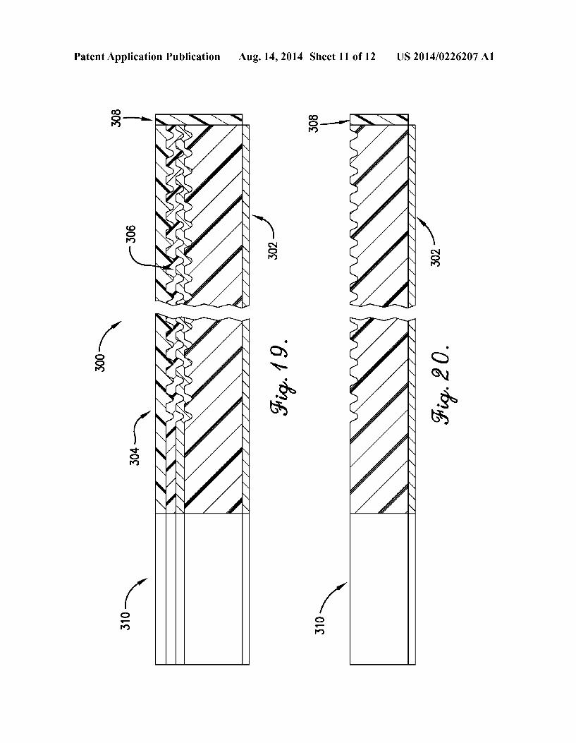
formed, the ?rst functional layer 26 typically includes pho tonic material such as titanium oxide, and the second func tional layer 60 includes plasmonic material such as silver. Furthermore, the ?rst functional layer 26 is deposited at angle of approximately zero degrees from planar normal. The sec ond functional layer 60 is typically deposited at an angle ranging from greater than zero degrees to approximately 85 degrees from planar normal. [0065] At least a portion of the steps of a method 200, in accordance with various aspects of the invention, for produc ing a mold 40 with a grating pattern 42 is shown in FIG. 18. The steps of the method 200 may be performed in the order as shown in FIG. 18, or they may be performed in a different order. Furthermore, some steps may be performed concur rently as opposed to sequentially. In addition, some steps may not be performed. [0066] Referring to step 201, an optical disc 300 is obtained, including a label side 302, a transparent side 304, and a metal layer 306, as seen in FIGS. 19 and 21. The optical disc 300 may include a perimeter ring 308 and a center ring 310 as well. The optical disc 300 may be of known optical data storage disc types with data tracks arranged in concentric circles. Exemplary optical discs 300 include 12-centimeter diameter discs, such as compact disc (CD), digital video disc (DVD), high de?nition DVD (HD-DVD), Blu-rayTM disc, and the like. Typically, the optical disc 300 is blank (with no pre-recorded data on it), single sided, and with a single data layer. The label side 302 may be what is considered the top surface of the disc, often with a manufacturer’s name or logo on it. The label side 302 may also have an opaque coating. The transparent side 304 may be considered the bottom surface of the disc, on the opposite side from the label. The label side 302 and the transparent side 304 may both include a rigid polymer material, such as polycarbonate, that gives the opti cal disc 300 its structure. During usage of the optical disc 300, a laser shines light through the transparent side 304 in order to read data from the optical disc 300. Thus, the transparent side 3 04 is transmissive to light of varying wavelengths. The metal layer 3 06 generally provides re?ection of the laser light which determines the data stored on the optical disc 300. The perim eter ring 308 is a space at the edge of the optical disc 300 in which there are no data tracks.
[0067] At the metal layer 306, there may be two grating patterns forming the data tracks, one on the label side 302 and one on the transparent side 3 04, wherein one grating pattern is a mirror image or negative of the other and the metal layer is positioned between the two patterns. Furthermore, the grating patterns may be similar to the grating pattern 42 and the array 14 of grating elements 16. [0068] Referring to step 202, a position of the metal layer 306 is determined with respect to the label side 302 and the transparent side 304. The thickness of the optical disc 300 is generally constant for the different types of discs, however the position of the metal layer 306 varies with the type. The metal layer 306 in a CD is close to the label side 302. The metal layer 306 in a DVD and an HD-DVD is positioned near the center of the optical disc 300. In a Blu-rayTM disc, the metal layer 306 is close to the transparent side 304. [0069] Referring to step 203, the optical disc 300 is split at the metal layer 306 along the plane of the disc from the outer edge at the perimeter ring 308 toward the center ring 310, if the metal layer 306 is closer to the transparent side 304 than the label side 302, as seen in FIG. 19. The optical disc 300 is likely a Blu-rayTM disc. An exemplary method to splitting the
US 2014/0226207 A1
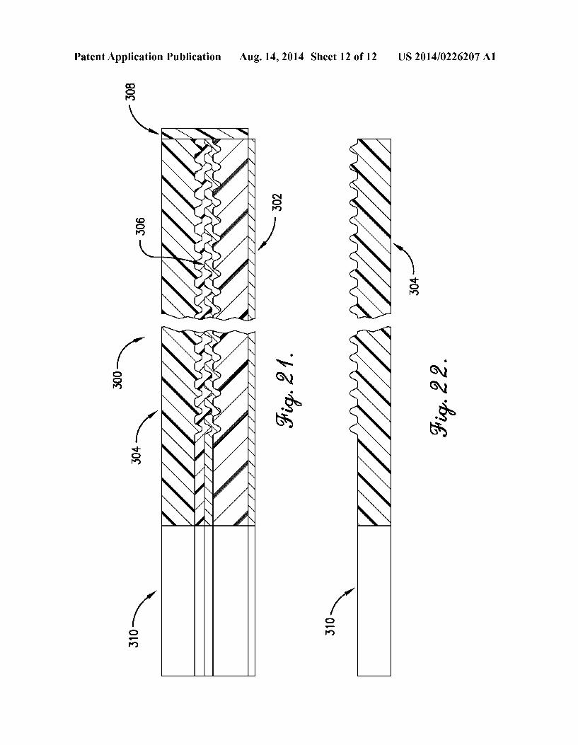
optical disc 300 includes cutting the optical disc 300 with a sharp object, such as a razor blade, at the edge of the disc parallel to its plane. The optical disc 300 usually separates into two pieces along the metal layer 306ithe two pieces being the label side 302 and the transparent side 304. [0070] Referring to step 204, the transparent side 304 and the metal layer 306 are removed from the optical disc 300. Thus, the label side 302 with a grating pattern remain, as seen in FIG. 20. In some cases, fragments of the metal layer 306 may remain as well.
[0071] Referring to step 205, the optical disc 300 is placed in a solvent to remove any remaining metal. An exemplary solvent includes 15% nitric acid. Other solvents, cleaners, and debris removal techniques may be utilized as well. [0072] Referring to step 206, the perimeter ring 308 is removed from the optical disc 300, if the metal layer 306 is not closer to the transparent side 304 than the label side 302, as seen in FIG. 21. The optical disc 300 may be a DVD or an HD-DVD. The perimeter ring 3 08 may be removed by cutting it off of the optical disc 300 using a sharp object or by grinding it off. Removal of the perimeter ring 308 may make it easier to access the metal layer 306 for performing the next step. [0073] Referring to step 207, the optical disc 300 is split at the metal layer 306 along the plane of the disc from the outer edge toward the center ring 310. As discussed in step 203, the optical disc 300 separates into two pieces, the label side 302 and the transparent side 304, along the metal layer 306. [0074] Referring to step 208, the label side 302 and the metal layer 306 are removed from the optical disc 300. Thus, the transparent side 304 with a grating pattern remain, as seen in FIG. 22. In some cases, fragments of the metal layer 306 may remain as well.
[0075] Referring to step 209, the optical disc 300 is placed in a solvent to remove any remaining metal. As with step 205, the solvent may include 15% nitric acid. Other solvents, cleaners, and debris removal techniques may be utilized as well. [0076] Although the invention has been described with ref erence to the embodiments illustrated in the attached drawing ?gures, it is noted that equivalents may be employed and substitutions made herein without departing from the scope of the invention as recited in the claims.
Having thus described various embodiments of the inven tion, what is claimed as new and desired to be protected by Letters Patent includes the following:
1. A grating structure comprising: a substrate including a smooth upper surface; a base layer positioned on the substrate, the base layer
including a ?rst surface with a plurality of grating elements posi
tioned adjacent one another, each grating element including a longitudinal peak and a longitudinal val ley, and
a second surface, opposing the ?rst surface, in contact with the upper surface of the substrate; and
a ?rst functional layer for providing electromagnetic ?eld enhancement in the vicinity of the grating structure, the functional layer positioned on the second surface of the base layer.
2. The grating structure of claim 1, wherein the ?rst func tional layer includes a longitudinal peak aligned with the peak of the base layer and a longitudinal valley aligned with the valley of the base layer.
Aug. 14, 2014
3. The grating structure of claim 1, wherein the ?rst func tional layer includes a nanogap, a plateau, and a tip, wherein the nanogap is a longitudinal valley, the tip is a longitudinal peak, and the plateau is a rounded surface extending therebe tween.
4. The grating structure of claim 3, wherein the tip includes a plurality of nano spurs abutting one another along the length thereof, wherein each nanospur includes or forms a peak.
5. The grating structure of claim 1, further comprising a second functional layer applied to an upper surface of the ?rst functional layer, such that the ?rst functional layer is formed from a dielectric and the second functional layer is formed from a metal or a metal alloy.
6. The grating structure of claim 1, wherein the ?rst func tional layer is formed from a metal or a metal alloy.
7. The grating structure of claim 1, wherein the ?rst func tional layer is formed from a dielectric.
8. A method of producing a grating structure, the method comprising the steps of:
forming a stamp from ?exible plastic material, the stamp including a negative of a periodic grating pattern on a ?rst surface;
forming an ink by applying a polymer ?lm to the stamp, the ink including a ?rst surface and an opposing second surface, wherein the ?rst surface of the ink contacts the ?rst surface of the stamp such that the ink retains a positive of the periodic grating pattern;
placing the ink and the stamp on a substrate such that the second surface of the ink contacts an upper surface of the substrate; and
removing the stamp from the ink by applying a tensional force to one edge of the stamp.
9. The method of claim 8, further comprising the step of applying a ?rst functional layer to the ?rst surface of the ink.
10. The method of claim 9, wherein the functional layer includes a metal or a metal alloy.
11. The method of claim 9, further comprising the step of applying a second functional layer to an upper surface of the ?rst functional layer.
12. The method of claim 11, wherein the ink includes a plane and the ?rst functional layer is deposited onto the ink approximately normal to the plane of the ink and the second functional layer is deposited onto the ?rst functional layer at an angle away from the plane of the ink.
13. The method of claim 9, wherein the ink includes a plane and the ?rst functional layer is deposited onto the ink at an angle away from normal to the plane of the ink.
14. The method of claim 13, wherein the angle ranges from greater than 0 degrees to approximately 85 degrees.
15. The method of claim 8, further comprising the step of applying a ?exible plastic material to a mold, which includes the grating pattern, to form the stamp.
16. The method of claim 15, wherein the mold includes an optical disc with an internal grating pattern, wherein a portion of the optical disc is removed to expose the grating pattern.
17. A method of producing a grating structure, the method comprising the steps of:
forming a stamp by applying a ?exible plastic material to a mold which includes a periodic grating pattern, wherein the stamp retains a negative of the grating pattern on a ?rst surface;
forming an ink by applying a polymer ?lm to the stamp, the ink including a ?rst surface and an opposing second surface, wherein the ?rst surface of the ink contacts the
US 2014/0226207 A1
?rst surface of the stamp such that the ink retains a positive of the periodic grating pattern;
placing the ink and the stamp on a substrate such that the second surface of the ink contacts an upper surface of the
substrate; removing the stamp from the ink by applying a tensional
force to one edge of the stamp; and applying a functional layer to the ?rst surface of the ink. 18. The method of claim 17, further comprising the step of
applying a second functional layer to an upper surface of the ?rst functional layer.
19. The method of claim 17, Wherein the ink includes a plane and the ?rst functional layer is deposited onto the ink approximately normal to the plane of the ink and the second functional layer is deposited onto the ?rst functional layer at an angle away from the plane of the ink.
20. The method of claim 17, Wherein the mold includes an optical disc With an internal grating pattern, Wherein a portion of the optical disc is removed to expose the grating pattern.
* * * * *
Aug. 14, 2014