
BQ25618/619 I2C Controlled 1-Cell 1.5-A Battery Charger ...
66
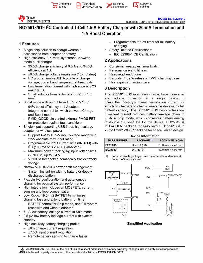
BQ25618/619 I 2 C Controlled 1-Cell 1.5-A Battery Charger with 20-mA Termination and 1-A Boost Operation 1 Features • Single chip solution to charge wearable accessories from adapter or battery • High-efficiency, 1.5-MHz, synchronous switch- mode buck charger – 95.5% charge efficiency at 0.5 A and 94.5% efficiency at 1 A – ±0.5% charge voltage regulation (10-mV step) – I 2 C programmable JEITA profile of charge voltage, current and temperature thresholds – Low termination current with high accuracy 20 mA±10 mA – Small inductor form factor of 2.5 x 2.0 x 1.0 mm 3 • Boost mode with output from 4.6 V to 5.15 V – 94% boost efficiency at 1-A output – Integrated control to switch between Charge and Boost mode – PMID_GOOD pin control external PMOS FET for protection against fault conditions • Single input supporting USB input, high-voltage adapter, or wireless power – Support 4-V to 13.5-V input voltage range with 22-V absolute max input rating – Programmable input current limit (IINDPM) with I 2 C (100 mA to 3.2 A, 100-mA/step) – Maximum power tracking by input voltage limit (VINDPM) up to 5.4 V – VINDPM threshold automatically tracks battery voltage • Narrow VDC (NVDC) power path management – System instant-on with no battery or deeply discharged battery • Flexible I 2 C configuration and autonomous charging for optimal system performance • High integration includes all MOSFETs, current sensing and loop compensation • Low R DSON 19.5-mΩ BATFET to minimize charging loss and extend battery run time – BATFET control for Ship mode, and full system reset with and without adapter • 7-µA low battery leakage current in Ship mode • 9.5-µA low battery leakage current with system standby • High accuracy battery charging profile – ±6% charge current regulation – ±7.5% input current regulation – Remote battery sensing to charge faster – Programmable top-off timer for full battery charging • Safety Related Certifications: – IEC 62368-1 CB Certification 2 Applications • Consumer wearables, smartwatch • Personal care and fitness • Headsets/headphone • Earbuds (True Wireless or TWS) charging case • Hearing aids charging case 3 Description The BQ25618/619 integrates charge, boost converter and voltage protection in a single device. It offers the industry's lowest termination current for switching chargers to charge wearable devices by full battery capacity. The BQ25618/619 best-in-class low quiescent current reduces battery leakage down to 6 uA in Ship mode, which conserves battery energy to double the shelf life for the device. BQ25619 is in 4x4 QFN package for easy layout. BQ25618 is in 2.0x2.4mm2 WCSP package for space limited design. Device Information PART NUMBER PACKAGE (1) BODY SIZE (NOM) BQ25618 DSBGA (30) 2.00 mm × 2.40 mm BQ25619 WQFN (24) 4.00 mm × 4.00 mm (1) For all available packages, see the orderable addendum at the end of the data sheet. VBUS SW SYS BAT I 2 C Bus TS Adapter Or Wireless RX QON REGN + I CHG Host Host Control Optional PMID Ear Buds SYS 3.5V-4.6V 4V – 13.5V Simplified Application BQ25618, BQ25619 SLUSDF8D – JUNE 2019 – REVISED DECEMBER 2021 An IMPORTANT NOTICE at the end of this data sheet addresses availability, warranty, changes, use in safety-critical applications, intellectual property matters and other important disclaimers. PRODUCTION DATA.
-
Upload
khangminh22 -
Category
Documents
-
view
3 -
download
0
Transcript of BQ25618/619 I2C Controlled 1-Cell 1.5-A Battery Charger ...
BQ25618/619 I2C Controlled 1-Cell 1.5-A Battery Charger with 20-mA Termination and 1-A Boost Operation
1 Features• Single chip solution to charge wearable
accessories from adapter or battery• High-efficiency, 1.5-MHz, synchronous switch-
mode buck charger– 95.5% charge efficiency at 0.5 A and 94.5%
efficiency at 1 A– ±0.5% charge voltage regulation (10-mV step)– I2C programmable JEITA profile of charge
voltage, current and temperature thresholds– Low termination current with high accuracy 20
mA±10 mA– Small inductor form factor of 2.5 x 2.0 x 1.0
mm3
• Boost mode with output from 4.6 V to 5.15 V– 94% boost efficiency at 1-A output– Integrated control to switch between Charge
and Boost mode– PMID_GOOD pin control external PMOS FET
for protection against fault conditions• Single input supporting USB input, high-voltage
adapter, or wireless power– Support 4-V to 13.5-V input voltage range with
22-V absolute max input rating– Programmable input current limit (IINDPM) with
I2C (100 mA to 3.2 A, 100-mA/step)– Maximum power tracking by input voltage limit
(VINDPM) up to 5.4 V– VINDPM threshold automatically tracks battery
voltage• Narrow VDC (NVDC) power path management
– System instant-on with no battery or deeply discharged battery
• Flexible I2C configuration and autonomous charging for optimal system performance
• High integration includes all MOSFETs, current sensing and loop compensation
• Low RDSON 19.5-mΩ BATFET to minimize charging loss and extend battery run time– BATFET control for Ship mode, and full system
reset with and without adapter• 7-µA low battery leakage current in Ship mode• 9.5-µA low battery leakage current with system
standby• High accuracy battery charging profile
– ±6% charge current regulation– ±7.5% input current regulation– Remote battery sensing to charge faster
– Programmable top-off timer for full battery charging
• Safety Related Certifications:– IEC 62368-1 CB Certification
2 Applications• Consumer wearables, smartwatch• Personal care and fitness• Headsets/headphone• Earbuds (True Wireless or TWS) charging case• Hearing aids charging case
3 DescriptionThe BQ25618/619 integrates charge, boost converter and voltage protection in a single device. It offers the industry's lowest termination current for switching chargers to charge wearable devices by full battery capacity. The BQ25618/619 best-in-class low quiescent current reduces battery leakage down to 6 uA in Ship mode, which conserves battery energy to double the shelf life for the device. BQ25619 is in 4x4 QFN package for easy layout. BQ25618 is in 2.0x2.4mm2 WCSP package for space limited design.
Device InformationPART NUMBER PACKAGE(1) BODY SIZE (NOM)
BQ25618 DSBGA (30) 2.00 mm × 2.40 mm
BQ25619 WQFN (24) 4.00 mm × 4.00 mm
(1) For all available packages, see the orderable addendum at the end of the data sheet.
VBUSSW
SYS
BAT
I2C Bus
TS
Adapter
Or
Wireless RX
QON
REGN+
ICHG
Host Host Control
Optional
PMIDEar
Buds
SYS 3.5V-4.6V4V ± 13.5V
Simplified Application
BQ25618, BQ25619SLUSDF8D – JUNE 2019 – REVISED DECEMBER 2021
An IMPORTANT NOTICE at the end of this data sheet addresses availability, warranty, changes, use in safety-critical applications, intellectual property matters and other important disclaimers. PRODUCTION DATA.
Table of Contents1 Features............................................................................12 Applications..................................................................... 13 Description.......................................................................14 Revision History.............................................................. 25 Description (continued).................................................. 36 Pin Configuration and Functions...................................47 Specifications.................................................................. 7
7.1 Absolute Maximum Ratings........................................ 77.2 ESD Ratings............................................................... 77.3 Recommended Operating Conditions.........................77.4 Thermal Information....................................................87.5 Thermal Information....................................................87.6 Electrical Characteristics.............................................87.7 Timing Requirements................................................137.8 Typical Characteristics.............................................. 14
8 Detailed Description......................................................168.1 Overview................................................................... 168.2 Functional Block Diagram......................................... 168.3 Feature Description...................................................17
8.4 Device Functional Modes..........................................318.5 Register Maps...........................................................32
9 Application and Implementation.................................. 469.1 Application Information............................................. 469.2 Typical Application.................................................... 46
10 Power Supply Recommendations..............................5011 Layout...........................................................................51
11.1 Layout Guidelines................................................... 5111.2 Layout Example...................................................... 51
12 Device and Documentation Support..........................5312.1 Device Support....................................................... 5312.2 Documentation Support.......................................... 5312.3 Receiving Notification of Documentation Updates..5312.4 Support Resources................................................. 5312.5 Trademarks.............................................................5312.6 Electrostatic Discharge Caution..............................5312.7 Glossary..................................................................53
13 Mechanical, Packaging, and Orderable Information.................................................................... 54
4 Revision HistoryNOTE: Page numbers for previous revisions may differ from page numbers in the current version.
Changes from Revision C (June 2021) to Revision D (December 2021) Page• Deleted tSU_STA, tHD_DAT, trDA, and tfDA from Timing Requirements.................................................................. 13
Changes from Revision B (September 2019) to Revision C (June 2021) Page• Added Safety Related Certifications: IEC 62368-1 CB Certification...................................................................1• Changed REG2 ICHG[5:0] 111100: 1430 mA to 111110: 1430 mA and 111100: 1500 mA to 111111: 1500 mA...
32
Changes from Revision A (July 2019) to Revision B (September 2019) Page• Added BQ25618................................................................................................................................................. 1
Changes from Revision * (June 2019) to Revision A (July 2019) Page• Changed from Advance Information to Production Data ................................................................................... 1
BQ25618, BQ25619SLUSDF8D – JUNE 2019 – REVISED DECEMBER 2021 www.ti.com
2 Submit Document Feedback Copyright © 2021 Texas Instruments Incorporated
Product Folder Links: BQ25618 BQ25619
5 Description (continued)The BQ25619/618 is a highly integrated 1.5-A switch-mode battery charge management and system power path management device for Li-ion and Li-polymer battery. It features fast charging with high input voltage support for a wide range of applications including wearables, and earphone charging case. Its low impedance power path optimizes switch-mode operation efficiency, reduces battery charging time, and extends battery run time during discharging phase. Its input voltage and current regulation, low termination current, and battery remote sensing deliver maximum charging power to the battery. The solution is highly integrated with input reverse-blocking FET (RBFET, Q1), high-side switching FET (HSFET, Q2), low-side switching FET (LSFET, Q3), and battery FET (BATFET, Q4) between system and battery. It also integrates the bootstrap diode for the high-side gate drive for simplified system design. The I2C serial interface with charging and system settings makes the device a truly flexible solution.
The device supports a wide range of input sources, including standard USB host port, USB charging port, USB compliant high voltage adapter and wireless power. It is compliant with USB 2.0 and USB 3.0 power spec with input current and voltage regulation. The device takes the result from the detection circuit in the system, such as USB PHY device.
The device integrates the buck charger and boost regulator into one solution with single inductor. The Boost mode supplies 5 V (adjustable 4.6 V/4.75 V/5 V/5.15 V) on PMID pin. Boost mode is used to save BOM and charge another battery by control of PMID_GOOD. The PMID_GOOD pin is used to drive the external PMOS FET to disconnect boost output PMID from the attached accessories.
The power path management regulates the system slightly above battery voltage but does not drop below 3.5-V minimum system voltage (programmable) with adapter applied. With this feature, the system maintains operation even when the battery is completely depleted or removed. When the input current limit or voltage limit is reached, the power path management automatically reduces the charge current. As the system load continues to increase, the battery starts to discharge the battery until the system power requirement is met. This supplement mode prevents overloading the input source.
The device initiates and completes a charging cycle without software control. It senses the battery voltage and charges the battery in three phases: pre-conditioning, constant current and constant voltage. At the end of the charging cycle, the charger automatically terminates when the charge current is below a preset limit and the battery voltage is higher than the recharge threshold. If the fully charged battery falls below the recharge threshold, the charger automatically starts another charging cycle.
The charger provides various safety features for battery charging and system operations, including battery negative temperature coefficient thermistor monitoring, charging safety timer and overvoltage and overcurrent protections. Thermal regulation reduces charge current when the junction temperature exceeds 110°C. The status register reports the charging status and any fault conditions. With I2C, the VBUS_GD bit indicates if a good power source is present, and the INT output immediately notifies host when a fault occurs.
The device also provides the QON pin for BATFET enable and reset control to exit low power Ship mode or full system reset function.
The BQ25619 device is available in 24-pin, 4 mm × 4 mm x 0.75 mm thin WQFN package and BQ25618 is available in 30-ball, 2.0 mm × 2.4 mm WCSP package.
www.ti.comBQ25618, BQ25619
SLUSDF8D – JUNE 2019 – REVISED DECEMBER 2021
Copyright © 2021 Texas Instruments Incorporated Submit Document Feedback 3
Product Folder Links: BQ25618 BQ25619

6 Pin Configuration and Functions
VAC
NC
PSEL
PMID_
GOOD/QON
VBUS
VBUS
REGN
TS
SDA
PMID
PMID
BTST
SYS
/CE
SW
SW
SYS
SYS
GND
GND
BAT
BAT
BAT STAT
/INTBATSNSSYSBAT SCL
A
1 2 3 4 5
B
C
D
E
F
Figure 6-1. BQ25618 YFF Package 30-Pin WCSP Top View
BQ25619
1
2
3
4
5
6
15
14
13
16
17
23 22 21 20 19
7 8 9 10 11 12
18
24
VAC
PSEL
PMID_GOOD
STAT
SCL
SDA
/INT
NC
/CE
BATSNS
TS
/QON
BAT
BAT
SYS
SYS
PGND
PGND
VBUS
PMID
REGN
BTST
SW
SW
Figure 6-2. BQ25619 RTW Package 24-Pin WQFN Top View
BQ25618, BQ25619SLUSDF8D – JUNE 2019 – REVISED DECEMBER 2021 www.ti.com
4 Submit Document Feedback Copyright © 2021 Texas Instruments Incorporated
Product Folder Links: BQ25618 BQ25619
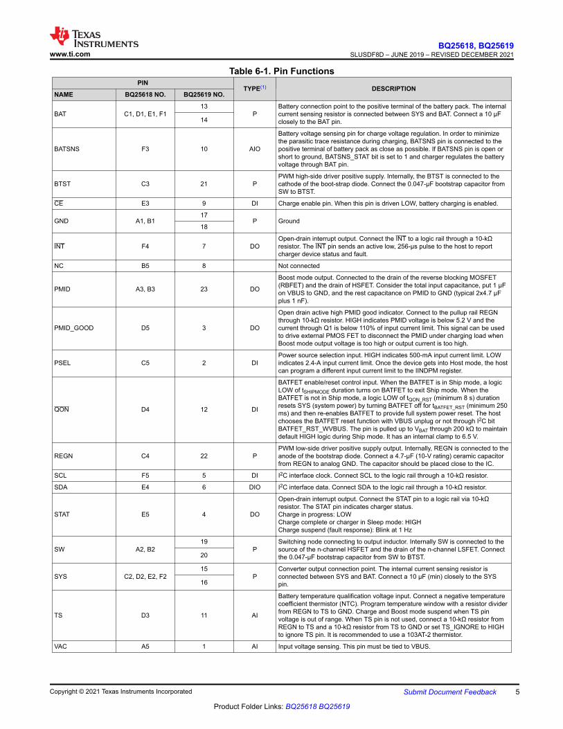
Table 6-1. Pin FunctionsPIN
TYPE(1) DESCRIPTIONNAME BQ25618 NO. BQ25619 NO.
BAT C1, D1, E1, F113
PBattery connection point to the positive terminal of the battery pack. The internal current sensing resistor is connected between SYS and BAT. Connect a 10 µF closely to the BAT pin.14
BATSNS F3 10 AIO
Battery voltage sensing pin for charge voltage regulation. In order to minimize the parasitic trace resistance during charging, BATSNS pin is connected to the positive terminal of battery pack as close as possible. If BATSNS pin is open or short to ground, BATSNS_STAT bit is set to 1 and charger regulates the battery voltage through BAT pin.
BTST C3 21 PPWM high-side driver positive supply. Internally, the BTST is connected to the cathode of the boot-strap diode. Connect the 0.047-μF bootstrap capacitor from SW to BTST.
CE E3 9 DI Charge enable pin. When this pin is driven LOW, battery charging is enabled.
GND A1, B117
P Ground18
INT F4 7 DOOpen-drain interrupt output. Connect the INT to a logic rail through a 10-kΩ resistor. The INT pin sends an active low, 256-µs pulse to the host to report charger device status and fault.
NC B5 8 Not connected
PMID A3, B3 23 DO
Boost mode output. Connected to the drain of the reverse blocking MOSFET (RBFET) and the drain of HSFET. Consider the total input capacitance, put 1 μF on VBUS to GND, and the rest capacitance on PMID to GND (typical 2x4.7 μF plus 1 nF).
PMID_GOOD D5 3 DO
Open drain active high PMID good indicator. Connect to the pullup rail REGN through 10-kΩ resistor. HIGH indicates PMID voltage is below 5.2 V and the current through Q1 is below 110% of input current limit. This signal can be used to drive external PMOS FET to disconnect the PMID under charging load when Boost mode output voltage is too high or output current is too high.
PSEL C5 2 DIPower source selection input. HIGH indicates 500-mA input current limit. LOW indicates 2.4-A input current limit. Once the device gets into Host mode, the host can program a different input current limit to the IINDPM register.
QON D4 12 DI
BATFET enable/reset control input. When the BATFET is in Ship mode, a logic LOW of tSHIPMODE duration turns on BATFET to exit Ship mode. When the BATFET is not in Ship mode, a logic LOW of tQON_RST (minimum 8 s) duration resets SYS (system power) by turning BATFET off for tBATFET_RST (minimum 250 ms) and then re-enables BATFET to provide full system power reset. The host chooses the BATFET reset function with VBUS unplug or not through I2C bit BATFET_RST_WVBUS. The pin is pulled up to VBAT through 200 kΩ to maintain default HIGH logic during Ship mode. It has an internal clamp to 6.5 V.
REGN C4 22 PPWM low-side driver positive supply output. Internally, REGN is connected to the anode of the bootstrap diode. Connect a 4.7-μF (10-V rating) ceramic capacitor from REGN to analog GND. The capacitor should be placed close to the IC.
SCL F5 5 DI I2C interface clock. Connect SCL to the logic rail through a 10-kΩ resistor.
SDA E4 6 DIO I2C interface data. Connect SDA to the logic rail through a 10-kΩ resistor.
STAT E5 4 DO
Open-drain interrupt output. Connect the STAT pin to a logic rail via 10-kΩ resistor. The STAT pin indicates charger status.Charge in progress: LOWCharge complete or charger in Sleep mode: HIGHCharge suspend (fault response): Blink at 1 Hz
SW A2, B219
PSwitching node connecting to output inductor. Internally SW is connected to the source of the n-channel HSFET and the drain of the n-channel LSFET. Connect the 0.047-μF bootstrap capacitor from SW to BTST.20
SYS C2, D2, E2, F215
PConverter output connection point. The internal current sensing resistor is connected between SYS and BAT. Connect a 10 µF (min) closely to the SYS pin.16
TS D3 11 AI
Battery temperature qualification voltage input. Connect a negative temperature coefficient thermistor (NTC). Program temperature window with a resistor divider from REGN to TS to GND. Charge and Boost mode suspend when TS pin voltage is out of range. When TS pin is not used, connect a 10-kΩ resistor from REGN to TS and a 10-kΩ resistor from TS to GND or set TS_IGNORE to HIGH to ignore TS pin. It is recommended to use a 103AT-2 thermistor.
VAC A5 1 AI Input voltage sensing. This pin must be tied to VBUS.
www.ti.comBQ25618, BQ25619
SLUSDF8D – JUNE 2019 – REVISED DECEMBER 2021
Copyright © 2021 Texas Instruments Incorporated Submit Document Feedback 5
Product Folder Links: BQ25618 BQ25619
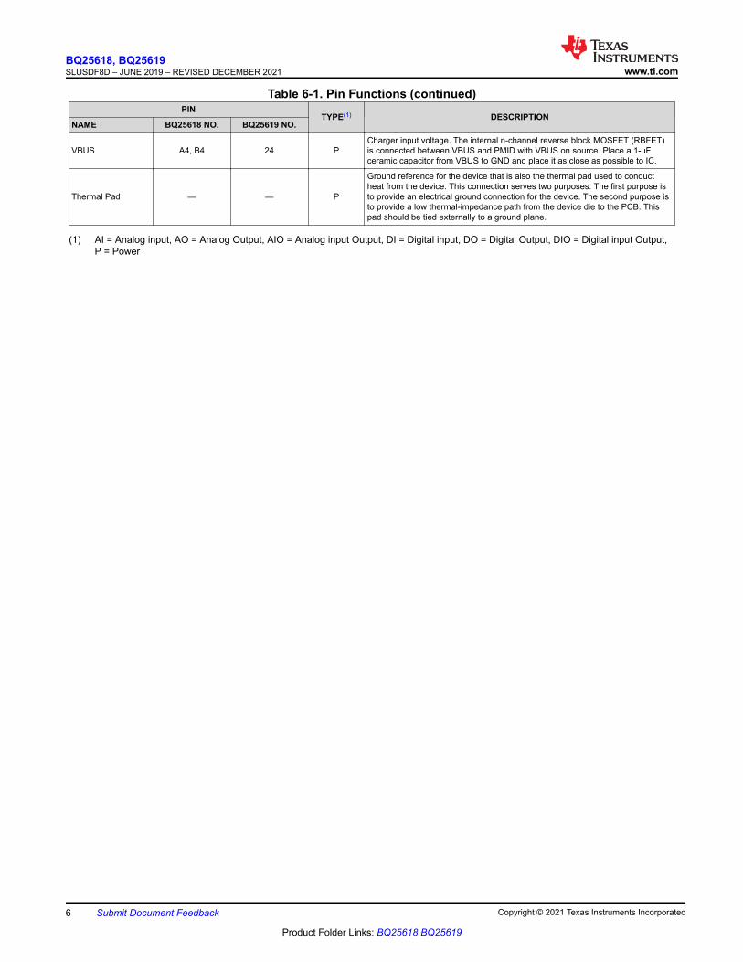
Table 6-1. Pin Functions (continued)PIN
TYPE(1) DESCRIPTIONNAME BQ25618 NO. BQ25619 NO.
VBUS A4, B4 24 PCharger input voltage. The internal n-channel reverse block MOSFET (RBFET) is connected between VBUS and PMID with VBUS on source. Place a 1-uF ceramic capacitor from VBUS to GND and place it as close as possible to IC.
Thermal Pad — — P
Ground reference for the device that is also the thermal pad used to conduct heat from the device. This connection serves two purposes. The first purpose is to provide an electrical ground connection for the device. The second purpose is to provide a low thermal-impedance path from the device die to the PCB. This pad should be tied externally to a ground plane.
(1) AI = Analog input, AO = Analog Output, AIO = Analog input Output, DI = Digital input, DO = Digital Output, DIO = Digital input Output, P = Power
BQ25618, BQ25619SLUSDF8D – JUNE 2019 – REVISED DECEMBER 2021 www.ti.com
6 Submit Document Feedback Copyright © 2021 Texas Instruments Incorporated
Product Folder Links: BQ25618 BQ25619

7 Specifications7.1 Absolute Maximum Ratingsover operating free-air temperature range (unless otherwise noted)(1)
MIN MAX UNITVoltage VAC (converter not switching) –2 22 V
Voltage VBUS (converter not switching) -2 22 V
Voltage PMID (converter not switching) –0.3 22 V
Voltage SW –0.3 16 V
Voltage BAT, SYS (converter not switching) –0.3 17 V
Voltage BTST –0.3 22 V
Voltage BATSNS (converter not switching) –0.3 7 V
Voltage PSEL, STAT, SCL, SDA, INT, PMID_GOOD, CE, TS, QON –0.3 7 V
Output Sink Current SDA, STAT, INT, PMID_GOOD 6 mA
TJ Junction temperature –40 150 °C
Tstg Storage temperature –55 150 °C
(1) Stresses beyond those listed under Absolute Maximum Rating may cause permanent damage to the device. These are stress ratings only, which do not imply functional operation of the device at these or any other conditions beyond those indicated under Recommended Operating Condition. Exposure to absolute-maximum-rated conditions for extended periods may affect device reliability.
7.2 ESD RatingsVALUE UNIT
V(ESD) Electrostatic dischargeHuman body model (HBM), per ANSI/ESDA/JEDEC JS-001, all pins(1) ±2000
VCharged device model (CDM), per JEDEC specification JESD22-C101, all pins(2) ±250
(1) JEDEC document JEP155 states that 500-V HBM allows safe manufacturing with a standard ESD control process. (2) JEDEC document JEP157 states that 250-V CDM allows safe manufacturing with a standard ESD control process.
7.3 Recommended Operating Conditionsover operating free-air temperature range (unless otherwise noted)
MIN NOM MAX UNITVVBUS Input voltage 4 13.5 V
VBAT Battery voltage 4.52 V
IVBUS Input current 3.2 A
ISW Output current (SW) 1.8 A
IBAT Fast charging current 1.5 A
IBAT RMS discharge current 5 A
TA Ambient temperature –40 85 °C
L Inductance 1 2.2 µH
CVBUS VBUS capacitance 1 µF
CPMID PMID capacitance 10 µF
CSYS SYS capacitance 10 µF
CBAT BAT capacitance 10 µF
CREGN REGN capacitance 4.7 µF
www.ti.comBQ25618, BQ25619
SLUSDF8D – JUNE 2019 – REVISED DECEMBER 2021
Copyright © 2021 Texas Instruments Incorporated Submit Document Feedback 7
Product Folder Links: BQ25618 BQ25619
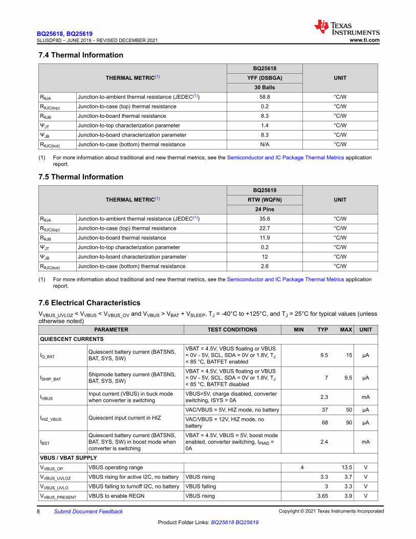
7.4 Thermal Information
THERMAL METRIC(1)
BQ25618UNITYFF (DSBGA)
30 BallsRθJA Junction-to-ambient thermal resistance (JEDEC(1)) 58.8 °C/W
RθJC(top) Junction-to-case (top) thermal resistance 0.2 °C/W
RθJB Junction-to-board thermal resistance 8.3 °C/W
ΨJT Junction-to-top characterization parameter 1.4 °C/W
ΨJB Junction-to-board characterization parameter 8.3 °C/W
RθJC(bot) Junction-to-case (bottom) thermal resistance N/A °C/W
(1) For more information about traditional and new thermal metrics, see the Semiconductor and IC Package Thermal Metrics application report.
7.5 Thermal Information
THERMAL METRIC(1)
BQ25619UNITRTW (WQFN)
24 PinsRθJA Junction-to-ambient thermal resistance (JEDEC(1)) 35.6 °C/W
RθJC(top) Junction-to-case (top) thermal resistance 22.7 °C/W
RθJB Junction-to-board thermal resistance 11.9 °C/W
ΨJT Junction-to-top characterization parameter 0.2 °C/W
ΨJB Junction-to-board characterization parameter 12 °C/W
RθJC(bot) Junction-to-case (bottom) thermal resistance 2.6 °C/W
(1) For more information about traditional and new thermal metrics, see the Semiconductor and IC Package Thermal Metrics application report.
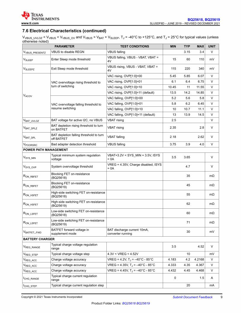
7.6 Electrical CharacteristicsVVBUS_UVLOZ < VVBUS < VVBUS_OV and VVBUS > VBAT + VSLEEP, TJ = -40°C to +125°C, and TJ = 25°C for typical values (unless otherwise noted)
PARAMETER TEST CONDITIONS MIN TYP MAX UNITQUIESCENT CURRENTS
IQ_BAT Quiescent battery current (BATSNS, BAT, SYS, SW)
VBAT = 4.5V, VBUS floating or VBUS = 0V - 5V, SCL, SDA = 0V or 1.8V, TJ < 85 °C, BATFET enabled
9.5 15 µA
ISHIP_BAT Shipmode battery current (BATSNS, BAT, SYS, SW)
VBAT = 4.5V, VBUS floating or VBUS = 0V - 5V, SCL, SDA = 0V or 1.8V, TJ < 85 °C, BATFET disabled
7 9.5 µA
IVBUSInput current (VBUS) in buck mode when converter is switching
VBUS=5V, charge disabled, converter switching, ISYS = 0A 2.3 mA
IHIZ_VBUS Quiescent input current in HIZVAC/VBUS = 5V, HIZ mode, no battery 37 50 µA
VAC/VBUS = 12V, HIZ mode, no battery 68 90 µA
IBST
Quiescent battery current (BATSNS, BAT, SYS, SW) in boost mode when converter is switching
VBAT = 4.5V, VBUS = 5V, boost mode enabled, converter switching, IPMID = 0A
2.4 mA
VBUS / VBAT SUPPLYVVBUS_OP VBUS operating range 4 13.5 V
VVBUS_UVLOZ VBUS rising for active I2C, no battery VBUS rising 3.3 3.7 V
VVBUS_UVLO VBUS falling to turnoff I2C, no battery VBUS falling 3 3.3 V
VVBUS_PRESENT VBUS to enable REGN VBUS rising 3.65 3.9 V
BQ25618, BQ25619SLUSDF8D – JUNE 2019 – REVISED DECEMBER 2021 www.ti.com
8 Submit Document Feedback Copyright © 2021 Texas Instruments Incorporated
Product Folder Links: BQ25618 BQ25619
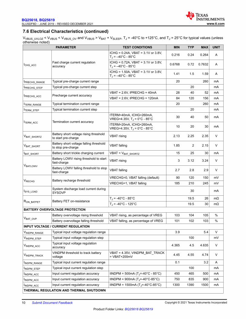
7.6 Electrical Characteristics (continued)VVBUS_UVLOZ < VVBUS < VVBUS_OV and VVBUS > VBAT + VSLEEP, TJ = -40°C to +125°C, and TJ = 25°C for typical values (unless otherwise noted)
PARAMETER TEST CONDITIONS MIN TYP MAX UNITVVBUS_PRESENTZ VBUS to disable REGN VBUS falling 3.15 3.4 V
VSLEEP Enter Sleep mode threshold VBUS falling, VBUS - VBAT, VBAT = 4V 15 60 110 mV
VSLEEPZ Exit Sleep mode threshold VBUS rising, VBUS - VBAT, VBAT = 4V 115 220 340 mV
VACOV
VAC overvoltage rising threshold to turn of switching
VAC rising, OVP[1:0]=00 5.45 5.85 6.07 V
VAC rising, OVP[1:0]=01 6.1 6.4 6.75 V
VAC rising, OVP[1:0]=10 10.45 11 11.55 V
VAC rising, OVP[1:0]=11 (default) 13.5 14.2 14.85 V
VAC overvoltage falling threshold to resume switching
VAC falling, OVP[1:0]=00 5.2 5.6 5.8 V
VAC falling, OVP[1:0]=01 5.8 6.2 6.45 V
VAC falling, OVP[1:0]=10 10 10.7 11.1 V
VAC falling, OVP[1:0]=11 (default) 13 13.9 14.5 V
VBAT_UVLOZ BAT voltage for active I2C, no VBUS VBAT rising 2.5 V
VBAT_DPLZBAT depletion rising threshold to turn on BATFET VBAT rising 2.35 2.8 V
VBAT_DPLBAT depletion falling threshold to turn off BATFET VBAT falling 2.18 2.62 V
VPOORSRC Bad adapter detection threshold VBUS falling 3.75 3.9 4.0 V
POWER PATH MANAGEMENT
VSYS_MINTypical minimum system regulation voltage
VBAT=3.2V < SYS_MIN = 3.5V, ISYS = 0A 3.5 3.65 V
VSYS_OVP System overvoltage threshold VREG = 4.35V, Charge disabled, ISYS = 0A 4.7 V
RON_RBFETBlocking FET on-resistance (BQ25618) 35 mΩ
RON_RBFETBlocking FET on-resistance (BQ25619) 45 mΩ
RON_HSFETHigh-side switching FET on-resistance (BQ25618) 55 mΩ
RON_HSFETHigh-side switching FET on-resistance (BQ25619) 62 mΩ
RON_LSFETLow-side switching FET on-resistance (BQ25618) 60 mΩ
RON_LSFETLow-side switching FET on-resistance (BQ25619) 71 mΩ
VBATFET_FWDBATFET forward voltage in supplement mode
BAT discharge current 10mA, converter running 30 mV
BATTERY CHARGER
VREG_RANGETypical charge voltage regulation range 3.5 4.52 V
VREG_STEP Typical charge voltage step 4.3V < VREG < 4.52V 10 mV
VREG_ACC Charge voltage accuracy VREG = 4.2V, TJ = –40°C - 85°C 4.183 4.2 4.2168 V
VREG_ACC Charge voltage accuracy VREG = 4.35V, TJ = –40°C - 85°C 4.333 4.35 4.367 V
VREG_ACC Charge voltage accuracy VREG = 4.45V, TJ = –40°C - 85°C 4.432 4.45 4.468 V
ICHG_RANGE Typical charge current regulation range 0 1.5 A
ICHG_STEP Typical charge current regulation step 20 mA
www.ti.comBQ25618, BQ25619
SLUSDF8D – JUNE 2019 – REVISED DECEMBER 2021
Copyright © 2021 Texas Instruments Incorporated Submit Document Feedback 9
Product Folder Links: BQ25618 BQ25619
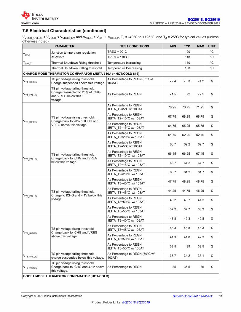
7.6 Electrical Characteristics (continued)VVBUS_UVLOZ < VVBUS < VVBUS_OV and VVBUS > VBAT + VSLEEP, TJ = -40°C to +125°C, and TJ = 25°C for typical values (unless otherwise noted)
PARAMETER TEST CONDITIONS MIN TYP MAX UNIT
ICHG_ACC Fast charge current regulation accuracy
ICHG = 0.24A, VBAT = 3.1V or 3.8V, TJ = –40°C - 85°C 0.216 0.24 0.264 A
ICHG = 0.72A, VBAT = 3.1V or 3.8V, TJ = –40°C - 85°C 0.6768 0.72 0.7632 A
ICHG = 1.50A, VBAT = 3.1V or 3.8V, TJ = –40°C - 85°C 1.41 1.5 1.59 A
IPRECHG_RANGE Typical pre-charge current range 20 260 mA
IPRECHG_STEP Typical pre-charge current step 20 mA
IPRECHG_ACC Precharge current accuracyVBAT = 2.6V, IPRECHG = 40mA 28 40 52 mA
VBAT = 2.6V, IPRECHG = 120mA 84 120 156 mA
ITERM_RANGE Typical termination current range 20 260 mA
ITERM_STEP Typical termination current step 20 mA
ITERM_ACC Termination current accuracy
ITERM=40mA, ICHG>260mA, VREG=4.35V, TJ = 0°C - 85°C 30 40 50 mA
ITERM=20mA, ICHG<260mA, VREG=4.35V, TJ = 0°C - 85°C 10 20 30 mA
VBAT_SHORTZBattery short voltage rising threshold to start pre-charge VBAT rising 2.13 2.25 2.35 V
VBAT_SHORTBattery short voltage falling threshold to stop pre-charge VBAT falling 1.85 2 2.15 V
IBAT_SHORT Battery short trickle charging current VBAT < VBAT_SHORTZ 15 25 30 mA
VBATLOWV
Battery LOWV rising threshold to start fast-charge VBAT rising 3 3.12 3.24 V
Battery LOWV falling threshold to stop fast-charge VBAT falling 2.7 2.8 2.9 V
VRECHG Battery recharge thresholdVRECHG=0, VBAT falling (default) 90 120 150 mV
VRECHG=1, VBAT falling 185 210 245 mV
ISYS_LOADSystem discharge load current during SYSOVP 30 mA
RON_BATFET Battery FET on-resistanceTJ = -40°C - 85°C 19.5 26 mΩ
TJ = -40°C - 125°C 19.5 30 mΩ
BATTERY OVERVOLTAGE PROTECTION
VBAT_OVPBattery overvoltage rising threshold VBAT rising, as percentage of VREG 103 104 105 %
Battery overvoltage falling threshold VBAT falling, as percentage of VREG 101 102 103 %
INPUT VOLTAGE / CURRENT REGULATIONVINDPM_RANGE Typical input voltage regulation range 3.9 5.4 V
VINDPM_STEP Typical input voltage regulation step 100 mV
VINDPM_ACC Typical input voltage regulation accuracy 4.365 4.5 4.635 V
VINDPM_TRACK VINDPM threshold to track battery voltage
VBAT = 4.35V, VINDPM_BAT_TRACK = VBAT+200mV 4.45 4.55 4.74 V
IINDPM_RANGE Typical input current regulation range 0.1 3.2 A
IINDPM_STEP Typical input current regulation step 100 mA
IINDPM_ACC Input current regulation accuracy IINDPM = 500mA (TJ=-40°C - 85°C) 450 465 500 mA
IINDPM_ACC Input current regulation accuracy IINDPM = 900mA (TJ=-40°C-85°C) 750 835 900 mA
IINDPM_ACC Input current regulation accuracy IINDPM = 1500mA (TJ=-40°C-85°C) 1300 1390 1500 mA
THERMAL REGULATION AND THERMAL SHUTDOWN
BQ25618, BQ25619SLUSDF8D – JUNE 2019 – REVISED DECEMBER 2021 www.ti.com
10 Submit Document Feedback Copyright © 2021 Texas Instruments Incorporated
Product Folder Links: BQ25618 BQ25619
7.6 Electrical Characteristics (continued)VVBUS_UVLOZ < VVBUS < VVBUS_OV and VVBUS > VBAT + VSLEEP, TJ = -40°C to +125°C, and TJ = 25°C for typical values (unless otherwise noted)
PARAMETER TEST CONDITIONS MIN TYP MAX UNIT
TREGJunction temperature regulation accuracy
TREG = 90°C 90 °C
TREG = 110°C 110 °C
TSHUT Thermal Shutdown Rising threshold Temperature Increasing 150 °C
Thermal Shutdown Falling threshold Temperature Decreasing 130 °C
CHARGE MODE THERMISTOR COMPARATOR (JEITA 616J or HOT/COLD 616)
VT1_RISE%TS pin voltage rising threshold, Charge suspended above this voltage.
As Percentage to REGN (0°C w/ 103AT) 72.4 73.3 74.2 %
VT1_FALL%
TS pin voltage falling threshold. Charge re-enabled to 20% of ICHG and VREG below thisvoltage.
As Percentage to REGN 71.5 72 72.5 %
VT2_RISE%
TS pin voltage rising threshold, Charge back to 20% of ICHG and VREG above this voltage.
As Percentage to REGN, JEITA_T2=5°C w/ 103AT 70.25 70.75 71.25 %
As Percentage to REGN, JEITA_T2=10°C w/ 103AT 67.75 68.25 68.75 %
As Percentage to REGN, JEITA_T2=15°C w/ 103AT 64.75 65.25 65.75 %
As Percentage to REGN, JEITA_T2=20°C w/ 103AT 61.75 62.25 62.75 %
VT2_FALL%
TS pin voltage falling threshold. Charge back to ICHG and VREG below this voltage.
As Percentage to REGN, JEITA_T2=5°C w/ 103AT 68.7 69.2 69.7 %
As Percentage to REGN, JEITA_T2=10°C w/ 103AT 66.45 66.95 67.45 %
As Percentage to REGN, JEITA_T2=15°C w/ 103AT 63.7 64.2 64.7 %
As Percentage to REGN, JEITA_T2=20°C w/ 103AT 60.7 61.2 61.7 %
VT3_FALL%
TS pin voltage falling threshold. Charge to ICHG and 4.1V below this voltage.
As Percentage to REGN, JEITA_T3=40°C w/ 103AT 47.75 48.25 48.75 %
As Percentage to REGN, JEITA_T3=45°C w/ 103AT 44.25 44.75 45.25 %
As Percentage to REGN, JEITA_T3=50°C w/ 103AT 40.2 40.7 41.2 %
As Percentage to REGN, JEITA_T3=55°C w/ 103AT 37.2 37.7 38.2 %
VT3_RISE%
TS pin voltage rising threshold. Charge back to ICHG and VREG above this voltage.
As Percentage to REGN, JEITA_T3=40°C w/ 103AT 48.8 49.3 49.8 %
As Percentage to REGN, JEITA_T3=45°C w/ 103AT 45.3 45.8 46.3 %
As Percentage to REGN, JEITA_T3=50°C w/ 103AT 41.3 41.8 42.3 %
As Percentage to REGN, JEITA_T3=55°C w/ 103AT 38.5 39 39.5 %
VT5_FALL%TS pin voltage falling threshold, charge suspended below this voltage.
As Percentage to REGN (60°C w/ 103AT) 33.7 34.2 35.1 %
VT5_RISE%
TS pin voltage rising threshold. Charge back to ICHG and 4.1V above this voltage.
As Percentage to REGN 35 35.5 36 %
BOOST MODE THERMISTOR COMPARATOR (HOT/COLD)
www.ti.comBQ25618, BQ25619
SLUSDF8D – JUNE 2019 – REVISED DECEMBER 2021
Copyright © 2021 Texas Instruments Incorporated Submit Document Feedback 11
Product Folder Links: BQ25618 BQ25619
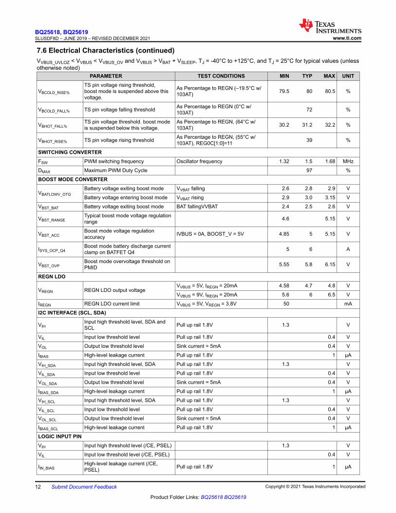
7.6 Electrical Characteristics (continued)VVBUS_UVLOZ < VVBUS < VVBUS_OV and VVBUS > VBAT + VSLEEP, TJ = -40°C to +125°C, and TJ = 25°C for typical values (unless otherwise noted)
PARAMETER TEST CONDITIONS MIN TYP MAX UNIT
VBCOLD_RISE%
TS pin voltage rising threshold, boost mode is suspended above this voltage.
As Percentage to REGN (–19.5°C w/ 103AT) 79.5 80 80.5 %
VBCOLD_FALL% TS pin voltage falling threshold As Percentage to REGN (0°C w/ 103AT) 72 %
VBHOT_FALL%TS pin voltage threshold. boost mode is suspended below this voltage.
As Percentage to REGN, (64°C w/ 103AT) 30.2 31.2 32.2 %
VBHOT_RISE% TS pin voltage rising threshold As Percentage to REGN, (55°C w/ 103AT), REG0C[1:0]=11 39 %
SWITCHING CONVERTERFSW PWM switching frequency Oscillator frequency 1.32 1.5 1.68 MHz
DMAX Maximum PWM Duty Cycle 97 %
BOOST MODE CONVERTER
VBATLOWV_OTGBattery voltage exiting boost mode VVBAT falling 2.6 2.8 2.9 V
Battery voltage entering boost mode VVBAT rising 2.9 3.0 3.15 V
VBST_BAT Battery voltage exiting boost mode BAT fallingVVBAT 2.4 2.5 2.6 V
VBST_RANGETypical boost mode voltage regulation range 4.6 5.15 V
VBST_ACCBoost mode voltage regulation accuracy IVBUS = 0A, BOOST_V = 5V 4.85 5 5.15 V
ISYS_OCP_Q4Boost mode battery discharge current clamp on BATFET Q4 5 6 A
VBST_OVPBoost mode overvoltage threshold on PMID 5.55 5.8 6.15 V
REGN LDO
VREGN REGN LDO output voltageVVBUS = 5V, IREGN = 20mA 4.58 4.7 4.8 V
VVBUS = 9V, IREGN = 20mA 5.6 6 6.5 V
IREGN REGN LDO current limit VVBUS = 5V, VREGN = 3.8V 50 mA
I2C INTERFACE (SCL, SDA)
VIHInput high threshold level, SDA and SCL Pull up rail 1.8V 1.3 V
VIL Input low threshold level Pull up rail 1.8V 0.4 V
VOL Output low threshold level Sink current = 5mA 0.4 V
IBIAS High-level leakage current Pull up rail 1.8V 1 µA
VIH_SDA Input high threshold level, SDA Pull up rail 1.8V 1.3 V
VIL_SDA Input low threshold level Pull up rail 1.8V 0.4 V
VOL_SDA Output low threshold level Sink current = 5mA 0.4 V
IBIAS_SDA High-level leakage current Pull up rail 1.8V 1 µA
VIH_SCL Input high threshold level, SDA Pull up rail 1.8V 1.3 V
VIL_SCL Input low threshold level Pull up rail 1.8V 0.4 V
VOL_SCL Output low threshold level Sink current = 5mA 0.4 V
IBIAS_SCL High-level leakage current Pull up rail 1.8V 1 µA
LOGIC INPUT PINVIH Input high threshold level (/CE, PSEL) 1.3 V
VIL Input low threshold level (/CE, PSEL) 0.4 V
IIN_BIAS High-level leakage current (/CE, PSEL) Pull up rail 1.8V 1 µA
BQ25618, BQ25619SLUSDF8D – JUNE 2019 – REVISED DECEMBER 2021 www.ti.com
12 Submit Document Feedback Copyright © 2021 Texas Instruments Incorporated
Product Folder Links: BQ25618 BQ25619
7.6 Electrical Characteristics (continued)VVBUS_UVLOZ < VVBUS < VVBUS_OV and VVBUS > VBAT + VSLEEP, TJ = -40°C to +125°C, and TJ = 25°C for typical values (unless otherwise noted)
PARAMETER TEST CONDITIONS MIN TYP MAX UNITLOGIC OUTPUT PIN
VOLOutput low threshold level (/INT, STAT, PMID_GOOD) Sink current = 5mA 0.4 V
IOUT_BIASHigh-level leakage current (/INT, STAT, PMID_GOOD) Pull up rail 1.8V 1 µA
7.7 Timing RequirementsMIN NOM MAX UNIT
VBUS / VBAT POWER UPtVBUS_OV VBUS OVP Reaction-time 130 ns
tPOORSRC Bad adapter detection duration 30 ms
tPOORSRC_RETRY Bad adapter detection retry wait time 2 s
BATTERY CHARGERtTERM_DGL Deglitch time for charge termination 30 ms
tRECHG_DGL Deglitch time for recharge threshold 30 ms
tTOP_OFF Typical top-off timer accuracy TOP_OFF_TIMER[1:0]=10 24 30 36 min
tSAFETY Charge safety timer accuracy, CHG_TIMER = 20hr 17 20 24 hr
tSAFETY Charge safety timer accuracy, CHG_TIMER = 10hr 8 10 12 hr
QON Timing
tSHIPMODEQON low time to turn on BATFET and exit shipmode (–10 ≤ TJ ≤ 60) 0.9 1.3 s
tQON_RST QON low time before BATFET full system reset (–10 ≤ TJ ≤ 60) 8 12 s
tBATFET_RST BATFET off time during full system reset (–10 ≤ TJ ≤ 60) 250 400 ms
tBATFET_DLY Delay time before BATFET turn off in ship mode (–10 ≤ TJ ≤ 60) 10 15 s
I2C INTERFACEfSCL SCL clock frequency 400 kHz
DIGITAL CLOCK AND WATCHDOGfLPDIG Digital low-power clock (REGN LDO is disabled) 30 kHz
fDIG Digital power clock 500 kHz
tLP_WDT Watchdog Reset time 160 s
tWDT Watchdog Reset time (WATCHDOG REG05[5:4] = 160s) 160 s
www.ti.comBQ25618, BQ25619
SLUSDF8D – JUNE 2019 – REVISED DECEMBER 2021
Copyright © 2021 Texas Instruments Incorporated Submit Document Feedback 13
Product Folder Links: BQ25618 BQ25619
7.8 Typical Characteristics
Charge Current (A)
Ch
arg
e E
ffic
ien
cy (
%)
0 0.2 0.4 0.6 0.8 1 1.2 1.4 1.675
80
85
90
95
100
Char
VBUS = 5 VVBUS = 9 VVBUS = 12 V
BQ25619EVM VBAT = 3.8V Inductor 2.2µH, DCR = 40 mΩ
Figure 7-1. Charge Efficiency
Charge Current (A)
Ch
arg
e E
ffic
ien
cy (
%)
0 0.2 0.4 0.6 0.8 1 1.2 1.4 1.665
70
75
80
85
90
95
100
Char
VBUS = 5 VVBUS = 9 VVBUS = 12 V
BQ25618EVM VBAT = 3.8V
Inductor 1.0µH, DCR = 27 mΩ
Figure 7-2. Charge Efficiency
Boost Output Current (A)
Boost E
ffic
iency (
%)
0 0.1 0.2 0.3 0.4 0.5 0.6 0.7 0.8 0.9 175
80
85
90
95
100
OTG_
VBAT = 3.2 VVBAT = 3.8 VVBAT = 4.2 V
BQ25619EVM VPMID = 4.6V
Inductor 2.2µH, DCR = 40 mΩ
Figure 7-3. Boost Efficiency
Boost Ouput Current (A)
Boost E
ffic
iency (
%)
0 0.1 0.2 0.3 0.4 0.5 0.6 0.7 0.8 0.9 175
80
85
90
95
100
Boos
VBAT = 4.2 VVBAT = 3.8 VVBAT = 3.2 V
BQ25618EVM VPMID = 4.6V 1.0 µH Inductor, DCR = 27 mΩ
Figure 7-4. Boost Efficiency
Charge Current (A)
Ch
arg
e C
urr
en
t A
ccura
cy (
%)
0 0.2 0.4 0.6 0.8 1 1.2 1.4 1.60
1
2
3
4
5
6
7
8
9
10
Char
VBUS = 5 VVBUS = 9 V
Figure 7-5. Charge Current AccuracyJunction Temperature (qC)
BA
TR
EG
Ch
arg
e V
olta
ge (
V)
-40 -15 10 35 60 85 110 1254.25
4.3
4.35
4.4
4.45
Char
VBATREG = 4.35 V
Figure 7-6. Battery Charge Voltage vs Junction Temperature
BQ25618, BQ25619SLUSDF8D – JUNE 2019 – REVISED DECEMBER 2021 www.ti.com
14 Submit Document Feedback Copyright © 2021 Texas Instruments Incorporated
Product Folder Links: BQ25618 BQ25619
Junction Temperature (qC)
Ch
arg
e C
urr
en
t (A
)
-40 -25 -10 5 20 35 50 65 800.4
0.6
0.8
1
1.2
1.4
1.6
85
Char
ICHG = 500 mAICHG = 1000 mAICHG = 1380 mA
Figure 7-7. Charge Current vs Junction Temperature
Junction Temperature (qC)
VIN
DP
M (
V)
-40 -25 -10 5 20 35 50 65 80 95 110 1254
4.1
4.2
4.3
4.4
4.5
4.6
VIND
VINDPM = 4.1 VVINDPM = 4.3 VVINDPM = 4.4 VVINDPM = 4.5 V
Figure 7-8. VINDPM vs Junction Temperature
Junction Temperature (qC)
SY
SM
IN V
olta
ge (
V)
-40 -25 -10 5 20 35 50 65 80 95 110 1253.6
3.65
3.7
3.75
3.8
VSYS
Figure 7-9. SYSMIN Voltage vs Junction Temperature (VSYS set at 3.5 V)
Junction Temperature (°C)
Inp
ut C
urr
en
t L
imit (
A)
-40 -25 -10 5 20 35 50 65 800.25
0.5
0.75
1
1.25
1.5
1.75
85
IIND
IINDPM = 0.5 AINDPM = 0.9 AINDPM = 1.5 A
Figure 7-10. Input Current Limit vs Junction Temperature
Junction Temperature (qC)
Boost O
utp
ut V
olta
ge (
V)
-40 -25 -10 5 20 35 50 65 80 95 110 1255
5.05
5.1
5.15
5.2
5.25
VOTG
BOOSTV = 5.0 VBOOSTV = 5.15 V
Figure 7-11. Boost Output Voltage vs Junction Temperature
www.ti.comBQ25618, BQ25619
SLUSDF8D – JUNE 2019 – REVISED DECEMBER 2021
Copyright © 2021 Texas Instruments Incorporated Submit Document Feedback 15
Product Folder Links: BQ25618 BQ25619

8 Detailed Description8.1 OverviewThe BQ25619/618 device is a highly integrated 1.5-A switch-mode battery charger for single cell Li-ion and Li-polymer battery. It includes an input reverse-blocking FET (RBFET, Q1), high-side switching FET (HSFET, Q2), low-side switching FET (LSFET, Q3), and battery FET (BATFET, Q4), and bootstrap diode for the high-side gate drive.
8.2 Functional Block Diagram
TSBattery
Sensing
Thermistor
I2C
Interface
USB
Adapter
+
±
+
±
FBO
PGND
REGN
RBFET (Q1)
LSFET (Q3)
HSFET (Q2)
SW
BATFET (Q4)
SYS
BAT
ICHG
VBUS_OVP_BOOST
/QON
Q1 Gate
Control
REGN
PMID
+
±
+
±
+
±
Q3_OCP_BOOST
Q2_UCP_BOOST
IQ3
IQ2
VVBUS
VOTG_OVP
VOTG_HSZCP
VOTG_BAT
ILSFET_UCP
IQ3
104% × V BAT_REG
BAT+
±
+
±
UCP
BATOVP
CONVERTERControl
+
±
+
±ICHG_REG
VBAT_REG
BAT
VSYSMIN
+
±
+
±
+
±
+
±
IINDPM
IC TJ
TREG
VINDPM
SYS
REGN
LDOEN_HIZ
UVLO
SLEEP
ACOV+
±
VVBUS_UVLOZ
VBAT + VSLEEP
VVAC_OV
BTST
REFRESH
Q2_OCP
VBTST_REFRESH
VBTST - VSW
IHSFET_OCP
IQ2
EN_CHARGE
EN_BOOST
EN_HIZ
Q4 Gate
Control
VQON
+
±
+
±
+
±
+
±
+
±
+
±
+
±
/CESDASCL
Input Source
Detection
REF
DAC
ICHG_REG
VBAT_REG
STAT
PMID_GOOD
INT
PSEL
CHARGE
CONTROL
STATE
MACHINE
Converter Control State
Machine
BATLOWV
SUSPEND
RECHRG
TERMINATION
BATSHORT
TSHUT
BAD_SRC
BAT_GD
TSHUT
IC TJ
BAT
VBATLOWV
BAT
IBADSRC
IDC
VBATGD
BAT
ITERM
ICHG
BAT
VSHORT
VREG -VRECHG
ICHG
BQ25618BQ25619
VVBUS
IIN
IIN
+
±
VVBUS
+
±
VVBUS
VVBUS
BATSNS
SNS
SNS
SNS
SNS
SNS
EN_REGN
Copyright © 2019, Texas Instruments Incorporated
VAC
VBUS
BQ25618, BQ25619SLUSDF8D – JUNE 2019 – REVISED DECEMBER 2021 www.ti.com
16 Submit Document Feedback Copyright © 2021 Texas Instruments Incorporated
Product Folder Links: BQ25618 BQ25619

8.3 Feature Description8.3.1 Power-On-Reset (POR)
The device powers internal bias circuits from the higher voltage of VBUS and BAT. When VVBUS rises above VVBUS_UVLOZ or VBAT rises above VBAT_UVLOZ, the sleep comparator, battery depletion comparator, and BATFET driver are active. The I2C interface is ready for communication and all registers are reset to default values. The host can access all registers after POR.
8.3.2 Device Power Up From Battery Without Input Source
If only the battery is present and the voltage is above depletion threshold (VBAT _DPLZ), the BATFET turns on and connects the battery to the system. The REGN stays off to minimize the quiescent current. The low RDSON of BATFET and the low quiescent current on BAT minimize the conduction loss and maximize the battery run time.
The device always monitors the discharge current through the BATFET. When the system is overloaded or shorted (IBAT > ISYS_OCP_Q4), the device turns off BATFET immediately.
With I2C, when the BATFET turns off due to overcurrent, the device sets the BATFET_DIS bit to indicate the BATFET is disabled until the input source plugs in again or one of the methods described in Section 8.3.7.2 is applied to re-enable BATFET.
8.3.3 Power Up From Input Source
When an input source is plugged in, the device checks the input source voltage to turn on the REGN LDO and all the bias circuits. It detects and sets the input current limit before the buck converter is started. The power-up sequence from input source is as listed:
1. Power Up REGN LDO, see Section 8.3.3.12. Poor Source Qualification, see Section 8.3.3.23. Input Source Type Detection is based on PSEL to set default input current limit (IINDPM threshold), see
Section 8.3.3.34. Input Voltage Limit Threshold Setting (VINDPM threshold), see Section 8.3.3.45. Power Up Converter, see Section 8.3.3.5
8.3.3.1 Power Up REGN LDO
The REGN LDO supplies internal bias circuits as well as the HSFET and LSFET gate drive. It also provides the bias rail to TS external resistors. The pull-up rail of STAT can be connected to REGN as well. The REGN LDO is enabled when all the below conditions are valid:
• VVBUS > VVBUS_UVLOZ• In buck mode, VVBUS > VBAT + VSLEEPZ• In boost mode, VVBUS < VBAT + VSLEEPZ• After 220-ms delay is completed
During high impedance mode when EN_HIZ bit is 1, REGN LDO turns off. The battery powers up the system.
8.3.3.2 Poor Source Qualification
After the REGN LDO powers up, the device starts to check current capability of the input source. The first step is poor source detection.
• VBUS voltage above VPOORSRC when pulling IBADSRC (typical 30 mA)
With I2C, once the input source passes poor source detection, the status register bit VBUS_GD is set to 1 and the INT pin is pulsed to signal to the host.
If the device fails the poor source detection, it repeats poor source qualification every 2 seconds.
8.3.3.3 Input Source Type Detection (IINDPM Threshold)
After poor source detection, the device runs input source detection through the PSEL pin. The PSEL pin sets input current limit 0.5 A (HIGH) or 2.4 A (LOW). After input source type detection is completed, the PMID_GOOD pin is asserted to HIGH and the PG_STAT bit goes to 1.
www.ti.comBQ25618, BQ25619
SLUSDF8D – JUNE 2019 – REVISED DECEMBER 2021
Copyright © 2021 Texas Instruments Incorporated Submit Document Feedback 17
Product Folder Links: BQ25618 BQ25619
With I2C, after input source type detection is completed, an INT pulse is asserted to the host. In addition, the following register bits are updated:
1. Input Current Limit (IINDPM) register is updated from detection result2. VBUS_STAT bit is updated to indicate USB or other input source3. PG_STAT bit is updated to indicate good adapter plugs in
The host can overwrite the IINDPM register to change the input current limit if needed.
8.3.3.3.1 PSEL Pins Sets Input Current Limit
The device with the PSEL pin directly takes the USB PHY device output to decide whether the input is a USB host or charging port. When the device operates in host-control mode, the host needs the INDET_EN bit set to 1 to update the IINDPM register. When the device is in default mode, the PSEL value updates IINDPM in real time.
Table 8-1. Input Current Limit Setting from PSELINPUT DETECTION PSEL PIN INPUT CURRENT LIMIT
(ILIM) VBUS_STAT
USB SDP HIGH 500 mA 001
Adapter LOW 2.4 A 011
8.3.3.4 Input Voltage Limit Threshold Setting (VINDPM Threshold)
The device has two modes to set the VINDPM threshold.
• Fixed VINDPM threshold. VINDPM is in default set at 4.5 V (programmable from 3.9 V to 5.4 V).• VINDPM threshold tracks the battery voltage to optimize the converter headroom between input and output.
When it is enabled in REG07[1:0], the actual input voltage limit is the higher of the VINDPM setting in register and VBAT + offset voltage in VINDPM_BAT_TRACK[1:0] .
8.3.3.5 Power Up Converter in Buck Mode
After the input current limit is set, the converter is enabled and the HSFET and LSFET start switching. The system voltage is powered from the converter instead of the battery. If battery charging is disabled, the BATFET turns off. Otherwise, the BATFET stays on to charge the battery.
The device provides soft start when the system rail is ramping up. When the system rail is below VBAT_SHORT, the input current is limited to the lower of 200 mA or IINDPM register setting. The system load should be appropriately planned not to exceed the 200-mA IINDPM limit. After the system rises above VBAT_SHORTZ, the device input current limit is the value set by the IINDPM register.
As a battery charger, the device deploys a highly efficient 1.5-MHz step-down switching regulator. The fixed frequency oscillator keeps tight control of the switching frequency under all conditions of input voltage, battery voltage, charge current, and temperature simplifying output filter design.
The converter supports PFM operation by default for fast transient response during system voltage regulation and better light load efficiency. The PFM_DIS bit disables PFM operation if system voltage is not in regulation.
8.3.3.6 HIZ Mode with Adapter Present
By setting the EN_HIZ bit to 1 with adapter, the device enters a high impedance state (HIZ). In HIZ mode, the system is powered from the battery even with good adapter present. The device is in the low input quiescent current state with Q1 RBFET, REGN LDO, and the bias circuits off.
8.3.4 Boost Mode Operation From Battery
The device supports boost converter operation to deliver power from the battery to other portable devices through a USB port. The output voltage is regulated at 5 V (programmable 4.6/4.75/5.0/5.15 V) and output current is up to 1 A. The user needs to have at least 350 mV between VBAT and Boost mode regulation voltage (VBST) to power up Boost mode reliably. For example, the BOOSTV[1:0] setting is recommended to be 4.75 V or higher if the battery voltage is 4.4 V.
Boost operation is enabled if the conditions below are valid:
BQ25618, BQ25619SLUSDF8D – JUNE 2019 – REVISED DECEMBER 2021 www.ti.com
18 Submit Document Feedback Copyright © 2021 Texas Instruments Incorporated
Product Folder Links: BQ25618 BQ25619
1. Register setting: BATFET_DIS = 0, CHG_COFNIG = 0 and BST_CONFIG = 12. BAT above VBST_BAT set by MIN_VBAT_SEL bit,3. VBUS less than VBAT + VSLEEP (in sleep mode) before converter starts.4. Voltage at TS (thermistor) pin, as a percentage of VREGN, is within acceptable range (VBHOT_RISE% < VTS% <
VBCOLD_FALL%)
During Boost mode, the status register VBUS_STAT bits are set to 111.
The converter supports PFM operation at light load in Boost mode. The PFM_DIS bit can be used to disable PFM operation in boost configuration.
The BQ25619/618 keeps the Q1 FET off during Boost mode. During adapter plug-in or removal, the charger automatically transitions between charging mode and Boost mode by setting the BST_CONFIG bit and CHG_CONFIG bit both to 1. When the adapter plugs in and the conditions to start a new charge cycle are valid, the device is in charging mode. If the adapter is removed and the boost enable conditions are valid, the device transits to Boost mode to power the accessories connected to PMID automatically.
8.3.5 Power Path Management
The device accommodates a wide range of input sources such as USB, wall adapter, or car charger. The device provides automatic power path selection to supply the system (SYS) from the input source (VBUS), battery (BAT), or both.
8.3.5.1 Narrow VDC Architecture
When the battery is below the minimum system voltage setting, the BATFET operates in linear mode (LDO mode), and the system is typically 180 mV above the minimum system voltage setting. As the battery voltage rises above the minimum system voltage, the BATFET is fully on and the voltage difference between the system and battery is the VDS of the BATFET.
When battery charging is disabled and above the minimum system voltage setting or charging is terminated, the system is always regulated at typically 50 mV above the battery voltage. The status register VSYS_STAT bit goes to 1 when the system is in minimum system voltage regulation.
BAT (V)
SY
S (
V)
2.7 2.9 3.1 3.3 3.5 3.7 3.9 4.1 4.33.1
3.3
3.5
3.7
3.9
4.1
4.3
4.5
D002
Minimum System VoltageCharge DisabledCharge Enabled
Figure 8-1. System Voltage vs Battery Voltage
8.3.5.2 Dynamic Power Management
To meet the maximum current limit in the USB specification and avoid overloading the adapter, the device features Dynamic Power Management (DPM), which continuously monitors the input current and input voltage. When input source is overloaded, either the current exceeds the input current limit (IINDPM) or the voltage falls below the input voltage limit (VINDPM). The device then reduces the charge current until the input current falls below the input current limit or the input voltage rises above the input voltage limit.
When the charge current is reduced to zero, but the input source is still overloaded, the system voltage starts to drop. Once the system voltage falls below the battery voltage, the device automatically enters the supplement
www.ti.comBQ25618, BQ25619
SLUSDF8D – JUNE 2019 – REVISED DECEMBER 2021
Copyright © 2021 Texas Instruments Incorporated Submit Document Feedback 19
Product Folder Links: BQ25618 BQ25619
mode where the BATFET turns on and the battery starts discharging so that the system is supported from both the input source and battery.
During DPM mode, the status register bits VINDPM_STAT or IINDPM_STAT go to 1.
8.3.5.3 Supplement Mode
When the system voltage falls below the battery voltage, the BATFET turns on and the BATFET gate is regulated so that the minimum BATFET VDS stays at 30 mV when the current is low. This prevents oscillation from entering and exiting the supplement mode.
As the discharge current increases, the BATFET gate is regulated with a higher voltage to reduce RDSON until the BATFET is in full conduction. At this point onwards, the BATFET VDS linearly increases with discharge current. Figure 8-2 shows the V-I curve of the BATFET gate regulation operation. The BATFET turns off to exit supplement mode when the battery is below battery depletion threshold.
Plot1
V(BAT-SYS) (mV)
Curr
ent
(A)
0 5 10 15 20 25 30 35 40 45 50 550
0.5
1
1.5
2
2.5
3
3.5
4
4.5
D001
Figure 8-2. BAFET V-I Curve
8.3.6 Battery Charging Management
The device charges a 1-cell Li-ion battery with up to 1.5-A charge current for a high capacity tablet battery. The 19.5-mΩ BATFET improves charging efficiency and minimizes the voltage drop during discharging.
8.3.6.1 Autonomous Charging Cycle
When battery charging is enabled (CHG_CONFIG bit = 1 and CE pin is LOW), the device autonomously completes a charging cycle without host involvement. The device default charging parameters are listed in Table 8-2. The host configures the power path and charging parameters by writing to the corresponding registers through I2C.
Table 8-2. Charging Parameter Default SettingDEFAULT MODE BQ25619/618Charging voltage 4.20 V
Charging current 340 mA
Pre-charge current 40 mA
Termination current 60 mA
Temperature profile JEITA
Safety timer 10 hours
A new charge cycle starts when the following conditions are valid:
• Converter starts• Battery charging is enabled (CHG_CONFIG bit = 1 and ICHG register is not 0 mA and CE is low)
BQ25618, BQ25619SLUSDF8D – JUNE 2019 – REVISED DECEMBER 2021 www.ti.com
20 Submit Document Feedback Copyright © 2021 Texas Instruments Incorporated
Product Folder Links: BQ25618 BQ25619
• No thermistor fault on TS. (TS pin can be ignored by setting TS_IGNORE bit to 1)• No safety timer fault• BATFET is not forced to turn off (BATFET_DIS bit = 0)
The device automatically terminates the charging cycle when the charging current is below the termination threshold, the battery voltage is above the recharge threshold, and the device is not in DPM mode or thermal regulation. When a fully charged battery is discharged below recharge threshold (selectable through VRECHG bit), the device automatically starts a new charging cycle. After the charge is done, a toggle of the CE pin or CHG_CONFIG bit initiates a new charging cycle. Adapter removal and replug will also restart a charging cycle.
The STAT output indicates charging status: charging (LOW), charging complete or charge disable (HIGH), or charging fault (blinking). The status register (CHRG_STAT) indicates the different charging phases: 00-charging disable, 01-precharge, 10-fast charge (CC) and constant voltage (CV), 11-charging done. Once a charging cycle is completed, an INT pulse is asserted to notify the host.
8.3.6.2 Battery Charging Profile
The device charges the battery in five phases: battery short, preconditioning, constant current, constant voltage, and top-off trickle charging (optional). At the beginning of a charging cycle, the device checks the battery voltage and regulates current and voltage accordingly.
Resistance between charger output and battery cell terminal such as board routing, connector, MOSFETs, and sense resistor can force the charging process to move from constant current to constant voltage too early and increase charge time. To speed up the charging cycle, the device provides the BATSNS pin to extend the constant current charge time to deliver maximum power to battery. The BATSNS pin is connected directly to the battery cell terminal to remotely sense battery cell voltage. BATSNS is by default enabled and can be disabled through the BATSNS_DIS bit. If BATSNS is connected to GND or left floating, the charger regulates the BAT pin instead.
Table 8-3. Charging Current SettingVBAT CHARGING CURRENT DEFAULT SETTING CHRG_STAT
< 2.2 V IBAT_SHORT 25 mA 01
2.2 V to 3 V IPRECHG 40 mA 01
> 3 V ICHG 340 mA 10
www.ti.comBQ25618, BQ25619
SLUSDF8D – JUNE 2019 – REVISED DECEMBER 2021
Copyright © 2021 Texas Instruments Incorporated Submit Document Feedback 21
Product Folder Links: BQ25618 BQ25619
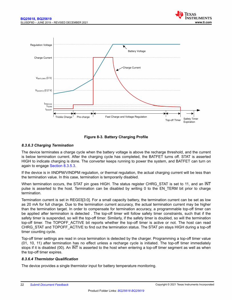
Regulation Voltage
Charge Current
VBATLOWV (3 V)
VSHORTZ (2.2 V)
IPRECHG
ITERM
ISHORT
Battery Voltage
Charge Current
Trickle Charge Pre-charge Fast Charge and Voltage RegulationSafety Timer
ExpirationTop-off Timer
Figure 8-3. Battery Charging Profile
8.3.6.3 Charging Termination
The device terminates a charge cycle when the battery voltage is above the recharge threshold, and the current is below termination current. After the charging cycle has completed, the BATFET turns off. STAT is asserted HIGH to indicate charging is done. The converter keeps running to power the system, and BATFET can turn on again to engage Section 8.3.5.3.
If the device is in IINDPM/VINDPM regulation, or thermal regulation, the actual charging current will be less than the termination value. In this case, termination is temporarily disabled.
When termination occurs, the STAT pin goes HIGH. The status register CHRG_STAT is set to 11, and an INT pulse is asserted to the host. Termination can be disabled by writing 0 to the EN_TERM bit prior to charge termination.
Termination current is set in REG03[3:0]. For a small capacity battery, the termination current can be set as low as 20 mA for full charge. Due to the termination current accuracy, the actual termination current may be higher than the termination target. In order to compensate for termination accuracy, a programmable top-off timer can be applied after termination is detected . The top-off timer will follow safety timer constraints, such that if the safety timer is suspended, so will the top-off timer. Similarly, if the safety timer is doubled, so will the termination top-off timer. The TOPOFF_ACTIVE bit reports whether the top-off timer is active or not. The host can read CHRG_STAT and TOPOFF_ACTIVE to find out the termination status. The STAT pin stays HIGH during a top-off timer counting cycle.
Top-off timer settings are read in once termination is detected by the charger. Programming a top-off timer value (01, 10, 11) after termination has no effect unless a recharge cycle is initiated. The top-off timer immediately stops if it is disabled (00). An INT is asserted to the host when entering a top-off timer segment as well as when the top-off timer expires.
8.3.6.4 Thermistor Qualification
The device provides a single thermistor input for battery temperature monitoring.
BQ25618, BQ25619SLUSDF8D – JUNE 2019 – REVISED DECEMBER 2021 www.ti.com
22 Submit Document Feedback Copyright © 2021 Texas Instruments Incorporated
Product Folder Links: BQ25618 BQ25619
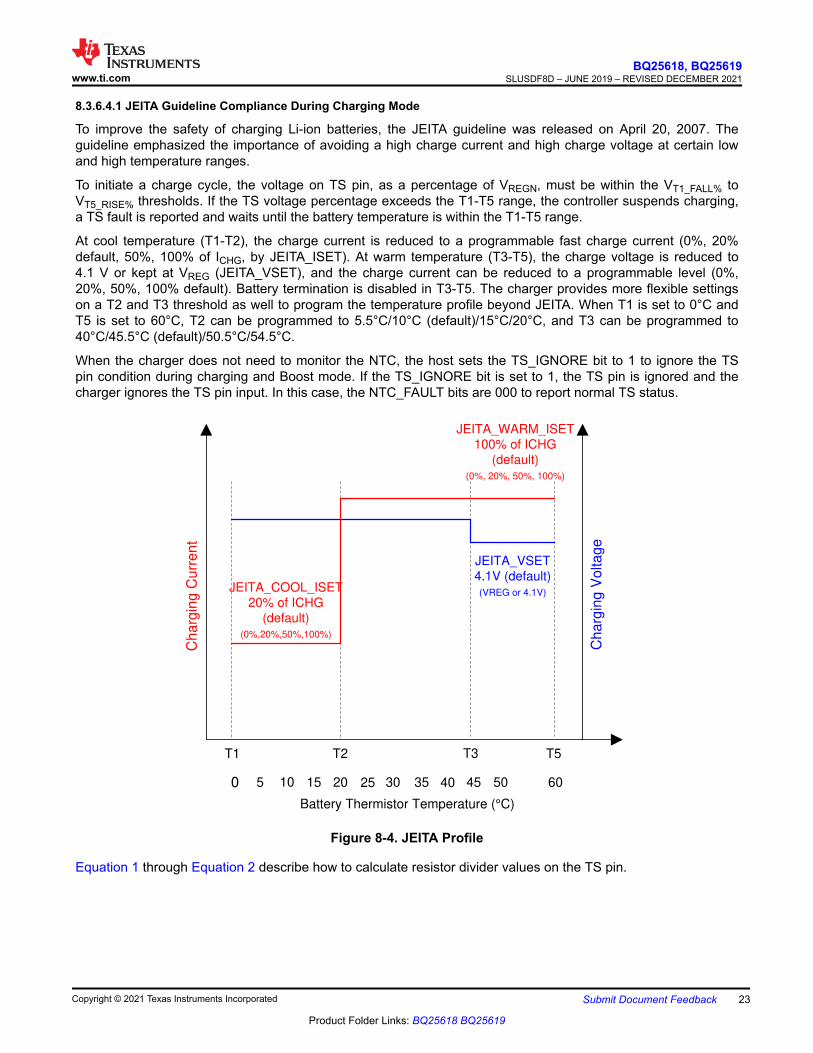
8.3.6.4.1 JEITA Guideline Compliance During Charging Mode
To improve the safety of charging Li-ion batteries, the JEITA guideline was released on April 20, 2007. The guideline emphasized the importance of avoiding a high charge current and high charge voltage at certain low and high temperature ranges.
To initiate a charge cycle, the voltage on TS pin, as a percentage of VREGN, must be within the VT1_FALL% to VT5_RISE% thresholds. If the TS voltage percentage exceeds the T1-T5 range, the controller suspends charging, a TS fault is reported and waits until the battery temperature is within the T1-T5 range.
At cool temperature (T1-T2), the charge current is reduced to a programmable fast charge current (0%, 20% default, 50%, 100% of ICHG, by JEITA_ISET). At warm temperature (T3-T5), the charge voltage is reduced to 4.1 V or kept at VREG (JEITA_VSET), and the charge current can be reduced to a programmable level (0%, 20%, 50%, 100% default). Battery termination is disabled in T3-T5. The charger provides more flexible settings on a T2 and T3 threshold as well to program the temperature profile beyond JEITA. When T1 is set to 0°C and T5 is set to 60°C, T2 can be programmed to 5.5°C/10°C (default)/15°C/20°C, and T3 can be programmed to 40°C/45.5°C (default)/50.5°C/54.5°C.
When the charger does not need to monitor the NTC, the host sets the TS_IGNORE bit to 1 to ignore the TS pin condition during charging and Boost mode. If the TS_IGNORE bit is set to 1, the TS pin is ignored and the charger ignores the TS pin input. In this case, the NTC_FAULT bits are 000 to report normal TS status.
Ch
arg
ing
Cu
rre
nt
10 25 40
T3 T5
Battery Thermistor Temperature (°C)
0 5 15 20 30 35 45 50 60
T1 T2
JEITA_WARM_ISET
100% of ICHG
(default)
(0%, 20%, 50%, 100%)
JEITA_COOL_ISET
20% of ICHG
(default)
(0%,20%,50%,100%)
Ch
arg
ing
Vo
lta
ge
JEITA_VSET
4.1V (default)
(VREG or 4.1V)
Figure 8-4. JEITA Profile
Equation 1 through Equation 2 describe how to calculate resistor divider values on the TS pin.
www.ti.comBQ25618, BQ25619
SLUSDF8D – JUNE 2019 – REVISED DECEMBER 2021
Copyright © 2021 Texas Instruments Incorporated Submit Document Feedback 23
Product Folder Links: BQ25618 BQ25619
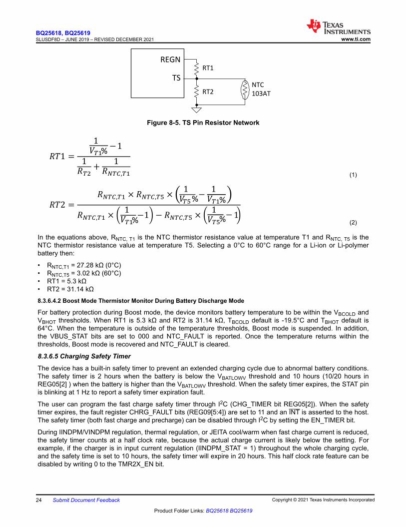
REGN
TSNTC
103AT
RT1
RT2
Figure 8-5. TS Pin Resistor Network
%
(1)
% %
% % (2)
In the equations above, RNTC, T1 is the NTC thermistor resistance value at temperature T1 and RNTC, T5 is the NTC thermistor resistance value at temperature T5. Selecting a 0°C to 60°C range for a Li-ion or Li-polymer battery then:
• RNTC,T1 = 27.28 kΩ (0°C)• RNTC,T5 = 3.02 kΩ (60°C)• RT1 = 5.3 kΩ• RT2 = 31.14 kΩ
8.3.6.4.2 Boost Mode Thermistor Monitor During Battery Discharge Mode
For battery protection during Boost mode, the device monitors battery temperature to be within the VBCOLD and VBHOT thresholds. When RT1 is 5.3 kΩ and RT2 is 31.14 kΩ, TBCOLD default is -19.5°C and TBHOT default is 64°C. When the temperature is outside of the temperature thresholds, Boost mode is suspended. In addition, the VBUS_STAT bits are set to 000 and NTC_FAULT is reported. Once the temperature returns within the thresholds, Boost mode is recovered and NTC_FAULT is cleared.
8.3.6.5 Charging Safety Timer
The device has a built-in safety timer to prevent an extended charging cycle due to abnormal battery conditions. The safety timer is 2 hours when the battery is below the VBATLOWV threshold and 10 hours (10/20 hours in REG05[2] ) when the battery is higher than the VBATLOWV threshold. When the safety timer expires, the STAT pin is blinking at 1 Hz to report a safety timer expiration fault.
The user can program the fast charge safety timer through I2C (CHG_TIMER bit REG05[2]). When the safety timer expires, the fault register CHRG_FAULT bits (REG09[5:4]) are set to 11 and an INT is asserted to the host. The safety timer (both fast charge and precharge) can be disabled through I2C by setting the EN_TIMER bit.
During IINDPM/VINDPM regulation, thermal regulation, or JEITA cool/warm when fast charge current is reduced, the safety timer counts at a half clock rate, because the actual charge current is likely below the setting. For example, if the charger is in input current regulation (IINDPM_STAT = 1) throughout the whole charging cycle, and the safety time is set to 10 hours, the safety timer will expire in 20 hours. This half clock rate feature can be disabled by writing 0 to the TMR2X_EN bit.
BQ25618, BQ25619SLUSDF8D – JUNE 2019 – REVISED DECEMBER 2021 www.ti.com
24 Submit Document Feedback Copyright © 2021 Texas Instruments Incorporated
Product Folder Links: BQ25618 BQ25619
During faults of BAT_FAULT, NTC_FAULT that lead to charging suspend, the safety timer is suspended as well. Once the fault goes away, the timer resumes. If the user stops the current charging cycle, and starts it again, the timer gets reset (toggle of CE pin or CHG_CONFIG bit).
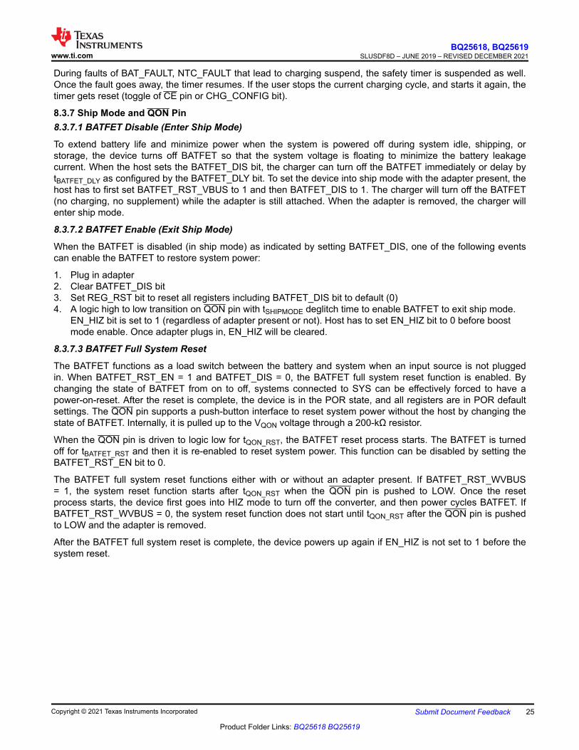
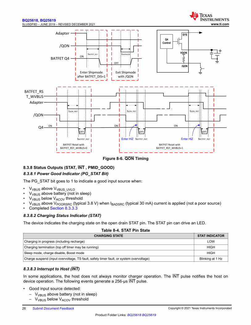
8.3.7 Ship Mode and QON Pin8.3.7.1 BATFET Disable (Enter Ship Mode)
To extend battery life and minimize power when the system is powered off during system idle, shipping, or storage, the device turns off BATFET so that the system voltage is floating to minimize the battery leakage current. When the host sets the BATFET_DIS bit, the charger can turn off the BATFET immediately or delay by tBATFET_DLY as configured by the BATFET_DLY bit. To set the device into ship mode with the adapter present, the host has to first set BATFET_RST_VBUS to 1 and then BATFET_DIS to 1. The charger will turn off the BATFET (no charging, no supplement) while the adapter is still attached. When the adapter is removed, the charger will enter ship mode.
8.3.7.2 BATFET Enable (Exit Ship Mode)
When the BATFET is disabled (in ship mode) as indicated by setting BATFET_DIS, one of the following events can enable the BATFET to restore system power:
1. Plug in adapter2. Clear BATFET_DIS bit3. Set REG_RST bit to reset all registers including BATFET_DIS bit to default (0)4. A logic high to low transition on QON pin with tSHIPMODE deglitch time to enable BATFET to exit ship mode.
EN_HIZ bit is set to 1 (regardless of adapter present or not). Host has to set EN_HIZ bit to 0 before boost mode enable. Once adapter plugs in, EN_HIZ will be cleared.
8.3.7.3 BATFET Full System Reset
The BATFET functions as a load switch between the battery and system when an input source is not plugged in. When BATFET_RST_EN = 1 and BATFET_DIS = 0, the BATFET full system reset function is enabled. By changing the state of BATFET from on to off, systems connected to SYS can be effectively forced to have a power-on-reset. After the reset is complete, the device is in the POR state, and all registers are in POR default settings. The QON pin supports a push-button interface to reset system power without the host by changing the state of BATFET. Internally, it is pulled up to the VQON voltage through a 200-kΩ resistor.
When the QON pin is driven to logic low for tQON_RST, the BATFET reset process starts. The BATFET is turned off for tBATFET_RST and then it is re-enabled to reset system power. This function can be disabled by setting the BATFET_RST_EN bit to 0.
The BATFET full system reset functions either with or without an adapter present. If BATFET_RST_WVBUS = 1, the system reset function starts after tQON_RST when the QON pin is pushed to LOW. Once the reset process starts, the device first goes into HIZ mode to turn off the converter, and then power cycles BATFET. If BATFET_RST_WVBUS = 0, the system reset function does not start until tQON_RST after the QON pin is pushed to LOW and the adapter is removed.
After the BATFET full system reset is complete, the device powers up again if EN_HIZ is not set to 1 before the system reset.
www.ti.comBQ25618, BQ25619
SLUSDF8D – JUNE 2019 – REVISED DECEMBER 2021
Copyright © 2021 Texas Instruments Incorporated Submit Document Feedback 25
Product Folder Links: BQ25618 BQ25619
VQON
/QON
SYS
Q4
Control
tQON_RST
/QON
tBATFET_RST
Q4
Adapter
/QON
BATFET Q4
tSHIPMODEtBATFET_DLY
Enter Shipmode
after BATFET_DIS=1
Exit Shipmode
with /QON
ON
OFF
OFF
ON
Adapter
tQON_RST
tBATFET_RST
OFF
ON
BATFET Reset with
BATFET_RST_WVBUS=0
Enter HIZ
tQON_RST
tBATFET_RST
OFF
ON
BATFET Reset with
BATFET_RST_WVBUS=1
Enter HIZ
BATFET_RS
T_WVBUS
Figure 8-6. QON Timing
8.3.8 Status Outputs (STAT, INT , PMID_GOOD)8.3.8.1 Power Good Indicator (PG_STAT Bit)
The PG_STAT bit goes to 1 to indicate a good input source when:
• VVBUS above VVBUS_UVLO• VVBUS above battery (not in sleep)• VVBUS below VACOV threshold• VVBUS above VPOORSRC (typical 3.8 V) when IBADSRC (typical 30 mA) current is applied (not a poor source)• Completed Section 8.3.3.3
8.3.8.2 Charging Status Indicator (STAT)
The device indicates the charging state on the open drain STAT pin. The STAT pin can drive an LED.
Table 8-4. STAT Pin StateCHARGING STATE STAT INDICATOR
Charging in progress (including recharge) LOW
Charging termination (top off timer may be running) HIGH
Sleep mode, charge disable, Boost mode HIGH
Charge suspend (input overvoltage, TS fault, safety timer fault, or system overvoltage) Blinking at 1 Hz
8.3.8.3 Interrupt to Host (INT)
In some applications, the host does not always monitor charger operation. The INT pulse notifies the host on device operation. The following events generate a 256-μs INT pulse.
• Good input source detected:– VVBUS above battery (not in sleep)– VVBUS below VACOV threshold
BQ25618, BQ25619SLUSDF8D – JUNE 2019 – REVISED DECEMBER 2021 www.ti.com
26 Submit Document Feedback Copyright © 2021 Texas Instruments Incorporated
Product Folder Links: BQ25618 BQ25619
– VVBUS above VPOORSRC (typical 3.8 V) when IBADSRC (typical 30 mA) current is applied (not a poor source)• Input adapter removed• USB/adapter source identified during Section 8.3.3.3.• Charge complete• Any FAULT event in REG09• VINDPM / IINDPM event detected (REG0A[1:0], maskable)• Top-off timer starts and expires
REG09[7:0] and REG0A[6:4] report charger operation faults and status change to the host. When a fault/status change occurs, the charger sends out an INT pulse and keeps the state in REG09[7:0]/REG0A[6:4] until the host reads the registers. Before the host reads REG09[7:0]/REG0A[6:4] and all the ones are cleared, the charger does not send any INT upon new fault/status change. To read the current status, the host has to read REG09/REG0A two times consecutively. The first read reports the pre-existing register status and the second read reports the current register status.
8.3.8.4 PMID Voltage Indicator (PMID_GOOD)
In the BQ25619/618, the accessory devices can be connected to the charger PMID pin to get power either from the adapter through the Q1 direct path or from battery Boost mode. An optional external PMOS FET can be placed between the charger PMID pin and accessory input to disconnect the power path during overcurrent and overvoltage conditions. PMID_GOOD is used to drive an external PMOS FET through an inverter. PMID_GOOD HIGH turns on an inverter to pull the PMOS FET gate low to turn on the PMOS FET, and PMID_GOOD LOW turns off the PMOS FET.
Upon adapter plug-in, PMID_GOOD goes from LOW to HIGH when VBUS rises above the battery but below VACOV, and passes poor source detection. During the operation, PMID_GOOD goes from HIGH to LOW if Q1 current exceeds 115% of the IINDPM threshold, (IBLK_OCP), or adapter voltage rises above 5.8 V (VBST_OVP).
The high-voltage adapter over VBST_OVP keeps charging the battery if all conditions are valid. The external PMOS FET stays off to protect the accessory from an overvoltage fault.
When the adapter is removed, PMID_GOOD goes LOW before battery Boost mode starts.
In battery Boost mode, the device regulates PMID voltage between 4.6 V to 5.15 V as a stable power supply to the accessory devices. PMID_GOOD goes from LOW to HIGH when PMID voltage rises above 3.8 V (VPOORSRC). Similar to the adapter present scenario, the PMID valid voltage range is between VPOORSRC and VBST_OVP. Once PMID voltage is out of this range, PMID_GOOD goes LOW to disconnect the accessory device from PMID. During Boost mode, all of the conditions to exit Boost mode will drive PMID_GOOD from HIGH to LOW, including Boost mode disable in register, ACOV, TS fault, battery depleted (VBAT_DPL), BATFET overcurrent, (ISYS_OCP_Q4), etc.
8.3.9 Protections8.3.9.1 Voltage and Current Monitoring in Buck Mode8.3.9.1.1 Input Overvoltage Protection (ACOV)
The input voltage is sensed via the VAC pin . The default OVP threshold is 14.2 V, and can be programmed at 5.7 V/6.4 V/11 V/14.2 V via OVP[1:0] register bits. ACOV event immediately stops converter switching whether in buck or Boost mode. The device automatically resumes normal operation once the input voltage drops back below the OVP threshold. During ACOV, REGN LDO is on, and the device does not enter HIZ mode.
During ACOV, the fault register CHRG_FAULT bits are set to 01. An INT pulse is asserted to the host.
8.3.9.1.2 System Overvoltage Protection (SYSOVP)
The charger device clamps the system voltage during a load transient so that the components connected to the system are not damaged due to high voltage. The VSYS_OVP threshold is about 300 mV above battery regulation voltage when battery charging is terminated. Upon SYSOVP, the converter stops switching immediately to clamp the overshoot. The charger pulls 30-mA ISYS_LOAD discharge current to bring down the system voltage.
www.ti.comBQ25618, BQ25619
SLUSDF8D – JUNE 2019 – REVISED DECEMBER 2021
Copyright © 2021 Texas Instruments Incorporated Submit Document Feedback 27
Product Folder Links: BQ25618 BQ25619
8.3.9.2 Voltage and Current Monitoring in Boost Mode8.3.9.2.1 Boost Mode Overvoltage Protection
When PMID voltage rises above the regulation target and exceeds VBST_OVP, the device stops switching immediately and the device exits Boost mode and PMID_GOOD is pulled low as well. The BST_CONFIG bit is set to 0. During Boost mode overvoltage, the fault register bit BOOST_FAULT is set to 1 to indicate a fault in boost operation. An INT is asserted to the host.
8.3.9.2.2 PMID Overcurrent Protection
The BQ25619/618 closely monitors the battery discharge current through BATFET (Q4) to ensure safe Boost mode operation. During an overcurrent condition when boost input current exceeds ISYS_OCP_Q4, the device latches off in 100 µs. When an overcurrent condition is detected, the fault register bit BOOST_FAULT is set high to indicate a fault in boost operation. An INT is asserted to the host.
8.3.9.3 Thermal Regulation and Thermal Shutdown8.3.9.3.1 Thermal Protection in Buck Mode
Besides the battery temperature monitor on the TS pin, the device monitors the internal junction temperature TJ to avoid overheating the chip and limits the IC junction temperature in buck mode. When the internal junction temperature exceeds the thermal regulation limit (110°C), the device lowers down the charge current. During thermal regulation, the actual charging current is usually below the programmed battery charging current. Therefore, termination is disabled, the safety timer runs at half the clock rate, and the status register THERM_STAT bit goes high.
Additionally, the device has thermal shutdown to turn off the converter and the BATFET when the IC surface temperature exceeds TSHUT 150°C. The BATFET and converter are enabled to recover when IC temperature is 130°C. The fault register CHRG_FAULT is set to 10 during thermal shutdown and an INT is asserted to the host.
8.3.9.3.2 Thermal Protection in Boost Mode
Besides the battery temperature monitor on the TS pin, the device monitors the internal junction temperature to provide thermal shutdown during Boost mode. When the IC junction temperature exceeds TSHUT 150°C, Boost mode is disabled by setting the BST_CONFIG bit low. When the IC junction temperature is below 145°C, the host can re-enable Boost mode.
8.3.9.4 Battery Protection8.3.9.4.1 Battery Overvoltage Protection (BATOVP)
The battery overvoltage limit is clamped at 4% above battery regulation voltage. When battery overvoltage occurs, the charger device immediately stops switching. The fault register BAT_FAULT bit goes high and an INT is asserted to the host.
8.3.9.4.2 Battery Overdischarge Protection
When the battery is discharged below VBAT_DPL_FALL, the BATFET latches off to protect the battery from overdischarge. To recover from overdischarge latch-off, an input source plug-in is required at VAC/VBUS.
8.3.9.4.3 System Overcurrent Protection
ISYS_OCP_Q4 sets the battery discharge current limit. Once IBAT > ISYS_OCP_Q4, the charger latches off Q4 and puts the device into Ship mode. All methods to exit Ship mode are valid to bring the part out of Q4 latch-off.
8.3.10 Serial Interface
The device uses an I2C compatible interface for flexible charging parameter programming and instantaneous device status reporting. I2CTM is a bi-directional 2-wire serial interface developed by Philips Semiconductor (now NXP Semiconductors). Only two bus lines are required: a serial data line (SDA) and a serial clock line (SCL). Devices can be considered as masters or slaves when performing data transfers. A master is the device which initiates a data transfer on the bus and generates the clock signals to permit that transfer. At that time, any device addressed is considered a slave.
BQ25618, BQ25619SLUSDF8D – JUNE 2019 – REVISED DECEMBER 2021 www.ti.com
28 Submit Document Feedback Copyright © 2021 Texas Instruments Incorporated
Product Folder Links: BQ25618 BQ25619
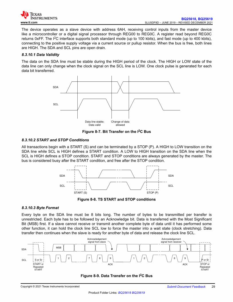
The device operates as a slave device with address 6AH, receiving control inputs from the master device like a microcontroller or a digital signal processor through REG00 to REG0C. A register read beyond REG0C returns 0xFF. The I2C interface supports both standard mode (up to 100 kbits), and fast mode (up to 400 kbits), connecting to the positive supply voltage via a current source or pullup resistor. When the bus is free, both lines are HIGH. The SDA and SCL pins are open drain.
8.3.10.1 Data Validity
The data on the SDA line must be stable during the HIGH period of the clock. The HIGH or LOW state of the data line can only change when the clock signal on the SCL line is LOW. One clock pulse is generated for each data bit transferred.
SDA
SCL
Data line stable;
Data valid
Change of data
allowed
Figure 8-7. Bit Transfer on the I2C Bus
8.3.10.2 START and STOP Conditions
All transactions begin with a START (S) and can be terminated by a STOP (P). A HIGH to LOW transition on the SDA line while SCL is HIGH defines a START condition. A LOW to HIGH transition on the SDA line when the SCL is HIGH defines a STOP condition. START and STOP conditions are always generated by the master. The bus is considered busy after the START condition, and free after the STOP condition.
SDA
SCL
SDA
SCL
START (S) STOP (P)
Figure 8-8. TS START and STOP conditions
8.3.10.3 Byte Format
Every byte on the SDA line must be 8 bits long. The number of bytes to be transmitted per transfer is unrestricted. Each byte has to be followed by an Acknowledge bit. Data is transferred with the Most Significant Bit (MSB) first. If a slave cannot receive or transmit another complete byte of data until it has performed some other function, it can hold the clock line SCL low to force the master into a wait state (clock stretching). Data transfer then continues when the slave is ready for another byte of data and release the clock line SCL.
SCL
SDAMSB
ACK ACK
1 2 7 8 9
Acknowledgement
signal from slave
Acknowledgement
signal from receiver
START or
Repeated
START
S or Sr
STOP or
Repeated
START
P or Sr1 2 8 9
Figure 8-9. Data Transfer on the I2C Bus
www.ti.comBQ25618, BQ25619
SLUSDF8D – JUNE 2019 – REVISED DECEMBER 2021
Copyright © 2021 Texas Instruments Incorporated Submit Document Feedback 29
Product Folder Links: BQ25618 BQ25619
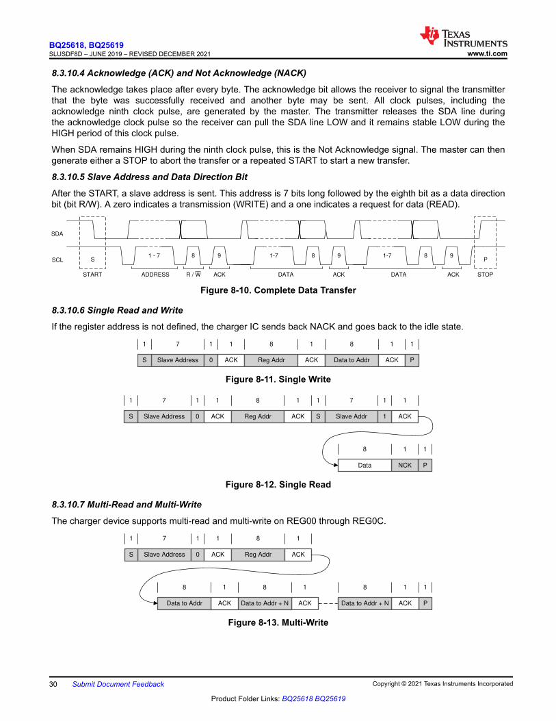
8.3.10.4 Acknowledge (ACK) and Not Acknowledge (NACK)
The acknowledge takes place after every byte. The acknowledge bit allows the receiver to signal the transmitter that the byte was successfully received and another byte may be sent. All clock pulses, including the acknowledge ninth clock pulse, are generated by the master. The transmitter releases the SDA line during the acknowledge clock pulse so the receiver can pull the SDA line LOW and it remains stable LOW during the HIGH period of this clock pulse.
When SDA remains HIGH during the ninth clock pulse, this is the Not Acknowledge signal. The master can then generate either a STOP to abort the transfer or a repeated START to start a new transfer.
8.3.10.5 Slave Address and Data Direction Bit
After the START, a slave address is sent. This address is 7 bits long followed by the eighth bit as a data direction bit (bit R/W). A zero indicates a transmission (WRITE) and a one indicates a request for data (READ).
SCL
SDA
START
S
ACK ACK STOP
P
ADDRESS DATA ACKDATA
81 - 7
R / W
9 1-7 8 9 81-7 9
Figure 8-10. Complete Data Transfer
8.3.10.6 Single Read and Write
If the register address is not defined, the charger IC sends back NACK and goes back to the idle state.
Slave AddressS 0 ACK Reg Addr ACK Data to Addr ACK P
1 7 1 1 8 1 8 1 1
Figure 8-11. Single Write
Slave AddressS 0 ACK Reg Addr ACK S Slave Addr ACK1
1 7 1 1 8 1 1 7 11
PNCKData
118
Figure 8-12. Single Read
8.3.10.7 Multi-Read and Multi-Write
The charger device supports multi-read and multi-write on REG00 through REG0C.
Slave AddressS 0 ACK Reg Addr ACK
1 7 1 1 8 1
ACK
1
PACKData to Addr + N
118
Data to Addr + N
8
ACK
1
Data to Addr
8
Figure 8-13. Multi-Write
BQ25618, BQ25619SLUSDF8D – JUNE 2019 – REVISED DECEMBER 2021 www.ti.com
30 Submit Document Feedback Copyright © 2021 Texas Instruments Incorporated
Product Folder Links: BQ25618 BQ25619
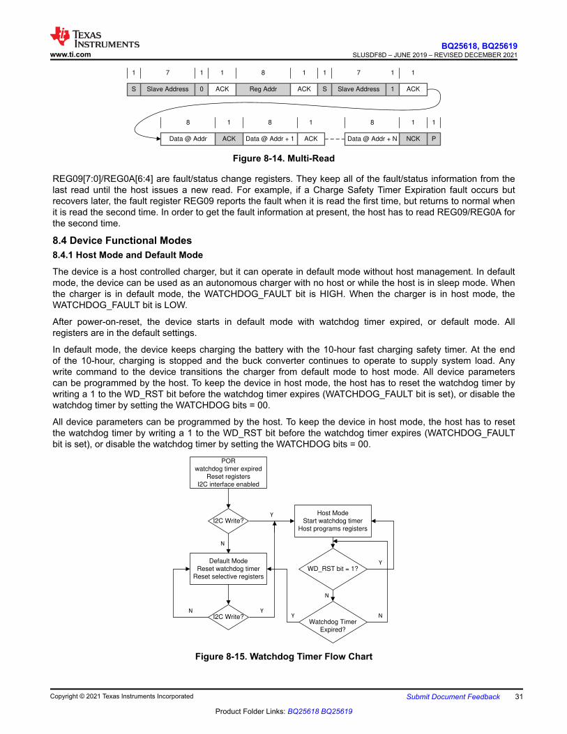
Slave AddressS 0 ACK Reg Addr ACK
1 7 1 1 8 1
ACK
1
PNCKData @ Addr + N
118
Data @ Addr + 1
8
ACK
1
Data @ Addr
8
Slave AddressS 1 ACK
1 7 1 1
Figure 8-14. Multi-Read
REG09[7:0]/REG0A[6:4] are fault/status change registers. They keep all of the fault/status information from the last read until the host issues a new read. For example, if a Charge Safety Timer Expiration fault occurs but recovers later, the fault register REG09 reports the fault when it is read the first time, but returns to normal when it is read the second time. In order to get the fault information at present, the host has to read REG09/REG0A for the second time.
8.4 Device Functional Modes8.4.1 Host Mode and Default Mode
The device is a host controlled charger, but it can operate in default mode without host management. In default mode, the device can be used as an autonomous charger with no host or while the host is in sleep mode. When the charger is in default mode, the WATCHDOG_FAULT bit is HIGH. When the charger is in host mode, the WATCHDOG_FAULT bit is LOW.
After power-on-reset, the device starts in default mode with watchdog timer expired, or default mode. All registers are in the default settings.
In default mode, the device keeps charging the battery with the 10-hour fast charging safety timer. At the end of the 10-hour, charging is stopped and the buck converter continues to operate to supply system load. Any write command to the device transitions the charger from default mode to host mode. All device parameters can be programmed by the host. To keep the device in host mode, the host has to reset the watchdog timer by writing a 1 to the WD_RST bit before the watchdog timer expires (WATCHDOG_FAULT bit is set), or disable the watchdog timer by setting the WATCHDOG bits = 00.
All device parameters can be programmed by the host. To keep the device in host mode, the host has to reset the watchdog timer by writing a 1 to the WD_RST bit before the watchdog timer expires (WATCHDOG_FAULT bit is set), or disable the watchdog timer by setting the WATCHDOG bits = 00.
POR
watchdog timer expired
Reset registers
I2C interface enabled
Y
N
Y
N
YNY
N
Default Mode
Reset watchdog timer
Reset selective registers
Host Mode
Start watchdog timer
Host programs registers
WD_RST bit = 1?
I2C Write?
I2C Write?
Watchdog Timer
Expired?
Figure 8-15. Watchdog Timer Flow Chart
www.ti.comBQ25618, BQ25619
SLUSDF8D – JUNE 2019 – REVISED DECEMBER 2021
Copyright © 2021 Texas Instruments Incorporated Submit Document Feedback 31
Product Folder Links: BQ25618 BQ25619
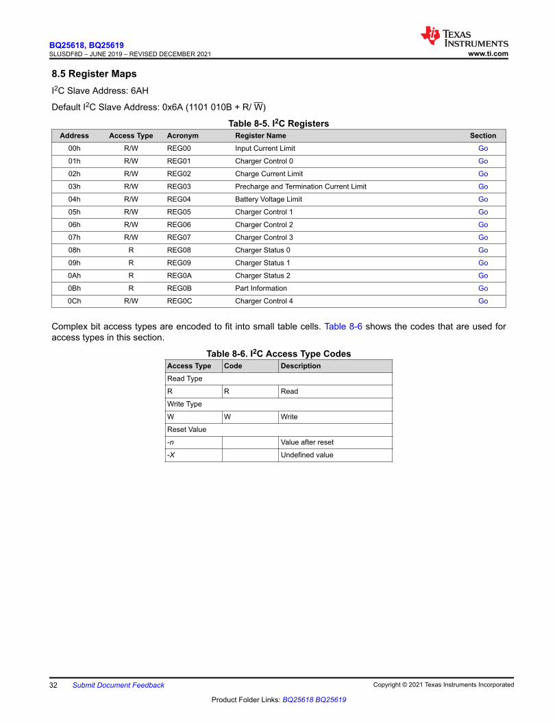
8.5 Register MapsI2C Slave Address: 6AH
Default I2C Slave Address: 0x6A (1101 010B + R/ W)
Table 8-5. I2C RegistersAddress Access Type Acronym Register Name Section
00h R/W REG00 Input Current Limit Go
01h R/W REG01 Charger Control 0 Go
02h R/W REG02 Charge Current Limit Go
03h R/W REG03 Precharge and Termination Current Limit Go
04h R/W REG04 Battery Voltage Limit Go
05h R/W REG05 Charger Control 1 Go
06h R/W REG06 Charger Control 2 Go
07h R/W REG07 Charger Control 3 Go
08h R REG08 Charger Status 0 Go
09h R REG09 Charger Status 1 Go
0Ah R REG0A Charger Status 2 Go
0Bh R REG0B Part Information Go
0Ch R/W REG0C Charger Control 4 Go
Complex bit access types are encoded to fit into small table cells. Table 8-6 shows the codes that are used for access types in this section.
Table 8-6. I2C Access Type CodesAccess Type Code DescriptionRead Type
R R Read
Write Type
W W Write
Reset Value
-n Value after reset
-X Undefined value
BQ25618, BQ25619SLUSDF8D – JUNE 2019 – REVISED DECEMBER 2021 www.ti.com
32 Submit Document Feedback Copyright © 2021 Texas Instruments Incorporated
Product Folder Links: BQ25618 BQ25619
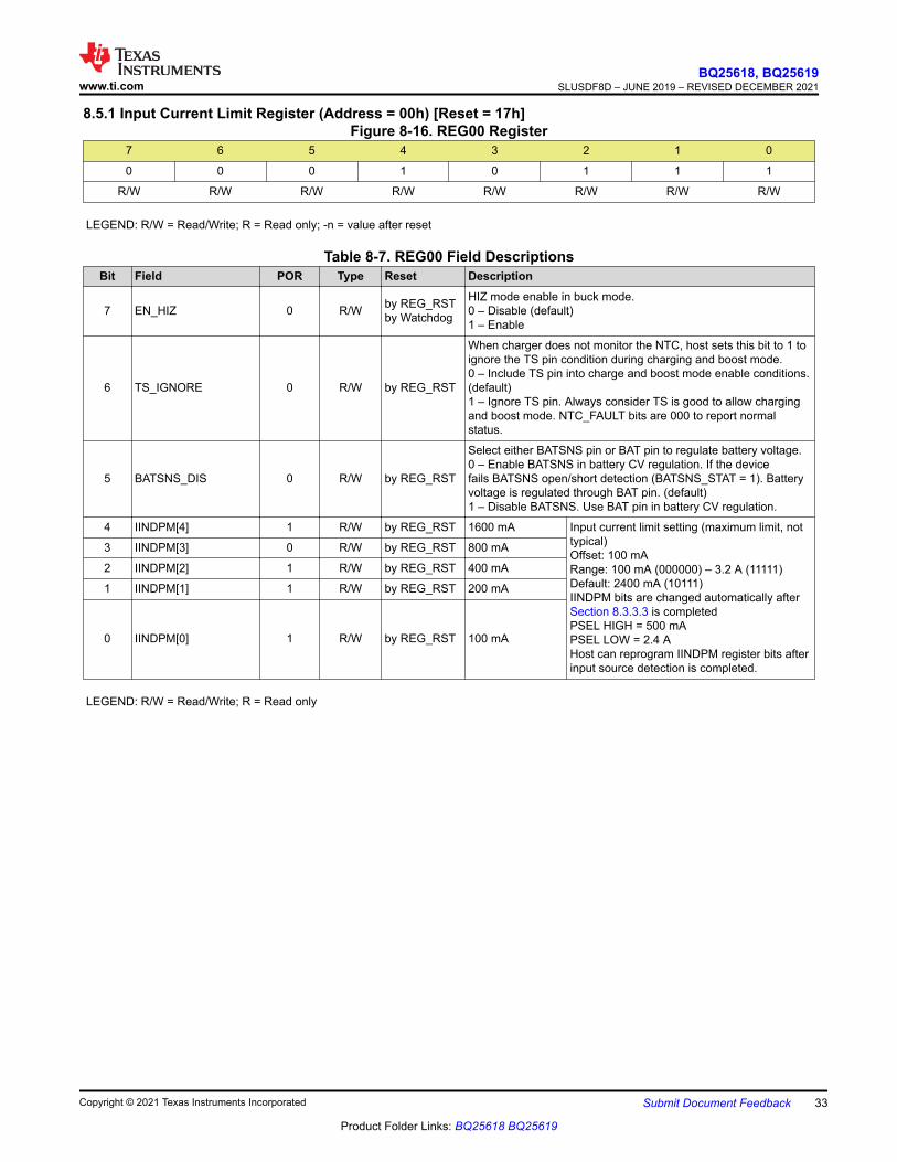
8.5.1 Input Current Limit Register (Address = 00h) [Reset = 17h]Figure 8-16. REG00 Register
7 6 5 4 3 2 1 0
0 0 0 1 0 1 1 1
R/W R/W R/W R/W R/W R/W R/W R/W
LEGEND: R/W = Read/Write; R = Read only; -n = value after reset
Table 8-7. REG00 Field DescriptionsBit Field POR Type Reset Description
7 EN_HIZ 0 R/W by REG_RSTby Watchdog
HIZ mode enable in buck mode.0 – Disable (default)1 – Enable
6 TS_IGNORE 0 R/W by REG_RST
When charger does not monitor the NTC, host sets this bit to 1 to ignore the TS pin condition during charging and boost mode.0 – Include TS pin into charge and boost mode enable conditions. (default)1 – Ignore TS pin. Always consider TS is good to allow charging and boost mode. NTC_FAULT bits are 000 to report normal status.
5 BATSNS_DIS 0 R/W by REG_RST
Select either BATSNS pin or BAT pin to regulate battery voltage.0 – Enable BATSNS in battery CV regulation. If the device fails BATSNS open/short detection (BATSNS_STAT = 1). Battery voltage is regulated through BAT pin. (default)1 – Disable BATSNS. Use BAT pin in battery CV regulation.
4 IINDPM[4] 1 R/W by REG_RST 1600 mA Input current limit setting (maximum limit, not typical)Offset: 100 mARange: 100 mA (000000) – 3.2 A (11111)Default: 2400 mA (10111)IINDPM bits are changed automatically after Section 8.3.3.3 is completedPSEL HIGH = 500 mAPSEL LOW = 2.4 AHost can reprogram IINDPM register bits after input source detection is completed.
3 IINDPM[3] 0 R/W by REG_RST 800 mA
2 IINDPM[2] 1 R/W by REG_RST 400 mA
1 IINDPM[1] 1 R/W by REG_RST 200 mA
0 IINDPM[0] 1 R/W by REG_RST 100 mA
LEGEND: R/W = Read/Write; R = Read only
www.ti.comBQ25618, BQ25619
SLUSDF8D – JUNE 2019 – REVISED DECEMBER 2021
Copyright © 2021 Texas Instruments Incorporated Submit Document Feedback 33
Product Folder Links: BQ25618 BQ25619
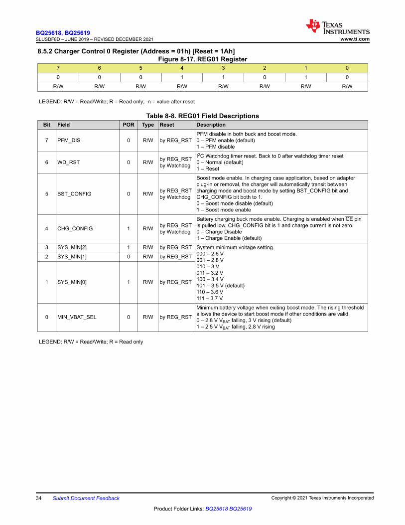
8.5.2 Charger Control 0 Register (Address = 01h) [Reset = 1Ah]Figure 8-17. REG01 Register
7 6 5 4 3 2 1 0
0 0 0 1 1 0 1 0
R/W R/W R/W R/W R/W R/W R/W R/W
LEGEND: R/W = Read/Write; R = Read only; -n = value after reset
Table 8-8. REG01 Field DescriptionsBit Field POR Type Reset Description
7 PFM_DIS 0 R/W by REG_RSTPFM disable in both buck and boost mode.0 – PFM enable (default)1 – PFM disable
6 WD_RST 0 R/W by REG_RSTby Watchdog
I2C Watchdog timer reset. Back to 0 after watchdog timer reset0 – Normal (default)1 – Reset
5 BST_CONFIG 0 R/W by REG_RSTby Watchdog
Boost mode enable. In charging case application, based on adapter plug-in or removal, the charger will automatically transit between charging mode and boost mode by setting BST_CONFIG bit and CHG_CONFIG bit both to 1.0 – Boost mode disable (default)1 – Boost mode enable
4 CHG_CONFIG 1 R/W by REG_RSTby Watchdog
Battery charging buck mode enable. Charging is enabled when CE pin is pulled low, CHG_CONFIG bit is 1 and charge current is not zero.0 – Charge Disable1 – Charge Enable (default)
3 SYS_MIN[2] 1 R/W by REG_RST System minimum voltage setting.000 – 2.6 V001 – 2.8 V010 – 3 V011 – 3.2 V100 – 3.4 V101 – 3.5 V (default)110 – 3.6 V111 – 3.7 V
2 SYS_MIN[1] 0 R/W by REG_RST
1 SYS_MIN[0] 1 R/W by REG_RST
0 MIN_VBAT_SEL 0 R/W by REG_RST
Minimum battery voltage when exiting boost mode. The rising threshold allows the device to start boost mode if other conditions are valid.0 – 2.8 V VBAT falling, 3 V rising (default)1 – 2.5 V VBAT falling, 2.8 V rising
LEGEND: R/W = Read/Write; R = Read only
BQ25618, BQ25619SLUSDF8D – JUNE 2019 – REVISED DECEMBER 2021 www.ti.com
34 Submit Document Feedback Copyright © 2021 Texas Instruments Incorporated
Product Folder Links: BQ25618 BQ25619
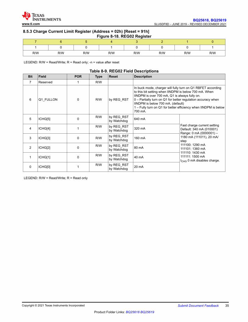
8.5.3 Charge Current Limit Register (Address = 02h) [Reset = 91h]Figure 8-18. REG02 Register
7 6 5 4 3 2 1 0
1 0 0 1 0 0 0 1
R/W R/W R/W R/W R/W R/W R/W R/W
LEGEND: R/W = Read/Write; R = Read only; -n = value after reset
Table 8-9. REG02 Field DescriptionsBit Field POR Type Reset Description7 Reserved 1 R/W
6 Q1_FULLON 0 R/W by REG_RST
In buck mode, charger will fully turn on Q1 RBFET according to this bit setting when IINDPM is below 700 mA. When IINDPM is over 700 mA, Q1 is always fully on.0 – Partially turn on Q1 for better regulation accuracy when IINDPM is below 700 mA. (default)1 – Fully turn on Q1 for better efficiency when IINDPM is below 700 mA.
5 ICHG[5] 0 R/W by REG_RSTby Watchdog 640 mA
Fast charge current settingDefault: 340 mA (010001)Range: 0 mA (0000001) – 1180 mA (111011), 20 mA/step111100: 1290 mA111101: 1360 mA111110: 1430 mA111111: 1500 mAICHG 0 mA disables charge.
4 ICHG[4] 1 R/W by REG_RSTby Watchdog 320 mA
3 ICHG[3] 0 R/W by REG_RSTby Watchdog 160 mA
2 ICHG[2] 0 R/W by REG_RSTby Watchdog 80 mA
1 ICHG[1] 0 R/W by REG_RSTby Watchdog 40 mA
0 ICHG[0] 1 R/W by REG_RSTby Watchdog 20 mA
LEGEND: R/W = Read/Write; R = Read only
www.ti.comBQ25618, BQ25619
SLUSDF8D – JUNE 2019 – REVISED DECEMBER 2021
Copyright © 2021 Texas Instruments Incorporated Submit Document Feedback 35
Product Folder Links: BQ25618 BQ25619
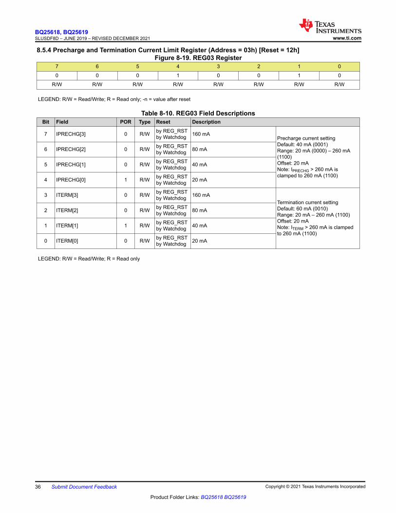
8.5.4 Precharge and Termination Current Limit Register (Address = 03h) [Reset = 12h]Figure 8-19. REG03 Register
7 6 5 4 3 2 1 0
0 0 0 1 0 0 1 0
R/W R/W R/W R/W R/W R/W R/W R/W
LEGEND: R/W = Read/Write; R = Read only; -n = value after reset
Table 8-10. REG03 Field DescriptionsBit Field POR Type Reset Description
7 IPRECHG[3] 0 R/W by REG_RSTby Watchdog 160 mA
Precharge current settingDefault: 40 mA (0001)Range: 20 mA (0000) – 260 mA (1100)Offset: 20 mANote: IPRECHG > 260 mA is clamped to 260 mA (1100)
6 IPRECHG[2] 0 R/W by REG_RSTby Watchdog 80 mA
5 IPRECHG[1] 0 R/W by REG_RSTby Watchdog 40 mA
4 IPRECHG[0] 1 R/W by REG_RSTby Watchdog 20 mA
3 ITERM[3] 0 R/W by REG_RSTby Watchdog 160 mA
Termination current settingDefault: 60 mA (0010)Range: 20 mA – 260 mA (1100)Offset: 20 mANote: ITERM > 260 mA is clamped to 260 mA (1100)
2 ITERM[2] 0 R/W by REG_RSTby Watchdog 80 mA
1 ITERM[1] 1 R/W by REG_RSTby Watchdog 40 mA
0 ITERM[0] 0 R/W by REG_RSTby Watchdog 20 mA
LEGEND: R/W = Read/Write; R = Read only
BQ25618, BQ25619SLUSDF8D – JUNE 2019 – REVISED DECEMBER 2021 www.ti.com
36 Submit Document Feedback Copyright © 2021 Texas Instruments Incorporated
Product Folder Links: BQ25618 BQ25619
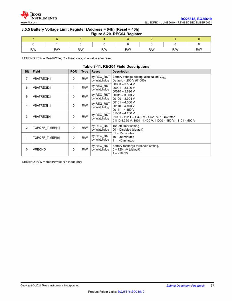
8.5.5 Battery Voltage Limit Register (Address = 04h) [Reset = 40h]Figure 8-20. REG04 Register
7 6 5 4 3 2 1 0
0 1 0 0 0 0 0 0
R/W R/W R/W R/W R/W R/W R/W R/W
LEGEND: R/W = Read/Write; R = Read only; -n = value after reset
Table 8-11. REG04 Field DescriptionsBit Field POR Type Reset Description
7 VBATREG[4] 0 R/W by REG_RSTby Watchdog
Battery voltage setting, also called VREG.Default: 4.200 V (01000)00000 – 3.504 V00001 – 3.600 V00010 – 3.696 V00011 – 3.800 V00100 – 3.904 V00101 – 4.000 V00110 – 4.100 V00111 – 4.150 V01000 – 4.200 V01001 - 11111 – 4.300 V - 4.520 V, 10 mV/step01110 4.350 V, 10011 4.400 V, 11000 4.450 V, 11101 4.500 V
6 VBATREG[3] 1 R/W by REG_RSTby Watchdog
5 VBATREG[2] 0 R/W by REG_RSTby Watchdog
4 VBATREG[1] 0 R/W by REG_RSTby Watchdog
3 VBATREG[0] 0 R/W by REG_RSTby Watchdog
2 TOPOFF_TIMER[1] 0 R/W by REG_RSTby Watchdog
Top-off timer setting.00 – Disabled (default)01 – 15 minutes10 – 30 minutes11 – 45 minutes
1 TOPOFF_TIMER[0] 0 R/W by REG_RSTby Watchdog
0 VRECHG 0 R/Wby REG_RSTby Watchdog
Battery recharge threshold setting.0 – 120 mV (default)1 – 210 mV
LEGEND: R/W = Read/Write; R = Read only
www.ti.comBQ25618, BQ25619
SLUSDF8D – JUNE 2019 – REVISED DECEMBER 2021
Copyright © 2021 Texas Instruments Incorporated Submit Document Feedback 37
Product Folder Links: BQ25618 BQ25619
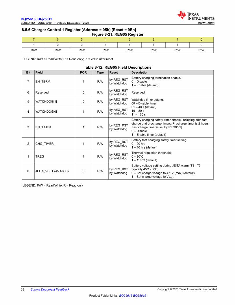
8.5.6 Charger Control 1 Register (Address = 05h) [Reset = 9Eh]Figure 8-21. REG05 Register
7 6 5 4 3 2 1 0
1 0 0 1 1 1 1 0
R/W R/W R/W R/W R/W R/W R/W R/W
LEGEND: R/W = Read/Write; R = Read only; -n = value after reset
Table 8-12. REG05 Field DescriptionsBit Field POR Type Reset Description
7 EN_TERM 1 R/W by REG_RSTby Watchdog
Battery charging termination enable.0 – Disable1 – Enable (default)
6 Reserved 0 R/W by REG_RSTby Watchdog Reserved
5 WATCHDOG[1] 0 R/W by REG_RSTby Watchdog
Watchdog timer setting.00 – Disable timer01 – 40 s (default)10 – 80 s11 – 160 s
4 WATCHDOG[0] 1 R/W by REG_RSTby Watchdog
3 EN_TIMER 1 R/W by REG_RSTby Watchdog
Battery charging safety timer enable, including both fast charge and precharge timers. Precharge timer is 2 hours. Fast charge timer is set by REG05[2]0 – Disable1 – Enable timer (default)
2 CHG_TIMER 1 R/W by REG_RSTby Watchdog
Battery fast charging safety timer setting.0 – 20 hrs1 – 10 hrs (default)
1 TREG 1 R/W by REG_RSTby Watchdog
Thermal regulation threshold:0 – 90°C1 – 110°C (default)
0 JEITA_VSET (45C-60C) 0 R/W by REG_RSTby Watchdog
Battery voltage setting during JEITA warm (T3 - T5, typically 45C - 60C)0 – Set charge voltage to 4.1 V (max) (default)1 – Set charge voltage to VREG
LEGEND: R/W = Read/Write; R = Read only
BQ25618, BQ25619SLUSDF8D – JUNE 2019 – REVISED DECEMBER 2021 www.ti.com
38 Submit Document Feedback Copyright © 2021 Texas Instruments Incorporated
Product Folder Links: BQ25618 BQ25619
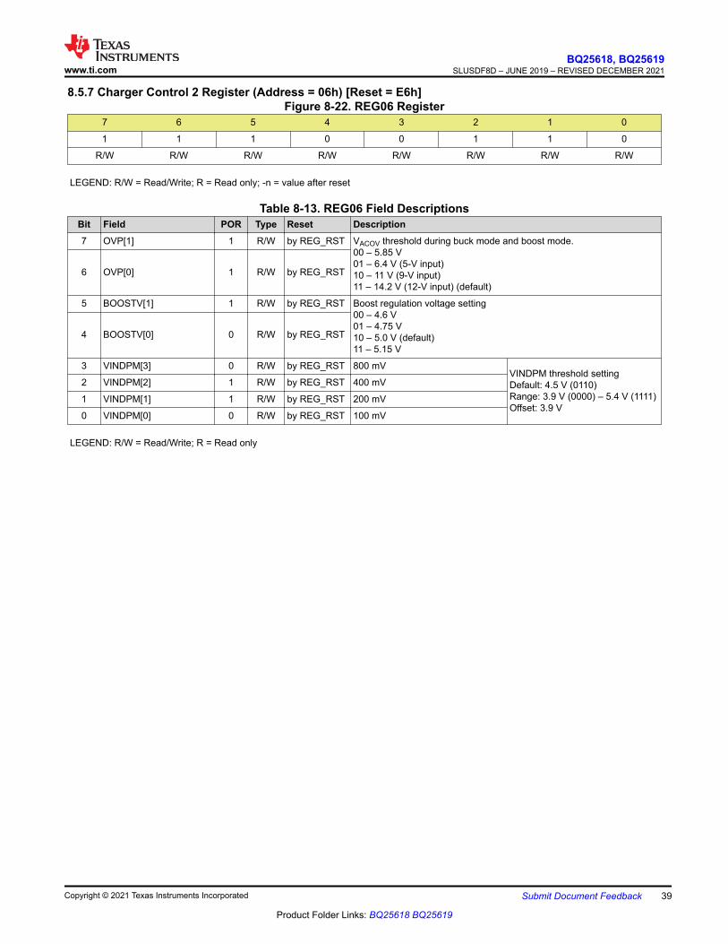
8.5.7 Charger Control 2 Register (Address = 06h) [Reset = E6h]Figure 8-22. REG06 Register
7 6 5 4 3 2 1 0
1 1 1 0 0 1 1 0
R/W R/W R/W R/W R/W R/W R/W R/W
LEGEND: R/W = Read/Write; R = Read only; -n = value after reset
Table 8-13. REG06 Field DescriptionsBit Field POR Type Reset Description7 OVP[1] 1 R/W by REG_RST VACOV threshold during buck mode and boost mode.
00 – 5.85 V01 – 6.4 V (5-V input)10 – 11 V (9-V input)11 – 14.2 V (12-V input) (default)
6 OVP[0] 1 R/W by REG_RST
5 BOOSTV[1] 1 R/W by REG_RST Boost regulation voltage setting00 – 4.6 V01 – 4.75 V10 – 5.0 V (default)11 – 5.15 V
4 BOOSTV[0] 0 R/W by REG_RST
3 VINDPM[3] 0 R/W by REG_RST 800 mVVINDPM threshold settingDefault: 4.5 V (0110)Range: 3.9 V (0000) – 5.4 V (1111)Offset: 3.9 V
2 VINDPM[2] 1 R/W by REG_RST 400 mV
1 VINDPM[1] 1 R/W by REG_RST 200 mV
0 VINDPM[0] 0 R/W by REG_RST 100 mV
LEGEND: R/W = Read/Write; R = Read only
www.ti.comBQ25618, BQ25619
SLUSDF8D – JUNE 2019 – REVISED DECEMBER 2021
Copyright © 2021 Texas Instruments Incorporated Submit Document Feedback 39
Product Folder Links: BQ25618 BQ25619
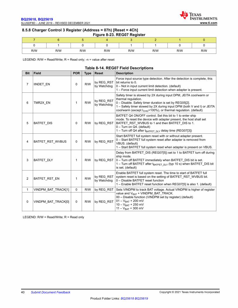
8.5.8 Charger Control 3 Register (Address = 07h) [Reset = 4Ch]Figure 8-23. REG07 Register
7 6 5 4 3 2 1 0
0 1 0 0 1 1 0 0
R/W R/W R/W R/W R/W R/W R/W R/W
LEGEND: R/W = Read/Write; R = Read only; -n = value after reset
Table 8-14. REG07 Field DescriptionsBit Field POR Type Reset Description
7 IINDET_EN 0 R/W by REG_RSTby Watchdog
Force input source type detection. After the detection is complete, this bit returns to 0.0 – Not in input current limit detection. (default)1 – Force input current limit detection when adapter is present.
6 TMR2X_EN 1 R/W by REG_RSTby Watchdog
Safety timer is slowed by 2X during input DPM, JEITA cool/warm or thermal regulation.0 – Disable. Safety timer duration is set by REG05[2].1 – Safety timer slowed by 2X during input DPM (both V and I) or JEITA cool/warm (except ICHG=100%), or thermal regulation. (default)
5 BATFET_DIS 0 R/W by REG_RST
BATFET Q4 ON/OFF control. Set this bit to 1 to enter ship mode. To reset the device with adapter present, the host shall set BATFET_RST_WVBUS to 1 and then BATFET_DIS to 1.0 – Turn on Q4. (default)1 – Turn off Q4 after tBATFET_DLY delay time (REG07[3])
4 BATFET_RST_WVBUS 0 R/W by REG_RST
Start BATFET full system reset with or without adapter present.0 – Start BATFET full system reset after adapter is removed from VBUS. (default)1 – Start BATFET full system reset when adapter is present on VBUS.
3 BATFET_DLY 1 R/W by REG_RST
Delay from BATFET_DIS (REG07[5]) set to 1 to BATFET turn off during ship mode.0 – Turn off BATFET immediately when BATFET_DIS bit is set.1 – Turn off BATFET after tBATFET_DLY (typ 10 s) when BATFET_DIS bit is set. (default)
2 BATFET_RST_EN 1 R/W by REG_RSTby Watchdog
Enable BATFET full system reset. The time to start of BATFET full system reset is based on the setting of BATFET_RST_WVBUS bit.0 – Disable BATFET reset function1 – Enable BATFET reset function when REG07[5] is also 1. (default)
1 VINDPM_BAT_TRACK[1] 0 R/W by REG_RST Sets VINDPM to track BAT voltage. Actual VINDPM is higher of register value and VBAT + VINDPM_BAT_TRACK.00 – Disable function (VINDPM set by register) (default)01 – VBAT + 200 mV10 – VBAT + 250 mV11 – VBAT + 300 mV
0 VINDPM_BAT_TRACK[0] 0 R/W by REG_RST
LEGEND: R/W = Read/Write; R = Read only
BQ25618, BQ25619SLUSDF8D – JUNE 2019 – REVISED DECEMBER 2021 www.ti.com
40 Submit Document Feedback Copyright © 2021 Texas Instruments Incorporated
Product Folder Links: BQ25618 BQ25619
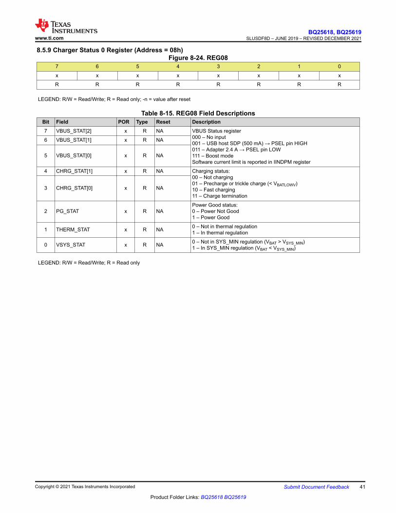
8.5.9 Charger Status 0 Register (Address = 08h)Figure 8-24. REG08
7 6 5 4 3 2 1 0
x x x x x x x x
R R R R R R R R
LEGEND: R/W = Read/Write; R = Read only; -n = value after reset
Table 8-15. REG08 Field DescriptionsBit Field POR Type Reset Description7 VBUS_STAT[2] x R NA VBUS Status register
000 – No input001 – USB host SDP (500 mA) → PSEL pin HIGH011 – Adapter 2.4 A → PSEL pin LOW111 – Boost modeSoftware current limit is reported in IINDPM register
6 VBUS_STAT[1] x R NA
5 VBUS_STAT[0] x R NA
4 CHRG_STAT[1] x R NA Charging status:00 – Not charging01 – Precharge or trickle charge (< VBATLOWV)10 – Fast charging11 – Charge termination
3 CHRG_STAT[0] x R NA
2 PG_STAT x R NAPower Good status:0 – Power Not Good1 – Power Good
1 THERM_STAT x R NA 0 – Not in thermal regulation1 – In thermal regulation
0 VSYS_STAT x R NA 0 – Not in SYS_MIN regulation (VBAT > VSYS_MIN)1 – In SYS_MIN regulation (VBAT < VSYS_MIN)
LEGEND: R/W = Read/Write; R = Read only
www.ti.comBQ25618, BQ25619
SLUSDF8D – JUNE 2019 – REVISED DECEMBER 2021
Copyright © 2021 Texas Instruments Incorporated Submit Document Feedback 41
Product Folder Links: BQ25618 BQ25619
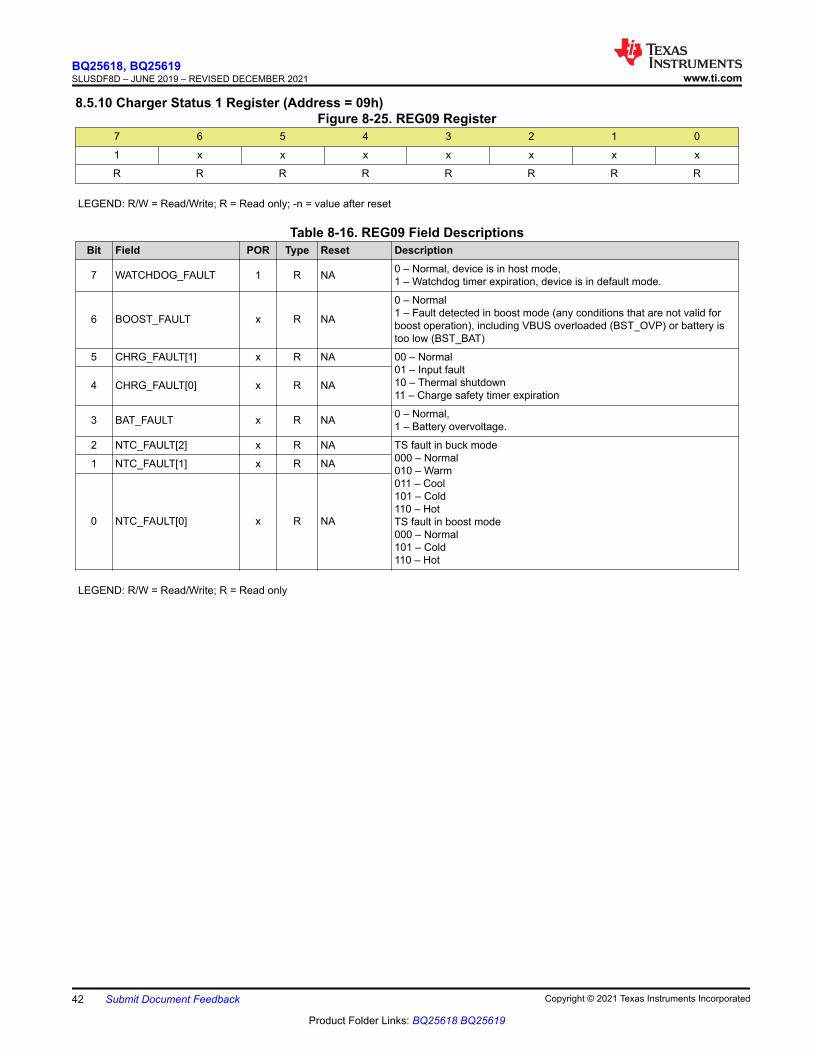
8.5.10 Charger Status 1 Register (Address = 09h)Figure 8-25. REG09 Register
7 6 5 4 3 2 1 0
1 x x x x x x x
R R R R R R R R
LEGEND: R/W = Read/Write; R = Read only; -n = value after reset
Table 8-16. REG09 Field DescriptionsBit Field POR Type Reset Description
7 WATCHDOG_FAULT 1 R NA 0 – Normal, device is in host mode,1 – Watchdog timer expiration, device is in default mode.
6 BOOST_FAULT x R NA
0 – Normal1 – Fault detected in boost mode (any conditions that are not valid for boost operation), including VBUS overloaded (BST_OVP) or battery is too low (BST_BAT)
5 CHRG_FAULT[1] x R NA 00 – Normal01 – Input fault10 – Thermal shutdown11 – Charge safety timer expiration
4 CHRG_FAULT[0] x R NA
3 BAT_FAULT x R NA 0 – Normal,1 – Battery overvoltage.
2 NTC_FAULT[2] x R NA TS fault in buck mode000 – Normal010 – Warm011 – Cool101 – Cold110 – HotTS fault in boost mode000 – Normal101 – Cold110 – Hot
1 NTC_FAULT[1] x R NA
0 NTC_FAULT[0] x R NA
LEGEND: R/W = Read/Write; R = Read only
BQ25618, BQ25619SLUSDF8D – JUNE 2019 – REVISED DECEMBER 2021 www.ti.com
42 Submit Document Feedback Copyright © 2021 Texas Instruments Incorporated
Product Folder Links: BQ25618 BQ25619
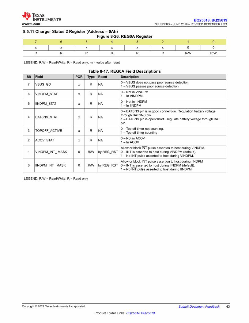
8.5.11 Charger Status 2 Register (Address = 0Ah)Figure 8-26. REG0A Register
7 6 5 4 3 2 1 0
x x x x x x 0 0
R R R R R R R/W R/W
LEGEND: R/W = Read/Write; R = Read only; -n = value after reset
Table 8-17. REG0A Field DescriptionsBit Field POR Type Reset Description
7 VBUS_GD x R NA 0 – VBUS does not pass poor source detection1 – VBUS passes poor source detection
6 VINDPM_STAT x R NA 0 – Not in VINDPM1 – In VINDPM
5 IINDPM_STAT x R NA 0 – Not in IINDPM1 – In IINDPM
4 BATSNS_STAT x R NA
0 – BATSNS pin is in good connection. Regulation battery voltage through BATSNS pin.1 – BATSNS pin is open/short. Regulate battery voltage through BAT pin.
3 TOPOFF_ACTIVE x R NA 0 – Top off timer not counting.1 – Top off timer counting
2 ACOV_STAT x R NA 0 – Not in ACOV1 – In ACOV
1 VINDPM_INT_ MASK 0 R/W by REG_RSTAllow or block INT pulse assertion to host during VINDPM.0 – INT is asserted to host during VINDPM (default).1 – No INT pulse asserted to host during VINDPM.
0 IINDPM_INT_ MASK 0 R/W by REG_RSTAllow or block INT pulse assertion to host during IINDPM0 – INT is asserted to host during IINDPM (default).1 – No INT pulse asserted to host during IINDPM.
LEGEND: R/W = Read/Write; R = Read only
www.ti.comBQ25618, BQ25619
SLUSDF8D – JUNE 2019 – REVISED DECEMBER 2021
Copyright © 2021 Texas Instruments Incorporated Submit Document Feedback 43
Product Folder Links: BQ25618 BQ25619
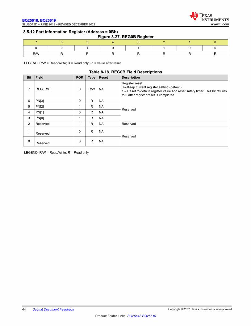
8.5.12 Part Information Register (Address = 0Bh)Figure 8-27. REG0B Register
7 6 5 4 3 2 1 0
0 0 1 0 1 1 0 0
R/W R R R R R R R
LEGEND: R/W = Read/Write; R = Read only; -n = value after reset
Table 8-18. REG0B Field DescriptionsBit Field POR Type Reset Description
7 REG_RST 0 R/W NA
Register reset0 – Keep current register setting (default).1 – Reset to default register value and reset safety timer. This bit returns to 0 after register reset is completed.
6 PN[3] 0 R NA
Reserved5 PN[2] 1 R NA
4 PN[1] 0 R NA
3 PN[0] 1 R NA
2 Reserved 1 R NA Reserved
1 Reserved 0 R NAReserved
0 Reserved 0 R NA
LEGEND: R/W = Read/Write; R = Read only
BQ25618, BQ25619SLUSDF8D – JUNE 2019 – REVISED DECEMBER 2021 www.ti.com
44 Submit Document Feedback Copyright © 2021 Texas Instruments Incorporated
Product Folder Links: BQ25618 BQ25619
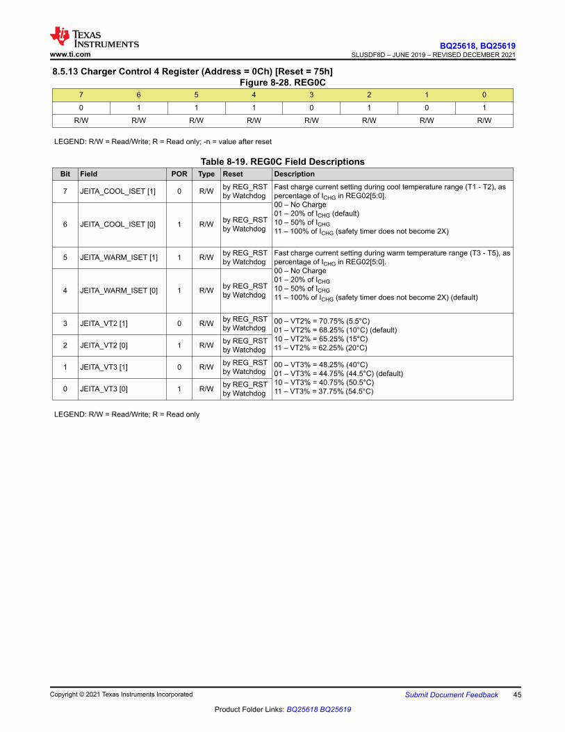
8.5.13 Charger Control 4 Register (Address = 0Ch) [Reset = 75h]Figure 8-28. REG0C
7 6 5 4 3 2 1 0
0 1 1 1 0 1 0 1
R/W R/W R/W R/W R/W R/W R/W R/W
LEGEND: R/W = Read/Write; R = Read only; -n = value after reset
Table 8-19. REG0C Field DescriptionsBit Field POR Type Reset Description
7 JEITA_COOL_ISET [1] 0 R/W by REG_RSTby Watchdog
Fast charge current setting during cool temperature range (T1 - T2), as percentage of ICHG in REG02[5:0].00 – No Charge01 – 20% of ICHG (default)10 – 50% of ICHG11 – 100% of ICHG (safety timer does not become 2X)
6 JEITA_COOL_ISET [0] 1 R/W by REG_RSTby Watchdog
5 JEITA_WARM_ISET [1] 1 R/W by REG_RSTby Watchdog
Fast charge current setting during warm temperature range (T3 - T5), as percentage of ICHG in REG02[5:0].00 – No Charge01 – 20% of ICHG10 – 50% of ICHG11 – 100% of ICHG (safety timer does not become 2X) (default)
4 JEITA_WARM_ISET [0] 1 R/W by REG_RSTby Watchdog
3 JEITA_VT2 [1] 0 R/W by REG_RSTby Watchdog
00 – VT2% = 70.75% (5.5°C)01 – VT2% = 68.25% (10°C) (default)10 – VT2% = 65.25% (15°C)11 – VT2% = 62.25% (20°C)2 JEITA_VT2 [0] 1 R/W by REG_RST
by Watchdog
1 JEITA_VT3 [1] 0 R/W by REG_RSTby Watchdog
00 – VT3% = 48.25% (40°C)01 – VT3% = 44.75% (44.5°C) (default)10 – VT3% = 40.75% (50.5°C)11 – VT3% = 37.75% (54.5°C)0 JEITA_VT3 [0] 1 R/W by REG_RST
by Watchdog
LEGEND: R/W = Read/Write; R = Read only
www.ti.comBQ25618, BQ25619
SLUSDF8D – JUNE 2019 – REVISED DECEMBER 2021
Copyright © 2021 Texas Instruments Incorporated Submit Document Feedback 45
Product Folder Links: BQ25618 BQ25619
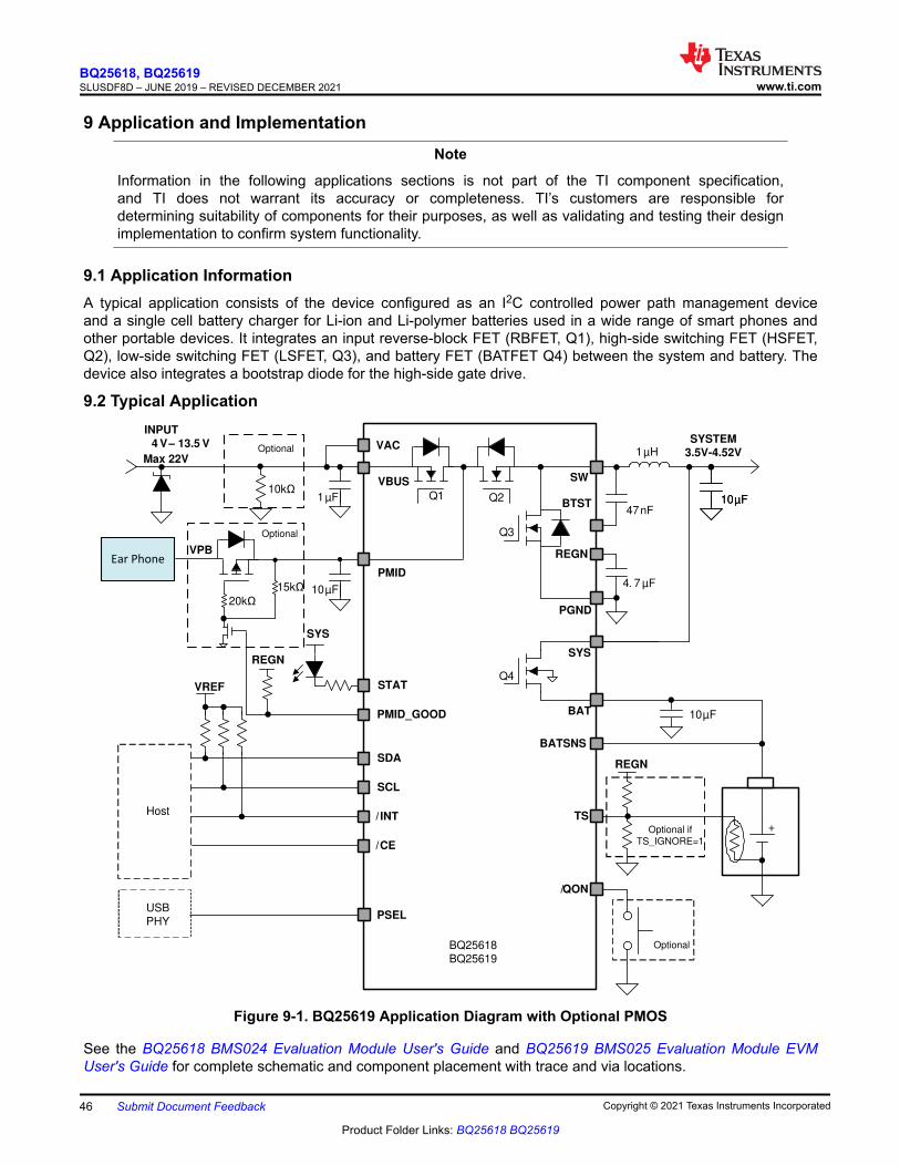
9 Application and ImplementationNote
Information in the following applications sections is not part of the TI component specification, and TI does not warrant its accuracy or completeness. TI’s customers are responsible for determining suitability of components for their purposes, as well as validating and testing their design implementation to confirm system functionality.
9.1 Application InformationA typical application consists of the device configured as an I2C controlled power path management device and a single cell battery charger for Li-ion and Li-polymer batteries used in a wide range of smart phones and other portable devices. It integrates an input reverse-block FET (RBFET, Q1), high-side switching FET (HSFET, Q2), low-side switching FET (LSFET, Q3), and battery FET (BATFET Q4) between the system and battery. The device also integrates a bootstrap diode for the high-side gate drive.
9.2 Typical Application
VBUS
Host
PMID
Q2
Q3
BTST
REGN
SW
PGND
SYSTEM
3.5V-4.52V
INPUT
4 V ± 13.5 V
SYS
BAT
STAT
PMID_GOOD
SYS
REGN
SDA
SCL
/INT
/CE
TS
REGN
/QON
VREFQ
47 nF1 µF
10 µF4. 7 µF
10 µF10 µF
10 µF
+
Optional
BATSNS
Q1
4
Ear Phone
1 µH
VPB
Max 22V
USBPHY
PSEL
VAC
15k
20k
Optional
10k
Optional
Optional if TS_IGNORE=1
BQ25618BQ25619
Figure 9-1. BQ25619 Application Diagram with Optional PMOS
See the BQ25618 BMS024 Evaluation Module User's Guide and BQ25619 BMS025 Evaluation Module EVM User's Guide for complete schematic and component placement with trace and via locations.
BQ25618, BQ25619SLUSDF8D – JUNE 2019 – REVISED DECEMBER 2021 www.ti.com
46 Submit Document Feedback Copyright © 2021 Texas Instruments Incorporated
Product Folder Links: BQ25618 BQ25619
9.2.1 Design Requirements
For this design example, use the parameters shown in the table below.
Table 9-1. Design ParametersPARAMETER VALUE
VVBUS voltage range 4 V to 13.5 V
Input current limit (REG00[4:0] ) 2.4 A
Fast charge current limit (REG02[5:0] ) 1.024 A
Minimum system voltage (REG01[3:1]) 3.5 V
Battery regulation voltage (REG04[7:3] ) 4.2 V
9.2.2 Detailed Design Procedure9.2.2.1 Inductor Selection
The 1.5-MHz switching frequency allows the use of small inductor and capacitor values to maintain an inductor saturation current higher than the charging current (ICHG) plus half the ripple current (IRIPPLE):
ISAT ≥ ICHG + (1/2) IRIPPLE (3)
The inductor ripple current depends on the input voltage (VVBUS), the duty cycle (D = VBAT/VVBUS), the switching frequency (fS) and the inductance (L).
INRIPPLE
V D (1 D)I
fs L
´ ´ -
=
´ (4)
The maximum inductor ripple current occurs when the duty cycle (D) is 0.5 or approximately 0.5. Usually inductor ripple is designed in the range between 20% and 40% maximum charging current as a trade-off between inductor size and efficiency for a practical design.
For compact solution size and efficiency at high current, a 1-µH inductor is recommended. To achieve better light load efficiency during boost mode (output current below 500 mA), the device also supports a 2.2-µH inductor with a 10-µF (min) cap on the system.
9.2.2.2 Input Capacitor and Resistor
Design the input capacitance to provide enough ripple current rating to absorb the input switching ripple current. Worst case RMS ripple current is half of the charging current when the duty cycle is 0.5. If the converter does not operate at 50% duty cycle, then the worst case capacitor RMS current ICIN occurs where the duty cycle is closest to 50% and can be estimated using Equation 5.
CIN CHGI I D (1 D)= ´ ´ - (5)
A low ESR ceramic capacitor such as X7R or X5R is preferred for the input decoupling capacitor and should be placed as close as possible to the drain of the high-side MOSFET and source of the low-side MOSFET. The voltage rating of the capacitor must be higher than the normal input voltage level. A 25-V or higher rated capacitor is preferred for a 12-V input voltage. Minimum capacitance of 10 μF is suggested for typical of 1.5-A charging current.
During high current output over 700 mA in boost mode, a 10-kΩ pull-down resistor on VBUS is recommended to keep VBUS low in case Q1 RBFET leakage gets high.
9.2.2.3 Output Capacitor
Ensure that the output capacitance has enough ripple current rating to absorb the output switching ripple current. Equation 6 shows the output capacitor RMS current ICOUT calculation.
www.ti.comBQ25618, BQ25619
SLUSDF8D – JUNE 2019 – REVISED DECEMBER 2021
Copyright © 2021 Texas Instruments Incorporated Submit Document Feedback 47
Product Folder Links: BQ25618 BQ25619
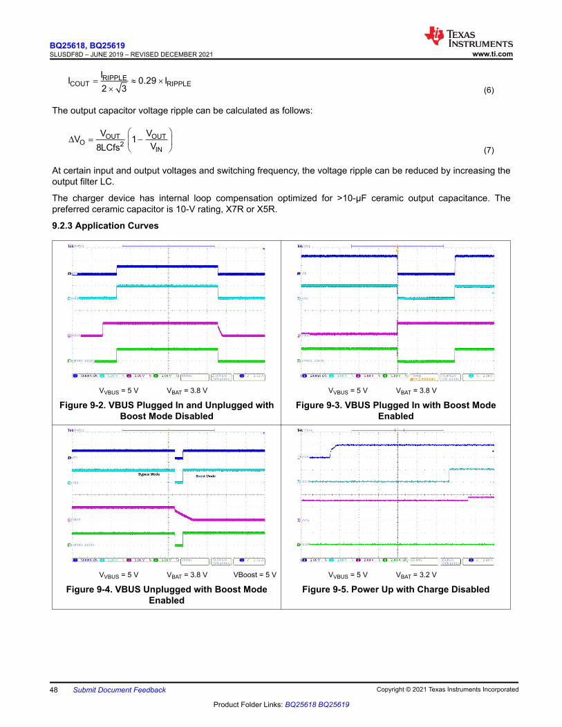
RIPPLECOUT RIPPLE
II 0.29 I
2 3= » ´
´ (6)
The output capacitor voltage ripple can be calculated as follows:
OUT OUTO 2
IN
V VV 1
V8LCfs
æ öD = -ç ÷
è ø (7)
At certain input and output voltages and switching frequency, the voltage ripple can be reduced by increasing the output filter LC.
The charger device has internal loop compensation optimized for >10-μF ceramic output capacitance. The preferred ceramic capacitor is 10-V rating, X7R or X5R.
9.2.3 Application Curves
VVBUS = 5 V VBAT = 3.8 V
Figure 9-2. VBUS Plugged In and Unplugged with Boost Mode Disabled
VVBUS = 5 V VBAT = 3.8 V
Figure 9-3. VBUS Plugged In with Boost Mode Enabled
VVBUS = 5 V VBAT = 3.8 V VBoost = 5 V
Figure 9-4. VBUS Unplugged with Boost Mode Enabled
VVBUS = 5 V VBAT = 3.2 V
Figure 9-5. Power Up with Charge Disabled
BQ25618, BQ25619SLUSDF8D – JUNE 2019 – REVISED DECEMBER 2021 www.ti.com
48 Submit Document Feedback Copyright © 2021 Texas Instruments Incorporated
Product Folder Links: BQ25618 BQ25619
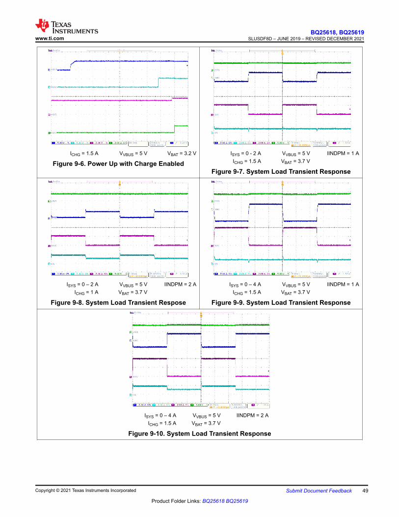
ICHG = 1.5 A VVBUS = 5 V VBAT = 3.2 V
Figure 9-6. Power Up with Charge EnabledISYS = 0 - 2 A VVBUS = 5 V IINDPM = 1 AICHG = 1.5 A VBAT = 3.7 V
Figure 9-7. System Load Transient Response
ISYS = 0 – 2 A VVBUS = 5 V IINDPM = 2 AICHG = 1 A VBAT = 3.7 V
Figure 9-8. System Load Transient Respose
ISYS = 0 – 4 A VVBUS = 5 V IINDPM = 1 AICHG = 1.5 A VBAT = 3.7 V
Figure 9-9. System Load Transient Response
ISYS = 0 – 4 A VVBUS = 5 V IINDPM = 2 AICHG = 1.5 A VBAT = 3.7 V
Figure 9-10. System Load Transient Response
www.ti.comBQ25618, BQ25619
SLUSDF8D – JUNE 2019 – REVISED DECEMBER 2021
Copyright © 2021 Texas Instruments Incorporated Submit Document Feedback 49
Product Folder Links: BQ25618 BQ25619

10 Power Supply RecommendationsIn order to provide an output voltage on SYS, the battery charger requires a power supply between 4 V and 13.5 V input with at least a 100-mA current rating connected to VBUS and a single-cell Li-ion battery with battery voltage greater than VBAT_UVLOZ connected to BAT. The source current rating needs to be at least 3 A in order for the buck converter of the charger to provide maximum output power to SYS.
BQ25618, BQ25619SLUSDF8D – JUNE 2019 – REVISED DECEMBER 2021 www.ti.com
50 Submit Document Feedback Copyright © 2021 Texas Instruments Incorporated
Product Folder Links: BQ25618 BQ25619
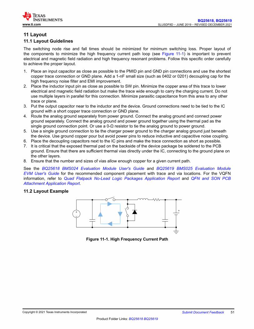
11 Layout11.1 Layout GuidelinesThe switching node rise and fall times should be minimized for minimum switching loss. Proper layout of the components to minimize the high frequency current path loop (see Figure 11-1) is important to prevent electrical and magnetic field radiation and high frequency resonant problems. Follow this specific order carefully to achieve the proper layout.
1. Place an input capacitor as close as possible to the PMID pin and GND pin connections and use the shortest copper trace connection or GND plane. Add a 1-nF small size (such as 0402 or 0201) decoupling cap for the high frequency noise filter and EMI improvement.
2. Place the inductor input pin as close as possible to SW pin. Minimize the copper area of this trace to lower electrical and magnetic field radiation but make the trace wide enough to carry the charging current. Do not use multiple layers in parallel for this connection. Minimize parasitic capacitance from this area to any other trace or plane.
3. Put the output capacitor near to the inductor and the device. Ground connections need to be tied to the IC ground with a short copper trace connection or GND plane.
4. Route the analog ground separately from power ground. Connect the analog ground and connect power ground separately. Connect the analog ground and power ground together using the thermal pad as the single ground connection point. Or use a 0-Ω resistor to tie the analog ground to power ground.
5. Use a single ground connection to tie the charger power ground to the charger analog ground just beneath the device. Use ground copper pour but avoid power pins to reduce inductive and capacitive noise coupling.
6. Place the decoupling capacitors next to the IC pins and make the trace connection as short as possible.7. It is critical that the exposed thermal pad on the backside of the device package be soldered to the PCB
ground. Ensure that there are sufficient thermal vias directly under the IC, connecting to the ground plane on the other layers.
8. Ensure that the number and sizes of vias allow enough copper for a given current path.
See the BQ25618 BMS024 Evaluation Module User's Guide and BQ25619 BMS025 Evaluation Module EVM User's Guide for the recommended component placement with trace and via locations. For the VQFN information, refer to Quad Flatpack No-Lead Logic Packages Application Report and QFN and SON PCB Attachment Application Report.
11.2 Layout Example
++
±
Figure 11-1. High Frequency Current Path
www.ti.comBQ25618, BQ25619
SLUSDF8D – JUNE 2019 – REVISED DECEMBER 2021
Copyright © 2021 Texas Instruments Incorporated Submit Document Feedback 51
Product Folder Links: BQ25618 BQ25619
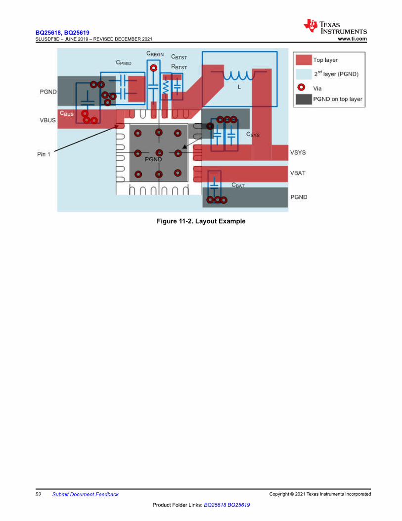
Figure 11-2. Layout Example
BQ25618, BQ25619SLUSDF8D – JUNE 2019 – REVISED DECEMBER 2021 www.ti.com
52 Submit Document Feedback Copyright © 2021 Texas Instruments Incorporated
Product Folder Links: BQ25618 BQ25619
12 Device and Documentation Support12.1 Device Support12.1.1 Third-Party Products Disclaimer
TI'S PUBLICATION OF INFORMATION REGARDING THIRD-PARTY PRODUCTS OR SERVICES DOES NOT CONSTITUTE AN ENDORSEMENT REGARDING THE SUITABILITY OF SUCH PRODUCTS OR SERVICES OR A WARRANTY, REPRESENTATION OR ENDORSEMENT OF SUCH PRODUCTS OR SERVICES, EITHER ALONE OR IN COMBINATION WITH ANY TI PRODUCT OR SERVICE.
12.2 Documentation Support12.2.1 Related Documentation
For related documentation see the following:
• BQ25619 BMS025 Evaluation Module User's Guide• BQ25618 BMS024 Evaluation Module User's Guide
12.3 Receiving Notification of Documentation UpdatesTo receive notification of documentation updates, navigate to the device product folder on ti.com. Click on Subscribe to updates to register and receive a weekly digest of any product information that has changed. For change details, review the revision history included in any revised document.
12.4 Support ResourcesTI E2E™ support forums are an engineer's go-to source for fast, verified answers and design help — straight from the experts. Search existing answers or ask your own question to get the quick design help you need.
Linked content is provided "AS IS" by the respective contributors. They do not constitute TI specifications and do not necessarily reflect TI's views; see TI's Terms of Use.
12.5 TrademarksTI E2E™ is a trademark of Texas Instruments.All trademarks are the property of their respective owners.12.6 Electrostatic Discharge Caution
This integrated circuit can be damaged by ESD. Texas Instruments recommends that all integrated circuits be handled with appropriate precautions. Failure to observe proper handling and installation procedures can cause damage.ESD damage can range from subtle performance degradation to complete device failure. Precision integrated circuits may be more susceptible to damage because very small parametric changes could cause the device not to meet its published specifications.
12.7 GlossaryTI Glossary This glossary lists and explains terms, acronyms, and definitions.
www.ti.comBQ25618, BQ25619
SLUSDF8D – JUNE 2019 – REVISED DECEMBER 2021
Copyright © 2021 Texas Instruments Incorporated Submit Document Feedback 53
Product Folder Links: BQ25618 BQ25619
13 Mechanical, Packaging, and Orderable InformationThe following pages include mechanical, packaging, and orderable information. This information is the most current data available for the designated devices. This data is subject to change without notice and revision of this document. For browser-based versions of this data sheet, refer to the left-hand navigation.
BQ25618, BQ25619SLUSDF8D – JUNE 2019 – REVISED DECEMBER 2021 www.ti.com
54 Submit Document Feedback Copyright © 2021 Texas Instruments Incorporated
Product Folder Links: BQ25618 BQ25619
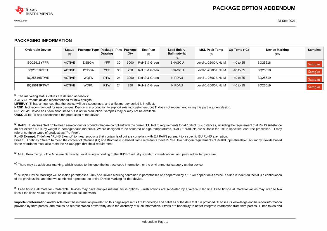
PACKAGE OPTION ADDENDUM
www.ti.com 28-Sep-2021
Addendum-Page 1
PACKAGING INFORMATION
Orderable Device Status(1)
Package Type PackageDrawing
Pins PackageQty
Eco Plan(2)
Lead finish/Ball material
(6)
MSL Peak Temp(3)
Op Temp (°C) Device Marking(4/5)
Samples
BQ25618YFFR ACTIVE DSBGA YFF 30 3000 RoHS & Green SNAGCU Level-1-260C-UNLIM -40 to 85 BQ25618
BQ25618YFFT ACTIVE DSBGA YFF 30 250 RoHS & Green SNAGCU Level-1-260C-UNLIM -40 to 85 BQ25618
BQ25619RTWR ACTIVE WQFN RTW 24 3000 RoHS & Green NIPDAU Level-1-260C-UNLIM -40 to 85 BQ25619
BQ25619RTWT ACTIVE WQFN RTW 24 250 RoHS & Green NIPDAU Level-1-260C-UNLIM -40 to 85 BQ25619
(1) The marketing status values are defined as follows:ACTIVE: Product device recommended for new designs.LIFEBUY: TI has announced that the device will be discontinued, and a lifetime-buy period is in effect.NRND: Not recommended for new designs. Device is in production to support existing customers, but TI does not recommend using this part in a new design.PREVIEW: Device has been announced but is not in production. Samples may or may not be available.OBSOLETE: TI has discontinued the production of the device.
(2) RoHS: TI defines "RoHS" to mean semiconductor products that are compliant with the current EU RoHS requirements for all 10 RoHS substances, including the requirement that RoHS substancedo not exceed 0.1% by weight in homogeneous materials. Where designed to be soldered at high temperatures, "RoHS" products are suitable for use in specified lead-free processes. TI mayreference these types of products as "Pb-Free".RoHS Exempt: TI defines "RoHS Exempt" to mean products that contain lead but are compliant with EU RoHS pursuant to a specific EU RoHS exemption.Green: TI defines "Green" to mean the content of Chlorine (Cl) and Bromine (Br) based flame retardants meet JS709B low halogen requirements of <=1000ppm threshold. Antimony trioxide basedflame retardants must also meet the <=1000ppm threshold requirement.
(3) MSL, Peak Temp. - The Moisture Sensitivity Level rating according to the JEDEC industry standard classifications, and peak solder temperature.
(4) There may be additional marking, which relates to the logo, the lot trace code information, or the environmental category on the device.
(5) Multiple Device Markings will be inside parentheses. Only one Device Marking contained in parentheses and separated by a "~" will appear on a device. If a line is indented then it is a continuationof the previous line and the two combined represent the entire Device Marking for that device.
(6) Lead finish/Ball material - Orderable Devices may have multiple material finish options. Finish options are separated by a vertical ruled line. Lead finish/Ball material values may wrap to twolines if the finish value exceeds the maximum column width.
Important Information and Disclaimer:The information provided on this page represents TI's knowledge and belief as of the date that it is provided. TI bases its knowledge and belief on informationprovided by third parties, and makes no representation or warranty as to the accuracy of such information. Efforts are underway to better integrate information from third parties. TI has taken and
PACKAGE OPTION ADDENDUM
www.ti.com 28-Sep-2021
Addendum-Page 2
continues to take reasonable steps to provide representative and accurate information but may not have conducted destructive testing or chemical analysis on incoming materials and chemicals.TI and TI suppliers consider certain information to be proprietary, and thus CAS numbers and other limited information may not be available for release.
In no event shall TI's liability arising out of such information exceed the total purchase price of the TI part(s) at issue in this document sold by TI to Customer on an annual basis.
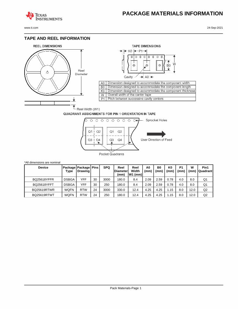
TAPE AND REEL INFORMATION
*All dimensions are nominal
Device PackageType
PackageDrawing
Pins SPQ ReelDiameter
(mm)
ReelWidth
W1 (mm)
A0(mm)
B0(mm)
K0(mm)
P1(mm)
W(mm)
Pin1Quadrant
BQ25618YFFR DSBGA YFF 30 3000 180.0 8.4 2.09 2.59 0.78 4.0 8.0 Q1
BQ25618YFFT DSBGA YFF 30 250 180.0 8.4 2.09 2.59 0.78 4.0 8.0 Q1
BQ25619RTWR WQFN RTW 24 3000 330.0 12.4 4.25 4.25 1.15 8.0 12.0 Q2
BQ25619RTWT WQFN RTW 24 250 180.0 12.4 4.25 4.25 1.15 8.0 12.0 Q2
PACKAGE MATERIALS INFORMATION
www.ti.com 24-Sep-2021
Pack Materials-Page 1
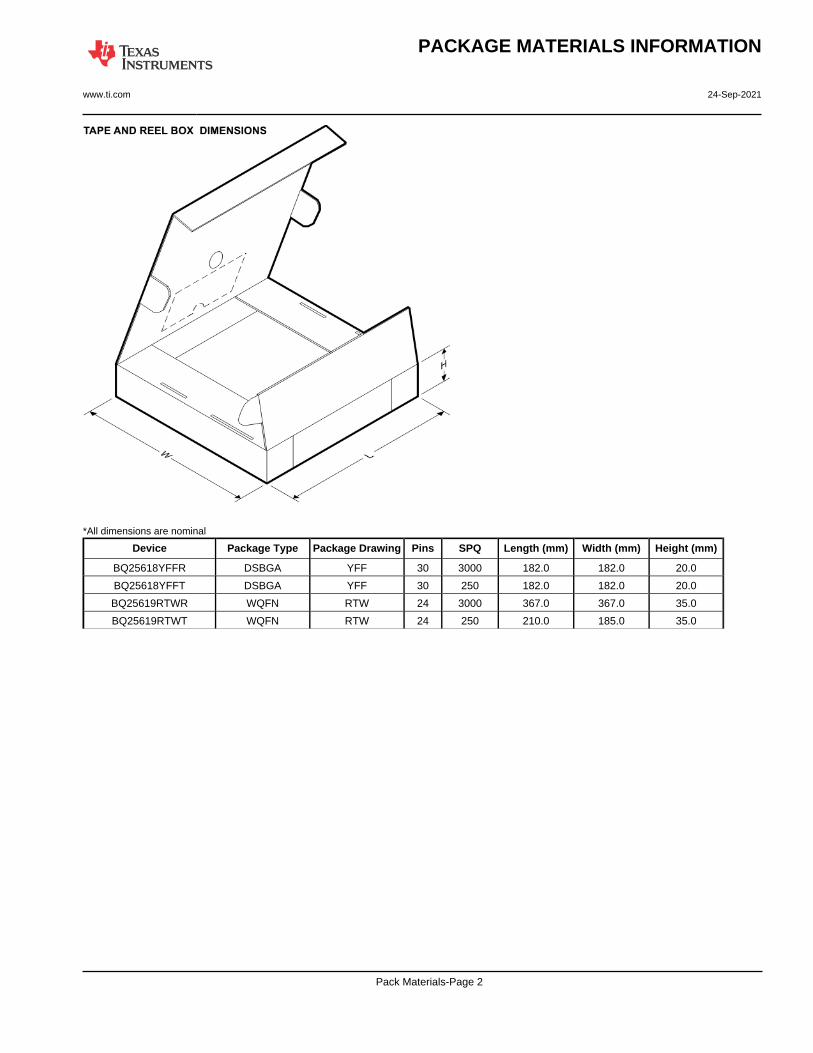
*All dimensions are nominal
Device Package Type Package Drawing Pins SPQ Length (mm) Width (mm) Height (mm)
BQ25618YFFR DSBGA YFF 30 3000 182.0 182.0 20.0
BQ25618YFFT DSBGA YFF 30 250 182.0 182.0 20.0
BQ25619RTWR WQFN RTW 24 3000 367.0 367.0 35.0
BQ25619RTWT WQFN RTW 24 250 210.0 185.0 35.0
PACKAGE MATERIALS INFORMATION
www.ti.com 24-Sep-2021
Pack Materials-Page 2
www.ti.com
GENERIC PACKAGE VIEW
This image is a representation of the package family, actual package may vary.Refer to the product data sheet for package details.
WQFN - 0.8 mm max heightRTW 24PLASTIC QUAD FLATPACK - NO LEAD4 x 4, 0.5 mm pitch
4224801/A

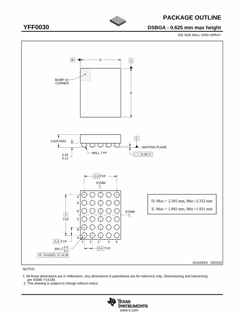
www.ti.com
PACKAGE OUTLINE
C0.625 MAX
0.300.12
2TYP
1.6 TYP
0.4 TYP
0.4 TYP30X 0.30.2
B E A
D
4219433/A 03/2016
DSBGA - 0.625 mm max heightYFF0030DIE SIZE BALL GRID ARRAY
NOTES: 1. All linear dimensions are in millimeters. Any dimensions in parenthesis are for reference only. Dimensioning and tolerancing per ASME Y14.5M. 2. This drawing is subject to change without notice.
BUMP A1CORNER
SEATING PLANE
BALL TYP 0.05 C
A
B
C
D
1 2 3
0.015 C A B
E
54
F
SYMM
SYMM
SCALE 4.500
D: Max =
E: Max =
2.392 mm, Min =
1.992 mm, Min =
2.332 mm
1.931 mm
www.ti.com
EXAMPLE BOARD LAYOUT
30X ( )0.23(0.4) TYP
(0.4) TYP
( )METAL
0.23 0.05 MAX
SOLDER MASKOPENING
METAL UNDERSOLDER MASK
( )SOLDER MASKOPENING
0.230.05 MIN
4219433/A 03/2016
DSBGA - 0.625 mm max heightYFF0030DIE SIZE BALL GRID ARRAY
NOTES: (continued) 3. Final dimensions may vary due to manufacturing tolerance considerations and also routing constraints. For more information, see Texas Instruments literature number SNVA009 (www.ti.com/lit/snva009).
SOLDER MASK DETAILSNOT TO SCALE
SYMM
SYMM
LAND PATTERN EXAMPLESCALE:25X
A
B
C
D
1 2 3 4 5
E
F
NON-SOLDER MASKDEFINED
(PREFERRED)
SOLDER MASKDEFINED
www.ti.com
EXAMPLE STENCIL DESIGN
(0.4)TYP
(0.4) TYP
30X ( 0.25)(R ) TYP0.05
METALTYP
4219433/A 03/2016
DSBGA - 0.625 mm max heightYFF0030DIE SIZE BALL GRID ARRAY
NOTES: (continued) 4. Laser cutting apertures with trapezoidal walls and rounded corners may offer better paste release.
SYMM
SYMM
SOLDER PASTE EXAMPLEBASED ON 0.1 mm THICK STENCIL
SCALE:30X
A
B
C
D
1 2 3
E
4 5
F

IMPORTANT NOTICE AND DISCLAIMERTI PROVIDES TECHNICAL AND RELIABILITY DATA (INCLUDING DATA SHEETS), DESIGN RESOURCES (INCLUDING REFERENCE DESIGNS), APPLICATION OR OTHER DESIGN ADVICE, WEB TOOLS, SAFETY INFORMATION, AND OTHER RESOURCES “AS IS” AND WITH ALL FAULTS, AND DISCLAIMS ALL WARRANTIES, EXPRESS AND IMPLIED, INCLUDING WITHOUT LIMITATION ANY IMPLIED WARRANTIES OF MERCHANTABILITY, FITNESS FOR A PARTICULAR PURPOSE OR NON-INFRINGEMENT OF THIRD PARTY INTELLECTUAL PROPERTY RIGHTS.These resources are intended for skilled developers designing with TI products. You are solely responsible for (1) selecting the appropriate TI products for your application, (2) designing, validating and testing your application, and (3) ensuring your application meets applicable standards, and any other safety, security, regulatory or other requirements.These resources are subject to change without notice. TI grants you permission to use these resources only for development of an application that uses the TI products described in the resource. Other reproduction and display of these resources is prohibited. No license is granted to any other TI intellectual property right or to any third party intellectual property right. TI disclaims responsibility for, and you will fully indemnify TI and its representatives against, any claims, damages, costs, losses, and liabilities arising out of your use of these resources.TI’s products are provided subject to TI’s Terms of Sale or other applicable terms available either on ti.com or provided in conjunction with such TI products. TI’s provision of these resources does not expand or otherwise alter TI’s applicable warranties or warranty disclaimers for TI products.TI objects to and rejects any additional or different terms you may have proposed. IMPORTANT NOTICE
Mailing Address: Texas Instruments, Post Office Box 655303, Dallas, Texas 75265Copyright © 2022, Texas Instruments Incorporated