PCA9536 Remote 4-Bit I2C and SMBus I/O Expander with ...
35
PCA9536 Remote 4-Bit I 2 C and SMBus I/O Expander with Configuration Registers 1 Features • Available in the Texas Instruments NanoFree ™ Package • Low standby current consumption of 1 μA Max • I 2 C to parallel port expander • Operating power-supply voltage range of 2.3 V to 5.5 V • 5-V Tolerant I/O ports • 400-kHz fast I 2 C bus • Input and output configuration register • Polarity inversion register • Internal power-on reset • No glitch on power up • Power-up with all channels configured as inputs • Noise filter on SCL/SDA inputs • Latched outputs with high-current drive maximum capability for directly driving LEDs • Latch-up performance exceeds 100 mA per JESD 78, class II • ESD Protection exceeds JESD 22 – 2000-V Human-body model (A114-A) – 200-V Machine model (A115-A) – 1000-V Charged-device model (C101) 2 Applications • Personal electronics – Wearables – Mobile phones – Gaming consoles • Servers • Routers 3 Description This 4-bit I/O expander for the two-line bidirectional bus (I 2 C) is designed for 2.3-V to 5.5-V V CC operation. It provides general-purpose remote I/O expansion for most microcontroller families through the I 2 C interface [serial clock (SCL), serial data (SDA)]. The PCA9536 features 4-bit Configuration (input or output selection), Input Port, Output Port, and Polarity Inversion (active high or active low) registers. At power on, the I/Os are configured as inputs with a weak pullup to V CC . However, the system controller can enable the I/Os as either inputs or outputs by writing to the I/O configuration bits. If no signals are applied externally to the PCA9536, the voltage level is 1, or high, because of the internal pullup resistors. The data for each input or output is stored in the corresponding Input Port or Output Port register. The polarity of the Input Port register can be inverted with the Polarity Inversion register and the system controller reads all registers. The system controller resets the PCA9536 in the event of a timeout or other improper operation by utilizing the power-on reset feature, which puts the registers in their default state and initializes the I 2 C/ SMBus state machine. The device outputs (latched) have high-current drive capability for directly driving LEDs, but has low current consumption. Device Information PART NUMBER PACKAGE (1) BODY SIZE (NOM) PCA9536 SOIC (8) 4.90 mm × 3.91 mm VSSOP (8) 3.00 mm × 3.00 mm (1) For all available packages, see the orderable addendum at the end of the datasheet. I2C or SMBus Controller (e.g. Processor) PCA9536 GND SCL SDA VCC P0 P1 P2 RESET, ENABLE, or control inputs INT or status outputs LEDs Buttons Peripheral Devices P3 Simplified Schematic PCA9536 SCPS125H – APRIL 2006 – REVISED MARCH 2022 An IMPORTANT NOTICE at the end of this data sheet addresses availability, warranty, changes, use in safety-critical applications, intellectual property matters and other important disclaimers. PRODUCTION DATA.
-
Upload
khangminh22 -
Category
Documents
-
view
1 -
download
0
Transcript of PCA9536 Remote 4-Bit I2C and SMBus I/O Expander with ...

PCA9536 Remote 4-Bit I2C and SMBus I/O Expander with Configuration Registers
1 Features• Available in the Texas Instruments NanoFree™
Package• Low standby current consumption of 1 μA Max• I2C to parallel port expander• Operating power-supply voltage range of 2.3 V to
5.5 V• 5-V Tolerant I/O ports• 400-kHz fast I2C bus• Input and output configuration register• Polarity inversion register• Internal power-on reset• No glitch on power up• Power-up with all channels configured as inputs• Noise filter on SCL/SDA inputs• Latched outputs with high-current drive maximum
capability for directly driving LEDs• Latch-up performance exceeds 100 mA per JESD
78, class II• ESD Protection exceeds JESD 22
– 2000-V Human-body model (A114-A)– 200-V Machine model (A115-A)– 1000-V Charged-device model (C101)
2 Applications• Personal electronics
– Wearables– Mobile phones– Gaming consoles
• Servers• Routers
3 DescriptionThis 4-bit I/O expander for the two-line bidirectional bus (I2C) is designed for 2.3-V to 5.5-V VCC operation. It provides general-purpose remote I/O expansion for most microcontroller families through the I2C interface [serial clock (SCL), serial data (SDA)].
The PCA9536 features 4-bit Configuration (input or output selection), Input Port, Output Port, and Polarity Inversion (active high or active low) registers. At power on, the I/Os are configured as inputs with a weak pullup to VCC. However, the system controller can enable the I/Os as either inputs or outputs by writing to the I/O configuration bits. If no signals are applied externally to the PCA9536, the voltage level is 1, or high, because of the internal pullup resistors. The data for each input or output is stored in the corresponding Input Port or Output Port register. The polarity of the Input Port register can be inverted with the Polarity Inversion register and the system controller reads all registers.
The system controller resets the PCA9536 in the event of a timeout or other improper operation by utilizing the power-on reset feature, which puts the registers in their default state and initializes the I2C/SMBus state machine.
The device outputs (latched) have high-current drive capability for directly driving LEDs, but has low current consumption.
Device InformationPART NUMBER PACKAGE(1) BODY SIZE (NOM)
PCA9536SOIC (8) 4.90 mm × 3.91 mm
VSSOP (8) 3.00 mm × 3.00 mm
(1) For all available packages, see the orderable addendum at the end of the datasheet.
I2C or SMBus Controller
(e.g. Processor) PCA9536
GND
SCL
SDAVCC
P0
P1
P2
RESET, ENABLE, or
control inputs
INT or status outputs
LEDs
Buttons
Peripheral Devices
P3
Simplified Schematic
PCA9536SCPS125H – APRIL 2006 – REVISED MARCH 2022
An IMPORTANT NOTICE at the end of this data sheet addresses availability, warranty, changes, use in safety-critical applications, intellectual property matters and other important disclaimers. PRODUCTION DATA.
Table of Contents1 Features............................................................................12 Applications..................................................................... 13 Description.......................................................................14 Revision History.............................................................. 25 Pin Configuration and Functions...................................36 Specifications.................................................................. 4
6.1 Absolute Maximum Ratings........................................ 46.2 ESD Ratings............................................................... 46.3 Recommended Operating Conditions.........................46.4 Thermal Information....................................................46.5 Electrical Characteristics.............................................56.6 I2C Interface Timing Requirements.............................66.7 Switching Characteristics............................................66.8 Typical Characteristics................................................ 7
7 Parameter Measurement Information.......................... 108 Detailed Description......................................................12
8.1 Overview................................................................... 128.2 Functional Block Diagram......................................... 128.3 Feature Description...................................................138.4 Device Functional Modes..........................................13
8.5 Programming............................................................ 138.6 Register Maps...........................................................15
9 Application Information Disclaimer............................. 199.1 Application Information............................................. 199.2 Typical Application.................................................... 19
10 Power Supply Recommendations..............................2210.1 Power-On Reset Errata...........................................2210.2 System Impact........................................................ 22
11 Layout...........................................................................2311.1 Layout Guidelines................................................... 2311.2 Layout Example...................................................... 23
12 Device and Documentation Support..........................2412.1 Documentation Support.......................................... 2412.2 Receiving Notification of Documentation Updates..2412.3 Support Resources................................................. 2412.4 Trademarks.............................................................2412.5 Electrostatic Discharge Caution..............................2412.6 Glossary..................................................................24
13 Mechanical, Packaging, and Orderable Information.................................................................... 24
4 Revision HistoryChanges from Revision G (June 2014) to Revision H (March 2022) Page• Changed all instances of legacy terminology to controller and target where I2C is mentioned..........................1• Deleted the DSBGA (YZP) package information................................................................................................ 1• Added the Simplified Schematic to the front page..............................................................................................1• Removed packaging information from the Absolute Maximum Ratings table.................................................... 4• Added Tstg to the Absolute Maximum Ratings table........................................................................................... 4• Added the Thermal Information table................................................................................................................. 4• Deleted VPOR from the Electrical Characteristics ...............................................................................................5• Added VPORR and VPORF to the Electrical Characteristics .................................................................................5• Changed the ICC stand by mode current max values for 5.5 V from 1 to 1.8 μA; 3.6 V from 0.9 to 1.2 μA; and
2.7 V from 0.8 to 1 μA in the Electrical Characteristics ......................................................................................5• Changed the tvd(data) and tvd(ack) MAX values from: 1 μs to: 3.45 μs in the Standard Mode timing....................6• Changed the ticr, tocf, and tocf MIN values in the Fast Mode timing.....................................................................6• Added the Overview section............................................................................................................................. 12• Added the Device Functional Modes section....................................................................................................13• Added Detailed Design Procedure section....................................................................................................... 20• Added Application Curves section.................................................................................................................... 21• Added the Layout section................................................................................................................................. 23
Changes from Revision F (September 2008) to Revision G (June 2014) Page• Added Power-On Reset Errata section.............................................................................................................22
PCA9536SCPS125H – APRIL 2006 – REVISED MARCH 2022 www.ti.com
2 Submit Document Feedback Copyright © 2022 Texas Instruments Incorporated
Product Folder Links: PCA9536
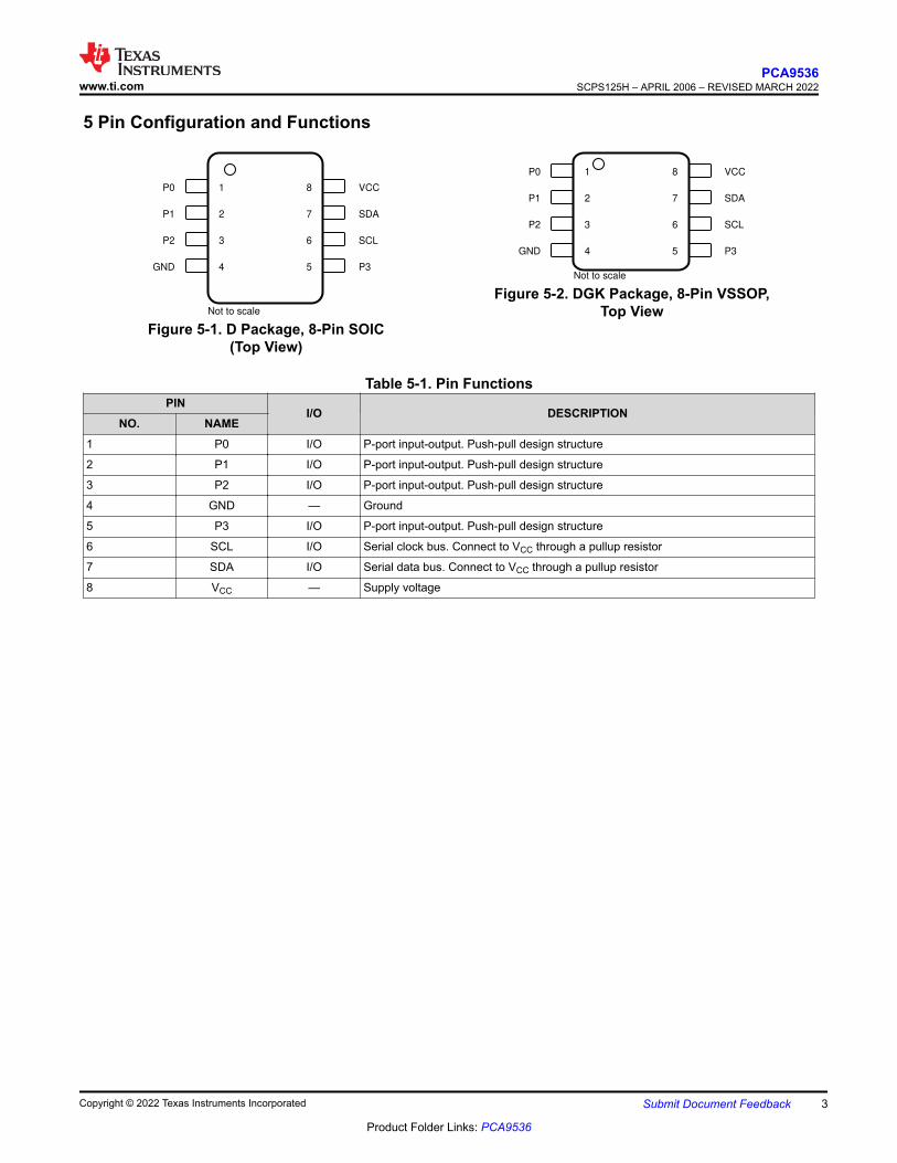
5 Pin Configuration and Functions
1P0 8 VCC
2P1 7 SDA
3P2 6 SCL
4GND 5 P3
Not to scale
Figure 5-1. D Package, 8-Pin SOIC(Top View)
1P0 8 VCC
2P1 7 SDA
3P2 6 SCL
4GND 5 P3
Not to scale
Figure 5-2. DGK Package, 8-Pin VSSOP,Top View
Table 5-1. Pin FunctionsPIN
I/O DESCRIPTIONNO. NAME
1 P0 I/O P-port input-output. Push-pull design structure
2 P1 I/O P-port input-output. Push-pull design structure
3 P2 I/O P-port input-output. Push-pull design structure
4 GND — Ground
5 P3 I/O P-port input-output. Push-pull design structure
6 SCL I/O Serial clock bus. Connect to VCC through a pullup resistor
7 SDA I/O Serial data bus. Connect to VCC through a pullup resistor
8 VCC — Supply voltage
www.ti.comPCA9536
SCPS125H – APRIL 2006 – REVISED MARCH 2022
Copyright © 2022 Texas Instruments Incorporated Submit Document Feedback 3
Product Folder Links: PCA9536
6 Specifications
6.1 Absolute Maximum Ratingsover operating free-air temperature range (unless otherwise noted) See (1)
MIN MAX UNIT
VCC Supply voltage –0.5 6 V
VI Input voltage (2) –0.5 6 V
VO Output voltage (2) –0.5 6 V
IIK Input clamp current VI < 0 –20 mA
IOK Output clamp current VO < 0 –20 mA
IIOK Input/output clamp current VO < 0 or VO > VCC ±20 mA
IOL Continuous output low current VO = 0 to VCC 50 mA
IOH Continuous output high current VO = 0 to VCC –50 mA
ICCContinuous current through GND –200
mAContinuous current through VCC 160
Tstg Storage temperature –65 150 °C
(1) Stresses beyond those listed under Absolute Maximum Ratings may cause permanent damage to the device. These are stress ratings only, which do not imply functional operation of the device at these or any other conditions beyond those indicated under Recommended Operating Conditions. Exposure to absolute-maximum-rated conditions for extended periods may affect device reliability.
(2) The input negative-voltage and output voltage ratings may be exceeded if the input and output current ratings are observed.
6.2 ESD RatingsMIN MAX UNIT
V(ESD) Electrostatic dischargeHuman body model (HBM), per ANSI/ESDA/JEDEC JS-001, all pins(1) 0 2000
VCharged device model (CDM), per JEDEC specification JESD22-C101, all pins(2) 0 1000
(1) JEDEC document JEP155 states that 500-V HBM allows safe manufacturing with a standard ESD control process.(2) JEDEC document JEP157 states that 250-V CDM allows safe manufacturing with a standard ESD control process.
6.3 Recommended Operating ConditionsMIN MAX UNIT
VCC Supply voltage 2.3 5.5 V
VIH High-level input voltageSCL, SDA 0.7 × VCC 5.5
VP3–P0 2 5.5
VIL Low-level input voltageSCL, SDA –0.5 0.3 × VCC
VP3–P0 –0.5 0.8
IOH High-level output current P3–P0 –10 mA
IOL Low-level output current P3–P0 25 mA
TA Operating free-air temperature –40 85 °C
6.4 Thermal InformationTHERMAL METRIC(1)
D (SOIC) DGK (VSSOP)UNIT
8 PINS 8 PINS
RθJA Junction-to-ambient thermal resistance 141.9 183.7 °C/W
RθJC(top) Junction-to-case (top) thermal resistance 82.6 76.9 °C/W
RθJB Junction-to-board thermal resistance 85.3 104.9 °C/W
ψJT Junction-to-top characterization parameter 32.3 18.7 °C/W
ψJB Junction-to-board characterization parameter 84.6 103.4 °C/W
(1) For more information about traditional and new thermal metrics, see the Semiconductor and IC Package Thermal Metrics application report.
PCA9536SCPS125H – APRIL 2006 – REVISED MARCH 2022 www.ti.com
4 Submit Document Feedback Copyright © 2022 Texas Instruments Incorporated
Product Folder Links: PCA9536

6.5 Electrical Characteristicsover recommended operating free-air temperature range (unless otherwise noted)
PARAMETER TEST CONDITIONS VCC MIN TYP(1) MAX UNIT
VIK Input diode clamp voltage II = –18 mA 2.3 V to 5.5 V –1.2 0 V
VPORR Power-on reset voltage, VCC rising VI = VCC or GND, IO = 0 1.2 1.6 V
VPORF Power-on reset voltage, VCC falling VI = VCC or GND, IO = 0 0.75 1 V
VOHP-port high-leveloutput voltage(2)
IOH = –8 mA
2.3 V 1.8
V
3 V 2.6
4.5 V 4.1
4.75 V 4.1
IOH = –10 mA
2.3 V 1.7
3 V 2.5
4.5 V 4
4.75 V 4
IOL
SDA VOL = 0.4 V 2.3 V to 5.5 V 3 10
mAP-port(3)
VOL = 0.5 V
2.3 V 8 10
3 V 8 14
4.5 V 8 17
4.75 V 8 32
VOL = 0.7 V
2.3 V 10 13
3 V 10 19
4.5 V 10 24
4.75 V 10 44
II SCL, SDA VI = VCC or GND 2.3 V to 5.5 V ±1 μA
IIH P-port VI = VCC 2.3 V to 5.5 V 1 μA
IIL P-port VI = GND 2.3 V to 5.5 V –100 μA
ICC
Operating mode
VI = VCC, IO = 0,I/O = inputs, fscl = 400 kHz
5.5 V 73 150
μA
3.6 V 9 50
2.7 V 7 30
VI = VCC, IO = 0,I/O = inputs, fscl = 100 kHz
5.5 V 14 25
3.6 V 9 20
2.7 V 6 15
Standby mode
VI = GND, IO = 0,I/O = inputs, fscl = 0 kHz
5.5 V 225 350
3.6 V 175 250
2.7 V 125 200
VI = VCC, IO = 0,I/O = inputs, fscl = 0 kHz
5.5 V 0.25 1.8
3.6 V 0.2 1.2
2.7 V 0.1 1
ΔICCAdditional current instandby mode
One input at VCC – 0.6 V,Other inputs at VCC or GND 2.3 V to 5.5 V 0.35
mAEvery LED I/O at VI = 4.3 V,fscl = 0 kHz 5.5 V 0.4
Ci SCL VI = VCC or GND 2.3 V to 5.5 V 4 5 pF
CioSDA
VIO = VCC or GND 2.3 V to 5.5 V5 6.5
pFP-port 7.5 9.5
(1) All typical values are at nominal supply voltage (2.5-, 3.3-, or 5-V VCC) and TA = 25°C.(2) The total current sourced by all I/Os must be limited to 85 mA.(3) Each I/O must be limited externally to a maximum of 25 mA, and the P-port (P3–P0) must be limited to a maximum current of 100 mA.
www.ti.comPCA9536
SCPS125H – APRIL 2006 – REVISED MARCH 2022
Copyright © 2022 Texas Instruments Incorporated Submit Document Feedback 5
Product Folder Links: PCA9536
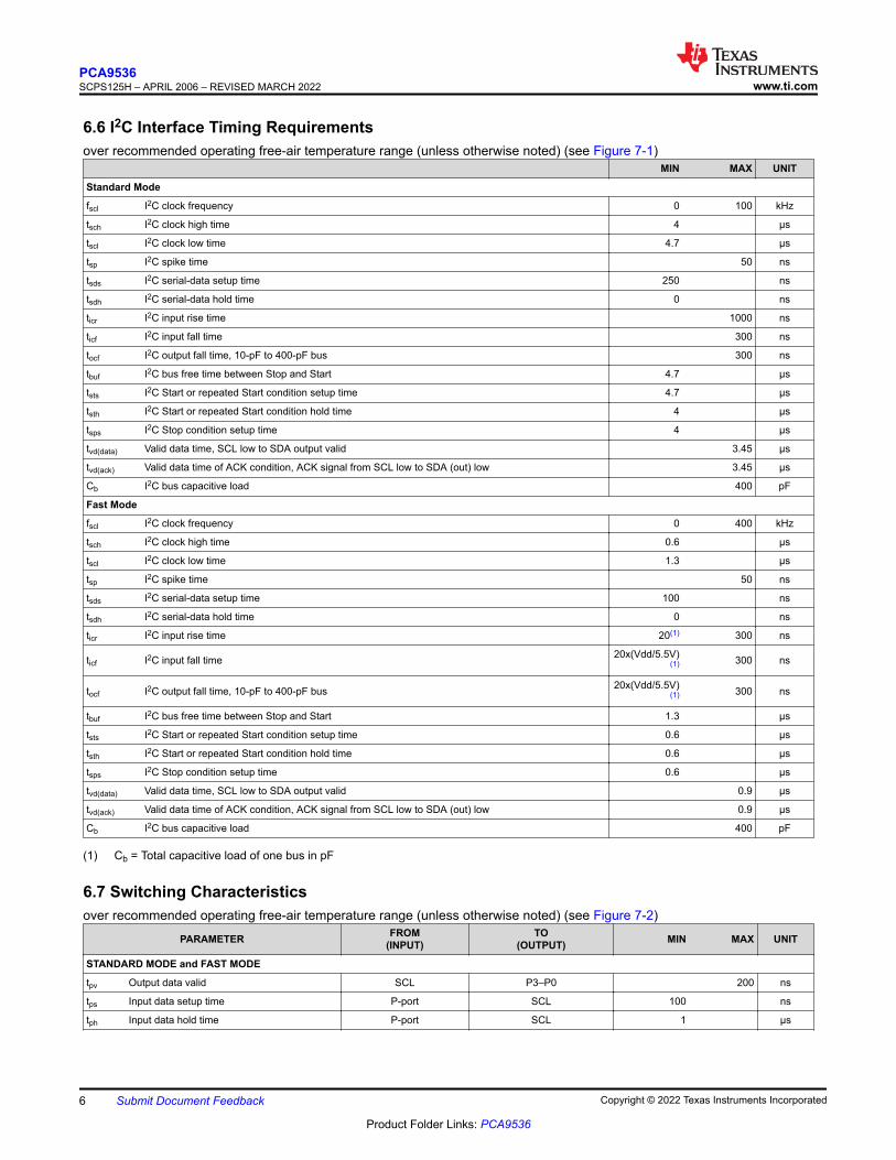
6.6 I2C Interface Timing Requirementsover recommended operating free-air temperature range (unless otherwise noted) (see Figure 7-1)
MIN MAX UNIT
Standard Mode
fscl I2C clock frequency 0 100 kHz
tsch I2C clock high time 4 μs
tscl I2C clock low time 4.7 μs
tsp I2C spike time 50 ns
tsds I2C serial-data setup time 250 ns
tsdh I2C serial-data hold time 0 ns
ticr I2C input rise time 1000 ns
ticf I2C input fall time 300 ns
tocf I2C output fall time, 10-pF to 400-pF bus 300 ns
tbuf I2C bus free time between Stop and Start 4.7 μs
tsts I2C Start or repeated Start condition setup time 4.7 μs
tsth I2C Start or repeated Start condition hold time 4 μs
tsps I2C Stop condition setup time 4 μs
tvd(data) Valid data time, SCL low to SDA output valid 3.45 μs
tvd(ack) Valid data time of ACK condition, ACK signal from SCL low to SDA (out) low 3.45 μs
Cb I2C bus capacitive load 400 pF
Fast Mode
fscl I2C clock frequency 0 400 kHz
tsch I2C clock high time 0.6 μs
tscl I2C clock low time 1.3 μs
tsp I2C spike time 50 ns
tsds I2C serial-data setup time 100 ns
tsdh I2C serial-data hold time 0 ns
ticr I2C input rise time 20(1) 300 ns
ticf I2C input fall time 20x(Vdd/5.5V)(1) 300 ns
tocf I2C output fall time, 10-pF to 400-pF bus 20x(Vdd/5.5V)(1) 300 ns
tbuf I2C bus free time between Stop and Start 1.3 μs
tsts I2C Start or repeated Start condition setup time 0.6 μs
tsth I2C Start or repeated Start condition hold time 0.6 μs
tsps I2C Stop condition setup time 0.6 μs
tvd(data) Valid data time, SCL low to SDA output valid 0.9 μs
tvd(ack) Valid data time of ACK condition, ACK signal from SCL low to SDA (out) low 0.9 μs
Cb I2C bus capacitive load 400 pF
(1) Cb = Total capacitive load of one bus in pF
6.7 Switching Characteristicsover recommended operating free-air temperature range (unless otherwise noted) (see Figure 7-2)
PARAMETER FROM(INPUT)
TO(OUTPUT) MIN MAX UNIT
STANDARD MODE and FAST MODE
tpv Output data valid SCL P3–P0 200 ns
tps Input data setup time P-port SCL 100 ns
tph Input data hold time P-port SCL 1 μs
PCA9536SCPS125H – APRIL 2006 – REVISED MARCH 2022 www.ti.com
6 Submit Document Feedback Copyright © 2022 Texas Instruments Incorporated
Product Folder Links: PCA9536
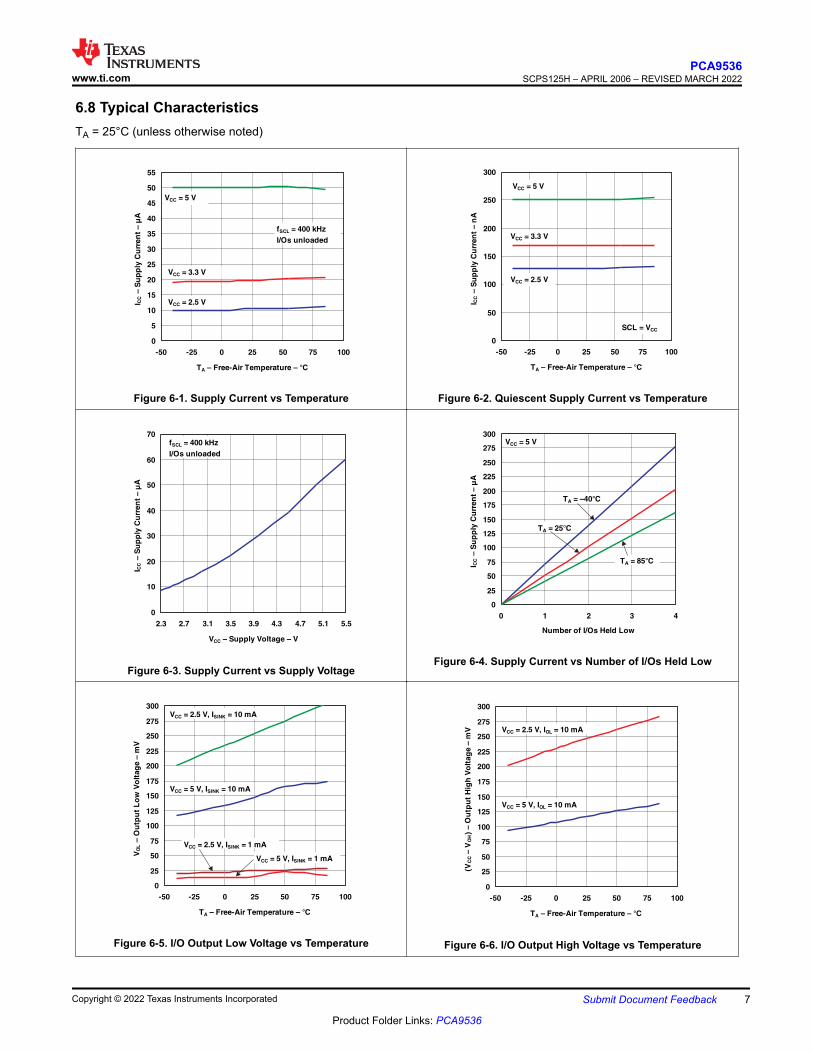
6.8 Typical CharacteristicsTA = 25°C (unless otherwise noted)
0
5
10
15
20
25
30
35
40
45
50
55
-50 -25 0 25 50 75 100
TA – Free-Air Temperature – °C
I CC
–S
up
ply
Cu
rren
t–
µA
VCC = 2.5 V
VCC = 3.3 V
VCC = 5 V
fSCL = 400 kHz
I/Os unloaded
Figure 6-1. Supply Current vs Temperature
0
50
100
150
200
250
300
-50 -25 0 25 50 75 100
TA – Free-Air Temperature – °C
I CC
–S
up
ply
Cu
rren
t–
nA
VCC = 2.5 V
VCC = 3.3 V
VCC = 5 V
SCL = VCC
Figure 6-2. Quiescent Supply Current vs Temperature
0
10
20
30
40
50
60
70
2.3 2.7 3.1 3.5 3.9 4.3 4.7 5.1 5.5
VCC – Supply Voltage – V
I CC
–S
up
ply
Cu
rren
t–
µA
fSCL = 400 kHz
I/Os unloaded
Figure 6-3. Supply Current vs Supply Voltage
0
25
50
75
100
125
150
175
200
225
250
275
300
0 1 2 3 4
Number of I/Os Held Low
I CC
–S
up
ply
Cu
rren
t–
µA
TA = –40°C
VCC = 5 V
TA = 25°C
TA = 85°C
Figure 6-4. Supply Current vs Number of I/Os Held Low
0
25
50
75
100
125
150
175
200
225
250
275
300
-50 -25 0 25 50 75 100
TA – Free-Air Temperature – °C
VO
L–
Ou
tpu
tL
ow
Vo
ltag
e–
mV
VCC = 5 V, ISINK = 10 mA
VCC = 2.5 V, ISINK = 10 mA
VCC = 2.5 V, ISINK = 1 mA
VCC = 5 V, ISINK = 1 mA
Figure 6-5. I/O Output Low Voltage vs Temperature
0
25
50
75
100
125
150
175
200
225
250
275
300
-50 -25 0 25 50 75 100
TA – Free-Air Temperature – °C
(VC
C–
VO
H)
–O
utp
ut
Hig
hV
olt
ag
e–
mV
VCC = 5 V, IOL = 10 mA
VCC = 2.5 V, IOL = 10 mA
Figure 6-6. I/O Output High Voltage vs Temperature
www.ti.comPCA9536
SCPS125H – APRIL 2006 – REVISED MARCH 2022
Copyright © 2022 Texas Instruments Incorporated Submit Document Feedback 7
Product Folder Links: PCA9536

6.8 Typical Characteristics (continued)TA = 25°C (unless otherwise noted)
0
5
10
15
20
25
30
0.0 0.1 0.2 0.3 0.4 0.5 0.6 0.7
VOL – Output Low Voltage – V
ISIN
K–
I/O
Sin
kC
urr
en
t–
mA TA = –40°C
VCC = 2.5 V
TA = 25°C
TA = 85°C
Figure 6-7. I/O Sink Current vs Output Low Voltage
0
5
10
15
20
25
30
35
40
0.0 0.1 0.2 0.3 0.4 0.5 0.6 0.7
VOL – Output Low Voltage – V
ISIN
K–
I/O
Sin
kC
urr
en
t–
mA
TA = –40°C
VCC = 3.3 V
TA = 25°C
TA = 85°C
Figure 6-8. I/O Sink Current vs Output Low Voltage
0
5
10
15
20
25
30
35
40
45
50
55
60
0.0 0.1 0.2 0.3 0.4 0.5 0.6 0.7
VOL – Output Low Voltage – V
ISIN
K–
I/O
Sin
kC
urr
en
t–
mA
TA = –40°C
VCC = 5 V
TA = 25°C
TA = 85°C
Figure 6-9. I/O Sink Current vs Output Low Voltage
0
5
10
15
20
25
30
0.0 0.1 0.2 0.3 0.4 0.5 0.6 0.7
(VCC – VOH) – Output High Voltage – V
I SO
UR
CE
–I/O
So
urc
eC
urr
en
t–
mA
TA = –40°C
VCC = 2.5 V
TA = 25°C
TA = 85°C
Figure 6-10. I/O Source Current vs Output High Voltage
0
5
10
15
20
25
30
35
40
45
0.0 0.1 0.2 0.3 0.4 0.5 0.6 0.7
(VCC – VOH) – Output High Voltage – V
I SO
UR
CE
–I/O
So
urc
eC
urr
en
t–
mA TA = –40°C
VCC = 3.3 V
TA = 25°C
TA = 85°C
Figure 6-11. I/O Source Current vs Output High Voltage
0
5
10
15
20
25
30
35
40
45
50
55
60
65
70
0.0 0.1 0.2 0.3 0.4 0.5 0.6 0.7
(VCC – VOH) – Output High Voltage – V
I SO
UR
CE
–I/O
So
urc
eC
urr
en
t–
mA
TA = –40°C
VCC = 5 V
TA = 25°C
TA = 85°C
Figure 6-12. I/O Source Current vs Output High Voltage
PCA9536SCPS125H – APRIL 2006 – REVISED MARCH 2022 www.ti.com
8 Submit Document Feedback Copyright © 2022 Texas Instruments Incorporated
Product Folder Links: PCA9536
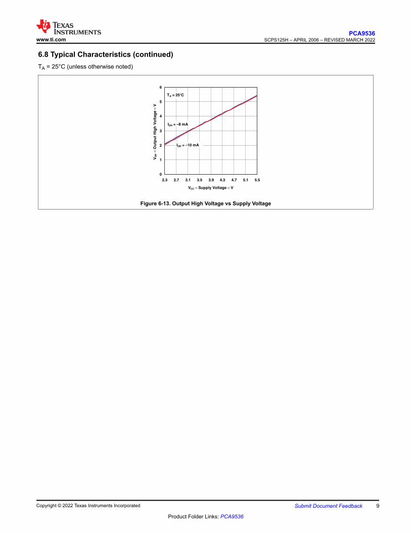
6.8 Typical Characteristics (continued)TA = 25°C (unless otherwise noted)
0
1
2
3
4
5
6
2.3 2.7 3.1 3.5 3.9 4.3 4.7 5.1 5.5
VCC – Supply Voltage – V
VO
H–
Ou
tpu
tH
igh
Vo
ltag
e–
V
IOH = –10 mA
IOH = –8 mA
TA = 25°C
Figure 6-13. Output High Voltage vs Supply Voltage
www.ti.comPCA9536
SCPS125H – APRIL 2006 – REVISED MARCH 2022
Copyright © 2022 Texas Instruments Incorporated Submit Document Feedback 9
Product Folder Links: PCA9536
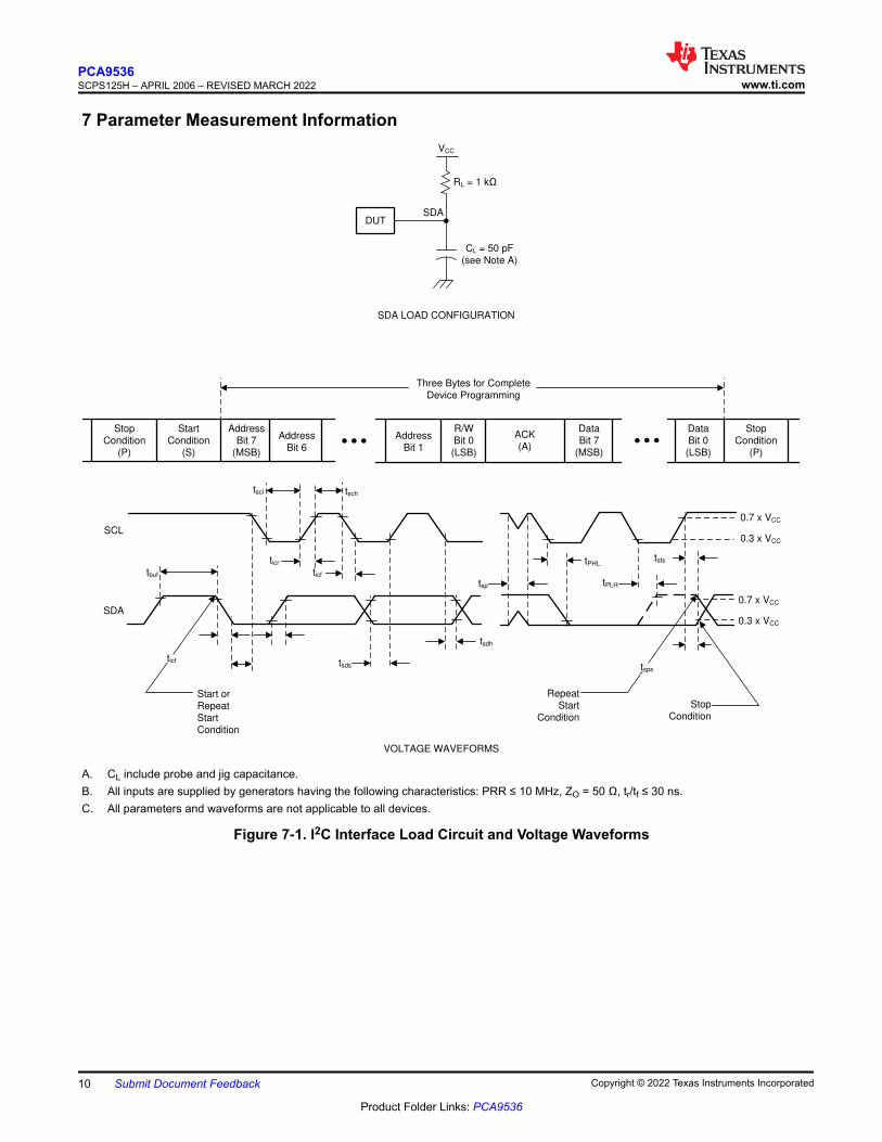
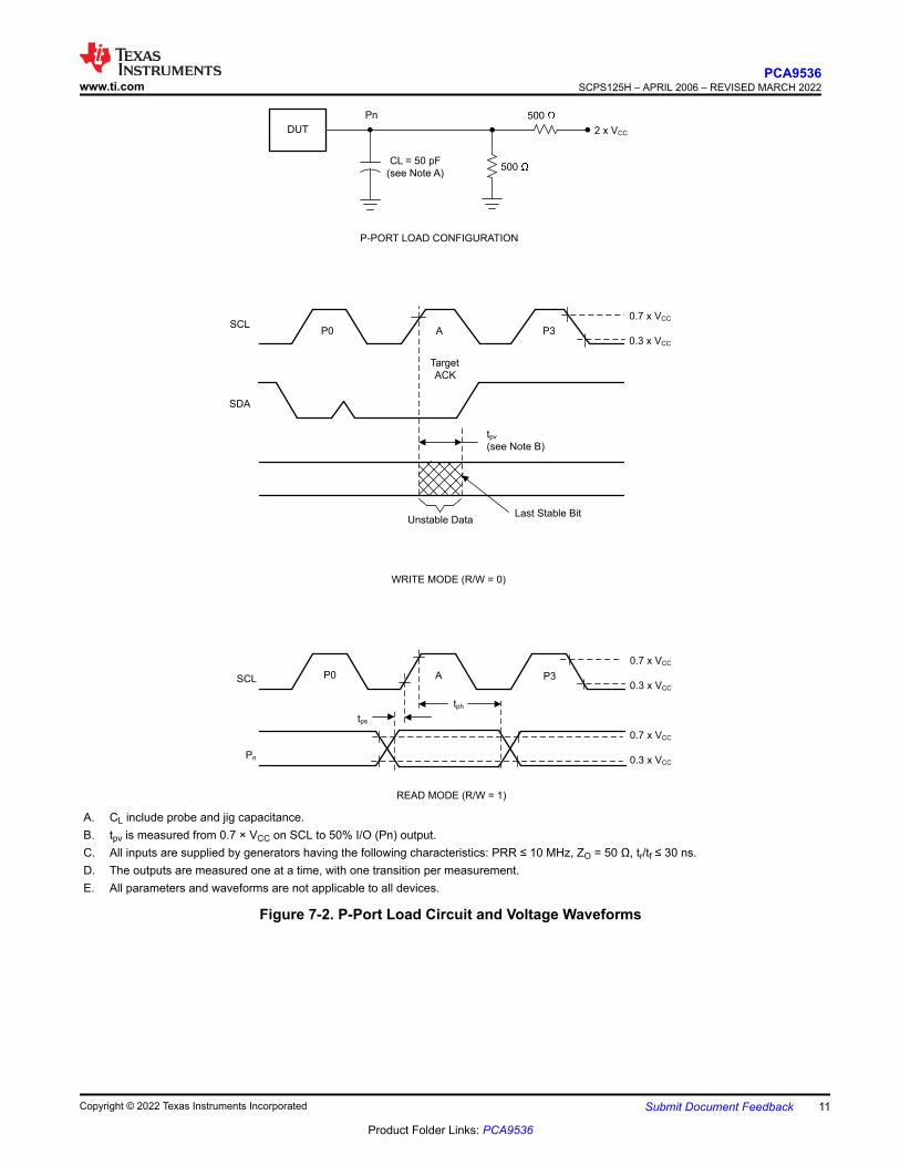
7 Parameter Measurement Information
Start or
Repeat
Start
Condition
Repeat
Start
Condition
Stop
Condition
tbuf
ticf
ticf
ticr
tscl tsch
tsds
tsdh
tsp
tPHL
tPLH
tsps
tsts
SCL
SDA
0.7 x VCC
0.3 x VCC
0.7 x VCC
0.3 x VCC
DUT
CL = 50 pF
(see Note A)
VCC
RL = 1 N
SDA
VOLTAGE WAVEFORMS
Three Bytes for Complete
Device Programming
SDA LOAD CONFIGURATION
Stop
Condition
(P)
Start
Condition
(S)
Address
Bit 7
(MSB)
Address
Bit 6
Address
Bit 1
R/W
Bit 0
(LSB)
ACK
(A)
Data
Bit 7
(MSB)
Data
Bit 0
(LSB)
Stop
Condition
(P)
A. CL include probe and jig capacitance.B. All inputs are supplied by generators having the following characteristics: PRR ≤ 10 MHz, ZO = 50 Ω, tr/tf ≤ 30 ns.C. All parameters and waveforms are not applicable to all devices.
Figure 7-1. I2C Interface Load Circuit and Voltage Waveforms
PCA9536SCPS125H – APRIL 2006 – REVISED MARCH 2022 www.ti.com
10 Submit Document Feedback Copyright © 2022 Texas Instruments Incorporated
Product Folder Links: PCA9536
DUT
Pn 500
2 x VCC
500 CL = 50 pF
(see Note A)
0.7 x VCC
0.3 x VCC
SCL
SDA
P0 A
Target
ACK
P3
Unstable DataLast Stable Bit
tpv
(see Note B)
P-PORT LOAD CONFIGURATION
WRITE MODE (R/W = 0)
P3AP0SCL
Pn
tps
tph
0.7 x VCC
0.3 x VCC
0.7 x VCC
0.3 x VCC
READ MODE (R/W = 1)
A. CL include probe and jig capacitance.B. tpv is measured from 0.7 × VCC on SCL to 50% I/O (Pn) output.C. All inputs are supplied by generators having the following characteristics: PRR ≤ 10 MHz, ZO = 50 Ω, tr/tf ≤ 30 ns.D. The outputs are measured one at a time, with one transition per measurement.E. All parameters and waveforms are not applicable to all devices.
Figure 7-2. P-Port Load Circuit and Voltage Waveforms
www.ti.comPCA9536
SCPS125H – APRIL 2006 – REVISED MARCH 2022
Copyright © 2022 Texas Instruments Incorporated Submit Document Feedback 11
Product Folder Links: PCA9536
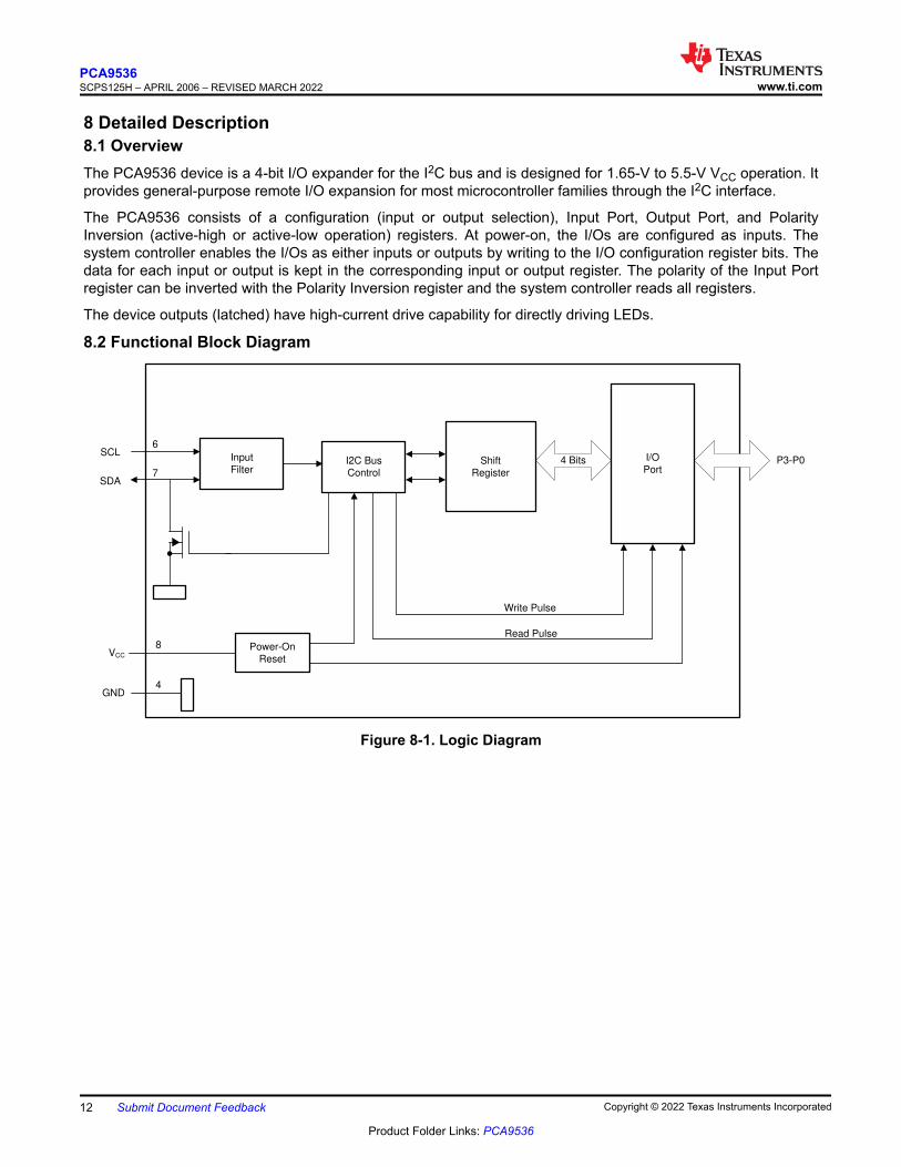
8 Detailed Description8.1 OverviewThe PCA9536 device is a 4-bit I/O expander for the I2C bus and is designed for 1.65-V to 5.5-V VCC operation. It provides general-purpose remote I/O expansion for most microcontroller families through the I2C interface.
The PCA9536 consists of a configuration (input or output selection), Input Port, Output Port, and Polarity Inversion (active-high or active-low operation) registers. At power-on, the I/Os are configured as inputs. The system controller enables the I/Os as either inputs or outputs by writing to the I/O configuration register bits. The data for each input or output is kept in the corresponding input or output register. The polarity of the Input Port register can be inverted with the Polarity Inversion register and the system controller reads all registers.
The device outputs (latched) have high-current drive capability for directly driving LEDs.
8.2 Functional Block Diagram
Input
FilterI2C Bus
Control
Shift
Register
4 Bits I/O
PortP3-P0
Power-On
Reset
SCL
SDA
VCC
GND
Write Pulse
Read Pulse8
4
6
7
Figure 8-1. Logic Diagram
PCA9536SCPS125H – APRIL 2006 – REVISED MARCH 2022 www.ti.com
12 Submit Document Feedback Copyright © 2022 Texas Instruments Incorporated
Product Folder Links: PCA9536
FF
D Q
CK QFF
D Q
CK Q
FF
D Q
CK Q
FF
D Q
CK Q
Data From
Shift Register
Data From
Shift Register
Write Configuration
Pulse
Write Pulse
Read Pulse
Data From Shift
Register
Write Polarity
Pulse
Configuration
Register
Output Port
RegisterInput Port
Register
Polarity Inversion
Register
Q2
Q1
Output Port
Register Data
VCC
P0 to P3
GND
Input Port
Register Data
Polarity
Register Data
ESD Protection
Diode
100 N
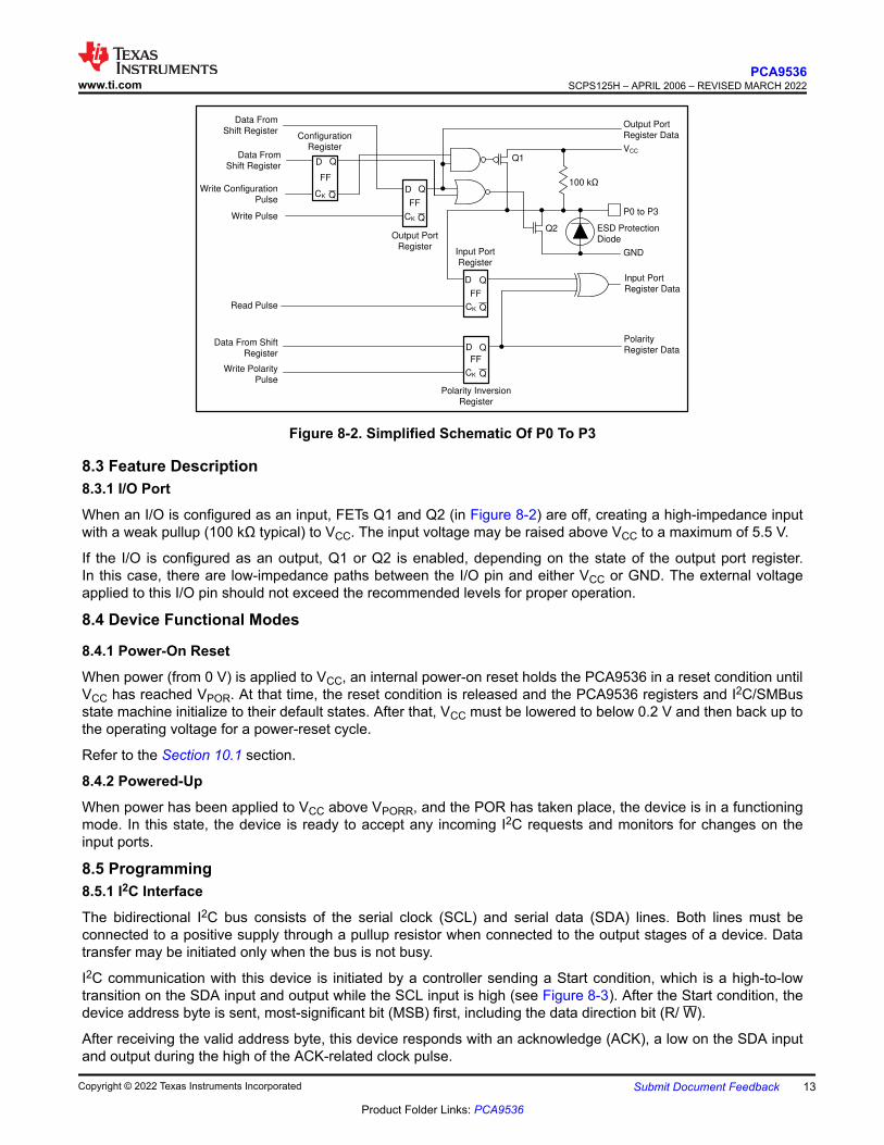
Figure 8-2. Simplified Schematic Of P0 To P3
8.3 Feature Description8.3.1 I/O Port
When an I/O is configured as an input, FETs Q1 and Q2 (in Figure 8-2) are off, creating a high-impedance input with a weak pullup (100 kΩ typical) to VCC. The input voltage may be raised above VCC to a maximum of 5.5 V.
If the I/O is configured as an output, Q1 or Q2 is enabled, depending on the state of the output port register. In this case, there are low-impedance paths between the I/O pin and either VCC or GND. The external voltage applied to this I/O pin should not exceed the recommended levels for proper operation.
8.4 Device Functional Modes
8.4.1 Power-On Reset
When power (from 0 V) is applied to VCC, an internal power-on reset holds the PCA9536 in a reset condition until VCC has reached VPOR. At that time, the reset condition is released and the PCA9536 registers and I2C/SMBus state machine initialize to their default states. After that, VCC must be lowered to below 0.2 V and then back up to the operating voltage for a power-reset cycle.
Refer to the Section 10.1 section.
8.4.2 Powered-Up
When power has been applied to VCC above VPORR, and the POR has taken place, the device is in a functioning mode. In this state, the device is ready to accept any incoming I2C requests and monitors for changes on the input ports.
8.5 Programming8.5.1 I2C Interface
The bidirectional I2C bus consists of the serial clock (SCL) and serial data (SDA) lines. Both lines must be connected to a positive supply through a pullup resistor when connected to the output stages of a device. Data transfer may be initiated only when the bus is not busy.
I2C communication with this device is initiated by a controller sending a Start condition, which is a high-to-low transition on the SDA input and output while the SCL input is high (see Figure 8-3). After the Start condition, the device address byte is sent, most-significant bit (MSB) first, including the data direction bit (R/ W).
After receiving the valid address byte, this device responds with an acknowledge (ACK), a low on the SDA input and output during the high of the ACK-related clock pulse.
www.ti.comPCA9536
SCPS125H – APRIL 2006 – REVISED MARCH 2022
Copyright © 2022 Texas Instruments Incorporated Submit Document Feedback 13
Product Folder Links: PCA9536
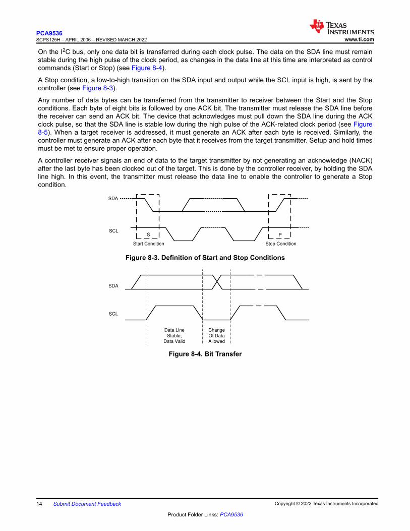
On the I2C bus, only one data bit is transferred during each clock pulse. The data on the SDA line must remain stable during the high pulse of the clock period, as changes in the data line at this time are interpreted as control commands (Start or Stop) (see Figure 8-4).
A Stop condition, a low-to-high transition on the SDA input and output while the SCL input is high, is sent by the controller (see Figure 8-3).
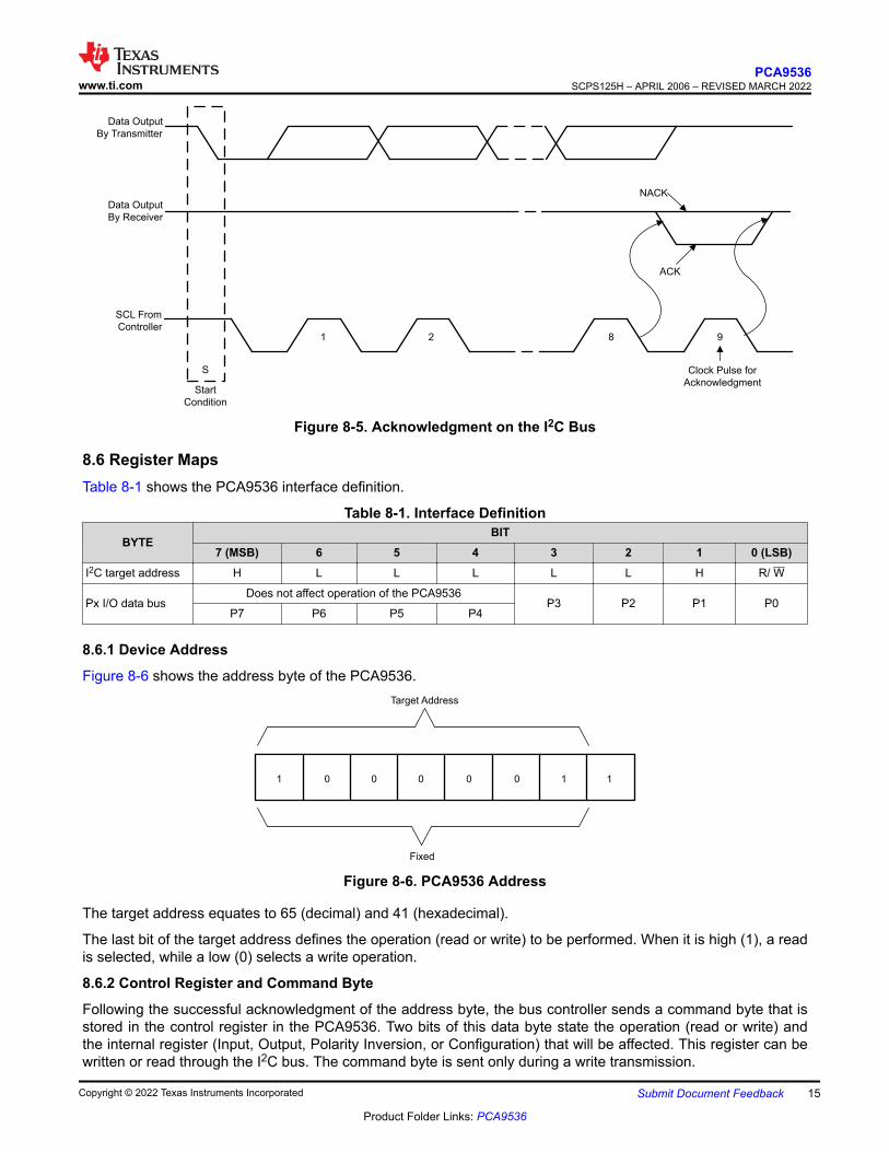
Any number of data bytes can be transferred from the transmitter to receiver between the Start and the Stop conditions. Each byte of eight bits is followed by one ACK bit. The transmitter must release the SDA line before the receiver can send an ACK bit. The device that acknowledges must pull down the SDA line during the ACK clock pulse, so that the SDA line is stable low during the high pulse of the ACK-related clock period (see Figure 8-5). When a target receiver is addressed, it must generate an ACK after each byte is received. Similarly, the controller must generate an ACK after each byte that it receives from the target transmitter. Setup and hold times must be met to ensure proper operation.
A controller receiver signals an end of data to the target transmitter by not generating an acknowledge (NACK) after the last byte has been clocked out of the target. This is done by the controller receiver, by holding the SDA line high. In this event, the transmitter must release the data line to enable the controller to generate a Stop condition.
SDA
SCLS P
Start Condition Stop Condition
Figure 8-3. Definition of Start and Stop Conditions
SDA
SCL
Data Line
Stable;
Data Valid
Change
Of Data
Allowed
Figure 8-4. Bit Transfer
PCA9536SCPS125H – APRIL 2006 – REVISED MARCH 2022 www.ti.com
14 Submit Document Feedback Copyright © 2022 Texas Instruments Incorporated
Product Folder Links: PCA9536
NACK
ACK
S
Start
Condition
Data Output
By Receiver
Data Output
By Transmitter
SCL From
Controller1 2 8 9
Clock Pulse for
Acknowledgment
Figure 8-5. Acknowledgment on the I2C Bus
8.6 Register MapsTable 8-1 shows the PCA9536 interface definition.
Table 8-1. Interface Definition
BYTEBIT
7 (MSB) 6 5 4 3 2 1 0 (LSB)I2C target address H L L L L L H R/ W
Px I/O data busDoes not affect operation of the PCA9536
P3 P2 P1 P0P7 P6 P5 P4
8.6.1 Device Address
Figure 8-6 shows the address byte of the PCA9536.Target Address
Fixed
1 0 0 0 0 0 1 1
Figure 8-6. PCA9536 Address
The target address equates to 65 (decimal) and 41 (hexadecimal).
The last bit of the target address defines the operation (read or write) to be performed. When it is high (1), a read is selected, while a low (0) selects a write operation.
8.6.2 Control Register and Command Byte
Following the successful acknowledgment of the address byte, the bus controller sends a command byte that is stored in the control register in the PCA9536. Two bits of this data byte state the operation (read or write) and the internal register (Input, Output, Polarity Inversion, or Configuration) that will be affected. This register can be written or read through the I2C bus. The command byte is sent only during a write transmission.
www.ti.comPCA9536
SCPS125H – APRIL 2006 – REVISED MARCH 2022
Copyright © 2022 Texas Instruments Incorporated Submit Document Feedback 15
Product Folder Links: PCA9536
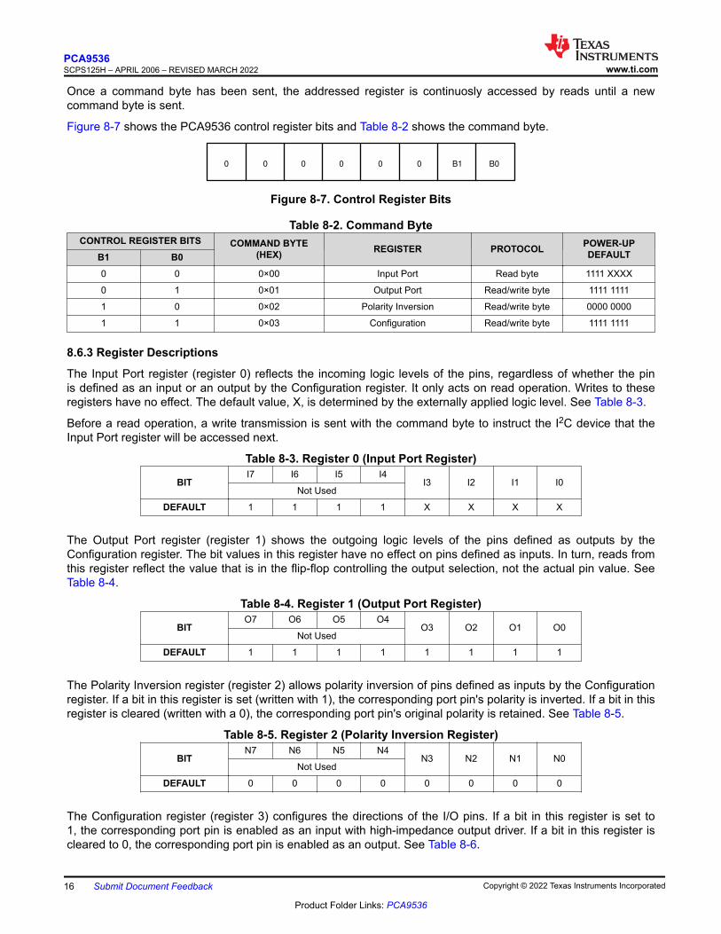
Once a command byte has been sent, the addressed register is continuosly accessed by reads until a new command byte is sent.
Figure 8-7 shows the PCA9536 control register bits and Table 8-2 shows the command byte.
0 0 0 0 0 0 B1 B0
Figure 8-7. Control Register Bits
Table 8-2. Command ByteCONTROL REGISTER BITS COMMAND BYTE
(HEX) REGISTER PROTOCOL POWER-UPDEFAULTB1 B0
0 0 0×00 Input Port Read byte 1111 XXXX
0 1 0×01 Output Port Read/write byte 1111 1111
1 0 0×02 Polarity Inversion Read/write byte 0000 0000
1 1 0×03 Configuration Read/write byte 1111 1111
8.6.3 Register Descriptions
The Input Port register (register 0) reflects the incoming logic levels of the pins, regardless of whether the pin is defined as an input or an output by the Configuration register. It only acts on read operation. Writes to these registers have no effect. The default value, X, is determined by the externally applied logic level. See Table 8-3.
Before a read operation, a write transmission is sent with the command byte to instruct the I2C device that the Input Port register will be accessed next.
Table 8-3. Register 0 (Input Port Register)
BITI7 I6 I5 I4
I3 I2 I1 I0Not Used
DEFAULT 1 1 1 1 X X X X
The Output Port register (register 1) shows the outgoing logic levels of the pins defined as outputs by the Configuration register. The bit values in this register have no effect on pins defined as inputs. In turn, reads from this register reflect the value that is in the flip-flop controlling the output selection, not the actual pin value. See Table 8-4.
Table 8-4. Register 1 (Output Port Register)
BITO7 O6 O5 O4
O3 O2 O1 O0Not Used
DEFAULT 1 1 1 1 1 1 1 1
The Polarity Inversion register (register 2) allows polarity inversion of pins defined as inputs by the Configuration register. If a bit in this register is set (written with 1), the corresponding port pin's polarity is inverted. If a bit in this register is cleared (written with a 0), the corresponding port pin's original polarity is retained. See Table 8-5.
Table 8-5. Register 2 (Polarity Inversion Register)
BITN7 N6 N5 N4
N3 N2 N1 N0Not Used
DEFAULT 0 0 0 0 0 0 0 0
The Configuration register (register 3) configures the directions of the I/O pins. If a bit in this register is set to 1, the corresponding port pin is enabled as an input with high-impedance output driver. If a bit in this register is cleared to 0, the corresponding port pin is enabled as an output. See Table 8-6.
PCA9536SCPS125H – APRIL 2006 – REVISED MARCH 2022 www.ti.com
16 Submit Document Feedback Copyright © 2022 Texas Instruments Incorporated
Product Folder Links: PCA9536
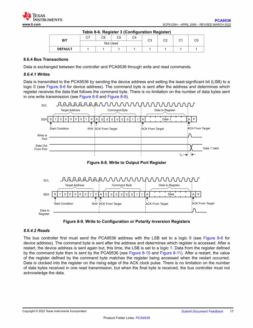
Table 8-6. Register 3 (Configuration Register)
BITC7 C6 C5 C4
C3 C2 C1 C0Not Used
DEFAULT 1 1 1 1 1 1 1 1
8.6.4 Bus Transactions
Data is exchanged between the controller and PCA9536 through write and read commands.
8.6.4.1 Writes
Data is transmitted to the PCA9536 by sending the device address and setting the least-significant bit (LSB) to a logic 0 (see Figure 8-6 for device address). The command byte is sent after the address and determines which register receives the data that follows the command byte. There is no limitation on the number of data bytes sent in one write transmission (see Figure 8-8 and Figure 8-9).
Data 11 0 0 0 0 0 1 0 A A AS 0 0 0 0 0 1 1 P0
1 2 3 4 6 7 8 9
Start Condition ACK From Target ACK From Target ACK From TargetR/W
Target Address Command Byte Data to Register
SCL
SDA
Write to
Port
tpv
Data Out
From Port Data 1 Valid
Figure 8-8. Write to Output Port Register
<br/>
Data1 0 0 0 0 0 1 0 A A AS 0 0 0 0 0 1 1 P()
1 2 3 4 6 7 8 9
Start Condition ACK From Target ACK From Target ACK From TargetR/W
Target Address Command Byte Data to Register
SCL
SDA
Data to
Register
Figure 8-9. Write to Configuration or Polarity Inversion Registers
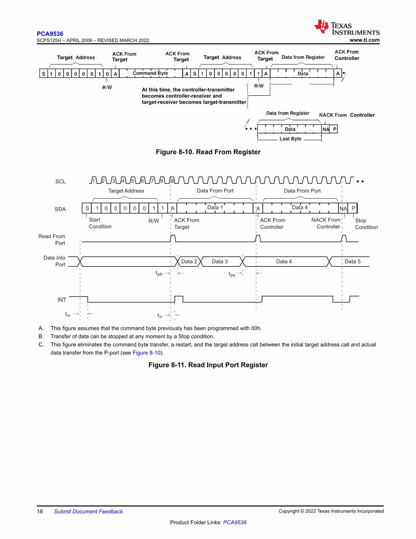
8.6.4.2 Reads
The bus controller first must send the PCA9536 address with the LSB set to a logic 0 (see Figure 8-6 for device address). The command byte is sent after the address and determines which register is accessed. After a restart, the device address is sent again but, this time, the LSB is set to a logic 1. Data from the register defined by the command byte then is sent by the PCA9536 (see Figure 8-10 and Figure 8-11). After a restart, the value of the register defined by the command byte matches the register being accessed when the restart occurred. Data is clocked into the register on the rising edge of the ACK clock pulse. There is no limitation on the number of data bytes received in one read transmission, but when the final byte is received, the bus controller must not acknowledge the data.
www.ti.comPCA9536
SCPS125H – APRIL 2006 – REVISED MARCH 2022
Copyright © 2022 Texas Instruments Incorporated Submit Document Feedback 17
Product Folder Links: PCA9536
Target Target Target Target Target Controller
Controller
At this time, the controller-transmitter
becomes controller-receiver and
target-receiver becomes target-transmitter
Figure 8-10. Read From Register
<br/>
SCL
SDA
INT
Start
ConditionR/W
Read From
Port
Data Into
Port
Stop
Condition
ACK From
Controller
NACK From
Controller
ACK From
Target
Data From PortTarget Address Data From Port
1 98765432
01 0S 00 0 1 1 A Data 1 Data 4A NA P
Data 2 Data 3 Data 4
t iv
tph tps
tir
Data 5
A. This figure assumes that the command byte previously has been programmed with 00h.B. Transfer of data can be stopped at any moment by a Stop condition.C. This figure eliminates the command byte transfer, a restart, and the target address call between the initial target address call and actual
data transfer from the P-port (see Figure 8-10).
Figure 8-11. Read Input Port Register
PCA9536SCPS125H – APRIL 2006 – REVISED MARCH 2022 www.ti.com
18 Submit Document Feedback Copyright © 2022 Texas Instruments Incorporated
Product Folder Links: PCA9536
9 Application Information DisclaimerNote
Information in the following applications sections is not part of the TI component specification, and TI does not warrant its accuracy or completeness. TI’s customers are responsible for determining suitability of components for their purposes, as well as validating and testing their design implementation to confirm system functionality.
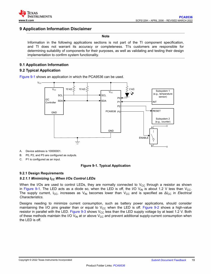
9.1 Application Information9.2 Typical ApplicationFigure 9-1 shows an application in which the PCA9536 can be used.
I2C
Controller
PCA9536
Subsystem 1
(e.g., temperature
sensor)
Subsystem 2
(e.g., counter)
ENABLE
A
B
P0
P1
P2
P3
SCL
SDA
GND
SCL
SDA
GND
VCC
VCC
VCC
INT
RESET
10 kΩ 10 kΩ 2 kΩ
A. Device address is 10000001.B. P0, P2, and P3 are configured as outputs.C. P1 is configured as an input.
Figure 9-1. Typical Application
9.2.1 Design Requirements9.2.1.1 Minimizing ICC When I/Os Control LEDs
When the I/Os are used to control LEDs, they are normally connected to VCC through a resistor as shown in Figure 9-1. The LED acts as a diode so, when the LED is off, the I/O VIN is about 1.2 V less than VCC. The supply current, ICC, increases as VIN becomes lower than VCC and is specified as ΔICC in Electrical Characteristics.
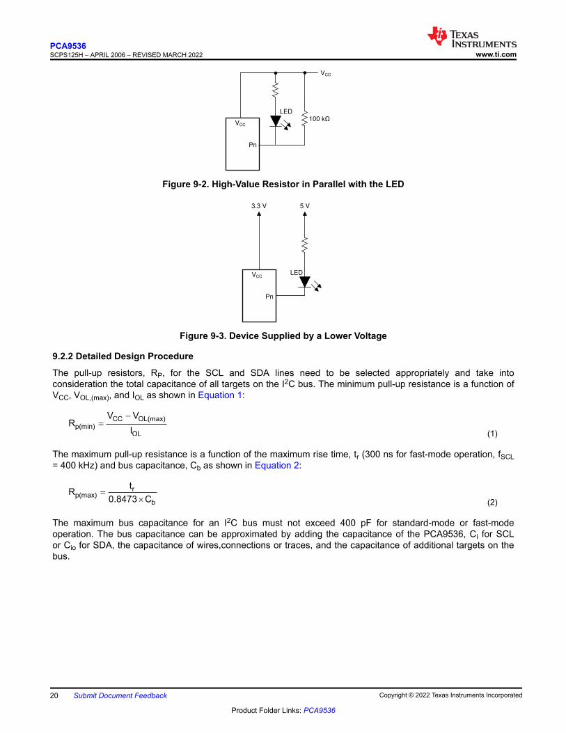
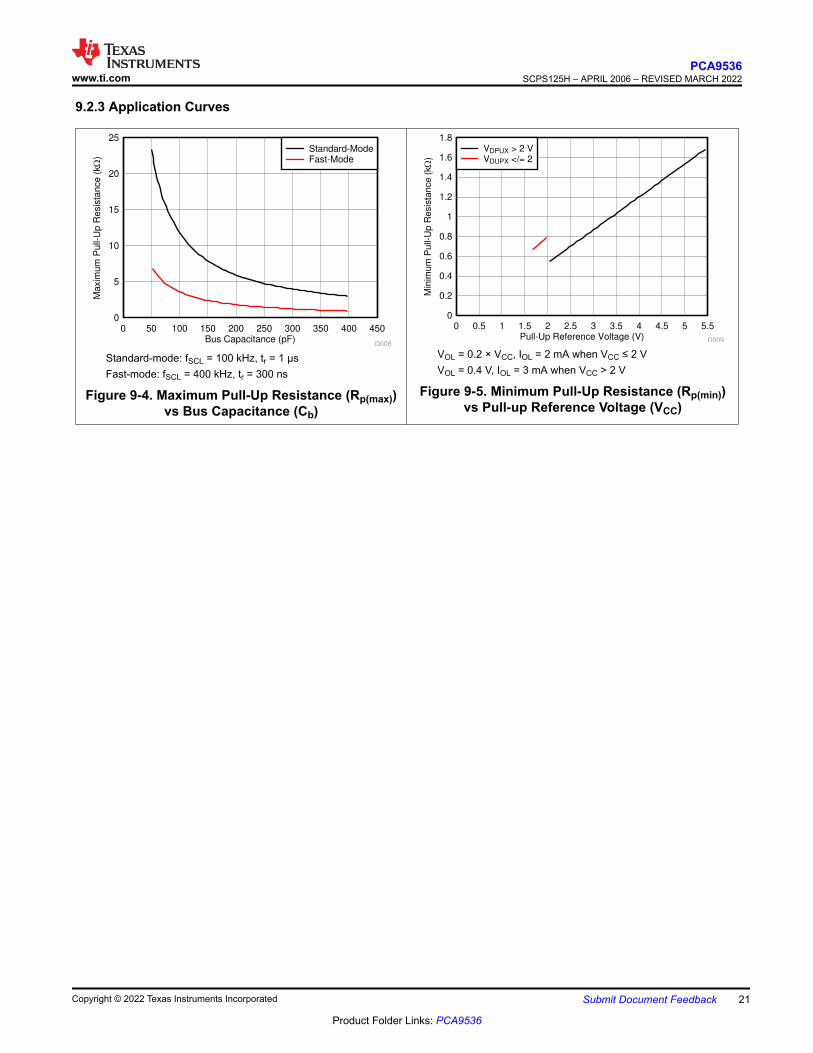
Designs needing to minimize current consumption, such as battery power applications, should consider maintaining the I/O pins greater than or equal to VCC when the LED is off. Figure 9-2 shows a high-value resistor in parallel with the LED. Figure 9-3 shows VCC less than the LED supply voltage by at least 1.2 V. Both of these methods maintain the I/O VIN at or above VCC and prevent additional supply-current consumption when the LED is off.
www.ti.comPCA9536
SCPS125H – APRIL 2006 – REVISED MARCH 2022
Copyright © 2022 Texas Instruments Incorporated Submit Document Feedback 19
Product Folder Links: PCA9536
LED
VCC
VCC
Pn
100 N
Figure 9-2. High-Value Resistor in Parallel with the LED
VCC
Pn
LED
3.3 V 5 V
Figure 9-3. Device Supplied by a Lower Voltage
9.2.2 Detailed Design Procedure
The pull-up resistors, RP, for the SCL and SDA lines need to be selected appropriately and take into consideration the total capacitance of all targets on the I2C bus. The minimum pull-up resistance is a function of VCC, VOL,(max), and IOL as shown in Equation 1:
CC OL(max)p(min)
OL
V VR
I
-
=
(1)
The maximum pull-up resistance is a function of the maximum rise time, tr (300 ns for fast-mode operation, fSCL = 400 kHz) and bus capacitance, Cb as shown in Equation 2:
rp(max)
b
tR
0.8473 C=
´ (2)
The maximum bus capacitance for an I2C bus must not exceed 400 pF for standard-mode or fast-mode operation. The bus capacitance can be approximated by adding the capacitance of the PCA9536, Ci for SCL or Cio for SDA, the capacitance of wires,connections or traces, and the capacitance of additional targets on the bus.
PCA9536SCPS125H – APRIL 2006 – REVISED MARCH 2022 www.ti.com
20 Submit Document Feedback Copyright © 2022 Texas Instruments Incorporated
Product Folder Links: PCA9536
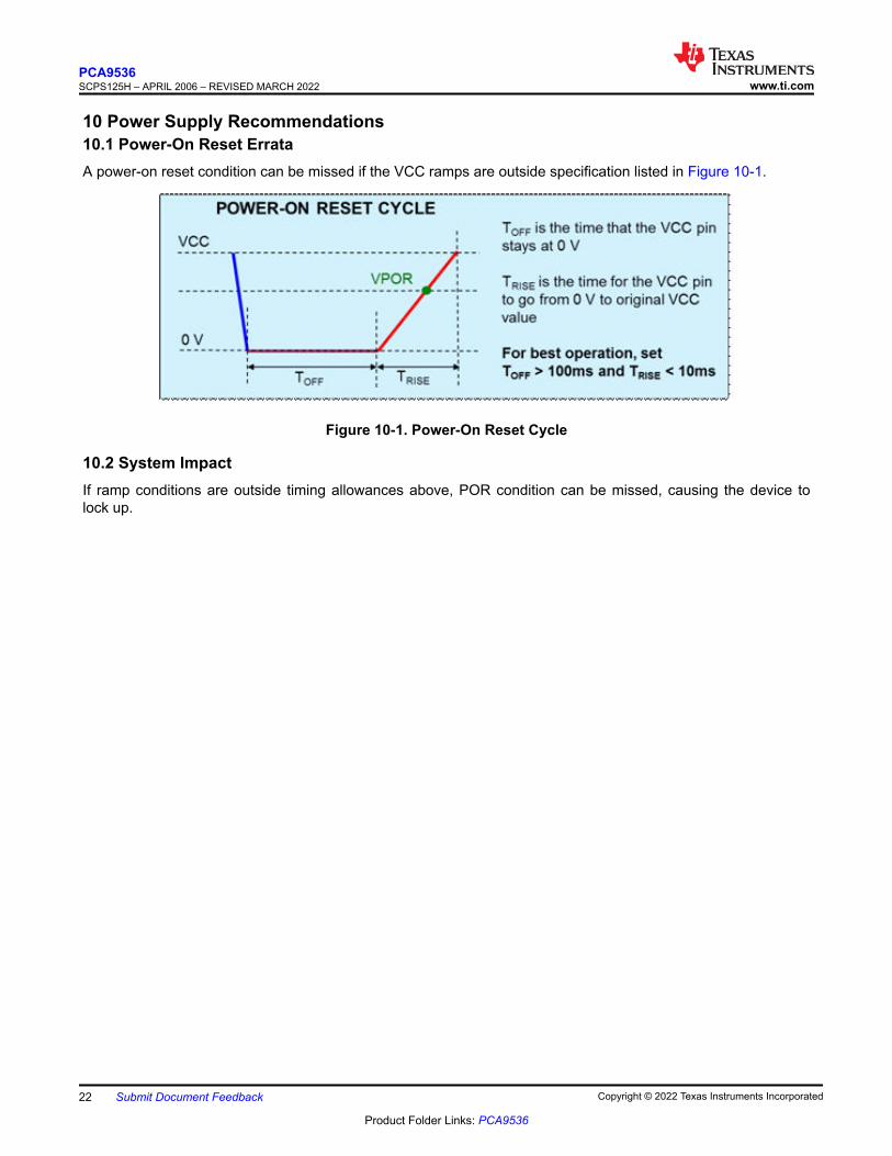
9.2.3 Application Curves
Bus Capacitance (pF)
Maxim
um
Pu
ll-U
p R
esis
tance (
k:
)
0 50 100 150 200 250 300 350 400 4500
5
10
15
20
25
D008
Standard-ModeFast-Mode
Standard-mode: fSCL = 100 kHz, tr = 1 µsFast-mode: fSCL = 400 kHz, tr = 300 ns
Figure 9-4. Maximum Pull-Up Resistance (Rp(max)) vs Bus Capacitance (Cb)
Pull-Up Reference Voltage (V)
Min
imum
Pull-
Up
Re
sis
tan
ce
(k:
)
0 0.5 1 1.5 2 2.5 3 3.5 4 4.5 5 5.50
0.2
0.4
0.6
0.8
1
1.2
1.4
1.6
1.8
D009
VDPUX > 2 VVDUPX </= 2
VOL = 0.2 × VCC, IOL = 2 mA when VCC ≤ 2 VVOL = 0.4 V, IOL = 3 mA when VCC > 2 V
Figure 9-5. Minimum Pull-Up Resistance (Rp(min)) vs Pull-up Reference Voltage (VCC)
www.ti.comPCA9536
SCPS125H – APRIL 2006 – REVISED MARCH 2022
Copyright © 2022 Texas Instruments Incorporated Submit Document Feedback 21
Product Folder Links: PCA9536
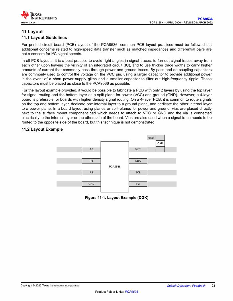
10 Power Supply Recommendations10.1 Power-On Reset ErrataA power-on reset condition can be missed if the VCC ramps are outside specification listed in Figure 10-1.
Figure 10-1. Power-On Reset Cycle
10.2 System ImpactIf ramp conditions are outside timing allowances above, POR condition can be missed, causing the device to lock up.
PCA9536SCPS125H – APRIL 2006 – REVISED MARCH 2022 www.ti.com
22 Submit Document Feedback Copyright © 2022 Texas Instruments Incorporated
Product Folder Links: PCA9536
11 Layout11.1 Layout GuidelinesFor printed circuit board (PCB) layout of the PCA9536, common PCB layout practices must be followed but additional concerns related to high-speed data transfer such as matched impedances and differential pairs are not a concern for I2C signal speeds.
In all PCB layouts, it is a best practice to avoid right angles in signal traces, to fan out signal traces away from each other upon leaving the vicinity of an integrated circuit (IC), and to use thicker trace widths to carry higher amounts of current that commonly pass through power and ground traces. By-pass and de-coupling capacitors are commonly used to control the voltage on the VCC pin, using a larger capacitor to provide additional power in the event of a short power supply glitch and a smaller capacitor to filter out high-frequency ripple. These capacitors must be placed as close to the PCA9536 as possible.
For the layout example provided, it would be possible to fabricate a PCB with only 2 layers by using the top layer for signal routing and the bottom layer as a split plane for power (VCC) and ground (GND). However, a 4-layer board is preferable for boards with higher density signal routing. On a 4-layer PCB, it is common to route signals on the top and bottom layer, dedicate one internal layer to a ground plane, and dedicate the other internal layer to a power plane. In a board layout using planes or split planes for power and ground, vias are placed directly next to the surface mount component pad which needs to attach to VCC or GND and the via is connected electrically to the internal layer or the other side of the board. Vias are also used when a signal trace needs to be routed to the opposite side of the board, but this technique is not demonstrated.
11.2 Layout Example
P1
P2
P0
GND
SDA
SCL
VCC
P3
PCA9536
CAP
GND
Figure 11-1. Layout Example (DGK)
www.ti.comPCA9536
SCPS125H – APRIL 2006 – REVISED MARCH 2022
Copyright © 2022 Texas Instruments Incorporated Submit Document Feedback 23
Product Folder Links: PCA9536
12 Device and Documentation Support12.1 Documentation Support12.1.1 Related Documentation
For related documentation see the following:
• I2C Bus Pull-Up Resistor Calculation• Maximum Clock Frequency of I2C Bus Using Repeaters• Introduction to Logic• Understanding the I2C Bus• Choosing the Correct I2C Device for New Designs
12.2 Receiving Notification of Documentation UpdatesTo receive notification of documentation updates, navigate to the device product folder on ti.com. Click on Subscribe to updates to register and receive a weekly digest of any product information that has changed. For change details, review the revision history included in any revised document.
12.3 Support ResourcesTI E2E™ support forums are an engineer's go-to source for fast, verified answers and design help — straight from the experts. Search existing answers or ask your own question to get the quick design help you need.
Linked content is provided "AS IS" by the respective contributors. They do not constitute TI specifications and do not necessarily reflect TI's views; see TI's Terms of Use.
12.4 TrademarksNanoFree™ and TI E2E™ are trademarks of Texas Instruments.All trademarks are the property of their respective owners.12.5 Electrostatic Discharge Caution
This integrated circuit can be damaged by ESD. Texas Instruments recommends that all integrated circuits be handled with appropriate precautions. Failure to observe proper handling and installation procedures can cause damage.ESD damage can range from subtle performance degradation to complete device failure. Precision integrated circuits may be more susceptible to damage because very small parametric changes could cause the device not to meet its published specifications.
12.6 GlossaryTI Glossary This glossary lists and explains terms, acronyms, and definitions.
13 Mechanical, Packaging, and Orderable InformationThe following pages include mechanical, packaging, and orderable information. This information is the most current data available for the designated devices. This data is subject to change without notice and revision of this document. For browser-based versions of this data sheet, refer to the left-hand navigation.
PCA9536SCPS125H – APRIL 2006 – REVISED MARCH 2022 www.ti.com
24 Submit Document Feedback Copyright © 2022 Texas Instruments Incorporated
Product Folder Links: PCA9536
PACKAGE OPTION ADDENDUM
www.ti.com 3-Jun-2022
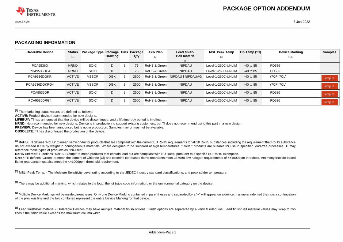
PACKAGING INFORMATION
Orderable Device Status(1)
Package Type PackageDrawing
Pins PackageQty
Eco Plan(2)
Lead finish/Ball material
(6)
MSL Peak Temp(3)
Op Temp (°C) Device Marking(4/5)
Samples
PCA9536D NRND SOIC D 8 75 RoHS & Green NIPDAU Level-1-260C-UNLIM -40 to 85 PD536
PCA9536DG4 NRND SOIC D 8 75 RoHS & Green NIPDAU Level-1-260C-UNLIM -40 to 85 PD536
PCA9536DGKR ACTIVE VSSOP DGK 8 2500 RoHS & Green NIPDAU | NIPDAUAG Level-1-260C-UNLIM -40 to 85 (7CF, 7CL) Samples
PCA9536DGKRG4 ACTIVE VSSOP DGK 8 2500 RoHS & Green NIPDAU Level-1-260C-UNLIM -40 to 85 (7CF, 7CL) Samples
PCA9536DR ACTIVE SOIC D 8 2500 RoHS & Green NIPDAU Level-1-260C-UNLIM -40 to 85 PD536 Samples
PCA9536DRG4 ACTIVE SOIC D 8 2500 RoHS & Green NIPDAU Level-1-260C-UNLIM -40 to 85 PD536 Samples
(1) The marketing status values are defined as follows:ACTIVE: Product device recommended for new designs.LIFEBUY: TI has announced that the device will be discontinued, and a lifetime-buy period is in effect.NRND: Not recommended for new designs. Device is in production to support existing customers, but TI does not recommend using this part in a new design.PREVIEW: Device has been announced but is not in production. Samples may or may not be available.OBSOLETE: TI has discontinued the production of the device.
(2) RoHS: TI defines "RoHS" to mean semiconductor products that are compliant with the current EU RoHS requirements for all 10 RoHS substances, including the requirement that RoHS substancedo not exceed 0.1% by weight in homogeneous materials. Where designed to be soldered at high temperatures, "RoHS" products are suitable for use in specified lead-free processes. TI mayreference these types of products as "Pb-Free".RoHS Exempt: TI defines "RoHS Exempt" to mean products that contain lead but are compliant with EU RoHS pursuant to a specific EU RoHS exemption.Green: TI defines "Green" to mean the content of Chlorine (Cl) and Bromine (Br) based flame retardants meet JS709B low halogen requirements of <=1000ppm threshold. Antimony trioxide basedflame retardants must also meet the <=1000ppm threshold requirement.
(3) MSL, Peak Temp. - The Moisture Sensitivity Level rating according to the JEDEC industry standard classifications, and peak solder temperature.
(4) There may be additional marking, which relates to the logo, the lot trace code information, or the environmental category on the device.
(5) Multiple Device Markings will be inside parentheses. Only one Device Marking contained in parentheses and separated by a "~" will appear on a device. If a line is indented then it is a continuationof the previous line and the two combined represent the entire Device Marking for that device.
(6) Lead finish/Ball material - Orderable Devices may have multiple material finish options. Finish options are separated by a vertical ruled line. Lead finish/Ball material values may wrap to twolines if the finish value exceeds the maximum column width.
Addendum-Page 1
PACKAGE OPTION ADDENDUM
www.ti.com 3-Jun-2022
Important Information and Disclaimer:The information provided on this page represents TI's knowledge and belief as of the date that it is provided. TI bases its knowledge and belief on informationprovided by third parties, and makes no representation or warranty as to the accuracy of such information. Efforts are underway to better integrate information from third parties. TI has taken andcontinues to take reasonable steps to provide representative and accurate information but may not have conducted destructive testing or chemical analysis on incoming materials and chemicals.TI and TI suppliers consider certain information to be proprietary, and thus CAS numbers and other limited information may not be available for release.
In no event shall TI's liability arising out of such information exceed the total purchase price of the TI part(s) at issue in this document sold by TI to Customer on an annual basis.
Addendum-Page 2
PACKAGE MATERIALS INFORMATION
www.ti.com 3-Jun-2022
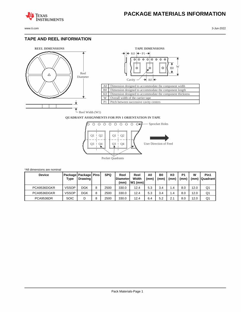
TAPE AND REEL INFORMATION
Reel Width (W1)
REEL DIMENSIONS
A0B0K0W
Dimension designed to accommodate the component lengthDimension designed to accommodate the component thicknessOverall width of the carrier tapePitch between successive cavity centers
Dimension designed to accommodate the component width
TAPE DIMENSIONS
K0 P1
B0 W
A0Cavity
QUADRANT ASSIGNMENTS FOR PIN 1 ORIENTATION IN TAPE
Pocket Quadrants
Sprocket Holes
Q1 Q1Q2 Q2
Q3 Q3Q4 Q4 User Direction of Feed
P1
ReelDiameter
*All dimensions are nominal
Device PackageType
PackageDrawing
Pins SPQ ReelDiameter
(mm)
ReelWidth
W1 (mm)
A0(mm)
B0(mm)
K0(mm)
P1(mm)
W(mm)
Pin1Quadrant
PCA9536DGKR VSSOP DGK 8 2500 330.0 12.4 5.3 3.4 1.4 8.0 12.0 Q1
PCA9536DGKR VSSOP DGK 8 2500 330.0 12.4 5.3 3.4 1.4 8.0 12.0 Q1
PCA9536DR SOIC D 8 2500 330.0 12.4 6.4 5.2 2.1 8.0 12.0 Q1
Pack Materials-Page 1
PACKAGE MATERIALS INFORMATION
www.ti.com 3-Jun-2022
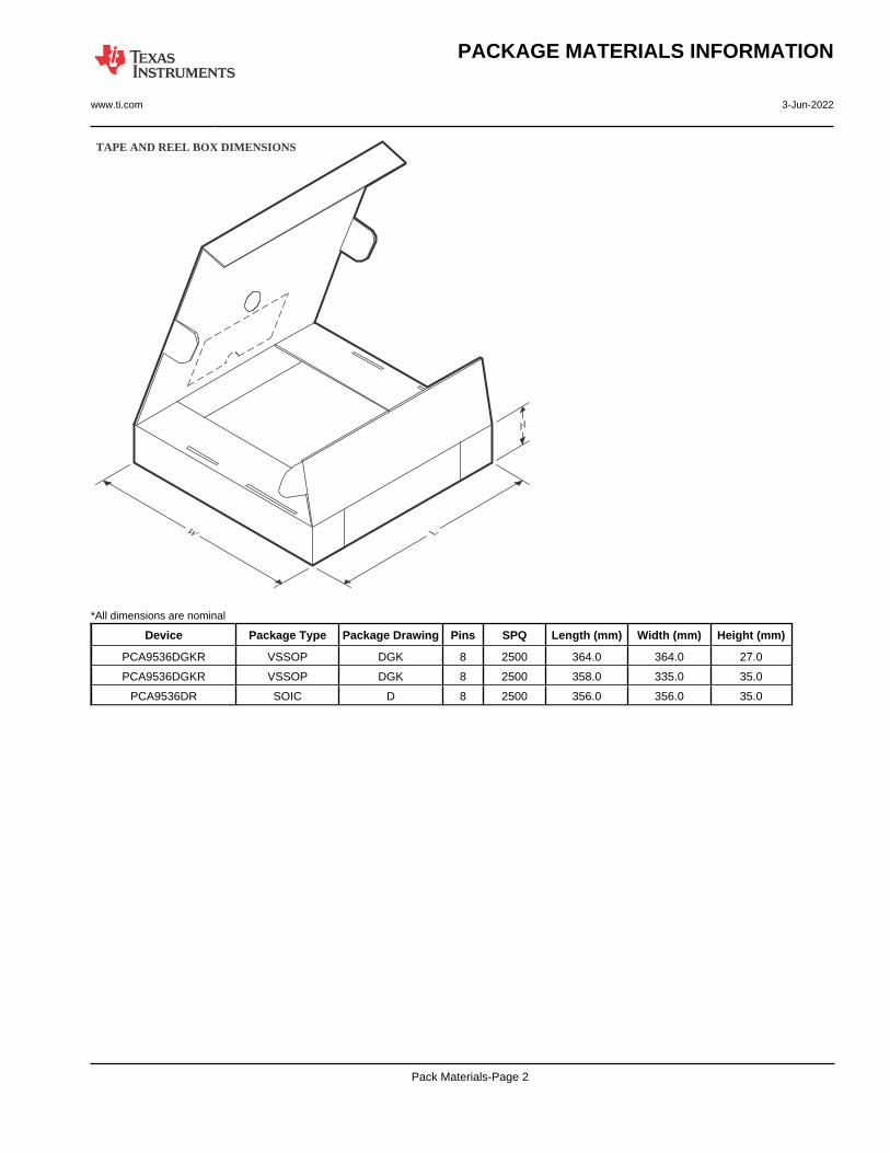
TAPE AND REEL BOX DIMENSIONS
Width (mm)
W L
H
*All dimensions are nominal
Device Package Type Package Drawing Pins SPQ Length (mm) Width (mm) Height (mm)
PCA9536DGKR VSSOP DGK 8 2500 364.0 364.0 27.0
PCA9536DGKR VSSOP DGK 8 2500 358.0 335.0 35.0
PCA9536DR SOIC D 8 2500 356.0 356.0 35.0
Pack Materials-Page 2
PACKAGE MATERIALS INFORMATION
www.ti.com 3-Jun-2022
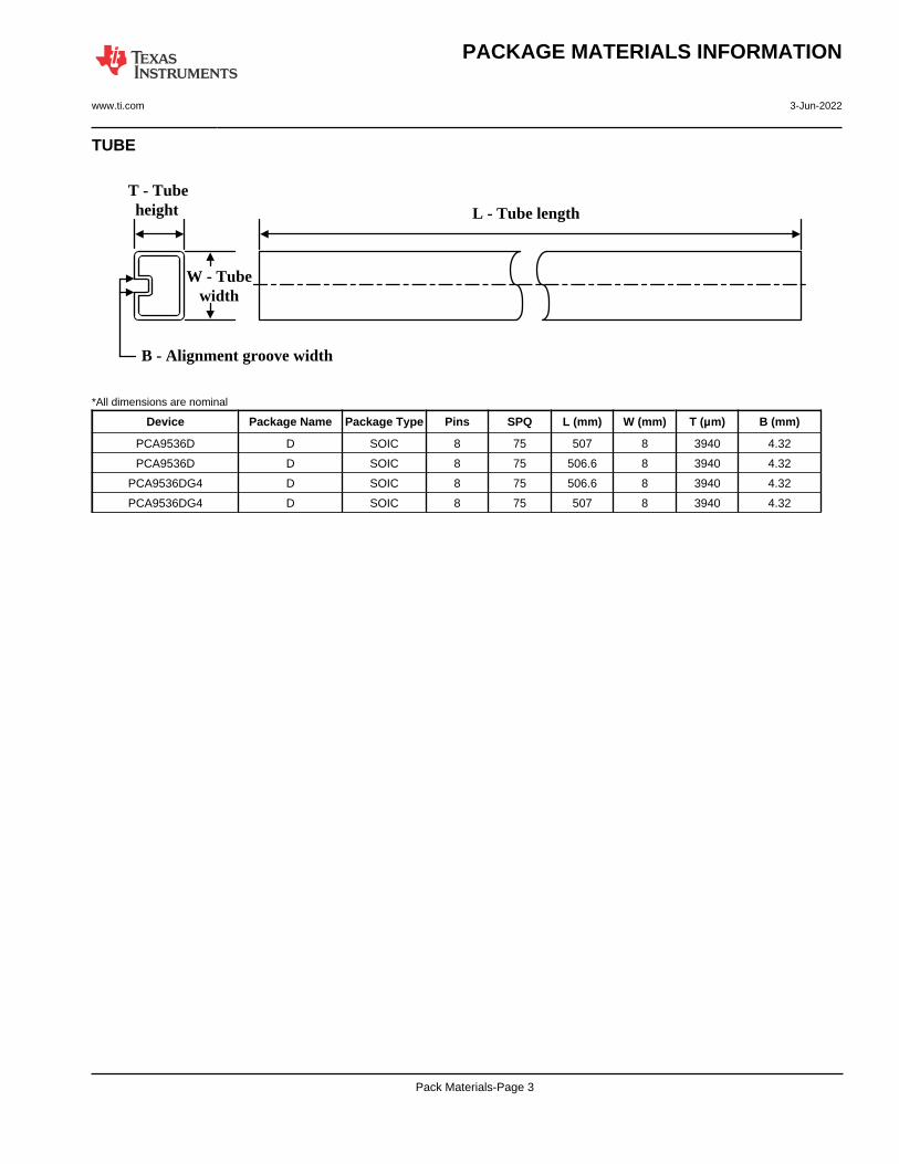
TUBE
L - Tube lengthT - Tube height
W - Tube width
B - Alignment groove width *All dimensions are nominal
Device Package Name Package Type Pins SPQ L (mm) W (mm) T (µm) B (mm)
PCA9536D D SOIC 8 75 507 8 3940 4.32
PCA9536D D SOIC 8 75 506.6 8 3940 4.32
PCA9536DG4 D SOIC 8 75 506.6 8 3940 4.32
PCA9536DG4 D SOIC 8 75 507 8 3940 4.32
Pack Materials-Page 3
www.ti.com
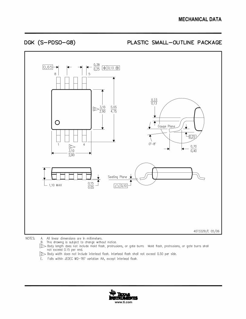
PACKAGE OUTLINE
C
.228-.244 TYP[5.80-6.19]
.069 MAX[1.75]
6X .050[1.27]
8X .012-.020 [0.31-0.51]
2X.150[3.81]
.005-.010 TYP[0.13-0.25]
0 - 8 .004-.010[0.11-0.25]
.010[0.25]
.016-.050[0.41-1.27]
4X (0 -15 )
A
.189-.197[4.81-5.00]
NOTE 3
B .150-.157[3.81-3.98]
NOTE 4
4X (0 -15 )
(.041)[1.04]
SOIC - 1.75 mm max heightD0008ASMALL OUTLINE INTEGRATED CIRCUIT
4214825/C 02/2019
NOTES: 1. Linear dimensions are in inches [millimeters]. Dimensions in parenthesis are for reference only. Controlling dimensions are in inches. Dimensioning and tolerancing per ASME Y14.5M. 2. This drawing is subject to change without notice. 3. This dimension does not include mold flash, protrusions, or gate burrs. Mold flash, protrusions, or gate burrs shall not exceed .006 [0.15] per side. 4. This dimension does not include interlead flash.5. Reference JEDEC registration MS-012, variation AA.
18
.010 [0.25] C A B
54
PIN 1 ID AREA
SEATING PLANE
.004 [0.1] C
SEE DETAIL A
DETAIL ATYPICAL
SCALE 2.800

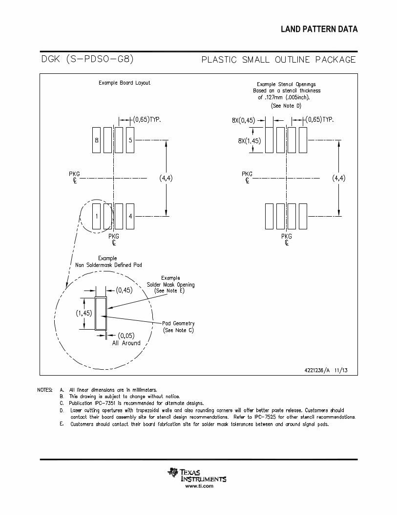
www.ti.com
EXAMPLE BOARD LAYOUT
.0028 MAX[0.07]ALL AROUND
.0028 MIN[0.07]ALL AROUND
(.213)[5.4]
6X (.050 )[1.27]
8X (.061 )[1.55]
8X (.024)[0.6]
(R.002 ) TYP[0.05]
SOIC - 1.75 mm max heightD0008ASMALL OUTLINE INTEGRATED CIRCUIT
4214825/C 02/2019
NOTES: (continued) 6. Publication IPC-7351 may have alternate designs. 7. Solder mask tolerances between and around signal pads can vary based on board fabrication site.
METALSOLDER MASKOPENING
NON SOLDER MASKDEFINED
SOLDER MASK DETAILS
EXPOSEDMETAL
OPENINGSOLDER MASK METAL UNDER
SOLDER MASK
SOLDER MASKDEFINED
EXPOSEDMETAL
LAND PATTERN EXAMPLEEXPOSED METAL SHOWN
SCALE:8X
SYMM
1
45
8
SEEDETAILS
SYMM
www.ti.com
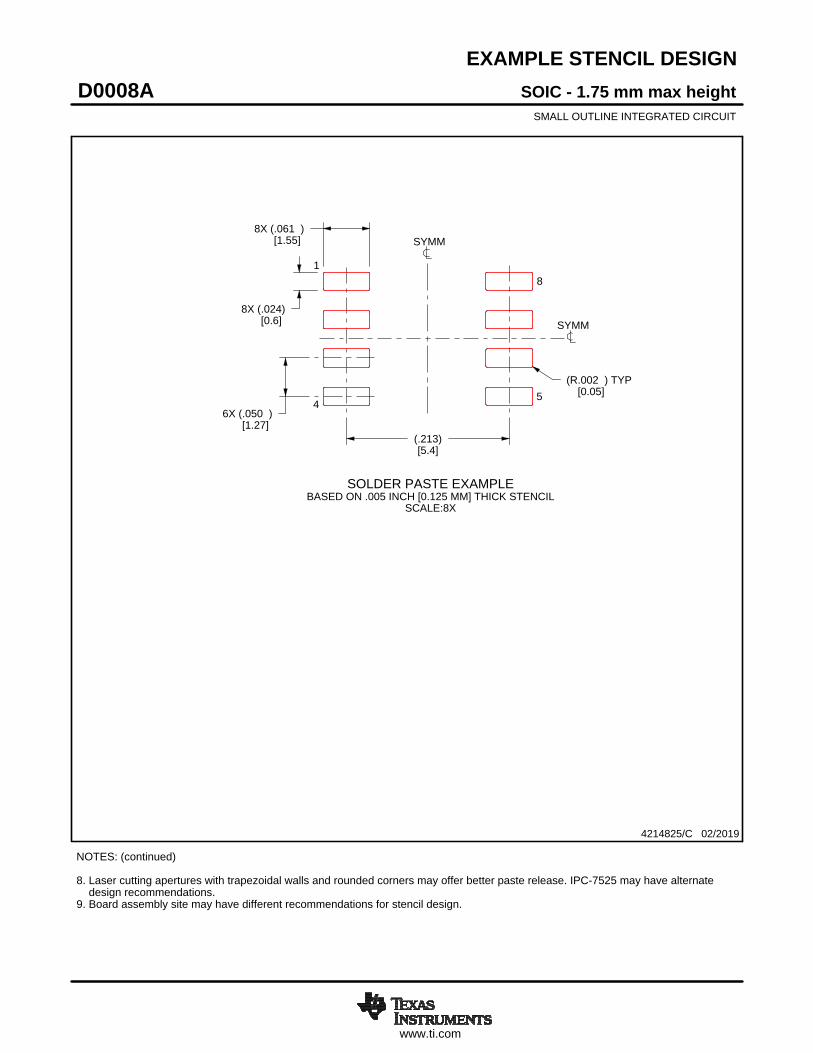
EXAMPLE STENCIL DESIGN
8X (.061 )[1.55]
8X (.024)[0.6]
6X (.050 )[1.27]
(.213)[5.4]
(R.002 ) TYP[0.05]
SOIC - 1.75 mm max heightD0008ASMALL OUTLINE INTEGRATED CIRCUIT
4214825/C 02/2019
NOTES: (continued) 8. Laser cutting apertures with trapezoidal walls and rounded corners may offer better paste release. IPC-7525 may have alternate design recommendations. 9. Board assembly site may have different recommendations for stencil design.
SOLDER PASTE EXAMPLEBASED ON .005 INCH [0.125 MM] THICK STENCIL
SCALE:8X
SYMM
SYMM
1
45
8
IMPORTANT NOTICE AND DISCLAIMERTI PROVIDES TECHNICAL AND RELIABILITY DATA (INCLUDING DATA SHEETS), DESIGN RESOURCES (INCLUDING REFERENCE DESIGNS), APPLICATION OR OTHER DESIGN ADVICE, WEB TOOLS, SAFETY INFORMATION, AND OTHER RESOURCES “AS IS” AND WITH ALL FAULTS, AND DISCLAIMS ALL WARRANTIES, EXPRESS AND IMPLIED, INCLUDING WITHOUT LIMITATION ANY IMPLIED WARRANTIES OF MERCHANTABILITY, FITNESS FOR A PARTICULAR PURPOSE OR NON-INFRINGEMENT OF THIRD PARTY INTELLECTUAL PROPERTY RIGHTS.These resources are intended for skilled developers designing with TI products. You are solely responsible for (1) selecting the appropriate TI products for your application, (2) designing, validating and testing your application, and (3) ensuring your application meets applicable standards, and any other safety, security, regulatory or other requirements.These resources are subject to change without notice. TI grants you permission to use these resources only for development of an application that uses the TI products described in the resource. Other reproduction and display of these resources is prohibited. No license is granted to any other TI intellectual property right or to any third party intellectual property right. TI disclaims responsibility for, and you will fully indemnify TI and its representatives against, any claims, damages, costs, losses, and liabilities arising out of your use of these resources.TI’s products are provided subject to TI’s Terms of Sale or other applicable terms available either on ti.com or provided in conjunction with such TI products. TI’s provision of these resources does not expand or otherwise alter TI’s applicable warranties or warranty disclaimers for TI products.TI objects to and rejects any additional or different terms you may have proposed. IMPORTANT NOTICE
Mailing Address: Texas Instruments, Post Office Box 655303, Dallas, Texas 75265Copyright © 2022, Texas Instruments Incorporated