BooleDozer: Logic synthesis for ASICs
68
Transcript of BooleDozer: Logic synthesis for ASICs
BooleDozer : Logic synthesis for ASICs
L. Stok
D. S. Kung
D. Brand
A. D. Drumm
A. J. Sullivan
L. N. Reddy
N. Hieter
D. J. Geiger
H. Chao
P. J. Osler
February 6, 1996
Logic synthesis is the process of automatically generating optimized logic level representation
from a high-level description. With the rapid advances in integrated circuit technology and
the resultant growth in design complexity, designers increasingly rely on logic synthesis to
shorten the design time, while achieving performance objectives. This paper describes the
IBM logic synthesis system BooleDozerTM; including its organization, main algorithms and
how it �ts into the design process. The BooleDozer logic synthesis system has been widely
used within IBM to successfully synthesize processor and ASIC designs.
1 Introduction
Logic synthesis is the process which compiles a register-transfer-level (RTL) description into
an optimized technology-speci�c network implementation. The design process including
BooleDozerTM is shown in Figure 1. The designer writes a structural and behavioral de-
1
scription of the circuit using a high-level design language (HDL) such as VHDL or Verilog.
The behavior of this description is checked using simulation. The high-level design is com-
piled into a register-transfer-level (RTL) network by a behavioral synthesis tool such as
HIS [1]. The RTL network is composed of equation blocks, functional blocks such as adders
and multiplexors, and primitive gates. The RTL network is the input to logic synthesis.
To illustrate this process, a simple VHDL example, shown in Figure 2, is used. This
input is processed by HIS producing the RTL network shown in Figure 3. This network
consists of technology-independent gates and is not optimized from a combinational point
of view (since that is the job of logic synthesis), but the sequential behavior has been deter-
mined. The multiplexor MUX was inferred from the second if statement where depending
on the value of A one of two values is assigned to R. Because of the �rst if statement the
value of R is stored in a register.
The output of logic synthesis is a network of gates in a target technology as shown in
Figure 4. The network has undergone some major changes to be discussed in the next
section. These changes e�ect the performance of the network but not the logical function.
This network is passed on to physical design (PD) for placement, layout and wiring. Physical
design information (e.g., wire capacitance, wire resistance, and placement information) can
be fed back into logic synthesis to allow iterative re�nement of the design.
Logic synthesis requires a description of the target technology in which the design is
to be implemented. Information includes physical information such as size and delay of
gates, and functional information such as logic equations for gates. To optimize a design for
performance a timing system is needed which can provide accurate delay estimates quickly.
BooleDozer uses the an incremental timing system called EinsTimerTM. Another important
input to logic synthesis is the performance goals for the design (e.g., cycle time and area).
Boolean checking can be used along with simulation to ensure that logic synthesis has
not changed the behavior of the design. Static timing analysis and simulation can be used
2
to verify the timing of the design.
To satisfy the various requirements, BooleDozer di�ers from other synthesis tools in
several ways. The �rst requirement is larger capacity (about 100 000 gates) than the current
industry practice. That implies not only an e�cient database, but also e�cient algorithms.
BooleDozer relies on compiler-like analysis techniques more than two-level [2, 3] or Binary
Decision Diagrams (BDD) [4] based techniques, whose performance degrades too quickly
with increasing problem size.
The second requirement is openness of all interfaces, which means that local support
people can write special purpose code in response to designers' needs. Also, the existing
design ow must be easy to rearrange to satisfy unique design requirements.
The third requirement concerns timing analysis. On one hand, timing analysis used
during synthesis must have the same accuracy as the analysis used for timing veri�cation.
On the other hand, it must be e�cient in the synthesis environment, where timing analysis
is performed very frequently.
The fourth requirement is for high reliability and testability. That implies that synthesis
must generate hardware testability structures, must produce highly testable designs, and
must handle special functions for error detection and fault isolation.
The �fth requirement is a close interaction with the designer. A logic designer uses many
pieces of information to construct a workable ASIC design which �ts the available area and
meets the timing requirements. Most of the research and development in logic synthesis
focuses on one or two of these pieces, but a good human designer tries to consider all factors
which a�ect each decision. Generally, only a small fraction of the information considered by
the designer is available to the synthesis tool. It is not di�cult to understand the e�ects this
can have on the quality of the results.
It is clear, through years of experience synthesizing high-performance VLSI designs, that
even an optimal Boolean minimization algorithm coupled with an ideal mapper coupled
3
with a state-of-the-art timing optimizer can still produce logic designs which do not meet
the designer's needs. Instead of reducing the design time, we are left with a network that is
unusable as is, nearly impossible to correlate to the source description, and painful to ana-
lyze. Certainly, this outcome does not meet our goal as tool developers to improve designer
productivity. Designers may be forced to manually design large portions of their logic down
to the cell level. Not only is this time consuming and error prone, but it forces gate-level
simulation and locks the design to a particular technology. Bridging the information gap
between designer and tool will give synthesis a reasonable chance of producing a high quality
network.
The rest of this paper describes the BooleDozer logic synthesis system designed to serve
the design community at IBM. Its design draws on the experience from the previous IBM
internal synthesis tools [5, 6] as well as from external synthesis tools [2, 7, 8]. BooleDozer is
the result of a joint project between IBM Yorktown Research, IBM Advanced Workstation
Division, and IBM Microelectronics Division. This has led to a powerful and customizable
logic synthesis system for high-performance processors and ASICs.
Section 2 of this paper gives an overview of the BooleDozer synthesis system. The
following sections (3 to 6) each describe one of the components that make up BooleDozer.
Section 7 describes a hierarchical design process showing how BooleDozer can be used to
solve the problems of designing large chips which have been divided into multiple partitions.
The �nal section illustrates BooleDozer's use on some of IBM's products.
2 BooleDozer system overview
The orthogonal decomposition of the logic synthesis problem leads to a modular design of
the BooleDozer logic synthesis system. Synthesis is done by a sequence of transformations.
Transformations are the �rst part of the orthogonal decomposition. There is a large set of
transformations to choose from. Most of them are independent and can be applied in any
4
order. We have to decide several issues in forming the sequence of transformations: \What
to apply?", \Where to apply it?", \Is it bene�cial?", and \Is it legal?". We illustrate the
issues on a simple example of double inverter removal. The transformation eliminates two
inverters in a row:
C = NOT(B), B = NOT(A) becomes C = A.
We have already settled the �rst issue of what to apply by restricting our example to double
inverter removal. But in general there are many transformations available and the most
appropriate must be selected by answering whether it is bene�cial.
The next issue is where to apply. Possible answers include \Everywhere," \Only on the
critical path," \Only where the designer explicitly speci�ed." The answer tends to depend on
the stage of synthesis. In early stages, transformations are allowed to make major changes,
while in later stages tighter restrictions are applied. Drivers are used to focus a speci�c
transformation (or set of transformations) on a speci�c piece of the network. Drivers form
the second part of the orthogonal decomposition.
If the decision of where to apply is done automatically, one must also consider the question
of when it should be applied. The order may have a signi�cant impact on the quality of the
�nal result or on CPU time. Even in our trivial example of double inverter removal, the order
is signi�cant, because from the three nets A, B, C, two disappear, including their names. If
there were more than two inverters in a row, di�erent nets (and di�erent net names) would
disappear, depending on the order in which the inverter pairs were removed.
While doing the transformation, one must ask whether it is bene�cial. Double inverter
removal tends to reduce area, but its impact on delay is less clear. If inverters are used to
build a fanout tree, eliminating them would make delay worse. The issue of bene�t is one
of the most di�cult because answering it requires predictions of the impact of remaining
design stages (rest of synthesis, placement, wiring, etc.). Cost/bene�t functions are usually
5
a combination of area, power, and delay. Separate modules are used to calculate area, power
and timing information. All of the modules operate in an incremental fashion, and therefore
can be used to constantly monitor the network changes in a very e�cient way. As the design
proceeds, they will be fed with more accurate information and calculate more precise results.
These predictors (estimators) form the third part of the orthogonal decomposition.
For some transformations one must make an explicit check of whether they are functionally
correct to be apply in this instance. BooleDozer relies on a test generator to check for logical
correctness. Logical correctness does not really arise in the case of double inverter removal,
but other types of functional correctness may be important such as electrical correctness (i.e.
can source A drive sink C). Checkers form the last part of the orthogonal decomposition.
While the above issues tend to be speci�c to each transformation, it is advantageous
to try to keep the issues orthogonal to one another. This way it is easy to control where
transformations apply, and in what order. The same transformation can be used to improve
area, delay, testability, power, etc. just by changing the parameters of \bene�t." Also, by
using independent modules, we can easily take advantage of new developments in BDDs,
test generators, etc.
2.1 Logic synthesis stages
In general, logic synthesis is divided into three stages: technology-independent optimization,
technology mapping, and timing optimization. As is the case with design automation in
general, earlier stages have greater freedom in restructuring the logic, but have a less accurate
estimate of the impact of the restructuring on the �nal product.
Technology-independent optimization
The primary function of the technology-independent optimization stage is to restructure the
logic to decrease network interconnections and circuit area and to remove logic redundancies.
6
This stage operates on the technology-independent network, i.e. a network in which the gates
are not bound to a particular technology cell but are generic logic gates. Area estimates are
based on number of connections (sink pins) or other approximate measures. A secondary
objective of this stage is to create a design that is free of gross timing problems. The overall
goal of timing optimization during this stage is to move nets forward which appear to be
critical. Timing estimates are based on the number of stages with some correction for fanin
and fanout. In spite of the inaccuracy of the delay prediction at this stage, gross timing
problems are more easily �xed here than in later stages.
A variety of algorithms exist to restructure logic, each of which attempts to reduce the
circuit complexity by reexpression of the logic in a form that requires fewer gates and/or con-
nections. Since most logic minimization algorithms are NP-complete, special heuristics have
been developed that can be used to optimize logic with near-optimal results. Depending on
the structure of the initial logic network, di�erent combinations of these algorithms produce
widely varying results. Therefore, the logic restructuring function in BooleDozer synthesis
has been broken down into several di�erent levels, each of which invokes combinations of
transformations found to have similar e�ects. At each higher level of restructuring, trans-
formations causing more drastic logic changes are invoked along with the transformations
of lower levels. These levels have been named dead, ow, down, atten, crush and destruct.
Each of the levels has its own set of properties which it maintains. When the level dead
is chosen, the transformations should not increase the fanin/fanout on any path. Major
actions at this level are removing constants and dangling logic and improving the testability.
When the level ow is chosen, the number of levels on any path may not increase; however,
fanin/fanout may increase. At the down level, the area of the logic is guaranteed not to in-
crease. This may be done at the cost of increasing the length of some paths. Flatten allows
the area increase to get better timing results. Crush attens multilevel AND/OR structures
into a two-level representation preserving some important structures such as XORs. Destruct
7
attens the logic completely and totally rebuilds the network. Table 1 shows the transfor-
mations used at each of these levels. The transformations are discussed in more detail in
Section 5.
As an example two technology independent transformations are applied to the network
of �gure Figure 3. One possible transformation eliminates the net S resulting in Figure 5.
This is an example of a simple local transformation where the amount of logic examined
is bounded to the immediate neighborhood. After that another transformation disconnects
net A from one of the OR gates, resulting in Figure 6. This is an example of a global
transformation, where the amount of logic examined cannot be bounded beforehand.
It is important to notice that the connection of A cannot be eliminated in Figure 3.
Thus, the �rst transformation enables the second; since this is a very common situation,
the sequence in which transformations are applied can have a signi�cant impact on the �nal
result.
Technology mapping
Technology mapping follows technology-independent optimization and is the implementation
of a Boolean network, referred to as the target network, using technology-dependent gates
from a prescribed library of primitives.
One possible mapping of the network from Figure 6 is shown in Figure 7 (OR2, OR3,
and MUXREG are names of technology cells.) The main objective is area optimization,
although delay is also taken into account. Please note that in Figure 7 the multiplexor has
been absorbed into a special register capable of the multiplexor function. This is an example
of the main challenge in technology mapping, namely how to take advantage of such special
features provided by the cell library.
Technology mapping in BooleDozer consists of two separate stages: matching and cover-
ing. Matching is the identi�cation of technology gates from the library which can implement
8
a subgraph of the target network. Covering is the selection of a set of consistent matches
as an implementation of the network with the objective of optimizing a cost function. The
cost functions of importance are area, delay, and power consumption. Transformations for
matching and covering are discussed in Section 5.
Timing correction
BooleDozer relies on the timing correction stage to ensure that the synthesized network
meets the timing constraints. Also, timing correction is used to ensure that there are no
electrical design rule violations in the design. Because of the unpredictable impact on the
timing of the total network, it is very di�cult to come up with globally optimal synthesis
algorithms for timing correction. Another approach is chosen in BooleDozer. A collection
of transformations are tested against the network and quickly evaluated. Transformations
providing the greatest improvements are then accepted and permanently applied to the
network. In some cases, transformations are allowed to make the delay temporarily worse in
order to prevent timing correction from falling into a local minima. The timing correction
transformations are general transformations which change the structure in an attempt to
improve the delay in a network and are not targeted to optimize a particular term in a delay
equation.
For instance, the network in Figure 7 might be transformed into that of Figure 4 if,
according to timing assertions, the signal on net A was late arriving. This change is made
at the cost of increased area.
Timing correction has the property that in the initial invocations, large improvements
are obtained. However, it becomes gradually more di�cult to improve the timing. To allow
the designer to control the running time, special commands are provided in the scripting
language to run for a particular amount of time [9].
Not only critical paths are important during timing correction; working on noncritical
9
logic can improve the overall performance of the design. Slowing down a noncritical path,
thereby reducing the load on the critical path, may speed up the critical path. Therefore,
the timing correction stage alternates between working on critical and noncritical portions
of the network.
Targeting special architectures
BooleDozer allows sets of transformations to be grouped in new stages to target special
architectures. Field Programmable Gate Arrays (FPGAs) is one example. FPGAs provide
a popular alternative to standard cells and mask programmed gate arrays for implementing
low volume ASICs. FPGAs also provide rapid and inexpensive prototype development and
shorten the development cycles. FPGAs consist of �eld customizable logic blocks which are
selected and con�gured. They also contain user programmable routing networks which can
be used to interconnect logic blocks in the FPGA.
A special technology mapping stage has been added to BooleDozer to handle look-up-
table based FPGAs. In addition, for those designs that are too large to �t on a single FPGA,
an automatic partitioning stage is provided to divide designs into a number of segments, each
of which can �t on a single FPGA.
2.2 Design representation
One of the fundamental problems of designing a synthesis system is the choice of repre-
sentation for internal design data. Di�erent classes of optimization algorithms may require
di�erent types of data representations. Improper choice of data representation may hinder
the e�ectiveness of an optimization algorithm and make the implementation unnecessarily
di�cult. In BooleDozer, several di�erent types of network representations are used, the
primary form being a technology-independent form. This form consists of sequential logic
and combinatorial logic implemented by a collection of gates ranging from basic primitives
10
such as ANDs, ORs, and XORs to complex gates such as adders, decoders, multiplexors,
and comparators.
By including complex gates as part of the basic building blocks in the design repre-
sentation, a tremendous amount of logical information can be stored at each node. This
information can often be exploited to create extremely e�cient logic optimizations. For ex-
ample, the knowledge that if a gate is a decoder its outputs are orthogonal can be directly
used by synthesis transformations. It enhances the ability of technology mapping to �nd
and implement complex technology gates.
The technology library is represented in a format that complements the underlying rep-
resentation of the design. Each technology gate has an associated technology-independent
function. Technology gates that do not correspond to any of the technology-independent
functions are represented either as a black box or as a Boolean equation.
3 Optimization targets
The goal of synthesis is to generate a logically correct implementation while optimizing
some prede�ned set of cost functions. The cost functions can be area, power, delay, or some
combination thereof. A common optimization target is the minimum area implementation
which satis�es the timing constraints imposed by the designer. An alternate goal might be
the fastest implementation whose power consumption is below a certain threshold. These
optimization problems are complicated by the fact that some of the optimization goals are
in con ict with one another, as evident in the area-delay and power-delay trade-o�s. Area
and power fortunately do correlate with each other and thus o�er simpli�cations in certain
optimization problems. In the following subsections, the estimation of these cost functions
is discussed. It is important to note that none of these estimates is a true measurement of
the corresponding physical values, since physical design information is lacking at this stage.
However, they do provide an e�ective guide for synthesis optimizations in the sense that
11
networks with a lower area cost usually occupy less chip area and the critical paths are
indeed critical in the chip.
3.1 Area
In the technology-independent phase, the area cost is estimated by the number of connections
in the network. Most of the synthesis transformations in the technology-independent phase
target reduction of the number of connections. In the technology-dependent phase, the area
cost is the sum of the areas of all of the technology mapped gates in the network. The wiring
area is ignored in this estimation.
3.2 Power
In static CMOS devices, energy is dissipated through gate-output transition, short circuit
current and leakage current. At the logic synthesis level of abstraction, only the contribution
due to gate-output transition is considered. The energy, E, dissipated per cycle of a static
CMOS gate, g, is given by
E =1
2V 2CgSg; (1)
where V is the positive supply voltage, Cg is the capacitive load that g is driving, and Sg is
the number of times the output of g switches. Hence, for a given circuit, power estimation
reduces to measuring the switching activity of every gate.
The switching activity of a gate depends on the sequence of input vectors applied to the
network and can be computed using simulation. For the purpose of logic synthesis, the power
measurements are used for guiding incremental changes in the network. The simulator is
invoked very frequently and must be very e�cient. Therefore, a simple zero delay simulator is
used with a sample sequence of Boolean input vectors. The sample input sequence is supplied
by the designer and is assumed to be representative of the power consumption behavior under
12
investigation. The input sequence is limited in length, which makes fast incremental updates
possible. With no timing information, detailed behavior (e.g., the e�ect of glitches and slew)
is ignored. The average energy consumption per cycle is computed for each net and is used
to guide transformations toward lower power consumption.
Switching activity can also be estimated using a probabilistic approach [10]. BooleDozer
avoided this because it requires functional evaluation at each gate, which could be very
expensive. Furthermore, temporal and spatial correlations of input signals are di�cult to
account for with a probabilistic approach.
3.3 Timing
The timing performance of a design is often the most important objective for logic synthe-
sis. The designer asserts the timing constraints by specifying arrival times for the primary
inputs, required times for the primary outputs and cycle times for various clocks and their
relative phases. It is necessary to compute delays of circuit components and propagate timing
information to determine whether the circuit has met the timing speci�cations.
Circuit simulation provides accuracy but is infeasible for determining the delays in a
large network. EinsTimer provides static timing analysis [11, 12] as an integral part of
BooleDozer. In static timing analysis, we ignore the function of the design and consider
only the possible timing relationships within it. In doing so, we always consider the worst
possible event that could occur in any functional simulation. In other words, the delay of a
path obtained using static timing analysis is always conservative. By ignoring the function
of the logic, we eliminate the need to simulate (or time) all possible input vectors and/or
state transitions, converting the problem which requires exponential time to one which can
be done in linear time. The drawback of static timing analysis is that the critical paths may
be false paths [13], causing the performance of the design to be underestimated. However,
recent experiments [14] have shown that when su�cient don't-care information is used in
13
synthesis, timing critical paths are rarely false.
Timing analysis is conceptually performed on a directed graph of the network. To keep
the analysis time linear in the size of the graph, this graph must be acyclic. EinsTimer does
have the capability to break cyclic graphs. The vertices, or nodes, of the graph are the points
at which events can occur (e.g., signals can arrive) and are referred to as timing points. The
timing points include boundary pins and pins on logic gates in the network.
Each timing point in the network has an associated arrival time ta(p) and an associated
required time tr(p). Arrival times at the primary inputs are given. EinsTimer propagates
these arrival times forward through the network and calculate arrival times at all other timing
points. Similarly, required times are derived from the required times at the primary outputs.
They are propagated backwards through the network. The slack s(p) of each timing point
is now de�ned by s(p) = tr(p)� ta(p). The worst slack sw(p) is de�ned as the most negative
slack on any timing point in the network. Note that a critical path can be de�ned as a path
from primary input to primary output on which all timing points will have the same worst
slack sw(p).
To accurately predict the e�ect of transformations on the total network delay, it is impor-
tant that the same timing model be used during optimization and during timing veri�cation.
Integrating a static timer into BooleDozer delivers the required accuracy. Equally important
is that changes to the network can be evaluated quickly. Incremental timing analysis enables
a very fast evaluation of what a changes to the topology means in terms of the underlying
delay model. Incremental recalculation can only be performed if the timing system's model
is updated in lock step with BooleDozer's model.
EinsTimer can analyze hierarchical designs, including those which include multiple uses
of pieces of the hierarchy. This feature is used later, in the section on optimizing designs
hierarchically.
The architecture of EinsTimer allows di�erent delay calculators to be used with the static
14
timer. For technology-independent gates, BooleDozer uses a simple linear delay model based
on load and number of inputs. For technology-dependent gates the delay model uses timing
equations from the technology vendor1.
EinsTimer also allows di�erent capacitance calculators to be used. This allows physical
design information to be used during a logic synthesis run. Initially, statistical data is
used to estimate the wire capacitance based on the number of pins connected to a net.
After placement has been done, a di�erent calculator can be used which estimates the wire
capacitance based on wire length estimates from the placement. Once wiring has been
done the capacitance values from the physical design tools can be used to obtain even more
accurate values.
4 Where to apply?
In BooleDozer, the code to decide where to do an action is separated from the code to
perform the action. The code which decides where to apply an action is called a driver; the
code which performs an action is called a transformation. The drivers invoke one or more
transformations and determine where and in what order transformations should be applied
to a set of logic nodes. This section describes the two main groups of drivers: general drivers
and timing drivers. Also presented is a mechanism to focus these transformations on a subset
of the network by user directives.
4.1 General drivers
The simplest drivers apply a list of transformations to all of the gates or nets in the network.
Sometimes it is important for gates or nets to be processed in a speci�c order. The \levelized"
drivers are used to process gates or nets in left to right (from inputs to outputs) or from right
to left order. These drivers can be used to improve run time performance if a transformation
1\DCL," a CFI/OVI Standard (in development)
15
is known to modify logic only to the left or to the right of the selected node. Sometimes
only a subset of the nodes has to be processed. The \with test" drivers allow a subset of
nodes to be chosen for processing. The �rst transformation in the list is called on a node;
if it returns TRUE, the rest of the transformations in the list are called on the node. Drivers
are also supplied to allow a transformation to be applied at a single box or net.
4.2 Timing drivers
Since many of the transformations that comprise delay optimization are local in scope,
decisions on when and where to apply them become very important. More complicated delay
rules reduce the ability of an algorithm to guess what e�ect changes to the network will have
on delay. To solve this problem, the transformation must actually be applied in order to
collect accurate delay data. The timing drivers apply a transformation, collect cost and
bene�t data, and then undo the transformation. The drivers may try other transformations
or other places before picking the \best" place to apply the \best" transformation.
These decisions are the sole responsibility of the timing drivers: critical, noncritical and
quick. To do the what-if analysis, a cost and a bene�t is associated with each transformation
to de�ne its overall quality. In the case of critical and quick, the bene�t is reduced circuit
delay and the cost is area or power.
Critical
The critical driver applies a list of transformations to the critical path in the network. Its
goal is to �nd the \best" pin in the critical path to apply the \best" transformation. Much
analysis is performed before a change to the network is accepted. The pseudocode shown
in Figure 8 describes the general operation of critical. Although the pseudocode does not
describe this, critical can work on the top N critical paths in the network.
16
Quick
The quick driver (Figure 9) applies a list of transformations to an ordered list of pins. Unlike
the critical driver, quick does not attempt to �nd the \best" pin at which a transformation
may be applied. Instead, at each pin in the list, it applies whichever transformation produces
the best results. Thus, the order of the incoming list of pins is important. The pins can be
processed in a \levelized" order (i.e., left to right) or by the number of critical paths passing
through them.
Noncritical
The noncritical driver is similar to quick in analysis, but its determination of quality is very
di�erent. Its goal is to reduce area and power at the cost of delay along noncritical paths.
Thus, it is important that all transformations be symmetric or have complement functions
such that all transformations can be easily be reversed.
4.3 Designer Interaction
To produce high-quality designs, interaction between the designer and synthesis tool is cru-
cial. The synthesis tool has to provide adequate feedback to show which type of decisions
it has taken and how they relate to the design description (VHDL/Verilog). The designer
needs control mechanisms to change the synthesis process in places where it is considered
inadequate.
The feedback function in BooleDozer is provided through a powerful graphical browser.
The browser has unique capabilities to interactively trace the important subsections of mil-
lion gate designs. Functional reconstruction of links to the design source help to correlate
modi�ed logic structure to the original functional description.
BooleDozer provides a designer control mechanism through user directives. User direc-
tives are most e�ective when manipulating factors that have the greatest in uence on the
17
�nal results. For example, the structure of the logic often prevents or enables good map-
ping and good timing correction. A designer can control the degree to which the structure
inherent in the source logic model is preserved or altered during Boolean optimization by
selecting a restructuring level from Table 1. This capability, though, is global to the entire
partition being synthesized. While this may seem su�cient, it works only when the design
is partitioned into small pieces, each of which has homogeneous structural characteristics.
Usually, data ow logic is highly structured and is described carefully. The designer knows
the path delays through the data ow fairly accurately and chooses not to let synthesis alter
the structure. Control logic, however, is much less structured; it combines many unrelated
signals which have a variety of path delays. The signi�cance of the structure in the control
logic description is low and the designer chooses to allow synthesis full freedom in simplifying
and reducing the structure of the controls. Another way to view this is using symmetry of
the logic: Data ow logic contains a great deal of symmetry while control logic has little
symmetry.
Given the ability to select how extensively logic structure is a�ected by synthesis, a
designer can repartition the logic in such a way that each piece is predominantly data ow
or controls. In reality, this is more di�cult and less desirable than it sounds. Often, there
is no natural point at which to divide controls from data ow. There may also be islands
of data ow-like logic in the control logic or vice versa. Further, there are other trade-o�s
between large and small partitions. As partitions become smaller, the number of partitions
grows along with the number of interconnections; thus, the number of boundary conditions
such as timing relationships which the designer must manage. Moreover, these boundaries
impose arti�cial barriers to logic and timing optimization.
It is better to give the designer a means of to adding information to the design, parti-
tioned intuitively, which describes the type or style of logic being represented than to force a
partition because of logic synthesis. This helps bridge the information gap and allows synthe-
18
sis to treat di�erent sections of the same partition in di�erent ways. These internal borders
between sections are simple to add or remove, have no boundary conditions to manage, and
are invisible to timing; they do not hinder propagation of delay information.
The type of logic is indicated in VHDL using the VHDL attribute LOGIC STYLE. This
attribute is applied to a label, either on a concurrent assignment statement or on a block.
HIS assigns attributes from an assignment statement to the node in the logic model which
represents that statement. HIS places attributes from a block label on the nodes representing
all of the statements contained in the block. BooleDozer then recognizes this attribute and
reacts according to the value of the attribute.
There are four possible values for the LOGIC STYLE attribute: CONTROL FLOW, PLA,
DATA FLOW, and DIRECT. CONTROL FLOW is assumed when no LOGIC STYLE attribute is present
and such logic is freely manipulated by BooleDozer depending on the amount of restructur-
ing selected for the partition. PLA is used to indicate areas in which two-level optimization
may be applied. DATA FLOW and DIRECT are both used to keep the structure as the designer
described it. DIRECT is used to tighten the designer's control of the process. It provides a way
to force a particular mapping solution without tying the logic description to an individual
technology.
Within DATA FLOW and DIRECT style logic, BooleDozer examines the nodes representing
assignment statements for structural elements. It does not automatically decompose assign-
ments into primitive functions, and it collapses identical functions within a statement into
single logic elements. A large sum-of-products statement becomes an AND-OR; an XOR of
several signals becomes a single, N-way XOR. This structural representation is maintained
throughout the logic optimization step and into mapping. DIRECT logic is mapped as closely
as possible into the target technology. Designers usually expect a one-for-one relationship
between a VHDL statement and a cell in the network (or N-for-one for vectored statements).
BooleDozer has more freedom with DATA FLOW logic. Rather than mapping this logic directly
19
into the technology, the structure is used to \seed" the mapping patterns [15] providing what
is known to be a good structure, while allowing the pattern matching functions to �nd other
viable matches. Any DIRECT logic for which no direct technology map exists is treated like
DATA FLOW logic. This allows a design targeted to one technology to be mapped into a dif-
ferent technology without special designer intervention, while still preserving the important
structure.
Apart from LOGIC STYLE, there are other directives which allow the designer to specify
lower level controls on logic synthesis. These directives include the following:
� Never change this gate (same as LOGIC STYLE=DIRECT).
� Do not duplicate this gate.
� Do not insert bu�er after this gate.
� Try to map logic to this gate.
� Do not combine this register with other registers.
� Use special register type (e.g., metastable-hardened).
� Preserve this net.
These directives increase both the exibility and complexity of BooleDozer.
5 Transformations
The previous sections discussed the drivers and other mechanisms to focus transformations
on speci�c parts of the network. The actual \work" is done by the logic transformations
themselves. A subset of the transformations, which can be applied in the various stages of
BooleDozer, is described in the following sections.
20
5.1 Cube factoring
Historically the term \cube factoring" has come from a two-level logic representation, where
a cube is an AND-expression. In terms of gate networks, cube factoring refers to extracting
one common gate from several gates (see Figure 10). The common gate can be extracted
from a group of AND/NAND gates, from a group of OR/NOR gates, or from a group of
XOR/XNOR gates. Cube factoring is used during technology-independent optimization to
reduce estimated area, and is based on a rectangle covering algorithm[2] to �nd the cubes
which reduce the number of connections by the largest amount.
5.2 Kernel factoring
While cube factoring extracts a common gate from several unrelated gates, kernel factoring
extracts a subnetwork from one cone of logic. In Figure 11 kernel factoring operates on
the input cone of P and extracts the function Q. The word \kernel" is usually used in the
context of two-level logic representation, but BooleDozer performs kernel factoring on mul-
tilevel logic[16]. In multilevel logic, kernel factoring becomes a specialized form of Shannon
expansion; for example, in Figure 11, Shannon expansion was done using the net C. Kernel
factoring is used during technology-independent optimization to reduce estimated area.
5.3 Optimization by global ow analysis
Global ow [17], which borrows from similar techniques used in language compilers, attempts
to reduce the number of connections in a network by analyzing the relationships between
nets on a global basis. For example, in Figure 12, the connections of the net S are reduced
from three to one. For this transformation, two steps are necessary. The �rst step performed
by global ow analysis determines which nets become 0 whenever S = 0. The second step
uses a minimum cut algorithm to determine where to connect S. This transformation is
performed during technology-independent optimization to reduce estimated area, but also
21
tends to have a bene�cial e�ect on delay.
5.4 Transduction
Transduction [18] replaces some functions with other, more e�cient ones. For example, in
Figure 13 the function of S can be replaced by C_D, because that is a so called \permissible
function" for the original function of S. A function is permissible if it can replace S without
changing the functionality of primary outputs.
While some synthesis systems actually calculate the permissible functions, BooleDozer
does not, because it would consume too much time and space. Instead for a given net
S, BooleDozer forms some candidate functions S 0 that might potentially replace S. The
functions S 0 may exist in the given network or may be formed by combining several existing
functions. The choice of S 0 depends on the optimization objective: area or delay. The
candidates S 0 are not guaranteed to be permissible functions for S; BooleDozer uses quick
simulation with random patterns to form candidates that are merely likely to be permissible.
Before the transformation is allowed, test generation is used to determine whether S 0 is
actually a permissible function for S. Transduction is used during technology-independent
optimization to reduce estimated area, and during timing optimization to reduce estimated
delay.
5.5 Redundancy removal
Redundancy removal is a special case of transduction in that the candidates S 0 are restricted
to the constants 0 and 1. For example, in Figure 14, the net A originally goes into some
combinational logic represented by the square box. Since that connection is not testable for
stuck at 1 fault, it can be replaced by the constant 1, which can then further simplify the
logic. The determination of the connections that are redundant is described in Section 6.
Redundancy removal is used during technology-independent optimization to improve area,
22
delay, and testability. It is also used after timing optimization to ensure high testability
coverage.
5.6 Technology mapping
Technology mapping follows technology-independent optimization and is the implementa-
tion of a Boolean network, henceforth referred to as the target network, using technology-
dependent gates from a prescribed library of primitives. The various approaches to this
mapping problem can be broadly divided into four categories: rule-based mapping [19],
graph matching [20], direct mapping [21] and functional matching [22]. Technology mapping
in BooleDozer uses a combination of all four approaches and divides the mapping process
into two separate phases: the matching phase and the covering phase. Matching is the iden-
ti�cation of a subgraph of the target network with technology implementations using gates
from the library. Covering is the selection of a set of consistent matches as an implemen-
tation of the network with the objective of optimizing a cost function. The cost function is
based on area, delay, and power consumption.
Matching
A match associated with a technology-independent subnetwork is a network of technology
gates which implements the same Boolean function as the subnetwork. A simple match is
one that contains only one technology gate with possible inversions at the inputs and out-
puts. A decomposition match is a network which contains more than one technology gate.
In BooleDozer, matches are obtained by using di�erent matching techniques, depending on
which is most e�ective and e�cient for the speci�c types of technology gates. Registers are
matched using a rule-based approach. Matches for basic primitives such as NAND, NOR,
OR, AND, AO, AOI, OA, OAI, XOR, and XNOR and more complex primitives such as
ADDER, MUX, and DECODER. are obtained using rule-based and direct matching tech-
23
niques. Decomposition matches are obtained mainly by a novel functional matching tech-
nique known as truth-table matching [23]. The Boolean functions of the subnetwork and the
technology gates are represented by truth tables which are a more convenient representation
than BDD's for the functional decomposition problem.
Matches for a network are obtained in the following fashion. Each node in the target
network is visited. Subgraphs rooted at the node are matched structurally (via pattern
matching) or functionally (via truth-table matching), and successful matches are attached
to the node.
Covering
The covering problem is the selection of matches for a functionally correct implementation
of the network while optimizing area, power or delay. The structural constraints to ensure
functional correctness can be converted to a Boolean satis�ability problem which can then
be solved by a binate covering algorithm. Unfortunately, this solution is infeasible because
of its complexity. Therefore, we need an e�cient heuristic to guide us to a near-optimal
solution. In the subsequent discussion, we focus on the area cost function. If the target
network is a tree, the minimum-area covering problem can be solved optimally by a dynamic
programming technique [20]. Essentially the optimal solution for a tree can be derived simply
from the optimal solution for each of its sub-trees. For every match M at the root of the
tree, the cumulative cost CM of an optimal cover containing M is the sum of the cost of M
and the cost of an optimal cover of each subtree rooted at the inputs of M . The best match
at the root is the match M b such that the cumulative cost CMb at the root is minimum and
CMb is the cost of an optimal cover for the tree.
For a general directed acyclic graph (DAG) network, the dynamic programming technique
is no longer optimal. One approach is to partition the network into trees and cover each one
optimally [20]. This approach would have been viable if the resulting tree partitions are large
24
so that matches across tree boundaries contribute to a second order e�ect which can be �xed
up by a post process. Empirically, the percentage of multiple fanout nets in IBM designs is
15 to 20 percent, which means that the size of a typical tree partition is small. Therefore we
decided against tree partitioning and use a global matching and covering algorithm instead.
The matches are separated into two di�erent classes: those with copy nets and those without.
A copy net is a net internal to a match which has fanouts to gates outside the match which
do not correspond to the outputs of the technology gates used in the match. The following
is the extension of the cost calculation to a general DAG. The cumulative cost at a net j,
Cj, of a match with j as an output and with no copies is simply
Cj =W
m+X
i2I
Bi
fi; (2)
where I is the set of input nets of the match, W is the anticipated cost of the match, m is
the number of outputs of the match, Bi is the best cumulative cost at net i and fi is the
fanout of net i.
If a match has copies, we compute for each copy net l the set Sl of input nets of the
match that are in the cone of in uence of l. Let ni be the number of times i appears in the
sets Sl for each copy net. Then the cumulative cost of the match is
Cj =W
m+X
i2I
Bi
fi + ni: (3)
The best match is the match with the minimum cumulative cost and this minimum cost
is associated with net j as the best cumulative cost. The initial condition is that the best
cumulative cost at the primary input nets and register output nets is zero. The anticipated
cost of a match is the cumulative cost at the output of the match if the best matches at
the input nets of the match are realized and double inverters are removed. The use of
decomposition matches and anticipated costs obviates the use of double inverter insertion at
every net.
25
The gates in the combinational network are topologically sorted from inputs to outputs.
The best cumulative cost for each net is computed in this topological order. With all of
the best cumulative costs, and best matches in place, the target network is bound to the
technology gates chosen as best matches. The order of binding is according to the following
queue. All of the primary output nets and register input nets are put on the queue. The
rest of the nets are inserted into the queue whenever all the gates to which they fanout are
bound to technology. In the course of technology binding, matches that can no longer be
realized are invalidated. In addition, the technology binding a�ects the fanout of the nets,
which in turn changes the cumulative cost of the matches. Therefore, we constantly update
the cumulative costs, and the best matches are replaced as more favorable ones take over.
Let us turn to Figure 15 for an illustration of the above concepts. The circuit shown
is part of a bigger circuit and nets k and l are primary outputs. The technology library
contains a two-input NAND (NAND2) with area 2 and a four-input two-port AND-OR
(AO22) with area 4. Each node is matched to a NAND2. In addition nodes b4 and b5 are
each matched to an AO22, as indicated by the dotted and dashed subgraphs, respectively.
The best cumulative cost at each net is shown next to the net. The best cumulative cost
calculation of b1 and b2 are straightforward since there is only one match for each node. The
best cumulative cost of b3 is 2 + 4 + 6/2 = 9 using Equation (2). The best cumulative cost
calculation of b5 demonstrates most of the �ne points in cost propagation. The �rst match
at b5 is a NAND2 and its cumulative cost is 2 + 16/2 + 9/2 = 14.5. The other match is
an AO22 with copy nets (nets h and j) so Equation (3) must be used. The cumulative cost
for the AO22 is 4 + 6/(1+1) + 8/(1+1) + 4/(1+1) + 6/(2+1) = 15. Hence the best match
at b5 is a NAND2 with best cumulative cost being 14.5. It is important to note that the
resulting implementation depends on the order of binding. If output l is bound �rst, the
best match at b5 is a NAND2. The best match at b4 is an AO22; hence, b2 and b3 are bound
to NAND2s, resulting in a partial area cost of 10. On the other hand, if k is bound �rst, an
26
AO22 will be implemented at the net k since the best match at b4 is an AO22. The node
b2 must then be copied thereby increasing the fanouts of nets c and d to 2 and reducing the
fanout of h to 1. As a result, the best match at b5 changes to an AO22. In this case the
partial implementation is two AO22s with a partial area cost of 8. We currently do not have
a good heuristic for ordering the sequence of binding.
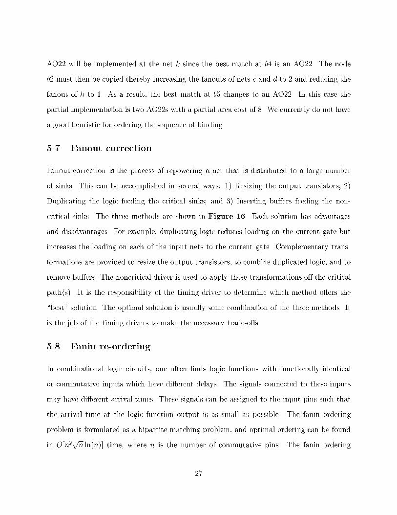
5.7 Fanout correction
Fanout correction is the process of repowering a net that is distributed to a large number
of sinks. This can be accomplished in several ways: 1) Resizing the output transistors; 2)
Duplicating the logic feeding the critical sinks; and 3) Inserting bu�ers feeding the non-
critical sinks. The three methods are shown in Figure 16. Each solution has advantages
and disadvantages. For example, duplicating logic reduces loading on the current gate but
increases the loading on each of the input nets to the current gate. Complementary trans-
formations are provided to resize the output transistors, to combine duplicated logic, and to
remove bu�ers. The noncritical driver is used to apply these transformations o� the critical
path(s). It is the responsibility of the timing driver to determine which method o�ers the
\best" solution. The optimal solution is usually some combination of the three methods. It
is the job of the timing drivers to make the necessary trade-o�s.
5.8 Fanin re-ordering
In combinational logic circuits, one often �nds logic functions with functionally identical
or commutative inputs which have di�erent delays. The signals connected to these inputs
may have di�erent arrival times. These signals can be assigned to the input pins such that
the arrival time at the logic function output is as small as possible. The fanin ordering
problem is formulated as a bipartite matching problem, and optimal ordering can be found
in O[n2pn ln(n)] time, where n is the number of commutative pins. The fanin ordering
27
algorithm employed in BooleDozer [24] gives optimal results over a wide range of delay
models. A simple example of fanin ordering is shown in Figure 17. In this example if signal
B is critical and signal C is not they can be switched so that signal B goes through one gate
instead of two but signal C now goes through two gates instead of one.
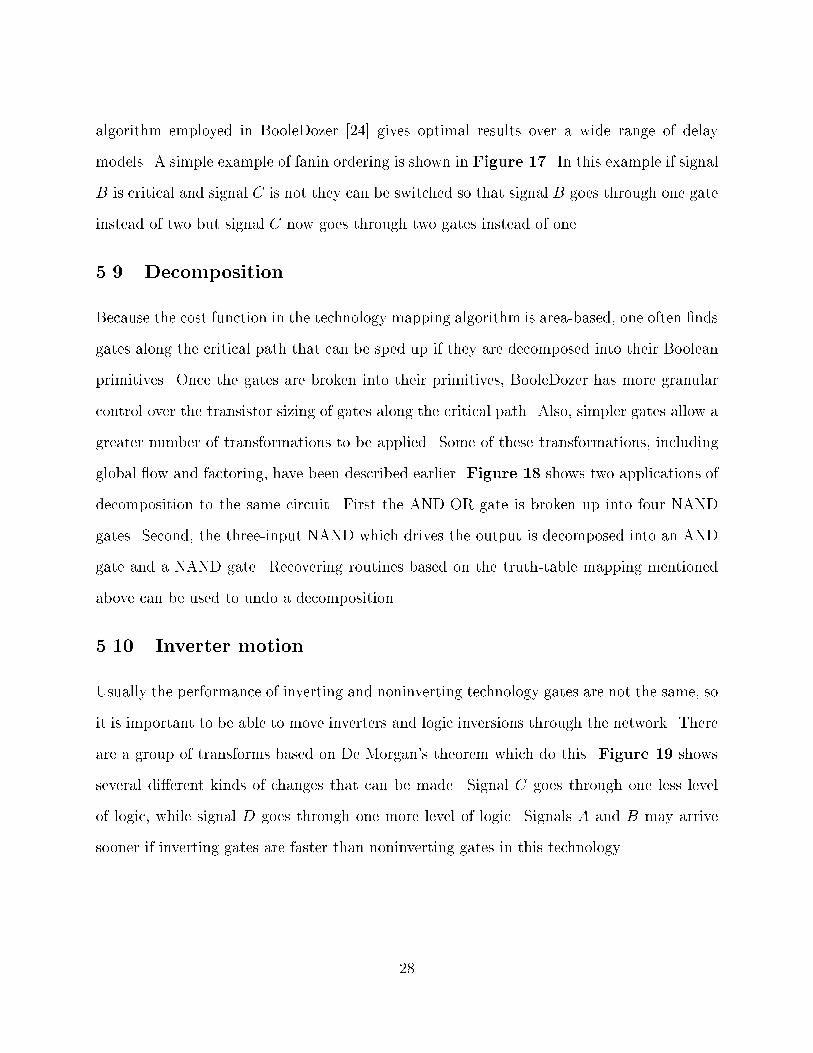
5.9 Decomposition
Because the cost function in the technology mapping algorithm is area-based, one often �nds
gates along the critical path that can be sped up if they are decomposed into their Boolean
primitives. Once the gates are broken into their primitives, BooleDozer has more granular
control over the transistor sizing of gates along the critical path. Also, simpler gates allow a
greater number of transformations to be applied. Some of these transformations, including
global ow and factoring, have been described earlier. Figure 18 shows two applications of
decomposition to the same circuit. First the AND-OR gate is broken up into four NAND
gates. Second, the three-input NAND which drives the output is decomposed into an AND
gate and a NAND gate. Recovering routines based on the truth-table mapping mentioned
above can be used to undo a decomposition.
5.10 Inverter motion
Usually the performance of inverting and noninverting technology gates are not the same, so
it is important to be able to move inverters and logic inversions through the network. There
are a group of transforms based on De Morgan's theorem which do this. Figure 19 shows
several di�erent kinds of changes that can be made. Signal C goes through one less level
of logic, while signal D goes through one more level of logic. Signals A and B may arrive
sooner if inverting gates are faster than noninverting gates in this technology.
28
5.11 FPGA technology mapping
Technology mapping for FPGAs can be performed by FPGA speci�c technology mappers [25,
26] or by using library-based technology mappers [20]. BooleDozer provides both FPGA
speci�c and library-based technology mappers for FPGAs.
BooleDozer provides FPGA speci�c mapping for any FPGA technology whose logic block
is based on a look-up-table (LUT). The core algorithm is based on an interesting theoretical
result for optimal tree mapping [26]. The time complexity is Ofmin[nk; n log(n)]g where k
is the number of inputs to the LUT and n is the number of nodes in the tree. We make use
of this algorithm directly by partitioning the network into trees and applying the optimal
tree mapping. Prior to partitioning, the XOR subgraphs in the network are mapped. This is
accomplished by �nding the XOR patterns and performing a standard technology mapping
on the network. After tree mapping, further optimization is done across tree boundaries to
further reduce the number of LUTs required. This procedure mainly focuses on optimizing
area. A crude level reduction option is provided by merging the remaining root nodes along
long paths. Our experiments indicate that on average the results obtained by our FPGA
speci�c mapper are about 10% better (in area) than our library-based mapper. When the
target device is the Xilinx XC4000 series [27], it is necessary to merge the resulting blocks
together according to the FPGA architecture to build a con�gurable logic block (CLB). A
Xilinx XC4000 series FPGA contains two 4-input LUTs, A and B, which feed a 3-input LUT,
C. The output from the B LUT is available as an optional output of the CLB thereby resulting
in a 9-input 2-output CLB. The merging program groups LUTs together in an architecture-
legal way with the objectives of reducing area, path length and interblock wiring. The
merging method used is structure-based and favors merges which use the full LUT and pin
resources of the CLB. It may be necessary for the program to duplicate logic in order to get
the best mapping of LUTs into CLBs.
The library-based technology mapper of BooleDozer is described in section 5.6. In order
29
to use this technology mapper for LUT-based FPGAs, we must provide the mapper with
a FPGA library. Most vendors provide an ASIC-like technology library to facilitate use
of standard technology mappers. For small values of k, a library which e�ectively consists
of all possible k-input functions can be generated. In practice, the number of all possible
k-input functions (22k
) is prohibitively large for k greater than 3. The size of the library can
be signi�cantly reduced by using equivalent classes based on symmetries and input/output
inversions [28, 29]. For example, the library size for 4-input LUTs can be reduced from
65 536 to 223 functions. The results for the BooleDozer library-based technology mapper
using these reduced libraries are better on average than some FPGA speci�c technology
mappers [29].
5.12 FPGA partitioning
In recent years, designs using FPGAs have grown from single chip applications to multichip
implementations of large logic networks. A special transformation has been added to Boole-
Dozer to provide an e�cient method to partition a design. The underlying algorithm of the
partitioner is based on a linear time graph partitioning heuristic [30]. The BooleDozer par-
titioner uses a novel multistep partitioning process [31] which is geared toward minimizing
both the number of the segments and the total number of I/O pins in the resulting partition.
The following is a brief overview of the partitioning process.
A FPGA has a �xed number of I/O pins and logic blocks. The partitioning problem for
FPGAs can be stated as follows. A partitioning is feasible if each segment in the partition
�ts on a single FPGA. A partitioning is infeasible if there is at least one segment that does
not �t on a single FPGA because the I/O limit is exceeded, the logic block limit is exceeded,
or both. Given a design that does not �t on a single FPGA and the size and the maximum
number of I/Os allowed per FPGA, the goal is a feasible partitioning with the minimum
number of segments.
30
The partitioner can be used in two di�erent modes. In the initial mode, it generates
a feasible partition by iteratively bipartitioning the design. In the improvement mode, the
partitioner attempts to improve an existing feasible solution by reducing the number of
segments, by reducing the total number of I/O pins in the partition, or both.
A design is initially modeled by a hypergraph H = fV;Eg, where V is a set of nodes
and E is a set of edges. V consists of a set of internal nodes that correspond either to the
logic modules in the design or to a subdesign in the case of hierarchical designs and a set of
terminal nodes that correspond to the primary I/Os of the design. E consists of the set of
nets which connect V in the design.
The following is a brief outline of the overall scheme employed by the partitioning process:
1. Construct a hypergraph H = fV;Eg to model the design as described above.
2. Run the partitioner in the initial mode on H and generate a feasible partitioning.
3. Derive a hierarchical hypergraph, H 0, by treating each segment in the partitioning as
a node in H 0.
4. PartitionH 0 under the same size and I/O constraints to reduce the number of segments
in the feasible partitioning.
5. Recover H by attening H 0 which imparts its partitioning information on the nodes of
H.
6. Run the partitioner in the improvement mode on H with its new partitioning as the
initial setting. Repeat steps 3 to 6 until no further improvement is observed.
Because the partitioning process is simple and fast, it is possible to perform multiple runs
of the partitioner. By providing procedures to generate and atten hypergraphs, a more
powerful (and potentially more expensive) technique of perturbation and relaxation [31] can
31
be used to further reduce the total number of segments. Note that the above partitioning
process assumes a single FPGA type. It can be extended to work with a mixture of FPGA
types with di�erent sizes and I/Os.
6 Boolean reasoning using a test generator
All the synthesis transformations described above rely on Boolean algebra to ensure cor-
rectness of their result. While some transformations (e.g., factoring) need only a subset of
the whole Boolean algebra, others (e.g., transduction and redundancy removal) require all
of it. As is common in other synthesis systems, reasoning about Boolean algebra need not
be built in into each transformation using it; instead transformations can call a separate
module dedicated to Boolean reasoning.
Mechanisms for Boolean reasoning are closely tied to the way in which Boolean functions
are represented. A crucial consideration is the size of this representation; as design size
grows, more and more compact representations are required.
Originally Boolean reasoning was performed on truth tables [32]. Since the size of a truth
table is guaranteed to be exponential in the number of input variables, truth tables were
replaced by two-level representations [33]. A two-level representation tends to be smaller than
a truth table, but its size may also grow exponentially. Therefore, instead of representing
the whole function in two levels, the function can be partitioned into \nodes," and each node
is then given a two-level representation [2]. So that optimization of individual nodes can
take advantage of the rest of the function, the rest of the function is represented in the form
of \don't cares." Since the two level don't care representation also grows exponentially, not
all of the function can be represented [34]. Therefore, two-level representations have been
replaced by BDDs. While BDDs tend to be more compact, they still may grow exponentially
with the size of the network. Therefore, in BooleDozer, Boolean reasoning is performed by
a test generator [35, 36], which operates on a gate network, thus avoiding the problems of
32
other existing representations.
It has been shown that there is no theoretical loss in using a test generator [37]; any
network can be transformed to any equivalent network by transformations, which do no
Boolean reasoning except to ask the test generator whether or not certain faults are testable.
While in theory that is the only question that has to be asked, in practice several other tasks
are performed. Some of them involve a simulator, which is commonly a part of any test
generation package. Simulation with random patterns allows us to answer some questions
faster than by calling the test generator.
There are two types of questions asked of the test generator: justi�cation questions and
propagation questions. The �rst involves propagation of values towards primary inputs only,
while the second also involves propagation of values towards primary outputs. Each type of
question uses a di�erent type of simulation as a possible shortcut to answering the question.
Good-machine simulation is used to speed up justi�cation questions, and fault simulation is
used to speed up propagation questions.
Justi�cation questions ask whether there exists an input pattern that would simultane-
ously satisfy conditions of the form Net1 = V al1; :::; Netk = V alk, where each Net is any net
of the network, and each V al is either 0 or 1. For example, the common question whether
x = i implies s = j (for nets x; s and Boolean values i; j) would be given to the test generator
as justi�cation of x = i; s = j. If the test generator is able to justify those two conditions
(i.e., does �nd an input pattern), the implication is false; if the test generator can prove that
there is no such input pattern, the implication is true. Justi�cation questions are used in
selector generation [38], false path analysis [39, 40], and other synthesis tasks.
Before using the test generator, BooleDozer performs good-machine simulation of the
whole design. The number of patterns is a parameter, which is discussed later. The objective
of the simulation is to associate a bit string with every net; the length of the bit string is
the number of patterns simulated. Each primary input and latch output is initialized to a
33
random bit string, and the simulation then assigns a bit string to each internal net according
to the net's function.
Every time the test generator is asked a justi�cation question, the simulation values can
be used to see if one of the random patterns satis�es the conditions to be justi�ed. If so,
the answer to the justi�cation question is a�rmative and there is no need to call the test
generator. The test generator is called only if none of the random patterns satis�es the
conditions of the justi�cation question. As a result, many justi�cation questions can be
answered using the simulation patterns, which takes constant time independent of the size
of the design.
Propagation type questions are of the form \Suppose a net S computes a function f .
If f is replaced by a di�erent function g, will that change the functionality F of the whole
design?" This question is asked in transduction, redundancy removal, veri�cation [41], and
incremental synthesis [42]. To answer this question in general, we use the following lemma.
Lemma 1 :
F (f) = F (g) i� F (f � g) = F (0);
F (f) = F (g) i� F (f � g) = F (1).
The expression F (f � g) represents a replacement of a subfunction f with f � g. Then
the test generator is asked whether the net S (which is now the output of the XOR gate) is
testable for stuck at 0 or 1 fault. If it is not testable for stuck at 0 fault [i.e., F (f � g) =
F (0)] then g can replace f without changing the functionality of the whole design [i.e.,
F (f) = F (g)]. If S is not testable for stuck at 1 [i.e., F (f � g) = F (1)] then g can replace
f without changing the functionality of the whole design [i.e., F (f) = F (g)].
In the simple case of redundancy removal, f � g simpli�es to either f or f , depending on
whether g = 0 or g = 1. Therefore, in the case of redundancy removal, there is no need for
the XOR gate; the testability of S is checked directly.
34
As good-machine simulation is used for a quick answer to the justi�cation type of ques-
tions, fault simulation is used for a quick answer to propagation type questions. However,
fault simulation may take time proportional to the size of the design, which tends to be
too slow. Therefore, BooleDozer sometimes uses approximate fault simulation [43], which
may give us an a�rmative answer in constant time. However, in contrast to good-machine
simulation, approximate fault simulation may err on either sides; therefore, an a�rmative
answer given by approximate fault simulation can be used to reject a change to logic, but
should not be used to accept a change.
For both simulation and test generation there is a trade-o� between e�ectiveness and
amount of resources consumed. The simulator takes as parameter the number of random
patterns to simulate. The larger that number, the longer it takes to simulate, the more
memory it takes to store the results, but the less often is there need for calling the test
generator. The test generator takes as parameter the number of backtracks. The larger that
number, the longer it may take to deliver an answer, but the less often will the test generator
fail to decide.
For any practical value of the parameter, it is possible that the test generator may not
be able to decide one way or the other. Any transformation relying on the test generator
must control how much time the test generator is allowed and must be prepared for the
possibility of an undetermined answer. The frequency of an undetermined answer is very
much application dependent, and it is hard to predict; however, BooleDozer adopted a test
generator based approach, because in our applications it fails less often than other methods,
in particular, BDD based methods.
7 Optimizing designs hierarchically
As the size of VLSI designs grows rapidly synthesis of very large at designs becomes expen-
sive and time consuming. The traditional way of dealing with these problems is through the
35
introduction of hierarchy in the designs. Hierarchical designs can be created such that the
individual pieces of the hierarchy are of a good size for synthesis and the number of pieces
in the hierarchy is proportional to the size of the designs. Synthesis can be run separately
on each of piece of the hierarchy, and these jobs can be run in parallel to reduce the total
runtime.
Technology-independent optimization and technology mapping can be dealt with e�ec-
tively in a parallel fashion. However, the timing correction of a large hierarchical design
is a di�cult problem. Unless strict latch-bounding constraints are imposed, it is di�cult
to resolve the results of timing a hierarchical piece by itself with the results of timing that
hierarchical piece in the context of the timing model of the entire design.
Consider the following approach to perform hierarchical timing correction. The entire
design is timed keeping track of the hierarchy boundaries. Timing constraint management
is done to adjust the measured arrival and required times at hierarchical boundaries. This is
done in order to drive timing correction to correct cross-hierarchy timing paths that violate
timing constraints. Timing constraint �les are generated for each piece in the hierarchy
specifying primary input arrival times, transition times, primary output required times, etc.
Next, timing correction is run in parallel on all the pieces using these timing constraint �les.
The process of constraint �le generation and timing correction is repeated until all timing
constraints are met, or until no further progress is made.
In this approach the boundary constraints speci�ed by the timing constraint �les are
static, and this causes the so-called boundary problems. In Figure 20, any e�ort to apply
timing correction to the logic in piece A fed by the register output does not result in an
equivalent improvement in arrival time at the input of the logic in piece B. This can lead
to over-correction of the logic.
Another problem hierarchical timing correction has to deal with is the parallel-timing-
correction convergence problem. Consider the situation shown in Figure 21, a hierarchical
36
design with two timing correctable pieces A and B and a net which is driven in piece A and
is used in piece B. At the beginning of the �rst timing correction iteration, piece A drives
the net with a bu�er. Piece B also bu�ers the net and distributes it to a number of sinks.
If the signal is late, timing correction will make an attempt to �x it. Timing correction is
run on the two pieces in parallel. The timing correction job on A decides to eliminate the
bu�er because the net is lightly loaded by B. Simultaneously, the timing correction job on
B drops the input bu�er because the drive strength of the output bu�er in A is su�cient to
drive all the sinks in B. Both jobs measure an improvement of the timing characteristics of
the net using the timing constraint �les which have not changed to re ect the work done by
the timing correction run. However, when the hierarchy is reassembled, no progress has been
made, and indeed the timing may have gotten worse. If timing correction is attempted in
parallel another time, the reverse happens, and both the input and the output are rebu�ered,
putting the design back in its original state.
The magnitude of the oscillation is dependent on two factors, the gain of the timing
correction (how much improvement is being made by timing correction), and the degree of
parallelism. In the trivial case, where there is no timing correction to be done, there is no
oscillation no matter what the degree of parallelism. Similarly there are no convergence
problems if the degree of parallelism is 1, no matter how much time is being extracted from
the network.
The following approach, called parallel hierarchical timing correction (PHTC) addresses
both problems. PHTC uses the hierarchical timing propagation capabilities of EinsTimer to
reduce the boundary problems. If the hierarchy is available, EinsTimer will correctly re ect
reductions in delay for piece A, in Figure 20, as changes to arrival times at piece B. The
parallel timing correction convergence problem is managed by controlling the number of peer
timing correction processes running in parallel.
Each process is in an endless loop:
37
1. Choose the next hierarchy piece to timing correct, ensuring that the piece is not being
timing corrected by any of the other processes.
2. Broadcast the name of the piece, such that all other processes are aware that it is being
timing corrected.
3. Timing correct the chosen piece.
4. Lock the netlist directory.
5. Output the netlist of the newly timing corrected piece to the netlist directory.
6. Read in all other hierarchy pieces that have been changed by other processes from the
netlist directory.
7. Unlock the netlist directory.
8. Reinitialize the timing subsystem.
9. Go to 1.
When a raw (not yet timing corrected) model is loaded into the system, the gross problems
that are corrected far outnumber the subtle boundary oriented convergence problems, and the
system can tolerate a large number of processes running simultaneously. As time progresses,
and the �xes being introduced become more speci�c, the susceptibility of those �xes to
oscillation grows. However, the probability of PHTC working on both the input and output
sides of a hierarchical boundary at the same time diminishes as the number of processes
running is reduced.
The pieces in the hierarchy may be processed multiple times. The amount of synthesis
e�ort applied is based on the number of times that the piece has been visited. Gross problems
in not yet timing corrected pieces of the hierarchy may cause the timing correction of the
38
other pieces to work on the wrong problems. Thus, it is not worthwhile to spend a lot of
e�ort in timing correction until the gross problems in all of the pieces have been �xed. The
�rst time around the hierarchy, timing correction is applied requesting a small amount of
e�ort, �xing gross problems. The second time around, a middle level of e�ort is requested,
and so on. It is not until all of the easy cross hierarchy timing problems have been solved
that the most advanced heuristics are chosen.
In general, it may not be necessary to process all of the pieces in the hierarchy with
medium or high levels of e�ort. Often, the critical path is contained in a few of the hierar-
chical elements, and the rest of the design warrants only a cursory pass of timing correction
to eliminate gross problems. It is advantageous to select the elements in the hierarchy on
the basis of some measure of the work they need. The heuristic PHTC uses in choosing the
next hierarchy piece to timing correct is as follows:
1. For each synthesizable piece, determine the worst slack in the piece, the sum of the
worst slacks for the 32 worst points, and the number of times timing correction has
been applied to the piece.
2. Build a list of these pieces, ordering �rst by the worst slack, and second by the sum of
the worst 32 points.
3. Truncate the list to the pieces on the worst path (all of the hierarchy pieces on the
worst path will have the same worst slack, and will appear on the top of the list), or
�ve pieces, whichever is longer.
4. Choose the piece from the truncated list that has had the least amount of timing
correction applied, and apply timing correction with the e�ort based on the number
of previous timing correction passes to that piece.
Any discussion about hierarchical timing correction must address the issue of hierarchy
39
reuse. When BooleDozer's timing correction routines request a slack for a particular point
in the network, they provide a hierarchy-unique speci�er of that point. The slack returned is
speci�c to that point in the hierarchy. One way to deal with hierarchy reuse is to clone these
portions of the hierarchy before timing correction. This is actually not such an onerous
burden. Generally, we get the most advantage out of timing correction on control logic,
and control logic can seldom be reused. However, it would be a simple change to the timing
subsystem to return the slack across all instances of that point in the entire hierarchy. In this
way, the timing correction routines would never make a change in a multiply used hierarchy
element that would be bene�cial to one instance and detrimental to another.
One feature of PHTC is that it can be used in an incremental fashion virtually unchanged.
Take a hypothetical change in the HDL for one of the hierarchical pieces. This piece is pushed
through technology-independent optimization and technology mapping, and inserted into the
rest of the design, which has already had a signi�cant amount of timing correction applied
to it. Because of the timing correction counts that are associated with all elements in the
hierarchy, if the new design appears in the critical path, it will be the immediate focus of
timing correction. Used in this fashion, last minute changes to the design can be processed
e�ciently.
8 Design examples
BooleDozer has been used within IBM to design many high-performance microprocessors
and ASIC chips. A short description of some representative designs is given below.
� The control logic for the PowerPC 601TM [44], PowerPC 603TM, and PowerPC 604TM
was designed in a proprietary high-level language, DSL, and synthesized using Boole-
Dozer.
40
� A high-performance PowerPCTM chip set optimized for commercial operations. It uses
BiCMOS technology and includes bit stacks. The chips were designed in VHDL.
� A single-chip, PowerPC processor. It was designed entirely in VHDL and uses a
pure ASIC CMOS technology, CMOS5L. This processor makes extensive use of the
LOGIC STYLE attribute to tune synthesis.
� A large, high-performance, semicustom, superscalar microprocessor, containing ap-
proximately 80 timing-correctable entities with a total of close to 300K cells of synthe-
sized control logic. This is the �rst production use of the PHTC system.
� A large System/390TM processor designed in VHDL. More than hundred partitions
were synthesized ranging in size from a couple of hundred lines of VHDL to close to
ten thousand lines. Resulting networks contained a few hundred to thousands of logic
cells, each matching the timing requirements of a few hundred MHz.
� A MPEG-2 video decoder chip which decompresses digital video data. The module
receives the compressed data at a rate of up to 15 Mb/s.
� A MPEG-2 video encoder chip set. It supports full motion video up to CCIR 601
resolution, 720x480 at 30Hz or 720x576 at 25Hz.
� A set of I/O and memory subsystem chips. They are pure CMOS5L ASICs, completely
synthesized designs. All were designed using VHDL.
9 Conclusions
In this paper the major features, algorithms and design representations which comprise the
BooleDozer logic synthesis have been presented. State-of-the-art synthesis algorithms and a
fast incremental timing subsystem have been used to create a leading synthesis tool. Boole-
Dozer uses a modular design following an orthogonal decomposition of the logic synthesis
41
problem. This has led to a collection of transformations operating under the control of a set
of drivers which can be ordered using a powerful scripting language to accommodate a wide
variety of design styles.
10 Acknowledgments
As an open system, BooleDozer has bene�ted greatly from the many contributions of the
IBM synthesis codevelopment and user community. The quality of this paper was greatly
improved by the very useful comments of the reviewers.
BooleDozer, EinsTimer, PowerPC 601, PowerPC 603, PowerPC 604, PowerPC, and Sys-
tem/390 are trademarks of International Business Machines Corporation.
References
[1] R. Bergamaschi, R. O'Connor, L. Stok, M. Moricz, S. Prakash, A. Kuehlmann, and
D. S. Rao, \High-level synthesis in an industrial environment," IBM J. of Res. and
Develop. 39, 131{148 (January/March 1995).
[2] R. K. Brayton, G. Hachtel, C. McMullen, and A. Sangiovanni-Vincentelli, Logic Min-
imization Algorithms for VLSI Synthesis, Kluwer Academic Publishers, The Nether-
lands, 1985.
[3] S. J. Hong, R. G. Cain, and D. L. Ostapko, \MINI: a heuristic approach for logic
minimization," IBM J. of Res. and Develop. 18, 443{458 (September 1974).
[4] R. E. Bryant, \Graph based algorithms for boolean function manipulation," IEEE
Trans. Computers C-35, 677{691 (August 1986).
42
[5] J. Darringer, W. Joyner, C. Berman, and L. Trevillyan, \Logic synthesis through local
transformations," IBM J. of Res. and Develop. 25, 272{280 (July 1981).
[6] J. Darringer, D. Brand, J. V. Gerbi, W. Joyner, and L. Trevillyan, \LSS: A system
for production logic synthesis," IBM J. of Res. and Develop. 28, 537{545 (September
1984).
[7] R. K. Brayton, R. Rudell, A. Sangiovanni-Vincentelli, and A. Wang, \MIS: A multiple-
level logic optimization system," IEEE Trans. Computer-Aided Design CAD-6, 1062{
1081 (November 1987).
[8] E. Detjens, G. Gannot, R. Rudell, A. Sangiovanni-Vincentelli, and A. Wang, \Technol-
ogy mapping in MIS," Proceedings of the IEEE International Conference on Computer-
Aided Design, November 1987, pp. 116{119.
[9] D. Brand, R. Damiano, L. van Ginneken, and A. Drumm, \In the driver's seat of
BooleDozer," Proceedings of the IEEE International Conference on Computer-Aided
Design, October 1994, pp. 518{521.
[10] F. N. Najm, \A survey of power estimation techniques in VLSI circuits," IEEE Trans.
VLSI 2, 446{455 (December 1994).
[11] R. B. Hitchcock Sr., G. L. Smith, and D. D. Cheng, \Timing analysis of computer
hardware," IBM J. Res. Develop. 26, 100{105 (January 1982).
[12] R. B. Hitchcock Sr., \Timing veri�cation and the timing analysis program," Proceedings
of the 19th ACM/IEEE Design Automation Conference, June 1982, pp. 594{604.
[13] D. Brand and V. S. Iyengar, \Timing analysis using functional analysis," IEEE Trans.
on Computers C-37, 1309{1314 (October 1988).
43
[14] D. Brand, R. Bergamaschi, and L. Stok, \Don't cares in synthesis: Theoretical pitfalls
and practical solutions," Computer Science Technical Report RC 20127 , IBM Thomas
J. Watson Research Center, Yorktown Heights, NY, September 1995.
[15] D. Kung, R. Damiano, T. Nix, and D. Geiger, \BDDMAP: A technology mapper based
on a new covering algorithm," Proceedings of the 29th ACM/IEEE Design Automation
Conference, June 1992, pp. 484{487.
[16] D. Brand, \PLA-based synthesis without PLAs," Proceedings of the International Work-
shop on Logic Synthesis, MCNC/IEEE/ACM, May 1989, p. 8.1.
[17] L. Berman and L. Tervillyan, \Global ow optimization in automatic logic design,"
IEEE Transactions on Computer-Aided Design CAD-10, 557{564 (May 1991).
[18] S. Muroga, Y. Kambayashi, H. C. Lai, and J. N. Culliney, \The transduction method {
design of logic networks based on permissible functions," IEEE Transactions on Com-
puters C-38, 1404{1424 (October 1989).
[19] D. Gregory, K. Bartlett, A. de Geus, and G. Hachtel, \Socrates: a system for au-
tomatically synthesizing and optimizing combinational logic," Proceedings of the 23rd
ACM/IEEE Design Automation Conference, ACM/IEEE, June 1986, pp. 79{85.
[20] K. Keutzer, \DAGON: technology binding and local optimization by DAG matching,"
Proceedings of the 24th ACM/IEEE Design Automation Conference, June 1987, pp.
341{347.
[21] M. Lega, \Mapping properties of multi-level logic synthesis operations," Proceedings of
the IEEE International Conference on Computer Design, October 1988, pp. 257{260.
44
[22] F. Mailhot and G. De Micheli, \Technology mapping using boolean matching and don't
care sets," Proceedings of the IEEE European Design Automation Conference, March
1990, pp. 212{216.
[23] L. Trevillyan, R. Damiano, D. Geiger, D. Kung, J. Ludwig, and T. Nix, \Method for
identifying technology primitives in logic functions," IBM Tech. Disclosure Bull., 359{
361 (May 1992).
[24] L. P. P. P. van Ginneken, \Fanin ordering in multi-slot timing analysis," Proceeding of
IEEE International Conference on Computer Design, 1992, pp. 44{47.
[25] R. J. Francis, J. Rose, and K. Chung, \Chortle: A technology mapping program for
lookup table-based �eld programmable gate arrays," Proceedings of the 27th ACM/IEEE
Design Automation Conference, June 1990, pp. 613{619.
[26] A. H. Farrahi and M. Sarrafzadeh, \Complexity of the lookup-table minimization prob-
lem for FPGA technology mapping," IEEE Trans. Computer-Aided Design CAD-13,
1319{1332 (November 1994).
[27] The Programmable Logic Data Book, Xilinx Corporation, San Jose, CA, 1994.
[28] S. Trimberger, \A small, complete mapping library for lookup-table-based FPGAs," 2nd
International Workshop on Field Programmable Logic and Applications, August 1992.
[29] L. Trevillyan, \An experiment in technology mapping for FPGAs using a �xed library,"
Proceedings of the International Workshop on Logic Synthesis, IEEE/ACM, 1993.
[30] C. M. Fidducia and R. M. Mattheyses, \A linear time heuristic for improving network
partitions," Proceedings of the 19th ACM/IEEE Design Automation Conference, June
1982, pp. 175{181.
45
[31] D. Kung and L. N. Reddy, \A multi-chip device partitioning process," Patent Applica-
tion YO994-218 , IBM Corporation, October 1994.
[32] M. Karnaugh, \The map method for synthesis of combinational logic circuits," Trans-
actions AIEE 72, 9, 593{599 1953.
[33] E. J. McCluskey, Introduction to the Theory of Switching Circuits, McGraw-Hill Book
Co., Inc., New York, 1965.
[34] A. Saldanha, A. R. Wang, R. K. Brayton, and A. Sangiovanni-Vincentelli, \Multi-level
logic simpli�cation using don't cares and �lters," Proceedings of the 26th ACM/IEEE
Design Automation Conference, June 1989, pp. 227{282.
[35] S. Kundu, L. H. Huisman, I. Nair, V. S. Iyengar, and L. N. Reddy, \A small test
generator for large designs," Proceedings of the International Test Conference, IEEE,
September 1992, pp. 30{40.
[36] R. P. Kunda, P. Narain, J. A. Abraham, and B. D. Rathi, \Speed up of test generation
using high-level primitives," Proceedings of the 27th ACM/IEEE Design Automation
Conference, June 1990, pp. 594{599.
[37] W. Kunz and P. R. Menon, \Multi-level logic optimization by implication analysis,"
Proceedings of the IEEE International Conference on Computer-Aided Design, Novem-
ber 1994, pp. 6{13.
[38] M. Berkelaar and L. P. P. P. van Ginneken, \E�cient orthonormality testing for synthe-
sis with pass-transistor selectors," Proceedings of the International Workshop on Logic
Synthesis, IEEE/ACM, May 1995.
[39] D. Brand and V. S. Iyengar, \Timing analysis using functional analysis," IEEE Trans.
Computers C-37, 1309{1314 (October 1988).
46
[40] P. C. McGeer and R. K. Brayton, Integrating Functional and Temporal Domains in
Logic Synthesis, Kluwer Academic Publishers, The Netherlands, 1991.
[41] D. Brand, \Veri�cation of large synthesized designs," Proceedings of the IEEE Interna-
tional Conference on Computer-Aided Design, November 1993, pp. 534{537.
[42] D. Brand, A. Drumm, S. Kundu, and P. Narain, \Incremental synthesis," Proceedings
of the IEEE International Conference on Computer-Aided Design, November 1994, pp.
14{18.
[43] M. Abramovici, P. R. Menon, and D. J. Miller, \Critical path tracing: An alternative
to fault simulation," IEEE Design & Test 1, 93{93 (February 1984).
[44] T. B. Brodnax, R. V. Billings, S. C. Glenn, and P. T. Patel, \Implementation of the
PowerPC 601 microprocessor," IBM J. of Res. and Develop. 38, 621{632 (September
1994).
Leon Stok IBM Research Division, Thomas J. Watson Research Center, P.O. Box 218,
Yorktown Heights, New York 10598 ([email protected]). Dr. Stok studied electrical
engineering at the Eindhoven University of Technology, The Netherlands, from which he
graduated with honors in 1986. In 1991 he received the Ph.D. degree from the Eindhoven
University. He is currently manager of the Logic Synthesis group in the System, Technology
and Science Department. Prior to this assignment, Dr. Stok worked in the \Unternehmens-
bereich Kommunikations-und Datentechnik" of Siemens AG in Munich in 1985, and in the
Mathematical Sciences Department of the IBM Thomas J. Watson Research Center during
the second half of 1989 and the �rst half of 1990. Dr. Stok has published several papers
on various aspects of logic, high-level and architectural synthesis and on automatic place-
ment and routing of schematic diagrams. His research interests include high-level and logic
synthesis, layout synthesis, and system synthesis and veri�cation. He is a member of the
47
Institute of Electrical and Electronics Engineers.
David S. Kung IBM Research Division, Thomas J. Watson Research Center, P.O. Box
218, Yorktown Heights, New York 10598 ([email protected]). Dr. Kung received the
B.A. from the University of California at Berkeley, the M.A. from Harvard University, and
the Ph.D. from Stanford University, all in physics. He spent two years as a postdoctoral
fellow at Stanford before joining IBM in 1986. Dr. Kung is currently in the Logic Synthesis
group at Yorktown. His research interests are logic and asynchronous synthesis.
Daniel Brand IBM Research Division, Thomas J. Watson Research Center, P.O. Box 218,
Yorktown Heights, New York 10598 ([email protected]). Dr. Brand received the Ph.D.
degree in computer science from the University of Toronto in 1976. Since then he has been
working at the IBM Thomas J. Watson Research Center, with temporary stays at the IBM
Zurich Research Laboratory, the Beijing Institute of Aeronautics and Astronautics, and the
Kyushu Institute of Technology. He has worked in the areas of veri�cation, communication
protocols and logic synthesis.
Anthony D. Drumm IBM Rochester, 3605 Highway 52 North, Rochester, Minnesota 55901
([email protected]). Mr. Drumm received his B.S. degree in electrical engineering cum
laude from The Ohio State University in 1977. He received his M.S. degree in computer
engineering from Syracuse University in 1983. In 1977, he joined IBM in Endicott, NY as
a designer in mid-range computers. Mr. Drumm began working on logic synthesis tools in
1984 and was one of the original architects of the BooleDozer logic synthesis system. In
1992, he transferred to IBM Rochester, where he continues this work. He is currently a
senior engineer with technical responsibility for logic synthesis in IBM's Systems Technology
and Architecture Division. Mr. Drumm has coauthored papers on logic synthesis; he holds
three U.S. patents.
48
Andrew J. Sullivan IBM Microelectronics Division, EDA Laboratory, 1580 Route 52,
Hopewell Junction, New York 12533. Mr. Sullivan received his undergraduate degree in
electrical engineering from Washington University in 1989, joining IBM in 1990. He is cur-
rently a member of the synthesis development team at the IBM Corporation in Poughkeepsie,
New York.
Lakshmi N. Reddy IBM Microelectronics Division, EDA Laboratory, 1580 Route 52,
Hopewell Junction, New York 12533 ([email protected]). Dr. Reddy received the B.E.
degree in electronics and communication engineering from Osmania University, Hyderabad,
India, in 1987, and the Ph.D. degree in electrical and computer engineering from the Univer-
sity of Iowa, in 1992. He is currently a sta� member at the IBM Corporation, Poughkeepsie,
New York. Dr. Reddy worked at the IBM Thomas J. Watson Research Center in the sum-
mer of 1991; he was with the Motorola ASIC CAD Division, Chandler, Arizona, during the
summer of 1990. His research interests include logic and FPGA synthesis, testing of VLSI
circuits, design for testability, and partitioning. He is a member of the Institute of Electrical
and Electronics Engineers.
Nathaniel Hieter IBM Microelectronics Division, EDA Laboratory, 1580 Route 52,
Hopewell Junction, New York 12533 ([email protected]). Mr. Hieter studied electrical
engineering at the California Institute of Technology, from which he received his undergrad-
uate degree in 1991. He has been a member of the BooleDozer Logic Synthesis development
team since 1990. His research interests include high-level and logic synthesis, speci�cally
delay optimization.
David J. Geiger IBM Microelectronics Division, 3605 Highway 52 North, Rochester, Min-
nesota 55901 (David [email protected]). Dr. Geiger received his Ph.D. in electrical
engineering from Carnegie-Mellon University in 1989. He has worked at the IBM EDA
49
Laboratory since then on high-level and logic synthesis.
Han Hsun Chao IBM Microelectronics Division, EDA Laboratory, 1580 Route 52, Hopewell
Junction, New York 12533 ([email protected]). Dr. Chao received his MS
degree in electrical engineering from The Rutgers University in 1982, joining IBM in 1983.
He was granted an IBM Resident Study Award from 1990 to 1991 to complete the Ph.D.
studies in computer engineering from Syracuse University. His research interests include
logic synthesis, veri�cation and diagnosis, and layout synthesis.
Peter J. Osler IBM Microelectronics Division, Essex Junction, Vermont 05452
([email protected]). Mr. Osler studied electrical engineering and computer science at
M.I.T., receiving bachelor's degrees in computer science and electrical engineering in 1983,
and after a two year hiatus at the IBM Thomas J. Watson Research Center, his master's
degree in electrical engineering in 1987. Since then he has participated in the design of
many CMOS VLSI circuits for the IBM Microelectronics Division, providing tools support
for simulation, synthesis, Boolean comparison, and static timing analysis. He is currently
an advisory engineer, in charge of static timing analysis and timing correction on a large
high-performance superscalar semi-custom microprocessor.
50
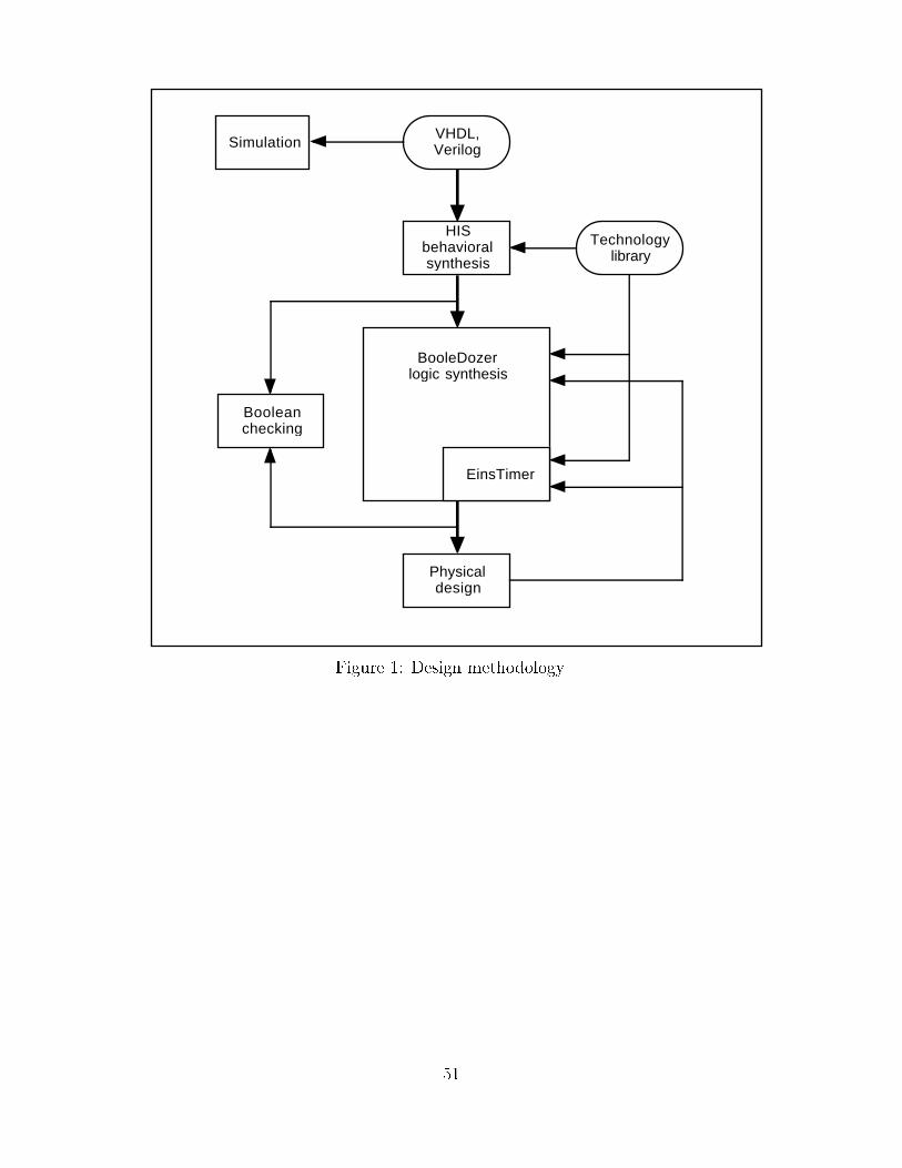
VHDL,VerilogSimulation
HISbehavioralsynthesis
Technologylibrary
Physicaldesign
Booleanchecking
BooleDozerlogic synthesis
EinsTimer
Figure 1: Design methodology.
51
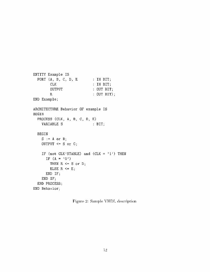
ENTITY Example IS
PORT (A, B, C, D, E : IN BIT;
CLK : IN BIT;
OUTPUT : OUT BIT;
R : OUT BIT);
END Example;
ARCHITECTURE Behavior OF example IS
BEGIN
PROCESS (CLK, A, B, C, D, E)
VARIABLE S : BIT;
BEGIN
S := A or B;
OUTPUT <= S or C;
IF (not CLK'STABLE) and (CLK = '1') THEN
IF (A = '0')
THEN R <= S or D;
ELSE R <= E;
END IF;
END IF;
END PROCESS;
END Behavior;
Figure 2: Sample VHDL description.
52
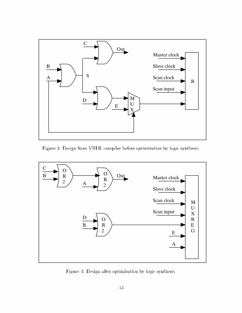
�
��
� ����������
� ��������
� �������
� �������
�
�
�
�
�
���
Figure 3: Design from VHDL compiler before optimization by logic synthesis.
�
�����������
�����������
����������
����������
�
�
�
�
�
��
�
�
�
�
�
��
��
��
Figure 4: Design after optimization by logic synthesis.
53
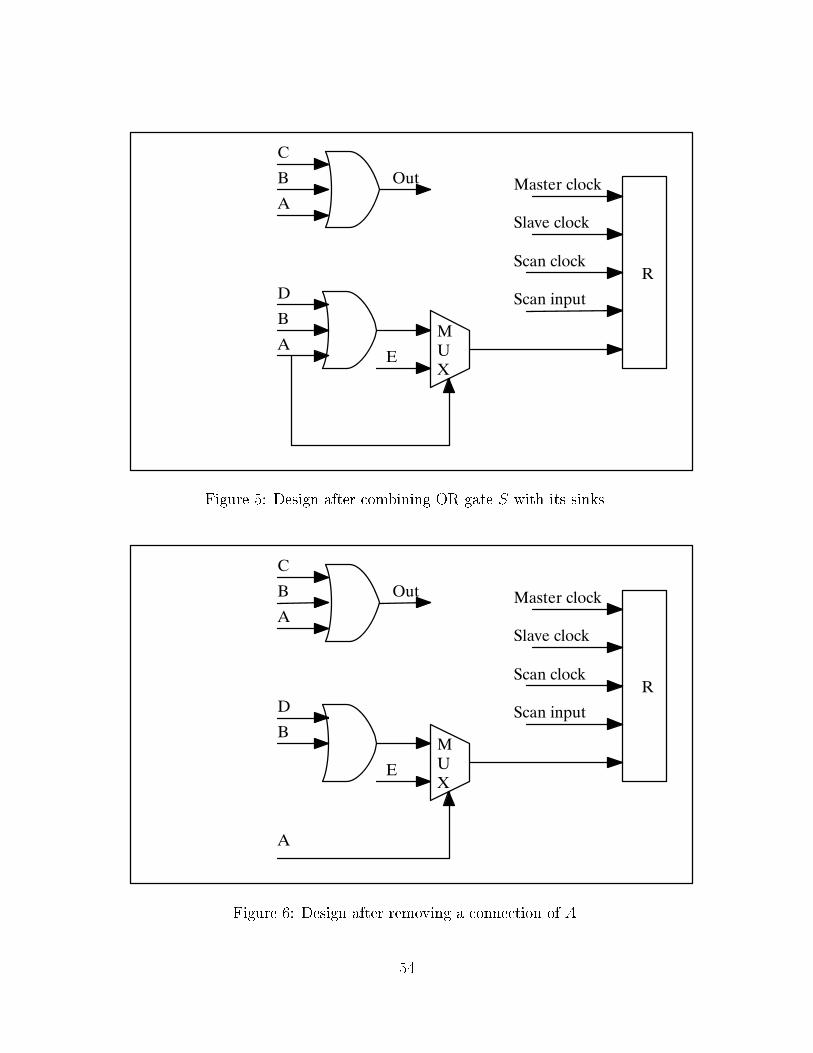
�
��
� ����������
� ��������
� �������
� �������
�
�
�
�
���
�
�
�
Figure 5: Design after combining OR gate S with its sinks.
��
�
� ����������
� ��������
� �������
� �������
�
�
�
�
���
�
�
�
Figure 6: Design after removing a connection of A.
54
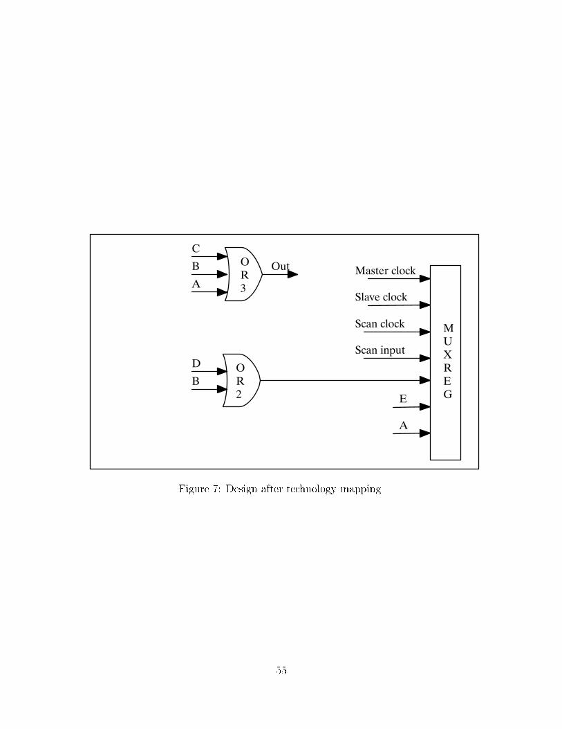
��
�����������
����������
���������
���������
�
�
�
�
�
���
�
�
�
�
���
���
Figure 7: Design after technology mapping.
55
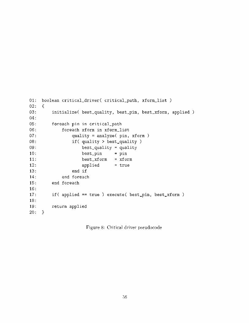
01: boolean critical_driver( critical_path, xform_list )
02: {
03: initialize( best_quality, best_pin, best_xform, applied )
04:
05: foreach pin in critical_path
06: foreach xform in xform_list
07: quality = analyze( pin, xform )
08: if( quality > best_quality )
09: best_quality = quality
10: best_pin = pin
11: best_xform = xform
12: applied = true
13: end if
14: end foreach
15: end foreach
16:
17: if( applied == true ) execute( best_pin, best_xform )
18:
19: return applied
20: }
Figure 8: Critical driver pseudocode.
56
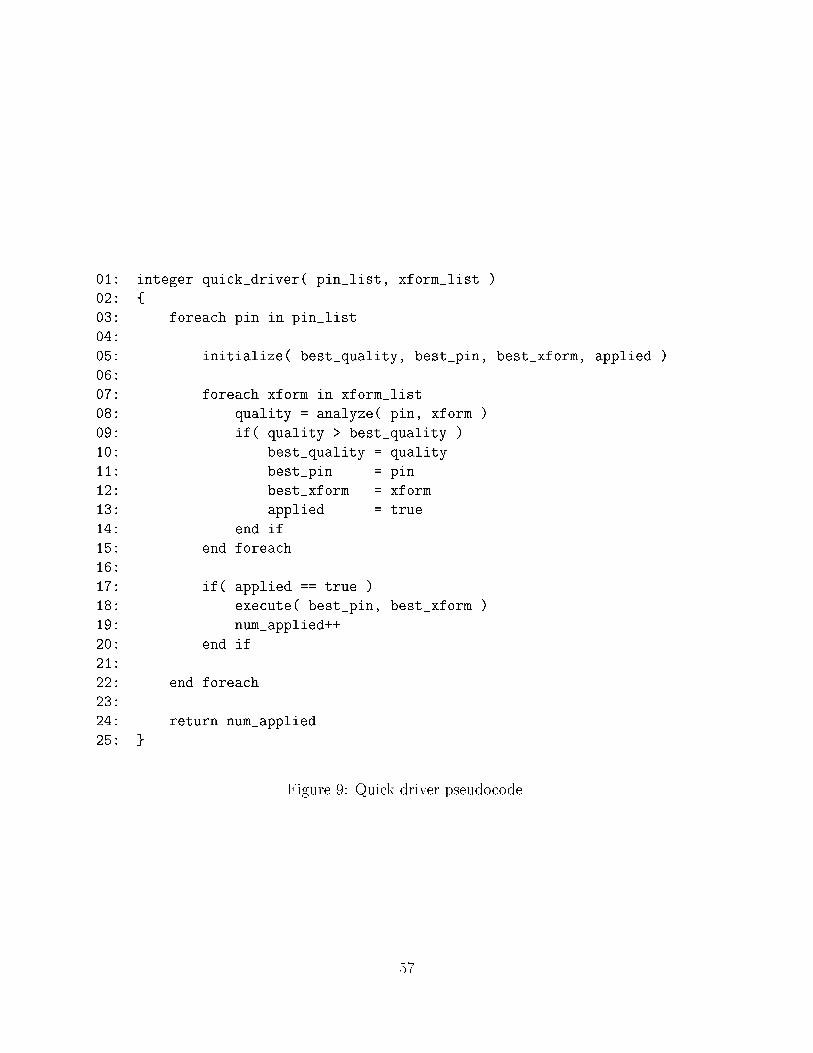
01: integer quick_driver( pin_list, xform_list )
02: {
03: foreach pin in pin_list
04:
05: initialize( best_quality, best_pin, best_xform, applied )
06:
07: foreach xform in xform_list
08: quality = analyze( pin, xform )
09: if( quality > best_quality )
10: best_quality = quality
11: best_pin = pin
12: best_xform = xform
13: applied = true
14: end if
15: end foreach
16:
17: if( applied == true )
18: execute( best_pin, best_xform )
19: num_applied++
20: end if
21:
22: end foreach
23:
24: return num_applied
25: }
Figure 9: Quick driver pseudocode.
57
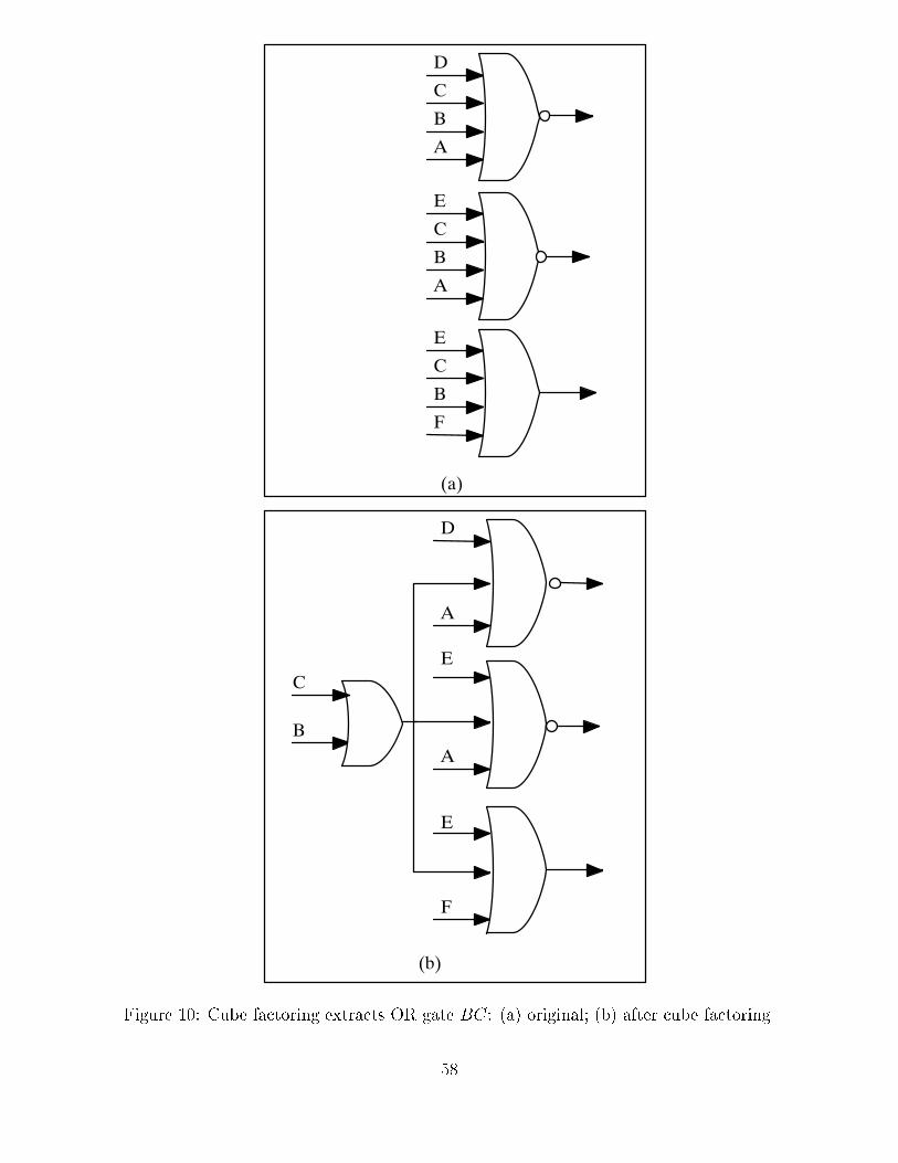
�
�
�
�
�
�
�
�
�
�
�
�
�
�
�
�
�
�
��
������������
Figure 10: Cube factoring extracts OR gate BC: (a) original; (b) after cube factoring.
58
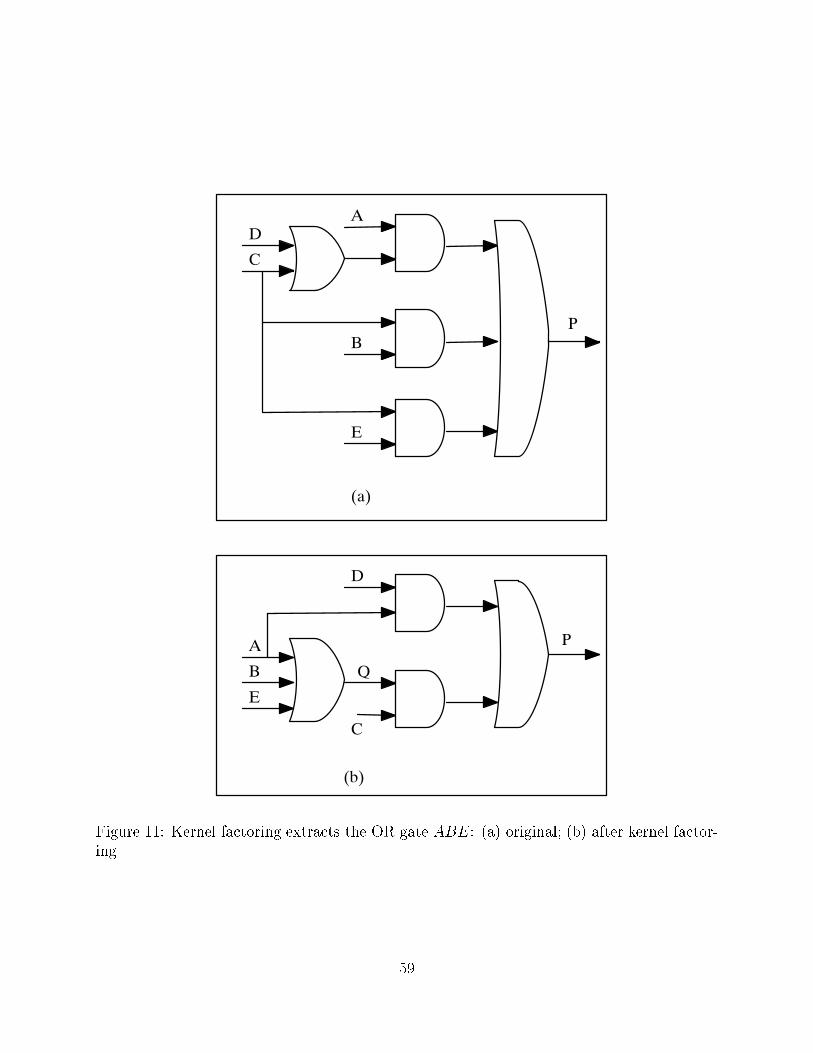
�
��
�
�
�
�
�
�
�
���
������������
Figure 11: Kernel factoring extracts the OR gate ABE: (a) original; (b) after kernel factor-ing.
59
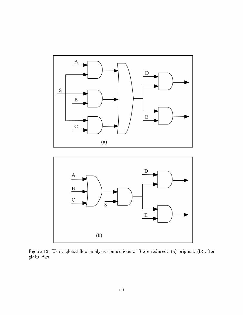
�
�
�
�
�
�
�
�
�
�
��
����������������������
Figure 12: Using global ow analysis connections of S are reduced: (a) original; (b) afterglobal ow.
60
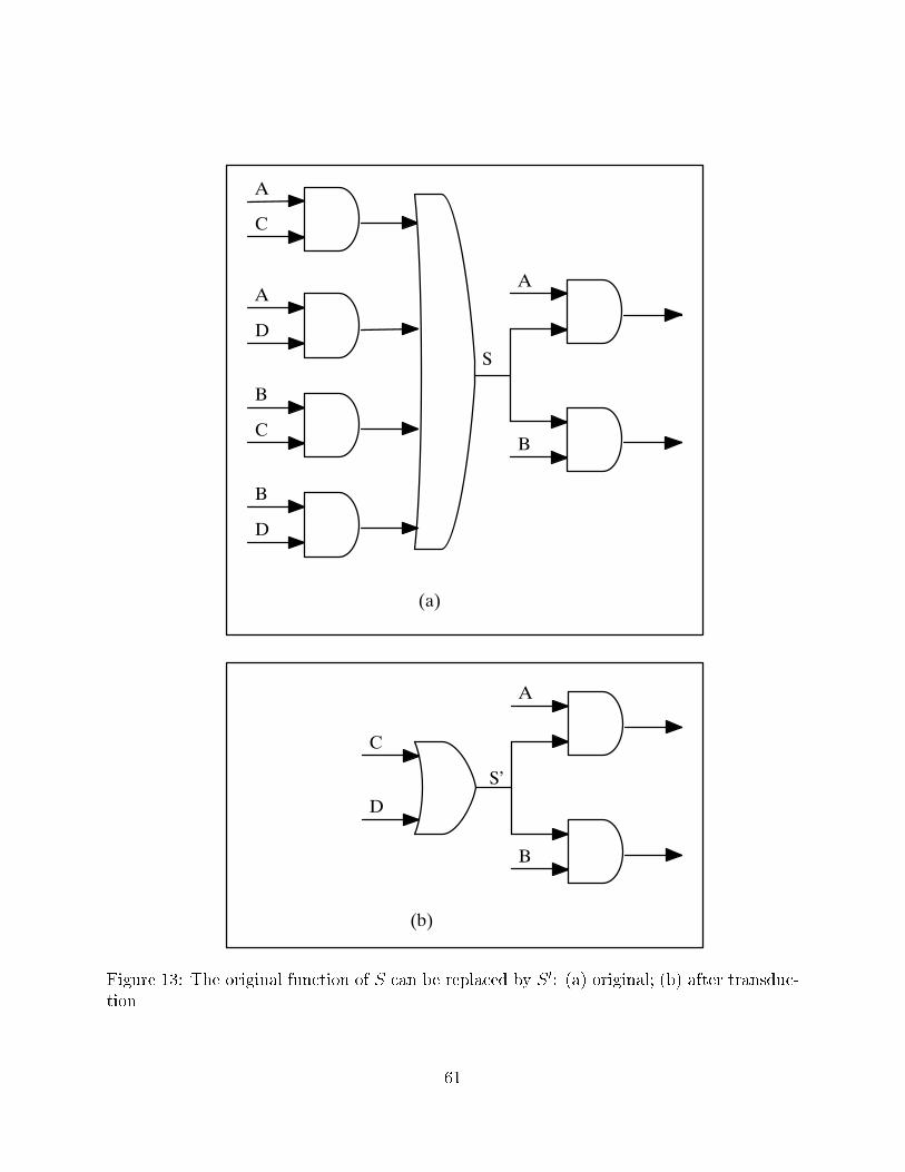
�
�
��
�
�
�
�
�
�
�
�
�
�
�
��
������������
Figure 13: The original function of S can be replaced by S 0: (a) original; (b) after transduc-tion.
61
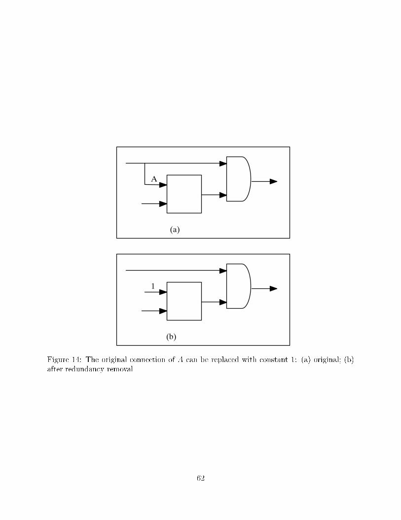
���������������
�
���
�
Figure 14: The original connection of A can be replaced with constant 1: (a) original; (b)after redundancy removal.
62
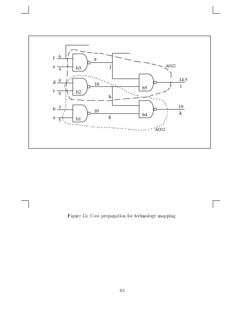
�
�
�
��
�
�
�
��
�
�
�
�
��
��
��
�
�
�
�
�
��
��
����
�
����
����
Figure 15: Cost propagation for technology mapping.
63
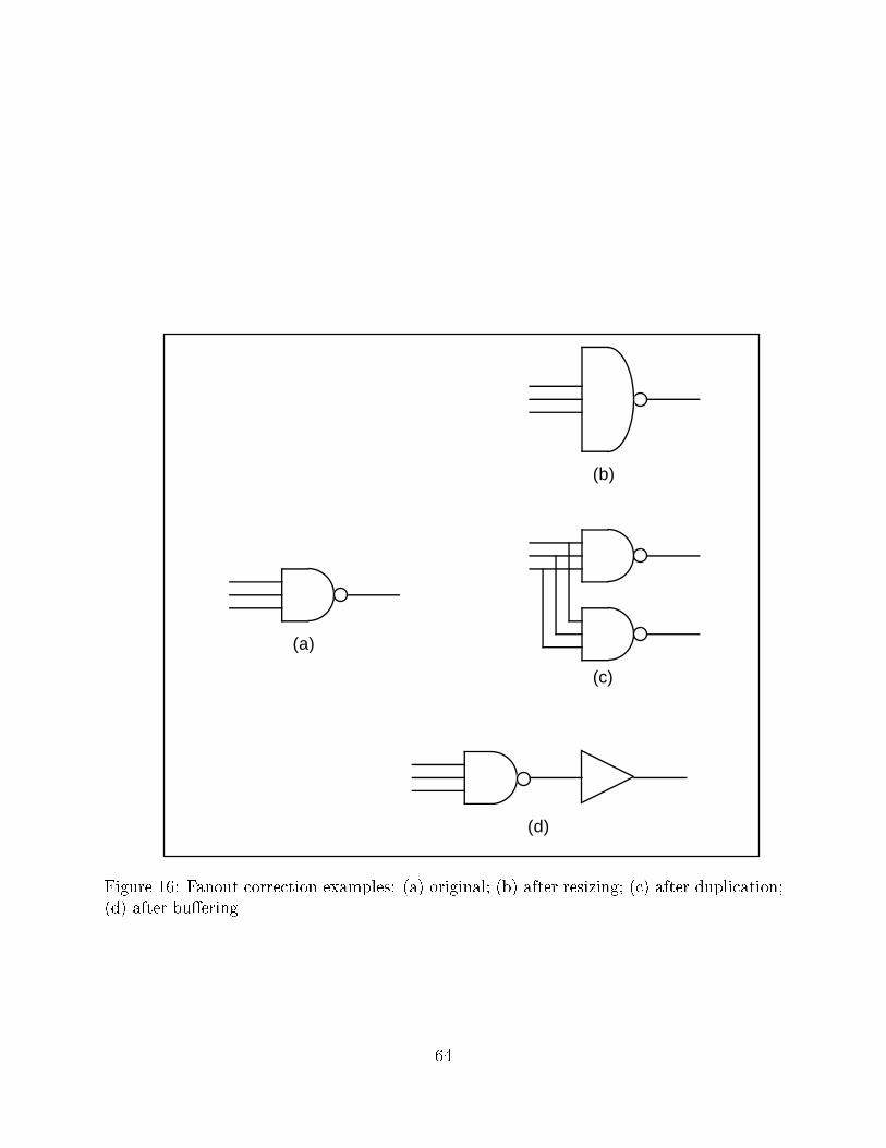
(a)
(b)
(c)
(d)
Figure 16: Fanout correction examples: (a) original; (b) after resizing; (c) after duplication;(d) after bu�ering.
64
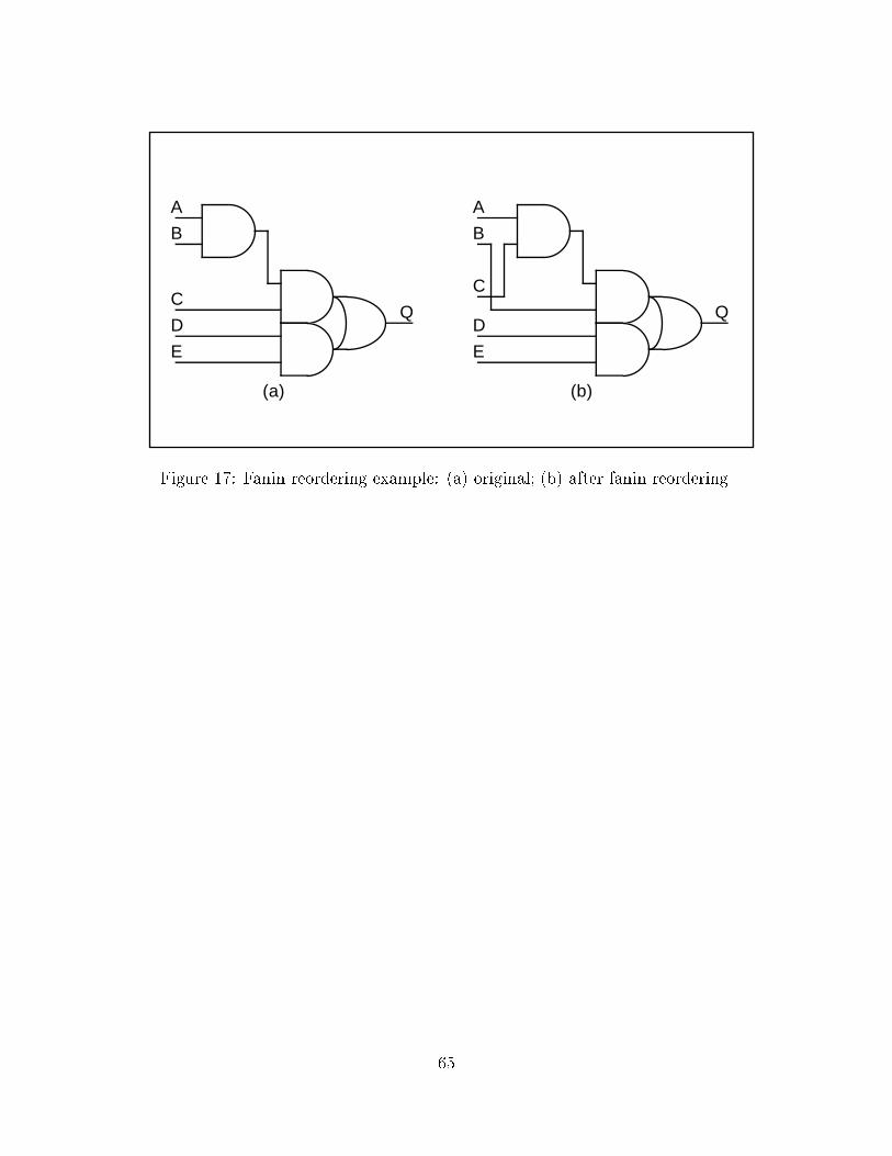
A
B
C
D
E
Q
A
B
C
D
E
Q
(a) (b)
Figure 17: Fanin reordering example: (a) original; (b) after fanin reordering.
65
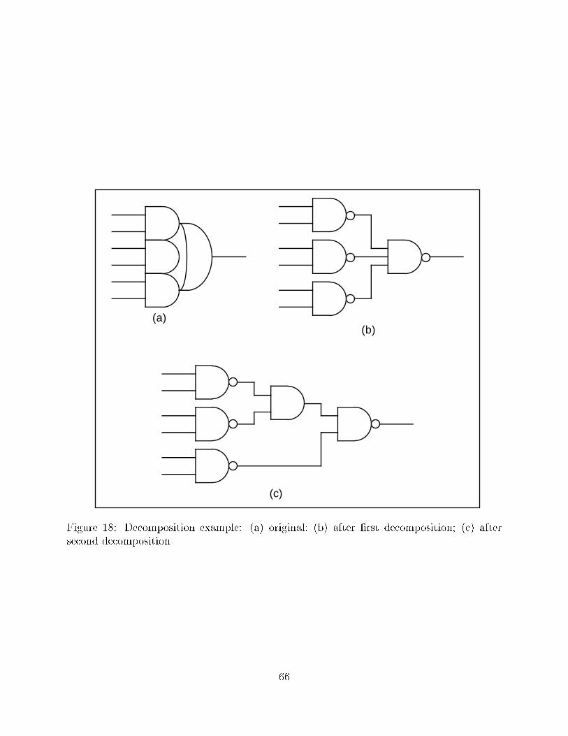
(a)(b)
(c)
Figure 18: Decomposition example: (a) original; (b) after �rst decomposition; (c) aftersecond decomposition.
66
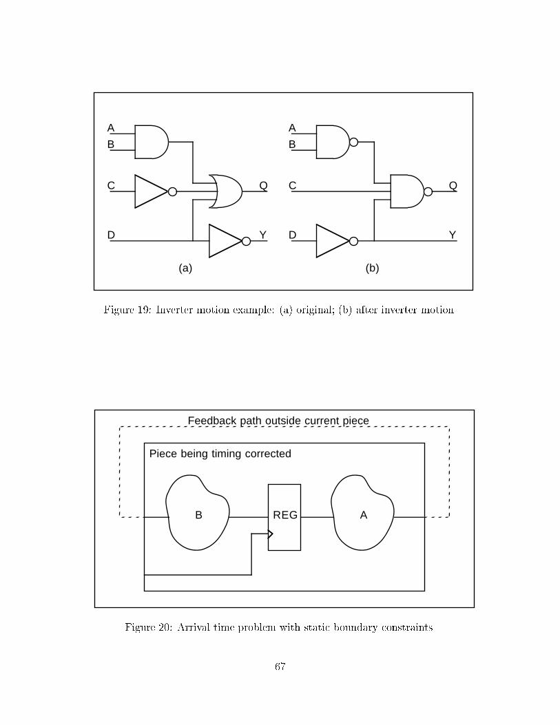
A
B
C
D
Q
Y
A
B
C
D
Q
Y
(a) (b)
Figure 19: Inverter motion example: (a) original; (b) after inverter motion.
Feedback path outside current piece
AB REG
Piece being timing corrected
Figure 20: Arrival time problem with static boundary constraints.
67
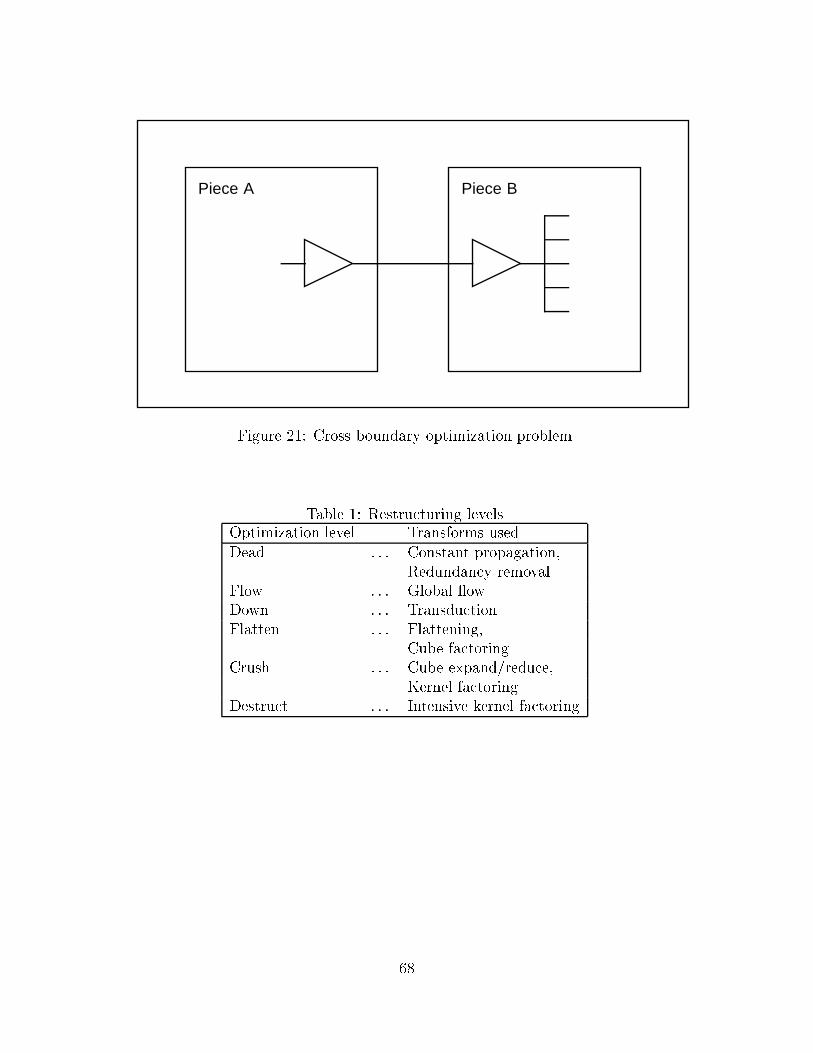
Piece A Piece B
Figure 21: Cross boundary optimization problem.
Table 1: Restructuring levels.Optimization level Transforms usedDead : : : Constant propagation,
Redundancy removalFlow : : : Global owDown : : : TransductionFlatten : : : Flattening,
Cube factoringCrush : : : Cube expand/reduce,
Kernel factoringDestruct : : : Intensive kernel factoring
68


![Argumentations and logic [1989]](https://static.fdokumen.com/doc/165x107/631eee640e3ac35f4f00659e/argumentations-and-logic-1989.jpg)