Navigating Transnationalism: Immigration and Reconfigured Ethnicity
Upload
khangminh22Category
view
2download
0
Measuring and Navigating the Gap Between FPGAs andASICs
by
Ian Carlos Kuon
A thesis submitted in conformity with the requirementsfor the degree of Doctor of Philosophy
Graduate Department of Electrical and Computer EngineeringUniversity of Toronto
Copyright c© 2008 by Ian Carlos Kuon

Abstract
Measuring and Navigating the Gap Between FPGAs and ASICs
Ian Carlos Kuon
Doctor of Philosophy
Graduate Department of Electrical and Computer Engineering
University of Toronto
2008
Field-programmable gate arrays (FPGAs) have enjoyed increasing use due to their low
non-recurring engineering (NRE) costs and their straightforward implementation pro-
cess. However, it is recognized that they have higher per unit costs, poorer performance
and increased power consumption compared to custom alternatives, such as application-
specific integrated circuits (ASICs). This thesis investigates the extent of this gap and it
examines the trade-offs that can be made to narrow it.
The gap between 90 nm FPGAs and ASICs was measured for many benchmark cir-
cuits. For circuits that only make use of general-purpose combinational logic and flip-
flops, the FPGA-based implementation requires 35 times more area on average than an
equivalent ASIC. Modern FPGAs also contain “hard” specific-purpose circuits such as
multipliers and memories and these blocks are found to narrow the average gap to 18 for
our benchmarks or, potentially, as low as 4.7 when the hard blocks are heavily used. The
FPGA was found to be on average between 3.4 and 4.6 times slower than an ASIC and
this gap was not influenced significantly by hard memories and multipliers. The dynamic
power consumption is approximately 14 times greater on average on the FPGA than on
the ASIC but hard blocks showed promise for reducing this gap. This is one of the most
comprehensive analyses of the gap performed to date.
The thesis then focuses on exploring the area and delay trade-offs possible through
architecture, circuit structure and transistor sizing. These trade-offs can be used to
selectively narrow the FPGA to ASIC gap but past explorations have been limited in
ii

their scope as transistor sizing was typically performed manually. To address this issue,
an automated transistor sizing tool for FPGAs was developed. For a range of FPGA
architectures, this tool can produce designs optimized for various design objectives and
the quality of these designs is comparable to past manual designs.
With this tool, the trade-off possibilities of varying both architecture and transistor-
sizing were explored and it was found that there is a wide range of useful trade-offs
between area and delay. This range of 2.1 × in delay and 2.0 × in area is larger than
was observed in past pure architecture studies. It was found that lookup table (LUT)
size was the most useful architectural parameter for enabling these trade-offs.
iii

Acknowledgements
Thanks must certainly first go to my supervisor, Jonathan Rose. His guidance and
enthusiasm have been crucial throughout this work. Even more important though, has
been his support and concern for me as a person. I am fortunate to have worked with
him.
I would also like to thank the others that have passed through Jonathan’s research
group. The search for clarity has been made easier by both this supportive group and
the general population of Pratt 392.
My work would not have been possible without the resources and information provided
by CMC Microsystems. The efforts of Eugenia Distefano and Jaro Pristupa are also
appreciated since their timely support ensured that computer problems never slowed me
down.
This work was improved by the opportunities to present it at Actel, Altera and Xilinx
as they provided essential information and feedback. In particular, Richard Cliff of Altera
provided information that was crucial to much of this work. I also benefited greatly from
the experience I gained through my internships at Altera.
My inherent cheapness might have barred me from graduate school. Therefore, I am
lucky to have been generously funded during my PhD by an NSERC Canada Graduate
Scholarship, a Mary Beatty Scholarship, a Rogers Scholarship, a Government of Ontar-
io/Montrose Werry Scholarship in Science and Technology, my supervisor (whose funds
for me came from an NSERC Discovery Grant and Altera), my parents and my wife. I
am extremely thankful to all these sources for ensuring that, despite now spending 11
years in school (or 23 depending how you count), I have never wanted for anything.
I greatly appreciate the support and patience of my wife throughout this work. My
many years in graduate school would have felt even longer without her.
Finally, the encouragement and support of my parents was essential for this work.
Much of the credit for any of my acheivements is owed to them.
iv

Contents
List of Tables viii
List of Figures x
List of Acronyms xii
1 Introduction 11.1 Measuring the FPGA to ASIC Gap . . . . . . . . . . . . . . . . . . . . . 31.2 Navigating the Gap . . . . . . . . . . . . . . . . . . . . . . . . . . . . . . 31.3 Organization . . . . . . . . . . . . . . . . . . . . . . . . . . . . . . . . . 4
2 Background 62.1 FPGA Architecture . . . . . . . . . . . . . . . . . . . . . . . . . . . . . . 6
2.1.1 Logic Block Architecture . . . . . . . . . . . . . . . . . . . . . . . 72.1.2 Routing Architecture . . . . . . . . . . . . . . . . . . . . . . . . . 112.1.3 Heterogeneity . . . . . . . . . . . . . . . . . . . . . . . . . . . . . 14
2.2 FPGA Circuit Design . . . . . . . . . . . . . . . . . . . . . . . . . . . . . 152.3 FPGA Transistor Sizing . . . . . . . . . . . . . . . . . . . . . . . . . . . 182.4 FPGA Assessment Methodology . . . . . . . . . . . . . . . . . . . . . . . 19
2.4.1 FPGA CAD Flow . . . . . . . . . . . . . . . . . . . . . . . . . . . 192.4.2 Area Model . . . . . . . . . . . . . . . . . . . . . . . . . . . . . . 202.4.3 Performance Measurement . . . . . . . . . . . . . . . . . . . . . . 22
2.5 Automated Transistor Sizing . . . . . . . . . . . . . . . . . . . . . . . . . 232.5.1 Static Transistor Sizing . . . . . . . . . . . . . . . . . . . . . . . . 242.5.2 Dynamic Sizing . . . . . . . . . . . . . . . . . . . . . . . . . . . . 262.5.3 Hybrid Approaches to Sizing . . . . . . . . . . . . . . . . . . . . . 272.5.4 FPGA-Specific Sizing . . . . . . . . . . . . . . . . . . . . . . . . . 28
2.6 FPGA to ASIC Gap . . . . . . . . . . . . . . . . . . . . . . . . . . . . . 28
3 Measuring the Gap 313.1 Comparison Methodology . . . . . . . . . . . . . . . . . . . . . . . . . . 32
3.1.1 Benchmark Circuit Selection . . . . . . . . . . . . . . . . . . . . . 333.2 FPGA CAD Flow . . . . . . . . . . . . . . . . . . . . . . . . . . . . . . . 353.3 ASIC CAD Flow . . . . . . . . . . . . . . . . . . . . . . . . . . . . . . . 37
3.3.1 ASIC Synthesis . . . . . . . . . . . . . . . . . . . . . . . . . . . . 39
v

3.3.2 ASIC Placement and Routing . . . . . . . . . . . . . . . . . . . . 403.3.3 Extraction and Timing Analysis . . . . . . . . . . . . . . . . . . . 41
3.4 Comparison Metrics . . . . . . . . . . . . . . . . . . . . . . . . . . . . . 423.4.1 Area . . . . . . . . . . . . . . . . . . . . . . . . . . . . . . . . . . 423.4.2 Delay . . . . . . . . . . . . . . . . . . . . . . . . . . . . . . . . . 433.4.3 Power . . . . . . . . . . . . . . . . . . . . . . . . . . . . . . . . . 43
3.5 Measurement Results . . . . . . . . . . . . . . . . . . . . . . . . . . . . . 463.5.1 Area . . . . . . . . . . . . . . . . . . . . . . . . . . . . . . . . . . 463.5.2 Delay . . . . . . . . . . . . . . . . . . . . . . . . . . . . . . . . . 583.5.3 Dynamic Power Consumption . . . . . . . . . . . . . . . . . . . . 653.5.4 Static Power Consumption . . . . . . . . . . . . . . . . . . . . . . 68
3.6 Summary . . . . . . . . . . . . . . . . . . . . . . . . . . . . . . . . . . . 72
4 Automated Transistor Sizing 744.1 Uniqueness of FPGA Transistor Sizing Problem . . . . . . . . . . . . . . 75
4.1.1 Programmability . . . . . . . . . . . . . . . . . . . . . . . . . . . 754.1.2 Repetition . . . . . . . . . . . . . . . . . . . . . . . . . . . . . . . 76
4.2 Optimization Tool Inputs . . . . . . . . . . . . . . . . . . . . . . . . . . 774.2.1 Logical Architecture Parameters . . . . . . . . . . . . . . . . . . . 774.2.2 Electrical Architecture Parameters . . . . . . . . . . . . . . . . . 784.2.3 Optimization Objective . . . . . . . . . . . . . . . . . . . . . . . . 79
4.3 Optimization Metrics . . . . . . . . . . . . . . . . . . . . . . . . . . . . . 804.3.1 Area Model . . . . . . . . . . . . . . . . . . . . . . . . . . . . . . 804.3.2 Performance Modelling . . . . . . . . . . . . . . . . . . . . . . . . 83
4.4 Optimization Algorithm . . . . . . . . . . . . . . . . . . . . . . . . . . . 864.4.1 Phase 1 – Switch-Level Transistor Models . . . . . . . . . . . . . 874.4.2 Phase 2 – Sizing with Accurate Models . . . . . . . . . . . . . . . 92
4.5 Quality of Results . . . . . . . . . . . . . . . . . . . . . . . . . . . . . . . 964.5.1 Comparison with Past Routing Optimizations . . . . . . . . . . . 974.5.2 Comparison with Past Logic Block Optimization . . . . . . . . . . 994.5.3 Comparison to Exhaustive Search . . . . . . . . . . . . . . . . . . 1044.5.4 Optimizer Run Time . . . . . . . . . . . . . . . . . . . . . . . . . 105
4.6 Summary . . . . . . . . . . . . . . . . . . . . . . . . . . . . . . . . . . . 106
5 Navigating the Gap through Area and Delay Trade-offs 1075.1 Area and Performance Measurement Methodology . . . . . . . . . . . . . 108
5.1.1 Performance Measurement . . . . . . . . . . . . . . . . . . . . . . 1095.1.2 Area Measurement . . . . . . . . . . . . . . . . . . . . . . . . . . 111
5.2 Transistor Sizing Trade-offs . . . . . . . . . . . . . . . . . . . . . . . . . 1125.3 Definition of “Interesting” Trade-offs . . . . . . . . . . . . . . . . . . . . 1155.4 Trade-offs with Transistor Sizing and Architecture . . . . . . . . . . . . . 118
5.4.1 Impact of Elasticity Threshold Factor . . . . . . . . . . . . . . . . 1215.5 Logical Architecture Trade-offs . . . . . . . . . . . . . . . . . . . . . . . 122
5.5.1 LUT Size . . . . . . . . . . . . . . . . . . . . . . . . . . . . . . . 1235.5.2 Cluster Size . . . . . . . . . . . . . . . . . . . . . . . . . . . . . . 124
vi

5.5.3 Segment Length . . . . . . . . . . . . . . . . . . . . . . . . . . . . 1255.6 Circuit Structure Trade-offs . . . . . . . . . . . . . . . . . . . . . . . . . 127
5.6.1 Buffer Positioning . . . . . . . . . . . . . . . . . . . . . . . . . . . 1275.6.2 Multiplexer Implementation . . . . . . . . . . . . . . . . . . . . . 128
5.7 Trade-offs and the Gap . . . . . . . . . . . . . . . . . . . . . . . . . . . . 1345.7.1 Comparison with Commercial Families . . . . . . . . . . . . . . . 137
5.8 Summary . . . . . . . . . . . . . . . . . . . . . . . . . . . . . . . . . . . 138
6 Conclusions and Future Work 1396.1 Contributions . . . . . . . . . . . . . . . . . . . . . . . . . . . . . . . . . 1396.2 Future Work . . . . . . . . . . . . . . . . . . . . . . . . . . . . . . . . . . 140
6.2.1 Measuring the Gap . . . . . . . . . . . . . . . . . . . . . . . . . . 1416.2.2 Navigating the Gap . . . . . . . . . . . . . . . . . . . . . . . . . . 143
6.3 Concluding Remarks . . . . . . . . . . . . . . . . . . . . . . . . . . . . . 145
Appendices 146
A FPGA to ASIC Comparison Details 146A.1 Benchmark Information . . . . . . . . . . . . . . . . . . . . . . . . . . . 146A.2 FPGA to ASIC Comparison Data . . . . . . . . . . . . . . . . . . . . . . 146
B Representative Delay Weighting 152B.1 Benchmark Statistics . . . . . . . . . . . . . . . . . . . . . . . . . . . . . 152B.2 Representative Delay Weights . . . . . . . . . . . . . . . . . . . . . . . . 155
C Multiplexer Implementations 159C.1 Multiplexer Designs . . . . . . . . . . . . . . . . . . . . . . . . . . . . . . 159C.2 Evaluation of Multiplexer Designs . . . . . . . . . . . . . . . . . . . . . . 160
D Architectures and Results from Trade-off Investigation 167
E Logical Architecture to Transistor Sizing Process 171
Bibliography 176
vii

List of Tables
2.1 Altera Stratix II Memory Blocks [16] . . . . . . . . . . . . . . . . . . . . 11
3.1 Summary of Process Characteristics . . . . . . . . . . . . . . . . . . . . . 333.2 Benchmark Summary . . . . . . . . . . . . . . . . . . . . . . . . . . . . . 363.3 Area Ratio (FPGA/ASIC) . . . . . . . . . . . . . . . . . . . . . . . . . . 473.4 Area Gap Estimation with Full Heterogeneous Block Usage . . . . . . . . 523.5 Area Ratio (FPGA/ASIC) – FPGA Area Measurement Accounting for
Logic Blocks with Partial Utilization . . . . . . . . . . . . . . . . . . . . 573.6 Critical Path Delay Ratio (FPGA/ASIC) – Fastest Speed Grade . . . . . 593.7 Critical Path Delay Ratio (FPGA/ASIC) – Slowest Speed Grade . . . . . 633.8 Impact of Retiming on FPGA Performance with Heterogeneous Blocks . 653.9 Dynamic Power Consumption Ratio (FPGA/ASIC) . . . . . . . . . . . . 663.10 Dynamic Power Consumption Ratio (FPGA/ASIC) for Different Measure-
ment Methods . . . . . . . . . . . . . . . . . . . . . . . . . . . . . . . . . 673.11 Static Power Consumption Ratio (FPGA/ASIC) at 25 ◦C with Typical
Silicon . . . . . . . . . . . . . . . . . . . . . . . . . . . . . . . . . . . . . 703.12 Static Power Consumption Ratio (FPGA/ASIC) at 85 ◦C with Worst Case
Silicon . . . . . . . . . . . . . . . . . . . . . . . . . . . . . . . . . . . . . 713.13 FPGA to ASIC Gap Measurement Summary . . . . . . . . . . . . . . . . 72
4.1 Logical Architecture Parameters Supported by the Optimization Tool . . 774.2 Area Model versus Layout Area . . . . . . . . . . . . . . . . . . . . . . . 834.3 Comparison of Routing Driver Optimizations . . . . . . . . . . . . . . . . 984.4 Comparison of Logic Cluster Delays from [18] for 180 nm with K = 4 . . 1014.5 Comparison of LUT Delays from [18] for 180 nm with N = 4 . . . . . . . 1024.6 Comparison of Logic Cluster Delays from [130] for 350 nm with K = 4 . 1034.7 Comparison of LUT Delays from [130] for 350 nm with N = 4 . . . . . . 1034.8 Comparison of Logic Cluster Delays from [14] for 350 nm CMOS with
K = 4 and N = 4 . . . . . . . . . . . . . . . . . . . . . . . . . . . . . . . 1044.9 Exhaustive Search Comparison . . . . . . . . . . . . . . . . . . . . . . . 105
5.1 Comparison of Delay Measurements between HSPICE and VPR for 20Circuits . . . . . . . . . . . . . . . . . . . . . . . . . . . . . . . . . . . . 110
5.2 Architecture Parameters . . . . . . . . . . . . . . . . . . . . . . . . . . . 1125.3 Area and Delay Changes from Transistor Sizing and Past Architectural
Studies . . . . . . . . . . . . . . . . . . . . . . . . . . . . . . . . . . . . . 114
viii

5.4 Range of Parameters Considered for Transistor Sizing and ArchitectureInvestigation . . . . . . . . . . . . . . . . . . . . . . . . . . . . . . . . . . 119
5.5 Optimization Objectives . . . . . . . . . . . . . . . . . . . . . . . . . . . 1195.6 Span of Different Sizings/Architecture . . . . . . . . . . . . . . . . . . . 1215.7 Span of Interesting Designs with Varied LUT Sizes . . . . . . . . . . . . 1235.8 Span of Interesting Designs with Varied Cluster Sizes . . . . . . . . . . . 1255.9 Span of Interesting Designs with Varied Segment Lengths . . . . . . . . . 1265.10 Comparison of Multiplexer Implementations . . . . . . . . . . . . . . . . 1305.11 Number of Transistors per Input for Various Multiplexer Widths . . . . . 1335.12 Potential Impact of Area and Delay Trade-offs on Soft Logic FPGA to
ASIC Gap . . . . . . . . . . . . . . . . . . . . . . . . . . . . . . . . . . . 1365.13 Area and Delay Trade-off Ranges Compared to Commercial Devices . . . 137
A.1 Benchmark Descriptions . . . . . . . . . . . . . . . . . . . . . . . . . . . 147A.2 FPGA and ASIC Operating Frequencies . . . . . . . . . . . . . . . . . . 148A.3 FPGA and ASIC Dynamic Power Consumption . . . . . . . . . . . . . . 149A.4 FPGA and ASIC Static Power Consumption – Typical . . . . . . . . . . 149A.5 FPGA and ASIC Static Power Consumption – Worst Case . . . . . . . . 150A.6 Impact of Retiming on FPGA Performance . . . . . . . . . . . . . . . . . 151
B.1 Normalized Usage of FPGA Components . . . . . . . . . . . . . . . . . . 153B.2 Usage of LUT Inputs . . . . . . . . . . . . . . . . . . . . . . . . . . . . . 155B.3 Representative Path Weighting Test Weights . . . . . . . . . . . . . . . . 157
D.1 Parameters Considered for Design Space Exploration . . . . . . . . . . . 168D.2 Architectures and Partial Results from Design Space Exploration . . . . 169
E.1 Architecture Parameters . . . . . . . . . . . . . . . . . . . . . . . . . . . 172E.2 Transistor Sizes for Example Architecture . . . . . . . . . . . . . . . . . 175
ix

List of Figures
2.1 Generic FPGA . . . . . . . . . . . . . . . . . . . . . . . . . . . . . . . . 72.2 Basic Logic Elements (BLEs) and Logic Clusters [14] . . . . . . . . . . . 82.3 Heterogeneous FPGAs . . . . . . . . . . . . . . . . . . . . . . . . . . . . 92.4 Altera Stratix II Logic Element [16] . . . . . . . . . . . . . . . . . . . . . 102.5 Altera Stratix II DSP Block [16] . . . . . . . . . . . . . . . . . . . . . . . 122.6 Routing Architecture Parameters [14] . . . . . . . . . . . . . . . . . . . . 132.7 Routing Segment Lengths . . . . . . . . . . . . . . . . . . . . . . . . . . 132.8 Routing Driver Styles . . . . . . . . . . . . . . . . . . . . . . . . . . . . . 142.9 Multiplexer Usage . . . . . . . . . . . . . . . . . . . . . . . . . . . . . . . 162.10 Implementation of Four Input Multiplexer and Buffer . . . . . . . . . . . 172.11 Alternate Multiplexer Implementations . . . . . . . . . . . . . . . . . . . 182.12 FPGA CAD Flow . . . . . . . . . . . . . . . . . . . . . . . . . . . . . . . 212.13 Minimum Width Transistor Area . . . . . . . . . . . . . . . . . . . . . . 22
3.1 ASIC CAD Flow . . . . . . . . . . . . . . . . . . . . . . . . . . . . . . . 383.2 Area Gap Compared to Benchmark Sizes for Soft-Logic Benchmarks . . . 493.3 Effect of Hard Blocks on Area Gap . . . . . . . . . . . . . . . . . . . . . 503.4 Area Gap vs. Average FPGA Interconnect Usage . . . . . . . . . . . . . 553.5 Effect of Hard Blocks on Delay Gap . . . . . . . . . . . . . . . . . . . . . 613.6 Speed Gap Compared to Benchmark Sizes for Logic Only Benchmarks . . 623.7 Speed Gap Compared to the Area Gap . . . . . . . . . . . . . . . . . . . 623.8 Effect of Hard Blocks on Power Gap . . . . . . . . . . . . . . . . . . . . 68
4.1 Repeated Equivalent Parameters . . . . . . . . . . . . . . . . . . . . . . 764.2 FPGA Optimization Path . . . . . . . . . . . . . . . . . . . . . . . . . . 854.3 FPGA Optimization Methodology . . . . . . . . . . . . . . . . . . . . . . 874.4 Switch-level RC Transistor Model . . . . . . . . . . . . . . . . . . . . . . 884.5 Example of a Routing Track modelled using RC Transistor Models . . . . 904.6 Pseudocode for Phase 2 of Transistor Sizing Algorithm . . . . . . . . . . 944.7 Test Structure for Routing Track Optimization . . . . . . . . . . . . . . . 974.8 Logic Cluster Structure and Timing Paths . . . . . . . . . . . . . . . . . 99
5.1 Performance Measurement Methodology . . . . . . . . . . . . . . . . . . 1095.2 Area Delay Space . . . . . . . . . . . . . . . . . . . . . . . . . . . . . . . 1145.3 Determining Designs that Offer Interesting Trade-offs . . . . . . . . . . . 1175.4 Area Delay Space with Interesting Region Highlighted . . . . . . . . . . . 118
x

5.5 Full Area Delay Space . . . . . . . . . . . . . . . . . . . . . . . . . . . . 1205.6 Impact of Elasticity Factor on Area, Delay and Area-Delay Ranges . . . 1225.7 Area Delay Space with Varied LUT Sizing . . . . . . . . . . . . . . . . . 1245.8 Area Delay Space with Varied Cluster Sizes . . . . . . . . . . . . . . . . 1255.9 Area Delay Space with Varied Routing Segment Lengths . . . . . . . . . 1265.10 Buffer Positioning around Multiplexers . . . . . . . . . . . . . . . . . . . 1285.11 Area Delay Trade-offs with Varied Pre-Multiplexer Inverter Usage . . . . 1295.12 Transistor Counts for Varied Multiplexer Implementations . . . . . . . . 1315.13 Transistor Counts for Varied Multiplexer Implementations using a Single
Configuration Bit Output . . . . . . . . . . . . . . . . . . . . . . . . . . 1325.14 Area Delay Trade-offs with Varied Multiplexer Implementations . . . . . 134
B.1 Input-dependant Delays through the LUT . . . . . . . . . . . . . . . . . 154B.2 Area and Delay with Varied Representative Path Weightings . . . . . . . 158
C.1 Two Level 16-input Multiplexer Implementations . . . . . . . . . . . . . 161C.2 Area Delay Trade-offs with Varied 16-input Multiplexer Implementations 163C.3 Area Delay Trade-offs with Varied 32-input Multiplexer Implementations 165
E.1 Terminology for Transistor Sizes . . . . . . . . . . . . . . . . . . . . . . . 173
xi

List of Acronyms
ALM Adaptive Logic Module
ALUT adaptive lookup table
ASIC application-specific integrated circuit
BLE Basic Logic Element
CAD computer-aided design
CMP Circuits Multi-Projets
CLB Cluster-based Logic Block
CMOS Complementary Metal Oxide Semiconductor
DFT Design for Testability
FPGA Field-programmable gate array
HDL hardware description language
LAB Logic Array Block
LUT lookup table
MPGA Mask-programmable Gate Array
MWTA minimum-width transistor areas
NMOS n-channel MOSFET
NRE non-recurring engineering
PLL phase-locked loop
PMOS p-channel MOSFET
QIS Quartus II Integrated Synthesis
SRAM Static random access memory
VCD Value Change Dump
xii

Chapter 1
Introduction
Field-programmable gate arrays (FPGAs) have become a standard medium for imple-
menting digital circuits and they are now used in a wide variety of markets including
telecommunications, automotive systems, high-performance computers and consumer
electronics. The primary advantages of FPGAs are that they offer lower non-recurring
engineering (NRE) costs and faster time to market than more customized approaches
such as full-custom or application-specific integrated circuit (ASIC) design. This pro-
vides digital circuit designers with access to many of the benefits of the latest process
technologies without the expense and effort that accompany these technologies when
custom design is used.
This simplified access to new technologies is possible because of the pre-fabricated and
programmable nature of FPGAs. With pre-fabrication, the challenges associated with
the latest processes are almost entirely shifted to the FPGA manufacturer whereas, for
custom fabrication, significant time and money must be spent on large teams of engineers
to address issues such as signal integrity, power distribution, process variability and soft
errors. Once these challenges are addressed and a design is finalized, the benefits of
FPGAs become even clearer since, due to the programmability of an FPGA, the design
can be implemented on an FPGA in seconds and the only cost of this implementation is
that of the FPGA itself. In contrast, for ASIC or full-custom designs, it takes months
and millions of dollars to create the masks defining the design and then fabricate the
silicon implementation [1]. The combined effect of these factors is that, while an ASIC
design cycle easily takes a year and a full-custom design even longer, the FPGA-based
design cycle can be completed in months for at least an order of magnitude lower costs.
1

Chapter 1. Introduction 2
However, FPGAs suffer from a number of significant limitations. Compared to the
non-programmable alternatives, FPGAs have much higher per unit costs, lower perfor-
mance and higher power consumption. Higher per unit costs arise because, compared to
custom designs, FPGAs require more silicon area to implement the same functionality.
This increased area not only affects costs, it also limits the size of the designs that can be
implemented with FPGAs. Lower performance can drive up costs as well as more paral-
lelism (and hence greater area) may be needed to achieve a performance target or, worse,
it simply may not be possible to achieve the desired performance on an FPGA. Simi-
larly, higher power consumption often precludes FPGAs from power-sensitive markets.
Together, this area, performance and power gap limits the markets for FPGAs.
Since this gap limits the use of FPGAs, research into FPGAs and their architec-
ture has focused, implicitly or explicitly, on narrowing the gap. As a result, significant
improvements have been made in industry and academia at improving FPGAs and re-
ducing the gap relative to their alternatives; however, the gap itself has not been studied
extensively. Its magnitude has only been measured through limited anecdotal or point
comparisons [2, 3, 4, 5]. As well, it has not been fully appreciated, at least academically,
that through varied architecture and electrical design, FPGAs can be created with a
wide range of area, delay and performance characteristics. These possibilities create a
large design space within which trade-offs can be made to reduce area at the expense of
performance or to improve performance at the expense of area. However, the extent to
which such trade-offs can be used to selectively narrow this gap is largely unknown.
Considering such trade-offs and thereby navigating the gap has become particularly
important as the use of FPGAs has expanded beyond their traditional markets. This
broader range of markets has made it necessary to develop multiple distinct FPGA fami-
lies that cater to the varied needs of these markets and, indeed, it has become a standard
trend for FPGA manufacturers to offer both a high-performance/high-cost family [6, 7]
and a lower-cost/low-performance family [8, 9]. If the FPGA market expands further, it
is likely that a greater number of FPGA families will be necessary and, therefore, it is
useful to examine the range of possible designs and the extent to which the gap can be
managed through varied design choices.
The goal of this work is to improve the understanding of the area, performance and
power gaps faced by FPGAs. This is done by first measuring the gap between FPGAs
and ASICs. It will be shown that this gap is large and the latter portion of this work
explores the design of FPGAs and how best to navigate the gap.

Chapter 1. Introduction 3
1.1 Measuring the FPGA to ASIC Gap
It has long been accepted that FPGAs suffer in terms of area, performance and power
consumption relative to the many more customized alternatives such as full custom de-
sign, ASICs, Mask-programmable Gate Arrays (MPGAs) and structured ASICs. In this
dissertation, the gap between a modern FPGA and a standard cell ASIC will be quanti-
fied. ASICs are selected as the comparison point because they are currently the standard
alternative to FPGAs when lower cost, better performance or lower power is desired.
Full custom design is typically only possible for extremely high volume products and
structured ASICs are not in widespread use. Measurements of the FPGA to ASIC gap
are useful for both the FPGA designers and architects who aim to narrow this gap and
the system designers who select the implementation platform for their design.
This comparison is non-trivial given the wide range of digital circuit applications and
the complexity of modern FPGAs and ASICs. An experimental approach, that will be
described in detail, is used to perform the comparison. One of the challenges, that also
makes this comparison interesting, is that FPGAs no longer consist of a homogeneous
array of programmable logic elements. Instead, modern FPGAs have added hard special-
purpose blocks, such as multipliers, memories and processors [6, 7], that are not fully
programmable and are often ASIC-like in their construction. The selection of the func-
tionality to include in these hard blocks is one of the central questions faced by FPGA
architects and this dissertation quantitatively explores the impact of these blocks on the
area, performance and power gaps. This is the first published work to perform a detailed
analysis of these gaps for modern FPGAs.
1.2 Navigating the Gap
Simply measuring the FPGA to ASIC gap is the first step towards understanding the
changes that can help narrow it. Given the complexity of modern FPGAs it is often
not possible for any single innovation to universally narrow the area, performance and
power gaps. Instead, as FPGAs inhabit a large design space comprising the wide range of
architectural and electrical design possibilities, trade-offs within this space that narrow
one dimension of the gap at the expense of another must be considered. Navigating the
gap through the exploration and exploitation of these trade-offs is the second focus of
this dissertation.

Chapter 1. Introduction 4
Exploring the breadth of the design space requires that all aspects of FPGA design be
considered from the architectural level, which defines the logical behaviour of an FPGA,
down to the transistor-level. With such a broad range of possibilities to consider, detailed
manual optimization at the transistor-level is not feasible. Therefore, to enable this
exploration, an automated transistor sizing tool was developed. Transistor-level design of
FPGAs has unique challenges due to the programmable nature of FPGAs which means
that the eventual critical paths are unknown at the design time of the FPGA itself.
An additional challenge is that architectural requirements constrain the optimizations
possible at the transistor-level. These challenges are described and investigated during
the design of the optimization tool.
With this transistor-level design tool and a previously developed architectural explo-
ration tool, VPR [10], it is possible to explore a range of architectures, circuit topologies
and transistor sizings. The trade-offs that are possible, particularly between performance
and area, will be examined to determine the magnitude of the trade-offs possible, the
most effective parameters for making trade-offs and the impact of these trade-offs on the
FPGA to ASIC gap.
1.3 Organization
The remainder of this thesis is organized as follows. Chapter 2 provides related back-
ground information on FPGA architecture, FPGA computer-aided design (CAD) tools,
past measurements of the gaps between FPGAs and ASICs and automated transistor
sizing.
Chapter 3 focuses on measuring the gap between FPGAs and ASICs. It describes
the empirical process used to quantify the area, performance and power gaps and then
presents the measurements obtained using that process. These results are analyzed in
detail to investigate the impact of a number of factors including the use of hard special-
purpose blocks.
The remainder of this work, in Chapters 4 and 5, is centred on navigating the FPGA
to ASIC gap. The transistor-level design tool developed to aid this investigation is
described in Chapter 4. That tool is used in Chapter 5 to explore the trade-offs that
are possible in FPGA design. Throughout this exploration the implications for the gap
between FPGAs and ASICs are considered.

Chapter 1. Introduction 5
Finally, Chapter 6 concludes with a summary of the primary contributions of this
work and possible avenues for future research. The appendices following that chapter
provide much of the raw data underlying the work presented in this thesis.
Chapter 2
Background
One goal of this thesis is to measure and understand the FPGA to ASIC gap. The gap is
affected by many aspects of FPGA design including the FPGA’s architecture, the circuit
structures used to implement the architectural features, and the sizing of the transistors
within those circuits. In this chapter, the terminology and the conventional design ap-
proaches for these three areas are summarized. As well, the standard methodology for
assessing the quality of an FPGA is reviewed. Such accurate assessments require the com-
plete transistor-level design of the FPGA. However, transistor-level design is an arduous
task and prior approaches to automated transistor sizing will be reviewed in this chapter.
Finally, previous attempts at measuring the FPGA to ASIC gap are reviewed. This re-
view will describe the issues that necessitated the more accurate comparison performed
as part of this thesis.
2.1 FPGA Architecture
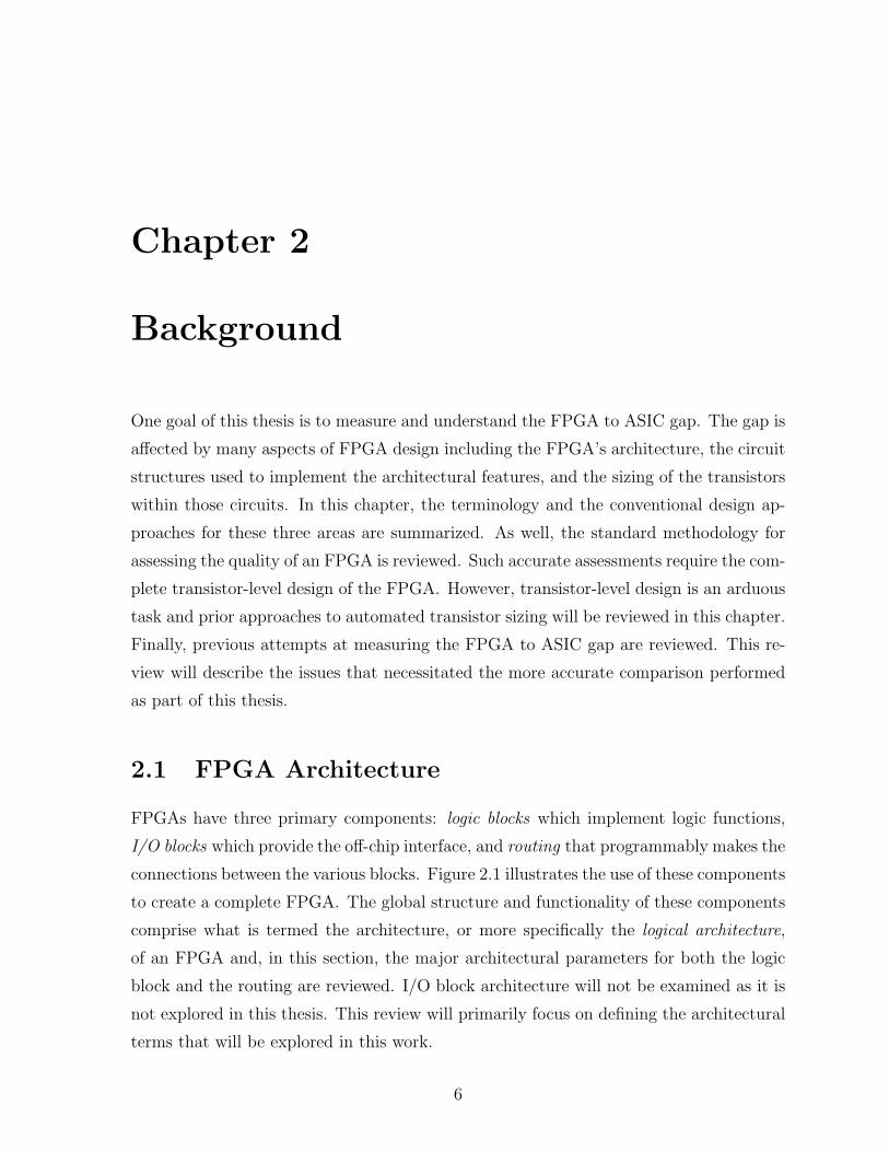
FPGAs have three primary components: logic blocks which implement logic functions,
I/O blocks which provide the off-chip interface, and routing that programmably makes the
connections between the various blocks. Figure 2.1 illustrates the use of these components
to create a complete FPGA. The global structure and functionality of these components
comprise what is termed the architecture, or more specifically the logical architecture,
of an FPGA and, in this section, the major architectural parameters for both the logic
block and the routing are reviewed. I/O block architecture will not be examined as it is
not explored in this thesis. This review will primarily focus on defining the architectural
terms that will be explored in this work.
6

Chapter 2. Background 7
Logic
B lock
Log ic
B lock
Log ic
B lock
Log ic
B lock
Log ic
B lock
Log ic
B lock
Log ic
B lock
Log ic
B lock
Log ic
B lock
Log ic
B lock
Log ic
B lock
Log ic
B lock
Log ic
B lock
Log ic
B lock
Log ic
B lock
Log ic
B lock
Log ic
B lock
Log ic
B lock
Log ic
B lock
Log ic
B lock
Log ic
B lock
Log ic
B lock
Log ic
B lock
Log ic
B lock
Log ic
B lock
I/O B lockR outing
Figure 2.1: Generic FPGA
2.1.1 Logic Block Architecture
It is the logic block that implements the logical functionality of a circuit and, therefore,
its architecture significantly impacts the area, performance and power consumption of
an FPGA. Logic blocks have conventionally and most commonly been built around a
lookup table (LUT) with K inputs that can implement any digital function of K inputs
and one output [11, 12, 8, 13]. Each LUT is generally paired with a flip-flop to form a
Basic Logic Element (BLE) [14] as illustrated in Figure 2.2(a). The output from each
logic element is programmably selected either from the LUT or the flip-flop. Modern
FPGAs have added many features to their logic elements including additional logic to
improve arithmetic operations [7, 6] and LUTs that can also be configured to be used as
memories [6, 7] or shift registers [7]. LUTs have also evolved away from simple K input,
one output structures to fracturable structures that allow larger LUTs to be split into
multiple smaller LUTs. For example, a 6-LUT that can be split into two independent
4-LUT [15, 16, 6, 17]. The specific features of the commercial FPGAs that will be used
for a portion of the work in this thesis will be described at the end of this section.
A BLE by itself could be used as a logic block in the array of Figure 2.1 but it
is now more common for BLEs to be grouped into logic clusters of N BLEs as shown
in Figure 2.2(b). (These logic clusters will also be referred to as Cluster-based Logic

Chapter 2. Background 8
K -input
LU TC lock
Inputs O utD FF
(a) Basic Logic Element (BLE)
B LE
N
B LE
1
C lock
I Inputs
N
B LE s N
O utputs
...
...I
N
(b) Logic Cluster
Figure 2.2: Basic Logic Elements (BLEs) and Logic Clusters [14]
Blocks (CLBs).) This is advantageous because it is frequently possible for input and
output signals to be shared within the cluster [14, 18]. Specifically, it has been observed
for logic clusters with N BLEs containing K-input LUTs that setting the number of
inputs, I as
I =K
2(N + 1) (2.1)
is sufficient to enable all the BLEs to be used in nearly all cases [18]. The intra-cluster
routing connecting the I logic block inputs to the BLE inputs is shown to be a full
cross-bar in Figure 2.2 and, for simplicity, this work will assume such a configuration.
However, it has been found that such flexibility is not necessary [19] and is no longer
common in modern FPGAs [20].
LUT-based logic blocks make up the soft logic fabric of an FPGA. While an FPGA
could be constructed purely from homogeneous soft logic, modern FPGAs generally in-
corporate other types of logic blocks such as multipliers [7, 6, 8, 9], memories [7, 6, 8, 9],
and processors [7]. This heterogeneous mixture of logic blocks is illustrated in Figure 2.3.
These alternate logic blocks only perform specific logic operations, such as multiplica-
tion, that could have also been implemented using the soft logic fabric of the FPGA and,

Chapter 2. Background 9
S oft
Log icM ultip lie r
S oft
Log ic
S oft
Log icM ultip lie r
S oft
Log ic
S oft
Log icM ultip lie r
S oft
Log ic
S oft
Log icM ultip lie r
S oft
Log ic
S oft
Log ic
S oft
Log ic
S oft
Log ic
S oft
Log ic
S oft
Log icM ultip lie r
S oft
Log ic
S oft
Log ic
M em ory
M em ory
S oft
Log icM ultip lie r
S oft
Log ic
M em ory
S oft
Log ic
Figure 2.3: Heterogeneous FPGAs
therefore, these blocks are considered to be hard logic. The selection of what to include
as hard logic on an FPGA is one of the central questions of FPGA architecture because
such blocks can provide area, performance and power benefits when used but waste area
when not used. In this thesis, the impact of these hard blocks on the FPGA to ASIC gap
will be examined. That investigation, in Chapter 3, focuses on one particular FPGA,
the Altera Stratix II [16], and the logic block architecture of this FPGA is now briefly
reviewed.
Logic Block Architecture of the Altera Stratix II
The Stratix II [16], like most modern FPGAs, contains a heterogeneous mixture of soft
and hard logic blocks. The soft logic block, known as a Logic Array Block (LAB), is built
as a cluster of eight logic elements. These logic elements are referred to as Adaptive Logic
Modules (ALMs) and a high-level view of these elements is illustrated in Figure 2.4. This
logic element contains a number of additional features not found in the standard BLE
described earlier. In particular to improve the performance of arithmetic operations there
are dedicated adder blocks, labelled adder0 and adder1, in the figure. The carry in input
to adder0 in the figure is driven by the carry out pin of the preceding logic element. This

Chapter 2. Background 10
D QTo general or
local routing
reg0
To general or
local routing
datae0
dataf0
shared_arith_in
shared_arith_out
reg_chain_in
reg_chain_out
adder0
dataa
datab
datac
datad
Combinational
Logic
datae1
dataf1
D QTo general or
local routing
reg1
To general or
local routing
adder1
carry_in
carry_out
Figure 2.4: Altera Stratix II Logic Element [16]
path is known as a carry chain and enables fast propagation of carry signals in multi-bit
arithmetic operations. Two registers are present in the ALM because the combinational
logic block can generate multiple outputs. The combinational block itself is a 6-input
LUT with additional logic and inputs that enable a number of alternate configurations
including the ability to implement two 4-LUTs each with four unique inputs or various
other combinations of 4-, 5- and 6-LUTs with shared inputs. To reflect this ability to
implement two logic functions the ALM is considered to be composed of two adaptive
lookup tables (ALUTs) and these ALUTs will be used as a measure of the size of a circuit
as they roughly correspond to the functionality of a 4-LUT.
To complement the soft logic, there are four different types of hard logic blocks. Three
of these blocks known as the M512, M4K and M-RAM blocks implement memories with
nominal sizes of 512 bits, 4 kbits and 512 kbits respectively. To allow these memories to
be used in a wide range of designs the depth and width can be programmably selected
from a range of sizes. The largest memory can, for example, be used in a number of
configurations ranging from 64K words by 8 bits to 4K words by 144 bits. The full
listing of possible configurations for the three block types is provided in Table 2.1.
The other hard block used in the Stratix II is known as a DSP block and is designed
to perform multiplication, multiply-add or multiply-accumulate operations. Again to
broaden the usefulness of this block a number of different configurations are possible
and the basic structure of the block that enables this flexibility is shown in Figure 2.5.
Specifically, a single DSP block can perform eight 9x9 multiplications or four 18x18

Chapter 2. Background 11
Table 2.1: Altera Stratix II Memory Blocks [16]
Memory Block M512 M4K M-RAM
Configurations 512× 1256× 2128× 464× 864× 932× 1632× 18
4K× 12K× 21K× 4512× 8512× 9256× 16256× 18128× 32128× 36
64K× 864K× 932K× 1632K× 1816K× 3216K× 368K× 648K× 724K× 1284K× 144
multiplications or a single 36x36 multiplication. Depending on the size and number of
multipliers used, addition or accumulation can also be performed in the block.
2.1.2 Routing Architecture
Programmable routing is necessary to make connections amongst the logic and I/O
blocks. A number of global routing topologies have been proposed and used including
row-based [21, 2], hierarchical [22, 23, 24] and island-style [14, 6, 7]. This thesis focuses
exclusively on island-style FPGAs as it is currently the dominant approach [6, 7, 8, 9].
An island-style topology was illustrated in Figures 2.1 and 2.3.
A number of parameters define the flexibility of these island-style FPGAs and these
parameters are illustrated in Figure 2.6. In this architecture, the routing network is
organized into channels running between each logic block and each individual routing
resource within these channels is known as a track or routing segment. From an FPGA
user’s perspective each track can be viewed simply as a wire; however, the physical
implementation of the track need not be just a wire. The number of tracks in a channel is
the channel width, W . Each track has a logical length, L, that is defined as the number of
logic blocks spanned by the track. This is illustrated in Figure 2.7. Connections between
routing tracks are made at the intersection of the channels in a switch block. The number
of tracks that any track can connect to in a switch block is the switch block flexibility,
Fs. The specific tracks to which each track connects is defined by the switch box pattern
and a number of patterns, such as disjoint and Wilton [25] patterns, have been used or
analyzed [26].

Chapter 2. Background 12
A dder /
S ubtractor /
A ccum ulator
1
A dder
M u lt ip lie r B lo c kPRN
CL RN
D
Q
ENA
PRN
CL RN
D
Q
ENA
PRN
CL RN
D
Q
ENA
PRN
CL RN
DQ
ENA
PRN
CL RN
D
Q
ENA
PRN
CL RN
DQ
ENA
PRN
CL RN
DQ
ENA
PRN
CL RN
D
Q
ENA
PRN
CL RN
DQ
ENA
PRN
CL RN
D
Q
ENA
PRN
CL RN
DQ
ENA
PRN
CL RN
D
Q
ENA
Su m m a tio n
Blo ck
A d d e r O u t p u t B lo c k
A dder /
S ubtractor /
A ccum ulator
2
Q1 .15
R ound /
S aturate
Q 1.15
R ound /
S aturate
Q 1. 15
R ound /
S aturate
Q 1.15
R ound /
S aturate
C LR N
DQEN A
Q 1.15
R ound /
S aturate
Q 1.15
R ound /
S aturate
18 x 18 M ultipl iers
(C an be split into 2 9 x 9 M ultipl iers )
Adders for M ultiply Accum ulate or 18 x 18 C om plex
M ultipl ication
Adder for 7 2 x 72 M ultipl ier
Figure 2.5: Altera Stratix II DSP Block [16]

Chapter 2. Background 13
Log ic
B lock
Log ic
B lock
Log ic
B lock
Log ic
B lock
C hanne l
W id th , W
O utpu t C onnection B lock
F c,ou t = 1 /4
Inpu t C onnection
B lock
F c,in = 2 /4
P rogram m able R outing
S w itch
S w itch B lockR outing T rack
L=1
L=2
Track Length
S w itch B lock
F lex ib ility
F s = 3
Figure 2.6: Routing Architecture Parameters [14]
Log ic
B lock
Log ic
B lock
Log ic
B lock
Log ic
B lock
Log ic
B lock
Log ic
B lock
Log ic
B lock
Log ic
B lock
Length 1 T rack Length 2 T rack Length 4 T rack
Figure 2.7: Routing Segment Lengths
The number of tracks within the channel that can connect to a logic block input is the
input connection block flexibility, Fc,in and the number of tracks to which a logic block
output can connect is the output connection block flexibility, Fc,out. While this output
connection block is shown as distinct from the switch block, the two are actually merged
in many commercial architectures [7, 6].
One significant attribute of the routing architecture is the nature of the connections
driving each routing track. In the past, approaches that allow each routing track to
be driven from multiple points along the track were common [14]. These multi-driver
designs required some form of tri-state mechanism on all potential drivers. A single driver
approach is now widely used instead [27, 6, 7]. These different styles are illustrated in

Chapter 2. Background 14
Logic B lock
Log ic B lock
Log ic B lock
Log ic B lock
(a) Multiple Driver Routing
Logic B lock
Log ic B lock
Log ic B lock
Log ic B lock
(b) Single Driver Routing
Figure 2.8: Routing Driver Styles
Figure 2.8. The single driver approach, while reducing the flexibility of the individual
routing tracks, was found to be advantageous for both area and performance reasons
[20, 28] because it allows standard inverters to drive each routing track instead of the
tri-state buffers or pass transistors required for the multi-driver approaches. Single-driver
routing is the only type of routing that will be considered in this work.
2.1.3 Heterogeneity
One aspect of FPGA architecture that transects the preceding discussions about logic
block and routing architectures is the introduction of heterogeneity to FPGAs. At the
highest-level FPGAs appear very regular as was shown in Figure 2.1 but such regularity
need not be the case. One example of this was described in Section 2.1.1 and illustrated
in Figure 2.3 in which heterogeneous logic blocks were added to the FPGA. Similarly,
routing resources can also vary throughout the FPGA and ideas such as having more
routing in the centre of the FPGA or near the periphery have been investigated in the
past [14].
There are two possible forms of heterogeneity: tile-based and resource-based. Tile-
based heterogeneity refers to the selection of logic blocks and routing parameters across
the FPGA. It is termed tile-based because FPGAs are generally constructed as an array
of tiles with each tile containing a single logic block and any adjacent routing. A single

Chapter 2. Background 15
tile can be replicated to create a complete FPGA [29] (ignoring boundary issues) if the
routing and logic block architecture is kept constant. Alternatively, additional tiles, with
varied logic blocks or routing, can be intermingled in the array as desired; however,
such tiles must be used efficiently to justify both their design and silicon costs. While
the previous example of heterogeneity in Figure 2.3 added heterogeneous features with
differing functions, it is also possible for this heterogeneity to be introduced between tiles
that are functionally identical by varying other characteristics such as their performance.
The other source of architectural heterogeneity, at the resource-level, occurs within
each tile. Both the logic block and the routing are composed of individual resources
such as BLEs and routing tracks respectively. Each of these individual resources could
potentially have its own unique characteristics or some or all of the resources could be
defined similarly. In this latter case, resources that are to be architecturally similar will be
called logically equivalent. Again, the determination of which resources to make logically
equivalent requires a balance between the design costs of making resources unique with
the potential benefits of introducing non-uniformity.
While this thesis will not extensively explore issues of heterogeneity, maintaining
logical equivalence has significant electrical design implications. All resources that are
logically equivalent must present the same behaviour (ignoring differences due to the pro-
cess variations after manufacturing) and, therefore, must have the same implementation
at the transistor-level.
2.2 FPGA Circuit Design
The architectural parameters described in the previous section define the logical be-
haviour of an FPGA but, for any architecture, there are a multitude of possible circuit-
level implementations. This section reviews the standard design practises for these cir-
cuits in FPGAs. There are a number of restrictions that are placed on the FPGAs that
are considered in this work which limit the circuit structures that must be considered.
First, only SRAM-based FPGAs, in which programmability is implemented using static
memory bits, will be used in this work because this approach is the dominant approach
used in industry [6, 7, 8, 9]. As well, with the exception of the measurements of the
FPGA to ASIC gap, homogeneous soft logic-based FPGAs with BLEs as shown in Fig-
ure 2.2(a) will be assumed. Finally, as mentioned previously, only single-driver routing
will be considered in this work.

Chapter 2. Background 16
S R A M
S R A M
S R A M
S R A M
S R A M
S R A M
S R A M
S R A M
Inpu ts
O utpu t
(a) Multiplexer as a lookup table (LUT)
O utpu t. . .Inpu ts
S R A M
bits
(b) Multiplexer as programmable routing
Figure 2.9: Multiplexer Usage
Given these restrictions, the only required circuit structures are inverters, multiplex-
ers, flip-flops and memory bits. Of these components, the flip-flops found in the BLEs
are only a small portion of the design and a standard master-slave arrangement can be
assumed [30]. The memory bits comprise a significant portion of the FPGA as they
store the configuration for all the programmable elements. These memory bits are imple-
mented using a standard six-transistor SRAM cell [14]. Similarly, the design of inverters is
straightforward and they are added as needed for buffering or logical inversion purposes.
This leaves multiplexers which are used both to implement logic and to enable pro-
grammable routing and these two uses are illustrated in Figure 2.9. Due this varied
usage, multiplexers may range in size from having 2 inputs to having 30 or more in-
puts. As FPGAs are replete with such multiplexers, their implementation affects the
area and performance of an FPGAs significantly and, therefore, to reduce area and im-
prove performance multiplexers are generally implemented using NMOS pass transistor
networks.
The use of only NMOS pass transistors poses a potential problem since an NMOS
pass transistor with a gate voltage of VDD is unable to pass a signal at VDD from source to
drain. Left unaddressed this could lead to excessive static power consumption because the
reduced output voltage from the multiplexer prevents the PMOS device in the proceeding
inverter from being fully cut-off. A standard remedy for this issue is the use of level
restoring PMOS pull-up transistors [15] as shown in Figure 2.10. An alternative solution
of gate boosting, in which the gate voltage is raised above the standard VDD, has also

Chapter 2. Background 17
S R A M S R A M
Inp
uts
M ultip lexer Buffer
Output
Figure 2.10: Implementation of Four Input Multiplexer and Buffer
been used [14]. Another less common alternative is to use complementary transmission
gates (with an NMOS and a PMOS) to construct the multiplexer tree [31, 32]; however,
such an approach could typically only be used selectively as use throughout the FPGA
would incur a massive area penalty.
There are also a number of alternatives for implementing the pass transistor tree.
An example of this is shown in Figure 2.11 in which two different implementations of an
8-input multiplexer are shown. The different approaches trade-off the number of memory
bits required with both the number of pass transistors required in the design and the
number through which a signal must pass. A range of strategies have been used including
fully encoded [14] (which uses the minimal number of memory bits), three-level partially-
decoded structures [33] and two-level partially-decoded structures [15, 31, 34]. This issue
of multiplexer structure is one area that is explored in this thesis.
In that exploration, multiplexers will be classified according to the number of pass
transistors a signal must travel through from input to output. At one extreme, a one-level
(or equivalently one-hot) multiplexer has only a single pass transistor on the signal path
and a two-level or three-level multiplexer has two or three pass transistors respectively.
For simplicity, it will be assumed that the multiplexers are homogeneous with all multi-
plexer inputs passing through the same number of pass transistors. However, it is often
necessary or useful as an optimization [15] to have shorter paths through the multiplexer.

Chapter 2. Background 18
S R A M S R A M S R A M S R A M S R A M S R A M
(a) Two-level 8-input multiplexer
S R A M S R A MS R A M
(b) Three-level 8-input multiplexer
Figure 2.11: Alternate Multiplexer Implementations
These varied implementation approaches are generally only used for the routing mul-
tiplexers. The multiplexers used to implement LUTs are typically constructed using a
fully encoded structure [14]. This avoids the need for any additional decode logic on any
user signal paths.
2.3 FPGA Transistor Sizing
Finally, after considering the circuit structures to use within the FPGA, the sizing of the
transistors within these circuits must be optimized as this also directly affects the area,
performance and power consumption of an FPGA. This optimization has historically
been performed manually [14, 35, 18, 28]. In these past works [14, 35, 18, 28], each
resource, such as a routing track, is individually optimized and the sizing which minimizes
the area delay product for that resource is selected. As this is a laborious process,
sizing was only performed once for one particular architecture and then, for architectural
studies, the same sizings were generally used as architectural parameters were varied.
The optimization goal for transistor sizing is frequently selected as minimizing the
area-delay product since this maximizes the throughput of the FPGA assuming that
the applications implemented on the FPGA are perfectly parallelizable [35]. However,
alternative approaches such as minimizing delay assuming a fixed “feasible” area [36] or
minimizing delay only [31, 32] have been used in the past. Such optimization assumed
an architecture in which the routing resources were all logically equivalent but another
possibility is to introduce resource-based heterogeneity by making some resources faster
than other resources. It has been found that sizing 20 % of the routing resources for speed
and the reminder for minimal area delay product yielded performance results similar to

Chapter 2. Background 19
when only speed was optimized but with significantly less area [35]. Similar conclusions
about the benefits of heterogeneously sizing some resources for speed were also reached in
[37, 36]. The relative amount of resources that can be made slower depends on the relative
speed differences. In a set of industrial designs it was observed that approximately 80 %
of the resources could tolerate a 25 % slowdown while approximately 70 % could tolerate
a 75 % slowdown [33, 38].
While transistor sizing certainly has a significant impact on the quality and efficiency
of an FPGA, most works have focused exclusively on the optimization of the routing
resources [31, 32, 36, 35] and do not consider the optimization of the complete FPGA.
As well, only a few discrete objectives such as area-delay or delay have typically been
considered instead of the large continuous range of possibilities that actually exist. Such
broad exploration was not possible because, with the exception of [31, 32], transistor
sizes were optimized manually. This greatly limited the ability to explore a wide range
of designs and the optimization tool developed as part of this thesis will address this
limitation.
2.4 FPGA Assessment Methodology
All these previously described aspects of FPGA design can have a significant effect on
the area, performance and power consumption of an FPGA. However, it is challenging to
accurately measure these qualities for any particular FPGA. The standard method used
has been an experimental approach [14] in which benchmark designs are implemented on
the FPGA by processing them through a complete CAD flow. From that implementation
the area, performance and the power consumption of each benchmark design can be
measured and then the effective area, performance, and power consumption of the FPGA
design can be determined by compiling the results across a set of benchmark circuits.
The details of this evaluation process are reviewed in this section.
2.4.1 FPGA CAD Flow
The CAD flow used for much of this work1 is the standard academic CAD flow for FPGAs
[14, 18, 28, 39] and is shown in Figure 2.12. The process illustrated in the figure takes
1The work in Chapter 3 makes use of commercial CAD tools and the details of that process will beoutlined in that chapter.

Chapter 2. Background 20
benchmark circuits and information about the FPGA design as inputs and determines
the area and critical path for each circuit. (Power consumption could be measured with
well-known modifications to the CAD tools [40, 41, 42] but the primary focus of this
work will be area and performance.) The required information about the FPGA design
includes both Logical Architecture definitions that describe the target configuration of
the attributes detailed in Section 2.1 and Electrical Design Information that reflects the
area and performance of the FPGA based on the circuit structure and sizing decisions.
The first step in the process is synthesis and technology mapping which optimizes and
maps the circuit into LUTs of the appropriate size [43, 44, 45, 46]. In the more general
case of an FPGA with a variety of hard and soft logic blocks the synthesis process would
also identify and map structures to be implemented using hard logic [47]. As only soft
logic is assumed in Chapters 4 and 5 of this work, such additional steps are not required
and the synthesis and mapping process is performed using SIS [48] with FlowMap [45].
The technology mapped LUTs and any flip-flops are then grouped into logic clusters in
the packing stage which is performed using T-VPack [49, 14].
Next, the logic clusters are placed onto the FPGA fabric which involves determining
the physical position for each block within the array of logic blocks. The goal in placing
the blocks is to create a design that minimizes wirelength requirements and maximizes
speed, if the tool is timing driven, and this problem has been the focus of extensive
study [50, 51, 52, 53, 54]. After the positions of the logic blocks are finalized, routing is
performed to determine the specific routing resources that will be used to connect the logic
block inputs and outputs. Again, the goal is to minimize the resources required and, if
timing-driven, to maximize the speed of the design [55, 56]. In this thesis, both placement
and routing will be performed with VPR [10] used in its timing driven mode. An updated
version of VPR that can handle the single-driver routing described in Section 2.1.2 is used
in this work. The details, regarding how specifically area and performance are typically
measured, are provided in the following sections.
2.4.2 Area Model
One important output from the previously described CAD flow is the area required for
each benchmark circuit. Two factors impact this area: the number of logic blocks required
and the size in silicon of those logic blocks and their adjacent routing. The first term, the

Chapter 2. Background 21
S ynthesis &
M apping
(S IS + F low M ap)
C lustering
(T -V P ack)
P lacem ent and
R outing
(V P R )
A rea and D elay
B enchm ark
C ircu its
Log ica l
A rch itecture
E lectrica l D esign
In form ation
Figure 2.12: FPGA CAD Flow
number of blocks is easily determined after packing while determining the second term,
the silicon area, is significantly more involved.
The most accurate area estimate would require the complete layout of every FPGA
design but this is clearly not feasible if a large number of designs are to be considered.
Simpler approaches such as counting the number of configuration bits or the number of
transistors in a design have been used but they are inaccurate as they fail to capture the
effect of circuit topology and transistor sizing choices on the silicon area. A compromise
approach is to consider the full transistor-level design of the entire FPGAs but use an
easily calculated estimate of each transistor’s laid out area. One such approach, known
as a minimum-width transistor area model, was first described in [14] and will serve as
the foundation for the area models in this thesis.
The basis for this model is a minimum-width transistor area which is the area re-
quired to enclose a minimum-width (and minimum-length) transistor2 and the white
space around it such that another transistor could be adjacent to this area while still
satisfying all appropriate design rules. This is illustrated in Figure 2.13. The area for
2The minimum width of a transistor is taken to be the minimum width in which the diffusion area isrectangular as shown in Figure 2.13. This width is generally set by contact size and spacing rules and,therefore it is greater than the absolute minimum width permitted by a process.

Chapter 2. Background 22
M in im um V ertica l S pacing
M in im um
H orizon ta l
S pacing
M in im um
W id th
P erim eter o f M in im um
W id th T ransis to r A rea
M in im um Length
Figure 2.13: Minimum Width Transistor Area
each transistor, in minimum-width transistor areas (MWTA), is then calculated as,
Minimum-width transistor areas(width) = 0.5 +width
2 ·Minimum Width(2.2)
where width is the total width of the transistor. The total silicon area is simply the
sum of the areas for each transistor. To enable process independent comparisons, the
total area is typically reported in minimum-width transistor areas [14, 18, 28] and not
as an absolute area in square microns. Since FPGAs are typically created as an array of
replicated tiles, the total silicon area can be computed as the product of the number of
tiles used and the area of each tile.
This approach to area modelling will serve as the basis for the area model used in
this work; however, as will be described in Chapter 4, some improvements will be made
to account for factors such as densely laid out configuration memory bits.
2.4.3 Performance Measurement
Equally as important as the area measurements are the performance measurements of the
FPGA. Performance is measured based on each circuit’s critical path delay as determined
by VPR [10, 14]. Delay modelling within VPR uses an Elmore delay-based model that
is augmented, using the approach from [57], to handle buffers together with the RC-tree
delays predicted by the standard Elmore model [58, 59]. With this model the delay for

Chapter 2. Background 23
a path, TD, is given by
TD =∑
i∈source-sink path
(Ri ·C (subtreei) + Tbuffer,i) (2.3)
where i is an element along the path, Ri is the equivalent resistance of element i,
C (subtreei) is the downstream dc-connected capacitance from element i, and Tbuffer,i
is the intrinsic delay of the buffer in element i if it is present [14]. While the Elmore
model has long been known to be limited in its accuracy [60, 61], the accuracy in this case
was found to be reasonable [14] and, more importantly, it had been previously observed
that it provided high fidelity despite the inaccuracies [61, 62]. However, it is recognized
in [14] that the most accurate and ideal approach would be full time-domain simula-
tion with SPICE. This approach of SPICE simulation will be used for most performance
measurements in this thesis as will be described in Chapter 4.
Irrespective of the specific delay model used, a necessary input is the properties of the
transistors whose behaviour is being modelled. Therefore, just as detailed transistor-level
design was necessary for the accurate area models described previously, this same level of
detail is also required for these delay models. From the transistor-level design, intrinsic
buffer delays and equivalent resistances and capacitances are determined and used as
inputs to the Elmore model.
2.5 Automated Transistor Sizing
Clearly, detailed transistor-level optimization is necessary to obtain accurate area and
delay measurements for an FPGA design. One of the goals of this work is to explore a
wide range of different FPGA designs, and, therefore, manual optimization of transistor
sizes as was done in the past [14, 28, 18] is not appropriate for this work. Instead, it is
is necessary to develop automated approaches to transistor sizing. Relevant work from
this area will be reviewed in this section; however, almost all prior work in this area is
focused on sizing for custom designs.
Automated approaches to transistor sizing can generally be classified as either dy-
namic or static. Dynamic approaches rely on time-domain simulations with a simulator
such as HSPICE but, due to the computational depends of such simulation, only the
delay of user specified and stimulated paths is optimized. Static approaches, based on

Chapter 2. Background 24
static timing analysis techniques, automatically find the worst paths but generally must
rely on simplified delay models.
2.5.1 Static Transistor Sizing
The central issues in static tuning are the selection of a transistor model and the algorithm
for performing the sizing. Early approaches [63] used the Elmore delay model along with
a simple transistor model consisting of gate, drain and source capacitances proportional
to the transistor width and a source-to-drain resistance inversely proportional to the
transistor width. The delay of a path through a circuit is the sum of the delays of each
gate along the path. For this simple model, this path delay is a posynomial function3
and a posynomial function can be transformed into a convex function. The delay of an
entire circuit is the maximum over all the combinational paths in the circuit and since the
maximum operation preserves convexity, the critical path delay can also be transformed
into a convex function. The advantage of the problem being convex is that any local
minimum is guaranteed to be the global minimum.
This knowledge that this optimization problem is convex was used in the development
of one of the first algorithmic attempts at transistor sizing [63]. The algorithm starts
with minimum transistor sizes throughout the design. Static timing analysis is performed
to identify any paths that fail to meet the timing constraints. Each of these failing paths
is then traversed backwards from the end of the path to the start. Each transistor on the
path is analyzed and the transistor which provides the largest delay reduction per area
increment is increased. The process repeats until all constraints are met. This approach
for sizing was implemented in a program called TILOS. For four circuits sized using
TILOS, with the largest consisting of 896 transistors, the delay was improved by 60 % on
average and the area increased by 16 % on average compared to the result before sizing.
However, the TILOS algorithm fails to guarantee an optimal solution. This occurs
despite the convex nature of the problem because the TILOS algorithm can terminate
3A posynomial resembles a polynomial except that all the coefficient terms and the variables arerestricted to the positive real numbers while the exponents can be any real number. More precisely, aposynomial function with K terms is a function, f : Rn → R, as follows
f (x) =K∑
k=1
ckxa1k1 xa2k
2 · · ·xankn (2.4)
where ck > 0 and a1k . . . ank ∈ R [64].

Chapter 2. Background 25
with a solution that is not a minimum. Such a situation can be caused by the combination
of three factors: 1) TILOS only considered the most critical path, 2) it only increased
the transistor sizes and 3) the definition of delay as the maximum of all possible paths
through a combinational block may result in discontinuous sensitivity measurements
(since an adjustment of one transistor size on the critical path may cause a different path
to become critical) which could lead to excessively large transistors on the former critical
path [65]. Due to these problems, examples have been encountered in which the circuit
is not sized correctly [65].
Numerous algorithmic improvements have been made to address this shortcoming.
One approach again leverages the convex nature of the problem and solved the prob-
lem with an interior point method which guaranteed an optimal solution to the sizing
problem [66]. However, the run time of this approach was unsatisfactory. A alternate
approach based on Lagrangian relaxation was estimated to be 600 times faster for a
circuit containing 832 transistors [67]. With this new method, an optimal solution is
still guaranteed. Another improvement on the original algorithm for producing optimal
solutions was the use of an iterative relaxation method that also achieved significant
run-time improvements [68]. This performance was only 2–4 times slower than a TILOS
implementation but delivered area savings of up to 16.5 % relative to the TILOS-based
approach.
While these algorithmic improvements were significant since they provided optimal
solutions with reasonable run times, this optimality is dependent on the delay and tran-
sistor models used. Unfortunately, the linear models used above have long been known
to be inaccurate [60]. More recently, the error with the Elmore delay models relative
to HSPICE has been found to be up to 28 % [69]. One factor that contributes to this
inaccuracy is that these models assume ideal (zero) transition times on all signals. This
transition time issue was partially addressed by including the effect of non-zero transi-
tion times in the delay model [66] but even with such improvements the models remained
inaccurate.
Another approach for addressing any inaccuracies was to use generalized posynomi-
als4 which improve the accuracy of the device models but retain the convexity of the
optimization problem [70]. To do this, delays for individual cells were curve fit to a
4Generalized posynomials are expressions consisting of a summation of positive product terms. Theproduct terms are the product of generalized posynomials of a lower degree raised to a positive realpower. The zeroth order generalized posynomial is defined as a regular posynomial. [64, 70]

Chapter 2. Background 26
generalized posynomial expression with the transistor widths, input transition times and
output load as variables. To reduce computation time requirements, this approach de-
composed all gates into a set of primitives. With these new models, convex optimizers
or TILOS-like algorithms could still be used for optimization. The accuracy was found
to be at worst 6 % when compared to SPICE for a specific test circuit.
One possibility besides convex curve fitting is the use of piecewise convex functions
[71]. With such an approach, the data is divided into smaller regions and each region is
modelled by an independent convex model. This improves the accuracy and also allows
the model to cover a larger range of input conditions. However, the lack of complete
convexity means that different and potentially non-optimal algorithms must be used for
sizing.
The difficulties in modelling are particularly problematic for FPGAs as the frequent
use of NMOS-only pass transistors adds additional complexity that is not encountered
as frequently in typical custom designs. This necessitates the consideration of dynamic
sizing approaches that perform accurate simulations.
2.5.2 Dynamic Sizing
With the difficulties in the transistor modelling necessary to enable static sizing ap-
proaches, the often considered alternative is dynamic simulation-based sizing. The pri-
mary advantage of such an approach is that the accuracy and modelling issues are avoided
because the circuit can be accurately simulated using foundry-provided device models.
The disadvantage, and the reason full simulation is generally not used with static anal-
ysis techniques, is that massive computational resources are required which limits the
size of the circuits that can be optimized. As well with the complex device models such
as the BSIM3 [72] or BSIM4 [73] models commonly used to capture modern transistor
behaviour, it is generally not possible to ascribe properties such as convexity to the op-
timization problem. Instead, the optimization space is exceedingly complex with many
local minima making it unlikely that optimal results will be obtained.
The first dynamic-based approaches simply automated the use of SPICE [74, 65]. An
improvement on this is to use a fast SPICE simulator with gradient-based optimization
[75]. Fast SPICE simulators are transistor-level simulators that use techniques such as
hierarchical partitioning and event-driven algorithms to outperform conventional SPICE
simulators with minimal losses in accuracy. For the optimizer in [75] known as Jiffy-

Chapter 2. Background 27
Tune, a fast spice simulator called SPECS was used with the LANCELOT nonlinear
optimization package. The selection of simulator is significant because, with SPECS, the
sensitivity to the parameters being tuned can be efficiently computed. The non-linear
solver, LANCELOT, uses a trust-region method to solve the optimization problem. Using
new methods for the gradient computation the capabilities of the optimizer are extended
to handle circuits containing up to 18 854 transistors. The authors report that the run-
time of the optimizer is similar to that which would have been required for a single full
SPICE simulation. While such capacity increases are encouraging, the size of circuits the
can be optimized is still somewhat limited and, therefore, alternative hybrid approaches
have also been considered.
2.5.3 Hybrid Approaches to Sizing
An alternative to purely static or dynamic methods is simulation-based static timing
analysis. This is used in EinsTuner which is a tool developed by IBM for static-analysis
based circuit optimization [76]. The tool is designed to perform non-linear optimization
on circuits consisting of parametrized gates. Each gate is modelled at the transistor
level using SPECS, the fast SPICE simulator. As described previously, SPECS can
easily compute gradient information with respect to parameters such as transistor widths,
output load and input slew. Thus, for each change in a gate’s size and input/output
conditions, the simulator is used to compute the cell delays, slews and gradients. Using
this gradient information, the LANCELOT nonlinear optimization package is used to
perform the actual optimization. Various optimization objectives are possible such as
minimizing the arrival time of all the paths through the combinational circuit subject to
an area constraint, minimizing a weighted sum of delays and area or minimizing the area
subject to a timing constraint. Given the expense of simulation and gradient calculations,
LANCELOT was modified to ensure more rapid convergence. Using EinsTuner, the
performance of a set of well-tuned circuits ranging in size from 6 to 2 796 transistors is
further improved by 20 % on average with no increase in area. This optimizer was further
updated to avoid creating a large number of equally critical paths which improves the
operation of the optimizer in the presence of manufacturing uncertainty [77].

Chapter 2. Background 28
2.5.4 FPGA-Specific Sizing
There has been at least one work that considered automated transistor sizing specifically
for FPGAs [31, 32]. This work focused exclusively on the optimization of the transistor
sizes for individual routing tracks. With this focus on a single resource, only one circuit
path had to be considered and, therefore, static analysis techniques were unnecessary.
A number of different methodologies were considered involving either simulation with
HSPICE or Elmore delay modelling and, in each case, the best sizing (for the given
delay model) for the optimizable parameters was found through an exhaustive search.
As the intent of the work was to investigate the usefulness of repeater insertion in routing
interconnect, such exhaustive searches were appropriate; however, for this thesis, since
the aim is to consider the design of a complete FPGA, exhaustive searching is not feasible
and alternative approaches will be considered and described in Chapter 4.
2.6 FPGA to ASIC Gap
The preceding sections have provided a basic overview of FPGA architectures and their
design and evaluation practises. Despite the many architectural and design improvements
that have been incorporated into FPGAs, they continue to be recognized as requiring
more silicon area, offering lower performance and consuming more power than more
customized approaches. One of the goals of this thesis is to quantify these differences
focusing in particular on the FPGA to ASIC gap. There have been some past attempts at
measuring these differences and these attempts are reviewed in this section. Throughout
this discussion and the rest of this thesis, the gap will be specified as the number of times
worse an FPGA is for the specified attribute compared to an ASIC.
One of the earliest statements quantifying the gap between FPGAs and pre-fabricated
media was by Brown et al. [2]. That work reported the logic density gap between FPGAs
and Mask-programmable Gate Arrays (MPGAs) to be between 8 to 12 times, and the
circuit performance gap to be approximately a factor of 3. The basis for these numbers
was a superficial comparison of the largest available gate counts in each technology, and
the anecdotal reports of the approximate typical operating frequencies in the two tech-
nologies at the time. While the latter may have been reasonable, the former potentially
suffered from optimistic gate counting in FPGAs as there is no standard method for
determining the number of gates that can be implemented in a LUT.

Chapter 2. Background 29
MPGAs are no longer commonly used and standard cell ASICs are a more standard
implementation medium. These standard cell implementations are reported to be on
the order of 33 % to 62 % smaller and 9 % to 13 % faster than MPGA implementations
[78]. Combined with the FPGA to MPGA comparison above, these estimates suggest
an area gap between FPGAs and standard-cell ASICs of 12 to 38. However, the reliance
of these estimates on only five circuits in [78] and the use of potentially suspect gate
counts in [2] makes this estimate of the area gap unreliable. Combining the MPGA:ASIC
and FPGA:MPGA delay gap estimates, the overall delay gap of FPGAs to ASICs is
approximately 3.3 to 3.5 times. Ignoring the reliance on anecdotal evidence [2], the
past comparison is dated because it does not consider the impact of hard blocks such as
multipliers and block memories that, as described in Section 2.1.1, are now common [6, 7].
The comparison performed in this thesis addresses this issue by explicitly considering the
impact of such blocks.
More recently, a detailed comparison of FPGA and ASIC implementations was per-
formed by Zuchowski et al. [3]. They found that the delay of an FPGA LUT was
approximately 12 to 14 times the delay of an ASIC gate. Their work found that this
ratio has remained relatively constant across CMOS process generations from 0.25 µm
to 90 nm. ASIC gate density was found to be approximately 45 times greater than that
possible in FPGAs when measured in terms of kilo-gates per square micron. Finally,
the dynamic power consumption of a LUT was found to be over 500 times greater than
the power of an ASIC gate. Both the density and the power consumption exhibited
variability across process generations but the cause of such variability was unclear. The
main issue with this work is that it also depends on the number of gates that can be
implemented by a LUT. In this thesis, this issue is handled by instead focusing on the
area, speed and power consumption of application circuits.
Wilton et al. [4] also examined the area and delay penalty of using programmable
logic. The approach taken for the analysis was to replace part of a non-programmable
design with programmable logic. They examined the area and delay of the programmable
implementation relative to the non-programmable circuitry it replaced. This was only
performed for a single module in the design consisting of the next state logic for a chip
testing interface. They estimated that when the same logic is implemented on an FPGA
fabric and directly in standard cells, the FPGA implementation is 88 times larger. They
measured the delay ratio of FPGAs to ASICs to be 2.0 times. This thesis improves on this
by comparing more circuits and using an actual commercial FPGA for the comparison.

Chapter 2. Background 30
Compton and Hauck [5] have also measured the area differences between FPGA and
standard cell designs. They implemented multiple circuits from eight different applica-
tion domains, including areas such as radar and image processing, on the Xilinx Virtex-II
FPGA, in standard cells on a 0.18 µm CMOS process from TSMC, and on a custom con-
figurable platform. Since the Xilinx Virtex-II is designed in 0.15 µm CMOS technology,
the area results are scaled up to allow direct comparison with 0.18 µm CMOS. Using
this approach, they found that the FPGA implementation is only 7.2 times larger on
average than a standard cell implementation. The authors believe that one of the key
factors in narrowing this gap is the availability of heterogeneous blocks such as memory
and multipliers in modern FPGAs and these claims are quantified in this thesis.
While this thesis focuses on the gap between FPGAs and ASICs, it is noteworthy
that the area, speed and power penalty of FPGAs is even larger when compared to the
best possible custom implementation using full-custom design. It has been observed that
full-custom designs tend to be 3 to 8 times faster than comparable standard cell ASIC
designs [1]. In terms of area, a full-custom design methodology has been found to achieve
14.5 times greater density than a standard cell ASIC methodology [79] and the power
consumption of standard cell designs has been observed as being between 3 to 10 times
greater than full-custom designs [80, 81].
Given this large ASIC to custom design gap, it is clear that FPGAs are far from the
most efficient implementation. The remainder of this thesis will focus on measuring the
extent of these inefficiencies and exploring the trade-offs that can be made to narrow the
gap. The deficiencies in the past measurements of the FPGA to ASIC gap necessitate
the more thorough comparison that will be described in the subsequent chapter.

Chapter 3
Measuring the Gap
The goal of this research is to explore the area, performance and power consumption gap
between FPGAs and standard cell ASICs. The first step in this process is measuring
the FPGA to ASIC gap. In the previous chapter, we described how all prior published
attempts to make this comparison were superficial since none of those works focused ex-
clusively on measuring this gap. In this chapter, we present a detailed methodology used
to measure this gap and the resulting measurements. A key contribution is the analysis
of the impact of logic block architecture, specifically the use of heterogeneous hard logic
blocks, on the area, performance and power gap. These quantitative measurements of
the FPGA to ASIC gap will benefit both FPGA architects, who aim to narrow the gap,
and system designers, who select implementation media based on their knowledge of the
gap. As well, this measurement of the gap motivates the latter half of the work in this
thesis which explores the trade-offs that can be made to selectively narrow one dimension
of the gap at the expense of another.
The FPGA to ASIC comparison described in this chapter will compare a 90 nm
CMOS SRAM-programmable FPGA to a 90 nm CMOS standard cell ASIC. An SRAM-
based FPGA is used because such FPGAs dominate the market and limiting the scope
of the comparison was necessary to make this comparison tractable. Similarly, a CMOS
standard cell implementation is the standard approach for ASIC designs [1, 82]. The
use of newer “structured ASIC” platforms [83, 84] is not as widespread or mature as the
market continues to rapidly evolve. This comparison will focus primarily on core logic.
It is true that I/O area constraints and power demands can be crucial considerations;
however, the core programmable logic of an FPGA remains fundamentally important.
31

Chapter 3. Measuring the Gap 32
A fair comparison between two very different implementation platforms is challenging.
To ensure that the results are understood in the proper context, we carefully describe
the comparison process used. The specific benchmarks used can also significantly impact
the results and, as will be seen in our results, the magnitude of the FPGA to ASIC
gap can vary significantly from circuit to circuit and application to application. Given
this variability, we perform the comparison using a large set of benchmark designs from
a range of application domains. However, using a large set of designs means that it is
not feasible to individually optimize each design. A team of designers focusing on any
single design could likely optimize the area, performance and power consumption of a
design more thoroughly but this is true of both the ASIC and FPGA implementations.
Therefore, this focus on multiple designs instead of single point comparisons (which as
described in Chapter 2 was typically done historically) increases the usefulness of these
measurements.
This chapter begins by describing the implementation media and the benchmarks
that will be used in the comparison. The details of the FPGA and ASIC implementation
and measurement processes are then reviewed. Finally the measurements of the area,
performance and power gap are presented and a number of issues impacting this gap are
examined.
3.1 Comparison Methodology
As described in Chapter 2, past measurements of the gaps between FPGAs and ASICs
have been based on simple estimates or single-point comparisons. In this work, the gap
is measured more definitively using an empirical method that includes the results from
many benchmark designs. Each benchmark design is implemented in an FPGA and using
a standard cell methodology. The silicon area, maximum operating frequency and power
consumption of the two implementations are compared to quantify the area, delay and
power gaps between FPGAs and ASICs.
Both the ASIC and FPGA-based implementations are built using 90 nm CMOS tech-
nology. For the FPGA, the Altera Stratix II [15, 16] FPGA, whose logic block archi-
tecture was described in Section 2.1.1, was selected based on the availability of specific
device data [85]. This device is fabricated using TSMC’s Nexsys 90 nm process [86].
The IC process we use for the standard cells is STMicroelectronic’s CMOS090 Design
Platform [87]. Standard cell libraries provided by STMicroelectronics are used. Since the

Chapter 3. Measuring the Gap 33
Table 3.1: Summary of Process Characteristics
Parameter TSMC 90 nm STMicroelectronics 90 nmValue Source Value Source
Metal 1 Half-Pitch 125 nm Measured [93] 140 nm Published [87]Minimum Gate Length 55 nm Measured [93]a 65 nm Published [87]Number of Metal Layers 9 Cu/1 Al Measured [93] 7 Cu/1 Al Published [87, 94]b
SRAM Bit Cell Size 0.99 µm2 Published [92] 0.99 µm2 Published [90](Ultra High Density)SRAM Bit Cell Size 1.15 µm2 Published [92] 1.15 µm2 Published [90](High Density)Nominal Core Voltage 1.2 V 1.2 V
aPublished reports have indicated that the nominal minimum gate length was 59 nm [93] or 65 nm[89].
bThe process allows for between 6-9 Cu layers [87]. The specific design kit available to us uses 7layers. We will use all these layers and assume that the additional metal layers could be used to improvepower and ground distribution.
Altera Stratix II is implemented using a multi-Vt process [88], we will assume a dual-Vt
process for the ASIC to ensure a fair comparison. Unfortunately, the TSMC and STMi-
croelectronics processes are certainly not identical; however, they share many similar
characteristics. These characteristics are summarized in Table 3.1. Different parameters
are listed in each row and the values of these parameters in the two processes is indi-
cated. The source of these values is labelled as either “Measured” which indicates that
the particular characteristic was measured by a third party or “Published” which means
that a foundry’s publications were used as the source of the data. Clearly, both processes
have similar minimum nominal poly lengths and metal 1 pitches [87, 89] and, in both
processes, SRAM bit cell sizes of 0.99 µm2 and 1.15 µm2 have been reported [90, 91, 92].
Given these similarities, it appears acceptable to compare the FPGA and ASIC despite
the different design platforms (and this is the best option available to us). The results
from both platforms will assume a nominal supply voltage of 1.2 V.
3.1.1 Benchmark Circuit Selection
It is important to ensure the benchmark designs are suitable for this empirical FPGA to
ASIC comparison. In particular, it is undesirable to use benchmarks that were designed
for a specific ASIC or FPGA platform as that could potentially unfairly bias the compari-

Chapter 3. Measuring the Gap 34
son. For this work, benchmarks were drawn from a range of sources including OpenCores1
and designs developed for projects at the University of Toronto [95, 96, 97, 47, 98, 99, 100].
All the benchmarks were written in either Verilog or VHDL. In general, the designs were
targeted for implementation on FPGAs. While none of the designs appeared to be heav-
ily optimized for a particular FPGA, this use of FPGA-focused designs does raise the
possibility of a bias in favour of FPGAs. However, this would be the typical result for
FPGA designers changing to target an ASIC. As well, this is necessary because we were
unable to obtain many ASIC-targeted designs (This is not surprising given the large costs
for ASIC development that make it undesirable to publicly release such designs). From
the available sources, the specific benchmarks to use were selected based on two critical
factors.
The first was to ensure that the Verilog or VHDL was synthesized similarly by the
different tools used for the FPGA and the ASIC implementations. Different tools were
used because we did not have access to a single synthesis tool that could adequately tar-
get both platforms. The preferred approaches to verifying that the synthesis was similar
in both cases are post-synthesis simulation and/or formal verification. Unfortunately,
verification through simulation was not possible due to the lack of test benches for most
designs and the lack of readily available formal verification tools prevented such tech-
niques from being explored. Instead, we compared the number of registers inferred by
the two synthesis processes, which we describe in Sections 3.2 and 3.3.1. We rejected
any design in which the register counts deviated by more than 5 %. Some differences in
the register count are tolerated because different implementations are appropriate on the
different platforms. For example, FPGA designs tend to use one-hot encoding for state
machines because of the low incremental cost for flip-flops.
Secondly, it was important to ensure that some of designs use the block memories
and dedicated multipliers on the Stratix II. This is important because one of the aims of
this work is to analyze the improvements possible when these hard dedicated blocks are
used. However, not all designs will use such features which made it essential to ensure
that the set of benchmarks includes both cases when these hard structures are used, and
are not used.
Based on these two factors, the set of benchmarks in Table 3.2 were selected for use in
this work. Brief descriptions and the source of each benchmark are given in Appendix A.
1OpenCores is an open source hardware effort which collects and archives a wide range of user-createdcores at http://www.opencores.org/.

Chapter 3. Measuring the Gap 35
To provide an indication of the size of the benchmarks, the table lists the number of Altera
Stratix II ALUTs (recall from Chapter 2 that an ALUT is “half” of a Stratix II Adaptive
Logic Module (ALM) and it is roughly equivalent to a 4-input LUT), 9x9 multipliers
and memory bits used by each design. The column labelled “Total 9x9 Multipliers”
indicates the number of these 9x9 multipliers (which, as described in Section 2.1.1, are
the smallest possible division of the Stratix II DSP Block) that are used throughout
the design including those used to implement the larger 18x18 or 36x36 multiplications
supported by the DSP block. Similarly, the number of memory bits indicates the number
of bits used across the three hard logic memory block sizes.
While every attempt was made to obtain benchmarks that are as large as possible
to reflect the realities of modern systems, the final set of benchmarks used for this work
are modest in size compared to the largest designs that can be implemented on the
largest Stratix II FPGA which contains 143 520 ALUTs, 768 9x9 multipliers and 9 383 040
memory bits [16]. This is a concern and various efforts to compensate for these modest
sizes are described later in this chapter. Despite these attempts to address potential size
issues, it is possible that with larger benchmarks different results would be obtained and,
in particular, there is the possibility that the results obtained will be somewhat biased
against FPGAs since FPGAs are engineered to handle significantly larger circuits than
those used in this work. This issue is examined in greater detail in Section 3.5.1.
The following sections will describe the processes used to implement these benchmarks
on the FPGA and as an ASIC.
3.2 FPGA CAD Flow
The benchmark designs were implemented on Altera Stratix II devices using the Altera
Quartus II v5.0SP1 software for all stages of the CAD flow. (This was the most recent
version of the software available at the time this work was completed.) Synthesis was
performed using Quartus II Integrated Synthesis (QIS) with all the settings left at their
default values. The default settings perform “balanced” optimization which focuses on
speed for timing critical portions of the design and area optimization for non-critical
sections. The defaults also allow the tool to infer the use of DSP blocks and memory
blocks automatically from the hardware description language (HDL).
Placement and routing with Quartus II was performed using the “Standard Fit”
effort level. This effort setting forces the tool to obtain the best possible timing results

Chapter 3. Measuring the Gap 36
Table 3.2: Benchmark Summary
Design ALUTs Total Memory9x9 Bits
Multipliers
booth 68 0 0rs encoder 703 0 0cordic18 2 105 0 0cordic8 455 0 0des area 595 0 0des perf 2 604 0 0fir restruct 673 0 0mac1 1 885 0 0aes192 1 456 0 0fir3 84 4 0diffeq 192 24 0diffeq2 288 24 0molecular 8 965 128 0rs decoder1 706 13 0rs decoder2 946 9 0atm 16 544 0 3 204aes 809 0 32 768aes inv 943 0 34 176ethernet 2 122 0 9 216serialproc 680 0 2 880fir24 1 235 50 96pipe5proc 837 8 2 304raytracer 16 346 171 54 758
regardless of timing constraints [101] and, hence, no timing constraints were placed on
any design in the reported results2. The final delay measurements were obtained using
the Quartus Timing Analyzer. As will be described in Section 3.4, area is measured
according to the number of logic clusters used and, therefore, we set the packer to cluster
elements into as few LABs as possible without significantly impacting speed. This is
done using special variables provided by Altera that mimic the effect of implementing
our design on a highly utilized FPGA. In addition to this, we used the LogicLock feature
of Quartus II to restrict the placement of a design to a rectangular region of LABs, DSP
blocks and memories [101]. By limiting the size of the region for each benchmark, the
implementation will more closely emulate the results expected for larger designs that
heavily utilize a complete FPGA. We allow Quartus II to automatically size the region
because we found that this automatic sizing generally delivered results with greater or
2To verify that this effort setting has the desired effect the results obtained were compared to theoperating frequency obtained when the clocks in the designs were constrained to an unattainable 1 GHz.Both approaches yielded similar results.

Chapter 3. Measuring the Gap 37
equal density than when we manually defined the region sizes to be nearly square with
slightly more LABs than necessary.
The selection of a specific Stratix II device is performed by the placement and routing
tool but we restrict the tool to use the fastest or the slowest speed grade parts depending
on the specific comparison being performed. These speed grades exist because most
FPGAs, including the Altera Stratix II, are speed binned which means that parts are
tested after manufacturing and sold based on their speed. The fastest FPGA speed grade
is a valid comparison point since those faster parts are available off-the-shelf. However,
exclusively using the fast speed grade devices favours the FPGA since ASICs generally
are not speed-binned [1]. (Alternatively, it could be argued that this is fair as one of the
advantages of FPGAs is that the diverse markets they serve make it effective to perform
speed binning.) As will be described later, the ASIC delay is measured assuming worst-
case temperature, voltage and process conditions. Comparing the ASIC results to the
slowest FPGA speed grade addresses this issue and allows for an objective comparison of
the FPGA and ASIC at worst case temperature, voltage and process. When presenting
the results, we will explicitly note which FPGA devices (fastest or slowest) were used.
Even within the same speed grade, the selection of a specific Stratix II part can have
a significant impact on the cost of an FPGA-based design and, for industrial designs,
the smallest (and cheapest) part would typically be selected. However, this issue is not
as important for our comparison because, as will be described later, the comparison
optimistically (for the FPGA) ignores the problem of device size granularity.
Finally, the reported operating frequency of a design is known to vary depending on
the random seed given to the placement tool. To reduce the impact of this variability
on our results, the entire FPGA CAD flow is repeated five times using five different
placement seeds. All the results (area, speed and power) are taken based on the placement
and routing that resulted in the fastest operating frequency.
3.3 ASIC CAD Flow
While the FPGA CAD flow is straightforward, the CAD flow for creating the standard
cell ASIC implementations is significantly more complicated. Our CAD flow is based on
Synopsys and Cadence tools for synthesis, placement, routing, extraction, timing analysis,
and power analysis. The steps involved along with the tools used are shown in Figure 3.1.
The CAD tools were provided through CMC Microsystems (http://www.cmc.ca).

Chapter 3. Measuring the Gap 38
S y nthe s isS yn o p sys
D e sig n C o m p ile r
P la c e m e nt a nd
R outingC a d e n ce S OC
E n co u n te r
E x tra c tionS yn o p sys
S ta r-R C X T
Tim ing A na ly s isS yn o p sys
P rim e Tim e
P owe r A na ly s is
S yn o p sys P rim e P o w e r
S im ula tionC a d e n ce
N C-S im
R TL D e sig n D e scrip tio n
A re a
D e la y
P o w e r
Figure 3.1: ASIC CAD Flow

Chapter 3. Measuring the Gap 39
A range of sources were used for determining how to properly use these tools. These
sources included vendor documentation, tutorials created by CMC Microsystems and
tool demonstration sessions provided by the vendors. In the following sections, all the
significant steps in this CAD flow will be described.
3.3.1 ASIC Synthesis
Synthesis for the ASIC implementation was completed using Synopsys Design Compiler
V-2004.06-SP1. All the benchmarks were synthesized using a common compile script
that performed a top-down compilation. This approach preserves the design hierarchy
and ensures that any inter-block dependencies are handled automatically [102, 103]. This
top-down approach is reasonable in terms of CPU time and memory size because all the
benchmarks have relatively modest sizes.
The compile script begins by analyzing the HDL source files for each benchmark.
Elaboration and linking of the top level module is then performed. After linking, the
following constraints are applied to the design. All the clocks in a design are constrained
to a 2 GHz operating frequency. This constraint is unattainable but, by over-constraining
the design, we aim to create the fastest design possible. In addition, an area constraint
of 0 units is also placed on the design. This constraint is also unattainable but this is a
standard practise for enabling area optimization [102].
The version of the STMicroelectronics 90 nm design kit available to us contains four
standard cell libraries. Two of the libraries contain general-purpose standard cells. One
version of the library uses low leakage high-Vt transistors while the other uses higher
performing standard-Vt transistors. The other set of two libraries include more complex
gates and is also available in high and standard-Vt versions. For compilation with Design
Compiler, all four libraries were set as target libraries meaning that the tool is free to
select cells from any of these libraries as it sees fit. The process from STMicroelectronics
also has the option for low-Vt transistors; however, standard cell libraries based on these
transistors were not available to us at the time of this work. Such cells would have offered
even greater performance at the expense of static power consumption.
Once the specific target cells and clock and area constraints are specified the design is
compiled with Design Compiler. The compilation was performed using the “high-effort”
setting. After the compile completed, an additional high-effort incremental compilation
Chapter 3. Measuring the Gap 40
is performed. This incremental compilation maintains or improves the performance of
the design by performing various gate-level optimizations [103].
Virtually all modern ASIC designs require Design for Testability (DFT) techniques
to simplify post-manufacturing tests. At a minimum, scan chains are typically used
to facilitate these tests [104]. This requires that all the sequential cells in the design
are replaced by scan-equivalent implementations. Accordingly, for all compilations with
Design Compiler, the Test Ready Compile option is used which automatically replaces
sequential elements with scan-equivalent versions. Such measures were not needed for
the FPGA-based implementation because testing is performed by the manufacturer.
After the high effort compilations are complete, the timing constraints are adjusted.
The desired clock period is changed to the delay that was obtained under the unattainable
constraints. With this new timing constraint, a final high effort compilation is performed.
“Sequential area recovery” optimizations are enabled for this compile which allows Design
Compiler to save area by remapping sequential elements that are not on a critical or
near-critical path. After this final compilation is complete, the scan-enabled flip flops are
connected to form the scan chains. The final netlist and the associated constraints are
then saved for use during placement and routing.
For circuits that used memory, the appropriate memory cores were generated by
STMicroelectronics using their custom memory compilers. CMC Microsystems and Cir-
cuits Multi-Projets (CMP) (http://cmp.imag.fr) coordinated the generation of these
memory cores with STMicroelectronics. When selecting from the available memories,
we chose compilers that delivered higher speeds instead of higher density or lower power
consumption. The memories were set to be as square as possible.
3.3.2 ASIC Placement and Routing
The synthesized netlist is next placed and routed with Cadence SOC Encounter GPS
v4.1.5. The placement and routing CAD flow was adapted from that described in the
Encounter Design Flow Guide and Tutorial [105]. The key steps in this flow are described
below.
The modest sizes of the benchmarks allow us to implement each design as an indi-
vidual block and the run times and memory usage were reasonable despite the lack of
design partitioning. For larger benchmarks, hierarchical chip floor-planning steps could

Chapter 3. Measuring the Gap 41
well have been necessary. Hierarchical design flows can result in lower quality designs
but are necessary to achieve acceptable run times and to enable parallel design efforts.
Before placement, a floorplan must be created. For this floorplan we selected a target
row utilization3 of 85 % and a target aspect ratio of 1.0. The 85 % target utilization was
selected to minimize any routing problems. Higher utilizations tend to make placement
and routing significantly more challenging [107]. Designs with large memory macro blocks
proved to be more difficult to place and route; therefore, the target utilization was lowered
to 75 % for those designs.
After the floorplan is created under these constraints, placement is performed. This
placement is timing-driven and optimization is performed based on the worst-case tim-
ing models. Scan chain reordering is performed after placement to reduce the wirelength
required for the scan chain. The placement is further optimized using Encounter’s “opt-
Design” macro command which performs optimizations such as buffer additions, gate
resizing and netlist restructuring. Once these optimizations are complete, the clock tree
is inserted. Based on the new estimated clock delays from the actual clock tree, setup and
hold time violations are then corrected. Finally, filler cells are added to the placement
in preparation for routing.
Encounter’s Nanoroute engine is used for routing. The router is configured to use
all seven metal layers available in the STMicroelectronics process used for this work.
Once the routing completes, metal fill is added to satisfy metal density requirements.
Detailed extraction is then performed. This extraction is not of the same quality as
the sign-off extraction but is sufficient for guiding the later timing-driven optimizations.
The extracted parasitic information is used to drive post-routing optimizations that aim
to improve the critical path of the design. These in-place optimizations include drive-
strength adjustments. After these optimizations, routing is again performed and the
design is checked for connectivity or design rule violations. The design is then saved in
various forms as required for the subsequent steps of the CAD flow.
3.3.3 Extraction and Timing Analysis
In our design environment, the parasitic extraction performed within SOC Encounter
GPS is not sufficiently accurate for the final sign-off timing and power analysis. Therefore,
3Row utilization is the total area required for standard cells relative to the total area available forplacement of the standard cells [106].

Chapter 3. Measuring the Gap 42
after placement and routing is complete, the final sign-off quality extraction is performed
using Synopsys Star-RCXT V-2004.06. This final extraction is saved for use during
the timing and power analysis that is performed using Synopsys PrimeTime SI version
X-2005.06 and Synopsys PrimePower version V-2004.06SP1 respectively.
3.4 Comparison Metrics
After implementing each design as an ASIC and using an FPGA, the area, delay and
power of each implementation were compared. The specific measurement approach can
significantly impact results; therefore, in this section, the measurement methodology for
each of the metrics is described in detail.
3.4.1 Area
The area for the standard cell implementation is defined in this work to be the final core
area of the placed and routed design. This includes the area for any memory macros
that may be required for a design. The area of the inputs and outputs is intentionally
excluded because the focus in this work is on the differences in the core logic.
Measuring the area of the FPGA implementation is less straightforward because the
benchmark designs used in this work generally do not fully utilize the logic on an FPGA.
To include the entire area of an FPGA that is not fully utilized would artificially quantize
the area measured to the vendor device sizes and would completely obscure the effects
we wish to measure. Instead, for the area measurements, only the silicon area for any
logic resources used by a design is included. The area of a design is computed as the
number of LABs, DSP blocks and memory blocks each multiplied by the silicon area of
that specific block. Again, the area of I/O’s is excluded to allow us to focus on the core
programmable logic. The silicon areas for each block were provided by Altera [85]. These
areas include the routing resources that surround each of the blocks. The entire area of
a block (such as a memory or LAB) is included in the area measurement regardless of
whether only a portion of the block is used. This block level granularity is potentially
pessimistic and in Section 3.5.1 the impact of this choice is examined. To avoid disclosing
any proprietary information, absolute areas are not reported and only the ratio of the
FPGA area to ASIC area will be presented.

Chapter 3. Measuring the Gap 43
This approach (of only considering the resources used) may also be considered opti-
mistic for the following reasons: first, it ignores the fact that FPGAs unlike ASICs are
not available in arbitrary sizes and, instead, a designer must select one particular discrete
size even if it is larger than required for the design. This optimism is acceptable because
we are focusing on the cost of the programmable fabric itself. As well, we optimistically
measure the area used for the hard logic blocks such as the multipliers and the memories.
In commercial FPGAs, the ratio of logic to memories to multipliers is fixed and a designer
must tolerate this ratio regardless of the needs of their particular design. For the area
calculations in this work, these fixed ratios are ignored and the area for a heterogeneous
structure is only included as needed. This implies that we will measure the best case
impact of these hard blocks.
3.4.2 Delay
The critical path of each ASIC and FPGA design is obtained from static timing analysis
assuming worst case operating conditions. This determines the maximum clock frequency
for each design. For the ethernet benchmark which contains multiple clocks, the geometric
mean of all the clocks in each implementation is compared. For the FPGA, timing
analysis was preformed using the timing analyzer integrated in Altera Quartus II4. Timing
analysis for the ASIC was performed using Synopsys PrimeTime SI which accounts for
signal integrity effects such as crosstalk when computing the delay. The use of different
timing analysis tools for the FPGA and the ASIC is a potential source of error in the delay
gap measurements since the tools may differ in their analysis and that may contribute to
timing differences that are not due to the differences in the underlying implementation
platforms. However, both tools are widely used in their respective domains and their
results are indicative of the results for typical users.
3.4.3 Power
Power is an important issue for both FPGA and ASIC designs but it is challenging to
fairly compare measurements between the platforms. This section describes in detail the
method used to measure the power consumption of the designs. For these measurements
we separate the dynamic and static contributions to the power consumption both to
4The timing analyzer used is now known as the Quartus II’s Classic Timing Analyzer.

Chapter 3. Measuring the Gap 44
simplify the analysis and because, as will be described later, a conclusive comparison of
the static power consumptions remained elusive.
It is important to note that in these measurements we aim to compare the power
consumption gap as opposed to energy consumption gap. To make this comparison
fair, we compare the power with both the ASIC and the FPGA performing the same
computation over the same time interval. An analysis of the energy consumption gap
would have to reflect the slower operating frequencies of the FPGA. The slower frequency
means that more time or more parallelism would be required to perform the same amount
of work as the ASIC design. To simplify the analysis in this work, only the power
consumption gap was be considered.
Also, it is significant that we perform this comparison using the same implementations
for the FPGA and the ASIC that were used for the delay measurements. For those
measurements, every circuit is designed to operate at the highest speed possible. This
is done because our goal is to measure the power gap between typical ASIC and FPGA
implementations as opposed to the largest possible power gap. Our results would likely
be different if we performed the comparison using an ASIC designed to operate at the
same frequency as the FPGA since power saving techniques could be applied to the ASIC.
Dynamic and Static Power Measurement
The preferred measurement approach, particularly for dynamic power measurements, is
to stimulate the post-placed and routed design with vectors representing typical usage
of the design. This approach is used when appropriate testbenches are available and
the results gathered using this method are labelled accordingly. However, in most cases,
appropriate testbenches are not available and we are forced to rely on a less accurate
approach of assuming constant toggle rates and static probabilities for all the nets in
each design.
The dynamic power measurements are taken assuming worst-case process, 85 ◦C and
1.2 V. Both the FPGA and ASIC implementations are simulated at the same operating
frequency of 33 MHz. This frequency was selected since it was a valid operating frequency
for all the designs on both platforms. Performing the comparison assuming the same
frequency of operation for both the ASIC and FPGA ensures that both implementations
perform the same amount of computation.

Chapter 3. Measuring the Gap 45
For the FPGA implementation, an exported version of the placed and routed design
was simulated using Mentor Modelsim 6.0c when the simulation-based method was pos-
sible. That simulation was used to generate a Value Change Dump (VCD) file containing
the switching activities of all the circuit nodes. Based on this information, the Quartus
II Power Analyzer measured the static and dynamic power consumption of the design.
Glitch filtering was enabled for this computation which ignores any transitions that do
not fully propagate through the routing network. Altera recommends using this setting
to ensure accurate power estimates [101]. Only core power (supplied by VCCINT) was
recorded because we are only interested in the power consumption differences of the core
programmable fabric. The power analyzer separates the dynamic and static contributions
to the total power consumption.
For the standard cell implementation, the placed and routed netlist was simulated
with back annotated timing using Cadence NC-Sim 5.40. Again, a VCD file was generated
to capture the state and transition information for the nets in the design. This file, along
with parasitic information extracted by Star-RCXT, is used to perform power analysis
with the Synopsys PrimePower tool, version V-2004.06SP1. PrimePower automatically
handles glitches by scaling the dynamic power consumption when the interval between
toggles is less than the rise and fall delays of the net. The tool also splits the power
consumption up into static and dynamic components.
In most cases, proper testbenches were not available and, for those designs, power
measurements were taken assuming all the nets in the design toggle at the same frequency
and have the same static probability. This approach does not accurately reflect the true
power consumption of a design but should be reasonable since the measurements are
only used for a relative measurement of an FPGA versus an ASIC. However, it should be
recognized that this approach may cause the power consumption of the clock networks
to be less than typically observed. Both the Quartus II Power Analyzer and Synopsys
PrimePower also offered the ability to use statistical vectorless estimation techniques in
which toggle rates and static probabilities are propagated statistically from source nodes
to the remaining nodes in design. However, the two power estimation tools produced
significantly different activity estimates when using this statistical method and, therefore,
it was decided to use the constant toggle rate method instead.

Chapter 3. Measuring the Gap 46
Dynamic and Static Power Comparison Methodology
Directly comparing the dynamic power consumption between the ASIC and the FPGA is
reasonable but the static power measurements on the FPGA require adjustments before a
fair comparison is possible to account for the fact that the benchmarks do not fully utilize
the FPGA device. Accordingly, the static power consumption reported by the Quartus
Power Analyzer is scaled by the fraction of the core FPGA area used by the particular
design. The fairness of this decision is arguable since end users would be restricted to
the fixed available sizes and would therefore incur the static power consumption of any
unused portions of their design. However, the discrete nature of the device sizes obscures
the underlying differences in the programmable logic that we aim to measure. Given
the arbitrary nature of the FPGA sizes and the existence of fine-grained programmable
lower power modes in modern FPGAs [6, 17] this appears to be a reasonable approach
to enable a fair comparison.
An example may better illustrate these static power adjustments. Assume a hypo-
thetical FPGA in which one LAB and one DSP block out of a possible 10 LABs and 2
DSP blocks are used. If the silicon area of the LAB and DSP block is 51 µm2 and the
area of all the LABs and DSP blocks is 110 µm2 then we would scale the total static
power consumption of the chip by 51/110 = 0.46. This adjustment assumes that leakage
power is approximately proportional to the total transistor width of a design which is
reasonable [108] and that the area of a design is a linear function of the total transistor
width which is also reasonable as FPGAs tend to be active area limited [14].
3.5 Measurement Results
All the benchmarks were implemented using the flow described in Sections 3.2 and 3.3.
Area, delay and power measurements were then taken using the approach described in
Section 3.4 and, in this section, the results for each of these metrics will be examined.
3.5.1 Area
The area gap between FPGAs and ASICs for the twenty-three benchmark circuits is
summarized in Table 3.3. The gap is reported as the factor by which the area of the
FPGA implementation is larger than the ASIC implementation. As a key goal of this
work is to investigate the effect of heterogeneous memory and multiplier blocks on the

Chapter 3. Measuring the Gap 47
Table 3.3: Area Ratio (FPGA/ASIC)
Logic Logic Logic Logic,Name & & Memory
Only DSP Memory & DSP
booth 33rs encoder 32cordic18 19cordic8 25des area 42des perf 17fir restruct 28mac1 43aes192 47fir3 45 17diffeq 41 12diffeq2 39 14molecular 47 36rs decoder1 54 58rs decoder2 41 37atm 70aes 24aes inv 19ethernet 34serialproc 36fir24 9.5pipe5proc 23raytracer 26
Geometric Mean 35 25 33 18
gap, the results in the table are separated into four categories based on which com-
binations of heterogeneous resources are used. Those benchmarks that used only soft
logic are labelled “Logic Only.” (Recall from Chapter 2 that the soft logic block in
the Stratix II is the LAB.) Those that used soft logic and hard DSP blocks contain-
ing multiplier-accumulators are labelled “Logic and DSP.” Those that used soft logic
and memory blocks are labelled “Logic and Memory,” and, finally, those that used all
three are labelled “Logic, DSP and Memory.” We implemented the benchmarks that
contained multiplication operations with and without the hard DSP blocks so results for
these benchmarks appear in two columns, to enable a direct measurement of the benefit
of these blocks.
In viewing Table 3.3, first, consider those circuits that only use the soft logic: the
area required to implement these circuits in FPGAs compared to standard cell ASICs is

Chapter 3. Measuring the Gap 48
on average5 a factor of 35 times larger, with the different designs ranging from a factor
of 17 to 54 times larger. This is significantly larger than the area gap suggested by [2],
which used extant gate counts as its source. It is much closer to the numbers suggested
by [3].
The range in the area gap from 17 to 54 times is clearly significant but the reason
for this variability is unclear. One potential reason for these differences was thought
to be the varying sizes of the benchmarks. It is known that FPGAs are architected to
handle relatively large designs and, therefore, it was postulated that the area gap would
shrink for larger designs that can take increasing advantage of the resources included
to handle those larger circuits. This idea was tested by comparing the area gap to the
size of the circuit measured in ALUTs and the results are plotted in Figure 3.2. Only
the soft-logic benchmarks are included to keep the analysis focused on benchmark sizes
and not issues surrounding the use of heterogeneous hard blocks. For these benchmarks,
there does not appear to be a relationship between benchmark size and the area gap and,
therefore, benchmark size does not appear to be the primary cause of the varying area
gap measurements. However, additional analysis on the effects of benchmark size on the
area gap is performed later in this section.
Another factor that could cause the variability in the area gap measurements between
designs is the capability of a LUT to implement a wide range of logic functions. For
example, a 2-input LUT can implement all possible two input functions including a 2-
input NAND, a 2-input AND or a 2-input XOR. The static CMOS implementations of
those gates would require 4 transistors, 6 transistors and 10 transistors respectively. Such
implementations would be used in the standard cell gates and, therefore, depending on
the specific logic function the area gap between the LUT and the standard cell gate will
vary significantly. As the LUT is the primary resource for implementing logic in the
soft logic portion of the FPGA, the characteristics of the logic implemented in those
LUTs may significantly affect the area gap. This potential source of the wide ranging
measurements was not investigated but it likely explains at least part of the variations
observed in the measurements.
5The results are averaged using the geometric mean. The geometric mean for n positive numbersa1, a2, . . . , an is the nth root of their product (i.e. n
√a1a2 · · · an). This is a better measure of the average
gap than alternative averages such as the arithmetic mean because the gap measurement is a multiplica-tive factor. For example, if two designs had an area gap of 0.25 and 4, then clearly the geometric meanof 1 would be more indicative of the typical result than the arithmetic mean of 2.125.

Chapter 3. Measuring the Gap 49
0
10
20
30
40
50
60
70
80
0 500 1000 1500 2000 2500 3000
Be n ch m ar k Siz e (A L UT s )
Are
a G
ap
Figure 3.2: Area Gap Compared to Benchmark Sizes for Soft-Logic Benchmarks
The third, fourth and fifth columns of Table 3.3 report the impact of the hard het-
erogeneous blocks. It can seen that these blocks do significantly reduce this area gap.
The benchmarks that make use of the hard multiplier-accumulators, in column three,
are on average only 25 times larger than an ASIC. When hard memories are used, the
average of 33 times larger is slightly lower than the average for regular logic and when
both multiplier-accumulators and memories are used, we find the average is 18 times.
Comparing the area gap between the benchmarks that make use of the hard multiplier-
accumulator blocks and those same benchmarks when the hard blocks are not used best
demonstrates the significant reduction in FPGA area when such hard blocks are avail-
able. In all but one case the area gap is significantly reduced6. This reduced area gap
was expected because these heterogeneous blocks are fundamentally similar to an ASIC
implementation with the only difference being that the FPGA implementation requires a
6The area gap of the rs decoder1 increases when the multiplier-accumulator blocks are used. Thissurprising result is attributed to the benchmark’s exclusive use of 5 bit by 5 bit multiplications and theseare more efficiently implemented (from a silicon area perspective) in regular logic instead of the StratixII’s 9x9 multiplier blocks.

Chapter 3. Measuring the Gap 50
0
10
20
30
40
50
60
70
80
0% 10% 20% 30% 40% 50% 60% 70%
Heterogeneous Content (% of Total FPGA Area)
Are
a G
ap
Figure 3.3: Effect of Hard Blocks on Area Gap
programmable interface to the outside blocks and routing. Hence, compared to soft logic
blocks which have both programmable logic and routing, these heterogeneous blocks are
less programmable.
It is noteworthy that there is also significant variability in the area gap for the bench-
marks that make use of the heterogeneous blocks. One contributor to this variability is
the varying amount of heterogeneous content. The classification system used in Table 3.3
is binary in that a benchmark either makes use of a hard structure or it does not but this
fails to recognize that the benchmarks differ in the extent to which the heterogeneous
blocks are used. An alternative approach is to consider the fraction of a design’s FPGA
area that is used by heterogeneous blocks. The area gap is plotted versus this measure
of heterogeneous content in Figure 3.3. The figure demonstrates the expected trend that
as designs make use of more heterogeneous blocks the area gap tends to decline. It is not
quantified in the figure but the reduction in the area gap is accompanied by a decrease
in the degree of programmability possible in FPGA.

Chapter 3. Measuring the Gap 51
While these results demonstrate the importance of these heterogeneous blocks in
improving the competitiveness of FPGAs, it is important to recall that for these hetero-
geneous blocks, the analysis is optimistic for the FPGAs. As described earlier, we only
consider the area of blocks that are used, and we ignore the effect of the fixed ratio of
logic to heterogeneous blocks that a user is forced to tolerate and pay for. Therefore,
the measurements will favour FPGAs for designs that do not fully utilize the available
heterogeneous blocks. This is the case for many of the benchmarks used in this work,
particularly the benchmarks with memory. However, this is also potentially unfair to the
FPGAs since FPGA manufacturers likely tailor the ratios of regular logic to multiplier
and memory blocks to the ratios seen in their customer’s designs. If it is assumed that
the ratios closely match, then bounds on the area gap can be estimated.
Approximate Bounds
The previous results demonstrated the trend that the area gap shrinks when an increasing
proportion of heterogeneous blocks is used. However, these results were based on bench-
marks that only partially exploited the available heterogeneous blocks and, instead, if all
the heterogeneous blocks were used, the resulting area gap could be significantly lower.
We can not directly determine the potential area gap in that case because no actual
benchmarks that fully used the heterogeneous blocks were available to us. However, with
a few assumptions, it is possible to estimate a bound on the area gap.
We will base this estimate on the assumption that all the core logic blocks are used
on a Stratix II device including both the soft logic blocks (LABs) and the heterogeneous
memory and multiplier blocks (DSP, M512, M4K and M-RAM blocks). The silicon
area for all these blocks on the FPGA is known but the ASIC area to obtain the same
functionality must be estimated. This area will be calculated by considering each logic
block type individually and estimating the area gap for that block (and its routing)
relative to an ASIC. Based on those area gaps, the ASIC area estimate can be computed
by determining each logic block’s equivalent ASIC area and then summing those areas
to get the total area.
The area gap estimates for each block type are summarized in Table 3.4. (Recall that
the functionality of these logic blocks was described in Section 2.1.1.) The estimate of 35
for the LAB (or soft logic) is based on the results described previously in this section. The
DSP, M512 and M4K blocks are assumed to have an area gap of 2. This assumption is

Chapter 3. Measuring the Gap 52
Table 3.4: Area Gap Estimation with Full Heterogeneous Block Usage
Block Estimated Area Gap
LAB 35DSP Block 2M512 Block 2M4K Block 2M-RAM Block 1
Gap with 100 % Core Utilization 4.7
based on the knowledge that, while the logic functionality itself is implemented similarly
in both the FPGA and the ASIC, the FPGA implementation requires additional area
for the programmable routing. The M-RAM block is a large 512 kbit memory and the
area overhead of the programmable interconnect is assumed to be negligible hence the
area gap of 1. (This is potentially optimistic as the M-RAM is a dual ported memory
and, when only a single port is required, the ASIC implementation would be considerably
smaller than the FPGA.) With these estimated area gaps, the full chip area gap can be
calculated as a weighted sum based on the silicon areas required for each of the block
types on the FPGA. Based on this calculation, the area gap could potentially be as low as
4.7 when all the hard blocks are used. (To avoid disclosing proprietary information, the
specific weights that produced this bound can not be disclosed.) Clearly, heterogeneous
blocks can play a significant role in narrowing the area gap.
While the focus of this work is on the core logic within the FPGA, it is worth noting
that the peripheral logic consumes a sizeable portion of the FPGA area. For one of
the smaller members of the original Stratix family (1S20), the periphery was reported
to consume 43 % of the overall area [109]. This peripheral area contains both the I/O
blocks that interface off-chip and other circuitry such as phase-locked loops (PLLs). If it
is assumed that, like the hard logic blocks on the FPGA, these peripheral blocks are more
efficient than soft logic then these blocks may further narrow the gap. This is especially
true for blocks such as PLLs which would be implemented similarly in both an ASIC and
a FPGA. However, some of the peripheral circuitry may be unnecessary in an ASIC im-
plementation. This is particularly true for circuitry related to the configuration memory
such as the drivers used to program the memory or the voltage regulators used to gener-
ate the appropriate voltages required for programming. This reduces the area savings of
the efficient hard peripheral blocks and, therefore, we will assume that on average all the
peripheral circuitry on the FPGA is twice as large as its ASIC implementation. Then,
Chapter 3. Measuring the Gap 53
if we assume all the peripheral circuitry is used and we use the earlier calculations for
the core logic, the FPGA to ASIC gap further shrinks to approximately 3.2 on average
across the Stratix II devices. Smaller devices benefit most from these assumptions as
the proportion of the peripheral area is larger and, under these assumptions, the area
gap narrows to 2.8 for the smallest Stratix II device. It clearly appears possible that
the full chip area gap will shrink if the FPGA’s peripheral circuitry can be implemented
efficiently; however, the assumed area gap for the periphery, while seemingly reasonable,
is unsubstantiated. It is left for future work to more thoroughly analyze the full chip
area gap by accurately exploring the area gap for the peripheral circuitry and the focus
of this work will now return to the core area gap measurements.
Impact of Benchmark Size on FPGA Area Measurements
One concern with the core area gap measurements is that they are significantly affected by
the size of the benchmark circuits. As described previously, in comparison to the largest
Stratix II devices, the benchmarks are relatively small in size. This is an issue because
the architecture of the Stratix II was designed to accommodate the implementation of
large circuits on those large FPGAs.
Earlier in this section, this issue was partially investigated by comparing the area
gap to the size of the benchmarks measured in the number of ALUTs used. No obvious
relationship between the circuit size and the area gap was observed. However, that
analysis did not examine the extent to which the FPGA architecture was exercised and,
in particular, the usage of the routing was not investigated. This issue of routing is
important because larger circuits generally require more routing in the form of greater
channel widths. The channel width for a FPGA family is typically determined based on
the needs of the largest and most routing-intensive circuits that can fit on the largest
device in the FPGA family. With the smaller circuits used in this work, it is possible
that the routing is not used as extensively and, therefore, a non-trivial portion of the
routing in the FPGA may be unused. This can cause the gap measurements to be biased
against the FPGA because, in the ASIC implementation, there is no unused routing.
It is useful to first investigate the theoretical impact on the area gap of this unused
FPGA routing. It has been reported that in modern FPGAs, such as the Stratix II,
the area for the soft logic, excluding the routing, is 40 % of the total area [47]. (In the
work in Chapters 4 and 5, we observed a similar trend for architectures with the large

Chapter 3. Measuring the Gap 54
LUT sizes now seen in high-performance FPGAs.) This leaves 60 % of the area for all
forms of routing. The routing into and inside of a logic block can be a sizeable portion
of this routing area. Based on our experiences with the work that will be described in
Chapters 4 and 5, it is common for at least a third of the total routing area to be used
by the routing into and within the logic block. The usage of this routing will primarily
depend on the utilization of the logic block. Fortunately, the FPGA CAD flow we use was
developed to ensure that the logic block was used as it would be used in large circuits.
Therefore, this routing should in general be highly used irrespective of the overall size of
the benchmark circuits.
This leaves the routing between logic blocks as the only potentially under-utilized
resource. We estimate that this inter-block routing accounts for at most only 40 % of
the total FPGA area. However, these resources typically can not be fully used. The
FPGA CAD software [101] indicates that using more than 50 % of the routing resources
in the FPGA will make it difficult to perform routing. Similarly, it has been observed
in academic studies that the average utilization of these resources is typically between
56 % and 71 % [110, 111, 112, 113]. Clearly, a sizeable portion of this routing is unused
regardless of the benchmark size. If it is assumed that at most 60 % of the routing can
be used on average then this means that at most 60 % × 40 % = 24 % of the FPGA area
would be unused by circuits with trivial routing needs. That translates into an area gap
of 27 instead of 35 for the soft logic circuits. While that is a significant reduction in the
area gap, it is clear that, even in the worst case with trivial benchmarks, the FPGA to
ASIC area gap would still be large. Furthermore, the benchmarks used in this work were
small but many were not trivially small and, therefore, it is useful to examine the actual
usage of the routing resources by the benchmarks.
This was done for all the benchmarks used to measure the area gap. As described pre-
viously, the FPGA CAD flow used LogicLock regions to restrict each design to a portion
of the FPGA and, therefore, it is only meaningful to consider the utilization within that
portion of the FPGA. Unfortunately, that specific routing utilization information is not
readily available from Quartus II. Instead, the average routing utilization was computed
as the total number of resources used divided by the number of resources available within
the region of the FPGA that was used. The resulting average utilization will be some-
what optimistic as it includes routing elements that were used to connect the LogicLock
region with the I/O pins. To partially account for this when calculating the average, it is

Chapter 3. Measuring the Gap 55
0
10
20
30
40
50
60
70
80
0 10 20 30 40 50 60
Are
a G
ap
Average FPGA Inter-Block Rou!ng U!liza!on (%)
Figure 3.4: Area Gap vs. Average FPGA Interconnect Usage
assumed that each I/O pin used two routing segments outside of the LogicLock region.
The area gap is plotted against this average routing utilization in Figure 3.4.
In the figure, it can be seen that the utilization is generally below the typical maximum
utilizations of between 50 % to 70 %. Nevertheless, a reasonable portion of the routing
is used in most cases and, therefore, the earlier worst-case estimate for the area gap
reduction due to underutilization of the routing was excessively pessimistic. Equally
significant is that increasing routing utilization has no apparent effect on the area gap
and the correlation coefficient of the area gap and the utilization is -0.2. Clearly, there
are other effects that impact the area gap more significantly than the routing utilization
or the benchmark size.
It should also be noted that benchmark size only has a modest effect on the routing
demands of a circuit once beyond a certain threshold. In [109], it was shown that for
benchmarks between 5000 logic elements7 and 25000 logic elements there was only a
modest increase in the required channel width. It is expected that this region of small
increases with circuit size would continue for even larger circuits. Some of the larger
7A logic element is approximately equivalent to the ALUTs used as a circuit size measure in thiswork.

Chapter 3. Measuring the Gap 56
circuits used in this work fall in this region and, with the flat increases to channel width
in the region, the behaviour of these large circuits should match those of the largest
circuits that can be implemented on the FPGA.
Based on this examination, it appears that the small sizes of the benchmarks used for
this work has not unduly influenced the results. In the worst case, it was estimated that
the impact on the results would be less than 24 % and, in practise, the impact should be
smaller since the benchmarks, while small, were not unreasonably small in terms of their
routing demands. Clearly, there must be other factors that affect the results and some
of these issues are explored in the following section.
Other Considerations
Besides the sizes of the benchmark circuits, there are a number of other factors that can
effect the measurements of the area gap. One factor is the approach used to determine
the area of a design on an FPGA. As described earlier, the approach used in this work is
to include the area for any resource used at the LAB, memory block or DSP block level.
If any of these blocks is even partially used, the entire area of the block (including the
surrounding routing) is included in the area measurement. This implicitly assumes the
FPGA CAD tools attempt to minimize LAB usage which is generally not the case for
designs that are small relative to the device on which they are implemented. The special
configuration of the Quartus II tools used in this work mitigated this problem.
An alternative to measuring area by the number of LABs used is to instead consider
the fraction of a LAB utilized based on the number of ALMs used in a LAB. The
area gap results using this area metric are summarized in Table 3.5. With this FPGA
area measurement technique, the area gap in all cases is reduced. The average area
gap for circuits implemented in LUT-based logic only is now 32 and the averages for
the cases when heterogeneous blocks are used have also become smaller. However, such
measurements are an optimistic lower bound on the area gap because it assumes that all
LABs can be fully utilized. As well, it ignores the impact such packing could have on
the speed of a circuit.
These measurement alternatives for the FPGA do not apply to the ASIC area mea-
surements. However, the ASIC area may be impacted by issues related to the absolute
size of the benchmarks used in this work. The density of the ASIC may decrease for
larger designs because additional white space and larger buffers may be needed to main-

Chapter 3. Measuring the Gap 57
Table 3.5: Area Ratio (FPGA/ASIC) – FPGA Area Measurement Accounting for LogicBlocks with Partial Utilization
Logic Logic Logic Logic,Name & & Memory
Only DSP Memory & DSP
booth 32rs encoder 31cordic18 19cordic8 25des area 41des perf 17fir restruct 27mac1 43aes192 47fir3 28 17diffeq 32 11diffeq2 32 14molecular 40 36rs decoder1 44 57rs decoder2 36 37atm 69aes 24aes inv 19ethernet 33serialproc 36fir24 8.5pipe5proc 22raytracer 26
Geometric Mean 32 24 32 17
tain speed and signal integrity for the longer wires inherent to larger designs. The FPGA
is already designed to handle those larger designs and, therefore, it would not face the
same area overhead for such designs. As well, with larger designs, hierarchical floorplan-
ning techniques, in which the design is split into smaller blocks that are individually
placed and routed, may become necessary for the ASIC. Such techniques often add
area overhead because the initial area budgets for each block are typically conservative
to avoid having to make adjustments to the global floorplan later in the design cycle.
As well, it may be desirable to avoid global routing over placed and routed blocks to
simplify design rule checking and this necessitates the addition of white space between
between blocks for the global routing. This further decreases the density of the ASIC
design; however, the FPGA would not suffer from the same effects. These factors may
be another reason why large benchmarks may have a narrower FPGA to ASIC area gap
but it is unlikely that these factors would lead to substantially different results.

Chapter 3. Measuring the Gap 58
As described earlier, the focus in this comparison is on the area gap between FPGAs
and ASICs for the core area only. This area gap is important because it can have a
significant impact on the cost difference between FPGAs and ASICs but other factors
can also be important. One such factor is the peripheral circuitry, which as discussed
previously may narrow the gap when fully utilized. The previous discussion of a bound
on the gap assumed that both the core and periphery logic were used fully but that need
not be the case. In particular, many small designs could be pad limited which would
mean that the die area would be set by the requirements for the I/O pads not by the core
logic area. In those cases, the additional core area required for an FPGA is immaterial.
Ultimately, area is important because of the strong input it has on the cost of a
device. The package costs, however, are also a factor that can reduce the significance of
the core area gap. For small devices, the cost of the package can be a significant fraction
of the total cost for a packaged FPGA. The costs for silicon are then less important and,
therefore, the large area gap between FPGAs and ASICs may not lead to a large cost
difference between the two implementation approaches.
Clearly, while the measurements reported in this section indicated that the area gap
is large, there are a number of factors that may effectively narrow the gap. However, area
is only one dimension of the gap between FPGAs and ASICs and the following section
examines delay.
3.5.2 Delay
The speed gap for the benchmarks used in this work is given in Table 3.6. (The absolute
frequency measurements for each benchmark can be found in Appendix A). The table
reports the ratio between the FPGA’s critical path delay relative to the ASIC for each of
the benchmark circuits. The results in the table are for the fastest speed grade FPGAs.
As was done for the area comparison, the results are categorized according to the types
of heterogeneous blocks that were used on the FPGA.
Table 3.6 shows that, for circuits with soft logic only, the average FPGA circuit is 3.4
times slower than the ASIC implementation. This generally confirms the earlier estimates
from [2], which were based on anecdotal evidence of circa-1991 maximum operating speeds
of the two technologies. However, these results deviate substantially from those reported
in [3], which is based on an apples-to-oranges LUT-to-gate comparison.

Chapter 3. Measuring the Gap 59
Table 3.6: Critical Path Delay Ratio (FPGA/ASIC) – Fastest Speed Grade
Name Logic Logic Logic Logic,& & Memory
Only DSP Memory & DSP
booth 5.0rs encoder 3.8cordic18 3.7cordic8 1.9des area 2.0des perf 3.1fir restruct 4.0mac1 3.8aes192 4.4fir3 3.9 3.5diffeq 4.0 4.1diffeq2 3.9 4.0molecular 4.6 4.7rs decoder1 2.5 2.9rs decoder2 2.2 2.4atm 2.9aes 3.8aes inv 4.3ethernet 4.3serialproc 2.8fir24 2.6pipe5proc 2.9raytracer 3.5
Geometric Mean 3.4 3.5 3.5 3.0
The circuits that make use of the hard DSP multiplier-accumulator blocks are on
average 3.5 times slower in the FPGA than in an ASIC and, in general, the use of the
hard block multipliers appeared to slow down the design as can be seen by comparing the
second and third column of Table 3.6. This result is surprising since intuition suggests
the faster hard multipliers would result in faster overall circuits.
We examined each of the circuits that did not benefit from the hard multipliers
to determine the reason this occurred. For the molecular benchmark, the delays with
and without the DSP blocks were similar because there are more multipliers in the
benchmark than there are DSP blocks. As a result, even when DSP blocks are used
the critical path on the FPGA is through a multiplier implemented employing regular
logic blocks. For the rs decoder1 and rs decoder2 benchmarks, only small 5x5 bit and
8x8 bit multiplications are performed and the DSP blocks which are based on 9x9 bit
multipliers do not significantly speed up such small multiplications. In such cases where
the speed improvement is minor, the extra routing that can be necessary to accommodate

Chapter 3. Measuring the Gap 60
the fixed positions of the hard multiplier blocks may eliminate the speed advantage of the
hard multipliers. Finally, the diffeq and diffeq2 benchmarks perform marginally slower
when the DSP blocks are used. These benchmarks contain two unpipelined stages of
32x32 multiplication that do not map well to the hard 36x36 multiplication blocks and it
appears that implementation in the regular logic clusters is efficient in such a case. With a
larger set of benchmark circuits it seems likely that more benchmarks that could benefit
from the use of the hard multipliers would have been encountered, particularly if any
designs were tailored specifically to the Stratix II DSP block’s functionality. However,
based on the current results, it appears that the major benefit of these hard DSP blocks
is not the performance improvement, if any, but rather the significant improvement in
area efficiency.
The circuits that make use of the block memory the FPGA-based designs are on
average 3.5 times slower and the benefit of the memory blocks appears to be similar to
benefits of the DSP blocks in that they only narrow the speed gap slightly, if at all, and
their primary benefit is improved area efficiency. For the few circuits using both memory
and multipliers, the FPGA is on average 3.0 times slower. This is an improvement over
the soft logic only results but it is inappropriate to draw a strong conclusion from this
given that the improvement is relatively small and that the result is from only three
benchmarks.
To better demonstrate the limited benefit of heterogeneous blocks in narrowing the
speed gap, Figure 3.5 plots the speed gap against the amount of heterogeneous content
in a design. As described previously, the amount of heterogeneous content is measured as
the fraction of the area used in the FPGA design for the hard memory and DSP blocks.
Unlike the results seen for the area gap, as the amount of hard content is increased the
delay gap does not narrow appreciably.
If heterogeneous content does not appear to impact the speed gap, this gives rise to
the question of what causes the large range in the measurement results. As was done
for the area gap, the speed gap for soft logic only circuits was compared to the size of
the circuits measured in ALUTs. The results are plotted in Figure 3.6 and, again, it
appears that there is no significant relationship between the speed gap and the size of
the benchmark. The speed gap was also compared to the area gap to see if there was any
relationship and these results are plotted in Figure 3.7 as the speed gap versus the area
gap. There does not appear to be any relationship between the two gaps. Therefore,
despite these investigations, the reason for the wide range in the speed gap measurements

Chapter 3. Measuring the Gap 61
0
1
2
3
4
5
6
0% 10% 20% 30% 40% 50% 60% 70%
Heterogeneous Content (% of Total FPGA Area)
Dela
y G
ap
Figure 3.5: Effect of Hard Blocks on Delay Gap
is unknown. As with the area gap, it may be partly due to specific logical characteristics
of the circuits but it is left to future work to determine what such factors may be.
Speed Grades
As described earlier, the FPGA delay measurements presented thus far employ the fastest
speed grade parts. Comparing to the fastest speed grade is useful for understanding
the best case disparity between FPGAs and ASICs but it is not entirely fair. ASICs
are generally designed for the worst case process and it may be fairer to compare the
ASIC performance to that of the slowest FPGA speed grade. Table 3.7 presents this
comparison. For soft logic only circuits, the ASIC performance is 4.6 times greater than
the slow speed grade FPGA. When the circuits make use of the DSP blocks the gap is
4.6 times and when memory blocks are used the performance difference is 4.8 times. For
the circuits that use both the memory and the multipliers, the average is 4.1 times. As
expected, the slower speed grade parts cause a larger performance gap between ASICs
and FPGAs.

Chapter 3. Measuring the Gap 62
0
1
2
3
4
5
6
0 500 1000 1500 2000 2500 3000
Be n ch m ar k Siz e (A L UT s )
Sp
ee
d G
ap
Figure 3.6: Speed Gap Compared to Benchmark Sizes for Logic Only Benchmarks
0
1
2
3
4
5
6
0 10 20 30 40 50 60 70 80
Are a G a p
Sp
ee
d G
ap
Figure 3.7: Speed Gap Compared to the Area Gap

Chapter 3. Measuring the Gap 63
Table 3.7: Critical Path Delay Ratio (FPGA/ASIC) – Slowest Speed Grade
Name Logic Logic Logic Logic,& & Memory
Only DSP Memory & DSP
booth 6.7rs encoder 5.3cordic18 5.1cordic8 2.5des area 2.8des perf 4.1fir restruct 5.2mac1 5.2aes192 6.0fir3 5.3 4.6diffeq 5.5 5.4diffeq2 5.3 5.4molecular 6.2 6.3rs decoder1 3.4 3.7rs decoder2 3.0 3.0atm 4.0aes 5.1aes inv 5.7ethernet 5.6serialproc 3.8fir24 3.8pipe5proc 3.9raytracer 4.7
Geometric Mean 4.6 4.6 4.8 4.1
Retiming and Heterogeneous Blocks
While the CAD flows described in Sections 3.2 and 3.3 aimed to produce the fastest
designs possible, there are a number of other non-standard optimizations that could
potentially further improve performance. Since this is true for both the FPGA and the
ASIC, it is likely that any such optimizations would not impact the gap measurements
due to their relative nature. However, one optimization, retiming, in particular warranted
further investigation as it has been suggested as playing a significant role in improving
the performance in designs with heterogeneous blocks [114].
Retiming involves moving registers within a user’s circuit in a manner that improves
performance (or power and area if desired) while preserving the external behaviour of the
circuit . When performance improvement is desired, retiming amounts to positioning the
registers within a design such that the logic delays between the registers are balanced.
For FPGAs with heterogeneous blocks, retiming may be particularly important because

Chapter 3. Measuring the Gap 64
the introduction of those heterogeneous blocks may lead to significant delay imbalances
as some portions of the circuit become faster when implemented in the dedicated block
while other portions are still implemented in the slower soft logic. With retiming those
imbalances could be lessened and the overall performance improved. In [114], significant
performance improvements are obtained with retiming and these gains are attributed
to the reduction of the delay imbalances introduced by the use of heterogeneous blocks
within the circuit.
Since [114] only considered a small number of benchmarks, we investigated the role of
retiming with heterogeneous blocks for our larger benchmark set. For this work, Quartus
II 7.1 was used and, in addition to the settings described in Section 3.2, the physical
synthesis register retiming option was enabled and the tool was configured to use its
“extra” effort setting. The LogicLock feature was disabled since operating frequency
was the primary concern. The results with these settings were compared to a baseline
case which did not use the physical synthesis options but did disable the LogicLock
functionality.
The performance improvement with retiming is given in Table 3.88. The table indi-
cates the average improvement in maximum operating frequency for each class of bench-
mark. The row labelled “All Circuits” gives the average results across all the benchmarks
and there is a performance improvement with retiming of 5.9 %. If the benchmark cat-
egories are considered, the “Logic-only Circuits” have an average improvement of 4.0 %
which is in fact larger than the improvements for the “Logic and DSP” and “Logic and
Memory” categories which improved by 3.7 % and 1.9 % respectively.
The “Logic, Memory and DSP” designs appear to benefit tremendously from retiming;
however, this large gain comes almost exclusively from two of the twelve designs in that
category. Those two designs, which are in fact closely related as they were created for a
single application, had frequency improvements of approximately 100 %. Accompanying
those large performance improvements was a significant increase in the number of registers
added to the circuit. The increase in registers for each class of benchmarks is listed in
the third column of Table 3.8 and the doubling of registers in those two benchmarks
is out of line from the other benchmarks. Given the unusual results with these two
benchmarks excluding them from the comparison appears to be appropriate and the final
8Since both the retiming and the baseline CAD flows were performed using the same tools, the fullset of benchmarks was used including those that were rejected from the FPGA to ASIC comparisons.These full results can be found in Appendix A.

Chapter 3. Measuring the Gap 65
Table 3.8: Impact of Retiming on FPGA Performance with Heterogeneous Blocks
BenchmarkCategory
Geometric MeanOperating Frequency
Increase (%)
Geometric MeanRegister CountIncrease (%)
All Circuits 5.9 % 9.7 %
Logic-only Circuits 4.0 % 11 %Logic and DSP Circuits 3.7 % 4.3 %Logic and Memory Circuits 1.9 % 2.7 %Logic, Memory and DSP Circuits 18 % 22 %
Logic, Memory and DSP Circuits (subset) 3.1 % 4.6 %
row of the table labelled “Logic, Memory and DSP Circuits (subset)” excludes those two
designs. We then see an average improvement of only 3.1 % which is again below the
improvement achieved in logic only circuits. It is possible that the results from the two
excluded benchmarks were valid as there does not appear to be anything abnormal in
the circuits to explain the significant improvements they achieved. An investigation with
more benchmarks is needed in the future to more thoroughly examine whether these
benchmarks were atypical as we assumed or were in fact indicative of the improvements
possible with retiming.
Based on these results (excluding the two outliers), retiming does not appear to offer
additional performance benefits to designs using heterogeneous blocks. Therefore, the
earlier conclusion that the performance gap between FPGAs and ASICs is not signifi-
cantly impacted by heterogeneous blocks remains valid. It should be emphasized that,
while retiming did clearly offer improved performance for all the FPGA designs on av-
erage, similar improvements for the ASIC designs could likely be achieved through the
addition of retiming to standard cell CAD flow. For that reason, FPGA to ASIC mea-
surements are taken using the standard CAD flows from Sections 3.2 and 3.3 that did
not make use of retiming.
3.5.3 Dynamic Power Consumption
The last dimension of the gap between FPGAs and ASICs is that of power consumption.
As mentioned previously, to simplify this analysis, the dynamic power and static power
consumption are considered separately and this section will focus on the dynamic power
consumption. In Table 3.9, we list the ratio of FPGA dynamic power consumption to

Chapter 3. Measuring the Gap 66
Table 3.9: Dynamic Power Consumption Ratio (FPGA/ASIC)
Name Method Logic Logic Logic Logic,Only & & Memory
DSP Memory & DSP
booth Sim 26rs encoder Sim 52cordic18 Const 6.3cordic8 Const 5.7des area Const 27des perf Const 9.3fir restruct Const 9.6mac1 Const 19aes192 Sim 12fir3 Const 12 7.5diffeq Const 15 12diffeq2 Const 16 12molecular Const 15 16rs decoder1 Const 13 16rs decoder2 Const 11 11atm Const 15aes Sim 13aes inv Sim 12ethernet Const 16serialproc Const 16fir24 Const 5.3pipe5proc Const 8.2raytracer Const 8.3
Geometric Mean 14 12 14 7.1
ASIC power consumption for the benchmark circuits. Again, we categorize the results
based on which hard FPGA blocks were used. As described in Section 3.4.3, two ap-
proaches are used for power consumption measurements and the table indicates which
method was used. “Sim” means that the simulation-based method (with full simulation
vectors) was used and “Const” indicates that a constant toggle rate and static probability
was applied to all nets in the design.
The results indicate that on average FPGAs consume 14 times more dynamic power
than ASICs when the circuits contain only soft logic. The simulation-based results are
compared to the constant-toggle rate measurements in Table 3.10 for the few circuits for
which this was possible. The results for each specific benchmark do differ substantially in
some cases; however, overall the ranges of the measurements are similar and these is no
obvious bias towards under or over-prediction. Therefore, while the constant toggle rate
method was not the preferred measurement approach, its results appear to be satisfactory.

Chapter 3. Measuring the Gap 67
Table 3.10: Dynamic Power Consumption Ratio (FPGA/ASIC) for Different Measure-ment Methods
Name Dynamic Power Consumption RatioSimulation-Based Constant Toggle Rate
Measurements Measurements
booth 26 30rs encoder 52 25aes192 12 30aes 13 9.5aes inv 12 6.8
When we examine the results for designs that include hard blocks such as DSP blocks
and memory blocks, we observe that the gap is 12, 14 and 7.1 times for the cases when
multipliers, memories and both memories and multipliers are used, respectively. The area
savings that these hard blocks enabled suggested that some power savings should occur
because a smaller area difference implies less interconnect and fewer excess transistors
which in turn means that the capacitive load on the signals in the design will be less.
With a lower load, dynamic power consumption is reduced and we observe this in general.
In particular, we note that the circuits that use DSP blocks consume equal or less power
when the area efficient DSP blocks are used as compared to when those same circuits
are implemented without the DSP blocks. The exceptions are rs decoder1 which suffered
from an inefficient use of the DSP blocks described in Section 3.5.1 and molecular.
In Figure 3.8, the power gap is plotted against the amount of heterogeneous content
in a design (with heterogeneous content again measured in terms of area). The chart
suggests that as designs use more heterogeneous resources, there is a slight reduction in
the FPGA to ASIC dynamic power gap. Such a relationship was expected because of
the previously shown reduction in the area gap with increased hard content.
Other Considerations
The clock network in the FPGA is designed to handle much larger circuits than were
used for this comparison. As a result, for these modestly sized benchmarks, the dynamic
power consumption of this large network may be disproportionately large. With larger
designs, the incremental power consumption of the clock network may be relatively small
and the dynamic power gap could potentially narrow as it becomes necessary to construct
equally large clock networks in the ASIC.

Chapter 3. Measuring the Gap 68
0
10
20
30
40
50
60
0% 10% 20% 30% 40% 50% 60% 70%
Heterogeneous Content (% of Total FPGA Area)
Dyn
amic
Pow
er G
ap
Figure 3.8: Effect of Hard Blocks on Power Gap
It is also important to recognize that core dynamic power consumption is only one
contributor to a device’s total dynamic power consumption. The other source of dynamic
power is the input/output cells. Past studies have estimated that I/O power consumption
is approximately 7 − 14 % of total dynamic power consumption [115, 116] but this can
be very design dependent. While the dynamic power consumption gap for the I/O’s
was not measured in this work, we anticipate that it would not be as large as the core
logic dynamic power gap because, like the multipliers and memories, I/O cells are hard
blocks with only limited programmability. Therefore, including the effect of I/O power
consumption is likely to narrow the overall dynamic power gap.
3.5.4 Static Power Consumption
In addition to the dynamic power, we measured the static power consumption of the
designs for both the FPGA and the ASIC implementations; however, as will be described,
we were unable to definitively quantify the size of the gap. We performed static power

Chapter 3. Measuring the Gap 69
measurements for both typical silicon at 25 ◦C and worst-case silicon at 85 ◦C. For these
power measurements, the worst case silicon is the fast process corner. To account for the
fact that the provided worst case standard cell libraries were characterized for a higher
temperature, the standard cell results were scaled by a factor determined from HSPICE
simulations of a small sample of cells. We did not need to scale the results for typical
silicon. Also, as described in Section 3.4.3, the FPGA static power measurements are
adjusted to reflect that only a portion of each FPGA is used in most cases.
Despite these adjustments, we did not obtain meaningful results for the static power
consumption comparison when the power was very small. Therefore, any results where
the static power consumption for the standard cell implementation was less than 0.1mW
(in the typical case) are excluded from the comparison. Based on these restrictions, the
results from this comparison, with the lower power benchmarks removed, are given in
Tables 3.11 and 3.12 for the typical and worst cases respectively. The tables list the ratio
of the static power measurement for the FPGA relative to the ASIC and, as was done
for the dynamic power measurements, the measurement method, either simulation-based
(“Sim”) or constant toggle-based (“Const”), is indicated in the second column of the
table.
Clearly, the typical and worst case results deviate significantly. For soft logic only
designs, on average the FPGA-based implementations consumed 81 times9 more static
power than the equivalent ASIC when measured for typical conditions and typical silicon
but this difference was only 5.1 times under worst case conditions for worst case silicon.
Similar discrepancies can be seen for the benchmarks with heterogeneous blocks.
Unfortunately, neither set of measurements offers a conclusive measure of the static
power consumption gap. Designers are generally most concerned about worst-case condi-
tions which makes the typical-case measurements uninformative and potentially subject
to error since more effort is likely spent by the foundries and vendors ensuring the ac-
curacy of the worst-case models. However, the worst-case results measured in this work
suffer from error introduced by our temperature scaling. As well, static power, which
is predominantly due to sub-threshold leakage for these processes [117], is very process
dependent and this makes it difficult to ensure a fair comparison given the available in-
formation. In particular, we do not know the confidence level of either worst-case leakage
9For the subset of benchmarks in Table 3.11 that are soft logic-only and do not have an DSP imple-mentation, which are the only soft logic results given in Table 3.12, the average static power consumptiongap is 74.

Chapter 3. Measuring the Gap 70
Table 3.11: Static Power Consumption Ratio (FPGA/ASIC) at 25 ◦C with Typical Sili-con
Name Method Logic Logic Logic Logic,Only & & Memory
DSP Memory & DSP
rs encoder Sim 50cordic18 Const 77des area Const 91des perf Const 51fir restruct Const 69mac1 Const 86aes192 Sim 85diffeq Const 86 25diffeq2 Const 91 32molecular Const 84 69rs decoder2 Const 130 120atm Const 230aes Sim 33aes inv Sim 31ethernet Const 170fir24 Const 13pipe5proc Const 160raytracer Const 97
Geometric Mean 81 51 80 59
estimate. These estimates are influenced by a variety of factors including the maturity of
a process and, therefore, a comparison of leakage estimates from two different foundries,
as we attempt to do here, may reflect the underlying differences between the foundries
and not the differences between FPGAs and ASICs that we seek to measure. Another
issue that makes comparison difficult is that, if static power is a concern for either FPGAs
or ASICs, manufacturers may opt to test the power consumption and eliminate any parts
which exceed a fixed limit. Both business and technical factors could impact those fixed
limits. Given all these factors, to perform a comparison in which we could be confident,
we would need to perform HSPICE simulations using identical process models. We did
not have these same concerns about dynamic power because process and temperature
variations have significantly less impact on dynamic power.
Despite our inability to reliably measure the static power consumption gap, the re-
sults do provide some useful information. In particular, we did find that, as expected,
the static power gap and the area gap are somewhat correlated. The correlation coeffi-
cient of the area gap to the static power gap is 0.73 and 0.76 for the typical and worst
case measurements respectively. This was expected because transistor width is generally

Chapter 3. Measuring the Gap 71
Table 3.12: Static Power Consumption Ratio (FPGA/ASIC) at 85 ◦C with Worst CaseSilicon
Name Method Logic Logic Logic Logic,Only & & Memory
DSP Memory & DSP
rs encoder Sim 3.4cordic18 Const 5.1des area Const 6.3des perf Const 3.5fir restruct Const 4.7mac1 Const 5.9aes192 Sim 6.7diffeq Const 1.7diffeq2 Const 2.2molecular Const 5.5rs decoder2 Const 8.2atm Const 17aes Sim 2.7aes inv Sim 2.5ethernet Const 13fir24 Const 1.0pipe5proc Const 5.9raytracer Const N/A
Geometric Mean 5.0 3.5 6.2 2.4
proportional to the static power consumption [108] and the area gap partially reflects
the difference in total transistor width between an FPGA and an ASIC. This relation-
ship is important because it demonstrates that hard blocks such as multipliers and block
memories, which reduced the area gap, reduce the static power consumption gap as well.
While the static power consumption gap is correlated with the area gap, it is poten-
tially noteworthy that the two gaps are not closer in magnitude. There are a number of
potential reasons for this difference. One is that there are portions of the FPGA, such
as the PLLs and large clock network buffers, which may contribute to the static power
consumption but are not present in the ASIC design. Our measurement method of reduc-
ing the static power according to the area used does not eliminate such factors; instead,
it only amortizes the power consumption of those additional features across the whole
device. Another source of difference between the area and static power consumption
gaps may be that the FPGA and the ASIC use different ratios of low-leakage high-Vt
transistors to leakier standard-Vt and/or low-Vt transistors. For instance a significant
portion of the area gap is due to the configuration memories in the FPGA but those
memories can make use of high-Vt devices as they are not performance critical. Given

Chapter 3. Measuring the Gap 72
Table 3.13: FPGA to ASIC Gap Measurement Summary
Metric Logic Only Logic & DSP Logic & Memory Logic, DSP,& Memory
Area 35 25 33 18Performance 3.4–4.6 3.4–4.6 3.5–4.8 3.0–4.1
Dynamic Power 14 12 14 7.1Static Power Inconclusive
the combination of these factors and the measurement challenges described previously,
the deviation between the static power and area gaps is somewhat understandable.
3.6 Summary
In this chapter, we have presented empirical measurements quantifying the gap between
FPGAs and ASICs for core logic and these results are summarized in Table 3.13. As
shown in the table, we found that for circuits implemented purely using soft logic, an
FPGA is on average approximately 35 times larger, between 3.4 to 4.6 times slower
and 14 times more power hungry for dynamic power as compared to a standard cell
implementation. While this core logic area gap may not be a concern for I/O lim-
ited designs, for core-area limited designs this large area gap contributes significantly
to the higher costs for FPGAs. When it is desired to match the performance of an
ASIC with an FPGA implementation, the area gap is effectively larger because ad-
ditional parallelism must be added to the FPGA-based design to achieve the same
throughput. If it is assumed that ideal speedup is possible (with 2 instances yielding
2× performance, 3 instances 3× performance, and so on) then the effective area gap is
Area Gap × Performance Gap = 3.4 × 35 = 119. Clearly, this massive gap prevents the
use of FPGAs in any cost-sensitive markets with demanding performance requirements.
The large power gap of 14 also detracts significantly from FPGAs and is one factor that
largely limits them to non-mobile applications.
As well, as described in Chapter 2, it is well known that ASICs are not the most
efficient implementation possible. If the ASIC to custom design gap is also considered
using the numbers from [80, 81, 1, 79], then compared to full custom design the soft logic
of an FPGA is potentially 508 times larger, 10.2 times slower and 42 times more power
hungry.

Chapter 3. Measuring the Gap 73
While heterogeneous blocks, in the form of memory and multipliers, were found to
significantly reduce the area gap and at least partially narrow the power consumption
gap, their effect on performance was minimal. Therefore, expanding the market for
FPGAs requires further work addressing these large gaps. The remainder of this thesis
focuses on understanding methods for narrowing this gap through appropriate electrical
design choices.

Chapter 4
Automated Transistor Sizing
The large area, performance and power gap between FPGAs and ASICs reported in the
previous chapter clearly demonstrates the need for continued research aimed at narrowing
this gap. While narrowing the gap will certainly require innovative improvements to
FPGA architectures, it is also instructive to gain a more thorough understanding of the
existing gap and the trade-offs that can be made with current architectures. This offers a
complementary approach for closing the gap. The navigation of the gap by exploring these
trade-offs is the focus of the remainder of this thesis. This exploration will consider the
three central aspects of FPGA design: logical architecture, circuit design and transistor
sizing. The challenge for such an exploration is that transistor sizing for FPGAs has been
performed manually in most past works [14, 18, 28] and that has limited the scope of
those previous investigations. To enable broader exploration in this work, an automated
approach for transistor sizing of FPGAs was developed and that is the subject of this
chapter.
Transistor sizing is important because accurate assessment of an FPGA’s area, perfor-
mance and power consumption requires detailed transistor-level information. With the
past manually sized designs, it was not feasible to optimize a design for each architecture
being investigated. Instead, a single carefully optimized design was created and then
only a portion of the design would be optimized when a new architecture was considered.
For example, in [18], as different LUT sizes were considered, the LUT delays were opti-
mized again but the remainder of the design was left unchanged. This means that many
potentially significant architecture and circuit design interactions were ignored. In [18],
the delay of a routing track of fixed logical length was taken to be constant but other
architectural parameters can significantly affect that routing track’s physical length and
74

Chapter 4. Automated Transistor Sizing 75
its delay. An automated transistor sizing tool will ensure that these important effects
are considered by optimizing the transistor-level design for each unique architecture. In
addition, an automated sizing tool enables a new axis of exploration, that of area and
performance trade-offs through transistor sizing. Previously, only a single sizing, such as
that which minimized the area-delay product, would have been considered. Exploration
of varied sizings has become particularly relevant because the market for FPGAs has
expanded to include sectors that have different area/cost and performance requirements.
The remainder of this chapter will describe the automated sizing tool developed to
enable these explorations. It was appropriate to develop a custom tool to perform this
sizing because the transistor sizing of FPGAs has unique attributes that require special
handling and this chapter first reviews these issues. The inputs and the metrics used
by the optimizer are then described in detail. Next, the optimization algorithm itself
is presented and, finally, the quality of results obtained using the optimization tool are
assessed through comparisons with past works.
4.1 Uniqueness of FPGA Transistor Sizing Problem
The optimization problem of transistor sizing for FPGAs is on the surface similar to the
problem faced by any custom circuit designer. It involves minimizing some objective
function such as area, delay or a product of area and delay, subject to a number of
constraints. Examples of typical constraints include: a requirement that transistors are
greater than minimum size, an area constraint limiting the maximum area of the design or
a delay constraint specifying the maximum delay. While this is a standard optimization
problem, the unique features of programmable circuit design create additional challenges
but also offer opportunities for simplification.
4.1.1 Programmability
The most significant unique feature of FPGA design optimization is that there is no
well-defined critical path. Different designs implemented on an FPGA will have different
critical paths that use the resources on the FPGA in varying proportions. Therefore, there
is no standard or useful definition for the “delay” of an FPGA; yet, a delay measurement
is necessary if the performance of an FPGA is to be optimized. Architectural studies have
addressed this challenge by using the full experimental process described in Section 2.4

Chapter 4. Automated Transistor Sizing 76
w bu f,p
w bu f,n
w m ux,n
z
w bu f,p
w bu f,n
w m ux,n
x y
Logic
B lock
Logic
B lock
Logic
B lock
wb
uf,
p
wb
uf,
n
wm
ux
,n wb
uf,
p
wb
uf,
n
wm
ux
,n
Figure 4.1: Repeated Equivalent Parameters
to assess the quality of an FPGA design. However, such an approach is not suitable for
transistor sizing as it is not feasible to evaluate the impact of every sizing change using
that full experimental flow. Instead, simplifications must be made and the handling of
this issue will be described in Section 4.3.2.
4.1.2 Repetition
The other feature of FPGA design is the significant number of logically equivalent com-
ponents. A simple example of this is shown in Figure 4.1 in which a single routing track
connects to equivalent tracks in different tiles and within each tile. Modern FPGAs con-
tain thousands of equivalent tiles each with potentially hundreds of equivalent resources
[6, 7] and, therefore, the number of logically equivalent components is large. Breaking
that equivalency by altering the sizes of some resources can be advantageous [35, 36, 37]
but such changes alter the logical architecture of the FPGA. Therefore, for transistor
sizing purposes, identical sizes for logically equivalent components must be maintained
as described in Section 2.1.3.
This requirement to maintain identical sizes has two significant effects: the first is
that it reduces the flexibility available during optimization. Figure 4.1 illustrates an
example of this where it would be advantageous to minimize intermediate loads, such
as that imposed by the multiplexer at y, when optimizing the delay from point x to z.
However, since the multiplexer at y is logically equivalent to the multiplexer at z, any
reduction in those transistor sizes might also increase the delay through the multiplexer
at z. Clearly, during optimization, the conflicting desires to reduce intermediate loads
must be balanced with the potential detrimental delay impact of such sizings.

Chapter 4. Automated Transistor Sizing 77
Table 4.1: Logical Architecture Parameters Supported by the Optimization Tool
Parameter Possible Settings
Logic Block Fully Populated Clusters of BLEsLUT Size No RestrictionCluster Size No RestrictionNumber of Cluster Inputs No RestrictionInput Connection Block Flexibility No RestrictionOutput Connection Block Flexibility No RestrictionRouting Structure Single Driver OnlyRouting Channel Width Multiples of Twice the Track LengthRouting Track Length No Restriction
The other effect of the requirement to maintain logical equivalency is that the number
of parameters that require optimization is greatly reduced. This enables approaches to
be considered that would not normally be possible when optimizing a design containing
the hundreds of millions of transistors now found in modern FPGAs [118]. Both of these
effects are considered in the optimization strategy developed in this chapter.
4.2 Optimization Tool Inputs
We have developed a custom tool to perform transistor sizing in the face of these unique
aspects of FPGA design. The goal of this tool is to determine the transistor sizings for an
FPGA design and to do this for a broad range of FPGAs with varied logical architectures,
electrical architectures, and optimization objectives. Accordingly, parameters describing
these variables must be provided as inputs to the tool. This section describes these inputs
and the range of parameters the tool is designed to handle.
4.2.1 Logical Architecture Parameters
The logical architecture of an FPGA comprises all the parameters that define its func-
tionality. The specific parameters that will be considered and any restrictions on their
values are summarized in Table 4.1. (The meaning of these parameters was described
in Section 2.1.) This list of parameters that can be explored includes the typical ar-
chitecture parameters such as LUT size, cluster size, routing channel width and routing
segment length that have been investigated in the past [14, 18].
However, a significant restriction in the parameters is that only soft logic and, fur-
thermore, only one class of logic blocks will be considered. This restriction still allows

Chapter 4. Automated Transistor Sizing 78
many architectural issues within this class of logic blocks to be investigated but it means
that larger changes including the use and architecture of hard blocks such as multipliers
or memories can not be investigated. This restriction is necessary to keep the scope
of this work tractable because the design of hard logic blocks often has its own unique
challenges, particularly in the case of memory. Ignoring the hard logic blocks is accept-
able as the soft logic comprises a large portion of the FPGA’s area [109] and soft logic
continues to significantly impact the overall area, performance and power consumption
of an FPGA as shown in Chapter 3. As well, while the design of the hard logic block
itself will not be considered, the design of the soft logic routing, which we will consider,
could be reused for hard logic blocks.
The other architectural restrictions relate to the routing. Only single driver routing
will be considered since, as described in Section 2.1.2, this is now the standard approach
for commercial FPGAs. It is also conventional to assume a uniform design and layout for
the FPGA. With a regular design, a single tile containing both logic and routing can be
replicated to create the full FPGA. However, this desire for regularity limits the number
of routing tracks in each channel to multiples of twice the track length. (Multiples of
twice the track length are required due to the single driver topology as it is necessary to
have an equal number of track running in each direction.)
4.2.2 Electrical Architecture Parameters
The logical architecture parameters discussed above define the functionality of the cir-
cuitry. However, there are a number of different possible electrical implementations that
can be used to implement that functionality and exploring these possibilities is another
goal of this work. As the FPGAs we will consider are composed solely of multiplexers,
buffers and flip-flops, the primary electrical issues to consider are multiplexer imple-
mentation and buffer placement relative to those multiplexers. Flip-flops consume a
relatively small portion of the FPGA area and are not a significant portion of typical
critical paths; therefore, their implementation choices will not be examined. The de-
sign of flip-flops can significantly affect power consumption but, as will be described in
the following section, this work focuses exclusively on area and delay trade-offs. For
multiplexers, there are a number of alternative electrical architectures that have been
used including fully encoded multiplexers [14], three-level partially-decoded structures
[33] or two-level partially-decoded structures [15, 31, 34]. The approaches offer different

Chapter 4. Automated Transistor Sizing 79
trade-offs between the delay through the multiplexer and the area required for the mul-
tiplexer. There are also issues to consider regarding the placement of buffers as it has
varied between placement at the input to multiplexers (in addition to the output) [18]
or simply at the output [15, 31]. Again, there are possible trade-offs that can be made
between performance and area. These implementation choices are left as inputs to allow
the impact of these parameters to be explored in Chapter 5.
4.2.3 Optimization Objective
Finally, the optimizer will also be used to explore the trade-offs possible through varied
transistor sizings. The most obvious such trade-offs are between area and performance as
improved performance often requires (selectively) increasing transistor sizes and thereby
area. We have chosen not to explore power consumption trade-offs for a number of rea-
sons. First, power consumption is closely related to area for many architectural changes
[39] and we confirmed this in our own architectural and transistor-sizing investigations.
The exploration of power would therefore add little to the breadth of the trade-offs ex-
plored but it requires CAD tools that support power optimization. The CAD tool flow
described in Section 2.4.1 that is used in this work does not support power optimiza-
tion and, therefore, extensive work would be required to add such support. Also, while
there are approaches such as power gating that alter the relationship between area and
power [119], such techniques require architectural changes. That would necessitate more
extensive changes to the CAD tools beyond those necessary to enable power optimization.
This leaves the exploration of area and performance trade-offs. To explore such
trade-offs, a method is needed for varying the emphasis placed on area or delay during
optimization. The optimizer could be set to aim for an arbitrary area or delay constraint
while minimizing the delay or area, respectively. However, such an approach does not
provide an intuitive feeling of the trade-offs being made. A more intuitive approach is
to have the optimizer minimize a function that reflects the desired importance of area
and delay and, for example, in past works [14, 28, 18], the optimization goal has been
to minimize the area-delay product. A more general form of such an approach is to
minimize
AreabDelayc (4.1)
with b and c greater than or equal to zero. With this form, area and delay after op-
timization can be varied by altering the b and c coefficients. This approach provides a

Chapter 4. Automated Transistor Sizing 80
better sense of the desired circuit design objective and also allows for direct comparisons
with designs that optimized the area-delay product. Therefore, this is the form of the
objective function that will be used in this work and appropriate values of b and c will be
provided as inputs to the optimization process. This objective function clearly requires
quantitative estimates of the area and delay of the design and the process for generating
these measurements is described in the following section.
4.3 Optimization Metrics
The sizing tool must appropriately optimize the area and performance of the FPGA given
the logical architecture, electrical architecture and optimization objective inputs. To do
this, the optimizer needs to have measures of area and performance and, since thousands
or more different designs will be considered, these measurements must be performed
efficiently. The issues of programmability described in Section 4.1 suggest that a full
experimental flow is necessary to obtain accurate area and performance measurements,
but efficiency dictates that simpler approaches are used. Therefore, proxies for the area
and performance of an FPGA were developed and are described in this section.
4.3.1 Area Model
The goal of the area model is to estimate the area of the FPGA based on its transistor-
level design with little manual effort or computation time. The manual effort per area
estimate must be low because of the large number of designs that will be considered.
Similarly, it is necessary to keep the computation time low to prevent area calculations
from dominating the optimization run times.
The desire for low effort clearly precludes the use of the most accurate approach for
measuring the area of a design which would be to lay out the full design. An alternative
of automated layout of the FPGA [120, 121, 122, 123] is also not appropriate both
because these approaches require manually designed cells as inputs1 and because the
tools require significant computational power. An alternative is to use area models that
are based simply on the number of transistors or the total width of the transistors. Such
1Standard cell libraries are not a suitable alternative because they would severely limit the specifictransistor sizings and circuit structures that could be considered. As well, it has been found that theyintroduce a significant area overhead [29, 122].

Chapter 4. Automated Transistor Sizing 81
models allow the area measurement to be calculated easily from a transistor-level netlist
but these approaches are not sufficiently accurate.
Instead, we will use a hybrid approach that estimates the area of each transistor
based on its width and then determines the area of the full design by summing the
estimated transistor areas. This approach, known as the minimum-width transistor areas
(MWTA) model [14], was described in Section 2.4.2. The original form of this model
was developed based on observations made from 0.35 µm and 0.40 µm CMOS processes.
These technologies are no longer current and, therefore, an updated MWTA model was
developed. In developing this new model, two goals were considered: first it should
reflect the design rules of modern processes and second it should incorporate the effects
of modern design practises. To ensure that the model is sufficiently accurate, the area of
manually created layouts will be compared to the area predicted by the model.
The original model [14] for estimating the area based on the transistor width, w, was
Area (w) =
(β +
w
α ·wminimum
)AreaMWTA (4.2)
with β = 0.5 and α = 2. We observed that these particular values of coefficients2 no
longer accurately reflected the number of minimum-width transistor areas required as
the width of a transistor is increased and, therefore, new values were determined based
on the design rules for the target process. The particular values used are not reported
to avoid disclosing information obtained under non-disclosure agreements3. These up-
dated coefficient values ensure that the model reflects current design rules but further
adjustments are necessary to capture the impact of standard layout practises.
The first such enhancement is necessary to reflect the impact of fingering on the
area of a transistor. This is an issue because performance-critical devices are typically
implemented using multi-fingered layouts as this reduces the diffusion capacitances and
thereby improves performance. However, the number of fingers in a device layout can
have a significant effect on the area as we observed that the α term for the 2-finger layout
was 32 % larger than the α factor for a non-fingered layout. To account for this, the area
2Due to the requirement that a minimum width device has an area of one minimum-width tran-sistor area, the two parameters α and β are not independent. Their values must satisfy the followingrelationship: α = 1
1−β .3While we cannot disclose the α and β coefficients for our target process, we can report that, for the
deep-submicron version (DEEP) of the Scalable CMOS design rules [124], α = 2.8 and β = 0.653. Thesenew values agree with the general trend we observe that α > 2 and β > 0.5.

Chapter 4. Automated Transistor Sizing 82
model will use a different set of β and α coefficients when a transistor’s width is large
enough to permit the use of two fingers. A maximum of two fingers will be assumed for
simplicity.
Another issue that is not reflected in the original MWTA model is that the layout of
some portions of an FPGA are heavily optimized because they are instantiated repeatedly
and cover a significant portion of the area of an FPGA. This is particularly true of the
configuration memory cells. This cell is used throughout the FPGA and it is also used
identically in every single FPGA design we will consider. Therefore, to obtain a more
accurate estimate of the memory cell’s area, we manually laid it out4. When laying
out the cell, it was apparent that there are significant area-saving opportunities possible
through the sharing of diffusion regions between individual bits. As bits usually occur in
groups such as when controlling a multiplexer, it is reasonable to assume such sharing is
generally possible. Our estimate of the typical configuration memory bit area therefore
assumes that diffusion sharing is possible in one dimension.
After these changes to the MWTA model, the estimated area was compared to the
actual area for three manually drawn designs. These three designs were a 2-level 16-input
multiplexer, a 2-level 32-input multiplexer5 and a 3-LUT. To improve the accuracy of
the estimate, the AreaMWTA factor in Equation 4.2 (which should be the minimum area
required for a minimum-width transistor as was shown in Figure 2.13) was scaled. The
scale factor was selected to minimize the absolute error of the predicted areas relative to
the actual areas for the three designs.
The estimated areas including the impact of the scaling factor are compared to the
actual areas in Table 4.2 for the three test cells. The cell being compared is indicated
in the first column and the area from the manual layout is given in the second column.
The third and fourth columns indicate the estimated area and the error in this estimate
relative to the actual area when the original MWTA model is used. The last two columns
provide the area estimate and the error when the updated model is used. Clearly, the new
model offers improved accuracy but error remains. However, the results were considered
4The cell was laid out using standard design rules. The use of the standard design rules and theassumption of the need for body contacts in every cell means that each bit is larger than the bit areain commercial memories [90, 91, 92]. While relaxed design rules are common for commercial memories[104], it will conservatively be assumed that such relaxed rules are not possible given the distributednature of the configuration memory throughout the FPGA.
5The 32-input multiplexer was sized differently than the 16-input multiplexer. As well, since it is alsoa 2-level multiplexer, the layout does not reuse any portion of the 16-input multiplexer layout.

Chapter 4. Automated Transistor Sizing 83
Table 4.2: Area Model versus Layout Area
Cell Actual MWTA Model [14] New ModelArea (µm2) Area (µm2) Error Area (µm2) Error
32-input Multiplexer & Buffer 164.2 226.6 38.0 % 209.6 27.7 %16-input Multiplexer & Buffer 67.3 64.0 −4.97 % 67.2 0.2 %3-input LUT 48.6 43.4 −8.67 % 48.6 0.0 %
sufficiently accurate for this work. There is, nevertheless, room for future work to develop
improved area modelling.
The final area metric for optimization purposes will be the area of a single tile (which
includes both the routing and the logic block) as determined using this area estimation
model. It should also be noted that the area estimates serve an additional purpose beyond
the direct area metric used for optimization. These estimates are also used to determine
the physical length of the programmable routing tracks. This is done by estimating the
X-Y dimensions of the tile from the area estimate for the full tile. The estimates of these
interconnect lengths are needed to accurately assess the performance of the FPGA. The
following section describes the use of these interconnect segments and the modelling of
delay.
4.3.2 Performance Modelling
The performance model used by the optimizer must reflect the performance of user de-
signs when implemented on the FPGA. It certainly is not feasible to perform the full
CAD flow with multiple benchmark designs for each change to the sizing of individual
transistors in the FPGA. Instead, a delay metric that can be directly measured by the
optimizer is needed. One potential solution is to take the circuitry of one or more critical
paths when implemented on the FPGA and use some function of the delays of those
paths as the performance metric. Such an approach is not ideal, however, because it
only reflects the usage of the FPGA by a few circuits. These sample circuits may only
use some of the resources on the FPGA or may use some resources more than is typi-
cal. The number of circuits could be expanded but that would cause the simulation and
optimization time to increase considerably.
Instead, to ensure a reasonable run-time, an alternative approach was developed. A
single artificial path was created and this path contains all the resources that could be on
the critical path of an application circuit. A simplified version of this path is illustrated

Chapter 4. Automated Transistor Sizing 84
in Figure 4.2. (The figure does not illustrate any of the additional loads that are on
the path shown but those loads are included where appropriate in the path used by the
optimizer.) This artificial path is the shortest path that contains all the unique resources
on the FPGA. To ensure realistic delay measurements, as shown in the figure, non-ideal
interconnect is assumed for both the routing tracks and the intra-cluster tracks. These
interconnect segments are assumed to be minimum width metal 3 layer wires and the
length of these tracks is set based on the estimated area.
This single path ensures that simulation times will be reasonable; however, an obvious
issue with this single artificial path is that it is unlikely to to be representative of typical
critical paths in the FPGA. Therefore, the delay of this artificial path would not be not
an effective gauge of the performance of the FPGA. However, the delay of this path
contains the delays of all the components that could be on the critical path. These
individual delays are labelled in the figure. Trouting,i is the delay of routing segment of
type i and it includes the delay of the multiplexer, buffer and interconnect. The delay
through the multiplexer and buffer into the logic block is TCLB in (Recall that a CLB
is a Cluster-based Logic Block) and the delay from the intra-cluster routing line to the
input of the LUT is referred to as TBLE in. The delay through the LUT depends on the
particular input of the LUT that was used. The inputs are numbered from slowest (1)
to fastest (LUT Size) and, hence, the delay through the LUT is TLUT,i where i is the
number of the LUT input. Finally, the delay from the output of the LUT to a routing
track inputs is TCLB out.
On their own the individual component delays are not useful measures of the FPGA
performance but, if those component delays are appropriately combined, then it is pos-
sible to obtain a representative measure of the FPGA performance. This representative
delay, Trepresentative, will be used as the performance metric and, to compute this delay,
each delay term, Tx, is assigned a weight wx. The representative delay is the calculated
as follows:
Trepresentative =
Num Segments∑i=1
wrouting,i ·Trouting,i +LUT Size∑
i=1
wLUT,i ·TLUT,i+
wCLB in ·TCLB in + wCLB out ·TCLB out + wBLE in ·TBLE in.
(4.3)

Chapter 4. Automated Transistor Sizing 85
Ro
uti
ng
Dri
ve
r 1
Ro
uti
ng
Dri
ve
r 1
Ro
uti
ng
Dri
ve
r 1
CL
B O
ut
Trouting,1
Ro
uti
ng
Dri
ve
r 2
Ro
uti
ng
Dri
ve
r 2
Ro
uti
ng
Dri
ve
r 2
Trouting,2
CL
B I
n
BL
E I
np
ut
4-L
UT
12
43
CL
B O
ut
BL
E I
np
ut
4-L
UT
12
43
CL
B O
ut
BL
E I
np
ut
4-L
UT
12
43
CL
B O
ut
...
TLUT,1
TLUT,2
TLUT,2
TBLE In
TCLB Out
TC
LB
In
RC
fo
r M
eta
l In
terc
on
ne
ct
=
Figure 4.2: FPGA Optimization Path

Chapter 4. Automated Transistor Sizing 86
The specific weights were set based on the frequency with which each resource was used on
average in the critical paths of a set of benchmark circuits. For the interested reader, the
impact of these weights on the optimization process is further discussed in Appendix B.
4.4 Optimization Algorithm
With the inputs and optimization metrics defined, the optimization process can now be
described. This optimization involves selecting the sizes of the transistors that can be
adjusted, w1 . . . wn, according to an objective function, f (w1 . . . wn), of the form shown
in Equation 4.1. The optimization problem can then be stated as follows:
min f (w1 . . . wn)
s.t. wi ≥ wmin i = 1, . . . , n.(4.4)
The optimization tool must perform this optimization for any combination of the param-
eters detailed in Section 4.2 to enable the exploration of design trade-offs that will be
performed in Chapter 5. Based on this focus, the goal is to obtain good quality results in
a reasonable amount of time. The run time will only be evaluated subjectively; however,
the quality of the results will be tested quantitatively in Section 4.5 by comparing the
results obtained using this tool to past works.
Two issues were considered when developing the optimization methodology: the tran-
sistor models and the algorithm used to perform the sizing. Simple transistor models
such as switch-level RC device models enable fast run-times and there are many straight-
forward optimization algorithms that can be used with these models. However, these
models are widely recognized as being inaccurate [60, 61]. The use of more accurate
models increases the computation time significantly as the model itself requires more
computation and the optimization algorithms used with these models also typically re-
quire complex computations. Neither of these two extremes appeared suitable on its own
for our requirements. Therefore, we adopted a hybrid approach that first uses simple
(and inaccurate) models to get the approximate sizes of all the devices. Those sizes are
then further optimized using accurate device models. We believe we can avoid the need
for complex optimization algorithms despite using the accurate models because the first
phase of optimization will have ensured that sizes are reasonable. This two step process
is illustrated in Figure 4.3 and described in detail below.

Chapter 4. Automated Transistor Sizing 87
Logical
Architecture
Optimization
Objective
Electrical
Architecture
Phase 1
RC Models
Phase 2
HSPICE-based
Optimized
Sizes
Figure 4.3: FPGA Optimization Methodology
4.4.1 Phase 1 – Switch-Level Transistor Models
For this first phase of optimization, the goal is to quickly optimize the design using
simple transistor models. One of the simplest possible approaches is to use switch-
level resistor and capacitor models. With such models the delay of a circuit can be
easily computed using the standard Elmore delay model [58, 59]. The optimization
of circuits using these models has been well-studied [66, 63, 67, 125] and it has been
recognized that delay modelled in this way is a posynomial function [63]. The expression
for area is also generally a posynomial function6. Therefore, the optimization objective
as a product of these posynomial area and delay functions is also a posynomial [64].
The optimization problem is then one of minimizing a posynomial function and such
an optimization problem can be mapped to a convex optimization problem [64]. This
provides the useful property that any local minimum solution obtained is in fact the global
minimum. Given these useful characteristics and the mature nature of this problem,
switch-level RC models were selected for use in this phase of optimization.
The algorithm to use for the optimization can be relatively simple since there is
no danger of being trapped in a sub-optimal local minima. Accordingly, the TILOS
6The use of multiple α and β coefficients in the calculation of the area of a transistor as described inSection 4.3.1 means that our expression for area is no longer a posynomial. Since having a posynomialfunction is desirable, for this phase of the optimization only, the α and β coefficients in the area modelare fixed to their two-fingered values.
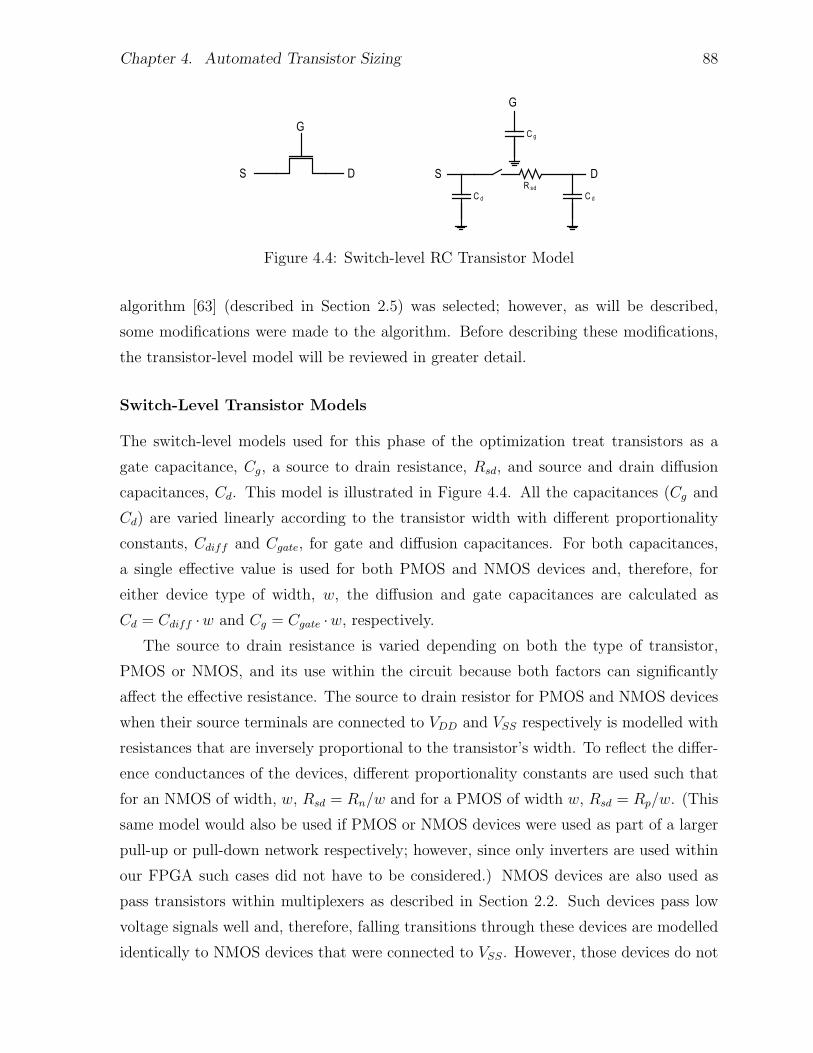
Chapter 4. Automated Transistor Sizing 88
C d
R sd
C d
C g
G
S D
G
S D
Figure 4.4: Switch-level RC Transistor Model
algorithm [63] (described in Section 2.5) was selected; however, as will be described,
some modifications were made to the algorithm. Before describing these modifications,
the transistor-level model will be reviewed in greater detail.
Switch-Level Transistor Models
The switch-level models used for this phase of the optimization treat transistors as a
gate capacitance, Cg, a source to drain resistance, Rsd, and source and drain diffusion
capacitances, Cd. This model is illustrated in Figure 4.4. All the capacitances (Cg and
Cd) are varied linearly according to the transistor width with different proportionality
constants, Cdiff and Cgate, for gate and diffusion capacitances. For both capacitances,
a single effective value is used for both PMOS and NMOS devices and, therefore, for
either device type of width, w, the diffusion and gate capacitances are calculated as
Cd = Cdiff ·w and Cg = Cgate ·w, respectively.
The source to drain resistance is varied depending on both the type of transistor,
PMOS or NMOS, and its use within the circuit because both factors can significantly
affect the effective resistance. The source to drain resistor for PMOS and NMOS devices
when their source terminals are connected to VDD and VSS respectively is modelled with
resistances that are inversely proportional to the transistor’s width. To reflect the differ-
ence conductances of the devices, different proportionality constants are used such that
for an NMOS of width, w, Rsd = Rn/w and for a PMOS of width w, Rsd = Rp/w. (This
same model would also be used if PMOS or NMOS devices were used as part of a larger
pull-up or pull-down network respectively; however, since only inverters are used within
our FPGA such cases did not have to be considered.) NMOS devices are also used as
pass transistors within multiplexers as described in Section 2.2. Such devices pass low
voltage signals well and, therefore, falling transitions through these devices are modelled
identically to NMOS devices that were connected to VSS. However, those devices do not

Chapter 4. Automated Transistor Sizing 89
pass signals that are near VDD well and a different resistance calculation is used for those
rising transitions. That resistance is calculated by fitting simulated data of such a device
to a curve of the form
Resistance (w) =Rn,1
wb. (4.5)
where Rn,1 and b are the constants determined through curve fitting. This fitting need
only be performed once for each process technology7. Using a different resistance calcu-
lation for pass transistor devices has been previously proposed [60]. It is unnecessary to
consider the transmission of logic zero signals through PMOS devices because, in general,
the circuits we will explore do not use PMOS pass transistors.
The use of these resistance and capacitance models is demonstrated in Figure 4.5.
In Figure 4.5(a) the routing track being modelled is shown and Figures 4.5(b) and (c)
illustrate the resistor and capacitor representation of that routing track for a falling and
rising transition respectively8. Based on these models, the delay for each transition can
computed using the Elmore delay [58, 59] as described in Section 2.4.3.
While these RC transistor models are computationally easy to calculate and provide
the useful property that the delay is a posynomial function, they are severely limited in
their accuracy [60, 61]. One frequently recognized limitation is the failure to consider the
impact of the input slope on the effective source to drain resistance and, while a number of
approaches have been proposed to remedy this [60, 126], the inaccuracies remain partic-
ularly for the latest technologies. Therefore, instead of developing improved switch level
models, the subsequent phase of optimization will refine the design using accurate device
models. Before describing that optimization, the TILOS-based optimization algorithm
will be reviewed.
TILOS-based algorithm
The task in this first phase of optimization is to optimize transistor sizes using the
previously described switch-level RC models. A TILOS-based [63] algorithm is used
for this optimization. Changes were made to the original TILOS algorithm to address
some of its known deficiencies and to adapt to the design environment employed in this
work. The basic algorithm along with the changes are described in this section. In
7This resistance model does not affect the posynomial nature of the delay since Rn,1 is always positive.8The falling or rising nature of the transition refers to the transition on the routing track itself.
Clearly, for the example shown in the figure since the track is driven by a single inverter, the inputtransition would be the inverse transition.

Chapter 4. Automated Transistor Sizing 90
w p
w n
w p
w n
w n,passw n,pass
(a) Simple Routing Track
C d iff(w p+w n) C d iffw n,pass C d iffw n,passM
R n/w n,pass
C gate(w p+w n)
R n/w n
(b) Resistance and Capacitance for Falling Transition
C d iff(w p+w n) C d iffw n,pass C d iffw n,passM
R n,1/w n,passb
C gate(w p+w n)
R p/w p
(c) Resistance and Capacitance for Rising Transition
Figure 4.5: Example of a Routing Track modelled using RC Transistor Models
this discussion, the algorithm will be described as changing parameter values not specific
transistor sizes to emphasize that transistors are not sized independently since preserving
logical equivalency requires groups of transistors to have matching sizes.
The TILOS-based phase of the optimization begins with all the transistors set to min-
imum size. For each parameter, the improvement in the objective function per change in
area is measured. This improvement per amount of area increase is termed the param-
eter’s sensitivity. With only a single representative path to optimize, the sensitivity of
every parameter must be measured since they can all affect the delay. Like the original
TILOS algorithm, the value of the parameter with the greatest sensitivity is increased.
In addition to this, the algorithm was modified to also decrease the size of the param-
eter with the most negative sensitivity. Negative sensitivity means that increasing the
parameter, increases the objective function. Therefore, decreasing the parameter im-
proves (reduces) the objective function. This eliminates one of the limitations of TILOS
which can prevent it from achieving optimal results. After the adjustments are made,
the process repeats and all the sensitivities are again measured.

Chapter 4. Automated Transistor Sizing 91
The sensitivity in the original TILOS implementation was computed analytically9
[63]. For this work, we compute the sensitivity numerically as follows:
Sensitivity(w) = −Objective (w + δw)−Objective (w)
Area (w + δw)− Area (w)(4.6)
where w is the width of the transistor or transistors whose sensitivity is being measured.
This numerical computation of the sensitivity requires multiple evaluations of the ob-
jective function which means that the computational demands for this approach may
be higher than an approach relying on analytic methods. However, this was not a con-
cern since this phase of optimization was not a significant bottleneck compared to the
following more computationally intensive phase.
In the later phases of optimization, only discrete sizes for each parameter are con-
sidered to reduce the size of the design space that must be explored. For example, in a
90 nm technology we would only consider sizes to the nearest 100 nm. Using these large
quantized transistor sizes with the numerical sensitivity calculations during the TILOS
optimization could lead to a sub-optimal result; however, to avoid this, the TILOS phase
of the algorithm does not maintain the predefined discrete sizes and, instead, uses sizing
adjustments that are one hundredth the size of the standard increment. This is the size
used for δw in the above expression. Once TILOS completes, sizes are rounded to the
nearest discrete size.
The modification to the algorithm that allows parameters to increase and decrease
in size has one significant side effect. It is possible for a parameter to oscillate from
having the greatest positive sensitivity to having the largest negative sensitivity. Without
any refinement, the algorithm would then alternate between increasing the size of the
parameter before decreasing it in the next cycle. Clearly, this is an artifact arising from
the numerical sensitivity measurements and the quantized adjustments to parameter
values. To address this, the last iteration in which a parameter was changed is recorded.
No changes in the opposite direction are permitted for a fixed number of iterations i.e.
if a parameter was increased in one iteration, it can not be decreased in the subsequent
iteration. This phenomenon of oscillatory changes in parameters can also occur amongst
a group of parameters and, for this reason, the number of iterations between changes must
be made larger than two as one might expect. We found experimentally that requiring
9An analytic expression for the derivative of the delay function with respect to the transistor widthwas determined which allowed the sensitivity at the current width to be computed directly [63].

Chapter 4. Automated Transistor Sizing 92
the number of iterations between changes to be one tenth the total number of parameters,
yielded satisfactory results. This approach also impacts the way in which this algorithm
terminates and that is reviewed in the following section.
Termination Criteria
The original TILOS algorithm terminates when the constraints are satisfied or when any
additional size increases worsen the performance of the circuit. These criteria where
suitable for the original algorithm but, due to the modifications made in the present
work, the termination criteria must also be modified. The issue with the first criterion
of terminating when the constraints are satisfied is that it is not applicable in our work
because the optimization problem is always one of minimizing an objective function with
the only constraints being the minimum width requirements of transistors. The second
criterion of stopping when no size increases are advantageous is also not useful due to
the capability of the current algorithm to decrease sizes as well.
Therefore, new termination criteria were necessary for use with the new algorithm.
The approach that was used is to terminate the algorithm when all the parameters either:
1. can not be adjusted, due to restrictions on oscillatory changes, or
2. offer no appreciable improvement from sizing changes.
With these requirements, there is the possibility that the algorithm will terminate before
achieving an optimal solution. This did not prove to be a major concern in practise in
part because the optimal solution would only be optimal for this simple device model.
The near-optimal result obtained with our algorithm provides a more than adequate
starting point for the next phase of optimization which will further refine the sizes.
4.4.2 Phase 2 – Sizing with Accurate Models
The sizes determined using the RC switch-level models in the previous phase are then
optimized with delay measurements taken based on more accurate device models. There
are a number of possible models that could be used ranging from improvements on the
basic RC model to foundry-supplied device models. We opted for the foundry supplied
models to ensure a high level of accuracy. It is feasible to consider using such models
because the circuit to be simulated (the single path described in Section 4.3.2) contains at
most thousands of transistors. This relatively modest transistor count also means that the
simulation using these device models can be performed using the full quality simulation of
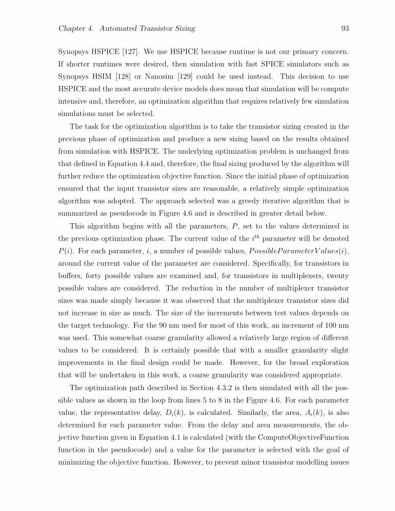
Chapter 4. Automated Transistor Sizing 93
Synopsys HSPICE [127]. We use HSPICE because runtime is not our primary concern.
If shorter runtimes were desired, then simulation with fast SPICE simulators such as
Synopsys HSIM [128] or Nanosim [129] could be used instead. This decision to use
HSPICE and the most accurate device models does mean that simulation will be compute
intensive and, therefore, an optimization algorithm that requires relatively few simulation
simulations must be selected.
The task for the optimization algorithm is to take the transistor sizing created in the
previous phase of optimization and produce a new sizing based on the results obtained
from simulation with HSPICE. The underlying optimization problem is unchanged from
that defined in Equation 4.4 and, therefore, the final sizing produced by the algorithm will
further reduce the optimization objective function. Since the initial phase of optimization
ensured that the input transistor sizes are reasonable, a relatively simple optimization
algorithm was adopted. The approach selected was a greedy iterative algorithm that is
summarized as pseudocode in Figure 4.6 and is described in greater detail below.
This algorithm begins with all the parameters, P , set to the values determined in
the previous optimization phase. The current value of the ith parameter will be denoted
P (i). For each parameter, i, a number of possible values, PossibleParameterV alues(i),
around the current value of the parameter are considered. Specifically, for transistors in
buffers, forty possible values are examined and, for transistors in multiplexers, twenty
possible values are considered. The reduction in the number of multiplexer transistor
sizes was made simply because it was observed that the multiplexer transistor sizes did
not increase in size as much. The size of the increments between test values depends on
the target technology. For the 90 nm used for most of this work, an increment of 100 nm
was used. This somewhat coarse granularity allowed a relatively large region of different
values to be considered. It is certainly possible that with a smaller granularity slight
improvements in the final design could be made. However, for the broad exploration
that will be undertaken in this work, a coarse granularity was considered appropriate.
The optimization path described in Section 4.3.2 is then simulated with all the pos-
sible values as shown in the loop from lines 5 to 8 in the Figure 4.6. For each parameter
value, the representative delay, Di(k), is calculated. Similarly, the area, Ai(k), is also
determined for each parameter value. From the delay and area measurements, the ob-
jective function given in Equation 4.1 is calculated (with the ComputeObjectiveFunction
function in the pseudocode) and a value for the parameter is selected with the goal of
minimizing the objective function. However, to prevent minor transistor modelling issues

Chapter 4. Automated Transistor Sizing 94
Input: Parameter values, P , from first phase of optimizationOutput: Final optimized parameter values, Pbegin1
repeat2
ParameterChanged = false;3
for i← 1 to NumberOfParameters do4
for k ∈ {PossibleParameterV alues(i)} do5
Di(k)= Delay from Simulation with P (i) = k;6
Ai(k)= Area with P (i) = k;7
end8
BestV alue = min {PossibleParameterV alues(i)};9
MinObjectiveFunctionV alue =10
ComputeObjectiveFunction(Di(BestV alue), Ai(BestV alue));for j = ({PossibleParameterV alues(i)} sorted smallest to largest) do11
CurrObjectiveV alue = ComputeObjectiveFunction(Di(j), Ai(j));12
if CurrObjectiveV alue < MinObjectiveFunctionV alue and13
Di(j) < (0.9999 ∗Di(BestV alue)) thenMinObjectiveFunctionV alue = CurrObjectiveV alue;14
BestV alue = j;15
end16
end17
if BestV alue 6= P (i) then18
ParameterChanged = true;19
P (i) = BestV alue;20
end21
end22
Reduce PossibleParameterV alues;23
until not ParameterChanged ;24
end25
Figure 4.6: Pseudocode for Phase 2 of Transistor Sizing Algorithm
or numerical noise from unduly influencing the optimization, the absolute minimum is
not necessarily accepted as the best parameter value. An alternative approach is needed
because, particularly for pure delay optimization, numerical or modelling issues would
occasionally lead to unrealistic sizings if the absolute minimum was simply used.
To avoid such issues, the specific approach used for selecting the best parameter value
starts by examining the results for the parameter value that produced the smallest area
design. The result for the objective function at this parameter value is used as the starting
minimum value of the objective function and is denoted as MinObjectiveFunctionV alue.
The next largest parameter value is then considered to see if it yielded a design that

Chapter 4. Automated Transistor Sizing 95
reduced the objective function; however, the objective function for this parameter value
will only be taken as a new minimum if it offers a non-trivial improvement in the objective
function. Specifically, the delay with the new parameter value must improve by at least
0.01 %. If the improvement satisfied this requirement, then the current value of the
objective function is taken as the minimum. If the improvement was insufficient or the
delay was in fact worse, then the minimum objective function value is left unchanged.
The process then repeats for the next largest parameter value. This whole process for
selecting the best parameter value is captured in lines 8 to 16 of the pseudocode. After
considering all the simulated parameter values, the parameter value that produced the
best minimum objective function is selected. This approach to selecting the minimum
also has the effect of ensuring that if two parameter values led to the same values for the
objective function then the parameter value with the smallest area would be selected.
Once the current best value of the parameter has been determined, this new value of
the parameter will be used when the next parameters are evaluated. This whole process
repeats for the next parameter.
Once all the parameters have been examined in this way, the entire process then
repeats again. It was found that in each subsequent pass through all the parameters
the range of values considered for each parameter could be reduced slightly with little
impact on the final results. Specifically, the number of values is reduced by 25 %. For
example, if ten values were evaluated for a parameter the current iteration then this
would be reduced to eight (due to rounding) for the next iteration. This range reduction
was implemented as it significantly reduced the amount of simulation required and it is
represented in the pseudocode with the “Reduce PossibleParameterValues” step.
The process repeats over all the parameters until one complete pass is made without
a change to any parameter. At this point the algorithm terminates and the final sizing
of the design has been determined.
Parameter Grouping
During the development of this algorithm, it was hypothesized that this greedy algorithm
would be limited if it considered transistor sizes individually because it can be advanta-
geous to adjust the sizes of closely connected transistors in tandem. For this reason, the
parameters considered during optimization also include parameters that affect groups of
transistors and, in particular, this is done for the buffers in the design. For example,

Chapter 4. Automated Transistor Sizing 96
in a two stage buffer, one optimization parameter linearly affects the sizes of all four
transistors in the design. Similarly, the two transistors in the second inverter stage can
be increased in size together. The two stage buffer is still described by four parameters
which means we retain the freedom to adjust each transistor size individually as well.
This is useful as it can enable improvements such as those possible by skewing the p-n
ratios to offset the slow rise times introduced by multiplexers implemented using NMOS
pass transistors.
Parameter Ordering
The described algorithm considers each parameter sequentially and, as the algorithm
progresses, updated values are used for the previously examined parameters. It seemed
possible that the ordering of the parameters could impact the optimization results. This
issue was examined by optimizing the same design with the same parameters but with
different orderings. The possibilities examined included random orderings and orderings
crafted to deal with the parameters in order of their subjective importance. In all cases,
similar results were obtained and, therefore, it was concluded that the ordering of the
parameters does not have a significant effect on the results from the optimizer.
To further test that these potential issues were adequately resolved and to determine
the overall quality of the optimization methodology, the following section compares the
results obtained from this methodology with past designs.
4.5 Quality of Results
The goal in creating the optimization tool based on the previously described algorithm
is to enable the exploration of the performance and area trade-offs that are possible
in the design of FPGAs. To ensure the validity of that exploration, the quality of the
results produced by the optimization tool was tested through comparison with past works.
Specifically, the post-optimization delays will be compared to work that considered the
transistor sizing of the routing resources within the FPGA [31, 32] and of the logic block
[14, 130, 18]. In addition to this, the performance of the optimizer will be compared to an
exhaustive search for a simplified problem for which exhaustive searching was possible.

Chapter 4. Automated Transistor Sizing 97
Input S tim ulus
D elay to be
O ptim ized
W ire length
Figure 4.7: Test Structure for Routing Track Optimization
4.5.1 Comparison with Past Routing Optimizations
The routing used to programmably interconnect the logic blocks has a significant impact
on the performance and area of an FPGA and its design has been the focus of extensive
study [28, 14, 35, 31, 32]. Most past studies focused on the designs using multi-driver
routing and any such results are not directly comparable to our work which exclusively
considered single driver routing. However, the design of single driver routing was explored
in [31, 32] and the results of that work will be compared to the results obtained using
designs generated by our optimizer.
Optimization purely for delay was the primary focus of [31, 32] and, specifically, the
delay to be optimized is shown in Figure 4.7 along with the circuitry used for waveform
shaping and output loading. The delay optimization was performed using the process
described in Section 2.5 in which the sizing of the buffers shown in the figure was opti-
mized using an exhaustive search to determine the overall buffer size and the number of
inverter stages to use. The size ratio between the inverters within the buffer was then
determined analytically.
For comparison purposes, our optimizer was configured to also operate on the path
illustrated in Figure 4.7. To match the procedure used in [31, 32], the delay to be
optimized was set to the delay shown in the figure instead of the representative delay
typically used by the optimizer. Similarly, the target technology was set to be TSMC’s
180 nm 1.8 V CMOS process [131] to conform with the process used in [31, 32].
As was done in [31, 32], optimization was performed for a number of interconnect
segment lengths and the results obtained by our optimizer are compared to [31, 32] in
Table 4.3. The first column of the table indicates the physical length of the interconnect
line driven by the buffer whose size was optimized. The results from [32] are then listed
in the second column labelled “As Published”. All the delays in the table are listed
in ps/mm and are the average of the rising and falling transitions. As was shown in

Chapter 4. Automated Transistor Sizing 98
Table 4.3: Comparison of Routing Driver Optimizations
Delay (ps/mm)Wirelength From [31, 32] Present Work
(mm ) As Published Replicated Minimum Mux Mux Optimization
0.5 408 410 409 2621 260 258 257 2032 192 189 193 1593 184 178 179 1604 191 181 176 168
Figure 4.7, the resistance and capacitance of the metal interconnect lines was modelled
and, since the specific manner in which this interconnect was modelled was not described
in [31, 32], slightly different results were obtained when the exact sizings reported in [31,
32] were simulated. These re-simulated delays are listed in the table in the column labelled
“Replicated”. Clearly, the differences are minor as they are at worst 11 ps/mm and
could also be caused by slightly different simulator versions (HSPICE Version A-2007.09
is used in our work). These replicated results are included to provide a fair comparison
with the column labelled “Minimum Mux” which indicates the results obtained by our
optimizer. The results from our work closely match the results obtained by [31, 32] and
vary between being 2.8 % faster to being 2.1 % slower as compared to the replicated delay
results. Clearly, our optimizer is able to produce designs that are comparable to those
from [31, 32].
Our optimizer also provides the added benefit that it can be used to perform more
thorough optimization. In [32], the multiplexers were assumed to use minimum width
transistors and, for the above comparison, this restriction was preserved. However, with
our sizing tool, it is possible to also consider the optimization of those transistor sizes.
The results when such optimization is permitted are listed in the column labelled “Mux
Optimization” in Table 4.3. Performance improvements of up to 36 % are observed when
the multiplexer transistor widths are increased. Clearly, the optimizer is able to both
deliver results on par with prior investigations while also enabling a broader optimization.
However, this comparison only considered the optimization of the routing drivers. The
logic block is also important and a comparison of its optimization is performed in the
next section.

Chapter 4. Automated Transistor Sizing 99
K -LU T D Q
B LE 2
B LE N
To
R outing
R outing T rack Log ic C lusterIn tra -c luster track
Input C onnection
B lock
B LE Input
B lock
...
...
...
A
BC
D
Figure 4.8: Logic Cluster Structure and Timing Paths
4.5.2 Comparison with Past Logic Block Optimization
The transistor-level design of the logic block has been examined in a number of past
works [14, 130, 18] and the designs created by our optimizer will be compared to these
past studies. For these previous investigations, the design of a complete logic cluster, as
shown in Figure 4.8, was performed. The goal in the transistor-level design of the logic
block was to produce a design with minimal area-delay product. However, only delay
measurements for a number of paths through the logic block will be compared as areas
were not reported.
For this comparison, our optimizer was set to perform sizing to minimize the design’s
area-delay product based on the area and delay measurements described previously in
this chapter. This means that the sizing of both the logic block and routing will be
performed whereas in the past works [14, 130, 18] only the logic block was considered.
Our approach is preferable because it attempts to ensure that area and delay are balanced
between the routing and the logic block.
The prior work considered the sizing for a number of different cluster sizes (N) and
LUT sizes (K) and the delays for these different cluster and LUT sizes will be compared.
In all cases the number of inputs to the cluster is set according to Equation 2.1. The
routing network will be built using length 4 wires and the channel width (W ) is set to
be 20 % more than the number of tracks needed to route the 20 largest MCNC bench-
mark circuits [132]. Fc,out was set to W/N and Fc,in was set to the lowest value that
did not cause a significant increase to the channel width. We implement all multiplexers
Chapter 4. Automated Transistor Sizing 100
having more than 4 inputs as a 2-level multiplexer and the multiplexer gates are driven
at nominal VDD (i.e. gate boosting is not performed and, to compensate, a PMOS level
restorer is used). While these choices for multiplexer implementation are now standard
[31, 32, 15], they are different than the choices that were made in [14, 130, 18] and the
impact of these differences will be discussed later in this section. Based on these assump-
tions, the optimizer was set to size the FPGA in the appropriate process technology and
the delays between points A, B, C, and D in Figure 4.8 will be compared to the past
results [18, 130, 14].
The delays obtained by the optimizer are compared to [18] in Table 4.4. For this
work, TSMC’s 180 nm 1.8 V CMOS process [131] was used. Table 4.4(a) lists the results
reported in [18] for a range of cluster sizes as indicated in the first column of the table.
All the results are for 4-LUT architectures. The remaining columns of the table list the
delays between the specified timing points10. The rightmost column labelled A to D is a
combination of the other timing points and it is a measure of the complete delay from a
routing track through the logic block to the driver of a routing track.
The delays from the designs created by the optimizer are tabulated in Table 4.4(b)
(All the delays are the maximum of the rise and fall delays for typical silicon under
typical conditions). The percentage improvement in delay obtained by the optimizer
relative to the delay from [18] is listed in Table 4.4(c). Clearly, the delays between A and
B, between B and C, and between D and C are significantly better with our optimizer
while the delay from C to D is worse. (The delays for C to D in both cases are for the
fastest input through the LUT. This will be the case for all delays involving the LUT
unless noted otherwise.) While the increases in delay are a potential concern, they may
be in part due to the specific positioning of the timing points relative to any buffers
and, therefore, the most meaningful comparison is for the delay from A to D which is the
complete path through the logic block. For that delay, the optimizer consistently delivers
modest improvements. The other potential cause of the significant differences observed
between the two sets of designs is the different area and delay metrics used. Unlike our
results, the optimization in [18] did not consider the delay or area of the full FPGA and,
therefore, area and delay may have been allocated differently when our optimizer was
used.
10For readers familiar with timing as specified in the VPR [10] architecture file, delay A toB is T ipin cblock, delay B to C is T clb ipin to sblk ipin, C to D is T comb and D to C isT sblk opin to sblk ipin.

Chapter 4. Automated Transistor Sizing 101
Table 4.4: Comparison of Logic Cluster Delays from [18] for 180 nm with K = 4
(a) Delays from [18]
Cluster Size A to B B to C C to D D to C A to D(N) (ps) (ps) (ps) (ps) (ps)
1 377 180 376 N/Aa 9332 377 221 385 221 9834 377 301 401 301 10796 377 332 397 332 11068 377 331 396 331 110410 377 337 387 337 1101
(b) Delays with Present Work
Cluster Size A to B B to C C to D D to C A to D(N) (ps) (ps) (ps) (ps) (ps)
1 156 0 444 N/Aa 5992 273 150 509 132 9324 299 155 536 141 9006 286 157 565 142 10098 317 152 538 133 100710 308 159 526 147 993
(c) Percent Improvement of Present Work over [18]
Cluster Size A to B B to C C to D D to C A to D(N) (ps) (ps) (ps) (ps) (ps)
1 59% 100% -18% N/Aa 36%2 28% 32% -32% 40% 5.2%4 21% 49% -34% 53% 8.3%6 24% 53% -42% 57% 8.8%8 16% 54% -36% 60% 8.8%10 18% 53% -36% 56% 10%
aThe “cluster” of size one is implemented without any intra-cluster routing and, therefore, there isno direct path from D to C.
For completeness, the delays from C to D for a range of LUT sizes are compared in
Table 4.5. The first column indicates the LUT size and the second and third columns list
the delay for C to D from [18] and our optimizer respectively. The fourth column lists the
percent improvement obtained by our optimizer. As observed with the data in Table 4.4,
the optimizer generally delivers slower delays than were reported in [18] but, again, this
may be caused by issues such as buffer positioning or area and delay measurement.
A comparison with the delays reported in [130] was also performed. In this case, the
target technology was TSMC’s 350 nm 3.3 V CMOS process [133]. The same optimization

Chapter 4. Automated Transistor Sizing 102
Table 4.5: Comparison of LUT Delays from [18] for 180 nm with N = 4
LUT Size From [18] This Work Percent Improvement(K) (ps) (ps) (%)
2 199 463 -133%3 283 511 -80%4 401 536 -34%5 534 552 -3%6 662 600 9%7 816 717 12%
process used in the previous comparison was used for this comparison and the results are
summarized in Table 4.6 for clusters ranging in size from 1 to 10. The published delays
from [130] are listed in Table 4.6(a) while the delays from the designs created by our
optimizer are given in Table 4.6(b). The improvement in percentage for our optimizer’s
designs is shown in Table 4.6(c). Again, while some of the delays are lower and others
larger, the most meaningful comparison is for the delay from A to D which is given in
the rightmost column of the table. For that delay path, improvements of between 11 %
and 22 % were observed. The delays of the C to D path for a range of LUT sizes are
summarized in Table 4.7 and, as before, for this portion of the delay, the design created
by our optimizer is slower than the previously published delays. Again, part of this
difference may be due to the positioning of buffers relative to the timing points since,
as was seen in Table 4.6, comparable delays for the overall path through the logic block
were observed.
The logic block delays obtained from the optimizer using TSMC’s 350 nm 3.3 V
CMOS process [133] were also compared to the results from [14] as is shown in Fig-
ure 4.8. For this comparison, the logic block consisted of 4-LUTs in clusters of size 4.
As in the previous tables, timing is reported relative to the points labelled in Figure 4.8.
The second row of the table lists those delays as reported in [14] and row labelled “This
Work” summarizes the delays obtained from the sizing created by our optimizer. The
percent improvement in delay obtained by the optimizer is given in the last row of the
table. As observed in the comparison with [18] and [130], improvements are seen for a
number of the timing paths while a slow down is observed for a portion of the path.
Again, the most useful comparison is the timing through the entire block from A to D
which is listed in the last column of the table. For that delay, a slight improvement in
the delay obtained by the optimizer is observed.

Chapter 4. Automated Transistor Sizing 103
Table 4.6: Comparison of Logic Cluster Delays from [130] for 350 nm with K = 4
(a) Delays from [130]
Cluster Size A to B B to C C to D D to C A to D(N) (ps) (ps) (ps) (ps) (ps)
1 760 140 438 140 13382 760 649 438 649 18474 760 761 438 761 19596 760 849 438 849 20478 760 892 438 892 209010 760 912 438 912 2110
(b) Delays with Present Work
Cluster Size A to B B to C C to D D to C A to D(N) (ps) (ps) (ps) (ps) (ps)
1 319 0 753 N/A 10722 436 325 877 289 16384 512 316 836 300 16646 448 336 812 322 15968 474 332 866 313 167210 510 365 847 321 1722
(c) Percent Improvement of Present Work over [130]
Cluster Size A to B B to C C to D D to C A to D(N) (ps) (ps) (ps) (ps) (ps)
1 58% 100% -72% N/A 20%2 43% 50% -100% 55% 11.3%4 33% 58% -91% 61% 15.1%6 41% 60% -85% 62% 22.0%8 38% 63% -98% 65% 20.0%10 33% 60% -93% 65% 18%
Table 4.7: Comparison of LUT Delays from [130] for 350 nm with N = 4
LUT Size From [130] This Work Percent Improvement(K) (ps) (ps) (%)
2 100 760 -660%3 294 756 -157%4 438 836 -91%5 562 862 -53%6 707 1013 -43%7 862 1065 -24%

Chapter 4. Automated Transistor Sizing 104
Table 4.8: Comparison of Logic Cluster Delays from [14] for 350 nm CMOS with K = 4and N = 4
A to B B to C C to D D to C A to D(ps) (ps) (ps) (ps) (ps)
From [14] 1040 340 465 620 1845This Work 512 316 836 300 1664
Percent Improvement 51% 7.1% -80% 52% 10%
While clearly the optimizer was able to create designs with overall performance com-
parable to the previously published works, there are differences between the works that
should be noted. Most significantly, the circuit structures used for the multiplexer differ
substantially. Two-level multiplexers were used in the designs created by the optimizer
(as is now standard [15]) but, in [14, 130, 18], fully encoded multiplexers with gate
boosting were used11. This means that, for all multiplexers with more than 4 inputs12,
the previous designs would be implemented using more than 2-levels of pass transistors.
However, the delay impact of the additional transistor levels is partially offset by the
use of gate boosting. Another difference is in the optimization process used. While the
designs produced with our optimizer were designed to minimize the area-delay product
for the whole FPGA, such an approach was not used in [14, 130, 18] which optimized the
area-delay product at a much finer granularity. This difference could lead to a different
allocation of area and performance across the FPGA.
We believe that because similar results were obtained these results validate our op-
timization process. The previously created designs were the result of months of careful
human effort. Our optimizer was able to match those results with a small fraction of the
effort. However, before putting this optimizer to use, one additional set of experiments
will be performed to further test the quality of the optimizer.
4.5.3 Comparison to Exhaustive Search
The results obtained using the optimizer were also compared to the best results obtained
from an exhaustive search with a goal of minimum delay for both optimizer and the
11It is not stated in [18, 134, 130] that fully encoded multiplexers with gate boosting are used but thishas been confirmed through private communications with the author.
12The CLB input multiplexer has Fc,in inputs (and that would generally be on the order of 10 orgreater) and the BLE input multiplexer has N + I = N + K
2 (N + 1) inputs. Therefore, both of thesemultiplexers would generally have more than 4 inputs.

Chapter 4. Automated Transistor Sizing 105
Table 4.9: Exhaustive Search Comparison
Test Routing Track Delay (ps) %Case Exhaustive This Work Difference
W 221.4 221.9 -0.2%X 226.9 230.1 -1.4%Y 224.9 224.9 0.0%Z 226.4 226.4 0.0%
exhaustive search. It is only possible to exhaustively optimize the sizes of a small num-
ber of transistors for this comparison because the number of test cases quickly grows
unreasonably large for the exhaustive search. Furthermore, to make the simulation time
reasonable, the path under optimization was simplified to be a properly loaded routing
segment similar to that shown in Figure 4.7. This simplified path has four transistors
in the buffer and two transistors in the multiplexer whose size could be adjusted. For
the comparison, only three of these transistor sizes will be optimized to keep the run
times reasonable. This comparison was performed using a 90 nm 1.2 V CMOS process
[87] from STMicroelectronics.
While only three transistor sizes were optimized in each test, we did vary the set
of specific transistors whose size could be adjusted. The delay for the routing segment
from our sizer and the exhaustive search were compared for four different combinations
of adjustable transistors. The two results were consistently within 1.2 % of each other
and the results are listed in Table 4.9. Each row contains the data for the optimization
performed using a different subset of adjustable parameters from the six possible perfor-
mance impacting parameters. The second column of the table reports the delay result
obtained using an exhaustive search of all possible values of the adjustable parameters
and the third column indicates the delay when those same parameters were sized by our
optimizer. The percentage difference is given in the fourth column. For these cases, our
optimization tool was on average 30.6 times faster than the exhaustive search. For a
larger number of adjustable sizes, the exhaustive search quickly becomes infeasible and
the speedup would grow significantly.
4.5.4 Optimizer Run Time
The preceding comparisons have shown that the optimization tool is able to achieve its
stated aim of producing realistic results across a range of design parameters. The other

Chapter 4. Automated Transistor Sizing 106
goal for this work was to have subjectively reasonable run times. For the experiments
performed in this chapter the run time varied between from 0.4 hours to 28 hours when
running on an Intel Xeon 5160 processor. The wide range in reported run times is due to
the various factors that affect the execution times. The two most significant factors are
the architectural parameters, as that impacts the artificial path used by the optimizer,
and the target technology, as the transistor models used by HSPICE affect its execution
time. Of these parameters, the LUT size is most significant as it both increases the
size of the LUTs and the number of LUTs included in the artificial path because each
additional LUT input adds an additional path that must be optimized. Therefore, the
longest run times were for 7-LUT architectures. For smaller LUT sizes, the run times
were significantly reduced. Given this, the execution time required for the optimization
tool was considered satisfactory as it will permit the exploration of a broad range of
parameters in Chapter 5.
4.6 Summary
This chapter has presented an algorithm and tool that performs transistor sizing for
FPGAs across a wide range of architectures, circuit designs and optimization objectives.
It has been shown that the optimizer is able to produce designs that are comparable to
past work but with significantly less effort thanks to the automated approach. The next
chapter will make use of this optimizer to explore the design space for FPGAs and the
trade-offs that can be made to narrow the FPGA to ASIC gap.

Chapter 5
Navigating the Gap through Area
and Delay Trade-offs
The measurement and analysis of the FPGA to ASIC gap in Chapter 3 found that there
is significant room for improvement in the area, performance and power consumption
of FPGAs. Whether it is possible to close the gap between FPGAs and ASICs is an
important open question. Our analysis in Chapter 3 (by necessity) focused on a single
FPGA design but there are in fact a multitude of different FPGA designs that can be
created by varying the logical architecture, circuit design and transistor-level sizing of
the device. The different designs within that rich design space offer trade-offs between
area and performance but exploring these trade-offs is challenging because accuracy ne-
cessitates that each design be implemented down to the transistor-level. The automated
transistor sizing tool described in the previous chapter makes such exploration feasible
and this chapter investigates the area and delay trade-offs that can be made within the
design space.
The goal in exploring these trade-offs is two-fold: the primary goal is to determine
the extent to which these trade-offs can be used to selectively narrow the FPGA to
ASIC gap. This could allow the creation of smaller and slower or faster and larger
FPGAs. It has become particularly relevant to consider such trade-offs as the market
for FPGAs has broadened to include both sectors with high performance requirements
such as high-speed telecommunications and sectors that are more cost focused such as
consumer electronics. Understanding the possible trade-offs could allow FPGAs to be
created that are better tailored to their end market. To aid such investigations, the second
107

Chapter 5. Navigating the Gap through Area and Delay Trade-offs 108
goal of this exploration is to determine the parameters either at the logical architecture
level or the circuit design level that can best enable these trade-offs.
We explore these trade-offs in the context of general purpose FPGAs that are not
designed for a specific domain of applications. Application-specific FPGAs have been
suggested in the past [135] and they likely do offer additional opportunities for making
design trade-offs. However, general purpose FPGAs continue to dominate the market
[6, 136, 7, 8, 137, 9] and are required in both cost-oriented and performance-oriented
markets.
This chapter will first describe the methodology used to measure the area and perfor-
mance of an FPGA design. To ensure the accuracy of the measurements, this methodol-
ogy is different than that used by the optimizer described in the previous chapter. The
trade-offs that are possible for a single architecture are then examined. It will be seen
that some trade-offs are not useful and, therefore, in Section 5.3, the criteria used to
determine whether such trade-offs are interesting are introduced. Using those criteria,
a large design space with varied architecture and transistor sizings is examined in Sec-
tion 5.4 to quantify the range of trade-offs possible. The logical architecture and circuit
structure parameters are then examined individually to determine which parameters are
most useful for making area and delay trade-offs. Finally, the impact of these trade-offs
on the gap between FPGAs and ASICs is examined in Section 5.7.
5.1 Area and Performance Measurement Methodol-
ogy
As described in Chapter 4, the inherent programmability of FPGAs means that until
an FPGA is programmed with an end-user’s design there is no definitive measure of the
performance or area of the FPGA. Only after a circuit is implemented on an FPGA is
it possible to measure the performance of the circuit and area consumed in the FPGA in
a meaningful manner. To explore the area and performance trade-offs accurately, a full
experimental process, as described in Section 2.4, is necessary and the specific process
that will be used is described in this section.

Chapter 5. Navigating the Gap through Area and Delay Trade-offs 109
Fu ll C A D Flo w
(S IS , T-V P A C K , V P R )
S P IC E
N etlis t of
C rit ic al P ath
H S P IC E
D elay
T rans is tor -
Lev el D es ignT im ing M odel
B enc hm ark
C irc uits
Figure 5.1: Performance Measurement Methodology
5.1.1 Performance Measurement
The performance of a particular FPGA implementation is measured experimentally using
the 20 largest MCNC benchmarks [132, 138]. Each benchmark circuit is implemented
through a complete CAD flow on a proposed FPGA fabric and a final delay measurement
is generated as an output. The geometric mean delay of all the circuits is then used as
the figure of merit for the performance of the FPGA implementation. This mean delay
will be referred to as the effective delay of the FPGA. The steps involved in generating
this delay measurement are illustrated in Figure 5.1.
Synthesis, packing, placement and routing of the benchmark circuit onto the FPGA
is done using SIS with FlowMap [139], T-VPack [140] and VPR [10] (an updated version
of VPR that handles unidirectional routing is used). The placement and routing process
is repeated with 10 different seeds for placement and the placement and routing with
the best performance is used for the final results. The tools cannot directly make use of
the transistor size definitions of the FPGA fabric and, instead, a simplified timing model
must be provided. This timing model is encapsulated in VPR’s architecture file and
includes fixed delays for both the routing tracks and the paths within the logic block.

Chapter 5. Navigating the Gap through Area and Delay Trade-offs 110
Table 5.1: Comparison of Delay Measurements between HSPICE and VPR for 20 Circuits
Design AverageHSPICE / VPR
Standard DeviationHSPICE / VPR
VPR to HSPICEDelay Correlation
Delay 1.05 0.123 0.971Area Delay 1.32 0.0921 0.977Area 0.939 0.0474 0.990
We generate this file automatically through simulation of the circuit design with the
appropriate transistor sizes.
After placement and routing is complete, VPR performs timing analysis to deter-
mine the critical path of the design implemented on the FPGA. While this provides an
approximate measure of the FPGA’s performance, it is not sufficiently accurate for our
purposes since the relatively simple delay model does not accurately capture the complex
behaviour of transistors in current technologies. To address this, we have created a mod-
ified version of VPR that emits the circuitry of the critical path. Any elements that load
this path are also included to ensure the delay measurement is accurate. This circuit
is then simulated with the appropriate transistor sizes and structures using Synopsys
HSPICE. The delay as measured by HSPICE is used to define the performance of this
benchmark implemented on this particular FPGA implementation.
To determine if the additional step of simulation with HSPICE was needed, a compari-
son was performed between the VPR reported critical path delay and the delay when that
same path was measured using HSPICE. This was done for one architecture using three
different FPGA transistor sizings. The twenty benchmark circuits were implemented on
these three different FPGA designs and the results of the comparison are summarized in
Table 5.1. The three different designs were created by changing the optimization objec-
tive of the design. In one case, the optimization exclusively aimed to minimize delay and
this is labelled as the “Delay” design in the first column of the table. For another design,
the objective was minimal area-delay product for the design and this is labelled as “Area
Delay”. Finally, area was minimized in the “Area” design. The second column reports
the average value across the twenty benchmarks of the delay from HSPICE divided by
the delay from VPR. With the average varying between 0.939 and 1.32 it is clear that
the delay model in VPR does not accurately reflect the delays of the different designs
and, therefore, simulation with HSPICE is essential to properly measuring the delays of
the different designs.
Chapter 5. Navigating the Gap through Area and Delay Trade-offs 111
The inaccuracy in the VPR delay model is a potential concern because the underlying
timing analysis used during routing is performed with the inaccurate timing model. As
a result, poor routing choices may be made since the timing analysis may incorrectly
predict the design’s critical path. Fully addressing this concern would require a complete
overhaul of VPR’s timing analysis engine but, fortunately, it was observed that such
extreme measures were not required. Table 5.1 also provides the correlation between the
VPR and HSPICE critical path delay measurements in the column labelled “VPR to
HSPICE Delay Correlation”. For every design, the two delay measurement approaches
are well correlated which demonstrates that, while the VPR model may be inaccurate
in predicting the delays of different transistor-level designs, for any particular design the
VPR model has a relatively high fidelity. An alternative measure of this can be seen
in the standard deviation across all the benchmarks of the HSPICE delay divided by
VPR delay measurements and this is listed in the table under the heading “Standard
Deviation HSPICE / VPR”. The standard deviations indicate that there is relatively low
variability across the measurements. In relative terms, the standard deviation is at most
12 % of the mean. Given this, it was considered reasonable to continue to rely on VPR’s
timing model for intermediate timing analyses; however, HSPICE measurements will be
used for the final performance measurement.
5.1.2 Area Measurement
The area model described in Section 4.3.1 was designed to predict the area of an FPGA
tile based on its transistor-level design. While considering only the tile area was accept-
able when focused purely on transistor sizing changes, if architectural changes are to be
considered (as they will be in this chapter) then the area metric must accurately capture
the different capabilities of the tiles from different architectures. This is crucial because
both LUT size and cluster size have a significant impact on the amount of logic that can
be implemented in each logic block and, therefore, the amount of logic in each tile.
To account for the varied logic capabilities, the effective area for a design is calculated
as the product of the tile area and the number of tiles required to implement the bench-
mark circuits. The count of required tiles only includes tiles in which the logic block is
used. Since each benchmark is placed onto an M ×M grid of tiles with M set to the
smallest value that will fit the benchmark, there may be tiles in which the routing is used
but not the logic block. Such tiles are not included as it would cause the tile count to be
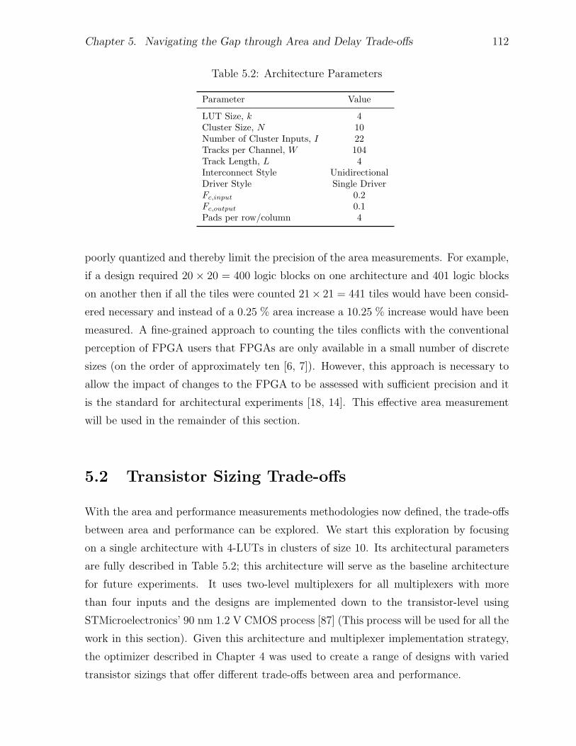
Chapter 5. Navigating the Gap through Area and Delay Trade-offs 112
Table 5.2: Architecture Parameters
Parameter Value
LUT Size, k 4Cluster Size, N 10Number of Cluster Inputs, I 22Tracks per Channel, W 104Track Length, L 4Interconnect Style UnidirectionalDriver Style Single DriverFc,input 0.2Fc,output 0.1Pads per row/column 4
poorly quantized and thereby limit the precision of the area measurements. For example,
if a design required 20 × 20 = 400 logic blocks on one architecture and 401 logic blocks
on another then if all the tiles were counted 21× 21 = 441 tiles would have been consid-
ered necessary and instead of a 0.25 % area increase a 10.25 % increase would have been
measured. A fine-grained approach to counting the tiles conflicts with the conventional
perception of FPGA users that FPGAs are only available in a small number of discrete
sizes (on the order of approximately ten [6, 7]). However, this approach is necessary to
allow the impact of changes to the FPGA to be assessed with sufficient precision and it
is the standard for architectural experiments [18, 14]. This effective area measurement
will be used in the remainder of this section.
5.2 Transistor Sizing Trade-offs
With the area and performance measurements methodologies now defined, the trade-offs
between area and performance can be explored. We start this exploration by focusing
on a single architecture with 4-LUTs in clusters of size 10. Its architectural parameters
are fully described in Table 5.2; this architecture will serve as the baseline architecture
for future experiments. It uses two-level multiplexers for all multiplexers with more
than four inputs and the designs are implemented down to the transistor-level using
STMicroelectronics’ 90 nm 1.2 V CMOS process [87] (This process will be used for all the
work in this section). Given this architecture and multiplexer implementation strategy,
the optimizer described in Chapter 4 was used to create a range of designs with varied
transistor sizings that offer different trade-offs between area and performance.

Chapter 5. Navigating the Gap through Area and Delay Trade-offs 113
The range of results is plotted in Figure 5.2. The Y-axis in the figure, the effective
delay, is the geometric mean delay across the benchmark circuits and the X-axis is the
area required for all the benchmarks. Each point in the figure indicates the area and
performance of a particular FPGA design. The different points are created by varying the
input parameters, b and c, that specify the objective function (AreabDelayc) to optimize.
At one extreme, area is the only concern (b = 1, c = 0) and at the other extreme, delay is
the only concern (b = 0, c = 1). In between, these extremes, various other combinations
of b and c are used. As described in Section 5.1, the area and performance are measured
using a the full FPGA CAD flow. Clearly, transistor sizing enables a large range of area
and delay possibilities. The range in these trade-offs is quantified as follows:
Area Range =Area of Largest Design
Area of Smallest Design, (5.1)
Delay Range =Delay of Slowest Design
Delay of Fastest Design. (5.2)
The largest design should also be the fastest design and the smallest design should be
slowest design. The area and delay range from Figure 5.2 are then 2.2 × and 8.0 ×,
respectively, using this definition for the ranges.
To provide a relative sense of the size of these ranges, Table 5.3 compares this area-
delay range to the range seen when architectural parameters have been varied in past
studies [134, 14]. Those studies considered the cluster size, LUT size and segment length
and the table lists the delay and area range when each of these attributes was varied. For
each of these parameters on their own, delay ranges between 1.6 and 2.2 and area ranges
between 1.5 and 1.6 were observed. The largest range is obtained when cluster size and
LUT sizes are both varied. In that case, ranges of 3.2 × and 1.7 × were observed in delay
and area respectively [134]. While the area range is of a similar magnitude to that seen
from transistor sizing, the delay range from architectural changes is considerably smaller
than that from transistor sizing indicating the significant effect transistor sizing can have
on performance.
The full range of transistor sizing possibilities illustrates the important role sizing
plays in determining performance trade-offs but reasonable architects and designers would
not consider this full range useful. At the area-optimized and the delay-optimized ex-
tremes, the trade-off between area and delay is severely unbalanced. This is particularly

Chapter 5. Navigating the Gap through Area and Delay Trade-offs 114
0
5E-09
1E-08
1.5E-08
2E-08
2.5E-08
3E-08
3.E+07 4.E+07 5.E+07 6.E+07 7.E+07 8.E+07 9.E+07
Eff
ec�
ve
De
lay
(s)
(Ge
om
etr
ic M
ea
n D
ela
y a
s M
ea
sure
d b
y H
SP
ICE
)
Effec�ve Area (um2)
Figure 5.2: Area Delay Space
Table 5.3: Area and Delay Changes from Transistor Sizing and Past Architectural Studies
Variable Delay Range Area Range
Transistor Sizing (Full) 8.0 2.2
Cluster Size (1-10) [134] 1.6 1.5LUT Size (2-7) [134] 2.2 1.5Segment Length (1-16) [14] 1.6 1.6Cluster & LUT Size [134] 3.2 1.7
true near the minimal area sizing where the large negative slope seen in Figure 5.2 indi-
cates that, for a slight increase in area, a significant reduction in delay can be obtained.
Quantitatively, there is a 14 % reduction in delay for only a 0.02 % increase in area.
Clearly, a reasonable designer would always accept that minor area increase to gain that
significant reduction in delay. Therefore, to ensure only realistic trade-offs are considered,
the range of trade-offs must be restricted and this restriction is described in the following
section.

Chapter 5. Navigating the Gap through Area and Delay Trade-offs 115
5.3 Definition of “Interesting” Trade-offs
The goal in exploring the area and performance trade-offs is to understand how the gap
between FPGAs and ASICs can be selectively narrowed by exploiting these trade-offs.
However, the trade-offs considered must be useful and, as seen in the previous section, an
imbalance between the area and delay trade-offs occurs at the extremes of the transistor
sizing trade-off curve shown earlier. Selecting the regions in which the trade-offs are
useful is a somewhat arbitrary decision. Intuitively, this region is where the elasticity
[141], defined as
elasticity =ddelay
darea· area
delay(5.3)
is neither too small or too large. Since we do not have a differentiable function relating
the delay and area for an architecture, we approximate the elasticity as:
elasticity =% change in delay
% change in area. (5.4)
An elasticity of -1 means that a 1 % area increase achieves a 1 % performance im-
provement. Clearly, a 1-for-1 trade-off between area and delay is useful. However, based
on conversations with a commercial FPGA architect [142], we will view the trade-offs
as useful and interesting when at most a 3 % area increase is required for a 1 % delay
reduction (an elasticity of -1/3) and when a 1 % area decrease increases delay by at most
3 % (an elasticity of -3). This factor of three that determines the degree to which area
and delay trade-offs can be imbalanced will be called the elasticity threshold factor. All
points within the range of elasticities set by the threshold factor will make up what we
call the interesting range of trade-offs. With this restriction, designs are removed both
because too much area is required for too small a performance improvement and because
too much performance is sacrificed for too small an area reduction. While this restric-
tion only explicitly considers delay and area, it has the effect of eliminating designs with
excessive power consumption because those designs would generally also have significant
area demands.
This approach is appropriate for considering the interesting regions of a single area-
delay curve. A more involved approach is necessary when considering discrete designs,
such as those from [134, 14], or multiple different trade-off curves. In such cases, the
process for determining the interesting design is as follows: first the set of potentially
interesting designs is determined by examining the designs ordered by their area. Starting

Chapter 5. Navigating the Gap through Area and Delay Trade-offs 116
for the minimum area design, each design is considered in turn. A design is added to
the set of potentially interesting designs if its delay is lower than all the other designs
currently in the potentially interesting set. This first step eliminates all designs that can
not be interesting because other designs provide better performance for less area. The
next step will apply the area-delay trade-off criterion to determine which designs are
interesting.
Two possibilities must be considered when evaluating whether a design is interesting.
These two possibilities are illustrated in Figure 5.3 through four examples. In these
examples, we will determine if the three designs labelled A, B and C are in the interesting
set. Design B is first compared to design A using the -1/3 elasticity requirement as shown
in Figures 5.3(a) and 5.3(b). If the delay improvement in B relative to A is too small
compared to the additional area required as it is in Figure 5.3(a), then design B would
be rejected. In Figure 5.3(b) the delay improvement is sufficiently large and design B
could be accepted as interesting. However, the design must also be compared to design
C. In this case, the -3 elasticity requirement is used. If the delay of B relative to C is too
large compared to the area savings of B relative to C the design would not be included
in the interesting set. Such a case is shown in Figure 5.3(c). An example in which design
B is interesting based on this test is illustrated in Figure 5.3(d). A design whose delay
satisfies both the -1/3 and the -3 requirements is included in the interesting set. At the
boundaries of minimum area or minimum delay (i.e. design A and design C respectively
if these were the only three designs being considered) only the one applicable elasticity
threshold must be satisfied.
When examining more than three designs, the process is the same except the com-
parison designs A and C need not be actual designs. Instead, those two points represent
the minimum and maximum interesting delays possible for the areas required for designs
A and C respectively. Equivalently, designs A and C are the largest or smallest designs
respectively that satisfied the -1/3 or -3 elasticity threshold. If no such designs exist then
the minimum area or delay of actual designs, respectively, would be used.
With this restriction to the interesting region, the range of trade-offs is decreased to
a range of 1.41 in delay from slowest to fastest and 1.47 in area from largest to smallest.
Figure 5.4 plots the data shown previously in Figure 5.2 but with the interesting points
highlighted. Clearly, there is a significant reduction in the effective design space but the
range is still appreciable and it demonstrates that there are a range of designs for a specific
architecture that can be useful. Applying this same criteria to the past investigation of

Chapter 5. Navigating the Gap through Area and Delay Trade-offs 117
De
lay
A rea
E lastic ity = -1 /3
A
B
C
(a) Design B is not interesting
De
lay
A rea
E lastic ity = -1 /3
A
B
C
(b) Design B may be interesting
B
A
De
lay
A rea
E lastic ity = -3
C
(c) Design B is not interesting
B
A
De
lay
A rea
E lastic ity = -3
C
(d) Design B may be interesting
Figure 5.3: Determining Designs that Offer Interesting Trade-offs
LUT size and cluster size [134], we find that the range of useful trade-offs is 1.17 for delay
from fastest to slowest and 1.11 for area from largest to smallest. This space is smaller
than the range observed for transistor sizing changes of a single architecture. From the
perspective of designing FPGAs for different points in the design space, transistor sizing
appears to be the more powerful tool. However, architecture and transistor sizing need
not be considered independently and, in the following section, we examine the size of the
design space when these attributes are varied in tandem.

Chapter 5. Navigating the Gap through Area and Delay Trade-offs 118
0
5E-09
1E-08
1.5E-08
2E-08
2.5E-08
3E-08
3.E+07 4.E+07 5.E+07 6.E+07 7.E+07 8.E+07 9.E+07
Eff
ec�
ve
De
lay
(s)
(Ge
om
etr
ic M
ea
n D
ela
y a
s M
ea
sure
d b
y H
SP
ICE
)
Effec�ve Area (um2)
Full Design Space
Interes!ng Region
Figure 5.4: Area Delay Space with Interesting Region Highlighted
5.4 Trade-offs with Transistor Sizing and Architec-
ture
For each logical architecture, a range of different transistor sizings, each with different
performance and area, is possible. In the previous section, only a single architecture was
considered, but now we explore varying the transistor sizes for a range of architectures.
We considered a range of architectures with varied routing track lengths (L), cluster
sizes (N) and LUT sizes (K). Table 5.4 lists the specific values that were considered
for each of these parameters. Not every possible combination of these parameter values
was considered and the full list of architectures that were considered can be found in
Appendix D. A comparison between architectures is most useful if the architectures
present the same ease of routing. Therefore, as each parameter is varied, it is necessary
to adjust other related architectural parameters such as the channel width (W ) and the
input/output pin flexibilities (Fc,in, Fc,out).
We determine appropriate values for the channel width (which is one factor affecting
the ease of routing) experimentally by finding the minimum width needed to route our

Chapter 5. Navigating the Gap through Area and Delay Trade-offs 119
Table 5.4: Range of Parameters Considered for Transistor Sizing and Architecture Inves-tigation
Parameter Values Considered
LUT Size (K) 2–7Cluster Size (N) 2, 4, 6, 8, 10, 12Routing Track Length (L) 1, 2, 4, 6, 8, 10
Table 5.5: Optimization Objectives
Optimization Objectives
Area1Delay1 Area2Delay1
Area3Delay1 Area4Delay1
Area6Delay1 Area8Delay1
Area10Delay1 Area1Delay2
Area1Delay3 Area1Delay4
Area1Delay6 Area1Delay8
Area1Delay10 Area1Delay0
Area0Delay1
benchmark circuits. The minimum channel width is increased by 20 % and rounded to
the nearest multiple of twice the routing segment length1 to get the final width. The
input pin flexibility (Fc,in) is determined experimentally as the minimum flexibility which
does not significantly increase the channel width requirements. The output flexibility is
set as, 1/N , where N is the cluster size. For each architecture, a range of transistor sizing
optimization objectives were considered. The typical objective functions used are listed
in Table 5.5. The results for all these architectures and sizes are plotted in Figure 5.5.
Again, each point in the figure indicates the delay and area of a particular combination
of architecture and transistor sizing. In total, 60 logical architectures were considered.
With the different sizings for each architecture, this gives a total of 1331 distinctly sized
architectures. The delay in all cases is the geometric mean delay across the benchmark
circuits and the area is the total area required to implement all the benchmarks.
The goal in considering this large number of architectures is to determine the range
of the area and performance trade-offs. However, trade-offs that are severely imbalanced
must be eliminated using the process described in the previous section. The smallest
(and slowest), the fastest (and largest) and the minimum area-delay designs from the
1The rounding of the channel width is necessary to ensure that the complete FPGAs can be createdby replicating a single tile. It is necessary to round to twice the segment length because, with thesingle-driver routing topology, there must be an equal number of tracks driving in each direction.

Chapter 5. Navigating the Gap through Area and Delay Trade-offs 120
2E-09
4E-09
6E-09
8E-09
1E-08
1.2E-08
1.4E-08
30000000 50000000 70000000 90000000 110000000 130000000 150000000
Eff
ec�
ve
De
lay
(s)
(Ge
om
etr
ic M
ea
n D
ela
y a
s M
ea
sure
d b
y H
SP
ICE
)
Effec�ve Area (um2)
All Points
Smallest Interes!ng
Min. Area Delay
Fastest Interes!ng
Figure 5.5: Full Area Delay Space
interesting set of designs are labelled in Figure 5.5. Clearly, there are both faster de-
signs and smaller designs but such designs require too much area or sacrifice too much
performance, respectively.
Compared to conventional experiments which would have only considered the mini-
mum area-delay point useful we see that in fact there are a wide range of designs that
are interesting when different design objectives are considered. The span of these designs
is of particular interest and is summarized in Table 5.6. We see that there is a range
of 2.03 × in area from the largest design to the smallest design. In terms of delay, the
range is 2.14 × from the slowest design relative to the fastest design. It is clear that when
creating new FPGAs there is a great deal of freedom in the area and delay trade-offs that
can be made and, as can be seen in Table 5.6, both transistor sizing and architecture
are key to achieving this full range. Before investigating the impact of the individual
architectural parameters, we investigate the effect of the elasticity threshold factor that
determined which designs were deemed to offer interesting trade-offs.

Chapter 5. Navigating the Gap through Area and Delay Trade-offs 121
Table 5.6: Span of Different Sizings/Architecture
Area Delay Area Delay Architecture(1E8 µm2) (ns) (µm2 · s)
Fastest Interesting 0.761 3.29 0.251 N=8, K=6, L=4Min. Area Delay 0.451 4.64 0.209 N=8, K=4, L=6Smallest Interesting 0.375 7.06 0.265 N=8, K=3, L=4
Range 2.03 2.14 1.27
5.4.1 Impact of Elasticity Threshold Factor
The area and delay ranges described previously were determined using the requirement
that trade-offs in area and delay differ by at most a factor of three. While this factor
of three threshold was selected based on the advice of a commercial architect, it is a
somewhat arbitrary threshold and it is useful to explore the impact of this factor on the
range.
To explore this issue, the elasticity threshold factor, that determines the set of inter-
esting designs, was varied. The resulting area, delay and area-delay ranges are plotted in
Figure 5.6 for the complete set of designs. As expected, increasing the threshold factor
increases the range of trade-offs since a larger factor permits a greater degree of imbal-
ance in the trade-offs between area and delay. The range does not increase indefinitely
and, for threshold factors greater than 6, there are only minor increases in the range.
The maximum value for the area range in Figure 5.6 is 3.1. This is larger than the
maximum range reported for a single architecture in Section 5.2 which is not surprising
as the additional architectures used in this section broaden the range of possible designs.
However, it is somewhat unexpected that the maximum delay range of 3.8 as seen in the
figure is considerably smaller than the unrestricted range of 8.0 reported in Section 5.2.
It is possible that the maximum delay range seen here could be further enlarged through
the addition of yet more architectures and designs. However, with the current set of
architectures and designs, the delay range is smaller because the additional architectures
offer substantially improved performance at the low area region of the design space. As
a result, the small and excessively slow designs seen in Section 5.2 are never useful.
The figure also demonstrated that the area and delay ranges are highly sensitive to the
elasticity threshold factor as a slight reduction or increase away from the value of three
used in this work could cause a substantial change to the area and delay ranges. This is a
potential concern since it suggests that changes to the optimizer or the architectures uses

Chapter 5. Navigating the Gap through Area and Delay Trade-offs 122
0
0.5
1
1.5
2
2.5
3
3.5
4
4.5
0 2 4 6 8 10 12
Range
Elas city Threshold Factor
Area Range Delay Range AreaDelay Range
Chosen Threshold
Figure 5.6: Impact of Elasticity Factor on Area, Delay and Area-Delay Ranges
could lead to changes in the reported ranges. Unfortunately, this sensitivity is inherent to
this problem and we will continue to use an elasticity threshold factor of 3 to determine
the designs that offer interesting trade-offs.
5.5 Logical Architecture Trade-offs
In the previous section, the range of possible area and delay trade-offs was quantified and
the impact of these trade-offs was examined. However, how these trade-offs are made
was not explored. In this section, three architectural parameters will be investigated to
better understand their usefulness with area and delay trade-offs.

Chapter 5. Navigating the Gap through Area and Delay Trade-offs 123
Table 5.7: Span of Interesting Designs with Varied LUT Sizes
Area Delay Area Delay LUT Size(1E8 µm2) (ns) (µm2 · s)
Smallest Interesting 0.1341 11.2 0.384 K=2Min. Area Delay 0.492 4.56 0.224 K=4Fastest Interesting 0.725 3.44 0.249 K=6
Range 2.1 3.3 1.7
5.5.1 LUT Size
First, we examine the impact of LUT size on area and delay. Delay versus area curves
are plotted in Figure 5.7 for architectures with clusters of size 10, routing segments of
length 4 and LUT sizes ranging from 2 to 6. The plotted effective delay is again the
geometric mean delay for the benchmarks and the area is the area required for all the
benchmark designs. The different curves in the figure plot the results for the different
LUT sizes. Within each curve, only transistor sizing is changed and that is accomplished
by varying the optimization objective input to the optimizer.
In the figure, all the curves intersect each other and, depending on the area, the
best delay is obtained from different LUT sizes. In fact, each LUT size is best at some
point in the design space. This indicates that, visually, LUT size is highly useful for
making trade-offs because performance can be improved with increasing area (and LUT
size.) When these designs are analyzed using the previously described interesting trade-
off requirements, we also find that there are designs from every architecture that satisfy
the requirements. The boundaries of the interesting region are summarized in Table 5.7.
The table lists the three main points within the space: the smallest interesting design,
the minimum area delay design and the fastest interesting design. For each of these
designs, the area, delay, area-delay product and LUT size are listed. The three designs
all have different LUT sizes which confirms the earlier observations. As well, the range
of trade-offs is large with an area range of 2.1 and a delay range of 3.3 when all these
architectures are considered2.
2The ranges are larger than the ranges reported in Section 5.4 because the additional architecturesused for the previous range numbers cause some of the architectures used here to fall outside of theinteresting region. However, the measurement of the range is still useful for comparing against theranges for other architectural changes.

Chapter 5. Navigating the Gap through Area and Delay Trade-offs 124
2E-09
3E-09
4E-09
5E-09
6E-09
7E-09
8E-09
9E-09
1E-08
30000000 50000000 70000000 90000000 110000000 130000000
Eff
ec�
ve
De
lay
(s)
(Ge
om
etr
ic M
ea
n D
ela
y a
s M
ea
sure
d b
y H
SP
ICE
)
Effec�ve Area (um2)
K = 2 K = 3 K = 4 K = 5 K = 6
Figure 5.7: Area Delay Space with Varied LUT Sizing
5.5.2 Cluster Size
The role of cluster size was also examined and, in Figure 5.8, the area and delay results
for varied transistor sizings of architectures with cluster sizes ranging from 2 to 12 are
plotted. In all the architecture, routing segments of length 4 and LUTs of size 4 are
used. It can be seen in the figure that the difference in area is relatively small between
the curves of different cluster sizes. The delay differences are also relatively minor and,
for most of the design space, a cluster size of 10 offers the lowest delay. Clearly, cluster
size provides much less leverage for trade-offs than LUT size. There is some opportunity
for trade-offs at the area and delay extremes as large cluster sizes are best for low delay
and small cluster are sizes best for low area designs. Table 5.8 summarizes the area,
delay, area-delay product and cluster size for boundaries of the interesting region for
these designs. From the table, it is apparent that the magnitude of the possible trade-
offs is significantly reduced compared to LUT size as the area range and delay range are
both only 1.7.

Chapter 5. Navigating the Gap through Area and Delay Trade-offs 125
3E-09
4E-09
5E-09
6E-09
7E-09
8E-09
9E-09
30000000 40000000 50000000 60000000 70000000 80000000 90000000 100000000
Effec
�ve
Del
ay (
s)(G
eom
etri
c Mea
n D
elay
as
Mea
sure
d by
HSP
ICE)
Effec�ve Area (um2)
N = 2 N = 4 N = 6 N = 8 N = 10 N = 12
Figure 5.8: Area Delay Space with Varied Cluster Sizes
Table 5.8: Span of Interesting Designs with Varied Cluster Sizes
Area Delay Area Delay Cluster Size(1E8 µm2) (ns) (µm2 · s)
Smallest Interesting 0.402 6.63 0.266 N=4Min. Area Delay 0.492 4.56 0.224 N=10Fastest Interesting 0.665 3.89 0.258 N=10
Range 1.7 1.7 1.2
It should be noted that for all cluster sizes fully populated intra-cluster routing is
assumed. As described in Section 2.1, full connectivity has been found to be unnecessary
[19]. With depopulated intra-cluster routing, it is possible that the usefulness of cluster
size for making trade-offs would be improved.
5.5.3 Segment Length
Figure 5.9 plots the transistor sizing curves for architectures with 4-LUT clusters of size
10 with the routing segment lengths varying from 1 to 8. It is immediately clear that

Chapter 5. Navigating the Gap through Area and Delay Trade-offs 126
3E-09
4E-09
5E-09
6E-09
7E-09
8E-09
9E-09
30000000 40000000 50000000 60000000 70000000 80000000 90000000 100000000
Eff
ec�
ve
De
lay
(s)
(Ge
om
etr
ic M
ea
n D
ela
y a
s M
ea
sure
d b
y H
SP
ICE
)
Effec�ve Area (um2)
L = 1 L = 2 L = 4 L = 6 L = 8
Figure 5.9: Area Delay Space with Varied Routing Segment Lengths
Table 5.9: Span of Interesting Designs with Varied Segment Lengths
Area Delay Area Delay Segment Length(1E8 µm2) (ns) (µm2 · s)
Smallest Interesting 0.431 5.79 0.250 L=4Min. Area Delay 0.492 4.56 0.224 L=4Fastest Interesting 0.665 3.89 0.258 L=4
Range 1.5 1.5 1.2
the length-1 and length-2 architectures are not useful in terms of area and delay trade-
offs. Similar conclusions have been made in past investigations [14]. From the trade-off
perspective, the remaining segment lengths are all very similar. In Table 5.9, the area,
delay and area-delay characteristics of the boundary designs from the interesting space
are summarized. Based on these designs, the interesting area and delay ranges are both
1.5 which is smaller than the ranges seen for cluster size and LUT size. Clearly, segment
length is not a powerful tool for adjusting area and delay as a single segment length
generally offers universally improved performance.
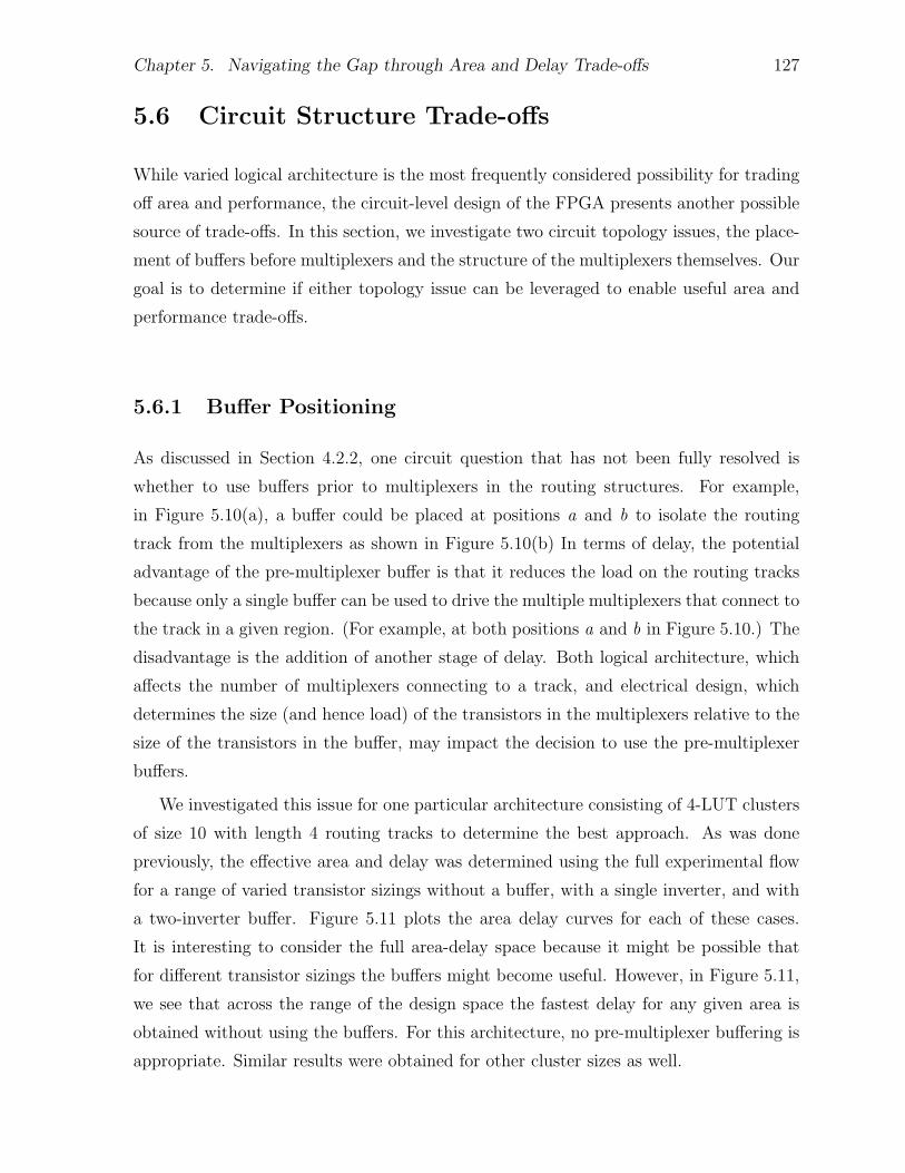
Chapter 5. Navigating the Gap through Area and Delay Trade-offs 127
5.6 Circuit Structure Trade-offs
While varied logical architecture is the most frequently considered possibility for trading
off area and performance, the circuit-level design of the FPGA presents another possible
source of trade-offs. In this section, we investigate two circuit topology issues, the place-
ment of buffers before multiplexers and the structure of the multiplexers themselves. Our
goal is to determine if either topology issue can be leveraged to enable useful area and
performance trade-offs.
5.6.1 Buffer Positioning
As discussed in Section 4.2.2, one circuit question that has not been fully resolved is
whether to use buffers prior to multiplexers in the routing structures. For example,
in Figure 5.10(a), a buffer could be placed at positions a and b to isolate the routing
track from the multiplexers as shown in Figure 5.10(b) In terms of delay, the potential
advantage of the pre-multiplexer buffer is that it reduces the load on the routing tracks
because only a single buffer can be used to drive the multiple multiplexers that connect to
the track in a given region. (For example, at both positions a and b in Figure 5.10.) The
disadvantage is the addition of another stage of delay. Both logical architecture, which
affects the number of multiplexers connecting to a track, and electrical design, which
determines the size (and hence load) of the transistors in the multiplexers relative to the
size of the transistors in the buffer, may impact the decision to use the pre-multiplexer
buffers.
We investigated this issue for one particular architecture consisting of 4-LUT clusters
of size 10 with length 4 routing tracks to determine the best approach. As was done
previously, the effective area and delay was determined using the full experimental flow
for a range of varied transistor sizings without a buffer, with a single inverter, and with
a two-inverter buffer. Figure 5.11 plots the area delay curves for each of these cases.
It is interesting to consider the full area-delay space because it might be possible that
for different transistor sizings the buffers might become useful. However, in Figure 5.11,
we see that across the range of the design space the fastest delay for any given area is
obtained without using the buffers. For this architecture, no pre-multiplexer buffering is
appropriate. Similar results were obtained for other cluster sizes as well.

Chapter 5. Navigating the Gap through Area and Delay Trade-offs 128
ba
Logic
B lock
Logic
B lock
Logic
B lock
Logic
B lock
Logic
B lock
Logic
B lock
(a) Routing Track without Pre-Multiplexer Buffers
ba
Logic
B lock
Logic
B lock
Logic
B lock
Logic
B lock
Logic
B lock
Logic
B lock
(b) Routing Track with Pre-Multiplexer Buffers
Figure 5.10: Buffer Positioning around Multiplexers
5.6.2 Multiplexer Implementation
The implementation of multiplexers throughout the FPGA is another circuit design issue
that has not been conclusively explored. With few exceptions [31, 32], multiplexers have
been implemented using NMOS only pass transistors [14, 28, 18, 33, 15] as described in
Section 2.2. However, this still leaves a wide range of possibilities in the structure of
those NMOS-only multiplexers. The approaches generally differ in the number of levels
of pass transistors through which an input signal must pass. Before exploring the impact
of multiplexer design choices on the overall area and performance of an FPGA, we first
examine the multiplexer design choices in isolation to provide a better understanding of
the potential impact of the choices.

Chapter 5. Navigating the Gap through Area and Delay Trade-offs 129
3.E-09
4.E-09
5.E-09
6.E-09
7.E-09
8.E-09
3.0E+07 5.0E+07 7.0E+07 9.0E+07 1.1E+08 1.3E+08
Eff
ec�
ve
De
lay
(s)
(Ge
om
etr
ic M
ea
n D
ela
y a
s M
ea
sure
d b
y H
SP
ICE
)
Effec�ve Area (um2)
No Inverters 1 inverter 2 inverters
Figure 5.11: Area Delay Trade-offs with Varied Pre-Multiplexer Inverter Usage
General Multiplexer Design Analysis
The three most frequently considered possibilities for a multiplexer are fully-encoded,
2-level and 1-level (or one-hot). Some of their main properties are summarized in Ta-
ble 5.10. The different design styles are given in the different rows of the table and
various properties are summarized in each row. Recall from Section 2.2 that one key
parameter of multiplexers is the number of levels of pass transistors that are traversed
from input to output. This characteristic for the three designs is summarized in the
row of the table labelled “Pass Transistor Levels.” The number of levels is constant
for the 1-level and 2-level designs but, in the fully encoded multiplexer, the number of
inputs to the multiplexer, X, determines the number of levels, dlog2 Xe. The number
of configuration bits required to control each multiplexer design is indicated in the row
labelled “Configuration Bits.” Clearly, the benefit of the fully-encoded multiplexer is
that it requires only dlog2 Xe configuration memory bits compared to 2√
X bits for the

Chapter 5. Navigating the Gap through Area and Delay Trade-offs 130
Table 5.10: Comparison of Multiplexer Implementations (X = Number of MultiplexerInputs)
Property Fully Encoded 2-level 1-level
Pass Transistor Levels dlog2 Xe 2 1Configuration Bits dlog2 Xe 2
√X X
Pass Transistors 2X − 2 X +√
X X
2-level multiplexer3 and X bits for the the 1-level multiplexer. Finally, the row labelled
“Pass Transistors” lists the total number of pass transistors required for the different
multiplexer styles. A fully encoded multiplexer design is worse by this metric as it needs
2X − 2 pass transistors compared to X +√
X and X pass transistors for the 2-level and
1-level designs respectively.
To better illustrate the impact of these differences in the number of configuration
memory bits and the number of pass transistors, Figure 5.12 plots the total number of
transistors (including both configuration bits and pass transistors) per multiplexer input
as a function of the input width of the multiplexer. The transistor count required per
input for the 1-level multiplexer is constant with 6 transistors required for the configura-
tion bit and 1 pass transistor per input. For the 2-level multiplexer, for each width the
topology that yielded the lowest transistor count was used. The number of transistors
required per input tends to decrease as the width of the multiplexer increases. A similar
trend can be seen with the fully encoded multiplexers. These results are also summarized
in Table 5.11. The table lists the various input widths and, for each width, the number
of transistors is given for each of the design styles. For the 2-level and fully encoded
results, the results depend on how the configuration bit is used. The previously plotted
data assumed that data and data from each bit were used. These results are summarized
in the columns labelled “2 O/Bit.” (Note that the 1-level design only uses one output
from each bit and, hence, its results are labelled as “1 O/Bit.”) To better illustrate
the differences between the fully encoded designs and the 2-level designs, the final two
columns of the table report the area savings, in transistor count, when the fully encoded
design is used instead of the 2-level design. For the larger multiplexers, the savings are
relatively constant at around 15 %.
3This is only an approximation of the number of the number of bits required for the 2-level multiplexerbecause the number of bits used at each level of the multiplexer must be a natural number. There arealso different implementations of 2-level multiplexers that will require more memory bits.
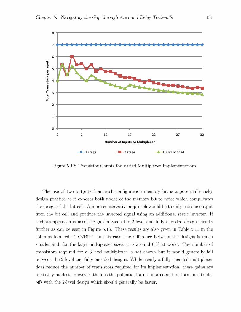
Chapter 5. Navigating the Gap through Area and Delay Trade-offs 131
0
1
2
3
4
5
6
7
8
2 7 12 17 22 27 32
To
tal
Tra
nsi
sto
rs p
er
Inp
ut
Number of Inputs to Mul!plexer
1 stage 2 stage Fully Encoded
Figure 5.12: Transistor Counts for Varied Multiplexer Implementations
The use of two outputs from each configuration memory bit is a potentially risky
design practise as it exposes both nodes of the memory bit to noise which complicates
the design of the bit cell. A more conservative approach would be to only use one output
from the bit cell and produce the inverted signal using an additional static inverter. If
such an approach is used the gap between the 2-level and fully encoded design shrinks
further as can be seen in Figure 5.13. These results are also given in Table 5.11 in the
columns labelled “1 O/Bit.” In this case, the difference between the designs is much
smaller and, for the large multiplexer sizes, it is around 6 % at worst. The number of
transistors required for a 3-level multiplexer is not shown but it would generally fall
between the 2-level and fully encoded designs. While clearly a fully encoded multiplexer
does reduce the number of transistors required for its implementation, these gains are
relatively modest. However, there is the potential for useful area and performance trade-
offs with the 2-level design which should generally be faster.

Chapter 5. Navigating the Gap through Area and Delay Trade-offs 132
0
1
2
3
4
5
6
7
8
2 7 12 17 22 27 32
To
tal
Tra
nsi
sto
rs p
er
Inp
ut
Number of Inputs to Mul!plexer
1 stage 2 stage Fully Encoded
Figure 5.13: Transistor Counts for Varied Multiplexer Implementations using a SingleConfiguration Bit Output
Area Delay Trade-offs using Varied Multiplexer Designs
Area and delay trade-offs in the design of an FPGA were explored for four different
multiplexer design styles. The first style uses 1-level multiplexers for all the multiplexers
in the FPGA. (While the LUT is constructed using a multiplexer, its implementation was
always the standard fully encoded structure.) The second style uses 2-level multiplexers in
every case except for multiplexers with 2 inputs. The third style uses 3-level multiplexers
except for multiplexers with four or fewer inputs which will be implemented using 1-level
or 2-level multiplexers according to their width. Finally the fourth approach uses fully
encoded multiplexers.
These approaches were applied in the design of an FPGA with a logical architecture as
described in Table 5.2. As in the previous investigations, transistor sizing is performed for
a range of design objectives for each multiplexer implementation strategy. The resulting

Chapter 5. Navigating the Gap through Area and Delay Trade-offs 133
Table 5.11: Number of Transistors per Input for Various Multiplexer Widths
Numberof
Inputs
Transistors per Input Improvement of FullyEncoded vs. 2-level1-level 2-level Fully Encoded
1 O/B 2 O/Bit 1 O/Bit 2 O/Bit 1 O/Bit 2 O/Bit 1 O/Bit
3 7 5.3 6.7 5.3 6.7 0% 0%4 7 4.5 5.5 4.5 5.5 0% 0%5 7 6.0 6.4 5.2 6.4 13% 0%6 7 5.3 5.7 4.7 5.7 13% 0%7 7 5.4 5.7 4.3 5.1 21% 10%8 7 5.0 5.3 4 4.8 20% 10%9 7 5.3 5.3 4.4 5.3 17% 0%10 7 4.8 5.0 4.2 5 13% 0%11 7 5.0 5.0 4 4.7 20% 5%12 7 4.8 4.8 3.8 4.5 19% 5%13 7 4.8 4.8 3.7 4.3 23% 10%14 7 4.6 4.6 3.6 4.1 22% 9%15 7 4.4 4.4 3.5 4 21% 9%16 7 4.3 4.3 3.4 3.9 21% 9%17 7 4.3 4.3 3.6 4.2 15% 1%18 7 4.2 4.2 3.6 4.1 15% 1%19 7 4.0 4.0 3.5 4 13% 0%20 7 3.9 3.9 3.4 3.9 13% 0%21 7 4.0 4.0 3.3 3.8 17% 5%22 7 3.8 3.8 3.3 3.7 14% 2%23 7 3.7 3.7 3.2 3.7 14% 2%24 7 3.7 3.7 3.2 3.6 14% 2%25 7 3.6 3.6 3.1 3.5 13% 2%26 7 3.6 3.6 3.1 3.5 15% 4%27 7 3.6 3.6 3.0 3.4 15% 4%28 7 3.5 3.5 3.0 3.4 14% 4%29 7 3.4 3.4 3.0 3.3 13% 3%30 7 3.4 3.4 2.9 3.3 13% 3%31 7 3.4 3.4 2.9 3.2 15% 6%32 7 3.4 3.4 2.9 3.2 15% 6%
area-delay trade-off curves are shown in Figure 5.14. Note that for this architecture the
largest multiplexer is the BLE Input multiplexer with 32 inputs.
The data in the figure indicates that the 1-level multiplexers offer a potential speed
advantage but the area cost for this speed-up is significant. Based on the previously de-
fined criteria of interesting designs, the 1-level multiplexer design does not offer a useful
trade-off. Similarly, the 3-level design offers area savings but these area savings are not
sufficient to justify the diminished performance. The fully encoded multiplexer designs
suffer significantly in terms of delay and, while they do yield the absolute smallest de-
signs, the area savings never overcome the delay penalty. Clearly, the 2-level multiplexer
implementation strategy is the most effective and, for that reason, all the work in this

Chapter 5. Navigating the Gap through Area and Delay Trade-offs 134
2E-09
4E-09
6E-09
8E-09
1E-08
1.2E-08
1.4E-08
3.E+07 4.E+07 5.E+07 6.E+07 7.E+07 8.E+07 9.E+07 1.E+08
Eff
ec�
ve
De
lay
(s)
(Ge
om
etr
ic M
ea
n D
ela
y a
s M
ea
sure
d b
y H
SP
ICE
)
Effec�ve Area (um2)
2-level 1-level 3-level Fully Encoded
Figure 5.14: Area Delay Trade-offs with Varied Multiplexer Implementations
chapter used the 2-level multiplexer topology. For any given multiplexer size, there are
a number of different 2-level topologies. The impact of these topologies is analyzed in
Appendix C and it was found to be relatively modest. Therefore, varied 2-level strategies
are not explored further.
5.7 Trade-offs and the Gap
The previous sections of this chapter have demonstrated that there are a wide range
of interesting area and delay trade-offs that can be made through varied architecture
and transistor sizing. One goal in examining the trade-offs was to understand how these
trade-offs could be used to selectively narrow the area and delay gaps and, in this section,
we investigate the impact of the trade-off ranges observed on the gap measurements from
Chapter 3.
The preceding work in this section has demonstrated that the design space for FPGAs
is large and, by simply varying the transistor sizing of a design, the area and delay of an
FPGAs can be altered dramatically. This presents a challenge to exploring the impact
of the trade-off ranges because the area and delay gap measurements were performed for

Chapter 5. Navigating the Gap through Area and Delay Trade-offs 135
a single commercial FPGA family, the Stratix II, and the trade-off decisions made by
the Stratix II’s designers and architects to conserve area or improve performance are not
known. As a result, the specific point occupied by this family within the large design
space is unknown.
To address this issue, we consider a range of circumstances for the possible trade-offs
that could be applied to the area delay gap. For example, in one case, it is assumed that
the Stratix II was designed to be at the performance extreme of the interesting region.
Based on that assumption, it could be possible to narrow the area gap by trading off
performance for area savings and create a design that is instead positioned at the area
extreme of the region. We compute the possible narrowed gap by applying the trade-off
range factors determined previously in this chapter. This is done as follows
Area Gap with Trade-off =Measured Area Gap
Area Range(5.5)
Delay Gap with Trade-off = Measured Delay Gap ·Delay Range. (5.6)
These trade-offs clearly narrow the gap in only one dimension and in the other dimension
the gap grows larger. If we were to assume that the Stratix II was designed with a greater
focus on area, then the trade-offs would be applied in the opposite manner with the area
gap growing and the delay gap narrowing by the area range and delay range factors
respectively.
The results for a variety of cases are summarized in Table 5.12. The row labelled
“Baseline” repeats the area and delay gap measurements for soft-logic only as reported
in Chapter 3. The subsequent rows list the area and delay gaps when the area and delay
trade-offs are used. The “Starting Point” column refers to the position within the design
space that the FPGA occupies before making any trade-offs and the “Ending Point”
describes the position in the design space after making the trade-offs. Three positions
within the design space are considered: Area, Delay and Area-Delay. The Area and
Delay points refer to the smallest and fastest positions (that still satisfy the interesting
trade-off requirements) in the design space respectively and the Area-Delay point refers
to the point within the design space with minimal Area-Delay. For the example described
above, the starting point would be the “Delay” point and the ending point would be the
“Area” point. When making trade-offs from the Area point to the Delay point or vice

Chapter 5. Navigating the Gap through Area and Delay Trade-offs 136
Table 5.12: Potential Impact of Area and Delay Trade-offs on Soft Logic FPGA to ASICGap
Starting Point Ending Point Area Gap Delay Gap
Baseline 35 3.4
Delay Area 18 7.1Delay Area-Delay 21 4.8
Area-Delay Area 29 5.2Area-Delay Delay 59 2.4
Area Delay 70 1.6
versa, the full area and delay range factors would be applied. For trade-offs involving
the Area-Delay point then only the range to or from that point would be considered.
For example, if starting at the “Delay” point and ending at the “Area-Delay” point the
partial ranges would be calculated as:
Partial Area Range =Area of Largest Design
Area of Area-Delay Design, (5.7)
Partial Delay Range =Delay of Area-Delay Design
Delay of Fastest Design(5.8)
and these ranges would be applied as per Equations 5.5 and 5.6 to determine the gap
after making the trade-offs.
From the data in the table, it is clear that leveraging the trade-offs can allow the area
and delay gap to vary significantly. In particular, it is most interesting to consider starting
from the delay optimized point in the design space because the Stratix II is Altera’s higher
performance/higher cost FPGA family [16] at the 90 nm technology node. In that case,
the area gap can be shrunk to 18 for soft logic and, if such trade-offs were combined
with the appropriate use of heterogeneous blocks, the overall area gap would shrink even
lower. The row in the table with an “Area” starting point and a “Delay” ending point
suggests that the delay gap could be narrowed (at the expense of area); however, this is
unlikely to be possible as the Stratix II is sold as a high performance part which suggests
its designers were not focused primarily on conserving area.
The extent of the trade-offs possible with power consumption was not examined ex-
tensively. However, it was observed that for a number of difference architectures and
sizings changes in power consumption were closely related to changes in area. If this
relationship is assumed to apply in general, then it follows that the range in power con-

Chapter 5. Navigating the Gap through Area and Delay Trade-offs 137
Table 5.13: Area and Delay Trade-off Ranges Compared to Commercial Devices
This Work Commercial DevicesArea-Delay vs. Delay Cyclone II vs. Stratix II
Delay Range 1.41 1.40Area Range 1.68 N/A
sumption from greatest consumption to least consumption varies by the same factor of
2.0 as the area range. This estimated power range can also be applied to the power
gap measurements from Chapter 3. If we apply the trade-offs from the delay optimized
extreme of the design space to the area optimized extreme, then the dynamic power con-
sumption gap could potentially narrow from 14 down to 7.0. While this highlights that
it may be possible to reduce the power gap significantly, this is only a very approximate
estimate of the possible changes and future work is needed to more accurately assess
these possibilities.
5.7.1 Comparison with Commercial Families
While the reduction in the area gap is useful, the impact on the delay gap is also sig-
nificant. It is useful to compare these trade-offs to those found in commercial FPGA
families. Altera has two 90 nm FPGA families, the high performance/high cost Stratix
II [16] and the lower cost/lower performance Cyclone II [143]. For the benchmarks used
in Chapter 3, the Stratix II was on average approximately 40 % faster than the Cyclone
II. This means that the delay range between these parts was 1.40. This closely matches
the delay range of 1.41 we observed between the largest/fastest design and the minimal
area-delay design. This result is summarized in Table 5.13.
Unfortunately, the core area for the Cyclone II is not known and, therefore, a direct
area comparison is not possible. However, an approximate measure of the area difference
can be made by comparing the prices of the different parts. The parts with the most
similar logic capabilities are the Stratix II 2S30 and Cyclone II 2C35, and the Stratix II
2S15 and Cyclone II 2C15. Using prices from http://www.buyaltera.com/ (an autho-
rized distribution site for Altera parts) for these sets of parts, the Stratix II was found
to have a price that is 4–6 times higher than the Cyclone II4. This only provides an
4Both sets of parts have a similar number of (equivalent) logic elements but the Stratix II containedmore memory and more multipliers; therefore, the range should be considered an upper bound on theprice difference.

Chapter 5. Navigating the Gap through Area and Delay Trade-offs 138
approximate indication of the area difference as price is affected by a number of factors
including profit margins, package costs, I/O differences and other differences in core logic
capabilities and, therefore, the true area difference is certainly smaller than the price dif-
ference suggests. Given these caveats, the 1.68 × area difference we observed between
the largest design and minimal area-delay design appears realistic.
5.8 Summary
In this chapter, we have explored the trade-offs between area and delay that are possible in
the design of FPGAs when both architecture and transistor sizing are varied. Compared
to past pure architectural studies, it was found that varying the transistor sizing of a
single architecture offers a greater range of possible trade-offs between area and delay
than was possible by only varying the architecture. By varying the architecture along
with the transistor sizings, we see that performance could be usefully varied by a factor
of 2.1 and area by a factor of 2.0. These trade-off ranges can be used to selectively
shrink the gap between FPGAs and ASICs to create slower and smaller FPGAs or faster
and larger FPGAs as desired. Specifically, for the soft logic of the FPGA the area gap
could shrink as low as 18 by taking advantage of these trade-offs. When making these
trade-offs, LUT size was found to be by far the most useful architectural parameter.

Chapter 6
Conclusions and Future Work
The focus of this thesis is on gaining a better understanding of the area, performance
and power consumption gap between FPGAs and ASICs. The first step in doing this
was to measure the gap. It was found that heterogeneous hard blocks can be useful
tools in narrowing the area gap but, regardless, the area, performance and power gap
for soft logic remains large. To address this large gap, the latter portion of this thesis
explored the opportunities to trade-off area and delay through varied transistor-level and
architectural trade-offs. Such trade-offs allow the gap to be navigated by improving one
attribute at the expense of another. The most significant contributions that were made
in this work are summarized in the following section.
6.1 Contributions
One significant result from this thesis has been in the most thorough analysis to date
of the area, performance and power consumption differences between FPGAs to ASICs.
It was found that designs implemented using only the soft logic of an FPGA used 35
times more area, were 3.4–4.6 times slower and used 14 times more dynamic power than
equivalent ASIC implementations. When designs also employed hard memory and multi-
plier blocks, it was observed that the area gap could be shrunk considerably. Specifically,
it was found that the area gap was 25 for circuits that used hard multiplier blocks, 33
for circuits that used hard memory blocks and 18 for circuits that used both multipliers
and memory blocks. These reductions in the area gap occurred even though none of the
benchmark circuits used all the available hard blocks on an FPGA. If it is optimistically
assumed that all hard blocks in the target FPGA were fully used then the area gap could
139

Chapter 6. Conclusions and Future Work 140
potentially shrink as low as 4.7 when only the core logic is considered or as low as 2.8
when the peripheral circuitry is also optimistically assumed to be fully used. Contrary to
popular perception, it was found that hard blocks did not offer significant performance
benefits as the average performance gap for circuits that used memory and multiplier
hard blocks was only 3.0–4.1. The hard blocks did appear to enable appreciable im-
provements to the dynamic power gap which was measured to be on average 7.1 for the
circuits that used both multiplier and memory hard blocks. This work was published in
[144, 145].
The automated transistor sizing tool for FPGAs developed as part of this dissertation
led to a number of contributions. This work was the first to consider the automated
transistor sizing of complete FPGAs and this raised a number of previously unexplored
issues. One such issue in particular is the impact of an FPGA’s programmability on
the transistor-level optimization choices. Due to the programmability, it is not known
what the critical paths of the FPGA will be when the FPGA is being designed. One
effective solution, the use of a representative path delay, was developed and described in
this work. In terms of optimization algorithms, a two-phased approach to optimization
that optimized sizes first based on RC transistor models and then using full simulation
with accurate models was developed. It was shown that this approach produced results
on par or better than past manual designs. As a direct contribution to the community, a
range of optimized designs created by the sizing tool was released at http://www.eecg.
utoronto.ca/vpr/architectures. These contributions were summarized in [146].
Finally, this thesis also demonstrated the large range of trade-offs that can be made
between area and performance. In past investigations, trade-offs had generally been
achieved through logical architecture changes but this work found that a significantly
wider range of trade-offs were possible when logical architecture and transistor sizing
changes were explored together. This broader range of trade-offs is significant as it
indicated the possibility of selectively narrowing the FPGA to ASIC gap. The analysis
of the trade-offs was also unique in that a quantitative method was used to determine if
a trade-off was useful and interesting. This work was published in [147].
6.2 Future Work
The outcomes of this research suggest a number of directions for future research both in
understanding the gap between FPGAs and ASICs and in narrowing it.

Chapter 6. Conclusions and Future Work 141
6.2.1 Measuring the Gap
The measurements of the FPGA to ASIC gap described in Chapter 3 offered one of the
most thorough measurements of this gap to date; however, further research in specific
areas could be useful to improve the understanding this gap. One of the issues raised in
Chapter 3 was the size of the benchmarks used in the comparison. The largest benchmark
used 9 656 ALMs while the largest currently announced FPGA with 272 440 ALMs [17]
offers over an order of magnitude more resources. Since FPGAs are architected to handle
those larger circuits, it could be informative to measure the gap using benchmarks that
fully exercise the capacity of the largest FPGAs. Additionally, it could also be interesting
to measure the gap with benchmarks that make more use of the hard blocks in the FPGA
since the benchmark circuits for the current work often did not use the hard blocks
extensively.
Another issue is that the measurement of the gap focused only on core logic and it
could be informative to extend the work to consider the I/O portions of the design. It
is possible that for designs that demand a large number of I/O’s the area gap could
effectively shrink if the design is pad limited. As well, for more typical core-limited
designs, I/O blocks may also impact the gap as they are essentially a form of hard block.
While an optimistic analysis of this effect was performed in Chapter 3, a more thorough
analysis as was done for the core logic could provide greater insight into the impact of
the I/O on the FPGA to ASIC gap. This could be particularly useful as the architecture
of the I/O’s has not been studied extensively and, with more quantitative assessments of
its role, new architectural enhancements may be discovered.
The area, performance and power consumption gap was also only measured at one
technology node, 90 nm CMOS, and there are many reasons why it could be useful to
explore the gap in another technology nodes. In [3], some measurements of the area,
performance and power gap were made in technologies ranging from 250 nm down to
90 nm and, as described in Section 2.6, there was significant variability observed between
technology nodes, particularly for area and performance. The reason for this variability is
unknown and more accurate measurements might uncover the reasons for the differences.
The knowledge of the cause of the difference, could point to possibilities for improving
FPGAs.
Furthermore, it would also be interesting to remeasure the gap in more modern tech-
nologies. Recent FPGAs in 40 nm and 65 nm CMOS have added programmable power

Chapter 6. Conclusions and Future Work 142
capabilities [17, 6] which allow portions of the FPGA to be programmably slowed down
to reduce leakage power. The programmability is accomplished through the use of body
biasing [148] which adds area overhead as additional wells and spacing are necessary to
support this adjustable body biases. There has been some work that has considered the
area impact of these schemes [149, 150] but to date no direct comparisons with ASICs
have been reported. Such comparisons could be interesting since, while body biasing
may be necessary to combat leakage power in ASICs, the fine-grained programmability
present in the FPGA would not be required and, hence, the area gap may potentially be
larger in the latest technologies.
This thesis focused exclusively on SRAM-based FPGAs as they dominate the mar-
ket; however, the development of flash and antifuse-based FPGAs [151, 152, 153] has
continued. Measuring the gap for such FPGAs would be interesting as they potentially
offer area savings. In addition to this, there are also a number of single or near-single
transistor one-time programmable memory designs that promise full compatibility with
standard CMOS processes [154, 155]. (The lack of CMOS compatibility has been one
of the major issues limiting the use of the flash and traditional antifuse-based FPGAs.)
While no current FPGAs make use of these memories as their sole configuration memory
storage, they could potentially be useful in future FPGA and investigating their impact
on the area, performance and power of FPGAs relative to ASICs could be informative.
The gap measurements were centred on three axes, area, performance and power con-
sumption, for the core logic. However, these measurements are only indirect measures of
the true variables that affect FPGA usage which are their system-level cost, performance
and power consumption. The addition of measurements that include the impact of the
I/O portion of the design as suggested previously would partially address this issue as
it would provide a better measure of system-level performance and power consumption.
However, silicon area is not always a reliable measure of system-level cost. For small de-
vices, the costs of the package can be a significant portion of the total device cost. Since
these costs may be similar for both ASICs and FPGAs, this could reduce the effective
cost gap between the implementation media. As well, it has long been known that yield
decreases at an exponential rate with increasing area [156] and that causes greater than
linear cost increases with increased area. Some FPGAs are able to mitigate this issue
through the use of redundancy [157, 158, 159] to correct faults. Such techniques increase
area but presumably lower costs. In contrast, the irregular nature of logic in ASICs likely
prevents the use of such techniques in ASICs. Clearly, there is a great deal of complexity

Chapter 6. Conclusions and Future Work 143
to the area and cost relationship and a more detailed analysis of these area and cost
issues could be informative.
Finally, as described in Chapter 3, measurements of the static power consumption gap
were inconclusive and more definitive measures of that axis would be useful in the future.
However, there are many challenges to getting reliable and comparable static power
measurements. One of the central challenges is that it is difficult to compare results
for parts from different foundries unless the accuracy of the estimates is well defined.
This is crucial as the goal in the static power comparison would be to compare FPGA
and ASIC technology and not any underlying foundry-specific issues. This particular
issue could be addressed by performing the comparison with both the FPGA and ASIC
implemented in the same process from the same foundry. However, this would not fully
address all issues because the FPGA manufacturers, due to technical or business factors,
may eliminate parts with unacceptable leakage. The removal of those leaky parts would
reduce the static power measurements for the FPGA but, since the same could also be
done for an ASIC, any static power consumption comparison must ensure that the results
are not influenced by such issues. Therefore, a fair comparison may require SPICE level
simulations of both the FPGA and the ASIC using identical process technology libraries.
A fair comparison such as that would certainly be useful as static power consumption
has become a significant concern in the latest process technology nodes.
6.2.2 Navigating the Gap
In addition to the avenues for future research in measuring the gap, there are also op-
portunities to explore in selectively narrowing the gap through design trade-offs. The
simplest extension would be to consider an even broader range of logical architectures.
One potential avenue is the use of routing segments with a mix of segment lengths, which
is common in commercial FPGAs [17, 7]. As well, changes to the logic cluster such as
intra-cluster depopulation [19, 20], the use of arithmetic carry chains and the addition
of dedicated arithmetic logic within the logic block warrant exploration. These ideas
have all been adopted in high-performance FPGAs [20, 15, 7, 17] but the impact of these
approaches on the area-delay design space and the associated trade-offs have not been
investigated.
Future research is also needed to investigate the impact of hard blocks such as mul-
tipliers and memories on the trade-offs that are possible. It was seen in Chapter 3 that

Chapter 6. Conclusions and Future Work 144
these hard blocks offer significant area benefits but that work only considered a sin-
gle architecture. With varied logical architectures and transistor sizings the role of hard
blocks throughout the design space could be better understood. A notation and language
that captures the issues of the supply and the demand of these blocks was introduced in
[160, 47] and that framework would certainly be useful for explorations of the impact of
hard blocks on the design space.
There is also clearly work that can be done exploring trade-offs of area and per-
formance with power consumption. As described previously, in many cases power and
area are closely related; however, there are a number of techniques that can alter this
relationship. In particular, the use of programmable body biasing [149, 150, 148] or
programmable VDD connections [161, 162, 163] can change the area, performance and
power relationships. While many of these ideas have been studied independently, the
use of these techniques has not been examined throughout the design space. For exam-
ple, it is not clear which techniques are useful for area constrained designs or what the
performance impact is with these techniques when no area increase is permitted.
An additional dimension for trade-offs that was not explored in this work was that of
the time required to implement (synthesize, place and route) designs on an FPGA. This
time, typically referred to as compile time, can be significantly impacted by architectural
changes such as altering the cluster size [164] or the number of routing resources. This
could enable interesting trade-offs as area savings could be made at the expense of in-
creased compile time but future research is needed to determine if any of these trade-offs
are viable. This will become particularly important as single-processor performance is
no longer growing at the same rate as FPGAs are increasing in size. If that discrepancy
is left unaddressed, it will lead to increased compile times and that could then threaten
to diminish one of the key advantages of FPGAs which is their fast design time.
There are also many opportunities for further research into the optimizer used to
perform transistor sizing. While the optimizer described in Chapter 4 delivered results
that were better or at worse comparable to past manually optimized designs, there is still
room for future improvement. In particular, little attention was paid to the run time of
the tool and research to develop alternative algorithms that lower the run time require-
ments would be useful. Another possibility for future research is the investigation of new
approaches to optimization that better handle the programmability of FPGAs. This
could allow optimization to be performed on hard blocks such as multipliers. Ultimately,
an improved optimizer could prove useful in the design of commercial FPGAs.

Chapter 6. Conclusions and Future Work 145
6.3 Concluding Remarks
This thesis has demonstrated that, while a large area, performance and power consump-
tion gap exists between FPGAs and ASICs, there is the potential to selectively narrow
these gaps through architectural and transistor-level changes. As described in the previ-
ous section there are many promising areas for future research that may provide a deeper
understanding of both the magnitude of the FPGA to ASIC gap and the trade-offs that
can be used to narrow it. This coupled with innovation in the architecture and design of
FPGAs may enable the broader use of FPGAs.

Appendix A
FPGA to ASIC Comparison Details
This appendix provides information on the benchmarks used for the FPGA to ASIC
comparisons in Chapter 3. As well, some of the absolute data from that comparison
is provided; however, area results are not included as that would disclose confidential
information.
A.1 Benchmark Information
Information about each of the benchmarks used in the FPGA to ASIC comparisons is
listed in Table A.1. For each benchmark, a brief description of what the benchmark does
is given along with information about its source. Most of the benchmarks were obtained
from OpenCores (http://www.opencores.org/) while the remainder of the benchmarks
came from either internal University of Toronto projects [98, 99, 95, 96] or external bench-
mark projects at http://www.humanistic.org/∼hendrik/reed-solomon/index.html
or http://www.engr.scu.edu/mourad/benchmark/RTL-Bench.html. As noted in the
table, in some cases, the benchmarks were not obtained directly from these sources and,
instead, were modified as part of the work performed in [47]. The modifications included
the removal of FPGA vendor-specific constructs and the correction of any compilation
issues in the designs.
A.2 FPGA to ASIC Comparison Data
The results in Chapter 3 were given only in relative terms. This section provides the raw
data underlying these relative comparisons. Table A.2 and Table A.3 list the maximum
146
Appendix A. FPGA to ASIC Comparison Details 147
Table A.1: Benchmark Descriptions
Benchmark Description
booth 32-bit serial Booth-encoded multiplier created by the authorrs encoder (255,239) Reed Solomon encoder from OpenCorescordic18 18-bit CORDIC algorithm implementation from OpenCorescordic8 8-bit CORDIC algorithm implementation from OpenCoresdes area DES Encryption/Decryption designed for area from OpenCores with mod-
ifications from [47]des perf DES Encryption/Decryption designed for performance from OpenCores
with modifications from [47]fir restruct 8-bit 17-tap finite impulse response filter with fixed coefficients from http:
//www.engr.scu.edu/mourad/benchmark/RTL-Bench.html with modifi-cations from [47]
mac1 Ethernet Media Access Control (MAC) block from OpenCores with modi-fications from [47]
aes192 AES Encryption/Decryption with 192-bit keys from OpenCoresfir3 8-bit 3-tap finite impulse response filter from OpenCores with modifications
from [47]diffeq Differential equation solver from OpenCores with modifications from [47]diffeq2 Differential equation solver from OpenCores with modifications from [47]molecular Molecular dynamics simulator [95]rs decoder1 (31,19) Reed Solomon decoder from http://www.humanistic.org/
∼hendrik/reed-solomon/index.html with modifications from [47]rs decoder2 (511,503) Reed Solomon decoder http://www.humanistic.org/
∼hendrik/reed-solomon/index.html with modifications from [47]atm High speed 32x32 ATM packet switch based on the architecture from [100]aes AES Encryption with 128-bit keys from OpenCoresaes inv AES Decryption with 128-bit keys from OpenCoresethernet Ethernet Media Access Control (MAC) block from OpenCoresserialproc 32-bit RISC processor with serial ALU [99, 98]fir24 16-bit 24-tap finite impulse response filter from OpenCores with modifica-
tions from [47]pipe5proc 32-bit RISC processor with 5 pipeline stages [99, 98]raytracer Image rendering engine [96]
operating frequency and dynamic power, respectively, for each design for both the FPGA
and ASIC. Finally, Tables A.4 and A.5 report the FPGA and ASIC absolute static power
measurements for each benchmark at typical and worst case conditions respectively. The
static power measurements for the FPGAs include the adjustments to account for the
partial utilization of each device as described in Section 3.4.3. Finally, Table A.6 sum-
marizes the results when retiming was used with the FPGA CAD flow as described in
Section 3.5.2. The benchmark size (in ALUTs), the operating frequency increase and the
total register increase are listed for each of the benchmarks.

Appendix A. FPGA to ASIC Comparison Details 148
Table A.2: FPGA and ASIC Operating Frequencies
BenchmarkMaximum Operating
Frequency (MHz)FPGA ASIC
booth 188.71 934.58rs encoder 288.52 1098.90cordic18 260.08 961.54cordic8 376.08 699.30des area 360.49 729.93des perf 321.34 1000.00fir restruct 194.55 775.19mac1 153.21 584.80aes192 125.75 549.45fir3 278.40 961.54diffeq 78.23 318.47diffeq2 70.58 281.69molecular 89.01 414.94rs decoder1 125.27 358.42rs decoder2 101.24 239.23atm 319.28 917.43aes 213.22 800.00aes inv 152.28 649.35ethernet 168.58 704.23serialproc 142.27 393.70fir24 249.44 645.16pipe5proc 131.03 378.79raytracer 120.35 416.67

Appendix A. FPGA to ASIC Comparison Details 149
Table A.3: FPGA and ASIC Dynamic Power Consumption
BenchmarkDynamic Power
Consumption(W)FPGA ASIC
booth 5.10E-03 1.71E-04rs encoder 4.63E-02 1.88E-03cordic18 6.75E-02 1.08E-02cordic8 1.39E-02 2.44E-03des area 3.50E-02 1.32E-03des perf 1.22E-01 1.31E-02fir restruct 2.47E-02 2.56E-03mac1 8.94E-02 4.63E-03aes192 1.04E-01 3.50E-03fir3 7.91E-03 1.06E-03diffeq 4.53E-02 3.86E-03diffeq2 5.18E-02 4.16E-03molecular 4.55E-01 2.76E-02rs decoder1 3.48E-02 2.20E-03rs decoder2 4.74E-02 4.29E-03atm 5.59E-01 3.71E-02aes 6.32E-02 6.71E-03aes inv 7.65E-02 1.13E-02ethernet 9.17E-02 5.91E-03serialproc 3.42E-02 2.16E-03fir24 1.18E-01 2.22E-02pipe5proc 5.11E-02 6.23E-03raytracer 8.99E-01 1.08E-01
Table A.4: FPGA and ASIC Static Power Consumption – Typical
BenchmarkStatic Power
Consumption (W)FPGA ASIC
rs encoder 1.31E-02 2.61E-04cordic18 4.43E-02 5.73E-04des area 1.14E-02 1.25E-04des perf 5.52E-02 1.08E-03fir restruct 1.40E-02 2.03E-04mac1 3.52E-02 4.08E-04aes192 1.61E-02 1.90E-04diffeq2 1.15E-02 3.63E-04molecular 1.27E-01 1.83E-03rs decoder1 1.74E-02 7.47E-05rs decoder2 2.31E-02 1.91E-04atm 2.46E-01 1.08E-03aes 1.67E-02 5.06E-04aes inv 2.06E-02 6.68E-04ethernet 5.11E-02 2.94E-04fir24 2.18E-02 1.66E-03pipe5proc 2.06E-02 1.27E-04raytracer 1.69E-01 1.74E-03

Appendix A. FPGA to ASIC Comparison Details 150
Table A.5: FPGA and ASIC Static Power Consumption – Worst Case
BenchmarkStatic Power
Consumption (W)FPGA ASIC
rs encoder 3.46E-02 1.00E-02cordic18 1.17E-01 2.27E-02des perf 1.45E-01 4.16E-02fir restruct 3.70E-02 7.86E-03mac1 9.28E-02 1.56E-02aes192 5.00E-02 7.51E-03diffeq 2.45E-02 1.44E-02diffeq2 3.04E-02 1.40E-02molecular 3.95E-01 7.19E-02rs decoder1 4.60E-02 3.02E-03rs decoder2 6.10E-02 7.46E-03atm 7.70E-01 4.61E-02aes 5.21E-02 1.93E-02aes inv 6.42E-02 2.58E-02ethernet 1.35E-01 1.07E-02fir24 6.80E-02 6.52E-02pipe5proc 5.44E-02 9.20E-03raytracer 7.14E-01 N/A

Appendix A. FPGA to ASIC Comparison Details 151
Table A.6: Impact of Retiming on FPGA Performance
BenchmarkBenchmarkCategory
ALUTsOperating Frequency
Increase (%)Register CountIncrease (%)
des area Logic 469 1.2 % 0.0 %booth Logic 34 0.0 % 0.0 %rs encoder Logic 683 0.0 % 0.0 %fir scu rtl Logic 615 14 % 89 %fir restruct1 Logic 619 11 % 64 %fir restruct Logic 621 15 % 76 %mac1 Logic 1852 0.0 % 0.0 %cordic8 Logic 251 0.0 % 0.0 %mac2 Logic 6776 0.0 % 0.0 %md5 1 Logic 2227 23 % 21 %aes no mem Logic 1389 0.0 % 0.0 %raytracer framebuf v1 Logic 301 3.0 % 0.0 %raytracer bound Logic 886 0.0 % 0.0 %raytracer bound v1 Logic 889 0.0 % 0.0 %cordic Logic 907 0.0 % 0.0 %aes192 Logic 1090 9.7 % 30 %md5 2 Logic 858 10 % 13 %cordic Logic 1278 0.0 % 0.0 %des perf Logic 1840 −0.5 % 1.0 %cordic18 Logic 1169 0.0 % 0.0 %aes inv no mem Logic 1962 0.0 % 0.0 %fir3 DSP 52 −14 % −40 %diffeq DSP 219 0.0 % 0.0 %iir DSP 284 0.0 % 0.0 %iir1 DSP 218 0.0 % 0.0 %diffeq2 DSP 222 0.0 % 0.0 %rs decoder1 DSP 418 5.4 % 7.5 %rs decoder2 DSP 535 −0.3 % 11 %raytracer gen v1 DSP 1625 0.0 % 0.0 %raytracer gen DSP 1706 0.0 % 0.0 %molecular DSP 6289 1.3 % 14 %molecular2 DSP 6557 24 % 71 %stereovision1 DSP 2934 36 % 19 %stereovision3 Memory 82 10 % 9.3 %serialproc Memory 671 −2.0 % 16 %raytracer framebuf Memory 457 12 % 0.0 %aes Memory 675 0.0 % 0.0 %aes inv Memory 813 0.0 % 0.0 %ethernet Memory 1650 −0.6 % 4.1 %faraday dma Memory 1987 0.5 % 0.9 %faraday risc Memory 2596 −1.0 % 1.3 %faraday dsp Memory 7218 −2.9 % −0.1 %stereovision0 v1 Memory 2919 −1.6 % 0.2 %atm Memory 10514 4.7 % 1.1 %stereovision0 Memory 19969 3.7 % 0.4 %oc54 cpu DSP & Mem 1543 0.0 % 0.0 %pipe5proc DSP & Mem 746 5.5 % 49 %fir24 DSP & Mem 821 −7.4 % −3.3 %fft256 nomem DSP & Mem 966 0.0 % 0.0 %raytracer top DSP & Mem 11438 14 % 0.0 %raytracer top v1 DSP & Mem 11424 11 % −0.3 %raytracer DSP & Mem 13021 3.0 % −0.6 %fft256 DSP & Mem 27479 0.0 % 0.0 %stereovision2 v1 DSP & Mem 27097 117 % 131 %stereovision2 DSP & Mem 27691 97 % 124 %

Appendix B
Representative Delay Weighting
The programmability of FPGAs means that the eventual critical paths are not known
at design time. However, a delay measurement is necessary if the performance of an
FPGA is to be optimized. A solution described in Section 4.3.2 was to create a path
containing all the possible critical path components. The delays of the components were
then combined as a weighted sum to reflect the typical usage of each component and that
weighted sum, which was termed the representative delay, was used as a measure of the
FPGAs performance during optimization. This appendix investigates the selection of the
weights used to compute the representative delay. As a starting point, the behaviour of
benchmark circuits is analyzed. That analysis provided one set of possible weights that
are then tested along with other possible weightings in Section B.2. The results from the
different weightings are compared and conclusions are made.
B.1 Benchmark Statistics
The representative delay is intended to capture the behaviour of typical circuits imple-
mented on the FPGA. Therefore, to determine appropriate values for the delay weight-
ings, it is useful to examine the characteristics of benchmark circuits. The focus in this
examination will be on how frequently the various components of the FPGA appear on
the critical paths of circuits. In particular, for the architecture we will consider, there are
four primary components whose usage effectively determines the usage of all the compo-
nents of the FPGA. These four components are the routing segments, the CLB1 inputs,
1Recall that a Cluster-based Logic Block (CLB) is the only type of logic block considered in thiswork.
152

Appendix B. Representative Delay Weighting 153
Table B.1: Normalized Usage of FPGA Components
Benchmark LUTs Routing Segments CLB Inputs CLB Outputs
alu4 0.20 0.43 0.14 0.23apex2 0.17 0.49 0.15 0.20apex4 0.17 0.46 0.17 0.20bigkey 0.12 0.53 0.18 0.18clma 0.19 0.44 0.14 0.22des 0.17 0.46 0.17 0.20diffeq 0.34 0.13 0.13 0.39dsip 0.12 0.53 0.18 0.18elliptic 0.25 0.31 0.15 0.29ex1010 0.16 0.55 0.12 0.18ex5p 0.16 0.47 0.18 0.18frisc 0.25 0.25 0.21 0.28misex3 0.18 0.42 0.18 0.21pdc 0.14 0.59 0.12 0.15s298 0.22 0.33 0.20 0.25s38417 0.22 0.33 0.18 0.27s38584.1 0.20 0.34 0.22 0.24seq 0.18 0.44 0.18 0.21spla 0.14 0.54 0.16 0.16tseng 0.26 0.26 0.17 0.31
Minimum 0.12 0.13 0.12 0.15Maximum 0.34 0.59 0.22 0.39Average 0.19 0.42 0.17 0.23
the CLB Outputs and the LUT. The usage of LUT will be examined in detail later in
this section.
The usage of these key components was tracked for the critical paths of the 20 MCNC
benchmark circuits [138] when implemented on the standard baseline architecture de-
scribed in Table 5.2. For each benchmark, the number of times each of the components
appear on the critical path was recorded. These numbers were normalized to the total
number of components on the benchmark’s critical path to allow for comparison across
benchmarks with different lengths of critical paths and the results are summarized in Ta-
ble B.1. The final three rows of the table indicate the minimum, maximum and average
normalized usage of each component. Clearly, there is a great deal of variation between
the benchmarks, in particular, in the relative demands placed on the LUTs versus the
routing segments. The optimization of an FPGA must attempt to balance these different
needs and, therefore, it seems appropriate to consider using these average path statistics
to determine the representative delay weights. Before examining the use of these weights,
the LUT usage will be more thoroughly investigated.

Appendix B. Representative Delay Weighting 154
SR AM bit
SR AM
bit
SR AM
bit
SR AM bit
SR AM
bit
SR AM
bit
SR AM bit
SR AM
bit
F ast InputSlow Input
LU T
Output
Figure B.1: Input-dependant Delays through the LUT
LUT Usage
In the previous results, the usage of the LUT was assumed to be the same in all cases.
However, in reality, the specific input to the LUT that is used has a significant effect on
the delay of a signal through the LUT. The reason for these differences is the imple-
mentation of the LUT as a fully encoded multiplexer structure and this is illustrated in
Figure B.1. These speed differences can be significant and, therefore, it is advantageous
to use the faster inputs on performance critical nets. Commercial CAD tools generally
perform such optimization [101] when possible and, as a result, the faster LUT inputs
appear more frequently on the critical path. This usage of some LUT inputs more than
other inputs has potentially important optimization implications because area can be
potentially conserved on less frequently used paths through the LUT. As the LUT uses
a significant portion of the FPGA area, such area savings can impact the overall area
and performance of the FPGA.
To address this, the usage of the LUT inputs was examined. Unfortunately, the
CAD tools used in this work do not recognize the timing differences between the LUT
inputs and, therefore, the input LUT usage is certainly not optimized. Instead, to gain a
sense of the relative importance of the different LUT inputs, the LUT usage for designs

Appendix B. Representative Delay Weighting 155
Table B.2: Usage of LUT Inputs
FPGA Family Logic Element LUT InputA (slowest) B C D E F (Fastest)
Stratix 4-LUT 0.215 0.251 0.197 0.336Cyclone 4-LUT 0.243 0.251 0.187 0.319Cyclone II 4-LUT 0.214 0.261 0.153 0.372Stratix II ALM (6-LUT) 0.099 0.103 0.202 0.117 0.041 0.439
implemented on commercial CAD tools was examined. For the set of benchmark circuits
in Table A.6, the critical path of each circuit was examined and the LUT input that
was used for each LUT on the critical path was tracked2. The results are summarized in
Table B.2 for all the benchmarks implemented on different FPGA families. The specific
FPGA family is listed in the first column of the table. The remaining columns indicated
the normalized usage of each input on the critical path from the slowest input to fastest
input. Clearly, fastest input is used most frequently while the remaining inputs are not
used as much. In general, the remaining inputs are all used with approximately equal
frequency.
These results, however, only provide statistics for the two commercially used LUT
sizes of 4 and 6. Since more LUT sizes will be examined in this work, it is necessary
to make some assumptions about the LUT usage. For simplicity, the fastest input will
be assumed to be used 50 % of the time and the remaining LUT usage will be divided
equally amongst the remaining LUT inputs. These relative LUT usage proportions will
be used to create a weighted sum of the individual LUT input delays that reflects the
overall behaviour of the LUT.
With the suitable weights now known for the LUTs and all the FPGA components, the
usage of these weights to create a representative delay will be examined in the following
section.
B.2 Representative Delay Weights
The representative delay measurement described in Section 4.3.2 attempts to capture the
performance of an FPGA with a single overall delay measurement. That overall measure-
ment is computed as the weighted combination of the delays of the FPGA components.
2These commercial devices have additional features in the logic element that may require the usageof particular inputs of the LUT. This may have some impact on the LUT usage results.

Appendix B. Representative Delay Weighting 156
The results from the previous section provided a measure of the relative usage of the
components within the FPGA and that is one possible weighting that can be applied to
the component delays. However, there are other possible weightings and, in this section,
a range of weightings will be examined. The full list of weightings that will be tested
is given in Table B.3. (Note that weighting number 1 approximately matches the av-
erage benchmark characteristics from Table B.1. It does not match precisely because a
different approach was used for calculating the average characteristics when this work
was performed.) Only a single routing weight is used as there was only a single type of
routing track in the test architecture. Similarly, the LUT weight is the weight for all
LUT inputs and the weight amongst the different input cases is split as described above.
These different weightings were used to create different representative path delays.
The optimization process described in Chapter 4 was then used to produce different
FPGA designs. For this optimization, an objective function of Area0Delay1 was used.
The area and delay of the design produced for each different weighting was then de-
termined using the standard experimental process with the full CAD flow as described
in Section 5.1. These area and delay results are plotted in Figure B.2. The Y-axis is
the geometric mean delay for the benchmark circuits and the X-axis refers to the area
required to implement all the benchmark designs.
The figure suggests that the final area and delay of the design does depend on the
weighting function used but the differences are not that in fact that large. The slowest
design is only 12 % slower than the fastest design and the largest design is only 24 %
larger than the smallest design. These differences are relatively small despite the massive
changes in the weightings. For example, Weightings 22 and 23 yielded the smallest
and largest designs respectively, yet the specific weights were widely different. This
effectively demonstrates that the final delay and area are not extremely sensitive to
the specific weights used for the representative path. Based on this observation, the
weights determined from the analysis of the benchmark circuits were used in this work
for simplicity. Slight performance improvements could be obtained with the use of one
of the alternate weights but that new weighting would likely only be useful for this
particular architecture. For another architecture, a new set of weights would be required
because the usage of the components would have changed. It would not be feasible to
revisit this issue of weighting for every single architecture and, instead, the same weights
were used in all cases. This does indicate a potential avenue for future work that better
incorporates the eventual usage of the FPGA components into the optimization process.

Appendix B. Representative Delay Weighting 157
Table B.3: Representative Path Weighting Test Weights
Weighting LUT Routing Segment CLB Input CLB OutputwLUT, wBLE in wrouting,i wCLB in wCLB out
1 20 40 17 232 10 50 17 233 30 30 17 234 40 20 17 235 50 10 17 236 20 47 10 237 20 42 15 238 20 37 20 239 20 32 25 2310 20 27 30 2311 20 53 17 1012 20 48 17 1513 20 43 17 2014 20 38 17 2515 20 33 17 3016 20 28 17 3517 30 10 25.5 34.518 26.7 20 22.7 30.719 23.3 30 19.8 26.820 16.7 50 14.2 19.221 13.3 60 11.3 15.322 10 70 8.5 11.523 55 5 17 2324 30 40 7 2325 35 40 2 2326 25 40 17 1827 30 40 17 1328 35 40 17 829 40 40 17 330 25 30 17 2831 30 20 17 3332 35 10 17 38

Appendix B. Representative Delay Weighting 158
3.6E-09
3.7E-09
3.8E-09
3.9E-09
4E-09
4.1E-09
4.2E-09
4.3E-09
4.4E-09
4.5E-09
70000000 75000000 80000000 85000000 90000000 95000000
Eff
ec�
ve
De
lay
(s
)
(Ge
om
etr
ic M
ea
n D
ela
y
as
Me
asu
red
by
HS
PIC
E)
Effec�ve Area (um2)
Figure B.2: Area and Delay with Varied Representative Path Weightings

Appendix C
Multiplexer Implementations
Multiplexers make up a large portion of an FPGA and, therefore, their design has a
significant effect on the overall performance and area of an FPGA. This appendix ex-
plores some of the issues surrounding the design of multiplexers to explore and justify
the choices made in the thesis. This complements the work in Section 5.6.2 which exam-
ined one attribute of multiplexer design: the number of levels. That previous analysis
considered the design of the entire FPGA and found that two-level multiplexers were
best. The following section revisits this issue of the number of levels in a multiplexer
and, in addition to this, the implementation choices for the multi-level multiplexers will
be further examined. For simplicity, this analysis will only consider the design and sizing
of the multiplexer while the design of the remainder of the FPGA will be treated as
constant.
C.1 Multiplexer Designs
In the earlier investigation of multiplexers the only design choice examined was that of
the number of levels in a multiplexer. That is certainly an important factor as each level
adds another pass transistor through which signals must pass. However, for any given
number of levels (except for one-level designs), there are generally a number of different
implementations possible. For example, a 16-input multiplexer could be implemented in
at least three different ways as shown in Figure C.1. These different implementations
will be described in terms of the number of configuration bits at each level of the pass
transistor tree. This makes the design in Figure C.1(b) a 8:2 implementation since the
first level has 8 bits to control the 8 pass transistors in each branch of the tree at this level.
159

Appendix C. Multiplexer Implementations 160
In the second and last stage of this multiplexer there are 2 bits. Some configurations allow
for more inputs than required such as the 6:3 design shown in Figure C.1(c) and, in that
case, the additional pass transistors could simply be eliminated. However, this creates
a non-symmetric multiplexer as some inputs will then be faster than other outputs.
In some cases this is clearly unavoidable, such as for a 13-input multiplexer, but, in
general, we will avoid these asymmetries and restrict our analysis to completely balanced
multiplexers.
C.2 Evaluation of Multiplexer Designs
We will examine a range of possible designs for both 16 input and 32 input multiplexers.
These sizes are particularly interesting because a 16-input multiplexer is within the range
of sizes typically found in the programmable routing and a 32-input multiplexer is a
typical size seen for the input multiplexers to the BLEs in large clusters. For both the 16-
input and 32-input designs, the possibilities considered ranged from a one-level (one hot)
design to four level designs (which is fully encoded in the case of the 16-input multiplexer.)
To simplify this investigation, minimum width transistors were assumed and the area of
the multiplexer was measured simply by counting the number of transistors, including
the configuration memory bits, in the design. While this is not the preferred analysis
approach, it was the most appropriate method at the time this work was performed.
This analysis still provides an indication of the minimum size of a design and its typical
performance.
The different 16-input designs are compared in Figure C.2. Each design is labelled
according to the number of configuration bits used in each stage as follows:
(Number of Inputs) (Bits in Level 1) (Bits in Level 2) (Bits in Level 3) (Bits in Level 4),
where Level 1 refers to the transistors that are closest to the inputs. For example, the
label “16 8 2 0 0” describes the 2-level 8:2 multiplexer shown in Figure C.1(b). The area
(in number of transistors) of the various configurations is shown in Figure C.2(a). The
fully encoded design, “16 2 2 2 2,” requires the least area as expected and the one hot
encoding requires the most area. There is also significant variability in the areas for the
different 2-level and 3-level designs.
The delay results are shown in Figure C.2(b). The reported delay is for the multiplexer
and the following buffer. These results indicate clearly that the most significant factor

Appendix C. Multiplexer Implementations 161
Inp
uts O utput
SR AM
bit
SR AM
bit
SR AM
bit
SR AM
bit
SR AM
bit
SR AM
bit
SR AM
bit
SR AM
bit
(a) 4:4 Implementation
Inp
uts Outpu t
SR AMb it
SR AMb it
SR AMb it
SR AMb it
SR AMb it
SR AMb it
SR AMb it
SR AMb it
SR AMb it
SR AMb it
(b) 8:2 Implementation
Figure C.1: Two Level 16-input Multiplexer Implementations

Appendix C. Multiplexer Implementations 162
Inp
uts
O utpu t
SR AM
bit
SR AM
bit
SR AM
bit
SR AM
bitSR AM
bit
SR AM
bit
SR AM
bit
SR AM
bit
SR AM
bit
(c) 6:3 Implementation
Figure C.1: Two Level 16-input Multiplexer Implementations
is the number of multiplexer levels and, as expected the performance degrades with an
increasing number of levels. The performance of the 2-level designs is certainly worse
than the 1-level design. The difference in performance is slightly larger than was observed
in Section 5.6.2 but this is likely due to the poor sizing used for the results in this section.
In Figure C.2(c) the different multiplexer configurations are compared in terms of their
area delay product. By this metric, the 2-level “16 4 4 0 0” and 3-level the “16 4 2 2 0”
designs are very similar. The lower delay for the 2-level 4:4 design clearly makes it the
preferred choice.
Similar trends can be seen in Figure C.3 which plots the results for the 32-input
multiplexer. Figure C.3(a) summarizes the area of the different designs. The 1-level
design requires the most area by far and the remainder of the designs with a few ex-
ceptions have relatively similar area requirements. The overall trend is unchanged from
the 16-input multiplexers as increasing the number of levels typically decreases the area.
The delay results are shown in Figure C.3(b). It is notable that the 1-level design no
longer offers the best performance and, instead, the best performance is obtained with
the “32 8 4 0 0” design. As was seen with the 16-input designs, the 3-level and 4-level
designs have longer delays. Finally, in Figure C.3(c), the area and delay measurements

Appendix C. Multiplexer Implementations 163
0
20
40
60
80
100
120
Are
a (
Nu
mb
er
of
Tra
nsi
sto
rs)
Mul!plexer Structure
(a) Transistor Count for Different Topologies of 16-input Multiplexer
0.00E+00
2.00E-11
4.00E-11
6.00E-11
8.00E-11
1.00E-10
1.20E-10
1.40E-10
1.60E-10
1.80E-10
Mu
tlip
lex
er
De
lay
(s)
Mul!plexer Structure
(b) Delay of Different Topologies of 16-input Multiplexer
Figure C.2: Area Delay Trade-offs with Varied 16-input Multiplexer Implementations

Appendix C. Multiplexer Implementations 164
0.00E+00
2.00E-09
4.00E-09
6.00E-09
8.00E-09
1.00E-08
1.20E-08
1.40E-08
Are
a D
ela
y (
Nu
mb
er
of
Tra
nsi
sto
rs ·
De
lay
)
Mul!plexer Structure
(c) Area Delay for Different Topologies of 16-input Multiplexer
Figure C.2: Area Delay Trade-offs with Varied 16-input Multiplexer Implementations
for each design are combined as the area-delay product. Again, some of the 2-level and
3-level designs achieve similar results but, with its lower delay, the 2-level design is a
more useful choice.
These results for the 16-input and the 32-input multiplexers confirm the observations
made in Section 5.6.2 that 2-level designs are the most effective choice. It is also clear
from these results that the number of levels could be useful for making area and delay
trade-offs as increasing the number of levels offers area savings but that comes at the
cost of degraded performance. However, the same potential opportunity for trade-offs
does not appear to exist when changing designs for any particular fixed number of levels
because one design tended to offer both the best area and performance. Therefore, only
the number of levels in a multiplexer was explored in Section 5.6.2. (However, the results
in Section 5.6.2 found that in practise the number of levels did not enable useful trade-
offs.)
These results do indicate that the specific design for any number of levels should be
selected judiciously. For example, the “32 2 16 0 0” is both slow and requires a lot of
area despite being a 2-level design. In this work, 2-level designs were selected based on

Appendix C. Multiplexer Implementations 165
0
50
100
150
200
250
Are
a (
Nu
mb
er
of
Tra
nsi
sto
rs)
Mul!plexer Structure
(a) Transistor Count for Different Topologies of 32-input Multiplexer
0.00E+00
2.00E-11
4.00E-11
6.00E-11
8.00E-11
1.00E-10
1.20E-10
1.40E-10
1.60E-10
1.80E-10
Mu
tlip
lex
er
De
lay
(s)
Mul!plexer Structure
(b) Delay of Different Topologies of 32-input Multiplexer
Figure C.3: Area Delay Trade-offs with Varied 32-input Multiplexer Implementations
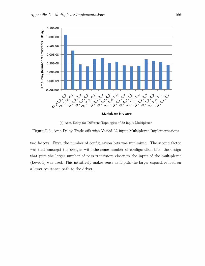
Appendix C. Multiplexer Implementations 166
0.00E+00
5.00E-09
1.00E-08
1.50E-08
2.00E-08
2.50E-08
3.00E-08
3.50E-08
Are
a D
ela
y (
Nu
mb
er
of
Tra
nsi
sto
rs ·
De
lay
)
Mul!plexer Structure
(c) Area Delay for Different Topologies of 32-input Multiplexer
Figure C.3: Area Delay Trade-offs with Varied 32-input Multiplexer Implementations
two factors. First, the number of configuration bits was minimized. The second factor
was that amongst the designs with the same number of configuration bits, the design
that puts the larger number of pass transistors closer to the input of the multiplexer
(Level 1) was used. This intuitively makes sense as it puts the larger capacitive load on
a lower resistance path to the driver.

Appendix D
Architectures and Results from
Trade-off Investigation
This appendix summarizes the architectures that were used for the design space explo-
ration in Chapter 5. The specific parameters that were varied for this exploration are
summarized in Table D.1 and the specific architectures used are listed in Table D.2. The
headings in Table D.2 refer to the abbreviations described in Table D.1. In all cases, the
intra-cluster routing was fully populated.
Table D.2 also lists effective area and delay results for three different sizings of
each architecture. The optimization objectives used to create the different sizings were
Area1Delay1 optimization, Area10Delay1 optimization and Delay optimization. For each
of these designs, the area and delay was measured using the experimental procedure out-
lined in Chapter 5. Many more sizings were used to produce the full results examined in
Chapter 5 and those results along with the full per circuit results for each FPGA design
can be found at http://www.eecg.utoronto.ca/∼jayar/pubs/theses/theses.html.
167

Appendix D. Architectures and Results from Trade-off Investigation 168
Table D.1: Parameters Considered for Design Space Exploration
Parameter Symbol
LUT Size KCluster Size NRouting Track Length Type 1 L1
Fraction of Tracks of Length Type 1 F1
Routing Track Length Type 2 L2
Fraction of Tracks of Length Type 2 F2
Input Connection Block Flexibility(as a fraction of the channel width) Fc,in
Output Connection Block Flexibility(as a fraction of the channel width) Fc,out
Channel Width WNumber of Inputs to Logic Block INumber of Inputs/Output pins per row or column
of logic blocks on each side of array I/Os per row/col

Appendix D. Architectures and Results from Trade-off Investigation 169
Tab
leD
.2:
Arc
hit
ectu
res
and
Par
tial
Res
ult
sfr
omD
esig
nSpac
eE
xplo
rati
on
NK
L1
F1
L2
F2
Fc,i
nF
c,o
ut
WI
I/O
sper
row
/co
l
Are
a10D
elay1
Optim
ized
Are
a1D
elay1
Optim
ized
Del
ay
Optim
ized
Are
aD
elay
Are
aD
elay
Are
aD
elay
23
41
0.2
50.5
48
52
4.0
2E
+07
1.1
6E
-08
5.1
5E
+07
6.9
4E
-09
1.0
0E
+08
5.5
2E
-09
24
41
0.2
50.5
56
62
4.3
5E
+07
9.7
2E
-09
5.5
1E
+07
6.0
8E
-09
1.1
3E
+08
4.7
8E
-09
25
41
0.2
50.5
56
82
4.9
9E
+07
8.2
4E
-09
6.0
6E
+07
5.0
9E
-09
1.2
6E
+08
4.2
5E
-09
42
41
0.2
0.2
556
52
3.3
9E
+07
1.3
1E
-08
4.4
0E
+07
8.3
9E
-09
8.7
6E
+07
6.4
2E
-09
43
41
0.2
0.2
564
82
3.5
5E
+07
9.5
9E
-09
4.3
8E
+07
6.3
0E
-09
8.4
9E
+07
4.9
1E
-09
44
41
0.2
50.2
564
10
43.8
9E
+07
7.8
1E
-09
4.6
2E
+07
5.2
5E
-09
9.1
1E
+07
4.1
9E
-09
45
41
0.2
0.2
556
13
44.3
6E
+07
6.8
9E
-09
5.1
8E
+07
4.5
1E
-09
1.0
6E
+08
3.7
2E
-09
46
41
0.2
0.2
556
15
45.2
2E
+07
5.7
0E
-09
6.1
5E
+07
3.9
5E
-09
1.4
4E
+08
3.5
8E
-09
47
41
0.2
0.2
556
18
57.0
4E
+07
4.8
7E
-09
7.7
4E
+07
3.7
0E
-09
1.6
7E
+08
3.1
8E
-09
62
41
0.1
50.1
67
64
72
3.2
3E
+07
1.3
2E
-08
4.0
6E
+07
8.4
9E
-09
7.6
8E
+07
6.2
4E
-09
63
41
0.2
0.1
67
80
11
3N
/A
N/A
4.4
9E
+07
5.8
5E
-09
8.0
3E
+07
4.5
6E
-09
64
41
0.2
50.1
680
14
43.9
9E
+07
7.4
8E
-09
4.8
4E
+07
4.8
0E
-09
8.6
6E
+07
4.0
5E
-09
66
41
0.2
0.1
67
80
21
65.5
2E
+07
5.2
9E
-09
6.4
3E
+07
3.7
0E
-09
1.3
2E
+08
3.3
6E
-09
82
41
0.1
50.1
25
80
93
3.2
6E
+07
1.2
7E
-08
4.1
1E
+07
8.2
4E
-09
7.4
3E
+07
6.1
8E
-09
83
21
0.2
50.1
25
76
14
84.0
6E
+07
1.0
7E
-08
5.0
7E
+07
6.5
9E
-09
9.3
2E
+07
5.1
5E
-09
83
41
0.2
0.1
25
88
14
4N
/A
N/A
4.3
6E
+07
5.8
9E
-09
8.0
5E
+07
4.5
4E
-09
84
11
0.2
50.1
25
82
18
84.3
3E
+07
1.2
6E
-08
5.3
3E
+07
6.6
9E
-09
1.0
9E
+08
5.4
1E
-09
84
21
0.2
50.1
84
18
44.1
8E
+07
8.2
7E
-09
5.0
2E
+07
5.2
2E
-09
9.6
2E
+07
4.2
4E
-09
84
41
0.2
50.1
88
18
44.0
8E
+07
7.4
5E
-09
4.8
7E
+07
4.8
6E
-09
8.8
0E
+07
3.9
5E
-09
84
61
0.2
50.1
96
18
44.0
4E
+07
7.2
9E
-09
4.6
8E
+07
4.6
8E
-09
8.2
3E
+07
3.9
9E
-09
85
21
0.2
50.1
25
80
23
8N
/A
N/A
5.8
7E
+07
4.6
2E
-09
1.1
1E
+08
3.9
2E
-09
85
41
0.2
0.1
25
88
23
64.8
2E
+07
6.6
0E
-09
5.6
3E
+07
4.2
2E
-09
1.0
4E
+08
3.5
1E
-09
86
21
0.2
50.1
25
76
27
85.9
5E
+07
6.0
5E
-09
7.0
5E
+07
4.0
8E
-09
1.2
7E
+08
3.4
8E
-09
86
41
0.2
0.1
25
88
27
75.6
8E
+07
5.3
1E
-09
6.4
4E
+07
3.7
5E
-09
1.2
8E
+08
3.4
4E
-09
87
21
0.2
50.1
25
80
32
87.7
8E
+07
5.3
9E
-09
9.2
5E
+07
3.6
9E
-09
1.6
7E
+08
3.1
4E
-09
87
41
0.2
0.1
25
96
32
81.4
3E
+08
3.0
5E
-09
8.0
7E
+07
3.8
4E
-09
N/A
N/A
10
24
10.2
0.1
80
11
33.3
5E
+07
1.2
7E
-08
4.1
4E
+07
8.0
6E
-09
7.4
5E
+07
6.3
3E
-09
10
31
10.2
50.1
88
17
84.0
2E
+07
1.5
3E
-08
5.1
2E
+07
8.2
1E
-09
1.0
1E
+08
6.4
7E
-09
10
32
10.2
50.1
92
17
84.1
8E
+07
1.0
0E
-08
5.1
0E
+07
6.5
0E
-09
9.7
8E
+07
5.0
3E
-09
10
34
10.2
0.1
104
17
6N
/A
N/A
4.5
6E
+07
5.7
2E
-09
8.0
9E
+07
4.4
7E
-09
Conti
nued
on
nex
tpage

Appendix D. Architectures and Results from Trade-off Investigation 170
Tab
leD
.2–
conti
nued
from
pre
vio
us
pag
eN
KL
1F
1L
2F
2F
c,i
nF
c,o
ut
WI
I/O
sper
row
/co
l
Are
a10D
elay1
Optim
ized
Are
a1D
elay1
Optim
ized
Del
ay
Optim
ized
Are
aD
elay
Are
aD
elay
Are
aD
elay
10
34
10.3
0.1
104
17
63.9
7E
+07
8.4
8E
-09
4.7
9E
+07
5.7
3E
-09
8.3
6E
+07
4.5
3E
-09
10
41
10.2
0.1
96
22
44.3
5E
+07
1.3
1E
-08
5.3
6E
+07
6.8
8E
-09
1.0
8E
+08
5.4
2E
-09
10
42
10.2
0.1
96
22
44.4
5E
+07
8.3
5E
-09
5.2
8E
+07
5.3
0E
-09
9.8
0E
+07
4.1
3E
-09
10
44
10.2
0.1
104
22
74.1
7E
+07
7.2
4E
-09
4.9
2E
+07
4.5
6E
-09
9.3
9E
+07
3.7
6E
-09
10
44
10.3
0.1
104
22
74.3
3E
+07
6.9
8E
-09
5.1
3E
+07
4.5
9E
-09
9.2
1E
+07
3.8
5E
-09
10
44
0.6
67
10
0.3
33
0.2
0.1
120
22
44.1
9E
+07
7.0
6E
-09
4.7
7E
+07
4.9
4E
-09
7.8
8E
+07
4.1
5E
-09
10
44
0.7
06
10
0.2
94
0.2
0.1
136
22
44.3
8E
+07
6.8
8E
-09
4.9
7E
+07
4.9
3E
-09
8.2
6E
+07
4.2
0E
-09
10
46
10.2
50.1
120
22
44.3
2E
+07
7.2
9E
-09
5.0
4E
+07
4.6
8E
-09
8.5
3E
+07
3.9
1E
-09
10
48
10.2
0.1
128
22
44.2
0E
+07
7.5
0E
-09
4.8
8E
+07
4.7
7E
-09
8.0
2E
+07
4.0
9E
-09
10
51
10.2
50.1
84
28
85.3
4E
+07
9.6
6E
-09
6.4
6E
+07
5.6
5E
-09
1.2
7E
+08
4.9
8E
-09
10
54
10.2
0.1
96
28
85.1
5E
+07
6.2
0E
-09
5.9
5E
+07
4.1
0E
-09
1.1
8E
+08
3.6
0E
-09
10
54
10.3
0.1
96
28
85.3
5E
+07
6.1
9E
-09
6.0
9E
+07
4.2
4E
-09
1.1
6E
+08
3.8
4E
-09
10
61
10.2
50.1
84
33
86.1
5E
+07
8.0
8E
-09
7.4
2E
+07
4.9
4E
-09
1.3
8E
+08
4.3
3E
-09
10
62
10.2
50.1
80
33
85.9
9E
+07
5.9
2E
-09
6.9
8E
+07
4.1
1E
-09
1.2
1E
+08
3.5
2E
-09
10
64
10.1
50.1
96
33
85.8
3E
+07
5.5
4E
-09
6.6
6E
+07
3.5
9E
-09
1.1
4E
+08
3.1
9E
-09
10
64
10.3
0.1
96
33
86.1
7E
+07
5.3
9E
-09
6.9
1E
+07
3.7
7E
-09
1.2
1E
+08
3.3
3E
-09
10
71
10.2
50.1
92
39
88.4
5E
+07
7.0
2E
-09
9.9
2E
+07
4.5
8E
-09
1.9
3E
+08
4.1
9E
-09
10
72
10.2
50.1
92
39
88.4
8E
+07
5.3
8E
-09
9.9
1E
+07
3.6
4E
-09
2.2
2E
+08
3.3
5E
-09
10
74
196
39
88.1
9E
+07
4.3
8E
-09
8.9
8E
+07
3.6
1E
-09
1.6
3E
+08
3.1
0E
-09
10
44
10.2
0.1
104
22
44.1
7E
+07
7.2
4E
-09
4.9
2E
+07
4.5
6E
-09
9.3
9E
+07
3.7
6E
-09
10
44
0.5
80.5
0.2
0.1
128
22
44.2
2E
+07
6.8
3E
-09
4.8
3E
+07
5.1
3E
-09
7.3
4E
+07
3.9
2E
-09
12
24
10.1
50.0
83
96
13
43.4
0E
+07
1.3
1E
-08
4.1
7E
+07
8.0
7E
-09
7.2
0E
+07
6.2
5E
-09
12
34
10.2
0.0
83
104
20
53.8
1E
+07
9.0
8E
-09
4.5
6E
+07
5.7
7E
-09
7.5
0E
+07
4.6
4E
-09
12
44
10.2
0.0
83
104
26
74.3
6E
+07
6.7
1E
-09
5.1
0E
+07
4.6
6E
-09
8.7
6E
+07
3.9
1E
-09
12
54
10.2
0.0
83
104
33
95.4
3E
+07
6.1
1E
-09
6.1
2E
+07
4.2
7E
-09
1.1
4E
+08
3.7
6E
-09
12
64
10.2
0.0
83
104
39
10
6.3
8E
+07
5.1
5E
-09
7.3
0E
+07
3.7
8E
-09
1.3
6E
+08
3.4
6E
-09

Appendix E
Logical Architecture to Transistor
Sizing Process
This appendix reviews the main steps in translating a logical architecture into a optimized
transistor-level netlist. This will done by way of example using the baseline architecture
from Chapter 5. The logical architecture parameters for this design are listed in Table E.1.
Starting from the architecture description, the widths (or fan-ins) of the multiplexers
in the design must first be determined. For the architectures considered in this work,
there are three multiplexers whose width must be determined. The Routing Mux is
the multiplexer used within the inter-block routing. Determining this width is rather
involved due to rounding issues and the possibility of tracks with multiple different seg-
ment lengths. However, for the baseline architecture, the width can be approximately
computed from the parameters in Table E.1 as follows,
WidthRouting Mux =2WL
Fs +(2W − 2W
L
)(Fs − 1) + Fc,outputWN2WL
≈ 12. (E.1)
The width of 12 would not be obtained if the numbers from Table E.1 are substituted
into the equation due to rounding steps that are omitted in the equation for simplicity.
The next multiplexer to be considered is the CLB Input Mux which is used within
the input connection block to connect the inter-block routing into the logic block. The
width of this multiplexer is
WidthCLB Input Mux = Fc,input ·W = 0.2 · 104 ≈ 22 (E.2)
171

Appendix E. Logical Architecture to Transistor Sizing Process 172
Table E.1: Architecture Parameters
Parameter Value
LUT Size, k 4Cluster Size, N 10Number of Cluster Inputs, I 22Tracks per Channel, W 104Track Length, L 4Interconnect Style UnidirectionalDriver Style Single DriverFc,input 0.2Fc,output 0.1Fs 3Pads per row/column 4
where again the rounding process has been omitted for simplicity.
Finally, the width of the multiplexers that connect the intra-cluster routing to the
BLEs is determined. These multiplexers are known as BLE Input Mux and are deter-
mined as follows
WidthBLE Input Mux = I + N = 22 + 10 = 32. (E.3)
There is an additional multiplexer inside the BLE but, for the architectures considered,
this multiplexer, the CLB Output Mux will always have 2 inputs, one from the LUT and
one from the flip-flop.
With the widths of the multiplexers known, appropriate implementations must be
determined. A number of implementation choices were examined in both Chapter 5 and
Appendix C. The specific implementation for each multiplexer will be selected based on
the input electrical parameters.
The transistor-level implementation of the remaining components of the FPGA is
straightforward. Buffers, with level-restorers, are necessary after all the multiplexers. If
desired, buffers are also added prior to the multiplexers; however, for this example, no
such buffers will be added. The LUT is implemented as a fully encoded multiplexer.
Buffers can be added inside the pass transistor tree as needed. For this particular design,
such buffers will not be added. Once these decisions have been made, the complete
structure of the FPGA is known.
The transistor sizes within this structure must then be optimized. This is done using
the optimizer described in Chapter 4. For this analysis, sizing will be performed with
the goal of minimizing the Area-Delay product. The resulting transistor sizes are listed
in Table E.2. In Figure E.1, the meaning of the different transistor size parameters is

Appendix E. Logical Architecture to Transistor Sizing Process 173
K-L
UT
DQ
BL
E 2
BL
E N
To
Ro
uti
ng
Ro
utin
g
Tra
ckL
og
ic C
lus
ter
Intr
a-c
lust
er
tra
ck
Inp
ut
Co
nne
ctio
n
Blo
ck
BL
E I
np
ut
Blo
ck
...
...
...
M U X_C LB _IN PU T
BU F F ER_ C LB _IN PU T _POST
M U X_ R OU T IN G
BU F F ER _R OU T IN G _POST
M U X_LE _IN PU T
BU F F ER _ LE _IN PU T _ POST
BU F F ER _ LU T _POST
M U X_C LB _OU T PU T
BU F F ER _ C LB_ OU T PU T _POST
Figure E.1: Terminology for Transistor Sizes

Appendix E. Logical Architecture to Transistor Sizing Process 174
illustrated through labels in the figure. For the buffers in the parameter list, stage0 refers
to the inverter stage within the buffer that is closest to the input. Similarly, level0 for
the multiplexers refers to the pass transistor grouping that is closest to the input. The
multiplicity of each multiplexer stage refers to the number of pass transistors within each
group of transistors at each level of the multiplexer. Equivalently, the multiplicity is also
the number of configuration memory bits needed at each level.
Once these sizes have been determined, the transistor-level design of the FPGA is
complete. The effective area and delay for this design can then be assessed using the full
experimental process described in Chapter 5.

Appendix E. Logical Architecture to Transistor Sizing Process 175
Table E.2: Transistor Sizes for Example Architecture
Parameter Value
MUX CLB INPUT num levels 2.00MUX CLB INPUT level0 width 0.24MUX CLB INPUT level0 multiplicity 6.00MUX CLB INPUT level1 width 0.24MUX CLB INPUT level1 multiplicity 4.00BUFFER CLB INPUT POST num stages 2.00BUFFER CLB INPUT POST stage0 nmos width 0.84BUFFER CLB INPUT POST stage0 pmos width 0.42BUFFER CLB INPUT POST stage1 nmos width 0.84BUFFER CLB INPUT POST stage1 pmos width 1.34BUFFER CLB INPUT POST pullup width 0.24BUFFER CLB INPUT POST pullup length 0.50MUX ROUTING num levels 2.00MUX ROUTING level0 width 1.64MUX ROUTING level0 multiplicity 4.00MUX ROUTING level1 width 1.84MUX ROUTING level1 multiplicity 3.00BUFFER ROUTING POST num stages 2.00BUFFER ROUTING POST stage0 nmos width 5.34BUFFER ROUTING POST stage0 pmos width 2.67BUFFER ROUTING POST stage1 nmos width 5.34BUFFER ROUTING POST stage1 pmos width 8.01BUFFER ROUTING POST pullup width 0.24BUFFER ROUTING POST pullup length 0.50MUX LE INPUT num levels 2.00MUX LE INPUT level0 width 0.24MUX LE INPUT level0 multiplicity 8.00MUX LE INPUT level1 width 0.24MUX LE INPUT level1 multiplicity 4.00BUFFER LE INPUT POST num stages 1.00BUFFER LE INPUT POST stage0 nmos width 0.64BUFFER LE INPUT POST stage0 pmos width 0.32BUFFER LE INPUT POST pullup width 0.24BUFFER LE INPUT POST pullup length 0.50LUT LUT0 stage0 width 0.24LUT LUT0 stage1 width 0.34LUT LUT0 stage2 width 0.34LUT LUT0 stage3 width 0.24LUT LUT0 stage0 buffer nmos width 0.34LUT LUT0 stage0 buffer pmos width 0.24LUT LUT0 stage pullup length 0.40LUT LUT0 stage pullup width 0.24LUT LUT0 signal buffer stage0 nmos width 0.34LUT LUT0 signal buffer stage0 pmos width 0.41LUT LUT0 signal buffer stage1 nmos width 0.24LUT LUT0 signal buffer stage1 pmos width 0.34BUFFER LUT POST num stages 2.00BUFFER LUT POST stage0 nmos width 0.54BUFFER LUT POST stage0 pmos width 0.38BUFFER LUT POST stage1 nmos width 1.08BUFFER LUT POST stage1 pmos width 1.30BUFFER LUT POST pullup width 0.24BUFFER LUT POST pullup length 0.50MUX CLB OUTPUT num levels 1.00MUX CLB OUTPUT level0 width 2.74MUX CLB OUTPUT level0 multiplicity 2.00BUFFER CLB OUTPUT POST stage0 nmos widths 3.94BUFFER CLB OUTPUT POST stage0 pmos widths 3.15BUFFER CLB OUTPUT POST stage1 nmos widths 3.94BUFFER CLB OUTPUT POST stage1 pmos widths 5.12BUFFER CLB OUTPUT POST pullup widths 0.24BUFFER CLB OUTPUT POST pullup lengths 0.50

Bibliography
[1] David Chinnery and Kurt Keutzer. Closing the Gap Between ASIC & Custom Toolsand Techniques for High-Performance ASIC Design. Kluwer Academic Publishers,2002.
[2] Stephen D. Brown, Robert Francis, Jonathan Rose, and Zvonko Vranesic. Field-programmable gate arrays. Kluwer Academic Publishers, 1992.
[3] Paul S. Zuchowski, Christopher B. Reynolds, Richard J. Grupp, Shelly G. Davis,Brendan Cremen, and Bill Troxel. A hybrid ASIC and FPGA architecture. InICCAD ’02, pages 187–194, November 2002.
[4] Steven J.E. Wilton, Noha Kafafi, James C. H. Wu, Kimberly A. Bozman, Vic-tor Aken’Ova, and Resve Saleh. Design considerations for soft embedded pro-grammable logic cores. IEEE Journal of Solid-State Circuits, 40(2):485–497, Febru-ary 2005.
[5] Katherine Compton and Scott Hauck. Automatic design of area-efficient config-urable ASIC cores. IEEE Transactions on Computers, 56(5):662–672, May 2007.
[6] Altera Corporation. Stratix III device handbook, Nov 2007. SIII5V1-1.4 http:
//www.altera.com/literature/hb/stx3/stratix3 handbook.pdf.
[7] Xilinx. Virtex-5 user guide, March 2008. UG190 (v4.0) http://www.xilinx.com/support/documentation/user guides/ug190.pdf.
[8] Altera Corporation. Cyclone III device handbook, Sept 2007. ver. CIII5V1-1.2http://www.altera.com/literature/hb/cyc3/cyclone3 handbook.pdf.
[9] Xilinx. Spartan-3E, November 2006. Ver. 3.4 http://direct.xilinx.com/
bvdocs/publications/ds312.pdf.
[10] Vaughn Betz and Jonathan Rose. VPR: A new packing, placement and routingtool for FPGA research. In Seventh International Workshop on Field-ProgrammableLogic and, pages 213–222, 1997.
[11] J. Rose, R.J. Francis, D. Lewis, and P. Chow. Architecture of field-programmablegate arrays: the effect of logic block functionality on area efficiency. IEEE Journalof Solid-State Circuits, 25(5):1217–1225, 1990.
176
Bibliography 177
[12] Altera Corporation. Stratix device family data sheet, volume 1, S5V1-3.4, January2006. http://www.altera.com/literature/hb/stx/stratix vol 1.pdf.
[13] Xilinx. Virtex-4 family overview, June 2005. http://www.xilinx.com/bvdocs/
publications/ds112.pdf.
[14] Vaughn Betz, Jonathan Rose, and Alexander Marquardt. Architecture and CADfor Deep-Submicron FPGAs. Kluwer Academic Publishers, 1999.
[15] David Lewis, Elias Ahmed, Gregg Baeckler, Vaughn Betz, Mark Bourgeault, DavidCashman, David Galloway, Mike Hutton, Chris Lane, Andy Lee, Paul Leventis,Sandy Marquardt, Cameron McClintock, Ketan Padalia, Bruce Pedersen, GilesPowell, Boris Ratchev, Srinivas Reddy, Jay Schleicher, Kevin Stevens, RichardYuan, Richard Cliff, and Jonathan Rose. The Stratix II logic and routing archi-tecture. In FPGA ’05: Proceedings of the 2005 ACM/SIGDA 13th internationalsymposium on Field-programmable gate arrays, pages 14–20, New York, NY, USA,2005. ACM Press.
[16] Altera Corporation. Stratix II Device Handbook SII5V1-4.3, May 2007. http:
//www.altera.com/literature/hb/stx2/stratix2 handbook.pdf.
[17] Altera Corporation. Stratix IV Device Handbook Volumes 1–4 SIV5V1-1.0,May 2008. http://www.altera.com/literature/hb/stratix-iv/stratix4
handbook.pdf.
[18] Elias Ahmed and Jonathon Rose. The effect of LUT and cluster size on deep-submicron FPGA performance and density. IEEE Transactions on Very LargeScale Integration (VLSI) Systems, 12(3):288–298, March 2004.
[19] Guy Lemieux and David Lewis. Using sparse crossbars within LUT clusters. InFPGA ’01: Proceedings of the 2001 ACM/SIGDA ninth international symposiumon Field programmable gate arrays, pages 59–68, New York, NY, USA, Feb. 2001.ACM.
[20] David Lewis, Vaughn Betz, David Jefferson, Andy Lee, Chris Lane, Paul Leventis,Sandy Marquardt, Cameron McClintock, Bruce Pedersen, Giles Powell, SrinivasReddy, Chris Wysocki, Richard Cliff, and Jonathan Rose. The StratixTM rout-ing and logic architecture. In FPGA ’03: Proceedings of the 2003 ACM/SIGDAeleventh international symposium on Field programmable gate arrays, pages 12–20.ACM Press, 2003.
[21] Actel Corporation. Act 1 series FPGAs, April 1996. http://www.actel.com/
documents/ACT1 DS.pdf.
[22] Altera Corporation. APEX 20K programmable logic device family data sheet, DS-APEX20K-5.1, March 2004. http://www.altera.com/literature/ds/apex.pdf.
[23] Altera Corporation. APEX II programmable logic device family, DS-APEXII-3.0,Aug 2002. http://www.altera.com/literature/ds/ds ap2.pdf.

Bibliography 178
[24] A. Aggarwal and D. Lewis. Routing architectures for hierarchical field-programmable gate arrays. In IEEE International Conference on Computer Design,pages 475–478, Oct 1994.
[25] S. Wilton. Architectures and Algorithms for Field-Programmable Gate Arrays withEmbedded Memories. PhD thesis, University of Toronto, 1997. Department ofElectrical and Computer Engineering.
[26] G. Lemieux and D. Lewis. Analytical framework for switch block design. In Inter-national Conference on Field Programmable Logic and Applications, pages 122–131,Sept. 2002.
[27] Steven P. Young, Trevor J. Bauer, Kamal Chaudhary, and Sridhar Krishnamurthy.FPGA repeatable interconnect structure with bidirectional and unidirectional in-terconnect lines, Aug 1999. US Patent 5,942,913.
[28] Guy Lemieux, Edmund Lee, Marvin Tom, and Anthony Yu. Directional and single-driver wires in FPGA interconnect. In IEEE International Conference on Field-Programmable Technology, pages 41–48, December 2004.
[29] Ian Kuon. Automated FPGA design, verification and layout. Master’s thesis,University of Toronto, 2004.
[30] Jan M. Rabaey. Digital Integrated Circuits A Design Perspective. Prentice Hall,1996.
[31] E. Lee, G. Lemieux, and S. Mirabbasi. Interconnect driver design for long wiresin field-programmable gate arrays. In Field Programmable Technology, 2006. FPT2006. IEEE International Conference on, pages 89–96, December 2006.
[32] Edmund Lee, Guy Lemieux, and Shahriar Mirabbasi. Interconnect driver design forlong wires in field-programmable gate arrays. Journal of Signal Processing Systems,51(1):57–76, April 2008.
[33] J. H. Anderson and F. N. Najm. Low-power programmable routing circuitry forFPGAs. In IEEE/ACM International Conference on Computer Aided Design 2004,pages 602–609, Washington, DC, USA, 2004. IEEE Computer Society.
[34] Steven P. Young. Six-input multiplexer with two gate levels and three memorycells, April 1998. US Patent 5,744,995.
[35] Vaughn Betz and Jonathan Rose. Circuit design, transistor sizing and wire layoutof FPGA interconnect. In Proceedings of the 1999 IEEE Custom Integrated CircuitsConference, pages 171–174, 1999.
[36] Vikas Chandra and Herman Schmit. Simultaneous optimization of driving bufferand routing switch sizes in an FPGA using an iso-area approach. In Proceedingsof the IEEE Computer Society Annual Symposium on VLSI (ISVLSI’02), pages28–33, 2002.

Bibliography 179
[37] Michael Hutton, Vinson Chan, Peter Kazarian, Victor Maruri, Tony Ngai, JimPark, Rakesh Patel, Bruce Pedersen, Jay Schleicher, and Sergey Shumarayev. In-terconnect enhancements for a high-speed PLD architecture. In Proceedings ofthe 2002 ACM/SIGDA tenth international symposium on Field-programmable gatearrays, pages 3–10, New York, NY, USA, 2002. ACM.
[38] J. Anderson and F. Najm. A novel low-power FPGA routing switch. In Proceedingsof the IEEE 2004 Custom Ingretated Circuits Conference, pages 719–722, Oct 2004.
[39] Fei Li, Y. Lin, Lei He, Deming Chen, and Jason Cong. Power modeling andcharacteristics of field programmable gate arrays. IEEE Transactions on Computer-Aided Design of Integrated Circuits and Systems, 24(11):1712–1724, Nov. 2005.
[40] Kara K. W. Poon, Steven J. E. Wilton, and Andy Yan. A detailed power modelfor field-programmable gate arrays. ACM Transactions on Design Automation ofElectronic Systems (TODAES), 10(2):279–302, 2005.
[41] Julien Lamoureux. On the interaction between power-aware computer-aided designalgorithms for field-programmable gate arrays. Master’s thesis, University of BritishColumbia, 2003.
[42] Julien Lamoureux and Steven J. E. Wilton. On the interaction between power-aware FPGA CAD algorithms. In ICCAD ’03: Proceedings of the 2003 IEEE/ACMinternational conference on Computer-aided design, page 701, Washington, DC,USA, 2003. IEEE Computer Society.
[43] R.K. Brayton, G.D. Hachtel, and A.L. Sangiovanni-Vincentelli. Multilevel logicsynthesis. Proceedings of the IEEE, 78(2):264–300, 1990.
[44] A. Sangiovanni-Vincentelli, A. El Gamal, and J. Rose. Synthesis methods for fieldprogrammable gate arrays. Proceedings of the IEEE, 81(7):1057–1083, 1993.
[45] Jason Cong and Yuzheng Ding. FlowMap: An optimal technology mapping algo-rithm for delay optimization in lookup-table based FPGA designs. IEEE Trans-actions on Computer-Aided Design of Integrated Circuits and Systems, 13(1):1–12,Jan 1994.
[46] J. Cong and Y. Ding. On area/depth trade-off in LUT-based FPGA technologymapping. IEEE Transactions on Very Large Scale Integration (VLSI) Systems,2(2):137–148, 1994.
[47] Peter Jamieson. Improving the Area Efficiency of Heterogeneous FPGAs withShadow Clusters. PhD thesis, University of Toronto, 2007.
[48] E. M. Sentovich, K. J. Singh, L. Lavagno, C. Moon, R. Murgai, A. Saldanha,H. Savoj, P. R. Stephan, R. K. Brayton, and A. L. Sangiovanni-Vincentelli. Sis:A system for sequential circuit synthesis. Technical Report UCB/ERL M92/41,University of California, Berkeley, Electronics Research Lab, Univ. of California,Berkeley, CA, 94720, May 1992.

Bibliography 180
[49] Alexander R. Marquardt. Cluster-based architecture, timing-driven packing andtiming-driven placement for FPGAs. Master’s thesis, University of Toronto, 1999.
[50] S. Kirkpatrick, C. D. Gelatt Jr, and M. P. Vecchi. Optimization by simulatedannealing. Science, 220(4598):671–680, May 1983.
[51] A.E. Dunlop and B.W. Kernighan. A procedure for placement of standard-cell VLSIcircuits. IEEE Transactions on Computer-Aided Design of Integrated Circuits andSystems, 4(1):92–98, 1985.
[52] J.M. Kleinhans, G. Sigl, F.M. Johannes, and K.J. Antreich. GORDIAN: VLSIplacement by quadratic programming and slicing optimization. IEEE Transactionson Computer-Aided Design of Integrated Circuits and Systems, 10(3):356–365, 1991.
[53] C.J. Alpert, T.F. Chan, A.B. Kahng, I.L. Markov, and P. Mulet. Faster minimiza-tion of linear wirelength for global placement. IEEE Transactions on Computer-Aided Design of Integrated Circuits and Systems, 17(1):3–13, 1998.
[54] C. Sechen and A. Sangiovanni-Vincentelli. The TimberWolf placement and routingpackage. IEEE Journal of Solid-State Circuits, 20(2):510–522, 1985.
[55] C. Ebeling, L. McMurchie, S.A. Hauck, and S. Burns. Placement and routingtools for the Triptych FPGA. IEEE Transactions on Very Large Scale Integration(VLSI) Systems, 3(4):473–482, 1995.
[56] S. Brown, J. Rose, and Z.G. Vranesic. A detailed router for field-programmablegate arrays. IEEE Transactions on Computer-Aided Design of Integrated Circuitsand Systems, 11(5):620–628, 1992.
[57] Takumi Okamoto and Jason Cong. Buffered Steiner tree construction with wiresizing for interconnect layout optimization. In ICCAD ’96: Proceedings of the1996 IEEE/ACM international conference on Computer-aided design, pages 44–49, Washington, DC, USA, 1996. IEEE Computer Society.
[58] W. C. Elmore. The transient response of damped linear networks with particularregard to wideband amplifiers. Journal of Applied Physics, 19:55–63, January 1948.
[59] Jorge Rubinstein, Paul Penfield, and Mark A. Horowitz. Signal delay in RC treenetworks. IEEE Transactions on Computer-Aided Design of Integrated Circuitsand Systems, 2(3):202–211, July 1983.
[60] John K. Ousterhout. Switch-level delay models for digital MOS VLSI. In DAC’84: Proceedings of the 21st conference on Design automation, pages 542–548, Pis-cataway, NJ, USA, 1984. IEEE Press.
[61] K. D. Boese, A. B. Kahng, B. A. McCoy, and G. Robins. Fidelity and near-optimality of Elmore-based routing constructions. In Proceedings of 1993 IEEEInternational Conference on Computer Design: VLSI in Computers and ProcessorsICCD’93, pages 81–84, 1993.

Bibliography 181
[62] Jason Cong and Lei He. Optimal wiresizing for interconnects with multiplesources. ACM Transactions on Design Automation of Electronic Systems (TO-DAES), 1(4):478–511, 1996.
[63] J. P. Fishburn and A.E. Dunlop. TILOS: A posynomial programming approach totransistor sizing. In International Conference on Computer Aided Design, pages326–328, November 1985.
[64] Stephen Boyd and Lieven Vandenberghe. Convex Optimization. Cambridge Uni-versity Press, 2003.
[65] Jyuo-Min Shyu and Alberto Sangiovanni-Vincentelli. ECSTASY: A new environ-ment for IC design optimization. In International Conference on Computer AidedDesign, pages 484–487, 1988.
[66] S. S. Sapatnekar, V. B. Rao, P.M. Vaidya, and Kang Sung-Mo. An exact solu-tion to the transistor sizing problem for CMOS circuits using convex optimization.IEEE Transactions on Computer-Aided Design of Integrated Circuits and Systems,12(11):1621–1634, November 1993.
[67] Chung-Pin Chen, Chris C. N. Chu, and D. F. Wong. Fast and exact simultaneousgate and wire sizing by langrangian relaxation. IEEE Transactions on Computer-Aided Design of Integrated Circuits and Systems, 18(7):1014–1025, July 1999.
[68] Vijay Sundararajan, Sachin S. Sapatnekar, and Keshab K. Parhi. Fast and exacttransistor sizing based on iterative relaxation. IEEE Transactions on Computer-Aided Design of Integrated Circuits and Systems, 21(5):568–581, 2002.
[69] Kishore Kasamsetty, Mahesh Ketkar, and Sachin Sapatnekar. A new class of convexfunctions for delay modeling and its application to the transistor sizing problem.IEEE Transactions on Computer-Aided Design of Integrated Circuits and Systems,19(7):779–788, July 2000.
[70] Mahesh Ketkar, Kishore Kasamsetty, and Sachin Sapatnekar. Convex delay modelsfor transistor sizing. In DAC ’00: Proceedings of the 37th Design AutomationConference, pages 655–660, New York, NY, USA, 2000. ACM Press.
[71] Hiran Tennakoon and Carl Sechen. Efficient and accurate gate sizing with piecewiseconvex delay models. In DAC ’05: Proceedings of the 42nd annual conference onDesign automation, pages 807–812, New York, NY, USA, 2005. ACM Press.
[72] Weidong Liu, Xiaodong Jin, Xuemei Xi, James Chen, Min-Chie Jeng, Zhihong Liu,Yuhua Cheng, Kai Chen, Mansun Chan, Kelvin Hui, Jianhui Huang, Robert Tu,Ping K. Ko, and Chenming Hu. BSIM3V3.3 MOSFET Model, July 2005. http:
//www-device.eecs.berkeley.edu/∼bsim3/ftpv330/Mod doc/b3v33manu.tar.
[73] Mohan V. Dunga, Wenwei (Morgan) Yang, Xuemei (Jane) Xi, Jin He, WeidongLiu, Kanyu, M. Cao, Xiaodong Jin, Jeff J. Ou, Mansun Chan, Ali M. Niknejad,

Bibliography 182
and Chenming Hu. BSIM4.6.1 MOSFET Model, May 2007. http://www-device.eecs.berkeley.edu/∼bsim3/BSIM4/BSIM461/doc/BSIM461 Manual.pdf.
[74] William Nye, David C. Riley, Alberto Sangiovanni-Vincentelli, and Andre L. Tits.DELIGHT.SPICE: An optimization-based system for the design of integrated cir-cuits. IEEE Transactions on Computer-Aided Design of Integrated Circuits andSystems, 7(4):501–519, 1988.
[75] Andrew R. Conn, Paula K. Coulman, Rudd A. Haring, Gregory L. Morrill, ChanduVisweswariah, and Chai Wah Wu. JiffyTune: circuit optimization using time-domain sensitivities. IEEE Transactions on Computer-Aided Design of IntegratedCircuits and Systems, 17(12):1292–1309, Dec 1998.
[76] A. R. Conn, I. M. Elfadel, Jr. W. W. Molzen, P. R. O’Brien, P. N. Strenski,C. Visweswariah, and C. B. Whan. Gradient-based optimization of custom circuitsusing a static-timing formulation. In DAC ’99: Proceedings of the 36th ACM/IEEEconference on Design automation, pages 452–459, New York, NY, USA, 1999. ACMPress.
[77] Xiaoliang Bai, Chandu Visweswariah, and Philip N. Strenski. Uncertainty-awarecircuit optimization. In DAC ’02: Proceedings of the 39th conference on Designautomation, pages 58–63, New York, NY, USA, 2002. ACM Press.
[78] H. S. Jones Jr., P. R. Nagle, and H. T. Nguyen. A comparison of standard celland gate array implementions in a common CAD system. In IEEE 1986 CustomIntegrated Circuits Conference, pages 228–232, 1986.
[79] William J. Dally and Andrew Chang. The role of custom design in ASIC chips. InDAC ’00: Proceedings of the 37th Design Automation Conference, pages 643–647.ACM Press, 2000.
[80] Andrew Chang and William J. Dally. Explaining the gap between ASIC and cus-tom power: a custom perspective. In DAC ’05: Proceedings of the 42nd annualconference on Design automation, pages 281–284, New York, NY, USA, 2005. ACMPress.
[81] David G. Chinnery and Kurt Keutzer. Closing the power gap between ASIC andcustom: an ASIC perspective. In DAC ’05: Proceedings of the 42nd annual con-ference on Design automation, pages 275–280, New York, NY, USA, 2005. ACMPress.
[82] Michael John Sebastian Smith. Application-Specific Integrated Circuits. Addison-Wesley, 1997.
[83] NEC Electronics. ISSP (Structured ASIC), 2005. http://www.necel.com/issp/
english/.
[84] Altera Corporation. HardCopy ASICs: Technology for business, 2008. http:
//www.altera.com/products/devices/hardcopy/hrd-index.html.

Bibliography 183
[85] Richard Cliff. Altera Corporation. Private Communication.
[86] Altera Corporation. Partnership with TSMC yields first silicon successon Altera’s 90-nm, low-k products, June 2004. http://www.altera.
com/corporate/news room/releases/releases archive/2004/products/
nr-tsmc partnership.html.
[87] STMicroelectronics. 90nm CMOS090 Design Platform, 2005. http://www.st.
com/stonline/products/technologies/soc/90plat.htm.
[88] Altera Corporation. Altera demonstrates 90-nm leadership by ship-ping world’s highest-density, highest-performance FPGA, January 2005.http://www.altera.com/corporate/news room/releases/releases archive/
2005/products/nr-ep2s180 shipping.html.
[89] C.C. Wu, Y.K. Leung, C.S. Chang, M.H. Tsai, H.T. Huang, D.W. Lin, Y.M. Sheu,C.H. Hsieh, W.J. Liang, L.K. Han, et al. A 90-nm cmos device technology with high-speed, general-purpose, and low-leakage transistors for system on chip applications.In Electron Devices Meeting, 2002. IEDM’02. Digest. International, pages 65–68,2002.
[90] P. Roche and G. Gasiot. Impacts of front-end and middle-end process modifica-tions on terrestrial soft error rate. IEEE Transactions on Device and MaterialsReliability, 5(3):382–396, 2005.
[91] STMicroelectronics. MOTOROLA, PHILIPS and STMicroelectronics IntroducesDebut Industry’s First 90-NANOMETER CMOS Design Platform, August 2002.http://www.st.com/stonline/press/news/year2002/t1222h.htm.
[92] Taiwan Semiconductor Manufacturing Company Ltd. TSMC 90nm technology plat-form, April 2005. http://www.tsmc.com/download/english/a05 literature/
90nm Brochure.pdf.
[93] Dick James. 2004 – the year of 90-nm: A review of 90 nm devices. In 2005IEEE/SEMI Advanced Semiconductor Manufacturing Conference and Workshop,pages 72–76, 2005.
[94] Emanuele Capitanio, Matteo Nobile, and Didier Renard. Removing aluminum capin 90 nm copper technology, 2006. www.imec.be/efug/EFUG2006 Renard.pdf.
[95] Navid Azizi, Ian Kuon, Aaron Egier, Ahmad Darabiha, and Paul Chow. Recon-figurable molecular dynamics simulator. In FCCM ’04: Proceedings of the 12thAnnual IEEE Symposium on Field-Programmable Custom Computing Machines,pages 197–206, Washington, DC, USA, 2004. IEEE Computer Society.
[96] J. Fender and J. Rose. A high-speed ray tracing engine built on a field-programmable system. In Field-Programmable Technology (FPT), 2003. Proceed-ings. 2003 IEEE International Conference on, pages 188–195, 2003.

Bibliography 184
[97] A. Darabiha, J. Rose, and J.W. Maclean. Video-rate stereo depth measurementon programmable hardware. In Computer Vision and Pattern Recognition, 2003.Proceedings. 2003 IEEE Computer Society Conference on, volume 1, 2003.
[98] Peter Yiannacouras, J. Gregory Steffan, and Jonathan Rose. Application-specificcustomization of soft processor microarchitecture. In FPGA ’06: Proceedings ofthe 2006 ACM/SIGDA 14th international symposium on Field Programmable GateArrays, pages 201–210, New York, NY, USA, 2006. ACM.
[99] Peter Yiannacouras. The microarchitecture of FPGA-based soft processors. Mas-ter’s thesis, University of Toronto, 2005.
[100] P. Chow, D. Karchmer, R. White, T. Ngai, P. Hodgins, D. Yeh, J. Ranaweera,I. Widjaja, and A. Leon-Garcia. A 50,000 transistor packet-switching chip for theStarburst ATMswitch. In Custom Integrated Circuits Conference, 1995., Proceed-ings of the IEEE 1995, pages 435–438, 1995.
[101] Altera Corporation. Quartus II Development Software Handbook, 5.0 edition, May2005.
[102] Synopsys. Design Compiler Reference Manual: Constraints and Timing, versionv-2004.06 edition, June 2004.
[103] Synopsys. Design Compiler User Guide, version v-2004.06 edition, June 2004.
[104] Neil H. E. Weste and David Harris. CMOS VLSI Design A Circuits and SystemsPerspective. Pearson Addison-Wesley, 2005.
[105] Cadence. Encounter Design Flow Guide and Tutorial, Product Version 3.3.1,February 2004.
[106] Dan Clein. CMOS IC layout : concepts, methodologies and tools. Elsevier Inc,2000.
[107] Xiaojian Yang, Bo-Kyung Choi, and M. Sarrafzadeh. Routability-driven whitespace allocation for fixed-die standard-cell placement. IEEE Transactions onComputer-Aided Design of Integrated Circuits and Systems, 22(4):410–419, April2003.
[108] Wenjie Jiang, Vivek Tiwari, Erik de la Iglesia, and Amit Sinha. Topological analysisfor leakage prediction of digital circuits. In ASP-DAC ’02: Proceedings of the2002 conference on Asia South Pacific design automation/VLSI Design, page 39,Washington, DC, USA, 2002. IEEE Computer Society.
[109] Paul Leventis, Mark Chan, Michael Chan, David Lewis, Behzad Nouban, GilesPowell, Brad Vest, Myron Wong, Renxin Xia, and John Costello. Cyclone: A low-cost, high-performance FPGA. In Proceedings of the IEEE 2003 Custom IngretatedCircuits Conference, pages 49–52, 2003.

Bibliography 185
[110] Jordan S. Swartz, Vaughn Betz, and Jonathan Rose. A fast routability-drivenrouter for FPGAs. In FPGA ’98: Proceedings of the 1998 ACM/SIGDA sixthinternational symposium on Field programmable gate arrays, pages 140–149, NewYork, NY, USA, 1998. ACM.
[111] Jordan S. Swartz. A high-speed timing-award router for FPGAs. Master’s the-sis, University of Toronto, 1998. http://www.eecg.toronto.edu/∼jayar/pubs/
theses/Swartz/JordanSwartz.pdf.
[112] Wei Mark Fang and Jonathan Rose. Modeling routing demand for early-stage fpgaarchitecture development. In FPGA ’08: Proceedings of the 16th internationalACM/SIGDA symposium on Field programmable gate arrays, pages 139–148, NewYork, NY, USA, 2008. ACM.
[113] Wei Mark Fang. Modeling routing demand for early-stage FPGA architecturedevelopment. Master’s thesis, University of Toronto, 2008.
[114] C.H. Ho, P.H.W. Leong, W. Luk, S.J.E. Wilton, and S. Lopez-Buedo. Virtualembedded blocks: A methodology for evaluating embedded elements in FPGAs.In Proc. IEEE Symposium on Field-Programmable Custom Computing Machines(FCCM), pages 45–44, 2006.
[115] Altera Corporation. Stratix II vs. Virtex-4 power comparison & estimation ac-curacy. White Paper, August 2005. http://www.altera.com/literature/wp/
wp s2v4 pwr acc.pdf.
[116] Li Shang, Alireza S. Kaviani, and Kusuma Bathala. Dynamic power consumptionin VirtexTM-II FPGA family. In Proceedings of the 2002 ACM/SIGDA tenth inter-national symposium on Field-programmable gate arrays, pages 157–164, New York,NY, USA, 2002. ACM Press.
[117] Vivek De and Shekhar Borkar. Technology and design challenges for low powerand high performance. In Proceedings of the 1999 international symposium on Lowpower electronics and design (ISLPED ’99), pages 163–168, New York, NY, USA,1999. ACM Press.
[118] Erich Goetting. Introducing the new Virtex-4 FPGA family. Xcell Journal, FirstQuarter 2006. http://www.xilinx.com/publications/xcellonline/xcell 52/
xc pdf/xc v4topview52.pdf.
[119] L. Cheng, F. Li, Y. Lin, P. Wong, and L. He. Device and Architecture Cooptimiza-tion for FPGA Power Reduction. IEEE Transactions on Computer-Aided Designof Integrated Circuits and Systems, 26(7):1211–1221, July 2007.
[120] Ian Kuon, Aaron Egier, and Jonathan Rose. Design, layout and verification of anFPGA using automated tools. In FPGA ’05: Proceedings of the 2005 ACM/SIGDA13th international symposium on Field-programmable gate arrays, pages 215–226,New York, NY, USA, 2005. ACM Press.

Bibliography 186
[121] Ketan Padalia, Ryan Fung, Mark Bourgeault, Aaron Egier, and Jonathan Rose.Automatic transistor and physical design of FPGA tiles from an architectural spec-ification. In FPGA ’03: Proceedings of the 2003 ACM/SIGDA eleventh interna-tional symposium on Field programmable gate arrays, pages 164–172, New York,NY, USA, 2003. ACM Press.
[122] Victor Aken’Ova, Guy Lemieux, and Resve Saleh. An improved ”soft” eFPGAdesign and implementation strategy. In Proceedings of the IEEE 2005 CustomIntegrated Circuits Conference, pages 178–181, September 2005.
[123] Shawn Phillips and Scott Hauck. Automatic layout of domain-specific reconfig-urable subsystems for system-on-a-chip. In Proceedings of the 2002 ACM/SIGDAtenth international symposium on Field-programmable gate arrays, pages 165–173.ACM Press, 2002.
[124] The MOSIS Service. MOSIS scalable CMOS (SCMOS) revision 8.00, October 2004.http://www.mosis.com/Technical/Designrules/scmos/scmos-main.html.
[125] Ivan Sutherland, Robert Sproule, and David Harris. Logical Effort : Designing fastCMOS circuits. Morgan Kaufmann Publishers, 1999.
[126] V. Eisele, B. Hoppe, and O. Kiehl. Transmission gate delay models for circuitoptimization. In Design Automation Conference, 1990. EDAC. Proceedings of theEuropean, pages 558–562, 1990.
[127] Synopsys. HSPICE. http://www.synopsys.com/products/mixedsignal/
hspice/hspice.html.
[128] Synopsys. HSIM. http://www.synopsys.com/products/mixedsignal/hsim/
hsim.html.
[129] Synopsys. NanoSim. http://www.synopsys.com/products/mixedsignal/
nanosim/nanosim.html.
[130] Elias Ahmed and Jonathan Rose. The effect of LUT and cluster size on deep-submicron FPGA performance and density. In FPGA ’00: Proceedings of the 2000ACM/SIGDA eighth international symposium on Field programmable gate arrays,pages 3–12, New York, NY, USA, 2000. ACM.
[131] Taiwan Semiconductor Manufacturing Company Ltd. TSMC 0.18 and 0.15-microntechnology platform, April 2005. http://www.tsmc.com/download/english/a05literature/0.15-0.18-micron Brochure.pdf.
[132] Saeyang Yang. Logic synthesis and optimization benchmarks user guide version3.0. Technical report, Microelectronics Center of North Carolina, Jan 1991.
[133] Taiwan Semiconductor Manufacturing Company Ltd. TSMC 0.35-micron tech-nology platform, April 2005. http://www.tsmc.com/download/english/a05
literature/0.35-micron Brochure.pdf.

Bibliography 187
[134] Elias Ahmed. The effect of logic block granularity on deep-submicron FPGAperformance and density. Master’s thesis, University of Toronto, 2001. http:
//www.eecg.toronto.edu/∼jayar/pubs/theses/Ahmed/EliasAhmed.pdf.
[135] K. Compton, A. Sharma, S. Phillips, and S. Hauck. Flexible routing architecturegeneration for domain-specific reconfigurable subsystems. In International Confer-ence on Field Programmable Logic and Applications, pages 59–68, 2002.
[136] Lattice Semiconductor Corporation. LatticeSC/M Family Handbook, Version 02.1,DS1004, June 2008. http://www.latticesemi.com/dynamic/view document.
cfm?document id=19028.
[137] Lattice Semiconductor Corporation. LatticeECP2/M Family Handbook, Ver-sion 02.9, HB1003, July 2007. http://www.latticesemi.com/dynamic/view
document.cfm?document id=21733.
[138] Ken McElvain. LGSynth93 benchmark set: Version 4.0, May 1993. Formerlyavailable at mcnc.org.
[139] Jason Cong, John Peck, and Yuzheng Ding. RASP: a general logic synthesis systemfor SRAM-based FPGAs. In FPGA ’96: Proceedings of the 1996 ACM fourthinternational symposium on Field-programmable gate arrays, pages 137–143, NewYork, NY, USA, 1996. ACM Press.
[140] A. Marquardt, V. Betz, and J. Rose. Using cluster-based logic blocks and timing-driven packing to improve FPGA speed and density. In ACM/SIGDA InternationalSymposium on Field Programmable Gate Arrays, pages 37–46, 1999.
[141] Jean E. Weber. Mathematical Analysis: Business and Economic Applications.Harper & Row, 3rd edition, 1976.
[142] Trevor Bauer. Xilinx. Private Communication.
[143] Altera Corporation. Cyclone II device handbook, Feb 2008. ver. CII5V1-3.3 http:
//www.altera.com/literature/hb/cyc2/cyc2 cii5v1.pdf.
[144] Ian Kuon and Jonathan Rose. Measuring the gap between FPGAs and ASICs. InFPGA ’06: Proceedings of the 2006 ACM/SIGDA 14th international symposium onField Programmable Gate Arrays, pages 21–30, New York, NY, USA, 2006. ACMPress.
[145] Ian Kuon and Jonathan Rose. Measuring the gap between FPGAs and ASICs.IEEE Transactions on Computer-Aided Design of Integrated Circuits and Systems,26(2):203–215, Feb 2007.
[146] Ian Kuon and Jonathan Rose. Automated transistor sizing for fpga architectureexploration. In DAC ’08: Proceedings of the 45th annual conference on Designautomation, pages 792–795, New York, NY, USA, 2008. ACM.

Bibliography 188
[147] Ian Kuon and Jonathan Rose. Area and delay trade-offs in the circuit and ar-chitecture design of FPGAs. In FPGA ’08: Proceedings of the 16th internationalACM/SIGDA symposium on Field programmable gate arrays, pages 149–158, NewYork, NY, USA, 2008. ACM.
[148] Altera Corporation. Stratix IV FPGA power management and advan-tages WP-01057-1.0, May 2008. http://www.altera.com/literature/wp/
wp-01059-stratix-iv-40nm-power-management.pdf.
[149] G. Nabaa, N. Azizi, and F.N. Najm. An adaptive FPGA architecture with processvariation compensation and reduced leakage. In Proceedings of the 43rd annualconference on Design automation, pages 624–629. ACM Press New York, NY, USA,2006.
[150] Arifur Rahman and Vijay Polavarapuv. Evaluation of low-leakage design tech-niques for field programmable gate arrays. In FPGA ’04: Proceedings of the 2004ACM/SIGDA 12th international symposium on Field programmable gate arrays,pages 23–30, New York, NY, USA, 2004. ACM.
[151] Actel Corporation. ProASIC3 flash family FPGAs, Feb 2008. http://www.actel.com/documents/PA3 DS.pdf.
[152] Actel Corporation. SX-A Family FPGAs v5.3, Feb 2007. http://www.actel.com/documents/SXA DS.pdf.
[153] Actel Corporation. Axcelerator family FPGAs, May 2005. http://www.actel.
com/documents/AX DS.pdf.
[154] Kilopass Technology Inc. Kilopass XPM embedded non-volatile memory solutions,2007. http://www.kilopass.com/public/Killopass Bro CR1-01(Web).pdf.
[155] Sidense Corp. Sidense the future of logic NVM, 2008. http://www.sidense.com/index.php?option=com content\&task=view\&id=130\&Itemid=30.
[156] R.M. Warner. Applying a composite model to the IC yield problem. IEEE Journalof Solid-State Circuits, 9(3):86–95, 1974.
[157] Altera Corporation. The Industry’s Biggest FPGAs, 2005. http://www.altera.
com/products/devices/stratix2/features/density/st2-density.html.
[158] Cameron McClintock, Andy L. Lee, and Richard G. Cliff. Redundancy circuitryfor logic circuits, Mar 2000. US Patent 6034536.
[159] Michael Chan, Paul Leventis, David Lewis, Ketan Zaveri, Hyun Mo Yi, and ChrisLane. Redundancy structures and methods in a programmable logic device, Feb2007. US Patent 7,180,324.
[160] P. Jamieson and J. Rose. Enhancing the area-efficiency of FPGAs with hard circuitsusing shadow clusters. In IEEE International Conference on Field-ProgrammableTechnology, pages 1–8, 2006.

Bibliography 189
[161] Fei Li, Yan Lin, and Lei He. Vdd programmability to reduce FPGA interconnectpower. In IEEE/ACM International Conference on Computer Aided Design 2004,2004.
[162] Fei Li, Yan Lin, and Lei He. FPGA power reduction using configurable dual-Vdd.In DAC ’04: Proceedings of the 41st annual conference on Design automation,pages 735–740, New York, NY, USA, 2004. ACM.
[163] A. Gayasen, K. Lee, N. Vijaykrishnan, M. Kandemir, M. J. Irwin, and T. Tuan.A dual-vdd low power FPGA architecture. In Proceedings of the InternationalConference on Field-Programmable Logic and Applications, pages 145–157, August2004.
[164] A. Marquardt, V. Betz, and J. Rose. Speed and area tradeoffs in cluster-basedFPGA architectures. IEEE Transactions on Very Large Scale Integration (VLSI)Systems, 8(1):84–93, 2000.
Copyright © 2022 FDOKUMEN