
BOOK Foundations of Circuits MIT
1009
-
Upload
independent -
Category
Documents
-
view
1 -
download
0
Transcript of BOOK Foundations of Circuits MIT


In Praise of Foundations of Analogand Digital Electronic Circuits
‘‘This book, crafted and tested with MIT sophomores in electrical engineering and computerscience over a period of more than six years, provides a comprehensive treatment of bothcircuit analysis and basic electronic circuits. Examples such as digital and analog circuitapplications, field-effect transistors, and operational amplifiers provide the platform formodeling of active devices, including large-signal, small-signal (incremental), nonlinear andpiecewise-linear models. The treatment of circuits with energy-storage elements in transientand sinusoidal-steady-state circumstances is thorough and accessible. Having taught fromdrafts of this book five times, I believe that it is an improvement over the traditional approachto circuits and electronics, in which the focus is on analog circuits alone.’’
- P A U L E . G R A Y , Massachusetts Institute of Technology
‘‘My overall reaction to this book is overwhelmingly favorable. Well-written and pedagog-ically sound, the book provides a good balance between theory and practical application. Ithink that combining circuits and electronics is a very good idea. Most introductory circuittheory texts focus primarily on the analysis of lumped element networks without puttingthese networks into a practical electronics context. However, it is becoming more critical forour electrical and computer engineering students to understand and appreciate the commonground from which both fields originate.’’
- G A R Y M A Y , Georgia Institute of Technology
‘‘Without a doubt, students in engineering today want to quickly relate what they learn fromcourses to what they experience in the electronics-filled world they live in. Understandingtoday’s digital world requires a strong background in analog circuit principles as well asa keen intuition about their impact on electronics. In Foundations. . . Agarwal and Langpresent a unique and powerful approach for an exciting first course introducing engineersto the world of analog and digital systems.’’
- R A V I S U B R A M A N I A N , Berkeley Design Automation
‘‘Finally, an introductory circuit analysis book has been written that truly unifies the treat-ment of traditional circuit analysis and electronics. Agarwal and Lang skillfully combinethe fundamentals of circuit analysis with the fundamentals of modern analog and digitalintegrated circuits. I applaud their decision to eliminate from their book the usual manda-tory chapter on Laplace transforms, a tool no longer in use by modern circuit designers. Iexpect this book to establish a new trend in the way introductory circuit analysis is taughtto electrical and computer engineers.’’
- T I M T R I C K , University of Illinois at Urbana-Champaign


Foundations of Analog andDigital Electronic Circuits

about the author s
Anant Agarwal is Professor of Electrical Engineering and Computer Science at the MassachusettsInstitute of Technology. He joined the faculty in 1988, teaching courses in circuits and electronics,VLSI, digital logic and computer architecture. Between 1999 and 2003, he served as an associatedirector of the Laboratory for Computer Science. He holds a Ph.D. and an M.S. in ElectricalEngineering from Stanford University, and a bachelor’s degree in Electrical Engineering from IITMadras. Agarwal led a group that developed Sparcle (1992), a multithreaded microprocessor, andthe MIT Alewife (1994), a scalable shared-memory multiprocessor. He also led the VirtualWiresproject at MIT and was a founder of Virtual Machine Works, Inc., which took the VirtualWireslogic emulation technology to market in 1993. Currently Agarwal leads the Raw project at MIT,which developed a new kind of reconfigurable computing chip. He and his team were awardeda Guinness world record in 2004 for LOUD, the largest microphone array in the world, whichcan pinpoint, track and amplify individual voices in a crowd. Co-founder of Engim, Inc., whichdevelops multi-channel wireless mixed-signal chipsets, Agarwal also won the Maurice Wilkes prizefor computer architecture in 2001, and the Presidential Young Investigator award in 1991.
Jeffrey H. Lang is Professor of Electrical Engineering and Computer Science at the MassachusettsInstitute of Technology. He joined the faculty in 1980 after receiving his SB (1975), SM (1977)and Ph.D. (1980) degrees from the Department of Electrical Engineering and Computer Science.He served as the Associate Director of the MIT Laboratory for Electromagnetic and ElectronicSystems between 1991 and 2003, and as an Associate Editor of ‘‘Sensors and Actuators’’ between1991 and 1994. Professor Lang’s research and teaching interests focus on the analysis, design andcontrol of electromechanical systems with an emphasis on rotating machinery, micro-scale sensorsand actuators, and flexible structures. He has also taught courses in circuits and electronics at MIT.He has written over 170 papers and holds 10 patents in the areas of electromechanics, powerelectronics and applied control, and has been awarded four best-paper prizes from IEEE societies.Professor Lang is a Fellow of the IEEE, and a former Hertz Foundation Fellow.
Agarwal and Lang have been working together for the past eight years on a fresh approach toteaching circuits. For several decades, MIT had offered a traditional course in circuits designed asthe first core undergraduate course in EE. But by the mid-‘90s, vast advances in semiconductortechnology, coupled with dramatic changes in students’ backgrounds evolving from a ham radio tocomputer culture, had rendered this traditional course poorly motivated, and many parts of it werevirtually obsolete. Agarwal and Lang decided to revamp and broaden this first course for EE, ECE orEECS by establishing a strong connection between the contemporary worlds of digital and analogsystems, and by unifying the treatment of circuits and basic MOS electronics. As they developedthe course, they solicited comments and received guidance from a large number of colleagues fromMIT and other universities, students, and alumni, as well as industry leaders.
Unable to find a suitable text for their new introductory course, Agarwal and Lang wrote thisbook to follow the lecture schedule used in their course. ‘‘Circuits and Electronics’’ is taught in boththe spring and fall semesters at MIT, and serves as a prerequisite for courses in signals and systems,digital/computer design, and advanced electronics. The course material is available worldwide onMIT’s OpenCourseWare website, http://ocw.mit.edu/OcwWeb/index.htm.
Foundations of Analog andDigital Electronic Circuits
a n a n t a g a r w a l
Department of Electrical Engineering and Computer Science,Massachusetts Institute of Technology
j e f f r e y h . l a n g
Department of Electrical Engineering and Computer Science,Massachusetts Institute of Technology
AMSTERDAM • BOSTON • HEIDELBERG • LONDONNEW YORK • OXFORD • PARIS • SAN DIEGO
SAN FRANCISCO • SINGAPORE • SYDNEY • TOKYOMORGAN KAUFMANN PUBLISHERS IS AN IMPRINT OF ELSEVIER

Publisher: Denise E. M. PenrosePublishing Services Manager: Simon CrumpEditorial Assistant: Valerie WitteCover Design: Frances BacaComposition: Cepha Imaging Pvt. Ltd., IndiaTechnical Illustration: Dartmouth Publishing, Inc.Copyeditor: Eileen KramerProofreader: Katherine HasalIndexer: Kevin BroccoliInterior printer: China Translation and Printing Services Ltd.Cover printer: China Translation and Printing Services Ltd.
Morgan Kaufmann Publishers is an imprint of Elsevier.500 Sansome Street, Suite 400, San Francisco, CA 94111
This book is printed on acid-free paper.
© 2005 by Elsevier Inc. All rights reserved.
Designations used by companies to distinguish their products are often claimed as trademarks or registeredtrademarks. In all instances in which Morgan Kaufmann Publishers is aware of a claim, the product names appear ininitial capital or all capital letters. Readers, however, should contact the appropriate companies for more completeinformation regarding trademarks and registration.
No part of this publication may be reproduced, stored in a retrieval system, or transmitted in any form or by anymeans electronic, mechanical, photocopying, scanning, or otherwise without prior written permission of thepublisher.
Permissions may be sought directly from Elsevier’s Science & Technology Rights Department in Oxford, UK:phone: (+44) 1865 843830, fax: (+44) 1865 853333, e-mail: [email protected]. You may also completeyour request on-line via the Elsevier homepage (http://elsevier.com) by selecting ‘‘Customer Support’’ and then‘‘Obtaining Permissions.’’
Library of Congress Cataloging-in-Publication DataISBN: 1-55860-735-8
For information on all Morgan Kaufmann publications,visit our Web site at www.mkp.com or www.books.elsevier.com
Printed in China5 6 7 8 9 5 4 3 2 1

To Anu, Akash, and AnishaAnant Agarwal
To Marija, Chris, John, MattJeffrey Lang


content s
Material marked with W W W appears on the Internet (please see Preface for details).
Preface ......................................................................................... xvii
Approach ............................................................................ xviiOverview ............................................................................ xixCourse Organization ............................................................. xxAcknowledgments ................................................................ xxi
c h a p t e r 1 The Circuit Abstraction ......................................... 3
1.1 The Power of Abstraction ...................................................... 31.2 The Lumped Circuit Abstraction ............................................. 51.3 The Lumped Matter Discipline ............................................... 91.4 Limitations of the Lumped Circuit Abstraction .......................... 131.5 Practical Two-Terminal Elements ............................................ 15
1.5.1 Batteries ................................................................ 161.5.2 Linear Resistors ...................................................... 181.5.3 Associated Variables Convention ............................... 25
1.6 Ideal Two-Terminal Elements ................................................ 291.6.1 Ideal Voltage Sources, Wires, and Resistors .................. 301.6.2 Element Laws ........................................................ 321.6.3 The Current Source Another Ideal Two-Terminal
Element ................................................................ 331.7 Modeling Physical Elements ................................................... 361.8 Signal Representation ............................................................ 40
1.8.1 Analog Signals ....................................................... 411.8.2 Digital Signals Value Discretization ........................ 43
1.9 Summary and Exercises ......................................................... 46
c h a p t e r 2 Resistive Networks ............................................... 53
2.1 Terminology ........................................................................ 542.2 Kirchhoff’s Laws ................................................................... 55
2.2.1 K C L ................................................................... 562.2.2 KVL ..................................................................... 60
2.3 Circuit Analysis: Basic Method ............................................... 662.3.1 Single-Resistor Circuits ............................................ 672.3.2 Quick Intuitive Analysis of Single-Resistor Circuits ........ 702.3.3 Energy Conservation ............................................... 71
ix

x C O N T E N T S
2.3.4 Voltage and Current Dividers ................................... 732.3.5 A More Complex Circuit ......................................... 84
2.4 Intuitive Method of Circuit Analysis: Series andParallel Simplification ............................................................. 89
2.5 More Circuit Examples .......................................................... 952.6 Dependent Sources and the Control Concept ............................ 98
2.6.1 Circuits with Dependent Sources ............................... 102W W W 2.7 A Formulation Suitable for a Computer Solution ....................... 107
2.8 Summary and Exercises ......................................................... 108
c h a p t e r 3 Network Theorems .............................................. 119
3.1 Introduction ........................................................................ 1193.2 The Node Voltage ................................................................ 1193.3 The Node Method ................................................................ 125
3.3.1 Node Method: A Second Example ............................. 1303.3.2 Floating Independent Voltage Sources ......................... 1353.3.3 Dependent Sources and the Node Method ................... 139
W W W 3.3.4 The Conductance and Source Matrices ........................ 145W W W 3.4 Loop Method ...................................................................... 145
3.5 Superposition ....................................................................... 1453.5.1 Superposition Rules for Dependent Sources .................. 153
3.6 Thévenin’s Theorem and Norton’s Theorem ............................ 1573.6.1 The Thévenin Equivalent Network ............................ 1573.6.2 The Norton Equivalent Network ............................... 1673.6.3 More Examples ...................................................... 171
3.7 Summary and Exercises ......................................................... 177
c h a p t e r 4 Analysis of Nonlinear Circuits ................................ 193
4.1 Introduction to Nonlinear Elements ........................................ 1934.2 Analytical Solutions .............................................................. 1974.3 Graphical Analysis ................................................................ 2034.4 Piecewise Linear Analysis ....................................................... 206W W W 4.4.1 Improved Piecewise Linear Models for Nonlinear
Elements ............................................................... 2144.5 Incremental Analysis ............................................................. 2144.6 Summary and Exercises ......................................................... 229
c h a p t e r 5 The Digital Abstraction .......................................... 243
5.1 Voltage Levels and the Static Discipline .................................... 2455.2 Boolean Logic ...................................................................... 2565.3 Combinational Gates ............................................................ 2585.4 Standard Sum-of-Products Representation ................................ 2615.5 Simplifying Logic Expressions ................................................ 262

C O N T E N T S xi
5.6 Number Representation ......................................................... 2675.7 Summary and Exercises ......................................................... 274
c h a p t e r 6 The MOSFET Switch ........................................... 285
6.1 The Switch .......................................................................... 2856.2 Logic Functions Using Switches .............................................. 2886.3 The MOSFET Device and Its S Model ..................................... 2886.4 MOSFET Switch Implementation of Logic Gates ...................... 2916.5 Static Analysis Using the S Model ........................................... 2966.6 The SR Model of the MOSFET .............................................. 3006.7 Physical Structure of the MOSFET .......................................... 3016.8 Static Analysis Using the SR Model ......................................... 306
6.8.1 Static Analysis of the NAND Gate Using theSR Model .............................................................. 311
6.9 Signal Restoration, Gain, and Nonlinearity ............................... 3146.9.1 Signal Restoration and Gain ..................................... 3146.9.2 Signal Restoration and Nonlinearity ........................... 3176.9.3 Buffer Transfer Characteristics and the Static
Discipline .............................................................. 3186.9.4 Inverter Transfer Characteristics and the Static
Discipline .............................................................. 3196.10 Power Consumption in Logic Gates ........................................ 320
W W W 6.11 Active Pullups ...................................................................... 3216.12 Summary and Exercises ......................................................... 322
c h a p t e r 7 The MOSFET Amplifier ........................................ 331
7.1 Signal Amplification .............................................................. 3317.2 Review of Dependent Sources ................................................ 3327.3 Actual MOSFET Characteristics .............................................. 3357.4 The Switch-Current Source (SCS) MOSFET Model ................... 3407.5 The MOSFET Amplifier ........................................................ 344
7.5.1 Biasing the MOSFET Amplifier ................................. 3497.5.2 The Amplifier Abstraction and the Saturation
Discipline .............................................................. 3527.6 Large-Signal Analysis of the MOSFET Amplifier ....................... 353
7.6.1 vIN Versus vOUT in the Saturation Region ................... 3537.6.2 Valid Input and Output Voltage Ranges ..................... 3567.6.3 Alternative Method for Valid Input and Output
Voltage Ranges ....................................................... 3637.7 Operating Point Selection ...................................................... 3657.8 Switch Unified (SU) MOSFET Model ...................................... 3867.9 Summary and Exercises ......................................................... 389

xii C O N T E N T S
c h a p t e r 8 The Small-Signal Model ......................................... 405
8.1 Overview of the Nonlinear MOSFET Amplifier ......................... 4058.2 The Small-Signal Model ......................................................... 405
8.2.1 Small-Signal Circuit Representation ........................... 4138.2.2 Small-Signal Circuit for the MOSFET Amplifier ........... 4188.2.3 Selecting an Operating Point ..................................... 4208.2.4 Input and Output Resistance, Current and
Power Gain ........................................................... 4238.3 Summary and Exercises ......................................................... 447
c h a p t e r 9 Energy Storage Elements ....................................... 457
9.1 Constitutive Laws ................................................................. 4619.1.1 Capacitors ............................................................. 4619.1.2 Inductors ............................................................... 466
9.2 Series and Parallel Connections ............................................... 4709.2.1 Capacitors ............................................................. 4719.2.2 Inductors ............................................................... 472
9.3 Special Examples .................................................................. 4739.3.1 MOSFET Gate Capacitance ..................................... 4739.3.2 Wiring Loop Inductance .......................................... 4769.3.3 IC Wiring Capacitance and Inductance ....................... 4779.3.4 Transformers ......................................................... 478
9.4 Simple Circuit Examples ........................................................ 480W W W 9.4.1 Sinusoidal Inputs .................................................... 482
9.4.2 Step Inputs ............................................................ 4829.4.3 Impulse Inputs ....................................................... 488
W W W 9.4.4 Role Reversal ......................................................... 4899.5 Energy, Charge, and Flux Conservation ................................... 4899.6 Summary and Exercises ......................................................... 492
c h a p t e r 1 0 First-Order Transients in Linear ElectricalNetworks ..................................................................................... 503
10.1 Analysis of RC Circuits .......................................................... 50410.1.1 Parallel RC Circuit, Step Input .................................. 50410.1.2 RC Discharge Transient ........................................... 50910.1.3 Series RC Circuit, Step Input ..................................... 51110.1.4 Series RC Circuit, Square-Wave Input ........................ 515
10.2 Analysis of RL Circuits .......................................................... 51710.2.1 Series RL Circuit, Step Input ..................................... 517
10.3 Intuitive Analysis .................................................................. 52010.4 Propagation Delay and the Digital Abstraction .......................... 525
10.4.1 Definitions of Propagation Delays .............................. 52710.4.2 Computing tpd from the SRC MOSFET Model ......... 529

C O N T E N T S xiii
10.5 State and State Variables ........................................................ 53810.5.1 The Concept of State ............................................... 53810.5.2 Computer Analysis Using the State Equation ............... 54010.5.3 Zero-Input and Zero-State Response .......................... 541
W W W 10.5.4 Solution by Integrating Factors .................................. 54410.6 Additional Examples ............................................................. 545
10.6.1 Effect of Wire Inductance in Digital Circuits ................. 54510.6.2 Ramp Inputs and Linearity ....................................... 54510.6.3 Response of an RC Circuit to Short Pulses and the
Impulse Response ................................................... 55010.6.4 Intuitive Method for the Impulse Response ................... 55310.6.5 Clock Signals and Clock Fanout ................................ 554
W W W 10.6.6 RC Response to Decaying Exponential ....................... 55810.6.7 Series RL Circuit with Sine-Wave Input ...................... 558
10.7 Digital Memory .................................................................... 56110.7.1 The Concept of Digital State ..................................... 56110.7.2 An Abstract Digital Memory Element ......................... 56210.7.3 Design of the Digital Memory Element ....................... 56310.7.4 A Static Memory Element ........................................ 567
10.8 Summary and Exercises ......................................................... 568
c h a p t e r 1 1 Energy and Power in Digital Circuits ..................... 595
11.1 Power and Energy Relations for a Simple RC Circuit .................. 59511.2 Average Power in an RC Circuit ............................................. 597
11.2.1 Energy Dissipated During Interval T1 ......................... 59911.2.2 Energy Dissipated During Interval T2 ......................... 60111.2.3 Total Energy Dissipated ........................................... 603
11.3 Power Dissipation in Logic Gates ............................................ 60411.3.1 Static Power Dissipation .......................................... 60411.3.2 Total Power Dissipation .......................................... 605
11.4 NMOS Logic ....................................................................... 61111.5 CMOS Logic ....................................................................... 611
11.5.1 CMOS Logic Gate Design ........................................ 61611.6 Summary and Exercises ......................................................... 618
c h a p t e r 1 2 Transients in Second-Order Circuits ...................... 625
12.1 Undriven LC Circuit .............................................................. 62712.2 Undriven, Series RLC Circuit .................................................. 640
12.2.1 Under-Damped Dynamics ........................................ 64412.2.2 Over-Damped Dynamics ......................................... 64812.2.3 Critically-Damped Dynamics .................................... 649
12.3 Stored Energy in Transient, Series RLC Circuit .......................... 651

xiv C O N T E N T S
W W W 12.4 Undriven, Parallel RLC Circuit ................................................ 654W W W 12.4.1 Under-Damped Dynamics ........................................ 654W W W 12.4.2 Over-Damped Dynamics ......................................... 654W W W 12.4.3 Critically-Damped Dynamics .................................... 65412.5 Driven, Series RLC Circuit ..................................................... 654
12.5.1 Step Response ........................................................ 65712.5.2 Impulse Response ................................................... 661
W W W 12.6 Driven, Parallel RLC Circuit .................................................... 678W W W 12.6.1 Step Response ........................................................ 678W W W 12.6.2 Impulse Response ................................................... 67812.7 Intuitive Analysis of Second-Order Circuits ............................... 67812.8 Two-Capacitor or Two-Inductor Circuits ................................. 68412.9 State-Variable Method ........................................................... 689
W W W 12.10 State-Space Analysis .............................................................. 691W W W 12.10.1 Numerical Solution ................................................. 691
W W W 12.11 Higher-Order Circuits ........................................................... 69112.12 Summary and Exercises ......................................................... 692
c h a p t e r 1 3 Sinusoidal Steady State: Impedance andFrequency Response ...................................................................... 703
13.1 Introduction ........................................................................ 70313.2 Analysis Using Complex Exponential Drive .............................. 706
13.2.1 Homogeneous Solution ........................................... 70613.2.2 Particular Solution .................................................. 70713.2.3 Complete Solution .................................................. 71013.2.4 Sinusoidal Steady-State Response .............................. 710
13.3 The Boxes: Impedance .......................................................... 71213.3.1 Example: Series RL Circuit ....................................... 71813.3.2 Example: Another RC Circuit ................................... 72213.3.3 Example: RC Circuit with Two Capacitors ................ 72413.3.4 Example: Analysis of Small Signal Amplifier with
Capacitive Load ..................................................... 72913.4 Frequency Response: Magnitude and Phase versus Frequency ...... 731
13.4.1 Frequency Response of Capacitors, Inductors,and Resistors ......................................................... 732
13.4.2 Intuitively Sketching the Frequency Response of RC andRL Circuits ............................................................ 737
W W W 13.4.3 The Bode Plot: Sketching the Frequency Response ofGeneral Functions ................................................... 741
13.5 Filters ................................................................................. 74213.5.1 Filter Design Example: Crossover Network .................. 74413.5.2 Decoupling Amplifier Stages ..................................... 746

C O N T E N T S xv
13.6 Time Domain versus Frequency Domain Analysis usingVoltage-Divider Example ....................................................... 75113.6.1 Frequency Domain Analysis ..................................... 75113.6.2 Time Domain Analysis ............................................ 75413.6.3 Comparing Time Domain and Frequency Domain
Analyses ................................................................ 75613.7 Power and Energy in an Impedance ......................................... 757
13.7.1 Arbitrary Impedance ............................................... 75813.7.2 Pure Resistance ....................................................... 76013.7.3 Pure Reactance ....................................................... 76113.7.4 Example: Power in an RC Circuit .............................. 763
13.8 Summary and Exercises ......................................................... 765
c h a p t e r 1 4 Sinusoidal Steady State: Resonance ....................... 777
14.1 Parallel RLC, Sinusoidal Response ........................................... 77714.1.1 Homogeneous Solution ........................................... 77814.1.2 Particular Solution .................................................. 78014.1.3 Total Solution for the Parallel RLC Circuit .................. 781
14.2 Frequency Response for Resonant Systems ............................... 78314.2.1 The Resonant Region of the Frequency Response .......... 792
14.3 Series RLC ........................................................................... 801W W W 14.4 The Bode Plot for Resonant Functions ..................................... 808
14.5 Filter Examples ..................................................................... 80814.5.1 Band-pass Filter ...................................................... 80914.5.2 Low-pass Filter ...................................................... 81014.5.3 High-pass Filter ...................................................... 81414.5.4 Notch Filter ........................................................... 815
14.6 Stored Energy in a Resonant Circuit ........................................ 81614.7 Summary and Exercises ......................................................... 821
c h a p t e r 1 5 The Operational Amplifier Abstraction .................. 837
15.1 Introduction ........................................................................ 83715.1.1 Historical Perspective ............................................... 838
15.2 Device Properties of the Operational Amplifier .......................... 83915.2.1 The Op Amp Model ............................................... 839
15.3 Simple Op Amp Circuits ........................................................ 84215.3.1 The Non-Inverting Op Amp ..................................... 84215.3.2 A Second Example: The Inverting Connection ............. 84415.3.3 Sensitivity .............................................................. 84615.3.4 A Special Case: The Voltage Follower ......................... 84715.3.5 An Additional Constraint: v+ − v− 0 ..................... 848
15.4 Input and Output Resistances ................................................. 84915.4.1 Output Resistance, Inverting Op Amp ........................ 849

xvi C O N T E N T S
15.4.2 Input Resistance, Inverting Connection ....................... 85115.4.3 Input and Output R For Non-Inverting Op Amp ......... 853
W W W 15.4.4 Generalization on Input Resistance ............................. 85515.4.5 Example: Op Amp Current Source ............................ 855
15.5 Additional Examples ............................................................. 85715.5.1 Adder ................................................................... 85815.5.2 Subtracter .............................................................. 858
15.6 Op Amp RC Circuits ............................................................ 85915.6.1 Op Amp Integrator ................................................. 85915.6.2 Op Amp Differentiator ............................................ 86215.6.3 An RC Active Filter ................................................. 86315.6.4 The RC Active Filter Impedance Analysis ................. 865
W W W 15.6.5 Sallen-Key Filter ..................................................... 86615.7 Op Amp in Saturation ........................................................... 866
15.7.1 Op Amp Integrator in Saturation ............................... 86715.8 Positive Feedback .................................................................. 869
15.8.1 RC Oscillator ......................................................... 869W W W 15.9 Two-Ports ........................................................................... 872
15.10 Summary and Exercises ......................................................... 873
c h a p t e r 1 6 Diodes .............................................................. 905
16.1 Introduction ........................................................................ 90516.2 Semiconductor Diode Characteristics ....................................... 90516.3 Analysis of Diode Circuits ...................................................... 908
16.3.1 Method of Assumed States ........................................ 90816.4 Nonlinear Analysis with RL and RC ........................................ 912
16.4.1 Peak Detector ......................................................... 91216.4.2 Example: Clamping Circuit ...................................... 915
W W W 16.4.3 A Switched Power Supply using a Diode ..................... 918W W W 16.5 Additional Examples ............................................................. 918
W W W 16.5.1 Piecewise Linear Example: Clipping Circuit ................. 918W W W 16.5.2 Exponentiation Circuit ............................................ 918W W W 16.5.3 Piecewise Linear Example: Limiter ............................. 918W W W 16.5.4 Example: Full-Wave Diode Bridge ............................. 918W W W 16.5.5 Incremental Example: Zener-Diode Regulator .............. 918W W W 16.5.6 Incremental Example: Diode Attenuator ..................... 91816.6 Summary and Exercises ......................................................... 919
a p p e n d i x a Maxwell’s Equations and the Lumped MatterDiscipline ..................................................................................... 927
A.1 The Lumped Matter Discipline ............................................... 927A.1.1 The First Constraint of the Lumped Matter Discipline .... 927

C O N T E N T S xvii
A.1.2 The Second Constraint of the Lumped MatterDiscipline .............................................................. 930
A.1.3 The Third Constraint of the Lumped MatterDiscipline .............................................................. 932
A.1.4 The Lumped Matter Discipline Applied to Circuits ........ 933A.2 Deriving Kirchhoff’s Laws ...................................................... 934A.3 Deriving the Resistance of a Piece of Material ............................ 936
a p p e n d i x b Trigonometric Functions and Identities .................. 941
B.1 Negative Arguments ............................................................. 941B.2 Phase-Shifted Arguments ....................................................... 942B.3 Sum and Difference Arguments .............................................. 942B.4 Products .............................................................................. 943B.5 Half-Angle and Twice-Angle Arguments .................................. 943B.6 Squares ............................................................................... 943B.7 Miscellaneous ...................................................................... 943B.8 Taylor Series Expansions ....................................................... 944B.9 Relations to e j θ .................................................................... 944
a p p e n d i x c Complex Numbers ............................................. 947
C.1 Magnitude and Phase ............................................................ 947C.2 Polar Representation ............................................................. 948C.3 Addition and Subtraction ....................................................... 949C.4 Multiplication and Division .................................................... 949C.5 Complex Conjugate .............................................................. 950C.6 Properties of e j θ ................................................................... 951C.7 Rotation .............................................................................. 951C.8 Complex Functions of Time ................................................... 952C.9 Numerical Examples ............................................................. 952
a p p e n d i x d Solving Simultaneous Linear Equations ................. 957
Answers to Selected Problems ......................................................... 959
Figure Credits ............................................................................... 971
Index ........................................................................................... 973


pre face
A P P R O A C H
This book is designed to serve as a first course in an electrical engineering oran electrical engineering and computer science curriculum, providing studentsat the sophomore level a transition from the world of physics to the world ofelectronics and computation. The book attempts to satisfy two goals: Combinecircuits and electronics into a single, unified treatment, and establish a strongconnection with the contemporary worlds of both digital and analog systems.
These goals arise from the observation that the approach to introduc-ing electrical engineering through a course in traditional circuit analysis is fastbecoming obsolete. Our world has gone digital. A large fraction of the studentpopulation in electrical engineering is destined for industry or graduate studyin digital electronics or computer systems. Even those students who remain incore electrical engineering are heavily influenced by the digital domain.
Because of this elevated focus on the digital domain, basic electrical engi-neering education must change in two ways: First, the traditional approachto teaching circuits and electronics without regard to the digital domain mustbe replaced by one that stresses the circuits foundations common to both thedigital and analog domains. Because most of the fundamental concepts in cir-cuits and electronics are equally applicable to both the digital and the analogdomains, this means that, primarily, we must change the way in which wemotivate circuits and electronics to emphasize their broader impact on digitalsystems. For example, although the traditional way of discussing the dynam-ics of first-order RC circuits appears unmotivated to the student headed intodigital systems, the same pedagogy is exciting when motivated by the switchingbehavior of a switch and resistor inverter driving a non-ideal capacitive wire.Similarly, we motivate the study of the step response of a second-order RLCcircuit by observing the behavior of a MOS inverter when pin parasitics areincluded.
Second, given the additional demands of computer engineering, manydepartments can ill-afford the luxury of separate courses on circuits and onelectronics. Rather, they might be combined into one course.1 Circuits courses
1. In his paper, ‘‘Teaching Circuits and Electronics to First-Year Students,’’ in Int. Symp. Circuitsand Systems (ISCAS), 1998, Yannis Tsividis makes an excellent case for teaching an integratedcourse in circuits and electronics.
xix

xx P R E F A C E
treat networks of passive elements such as resistors, sources, capacitors,and inductors. Electronics courses treat networks of both passive elementsand active elements such as MOS transistors. Although this book offersa unified treatment for circuits and electronics, we have taken some painsto allow the crafting of a two-semester sequence one focused on cir-cuits and another on electronics from the same basic content in thebook.
Using the concept of ‘‘abstraction,’’ the book attempts to form a bridgebetween the world of physics and the world of large computer systems. Inparticular, it attempts to unify electrical engineering and computer science as theart of creating and exploiting successive abstractions to manage the complexityof building useful electrical systems. Computer systems are simply one type ofelectrical system.
In crafting a single text for both circuits and electronics, the book takesthe approach of covering a few important topics in depth, choosing more con-temporary devices when possible. For example, it uses the MOSFET as thebasic active device, and relegates discussions of other devices such as bipolartransistors to the exercises and examples. Furthermore, to allow students tounderstand basic circuit concepts without the trappings of specific devices, itintroduces several abstract devices as examples and exercises. We believe thisapproach will allow students to tackle designs with many other extant devicesand those that are yet to be invented.
Finally, the following are some additional differences from other books inthis field:
The book draws a clear connection between electrical engineering andphysics by showing clearly how the lumped circuit abstraction directlyderives from Maxwell’s Equations and a set of simplifying assumptions.
The concept of abstraction is used throughout the book to unifythe set of engineering simplifications made in both analog and digitaldesign.
The book elevates the focus of the digital domain to that of analog.However, our treatment of digital systems emphasizes their analog aspects.We start with switches, sources, resistors, and MOSFETs, and apply KVL,KCL, and so on. The book shows that digital versus analog behavior isobtained by focusing on particular regions of device behavior.
The MOSFET device is introduced using a progression of models ofincreased refinement the S model, the SR model, the SCS model, andthe SU model.
The book shows how significant amounts of insight into the static anddynamic operation of digital circuits can be obtained with very simplemodels of MOSFETs.

P R E F A C E xxi
Various properties of devices, for example, the memory property of capaci-tors, or the gain property of amplifiers, are related to both their use in analogcircuits and digital circuits.
The state variable viewpoint of transient problems is emphasized for itsintuitive appeal and since it motivates computer solutions of both linear ornonlinear network problems.
Issues of energy and power are discussed in the context of both analog anddigital circuits.
A large number of examples are picked from the digital domain emphasizingVLSI concepts to emphasize the power and generality of traditional circuitanalysis concepts.
With these features, we believe this book offers the needed foundationfor students headed towards either the core electrical engineering majorsincluding digital and RF circuits, communication, controls, signal processing,devices, and fabrication or the computer engineering majors includingdigital design, architecture, operating systems, compilers, and languages.
MIT has a unified electrical engineering and computer science department.This book is being used in MIT’s introductory course on circuits and elec-tronics. This course is offered each semester and is taken by about 500 studentsa year.
O V E R V I E W
Chapter 1 discusses the concept of abstraction and introduces the lumpedcircuit abstraction. It discusses how the lumped circuit abstraction derivesfrom Maxwell’s Equations and provides the basic method by which electricalengineering simplifies the analysis of complicated systems. It then introducesseveral ideal, lumped elements including resistors, voltage sources, and currentsources.
This chapter also discusses two major motivations of studying electroniccircuits modeling physical systems and information processing. It introducesthe concept of a model and discusses how physical elements can be modeledusing ideal resistors and sources. It also discusses information processing andsignal representation.
Chapter 2 introduces KVL and KCL and discusses their relationship toMaxwell’s Equations. It then uses KVL and KCL to analyze simple resis-tive networks. This chapter also introduces another useful element called thedependent source.
Chapter 3 presents more sophisticated methods for network analysis.Chapter 4 introduces the analysis of simple, nonlinear circuits.

xxii P R E F A C E
Chapter 5 introduces the digital abstraction, and discusses the second majorsimplification by which electrical engineers manage the complexity of buildinglarge systems.2
Chapter 6 introduces the switch element and describes how digital logicelements are constructed. It also describes the implementation of switches usingMOS transistors. Chapter 6 introduces the S (switch) and the SR (switch-resistor) models of the MOSFET and analyzes simple switch circuits usingthe network analysis methods presented earlier. Chapter 6 also discusses therelationship between amplification and noise margins in digital systems.
Chapter 7 discusses the concept of amplification. It presents the SCS(switch-current-source) model of the MOSFET and builds a MOSFET amplifier.
Chapter 8 continues with small signal amplifiers.Chapter 9 introduces storage elements, namely, capacitors and inductors,
and discusses why the modeling of capacitances and inductances is necessaryin high-speed design.Chapter 10 discusses first order transients in networks. This chapter alsointroduces several major applications of first-order networks, including digitalmemory.
Chapter 11 discusses energy and power issues in digital systems andintroduces CMOS logic.
Chapter 12 analyzes second order transients in networks. It also discussesthe resonance properties of RLC circuits from a time-domain point of view.
Chapter 13 discusses sinusoidal steady state analysis as an alternative tothe time-domain transient analysis. The chapter also introduces the concepts ofimpedance and frequency response. This chapter presents the design of filtersas a major motivating application.
Chapter 14 analyzes resonant circuits from a frequency point of view.Chapter 15 introduces the operational amplifier as a key example of the
application of abstraction in analog design.Chapter 16 discusses diodes and simple diode circuits.The book also contains appendices on trignometric functions, complex
numbers, and simultaneous linear equations to help readers who need a quickrefresher on these topics or to enable a quick lookup of results.
2. The point at which to introduce the digital abstraction in this book and in a correspondingcurriculum was arguably the topic over which we agonized the most. We believe that introducingthe digital abstraction at this point in the course balances (a) the need for introducing digital systemsas early as possible in the curriculum to excite and motivate students (especially with laboratoryexperiments), with (b) the need for providing students with enough of a toolchest to be able toanalyze interesting digital building blocks such as combinational logic. Note that we recommendintroduction of digital systems a lot sooner than suggested by Tsividis in his 1998 ISCAS paper,although we completely agree his position on the need to include some digital design.

P R E F A C E xxiii
C O U R S E O R G A N I Z A T I O N
The sequence of chapters has been organized to suit a one or two semesterintegrated course on circuits and electronics. First and second order circuits areintroduced as late as possible to allow the students to attain a higher level ofmathematical sophistication in situations in which they are taking a course ondifferential equations at the same time. The digital abstraction is introduced asearly as possible to provide early motivation for the students.
Alternatively, the following chapter sequences can be selected to orga-nize the course around a circuits sequence followed by an electronics sequence.The circuits sequence would include the following: Chapter 1 (lumped circuitabstraction), Chapter 2 (KVL and KCL), Chapter 3 (network analysis), Chapter 5(digital abstraction), Chapter 6 (S and SR MOS models), Chapter 9 (capacitorsand inductors), Chapter 10 (first-order transients), Chapter 11 (energy andpower, and CMOS), Chapter 12 (second-order transients), Chapter 13 (sinu-soidal steady state), Chapter 14 (frequency analysis of resonant circuits), andChapter 15 (operational amplifier abstraction optional).
The electronics sequence would include the following: Chapter 4 (nonlinearcircuits), Chapter 7 (amplifiers, the SCS MOSFET model), Chapter 8 (small-signal amplifiers), Chapter 13 (sinusoidal steady state and filters), Chapter 15(operational amplifier abstraction), and Chapter 16 (diodes and power circuits).
W E B S U P P L E M E N T S
We have gathered a great deal of material to help students and instructorsusing this book. This information can be accessed from the Morgan Kaufmannwebsite:
www.mkp.com/companions/1558607358The site contains:
Supplementary sections and examples. We have used the icon W W W inthe text to identify sections or examples.
Instructor’s manual
A link to the MIT OpenCourseWare website for the authors’ course,6.002 Circuits and Electronics. On this site you will find:
Syllabus. A summary of the objectives and learning outcomes forcourse 6.002.
Readings. Reading assignments based on Foundations of Analog andDigital Electronic Circuits.
Lecture Notes. Complete set of lecture notes, accompanying videolectures, and descriptions of the demonstrations made by theinstructor during class.

xxiv P R E F A C E
Labs. A collection of four labs: Thevenin/Norton Equivalents andLogic Gates, MOSFET Inverting Amplifiers and First-Order Circuits,Second-Order Networks, and Audio Playback System. Includes anequipment handout and lab tutorial. Labs include pre-lab exercises,in-lab exercises, and post-lab exercises.
Assignments. A collection of eleven weekly homework assignments.
Exams. Two quizzes and a Final Exam.
Related Resources. Online exercises in Circuits and Electronics fordemonstration and self-study.
A C K N O W L E D G M E N T S
These notes evolved out of an initial set of notes written by Campbell Searle for6.002 in 1991. The notes were also influenced by several who taught 6.002 atvarious times including Steve Senturia and Gerry Sussman. The notes have alsobenefited from the insights of Steve Ward, Tom Knight, Chris Terman, RonParker, Dimitri Antoniadis, Steve Umans, David Perreault, Karl Berggren, GerryWilson, Paul Gray, Keith Carver, Mark Horowitz, Yannis Tsividis, Cliff Pollock,Denise Penrose, Greg Schaffer, and Steve Senturia. We are also grateful to ourreviewers including Timothy Trick, Barry Farbrother, John Pinkston, StephaneLafortune, Gary May, Art Davis, Jeff Schowalter, John Uyemura, Mark Jupina,Barry Benedict, Barry Farbrother, and Ward Helms for their feedback. The helpof Michael Zhang, Thit Minn, and Patrick Maurer in fleshing out problems andexamples; that of Jose Oscar Mur-Miranda, Levente Jakab, Vishal Kapur, MattHowland, Tom Kotwal, Michael Jura, Stephen Hou, Shelley Duvall, AmandaWang, Ali Shoeb, Jason Kim, Charvak Karpe and Michael Jura in creatingan answer key; that of Rob Geary, Yu Xinjie, Akash Agarwal, Chris Lang,and many of our students and colleagues in proofreading; and that of AnneMcCarthy, Cornelia Colyer, and Jennifer Tucker in figure creation is also grate-fully acknowledged. We gratefully acknowledge Maxim for their support of thisbook, and Ron Koo for making that support possible, as well as for capturingand providing us with numerous images of electronic components and chips.Ron Koo is also responsible for encouraging us to think about capturing andarticulating the quick, intuitive process by which seasoned electrical engineersanalyze circuits our numerous sections on intuitive analysis are a direct resultof his encouragement. We also thank Adam Brand and Intel Corp. for providingus with the images of the Pentium IV.

c h a p t e r 1
1.1 T H E P O W E R O F A B S T R A C T I O N
1.2 T H E L U M P E D C I R C U I T A B S T R A C T I O N
1.3 T H E L U M P E D M A T T E R D I S C I P L I N E
1.4 L I M I T A T I O N S O F T H E L U M P E D C I R C U I T A B S T R A C T I O N
1.5 P R A C T I C A L T W O - T E R M I N A L E L E M E N T S
1.6 I D E A L T W O - T E R M I N A L E L E M E N T S
1.7 M O D E L I N G P H Y S I C A L E L E M E N T S
1.8 S I G N A L R E P R E S E N T A T I O N
1.9 S U M M A R Y
E X E R C I S E S
P R O B L E M S


the c i rcu i t ab s tract ion 1‘‘Engineering is thepurposeful use of science.’’s t e v e s e n t u r i a
1.1 T H E P O W E R O F A B S T R A C T I O N
Engineering is the purposeful use of science. Science provides an understandingof natural phenomena. Scientific study involves experiment, and scientific lawsare concise statements or equations that explain the experimental data. Thelaws of physics can be viewed as a layer of abstraction between the experimentaldata and the practitioners who want to use specific phenomena to achieve theirgoals, without having to worry about the specifics of the experiments andthe data that inspired the laws. Abstractions are constructed with a particularset of goals in mind, and they apply when appropriate constraints are met.For example, Newton’s laws of motion are simple statements that relate thedynamics of rigid bodies to their masses and external forces. They apply undercertain constraints, for example, when the velocities are much smaller than thespeed of light. Scientific abstractions, or laws such as Newton’s, are simple andeasy to use, and enable us to harness and use the properties of nature.
Electrical engineering and computer science, or electrical engineering forshort, is one of many engineering disciplines. Electrical engineering is thepurposeful use of Maxwell’s Equations (or Abstractions) for electromagneticphenomena. To facilitate our use of electromagnetic phenomena, electricalengineering creates a new abstraction layer on top of Maxwell’s Equationscalled the lumped circuit abstraction. By treating the lumped circuit abstrac-tion layer, this book provides the connection between physics and electricalengineering. It unifies electrical engineering and computer science as the artof creating and exploiting successive abstractions to manage the complexity ofbuilding useful electrical systems. Computer systems are simply one type ofelectrical system.
The abstraction mechanism is very powerful because it can make thetask of building complex systems tractable. As an example, consider the forceequation:
F = ma. (1.1)
3

4 C H A P T E R O N E t h e c i r c u i t a b s t r a c t i o n
The force equation enables us to calculate the acceleration of a particle witha given mass for an applied force. This simple force abstraction allows us todisregard many properties of objects such as their size, shape, density, andtemperature, that are immaterial to the calculation of the object’s acceleration.It also allows us to ignore the myriad details of the experiments and observa-tions that led to the force equation, and accept it as a given. Thus, scientificlaws and abstractions allow us to leverage and build upon past experience andwork. (Without the force abstraction, consider the pain we would have to gothrough to perform experiments to achieve the same result.)
Over the past century, electrical engineering and computer science havedeveloped a set of abstractions that enable us to transition from the physicalsciences to engineering and thereby to build useful, complex systems.
The set of abstractions that transition from science to engineering andinsulate the engineer from scientific minutiae are often derived through thediscretization discipline. Discretization is also referred to as lumping. A disciplineis a self-imposed constraint. The discipline of discretization states that we chooseto deal with discrete elements or ranges and ascribe a single value to eachdiscrete element or range. Consequently, the discretization discipline requiresus to ignore the distribution of values within a discrete element. Of course, thisdiscipline requires that systems built on this principle operate within appropriateconstraints so that the single-value assumptions hold. As we will see shortly,the lumped circuit abstraction that is fundamental to electrical engineering andcomputer science is based on lumping or discretizing matter.1 Digital systemsuse the digital abstraction, which is based on discretizing signal values. Clockeddigital systems are based on discretizing both signals and time, and digitalsystolic arrays are based on discretizing signals, time and space.
Building upon the set of abstractions that define the transition from physicsto electrical engineering, electrical engineering creates further abstractions tomanage the complexity of building large systems. A lumped circuit elementis often used as an abstract representation or a model of a piece of mate-rial with complicated internal behavior. Similarly, a circuit often serves as anabstract representation of interrelated physical phenomena. The operationalamplifier composed of primitive discrete elements is a powerful abstractionthat simplifies the building of bigger analog systems. The logic gate, the digitalmemory, the digital finite-state machine, and the microprocessor are themselvesa succession of abstractions developed to facilitate building complex computerand control systems. Similarly, the art of computer programming involvesthe mastery of creating successively higher-level abstractions from lower-levelprimitives.
1. Notice that Newton’s laws of physics are themselves based on discretizing matter. Newton’s lawsdescribe the dynamics of discrete bodies of matter by treating them as point masses. The spatialdistribution of properties within the discrete elements are ignored.

1.2 The Lumped Circuit Abstraction C H A P T E R O N E 5
Laws of physics
Lumped circuit abstraction
Digital abstraction
Logic gate abstraction
Memory abstraction
Finite-state machine abstraction
Programming language abstraction
Assembly language abstraction
Microprocessor abstraction
Nature
Doom, mixed-signal chip
Phys
ics
Cir
cuits
and
elec
tron
ics
Dig
ital l
ogic
Com
pute
rar
chite
ctur
eJa
vapr
ogra
mm
ing
F IGURE 1.1 Sequence ofcourses and the abstraction layersintroduced in a possible EECScourse sequence that ultimatelyresults in the ability to create thecomputer game “Doom,” or amixed-signal (containing bothanalog and digital components)microprocessor supervisory circuitsuch as that shown in Figure 1.2.
F IGURE 1.2 A photograph ofthe MAX807L microprocessorsupervisory circuit from MaximIntegrated Products. The chip isroughly 2.5 mm by 3 mm. Analogcircuits are to the left and center ofthe chip, while digital circuits are tothe right. (Photograph Courtesy ofMaxim Integrated Products.)
Figures 1.1 and 1.3 show possible course sequences that students mightencounter in an EECS (Electrical Engineering and Computer Science) or an EE(Electrical Engineering) curriculum, respectively, to illustrate how each of thecourses introduces several abstraction layers to simplify the building of usefulelectronic systems. This sequence of courses also illustrates how a circuits andelectronics course using this book might fit within a general EE or EECS courseframework.
1.2 T H E L U M P E D C I R C U I T A B S T R A C T I O N
Consider the familiar lightbulb. When it is connected by a pair of cables toa battery, as shown in Figure 1.4a, it lights up. Suppose we are interested infinding out the amount of current flowing through the bulb. We might go aboutthis by employing Maxwell’s equations and deriving the amount of current by

6 C H A P T E R O N E t h e c i r c u i t a b s t r a c t i o n
F IGURE 1.3 Sequence ofcourses and the abstraction layersthat they introduce in a possible EEcourse sequence that ultimatelyresults in the ability to create awireless Bluetooth analogfront-end chip.
Laws of physics
Lumped circuit abstraction
Amplifier abstraction
Operational amplifier abstraction
Filter abstraction
Nature
Bluetooth analog front-end chip
Phys
ics
Mic
roel
ectr
onic
s
Cir
cuits
and
elec
tron
ics
RF
desi
gnF IGURE 1.4 (a) A simplelightbulb circuit. (b) The lumpedcircuit representation.
I
Lightbulb
(a) (b)
V
+
-
I
RV
+
-
a careful analysis of the physical properties of the bulb, the battery, and thecables. This is a horrendously complicated process.
As electrical engineers we are often interested in such computations in orderto design more complex circuits, perhaps involving multiple bulbs and batteries.So how do we simplify our task? We observe that if we discipline ourselves toasking only simple questions, such as what is the net current flowing throughthe bulb, we can ignore the internal properties of the bulb and represent thebulb as a discrete element. Further, for the purpose of computing the current,we can create a discrete element known as a resistor and replace the bulb withit.2 We define the resistance of the bulb R to be the ratio of the voltage appliedto the bulb and the resulting current through it. In other words,
R = V/I.
Notice that the actual shape and physical properties of the bulb are irrelevantprovided it offers the resistance R. We were able to ignore the internal propertiesand distribution of values inside the bulb simply by disciplining ourselves notto ask questions about those internal properties. In other words, when askingabout the current, we were able to discretize the bulb into a single lumpedelement whose single relevant property was its resistance. This situation is
2. We note that the relationship between the voltage and the current for a bulb is generally muchmore complicated.

1.2 The Lumped Circuit Abstraction C H A P T E R O N E 7
analogous to the point mass simplification that resulted in the force relation inEquation 1.1, where the single relevant property of the object is its mass.
As illustrated in Figure 1.5, a lumped element can be idealized to the point
Terminal Terminal
Element
F IGURE 1.5 A lumped element.
where it can be treated as a black box accessible through a few terminals. Thebehavior at the terminals is more important than the details of the behaviorinternal to the black box. That is, what happens at the terminals is more impor-tant than how it happens inside the black box. Said another way, the black boxis a layer of abstraction between the user of the bulb and the internal structureof the bulb.
The resistance is the property of the bulb of interest to us. Likewise, thevoltage is the property of the battery that we most care about. Ignoring, fornow, any internal resistance of the battery, we can lump the battery into adiscrete element called by the same name supplying a constant voltage V, asshown in Figure 1.4b. Again, we can do this if we work within certain con-straints to be discussed shortly, and provided we are not concerned with theinternal properties of the battery, such as the distribution of the electrical field.In fact, the electric field within a real-life battery is horrendously difficult to chartaccurately. Together, the collection of constraints that underlie the lumped cir-cuit abstraction result in a marvelous simplification that allows us to focus onspecifically those properties that are relevant to us.
Notice also that the orientation and shape of the wires are not relevantto our computation. We could even twist them or knot them in any way.Assuming for now that the wires are ideal conductors and offer zero resistance,3
we can rewrite the bulb circuit as shown in Figure 1.4b using lumped circuitequivalents for the battery and the bulb resistance, which are connected by idealwires. Accordingly, Figure 1.4b is called the lumped circuit abstraction of thelightbulb circuit. If the battery supplies a constant voltage V and has zero internalresistance, and if the resistance of the bulb is R, we can use simple algebra tocompute the current flowing through the bulb as
I = V/R.
Lumped elements in circuits must have a voltage V and a current I definedfor their terminals.4 In general, the ratio of V and I need not be a constant.The ratio is a constant (called the resistance R) only for lumped elements that
3. If the wires offer nonzero resistance, then, as described in Section 1.6, we can separate each wireinto an ideal wire connected in series with a resistor.
4. In general, the voltage and current can be time varying and can be represented in a more generalform as V(t) and I(t). For devices with more than two terminals, the voltages are defined for anyterminal with respect to any other reference terminal, and the currents are defined flowing intoeach of the terminals.

8 C H A P T E R O N E t h e c i r c u i t a b s t r a c t i o n
obey Ohm’s law.5 The circuit comprising a set of lumped elements must alsohave a voltage defined between any pair of points, and a current defined intoany terminal. Furthermore, the elements must not interact with each otherexcept through their terminal currents and voltages. That is, the internal physicalphenomena that make an element function must interact with external electricalphenomena only at the electrical terminals of that element. As we will see inSection 1.3, lumped elements and the circuits formed using these elements mustadhere to a set of constraints for these definitions and terminal interactions toexist. We name this set of constraints the lumped matter discipline.
The lumped circuit abstraction Capped a set of lumped elements that obey thelumped matter discipline using ideal wires to form an assembly that performsa specific function results in the lumped circuit abstraction.
Notice that the lumped circuit simplification is analogous to the point-masssimplification in Newton’s laws. The lumped circuit abstraction represents therelevant properties of lumped elements using algebraic symbols. For exam-ple, we use R for the resistance of a resistor. Other values of interest, suchas currents I and voltages V, are related through simple functions. Theease of using algebraic equations in place of Maxwell’s equations to designand analyze complicated circuits will become much clearer in the followingchapters.
The process of discretization can also be viewed as a way of modelingphysical systems. The resistor is a model for a lightbulb if we are interested infinding the current flowing through the lightbulb for a given applied voltage.It can even tell us the power consumed by the lightbulb. Similarly, as we willsee in Section 1.6, a constant voltage source is a good model for the batterywhen its internal resistance is zero. Thus, Figure 1.4b is also called the lumpedcircuit model of the lightbulb circuit. Models must be used only in the domainin which they are applicable. For example, the resistor model for a lightbulbtells us nothing about its cost or its expected lifetime.
The primitive circuit elements, the means for combining them, and themeans of abstraction form the graphical language of circuits. Circuit theory is awell established discipline. With maturity has come widespread utility. The lan-guage of circuits has become universal for problem-solving in many disciplines.Mechanical, chemical, metallurgical, biological, thermal, and even economicprocesses are often represented in circuit theory terms, because the mathematicsfor analysis of linear and nonlinear circuits is both powerful and well-developed.For this reason electronic circuit models are often used as analogs in the study ofmany physical processes. Readers whose main focus is on some area of electri-cal engineering other than electronics should therefore view the material in this
5. Observe that Ohm’s law itself is an abstraction for the electrical behavior of resistive material thatallows us to replace tables of experimental data relating V and I by a simple equation.

1.3 The Lumped Matter Discipline C H A P T E R O N E 9
book from the broad perspective of an introduction to the modeling of dynamicsystems.
1.3 T H E L U M P E D M A T T E R D I S C I P L I N E
The scope of these equations is remarkable, including as it does the fundamen-tal operating principles of all large-scale electromagnetic devices such as motors,cyclotrons, electronic computers, television, and microwave radar.
h a l l i d a y a n d r e s n i c k o n m a x w e l l ’ s e q u a t i o n s
Lumped circuits comprise lumped elements (or discrete elements) con-
I
V+ -
F IGURE 1.6 A lumped circuitelement.
nected by ideal wires. A lumped element has the property that a unique terminalvoltage V(t) and terminal current I(t) can be defined for it. As depicted inFigure 1.6, for a two-terminal element, V is the voltage across the terminalsof the element,6 and I is the current through the element.7 Furthermore, forlumped resistive elements, we can define a single property called the resistance Rthat relates the voltage across the terminals to the current through the terminals.
The voltage, the current, and the resistance are defined for an elementonly under certain constraints that we collectively call the lumped matter dis-cipline (LMD). Once we adhere to the lumped matter discipline, we can makeseveral simplifications in our circuit analysis and work with the lumped circuitabstraction. Thus the lumped matter discipline provides the foundation for thelumped circuit abstraction, and is the fundamental mechanism by which we areable to move from the domain of physics to the domain of electrical engineer-ing. We will simply state these constraints here, but relegate the developmentof the constraints of the lumped matter discipline to Section A.1 in Appendix A.Section A.2 further shows how the lumped matter discipline results in the sim-plification of Maxwell’s equations into the algebraic equations of the lumpedcircuit abstraction.
The lumped matter discipline imposes three constraints on how we chooselumped circuit elements:
1. Choose lumped element boundaries such that the rate of change ofmagnetic flux linked with any closed loop outside an element must bezero for all time. In other words, choose element boundaries such that
∂B
∂t= 0
through any closed path outside the element.
6. The voltage across the terminals of an element is defined as the work done in moving a unitcharge (one coulomb) from one terminal to the other through the element against the electricalfield. Voltages are measured in volts (V), where one volt is one joule per coulomb.
7. The current is defined as the rate of flow of charge from one terminal to the other through theelement. Current is measured in amperes (A) , where one ampere is one coulomb per second.

10 C H A P T E R O N E t h e c i r c u i t a b s t r a c t i o n
2. Choose lumped element boundaries so that there is no total time varyingcharge within the element for all time. In other words, choose elementboundaries such that
∂q
∂t= 0
where q is the total charge within the element.
3. Operate in the regime in which signal timescales of interest are muchlarger than the propagation delay of electromagnetic waves across thelumped elements.
The intuition behind the first constraint is as follows. The definition of thevoltage (or the potential difference) between a pair of points across an elementis the work required to move a particle with unit charge from one point to theother along some path against the force due to the electrical field. For the lumpedabstraction to hold, we require that this voltage be unique, and therefore thevoltage value must not depend on the path taken. We can make this true byselecting element boundaries such that there is no time-varying magnetic fluxoutside the element.
If the first constraint allowed us to define a unique voltage across theterminals of an element, the second constraint results from our desire to definea unique value for the current entering and exiting the terminals of the element.A unique value for the current can be defined if we do not have charge buildupor depletion inside the element over time.
Under the first two constraints, elements do not interact with each otherexcept through their terminal currents and voltages. Notice that the first twoconstraints require that the rate of change of magnetic flux outside the elementsand net charge within the elements is zero for all time.8 It directly follows thatthe magnetic flux and the electric fields outside the elements are also zero.Thus there are no fields related to one element that can exert influence onthe other elements. This permits the behavior of each element to be ana-lyzed independently.9 The results of this analysis are then summarized by the
8. As discussed in Appendix A, assuming that the rate of change is zero for all time ensures thatvoltages and currents can be arbitrary functions of time.
9. The elements in most circuits will satisfy the restriction of non-interaction, but occasionally theywill not. As will be seen later in this text, the magnetic fields from two inductors in close proximitymight extend beyond the material boundaries of the respective inductors inducing significant electricfields in each other. In this case, the two inductors could not be treated as independent circuitelements. However, they could perhaps be treated together as a single element, called a transformer,if their distributed coupling could be modeled appropriately. A dependent source is yet anotherexample of a circuit element that we will introduce later in this text in which interacting circuitelements are treated together as a single element.

1.3 The Lumped Matter Discipline C H A P T E R O N E 11
relation between the terminal current and voltage of that element, for example,V = IR. More examples of such relations, or element laws, will be presented inSection 1.6.2. Further, when the restriction of non-interaction is satisfied, thefocus of circuit operation becomes the terminal currents and voltages, and notthe electromagnetic fields within the elements. Thus, these currents and voltagesbecome the fundamental signals within the circuit. Such signals are discussedfurther in Section 1.8.
Let us dwell for a little longer on the third constraint. The lumped elementapproximation requires that we be able to define a voltage V between a pair ofelement terminals (for example, the two ends of a bulb filament) and a currentthrough the terminal pair. Defining a current through the element means thatthe current in must equal the current out. Now consider the following thoughtexperiment. Apply a current pulse at one terminal of the filament at time instantt and observe both the current into this terminal and the current out of theother terminal at a time instant t + dt very close to t. If the filament werelong enough, or if dt were small enough, the finite speed of electromagneticwaves might result in our measuring different values for the current in and thecurrent out.
We cannot make this problem go away by postulating constant currentsand voltages, since we are very much interested in situations such as thosedepicted in Figure 1.7, in which a time-varying voltage source drives a circuit.
Instead, we fix the problem created by the finite propagation speeds ofelectromagnetic waves by adding the third constraint, namely, that the timescaleof interest in our problem be much larger than electromagnetic propagationdelays through our elements. Put another way, the size of our lumped elementsmust be much smaller than the wavelength associated with the V and I signals.10
Under these speed constraints, electromagnetic waves can be treated as ifthey propagated instantly through a lumped element. By neglecting propagation
R1
R2v2
++
-
Signalgenerator -
v(t)
v1
+
-F IGURE 1.7 Resistor circuitconnected to a signal generator.
10. More precisely, the wavelength that we are referring to is that wavelength of the electromag-netic wave launched by the signals.

12 C H A P T E R O N E t h e c i r c u i t a b s t r a c t i o n
effects, the lumped element approximation becomes analogous to the point-mass simplification, in which we are able to ignore many physical properties ofelements such as their length, shape, size, and location.
Thus far, our discussion focused on the constraints that allowed us to treatindividual elements as being lumped. We can now turn our attention to circuits.As defined earlier, circuits are sets of lumped elements connected by ideal wires.Currents outside the lumped elements are confined to the wires. An ideal wiredoes not develop a voltage across its terminals, irrespective of the amount ofcurrent it carries. Furthermore, we choose the wires such that they obey thelumped matter discipline, so the wires themselves are also lumped elements.
For their voltages and currents to be meaningful, the constraints that applyto lumped elements apply to entire circuits as well. In other words, for voltagesbetween any pair of points in the circuit and for currents through wires to bedefined, any segment of the circuit must obey a set of constraints similar tothose imposed on each of the lumped elements.
Accordingly, the lumped matter discipline for circuits can be stated as
1. The rate of change of magnetic flux linked with any portion of the circuitmust be zero for all time.
2. The rate of change of the charge at any node in the circuit must be zerofor all time. A node is any point in the circuit at which two or moreelement terminals are connected using wires.
3. The signal timescales must be much larger than the propagation delay ofelectromagnetic waves through the circuit.
Notice that the first two constraints follow directly from the correspond-ing constraints applied to lumped elements. (Recall that wires are themselveslumped elements.) So, the first two constraints do not imply any new restrictionsbeyond those already assumed for lumped elements.11
The third constraint for circuits, however, imposes a stronger restrictionon signal timescales than for elements, because a circuit can have a much largerphysical extent than a single element. The third constraint says that the cir-cuit must be much smaller in all its dimensions than the wavelength of light atthe highest operating frequency of interest. If this requirement is satisfied, thenwave phenomena are not important to the operation of the circuit. The circuitoperates quasistatically, and information propagates instantaneously across it.For example, circuits operating in vacuum or air at 1 kHz, 1 MHz, and 1 GHzwould have to be much smaller than 300 km, 300 m, and 300 mm, respectively.
11. As we shall see in Chapter 9, it turns out that voltages and currents in circuits result in electricand magnetic fields, thus appearing to violate the set of constraints to which we promised to adhere.In most cases these are negligible. However, when their effects cannot be ignored, we explicitlymodel them using elements called capacitors and inductors.

1.4 Limitations of the Lumped Circuit Abstraction C H A P T E R O N E 13
Most circuits satisfy such a restriction. But, interestingly, an uninterrupted5000-km power grid operating at 60 Hz, and a 30-cm computer mother-board operating at 1 GHz, would not. Both systems are approximately onewavelength in size so wave phenomena are very important to their operationand they must be analyzed accordingly. Wave phenomena are now becomingimportant to microprocessors as well. We will address this issue in more detailin Section 1.4.
When a circuit meets these three constraints, the circuit can itself beabstracted as a lumped element with external terminals for which voltages andcurrents can be defined. Circuits that adhere to the lumped matter disciplineyield additional simplifications in circuit analysis. Specifically, we will show inChapter 2 that the voltages and currents across the collection of lumped cir-cuits obey simple algebraic relationships stated as two laws: Kirchhoff’s voltagelaw (KVL) and Kirchhoff’s current law (KCL).
1.4 L I M I T A T I O N S O F T H E L U M P E D C I R C U I TA B S T R A C T I O N
We used the lumped circuit abstraction to represent the circuit pictured inFigure 1.4a by the schematic diagram of Figure 1.4b. We stated that it waspermissible to ignore the physical extent and topology of the wires connectingthe elements and define voltages and currents for the elements provided theymet the lumped matter discipline.
The third postulate of the lumped matter discipline requires us to limitourselves to signal speeds that are significantly lower than the speed of elec-tromagnetic waves. As technology advances, propagation effects are becomingharder to ignore. In particular, as computer speeds pass the gigahertz range,increasing signal speeds and fixed system dimensions tend to break our abstrac-tions, so that engineers working on the forefront of technology must constantlyrevisit the disciplines upon which abstractions are based and prepare to resortto fundamental physics if the constraints are violated.
As an example, let us work out the numbers for a microprocessor. In amicroprocessor, the conductors are typically encased in insulators such as sil-icon dioxide. These insulators have dielectric constants nearly four times thatof free space, and so electromagnetic waves travel only half as fast throughthem. Electromagnetic waves travel at the speed of approximately 1 foot or30 cm per nanosecond in vacuum, so they travel at roughly 6 inches or 15 cmper nanosecond in the insulators. Since modern microprocessors (for exam-ple, the Alpha microprocessor from Digital/Compaq) can approach 2.5 cm insize, the propagation delay of electromagnetic waves across the chip is on theorder of 1/6 ns. These microprocessors are approaching a clock rate of 2 GHzin 2001. Taking the reciprocal, this translates to a clock cycle time of 1/2 ns.Thus, the wave propagation delay across the chip is about 33% of a clockcycle. Although techniques such as pipelining attempt to reduce the number of

14 C H A P T E R O N E t h e c i r c u i t a b s t r a c t i o n
elements (and therefore distance) a signal traverses in a clock cycle, certain clockor power lines in microprocessors can travel the full extent of the chip, and willsuffer this large delay. Here, wave phenomena must be modeled explicitly.
In contrast, slower chips built in earlier times satisfied our lumped matterdiscipline more easily. For example, the MIPS microprocessor built in 1984 wasimplemented on a chip that was 1 cm on a side. It ran at a speed of 20 MHz,which translates to a cycle time of 50 ns. The wave propagation delay acrossthe chip was 1/15 ns, which was significantly smaller then the chip cycle time.
As another example, a Pentium II chip built in 1998 clocked at 400 MHz,but used a chip size that was more or less the same as that of the MIPSchip namely, about 1 cm on a side. As calculated earlier, the wave propaga-tion delay across a 1-cm chip is about 1/15 ns. Clearly the 2.5-ns cycle time ofthe Pentium II chip is still significantly larger than the wave propagation delayacross the chip.
Now consider a Pentium IV chip built in 2004 that clocked at 3.4 GHz, andwas roughly 1 cm on a side. The 0.29-ns cycle time is only four times the wavepropagation delay across the chip!
If we are interested in signal speeds that are comparable to the speed ofelectromagnetic waves, then the lumped matter discipline is violated, and there-fore we cannot use the lumped circuit abstraction. Instead, we must resortto distributed circuit models based on elements such as transmission linesand waveguides.12 In these distributed elements, the voltages and currentsat any instant of time are a function of the location within the elements. Thetreatment of distributed elements are beyond the scope of this book.
The lumped circuit abstraction encounters other problems with time-varying signals even when signal frequencies are small enough that propaga-tion effects can be neglected. Let us revisit the circuit pictured in Figure 1.7 inwhich a signal generator drives a resistor circuit. It turns out that under certainconditions the frequency of the oscillator and the lengths and layout of the wiresmay have a profound effect on the voltages. If the oscillator is generating a sinewave at some low frequency, such as 256 Hz (Middle C in musical terms), thenthe voltage divider relation developed in Chapter 2 (Equation 2.138) could beused to calculate with some accuracy the voltage across R2. But if the frequencyof the sine wave were 100 MHz (1 × 10⁸ Hertz), then we have a problem. Aswe will see later, capacitive and inductive effects in the resistors and the wires(resulting from electric fields and magnetic fluxes generated by the signal) will
12. In case you are wondering how the Pentium IV and similar chips get away with high clockspeeds, the key lies in designing circuits and laying them out on the chip in a way that most signalstraverse a relatively small fraction of the chip in a clock cycle. To enable succeeding generationsof the chip to be clocked faster, signals must traverse progressively shorter distances. A techniquecalled pipelining is the key enabling mechanism that accomplishes this. The few circuits in whichsignals travel the length of the chip must be designed with extreme care using transmission lineanalysis.

1.5 Practical Two-Terminal Elements C H A P T E R O N E 15
seriously affect the circuit behavior, and these are not currently represented inour model. In Chapter 9, we will separate these effects into new lumped ele-ments called capacitors and inductors so our lumped circuit abstraction holdsat high frequencies as well.
All circuit model discussions in this book are predicated on the assumptionthat the frequencies involved are low enough that the effects of the fields can beadequately modeled by lumped elements. In Chapters 1 through 8, we assumethat the frequencies involved are even lower so we can ignore all capacitive andinductive effects as well.
Are there other additional practical considerations in addition to the con-straints imposed by the lumped matter discipline? For example, are we justifiedin neglecting contact potentials, and lumping all battery effects in V? Can weneglect all resistance associated with the wires, and lump all the resistive effectsin a series connected resistor? Does the voltage V change when the resistorsare connected and current flows? Some of these issues will be addressed inSections 1.6 and 1.7.
1.5 P R A C T I C A L T W O - T E R M I N A L E L E M E N T S
Resistors and batteries are two of our most familiar lumped elements. Suchlumped elements are the primitive building blocks of electronic circuits.Electronic access to an element is made through its terminals. At times, ter-minals are paired together in a natural way to form ports. These ports offer analternative view of how electronic access is made to an element. An example ofan arbitrary element with two terminals and one port is shown in Figure 1.8.Other elements may have three or more terminals, and two or more ports.
Most circuit analyses are effectively carried out on circuits containing onlytwo-terminal elements. This is due in part to the common use of two-terminalelements, and in part to the fact that most, if not all, elements having morethan two terminals are usually modeled using combinations of two-terminalelements. Thus, two-terminal elements appear prominently in all electronic
v
i
-
+
Terminal
Port
Terminal
Element
F IGURE 1.8 An arbitrarytwo-terminal circuit element.
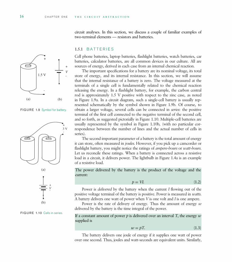
16 C H A P T E R O N E t h e c i r c u i t a b s t r a c t i o n
circuit analyses. In this section, we discuss a couple of familiar examples oftwo-terminal elements resistors and batteries.
1.5.1 B A T T E R I E S
Cell phone batteries, laptop batteries, flashlight batteries, watch batteries, carbatteries, calculator batteries, are all common devices in our culture. All aresources of energy, derived in each case from an internal chemical reaction.
The important specifications for a battery are its nominal voltage, its totalstore of energy, and its internal resistance. In this section, we will assumethat the internal resistance of a battery is zero. The voltage measured at theterminals of a single cell is fundamentally related to the chemical reactionreleasing the energy. In a flashlight battery, for example, the carbon centralrod is approximately 1.5 V positive with respect to the zinc case, as notedin Figure 1.9a. In a circuit diagram, such a single-cell battery is usually rep-
+
-
1.5 VV
+
-
(a) (b)
F IGURE 1.9 Symbol for battery.
resented schematically by the symbol shown in Figure 1.9b. Of course, toobtain a larger voltage, several cells can be connected in series: the positiveterminal of the first cell connected to the negative terminal of the second cell,and so forth, as suggested pictorially in Figure 1.10. Multiple-cell batteries areusually represented by the symbol in Figure 1.10b, (with no particular cor-respondence between the number of lines and the actual number of cells inseries).
+
-3 V
V+
-
(a)
(b)
F IGURE 1.10 Cells in series.
The second important parameter of a battery is the total amount of energyit can store, often measured in joules. However, if you pick up a camcorder orflashlight battery, you might notice the ratings of ampere-hours or watt-hours.Let us reconcile these ratings. When a battery is connected across a resistiveload in a circuit, it delivers power. The lightbulb in Figure 1.4a is an exampleof a resistive load.
The power delivered by the battery is the product of the voltage and thecurrent:
p = VI. (1.2)
Power is delivered by the battery when the current I flowing out of thepositive voltage terminal of the battery is positive. Power is measured in watts.A battery delivers one watt of power when V is one volt and I is one ampere.
Power is the rate of delivery of energy. Thus the amount of energy wdelivered by the battery is the time integral of the power.
If a constant amount of power p is delivered over an interval T, the energy wsupplied is
w = pT. (1.3)
The battery delivers one joule of energy if it supplies one watt of powerover one second. Thus, joules and watt-seconds are equivalent units. Similarly,

1.5 Practical Two-Terminal Elements C H A P T E R O N E 17
if a battery delivers one watt for an hour, then we say that it has supplied onewatt-hour (3600 joules) of energy.
Assuming that the battery terminal voltage is constant at V, because thepower delivered by the battery is the product of the voltage and the current,an equivalent indication of the power delivered is the amount of current beingsupplied. Similarly, the product of current and the length of time the bat-tery will sustain that current is an indication of the energy capacity of thebattery. A car battery, for instance, might be rated at 12 V and 50 A-hours.This means that the battery can provide a 1-A current for 50 hours, or a 100-Acurrent for 30 minutes. The amount of energy stored in such a battery is
Energy = 12 × 50 = 600 watt-hours = 600 × 3600 = 2.16 × 10⁶ joules.
e x a m p l e 1.1 a l i t h i u m - i o n b a t t e r y A Lithium-Ion (Li-Ion)battery pack for a camcorder is rated as 7.2 V and 5 W-hours. What are its equivalentratings in mA-hours and joules?
Since a joule( J ) is equivalent to a W-second, 5 W-hours is the same as 5 × 3600 =18000 J.
Since the battery has a voltage of 7.2 V, the battery rating in ampere-hours is 5/7.2 =0.69. Equivalently, its rating in mA-hours is 690.
e x a m p l e 1.2 e n e r g y c o m p a r i s o n Does a Nickel-Cadmium(Ni-Cad) battery pack rated at 6 V and 950 mA-hours store more or less energy thana Li-Ion battery pack rated at 7.2 V and 900 mA-hours?
We can directly compare the two by converting their respective energies into joules. TheNi-Cad battery pack stores 6 × 950 × 3600/1000 = 20520 J, while the Li-Ion batterypack stores 7.2 × 900 × 3600/1000 = 23328 J. Thus the Li-Ion battery pack storesmore energy.
When a battery is connected across a resistor, as illustrated in Figure 1.4,we saw that the battery delivers energy at some rate. The power was the rateof delivery of energy. Where does this energy go? Energy is dissipated bythe resistor, through heat, and sometimes even light and sound if the resistoroverheats and explodes! We will discuss resistors and power dissipation inSection 1.5.2.
If one wishes to increase the current capacity of a battery without increas-
+1.5 V
V+
V+
V
+
-
-
- -
(a)
(b)
F IGURE 1.11 Cells in parallel.
ing the voltage at the terminals, individual cells can be connected in parallel,as shown in Figure 1.11. It is important that cells to be connected in paral-lel be nearly identical in voltage to prevent one cell from destroying another.For example, a 2-V lead-acid cell connected in parallel with a 1.5 V flashlightcell will surely destroy the flashlight cell by driving a huge current through it.

18 C H A P T E R O N E t h e c i r c u i t a b s t r a c t i o n
The corresponding constraint for cells connected in series is that the nom-inal current capacity be nearly the same for all cells. The total energystored in a multicell battery is the same for series, parallel, or series-parallelinterconnections.
1.5.2 L I N E A R R E S I S T O R S
Resistors come in many forms (see Figure 1.12), ranging from lengths of
F IGURE 1.12 Discrete resistors(above), and Deposits integrated-circuit resistors (below). The imageon the bottom shows a smallregion of the MAX807L micro-processor supervisory circuit fromMaxim Integrated Products, anddepicts an array of silicon-chromium thin-film resistors, eachwith 6 µm width and 217.5 µmlength, and nominal resistance50 k. (Photograph Courtesy ofMaxim Integrated Products.)
nichrome wire used in toasters and electric stoves and planar layers of polysili-con in highly complex computer chips, to small rods of carbon particles encasedin Bakelite commonly found in electronic equipment. The symbol for resistorsin common usage is shown in Figure 1.13.
R
F IGURE 1.13 Symbol forresistor.
Over some limited range of voltage and current, carbon, wire andpolysilicon resistors obey Ohm’s law:
v = iR (1.4)
that is, the voltage measured across the terminals of a resistor is linearlyproportional to the current flowing through the resistor. The constant of pro-portionality is called the resistance. As we show shortly, the resistance of apiece of material is proportional to its length and inversely proportional to itscross-sectional area.
In our example of Figure 1.4b, suppose that the battery is rated at 1.5 V.Further assume that the resistance of the bulb is R = 10 . Assume that theinternal resistance of the battery is zero. Then, a current of i = v/R = 150 mAwill flow through the bulb.
e x a m p l e 1.3 m o r e o n r e s i s t a n c e In the circuit in Figure 1.4b,suppose that the battery is rated at 1.5 V. Suppose we observe through some means acurrent of 500 mA through the resistor. What is the resistance of the resistor?
For a resistor, we know from Equation 1.4 that
R = v
i
Since the voltage v across the resistor is 1.5 V and the current i through the resistor is500 mA, the resistance of the resistor is 3 .
The resistance of a piece of material depends on its geometry. As illus-trated in Figure 1.14, assume the resistor has a conducting channel withcross-sectional area a, length l, and resistivity ρ. This channel is terminatedat its extremes by two conducting plates that extend to form the two terminalsof the resistor. If this cylindrical piece of material satisfies the lumped matter

1.5 Practical Two-Terminal Elements C H A P T E R O N E 19
Area a
i
+ -v
l
Resistivity ρ F IGURE 1.14 A cylindrical-wireshaped resistor.
discipline and obey’s Ohm’s law, we can write13
R = ρl
a(1.5)
Equation 1.5 shows that the resistance of a piece of material is proportional toits length and inversely proportional to its cross-sectional area.
Similarly, the resistance of a cuboid shaped resistor with length l, width w,and height h is given by
R = ρl
wh(1.6)
when the terminals are taken at the pair of surfaces with area wh.
e x a m p l e 1.4 r e s i s t a n c e o f a c u b e Determine the resistanceof a cube with sides of length 1 cm and resistivity 10 ohm-cms, when a pair of oppositesurfaces are chosen as the terminals.
Substituting ρ = 10 -cm, l = 1 cm, w = 1 cm, and h = 1 cm in Equation 1.6, we getR = 10 .
e x a m p l e 1.5 r e s i s t a n c e o f a c y l i n d e r By what factor isthe resistance of a wire with cross-sectional radius r greater than the resistance of a wirewith cross-sectional radius 2r?
A wire is cylindrical in shape. Equation 1.5 relates the resistance of a cylinder to itscross-sectional area. Rewriting Equation 1.5 in terms of the cross-sectional radius rwe have
R = ρl
π r 2.
From this equation it is clear that the resistance of a wire with radius r is four timesgreater than that of a wire with cross-sectional radius 2r.
13. See Appendix A.3 for a derivation.

20 C H A P T E R O N E t h e c i r c u i t a b s t r a c t i o n
e x a m p l e 1.6 c a r b o n - c o r e r e s i s t o r s The resistance of smallcarbon-core resistors can range from 1 to 106 . Assuming that the core of theseresistors is 1 mm in diameter and 5 mm long, what must be the range of resistivity ofthe carbon cores?
Given a 1-mm diameter, the cross-sectional area of the core is A ≈ 7.9 × 10⁻⁷ m2.Further, its length is l = 5 × 10⁻³m. Thus, A/l ≈ 1.6 × 10⁻⁴ m.
Finally, using Equation 1.5, with 1 ≤ R ≤ 106 , it follows that the approximaterange of its resistivity is 1.6 × 10⁻⁴ m ≤ ρ ≤ 1.6 × 10²m.
e x a m p l e 1.7 p o l y - c r y s t a l l i n e s i l i c o n r e s i s t o r
A thin poly-crystalline silicon resistor is 1 µm thick, 10 µm wide, and 100 µm long,where 1 µm is 10−6 m. If the resistivity of its poly-crystalline silicon ranges from10−6 m to 102 m, what is the range of its resistance?
The cross-sectional area of the resistor is A = 10−11 m, and its length is l = 10−4 m.Thus l/A = 107 m−1. Using Equation 1.5, and the given range of resistivity, ρ, theresistance satisfies 10 ≤ R ≤ 109 .
e x a m p l e 1.8 r e s i s t a n c e o f p l a n a r m a t e r i a l s o n
a c h i p Figure 1.15 shows several pieces of material with varying geometries.Assume all the pieces have the same thickness. In other words, the pieces of materialare planar. Let us determine the resistance of these pieces between the pairs of terminalsshown. For a given thickness, remember that the resistance of a piece of material in theshape of a cuboid is determined by the ratio of the length to the width of the piece ofmaterial (Equation 1.6). Assuming that Ro is the resistance of a piece of planar material
F IGURE 1.15 Resistors ofvarious shapes.
44
33 6
2
121 6
2
9
6
6 3
M1 M2 M3
M4 M5
M6 M7

1.5 Practical Two-Terminal Elements C H A P T E R O N E 21
with unit length and width, show that the resistance of a piece of planar material withlength L and width W is (L/W )Ro.
From Equation 1.6, the resistance of a cuboid shaped material with length L,width W, height H, and resistivity ρ is
R = ρL
WH. (1.7)
We are given that the resistance of a piece of the same material with L = 1 and W = 1is Ro. In other words,
Ro = ρ1
H. (1.8)
Substituting Ro = ρ/H in Equation 1.7, we get
R = L
WRo. (1.9)
Now, assume Ro = 2 k for our material. Recall that Ohms are the unit of resistanceand are written as . We denote a 1000- value as kilo- or k. Assuming that thedimensions of the pieces of material shown in Figure 1.15 are in µ-m, or micrometers,what are their resistances?
First, observe that pieces M1, M2, and M6 must have the same resistance of 2 k becausethey are squares (in Equation 1.9, notice that L/W = 1 for a square).
Second, M3 and M7 must have the same resistance because both have the same ratioL/W = 3. Therefore, both have a resistance of 3 × 2 = 6 k. Among them, M4 hasthe biggest L/W ratio of 12. Therefore it has the largest resistance of 24 k. M5 has thesmallest L/W ratio of 1/3, and accordingly has the smallest resistance of 2/3 k.
Because all square pieces made out of a given material have the same resistance (provided,of course, the pieces have the same thickness), we often characterize the resistivity ofplanar material of a given thickness with
R = Ro, (1.10)
where Ro is the resistance of a piece of the same material with unit length and width.Pronounced ‘‘R square,’’ R is the resistance of a square piece of material.
e x a m p l e 1.9 m o r e o n p l a n a r r e s i s t a n c e s Referringback to Figure 1.15, suppose an error in the material fabrication process results in eachdimension (L and W) increasing by a fraction e. By what amount will the resistances ofeach of the pieces of material change?

22 C H A P T E R O N E t h e c i r c u i t a b s t r a c t i o n
Recall that the resistance R of a planar rectangular piece of material is proportional toL/W. If each dimension increases by a fraction e, the new length becomes L(1 + e) andthe new width becomes W(1 + e). Notice that the resistance given by
R = L(1 + e)
W(1 + e)Ro = L
WRo
is unchanged.
e x a m p l e 1.10 r a t i o o f r e s i s t a n c e s Referring again toFigure 1.15, suppose the material fabrication process undergoes a ‘‘shrink’’ to decreaseeach dimension (this time around, increasing the thickness H in addition to L andW) by a fraction α (e.g., α = 0.8). Assume further, that the resistivity ρ changes bysome other fraction to ρ′. Now consider a pair of resistors with resistances R1 andR2, and original dimensions L1, W1 and L2, W2 respectively, and the same thicknessH. By what fraction does the ratio of the resistance values change after the processshrink?
From Equation 1.7, the ratio of the original resistance values is given by
R1
R2= ρL1/(W1H)
ρL2/(W2H)= L1/W1
L2/W2.
Let the resistance values after the process shrink be R′1 and R′
2. Since each dimensionshrinks by the fraction α, each new dimension will be α times the original value. Thus,for example, the length L1 will change to αL1. Using Equation 1.7, the ratio of the newresistance values is given by
R′1
R′2
= ρ′αL1/(αW1αH)
ρ′αL2/(αW2αH)= L1/W1
L2/W2
In other words, the ratio of the resistance values is unchanged by the processshrink.
The ratio property of planar resistance that is that the ratio of the resistancesof rectangular pieces of material with a given thickness and resistivity is independentof the actual values of the length and the width provided the ratio of the length and thewidth is fixed enables us to perform process shrinks (for example, from a 0.25-µmprocess to a 0.18-µm process) without needing to change the chip layout. Processshrinks are performed by scaling the dimensions of the chip and its components by thesame factor, thereby resulting in a smaller chip. The chip is designed such that relevant

1.5 Practical Two-Terminal Elements C H A P T E R O N E 23
F IGURE 1.16 A silicon wafer.(Photograph Courtesy of MaximIntegrated Products.)
F IGURE 1.17 A chip photo ofIntel’s 2-GHz Pentium IV processorimplemented in 0.18µm-technology.The chip is roughly 1 cm on a side.(Photograph courtesy of IntelCorp.)
signal values are derived as a function of resistance ratios,14 thereby ensuring that thechip manufactured after a process shrink continues to function as before.
VLSI stands for ‘‘Very Large Scale Integration.’’ Silicon-based VLSI is the technologybehind most of today’s computer chips. In this technology, lumped planar elementssuch as wires, resistors, and a host of others that we will soon encounter, are fabricatedon the surface of a planar piece of silicon called a wafer (for example, see Figures 1.15and 1.12). A wafer has roughly the shape and size of a Mexican tortilla or an Indianchapati (see Figure 1.16). The planar elements are connected together using planar wiresto form circuits. After fabrication, each wafer is diced into several hundred chips or‘‘dies,’’ typically, each the size of a thumbnail. A Pentium chip, for example, containshundreds of millions of planar elements (see Figure 1.17). Chips are attached, or bonded,to packages (for example, see Figure 12.3.4), which are in turn mounted on a printed-circuit board along with other discrete components such as resistors and capacitors (forexample, see Figure 1.18) and wired together.
14. We will study many such examples in the ensuing sections, including the voltage divider inSection 2.3.4 and the inverter in Section 6.8.

24 C H A P T E R O N E t h e c i r c u i t a b s t r a c t i o n
F IGURE 1.18 A printed-circuitboard containing several inter-connected chip packages anddiscrete components such asresistors (tiny box-like objects) andcapacitors (tall cylindrical objects).(Photograph Courtesy of AnantAgarwal, the Raw Group.)
As better processes become available, VLSI fabrication processes undergo periodicshrinks to reduce the size of chips without needing significant design changes. ThePentium III, for example, initially appeared in the 0.25-µm process, and later in the0.18-µm process. The Pentium IV chip shown in Figure 1.17 initially appeared in a0.18-µm process in the year 2000, and later in 0.13-µm and 0.09-µm processes in2001 and 2004, respectively.
There are two important limiting cases of the linear resistor: open circuitsand short circuits. An open circuit is an element through which no currentflows, regardless of its terminal voltage. It behaves like a linear resistor in thelimit R → ∞.
A short circuit is at the opposite extreme. It is an element across which novoltage can appear regardless of the current through it. It behaves like a linearresistor in the limit R → 0. Observe that the short circuit element is the sameas an ideal wire. Note that neither the open circuit nor the short circuit dissipatepower since the product of their terminal variables (v and i ) is identically zero.
Most often, resistances are thought of as time-invariant parameters. But ifthe temperature of a resistor changes, then so too can its resistance. Thus, alinear resistor can be a time-varying element.
The linear resistor is but one example of a larger class of resistive elements.In particular, resistors need not be linear; they can be nonlinear as well. Ingeneral, a two-terminal resistor is any two-terminal element that has an alge-braic relation between its instantaneous terminal current and its instantaneousterminal voltage. Such a resistor could be linear or nonlinear, time-invariant ortime-varying. For example, elements characterized by the following elementrelationships are all general resistors:
Linear resistor: v(t) = i(t)R(t)
Linear, time-invariant resistor: v(t) = i(t)R
Nonlinear resistor: v(t) = Ki(t)3

1.5 Practical Two-Terminal Elements C H A P T E R O N E 25
However, as introduced in Chapter 9, elements characterized by theserelationships are not general resistors:
v(t) = Ldi(t)
dt
v(t) = 1
C
∫ t
−∞i(t′)dt′
What is important about the general resistor is that its terminal currentand voltage depend only on the instantaneous values of each other. For ourconvenience, however, an unqualified reference to a resistor in this book meansa linear, time-invariant resistor.
1.5.3 A S S O C I A T E D V A R I A B L E S C O N V E N T I O N
Equation 1.4 implies a specific relation between reference directions chosen forvoltage and current. This relation is shown explicitly in Figure 1.19: the arrow
v
Ri
+ -
F IGURE 1.19 Definition ofterminal variables v and i for theresistor.
that defines the positive flow of current (flow of positive charge) is directed in atthe resistor terminal assigned to be positive in voltage. This convention, referredto as associated variables, is generalized to an arbitrary element in Figure 1.20and will be followed whenever possible in this text. The variables v and i arecalled the terminal variables for the element. Note that the values of each ofthese variables may be positive or negative depending on the actual directionof current flow or the actual polarity of the voltage.
i
v
i
-
+
F IGURE 1.20 Definition of theterminal variables v and i for atwo-terminal element under theassociated variables convention.
Associated Variables Convention Define current to flow in at the deviceterminal assigned to be positive in voltage.
When the voltage v and current i for an element are defined under theassociated variables convention, the power into the element is positive whenboth v and i are positive. In other words, energy is pumped into an elementwhen a positive current i is directed into the voltage terminal marked positive.Depending on the type of element, the energy is either dissipated or stored.Conversely, power is supplied by an element when a positive current i is directedout of the voltage terminal marked positive. When the terminal variables for aresistor are defined according to associated variables, the power dissipated inthe resistor is a positive quantity, an intuitively satisfying result.
While Figure 1.20 is quite simple, it nonetheless makes several importantpoints. First, the two terminals of the element in Figure 1.20 form a single portthrough which the element is addressed. Second, the current i circulates throughthat port. That is, the current that enters one terminal is instantaneously equalto the current that exits the other terminal. Thus, according to the lumpedmatter discipline, net charge cannot accumulate within the element. Third, thevoltage v of the element is defined across the port. Thus, the element is assumedto respond only to the difference of the electrical potentials at its two terminals,

26 C H A P T E R O N E t h e c i r c u i t a b s t r a c t i o n
and not to the absolute electric potential at either terminal. Fourth, the current isdefined to circulate positively through the port by entering the positive voltageterminal and exiting the negative voltage terminal. Which terminal is chosen asthe positive voltage terminal is arbitrary, but the relation defined between thecurrent and voltage is not. Lastly, for brevity, the current that exits the negativevoltage terminal is usually never labeled, but it is always understood to be equalto the current that enters the positive voltage terminal.
e x a m p l e 1.11 t e r m i n a l v a r i a b l e s v e r s u s e l e m e n t
p r o p e r t i e s Figures 1.21a and b shows two possible legal definitions for ter-minal variables for a 3 V battery. What is the value of terminal variable v in eachcase?
For Figure 1.21a, we can see that terminal variable v = 3 V. For Figure 1.21b, however,v = −3 V .
v
i
-
+
3 V
(a)
+
-
v
i +
-
3 V
(b)
-
+
F IGURE 1.21 Terminal variableassignments for a battery.
This example highlights the distinction between a terminal variable and an elementproperty. The battery voltage of 3 V is an element property, while v is a terminalvariable that we have defined. Element properties are usually written inside the elementsymbol, or if that is inconvenient, they are written next to the element (e.g., the batteryvoltage). Terminal polarities and terminal variables are written close to the terminals.
e x a m p l e 1.12 f u n w i t h t e r m i n a l v a r i a b l e s Figure1.22 shows some two-terminal element connected to an arbitrary circuit at the pointsx and y. The element terminal variables v and i are defined according to the associ-
v
i
-
+x
y
2 A
F IGURE 1.22 Terminal variableassignments for a two-terminalelement.
ated variables convention. Suppose that a current of 2 A flows into the circuit terminalmarked x. What is the value of terminal variable i?
Since the chosen direction of the terminal variable i is opposite to that of the 2 A current,i = −2 A.
Now suppose that the two terminal element is a resistor (see Figure 1.23) with resistance
v
i
-
+x
y
2 A
R
F IGURE 1.23 Terminal variableassignments for a resistor.
R = 10 Ohms. Determine the value of v.
We know that under the associated variables convention the terminal variablesfor a resistor are related as
v = iR
Given that R = 10 and i = −2 A,
v = (−2)10 = −20 V
Next, suppose that the two terminal element is a 3 V battery with the polarity shownin Figure 1.24a. Determine the values of terminal variables v and i.
As determined earlier, i = −2 A. For the polarity of the battery shown in Figure 1.24a,v = 3 V.

1.5 Practical Two-Terminal Elements C H A P T E R O N E 27
Now, suppose the 3 V battery is connected with the polarity shown in Figure 1.24b.Determine that values of v and i.
As before, i = −2 A. With the reversed battery connection shown in Figure 1.24b, v
i
-
+
3 V
(a)
+
-
x
y
2 A
(b)
v
i
-
+
3 V+
-
x
y
2 A
F IGURE 1.24 The two-terminalelement is a battery.
v = −3 V.
Under the associated variables convention, the instantaneous power p suppliedinto an element is given by
p = vi (1.11)
with units of watts (W).
Note that both v and i, and therefore the instantaneous power p, can befunctions of time. For a resistor, p = vi represents the instantaneous powerdissipated by the resistor.
Correspondingly, the amount of energy (in units of joules) supplied to anelement during an interval of time between t1 and t2 under the associatedvariables convention is given by
w =∫ t2
t1vi dt. (1.12)
For a resistor, by noting that v = iR from Equation 1.4, the power relationfor a two-terminal element (Equation 1.11) can be equivalently written as
p = i 2R (1.13)
or
p = v 2
R. (1.14)
e x a m p l e 1.13 p o w e r i n t o a r e s i s t o r Determine the powerfor the resistor in Figure 1.23. Confirm mathematically that the power is indeed suppliedinto the resistor.
We know that i = −2 A and v = −20 V. Therefore, the power is given by
p = vi = (−20V )(−2A) = 40 W
By our associated variables convention, the product p = vi yields the power suppliedinto the element. Thus, we can confirm that 40 W of power is being supplied into theresistor. From the properties of a resistor, we also know that this power is dissipated inthe form of heat.

28 C H A P T E R O N E t h e c i r c u i t a b s t r a c t i o n
e x a m p l e 1.14 p o w e r s u p p l i e d b y a b a t t e r y Determinethe power for the battery using the two assignments of terminal variables in Figures 1.25aand 1.25b.
For the assignment of terminal variables in Figure 1.25a, i = −2 A and v = 3 V. Thus,by associated variables, power into the battery is given by
p = vi = (3V )(−2A) = −6 W
Since the power into the battery is negative, the power supplied by the battery is positive.Thus, in the circuit of Figure 1.25a, the battery is delivering power.
Next, let us analyze the same circuit with the assignment of terminal variables inv
i
-
+
3 V
(b)
+
-
x
y
2 A
v
i
-
+
3 V
(a)
+
-
x
y
2 A
F IGURE 1.25 Alternativeassignments of terminal variables.
Figure 1.25b. For this assignment, i = 2 A and v = −3 V. Thus, by associated variables,power into the battery is given by
p = vi = (−3V )(2A) = −6 W
In other words, the battery is delivering 6 watts of power. Since the circuit is the same, itis not surprising that our result has not changed when the terminal variable assignmentsare reversed.
e x a m p l e 1.15 p o w e r s u p p l i e d v e r s u s p o w e r
a b s o r b e d b y a b a t t e r y In simple circuits, for example, circuits con-taining a single battery, we do not have to undergo the rigor of associated variablesto determine whether power is being absorbed or supplied by an element. Let us workout such an example. In our lightbulb circuit of Figure 1.4b, suppose that the batteryis rated at 1.5 V and 1500 J. Assume that the internal resistance of the battery is zero.Further assume that the resistance of the bulb is R = 10 . What is the power dissipatedin the resistor?
The power dissipated in the resistor is given by
p = VI = V2
R= 1.52
10= 0.225 W
Since the entire circuit comprises a battery and a resistor, we can state without a lot ofanalysis that the resistor dissipates power and the battery supplies it. How much powerdoes the battery provide when it is connected to the 10- resistor? Suppose the batterysupplies a current I. We can quickly compute the value of this current as:
I = V
R= 1.5
10= 0.15 A

1.6 Ideal Two-Terminal Elements C H A P T E R O N E 29
Thus the power delivered by the battery is given by
p = VI = 1.5 × 0.15 = 0.225 W
Not surprisingly, the power delivered by the battery is the same as the power dissipatedin the resistor. Note that since the circuit current I has been defined to be directed out ofthe positive battery terminal in Figure 1.4b, and since the current is positive, the batteryis supplying power.
How long will our battery last when it is connected to the 10- resistor? Since thebattery is supplying 0.225 W of power, and since a watt represents energy dissipationat the rate of one joule per second, the battery will last 1500/0.225 = 6667 s.
e x a m p l e 1.16 p o w e r r a t i n g o f a r e s i s t o r In a circuitsuch as that shown in Figure 1.4b, the battery is rated at 7.2 V and 10000 J. Assume thatthe internal resistance of the battery is zero. Further assume that the resistance in thecircuit is R = 1 k. You are given that the resistor can dissipate a maximum of 0.5 Wof power. ( In other words, the resistor will overheat if the power dissipation is greaterthan 0.5 W.) Determine the current through the resistor. Further, determine whetherthe power dissipation in the resistor exceeds its maximum rating.
The current through the resistor is given by
I = V
R= 7.2
1000= 7.2 mA
The power dissipation in the resistor is given by
p = I 2R = (7.2 × 10⁻³)2103 = 0.052 W
Clearly, the power dissipation in the resistor is well within its capacity.
1.6 I D E A L T W O - T E R M I N A L E L E M E N T S
As we saw previously, the process of discretization can be viewed as a wayof modeling physical systems. For example, the resistor is a lumped modelfor a lightbulb. Modeling physical systems is a major motivation for studyingelectronic circuits. In our lightbulb circuit example, we used lumped electricalelements to model electrical components such as bulbs and batteries. In general,modeling physical systems involves representing real-world physical processes,whether they are electrical, chemical, or mechanical, in terms of a set of idealelectrical elements. This section introduces a set of ideal two-terminal elementsincluding voltage and current sources, and ideal wires and resistors, which formour primitives in the vocabulary of circuits.

30 C H A P T E R O N E t h e c i r c u i t a b s t r a c t i o n
The same set of ideal two-terminal elements serve to build either informa-tion processing or energy processing systems as well. Information and energyprocessing includes the communication, storage, or transformation of informa-tion or energy, and is a second major motivation for studying electronic circuits.Whether we are interested in modeling systems or in information and energyprocessing, it is essential to be able to represent five basic processes in terms ofour lumped circuit abstraction.
1. Sources of energy or information
2. Flow of energy or information in a system
3. Loss of energy or information in a system
4. Control of energy flow or information flow by some external force
5. Storage of energy or information
We will discuss ideal two-terminal elements that represent the first threeof these in this section, deferring control and storage until Chapters 6 and 9,respectively.
1.6.1 I D E A L V O L T A G E S O U R C E S , W I R E S ,A N D R E S I S T O R S
Familiar primary sources of energy in our daily lives are sunlight, oil, and coal.Secondary sources would be power plants, gasoline engines, home-heatingfurnaces, or flashlight batteries. In heating systems, energy flows through airducts or heating pipes; in electrical systems the flow is through copper wires.15
Similarly, information sources include speech, books, compact discs, videos,(a)
+
-
V+
-V
(b)
+
-v(t)
(c)
F IGURE 1.26 Circuit symbol fora voltage source: (a) battery;(b) voltage source; (c) voltagesource.
and the web (some of it, anyway!). Information flow in speech systems isthrough media such as air and water; in electronic systems, such as computersor phones, the flow relies on conducting wires. Sensors such as microphones,magnetic tape heads, and optical scanners convert information from variousforms into an electrical representation. None of these elements is ideal, so ourfirst task is to invent ideal energy or information sources and ideal conductorsfor energy or information flow.
Conceptually, it is relatively easy to extrapolate from known propertiesof a battery to postulate an ideal voltage source as a device that maintains aconstant voltage at its terminals regardless of the amount of current drawnfrom those terminals. To distinguish such an ideal element from a battery16
(see Figure 1.26a), we denote a voltage source by a single circle with polarity
15. Or, more accurately, in the fields between the wires.
16. In general, a physical battery has some internal resistance, which we ignored in our previousexamples. A more precise relationship between the ideal voltage source and the battery is developedin Section 1.7.

1.6 Ideal Two-Terminal Elements C H A P T E R O N E 31
markings inside it, as in Figure 1.26b. If the voltage source supplies a voltage V,then we also include the V symbol inside the circle (or just outside the circle ifthere is not enough room to write the symbol inside). In the same manner, wemight also represent an information source, such as a microphone or a sensor, asa voltage source providing a time-varying voltage v(t) at its output (Figure 1.26c).We can assume that the voltage v(t) depends solely on the microphone signaland is independent of the amount of current drawn from the terminals. (Notethat V and v(t) in Figure 1.26 are element values and not terminal variables.)
We will see two types of voltage sources: independent and dependent. Anindependent voltage source supplies a voltage independent of the rest of thecircuit. Accordingly, independent sources are a means through which inputscan be made to a circuit. Power supplies, signal generators, and microphonesare examples of independent voltage sources. The circle symbol in Figure 1.26brepresents an independent voltage source. In contrast to an independent voltagesource, a dependent voltage source supplies a voltage as commanded by a signalfrom within the circuit of which the source is a part. Dependent sources aremost commonly used to model elements having more than two terminals. Theyare represented with a diamond symbol; we shall see examples of these in futurechapters.
In a manner similar to our invention of the ideal voltage source, we pos-tulate an ideal conductor to be one in which any amount of current can flowwithout loss of voltage or power. The symbol for an ideal conductor is shown
(a) (b)
F IGURE 1.27 Circuit symbol foran ideal conductor: (a) perfectconductor; (b) wire with nonzeroresistance.
in Figure 1.27a. Notice that the symbol is just a line. The ideal conductor is nodifferent from the ideal wire we saw earlier. Ideal conductors can be used torepresent a channel for fluid flow in hydrodynamic systems.
Any physical length of wire will have some nonzero resistance. The resis-tance dissipates energy and represents a loss of energy from the system. If thisresistance is important in a particular application, then we can model the wireas an ideal conductor in series with a resistor, as suggested in Figure 1.27b. Tobe consistent, we now state that the resistor symbol introduced in Figure 1.19represents an ideal linear resistor, which by definition obeys Ohm’s law
v = iR (1.15)
for all values of voltage and current. Resistors can be used to model processessuch as friction that result in energy loss in a system. Note that because thiselement law is symmetric, it is unchanged if the polarities of the current andvoltage definitions are reversed. Sometimes it is convenient to work with recip-rocal resistance, namely the conductance G having the units of Siemens (S). Inthis case,
G = 1
R(1.16)
and
i = Gv. (1.17)

32 C H A P T E R O N E t h e c i r c u i t a b s t r a c t i o n
Most often, resistances and conductances are thought of as time-invariantparameters. But if the temperature of a resistor changes, then so too canits resistance and conductance. Thus, a linear resistor can be a time-varyingelement.
1.6.2 E L E M E N T L A W S
From the viewpoint of circuit analysis, the most important characteristic of atwo-terminal element is the relation between the voltage across and the currentthrough its terminals, or the v i relationship for short. This relation, calledthe element law, represents the lumped-parameter summary of the electronicbehavior of the element. for example, as seen in Equation 1.15,
v = iR
is the element law for the resistor. The element law is also referred to as theconstituent relation, or the element relation. In order to standardize the manner
i
v
Slope =1
R---
0
F IGURE 1.28 Plot of the v–irelationship for a resistor.
in which element laws are expressed, the current and voltage for all two-terminalelements are defined according to the associated variables convention shown inFigure 1.19. Figure 1.28 shows a plot of the v i relationship for a resistor whenv and i are defined according to the associated variables convention.
The constituent relation for the independent voltage source in Figure 1.26b
i
vV0
(b)
-
+
i
vV+
-
(a)
F IGURE 1.29 (a) Independentvoltage source with assignedterminal variables, (b) v–i relation-ship for the voltage source.
supplying a voltage V is given by
v = V (1.18)
when its terminal variables are defined as in Figure 1.29a. A plot of the v irelationship is shown in Figure 1.29b. Observe the clear distinction betweenthe element parameter V and its terminal variables v and i.
Similarly, the element law for the ideal wire (or a short circuit) is given by
v = 0. (1.19)
Figure 1.30a shows the assignment of terminal variables and Figure 1.30bplots the v i relationship.
Finally, the element law for an open circuit is given by
i = 0. (1.20)
Figure 1.31a shows the assignment of terminal variables and Figure 1.31bplots the v − i relationship.
Comparing the v i relationship for the resistor in Figure 1.28 to those for ashort circuit in Figure 1.30 and an open circuit in Figure 1.31, it is evident thatthe short circuit and open circuit are limiting cases for a resistor. The resistorapproaches the short circuit case as its resistance approaches zero. The resistorapproaches the open circuit case as its resistance approaches infinity.

1.6 Ideal Two-Terminal Elements C H A P T E R O N E 33
e x a m p l e 1.17 m o r e o n t e r m i n a l v a r i a b l e s v e r s u s
e l e m e n t p r o p e r t i e s Figure 1.32 shows a 5-V voltage source connectedto an arbitrary circuit at the points x and y. Its terminal variables v and i are defined
-
+
i
v
(a)
i
v0
(b)
F IGURE 1.30 (a) Ideal wire withterminal variables, (b) v–i relation-ship for the wire.
according to the associated variables convention as indicated in the figure. Supposethat a current of 2 A flows into the circuit terminal marked x. What are the values ofv and i?
For the assignment of terminal variables shown in Figure 1.32, i = 2 A andv = −5 V.
Notice the distinction between terminal variables and element properties in thisexample. The source voltage of 5 V is an element property, while v is a terminal variablethat we have defined. Similarly, the polarity markings inside the circle are a property ofthe source, while the polarity markings outside the circle representing the source relateto the terminal variable v. When possible, we attempt to write the element values insidethe element symbol, while the terminal variables are written outside.
e x a m p l e 1.18 c h a r t i n g V I r e l a t i o n s h i p s An experi-mental way of charting the v i relationship for a two-terminal element is to connectan oscilloscope and an oscillator (or a signal generator set to produce an oscillatory out-put) in a curve-plotter configuration as suggested in Figure 1.33. The oscillator producesa voltage given by
i
v0
(b)
-
+
i
v
(a)
F IGURE 1.31 (a) An opencircuit element with terminalvariables, (b) v–i relationshipfor the open circuit.
vi = Vcos(ωt).
The basic concept is to use the oscillator to drive current into some arbitrary two-terminaldevice, and measure the resulting voltage vD and current iD. Notice that the terminalvariables for the two-terminal device, vD and iD, are defined according to the associatedvariables convention. As can be seen from the circuit, the horizontal deflection will beproportional to vD, and the vertical deflection will be proportional to vR, and henceto iD, assuming resistor R obeys Ohm’s law, and the horizontal and vertical amplifierinputs to the oscilloscope draw negligible current.
1.6.3 T H E C U R R E N T S O U R C E — A N O T H E R I D E A LT W O - T E R M I N A L E L E M E N T
In some fields of engineering, there are two obvious sources of power thatappear to have dual properties. Think, for example, of air pumps. For anordinary tire pump, the higher the air pressure, the harder the person at thepump-handle has to work. But with a household vacuum cleaner, also an airpump of sorts, you can hear the motor actually speed up if the air flow out ofthe machine is blocked, and a measurement of motor current would confirmthat the power to the motor goes down under these conditions.

34 C H A P T E R O N E t h e c i r c u i t a b s t r a c t i o n
It seems reasonable, then, to look for an electrical source that has charac-
v
i
-
+
x
y
2 A
5 V+
-
F IGURE 1.32 Terminal variablesversus element properties.
teristics that are the dual of those of the battery, in that the roles of current andvoltage are interchanged. From the point of view of v i characteristics, this isa simple task. The ideal voltage source appears as a vertical line in v i space,so this other source, which we call an ideal current source, should appear as ahorizontal line, as in Figure 1.34. Such a source maintains its output current atsome constant value I regardless of what voltage appears across the terminals.
The element law for a current source supplying a current I is given by
i = I. (1.21)
If the source were left with nothing connected across its terminals, then, intheory at least, the terminal voltage must rise to infinity because the constantcurrent flowing through an infinite resistance gives infinite voltage. Recall theanalogous problem with the ideal voltage source: If a short circuit is applied,the terminal current must become infinite.
It is difficult at first to have an intuitive grasp of the current source, princi-pally because there is no familiar device available at the electronic parts counterthat has these properties. However, one can still find special devices that deliverconstant current to the arc lamps to illuminate the streets of Old Montreal,and we will show later that MOSFETs and Op Amps make excellent currentsources. But these are not as familiar as the flashlight battery.
e x a m p l e 1.19 c u r r e n t s o u r c e p o w e r Determine thepower for the 3-A current source in Figure 1.35 if a measurement shows that v = 5 V.
For the assignment of terminal variables in Figure 1.35, i = −3 A. Further, we are giventhat v = 5V. Power into the current source is given by
p = vi = (5V )(−3A) = −15 W.
Since the power into the current source is negative, we determine that power is beingsupplied by the current source.
F IGURE 1.33 Charting on anoscilloscope the v–i relationship fora two-terminal element.
-
+ Unknown2-terminaldevice
vD Oscilloscopewithbalancedinputs
Resistor ofknown valueR
vR-
+
iD
Testoscillator
V+
V-
H+
H-
+
-vi = V cos(ωt)

1.6 Ideal Two-Terminal Elements C H A P T E R O N E 35
Before proceeding further, it is important to distinguish between the model
I
i
v
i = constant
i
+
-
I
v
0
F IGURE 1.34 v–i plot forcurrent source.
of a two-terminal element and the element itself. The models, or element laws,presented in this section are idealized. They describe a simplified behavior
v
i
-
+x
y
3 A
F IGURE 1.35 Power for thecurrent source.
of the real elements (a voltage source for a battery, for instance). From thispoint forward, we will focus on circuits comprising only ideal elements, andmake only occasional reference to reality. Nonetheless, it is important to realizein practice that the result of a circuit analysis is only as good as the modelson which the analysis is based. Part of any discrepancy between theory andexperiment may be a result of the fact that the elements do not really behaveas the elements laws predict.
The v i relation is useful to describe other systems as well, not just primi-tive two-terminal elements such as sources and resistors. When creating circuitmodels for these systems, it is often the case that an electronic circuit canbe abstracted as a black box accessible through a few terminals. As with anyabstraction, the details of behavior at the interfaces (terminals, in our case)are more important than the details of behavior internal to the black box.That is, what happens at the terminals is more important than how it hap-pens inside the black box. Furthermore, it is often the case that the terminalscan be paired into ports in a natural way following the function of the circuit.For example, a complex amplifier or filter is often described by the relationbetween an input signal presented to the amplifier or filter at one pair of ter-minals or port, and an output signal presented by the amplifier or filter ata second port. In this case, the terminal pairs or ports take on special sig-nificance, and the voltage across the port and the current through the portbecome the port variables in terms of which the electronic circuit behavior isdescribed.
In principle, an electronic circuit can have one or more ports, although inpractice it is common to define only a few ports to simplify matters. For exam-ple, an amplifier may be described in terms of its input port, its output port,and one or more ports for connection to power supplies. Even simple network
i
v
+
-
F IGURE 1.36 Definition of thevoltage and current for a port.
elements such as sources, resistors, capacitors, and inductors can be thought ofas one-port devices. Voltages are defined across the ports and currents throughthe ports as illustrated in Figure 1.36. Observe that the assignment of refer-ence directions related to v and i follows the associated variables conventiondiscussed in Section 1.5.2.
The notion of a port is much more general than its use in electronic cir-cuit analysis would indicate. Many physical systems, such as mechanical, fluid,or thermal systems can be characterized by their behavior at a few ports. Fur-thermore, as depicted in Table 1.1 they have through and across parametersanalogous to currents and voltages. Circuit models for these systems would usevoltages and currents to model the corresponding through and across variablesin those systems.

36 C H A P T E R O N E t h e c i r c u i t a b s t r a c t i o n
t h r o u g h a c r o s s
Current Voltage
Force Motion
Flow Pressure
Heat Flux Temperature
Consumption Wealth
TABLE 1.1 Through and acrossvariables in physical and economicsystems.
1.7 M O D E L I N G P H Y S I C A L E L E M E N T S
Thus far, we have invented four ideal, primitive elements and studied theirv i characteristics. These ideal elements included the independent voltagesource, the independent current source, the linear resistor, and the perfect con-ductor. Let us now return to building models for some of the physical elementswe have seen thus far in terms of the four ideal elements.
Indeed, Figure 1.27b is one example of a model. We have modeled aphysical device, namely, a length of copper wire, by a pair of ideal two-terminalelements: a perfect conductor and a linear resistance. Obviously this modelis not exact. For example, if 1000 A of current flowed through a piece of14-gauge copper wire (standard house wire designed to carry 15 A), the wirewould become hot, glow brightly, and probably melt, thereby converting itselffrom a resistor with a very small resistance, for example, 0.001 , to an infiniteresistor. Our model, consisting of an ideal conductor in series with an ideal0.001- resistor, shows no such behavior: With 1000 A flowing, a one-voltdrop would develop across the resistor, and one thousand watts of powerwould be dissipated, presumably in heat, as long as the current flowed. Nosmoke, no burnout.
In a similar way we can devise a model for a battery out of our idealelements. When a flashlight bulb is connected to a new nominally 6-V battery,the voltage at the terminals of the battery (usually called the terminal voltage)drops from 6.2 V to perhaps 6.1 V. This drop results from the internal resistanceof the battery. To represent this effect, we model the battery as an ideal voltagesource in series with some small resistor R as shown in Figure 1.37a. The drop in
F IGURE 1.37 One model for abattery.
+
-
(b)
R
(a)
V+
-
V

1.7 Modeling Physical Elements C H A P T E R O N E 37
R
Lightbulbvt
-
+
V+
-
F IGURE 1.38 Battery modeland lightbulb.
+
-
(b)
Rm
(a)
V(t)+
-F IGURE 1.39 A microphonemodel.
terminal voltage when the bulb is initially connected will be properly representedin the circuit model of Figure 1.38 if the value of R is appropriately chosen.However, the model is still not exact. For example, if a lightbulb is connectedto a battery for some time, the battery voltage will slowly drop as the energyis drained from the battery. The model battery will not ‘‘run down,’’ but willcontinue to light the bulb indefinitely.
A similar model might apply for a microphone. When an informationprocessing system such as an amplifier is connected to the microphone, itsoutput might drop from a 1-mV peak-to-peak signal to a 0.5-mV peak-to-peaksignal due to the internal resistance of the microphone. As with the battery, wecan model the microphone as a voltage source in series with a resistance Rm asdepicted in Figure 1.39. Although the output voltage of the microphone willnot run down over time, its model is not exact for other reasons. For example,the voltage drop in the signal might be related to the signal frequency.
It is obvious that these ‘‘defects’’ in the models could be corrected by makingthe models more complicated. But the considerable increase in complexitymight not be justified by the improvement in model accuracy. Unfortunately,it is not always obvious in a given problem how to find a reasonable balancebetween simplicity and accuracy. In this text we will always strive for simplicityon the following basis: Computer solutions for any of the problems we discussare always available, and these can be structured to have great accuracy. Soit makes sense in modeling with circuit elements, as opposed to computermodeling, to strive for insight rather than accuracy, for simplicity rather thancomplexity.

38 C H A P T E R O N E t h e c i r c u i t a b s t r a c t i o n
F IGURE 1.40 i–v plot for aresistor. v
i
Slope = 1R---
It is appropriate at this point to check experimentally the validity of themodels developed here by plotting their v i characteristics. The v i character-istics can be plotted using the setup shown in Figure 1.33. First, use a 100-1/10-W resistor as the ‘‘unknown’’ two-terminal device. If the oscillator volt-age is a few volts, a straight line passing through the origin with slope 1/Rwill appear on the screen (see Figure 1.40), showing that Ohm’s law applies.However, if the voltage is increased so that vD is 5 or 10 V, then the 1/10-Wresistor will heat up, and its value will change. If the oscillator is set to a verylow frequency, say 1 Hz, the resistor heats up and cools down in the sourceof each cycle, so the trace is decidedly nonlinear. If the oscillator is in the mid-audio range, say 500 Hz, thermal inertia prevents the resistor from changingtemperature rapidly, so some average temperature is reached. Thus the line willremain straight, but its slope will change as a function of the amplitude of theapplied signal.
Resistor self-heating, with the associated change in value, is obviouslyundesirable in most circuit applications. For this reason manufacturers pro-vide power ratings for resistors, to indicate maximum power dissipation(pmax) without significant value change or burnout. The power dissipated in aresistor is
p = vi, (1.22)
which is the hyperbola in v i space, as indicated in Figure 1.41. Our ideal-resistor model ohmic with constant value matches the actual resistorbehavior only in the region between the hyperboli.
The plot on the oscilloscope face will also deviate from a straight line if theoscillator frequency is made high enough. Under this condition, capacitive andinductive effects in the circuit will generate an elliptical pattern. These will bediscussed in later chapters.

1.7 Modeling Physical Elements C H A P T E R O N E 39
v
i
pmax
pmax
Slope = 1R---
F IGURE 1.41 Power constraint for a resistor in the i – v plane.
vt
i
V0
F IGURE 1.42 i–v characteristic of a battery at low currentlevels.
Now plot the i v characteristic of a battery. At low current levels, thecurve appears as a vertical line in i v space (see Figure 1.42). But if the oscillatoramplitude is increased so that substantial currents are flowing, and we makean appropriate change in scope vertical sensitivity, the line remains straight,but now has a definite tip, as suggested by Figure 1.43a, indicating a nonzeroseries resistance. If the battery terminal voltage and current are defined as in
+-V
R
i
V
Slope = 1R---
+
-
i
-
+
vt
vt
vt
Short-circuitcurrent
Open-circuitvoltage
(a)
i
(b)
(c)
V
0F IGURE 1.43 Battery character-istic, larger current scale.

40 C H A P T E R O N E t h e c i r c u i t a b s t r a c t i o n
Figure 1.43b, then from the model in Figure 1.43c, an appropriate expressionfor the terminal voltage is17
vt = V + iR (1.23)
Note that because of our choice of variables, in the first quadrant currentis flowing into the positive terminal, that is, the battery is being charged, hencethe terminal voltage is actually larger than the nominal voltage. The fact thatthe plot is almost a straight line validates our assumption that the battery canbe modeled as a voltage source in series with a linear resistor. Note further thatgraphs such as Figure 1.43a can be characterized by only two numbers, a slopeand an intercept. The slope is 1/R where R is the series resistance in the model.The intercept can be specified either in terms of a voltage or a current. If wechoose a voltage, then because the intercept is by definition at zero current, itis called the open-circuit voltage. If the intercept is specified in terms of current,it is called the short-circuit current, because by definition the voltage is zero atthat point. These terms reappear in Chapter 3 from a very different perspective:Thevenin’s Theorem.
This section described how we model physical elements such as batteriesand wires in terms of ideal two-terminal elements such as independent voltagesources, resistors, and ideal wires. Our ideal circuit elements such as indepen-dent voltage sources and resistors also serve as models for physical entities suchas water reservoirs and friction in water tubes, respectively. In the circuit modelfor a physical system, water pressure is naturally represented using a voltage,and water flow using a current. Water pressure and water flow, or the corre-sponding voltage and current, are fundamental quantities. In such systems, wewill also be concerned with the amount of energy stored in the system, and therate at which energy is being dissipated.
1.8 S I G N A L R E P R E S E N T A T I O N
The previous sections discussed how lumped circuit elements could serve asmodels for various physical systems or be used to process information. Thissection draws the correspondence between variables in physical systems andthose in the electrical circuit model. It also discusses how electrical systemsrepresent information and energy.
As discussed earlier, one of the motivations for building electronic circuits isto process information or energy. Processing includes communication, storage,and computation. Stereo amplifiers, computers, and radios are examples ofcommonplace electronic systems for processing information. Power supplies
17. For now, we simply state the equation, and postpone the derivation to Chapter 2 (seethe example related to Figure 2.61) after we have mastered a few basic circuit analysis techniques.

1.8 Signal Representation C H A P T E R O N E 41
and our familiar lightbulb circuit are examples of electronic circuits that processenergy.
In both cases, the physical quantity of interest, either the information orthe energy, is represented in the circuit by an electrical signal, namely a currentor a voltage, and circuit networks are used to process these signals. Thus, themanner in which a circuit fulfills its purpose is effectively the manner in whichit treats the signals that are its terminal currents and voltages.
1.8.1 A N A L O G S I G N A L S
Signals in the physical world are most commonly analog, that is, spanninga continuum of values. Sound pressure is such a signal. The electromagneticsignal picked up by a mobile phone antenna is another example of an analogsignal. Not surprisingly, most circuits that interact with the physical world mustbe able to process analog signals.
Figure 1.44 shows several examples of analog signals. Figure 1.44b showsa DC current signal, while the remainder are various forms of voltage signals.
Figure 1.44a shows a sinusoidal signal with frequency 1 MHz and phaseoffset (or phase shift) π/4 rad. The same frequency can also be expressed as106 Hz, or 2π106 rad/s, and the phase offset as 45 degrees. The reciprocal ofthe frequency gives the period of oscillation or the cycle time, which is 1 µsfor our sinusoid. Our sinusoid has an average value of zero. This signal can bedescribed as a sinusoid with an amplitude (or magnitude, or maximum value)of 10 V, or equivalently as a sinusoid with a peak-to-peak swing of 20 V.
Sinusoids are an important class of signals that we will encounter frequentlyin this book. In general, a sinusoidal signal v can be expressed as
v = Asin(ωt + φ)
where A is the amplitude, ω is the frequency in radians per second, t is the time,and φ is the phase offset in radians.
t
v(V)
0
10
1 µs 2 µs 3 µs
(a) v = 10 sin 2π × 106t + π4---
10 ⁄ 2
t
i (A)
0
5
(b) i = 5 A
t
v (V)
0
10
0.5 µs 1 µs 1.5 µs 2 µs
0.5 µs 1 µs 1.5 µs 2 µs
(c) Square wave of frequency 1 MHz
t
v (V)
0
5
(d) Square wave with zero offset
t
v (V)
0
(e) Amplitude variation
t
v (V)
0
(f) Frequency variation
F IGURE 1.44 Several examplesof analog signals: (a) a 1-MHzsinusoidal signal with amplitude10 V and a phase offset of π/4;(b) a 5-A DC signal; (c) a 1-MHzsquare wave signal with a 5-Voffset; (d) a 1-MHz square wavesignal with zero offset; (e) a signalcarrying information in itsamplitude; (f) a signal carryinginformation in its frequency.
Figures 1.44c and d show square wave signals. The square wave inFigure 1.44c has a peak-to-peak value of 10 V and an average value (or DC offset)of 5 V, while the square wave signal in Figure 1.44d has the same peak-to-peakvalue, but zero offset.
Information can be represented in one of many forms, for example, theamplitude, phase, or frequency. Figure 1.44e shows a signal (for example, froma microphone) that carries information in its amplitude, and Figure 1.44f showsa signal that is carrying information in its frequency.
To complete this section, we briefly touch on the concept of root meansquare value to describe signals. Recall that our signal in Figure 1.44a wasdescribed as a sinusoid with an amplitude of 10 V. The same signal can bedescribed as a sinusoid with rms (root mean square) value of 10/
√2. For a

42 C H A P T E R O N E t h e c i r c u i t a b s t r a c t i o n
sinusoidal signal, or for that matter, any periodic signal v with period T, therms is computed as follows:
vrms =√
1
T
∫ t1+T
t1v 2(t)dt (1.24)
where the integration is performed over one cycle.The significance of the rms value of a periodic signal can be seen by com-
puting the average power p delivered to a resistance of value R by a periodicvoltage signal v(t) with period T. For periodic signals, the average power canbe obtained by integrating the power over one cycle and dividing by the cycletime:
p = 1
T
∫ t1+T
t1
v 2(t)
Rdt. (1.25)
For a linear, time-invariant resistor, we can pull R out of the integral towrite
p = 1
R
1
T
∫ t1+T
t1v 2(t)dt (1.26)
By defining the rms value of a periodic signal as in Equation 1.24 we can rewriteEquation 1.26 as
p = 1
Rv 2
rms (1.27)
By the artful definition of Equation 1.24, we have managed to obtain anexpression for power resembling that due to a DC signal. In other words, therms value of a periodic signal is the value of a DC signal that would have resultedin the same average power dissipation.18 In like manner, the rms value of a DCsignal is simply the constant value of the signal itself.
Thus, a sinusoidal voltage with rms value vrms applied across a resistor ofvalue R will result in an average power dissipation of v 2
rms/R.For example, 120-V 60-Hz wall outlets in the United States are rated by
their rms values. Thus, they supply a sinusoidal voltage with a peak amplitudeof 120 × √
2 = 170 V.
Native Signal Representation
Sometimes, circuit signals provide a native representation of physical quanti-ties, as was the case with our lightbulb example in Figure 1.4. The circuit inFigure 1.4b was a model of the physical circuit in Figure 1.4a, which comprised
18. This new voltage unit, called the rms, was originally defined by the pioneers of the electricpower industry to avoid (or possibly perpetuate) confusion between DC power and AC power.
1.8 Signal Representation C H A P T E R O N E 43
a battery, wires, and a lightbulb. The purpose of the original circuit was toconvert chemical energy stored in the battery into light. To do so, the batteryconverted the chemical energy to electrical energy, the wires then guided theelectrical energy to the lightbulb, and the lightbulb converted at least some ofthis electrical energy to light. Thus, the circuit in Figure 1.4 performed a veryprimitive form of energy processing.
The circuit in Figure 1.4 was proposed to model the original circuit, andto help determine such quantities as the current flowing through the lightbulband the power dissipated in it. In this case, the signal representations in thelumped-parameter circuit were chosen naturally. The quantities of interest inthe physical circuit, namely its voltages and currents, were represented by thesame voltages and currents in the circuit model. This is an example of nativesignal representation.
Non-Native Signal Representation
A more interesting occurrence is that of non-native signal representation. Inthis case, electrical signals are used to represent non-electrical quantities, whichis common in electronic signal processing. For example, consider an electronicsound amplifier. Such a system might begin with a front-end transducer, such asa microphone, that converts sound into an electrical signal that represents thesound. This electrical signal is then amplified, and possibly filtered, to producea signal representing the desired output sound. Finally, a back-end transducer,such as a speaker, converts the processed electrical signal back into sound.Because electrical signals can be transduced and processed with ease, electroniccircuits provide an amazingly powerful means for information processing, andhave all but replaced native processing. For example, electronic amplifiers havenow replaced megaphones.
The choice of signal type, for example current or voltage, often depends onthe availability of convenient transducers (elements that convert from one formof energy to another for example, sound to electricity), power considera-tions, and the availability of appropriate circuit elements. Voltage is a popularrepresentation and is used throughout this book. We will also see several situ-ations later in which a voltage signal is converted to a current signal and viceversa as it is being processed in an electronic system.
1.8.2 D I G I T A L S I G N A L S — V A L U E D I S C R E T I Z A T I O N
In contrast to the continuous representation of analog signals, we can quan-tize signals into discrete or lumped signal values. Value discretization formsthe basis of the digital abstraction, which yields a number of advantagessuch as better noise immunity compared to an analog signal representation.Although most physical signals are analog in nature, it is worth noting thatthere are a few physical signals that are naturally quantized, and so would have

44 C H A P T E R O N E t h e c i r c u i t a b s t r a c t i o n
a naturally quantized signal representation. Wealth is an example of such asignal since monetary currencies are not generally considered to be infinitelydivisible.19
To illustrate value discretization, consider the discretization of voltage asshown in Figure 1.45. Here, we discretize voltage into a finite number of infor-mation levels, for example, the two levels named ‘‘0’’ and ‘‘1.’’ Under thisquantization, if a voltage is observed to be below 2.5 V we interpret its value asrepresenting the information level ‘‘0.’’ If its value is above 2.5 V, we interpretit as representing the information level ‘‘1.’’ Correspondingly, to produce theinformation level ‘‘0,’’ we use any voltage less than 2.5 V. For example, wemight use 1.25 V. Correspondingly, to produce the information level ‘‘1,’’ wemight use the voltage 3.75 V.
2.5
0
2.5
0
“0”
“1”v(V)
t
Continuous
t
Discrete
v(V)
F IGURE 1.45 Voltage valuediscretization into two levels.
As discussed in Chapter 5, discrete signals offer better noise immunitythan analog signals, but they do so at the expense of precision. If the noise thatcorrupts a discrete signal does not move its physical value past a discretizationthreshold, then the noise will be ignored. For example, suppose the informationlevel ‘‘0’’ in Figure 1.45 is represented by a 1.25-V signal, and the informationlevel ‘‘1’’ in Figure 1.45 is represented by a 3.75-V signal. Provided the volt-age does not rise above 2.5 V for ‘‘0,’’ or does not fall below 2.5 V for a‘‘1,’’ it will be interpreted correctly. Thus, this discrete signal representation isimmune to ±1.25-V noise. Notice, however, the loss in precision our coarsetwo-level representation is unable to distinguish between small changes in thevoltage.20
In general, we can discretize values into any number of levels, for exam-ple, four. Thus the representation discussed thus far is a special case of valuediscretization called the binary representation where we discretize the voltage(or current for that matter) into two information levels: ‘‘0’’ and ‘‘1.’’ Becausesystems using more than two levels are difficult to build, most digital systems inuse today use the binary representation. Accordingly, the digital representationhas become synonymous with the binary representation.
19. Notice that before the advent of currencies, the barter system prevailed, and wealth was indeedanalog in nature, since a loaf of bread, or a plot of land for that matter, theoretically is infinitelydivisible!
20. For applications that care only about whether a signal is above or below some threshold, theloss in precision is of no consequence, and a two-level representation is sufficient. However, forother applications that care about small changes in a signal, the basic two-level representation ofa signal must be extended. We show in Chapter 5 that practical digital systems can offer botharbitrary degrees of precision and noise immunity through a process of discretization and coding.Briefly, to recover some precision while retaining noise immunity, digital systems quantize signalsinto a large number of levels for example, 256 and code these levels into a few binarydigits 8, in our example, where each binary digit can be represented as a two-level voltage ona single wire. This method converts an analog signal on a single wire into a binary encoded signalon several wires, where each wire carries a voltage that can vary between two levels.

1.8 Signal Representation C H A P T E R O N E 45
Native and Non-Native Signal Representation
As with analog signals, discrete signals can provided both native and non-nativesignal representations. The discrete binary values of 0 and 1 are a native repre-sentation for logic because they correspond naturally to the logical TRUE andFALSE values. Non-native signal representations can be derived from discretesignals by using sequences of digits having the value 0 or 1 to encode numberswhose values correspond to signal values of interest. Chapter 5 covers this topicin greater detail.
When designing a non-native information processing system, there aremany choices for signal representation. For example, the use of voltage versuscurrent, or analog versus discrete signals are two such choices. Each represen-tation has its advantages and disadvantages, and facilitates a certain kind ofprocessing. For example, digital representations offer noise immunity at theexpense of precision. How these choices are made is usually application spe-cific, and often depends on the availability of convenient transducers, powerand noise considerations, and the availability of appropriate elements. The useof voltage to represent signals is probably most common, and is used routinelyhere. However, we will also encounter situations in which the signal repre-sentation switches from a voltage to a current and back again as the signal isprocessed.

46 C H A P T E R O N E t h e c i r c u i t a b s t r a c t i o n
1.9 S U M M A R Y The discretization of matter into lumped elements such as batteries and
resistors that obey the lumped matter discipline and connecting them usingideal wires is the essence of the lumped circuit abstraction.
The lumped matter discipline for lumped elements includes the followingconstraints:
1. The boundaries of the discrete elements must be chosen so that
∂B
∂t= 0
through any closed path outside the element for all time.
2. The elements must not include any net time-varying charge for all time.In other words,
∂q
∂t= 0
where q is the total charge within the element.
3. We must operate in the regime in which timescales of interest are muchlarger than the propagation delay of electromagnetic waves through theelements.
The lumped matter discipline for lumped circuits includes the followingconstraints:
1. The rate of change of magnetic flux linked with any portion of thecircuit must be zero for all time.
2. The rate of change of the charge at any node in the circuit must be zerofor all time.
3. The signal timescales must be much larger than the propagation delayof electromagnetic waves through the circuit.
The associated variables convention defines current to flow in at the deviceterminal assigned to be positive in voltage.
The instantaneous power consumed by a device is given by p(t) = v(t)i(t),where v(t) and i(t) are defined using the associated variables discipline.Similarly, the instantaneous power delivered by a device is given byp(t) = −v(t)i(t). The unit of power is the watt.

1.9 Summary C H A P T E R O N E 47
The amount of energy w(t) consumed by a device over an interval of timet1 → t2, is given by
w(t) =∫ t2
t1v(t)i(t)dt
where v(t) and i(t) are defined using the associated variables discipline. Theunit of energy is the joule.
Ohm’s law states that resistors that obey Ohm’s law satisfy the equation v =iR, where R is constant. The resistance of a piece of homogeneous materialis proportional to its length and inversely proportional to its cross-sectionalarea.
The resistance of a planar piece of material with length L and width W isgiven by L
W× R, where R is the resistance of a square piece of material.
The four ideal circuit elements are the ideal conductor, the ideal linearresistor, the voltage source, and the current source. The element law forthe ideal conductor is
v = 0,
for the resistor with resistance R is
v = iR,
for the voltage source supplying a voltage V is
v = V,
and for the current source supplying a current I is
i = I.
The representation of parameters in physical systems by their equivalentelectrical circuit parameters has been discussed.
The representation of information in terms of analog and digital electricalsignals has been discussed.
In the process of introducing the elements and their element laws, wedefined the symbols and units for various physical quantities. These definitionsare summarized in Table 1.2. The units can be further modified with engineeringmultipliers. Several common multipliers and their corresponding prefix symbolsand values are given in Table 1.3.

48 C H A P T E R O N E t h e c i r c u i t a b s t r a c t i o n
q u a n t i t y s y m b o l u n i t s s y m b o l
Time t Second s
Frequency f Hertz Hz
Current i Ampere A
Voltage v Volt V
Power p Watt W
Energy w Joule J
Resistance R Ohm
Conductance G Siemen S
TABLE 1.2 Electricalengineering quantities, their units,and symbols for both.
m u l t i p l i e r p r e f i x v a l u e
peta P 1015
tera T 1012
giga G 109
mega M 106
kilo k 103
milli m 10−3
micro µ 10−6
nano n 10−9
pico p 10−12
femto f 10−15
TABLE 1.3 Commonengineering multipliers.
E X E R C I S E S e x e r c i s e 1 .1 Quartz heaters are rated according to the average power drawnfrom a 120-V AC 60-Hz voltage source. Estimate the resistance (when operating) a1200-W quartz heater.
NOTE: The voltage waveform for a 120-V AC 60-Hz waveform is
v(t) = √2 120 cos(2π60t).
The factor of√
2 in the peak amplitude cancels when the average power is com-puted. One result is that the peak amplitude of the voltage from a 120-volt wall outletis about 170 volts.

1.9 Summary C H A P T E R O N E 49
e x e r c i s e 1 .2
a) The battery on your car has a rating stated in ampere-hours that permits you toestimate the length of time a fully charged battery could deliver any particular currentbefore discharge. Approximately how much energy is stored by a 50 A-hour 12-Vbattery?
b) Assuming 100% efficient energy conversion, how much water stored behind a 30 mhigh hydroelectric dam would be required to charge the battery?
e x e r c i s e 1 .3 In the circuit in Figure 1.46, R is a linear resistor and v = VDC
a constant (DC) voltage. What is the power dissipated in the resistor, in terms of Rand VDC?
R
+
v
−
F IGURE 1.46e x e r c i s e 1 .4 In the circuit of the previous exercise (see Figure 1.46), v =VAC cosωt, a sinusoidal (AC) voltage with peak amplitude VAC and frequency ω, inradians/sec.
a) What is the average power dissipated in R?
b) What is the relationship between VDC and VAC in Figure 1.46 when the averagepower in R is the same for both waveforms?
P R O B L E M Sp r o b l e m 1.1 Determine the resistance of a cube with sides of length l cms andresistivity 10 -cm, when a pair of opposite surfaces are chosen as the terminals.
p r o b l e m 1.2 Sketch the v i characteristic of a battery rated at 10 V with aninternal resistance of 10 Ohms.
p r o b l e m 1.3 A battery rated at 7.2 V and 10000 J is connected across a light-bulb. Assume that the internal resistance of the battery is zero. Further assume that theresistance of the lightbulb is 100 .
1. Draw the circuit containing the battery and the lightbulb and label the terminalvariables for the battery and the lightbulb according to the associated variablesdiscipline.
2. What is the power into the lightbulb?
3. Determine the power into the battery.
4. Show that the sum of the power into the battery and the power into the bulbis zero.
5. How long will the battery last in the circuit?

50 C H A P T E R O N E t h e c i r c u i t a b s t r a c t i o n
p r o b l e m 1.4 A sinusoidal voltage source
v = 10 V sin(ωt)
is connected across a 1 k resistor.
1. Make a sketch of p(t), the instantaneous power supplied by the source.
2. Determine the average power supplied by the source.
3. Now, suppose that a square wave generator is used as the source. If the square wavesignal has a peak-to-peak of 20 V and a zero average value, determine the averagepower supplied by the source.
4. Next, if the square wave signal has a peak-to-peak of 20 V and a 10 V average value,determine the average power supplied by the source.

c h a p t e r 2
2.1 T E R M I N O L O G Y
2.2 K I R C H H O F F ’ S L A W S
2.3 C I R C U I T A N A L Y S I S : B A S I C M E T H O D
2.4 I N T U I T I V E M E T H O D O F C I R C U I T A N A L Y S I S : S E R I E S A N D P A R A L L E L S I M P L I F I C A T I O N
2.5 M O R E C I R C U I T E X A M P L E S
2.6 D E P E N D E N T S O U R C E S A N D T H E C O N T R O L C O N C E P T
2.7 A F O R M U L A T I O N S U I T A B L E F O R A C O M P U T E R S O L U T I O N *
2.8 S U M M A R Y
E X E R C I S E S
P R O B L E M S


re s i s t i v e network s 2A simple electrical network made from a voltage source and four resistors isshown in Figure 2.1. This might be an abstract representation of some realelectrical network, or a model of some other physical system, for example, aheat flow problem in a house. We wish to develop systematic general methodsfor analyzing circuits such as this, so that circuits of arbitrary complexity canbe solved with dispatch. Solving or analyzing a circuit generally involves findingthe voltage across, and current through, each of the circuit elements. Systematicgeneral methods will also enable us to automate the solution techniques so thatcomputers can be used to analyze circuits. Later on in this chapter and in thenext, we will show how our problem formulation facilitates direct computeranalysis.
To make the problem specific, suppose that we wish to find the currenti4 in Figure 2.1, given the values of the voltage source and the resistors. Ingeneral, we can resort to Maxwell’s Equations to solve the circuit. But thisapproach is really impractical. Instead, when circuits obey the lumped matterdiscipline, Maxwell’s Equations can be dramatically simplified into two algebraicrelationships stated as Kirchhoff’s voltage law (KVL) and Kirchhoff’s current law(KCL). This chapter introduces these algebraic relationships and then uses themto develop a systematic approach to solving circuits, thereby finding the currenti4 in our specific example.
This chapter first reviews some terminology that will be useful in our discus-sions. We will then introduce Kirchhoff’s laws and work out some examplesto develop our facility with these laws. We will then introduce a systematicmethod for solving circuits based on Kirchhoff’s laws using a very simple,
i4V+
−
a b
c
d
v4
+
−
F IGURE 2.1 Simple resistivenetwork.
53

54 C H A P T E R T W O r e s i s t i v e n e t w o r k s
illustrative circuit. We will then apply the same systematic method to solvemore complicated examples, including the one shown in Figure 2.1.
2.1 T E R M I N O L O G Y
Lumped circuit elements are the fundamental building blocks of electronic cir-cuits. Virtually all of our analyses will be conducted on circuits containingtwo-terminal elements; multi-terminal elements will be modeled using combi-nations of two-terminal elements. We have already seen several two-terminalelements such as resistors, voltage sources, and current sources. Electronicaccess to an element is made through its terminals.
An electronic circuit is constructed by connecting together a collection ofseparate elements at their terminals, as shown in Figure 2.2. The junction pointsat which the terminals of two or more elements are connected are referred to asthe nodes of a circuit. Similarly, the connections between the nodes are referredto as the edges or branches of a circuit. Note that each element in Figure 2.2forms a single branch. Thus an element and a branch are the same for circuitscomprising only two-terminal elements. Finally, circuit loops are defined to beclosed paths through a circuit along its branches.
Several nodes, branches, and loops are identified in Figure 2.2. In the circuitin Figure 2.2, there are 10 branches (and thus, 10 elements) and 6 nodes.
As another example, a is a node in the circuit depicted in Figure 2.1 atwhich three branches meet. Similarly, b is a node at which two branches meet.ab and bc are examples of branches in the circuit. The circuit has five branchesand four nodes.
Since we assume that the interconnections between the elements in a circuitare perfect (i.e., the wires are ideal), then it is not necessary for a set of elementsto be joined together at a single point in space for their interconnection to beconsidered a single node. An example of this is shown in Figure 2.3. Whilethe four elements in the figure are connected together, their connection doesnot occur at a single point in space. Rather, it is a distributed connection.
F IGURE 2.2 An arbitrary circuit.
Nodes
Loop
Branch
Elements

2.2 Kirchhoff’s Laws C H A P T E R T W O 55
Elements
Distributed nodeIdeal wires
A
BC
D
A
B
C
D
F IGURE 2.3 Distributedinterconnections of four circuitelements that nonetheless occurat a single node.
Branch current
+
-
Branchvoltage
vi
F IGURE 2.4 Voltage and currentdefinitions illustrated on a branch ina circuit.
Nonetheless, because the interconnections are perfect, the connection can beconsidered to be a single node, as indicated in the figure.
The primary signals within a circuit are its currents and voltages, which wedenote by the symbols i and v, respectively. We define a branch current as thecurrent along a branch of the circuit (see Figure 2.4), and a branch voltage as thepotential difference measured across a branch. Since elements and branches arethe same for circuits formed of two-terminal elements, the branch voltages andcurrents are the same as the corresponding terminal variables for the elementsforming the branches. Recall, as defined in Chapter 1, the terminal variables foran element are the voltage across and the current through the element.
As an example, i4 is a branch current that flows through branch bc in thecircuit in Figure 2.1. Similarly, v4 is the branch voltage for the branch bc.
2.2 K I R C H H O F F ’ S L A W S
Kirchhoff’s current law and Kirchhoff’s voltage law describe how lumped-parameter circuit elements couple at their terminals when they are assembledinto a circuit. KCL and KVL are themselves lumped-parameter simplificationsof Maxwell’s Equations. This section defines KCL and KVL and justifies thatthey are reasonable using intuitive arguments.1 These laws are employed incircuit analysis throughout this book.
1. The interested reader can refer to Section A.2 in Appendix A for a derivation of Kirchhoff’s lawsfrom Maxwell’s Equations under the lumped matter discipline.

56 C H A P T E R T W O r e s i s t i v e n e t w o r k s
2.2.1 K C L
Let us start with Kirchhoff’s current law (KCL).
KCL The current flowing out of any node in a circuit must equal the currentflowing in. That is, the algebraic sum of all branch currents flowing into anynode must be zero.
Put another way, KCL states that the net current that flows into a nodethrough some of its branches must flow out from that node through itsremaining branches.
Referring to Figure 2.5, if the currents through the three branches into nodea are ia, ib, and ic, then KCL states that
ia + ib + ic = 0.
Similarly, the currents into node b must sum to zero. Accordingly, wemust have
−ib − i4 = 0.
KCL has a simple intuitive justification. Referring to the closed box-likesurface depicted in Figure 2.5, it is easy to see that the currents ia, ib, and icmust sum to zero, for otherwise, there would be a continuous charge buildupat node a. Thus, KCL is simply a statement of the conservation of charge.
Let us now illustrate the different interpretations of KCL with the helpof Figure 2.6. Which interpretation you use depends upon convenience andthe specific circuit you are trying to analyze. Figure 2.6 shows a node joiningN branches. Each of the branches contains some two-terminal element, thespecifics of which are not relevant to our discussion. Note that all branch cur-rents are defined to be positive into the node. Since KCL states that no net
V+
- i4
ibia
ic
b
c
d
a
Sb
Sa
Sc
F IGURE 2.5 Currents into a node in the network.
i1 iN
i2 iN-1. . .
F IGURE 2.6 A node at which N branches join.

2.2 Kirchhoff’s Laws C H A P T E R T W O 57
i1 i2. . .. . .
i1 i2F IGURE 2.7 Two series-connected circuit elements.
current can flow into a node, it follows for the node in Figure 2.6 that
N∑n=1
in = 0. (2.1)
Next, by negating Equation 2.1, KCL becomes
N∑n=1
(−in) = 0. (2.2)
Since −in is a current defined to be positive out from the node in Figure 2.6,this second form of KCL states that no net current can flow out from a node.Finally, Equation 2.1 can be rearranged to take the form
M∑n=1
in =N∑
n=M+1
(−in), (2.3)
which demonstrates that the current flowing into a node through one set ofbranches must flow out from the node through the remaining branches.
An important simplification of KCL focuses on the two series-connectedcircuit elements shown in Figure 2.7. Taking KCL to state that no net currentcan flow into a node, the application of KCL at the node between the twoelements yields
i1 − i2 = 0 ⇒ i1 = i2. (2.4)
This result is important because it shows that the branch currents passingthrough two series-connected elements must be the same. That is, there isnowhere for the current i1 to go as it enters the node connecting the two ele-ments except to exit that node as i2. In fact, with multiple applications of KCL,this observation is extendible to a longer string of series-connected elements.Such an extension would show that a common branch current passes througha string of series-connected elements.
e x a m p l e 2.1 a m o r e g e n e r a l u s e o f k c l To illustratethe more general use of KCL consider the circuit in Figure 2.8, which has six branches
i1
i2i3
i4 i5
i6
Node 1
Node
Node 2 Node 43
F IGURE 2.8 A circuit illustratinga more general use of KCL.

58 C H A P T E R T W O r e s i s t i v e n e t w o r k s
connecting four nodes. Again, taking KCL to state that no net current can flow into anode, the application of KCL to the four nodes in the circuit yields
Node 1: 0 = −i1 − i2 − i3 (2.5)
Node 2: 0 = i1 + i4 − i6 (2.6)
Node 3: 0 = i2 − i4 − i5 (2.7)
Node 4: 0 = i3 + i5 + i6. (2.8)
Note that because each branch current flows into exactly one node and out from exactlyone node, each branch current appears exactly once in Equations 2.5 through 2.8 posi-tively, and exactly once negatively. This would also be true if Equations 2.5 through 2.8were all written to state that no net current can flow out from a node. Such patterns canoften be used to spot errors.
It is also because each branch current flows into exactly one node and out from exactlyone node that summing Equations 2.5 through 2.8 yields 0 = 0. This in turn showsthat the four KCL equations are dependent. In fact, a circuit with N nodes will haveonly N − 1 independent statements of KCL. Therefore, when fully analyzing a circuit itis both necessary and sufficient to apply KCL to all but one node.
If some of the branch currents in a circuit are known, then it is possible that KCL alone
i2
i4 i5
i6
i1 = 1 A i3 = 3 A
F IGURE 2.9 The circuit inFigure 2.8 with two branch currentsnumerically defined.
can be used to find other branch currents in the circuit. For example, consider the circuitin Figure 2.8 with i1 = 1 A and i3 = 3 A, as shown in Figure 2.9. Using Equation 2.5,namely KCL for Node 1, it can be seen that i2 = −4 A. This is all that can be learnedfrom KCL alone given the information in Figure 2.9.
But, if we further know that i5 = −2 A, for example, we can learn from KCL appliedto the other nodes that i4 = −2 A and i6 = −1 A.
e x a m p l e 2.2 u s i n g k c l t o d e t e r m i n e a n u n k n o w n
b r a n c h c u r r e n t Figure 2.10 shows five branches meeting at a node insome circuit. As shown in the figure, four of the branch currents are given. Determine i.
By KCL, the sum of all the currents entering a node must equal the sum of all the currentsexiting the node. In other words,
2 A
3 A
6 A
12 A
i
F IGURE 2.10 Five branchesmeeting at a node.
2 A + 3 A + 6 A = 12 A + i
Thus, i = −1A.
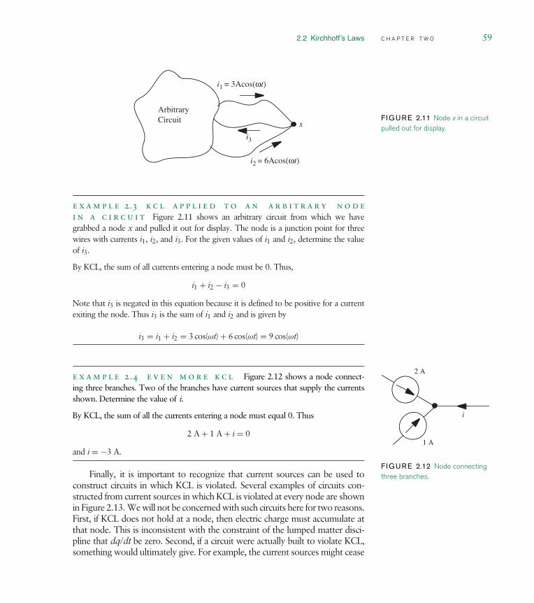
2.2 Kirchhoff’s Laws C H A P T E R T W O 59
x
ArbitraryCircuit
i1 = 3Acos(ωt)
i2 = 6Acos(ωt)
i3
F IGURE 2.11 Node x in a circuitpulled out for display.
e x a m p l e 2.3 k c l a p p l i e d t o a n a r b i t r a r y n o d e
i n a c i r c u i t Figure 2.11 shows an arbitrary circuit from which we havegrabbed a node x and pulled it out for display. The node is a junction point for threewires with currents i1, i2, and i3. For the given values of i1 and i2, determine the valueof i3.
By KCL, the sum of all currents entering a node must be 0. Thus,
i1 + i2 − i3 = 0
Note that i3 is negated in this equation because it is defined to be positive for a currentexiting the node. Thus i3 is the sum of i1 and i2 and is given by
i3 = i1 + i2 = 3 cos(ωt) + 6 cos(ωt) = 9 cos(ωt)
e x a m p l e 2.4 e v e n m o r e k c l Figure 2.12 shows a node connect-ing three branches. Two of the branches have current sources that supply the currentsshown. Determine the value of i.
By KCL, the sum of all the currents entering a node must equal 0. Thus
2 A
1 A
i
F IGURE 2.12 Node connectingthree branches.
2 A + 1 A + i = 0
and i = −3 A.
Finally, it is important to recognize that current sources can be used toconstruct circuits in which KCL is violated. Several examples of circuits con-structed from current sources in which KCL is violated at every node are shownin Figure 2.13. We will not be concerned with such circuits here for two reasons.First, if KCL does not hold at a node, then electric charge must accumulate atthat node. This is inconsistent with the constraint of the lumped matter disci-pline that dq/dt be zero. Second, if a circuit were actually built to violate KCL,something would ultimately give. For example, the current sources might cease

60 C H A P T E R T W O r e s i s t i v e n e t w o r k s
to function as ideal sources as they oppose one another. In any case, the behav-ior of the real circuit would not be well modeled by the type of circuit shownin Figure 2.13, and so there is no reason to study the latter.
2.2.2 K V L
Let us now turn our attention to Kirchhoff’s voltage law (KVL). KVL is appliedto circuit loops, that is, to interconnections of branches that form closed pathsthrough a circuit. In a manner analogous to KCL, Kirchhoff’s voltage law canbe stated as:
1 A 2 A
1 A 2 A 3 A
1 A 3 A
2 A
F IGURE 2.13 Circuits thatviolate KCL.
KVL The algebraic sum of the branch voltages around any closed path in anetwork must be zero.
Alternatively, it states that the voltage between two nodes is independentof the path along which it is accumulated.
In Figure 2.14, the loop starting at node a, proceeding through nodes band c, and returning to a, is a closed path. In other words, the closed loopdefined by the three circuit branches a → b, b → c, and c → a in Figure 2.14is a closed path.
According to KVL, the sum of the branch voltages around this loop is zero.That is,
vab + vbc + vca = 0
In other words,
v1 + v4 + v3 = 0
where we have taken the positive sign for each voltage when going from thepositive terminal to the negative terminal. It is important that we are consistentin how we assign polarities to voltages as we go around the loop.
A helpful mnemonic for writing KVL equations is to assign the polarity to agiven voltage in accordance with the first sign encountered when traversing thatvoltage around the loop.
Like KCL, KVL has an intuitive justification as well. Recall that the def-inition of the voltage between a pair of nodes in a circuit is the potential
F IGURE 2.14 Voltages in aclosed loop in the network. i4
a b
c
+ v1 -
+ v
3 - +
v4 -
V+
-
d
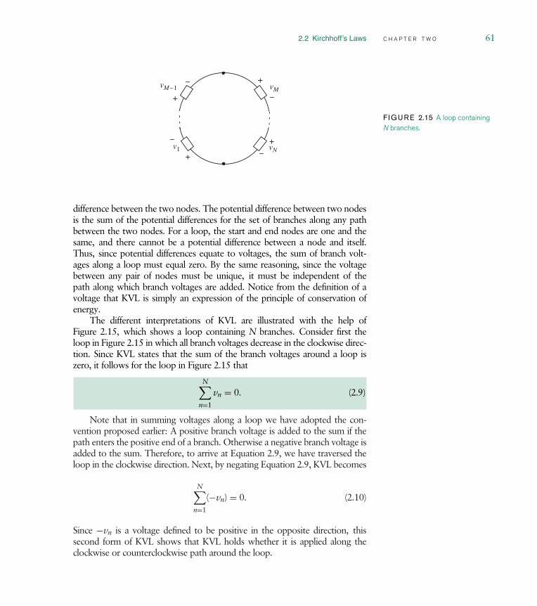
2.2 Kirchhoff’s Laws C H A P T E R T W O 61
vM–1 vM
v1 vN
+
+
+
+
F IGURE 2.15 A loop containingN branches.
difference between the two nodes. The potential difference between two nodesis the sum of the potential differences for the set of branches along any pathbetween the two nodes. For a loop, the start and end nodes are one and thesame, and there cannot be a potential difference between a node and itself.Thus, since potential differences equate to voltages, the sum of branch volt-ages along a loop must equal zero. By the same reasoning, since the voltagebetween any pair of nodes must be unique, it must be independent of thepath along which branch voltages are added. Notice from the definition of avoltage that KVL is simply an expression of the principle of conservation ofenergy.
The different interpretations of KVL are illustrated with the help ofFigure 2.15, which shows a loop containing N branches. Consider first theloop in Figure 2.15 in which all branch voltages decrease in the clockwise direc-tion. Since KVL states that the sum of the branch voltages around a loop iszero, it follows for the loop in Figure 2.15 that
N∑n=1
vn = 0. (2.9)
Note that in summing voltages along a loop we have adopted the con-vention proposed earlier: A positive branch voltage is added to the sum if thepath enters the positive end of a branch. Otherwise a negative branch voltage isadded to the sum. Therefore, to arrive at Equation 2.9, we have traversed theloop in the clockwise direction. Next, by negating Equation 2.9, KVL becomes
N∑n=1
(−vn) = 0. (2.10)
Since −vn is a voltage defined to be positive in the opposite direction, thissecond form of KVL shows that KVL holds whether it is applied along theclockwise or counterclockwise path around the loop.

62 C H A P T E R T W O r e s i s t i v e n e t w o r k s
F IGURE 2.16 A loop containingN branches with some of thevoltage definitions reversed.
vM–1 vM
v1 vN
+ +
++
Node M
Node 1
e x a m p l e 2.5 p a t h i n d e p e n d e n c e o f k v l Consider theloop in Figure 2.16 in which some of the voltage definitions are reversed for convenience.Applying KVL to this loop yields
M−1∑n=1
vn +N∑
n=M
(−vn) = 0 ⇒M−1∑n=1
vn =N∑
n=M
vn. (2.11)
The second equality in Equation 2.11 demonstrates that the voltage between twonodes is independent of the path along which it accumulated. In this case, the secondequality shows that the voltage between Nodes 1 and M is the same whether accumu-lated along the path up the left side of the loop or the path up the right side of theloop.
An important simplification of KVL focuses on the two parallel-connectedcircuit elements shown in Figure 2.17. Starting from the upper node and apply-ing KVL in the counterclockwise direction around the loop between the two
+
v1
+
v2
F IGURE 2.17 Two parallel-connected circuit elements.
circuit elements yields
v1 − v2 = 0 ⇒ v1 = v2. (2.12)
This result is important because it shows that the voltages across two parallel-connected elements must be the same. In fact, with multiple applications ofKVL, this observation is extendible to a longer string of parallel-connectedelements. Such an extension would show that a common voltage appears acrossall parallel-connected elements in the string.
e x a m p l e 2.6 a m o r e g e n e r a l u s e o f k v l To illustratethe more general use of KVL consider the circuit in Figure 2.18, which has six branchesconnecting four nodes. Four paths along the loops through the circuit are also defined inthe figure; note that the external loop, Loop 4, is distinct from the other three. Applying

2.2 Kirchhoff’s Laws C H A P T E R T W O 63
v2
v6
Loop 1 Loop 2
Loop 3
Loop 4
+ +
–
+–
+ –
+
–
+
–
v 1 v3
v 4 v5
–
F IGURE 2.18 A circuit havingfour nodes and six branches.
KVL to the four loops yields
Loop 1: 0 = −v1 + v2 + v4 (2.13)
Loop 2: 0 = −v2 + v3 − v5 (2.14)
Loop 3: 0 = −v4 + v5 − v6 (2.15)
Loop 4: 0 = v1 + v6 − v3 (2.16)
Note that the paths along the loops have been defined so that each branch voltage istraversed positively around exactly one loop and negatively around exactly one loop.It is for this reason that each branch voltage appears exactly once in Equations 2.13through 2.16 positively, and exactly once negatively. As with the application of KCL,such patterns can often be used to spot errors.
It is also because each branch voltage is traversed exactly once positively and oncenegatively that summing Equations 2.13 through 2.16 yields 0 = 0. This in turn showsthat the four KVL equations are dependent. In general, a circuit with N nodes and Bbranches will have B − N + 1 loops around which independent applications of KVL canbe made. Therefore, while analyzing a circuit it is necessary to apply KVL only to theseloops, which will in total, traverse each branch at least once in the process.
If some of the branch voltages in a circuit are known, then it is possible that KVLalone can be used to find other branch voltages in the circuit. For example, consider
v2
v6
+ +
–
+–
+ –
+–
+–
v 4 v5
–v1 1 V= v3 3 V=
F IGURE 2.19 The circuit inFigure 2.18 with two branchvoltages numerically defined.
the circuit in Figure 2.18 with v1 = 1 V and v3 = 3 V, as shown in Figure 2.19. UsingEquation 2.16, namely KVL for Loop 4, it can be seen that v6 = 2 V. This is all thatcan be learned from KVL alone given the information in Figure 2.19. But, if we furtherknow that v2 = 2 V, for example, we can learn from KVL applied to the other loopsthat v4 = −1 V and v5 = 1 V.

64 C H A P T E R T W O r e s i s t i v e n e t w o r k s
Finally, it is important to recognize that voltage sources can be used to con-struct circuits in which KVL is violated. Several examples of circuits constructedfrom voltage sources in which KVL is violated around every loop are shownin Figure 2.20. As with circuits that violate KCL, we will not be concernedwith circuits that violate KVL, for two reasons. First, if KVL does not holdaround a loop, then magnetic flux linkage will accumulate through that loop.This is inconsistent with the constraint of the lumped matter discipline thatdB/dt = 0 outside the elements. Second, if a circuit were actually built to vio-late KVL, something would ultimately give. For example, the voltage sourcesmight cease to function as ideal sources as they oppose one another. Alterna-tively, the loop inductance might begin to accumulate flux linkage, leading tohigh currents that would damage the voltage sources or their interconnections.In any case, the behavior of the real circuit would not be well modeled by the
1 V 2 V+– +–
1 V 2 V 3 V+– +– +–
1 V 3 V
2 V
+–+–
+–
F IGURE 2.20 Circuits thatviolate KVL.
type of circuit shown in Figure 2.20, and so there is no reason to study thelatter.
e x a m p l e 2.7 v o l t a g e s o u r c e s i n s e r i e s Two 1.5-V volt-age sources are connected in series as shown in Figure 2.21. What is the voltage v attheir terminals?
To determine v, employ, for example, a counterclockwise application of KVL around
+
-
v
+
-
1.5 V+
-
1.5 V
F IGURE 2.21 The seriesconnection of two 1.5-V batteries.
the circuit, treating the port formed by the two terminals as an element having voltage v.In this case, 1.5 V + 1.5 V − v = 0, which has for its solution v = 3 V.
e x a m p l e 2.8 k v l The voltages across two of the elements in the circuit inFigure 2.22 are measured as shown. What are the voltages, v1 and v2, across the othertwo elements?
Since element #1 is connected in parallel with element #4, the voltages across themmust be the same. Thus, v1 = 5 V. Similarly, the voltage across the series connection ofelements #2 and #3 must also be 5 V, so v2 = 3 V. This latter result can also be obtainedthrough the counterclockwise application of KVL around the loop including elements#2, #3, and #4, for example. This yields, v2 + 2 V − 5 V = 0. Again, v2 = 3 V.
e x a m p l e 2.9 v e r i f y i n g k v l f o r a c i r c u i t Verify thatthe branch voltages shown in Figure 2.23 satisfy KVL.
Summing the voltages in the loop e, d, a, b, e, we get
−3 − 1 + 3 + 1 = 0.
Similarly, summing the voltages in the loop e, f, c, b, e, we get
+1 − (−2) − 4 + 1 = 0.

2.2 Kirchhoff’s Laws C H A P T E R T W O 65
#1
+
+
+
-
-
-
v1
v2
5 V
+
-#2
#3
#4
2 V
F IGURE 2.22 A circuit with two measured and twounmeasured voltages.
a b c
d
+ - + -
1 V
+
-
+
-
+
-+ -e f
+ -+
-
+
-g
3 V
3 V
4 V
1 V -2 V
1 V
2 V 1 V
F IGURE 2.23 A circuit with element voltages as shown.
Finally, summing the voltages in the loop g, e, f, g, we get
−2 + 1 + 1 = 0.
KVL is satisfied since the sum of the voltages around each of the three circuit loopsis zero.
e x a m p l e 2.10 s u m m i n g v o l t a g e s a l o n g d i f f e r e n t
p a t h s Next, given the branch voltages shown in Figure 2.23, determine the volt-age vga between the nodes g and a by summing the branch voltages along the path g, e,d, a. Then, show that vga is the same if path g, f, c, b, a is chosen.
Summing the voltage increases along the path g, e, d, a, we get
vga = −2 V − 3 V − 1 V = −6 V.
Similarly, summing the voltage increases along the path g, f, c, b, a we get
vga = −1 V − (−2 V) − 4 V − 3 V = −6 V.
Clearly, both paths yield −6 V for vga.

66 C H A P T E R T W O r e s i s t i v e n e t w o r k s
Thus far, Chapters 1 and 2 have shown that the operation of a lumpedsystem is described by two types of equations: equations that describe thebehavior of its individual elements, or element laws (Chapter 1), and equationsthat describe how its elements interact when they are connected to form thesystem, or KCL and KVL (Chapter 2). For an electronic circuit, the elementlaws relate the branch currents to the branch voltages of the elements. Theinteractions between its elements are described by KCL and KVL, which arealso expressed in terms of branch currents and voltages. Thus, branch currentsand voltages become the fundamental signals within a lumped electronic circuit.
2.3 C I R C U I T A N A L Y S I S : B A S I C M E T H O D
We are now ready to introduce a systematic method of solving circuits. It isframed in the context of a simple class of circuits, namely circuits containingonly sources and linear resistors. Many of the important analysis issues canbe understood through the study of these circuits. Solving a circuit involvesdetermining all the branch currents and branch voltages in the circuit. In practice,some currents or voltages may be more important than others, but we will notmake that distinction yet.
Before we return to the specific problem of analyzing the electrical networkshown in Figure 2.1, let us first develop the systematic method using a fewsimpler circuits and build up our insight into the technique. We saw previouslythat under the lumped matter discipline, Maxwell’s Equations reduce to thebasic element laws and the algebraic KVL and KCL. Accordingly, a systematicsolution of the network involves the assembly and subsequent joint solutionof two sets of equations. The first set of equations comprise the constituentrelations for the individual elements in the network. The second set of equationsresults from the application of Kirchhoff’s current and voltage laws.
This basic method of circuit analysis, also called the KVL and KCL method orthe fundamental method, is outlined by the following steps:
1. Define each branch current and voltage in the circuit in a consistentmanner. The polarities of these definitions can be arbitrary fromone branch to the next. However, for any given branch, follow theassociated variables convention (see Section 1.5.3 in Chapter 1). In otherwords, the branch current should be defined as positive into the positivevoltage terminal of the branch. By following the associated variables,element laws can be applied consistently, and the solutions will followa much clearer pattern.
2. Assemble the element laws for the elements. These element laws willspecify either the branch current or branch voltage in the case of anindependent source, or specify the relation between the branch current

2.3 Circuit Analysis: Basic Method C H A P T E R T W O 67
and voltage in the case of a resistor. Examples of these element lawswere presented in Section 1.6.
3. Apply Kirchhoff’s current and voltage laws as discussed in Section 2.2.
4. Jointly solve the equations assembled in Steps 2 and 3 for the branchvariables defined in Step 1.
The remainder of this chapter is devoted to circuit analysis examples thatrigorously follow these steps.
Once the two sets of equations are assembled, which is a relatively easytask, the analysis of a circuit essentially becomes a problem of mathematics, asindicated by Step 4. That is, the equations assembled earlier must be combinedand used to solve for the branch currents and voltages of interest. However,because there is more than one way to approach this problem, our study ofcircuit analysis does not end with the direct approach outlined here. Consider-able time can be saved, and considerable insight can be gained, by approachingcircuit analyses in different ways. These gains are important subjects of thisand future chapters.
2.3.1 S I N G L E - R E S I S T O R C I R C U I T S
To illustrate our basic approach to circuit analysis, consider the simple circuitRI
F IGURE 2.24 A circuit with onlyone independent current sourceand one resistor.
shown in Figure 2.24. The circuit has one independent source and one resistor,and so has two branches, each with a current and a voltage. The goal of our
-
+
R
i1 i2
v1
+
-
v2I
F IGURE 2.25 Assignment ofbranch variables.
circuit analysis is to find these branch variables.Step 1 in the analysis is to label the branch variables. We do so in Figure 2.25.
Since there are two branches, there are two sets of variables. Notice that thebranch variables for the current source branch and for the resistor branch eachfollow the associated variables convention.
Now, we proceed with Steps 2 through 4: assemble the element laws,apply KCL and KVL, and then simultaneously solve the two sets of equationsto complete the analysis.
The circuit has two elements. Following Step 2 we write the two elementlaws for these elements as
i1 = −I, (2.17)
v2 = Ri2, (2.18)
respectively. Here, v1, i1, v2, and i2 are the branch variables. Note the dis-tinction between the branch variable i1 and the source amplitude I. Here, theindependent source amplitude I is assumed to be known.
Next, following Step 3, we apply KCL and KVL to the circuit. Since thecircuit has two nodes, it is appropriate to write KCL for one node, as discussed

68 C H A P T E R T W O r e s i s t i v e n e t w o r k s
in Section 2.2.1. The application of KCL at either node yields
i1 + i2 = 0. (2.19)
The circuit also has two branches that form one loop. So, following the discus-sion in Section 2.2.2 it is appropriate to write KVL for one loop. Starting at theupper node and traversing the loop in a clockwise manner, the application ofKVL yields
v2 − v1 = 0. (2.20)
Notice we have used our mnemonic discussed in Section 2.2.2 for writing KVLequations. For example, in Equation 2.20, we have assigned a + polarity to v2since we first encounter the + sign when traversing the branch with variablev2. Similarly, we have assigned a − polarity to v1 since we first encounterthe − sign when traversing the v1 branch.
Finally, following Step 4, we combine Equations 2.17 through 2.20 andsolve jointly to determine all four branch variables in Figure 2.25. This yields
−i1 = i2 = I, (2.21)
v1 = v2 = RI, (2.22)
and completes the analysis of the circuit in Figure 2.25.
e x a m p l e 2.11 s i n g l e - r e s i s t o r c i r c u i t w i t h o n e
i n d e p e n d e n t v o l t a g e s o u r c e Now consider another simplecircuit shown in Figure 2.26. This circuit can be analyzed in an identical manner. Ittoo has two elements, namely a voltage source and a resistor. Figure 2.26 already showsthe definitions of branch variables, and so accomplishes Step 1.
-
+
R
i1 i2
v1
+
-
v2V+
-
F IGURE 2.26 A circuit with onlyone independent voltage sourceand one resistor.
Next, following Step 2 we write the element laws for these elements as
v1 = V (2.23)
v2 = Ri2, (2.24)
respectively. Here, the independent source amplitude V is assumed to be known.
Next, following Step 3, we apply KCL and KVL to the circuit. Since the circuit has twonodes, it is again appropriate to write KCL for one node. The application of KCL ateither node yields
i1 + i2 = 0. (2.25)
The circuit also has two branches that form one loop, so it is again appropriate to writeKVL for one loop. The application of KVL around the one loop in either direction yields
v1 = v2. (2.26)

2.3 Circuit Analysis: Basic Method C H A P T E R T W O 69
Finally, following Step 4, we combine Equations 2.23 through 2.26 to determine all fourbranch variables in Figure 2.26. This yields
−i1 = i2 = V
R, (2.27)
v1 = v2 = V, (2.28)
and completes the analysis of the circuit in Figure 2.26.
For the circuit in Figure 2.25, there are four equations to solve for fourunknown branch variables. In general, a circuit having B branches will have 2Bunknown branch variables: B branch currents and B branch voltages. To findthese variables, 2B independent equations are required, B of which will comefrom element laws, and B of which will come from the application of KVL andKCL. Moreover, if the circuit has N nodes, then N−1 equations will come fromthe application of KCL and B−N+1 equations will come from the applicationof KVL.
While the two examples of circuit analysis presented here are admittedlyvery simple, they nonetheless illustrate the basic steps of circuit analysis: labelthe branch variables, assemble the element laws, apply KCL and KVL, andsolve the resulting equations for the branch variables of interest. While we willnot always follow these steps explicitly and in exactly the same order in futurechapters, it is important to know that we will nonetheless process exactly thesame information.
It is also important to realize that the physical results of the analysis of thecircuit in Figure 2.25, and of any other circuit for that matter, cannot dependon the polarities of the definitions of the branch variables. We will work anexample to illustrate this point.
e x a m p l e 2.12 p o l a r i t i e s o f b r a n c h v a r i a b l e s
Consider the analysis of the circuit in Figure 2.27, which is physically the same as thecircuit in Figure 2.25. The only difference in the two figures is the reversal of the polari-
-
+
R
i1
i2
v1
+
-
v2I
F IGURE 2.27 A circuit similar tothe one shown in Figure 2.24.
ties of i2 and v2. The circuit in Figure 2.27 circuit has the same two elements, and theirelement laws are still
i1 = −I (2.29)
v2 = Ri2. (2.30)
Note that the polarity reversal of i2 and v2 has not changed the element law for theresistor from Equation 2.18 because the element law for a linear resistor is symmetricwhen the terminal variables are defined according to the associated variables convention.The circuit also has the same two nodes and the same loop. The application of KCL at

70 C H A P T E R T W O r e s i s t i v e n e t w o r k s
either node now yieldsi1 − i2 = 0, (2.31)
and the application of KVL around the loop now yields
v1 + v2 = 0. (2.32)
Note that Equations 2.31 and 2.32 differ from Equations 2.19 and 2.20 because of thepolarity reversal of i2 and v2. Finally, combining Equations 2.29 through 2.32 yields
−i1 = −i2 = I (2.33)
v1 = −v2 = RI, (2.34)
which completes the analysis of the circuit in Figure 2.27.
Now compare Equations 2.33 and 2.34 to Equations 2.21 and 2.22. The importantobservation here is that they are the same except for the polarity reversal of the solutionsfor i2 and v2. This must be the case because the circuits in Figures 2.25 and 2.27 arephysically the same, and so their branch variables must also be physically the same. Sincewe have chosen to define two of these branch variables with different polarities in thetwo figures, the signs of their values must differ accordingly so that they describe thesame physical branch current and voltage.
2.3.2 Q U I C K I N T U I T I V E A N A L Y S I S O FS I N G L E - R E S I S T O R C I R C U I T S
Before moving on to more complex circuits, it is worthwhile to analyze thecircuit in Figure 2.25 in a more intuitive and efficient manner. Here, the elementlaw for the current source directly states that i1 = −I. Next, the applicationof KCL to either node reveals that i2 = −i1 = I. In other words, the currentfrom the source flows entirely through the resistor. Next, from the element lawfor the resistor, it follows that v2 = Ri2 = RI. Finally the application of KVLto the one loop yields v1 = v2 = RI to complete the analysis.
e x a m p l e 2.13 q u i c k i n t u i t i v e a n a l y s i s o f a
s i n g l e - r e s i s t o r c i r c u i t This example considers the circuit inFigure 2.26. Here, the element law for the voltage source directly states that v1 = V.Next, the application of KVL around the one loop reveals that v2 = v1 = V. In otherwords, the voltage from the source is applied directly across the resistor. Next, from theelement law for the resistor, it follows that i2 = v2/R = V/R. Finally, the application ofKCL to either node yields i1 = −i2 = −V/R to complete the analysis. Notice that wehad made use of a similar intuitive analysis in solving our battery and lightbulb examplein Chapter 1.
The important message here is that it is not necessary to first assembleall the circuit equations, and then solve them all at once. Rather, using a little

2.3 Circuit Analysis: Basic Method C H A P T E R T W O 71
intuition, it is likely to be much faster to approach the analysis in a differentmanner. We will have more to say about this in Section 2.4 and in Chapter 3.
2.3.3 E N E R G Y C O N S E R V A T I O N
Once the branch variables of a circuit have been determined, it is possible toexamine the flow of energy through the circuit. This is often a very importantpart of circuit analysis. Among other things, such an examination should showthat energy is conserved in the circuit. This is the case for the circuits in Fig-ures 2.25 and 2.26. Using Equations 2.21 and 2.22 we see that the power intothe current source in Figure 2.25 is
i1v1 = −RI2 (2.35)
and that the power into the resistor is
i2v2 = RI2. (2.36)
The negative sign in Equation 2.35 indicates that the current source actuallysupplies power.
Similarly, using Equations 2.27 and 2.28 we see that the power into thevoltage source in Figure 2.26 is
i1v1 = −V2
R(2.37)
and that the power into the resistor is
i2v2 = V2
R. (2.38)
In both cases, the power generated by the source is equal to the power dissipatedin the resistor. Thus, energy is conserved in both circuits.
Conservation of energy is itself an extremely powerful method for obtain-ing many types of results in circuits. It is particularly useful in dealing withcomplicated circuits that contain energy storage elements such as inductorsand capacitors that we will introduce in later chapters. Energy methods canoften allow us to obtain powerful results without a lot of mathematical grunge.We will use two energy-based approaches in this book.
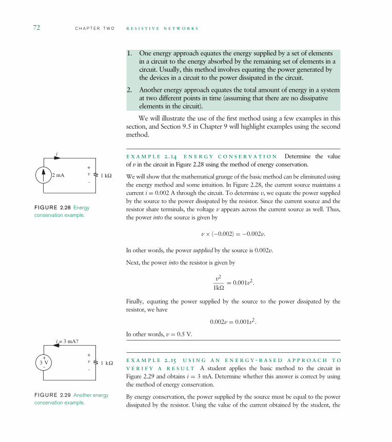
72 C H A P T E R T W O r e s i s t i v e n e t w o r k s
1. One energy approach equates the energy supplied by a set of elementsin a circuit to the energy absorbed by the remaining set of elements in acircuit. Usually, this method involves equating the power generated bythe devices in a circuit to the power dissipated in the circuit.
2. Another energy approach equates the total amount of energy in a systemat two different points in time (assuming that there are no dissipativeelements in the circuit).
We will illustrate the use of the first method using a few examples in thissection, and Section 9.5 in Chapter 9 will highlight examples using the secondmethod.
e x a m p l e 2.14 e n e r g y c o n s e r v a t i o n Determine the valueof v in the circuit in Figure 2.28 using the method of energy conservation.
1 kΩ 2 mA
i
+
-
v
F IGURE 2.28 Energyconservation example.
We will show that the mathematical grunge of the basic method can be eliminated usingthe energy method and some intuition. In Figure 2.28, the current source maintains acurrent i = 0.002 A through the circuit. To determine v, we equate the power suppliedby the source to the power dissipated by the resistor. Since the current source and theresistor share terminals, the voltage v appears across the current source as well. Thus,the power into the source is given by
v × (−0.002) = −0.002v.
In other words, the power supplied by the source is 0.002v.
Next, the power into the resistor is given by
v2
1k= 0.001v2.
Finally, equating the power supplied by the source to the power dissipated by theresistor, we have
0.002v = 0.001v2.
In other words, v = 0.5 V.
e x a m p l e 2.15 u s i n g a n e n e r g y - b a s e d a p p r o a c h t o
v e r i f y a r e s u l t A student applies the basic method to the circuit inFigure 2.29 and obtains i = 3 mA. Determine whether this answer is correct by using
1 k3 V
i = 3 mA?
+
-
v+
-Ω
F IGURE 2.29 Another energyconservation example.
the method of energy conservation.
By energy conservation, the power supplied by the source must be equal to the powerdissipated by the resistor. Using the value of the current obtained by the student, the

2.3 Circuit Analysis: Basic Method C H A P T E R T W O 73
energy dissipated by the resistor is given by
i2 × 1K = 9 mW.
The energy into the voltage source is given by
3 V × 3 mA = 9 mW.
In other words, the energy supplied by the source is given by −9 mW. Clearly theenergy supplied by the source is not equal to the energy dissipated by the resistor, andso i = 3 mA is incorrect. Notice that if we reverse the polarity of i, energy will beconserved. Thus, i = −3 mA is the correct answer.
2.3.4 V O L T A G E A N D C U R R E N T D I V I D E R S
We will now tackle several circuits called dividers that are slightly more complexthan the simplest single-loop, two-node, two-element circuits of the previoussection. These circuits will comprise a single loop and three or more elements,or two nodes and three or more elements. Dividers produce fractions of inputcurrents or voltages and will be encountered often in subsequent chapters. Forthe moment, however, they are good examples on which to practice circuitanalysis, and we can use them to gain important insight into circuit behavior.
Voltage Dividers
A voltage divider is an isolated loop that contains two or more resistors and a
R1
R2v2
R1
R2v2
+ -
+
-
(a)
+
-
(b)V+-
F IGURE 2.30 Voltage-dividercircuit.
voltage source in series. A physical voltage divider circuit is illustrated pictoriallyin Figure 2.30a. We have connected two resistors in series, and connected thepair by some wires to a battery. Such a circuit is useful if we wish to obtain somearbitrary fraction, say 10%, of the battery voltage at the terminals marked v2.To find the relation between v2 and the battery voltage and resistor values, wedraw the circuit in schematic form, as shown in Figure 2.30b. We then followthe basic four-step method outlined in Section 2.3 to solve the circuit.
1. The circuit has three elements, or branches, and hence it will have sixbranch variables. Figure 2.31 shows one possible assignment of branch
R1
R2
+
-
v1
+
-
v2
i2
V+
-
i1
-
+
v0
i0
F IGURE 2.31 Assignment ofbranch variables to the voltagedivider.
variables.To find these branch variables, we again assemble the element
laws and the appropriate applications of KCL and KVL, and thensimultaneously solve the resulting equations.
2. The three element laws are
v0 = −V (2.39)

74 C H A P T E R T W O r e s i s t i v e n e t w o r k s
v1 = R1i1 (2.40)
v2 = R2i2. (2.41)
3. Next, we apply KCL and KVL. The application of KCL to the two uppernodes yields
i0 = i1 (2.42)
i1 = i2 (2.43)
and the application of KVL to the one loop yields
v0 + v1 + v2 = 0. (2.44)
4. Finally, Equations 2.39 through 2.44 can be solved for the six unknownbranch variables. This yields
i0 = i1 = i2 = 1
R1 + R2V (2.45)
and
v0 = −V (2.46)
v1 = R1
R1 + R2V (2.47)
v2 = R2
R1 + R2V. (2.48)
This completes the analysis of the two-resistor voltage divider.From the results of this analysis it should be apparent why the circuit in
Figure 2.31 is called a voltage divider. Notice that v2 is some fraction (specifically,R2/(R1 +R2)) of the source voltage V, as desired. The fraction is the ratio of theresistance about which the voltage is measured and the sum of the resistances.By adjusting the relative values of R1 and R2 we can make this fraction adjustanywhere from 0 to 1. If, for example, we wish v2 to be one-tenth of V,as suggested at the start of this example, then R1 should be nine times asbig as R2.
Notice also that v1 + v2 = V, and that the two resistors divide the voltageV in proportion to their resistances since v1/v2 = R1/R2. For example, if R1 istwice R2 then v1 is twice v2.

2.3 Circuit Analysis: Basic Method C H A P T E R T W O 75
The voltage-divider relationship in terms of conductance can be foundfrom Equation 2.48 by substituting the conductances in place of the resistances:
v2 = 1/G2
1/G1 + 1/G2V (2.49)
= G1
G1 + G2V. (2.50)
Hence the voltage-divider relations expressed in terms of conductances involvethe conductance opposite the desired voltage, divided by the sum of the twoconductances.
The simple circuit topology of Figure 2.30 is so common that the voltage-divider relation given by Equation 2.48 will become a primitive in our circuitvocabulary. It is helpful to build up a set of such primitives, which are reallysolved simple cases, to speed up circuit analysis, and to facilitate intuition.
A simple mnemonic: For the voltage v2, take the resistance associated with v2divided by the sum of the two resistances, multiplied by the voltage applied tothe pair.
e x a m p l e 2.16 v o l t a g e d i v i d e r A voltage divider circuit such asthat in Figure 2.30 has V = 10 V and R2 = 1 k. Choose R1 such that v2 is 10% of V.
By the voltage divider relation of Equation 2.48, we have
v2 = R2
R1 + R2V.
For v2 to be 10% of V we must have
v2
V= 0.1 = R2
R1 + R2.
For R2 = 1 k, we must choose R1 such that
0.1 = 1 k
R1 + 1 k
or R1 = 9 k.
e x a m p l e 2.17 t e m p e r a t u r e v a r i a t i o n Consider the cir-cuit in Figure 2.31 in which V = 5 V, R1 = 103 , and R2 = 103 (1 + T/(500 C)) ,where T is the temperature of the second resistor. Over what range does v2 vary if Tvaries over the range −100 C ≤ T ≤ 100 C?

76 C H A P T E R T W O r e s i s t i v e n e t w o r k s
Given the temperature range, R2 varies over the range:
0.8 × 10³ ≤ R2 ≤ 1.2 × 10³ .
Therefore, following Equation 2.48, 2.2 V ≤ v2 ≤ 2.7 V, with the higher voltageoccurring at the higher temperature.
Having determined its branch variables we can now examine the flowof energy through the two-resistor voltage divider. Using Equations 2.45through 2.48 we see that the power into the source is
i0v0 = − V2
R1 + R2(2.51)
and that the power into each resistor is
i1v1 = R1V2
(R1 + R2)2(2.52)
i2v2 = R2V2
(R1 + R2)2. (2.53)
Since the power into the voltage source is the opposite of the total power intothe two resistors, energy is conserved in the two-resistor voltage divider. Thatis, the power generated by the voltage source is exactly dissipated in the tworesistors.
Resistors in Series
In electronic circuits one often finds resistors connected in series, as shown inFigures 2.31 and 2.32. For example, in our lightbulb example of Chapter 1,
R2R1
F IGURE 2.32 Resistors inseries.
suppose the wire had a nonzero resistance, then the current through the wirewould be related to the value of several resistances including those ofthe wires and the bulb in series. Our lumped circuit abstraction and theresulting Kirchhoff’s laws allow us to calculate the equivalent resistance of suchcombinations using simple algebra.
Specifically, the analysis of the voltage divider shows that two resistors inseries act as a single resistor having a resistance RS equal to the sum of the twoindividual resistances R1 and R2. In other words, series resistances add.
RS = R1 + R2 (2.54)
To see this, observe that the voltage source in Figure 2.31 applies the volt-age V to two series resistors R1 and R2, and that from Equation 2.43 theseresistors respond with the common current i1 = i2 through their branches.Further, observe from Equation 2.45 that this common current, i = i1 = i2,

2.3 Circuit Analysis: Basic Method C H A P T E R T W O 77
is linearly proportional to the voltage from the source. Specifically, fromEquation 2.45, the common current is given by
i = 1
R1 + R2V. (2.55)
By comparing Equation 2.55 to Equation 1.4, we conclude that for tworesistors in series, the equivalent resistance of the pair when viewed from theirouter terminals is the sum of the individual resistance values. Specifically, ifRS is the resistance of the series resistor pair, then, from Equation 2.55, wefind that
RS = V
i= R1 + R2. (2.56)
This is consistent with the physical derivation of resistance in Equation 1.6since placing resistors in series essentially increases their combined length.
By substituting their conductances, we can also obtain the equivalentconductance of a pair of conductances in series as
1
GS= 1
G1+ 1
G2. (2.57)
Simplifying,
GS = G1G2
G1 + G2. (2.58)
As shown in the ensuing example, we can generalize our result fortwo series resistors to N resistors in series as:
RS = R1 + R2 + R3 + · · · RN. (2.59)
Remember this result as another common circuit primitive.
e x a m p l e 2.18 a n N - r e s i s t o r v o l t a g e d i v i d e r Nowconsider a more general voltage divider having N resistors, as shown in Figure 2.33.It can be analyzed in the same manner as the two-resistor voltage divider. The onlydifference is that there are now more unknowns to find, and hence more equations to
R1
RN
+
-
v1
+
-
vN
iN
V+
-
i1
-
+
v0
i0
. . .
F IGURE 2.33 A voltage dividerwith N resistors.
work with. To begin, suppose we assign the branch variables as shown in Figure 2.33.
The element laws are
v0 = −V (2.60)
vn = Rnin, 1 ≤ n ≤ N. (2.61)

78 C H A P T E R T W O r e s i s t i v e n e t w o r k s
Next, the application of KCL to the N − 1 upper nodes yields
in = in−1, 1 ≤ n ≤ N (2.62)
and the application of KVL to the one loop yields
v0 + v1 + · · · vN = 0. (2.63)
Finally, Equations 2.60 through 2.63 can be solved to yield
in = 1
R1 + R2 + · · · RNV, 0 ≤ n ≤ N (2.64)
v0 = −V (2.65)
vn = Rn
R1 + R2 + · · · RNV, 1 ≤ n ≤ N. (2.66)
This completes the analysis.
As was the case for the two-resistor voltage divider, the preceding analysis shows thatseries resistors divide voltage in proportion to their resistances. This follows from theRn in the numerator of the right-hand side of Equation 2.66.
Additionally, the analysis again shows that series resistances add. To see this, let RS bethe equivalent resistance of the N series resistors. Then, from Equation 2.64 we see that
RS = V
in= R1 + R2 + · · · RN. (2.67)
This result is summarized in Figure 2.34.
Finally, the two voltage-divider examples illustrate an important point, namely that serieselements all carry the same branch current because the terminals from these elementsare connected end-to-end without connection to additional branches through which thecurrent can divert. This results in the KCL seen in Equations 2.42, 2.43, and 2.62, whichstate the equivalence of the branch currents.
F IGURE 2.34 The equivalenceof series resistors.
R1
R2 RS = R1 + R2 + ... + RN
RN
. . .

2.3 Circuit Analysis: Basic Method C H A P T E R T W O 79
e x a m p l e 2.19 v o l t a g e - d i v i d e r c i r c u i t Determine v1 andv2 for the voltage-divider circuit in Figure 2.35 with R1 = 10 , R2 = 20 , andv(t) = 3 V using (a) the basic method and (b) the results from voltage dividers.
(a) Let us first analyze the circuit using the basic method.
1. Assign variables as in Figure 2.36.
2. Write the constituent relations
v0 = 3 V (2.68)
v1 = 10i1 (2.69)
v2 = 20i2. (2.70)
3. Write KCL
i1 − i2 = 0. (2.71)
4. Write KVL
−v0 + v1 + v2 = 0. (2.72)
Now eliminate i1 and i2 from Equations 2.69, 2.70, and 2.71, to obtain
v1 = v2
2. (2.73)
Substituting this result and v0 = 3 V into Equation 2.72, we obtain
−3 V + v2
2+ v2 = 0. (2.74)
R1
R2v2
++
-
Signalgenerator
-v(t)
v1
+
-
F IGURE 2.35 Voltage-divider circuit.
10 Ωi1
v2
+
-
v1
+
+ i2
20 Ω-
-
3 V v0
+
-
F IGURE 2.36 Voltage divider with variables assigned.

80 C H A P T E R T W O r e s i s t i v e n e t w o r k s
Hence,
v2 = 2
33 V = 2 V (2.75)
and from Equation 2.73, v1 = 1 V.
(b) Using the voltage-divider relation, we can write by inspection the value v2 as afunction of the source voltage as follows:
v2 = 20
10 + 203 V = 2 V.
Similarly,
v1 = 10
10 + 203 V = 1 V.
Current Dividers
A current divider is a circuit with two nodes joining two or more parallel resistors
-
+
i0 i2
v0
+
-
v1I R1
i1R2
+
-
v2
F IGURE 2.37 A current dividerwith two resistors.
and a current source. Two current dividers are shown in Figures 2.37 and 2.38,the first with two resistors and the second with N resistors. In these circuits,
-
+
i0
v0
+
-
v1I R1
i1RN
+
-
vN
iN. . .
. . .
F IGURE 2.38 A current dividerwith N resistors.
the resistors share, or divide, the current from the source in proportion to theirconductances. It turns out that the equations for voltage dividers comprisingvoltages and resistances, and those for current dividers comprising currentsand conductances, are very similar. Therefore, to highlight the duality betweenthese two types of circuits, we will attempt to mirror the steps from our voltagedivider discussion.
Consider the two-resistor current divider shown in Figure 2.37. It hasthree elements, or branches, and hence six unknown branch variables. To findthese branch variables we again assemble the element laws and the appropriateapplications of KCL and KVL, and then simultaneously solve the resultingequations. First, the three element laws are
i0 = −I (2.76)
v1 = R1i1 (2.77)
v2 = R2i2. (2.78)
Next, the application of KCL to either node yields
i0 + i1 + i2 = 0 (2.79)
and the application of KVL to the two internal loops yields
v0 = v1 (2.80)
v1 = v2. (2.81)

2.3 Circuit Analysis: Basic Method C H A P T E R T W O 81
Finally, Equations 2.76 through 2.81 can be solved for the six unknown branchvariables. This yields
i0 = −I (2.82)
i1 = R2
R1 + R2I (2.83)
i2 = R1
R1 + R2I (2.84)
and
v0 = v1 = v2 = R1R2
R1 + R2I. (2.85)
This completes the analysis of the two-resistor current divider.The nature of the current division in Equations 2.83 and 2.84 is more
obvious if they are expressed in terms of the conductances G1 and G2 whereG1 ≡ 1/R1 and G2 ≡ 1/R2. With these definitions, i1 and i2 in Equations 2.83and 2.84 become
i1 = G1
G1 + G2I (2.86)
i2 = G2
G1 + G2I. (2.87)
It is now apparent that i1 + i2 = I, and that the two resistors divide the currentI in proportion to their conductances since i1/i2 = G1/G2. For example, if G1is twice G2 then i1 is twice i2.
To summarize our current divider discussion:
The current i2 is equal to the input current I multiplied by a factor, this timemade up of the opposite resistor, R1, divided by the sum of the two resistors(see Equation 2.84).
This relation will also become a useful primitive in our analysis vocabulary.As we did with voltage dividers, we can now examine the flow of energy
through the two-resistor current divider. Using Equations 2.82 through 2.85we see that the power into the source is
i0v0 = − R1R2I2
R1 + R2(2.88)
and that the power into each resistor is
i1v1 = R1R22I2
(R1 + R2)2(2.89)

82 C H A P T E R T W O r e s i s t i v e n e t w o r k s
i2v2 = R21R2I2
(R1 + R2)2. (2.90)
Since the power into the current source is the opposite of the total power intothe two resistors, energy is conserved in the two-resistor current divider. Thatis, the power generated by the current source is exactly dissipated in the tworesistors.
Resistors in Parallel
Resistors in parallel occur as commonly as resistors in series. Two resistors inR1
R2
F IGURE 2.39 Resistors inparallel.
parallel are shown in Figures 2.37 and 2.39.Our preceding analysis shows that the two resistors in parallel act as a
single resistor RP having a conductance GP (where GP = 1/RP) equal to thesum of the two individual conductances. In other words, parallel conductancesadd:
GP = G1 + G2 (2.91)
To see this, observe that the current source in Figure 2.37 applies thecurrent I to two parallel resistors, and that from Equation 2.85 these resistorsrespond at their terminals with the common voltage v = v1 = v2 that is linearlyproportional to the current from the source. Thus, the resistors behave togetheras a single resistor when viewed from their common terminals.
Let GP be the conductance of the parallel resistor pair. Then, from Equa-tion 2.85, with the substitution of G1 ≡ 1/R1 and G2 ≡ 1/R2, and v = v1 = v2,we can write
v = R1R2
R1 + R2I. (2.92)
Or, in terms of conductances,
v = 1
G1 + G2I. (2.93)
In other words,
GP = I
v= G1 + G2. (2.94)
Hence, the equivalent conductance of the two parallel resistors is the sum oftheir individual conductances. This is consistent with the physical derivation ofresistance in Equation 1.6 since placing resistors in parallel essentially increasestheir combined cross-sectional area.
In practice, it is more common to work with resistances than it is to workwith conductances, although conductances are sometimes more convenient.For this reason, it is worthwhile to find the equivalent resistance of two parallel

2.3 Circuit Analysis: Basic Method C H A P T E R T W O 83
resistors in terms of the individual resistances. Let the equivalent resistance beRP. Then, from Equation 2.94 it follows that
1
RP= GP = G1 + G2 = 1
R1+ 1
R2(2.95)
from which it follows that the equivalent resistance of two resistances inparallel is given by
RP = R1R2
R1 + R2(2.96)
which is the product of the two resistor values divided by their sum. Thisrelation can also be observed in 2.92, which has a form analogous to Ohm’slaw (Equation 1.4).
Parallel resistors occur frequently enough to merit a shorthand notation:the two resistor values separated by two parallel vertical lines
R1‖R2 = R1R2
R1 + R2. (2.97)
As we show shortly, we can generalize this result to N resistors connectedin parallel. If the equivalent resistance for N resistors connected in parallel isgiven by RP, then the reciprocal of RP is given in terms of R1, R2, R3, . . . RN as
1
RP= 1
R1+ 1
R2+ 1
R3+ · · · 1
Rn. (2.98)
The equivalent resistance of N resistors in parallel is yet another example of auseful primitive that is worth remembering.
The shorthand notation for N resistances in parallel is
RP = R1‖R2‖R3‖ · · · RN. (2.99)
As an example, when N resistors, each with resistance R, are connected inparallel, the effective resistance is simply
RP = R
N. (2.100)
W W W e x a m p l e 2.20 a n N - r e s i s t o r c u r r e n t d i v i d e r
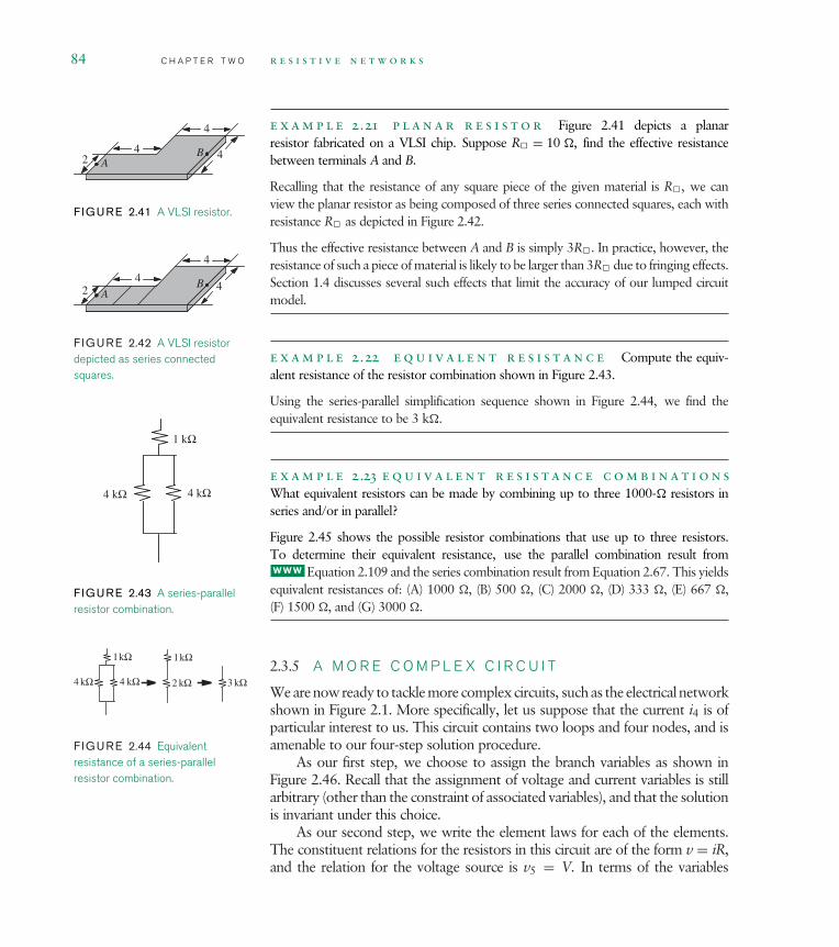
84 C H A P T E R T W O r e s i s t i v e n e t w o r k s
e x a m p l e 2.21 p l a n a r r e s i s t o r Figure 2.41 depicts a planarresistor fabricated on a VLSI chip. Suppose R = 10 , find the effective resistancebetween terminals A and B.
4
4 42 AB
F IGURE 2.41 A VLSI resistor.
Recalling that the resistance of any square piece of the given material is R, we canview the planar resistor as being composed of three series connected squares, each withresistance R as depicted in Figure 2.42.
4
442 A
B
F IGURE 2.42 A VLSI resistordepicted as series connectedsquares.
Thus the effective resistance between A and B is simply 3R. In practice, however, theresistance of such a piece of material is likely to be larger than 3R due to fringing effects.Section 1.4 discusses several such effects that limit the accuracy of our lumped circuitmodel.
e x a m p l e 2.22 e q u i v a l e n t r e s i s t a n c e Compute the equiv-alent resistance of the resistor combination shown in Figure 2.43.
1 kΩ
4 kΩ 4 kΩ
F IGURE 2.43 A series-parallelresistor combination.
Using the series-parallel simplification sequence shown in Figure 2.44, we find theequivalent resistance to be 3 k.
1kΩ
4 kΩ 4 kΩ
1kΩ
2 kΩ 3 kΩ
F IGURE 2.44 Equivalentresistance of a series-parallelresistor combination.
e x a m p l e 2.23 e q u i v a l e n t r e s i s t a n c e c o m b i n a t i o n s
What equivalent resistors can be made by combining up to three 1000- resistors inseries and/or in parallel?
Figure 2.45 shows the possible resistor combinations that use up to three resistors.To determine their equivalent resistance, use the parallel combination result fromW W W Equation 2.109 and the series combination result from Equation 2.67. This yieldsequivalent resistances of: (A) 1000 , (B) 500 , (C) 2000 , (D) 333 , (E) 667 ,(F) 1500 , and (G) 3000 .
2.3.5 A M O R E C O M P L E X C I R C U I T
We are now ready to tackle more complex circuits, such as the electrical networkshown in Figure 2.1. More specifically, let us suppose that the current i4 is ofparticular interest to us. This circuit contains two loops and four nodes, and isamenable to our four-step solution procedure.
As our first step, we choose to assign the branch variables as shown inFigure 2.46. Recall that the assignment of voltage and current variables is stillarbitrary (other than the constraint of associated variables), and that the solutionis invariant under this choice.
As our second step, we write the element laws for each of the elements.The constituent relations for the resistors in this circuit are of the form v = iR,and the relation for the voltage source is v5 = V. In terms of the variables
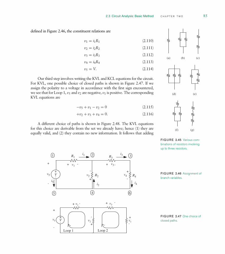
2.3 Circuit Analysis: Basic Method C H A P T E R T W O 85
defined in Figure 2.46, the constituent relations are
(a) (b) (c)
(d) (e)
(f) (g)
F IGURE 2.45 Various com-binations of resistors involvingup to three resistors.
v1 = i1R1 (2.110)
v2 = i2R2 (2.111)
v3 = i3R3 (2.112)
v4 = i4R4 (2.113)
v5 = V. (2.114)
Our third step involves writing the KVL and KCL equations for the circuit.For KVL, one possible choice of closed paths is shown in Figure 2.47. If weassign the polarity to a voltage in accordance with the first sign encountered,we see that for Loop 1, v5 and v2 are negative, v1 is positive. The correspondingKVL equations are
−v5 + v1 − v2 = 0 (2.115)
+v2 + v3 + v4 = 0. (2.116)
A different choice of paths is shown in Figure 2.48. The KVL equationsfor this choice are derivable from the set we already have; hence (1) they areequally valid, and (2) they contain no new information. It follows that adding
i11 2 3R1
R2
i2i5
i3
v4
+
-
-
+
v3+ - +
i4
645
R4
R3
+
-V v2
v1 -
v5
+
-
F IGURE 2.46 Assignment ofbranch variables.
v4
+
-
-
+
v3+ - +
v2
v1-
Loop 1 Loop 2
+-V
v5
+
-
F IGURE 2.47 One choice ofclosed paths.

86 C H A P T E R T W O r e s i s t i v e n e t w o r k s
F IGURE 2.48 Alternative choiceof paths.
Loop a
Loop b
+
-Vv5
+
-
v4
+
-
-
+
v3+ - +
v2
v1-
a third loop (loop b, Figure 2.48) to Figure 2.47 will not yield a KVL equationindependent of Equations 2.115 and 2.116.2
We now write the KCL equations. From Figure 2.46, at Node 1, KCLyields
−i5 − i1 = 0 (2.117)
and at Node 2
+i1 + i2 − i3 = 0 (2.118)
and at Node 3
i3 − i4 = 0. (2.119)
As in the case of loops, it is possible to write KCL at Node 4, but theequation is not independent of those we already have.
One might be tempted to write node equations for the junctions labeled5 and 6, but this doesn’t make much sense. The branch between 4 and 6 isa perfect conductor, hence it is really just part of the copper lead attached toresistor R4. For this reason we did not bother defining a separate current variablefor this branch. A similar argument applies to branch 4-5.
Another way to emphasize that 5 and 6 are not true nodes is to redrawthe circuit as shown in Figure 2.49. Clearly the circuit topology is unchanged inthe sense that the interconnections among resistors and source are the same asbefore, but the false nodes have disappeared. We conclude that a node shouldbe defined as a junction where two or more circuit elements, other than perfectconductors, join together. Whenever a number of circuit elements connect toone perfect conductor, (for example, 5, 4, 6 in Figure 2.46) only one node iscreated.
2. A detailed treatment of the topological issues underlying these rules is contained in Guillemin(Introductory Circuit Theory, Will, 1953) or Bose and Stevens (Introductory Network Theory,Harper and Row, 1965).

2.3 Circuit Analysis: Basic Method C H A P T E R T W O 87
R2V+
-
1 2
4
3R1 R3
R4
F IGURE 2.49 Circuit inFigure 2.46 redrawn.
We now have ten independent equations (Equations 2.110 through 2.119)and ten unknowns: five voltages and five currents. Thus the equations canbe solved for any variable by simple algebra. To find i4, for example, we canfirst substitute the constituent relations, Equations 2.110 through 2.114 intoEquations 2.115 and 2.116:
−V + i1R1 − i2R2 = 0 (2.120)
i2R2 + i3R3 + i4R4 = 0. (2.121)
Now eliminating i2 and i3 using Equations 2.118 and 2.119
−V + i1R1 + (i1 − i4) R2 = 0 (2.122)
(−i1 + i4)R2 + i4R3 + i4R4 = 0. (2.123)
Rewriting to collect variables and place in the known voltages on the right-hand side of each equation, we obtain
i1 (R1 + R2) − i4R2 = V (2.124)
−i1R2 + i4 (R2 + R3 + R4) = 0, (2.125)
which can be expressed in matrix form as[(R1 + R2) −R2
−R2 (R2 + R3 + R4)
] [i1i4
]=
[V
0
]. (2.126)
The matrix equation is in the form
Ax = b
where x is a column vector of the unknowns (i1 and i4) and b is the columnvector of drive voltages and currents (in this case, just V). This vector ofunknowns can be solved by using standard linear algebraic techniques.

88 C H A P T E R T W O r e s i s t i v e n e t w o r k s
For example, i4 can be found by applying Cramer’s Rule3
i4 = VR2
(R1 + R2)(R2 + R3 + R4) − R22
(2.127)
= VR2
R1R2 + R1R3 + R1R4 + R2R3 + R2R4. (2.128)
With some more effort, we can find the rest of the branch variables as givenbelow
−i5 = i1 = R2 + R3 + R4
R1(R2 + R3 + R4) + R2(R3 + R4)V (2.129)
i2 = − R3 + R4
R1(R2 + R3 + R4) + R2(R3 + R4)V (2.130)
i3 = i4 = R2
R1(R2 + R3 + R4) + R2(R3 + R4)V (2.131)
v5 = V (2.132)
v1 = R1(R2 + R3 + R4)
R1(R2 + R3 + R4) + R2(R3 + R4)V (2.133)
v2 = − R2(R3 + R4)
R1(R2 + R3 + R4) + R2(R3 + R4)V (2.134)
v3 = R2R3
R1(R2 + R3 + R4) + R2(R3 + R4)V (2.135)
v4 = R2R4
R1(R2 + R3 + R4) + R2(R3 + R4)V. (2.136)
This completes our analysis.Note that in Figure 2.46, resistors R1 and R2 alone do not form a simple
voltage divider because of the presence of R3 and R4. It is true, however, thatR3 and R4 form a voltage divider. Further, R1 and the net resistance of R2, R3,and R4 form a second voltage divider.
The analysis of the circuit in Figure 2.46 following the general approachdeveloped in this chapter is both straightforward and tedious, with emphasis on
3. Cramer’s Rule is a popular method for solving equations of the type Ax = b, where x and b arecolumn vectors, and A is a matrix. See Appendix D for more details.

2.4 Intuitive Method of Circuit Analysis C H A P T E R T W O 89
tedious. Fortunately, as we shall see in Chapter 3, there are much less tediousapproaches to this analysis. However, in advance of that we can still simplify theanalysis by employing results taken solely from earlier sections of this chapter.Specifically, Section 2.4 shows that we can employ the equivalence of paralleland series resistors, and the behavior of current and voltage dividers, to developan intuitive and simple approach to solving many types of circuits.
2.4 I N T U I T I V E M E T H O D O F C I R C U I TA N A L Y S I S : S E R I E S A N DP A R A L L E L S I M P L I F I C A T I O N
To develop our intuition, let us first illustrate the method with the simplevoltage divider in Figure 2.50a. Suppose we were interested in determining thevoltage across resistor R2. The figure shows a few important variables markedon it. An intuitive way of analyzing the circuit is to replace the two resistors bythe series equivalent, as in Figure 2.50b, then find i1 using Ohm’s law. FromEquation 2.56, the equivalent series resistance is given by
RS = R1 + R2
and from Equation 1.4
i1 = V/RS.
Because i1 must be the same in the two circuits (in Figures 2.50a and 2.50b),we can now find v2 from Figure 2.50a
v2 = i1R2 (2.137)
=(
R2
R1 + R2
)V. (2.138)
We have now determined the value of v2 in a few simple steps using resultsfrom series resistances and Ohm’s law. In the future, we will actually write downthe result for the voltage divider in a single step by directly applying the voltagedivider relation in Equation 2.138.
(a)
R1
R2v2
i1
+
-
V+-
(b)Rs
i1
V+-
F IGURE 2.50 An intuitive way ofanalyzing the voltage divider circuit.

90 C H A P T E R T W O r e s i s t i v e n e t w o r k s
It is worth dwelling on a couple of the ‘‘key moves’’ of our intuitive method.The basic approach is to first collapse, then expand. Notice that our first movewas to collapse a set of resistances into a single equivalent resistance. Then, wefound the current into the equivalent resistance. Finally, we took an expandedview of the two resistances to determine the specific voltage of interest.
Let us now use our intuition to develop an alternative method of ana-lyzing the circuit in Figure 2.46 (repeated in Figure 2.51a for convenience). Itwill be obvious that the intuitive method is far less tedious than the rigorous
-
+i0
v0
+
-
v1
R1 i2
R2
+
-v2V
+-
v4 R4
+ -i1v3+ -i3
R3 i4
(a)
-
+i0
v0
+
-
v1
R1 i2
R2v2V
+-
+ -i1 i3
(b)
R3 R4+
-
+i0
v0
v1
R1
V+-
+ -i1
(c)
R2 R3 R4)+(R2 + R3 + R4
-
-
+i0
v0V+-
(d)
R1 R2 + R3 + R4-+
+
-v2
i1
R2 R3 R4)+(
F IGURE 2.51 Collapsing thecircuit.
application of the basic method in Section 2.3.Our alternative analysis of the circuit in Figure 2.51a follows the two basic
moves suggested earlier first collapse, then expand. Accordingly, our anal-ysis begins by collapsing the circuit using the equivalence of parallel and seriesresistors. This process is illustrated in Figure 2.51. Note that all branch variablesthat can be preserved during this collapse are shown in Figure 2.51. First, theseries resistors R3 and R4 are combined to yield the circuit in Figure 2.51b.Next, R2 is combined in parallel with the series equivalent of R3 and R4 toyield the circuit in Figure 2.51c. Finally, the two remaining series resistors arecombined in series to yield the circuit in Figure 2.51d.
We now analyze our collapsed circuit in Figure 2.51d. Trivially, we knowthat
v0 = V
and
i0 = −i1.
Now, following the results of Section 2.3.1, or equivalently by applyingOhm’s law directly, we know that
i1 = V(R1 + R2(R3+R4)
R2+R3+R4
) .
Thus, at this point, i0, v0, and i1 are known.Our intuitive analysis concludes by expanding the circuit in Figure 2.51d
progressively. As we expand, we determine the values of as many of the variablesas we can in terms of previously computed variables. Following this process,first, the circuit in Figure 2.51c can be viewed as a voltage divider of v0. In otherwords, i1 can be multiplied by each of its two resistances to determine v1 andv2. Thus,
v1 = VR1(
R1 + R2(R3+R4)R2+R3+R4
)

2.4 Intuitive Method of Circuit Analysis C H A P T E R T W O 91
and
v2 = V
R2(R3+R4)R2+R3+R4(
R1 + R2(R3+R4)R2+R3+R4
) .
Next, since v2 is now known, R2 and the series equivalent of R3 and R4 inFigure 2.51b can each be divided into v2 to determine i2 and i3. In other words,
i2 = v2
R2
i3 = v2
R3 + R4.
Alternatively, i2 and i3 can be determined by viewing R2 and the series equivalentof R3 and R4 as a current divider of i1.
Finally, since i3 is now known, R3 and R4 in Figure 2.51a can be viewedas a voltage divider of v2, or they can be multiplied by i3 = i4, to determine v3and v4. Doing so yields
v3 = i3R3
and
v4 = i3R4.
This completes the intuitive analysis of the circuit in Figure 2.51a. The importantobservation here is that the alternative approach to circuit analysis outlined inFigure 2.51 is considerably simpler than the direct approach.
e x a m p l e 2.24 c i r c u i t a n a l y s i s s i m p l i f i c a t i o n Asanother example of circuit analysis simplification, consider the network of twelve resis-tors shown in Figure 2.52. Each resistor in the network has resistance R, and together
A
B
(a) (b)
(f)(e)
(d)
(h) (g)
(c)
F IGURE 2.52 A cubic resistivenetwork.
the network outlines the shape of a cube. Additionally, the network has two terminalsmarked A and B, which extend from opposite corners of the cube to form a port. Wewish to determine the equivalent resistance of the network as viewed through this port.
To determine the network resistance, we turn the network into a complete circuit byconnecting a hypothetical current source to its terminals as shown in Figure 2.53. Notethat the circuit in Figure 2.53 is now much the same as the circuit in Figure 2.25; the twocircuits differ only in the complexity of the resistive network across the current source.Next, we compute the voltage across the port that appears in response to the applicationof the current source. The ratio of this voltage to the source current is then the equivalentresistance of the network as viewed through the port. Note that this procedure doeswork as desired for the circuit in Figure 2.25 since the division of Equation 2.22 by Iyields v2/I = R.

92 C H A P T E R T W O r e s i s t i v e n e t w o r k s
F IGURE 2.53 Introducing acurrent into the A–B terminal pairof the cubic network.
i1
i3
i2
i6
i5
i4
I
A
B
(a) (b)
(f)(e)
(d)
(h) (g)
(c)
i7
i12
i11i9 i10
i8
Turning now to the analysis of the circuit in Figure 2.53, we see that it involves thedetermination of 26 branch variables, which seems like a painful task. Fortunately, thisanalysis can be greatly simplified by taking advantage of the symmetry of the circuit, andthat is the primary observation to be made here. As a consequence of the symmetry ofthe circuit, the three branch currents i1, i2, and i3 are identical, as are the three branchcurrents i4, i5, and i6. Further, KCL applied to the two nodes at the port terminalsshows that the sum of each group of three branch currents is I, so all six branch currentsequal I/3.
Next, again due to the symmetry of the circuit, the six branch currents i7 through i12
are all identical. Further, KCL applied to any interior node shows that these six branchcurrents all equal I/6. Now, all branch currents in the circuit are known.
So, through their element laws, the branch voltages across all twelve resistors are known,leaving the branch voltage across the current source as the only remaining unknown.Finally through the application of KVL around any loop that passes through the currentsource we see that its branch voltage is 5RI/6. Dividing this voltage by I yields 5R/6 asthe equivalent resistance of the cubic network of resistors.
While this solution yields an interesting result, the more important observation is theimportance of simplifying a circuit, in this case through symmetry, before attempting itsanalysis.
e x a m p l e 2.25 r e s i s t a n c e o f a c u b i c n e t w o r k Analternative method for determining the equivalent resistance of the cubic network inFigure 2.52 that uses series-parallel simplifications is now shown. Also suppose thateach of the resistors in the network in Figure 2.52 has a resistance of 1 k. Our goal

2.4 Intuitive Method of Circuit Analysis C H A P T E R T W O 93
A
B
(b) (d) (e)
(a)
(c) (h) (f)
(g)
F IGURE 2.54 Simplifiednetwork.
is to find the equivalent resistance of this resistive network when looking into the A Bterminal pair.
First, observe the symmetry property of this resistive network. From any of the eightvertices, the network looks identical, and therefore, the resistance between any pair ofvertices connected by the solid diagonal (for example, (a)-(g), (b)-(h), (e)-(c), etc.) is thesame. Furthermore, looking into A, the set of paths from A to B starting along theedge (a)-(d) are matched by a set of paths starting along the edge (a)-(b), or by a set ofpaths starting along the edge (a)-(e). Therefore, when we apply a current I as shown inFigure 2.53, it must split evenly into i1, i2, and i3. Likewise, it draws current off thenetwork evenly, that is, i4, i5, and i6 are the same. Since the same current and resistancecauses the same voltage drop across the resistors, we conclude that nodes (b), (d), and(e) have the same voltage, and nodes (h), (c), and (f) also have the same voltage withrespect to any reference node.
Notice that if we connect nodes with identical voltages by an ideal wire it does notdraw any current and does not change the behavior of the circuit. Therefore, for thepurpose of computing the resistance, we can connect all nodes with identical voltages,and simplify the network to the one shown in Figure 2.54.
We can now apply our series and parallel rules to determine the equivalent resistance as
1 k‖1 k‖1 k + 1 k‖1 k‖1 k‖1 k‖1 k‖1 k + 1 k‖1 k‖1 k
which equals
11
1 k+ 1
1 k+ 1
1 k
+ 11
1 k+ 1
1 k+ 1
1 k+ 1
1 k+ 1
1 k+ 1
1 k
+ 11
1 k+ 1
1 k+ 1
1 k
= 5
6k.
e x a m p l e 2.26 r e s i s t o r r a t i o s Consider the more involvedvoltage-divider circuit in Figure 2.55a. The voltage source represents a battery that

94 C H A P T E R T W O r e s i s t i v e n e t w o r k s
F IGURE 2.55 Resistor circuit:(a) more complex voltage - dividercircuit; (b) shorthand notation. R1 R2 R3
RLVO
VS = 5 V
Gnd
(b)
R1 R2 R3
RL
VO
+- VS = 5 V
(a)
+
-
is supplying power to the rest of the circuit. Further, assume that the voltage VO is ofinterest to us. Notice also that the two voltages VS and VO share a common negativereference node. A power supply voltage source and a common voltage reference will beencountered so commonly in our circuit language that it is worth creating an idiomaticrepresentation for them.
Figure 2.55b introduces our shorthand notation. First, batteries that serve as powersupplies are often not shown explicitly and use the upwards pointing arrow notationinstead. VS represents the power supply voltage. Often, we are also interested in mea-suring voltages with respect to a common reference node, termed the ground node. Thisnode is represented with an upside-down ‘‘T’’ symbol as shown in the figure. The polar-ity symbols corresponding to voltages that are referenced from this node are not shownexplicitly. Rather, the negative symbol is associated with the ground node and the plussymbol is associated with the node adjacent to which the voltage variable appears.4
Now, referring to Figure 2.55b, suppose R1 = R2 = R3 = 10 k, how do we chooseRL such that VO < 1 V?
The equivalent resistance of the three resistors in parallel is given by Equation 2.98.Thus,
Req = 10k‖10k‖10k = 10
3k.
Using the voltage divider relationship, we require that
VO = 5Req
(RL + Req)< 1,
which implies that RL has to be at least four times as large as Req. In other words
RL >40
3k.
4. Chapter 3 will discuss the concepts of ground nodes as well as node voltages in more detail.

2.5 More Circuit Examples C H A P T E R T W O 95
2.5 M O R E C I R C U I T E X A M P L E S
Let us now return to applying the basic method to several other circuits. Con-sider, for example, the circuit in Figure 2.56, which we will see again inChapter 3. What is new about this circuit is that it contains two sources. Itis not amenable to the intuitive method discussed in Section 2.4. Nonetheless,it can be analyzed by the basic approach presented in Section 2.3.
-
+i0
v0
+
-
v1
R1 i2
R2 v2V+-
+ -i1 i3
+
-v3I
F IGURE 2.56 A circuit with twoindependent sources.
The element laws for this circuit are
v0 = V (2.139)
v1 = R1i1 (2.140)
v2 = R2i2 (2.141)
i3 = −I. (2.142)
Next, the application of KCL to the two upper nodes yields
i0 = −i1 (2.143)
i1 = i2 + i3 (2.144)
and the application of KVL to the two internal loops yields
v0 = v1 + v2 (2.145)
v2 = v3. (2.146)
Finally, Equations 2.139 through 2.146 can be solved to yield
−i0 = i1 = − R2
R1 + R2I + 1
R1 + R2V (2.147)
i2 = R1
R1 + R2I + 1
R1 + R2V (2.148)
i3 = −I (2.149)
v0 = V (2.150)
v1 = − R1R2
R1 + R2I + R1
R1 + R2V (2.151)
v2 = v3 = R1R2
R1 + R2I + R2
R1 + R2V (2.152)
to complete the analysis.What is most interesting about the results of this analysis is that each
branch variable in Equations 2.147 through 2.152 is a linear combination of

96 C H A P T E R T W O r e s i s t i v e n e t w o r k s
a term proportional to I and a term proportional to V. This suggests that wecould analyze the circuit first with V = 0 and second with I = 0, and thencombine the two analyses to obtain Equations 2.147 through 2.152. This is infact possible, and it leads to yet further analysis simplifications as we shall seein Chapter 3.
Let us now practice the basic method on several other examples.
e x a m p l e 2.27 c i r c u i t w i t h t w o i n d e p e n d e n t
s o u r c e s Analyze the circuit in Figure 2.57 using the basic method. Further, show
-
+i0
v0
+
-
v1
i2
v22 V+-
+ -i1
-
+v3
3 Ai3
2 Ω
3 Ω
F IGURE 2.57 Another circuitwith two independent sources.
that energy is conserved in the circuit.
The branch variable assignments are shown in the figure. The element laws for thiscircuit are
v0 = 2 V
v1 = 3i1
v2 = 2i2
i3 = 3 A.
Applying KCL to the two upper nodes gives us
i0 + i1 + i2 = 0
i1 = −i3.
Applying KVL to the two internal loops yields
v0 = v2
v2 = −v3 + v1.
Solving the preceding eight equations, we get v0 = 2 V, v1 = −9 V, v2 = 2 V,v3 = −11 V, i0 = 2 A, i1 = −3 A, i2 = 1 A, and i3 = 3 A.
To show that energy is conserved, we need to compare the power dissipated by theresistors and the power generated by the sources. The power into the resistors is given by
(−9 V) × (−3 A) + (2 V) × (1 A) = 29 W.
The power into the sources is given by
(2 V) × (2 A) + (−11) × (3 A) = −29 W.
It is easy to see that the power dissipated by the resistors equals the power gener-ated by the sources. Thus, energy is conserved.

2.5 More Circuit Examples C H A P T E R T W O 97
W W W e x a m p l e 2.28 b a s i c c i r c u i t a n a l y s i s m e t h o d
e x a m p l e 2.29 d e t e r m i n i n g t h e I V c h a r a c t e r -
i s t i c s o f a c i r c u i t Determine the i v relationship for the two-terminaldevice shown in Figure 2.61a. Make a sketch of the i v relationship for R = 4 andV = 5 V. As shown in the figure, assume that the internals of the device can be modeledas a voltage source in series with a resistor.
We will find the i v relationship of the device by applying some form of excitation to thedevice terminals and obtaining the relationship between the values of i and v. One of thesimplest inputs we can apply is a current source providing a current itest, as illustratedin Figure 2.61b. The figure also shows the assignment of branch variables.
We will proceed by solving for the branch variables, v1, i1, v2, i2, v3, and i3, and thenobtain the i v relationship by expressing v and i in terms of the expressions for thebranch variables. Using the basic method, we first write the element laws
v1 = V
v2 = i2R
i3 = −itest.
Next, we apply KCL to the two upper nodes
i1 = −i2
i2 = i3
and KVL to the loop
v1 − v3 − v2 = 0.
These six equations can be solved to yield
i1 = −i2 = −i3 = itest
+
-V
R
i
+
-
v
(b)
itest
+
-
+ -
+
-
v1
i1
v2
i3
v3
i2
+
-V
R
i
+
-
v
(a)
Two-terminal device
F IGURE 2.61 Determining thei – v characteristics: (a) a two-terminal device; (b) assignment ofbranch variables to the circuit con-structed to determine the i – vcharacteristics of the device.

98 C H A P T E R T W O r e s i s t i v e n e t w o r k s
F IGURE 2.62 A plot of the i – vcharacteristics for the device. v = 5 V
Slope1R---
14---= =
v (V)
i (A
)
0
Ω
and
v1 = V, v2 = −itestR, and v3 = V + itestR.
We can now write the expression for v as
v = v3 = V + itestR
and substituting i = itest, we obtain the relationship between i and v as
v = V + iR.
In other words, the i v relationship is given by
i = v − V
R.
Substituting V = 5 volts and R = 4 , we get
i = v − 5
4.
This relationship is plotted in Figure 2.62.
2.6 D E P E N D E N T S O U R C E S A N DT H E C O N T R O L C O N C E P T
Section 1.6 introduced the voltage source and the current source as ideal mod-els for energy sources. We call these independent sources because their valuesare independent of circuit operation. But many sources have values that aredependent on, that is, controlled by some other parameters in the system. Forexample, the accelerator pedal in an automobile controls the power deliveredby the engine; the handle on a sink faucet controls the flow of water; and
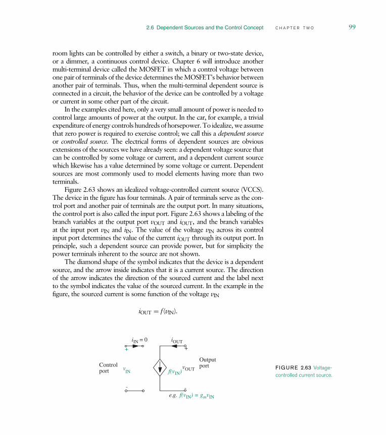
2.6 Dependent Sources and the Control Concept C H A P T E R T W O 99
room lights can be controlled by either a switch, a binary or two-state device,or a dimmer, a continuous control device. Chapter 6 will introduce anothermulti-terminal device called the MOSFET in which a control voltage betweenone pair of terminals of the device determines the MOSFET’s behavior betweenanother pair of terminals. Thus, when the multi-terminal dependent source isconnected in a circuit, the behavior of the device can be controlled by a voltageor current in some other part of the circuit.
In the examples cited here, only a very small amount of power is needed tocontrol large amounts of power at the output. In the car, for example, a trivialexpenditure of energy controls hundreds of horsepower. To idealize, we assumethat zero power is required to exercise control; we call this a dependent sourceor controlled source. The electrical forms of dependent sources are obviousextensions of the sources we have already seen: a dependent voltage source thatcan be controlled by some voltage or current, and a dependent current sourcewhich likewise has a value determined by some voltage or current. Dependentsources are most commonly used to model elements having more than twoterminals.
Figure 2.63 shows an idealized voltage-controlled current source (VCCS).The device in the figure has four terminals. A pair of terminals serve as the con-trol port and another pair of terminals are the output port. In many situations,the control port is also called the input port. Figure 2.63 shows a labeling of thebranch variables at the output port vOUT and iOUT, and the branch variablesat the input port vIN and iIN. The value of the voltage vIN across its controlinput port determines the value of the current iOUT through its output port. Inprinciple, such a dependent source can provide power, but for simplicity thepower terminals inherent to the source are not shown.
The diamond shape of the symbol indicates that the device is a dependentsource, and the arrow inside indicates that it is a current source. The directionof the arrow indicates the direction of the sourced current and the label nextto the symbol indicates the value of the sourced current. In the example in thefigure, the sourced current is some function of the voltage vIN
iOUT = f (vIN).
iIN = 0
vIN
+
-
+
-
f(vIN)
f(vIN) = gmvIN
vOUT
e.g.
Controlport
Outputport
iOUT
F IGURE 2.63 Voltage-controlled current source.

100 C H A P T E R T W O r e s i s t i v e n e t w o r k s
When the device is connected in a circuit, vIN might be another branchvoltage in the circuit.
We often deal with linear dependent sources. A linear voltage-controlledcurrent source is characterized by the equation:
iOUT = gvIN (2.173)
where g is a constant coefficient. When the dependent source is a voltage-controlled current source, the coefficient g is called the transconductance withunits of conductance. Notice that Equation 2.173 is the element law for ourdependent source expressed as usual in terms of the branch variables. We alsoneed to summarize the behavior of the input port to completely characterizethe dependent source. Since our idealized VCCS does not require any powerto be supplied at its input, the element law for the input port is simply
iIN = 0 (2.174)
which is simply the element law for an infinite resistance. For the ideal dependentsources considered in this book, we will assume that the control ports are ideal,that is, they draw zero power.
Figure 2.64 shows a circuit containing our dependent source. For clarity,the dependent source device is shown within the dashed box. In the figure, anindependent voltage source (sourcing a voltage V) is connected to the controlport and a resistor is connected to the output port. For the connection shown,because
vIN = V
the output current iOUT will be g times the input voltage V. We will completethe full analysis of the circuit shortly, and show that the presence of a dependentsource does not alter the manner in which our approach to circuit analysis isapplied.
Figure 2.65 shows another circuit containing our dependent source. In thiscircuit, the control port is connected across a resistor with resistance RI. Accord-ingly, the voltage across RI becomes the guiding voltage for the dependentsource.
F IGURE 2.64 A circuit con-taining a voltage-controlledcurrent source.
vIN gvIN vOUT
iIN+
-
+
-
iOUT
V+- RL

2.6 Dependent Sources and the Control Concept C H A P T E R T W O 101
vIN gvIN vOUT
iIN+
-
+
-
iOUT
RLRII
vI
+
-
iIF IGURE 2.65 Another circuitcontaining a voltage-controlledcurrent source.
Figure 2.66 illustrates the four types of linear dependent sources.Figure 2.66a depicts our now familiar voltage-controlled current source.Figure 2.66b depicts another type of dependent current source whose guidingvariable is a branch current. This dependent source is called a current-controlledcurrent source (CCCS).
The element law for the CCCS in Figure 2.66b is
iOUT = αiIN. (2.175)
The unitless coefficient α is referred to as a current transfer ratio. Further-more, for a CCVS vIN = 0.
Figures 2.66c and 2.66d depict the symbols for dependent voltage sources.A dependent voltage source supplies a branch voltage that is a function of some
vIN gvIN vOUT
iIN+
-
+
-
(a)
vIN αiIN vOUT
iIN+
-
+
-
(b)
vIN µvIN vOUT
iIN+
-
+
-
(c)
iOUT
iOUT
iOUT
vIN riIN vOUT
iIN+
-
+
-
(d)
iOUT
+-
+-
F IGURE 2.66 Four types ofdependent sources: (a) VCCS(voltage-controlled current source);(b) CCCS (current-controlledcurrent source); (c) VCVS(voltage-controlled voltage source);(d) CCVS (current-controlledvoltage source).
other signal within the circuit. Figure 2.66c shows a voltage-controlled voltagesource (VCVS) and Figure 2.66d shows a current-controlled voltage source(CCVS). The guiding variable for a VCVS is a branch voltage, and that for aCCVS is a branch current. The diamond shape of their symbols again indicatesthat they are dependent sources, and the ± inside indicates that they are voltagesources. The polarity the ± indicates the polarity of the sourced voltage andthe label next to the symbol indicates the value of the sourced voltage.
In the case of the VCVS in Figures 2.66c, the sourced voltage is equal toµvIN, where vIN is a voltage across another branch of the circuit and µ is aunitless coefficient. Thus, the element law for the VCVS in Figure 2.66 is
vOUT = µvIN. (2.176)
The coefficient µ is referred to as a voltage transfer ratio. Furthermore, for aVCVS iIN = 0.
In the case of the CCVS in Figures 2.66d, the sourced voltage is equal toriIN, where iIN is the current through another branch of the circuit and r is acoefficient having the units of resistance. Thus, the element law for the CCVSin the figure is
vOUT = riIN. (2.177)
The coefficient r is referred to as a transresistance.

102 C H A P T E R T W O r e s i s t i v e n e t w o r k s
Finally, for both the dependent current source and the dependent voltagesource it is once again important to distinguish between the symbols that definethem (e.g., g) and the branch variables that are defined (e.g., vIN, iIN, vOUT, andiOUT) in order to express their element laws. In particular, the branch variabledefinitions may be reversed for convenience, which will lead to a negation ofthe corresponding element laws.
2.6.1 C I R C U I T S W I T H D E P E N D E N T S O U R C E S
Let us now return to the analysis of our circuit in Figure 2.64, which containsa dependent voltage source. Nonetheless, the circuit can be analyzed by thebasic approach presented in this chapter.
Figure 2.67 shows an assignment of the branch variables. The branchvariables include v0, i0, vIN, iIN, vOUT, iOUT, vR, and iR.
The element laws for this circuit are
v0 = V (2.178)
iIN = 0 (2.179)
vR = RLiR (2.180)
iOUT = gvIN. (2.181)
Next, the application of KCL to the two upper nodes yields
i0 = −iIN (2.182)
iOUT = −iR (2.183)
and the application of KVL to the two loops yields
v0 = vIN (2.184)
vR = vOUT. (2.185)
F IGURE 2.67 Assignment ofbranch variables.
vIN gvINvOUT
iIN+
-
+
-
iOUT
V+- RL
v0
+
-
i0
vR
+
-
iR

2.6 Dependent Sources and the Control Concept C H A P T E R T W O 103
Finally, Equations 2.178 through 2.185 can be solved for the branchvariables to yield
i0 = iIN = 0 (2.186)
v0 = vIN = V (2.187)
iOUT = −iR = −gV (2.188)
vR = vOUT = −gVRL (2.189)
to complete the analysis.The presence of the dependent source in the circuit in Figure 2.67 does not
alter the manner in which our approach to circuit analysis is applied. While thisis an important observation, there is arguably a more important observationconcerning the analysis of the dependent-source circuit, namely that it canproceed in stages. That is, it is possible to first analyze the operation of the‘‘input side’’ of the circuit, that is, the independent voltage source and theinput of the dependent source, and then separately analyze the operation ofthe ‘‘output side,’’ that is, the dependent current source and the resistor RL.We will term this approach the sequential approach to circuit analysis.
To see this, observe that the equations representing the input side of thecircuit, namely, Equations 2.178, 2.179, 2.182, and 2.184 can be solved triviallyby themselves to yield the values of v0, i0, vIN, and iIN (see Equations 2.186and 2.187).
Then, with vIN treated as a known signal, the equations representing theoutput side of the circuit, namely Equations 2.180, 2.181, 2.183, and 2.185,can be solved by themselves to yield the values of vOUT, iOUT, vR, and iR (seeEquations 2.188 and 2.189) a result that is identical to that obtained for thecircuit in Figure 2.25.
At this point you are probably wondering why it is that we were able toadopt such a sequential approach to analyzing the circuit in Figure 2.67. Thesame sequential approach does not work for the circuit in Figure 2.46. Theintuition behind this useful property is that our idealized dependent source hasdecoupled the circuit into two parts an input part and an output part. Becauseour dependent source model has an open circuit at its terminals marked by thebranch voltage vIN, the behavior of the input part is completely independentof the output part of the circuit. In other words, in determining the behaviorof the input part, it is as if the output did not even exist. The output part,however, does depend on one of the input variables, namely, vIN. However,once the value of the control input vIN is determined through an analysis ofthe input part, it fixes the value of the dependent source. Thus, the dependentsource can be treated as an independent source for the purpose of analyzing theoutput part.

104 C H A P T E R T W O r e s i s t i v e n e t w o r k s
F IGURE 2.68 The input port ofan idealized dependent source isnot shown explicitly.
vI gvI vOUT
+
-
+
-
iOUT
RLRII
iI
Such a sequential approach to circuit analysis is commonly applied to cir-cuits involving dependent sources, when the circuit does not introduce anyexternal coupling between the control port and the output port of the dependentsources. We will use this approach to advantage in future chapters.
The analysis of circuits with idealized dependent sources admits one othersimplification. In an idealized dependent source, the input port (or control port)is an open circuit if the guiding variable is a voltage. Similarly, the input is ashort circuit if the guiding variable is a current. Thus, the presence of the inputport does not really affect the behavior of the input part of the circuit. Theidealized input port is simply present to sample the value of a branch current orvoltage without changing the value of the existing branch variable. Therefore,we do not really need to show the input port of the dependent source explicitly,thereby reducing the number of branch variables that we have to deal with.
For example, the input port of the dependent source marked with thebranch variables vIN and iIN in Figure 2.65 is an open circuit. Accordingly,iIN = 0 and vIN = vI, the voltage across the resistor RI. Therefore, we canequivalently use the circuit in Figure 2.68, where the input port of the dependentsource is not shown explicitly, and the current sourced by the dependent sourceis specified directly in terms of vI, the voltage across the resistor RI. We havethus eliminated the branch variables vIN and iIN from our analysis.
As depicted in Figure 2.69, the same simplification can be made for adependent source in which the guiding branch variable is a current. Figure 2.69ashows a circuit containing a current controlled current source with the controlport marked and all branch variables labeled explicitly. Figure 2.69b shows the
F IGURE 2.69 Simplifying acircuit with a dependent sourceby not showing the control portexplicitly: (a) with control portmarked and branch variableslabeled explicitly; (b) withsimplification.
-
+
i0
v0 +
-v1
R1
i2
V+
- i1
i3
-
+
v3
+
-
v2R2
αiIN
(a)
iIN+-
vIN
-
+
i0
v0
+
-
v1 R1
i2
V+-
i1 i3
-
+
v3
+
-
v2 R2
αi1
(b)

2.6 Dependent Sources and the Control Concept C H A P T E R T W O 105
same circuit after making the simplification, where the sourced current is nowspecified in terms of i1. Notice that there is a lot less clutter in the latter figure.
e x a m p l e 2.30 curr en t - con tro l l ed curr en t sourc e
Consider next the circuit shown in Figure 2.69b. This circuit contains a dependentcurrent source. Notice that we have applied a simplification suggested earlier by notshowing the control port of the dependent source explicitly. The current sourced by thedependent source is guided by the current i1.
Let us now analyze this circuit. The branch variables are assigned as shown inFigure 2.69b.
The element laws for this circuit are
v0 = V (2.190)
v1 = R1i1 (2.191)
v2 = R2i2 (2.192)
i3 = −αi1. (2.193)
Next, the application of KCL to the two upper nodes yields
i0 + i1 = 0 (2.194)
i2 + i3 = 0 (2.195)
and the application of KVL to the two loops yields
v0 = v1 (2.196)
v2 = v3. (2.197)
Finally, Equations 2.190 through 2.197 can be solved to yield
−i0 = i1 = V
R1(2.198)
−i3 = i2 = αV
R1(2.199)
v0 = v1 = V (2.200)
v2 = v3 = αR2V
R1(2.201)
to complete the analysis.

106 C H A P T E R T W O r e s i s t i v e n e t w o r k s
e x a m p l e 2.31 i n tu i t i v e s equ en t i a l a p p roach for
t h e c c c s Alternatively, we can solve the circuit in Figure 2.69b in a few lines ifwe use the intuitive sequential approach. Assume that we are interested in finding outthe branch variables related to R2.
Using the sequential approach, first, let us tackle the input part of the circuit. Since thevoltage V appears across R1, the current through R1 is
i1 = V
R1.
Now let us tackle the output part of the circuit. The current through the current sourceis in the same direction as i2, and so
i2 = αi1 = αV
R1.
Applying Ohm’s law, we get
v2 = αVR2
R1.
Not surprisingly, this result is the same as that in Equation 2.201.
e x a m p l e 2.32 b r anch var i a b l e s Analyze the circuit in Figure2.70 and determine the values of all the branch variables. Further, show that energyis conserved in the circuit.
We will analyze the circuit intuitively, applying element laws, KVL and KCL, using thesequential approach. Looking at the input side, since the voltage source appears acrossan open circuit, it is easy to see that both v0 and vIN are two volts. Similarly, both i0and iIN are zero. Thus, we have determined all the branch variables at the input side.
Next, let us analyze the output part of the circuit. Since we know the value of vIN, thecurrent through the current source is determined as
0.001vIN = 0.002 A.
F IGURE 2.70 A circuitcontaining a voltage-controlledcurrent source.
vIN
0.001vIN
vOUT
iIN+
-
+
-
iOUT
2 V+-
v0
+
-
i0
vR
+
-
iR
3 kΩ

2.7 A Formulation Suitable for a Computer Solution * C H A P T E R T W O 107
Since the current source current is in the same direction as iOUT, and in the oppositedirection as iR, we obtain from KCL
iOUT = 0.002 A
and
iR = −0.002 A.
Finally, applying the element law for a resistor, we obtain
vR = 3 × 10³iR = −6 V
and from KVL, we obtain
vOUT = vR = −6 V.
This completes our analysis, since all output side branch variables are also known.
To verify that energy is conserved in the circuit, we must show that the power dissipatedby the elements is equal to the power supplied. Since the input side current is zero, thereis no power dissipated or supplied at the input side. At the output side, the powerdissipated in the 3-k resistor is given by
3 k × i2R = 0.012 W.
The power into the dependent current source is given by
vOUT × iOUT = −6 × 0.002 = −0.012 W.
In other words, the power supplied by the current source is 0.012 W. Since the powersupplied is equal to the power dissipated, energy is conserved.
More examples containing dependent sources are given in Section 7.2.
W W W e x a m p l e 2.33 vo l t ag e - con tro l l ed r e s i s t or
W W W 2.7 A F O R M U L A T I O N S U I T A B L E F O R AC O M P U T E R S O L U T I O N *

108 C H A P T E R T W O r e s i s t i v e n e t w o r k s
2.8 S U M M A R Y KCL is a law stating that the algebraic sum of the currents flowing into any
node in a network must be zero.
KVL is a law stating that the algebraic sum of the voltages around anyclosed path in a network must be zero.A helpful mnemonic for writing KVL equations is to assign the polarity to agiven voltage in accordance with the first sign encountered when traversingthat voltage around the loop.
The following is the basic method (or fundamental method or KVL/KCLmethod) of solving networks:
1. Define voltages and currents for each element.2. Write KVL.3. Write KCL.4. Write constituent relations.5. Solve.
The series-parallel simplification method is an intuitive method of solvingmany types of circuits. This approach first collapses a set of resistances intoa single equivalent resistance. Then, it successively expands the collapsedcircuit and determines the values of all possible branch variables at eachstep.
The equivalent resistance for two resistors in series is RS = R1 + R2.
The equivalent resistance of resistors in parallel is RP = R1‖R2 =R1R2/(R1 + R2).
Voltage divider relation means that when two resistors with values R1 andR2 are connected in series across a voltage source with voltage V, thevoltage across R2 is given by
(R2/(R1 + R2)
)V.
Current divider relation means that when two resistors with values R1 andR2 are connected in parallel across a current source with current I, thecurrent through R2 is given by
(R1/(R1 + R2)
)I.
This chapter discussed four types of dependent sources: voltage-controlledcurrent sources (VCCS), current-controlled current sources (CCCS),voltage-controlled voltage sources (VCVS), and current-controlled voltagesources (CCVS).
The sequential method of circuit analysis is an intuitive approach that canoften be applied to circuits containing dependent sources when the controlport of the dependent source is ideal. This approach first analyzes the circuiton the input side of the dependent source, and then separately analyzes theoperation of the output side of the dependent source.

2.8 Summary C H A P T E R T W O 109
Conservation of energy is a powerful method for obtaining many types ofresults in circuits. Energy methods are intuitive and can often allow us toobtain powerful results without a lot of mathematical grunge. One energyapproach equates the energy supplied by a set of elements in a circuit tothe energy absorbed by the remaining set of elements in a circuit. Anotherenergy approach equates the total amount of energy in a system at twodifferent points in time (assuming that there are no dissipative elements inthe circuit).
E X E R C I S E Se x e r c i s e 2.1 Find the equivalent resistance from the indicated terminal pair ofthe networks in Figure 2.72.
1 Ω
4 Ω 3 Ω
2 Ω 2 Ω
2 Ω
1 Ω
2 Ω 2R 2R2R R
RRRR
(a) (b) (c)
F IGURE 2.72
e x e r c i s e 2.2 Determine the voltages vA and vB (in terms of vS) for the networkshown in Figure 2.73. vS
vB
6 vA
vA
3 vA
2 vA
++
+
+
+
+
−
−
−
−
−
−
F IGURE 2.73
e x e r c i s e 2.3 Find the equivalent resistance between the indicated terminals (allresistances in ohms) in Figure 2.74.
5
Ω
Ω
Ω Ω Ω
ΩΩ
Ω
Ω
Ω Ω Ω Ω
Ω
Ω
10 10 2 3 6
4
2
2
1
4
2
32
1
(a) (b)
(c) (d) Difficult
F IGURE 2.74
e x e r c i s e 2.4 Determine the indicated branch voltage or branch current in eachnetwork in Figure 2.75.
e x e r c i s e 2.5 Find the equivalent resistance at the indicated terminal pair foreach of the networks shown in Figure 2.76.

110 C H A P T E R T W O r e s i s t i v e n e t w o r k s
F IGURE 2.75
2 Ω
(a) (b) (c)
(e)
v
+
−
2 MΩ
1 µA
2 Ω 20 kΩV
+
−
i
6 V+
−
(d)
+−
10 kΩ
30 V
i
20 kΩ30 V
i
20 kΩ+−
(f)
2 MΩ1 µA 2 MΩ
i
3 A
10 kΩ
F IGURE 2.76
(a) (b)
(d) (e)
R1
R1
R2
R2
R2 R3
R2
R1
R1
R1
R2
R3
R3
R3 R4R4
R3(c)
e x e r c i s e 2.6 In the circuit in Figure 2.77, v, i, and R1 are known. Find R2.
v = 5 V
i = 40 µA
R1 = 150 k
R1 R2
i
+
v
−
F IGURE 2.77
e x e r c i s e 2.7 In the circuit in Figure 2.78, vo = 6 V, R1 = 100 , R2 = 25 ,and R3 = 50 . Which of the resistors if any, are dissipating less than 1/4 watt?
vo+−
R1
R2 R3
F IGURE 2.78
e x e r c i s e 2.8 Sketch the i v characteristics for the networks in Figure 2.79.Label intercepts and slopes.
e x e r c i s e 2.9
a) Assign branch voltages and branch current variables to each element in the networkin Figure 2.80. Use associated reference directions.

2.8 Summary C H A P T E R T W O 111
10 Ω
(a)
v
+
−
i
5 V
(b)
v+
−
i
+− 2 V
(c)
v+
−
i 5 Ω
+−
6 Ω
(d)
v+
−
i 4 Ω
2 A
(e)
v+
−
i 5 Ω
4 Ω
F IGURE 2.79
A
+
−
B
E
C D
iA
vA F IGURE 2.80
b) How many linearly independent KVL equations can be written for this network?
c) How many linearly independent KCL equations can be written for this network?
d) Formulate a set of KVL and KCL equations for the network.
e) Assign nonzero numbers to each branch current such that your KCL equations aresatisfied.
f) Assign nonzero numbers to each branch voltage such that your KVL equations aresatisfied.
g) As a check on your result, you can draw on the fact that power is conservedin a network that obeys KVL and KCL. Therefore calculate the quantity
∑vnin.
It should be zero.
e x e r c i s e 2.10 A portion of a larger network is shown in Figure 2.81. Showthat the algebraic sum of the currents into this portion of the network must be zero.
P R O B L E M Sp r o b l e m 2.1 A pictorial diagram for a flashlight is shown in Figure 2.82. Thetwo batteries are identical, and each has an open-circuit voltage of 1.5 V. The lamp

112 C H A P T E R T W O r e s i s t i v e n e t w o r k s
F IGURE 2.81
iA
iB iC
has a resistance of 5 when lit. With the switch closed, 2.5 V is measured across thelamp. What is the internal resistance of each battery?
Bat
tery
Bat
tery
+
-
+
-
Lamp
Switch
F IGURE 2.82
p r o b l e m 2.2 Determine the current i0 in the circuit in Figure 2.83 by workingwith resistors in series and parallel.
2 Ω0.4 Ai0
1 Ω
2 Ω 2 Ω
F IGURE 2.83
p r o b l e m 2.3 Find the resistance between nodes A and B in Figure 2.84. Allresistors equal 1 .
A
B
F IGURE 2.84
p r o b l e m 2.4 For the circuit in Figure 2.85, find values of R1 to satisfy each ofthe following conditions:
12 V
3 Ω
R1
+
-
+
-v
i
F IGURE 2.85
a) v = 3 V
b) v = 0 V
c) i = 3 A
d) The power dissipated in R1 is 12 W.
p r o b l e m 2.5 Find the equivalent resistance RT at the indicated terminals foreach of the networks in Figure 2.86.

2.8 Summary C H A P T E R T W O 113
p r o b l e m 2.6 In each network in Figure 2.87, find the numerical valuesof the indicated variables (units are amperes, volts, and ohms).
R1
R2
R3
(a)
R1 R2 R3
(b)
R1
R2 R3
(d)
R1
R2
R3
R4
(e)
R1
R2
R3
(c)
F IGURE 2.86
+
-
+
-
+
-
+
-
+-+ -
+
-
1 A 1 V - 4 A 2 V
v2v1
4 V
i1
i1
v1 Ω
V3 = 5 V
I3 = 5 A
F IGURE 2.87
p r o b l e m 2.7 For the circuit in Figure 2.88, determine the current i3 explicitlyin terms of all circuit parameters.
i3v R2
R3R1+-
F IGURE 2.88
p r o b l e m 2.8 Determine explicitly the voltage v3 in the circuit in Figure 2.89.
+
-
R3I
R4
R2
R1 v3
F IGURE 2.89
p r o b l e m 2.9 Calculate the power dissipated in the resistor R in Figure 2.90.
p r o b l e m 2.10 Design a resistor attenuator to make vo = vi/1000, using thecircuit configuration given in Figure 2.91, and resistor values available in your lab. Thisproblem is underconstrained so it has many answers.

114 C H A P T E R T W O r e s i s t i v e n e t w o r k s
F IGURE 2.90
4 Ω
3 V
2 Ω = R
1 Ω 2 Ω+-
F IGURE 2.91
+
-
R3
viR4R2
R1
vo+-
p r o b l e m 2.11 Consider the network in Figure 2.92 in which a non-ideal batterydrives a load resistor RL. The battery is modeled as a voltage source VS in series with aresistor RS. The following are some proofs about power transfer:
a) Prove that for RS variable and RL fixed, the power dissipated in RL is maximumwhen RS = 0.
vS
RS
RL
+-
Sourcenetwork
Load
F IGURE 2.92
b) Prove that for RS fixed and RL variable, the power dissipated in RL is maximumwhen RS = RL (‘‘matched resistances’’).
c) Prove that for RS fixed and RL variable, the condition that maximizes the powerdelivered to the load RL requires that an equal amount of power be dissipated in thesource resistance RS.
F IGURE 2.93
v+
-3 Ω
i
v+
-4 Ω
i
2 A v+
-
4 Ωi
8 V+-
v+
-3 A
i
v+
-3 Ω
i4 Ω
v+
-4 Ω
i
3 Ω

2.8 Summary C H A P T E R T W O 115
p r o b l e m 2.12 Sketch the v i characteristics for the networks in Figure 2.93.Label intercepts and slopes.
p r o b l e m 2.13
a) Find i1, i2, and i3 in the network in Figure 2.94. (Note that i3 does not obey theR2
R1i1
vA
R3 i3
i2+-
+- vB
v1+ - v3+ -
v2
+
-
F IGURE 2.94
standard convention for current direction.)
b) Show that energy is conserved in this network.
p r o b l e m 2.14 Assume that you have an arbitrary network of passive two-terminal resistive elements in which the i v characteristic of each element does nottouch either the v-axis or the i-axis, except that each i v characteristic passes throughthe origin. Prove that all branch currents and branch voltages in the network are zero.
R2v I
R1 R3
R4+-
F IGURE 2.95
p r o b l e m 2.15 Solve for the voltage across resistor R4 in the circuit inFigure 2.95 by assigning voltage and current variables for each resistor.
p r o b l e m 2.16 Find the potential difference between each of the lettered nodes
A
C
D
B
2 A
150 Ω 100 Ω
150 Ω 100 Ω
25 Ω 50 Ω20 Ω 20 ΩE
D
F IGURE 2.96
(A, B, C, and D) in Figure 2.96 and ground. All resistances are in ohms.
p r o b l e m 2.17 Find the voltage between node C and the ground node inFigure 2.97. All resistances are in ohms.
100 V +-
+-
A
2 AC B
D
200 VGrounded node
i1
i2
i3
85 Ω
35 Ω
40 Ω
15 Ω25 Ω
5 Ω
20 Ω
F IGURE 2.97


c h a p t e r 3
3.1 I N T R O D U C T I O N
3.2 T H E N O D E V O L T A G E
3.3 T H E N O D E M E T H O D
3.4 L O O P M E T H O D *
3.5 S U P E R P O S I T I O N
3.6 T H É V E N I N ’ S T H E O R E M A N D N O R T O N ’ S T H E O R E M
3.7 S U M M A R Y
E X E R C I S E S
P R O B L E M S


network theorems 33.1 I N T R O D U C T I O N
The basic network analysis method introduced in Chapter 2 is fundamentalbut unfortunately often insufficient. The problem is that frequently we dealwith complicated circuits in which we are interested in relating only one outputvariable to one input variable. For example, in analyzing a high-fidelity audioamplifier, we might wish to find only the relationship between the voltage atthe output terminals and the voltage at the input terminals. The intermediatevoltage and current variables might be of no direct interest to us, yet by theanalysis method of Chapter 2, we are forced to define all such variables, and thensystematically eliminate them. Even worse, a circuit with N branches, each withits own voltage and current, will in general have 2N unknown branch variables.Thus, 2N equations must be solved simultaneously in order to complete theanalysis. Even for a simple circuit, 2N can be an unwieldy number.
Fortunately, there exist better approaches to the organization of circuitanalysis, and these approaches are the subject of this chapter. In this chap-ter, we develop a number of network theorems, all based on the fundamentalmethods of Chapter 2, which greatly simplify circuit analysis, and providesubstantial insight about how circuits behave. These theorems also provideus with additional circuit vocabulary and a little more abstraction.
The first of these powerful techniques, called the node method, is funda-mental and can be applied to any circuit, linear or nonlinear. The node methodworks with a set of variables called the node voltages. So, before we presentthe node method, let us discuss the concept of node voltages, and build up ourfacility to work with them.
3.2 T H E N O D E V O L T A G E
In Chapters 1 and 2 we worked with branch voltages. A branch voltage is thepotential difference across the element in a branch. In like manner, we can definea node voltage.
A node voltage is the potential difference between the given node and someother node that has been chosen as a reference node. The reference node iscalled the ground.
Current flows from the node with the higher potential to the node withthe lower potential.
119

120 C H A P T E R T H R E E n e t w o r k t h e o r e m s
Although the choice of reference node is in fact arbitrary, it is most con-venient to choose the node that has the maximum number of circuit elementsconnected to it. The potential at this node is defined to be zero V, or ground-zeropotential. In electrical and electronic circuits, this node will usually correspondto the ‘‘common ground’’ of the system, and is usually connected to the systemchassis. Assigning zero potential to the ground node is permissible because ele-ments respond only to their branch voltages and not to their absolute terminalvoltages. Thus, an arbitrary constant potential may be uniformly added to allterminal voltages across the circuit thereby permitting any node to be selectedas ground. A node will have a negative voltage if its potential is lower than thatof the ground node.
Figure 3.1a shows a circuit that we saw earlier in Chapter 2, and illustrates
ea
2 V+- 1 Ω
1 A1 Ωa b
c
ea2 V+- 1 Ω
1 A1 Ωa
b
c
eb
(a)
(b)
eb
F IGURE 3.1 Ground node andnode voltages.
some new notation. Node c has been chosen as ground. The upside down ‘‘T ’’symbol is the notation for the ground node. Nodes a and b are two other nodesof this circuit. Their node voltages ea and eb are marked. Figure 3.1b illustratesthat the node voltages are measured with respect to the ground node.
Now, let us practice working with node voltages. Figure 3.2 shows ourcircuit from Figure 3.1 with a known set of branch voltages and currents. Let usdetermine the node voltages ea and eb. The node voltage ea is the potential dif-ference between node a and node c. To find the potential difference, let us startat node c and work our way to node a accumulating potential differences alongthe path c → a. Thus, starting at node c, we count an increase in potential of 2 Vas we traverse the voltage source and reach node a. Thus ea = 2 V.
Similarly, eb is the potential difference between nodes b and c. Therefore,starting at node c and heading towards node b across the 1- resistor, wenotice a potential increase of 1.5 V. So eb = 1.5 V.
Notice that from KVL, a given node’s voltage should be the same irrespec-tive of the path along which voltages are accumulated. Thus, let us confirmthat the value of eb that is obtained by taking the path c → a → b isthe same as that obtained by taking the direct path c → b. Starting at c,we first accumulate the voltage of 2 V as we cross the voltage source and reachnode a. Then, proceeding towards node b, we notice a 0.5-V drop across the1- resistor, resulting in a 1.5-V value for eb, as seen earlier.
As we will see shortly, the node method will determine all the node voltagesin a circuit. Once node voltages are known, we can readily determine all the
F IGURE 3.2 Determining thenode voltages from the branchvariables.
-
+ +
-
ea
2 V+
-
+ -
+
-
1 Ω 1 A
a b
c
1.5 V1.5 V–
2 V
eb
0.5 V
0.5 A–0.5 A 1.5 A
1 A
1 Ω

3.2 The Node Voltage C H A P T E R T H R E E 121
-
+i0
v0
+
-
v1
i2
v22 V+-
+ -i1 i3
+
-v31 Ω 1 A
1 Ω2 V
a b
c
1.5 V
F IGURE 3.3 Determining thebranch variable values from nodevoltages.
branch variables. As an example, Figure 3.3 shows our circuit from Figure 3.1with a known set of node voltages. Let us determine the values of the branchvariables.
Let us first determine the value of v1. The branch voltage v1 is the potentialdifference between the nodes a and b. In other words,
v1 = ea − eb = 2 V − 1.5 V = 0.5 V.
We need to be careful with voltage polarities as we obtain branch voltages bytaking the difference of a pair of node voltages. As depicted in Figure 3.4, the
va vb
vab+ -
F IGURE 3.4 Branch and nodevoltages for the element arerelated as vab = va − vb .
relationship between the branch voltage vab and node voltages va and vb isgiven by
vab = va − vb. (3.1)
Intuitively, if va > vb, then vab is positive when its positive polarity coincideswith the node with voltage va.
Similarly, noting that the potential of the ground node is taken as 0 V,
v0 = ea − ec = 2 V − 0 V = 2 V
and
v2 = v3 = eb − ec = 1.5 V − 0 V = 1.5 V.
The branch currents are easily determined from the branch voltages andelement laws as:
i1 = v1
1 = 0.5 A
i2 = v2
1 = 1.5 A
i0 = −i1 = −0.5 A

122 C H A P T E R T H R E E n e t w o r k t h e o r e m s
and
i3 = −1 A.
e x a m p l e 3.1 n o d e v o l t a g e s Determine the node voltages corre-sponding to nodes c and b for the circuit in Figure 3.5. Assume that g is taken as theground node.
Let vc and vb denote the voltages at nodes c and b, respectively. To find vc, let us followthe path g → f → c. Accordingly, there is a 1-V increase in potential from g to f, and afurther −2-V ‘‘increase’’ from f to c resulting in an accumulated potential of −1 V at c.Thus vc = −1 V.
Similarly, because the potential at node b is 4 V higher than that at node c, we get
vb = 4 V + vc = 4 V − 1 V = 3 V.
e x a m p l e 3.2 b r a n c h v o l t a g e s Determine all the branch volt-ages for the circuit in Figure 3.6 when the node voltages are measured with respectto node e.
We find each of the branch voltages by taking the difference of the appropriate nodevoltages. Let us denote the voltage of node i as vi:
v1 = va − vb = −1 V
v2 = vb − ve = 2 V
v3 = vb − vc = −1 V
F IGURE 3.5 Circuit fordetermining node voltages.
a b c
d
+ - + -
1 V+
-
+
-
+
-+ -e f
+ -+
-
+
-g
3 V
3 V
4 V
1 V -2 V
1 V
2 V 1 V

3.2 The Node Voltage C H A P T E R T H R E E 123
a
b
c
e
v1+ -
v4
+
-
v2
+
-v3
+
-
v7
+
-
v6+ -
v5+
-
d
1 V
1 V
2 V
3 V
F IGURE 3.6 Circuit fordetermining branch voltages.
v4 = va − ve = 1 V
v5 = vd − ve = 1 V
v6 = vd − vc = −2 V
v 7 = ve − vc = −3 V.
Once all the branch voltages are known, the branch currents can readily be found fromthe branch voltages and the individual element laws. For example, if the element withthe branch voltage v1 is a resistor with resistance 1 k, then its branch current i1 definedaccording to associated variables is given by
i1 = v1
1 k= −1 mA.
Thus far, in this section, we have shown that once the node voltagesfor a circuit are known, we can readily determine all the branch voltages byapplying KVL, and then the branch currents from the branch voltages andelement laws. Since we can determine branch currents from node voltages andelement laws, we can also write KCL for each of the nodes in a network interms of node voltages and the element parameters. Although our doing soappears unmotivated at this point, we will make use of this fact in node analysisin Section 3.3.
For example, consider the subcircuit shown in Figure 3.7. Let us write
. . .. . .
. . . . . .
i4
i2
i1
+
-e10
i3R2
R1
R3
R4
e1
e0
e4
e3e2
0
3
41
2
F IGURE 3.7 Circuit for writingKCL.
KCL for Node 0 directly in terms of the node voltages e0, e1, e2, e3, and e4,(defined with respect to some ground).
Let us start by determining the current through the resistance R1 intoNode 0. The branch voltage across the resistance R1 is given by applying

124 C H A P T E R T H R E E n e t w o r k t h e o r e m s
KVL as
e10 = e1 − e0
where the negative polarity of e10 is defined to be at Node 0. Thus, the currenti1 through the resistance R1 into Node 0 is given by using the element lawfor a resistor as
i1 = e10
R1.
In terms of the node voltages,
i1 = e1 − e0
R1.
We can determine the currents into Node 0 through the other resistorsin a similar manner:
i2 = e2 − e0
R2
i3 = e3 − e0
R3
i4 = e4 − e0
R4.
We can now write KCL for Node 0 in terms of node voltages and elementvalues as
e1 − e0
R1+ e2 − e0
R2+ e3 − e0
R3+ e4 − e0
R4= 0. (3.2)
e x a m p l e 3.3 k c l Show that the node with voltage e = 7 V in Figure 3.8satisfies KCL.
2 A 10 A
e = 7 V
1 Ω 7 Ω
F IGURE 3.8 Satisfying KCL.
For KCL to be satisfied at the node with node voltage e, the currents leaving the nodemust be zero. In other words
2 A + (7 − 0) V
1 + (7 − 0) V
7 − 10 A
must be 0. It is easy to see that this expression equals 0, and so KCL is satisfied.

3.3 The Node Method C H A P T E R T H R E E 125
. . .
. . .
31 2. . .
5 A
2 kΩ 1 kΩ
4 kΩ 1 kΩ
I
4 kΩ 7 V 3 V 8 V F IGURE 3.9 Portion of a circuitcontaining three nodes.
e x a m p l e 3.4 m o r e k c l Figure 3.9 shows a portion of a circuit con-taining three nodes: 1, 2, and 3. The node voltages with respect to some ground areshown.
1. Write KCL for Node 2 in Figure 3.9 in terms of the node voltages and elementvalues.
2. Determine the current I through the current source.
KCL for Node 2 in terms of node voltages and element values is given by:
3 V − 7 V
4 k+ 3 V − 7 V
1 k+ 3 V − 8 V
1 k+ I = 0.
Simplifying, we obtain I = 10 mA.
In summary, a voltage is always defined as the potential difference betweena pair of points the two branch terminals for a branch voltage, and two nodesfor a node voltage. Accordingly, voltage measurement instruments have twoleads one to connect to the node in question and one to the reference nodeor ground. Thus, when we refer to a node voltage, we are also making implicitreference to a common ground node.
Interestingly, the significance of potential differences between pairs ofnodes is easily illustrated with the example of a person hanging from a highvoltage line. Although we do not recommend that you try this, a person hang-ing from a high voltage line is safe as long as no part of their body touches theground. However, a deadly current would flow if the person were to touch theground or another wire at a different potential.
Node voltages will be used in the next section as the variables in the nodemethod. The node method will solve for the node voltages, which as we sawin this section, are sufficient to determine all the branch voltages and currents.
3.3 T H E N O D E M E T H O D
Perhaps the most powerful approach of circuit analysis is referred to as nodeanalysis. Node analysis is based on the combination of element laws, KCL, and

126 C H A P T E R T H R E E n e t w o r k t h e o r e m s
KVL, just as was the basic approach presented in Chapter 2. Thus, it introducesno new physics, and it processes exactly the same information. However, nodeanalysis organizes the analysis of a circuit in a manner that yields a relativelymanageable problem, and this is what makes it particularly powerful.1
Let us illustrate the method with an example. Suppose we wish to findthe voltage across and the current through resistor R1 in the circuit shownin Figure 3.10. Notice that the circuit in the figure is identical to the one weanalyzed in Figure 2.56 using the basic method, and therefore node analysis ofit must yield the results in Equations 2.151 and 2.147 for the branch voltageand current corresponding to R1. For node analysis, instead of defining voltageand current variables for each element in the network, we will choose nodevoltages as our variables.
R1
R2V+
-I
V e
Node 1 Node 2
Node 3
F IGURE 3.10 A resistive circuit.
As discussed in the previous section, since node voltages are defined withrespect to a common reference, we first need to choose our reference groundnode. While any node may be selected as the ground node, some nodes aremore useful as ground nodes than others. Such useful nodes include thosewith the maximum number of circuit elements connected to it. Another usefulground node is one that connects to the maximum number of voltage sources.Sometimes the operation of a circuit may be more intuitively understood witha particular selection of the ground node. Alternatively, voltage measurementsare often more easily or safely made with respect to a certain node and so thatnode might naturally be selected as the ground node.
One choice of ground node and a corresponding set of node voltages isdefined in the figure. Node 3 is a good choice because it has three branchesand it connects directly to the voltage source. Since the independent voltagesource has a known voltage V, we can directly label the voltage of Node 1 as Vusing the element law for an independent voltage source. Thus, we have oneunknown node voltage e. Because node voltages identically satisfy KVL, it is notnecessary to write KVL. To demonstrate this point, let us write KVL aroundthe loops. Doing so, we find
−V + (V − e) + e = 0 (3.3)
−e + e = 0. (3.4)
Both of these equations are identically zero for all values of the node voltagevariables: As promised, this choice of voltage variables automatically satisfiesKVL. So to solve the circuit it is not necessary to write KVL. Instead, we
1. While node analysis is generally quite simple, it is complicated by the presence of floatingindependent voltage sources and by the presence of dependent sources. Note that a floating inde-pendent voltage source is a source that has neither terminal connected to ground, neither directlynor through one or more other independent voltage sources. Consequently, we first introducenode analysis without these complications, and then treat these complications in succession.

3.3 The Node Method C H A P T E R T H R E E 127
will directly proceed with writing KCL equations. Furthermore, to save timethe KCL equations can be written directly in terms of the node voltages andthe resistors’ values. Since we have only one unknown, e, we need only oneequation. Hence, at Node 2,
e − V
R1+ e
R2− I = 0. (3.5)
Notice that the preceding step is actually two substeps bundled into one:(1) writing KCL in terms of currents and (2) substituting immediately nodevoltages and element parameters for the currents by using KVL and elementlaws. By doing these two substeps together, we have eliminated the need todefine branch currents.
Note that in one step we have one unknown and one equation, whereas bythe KVL and KCL method of Chapter 2 we would have written eight equationsin eight unknowns. Further, note that both the device law for every resistor andall independent statements of KVL for the circuit have been used in writingEquation 3.5.
The voltage e can now be determined easily as
e(
1
R1+ 1
R2
)= I + V
R1. (3.6)
It is wise to check dimensions at this point: Each term in this exam-ple should have the dimensions of current. Our equation can be somewhatsimplified by rewriting in terms of conductance rather than resistance:
e(G1 + G2) = I + VG1 (3.7)
where G1 = 1/R1 and G2 = 1/R2. Simplifying further,
e = 1
G1 + G2I + G1
G1 + G2V. (3.8)
In terms of resistances,
e = R1R2
R1 + R2I + R2
R1 + R2V. (3.9)
Once we have determined the values of the node voltages, we can easilyobtain the branch currents and voltages from the node voltages by using KVLand the constituent relations. For example, suppose we are interested only

128 C H A P T E R T H R E E n e t w o r k t h e o r e m s
F IGURE 3.11 A resistive circuit.
-
+i0
v0
+
-
v1
R1 i2
R2 v2V+
-
+ -
i1 i3
+
-v3I
V e
Node 1 Node 2
Node 3
in v1, the voltage across R1, and i1, the current through R1, as illustrated inFigure 3.11. Then
v1 = V − e = − 1
G1 + G2I + G2
G1 + G2V (3.10)
and
i1 = (V − e)G1 = − G1
G1 + G2I + G1G2
G1 + G2V. (3.11)
In terms of resistances, v1 and i1 are given by
v1 = − R1R2
R1 + R2I + R1
R1 + R2V
and
i1 = − R2
R1 + R2I + 1
R1 + R2V.
For completeness, let us go ahead and determine the other branch voltagesand currents as well:
v0 = V (3.12)
v2 = v3 = e = 1
G1 + G2I + G1
G1 + G2V (3.13)
i0 = −i1 = G1
G1 + G2I −
(G1 − G2
1
G1 + G2
)V (3.14)
i2 = eG2 = G2
G1 + G2I + G1G2
G1 + G2V (3.15)

3.3 The Node Method C H A P T E R T H R E E 129
i3 = −I. (3.16)
This completes the node analysis.A comparison of the equations for the branch voltages and currents (Equa-
tions 3.10 through 3.16) with the corresponding Equations 2.147 through 2.152in Chapter 2 shows that the node analysis has resulted in the same expressionsfor the branch variables as did the direct analysis presented. However, the nodeanalysis obtained these results in a much simpler manner. The direct analysisof Chapter 2 involved the solution of eight simultaneous equations, namelyEquations 2.139 through 2.146, while the node analysis involved the solutionof only one equation, namely Equation 3.5, and the explicit back substitutionof its solution.
In summary, the specific steps of the node method can be written as:
1. Select a reference node, called ground, from which all other voltages willbe measured. Define its potential to be 0 V.
2. Label the potentials of the remaining nodes with respect to the groundnode. Any node connected to the ground node through either anindependent or a dependent voltage source should be labeled with thevoltage of that source. The voltages of the remaining nodes are theprimary unknowns and should be labeled accordingly. In this chapter wewill denote the unknown node voltages by the symbol e. Since there aregenerally far fewer nodes than branches in a circuit, there will be far fewerprimary unknowns to determine in a node analysis.
3. Write KCL for each of the nodes that has an unknown node voltage (inother words, the ground node and nodes with voltage sources connectedto ground are excluded), using KVL and element laws to obtain thecurrents directly in terms of the node voltage differences and elementparameters. Thus, one equation is written for each unknown nodevoltage.
4. Solve the equations resulting from Step 3 for the unknown nodevoltages. This is the most difficult step in the analysis.
5. Back-solve for the branch voltages and currents. More specifically, usenode voltages and KVL to determine branch voltages as desired. Then,use the branch voltages, the element laws, and KCL to determine thebranch currents, again as desired.
At this point, it is instructive to make some general comments about theequations produced by the node method. Although the actual collection of con-ductance terms in Equation 3.8 is not particularly educational in this somewhatcontrived example, the general form of the equation is useful. The right-handside has two terms, one for each source, and these source terms enter the

130 C H A P T E R T H R E E n e t w o r k t h e o r e m s
equation as sums, and not products. Equations will always be of this form if thecircuit is made up of linear elements. In fact, we use this property to define alinear network: A network is linear if the response to an input ax1 + bx2 is thesame as a times the response to x1 alone plus b times the response to x2 alone.That is, if f (x) is the response to some excitation x, then the system is linear ifand only if
f (ax1 + bx2) = af (x1) + bf (x2). (3.17)
3.3.1 N O D E M E T H O D : A S E C O N D E X A M P L E
As a second, and slightly more complex, example of node analysis, considerthe circuit shown in Figure 3.12, which is the same as that shown in Figure 2.46except for the addition of an independent current source. Specifically, supposewe wish to find the voltage across and the current through resistor R3.
The first two steps in its node analysis, namely the selection of a groundnode and the labeling of its node voltages, are already complete. As shown inFigure 3.12, Node 4 is selected as the ground node, Node 3 is labeled with theknown voltage V of the independent source, and Nodes 1 and 2 are labeledwith the unknown node voltages e1 and e2, respectively. Node 4 is a goodchoice for the ground node because it joins the largest number of branches andconnects directly to the voltage source.
Next, following Step 3, we write KCL for Nodes 1 and 2 in terms of theunknown node voltages. This yields
(V − e1)
R1+ (e2 − e1)
R3− e1
R2= 0 (3.18)
for Node 1, and
(e1 − e2)
R3− e2
R4+ I = 0 (3.19)
for Node 2.Note that in one step we have generated two equations and two unknowns,
whereas by the KVL and KCL method of Chapter 2 we would have writtentwelve equations in twelve unknowns. The voltages e1 and e2 can now be
F IGURE 3.12 A resistive circuit.
R1
R2
-
+
e1+
+
R3
-V
-
R4I
1
e2
23
4
V
-
+

3.3 The Node Method C H A P T E R T H R E E 131
determined by standard algebraic methods. First, rewrite the equations withthe source terms on the left-hand side of the equations, and the dependentvariables on the right:
V
R1= e1
(1
R1+ 1
R2+ 1
R3
)− e2
R3(3.20)
I = − e1
R3+ e2
(1
R3+ 1
R4
). (3.21)
Rewriting in terms of conductance to simplify our calculations:
G1V = e1(G1 + G2 + G3) − e2G3 (3.22)
I = −e1G3 + e2(G3 + G4). (3.23)
Application of Cramer’s rule (see Appendix D), yields
e1 = VG1(G3 + G4) + IG3
(G1 + G2 + G3)(G3 + G4) − G23
(3.24)
= V(G1G3 + G1G4) + IG3
G1G3 + G1G4 + G2G3 + G2G4 + G3G4. (3.25)
Similarly, we can obtain e2 as
e2 = G1G3V + (G1 + G2 + G3)I
(G1 + G2 + G3)(G3 + G4) − G23
. (3.26)
All node voltages are now known, and from these node voltages all branchvariables in the circuit can be explicitly determined by using KVL and the con-stituent relations. For example, suppose the voltage across R3 is v3, and thecurrent through R3 is i3, as illustrated in Figure 3.13. Then
v3 = e1 − e2
R1
R2
-
+
e1+
+
R3
-V
-
R4 I
1
e2
2
v3 -+
i3F IGURE 3.13 The resistivecircuit.

132 C H A P T E R T H R E E n e t w o r k t h e o r e m s
and
i3 = e1 − e2
R3.
Since the circuit in Figure 3.12, with I = 0, is the same as the circuit inFigure 2.46, the analysis of the two circuits (with I = 0) using the basic andthe node methods should yield the same results. Accordingly, the reader mightwant to compare the values for v3 and i3 obtained here, with those obtained inEquations 2.135 and 2.131.
This example illustrates an important circuit property: The structure of anode equation is closely related to the topology of the circuit. We will brieflyintroduce this relationship here, and spend some more time on this topic inSection 3.3.4. First, let us write our two node equations 3.22 and 3.23 inmatrix form:
[G1 + G2 + G3 −G3
−G3 G3 + G4
] [e1
e2
]=
[G1 0
0 1
] [VI
]. (3.27)
The matrix equation is in the form
G e = S s (3.28)
where e is a column vector of unknown voltages and s is the column vector ofknown source amplitudes. G is called the conductance matrix and S is calledthe source matrix for reasons that will be apparent shortly. In Equation 3.22,written at the e1 node, we note from Figure 3.12 that the coefficient of the e1term (the first term in the first row of the G matrix) is the sum of the conduc-tances connected to the e1 node. Similarly in Equation 3.23, the coefficient ofthe e2 term (the second term in the second row of the G matrix) is the sumof the conductances connected to the e2 node. (These terms are often calledthe ‘‘self ’’ conductances.) The off-diagonal coefficients represent conductancesconnected between the corresponding nodes, the ‘‘mutual’’ conductances. InEquation 3.22, for example, the coefficient of the e2 term (the second term inthe first row of the G matrix) is the mutual conductance between the e1 node(because this is the e1 equation) and e2. For linear resistive circuits, the off-diagonal terms are negative, assuming that the equations have been structuredto make the main-diagonal terms positive.
It is self-evident that with circuits made up of linear resistors, the mutualconductance e1 to e2 must be the same as the mutual conductance from e2 toe1. Hence the two off-diagonal coefficients in the node equations are identical.More generally, we expect node equation coefficients to exhibit mirror symme-try about the main diagonal for linear resistive circuits, as is evident from the Gmatrix. These helpful topological constraints are destroyed if we do not apply

3.3 The Node Method C H A P T E R T H R E E 133
KCL at the nodes defined by the node voltages. Such a procedure is mathemat-ically correct (the new equations are derivable by algebraic manipulation of theoriginal equations, Equations 3.22 and 3.23) but the symmetries are gone.
Interestingly, the SPICE software package uses the node method to solvecircuits. The program takes as input a file containing a description of the circuittopology and by systematically following the node method produces a matrixequation such as that in Equation 3.27. It then solves for the vector of unknownse using standard linear algebraic techniques.
e x a m p l e 3.5 n o d e m e t h o d Determine the current i through the5- resistor in the circuit in Figure 3.14.
Let us use the node method to solve the circuit. As Step 1 of node analysis, we willchoose Node 1 as our ground node as depicted in Figure 3.14.
Step 2 labels the potentials of the remaining with respect to the ground node. Figure 3.14shows such a labeling. Since Node 2 is connected to the ground node through anindependent voltage source, it is labeled with the voltage of the source, namely 1 V.Node 3 is labeled with a node voltage e1 and Node 4 is labeled with a node voltage e2.
Next, following Step 3, we write KCL for Nodes 3 and 4. KCL for Node 3 is
e1 − 1
3+ e1
4+ e1 − e2
2+ 2 = 0
and that for Node 4 is
−2 + e2 − e1
2+ e2
5− 1 = 0.
Following Step 4 we solve these equations to determine the unknown node voltages.This yields
e1 = 0.65 V
and
e2 = 4.75 V.
+-
1 A
1 V e13 Ω
4 Ω 5 Ω
e2
2 Ω
3
1
2 4
1 V
2 A
i
F IGURE 3.14 Determining theunknown current i.

134 C H A P T E R T H R E E n e t w o r k t h e o r e m s
We can now determine i as
i = 4.75
5= 0.95 A.
e x a m p l e 3.6 n o d e m e t h o d s o l u t i o n o f t h e
v o l t a g e - d i v i d e r c i r c u i t Lest you think the node method is appli-cable only to complex circuits with many nodes, let us apply the node method to thesimple voltage-divider circuit in Figure 3.15 to obtain the voltage vO.
The ground node is selected as shown in Figure 3.15. The circuit in Figure 3.15 hasone unknown node voltage, vO, also as marked in the figure. So, Steps 1 and 2 arecomplete.
Following Step 3, we write KCL for the node with the unknown node voltage:
1 kΩ
2 kΩ
9 V +
-vO
9 V
F IGURE 3.15 The voltage-divider circuit.
vO − 9
1 k+ vO
2 k= 0.
Multiplying throughout by 2k we obtain
2vO − 18 + vO = 0
which yields
vO = 6 V.
e x a m p l e 3.7 f i n d n o d e v o l t a g e u s i n g t h e n o d e
m e t h o d Determine the node voltage vO in the circuit shown in Figure 3.16 usingthe node method.
The circuit in Figure 3.16 has only one unknown node voltage, vO, as marked in thefigure. Figure 3.16 also shows a ground node, and so Steps 1 and 2 are complete.+
-
vO
1 kΩ
5 V +-
6 V
1 kΩ
F IGURE 3.16 A summingcircuit.
Following Step 3, we write KCL for the node with the unknown node voltage:
vO − 5
1 k+ vO − 6
1 k= 0.
Multiplying throughout by 1 k we obtain
vO − 5 + vO − 6 = 0

3.3 The Node Method C H A P T E R T H R E E 135
which simplifies to
vO = 5 V + 6 V
2
or
vO = 5.5 V.
The circuit in Figure 3.16 is called an adder circuit since vO is proportional to the sumof the input voltages.
e x a m p l e 3.8 m o r e o n t h e n o d e m e t h o d Determine thenode voltage v in the circuit in Figure 3.17 using the node method.
The ground node and unknown node variables are marked as shown in Figure 3.17.Next, following Step 3, we write KCL for the node with the unknown voltage.
Then, we write KCL for the node with the unknown node voltage:.
2 V +
-
v
3 A 2 Ω
3 Ω
2 V
F IGURE 3.17 A circuit with twoindependent sources.
v − 2
3= 3 V.
Thus,
v = 11 V.
Compare the node analysis shown here with the basic method applied to the samecircuit on page 190.
W W W e x a m p l e 3.9 e v e n m o r e o n t h e n o d e m e t h o d
3.3.2 F L O A T I N G I N D E P E N D E N T V O L T A G E S O U R C E S
Node analysis as described here does not work for circuits that contain floatingindependent voltage sources such as the one shown in Figure 3.20. A floatingindependent voltage source is a voltage source that has neither terminal con-nected to ground, neither directly nor through one or more other independentvoltage sources. The reason node analysis does not work is that the elementlaw for an independent voltage source does not relate its branch current to itsbranch voltage. Therefore, it is not possible to complete Step 3 of node analysisif the circuit contains a floating independent voltage source. In this case, it isnecessary to modify the node analysis slightly.
To apply node analysis to a circuit containing a floating voltage source wemust realize that the node voltages at the terminals of the source are directly
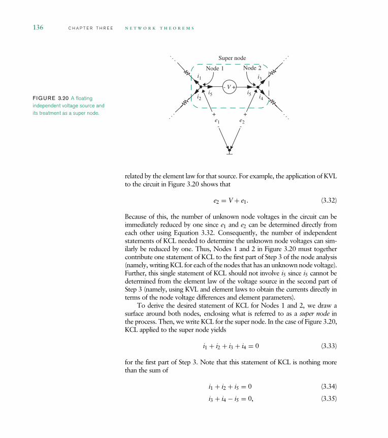
136 C H A P T E R T H R E E n e t w o r k t h e o r e m s
F IGURE 3.20 A floatingindependent voltage source andits treatment as a super node.
. . .
. . . . . .
. . .
i3
i4i5i5
i1
i2
Node 1 Node 2
Super node
+
-e1
+
-e2
- V +
related by the element law for that source. For example, the application of KVLto the circuit in Figure 3.20 shows that
e2 = V + e1. (3.32)
Because of this, the number of unknown node voltages in the circuit can beimmediately reduced by one since e1 and e2 can be determined directly fromeach other using Equation 3.32. Consequently, the number of independentstatements of KCL needed to determine the unknown node voltages can sim-ilarly be reduced by one. Thus, Nodes 1 and 2 in Figure 3.20 must togethercontribute one statement of KCL to the first part of Step 3 of the node analysis(namely, writing KCL for each of the nodes that has an unknown node voltage).Further, this single statement of KCL should not involve i5 since i5 cannot bedetermined from the element law of the voltage source in the second part ofStep 3 (namely, using KVL and element laws to obtain the currents directly interms of the node voltage differences and element parameters).
To derive the desired statement of KCL for Nodes 1 and 2, we draw asurface around both nodes, enclosing what is referred to as a super node inthe process. Then, we write KCL for the super node. In the case of Figure 3.20,KCL applied to the super node yields
i1 + i2 + i3 + i4 = 0 (3.33)
for the first part of Step 3. Note that this statement of KCL is nothing morethan the sum of
i1 + i2 + i5 = 0 (3.34)
i3 + i4 − i5 = 0, (3.35)

3.3 The Node Method C H A P T E R T H R E E 137
which are the individual statements of KCL for Nodes 1 and 2. Following this,in the second part of Step 3, the currents are eliminated by substituting nodevoltages and element parameters in their place. In our example, i1 and i2 aredetermined using e1 and the parameters of the elements through which i1 andi2 flow. Similarly i3 and i4 are determined using e1 + V and the parameters ofthe elements through which i3 and i4 flow, with e1 serving as the one unknownnode voltage.
Alternatively, i1 and i2 can be determined using e2 −V, and i3 and i4 can bedetermined using e2, with e2 serving as the one unknown node voltage. Finally,it should be recognized that a floating string of independent voltage sources ishandled in exactly the same manner as a floating isolated independent voltagesource.
Let us illustrate node analysis applied to a circuit with a floating independentvoltage source, and hence a super node, using the circuit shown in Figure 3.21.The circuit is the same as that shown in Figure 3.10 except that Node 2 isnow selected as the ground node, and the node voltages for Nodes 1 and 3are defined differently. The super node containing the floating voltage sourceis also marked in the figure.
The primary unknown in the circuit, e, is now the voltage at Node 3. Notealso that the voltage at Node 1, the other node in the super node, is labeledin terms of e. By defining the ground node and labeling the node voltages, wehave completed Steps 1 and 2 in the node analysis.
Next we perform Step 3 for the super node. This yields
e + V
R1+ e
R2+ I = 0. (3.36)
In Equation 3.36, (e + V )/R1 is the current (written in terms of node voltagesand element parameters) out of the super node through the branch containing
R1
R2V+
-I
e+V
e
Node 1Node 2
Node 3
Super node
F IGURE 3.21 A circuit witha floating independent voltagesource.

138 C H A P T E R T H R E E n e t w o r k t h e o r e m s
R1. Similarly, e/R2 is the current out of the super node through R2, and I is thecurrent through the third branch from the super node.
Following Step 4, the solution of Equation 3.36 is
e = − R1R2
R1 + R2I − R2
R1 + R2V. (3.37)
Finally, to complete the node analysis, the solution for e could be used in Step 5of node analysis to determine the branch voltages and then the branch currentsin the circuit. While we will not do this here, it is worthwhile to see that it willyield the same results as in Equations 3.10 through 3.16, providing that thebranch currents and voltages are defined in the same manner. To see that thiswill be the case, observe that e in Equation 3.37 is the same as in Equation 3.9except for a minus sign, owing to the change in the sign of e as defined inFigures 3.10 and 3.21.
e x a m p l e 3.10 f l o a t i n g i n d e p e n d e n t v o l t a g e
s o u r c e As another example of node analysis applied to a circuit with a floatingindependent voltage source, consider the circuit shown in Figure 3.22. In this circuit, thevoltage source having value V3 is the only floating independent voltage source. Becausethe source having value V1 is connected to ground at Node 5 it is not a floating source,hence Node 1 is labeled with the node voltage V1. Similarly, the source having value V2
is not a floating source because it is connected to ground through the known voltageV1, hence Node 2 is labeled with the known node voltage V1 + V2. Thus, only thevoltages at Nodes 3 and 4 in the super node are unknown. In Figure 3.22, Node 3 islabeled with the unknown node voltage e, and so Node 4 is labeled with the node voltagee + V3.
F IGURE 3.22 Another circuitwith a floating independent voltagesource.
G1
G3
V2+-
e
Node 2
Node 3
Node 4
+-
V3
V1+-
Node 1G2
V1 V2+ e V3+
Super node
Node 5

3.3 The Node Method C H A P T E R T H R E E 139
To continue the node analysis of the circuit in Figure 3.22, we perform Step 3 for thesuper node. This yields
G1 [(e + V3) − (V1 + V2)] + G2(e − V1) + G3e = 0. (3.38)
Here, conductances have been used for convenience. Following Step 4, the solution ofEquation 3.38 is
e = (G1 + G2)V1 + G1V2 − G1V3
G1 + G2 + G3. (3.39)
Finally, to complete the node analysis, the solution for e could be used in Step 5 todetermine the branch voltages and then the branch currents in the circuit. We will notdo this here.
3.3.3 D E P E N D E N T S O U R C E S A N D T H E N O D EM E T H O D
A dependent source will also complicate the node analysis previously describedwhen its element law does not easily relate its branch current to its branchvoltage. In this case, it will again not be possible to complete Step 3, and so it isagain necessary to modify the node analysis slightly. Since there are four typesof dependent sources, and the branch currents and voltages that control themcan appear through or across many different types of elements, it is impracticalto treat each case separately in its most efficient manner. As a compromise,
i
. . .
. . .
. . .
f(i)
F IGURE 3.23 A circuitcontaining a dependent currentsource.
we present here a single method that treats all cases of dependent sources, andillustrate how this method can be made more efficient in a few illustrative cases.We will illustrate the method using the circuit in Figure 3.23, which contains adependent current source, whose current is some function of a branch variablei as shown in the figure.
Our method of applying node analysis to a circuit containing dependentsources begins by assuming that we know the value of each dependent source.This assumption allows us to treat each dependent source as an independentsource, and carry out a node analysis of the circuit as described in the previ-ous subsections. For example, in the case of a dependent current source (seeFigure 3.23), we replace the dependent source with an independent currentsource with some assumed current, say I (see Figure 3.24), and carry out ourusual five-step node analysis. As part of this analysis we solve for the branchvariables that control the dependent sources in terms of the assumed sourcevalues.
iI
. . .
. . .
. . .
F IGURE 3.24 Replacing thedependent current source with anindependent current source withan assumed current I.
Of immediate interest are the expressions for the branch variables thatcontrol dependent sources. In our example, this branch variable is i. Next, wesubstitute these expressions for the controlling variables into the element lawsfor the dependent sources, and self-consistently solve for the actual values of thedependent sources. Continuing with our dependent current source example of

140 C H A P T E R T H R E E n e t w o r k t h e o r e m s
Figure 3.23, suppose that the expression for i is some function of the assumedcurrent I and is of the form
i = g (I ). (3.40)
We substitute this expression for the branch variable into the element lawfor the dependent current source as
I = f (i ) = f ( g(I )) (3.41)
and solve for I. The solution for I will not contain the variable i. Note that if theexpression for i shown in Equation 3.40 does not contain I, then no additionalwork needs to be done to solve for I, since f ( g(I )) is itself a solution for I.
Finally, we back-substitute the actual values of the dependent sourcesin other words, the solution for I into the original node analysis, therebycompleting the analysis in total.
As a concrete example, suppose the dependence source function
f (i ) = 10i.
Further, suppose we obtain the following expression for i as a function of theassumed current I:
i = g (I ) = I
2+ 2 A.
Then, according to Equation 3.41,
I = f ( g(I )) = 10[
I
2+ 2 A
].
Solving, we get
I = −5 A.
As expected, the solution for I does not contain the variable i.This modification to the original node analysis is not always the most
efficient method of analysis, but it always works. However, when the elementlaws for the dependent sources can be easily expressed in terms of the nodevoltages, it is possible to take a more intuitive approach and apply the simplenode analysis described in Section 3.3 without modification. In our example ofFigure 3.23, suppose that the circuit on the left has the node voltages shown

3.3 The Node Method C H A P T E R T H R E E 141
in Figure 3.25. In this case, it is easy to see that the element law for the currentsource can be easily written in terms of the node voltages as
f (i ) = f(
ea − eb
R
)
and our simple node analysis can be applied without modification. We will doexamples using both the modified and unmodified versions of the node method.
i. . .
. . .
ea
ebR
f(i)
F IGURE 3.25 Node voltages.To illustrate our modified method of node analysis for a circuit containing
a dependent source, consider the analysis of the circuit shown in Figure 3.26.This circuit has one dependent source, namely a CCCS. To analyze this circuitusing the node method, we first replace its CCCS with an independent currentsource carrying a known current, say I, and analyze the resulting circuit. Theresulting circuit, however, is exactly that shown in Figure 3.10, which we havealready analyzed using the node method in Section 3.3. Note that the value I inFigure 3.10 replaces the value αi1 in Figure 3.26. Thus, we are partially donewith the analysis of the circuit in Figure 3.26.
-
+i0
v0
+
-
v1
R1 i2
R2 v2V+-
+ -i1 i3
+
-v3
V e
αi1
F IGURE 3.26 A circuit with adependent source.
The results of our analysis of the circuit in Figure 3.10 appear in Equa-tions 3.10 through 3.16. Let us copy them here for convenience after replacingconductances with resistances.
v0 = V (3.42)
i0 = R2
R1 + R2I − 1
R1 + R2V (3.43)
v1 = − R1R2
R1 + R2I + R1
R1 + R2V (3.44)
i1 = − R2
R1 + R2I + 1
R1 + R2V (3.45)
v2 = v3 = R1R2
R1 + R2I + R2
R1 + R2V (3.46)
i2 = R1
R1 + R2I + 1
R1 + R2V (3.47)
i3 = −I. (3.48)
Of particular interest from that analysis is the value of i1 because i1 controlsthe CCCS in Figure 3.26. Using the result for i1 from Equation 3.45 we nextwrite
I = αi1 = α
[− R2
R1 + R2I + 1
R1 + R2V
]. (3.49)

142 C H A P T E R T H R E E n e t w o r k t h e o r e m s
The first equality in Equation 3.49 expresses the equality of the CCCS inFigure 3.26 and its surrogate independent current source in Figure 3.10. Thesecond equality follows from the substitution for i1 using Equation 3.45 fromthe node analysis of the circuit in Figure 3.10. Since i1 is determined in termsof I during that analysis, Equation 3.49 becomes an implicit equation that mustbe solved for I. This solution yields
I = α
R1 + (1 + α)R2V. (3.50)
The actual value of the CCCS is now known.Finally, we back-substitute Equation 3.50, namely the actual value of I, into
Equations 3.42 through 3.48 to obtain
v0 = V (3.51)
i0 = − 1
R1 + (1 + α)R2V (3.52)
v1 = R1
R1 + (1 + α)R2V (3.53)
i1 = 1
R1 + (1 + α)R2V (3.54)
v2 = v3 = (1 + α)R2
R1 + (1 + α)R2V (3.55)
i2 = 1 + α
R1 + (1 + α)R2V (3.56)
i3 = −α
R1 + (1 + α)R2V. (3.57)
This completes the analysis of the circuit in Figure 3.26.While the preceding analysis is not terribly difficult, it can nonetheless be
carried out more efficiently in many cases. As mentioned previously, commonly,it is possible to apply the simple node analysis described in Section 3.3 withoutmodification because the element law for the CCCS can be easily expressed interms of the node voltage e. To see this, we begin by performing Step 3 ofnode analysis to write
e − V
R1+ e
R2− α
V − e
R1= 0 (3.58)
for the node at which e is defined. Note that in the third term in Equation 3.58,(V − e)/R1 has been substituted for i1.

3.3 The Node Method C H A P T E R T H R E E 143
Next, following Step 4, we solve Equation 3.58 for e to obtain
e = (1 + α)R2
R1 + (1 + α)R2V. (3.59)
This result is the same as expressed in Equation 3.55. The remainder ofthe node analysis, namely Step 5, then proceeds to yield Equations 3.51through 3.57 directly. It is important to note, however, that the node anal-ysis of circuits containing dependent sources cannot always be easily simplifiedin this manner.
e x a m p l e 3.11 d e p e n d e n t c u r r e n t s o u r c e Now, let usanalyze a slightly different circuit containing a dependent source as shown in Figure 3.27.The node voltages vO and vI are marked. The dependent current source supplies acurrent
iO = f (x)
where we will consider two cases:
1. In the first case, x is the voltage vI, and the current
iO = −GmvI.
2. In the second case, x is the current iI, and
iO = −βiI.
Let us suppose that we are specifically interested in determining vO as a function of vI
in both cases.
Let us consider the first case in which
iO = −GmvI.
vI vO
RLRI
iIiO = f(x)
vI+
-
RP
F IGURE 3.27 Anotherdependent current source circuit.

144 C H A P T E R T H R E E n e t w o r k t h e o r e m s
Notice that iO is directly expressed in terms of a node voltage, and so we can apply oursimple node analysis technique without any modification, remembering, however, tosubstitute the element law for the dependent source current when writing KCL for thenodes with unknown voltages.
Since the ground and node voltages have been defined as shown in Figure 3.27, Steps 1and 2 of node analysis are complete.
For Step 3, we write KCL at the node with the unknown voltage vO by summing thecurrents into the node as follows:
vI − vO
RP+ (−GmvI) = vO
RL. (3.60)
Notice that we have used the element law for the dependent current source, namely,
iO = −GmvI
to substitute for the current into the node from the dependent current source.
By simplifying Equation 3.60, we obtain:
vO = (1 − GmRP)RL
RP + RLvI. (3.61)
We have thus expressed vO as a function of vI when iO = −GmvI.
Let us now consider the second case in which
iO = −βiI.
Although not directly expressed in terms of a node voltage, it easy to see that iO can beexpressed in terms of a node voltage by substituting iI = vI/RI as follows:
iO = −βvI
RI.
Thus, as in the first case, we can apply our simple node analysis technique without anymodification. Going to Step 3 of node analysis, we write KCL at the node with theunknown voltage vO by summing the currents into the node as follows:
vI − vO
RP+ (−β
vI
RI) = vO
RL. (3.62)
Notice that we have used the element law for the dependent current source, namely,
iO = −βvI
RI
to substitute for the current into the node from the dependent current source.

3.4 Loop Method * C H A P T E R T H R E E 145
By simplifying Equation 3.62, we obtain:
vO =(
1 − β RPRI
)RL
RP + RLvI. (3.63)
We have thus expressed vO as a function of vI when iO = −βiI.
W W W e x a m p l e 3.12 a m o r e c o m p l e x d e p e n d e n t -
c u r r e n t s o u r c e p r o b l e m
W W W 3.3.4 T H E C O N D U C T A N C E A N DS O U R C E M A T R I C E S *
W W W 3.4 L O O P M E T H O D *
W W W e x a m p l e 3.13 l o o p m e t h o d
3.5 S U P E R P O S I T I O N
Suppose we make the circuit in Figure 3.12 one step more complicated byadding a third source, as shown in Figure 3.33. Straightforward node analysisfollowing the procedure outlined by the node method yields
(V1 − e1)G1 + (V2 − e1)G2 + (e2 − e1)G3 = 0 (3.97)
(e1 − e2)G3 − e2G4 + I = 0. (3.98)
Collecting the source terms on the left side:
V1G1 + V2G2 = e1(G1 + G2 + G3) − e2G3 (3.99)
I = −e1G3 + e2(G3 + G4). (3.100)
R1
R2+
R3
-V1 R4
I
e2
V2
+
-
e1
F IGURE 3.33 A network withthree sources.

146 C H A P T E R T H R E E n e t w o r k t h e o r e m s
Let us again find e1:
e1 = (V1G1 + V2G2)(G3 + G4) + IG3
(G1 + G2 + G3)(G3 + G4) − G23
(3.101)
= V1G1(G3 + G4) + V2G2(G3 + G4) + IG3
G1G3 + G1G4 + G2G3 + G2G4 + G3G4. (3.102)
Again note the structure of this expression:
All denominator terms are of the same sign. Thus the denominatorcannot be made zero for any nonzero values of conductances. (If thedenominator could be made zero, we could get infinite e1 for finitesources values, a violation of conservation of energy.)
Each term on the right consists of one source term multiplied by aresistive (or conductive) factor. There are no products of source terms.
We now wish to translate these mathematical constraints to circuitconstraints, to find simpler methods for analyzing multi-source networks.Specifically, we wish to find the terms in Equation 3.102, by inspection, fromFigure 3.33. The mathematics says that, because of linearity, the first termremains unchanged if the other two sources are set to zero. We must now inter-pret this statement in circuit terms. Mathematically, we wish to set variable V2to zero, so in circuit terms we must set voltage source V2 to zero. By definition,source V2 must now be zero regardless of what current flows through it, thatis, it must be a short circuit. So in general, setting a voltage source to zero isequivalent in circuit terms to replacing that source by a short circuit. Similarly,setting I to zero means that no current can flow through that branch of thecircuit regardless of the terminal voltage. Hence setting a current source to zerois equivalent in circuit terms to replacing that source by an open circuit. Theseare two additional important circuit primitives. Applying these two conceptsto Figure 3.33, we can find the first term in Equation 3.102, that is, the partof e1 arising from source V1, by forming a subcircuit from Figure 3.33 with V2and I set to zero as shown in Figure 3.34a. Thus, in Figure 3.34a, e1A is thevoltage component of e1 due to source V1 acting alone. Now e1A can be foundby inspection using the voltage-divider primitive:
e1A = V1R2‖(R3 + R4)
R1 + R2‖(R3 + R4)(3.103)
where the two vertical lines are shorthand notation for ‘‘in parallel with.’’ Thenumerator, for example, is R2 in parallel with the sum of R3 and R4. Thecalculation is somewhat simplified if we use conductance instead of resistance.

3.5 Superposition C H A P T E R T H R E E 147
Using the conductance form of the voltage-divider relation (Equation 2.50),we find
e1A = V1G1
G1 + G2 + G3G4/(G3 + G4)(3.104)
where the two conductances in series, G3 and G4 are calculated usingEquation 2.58. Both of these expressions are the same as the first term in Equa-tion 3.102, after some manipulation. Note that the form of Equation 3.104 ismuch simpler and more insightful than the forms in Equations 3.101 and 3.102,because the derivation in terms of the voltage-divider primitive reveals the basicstructure of the circuit. But the main point of this development is to show thatthe effect of source V1 on the node voltage e1 can be found very easily byforming a subcircuit in which V2 and I are set to zero.
By the same argument, the effect of V2 and I on e1 can be calculatedusing the subcircuits shown in Figure 3.34b and 3.34c, respectively. For V2,sources V1 and I are set to zero, as shown in Figure 3.34b. Clearly circuits 3.34aand 3.34b are identical in topology, so the effect of V2 on e1 can be written fromEquation 3.103 by interchanging R1 and R2, or G1 and G2 in Equation 3.104.This will give us e1B, the component of e1 due to voltage source V2.
To find the effect of I, it is necessary to set both V1 and V2 to zero, thatis, replace each by a short circuit, as shown in Figure 3.34c. Now e1C can be
R1
R2+
R3
-V1
R4 I = 0
e2A
V2 = 0
e1A
R1 R2
R3
V1 = 0R4V2
+
-
e1B
(a)
I = 0
(b)
R2R1
R3
V1 = 0R4I
i3
V2 = 0
e1C
(c)
F IGURE 3.34 Subcircuits.
148 C H A P T E R T H R E E n e t w o r k t h e o r e m s
found by noting that the total conductance of the path to the left of the sourceis, from Equations 2.94 and 2.58,
G = (G1 + G2)G3
G1 + G2 + G3. (3.105)
Hence, from the current divider relation, the current through R3 is
iR3 = GI
G + G4. (3.106)
Now e1C can be found from the relation
e1C = iR3
G1 + G2(3.107)
= GI
(G + G4)(G1 + G2)(3.108)
which, on substitution of Equation 3.105 and simplification, reduces to
e1C = IG3
(G1 + G2)G3 + G4(G1 + G2) + G3G4. (3.109)
This is equivalent to the third term in Equation 3.102.This example illustrates both the use of superposition to solve a network
with several sources, and also shows how primitives (elementary procedures)can be used to solve circuits by inspection. Generalizing, we note that any messylinear network the one in Figure 3.35, for example must somehow yieldto straightforward network analysis and lead to a set of equations of the form
V1G1a + V2G1b + · · · + I1 + · · · = e1G11 + e2G12 + · · · (3.110)
V1G2a + · · · · · · · · · · · · = e1G21 + e2G22 + · · ·V1G3a + · · · · · · · · · · · · = e1G31 + · · ·
These have been written in the standard form, with source terms on theleft in each equation. All of the unknown variables appear on the right side, eachmultiplied by conductances: the sum of the appropriate ‘‘self ’’ conductancesfor terms along the main diagonal, and the sum of the appropriate ‘‘mutual’’conductances elsewhere.
Further, the solution of such a set of linear simultaneous equations willalways result in an expression of the general form of Equation 3.102, in whichthe voltage or current we are trying to evaluate will be equal to a sum of termseach involving only one source.

3.5 Superposition C H A P T E R T H R E E 149
+
+ -V3
I1
I2V 2-
+ -V1
F IGURE 3.35 A resistivenetwork.
The superposition theorem thus states that in a linear network with a num-ber of independent sources, the response can be found by summing the responsesto each independent source acting alone, with all other independent sources set tozero. These individual responses can be found very readily by forming subcircuitsin which all independent sources except one are set to zero.
Accordingly, the superposition method for linear networks can be statedas follows:
The Superposition Method1. For each independent source, form a subcircuit with all other
independent sources set to zero. Setting a voltage source to zero impliesreplacing the voltage source with a short circuit, and setting a currentsource to zero implies replacing the current source with an open circuit.
2. From each subcircuit corresponding to a given independent source, findthe response to that independent source acting alone. This step resultsin a set of individual responses.
3. Obtain the total response by summing together each of the individualresponses.
e x a m p l e 3.14 s u p e r p o s i t i o n a n a l y s i s o f a v e r a g -
i n g c i r c u i t Show that the node voltage v0 in the circuit shown in Figure 3.36
+-
v0
1 kΩ
5 V+-
6 V
1 kΩ
F IGURE 3.36 Circuit forperforming superposition analysis.
is the average of the two input voltages using the method of superposition.
By the method of superposition, the voltage v0 can be determined by summing the
+-
v05
1 kΩ
5 V
1 kΩ
F IGURE 3.37 Circuit with 5-Vsource acting alone.
responses of each of the sources acting alone. We will first obtain v05, the responseof the 5-V source acting alone. The subcircuit corresponding to the 5-V source actingalone is shown in Figure 3.37. Notice we have shorted the 6 V source.
By the voltage divider action, we can write
v05 = 1 k
1 k + 1 k5 V = 5
2V.

150 C H A P T E R T H R E E n e t w o r k t h e o r e m s
Next, we obtain v06, the response of the 6-V source acting alone. The subcircuit corre-sponding to the 6-V source acting alone is shown in Figure 3.38. In this case, we have
v06
1 kΩ
+
-6 V
1 kΩ
F IGURE 3.38 Circuit with 6-Vsource acting alone.
shorted the 5-V source.
Again, by the voltage divider action, we can write
v06 = 1 k
1 k + 1 k6 V = 6
2V.
We now sum the two partial responses to obtain
v0 = v05 + v06 = 5 + 6
2= 5.5 V.
It is easy to see that v0 is the average of the two input voltages.
e x a m p l e 3.15 a p p l y i n g t h e m e t h o d o f s u p e r -
p o s i t i o n Figure 3.39 shows a circuit containing an independent voltage sourceand an independent current source. Determine the current I.
We will use the method of superposition to solve this circuit in two different ways. First,we will obtain the node voltage e using superposition, and then, using the value of e,obtain the current I. Our second approach will directly determine I using the method ofsuperposition.
First Method
Let us first determine the value of e using superposition. By the method of superposi-tion, the voltage e can be determined by summing the responses of each of the sourcesacting alone. We will first obtain ev, the response of the voltage source acting alone.The subcircuit corresponding to the voltage source acting alone is shown in Figure 3.40.Notice we have turned the current source off by open-circuiting it.
By the voltage divider action, we can write
ev = 12
2 + 2= 1
2V.
F IGURE 3.39 Circuit with twoindependent sources. 1 V
+-
1 A
e
2 Ω
2 Ω 2 Ω
I

3.5 Superposition C H A P T E R T H R E E 151
1 V+-
ev
2 Ω
2 Ω 2 Ω
1 V+-
ev
2 Ω
2 Ω
F IGURE 3.40 Subcircuitcorresponding to the voltagesource acting alone.
1 A
ei
2 Ω
2 Ω 2 Ω
1 A
ei
1 Ω
2 Ω
F IGURE 3.41 Subcircuitcorresponding to the currentsource acting alone.
Next, we obtain ei, the response of the current source acting alone. The subcircuitcorresponding to the current source acting alone is shown in Figure 3.41. In this case,we have shorted the voltage source.
We first simplify the subcircuit by replacing the pair of 2- resistors in parallel with anequivalent 1- resistor as depicted in Figure 3.41. Then, since the 1-A current flowsthrough each of the resistors, the voltage across the 1- resistor is equal to ei. In otherwords,
ei = 1 A × 1 = 1 V.
We now sum the two partial responses to obtain the total response e. That is,
e = ev + ei = 1
2V + 1 V = 1.5 V.
We can now determine I as
I = e
2 = 0.75 A.
Second Method
Next, we will directly determine I using superposition. Superposition says that I can bedetermined by summing the currents generated by each of the sources acting alone. Wewill first obtain Iv, the current due to the voltage source acting alone. The subcircuitcorresponding to the voltage source acting alone is shown in Figure 3.42.
1 V+
-2 Ω
2 Ω
Iv
F IGURE 3.42 Subcircuitcorresponding to the voltagesource acting alone.

152 C H A P T E R T H R E E n e t w o r k t h e o r e m s
The current in the subcircuit is given by the voltage divided by the sum of the resistors.In other words,
Iv = 1 V
2 + 2 = 0.25 A.
Next, we obtain Ii, the response of the current source acting alone. The subcircuitcorresponding to the current source acting alone is shown in Figure 3.43.
1 A
2 Ω
2 Ω 2 Ω
Ii
F IGURE 3.43 Subcircuitcorresponding to the currentsource acting alone.
By the current divider relation, it is easy to see that Ii = 0.5 A, since the 1-A currentsupplied by the current source divides equally into the two branches of the subcircuit inFigure 3.43.
We now sum the two partial responses to obtain the total response I. That is,
I = Iv + Ii = 0.25 A + 0.5 A = 0.75 A.
e x a m p l e 3.16 r e s i s t i v e a d d e r c i r c u i t An elementaryresistive adding circuit is shown in Figure 3.44a. This circuit might be used to addtogether a number of microphone signals before sending them to one amplifier. (Noticethat this circuit is a generalization of the circuit in Figure 3.36.) We shall discover betterways of building such a circuit in later chapters, but the present form serves as a goodillustration of the principle of superposition.
From the preceding discussion, the effect on the output voltage Vo of the source V1
acting alone can be found by forming a subcircuit in which all other independent sourcesare set to zero, which in this case means replacing V2, V3, and V4 by short circuits, asshown in Figure 3.44b. Now Voa, the response to V1 alone, can be found by inspection
RR
Vo
(a)
RR+
-
R Voa
(b)
+
-
R R
R
+
-V4
+
-V3
+
-V2
+
-V1
+
-V1
F IGURE 3.44 Resistive addingcircuit.

3.5 Superposition C H A P T E R T H R E E 153
using the voltage-divider relation
Voa = R/3
R + R/3V1. (3.111)
The complete response is the sum of four such terms, which in this special case all havethe same coefficient
Vo = 1
4(V1 + V2 + V3 + V4). (3.112)
Note that there is no restriction on the nature of the sources (other than frequencylimits, etc., as discussed in Chapter 1). The sources could be DC, sine waves or squarewaves, speech, or a mixture of these. Equation 3.112 states that the output will be thesum of these individual signals, each multiplied by a constant, a ‘‘scaling factor.’’ If theinputs were four sine waves, each at a different frequency, then the output voltage wouldbe the sum of these four sinusoids, appropriately scaled. No other frequencies would bepresent in the output signal. Thus a further consequence of linearity is that, whateverfrequencies are present at the input or inputs of a linear system, these and only thesefrequencies will appear at the output.
W W W e x a m p l e 3.17 s u p e r p o s i t i o n a p p l i e d t o a
b e e h i v e n e t w o r k
3.5.1 S U P E R P O S I T I O N R U L E S F O R D E P E N D E N TS O U R C E S
When the dependencies are linear, dependent sources are amenable to the set ofanalyses discussed earlier in Chapters 2 and 3. Care must be taken, however, inapplying the superposition principle. Recall that the principle of superpositionallows linear multisource networks to be solved for one source at a time bysetting all other independent sources to zero. Setting a voltage source to zeromeans replacing it with a short circuit; a current source set to zero is an opencircuit. The complete response is the sum of the responses to each individualsource.
What do we do about dependent sources? A practical way is to leave all thedependent sources in the circuit. The network can then be solved for oneindependent source at a time by setting all other independent sources to zero,and summing the individual responses.
Alternatively, the dependent sources could be treated as independentsources, and in a final step of the analysis, their dependencies must be back-substituted in terms of other network parameters. However, this method tendsto be impractical.

154 C H A P T E R T H R E E n e t w o r k t h e o r e m s
e x a m p l e 3.18 a s i n g l e d e p e n d e n t s o u r c e a n d
s u p e r p o s i t i o n Consider the circuit in Figure 3.49. It contains two indepen-dent sources and one dependent source. Using the superposition method, let us derivethe output voltage vO.
We will solve the circuit by leaving the dependent current source in the circuitand summing the responses of each of the independent sources acting alone.
1-V Source Acting Alone
Figure 3.50 shows the circuit corresponding to the 1-V source acting alone, where vO1
is the corresponding response. Notice that the dependent current source has been leftin the circuit, and the 2-V source has been shorted out.
By the voltage divider relation, we know that
v1 = 0.5 V.
Thus,
vO1 = 1
100v1 × 1 k = 5 V.
2-V Source Acting Alone
Figure 3.51 shows the circuit corresponding to the 2-V source acting alone, where vO2
is the corresponding response. By the voltage-divider relation, we know that
v2 = 1 V.
Thus,
vO2 = 1
100v2 × 1 k = 10 V.
v
1 kΩ1 kΩ
1100Ω------------- v
+-
1 V
vO
1 kΩ
+-
2 V
F IGURE 3.49 Circuit containing two independentsources and one dependent source.
v1
1 kΩ
1 kΩ
1100Ω
v1
+-
1 V
vO1
1 kΩ
F IGURE 3.50 Subcircuit corresponding tothe 1-V source acting alone.

3.5 Superposition C H A P T E R T H R E E 155
v2
1 kΩ1 kΩ
1100Ω
v2
vO2
1 kΩ
+-
2 V
F IGURE 3.51 Subcircuitcorresponding to the 2-V sourceacting alone.
Summing the two responses, we get the total response as
vO = vO1 + vO2 = 15 V.
e x a m p l e 3.19 m u l t i p l e d e p e n d e n t s o u r c e s a n d
s u p e r p o s i t i o n As a more complicated example, consider the circuit inFigure 3.52. Using the superposition method, let us derive the output voltage vo asa function of vi.
This circuit has two dependent current sources and two independent voltage sources(v1 and v2). We will solve this problem by leaving both the dependent current sources inthe circuit and summing the responses of each of the independent sources acting alone.We also define two intermediate variables, the node voltages va and vb.
v1 Acting Alone
We will first obtain the response with v1 acting alone. Figure 3.53 shows the circuitcorresponding to v1 acting alone. vo1 is the corresponding response. Notice that the
i1 = gmv1
RI
i2 = gmv2
+-
v1= vi+- RI
RL
v2 = -vi
RL
vo
R
+ -
a b
c
vbva
F IGURE 3.52 Circuit with multiple dependentsources.
i1 = gmv1
RI
i2 = 0
v1= vi+-
RI
RL
v2 = 0
RL
vo1
R
+ -
a b
c
vb1va1
F IGURE 3.53 Subcircuit corresponding to v1 actingalone.

156 C H A P T E R T H R E E n e t w o r k t h e o r e m s
dependent current sources have been left in the circuit, and v2 has been shorted out.Since v2 = 0, we find that i2 = 0 (in other words, the dependent current source behaveslike an open circuit).
We will first determine va1 and vb1, the node voltages at the nodes a and b due to v1
acting alone. We will then determine vo1 as their difference.
Since i2 = 0, there is no voltage drop across the resistor RL connected to node b.So, node b will be at ground potential. In other words,
vb1 = 0.
We can obtain va1 by using KVL as
va1 = 0 − i1RL = −gmv1RL = −gmviRL.
Therefore
vo1 = va1 − vb1 = −gmviRL.
v2 Acting Alone
Figure 3.54 shows the circuit corresponding to v2 acting alone. vo2 is the correspond-ing response. In this circuit, since v1 = 0, we find that i1 = 0.
Since i1 = 0, there is no voltage drop across the resistor RL connected to node a, andso, this time around, node a will be at ground potential. In other words,
va2 = 0.
F IGURE 3.54 Subcircuitcorresponding to v2 acting alone.
i1 = 0
RI
i2 = gmv2
+-v1 = 0
+- RI
RL
v2 = -vi
RL
vo2
R
+ -
a b
c
vb2va2

3.6 Thévenin’s Theorem and Norton’s Theorem C H A P T E R T H R E E 157
We can obtain vb2 by using KVL as
vb2 = 0 − i2RL = −gmv2RL = −gm(−vi)RL = gmviRL.
Therefore
vo2 = va2 − vb2 = −gmviRL.
We can now obtain the total response by summing the responses to each of theindependent sources acting alone. In other words,
vo = vo1 + vo2 = −2gmviRL.
3.6 T H É V E N I N ’ S T H E O R E M A N DN O R T O N ’ S T H E O R E M
3.6.1 T H E T H É V E N I N E Q U I V A L E N T N E T W O R K
A simple extension of the concept of superposition yields two additional net-work theorems of great power, which allow us to suppress a lot of detail incircuit analysis and focus attention only on that part of a network we are reallyinterested in. Consider, for example, a battery, or a high-fidelity power ampli-fier, or a wall outlet for 110-V AC power, or a power supply for a computer.What is the simplest way to describe the electrical properties of each of thesesystems at its output terminals? Is one parameter needed, or ten, or fifty? Clearlythe voltage measured with a high-quality meter that draws negligible currentis one important parameter (the open-circuit voltage mentioned in Section 1.7).Likewise we would want to know the frequency: zero frequency for the battery,60 hertz (or 50 or even 25 in some countries) for the power line, etc. But wehave already observed another effect that is important. When current is drawnfrom any of these systems, the voltage at the terminals drops. Depending onthe quality of the wiring in a dormitory, the lights may dim noticeably when atoaster is plugged into the same circuit. Or the voltage of the flashlight batterywill drop when a bulb is connected and current flows, as noted in Section 1.7.How can this effect be characterized? For the battery, is it necessary to makemeasurements at 100 current levels, and plot a curve of the characteristic?
If the system is linear, then the answer to this question is very simple. Wewill show that any collection of voltage sources, current sources, and resistorscan be represented at any one pair of terminals by one voltage source and oneresistor, or by one current source and one resistor. The graphical constructionof Figure 1.43 already hinted at this fact, but we present here a more formalproof. We start with a general linear network containing sources and resistors,shown as an amorphous box in Figure 3.55a. We presume that the only two

158 C H A P T E R T H R E E n e t w o r k t h e o r e m s
I V
+
+-
i
+
i
itestI
VitestV = 0I = 0
itest = 0+-
(a)(b)
(c)(d) I
-v vt
-
+va
i
+vb
i
- -
+-
V
F IGURE 3.55 Derivation of theThévenin network. terminals we are interested in are shown emerging on the right. We wish to
find the relationship between v and i at these terminals.To find v in terms of i, we need to apply some form of excitation, and
measure the response. The derivation is simplest if we use either a voltagesource or a current source, rather than a complicated excitation network. InFigure 3.55b, we have chosen to apply a test current source to the terminals. Tocalculate the response vt by superposition, first set all the internal independentsources to zero, as in Figure 3.55c, and calculate the voltage va. As discussedin Section 3.5.1, dependent sources are left as is. Then set itest to zero, as inFigure 3.55d, and calculate vb. The desired value of vt is the sum va + vb. FromFigure 3.55c,
va = itestRt (3.113)
where Rt is the net resistance measured between the two terminals when allinternal independent sources are set to zero. Resistance Rt is called the ThéveninEquivalent Resistance. From Figure 3.55d, vb is obviously just the voltageappearing at the terminals of the original network when no current is flowing;we call this the open-circuit voltage. That is,
vb = voc. (3.114)
Now by superposition,
vt = va + vb = voc + itestRt. (3.115)
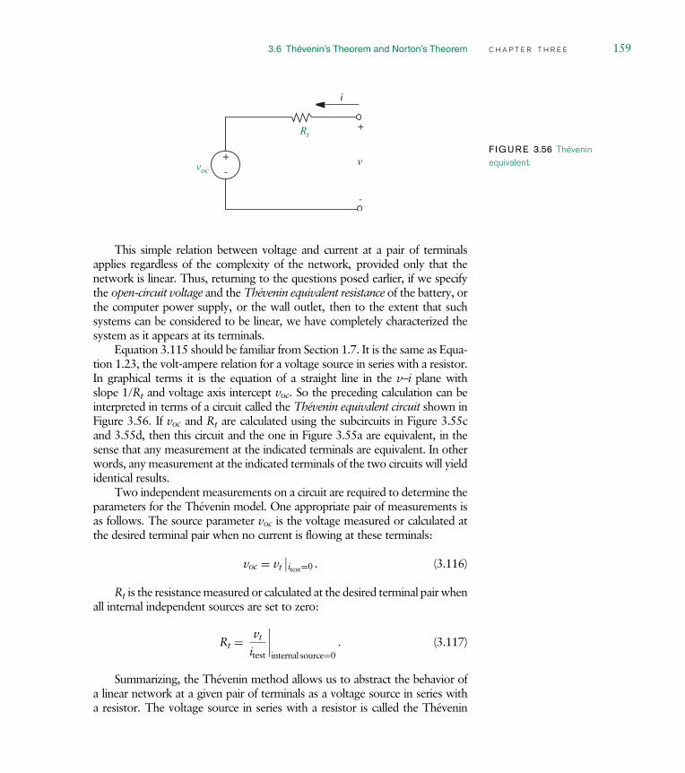
3.6 Thévenin’s Theorem and Norton’s Theorem C H A P T E R T H R E E 159
Rt
+
-voc
i
v
+
-
F IGURE 3.56 Théveninequivalent.
This simple relation between voltage and current at a pair of terminalsapplies regardless of the complexity of the network, provided only that thenetwork is linear. Thus, returning to the questions posed earlier, if we specifythe open-circuit voltage and the Thévenin equivalent resistance of the battery, orthe computer power supply, or the wall outlet, then to the extent that suchsystems can be considered to be linear, we have completely characterized thesystem as it appears at its terminals.
Equation 3.115 should be familiar from Section 1.7. It is the same as Equa-tion 1.23, the volt-ampere relation for a voltage source in series with a resistor.In graphical terms it is the equation of a straight line in the v i plane withslope 1/Rt and voltage axis intercept voc. So the preceding calculation can beinterpreted in terms of a circuit called the Thévenin equivalent circuit shown inFigure 3.56. If voc and Rt are calculated using the subcircuits in Figure 3.55cand 3.55d, then this circuit and the one in Figure 3.55a are equivalent, in thesense that any measurement at the indicated terminals are equivalent. In otherwords, any measurement at the indicated terminals of the two circuits will yieldidentical results.
Two independent measurements on a circuit are required to determine theparameters for the Thévenin model. One appropriate pair of measurements isas follows. The source parameter voc is the voltage measured or calculated atthe desired terminal pair when no current is flowing at these terminals:
voc = vt∣∣itest=0 . (3.116)
Rt is the resistance measured or calculated at the desired terminal pair whenall internal independent sources are set to zero:
Rt = vt
itest
∣∣∣∣internal source=0
. (3.117)
Summarizing, the Thévenin method allows us to abstract the behavior ofa linear network at a given pair of terminals as a voltage source in series witha resistor. The voltage source in series with a resistor is called the Thévenin

160 C H A P T E R T H R E E n e t w o r k t h e o r e m s
equivalent circuit of the network. The Thévenin equivalent circuit can be used tomodel the effect of the given network on other circuits external to the network.
A Method for Determining the Thévenin Equivalent Circuit The Théveninequivalent circuit for any linear network at a given pair of terminals consistsof a voltage source vTH in series with a resistor RTH. The voltage vTH andresistance RTH can be obtained as follows:1. vTH can be found by calculating or measuring the open-circuit voltage at
the designated terminal pair on the original network.
2. RTH can be found by calculating or measuring the resistance of theopen-circuit network seen from the designated terminal pair with allindependent sources internal to the network set to zero. That is,with independent voltage sources replaced with short circuits, andindependent current sources replaced with open circuits. (Dependentsources must be left intact, however.)
e x a m p l e 3.20 t h é v e n i n m e t h o d Let us now illustrate the
3 V +
-
1 Ω
2 Ω
a
a′
+
-
v
(a)
vTH+
-
RTH
a
a′
+
-
v
(b)
i
i
F IGURE 3.57 Example circuit toillustrate the Thévenin method:(a) a network; (b) its Théveninequivalent network.
method using a simple example. Figure 3.57a shows a network and Figure 3.57b showsits Thévenin equivalent network viewed from the network’s aa′ port. Determine thevalues of vTH and RTH.
1 Ω
2 Ω
a
a′
RTH
F IGURE 3.58 Network with thevoltage source replaced with ashort.
By the first step of the Thévenin method, the voltage vTH is given by the open-circuitvoltage of the network at the aa′ port. The open-circuit voltage is the voltage at theaa′ network port when there is no external circuit element connected across the port.(Note that the 2- resistor is internal to the network and should not be disconnected.)Figure 3.57a shows this situation. The open-circuit voltage that would be measured atthe aa′ port is given by the voltage-divider relation as
vTH = 3 V2
1 + 2 = 2 V.
By the second step of the Thévenin method, the resistance RTH is found by measuringthe resistance of the open-circuit network seen from the aa′ port with the independentvoltage source set to zero; that is, with the voltage source replaced with a short circuit.The network with the voltage source replaced with a short is shown in Figure 3.58.
The resistance viewed from the aa′ port is given by
RTH = 1‖2 = 2
3.
The resulting Thévenin equivalent circuit is drawn in Figure 3.59.
e x a m p l e 3.21 m o r e o n t h e t h é v e n i n m e t h o d Let usnow work out a couple of related examples to illustrate the power of the Thévenin

3.6 Thévenin’s Theorem and Norton’s Theorem C H A P T E R T H R E E 161
2 V+
-
23---
a
a′
+
-
v
Ω
F IGURE 3.59 Theresulting Théveninequivalent circuit.
2 Ω
2 Ω
a
a′
2 A
I1
1 V+-
F IGURE 3.60 Circuit to illustrate thepower of the Thévenin method.
method. First, suppose we are asked to determine the current I1 through the voltagesource in the circuit in Figure 3.60.
2 Ω
2 Ω
a
2 A
(a)
vTH+
-
RTH
a
(b)
a′
a′
F IGURE 3.61 Théveninequivalent network.
Let us use the Thévenin method to obtain the desired current. To apply the Théveninmethod, we will replace the network to the left of the voltage source (that is, to the left ofthe aa′ terminal pair, and depicted in Figure 3.61a) with its Thévenin equivalent network(depicted in Figure 3.61b). Once this replacement is made, as illustrated in Figure 3.62,then, the current I1 can be written by inspection as
I1 = vTH − 1 V
RTH. (3.118)
vTH and RTH are the Thévenin equivalent parameters. The first step of the Théveninmethod is to measure vTH. As shown in Figure 3.63, vTH is the open-circuit voltagemeasured at the aa′ port.
a I1
1 V +-
+-
vTH
RTH
a′
F IGURE 3.62 Circuit with networkto the left of the aa′ terminal pairreplaced with its Thévenin equivalent.
2 Ω
2 Ω
a
2 A
+
-
vTH
a′
F IGURE 3.63 Open-circuitvoltage.

162 C H A P T E R T H R E E n e t w o r k t h e o r e m s
Since the 2-A current flows through both the 2- resistors in Figure 3.63, vTH can bewritten by inspection as
vTH = 2 A × 2 = 4 V.
By the second step of the Thévenin method, the resistance RTH is found by measuringthe resistance of the open-circuit network seen from the aa′ port with the independentcurrent source set to zero; that is, with the current source replaced with an open circuitas illustrated in Figure 3.64. It is easy to see that
RTH = 2 .
Having determined the Thévenin equivalent parameters vTH and RTH, we cannow obtain I1 from Equation 3.118 as
I1 = 4 V − 1 V
2 = 3
2A.
Notice that in this example the Thévenin method has allowed us to tackle a givenproblem (the circuit in Figure 3.60) by splitting it into three trivial subproblems, namely,the circuits in Figures 3.63, 3.64, and 3.62.
To further illustrate the power of the Thévenin method, suppose that the 1-V source inFigure 3.60 is replaced by a 10- resistor as illustrated in Figure 3.65, and we are askedto find the current I2 through the 10- resistor.
We first notice that the network to the left of the terminal pair aa′ in Figure 3.65is unchanged from that in Figure 3.60. Thus, from the viewpoint of determining aparameter relating to the network on the right side of the aa′ terminal pair, we canreplace that network on the left with its Thévenin equivalent determined previously asillustrated in Figure 3.66.
2 Ω
2 Ω
a
RTH
a′
F IGURE 3.64 Measuring RTH .
2 Ω
2 Ω
a
2 A 10 Ω
I2
a′
F IGURE 3.65 Circuit to further illustratethe power of the Thévenin method.
a
10 Ω
I2
VTH
RTH
+-
a′
F IGURE 3.66 Circuit with network to theleft of the aa′ terminal pair replaced with itsThévenin equivalent.

3.6 Thévenin’s Theorem and Norton’s Theorem C H A P T E R T H R E E 163
The current I2 can be quickly determined from the network in Figure 3.66 as
I2 = vTH
RTH + 10 .
We know that vTH = 4 V and RTH = 2 , and so I2 = 1/3 A.
e x a m p l e 3.22 b r i d g e c i r c u i t Determine the current I in thebranch ab in the circuit in Figure 3.67.
There are many approaches that we can take to obtain the current I. For example, wecould apply the node method and determine the node voltages at nodes a and b andthereby determine the current I. However, since we are interested only in the current I,a full blown node analysis is not necessary; rather we will find the Thévenin equivalentnetwork for the subcircuit to the left of the aa′ terminal pair (Network A) and forthe subcircuit to the right of the bb′ terminal pair (Network B), and then using thesesubcircuits solve for the current I.
Let us first find the Thévenin equivalent for Network A. This network is shown inFigure 3.68a. Let vTHA and RTHA be the Thévenin parameters for this network.
We can find vTHA by measuring the open-circuit voltage at the aa′ port in the networkin Figure 3.68b. We find by inspection that
vTHA = 1 V
Notice that the 1-A current flows through each of the 1- resistors in the loop containingthe current source, and so v1 is 1 V. Since there is no current in the resistor connectedto the a′ terminal, the voltage v2 across that resistor is 0. Thus vTHA = v1 + v2 = 1 V.
We find RTHA by measuring the resistance looking into the aa′ port in the network inFigure 3.68c. The current source has been turned into an open circuit for the purpose
1 A
a
1 Ω
1 Ω
1 Ω
1 Ω
1 A
1 Ω 1 Ω1 Ω
1 ΩIb
Network A Network B
a′ b′
F IGURE 3.67 Determining thecurrent in the branch ab.

164 C H A P T E R T H R E E n e t w o r k t h e o r e m s
F IGURE 3.68 Finding theThévenin equivalent for Network A.
1 A
a
1 Ω
1 Ω1 Ω
1 Ω
(a)
vTHA
RTHA
(b)
(c)
1 A
a
1 Ω
1Ω 1Ω1 Ω
vTHA
+
-v2+ -
v1+
-
a
1 Ω
1 Ω1 Ω
1 ΩRTHAa′
a′
a′
F IGURE 3.69 Finding theThévenin equivalent for Network B.
1 A
1 Ω 1 Ω
1 Ωb
vTHB
RTHB
(b)
(c)
1 A
1 Ω 1 Ω
1 ΩbvTHB
+
-
1 Ω 1 Ω
1 ΩbRTHB
(a)
b′
b′
b′
of measuring RTHA. By inspection, we find that
RTHA = 2 .
Let us now find the Thévenin equivalent for Network B shown in Figure 3.69a. LetvTHB and RTHB be the Thévenin parameters for this network.
vTHB is the open-circuit voltage at the bb′ port in the network in Figure 3.69b. Usingreasoning similar to that for vTHA we find
vTHB = −1 V.

3.6 Thévenin’s Theorem and Norton’s Theorem C H A P T E R T H R E E 165
a-1 V
1 Ω 2 Ω
Ib
Network A Network B
+-
1 V
2 Ω
+- a′ b′
F IGURE 3.70 Networks A andB replaced by their Théveninequivalents.
RTHB is the resistance looking into the bb′ port in the network in Figure 3.69c. Byinspection,
RTHB = 2 .
Replacing Network A and Network B with their Thévenin equivalents, we obtain theequivalent circuit in Figure 3.70.
The current I is easily determined as
I = 1 V − (−1 V )
2 + 1 + 2 = 2
5A.
Notice in this example we were able to solve a relatively complicated problem by com-posing the results of five subproblems (namely, the circuits in Figures 3.68b, 3.68c,3.69b, 3.69c, and 3.70), each of which was solvable by inspection.
e x a m p l e 3.23 t h é v e n i n a n a l y s i s o f a c i r c u i t
w i t h a d e p e n d e n t s o u r c e Find the Thévenin equivalent circuit forthe network to the left of the aa′ terminal pair in Figure 3.71. Notice that this circuitcontains a dependent source.
The network whose Thévenin equivalent is desired is shown in Figure 3.72. Let vTH
and RTH be the Thévenin parameters for this network.
vI
1 kΩ 2 kΩ 8
100ΩvI
a
10 kΩ +-
2 cos(ωt)
a′
F IGURE 3.71 Thévenin analysisof a circuit with a dependentsource.

166 C H A P T E R T H R E E n e t w o r k t h e o r e m s
F IGURE 3.72 Network to bereplaced by its Thévenin equivalent.
vI
1 kΩ 2 kΩ8
100Ω-------------vI
a
+-
2 cos(ωt)
vTH
vTH
+
-a′
Determining vTH
We first find vTH by computing the open-circuit voltage at the aa′ port of the circuit inFigure 3.72. We will find this voltage by applying the node method. Since the currentof the dependent source is expressible directly in terms of a node voltage, we can applythe node method without modification.
Figure 3.72 shows the ground node, and the two other nodes labeled with thenode voltages vI and vTH. Notice that vI is already known to be
vI = 2 cos(ωt).
This completes Steps 1 and 2 of the node method.
Following Step 3 of the node method, we write KCL for Node a.
vTH
2 k+ 8
100 SvI = 0.
Next, applying Step 4, we simplify the preceding equation to get
vTH = −160vI = −320 cos(ωt).
Since we were interested only in the node voltage vTH, we do not have to completeStep 5 of node analysis.
Determining RTH
We now find RTH by computing the resistance looking into the aa′ port in the networkin Figure 3.73. The independent voltage source has been turned into a short circuit for
F IGURE 3.73 Determining RTH .
vI = 0
1 kΩ 2 kΩ
8100Ω-------------vI = 0
a
RTH
a′

3.6 Thévenin’s Theorem and Norton’s Theorem C H A P T E R T H R E E 167
the purpose of computing RTH. The dependent source, however, is left in the circuit.Since vI = 0, the current through the dependent current source is 0, and therefore, thedependent source behaves like an open circuit. Thus,
RTH = 2 k.
The resulting Thévenin circuit is shown in Figure 3.74.
+
-
2 kΩ
a
–320 cos(ωt)
a′
F IGURE 3.74 ResultingThévenin circuit.
3.6.2 T H E N O R T O N E Q U I V A L E N T N E T W O R K
An analogous derivation to that in Section 3.6.1 gives rise to the Norton equiv-alent network. Recall that our goal is to find the v i relation for the network inFigure 3.75a so that we can replace the network with a simple equivalent circuitthat yields the same v i relation as the original network. To find the v i relation-ship, this time we apply a test voltage vtest to the circuit, as in Figure 3.75b, andfind the resultant current it. Using superposition, the two subcircuits neededto find it are shown in Figure 3.75c and 3.75d. In 3.75c, vtest is set to zeroand we measure ia. In 3.75d, all independent sources are set to zero and wemeasure ib. Then,
it = ia + ib.
From Figure 3.75c,
ia = −isc (3.119)
ib
I V +-
+ vtest
it
-V = 0I = 0
vtest
(b)
(d)
+-
I V +- vtest = 0
(c)ia
isc
I V +-
(a) +
-
v
i
F IGURE 3.75 Derivation ofNorton network.

168 C H A P T E R T H R E E n e t w o r k t h e o r e m s
where isc is the current that flows in the short circuit across the network ter-minals in response to the internal sources, and thus is the short circuit current.From Figure 3.75d,
ib = vtest
Rt(3.120)
where Rt is the net resistance measured between the terminals when all internalindependent sources are set to zero. Because this calculation and the one inFigure 3.55c are identical (except for a change in excitation) the parameter Rtis obviously the same in both calculations.
To complete the derivation, we find by superposition
it = ia + ib = −isc + vtest
Rt. (3.121)
As in the Thévenin derivation, this equation can be interpreted in termsof a circuit. It states that the terminal current is the sum of two components:a current source isc and a resistor current vtest/Rt. Hence the Norton equiv-alent network, Figure 3.76, has a current source in parallel with a resistor.
Rtisc
F IGURE 3.76 The Nortonequivalent network.
Examination of either the two equations, Equations 3.121 and 3.115, or thetwo figures, Figures 3.56 and 3.76 show that there is a simple relation betweenvoc and isc. Working from the figures, we can calculate the open-circuit voltageof each circuit to find
voc = iscRt. (3.122)
Thus it is a simple matter to change from one of these equivalentnetworks to the other.
To determine the Norton parameters for some circuit, again two indepen-dent measurements are required. The source parameter isc could be found byapplying a short to the circuit terminals and measuring the resultant current.The resistance parameter is measured as before in Equation 3.117. Note thatthe source parameters isc, voc are related by Equation 3.122, so measuring orcalculating any two of voc, isc and Rt is sufficient to characterize both the Nortonand the Thévenin model. In particular, it is often convenient to find Rt fromtwo simple terminal measurements on the circuit
Rt = voc
isc. (3.123)
In summary, the Norton method allows us to abstract the behavior of alinear network at a given pair of terminals as a current source in parallel witha resistor. The current source in parallel with the resistor is called the Nortonequivalent circuit of the network. Like the Thévenin equivalent, the Norton

3.6 Thévenin’s Theorem and Norton’s Theorem C H A P T E R T H R E E 169
equivalent circuit can also be used to model the effect of the given networkon other circuits external to the network.
A Method for Determining the Norton Equivalent Circuit The Norton equiv-alent circuit for any linear network at a given pair of terminals consists of acurrent source iN in parallel with a resistor RN. The current iN and resistanceRN can be obtained as follows:1. iN can be found by applying a short at the designated terminal pair on
the original network and calculating or measuring the current throughthe short circuit.
2. RN can be found in the same manner as RTH, that is, by calculating ormeasuring the resistance of the open-circuit network seen from thedesignated terminal pair with all independent sources internal to thenetwork set to zero; that is, with voltage sources replaced with shortcircuits, and current sources replaced with open circuits.
e x a m p l e 3.24 n o r t o n e q u i v a l e n t Figure 3.77a shows a net-
3 V+-
1 Ω
2 Ω
a+
-
v
(a)
iN RN
a+
-
v
(b)
i
i
a′
a′
F IGURE 3.77 Norton equivalentnetwork: (a) a network; (b) itsNorton equivalent network.
work and Figure 3.77b shows its Norton equivalent network viewed from thenetwork’s aa′ port. Determine the values of iN and RN.
By the first step of the Norton method, the current iN is given by applying a short atthe aa′ terminal pair and calculating the current through the short circuit. Figure 3.78shows the network with a short at the aa′ terminal pair.
The current through the short at the aa′ terminal pair in Figure 3.78 is given by3 V
+-
1 Ω
2 Ω
a
iN
a′
F IGURE 3.78 Determining iN .iN = 3 V
1 = 3 A.
By the second step of the Norton method, the resistance RN is found by measuring1 Ω
2 Ω
a
RN
a′
F IGURE 3.79 Determining RN .
the resistance of the open-circuit network seen from the aa′ port with the independentvoltage source set to zero. The network with the voltage source replaced with a shortis shown in Figure 3.79.
The resistance viewed from the aa′ port is given by
RN = 1 ‖2 = 2
3.
The resulting Norton equivalent circuit is drawn in Figure 3.80.
3 A23-- Ω
a
a′
F IGURE 3.80 Resulting Nortonequivalent circuit.
e x a m p l e 3.25 m o r e o n t h e n o r t o n m e t h o d Deter-mine the current I1 through the voltage source in the circuit in Figure 3.81 using theNorton method.
To apply the Norton method, we will replace the network to the left of the aa′ terminalpair with its Norton equivalent network comprising a current source with current iN in

170 C H A P T E R T H R E E n e t w o r k t h e o r e m s
2 Ω
2 Ω
a
2 A
I1
1 V +-
a′
F IGURE 3.81 Circuit for applying the Norton method.
parallel with a resistance of value RN. The first step of the Norton method is to measureiN, which is the short-circuit current measured at a short circuit applied at the aa′ portas shown in Figure 3.82. Since all of the 2-A current flows through the short,
2 A
2 Ω
2 Ω
a
iN
a′
F IGURE 3.82 Determining iN .
2 Ω
2 Ω
a
RN
a′
F IGURE 3.83 Determining RN .
iN = 2 A.
By the second step of the Norton method, the resistance RN is found by measuring theresistance of the open-circuit network seen from the aa′ port with the current sourcereplaced with an open circuit as illustrated in Figure 3.83. It is easy to see that
RN = 2 .
The resulting Norton equivalent circuit is depicted in Figure 3.84.
Having determined the Norton equivalent circuit, we can now obtain I1 by connectingthis equivalent circuit to the source on the right-hand side of the aa′ terminal pair asshown in Figure 3.85.
2 A2 Ω
a
a′
F IGURE 3.84 Resulting Nortonequivalent circuit.
Since the voltage across the 2- resistor is 1 V, the current through the 2- resistor is0.5 A. By applying KCL at Node a, we get
2 A 2 Ω
a
+-
1 V
I1
a′
F IGURE 3.85 Connecting backthe Norton equivalent circuit todetermine I1.
−2 A + 0.5 A + I1 = 0.
Or, I1 = 1.5 A.
e x a m p l e 3.26 n o r t o n e q u i v a l e n t n e t w o r k Let usrevisit the example in Figure 3.71 and this time around determine the Norton equivalentcircuit for the network to the left of the aa′ terminal pair. Let IN and RN be the Nortonparameters for this network.
Determining IN
We first find IN by computing the short-circuit current through the short placed at theaa′ terminal pair as depicted in Figure 3.86. IN can be determined by inspection as
IN = − 8
100vI = − 4
25cos(ωt).

3.6 Thévenin’s Theorem and Norton’s Theorem C H A P T E R T H R E E 171
1 kΩ 2 kΩ 8
100Ω------------vI
vIa
+-
2 cos(ωt)IN
a′
F IGURE 3.86 Determining iN .
vI = 0
1 k 2 kΩ 8100Ω-------------
a
RTHΩvI = 0
a′
F IGURE 3.87 Determining RN .
Determining RN
We now find RN by computing the resistance looking into the aa′ port in the networkin Figure 3.87. As computed in the Thévenin version of this example, 2 kΩ
a4
25cos(ωt)
a′
−
F IGURE 3.88 Resulting Nortonequivalent circuit.
RN = 2 k.
The resulting Norton circuit is shown in Figure 3.88.
3.6.3 M O R E E X A M P L E S
Norton and Thévenin equivalents are particularly useful because often the twoparameters are easy to find, as a consequence of the strong circuit constraintsimposed as shown in Figures 3.55 and 3.75. This is best illustrated by anexample. Suppose we are given the network in Figure 3.89a, and are asked tofind the voltage across R3 for a number of different values of R3. We could justsolve the whole network for each value of R3, but a simpler approach is to findthe Thévenin equivalent of the network driving R3, that is, the network to theleft of the points x x. For clarity in this first example, we abstract this portionof the network in Figure 3.89b.
As we have noted, there are several ways to make the calculations, so itpays to examine the possibilities and choose the easiest route. The open-circuitvoltage appears directly in the abstracted circuit, Figure 3.89b. The short-circuitcurrent can be found from Figure 3.89c, and Rt from 3.89d. By inspection fromFigure 3.89d,
Rt = R1‖R2. (3.124)

172 C H A P T E R T H R E E n e t w o r k t h e o r e m s
R1
R2+-V(a) R3
(c)
Rt
R3
Iv
x
x
+
-
R1
R2V voc
+
-
R1
R2V isc
+
-
(d)
R1
R2V =0 I = 0 Rt
(b)
voc I VR1------+
Rt=(e)
I
I+-
+-
+-
F IGURE 3.89 Example in whichwe are to find voltage across R3 forseveral different values of R3. In Figure 3.89c, the short-circuit constraint makes the calculation of isc for
this particular topology easy. Because of the short circuit, R2 can have no voltageacross it, hence has no current flowing through it. Now by superposition,
isc = I + V/R1. (3.125)
The calculation of voc from Figure 3.89b is straightforward, but a step morecomplicated than the preceding ones, so normally it would not be attempted.But for completeness, superposition of the two sources gives
voc = vR2
R1 + R2+ I(R1R2)
R1 + R2. (3.126)
It is clearly easier to find voc from Equations 3.122, 3.124, and 3.125:
voc = (I + V/R1)Rt. (3.127)
Hence the complete circuit with the left half replaced by its Thévenin equiv-alent is as shown in Figure 3.89e. Now the voltage across R3 for the variousvalues of R3 can be found by inspection. It should be noted that the Nortonequivalent would have been just as effective in this problem. Also note that thecircuit constraints imposed by the definitions of Rt, isc, and voc often make thecalculations of these parameters very easy, even in complicated networks.
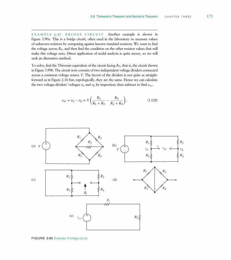
3.6 Thévenin’s Theorem and Norton’s Theorem C H A P T E R T H R E E 173
e x a m p l e 3.27 b r i d g e c i r c u i t Another example is shown inFigure 3.90a. This is a bridge circuit, often used in the laboratory to measure valuesof unknown resistors by comparing against known standard resistors. We want to findthe voltage across R5, and then find the condition on the other resistor values that willmake this voltage zero. Direct application of nodal analysis is quite messy, so we willseek an alternative method.
To solve, find the Thévenin equivalent of the circuit facing R5, that is, the circuit shownin Figure 3.90b. The circuit now consists of two independent voltage dividers connectedacross a common voltage source V. The layout of the dividers is not quite as straight-forward as in Figure 2.36 but, topologically, they are the same. Hence we can calculatethe two voltage-dividers’ voltages va and vb by inspection; then subtract to find voc.
voc = va − vb = V(
R3
R1 + R3− R4
R2 + R4
). (3.128)
R1 R2
+-V(a)
R3
Rt
R1 R2+-V voc
+ -(b)
(e)
R5
R4
Rt
R3 R4
vbva
R1 R2(c)
R3 R4
R5voc -+
(d)
R1 R2
R3 R4
F IGURE 3.90 Example: A bridge circuit.

174 C H A P T E R T H R E E n e t w o r k t h e o r e m s
Now find the Thévenin equivalent resistance with V set to zero, that is, for the circuitshown in Figure 3.90c. This is identical to the circuit in 3.90d,
Rt = (R1‖R3) + (R2‖R4). (3.129)
The complete circuit can now be drawn as in Figure 3.90e. It is clear that the voltageacross R5 will be zero if voc is zero, that is, if
R3
R1 + R3= R4
R2 + R4(3.130)
or equivalently
R3
R1= R4
R2. (3.131)
Thus if R5 is replaced by a voltmeter, the circuit can be used to find an unknownresistor, say R3, in terms of three known resistors. Make one of the resistors, say R1,a decade box with known resistance values and adjust until the voltmeter reads zero.The value of R3 is then given by Equation 3.131.
Two closing comments: First, note that the identity of all voltages and currents insidethe network that is replaced by the Thévenin or Norton circuit in general lose theiridentity; only the terminal voltage and current are preserved. Thus, for example, thecurrent through R3 in Figure 3.90a does not appear as any identifiable current flowingin the Thévenin circuit in Figure 3.90e. Second, if one wishes to measure the Théveninor Norton parameters of a system in the laboratory, two independent measurementsare required in order to specify the two parameters in the model. In addition, certainpractical issues must be faced. For example, it is unwise, in fact dangerous, to apply ashort circuit to a large battery such as an automobile storage battery in an attempt tomeasure the short-circuit current as suggested in Figure 3.75b. A better procedure is tofirst measure the open-circuit voltage, then measure the terminal voltage when someknown resistor is connected to the battery. These two measurements can then be usedto find Rt.
e x a m p l e 3.28 n o r t o n a n d t h é v e n i n e q u i v a l e n t s
As another simple example, let us find the Norton and Thévenin equivalent networksand their v i characteristics for the two circuits shown in Figure 3.91.
V+
-
R1
R2 v
+
-
i
I R1 R2 v
+
-
(a) Network I
(b) Network II
F IGURE 3.91 Two simplenetworks: (a) Network I;(b) Network II.
Let us start with Network A. First, let us find the Thévenin equivalent circuit. Shortingthe voltage source results in the circuit shown in Figure 3.92. Therefore, RTH = RN =R1‖R2 = R1R2/(R1 + R2), where RTH and RN are the Thévenin and Norton equivalentresistors, respectively. From the voltage-divider relationship, open circuit voltage voc
is VR2/(R1 + R2). This yields the Thévenin equivalent circuit on the left-hand side ofFigure 3.93.
R1 R2
F IGURE 3.92 Equivalentresistance of the network.

3.6 Thévenin’s Theorem and Norton’s Theorem C H A P T E R T H R E E 175
+
-
i
v
+
-
v
+
-
R2 V⋅R1 R2+( )
-----------------------
R1 R2⋅R1 R2+( )
-----------------------
R1 R2⋅R1 R2+( )
-----------------------VR1------
i
F IGURE 3.93 Equivalent networks.
V+
-
R1
R2
i
isc = V/R1
F IGURE 3.94 Short circuit current.
slope = (R1+R2) /R1R2
-V/R1
VR2/(R1+R2)
i
v
F IGURE 3.95 The i–v characteristics of the network.
Now, let us find the Norton equivalent circuit for Network A. Referring to Figure 3.94,the short-circuit current isc is V/R1. Therefore, the Norton equivalent network is asshown on the right-hand side of Figure 3.93.
The v i curve of the circuit must pass through points (voc, 0) and (0, −isc), asshown in Figure 3.95.
Let us now analyze Network B. Turning off the current source results in the circuitshown in Figure 3.92, which yields R1R2/(R1 + R2) as the equivalent resistance for boththe Thévenin and Norton equivalent networks. The open-circuit voltage is IR1‖R2.Thus, voc = R1R2I/(R1 + R2). As illustrated in Figure 3.96, all of the current will flowthrough the branch with zero resistance, that is isc = I.
The equivalent networks are shown in Figure 3.97, and the v i characteristics areshown in Figure 3.98.
I R1 R2 isc = I
i = 0 i = 0
F IGURE 3.96 Short-circuit current.
+
-
i
v
+
-
v
+
-
R1 R2 I⋅ ⋅R1 R2+( )
-----------------------
R1 R2⋅R1 R2+( )
-----------------------
R1 R2⋅R1 R2+( )
-----------------------I
i
F IGURE 3.97 Equivalent networks.

176 C H A P T E R T H R E E n e t w o r k t h e o r e m s
slope = (R1+R2)/R1R2
-IIR1R2/(R1+R2)
i
v
F IGURE 3.98 The v–i characteristics of the network.
V+
-
R1
R2
R3
R5
R4
x y
F IGURE 3.99 Resistive circuit.
e x a m p l e 3.29 a d i f f e r e n t a p p r o a c h u s i n g t h e
t h é v e n i n m e t h o d The network shown in Figure 3.99 was solved earlierusing the Thévenin method (see Figure 3.90). In this example, we will solve the samecircuit using the Thévenin method, but with a slightly different approach.
Making the observation that the voltages at points x and y are the same, we cantransform the circuit into the equivalent circuit shown in Figure 3.100. We can thentransform the circuits in Figures 3.100a and 3.100b into their Thévenin equivalent net-works. Figure 3.100a will have a source voltage of VR2/(R1 + R2) and an equivalentresistance of R1‖R2. Figure 3.100b will have a source voltage of VR5/(R4 + R5) andan equivalent resistance of R4‖R5.
The new circuit is shown in Figure 3.101. Notice that the new circuit is much easierto analyze. We leave the rest of the analysis as an exercise for you.
V+
-
R1
R2
R3
R5
R4
V+
-
(a) (b)
F IGURE 3.100 Equivalent circuit with two voltage sources.
VR2/(R1+R2)+
-V+
-
R3R1||R2 R4||R5
VR5/(R4+R5)V
F IGURE 3.101 Equivalent Thévenin circuit.
3.7 Summary C H A P T E R T H R E E 177
3.7 S U M M A R Y In the node method one node is designated as a reference or ground node,
and all other node voltages are measured with respect to that node. Onlythe KCL equations and the constituent relations need be written.
In the loop method currents are defined to flow in loops. Loop currents aredefined until all branches are traversed by at least one current. Only KVLequations need be written.
Superposition means that if the circuit is linear, multisource networks canbe solved for one source at a time by setting all other independent sources tozero. Setting a voltage source to zero means replacing it with a short circuit;a current source set to zero is an open circuit. The complete response isthe sum of the responses to each individual source.
For circuits with dependent sources, a practical solution is to leave all thedependent sources in the circuit. The network can then be solved for oneindependent source at a time by setting all other independent sources tozero, and summing the individual responses.
The Thévenin equivalent circuit for any linear network at a given pair of ter-minals consists of a voltage source in series with a resistor. The elementvalue for the Thévenin equivalent voltage source can be found by calculat-ing or measuring at the designated terminal pair on the original network theopen-circuit voltage. The equivalent resistance can be calculated or mea-sured as the resistance of the network seen from the designated terminalpair with all independent sources internal to the network set to zero.
The Norton equivalent circuit contains a current source in parallel with aresistor. The element value for the Norton equivalent current source canbe found by calculating or measuring at the designated terminal pair on theoriginal network the short circuit current. As with the Thévenin equivalentresistance, the Norton equivalent resistance can be calculated or measuredas the resistance of the network seen from the designated terminal pair withall independent sources internal to the network set to zero. Note that thevalue of the equivalent resistance is the same for the Thévenin and Nortonequivalent circuits, that is, RTH = RN.
Since the Thévenin equivalent voltage vTH, the Norton equivalent currentiN, and the equivalent resistance RTH = RN are related as
vTH = iNRTH,
the element values for these equivalents can be found by calculating ormeasuring any two of the open-circuit voltage, the short-circuit current, orthe resistance.

178 C H A P T E R T H R E E n e t w o r k t h e o r e m s
Circuit analysis is often simplified by applying superposition or findingThévenin or Norton equivalents, because complicated circuits are reducedto simpler circuits, for which the solution may already be known.
E X E R C I S E S e x e r c i s e 3 .1 Write node equations for the network in Figure 3.102. Solve forthe node voltages, and use these voltages to find the branch current i. To minimizeerrors and facilitate answer-checking, it is helpful to obtain literal expressions beforesubstituting numerical values for the parameters:
V = 2 V R3 = 3 R1 = 2 R4 = 2 R2 = 4 R5 = 1
V+
-
R1
R2
R5R3
R4i
F IGURE 3.102
e x e r c i s e 3 .2 Find the Norton equivalent at the indicated terminals for eachnetwork in Figure 3.103.
Vo
+-
v
i
+
-
R2
Is
R1
5 v+-
2 Ω v
i
-
+3 Ω
F IGURE 3.103e x e r c i s e 3 .3 Find the Thévenin equivalent for each network in Figure 3.104.
v
i
+
-
R2 Isv
i+
-
R2Is
R1R1
R3
F IGURE 3.104
e x e r c i s e 3 .4 Find v0 in Figures 3.105a and 3.105b by superposition.
(a)
(b)
v0+-
3 Ω
2 Ω
2 Ω
3 Ω
+-
31 A
62 V
v0
+
-6 A
+-
10 V
4 kΩ1 kΩ
2 kΩ
3 kΩ
F IGURE 3.105e x e r c i s e 3 .5 Use superposition to find the voltage v in the network inFigure 3.106.

3.7 Summary C H A P T E R T H R E E 179
1 V+-
1 Ω
2 Ω1 Ω 1 A
1 Ω
1 Ω
v+
-
1 Ω
2 Ω 1 A F IGURE 3.106
e x e r c i s e 3 .6 Determine (and label carefully) the Thévenin equivalent for thenetwork in Figure 3.107:
R1 = 2 k R2 = 1 k i0 = 3 mA cos(ωt)
R2v
+
-
i
i0
R1
F IGURE 3.107e x e r c i s e 3 .7 Determine and label carefully the Norton equivalent for thenetwork in Figure 3.108.
4 mA
5 kΩ
2 kΩ
1 kΩ
a
b
F IGURE 3.108
e x e r c i s e 3 .8 Find the Thévenin equivalent for the circuit at the terminals AA′in Figure 3.109.
10 V
1 kΩ
2 kΩ
A
A′
2 kΩ
+-
F IGURE 3.109
e x e r c i s e 3 .9 The resistive network shown in Figure 3.110 is excited by two
v1(t) v2(t)
2 Ω
i(t)
2 Ω
+-
+-1 Ω
F IGURE 3.110
voltage sources v1(t) and v2(t).
a) Express the current i(t) through the 1- resistor as a function of v1(t) and v2(t).
b) Determine the total energy dissipated in the 1- resistor due to both v1(t) and v2(t)from time T1 to time T2.
c) Derive the constraint between v1(t) and v2(t) such that the value for (b) can becomputed by adding the energies dissipated when each source acts alone (that is, bysuperposition).
e x e r c i s e 3 .10 Find the Norton equivalent at the terminals marked x x in thecircuit in Figure 3.111.
Io = 3 A
2 Ω
Vo = 5 V+-1 Ω
x4 Ω
2 Ω
x
F IGURE 3.111
e x e r c i s e 3 .11 Find the Thévenin equivalent for the circuit in Figure 3.112 atthe terminals AA′.

180 C H A P T E R T H R E E n e t w o r k t h e o r e m s
12 V
6 Ω
1 A3 Ω
A
+-
A′
F IGURE 3.112
e x e r c i s e 3 .12 In the network in Figure 3.113, find an expression for v2.
R1v3
I3
- +R2
v2+ -
F IGURE 3.113
e x e r c i s e 3 .13 The networks in Figure 3.114 are equivalent (that is, have thesame v i relation) at terminals A A′. Find vT and RT.
R1v3
I3
- +
v
+
-
A
A′
R2
i
RT
vTv
+
-
A
A′
i
+-
F IGURE 3.114e x e r c i s e 3 .14 For each of the circuits in Figure 3.115 give the number ofindependent node variables needed for a solution of the problem by the node method.
R2
I2
R4
R1
R3 R5
I1
v
R1
+ -
R4
R5
R4R3R2
Iv
F IGURE 3.115
e x e r c i s e 3 .15 For the circuit shown in Figure 3.116, write a complete set ofnode equations for the voltages va, vb, and vc. Use conductance instead of resistance.Simplify the equations by collecting terms and arranging them in the ‘‘standard’’ formfor n linear equations in n unknowns. (Do not solve the equations.)
v
I
R6R5
R3 R4
R2R1
va vbvc
+-
F IGURE 3.116
e x e r c i s e 3 .16 For the circuit shown in Figure 3.117, use superposition to findv in terms of the R’s and source amplitudes.

3.7 Summary C H A P T E R T H R E E 181
e x e r c i s e 3 .17 Find the Thévenin equivalent of the circuit in Figure 3.118 atthe terminals indicated.
v
R1R3
R2
v2
+-
+-
I
v1
+
-
F IGURE 3.117
vR1
R3
R2v
+
-I
+-
i
F IGURE 3.118
e x e r c i s e 3 .18 In the circuit shown in Figure 3.119 there are five nodes, onlythree of which are independent. Take node E as a reference node, and treat nodes A, B,and D as the independent nodes.
a) Write an expression for vC, the voltage on node C, in terms of vA, vB, vD,and v1.
b) Write a complete set of node equations that can be solved to find the unknown
R2
R6R5
V1+ -
R3
R1
A CBD
E
R4
F IGURE 3.119
voltages in the circuit. (Do not solve the set of equations but do group them neatly.)
e x e r c i s e 3 .19 Consider the circuit in Figure 3.120.
25 V
300 Ω
+ -
-
+
v100 Ω
50 Ω i
0.5 A
A′
A′
F IGURE 3.120
a) Find a Norton equivalent circuit for this circuit at terminals A A′.
b) Find the Thévenin equivalent circuit corresponding to your answer in (a).
e x e r c i s e 3 .20 Measurements made on terminals B B′ of a linear circuit inFigure 3.121a, which is known to be made up only of independent voltage sourcesand current sources, and resistors, yield the current-voltage characteristics shown in
v
R
B
B′
V +-
+-
iI
(a)
1020
30
-10
-20
-30
-4
-3 -2 -1
1 2 3 4 5
40
v (V)
(b)
i (mA)
F IGURE 3.121Figure 3.121b.

182 C H A P T E R T H R E E n e t w o r k t h e o r e m s
a) Find the Thévenin equivalent of this circuit.
b) Over what portions, if any, of the v i characteristics does this circuit absorbpower?
e x e r c i s e 3 .21
a) Write in standard form the minimum number of node equations needed to analyzethe circuit in Figure 3.122.
F IGURE 3.122 R4R1
i4
I+-
R5R2
R3
v
b) Determine explicitly the current i4.
e x e r c i s e 3 .22
a) Find the Thévenin equivalent of the circuit in Figure 3.123.
F IGURE 3.123 R4R1
R2
R3
v
R8
R6
AR7
R5
+-
A′
I
b) Find the Norton equivalent of the circuit in Figure 3.124.
F IGURE 3.124I
R1
v R4
1R2
R3
+-
1
e x e r c i s e 3 .23
a) Find the Norton equivalent of the circuit in Figure 3.125.

3.7 Summary C H A P T E R T H R E E 183
I
R1 v
1R4
+-
1
R2 R3 R5
R6
R7
F IGURE 3.125
b) Find the Thévenin equivalent of the circuit in Figure 3.126.
I
A
A′
R1 R2 R3
R4
v+- F IGURE 3.126
e x e r c i s e 3 .24 Find the Thévenin equivalent circuit as seen from the terminalsa b in Figure 3.127.
10 mA 10 kΩ 2 V +-
10 kΩ
a
bF IGURE 3.127
e x e r c i s e 3 .25 Find the node potential E in Figure 3.128.
5 V 8 kΩ
1 V
+ -
+-
8 kΩ
0.4 kΩ
E
2.5 mA F IGURE 3.128
e x e r c i s e 3 .26 For the circuit in Figure 3.129, write the node equations. Donot solve, but write in matrix form: source terms on the left, unknown variables on theright.

184 C H A P T E R T H R E E n e t w o r k t h e o r e m s
F IGURE 3.129
V
+ -R1 R2
R2R3
e x e r c i s e 3 .27 Find v1 by superposition for the circuit in Figure 3.130.
F IGURE 3.130V
R1
R2
v1
R3
+-I
P R O B L E M S p r o b l e m 3.1 A fuse is a wire with a positive temperature coefficient of resis-tance (in other words, its resistance increases with temperature). When a current ispassed through the fuse, power is dissipated in the fuse, which raises its temperature.
F IGURE 3.131I0 Fuse
Use the following data to determine the current I0 at which the fuse (in Figure 3.131)will blow (that is, its temperature goes up without limit).
Fuse Resistance:R = 1 + a T
a = 0.001 /CT = Temperature rise above ambient
Temperature rise:T = βPβ = (
1/.225)C/W
P = power dissipated in fuse

3.7 Summary C H A P T E R T H R E E 185
p r o b l e m 3.2
a) Prove, if possible, each of the following statements. If a proof is not possible, illustratethe failure with a counter-example and restate the theorem with a suitable restrictionso it can be proved.
i) In a network containing only linear resistors, every branch voltage and branchcurrent must be zero.
ii) The equivalent of a one-port network containing only linear resistors is a linearresistor.
b) To demonstrate that you understand superposition, construct an example that showsexplicitly that a network containing a nonlinear resistor will not obey superposition.You may select any nonlinear element (provided you show that it is not linear) andany simple network containing that element.
p r o b l e m 3.3 Find V0 in Figure 3.132. Solve by (1) node method,(2) superposition. All resistances are in ohms.
2
V0 +- 4
+
-
2
8 V 6 A 6
Ω
Ω Ω
Ω
F IGURE 3.132
p r o b l e m 3.4 Consider Figure 3.132. Find the Norton equivalent of thenetwork as seen at the terminals on the right.
p r o b l e m 3.5
a) Find Req, the equivalent resistance ‘‘looking into’’ the terminals on the right of thecircuit in Figure 3.133.
R 2 R
R R R
2 R2 R Req = ?
F IGURE 3.133
b) Find the Thévenin equivalent, looking into the terminals on the right of the circuitin Figure 3.134.

186 C H A P T E R T H R E E n e t w o r k t h e o r e m s
F IGURE 3.134
1 Ω
Vo1 A
+
-
1 Ω
1 Ω
1 Ω
2 Ω 2 Ω2 Ω
p r o b l e m 3.6 Find vi for I = 3 A, V = 2 V in Figure 3.135. Strategy: To avoidnumerical errors, derive expressions in literal form first, then check dimensions.
F IGURE 3.135
I
+
-
2 Ω
vi
V
-
3 Ω
2 Ω2 Ω
2 Ω+
p r o b l e m 3.7 For the circuits in Figures 3.136a and 3.136b:
a) Find vo for R1 = R.
b) Find vo for R1 = R.
c) Find the Thévenin equivalent for the network to the right of points AB, assuming
V
RR
A
RR1
vo+-
B
+ -
(a)
V
RR
RR1
vo
+-
A
B
R+ -
(b)
F IGURE 3.136
R1 = R.
p r o b l e m 3.8
a) Determine the equation relating i to v in Figure 3.137.
F IGURE 3.137
i
2 Ω 2 Av
4 Ω1 Ω+
-
3 Ω
b) Plot the v i characteristics of the network.
c) Draw the Thévenin equivalent circuit.
d) Draw the Norton equivalent circuit.

3.7 Summary C H A P T E R T H R E E 187
p r o b l e m 3.9 In Figure 3.138, find vo via (a) superposition, (b) the nodemethod.
i
4 Ω8 A vo
1 Ω 2 Ω+
-
6 ΩAo V+-
F IGURE 3.138
p r o b l e m 3.10 Use the following three different methods to find i inFigure 3.139:
1) Node method
3 V
6 Ω 2 A
3 Ω
6 Ω 3 Ω
+-i
F IGURE 3.139
2) Superposition
3) Alternate Thévenin/Norton transformations
p r o b l e m 3.11 A student is given an unknown resistive network as illus-trated in Figure 3.140. She wishes to determine whether the network is linear, andif it is, what its Thévenin equivalent is.
Resistive network
Unknown network
F IGURE 3.140
The only equipment available to the student is a voltmeter (assumed ideal), 100-k and1-M test resistors that can be placed across the terminals during a measurement (seeFigure 3.141).
V R+
-V
Resistivenetwork
Unknownnetwork
Test resistor
Voltmeter
F IGURE 3.141

188 C H A P T E R T H R E E n e t w o r k t h e o r e m s
The following data were recorded:
Test Resistor Voltmeter Reading
Absent 1.5 V100 k 0.25 V1 M 1.0 V
What should the student conclude about the network from these results? Support yourconclusion with plots of the network v i characteristics.
p r o b l e m 3.12
a) Devise an electrical circuit of voltage sources and resistors that will ‘‘calculate’’ thebalance point (center of mass) of the massless bar shown in Figure 3.142, for threearbitrary masses hung at three arbitrary places along the bar. We want the circuit togenerate a voltage that is proportional to the position of the balance point. Writethe equation for your network, and show that it performs the required calculation.(Work with conductances and superposition for a simple solution.)
F IGURE 3.142
Mass A Mass B Mass C
b) Extend your result in part (a) to two dimensions; that is, devise a new network (whichwill have more voltage sources and more resistors than above) that can find the centerof mass of a triangle with arbitrary weights handing from its three corners. Thenetwork will now have to give you two voltages, one representing the x-coordinateand the other the y-coordinate of the center of mass. This system is a barycentriccoordinate calculator, and can be used as the input for video games, or to simulatetrichromatic color vision in the human eye.
p r o b l e m 3.13
a) Find the Thévenin equivalent for the network in Figure 3.143 at the terminals CB.The current source is a controlled source. The current flowing through the current
F IGURE 3.143
C
I1
I1 +
-10 kΩ
+-
Vs 100 kΩ
B
b
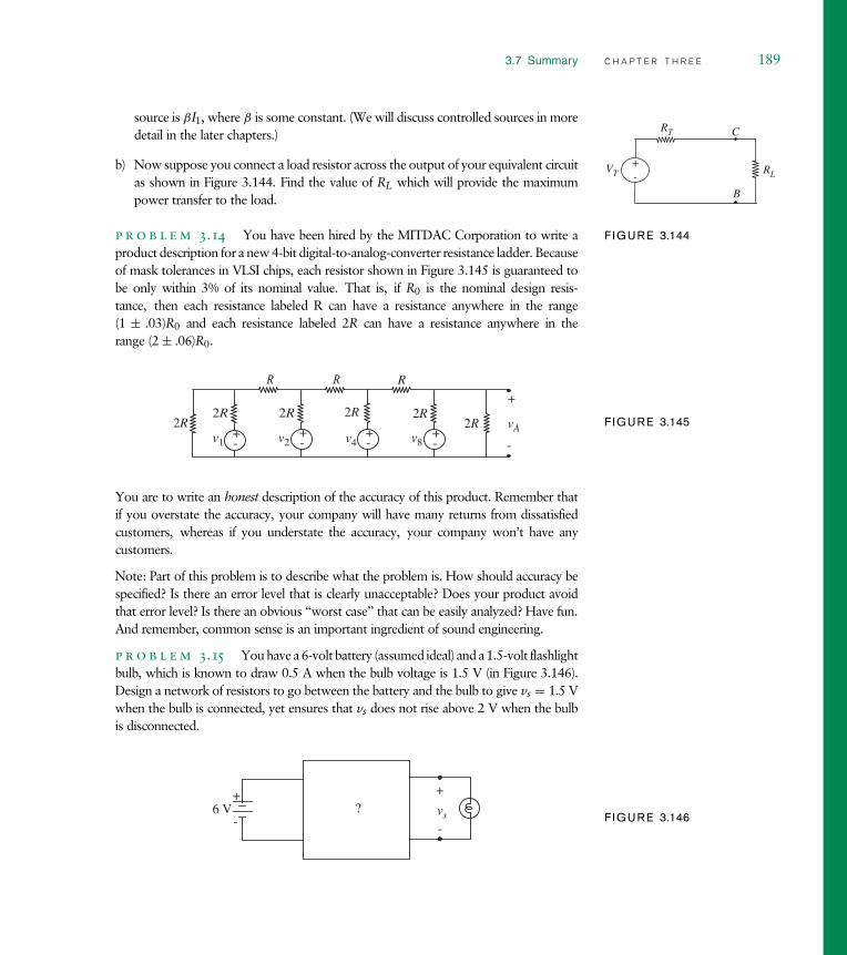
3.7 Summary C H A P T E R T H R E E 189
source is βI1, where β is some constant. (We will discuss controlled sources in moredetail in the later chapters.)
b) Now suppose you connect a load resistor across the output of your equivalent circuitas shown in Figure 3.144. Find the value of RL which will provide the maximumpower transfer to the load.
C
+-
VT RL
B
RT
F IGURE 3.144p r o b l e m 3.14 You have been hired by the MITDAC Corporation to write aproduct description for a new 4-bit digital-to-analog-converter resistance ladder. Becauseof mask tolerances in VLSI chips, each resistor shown in Figure 3.145 is guaranteed tobe only within 3% of its nominal value. That is, if R0 is the nominal design resis-tance, then each resistance labeled R can have a resistance anywhere in the range(1 ± .03)R0 and each resistance labeled 2R can have a resistance anywhere in therange (2 ± .06)R0.
R
2R2R
+-
2R
+-
2R
+-
2R
+-
2R
R R
v1 v2 v4 v8
vA
+
-
F IGURE 3.145
You are to write an honest description of the accuracy of this product. Remember thatif you overstate the accuracy, your company will have many returns from dissatisfiedcustomers, whereas if you understate the accuracy, your company won’t have anycustomers.
Note: Part of this problem is to describe what the problem is. How should accuracy bespecified? Is there an error level that is clearly unacceptable? Does your product avoidthat error level? Is there an obvious ‘‘worst case’’ that can be easily analyzed? Have fun.And remember, common sense is an important ingredient of sound engineering.
p r o b l e m 3.15 You have a 6-volt battery (assumed ideal) and a 1.5-volt flashlightbulb, which is known to draw 0.5 A when the bulb voltage is 1.5 V (in Figure 3.146).Design a network of resistors to go between the battery and the bulb to give vs = 1.5 Vwhen the bulb is connected, yet ensures that vs does not rise above 2 V when the bulbis disconnected.
vs
+
-
+
-?6 V
F IGURE 3.146


c h a p t e r 4
4.1 I N T R O D U C T I O N T O N O N L I N E A R E L E M E N T S
4.2 A N A L Y T I C A L S O L U T I O N S
4.3 G R A P H I C A L A N A L Y S I S
4.4 P I E C E W I S E L I N E A R A N A L Y S I S
4.5 I N C R E M E N T A L A N A L Y S I S
4.6 S U M M A R Y
E X E R C I S E S
P R O B L E M S


analy s i s o f nonl inear
c i rcu i t s 4Thus far we have discussed a variety of circuits containing linear devices suchas resistors and voltage sources. We have also discussed methods of analyz-ing linear circuits built out of these elements. In this chapter, we extend ourrepertoire of network elements and corresponding analysis techniques by intro-ducing a nonlinear two-terminal device called a nonlinear resistor. Recall, fromSection 1.5.2, a nonlinear resistor is an element that has a nonlinear, alge-braic relation between its instantaneous terminal current and its instantaneousterminal voltage. A diode is an example of a device that behaves like a non-linear resistor. In this chapter, we will introduce methods of analyzing generalcircuits containing nonlinear elements, trying whenever possible to use analysismethods already introduced in the preceding chapters. Chapter 7 will developfurther the basic ideas on nonlinear analysis and Chapter 8 will expand onthe concept of incremental analysis introduced in this chapter. Chapter 16 willelaborate on diodes.
iD
vD -+
F IGURE 4.1 The symbol for adiode.
4.1 I N T R O D U C T I O N T O N O N L I N E A RE L E M E N T S
Before we begin our analysis of nonlinear resistors, we will describe as examplesseveral nonlinear resistive devices, by their v i characteristics, just as we did forthe resistor, the battery, etc. The first of the nonlinear devices that we discuss isthe diode. Figure 4.1 shows the symbol for a diode. The diode is a two-terminal,nonlinear resistor whose current is exponentially related to the voltage acrossits terminals.
An analytical expression for the nonlinear relation between the voltage vD andthe current iD for the diode is the following:
iD = Is(e vD/VTH − 1). (4.1)
For silicon diodes the constant Is is typically 10−12 A and the constant VTH istypically 0.025 V. This function is plotted in Figure 4.2.
vD
iD
F IGURE 4.2 v–i characteristicsof a silicon diode.
vH
iH
F IGURE 4.3 Another nonlinearv–i characteristics.
An analytical expression for the relationship between voltage vH and cur-rent iH for another hypothetical nonlinear device is shown in Equation 4.2. Inthe equation, IK is a constant. The relationship is plotted in Figure 4.3.
iH = IKv 3H. (4.2)
193

194 C H A P T E R F O U R a n a l y s i s o f n o n l i n e a r c i r c u i t s
The v i relationship for yet another two-terminal nonlinear device isshown in Equation 4.3. Figure 8.11 in Chapter 8 introduces such a nonlineardevice. For this device the current is related to the square of the terminal voltage.In this equation, K and VT are constants. The variables iDS and vDS are theterminal variables for the device. The relationship is plotted in Figure 4.4.
iDS =
K(vDS − VT)2
2for vDS ≥ VT
0 for vDS < VT
. (4.3)vDS
iDS
0 VT
F IGURE 4.4 The v–i character-istics for a square law device.
e x a m p l e 4.1 s q u a r e l a w d e v i c e For the nonlinear resistordevice following the square law in Figure 4.4, determine the value of iDS for vDS = 2 V.We are given that VT = 1 V and K = 4 mA/V2.
For the parameters that we have been given (vDS = 2 V and VT = 1 V), it is easy tosee that
vDS ≥ VT.
From Equation 4.3, the expression for iDS when vDS ≥ VT is
iDS = K(vDS − VT)2
2.
Substituting the known numerical values,
iDS = 4 × 10⁻³(2 − 1)2
2= 2 mA.
How does iDS change if vDS is doubled?
If vDS is doubled to 4 V,
iDS = K(vDS − VT)2
2= 4 × 10⁻³(4 − 1)2
2= 18 mA
In other words, iDS increases to 18 mA when vDS is doubled.
What is the value of iDS if vDS is changed to 0.5 V?
For vDS = 0.5 V and VT = 1 V,
vDS < VT.
From Equation 4.3, we get
iDS = 0.
When operating within some circuit, the current through our square law deviceis measured to be 4 mA. What must be the voltage across the device?

4.1 Introduction to Nonlinear Elements C H A P T E R F O U R 195
We are given that iDS = 4 mA. Since there is a current through the device, the equationthat applies is
iDS = K(vDS − VT)2
2.
Substituting known values,
8 × 10−3 = 4 × 10⁻³(vDS − 1)2
2.
Solving for vDS, we get
vDS = 3 V.
e x a m p l e 4.2 d i o d e e x a m p l e For the diode shown in Figure 4.1,determine the value of iD for vD = 0.5 V, 0.6 V, and 0.7 V. We are given that VTH =0.025 V and Is = 1 pA.
From the device law for a diode given in Equation 4.1, the expression for iD is
iD = Is(evD/VTH − 1).
Substituting the known numerical values for vD = 0.5 V, we get
iD = 1 × 10⁻¹²(e0.5/0.025 − 1) = 0.49 mA.
Similarly, for vD = 0.6 V, iD = 26 mA, and for vD = 0.7 V, iD = 1450 mA. Notice thedramatic increase in current as vD increases beyond 0.6 V.
What is the value of iD if vD is −0.2 V?
iD = Is(evD/VTH − 1) = 1 × 10⁻¹²(e−0.2/0.025 − 1) = −0.9997 × 10⁻¹²A.
The negative sign for iD simply reflects the fact that when vD is negative, so is thecurrent.
When operating within some circuit, the current through the diode is measured to be8 mA. What must be the voltage across the diode?
We are given that iD = 8 mA. Using the diode equation, we get
8 × 10−3 = Is(e vD/VTH − 1) = 1 × 10⁻¹²(e vD/0.025 − 1).
Simplifying, we get
e vD/0.025 = 8 × 10⁹ + 1.

196 C H A P T E R F O U R a n a l y s i s o f n o n l i n e a r c i r c u i t s
Taking logs on both sides, and solving for vD, we get
vD = 0.025 ln(8 × 10⁹ + 1) = 0.57 V.
e x a m p l e 4.3 a n o t h e r s q u a r e l a w d e v i c e p r o b l e m
The nonlinear device shown in Figure 4.5 is characterized by this device equation:
iD
vD
+
-
F IGURE 4.5 A nonlinear device.
iD = 0.1v 2D for vD ≥ 0, (4.4)
iD is given to be 0 for vD < 0.
Given that V = 2 V, determine iD for the circuit in Figure 4.6.iD
vD
+
-
V+
-
F IGURE 4.6 A circuit containingthe nonlinear device.
Using the device equation for vD ≥ 0,
iD = 0.1v 2D = 0.1 × 22 = 0.4 A (4.5)
The nonlinear device is connected to some arbitrary circuit as shown in Figure 4.7.Following the associated variables discipline, the branch variables vB and iB for thedevice are defined as shown in the same figure. Suppose that a measurement revealsthat iB = −1 mA. What must be the value of vB?
Notice that the polarity of the branch variables has been reversed in Figure 4.7 from
vB
-
+
Arbitrarycircuit
iB
F IGURE 4.7 The nonlineardevice connected to an arbitrarycircuit.
those in Figure 4.5. With this definition of the branch variables, the device equationbecomes
−iB = 0.1v 2B for vB ≤ 0. (4.6)
Furthermore, iB is 0 for vB > 0.
Given that iB = −1 mA, Equation 4.6 yields
−(−1 × 10⁻³) = 0.1v 2B where vB ≤ 0.
In other words, vB = −0.1 V.
i1
vD
+
-
V+
-D1
i
i2D2
F IGURE 4.8 Nonlinear devicesconnected in parallel.
Given that V = 2 V, determine i for the circuit in Figure 4.8.
Since the voltage across each of the nonlinear devices connected in parallel is vD = 2 V,the current through each nonlinear device is the same as that calculated in Equation 4.5.In other words,
i1 = i2 = 0.4 A.
Therefore, i = i1 + i2 = 0.8 A.

4.2 Analytical Solutions C H A P T E R F O U R 197
Given the analytical expression for the characteristic of a nonlinear device,such as that for the diode in Equation 4.1, how can we calculate the voltagesand currents in a simple circuit such as Figure 4.9? In the following sections wewill discuss four methods for solving such nonlinear circuits:
1. Analytical solutions
2. Graphical analysis
3. Piecewise linear analysis
4. Incremental or small signal analysis
4.2 A N A L Y T I C A L S O L U T I O N S
We first try to solve the simple nonlinear resistor circuit in Figure 4.9 by ana-lytical methods. Assume that the hypothetical nonlinear resistor in the figure ischaracterized by the following v i relationship:
iD =
Kv 2D for vD > 0
0 for vD ≤ 0.(4.7)
The constant K is positive.
-
+R
-+
vD
iD
E
-
+vD
iDNonlinear resistor
iD KvD2= for vD > 0
iD 0= otherwise
F IGURE 4.9 A simple circuitwith a nonlinear resistor.
This circuit is amenable to a straightforward application of the nodemethod. Recall that the node method and its foundational Kirchhoff’s voltageand current laws are derived from Maxwell’s Equations with no assumptionsabout linearity. (Note, however, that the superposition method, the Théveninmethod, and the Norton method do require a linearity assumption.)
To apply the node method, we first choose a ground node and label thenode voltages as illustrated in Figure 4.10. vD is our only unknown node voltage.
Next, following the node method, we write KCL for the node that has anunknown node voltage. As prescribed by the node method, we will use KVLand the device relation (iD = Kv 2
D) to obtain the currents directly in terms of thenode voltage differences and element parameters. For the node with voltage vD,
vD − E
R+ iD = 0 (4.8)
-
+
R
-
+
vD
iD
E
E vD
F IGURE 4.10 The nonlinearcircuit with the ground nodechosen and node voltages labeled.

198 C H A P T E R F O U R a n a l y s i s o f n o n l i n e a r c i r c u i t s
Note that this is not quite our node equation, because of the presence of the iDterm. To get the node equation we need to substitute for iD in terms of nodevoltages. Recall that the nonlinear device v i relation is
iD = Kv 2D. (4.9)
Note that this device equation applies for positive vD. We are given that iD = 0when vD ≤ 0.
Substituting the nonlinear device v i relationship for iD in Equation 4.8,we get the required node equation in terms of the node voltages:
vD − E
R+ Kv 2
D = 0. (4.10)
For our device, note that Equation 4.9 holds only for vD > 0. For vD ≤ 0,iD is 0.
Simplifying Equation 4.10, we obtain the following quadratic equation.
RKv 2D + vD − E = 0.
Solving for vD and choosing the positive solution
vD = −1 + √1 + 4RKE
2RK. (4.11)
The corresponding expression for iD can be obtained by substituting theprevious expression for vD into Equation 4.9 as follows:
iD = K
[−1 + √
1 + 4RKE
2RK
]2
. (4.12)
It is worth discussing why we ignored the negative solution. As shown inFigure 4.11, two mathematical solutions are possible when we solve Equa-tions 4.10 and 4.9. However, the dotted curve in Figure 4.11 is part of
F IGURE 4.11 Solutions toequations Equations 4.10 and 4.9.
iD
EvD
iD = KvD2
E/RiD
1R---–=
Physicalsolution
Non-physicalundesiredsolution
(vD – E)

4.2 Analytical Solutions C H A P T E R F O U R 199
Equation 4.9 but not the physical device. Because, recall, Equation 4.9 appliesonly for positive vD. When E is negative, iD will be equal to 0 and vD will beequal to E.
e x a m p l e 4.4 o n e n o n l i n e a r d e v i c e , s e v e r a l
s o u r c e s , a n d r e s i s t o r s Shown in Figure 4.12 is a circuit of no obvi-ous value, which we use to illustrate how to solve nonlinear circuits with more than onesource present, using the nonlinear analysis method just discussed. Let us assume thatwe wish to calculate the nonlinear device current iD.
Assume that the nonlinear device is characterized by the following v i relationship:
iD =
Kv 2D for vD > 0
0 for vD ≤ 0.(4.13)
The terminal variables for the nonlinear device are defined as shown in Figure 4.9, andthe constant K is positive.
Linear analysis techniques such as superposition cannot be applied to the whole circuitbecause of the nonlinear element. But because there is only one nonlinear device, it ispermissible to find the Thévenin (or Norton) equivalent circuit faced by the nonlineardevice (see Figures 4.13a and b), because this part of the circuit is linear. Then wecan compute easily the terminal voltage and current for the nonlinear device using thecircuit in Figure 4.13b from Equations 4.11 and 4.12.
First, to find the open-circuit voltage, we draw the linear circuit as seen from the nonlin-ear device terminals in Figure 4.13c. Superposition or any other linear analysis methodcan now be used to calculate the open-circuit voltage:
VTH = VR2
R1 + R2− I0R3. (4.14)
The Thévenin equivalent resistance, RTH, the resistance seen at the terminals inFigure 4.13d, with the sources set to zero is
RTH = (R1||R2) + R3. (4.15)
R2V R3
R1
I0
iD
i3
+
-F IGURE 4.12 Circuit withseveral sources and resistors.

200C
HA
PT
ER
FO
UR
an
al
ysis
of
no
nl
in
ea
rc
ir
cu
it
s
R2(a) V R3
RTH
RTH
VTH
(c)
R1
I0
iD
i3
+ -
R2V
VTH
R3
R1
I0
(e)
iD+
-
-
+
+
-(b)
RTH
VTH
+
-
(d) R2 R3
R1
F IGURE 4.13 Analysis using Thévenin’s Theorem.

4.2 Analytical Solutions C H A P T E R F O U R 201
When we reconnect the nonlinear device to this Thévenin circuit, as in Figure 4.13e,we are back to a familiar example: one nonlinear device, one source, and one resistor.The desired device current iD can be found by a nonlinear analysis method, such as thatused to solve the circuit in Figure 4.9.
One further comment: If in the problem statement we had been asked to find one of theresistor currents, say i3, rather than iD, then the Thévenin circuit, Figure 4.13e, wouldnot give this current directly, because the identity of currents internal to the Théveninnetwork are in general lost, as noted in Chapter 3. Nonetheless, the Thévenin approachis probably the best, as it is a simple matter to work back through the linear part ofthe network to relate i3 to iD. In this case, once we have computed iD, we can easilydetermine i3 from Figure 4.13a using KCL,
i3 = iD + I0. (4.16)
W W W e x a m p l e 4.5 n o d e m e t h o d
e x a m p l e 4.6 a n o t h e r s i m p l e n o n l i n e a r c i r c u i t
Let us try to solve the nonlinear circuit containing a diode in Figure 4.16 by analyticalmethods. Following the node method, we first choose the ground node and label thenode voltages as illustrated in Figure 4.17.
Next, we write KCL for the node with the unknown node voltage, and substitute forthe diode current using the diode equation
vD − E
R+ iD = 0 (4.18)
iD = Is(e vD/VTH − 1). (4.19)
-
+
R
-
+
-+
vD
iD
E
vR
F IGURE 4.16 A simple non-linearcircuit containing a diode.
-
+
R
-
+
vD
iD
E
vDE
F IGURE 4.17 The circuit with theground node and the node voltagesmarked.

202 C H A P T E R F O U R a n a l y s i s o f n o n l i n e a r c i r c u i t s
If iD is eliminated by substituting Equation 4.19 into Equation 4.18, the followingtranscendental equation results:
vD − E
R+ Is(e vD/VTH − 1) = 0.
This equation must be solved by trial and error. Easy via computer, but not veryinsightful.
e x a m p l e 4.7 s e r i e s - c o n n e c t e d d i o d e s Referring to theseries-connected diodes in Figure 4.18, determine v1, v2, v3, and v4, given that I = 2 A.The parameters in the diode relation are given to be Is = 10−12 A, VTH = 0.025 V.
We will first use the node method to solve this problem. Figure 4.18 shows the groundnode and the node voltages. There are four unknown node voltages. Next, we writeKCL for each of the nodes. As prescribed by the node method, we will use KVL and thediode relation (Equation 4.1) to obtain the currents directly in terms of the node voltagedifferences and element parameters. For the node with voltage v1,
10−12(e v1/0.025 − 1) = 10−12(e (v2−v1)/0.025 − 1). (4.20)
The term on the left-hand side is the current through the lowermost device expressedin terms of node voltages. Similarly, the term on the right-hand side is the currentthrough the device that is second from the bottom.
v3
v2
v1
v4
I
F IGURE 4.18 Series connecteddiodes.
Similarly, we can write the node equations for the nodes with voltages v2, v3, and v4 asfollows:
10−12(e (v2−v1)/0.025 − 1) = 10−12(e (v3−v2)/0.025 − 1) (4.21)
10−12(e (v3−v2)/0.025 − 1) = 10−12(e (v4−v3)/0.025 − 1) (4.22)
10−12(e (v4−v3)/0.025 − 1) = I. (4.23)
Simplifying, and taking the log on both sides of Equations 4.20 through 4.23, we get
v1 = v2 − v1 (4.24)
v2 − v1 = v3 − v2 (4.25)
v3 − v2 = v4 − v3 (4.26)
v4 − v3 = 0.025 ln(1012I + 1). (4.27)

4.3 Graphical Analysis C H A P T E R F O U R 203
Given that I = 2 A, we can solve for v1, v2, v3, and v4, to get
v1 = 0.025 ln(1012I + 1) = 0.025 ln(1012 × 2 + 1) = 0.71 V
v2 = 2v1 = 1.42 V
v3 = 3v1 = 2.13 V
v4 = 4v1 = 2.84 V.
Notice that we could have also solved the circuit intuitively by observing that the same2-A current flows through each of the four identical diodes. Thus, the same voltagemust drop across each of the diodes. In other words,
I = 10−12(e v1/0.025 − 1)
or,
v1 = 0.025 ln(1012I + 1).
For I = 2 A,
v1 = 0.025 ln(1012 × 2A + 1) = 0.71 V.
Once the value of v1 is known, we can easily compute the rest of the node voltages from
v1 = v2 − v1 = v3 − v2 = v4 − v3.
W W W e x a m p l e 4.8 m a k i n g s i m p l i f y i n g a s s u m p t i o n s
W W W e x a m p l e 4.9 v o l t a g e - c o n t r o l l e d n o n l i n e a r
r e s i s t o r
4.3 G R A P H I C A L A N A L Y S I S
Unfortunately, the preceding examples are a rather special case. There aremany nonlinear circuits that cannot be solved analytically. The simple circuitin Figure 4.16 is one such example. Usually we must resort to trial-and-errorsolutions on a computer. Such solutions provide answers, but usually givelittle insight about circuit performance and design. Graphical solutions, on theother hand, provide insight at the expense of accuracy. So let us re-examinethe circuit in Figure 4.16 with a graphical solution in mind. For concreteness,we will assume that E = 3 V and R = 500 , and that we are required todetermine vD, iD, and vR.

204 C H A P T E R F O U R a n a l y s i s o f n o n l i n e a r c i r c u i t s
We have already found the two simultaneous equations, Equations 4.18and 4.19, that describe the circuit. For convenience, let us rewrite theseequations here after moving a few terms around:
iD = −vD − E
R(4.31)
iD = Is(e vD/VTH − 1). (4.32)
To solve these expressions graphically, we plot both on the same coor-dinates and find the point of intersection. Because we are assuming that wehave a graph of the nonlinear function, in this case Figure 4.2, the simplestcourse of action is to plot the linear expression, Equation 4.31, on this graph,as shown in Figure 4.20. The linear constraint of Equation 4.31 is usually calleda ‘‘load line’’ for historical reasons arising from amplifier design (as we will seein Chapter 7).
Equation 4.31 plots as a straight line of slope −1/R intersecting the vDaxis, (iD = 0) at vD = E. (The negative sign may be a bit distressing, butdoes not represent a negative resistance, just the fact that iD and vD are notassociated variables for the resistors.) For the particular values in this circuit, thegraph indicates that iD must be about 5 mA, and vD, about 0.6 V. Once weknow that iD is 5 mA, it immediately follows that
vR = iDR = 5 × 10−3 × 500 = 2.5 V.
It is easy to see from the construction that if E were made three timesas large, the voltage across the diode would increase by only a small amount,perhaps to about 0.65 V. This illustrates the kind of insight available fromgraphical analysis.
The graphical method described here is really more general than it mightat first appear. For circuits containing many resistors and sources, but only onenonlinear element, the rest of the circuit, exclusive of the one nonlinear element,is by definition linear. Hence, as described previously in Example 4.4, regardlessof circuit complexity we can reduce the circuit to the form in Figure 4.16 by
F IGURE 4.20 Graphical solutionfor diode circuit. The graphassumes that E = 3 V andR = 500 .
10 mA
iD
1 V EvD
Slope = -1/R5 mA
0.6 V

4.3 Graphical Analysis C H A P T E R F O U R 205
the application of Thévenin’s Theorem to the linear circuit facing the nonlinearelement.
For circuits with two nonlinear elements, the method is less useful, as itinvolves sketching one nonlinear characteristic on another. Nonetheless, crudesketches can still provide much insight.
e x a m p l e 4.10 h a l f - w a v e r e c t i f i e r Let us carry the diode-resistor example of Figure 4.16 and Figure 4.20 a step further, and allow the drivingvoltage to be a sinusoid rather than DC. That is, let vI = Eo cos(ωt). Also, for reasonsthat will become evident, let us calculate the voltage across the resistor rather than thediode voltage. The graphical solution is no different than before, except that now wemust solve for the voltage assuming a succession of values of vI, and visualize how theresultant time waveform should appear.
The circuit now looks like Figure 4.21a. The diode characteristic with a number ofdifferent plots of Equation 4.31 (or load lines), corresponding to a representative set ofvalues of vI, is shown in Figure 4.21b. In Figures 4.21c and 4.21d we show the inputsinusoid vI(t), and the corresponding succession of values of vO(t) derived from thegraphical analysis in Figure 4.21b. Note from Figure 4.21a (or Equation 4.31) that
vO = vI − vD (4.33)
iD
vD
vI
vD vO
(b)
RvI = Eo cos(ωt)-
+
vO
iD
-+vD
(a)
+-
vI
t
(c)
vI
vO
vI , vO
t
(d)
F IGURE 4.21 Half-wave rectifier.

206 C H A P T E R F O U R a n a l y s i s o f n o n l i n e a r c i r c u i t s
and thus in the graph vO is the horizontal distance from the load line intersection onthe vD axis to vI.
A number of interesting conclusions can be drawn from this simple example. First, wereally do not have to repeat the load line construction fifty times to visualize the outputwave. It is clear from the graph that whenever the input voltage is negative, the diodecurrent is so small that vO is almost zero. Also, for large positive values of vI, the diodevoltage stays relatively constant at about 0.6 volts (due to the nature of the exponential),so the voltage across the resistor will be approximately vI − 0.6 V. This kind of insightis the principal value of the graphical method.
Second, in contrast to all previous examples, the output waveform in this circuit isa gross distortion of the input waveform. Note in particular that the input voltagewaveform has no average value, (no DC value), whereas the output has a significant DCcomponent, roughly 0.3 Eo. The DC motors in most toys, for example, will run nicelyif connected across the resistor in the circuit of Figure 4.21a, whereas they will not runif driven directly by the sinusoid vI(t). This circuit is called a half-wave rectifier, because itreproduces only half of the input wave. Rectifiers are present in power supplies of mostelectronic equipment to generate DC from the 60-Hz ‘‘sinusoidal’’ wave from 110-VAC power line.
4.4 P I E C E W I S E L I N E A R A N A L Y S I S
In the third of the four major methods of analysis for networks containingnonlinear elements, we represent the nonlinear v i characteristics of eachnonlinear element by a succession of straight-line segments, then make cal-culations within each straight-line segment using the linear analysis toolsalready developed. This is called piecewise linear analysis. We will first illus-trate piecewise linear analysis by using as an example a very simple piecewiselinear model for the diode called the ideal diode model.
First, let us develop a simple piecewise linear model for the diode, and thenuse the piecewise linear method to analyze the circuit in Figure 4.16.
As can be seen from Figure 4.22a, the essential property of a diode is that foran applied positive voltage vD in excess of 0.6 volts, large amounts of current
F IGURE 4.22 v–i characteristicsof a silicon diode plotted usingdifferent scales. vD
10 pA
iD
vD
10 mAiD
5 V(a) (b)0.5 V

4.4 Piecewise Linear Analysis C H A P T E R F O U R 207
flow, whereas for negative voltages very small currents flow. Figure 4.22b iD
vD
(a)
iD+
-
vD
(b)
Short
Opencircuit
circuit
F IGURE 4.23 A piecewiselinear approximation for the diode:the ideal diode model.
draws the v i curve using a larger scale and highlights this dichotomy. Thecrudest approximation that preserves this dichotomy is the characteristic shownin Figure 4.23a: two linear segments intersecting at the origin, one of zero slope,indicating the behavior of an open circuit, the other infinite, indicating a shortcircuit. The abstraction is of sufficient use that we give it a special symbol, asshown in Figure 4.23b. This is yet another primitive in our vocabulary, calledan ideal diode.
The behavior of this piecewise linear model can be summarized in twostatements, one for each of the segments:
Diode ON (short circuit): vD = 0 for all positive iD. (4.34)
Diode OFF (open circuit): iD = 0 for all negative vD. (4.35)
We now use the diode model comprising two straight-line segments toillustrate the piecewise linear analysis method applied to the circuit in Figure 4.16(also shown in Figure 4.24a). In particular, we will determine the voltage vRacross the resistor and the current iD through the resistor for two values of theinput voltage, E = 3 V and E = −5 V, and given that R = 500 .
The piecewise linear analysis technique proceeds by focusing on onestraight-line segment at a time, and using our previously developed linear anal-ysis tools to make calculations within each segment. Notice that we are ableto apply our linear analysis tools because the nonlinear device characteristicsare approximated as linear within each segment. To facilitate our calculations,let us first draw the circuit that results for each of the straight-line segmentscomprising the ideal diode model.
-
+
R
-
+
-+
vD
iD
E
vR
(a)
-
+
R
-
+
-+
vD
iD
E
vR
(b) Short circuit segment
-
+
R
-
+
-+
vD
iD
E
vR
(c) Open circuit segment
F IGURE 4.24 Piecewise linearanalysis of a simple diode circuit.

208 C H A P T E R F O U R a n a l y s i s o f n o n l i n e a r c i r c u i t s
Short circuit segment: Figure 4.24b shows the resulting circuit when the diodeis operating as a short circuit. When iD and vD are in this straight-line segmentof the characteristic, trivial calculations show that
iD = E
R(4.36)
and
vR = iDR = E
RR = E. (4.37)
Open circuit segment: Figure 4.24c shows the corresponding circuit whenthe diode is operating as an open circuit. When iD and vD are in this partof the characteristic, it is clear that
iD = 0 (4.38)
and
vR = 0. (4.39)
Combining the results: All that remains now is to determine which of the twosegments of operations apply when E = 3 V and when E = −5 V. A little bit ofintuition tells us that when E = 3 V, the short circuit segment applies. Noticethat both the resistor and the diode (a nonlinear resistor) do not produce power,and so the direction of the current must be such that the voltage source deliverspower. In other words, when E is positive, so must iD. From Equation 4.34,when iD is positive, the diode is ON. In this segment, from Equations 4.36and 4.37
iD = E
R= 3
500= 6 mA (4.40)
and
vR = 3 V.
Compared with the numbers obtained earlier in Section 4.3 using graphicalanalysis for E = 3 V, we see that piecewise linear analysis using an approximatemodel for the diode has yielded reasonably accurate results (6 mA versus 5 mAfor iD, and 3 V versus 2.5 V for vR).
Intuition also tells us that when E = −5 V, the open circuit segmentapplies. For the negative input voltage, vD is negative. From Equation 4.35,when vD is negative, the diode is OFF. In this segment, from Equations 4.38and 4.39, both iD and vR are 0.
Notice that the piecewise linear analysis method enabled us to break downa nonlinear analysis problem into multiple linear problems, each of which wasvery simple. However, an interesting aspect of the method is figuring out the

4.4 Piecewise Linear Analysis C H A P T E R F O U R 209
segment of operation associated with each of the nonlinear devices. This wasnot too hard with a single nonlinear device such as an ideal diode, but can bechallenging when there are a number of nonlinear devices. It turns out thatthe approach that we discussed in this example generalizes to the method ofassumed states, which will be discussed in more detail in Chapter 16.
e x a m p l e 4.11 p i e c e w i s e l i n e a r a n a l y s i s o f a
h y p o t h e t i c a l n o n l i n e a r d e v i c e Figure 4.25a shows a circuitcontaining some hypothetical nonlinear device whose v i characteristics are approxi-mated using the piecewise-linear graph shown in Figure 4.25b. The nonlinear devicewith its terminal voltage and current defined as shown in Figure 4.26a might have anactual v i curve as illustrated in Figure 4.26b. Figure 4.26c shows the correspondencebetween the device’s actual v i curve and the piecewise linear model.
The behavior of the piecewise linear model for our nonlinear device can be summarizedin two statements, one for each of the straight-line segments:
Resistance R1 for all positive iD (4.41)
Resistance R2 for all negative iD (4.42)
R
I
iDvD
vD
+
-
(a)
R
I
iD (iD ≥ 0)vD
+
-
(c)
R1
R
I
iD (iD < 0)vD
+
-
(d)
R2
0
(iD ≥ 0)
(iD < 0)
slope = 1/R1
slope = 1/R2
iD
(b)
F IGURE 4.25 A circuitcontaining a nonlinear devicewhose characteristics are modeledusing a piecewise linear approxi-mation. In (b), R1 = 100 andR2 = 10 k.
iD
iD
vD
vD
+
-
(a)0
(iD ≥ 0)
(iD < 0) slope = 1/R2
slope = 1/R1
vD
iD
(c)
R2 = 10 kΩ
R1 = 100 Ω
0
(b)
F IGURE 4.26 A hypotheticalnonlinear device whose character-istics are modeled using a piece-wise linear approximation.

210 C H A P T E R F O U R a n a l y s i s o f n o n l i n e a r c i r c u i t s
Let us apply the piecewise linear analysis method to the circuit in Figure 4.25(a). Specifi-cally, let us determine the voltage vD across the nonlinear device for various values ofthe current I sourced by the independent current source. Specifically, we will deter-mine vD for I = 1 mA, I = −1 mA, and when I is a sinusoidal current of the form0.002 A cos
(ωt
).
Following the piecewise linear analysis technique, let us focus on one straight-linesegment at a time. Accordingly, we draw the circuit that results for each of the segments.
R1 segment: Figure 4.25c shows the resulting circuit when the nonlinear device isoperating in its R1 segment. This segment applies when iD is positive.Since iD = I, the R1 segment applies when I is positive. A simpleapplication of Ohm’s Law for the R1 resistor yields
vD = I R1. (4.43)
R2 segment: Figure 4.25d shows the circuit when the nonlinear device is operatingin its R2 segment. This segment applies when iD is negative; in otherwords, when I is negative. In this segment, we obtain
vD = I R2. (4.44)
Summarizing,
When I ≥ 0 : vD = I R1 (4.45)
When I < 0 : vD = I R2. (4.46)
Thus, for I = 1 mA, Equation 4.45 applies. Therefore
vD = IR1 = 0.001 × 100 = 0.1 V.
Similarly, for I = −1 mA, Equation 4.46 applies. Therefore
vD = IR2 = −0.001 × 10000 = −10 V.
Let us now determine vD for the cosine current input depicted in Figure 4.27a. WhenI ≥ 0,
vD = I R1 = I × 100
as shown in Figure 4.27b. Similarly, when I < 0,
vD = I R2 = I × 10000
as shown in Figure 4.27c. Piecing together the two results for I ≥ 0 and I < 0, weobtain the complete waveform for the output vD as shown in Figure 4.27d.

4.4 Piecewise Linear Analysis C H A P T E R F O U R 211
t
I (A)
0.002(a)
(b)
t
vD (V)
0.2
(d) Total
t
vD (V)
0.2
t
vD (V)
-20
(c) iD < 0
-20
0
iD 0≥
F IGURE 4.27 Cosine input.
e x a m p l e 4.12 s u p e r p o s i t i o n a p p l i e d i n l i n e a r
s e g m e n t s Although the previous examples illustrated the piecewise linear analy-sis method, they did not do full justice to the power of the technique, since the equivalentcircuits within each of the linear segments were very simple (for example, the circuits inFigures 4.24b and 4.24c, or the circuits in Figures 4.25c and 4.25d, and did not requireany of our powerful analysis techniques such as superposition that rely on linearity. Wewill now work a slightly more complicated example to illustrate the full power of thepiecewise linear analysis method.
Consider the circuit in Figure 4.28 containing the hypothetical nonlinear device fromExample 4.11 (shown in Figure 4.26a) and two independent sources. Suppose we areasked to determine the value of vB. The presence of the nonlinear device does notallow the application of superposition, since superposition relies on the assumption oflinearity.
Let us use the piecewise linear analysis method to solve this problem. The piecewise linearmodel for the device characteristics is shown in Figure 4.26c. Recall, the nonlinear device

212 C H A P T E R F O U R a n a l y s i s o f n o n l i n e a r c i r c u i t s
F IGURE 4.28 A circuit contain-ing a nonlinear device and multiplesources.
5 kΩ
1 mA
2 kΩ
+-1 V
1 kΩ 3 kΩ
vB
+
-vD
+
-
iD
F IGURE 4.29 Equivalent circuitin the linear segment withslope 1/R1.
5 kΩ
1 mA
2 kΩ
+-1 V
1 kΩ 3 kΩ
vB
+
-R1 = 100 Ω
behaves like a resistor of value R1 when iD ≥ 0, and like a resistor of value R2 wheniD < 0.
For the polarities of the current source and the voltage source shown in Figure 4.28, thecurrent iD through the nonlinear device will be positive.1 Accordingly, the R1 segmentof device operation applies and the equivalent circuit is as shown in Figure 4.29. InFigure 4.29, we have replaced the nonlinear device with a resistor of value R1.
The circuit in Figure 4.29 is linear, so any of our linear techniques can be used. We willuse superposition to solve this circuit. According to the first step of the superpositionmethod, for each independent source, we must form a subcircuit with all other indepen-dent sources set to zero. Setting a voltage source to zero implies replacing the voltagesource with a short circuit, and setting a current source to zero implies replacing thecurrent source with an open circuit. Figure 4.30a shows the subcircuit with the voltagesource set to zero, and Figure 4.30b shows the subcircuit with the current source setto zero.
Now, according to the second step of the superposition method, we must find theresponse of each independent source acting alone from the corresponding subcircuit.Let us denote the response of the current source acting alone as vBI, and the responseof the voltage source acting alone as vBV.
1. In general, we can determine the polarity of iD by applying a Thévenin reduction on the circuitfacing the nonlinear device. iD will be positive if the Thévenin voltage driving the device is alsopositive.

4.4 Piecewise Linear Analysis C H A P T E R F O U R 213
5 kΩ
1mA
2 kΩ
1 kΩ 3 kΩ
vBI
+
-R1 = 100 Ω
(a)
5 kΩ 2 k
+-1 V
1 kΩ 3 kΩ
vBV
+
-R1 = 100 Ω
(b)
x
Ω
F IGURE 4.30 Circuits with eachof the sources acting alone.
vBI: We will analyze the circuit in Figure 4.30a using the intuitive approach ofseries-parallel reductions discussed in Section 2.4 to obtain vBI. In this approach,we will first collapse all the resistances into an equivalent resistance Req seen bythe current source and multiply that resistance by 1 mA. The equivalentresistance seen by the current source is given by
Req = (((3 k + 100 )‖2 k) + 1 k)‖5 k.
Simplifying, we get
Req = 1.535 k.
Multiplying Req by the current source current we get
vBI = 1.535 k × 1 mA = 1.535 V.
vBV: We now analyze the circuit in Figure 4.30b to obtain vBV. We will again use theintuitive approach suggested in Section 2.4 involving first collapsing, thenexpanding the circuit. Suppose we knew the voltage vx at node x, then we caneasily obtain vBV by the voltage divider relation. We can obtain vx by firstcollapsing the circuit in Figure 4.30b into the equivalent circuit in Figure 4.31
2 kΩ
+
-
Rx
x
vx
1 V
F IGURE 4.31 Collapsed circuit.
and applying the voltage divider relation. Rx in the circuit in Figure 4.31 isfound by collapsing the 1-k, 5-k, 3-k, and the 100- resistances into anequivalent resistance as follows:
Rx = (1 k + 5 k)‖(3 k + 100 ) = 2.05 k.
By the voltage divider relation
vx = 1 VRx
2 k + Rx= 1 V
2.05 k
2 k + 2.05 k= 0.51 V.
We now obtain vBV by expanding the circuit in Figure 4.31 to the originalcircuit in Figure 4.30b and using the voltage divider relation as follows:
vBV = vx5 k
1 k + 5 k= 0.51 V
5 k
1 k + 5 k= 0.425 V.

214 C H A P T E R F O U R a n a l y s i s o f n o n l i n e a r c i r c u i t s
As the final step of the superposition method, we obtain the total response by summingtogether each of the individual responses:
vB = vBI + vBV = 1.535 V + 0.425 V = 1.96 V.
Thus, we have our desired answer. Notice that we were able to apply the powerfulsuperposition method by focusing on a straight line segment of the nonlinear device.
W W W e x a m p l e 4.13 h a l f - w a v e r e c t i f i e r r e - e x a m -
i n e d
W W W 4.4.1 I M P R O V E D P I E C E W I S E L I N E A R M O D E L SF O R N O N L I N E A R E L E M E N T S *
W W W e x a m p l e 4.14 a n o t h e r e x a m p l e u s i n g p i e c e -
w i s e l i n e a r m o d e l i n g
W W W e x a m p l e 4.15 t h e d i o d e r e s i s t a n c e
W W W e x a m p l e 4.16 a m o r e c o m p l i c a t e d p i e c e w i s e
l i n e a r m o d e l
4.5 I N C R E M E N T A L A N A L Y S I S
There are many applications in electronic circuits where nonlinear devices areoperated only over a very restricted range of voltage or current, as in many sen-sor applications and most audio amplifiers, for example. In such cases, it makessense to find a piecewise linear device model in a way that ensures maximumaccuracy of fit over that narrow operating range. This process of linearizingdevice models over a very narrow operating range is called incremental analysisor small-signal analysis. The benefit of incremental analysis is that the incre-mental variables satisfy KVL and KCL, as well as linear v i relations over thenarrow operating range.
We note, however, that this almost linear mode of operation of nonlineardevices over a narrow operating range is more common with MOSFET circuits(discussed in Chapter 8) than with nonlinear resistors. However, because of thesimplicity of nonlinear resistor circuits, we introduce the concept of incrementalanalysis here, recognizing that the principal application will come later.

4.5 Incremental Analysis C H A P T E R F O U R 215
iD ID
vD
∆vI = 0.001 V sin(ωt)
VI = 0.7 V+
iD
+-
- VD = VI
+vD-
F IGURE 4.37 Incrementalanalysis.
We will discuss incremental analysis using the diode as an example.Suppose we wish to determine the value of the diode current iD in the cir-cuit in Figure 4.37. Here we have a diode and a pair of voltage sources as inmany previous examples, but in this case one source, VI, is fixed at a value of,say, 0.7 V, and the other, vI, is a 1-mV sinusoid. Inputs of this form a DCvalue plus a small time-varying component occur frequently in practice, andso it is important to find a simple way to solve for the circuit response for thistype of input. We could, of course, take the obvious analytical approach andwrite
iD = Is(
e(0.7 V+0.001 V sin(ωt))/VTH − 1)
(4.53)
but it leaves us with a complicated expression from which the form of theoutput is not readily apparent.
We will abandon the straightforward approach, and instead, cast off in aslightly different direction. Clearly, with the given values of the drive, this isa case where the diode is being operated only over a very restricted region ofits nonlinear v i characteristics: the diode will always have a large positive DCoffset voltage across it (given by VI), and the diode current will vary only by asmall amount around ID (as depicted in the graphical sketch in Figure 4.37) dueto the small signal vI superimposed on the DC input voltage. Thus a sensibleapproach is to model the diode characteristic accurately in the vicinity of ID (asdepicted by the small straight line segment tangent to the curve at the VI, IDpoint, as shown in Figure 4.37) and disregard the rest of the curve. The TaylorSeries expansion is the appropriate tool to employ for this task:
y = f (x) = f (Xo) + df
dx
∣∣∣∣Xo
(x − Xo) + 1
2!d2f
dx2
∣∣∣∣∣Xo
(x − Xo)2 + · · · (4.54)
This is an expansion of the y versus x relation about the point f (Xo), Xo.For our device iD versus vD relation,
iD = f (vD)
we need to develop the corresponding expansion about f (VD), VD, whereID = f (VD).

216 C H A P T E R F O U R a n a l y s i s o f n o n l i n e a r c i r c u i t s
For our example, the source voltages VI and vI are applied directly acrossthe diode, so the corresponding diode voltages are given by VD = VI andvD = vI.
Thus, in terms of diode parameters, the corresponding Taylor Seriesexpansion of iD = f (vD) about f (VD), VD is:
iD = f (vD) = f (VD) + df
dvD
∣∣∣∣VD
(vD − VD) + 1
2!d 2f
dv 2D
∣∣∣∣∣VD
(vD − VD)2 + · · ·
(4.55)
For our diode example, mathematically we wish to expand the diodeequation
iD = Is(
e(VD+vD)/VTH − 1)
(4.56)
about the operating point VD, ID. In circuit terms we are calculating the responseiD when a voltage vD = VD + vD, is applied to a diode, as in Figure 4.37.The current iD will be of the form
iD = ID + iD. (4.57)
The Taylor series expansion of Equation 4.56 is
iD = Is(
e VD/VTH − 1)
+ 1
VTH
(Ise VD/VTH
)vD
+ 1
2
(1
VTH
)2 (Ise VD/VTH
)(vD)2 + · · · (4.58)
Simplifying,
iD = Is(
eVD/VTH −1)+
(IseVD/VTH
)[1
VTHvD+ 1
2
(1
VTH
)2
(vD)2+···]
.
(4.59)
Now if we are assured that the excursions away from the DC operatingpoint VD, ID are small, so that vD is very small compared to VTH (as in thiscase, since VTH is typically 0.025 V and we are given that vD = 0.001 V) wecan ignore the second and higher order terms in the expansion:
iD = Is(
e VD/VTH − 1)
+(
Ise VD/VTH) [
1
VTHvD
]. (4.60)

4.5 Incremental Analysis C H A P T E R F O U R 217
We know that the output current is composed of a DC component ID anda small perturbation iD. Thus, we can write
ID + iD = Is(
eVD/VTH − 1)
+(
IseVD/VTH) [
1
VTHvD
]. (4.61)
Equating corresponding DC terms and corresponding incremental terms:
ID = Is(
eVD/VTH − 1)
(4.62)
iD =(
IseVD/VTH) 1
VTHvD. (4.63)
Note that ID is simply the DC bias current related to the DC input voltageVD. Accordingly, the DC terms relating ID to VD can be equated as in Equa-tion 4.62 because the operating point values ID, VD satisfy Equation 4.1, whichis the diode equation. When the DC terms are eliminated from both sides ofEquation 4.61, the incremental relation shown in Equation 4.63 results.
Thus the response current to an applied voltage VD + vD contains twoterms: a large DC current ID and a small current proportional to vD, if wekeep vD small enough.
A graphical interpretation of this result is often helpful. As shown inFigure 4.37, Equation 4.61 is the straight line passing through the DC operatingpoint VD, ID and tangent to the curve at that point. The higher order terms inEquation 4.58 that we neglected would add quadratic, cubic, etc., terms to themodel, thereby improving the fit over a wider region.
For the particular case of incremental analysis with the diode equation, wecommonly make the following approximation to Equation 4.63:
iD = Is(
eVD/VTH − 1) 1
VTHvD (4.64)
where the −1 term is artificially included because it is small in comparison toeVD/VTH . With the inclusion of the −1 term, we can simplify further and writean approximate expression for the incremental diode current:
iD = ID1
VTHvD. (4.65)
Figure 4.38 provides further insight into the result in Equations 4.62 and4.63 (or its simplified form in Equation 4.65). Equation 4.62 establishes theVD, ID operating point or the bias point of the diode. ID/VTH is the slope ofthe v i curve at the point VD, ID. The product of the slope of the v i curve atVD, ID (given by ID/VTH) and the small perturbation in applied diode voltage

218 C H A P T E R F O U R a n a l y s i s o f n o n l i n e a r c i r c u i t s
F IGURE 4.38 Graphicalinterpretation of operating pointand incremental signals.
ID
vD
iD
VD
vD
iD
∆
∆
Slope of thei-v curve atthe operatingpoint VD, IDgiven by
IDvTH
(given by vD) yields an approximation iD = ID/VTHvD to the resultingperturbation in the diode current.
It is a simple matter to estimate the quality of fit. Taking the ratio of thethird term to the second term on Equation 4.58, we obtain
third term
second term= 1
2
1
VTHvD. (4.66)
At room temperature, VTH is roughly 25 mV. Thus, if we want the thirdterm to be no more than 10% of the second, vD must be restricted to be lessthan 5 mV.
We do not have to go through the mechanics of a Taylor series expan-sion each time that we wish to find the relationship between the incrementalparameters iD and vD. Rather, we can find the relationship between theincremental parameters directly from the iD = f (vD) relationship using
iD = df
dvD
∣∣∣∣VD
vD (4.67)
The relationship in Equation 4.67 is itself derived from the Taylor seriesexpansion as follows. Recalling Equation 4.55,
iD = f (vD) = f (VD) + df
dvD
∣∣∣∣VD
(vD − VD) + 1
2!d2f
dv2D
∣∣∣∣∣VD
(vD − VD)2 + · · ·
(4.68)

4.5 Incremental Analysis C H A P T E R F O U R 219
and replacing iD by its DC value plus an increment (iD = ID + iD), thedifference (vD − VD) by vD, and
ID = f (VD) (4.69)
we rewrite Equation 4.68 as
ID + iD = ID + df
dvD
∣∣∣∣VD
vD + 1
2!d2f
dv2D
∣∣∣∣∣VD
v2D + · · · (4.70)
Now, deleting ID on both sides of the equation, and assuming vD is smallenough that we can ignore second order terms in vD we get
iD = df
dvD
∣∣∣∣VD
vD. (4.71)
In words, the incremental change in the current is equal to df/dvD evaluatedat vD = VD, multiplied by the incremental change in the voltage.
You can verify that applying Equation 4.71 to the diode equation
iD = f (vD) = Is(evD/VTH − 1)
yields the same expression for iD as that in Equation 4.63.The same result can be developed graphically from Figure 4.38. The incre-
mental current iD is simply the product of vD and the slope of the iD versusvD curve at the point ID, VD. The slope of the iD versus vD curve at the pointID, VD is given by:
Slope of the iD versus vD curve = df (vD)
dvD
∣∣∣∣VD
.
To wrap up our example of Figure 4.37, let us obtain the numerical valueof iD for the given form of vD. We are given that the input is of the form
vI = VI + vI = 0.7 V + 0.001 V sin(ωt).
Since the input is applied directly across the diode, the corresponding relationin terms of diode voltages is
vD = VD + vD = 0.7 V + 0.001 V sin(ωt).
When vD is small enough, iD can be written in the form
iD = ID + iD.

220 C H A P T E R F O U R a n a l y s i s o f n o n l i n e a r c i r c u i t s
From Equation 4.69,
ID = f (VD) = Is(
e0.7/VTH − 1)
and, from Equation 4.71,
iD = df
dvD
∣∣∣∣VD
vD = Ise0.7/VTH1
VTH0.001 sin ωt.
Substituting Is = 1 pA and VTH = 0.025 V (at room temperature), the diodeparameters, we find that ID = 1.45 A and iD = 0.058 A sin(ωt).
The values of ID and iD immediately confirm that iD is the sum of a DCterm and a small time-varying sinusoidal term. Observe further the ease withwhich we obtained the form of iD, and contrast with the uninsightful expressionin Equation 4.53 that resulted from the brute-force analytical approach.
Although this process yielded fairly quickly the form of iD, a bit of insightwill simplify the process even further by enabling the use of linear circuit tech-niques to solve the problem as promised in the introduction of this section.We proceed by drawing attention to Equation 4.61. Equation 4.61 is certainlynonlinear. But an important interpretation central to all incremental argumentsallows us to solve the problem by linear circuit methods. Note from Equa-tion 4.62 that the first term in Equation 4.61, the DC current ID, is independentof vD. It depends only on the circuit parameters and the DC voltage VDwhich is the same as the DC source voltage VI. Thus ID can be found withvD, set to zero. On this basis, the second term in Equation 4.61 is linear invD, because we have shown that there is no hidden vD dependence in ID.Hence the second term, the change in the current i is linearly proportional to thechange in v, can be found from a linear circuit.
But what is the form of this linear circuit that can facilitate the computationof iD? Observe that the constant of proportionality relating iD and vD is
iDvD
= gd = 1
VTHID (4.72)
or more generally, from Equation 4.71,
iDvD
= gd = df
dvD
∣∣∣∣VD
, (4.73)

4.5 Incremental Analysis C H A P T E R F O U R 221
which can be interpreted as a linear conductance (the slope of the v icharacteristic at VD, ID), or a linear resistance of value
rd = VTH
ID(4.74)
for a diode.
In general, the incremental behavior of a nonlinear device is that of a linearresistor, whose value rd is given by
rd = 1df
dvD
∣∣∣vD=VD
. (4.75)
For a diode, because VTH is about 25 mV at room temperature, for ID =1 mA, the incremental resistance rd = 25 . Similarly, for ID = 1.45 A, rd =0.017 . Note: The incremental resistance in general is not the same as the resis-tor Rd used in the piecewise linear model of W W W Figure 4.33c. There we weretrying for a fit over a large range of current, and hence would compromise on adifferent resistance value. The difference between Rd and rd can be clearly under-stood by comparing the two graphical interpretations, W W W Figures 4.33dand 4.37.
In circuit terms, Equation 4.73 can be interpreted as depicted in Figure 4.39.iD can now be found trivially from the linear circuit in Figure 4.39, whererd = 1/gd. For ID = 1.45 A, rd is 0.017 at room temperature, and
iD = vD
rd= 0.059 A sin(ωt).
In summary, we began our analysis with the goal of determining the current(iD) through the diode when an input voltage in the form of a DC value (VD)plus a small time-varying component (vD) is applied across it. Equation 4.61shows that the resulting diode current is made up of two terms, a DC term,ID, which depends only on the DC voltage applied VD, and a small-signal orincremental term iD, which depends on the small-signal voltage and also onthe DC voltage VD. But for fixed VD, the incremental current iD is linearlyrelated to vD. The constant of proportionality is a conductance gd given byEquation 4.73. Because the incremental circuit model of Figure 4.39 correctlyrepresents the relationship between iD and vD, this linear circuit can be usedto solve for iD. In many situations, only the incremental change in the output
+
-
+-∆vI = 0.001 V sin(ωt)
∆iD
∆vDrd
1df
dvD---------
VD
-----------------= F IGURE 4.39 Linear circuit fordetermining the value of iD .

222 C H A P T E R F O U R a n a l y s i s o f n o n l i n e a r c i r c u i t s
is of interest, and our analysis will end here. If the total value of the output (iD)is desired, then it can be obtained by summing iD and the DC component ID.
Thus, based on the preceding discussion, a systematic procedure for find-ing incremental voltages and currents for a circuit with a nonlinear devicecharacterized by the v i relation iD = f (vD) is as follows:
1. Find the DC operating variables, ID and VD, using the subcircuit derivedfrom the original circuit by setting all small-signal sources to zero. Any ofthe methods of analyzing nonlinear circuits discussed in the precedingsections analytical, graphical, or piecewise linear is appropriate.
2. Find the incremental output voltage and incremental nonlinear devicecurrent (the change away from the DC variables calculated in Step 1)by forming an incremental subcircuit in which the nonlinear device isreplaced by a resistor of value rd (computed as shown in Equation 4.75),and all DC sources are set to zero. (That is, voltage sources are replacedby short circuits, and current sources by open circuits.) The incrementalsubcircuit is linear, so incremental voltages and currents can be calculatedby any of the linear analysis techniques developed in Chapter 3, includingsuperposition, Thévenin, etc.
One final note on notation before we work a few examples to illustrate thesmall signal approach. For convenience, we will introduce the following nota-tion to distinguish between total variables, their DC operating or bias values,and their incremental excursions about the operating points. As illustrated inFigure 4.40, we will denote total variables with small letters and capital sub-scripts, DC operating point variables using all capitals, and incremental valuesusing all small letters. Thus, vD denotes the total voltage across the device, VDthe DC operating point, and vd = vD the incremental component. Since thetotal variable is the sum of the two components, we have
vD = VD + vd.
F IGURE 4.40 Notation foroperating point, small signal, andtotal variables.
ID
vD
iD
VD vd
id
vD
iD

4.5 Incremental Analysis C H A P T E R F O U R 223
+
-
iDvD
iD f(vD) Is e
vDVTH---------
– 1= = idvdrd-----=
+
-
vd
id
rd1
d( f(vD))vD vD = VD
VTHID
----------= =
Large signal Small signal
F IGURE 4.41 Large signal andsmall signal diode models.
Similarly, for the current
iD = ID + id.
Figure 4.41 summarizes the large and small signal models for the diode interms of our new notation.
e x a m p l e 4.17 i n c r e m e n t a l m o d e l f o r s q u a r e l a w
d e v i c e Derive an incremental model for the square law device shown inFigure 4.42a. Assume that the device is characterized by the following v i relationship:
+
vD
+
-
rd vd
(b)
id
(a)
iD = Kv2D
-
for vD > 0
F IGURE 4.42 A square lawdevice and its incremental model.(a) a square law device, (b)incremental model.
iD = Kv 2D for vD > 0
= 0 for vD ≤ 0
where K = 1 mA/V2, and that the operating point values for VD and ID are 1 V and1 mA respectively.
We know from Equation 4.75 that the incremental model for a nonlinear device is a linearresistor of value rd as depicted in Figure 4.42. The value of the resistance is given by
rd = 1df
dvD
∣∣∣vD=VD
.
Substituting, f (vD) = Kv2D, we obtain
rd = 1
2KvD|vD=VD=1 V= 500 .
e x a m p l e 4.18 i n c r e m e n t a l m o d e l f o r a r e s i s t o r
We will show that the incremental model for a linear resistor of value R is also a resistorof value R. Intuitively, since the v i relation for a linear resistor is a straight line, theslope (given by 1/R) is the same for all values of the resistor voltage and current. Further,since the incremental resistance r is the reciprocal of the slope, it follows that r = R.

224 C H A P T E R F O U R a n a l y s i s o f n o n l i n e a r c i r c u i t s
+
-
vO
1 mV AC
1 V DC
+-
+-
(a)
iDvi
VI
+
-
1 mV AC+-
0 V
rd vo
(c) Incremental subcircuit
idvi
+
-
VO1 V DC+-
0 V
(b) DC subcircuit for operatingpoint analysis
ID
VI
F IGURE 4.43 Incrementalanalysis of nonlinear resistor. Parts(b) and (c) show the DC and theincremental subcircuits,respectively.
We can also show the same result mathematically as follows. The v i relation for theresistor is given by
i = v
R.
We obtain the incremental resistance r for resistor voltage and current (V, I ) usingEquation 4.75:
r = 1d(v/R)
dv
∣∣∣v=V
= R.
e x a m p l e 4.19 i n c r e m e n t a l a n a l y s i s o f s q u a r e
l a w d e v i c e Suppose we are interested in finding the current iD through thesquare law device in Figure 4.43. The device is driven by a DC voltage in serieswith a small AC voltage. The square law device is characterized by the following v irelationship:
iD = Kv 2O for vO > 0. (4.76)
The current iD is 0 for vO ≤ 0. Assume K = 1 mA/V2.
Since the input to the nonlinear device is the sum of a DC component and a rela-tively small AC component, incremental analysis is the appropriate tool for our task.Incremental analysis comprises the following steps:
1. Find the DC operating variables ID and VO by setting all small-signal sources tozero.
2. Find the incremental device current id by forming an incremental subcircuit inwhich the nonlinear device is replaced by a linear resistor of value rd (fromEquation 4.75), and all DC sources are set to zero.
Following the first step of incremental analysis, we draw the DC subcircuit Figure 4.43band mark the operating-point variables ID, VO. The AC source is set to zero. Byinspection from Figure 4.43b
VO = VI = 1 V.

4.5 Incremental Analysis C H A P T E R F O U R 225
and
ID = KV2O = 1 mA.
Next, following the second step of incremental analysis we draw the incremental sub-circuit in Figure 4.43b. Here, we set the DC source to zero, and replace the nonlineardevice with a linear resistor of value rd, where
rd = 1d(Kv2
O)dvO
∣∣∣vO=VO
= 1
2KVO.
Substituting VO = 1 V, we obtain
rd = 500 .
Now that we know the value of rd, we can obtain the small-signal component id fromthe small signal circuit. Accordingly,
id = vi
rd.
Substituting numerical values, we find that id is a 2-µA AC current. Thus, the totalcurrent iD is the sum of a 1-mA DC current and a 2-µA AC current. This completesour analysis.
e x a m p l e 4.20 v o l t a g e r e g u l a t o r b a s e d o n a
n o n l i n e a r r e s i s t o r To illustrate the use of incremental analysis, weexamine the nonlinear device circuit shown in Figure 4.44a, a crude form of voltageregulator based on the hypothetical nonlinear resistor discussed earlier. Assume R = 1kand that the nonlinear device is characterized by the following v i relationship:
iD = Kv 2O for vO > 0. (4.77)
The current iD is 0 for vO ≤ 0. Assume K = 1 mA/V2.
We assume that the supposedly DC source (vI) supplying the circuit in reality has 5 voltsof DC (VI) with 50 mV of AC (vi, also called a ripple) superimposed. The regulatoris designed to reduce this unwanted AC component relative to the DC. Our task isto determine the magnitude of the ripple in the output, and the extent to which ourregulator has been able to reduce the ripple amplitude relative to the DC voltage.
To understand how the circuit operates, we will perform an incremental analysis onthe circuit by following these two steps:
1. Find the DC operating variables ID and VO by setting all small-signal sources tozero. This will require a nonlinear analysis using one of the nonlinear approaches

226 C H A P T E R F O U R a n a l y s i s o f n o n l i n e a r c i r c u i t s
+
-
vOTotal
50 mV AC
5 V DC
+-
+-
R
source
(a)
iD
vI
vi
VI
+
-
50 mV AC+-
0 V
R
rd vo
(c) Incremental AC subcircuit
idvi
+
-
VO5 V DC+-
0 V
R
(b) DC subcircuit for operatingpoint analysis
ID
VI
F IGURE 4.44 Nonlinear resistorvoltage regulator. Parts (b) and (c)show the DC and the incrementalsubcircuits, respectively. The sub-circuits are derived according tothe discussion preceding thisexample. For more discussion ofDC and incremental subcircuits,see Section 8.2.1 in Chapter 8.
previously discussed, for example, analytical (using the node method), graphical orpiecewise linear.
2. Find the incremental output voltage vo and incremental nonlinear device current idby forming an incremental subcircuit in which the nonlinear device is replaced by alinear resistor of value rd (from Equation 4.75), and all DC sources are set to zero.The incremental circuit will be linear, so any of our linear techniques will apply, forexample, superposition, Thévenin.
Following the first step of incremental analysis, we draw the DC subcircuit Figure 4.44band mark the operating-point variables ID, VO. Notice that we have set the small-signalsource to zero.
We will now use the analytical analysis method to determine ID and VO. By inspectionfrom Figure 4.44b,
−VI + IDR + VO = 0 (4.78)
ID = KV2O. (4.79)
Eliminating ID, we get
RKV2O + VO − VI = 0.
Solving for VO, we get:
VO = −1 + √1 + 4VIRK
2RK. (4.80)
Substituting K = 1 mA/V2, R = 1 k, and VI = 5 V, we obtain the operatingpoint values:
VO = 1.8 V
ID = 3.24 mA.
VO is the DC component of the output. This completes the first step of incrementalanalysis.

4.5 Incremental Analysis C H A P T E R F O U R 227
Next, following the second step of incremental analysis we draw the incremental sub-circuit in Figure 4.44c. This time around, we set the DC source to zero, and replace thenonlinear resistor with a linear resistor of value rd.
We can now find the incremental values id, vo from Figure 4.44c if we know the value ofrd. Accordingly, we first determine the value of rd. We know from Equation 4.71 that
id = d(Kv 2O)
dvO
∣∣∣∣∣vO=VO
vo
so
rd = 1d(Kv 2
O)dvO
∣∣∣vO=VO
.
Simplifying,
rd = 1
2KVO.
Substituting the numerical values, rd = 1/(2 × 1 × 10−3 × 1.8) = 278 .
Now that we know the value of rd, we can obtain the small-signal component of theoutput vo from the small signal AC circuit in Figure 4.44c. Notice that the circuit inFigure 4.44c is a voltage divider. Thus, the small signal AC output
vo = vird
R + rd(4.81)
= 50 × 10−3 278
1000 + 278= 10.9 mV.
and
id = vo
rd= 0.0109
278= 0.039 mA.
This completes our analysis.2
Although both the DC and the AC components of the output voltage are smaller thanthe corresponding input components, the important parameter is the fractional ripple,the ratio of the ripple to the DC. At the input,
fractional ripple = 50 × 10−3
5= 10−2 (4.82)
2. As an interesting aside, we can alternatively obtain vo mathematically by starting from theequation relating vO to vI:
vO = −1 + √1 + 4vIRK
2RK.

228 C H A P T E R F O U R a n a l y s i s o f n o n l i n e a r c i r c u i t s
and at the output,
fractional ripple = 10.9 × 10⁻³
1.8 0.6 × 10⁻², (4.83)
so the ripple has been reduced relative to the DC by a factor of about 1.7. This levelof reduction is not particularly exciting. As can be seen from Equation 4.81, we canimprove the level of reduction by reducing the value of rd. One way to do so is toreplace the nonlinear resistor of this example with one whose v i curve has a steeperslope as seen in the next example.
It is important to understand that the mathematical basis for incremental analysis andfor the formation of the two subcircuits, as in Figure 4.44, is not superposition, but aparticular interpretation of a Taylor series expansion. Even though we keep only thefirst two terms of the series, as in Equation 4.61, the relationship is still nonlinear, andhence superposition cannot apply.
W W W e x a m p l e 4.21 d i o d e r e g u l a t o r
W W W e x a m p l e 4.22 s m a l l s i g n a l a n a l y s i s u s i n g a
p i e c e w i s e l i n e a r d i o d e m o d e l
Observing that the incremental change in vO is given by the product of the incremental change invI and the slope of the vO versus vI curve evaluated at VI, we can write
vo =d
(−1+√
1+4vIRK2RK
)
dvI
∣∣∣∣∣∣∣∣vI=VI
vi.
Simplifying,
vo = 1√1 + 4VIRK
vi
= 10.9 mV
which is the same as the value obtained by analyzing the small-signal circuit.

4.6 Summary C H A P T E R F O U R 229
4.6 S U M M A R Y This chapter introduced nonlinear circuits and their analyses. Nonlinear
circuits include one or more nonlinear devices, which display a nonlinearv i relationship. Nonlinear circuits obey KVL and KCL and can be solvedusing the basic KVL/KCL method or the node method. Note that theKVL/KCL method or the node method do not make any assumptionsabout linearity.
We discussed four methods for solving nonlinear circuits including theanalytical method, the graphical method, the piecewise linear method, andthe small signal method (also known as the incremental method).
The analytical method uses KVL/KCL or the node method to writethe circuit equations and solves them directly. The graphical method usesa graph of the v i relation of the nonlinear device and the graph capturingthe circuit constraint to solve for the operating point. The piecewise lin-ear method represents the v i characteristics of a nonlinear element by asuccession of straight-line segments, then makes calculations within eachstraight-line segment using linear analysis tools.
The small signal method applies to circuits in which nonlinear devicesare operated only over a very small range of voltage or current values.For small perturbations of voltages or currents about a nominal operatingpoint, nonlinear device behavior can be approximated using a piecewiselinear model that provides a good fit in the narrow operating range. Thus,incremental variables not only satisfy KVL and KCL, but also linear v irelations over the narrow operating range.
We introduced the following notation to distinguish between total vari-ables, DC operating values, and small signal variables:
We denote total variables with small letters and capital subscripts,e.g., vD,
DC operating point variables using all capitals, e.g., VD, and incremental values using all small letters, e.g., vd.
A systematic procedure for finding incremental voltages and currents fora circuit with a nonlinear device characterized by the v i relation:
iD = f (vD)
is the following:
1. Find the DC operating variables ID and VD using the subcircuit derivedfrom the original circuit by setting all small-signal sources to zero. Any ofthe methods discussed in the preceding sections analytical, graphical,or piecewise linear is appropriate.

230 C H A P T E R F O U R a n a l y s i s o f n o n l i n e a r c i r c u i t s
2. Find the incremental output voltage and incremental nonlinear devicecurrent by forming an incremental subcircuit in which the nonlineardevice is replaced by a resistor of value rd, where
rd = 1df (vD)dvD
∣∣∣vD=VD
,
other linear resistances are retained as is, and all DC sources are set tozero. The incremental subcircuit is linear, so incremental voltages andcurrents can be calculated by any of the linear analysis techniques.
E X E R C I S E S e x e r c i s e 4.1 Consider a two-terminal nonlinear device (see Figure 4.47) whosev i characteristic is given by:
iA = f (vA) (4.92)iA
vA
+
-
F IGURE 4.47
Show that the incremental change in the current (iA = ia) for an incremental changein the voltage (vA = va) at the DC operating point Va, IA is given by:
ia = df (vA)
dvA
∣∣∣∣vA=VA
va.
(Hint: Substitute iA = IA + ia and vA = VA + va in Equation 4.92, expand using Taylorseries, ignore second order and higher terms in va, and equate corresponding DC andsmall signal terms.)
e x e r c i s e 4.2 Suppose the two-terminal nonlinear device from the previousexercise (see Figure 4.47) has the following v i characteristic:
iA = f (vA) = cXv 2A + cYvA + cZ for vA ≥ 0, and f (vA) = 0 otherwise.
a) Find the operating point current IA for an operating point voltage VA, where VA > 0.
b) Find the incremental change in the current ia for an incremental change in the voltageva at the operating point VA, IA.
c) By what fraction does ia change for a y percent change in va?
d) Suppose the nonlinear device is biased at V′A instead of VA, where V′
A is y percentgreater than VA. Find the incremental change in the current (i′a) for an incrementalchange in the voltage (va) at this new bias point. By what fraction is i′a different fromthe ia calculated in part (b).
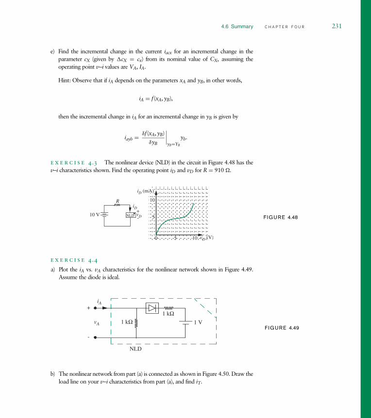
4.6 Summary C H A P T E R F O U R 231
e) Find the incremental change in the current iacx for an incremental change in theparameter cX (given by cX = cx) from its nominal value of CX, assuming theoperating point v i values are VA, IA.
Hint: Observe that if iA depends on the parameters xA and yB, in other words,
iA = f (xA, yB),
then the incremental change in iA for an incremental change in yB is given by
iayb = δf (xA, yB)
δyB
∣∣∣∣yB=YB
yb.
e x e r c i s e 4.3 The nonlinear device (NLD) in the circuit in Figure 4.48 has thev i characteristics shown. Find the operating point iD and vD for R = 910 .
R
10 V+- 5
1010
5 1010 vD (V)
iD (mA)(mA)
0
5
10
5 10 vD (V)
iD (mA)
NLD vD
iD
0
F IGURE 4.48
e x e r c i s e 4.4
a) Plot the iA vs. vA characteristics for the nonlinear network shown in Figure 4.49.Assume the diode is ideal.
vA
NLD
1 kΩ 1 V
1 kΩ+
-
iA
F IGURE 4.49
b) The nonlinear network from part (a) is connected as shown in Figure 4.50. Draw theload line on your v i characteristics from part (a), and find iT.

232 C H A P T E R F O U R a n a l y s i s o f n o n l i n e a r c i r c u i t s
F IGURE 4.50 3.5 V vT
+
-
1 kΩ iT
NLD+-
e x e r c i s e 4.5 Consider two identical semiconductor diodes, each of which hasan v i relation:
iD = IS(
evD/VTH − 1)
. (4.93)
a) Find the relation of i to v for the pair connected in parallel as shown inFigure 4.51a.
(a)
(b)
F IGURE 4.51 b) Find the relation of i to v for the pair connected in series as shown in Figure 4.51b.
e x e r c i s e 4.6 For the circuit in Figure 4.52, find the input characteristic, i versusv, and the transfer characteristic i2 versus v. I is fixed and positive. Express your resultsin graphs, labeling all slopes, intercepts, and coordinates of any break points.
F IGURE 4.52 v R1 I
+
−
i
i2R2
e x e r c i s e 4.7 For the circuit in Figure 4.53 and the values shown below, sketchthe waveform of i(t). On your sketch, show when the ideal diode is on and whenit is off.
vi = 10 sin(t) V0 = 5 V R = 1 .
F IGURE 4.53vi
R
Vo+
-
i+
-

4.6 Summary C H A P T E R F O U R 233
P R O B L E M Sp r o b l e m 4.1 Consider the circuit containing a nonlinear element N as shownin Figure 4.54. The v i relation for N is given by:
iA = c2v 2A + c1vA + c0 for vA ≥ 0, and iA = 0 otherwise.
-
+
R
-
+vA
iA
vI N F IGURE 4.54
a) Solve for iA and vA using the analytical method.
b) Find the operating point values of the nonlinear element’s voltage and current forvI = VI, where VI is positive.
c) Find the incremental change in iA (given by ia) for an incremental change in vI (givenby vi).
d) Determine the incremental change in the voltage across the resistor R foran incremental change in the input vI (given by vi).
e) Find the incremental change in iA for a 2% increase in the value of R.
f) Find the incremental change in iA for an incremental change in vA at the bias pointVA, IA.
g) Suppose we replace the source vI with a DC voltage VI in series with a smalltime-varying voltage vi = vo cos(ωt). Determine the time varying component of iA.
h) Suppose we now replace vI = VI + vi, where VI = 10 V and vi = 1 V.
i) Find the bias point DC current IA corresponding to VI = 10 V.ii) Find the value of ia corresponding to vi = 1 V using small signal analysis.iii) Find the value of iA using small signal analysis. (Use iA = IA + ia.)iv) Find the value of iA using the analytical method for vI = VI + vi = 11 V.
N2N1
i1 i2+
iS
-
v
v (V)1
-1
-1
1
i1(A)
v (V)1
-1
1
i2(A)
2
F IGURE 4.55
v) Now, find the exact value of the ia using ia = iA − IA.vi) What is the error in the value of ia computed using the small signal method?
p r o b l e m 4.2 The circuit shown in Figure 4.55 contains two nonlinear devicesand a current source. The characteristics of the two devices are given. Determine thevoltage, v, for (a) iS = 1 A, (b) iS = 10 A, (c) iS = 1 cos (t).
p r o b l e m 4.3 A plot (hypothetical) of the v i characteristics, (terminal voltageas a function of the current drawn out, and not its associated variables) for a battery isshown in Figure 4.56(a).

234 C H A P T E R F O U R a n a l y s i s o f n o n l i n e a r c i r c u i t s
a) If a 2- resistor is connected across the battery terminals, find the terminal voltageof the battery and the current through the resistor.
b) A lightbulb is a nonlinear resistance because of self-heating effects. A hypotheticalv i plot is shown in Figure 4.56(b). Find the bulb current and bulb voltage if thelamp is connected to the battery.
1 2 3 40
2
1
3
I (A)
1 2 3 40(V)
(V)V
(A)I
(a)
(b)
5
5 V
2
1
F IGURE 4.56
c) Devise a piecewise-linear model for the battery which is reasonably accurate overthe current range 0 2 A.
d) Use this piecewise-linear battery model to find the battery voltage and bulb currentif the bulb and 2- resistor are connected in series to the battery.
p r o b l e m 4.4
a) Assuming the diode can be modeled as an ideal diode, and R1 = R2, plot thewaveform vo(t) for the circuit in Figure 4.57, assuming a triangle wave input. Writean expression for vo(t) in terms of vi, R1, and R2.
vi R2 vo
vi
t
+-
+
-
R1
F IGURE 4.57
b) If the triangle wave has a peak amplitude of only 2 volts, and R1 = R2, a moreaccurate diode model must be used. Plot and write an expression for vo assumingthat the diode is modeled using an ideal diode in series with a 0.6-volt source. Drawthe transfer curve vo versus vi.
p r o b l e m 4.5 Figure 4.58 is an illustration of a crude Zener-diode regulatorcircuit.
∆v
vovZ (V)
+
-
R1 = 1 kΩ
+-
+-
50 mV AC
10 V DCV
-4
-8
8
4-4 -2
2
iZ(mA)
vZ
+
-
iZ
F IGURE 4.58
a) Using incremental analysis, estimate from the graph an analytical expression for vo
in terms of V and v.
b) Calculate the amount of DC and the amount of AC in the output voltage using theZener-diode characteristic to find model values. (Numbers, please.)

4.6 Summary C H A P T E R F O U R 235
c) What is the Thévenin output resistance of the power supply, that is, the Théveninresistance seen looking in at the vo terminals?
p r o b l e m 4.6 The terminal voltage-current characteristic of a single solar cell isshown in Figure 4.59a. Note that this is a sketch of the terminal voltage as a function ofcurrent drawn out (i.e., not the associated variable convention). An array is made by con-necting a total of 100 such cells as follows: Ten solar cells are connected in series. Ten setsof these are made. These ten series strips are then connected in parallel (see Figure 4.59b).
term
inal
vol
tage
of s
ingl
e ce
ll
0.25 V
0.5 V
0.6 V linear region
non-linear region
linear region
0.1 A 0.2 A 0.25 A 0.3 A
V
I
current drawn out
1 2 9 10
1234
910
V
+
-
(a) (b)
F IGURE 4.59
If a 3- resistor is connected across this new two-terminal element (the 100-cell array),determine the terminal voltage across and the current through the resistor.
p r o b l e m 4.7 The junction field-effect transistor ( JFET) with the specific con-nection shown in Figure 4.60a (gate and source shorted together) behaves as a two-terminal device. The vD iD characteristics of the resulting two-terminal device shownin Figure 4.60b saturates at current IDSS for vD greater than a voltage VP, called thepinch-off voltage. In the two-terminal configuration shown, the JFET characteristic is
iD = IDSS
[2(vD/VP) − (vD/VP)2
]for vD ≤ VP
and
iD = IDSS for vD > VP.
As illustrated in Figure 4.60c, this two-terminal device can be used to make awell-behaved DC current source, even starting with a ripple-containing power supply(depicted as vS), as would be obtained from ordinary rectifier circuits. Suppose the voltagesource vS has an average value VS and a 60-Hz ‘‘ripple component,’’ vr = a cos(ωt) asshown in Figure 4.60d.
(a)
iD
vD
+
-
vS+- R
i
(c)
IDSS
vP
iD
vD
(b)
2vP0
VS
vS
t
(d)
0 2πω------
4πω------
a
F IGURE 4.60
a) First assume that there is no ripple (a = 0). Find the current i through the resistorR as a function of VS for a value of R = 1 k. At what value of VS does the

236 C H A P T E R F O U R a n a l y s i s o f n o n l i n e a r c i r c u i t s
current stabilize at IDSS? How would this value change if R were doubled in value?Explain.
b) Now assume a = 0.1 V and R = 1 k. Make reasonable approximations to findthe current waveform when VS = 5 V, VS = 10 V, and VS = 15 V. Determine ineach case the average value of the current i and the magnitude and frequency of thelargest sinusoidal component of the current.
p r o b l e m 4.8 The current-voltage characteristic of a photovoltaic energy con-verter (solar cell) shown in Figure 4.61 can be approximated by
R v Sunlight
+
-
i
F IGURE 4.61
i = I1(e v/VTH − 1) − I2
where the first term characterizes the diode in the dark and I2 is a term thatdepends on light intensity.
Assume I1 = 10−9 and assume light exposure such that I2 = 10−3 A.
a) Plot the v i characteristic of the solar cell. Be sure to note the values of open-circuitvoltage and short-circuit current. (Note, however, that the characteristic is clearlynonlinear. Therefore, Thévenin or Norton equivalents do not apply.)
b) If it is desired to maximize the power that the solar cell can deliver to a resistiveload, determine the optimum value of the resistor. How much power can this celldeliver?
p r o b l e m 4.9
a) A nonlinear device has v i characteristics shown in Figure 4.62. Assuming that Sis an ideal voltage source, which connection, (a), (b), or (c) consumes most power?What if S is an ideal current source?
F IGURE 4.62
A
+
-vA
iAiA
vA = K iA2 for
vA = 0 for iA < 0
vA
A
ASV
I+
-
AS
I
A
(i) n A’s in series (ii) n A’s in parallel
iA 0≥
BS
I
B
(iii) n B’s in parallel, each
V
+
-
V
+
-
B is n A’s in series
B
where K = 1.0 V/A2

4.6 Summary C H A P T E R F O U R 237
b) Another crazy device, C, with v i characteristics as shown in Figure 4.63, is intro-duced. If device A and device C are connected in series across an ideal voltage sourceof 6 volts, what is the current flow in the circuit? (You can solve it either analyticallyor graphically.)
C
+
-
vC
iC
iC (A)
vC (V)
4
2
155 10
F IGURE 4.63
p r o b l e m 4.10 In the circuit in Figure 4.64, assume v1 = 0.5 V andv2 = A2 cos(ωt), where A2 = 0.001 V. Assume further that VTH = 25 mV.
+
-
vv1
v2+-
+-
I1 = 10-9A
i
i I1 e
vV TH---------
1–
=
F IGURE 4.64
a) Find the current i if only the v1 source is connected (i.e., with the v2 source shortedout).
b) Find the current i if only the v2 source is connected.
c) Find the current i if both sources are connected as shown. Is superposition obeyed?Explain.
d) Based on your answer in (c) discuss the dependence of the amplitude of the sinusoidalcomponent of the current on the amplitude A2. How big can A2 be before significantgeneration of harmonics will occur? (HINT: Taylor’s theorem is relevant to thisproblem.)
p r o b l e m 4.11 This problem concerns the circuit illustrated in Figure 4.65:
R1 = 1.0 k R2 = 1.0 k R3 = 0.5 k R4 = 1 k
vI D1
R1
R2 R4
R3
+
-
iD
vD+-
F IGURE 4.65
For D1 : iD = IS(e vD/VTH − 1) with IS = 1 × 10⁻⁹ A and VTH = 25 mV.
a) Find the Thévenin equivalent circuit for the circuit connected to the diode.

238 C H A P T E R F O U R a n a l y s i s o f n o n l i n e a r c i r c u i t s
b) Assume that for bias point determination the diode can be modeled by an idealdiode and a 0.6-volt battery. What are vD and iD when v1 = 4 V?
c) Find a linear equivalent model for this diode valid for small signal incrementaloperation about the bias point determined from part b.
d) Use your model of part c to find vd(t) if vI = 4 V + 0.004 V cos(ωt) V.
p r o b l e m 4.12 Consider the circuit in Figure 4.66. The voltage source and thecurrent source are the sum of a DC-level and an AC-perturbation:
v = V + v
i = I + i
such that V = 30 V (DC), I = 10 A (DC), v = 100 mV (AC), i = 50 mA (AC).
i v0Z0R1
R2
+
-
i0- +
v
F IGURE 4.66
The resistors have the following values: R1 = R2 = 1/2 . The nonlinear element Z0
has the characteristic:
i0 = v0 + v 20 .
Find, by incremental analysis, the DC and AC components of the outputvoltage v0. (Remark: You can assume in your analysis that the nonlinear element isbehaving as a passive element, i.e., is consuming power.)
p r o b l e m 4.13 The circuit shown in Figure 4.67 contains a nonlinear elementwith the following properties:
iN = 10−4v 2N when v N > 0
iN = 0 when v N < 0
where iN is in A and vN is in V.
The output voltage, vOUT, may be written approximately as the sum of the two terms:
vOUT VOUT + vout, (4.94)

4.6 Summary C H A P T E R F O U R 239
vi
+ -iNvN
vOUTVB
+
-+
-
+-
R
F IGURE 4.67
where VOUT is a DC voltage produced by VB and vout is the incremental voltageproduced by the incremental voltage source vi.
Assuming that vi = 10−3 sin(ωt) V and VB is such that the nonlinear element operateswith VN = 10 volts, determine the incremental output voltage vout.
p r o b l e m 4.14 Consider the diode network shown in Figure 4.68.
For purposes of this problem, the iD − vD characteristics of all of the diodes can beaccurately represented as
iD = ISe(vD/25 mV ) where IS = 1 mA/e25.
Do not use a piecewise-linear model.
∆i
+
-1 mA
1 mA -
+ V2 + ∆v2
V1 + ∆v1
F IGURE 4.68
a) First, assume that i = 0. (Thus vi = v2 = 0.) What are the operating-pointvalues of voltages V1 and V2?
b) Now assume that i is nonzero, but small enough so that incremental analysis canbe used to determine v1 and v2. What is the ratio v1/v2 ?


c h a p t e r 5
5.1 V O L T A G E L E V E L S A N D T H E S T A T I C D I S C I P L I N E
5.2 B O O L E A N L O G I C
5.3 C O M B I N A T I O N A L G A T E S
5.4 S T A N D A R D S U M - O F - P R O D U C T S R E P R E S E N T A T I O N
5.5 S I M P L I F Y I N G L O G I C E X P R E S S I O N S
5.6 N U M B E R R E P R E S E N T A T I O N
5.7 S U M M A R Y
E X E R C I S E S
P R O B L E M S
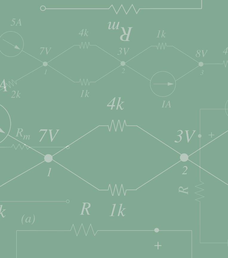

the d ig i t a l ab s tract ion 5Value discretization forms the basis of the digital abstraction. The idea is to lumpsignal values that fall within some interval into a single value. We saw an exampleof value discretization earlier in Figure 1.45 (repeated here for convenienceas Figure 5.1) where a voltage signal was discretized into two levels. In thisexample, an observed voltage value between 0 volts and 2.5 volts is treated asa ‘‘0,’’ and a value between 2.5 volts and 5 volts as a ‘‘1.’’ Correspondingly, totransmit the logical value ‘‘0’’ over a wire, we place the nominal voltage levelof 1.25 on the wire. Similarly, to transmit the logical ‘‘1,’’ we place the nominalvoltage level of 3.75 volts on the wire.1 The discrete signal shown in Figure 5.1comprises the sequence of values ‘‘0,’’ ‘‘1,’’ ‘‘0,’’ ‘‘1,’’ ‘‘0.’’
Although the digital approach seems wasteful of signal dynamic range, ithas a significant advantage over analog transmission in the presence of noise.Notice, this representation is immune to symmetric noise with a peak to peakvalue less than 2.5 V. To illustrate, consider the situation depicted in Figure 5.2in which a sender desires to transmit a value A to a receiver. The figure illustratesboth an analog case and a digital case. In the analog case, let us suppose thatthe value A is 2.4 V. The sender transmits A by representing it as a voltagelevel of 2.4 V on a wire. Noise during transmission (represented as a 0.2-V
2.5
0
2.5
0
“0”
“1”v(V)
t
Continuous
t
Discrete
v(V)
F IGURE 5.1 Value discretizationinto two levels.
noise voltage source in the figure) changes this voltage to 2.6 V at the receiver,resulting in the receiver interpreting the value incorrectly as 2.6.
In the digital case, suppose that the value A is a logical ‘‘0.’’ The sendertransmits this value of A by representing it as a voltage level of 1.25 V onthe wire, which is received as a voltage level of 1.45 by the receiver becauseof the series noise source. In this situation, since the received voltage fallsbelow the 2.5-V threshold, the receiver interprets it correctly as a logical ‘‘0.’’Thus, the sender and receiver were able to communicate without error in thedigital case.
To illustrate further, consider the waveforms in Figure 5.3. Figure 5.3ashows a discretized signal waveform produced by a sender corresponding to
1. It turns out that the mapping of voltage ranges to logical values has a significant impact on therobustness of digital circuits, and a methodical way of selecting the mapping will be presented inSection 5.1. But for now, let us proceed with this rather arbitrarily chosen mapping, and continueto build our intuition.
243

244 C H A P T E R F I V E t h e d i g i t a l a b s t r a c t i o n
F IGURE 5.2 Signal transmissionin the presence of noise. The noiseis represented as a series voltagesource.
Analog
Digital
vIN
vINvOUT
SenderA = 2.4
SenderA = “0”
ReceiverA = “0”
ReceiverA = 2.6
Noise 0.2 V
Noise 0.2 V
vOUT = 2.4 V
vOUT
vOUT = 1.25 V vIN = 1.45 V
vIN = 2.6 V
- +
- +
+-
+-
+-
+-
a ‘‘0,’’ ‘‘1,’’ ‘‘0,’’ ‘‘1,’’ ‘‘0’’ sequence. Figure 5.3b shows the same signal with thesuperposition of some amount of noise, possibly during transmission througha noisy environment. The receiver will be able to receive the sequence correctlyprovided the noise levels in Figure 5.3b are small enough that the voltages
(a)
(b)
2.5
0
“0”
“1”v(V)
t
2.5
0
“0”
“1”v(V)
t
F IGURE 5.3 Noise immunity fordiscretized signals: (a) a digitalsignal produced by a sender; (b)the signal received by a receiverfollowing transmission through anoisy environment.
for a logical 0 signal do not exceed 2.5 V, and the voltages for a logical 1 signaldo not fall below 2.5 V. Specifically, notice that the binary mapping we havechosen is immune to symmetric noise with a peak-to-peak value less than 2.5 V.
Of course, the discrete representation does not come for free. Consideringour example in Figure 5.1, in the analog case, a single wire could carry anyvalue, for example, 1.1, 2.9, or 0.9999999 V. However, in the digital case,a wire is restricted to one of only two values: ‘‘0’’ and ‘‘1,’’ thereby losingprecision significantly.
Two levels of signal precision are sufficient for many applications. Asone example, logic computations involve signals that commonly take on oneof two values: TRUE or FALSE. Indeed, most of this chapter (specifically,Sections 5.2, 5.3, and 5.5) deals exclusively with signals that can take on oneof two values. Each of these two-level signals is communicated over a singlewire. However, there are other applications that require more levels of preci-sion. For example, a speech signal processing application might involve speechsignals with 256 or more levels of precision. One approach to achieving moreprecision is to use coding to create multi-digit numbers. When each digit takeson one of two values, the digit is called a binary digit, or bit. Much as thefamiliar decimal system uses multiple digits to represent numbers other than0 through 9, the binary system uses multiple bits to represent numbers otherthan 0 or 1. Multi-bit signals are commonly transmitted by allocating multiplewires one for each bit, or occasionally, by time multiplexing multiple bitson a single wire. This approach of representing numbers in the binary systemis discussed further in Section 5.6. For now, we return to our discussion of thetwo-level representation.
The two-level representation is commonly known as the binary representa-tion. Virtually all digital circuits use the binary representation because two-level

5.1 Voltage Levels and the Static Discipline C H A P T E R F I V E 245
t r u e f a l s e
0 V 5 V
5 V 0 V
2 V 0 V
0 V 1 V
ON OFF
0 V < v < 2.5 V 2.5 V < v < 5 V
0 V < v < 1 V 4 V < v < 5 V
0 µA 2 µA
TABLE 5.1 Binary signalrepresentation. v represents thevalue of some parameter.
circuits are much easier to build than multilevel circuits. The two levels in thebinary representation are variously called (a) TRUE or FALSE, (b) ON or OFF,(c) 1 or 0, (d) HIGH or LOW.
Digital signals are commonly implemented using voltage levels, for exam-ple, 0 V to represent FALSE, and 5 V to represent TRUE. We observe, however,that our choice of representing logical values with specific physical values (forexample, representing a logical TRUE with 5 V and a logical FALSE with 0 V)is rather arbitrary. We can equivalently choose to represent a logical TRUE with0 V and a logical FALSE with 5 V. Unless specifically mentioned otherwise, thisbook adopts the convention that TRUE and high correspond to the logical 1,and conversely, FALSE and low correspond to the logical 0. Table 5.1 depictsthese and several other physical realizations of the binary signals, TRUE andFALSE.
5.1 V O L T A G E L E V E L S A N D T H ES T A T I C D I S C I P L I N E
The previous section illustrated several ways to represent binary values. Therepresentations differed not only in the signal type (for example, current versusvoltage), but also in the signal values (for example, 5 V versus 4 V to represent alogical 1). Because we require that digital devices built by various manufacturerstalk to each other, the devices must adhere to a common representation. Therepresentation must allow for large enough design margins so that devices canbe built out of a wide range of technologies. Furthermore, the representationshould be such that the devices operate correctly even in the presence of someamount of noise.
The static discipline is a specification for digital devices. The static disci-pline requires devices to adhere to a common representation, and to guaranteethat they interpret correctly inputs that are valid logical signals according to thecommon representation, and to produce outputs that are valid logical signals

246 C H A P T E R F I V E t h e d i g i t a l a b s t r a c t i o n
F IGURE 5.4 Senders andreceivers use an agreed-uponmapping between voltage levelsand logical signals so that they cancommunicate with each other.
Valid1
Valid0
0 V
5 V
2.5 VSender Receiver
“1”
“0” “0”
“1”
provided they receive valid logical inputs. By adhering to a common repre-sentation, digital devices based on different technologies or built by differentmanufacturers can communicate with each other.
We will begin with a simple representation, and then successively improveit until we have a representation that can serve as the basis for a static discipline.One of the representations we saw earlier divided a voltage range into twointervals and associated a logic value with each, namely,
Logic 0 : 0.0 V ≤ V < 2.5 V. (5.1)
Logic 1 : 2.5 V ≤ V ≤ 5.0 V. (5.2)
This simple representation is illustrated in Figure 5.4. According to this repre-sentation, if a receiver saw 2 V on a wire it would interpret it as a 0. Similarly,a receiver would interpret 4 V on a wire as a 1. Assume, for now, that valuesoutside this range are invalid.
What voltage level should a sender place on a wire? According to ourrepresentation, any value between 0 V and 2.5 V would suffice for a logical 0,and any value between 2.5 V and 5 V would work for a logical 1.
Devices that obey this representation would be able to communicate witheach other successfully. In other words, as depicted in Figure 5.4, a sendingdevice connected to a receiving device is allowed to output any value between0 V and 2.5 V (for example, 0.5 V) for a logical 0, and any value between 2.5 Vand 5 V (for example, 4 V) for a logical 1. Correspondingly, the receiving devicemust interpret all values between 0 V and 2.5 V as a logical 0, and all valuesbetween 2.5 V and 5 V as a logical 1. Thus, our simple representation allowsa fair bit of flexibility because valid logical 1 signals and logical 0 signals canoccupy a range of values.

5.1 Voltage Levels and the Static Discipline C H A P T E R F I V E 247
Valid1
Valid0
0 V
5 V
Sender Receiver
“1”
“0” “0”
“1”
VH
VL
Forbiddenregion
F IGURE 5.5 A representationwith forbidden regions showing themapping of voltage levels andlogical values.
There is one problem, however. What does the receiver do if it sees avoltage level of 2.5 V on the wire? Does it interpret this signal value as a logical0 or as a logical 1? To eliminate such confusion, we further prescribe a forbiddenregion that separates the two valid regions. We further allow the behavior ofthe receiving device to be undefined if it sees a voltage in the forbidden region.Thus, the correspondence between voltage levels and logic signals from theviewpoint of a receiver might look like:
Logic 0 : 0 V ≤ V ≤ 2 V. (5.3)
Logic 1 : 3 V ≤ V ≤ 5 V. (5.4)
This representation using a forbidden region is illustrated in Figure 5.5. In thisrepresentation, a receiver interprets signals above 3 V as a logical 1 and voltagesbelow 2 V as a logical 0. Signal voltages between 2 V and 3 V are invalid.
As marked in Figure 5.5, the largest voltage that a receiver will interpretas a valid logical 0 is termed the low voltage threshold, VL, and the smallestvoltage that a receiver will interpret as a valid logical 1 is termed the highvoltage threshold, VH.
In our representation with the forbidden region, a sender can output anyvoltage value between VH and 5 V for a logical 1, and any value between 0 Vand VL for a logical 0. A sender must never output a value in the forbiddenregion. Correspondingly, as illustrated in Figure 5.5, a receiver must interpretany voltage value between VH and 5 V as a logical 1, and any value between0 V and VL as a logical 0. The behavior of the receiver can be undefined if it seesa voltage value between VL and VH because these values are in the forbiddenregion.

248 C H A P T E R F I V E t h e d i g i t a l a b s t r a c t i o n
F IGURE 5.6 For many practicaldevices, a sender can output anyvoltage value above VH for alogical 1, and any voltage valuebelow VL for a logical 0.
Valid1
Valid0
0 V
5 V
Sender Receiver
“1”
“0” “0”
“1”
VH
VL
Forbiddenregion
It often turns out that practical circuits are able to correctly interpret valuesoutside the extremum points (below 0 volts for a logical 0 and above 5 Vfor a logical 1), within certain limits, of course. When devices can make thisinterpretation, our representation with the forbidden region allows senders tooutput any voltage value above VH for a logical 1. Similarly, senders can outputany value below VL for a logical 0. We will assume throughout this book thatdevices can make this interpretation safely. Figure 5.6 illustrates a simple andpractical representation that uses this assumption.
There is one other problem with our representations illustrated inFigures 5.6 and 5.5: They do not offer any immunity to noise. To illustrate,consider our representation in Figure 5.5 with a high and low voltage thresh-old bounding a forbidden region. In that representation, recall that senders canoutput voltages above VH and below 5 V for logical 1’s and voltages below VLand above 0 V for logical 0’s. Receivers must correspondingly interpret outputvoltages above VH as logical 1’s and voltages below VL as logical 0’s.
A sender wishing to place a logical 0 on a wire can therefore output thevoltage VL, which falls within the valid range for a logical 0. Receivers observingthe value VL transmitted on the wire will correctly interpret it as a logical 0.However, the presence of even the smallest amount of (positive) noise will forcethe voltage signal on the wire into the forbidden region, thereby causing thesignal to become invalid. Thus, we say that the representation of Figure 5.5offers no margin for noise.
Clearly we would like a representation that offers the maximum amount ofnoise immunity during transmission between the sender and the receiver. Oneway of achieving this is to place tighter restrictions on the values that senderscan send. As an example, suppose that a receiver can interpret voltages that fall

5.1 Voltage Levels and the Static Discipline C H A P T E R F I V E 249
CorrectreceptionvINvOUT
SenderA = 0
ReceiverA = 0
Noise 0.6 V
vOUT = 0.5 V vIN = 1.1 V (< 2 V)
IncorrectreceptionvINvOUT
SenderA = 0
ReceiverA = ?
Noise 1.6 V
vOUT = 0.5 V vIN = 2.1 V (> 2 V)
- +
- +
F IGURE 5.7 Noise margins andsignal transmission.
below 2 V as a logical 0. Further, suppose that senders are restricted to sendingvoltages lower than 0.5 V for a logical 0. Then, it takes at least 1.5 V of (positive)noise to force the sender’s voltage signal on the wire into the forbidden region.We say that such a choice of voltage levels offers a noise immunity of 1.5 V fora logical 0.2
As an illustration of the notion of noise margins, consider the two sit-uations in Figure 5.7.3 In the first instance, the sender sends a 0 by placingvOUT = 0.5 V (corresponding to the highest legal output voltage for a logic 0)on the wire. The receiver is able to interpret the value as a 0 because thereceived value is within the low input voltage threshold of 2 V.
In the second situation, however, the receiver is unable to interpret thesignal correctly because the noise level of 1.6 V is higher than the noise marginof 1.5 V.
As another example concerning logical 1’s, suppose that a receiver caninterpret voltages that are above 3 V as a logical 1. Further, suppose thatsenders are restricted to sending voltages higher than 4.5 V for a logical 1.Then, it takes at least 1.5 V of noise to force the sender’s voltage signal on thewire into the forbidden region. We say that such a choice of voltage levels offersa noise immunity of 1.5 volts for a logical 1.
2. As mentioned earlier, because most practical receiver circuits are able to correctly interpret valuesoutside the extremum points (below 0 volts for a logical 0 and above 5 volts for a logical 1), weconcern ourselves with providing for a noise margin only between the output value range and theforbidden region, and ignore the effect of noise that tends to push a value outside the extremumbounds.
3. Notice that the signal voltages in the figure are taken with respect to a ground node that iscommon to both the sender and the receiver. This ground node that is common to senders andreceivers is often not shown explicitly, but it is always present! Many a novice designer has forgottento connect together a common ground between subsystems and has found that the system doesnot work. Remember, currents flow in loops and the ground connection provides a return path forthe current.

250 C H A P T E R F I V E t h e d i g i t a l a b s t r a c t i o n
F IGURE 5.8 A mappingbetween voltage levels and logicalsignals that provides noisemargins. For a logical high, sendersmust output values in the VOH to5-V range. For a logical low,senders must output values in the0 V to VOL range. Receivers mustcorrespondingly interpret valuesgreater than VIH as a logical high,and output values lower than VIL asa logical low.
Valid1
Valid0
0 V
5 V
Sender Receiver
“1”
“0” “0”
“1”
VIH
VIL
Forbiddenregion
VOH
VOL
1Noise
margin
0Noise
margin
The tighter bounds on the voltage values for a sender compared to thosefor a receiver result in an asymmetry in input and output voltage thresholds.This asymmetry is reflected in Figure 5.8, which shows the correspondencebetween valid voltage levels and logic signals that is in common use in digitalcircuits.
To send a logical 0, the sender must produce an output voltage value thatis less than VOL. Correspondingly, the receiver must interpret input voltagesbelow VIL as a logical 0.
To allow for a reasonable noise margin, VIL must be greater than VOL.
Similarly, to send a logical 1, the sender must produce an output voltage valuethat is greater than VOH. Further, the receiver must interpret voltages aboveVIH as a logical 1.
To allow for a reasonable noise margin, VOH must greater than VIH.4 Wecan define both a noise margin for transmitting logical 1’s and for transmittinglogical 0’s.
Noise Margin: The absolute value of the difference between the prescribedoutput voltage for a given logical value and the corresponding forbidden regionvoltage threshold for the receiver is called the noise margin for that logicalvalue.
4. The simple representation in Figure 5.5 can be viewed as one in which VOH = VIH = VH andVOL = VIL = VL. Notice that the simple representation of Figure 5.5 offers zero noise margins.

5.1 Voltage Levels and the Static Discipline C H A P T E R F I V E 251
As the name suggests, the noise margin allows the receiver to interpret avalue correctly even if some amount of noise is imposed on a sender’s signal.Figure 5.9a illustrates a scenario in which a sender outputs a 01010 sequenceby producing the appropriate output voltage levels (between VOH and 5 V fora logical 1, and between 0 V and VOL for a logical 0). Provided that the noise
“0”
0
VOL
VIL
VIH
VOH
“0” “1”V
t
(a)
“0” “1”
“0”
0
VOL
VIL
VIH
VOH
“0” “1”V
t
(b)
“0” “1”
Sender
Receiver
F IGURE 5.9 Senders mustoutput voltages between VOHand 5 V to send a logical 1, andbetween 0 V and VOL for alogical 0. Correspondingly,receivers can interpret valuesgreater than VIH as a logical high,and values lower than VIL as alogical low. The hashed regions arethe valid ranges for senders andreceivers.
does not exceed the noise margins (voltages for a logical 0 do not exceed VILand voltages for a logical 1 do not fall below VIH), a receiver is able to correctlyinterpret the signal as illustrated in Figure 5.9b.
As illustrated in Figure 5.8, the noise margin for a logical 0 is given by
NM0 = VIL − VOL (5.5)
and the noise margin for a logical 1 is given by
NM1 = VOH − VIH. (5.6)
The region between VIL and VIH is the forbidden region.Devices that adhere to this discipline will be able to communicate with
each other and be immune to noise levels that fall within the noise margins.When NM1 and NM0 are equal, we say that the noise margins are symmetric.
Relating the threshold voltage parameters to the numbers used in ourexample, VOH corresponds to 4.5 V, VOL corresponds to 0.5 V, VIH corre-sponds to 3 V, and VIL corresponds to 2 V. This mapping is illustrated inFigure 5.10. For our example, the noise margin for a logical 0, NM0, is 1.5 V(2 V − 0.5 V), which is the difference between VIL, the maximum input voltagerecognized by a receiver as a logic 0, and VOL, the highest legal output voltagefor a logic 0. Similarly, the noise margin for a 1, NM1, is also 1.5 V (4.5 V −3 V), which is the difference between VOH, the minimum legal output voltagefor a logic 1, and VIH, the minimum input voltage recognized by a receiver asa logic 1.
Valid1
Valid0
0 V
5 V
Sender Receiver
“1”
“0” “0”
“1”
VIH
VIL
Forbiddenregion
VOH
VOL
1Noisemargin
0Noisemargin
0 V
5 V
3 V
2 V
4.5 V
0.5 V
F IGURE 5.10 An example of amapping between voltage levelsand logical values.

252 C H A P T E R F I V E t h e d i g i t a l a b s t r a c t i o n
Static discipline The static discipline is a specification for digital devices. Thestatic discipline requires devices to interpret correctly voltages that fall withinthe input thresholds (VIL and VIH). As long as valid inputs are provided to thedevices, the discipline also requires the devices to produce valid output voltagesthat satisfy the output thresholds (VOL and VOH).
When designing logic devices, we are often interested in maximizing thenoise margins to achieve maximum noise immunity. Referring to Figure 5.8,the 0 noise margin, NM0 = VIL − VOL, can be maximized by maximizingVIL and minimizing VOL. Similarly, the 1 noise margin, NM1 = VOH − VIH,can be maximized by maximizing VOH and minimizing VIH. As we will see inChapter 6, the maximum noise margins for devices are limited by the devicecharacteristics or by considerations of symmetry between the low and highnoise margins.
e x a m p l e 5.1 o b s e r v i n g a s t a t i c d i s c i p l i n e The devicecompany Yehaa Microelectronics, Inc. has developed a new process technology that isable to produce large quantities of a certain type of digital device known as an adder ata very low cost. For a logical 0, their adders produce a voltage level of 0.5 V at theiroutputs. Similarly, when outputting a logical 1, their adders produce the voltage level of4.5 V. Furthermore, the Yehaa adders are able to interpret all signals between 0 V and2 V at their inputs as a logical 0, and all signals between 3 V and 5 V as a logical 1.
Yehaa’s sales team discovers that networking equipment company Disco Systems Inc.buys huge quantities of adder devices from a competitor Yikes Devices, Inc. Upon furtherresearch, the Yehaa sales team finds that the hardware systems in one of Disco’s productlines operate under a static discipline with the following voltage thresholds:
VIL = 2 V, VIH = 3.5 V, VOL = 1.5 V and VOH = 4 V.
In other words, the mapping between voltage ranges and logical values in Disco’s staticdiscipline is as summarized in Figure 5.11.
F IGURE 5.11 The mappingbetween voltage levels and logicvalues in the static discipline usedby Disco Systems.
Valid1
Valid0
0 V
5 V
Sender Receiver
“1”
“0” “0”
“1”
Forbiddenregion
1Noisemargin
0Noisemargin
0 V
5 V
3.5 V
2 V
4 V
1.5 V
VOH
VIH
VIL
VOL

5.1 Voltage Levels and the Static Discipline C H A P T E R F I V E 253
Valid1
Valid0
0 V
5 V
Sender Receiver
“1”
“0” “0”
“1”
Forbiddenregion
1Noisemargin
0Noisemargin
0 V
5 V
3.5 V
2 V
4 V
1.5 V
VOH
VIH
VIL
VOL
4.5 V
0.5 V
2 V
3 V F IGURE 5.12 Comparing thevoltages produced by Yehaaagainst the voltage levels requiredby the static discipline used byDisco Systems.
Yehaa’s sales team wishes to sell their adders to Disco at a lower cost than those fromYikes, but first, Yehaa must determine whether their adders can safely replace the addersfrom Yikes. The sales team asks their development engineers to determine whetherYehaa’s adders satisfy the static discipline under which Disco’s system operates.
The development team first looks at the output level for a logical 1 required by Disco’sstatic discipline. The static discipline used by Disco requires devices to produce voltagesbetween 4 V (VOH) and 5 V for a logical 1. As illustrated in Figure 5.12, Yehaa’s devicesproduce a voltage level of 4.5 V for a logical 1, which falls within the required range,and so they satisfy the VOH requirement.
Next, they look at the output voltage level for a logical 0. As depicted in Figure 5.12,Yehaa’s devices produce a voltage level of 0.5 V for a logical 0, which falls within the0 V to 1.5 V (VOL) range required for logical 0’s by Disco’s static discipline. Thus,Yehaa’s devices satisfy the VOL requirement.
The engineers now turn their attention to the input voltage levels required by Disco’sstatic discipline. Yehaa’s devices are able to interpret voltages as high as 2 V as a logical 0,so they can interpret any voltage between 0 V and 2 V (VIL) as a logical 0, just as requiredby Disco’s static discipline. Thus, the Yehaa devices satisfy the VIL requirement.
Similarly, Yehaa’s devices are able to interpret voltages between 3.5 V (VIH) and 5 V asa logical 1, which again satisfies the VIH requirement of Disco’s static discipline. The factthat the Yehaa devices interpret certain voltages in Disco’s forbidden region (specifically,those between 3 V and 3.5 V) as a logical 1 is irrelevant since devices are allowed arbitrarybehavior for values in the forbidden region.
Thus, the development engineers are able to tell their sales team that Yehaa’s adderssatisfy Disco’s static discipline and so they can be used as replacements for Disco’sexisting adders.

254 C H A P T E R F I V E t h e d i g i t a l a b s t r a c t i o n
e x a m p l e 5.2 v i o l a t i n g a s t a t i c d i s c i p l i n e Yikes dis-covers that Disco is considering switching to Yehaa adders because Yehaa’s devices arecheaper than Yikes devices. The Yikes sales team goes over their own product list andnotices that they do carry a new adder that they can sell to Disco at an even lower costthan the Yehaa adders. Overjoyed, the sales team asks their own development engineersto check whether these new adders satisfy Disco’s static discipline.
The new adders of Yikes have the following properties: For a logical 0, the new addersproduce a voltage level of 1.7 V at their outputs. Similarly, when outputting a logical 1,their adders produce the voltage level of 4.5 V. The new Yikes adders interpret allsignals between 0 V and 1.5 V at their inputs as a logical 0, and all signals between 4 Vand 5 V as a logical 1. Their behavior for input signals in the 1.5 V to 4 V range isundefined.
Furthermore, recall that Disco’s systems operate under a static discipline with thefollowing voltage thresholds: VIL = 2 V, VIH = 3.5 V, VOL = 1.5 V, and VOH = 4 V.
The Yikes development team first looks at the output voltage levels required by Disco’sstatic discipline. They observe that the 4.5-V output produced by their new adders fallswithin Disco’s legitimate range for a logical 1 (between VOH = 4 V and 5 V), thussatisfying the VOH requirement.
Next, they turn their attention to the output voltage level required for a logical 0. Totheir disappointment, they discover that the 1.7-V output produced by their new addersfor a logical 0 output is greater than the maximum value of VOL = 1.5 V allowed byDisco. Thus their new adders violate the VOL requirement. At this point, the Yikesdevelopment team reluctantly concludes that their new adders cannot be sold to Disco.
As an exercise in futility, the development engineers further investigate the input voltagelevels. Disco’s static discipline requires that devices interpret any voltage between 0 Vand 2 V (VIL) as a logical 0. The new adders from Yikes fail this test because they areunable to interpret signals above 1.5 V as a logical 0.
Next, the engineers investigate the input high voltage level, but quickly discover that thesituation is even worse. Disco’s systems require that all devices interpret voltages in therange 3.5 V (VIH) to 5 V as a logical 1. Unfortunately, their new adders can guaranteeto interpret voltages only in the range 4 V to 5 V as a logical 1. Their behavior for inputvoltages in the range 3.5 V to 4 V is undefined. Since Disco’s devices can legitimatelyproduce voltages in this range for a logical 1, the new Yikes adders cannot co-exist withthe existing Disco devices.
e x a m p l e 5.3 n o i s e m a r g i n s Recall that the hardware systems inone of Disco’s product lines operate under a static discipline with the following voltagethresholds: VIL = 2 V, VIH = 3.5 V, VOL = 1.5 V, and VOH = 4 V. Compute thenoise margins.

5.1 Voltage Levels and the Static Discipline C H A P T E R F I V E 255
From Equation 5.5, the noise margin for a logical 0 is given by
NM0 = VIL − VOL = 2 V − 1.5 V = 0.5 V.
Similarly, from Equation 5.6, the noise margin for a logical 1 is given by
NM1 = VOH − VIH = 4 V − 3.5 V = 0.5 V.
e x a m p l e 5.4 a s t a t i c d i s c i p l i n e w i t h i m p r o v e d
n o i s e m a r g i n s Disco Systems Inc. has been having intermittent faults in itssystems. Their system architects figure out that because the static discipline they haveadopted does not provide a sufficient noise margin, their systems are susceptible tonoise. To improve the noise immunity of their systems, they decide to upgrade theirsystems to a new static discipline in which the output high voltage threshold is increasedby 0.5 V, and the output low voltage threshold is decreased by 0.5 V. Both the inputvoltage thresholds remain unchanged. In other words, the improved static discipline hasthe following voltage thresholds:
VIL = 2 V, VIH = 3.5 V, VOL = 1 V, and VOH = 4.5 V.
This choice affords their system a symmetric noise margin of 1 V. In other words, thenoise margins for a logical 0 and a logical 1 are equal and are given by
NM0 = 2 V − 1 V = 1 V
and
NM1 = 4.5 V − 3.5 V = 1 V
On hearing the upgrade announcement from Disco, the sales team of Yehaa claims thatthe adders they have sold Disco can be used under the upgraded static discipline. Let usdetermine whether this claim is true.
Recall, that Yehaa’s adders behave as follows: For a logical 0, Yehaa’s adders producea voltage level of 0.5 V at their outputs. Similarly, when outputting a logical 1, theiradders produce the voltage level of 4.5 V. Yehaa adders are able to interpret all signalsbetween 0 V and 2 V at their inputs as a logical 0, and all signals between 3 V and 5 Vas a logical 1.
To operate under Disco’s upgraded static discipline, we know that the adders mustoperate correctly with the tighter bounds on the output thresholds:
When outputting a logical 1, the voltage their outputs produce must be at leastVOH = 4.5 V. Since the Yehaa adders produce a 4.5 V output for a logical 1, theybarely satisfy this condition.

256 C H A P T E R F I V E t h e d i g i t a l a b s t r a c t i o n
When outputting a logical 0, the voltage their outputs produce must be no greaterthan VOL = 1 V. Since the Yehaa adders produce a 0.5-V output for a logical 0,they satisfy this condition easily.
Thus, we have shown that the claim made by the Yehaa sales team is true.
e x a m p l e 5.5 c o m p a r i n g n o i s e m a r g i n s Which of the twostatic disciplines shown below offers better noise margins?
Static discipline A has the voltage thresholds given by:
VIL = 1.5 V, VIH = 3.5 V, VOL = 1 V, and VOH = 4 V.
Static discipline B has the voltage thresholds given by:
VIL = 1.5 V, VIH = 3.5 V, VOL = 0.5 V, and VOH = 4.5 V.
For static discipline A:
NM0 = 1.5 V − 1 V = 0.5 V
and
NM1 = 4 V − 3.5 V = 0.5 V.
For static discipline B:
NM0 = 1.5 V − 0.5 V = 1 V
and
NM1 = 4.5 V − 3.5 V = 1 V.
Thus, the voltage thresholds of static discipline B offer a better noise margin.
5.2 B O O L E A N L O G I C
The binary representation has a natural correspondence to logic, and thereforedigital circuits are commonly used to implement logic procedures. For example,consider the logical ‘‘if’’ statement:
If X is TRUE AND Y is TRUE then Z is TRUE else Z is FALSE.
We can represent this statement using a boolean equation as:
Z = X AND Y.
In the previous equation, Z is true only when both X and Y are TRUEand FALSE otherwise. For brevity we often represent the AND function using

5.2 Boolean Logic C H A P T E R F I V E 257
the ‘‘·’’ symbol as:
Z = X · Y.
Just as we represent the algebraic expression x × y as xy, we often drop
o p e r a t o r s y m b o l
AND ·OR +
NOT ∼
TABLE 5.2 Some logicoperations and their symbols.
the AND symbol and write:
Z = X · Y = XY.
The boolean equation for the statement:
x y z
0 0 00 1 01 0 01 1 1
TABLE 5.3 Truth table forZ = X · Y.
If (A is TRUE) OR (B is NOT TRUE) then (C is TRUE) else (C is FALSE)
is
C = A + B.
x y z
0 0 00 1 11 0 11 1 1
TABLE 5.4 Truth table forZ = X + Y.
The preceding equation contains two other useful functions. The OR func-tion is represented using ‘‘+’’ and the NOT function using the bar symbol as in‘‘X ’’ or the ∼ symbol as in ∼ X. For example, we represent the condition ‘‘Bis FALSE’’ as B or ∼ B. We call B the complement of B. The logic operatorsthat we have seen thus far are summarized in Table 5.2. For convenience, wewill use 1, TRUE, and high interchangeably. Similarly, we will use 0, FALSE,and low interchangeably.
e x a m p l e 5.6 m o t i o n d e t e c t o r l o g i c Let us write theboolean expression for a motion detector that operates as follows: The circuit must
x z
0 11 0
TABLE 5.5 Truth table for Z =X.
produce a signal L to turn on a set of lights when the signal M from a motion sensor ishigh, provided it is not daytime. Assume that a light sensor produces a signal D that ishigh during daytime.5
a b c
0 0 10 1 01 0 11 1 1
TABLE 5.6 Truth table forC = A + B.
Notice that L is nominally low. It must become high when M is high and D is low.Therefore, we can write
L = MD.
Truth table We often find it convenient to use a truth table representa-tion of boolean functions. A truth table enumerates all possible input valuecombinations and the corresponding output values.
For example, the truth table representation for Z = X · Y is shown inTable 5.3, that for Z = X + Y is shown in Table 5.4, that for Z = X is shownin Table 5.5, and that for C = A + B is shown in Table 5.6. As discussed
5. Assume, of course, that the light sensor does not respond to the lights that are turned on by themotion detector.
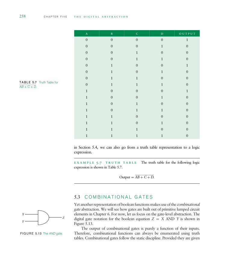
258 C H A P T E R F I V E t h e d i g i t a l a b s t r a c t i o n
a b c d o u t p u t
0 0 0 0 1
0 0 0 1 0
0 0 1 0 0
0 0 1 1 0
0 1 0 0 1
0 1 0 1 0
0 1 1 0 0
0 1 1 1 0
1 0 0 0 1
1 0 0 1 0
1 0 1 0 0
1 0 1 1 0
1 1 0 0 0
1 1 0 1 0
1 1 1 0 0
1 1 1 1 0
TABLE 5.7 Truth Table forAB + C + D.
in Section 5.4, we can also go from a truth table representation to a logicexpression.
e x a m p l e 5.7 t r u t h t a b l e The truth table for the following logicexpression is shown in Table 5.7.
Output = AB + C + D.
5.3 C O M B I N A T I O N A L G A T E S
Yet another representation of boolean functions makes use of the combinationalgate abstraction. We will see how gates are built out of primitive lumped circuitelements in Chapter 6. For now, let us focus on the gate-level abstraction. Thedigital gate notation for the boolean equation Z = X AND Y is shown inFigure 5.13.
ZX
Y
F IGURE 5.13 The AND gate.
The output of combinational gates is purely a function of their inputs.Therefore, combinational functions can always be enumerated using truthtables. Combinational gates follow the static discipline. Provided they are given

5.3 Combinational Gates C H A P T E R F I V E 259
inputs that fall within valid input levels, they will produce outputs that satisfyvalid output thresholds.
Combinational gate abstraction A combinational gate is an abstract represen-tation of a circuit that satisfies two properties:1. Its outputs are a function of its inputs alone.
2. It satisfies the static discipline.
Figure 5.14 shows several useful gate symbols. We have already seen thegate-level representation of the AND function. The OR gate performs theOR function of its inputs. The NOT gate takes the complement of its input.For convenience, we often denote the NOT function in logic circuits usingthe ‘‘’’ symbol. The buffer gate or identity gate simply copies the input valueto its output, that is, A = A. Its use will become apparent in Section 6.9.2.The NAND function is equivalent to the AND operation followed by the NOToperation. For example, A = B NAND C is equivalent to A = B AND C. It isalso equivalent to the statement: A is FALSE only if both B and C are TRUE.Similarly, the NOR operation is equivalent to the OR operation followed bythe NOT operation.
OR
AND
NOT
NAND
NOR
BUFFER
F IGURE 5.14 Gate symbols.
A truth table illustrating several of these functions is shown in Table 5.8.Each output column in the truth table corresponds to the given booleanfunction.
Gates can have multiple inputs. For example, we can have a four-input ANDgate that implements the function E = A · B · C · D as shown in Figure 5.15.
As shown in Figure 5.16, we can combine digital gates using wiresto implement digital circuits, thereby creating more complicated booleanfunctions.
Figure 5.17 shows a graphical view of the inputs and output for the digitalcircuit in Figure 5.16. Notice that the output continues to be valid even whenthe input signal is noisy.
As we might expect, gates are themselves implemented using lumped cir-cuit elements, such as resistors and current sources. In other words, a gaterepresenting the function F is simply an abstraction for a circuit that performsthe function F. The circuit for an AND gate produces 5 V at its output when
i n p u t s a n d o r n a n d n o r
B C B · C B + C B · C B + C
0 0 0 0 1 1
0 1 0 1 1 0
1 0 0 1 1 0
1 1 1 1 0 0
TABLE 5.8 Truth table forseveral two-input functions.

260 C H A P T E R F I V E t h e d i g i t a l a b s t r a c t i o n
both its inputs are at 5 V, and produces 0 V otherwise. We will defer the actualimplementation of digital gates to later chapters, and for now, use the con-venient gate abstraction to build more complicated digital systems to processinformation.
Four-Input AND
F IGURE 5.15 A four-input ANDgate.
A
BC
F IGURE 5.16 The gate-leveldigital circuit for C = A + B.
e x a m p l e 5.8 g a t e - l e v e l i m p l e m e n t a t i o n Let us imple-ment the logic expression Output = AB + C + D using gates. Notice that we have achoice in implementing this expression. We can use one two-input AND gate, a three-input OR gate, and an inverter as shown in Figure 5.18. We can also replace the ORgate-inverter pair with a NOR gate. Alternatively, by rewriting the expression as
Output = ((AB) + (C + D))
we can implement the same circuit using an AND gate, an OR gate, and a NOR gate.We can also check each of the circuits against the truth table, and convince ourselvesthat they do work as desired.
e x a m p l e 5.9 m o r e g a t e - l e v e l i m p l e m e n t a t i o n s
Now, let us design a circuit for the expression: (A + B)CD. We can rewrite theexpression as
(A + B)CD = ((A + B)(CD)).
The corresponding gate-level implementation is shown in Figure 5.19.
F IGURE 5.17 A noisy signalinput to a digital circuit.
0VOL
VIL
VIH
VOH
5
0
0
5
0
5
C
5
A
B
1 0 1
0 1 0
0 1 0 1
0VOL
VIL
VIH
VOH
5
0VOL
VIL
VIH
VOH
5
time

5.4 Standard Sum-of-Products Representation C H A P T E R F I V E 261
A
CB
D
A
CB
D
A
C
B
D
F IGURE 5.18 Implementationsof AB + C + D.
A
C
B
D
F IGURE 5.19 Implementation
of (A + B)CD.
e x a m p l e 5.10 y e t a n o t h e r g a t e - l e v e l i m p l e m e n -
t a t i o n A circuit for the expression A+BB+C is shown in Figure 5.20. It requires
A
C
B
F IGURE 5.20 Implementationof A + BB + C.
three gates.
5.4 S T A N D A R D S U M - O F - P R O D U C T SR E P R E S E N T A T I O N
The previous two sections showed that logic expressions can be represented astruth tables or gate-level circuits. In this section, we will show the equivalenceof the representations by discussing how we can derive automatically a logicexpression from a truth table. Before we do so, it is useful to introduce a standardor canonic form of writing logic expressions called the sum-of-products form.
Sum-of-products As the name implies, logic expressions in the sum-of-products form are represented using two levels of operations as a set of product(AND) terms, each comprising one or more variables in their true forms (forexample, A) or complement forms (e.g., A), combined using the OR function.
For example, the logic expression AD + ABC + ABC is in a sum-of-products representation containing the sum of three product terms. The firstterm contains two variables, while the latter two terms contain three variableseach. The expression AB+C+D+B is also in a sum-of-products representation.
The expression AB + C, however, is not in a sum of products representa-tion, and neither is the expression (A + B)(B + C). (Section 5.5 will discuss howwe can convert such expressions to a sum-of-products representation.)
We can write a sum-of-products expression from a truth table representationby first writing a product term for each row in the truth table with a 1 in itsoutput column, and then summing these product terms. Each product termcomprises an AND function of all the input variables. A variable will appear inits true or complement form in a product term corresponding to a given rowin the truth table depending on whether it appears as a 1 or a 0 in that row.
Thus, for example, a logic expression for the truth table in Figure 5.4 is
Z = XY + XY + XY. (5.7)
By construction, this expression is in a sum-of-products form. It has threeproduct terms corresponding to the three 1’s in the output column of the truthtable. Since X and Y appear as a 0 and a 1, respectively, in the first row with a 1output, they contribute the product term X Y to the overall expression for Z.Similarly, the remaining two product terms come from the third and fourthrows of the truth table, respectively.

262 C H A P T E R F I V E t h e d i g i t a l a b s t r a c t i o n
Notice, however, the expression for Z in Equation 5.7 is quite a bit differ-ent from the expression for Z (namely, X + Y ) shown in Table 5.4. The twoexpressions are in fact equivalent. This should be self-evident since both expres-sions represent the same truth table, but this fact will become obvious afterSection 5.5 (and specifically, Example 5.13) shows how such logic expressionscan be simplified.
e x a m p l e 5.11 l o g i c e x p r e s s i o n f r o m a t r u t h
t a b l e Write a logic expression corresponding to the truth table in Table 5.7.
There are three 1’s in the output column of the truth table in Table 5.7, and so weexpect to see three product terms. The product term corresponding to the 1 in the firstrow is A B C D. Similarly, the next two products terms are A B C D, and A B C D.These three terms are combined with the OR function to yield the logic expressioncorresponding to the truth table as
Output = A B C D + A B C D + A B C D. (5.8)
Example 5.14 will show that this sum-of-products expression is equivalent to the logicexpression shown in the caption of Table 5.7.
5.5 S I M P L I F Y I N G L O G I C E X P R E S S I O N S
We are often interested in simplifying logic expressions to minimize theirimplementation cost. For example, although the expression A + BB + Cappears to require three gates,6 simplification of the logic expression will resultin a single gate. Notice that the expression BB always results in the answer 0(a variable and its complement can never be TRUE at the same time). Further-more, observe that A+0 is always A. From these observations, we can simplifythe expression as
A + BB + C = A + 0 + C = A + C.
The reader can also verify that the expressions A + BB + C and A + Care equivalent by developing the corresponding truth tables as illustrated inTable 5.9.
The following primitive rules come in handy for simplifying logic expressions:
A · A = 0 (5.9)
A · A = A (5.10)
6. Assuming that A, B, B, and C are available as inputs.

5.5 Simplifying Logic Expressions C H A P T E R F I V E 263
A · 0 = 0 (5.11)
A · 1 = A (5.12)
A + A = 1 (5.13)
A + A = A (5.14)
A + 0 = A (5.15)
A + 1 = 1 (5.16)
A + AB = A + B (5.17)
A(B + C) = AB + AC (5.18)
AB = BA (5.19)
A + B = B + A (5.20)
(AB)C = A(BC) (5.21)
(A + B) + C = A + (B + C) (5.22)
You can verify these rules by comparing their truth tables. For example,the truth table comparing A + AB and A + B is shown in Table 5.10.
The following are another set of useful equalities called De Morgan’s laws:
A · B = A + B (5.23)
A + B = A · B. (5.24)
A B C A + B B + C A + C
0 0 0 0 0
0 0 1 1 1
0 1 0 0 0
0 1 1 1 1
1 0 0 1 1
1 0 1 1 1
1 1 0 1 1
1 1 1 1 1
TABLE 5.9 Truth table forcomparing the two expressionsA + BB + C and A + C.

264 C H A P T E R F I V E t h e d i g i t a l a b s t r a c t i o n
A B AB A + AB A + B
0 0 0 0 0
0 1 1 1 1
1 0 0 1 1
1 1 0 1 1
TABLE 5.10 Truth table forcomparing the two expressionsA + AB and A + B. Notice that forconvenience we have added anextra column for the intermediateexpression AB.
De Morgan’s laws can also be verified by developing truth tables as illus-trated in Table 5.11. Notice that the columns for A · B and A + B are identical.Similarly, observe that the columns for A + B and A · B are identical, therebyverifying De Morgan’s laws.
A B A B A · B A + B A · B A + B A · B A + B
0 0 1 1 0 0 1 1 1 1
0 1 1 0 0 1 1 0 0 1
1 0 0 1 0 1 1 0 0 1
1 1 0 0 1 1 0 0 0 0
TABLE 5.11 Truth table forverifying De Morgan’s laws.
De Morgan’s laws can be expressed in terms of the gate notation asdepicted in Figure 5.21. Consequently, the symbols on the right-hand sideof the figure are often used in place of the corresponding NAND gate or theNOR gate.
These rules can be used to simplify logic expressions to reduce the numberof gates required to implement them. For example, a direct implementation ofthe logic expression ABB + BC + C appears to take five 2-input gates as seenfrom Figure 5.22. The implementation used in Figure 5.22 assumes that bothTRUE and complement forms of each variable are available as inputs. In otherwords, for each variable X, we assume that both X and X are available as inputs.Otherwise, we would need two additional inverters.
To reduce the number of gates required for its implementation, we cansimplify the expression ABB + BC + C as follows: We first collect terms as
F IGURE 5.21 Gateequivalences implied by DeMorgan’s laws.
A CBA CB
CA
CB
=
=AB

5.5 Simplifying Logic Expressions C H A P T E R F I V E 265
C
C
B
A
B
BF IGURE 5.22 Direct implemen-tation of ABB + BC + C.
shown below by applying the rule suggested by Equation 5.21:
ABB + BC + C = A(BB) + BC + C.
Then, we apply the simplification suggested by Equation 5.9 and obtain
A(BB) + BC + C = A0 + BC + C.
Applying Equation 5.11 we get
A0 + BC + C = 0 + BC + C.
Grouping terms as suggested by Equation 5.22 we get
0 + BC + C = (0 + BC) + C.
Applying Equations 5.20 and 5.15 we get
(0 + BC) + C = BC + C.
Finally, applying Equation 5.17 after recognizing that both the AND and the
C
B
F IGURE 5.23 Implementationof B + C, which results fromsimplifying ABB + BC + C.
OR operators are commutative (from Equations 5.19 and 5.20) we obtain thefinal simplified form
BC + C = B + C.
The implementation of B + C takes just one gate and is shown in Figure 5.23.You might wish to work through some input values and verify that the circuitsin Figures 5.22 and 5.23 are equivalent.
The preceding rules can also be used to simplify logic expressions into astandard or canonic form. A standard form of representation makes it easyto compare the costs of competing implementations. One canonic form thatwe have seen previously in Section 5.4 is the sum-of-products form. Recall thatlogic expressions in this form are represented using two levels of operations as aset of product (AND) terms combined using the OR function. For example, the

266 C H A P T E R F I V E t h e d i g i t a l a b s t r a c t i o n
expression AB + C + D is in a sum-of-products representation. The expressionAB + C + D, however, is not. We can convert the latter expression into thesum-of-products form A C D + B C D using the equivalence rules as follows:
AB + C + D = (AB) + (C + D) (5.25)
= (AB) (C + D) (5.26)
= (A + B)(C D) (5.27)
= (A)(C D) + (B)(C D) (5.28)
= A C D + B C D. (5.29)
We can also use the equalities to simplify expressions into their respectiveminimal forms. A commonly used form is called the minimum sum-of-productsform. For example, A + A + AC + D is a valid sum-of-products representation.Since A + A = A, and A + AC = A + C, its minimum sum-of-products formis simply A + C + D.
It turns out that the expression in our previous example A C D + B C Dis also the minimum sum-of-products representation.
e x a m p l e 5.12 m i n i m u m s u m - o f - p r o d u c t s f o r m Findthe minimum sum-of-products representation for the boolean function A + AC + B.
We first write the sum-of-products representation:
A + AC + B = A + (A + C ) + B
= A + (A + C ) + B
= A + A + C + B
= A + C + B.
Here, A + A + C + B is in a sum-of-products form. The minimum sum-of-productsform, however, is A + C + B.
e x a m p l e 5.13 s i m p l i f y i n g a l o g i c e x p r e s s i o n Findthe minimum sum-of-products representation for the boolean expression in Equa-tion 5.7, namely
Z = X Y + X Y + X Y.

5.6 Number Representation C H A P T E R F I V E 267
The following sequence of simplifications show that this expression for Z is equivalentto X + Y:
Z = XY + XY + XY
= XY + X(Y + Y)
= XY + X · 1
= XY + X
= Y + X.
W W W e x a m p l e 5.14 s i m p l i f y i n g a n o t h e r l o g i c
e x p r e s s i o n
e x a m p l e 5.15 i m p l e m e n t a t i o n u s i n g n o r s It turns outthat certain types of gates take up less room or are easier to build in certain technologiesthan other types of gates. We can make use of the equivalence rules to convert a circuitfrom one form to another. Let us derive an implementation of the AND function basedon two-input NOR gates. In other words, we wish to transform the expression Z =A · B into one that uses only NOR operators. The following steps show how we cantransform the AND expression into one that uses three NOR operations:
A · B = (A + A) · (B + B) (5.32)
= (A + A) · (B + B) (5.33)
= (A + A) + (B + B). (5.34)
W W W e x a m p l e 5.16 y e t a n o t h e r i m p l e m e n t a t i o n
u s i n g n o r s
5.6 N U M B E R R E P R E S E N T A T I O N
As discussed earlier, the binary representation restricts a signal to either ahigh or low value. These two values can be used to represent two numbers:for example, 0 and 1. How do we represent other numbers? We brieflyoverview one alternative.7 Just as a single decimal digit can represent one of ten
7. Number representation is a lengthy topic in itself, and the interested reader is referred toComputation Structures, by Ward and Halstead.

268 C H A P T E R F I V E t h e d i g i t a l a b s t r a c t i o n
values (0, 1, 2, …, 9), a single binary digit (termed a bit) represents one of twovalues (0, 1).
Bigger numbers are constructed by concatenating multiple digits. Themultiple-digit decimal number ijk formed by concatenating the decimal digitsi, j, and k, has the value
i × 102 + j × 101 + k × 100.
Similarly, the multiple-digit binary number lmn formed by concatenating thebinary digits l, m, and n, has the value
l × 22 + m × 21 + n × 20.
In general, the value of the binary number AnAn−1 . . . A2A1A0 is given by
i=n∑i=0
Ai2i. (5.38)
Thus the binary number 10 corresponds to the decimal number 2, thebinary number 11 corresponds to the decimal number 3, and the binary number101 corresponds to the decimal number 5. To distinguish the binary number10 from the decimal number 10, we denote the binary number as 0b10 whenthere is a possibility of confusion.
e x a m p l e 5.17 b i n a r y n u m b e r r e p r e s e n t a t i o n Whatis the value of the binary number 1110?
The value of the binary number 1110 is given by Equation 5.38 as
1 × 23 + 1 × 22 + 1 × 21 + 0 × 20
which is 14 (decimal).
How do we represent negative numbers? One simple alternative is to inter-pret the leading bit as a sign bit: a 0 denotes a positive number and a 1 denotesa negative number. Therefore, the number 110 represents −2, and the number010 represents 2. When the interpretation of the leading bit (sign bit or valuebit) is not clear from the context, to avoid confusion, it is important to indicatethe numbering system being assumed when specifying a binary number.
V7 = 5 V
V6 = 0 V
V5 = 0 V
V4 = 5 V
V3 = 0 V
V2 = 0 V
V1 = 0 V
V0 = 5 V
W7
W6
W5
W4
W3
W2
W1
W0
F IGURE 5.26 Numberrepresentation. e x a m p l e 5.18 n e g a t i v e b i n a r y n u m b e r r e p r e s e n -
t a t i o n Consider a bundle of 8 wires named W0 through W7 as shown inFigure 5.26. Let the value of the voltage on the wire Wi be termed Vi. Let us use

5.6 Number Representation C H A P T E R F I V E 269
a voltage level of 0 V to denote a logical 0 and a voltage level of 5 V to denote a logical1. Also, let us use the leading bit (value on W7) to represent the sign of the number.What is the decimal representation of the number encoded in the wires?
Let the logic value on wire Wi be Ai. Then, A7 is the sign bit, and A6A5A4A3A2A1A0
is the binary number. The decimal value of the number is given by theformula:
(−1)A7
i=6∑i=0
Ai2i.
We are given, V7 = 5 V, V6 = 0 V, V5 = 0 V, V4 = 5 V, V3 = 0 V, V2 = 0 V,V1 = 0 V, and V0 = 5 V. Therefore, A7 = 1, A6 = 0, A5 = 0, A4 = 1, A3 = 0,A2 = 0, A1 = 0, and A0 = 1. In other words, the sign bit is 1, and the binarynumber is A6A5A4A3A2A1A0 = 0010001. Thus, the corresponding decimal numberis −17.
Operations on binary numbers can be performed in a manner analogous tooperations on decimal numbers. To illustrate the correspondence, Figure 5.27a
Decimal addition
2 6 8 7
1 1 3
1 Carry digit
Sum digit
(a)
Binary addition
1 1 1 1
1 1 0
1 Carry bit
Sum bit
(b)
F IGURE 5.27 Addition of a pairof two-digit numbers.
shows the addition of a pair of decimal numbers 26 and 87, and Figure 5.27bdepicts the addition of a pair of positive binary numbers 11 and 11. In boththe decimal and binary case, observe that the addition of the digits in a columngenerates a sum digit and a carry digit into the next higher digit column.8
Observe further that adding a pair of two-digit numbers can sometimes resultin a three-digit sum.
e x a m p l e 5.19 a d d i n g a p a i r o f t w o - b i t p o s i t i v e
i n t e g e r s Suppose we wish to add a pair of two-bit positive numbers A : A1A0
and B : B1B0. We will implement a two-bit adder using two techniques. The first methodwill write the truth table for the entire operation and implement it directly. The secondmethod will first implement a one-bit adder using the truth table method, and thenuse the one-bit adder circuit to compose a two-bit adder. Let us denote the answer asS : S2S1S0.
First method We first write the truth table for the two-bit adder as shown inTable 5.12. From the truth table, we obtain the sum-of-products representation for
8. Although a binary digit is called a bit, we use the term digit here since we are referring to boththe decimal digit and the binary digit.

270 C H A P T E R F I V E t h e d i g i t a l a b s t r a c t i o n
A1 A0 B1 B0 S2 S1 S0
0 0 0 0 0 0 0
0 0 0 1 0 0 1
0 0 1 0 0 1 0
0 0 1 1 0 1 1
0 1 0 0 0 0 1
0 1 0 1 0 1 0
0 1 1 0 0 1 1
0 1 1 1 1 0 0
1 0 0 0 0 1 0
1 0 0 1 0 1 1
1 0 1 0 1 0 0
1 0 1 1 1 0 1
1 1 0 0 0 1 1
1 1 0 1 1 0 0
1 1 1 0 1 0 1
1 1 1 1 1 1 0
TABLE 5.12 Truth table for thetwo-bit adder.
each of S0, S1, and S2 as follows:
S0 = A1A0B1B0 + A1A0B1B0
+ A1A0B1B0 + A1A0B1B0
+ A1A0B1B0 + A1A0B1B0
+ A1A0B1B0 + A1A0B1B0 (5.39)
= A0B0 + A0B0 (5.40)
S1 = A1A0B1B0 + A1A0B1B0
+ A1A0B1B0 + A1A0B1B0
+ A1A0B1B0 + A1A0B1B0
+ A1A0B1B0 + A1A0B1B0 (5.41)
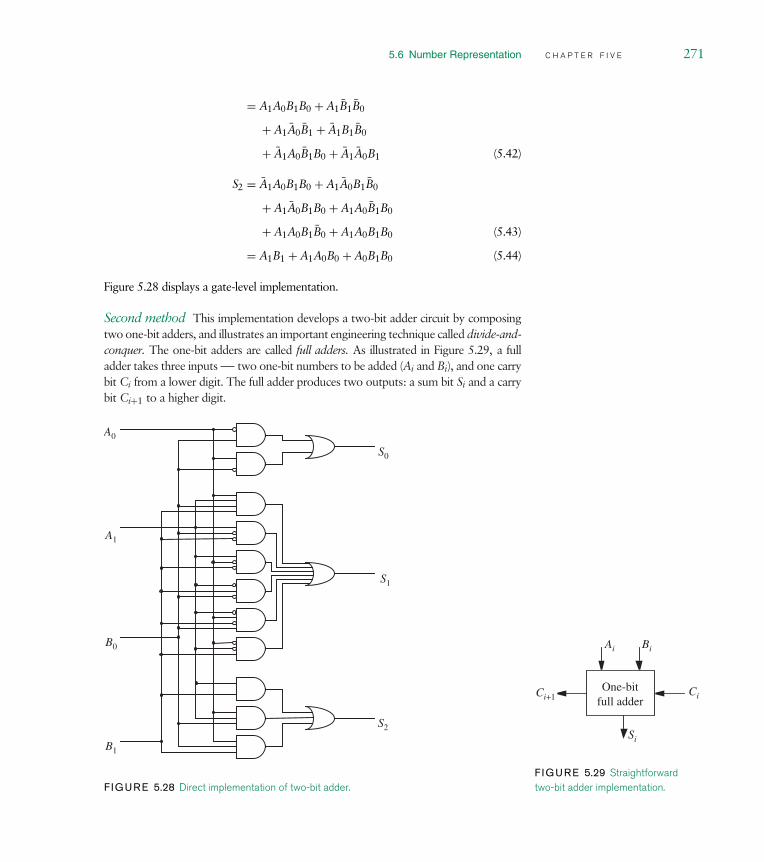
5.6 Number Representation C H A P T E R F I V E 271
= A1A0B1B0 + A1B1B0
+ A1A0B1 + A1B1B0
+ A1A0B1B0 + A1A0B1 (5.42)
S2 = A1A0B1B0 + A1A0B1B0
+ A1A0B1B0 + A1A0B1B0
+ A1A0B1B0 + A1A0B1B0 (5.43)
= A1B1 + A1A0B0 + A0B1B0 (5.44)
Figure 5.28 displays a gate-level implementation.
Second method This implementation develops a two-bit adder circuit by composingtwo one-bit adders, and illustrates an important engineering technique called divide-and-conquer. The one-bit adders are called full adders. As illustrated in Figure 5.29, a fulladder takes three inputs two one-bit numbers to be added (Ai and Bi), and one carrybit Ci from a lower digit. The full adder produces two outputs: a sum bit Si and a carrybit Ci+1 to a higher digit.
A0
A1
B0
B1
S0
S1
S2
F IGURE 5.28 Direct implementation of two-bit adder.
Ai Bi
Ci
Si
Ci+1One-bit
full adder
F IGURE 5.29 Straightforwardtwo-bit adder implementation.

272 C H A P T E R F I V E t h e d i g i t a l a b s t r a c t i o n
Ai Bi Ci Ci+1 Si
0 0 0 0 0
0 0 1 0 1
0 1 0 0 1
0 1 1 1 0
1 0 0 0 1
1 0 1 1 0
1 1 0 1 0
1 1 1 1 1
TABLE 5.13 Truth table for theone-bit full adder.
F IGURE 5.30 One-bit full adderimplementation.
Ai
Bi
Ci
Ci+1
Si
The truth table for the one-bit full adder is depicted in Table 5.13.
From the table, we derive the logic expression for the sum bit Si and the carry bit Ci+1
as follows:
Si = AiBiCi + AiBiCi
+ AiBiCi + AiBiCi (5.45)
Ci+1 = AiBiCi + AiBiCi
+ AiBiCi + AiBiCi. (5.46)
Figure 5.30 shows a gate-level full adder circuit based on the logic expressions for Si
and Ci+1.
We can create a two bit adder out of a pair of one-bit full adders by feeding the carry-outbit (Ci+1) of one adder to the carry-in bit (Ci) of another adder. The carry-in bit of the

5.6 Number Representation C H A P T E R F I V E 273
B0A0B1A1
S0S1
C2One-bit
full adderOne-bit
full adder
C1C0 = 0
F IGURE 5.31 A two-bitripple-carry adder using twoone-bit full adders.
BiAiBi+1Ai+1
SiSi+1
Ci+2 Two-bit adder Ci F IGURE 5.32 A two-bit adderblock.
B4A4B5A5
S4S5
C8Two-bit adder
C0 = 0
B6A6B7A7
S6S7
Two-bit adder
B0A0B1A1
S0S1
Two-bit adder
B2A2B3A3
S2S3
Two-bit adderC6 C4
C2F IGURE 5.33 An eight-bit addercircuit.
low-digit adder is set to 0. The two bit-adder is shown in Figure 5.31. Because the carrybit ripples through the adders, this type of adder circuit is called a ripple-carry adder.Similarly, we can use n one-bit full adders to construct an n-bit adder.9
e x a m p l e 5.20 b u i l d i n g a n e i g h t - b i t a d d e r Let usnow build an adder that can add two eight-bit integers using the two-bit adder circuitsfrom Figure 5.31 as the building blocks. First, for convenience, let us abstract the cir-cuit from Figure 5.31 into an adder block for a pair of two-bit integers as shown inFigure 5.32.
Much as we ganged together the one-bit adder blocks, we can cascade together thetwo-bit adder blocks to form the eight-bit adder as shown in Figure 5.33.
9. As an exercise, you are encouraged to construct a one-bit full adder using two half adders. A halfadder takes two bits Ai and Bi as inputs and produces as its output a sum bit Si and a carry-outbit Ci+1.

274 C H A P T E R F I V E t h e d i g i t a l a b s t r a c t i o n
5.7 S U M M A R Y This chapter introduced the digital abstraction, which is based on the notion
of lumping signal values into two levels high and low. Digital circuitsare designed to be more immune to noise than their analog counterparts.The degree of noise immunity of a digital circuit is governed by the voltagethresholds of the static discipline to which the circuit adheres.
The static discipline requires digital devices to adhere to a common rep-resentation for their input and output voltages, and to guarantee thatthey interpret correctly inputs that are valid logical signals according tothe common representation, and to produce outputs that are valid logicalsignals provided they receive valid logical inputs. By adhering to a commonrepresentation, digital devices based on different technologies or built bydifferent manufacturers can communicate with each other. The commonrepresentation is specified in terms of four voltage thresholds:
VOH The lowest output voltage value that a digital device can producewhen it outputs a logical 1.
VOL The highest output voltage value that a digital device can producewhen it outputs a logical 0.
VIH The lowest input voltage value that a digital device must recognizeas a logical 1.
VIL The highest input voltage value that a digital device mustrecognize as a logical 0.
The voltage thresholds associated with a static discipline determine thenoise margins. The 0 noise margin is given by
NM0 = VIL − VOL
and the 1 noise margin is given by
NM1 = VOH − VIH.
We also discussed several representations of digital logic including truthtables, which are a tabular representation; boolean expressions, whichare akin to algebraic expressions; and combinational gates, which are agraphical circuit representation.
E X E R C I S E S e x e r c i s e 5 .1 Write a boolean expression for the following statement: ‘‘Z isTRUE if either X or Y is FALSE, otherwise Z is FALSE.’’ Write a truth table for thisexpression.

5.7 Summary C H A P T E R F I V E 275
e x e r c i s e 5 .2 Write a boolean expression for the following statement: ‘‘Z isFALSE if either X or Y is FALSE, otherwise Z is TRUE.’’ Write a truth table for thisexpression.
e x e r c i s e 5 .3 Write a boolean expression for the following statement: ‘‘Z isTRUE if no more than two of W, X, and Y are TRUE, otherwise Z is FALSE.’’
e x e r c i s e 5 .4 Consider the statement: ‘‘Z is TRUE if at least two of W, X, andY are TRUE, otherwise Z is FALSE.’’
a) Write a boolean expression for this statement.
b) Write a truth table for the function Z.
c) Implement Z using only AND, OR, and NOT gates. The inputs W, X, andY are available. Each gate may have an arbitrary number of inputs. (Hint:A sum-of-products representation of the boolean expression will facilitate thisimplementation.)
d) Implement Z using only AND, OR, and NOT gates. Each gate may have no morethan two inputs. As before, the inputs W, X, and Y are available.
e) Implement Z using only NAND and NOR gates. (Hint: a NAND gate or a NORgate with its inputs tied together behaves like an inverter.)
f) Implement Z using only NAND gates. (Hint: Use De Morgan’s laws.)
g) Implement Z using only NOR gates. (Hint: Use De Morgan’s laws.)
h) Repeat part (d) and attempt to minimize the number of gates used.
i) Repeat part (d) and attempt to minimize the number of gates used, assuming thatthe inputs are available both in their true and complement forms. In other words,assume that in addition to W, X, and Y, the inputs W, X, and Y, are also available.
e x e r c i s e 5 .5 Represent the decimal number 4 as an unsigned, three-bit binarynumber and as an unsigned, four-bit binary number. Unsigned numbers do not includea sign bit. For example, 11110 is the unsigned, binary representation of the decimalnumber 30.
e x e r c i s e 5 .6 Consider the functions F(A, B, C) and G(A, B, C) specified in thetruth table given in Table 5.14.
a) Write a logic expression corresponding to the functions F(A, B, C) and G(A, B, C).
b) Implement F(A, B, C) with logic gates.

276 C H A P T E R F I V E t h e d i g i t a l a b s t r a c t i o n
A B C F(A, B, C) G(A, B, C)
0 0 0 1 0
0 0 1 0 0
0 1 0 0 0
0 1 1 0 1
1 0 0 1 0
1 0 1 1 1
1 1 0 0 1
1 1 1 1 1
TABLE 5.14 Truth table forExercise 5.6
c) Implement F(A, B, C) using only two-input gates.
d) Implement F(A, B, C) using only two-input NAND gates. (Hint: Use De Morgan’slaws.)
e) Repeat parts (b) through (d) for the function G(A, B, C).
e x e r c i s e 5 .7 Consider the following four logic expressions:
(A + B)(A · B + C) + C · D
(A · C + B · D)(D + B + A
A + B · D + A · C · D
((A + C) + B + D) + A · C · D
a) Give an implementation using gates for each of the four logic expressions.
b) Write the truth table for each of the four expressions.
c) Suppose you know that A = 0. Simplify the four expressions under this constraint.
d) Simplify the four expressions assuming that A and B are related as A = B.
e x e r c i s e 5 .8 A logic gate obeys a static discipline with the following voltagelevels: VIH = 3.5 V, VOH = 4.3 V, VIL = 1.5 V, and VOL = 0.9 V. (a) Whatrange of voltages will be treated as invalid under this discipline? (b) What are its noisemargins?

5.7 Summary C H A P T E R F I V E 277
e x e r c i s e 5 .9 Consider a family of logic gates that operates under the staticdiscipline with the following voltage thresholds: VIL = 1.5 V, VOL = 0.5 V,VIH = 3.5 V, and VOH = 4.4 V.
a) Graph an input-output voltage transfer function of a buffer satisfying the four voltagethresholds.
b) Graph an input-output voltage transfer function of an inverter satisfying the fourvoltage thresholds.
c) What is the highest voltage that can be output by an inverter for a logical 0output?
d) What is the lowest voltage that can be output by an inverter for a logical 1output?
e) What is the highest voltage that must be interpreted by a receiver as a logical 0?
f) What is the lowest voltage that must be interpreted by a receiver as a logical 1?
g) Does this choice of voltage thresholds offer any immunity to noise? If so, determinethe noise margins.
e x e r c i s e 5 .10 Consider a family of logic gates that operates under the staticdiscipline with the following voltage thresholds: VIL = VOL = 0.5 V and VIH =VOH = 4.4 V.
a) Graph an input-output voltage transfer function of a buffer satisfying the two voltagethresholds.
b) Graph an input-output voltage transfer function of an inverter satisfying the twovoltage thresholds.
c) What is the highest voltage that can be output by an inverter for a logical 0output?
d) What is the lowest voltage that can be output by an inverter for a logical 1output?
e) What is the highest voltage that must be interpreted by a receiver as a logical 0?
f) What is the lowest voltage that must be interpreted by a receiver as a logical 1?
g) Does this choice of voltage thresholds offer any immunity to noise?

278 C H A P T E R F I V E t h e d i g i t a l a b s t r a c t i o n
P R O B L E M S p r o b l e m 5.1 Derive a truth table and a boolean expression that describes theoperation of each digital circuit shown in Figure 5.34.
A
C
B
D
(a)
Z
A
C
B
D
(b)
Z
A
C
B
(c)
Z
A
C
B
(d)
Z
A
C
B
(e)
Z
A
C
B
(f)
Z
F IGURE 5.34
p r o b l e m 5.2 Draw an output voltage waveform for the circuit in Figure 5.34cin response to the input voltage waveforms shown in Figure 5.35. Assume that the gatesin the circuit obey the static discipline with VOH = 4 V, VIH = 3 V, VOL = 1 V, andVIL = 2 V.
0
5 V
1 V
4 V
3 V
2 V
A
BC
t
F IGURE 5.35
p r o b l e m 5.3 The truth table for a ‘‘ones count’’ circuit is given in Table 5.15.This circuit has four inputs: A, B, C, and D, and three outputs OUT0, OUT1, and OUT2.Together, the signals OUT0, OUT1, and OUT2 represent a three-bit positive integerOUT2OUT1OUT0. The output integer OUT2OUT1OUT0 reflects the number of onesin the input. Using only NAND, NOR, and NOT gates, design an implementation forthe circuit. Each gate may have an arbitrary number of inputs.
p r o b l e m 5.4 A four-input multiplexer module is shown in Figure 5.36. Themultiplexer has two select signals S1 and S0. The value on the select signals determineswhich of the inputs A, B, C, and D appears at the output. As illustrated in the figure,A is selected if S1S0 is 00, B if S1S0 is 01, C if S1S0 is 10, and D if S1S0 is 11. Write aboolean expression for Z in terms of S1S0, A, B, C, and D. Implement the multiplexerusing only NAND gates.
p r o b l e m 5.5 A four-input demultiplexer module is shown in Figure 5.37. Thedemultiplexer has two select signals, S1 and S0. The select signals determine on whichof the outputs (OUT0, OUT1, OUT2, or OUT3) the input IN appears. As illustrated inthe figure, IN appears at output OUT0 if S1S0 is 00, at OUT1 if S1S0 is 01, at OUT2 ifS1S0 is 10, and at OUT3 if S1S0 is 11. An output is 0 if it is not selected. Write a booleanexpression for each of the outputs in terms of S1S0 and IN. Implement the demultiplexerusing only NAND gates.
p r o b l e m 5.6 Implement the ‘‘greater-than’’ circuit depicted in Figure 5.38using NAND gates. A and B represent one-bit positive integers. The output Z is 1if A is greater than B, otherwise Z is 0.

5.7 Summary C H A P T E R F I V E 279
A B C D OUT2 OUT1 OUT0
0 0 0 0 0 0 0
0 0 0 1 0 0 1
0 0 1 0 0 0 1
0 0 1 1 0 1 0
0 1 0 0 0 0 1
0 1 0 1 0 1 0
0 1 1 0 0 1 0
0 1 1 1 0 1 1
1 0 0 0 0 0 1
1 0 0 1 0 1 0
1 0 1 0 0 1 0
1 0 1 1 0 1 1
1 1 0 0 0 1 0
1 1 0 1 0 1 1
1 1 1 0 0 1 1
1 1 1 1 1 0 0
TABLE 5.15 Truth table for a“ones count” circuit.
p r o b l e m 5.7 Implement the four-input ‘‘odd’’ or ‘‘odd parity’’ circuit depictedin Figure 5.39 using NOR gates. In this circuit, the output Z is high if an odd number of
00
01
10
11
A
B
C
D
2
Z
S1S0
F IGURE 5.36 A four-inputmultiplexer module. The “2” besidethe wire corresponding to theselect signals is a short-handnotation indicating there are twowires present.
00
01
10
11
OUT0
OUT1
OUT2
OUT3
2
S1S0
IN
F IGURE 5.37
the inputs are high, otherwise the output Z is low. How would you use the four-input‘‘odd’’ circuit module shown in Figure 5.39 to implement a three-input ‘‘odd’’ circuit?If this cannot be done, discuss why not.
p r o b l e m 5.8 Figure 5.40 depicts a four-input majority circuit module. Theoutput Z of this circuit module is high if a majority of the inputs are high. Write aboolean expression for Z in terms of A0, A1, A2, and A3. How would you use thefour-input majority circuit module shown in Figure 5.40 to implement a three-inputmajority circuit and a two-input majority circuit? If either of these cannot be done,discuss why not.
p r o b l e m 5.9 Figure 5.41 illustrates a two-bit grey code converter. Its outputsOUT0, and OUT1, are equal to the inputs when the IN0, IN1 are 00 or 01. However,when the inputs IN0, IN1 are 10 and 11, the outputs OUT0 and OUT1 are 11 and 10,respectively. Implement the grey code converter using two-input NAND gates.
p r o b l e m 5.10 Figure 5.42 illustrates input-output voltage transfer functionsfor several one-input one-output devices. For the voltage thresholds VOL, VIL, VOH,and VIH as shown, which of the devices can serve as valid inverters?

280 C H A P T E R F I V E t h e d i g i t a l a b s t r a c t i o n
p r o b l e m 5.11 Suppose we wish to build a two-bit adder circuit (see
>A
B Z
F IGURE 5.38
ODD
A0
Z
A1
A2
A3
F IGURE 5.39
A0
Z
A1
A2
A3
Majority
F IGURE 5.40
IN 0
IN 1
OUT 0
OUT 1
F IGURE 5.41
Adder
A1 A0 B1 B0
C1
S1 S0
F IGURE 5.43
Figure 5.43) that takes as input a pair of two-bit positive integers A1A0 and B1B0 andproduces a two-bit sum output S1S0 and a carry-out bit C1. Write a truth table and aboolean expression for the carry-out bit in terms of the inputs.
Now, suppose we wish to build a two-bit adder circuit (see Figure 5.44) that takes asinput a pair of two-bit positive integers A1A0 and B1B0, and a carry-in bit C0, andproduces a two-bit sum output S1S0 and a carry-out bit C1. Write a truth table and aboolean expression for the carry-out bit in terms of the inputs.
p r o b l e m 5.12 Suppose we have two logic families named NTL and YTL. TheNTL family of logic gates operates under the static discipline with the following voltagethresholds: VIL = 1.5 V, VOL = 1.0 V, VIH = 3.5 V, and VOH = 4 V. The YTLfamily, on the other hand, is characterized by the voltage thresholds: VIL = 0.8 V,VOL = 0.3 V, VIH = 3.0 V, and VOH = 4.5 V. Will a YTL inverter driving the input of
E
BC
AFD
0 VIL VIH
5 V
VOL
VOH
5 V
VIN
VOUT
F IGURE 5.42
Adder C0C1
A0A1 B1 B0
S1 S0
F IGURE 5.44

5.7 Summary C H A P T E R F I V E 281
an NTL inverter operate correctly? Explain. Will an NTL inverter driving the input ofan YTL inverter operate correctly? Explain.
p r o b l e m 5.13 Consider a family of logic gates that operates under the staticdiscipline with the following voltage thresholds: VOL = 0.5 V, VIL = 1.6 V,VOH = 4.4 V, and VIH = 3.2 V.
a) Graph an input-output voltage transfer function of a buffer satisfying the four voltagethresholds.
b) Graph an input-output voltage transfer function of an inverter satisfying the fourvoltage thresholds.
c) What is the highest voltage that can be output by an inverter for a logical 0 output?
d) What is the lowest voltage that can be output by an inverter for a logical 1 output?
e) What is the highest voltage that must be interpreted by a receiver as a logical 0?
f) What is the lowest voltage that must be interpreted by a receiver as a logical 1?
g) When transmitting information over a noisy wire, buffers can be used to minimizetransmission errors by restoring signal values. Consider the transmission of data
A
C
B
(a)
Z
Stuck at 1
A
C
B
(b)
Z
Stuck at 1
A
C
B
(c)
Z
Stuck at 1
Stuck at 1
A
C
B
(d)
ZStuck at 0
Stuck at 0
F IGURE 5.45
over a noisy wire that picks up a maximum of 80 mV symmetric peak-to-peak noiseper centimeter. How many buffers are needed to transmit a signal over a distanceof 2 meters in this noisy environment?
h) How large are the 0 and 1 noise margins for a buffer in this logic family? Nowconsider three buffers connected in series and behaving as a single buffer. What arethe noise margins for this new buffer?
p r o b l e m 5.14 Many manufacturing flaws in digital circuits can be modeled asstuck-at faults. The output of a gate is said to suffer from a stuck-at-1 fault if the outputis a 1 irrespective of its input values. Similarly, a stuck-at-0 fault at an output causes theoutput to produce a 0 at all times.
a) Consider the circuits shown in Figure 5.45 with one or more faults. Write an expres-sion for each of the outputs in terms of the input variables for the given faults. (Hint:As an example, the output of the faulty circuit in Figure 5.45a will be independentof the input variable C).
A
C
B
(a)
Z
Stuck at X
N1
N2
N3
A
ZB
C
(b)
F IGURE 5.46

282 C H A P T E R F I V E t h e d i g i t a l a b s t r a c t i o n
b) Suppose we are given the faulty circuit in Figure 5.46a where the output of NANDgate N2 is known to have a stuck-at fault. However, we do not know whether it is astuck-at-1 fault or a stuck-at-0 fault. Further, as illustrated in Figure 5.46b, supposethat we have access only to the inputs A, B, and C, and the output Z. In otherwords, we are unable to directly observe the output X of the faulty NAND gateN2. How would you go about determining whether N2 suffers from a stuck-at-1fault or a stuck-at-0 fault?
c h a p t e r 6
6.1 T H E S W I T C H
6.2 L O G I C F U N C T I O N S U S I N G S W I T C H E S
6.3 T H E M O S F E T D E V I C E A N D I T S S M O D E L
6.4 M O S F E T S W I T C H I M P L E M E N T A T I O N O F L O G I C G A T E S
6.5 S T A T I C A N A L Y S I S U S I N G T H E S M O D E L
6.6 T H E S R M O D E L O F T H E M O S F E T
6.7 P H Y S I C A L S T R U C T U R E O F T H E M O S F E T
6.8 S T A T I C A N A L Y S I S U S I N G T H E S R M O D E L
6.9 S I G N A L R E S T O R A T I O N , G A I N , A N D N O N L I N E A R I T Y
6.10 P O W E R C O N S U M P T I O N I N L O G I C G A T E S
6.11 A C T I V E P U L L U P S
6.12 S U M M A R Y
E X E R C I S E S
P R O B L E M S

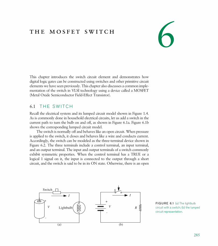
the mos f e t sw i tch 6This chapter introduces the switch circuit element and demonstrates howdigital logic gates can be constructed using switches and other primitive circuitelements we have seen previously. This chapter also discusses a common imple-mentation of the switch in VLSI technology using a device called a MOSFET(Metal Oxide Semiconductor Field-Effect Transistor).
6.1 T H E S W I T C H
Recall the electrical system and its lumped circuit model shown in Figure 1.4.As is commonly done in household electrical circuits, let us add a switch in thecurrent path to turn the bulb on and off, as shown in Figure 6.1a. Figure 6.1bshows the corresponding lumped circuit model.
The switch is normally off and behaves like an open circuit. When pressureis applied to the switch, it closes and behaves like a wire and conducts current.Accordingly, the switch can be modeled as the three-terminal device shown inFigure 6.2. The three terminals include a control terminal, an input terminal,and an output terminal. The input and output terminals of a switch commonlyexhibit symmetric properties. When the control terminal has a TRUE or alogical 1 signal on it, the input is connected to the output through a shortcircuit, and the switch is said to be in its ON state. Otherwise, there is an open
+
-
V
I
Lightbulb
Switch
(a)
+
-
V
I
R
S
(b)
F IGURE 6.1 (a) The lightbulbcircuit with a switch; (b) the lumpedcircuit representation.
285
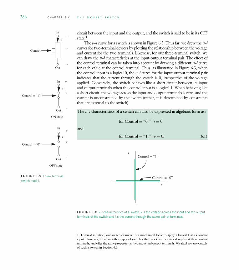
286 C H A P T E R S I X t h e m o s f e t s w i t c h
circuit between the input and the output, and the switch is said to be in its OFFstate.1
The v i curve for a switch is shown in Figure 6.3. Thus far, we drew the v icurves for two-terminal devices by plotting the relationship between the voltageand current for the two terminals. Likewise, for our three-terminal switch, wecan draw the v i characteristics at the input-output terminal pair. The effect ofthe control terminal can be taken into account by drawing a different v i curvefor each value at the control terminal. Thus, as illustrated in Figure 6.3, whenthe control input is a logical 0, the v i curve for the input-output terminal pair
In
Out
In
Out
Control = “0”
Control = “1”
ON state
OFF state
Control
In
Out
+
-
v
i
+
-
v
+
-
v
i
i
F IGURE 6.2 Three-terminalswitch model.
indicates that the current through the switch is 0, irrespective of the voltageapplied. Conversely, the switch behaves like a short circuit between its inputand output terminals when the control input is a logical 1. When behaving likea short circuit, the voltage across the input and output terminals is zero, and thecurrent is unconstrained by the switch (rather, it is determined by constraintsthat are external to the switch).
The v i characteristics of a switch can also be expressed in algebraic form as:
for Control = ‘‘0, ’’ i = 0
and
for Control = ‘‘1, ’’ v = 0. (6.1)
v
iControl = “1”
Control = “0”
F IGURE 6.3 v–i characteristics of a switch. v is the voltage across the input and the outputterminals of the switch and i is the current through the same pair of terminals.
1. To build intuition, our switch example uses mechanical force to apply a logical 1 at its controlinput. However, there are other types of switches that work with electrical signals at their controlterminals, and offer the same properties at their input and output terminals. We shall see an exampleof such a switch in Section 6.3.

6.1 The Switch C H A P T E R S I X 287
+
-
V
I
R
S
(a) Switch in the OFF state
+
-
V
I
R
S
(b) Switch in the ON state
i
+ -v
i
+ -v
Control = “0” Control = “1”
F IGURE 6.4 (a) Linear sub-circuit formed when the switch is inthe OFF state; (b) linear subcircuitformed when the switch is in theON state.
Although the switch is a nonlinear device, circuits containing a switchand other linear devices can be analyzed by considering two linear subcir-cuits: one when the switch is in its ON state and one for the switch in itsOFF state. Thus, standard linear techniques can be applied to each subcir-cuit. Figure 6.4 illustrates the two subcircuits for our lightbulb circuit example.Analyzing Figure 6.4a, it is easy to see that the current I is zero when the switchis OFF. Similarly, analyzing Figure 6.4b, the current is given by I = V/R whenthe switch is in the ON state.
e x a m p l e 6.1 c i r c u i t c o n t a i n i n g a s w i t c h Determinethe current through resistor R1 in the circuit shown in Figure 6.5a.
R2R1
Switch
(a)
R2
i1a
R1
(b)
R2
i1b
R1
(c)
Control = “1”
Control = “0”
i1
i
i
i
F IGURE 6.5 (a) Circuitcontaining a current source, tworesistors, and a switch; (b) linearsubcircuit formed when the switchis in the ON state; (c) linear sub-circuit formed when the switch isin the OFF state.
The circuit in Figure 6.5a is nonlinear because it contains a switch. Since the onlynonlinear element in the circuit is the switch, we can analyze this circuit by consideringthe two linear subcircuits formed for each of the two states of the switch.
Figure 6.5b shows the linear subcircuit formed when the switch is in the ON state. Wecan obtain the desired current i1a for the ON-state circuit by using the current dividerrelation from Equation 2.84. The current divider relation states that when two resistorsare connected in parallel, the current through one of the resistors is equal to the totalcurrent through the two resistors multiplied by a factor, which is made up of the oppositeresistance divided by the sum of the two resistances. Accordingly, (when the switch isin the ON state):
i1a = iR2
R1 + R2.
Figure 6.5c shows the linear subcircuit formed when the switch is in the OFF state. Inthis case, the entire current from the current source flows through the resistor R1. Thus,(when the switch is in the OFF state):
i1b = i.

288 C H A P T E R S I X t h e m o s f e t s w i t c h
F IGURE 6.6 (a) The lightbulbcircuit with switch in an ANDconfiguration; (b) the lightbulbcircuit with switches in an ORconfiguration.
+
-
V
I
Lightbulb
A B
(a)
+
-
V
I
Lightbulb
A
B
(b)
6.2 L O G I C F U N C T I O N S U S I N G S W I T C H E S
Next, consider the lightbulb circuit with a pair of switches connected in seriesas depicted in Figure 6.6a. The lightbulb can be turned on only by closingboth the switches A and B. Similarly, Figure 6.6b shows a circuit with a pairof switches connected in an OR configuration. In the latter configuration, thebulb can be turned on by closing either switch A or switch B.
These circuits provide us with the insight into implementing logic func-tions using switches: Series connected switches implement the AND functionand parallel connected switches implement the OR function. Switches can becombined in AND-OR configurations to implement more complicated func-tions. As shown previously, the switches implement a form of digital logiccalled steering logic. In this form, switches steer values (for example, a highvoltage) along various paths. As we continue our discussion, we shall also seehow switches can be used to build our familiar combinational logic gates.
One of the unappealing features of the mechanical switches in Figure 6.1was that they responded only to mechanical pressure at their control terminal.The need for mechanical pressure would make it unacceptably hard to buildlogic circuits because the voltage at the output of a given switch would have tosomehow be converted to a mechanical pressure to influence another switch.Preferably, a three-terminal switch device that responded to voltages wouldenable the construction of switching circuits using voltages alone. The MOSFETis one such device that can be implemented cheaply in VLSI technology.
6.3 T H E M O S F E T D E V I C E A N D I T S S M O D E L
The MOSFET belongs to a class of devices called transistors. The MOSFET is athree-terminal device with a control terminal, an input terminal, and an outputterminal (see Figure 6.7). We will discuss its physical structure in Section 6.7.

6.3 The MOSFET Device and Its S Model C H A P T E R S I X 289
F IGURE 6.7 Discrete MOSFETs.The rightmost device with threeleads contains a single MOSFET,while the middle package containsmultiple MOSFETs. (PhotographCourtesy of Maxim IntegratedProducts.)
Its circuit symbol is shown in Figure 6.8. As shown in Figure 6.8, the controlterminal of the MOSFET is called its gate G, the input terminal its drain D, andthe output terminal its source S. For our purposes, we can treat the source anddrain in a symmetric fashion. The name assignment is related to the direction ofcurrent flow. The terminals are labeled such that current flows from the drain
Control
Input
Outputterminal
D
S
Gterminal
terminal
F IGURE 6.8 The MOSFETcircuit symbol.
to the source.2 Equivalently, the channel terminal with the higher voltage islabeled as the drain.
As depicted in Figure 6.9, let the voltage across the gate and source ofthe MOSFET be vGS, and the voltage across the drain and the source be vDS.The current through G terminal is called iG and that through the D terminal istermed iDS.
A simple circuit model for a specific type of MOSFET device called then-channel MOSFET is depicted in Figure 6.10.3 This model based on the
D
S
G
vGS
vDS+
+
-
iDS
iG
F IGURE 6.9 Definitions of vGS ,vDS , and iDS .
simple switch is called the MOSFET’s Switch Model, or S Model for short.4
The device is in the ON state when vGS crosses a threshold voltage VT,otherwise it is off. A typical value for VT for n-channel MOSFETs is 0.7 volts,but it can be varied by the manufacturing process.5 In the ON state, the S modelapproximates the connection between the drain and the source as a short circuit.In practice, there is some nonzero resistance between the drain and the source,
2. You are is probably wondering why the nomenclature of the drain and the source seems reversedfrom the more logical choice relating the source to the input and the drain to the output. It turnsout that the names stem from the internal conduction properties of the MOSFET. Electrons arethe majority carriers in the n-channel MOSFET shown. S is the source of electrons and D is thedrain of electrons.
3. We will see a complementary MOS transistor called the p-channel transistor later.
4. We will examine increasingly sophisticated models for the MOSFET device in the followingchapters. These models will reflect aspects of the MOSFET’s behavior that are not adequatelycaptured by our simple switch model.
5. To simplify the math in our quantatitive examples on MOSFETs, this book commonly uses1-volt thresholds.

290 C H A P T E R S I X t h e m o s f e t s w i t c h
but we ignore this resistance in the S model. Section 6.6 will discuss the switch-resistor model (or the SR model), which attempts to account for this resistance.In the OFF state, an open circuit exists between the drain and the source. As
D
S
G
D
S
G
OFF
vGS < VT
vGS ≥ VT
ONiG = 0
iG = 0
D
S
G
iG
iDS
iDS
iDS
F IGURE 6.10 The S model ofthe MOSFET.
illustrated in Figure 6.10, an open circuit exists between the gate and the source,and between the gate and the drain at all times. Thus, iG = 0 always.
Much as we did for the switch, we can plot the v i characteristics betweenthe D and S terminals of the MOSFET for various gate-to-source voltages usingthe S model. Figure 6.11 shows this graph. Notice that the curves are shownonly for the top-right quadrant. Because we define the drain to be the terminalwith the higher voltage, by definition, vDS can never be negative.6 Therefore, theleft quadrants are irrelevant. Similarly, the bottom-right quadrant is not shownbecause iDS is positive when vDS is positive. Unlike the MOSFET, devices forwhich this is not true (for example, batteries) are capable of providing power.Like the switch with a zero on its control input, the connection between the
vGS < VT
vDS
iDSvGS > VT
vDS = 0
iDS = 0
_
D and S terminals looks like an open circuit (iDS = 0) when vGS < VT. Incontrast, the connection between D and S looks like a short circuit (vDS = 0)when vGS ≥ VT.
We can summarize the S model for the MOSFET in algebraic form by statingits v i characteristics as follows:
for vGS < VT, iDS = 0
and
for vGS ≥ VT, vDS = 0 (6.2)
Our discussion thus far treated a MOSFET as a three-terminal device.Notice, however, that the MOSFET is controlled by the voltage across a pair ofterminals, namely, G and S. Similarly, we were interested in the voltage across,and current through, the D and S terminal pair. As discussed in Section 1.5,this natural pairing of terminals suggests an alternate MOSFET representationusing ports. As shown in Figure 6.12, we can treat the G and S terminal pair asthe input port or the control port and the D and S terminal pair as the outputport of the MOSFET.
6. When fabricated on a VLSI chip, the physical MOSFET itself is symmetric with respect tothe drain and source. (Note, however, discrete MOSFET devices suitable for use on a bread-board are not symmetric.) So its drain and source labels can be interchanged without changing thedevice. Accordingly, if the drain and source nomenclature was unrelated to the potential differencebetween the two terminals, the MOSFET characteristic would look like as in the adjacent figure.As depicted, there is an open circuit between D and S when vGS < VT, and a short circuit whenvGS ≥ VT. When the open circuit exists, vDS can take on any value (positive or negative) as deter-mined by external circuit constraints. Similarly, when the short circuit exists, iDS is unconstrained.Interestingly, notice here that the model we choose for an element depends on the way we use theelement as much as on the physical construction of the element!

6.4 MOSFET Switch Implementation of Logic Gates C H A P T E R S I X 291
Notice further that we if choose our digital representation such that the
vGS < VT
vDS
iDSvGS ≥ VT
vDS = 0
iDS = 0
0
F IGURE 6.11 MOSFETcharacteristics with the S model.
Input
OutputD
S
G
port
port+
-vGS
+
-
vDS
iDS
F IGURE 6.12 Port represen-tation of a MOSFET.
logical 1 is represented with a value greater than 1 volt, then the MOSFEToperates as a switch that turns on when its gate-to-source port has a logical 1signal on it. Figure 6.13 shows the lightbulb circuit using MOSFETs to imple-ment the AND switching function. In this circuit, the bulb turns on only whenboth A and B are 1.
6.4 M O S F E T S W I T C H I M P L E M E N T A T I O NO F L O G I C G A T E S
Let us now build logic gates using MOSFETs. Consider the circuit shown inFigure 6.14, which comprises a MOSFET and a load resistor powered by asupply voltage VS. The input to the circuit is connected to the gate of theMOSFET, the source is tied to ground, and drain is tied to VS in series with aload resister RL. The same circuit is redrawn on the right-hand side using theshorthand notation for the power and ground terminals.
+
-
V
I
R
A B
F IGURE 6.13 The lightbulbcircuit using MOSFETs.
Ground
VS
vIN
vOUT
RL
+-5 V
(a)
iIN
VS
vIN
vOUT
RL
iIN
(b)
F IGURE 6.14 (a) The MOSFETinverter; (b) the same invertercircuit using the shorthand notationfor power and ground.

292 C H A P T E R S I X t h e m o s f e t s w i t c h
F IGURE 6.15 The inverterabstraction and its internal circuit.IN and OUT are the logical valuesrepresented by vIN and vOUT.
VS
RL
IN OUT
Figure 6.15 shows the relationship between the terminals of the MOSFET-based inverter circuit and the abstract inverter gate.
The left-hand side of Figure 6.16 shows the corresponding abstract
VS
IN
OUTIN
OUT
F IGURE 6.16 The invertershown with explicit and implicitpower connections.
inverter with the power connections, and the right-hand side shows the inverterabstraction as we know it with implicit power connections. Notice that theinverter abstraction hides the internal circuit details and provides a simple usagemodel to the user of the inverter logic gate. The internal details are irrelevantto the gate-level logic designer.7
Let us analyze the behavior of the circuit by replacing the MOSFET withits equivalent S model. Figure 6.17 displays the equivalent model for the circuitshown in Figure 6.14. Let us assume that a logical high is represented using 5 Vand a logical low using 0 V.
As shown in Figure 6.17, when the input vIN is high, the MOSFET is inthe ON state (assuming that the high voltage level is above the threshold VT),thereby pulling the output voltage to a low value.8 In contrast, when the inputis low, the MOSFET is off, and the output is raised to a high value by RL. Herewe see the purpose of the load resistor9 RL it provides a logical 1 outputwhen the MOSFET is off. Furthermore, RL is usually chosen to be large sothat the current is limited when the MOSFET is on.10 Because the resistance
7. What if sophisticated logic designers want to optimize their design for certain parameters suchas speed or area that are not captured by the gate-level abstraction? Later chapters will discusshow the gate-level abstraction is augmented with additional parameters such as gate delay andsize derived from the internal circuit so that the logic designer can optimize their gate-levelcircuit without being forced to delve into the internal details of the gate.
8. Because the MOSFET in Figure 6.14 serves to pull the output voltage to a low value when it isits ON state, the MOSFET is sometimes referred to as the pulldown MOSFET.
9. Because it pulls the output to a high value, the load resistor is sometimes referred to as the pullupresistor.
10. We will see additional design constraints on RL as we progress to more accurate MOSFETmodels.

6.4 MOSFET Switch Implementation of Logic Gates C H A P T E R S I X 293
between the gate-to-source and the drain-to-source ports of the MOSFET isinfinity in the S model, the current iIN is 0.
VS
vOUT = Low
RL
VS
vOUT = High
RL
vIN = High
vIN = Low
iIN
iIN
F IGURE 6.17 The S circuitmodel of the n-channel MOSFETinverter.
We can write the input-output relationships in a truth table as shownin Table 6.1. As is apparent from the table, the logical values IN and OUTrepresented by vIN and vOUT exhibit the behavior of an inverter.
i n o u t
0 1
1 0
TABLE 6.1 Truth table for theMOSFET circuit.
Figure 6.18 shows a sample input waveform and the corresponding outputwaveform for our circuit. We can also plot the vIN versus vOUT voltage transfercurve for the inverter circuit as shown in Figure 6.19. The input-output transfercurve for the inverter also called the inverter characteristic allows us todetermine whether the inverter satisfies a given static discipline. We will discussthe inverter characteristic and how it relates to the static discipline in Section 6.5.
We can also construct other gates in like manner. Figure 6.20 shows aNAND gate circuit and Figure 6.21 shows its equivalent S circuit model. It is
0VOL
VIL
VIH
VOH
5
0
5
0
5
vIN
vOUT
t
0VOL
VIL
VIH
VOH
5
F IGURE 6.18 Sample input-output waveforms for the inverter.
vIN (V)
vOUT (V)Ideal inverter characteristic5 V
VT
0 V0 V 5 V
F IGURE 6.19 The transfercharacteristic of the inverter.

294 C H A P T E R S I X t h e m o s f e t s w i t c h
easy to see that the output is a 0 only when both inputs are high. The outputis high otherwise.11
VS
A
C
RL
B
M1
M2
F IGURE 6.20 The circuit for aNAND gate.
Using intuition from the two-input NAND circuit, we can build multiple-input NAND and NOR circuits. Figure 6.22a shows an n-input NOR gateand 6.22b shows an n-input NAND gate. In the multiple-input NOR gate, theoutput is pulled to ground when any of the inputs is high. Correspondingly, inthe NAND gate, the output remains high if even one input is low.
VS
C = 1
RL
A = 0 B = 0
M1M2
VS
C = 0
RL
A = 1B = 1
M1M2
VS
C = 1
RL
A = 1 B = 0
M1M2
VS
C = 1
RL
A = 0B = 1
M1M2
F IGURE 6.21 The S circuit model for a NAND gate.
F IGURE 6.22 Multiple-inputNOR and NAND gates.
VS
Out
In1 In2 Inn-1 Inn
VS
Out
In1
In2
Inn
RL RL
(a) (b)
e x a m p l e 6.2 c o m b i n a t i o n a l l o g i c u s i n g m o s f e t s
Recall the two combinational logic expressions whose gate-level implementa-tions we had seen earlier:
AB + C + D
(A + B)CD
11. Notice that if both switches are off, the voltage at the node connecting M1 and M2 appears tobe undefined. Therefore vGS for M1 also appears to be undefined. In practice, however, MOSFETswitches are not perfect open circuits, rather they have a very high resistance between their drainand source in the off state. Thus, the voltage between M1 and M2 will be given by a voltage dividerrelationship. In any case, vGS for M1 will not impact the output voltage of the gate.

6.4 MOSFET Switch Implementation of Logic Gates C H A P T E R S I X 295
VS
OUT
A
C D
RL
B
F IGURE 6.23 Transistor-levelimplementation of AB + C + D.
In our earlier example, we had implemented these expressions using several abstractlogic gate elements. Now that we understand how gates are constructed using MOSFETsand resistors, we can actually construct a single compound combinational logic gateusing MOSFETs and resistors that implements each of these functions.12
Let us consider the first expression: AB + C + D. Using the intuition that switches inseries implement the AND property and switches in parallel implement the OR property,we can implement the first expression as shown in Figure 6.23. By checking the circuitagainst its truth table, we can convince ourselves that the circuit does work as desired.
Figure 6.24 shows the circuit for the second expression: (A + B)CD.
A B
C
D
VS
RL
Out
F IGURE 6.24 Transistor-level
implementation of (A + B)CD.
e x a m p l e 6.3 m o r e c o m b i n a t i o n a l l o g i c u s i n g
m o s f e t s Let us now construct the logic expression (A + B)CD using MOSFETs.Since (A + B)CD is simply the complement of (A + B)CD, we can obtain (A + B)CDby inverting the output from Figure 6.24, as illustrated in Figure 6.25.
It is important to point out two key properties of the MOSFET that makeit an ideal component for building gates:
1. First, notice that we could compose multiple gate components into morecomplicated circuits without worrying about the internal circuit of
12. Direct transistor implementation potentially can yield savings in the number of transistors andresistors used. However, should you consider discarding the gate-level abstraction in favor ofbuilding logic functions directly out of transistors, remember that transistor-level implementationof complex logic functions can be a much more arduous task than a gate-level implementation.The difficulty will become apparent as we move to the more realistic switch-resistor MOSFETmodel discussed in Section 6.6. As a general guideline, the designer should use the highest level ofabstraction with which to accomplish a design.

296 C H A P T E R S I X t h e m o s f e t s w i t c h
F IGURE 6.25 Transistor-levelimplementation of (A + B)CD. A B
C
D
VS
RL
VS
RL
Out
the gates. The reason we are able to do so is that the output of theMOSFET has no effect on its inputs. In other words, although the inputvoltage at G impacts the behavior of the MOSFET at its D and Sterminals, the voltages or currents at its D and S terminals have no impacton G.
2. Second, the infinite resistance seen at the gate (G terminal) of a MOSFETmakes it have no effect on the output of another gate driving its input.This feature of the MOSFET allows us to build systems containing manygates without worrying about how each gate affects the logical propertiesof other gates to which it is connected. This property of a gate is calledcomposability. Imagine if the MOSFET input had zero resistance. In thatcase, we would not be able to connect the output of one inverter to theinput of another and expect the first inverter to satisfy the static discipline.
We shall see later in Section 6.9.1 that the ability to build amplification intodevices containing MOSFETs further facilitates composability.
6.5 S T A T I C A N A L Y S I S U S I N G T H E S M O D E L
The input-output transfer curve for the inverter shown in Figure 6.19, orthe inverter characteristic, contains all the information necessary to determinewhether the inverter satisfies a given static discipline.
Recall that the static discipline for a logic gate guarantees that the outputsof the gate will meet the output constraints specified by the discipline, providedits inputs meet the input constraints. Recall, further, that a static disciplinewith its associated voltage thresholds is necessary to establish a standardizedrepresentation so that the logic devices from several vendors can operate witheach other correctly. Similarly, a user who wants to build a system can selectthe best devices from several vendors provided they meet the voltage thresholdsestablished by the static discipline adopted by the user.

6.5 Static Analysis Using the S Model C H A P T E R S I X 297
VIL
VOH
VOL
VIH
0 V
1 V
2 V
3 V
4 V
5 V
IN OUT
GATE
Input Output
Valid 1
Valid 0
Valid 1
Valid 00 V
1 V
2 V
3 V
4 V
5 V
F IGURE 6.26 Input and outputvoltage thresholds for a logic gate.
Output voltage levels are generally stricter than input voltage levels (higherthan the corresponding input high and lower than the corresponding input low)to provide for noise margins. Figure 6.26 illustrates the asymmetry betweeninputs and outputs. At the input of the gate, any voltage level lower than VILis recognized as a valid low, and any voltage higher than VIH is a valid high. Atits output, the gate guarantees to produce a voltage level higher than VOH fora valid high, and a voltage level lower than VOL for a valid low.
Voltage levels between VIL and VIH are invalid at the input, and levelsbetween VOL and VOH are invalid at the output. Because the output levelsare stricter than the input thresholds, the static discipline provides for noisemargins.
Based on the inverter characteristic (repeated here in Figure 6.27 for conve-nience), we can determine whether the inverter satisfies a given static discipline.As an example, let us determine whether the inverter satisfies a static disciplinewith the following voltage thresholds:
VOH = 4.5 V, VOL = 0.5 V, VIH = 4 V, and VIL = 0.9 V.
vIN (V)
vOUT (V)
Ideal inverter characteristic5 V
VT
0 V0 V 5 V
F IGURE 6.27 The transfercharacteristic of the inverter.

298 C H A P T E R S I X t h e m o s f e t s w i t c h
F IGURE 6.28 A mappingbetween logic values and voltagelevels corresponding to a staticdiscipline appropriate for theinverter.
5 V vIN
vOUT
VOH = 4.5 V
VIH
= 4
V
VT =
1 V
VOL = 0.5 V
VIL
= 0
.9 V
0 V
5 V
Figure 6.28 shows the voltage thresholds for the given static disciplinesuperimposed on the inverter transfer function. Let us check each of the outputand input thresholds.
VOH: The inverter produces an output high of 5 V. Clearly, this outputvoltage level for a logical 1 is greater than the 4.5-V output-highthreshold required by the static discipline.13
VOL: The inverter produces an output low of 0 V. This output voltage islower than the output-low threshold of 0.5 V required by the staticdiscipline.14
VIH: For our static discipline, VIH = 4 V. To obey the static discipline theinverter must interpret any voltage above 4 V as a logical 1. This iscertainly true for our inverter. Our inverter turns on when the inputvoltage is greater than VT = 1 V and pulls the output to a valid lowvoltage. Thus it interprets any voltage above 1 V as a logical 1.15
13. It turns out that our inverter can satisfy a static discipline with a VOH as high as 5− V. Thenotation 5− V implies a voltage that is slightly below 5 V.
14. Notice that our inverter can satisfy a static discipline with a VOL as low as 0+ V. The notation0+ V implies a voltage that is slightly above 0 V.
15. In fact, our inverter can satisfy a static discipline with a VIH as low as 1+ V, because the inverterproduces a valid low output voltage for inputs greater than VT = 1 V.

6.5 Static Analysis Using the S Model C H A P T E R S I X 299
VIL: For our static discipline, VIL = 0.9 V. This means that to obey thestatic discipline the inverter must interpret any voltage below 0.9 V asa logical 0. This is true for our inverter. The inverter is off when itsinput voltage is below VT = 1 V, and its output is at 5 V. Since theinverter produces a valid (output) high output voltage for inputvoltages below 0.9 V, it satisfies the static discipline.16
e x a m p l e 6.4 s t a t i c d i s c i p l i n e For fun, let us check to seewhether our inverter satisfies a static discipline used by Disco Systems Inc. Assumethat some of Disco’s systems adhere to a static discipline with the following voltagethresholds:
VOH = 4 V, VOL = 1 V, VIH = 3.5 V, and VIL = 1.5 V.
To operate under this static discipline, we know that our inverters must operate asfollows:
When outputting a logical 1, the voltage their outputs produce must be at leastVOH = 4 V. Since our inverters produce a 5-V output for a logical 1, they satisfythis condition.
When outputting a logical 0, the voltage their outputs produce must be no greaterthan VOL = 1 V. Since our inverters produce a 0-V output for a logical 0, theysatisfy this condition easily.
At their inputs, the inverters must recognize voltages greater than VIH = 3.5 V asa logical 1. Since our inverters recognize voltages above 1 V as a logical 1, theysatisfy this condition as well.
Finally, at their inputs, the inverters must recognize voltages less than VIL = 1.5 Vas a logical 0 if they are to satisfy Disco’s static discipline. Unfortunately, ourinverters can recognize voltages only below 1 V as a 0, and thus do not satisfy thiscondition.
Thus, our inverters cannot be used in Disco’s systems.
We can also conduct a static analysis of other digital MOSFET circuits,such as those Section 6.4. When the S model for the MOSFET is used, theinput and output voltage thresholds for the NAND and other digital circuitscome out to be identical to those for the inverter. Thus, the results of static
16. In fact, our inverter can satisfy a static discipline with a VIL as high as 1− V, because the inverterproduces a valid high output voltage for inputs less than VT = 1 V.

300 C H A P T E R S I X t h e m o s f e t s w i t c h
analysis for these circuits are identical to those for the inverter. For example,like the inverter, the NAND circuit satisfies a static discipline with the followingvoltage thresholds: VOH = 4.5 V, VOL = 0.5 V, VIH = 4 V, and VIL = 0.9 V.Similarly, the NAND is not able to satisfy the static discipline with these voltagethresholds: VOH = 4 V, VOL = 1 V, VIH = 3.5 V, and VIL = 1.5 V.
6.6 T H E S R M O D E L O F T H E M O S F E T
The S model for the MOSFET discussed thus far is actually a gross simplifica-tion of the actual properties of the MOSFET. In particular, a practical MOSFET
D
S
G
D
S
G
RON
OFF State
ON State
vGS < VT
vGS ≥ VT
iG = 0
iDS
iDS
iG = 0
F IGURE 6.29 The switch-resistor model of the n-channelMOSFET.
displays a non-zero resistance between its D and S terminals when it is on.17
Accordingly, a slightly more accurate model for the MOSFET uses a resistanceRON in place of the short between D and S when the MOSFET is on. Figure 6.29shows the Switch-Resistor model (or SR model) of the n-channel MOSFET.
When the MOSFET is off, there is no connection between the drain andthe source. If the voltage vGS between the gate and source terminals is aboveVT, the MOSFET turns on and displays a resistance RON between its D andS terminals. As before, there is an open circuit between the gate and sourceterminals and the gate and drain terminals of the MOSFET, so iG = 0.
The SR model is a better approximation of MOSFET behavior than theS model. In fact, it is easy to see that the SR model reduces to the S model ifRON is zero. However, the SR model still is a gross simplification of MOSFETbehavior. In particular, although the MOSFET displays resistive behavior whenvDS vGS − VT, the resistance RON is not fixed. Rather, it is a function ofvGS. Furthermore, when vDS is comparable to, or greater than, vGS − VT, thedrain-to-source behavior is not resistive at all, rather it is that of a current source.However, the fixed resistance model is much simpler and suffices for analyzingsome aspects of digital circuits because the gate voltage is bimodal low orhigh. When the voltage is low, the MOSFET turns off, and when the voltageis high, the drain-source connection offers a resistance RON related to the gatevoltage. Since there is only one value for the gate voltage when the input is high(for example VS), and accordingly, one value for the resistance RON, we canuse this value for RON in our model. In summary, the SR model is valid onlywhen vDS vGS − VT, and when there is only one value for the gate voltagewhen the input is high (for example vGS = VS). Chapter 7 will discuss morecomprehensive models for the MOSFET that are valid across a wider range ofvalues for vGS and vDS.
The characteristics of the MOSFET according to the SR model are graphi-cally displayed in Figure 6.31. These curves can be plotted by measuring the
iDSD
S
GvGS+
-
+
-vDS
F IGURE 6.30 Setup forobserving MOSFET characteristics.
various voltages and currents from the setup in Figure 6.30.
17. And in fact, all practical switches display a nonzero resistance between their input and outputterminals in the ON state.
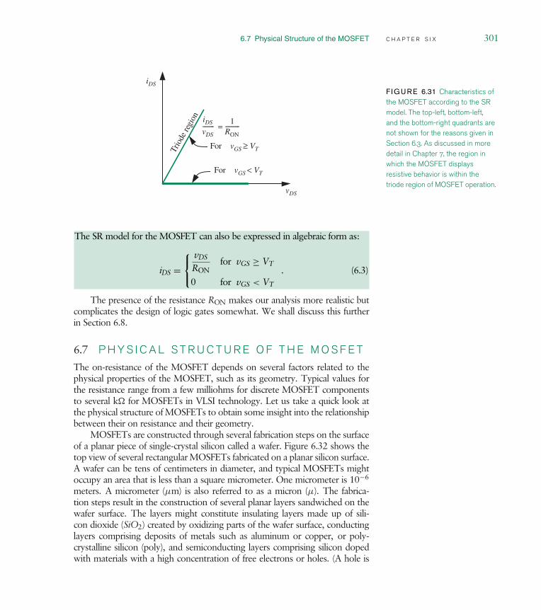
6.7 Physical Structure of the MOSFET C H A P T E R S I X 301
Trio
de re
gion
vDS
iDS
1RON----------
iDS
vDS-------- =
vGS ≥ VTFor
vGS < VTFor
F IGURE 6.31 Characteristics ofthe MOSFET according to the SRmodel. The top-left, bottom-left,and the bottom-right quadrants arenot shown for the reasons given inSection 6.3. As discussed in moredetail in Chapter 7, the region inwhich the MOSFET displaysresistive behavior is within thetriode region of MOSFET operation.
The SR model for the MOSFET can also be expressed in algebraic form as:
iDS =
vDS
RONfor vGS ≥ VT
0 for vGS < VT
. (6.3)
The presence of the resistance RON makes our analysis more realistic butcomplicates the design of logic gates somewhat. We shall discuss this furtherin Section 6.8.
6.7 P H Y S I C A L S T R U C T U R E O F T H E M O S F E T
The on-resistance of the MOSFET depends on several factors related to thephysical properties of the MOSFET, such as its geometry. Typical values forthe resistance range from a few milliohms for discrete MOSFET componentsto several k for MOSFETs in VLSI technology. Let us take a quick look atthe physical structure of MOSFETs to obtain some insight into the relationshipbetween their on resistance and their geometry.
MOSFETs are constructed through several fabrication steps on the surfaceof a planar piece of single-crystal silicon called a wafer. Figure 6.32 shows thetop view of several rectangular MOSFETs fabricated on a planar silicon surface.A wafer can be tens of centimeters in diameter, and typical MOSFETs mightoccupy an area that is less than a square micrometer. One micrometer is 10−6
meters. A micrometer (µm) is also referred to as a micron (µ). The fabrica-tion steps result in the construction of several planar layers sandwiched on thewafer surface. The layers might constitute insulating layers made up of sili-con dioxide (SiO2) created by oxidizing parts of the wafer surface, conductinglayers comprising deposits of metals such as aluminum or copper, or poly-crystalline silicon (poly), and semiconducting layers comprising silicon dopedwith materials with a high concentration of free electrons or holes. (A hole is

302 C H A P T E R S I X t h e m o s f e t s w i t c h
F IGURE 6.32 Top view ofseveral n-channel MOSFETsfabricated on a chip. The squareMOSFETs in the center of thephotograph have a width andlength of 100 µm. (PhotographCourtesy of Maxim IntegratedProducts.)
a positively charged element, and comprises an atom with a missing electron.)Doping is accomplished by diffusion or by ion implantation. The conductinglayers are separated by the insulating layers. Connections between layers sepa-rated by insulating material are created by etching contact holes in the insulatingmaterial and ‘‘pouring’’ metal through the contact holes.
Silicon doped with a material rich in electrons is called an n-type semicon-ductor. Similarly, silicon doped with a material rich in holes is called a p-typesemiconductor. As the word ‘‘semiconductor’’ implies, silicon doped with eithern-type or p-type material is a fairly good conductor of electricity. We use thenotation n+ or p+ to refer to silicon that is heavily doped with n-type or p-typematerial, respectively. n+ or p+ type semiconductors are even better conduc-tors. We commonly refer to n-type or p-type doped silicon areas as diffusionregions.
Figures 6.33 and 6.34 show sketches of two views of the physical structureof an n-channel MOSFET. An n-channel MOSFET is constructed on the surfaceof p-type silicon called the substrate. Two n+ doped regions separated by asmall distance (for example, 0.07 µ in digital devices, and quite a bit larger in
F IGURE 6.33 A simplifiedcross-sectional view of ann-channel MOSFET.
n+ n+
p substrate
Gate oxideGate
S
G
D

6.7 Physical Structure of the MOSFET C H A P T E R S I X 303
n+ n+
p substrate
Gate oxideGate
S
D
G
L
W
F IGURE 6.34 A three-dimensional view of ann-channel MOSFET.
analog applications) constitute the source and the drain. The region separatingthe source and the drain is called the channel region. The channel region isoverlayed with a thin insulating layer (for example, 0.01 µm thick) made outof silicon dioxide (commonly called gate oxide). The gate oxide layer is inturn sandwiched between a layer of conducting polysilicon on top and thep-type substrate. The polysilicon layer top of the gate oxide forms the gate ofthe MOSFET.
Although the precise mechanics of how a MOSFET works is beyond thescope of this discussion, the following provides some intuition on its operation.First, recall that n+-type silicon conducts through the motion of its free elec-trons. Let us consider the case where the gate and the source of the MOSFETare connected to ground, as illustrated in Figure 6.35. In this situation, vGS = 0.Because the n+ doped source and drain are separated by a p-type layer, theywill not conduct any current when a voltage is applied across them (vDS > 0).
However, when a positive voltage is applied at the gate of the device(vGS > 0), negative charges are attracted to the surface from the nearby negative-charge-rich source region (as shown in Figure 6.36) and positive charges arerepelled from the surface. Of course, no current flows between the gate andthe substrate because of the insulating gate oxide layer. As the gate voltage
n+ n+
p substrate
Gate oxideGate
S D
G
- - -- --
- - - -
-
-
- --
-- - -- - -- -- -- --
Ground
Ground Ground
F IGURE 6.35 MOSFEToperation when the gate isconnected to ground.
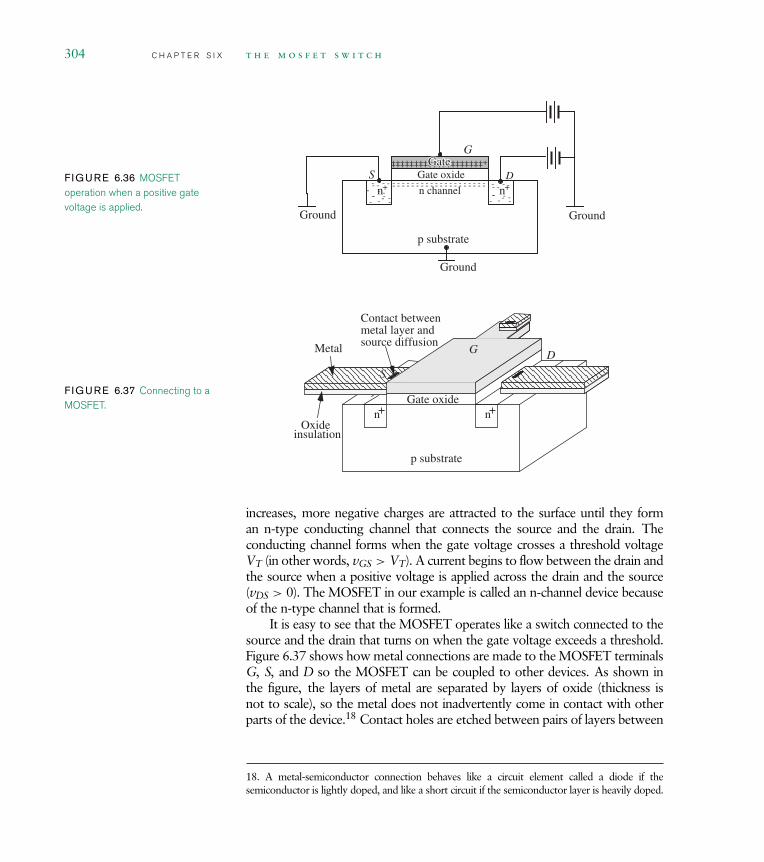
304 C H A P T E R S I X t h e m o s f e t s w i t c h
F IGURE 6.36 MOSFEToperation when a positive gatevoltage is applied.
n+ n+
p substrate
Gate oxideS D
G
--
--
---
--
-
-
-
- -
-
-
-- -- -
-- -- -- --
Ground
Ground Ground
- - - - - - - - - - - - - - - - - - - - - - - - - - - - - - - - - - - - - - - -
+++++++++++++++++++++++++++++++++++++++++
n channel
GateGateGate
F IGURE 6.37 Connecting to aMOSFET.
n+ n+
p substrate
Gate oxide
D
gateSS
G
Contact betweenmetal layer andsource diffusion
Oxideinsulation
Metal
increases, more negative charges are attracted to the surface until they forman n-type conducting channel that connects the source and the drain. Theconducting channel forms when the gate voltage crosses a threshold voltageVT (in other words, vGS > VT). A current begins to flow between the drain andthe source when a positive voltage is applied across the drain and the source(vDS > 0). The MOSFET in our example is called an n-channel device becauseof the n-type channel that is formed.
It is easy to see that the MOSFET operates like a switch connected to thesource and the drain that turns on when the gate voltage exceeds a threshold.Figure 6.37 shows how metal connections are made to the MOSFET terminalsG, S, and D so the MOSFET can be coupled to other devices. As shown inthe figure, the layers of metal are separated by layers of oxide (thickness isnot to scale), so the metal does not inadvertently come in contact with otherparts of the device.18 Contact holes are etched between pairs of layers between
18. A metal-semiconductor connection behaves like a circuit element called a diode if thesemiconductor is lightly doped, and like a short circuit if the semiconductor layer is heavily doped.

6.7 Physical Structure of the MOSFET C H A P T E R S I X 305
which connections are desired (much like a staple) and metal is allowed to flowthrough.
The conducting n-channel that is formed in the MOSFET discussed hereis not an ideal conductor and has some resistance RON. Also notice that theresistance of the gate is related to the geometry of the channel. Let the channellength be L and the channel width be W. Then, the resistance is proportionalto L/W. If Rn is resistance per square of the n-channel MOSFET in its on state,then the resistance of the channel is given by
RON = RnL
W. (6.4)
In any VLSI technology, there is a minimum fabricatable value for the MOSFETchannel length. Clearly, smaller dimensions mean that a VLSI chip of a givensize can hold more logic. As we shall see later, smaller dimensions also result inhigher speeds of operation. VLSI technologies are characterized by this mini-mum channel length. For example, a 0.2-µm process yields gate lengths in thevicinity of L = 0.2 µm. Historically, technologists have been able to decreasegate lengths by about a factor of two every four years over the past two decades.See Table 6.2 for the scaling factors observed by the authors in projects in whichthey were involved, and Figure 6.38 for a cross-sectional view of Intel’s 0.13 µm
y e a r d e s i g n m i n l
1981 Analog echo canceler 8 µm
1984 Telecom bus controller 4 µm
1987 RISC microprocessor 2 µm
1994 Multiprocessor communicationscontroller
0.5 µm
2002 Raw microprocessor 0.18 µm
TABLE 6.2 Historical gate-length scaling observations.
F IGURE 6.38 A cross-sectionalTEM (transmission electronmicroscope) picture of Intel’s0.13-µm generation logic transistor.(Photograph Courtesy of IntelCorporation.)

306 C H A P T E R S I X t h e m o s f e t s w i t c h
generation logic transistor. This torrid pace of technological development showsno signs of slowing down at the time of this writing.
6.8 S T A T I C A N A L Y S I S U S I N G T H E S R M O D E L
The presence of the on resistance RON complicates the design of logic gatesslightly, but adds more realism to the model. Let us analyze our familiar invertercircuit shown in Figure 6.14 using the SR model of the MOSFET. In particular,let us derive its input-output transfer characteristic. Figure 6.39 shows the circuit
VS
vO
RL
VS
vO
RL
vIN = High
vIN = Low
RON
F IGURE 6.39 Circuit model ofthe n-channel MOSFET inverterusing the SR MOSFET model.
model of the inverter using the SR model of the MOSFET.As shown in Figure 6.39, when the input is low, the MOSFET is off, and
the output is raised to a high value.However, when the input vIN is high (and above the threshold VT), the
MOSFET is on and displays a resistance RON between its D and S terminals,thereby pulling the output voltage lower. However, the output voltage is not0 V as predicted by the simpler S model of the MOSFET. Instead, the value ofthe output voltage is given by the voltage-divider relationship:
vOUT = VSRON
RON + RL. (6.5)
The resulting inverter transfer characteristics, assuming VS = 5 V, VT =1 V, RON = 1 k, and RL = 14 k, are shown in Figure 6.40. Notice that thelowest output voltage of the inverter is no longer 0 V, rather it is
VSRON
RON + RL= 0.33 V.
F IGURE 6.40 Inverter transfercharacteristics using the SR model.
5 V vIN
vOUT
5 V
VT =
1V
VS RON
RON + RL----------------------- = 0.33 V
0 V

6.8 Static Analysis Using the SR Model C H A P T E R S I X 307
Before embarking on a detailed static analysis of our inverter, let us con-duct a simple electrical switching analysis to build intuition. In particular, wewill analyze the relationship between VT, VS, RL, and RON, and the switchingbehavior of the inverter. As a minimum, when a sending inverter drives a receiv-ing inverter, the sender must be able to switch the MOSFET in the receivinginverter into its ON state when the sender produces a high voltage. Similarly,the sender must be able to switch the MOSFET in the receiving inverter intoits OFF state when the sender produces a low voltage.
Our inverter produces a high output of VS, so it is easy to see that the highoutput can turn the MOSFET in a receiving inverter into its ON state (provided,of course, that VS > VT). Because the inverter produces a nonzero low output,more care needs to be taken in the choice of resistance values and the MOSFETparameters. Specifically, for our inverter design, the voltage output for a logical0 must be low enough that the MOSFET in the receiver stays OFF. Becausethe MOSFET turns ON for an input voltage greater than VT, the followingcondition must be met for the low output of one inverter to be able to drivethe MOSFET in another inverter into its OFF state:
VSRON
RON + RL< VT. (6.6)
Equation 6.6 specifies a key relation between the inverter device parametersfor it to be usable as a switching device. Note that we do not distinguish betweenthe MOSFET or resistance value parameters for the sender and the receiver,since the device must be able to serve as both a sender and a receiver.
e x a m p l e 6.5 s w i t c h i n g a n a l y s i s o f a n i n v e r t e r
Assume the following values for the inverter circuit parameters: VS = 5 V, VT = 1 V,and RL = 10 k. Assume, further, that Rn = 5 k for the MOSFET. Determine a W/Lsizing for the MOSFET so that the inverter gate output for a logical 0 is able to switchOFF the MOSFET of another inverter.
Equation 6.6 shows the condition that our inverter must satisfy for its logical 0 outputto be able to turn off a MOSFET. From Equation 6.4, we know that the ON stateresistance of the MOSFET is given by
RON = RnL
W.
Substituting this relation into Equation 6.6, we get the following constraint on the W/Lratio of the inverter MOSFET:
VSRn
LW
RnLW
+ RL< VT.

308 C H A P T E R S I X t h e m o s f e t s w i t c h
Simplifying, we obtain the following constraint on W/L:
W
L>
Rn(VS − VT)
VTRL.
Substituting, Rn = 5 k, VS = 5 V, VT = 1 V, and RL = 10 k, we obtain
W
L> 2.
For the parameter values that we have been given, this result indicates that our inverterMOSFET must be sized such that its W/L ratio is greater than 2.
Commonly, it is not enough for the inverter to meet the preceding switch-ing criteria. In real systems, however, it must also provide for adequate noisemargins by satisfying a static discipline. The inverter characteristic shown inFigure 6.40 provides us with adequate information to determine whether theinverter satisfies a given static discipline. As an example, let us determinewhether the inverter satisfies a static discipline with the following voltagethresholds:
VOH = 4.5 V, VOL = 0.5 V, VIH = 4 V, and VIL = 0.9 V.
Figure 6.41 shows the voltage thresholds for the given static disciplinesuperimposed on the inverter transfer function. Let us check each of the outputand input thresholds.
VOH: The inverter produces an output high of 5 V. Clearly, this outputvoltage level for a logical 1 is greater than the 4.5-V output-highthreshold required by the static discipline.19
VOL: The inverter produces an output low of 0.33 V. This output voltage islower than the output-low threshold of 0.5 V required by the staticdiscipline.20
VIH: For our static discipline, VIH = 4 V. To obey the static discipline theinverter must interpret any voltage above 4 V as a logical 1. This iscertainly true for our inverter.21
VIL: For our static discipline, VIL = 0.9 V. This means that to obey thestatic discipline the inverter must interpret any voltage below 0.9 V asa logical 0. This is also true for our inverter.22
19. In fact, our inverter can satisfy a static discipline with a VOH as high as 5− V.
20. Notice that our inverter can satisfy a static discipline with a VOL as low as 0.33+ V.
21. In fact, our inverter can satisfy a static discipline with a VIH as low as V+T V.
22. In fact, our inverter can satisfy a static discipline with a VIL as high as V −T V.

6.8 Static Analysis Using the SR Model C H A P T E R S I X 309
5 V
vIN
vOUT
5 V
VT =
1 V
0 V
VOH = 4.5 V
VOL = 0.5 VV
IL =
0.9
V
VIH
= 4
V
0.33 V
F IGURE 6.41 A mappingbetween logic values and voltagelevels corresponding to a staticdiscipline appropriate for theinverter analyzed using the SRmodel.
Thus our inverter satisfies the static discipline with the voltage thresholds:VOH = 4.5 V, VOL = 0.5 V, VIH = 4 V, and VIL = 0.9 V, even when the SRmodel is used when RL = 14 k and RON = 1 k.
e x a m p l e 6.6 d e s i g n i n g a n i n v e r t e r t o m e e t t h e
c o n s t r a i n t s o f a g i v e n s t a t i c d i s c i p l i n e Suppose weare given a static discipline with the following voltage thresholds: VOH = 4.5 V,VOL = 0.2 V, VIH = 4 V, and VIL = 0.9 V. Let us determine whether our invertersatisfies the constraints of this static discipline, and if it does not, let us redesign theinverter so that it does.
Let us begin by comparing the transfer characteristics of our inverter against the voltagethresholds of the given static discipline. As shown in Figure 6.40, recall that our inverterproduces a high output of 5 V, and a low output of 0.33 V. It can interpret voltagesbelow VT = 1 V as a logical 0 and voltages above VT = 1 V as a logical 1.
1. When outputting a logical 1, the voltage produced by our inverter must be greaterthan VOH = 4.5 V. Since our inverters produce a 5-V output for a logical 1, theysatisfy this condition.
2. When outputting a logical 0, the voltage must be no greater than VOL = 0.2 V.Since our inverters produce a 0.33-V output for a logical 0, they violate thiscondition.
3. At their inputs, they must recognize voltages greater than VIH = 4 V as a logical1. Since our inverters recognize voltages above 1 V as a logical 1, they satisfy thiscondition as well.

310 C H A P T E R S I X t h e m o s f e t s w i t c h
4. Finally, at their inputs, the inverters must recognize voltages less than VIL = 0.9 Vas a logical 0 if they are to satisfy the static discipline. Our inverters satisfy thiscondition as well.
Since the output low voltage produced by our inverters is 0.33 V, which is higher thanthe required VOL = 0.2 V, our inverters do not meet the constraints of the given staticdiscipline.
How might we redesign our inverter to meet the given static discipline? Notice thataccording to Equation 6.5 the output voltage of the inverter for a high input is given by
vOUT = VSRON
RON + RL.
The output vOUT is 0.33 V for VS = 5 V, RON = 1 k and RL = 14 k.
We need our inverter to produce an output lower than 0.2 V for a high input. In otherwords,
0.2V > VSRON
RON + RL. (6.7)
We have three choices to reduce the output voltage: reduce VS, reduce RON, or increaseRL. Reducing VS will also reduce the output high voltage, so that is not such a goodstrategy. Instead, we will look to working with the resistances.
First, let us try to increase RL. Rearranging Equation 6.7, we get:
RL > VSRON
0.2− RON.
For VS = 5 V and RON = 1 k, we have
RL > 24 k.
In other words, we can choose RL > 24 k, which will result in a output voltage for alogical 0 that is lower than 0.2 V. However, it turns out that large values of resistanceare hard to achieve in VLSI technology. Section 6.11 shows how another MOSFET canbe used in place of the pullup resistor.
Alternatively, we can try to reduce RON by increasing the W/L ratio of the MOSFET.Let us determine the minimum W/L ratio.
From Equation 6.7, we can find the constraint on RON that allows the output lowvoltage to be less than 0.2 V as
RON <0.2RL
VS − 0.2.

6.8 Static Analysis Using the SR Model C H A P T E R S I X 311
For VS = 5 V and RL = 14 k, we have
RON < 0.58 k.
Since RON = RnLW
, (see Equation 6.4), and assuming Rn = 5 k for our MOSFET,we get
5 kL
W< 0.58 k.
In other words, choosing a MOSFET with W/L > 8.62 will result in an output voltagefor a logical 0 that is lower than 0.2 V.
6.8.1 S T A T I C A N A L Y S I S O F T H E N A N DG A T E U S I N G T H E S R M O D E L
We can also analyze other gates in like manner. Figure 6.42 shows the equivalentcircuit for the NAND gate shown in Figure 6.20 based on the SR MOSFETmodel.
In this case, the output voltage when both inputs are high is given by
vOUT = VS2RON
2RON + RL.
Let us determine whether our NAND gate with VS = 5 V, RL = 14 k,and MOSFET properties RON = 1 k and VT = 1 V, satisfies a static disciplinewith the following voltage thresholds:
VS
OUT
RL
A = High RON
RONB = High
F IGURE 6.42 SR circuit modelfor NAND gate.
VOH = 4.5 V, VOL = 0.5 V, VIH = 4 V, and VIL = 0.9 V.
Recall that our inverter with characteristics shown in Figure 6.40 satis-fied this static discipline. Now let’s check out our NAND gate. Figure 6.43shows the voltage thresholds for the given static discipline superimposed on theinverter transfer function. As before, let us check each of the output and inputthresholds.
Like the inverter, the NAND gate produces an output high of 5 V, andtherefore satisfies the output-high voltage threshold of 4.5 V. Similarly, theNAND gate satisfies both the VIH = 4 V and the VIL = 0.9 V thresholds sinceit interprets voltages above 4 V at its input as a logical 1 and voltages below0.9 V at its inputs as a logical 0.
Let us now look at VOL. When outputting a logical 0, the NAND gateproduces a voltage
vOUT = VS2RON
2RON + RL.

312 C H A P T E R S I X t h e m o s f e t s w i t c h
F IGURE 6.43 The voltage levelscorresponding to a static disciplinesuperimposed on the NAND gate’stransfer characteristics.
5 V vIN
vOUT
5 V
VT
= 1
V
0 V
VOH = 4.5 V
VOL = 0.5 V
VIL
= 0
.9 V
VIH
= 4
V
0.66 V
For VS = 5 V, RL = 14 k, and RON = 1 k, we get vOUT = 0.625 V, whichis nearly twice that produced by the inverter for a logical 0 output. This is notsurprising since there are two MOSFETs in series in the pulldown network.Since this output voltage is greater than VOL = 0.5 V, we conclude that ourNAND does not satisfy the static discipline.
How might we redesign our NAND gate such that it satisfies the staticdiscipline? One approach is to increase RL such that
0.5 V > VS2RON
2RON + RL.
In other words,
RL > VS2RON
0.5− 2RON.
For VS = 5 V and RON = 1 k, we have
RL > 18 k.
This means that we can choose RL > 18 k for the NAND gate, which willresult in a output voltage for a logical 0 that is lower than 0.5 V, therebysatisfying the static discipline.

6.8 Static Analysis Using the SR Model C H A P T E R S I X 313
e x a m p l e 6.7 s w i t c h i n g a n a l y s i s o f a n a n d g a t e
Consider the NAND gate in Figure 6.42. Assume the following values for the circuitparameters: VS = 5 V, VT = 1 V, and RL = 10 k. Assume, further, that Rn = 5 k
for each of the MOSFETs. Determine a W/L sizing for the MOSFETs so that theNAND gate output is able to switch ON or OFF the MOSFET of another gate such asan inverter.
Since the NAND gate produces a high output of 5 V, its output applied to the gate ofanother MOSFET (with a VT = 1 V) can clearly drive the MOSFET into its ON state.
We now have to determine whether its low output can turn a MOSFET OFF. Recallthat the NAND gate produces the following output voltage for a logical 0:
vOUT = VS2RON
2RON + RL.
For a MOSFET driven by the output to remain OFF, we must have
vOUT = VS2RON
2RON + RL< VT.
From Equation 6.4, we know that the ON state resistance of the MOSFETs is given by
RON = RnL
W.
Thus, we can write the following constraint on the W/L ratio of the two NAND gateMOSFETs:
VS2Rn
LW
2RnLW
+ RL< VT.
Simplifying, we obtain the following constraint on W/L:
W
L>
2Rn(VS − VT)
VTRL.
Substituting, Rn = 5 k, VS = 5 V, VT = 1 V, and RL = 10 k, we obtain
W
L> 4.
In other words, the two MOSFETs must be sized such that each of their W/L ratios isgreater than 4. Notice that as the number of MOSFETs connected in series increases,so must their sizes to ensure they produce a low enough output voltage that is able toswitch OFF a MOSFET connected to the output.

314 C H A P T E R S I X t h e m o s f e t s w i t c h
F IGURE 6.44 Noise marginsand signal transmission.
Send 0 Receive 0 Noise 0.6 V
vO = 1 V vI = 1.6 V(< 2 V)
Send 0
vO = 1 V
I B
6.9 S I G N A L R E S T O R A T I O N , G A I N ,A N D N O N L I N E A R I T Y
We saw in an earlier chapter (Figure 5.7) that the provision of noise marginsenables error-free communication in the presence of noise. We will revisit theexample in Figure 5.7 to demonstrate that logic devices must incorporate bothgain and nonlinearity to provide nonzero noise margins.23
6.9.1 S I G N A L R E S T O R A T I O N A N D G A I N
Figure 6.44 shows a situation similar to that in Figure 5.7, but for concreteness,replaces the first logic gate with an inverter I and the second with a buffer B.Like the inverter, the buffer has a single input and a single output. It performsthe identity function, that is it simply copies the input value to its output. Thistime around, we will focus on the conditions at the buffer. Assume that bothour logic gates adhere to a static discipline with the following voltage levels:
VIL = 2 V
VIH = 3 V
VOL = 1 V
VOH = 4 V.
In our example, the inverter sends a 0 by placing vOUT = 1 V (correspond-ing to VOL) on the wire. Figure 6.44 shows 0.6 V of noise being added tothe signal by the transmission channel. However, the buffer is able to correctlyinterpret the received value as a 0 because the received value of 1.6 V is withinthe low input voltage threshold of VIL = 2 V. The buffer, in turn, performs theidentity logical operation on the signal and produces a logical 0 at its output.According to the static discipline, the voltage level at the buffer’s output is 1 Vcorresponding to VOL.
Figure 6.45 shows the same situation replacing the actual voltage levelswith the respective parameters for transmitting a logical 0 and a logical 1.
23. We will see the concept of gain showing up again in the context of analog design in Chapter 7.

6.9 Signal Restoration, Gain, and Nonlinearity C H A P T E R S I X 315
Send 0 Receive 0Noise 0.6 V
vO = VOL vI < VIL
Send 0
vO = VOL
I
Send 1 Receive 1Noise 0.6 V
vO = VOH vI > VIH
Send 1
vO = VOH
I B
B
F IGURE 6.45 Low and highthresholds for the input and output.
VIL
VOH
VOL
VIH
0 V
1 V
2 V
3 V
4 V
5 V
IN OUT
GATE
Input Output
Valid 1
Valid 0
Valid 1
Valid 00 V
1 V
2 V
3 V
4 V
5 V
F IGURE 6.46 Signal restorationand amplification.
In Figure 6.44, notice that to obey the static discipline, the buffer mustconvert the 1.6-V signal at its input to a 1-V value at its output. In fact, thebuffer must restore any voltage up to 2 V at its input to voltage of 1 V or lowerat its output. Similarly, corresponding to a logical high, it must restore anyvoltage above 3 V at its input to 4 V or higher at its output. This restorationproperty is key to our being able to compose multiple logic devices together.Because each level of logic restores or cleans up signals, we can decouple thenoise introduced between each pair of levels. This noise decoupling benefit ofrestoring logic enables us to build complicated multistage logic systems.
As Figure 6.46 depicts, logic devices must restore input signals that lie inthe range 0 V < vI < VIL for logical 0’s and VIH < vI < 5 V for logical 1’s tooutput signals that are restricted to the range 0 V < vO < VOL for logical 0’sand VOH < vO < 5 V for logical 1’s, respectively.
Observe further that the restrictions in Figure 6.46 imply that a non-inverting device such as a buffer or an AND gate must convert an input low tohigh transition of the form VIL → VIH to an output low to high transition ofthe form VOL (or lower) → VOH (or higher). This scenario is depicted by thearrows in Figure 6.46. The same situation is described using input and outputwaveforms in Figure 6.47. It is clear from the figures that a static discipline

316 C H A P T E R S I X t h e m o s f e t s w i t c h
F IGURE 6.47 Input waveformand restored output waveform.
0 V1 V2 V3 V4 V5 V
0 V1 V2 V3 V4 V5 V
0 V1 V2 V3 V4 V5 V
0 V1 V2 V3 V4 V5 V
Input
Output
VILIL
VIHIHVIL
VIH
VILIL
VIHIHVIL
VIH
VOHOH
VOLOL
VOHOH
VOLOL
VOH
VOL
VOH
VOL
that provides for nonzero noise margins requires logic devices that provide aminimum gain.
Algebraically, nonzero noise margins require that
VIL > VOL. (6.8)
and
VOH > VIH. (6.9)
The magnitude of the change in the voltage for an input transition fromVIL → VIH is given by
vI = VIH − VIL.
The corresponding magnitude of the (minimum) change at the output isgiven by
vO = VOH − VOL.
Therefore, the gain of a device that can convert a VIL → VIH transition atits input to a VOL → VOH transition at its output is given by
Gain = vO
vI= VOH − VOL
VIH − VIL.
From the noise-margin inequalities in Equations 6.8 and 6.9, we have
VOH − VOL > VIH − VIL.

6.9 Signal Restoration, Gain, and Nonlinearity C H A P T E R S I X 317
Therefore, the magnitude of the gain for an input transition VIL → VIH mustbe greater than 1. In other words,
Gain = VOH − VOL
VIH − VIL> 1. (6.10)
Similarly, inverting devices such as inverters or NAND gates must convertinput low to high transitions of the form VIL → VIH to output high to lowtransitions of the form VOH → VOL. Like the non-inverting case, the conditionson the magnitude of the gain for transitions from VIL → VIH remain unchanged.
Returning to our buffer example, the gain for the VIL → VIH transition isgiven by
Gain = VOH − VOL
VIH − VIL
= 4V − 1V
3V − 2V
= 3.
Since the buffer and the inverter follow the same voltage thresholds, themagnitude of the gain for the VIL → VIH transition at the input of the inverteris also 3. Clearly, the greater the noise margins, the greater the required gainfor the VIL → VIH transition.
6.9.2 S I G N A L R E S T O R A T I O N A N D N O N L I N E A R I T Y
You might have realized that although logic devices must demonstrate a gaingreater than unity when they transition from VIL to VIH, they must also atten-uate the signal at other times. For example, Figure 6.48 shows the signalfrom Figure 6.47 with some noise superimposed on it. It should be clear fromFigure 6.48 that to obey the static discipline the buffer has reduced the 0-V to2-V noise excursions at the input to 0-V to 1-V noise excursions at its output.
We can also verify this fact using the basic noise-margin inequalities inEquations 6.8 and 6.9. Equations 6.8 implies that any voltage between 0 andVIL at the input must be attenuated to a voltage between 0 and VOL at the output(see Figure 6.49). Since VIL > VOL according to Equation 6.8, it follows thatvoltage transfer ratio must be less than unity. In other words,
VOL − 0
VIL − 0= VOL
VIL< 1.
The same reasoning applies to valid high voltages. Because VIH < VOH,
5 − VOH
5 − VIH< 1.

318 C H A P T E R S I X t h e m o s f e t s w i t c h
F IGURE 6.48 Input waveformand restored output waveform inthe presence of noise.
0 V1 V2 V3 V4 V5 V
0 V1 V2 V3 V4 V5 V
0 V1 V2 V3 V4 V5 V
0 V1 V2 V3 V4 V5 V
Input
Output
VILIL
VOHOH
VOLOL
VIHIH
VILIL
VOHOH
VOLOL
VIHIH
VIL
VOH
VOL
VIH
VIL
VOH
VOL
VIH
F IGURE 6.49 Signal restorationand attenuation. VIL
VOH
VOL
VIH
0 V
1 V
2 V
3 V
4 V
5 V
0 V
1 V
2 V
3 V
4 V
5 VInput Output
Valid 1
Valid 0
Valid 1
Valid 0
The amplification requirement for low to high transitions of the formVIL → VIH, and the attenuation requirement in other regions, mandates theuse of nonlinear devices in logic gates.24
6.9.3 B U F F E R T R A N S F E R C H A R A C T E R I S T I C S A N DT H E S T A T I C D I S C I P L I N E
The presence of gain and nonlinearity in the buffer become abundantly clear ifwe look at its transfer characteristic. Figure 6.50 graphically plots the transfercharacteristic of a logic device that can serve as a valid buffer. The shadedregion depicts the valid region for the buffer transfer curve. The x-axis showsinput voltages and the y-axis output voltages. We can make several interestingobservations from this graph. Notice that valid input voltages result in validoutput voltages. For example, input voltages less than VIL produce outputvoltages less than VOL, and input voltages greater than VIH produce outputvoltages greater than VOH. Also notice that the amplification occurs when the
24. As an exercise in futility, you might want to attempt building a simple logic gate, such as abuffer, with nonzero noise margins, using resistors alone.

6.9 Signal Restoration, Gain, and Nonlinearity C H A P T E R S I X 319
vI
vO
VIL VIH
VOH
VOL
Slope > 1 Slope < 1
Slope < 1F IGURE 6.50 The buffercharacteristic.
curve is in the forbidden region. In other words, the slope of the transfer curvein the forbidden region is greater than one.
As discussed earlier, recall that it is not sufficient for a valid logicdevice to have gain in the forbidden region. The transfer characteristic for inputvalues between 0 V and VIL must have an overall gain of less than unity. Accord-ingly, notice that the transfer curve shown in Figure 6.50 attenuates voltagesthat lie in the valid input low or valid input high intervals.
Observe further that the transfer curve for the buffer passes through theforbidden region. Doesn’t this violate our initial premise that voltages in theforbidden region were disallowed? Recall that the static discipline requiresthe logic gate to guarantee valid outputs only for valid inputs. That the outputsare in the forbidden region when the inputs are invalid is of no consequence.
6.9.4 I N V E R T E R T R A N S F E R C H A R A C T E R I S T I C S A N DT H E S T A T I C D I S C I P L I N E
Let us now briefly examine a transfer curve for the hypothetical, but valid,inverter shown in Figure 6.51. Referring to Figure 6.51, provided the input volt-age is lower than VIL, an inverter satisfies the static discipline if it guarantees toprovide an output voltage level greater than VOH. Similarly, for an input voltagehigher than VIH, the inverter guarantees to provide an output that is below VOL.
As discussed for the non-inverting buffer, the magnitude of the slope ofthe transfer curve in the forbidden region is greater than unity. Similarly, themagnitude of the slope of each of the curve segments in the valid regions is lessthan unity.
For maximum noise immunity, the separation between VOL and VOHshould be as high as possible at output, and that between VIL and VIH to beas low as possible. This is equivalent to maximizing the area of the grey boxes

320 C H A P T E R S I X t h e m o s f e t s w i t c h
F IGURE 6.51 The invertercharacteristic.
vI
vOIdeal characteristic
Typical characteristic
VIL VIH
VOH
VOL
shown in Figure 6.51. An ideal inverter characteristic will look like the thick lineshown in the figure.
6.10 P O W E R C O N S U M P T I O N I N L O G I C G A T E S
We can use the SR model to calculate the maximum power consumed by logicgates. We consider a simple case here, and postpone more discussion to Chap-ter 11. Referring to Figure 6.52, the power consumed by a logic gate is given by
VS
vOUT
RL
vIN = High Rpd
I
F IGURE 6.52 Powerconsumption in logic gates.
Power = VSI = V2S
RL + Rpd. (6.11)
The power consumed depends on the load resistance and the resis-tance of the pulldown network Rpd. For the inverter, the power consumedis zero when the input is low. The maximum power is consumed when theinput is high and Rpd = RON.VS
B
OUTA
C
VSR6
R7
F IGURE 6.53 A logic circuitcomprising MOSFET switches andresistors.
e x a m p l e 6.8 p o w e r i n l o g i c g a t e s Write a boolean equa-tion for OUT in terms of the inputs for the circuit in Figure 6.53.
OUT = A(B + C).
Determine the power consumed by the circuit when A = 1, B = 1, and C = 1. Assumethat the on-state resistance of the MOSFETs is RON.
When all the inputs are high, the relevant equivalent circuit is shown in Figure 6.54. Thepower is given by
P = V2S
(1
2RON + R6+ 1
RON + R7
).

6.11 Active Pullups C H A P T E R S I X 321
W W W 6.11 A C T I V E P U L L U P S VS
OUT
VSR6
R7
RON
RON
RON
F IGURE 6.54 Equivalent circuitwhen all inputs are high.
W W W e x a m p l e 6.9 s i z i n g p u l l u p d e v i c e s
W W W e x a m p l e 6.10 c o m b i n a t i o n a l l o g i c u s i n g
m o s f e t s w i t c h e s

322 C H A P T E R S I X t h e m o s f e t s w i t c h
6.12 S U M M A R Y This chapter introduced our first three-terminal device, namely a switch. A
common way of using three-terminal devices is to pair their terminals intoa pair of ports called the control port and the output port.
We also introduced the MOSFET device, which is a three-terminal circuitelement. Although, as we will see in Chapter 7, the MOSFET has a veryrich behavior, it can be grossly characterized as a switch. We developed theS and the SR models for the MOSFET, which capture its basic switch-likebehavior.
This chapter also showed how digital gates could be built using MOSFETsand resistors. We discussed how the digital circuits had to be designed sothey met the VIH, VOH, VIL, and VOL voltage thresholds specified by agiven static discipline. We also estimated the power dissipation of logicgates using their circuit models.
E X E R C I S E S e x e r c i s e 6.1 Give a resistor-MOSFET implementation of the following logicfunctions. Use the S model of the MOSFET for this exercise (in other words, you mayassume that the on-state resistance of the MOSFETs is 0).
(A + B) · (C + D)
A · B · C · D
(Y · W)(X · W)(X · Y · W)
e x e r c i s e 6.2 Write a boolean expression that describes the function of eachof the circuits in Figure 6.59.
e x e r c i s e 6.3 Figure 6.60 shows an inverter circuit using a MOSFET and aresistor. The MOSFET has a threshold voltage VT = 2 V. Assume that VS = 5 V andRL = 10 k. For this exercise, model the MOSFET using its switch model. In otherwords, assume that the on-state resistance of the MOSFET is 0.
a) Draw the input versus output voltage transfer curve for the inverter.
b) Does the inverter satisfy the static discipline for the voltage thresholds VOL = 1V, VIL = 1.5 V, VOH = 4 V and VIH = 3 V? Explain. (Hint: To satisfy thestatic discipline, the inverter must interpret correctly input values that are valid logicsignals. Furthermore, given valid logic inputs, the inverter must also output validlogic signals. Valid logic 0 input signals are represented by voltages less than VIL,valid logic 1 input signals are represented by voltages greater than VIH, valid logic 0output signals are represented by voltages less than VOL, and valid logic 1 outputsignals are represented by voltages greater than VOH.)

6.12 Summary C H A P T E R S I X 323
c) Does the inverter satisfy the static discipline if the VIL specification was changed toVIL = 2.5 V? Explain.
VS
A
OUT
(a)
R2R1
(d)
A
BC
VS
OUT
EN
R8
VS
A
OUT
B
(b)
R3R4
R5
VS
VS
B
OUTA
(c)
C
R6
R7
F IGURE 6.59
d) What is the maximum value of VIL for which the inverter will satisfy the staticdiscipline?
e) What is the minimum value of VIH for which the inverter will satisfy the staticdiscipline?
e x e r c i s e 6.4 Consider, again, the inverter circuit shown in Figure 6.60. TheMOSFET has a threshold voltage VT = 2 V. Assume that VS = 5 V and RL = 10k.For this exercise, model the MOSFET using its switch-resistor model. Assume that theon-state resistance of the MOSFET is RON = 8 k.
VS
IN
OUT
RL
F IGURE 6.60
a) Does the inverter satisfy the static discipline, which has voltage thresholds given byVOL = VIL = 1 V and VOH = VIH = 4 V? Explain.
b) Does the inverter satisfy the static discipline for the voltage thresholds VOL = VIL =2.5 V and VOH = VIH = 3 V? Explain.
c) Draw the input versus output voltage transfer curve for the inverter.
d) Is there any value of VIL for which the inverter will satisfy the static discipline?Explain.
e) Now assume that RON = 1k and repeat parts (a), (b), and (c).
e x e r c i s e 6.5 Compute the worst-case power consumed by the inverter shownin Figure 6.60. The MOSFET has a threshold voltage VT = 2 V. Assume that VS = 5 Vand RL = 10 k. Model the MOSFET using its switch-resistor model, and assume thatthe on-state resistance of the MOSFET is RON = 1 k.
e x e r c i s e 6.6 Consider again the circuits in Figure 6.59. Using the switch-resistor model of the MOSFET, choose minimum values for the various resistors inFigure 6.59 so each circuit satisfies the static discipline with voltage thresholds given byVIL = VOL = VS/10 and VIH = VOH = 4VS/5. Assume the on-state resistance of theMOSFET is RON and that its turn-on threshold voltage VT = VS/9.
e x e r c i s e 6.7 Consider a family of logic gates that operates under the staticdiscipline with the following voltage thresholds: VOL = 0.5 V, VIL = 1.6 V, VOH =4.4 V, and VIH = 3.2 V.
a) Graph an input-output voltage transfer function of a buffer satisfying the four voltagethresholds.
b) What is the highest voltage that can be output by an inverter for a logical 0output?

324 C H A P T E R S I X t h e m o s f e t s w i t c h
c) What is the lowest voltage that can be output by an inverter for a logical 1output?
d) What is the highest voltage that must be interpreted by a receiver as alogical 0?
e) What is the lowest voltage that must be interpreted by a receiver as alogical 1?
f ) What is the 0 noise margin provided by this logic family?
g) What is the 1 noise margin provided by this logic family?
h) What is the minimum voltage gain the buffer must provide in the forbiddenregion?
P R O B L E M S p r o b l e m 6.1
a) Write a truth table and a boolean equation relating the output Z to A, A, B, and C,when these are input to the circuit shown in Figure 6.61.
Z
A
A
B
B
C
VS
R
F IGURE 6.61
b) Suppose the circuit in Figure 6.61 suffers a manufacturing error that results in a shortbetween the pair of wires depicted in Figure 6.62. Write a truth table and a booleanequation relating the output Z to A, A, B, and C, for the resulting circuit.
Z
A
B
B
C
VS
R
A
F IGURE 6.62
p r o b l e m 6.2 A specific type of MOSFET has VT = −1 V. The MOSFET isin the ON state (a short exists between its drain and source) when vGS ≥ VT. TheMOSFET is in the OFF state (an open circuit exists between its drain and source) whenvGS < VT.
(a) Graph the iDS versus vGS characteristics of this MOSFET.
(b) Graph the iDS versus vDS characteristics this of the MOSFET for vGS ≥ VT andvGS < VT.

6.12 Summary C H A P T E R S I X 325
p r o b l e m 6.3 Consider a family of logic gates that operate under the static dis-cipline with the following voltage thresholds: VOL = 1 V, VIL = 1.3 V, VOH = 4 V,and VIH = 3 V. Consider the N-input NAND gate design shown in Figure 6.63. In thedesign R = 100k and RON for the MOSFETs is given to be 1k. VT for the MOSFETsis 1.5 V. What is the maximum value of N for which the NAND gate will satisfy thestatic discipline? What is the maximum power dissipated by the NAND gate for thisvalue of N?
Z
A1 A2 A3 ...
R
An
VS
F IGURE 6.63
p r o b l e m 6.4 Consider the N-input NOR gate shown in Figure 6.64. Assumethat the on-state resistance of each of the MOSFETs is RON. For what set of inputs doesthis gate consume the maximum amount of power? Compute this worst-case power.
Z
A1 A2 A3
R
A4 ... An
VS
F IGURE 6.64
p r o b l e m 6.5 Consider the circuit shown in Figure 6.65. We wish to design thecircuit so it operates under a static discipline with voltage thresholds VOL, VIL, VOH, and
Z
A11
R
A12
A13
A1n
A21
A22
A23
A2n
Am1
Am2
Am3
Amn
VS
F IGURE 6.65

326 C H A P T E R S I X t h e m o s f e t s w i t c h
VIH. Assume that the on-state resistance of each of the MOSFETs is RON and that theMOSFET threshold voltage is VT. Assume that the given values satisfy the constraintsVS ≥ VOH and VIL < VT. For what values of n and m does this gate operate under thestatic discipline? What is the worst case power consumed by this circuit?
Z
A
B
VS
L1
W1
-----
-----
-----
L2W2
L3W3
VA
F IGURE 6.66
p r o b l e m 6.6 Consider a family of logic gates that operate under the static dis-cipline with the following voltage thresholds: VOL = 0.5 V, VIL = 1 V, VOH = 4.5 V,and VIH = 4.0 V.
a) Graph an input-output voltage transfer function of an inverter satisfying the fourvoltage thresholds.
b) Using the switch-resistor MOSFET model, design an inverter satisfying the staticdiscipline for the four voltage thresholds using an n-channel MOSFET and a resistor.The MOSFET has Rn = 1 k and VT = 1.8 V. Recall, RON = Rn(L/W). AssumeVS = 5 V and R for a resistor is 500 . Further assume that the area of the inverteris given by the sum of the areas of the MOSFET and the resistor. Assume that thearea of a device is L × W. The inverter should take as little area as possible withminimum size for L or W being 0.5 µm. Graph the input-output transfer functionof the inverter. What is the total area of the inverter? What is its maximum staticpower dissipation?
p r o b l e m 6.7 Consider a family of logic gates that operates under the static dis-cipline with the following voltage thresholds: VOL = 0.5 V, VIL = 0.9 V, VOH = 4.5V, and VIH = 4 V. Using the switch-resistor MOSFET model, design a 2-input NANDgate satisfying the static discipline for the four voltage thresholds using three n-channelMOSFETs as illustrated in Figure 6.66 (the MOSFET with its gate connected to a volt-age VA and drain connected to the power supply VS serves as the pullup). VA is chosensuch that VA > VS + VT. The MOSFETs have Rn = 1 k and VT = 1.8 V. Recall,RON = Rn(L/W). Assume VS = 5 V. Further assume that the area of the NAND gate isgiven by the sum of the areas of the three MOSFETs. Assume that the area of a deviceNAND
circuit
NANDcircuit
Circuit X
AB
CD
E
NAND circuit
RL
F IGURE 6.67
is L × W. The NAND gate should take as little area as possible with minimum size forL or W being 0.5 µm. What is the total area of the NAND gate?
p r o b l e m 6.8 Remember that a NAND gate can be implemented as a circuitwith two n-channel MOSFETs and a pullup resistor RL. Let us call it the NAND cir-cuit shown in Figure 6.67. These NAND circuits are used by Penny-Wise ComputerCorporation in their computer boards. In one ill-fated shipment of computer boards,the outputs of a pair of NAND circuits get shorted accidentally resulting in the effectiveCircuit X shown in Figure 6.67.
a) What logic function does Circuit X implement? Construct its truth table.
b) If we connect n identical NAND circuits together in parallel forming Circuit Y asshown in Figure 6.68, what is the general form of the logic function it implements?

6.12 Summary C H A P T E R S I X 327
c) If for each MOSFET, Ron = 500 , RL = 100 k, and VT = 1.8 V, how manyNAND circuits can we connect in parallel and still satisfy the static discipline for thevoltage thresholds given by: VIL = VOL = 0.5 V and VIH = VOH = 4.5 V?
NANDcircuit
NANDcircuit
NAND circuit
Circuit Y
I1I2
I3I4
I2n-1I2n
Out
F IGURE 6.68
d) We now connect identical NAND circuits together and have the resulting Circuit Ysatisfy the static discipline for the voltage thresholds in part (c) with RL = 500 .Give specifications on the dimensions of the MOSFETs such that total MOSFETarea is minimized. As before, assume that the area of a device is L × W. Assume thatRn = 1 k and no resistor dimension or MOSFET gate dimension should be smallerthan 0.5 µm. For what inputs does Circuit Y dissipate maximum static power, andwhat is that power?
e) Now, choose a static discipline with voltage thresholds given by: VOL = 0.5 V,VIL = 1.6 V, VOH = 4.4 V, and VIH = 3.2 V. As before, each MOSFET hasRon = 500 , RL = 100 k, and VT = 1.8 V. How many NAND circuits canwe connect in parallel and still satisfy this static discipline?
f ) Repeat part (d) assuming the voltage thresholds given in part (e).
p r o b l e m 6.9 Consider a family of logic gates that operates under the staticdiscipline with the following voltage thresholds: VOL = 0.5 V, VIL = 1.6 V, VOH =4.4 V, and VIH = 3.2 V.
a) Graph an input-output voltage transfer function of an inverter satisfying the fourvoltage thresholds.
b) Using the switch-resistor MOSFET model, design an inverter satisfying the staticdiscipline for the four voltage thresholds using an n-channel MOSFET withRn = 1 k and VT = 1.8 V. Recall, Ron = Rn(L/W). Assume VS = 5 V and R
for a resistor is 500 . Further assume that the area of the inverter is given bythe sum of the areas of the MOSFET and the resistor. Assume that the area of adevice is L × W. The inverter should take as little area as possible with minimumsize for L or W being 0.5 µm. Graph the input-output transfer function of theinverter. What is the total area of the inverter? What is its static power dissipation?


c h a p t e r 7
7.1 S I G N A L A M P L I F I C A T I O N
7.2 R E V I E W O F D E P E N D E N T S O U R C E S
7.3 A C T U A L M O S F E T C H A R A C T E R I S T I C S
7.4 T H E S W I T C H - C U R R E N T S O U R C E ( S C S ) M O S F E T M O D E L
7.5 T H E M O S F E T A M P L I F I E R
7.6 L A R G E - S I G N A L A N A L Y S I S O F T H E M O S F E T A M P L I F I E R
7.7 O P E R A T I N G P O I N T S E L E C T I O N
7.8 S W I T C H U N I F I E D ( S U ) M O S F E T M O D E L
7.9 S U M M A R Y
E X E R C I S E S
P R O B L E M S

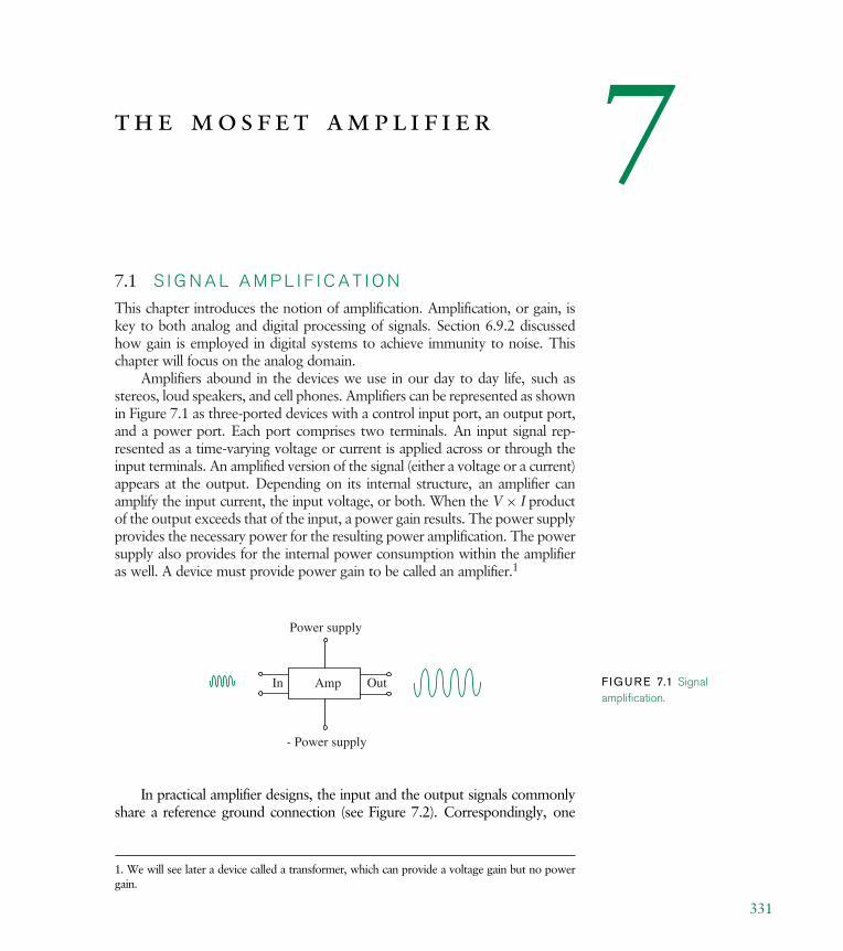
the mos f e t ampl i f i e r 77.1 S I G N A L A M P L I F I C A T I O N
This chapter introduces the notion of amplification. Amplification, or gain, iskey to both analog and digital processing of signals. Section 6.9.2 discussedhow gain is employed in digital systems to achieve immunity to noise. Thischapter will focus on the analog domain.
Amplifiers abound in the devices we use in our day to day life, such asstereos, loud speakers, and cell phones. Amplifiers can be represented as shownin Figure 7.1 as three-ported devices with a control input port, an output port,and a power port. Each port comprises two terminals. An input signal rep-resented as a time-varying voltage or current is applied across or through theinput terminals. An amplified version of the signal (either a voltage or a current)appears at the output. Depending on its internal structure, an amplifier canamplify the input current, the input voltage, or both. When the V × I productof the output exceeds that of the input, a power gain results. The power supplyprovides the necessary power for the resulting power amplification. The powersupply also provides for the internal power consumption within the amplifieras well. A device must provide power gain to be called an amplifier.1
OutIn Amp
Power supply
- Power supply
F IGURE 7.1 Signalamplification.
In practical amplifier designs, the input and the output signals commonlyshare a reference ground connection (see Figure 7.2). Correspondingly, one
1. We will see later a device called a transformer, which can provide a voltage gain but no powergain.
331

332 C H A P T E R S E V E N t h e m o s f e t a m p l i f i e r
of the terminals of each of the ports is commonly tied to a reference ground.Furthermore, the power port is commonly not shown explicitly.
OutIn Amp
Power supply
or
OutIn Amp
F IGURE 7.2 Reference groundand implicit power connections.
Besides their use in communication to overcome the dissipative effects ofthe communication medium (for example, in loud speakers or in wireless net-working systems), amplifiers are useful for signal transmission in the presence ofnoise. Figures 7.3 and 7.4 show two signal transmission scenarios. In Figure 7.3,the signal transmitted in its native form is overwhelmed by noise at the receiver.In Figure 7.4, however, the amplified signal is seen to be much more tolerant tonoise. (Contrast this with the application of amplification for noise immunityin digital systems as discussed in Section 6.9.2.)
A less obvious but equally important application of amplifiers is buffering.As the name implies, a buffer isolates one part of a system from another. Buffersallow us to compose complicated systems from smaller components by isolat-ing the behavior of the individual components from each other. Many sensors,for example, produce a voltage signal, but cannot supply a large amount ofcurrent. (For instance, they might have a high Thévenin resistance.) However,later processing stages might require that the device supply a given amount ofcurrent. If this high current is drawn, a large voltage drop across the internalresistance of the sensor seriously attenuates the output voltage. In such situa-tions, we might employ a buffer device that replicates the sensor’s voltage signalat its output but can also provide a large amount of current. In such bufferingapplications, we shall often see amplifiers with less than unity voltage gain, butgreater than unit current and power gain.
7.2 R E V I E W O F D E P E N D E N T S O U R C E S
Before we get into the design and analysis of amplifiers, let us take a momentto review dependent sources. Because amplifiers are naturally modeled using
F IGURE 7.3 Signal transmissionin the presence of noise.
Transmission channel
ReceiverSenderNoise
Useful signal
Signal overwhelmed by noise
F IGURE 7.4 Amplificationprovides noise tolerance.
ReceiverSenderNoise
Signal
Amp
Amplified signal

7.2 Review of Dependent Sources C H A P T E R S E V E N 333
iIN = 0
vIN
+
-
+
-
f(vIN)vOUT
e.g. f(vIN) = gmvIN
Controlport
Outputport
iOUT
F IGURE 7.5 Voltage-controlledcurrent source.
dependent sources, analysis of circuits with dependent sources will come inhandy in their design.
Dependent sources serve to model control of energy or information flow.Recall that control of energy or information flow was one of five basic processesidentified in Section 1.6 in Chapter 1. Figure 7.5 shows the familiar voltagecontrolled current source that we saw in Chapter 2. As we shall illustrate shortly,small amounts of energy at the control port of such dependent sources cancontrol or steer huge amounts of energy at the output port.
e x a m p l e 7.1 v o l t a g e - c o n t r o l l e d c u r r e n t s o u r c e
c i r c u i t Consider the circuit shown in Figure 7.6. Let vI be the voltage sourcedby an independent voltage source. The current iO = f (x) produced by the dependentcurrent source is a function of other values in the circuit. Let us first analyze the circuitwhen the output of the current source depends on a voltage:
iO = f (vI) = −gmvI.
vO versus vI Let us attempt to determine vO as a function of vI. Figure 7.6 showsour selection of a ground node and the labeling of nodes with their node voltage vari-ables. vO is the only unknown node voltage. Writing the corresponding node equation,we get
vO
RL= iO = f (vI).
vI vO
RLRI
iIiO = f(x)
vI
+
-F IGURE 7.6 A circuit using aVoltage-controlled current source.

334 C H A P T E R S E V E N t h e m o s f e t a m p l i f i e r
Since f (vI) = −gmvI, we get our node equation
vO
RL= −gmvI. (7.1)
Equation 7.1 shows the desired relationship between vO and vI and completesour solution. The voltage gain is given by
vO
vI= −gmRL.
Notice that we obtain a voltage gain greater than unity if gmRL > 1. Thus, the circuit inFigure 7.6 behaves as an amplifier for properly chosen values of RL. In other words, thecircuit produces an amplified version of vI at its output vO. Section 7.4 will introducea physical device that behaves as a voltage-controlled current source and develops anamplifier based on that device.
iO versus iI Next, let us determine iO versus iI. Substituting vI = iIRI and vO = iORL
in Equation 7.1, we can write
iORL = −gmRLiIRI,
which simplifies to
iO = −gmRIiI. (7.2)
Thus, the current gain is given by
iOiI
= −gmRI.
Notice that the dependent source provides a current gain greater than unity if gmRI > 1.
PO versus PI Let us now determine the input power PI versus the output power PO.By multiplying the left-hand sides and the right-hand sides of Equations 7.1 and 7.2, wecan write
vOiO = g 2mRLRIvIiI. (7.3)
In other words,
PO = g 2mRLRIPI.
The power gain is given by
PO
PI= g 2
mRLRI.

7.3 Actual MOSFET Characteristics C H A P T E R S E V E N 335
Thus, the dependent source provides a power gain greater than unity wheng 2
mRLRI > 1.
e x a m p l e 7.2 c u r r e n t - c o n t r o l l e d c u r r e n t s o u r c e
Let us rework the circuit of Figure 7.6 and obtain its vO versus vI relation assuming thatthe output of the current source depends on a current:
iO = f (iI) = −βiI
where β is a constant. As before, let us attempt to determine vO as a function of vI.Writing the node equation,
vO
RL= iO = f (iI)
or,
vO
RL= f (iI).
Substituting f (iI) = −βiI, we get our desired node equation
vO
RL= −βiI.
Since iI = vI/RI, we get
vO = −βRL
RIvI. (7.4)
Equation 7.4 gives the relationship between vO and vI and completes our solution.
7.3 A C T U A L M O S F E T C H A R A C T E R I S T I C S
Chapter 6 introduced the MOSFET and developed simple digital logic circuitsusing the device. That chapter also used the simplistic S model and the SRmodel of the MOSFET to analyze digital logic circuits. The SR model uses afixed RON between the D and S terminals of the MOSFET when vGS ≥ VT.This model is a reasonable representation of MOSFET behavior only when thedrain voltage is smaller than the gate voltage minus one threshold drop. In otherwords, when
vDS < vGS − VT. (7.5)
Accordingly, the SR model is useful to design and analyze digital circuitgates because a common mode of operation for the MOSFET within digital

336 C H A P T E R S E V E N t h e m o s f e t a m p l i f i e r
gates is one in which the gate voltage is high and the drain voltage is relativelylow. For example, we might have VOH = 4 V applied as a logical-high inputto the gate of a MOSFET in an inverter (assume VT for the MOSFET is givento be 1 V), which might produce as the output a corresponding logical-lowdrain voltage VOL = 1 V. With these values, vDS = 1 V, vGS = 4 V. SinceVT = 1 V, the constraint in Equation 7.5 is satisfied.
However, there are other situations demanding higher drain voltages inwhich we wish to use the MOSFET in an ON state. The SR model of theMOSFET is inappropriate in this region. This section will first show why the SRmodel is inadequate when vDS ≥ vGS−VT. We will then take a look at the actualMOSFET characteristics and then explore the possibility of creating a simplepiecewise-linear model for the MOSFET in the region where vDS ≥ vGS − VT.
We will use the setup shown in Figure 7.7 to observe the actual MOSFETcharacteristics. Let us start by applying a fixed, high gate-to-source voltagesuch that
vGS
iDSD
S
G+
-
vDS+
-
F IGURE 7.7 Setup forobserving MOSFET characteristics.
vGS ≥ VT
and observing the value of iDS as the drain-to-source voltage vDS is increased.As illustrated in Figure 7.8, we observe that iDS increases more or less linearlyas vDS is increased from 0 V. The approximately linear relationship betweeniDS and vDS exists for small values of vDS, and
vDS
iDS= RON.
The linear relationship between iDS and vDS reflects resistive behavior for smallvDS, and is nicely captured by our SR model of the MOSFET.
Now, keeping the value of vGS at the same fixed value, we increase vDSfurther, and plot our observations in Figure 7.9. Notice that as vDS approachesthe value of vGS − VT, the curve bends and begins to flatten out. In otherwords, the current iDS saturates as vDS begins to exceed vGS − VT. In fact,
F IGURE 7.8 The MOSFETcharacteristics match the SRmodel for a fixed value of vGS ,when vGS ≥ VT and vDS is small(specifically, whenvDS < vGS − VT).
Trio
de re
gion
vDS
iDS
1RON----------
iDSvDS-------- =
vGS ≥ VTFor
0

7.3 Actual MOSFET Characteristics C H A P T E R S E V E N 337
Trio
de r
egio
n
vDS
iDS
For vGS ≥ VT
vDS ≥ vGS – VT
0
vDS < vGS – VT
vDS = vGS – VT
Saturation region
F IGURE 7.9 The current iDS begins to saturate asvDS approaches the value of vGS − VT .
Trio
de r
egio
n
vDS
iDS
1RON----------
iDSvDS-------- =
vGS ≥ VTFor
vDS = vGS – VT
0
Saturationregion
F IGURE 7.10 The saturation region of MOSFEToperation.
as illustrated in Figure 7.10, for a given value of vGS, the iDS curve becomesvirtually flat for large values of vDS. Accordingly, the region where vDS ≥vGS − VT is called the saturation region of MOSFET operation. In contrast,the region where vDS < vGS − VT is called the triode region. Not surprisingly,the SR model applies with a fair degree of accuracy only in the triode regionof MOSFET operation. In the saturation region, because iDS does not changeas vDS increases, the MOSFET behaves like a current source. (Recall, fromFigure 1.34, the v i curve for a current source is a horizontal line.)
The iDS curve in Figure 7.10 was measured keeping vGS constant at somevalue greater than VT. It turns out that the iDS curves saturate at a differentvalue for different values of vGS. Thus, as illustrated in Figure 7.11, we get adifferent iDS versus vDS curve for each setting of vGS (for example, vGS1, vGS2,and so on), resulting in a family of iDS versus vDS curves. This family of curvesrepresents the actual MOSFET characteristics. Notice that the slope of each ofthe curves in the triode region also varies somewhat with vGS.
The actual MOSFET characteristics with the triode, saturation, and cutoffregions marked are shown in Figure 7.12. The dashed line represents the locusof the points for which
vDS = vGS − VT.
The MOSFET is in cutoff for
vGS < VT.
The MOSFET operates in its triode region for points to the left of the dashedline, where
vDS < vGS − VT and vGS ≥ VT.

338 C H A P T E R S E V E N t h e m o s f e t a m p l i f i e r
iDS
vDS
vGS1
vGS ≥ VT
vGS < VT
vGS2
vGS3
vGS4
vGS5
vGS6
v GS6
v GS5
v GS4
v GS3
v GS2
v GS1
F IGURE 7.11 Actual characteristics of the MOSFET. Eachsetting of vGS results in a separate iDS versus vDS curve.
iDS
vDS
Tri
ode
reg
ion
Saturation region
v DS
= v
GS
– V
T
0vGS < VT
vGS ≥ VT
Cutoff regionvGS1
vGS2
vGS3
vGS4
vGS5
vGS6
vGS1vGS2v GS3
v GS4
v GS5
v GS6
F IGURE 7.12 Actual characteristics of the MOSFETshowing the triode, saturation, and cutoff regions.
The MOSFET operates in its saturation region for points to the right ofthe dashed line, where the following two conditions are met
vDS ≥ vGS − VT and vGS ≥ VT.
Saturation Region Operation of the MOSFET A MOSFET operates in thesaturation region when the following two conditions are met:
vGS ≥ VT (7.6)
and
vDS ≥ vGS − VT. (7.7)
Given the more or less straight-line behavior of the iDS versus vDS curvesto the left and to the right of the dashed line in Figure 7.12, it is naturalto seek a piecewise-linear model for the MOSFET. Recall from Section 4.4,piecewise-linear modeling represents nonlinear v i characteristics by a succes-sion of straight-line segments, and makes calculations within each straight-linesegment using linear analysis tools. Figure 7.13 shows our choice of straight-linesegments that model the actual MOSFET characteristics.
To the right of the vDS = vGS − VT boundary (represented by the dashedline in Figure 7.13) we have the saturation region, in which we use a set ofhorizontal straight-line segments (one for each value of vGS) to represent theactual MOSFET characteristics. The straight-line segments representing themodel are shown as thick grey lines. The circuit interpretation of each ofthe horizontal straight-line segments is a current source. Furthermore, because

7.3 Actual MOSFET Characteristics C H A P T E R S E V E N 339
iDS
vDS
Tri
ode
regi
on (
SR M
odel
)
Saturation region
0
(SCS Model)
1RON------------
vGS < VT
vGS ≥ VT
v DS
= v
GS
– V
T
vGS1
vGS2
vGS3
vGS4
vGS5
vGS6
F IGURE 7.13 SR and SCSmodels.
the value of the current depends on the value of vGS, the behavior is that of avoltage-controlled current source. This behavior, captured by the switch currentsource (SCS) model of the MOSFET, applies only in the saturation region of theMOSFET. We will have a lot more to say about this saturation region modelof the MOSFET in Section 7.4.
To the left of the vDS = vGS − VT boundary, we have the triode region,in which one possible modeling choice uses a single straight-line segment toapproximate the iDS versus vDS curve for a given value of vGS. Such a straight-line segment approximating the iDS versus vDS curve for a given vGS is shown asthe thick grey line to the left of the vDS = vGS − VT boundary. You will noticethat this choice of a single straight-line segment with a given slope 1/RON fora fixed value of vGS is our familiar SR model from Section 6.6. Intuitively, thesingle straight-line segment model suggests that the MOSFET behaves like aresistor with a fixed value RON for a given value of vGS, provided that vGS ≥ VTand vDS < vGS − VT.
When the MOSFET curves are drawn using a compressed scale on thex-axis as in Figure 7.14, we see even the S model is not unreasonable in thetriode region since it captures the gross characteristics of the MOSFET.
Of course, it is also possible to model the complete operation of theMOSFET (for any value of vGS) using a more sophisticated nonlinear model.This results in the Switch Unified (SU) model, which is discussed further inSection 7.8. Although the SU model captures the complete characteristics ofthe MOSFET, for simplicity, we will focus on the SR and the SCS models.Accordingly, unless specifically mentioned otherwise, we will use the SR modelfor the triode region of the MOSFET when analyzing digital systems (since wework with a fixed high value of vGS, where vGS ≥ VT and vDS < vGS − VT),and the SCS model in the saturation region (vGS ≥ VT and vDS ≥ vGS − VT)for analog systems.

340 C H A P T E R S E V E N t h e m o s f e t a m p l i f i e r
F IGURE 7.14 S and SCSmodels.
iDS
vDS
Tri
ode
regi
on (
S M
odel
)
Saturation regionv DS
= v
GS
– V
T
0
(SCS Model)
vGS ≥ VT
vGS < VTvGS1
vGS2
vGS3
vGS4
vGS5
vGS6
As one final observation on the various models, notice in Figure 7.13 thediscontinuity in the iDS versus vDS curve according to the SR model in thetriode region, and the SCS model in the saturation region. In other words, if aMOSFET operates in a circuit such that vDS = vGS − VT, the two models willgive very different results. We can live with this discontinuity provided we do notattempt to reconcile the results from the two models in the same analysis.2 Youmust choose between the two models depending on the particular situation.Specifically, use the SR model when operating with a fixed vGS in the trioderegion, and use the SCS model when operating in the saturation region. TheSR model is appropriate for use in our digital circuits because of the invertingproperty of the type of digital circuits discussed here (for example, our familiarinverter). Since the drain voltage in our digital circuits is low when the gatevoltage is high, the triode region of MOSFET operation applies, and therefore,the SR model is appropriate. Conversely, in the design of amplifiers, we willestablish the saturation discipline, which will constrain amplifier designs tooperate MOSFETs exclusively in their saturation region, thereby allowing theuse of the SCS model.
7.4 T H E S W I T C H - C U R R E N T S O U R C E ( S C S )M O S F E T M O D E L
We saw in the previous section that when the gate voltage of the MOSFETis greater than the threshold voltage, and the drain voltage is greater than thegate voltage minus one threshold drop (vDS ≥ vGS − VT), a voltage-controlledcurrent source model is appropriate for the MOSFET. The switch-current source
2. As discussed in Section 7.8, the SU model eliminates the discontinuity.

7.4 The Switch-Current Source (SCS) MOSFET Model C H A P T E R S E V E N 341
D
S
G
D
S
G
D
S
G
(a) MOS device (b) Open state (c) Closed state
iDS = f(vGS)K(vGS – VT)2
2-------------- --------------------=
vGS < VT vGS ≥ VT
Valid when vDS ≥ vGS – VT
iG = 0 iG = 0
F IGURE 7.15 The switch-current source model of theMOSFET.
model (or SCS model) of the MOSFET captures this behavior and is depictedin Figure 7.15.
As depicted in Figure 7.15b, when vGS < VT, the MOSFET is OFF and anopen circuit exists between the drain and the source. For the SCS model, thecurrent iG into the gate terminal is zero.
When vGS ≥ VT, and vDS ≥ (vGS − VT), the amount of current providedby the source is given by
iDS = K(vGS − VT)2
2(7.8)
where K is a constant having units of A/V2. The value of K is related to thephysical properties of the MOSFET.3
As in the OFF state, the current iG into the gate terminal is zero, reflectingan open circuit both between the gate and the source, and the gate and thedrain.
As mentioned earlier, the region of operation in which vDS ≥ (vGS − VT)is called the saturation region. The region in which vDS < (vGS − VT) iscalled the triode region. The characteristics of the MOSFET in the saturationregion according to the SCS model are summarized graphically in Figure 7.16.Compare these characteristics with those for the SR model in the triode regiondisplayed earlier in Figure 6.31.
The constraint curve separating the triode and saturation regions inFigure 7.16 given by
vDS = vGS − VT (7.10)
3. The parameter K is related to the physical structure of the MOSFET as follows:
K = KnW
L. (7.9)
In Equation 7.9, W is the MOSFET gate width and L is the gate length. Kn is a constant related toother MOSFET properties such as the thickness of its gate oxide.

342 C H A P T E R S E V E N t h e m o s f e t a m p l i f i e r
F IGURE 7.16 Characteristics ofthe MOS device in the saturationregion.
iDS
vDS
iDS
vGSVT
K(vGS – VT)2
2---------------------------------
valid when vDS ≥ vGS – VT
v DS =
vG
S –
VT
K2----v2
DS
vGS1
vGS2
vGS3
vGS4
vGS5
vGS6
can also be rewritten in terms of iDS and vDS by substituting vDS = (vGS − VT)in Equation 7.8 as follows:
iDS = K
2v 2
DS. (7.11)
The following is a summary of the SCS model of the MOSFET in algebraicform. The model applies only in the saturation region of MOSFET operation,that is, when vDS ≥ vGS − VT.
iDS =
K(vGS − VT)2
2for vGS ≥ VT and vDS ≥ vGS − VT
0 for vGS < VT.(7.12)
e x a m p l e 7.3 a m o s f e t c i r c u i t Determine the current iDS forthe circuit in Figure 7.17. For the MOSFET, assume that K = 1 mA / V2 and VT = 1 V.
It is easy to see that the MOSFET in Figure 7.17 is operating in its saturation region,since the drain-to-source voltage (5 V) is greater than vGS − VT (2 V − 1 V = 1 V ).Therefore, we can directly calculate the desired current using the MOSFET equation forsaturation region operation
iDS = K(vGS − VT)2
2.
Substituting vGS = 2 V, K = 1 mA / V2 and VT = 1 V, we obtain iDS = 0.5 mA.
F IGURE 7.17 A simpleMOSFET circuit.
5 V2 V
iDSD
S
G+-+
-

7.4 The Switch-Current Source (SCS) MOSFET Model C H A P T E R S E V E N 343
e x a m p l e 7.4 s a t u r a t i o n r e g i o n o p e r a t i o n Keepingthe gate-to-source voltage for the MOSFET in the circuit shown in Figure 7.17 at 2 V,what is the minimum value of the drain-to-source voltage vDS for which the MOSFETwill operate in saturation?
The MOSFET operates in saturation under the following constraints
vGS ≥ VT
and
vDS ≥ vGS − VT.
Since vGS is given to be 2 V and VT is 1 V, the first constraint is satisfied. Substitutingfor vGS and VT in the second constraint, we obtain the following constraint on vDS forsaturation region operation
vDS ≥ 1 V.
Thus the minimum value for vDS is 1 V.
e x a m p l e 7.5 s a t u r a t i o n r e g i o n o p e r a t i o n Next,keeping the drain-to-source voltage for the MOSFET in the circuit shown in Figure 7.17at 5 V, what is the range of values for vGS for which the MOSFET will operate insaturation?
The lowest value for vGS is 1 V, since below that the MOSFET enters cutoff.
The highest value for vGS is determined by the constraint
vDS ≥ vGS − VT.
For vDS = 5 V and VT = 1 V, the highest value for vGS is 6 V. If vGS is increasedbeyond 6 V, the MOSFET enters the triode region.
e x a m p l e 7.6 a c i r c u i t c o n t a i n i n g t w o m o s f e t s
Determine the voltage vO for the MOSFET circuit shown in Figure 7.18. You are given
2 V+
-
vO5 V+
-
10 V+
-DG
S
DG
S
M1
M2
iD
F IGURE 7.18 A circuit con-taining two MOSFETs. We are toldthat both MOSFETs operate in thesaturation region.
that both MOSFETs operate in the saturation region. The MOSFETs are identical andare characterized by these parameter values: K = 4 mA / V2 and VT = 1 V.
Since we are told that both MOSFETs operate in the saturation region, and since iDS
for both MOSFETs is the same, their respective gate-to-source voltages must also beequal. Recall that the drain-to-source current according to the SCS model is independent

344 C H A P T E R S E V E N t h e m o s f e t a m p l i f i e r
of vDS, provided the MOSFET is in saturation. Thus, equating the gate-to-sourcevoltages for MOSFETs M1 and M2 we have
5 − vO = 2.
In other words, vO = 3 V. It is easy to verify that vO = 3 V implies that both MOSFETsare indeed in saturation.
Observe further that the drain-to-source voltages across the two MOSFETs operatingas voltage-controlled voltage sources are not equal, even though the currents throughthe two devices are identical.
7.5 T H E M O S F E T A M P L I F I E R
A MOSFET amplifier circuit is shown in Figure 7.19. Remarkably, this circuitis identical to the inverter circuit we saw earlier! Unlike the inverter circuit,however, the input and output voltages of the MOSFET amplifier must becarefully chosen so that the MOSFET operates in its saturation region. In thesaturation region of operation, the SCS model can be used to analyze theMOSFET amplifier. Constraining the inputs so that the MOSFET is alwaysin saturation results in the desired amplifier behavior, and furthermore, it sig-vIN
+
-
RL
VS
vO
F IGURE 7.19 The MOSFETamplifier. The up-arrow labeled VSrepresents a connection through apower supply voltage source toground.
nificantly simplifies our analysis. This constraint on how we use a MOSFETamplifier is yet another example of a discipline to which we adhere in circuitdesign and analysis. This discipline is called the saturation discipline and isdiscussed further in Section 7.5.2.
Let us examine the amplifier circuit in Figure 7.19. We will do so by replac-ing the MOSFET in Figure 7.19 with its SCS circuit model from Figure 7.15 asillustrated in Figure 7.20. As our first step, let us determine the conditions onthe circuit such that the MOSFET is in saturation. When the MOSFET is con-
+-
vIN
vO
VS
K(vIN – VT)2
2
RL
iD = --------------------------------
F IGURE 7.20 SCS circuit modelof the MOSFET amplifier. iD is theMOSFET drain-to-source current.
nected in a circuit as shown, the following relationships between the MOSFETvoltages and the circuit voltages apply:
vGS = vIN
vDS = vO
and
iDS = iD.
Accordingly, the MOSFET is in saturation when the following constraintsare met:
vIN ≥ VT

7.5 The MOSFET Amplifier C H A P T E R S E V E N 345
and
vO ≥ vIN − VT.
In saturation, recall that the drain-to-source current of the MOSFET is givenby Equation 7.12 in terms of the MOSFET parameters as
iDS = K(vGS − VT)2
2.
In terms of the amplifier circuit parameters, this equation becomes
iD = K(vIN − VT)2
2. (7.13)
Next, we will attempt to answer the following question: What is the rela-tionship between the amplifier output vO and its input vIN? This relationshipwill describe the gain of the amplifier. Notice here an advantage of the satura-tion discipline our constraint that the circuit inputs will be chosen so thatthe MOSFET is always in saturation allows us to focus on the saturation regionof operation of the MOSFET and ignore its triode and cutoff region operation.
We will begin by formulating the output voltage vO as a function of theinput voltage vIN. Any of the methods described in Chapters 2 and 3 can beused to analyze this circuit. We will use the node method here. The groundnode is marked in the circuit in Figure 7.20, and so are the node voltages vO,vIN, and VS. Since the current into the MOSFET gate is zero, the node withvoltage vO is the only interesting node in the circuit. Writing the node equation,we get
iD = VS − vO
RL.
Multiplying throughout by RL and rearranging terms, we get
vO = VS − iDRL.
In other words, vO is equal to the power supply voltage minus the voltage dropacross RL. When vIN ≥ VT and vO ≥ vIN − VT, we know that the MOSFETis in saturation and the SCS model for the MOSFET applies. Substituting foriD from Equation 7.13, we get the transfer function of the amplifier given by
vO = VS − K(vIN − VT)2
2RL. (7.14)

346 C H A P T E R S E V E N t h e m o s f e t a m p l i f i e r
F IGURE 7.21 vO versus vINcurve for the amplifier.
VT vIN
vOVS
MOSFET is insaturation withinthis region (vO > vIN – VT and vIN ≥ VT)
Triode region
Cutoffregion (vIN < VT)
(vO < vIN – VT and vIN ≥ VT)
The transfer function relates the value of the output voltage to that of theinput voltage. Accordingly, the gain of the amplifier is given by
vO
vIN= VS − K (vIN−VT)2
2RL
vIN. (7.15)
Figure 7.21 plots vO versus vIN for the MOSFET amplifier. This decidedlynonlinear relationship is called the transfer function of the amplifier. WhenvIN < VT, the MOSFET is off and the output voltage is VS. In other words,iD = 0 when vIN < VT. As vIN increases beyond the threshold voltage VT,so does the current sustained by the MOSFET. Therefore vO rapidly decreasesas vIN increases. The MOSFET operates in the saturation region until the out-put voltage vO falls one threshold below the gate voltage, at which point theMOSFET enters the triode region (shown as a dashed line in Figure 7.21), andthe saturation model and Equation 7.14 are no longer valid.
As shown in Figure 7.22, notice that the magnitude of the slope of certainregions of the curve is greater than one, thereby amplifying input signals thatfall within this region. Shortly, we will take a more careful look at how we canconnect an input signal to the amplifier so that it is amplified by leveraging the
F IGURE 7.22 In certain parts,the magnitude of the slope of thevO versus vIN curve is greaterthan one.
VT vIN
vO
VS
Magnitude ofthe slope isgreater than one

7.5 The MOSFET Amplifier C H A P T E R S E V E N 347
amplifier transfer function. But before we do so, let us examine the transferfunction using numerical quantities to build up our insight.
We will examine the relationship between vIN and vOUT for the amplifiershown in Figure 7.20 for the following parameters:
VS = 10 V
K = 1 mA / V2
RL = 10 k
VT = 1 V.
Substituting in Equation 7.14, we get
vO = VS − K(vIN − VT)2
2RL (7.16)
= 10 − (10−3)
((vIN − 1)2
2
)10 × 103 (7.17)
= 10 − 5(vIN − 1)2. (7.18)
For example, substituting vIN = 2 V in Equation 7.18, we obtain vO = 5 V.We can tabulate the input-output voltage relationship for a larger number ofquantities as shown in Table 7.1.
vIN vOUT
1 10
1.4 9.2
1.5 8.8
1.8 6.8
1.9 6
2 5
2.1 4.0
2.2 2.8
2.3 1.6
2.32 1.3
2.35 0.9
2.4 ∼ 0
TABLE 7.1 vIN versus vOUT forthe MOSFET amplifier. All valuesare in volts. Observe that theMOSFET amplifier goes into thetriode region for vIN > 2.3 V andthe SCS model for the MOSFETdoes not apply.

348 C H A P T E R S E V E N t h e m o s f e t a m p l i f i e r
We can make a number of observations from Table 7.1. First, the amplifierclearly demonstrates voltage gain (change in the output voltage divided by thechange in the input voltage) because the input ranging from 1 V to 2.4 V causesthe output to change from 10 V to 0 V.
Second, the gain is nonlinear. From Table 7.1, when the input changesfrom 2 V to 2.1 V, the output changes from 5 V to 4 V, exhibiting a localvoltage gain of 10. However, when the input changes from 1.4 V to 1.5 V, theoutput changes by merely 0.4 V, exhibiting a local voltage gain of 4. This fact isevident from the different slopes at various points in the transfer curve shownin Figure 7.22.
Third, the saturation discipline is met only for vIN values between 1 V andapproximately 2.3 V. When the input vIN is less than 1 V, the MOSFET isin cutoff. Similarly, when vIN is greater than approximately 2.3 V, the outputfalls more than one threshold drop below the input. For instance, notice thatwhen vIN is 2.32 V, the output is 1.3 V, which is more than one threshold dropbelow the input voltage.
e x a m p l e 7.7 a m o s f e t a m p l i f i e r Consider the MOSFETamplifier shown in Figure 7.23. Assume that the MOSFET operates in the saturationregion. For the parameters shown in the figure, determine the output voltage vO giventhat the input voltage vIN = 2.5 V. From the value of vO verify that the MOSFET isindeed in saturation.
vIN+-
5 V
vO
K = 0.5 mA/V2 VT = 0.8 V
1 kΩ
F IGURE 7.23 A MOSFETamplifier example.
From Equation 7.14 we know that the relationship between the input and outputvoltages for a MOSFET amplifier under the saturation discipline is given by
vO = VS − K(vIN − VT)2
2RL.
Substituting for K, VS, VT, RL, and vIN, we obtain directly the value of vO:
vO = 5 − 0.5 × 10⁻³ (2.5 − 0.8)2
21 × 103
= 4.28 V.
For the MOSFET to be in saturation, two conditions must be met:
vGS ≥ VT
and
vDS ≥ vGS − VT.

7.5 The MOSFET Amplifier C H A P T E R S E V E N 349
Since vGS = vIN = 2.5 V, and VT = 0.8 V, the first condition is met. Similarly, sincevDS = vO = 4.28 V, and vGS − VT = 1.7 V, the second condition is also met. Thusthe MOSFET is indeed in saturation.
e x a m p l e 7.8 a m o s f e t s o u r c e - f o l l o w e r c i r c u i t
Another useful MOSFET circuit is the source follower shown in Figure 7.24. For rea-
+- vOUT
VS
vIN+
-
iDEquivalentSCS model
+- vOUT
VS
vIN+
-
GD
S
(saturation)
K = 2 mA/V2 VT = 1 V
1 kΩ
1 kΩ
F IGURE 7.24 Source followercircuit.
sons that will be clear in our discussion of the source follower in Chapter 8, the sourcefollower is also called a buffer circuit. Assuming that the MOSFET operates in the sat-uration region, determine the output voltage vOUT and the current iD given that theinput voltage vIN = 2 V, for the parameters indicated in the Figure 7.24.
We determine vOUT by writing the node equation for the output node:
iD = vOUT
1 × 10³. (7.19)
Substituting for iD using the SCS model for the MOSFET we get
2 × 10⁻³ (2 V − 1 V − vOUT)2
2= vOUT
1 × 10³.
Simplifying we get
v 2OUT − 3vOUT + 1 = 0.
The two roots of the equation are 2.6 and 0.4. We pick the smaller of the two roots,since, for saturation operation, the solution must satisfy
vIN − vOUT ≥ VT.
In other words,
2.5 V − vOUT ≥ 1 V.
Thus, vOUT = 0.4 V. Substituting into Equation 7.19
iD = 0.4 mA.
7.5.1 B I A S I N G T H E M O S F E T A M P L I F I E R
Figure 7.21 showed that the MOSFET is in saturation only within a certainregion of the amplifier transfer curve. The MOSFET circuit works as a reason-able amplifier only within this region, which, as shown in Table 7.1, ranges

350 C H A P T E R S E V E N t h e m o s f e t a m p l i f i e r
F IGURE 7.25 Boosting theinput signal of interest with asuitable DC offset so that theMOSFET operates in its saturationregion for the entire range of inputsignal excursions. vIN
vO
VY
vA
VS
VX
vB
t
t
F IGURE 7.26 Circuit forboosting the input signal of interest(vA) with a suitable DC offset (VX)so that the MOSFET operates in itssaturation region for the entirerange of input signal excursions.
VX+-
RL
VS
vO = VY + vB
vA+-
vIN
from an input of 1 volt to about 2.32 volts. In order to ensure that the amplifieroperates within this region of the curve, we must transform the input voltageappropriately. As illustrated in Figure 7.25, one way of doing so is to boost thesignal that we want to amplify (for example, vA) with a DC offset (say, VX) sothat the amplifier operates in its saturation region even for negative excursionsof the input signal. Figure 7.26 shows the corresponding circuit that adds anoffset to the input signal by connecting a DC voltage source (VX) in series withthe input signal source (vA). In other words, we have
vIN = VX + vA
where vA is the desired input signal.Notice in Figure 7.25 that the corresponding output voltage vO also con-
tains a DC offset VY added to the time varying output signal vB. vB is anamplified version of the input signal vA.

7.5 The MOSFET Amplifier C H A P T E R S E V E N 351
vIN
vO
VS
0
t
t
F IGURE 7.27 A sinusoidal inputsignal with zero offset results in ahighly distorted output signal.
Contrast the amplifier behavior for the input signal source with a suitableDC offset voltage shown in Figure 7.25 with that for the input signal sourceapplied directly Figure 7.27. When the input signal is applied to the amplifierwithout a DC offset, the MOSFET operates in its cutoff region for most ofthe input signal, and the output is highly distorted, bearing little resemblanceto the input. The form of distortion suffered by the signal in the example inFigure 7.27 is called clipping.
The use of the amplifier with an input DC offset (and a resulting outputoffset) is important enough to merit some new terminology. The DC offset (forexample, VX) applied to the input of the amplifier is also called a DC bias. Theuse of the DC offset voltage at the input establishes an operating point for theamplifier. The operating point is sometimes referred to as the bias point. As anexample, the operating point values of the input and output voltages for theamplifier in Figure 7.26 are VX and VY, respectively. We can select differentoperating points for the amplifier by applying different values of the input DCoffset voltage. Section 7.7 discusses various methods of choosing an operatingpoint.
We make one final observation about our amplifier. Although vB is anamplified version of the input signal vA when the input signal is boosted witha DC offset, vB is not linearly related to vA. Notice from Equation 7.14that our amplifier is nonlinear even when the MOSFET operates in thesaturation region. Fortunately, the MOSFET amplifier behaves as an approxi-mately linear amplifier for small signals; in other words, when the desired inputsignal vA is very small. However, we will postpone a more detailed analysis of

352 C H A P T E R S E V E N t h e m o s f e t a m p l i f i e r
F IGURE 7.28 The MOSFETamplifier abstraction.
iDSD
S
G
Amp
RL
+vIN-
+vO-
iOiIN
+
vIN
-
+
vO
-
iIN
iO
the amplifier’s small signal behavior to Chapter 8. Accordingly, for now, andin the rest of this chapter, we will not assume that the input is a small signal.Rather, we will assume that the input vIN that is fed into the amplifier comprisesboth the signal component of interest to this user (which may be a large valuedsignal), and a DC offset (or DC bias). For simplicity, all calculations will beperformed on this boosted signal.
7.5.2 T H E A M P L I F I E R A B S T R A C T I O N A N DT H E S A T U R A T I O N D I S C I P L I N E
We would like the user of a MOSFET amplifier to be able to treat it asthe abstract entity depicted in Figure 7.28, ignoring the internal details of thecircuit. This abstract amplifier has vIN and iIN at its input port and vO and iOat its output port, and provides power gain. Details such as the power supplyand the like are hidden from the user. The amplifier shown in Figure 7.28 usesground as an implicit second terminal for both the input port and the outputport. This form of amplifier is also called the single-ended amplifier.
Much like the gate abstraction went hand in hand with the staticdiscipline which dictated the valid range for applied inputs and expectedoutputs the amplifier abstraction is associated with the saturation discipline,which prescribes constraints on the valid set of applied input signals andexpected output signals. The saturation discipline simply says that the ampli-fier be operated in the saturation region of the MOSFET. As we shall see shortly,we choose this definition of the saturation discipline, because the amplifier pro-vides a good amount of power gain in the saturation region, thereby operatingwell as an amplifier.
Specification of the saturation discipline serves two purposes: First, it pre-scribes constraints on how the device can be used; and second, it establishes aset of design criteria for the device. The amplifier abstraction and its associatedusage discipline can be likened to procedural abstractions in software systems.Software procedures are an abstraction for the internal function they imple-ment. Procedures are also associated with a usage discipline often articulated

7.6 Large-Signal Analysis of the MOSFET Amplifier C H A P T E R S E V E N 353
as comments at the head of the procedure. Section 7.6 will be concerned withidentifying valid usage ranges under the saturation discipline.
7.6 L A R G E - S I G N A L A N A L Y S I S O FT H E M O S F E T A M P L I F I E R
Two forms of analysis come in handy for amplifiers: a large signal analysis and asmall signal analysis. Large signal analysis deals with how the amplifier behavesfor large changes in the input voltage, in other words, changes that are ofthe same magnitude as the operating parameters of the amplifier. Large signalanalysis also determines the range of inputs for which the amplifier operatesunder the saturation discipline for the reasons discussed in Section 7.5.1. Thissection deals with large signal analysis. The next chapter deals with small signalanalysis.
Large signal analysis attempts to answer the following specific questions relatedto the design of the amplifier:
1. What is the relationship between the amplifier output vO and its input vINin the saturation region? Equation 7.14, developed using the analyticalmethod, summarized the answer to this question. For variety, this sectionwill use the graphical method to determine the same relationship.
2. What is the range of valid input values for the amplifier under thesaturation discipline? What is the corresponding range of output values?
Figure 7.29 shows the MOSFET amplifier, and Figure 7.30 replaces
vIN +
-
RL
VS
vO
F IGURE 7.29 MOSFETamplifier circuit. For the parametersshown here, vIN is the same as vGSand vO is the same as vDS .Similarly, iDS is the same as iD .
the MOSFET with its equivalent circuit model. In this section, we willuse the graphical method of analyzing nonlinear circuits (introduced earlierin Section 4.3) to determine the answers to our questions.
+-
vIN
vO
VS
iDK(vIN – VT)2
2---------------------------------=
RL
F IGURE 7.30 MOSFETamplifier — large signal model.
Specifically, Section 7.6.1 will discuss the answer to the first question, andSection 7.6.2 will address the second question.
7.6.1 vIN V E R S U S vOUT I N T H E S A T U R A T I O N R E G I O N
Writing the node equation for the output node gives us the followingrelationship between iDS and vDS:
vDS = VS − iDSRL. (7.20)
Recall that for our circuit vIN is the same as vGS, vO is the same as vDS, andiDS is the same as iD, where vIN, vO, and iD are the amplifier circuit variables,and vGS, vDS, and iDS are the MOSFET variables.
Previously, using the analytical approach to solving our nonlinear amplifierproblem, we substituted for iDS from Equation 7.12 into Equation 7.20 andobtained the input versus output voltage relationship shown in Equation 7.14.

354 C H A P T E R S E V E N t h e m o s f e t a m p l i f i e r
This time around, we will use the graphical method to obtain thesame relationship. We begin by rewriting Equation 7.20 as
iDS = VS
RL− vDS
RL. (7.21)
As Equation 7.21 demonstrates, the load resistor RL forces an affine rela-tionship between iDS and vDS. Figure 7.31 plots this affine relationship. The linerepresenting the affine relationship between the output current and the voltageforced by the load resistor is called the load line. The slope of the line is inverselyproportional to the load resistance.
Also, recall that the MOSFET SCS model forces the relationship capturedby Equation 7.8, namely,
iDS = K(vGS − VT)2
2
and graphed in Figure 7.16 between the input voltage vGS and the MOSFETcurrent iDS. The output current and voltage must thus satisfy both the load-lineconstraint and the MOSFET vDS versus iDS relationships. We can graphicallysolve for the behavior of the output voltage by overlaying the load-line rela-tionship on the iDS versus vDS characteristics of the MOSFET in the saturationregion as depicted in Figure 7.32.
iDS
vDS VS
VS
RL------
1–RL------
F IGURE 7.31 The load line for the MOSFET amplifier.
vGS1
iDS
vDS VS
VS
RL------
i DS
K 2----v D
S2
=
vGS2
vGS3
vGS4
vGS6
vGS5
F IGURE 7.32 Load line super-imposed on the characteristiccurves of the MOSFET.
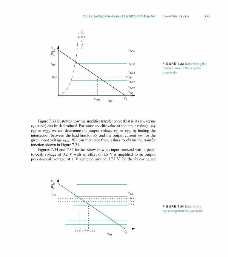
7.6 Large-Signal Analysis of the MOSFET Amplifier C H A P T E R S E V E N 355
vGS1
vGS2
vGS3
vGS4
vGS5iDS
vDSVS
V S
RL------
vDSi
iDSi vGSi
vGS6
i DS
K 2----v D
S2
=
F IGURE 7.33 Determining thetransfer curve of the amplifiergraphically.
Figure 7.33 illustrates how the amplifier transfer curve (that is, its vIN versusvO curve) can be determined. For some specific value of the input voltage, sayvIN = vGSi, we can determine the output voltage vO = vDSi by finding theintersection between the load line for RL and the output current iDSi for thegiven input voltage vGSi. We can then plot these values to obtain the transferfunction shown in Figure 7.21.
Figures 7.34 and 7.35 further show how an input sinusoid with a peak-to-peak voltage of 0.2 V with an offset of 1.5 V is amplified to an outputpeak-to-peak voltage of 1 V centered around 3.75 V for the following set
iDS
vDSVS
V S
RL------
1.5 V1.6 V
1.4 V
4.2 V3.75 V3.2 V
vGS
F IGURE 7.34 Determiningsignal amplification graphically.

356 C H A P T E R S E V E N t h e m o s f e t a m p l i f i e r
F IGURE 7.35 Signalamplification.
4.2 V
3.2 V
3.75 V
1.5 V 1.6 V
1.4 V t
v
vO
vIN
0
of parameters:
RL = 10 k (7.22)
K = 1 mA / V2 (7.23)
VS = 5 V (7.24)
VT = 1 V. (7.25)
We note that the output will not be a perfect sinusoid like the input becausethe amplifier is non-linear.
This concludes our discussion of the first part of large signal analysis fora MOSFET based amplifier, namely, determining the relationship between theinput and output voltage. Before we move on to the second part of largesignal analysis, it is worth spending a few moments comparing the graphicalmethod and the analytical method. To be sure, either method can be used inmost situations. The analytical method is useful when simple expressions cap-ture the behavior of the devices, as was the case for our MOSFET amplifier.The graphical method discussed in this section, however, is often more accu-rate when device characteristics measured from a physical device are available.The discrete devices you will come across in the laboratory, for example, willoften come with data sheets containing their v i characteristics.
7.6.2 V A L I D I N P U T A N D O U T P U T V O L T A G E R A N G E S
Let us now answer the second question of large signal analysis, namely, whatare valid input and output voltage ranges for the amplifier under the saturationdiscipline? These ranges will provide the outer voltage limits to input signalssuch as those in Figure 7.35. The limits will also provide insights into thenominal voltage about which the input signal should be centered, or, in otherwords, how to choose the operating point of the amplifier.

7.6 Large-Signal Analysis of the MOSFET Amplifier C H A P T E R S E V E N 357
Valid voltage range The range of input voltages (and the resulting range ofoutput voltages) for which the MOSFET (or MOSFETs) in the circuit operatein the saturation region.
The amplifier will amplify input signals when it is operating in this rangewithout clipping the signal or introducing significant amounts of distortion.(Signal clipping occurs when the amplifier output cannot go beyond a certainvoltage or current level.)
Let us begin by making some general observations about the current andvoltage limits to build up our intuition. Observe that iDS can range only from0 → VS/RL. The output voltage is VS when iDS is zero. iDS is zero for inputvoltages less than VT. Similarly, the output voltage is 0 when the current isVS/RL, and the input voltage is at some high value greater than VT. The limitsof saturation region operation lie somewhere within the iDS current limits of 0and VS/RL.
The valid range of input voltages has a lower limit and an upperlimit. The lower limit on input voltages is easy to determine.
Lowest Valid Input Voltage
Notice from Figure 7.36 that the input voltage must be greater than VT for theMOSFET to exit its cut off region. When the input voltage is VT, the MOSFETexits its cutoff region and the output voltage of the amplifier is VS. When theinput voltage is equal to VT, any positive value of vDS will cause the MOSFETto operate in its saturation region. Because we design the amplifier with VS > 0,and since vDS = VS, the MOSFET will be in its saturation region. Since VT isthe lowest voltage for which the MOSFET is in saturation, we get
lowest valid input voltage = VT. (7.26)
The corresponding value of the output voltage is VS. The point labeled (x)corresponding to the point (VT, VS) on the amplifier vIN versus vO transfer curvein Figure 7.36 denotes the low end of the valid input voltage range.
VT vIN
vO
VS
45o
vO = vIN – VT
MOSFET is insaturation withinthis region (vO > vIN – VT and vIN ≥ VT)
vO < vIN – VT and vIN ≥ VT
(x)
(y)
Triode region
F IGURE 7.36 The lowest validinput voltage under the saturationdiscipline is marked by the point(x ), and the highest valid inputvoltage under the saturation dis-cipline is marked by the point ( y ).

358 C H A P T E R S E V E N t h e m o s f e t a m p l i f i e r
Highest Valid Input Voltage
Next, we will determine the highest value of the input voltage for which theMOSFET satisfies the saturation discipline. Notice that the MOSFET goes intothe triode region when the output voltage vO falls one threshold drop belowthe input voltage vIN. In other words, when
vO = vIN − VT.
Thus, the valid high input voltage is that value of vIN beyond which theMOSFET enters the triode region.
To build intuition, we first determine graphically the input voltage forwhich the output crosses into the triode region as follows. Referring toFigure 7.36, the straight line drawn at 45 to the vIN axis and intersectingit at VT reflects the set of points in the vIN versus vO plane for which
vO = vIN − VT
assuming, of course, that vIN and vO use the same scale. Thus, the point (y) atwhich this 45o line intersects the vIN versus vO transfer curve marks the upperlimit of the valid input range.
We can also determine analytically the value of this upper limit by solvingfor the intersection of the straight line in Figure 7.36 represented by
vO = vIN − VT (7.27)
and the transfer curve determined by Equation 7.14, which we rewrite here forconvenience:
vO = VS − K(vIN − VT)2
2RL. (7.28)
The intersection of these two curves is marked by the point (y) in Figure 7.36.Substituting the expression for vO from Equation 7.27 into Equation 7.28we get
vIN − VT = VS − K(vIN − VT)2
2RL. (7.29)
Rearranging terms, we have
RLK
2(vIN − VT)2 + (vIN − VT) − VS = 0. (7.30)
The value of vIN that solves Equation 7.30 is the highest value of vIN for whichthe MOSFET operates in saturation.

7.6 Large-Signal Analysis of the MOSFET Amplifier C H A P T E R S E V E N 359
Solving for vIN − VT, we get
vIN − VT = −1 + √1 + 2VSRLK
RLK. (7.31)
In other words,
vIN = −1 + √1 + 2VSRLK
RLK+ VT. (7.32)
This value of vIN is the highest input voltage that satisfies the saturationdiscipline and corresponds to the point marked (y) in Figure 7.36.
Summarizing, the maximum valid input voltage range is
VT → −1 + √1 + 2VSRLK
RLK+ VT
and the maximum valid output voltage range is
VS → −1 + √1 + 2VSRLK
RLK.
As illustrated in Figure 7.37, the MOSFET enters its cutoff region for inputvoltages lower than VT, and goes into the triode region for input voltagesgreater than
((−1 + √
1 + 2VSRLK ) / RLK) + VT. The corresponding drain
current range is
0 → K
2(vIN − VT)2
where we substitute((−1 + √
1 + 2VSRLK ) / RLK) + VT.
This completes the second step of large signal analysis.
vO
VS
Cutoffregion
Saturationregion
Trioderegion
VT vIN
45o
F IGURE 7.37 Cutoff, saturation,and triode regions of operation ofthe MOSFET amplifier.

360 C H A P T E R S E V E N t h e m o s f e t a m p l i f i e r
e x a m p l e 7.9 v a l i d i n p u t a n d o u t p u t r a n g e s f o r
a m p l i f i e r Let us now determine the valid input voltage range and thecorresponding output voltage range for the amplifier given the following circuitparameters:
RL = 10 k (7.33)
K = 1 mA / V2 (7.34)
VS = 5 V (7.35)
VT = 1 V. (7.36)
From Equation 7.26, we know that VT = 1 V is at the low end of the valid inputrange. The corresponding value of vO is VS = 5 V and the current iD is 0.
Next, to obtain the highest value of the input voltage for saturation region operation ofthe MOSFET amplifier we substitute the values of these parameters in Equation 7.32.
Highest valid input voltage = VT + −1 + √1 + 2VSRLK
RLK
= 1 + −1 +√
1 + 2 × 5 × 10 × 103 × 10−3
10 × 103 × 10−3
≈ 1.9 V.
In other words, 1.9 V is the highest value of the input voltage that ensures satura-tion region operation of the amplifier. We can also solve for the corresponding valuesof vO and iD from Equations 7.27 and 7.8 as follows:
vO = vIN − VT = 1.9 − 1 = 0.9 V
iD = K
2(vIN − VT)2 = 0.41 mA.
In summary, the maximum valid range for the input voltage is
1 V → 1.9 V
and the maximum valid range for the output voltage is
5 V → 0.9 V.
The corresponding drain current range is
0 mA → 0.41 mA

7.6 Large-Signal Analysis of the MOSFET Amplifier C H A P T E R S E V E N 361
iDS
0.5 mA
5 V
vGS = 1.9 V
vGS = 1 V
(0.9 V, 0.41 mA)
(5 V, 0 mA)
0 vDS
F IGURE 7.38 Valid input andoutput voltage ranges.
These values are plotted on a graph of the amplifier load line and the MOSFET devicecharacteristics in Figure 7.38.
e x a m p l e 7.10 v a l i d r a n g e s f o r t h e s o u r c e
f o l l o w e r c i r c u i t Let us derive the valid operating ranges for the sourcefollower circuit shown earlier in Figure 7.24, and repeated here in Figure 7.39 forconvenience. Assume that VS = 10 V.
Recall that the valid input voltage range is defined as the range of input voltages forwhich the MOSFET operates under the saturation discipline. Two conditions must bemet for the MOSFET to remain in saturation:
vGS ≥ VT (7.37)
and
+- vOUT
VS
vIN+
-
iDEquivalentSCS model
+- vOUT
VS
vIN+
-
G D
S
(saturation)
K = 2 mA/V2 VT = 1 V
1 kΩ
1 kΩ
F IGURE 7.39 Source-followercircuit.
vDS ≥ vGS − VT. (7.38)
The first condition requires that vIN − vOUT ≥ VT, or,
vIN ≥ vOUT + VT.
Since the minimum value of vOUT is 0 V, the minimum value of vIN for saturationregion MOSFET operation is given by
vIN = VT = 1 V.
The second condition requires that
vDS ≥ vGS − VT,

362 C H A P T E R S E V E N t h e m o s f e t a m p l i f i e r
which implies that
VS − vOUT ≥ vIN − vOUT − VT.
Rearranging terms and simplifying, we obtain
vIN ≤ VS + VT.
In other words, the maximum value of vIN is given by
vIN = 10 V + 1 V = 11 V.
Summarizing, the valid input range is given by
1 V → vIN → 11 V.
The corresponding output voltage range is easily determined. At the low end of thevalid range, we know that vOUT = 0 for vIN = 1 V. At the high end of the valid range,vOUT is determined by writing the node equation for the output node and substitutingvIN = 11 V:
iD = vOUT
1 × 10³.
Substituting for iD using the SCS model for the MOSFET we get
2 × 10⁻³ (11 V − 1 V − vOUT)2
2= vOUT
1 × 10³.
Simplifying, we get
v2OUT − 21vOUT + 100 = 0.
The two roots of the equation are 13.7 and 7.3. We pick the smaller of the two roots,since, for saturation operation, vOUT must be at least one VT below the input voltage.Thus,
vOUT = 7.3 V.
The valid output voltage range is given by
0 V → vOUT → 7.3 V.
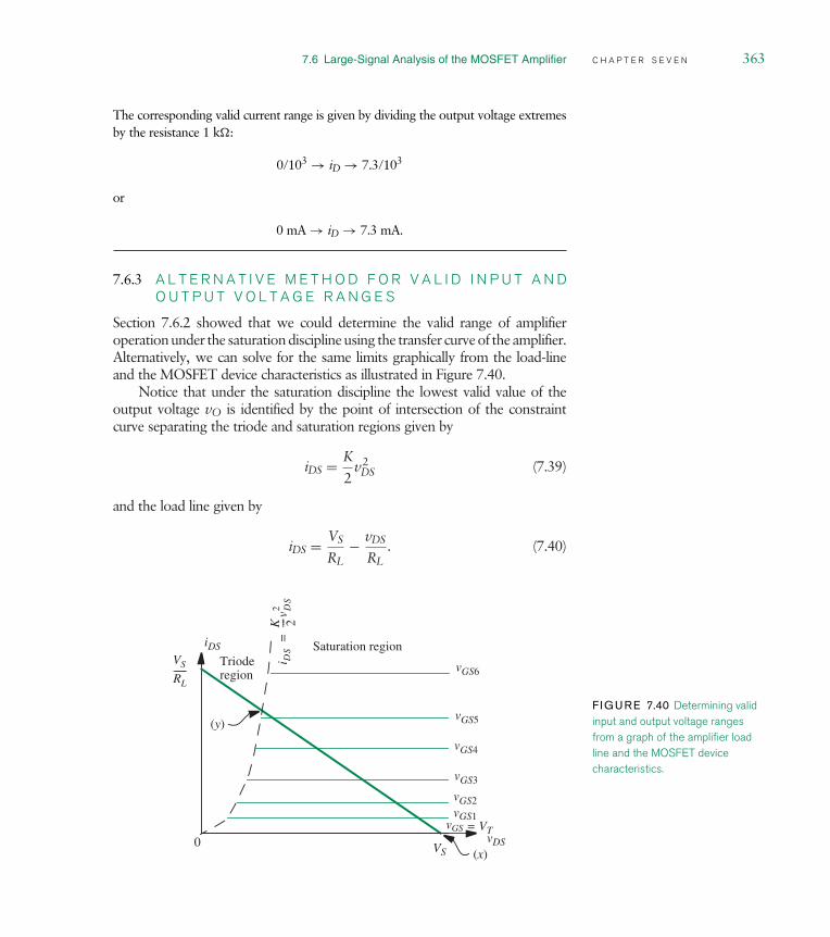
7.6 Large-Signal Analysis of the MOSFET Amplifier C H A P T E R S E V E N 363
The corresponding valid current range is given by dividing the output voltage extremesby the resistance 1 k:
0/103 → iD → 7.3/103
or
0 mA → iD → 7.3 mA.
7.6.3 A L T E R N A T I V E M E T H O D F O R V A L I D I N P U T A N DO U T P U T V O L T A G E R A N G E S
Section 7.6.2 showed that we could determine the valid range of amplifieroperation under the saturation discipline using the transfer curve of the amplifier.Alternatively, we can solve for the same limits graphically from the load-lineand the MOSFET device characteristics as illustrated in Figure 7.40.
Notice that under the saturation discipline the lowest valid value of theoutput voltage vO is identified by the point of intersection of the constraintcurve separating the triode and saturation regions given by
iDS = K
2v 2
DS (7.39)
and the load line given by
iDS = VS
RL− vDS
RL. (7.40)
vGS1
vGS2
vGS3
vGS4
vGS5
iDS
vDSVS
VS
RL------ vGS6
i DS
K 2----v D
S2
=
(y)
(x)
Saturation regionTrioderegion
0vGS = VT
F IGURE 7.40 Determining validinput and output voltage rangesfrom a graph of the amplifier loadline and the MOSFET devicecharacteristics.
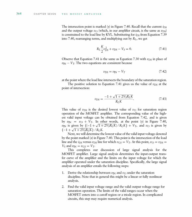
364 C H A P T E R S E V E N t h e m o s f e t a m p l i f i e r
The intersection point is marked (y) in Figure 7.40. Recall that the current iDSand the output voltage vO (which, in our amplifier circuit, is the same as vDS)is constrained to the load line by KVL. Substituting for iDS from Equation 7.39into 7.40, rearranging terms, and multiplying out by RL, we get
RLK
2v 2
DS + vDS − VS = 0. (7.41)
Observe that Equation 7.41 is the same as Equation 7.30 with vDS in place ofvIN − VT. The two equations are consistent because
vDS = vIN − VT (7.42)
at the point where the load line intersects the boundary of the saturation region.The positive solution to Equation 7.41 gives us the value of vDS at the
point of intersection:
vDS = −1 + √1 + 2VSRLK
RLK. (7.43)
This value of vDS is the desired lowest value of vO for saturation regionoperation of the MOSFET amplifier. The corresponding value of the high-est valid input voltage can be obtained from Equation 7.42, and is givenby vIN = vO + VT. In other words, at the point (y) in Figure 7.40,vIN is given by
((−1 + √
1 + 2VSRLK ) / RLK) + VT, and vO is given by(−1 + √
1 + 2VSRLK)
/ RLK.Next, we will determine the lowest value of the valid input voltage denoted
by the point marked (x) in Figure 7.40. This point is the intersection of the loadline and the iDS versus vDS line for which vGS = VT. At this point, vO = vDS =VS and vIN = vGS = VT.
This completes our discussion of large signal analysis for theMOSFET amplifier. Large signal analysis determines the input-output trans-fer curve of the amplifier and the limits on the input voltage for which theamplifier operated under the saturation discipline. Specifically, the large signalanalysis of an amplifier entails the following steps:
1. Derive the relationship between vIN and vO under the saturationdiscipline. Note that in general this might be a linear or fully nonlinearanalysis.
2. Find the valid input voltage range and the valid output voltage range forsaturation operation. The limits of the valid ranges occur when theMOSFET enters into a cutoff region or a triode region. In complicatedcircuits, this step may require numerical analysis.

7.7 Operating Point Selection C H A P T E R S E V E N 365
Among other things, the limits determined in large signal analysis come inhandy in determining a reasonable operating point for the amplifier. This willbe the next topic of discussion.
7.7 O P E R A T I N G P O I N T S E L E C T I O N
We are often interested in amplifying time-varying signals. Because the amplifierturns off for input voltages less than VT, it is important to add an appropriateDC offset voltage to the time-varying input signal so that the amplifier remainsin the saturation region for the entire range of input voltage variation. Thisinput DC offset voltage defines the operating point of the amplifier. The DCoffset must be chosen carefully, for if it is too large, the amplifier will be pushedinto the triode region, and if it is too low, the amplifier will slide into the cutoffregion. How do we choose this operating point?
Time-varying signals such as those in Figure 7.35 are characterized by theirpeak-to-peak voltage and their DC offset. For example, the sinusoidal signalvIN in Figure 7.35 has a peak-to-peak value of 0.2 V and a DC offset of 1.5 V.Since the MOS amplifier is nonlinear, we define the output offset as the valueof vO when the DC input offset voltage is the only signal applied at the input.Although the time-varying portion of the signal is of interest to us, as discussedin Section 7.5.1, the DC offset is provided simply to keep the amplifier operatingin its saturation region.
The input offset voltage is also called the input bias voltage or the inputoperating voltage. The corresponding output voltage and the output currentdefine the output operating point of the amplifier. Together, the input biasvoltage, and the corresponding output voltage and the output current, definethe operating point of the amplifier. We denote the operating point values ofvIN, vO, and iD as VIN, VO, and ID, respectively. As illustrated in Figure 7.41,
vGS1
vGS2
vGS3
vGS4
vGS5
iDS
vDSVS
V S
RL------ vGS6
(y)
(x)0
Valid range foroperating point
VO
VINID
F IGURE 7.41 Valid range foroperating point under thesaturation discipline.

366 C H A P T E R S E V E N t h e m o s f e t a m p l i f i e r
the operating point can be legally situated anywhere along the load line in thevalid range between the points (x) and (y).
There are several factors that can govern our choice of the operating point.For example, the operating point dictates the maximum dynamic range of theinput signal for both positive and negative excursions for which the MOSFEToperates in saturation. As can be seen from Equation 7.15, the operating pointvalue of the input voltage also governs the signal gain of the amplifier. Thissection will focus on selecting an operating point based on maximizing theuseful input signal range. We will have more to say about the relationshipbetween the gain of the amplifier and its operating point in Section 8.2.3 inChapter 8.
Let us assume that the input signal has symmetric peak-to-peak swingsabout the DC offset. In other words, we will assume an equal magnitude forboth the positive and negative excursions of the time-varying signal from theDC offset, as is the case for the input signal vIN in Figure 7.35 (but not for theoutput signal vO). To obtain maximum useful input signal range, we mightchoose the input bias voltage VIN to be at the center of the valid range of inputvoltages for the amplifier, as illustrated in Figure 7.42.
Accordingly, for the amplifier parameters that we have been using thus far,
RL = 10 k (7.44)
K = 1 mA / V2 (7.45)
VS = 5 V (7.46)
VT = 1 V (7.47)
because our amplifier operates under the saturation discipline for input voltagesin the range 1 V → 1.9 V, we might choose an input operating point voltageat the center of this range, namely VIN = 1.45 V. This choice is illustrated in
F IGURE 7.42 Selection of theinput operating point.
VT vIN
vO
VS
vO = vIN – VT
vO < vIN – VT
vO > vIN – VT
VIN
VO
(x)
(y)
Validoutputrange
Valid input range
0

7.7 Operating Point Selection C H A P T E R S E V E N 367
iDS
vDS
0.5 mA
5 V
vGS = 1.9 V
vGS = 1 V
0.41 mA
0.9 V
vGS = 1.45 V0.1 mA
4 V
Operating point: (4 V, 0.1 mA)
0 mA
F IGURE 7.43 Operating pointand valid input and output voltageranges.
1 V vIN
vO
5 V
vO vIN VT–=
1.45 V
4 V
(x)
(y)
0.45 V
0.9 V
1.9 V
(1.45 V, 4 V)
0
0 .45 V
F IGURE 7.44 Input operatingpoint.
Figure 7.43, which is an iDS versus vDS graph, and in Figure 7.44, which showsthe corresponding vIN versus vOUT graph. As we expect, the output will varybetween 0.9 V and 5 V as the input varies between 1 V and 1.9 V.
Let us take a closer look at the behavior of the amplifier for the given inputbias voltage by determining the corresponding output operating point. For agiven input operating point voltage VIN, we can determine the operating pointoutput voltage VO from Equation 7.14, and the operating point output currentID from the MOSFET SCS model given in Equation 7.8. Substituting for thecircuit parameters in Equation 7.14 we get
VO = VS − K(VIN − VT)2
2RL
= 5 − 10−3 (1.45 − 1)2
2104
= 4 V.
368 C H A P T E R S E V E N t h e m o s f e t a m p l i f i e r
From Equation 7.8 we get ID as
ID = K(VIN − VT)2
2
= 10−3(1.45 − 1)2
2
= 0.1 mA.
Thus the operating point for the amplifier is defined by
VIN = 1.45 V
VO = 4 V
ID = 0.1 mA.
This operating point maximizes the peak-to-peak input voltage swing for whichthe amplifier operates under the saturation discipline.
The operating point for our amplifier, along with the valid input and outputvoltage ranges, is shown in Figure 7.43. For this choice of the operating point,the maximum input voltage swing for positive excursions is 1.45 V → 1.9 V,and the maximum input voltage swing for negative excursions is 1.45 V → 1 V.The corresponding output voltage swings are 4 V → 0.9 V and 4 V → 5 V.
Although we chose the input operating point to be at the center of thevalid input range, notice the asymmetry of the output voltage range aboutthe output operating voltage. The asymmetry arises from the nonlinearity ofthe gain of the MOSFET amplifier. The next chapter will discuss an approachby which we can treat MOSFET amplifiers as linear amplifiers. Depending onour desired input and output voltage swings, and also amplifier gain, we canalso choose other operating points for the amplifier. Other criteria for choosingthe operating point might include concerns of stability and power dissipation,but these are beyond the scope of our discussion.
e x a m p l e 7.11 o p e r a t i n g p o i n t f o r t h e m o s f e t
s o u r c e f o l l o w e r c i r c u i t Modify the source follower circuit fromFigure 7.24 to include an input bias voltage that maximizes input voltage swing. Assumethat VS = 10 V.
Figure 7.45 shows the biased circuit, where VB is the bias voltage and vA is the inputsignal. The total signal, vIN, is the sum of the offset voltage and the actual input. Recallthat the input offset voltage (VB) is applied to boost the input signal (vA) in a way thatthe MOSFET remains in saturation for the maximum positive and negative excursionsof the input signal.

7.7 Operating Point Selection C H A P T E R S E V E N 369
vOUT
VS = 10 V
+
-
GD
S
K = 2 mA/V2 VT = 1 V+
-vA
+-
VBvIN
1 kΩ
F IGURE 7.45 Source-followercircuit with input bias.
From Example 7.10, we know that the valid range for the total input vIN is given by
1 V → vIN → 11 V.
We can obtain the maximum input swing under saturation operation by biasing theinput at the midpoint of the input valid range. In other words, we choose
VB = 6 V.
This choice of input offset voltage allows a peak-to-peak swing of 10 V for the inputsignal vA.
e x a m p l e 7.12 l a r g e s i g n a l a n a l y s i s o f a n o t h e r
m o s f e t a m p l i f i e r The circuit shown in Figure 7.46 is a MOSFET ampli-fier. We wish to determine the large-signal input-output behavior of this amplifier. Wealso wish to determine the range of vIN over which the MOSFET operation remains inthe saturation region. In this example, we will assume that the MOSFET is characterizedby VT = 1 V and K = 1 mA/V2.
Resistors R1 and R2 form a voltage divider from VS that establishes the constant biasvoltage VB at the gate of the MOSFET. That bias voltage is VB = 1.6 V.
+
-
vOUT
vIN+-
+- +
-VB
vGS
+
-
R1 = 84 kΩ
R2 = 16 kΩ
-
+
vDS
R3 = 20 kΩ
VS = 10 V
F IGURE 7.46 Another MOSFETamplifier with the input connectedto the source, and biasing providedby a voltage divider formed byresistors R1 and R2.

370 C H A P T E R S E V E N t h e m o s f e t a m p l i f i e r
Next, applying KVL yields vGS = VB − vIN. From this it follows that
vOUT = VS − R3K
2(VB − vIN − VT)2,
which evaluates to
vOUT = 10 − 10 × (0.6 − vIN)2.
Thus, for example, for vIN = 0 V, the output vOUT = 6.4 V.
We now determine the range of vIN over which the MOSFET operation remains in thesaturation region. To do so, the MOSFET voltages must satisfy vDS ≥ vGS − VT ≥ 0.For the amplifier shown in Figure 7.46, this is equivalent to
vOUT − vIN ≥ VB − vIN − VT ≥ 0.
By violating the first inequality, the MOSFET operation enters its triode region, andby violating the second inequality, the MOSFET operation enters its cutoff region.Numerically, this evaluates to
−0.3695 V ≤ vIN ≤ 0.6 V,
which corresponds to
0.6 V ≤ vOUT ≤ 10 V.
Thus, note that the MOSFET operation can remain saturated for both positive andnegative values of vIN.
e x a m p l e 7.13 b i p o l a r j u n c t i o n t r a n s i s t o r ( b j t )
Figure 7.47a depicts another three-terminal device, called the bipolar junction transistor(BJT), that is in common use in VLSI circuits. A BJT has three terminals called the base(B), the collector (C), and the emitter (E). Figure 7.47b marks the device with its relevantvoltage and current parameters.vCE
+
-
B
C
E
B
C
E
iC
iB
iEvBE
+
-
(a)
(b)
F IGURE 7.47 A bipolar junctiontransistor.
In this example, we will compare the actual characteristics of the BJT with those predictedby a simple piecewise linear model. The actual characteristics of a BJT (iC versus vCE forvarious values of iB) are shown in Figure 7.48. The horizontal nature of the iC versus vCE
curves indicates that the device operates like a dependent current source when the basecurrent iB > 0 and the collector-to-emitter voltage (vCE) is greater than approximately0.2 V. The current supplied by the current source is typically about 100 times the basecurrent. Although these curves are qualitatively similar to those of a MOSFET, thereare also some differences. First, notice that we have chosen the BJT’s base current iB

7.7 Operating Point Selection C H A P T E R S E V E N 371
iC (mA)
vCE
iB > 0
iB = 0 Cutoff region
Active region iB
10 µA
20 µA
30 µA
40 µA
50 µA
60 µA
70 µA
Satu
ratio
n r
egio
n
0.2 V
F IGURE 7.48 Actual character-istic curves for a bipolar junctiontransistor.
as our control parameter (the control parameter was the gate-to-source voltage for theMOSFET, and the gate current was zero). Second, the collector current is linearly relatedto the base current (when the MOSFET operated as a current source, its drain currentwas quadratically related to the gate-to-source voltage).
The BJT characteristics show three regions of operation:
1. When iB > 0 and vCE > 0.2 V, the BJT is said to be in the active region ofoperation. In this region, the horizontal collector current curves display a current-source-like behavior. As we shall see momentarily, the active region will be thepredominant region of interest for analog circuit designs.
2. When iB = 0, the BJT is said to be in the cutoff region.
3. Finally, when iB > 0 and vCE ≤ 0.2 V, (that is, the region to the left of the verticaldashed line in Figure 7.48), the collector current drops sharply, and the BJT is saidto be in the saturation region.4
Figure 7.49b shows a model for the BJT containing a current-controlled current sourceand a pair of diodes (a base-emitter diode and a base-collector diode). The currentsupplied by the dependent source is β times iB′ . The parameter β is a constant with
4. The saturation region in BJTs is completely unrelated to the saturation region in MOSFETs, andin fact, normal operation of BJTs attempts to avoid this region. This duplication of terms onerepresenting the favored region of operation in MOSFETs, and the other representing an avoidedregion of operation in BJTs can be the source of confusion, but, unfortunately, has become thenorm in circuit parlance.

372 C H A P T E R S E V E N t h e m o s f e t a m p l i f i e r
a typical value of around 100. (We show shortly that the base current iB = iB′ in theregion of BJT operation that is of interest to us.)
Although we can analyze circuits directly with the model in Figure 7.49b, our analysisvCE
+
-
C
BbiB′
E
B
C
E
iC
iB
iEvBE
+
-
(a)
(c)
vCE
+
-
iC
iB
iE
vBE
+
-
0.6 V+-
C
B
biB′
(b)
iB
E
0.4 V+ -
iB′
iB′
F IGURE 7.49 (a) A bipolarjunction transistor; (b) a model forthe BJT; (c) a piecewise-linearmodel for the BJT.
can be significantly simplified by using simple piecewise-linear models for the diodes.Figure 7.49c depicts such a piecewise-linear model for the BJT, in which we have replacedthe diodes with simple piecewise-linear diode models comprising an ideal diode in serieswith a voltage source (from Figure 4.33a). In the model in Figure 7.49c, the dependentcurrent source models the horizontal active region curves of the BJT.
The states of the two diodes (both ON, both OFF, and one OFF and one ON) result indistinct piecewise linear regions of BJT operation. Both diodes (in Figure 7.49c) in theirOFF state model cutoff: when the base current iB is zero, both the diodes are OFF, andso is the current source. Figure 7.50a depicts the corresponding BJT model in the cutoffregion. Observe that in the cutoff region
iB = iB′
because the base-to-collector diode is off.
When iB > 0 and
vCE > vBE − 0.4 V (7.48)
the emitter diode is ON and the collector diode is OFF, and the active region results.In this region of operation, as illustrated in the active region BJT model in Figure 7.50b,the ideal diode between the base and emitter turns ON and appears as a short circuit.The 0.6-V source models the corresponding 0.6-V diode drop. Observe further that
iB = iB′
in the active region because the base-to-collector diode is off. In the active region, BJTsdisplay a more-or-less constant voltage drop of about 0.6 V between their base andemitter terminals when the base current iB > 0 (a fact not evident from the characteristiccurves in Figure 7.48).
The condition vCE > vBE − 0.4 V ensures that the base-collector diode stays OFF. Thecondition states that the collector voltage must not fall below the base voltage by morethan 0.4 V, because if it did, the base-collector diode would turn ON.5 In the active
5. Although the constraint for active-region operation
vCE > vBE − 0.4 V.
is equivalent to the simpler constraints
vBC < 0.4 V or vCE > 0.2 V.
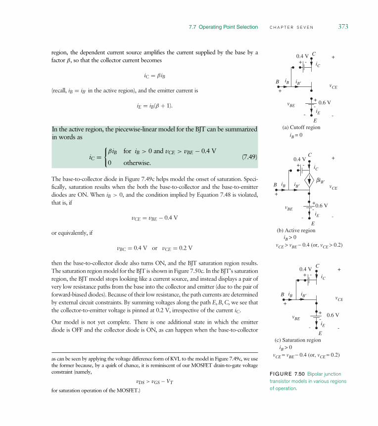
7.7 Operating Point Selection C H A P T E R S E V E N 373
region, the dependent current source amplifies the current supplied by the base by afactor β , so that the collector current becomes
C
B
E(c) Saturation region
+
-
0.6 V+-
0.4 V+ -
C
B
E(a) Cutoff region
+
-
+
-
0.6 V+-
0.4 V+ -
iB = 0
iB′ vCE
iC
iB
iE
vBE
C
B
E(b) Active region
+
-
0.6 V+-
0.4 V+ -
iB > 0
iB > 0
iB′
iB′
biB′
+
-
vCE
+
-
vCE
iB
iB
iC
iC
iE
iE
vBE
vBE
vCE > vBE − 0.4 (or, vCE > 0.2)
vCE = vBE − 0.4 (or, vCE = 0.2)
F IGURE 7.50 Bipolar junctiontransistor models in various regionsof operation.
iC = βiB
(recall, iB = iB′ in the active region), and the emitter current is
iE = iB(β + 1).
In the active region, the piecewise-linear model for the BJT can be summarizedin words as
iC =
βiB for iB > 0 and vCE > vBE − 0.4 V
0 otherwise.(7.49)
The base-to-collector diode in Figure 7.49c helps model the onset of saturation. Speci-fically, saturation results when the both the base-to-collector and the base-to-emitterdiodes are ON. When iB > 0, and the condition implied by Equation 7.48 is violated,that is, if
vCE = vBE − 0.4 V
or equivalently, if
vBC = 0.4 V or vCE = 0.2 V
then the base-to-collector diode also turns ON, and the BJT saturation region results.The saturation region model for the BJT is shown in Figure 7.50c. In the BJT’s saturationregion, the BJT model stops looking like a current source, and instead displays a pair ofvery low resistance paths from the base into the collector and emitter (due to the pair offorward-biased diodes). Because of their low resistance, the path currents are determinedby external circuit constraints. By summing voltages along the path E, B, C, we see thatthe collector-to-emitter voltage is pinned at 0.2 V, irrespective of the current iC.
Our model is not yet complete. There is one additional state in which the emitterdiode is OFF and the collector diode is ON, as can happen when the base-to-collector
as can be seen by applying the voltage difference form of KVL to the model in Figure 7.49c, we usethe former because, by a quirk of chance, it is reminiscent of our MOSFET drain-to-gate voltageconstraint (namely,
vDS > vGS − VT
for saturation operation of the MOSFET.)

374 C H A P T E R S E V E N t h e m o s f e t a m p l i f i e r
F IGURE 7.51 Characteristiccurves for a bipolar junctiontransistor as predicted by thepiecewise linear model.
iC (mA)
vCE
iB > 0
iB = 0 Cutoff region
Active region iB
10 µA
20 µA
30 µA40 µA
50 µA
60 µA
70 µAvCE > vBE – 0.4 V
0.2 V
Satu
ratio
n re
gion
voltage is 0.4 V, and the base-to-emitter voltage is less than 0.6 V. This region ofoperation is called the reverse injection region. In this region, the behavior of the BJT isthat of a forward biased diode between the base and the collector, and an open circuitat the emitter.
For simplicity, our introductory treatment will choose not to study both the reverseinjection and the saturation regions. Accordingly, our BJT circuits will all be designed toavoid completely these regions of behavior.
In the rest of this example, we will discuss the piecewise-linear model for the BJT pre-sented in Figure 7.49c and compare its predictions with the measured characteristics(iC versus vCE for various values of iB) shown in Figure 7.48. We will plot thecharacteristics predicted by the piecewise-linear model assuming β = 100.
To plot the characteristics, we identify BJT behavior in the two piecewise-linear regionsof operation that are of interest to us, and shown in Figure 7.50: cutoff and active.We first observe that iC is zero when the BJT is in cutoff, that is, when iB = 0 (seeFigure 7.50a). The curve labeled ‘‘Cutoff region’’ in Figure 7.51 depicts this situation.
Next, when iB > 0 and vCE > vBE −0.4 V (or, equivalently, vCE > 0.2 V), the collectorcurrent is a constant at β times the base current (Figure 7.50b). In the iC versus vCE plotin Figure 7.51, these constant current curves appear as horizontal lines. Because β is aconstant, the iC versus iB relationship is linear, and so the lines are equally spaced forequal increments in iB.
Finally, when iB > 0 and vCE = vBE − 0.4 V (or, equivalently, when vCE = 0.2 V), thesaturation region model applies (Figure 7.50c). vCE is correctly shown as being pinned at0.2 V. The vertical line at vCE = 0.2 V corresponding to iC indicates a short-circuit-likebehavior in which the collector current is limited only by external circuit constraints.
The similarity of the curves in Figures 7.48 and 7.51 show that our simple piecewise-linearmodel is quite a good match for the behavior of the BJT.

7.7 Operating Point Selection C H A P T E R S E V E N 375
As a final thought, although our piecewise linear model for the BJT seems a bit com-plicated at first glance, analog circuits are commonly designed such that BJT always
vCE
+
-
C
BbiB
E
B
C
E
iCiB
iEvBE
+
-
(a)
(b)
vCE
+
-
iC
iB
iE
vBE
+
-
0.6 V+-
F IGURE 7.52 A simpler BJTmodel suitable for the cutoff andactive regions.
operates in its active region, and the base-to-collector diode is always OFF.6 We canachieve the desired effect by ensuring that the base-to-collector voltage never exceeds0.4 V during normal operation (that is, vBC < 0.4 V, or equivalently, vCE > vBE−0.4 V).This assumption will be made in all the BJT circuits in this book, so the collector diodecan be safely ignored. The resulting, simplified BJT model is depicted in Figure 7.52.
e x a m p l e 7.14 b j t c i r c u i t p a r a m e t e r s Figure 7.53 showsmeasured values of iB and vBE for a BJT within a circuit. Find the corresponding valuesof vBE, iC, and iE using the BJT model containing two ideal diodes and a voltage source(Figure 7.49c).
Since iB > 0 and vCE > 0.2 V, it immediately follows that the BJT operates in its activeregion. In other words, the emitter diode in Figure 7.49c must be ON, and the collectordiode must be OFF (see the active region BJT model in Figure 7.50b). Since the emitterdiode is ON, it appears as a short circuit, and so
vBE = 0.6 V.
Based on the active region model in Figure 7.50b, since iB = 0.01 mA,
iC = βiB = 1 mA.
Summing the currents into the base and collector terminals, we get
iE = iB + iC = 1.01 mA.
B
C
E
Circuit
0.01 mA
+
-
5 V b = 100
iE
iC
+
-vBE
F IGURE 7.53 A bipolar junctiontransistor in a circuit.
6. This design choice is not unlike the one we made with MOSFETs, where circuit parameterswere chosen so that the MOSFET always operated in saturation.

376 C H A P T E R S E V E N t h e m o s f e t a m p l i f i e r
e x a m p l e 7.15 a b j t a m p l i f i e r Figure 7.54 shows an amplifier cir-cuit based on a BJT. This BJT amplifier configuration is called a common emitter amplifiersince the emitter terminal of the BJT is common across the input and output ports.
vIN
RL
VS
vO
B C
E+-
RI +
-
F IGURE 7.54 A BJT amplifier.
Using the piecewise-linear model for the BJT, determine the relationship between vO
and vIN, assuming that the BJT device is operating in its active region. Using this relation,determine the values of vO for vIN = 1 V, 1.1 V, and 1.2 V, given that RI = 100 k,RL = 10 k, β = 100, and VS = 10 V.
Figure 7.55 shows the equivalent circuit for the amplifier in which the BJT has beenreplaced with its piecewise-linear model. Notice we can safely ignore the collector diodeand use the simple BJT model in Figure 7.52 since we are told that the BJT is operating inits active region. Figure 7.56 further shows the active region subcircuit for the amplifier.
The relationship between vO and vIN can be determined in a few short steps from theactive region subcircuit. The current through RI is simply the voltage difference acrossthe resistor divided by the resistance:
iB = vIN − 0.6
RI. (7.50)
Once iB is known, we can immediately determine the output voltage by writing thenode equation for the node with voltage vO as follows:
VS − vO
RL= βiB.
Substituting for iB from Equation 7.50 and simplifying, we obtain the following relationbetween vO and vIN:
vO = VS − (vIN − 0.6)
RIβRL. (7.51)
vO
biB
RL
+-
VS
vIN
RI
+-
B
C
0.6 V+-E
iB
iC
F IGURE 7.55 Equivalent circuit for the BJT amplifier.
vO
biB
RL
+-
VS
vIN
RI
+- 0.6 V +
-
iB
iC
B
C
E
F IGURE 7.56 Active region subcircuit for the BJT amplifier.

7.7 Operating Point Selection C H A P T E R S E V E N 377
Next, substituting RI = 100 k, RL = 10 k, β = 100, and VS = 10 V, we obtain
vO = 16 − 10vIN.
For vIN = 1 V, 1.1 V and 1.2 V, vO is 6 V, 5 V and 4 V, respectively.
As a further exercise, we will go ahead and confirm that the BJT is indeed in its activeregion for the highest input voltage applied. (Remember that the higher the base voltagethe more likely it is that the collector diode in Figure 7.49c is turned ON. Thus, we needcheck only for the highest input voltage.)
The highest input voltage considered in this example is 1.2 V. For 1.2 V, the collec-tor voltage vO = 4 V. Since, in our circuit, vO = vCE = 4 V, the base-to-collectorvoltage is
vBC = vBE − vCE = 0.6 − 4 = −3.4 V.
Since the voltage vBC across the collector diode in Figure 7.49c is −3.4 V, which is lessthan 0.4 V, the collector diode is going to be OFF. (Equivalently, since vCE > 0.2 V, wecan directly say that that the collector diode is OFF.) We have thus confirmed that theBJT is in its active region.
e x a m p l e 7.16 l a r g e s i g n a l a n a l y s i s o f t h e b j t
a m p l i f i e r Perform a large signal analysis of the BJT amplifier shown inFigure 7.54. Assume that RI = 100 k, RL = 10 k, β = 100, and VS = 10 V.
For BJT circuits with input vIN and output vO, large signal analysis attempts to answerthe following questions:
1. What is the relationship between vO and vIN in the active region?
2. What is the range of valid input values for active region operation of the BJT?What is the corresponding range of output values?
From Equation 7.51 in Example 7.15, we know that the relation between vO and vIN
for the BJT amplifier is
vO = VS − (vIN − 0.6)
RIβRL,
thereby completing the first step of large signal analysis.
Next, let us determine the range of input values for which the BJT operates in its activeregion. To do so, we will first draw a graph of vO versus vIN to obtain insight into thebehavior of the amplifier for various values of the input voltage. When vIN = 0, we see

378 C H A P T E R S E V E N t h e m o s f e t a m p l i f i e r
vO
RL
+
-VS
vIN
RI
+- 0.6 V +
-
iB
B
C
E
F IGURE 7.57 Cutoff region subcircuit for the BJT amplifier.
0.6 V vIN
vO
VS BJT is in itsactive region
vCE = vBE – 0.4 V
0.2 V
0 1.58 V
BJT is in saturation
vCE > vBE – 0.4 V
BJT is in its cutoff region
F IGURE 7.58 vO versus vIN for the BJT amplifier.
that iB = 0, and so the BJT is in cutoff. The cutoff region subcircuit for the BJT amplifieris shown in Figure 7.57. In cutoff, both the diode and current sources are replaced byopen circuits. It is easy to see from the circuit in Figure 7.57 that
vO = VS.
Inspection of the amplifier equivalent circuit in Figure 7.55 indicates that the input cur-rent iB will be zero (and the ideal diode will remain OFF ) as long as vIN < 0.6. Thusthe output vO will remain at VS for vIN < 0.6. This fact is graphed in Figure 7.58 as thehorizontal straight line at voltage VS for vIN < 0.6.
When vIN exceeds 0.6 V by a small amount,7 the ideal diode turns ON, and currentbegins to flow through the resistor RI. In this situation, the active region equivalentcircuit in Figure 7.56 results. In the active region, vO is given by
vO = VS − (vIN − 0.6)
RIβRL. (7.52)
This relationship appears as a straight line with slope −βRL/RI in the vO versus vIN
graph and is plotted as such in Figure 7.58. Thus,
vIN = 0.6 V
7. If vIN exceeds 0.6 V by a large amount, the BJT might enter saturation. We will determine thissaturation region boundary momentarily.

7.7 Operating Point Selection C H A P T E R S E V E N 379
and
iB = 0
are the input parameters at the lower boundary of the active region.
The vO versus vIN relationship in the active region shows that vO decreases linearlyas vIN increases. The linear relationship applies as long as the BJT remains in its activeregion of operation. The upper boundary (with respect to the input voltage) of theactive region is reached when vIN becomes large, and vO becomes small enough thatthe condition
vCE > vBE − 0.4 V
is no longer met. Since vCE = vO and vBE is pinned at 0.6 V (from the active regionamplifier subcircuit in Figure 7.56), vO reaches the boundary point of the active regionwhen
vO = 0.6 − 0.4 = 0.2 V.
The corresponding value of iC is given by
iC = VS − 0.2 V
RL= 980 µA.
The input voltage corresponding to this output voltage can be found by solving for vIN
from Equation 7.52 as follows
0.2 = 10 − vIN − 0.6 V
100k100 × 10 k.
Solving, we get
vIN = 1.58 V.
This upper boundary of the active region (with respect to vIN) is marked in Figure 7.58.The corresponding value of iB can be found from
iB = vIN − 0.6
RI= 9.8 µA.
Once the BJT exits the active region and enters the BJT saturation region (for vIN ≥1.58 V), the saturation model for the BJT in Figure 7.50c applies and the equivalent

380 C H A P T E R S E V E N t h e m o s f e t a m p l i f i e r
F IGURE 7.59 Saturation regionsubcircuit for the BJT amplifier.
vO
RL
+-
VS
vIN
RI
+- 0.6 V+
-B
C
E
0.4 V+ -
subcircuit in Figure 7.59 best models the saturation region operation of the amplifier.By a straightforward application of KVL, we find that vO is given by
vO = 0.6 − 0.4 = 0.2 V.
In other words, vO is pinned at 0.2 V by the BJT in its saturation region when the inputvoltage vIN exceeds 1.58 V. This fact is plotted as a horizontal line at vO = 0.2 V inFigure 7.58.
To summarize, the limits on the inputs for active region operation are given by
0.6 V < vIN < 1.58 V
and
0 < iB < 9.8 µA.
The corresponding limits on the outputs are given by
10 V > vO > 0.2 V
and using iC = βiB,
980 µA > iC > 0 A.
e x a m p l e 7.17 s e l e c t i n g a n o p e r a t i n g p o i n t f o r
t h e b j t a m p l i f i e r Choose an operating point for the amplifier analyzedin Example 7.16 to maximize the input voltage swing. What is the corresponding output
RL
VS
vO
B C
E
RI +
-
+-vA
+-VBvIN
F IGURE 7.60 BJT amplifiershowing the input bias voltageexplicitly.
operating point and the output voltage swing? Is the output swing symmetric about theoutput operating point?
The BJT amplifier circuit in Figure 7.54 is redrawn in Figure 7.60 to show explicitly thatthe input voltage vIN is the sum of a bias voltage VB and the signal vA. Our first task

7.7 Operating Point Selection C H A P T E R S E V E N 381
is to find the input operating point (VB, IB). We do so by reviewing the results fromExample 7.16.
From Example 7.16, we know that the valid range for the total input voltage vIN toensure active region operation is given by
0.6 V < vIN < 1.58 V.
The corresponding range for the input current is
0 < iB < 9.8 µA.
We can obtain the maximum input swing for active region operation by biasing theinput at the midpoint of the input valid range. In other words, we choose
VB = 1.09 V
and
IB = 4.9 µA.
The corresponding value for the output operating point voltage VO can be obtainedfrom Equation 7.52 as
VO = VS − (VB − 0.6 V )
RIβRL = 5.1 V.
Similarly, the value of the output operating point current IC is given by
IC = βIB = 490 µA.
We know from Example 7.16, that the output voltage swing for active region operationis given by
10 V > vO > 0.2 V
Our output operating point of 5.1 V falls in the center of this range, and so the outputswing is symmetric about the 5.1 V operating point. The symmetry results directly fromthe linearity of the BJT in its active region. Contrast this result with that for the MOSFET(Section 7.7), in which the output swing was asymmetric due to the MOSFET’s nonlinearbehavior in its saturation region.
W W W e x a m p l e 7.18 b e t t e r b j t m o d e l s

382 C H A P T E R S E V E N t h e m o s f e t a m p l i f i e r
e x a m p l e 7.19 l a r g e s i g n a l a n a l y s i s o f a d i f f e r -
e n t i a l a m p l i f i e r This example studies the differential amplifier shown inFigure 7.62. Differential amplifiers are widely used in analog signal processing, and arethe heart of operational amplifiers. The applications of differential amplifiers are bestdiscussed in the context of small signal analysis, and so we defer a detailed discussion ofthe applications until Chapter 8. Furthermore, a complete operational amplifier circuitwill be studied in detail in Example 7.21, and operational amplifier applications will bediscussed in Chapter 15. So for the present purposes, we will simply treat the amplifierin Figure 7.62 as yet another example of a MOSFET amplifier.
The amplifier in Figure 7.62 has two input voltages, vIN1 and vIN2; and one outputvoltage, vOUT. The goal of this exercise is therefore to determine vOUT as a function ofvIN1 and vIN2. The VS and IS sources serve only to bias the amplifier, and are assumedto be constant.
To begin the analysis, we assume that both MOSFETs are identical, and thatboth MOSFETs operate in their saturation regions. Therefore,
iD1 = K
2(vGS1 − VT)2 (7.53)
iD2 = K
2(vGS2 − VT)2. (7.54)
Further, from KCL applied to the node at which the two MOSFETs and thecurrent source join,
iD1 + iD2 = IS, (7.55)
and from KVL applied to the loop around the two MOSFETs through ground,
vIN1 − vGS1 + vGS2 − vIN2 = 0. (7.56)
F IGURE 7.62 A differentialamplifier.
+
-
vOUT
R
+-
+-
VS
VS
vIN1+-
IS
iD2
M2
+-
vGS2vGS1++
- -
M1
iD1
vIN2
7.7 Operating Point Selection C H A P T E R S E V E N 383
Finally, at the output of the amplifier,
vOUT = VS − RiD2, (7.57)
where it has been assumed that iOUT = 0. Equations 7.53 through 7.57 may now besolved to determine vOUT as a function of vIN1 and vIN2. We will do so in two steps.First, Equations 7.53 through 7.56 will be solved to determine iD2 as a function of vIN1
and vIN2. Then, Equation 7.57 will be used to determine vOUT from iD2.
To determine iD2, first substitute Equation 7.53 into Equation 7.55 to eliminate iD1,then substitute Equation 7.56 into the result to eliminate vGS1, and finally substituteEquation 7.54 into the result to eliminate vGS2. This yields
IS = iD2 + K
2
vIN1 − vIN2 +
√2iD2
K
2
. (7.58)
Equation 7.58 is a quadratic equation in√
2iD2/K and can be rewritten as
2
√2iD2
K
2
+ 2(vIN1 − vIN2)
√2iD2
K+ (vIN1 − vIN2)
2 − 2ISK
. (7.59)
From Equations 7.58 and 7.59 it is apparent that iD2 depends only on the differencevoltage vIN1 − vIN2 when both MOSFETs operate in their saturation regions. That iswhy the amplifier is referred to as a differential amplifier.
The solution to Equation 7.59 is
iD2 = K
8
√4ISK
− (vIN1 − vIN2)2 − vIN1 + vIN2
2
. (7.60)
Note that the positive sign in the solution to Equation 7.59 is chosen in Equation7.60 because
√2iD2/K must be positive. Finally, Equation 7.60 can be substituted into
Equation 7.57 to yield
vOUT = VS − RK
8
√4ISK
− (vIN1 − vIN2)2 − vIN1 + vIN2
2
. (7.61)
From symmetry, iD1 may also determined to be
iD1 = K
8
√4ISK
− (vIN2 − vIN1)2 − vIN2 + vIN1
2
. (7.62)

384 C H A P T E R S E V E N t h e m o s f e t a m p l i f i e r
From Equations 7.60 and 7.62 it is apparent that the amplifier functions such that thedifference voltage vIN1 − vIN2 steers the total current IS towards either iD1 or iD2,depending on its sign.
Equations 7.60 through 7.62 are valid only as long as both MOSFETs remain in theirsaturation region of operation. One requirement for saturation operation is that |vIN1 −vIN2| must not be so large that either MOSFET is cut off. Thus,
√2iD2/K, and similarly√
2iD1/K, must be positive. From Equations 7.53 and 7.54, this is equivalent to vGS1 >
VT and vGS2 > VT. From Equations 7.60 and 7.62, cutoff is therefore avoided aslong as
2ISK
> (vIN1 − vIN2)2. (7.63)
Additionally, neither MOSFET may be driven into its triode region. This may be avoidedby using a sufficiently large value of VS, or alternatively by further limiting the allowablerange of vIN1 and vIN2.
e x a m p l e 7.20 m o r e o n t h e d i f f e r e n t i a l a m p l i f i e r
Next, we discuss a numerical example related to the differential amplifier ofExample 7.19. For this amplifier, let VS = 10 V, IS = 0.5 mA, K = 1 mA/V2,VT = 1 V, and R = 10 k.
Given these parameters, from Equation 7.61,
vOUT = 10 V − 1.25 V−1(√
2 V2 − (vIN1 − vIN2)2 − vIN1 + vIN2
)2. (7.64)
Note that when vIN1 = vIN2, iD1 = iD2 = IS/2 = 0.25 mA, and so vOUT = 7.5 V.
Further, from Equation 7.63,
|vIN1 − vIN2| < 1 V (7.65)
to avoid cutoff. Correspondingly, vOUT will range from 10 V when MOSFET M2 is cutoff by the application of vIN1 − vIN2 = 1 V, to 5 V when MOSFET M1 is cut off by theapplication of vIN2 − vIN1 = 1 V.
e x a m p l e 7.21 l a r g e s i g n a l a n a l y s i s o f a n o p e r a -
t i o n a l a m p l i f i e r c i r c u i t As will be clear in Chapter 15, the dif-ferential amplifier shown in Figure 7.62 does not quite fit our notion of an operationalamplifier because vOUT is not zero for vIN1 = vIN2. This can be remedied with the addi-tion of a common-source stage built with a p-channel MOSFET, as shown in Figure 7.63.The common-source stage shifts the level of the output so that vOUT can be zero forvIN1 = vIN2. It also provides additional voltage gain. Thus the circuit in Figure 7.63serves as a simple operational amplifier.

7.7 Operating Point Selection C H A P T E R S E V E N 385
+
-
vOUT
R1
+-
R2
+-
VS
VS
vSG3
vIN1+- vIN2
IS
iD2
iD3
M3
+-
+
-G
S
DM1 M2 F IGURE 7.63 An operational
amplifier built using a differentialamplifier and a p-channel MOSFETamplifier.
The behavior of a p-channel MOSFET essentially mirrors that of the n-channel MOSFET.Correspondingly, vGS, vDS, and iD are all negative in the saturation region. Further, thethreshold voltage VT is typically negative. Only the parameter K is positive. Thus, fora p-channel MOSFET,
iD = −K
2(vGS − VT)2 (7.66)
vDS ≤ vGS − VT ≤ 0 (7.67)
in the saturation region. Often, it is convenient to work with positive numbers.In this case, Equations 7.66 and 7.67 can be rewritten as
−(−iD) = K
2(vSG + VT)2 (7.68)
vSD ≥ vSG + VT ≥ 0. (7.69)
In Equations 7.68 and 7.69, vSG, vSD, −iD, and K are all positive. Only VT is negative.We will use the latter formulation here.
To determine vOUT in the operational amplifier as a function of vIN1 and vIN2, we againassume that the two n-channel MOSFETs are identical, and that all three MOSFETsoperate in the saturation region. To distinguish the n-channel MOSFETs from thep-channel MOSFET, denote the n-channel MOSFET parameters by Kn and VTn, andthe p-channel MOSFET parameters by Kp and VTp. Again, all parameters are positiveexcept for VTp.
The differential stage of the operation amplifier has already been analyzed in Example7.19. In particular, from Equation 7.60 in Example 7.19 it was determined that
vSG3 = R1iD2 = R1Kn
8
(√4ISKn
− (vIN1 − vIN2)2 − vIN1 + vIN2
)2
. (7.70)

386 C H A P T E R S E V E N t h e m o s f e t a m p l i f i e r
The common-source stage built with the p-channel MOSFET behaves according to
vOUT = −VS + R2(−iD3) = −VS + R2Kp
2(vSG3 + VTp)2. (7.71)
Combining Equations 7.70 and 7.71,
vOUT = R2Kp
2
R1Kn
8
(√4ISKn
−(vIN1−vIN2)2−vIN1+vIN2
)2
+VTp
2
−VS. (7.72)
Finally, in order to meet the requirement that vOUT = 0 when vIN1 = vIN2, it must bethe case that
VS = R2Kp
2
(R1IS
2+ VTp
)2. (7.73)
In general, it is also necessary to derive the conditions under which all MOSFETs remainin their saturation region of operation. For brevity, we will not do that here.
e x a m p l e 7.22 n u m e r i c a l a n a l y s i s o f o p a m p
c i r c u i t Let us now conduct a numerical analysis of the operational amplifier ofExample 7.21. Following Example 7.20, let VS = 10 V, IS = 0.5 mA, Kn = 1 mA/V2,VTn = 1 V, and R1 = 10 k. Further, let Kp = 1 mA/V2 and VTp = −1.5 V.
Then, from Equation 7.73, R2 must be 20 k in order for vOUT to be biased at 0 Vwhen vIN1 = vIN2. Given this design, Equation 7.72 yields
vOUT = 10 V−1
(1.25 V−1
(√2 V2 − (vIN1 − vIN2)2 − vIN1 + vIN2
)2
− 1.5 V
)2
− 10 V (7.74)
as the unloaded input-output relation of the operational amplifier, assuming that allMOSFETs remain in their saturation region of operation. This is a complicated nonlinearequation, but as shown in the following chapter, it simplifies significantly and becomeslinear for small signals.
7.8 S W I T C H U N I F I E D ( S U ) M O S F E T M O D E L
This section presents a more elaborate model of the MOSFET and can beskipped without loss of continuity.
The actual characteristics of the MOSFET shown in Figure 7.12 indicatethat the MOSFET has very interesting behavior in the triode region. For a fixed

7.8 Switch Unified (SU) MOSFET Model C H A P T E R S E V E N 387
vGS, we approximated the behavior as a linear resistor using the SR model.Clearly, the SR model does not capture MOSFET behavior if we vary vGS.Worse yet, even for a given value of vGS, the SR model becomes inaccurate asthe value of vDS approaches vGS − VT. For more accuracy, we can develop amore elaborate model for the triode region operation of the MOSFET. Aban-doning the piecewise-linear method, this more elaborate model characterizesthe behavior of the MOSFET in the triode region as a nonlinear resistor, whosecharacteristics depend on vGS. When combined with the SCS model for thesaturation region, the nonlinear resistor model in the triode region results ina continuous set of MOSFET curves. The resulting combined model for thetriode and saturation regions is called the switch unified model or the SU modelof the MOSFET.
The SU model can be summarized as follows:
iDS =
K[
(vGS − VT)vDS − v2DS2
]for vGS ≥ VT and vDS < vGS − VT
K(vGS−VT)2
2for vGS ≥ VT and vDS ≥ vGS − VT
0 for vGS < VT.(7.75)
The characteristics of the MOSFET according to the SU model are plottedin Figure 7.64. As promised, notice that the curves in the triode and the satu-ration regions are continuous and provide a good match with actual MOSFETcharacteristics shown in Figure 7.11.
iDS
vDS
vGS1
vGS2
vGS3
vGS4
vGS5
vGS6
vGS2
vGS3
vGS4
v GS5
v GS6
vGS1
Tri
ode
reg
ion Saturation region
v DS
v GS
VT
–=
0
vGS < VT
vGS VT≥
Cutoff region
F IGURE 7.64 Characteristics ofthe MOSFET device according tothe SU model.

388 C H A P T E R S E V E N t h e m o s f e t a m p l i f i e r
e x a m p l e 7.23 a n a l y s i s u s i n g t h e s u m o d e l Determinethe voltage vO for the MOSFET circuit shown in Figure 7.65. You are given thatMOSFET M1 operates in its saturation region, and that MOSFET M2 operates in thetriode region. The MOSFET parameters are indicated in Figure 7.65.
2 V+-
vO5 V +-
10 V +- DG
S
DGS
M1
M2
iDK = 2 mA/V2
VT = 1 V
K = 64 mA/V2 VT = 1 V
F IGURE 7.65 A circuitcontaining two MOSFETs. We aretold that M1 operates in thesaturation region and that M2operates in the triode region.
For the MOSFET circuit shown in Figure 7.65, iDS for both MOSFETs is the same.Accordingly, we will write expressions for iDS for both MOSFETs, and equate them toobtain the voltage vO. We are told that MOSFET M1 operates in its saturation region,and so the saturation region equation applies. Thus for MOSFET M1
iD = K(vGS − VT)2
2.
Substituting vGS = 5 − vO, VT = 1 V, and K = 2 mA/V2, we get
iD = 10−3(4 − vO)2. (7.76)
Next, since we are given that M2 operates in the triode region, we can write
iD = K
[(vGS − VT)vDS − v 2
DS
2
].
Substituting vGS = 2 V − 1 V, VT = 1 V, vDS = vO, and K = 64 mA/V2, andsimplifying, we get
iD = 64 × 10−3
[vO − v 2
O
2
]. (7.77)
Equating the right-hand sides of Equations 7.76 and 7.77, and simplifying, we get thefollowing equation for vO:
33v 2O − 72vO + 16 = 0,
which yields
vO = 0.25 V.
When vO is 0.25 V it is easy to see that M1 is indeed in saturation and M2 is in thetriode region.

7.9 Summary C H A P T E R S E V E N 389
7.9 S U M M A R Y The last two chapters have discussed a set of progressively more elabo-
rate models for the MOSFET. This section summarizes the models anddiscusses when it is appropriate to use each of the models.
The simplest model for the MOSFET is the S model. This switch modelmodels the on-off behavior of the MOSFET. Accordingly, the S model isappropriate when the designer cares only about the logical behavior of acircuit containing MOSFETs; in other words, where the voltage values ofinterest are only highs and lows. Thus, the S model is commonly usedto arrive at the topology of a digital circuit to perform some given logicalfunction. The S model is also useful in certain analog situations where thespecific properties of the MOSFET beyond its on-off behavior have noeffect on circuit behavior. Certain power circuits that use the MOSFET as aswitch fall under this category.
The SR model of the MOSFET characterizes the behavior of the MOSFETas a resistor when the MOSFET is in its ON state, and vGS is fixed. The SRmodel is appropriate for most types of simple analyses involving digital cir-cuits, such as static discipline computations of voltage levels, simple powercalculations, and, as will be discussed in later chapters, delay calculations.Although technically the SR model is valid only in the MOSFET’s trioderegion (that is, when vDS < (vGS − VT)), for simplicity, we ignore thislimitation and apply it in digital circuit applications irrespective of the valueof the drain voltage, since the model is such a gross simplification of theMOSFET’s behavior in the first place.
The SCS model characterizes the behavior of the MOSFET in its saturationregion. By designing analog circuits to adhere to the saturation discipline,the SCS model is appropriate for most of our analog applications such asamplifiers and analog filters.
The SU model provides accurate models of the MOSFET in both the triodeand the saturation regions, but is more complicated. In its saturation region,it behaves as the SCS model. So, for analog circuits that are designed toadhere to the saturation discipline its use is no different than the use ofthe SCS model. Thus the SU model is useful when the designer wishesto conduct very accurate analyses of digital or analog circuits in whichthe MOSFETs are allowed to operate in both their triode and saturationregions. To analyze a circuit containing MOSFETs, the designer first makesan educated guess as to the region triode, saturated, or cutoff inwhich each of the MOSFETs operates. Then, the designer writes nodeequations for the circuit, selecting appropriate device equations for each ofthe MOSFETs. After solving the set of equations for the node voltages andedge currents, the designer must confirm that their initial guess as to thestate of the MOSFET is consistent with the final node voltages. We leave a

390 C H A P T E R S E V E N t h e m o s f e t a m p l i f i e r
detailed treatment of the SU model for more advanced courses on circuits.In the rest of this book, we will focus on the S, the SR, and the SCS models.
This chapter also introduced the MOSFET amplifier. The amplifier is anexample of a nonlinear circuit. We chose to operate the amplifier under thesaturation discipline so that it provided a voltage gain for an input signaland so that the MOSFET operated solely in its saturation region, wherethe SCS model applied. We also discussed the application of a DC offsetvoltage at the input of the amplifier to boost the signal of interest sufficientlyso that the amplifier operated in saturation for the entire dynamic rangeof input signal variation. The application of a DC offset established a DCoperating point for the amplifier.
We introduced large signal analysis for the amplifier. Large signal analysissummarizes how the amplifier behaves for large swings in the input signaland involves answering the following questions:
1. What is the relationship between the amplifier output vO and its inputvIN in the saturation region?
2. What is the range of valid input values for the amplifier under thesaturation discipline? What is the corresponding range of valid outputvalues?
The next chapter will discuss a small signal analysis of the amplifier. Smallsignal analysis is appropriate when the input signal perturbations about theoperating point are very small.
E X E R C I S E S e x e r c i s e 7.1 Determine the voltage vO across the voltage-dependent currentsource shown in the circuit in Figure 7.66 when
R v
vO
+
-
VS -+
+
-
i = f(v)
F IGURE 7.66
i = f (v) = K
v 2.
e x e r c i s e 7.2 Consider the circuit containing the dependent current sourceshown in Figure 7.67.
RIvB
vI -+
+
-
iB
Rv
vO
+
-
iD
F IGURE 7.67

7.9 Summary C H A P T E R S E V E N 391
a) Determine vO in terms of vI if iD = K1vB. What are the units of K1?
b) Determine vO in terms of vI if iD = K2iB. What are the units of K2?
c) Determine vO in terms of vI if iD = K3v 2B . What are the units of K3?
d) Determine vO in terms of vI if iD = K4i 2B . What are the units of K4?
e x e r c i s e 7.3 The resistance R in the circuit shown in Figure 7.68 depends onthe voltage across resistor RB. Determine vB if
RB vB
VS -+
+
-
RA
R = f (vB)
F IGURE 7.68R = K
vB.
e x e r c i s e 7.4 A MOSFET is characterized by the following equation:
iDS = K
2(vGS − VT)2
in its saturation region. A MOSFET operates in the saturation region for
vDS ≥ vGS − VT and vGS ≥ VT.
Express the vDS ≥ vGS − VT constraint in terms of iDS and vDS.
e x e r c i s e 7.5 The MOSFET in Figure 7.69 is characterized by the equation:
iDS = K
2(vGS − VT)2
in its saturation region according to the SCS model. The MOSFET operates in thesaturation region for
D
vR
5 V +-
5 sin(ωt)+-S
G
+
-1 Ω
vD
+
-
F IGURE 7.69vDS ≥ vGS − VT and vGS ≥ VT.
The MOSFET operates in its triode region for
vDS < vGS − VT and vGS ≥ VT.
Suppose the MOSFET is characterized by the SR model in its triode region. In otherwords,
iDS = vDS
RON

392 C H A P T E R S E V E N t h e m o s f e t a m p l i f i e r
in the triode region. Assume that RON is a constant with respect to iDS and vDS, but itsvalue is some function of vGS. Further suppose that iDS = 0 when vGS < VT:
a) For vGS = 5 V, what value of RON makes the MOSFET iDS versus vDS characteristiccontinuous between its triode and saturation regions of operation?
b) Plot vR versus vD for the circuit shown in Figure 7.69. This circuit is useful inplotting the MOSFET characteristics. Assume that K = 1 mA/V2 and VT = 1 V.Use the value of RON calculated in (a). Use a volt scale for VD and a millivolt scalefor vR.
e x e r c i s e 7.6 Consider the MOSFET amplifier shown in Figure 7.70. Assumethat the amplifier is operated under the saturation discipline. In its saturation region, theMOSFET is characterized by the equation:
iDS = K
2(vGS − VT) 2
where iDS is the drain-to-source current when a voltage vGS is applied across its gate-to-source terminals.
vO
RL
VS
+
-vI
D
S
iDSG
F IGURE 7.70
a) Draw the equivalent circuit for the amplifier based on the SCS model of the MOSFET.
b) Write an expression relating vO to iDS.
c) Write an expression relating iDS to vI.
d) Write an expression relating vO to vI.
e) Suppose that an input voltage VI results in an output voltage VO. By what factormust VI be increased (or decreased) so that the output voltage is doubled?
f) Suppose, again, that an input voltage VI results in an output voltage VO. Suppose,further, that we desire an output voltage that is 2VO. Assuming that both theinput voltage and the MOSFET do not change, what are all the possible ways ofaccomplishing the desired doubling of the output voltage?
g) The power consumed by the MOSFET amplifier in Figure 7.70 is given by VSiDS,assuming that no current is draw out of the vO terminal. Which of the alternativesfor doubling VO from parts (e) and (f) will result in the lowest power consumption?
e x e r c i s e 7.7 Consider, again, the MOSFET amplifier shown in Figure 7.70.Assume that the amplifier is operated under the saturation discipline. The MOSFETin doctored so its threshold voltage is 0. In other words, the saturation region of the

7.9 Summary C H A P T E R S E V E N 393
MOSFET is now characterized by the equation:
iDS = K
2v 2
GS
where iDS is the drain-to-source current when a voltage vGS is applied across its gate-to-source terminals. The following questions relate to the large-signal analysis of theamplifier:
a) Derive the relationship between the output voltage vO and the input voltage vI.
b) Derive the range of valid input voltages. Under the saturation discipline, validinput voltages are those that result in saturation region operation of the ampli-fier. Determine the corresponding range of output voltages (vO) and output currents(iDS).
c) Suppose we wish to amplify an AC input signal vi. Assume that vi has a zero DCoffset. Draw a circuit showing how a separate DC input voltage VI can be used tobias the amplifier in a region where saturation region operation is achieved for bothpositive and negative excursions of vi. Assuming the vi has symmetric positive andnegative swings, how would you choose the input operating point for the amplifierthat allows a maximum peak-to-peak voltage range for vi? What is the correspondingoutput operating point (vO and iDS)?
e x e r c i s e 7.8 The three terminal device shown in Figure 7.71a is called a bipolarjunction transistor (BJT). Figure 7.71b shows a piecewise-linear model for the device, inwhich the parameter β is a constant. When
iB > 0
and
vCE > vBE − 0.4 V,
the emitter diode behaves like a short circuit, the collector diode like an open circuit,and the collector current is given by:
vCE
+
-
B
C
E
iCiB
iEvBE
+
-
(a)
(b)
C
BbiB
E
vCE
+
-
iC
iB
iE
vBE
+
-
0.6 V+-
0.4 V+ -
F IGURE 7.71 (a) A bipolarjunction transistor. B stands forbase, E for emitter, and C forcollector; (b) a piecewise-linearmodel for the BJT.
iC = βiB.
Under the given constraints, the BJT is said to operate in its active region. For the restof this exercise, assume that β = 100:
a) Determine the collector current iC for a base current iB = 1 µA and vCE = 2 Vusing the model in Figure 7.71b.

394 C H A P T E R S E V E N t h e m o s f e t a m p l i f i e r
b) Sketch a graph of iC versus vCE for iB = 1 µA. Using the model in Figure 7.71b.In drawing this graph, assume that the current source turns off for
vCE ≤ vBE − 0.4 V.
e x e r c i s e 7.9 Consider the bipolar junction transistor (BJT) amplifier shown inFigure 7.72. Assume that the BJT is characterized by the large signal model from Exercise7.8, and that the BJT operates in its active region. Assume further that VS = 5 V,RL = 10 k, RI = 500 k, and β = 100.
a) Draw the equivalent circuit for the BJT amplifier based on the large signal BJT modelfrom Exercise 7.8.
b) Write an expression relating vO to iC.vI
RL
VS
vO
B
C
E+-
RI
iB
iC
b
iE
F IGURE 7.72 c) Write an expression relating iC to vI.
d) Write an expression relating iE to iB.
e) Write an expression relating vO to vI.
f) What is the value of vO for an input voltage vI = 0.7 V? What are the correspond-ing values of iB, iC, and iE?
e x e r c i s e 7.10 In this exercise you will perform a large signal analysis ofthe BJT amplifier shown in Figure 7.72. Assume that the BJT is characterized by thelarge signal model from Exercise 7.8. Assume further that VS = 5 V, RL = 10 k,RI = 500 k, and β = 100.
a) Write an expression relating vO to vI.
b) What is the lowest value of the input voltage vI for which the BJT operates in itsactive region? What are the corresponding values of iB, iC, and vO?
c) What is the highest value of the input voltage vI for which the BJT operates in itsactive region? What are the corresponding values of iB, iC, and vO?
d) Sketch a graph of vO versus vI for the four parameter values given.
P R O B L E M S p r o b l e m 7.1 Consider the MOSFET voltage divider circuit shown inFigure 7.73. Assume that both MOSFETs operate in the saturation region. Determinethe output voltage VO as a function of the supply voltage VS, the gate voltages VA
and VB, and the MOSFET geometries L1, W1, and L2, W2. Assume that the MOSFETthreshold voltage is VT, and remember, K = KnW/L.

7.9 Summary C H A P T E R S E V E N 395
p r o b l e m 7.2 An inverting MOSFET amplifier is shown in Figure 7.74,
VO
VS
+-
+-
VA
VB
L1
W1
L2
W2
F IGURE 7.73
together with an iDS vDS characteristic for the MOSFET. This characteristic is simplerthan the SCS model presented in this chapter. The characteristic is simply the standardMOSFET characteristic with the triode region compressed onto the y-axis.
Alternatively, this characteristic can be viewed as describing ideal switch behavior that isextended to exhibit a saturating drain-source current. In other words, for vGS < VT, theMOSFET behaves like an open switch with iDS = 0. For vGS ≥ VT, the MOSFETbehaves like a closed switch with vDS = 0 provided that iDS < K/2(vGS − VT)2.However, once iDS reaches K/2(vGS − VT)2, which is the maximum current theMOSFET can carry for a given vGS, MOSFET operation enters a saturation regionin which the MOSFET behaves as a current source of value K/2(vGS − VT)2. Saturatedoperation is as described by the saturation model given in Figure 7.74.
a) Determine vOUT as a function of vIN for 0 ≤ vIN.
b) What is the lowest value of vIN for which vOUT = 0?
c) Assume that VS = 15 V, R = 15 k, VT = 1 V, and K = 2 mA/V2. Graph vOUT
versus vIN for 0 V ≤ vIN ≤ 3 V.
d) On the input-output graph, identify the regions over which the MOSFET behavesas an open circuit, behaves as a short circuit, and exhibits saturated behavior.
+-
vIN
R
VS
D
S
GvOUT
+
-
G
D
S
+
-vGS
iDSK2---- vGS VT–( ) 2=
n-channel MOSFET model
vDS
iDS
Saturation region
n-channel MOSFETfor the saturation regioncharacteristic
vGS < VT
Closed switchbehavior on theiDS axis
Open switch behavioron the vDS axis
vDS
+
-
vGS V T≥
F IGURE 7.74
p r o b l e m 7.3 A two-stage amplifier is shown in Figure 7.75. It is constructedby cascading two one-stage amplifiers of the type seen in Problem 7.2. In analyzingthis amplifier, use the MOSFET model described in Problem 7.2 and illustrated inFigure 7.74.

396 C H A P T E R S E V E N t h e m o s f e t a m p l i f i e r
F IGURE 7.75
+-
vIN
R
VS
R
VS
vOUT
-
+
vMID
+
-
a) The fact that a second amplifier stage is connected to the first amplifier stage doesnot change the operation of the first stage. That is, the relation between vMID andvIN here is the same as the relation between vOUT and vIN in Problem 7.2. Why?What terminal characteristic of the second MOSFET must change in order for thisnot to be true?
b) Derive the relation between vMID and vIN for 0 ≤ vIN, and the relation betweenvOUT and vMID for 0 ≤ vMID ≤ VS. (Hint: see Problem 7.2.)
c) Derive the relation between vOUT and vIN for 0 ≤ vIN.
d) Determine the range of input voltages for which both MOSFETs operate under thesaturation discipline. What are the corresponding ranges for vMID and vOUT?
e) Using the numerical parameters given in Problem 7.2, graph vOUT versus vIN forvIN for 0 V ≤ vIN ≤ 3 V. Compare this graph to the input-output graph found inProblem 7.2, and explain the differences.
p r o b l e m 7.4 Consider again the two-stage amplifier shown in Figure 7.75.Suppose that the MOSFETs are characterized by the following equation in theirsaturation region:
iDS = K
2v 2
GS.
In other words, the threshold voltage VT = 0. Furthermore, the MOSFETs operate intheir saturation region when
vDS ≥ vGS and vGS ≥ 0.
Show that there is only one input voltage for which both stages simultaneously operateunder the saturation discipline. What is that input voltage?
p r o b l e m 7.5 Consider the ‘‘source-follower’’ or ‘‘buffer’’ circuit shown inFigure 7.76. Use the SCS MOSFET model (with parameters VT and K) to perform

7.9 Summary C H A P T E R S E V E N 397
a large-signal analysis of this circuit according to the following steps:
a) Assuming that the MOSFET operates in its saturation region, show that vOUT isrelated to vIN according to
vOUT =[√
(2/RK) + 4(vIN − VT) − √2/RK
2
]2
.
b) Determine the range of vIN over which the assumption of saturated MOSFEToperation holds. What is the corresponding range for vOUT?
+- R vOUT
VS
vIN+
-
iD
EquivalentSCS model
+- R vOUT
VS
vIN+
-
GD
S (saturation)
F IGURE 7.76
p r o b l e m 7.6 This problem studies the use of a mythical MOSFET-like devicecalled a ZFET to construct an amplifier as shown in Figure 7.77. The ZFET operatesin its saturation region when vGS ≥ 0 and vDS > 0. In this region, the drain-sourceterminal relation is iDS = Kv 3
GS, where K is a constant having units of A/V3. WhenvDS = 0, the ZFET exhibits a short circuit between its drain and source terminals, and issaid to operate outside its saturation region. Similarly, the ZFET exhibits an open circuitfor vGS < 0 as it again operates outside its saturation region. Finally, the gate terminalalways exhibits an open circuit. These characteristics are summarized in Figure 7.77,beneath the symbol for the ZFET.
iDS
vDS
+
-
+
-
D
G
SvGS
vOUT
RL
GS
vIN
D
VS
vGS 0≥
iDS KvGS3=
vDS 0>For
ZFET Symbol
ZFET Amplifier
F IGURE 7.77a) Assuming saturated operation of the ZFET, determine vOUT as a function of vIN.
b) Over what range of vIN will the ZFET operate in its saturation region?
c) Assume that VS = 10 V, RL = 1 k, and K = 0.001 A/V3. Sketch and clearly labelvOUT as a function of vIN for −1 V ≤ vIN ≤ 3 V.
d) Given the parameters of part (c), can the amplifier be used as an inverter that providesa valid output high voltage threshold of VH = 7 V? Why or why not? Assume thatVL = 2 V.
e) Given the parameters of part (c), can the amplifier can be used as an inverter thatprovides a valid output high voltage threshold of VH = 7 V? Why or why not? Thistime around, assume that VL = 1 V.

398 C H A P T E R S E V E N t h e m o s f e t a m p l i f i e r
p r o b l e m 7.7 Consider the difference amplifier circuit shown in Figure 7.78.Notice that the difference amplifier is powered by +VS and −VS power supplies.Assume that all MOSFETs operate under the saturation discipline, and, unless indicatedotherwise, are characterized by the parameters K and VT.
F IGURE 7.78
(b)
RL
vS
VS- +
vO
RL
VBKB Kn
WL-----=
VS+ -
VT
(c)
RL
vS
VS- +
vOB
RL
I
++
+++
--
- -vOA
vIA vIB
-vO
VS+ -
RL
vO
RL
vS
VS- +I
VS+ -
(a)
a) Determine vO and vS for the connection shown in Figure 7.78a. In this figure, thegates of the MOSFETs are connected to ground.
b) Consider the difference amplifier version shown in Figure 7.78b. In this figure, aMOSFET implementation of a current source replaces the abstract current sourcefrom Figure 7.78a. Determine values for VB and W/L such that the circuit in (b) isequivalent to that in (a).
c) The difference amplifier in Figure 7.78c is driven by two input voltages vIA and vIB asshown. Assume that the input voltages satisfy the following constraint vIA = −vIB
at all times. Determine vOA, vOB, and vO as a function of vIA.
p r o b l e m 7.8 Consider the amplifier circuit shown in Figure 7.79. The ampli-fier is powered by a +VS and a −VS power supply.
a) Determine vO and iD as a function of vI under the saturation discipline. Assume thatthe MOSFET parameters K and VT are given.
b) Determine the range of valid input voltages for saturation region operation.Determine the corresponding valid range for vO and iD.
c) Determine the output voltage when the input is grounded; in other words, forvI = 0.
+- VS
vO
RL
vI
+ VS -
+-
iD
F IGURE 7.79 d) Determine the value of vI for which vI = vO in terms of VS, RL, and the MOSFETparameters.

7.9 Summary C H A P T E R S E V E N 399
p r o b l e m 7.9 Consider the current mirror circuit in Figure 7.80.
ILRC
VS
I
W1L1-------
+-W2L2-------
VL
(a)
ILRC
VS
I
W1L1-------
+-W2
L2-------
VL
(b)
RL
F IGURE 7.80
a) Referring to Figure 7.80a, determine IL as a function of I assuming both MOSFETsoperate under the saturation discipline. Both MOSFETs have the same values forKn and VT. Does IL change if VL changes? What are the conditions under whichIL = I ?
b) Now consider Figure 7.80b. The current I can be increased either by increasing VS ordecreasing RC. Assuming that either VS or RC may be changed, and that W1/L1 =W2/L2 = W/L, determine the range of values of I for which both MOSFETs operateunder the saturation discipline. Assume both MOSFETs have the same values forKn and VT.
p r o b l e m 7.10 Consider the circuit shown in Figure 7.81. Assume that theMOSFET operates under the saturation discipline.
ID
RS
VS
SvO
G RD
+ -
D
VS -+
F IGURE 7.81
a) Draw the SCS equivalent circuit by replacing the MOSFET by its SCS model.
b) Determine vO and iD in terms of RD, RS, VS, and the MOSFET parameters Kand VT.
p r o b l e m 7.11 Consider the ‘‘common-gate amplifier’’ circuit shown inFigure 7.82. Assume that the MOSFET operates under the saturation discipline.
a) Draw the SCS equivalent circuit by replacing the MOSFET by its SCS model.

400 C H A P T E R S E V E N t h e m o s f e t a m p l i f i e r
ID
VS
SvO
G RD
+ -
D
VS -+
+-vI
F IGURE 7.82
b) Determine vO and iD in terms of vI, RD, VS, and the MOSFET parameters Kand VT.
c) Determine the range of values of vI for which the MOSFET operates under thesaturation discipline. What is the corresponding range of vO?
p r o b l e m 7.12 Consider the MOSFET circuit shown in Figure 7.83. Determine
RL
vO
R1
VS
R2
vA
F IGURE 7.83
the value of vO in terms of the other circuit parameters. Assume the MOSFET is insaturation and is characterized by the parameters K and VT.
p r o b l e m 7.13 Consider the MOSFET circuit shown in Figure 7.84. DetermineRL
vO
VS
vA
RG
RF
F IGURE 7.84
the value of vO in terms of the other circuit parameters. Assume the MOSFET is insaturation and is characterized by the parameters K and VT.
p r o b l e m 7.14 Figure 7.85 shows a MOSFET amplifier driving a load resistor
RL
vO
VS
+-
REvI
F IGURE 7.85
RE. The MOSFET operates in saturation and is characterized by parameters K and VT.Determine vOUT versus vIN for the circuit shown.
p r o b l e m 7.15 Determine vOUT versus vIN for the circuit shown in Figure 7.86.Assume that the MOSFET operates in saturation and is characterized by the parametersK and VT. What is the value of vOUT when vIN = 0?
p r o b l e m 7.16 Determine vO versus vI for the circuit shown in Figure 7.87.Assume that the MOSFET operates in saturation and is characterized by the parametersK and VT. What is the value of vO when vI = 0?
p r o b l e m 7.17 Determine vO versus vI for the circuit shown in Figure 7.88.Assume that the MOSFET operates in saturation and is characterized by the parametersK and VT.
p r o b l e m 7.18 Consider the BJT circuit called the ‘‘common-collectoramplifier’’ shown in Figure 7.89. This BJT amplifier configuration is also called the sourcefollower circuit. For this problem, use the piecewise-linear BJT model from Exercise 7.8.Assume that the BJT operates in its active region.
a) Draw the active-region equivalent circuit of the BJT source follower by replacing theBJT by its piecewise-linear model.

7.9 Summary C H A P T E R S E V E N 401
- VS +
RD
vI
VS -+
vO
RS
F IGURE 7.86
- VS +
RD
vI
+ VS -
vO
RS
F IGURE 7.87
RL
vO
VS
vIR1
R2
F IGURE 7.88
RE
VS
vO
B
C
ERI
iB
iC
b
vI+-
F IGURE 7.89
b) Assuming active region operation, determine vO in terms of vI, RI, RE, and the BJTparameter β .
c) What is the value of vO when βRE >> RI?
d) Compute the value of vO given that vI = 3 V, RI = 10 k, RE = 100 k, β = 100,and VS = 10 V.
e) Determine the range of values of vI for which the BJT operates in its active regionfor the parameter values given in (d). What is the corresponding range of vO?
p r o b l e m 7.19 Consider the compound three-terminal device formed by con-necting two BJTs in the configuration shown in Figure 7.90. The three terminals are
B′
C′
E′
b
b
F IGURE 7.90
402 C H A P T E R S E V E N t h e m o s f e t a m p l i f i e r
labeled C′, B′, and E′. The two BJTs are identical, each with β = 100. Assume thateach of the BJTs operates in the active region.
a) Draw the active-region equivalent circuit of the compound BJT by replacing each ofthe BJTs by the piecewise-linear model shown in Exercise 7.8. Clearly label the C′,B′, and E′ terminals.
b) In the configuration shown, the compound device behaves like a BJT. Determine thevalue of the current gain β ′ for this compound BJT.
c) When the base current iB′ > 0, determine the voltage between the B′ and E′terminals.

c h a p t e r 8
8.1 O V E R V I E W O F T H E N O N L I N E A R M O S F E T A M P L I F I E R
8.2 T H E S M A L L - S I G N A L M O D E
8.3 S U M M A R Y
E X E R C I S E S
P R O B L E M S


the smal l - s i gnal model 88.1 O V E R V I E W O F T H E N O N L I N E A R
M O S F E T A M P L I F I E R
An unfortunate feature of the MOSFET amplifier discussed in Chapter 7 wasits nonlinear input-output relationship. Shown in Figure 8.1, the MOSFET
vI+
-
RL
VS
vO
+-
vI
vO
VS
iDK vI VT–( )2
2-----------------------------=
RL
F IGURE 8.1 The MOSFETamplifier and its SCS circuit model.
amplifier has the following input-output relationship:
vO = VS − iDRL. (8.1)
Substituting for the current iD in terms of the MOSFET input voltage underthe saturation discipline, we get the following nonlinear relationship betweenvI and vO:
vO = VS − K(vI − VT)2
2RL. (8.2)
The nonlinear relationship between the input and the output voltage isplotted in Figure 8.2. The nonlinear relationship makes it difficult for us toanalyze and to build circuits using the amplifier.
8.2 T H E S M A L L - S I G N A L M O D E L
Many circuit applications, such as audio amplifiers, demand a linear amplifierof the form depicted in Figure 8.3. The amplifier shown in the figure has aconstant gain A that is independent of the input voltage. Does that mean wecannot use the MOSFET amplifier in these linear applications? It turns outthat total variables representing signals such as those input to an audio ampli-fier commonly consist of two components: a DC offset (or an average value),plus a time-varying component with a zero average. We will show that if thetime-varying component is small, then the incremental amplification providedby the MOSFET amplifier to the time-varying component about the operatingpoint defined by the input DC offset will be approximately linear. As we saw inSection 4.5, this observation actually generalizes to arbitrary nonlinear circuits:The response of a circuit to small perturbations about an operating point willbe linear. Thus, if the signals of interest to us can be represented as small per-turbations about an operating point, then the response of arbitrary nonlinear
405
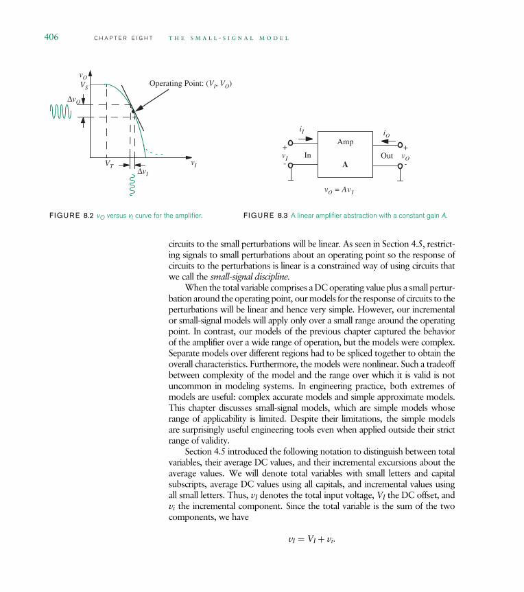
406 C H A P T E R E I G H T t h e s m a l l - s i g n a l m o d e l
VT vI
vO
∆vO
∆vI
VSOperating Point: (VI, VO)
F IGURE 8.2 vO versus vI curve for the amplifier.
Amp
In OutA
vO = AvI
+vI-
+vO-
iI iO
F IGURE 8.3 A linear amplifier abstraction with a constant gain A.
circuits to the small perturbations will be linear. As seen in Section 4.5, restrict-ing signals to small perturbations about an operating point so the response ofcircuits to the perturbations is linear is a constrained way of using circuits thatwe call the small-signal discipline.
When the total variable comprises a DC operating value plus a small pertur-bation around the operating point, our models for the response of circuits to theperturbations will be linear and hence very simple. However, our incrementalor small-signal models will apply only over a small range around the operatingpoint. In contrast, our models of the previous chapter captured the behaviorof the amplifier over a wide range of operation, but the models were complex.Separate models over different regions had to be spliced together to obtain theoverall characteristics. Furthermore, the models were nonlinear. Such a tradeoffbetween complexity of the model and the range over which it is valid is notuncommon in modeling systems. In engineering practice, both extremes ofmodels are useful: complex accurate models and simple approximate models.This chapter discusses small-signal models, which are simple models whoserange of applicability is limited. Despite their limitations, the simple modelsare surprisingly useful engineering tools even when applied outside their strictrange of validity.
Section 4.5 introduced the following notation to distinguish between totalvariables, their average DC values, and their incremental excursions about theaverage values. We will denote total variables with small letters and capitalsubscripts, average DC values using all capitals, and incremental values usingall small letters. Thus, vI denotes the total input voltage, VI the DC offset, andvi the incremental component. Since the total variable is the sum of the twocomponents, we have
vI = VI + vi.

8.2 The Small-Signal Model C H A P T E R E I G H T 407
VT vI
vOVS
F IGURE 8.4 A small segment ofthe vO versus vI curve.
VI+-
RL
VS
vO = f(VI + vi)
vi+-
VS
iDK([VI + vi] − VT)2
2----------------------------------------------=
RL
VO = f(VI + vi)
VI+-
vi+-
F IGURE 8.5 Superimposing asmall (possibly time-varying) signalon the DC bias voltage at the inputof the MOSFET amplifier, and thecorresponding SCS circuit modelfor the combined input signal.
Let us revisit the transfer curve of the amplifier shown in Figure 8.2. Con-sider a very small region of the transfer curve in the vicinity of the operatingpoint (VI, VO). The slope of the curve segment is depicted in the figure. Asillustrated in Figure 8.4, if we focus our attention on the small curve segmentshown, it looks more or less linear. We will use this intuition to develop anabstraction for amplifiers that appears linear for very small variations in theinput voltage.
The basic idea is that the amplifier transfer function appears linear for smallperturbations in the input voltage about a given bias point. We can arrive at thesame result analytically. Suppose that the amplifier is biased at some bias point:(VI, VO). Now suppose that we superimpose a small signal vI = vi on VI asdepicted in Figure 8.5. An example of a DC signal with a small superimposedtime-varying signal is shown in Figure 8.6.
We know from the SCS model of the MOSFET (see Equation 7.8) that thecurrent through the MOSFET is related to its gate voltage as:
iDS = K(vGS − VT)2
2. (8.3)

408 C H A P T E R E I G H T t h e s m a l l - s i g n a l m o d e l
F IGURE 8.6 A small time-varying signal combined witha DC offset voltage.
vI = VI + vi
vI
VI
vi
t
F IGURE 8.7 Output current forthe MOSFET for the combinedinput voltage.
iDS
vGSVT
K(vGS – VT)2
2--------------------------------
VI
ID
vi
id
iD
vI
Bias pointvgs
ids
For the combined input signal shown in Figure 8.5, the response currentiD through the MOSFET is the sum of two components: a bias current ID anda change id due to the incremental input signal vi. As depicted in Figure 8.7,this combined current can be obtained by substituting for vGS as
iD = f (VI + vi) = ID + id = K([VI + vi] − VT)2
2. (8.4)
Since we know that vi is small compared to VI, we can adopt the followinglinearization technique to obtain the combined response: Model the MOSFETcharacteristic curve accurately only in the vicinity of the bias point VI and dis-regard the rest of the curve. The Taylor series expansion is the natural tool forthis task.
The Taylor series expansion for the function y = f (x) in the vicinity ofx = Xo is given by:
y = f (x) = f (Xo) + df
dx
∣∣∣∣Xo
(x − Xo) + 1
2!d2f
dx2
∣∣∣∣∣Xo
(x − Xo)2 + · · ·

8.2 The Small-Signal Model C H A P T E R E I G H T 409
Our goal is to use the Taylor series method to expand the MOSFET SCSequation for the combined input voltage given in Equation 8.4 about the biasvoltage VI. For our Taylor expansion, VI corresponds to Xo, x correspondsto VI + vi, or x − Xo corresponds to vi, and y corresponds to iD = ID + id.Applying the Taylor expansion to Equation 8.4 about VI we get
iD = f (VI + vi) = K[(VI + vi) − VT]22
(8.5)
= K(VI − VT)2
2+ K(VI − VT)vi + K
2v2
i . (8.6)
If the incremental signal vi is small enough to permit us to ignore the secondorder term (and higher terms, when they exist) in the Taylor series expansion,the following simplification results:
iD ≈ K(VI − VT)2
2+ K(VI − VT)vi. (8.7)
We know that the output current is composed of a DC component ID anda small perturbation id. Thus, we can write
ID + id = K(VI − VT)2
2+ K(VI − VT)vi. (8.8)
Equating DC terms and corresponding incremental terms:
ID = K(VI − VT)2
2(8.9)
id = K(VI − VT)vi. (8.10)
Note that ID is simply the DC bias current related to the DC input voltage VI.Accordingly, the DC terms relating ID to VI can be equated as in Equation 8.9because the operating point values ID, VI satisfy Equation 8.3, which is theMOSFET equation. When the DC terms are eliminated from both sides ofEquation 8.8, the incremental relation shown in Equation 8.10 results.
Notice that the change in the output current id is linearly related to thechange in the input voltage vi provided that vi is small compared to VI. Wenote that Equation 8.9 is exact because the small-signal model goes through theexact model at the operating point. However, Equation 8.10 is approximatebecause of the linearization.
A graphical interpretation of this result provides additional intuition. Asshown in Figure 8.8, Equation 8.8 is a straight line passing through the DCoperating point VI, ID and tangent to the curve at that point. Using the tangent

410 C H A P T E R E I G H T t h e s m a l l - s i g n a l m o d e l
F IGURE 8.8 Incrementalchange in the output current forthe MOSFET for a small change inthe input voltage.
iDS
vGSvT
K(vGS – vT)2
2-------------------------------
VI
ID
vi
id
iD
vI
Bias pointvgs
ids
to compute the incremental change in the signal about the operating point istantamount to replacing the actual curve with the tangent. Clearly, the tangentapproximation is valid only for points that are close to the operating point. Thehigher-order term in Equation 8.6 that we neglected would add a quadraticterm to the model, thereby making the fit exact for our model.
Let us return to the relationship between the incremental output currentand the incremental input voltage for the MOSFET:
id = K(VI − VT)vi. (8.11)
The K(VI − VT) term in Equation 8.11 relates the input voltage to thecurrent through the MOSFET. Notice that for a given DC bias, the K(VI − VT)term is a constant. Since the form of Equation 8.11 is similar to that for aconductance, the K(VI −VT) term is called the incremental transconductance gmof the MOSFET. Accordingly, we can write
id = gmvi (8.12)
where
gm = K(VGS − VT). (8.13)
In our example, VGS = VI.Returning to our amplifier, we can express the total output voltage vO as
the sum of the output operating voltage VO and the incremental change vo as
vO = VO + vo.
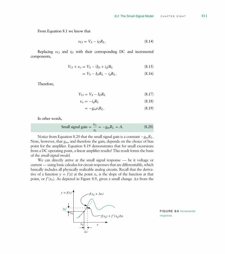
8.2 The Small-Signal Model C H A P T E R E I G H T 411
From Equation 8.1 we know that
vO = VS − iDRL. (8.14)
Replacing vO and iD with their corresponding DC and incrementalcomponents,
VO + vo = VS − (ID + id)RL (8.15)
= VS − IDRL − idRL. (8.16)
Therefore,
VO = VS − IDRL (8.17)
vo = −idRL (8.18)
= −gmviRL. (8.19)
In other words,
Small signal gain = vo
vi= −gmRL = A. (8.20)
Notice from Equation 8.20 that the small signal gain is a constant −gmRL.Note, however, that gm, and therefore the gain, depends on the choice of biaspoint for the amplifier. Equation 8.19 demonstrates that for small excursionsfrom a DC operating point, a linear amplifier results! This result forms the basisof the small-signal model.
We can directly arrive at the small signal response be it voltage orcurrent using basic calculus for circuit responses that are differentiable, whichbasically includes all physically realizable analog circuits. Recall that the deriva-tive of a function y = f (x) at the point xo is the slope of the function at thatpoint, or f ′(xo). As depicted in Figure 8.9, given a small change x from the
x0
f(x0) + f ′(x0)∆x
∆y
x
f(x0 + ∆x)y = f(x)
∆x
y0F IGURE 8.9 Incrementalresponse.

412 C H A P T E R E I G H T t h e s m a l l - s i g n a l m o d e l
point xo, we can compute the response to the change as the product of theslope at that point and x. In other words,
f (xo + x) = f (xo) + df (x)
dx
∣∣∣∣xo
x.
Thus the incremental change in the output is given by
y = dy
dx
∣∣∣∣xo
x. (8.21)
In particular, we can obtain the incremental voltage gain directly fromthe voltage transfer function, without first determining the incremental outputcurrent. The input-output voltage relationship for the MOSFET amplifier isgiven by
vO = f (vI)
= VS − K(vI − VT)2
2RL.
As before, let vi = vI denote a small change in the input voltage, and letvo = vO denote the corresponding change in the output voltage. Then,
vo = df (vI)
dvI
∣∣∣∣vI=VI
vi
= −K(vI − VT)RL∣∣vI=VI
vi
= −K(VI − VT)RLvi
= −gmRLvi.
Not surprisingly, this result is the same as the one we obtained earlier.To summarize, the small-signal model is a statement of a particular type
of linearized analysis of our circuits, which applies when the desired circuitresponds to signals that can be represented as an incremental perturbation overa DC operating value. Put another way, it is a statement of a particular type ofconstraint on our use of circuits called the small-signal discipline that allows usto obtain linear behavior from nonlinear circuits over small ranges of operation.
Small signal model The responses of circuits to incremental changes from aknown DC operating point will be linear to a good approximation.

8.2 The Small-Signal Model C H A P T E R E I G H T 413
A systematic procedure for finding incremental signal responses based onthe preceding discussion involves two steps:
1. Find the DC operating point of the circuit using DC values and thecomplete characteristics of the devices. Determine the correspondinglarge-signal response (possibly nonlinear) to the desired input.
2. Apply the Taylor expansion method to the large-signal response to derivethe small-signal response. Alternatively, as discussed in Section 8.2.1,replace the large-signal circuit with its equivalent small-signal modelbased on the Taylor expansion and obtain the small-signal response.
Small-signal analysis is an extremely useful technique that applies to allphysical systems with differentiable characteristics. In essence, it says that if weoperate within a small-signal discipline, the response of any physical systemto small perturbation will be linear! In turn, the effectively linear system isamenable to linear analysis techniques, such as superposition.
For example, consider a two-terminal sensor S that behaves like atemperature-dependent voltage source with the following nonlinear relation-ship between its terminal voltage vS and its temperature tS:
vS = Bt 3S
where B is some constant. If the ambient temperature is TS and the correspond-ing voltage is VS, we can relate the incremental change in the terminal voltage vsto an incremental change in the temperature ts using Equation 8.21 as follows:
vs = 3B t 2S
∣∣∣tS=TS
ts.
In other words,
vs = 3BT2Sts.
When operating at a given ambient temperature, 3BT2S is a constant. Therefore,
the voltage response of the sensor to small changes in the temperature aroundan ambient will be linear.
8.2.1 S M A L L - S I G N A L C I R C U I T R E P R E S E N T A T I O N
A model that involves only the small-signal variables of a circuit, and hencedescribes purely the small-signal behavior of that circuit, would greatly facilitatesmall-signal analysis. Fortunately, such a small-signal model is relatively straight

414 C H A P T E R E I G H T t h e s m a l l - s i g n a l m o d e l
forward to develop by executing the following procedure:
1. Set each source to its operating-point value, and determine the operating-point branch voltages and currents for each component in the circuit.This is most likely the longest step in the procedure.
2. Linearize the behavior of each circuit component about its operatingpoint. That is, determine the linearized small-signal behavior of eachcomponent, and select a linear component to represent this behavior.The parameters of the small-signal components will commonly dependon the operating point voltages or currents.
3. Replace each original component in the circuit with its linearizedequivalent and re-label the circuit with the small-signal branch variables.The resulting circuit is the desired small-signal model.
The circuit that is generated by this procedure is the desired small-signalcircuit model, and is analogous to equating the small signal terms on bothsides of Equation 8.8 yielding the equalities in Equation 8.10. Further, it is alinear circuit, and hence the analysis tools developed for linear circuits, such assuperposition and the Thévenin equivalent model, may be applied to its analysis.
At this point, it is worth discussing why the procedure works. To begin,recognize that the operation of a circuit is described in total by two sets ofequations: the circuit connection laws of KVL and KCL, and the constitutivelaws that describe the behavior of the individual circuit components. With thisrecognition, the small-signal analysis of a circuit may also be described by thefollowing more direct mathematical procedure:
1. Set each source to its operating-point value, and combine the equationsto determine the operating point of the circuit. This is essentially thesame step as in the previous procedure.
2. Return to the original set of equations. For each variable in everyequation, substitute for the total variable the sum of its operating-pointvalue and its small-signal value. Then, linearize the equations around theoperating point assuming that the small-signal terms are small.
3. Cancel the operating-point variables from the linearized equations to yielda set of linear equations that relate the small signals to themselves. Thiscancellation must always be possible since the linearization is defined topass through the operating-point. This cancellation is akin to separatelyequating the operating point variables and the incremental variables as wedid in Equation 8.10.1
1. In other words, we start with a set of equalities defining the operating point using operating-pointvariables, for example,
VO = AVI.

8.2 The Small-Signal Model C H A P T E R E I G H T 415
4. Complete the small-signal analysis by combining the linearized equationsto determine the desired small-signal variables in terms of the small-signalinputs at the sources.
Now, let us examine the last procedure more closely. Notice that in Step 2it is actually necessary to linearize only the constitutive laws that describe thebehavior of the individual circuit components because KVL and KCL are alreadylinear equations. It is for this reason that the first procedure called for thelinearization of only the constitutive laws. Further, because KVL and KCL con-stitute a linear set of equations, they are unchanged by the linearization step.This is important to recognize because KVL and KCL contain the informa-tion concerning the topology of the original circuit. That is, they state whichbranches are connected to which nodes, and which branches connect to formwhich loops. Since KVL and KCL are unaffected by the linearization step,the topological information is preserved during linearization. It is for this rea-son that the small-signal circuit model has the same topology as the originalcircuit. Thus, the linearized set of equations describing the behavior of thesmall-signal circuit variables that is generated by the more formal mathemati-cal procedure comprises the original KVL and KCL equations, and linearizedcomponent constitutive laws. Thus, to develop a small-signal circuit modelit is necessary to determine only equivalent linearized circuit components andsubstitute them into the circuit in place of their corresponding original circuitcomponents.
Small-signal circuit models for various devices are summarized inFigure 8.10.
The small-signal equivalent model for an independent DC voltage sourceis a short circuit because its output voltage does not change for anyperturbation of the current through it. In particular, the power supplyconnection labeled VS in most of our circuits gets shorted to ground inthe incremental circuit.
The small-signal model for an independent DC current source is an opencircuit.
We then linearize, and obtain a new set of equalities in operating-point variables andincremental variables, for example,
VO + vo = AVI + Avi.
The equalities that defined the operating point in the first place (namely, VO = AVI in ourexample) may always be cancelled out of the linearized equations since they are only additivelyconnected to the small-signal variables. For our example, we thus obtain
vo = Avi.

416 C H A P T E R E I G H T t h e s m a l l - s i g n a l m o d e l
F IGURE 8.10 Small-signalequivalent models.
va
+
-
V0
GD
S
D
G
S
D
G
S
RRR
V0
I0 I0
vA
+
-
iA = f(vA) ia=
ia
+
-
Large signal Small signal
iA
+
-
vA= f(iA)
+
-
ids---------------------------------iDS =K(vGS − VT)2
= K(VGS − VT)vgs2
---------------
---------------
va =df(iA)diA
iaIA
---------------
---------------
df(vA)dvA
vaVA
A resistor behaves identically for a large signal or a small-signal. Thereforeits small-signal and large-signal models are the same.
For a MOSFET, the derivation resulting in Equation 8.11 shows how torelate the incremental drain to source current ids to the incremental gateto source voltage vgs.
By definition, an input signal vI has an incremental component vi anda DC component VI.
In general, if a device variable xB depends on some other variable xA as
xB = f (xA),
then the incremental change in xB due to an small change in xA is given by
xb = df (xA)
dxA
∣∣∣∣xA=XA
xa (8.22)
where XA is the operating point value of xA.
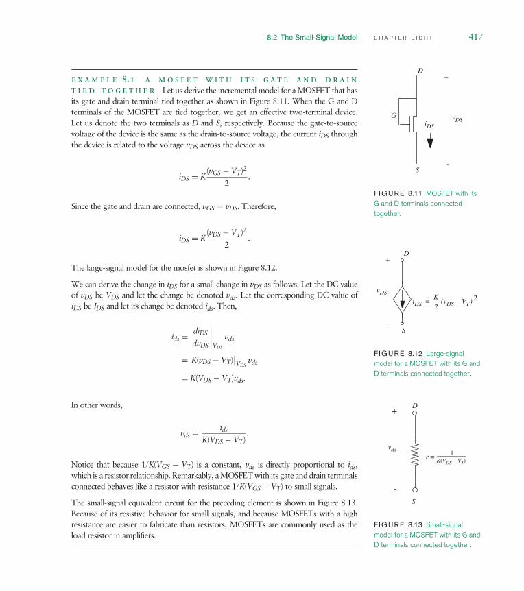
8.2 The Small-Signal Model C H A P T E R E I G H T 417
e x a m p l e 8.1 a m o s f e t w i t h i t s g a t e a n d d r a i n
t i e d t o g e t h e r Let us derive the incremental model for a MOSFET that hasits gate and drain terminal tied together as shown in Figure 8.11. When the G and Dterminals of the MOSFET are tied together, we get an effective two-terminal device.Let us denote the two terminals as D and S, respectively. Because the gate-to-sourcevoltage of the device is the same as the drain-to-source voltage, the current iDS through
vDSiDS
G
S
D+
-
F IGURE 8.11 MOSFET with itsG and D terminals connectedtogether.
the device is related to the voltage vDS across the device as
iDS = K(vGS − VT)2
2.
Since the gate and drain are connected, vGS = vDS. Therefore,
iDS = K(vDS − VT)2
2.
The large-signal model for the mosfet is shown in Figure 8.12.
We can derive the change in iDS for a small change in vDS as follows. Let the DC valueof vDS be VDS and let the change be denoted vds. Let the corresponding DC value ofiDS be IDS and let its change be denoted ids. Then,
vDS
iDS = (vDS - VT) 2
S
D+
-
K2----
F IGURE 8.12 Large-signalmodel for a MOSFET with its G andD terminals connected together.
ids = diDS
dvDS
∣∣∣∣VDS
vds
= K(vDS − VT)∣∣VDS
vds
= K(VDS − VT)vds.
In other words,
vds = ids
K(VDS − VT).
Notice that because 1/K(VGS − VT) is a constant, vds is directly proportional to ids,which is a resistor relationship. Remarkably, a MOSFET with its gate and drain terminalsconnected behaves like a resistor with resistance 1/K(VGS − VT) to small signals.
The small-signal equivalent circuit for the preceding element is shown in Figure 8.13.
vdsr =
S
D+
-
1K(VDS – VT)-------------------------------
F IGURE 8.13 Small-signalmodel for a MOSFET with its G andD terminals connected together.
Because of its resistive behavior for small signals, and because MOSFETs with a highresistance are easier to fabricate than resistors, MOSFETs are commonly used as theload resistor in amplifiers.

418 C H A P T E R E I G H T t h e s m a l l - s i g n a l m o d e l
8.2.2 S M A L L - S I G N A L C I R C U I T F O R T H EM O S F E T A M P L I F I E R
Let us now develop the small-signal equivalent circuit for the MOS amplifiershown in Figure 8.14. Recall that developing the small-signal model involvesthe following steps:
1. Set each source to its operating-point value, and determine the operating-point branch voltages and currents for each component in the circuit.
2. Determine the linearized small-signal behavior of each component, andselect a linear component to represent this behavior.
3. Replace each original component in the circuit with its linearizedequivalent and re-label the circuit with the small-signal branch variables.The resulting circuit is the desired small-signal model.
As the first step, let us determine the operating point of the MOSFETamplifier for its bias voltages using the large-signal SCS circuit model depictedin Figure 8.15. Assuming that the input bias voltage is VI, we can determine theoutput operating current ID and the output operating voltage VO. We explicitlyshow the power supply voltage source VS to facilitate deriving the small-signalmodel.
F IGURE 8.14 The MOSFETamplifier.
+-
vI
vO
VS
iD 2----------------------------=
RL
K(vI − VT)2
F IGURE 8.15 Computing theoperating point of the MOSFETamplifier based on the large-signalSCS model. +
-VI
VO
VS
IDK(VI – VT)2
2------------------------------=
RL
+-VS

8.2 The Small-Signal Model C H A P T E R E I G H T 419
The output operating current ID is directly calculated from the MOSFETcharacteristic equation as:
ID = K
2(VI − VT)2.
The output operating voltage is obtained by applying KVL for the loopcomprising the power supply, the MOSFET, and RL as follows:
VO = VS − IDRL (8.23)
= VS − K
2(VI − VT)2RL. (8.24)
As the second step, we determine the linearized small-signal models foreach component. Referring to Figure 8.10, we see that the small-signal modelfor the DC power supply is a short. The small-signal model for the resistor is thesame as its large-signal model. Finally, the linearized small-signal model for theMOSFET in saturation is a voltage-dependent current source whose small-signalcurrent is linearly related to the small-signal gate-to-source voltage as:
ids = K(VGS − VT)vgs.
Notice that the biasing of the large-signal circuit determines the parameters ofthe small-signal circuit (for example, the small-signal current source parameterK(VI − VT) depends on the input bias voltage, VI).
As the third step, we replace each original component in the circuit withits linearized equivalent and re-label the circuit with the small-signal branchvariables vi, vo, and id as depicted in Figure 8.16.
The small-signal circuit model can be analyzed to determine the circuitresponse to small signals. For example, we can use Figure 8.16 to determinethe small-signal gain of the MOSFET amplifier. Applying KVL at the output,we get
vo = −idRL (8.25)
= −K(VI − VT)viRL (8.26)
+-vi
vo
id K(VI – VT)vi=
RLF IGURE 8.16 The small-signalSCS circuit model for the MOSFETamplifier.

420 C H A P T E R E I G H T t h e s m a l l - s i g n a l m o d e l
Thus, the small-signal gain is given by
vo
vi= −K(VI − VT)RL (8.27)
= −gmRL (8.28)
where
gm = K(VGS − VT) (8.29)
is the transconductance of the MOSFET.As an example, let us compute the small-signal gain for the following
amplifier parameters:
VS = 10 V
K = 1 mA/V2
RL = 10 k
VT = 1 V.
Also, suppose the input bias voltage is chosen to be VI = 2 V. Asdetermined earlier in Equation 8.24,
VO = VS − K
2(VI − VT)2RL.
Substituting, the given parameters, we get VO = 5 V.We can now calculate the magnitude of the voltage gain as
vo
vi= K(VI − VT)RL
= 10−3(VI − 1)104
= 10.
8.2.3 S E L E C T I N G A N O P E R A T I N G P O I N T
Small-signal operation requires that the total input signal appear as a smallperturbation about a DC offset. The input DC offset establishes an operatingpoint for the amplifier. Section 7.7 discussed the issue of operating points in thecontext of large signals, and proposed a method for selecting the operating pointbased on maximizing the dynamic input signal range. Specifically, Section 7.7suggested that the operating point be chosen as the midpoint of the valid inputvoltage range of amplifier operation under the saturation discipline. This made

8.2 The Small-Signal Model C H A P T E R E I G H T 421
VI
|Gain|
VT = 1 V
10
20
F IGURE 8.17 Magnitude of thesmall-signal gain of the amplifierfor various values of the inputoperating point voltage VI .
sense, since the input signals were large and maximizing the input dynamicrange enabled the amplifier to deal with the largest possible input signals.
When dealing with small signals, other criteria are often more important inselecting the operating point than just obtaining maximum dynamic range. Onecriterion is the small-signal gain of the amplifier. As evident from Equation 8.28,the small-signal gain of the amplifier is dependent on the input operating pointvoltage VI. The magnitude of the small-signal gain is given by
∣∣∣∣vo
vi
∣∣∣∣ = K(VI − VT)RL. (8.30)
Figure 8.17 plots the magnitude of the gain for various values of VI. The graphindicates that the amplifier gain increases with increasing VI.
As an example, assuming these parameters for our amplifier,
VS = 10 V
K = 1 mA/V2
RL = 10 k
VT = 1 V
let us determine a value for the input operating-point voltage VI that will resultin a gain of 12.
Substituting the required gain into Equation 8.30, we have
12 = 1 × 10⁻³(VI − 1)10 × 103.
Solving, we obtain VI = 2.2 V. This means that an input DC offset of 2.2 Vwill result in a small-signal gain magnitude of 12.

422 C H A P T E R E I G H T t h e s m a l l - s i g n a l m o d e l
Now, assuming that the input signal is a small-signal sinusoid superimposedon the DC offset of 2.2 V, let us determine the maximum valid peak-to-peakswing for the sinusoid. We refer back to Section 7.6.2 to answer this question.From Section 7.6.2, we know that under the saturation discipline, the maximumvalid range for the input voltage is VT → −1 + √
1 + 2VSRLK/RLK + VT.For the given parameters, the valid range for input voltages is 1 V →
2.32 V. In other words, as discussed in Section 7.6.2, input voltages under 1 Vwill result in cutoff region operation of the MOSFET, while those over 2.32 Vwill result in triode region operation. Operation in either the cutoff region orthe triode region will result in severe signal distortion.
Since the input offset is 2.2 V, and the maximum valid input voltage is2.32 V, the maximum positive swing for saturation region operation of theMOSFET is given by 2.32 V − 2.2 V = 0.12 V. Thus, the maximum peak-to-peak swing for the input sinusoid is 2 × 0.12 V = 0.24 V. Notice the cleartradeoff we have made between gain and dynamic range. To increase the gain,we had to bias the amplifier with a high input bias voltage, which was closeto the high end of the valid input signal range. However, the high input biasvoltage limited the positive signal swing.
Another criterion that is often important is the output operating-pointvoltage. This is important when the amplifier must drive another circuit stageand the output operating-point voltage of the amplifier determines the inputoperating-point voltage of the next stage.
For example, consider the two-stage amplifier shown in Figure 8.18. Inthis circuit, VIA provides the DC bias for the first stage. Its output, in turn, VOAprovides the DC bias for the second stage. Thus, VOA = VIB.
Assuming the following parameters for our amplifier,
VS = 10 V
K = 1 mA/V2
R = 10 k
VT = 1 V
F IGURE 8.18 A two-stageamplifier.
+-
VIA
R
VS
R
VS
VOB
-
+
VOA
+
-VIB
+
-

8.2 The Small-Signal Model C H A P T E R E I G H T 423
suppose the first stage is biased at VI A = 2.2 V to achieve a small-signal gainmagnitude of 12. Let us determine whether the output operating-point voltageof the first stage can provide a valid input bias voltage for the second stage.
When the first stage is biased at VI A = 2.2 V, the first stage operating-pointoutput voltage VOA is given by Equation 8.24. Substituting the parameters forour circuit, we have
VOA = VS − K
2(VI A − VT)2R
= 10 − 1 × 10⁻³
2(2.2 − 1)210 × 103
= 2.8 V.
From Section 7.6.2, we know that under the saturation discipline, the max-imum valid range for the input voltage of the second stage is VT → −1 +√
1 + 2VSRK/RK + VT. Substituting the circuit parameters, the valid inputrange for the second stage comes out to be 1 V → 2.32 V. Since VOA exceedsthe upper bound (2.8 V > 2.32 V), we conclude that the first stage cannot pro-vide a valid input bias voltage for the second stage when the first stage input biasis set at 2.2 V. We can correct this situation by increasing VI A, or by increasingR for the first stage.
8.2.4 I N P U T A N D O U T P U T R E S I S T A N C E ,C U R R E N T A N D P O W E R G A I N
The small-signal equivalent circuit also allows us to determine other importantcircuit parameters, such as the small-signal input resistance, output resistance,current gain, and power gain. Since the amplifier behaves as a linear networkfor small signals, it can be characterized by a Thévenin equivalent when viewedfrom any given port. The input and output resistance come in handy in thisThévenin characterization. Let us determine these values for the MOSFETamplifier using its small-signal circuit in Figure 8.16. Since these parameters areexternally observed quantities, they are defined with respect to the external portsof the amplifier abstraction. Thus, it is important that we define precisely whatconstitutes the input and output ports of the small-signal amplifier. Figure 8.19shows the relationship between the external ports of the amplifier circuit and thesmall-signal model. Notice that we have internalized the input bias voltage intothe small-signal amplifier abstraction so the user of the amplifier does not have toprovide the appropriate input bias voltage. Instead, the user can simply providea small input signal and observe the resulting signal output superimposed onthe DC output offset.

424 C H A P T E R E I G H T t h e s m a l l - s i g n a l m o d e l
VI+
-
RL
VS
vi
vO
Small-Signal
Amplifier
ii
iO
+
-
+
-
(a)
id = K(VI – VT)vi
RL
ii
vi
vo
io
-
+
-
+
(b)
F IGURE 8.19 Amplifier inputand output ports: (a) amplifiercircuit; (b) small-signal model. Asshown in the amplifier circuit, wehave internalized the input biasvoltage into the small-signalamplifier abstraction.
Input Resistance ri
Incremental input resistance The change in the input current for a small changein the input voltage.
Accordingly, as depicted in Figure 8.20 we compute it by applying a small testvoltage vtest at the input and measuring the corresponding current itest. All otherindependent small-signal voltages or DC voltage sources are shorted. Similarly,all other independent small-signal or DC current sources are turned into opencircuits.
The input resistance for the MOSFET amplifier is given by
ri = vtest
itest= vtest
0= ∞. (8.31)
F IGURE 8.20 Input resistancemeasurement. id = K(VI – VT)vtest
RL+
-
+-vtest
itest

8.2 The Small-Signal Model C H A P T E R E I G H T 425
RL
vi = 0 id = K(VI – VT)vi = 0
+-
vtest
itest
F IGURE 8.21 Output resistancemeasurement.
For the SCS MOSFET model, the gate does not draw any current (itest = 0),so the input resistance is infinite.
Output Resistance rout
Incremental output resistance The change in the output current for a smallchange in the output voltage.
We must assume, of course, that the circuit is biased properly. As depicted inFigure 8.21, we compute the output resistance by applying a small test voltagevtest at the output and measuring the corresponding current itest. As before,all other independent small-signal voltages or DC voltage sources are shorted.Thus the small-signal input voltage vi is set to 0. Similarly, all other independentsmall-signal or DC current sources are turned into open circuits.
The output resistance is given by
rout = vtest
itest= RL. (8.32)
Because the input small-signal voltage is set to zero, the current throughthe MOSFET is 0. In other words, the MOSFET behaves like an open circuit.Thus the output resistance for small signals is RL.
Current Gain
Analogous to the voltage gain, we can define a current gain for an amplifierthat supplies an external current.
Incremental current gain The change in the output current divided by thechange in the input current, for a given external load resistance.
As depicted in Figure 8.22, we can compute the current gain by applying asmall test voltage at the input and measuring both the input current itest andthe output current io. The ratio io/itest is the current gain. Note that the outputcurrent is not the current that flows through the dependent current source,rather it is the current that is drawn by an external load resister RO. Becauseit is dependent on the value of the load resistor, the current gain is defined

426 C H A P T E R E I G H T t h e s m a l l - s i g n a l m o d e l
F IGURE 8.22 Current gainmeasurement. As an exercise, weplace a resistance Ri between theinput terminal and ground. For aMOSFET, Ri = ∞.
RL
id = K(VI – VT)vtest+-vtest
itestRO
io
irl
vo
Ri
+
-
for a given load resistance. The introduction of an external load resistance alsoreduces the voltage gain of the amplifier because it appears in parallel with theinternal load resistor RL.
The current gain with an external load resistance RO is given by
Current gain = ioitest
. (8.33)
Let us go through the exercise of determining the value of io assumingthere is some finite input resistance Ri as shown in Figure 8.22. Substituting forio and itest in terms of the respective voltages,
Current gain =voROvtestRi
(8.34)
= vo
vtest
Ri
RO. (8.35)
Equation 8.35 says that the current gain is proportional to the product of thevoltage gain and the ratio of the input resistance and the output resistance.
We can determine the voltage gain vo/vtest by substituting for vo in termsof the current id and the parallel resistance pair RL and RO as
vo
vtest= −K(VI − VT)vtest(RL‖RO)
vtest.
In other words,
vo
vtest= −K(VI − VT)(RL‖RO). (8.36)
Notice that the voltage gain of the amplifier with an external load is lower thanan unloaded amplifier. Substituting the expression for the voltage gain into

8.2 The Small-Signal Model C H A P T E R E I G H T 427
Equation 8.35, we get an expression for the current gain:
Current gain = −K(VI − VT)(RL‖RO)Ri
RO. (8.37)
Since Ri = ∞ for the MOSFET, the corresponding current gain is alsoinfinite.
Power Gain
Incremental power gain The ratio of the power supplied by the amplifier to anexternal load to that supplied to the amplifier by the input source.
Referring to Figure 8.22, we can compute the power gain as follows: We applya small test voltage at the input and measure the input current itest. We alsomeasure the corresponding output voltage vo and output current io supplied tothe external load resistor. We compute the power supplied by the input sourceas vtestitest. Similarly, we compute the power supplied to the external load asvoio. As we did for the current gain, let us assume that the amplifier has aninput resistance Ri. The power gain is given by
Power gain = voiovtestitest
= vo
vtest
ioitest
. (8.38)
We know both the voltage gain and the current gain from Equations 8.36and 8.37, respectively. Substituting in the above equation we get,
Power gain = vo
vtest
ioitest
(8.39)
= [−K(VI − VT)(RL‖RO)][−K(VI − VT)(RL‖RO)
Ri
RO
](8.40)
= [K(VI − VT)(RL‖RO)]2 Ri
RO. (8.41)
Since Ri = ∞ for the MOSFET amplifier, the power gain is also infinite.In practical circuits, however, there is always some input resistance, so thepower gain is finite.
e x a m p l e 8.2 v o l t a g e - c o n t r o l l e d c u r r e n t s o u r c e
Let us perform a small-signal analysis of the voltage-controlled current source circuitshown in Figure 8.23. Referring to Figure 8.23, the current iO depends on voltagesource vI according to
iO = 1
L(vI − 1)
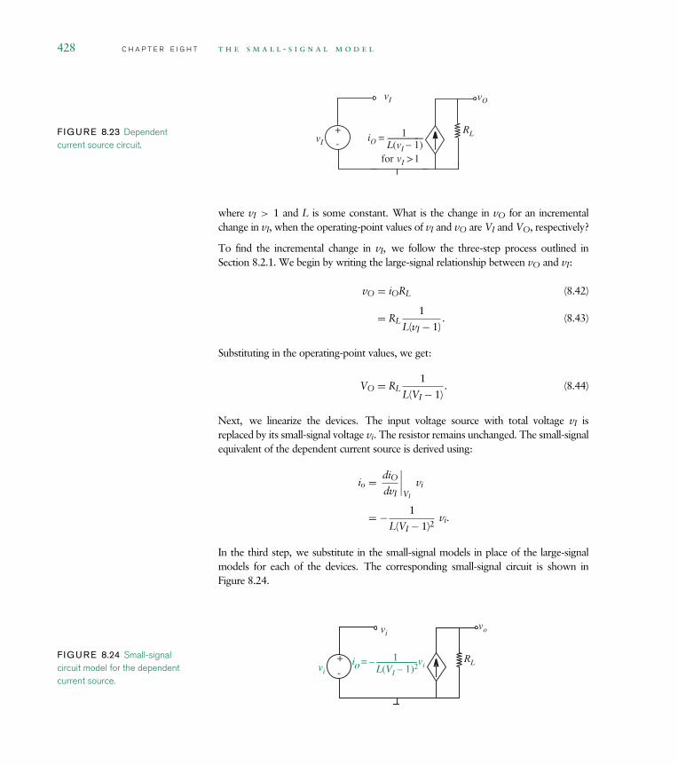
428 C H A P T E R E I G H T t h e s m a l l - s i g n a l m o d e l
F IGURE 8.23 Dependentcurrent source circuit.
RL
vI vO
+- vI iO
1---------------------=
for vI >1L(vI − 1)
where vI > 1 and L is some constant. What is the change in vO for an incrementalchange in vI, when the operating-point values of vI and vO are VI and VO, respectively?
To find the incremental change in vI, we follow the three-step process outlined inSection 8.2.1. We begin by writing the large-signal relationship between vO and vI:
vO = iORL (8.42)
= RL1
L(vI − 1). (8.43)
Substituting in the operating-point values, we get:
VO = RL1
L(VI − 1). (8.44)
Next, we linearize the devices. The input voltage source with total voltage vI isreplaced by its small-signal voltage vi. The resistor remains unchanged. The small-signalequivalent of the dependent current source is derived using:
io = diOdvI
∣∣∣∣VI
vi
= − 1
L(VI − 1)2vi.
In the third step, we substitute in the small-signal models in place of the large-signalmodels for each of the devices. The corresponding small-signal circuit is shown inFigure 8.24.
F IGURE 8.24 Small-signalcircuit model for the dependentcurrent source.
RL
vivo
+- vi
io1--------------------------------vi–=
L(VI – 1)2
8.2 The Small-Signal Model C H A P T E R E I G H T 429
We can now derive the change in the output voltage for a small change in the inputvoltage from the small-signal circuit by writing KVL for the output loop:
vo = ioRL = − 1
L(VI − 1)2viRL.
We can also derive the change in the output voltage for a small change in the inputvoltage directly from the vO versus vI relationship given by Equation 8.43.
vo = dvO
dvI
∣∣∣∣VI
vi = − 1
L(VI − 1)2viRL.
e x a m p l e 8.3 s m a l l - s i g n a l a n a l y s i s o f a d i f f e r -
e n c e a m p l i f i e r The difference amplifier is a building block for high-qualityamplification and is useful for processing small signals. When a signal is noisy, straight-forward use of an amplifier would amplify both the signal and the noise. However,under certain conditions that we will see shortly, a difference amplifier (also called adifferential amplifier) can be used to amplify the signal by a much larger gain relativeto the noise. Difference amplifiers are also used in building operational amplifiers, andsuitable difference amplifier circuits are discussed in Examples 7.19 and 8.10.
Suppose the signal is available in differential form. In other words, suppose the signalis available as the relative voltage output (vA − vB) on a pair of terminals A and B. Forexample, as the output of the tape-head in a tape-recorder, the output of an instrumen-tation device or a sensor. Such a sensor often resembles one of our primitive elementsfor example, a variable resistor. The element might produce a voltage signal across itsterminals related to some externally sensed parameter such as temperature, gas con-centration, or magnetic field strength. Often, a pair of wires carrying the signal mighttravel through a noisy environment resulting in the coupling of more or less the sameamount of noise (vn) on each of the two wires, as depicted in Figure 8.25.2 In othersituations, the two wires might both carry a common DC bias. In such situations, adifference amplifier can help amplify just the differential signal component and discardthe common noise component.
The difference amplifier abstraction is shown in Figure 8.26. It is a two-port device withone differential input port and one single-ended output port. The input port has twoinput terminals. The + input is called the non-inverting input and the − input is calledthe inverting input. It has an output port across which vO appears.
2. In fact, the wires are often twisted together to ensure that when there is noise, the same amountof noise infects both wires.

430 C H A P T E R E I G H T t h e s m a l l - s i g n a l m o d e l
F IGURE 8.25 A differentialsignal.
Sensor
vA
vBvD+
-
vn vA + vn
vB + vn
F IGURE 8.26 Differenceamplifier black box representation.
Differential
amplifier
Ground
vA
vB
vO
+
-
F IGURE 8.27 Single-endeddifference amplifier structure.
Source-coupledamplifier
SubtracterA - B
A
B
vX
vY vO
vA
vB
Single-ended difference amplifier
We can also build a single-ended difference amplifier from a differential output differenceamplifier as shown Figure 8.27.
The behavior of the difference amplifier is best explained by considering its effect on thefollowing signals related to the two components, vA and vB:
1. A difference-mode component signal,
vD = vA − vB (8.45)
2. And a common-mode component signal,
vC = vA + vB
2. (8.46)
The output of the difference amplifier is a function of these two components of theinput,
vO = ADvD + ACvC (8.47)

8.2 The Small-Signal Model C H A P T E R E I G H T 431
where AD is called the difference-mode gain and AC is called the common-mode gain.The key in using a difference amplifier is to encode the useful signal in the difference-mode component and the noise in the common-mode component. Then if we makeAD large and AC small, we achieve our goal of noise reduction. Usually we use thecommon-mode rejection ratio (CMRR) to describe the ability of the amplifier to rejectthe common-mode noise:
CMRR = AD
AC. (8.48)
MOSFET Implementation of the Difference Amplifier
Let us study a MOSFET version of the difference amplifier. The amplifier employs a pairof matching transistors called the source-coupled pair. The source-coupled amplifier isshown in Figure 8.28. vA and vB are the inputs, and vX and vY are the outputs. Assume
RL RL
vX vY
vA vB
VS
I Ri
+-
vA+-
vB
F IGURE 8.28 Source-coupleddifference amplifier. All voltagesare measured with respect toground.
vA and vB are the input voltages measured with respect to ground. Also assume thatva and vb are small variations in the inputs, and that vx and vy are the correspondingsmall-signal variations in the output. The source-coupled pair is connected in series witha DC current source with a high internal resistance Ri. (We can implement the currentsource using a MOSFET biased to operate in its saturation region, but we do not show ithere. For simplicity, we use an abstract non-ideal current source instead. In other words,the current source has a finite resistance, Ri.) Let the current provided by the DC currentsource be I.
Let us examine the difference amplifier using its small-signal model shown in Figure 8.29.RL RL
Ri
gm2vgs2gm1vgs1
F IGURE 8.29 Source-coupleddifference amplifier — small-signalmodel.
Notice that an ideal current source acts like an open circuit, but a current source with aninternal Norton equivalent resistance Ri behaves like a resistor to incremental changesin its terminal variables. The MOSFETs are replaced by their small equivalent currentsources. The voltages vgs1 and vgs2 are the small-signal voltages between the gate andsource of the two input MOSFETs resulting from a small change in the input voltagesvA and vB.
The gain parameters gm1 and gm2 for the MOSFETs depend on the operating-pointvalues of the currents through them. Assuming that the current through Ri is negligible,by symmetry, we find that the current I divides equally between the two MOSFETs.Thus each has an operating-point current equal to I/2. From the SCS model for theMOSFETs, given VT and K, we can thus find the bias input voltages VGS1 and VGS2 interms of I. In turn, the respective gains gm1 and gm2 can be determined in terms of VGS1
and VGS2, which are themselves functions of I.
Recall that
the difference-mode component:
vD = vA − vB

432 C H A P T E R E I G H T t h e s m a l l - s i g n a l m o d e l
and the common-mode component
vC = vA + vB
2.
Therefore, we can decompose the inputs into their difference- and common-modecomponent as follows:
vA = vC + vD
2
vB = vC − vD
2.
We will discuss each mode separately, and then summarize the behavior of the entireamplifier.
Difference-Mode Model
We first examine the circuit with the difference-mode part of the input only. Refer toFigure 8.30 for the circuit and its small-signal model. Assume that the two MOSFET’shave identical characteristics, gm1 = gm2 = gm. An application of KCL at the sourcenode of the two MOSFETs (in other words, the node with the small-signal voltage vs)yields
gmvgs1 + gmvgs2 = vs/Ri. (8.49)
From Figure 8.30 we can also write
vd
2− vgs1 = vs
−vd
2− vgs2 = vs.
F IGURE 8.30 Difference-modemodel. All voltages are measuredwith respect to ground.
RL RLvX vY
VSRL RL
Ri
gm2vgs2gm1vgs1
+-
+-
vsvgs1 vgs2
+ +-
(b) Small-signal model(a) Differential mode input only
vD2------–
vd2-----
vd2-----–
vx vy
vD2-----
vS-+
-+-

8.2 The Small-Signal Model C H A P T E R E I G H T 433
vs
vx
+
-
vy
+
-
gm2------– vd⋅
gm2------ vd⋅RL RL
F IGURE 8.31 Difference-mode simplifiedmodel.
vy
+
-
vx
+
-
–gmRLvd gmRLvd
2-------------------------
RLRL
2----------------------+
-+-
F IGURE 8.32 Difference-modeThévenin equivalent circuit.
Substituting vgs1 and vgs2 in terms of vd into Equation 8.49, we obtain
gm
(vd
2− vs
)+ gm
(−vd
2− vs
)= vs
Ri(8.50)
−2gmvs = vs
Ri. (8.51)
Since gm and Ri are independent of each other, vs = 0. This result greatly simplifies ourcircuit to the one in Figure 8.31. Converting it to the Thévenin equivalent model, weobtain the circuit shown in Figure 8.32.
We see that
vx = − gmRLvd
2
and
vy = gmRLvd
2.
Thus, the small-signal output voltage across the output terminal pair is given by
vo = vx − vy = −gmRLvd.
This yields a difference-mode small-signal gain
Ad = vo
vd= −gmRL.
Common-Mode Model
We will now examine the behavior of the circuit for the common-mode input. Thecircuit and small-signal model is shown in Figure 8.33. The small-signal change in the

434 C H A P T E R E I G H T t h e s m a l l - s i g n a l m o d e l
F IGURE 8.33 Common-modemodel.
(a) Common-mode input only (b) Small-signal model
RL RL
vX vY
vC vC
VS
RL RL
Ri
gm2vgs2gm1vgs1
-+-
vc+-vc
vsvgs1
vgs2+ +- -+
-+-
vs
vx
+
-
vy
+
-
12 Ri⋅------------ vc⋅RL RL
12 Ri⋅------------ vc⋅
Ri
F IGURE 8.34 Common-mode Nortonequivalent circuit.
vy
+
-
vx
+
-
–RLvc
2Ri----------------
–RLvc2Ri
-----------------
RLRL
+-
+-
F IGURE 8.35 Common-mode Théveninequivalent circuit.
common-mode input is denoted vc. Observe that vgs1 = vgs2 = vgs, and vgs = vc − vs.Application of KCL at vs again yields
gmvgs + gmvgs = vs
Ri(8.52)
2gmvgs = vc − vgs
Ri(8.53)
vgs = 1
2gmRi + 1vc. (8.54)
Assuming Ri is large, so that 2gmRi 1, we can simplify Equation 8.54 to
vgs ≈ 1
2gmRivc.
Therefore, the two dependent current sources will have value
1
2Rivc.
The simplified circuit is shown in Figure 8.34. Transforming the circuit into its Théveninequivalent circuit gives the circuit shown in Figure 8.35.

8.2 The Small-Signal Model C H A P T E R E I G H T 435
From the Thévenin equivalent circuit, notice that
vx = vy = −RLVC
2Ri.
Remarkably,
vo = vx − vy = 0
effectively yielding a common-mode small-signal gain of 0.
Overall Behavior
Putting it all together, we combine the small-signal difference-mode circuit fromFigures 8.32 with the small-signal common-mode circuit in 8.35 and obtain the cir-cuit shown in Figure 8.36. Notice that we are able to do such a superposition because ofthe linearity property of our small-signal circuits. The output of the difference amplifieris the difference between vx and vy, which gives a difference-mode gain of −gmRL andcommon-mode gain of 0.
Input and Output Resistances
Computing the input and output resistances for the difference amplifier is fairly easy.When we apply the small input signals va and vb, there will not be any current flowinginto the MOSFETs, so, we have infinite input resistance.
To compute the small-signal output resistance looking in from one of the terminals ofthe output port, we turn off all independent sources by setting va = 0 and vb = 0,in effect, turning off vc and vd. We introduce a test voltage at the desired output andshort the other output to ground. Therefore, the overall circuit is transformed to theone shown in Figure 8.37. Thus the output resistance looking into ports vx or vy andground will be RL.
+-
+-
vy
+
-
vx
+
-
–gmRLvd
2-----------------------
RLvc
2Ri-----------
RLRL
gmRLvd
2---------------------
RLvc
2Ri-------------––
F IGURE 8.36 Differenceamplifier Thévenin equivalentcircuit.
vtest
+
-
vx
+
-
RLRLitest
F IGURE 8.37 Differenceamplifier output resistance.

436 C H A P T E R E I G H T t h e s m a l l - s i g n a l m o d e l
e x a m p l e 8.4 s o u r c e f o l l o w e r A useful circuit we have seenbefore3 is the source follower shown in Figure 8.38. The source follower in the figure
vI+
-RS
vO
VS
RL
F IGURE 8.38 Source-followercircuit.
is shown driving an external load resistor RL. Assume that the total input voltage vI
includes the appropriate DC bias voltage to meet the saturation discipline. The small-signal equivalent circuit for the source follower is shown in Figure 8.39. Let us analyzethis circuit by computing its small-signal gain.
The small-signal output vo can be expressed in terms of the circuit parameters as
vo = gmvgs(RL‖RS)
where vgs is the voltage between the gate and the source of the MOSFET. Using KVL,observe that vgs = vi − vo. Therefore, we can write
vo = gm(vi − vo)(RL‖RS) (8.55)
vo
(1
RL‖RS+ gm
)= gmvi (8.56)
vo = RLRS gm
RL + RS + RLRS gmvi (8.57)
vo
vi= RLRS gm
RL + RS + RLRS gm. (8.58)
Thus the gain is slightly less than 1. An important special case of Equation 8.59 is whenRL is very large. Thus, when RL → ∞,
vo
vi= RS gm
1 + RS gm. (8.59)
F IGURE 8.39 Source-followersmall-signal model. gm , thetransconductance of the MOSFET,is given by K(VGS − VT), whereVGS is the operating-point value ofthe gate-to-source voltage for theMOSFET. (See Example 7.8 orProblem 7.5 in Chapter 7 to seehow the operating-point param-eters of the source follower can becalculated.)
vi+- RLRS
vgs+ -
gmvgs
+
-
vo
3. See Example 7.8 and Problem 7.5 in Chapter 7.

8.2 The Small-Signal Model C H A P T E R E I G H T 437
RLRS
vgs+ -
ids = gmvgs+-
vtest
itesta
is il
F IGURE 8.40 Source-followeroutput resistance.
When gm is large, irrespective of the values of RL and RS, Equation 8.58 can berewritten as
vo
vi≈ 1.
To find out why such a circuit is useful, let us compute the input and output resistancesof the source-follower device.
Small-Signal Input and Output Resistances
The input resistance ri is easily calculated. Since no current flows into the MOSFET, theinput resistance is infinity.
Computing the output resistance needs more work. As depicted in Figure 8.40, let usturn off the independent sources, apply a small test voltage vtest at the output terminaland measure the corresponding current itest. The output resistance will be given byrout = vtest/itest.
In order to compute rout, we apply KCL at node a shown in Figure 8.40. The dependentsource current ids depends on vgs, and vgs equals −vtest. Therefore, we have
ids + itest = is + il (8.60)
−gmvtest + itest = vtest
RL‖RS. (8.61)
Rearranging the terms and simplifying the expression, we obtain
vtest
(gm + 1
RL‖RS
)= itest
This leads to
rout = vtest
itest= RLRS
gmRLRS + RL + RS.
When gm, RL, and RS are large, RL + RS becomes insignificant compared to gmRLRS.Therefore, we can simplify,
rout ≈ 1
gm.

438 C H A P T E R E I G H T t h e s m a l l - s i g n a l m o d e l
F IGURE 8.41 Small-signalmodel of the MOSFET amplifier inFigure 7.46.
+ -vgs
+
-
vout+-
vin13.4 kΩ
R1 R2
mAV
--------- vgs
R3 = 20 kΩ
K(VGS – VT)vgs = 0.6
Since gm can be made very large, the output resistance can be made low. The low outputresistance makes the source follower useful as a buffer device, which can provide a largeamount of current gain.
e x a m p l e 8.5 s m a l l - s i g n a l a n a l y s i s o f a n o t h e r
m o s f e t a m p l i f i e r In this example, we examine the small-signal behaviorof the MOSFET amplifier shown in Figure 7.46 and studied in Example 7.12. Thisamplifier works well for both positive and negative values of v IN, and so we will choosethe input bias voltage to be VIN = 0 V for the small-signal analysis. Therefore
v IN ≡ VIN + vin = vin.
To determine the remaining bias voltages in the amplifier, we set vin = 0 V, whichresults in v IN = 0 V. From the results of Example 7.12, we can then determine the biasvoltages VOUT = 6.4 V and VGS = 1.6 V.
Next, following the method of Section 8.2, we construct the small-signal circuit modelshown in Figure 8.41. Analyzing the small-signal circuit model, we obtain
vout = R3K(VGS − VT)vin = 12 v in.
Therefore, the small-signal gain is 12 at the bias voltage VIN = 0. The same result canbe obtained by evaluating
dvOUT/dvIN|vIN = 0
using the results of Example 7.12.
e x a m p l e 8.6 s m a l l - s i g n a l m o d e l f o r t h e b j t Inthis example, we will develop the small-signal model for the BJT by linearizing thepiecewise linear BJT model studied earlier in Figure 7.49c in Example 7.13. Figure 8.42bdepicts the large-signal model (from Figure 7.49c) for the BJT under the constraint that

8.2 The Small-Signal Model C H A P T E R E I G H T 439
the BJT operates in its active region. When operating in the active region, the base-to-collector diode shown in Figure 7.49c behaves like an open circuit, and so it can be safelyignored in our analysis.
Figure 8.42c depicts the small-signal model of the BJT based on the piecewise-linearvCE
+
-
B
C
E
iCiB
iEvBE
+
-
(a) BJT symbol
C
BbiB
E
(b) BJT large-signal modelassuming BJT is in active region
vCE
+
-
iC
iB
iE
vBE
+
-
0.6 V+-
C
Bbib
E
ic
ib
ie
(c) BJT small-signal model
F IGURE 8.42 Small-signalmodel for the BJT.
model in Figure 8.42b. In the active region, the ideal diode in Figure 8.42b behaveslike a short circuit. Furthermore, the 0.6-V voltage source appears as a short circuit forincremental changes. Finally, since the active region relationship between iB and iC islinear, and given by
iC = βiB,
the relationship between the incremental signals ic and ib is also the same:
ic = βib.
Alternatively, we can derive the incremental change in the collector current for a smallchange in the base current mathematically from Equation 8.22 as follows:
ic = diCdiB
∣∣∣∣iB=IB
ib
= dβiBdiB
∣∣∣∣iB=IB
ib
= βib.
Next, we will use the small-signal model for the BJT in a few examples.
e x a m p l e 8.7 s m a l l - s i g n a l a n a l y s i s o f t h e b j t
a m p l i f i e r In this example, we will study the small-signal behavior of the com-mon emitter BJT amplifier shown in Figure 7.54, which is redrawn here in Figure 8.43to show that the total input vIN is the sum of a DC offset voltage VIN and a small-signalvoltage vin. In keeping with our usual small-signal notation, the total, operating point,and small-signal voltages at the output are given by vO, VO, and vo respectively. We willcompute the small-signal gain of the amplifier assuming that the amplifier operates in itsactive region, and given that RI = 100 k, RL = 10 k, and VS = 10 V. Assume thatthe current gain parameter β for the BJT is 100, and that the input operating voltage ischosen to be VIN = 1 V.
We now begin the small-signal analysis of our BJT amplifier. The first step of small-signalanalysis is to determine the operating-point variables in the circuit. Although not strictly

440 C H A P T E R E I G H T t h e s m a l l - s i g n a l m o d e l
RL
VS
B C
E
RI
+-vin
+-VINvIN
vO = VO + vo
F IGURE 8.43 Our BJT amplifier showingthe small-signal and bias input voltages.
vo
bib
RL
vin
RI
+-
ib
ic
B
C
E
F IGURE 8.44 Small-signal circuit modelfor the BJT amplifier.
necessary,4 we will go ahead with the operating-point analysis to verify that the BJT isindeed operating in its active region for the given parameters. From the transfer functionrelation in Equation 7.51, we know that
VO = VS − (VIN − 0.6)
RIβRL.
Substituting our specific parameter values, we obtain
VO = 6 V.
Since, VCE = VO = 6 V and VBE = VIN = 1 V, it is easy to see that the BJT constraintfor active region operation given by
VCE > VBE − 0.4 V
is satisfied.
As the second step, we must determine linearized small-signal models for each of thecircuit components. This step is trivial for our example, since all the elements are linear(including the BJT, since we are given that it always operates in its active region). Thesmall-signal equivalents for the DC sources are short circuits, and those for the linearresistors are the resistors themselves. Finally, we will use the small-signal model for theBJT operating in its active region (developed in Example 8.6) illustrated in Figure 8.42c.
Proceeding with the third step of small-signal analysis, Figure 8.44 shows the small-signalcircuit for the amplifier in which the components have been replaced by their respective
4. This step is not strictly necessary in our example because all the elements are linear (including theBJT, since we are given that it always operates in its active region). For linear elements, the small-signal model relationships are independent of their operating points. Compare, for example, thesmall-signal relations for the BJT and the MOSFET shown in Equations 8.62 and 8.10, respectively.

8.2 The Small-Signal Model C H A P T E R E I G H T 441
linearized equivalents, and in which small-signal branch variables have replaced the totalvariables.
The small-signal gain can now be determined by writing the node equation for the outputnode
vo
RL= −βib.
Substituting ib = vin/RI, we get
vo
RL= −β
vin
RI.
Simplifying, we obtain the small-signal gain of the BJT amplifier
Small-signal gain = vo
vin= −β
RL
RI. (8.62)
Notice here that the gain of the BJT amplifier is independent of the operating point,provided the BJT operates in the active region. For a given BJT device (that is, a fixedvalue for β) the gain can be increased by increasing RL or decreasing RI.
Finally, substituting RI = 100 k, RL = 10 k, β = 100, we obtain
Small-signal gain = −10.
This concludes our analysis.
e x a m p l e 8.8 s m a l l - s i g n a l i n p u t a n d o u t p u t
r e s i s t a n c e o f t h e b j t a m p l i f i e r Let us first compute thesmall-signal input and output resistances of the common emitter BJT amplifier. Thegeneral approach to doing so is to turn off all independent sources and to apply atest voltage (or current) at the input or output port as appropriate and to measure theresulting current (or voltage). The ratio of the voltage to the current gives the resistance.
The input resistance ri is easily calculated. For an applied test voltage vin (see Figure 8.45),
vo
bib
RL
vtest
RI
+-
ib
ic
B
C
E
F IGURE 8.45 Applying asmall-signal test voltage to theinput port of the BJT amplifier tocompute the small-signal inputresistance.
the resulting current into the input B terminal ib is given by
ib = vtest
RI.
Thus the input resistance ri is simply RI.
As illustrated in Figure 8.46, we compute the output resistance by turning off all inde-
bib
RL
RI ib
ic
B
C
E
vtest+-
io
F IGURE 8.46 Applying asmall-signal test voltage to theoutput port of the BJT amplifier tocompute the small-signal outputresistance.
pendent sources, and applying a small test voltage vtest at the output port and measuringthe corresponding current io. The output resistance will be given by rout = vtest/io.

442 C H A P T E R E I G H T t h e s m a l l - s i g n a l m o d e l
In order to compute rout, we apply KCL at the node labeled C shown in Figure 8.46.Summing all the currents going into node C, we get
io − vtest
RL− βib = 0.
Since ib = 0 (the voltage across RI is zero), we get
rout = vtest
io= RL.
e x a m p l e 8.9 s m a l l - s i g n a l c u r r e n t g a i n a n d
p o w e r g a i n o f t h e b j t a m p l i f i e r In this example, let uscompute the incremental current and power gain for the common emitter BJT amplifier.Both the current gain and the power gain are defined as the current or power suppliedto an external load divided by the current or power supplied by an input source. Accord-ingly, as illustrated in Figure 8.47, let us add an external load resistance ROUT to ourcircuit to facilitate current and power gain measurements.
bib
RL
RI ib
ic
B
C
E
vtest +-
ioutitest ROUT
vo
F IGURE 8.47 Incrementalcircuit for the BJT amplifierincluding an external load resistorto facilitate current gain and powergain calculations.
The incremental current gain is defined as the change in the output current (iout) dividedby the change in the input current (itest), for a given external load resistance. We beginby writing the node equation for the node labeled C
iout + ic + vo
RL= 0. (8.63)
We will obtain the desired relation between iout and itest if we can replace ic and vo interms of itest. From the BJT relation, we know that
ic = βib = βitest. (8.64)
To determine vo in terms of itest, observe that vo is the voltage drop across the parallelresistor pair comprising RL and ROUT. In other words,
vo = −ic(RL‖ROUT).
Substituting for ic, we get the desired relation between vo and itest:
vo = −βitest(RL‖ROUT). (8.65)
Substituting for ic and vo from Equations 8.64 and 8.65 into 8.63 we obtain
iout + βitest − βitest(RL‖ROUT)
RL= 0.

8.2 The Small-Signal Model C H A P T E R E I G H T 443
Dividing throughout by itest and simplifying, we obtain the current gain as
Current gain = iout
itest= −β
RL
RL + ROUT. (8.66)
Intuitively, we can also obtain the same current gain result in two short steps as follows:First, notice that the current ic is simply itest amplified by a factor β . Second, the fractionof the amplified current βitest that flows into ROUT is given by the current-divider relationfrom Equation 2.84 as the ratio of the opposite resistor RL divided by the sum of thetwo resistors (RL + ROUT).
Next, the incremental power gain is defined as the ratio of the power supplied into theoutput resistor (voiout) and the power supplied by the input source (vtestitest), for a givenexternal load resistance. As suggested by Equation 8.38, the power gain is equivalent tothe product of the current gain and the voltage gain for the BJT amplifier.
For the BJT amplifier that includes an output load resistance, the current gain is givenby Equation 8.66. For reasons that will be obvious momentarily, we will rewrite thecurrent gain in terms of the parallel combination of RL and ROUT as
iout
itest= −β
(RL‖ROUT)
ROUT. (8.67)
We can determine the voltage gain by including the effect of the output load resistanceROUT on the voltage gain equation of the BJT given by Equation 8.62. We do so byreplacing the resistance RL in Equation 8.62 with the equivalent resistance of the parallelresistor pair RL and ROUT as
vo
vtest= −β
RL‖ROUT
RI. (8.68)
Taking the product of the current gain (Equation 8.67) and the voltage gain (Equa-tion 8.68) and simplifying, we obtain
Power gain = β2 (RL‖ROUT)2
ROUTRI.
e x a m p l e 8.10 s m a l l s i g n a l o f t h e o p e r a t i o n a l
a m p l i f i e r c i r c u i t This example develops a small-signal model of theoperational amplifier circuit shown in Figure 7.63 and previously discussed in Exam-ple 7.21. It then uses that model to determine the small-signal gain of the amplifier.The small-signal model and gain are determined for the bias conditions established byVIN1 = VIN2 = 0. Under these balanced bias conditions, ID1 = ID2 = I/2.

444 C H A P T E R E I G H T t h e s m a l l - s i g n a l m o d e l
F IGURE 8.48 A small-signalmodel of the operational amplifiercircuit.
+ +
-
voutR1+-
+-
g2vgs2
+vgs2vgs1
g1vgs1
vgs3
--
+
-g3vgs3 R2
vin2vin1
Figure 8.48 shows a small-signal model of the operational amplifier shown in Figure 7.63.The three MOSFET transconductances g1, g2, and g3 in Figure 8.48 are not yetdetermined.
Following the results summarized in Figure 8.10, the small-signal transconductances ofthe n-channel MOSFETs are given by
g1 = Kn(VGS1 − VT) (8.69)
g2 = Kn(VGS2 − VT). (8.70)
However, remember that we have chosen to bias the operational amplifier such that
ID1 = I
2= Kn
2(VGS1 − VT)2 (8.71)
ID2 = I
2= Kn
2(VGS2 − VT)2. (8.72)
Equations 8.71 and 8.72 can be substituted into Equations 8.69 and 8.70, respectively,to yield
g1 = g2 =√
KnI. (8.73)
A similar small-signal model of the p-channel MOSFET can also be determined followingthe approach developed in Section 8.2. Specifically, taking the slope of Equation 8.67 atits bias point yields
− − id ≈ K(VSG + VT)vsg (8.74)
and so the transconductance from vsg to −id is in general given by
g = K(VSG + VT) = √2K(−ID) (8.75)

8.2 The Small-Signal Model C H A P T E R E I G H T 445
where the large-signal bias condition for the p-channel MOSFET has been used to derivethe last equality. Applying this to the operational amplifier shown in Figure 8.48 yields
g3 =√
2Kp(−ID3). (8.76)
The small-signal model can now be used to determine the small-signal gain of the oper-ational amplifier. Consider first the portion of the small-signal model that correspondsto the differential amplifier alone. KCL applied to the node between the two n-channelMOSFETs yields
id1 + id2 = g1vgs1 + g2vgs2 = 0. (8.77)
Thus, an increase in one drain current in the differential amplifier is matched by an equaldecrease in the other drain current since both drain currents must sum to I. Next, theapplication of KVL to the loop around the two MOSFETs through ground yields
vin1 − vin2 = vgs1 − vgs2. (8.78)
Finally, combining Equations 8.73, 8.77, and 8.78 with the observation from Figure 8.48that vsg3 = R1g2vgs2 yields
vsg3 = −R1√
KnI
2(vin1 − vin2) (8.79)
as the small-signal gain of the differential amplifier.
Consider next the portion of the small-signal circuit that corresponds to the common-source stage built with the p-channel MOSFET. For this stage, the small-signal modelshows that
vout = R2
√2Kp(−ID3)vsg3 (8.80)
where Equation 8.76 has been used to rewrite g3. Note that the gain of this stage ispositive because that gain is from vsg3 to vout.
Finally, Equations 8.79 and 8.80 can be combined to yield
vout = R1R2√
2KnKpI(−ID3)
2(vin2 − vin1) (8.81)
as the small-signal gain of the unloaded operational amplifier.
In operational amplifier parlance (see Chapter 15), from Equation 8.81 we see that vIN1
and vIN2 play the roles of v− and v+, respectively.

446 C H A P T E R E I G H T t h e s m a l l - s i g n a l m o d e l
e x a m p l e 8.11 m o r e o n t h e s m a l l - s i g n a l m o d e l
o f t h e o p e r a t i o n a l a m p l i f i e r We will now work a numericalexample related to the operational amplifier design described in Example 8 .10, assumingthat −ID3 = 0.5 mA.
Substitution of this value of −ID3 and the parameters from Example 8 .10, into Equation8.81 yields
vout = 50√
2(vin2 − vin1). (8.82)
Thus, the small-signal gain of the operational amplifier is approximately 71.
8.3 summary C H A P T E R E I G H T 447
8.3 S U M M A R Y This chapter expanded on our treatment of small-signal models, focusing
on the model for three-terminal devices and amplifiers. As first introducedin Section 4.5, small-signal analysis applies when devices and circuits thatare possibly nonlinear are operated over a very narrow range. Small-signalanalysis finds a piecewise linear model that ensures maximum accuracy offit over that narrow operating range. The principal benefit of small-signalmodels is that the small-signal variables display linear v i relations over thenarrow operating range, thereby enabling the use of all of our linear analysistechniques such as superposition, Thévenin, and Norton.
This chapter also introduced the small-signal circuit model. The small-signal circuit facilitates small-signal analysis by creating a circuit that isrepresentative of the original large-signal circuit and involves only its small-signal variables. The small-signal circuit can be derived from the originalcircuit by executing the following procedure:
1. Set each source to its operating-point value, and determine theoperating-point branch voltages and currents for each component inthe circuit. This step involves a large-signal analysis that is possiblynonlinear.
2. Determine the linearized small-signal behavior of each componentabout its operating point, and select a linear component to representthis behavior.
3. Replace each original component in the circuit with its linearized equiva-lent (also called the small-signal equivalent model) and re-label the circuitwith the small-signal branch variables. The resulting circuit is the desiredsmall-signal model.
The small-signal equivalent model for an independent DC voltage source isa short circuit, while that for an independent DC current source is an opencircuit. The small-signal equivalent model for a resistor is the resistor itself.The small-signal model for a MOSFET is shown in Figure 8.10.
E X E R C I S E Se x e r c i s e 8.1 Consider the amplifier shown in Figure 8.49. The MOSFET oper-ates in its saturation region and is characterized by the parameters VT and K. Theinput voltage vI comprises the sum of a DC bias voltage VI and a sinusoid of the formvi = A sin(ωt). Assume that A is very small compared to VI. Let the output voltage vO
comprise a DC bias term VO and a small-signal response term vo.
a) Determine the output operating point voltage VO for the input bias of VI.
b) Determine the small-signal gain of the amplifier.

448 C H A P T E R E I G H T t h e s m a l l - s i g n a l m o d e l
c) Draw the form of the input and output voltages as a function of time, clearly showingthe DC and time-varying small-signal components.
RL
vO
A sin (ωt)
VS
VI
+
+
-
-
F IGURE 8.49
e x e r c i s e 8.2 Develop the small-signal model for a two-terminal device formedby a MOSFET with its gate tied to its drain, operating under the saturation discipline,with parameters VT and K.
e x e r c i s e 8.3 Develop the small-signal model for a two-terminal device formedbetween the drain and source terminals of a MOSFET with a 2 volt DC source connectedbetween its gate and source terminals (VGS = 2 V). Assume the MOSFET operatesunder the saturation discipline. Assume further that VT = 1 volt for the MOSFET.
e x e r c i s e 8.4 Consider the MOSFET amplifier shown in Figure 8.50. Assume
vO
RL
VS
+
-vI
D
S
iDSG
F IGURE 8.50
that the amplifier is operated under the saturation discipline. In its saturation region, theMOSFET is characterized by the equation
iDS = K
2(vGS − VT)2
where iDS is the drain-to-source current when a voltage vGS is applied across its gate-to-source terminals.
a) Write an expression relating vO to vI. What is its operating-point output voltage VO,given an input operating-point voltage of vI? What is the corresponding operating-point current IDS?
b) Assuming an operating-point input voltage of VI, derive the expression relatingthe small-signal output voltage vo to the small-signal input vi from the relationshipbetween vO and vI. What is the small-signal gain of the amplifier at the input operatingpoint of VI?
c) Draw the small-signal equivalent circuit for the amplifier based on the SCS model ofthe MOSFET assuming the operating-point input voltage is VI.
d) Derive an expression for the small-signal gain of the amplifier from the small-signalequivalent circuit. Verify that the gain computed from the small-signal equivalentcircuit is identical to the gain computed in part (b).
e) By what factor must RL change to double the small-signal gain of the amplifier?What is the corresponding change in the output bias voltage?
f ) By what factor must VI change to double the small-signal gain of the amplifier? Whatis the corresponding change in the output bias voltage?
e x e r c i s e 8.5 Consider again the MOSFET amplifier shown in Figure 8.50.Assume as before that the MOSFET is operated under the saturation discipline, and thatits parameters are VT and K.
a) What is the range of valid input voltages for the amplifier? What is the correspondingrange of valid output voltages?
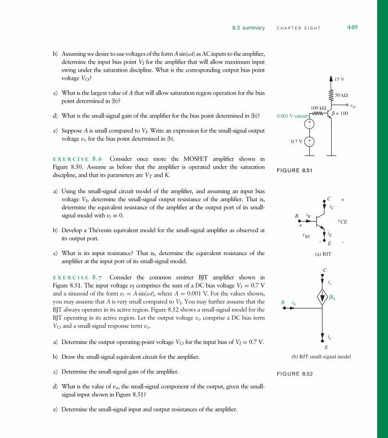
8.3 summary C H A P T E R E I G H T 449
b) Assuming we desire to use voltages of the form A sin(ωt) as AC inputs to the amplifier,determine the input bias point VI for the amplifier that will allow maximum inputswing under the saturation discipline. What is the corresponding output bias pointvoltage VO?
c) What is the largest value of A that will allow saturation region operation for the biaspoint determined in (b)?
d) What is the small-signal gain of the amplifier for the bias point determined in (b)?
e) Suppose A is small compared to VI. Write an expression for the small-signal outputvoltage vo for the bias point determined in (b).
e x e r c i s e 8.6 Consider once more the MOSFET amplifier shown inFigure 8.50. Assume as before that the amplifier is operated under the saturationdiscipline, and that its parameters are VT and K.
a) Using the small-signal circuit model of the amplifier, and assuming an input biasvoltage VI, determine the small-signal output resistance of the amplifier. That is,determine the equivalent resistance of the amplifier at the output port of its small-signal model with vi ≡ 0.
b) Develop a Thévenin equivalent model for the small-signal amplifier as observed atits output port.
c) What is its input resistance? That is, determine the equivalent resistance of theamplifier at the input port of its small-signal model.
e x e r c i s e 8.7 Consider the common emitter BJT amplifier shown inFigure 8.51. The input voltage vI comprises the sum of a DC bias voltage VI = 0.7 V
50 kΩ
vO
0.001 V sin(ωt)
15 V
0.7 V
+
+
-
-
100 kΩb = 100
F IGURE 8.51
and a sinusoid of the form vi = A sin(ωt), where A = 0.001 V. For the values shown,you may assume that A is very small compared to VI. You may further assume that theBJT always operates in its active region. Figure 8.52 shows a small-signal model for the
vCE
+
-
B
C
E
iCiB
iEvBE
+
-
(a) BJT
C
Bbib
E
ic
ib
ie
(b) BJT small-signal model
F IGURE 8.52
BJT operating in its active region. Let the output voltage vo comprise a DC bias termVO and a small-signal response term vo.
a) Determine the output operating-point voltage VO for the input bias of VI = 0.7 V.
b) Draw the small-signal equivalent circuit for the amplifier.
c) Determine the small-signal gain of the amplifier.
d) What is the value of vo, the small-signal component of the output, given the small-signal input shown in Figure 8.51?
e) Determine the small-signal input and output resistances of the amplifier.

450 C H A P T E R E I G H T t h e s m a l l - s i g n a l m o d e l
f ) Determine the small-signal current and power gain of the amplifier, assuming thatthe amplifier drives a load RO = 50 k that is connected between the output nodeand ground.
P R O B L E M S p r o b l e m 8.1 This problem studies the small-signal analysis of the MOSFETamplifier discussed in Problem 7.3 (Figure 7.75).
a) First, consider biasing the amplifier. Determine VIN, the bias component of vIN,so that vOUT is biased to VOUT where 0 < VOUT < VS. Find VMID, the biascomponent of vMID in the process.
b) Next, let v IN = VIN + vin where vin is considered to be a small perturbation of vIN
around VIN. Make the substitution for vIN and linearize the resulting expressionfor vOUT. Your answer should take the form vOUT = VOUT + vout, where vouttakes the form vout = Gvin. Note that vout is the small-signal output and G is thesmall-signal gain. Derive an expression for G.
c) For what value of VIN is vOUT biased to VOUT = VS/2? For this value of VIN,evaluate Gm using the numerical parameters given in Problem 7.2. You should findthat this gain is the slope of the input-output graph from Problem 7.3 evaluated atthe bias point.
p r o b l e m 8.2 Consider again the buffer described in Problem 7.5 (Figure 7.76).Perform a small-signal analysis of this circuit according to the following steps. Assumethat the MOSFET operates in its saturation region and continue to use the SCS MOSFETmodel with parameters VT and K.
a) Draw the small-signal circuit model of the buffer.
b) Show that the small-signal transconductance gm of the MOSFET is given by
gm = K(VIN − VOUT − VT)
where VIN and VOUT are the bias, or operating-point, input and output voltages,respectively.
c) Determine the small-signal gain of the buffer. That is, determine the ratio vout/vin.
d) Determine the small-signal output resistance of the buffer. That is, determine theequivalent resistance of the buffer at the output port of its small-signal model withvin ≡ 0.
e) Assume that VT = 1 V, K = 2 mA/V2, R = 1 k, and VS = 10 V. Under thisassumption, design the input bias voltage to satisfy the following two objectives:First, MOSFET operation must remain within the saturation region for |vin| ≤0.25 V. Second, the output resistance of the small-signal model must be minimized.

8.3 summary C H A P T E R E I G H T 451
f ) Again assume that VT = 1 V, K = 2 mA/V2, R = 1 k, and VS = 10 V. ForVIN = 3 V, compute the small-signal gain and output resistance.
g) Determine the small-signal input resistance of the buffer. That is, determine theequivalent resistance of the buffer at the input port of its small-signal model.
p r o b l e m 8.3 This problem studies the small-signal analysis of the ZFET ampli-fier from Problem 7.6 (Figure 7.77). Assume that the amplifier is biased at an inputvoltage VIN such that the ZFET exhibits saturated operation; the corresponding biasoutput voltage is VOUT. For this case, derive the small-signal voltage gain vout/vin of theamplifier.
p r o b l e m 8.4 The circuit shown in Figure 8 .4 delivers a nearly constant currentto its load despite the fact that the power supply is noisy. The noise is modeled bythe small signal vs superimposed on the constant-supply voltage VS. Thus, VS andvs are the large-signal and small-signal components of the total power supply voltagevS, respectively. IL and il are the large-signal and small-signal components of the load
+-
+-
Slope 1RN-------=
VN
i
v
+
-
v
i
Load
vs
VS
RBiL = IL + il
vS G S
D
0
Current source& load
Nonlinear resistor
Nonlinear resistor
F IGURE 8.53
current iL, respectively. The noise vs in the power supply voltage satisfies vs VS, andis responsible for the presence of il in iL.
The current source contains a MOSFET which operates in its saturation region suchthat iDS = K
2(vGS − VT)2. The current source also contains a nonlinear resistor whose
terminal characteristics are described graphically next. Assume that VS > VN > VT.
a) Assume vs = 0. Determine VGS, the large-signal component of vGS, in terms of RB,RN, VN, and VS.
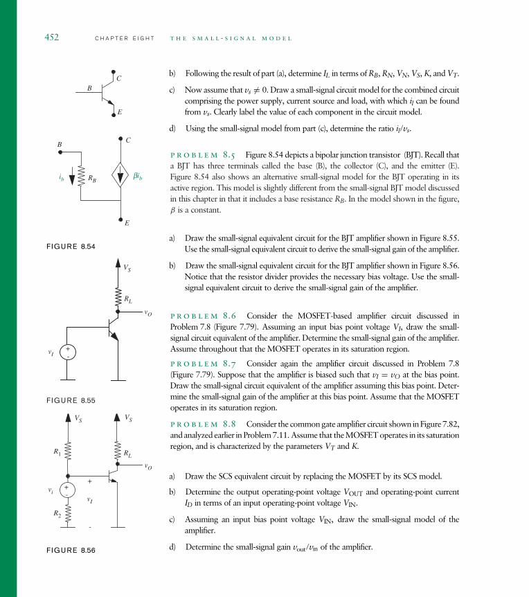
452 C H A P T E R E I G H T t h e s m a l l - s i g n a l m o d e l
b) Following the result of part (a), determine IL in terms of RB, RN, VN, VS, K, and VT.
c) Now assume that vs = 0. Draw a small-signal circuit model for the combined circuitcomprising the power supply, current source and load, with which il can be foundfrom vs. Clearly label the value of each component in the circuit model.
d) Using the small-signal model from part (c), determine the ratio il/vs.
p r o b l e m 8.5 Figure 8.54 depicts a bipolar junction transistor (BJT). Recall that
RB
CB
ib bib
E
BC
E
F IGURE 8.54
a BJT has three terminals called the base (B), the collector (C), and the emitter (E).Figure 8.54 also shows an alternative small-signal model for the BJT operating in itsactive region. This model is slightly different from the small-signal BJT model discussedin this chapter in that it includes a base resistance RB. In the model shown in the figure,β is a constant.
RL
vO
VS
+-
vI
F IGURE 8.55
a) Draw the small-signal equivalent circuit for the BJT amplifier shown in Figure 8.55.Use the small-signal equivalent circuit to derive the small-signal gain of the amplifier.
b) Draw the small-signal equivalent circuit for the BJT amplifier shown in Figure 8.56.Notice that the resistor divider provides the necessary bias voltage. Use the small-signal equivalent circuit to derive the small-signal gain of the amplifier.
RL
vO
R1
VS
R2
VS
+-
vivI
+
-
F IGURE 8.56
p r o b l e m 8.6 Consider the MOSFET-based amplifier circuit discussed inProblem 7.8 (Figure 7.79). Assuming an input bias point voltage VI, draw the small-signal circuit equivalent of the amplifier. Determine the small-signal gain of the amplifier.Assume throughout that the MOSFET operates in its saturation region.
p r o b l e m 8.7 Consider again the amplifier circuit discussed in Problem 7.8(Figure 7.79). Suppose that the amplifier is biased such that vI = vO at the bias point.Draw the small-signal circuit equivalent of the amplifier assuming this bias point. Deter-mine the small-signal gain of the amplifier at this bias point. Assume that the MOSFEToperates in its saturation region.
p r o b l e m 8.8 Consider the common gate amplifier circuit shown in Figure 7.82,and analyzed earlier in Problem 7.11. Assume that the MOSFET operates in its saturationregion, and is characterized by the parameters VT and K.
a) Draw the SCS equivalent circuit by replacing the MOSFET by its SCS model.
b) Determine the output operating-point voltage VOUT and operating-point currentID in terms of an input operating-point voltage VIN.
c) Assuming an input bias point voltage VIN, draw the small-signal model of theamplifier.
d) Determine the small-signal gain vout/vin of the amplifier.

8.3 summary C H A P T E R E I G H T 453
e) Determine the small-signal output resistance of the amplifier. That is, determine theequivalent resistance of the amplifier at the output port of its small-signal modelwith vi ≡ 0. Is the small-signal output resistance greater than, less than, or equal tothat of the ‘‘common source’’ amplifier shown in Figure 8.50?
f ) Determine the small-signal input resistance of the amplifier. That is, determine theequivalent resistance of the amplifier at the input port of its small-signal model.Is the small-signal input resistance greater than, less than, or equal to that of the‘‘common source’’ amplifier shown in Figure 8.50?
p r o b l e m 8.9 Consider the circuit illustrated in Figure 7.86 and analyzed inProblem 7.15. Assume that the MOSFET operates in its saturation region, and ischaracterized by the parameters VT and K.
a) Draw the SCS equivalent circuit by replacing the MOSFET by its SCS model.
b) Determine the output operating-point voltage VO and operating-point current IDin terms of an input operating-point voltage VI.
c) Assuming an input bias point voltage VI, draw the small-signal model.
d) Determine the small-signal gain vo/vi.
e) Determine the small-signal output resistance.
f ) Determine the small-signal input resistance.
p r o b l e m 8.10 Consider the circuit illustrated in Figure 7.87 and analyzed inProblem 7.16. Assume that the MOSFET operates in its saturation region, and ischaracterized by the parameters VT and K.
a) Draw the SCS equivalent circuit by replacing the MOSFET by its SCS model.
b) Determine the output operating-point voltage VO and operating-point current IDin terms of an input operating-point voltage VI.
c) Assuming an input bias point voltage VI, draw the small-signal model.
d) Determine the small-signal gain vo/vi.
e) Determine the small-signal output resistance.
f ) Determine the small-signal input resistance.
p r o b l e m 8.11 This problem studies the small-signal analysis of the amplifieranalyzed in Problem 7.14 (see Figure 7.85). Assume that the MOSFET operates in itssaturation region, and is characterized by the parameters VT and K.
a) Draw the small-signal equivalent circuit of the amplifier driving the load resistor RE,assuming an input bias voltage VI.
b) Determine the small-signal gain of the amplifier when it is driving the load RE.

454 C H A P T E R E I G H T t h e s m a l l - s i g n a l m o d e l
p r o b l e m 8.12 This problem studies the small-signal analysis of the circuit ana-lyzed in Problem 7.17 (see Figure 7.88). Assume that the MOSFET operates in itssaturation region, and is characterized by the parameters VT and K.
a) Draw the small-signal equivalent circuit assuming an input bias voltage VI. What isthe value of gm for the MOSFET under the given biasing conditions?
b) Determine the small-signal voltage gain vo/vi. What does the vo/vi expressionsimplify to when each of gmR1, gmR2, and gmRL is much greater than 1?
p r o b l e m 8.13 This problem studies the small-signal analysis of the sourcefollower (or common collector) BJT circuit analyzed in Problem 7.18 (see Figure 7.89).Assume that the BJT operates in its active region throughout this problem.
a) Determine the output operating-point voltage VO and operating-point current IEin terms of an input operating-point voltage VI.
b) Assuming an input bias point voltage VI, draw the small-signal model of the source-follower amplifier.
c) Determine the small-signal gain vo/vi of the amplifier.
d) Determine the small-signal output resistance of the source follower amplifier. Is thisresistance greater than, less than, or equal to that of the ‘‘common emitter’’ amplifieranalyzed in Exercise 8.7 and shown in Figure 8.51?
e) Determine the small-signal input resistance of the amplifier. Is the input resistancegreater than, less than, or equal to that of the ‘‘common emitter’’ amplifier shownin Figure 8.51?
f ) Determine the small-signal current and power gain of the source follower amplifier.Assume for this part that the amplifier is driving an output load of RO connectedbetween the output node and ground.
p r o b l e m 8.14 Consider again the compound three-terminal device formed byconnecting two BJTs in the configuration shown in Figure 7.90 (Problem 7.19). Thisproblem relates to the small-signal analysis of this device. Assume that the two BJTs areidentical, each with β = 100, and that each of the BJTs operates in the active region.
a) Draw the active-region equivalent circuit of the compound BJT by replacing each ofthe BJTs by the piecewise linear (large signal) model shown in Exercise 7.8. Clearlylabel the C′, B′, and E′ terminals.
b) Develop a small-signal model containing a single dependent current source for thecompound device by linearizing the circuit model in (a) and simplifying suitably.

c h a p t e r 9
9.1 C O N S T I T U T I V E L A W S
9.2 S E R I E S A N D P A R A L L E L C O N N E C T I O N S
9.3 S P E C I A L E X A M P L E S
9.4 S I M P L E C I R C U I T E X A M P L E S
9.5 E N E R G Y , C H A R G E , A N D F L U X C O N S E R V A T I O N
9.6 S U M M A R Y
E X E R C I S E S
P R O B L E M S


energy s torage e l ement s 9To this point in our study of electronic circuits, time has not been important.The analyses and designs we have performed so far have been static, and allcircuit responses at a given time have depended only on the circuit inputs atthat time. An important consequence of this is that our circuits have so farresponded to input changes infinitely fast. This of course does not happen inreality. Circuits do take time to respond to their inputs, and this delay is oftenof significant importance.
As an example of circuit delays, and the importance of time in describing theresponse of a circuit, consider the two cascaded inverters shown in Figure 9.1.The ideal response of the first inverter, based on our analysis of electronic circuitsto this point, is shown in Figure 9.2. A square-wave input yields an invertedsquare-wave output. However, in reality, the output shown in Figure 9.3 ismore likely to occur, which is a much more complex function of time. Thisexample is discussed in detail in Section 10.4, where we will show that thecomplex time behavior shown in Figure 9.3 directly relates to the speed atwhich circuits can operate. In this chapter, we will lay the foundation for thatdiscussion.
In order to explain the temporal behavior of circuit responses such as thatshown in Figure 9.3, we must introduce two new elements, namely capacitorsand inductors. For example, we shall see that it is a capacitance internal tothe MOSFET that is responsible for the non-ideal inverter response shown inFigure 9.3. For simplicity, we did not model that characteristic of the MOSFETin earlier chapters, but we will begin to do so now in Section 9.3.1.
There are other ways in which a capacitance or an inductance can inad-vertently slow down a circuit. One way is shown in Figure 9.4. This figure
+
-vI
+
-vO
. . .
F IGURE 9.1 Two cascadedinverters.
457

458 C H A P T E R N I N E e n e r g y s t o r a g e e l e m e n t s
t
vI
t
vO
F IGURE 9.2 Ideal response of the first inverter to asquare-wave input.
t
vI
t
vO
F IGURE 9.3 Observed response of the first inverter to asquare-wave input.
F IGURE 9.4 The behavior ofa real interconnect between twoinverters.
. . .. . .
. . .. . . i
i
+
-
+
-
+
-
+
-E
+q
-q
B
B
shows two inverters communicating over a long interconnect. As we discussedin Chapter 1, within our lumped-circuit abstraction, the interconnect is perfect.Specifically, by the definition of the lumped circuit abstraction (see Section 1.2),the wires interconnecting the elements have no resistance. Furthermore, by thelumped matter discipline which underlies the lumped circuit abstraction, thewires and other circuit elements store no electric charge and link no magneticflux outside the elements. Reality, however, is different, and in some cases thisdifference is important. As Figure 9.4 shows, any interconnect having a potentialdifference with its surroundings actually stores an electric charge q that sourcesan electric field E between that charge and its image. Furthermore, in order tosupply the charge, a current i must flow around the interconnect loop. Thiscurrent in turn generates a magnetic flux density B that is linked by the loop.So, real interconnects do store electric charge and do link external magneticflux, thereby appearing to violate the lumped matter discipline. They will alsoexhibit a nonzero resistance. These factors can all contribute to a reduction inthe speed of the circuit as a whole, and at times it is important to study theseeffects.

C H A P T E R N I N E 459
Reality now presents us with a dilemma. On the one hand, we wish to workwithin the framework of the lumped circuit abstraction so that the circuits westudy all fit within this easily-managed framework. On the other hand, weshould not be forced to ignore circuit effects, in this case parasitic resistance,capacitance, and inductance, that significantly affect circuit performance. Theresolution of this dilemma is the modeling compromise mentioned in Chapter 1.Figure 1.27 in Chapter 1 used an ideal wire in series with a lumped resistance tomodel a physical wire with some parasitic resistance. Similarly, we will introducelumped capacitors and lumped inductors to model the effect of the charge andthe flux. As illustrated in Figure 9.5, a capacitor comprising a pair of parallelplates collects the positive and negative charge on its plates and effectivelymodels the distributed charge. Notice that because the capacitor contains equalpositive and negative charges the net charge within the capacitor element iszero, thereby satisfying the lumped matter discipline. Thus, the capacitor canbe viewed as a lumped element. In like manner, we will introduce a lumpedinductor to model the effect of the flux linked with the wires as illustrated inFigure 9.6. The lumped matter discipline is satisfied because the flux is entirelycontained inside the lumped inductor, and there is no net flux outside theelement.
By using lumped resistors, capacitors, and inductors to model the effectof the resistance, charge, and flux associated with the physical wiring of the
. . .. . .
. . .. . .
+
-
+
-
+
-
+
-E
+q
-q
. . .. . .
. . .. . .
+
-
+
-
+
-
+
-
+q
-qE
F IGURE 9.5 The capacitormodels the effect of the distributedcharge.
. . .. . .
. . .. . .F IGURE 9.6 The inductormodels the effect of the flux.

460 C H A P T E R N I N E e n e r g y s t o r a g e e l e m e n t s
. . .
CI
. . .RI
LI
F IGURE 9.7 Capturing the parasitic effectsof resistance, charge, and flux through the useof resistors, capacitors, and inductors,respectively. Capacitors and inductors areformally introduced in Section 9.1.
. . .
CI2------
CI2------
. . .RI
LI
(a)
. . .
CI
. . .
RI2------
RI2------
LI2-----
LI2-----
(b)
F IGURE 9.8 Two different lumped models foran interconnect that account for interconnectresistance, capacitance, and inductance.
circuit, as shown in Figure 9.7, the wiring within the augmented circuit modelremains perfect in keeping with the lumped circuit abstraction. In the figure, theinterconnect resistance, capacitance, and inductance are RI, CI, and LI in total,respectively.
Figure 9.7 represents one of the simplest models used to model real inter-connects. For more accuracy, since we can use as many additional lumpedelements as we wish, we can arbitrarily approach the distributed modelinglimit, although in general this is not necessary. For example, the two modelsshown in Figure 9.8 do a better job of modeling reality. The interconnect modelin Figure 9.8a is a ‘‘’’ model in which the resistance and inductance is placedbetween the split capacitance. The interconnect model in Figure 9.8b is a ‘‘T’’model in which the capacitance is placed between the split resistance and induc-tance. As discussed in Section 9.3.1, we will adopt a similar lumped modelingapproach to the capacitances at work within the MOSFET.
From the preceding discussion it might appear that capacitors and inductorsappear only as parasitics in circuits, causing undesirable delays. This is far fromthe truth. While they can and do act in that role, they are also often purposefullyintroduced into circuits, both as discrete devices on breadboards and printed-circuit boards, and as integrated-circuit components on a chip (see Figures 9.9and 9.10 for examples of capacitors and inductors, respectively). For example,they are the cornerstones of memories, filters, samplers, and energy processingcircuits. We shall see many examples of these in future chapters as well. Thus,we have many reasons to study capacitors and inductors.

9.1 Constitutive Laws C H A P T E R N I N E 461
F IGURE 9.9 Examples ofdiscrete capacitors (left) andintegrated-circuit capacitors (right).The image on the right shows asmall region of the MaximMAX1062 analog-to-digitalconverter chip and depicts an arrayof polysilicon-to-polysiliconcapacitors, each measuring15.9 µm by 15.9 µm. (PhotographCourtesy of Maxim IntegratedProducts.)
F IGURE 9.10 Examples ofdiscrete inductors. (PhotographCourtesy of Maxim IntegratedProducts.)
9.1 C O N S T I T U T I V E L A W S
In this section, we formally introduce the capacitor and inductor in the abstract,and develop the constitutive laws that relate their branch variables. Capacitorsand inductors, which are the electric and magnetic duals of each other, dif-fer from resistors in several significant ways. Most importantly, their branchvariables do not depend algebraically upon each other. Rather, their relationsinvolve temporal derivatives and integrals. Thus, the analysis of circuits contain-ing capacitors and inductors involve differential equations in time. To emphasizethis, we will explicitly show the time dependence of all variables in this chapter.
9.1.1 C A P A C I T O R S
To understand the behavior of a capacitor, and to illustrate the manner inwhich a lumped model can be developed for it, consider the idealized two-terminal linear capacitor shown in Figure 9.11. In this capacitor each terminal isconnected to a conducting plate. The two plates are parallel and are separatedby a gap of length l. Their area of overlap is A. Note that these dimensions willbe functions of time if the geometry of the capacitor varies. The gap is filledwith an insulating linear dielectric having permittivity ε.
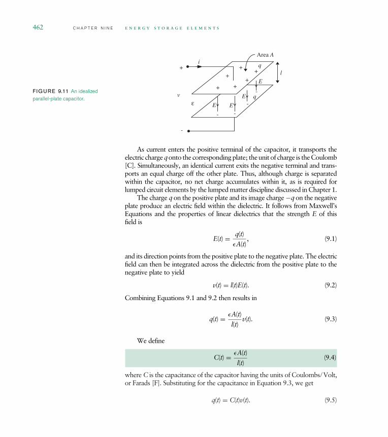
462 C H A P T E R N I N E e n e r g y s t o r a g e e l e m e n t s
F IGURE 9.11 An idealizedparallel-plate capacitor.
E E
E
E
q
l
ε
+
-
+
-
+
-
+
-
+++
-
v
Area A
qi
As current enters the positive terminal of the capacitor, it transports theelectric charge q onto the corresponding plate; the unit of charge is the Coulomb[C]. Simultaneously, an identical current exits the negative terminal and trans-ports an equal charge off the other plate. Thus, although charge is separatedwithin the capacitor, no net charge accumulates within it, as is required forlumped circuit elements by the lumped matter discipline discussed in Chapter 1.
The charge q on the positive plate and its image charge −q on the negativeplate produce an electric field within the dielectric. It follows from Maxwell’sEquations and the properties of linear dielectrics that the strength E of thisfield is
E(t) = q(t)
εA(t), (9.1)
and its direction points from the positive plate to the negative plate. The electricfield can then be integrated across the dielectric from the positive plate to thenegative plate to yield
v(t) = l(t)E(t). (9.2)
Combining Equations 9.1 and 9.2 then results in
q(t) = εA(t)
l(t)v(t). (9.3)
We define
C(t) = εA(t)
l(t)(9.4)
where C is the capacitance of the capacitor having the units of Coulombs/Volt,or Farads [F]. Substituting for the capacitance in Equation 9.3, we get
q(t) = C(t)v(t). (9.5)

9.1 Constitutive Laws C H A P T E R N I N E 463
In contrast to the resistor, which exhibits an algebraic relation between itsbranch current and voltage, the capacitor does not. Rather, it exhibits an alge-braic relation between its branch voltage and its stored charge. Had the dielectricnot been linear, this relation would have been nonlinear. While some capacitorsexhibit such nonlinear behavior, we will focus only on linear capacitors.
The rate at which charge is transported onto the positive plate of thecapacitor is
dq(t)
dt= i(t). (9.6)
From Equation 9.6 we see that the Ampere is equivalent to a Coulomb/second.Equation 9.6 can be combined with Equation 9.5 to yield
i(t) = d(C(t)v(t))
dt(9.7)
which is the element law for an ideal linear capacitor. Unless stated otherwise,we will assume in this text that capacitors are both linear and time-invariant.For linear, time-invariant capacitors, Equations 9.5 and 9.7 reduce to
q(t) = Cv(t) (9.8)
i(t) = Cdv(t)
dt, (9.9)
respectively, with the latter being the element law for a linear time-invariantcapacitor.1
The symbol for an ideal linear capacitor is shown in Figure 9.12. It is chosen
+
C
-
v
idqdt------=
q
v
C
F IGURE 9.12 The symbol andvoltage-charge relation for theideal linear capacitor. The elementlaw for the capacitor is i = Cdv/dt.
to represent the parallel-plate capacitor shown in Figure 9.11. Also shown inFigure 9.12 is a graph of the relation between the branch voltage and storedcharge of the capacitor.
One of the important properties of a capacitor is its memory property. Infact, it is this property that allows the capacitor to be the primary memory
1. Although we will focus primarily on linear, time-invariant capacitors in this text, we note thatsome interesting transducers such as electric microphones and speakers, and other electric sensorsand actuators, are appropriately modeled with time-varying capacitors. Similarly, most capacitorsused in electronic equipment (paper, mica, ceramic, etc.) are linear, but often vary a small amountwith temperature (a part of 104 per degree centigrade). But many are nonlinear. The chargeassociated with a reverse-biased semiconductor diode, for example, varies as the 2/3 power ofvoltage, because the distance d, the effective width of the space-charge layer, is a function ofvoltage
q = K(ψ
2/3o − (ψo − v)2/3
)(9.10)
when ψo, the contact potential, is a few tenths of a volt. From the above we can determine thatthe capacitance of the reverse-biased diode varies as v−1/3.

464 C H A P T E R N I N E e n e r g y s t o r a g e e l e m e n t s
element in all integrated circuits. To see this property, we integrate Equation9.6 to produce
q(t) =∫ t
−∞i(t)dt (9.11)
or, with the substitution of Equation 9.8, to produce
v(t) = 1
C
∫ t
−∞i(t)dt. (9.12)
Equation 9.12 shows that the branch voltage of a capacitor depends on theentire past history of its branch current, which is the essence of memory. Thisis in marked contrast to a resistor (either linear or nonlinear), which exhibits nosuch memory property.
At first glance, it might appear that it is necessary to know the entire historyof the current i in detail in order to carry out the integrals in Equations 9.11 and9.12. This is actually not the case. For example, consider rewriting Equation9.11 as
q(t2) =∫ t2
−∞i(t)dt
=∫ t2
t1i(t)dt +
∫ t1
−∞i(t)dt
=∫ t2
t1i(t)dt + q(t1). (9.13)
The latter equality shows that q(t1) perfectly summarizes, or memorizes, theentire accumulated history of i(t) for t ≤ t1. Thus, if q(t1) is known, it isnecessary and sufficient to know i only over the interval t1 ≤ t ≤ t2 in orderto determine q(t2). For this reason, q is referred to as the state of the capacitor.For linear time-invariant capacitors, v can also easily serve as a state becausev is proportionally related to q through the constant C. Accordingly, we canrewrite Equation 9.12 as
v(t2) = 1
C
∫ t2
−∞i(t)dt
= 1
C
∫ t2
t1i(t)dt + 1
C
∫ t1
−∞i(t)dt
= 1
C
∫ t2
t1i(t)dt + v(t1). (9.14)

9.1 Constitutive Laws C H A P T E R N I N E 465
Thus, we see that v(t1) also memorizes the entire accumulated history of i(t)for t ≤ t1 and can serve as the state of the capacitor.
Associated with the ability to exhibit memory is the property of energystorage, which is often exploited by circuits that process energy. To determinethe electric energy wE stored in a capacitor, we recognize that the power iv isthe rate at which energy is delivered to the capacitor through its port. Thus,
dw E(t)
dt= i(t)v(t). (9.15)
Next, substitute for i using Equation 9.6, cancel the time differentials, and omitthe parametric time dependence to obtain
dw E = vdq. (9.16)
Equation 9.16 is a statement of incremental energy storage within the capacitor.It states that the transport of the incremental charge dq from the negative plateof the capacitor to the top plate across the electric potential difference v storesthe incremental energy dwE within the capacitor. To obtain the total storedelectric energy, we must integrate Equation 9.16 with v treated as a functionof q. This yields
w E =∫ q
0v(x)dx (9.17)
where x is a dummy variable of integration. Finally, substitution of Equation9.8 and integration yields
Stored energy = w E(t) = q2(t)
2C= Cv(t)2
2(9.18)
as the electric energy stored in a capacitor. The units of energy is the Joule [ J ], orWatt-second. Unlike a resistor, a capacitor stores energy rather than dissipates it.
Capacitors come in an enormous range of values. For example, two piecesof insulated wire about an inch long, when twisted together, will have a capaci-tance of about 1 picofarad (10−12 farads). A low-voltage power supply capacitoran inch in diameter and a few inches long could have a capacitance of 100,000microfarads (0.1 farad; 1 microfarad, abbreviated as µF, is 10−6 F).
A real capacitor can exhibit richer behavior than that described here. Forexample, leakage current can flow through its dielectric. The practical signifi-cance of dielectric leakage is that eventually the charge stored on a capacitorcan leak off. Thus, eventually a real capacitor will lose its memory. Fortu-nately, capacitors can be made with very low leakage (in other words, with veryhigh resistance) in which case they are excellent long-term memory devices.However, if the dielectric leakage is large enough to be significant, then it canbe modeled with a resistor in parallel with the capacitor.

466 C H A P T E R N I N E e n e r g y s t o r a g e e l e m e n t s
Other non-idealities include the distributed series resistance, and even seriesinductance, that arises in foil-wound capacitors in particular. These character-istics limit the power-handling capability of a real capacitor, and the frequencyrange over which a real capacitor behaves like an ideal capacitor. They can oftenbe explicitly modeled with a single series resistor and inductor, respectively.
e x a m p l e 9.1 p a r a l l e l p l a t e c a p a c i t o r Suppose theparallel-plate capacitor in Figure 9.11 is 1 m square, has a gap separation of 1 µm,and is filled with a dielectric having permittivity of 2ε, where ε ≈ 8.854 × 10⁻¹² F/mis the permittivity of free space. What is its capacitance? How much charge and energydoes it store if its terminal voltage is 100 V?
The capacitance is determined from Equation 9.4 with ε = 1.8×10⁻¹¹ F/m, A = 1 m2
and l = 10−6 m. It is 18 µF. The charge is determined from Equation 9.8 with v = 100 V.It is 1.8 mC. Finally, the stored energy is determined from Equation 9.18. It is 90 mJ.
9.1.2 I N D U C T O R S
As we saw in Section 9.1.1, from the perspective of modeling electrical systems,the capacitor is a circuit element to model the effect of electric fields. Corre-spondingly, the inductor models the effect of magnetic fields. To understandthe behavior of an inductor, and to illustrate the manner in which a lumpedmodel can be developed for it, consider the idealized two-terminal linear induc-tor shown in Figure 9.13. In this inductor a coil with a terminal on each endis wound with N turns around a toroidal core made from an insulator havingmagnetic permeability µ. The length around the core is l and its cross-sectionalarea is A. Note that these dimensions will be functions of time if the geometryof the inductor varies.
The current in the coil produces a magnetic flux in the inductor. Ideally, thismagnetic flux does not stray significantly from the core, so that the flux outside
F IGURE 9.13 An idealizedtoroidal inductor.
+
-
v
Area A
B
l
i
µ
N turns

9.1 Constitutive Laws C H A P T E R N I N E 467
the element is negligible. Thus the inductor can be treated as a lumped circuitelement that satisfies the lumped matter discipline discussed in Chapter 1. FromMaxwell’s Equations and the properties of permeable materials, the density Bof the flux is
B(t) = µNi(t)
l(t), (9.19)
and its direction is around the core. The magnetic flux density can be integratedacross the core to yield
(t) = A(t)B(t) (9.20)
where is the total flux passing through the core, and hence through one turnof the coil. Since the flux is linked N times by the N-turn coil, the total fluxλ linked by the coil is
λ(t) = N (t) = N A(t)B(t). (9.21)
The units of flux linkage is the Weber [Wb]. Combining Equations 9.19 and9.21 results in
λ(t) = µN2A(t)
l(t)i(t). (9.22)
We define L, the inductance of the inductor, as
L(t) = µN2A(t)
l(t). (9.23)
L has the units of Webers/Ampere, or Henrys [H]. That is, inductance is thenumber of flux linkages per ampere. Substituting for L in Equation 9.22 weobtain the following relation for the total flux linked by the inductor
λ(t) = L(t)i(t). (9.24)
In contrast to the resistor, which exhibits an algebraic relation between itsbranch current and voltage, the inductor does not. Rather, like the capacitor, itexhibits an algebraic relation between its branch current and its flux linkage. Hadthe core not been magnetically linear, this relation would have been nonlinear.While most inductors exhibit such nonlinear behavior for sufficiently high B,we will focus only on linear inductors.
Again from Maxwell’s Equations, the rate at which flux linkage builds upin the inductor is
dλ(t)
dt= v(t). (9.25)
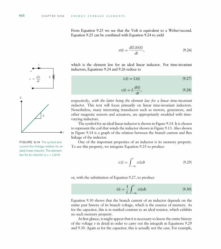
468 C H A P T E R N I N E e n e r g y s t o r a g e e l e m e n t s
From Equation 9.25 we see that the Volt is equivalent to a Weber/second.Equation 9.25 can be combined with Equation 9.24 to yield
v(t) = d(L(t)i(t))
dt, (9.26)
which is the element law for an ideal linear inductor. For time-invariantinductors, Equations 9.24 and 9.26 reduce to
λ(t) = Li(t) (9.27)
v(t) = Ldi(t)
dt, (9.28)
respectively, with the latter being the element law for a linear time-invariantinductor. This text will focus primarily on linear time-invariant inductors.Nonetheless, many interesting transducers such as motors, generators, andother magnetic sensors and actuators, are appropriately modeled with time-varying inductors.
The symbol for an ideal linear inductor is shown in Figure 9.14. It is chosento represent the coil that winds the inductor shown in Figure 9.13. Also shownin Figure 9.14 is a graph of the relation between the branch current and flux
+
L
-
i
vd λdt------=
i
L
λ
F IGURE 9.14 The symbol andcurrent-flux-linkage relation for anideal linear inductor. The elementlaw for an inductor is v = Ldi/dt.
linkage of the inductor.One of the important properties of an inductor is its memory property.
To see this property, we integrate Equation 9.25 to produce
λ(t) =∫ t
−∞v(t)dt (9.29)
or, with the substitution of Equation 9.27, to produce
i(t) = 1
L
∫ t
−∞v(t)dt. (9.30)
Equation 9.30 shows that the branch current of an inductor depends on theentire past history of its branch voltage, which is the essence of memory. Asfor the capacitor, this is in marked contrast to an ideal resistor, which exhibitsno such memory property.
At first glance, it might appear that it is necessary to know the entire historyof the voltage v in detail in order to carry out the integrals in Equations 9.29and 9.30. Again as for the capacitor, this is actually not the case. For example,

9.1 Constitutive Laws C H A P T E R N I N E 469
consider rewriting Equation 9.29 as
λ(t2) =∫ t2
−∞v(t)dt
=∫ t2
t1v(t)dt +
∫ t1
−∞v(t)dt
=∫ t2
t1v(t)dt + λ(t1). (9.31)
The latter equality shows that λ(t1) perfectly summarizes, or memorizes, theentire accumulated history of v(t) for t ≤ t1. Thus, if λ(t1) is known, it isnecessary and sufficient to know v only over the interval t1 ≤ t ≤ t2 in order todetermine λ(t2). For this reason, λ, the total flux linked by the coil, is referred toas the state of the inductor. For linear time-invariant inductors, i can also easilyserve as a state because i is proportionally related to λ through the constant L.Accordingly, we can rewrite Equation 9.30 as
i(t2) = 1
L
∫ t2
−∞v(t)dt
= 1
L
∫ t2
t1v(t)dt + 1
L
∫ t1
−∞v(t)dt
= 1
L
∫ t2
t1v(t)dt + i(t1). (9.32)
Equation 9.32 shows that i can also serve as the state of an inductor.As with the capacitor, associated with the ability to exhibit memory is the
property of energy storage, which is often exploited by circuits that processenergy. To determine the magnetic energy wM stored in an inductor, we rec-ognize that the power iv is the rate at which energy is delivered to the inductorthrough its port. Thus,
dw M(t)
dt= i(t)v(t). (9.33)
Next, substitute for v using Equation 9.25, cancel the time differentials, andomit the parametric time dependence to obtain
dw M = idλ. (9.34)
Equation 9.34 is a statement of incremental energy storage within the inductor.To obtain the total stored magnetic energy, we must integrate Equation 9.34

470 C H A P T E R N I N E e n e r g y s t o r a g e e l e m e n t s
with i treated as a function of λ. This yields
w M =∫ λ
0i(x)dx (9.35)
where x is a dummy variable of integration. Finally, substitution of Equation9.27 and integration yields
Stored energy = w M(t) = λ2(t)
2L= Li(t)2
2(9.36)
as the magnetic energy stored in an inductor. Unlike a resistor, but like acapacitor, an inductor stores energy rather than dissipates it.
A real inductor exhibits richer behavior than that described here. For exam-ple, it can exhibit a significant coil resistance. The practical significance of thisresistance is that it eventually dissipates any energy stored in the inductor.Unfortunately, this resistance is usually significant so that inductors make poormemory devices. When it is necessary to model this energy loss, the coilresistance can be modeled as a resistor in series with the ideal inductor.
Other non-idealities include core loss and inter-turn capacitance. Thesecharacteristics limit the power-handling efficiency of a real inductor, and thefrequency range over which a real inductor behaves like an ideal inductor. Theycan often be modeled with a parallel resistor and capacitor, respectively.
e x a m p l e 9.2 t o r o i d a l i n d u c t o r Suppose the toroidal induc-tor in Figure 9.13 has a cross-sectional area of 1 cm2, has a length around its toroidof 10 cm, has a coil with 100 turns, and is filled with free space having permeabilityµ = 4π × 10−7 H/m. What is its inductance? How much flux does its coil link, andwhat energy does it store if its terminal current is 0.1 A?
The inductance is determined from Equation 9.23 with µ = 4π × 10−7 H/m, A =10−4 m2, l = 0.1 m and N = 100. It is 13 µH. The flux linkage is determined fromEquation 9.24 with i = 0.1 A. It is 1.3 µWb. Finally, the stored energy is determinedfrom Equation 9.36. It is 0.063 µJ.
9.2 S E R I E S A N D P A R A L L E L C O N N E C T I O N S
In Section 2.3.4, we saw that the resistances of resistors in series add, and thatthe conductances of resistors in parallel add. Thus, series and parallel resistorscould be represented as a single resistor with an appropriate resistance. Theseaddition rules later became useful as a means of simplifying circuits and theiranalyses. As we shall see in this section, similar rules may be derived for bothcapacitors and inductors, and these rules are equally useful.

9.2 Series and Parallel Connections C H A P T E R N I N E 471
9.2.1 C A P A C I T O R S
Consider first the series combination of two capacitors as shown in Figure 9.15;we will assume here that the two capacitors were uncharged at the time of theirconnection. Since the two capacitors share a common current, it follows fromEquation 9.11 that they store a common charge q, as shown in Figure 9.15.Thus, following Equation 9.8,
+
-
v
C1
+
v1
- -
+
v2C2
q
q
q
F IGURE 9.15 Two capacitors inseries.
q(t) = C1v1(t) = C2v2(t). (9.37)
Next, using KVL we observe that
v(t) = v1(t) + v2(t). (9.38)
Finally, since the effective capacitance C of the two series capacitors isq/v, it follows that
1
C= v(t)
q(t)= 1
C1+ 1
C2,
or,
C = C1C2
C1 + C2(9.39)
where the second equality results from the substitution of Equation 9.38 andthen Equation 9.37. Thus, we see that the reciprocal capacitances of capacitorsin series add. This is consistent with the physical derivation of capacitancein Equation 9.4 since placing capacitors in series essentially increases theircombined gap length.
Now consider the parallel combination of two capacitors as shown inFigure 9.16. Since the two capacitors share a common voltage v, it follows
+
C1
-
q1
q
v
q2
C2
F IGURE 9.16 Two capacitors inparallel.
from 9.8 that
v(t) = q1(t)
C1= q2(t)
C2. (9.40)
Next, using KCL and Equation 9.11 we observe that
q(t) = q1(t) + q2(t). (9.41)
Finally, since the effective capacitance C of the two parallel capacitors is q/v, itfollows that
C = q(t)
v(t)= C1 + C2 (9.42)
where the second equality results from the substitution of Equation 9.41and then Equation 9.40. Thus, we see that the capacitances of capacitors
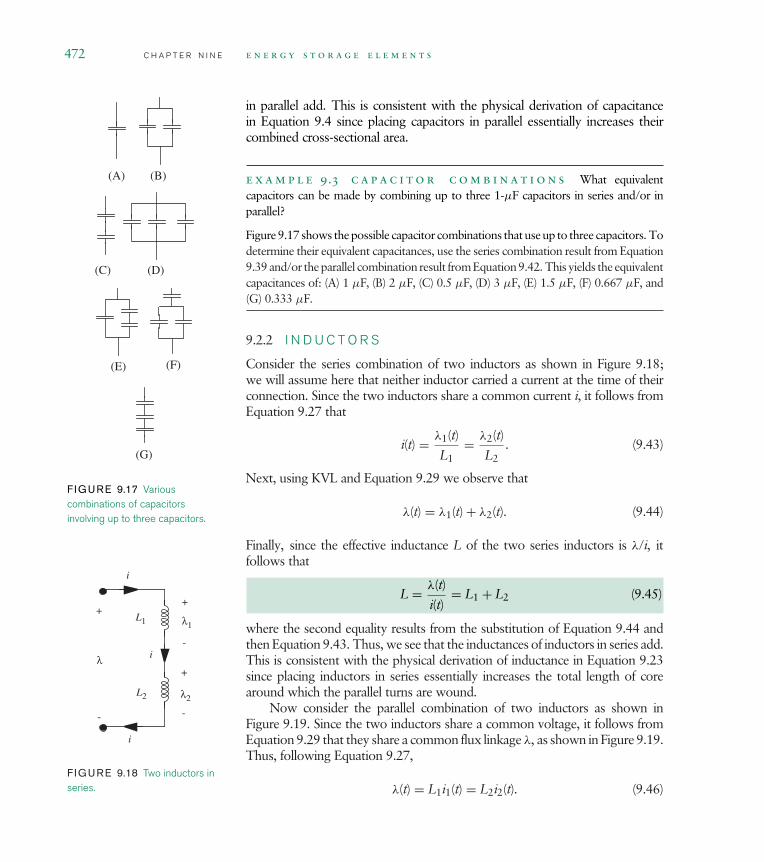
472 C H A P T E R N I N E e n e r g y s t o r a g e e l e m e n t s
in parallel add. This is consistent with the physical derivation of capacitancein Equation 9.4 since placing capacitors in parallel essentially increases theircombined cross-sectional area.
e x a m p l e 9.3 c a p a c i t o r c o m b i n a t i o n s What equivalentcapacitors can be made by combining up to three 1-µF capacitors in series and/or inparallel?
Figure 9.17 shows the possible capacitor combinations that use up to three capacitors. To
(A) (B)
(C) (D)
(E) (F)
(G)
F IGURE 9.17 Variouscombinations of capacitorsinvolving up to three capacitors.
determine their equivalent capacitances, use the series combination result from Equation9.39 and/or the parallel combination result from Equation 9.42. This yields the equivalentcapacitances of: (A) 1 µF, (B) 2 µF, (C) 0.5 µF, (D) 3 µF, (E) 1.5 µF, (F) 0.667 µF, and(G) 0.333 µF.
9.2.2 I N D U C T O R S
Consider the series combination of two inductors as shown in Figure 9.18;we will assume here that neither inductor carried a current at the time of theirconnection. Since the two inductors share a common current i, it follows fromEquation 9.27 that
i(t) = λ1(t)
L1= λ2(t)
L2. (9.43)
Next, using KVL and Equation 9.29 we observe that
λ(t) = λ1(t) + λ2(t). (9.44)
Finally, since the effective inductance L of the two series inductors is λ/i, itfollows that
L = λ(t)
i(t)= L1 + L2 (9.45)
where the second equality results from the substitution of Equation 9.44 and+
-
L1
+
- -
+
L2
i
i
i
λ1
λ
λ2
F IGURE 9.18 Two inductors inseries.
then Equation 9.43. Thus, we see that the inductances of inductors in series add.This is consistent with the physical derivation of inductance in Equation 9.23since placing inductors in series essentially increases the total length of corearound which the parallel turns are wound.
Now consider the parallel combination of two inductors as shown inFigure 9.19. Since the two inductors share a common voltage, it follows fromEquation 9.29 that they share a common flux linkage λ, as shown in Figure 9.19.Thus, following Equation 9.27,
λ(t) = L1i1(t) = L2i2(t). (9.46)

9.3 Special Examples C H A P T E R N I N E 473
Next, using KCL we observe that
i(t) = i1(t) + i2(t). (9.47)
Finally, since the effective inductance L of the two parallel inductors is λ/i, itfollows that
+
L1
-
i1
i
λL2
i2
F IGURE 9.19 Two inductors inparallel.
1
L= i(t)
λ(t)= 1
L1+ 1
L2,
or,
L = L1L2
L1 + L2(9.48)
where the second equality results from the substitution of Equation 9.47 andthen Equation 9.46. Thus, we see that the reciprocal inductances of inductorsin parallel add. This is consistent with the physical derivation of inductancein Equation 9.23 since placing inductors in parallel essentially increases thecross-sectional area of the core around which the turns are wound.
e x a m p l e 9.4 i n d u c t o r c o m b i n a t i o n s What equivalentinductors can be made by combining up to three 1-µH inductors in series and/or inparallel?
Figure 9.20 shows the possible inductor combinations that use up to three induc-
(A) (B) (C) (D)
(E) (F) (G)
F IGURE 9.20 Various combi-nations of inductors involving up tothree inductors.
tors. To determine their equivalent inductances, use the series combination resultfrom Equation 9.45 and/or the parallel combination result from Equation 9.48. Thisyields the equivalent inductances of: (A) 1 µH, (B) 0.5 µH, (C) 2 µH, (D) 0.333 µH,(E) 0.667 µH, (F) 1.5 µH, and (G) 3 µH.
9.3 S P E C I A L E X A M P L E S
In this section, we examine several parasitic capacitances and inductances thatare commonly encountered inside integrated circuits, and in external wiringconnections to them and other circuit elements. There is again the danger thatthis discussion implies that capacitors and inductors appear most commonlyas parasitics in circuits. This is certainly not the case. Rather, we examinethe parasitics here primarily for interest sake, and because they will provideinteresting and important circuit examples in future chapters.
9.3.1 M O S F E T G A T E C A P A C I T A N C E
Let us now take a closer look at the structure and operation of the MOSFETin order to better understand its dynamic behavior. Figure 9.21 reviews the
n+ n+
p substrate
Gate oxideGate
S D
G
Channel
Source Drain
F IGURE 9.21 MOSFETstructure.

474 C H A P T E R N I N E e n e r g y s t o r a g e e l e m e n t s
n+ n+
p substrate
Gate oxideS D
G
n channel+-
vDS
Source Drain
+-
vGS
+
-
+
-
+
-
+
-
+
-
+
-
+
-
GateGateGate
F IGURE 9.22 MOSFET with a positivevoltage applied at the gate relative to thesource and substrate.
+
-
+
-
+
-
+
-
+
-
+
-
+
-
L
dεox
Gate conductor
DrainSource
Channel
E
n+ n+Gate oxide
Gate width w
F IGURE 9.23 Electric charge and field withinthe MOSFET with a positive voltage applied at thegate relative to the source and substrate.
structure of the n-channel MOSFET. The figure identifies its n+-type sourceand drain, its p-type substrate, its channel region, its gate conductor, and thesilicon dioxide dielectric that separates its gate and channel.
Figure 9.22 shows the same n-channel MOSFET with its source and sub-strate grounded, and positive voltages applied to its gate and drain. As thepositive gate voltage is applied, electrons flow from the source into the channeland accumulate beneath the gate. When the gate voltage exceeds the thresholdvoltage of the MOSFET, the electron density beneath the gate becomes suffi-ciently high to invert the channel from p-type silicon to n-type silicon. Thus, acontinuous n-type channel forms between the source and drain, thereby allow-ing electrons to flow from the source to the drain, and hence current to flowfrom the drain to the source, in the response to the positive drain voltage.
The important observation here from Figure 9.22 is that in the processof inverting its channel, and turning itself on, the MOSFET actually forms aparallel-plate capacitor between its gate and channel. This is emphasized inFigure 9.23, which shows the electric field E in the silicon dioxide emanatingfrom the positive charge on the gate and terminating on the negative charge inthe channel. Comparing this figure to Figure 9.11 leads to the realization (fromEquation 9.4) that the gate-to-channel capacitance is approximately
εOXLW
d
where εOX ≈ 3.9ε is the permittivity of the silicon dioxide, d is the thicknessof the silicon dioxide, L is the channel length, and W is the channel width. Theproduct LW is the gate area.
Since the electrons that fill the channel originate from the source, and sincetheir image charges reside on the gate, the gate-to-channel capacitance thatwe identified in Figures 9.22 and 9.23 appears between the gate and source

9.3 Special Examples C H A P T E R N I N E 475
of the MOSFET when viewed from the MOSFET terminals. For this reasonthe capacitance is usually referred to as the gate-to-source capacitance of theMOSFET, or CGS. In other words,
CGS = εOXLW
d. (9.49)
Often, the ratio εOX/d is referred to as COX, the gate-to-channelcapacitance per unit area of the MOSFET gate. In other words,
COX = εOX
d
This realization also leads to the augmented switch-resistor-capacitor (SRC)model of the MOSFET shown in Figure 9.24. Here, a lumped capacitor is addedto the SR model to account for the charge that must be supplied to the gateconductor and channel in order to turn on the MOSFET. Thus, we developa model that describes the behavior of the MOSFET yet satisfies the lumpedmatter discipline.
D
S
G
OFF State
CGS
vGS < VT
D
RON
ON State
vGS ≥ VT
S
G
CGS
F IGURE 9.24 The switch-resistor-capacitor (SRC) modelof the MOSFET.
Because the SRC model contains a capacitor between the gate and sourceterminals of the MOSFET, a current will flow into the gate terminal and outfrom the source terminal of that model as the gate-to-source voltage of theMOSFET varies. This current transports the charge that accumulates withinthe MOSFET as seen in Figures 9.22 and 9.23. Following Equation 9.9, thecurrent is given by
iG = CGSdvGS
dt(9.50)
where
CGS = COXLW. (9.51)
From Equation 9.50 we can now begin to see the reason for the inverter behaviorobserved in Figure 9.3. It will take time for the gate current to transport chargeonto the gate, and hence it will take time for the gate voltage to rise. Thus, itwill take time for the inverter to pass a signal from its input to its output. Wewill have more to say about this in Section 10.4.
Finally, it is important realize that the dynamic behavior of a real MOSFETis actually much more complex than described here. In reality a MOSFETactually has many internal capacitances of importance, including capacitancesbetween its gate and drain, its gate and source, its gate and substrate, its drainand source, its drain and substrate, and its source and substrate. Further, mostof these capacitances are actually functions of vGS and vDS. For our purposes,we will work primarily with CGS and assume that it is a constant capacitance.

476 C H A P T E R N I N E e n e r g y s t o r a g e e l e m e n t s
F IGURE 9.25 MOSFET gateswith different dimensions; alldimensions in the figure are in µm.
44
33 6
2
121
6
2
9
6
6 3
M1 M2 M3
M4M5
M6 M7
e x a m p l e 9.5 g a t e c a p a c i t a n c e s o f m o s f e t s Figure 9.25shows the top view of several rectangular MOSFET gates fabricated within anintegrated circuit. Let us assume that the silicon-dioxide dielectric is characterized byCOX ≈ 4 f F/µm2, and find the gate capacitances CGS for each MOSFET.
To do so, we use Equation 9.51. To begin, notice that MOSFETs M3, M4, and M5must have the same capacitance because they have the same area of 12 µm2. Theircapacitance is therefore 48 fF. MOSFET M5 has the biggest area of 36 µm2, and soit has the biggest capacitance of 144 fF, while MOSFET M2 has the smallest area of9 µm2, and so it has the smallest capacitance of 36 fF. MOSFETs M1 and M7 havecapacitances 64 fF and 108 fF, respectively.
9.3.2 W I R I N G L O O P I N D U C T A N C E
The most common parasitic inductance is the inductance associated with awiring loop. In the lumped circuit abstraction, this inductance is ignored unlessit is explicitly modeled in a circuit using an additional lumped inductor. Toestimate the inductance of a wiring loop, consider the circular loop of wire infree space shown in Figure 9.26. The loop has a loop radius R and a wire radius
R
2 A
F IGURE 9.26 A wiring loop.
A. Its inductance L is given approximately by2
L = µR(
ln(
8R
A
)− 2
). (9.52)
This expression can also be used to successfully approximate the inductance ofmany noncircular wiring loops.
2. See Ramo, Whinnery, and Van Duzer, Fields and Waves in Communication Electronics, P. 311,John Wiley, 1965.

9.3 Special Examples C H A P T E R N I N E 477
e x a m p l e 9.6 i n d u c t a n c e o f a w i r i n g l o o p Supposea wiring loop in free space has a 5-mm diameter and is made from 200-µm-thick wire.What is its inductance?
Using Equation 9.52 with R = 2.5×10⁻³ m, A = 10−4 m, and µ = 4π ×10−7 H/m,the inductance is found to be 10 nH.
9.3.3 I C W I R I N G C A P A C I T A N C E A N D I N D U C T A N C E
Let us now return to Figure 9.4, and develop a model for the capacitance andinductance of the conductors inside an integrated circuit (IC) that are impliedby the figure. Many conductors inside integrated circuits can be modeled asa flat conductor above a conducting substrate, or ground plane, as shown inFigure 9.27.
The conductor in the figure has a width W, and it is located the distanceG above the ground plane. Such conductors are typically surrounded by aninsulating dielectric having a permittivity of ε > ε and a permeability of µ.Under the assumption that W G, we can ignore the fringing electric andmagnetic fields at the edges of the conductor. In this case, the capacitance C andinductance L of the conductor per unit length along its length is approximately
C = εW
G(9.53)
L = µG
W. (9.54)
In other cases, however, the width of the conductor is not large compared toits elevation above the ground plane. An example of this is a narrow printedcircuit board trace. In such cases the conductor might alternatively be modeledas a cylindrical conductor above a ground plane as shown in Figure 9.28.
W
G
Conductor
Groundplane
ε
F IGURE 9.27 A flat conductor above a conducting ground plane.
H
Conductor
Groundplane
ε
R
F IGURE 9.28 A cylindrical conductor above a conductingground plane.

478 C H A P T E R N I N E e n e r g y s t o r a g e e l e m e n t s
The conductor in Figure 9.28 has a radius R and is centered the distanceH above the ground plane. It has a capacitance C and inductance L per unitlength of approximately
C = 2πε
ln(
HR
+√
H2
R2 − 1) (9.55)
L = µ2π
ln
H
R+
√H2
R2− 1
(9.56)
along its length. Together, the conductors shown in Figures 9.27 and 9.28 canbe used to model a wide variety of interconnects.
Finally, notice that for both interconnects,
CL = εµ.
It follows from Maxwell’s Equations that this will always be the case forany two-wire interconnect having constant cross section along its length. Thus,any effort to reduce either C or L will result in an increase of the other.
e x a m p l e 9.7 c a p a c i t a n c e o f i n t e g r a t e d - c i r c u i t
i n t e r c o n n e c t Consider an integrated-circuit interconnect, such as theone shown in Figure 9.27, with W = 2 µm, G = 0.1 µm, and ε = 3.9ε. Whatis its capacitance and inductance per unit length?
Using Equations 9.53 and 9.54, C = 690 pF/m = 0.69 fF/µm, and L = 63 nH/m =63 fH/µm.
e x a m p l e 9.8 p r i n t e d - c i r c u i t - b o a r d t r a c e Considermodeling a printed-circuit-board trace as a cylindrical conductor above a ground plane,as shown in Figure 9.28. Let R = 0.5 mm, H = 2 mm, and ε = ε. What is itscapacitance and inductance per unit length?
Using Equations 9.55 and 9.56, C = 27 pF/m, and L = 410 nH/m.
9.3.4 T R A N S F O R M E R S
A transformer is a two-port device made by winding a second coil around theinductor, for example, that shown in Figure 9.13. Let the first (or primary) coilhave N1 turns and the second (or secondary) coil have N2 turns. The symbol foran ideal transformer having this construction is shown in Figure 9.29. The twodots indicate the ends of the two coils that are wound in the same direction.

9.3 Special Examples C H A P T E R N I N E 479
+
-
v1
N1
+
-
v2
N2
i2i1
:
F IGURE 9.29 The symbol for an ideal transformer.
+
-
N1
N2------ v2
+-
+
-
v2N1N2----- i1
i2i1
v1
F IGURE 9.30 A useful model for an ideal transformer.
In an ideal transformer, the coils are wound so tightly against eachother that each of their turns links the same flux (t). It then follows fromEquations 9.25 and 9.21 that
v1 = N1d(t)
dt(9.57)
v2 = N2d(t)
dt(9.58)
so that
v1(t)
N1= v2(t)
N2. (9.59)
In an ideal transformer, the core is also infinitely permeable, that is, µ = ∞. Fora single-coil inductor carrying a finite flux (t) = λ(t)/N, Equation 9.22 showsthat the total ampere-turns Ni(t) flowing around the core through the coil mustvanish as µ becomes infinite. In an ideal transformer, the total ampere turnsmust similarly vanish, and so
N1i1(t) + N2i2(t) = 0 (9.60)
or
N1i1(t) = −N2i2(t). (9.61)
Equations 9.59 and 9.61 are the constitutive equations for an ideal transformer.By combining Equations 9.59 and 9.61, it can be observed that
v1(t)i1(t) = −v2(t)i2(t). (9.62)
Thus, the power flowing into one port of an ideal transformer must instanta-neously flow out from the second port. Said differently, an ideal transformercannot store energy. This is consistent with having an infinitely permeable core.
A very useful model for an ideal transformer is shown in Figure 9.30.This model uses two dependent sources to enforce Equations 9.59 and 9.61.The voltage-dependent voltage source enforces Equation 9.59 and the current-dependent current source enforces Equation 9.61.

480 C H A P T E R N I N E e n e r g y s t o r a g e e l e m e n t s
e x a m p l e 9.9 a t r a n s f o r m e r A transformer can be used to trans-form the 120-Volt rms utility voltage to a voltage that can power a 5-V DC load.To do so, what must be the approximate turns ratio of the transformer?
If the primary of the transformer is connected to the utility, then+
C-
v(t)I(t)
F IGURE 9.31 A current sourcedriving a capacitor.
C
i(t)
V(t)+
-
F IGURE 9.32 A voltage sourcedriving a capacitor.
L
i t)(
V(t)+
-
F IGURE 9.33 A voltage sourcedriving an inductor.
+L
-
v(t)I(t)
F IGURE 9.34 A current sourcedriving an inductor.
v1 = 120√
2 sin(2π 60 t),
where the frequency of the utility voltage is 60 Hz (or 60 cycles per second), or 2π 60radians per second. Thus, the primary has a peak voltage of 170 V. At the secondary, itis desired that v2 have a peak of 5 V, and so the turns ratio should be approximately
N1/N2 = 34.
A real transformer designed for this application would actually have a slightly smallerturns ratio so that v2 would ideally be somewhat larger than 5 volts. This allows forvoltage drops across coil resistances and leakage inductances found in practical devices.
9.4 S I M P L E C I R C U I T E X A M P L E S
To complete our introduction to capacitors and inductors, let us now examinetheir behavior in the simple circuits shown in Figures 9.31 through 9.34. Thesecircuits are the same as those shown in Figures 2.25 and 2.26, except for thereplacement of the resistor in the latter figures by the capacitor or inductor in theformer figures. Because the two sets of circuits are so similar, we could analyzethe circuits shown in Figures 9.31 through 9.34 using the same approach appliedin Chapter 2 to the circuits shown in Figures 2.25 and 2.26. Alternatively, wecould carry out a node analysis as developed in Section 3.3. However, since thecircuits here are simple, we will follow the more intuitive approach outlined atthe end of Section 2.4, and save the formalities for the analysis of more complexcircuits in future chapters.
Consider first the circuit shown in Figure 9.31. In this circuit, the current Ifrom the source must circulate through the capacitor. Thus, the current throughboth elements is known. Next, following Equation 9.12, the voltage v acrossthe capacitor, and hence across the current source, is given by
v(t) = 1
C
∫ t
−∞I(t)dt. (9.63)
All branch variables are now known.Consider next the circuit shown in Figure 9.32. In this circuit, the voltage V
from the source must also appear across the capacitor. Thus, the voltage across

9.4 Simple Circuit Examples C H A P T E R N I N E 481
both elements is known. Next, following Equation 9.9, the current i circulatingthrough both the capacitor and the voltage source is given by
i(t) = CdV(t)
dt. (9.64)
Again, all branch variables are now known.Now consider the circuit shown in Figure 9.33. In this circuit, the voltage
V from the source must also appear across the inductor, just as it appearedacross the capacitor in Figure 9.32. Thus, following Equation 9.30, the currentcirculating through both the inductor and the voltage source is given by
i(t) = 1
L
∫ t
−∞V(t)dt. (9.65)
All branch variables are now known.Finally, consider the circuit shown in Figure 9.34. In this circuit, the
current I from the source must circulate through the inductor, just as it didthrough the capacitor shown in Figure 9.31. Thus, following Equation 9.28,the voltage v appearing across both the inductor and the current source isgiven by
v(t) = LdI(t)
dt. (9.66)
Once again, all branch variables are now known.In the following subsections, we will consider specific examples of the
source current I and source voltage V. However, before doing so, it is worthnoting the similarity between the analyses of the four circuits we have juststudied. Because capacitors and inductors are duals of each other, we findthat the circuits are as well. For example, the circuits shown in Figures 9.31and 9.33 are duals. Capacitance interchanges with inductance, and currentinterchanges with voltage, as can be seen by comparing Equations 9.63 and9.65. Similarly, the circuits shown in Figures 9.32 and 9.34 are duals. Again,capacitance interchanges with inductance and current interchanges with voltage,as can be seen by comparing Equations 9.64 and 9.66.
It is also interesting to note that the circuits shown in Figures 9.31 through9.34 perform either integration or differentiation of the source current or voltageas it produces the branch voltages or currents, respectively. Thus, if viewed inthis way each circuit is an integrator or differentiator. We will make use of thiscapability of capacitors and inductors in future chapters as we build filters andother signal processing circuits.

482 C H A P T E R N I N E e n e r g y s t o r a g e e l e m e n t s
W W W 9.4.1 S I N U S O I D A L I N P U T S *
9.4.2 S T E P I N P U T S
Step functions, and their integrals and derivatives, constitute another importantclass of inputs to electronic circuits. So, as an example of a step input to thecircuit shown in Figure 9.31 (redrawn here as Figure 9.36 for convenience),
+C
-
v t( )I(t)
F IGURE 9.36 A current sourcedriving a capacitor.
consider the source step function:
I(t) =
0 t ≤ 0
I t > 0.(9.75)
Note that the source is zero for t ≤ 0, but nonzero for t > 0, so that it effectivelyturns on at t = 0. A sketch of the current step input is shown in Figure 9.37a.
t
I(t)
0
Io
(a)
t
v(t)
0
Io
C-----
(b)
F IGURE 9.37 The current andvoltage in the circuit shown inFigure 9.36.
To complete the analysis of the circuit, we substitute the correspond-ing source function from Equation 9.75 into Equation 9.63 and carry out theindicated integration.3 The substitution of Equation 9.75 into Equation 9.63yields
v(t) =
0 t ≤ 0
ItC
t > 0(9.76)
for the circuit shown in Figure 9.36. This result is shown in Figure 9.37b.Let us now examine the operation of the circuit shown in Figure 9.36
more closely. Once the current source steps its value to I, it begins to delivercharge to the capacitor at that constant rate. The charge then accumulateslinearly in the capacitor, much like water would accumulate in a glass from afaucet set to deliver that water at a constant rate. Since charge and voltage areproportional through the constant capacitance C of the linear time-invariantcapacitor, the voltage across the capacitor also increases linearly. This is asshown in Figure 9.37.
Figure 9.37 also illustrates another very important point, namely that thecharge stored in, and hence the voltage appearing across, a capacitor is a con-tinuous function of time. Even though I steps discontinuously at t = 0, v doesnot; the state q, and hence v, is continuous. The only way for v to take adiscontinuous step would be for the current source to deliver a nonzero chargein zero time, which requires an infinite current. This is of course not a practicalpossibility, although we will see that such a mathematical construction can beused very effectively to model certain physical phenomena.
3. This is relatively easy for the integration, but as we will see shortly, it requires some thoughtwhen the circuit involves a differentiation.

9.4 Simple Circuit Examples C H A P T E R N I N E 483
The behavior seen in Figure 9.37 also begins to explain the delays seenin Figure 9.3, although as we shall see in Chapter 10 the details are slightlydifferent. As we see in Figure 9.37, it takes time for a finite current source tocharge a capacitor, and hence to raise its voltage. In the case of the two invertersshown in Figure 9.1, it takes time for the first inverter to change the voltage atthe input to the second inverter. This is because it takes time for the first inverterto charge and discharge the gate-to-source capacitance of the MOSFET in thesecond inverter. The time it takes for this voltage to cross the threshold voltageof the MOSFET is also ultimately responsible for a delay at the output of thesecond inverter.
e x a m p l e 9.10 m o s f e t g a t e - t o - s o u r c e c a p a c i t a n c e
Suppose that the gate-to-source capacitance CGS for a particular MOSFET is 100 fF.What constant gate current would be required to raise the gate-to-source voltage of thatMOSFET from 0 V to 5 V in 10 ns?
L
i(t)
V(t)+
-
F IGURE 9.38 A voltage sourcedriving an inductor.
This problem is well modeled by Figure 9.31 with I being a current step. Hence, Equation9.76 and Figure 9.37 apply. Since the voltage slope is to be 5 V in 10 ns, or 5×10⁸ V/s,and since the capacitance is 100 fF, the current must be 50 µA.
A second way to solve this problem is to use Equation 9.8 with C = 100 fF and v = 5 Vto determine that the gate current must deliver a charge of 500 fC. Since this chargeflows at a constant rate over a 10-ns period, the current must be 50 µA.
e x a m p l e 9.11 v o l t a g e s t e p i n p u t t o a n i n d u c t o r
As our next example, let us consider a voltage step input of the following form:
V(t) =
0 t ≤ 0
V t > 0. (9.77)
to the circuit shown in Figure 9.33 (redrawn here as Figure 9.38). The voltage step inputis sketched in Figure 9.39a.
t
V(t)
0
Vo
(a)
t
i(t)
0
Vo
L------
(b)
F IGURE 9.39 The current andvoltage in the circuit shown inFigure 9.38.
Since they are duals, the operation of the circuit in Figure 9.38 is much the same asthat of the circuit in Figure 9.36. Once the voltage source steps its value to V thecurrent through the inductor begins to increase linearly. More formally, the substitutionof Equation 9.77 into Equation 9.65 yields
i(t) =
0 t ≤ 0
VtL
t > 0.(9.78)
This is as shown in Figure 9.39b.

484 C H A P T E R N I N E e n e r g y s t o r a g e e l e m e n t s
Figure 9.39 also illustrates an important point, namely that the flux linked by, and hencethe current through, an inductor is a continuous function of time. Even though V stepsdiscontinuously at t = 0, i does not; the state λ, and hence i, is continuous. The only wayfor i to take a discontinuous step would be for the voltage source to deliver a nonzeroflux linkage in zero time, which requires an infinite voltage. This is of course also nota practical possibility, although we will see that such a mathematical construction canalso be used very effectively to model certain physical phenomena.
e x a m p l e 9.12 r e l a y A relay is constructed as an electromagnet thatopens and closes a mechanical switch. Suppose that the electromagnet can be mod-eled as an inductor having a 10-mH inductance. Suppose further that it will close themechanical switch once its current reaches 10 mA. What voltage step must be appliedto the electromagnet to close the switch in 100 µs?
This problem is well modeled by Figure 9.33 with V being a voltage step. Hence,Equation 9.78 and Figure 9.39 apply. Since the current slope is to be 10 mA in 100 µs,or 100 A/s, and since the inductance is 10 mH, the voltage must be 1 V.
A second way to solve this problem is to use Equation 9.27 with L = 10 mH andi = 10 mA to determine that the voltage source must deliver a flux linkage of 10−4 Wb.Since this flux linkage is to be delivered at a constant rate over a 100-µs period, thevoltage must be 1 V.
Let us now turn to the circuit shown in Figure 9.32 (redrawn here asFigure 9.40). Let us analyze its operation with a voltage source that takes a
C
i(t)
V(t)+
-
F IGURE 9.40 A voltage sourcedriving a capacitor.
discontinuous step as expressed in the following equation
V(t) =
0 t ≤ 0
V t > 0. (9.79)
and sketched in Figure 9.45a.To analyze its operation with a source that takes a discontinuous
step, we refer to Equation 9.64, and notice that we must contend with thedifferentiation of the step at t = 0. We can develop an understanding of thisdifferentiation with the help of the ramping unit step function u(t; T ) definedin Figure 9.41. Here, u(t; T ) is a function of time t, having the ramp duration T
t
u(t; T)
0
1
T
F IGURE 9.41 The ramping unitstep function u(t; T ).
as a parameter.
t
u(t)
0
1
F IGURE 9.42 The unit stepfunction u(t).
Note that the ramp in u(t; T ), which occurs over the period 0 ≤ t ≤ T,becomes increasingly steeper as the ramp width T approaches 0. In fact, it isu(t; T ) in the limit T → 0, or simply u(t), as illustrated in Figure 9.42. Noticethat the ideal unit step is the function at work in Equation 9.79. Recognizing thislimiting behavior, our approach to dealing with the differentiation of a step willbe to take a more roundabout, but easier route: We will compute the responseof the circuit to a ramping unit step function, and then take the limit as T → 0.

9.4 Simple Circuit Examples C H A P T E R N I N E 485
t0 T
δ(t; T )
1T---
F IGURE 9.43 The unit-area pulse functionδ(t; T ) obtained by differentiating the rampingunit step function u(t; T ).
t0 T
δ(t; T )
t0 T
δ(t; T )
t0
δ(t)
t0 T
δ(t; T )1T---
1T---
1T---
F IGURE 9.44 The unit-area pulse function becomes the unitimpulse in the limit as T →0.
Thus, we can rewrite Equation 9.79 in terms of the unit step function as
V(t) = V limT→0
u(t; T ) ≡ Vu(t). (9.80)
The ramping unit step function u(t; T ) can be differentiated to yield the unit-areapulse function δ(t; T ) shown in Figure 9.43. This function becomes increasinglynarrow and tall as T approaches 0, but in doing so it maintains unit area, asdepicted in Figure 9.44. In the limit T → 0, δ(t; T ) becomes the unit impulse(see the right-most graph in Figure 9.44, which we will simply denote by δ(t).
The unit impulse4 has several important properties for our purposes. Theseproperties are
δ(t) = 0 for t = 0 (9.81)
∫ t
−∞δ(t)dt = u(t) ⇔ δ(t) = du(t)
dt(9.82)
∫ ∞
−∞δ(t)dt = 1. (9.83)
4. u(t) and δ(t) are commonly used to represent the unit step function and the unit impulse function,respectively. Sometimes, the following notation is also used: u0(t) to represent a unit impulse attime t = 0. The notation un(t) is used to represent the function that results from differentiating theimpulse n times, and the notation u−n(t) represents the function that results from integrating theimpulse n times. Thus u−1(t) represents the unit step at time t = 0, u−2(t) the ramp, and u1(t)the doublet at time t = 0.

486 C H A P T E R N I N E e n e r g y s t o r a g e e l e m e n t s
Each of these properties can be deduced from the properties of δ(t; T ) in thelimit T → 0. Finally, note that in accordance with Figure 9.43, the units of δ(t)are reciprocal time.
Now that we have the definitions and limiting interpretations ofu(t; T ) and δ(t; T ) in hand, we can complete the analysis of the circuit shown inFigure 9.40 with a source that steps discontinuously. Suppose that the voltagesource in the figure produces the ramping voltage step given by
V(t) = Vu(t; T ). (9.84)
Substitution of Equation 9.84 into Equation 9.64 then yields
i(t) = CVδ(t; T ). (9.85)
Equation 9.85 shows that the voltage source supplies the current CV/T duringthe period 0 ≤ t ≤ T as it ramps up the capacitor voltage from 0 V to V; notethat δ(t; T ) = 1/T during that period. In ramping up the capacitor voltage toV, the source delivers the charge CV in accordance with Equation 9.8. Thiscan be verified by integrating i over 0 ≤ t ≤ T.
Now consider the circuit behavior described by Equations 9.84 and 9.85in the limit T → 0. In this case, V becomes the discontinuous voltage stepdescribed by Equations 9.79 and 9.80, and i becomes
i(t) = CVδ(t) (9.86)
which is the desired response to the discontinuous step in the source voltage.The forms of the input voltage step and the current impulse response for thecircuit in Figure 9.32 are depicted in Figure 9.45.
t
V(t)
0
Vo
(a)
t
i(t)
0
CVo
(b)
F IGURE 9.45 The voltage andcurrent in the circuit shown inFigure 9.32 for a step voltage input.
This response can also be obtained directly by substituting Equation 9.80into Equation 9.64, and then making use of Equation 9.82. At first glance, itmight not appear that CVδ(t) has the units of current, but it does because CVhas the units of charge, and δ(t) has the units of reciprocal time. In fact, CV isthe total charge delivered by the impulse current.
From our limiting interpretation of the impulse, we see that i in Equation9.86 is a current that instantaneously delivers the charge CV to the capacitorat t = 0. Thus, the charge stored in the capacitor takes a step at t = 0, and sothe voltage steps too as driven by the source. This illustrates an important pointmade earlier, namely that it takes an infinite current to cause the charge storedby, and hence the voltage appearing across, a capacitor to take a discontinuousstep. Thus, except under unusual circumstances involving infinite currents, thestate of a capacitor is a continuous function of time.
e x a m p l e 9.13 c u r r e n t s t e p i n p u t t o a i n d u c t o r
Our next example considers a current step input of the following form (and sketched
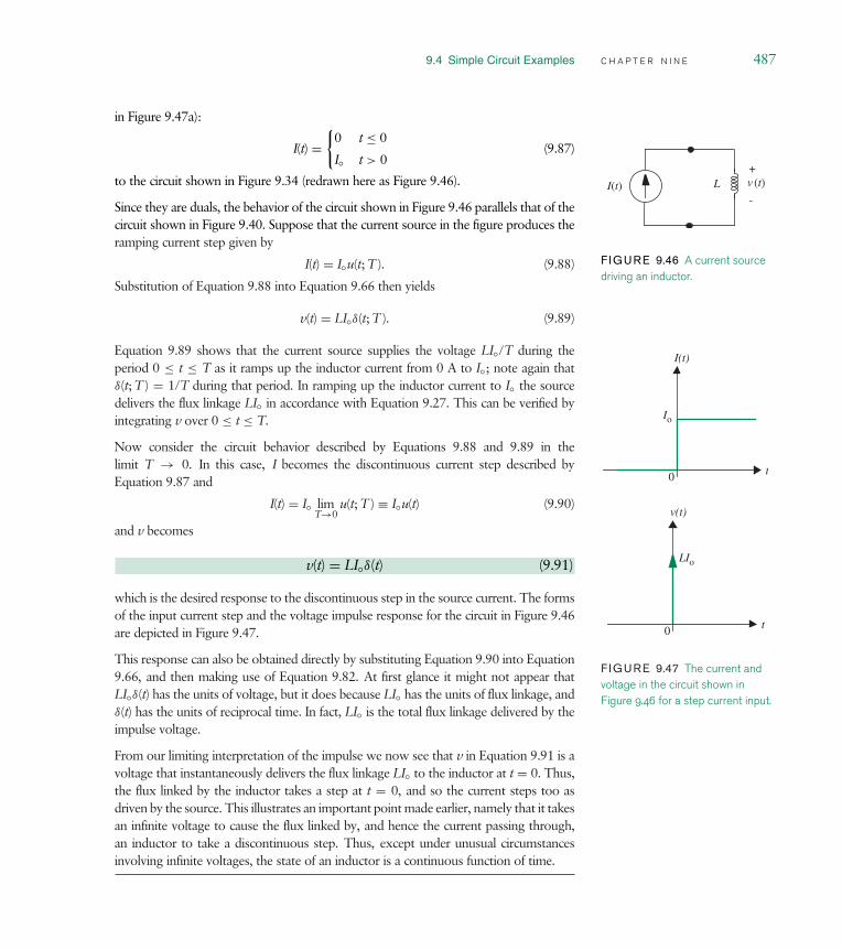
9.4 Simple Circuit Examples C H A P T E R N I N E 487
in Figure 9.47a):
I(t) =
0 t ≤ 0
I t > 0(9.87)
to the circuit shown in Figure 9.34 (redrawn here as Figure 9.46).
Since they are duals, the behavior of the circuit shown in Figure 9.46 parallels that of thecircuit shown in Figure 9.40. Suppose that the current source in the figure produces the
+L
-
v t)(I(t)
F IGURE 9.46 A current sourcedriving an inductor.
ramping current step given by
I(t) = Iu(t; T ). (9.88)
Substitution of Equation 9.88 into Equation 9.66 then yields
v(t) = LIδ(t; T ). (9.89)
Equation 9.89 shows that the current source supplies the voltage LI/T during theperiod 0 ≤ t ≤ T as it ramps up the inductor current from 0 A to I; note again thatδ(t; T ) = 1/T during that period. In ramping up the inductor current to I the sourcedelivers the flux linkage LI in accordance with Equation 9.27. This can be verified byintegrating v over 0 ≤ t ≤ T.
Now consider the circuit behavior described by Equations 9.88 and 9.89 in thelimit T → 0. In this case, I becomes the discontinuous current step described byEquation 9.87 and
I(t) = I limT→0
u(t; T ) ≡ Iu(t) (9.90)
and v becomes
v(t) = LIδ(t) (9.91)
which is the desired response to the discontinuous step in the source current. The formsof the input current step and the voltage impulse response for the circuit in Figure 9.46are depicted in Figure 9.47.
t
I(t)
0
Io
t
v(t)
0
LIo
F IGURE 9.47 The current andvoltage in the circuit shown inFigure 9.46 for a step current input.
This response can also be obtained directly by substituting Equation 9.90 into Equation9.66, and then making use of Equation 9.82. At first glance it might not appear thatLIδ(t) has the units of voltage, but it does because LI has the units of flux linkage, andδ(t) has the units of reciprocal time. In fact, LI is the total flux linkage delivered by theimpulse voltage.
From our limiting interpretation of the impulse we now see that v in Equation 9.91 is avoltage that instantaneously delivers the flux linkage LI to the inductor at t = 0. Thus,the flux linked by the inductor takes a step at t = 0, and so the current steps too asdriven by the source. This illustrates an important point made earlier, namely that it takesan infinite voltage to cause the flux linked by, and hence the current passing through,an inductor to take a discontinuous step. Thus, except under unusual circumstancesinvolving infinite voltages, the state of an inductor is a continuous function of time.

488 C H A P T E R N I N E e n e r g y s t o r a g e e l e m e n t s
9.4.3 I M P U L S E I N P U T S
We introduced impulse functions in the previous section. Recall that an unitimpulse denoted by δ(t) has the following properties.
δ(t) = 0 for t = 0 (9.92)
∫ t
−∞δ(t)dt = u(t) ⇔ δ(t) = du(t)
dt(9.93)
∫ ∞
−∞δ(t)dt = 1. (9.94)
In other words, the impulse δ(t) is nonzero only for t = 0. Its integral producesthe unit step function, and the area under it is 1.
Recall further that the unit-area pulse function in Figure 9.44 becomes theunit impulse in the limit as T → 0.
Figure 9.48a shows a unit current impulse and Figure 9.48b shows a currentimpulse with area under the impulse Q. In other words,
∫ ∞
−∞i(t)dt =
∫ ∞
−∞δ(t)dt = 1 (9.95)
for the current in Figure 9.48a, and
∫ ∞
−∞i(t)dt =
∫ ∞
−∞Qδ(t)dt = Q (9.96)
for the current in Figure 9.48b.
t0
I t( )
1
(a)
t0
I t( )
Q
(b)
F IGURE 9.48 (a) The unitimpulse δ(t); (b) an impulse witharea Q.
+C
-
v t)(I(t)
F IGURE 9.49 A current sourcedriving a capacitor.
Let us analyze the circuit in Figure 9.31 (redrawn in Figure 9.49 for conve-nience) for an impulse input current with strength Q. In other words, an inputcurrent of the form:
I(t) = Qδ(t).
Recall that solving the circuit implies finding the values of all the branchvariables. The one branch variable that is unknown in the circuit is the voltagev(t). We can obtain v(t) by integrating the current through the capacitor as
v(t) = 1
C
∫ t
−∞I(t)dt
= 1
C
∫ t
−∞Qδ(t)dt
= 1
CQu(t). (9.97)

9.5 Energy, Charge, and Flux Conservation C H A P T E R N I N E 489
Thus, a current impulse of strength Q that occurs at time t deposits a charge Qon the capacitor. This charge results in the capacitor voltage jumping to 1
CQ
at time t as illustrated in Figure 9.50.
Before ending this subsection, it is worthwhile to comment on impulsesources. Since impulses are a mathematical invention, and not a physical occur-rence, it might appear that they have limited practical value. However, thisis not the case. We often encounter sources that produce very narrow pulsesof voltage or current. When these pulses are so narrow that we do not reallycare about the details of their shape, then we can model them very simplyby an impulse with an equivalent area. From a mathematical viewpoint, thisoffers a significant savings since an impulse source is much easier to deal withthan a source that produces a pulse with a complex shape. Thus, impulses areactually very useful modeling tools.
t
I(t)
0
Q
t
v(t)
0
QC----
F IGURE 9.50 The current andvoltage in the circuit shown inFigure 9.32 for an impulse currentinput.
W W W 9.4.4 R O L E R E V E R S A L *
9.5 E N E R G Y , C H A R G E , A N DF L U X C O N S E R V A T I O N
In Section 9.2, we studied the parallel combination of capacitors that stored nocharge at the time of their connection, and the series combination of inductorsthat linked no flux at the time of their connection. In this section, we extendthat study to consider connections in the presence of initial charge and fluxlinkage.
Consider the parallel connection of the two initially-charged capacitorsshown in Figure 9.51; the connection occurs when the switch closes. We wish
v1 C1 C2 v2
+
--
+q2q1
F IGURE 9.51 Two capacitorsconnected in parallel through aswitch.
to determine the state of the capacitors after the switch is closed. KCL appliedto the bottom node of the circuit dictates that
dq1(t)
dt+ dq2(t)
dt= d
dt(q1(t) + q2(t)) = 0. (9.98)
Equation 9.98 states that the total charge q1+q2 on both capacitors is constant,and hence conserved for all time, even as the switch closes. Now, let the switchclose at t = 0. After the switch closes, that is, for t > 0, KVL applied to theloop in Figure 9.51 dictates that
v1(t) = v2(t), (9.99)
and, with the help of Equation 9.8, that
q1(t)
C1= q2(t)
C2. (9.100)

490 C H A P T E R N I N E e n e r g y s t o r a g e e l e m e n t s
We can now use Equations 9.98 and 9.100 to determine the capacitorcharges, and, with the help of Equation 9.8, the common voltage after theswitch is closed. To begin, let us denote the charges on the two capacitorsprior to switch closure as Q1 and Q2. Then, from Equation 9.98,
q1(t) + q2(t) = Q1 + Q2. (9.101)
Next, Equations 9.100 and 9.101 can be jointly solved to yield
q1(t) = C1
C1 + C2(Q1 + Q2) (9.102)
q2(t) = C2
C1 + C2(Q1 + Q2) (9.103)
for t > 0. Finally, Equations 9.102 and 9.103 can be substituted in Equation9.8 to yield
v1(t) = q1(t)
C1= Q1 + Q2
C1 + C2(9.104)
v2(t) = q2(t)
C2= Q1 + Q2
C1 + C2, (9.105)
again for t > 0. According to Equations 9.102 and 9.103, the capacitors sharethe total charge in proportion to their capacitance.
While charge is conserved during the closure of the switch, it is interestingto note that energy is not. Using Equation 9.18, the total energy stored betweenthe two capacitors before the switch is closed is found to be
wE(t < 0) = Q21
2C1+ Q2
2
2C2. (9.106)
Using Equations 9.102, 9.103, and 9.18, the total energy stored after the switchis closed is found to be
wE(t > 0) =(
C1(Q1 + Q2)C1 + C2
)2 12C1
+(
C2(Q1 + Q2)C1 + C2
)2 12C2
= (Q1 + Q2)2
2(C1 + C2). (9.107)

9.5 Energy, Charge, and Flux Conservation C H A P T E R N I N E 491
The two energies are not equal. Further, with a little algebraic manipulation, itcan be seen that
wE(t < 0) − wE(t > 0) = 1
2
C1C2
C1 + C2
(Q1
C1− Q2
C2
)2
≥ 0, (9.108)
and so energy is always lost during the closure of the switch, except for thespecial case in which v1 and v2 are equal before the switch closes. Where the lostenergy goes is not apparent from Figure 9.51 because it is an idealized figure.Perhaps the energy is dissipated in the wires used to connect the two capacitorsand the switch. Or, perhaps it is dissipated in a spark as the switch closes. Itmight even be lost as radiated electromagnetic energy. In any case, it is lost.One of the problems at the end of this chapter explores this loss further.
F IGURE 9.52 Two inductorsconnected in series through aswitch.
Finally, we note that arguments similar to those presented here can bemade for inductors connected in series. The corresponding circuit is shownin Figure 9.52. Initially, the switch is closed, allowing each inductor to carryan arbitrary current. Then, the switch opens. In this way, two inductors withdifferent initial currents are connected in series. Using arguments similar tothose presented earlier it is possible to determine the inductor currents and fluxlinkages after the switch opens. Then, it is straightforward to show that energyis lost during the opening of the switch.
e x a m p l e 9.14 c h a r g e s h a r i n g i n c a p a c i t o r s InFigure 9.51, suppose that C1 = 1 µF and C2 = 10 µF. Further, suppose that v1 = 10 Vand v2 = 1 V before the switch is closed. How much energy is stored in the twocapacitors before the switch is closed? Also, how much energy is lost during the switchclosure, and what is the common voltage across the capacitors after the switch closes?
To begin, we find the charge on each capacitor before the switch closes. Using Equation9.8, Q1 = 10 µC and Q2 = 10 µC. Next, use Equations 9.102 and 9.103 to determinethat q1 = 20/11 µC and q2 = 200/11 µC after the switch closes. Equation 9.103 or9.104 can then be used to determine that v1 = v2 = 20/11 V after the switch closes.Finally, Equations 9.106 and 9.108 are used to determine that the initial stored energyis 55 µJ, and that the energy lost is approximately 36.8 µJ.

492 C H A P T E R N I N E e n e r g y s t o r a g e e l e m e n t s
9.6 S U M M A R Y In this chapter, we introduced capacitors and inductors, and derived their
lumped element laws from more fundamental distributed physics. Sincethose element laws involved time derivatives, or alternatively time inte-grals, time became an important variable in this chapter. This was not thecase in previous chapters because the circuits we studied there containedonly sources, resistors, and idealized MOSFETs, all of which have purelyalgebraic element laws. Because time was an important variable in this chap-ter, we also began to consider a richer class of functions for the sourcesthat would input signals into a circuit. These functions included sinusoids,steps, and impulses. The circuit responses to these inputs became our firstexamples of transients in electronic circuits.
When we first introduced capacitors and inductors, we did so through theeffects that parasitic capacitance and inductance can have on the perfor-mance of an electronic circuit. This in turn caused us to re-evaluate ourlumped matter discipline, under which such parasitics do not, by defini-tion, exist. In the end we made a modeling compromise to preserve thelumped matter discipline while admitting the existence of important par-asitics. That compromise was to augment an original circuit with lumpedelements to model the important parasitics, with the understanding thatthe augmented model obeys the lumped matter discipline. While this iscertainly an important issue, it is also important to realize that capacitorsand inductors are useful well beyond the modeling of parasitics. As we shallsee in future chapters they are frequently used on purpose.
Through our analysis of capacitors and inductors, and several simple circuitsthat contained them, we have seen that these elements exhibit memory andare capable of reversible energy storage. A simple experiment will illustrate.As illustrated in Figure 9.53, charge up a capacitor by connecting it to apower supply (position 1), then disconnect the supply (position 2). Thecapacitor will ‘‘remember’’ the voltage of the supply for hours if a high-quality capacitor is used. A similar experiment performed with a resistorproduces no memory; when the power supply is disconnected, the resistorvoltage instantly falls to zero.
F IGURE 9.53 The capacitorholds its voltage for a long periodof time.
R
CV+
-
(1)
(2)
R
CV+
-
(1)
(2)

9.6 Summary C H A P T E R N I N E 493
The corresponding experiment on an inductor yields less exciting results,however. Establish an inductor current by the circuit in Figure 9.54, withthe switch in position 1. Then move the switch to position 2 (make beforebreak). The current will decay to zero in fractions of a second, becausethe energy stored in the magnetic field is rapidly dissipated in the internalresistance of the coil.
R
LV+
-
(1)
(2)
R
LV+
-
(1)
(2)
RLRL
F IGURE 9.54 The inductorholds its current for a very shortperiod of time.
Memory and reversible energy storage are characteristics associated withthe state of the elements: charge in the case of the capacitor and fluxlinkage in the case of the inductor. This behavior is quite different from thebehavior of ideal resistors. Ideal resistors do not exhibit memory, and theyirreversibly dissipate energy.
The element law for a capacitor is
i = Cdv
dt
and that for an inductor is
v = Ldi
dt.
The energy stored in a capacitor is
w E(t) = q 2(t)
2C= Cv(t)2
2.
The energy stored in an inductor is
w M(t) = λ2(t)
2L= Li(t)2
2.
Finally, in the process of introducing capacitors and inductors, we definedthe symbols and units for various physical quantities. These definitionsare summarized in Table 9.1. The units can be further modified with theengineering multipliers listed in Table 1.3.

494 C H A P T E R N I N E e n e r g y s t o r a g e e l e m e n t s
q u a n t i t y s y m b o l u n i t s s y m b o l
Time t Second s
Charge q Coulomb C
Capacitance C Farad F
Flux Linkage λ Weber Wb
Inductance L Henry H
Energy w Joule J
TABLE 9.1 Electrical engineer-ing quantities, their units, andsymbols for both.
E X E R C I S E S e x e r c i s e 9.1 Find the equivalent capacitance between the two terminals ineach of the networks in Figure 9.55.
e x e r c i s e 9.2 Find the equivalent capacitance or inductance for each case inFigure 9.56.
e x e r c i s e 9.3 Consider a power line on a computer backplane that is 2.5 mmwide, and separated from its underlying ground plane by 25 µm. Let the permittivityand permeability of the separating insulator be 2ε and µ, respectively. What is thecapacitance and inductance of the line per 10 cm of length?
If the voltage on the line is 5 V, how much energy is stored in its capacitance per 10 cmof length? If the current through the line is 1 A, how much energy is stored in itsinductance per 10 cm of length?
e x e r c i s e 9.4 A current source drives a capacitor as shown in Figure 9.57. Thesource current is as shown in Figure 9.58 for 0 ≤ t ≤ T. If the capacitor voltage is V att = T, what was it at t = 0?
(a)
1 µF 3 µF
(b) 1 µF
3 µF
(c) 3 µF
2 µF
1 µF
F IGURE 9.55
+C
-v(t)I(t)
F IGURE 9.57 A current source driving a capacitor.
t
I(t)
Io
T2---
Qo
T0
F IGURE 9.58 Source current.
e x e r c i s e 9.5 A voltage source drives an inductor as shown in Figure 9.59.The source voltage is as shown in Figure 9.60 for 0 ≤ t ≤ T. If the inductor current isI at t = T, what was it at t = 0?
e x e r c i s e 9.6 Figure 9.61 shows four circuits, labeled ‘‘1’’ through ‘‘4,’’together with the waveform for the source in each circuit. The figure also shows fourbranch-variable waveforms, labeled ‘‘a’’ through ‘‘d,’’ that could correspond to the branchcurrent i or branch voltages v labeled in the circuits. Match the branch variable waveformsto the appropriate circuit and source waveform.

9.6 Summary C H A P T E R N I N E 495
2 µF
(a)
1 µF
(b)
10 pF
1 µF
30 pF
1 µF
10 pF
(c)
2 mH
1 mH
(d)
2 mH
1 µH
(e)
1 mH
1 µH
2 mH
(f )
F IGURE 9.56
L
i(t)
V(t)+-
F IGURE 9.59 A current source driving an inductor.
t
V(t)
Vo
T2---
Λo
T0
F IGURE 9.60 Source current.
t
i
+
t t t
V I V I
V I +-- v
i
+V I+
-v
t t t t
(2) (3)(1) (4)
(a) (b) (c) (d)
-
F IGURE 9.61

496 C H A P T E R N I N E e n e r g y s t o r a g e e l e m e n t s
P R O B L E M S p r o b l e m 9.1 A voltage source is connected in series with two capacitors asshown in Figure 9.62. The source voltage is V(t) = 5 V u(t), as shown. If the current iand voltage v are given by i(t) = 4 µC δ(t) and v(t) = 1 V u(t), again as shown, what areC1 and C2?
+
-t
V(t)
5 VV(t)
i
v
C1
C2
+
t
i(t)
t
v(t)
1 V4 µC
F IGURE 9.62
p r o b l e m 9.2 A current source is connected in parallel with two inductors asshown in Figure 9.63. The source current is i(t) = 400 A/s u(t), as shown. If the currenti and voltage v are given by i(t) = 100 A/s u(t) and v(t) = 0.3 V u(t), again as shown,what are L1 and L2?
t
I(t)
400 AS----
i
L1 L2
+
–
v
t
100 AS----
t
1 VI(t)
i(t) v(t)
F IGURE 9.63
p r o b l e m 9.3 A current source drives a series-connected capacitor and inductoras shown in Figure 9.64. Let I(t) = I sin(ωt)u(t), and assume that the inductor and
I(t)C
L
+
–
v(t)
F IGURE 9.64
+V(t)
i(t)
F IGURE 9.65
capacitor both stored no energy prior to t = 0.
Determine the voltage v for t ≥ 0.
Is there any relation between I, ω, C, and L for which v is constant for t ≥ 0? If so,state the relation and determine v.
p r o b l e m 9.4 A voltage source drives a parallel-connected capacitor and induc-tor as shown in Figure 9.65. Let V(t) = V sin(ωt)u(t), and assume that the inductor andcapacitor both stored no energy prior to t = 0.
Determine the current i for t ≥ 0.
Is there any relation between V, ω, C, and L for which i is constant for t ≥ 0? If so,state the relation and determine i.

9.6 Summary C H A P T E R N I N E 497
p r o b l e m 9.5 A constant voltage source having value V drives a time-varying
V+
C(t)
i(t)
F IGURE 9.66
capacitor as shown in Figure 9.66. The time-varying capacitance is given by C(t) =C0 + C1 sin(ωt). Determine the capacitor current i(t).
p r o b l e m 9.6 A constant current source having value I drives a time-varyinginductor as shown in Figure 9.67. The time-varying inductance is given by L(t) =
I
+
–
L(t)vt
F IGURE 9.67
L0 + L1 sin(ωt). Determine the inductor voltage v(t).
p r o b l e m 9.7 Consider the parallel plate capacitor shown in Figure 9.68.Assume that the dielectric is free space so that ε = ε.
E E
E
E
q
l
ε
+
-
+
-
+
-
+
-
+
++
-
v
Area A
qi
F IGURE 9.68
Suppose the capacitor is charged to the voltage V. Determine the charge and the electricenergy stored in the capacitor in this case.
The capacitor is disconnected from the charging source so that its stored charge remainsconstant. Following that, its plates are pulled apart so as to double the distance betweenthem; that is, the gap separation is now 2l. For this new configuration, determine thevoltage across the terminals of the capacitor and the energy stored in the capacitor.Explain how the stored energy changes.
p r o b l e m 9.8 Figure 9.69 shows two capacitive two-port networks. One is a‘‘’’ network, and one is a ‘‘T’’ network. For the network, find i1P and i2P as functionsof v1P and v2P. For the T network, find i1T and i2T as functions of v1T and v2T.
How must C1P, C2P, and C3P be related to C1T, C2T, and C3T for both networks tohave the same terminal relations?
p r o b l e m 9.9 Figure 9.70 shows two inductive two-port networks. One is a‘‘’’ network, and one is a ‘‘T’’ network. For the network, find v1P and v2P asfunctions of i1P and i2P. For the T network, find v1T and v2T as functions of i1T and i2T.

498 C H A P T E R N I N E e n e r g y s t o r a g e e l e m e n t s
F IGURE 9.69 (a) A capacitive Ttwo-port network; and (b) acapacitive two-port network.
+
–
+
–
v1p
i1p i2p
C1p C2p
C3pv2p
+
–
+
–
i1T i2T
v1T v2TC3T
C1T C2T
(a) (b)
How must L1P, L2P, and L3P be related to L1T, L2T, and L3T for both networks tohave the same terminal relations?
F IGURE 9.70 (a) An inductive Ttwo-port network; and (b) aninductive two-port network.
+
–
+
–
v1p
i1p i2p
L1p L2p
L3pv2p
+
–
+
–
i1T i2T
v1T v2TL3T
L1T L2T
(a) (b)
p r o b l e m 9.10 This problem examines in more detail why energy is lost whenthe switch in Figure 9.71 closes. To do so, we examine the transient that occurs duringthe closure of the switch. In preparation for this, let t = 0 be the time at which theswitch first begins to close, and let t = T be the time at which the circuit reaches steadystate. The charges on the two capacitors prior to switch closure are given to be Q1
and Q2.
v1 C1 C2 v2+
--
+q2q1
F IGURE 9.71Further, let q1(t) be any function defined over the interval 0 ≤ t ≤ T such that
q1(0) = Q1
and q1(T ) is the steady state charge on the capacitor given by
q1(T ) = C1
C1 + C2(Q1 + Q2).
In this way, the function q1 is an arbitrary transient connecting the initial and finalcharge during the switch closure.
(a) Use the charge conservation relation:
q1(t) + q2(t) = Q1 + Q2
to find q2 in terms of q1 for 0 ≤ t ≤ T. Then, use the equation:
dq(t)
dt= i(t)

9.6 Summary C H A P T E R N I N E 499
to determine i1 and i2, again in terms of q1 for 0 ≤ t ≤ T. Finally, use theequation:
q(t) = Cv(t)
to find v1 and v2, also in terms of q1 for 0 ≤ t ≤ T. The entire transient is nowdescribed in terms of the arbitrary function q1.
(b) During the transient, the difference between v1 and v2 must appear across someelement or elements within the circuit. KVL requires this. For example, it couldappear across the wiring resistance or the switch, or a combination of both. In anycase, energy is lost as a current passes through this voltage difference. If we considerthe voltage difference to be (v1 − v2), as opposed to its opposite, then it is i2 thatpasses into the positive terminal of this difference. Why?
(c) The product i2(v1 − v2) is the power dissipated during the transient. Determinethis power in terms of q1 for 0 ≤ t ≤ T.
(d) Integrate the power found in the part (c) over the interval 0 ≤ t ≤ T to find theenergy lost during the transient. Also, show that the energy lost is equal to theenergy difference in
w E(t < 0) − w E(t > 0) = 1
2
C1C2
C1 + C2
(Q1
C1− Q2
C2
)2.
Remarkably, the energy lost is independent of the interior details of the functionchosen for q1. Since these details are equivalent to the details of the loss mechanism,it is apparent that the amount of energy lost is independent of how it is lost.


c h a p t e r 10
10.1 A N A L Y S I S O F R C C I R C U I T S
10.2 A N A L Y S I S O F R L C I R C U I T S
10.3 I N T U I T I V E A N A L Y S I S
10.4 P R O P A G A T I O N D E L A Y A N D T H E D I G I T A L A B S T R A C T I O N
10.5 S T A T E A N D S T A T E V A R I A B L E S
10.6 A D D I T I O N A L E X A M P L E S
10.7 D I G I T A L M E M O R Y
10.8 S U M M A R Y
E X E R C I S E S
P R O B L E M S


f i r s t -order tran s i ent s in
l inear e l ectr i ca l
network s10
As illustrated in Chapter 9, capacitances and inductances impact circuit behavior.The effect of capacitances and inductances is so acute in high-speed digital cir-cuits, for example, that our simple digital abstractions developed in Chapter 6based on a static discipline become insufficient for signals that undergo transi-tions. Therefore, understanding the behavior of circuits containing capacitorsand inductors is important. In particular, this chapter will augment our digitalabstraction with the concept of delay to include the effects of capacitors andinductors.
Looked at positively, because they can store energy, capacitors and induc-tors display the memory property, and offer signal-processing possibilities notavailable in circuits containing only resistors. Apply a square-wave voltage to amulti-resistor linear circuit, and all of the voltages and currents in the networkwill have the same square-wave shape. But include one capacitor in the circuitand very different waveforms will appear sections of exponentials, spikes,and sawtooth waves. Figure 10.1 shows an example of such waveforms forthe two-inverter system of Figure 9.1 in Chapter 9. The linear analysis tech-niques already developed node equations, superposition, etc. are adequatefor finding appropriate network equations to analyze these kinds of circuits.However, the formulations turn out to be differential equations rather thanalgebraic equations, so additional skills are needed to complete the analyses.
+-
vI+
-vO
. . .t
vI
t
vO
F IGURE 10.1 Observedresponse of the first inverterto a square-wave input.
503

504 C H A P T E R T E N f i r s t - o r d e r t r a n s i e n t s
This chapter will discuss systems containing a single storage element, namely,a single capacitor or a single inductor. Such systems are described by simple,first-order differential equations. Chapter 12 will discuss systems containingtwo storage elements. Systems with two storage elements are described bysecond-order differential equations.1 Higher-order systems are also possible,and are discussed briefly in Chapter 12.
This chapter will start by analyzing simple circuits containing one capacitor,one resistor, and possibly a source. We will then analyze circuits containing oneinductor and one resistor. The two-inverter circuit of Figure 10.1 is examinedin detail in Section 10.4.
10.1 A N A L Y S I S O F R C C I R C U I T S
Let us illustrate first-order systems with a few primitive examples containing aresistor, a capacitor, and a source. We first analyze a current source driving theso-called parallel RC circuit.
10.1.1 P A R A L L E L R C C I R C U I T , S T E P I N P U T
Shown in Figure 10.2a is a simple source-resistor-capacitor circuit. On the basisof the Thévenin and Norton equivalence discussion in Section 3.6.1, this circuitcould result from a Norton transformation applied to a more complicated
F IGURE 10.2 Capacitorcharging transient.
I0
t0
i(t)
I0R
t0
vC
C vC (t)
+-
i(t) R(a)
(b)
(c) Time constant RC
1. However, a circuit with two storage elements that can be replaced by a single equivalent storageelement remains a first-order circuit. For example, a pair of capacitors in parallel can be replacedwith a single capacitor whose capacitance is the sum of the two capacitances.
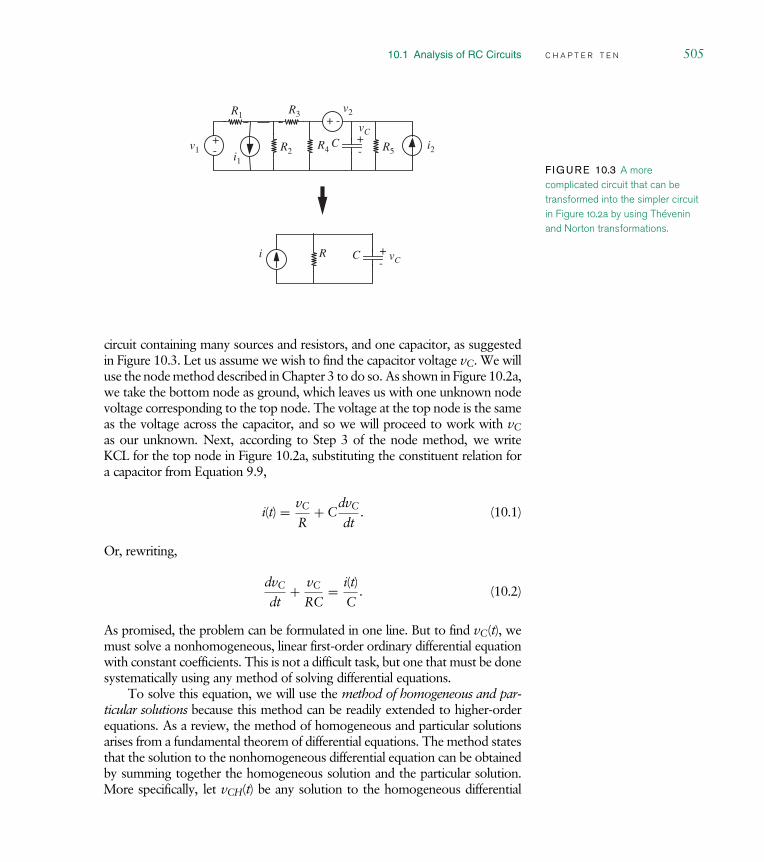
10.1 Analysis of RC Circuits C H A P T E R T E N 505
+-
- +
v1
R1 R3v2
i2R5
vC
R4R2i1
+-
C
vCRi +
-C
F IGURE 10.3 A morecomplicated circuit that can betransformed into the simpler circuitin Figure 10.2a by using Théveninand Norton transformations.
circuit containing many sources and resistors, and one capacitor, as suggestedin Figure 10.3. Let us assume we wish to find the capacitor voltage vC. We willuse the node method described in Chapter 3 to do so. As shown in Figure 10.2a,we take the bottom node as ground, which leaves us with one unknown nodevoltage corresponding to the top node. The voltage at the top node is the sameas the voltage across the capacitor, and so we will proceed to work with vCas our unknown. Next, according to Step 3 of the node method, we writeKCL for the top node in Figure 10.2a, substituting the constituent relation fora capacitor from Equation 9.9,
i(t) = vC
R+ C
dvC
dt. (10.1)
Or, rewriting,
dvC
dt+ vC
RC= i(t)
C. (10.2)
As promised, the problem can be formulated in one line. But to find vC(t), wemust solve a nonhomogeneous, linear first-order ordinary differential equationwith constant coefficients. This is not a difficult task, but one that must be donesystematically using any method of solving differential equations.
To solve this equation, we will use the method of homogeneous and par-ticular solutions because this method can be readily extended to higher-orderequations. As a review, the method of homogeneous and particular solutionsarises from a fundamental theorem of differential equations. The method statesthat the solution to the nonhomogeneous differential equation can be obtainedby summing together the homogeneous solution and the particular solution.More specifically, let vCH(t) be any solution to the homogeneous differential

506 C H A P T E R T E N f i r s t - o r d e r t r a n s i e n t s
equation
dvC
dt+ vC
RC= 0 (10.3)
associated with our nonhomogeneous differential equation 10.2. The homo-geneous equation is derived from the original nonhomogeneous equation bysetting the driving function, i(t) in this case, to zero. Further, let vCP(t) be anysolution to Equation 10.2. Then, the sum of the two solutions,
vC(t) = vCH(t) + vCP(t)
is a general solution or a total solution to Equation 10.2. vCH(t) is called thehomogeneous solution and vCP(t) is called the particular solution. When dealingwith circuit responses, the homogeneous solution is also called the naturalresponse of the circuit because it depends only on the internal energy storageproperties of the circuit and not on external inputs. The particular solution isalso called the forced response or the forced solution because it depends on theexternal inputs to the circuit.
Let us now return to the business of solving Equation 10.2. To make theproblem specific, assume that the current source i(t) is a step function
i(t) = I0 t > 0 (10.4)
as shown in Figure 10.2b. Further, we assume for now that the voltage on thecapacitor was zero before the current step was applied. In mathematical terms,this is an initial condition
vC = 0 t < 0. (10.5)
The method of homogeneous and particular solutions proceeds in three steps:
1. Find the homogeneous solution vCH.
2. Find the particular solution vCP.
3. The total solution is then the sum of the homogeneous solution and theparticular solution. Use the initial conditions to solve for the remainingconstants.
The first step is to solve the homogeneous equation, formed by setting thedriving function in the original differential equation to zero. Then, any methodof solving homogeneous equations can be used. In this case the homogeneousequation is
dvCH
dt+ vCH
RC= 0. (10.6)

10.1 Analysis of RC Circuits C H A P T E R T E N 507
We assume a solution of the form
vCH = Aest (10.7)
because the homogeneous solution for any linear constant-coefficient ordinarydifferential equation is always of this form. Now we must find values for theconstants A and s. Substitution into Equation 10.6 yields
Asest + Aest
RC= 0. (10.8)
The value for A cannot be determined from this equation, but discarding thetrivial solution of A = 0, we find
s + 1
RC= 0 (10.9)
because est is never zero for finite s and t, so can be factored out. Hence
s = − 1
RC. (10.10)
Equation 10.9 is called the characteristic equation of the system, and s = −1/RCis a root of this characteristic equation. The characteristic equation summarizesthe fundamental dynamic properties of a circuit, and we will have much moreto say about it later chapters. For reasons that will become clear in Chapter 12,the root of the characteristic equation, s, is also called the natural frequencyof the system.
We now know that the homogeneous solution is of the form
vCH = Ae−t/RC. (10.11)
The product RC has the dimensions of time and is called the time constant ofthe circuit.
The second step is to find a particular solution, that is, to find any solutionvCP that satisfies the original differential equation; it need not satisfy the initialconditions. That is, we are looking for any solution to the equation
I0 = vCP
R+ C
dvCP
dt. (10.12)
Since the drive I0 is constant in time for t > 0, one acceptable particular solutionis also a constant:
vCP = K . (10.13)

508 C H A P T E R T E N f i r s t - o r d e r t r a n s i e n t s
To verify this, we substitute into Equation 10.12
I0 = K
R+ 0 (10.14)
K = I0R . (10.15)
Because Equation 10.14 can be solved for K , we are assured that our ‘‘guess’’about the form of the particular solution, that is, Equation 10.13, was correct.2
Hence the particular solution is
vCP = I0R. (10.16)
The total solution is the sum of the homogeneous solution (Equation 10.11)and the particular solution (Equation 10.16)
vC = Ae−t/RC + I0R. (10.17)
The only remaining unevaluated constant is A, and we can solve for this byapplying the initial condition. Equation 10.5 applies for t less than zero, andour solution, Equation 10.17 is valid for t greater than zero. These two parts ofthe solution are patched together by a continuity condition derived from Equa-tion 9.9: An instantaneous jump in capacitor voltage requires an infinite spikein current, so for finite current, the capacitor voltage must be continuous. Thiscircuit cannot support infinite capacitor current (because i(t) is finite, the infinitecurrent would have to come from the resistor, and this is impossible). Thus weare justified in assuming continuity of vC, hence can equate the solutions fornegative time and positive time by solving at t = 0
0 = A + I0R. (10.18)
Thus
A = −I0R (10.19)
and the complete solution for t > 0 is
vC = −I0Re−t/RC + I0R
2. Alternatively, a guess ofvCP = Kt,
where K is a constant independent of t, would not be correct, since substituting into Equation 10.12yields
I0 = Kt
R+ CK
which cannot be solved for a time-independent K.

10.1 Analysis of RC Circuits C H A P T E R T E N 509
I0R
t0
vC
Large RC
Small RC
F IGURE 10.4 Significance ofthe RC time constant.
or
vC = I0R(1 − e−t/RC). (10.20)
This is plotted in Figure 10.2c.Some comments at this point help to give perspective. First, notice that
capacitor voltage starts from a zero value at t = 0 and reaches its final valueof I0R for large t. The increase from 0 to I0R has a time constant RC. Thefinal value of I0R for the capacitor voltage implies that all of the current fromthe current source flows through the resistor, and the capacitor behaves like anopen circuit (for large t).
Second, the initial value of 0 for the capacitor voltage implies that at t = 0all of the current from the current source must be flowing through the capacitor,and none through the resistor. Thus the capacitor behaves like an instantaneousshort circuit at t = 0.
Third, the physical significance of the time constant RC can now be seen.Illustrated in Figure 10.4, it is the temporal scale factor that determines howrapidly the transient goes to completion.
Finally, it may seem that the solution to such a simple problem can’t pos-sibly be as involved as this appears Correct. This problem and most first-ordersystems with step excitation can be solved by inspection (see Section 10.3).But here we are trying to establish general methods, and have chosen thesimplest example to illustrate the method.
10.1.2 R C D I S C H A R G E T R A N S I E N T
With the capacitor now charged, assume that the current source is suddenly setto zero as suggested in Figure 10.5a, where for convenience, the time axis isredefined so that the turn-off occurs at t = 0. The relevant circuit to analyze theRC turn-off or discharge transient now contains just a resistor and a capacitoras indicated in Figure 10.5c. The voltage on the capacitor at the start of theexperiment is represented by the initial condition
vC = I0R t < 0. (10.21)
This RC discharge scenario is identical to that of a circuit containing a resistorand a capacitor, where there is an initial voltage vC(0) = I0R on the capacitor.

510 C H A P T E R T E N f i r s t - o r d e r t r a n s i e n t s
F IGURE 10.5 RC dischargetransient.
I0
t0
i(t)
I0R
t0
vC
(a)
(b)
Time constant RC
R C vC
+
-
iCvC(0) = I0R
(c)
Because the drive current is zero, the differential equation for t greater thanzero is now
0 = vC
R+ CdvC
dt. (10.22)
As before, the homogeneous solution is
vCH = Ae−t/RC (10.23)
but now the particular solution is zero, since there is no forcing input, soEquation 10.23 is the total solution. In other words,
vC = vCH = Ae−t/RC.
Equating Equations 10.21 and 10.23 at t = 0, we find
I0R = A (10.24)
so the capacitor voltage waveform for t > 0 is
vC = I0Re−t/RC. (10.25)
This solution is sketched in Figure 10.5b.

10.1 Analysis of RC Circuits C H A P T E R T E N 511
In general, for a resistor and capacitor circuit with an initial voltage vC(0)on the capacitor, the capacitor voltage waveform for t > 0 is
vC = vC(0)e−t/RC. (10.26)
Properties of Exponentials
Because decaying exponentials occur so frequently in solutions to simple RCand RL transient problems, it is helpful at this point to discuss some of theproperties of these functions as an aid to sketching waveforms.
For a general exponential function of the form
x = Ae−t/τ (10.27)
the initial slope of the exponential is
dx
dt
∣∣∣∣t=0
= −A
τ.
Hence the initial slope of the curve, projected to the time axis, intercepts thetime axis at t = τ , irrespective of the value of A, as shown in Figure 10.6a.
Furthermore, notice that when t = τ , the function in Equation 10.27becomes
x(t = τ ) = A
e.
In other words, the function reaches 1/e of its initial value irrespectiveof the value of A. Figure 10.6b depicts this point in the exponentialcurve.
Because e−5 = 0.0067, it is common to assume for the t greater thanfive time constants, that is,
t > 5τ
the function is essentially zero (see Figure 10.6a). That is, we assume thetransient has gone to completion.
We will see later that these properties of the time constant τ make it useful inobtaining rough estimates for time durations associated with rising or fallingexponentials.
10.1.3 S E R I E S R C C I R C U I T , S T E P I N P U T
Let us now convert the Norton source in Figure 10.2 to a Thévenin source inFigure 10.7 and determine the capacitor voltage as a function of time. The inputwaveform vS is assumed to be a voltage step of magnitude V applied at t = 0,

512 C H A P T E R T E N f i r s t - o r d e r t r a n s i e n t s
F IGURE 10.6 Properties ofexponentials.
t0
(a)
0.2 A0.4 A
A
0.6 A0.8 A
Ae–t ⁄ τ
τ 2τ 3τ 4τ
Time constant τ
5τt
0(b)
0.2 A0.4 A
A
0.6 A0.8 A
τ 2τ 3τ 4τ
Time constant τAe---
5τ
Ae–t ⁄ τ
F IGURE 10.7 Series RC circuitwith step input.
vI(t)
R
C vC
+
-
+-
V
t
vI
iC
(b) Waveforms
vIV
t
(a) Circuit
t
vC
iC
V
VO
V – VO
R-----------------
t0
0
0
vC (0) = VO
but this time around, we assume the capacitor voltage is VO just before thestep.3 That is, the initial condition on the circuit is
vC = VO t < 0. (10.28)
3. For the purpose of determining the response for t ≥ 0, it does not really matter to us how thecapacitor voltage became VO for t = 0, or the value of the capacitor voltage for t < 0. Nevertheless,

10.1 Analysis of RC Circuits C H A P T E R T E N 513
The differential equation can be found by using the node method. ApplyingKCL at the node with voltage vC, we get
vC − vI
R+ C
dvC
dt= 0.
Dividing by C and rearranging terms,
dvC
dt+ vC
RC= vI
RC. (10.29)
The homogeneous equation is
dvCH
dt+ vCH
RC= 0 (10.30)
which, as expected, is the same as that in Equation 10.6 for the Norton cir-cuit, since the Norton and Thévenin circuits are equivalent. Borrowing thehomogeneous solution to Equation 10.6, we have
vCH = Ae−t/RC (10.31)
where RC is the time constant of the circuit.Let us now find the particular solution. Since the input drive is a step of
magnitude V, the particular solution is any solution to
dvCP
dt+ vCP
RC= V
RC. (10.32)
the following is one possible circuit that will realize the given initial condition on the capacitor andthe effect of a step input:
V
R
C vC
+
-
+
-
iC +
-VO
t = 0 t = 0 S1S2
In the circuit, a DC source with value VO is applied across the capacitor using switch S1. The DCsource forces the capacitor voltage to VO. This DC source is switched out as shown at t = 0, andanother DC source with voltage V is switched in using switch S2. This action applies a step voltageof magnitude V to the capacitor, which has an initial voltage VO at t = 0.

514 C H A P T E R T E N f i r s t - o r d e r t r a n s i e n t s
Because the drive is a step, which is constant for large t, we can assume aparticular solution of the form
vCP = K. (10.33)
Substituting into Equation 10.32, we obtain
K
RC= V
RC.
which implies K = V. So the particular solution is
vCP = V. (10.34)
Summing vCH and vCP, we obtain the complete solution:
vC = V + Ae−t/RC. (10.35)
The initial condition can now be applied to evaluate A. Given that the capacitorvoltage must be continuous at t = 0, we have
vC(t = 0) = VO.
Thus, at t = 0, Equation 10.35 yields
A = VO − V.
The complete solution for the capacitor voltage for t > 0 is now
vC = V + (VO − V)e−t/RC (10.36)
where, V is the input drive voltage for t > 0 and VO is the initial voltage onthe capacitor. As a quick sanity check, substituting t = 0, we get vC(0) = VO,and substituting t = ∞, we get vC(∞) = V. Both these boundary values arewhat we expect, since the initial condition on the capacitor is VO, and since theinput voltage must appear across the capacitor after a long period of time.
By rearranging the terms, Equation 10.36 can be equivalently written as
vC = VOe−t/RC + V(1 − e−t/RC). (10.37)
Finally, from Equation 9.9, the current through the capacitor is
iC = CdvC
dt= V − VO
Re−t/RC. (10.38)
This expression for iC also matches our expectations since iC must be 0 when t islarge, and the since the capacitor behaves like a voltage source with voltage VOduring the step transition at t = 0, the current at t = 0 must equal (V − VO)/R.
10.1 Analysis of RC Circuits C H A P T E R T E N 515
These waveforms are shown in Figure 10.7b.If we desire the voltage vR across the resistor, we can easily obtain it by
applying KVL as
vR = vI − vC
where we take the positive reference for vR on the input side of the resistor.Alternatively, we can obtain vR by taking the product of the current and theresistance as
vR = iCR.
As one final point of interest, notice that Equation 10.36 was derived assumingboth an initial nonzero state (VO) and a nonzero input (a step of voltage V).
Substituting V = 0 in Equation 10.36 we obtain the so called zero inputresponse (ZIR):
vC = VOe−t/RC (10.39)
and substituting VO = 0 in Equation 10.36 we obtain the zero stateresponse (ZSR):
vC = V − Ve−t/RC. (10.40)
In other words, the zero input response is the response for nonzero initialconditions, but where the input drive is zero. In contrast, the zero state responseis the response of the circuit when the initial state is zero, that is, all capacitorvoltages and inductor currents are initially zero.
Notice also that the total response is the sum of the ZIR and the ZSR,
as can be verified by adding the right-hand sides of Equations 10.39 and 10.40and comparing to the right-hand side of Equation 10.36. We will have a lotmore to say about the ZIR and the ZSR in Section 10.5.3.
10.1.4 S E R I E S R C C I R C U I T , S Q U A R E - W A V E I N P U T
Examination of the waveforms in Figure 10.5a and 10.5b indicates that thepresence of the capacitor has changed the shape of the input wave. When a squarepulse is applied to the RC circuit, a decidedly non-square pulse, with slow riseand slow decay, results. The capacitor has allowed us to do a limited amountof wave shaping. This concept can be further developed by an experiment inwhich we drive the circuit with a square wave.
In this experiment, we will use a Thévenin source as in Figure 10.8. Thesource can be a standard laboratory square-wave generator. The input squarewave is marked as a in Figure 10.8. Several quite distinctive wave shapes forvC(t) can be derived, depending on the relation between the period of the drivingsquare wave and the time constant RC of the network. These waveforms areall essentially variations on the solution derived in the preceding sections.

516 C H A P T E R T E N f i r s t - o r d e r t r a n s i e n t s
F IGURE 10.8 Response tosquare wave.
Vt
0
vI
vI(t)
R
C vC
+
-
Vt
0
vC b
d
c
+-
-V
iCvR+ -
a
For the case where the circuit time constant is very short compared to thesquare-wave period, the exponentials go to completion relatively rapidly, assuggested by waveform b in Figure 10.8. The capacitor waveform thus closelyresembles the input waveform, except for a small amount of rounding at thecorners.
If the time constant is a substantial fraction of the pulse length, then thesolution appears as waveform c in Figure 10.8. Note that the drawing impliesthat the transients still go almost to completion, so there is an upper limit onthe RC product for this solution to apply. Assuming, as noted here, that simpletransients are complete for times greater than five time constants, the RC prod-uct must be less than one-fifth of the pulse length, or one tenth the square-waveperiod for this solution to apply.
When the circuit time constant is much longer than the square-waveperiod, waveform d, shown in Figure 10.8, results. Here the transient clearlydoes not go to completion. In fact, only the first part of the exponential isever seen. The waveform looks almost triangular, the integral of the inputwave. This can be seen from the differential equation describing the circuit.Application of KVL gives
vI = iCR + vC. (10.41)
Upon substitution of the constituent relation for the capacitor, Equation 9.9,we obtain the differential equation
vI = RCdvC
dt+ vC. (10.42)

10.2 Analysis of RL Circuits C H A P T E R T E N 517
It is clear from Equation 10.42 or Figure 10.8 that as the circuit time constantbecomes bigger, the capacitor voltage vC must become smaller. For waveformd the time constant RC is large enough that vC is much smaller than vI, so inthis case Equation 10.41 can be approximated by
vI iCR. (10.43)
Physically, the current is now determined solely by the drive voltage and theresistor, because the capacitor voltage is almost zero. Integrating both sides ofEquation 10.42 assuming vC is negligible, we obtain
vC 1
RC
∫vIdt + K (10.44)
where the constant of integration K is zero. Thus for large RC, the capacitorvoltage is approximately the integral of the input voltage. This is a very usefulsignal-processing property. In Chapter 15 we will show that a much closerapproximation to ideal integration can be obtained by adding an Op Amp tothe circuit.
It is a simple matter to find the voltage across the resistor in the circuit ofFigure 10.8 because we can find the current from the capacitor voltage usingEquation 9.9,
vR = iCR = RCdvC
dt.
Thus, during the charge interval, for example, from Equation 10.20, assumingthe transients go to completion,
vC = V(1 − e−t/RC).
Hence
vR = Ve−t/RC.
The wave shapes in Figure 10.8 change very little if the input signal vI has zeroaverage value, that is, if vI is changed so that it jumps back and forth from −V/2to +V/2. Specifically, vC also has zero average value, and if the transients go tocompletion, as in wave forms b and c, the excursions will be −V/2 and +V/2.
10.2 A N A L Y S I S O F R L C I R C U I T S
10.2.1 S E R I E S R L C I R C U I T , S T E P I N P U T
Figure 10.9 will serve as a simple illustration of a transient involving an inductor.(See the example discussed in Section 10.6.1 for a practical application of theanalysis involving inductor transients.) The input waveform vS is assumed to

518 C H A P T E R T E N f i r s t - o r d e r t r a n s i e n t s
F IGURE 10.9 Inductor currentbuildup.
V
t
vS
vL
(b) Waveforms
vSV
t
(a) Circuit
t
iL
V
vS(t)
R
L vL
+
-
+-
iL
V eRL
− -- t
Time constant L/R
VR----
0
be a voltage step applied at t = 0 (see Figure 10.9a), and the inductor currentis assumed to be zero just before the step. That is, the initial condition on thecircuit is
iL = 0 t < 0. (10.45)
Suppose that we are interested in solving for the current iL. As before, wecan use the node method to obtain an equation involving the unknown nodevoltage vL, and then use the constituent relation for an inductor from Equa-tion 9.28 to substitute for vL in terms of the variable of interest to us, namelyiL. For variety, however, we will derive the same differential equation in iL byapplying KVL:
−vS + iLR + LdiLdt
= 0. (10.46)
The homogeneous equation is
LdiLH
dt+ iLHR = 0. (10.47)
Assume a solution of the form
iLH = Aest. (10.48)

10.2 Analysis of RL Circuits C H A P T E R T E N 519
Hence
LsAest + RAest = 0. (10.49)
For nonzero A (A = 0 is a trivial solution)
Ls + R = 0.
or
s + R
L= 0 (10.50)
s = −R/L. (10.51)
Equation 10.50 is the characteristic equation for our circuit, and Equation 10.50gives the natural frequency.
The homogeneous solution is thus
iLH = Ae−(R/L)t (10.52)
where the time constant is in this case L/R.
The particular solution can be obtained by solving
iLPR + LdiLP
dt= vS. (10.53)
Because the drive is a step, which is constant for large t, it is again appropriateto assume a particular solution of the form
iLP = K. (10.54)
Substituting into Equation 10.53, and noting that for large t, vS = V, we obtain
KR = V.
or,
K = V
R. (10.55)
So, from Equation 10.54, the particular solution is
iLP = V
R(10.56)

520 C H A P T E R T E N f i r s t - o r d e r t r a n s i e n t s
F IGURE 10.10 Response to asquare-wave input. t
vS
t
vL
and the complete solution is of the form
iL = V
R+ Ae(−R/L)t. (10.57)
The initial condition together with a continuity condition, can now be appliedto evaluate A. The continuity condition for inductor current can be found fromEquation 9.28. If it can be shown that the inductor voltage cannot be infinitein the circuit, then di/dt must be finite, hence the inductor current must becontinuous. For this particular circuit, with finite vS, we are assured of finite vL,hence iL in Equation 10.57 can be evaluated at t = 0, and set equal to the initialvalue, Equation 10.45:
V
R+ A = 0. (10.58)
The complete solution for the inductor current for t > 0 is now
iL = V
R
(1 − e−(R/L)t
)(10.59)
and, from Equation 9.28, the voltage across the inductor is
vL = LdiLdt
= Ve−(R/L)t. (10.60)
These waveforms are shown in Figure 10.9b. Notice that the inductor currenthas an initial value of 0 and a final value of V/R. Thus the inductor behaves likean instantaneous open circuit at t = 0 and a short circuit for large t, for the stepvoltage input at t = 0. vL is correspondingly V at t = 0 and 0 for large t.
The response to a square-wave input is shown in Figure 10.10.
10.3 I N T U I T I V E A N A L Y S I S
The previous sections illustrated the general method of analyzing linear RCand RL circuits. The several examples with step-function drive that we workedpreviously suggest that such circuits have a very limited range of solutions.

10.3 Intuitive Analysis C H A P T E R T E N 521
(a) Circuit
t
vC
V
VO
0
Initial Transition Final
(d) Initial, transition, and final intervals
V
R
C vC
+
-
+-
iC +-
VO
t = 0 -t = 0
S1S2
(b) t < 0 -
C vC
+
-
iC +-
S1
(c) t » 0, final interval
V
R
C vC
+
-
+-
iCS2
t
vC
V
VO
0
Initial Transition Final
(e) Complete response
t ≤ 0+ t » 0t > 0+
VO
F IGURE 10.11 Step responseof series RC circuit. Thearrangement of switches providesfor the initial voltage VO on thecapacitor, and an input step voltageof magnitude V at t = 0.
The two basic forms that we saw are e−αt and (1 − e−αt). Accordingly, it turnsout that for simple excitations, such as the step and the impulse, the responseof first-order systems can be sketched easily using some intuition.
Let us illustrate using the step response of a series RC circuit inFigure 10.11a as an example. We will address the most general case, namely onein which there is both a nonzero initial state and a nonzero input. The seeminglyelaborate arrangement of switches simply provides for the initial voltage VO onthe capacitor, and an input step voltage of magnitude V at t = 0, a situationsimilar to that in Section 10.1.3. For the purposes of sketching our result, wewill further assume that V > VO. As illustrated in Figure 10.11a, switch S1 isinitially closed and S2 is open, resulting in the voltage VO being applied directlyacross capacitor. Just before t = 0, that is, at t = 0−, S1 is opened (S2 remainsopen). Then, at t = 0, S2 is closed (S1 remains open). The closing of S2 andopening of S1 results in an series RC circuit with a step voltage V applied att = 0.

522 C H A P T E R T E N f i r s t - o r d e r t r a n s i e n t s
Suppose we are interested in sketching the voltage vC as a function oftime.4 The form of the response can be sketched intuitively by identifying threeintervals of operation as indicated in Figure 10.11d: the initial interval, whichextends until t = 0+ (that is, the time instant just after t = 0), the transitioninterval, which is identified as the interval after t = 0+, and the final interval,where S2 has been closed and S1 has been open for a long time.
The overall response can be quickly sketched through inspection by firstdetermining the initial and final interval values of the voltage on the capacitor.
Initial Interval (t ≤ 0+) During this initial interval, when S1 is closed (t < 0−),the effective circuit is as shown in Figure 10.11b, with a DC source with volt-age VO appearing across the capacitor. Thus, the capacitor voltage is VOduring t < 0−.
Next, notice that in the short period of time between t = 0− and t = 0,and still within the initial interval, the capacitor is not connected to any othercircuit (recall S1 is opened at t = 0− and S2 is closed immediately thereafterat t = 0). Assuming the capacitor is ideal, it holds its charge and so its voltageremains at VO until the switch S1 is closed.
Then, at t = 0, S1 is closed, resulting in a finite step of magnitude Vbeing applied to a series RC circuit in which the capacitor has a voltage VOacross it. Let us now determine the capacitor voltage at t = 0+, just after thestep. From the element law of the capacitor (Equation 9.7), we know that aninstantaneous jump in capacitor voltage requires an infinite spike (that is, animpulse) in current. Since a finite step voltage applied across a resistor cannotsupport an infinite spike in current, we conclude that the capacitor voltagecannot change instantaneously, rather it must be continuous. Thus, the voltageacross the capacitor at t = 0+ must also be VO. This is our initial conditionon the capacitor. The voltage across the capacitor during the initial interval(t ≤ 0+) is sketched in Figure 10.11d.
Final Interval (t 0) We next turn our attention to the final interval. Todetermine the capacitor voltage in the final interval, observe that our situationis identical to that of a DC source with voltage V applied across the seriescombination of R and C as shown in Figure 10.11c. Since the capacitor currentis proportional to the rate of change of the capacitor voltage (Equation 9.7), ina DC situation, where all transients have died out, the current flowing throughthe capacitor must be zero. In other words, in a DC situation, the capacitorvoltage has attained some fixed value, and hence the capacitor current is zero.Effectively, the capacitor behaves like an open circuit for DC sources. Sinceno current is flowing, the drop across the resistor must be zero. Thus, to
4. Other branch variables in the circuit such as iC and vR share the same general form and can bederived in an analogous fashion.

10.3 Intuitive Analysis C H A P T E R T E N 523
satisfy KVL, the capacitor voltage must equal V, the voltage of the DC source.This value is sketched in the final interval in Figure 10.11d.
Transition Interval (t > 0+) We have now sketched the initial and final valuesof the capacitor voltage. The transition interval for t > 0+ remains to beanalyzed. During this interval, observe that the capacitor voltage cannot jumpinstantaneously from VO to V due to the continuity condition. Specifically, weknow from the solution to the homogeneous equation for the RC circuit thatthe transient follows an exponential form, either rising (1 − e−t/RC) or falling(e−t/RC), with time constant RC. (For the corresponding inductor-resistor circuitthe time constant will be L/R.) In our case, since V > VO, the transient will bea rising exponential.
Complete Response The complete response for all of the three regions issketched in Figure 10.11e.
The corresponding equation for the capacitor voltage that matches theinitial and final values, and the exponential with time constant RC, for t ≥ 0, is
vC = V + (VO − V)e−t/RC.
In other words, for t ≥ 0,
vC = final value + (initial value − final value)e−t/time constant (10.61)
or equivalently, rearranged a little bit,
vC = initial value e−t/time constant + final value(1 − e−t/time constant)(10.62)
You might want to confirm that Equation 10.61 combined with the appropriateboundary conditions results in the same solutions as obtained by solving thedifferential equations in the previous sections. For example, for the RC dischargetransient example of Section 10.1.2, the initial capacitor voltage is given asvC(0) and the final value is zero. Substituting VO = vC(0) and V = 0 intoEquation 10.61, we obtain
vC = vC(0)e−t/RC
which is the same as the expression obtained in Equation 10.26.At this point, we take a moment to make a couple of other helpful obser-
vations. Sometimes, we desire the response related to the capacitor current.The responses related to the capacitor current can be easily determined fromthe voltage response and the capacitor element law. However, the currentresponse can also be directly obtained by using the same type of insight that weused to obtain the voltage response. Here, we would seek the initial and finalvalues of the current. In our example, the final value of the capacitor current

524 C H A P T E R T E N f i r s t - o r d e r t r a n s i e n t s
after all transients have died out is 0. The initial value of the current (at t = 0)can also be determined easily. Since the capacitor voltage at t = 0 is VO, theinstantaneous current through the capacitor at t = 0 is given by
iC(t = 0) = V − VO
R
which is the voltage across the resistor (V − VO) divided by the resistance (R).Thus, at the instant that the switch S1 is closed, the capacitor behaves likean instantaneous voltage source with voltage VO. In like manner, if the initialvoltage on the capacitor were zero (that is, VO = 0), then the capacitor wouldbehave like an instantaneous short circuit. In either case, notice that the capacitorcurrent is not necessarily continuous, only the state variable. In our example,the capacitor current jumps from 0 to (V − VO)/R at t = 0. The current decaysexponentially with time constant RC from the initial value of (V − VO)/R att = 0 to its final value of zero. The current response is plotted in Figure 10.12.
Time constant RC
t
iC
0
V VO–
R-----------------
Initial value
Finalvalue 0
F IGURE 10.12 Currentresponse of a series RC circuitto a step input.
Inductors can be treated in a similar manner. The key difference is that thestate variable for an inductor is its current. Accordingly, the inductor currentis continuous (recall, from Equation 9.26, an instantaneous jump in induc-tor current requires an infinite spike, that is, an impulse, in the voltage). Todetermine initial and final values of the inductor current, remember that theinductor behaves like a long-term short circuit for DC current sources, and likean instantaneous open circuit for abrupt transitions.5 The time constant forcircuits containing an inductor and a resistor is L/R. With these definitions,Equation 10.61 is equally applicable to inductor-resistor circuits.
As an inductor-resistor example, consider the current response of the seriesRL circuit from Figure 10.9a redrawn in Figure 10.13. As sketched in Figure10.13, the initial current through the inductor is zero. The final current throughthe inductor is V/R, because the inductor behaves like a long-term short circuit.The time constant of the circuit is L/R. Substituting into Equation 10.61, we get
iL = V
R+
(V
R− 0
)e− t
L/R
or
iL = V
R
(1 − e
− tL/R
)
which is identical to Equation 10.59.
5. If the inductor current were nonzero, then it would behave like an instantaneous current sourcefor abrupt transitions.
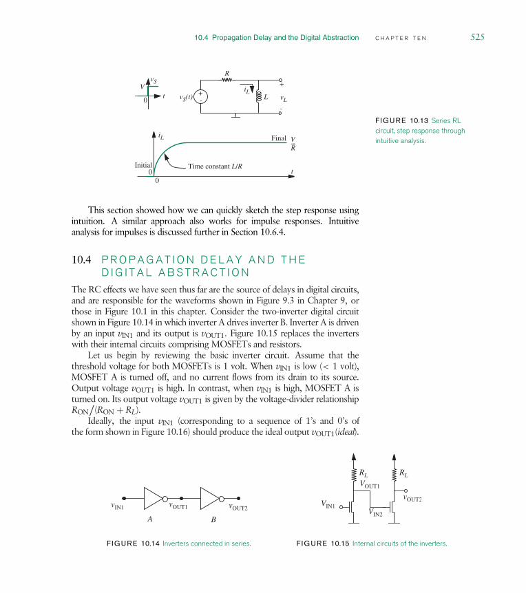
10.4 Propagation Delay and the Digital Abstraction C H A P T E R T E N 525
vSV
t
t
iL
vS(t)
R
L vL
+
-
+-
iL
Time constant L/R
VR----
0
Initial
Final
00
F IGURE 10.13 Series RLcircuit, step response throughintuitive analysis.
This section showed how we can quickly sketch the step response usingintuition. A similar approach also works for impulse responses. Intuitiveanalysis for impulses is discussed further in Section 10.6.4.
10.4 P R O P A G A T I O N D E L A Y A N D T H ED I G I T A L A B S T R A C T I O N
The RC effects we have seen thus far are the source of delays in digital circuits,and are responsible for the waveforms shown in Figure 9.3 in Chapter 9, orthose in Figure 10.1 in this chapter. Consider the two-inverter digital circuitshown in Figure 10.14 in which inverter A drives inverter B. Inverter A is drivenby an input vIN1 and its output is vOUT1. Figure 10.15 replaces the inverterswith their internal circuits comprising MOSFETs and resistors.
Let us begin by reviewing the basic inverter circuit. Assume that thethreshold voltage for both MOSFETs is 1 volt. When vIN1 is low (< 1 volt),MOSFET A is turned off, and no current flows from its drain to its source.Output voltage vOUT1 is high. In contrast, when vIN1 is high, MOSFET A isturned on. Its output voltage vOUT1 is given by the voltage-divider relationshipRON
/(RON + RL).
Ideally, the input vIN1 (corresponding to a sequence of 1’s and 0’s ofthe form shown in Figure 10.16) should produce the ideal output vOUT1(ideal).
A B
vOUT1 vOUT2vIN1
F IGURE 10.14 Inverters connected in series.
RL RL
VIN1
VOUT1
vOUT2
VIN2
F IGURE 10.15 Internal circuits of the inverters.

526 C H A P T E R T E N f i r s t - o r d e r t r a n s i e n t s
F IGURE 10.16 Characteristicsof ideal and actual inverters.
tpd,1 0
5 V
0.2 V vOUT1(Ideal)
5 V
0.2 V vOUT1(Actual)
5 V
0 V vIN1
VOH VOL
tpd,0 1 tpd,1 0
A B
As shown in Figure 10.16, the output of an ideal inverter should show a changeat the same instant as the input. Furthermore, the output should be an idealsquare wave just like the input.
However, in practice, if we were to observe the output vOUT1 on an oscil-loscope, we would notice that the change in the output is not instantaneous;rather the output changes from one valid voltage level (for example, a logical 0)to another valid voltage level (for example, a logical 1) more slowly over a smallperiod of time as suggested by the signal marked vOUT1(actual) in Figure 10.16.How does this slow transition affect the behavior of the digital circuit?
Recall that the vOUT1 signal represents a digital signal, so it must reach VOHso that the gate that produced it adheres to the static discipline and we obtaina nonzero noise margin. As suggested in the lowermost signal in Figure 10.16,notice that the VOH crossing happens at a time interval tpd,1→0 after the inputchanges from a 1 to a 0. Thus, effectively, there is a delay of tpd,1→0 between themoment that the input changes to a 0 to the moment that the output changesto a valid 1.
This period of time is called the propagation delay6 through inverter A for a 1to 0 transition at the input and is denoted as tpd,1→0.
As suggested in the lowermost signal in Figure 10.16,
the inverter is also characterized by a 0 → 1 propagation delay. This delay isdenoted as tpd,0→1.
The tpd,1→0 and tpd,0→1 delays are not necessarily equal. For simplicity, weoften characterize digital gates by a single delay called its propagation delay tpdand choose
tpd = max(tpd,1→0, tpd,0→1). (10.63)
6. The propagation delay is sometimes defined as the time interval from the 50% point of the inputsignal transition to the 50% point of the output signal transition.

10.4 Propagation Delay and the Digital Abstraction C H A P T E R T E N 527
10.4.1 D E F I N I T I O N S O F P R O P A G A T I O N D E L A Y S
The following are more general definitions of propagation delays associatedwith digital gates with multiple inputs and outputs. The reader wishing toreturn to the computation of tpd for our inverter example can skip this sectionwithout loss of continuity and proceed directly to Section 10.4.2.
tpd,1→0 We define tpd,1→0 for a given input terminal and a given output termi-nal of a combinational digital circuit as the signal propagation delay fromthe input terminal to the output terminal for a high to low instantaneoustransition at the input. More precisely, tpd,1→0 for an input-output terminalpair is the time interval from the moment that the input changes from a 1to a 0 to the moment that the output reaches a corresponding valid outputvoltage level (VOH or VOL).
tpd,0→1 Similarly, we define tpd,0→1 for a given input terminal and a given outputterminal of a combinational circuit as the signal propagation delay throughinput-output terminal pair for a low to high instantaneous transition at theinput. More precisely, tpd,0→1 for an input-output terminal pair is the timeinterval from the moment that the input changes from a 0 to a 1 to themoment that the output reaches a corresponding valid output voltage level.
tpd for an Input-Output Terminal Pair: We define the propagation delay tpdbetween an input terminal and an output terminal of a combinationalcircuit as
tpd = max(tpd,1→0, tpd,0→1)
where tpd,1→0 and tpd,0→1 are the corresponding 1 → 0 and 0 → 1 delaysfor the same input-output terminal pair.
Propagation Delay tpd for a Combinational Gate: If ti,jpd is the propagation delaybetween input terminal i and output terminal j of a digital gate, then thepropagation delay of the gate is given by
tpd = maxi,jti,jpd ,
which is the maximum delay of all input to output paths. The propagationdelay is also called the gate delay.
In the simple example shown in Figure 10.16, the propagation delaythrough the inverter for a low to high transition at the input, tpd,0→1, is alsoequal to the rise time of the output of the inverter. Similarly, tpd,1→0, is alsoequal to the fall time of the inverter output. The rise and fall times are propertiesof output terminals of circuits, while propagation delays measure the relative

528 C H A P T E R T E N f i r s t - o r d e r t r a n s i e n t s
signal transition times between inputs and outputs of circuits. The rise and falltimes are defined as follows:7
Rise Time In general, the rise time for an output is defined as the delay in risingfrom its lowest value to a valid high (VOH) at that output.Fall Time The fall time for an output is defined as the delay in falling from itshighest value to a valid low (VOL) at the same output.
In general, the propagation delay and the rise/fall time are not equal. The0 → 1 propagation delay for a digital circuit is the time between an input 0 to1 transition (the input transition is assumed to happen instantaneously) and thecorresponding output transition. The output transition is assumed to completeonly when the output voltage crosses the appropriate output voltage threshold.The propagation delay and the rise/fall times are usually not equal when thedigital circuit consists of multiple stages. When a circuit consists of multiplestages, the rise/fall time at the output is usually a function of the propertiesof the output circuit alone. However, the propagation delay is the sum of thedelays of each of the stages.
How does the propagation delay impact our digital abstraction? Noticethat the slowly rising output of the inverter now spends a nonzero amount oftime in the invalid output voltage range, namely VIL → VIH. This appears toviolate the static discipline. Recall that the static discipline requires that devicesproduce valid output voltages that satisfy the output thresholds when valid inputvoltages are supplied. We get around this difficulty by observing that the inverteroutput eventually crosses the valid output threshold. Furthermore, notice thatthe static discipline does not take a position on time. In other words, it doesnot require gates to produce valid outputs instantaneously if the inputs change.Accordingly, to make the this fact explicit, we can modify the statement of thestatic discipline by requiring that devices produce valid output voltages (in a finiteamount of time) that satisfy the output thresholds when valid input voltages aresupplied.
Revised statement of the static discipline The static discipline is a specificationfor digital devices. The static discipline requires devices to interpret correctlyvoltages that fall within the input thresholds (VIL and VIH). Provided valid
7. The rise and fall times are sometimes defined slightly differently. For example, the rise time of anode that transitions from a low to a high voltage might be defined as the time taken by a signalat that node to rise from 5% to 95% of the change in voltage. Alternatively, the rise time can bedefined as the time taken by a signal at that node to rise from a valid low voltage VOL to a validhigh voltage VOH. As one more possibility, the rise time might be defined as the time taken bya signal to rise from its lowest value to 50% of the voltage difference. Corresponding definitionsfor the fall time also exist. The vagueness of these definitions only serves the interests of productmarketeers, but for us, the important thing to learn is how to calculate the time intervals betweenany pair of signal values.

10.4 Propagation Delay and the Digital Abstraction C H A P T E R T E N 529
inputs are provided to the devices, the discipline also requires the devices toproduce valid output voltages (in a finite amount of time) that satisfy the outputthresholds (VOL and VOH).
We can also refine our combinational gate abstraction to include the notionof a propagation delay, so that the abstraction remains valid in the presence oftransitioning signals. Recall, the properties of a combinational gate as previouslydefined in Chapter 5.3: (1) The gate’s outputs are a function of its inputs aloneand (2) the gate must satisfy the static discipline. In the presence of a finite gatedelay, there is a small period of time following an input transition in which theoutputs do not reflect the new inputs; rather they reflect the old inputs. Thus ourpreviously defined gate abstraction is violated. We negotiate this inconsistencyby introducing a timing specification into our gate abstraction.
Revised statement of the combinational gate abstraction A combinational gateis an abstract representation of a circuit that satisfies these properties:
1. Its outputs will be valid no later than tpd after an instantaneous change inits inputs.
2. Its outputs are a function of its inputs alone (after an interval of time nogreater than tpd following a change in its inputs).
3. It satisfies the static discipline.
Now that we have included the propagation delay of a device in its abstractspecification, an additional benefit results: A gate-level circuit will now carryinformation on both its logic function and its speed. A rough estimate of thedelay from any input to any output of a logic circuit along a path with multiplegates can be obtained by summing the propagation delays of each of the gatesin that path. Thus, for example, if inverters are characterized by a tpd of 1 nsand OR gates with a tpd of 2 ns, then in the circuit in Figure 5.16 in Chapter 5,the delay from the input A to output C would be 2 ns, while the delay fromthe input B to output C would be 3 ns. If digital circuit designers need moreaccurate timing information for a circuit comprising multiple devices, or if theyneed to derive the tpd of a single device, then they must use the analysis methodsdiscussed in the ensuing sections.
10.4.2 C O M P U T I N G tpd F R O M T H ES R C M O S F E T M O D E L
Let us now compute the magnitude of the propagation delay. We use the switch
D
S
G
OFF State
CGS
vGS < VT
D
RON
ON State
vGS ≥ VT
S
G
CGS
F IGURE 10.17 The switch-resistor capacitor model of theMOSFET.
resistor capacitor (SRC) model of the MOSFET introduced in Section 9.3.1 todetermine this delay. Recall that we augmented the SR model of the MOSFETwith a gate-to-source capacitor and created the SRC MOSFET model shownin Figure 10.17.

530 C H A P T E R T E N f i r s t - o r d e r t r a n s i e n t s
Recall that the propagation delay results from the finite amount of timerequired for the output to transition from a given valid output voltage level toanother when the input to the circuit transitions. The slower transition at theoutput is attributable to RC effects. Figure 10.18 replaces the inverters with
RL RL
VIN1
VOUT1
vOUT2
VIN2
F IGURE 10.18 Internal circuitsof the inverters.
their internal circuits comprising MOSFETs and resistors. Figure 10.19 furtherreplaces the MOSFETs with their SRC circuit model when vIN1 applied to theinverter A corresponds to a logical 1. For this vIN1, the MOSFET in inverter Awill be on, and the MOSFET in inverter B will be off. Similarly, Figure 10.20shows the circuit model when vIN1 applied to inverter A corresponds to alogical 0. For this vIN1, the MOSFET in inverter A will be off, and the MOSFETin inverter B will be on. Thus, when alternating logical 1’s and 0’s are appliedto the input to the inverter pair, and the inverters are allowed to reach steadystate after each transition, the equivalent circuit model alternates between thetwo circuits in Figures 10.19 and 10.20.
Let us first analyze the circuit qualitatively. Consider the case where vIN1 hasbeen high for a long period of time and focus on the part of the circuit boundedby the dashed box in the Figure 10.19, which includes the load resistor andRON of inverter A and the gate-to-source capacitor of inverter B. Since thecircuit is in its steady state, the capacitor behaves as an open circuit, and so thevoltage across the capacitor will be established by the voltage-divider subcircuitcomprising the supply VS, and the resistors RL and RON. Assuming RL RON,the capacitor voltage will have a low value (close to 0 volts).
F IGURE 10.19 SRC circuitmodel of inverters connected inseries when the input is high.
VS
RON
RL
VS
RLvIN1
CGS1
vOUT1
CGS2
vOUT2
F IGURE 10.20 SRC circuitmodel of inverters connected inseries when the input is low.
VS
RON
RL
VS
RL
vIN1
CGS1
vOUT1
CGS2
vOUT2

10.4 Propagation Delay and the Digital Abstraction C H A P T E R T E N 531
Next, focus on the time instant when the input voltage vIN1 switches froma high to a low value (for example, 5 to 0 volts), turning the first MOSFET off.At this transition instant, the capacitor CGS2 is almost completely discharged(assuming that RL RON for the inverters). Therefore, the voltage acrossCGS2, which corresponds to the voltage vOUT1 on the output of inverter A, willbe initially close to 0 V. This is depicted as the time instant A in Figure 10.16.
After the first MOSFET turns off, Figure 10.20 applies. Focus again on thepart of the circuit bounded by the dashed box. It is easy to see that the circuitinside the dashed box is a first-order RC circuit. Remember, the voltage acrossCGS2 is low initially. Now, VS begins to charge CGS2 through the resistor RL.The equivalent RC circuit for the devices in the box are shown in Figure 10.21.As the capacitor charges up, the output voltage of inverter A rises. This voltagemust rise above the valid logical output high threshold, namely VOH, to satisfythe static discipline. Notice that although the second MOSFET will turn onwhen vOUT1 crosses its VT threshold (for example, 1 V), we require vOUT1 toreach VOH to achieve a modest noise margin. Notice that the presence of thecapacitor CGS2 makes vOUT1 take a finite amount of time to rise to the requiredVOH level. As we saw before, this interval of time is called the propagation delayfor the inverter for a high to low transition at the input and is denoted by tpd,1→0.As discussed earlier, the output capacitor charge-up time is also called the risetime of the inverter.
VS
+
-
RL
CGS2
vOUT1
iC+
-
vC
F IGURE 10.21 Equivalentcircuit when CGS2 is charging.
Next, let us consider the time instant when the input voltage switches from0 volts to 5 volts, turning the first MOSFET on. Let us assume that this 0-V to5-V transition happens after a sufficiently long period of time so that CGS2 isinitially charged up to its steady state value of 5 V. When the first gate is turnedon, CGS2 begins to discharge. The RC circuit and its Thévenin equivalent for thedischarge is shown in Figure 10.22. For the logical 0 to logical 1 transition at theinput to be reflected at the output of inverter A, the voltage across CGS2 needsto go below the valid logical output low threshold, VOL. As before, althoughMOSFET B will turn off when vOUT1 drops below 1 volt, we require the outputto go below VOL to provide for an adequate noise margin. The interval of timecorresponding to the output capacitor discharge for an inverter is also calledthe propagation delay for the inverter for a low to high transition at the input and
VS
+
-
RL
RON+-
RL||RON
(a) RC circuit model (b) Thévenin equivalent network
CGS2
VOUT1
CGS2VSRON
RON + RL----------------------- F IGURE 10.22 Equivalent
circuit when CGS2 is discharging.

532 C H A P T E R T E N f i r s t - o r d e r t r a n s i e n t s
is denoted by tpd,0→1. Furthermore, as stated previously, the output capacitordischarge time is also called the fall time of inverter A.
The propagation delay tpd for inverter A is simply taken as the maximumof tpd,0→1 and tpd,1→0.
At this point, it is worth discussing a slight mismatch between the digitalgate abstraction and the physical realities of computing the propagation delay.From the viewpoint of the digital gate abstraction, the propagation delay tpd isa property of the digital gate. Accordingly, we might say that an inverter (forexample, one identical to inverter A) always has a propagation delay of 2 ns.However, the example discussed thus far illustrates that the propagation delayof an inverter depends not only on the characteristics of its internal compo-nents, but also on the size of the capacitance that it is driving, and therefore thepropagation delay of the inverter can change depending on its environment.In particular, the propagation delay of inverter A in our example depends onthe input capacitance of inverter B. Thus, strictly speaking, it makes no senseto define the propagation delay of a device in isolation. However, for conve-nience, we would like to characterize devices with a single tpd without definingtheir surrounding environment, so this simple device model can be used toobtain quick estimates of digital circuit delays when multiple gates are con-nected together. Accordingly, unless explicitly stated otherwise, device librariesor catalogs define a tpd for a gate assuming it is driving a ‘‘typical’’ loadcommonly, four minimum sized inverters.8
Computing tpd,0→1
Let us now determine quantitatively the propagation delay for a low to hightransition at the input of the inverter. Assume through the rest of this examplethat a valid output low voltage, VOL, is 1 volt, and that a valid output highvoltage, VOH, is 4 volts. Also assume RON is 1 k, and that the thresholdon-voltage for the MOSFET is 1 volt. Also assume that RL is 10 k.
In this case, as discussed earlier, CGS2 is initially charged to 5 volts. Weneed to determine the time taken for the capacitor voltage to drop from 5 toVOL = 1 volts.
When the input is high, Figure 10.22 shows the equivalent circuit. Let usdenote the Thévenin equivalent resistance RL‖RON as RTH, and the Théveninequivalent voltage VSRON/(RON +RL) as VTH. Let us also denote the capacitorvoltage vOUT1 by vC, and the current through the circuit by iC as shown inFigure 10.23.
VTH+
-
RTH
CGS2
iC
vC
F IGURE 10.23 Equivalentcircuit when CGS2 is discharging.
8. A related metric that is sometimes used to characterize the speed of a process technology is calledthe fan-out-of-4 (or FO4) delay. The FO4 delay for a process technology is the propagation delayof a minimum sized inverter driving four other inverters of the same size.

10.4 Propagation Delay and the Digital Abstraction C H A P T E R T E N 533
Using the node method, we obtain,
vC − VTH
RTH+ CGS2
dvC
dt= 0.
Rearranging,
RTHCGS2dvC
dt+ vC = VTH. (10.64)
Solving Equation 10.64 yields
vC(t) = VTH + Ae−t/RTHCGS2 . (10.65)
Substituting the initial condition vC(0) = VS, we obtain the final solution:
vC(t) = VTH + (VS − VTH)e−t/RTHCGS2 . (10.66)
How long does it take for vC to drop below 1 volt? To obtain this duration,we must solve for the value of t that satisfies
VTH + (VS − VTH)e−t/RTHCGS2 < 1.
In other words,
t > −RTHCGS2 ln(
1 − VTH
VS − VTH
).
For RL = 10 k and RON = 1 k, RTH = 10000/11, and VTH = VS/11.Substituting VS = 5 V and VTH = 5/11 V, the value of t must satisfy
t > −RTHCGS2 ln(
3
25
).
Substituting for RTH, the value of t must satisfy
t > −10000
11CGS2 ln
(3
25
). (10.67)
Suppose the gate capacitance CGS2 = 100 fF. We then have
t > −10
11× 103 × 100 × 10−15 × ln(3/25)
or,
t > 0.1928 ns. (10.68)
Thus tpd,0→1 = 0.1928 ns.
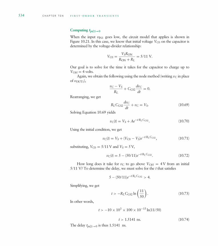
534 C H A P T E R T E N f i r s t - o r d e r t r a n s i e n t s
Computing tpd,1→0
When the input vIN1 goes low, the circuit model that applies is shown inFigure 10.21. In this case, we know that initial voltage VC0 on the capacitor isdetermined by the voltage-divider relationship:
VC0 = VSRON
RON + RL= 5/11 V.
Our goal is to solve for the time it takes for the capacitor to charge up toVOH = 4 volts.
Again, we obtain the following using the node method (writing vC in placeof vOUT1),
vC − VS
RL+ CGS2
dvC
dt= 0.
Rearranging, we get
RLCGS2dvC
dt+ vC = VS. (10.69)
Solving Equation 10.69 yields
vC(t) = VS + Ae−t/RLCGS2 . (10.70)
Using the initial condition, we get
vC(t) = VS + (VC0 − VS)e−t/RLCGS2 , (10.71)
substituting, VC0 = 5/11 V and VS = 5 V,
vC(t) = 5 − (50/11)e−t/RLCGS2 . (10.72)
How long does it take for vC to go above VOH = 4 V from an initial5/11 V? To determine the delay, we must solve for the t that satisfies
5 − (50/11)e−t/RLCGS2 > 4.
Simplifying, we get
t > −RLCGS2 ln(
11
50
). (10.73)
In other words,
t > −10 × 103 × 100 × 10−15 ln(11/50)
t > 1.5141 ns. (10.74)
The delay tpd,1→0 is thus 1.5141 ns.

10.4 Propagation Delay and the Digital Abstraction C H A P T E R T E N 535
Notice the RLCGS2 factor in Equation 10.73. In typical circuits, a ballparkestimate of the delay can be obtained by simply taking the product of thecapacitance and the effective resistance through which it charges. In our case,tpd,1→0 ≈ RLCGS2 = 10 × 103 × 100 × 10−15 = 1 ns. Similarly, the ballparkestimate of tpd,0→1 is given by tpd,0→1 ≈ RTHCGS2 = 10/11 × 103 × 100 ×10−15 = 0.09 ns.
Computing tpd
By our definition, the propagation delay of the gate tpd is the greater of therising and falling delays. In other words,
tpd = max(tpd,0→1, tpd,1→0).
Therefore, tpd = 1.5141 ns.
e x a m p l e 10.1 w i r e l e n g t h o n a v l s i c h i p In this exam-ple, we will examine how wire length becomes an important issue in the design of VLSIchips. Consider the inverter pair circuit in Figure 10.14. Suppose the two inverters areon the opposite ends of a chip that is 1 cm on a side. The resulting long wire connectingthem can no longer be treated as an ideal conductor with no resistance or capacitance.Instead we must replace the wire with an ideal wire in combination with a wire capaci-tance and a wire resistance. The resulting RC delays can be significantly higher than theRC delays of inverters connected to each other with short wires.
Figure 10.24 depicts graphically the wire connecting the two inverters on the VLSI chip.Assume the wire is of length L and width W. The MOSFETs have gate lengths Lg andgate widths Wg. Since the length of the wire is significant, we need to model it carefully.Let the wire resistance be denoted Rwire and the wire capacitance Cwire. The circuitmodel for the inverter pair taking into account wire parasitics is shown in Figure 10.25.
MOSFETMOSFET
W
L
Long wireInsulated
(Grounded)substrate
Connectedto otherdevices F IGURE 10.24 Long wire on a
VLSI chip.

536 C H A P T E R T E N f i r s t - o r d e r t r a n s i e n t s
F IGURE 10.25 Circuit model oflong wire on a VLSI chip.
VS
vIN1
CGS1RON
RL
VS
RON
RL
CGS2
vC vOUT2
Cwire
Rwire
vOUT1
(Here we assume that the parasitic inductance of the wire according to the model inFigure 9.7 in Chapter 9 is zero.)
If the sheet resistance of the wire is R (see Equations 1.10 and 1.9), we know,
Rwire = (L/W)R.
Similarly, if Co is the capacitance per unit area of the wire, (formed between the wire,insulation, and the grounded substrate), we know
Cwire = LWCo.
Clearly, the longer the wire, the larger its capacitance and resistance. Recalling thatdelays are related to the RC time constants, notice that the RC product for the wire is
RwireCwire = (L/W)R × LWCo = L2RCo.
The L2 term in the RC product implies that wire delays grow as the square of wirelengths. Assume that the wire is 1 µm wide and 1000 µm long. Further, assume R is2 and Co is 2 fF/µm2. Therefore,
Rwire = 1000 × 2 = 2 k
and
Cwire = 1000 × 2fF = 2 pF.
The RC time constant for the wire is
VS
+
-
RL+Rwire
CGS2+Cwire
vC
F IGURE 10.26 Charging thewire capacitor on a VLSI chip.
RwireCwire = 2 × 103 × 2 × 10−12 = 4 ns.
Figures 10.26 and 10.27 show the relevant circuit models for charging and dischargingthe wire capacitance Cwire and gate capacitance CGS2. Let us assume values for VOL

10.4 Propagation Delay and the Digital Abstraction C H A P T E R T E N 537
VS
+
-
RL
RON+
-
RL||RON+Rwire
VTH
(a) RC Circuit Model (b) Thévenin Equivalent Network
Rwire
CGS2+CwireCGS2+Cwire
vC vC
F IGURE 10.27 Discharging thewire capacitor on a VLSI chip.
and VOH to be the same as those used in Section 10.4.2. In other words, VOH = 4Vand VOL = 1V.
When the input VIN1 transitions from high to low, Figure 10.26 applies, and we canuse the results from Section 10.4.2 to compute the propagation delay tpd,1→0 by using(RL + Rwire) in place of RL and (CGS2 + Cwire) in place of CGS2. Thus, the propagationdelay for RL = 10 k, RON = 1 k, CGS2 = 100 fF is given by
tpd,1→0 = −(RL + Rwire) × (CGS2 + Cwire) ln(11/50)
= −(10 + 2) × 103 × (100 + 2000) × 10−15 × ln(11/50).
Thus,
tpd,1→0 = 38.15 ns. (10.75)
When the input vIN1 makes a low to high transition, Figure 10.27 applies, and wecan use the results from Section 10.4.2 to compute the propagation delay tpd,0→1 with(RL‖RON +Rwire) in place of RTH and (CGS2 +Cwire) in place of CGS2. For RL = 10 k,RON = 1 k, CGS2 = 100 fF, we get:
tpd,0→1 = −(RL‖RON + Rwire)(CGS2 + Cwire) ln(3/25)
= −(
10
11+ 2
)× 103 × (100 + 2000) × 10−15 × ln(3/25),
or,
tpd,0→1 = 12.9 ns. (10.76)
Thus, we see that tpd,0→1 = 12.9 ns, which is significantly higher than the delay whenthe wire effects were not included.
Choosing the larger of the rise and fall delays, we observe that tpd = 38.15 ns. Clearly,the wire delay has increased the circuit delay by more than an order of magnitude.
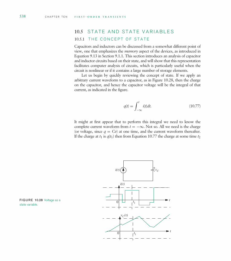
538 C H A P T E R T E N f i r s t - o r d e r t r a n s i e n t s
10.5 S T A T E A N D S T A T E V A R I A B L E S
10.5.1 T H E C O N C E P T O F S T A T E
Capacitors and inductors can be discussed from a somewhat different point ofview, one that emphasizes the memory aspect of the devices, as introduced inEquation 9.13 in Section 9.1.1. This section introduces an analysis of capacitorand inductor circuits based on their state, and will show that this representationfacilitates computer analysis of circuits, which is particularly useful when thecircuit is nonlinear or if it contains a large number of storage elements.
Let us begin by quickly reviewing the concept of state. If we apply anarbitrary current waveform to a capacitor, as in Figure 10.28, then the chargeon the capacitor, and hence the capacitor voltage will be the integral of thatcurrent, as indicated in the figure.
q(t) =∫ t
−∞i(t)dt. (10.77)
It might at first appear that to perform this integral we need to know thecomplete current waveform from t = −∞. Not so. All we need is the charge(or voltage, since q = Cv) at one time, and the current waveform thereafter.If the charge at t1 is q(t1) then from Equation 10.77 the charge at some time t2
F IGURE 10.28 Voltage as astate variable.
t0
i(t)
i(t) vC+-
t1
t0
vC (t)
t1

10.5 State and State Variables C H A P T E R T E N 539
greater than t1 is
q(t2) =∫ t1
−∞i(t) +
∫ t2
t1i(t)dt (10.78)
= q(t1) +∫ t2
t1i(t)dt. (10.79)
All of the relevant past history of the circuit prior to t1 is summarized inone value, q(t1). Variables that have this property are called state variables. ThusEquation 10.79 indicates that if we know the value of the state variable at onetime, and the value of the input variable thereafter, we can find the value of thestate variable for any subsequent time.
For linear time-invariant capacitors, the capacitor voltage is also a statevariable, because
q = Cv.
For an inductor, the fundamental state variable is the total flux linked by theinductor, λ. Recall from Equation 9.32, if the inductor is linear and time-invariant, the current is equally appropriate as a state variable since it is linearlyrelated to λ as
i = λ
L.
From this point of view, the first-order differential equations for the RC and RLcircuits, Equations 10.2, 10.42, and 10.46 can all be written as state equations
d
dt(state variable) = f (state variable, input variable). (10.80)
For the linear case, f is a linear function, so Equation 10.80 becomes
d
dt(state variable) = K1(state variable present value) + K2(input variable).
(10.81)For example, consider Equation 10.2 for the circuit in Figure 10.2a:
dvC
dt+ vC
RC= i(t)
C
This equation can be written in the canonic state equation form of Equa-tion 10.81 as
dvC
dt= − vC
RC+ i(t)
C(10.82)
where the only state variable is vC.

540 C H A P T E R T E N f i r s t - o r d e r t r a n s i e n t s
10.5.2 C O M P U T E R A N A L Y S I S U S I N GT H E S T A T E E Q U A T I O N
One advantage of the state equation formulation is that even in the nonlinearcase, the equations can be readily solved on a computer.9 If the input signaland the initial value of the state variable are known, then the slope of the statevariable, that is,
d
dt(state variable)
can be found from Equation 10.81. The value of the state variable at timet + t can now be estimated by standard numerical methods (Euler’s method,Runge-Kutta, etc.). The process can now be repeated until the entire waveformis found.
Continuing with our example in Equation 10.82, suppose that the inputsignal i(t) is known for all time. Also, suppose that the value of the state variableat time t = t0, namely vC(t0), is known. Then, Euler’s method10 approximatesthe value of the state variable at time t = t0 + t as
vC(t0 + t) = vC(t0) − vC(t0)
RCt + i(t0)
Ct. (10.83)
The value of vC at time t = t0 +2t can be determined in like manner from thevalue of vC(t0 + t) and i(t0 + t). Subsequent values of vC can be determinedusing the same process. By choosing small enough values of t, a computercan determine the waveform for vC(t) to an arbitrary degree of accuracy. Thisprocess illustrates the fact that the initial state contains all the information that isnecessary to determine the entire future behavior of the system from the initialstate and the subsequent input.
This procedure works even for circuits with many capacitors and inductors,linear or nonlinear, because these higher-order circuits can be formulated interms of a set of first-order state equations like Equation 10.80, one for eachenergy-storage element (with an independent state variable) in the network.Chapter 12 discusses such an example in Section 12.10.1.
9. To build intuition, we will describe a simple computer method here. However, we note thatother more efficient methods are employed in practice.
10. Euler’s method is based on the following discrete approximation:
dvC(t)
dt≈ vC(t + t) − vC(t)
t.

10.5 State and State Variables C H A P T E R T E N 541
t0
V2
V1 > V2
V1 = V2
V1 < V2
(b)
vC
vCC
+
-
(1)
(2)
(a)
V1 V2
+
-
+
-
R
F IGURE 10.29 Transient withinitial charge on capacitor.10.5.3 Z E R O - I N P U T A N D Z E R O - S T A T E R E S P O N S E
Another advantage of the state variable point of view is that it allows us tosolve transient problems by superposition. Specifically, we find first the zero-input response, the response for the true initial conditions, with the input drivezero. Then we find the zero-state response, the response of the circuit whenthe initial state is zero, that is, all capacitor voltages and inductor currents areinitially zero. The total response is the sum of the zero-input response (ZIR)and the zero-state response (ZSR).
Relating these ideas to Equation 10.81, finding the zero-input-responseinvolves solving the equation:
d
dt(state variable) = K1(state variable present value) (10.84)
using the true initial conditions for the state variable. Finding the zero-state-response involves solving the equation:
d
dt(state variable) = K1(state variable present value) + K2(input variable)
(10.85)with the initial value of the state variable set to 0.
Let us illustrate these ideas with an example. The circuit shown inFigure 10.29a contains a switch, which is moved from position (1) to posi-tion (2) at t = 0. If the switch has been in position (1) for a long time, thecapacitor will be charged to the voltage V1. That is, the initial condition for thecircuit is
vC = V1 t < 0. (10.86)
When the switch is moved to position (2), there will be a transient charge (ordischarge) until the capacitor voltage reaches a new steady state.

542 C H A P T E R T E N f i r s t - o r d e r t r a n s i e n t s
The governing differential equation is the same as the previous capacitorexample in Section 10.1.4, Equation 10.42:
vI = RCdvC
dt+ vC. (10.87)
Writing the same equation in canonic state equation form, we get
dvC
dt= − vC
RC+ vI
RC. (10.88)
First, let us first solve for the capacitor voltage directly by finding the homoge-neous solution and particular solution. We will then derive the capacitor voltageby obtaining the ZIR and ZSR.
The homogeneous solution is
vC = Ae−t/RC. (10.89)
By inspection from Equation 10.89, the particular solution must be
vC = V2. (10.90)
The complete solution is the sum of these two:
vC = Ae−t/RC + V2. (10.91)
Equating Equation 10.91 at t = 0 to the stated initial condition, Equation 10.86,
vC = V1 = A + V2. (10.92)
A = V1 − V2. (10.93)
Hence the complete solution for t > 0 is
vC = V2 + (V1 − V2)e−t/RC. (10.94)
Plots of this result are shown in Figure 10.29b. As indicated, the responsedepends on the relative size of V1 and V2. For one particular value, namelyV1 = V2, there is no transient, as is obvious from physical considerations.
In Equation 10.94 the first term is the particular solution, and the secondis the homogeneous solution.
Next, to obtain insight into the method involving the ZIR and ZSR, a trivialrewrite of Equation 10.94 yields
vC = V1e−t/RC + V2(1 − e−t/RC). (10.95)
Now the first term is the response to an initial state, in this case an initialcapacitor, and no input. This we call the zero-input response (ZIR). The second

10.5 State and State Variables C H A P T E R T E N 543
V1 vC
+
-
C
+
-
(1)
(2)
R
(a)
t0
vC
V1
(b)
F IGURE 10.30 Zero-inputsubcircuit and response.
term is the response to an external input, for no initial capacitor charge: thezero-state response (ZSR).11 To verify, let us now solve directly for the ZIRand the ZSR by superposition.
The subcircuit for finding the ZIR is shown in Figure 10.30a. As before,the capacitor is initially charged to V1, but here the input for t > 0 is zero, soafter the switch moves to position (2), the capacitor simply discharges to zero.Formally, the corresponding equation to be solved to obtain the ZIR is
dvC
dt= − vC
RC(10.96)
with the initial condition on the capacitor voltage being V1.The homogeneous solution is
vC = V1e−t/RC. (10.97)
This is the complete zero-input response, because the particular solution is zero.The subcircuit for finding the zero-state response is shown in Figure 10.31a.The corresponding equation to be solved to obtain the ZSR is
dvC
dt= − vC
RC+ vI
RC. (10.98)
with the initial condition on the capacitor voltage chosen as 0.
t
vC
(b)0
V1vC
+
-
C+
-
(1)
(2)R
(a)
F IGURE 10.31 Zero-statesubcircuit and response.
11. Notice the similarity between this and Equation 10.62.

544 C H A P T E R T E N f i r s t - o r d e r t r a n s i e n t s
The homogeneous solution is as in Equation 10.89, and the particularsolution is again V2, so the solution is of the form
vC = Ae−t/RC + V2. (10.99)
This time by definition the initial condition is zero, so evaluating right after theswitch is thrown,
0 = A + V2 (10.100)
and the complete zero-state response for t > 0 is
vC = V2(1 − e−t/RC). (10.101)
The total response is the sum of the ZIR and ZSR from Equations 10.101and 10.97 and is given by
vC = V1e−t/RC + V2(1 − e−t/RC). (10.102)
Observe that Equation 10.102 agrees with the formulation of Equation 10.94.
Comments
The particular solution and the homogeneous solution are terms whichapply to a method of solving differential equations.
Zero-input and zero-state responses arise from a particular way of parti-tioning the circuit problem into two simpler subproblems. The resultingsubcircuits can be solved by finding the homogeneous solution andparticular solution in each case.
For the ZIR, the particular solution will by definition be zero. Hence allZIRs will be homogeneous solutions.
But all ZSRs are not particular solutions, because there is also ahomogeneous solution associated with the ZSR. The e−t/RC term inEquation 10.101 is an example of this.
A major advantage to the state variable point of view is that any arbi-trary ZIR can be added to any ZSR solution we have already worked out.Thus any transient problem with zero initial conditions can be easily gener-alized to one with arbitrary initial conditions. This concept will be illustratedin the examples in Section 10.6.
W W W 10.5.4 S O L U T I O N B Y I N T E G R A T I N G F A C T O R S *

10.6 Additional Examples C H A P T E R T E N 545
10.6 A D D I T I O N A L E X A M P L E S
10.6.1 E F F E C T O F W I R E I N D U C T A N C EI N D I G I T A L C I R C U I T S
Section 10.4 showed that RC effects lead to propagation delay in digital circuits.It turns out that when parasitic inductors are present, RL effects can be asimilar source of propagation delay. Consider the inverter circuit shown inFigure 10.32a. Assume that a poor design has resulted in a long wire connectingthe MOSFET drain to the output of the inverter. A circuit model of the invertershowing the parasitic wire inductance is depicted in Figure 10.32b.
Assume that the inverter has a 0-V input as an initial condition. TheMOSFET is in its off state and the current iL through the inductor L willbe 0. The voltage vL across the inductor is also 0. Now suppose that a 0-Vto VS-step is applied to the input of the inverter as illustrated in Figure 10.32a.Assume that our goal is to determine the current iL through the inductor andthe voltage vL across the inductor as a function of time.
The step input to the inverter results in a corresponding VS-step appliedto the RL circuit at the output of the inverter as illustrated in Figure 10.32c.From the initial conditions, at t = 0, both iL and vL are 0. From this point on,the situation is identical to that for the RL transient discussed in Section 10.2.1with V used in place of VS. Therefore the analysis presented in Section 10.2.1applies.
It is interesting to speculate as to what will happen if the switch inFigure 10.32c is opened after being closed for a long time. When the switch isopened, the inductor current cannot go to zero instantaneously. Since a prac-tical open switch behaves as an extremely high resistance, the current throughthe inductor will result in a huge voltage spike across the switch, and possiblydamage it.
10.6.2 R A M P I N P U T S A N D L I N E A R I T Y
Solutions become somewhat more complicated when we move beyond simplestep inputs. Consider the case of a series RC circuit with a voltage ramp drive,
vI
VSt
R
vI
vO
VS
(a) Inverter with a long wire connecting the output and the MOSFET drain
R
vI
vO
VS
L
(b) Circuit model (c) Circuit for step input at vI
VS
R
L vL
+
-
+- iL
Switch is closedat t = 0
F IGURE 10.32 Inverter circuitwith parasitic inductance.

546 C H A P T E R T E N f i r s t - o r d e r t r a n s i e n t s
that is
vI = S1t t > 0 (10.113)
where S1 has the dimensions of volts per second. The circuit and input waveformare sketched in Figures 10.33a and b. Let us first find the zero-state response,by assuming that the capacitor is initially uncharged. The differential equationis, from before,
vI = S1t = RCdvC
dt+ vC. (10.114)
We will solve this using our usual method of homogeneous and particularsolutions. The homogeneous solution has the usual form:
vC = Ae−t/RC. (10.115)
This homogeneous solution is plotted in Figure 10.33c. We must now find aparticular solution that is appropriate for a ramp input. Because the drive is aramp, a good first guess is a ramp of the same slope as the input:
vC = K2t. (10.116)
Substituting this into the differential equation, Equation 10.114, we obtain
S1t = RCK2 + K2t. (10.117)
Because there is no solution for K2 unless RC = 0, our initial guess for theparticular solution is not quite correct. We need another degree of freedom inthe solution, so an appropriate second guess is
vC = K2t + K3. (10.118)
Now from Equation 10.114:
S1t = RCK2 + K2t + K3. (10.119)
Whence
S1 = K2 (10.120)
K3 = −S1RC (10.121)
and the particular solution is
vC = S1(t − RC). (10.122)
This is a ramp with the same slope as the input ramp, except delayed in timeby one time constant, as shown in Figure 10.33d.

10.6 Additional Examples C H A P T E R T E N 547
t
vC
vC
+
-
CvI
R vI
S1 t
t
t
vC
t
vC
Homogeneous solution
(a) Circuit
(c) Homogeneous solution
Particular integral
0
0
0
Total solution
(e) Total solution
A
vI
t = RC
RC
RCS1
vI
+-
(b) Input
(d) Particular solution
F IGURE 10.33 Response of RC circuit to ramp.

548 C H A P T E R T E N f i r s t - o r d e r t r a n s i e n t s
The complete solution is of the form
vC = Ae−t/RC + S1(t − RC) for t > 0. (10.123)
Because we are finding the zero-state response, the initial condition is bydefinition zero, so evaluating Equation 10.123 at t = 0, we find
A = S1RC.
Hence the complete solution for t > 0 is
vC = S1(t − RC) + S1RCe−t/RC (10.124)
and is plotted in Figure 10.33e.The waveforms in Figures 10.33b and 10.33e are related in a special way to
those in Figures 10.2b and 10.2c. Note first that the input signal in this problemis the integral of the input signal in Figure 10.2 (assuming a Thévenin source).Now, from Figures 10.33e and 10.2c, or from Equations 10.124 and 10.20, theoutput signal here is the integral of the output signal in Figure 10.2,12 again,assuming that we are dealing with the zero-state response.
In general, as long as one restricts integral operations to t greater than zero,the zero-state response of the integral of some input signal is the integral of thezero-state response to that signal.
This follows from superposition if one considers integration as a summationprocess. In effect we are commuting two linear operators. The same is true fordifferentiation as well:
The response to a signal derived by differentiating an input can be obtained bydifferentiating the output.
Let us follow this example one step further, and consider the case where thereis an initial voltage V0 on the capacitor at t = 0, before the ramp is applied.
12. Notice that if we take the integral of Equation 10.20, namely,
vC = I0R(1 − e−t/RC)
we obtainvC = I0Rt + I0R RCe−t/RC + K1
where, to get the zero initial condition on vC, we set the constant of integration K1 = −I0R RC,and obtain
vC = I0R(t − RC) + I0R RCe−t/RC,
which is a Thévenin version of Equation 10.124.

10.6 Additional Examples C H A P T E R T E N 549
t
vC
Homogeneous solution
Particular integral
0
vI
Total solution
-S1RC
V0 + S1RC
V0F IGURE 10.34 Ramp responsefor initial charge on capacitor.
Formally, the initial condition now is
vC = V0 t < 0. (10.125)
This time around, since there is an initial condition on the capacitor, we are nolonger dealing with just the zero-state response, so we cannot simply take theintegral. One approach is to notice that Equation 10.124 is in effect the zero-state response, so if we find the zero-input response corresponding to the initialcondition of Equation 10.125, then the complete solution is the sum of thesetwo responses. We know from previous examples, or from Equation 10.97,that the ZIR for an RC circuit with an initial voltage V0 is
vC = V0e−t/RC (10.126)
so the total solution for t > 0 is
vC = V0e−t/RC + S1t − S1RC(1 − e−t/RC). (10.127)
One possible form of this solution is sketched in Figure 10.34. This exampleillustrates one of the advantages of the state-variable approach. Once we havefound the solution for some input waveform and zero initial conditions, thesolution for the same input with arbitrary initial conditions can be found byadding the appropriate ZIR solution.
e x a m p l e 10.2 t v d e f l e c t i o n s y s t e m Most television sets
iL
t
R
L iLvI
+-
F IGURE 10.35 TV deflectioncoil.
use magnetic deflection in the cathode-ray tube. To obtain the raster scan for thepicture, it is necessary to develop a ramp of current flowing through the deflectioncoil, as sketched in Figure 10.35. We wish to find the required waveform of vI that will

550 C H A P T E R T E N f i r s t - o r d e r t r a n s i e n t s
generate the current ramp. The coil losses have been explicitly modeled in Figure 10.35by the resistor R.
The differential equation for the circuit is, from KVL
vI = iR + Ldi
dt. (10.128)
We want a current waveform, for t > 0, of the form
i = S1t. (10.129)
Hence
vI = S1Rt + S1L (10.130)
for t > 0. Thus to produce a ramp of current in the inductor, we need to drive with thesum of a step and a ramp.
W W W e x a m p l e 10.3 s o l u t i o n b y i n t e g r a t i n g
f a c t o r s
10.6.3 R E S P O N S E O F A N R C C I R C U I T T O S H O R TP U L S E S A N D T H E I M P U L S E R E S P O N S E
It was shown in Section 10.1.4 that when the time constant of an RC circuitbecomes much longer than the period of a periodic input signal, the capacitorvoltage begins to approximate the integral of the input wave. Let us examine thisproperty in more detail by finding the response of the RC circuit in Figure 10.36when the input is a short pulse of amplitude Vp and duration tp.
We have seen several problems of this sort, so the general form of thecapacitor voltage can be written by inspection. Assuming that the capacitoris initially uncharged, the response during the pulse, when the capacitor ischarging is
vC = Vp
(1 − e−t/RC
)0 ≤ t ≤ tp. (10.135)
If tp is long enough for this transient to essentially go to completion, then att = tp, the end of the pulse, the capacitor voltage will be Vp. The response afterthe pulse has ended, when the capacitor is discharging, is thus
vC = Vpe−(t−tp)/RC t ≥ tp RC. (10.136)
The t − tp factor in the exponent indicates that there is a time delay in the startof the wave of an amount tp. This solution is shown in Figure 10.36b.

10.6 Additional Examples C H A P T E R T E N 551
ttp
ttp
vC
(a) Circuit
vC
+
-
CvI
R
Vp
Vp
vI
(b) Waveforms
vI
Vp
tpt
0
+-
F IGURE 10.36 Response of RCcircuit to pulse.
vI
Vp
tpt
0
ttp
Vp
vI
0
ttp
vC
(a)
Vp
0
Vp(1 – etp ⁄RC)
(b)
ttp
vC
Vp
0
Vp
tpRC--------
F IGURE 10.37 Response of RCcircuit to short pulse.
If the pulse is made shorter than in Figure 10.36, the charging transient canno longer reach completion. This is illustrated in Figure 10.37a. Equation 10.135is still appropriate for the charging interval, but the response no longer reachesVp. The maximum value, at t = tp, is
vC(tp) = Vp
(1 − e−tp/RC
). (10.137)
The discharge now has essentially the same form as before, but is smaller. Thatis, for t greater than tp, the capacitor voltage is
vC =[Vp
(1 − e−tp/RC
)]e−(t−tp)/RC. (10.138)

552 C H A P T E R T E N f i r s t - o r d e r t r a n s i e n t s
If we make the pulse even shorter yet, as in Figure 10.37b, the picture actuallybecomes simpler. The charging part of the wave begins to look almost like astraight line. Mathematically, this can be shown by expanding the exponentialin a series
e−x = 1 − x + x2
2! · · · (10.139)
when the charging waveform becomes, from Equation 10.135
vC = Vp
[t
RC− 1
2
(t
RC
)2
+ · · ·]
. (10.140)
For times much less than the time constant RC, that is, t RC, we candiscard all higher terms, leaving
vC Vpt
RC, (10.141)
which is the equation for the straight line we observe in the first part ofFigure 10.37b.
Physically, when the pulse is very short the capacitor voltage is alwaysmuch smaller than the pulse voltage, so during the pulse the current is roughlyconstant at a value
iC Vp
R. (10.142)
The capacitor voltage is the integral of this current, hence is a ramp:
vC = 1
C
∫iCdt (10.143)
Vpt
RC. (10.144)
At the end of the pulse, the capacitor voltage has reached its maximum value of
vC(tp) VptpRC
(10.145)
so the discharge waveform for t greater than tp is
vC [
VptpRC
]e−(t−tp)/RC. (10.146)
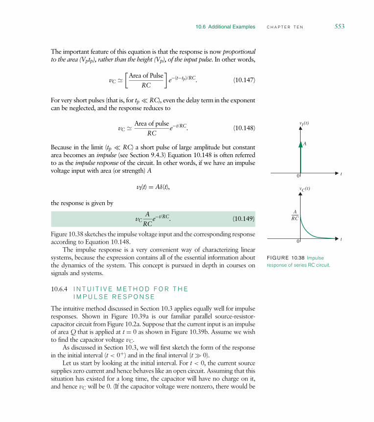
10.6 Additional Examples C H A P T E R T E N 553
The important feature of this equation is that the response is now proportionalto the area (Vptp), rather than the height (Vp), of the input pulse. In other words,
vC [
Area of Pulse
RC
]e−(t−tp)/RC. (10.147)
For very short pulses (that is, for tp RC), even the delay term in the exponentcan be neglected, and the response reduces to
vC Area of pulse
RCe−t/RC. (10.148)
Because in the limit (tp RC) a short pulse of large amplitude but constantarea becomes an impulse (see Section 9.4.3) Equation 10.148 is often referredto as the impulse response of the circuit. In other words, if we have an impulsevoltage input with area (or strength) A
vI(t) = Aδ(t),
the response is given by
vCA
RCe−t/RC. (10.149)
Figure 10.38 sketches the impulse voltage input and the corresponding responseaccording to Equation 10.148.
t
vI (t)
0
A
t
vC (t)
0
ARC--------
F IGURE 10.38 Impulseresponse of series RC circuit.
The impulse response is a very convenient way of characterizing linearsystems, because the expression contains all of the essential information aboutthe dynamics of the system. This concept is pursued in depth in courses onsignals and systems.
10.6.4 I N T U I T I V E M E T H O D F O R T H EI M P U L S E R E S P O N S E
The intuitive method discussed in Section 10.3 applies equally well for impulseresponses. Shown in Figure 10.39a is our familiar parallel source-resistor-capacitor circuit from Figure 10.2a. Suppose that the current input is an impulseof area Q that is applied at t = 0 as shown in Figure 10.39b. Assume we wishto find the capacitor voltage vC.
As discussed in Section 10.3, we will first sketch the form of the responsein the initial interval (t < 0+) and in the final interval (t 0).
Let us start by looking at the initial interval. For t < 0, the current sourcesupplies zero current and hence behaves like an open circuit. Assuming that thissituation has existed for a long time, the capacitor will have no charge on it,and hence vC will be 0. (If the capacitor voltage were nonzero, there would be

554 C H A P T E R T E N f i r s t - o r d e r t r a n s i e n t s
a current through R. This current would deplete the charge on the capacitor,till no charge exists.)C vC (t)
+
-i(t) R
t
vC (t)
0
t
i(t)
0
Q
QC----Initial
value
Finalvalue
(a)
(b)
(c)
Time constant RC
t
vC (t)
0
QC----Initial
value
Finalvalue
(d)
F IGURE 10.39 Intuitive methodof sketching the impulse responseof parallel RC circuit.
Next, the current impulse appears at t = 0. The capacitor behaves likean instantaneous short to the current impulse, and so the current favors thecapacitor over the resistor. The entire impulse current flows through the capaci-tor at t = 0, depositing charge Q on it. Corresponding to the appearance ofcharge Q on the capacitor, from Equation 9.8, the capacitor voltage jumpsinstantaneously to
vC(0) = Q
C.
Thus, at t = 0+ we are left with the voltage Q/C across the capacitor. Observethat the impulse has effectively established the initial conditions on the circuit.
This completes our intuitive analysis of the initial interval. vC during thisinterval is sketched in Figure 10.39c.
Next, we examine the final interval (t 0). Since its current is zero fort > 0, we can again replace the current source with an open circuit. After a longperiod of time, a DC situation exists, and the capacitor voltage will be zero.The zero value for vC for t 0 is also sketched in Figure 10.39c.
Finally, in the transition interval, the capacitor follows its usual expo-nential response with time constant RC. The complete curve is sketched inFigure 10.39d.
10.6.5 C L O C K S I G N A L S A N D C L O C K F A N O U T
In most digital systems, a clock signal is provided to different modules of thesystem. A clock signal is typically a square wave between 0 volts and the supplyvoltage. The clock signal provides a global time base that prescribes whenactions happen in systems. The use of a clock attempts to solve the followingproblem faced by the receiver in a pair of communicating digital systems: Howto determine when a signal supplied by the sender is valid. Or conversely,how to recognize when a signal might be in the midst of transitioning to anew value. For example, we might use a stable-high clock discipline in whichthe sender promises to provide output signals so that they remain stable duringthe high part of the clock waveform. In other words, signals are allowed totransition only during the low parts of a clock. Correspondingly, the receiverpromises to observe incoming signals only when the clock is high. Accordingly,the receiver circuit guarantees that its own outputs are stable when the clock ishigh, provided, of course, valid inputs are fed to it.
As an example of the benefits of clocked circuits, consider the digital systemin Figure 10.40 in which two digital circuits are coupled to each other. Bothare fed by the same timebase or clock. Inputs are fed to the first circuit in away that input transitions happen only during the low parts of the clock signal.As shown in Figure 10.40, assume an input sequence 011 is fed to circuit 1.Similarly it produces outputs (for example 101) that are stable during the high

10.6 Additional Examples C H A P T E R T E N 555
0 1 1 1 0 1Digital circuit 1
Digitalcircuit 2
clk clk
F IGURE 10.40 Clocked digitalsystems.
periods of the clock. Since the same clock is fed to both circuits, digital circuit 2can observe the signal only during the periods in which the signal is valid.
Now suppose we did not use a clock. As we saw previously, RC delayscause signals to go through invalid signal levels for a finite period of time whenthey transition from one value to another. Without some mechanism such as aclock and an associated discipline, there would be no way in which the seconddigital circuit could tell when it was receiving a valid signal. As we shall see in alater chapter, telling apart a valid signal from a transitional value is particularlydifficult when signals display oscillatory or ringing behavior.
The use of a clock discipline represents an instance of time discretization.Lumping of time into invalid periods and valid periods gives us the clockeddigital abstraction and significantly simplifies the orchestrating of communica-tion between individual circuit modules. Lumping occurs because we do notcare about the precise moment when a signal is sampled, provided, of course,the signal is sampled within the valid period.
CLOCK
Module 1
Module 2
Module n
F IGURE 10.41 Clock signal fordigital modules.
Figure 10.41 shows a clocked digital system in which several modulesare provided a global clock timebase produced by a single clock device. Oneapproach simply connects the clock signal generator to all the modules usingone long wire. This naive approach often fails because of the RC delay asso-ciated with the long wire and the input capacitances of the driven modules.Figure 10.42 shows a circuit model for the clock distribution system. We havelumped the resistance of the wire into a single resistance Rwire. Although it isnot shown in Figure 10.42, the resistance of the gate driving the clock will alsoappear in series with the resistance of the wire. The gate capacitors appear asparallel loads on the wire and therefore add together to yield a large equivalentcapacitor:
Ceq =n∑
i=1
CGSi.
We know from our previous examples that slow rise and fall times at the outputof a circuit result in signal delay. The rise and fall times are proportional to theRC time constant. A large value for C results in long rise and fall times, therebylimiting the clock frequency. As Figure 10.43 illustrates, notice that to achieve avalid clock signal, the clock period T must be larger than the sum of the rise andfall times of the clock signal. For the clock example, let us define the rise time
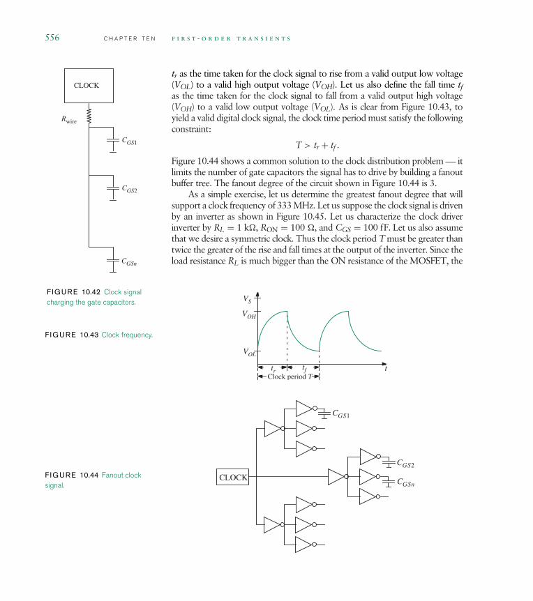
556 C H A P T E R T E N f i r s t - o r d e r t r a n s i e n t s
tr as the time taken for the clock signal to rise from a valid output low voltage(VOL) to a valid high output voltage (VOH). Let us also define the fall time tf
CGS1
CGS2
CGSn
CLOCK
Rwire
F IGURE 10.42 Clock signalcharging the gate capacitors.
as the time taken for the clock signal to fall from a valid output high voltage(VOH) to a valid low output voltage (VOL). As is clear from Figure 10.43, toyield a valid digital clock signal, the clock time period must satisfy the followingconstraint:
T > tr + tf .
Figure 10.44 shows a common solution to the clock distribution problem itlimits the number of gate capacitors the signal has to drive by building a fanoutbuffer tree. The fanout degree of the circuit shown in Figure 10.44 is 3.
As a simple exercise, let us determine the greatest fanout degree that willsupport a clock frequency of 333 MHz. Let us suppose the clock signal is drivenby an inverter as shown in Figure 10.45. Let us characterize the clock driverinverter by RL = 1 k, RON = 100 , and CGS = 100 fF. Let us also assumethat we desire a symmetric clock. Thus the clock period T must be greater thantwice the greater of the rise and fall times at the output of the inverter. Since theload resistance RL is much bigger than the ON resistance of the MOSFET, the
F IGURE 10.43 Clock frequency.
VOL
VOH
VS
tr tfClock period T
t
F IGURE 10.44 Fanout clocksignal.
CLOCK
CGS1
CGS2
CGSn

10.6 Additional Examples C H A P T E R T E N 557
CGS1
CGS2
CGSn
CLOCK
Rwire
CGS1
CGS2
CGSn
CLOCK
Rwire
RL
VS
F IGURE 10.45 Clock invertercharging the gate capacitors.
rise time will be greater than the fall time. Accordingly, we focus on calculatingthe rise time tr. As defined earlier, let Ceq represent the total capacitance drivenby the clock inverter.
Let us now compute tr. As defined earlier, tr is the time taken for theclock signal to rise from VOL to VOH. The equivalent circuit for computing tris suggested in Figure 10.46. The circuit shows the equivalent capacitor being
VS
+
-
Req = RL + Rwire
Ceq
vC
iC
F IGURE 10.46 Equivalentcircuit for determining the clockrise time.
charged by the supply VS through the RL and Rwire resistances. Let us denoteReq = RL + Rwire. The initial voltage on the capacitor VC0 = VOL.
Using the node method for the circuit shown in Figure 10.46, we get
vC − VS
Req+ Ceq
dvC
dt= 0.
Rearranging, we obtain the differential equation
ReqCeqdvC
dt+ vC = VS. (10.150)
Solving Equation 10.150, we get
vC(t) = VS + Ae−t/ReqCeq . (10.151)
We know that the voltage on the capacitor at t = 0 is VOL. Using this initialcondition, we solve for A and obtain
vC(t) = VS − (VS − VOL)e−t/ReqCeq . (10.152)

558 C H A P T E R T E N f i r s t - o r d e r t r a n s i e n t s
The time taken for vC to reach VOH from its initial value of VOL, namely tr,can be obtained from
VOH = VS − (VS − VOL)e−tr/ReqCeq . (10.153)
In other words,
tr = −ReqCeq ln(
VS − VOH
VS − VOL
). (10.154)
Assuming VOL = 1 V, VOH = 4 V, and VS = 5 V
tr = −ReqCeq ln(
1
4
).
For RL = 1 k and Rwire ≈ 0, we get
tr = 1.386 × 10³Ceq.
To achieve a frequency greater than 333 MHz, the period T must be less than1/333 MHz = 3 ns. Accordingly, since tr < T/2 = 1.5 ns,
1.5 × 10⁻⁹ > 1.386 × 10³Ceq.
In other words,
Ceq < 1.08 pF.
Thus the total driven capacitance must be less than 1.08 pF. Suppose the invert-ers used in the clock buffer tree are identical to the clock driver inverters, thenif the value of each gate capacitor is 100 fF, the maximum fanout degree mustbe less than 1080 fF / 100 fF. Thus the maximum fanout degree is 10.
W W W 10.6.6 R C R E S P O N S E T O D E C A Y I N GE X P O N E N T I A L *
10.6.7 S E R I E S R L C I R C U I T W I T H S I N E - W A V E I N P U T
Figure 10.48 shows a series RL circuit being driven with a sinewave voltagesource suddenly applied at t = 0:
R
vO
+
-
iLL
-vI+
F IGURE 10.48 RL circuit withsine-wave drive.
vI = Vsin(ωt) t > 0. (10.167)
Let us find the voltage across the inductor, assumed to be ideal. For simplicitywe assume zero initial state,
iL = 0 t < 0. (10.168)

10.6 Additional Examples C H A P T E R T E N 559
From KVL around the loop,
vI = iLR + LdiLdt
. (10.169)
The homogeneous solution, from Section 10.2.1, Equation 10.52, is
iL = Ae−(R/L)t. (10.170)
Because the input is a sine wave, a reasonable first guess for the particularsolution is
iL = Ksin(ωt). (10.171)
From Equation 10.169 for t > 0,
Vsin(ωt) = KRsin(ωt) + LωKcos(ωt). (10.172)
This can’t be solved for K unless L is zero, so our first guess is not quite right.We need another degree of freedom in the solution, so try
iL = K1 sin(ωt) + K2 cos(ωt). (10.173)
Now Equation 10.169 becomes
Vsin(ωt) = K1 R sin(ωt)+K2 R cos(ωt)+K1 ω cos(ωt)−K2Lω sin (ωt) (10.174)
Equating sine terms, and equating cosine terms, we find
V = K1R − K2Lω (10.175)
0 = K1Lω + K2R (10.176)
which yields, via Cramer’s Rule (see Appendix D),
K1 = VR
R2 + ω2L2(10.177)
K2 = V−ωL
R2 + ω2L2. (10.178)
The complete solution is of the form
iL = Ae−(R/L)t + VR
R2 + ω2L2sin(ωt) − V
ωL
R2 + ω2L2cos(ωt), t ≥ 0.
(10.179)

560 C H A P T E R T E N f i r s t - o r d e r t r a n s i e n t s
F IGURE 10.49 Waveforms forRL circuit with sinewave drive.
|
t
0
v I
t
0
Hom
ogen
eous
Solu
tion
Particularsolution
Total solution i L
The value of A can be found by applying the initial condition, Equation 10.168,to Equation 10.179, with t = 0, whence
A = VωL
R2 + ω2L2. (10.180)
The solution is shown in Figure 10.49.Equation 10.179 is fairly easy to interpret when t is large enough that the
exponential term has died away. If the drive frequency is very low, such that
ω R
L, (10.181)

10.7 Digital Memory C H A P T E R T E N 561
then the current reduces to
iL V
Rsin(ωt). (10.182)
That is, at low frequencies, the current is determined only by the resistor, andthe inductor behaves like a short circuit.
At high frequencies, that is, for
ω R
L(10.183)
Equation 10.179 reduces to
iL −V
ωLcos(ωt). (10.184)
In this case, the current is determined almost solely by the inductor. Note thatthe current is still sinusoidal, but now is 90 degrees out of phase with the appliedvoltage. Also, the magnitude of the current becomes smaller and smaller as thefrequency of the applied sinewave increases.
It is a little disappointing that such a simple circuit can lead to this level ofalgebra. But fortunately there is a simpler approach that can be used for linearcircuits. This approach, discussed in Chapter 13, reduces all the differentialequations to algebraic expressions.
10.7 D I G I T A L M E M O R Y
This chapter demonstrated previously that the memory aspect of capacitors andinductors formalized using the notion of state variables provided many uses inthe analog domain. The same memory property can also be utilized in the digitaldomain to implement digital memory using the analogous concept of digitalstate. Digital memory is not only an important application of capacitors, but itis of fundamental importance in its own right.
10.7.1 T H E C O N C E P T O F D I G I T A L S T A T E
A common example of the use of memory involves the digital calculator.Suppose we wish to compute the value of the expression (a × b) + (c × d).We might first multiply a and b and store the result (a × b) in memory. Wemight then multiple c and d, and add the resulting value (c × d) to (a × b) byrecalling the latter value from memory. Observe that the calculator containeda key to explicitly store a given value into the memory. Observe further thatonce a value was stored in memory, it could be read from memory any num-ber of times, without affecting the value in memory. In fact, it remained valid

562 C H A P T E R T E N f i r s t - o r d e r t r a n s i e n t s
until another value was explicitly stored in memory or it was erased. Erasurecorresponds to replacing the existing value with a zero value.
Memory has many uses. In this example, memory is used as a scratchpadarea to store partial results. Memory is also useful to store values input to asystem from the outside world. Memory enables short-lived external inputs tobe available to system circuitry for a longer period of time.
Memory is also useful in enabling better resource utilization. Suppose wewish to add three numbers A0 through A2. The addition can be accomplishedusing two adder circuits as follows: The first and second numbers are fed tothe first adder. The result of the first adder and the third value are fed to thesecond adder. The sum S is obtained as the output of the second adder.
Alternatively, we can utilize memory to accomplish the addition of threenumbers with a single adder as follows: Feed the first and second numbers tothe adder. Store the partial result in memory. Then feed the partial result frommemory and the third number to the same adder. The adder output is thedesired result.
The same concept can be generalized to add a long sequence of num-bers. At any given instant, the memory stores the partial result correspondingto all the numbers that occurred till that instant. For our addition example,notice that future results depend only on the value stored in memory and futureinputs. Future results do not depend on the exactly how the memory was timesequenced, just its final state. This observation stems from the concept of a‘‘state variable’’ that we saw earlier. The value stored in memory is simply adigital state variable in a manner analogous to an analog state variable valuestored on a capacitor.
The next section discusses how capacitors can be used to build digitalmemory.
10.7.2 A N A B S T R A C T D I G I T A L M E M O R Y E L E M E N T
Before we discuss how to implement memory, let us first define an abstractmemory element and understand how it can be used in a small system.Figure 10.50 shows an abstract memory element that can store one bit of data.It has an input dIN, an output dOUT, and a control input called store. As sug-gested by the waveforms in Figure 10.50, the input dIN is copied into memorywhen the store signal is high. The value stored in the memory is available to
F IGURE 10.50 An abstractone-bit memory element.
Memory
dOUT
Store
dIN
t
dIN
Store
dOUT

10.7 Digital Memory C H A P T E R T E N 563
be read as the output dOUT. If no new value is written into the memory, thelast written value is stored indefinitely. If the memory is read while it is beingwritten (that is, when the store signal is high), then the output simply reflectsthe value at the input.
e x a m p l e 10.4 m o t i o n d e t e c t o r c i r c u i t r e v i s i t e d
Let us use the memory element that we have just defined in a simple digital design.Recall the motion detector circuit from Chapter 5. The motion detector circuit wasrequired to produce a signal L to turn on a set of lights when the signal M from amotion sensor was high, provided it was not daytime. We assumed that a light sensorproduced a signal D that was high when it was day. We had written the following logicexpression for L:
L = MD.
A problem with this design is that the lights that were turned on by the assertion of Mwould go off the instant M was de-asserted.13 Let us consider a more useful design inwhich we require the lights to stay on even after the motion signal M goes away. Tomake this happen, we need some form of memory to remember the occurrence of M,
Memory
dOUT
Store
dIN
Reset
even after the M signal goes away. The desired circuit uses a memory element and isshown in Figure 10.51. In this circuit, the signal M is connected to the store input of thememory, and the signal D is connected to the dIN input of the memory. As depictedin the signal waveforms in Figure 10.51, the memory output remains high if motion isdetected even when D is false.14
10.7.3 D E S I G N O F T H E D I G I T A L M E M O R Y E L E M E N T
How do we implement a memory element? The memory element must bedesigned so that it stores indefinitely any value that has been written into it.Recall that a capacitor has the same property. Provided its discharge path hasa high time constant, a capacitor can store a charge for a long period of time.Furthermore, we can use a switch to enable charging the capacitor from a giveninput.
13. To ‘assert’ is to set the value to a logical 1, while to ‘de-assert’ is to set the value to a logical 0.
14. Our circuit shown in Figure 10.51 has one other problem. How do the lights turn off? Itshould be apparent from the circuit that L will go back to 0 when motion is detected during thedaytime. However, relying on the appearance of signal M during the daytime to turn off the lights isunappealing. One solution is to modify our memory abstraction to include a reset signal as follows:The value in memory is set to 0 when the reset input is high. (Our memory abstraction can includethe additional property that the reset signal overrides the store signal if both are on at the sametime.) Our motion detector circuit output L can now be turned off by asserting the reset signal ofthe memory. The reset terminal of memory can be connected to the signal D so that the memorycontents and therefore the lights go off whenever it is day.
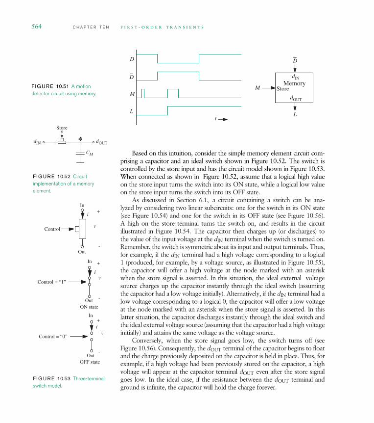
564 C H A P T E R T E N f i r s t - o r d e r t r a n s i e n t s
F IGURE 10.51 A motiondetector circuit using memory.
Memory
dOUT
Store
dIN
M
L
D
t
D
M
L
D
Based on this intuition, consider the simple memory element circuit com-prising a capacitor and an ideal switch shown in Figure 10.52. The switch iscontrolled by the store input and has the circuit model shown in Figure 10.53.When connected as shown in Figure 10.52, assume that a logical high value
dIN dOUT
Store
CM
*
F IGURE 10.52 Circuitimplementation of a memoryelement.
on the store input turns the switch into its ON state, while a logical low valueon the store input turns the switch into its OFF state.
As discussed in Section 6.1, a circuit containing a switch can be ana-lyzed by considering two linear subcircuits: one for the switch in its ON state(see Figure 10.54) and one for the switch in its OFF state (see Figure 10.56).A high on the store terminal turns the switch on, and results in the circuitillustrated in Figure 10.54. The capacitor then charges up (or discharges) tothe value of the input voltage at the dIN terminal when the switch is turned on.Remember, the switch is symmetric about its input and output terminals. Thus,for example, if the dIN terminal had a high voltage corresponding to a logical1 (produced, for example, by a voltage source, as illustrated in Figure 10.55),the capacitor will offer a high voltage at the node marked with an asteriskwhen the store signal is asserted. In this situation, the ideal external voltage
Control
In
Out
+
-
v
i
In
Out
Control = “0”
OFF state
+
-
vi
In
Out
Control = “1”
ON state
+
-
vi
F IGURE 10.53 Three-terminalswitch model.
source charges up the capacitor instantly through the ideal switch (assumingthe capacitor had a low voltage initially). Alternatively, if the dIN terminal had alow voltage corresponding to a logical 0, the capacitor will offer a low voltageat the node marked with an asterisk when the store signal is asserted. In thislatter situation, the capacitor discharges instantly through the ideal switch andthe ideal external voltage source (assuming that the capacitor had a high voltageinitially) and attains the same voltage as the voltage source.
Conversely, when the store signal goes low, the switch turns off (seeFigure 10.56). Consequently, the dOUT terminal of the capacitor begins to floatand the charge previously deposited on the capacitor is held in place. Thus, forexample, if a high voltage had been previously stored on the capacitor, a highvoltage will appear at the capacitor terminal dOUT even after the store signalgoes low. In the ideal case, if the resistance between the dOUT terminal andground is infinite, the capacitor will hold the charge forever.
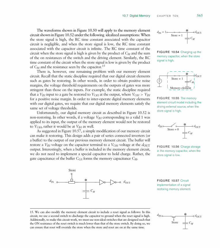
10.7 Digital Memory C H A P T E R T E N 565
The waveforms shown in Figure 10.50 will apply to the memory elementcircuit shown in Figure 10.52 under the following idealized assumptions: When
dIN = 1 dOUTStore = 1
CM
*
F IGURE 10.54 Charging up thememory capacitor, when the storesignal is high.
the store signal is high, the RC time constant associated with the capacitorcircuit is negligible, and when the store signal is low, the RC time constantassociated with the capacitor circuit is infinite. The RC time constant of the
dOUTStore = 1
CM
*V+-
Memory element
F IGURE 10.55 The memoryelement circuit model including thedriving external source, when thestore signal is high.
dIN dOUTStore = 0
CM
*
F IGURE 10.56 Charge storagein the memory capacitor, when thestore signal is low.
circuit when the store signal is high is given by the product of CM and the sumof the on resistances of the switch and the driving element. Similarly, the RC
dIN dOUT
Store CM
*
time constant of the circuit when the store signal is low is given by the productof CM and the resistance seen by the capacitor.15
There is, however, one remaining problem with our memory elementcircuit. Recall that the static discipline required that our digital circuit elementssuch as gates be restoring. In other words, in order to obtain positive noisemargins, the voltage threshold requirements on the outputs of gates was morestringent than those on the inputs. For example, the static discipline requiredthat a VIH input to a gate be restored to VOH at the output, where VOH > VIHfor a positive noise margin. In order to inter-operate digital memory elementswith our digital gates, we require that our digital memory elements satisfy thesame set of voltage thresholds.
Unfortunately, our digital memory circuit as described in Figure 10.52 isnon-restoring. In other words, if a voltage VIH corresponding to a valid 1 wasapplied to its input, the output of the memory element would not be restoredto VOH, rather it would be at VIH as well.
As suggested in Figure 10.57, a simple modification of our memory circuitcan make it restoring. This design adds a pair of series connected inverters (ora buffer) to the output of our previous memory element circuit. The buffer willrestore a VIH voltage on the capacitor terminal to a VOH voltage at the dOUToutput. Interestingly, when a buffer is included in the memory element circuit,we do not need to implement a special capacitor to hold charge. Rather, thegate capacitance of the buffer CGS forms the memory capacitance CM.
dOUTdIN
Store
CM
* F IGURE 10.57 Circuitimplementation of a signalrestoring memory element.
15. We can also modify the memory element circuit to include a reset signal as follows: In thiscircuit, we use a second switch to discharge the capacitor to ground when the reset signal is high.Additionally, to make this circuit work, we must use non-ideal switches that are designed such thatthe ON resistance of the reset switch is much lower than that of the store switch. By doing so, wecan ensure that reset will override the store when the store and reset are on at the same time.

566 C H A P T E R T E N f i r s t - o r d e r t r a n s i e n t s
F IGURE 10.58 Memorycapacitor discharge due to loadresistances for the unbufferedmemory element.
dINdOUT
Store = 0 CM
*RL
Memory element External logic device
F IGURE 10.59 Memorycapacitor’s charge is protected inthe buffered memory element.
dINdOUT
Store = 0 CM
*RL
Memory element External logic device
By isolating the capacitor from the circuit that reads the stored value, thebuffer offers added advantages. As shown in Figure 10.58, devices that read thevalue stored on the capacitor might have relatively low resistances associatedwith them, thereby discharging the capacitor in our original unbuffered memorycircuit. In contrast, the buffered design of the memory element circuit shown inFigure 10.59 protects the capacitor’s charge from the external circuit. By carefuldesign of the memory element, the input resistance of the buffer can be madeto be very large, thereby ensuring a large discharge time constant.
In practice, capacitors will leak their charge over time due to parasiticresistances. Let us suppose the capacitor gradually discharges through a parasiticresistance RP (see Figure 10.60). In this situation, for how long will the valuestored in the capacitor remain valid after the store signal is de-asserted?
There are two cases to consider. First, if a 0 is stored on the capacitor, thenthe 0 value will be held indefinitely even with a low parasitic resistance. Noticethat as the capacitor discharges to ground, the 0 stored on it will remain a 0.
The second case is more interesting. In this case, a 1 is written on thecapacitor. Assume that the voltage corresponding to a 1 is VS. The value storedon the capacitor will be read as a valid 1 by the buffer until it reaches the VIHvoltage threshold. Thus the period over which the memory element will storea valid 1 is the interval over which the voltage drops from VS to VIH. Wecan compute this duration from capacitor discharge dynamics (for example,
F IGURE 10.60 Charge leakagefrom the memory capacitor for thebuffered memory element.
dIN
Store = 0 CM
*RP
dOUT

10.7 Digital Memory C H A P T E R T E N 567
see Equation 10.26). When a capacitor CM charged to an initial voltage VSdischarges through a resistor RP, its voltage vC as a function of time is given bythe following equation:
vC = VSe−t/RPCM .
The time taken for vC to drop from VS to VIH is given by
tVS→VIH = −RPCM lnvIH
VS.
As an example, suppose that CM = 1 pF, RP = 109 , VS = 5 V, andVIH = 4 V. Then tVS→VIH = 0.22 milliseconds.
10.7.4 A S T A T I C M E M O R Y E L E M E N T
The one-bit memory element that we have discussed thus far is called a dynamicone-bit memory element or a dynamic D-latch. It is dynamic in the sense that itstores a value written into it only for a finite amount of time (due to nonzeroparasitic resistances in practical implementations). The static one-bit memoryelement or a static D-latch is another type of memory element that has the samelogic properties as the dynamic D-latch, but can store a value written into itindefinitely.
Figure 10.61 shows one possible circuit for a static memory element. In thiscircuit, a non-ideal switch with a very high ON resistance is connected betweenthe power supply and the storage node of the memory element. When theoutput of the memory element is a logical 1, this switch is turned on andintroduces a small stream of charge into the storage node to offset any leakage.Because it trickles charges into the node, this switch is called a trickle switch.The ON resistance of the trickle switch is made very large compared to theON resistance of the store switch, so that the trickle input can be overriddeneasily by the input dIN. A detailed circuit design of the static latch is beyondthe scope of this book. The interested reader is referred to ‘Principles of CMOSVLSI Design,’ by Weste and Eshraghian.
dOUTdIN
Store
CM
*
VS
F IGURE 10.61 Circuitimplementation of a static memoryelement using a trickle switch.

568 C H A P T E R T E N f i r s t - o r d e r t r a n s i e n t s
10.8 S U M M A R Y The first-order differential equations that result from applying KVL and
KCL to networks containing sources, resistors, and one energy-storageelement can be derived using the node method or the other approachesdescribed in Chapter 3. These differential equations can be solved by findingthe homogeneous solution and the particular solution.
The response of RC circuits resembles rising or decaying exponentials withthe time constant RC. As an example, for a series RC circuit driven by avoltage step of amplitude VI at t = 0, the capacitor voltage for t > 0 isgiven by
vC(t) = VI + (VO − VI)e−t/RC
where VO is the initial voltage on the capacitor. In general, the response of a first order circuit (RC or RL) will be of the
form
vC = final value + (initial value − final value)e−t/time constant
where the time constant is RC for a resistor-capacitor circuit and L/R for anresistor-inductor circuit. This form of the response in RC and RL circuits isshared by other branch variables such as the capacitor or inductor currentand resistor voltage.
Capacitors behave like open circuits when a circuit containing capacitorsis driven by a DC voltage source. Conversely, a capacitor behaves likean instantaneous short circuit when inputs make an abrupt transition (forexample, a step). (If the capacitor voltage were nonzero, then the capacitorwould behave like a voltage source for abrupt transitions.)
Inductors behave like short circuits when a circuit containing inductors isdriven by a DC current source. Conversely, an inductor behaves like aninstantaneous open circuit for inputs that make an abrupt transition (forexample, a step). (If the inductor current were nonzero, then it wouldbehave like a current source for abrupt transitions.)
The zero-input response is the response of the system to the initial storedenergy, assuming no drive.
The zero-state response is the the response to an applied drive signal, forno initial stored energy.
When the input signal is a short pulse (short compared to the time constantof the circuit), the response is proportional to the area of the applied pulserather than to its height or shape.
It is often convenient to break down a problem involving energy-storage ele-ments into two parts. First, calculate the zero-input response, the response

10.8 Summary C H A P T E R T E N 569
of the system to the initial stored energy, assuming no drive. Then calcu-late the zero-state response, the response to the applied drive signal, for noinitial stored energy.
If we restrict integral operations to t greater than zero, the zero-stateresponse of the integral of some input signal is the integral of the zero-state response to that signal. The same is true for differentiation: Theresponse to a signal derived by differentiating an input can be obtained bydifferentiating the output.
The rise time for an output node is defined as the delay in rising from itslowest value to a valid high (VOH) at that output.
The fall time for an output node is defined as the delay in falling from itshighest value to a valid low (VOL) at the same output.
The delay tpd,1→0 for an input-output terminal pair of a gate is the timeinterval between a 1 to a 0 transition at the input to the moment that theoutput reaches a corresponding valid output voltage level (VOH or VOL).
The delay tpd,0→1 for an input-output terminal pair of a gate is the timeinterval between a 0 to a 1 transition at the input to the moment that theoutput reaches a corresponding valid output voltage level (VOL or VOH).
E X E R C I S E Se x e r c i s e 10.1 Using superposition, determine the current i1(t) for the networkshown in Figure 10.62. The network is at rest for t < 0.
i1(t) 1 H
vS (t) +- 3 kΩ iS (t)
iS (t)
vS (t)
1 mA
1 V
t
t
F IGURE 10.62
e x e r c i s e 10.2 Find and sketch the zero state response for t > 0 inFigure 10.63. iS is a 10-mA step at t = 0. vR(t)iS 100 Ω 10 mH
+
-
iL(t)
F IGURE 10.63
e x e r c i s e 10.3 In the circuit in Figure 10.64, i(t) = 100 µA, 0 < t < 1 s, zero
i(t) 10 µF
+
-
vC
F IGURE 10.64
otherwise. At time t = 2, the voltage vC = 5 V. What is vC at time t = −1 s?
e x e r c i s e 10.4 In the circuit in Figure 10.65, the switch is closed at time t = 0and opened at t = 1 second. Sketch vC(t) for all times.
100 µF
+
-
vC (t)
+- 11 V 1 kΩ
10 kΩ
F IGURE 10.65
e x e r c i s e 10.5 Find and sketch the zero-input response for t > 0 in eachnetwork in Figure 10.66 for the given initial conditions.

570 C H A P T E R T E N f i r s t - o r d e r t r a n s i e n t s
e x e r c i s e 10.6 Find and sketch the response for t > 0 in each network inFigure 10.67. Assume that the input is as shown for t > 0 , and assume an initial zerostate (in other words, show the zero state response).
e x e r c i s e 10.7 For the current source shown in Figure 10.68, assume iSconsists of a single rectangular current pulse of amplitude I0 amps and duration t0seconds.
i
+-
1 kΩ1 µF
v(0) = 6 V
1 kΩ
v
1 kΩ1 mH
1 kΩ
i(0) = 6 mA
i1 kΩ1 mH
1 kΩ
Switch opens at t = 0
+
-6 V
+-
1 kΩ1 µF v
+
-6 V
Switch opens at t = 0
(a)
(b)
(c)
(d)
F IGURE 10.66
a) Find the zero-state response to iS.
b) Sketch the zero-state response for the cases:
i) t0 RC
ii) t0 = RC
iii) t0 RC
c) Show that for t0 RC, (the case of a short pulse), the response for t > t0 dependsonly on the area of the pulse (I0t0), and not on i0 or t0 separately.
+-
10 mH
1 µF
vA = 1 V, constant
100 Ω
v
iB = 1 µA, constant
10 kΩ
vA
vC = 10e−103t
iD = (10−6)e−103t
(a)
(b)
(c)
(d)
i+-
iB
1 mH
1 kΩ
vC
i+-
+
- .1 µFviD
F IGURE 10.67
R+
-viS C
F IGURE 10.68
e x e r c i s e 10.8 Identify the state variable in each network in Figure 10.69. Writethe corresponding state equation and find the time constants.
e x e r c i s e 10.9 In the circuit in Figure 10.70, v(t) = 5 mV for 0 < t < 1 s, andzero otherwise. At time t = 4 s, i(t) = 7 A. What is i(t) at time t = −1 s?
e x e r c i s e 10.10 Identify appropriate state variables for the network inFigure 10.71 and write the state equations.
e x e r c i s e 10.11 In Figure 10.72, R1 = 1 k, R2 = 2 k, and C = 10 µF.The driving voltage vS = 0 for t < 0. Assume vS is a 3-volt step at t = 0. Make a sketchof vC(t) for t > 0. Be sure to label the dimensions of the voltage and time axes andidentify characteristic waveform shapes with suitable expressions.
e x e r c i s e 10.12 Identify state variables and write appropriate state equationsfor the circuit in Figure 10.73.
e x e r c i s e 10.13 Referring to Figure 10.74, before the switch is closed, thecapacitor is charged to a voltage vS = 2 V. The switch is closed at t = 0. Find anexpression for vC(t) for t > 0. Sketch vC(t).

10.8 Summary C H A P T E R T E N 571
e x e r c i s e 10.14 Find the time constant of the circuit shown in Figure 10.75.
e x e r c i s e 10.15 A two-input RC circuit is shown in Figure 10.76. (Parts a, b,and c are independent questions.)
a) You should realize that the ‘‘bridge’’ of capacitors can be replaced by a single capacitorin this problem. What is the value of the single equivalent capacitor?
b) Consider operation with iI(t) = 0 and vI(t) = 0 for t ≥ 0. The voltage vO(t) is knownto be 1 volt at a time t = 0. Determine vO(t) for all t > 0.
C
(a)
(b)
1 µF
(c)
(d)
R
L
R
i0
+-v0
1 kΩ+-
vC
1 kΩ
1 mH 1 kΩ+-
v0
1 kΩ
F IGURE 10.69
L = 1 mH
+
-v(t)
i(t)
F IGURE 10.70
C L+-
vS
R1 R2
F IGURE 10.71
C+-vS
R1 R2
+
-
vCvS
0, (t < 0)3 V, (t ≥ 0)
=
F IGURE 10.72
+-
vS
R1 L1 - M L2 - M
M R2
F IGURE 10.73
+-
R
vC(t)V = 1 V+
-C
F IGURE 10.74
1 µF
1 kΩ
iS(t) +-
1 kΩ
1 kΩ vS(t)
F IGURE 10.75
0.5 µF
iI(t)+-
1 kΩ
1 kΩ vI(t)
2 kΩ
+-vO
0.5 µF 1.5 µF
1.5 µF
F IGURE 10.76

572 C H A P T E R T E N f i r s t - o r d e r t r a n s i e n t s
c) A different constraint is that sources iI(t) and vI(t) are zero for t < 0 and thatvO(0) = 0. Sources iI(t) and vI(t) undergo step transitions of +1 mA and +1 volt,respectively, at time t = 0. Determine vO(t) for all time.
e x e r c i s e 10.16 In the circuit in Figure 10.77, R1 = 1 k, R2 = 2 k, andC = 3 µF. Assume initial rest conditions (zero initial state), and assume that v1 has a6-volt step at t = 0. Find v2(t) for t > 0. Sketch and label.
R2v1+− v2
R1 C
+
−
F IGURE 10.77
e x e r c i s e 10.17 Consider the circuit shown in Figure 10.78. Sketch and labelvO(t) for i1(t) a step as shown in Figure 10.79. Assume vO = 0 for t < 0.
R1i1(t) vO4ib
C+
−
ib
F IGURE 10.78
I
t
i1
F IGURE 10.79
e x e r c i s e 10.18 For the circuit shown in Figure 10.80, find the characteristicequation and the zeroinput response assuming that the capacitor was initially chargedto 1 volt. Label your graph.R
vI(t)+- vO(t)
4R
C
+
-
F IGURE 10.80
e x e r c i s e 10.19 The excitation function for all four of the circuits shown inFigure 10.81 is
vS(t) = 0, t < 0
vS(t) = 10 V, t ≥ 0.
For each of the circuits, select the time function on the right that corresponds in magni-tude and shape to the output, vO(t). Assume that all capacitors and inductors have zeroinitial states, (the appropriate state variable is zero for t less than zero). If no matchingresponse exists, say so and explain briefly. All responses are made up of ‘‘straight lines’’and ‘‘exponentials.’’ You may choose a time function more than once. (Note that part(d) shows an op-amp circuit. Op-amps will be covered in later chapters.)
e x e r c i s e 10.20 An RC network is shown in Figure 10.82. The voltage v andthe current i are constant for all time. Prior to t = 0, the circuit is in equilibrium withthe switch closed. At time t = 0, the switch is opened, and it is then closed some timelater. The waveform in Figure 10.83 is observed for vC(t).
What are the value of τ1, τ2, and the final value V1? (Note: The figure may not be toscale.)

10.8 Summary C H A P T E R T E N 573
vS(t)
vS(t)
vS(t)
vS(t)
+- vO(t)
R
C+
-
Response number ______
+-
R
2C+
-R
Response number ______
+-
L
R
Response number ______
C
R
-+ +
-
−10 V
+10 V
Response number ______
Op-amp saturation at ±10 V
vO(t)
10 V
t
vO(t)
vO(t)
+
-vO(t)
vO(t)
10 Vt
vO(t)
−10 V
vO(t)
5 Vt
(a)
(b)
(c)
(d)
(1)
(2)
(3)
(4)
(5)
(6)
(7)
(8)
vO(t)
10 V
t
vO(t)
10 V
t
vO(t)
5 Vt
vO(t)10 V
t
5 V
F IGURE 10.81
iv +-
vC(t)
2 kΩ
1 µF+-
1 kΩ1 kΩ
2 kΩ
switch
F IGURE 10.82
vC(t)
2 V
Switch open Switch closed
Timeconstant τ1
V1 (Final value)Timeconstant τ2
t
F IGURE 10.83

574 C H A P T E R T E N f i r s t - o r d e r t r a n s i e n t s
e x e r c i s e 10.21 In the two following cases in Figure 10.84 the input vIN(t) =10u−1(t), a 10-V step16 starting at time t = 0. Give for each case:
a) The time constant of the circuit.
b) An analytic expression for the signal vOUT(t) as a function of time.
c) A labeled sketch of the output signal vOUT(t) as a function of time. Be sure to labelthe time and voltage scales.
e x e r c i s e 10.22 In each of the following cases, find by inspection and give
1 MΩ
1 µF
+-vIN(t)
+
-
vOUT(t)
(a)
1 mH500 Ω
+-vIN(t)
+
-
vOUT(t)
(b)
500 Ω
F IGURE 10.84 i) an expression for the time constant τ ,
ii) a sketch of the signal versus time,
iii) an analytic expression for the signal in terms of τ and any other necessaryparameters.
a) Referring to Figure 10.85, find v(t) for t > 0 given i(t = 0) = I0.
L
i
R1
+
-
vR2
(a)
F IGURE 10.85b) Referring to Figure 10.86, find i2(t) given i1(t = 0) = I0/2.
L1i1
I0
R
L2
i2
(b)
F IGURE 10.86
c) Referring to Figure 10.87, find v(t) for t > 0 given that the switch is moved from1 to 2 at t = 0.
(c)
C2
V0
R1 C1
R2v+
−
1
2+
−
F IGURE 10.87
e x e r c i s e 10.23 For the circuit in Figure 10.88, with no charge on the capacitorat t = 0, given that if vI = Atu−1(t) then vC = [A(t − τ ) + Aτ e−t/τ ]u−1(t). Note thatu−1(t) represents a unit step at t = 0.
16. Recall that the notation u0(t) represents an impulse at time t . The notation un(t) representsthe function that results from differentiating the impulse times, and the notation u−n(t) representsthe function that results from integrating the impulse times. Thus u−1(t) represents the unit stepat time t, u−2(t) the ramp, and u1(t) the doublet at time t. The unit step u−1(t) is also commonlyrepresented as u(t), and the unit impulse u0(t) as δ(t).

10.8 Summary C H A P T E R T E N 575
R+
−vC
vI C+−
F IGURE 10.88
t
vCvI
tτ
F IGURE 10.89
Find the following:
a) vC(t) when the input is the same as previously given but vC(t = 0) = V0.
b) vC(t) when vC(0) = 0 and vI(t) = Bu−1(t). Note that u−1(t) represents a unit stepat t = 0.
c) vC(t) for t ≥ T when vC(0) = 0 and
vI(t) =
0 t ≤ 0At 0 ≤ t ≤ TAT T ≤ t.
e x e r c i s e 10.24 A digital memory element is implemented as illustrated inFigure 10.90. Sketch the waveform at the output of the memory element for the inputsignals shown in Figure 10.91. Assume that the switch is ideal and that the memoryelement has a 0 stored in it initially.
dOUTdIN
Store
CM
*F IGURE 10.90
t
dIN
Store
dOUT
F IGURE 10.91

576 C H A P T E R T E N f i r s t - o r d e r t r a n s i e n t s
P R O B L E M S p r o b l e m 10.1 Figure 10.92a illustrates an inverter INV1 driving anotherinverter INV2. The corresponding equivalent circuit for the inverter pair is illustratedin Figure 10.92b. A, B, and C represent logical values, and vA, vB, and vC representvoltage levels. The equivalent circuit model for an inverter based on the SRC model ofthe MOSFET is depicted in Figure 10.93.
INV1 INV2
(a)
A B C
vA
+
-+-
+- vB
vC
VS VS
RL RL
(b)
F IGURE 10.92
a) Write expressions for the rise and fall times of INV1 for the circuit configurationshown in Figure 10.92. Assume that the inverters satisfy the static discipline withvoltage thresholds VIL = VOL = VL and VIH = VOH = VH.(Hint: The rise time of INV1 is the time vB requires to transition from the lowestvoltage reached by vB (given by the voltage divider action of RL and RON) to VH
for a VS to 0-V step transition at the input vA. Similarly, the fall time of INV1 is thetime vB requires to transition from the highest voltage reached by vB (that is, VS) toVL for a 0-V to VS step transition at the input vA.)
b) What is the propagation delay tpd of INV1 in the circuit configuration shown inFigure 10.92, for RON = 1 k, RL = 10RON, CGS = 1 nF, VS = 5 V, VL = 1 V,and VH = 3 V?
VS
vIN
CGS
RON
RL
vOUT
vIN ≥ VT
VS
vIN
CGS
RL
vOUT
vIN < VT
F IGURE 10.93p r o b l e m 10.2 The inverter-pair comprising INV1 and INV2 studied in Prob-lem 10.1 (see Figure 10.92) drives another inverter INV3 as illustrated in Figure 10.94a.Logically, the series connected pair of inverters INV1 and INV2 function as a buffer,as depicted in Figure 10.94b. The equivalent circuit of the buffer circuit driving INV3is illustrated in Figure 10.94c. For this problem, use the equivalent circuit model foran inverter based on the SRC model of the MOSFET as depicted in Figure 10.93.Assume further that each of the inverters satisfies the static discipline with voltage thresh-olds VIL = VOL = VL and VIH = VOH = VH. Assume further that the MOSFETthreshold voltage is VT. (Note that to satisfy the static discipline, the following is true:VL < VT < VH.)
a) Referring to Figure 10.94c, assume that the input to the buffer vA undergoes a steptransition from 0 V to VS at time t = 0. Write an expression for vB(t) for t ≥ 0

10.8 Summary C H A P T E R T E N 577
INV1 INV2 INV3
(a)
BUF
BUF INV3
INV1
vA
VS
+
-+-+-
+
-vB vC
vD
VSVS
INV2 INV3
RL RL RL
(c)
BUF
(b)
F IGURE 10.94
for the step transition in vA. (Hint: See the fall time calculation in Problem 10.1a.)Sketch the form of vB for t ≥ 0.
b) Referring to Figure 10.94c, assume that the input to the buffer vA undergoes a steptransition from 0 V to VS at time t = 0. Write an expression for vC(t) for t ≥ 0for the step transition in vA. (Hint: Refer to the sketch of vB drawn in part (a.) TheMOSFET in INV2 stays on for vB ≥ VT, and turns off when vB < VT.) Sketch theform of vC(t) for t ≥ 0.
c) Write an expression for the rise time of the buffer for the circuit configuration shownin Figure 10.94c. (Hint: Refer to the sketch of vC from part (b.) The rise time of thebuffer is the time vC requires to transition from the lowest voltage reached by vC toVH from the time the input vA makes a step transition from 0 V to VS. Note thatthe rise time of the buffer includes the internal buffer fall delay, which is the timevB takes to transition from VS to VT, and the additional time vC takes to transitionfrom its lowest voltage to VH.)
d) Referring to Figure 10.94c, assume that the input to the buffer vA undergoes a steptransition from VS to 0 V at time t = 0. Write an expression for vB(t) for t ≥ 0 forthe step transition in vA. Sketch the form of vB for t ≥ 0.
e) Referring to Figure 10.94c, assume that the input to the buffer vA undergoes a steptransition from VS to 0 V at time t = 0. Write an expression for vC(t) for t ≥ 0for the step transition in vA. (Hint: Refer to the sketch of vB drawn in part (d.) TheMOSFET in INV2 stays off for vB < VT, and turns on when vB ≥ VT.) Sketch theform of vC(t) for t ≥ 0.
f) Write an expression for the fall time of the buffer for the circuit configuration shownin Figure 10.94c. (Hint: Refer to the sketch of vC from part (e.) The fall time of thebuffer is the time vC requires to transition from VS to VL from the time the inputvA makes a step transition from VS to 0 V. Note that the fall time of the buffer isthe sum of two components: (1) the internal buffer rise delay, or the time vB takesto transition from its lowest voltage to VT and (2) the additional time vC takes totransition from VS to VL.)

578 C H A P T E R T E N f i r s t - o r d e r t r a n s i e n t s
g) Compute the rise time and the fall time for the buffer assuming that RON = 1 k,RL = 10RON, CGS = 1 nF, VS = 5 V, VL = 1 V, VT = 2 V, and VH = 3 V.
h) What is the propagation delay tpd of the buffer when the buffer output is connectedto a single inverter using an ideal wire as shown in Figure 10.94c?
i) Notice that unlike the delay calculation in Problem 10.1, we needed the value of VT
to obtain the buffer delay. Why was it necessary in the case of the buffer?
j) An approximate value for the buffer delay can be obtained by doubling the individualinverter delay. Estimate the buffer delay by using the inverter delay computed inProblem 10.1b. What is the percentage error in the value of this estimated delay ascompared to the accurate buffer delay computed in part (i) of this problem?
p r o b l e m 10.3 The circuit depicted in Figure 10.95 implements the logic func-tion Z = (ABC + D)E. Suppose the output of this circuit drives an inverter witha gate capacitance of CGS. Assume that the MOSFETs in the circuit have on resis-tance RON, and that the high and low voltage thresholds are VIH = VOH = VH andVIL = VOL = VL, respectively.
ZA
B
C
RL
D
E
VS
F IGURE 10.95 a) What combination of logical inputs will result in the worst-case fall time for thecircuit?
b) Derive an expression for the worst-case fall time in terms of VS, RL, RON, VL, andVH. Not all variables need appear in your answer.
c) Derive an expression for the worst-case rise time.
p r o b l e m 10.4 Figure 10.96 illustrates an inverter INV A connected to anotherinverter INV B by a wire of length l on a VLSI chip.
A l C
INVA INVB
DB
F IGURE 10.96
Figure 10.97 shows a lumped circuit model for the (nonideal) wire of length l in a VLSIchip, and Figure 10.98 shows the equivalent circuit model for the inverter pair connectedby the nonideal wire based on the SRC model for the MOSFET. Assume that the logicdevices satisfy a static discipline with voltage thresholds given by VIL = VOL = VL andVIH = VOH = VH, and that the supply voltage is VS.
B Cl
CBlR0
lC0
F IGURE 10.97 Suppose INV A is driven by a 0 to 1 transition at its input (denoted vINA) at time t = 0.Determine tpd,0→1, the propagation delay through INV A for a 0 to 1 transition atits input. Recall that by our definition tpd,0→1 is the time taken by the input to INV B,

10.8 Summary C H A P T E R T E N 579
VS
vINA
CGSARON
RL
VS
RON
RL
CGSB
vINB vOUTB
Cwire
Rwire
vOUTA
F IGURE 10.98
namely vINB, to fall from VS to VL following the 0 to 1 transition at the input of INV A.Express your answer in terms of VS, VL, RON, CGS, the wire length l, and the wiremodel parameters. By what factor does the delay increase for a 2× increase in the wirelength l?
p r o b l e m 10.5 Figure 10.99 illustrates an inverter INV A driving n other invert-ers INV1 through INVn. As in Problem 10.1, each of the inverters is constructed
INV1
INV2
INV3
INVn
INVA
F IGURE 10.99
using a MOSFET and a resistor RL, and the inverters satisfy the static discipline withvoltage thresholds VIL = VOL = VL and VIH = VOH = VH. Model the MOSFETsusing the SRC model with MOSFET on resistance RON and gate capacitance CGS as inProblem 10.1 (see Figure 10.93.)
a) What are the rise and fall times for INV A? (Hint: Sum the input capacitances of eachof the inverters into a single lumped value, and use your answer from Problem 10.1to solve this part.) How does the rise time increase as the number of driven invertersn increases?
INVA
INV1
INV2
INV3
INVn
wire 1
wire 2
wire n
wire 3
F IGURE 10.100
b) What is the propagation delay tpd of INV A in the circuit configuration shown inFigure 10.99, for RON = 1 k, RL = 10RON, CGS = 1 nF, VS = 5 V, VL = 1 V,and VH = 3 V.
c) Now, assume that each of the wires connecting the output of INV A to each of theinverters INV1 through INVn is nonideal as depicted in Figure 10.100. Model eachof the wires using the model shown in Figure 10.101. Assuming that the input ofINV A makes a step transition from 1 to 0, find the rise time at the input of any oneof the inverters INVi driven by INV A.
RW
CW
F IGURE 10.101
d) Compute the value of the rise time determined in part (c) for the following param-eters: RON = 1 k, RL = 10RON, CGS = 1 nF, RW = 100 , CW = 10 nF,VS = 5 V, VL = 1 V, and VH = 3 V.
p r o b l e m 10.6 As can be seen from the answer to Problem 10.4, long wireshave a serious negative impact on the delay. One way to alleviate the wire delay

580 C H A P T E R T E N f i r s t - o r d e r t r a n s i e n t s
problem is to introduce buffers when driving long wires, as illustrated in Figure 10.102.Assume that the buffer is constructed as depicted in Figure 10.94c using a pair of invert-ers identical to the inverters in this problem. In other words, the input of a bufferhas a capacitance CGS to ground, and the output of a buffer have the same drivecharacteristics as an inverter output. For this problem, you will ignore the internaldelay of the buffer. (See Problem 10.2c and f for a definition of the internal bufferdelay.) In other words, assume that a buffer driving zero output capacitance has zerodelay.
By introducing a buffer, the effective length of wire driven by either the inverter INV Aor the buffer is l/2. For large l, given the nonlinear relationship between wire length anddelay, the sum of the delays in driving the two l/2 wire segments is smaller than drivinga single wire segment of length l.
F IGURE 10.102 A B C D
INVA INVB
l2--- l
2---
a) Compute the propagation delay between the input of INV A and the input of INV Bfor the circuit in Figure 10.102. Assume that rising transitions are longer than fallingtransitions at the output of either the inverters or the buffers.
(Hint: The total delay from the input of INV A to the output of INV B is the sumof the following two quantities: (1) the propagation delay of INV A driving the wiresegment of length l/2 and a capacitance CGS corresponding to the gate capacitanceof the buffer, and (2) the propagation delay of the buffer driving the second wiresegment of length l/2 and a capacitance CGS corresponding to the gate capacitanceof INV B. Remember, the buffer has zero delay when it is driving zero outputcapacitance.)
b) Figure 10.103 shows a circuit in which n−1 buffers are introduced between INV Aand INV B. INV A and each of the buffers drives a segment of wire of length l/n.Compute the propagation delay between the input of INV A and the input of INV Bfor this case.
F IGURE 10.103 A B C D
INVA INVB
ln---
B1
ln---
ln---… l
n---
B2 ... Bn-1
c) Determine the number of buffers for which the propagation delay for the circuit inFigure 10.103 is minimized.

10.8 Summary C H A P T E R T E N 581
p r o b l e m 10.7 Figure 10.104 shows a buffer BUF1 driving a large load capacitorCL. The buffer is built using an inverter pair as in Figure 10.94c. The width-to-lengthratio of each NMOS transistor in the buffer is W/L and the resistors have a value RL.Accordingly, the gate capacitance seen at the input of the buffer is given by (W/L)CGS.The buffer satisfies a static discipline with voltage thresholds given by VIL = VOL = VL
and VIH = VOH = VH. The supply voltage is VS. Assume that the internal buffer delay
BUF1
CL
A
WL----- RL,
F IGURE 10.104
(as defined in Problem 10.2c) is zero. Assume that there is a 0 to 1 transition at the inputA at time t = 0.
a) Compute the propagation delay for the buffer BUF1 driving the load CL for therising transition at the input A.
b) Now consider Figure 10.105. This figure shows the use of a second buffer withlarger transistors and smaller valued load resistors (x > 1) interposed between thefirst buffer and the load capacitor. Compute the propagation delay for the bufferBUF1 in series with BUF2 driving the load CL for the rising transition at the inputA. Assuming that CL is much larger than the input gate capacitances of the twobuffers, and that x > 1, is the delay computed in part (b) greater than or less thanthe delay computed in part (a)?
BUF1
CL
A
BUF2
WL----- RL,
xWL-----
RL
x------,
F IGURE 10.105
c) Consider Figure 10.106. This figure shows the use of a series of n buffers in whichBUFi has transistors that have a width x times that of BUFi − 1 and resistors thatare a factor x smaller than that of BUFi − 1. n is chosen such that CL is x times thegate capacitance of BUFn. In other words, n satisfies the equation:
CL = xn W
LCGS.
Compute the propagation delay for the sequence of n buffers driving the load CL
for the rising transition at the input A. As before, assume that CL is larger than theinput gate capacitances of each of the buffers and that x > 1.
BUF1
CL
BUF2 BUF3 BUFn
WL----- RL,
A
xWL-----
RLx----, x2 W
L-----
RL
x2-----, xn–1 W
L-----
RL
xn–1------------,
...
F IGURE 10.106

582 C H A P T E R T E N f i r s t - o r d e r t r a n s i e n t s
c) Determine the value of x for which the propagation delay computed in part (b) isminimized.
p r o b l e m 10.8 In this problem, you will study the effect of parasitic inductancesin VLSI packages. VLSI chips are sealed inside plastic or ceramic packages and connec-tions to certain nodes of their internal circuitry (for example, power supply, ground,input nodes, and output nodes) need to be extended outside the package. These exten-sions are commonly accomplished by first connecting the internal node to a metallic‘‘pad’’ on the VLSI chip. In turn, the pad is connected to one end of a package ‘‘pin’’using a wire that is bonded to the pad at one end and the pin at the other. The packagepin, which extends outside the package, is commonly connected to external connectionsusing a PC board.
Together the package pin, the bond wire, and the internal chip wire are associatedwith a nonzero parasitic inductance. In this problem, we will study the effect of theparasitic inductance associated with power supply connections. Figure 10.107 showsa model of our situation. Two inverters with load resistors R1 and R2 and MOSFETswith width-to-length ratios W1/L1 and W2/L2, respectively, are connected to the samepower supply node on the chip that is labeled with a voltage vP. Ideally this chip-levelpower supply node would be extended with an ideal wire outside the chip to the externalpower supply VS shown in Figure 10.107. However, notice the parasitic inductance LP
interposed between the power supply node on the chip (marked with voltage vP) andthe external power supply node (marked with voltage VS.)
F IGURE 10.107
vP
C
VS
LP
R2R1
A B = 0 W1
L1------ W2
L2------
tt0
0 V
vA
5 V
Assume that the input B is 0 V at all times. Assume further that the input A has 0 Vapplied to it initially. At time t = t0, a 5-V step is applied at the input A. Plot the formof vP as a function of time. Clearly show the value of vP just prior to t0 and just after t0.Assume that the ON resistance of a MOSFET is given by the relation (W/L)Rn and thatMOSFET’s threshold voltage is VT < VS. Also assume that VT < 5 V.

10.8 Summary C H A P T E R T E N 583
v
+
-i(t) Box
F IGURE 10.108
(s)t20
i
3
1
2
(A)
5
F IGURE 10.109
p r o b l e m 10.9 A certain box, known to contain only linear elements (and noindependent sources), is connected as shown in Figure 10.108.
The current waveform i(t) has the form shown in Figure 10.109.
The voltage v is zero for all t < 0, and is 1 volt for 0 < t < 2. What is v during theinterval from t = 2 to t = 5? Show one simple possibility for the circuit in the box.
p r o b l e m 10.10 As illustrated in Figure 10.110, a capacitor and resistor can beused to filter or smooth the waveforms we derived from a half-wave rectifier, to getsomething closer to a DC voltage at the output, for use in a power supply, for example.
V
0
vS
t1 t2 t1
time
vOC
+
-
vS
+
-
R F IGURE 10.110
For simplicity, assume the voltage from source vS is a square wave. Assume that at t = 0,vO = 0, that is, the circuit is at rest. Now assuming that R is small enough to makethe circuit time constant much smaller than t1 or t2, calculate the voltage waveforms foreach half cycle of the input wave. Find the average value of the output voltage vO fort1 = t2. Sketch the waveforms carefully. For this choice of R, it should be clear that nouseful smoothing has been accomplished.
p r o b l e m 10.11 For R much larger than the value used in Problem 10.10, sothat the circuit time constant is much larger than t1 or t2, (so that the exponentials can beapproximated by straight lines) calculate vO for the first half cycle of vS, and the secondhalf cycle. Sketch the result. Note that the solution does not return to the initial pointof vO = 0 after one cycle, so is not in the ‘‘steady state’’ yet.

584 C H A P T E R T E N f i r s t - o r d e r t r a n s i e n t s
p r o b l e m 10.12 You can see from Problem 10.10 that for circuit time constantτ t1 and t2 the capacitor voltage starts from some value Vmin and increases whenvS is positive; then when vS is zero, vO starts at some value Vmax and decreases. Bydefinition, the ‘‘steady state’’ of the circuit is when vO charges from Vmin to Vmax, thendischarges from Vmax to the same Vmin. Assuming t1 = t2, sketch the vO waveform inthe steady state.
Find the average value of the voltage vO. Problem 10.11 may give you a hint. Explainyour answer. It may help to consider the waveform vS to be made up of a DCvoltage V/2 and a symmetrical square wave whose values alternate between +V/2and −V/2.
p r o b l e m 10.13 This problem (see Figure 10.111) involves a capacitor and twoswitches. The switches are periodically driven by external clock controls at frequency f0such that first S1 is closed and S2 is open for time 1
2f0, and then S2 is closed and S1 open
for time 12f0
.
F IGURE 10.111 vA
Closed
S2CTime
Switch statesS1
+-
iAS1
Open
1f0-----
Closed
Time
S2
Open
You can assume that the clock drives are non-overlapping; that is, S1 and S2 are neverboth closed at the same instant. S1 opens just before S2 closes, and S2 opens just beforeS1 closes.
a) Find an effective average current iA by determining the average rate of charge transferover several clock cycles. Suppose vA = A cos(ωt) where ω 2π f0. Sketch iA andvA on the same axes.
b) Examine your results for iA and vA from part (a). They should be in phase, and theamplitude of iA should be proportional to the amplitude of vA. This is a funny formof ‘‘resistor.’’ What is the ‘‘resistor’’ value? Where does the energy supplied by vA
actually go?
(Comment: Circuits of this type are now commonly used in a type of MOS integratedcircuit to make elements that simulate resistors with precisely controlled values. Thevalue of such elements is that precise control of capacitor sizes and clock frequencies iseasy in MOS integrated circuits, but precise control of resistor values is hard.)

10.8 Summary C H A P T E R T E N 585
p r o b l e m 10.14 State variables can be used to describe the behavior of a widerange of physical systems. For each of the examples below, try to determine thefollowing:
i) The number of state variables that are needed to describe the system, that is, howmany state variables.
ii) Which physical variables can serve as state variables.
iii) The form of the state equations, including the identification of inputs.
iv) A simple circuit that can represent the system (an electrical analog.)
Here are the examples:
a) A hockey puck leaves a hockey player’s stick with velocity v0 and slides along theice until it comes to rest (assume a very large hockey rink, or a very weak shot.)
b) Halfway through your shower each morning, the water temperature suddenlyplunges toward freezing, presumably because your roommates were up earlier andshowered first.
c) A simple pendulum starts from rest with an initial angular displacement 0, androcks back and forth until it eventually comes to rest.
(COMMENT: Part (a) is easy if you concentrate only on the velocity, and is more difficultin terms of the circuit analogy if you include the position as well. Parts (b) and (c) lendthemselves to excellent descriptions with circuit analogs.)
p r o b l e m 10.15 Figure 10.112 shows the use of a filter choke. LoadFilter choke
L
vS
i+- R
Source
F IGURE 10.112Assume that the waveform for vS for parts (a) and (b) is a series of square pulses startingat t = 0 as shown in Figure 10.113.
Assume that the waveform for vS for parts (c) and (d) is a half-rectified sine wave asshown in Figure 10.114.
V0 -
0
vS
t1 t2 t1
Pulse continues
t1 t1 + t2 ... etc. t
F IGURE 10.113

586 C H A P T E R T E N f i r s t - o r d e r t r a n s i e n t s
F IGURE 10.114
V0 -
vS
Continues
t3 2t3 ... t3t3 etc.
a) Assume initial rest conditions at t = 0−, and assume that both t1 and t2 are longcompared to the time constant of the network. Determine each of the following:
i) Calculate the current waveform for the first cycle (0 ≤ t < t1 + t2), the secondcycle [(t1 + t2) ≤ t < 2(t1 + t2)], and a typical cycle after stead-state periodicconditions have been reached.
ii) How many cycles are required to go from initial rest to steady-state conditions?
iii) In steady state, determine the average load current, the amplitude of the varia-tions in load current through one cycle, the average energy stored in the inductor,and the ratio of this stored energy to the energy dissipated in the load duringone complete cycle.
b) Repeat part (a) for the case where both t1 and t2 are short compared to the timeconstant of the network.
c) Now assume that as a filter designer, you are faced with the problem of selectingthe inductor value to produce relatively smooth, ripple-free current in a load from avoltage source with a strongly pulsating value, such as the half-wave rectified sinewave shown in Figure 10.114. What method would you use to specify the inductorvalue with which to achieve a specified maximum variation in load current? Whymight the specifications of a huge L value, much larger than might be needed, be apoor design?
d) Try your hand at a design: Assume that the source waveform is half-wave rectified60 hz 115 V AC, the load resistor is 16.2 , and it is desired to have a load currentripple of 5% of the average load current. Make reasonable approximations.
p r o b l e m 10.16 Consider the circuit shown in Figure 10.115.
a) Plot vR and vC for several cycles of the indicated input waveform. Assume the RCtime constant is 10t1.

10.8 Summary C H A P T E R T E N 587
vC
+
-
vI+-
RVP -
0
vI
t1 tt1
vR+ -
C
F IGURE 10.115
b) During the first several cycles, the vC waveform does not repeat, but after sometime, vC is cyclic. Find and sketch this cyclic waveform. Dimension key values.
p r o b l e m 10.17 Referring to Figure 10.116, for vI = Kt, a ramp starting att = 0, find expressions for vR and vL. Plot the waveforms.
Kt
0
vI
t
vR
+
-
vI+-
R
vL+ -
L
F IGURE 10.116
p r o b l e m 10.18 Referring to Figure 10.117, given an initial inductor currentiL(0) = 1 mA, find the expression for vR and vL. Plot the waveforms.
p r o b l e m 10.19 The purpose of this problem is to illustrate the important factthat although the zero-state response of a linear circuit is a linear function of its input, thecomplete response is not. Consider the linear circuit shown in Figure 10.118.
a) Let i(0) = 2 mA. Let i1 and i2 be the responses resulting from voltages e1 and e2
applied one at a time, where
e1 =
0, t < 010 volts, t ≥ 0
(10.185)
e2 =
0, t < 020 volts, t ≥ 0.
(10.186)
Plot i1 and i2 as functions of t. Is it true that i2(t) = 2i1(t) for all t ≥ 0?
vR
+ -
IS RK1t
VS
t
vL
+
-
L2R
VSiL+
- 2RK2t
IS
t
F IGURE 10.117
e1
R = 5 kΩ
i+-
+-
e2
L = 1 mH
F IGURE 10.118
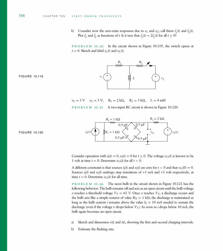
588 C H A P T E R T E N f i r s t - o r d e r t r a n s i e n t s
b) Consider now the zero-state responses due to e1 and e2; call them i′1(t) and i′2(t).Plot i′1 and i′2 as functions of t. Is it true that i′2(t) = 2i′1(t) for all t ≥ 0?
p r o b l e m 10.20 In the circuit shown in Figure 10.119, the switch opens att = 0. Sketch and label iL(t) and vL(t).
F IGURE 10.119 v1
R1
+- L v2
+-
R2
v1 = 5 V v2 = 3 V, R1 = 2 k, R2 = 3 k, L = 4 mH
p r o b l e m 10.21 A two-input RC circuit is shown in Figure 10.120.
F IGURE 10.120 R1 = 1 kΩ
R3 = 2 kΩ
+
-vO
0.5 µF
iI(t) vI(t)+-
R2 = 1 kΩ
0.5 µF
0.5 µF0.5 µF
Consider operation with iI(t) = 0, vI(t) = 0 for t ≥ 0. The voltage vO(t) is known to be1 volt at time t = 0. Determine vO(t) for all t > 0.
A different constraint is that sources iI(t) and vI(t) are zero for t < 0 and that vO(0) = 0.Sources iI(t) and vI(t) undergo step transitions of +1 mA and +1 volt respectively, attime t = 0. Determine vO(t) for all time.
p r o b l e m 10.22 The neon bulb in the circuit shown in Figure 10.121 has thefollowing behavior: The bulb remains off and acts as an open circuit until the bulb voltagev reaches a threshold voltage VT = 65 V. Once v reaches VT, a discharge occurs andthe bulb acts like a simple resistor of value RN = 1 k; the discharge is maintained aslong as the bulb current i remains above the value IS = 10 mA needed to sustain thedischarge (even if the voltage v drops below VT.) As soon as i drops below 10 mA, thebulb again becomes an open circuit.
a) Sketch and dimension v(t) and i(t), showing the first and second charging intervals.
b) Estimate the flashing rate.

10.8 Summary C H A P T E R T E N 589
90 V
R = 1 MΩ
v
i+
-
+
-C = 10 µF
Neonbulb
F IGURE 10.121
p r o b l e m 10.23 Because of the input resistance and capacitance of an oscillo-scope, laboratory observations of transients, such as the step response of the R1 − C1
circuit in Figure 10.122 may have errors in them.
vB
+
-
R2
R1
C1 C2vA
+-
Unitstep
Displayedon scope
Circuit being tested Scope input impedance
F IGURE 10.122
a) Assuming that the effect of connecting the oscilloscope to the circuit under test isto add R2 and C2 as shown in Figure 10.122, find and sketch the step responsethat will be observed at vB in this circuit. Discuss the errors introduced by thescope by comparing your result to what would be observed if the scope were ideal(R2 → ∞, C2 → 0.) Assume zero initial state.
b) A common method of coping with the errors of part (a) is to use a compensatedattenuator in series with the scope (see in Figure 10.123.) For simplicity, we examinewhat the compensated scope displays when it is connected directly to the unit stepwithout the R1 − C1 circuit of part (a). Assume zero initial state before the step isapplied.
i) What is vB immediately after the step is applied, that is, at t = 0+?
ii) What is vB as t → ∞?
vB
+
-
R2
R3
C2vA
+-
Unitstep
Displayedon scope
Compensated Scope input
C3
attenuator impedance
F IGURE 10.123

590 C H A P T E R T E N f i r s t - o r d e r t r a n s i e n t s
iii) Using your results, find vB(t) for all t.
iv) What conditions on R2, C2, R3, and C3 must be satisfied in order that therebe no natural response component, that is, no transient, in vB(t)? What is vB(t)in this case?
p r o b l e m 10.24 The RL circuit shown in Figure 10.124 is driven with the rampvI(t) = K1t, for t greater than zero, and vI(t) = 0, t < 0.
vI(t)R
L+-
iL(t)
vI(t)
t
K1t
F IGURE 10.124
a) Assuming iL(0−) = 0, sketch the current iL(t). Also find an analytic expression foriL(t).
b) In some applications, such as generating a linear sweep for a magnetically deflectedcathode-ray tube, we want to make iL(t) a linear ramp as shown in Figure 10.125.
iL(t)
t
iL(t) = K2t
F IGURE 10.125
Find a new input waveform vI(t) such that iL(t) = K2t, t > 0. Plot vI(t). Label allvalues and slopes.
p r o b l e m 10.25 For the RL circuit shown in Figure 10.126, sketch and label vR
versus time for t > 0. Assume iL(t < 0) = 0, and that T1 is five times as long as thecircuit time constant.
F IGURE 10.126vI
RL+
-
iL
vI
0 tT1
Area = A
Are
a =
A
p r o b l e m 10.26 With the capacitor initially at rest (vC(0) = 0) and discon-nected, the switch is closed to position (1) at time t = 0 in Figure 10.127.
a) Sketch the waveform vC(t) for t > 0. Label all relevant points on Figure 10.127 andcalculate the time constant.
F IGURE 10.127vC(t)
+
-R3
R1
CV+- R2
1 2
t = 0

10.8 Summary C H A P T E R T E N 591
b) At a time T > 0 (at least five time constants later), the switch is thrown (instan-taneously) to position (2). Sketch vC(t) for t > T and label all relevant points onFigure 10.127
c) With R1 = R2 = R3, is the time constant in part (a) greater than, less than, or equalto the time constant in part (b)?
p r o b l e m 10.27 For the circuit shown in Figure 10.128, sketch and label vR
versus time. Assume that vI = K1 for a long time prior to t = 0 as illustrated in the
vI RC
+-
vR
+
-
vI
t
K3t
K1
K2
F IGURE 10.128
figure.
Note that this problem can be solved in a number of simple steps by breaking the problemdown into parts and solving each part. There are several ways to do this breakdown, allof roughly equal ease.
p r o b l e m 10.28 You are given the RC circuit shown in Figure 10.129.
a) Suppose you observe that vO(t) is a triangular pulse, as shown in the sketch inFigure 10.130. Find and draw the waveform vI(t) that must be applied to producethis output signal. Label times and magnitudes, and significant parameters of thefunction.
b) Now the input signal is changed. You apply a ramp starting at t = 0, vI(t) = tu−1(t),as the input signal vI(t). (Note that u−1(t) represents a unit step at t = 0.) Sketchand label the output signal vO(t) for 0 < t < 5.
vI(t)
1 MΩ
+- vO(t)
+
-
1 µF
F IGURE 10.129
c) Give an analytic expression for the output signal vO(t) you sketched in (b).
vO (V)
t (s)-10 10-5 5
-5
5
F IGURE 10.130
p r o b l e m 10.29 Consider the digital memory element shown in Figure 10.131.The voltage at the storage node with respect to ground is denoted vM. The figure alsoshows a parasitic resistance RP from the storage node to ground. This resistance willcause a leakage of the charge stored in the memory.
The signal A is fed to an inverter and the inverter drives the input dIN of the mem-ory element. All inverters shown in Figure 10.131 have a load resistor RL and the on

592 C H A P T E R T E N f i r s t - o r d e r t r a n s i e n t s
F IGURE 10.131dOUTdIN
Store
CM
vMA
RP
resistance of the pulldown MOSFETs in each of the inverters is RON. Assume that theon resistance of the switch driven by the Store signal is also RON. The supply voltage isVS and the threshold voltage for the MOSFETs is VT. In doing this problem, assumethat RP is much larger than either RON or RL.
a) Suppose that a 0-V to VS-step is applied at the Store input of the memory elementat t = 0. Sketch vM(t) for t ≥ 0, assuming that vM(t = 0) = 0, and that A is at0 V throughout. Assuming that RON RP, what is the maximum value attainedby vM?
b) Suppose, now, that a rectangular pulse of height VS is applied at the Store input of thememory element, and that A is at 0 V throughout. The rising transition of the pulseoccurs at t = 0 and the falling transition at t = T. Determine the minimum value ofthe pulse width T so that vM can charge up to VH, where VH = VIH = VOH, thehigh voltage threshold of the static discipline. Assume the following: vM(t = 0) = 0;VH < VS; VH > VT.
c) Let us now consider the case in which A is at VS throughout, and vM(t = 0) = VS.Sketch vM(t) for t ≥ 0, when a 0-V to VS-step is applied at the Store input of thememory element at t = 0. What is the minimum value attained by vM?
d) Suppose, now, that a rectangular pulse of height VS is applied at the Store inputof the memory element. The rising transition of the pulse occurs at t = 0 and thefalling transition at t = T. Determine the minimum value of the pulse width T sothat vM can discharge from VS to VL, where VL = VIL = VOL, the low voltagethreshold of the static discipline. Assume as in (c) that A is at VS throughout andthat vM(t = 0) = VS. Assume further that VL < VT and that VL is greater than theminimum value attainable by vM.
e) Suppose the memory element is storing a 1 (assume vM = VS) at t = 0 and thatStore = 0. Assuming that no further Store signals occur, determine the period oftime for which the output (dOUT) of the memory element will be valid. (Hint: theoutput becomes invalid when dOUT switches from 1 to 0.)

c h a p t e r 11
11.1 P O W E R A N D E N E R G Y R E L A T I O N S F O R A S I M P L E R C C I R C U I T
11.2 A V E R A G E P O W E R I N A N R C C I R C U I T
11.3 P O W E R D I S S I P A T I O N I N L O G I C G A T E S
11.4 N M O S L O G I C
11.5 C M O S L O G I C
11.6 S U M M A R Y
E X E R C I S E S
P R O B L E M S


energy and power in
d ig i t a l c i rcu i t s 11Digital circuits form the basis of a large number of battery-powered appliancesused in our day to day life, including cell phones, beepers, digital watches, cal-culators, and laptop computers. A battery of a given weight and size stores afixed amount of energy. The amount of time that the battery will last beforerequiring a replacement or a recharge depends on the amount of energy con-sumed by the device. Similarly, the heat generated by a device depends onits energy consumption rate, or power dissipation. Thus, both the amount ofenergy consumed by a device and the rate of energy consumption are criticalissues in the design of circuits.
11.1 P O W E R A N D E N E R G Y R E L A T I O N S F O RA S I M P L E R C C I R C U I T
Let us first develop the power and energy relations for the simple RC circuitshown in Figure 11.1. Assume that the switch is closed at time t = 0 connectingthe voltage source to the RC network. Further, assume that the capacitor haszero charge on it initially.
We know that the power delivered to a two-terminal element at any giveninstant of time t with a voltage v(t) across it and a current i(t) through it is given by
p(t) = v(t)i(t) (11.1)
where the current i(t) is defined to be positive if it enters the element at theterminal with the positive voltage. Power is delivered to the element if i(t) ispositive, for example, in a resistor or a charging capacitor. A resistor dissipates
C
vCR
V+
-
F IGURE 11.1 Energy drawnfrom a power source by a simpleRC circuit.
595

596 C H A P T E R E L E V E N e n e r g y a n d p o w e r i n d i g i t a l c i r c u i t s
energy, while a capacitor stores it. Power is delivered by an element if i(t) isnegative, for example, in a battery or in a discharging capacitor.
Referring to Figure 11.1, when the switch is closed, the voltage sourcebegins to charge the capacitor C through the resistor R. What is the instanta-neous power drawn from the voltage source? The instantaneous power drawnfrom the voltage source is given by
p(t) = Vi(t) (11.2)
where
i(t) = V − vC(t)
R. (11.3)
Using the equations derived for capacitor charging dynamics in Section 10.4,we can write
vC = V(1 − e−tRC ) (11.4)
Substituting the expression for vC from Equation 11.4 into Equation 11.3, andthat for i(t) from Equation 11.3 into Equation 11.2, we get
p(t) = V2
Re
−tRC . (11.5)
What is the total amount of energy supplied by the voltage source if theswitch is closed for a long period of time? Since power is the rate at whichenergy is supplied, the energy w supplied over an interval of time 0 → T, isgiven by
w =∫ T
0p(t)dt. (11.6)
The total amount of energy supplied by the voltage source can be obtained bytaking the limit as T goes to ∞.
Thus, the total amount of energy supplied by the voltage source as T goesto ∞ is given by
w =∫ t = ∞
t = 0
V2
Re
−tRC dt
= −V2
RRCe
−tRC
∣∣∣∣∣t = ∞
t = 0
= CV2.

11.2 Average Power in an RC Circuit C H A P T E R E L E V E N 597
What is the amount of energy stored in the capacitor when T goes to ∞?After a long period of time, the capacitor will charge up to the voltage V. FromEquation 9.18, the amount of energy stored on a capacitor with a voltage Vacross it is given by 1/2CV2.
What is the amount of energy dissipated by the resistor? Since the voltagesource supplies an amount of energy equal to CV2, and the amount of energystored in the capacitor is 1/2CV2, the remaining half of the energy supplied bythe voltage source must have been dissipated in the resistor. We can verify thisby explicitly computing the energy dissipated in the resistor as follows. Theinstantaneous power for the resistor is given by
p(t) = i(t)2R
=(
V
Re
−tRC
)2
R
= V2
Re
−2tRC .
The energy dissipated in the resistor over the interval t = 0 to t = ∞ isgiven by
w =∫ t = ∞
t = 0
V2
Re
−2tRC dt
= −V2
R
RC
2e
−2tRC
∣∣∣∣∣t = ∞
t =
= −V2C
2e
−2tRC
∣∣∣∣∣t = ∞
t = 0
= 1
2CV2.
Interestingly, notice that if the transients are allowed to settle, the total energydissipated in the resistor when charging a capacitor is independent of itsresistance value. The same is true when discharging a capacitor through aresistor.
11.2 A V E R A G E P O W E R I N A N R C C I R C U I T
Let us now derive the average power dissipated by the slightly more compli-cated circuit depicted in Figure 11.2 comprising two resistors and a capacitorconnected to a voltage source through a switch. Assume that a square wave

598 C H A P T E R E L E V E N e n e r g y a n d p o w e r i n d i g i t a l c i r c u i t s
F IGURE 11.2 An RC circuit witha switch.
C
vCR1
V+
-R2
S
S
T1 T2
Switchclosed
Switchopen
T
signal S with a cycle time of T such as that shown in Figure 11.2 controls theswitch, so that the switch is closed for an interval T1, then open for an inter-val T2, and so on. When the switch is closed, the voltage source charges upthe capacitor. The capacitor discharges through resistor R2 when the switch isopen. We will be particularly interested in the special case where the T1 andT2 intervals are large enough that the capacitor voltages during each of theintervals T1 and T2 reach their respective steady state values.
As current flows through the resistors, energy is dissipated. However, thecapacitor does not dissipate energy. It simply stores energy when the switchis closed (during T1) and supplies this stored energy when the switch is open(during T2). We can derive the instantaneous power p(t) dissipated in the circuitas a function of time. We can also derive the average power p dissipated by thecircuit.
The average power is defined as the total amount of energy w dissipated duringsome time interval, divided by the length of the time interval T.
In other words,
p = w
T.
More specifically, if w1 is the energy dissipated during the interval T1 and w2 isthe energy dissipated during the interval T2, then the average power dissipatedin the circuit is given by
p = w1 + w2
T. (11.7)

11.2 Average Power in an RC Circuit C H A P T E R E L E V E N 599
C
vCR1
V R2
+
-
F IGURE 11.3 Equivalent circuit with theswitch closed.
C
vCRTH = R1||R2
VTH
+
-VTH =V R2
R1+R2
F IGURE 11.4 Thévenin equivalent circuitwith the switch closed.
We will also use the fact that the energy dissipated within some interval oftime is the time integral of the instantaneous power within that interval. Forexample, the energy dissipated within the time interval T is given by
wT =∫ t=T
t=0p(t)dt. (11.8)
11.2.1 E N E R G Y D I S S I P A T E D D U R I N G I N T E R V A L T1
Let us first consider the case when the switch is closed and derive the value of w1.When the switch is closed, the circuit shown in Figure 11.3 applies.
To compute the energy dissipated by the circuit, we first need to determinethe currents through the resistors R1 and R2. To facilitate the computation ofthe currents, let us first determine vC. To simplify the calculation of vC, wetransform the circuit shown in Figure 11.3 to its Thévenin equivalent shown inFigure 11.4. We assume that time t starts from 0 at the moment that the signalS transitions from low to high. From the circuit in Figure 11.4, we can write anexpression for the voltage vC as
vC = VTH
(1 − e
−tRTHC
).
We will be particularly interested in the special case in which t → ∞. Whent → ∞, vC → VTH.
We are now ready to determine the instantaneous power dissipated in thecircuit when the switch is closed. In general, we cannot use the Thévenin equiv-alent circuit to determine the power consumed in the original circuit because thepower computation is a nonlinear process. Therefore, returning to the circuit inFigure 11.3, the instantaneous power dissipated by the circuit when the switchis closed is given by the sum of the power dissipated in resistors R1 and R2.

600 C H A P T E R E L E V E N e n e r g y a n d p o w e r i n d i g i t a l c i r c u i t s
Recalling that the power dissipated in a resistance R with a voltage v across itis v2/R, we can write
p(t) = Power in R1 + Power in R2
= (V − vC)2
R1+ v2
C
R2
= [V − VTH(1 − e−t
RTHC )]2R1
+ [VTH(1 − e−t
RTHC )]2R2
.
We are now in a position to derive the energy dissipated in the circuit using therelationship from Equation 11.8.
w1 =∫ t=T1
t=0
[V − VTH(1 − e
−tRTHC )
]2
R1+
[VTH(1 − e
−tRTHC )
]2
R2
dt,
which yields:
w1 = V2TH
R2
[t − RTHC
2e
−2tRTHC + 2RTHCe
−tRTHC
]t = T1
t = 0
+ 1
R1
[(V − VTH)2t − V2
THRTHC
2e
−2tRTHC − 2(V − VTH)VTHRTHCe
−tRTHC
]t = T1
t = 0
= V2TH
R2
[T1 − RTHC
2e
−2T1RTHC + 2RTHCe
−T1RTHC
]
− V2TH
R2
[−RTHC
2+ 2RTHC
]
+ 1
R1
[(V − VTH)2T1 − V2
THRTHC
2e
−2T1RTHC − 2(V − VTH)VTHRTHCe
−T1RTHC
]
− 1
R1
[−V2
THRTHC
2− 2(V − VTH)VTHRTHC
].

11.2 Average Power in an RC Circuit C H A P T E R E L E V E N 601
Separating the terms containing a T1 factor, we get
w1 = V2T1
R1 + R2+ V2
TH
R2
[−RTHC
2e
−2T1RTHC + 2RTHCe
−T1RTHC
]
− V2TH
R2
[−RTHC
2+ 2RTHC
]
+ 1
R1
[−V2
THRTHC
2e
−2T1RTHC − 2(V − VTH)VTHRTHCe
−T1RTHC
]
− 1
R1
[−V2
THRTHC
2− 2(V − VTH)VTHRTHC
].
Rearranging and simplifying,
w1 = V2T1
R1 + R2+ CV2
TH
2
(1 − e
−2T1RTHC
). (11.9)
When T1 RTHC, the capacitor can be assumed to charge up to its steady-state value of VTH, and e−2T1/RTHC → 0. In this situation, the above expressionfor w1 simplifies to:
w1 = V2
R1 + R2T1 + V2
THC
2(11.10)
where
VTH = VR2
R1 + R2.
11.2.2 E N E R G Y D I S S I P A T E D D U R I N G I N T E R V A L T2
Now, let us consider the second interval T2 in which the switch is off. DuringT2, the capacitor discharges through the resistor R2. For simplicity, let usassume the special case considered in the previous section in which T1 RTHC.In this case, at the start of the second interval, the capacitor will have an initial
C
vC
R2
F IGURE 11.5 Equivalent circuitwith the switch open.
voltage of VTH across it.As in the previous section, let us first determine vC. When the switch is
off, the circuit shown in Figure 11.5 applies. For this derivation we assume

602 C H A P T E R E L E V E N e n e r g y a n d p o w e r i n d i g i t a l c i r c u i t s
that time t starts from 0 at the moment that the signal S transitions from highto low. Since the initial voltage on the capacitor is VTH, the voltage vC isgiven by
vC = VTHe−t
R2C .
Notice that as t → ∞, the capacitor voltage vC → 0.We are now ready to determine the instantaneous power dissipated in the
circuit when the switch is open. The instantaneous power dissipated in resistorR2 is given by
p(t) = v 2C
R2
= 1
R2
(VTHe
−tR2C
)2
.
The corresponding energy consumed during T2 is given by
w2 =∫ t = T2
t = 0p(t)dt (11.11)
=∫ t = T2
t = 0
v 2C
R2dt (11.12)
=∫ t = T2
t = 0
1
R2
(VTHe
−tR2C
)2
(11.13)
= −1
2R2V2
THR2Ce−2tR2C
∣∣∣∣t = T2
t = 0(11.14)
= V2THC
2
(1 − e
−2T2R2C
). (11.15)
When T2 R2C, we can ignore the second term in the above equation andwrite:
w2 = V2THC
2. (11.16)

11.2 Average Power in an RC Circuit C H A P T E R E L E V E N 603
11.2.3 T O T A L E N E R G Y D I S S I P A T E D
Combining Equations 11.10 and 11.16, for the case of T1 RTHC andT2 R2C we obtain the total energy dissipated in a cycle T:
w = w1 + w2 = V2
R1 + R2T1 + V2
THC
2+ V2
THC
2.
Combining terms, we get
w = V2
R1 + R2T1 + V2
THC.
Dividing by T we get the average power p:
p = V2
(R1 + R2)
T1
T+ V2
THC
T. (11.17)
For a symmetric square wave, T1 = T/2, so Equation 11.17 simplifies to:
p = V2
2(R1 + R2)+ V2
THC
T. (11.18)
Equation 11.18 shows that the average power is the sum of two terms. Thefirst term is independent of the time period of the square wave and is called thestatic power pstatic. It can be computed independently by removing all capacitorsand inductors from the circuit (in other words, replace the capacitors with opencircuits and inductors with short circuits). The second term is related to thecharging and discharging of the capacitor, and depends on the time periodof the square wave. This term is called the dynamic power pdynamic. In otherwords,
pstatic = V2
2(R1 + R2)(11.19)
pdynamic = V2THC
T. (11.20)
Notice that if the switch were kept closed for a long period of time, nodynamic power is dissipated in the steady state. Notice further that the dynamicpower dissipation is proportional to the capacitor value, the switching fre-quency, and the square of the voltage, but independent of the resistancevalue.
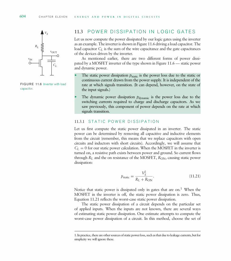
604 C H A P T E R E L E V E N e n e r g y a n d p o w e r i n d i g i t a l c i r c u i t s
11.3 P O W E R D I S S I P A T I O N I N L O G I C G A T E S
Let us now compute the power dissipated by our logic gates using the inverteras an example. The inverter is shown in Figure 11.6 driving a load capacitor. The
vIN
vOUT
RL
CL
VS
F IGURE 11.6 Inverter with loadcapacitor.
load capacitor CL is the sum of the wire capacitance and the gate capacitancesof the devices driven by the inverter.
As mentioned earlier, there are two different forms of power dissi-pated by a MOSFET inverter of the type shown in Figure 11.6 static powerand dynamic power.
The static power dissipation pstatic is the power loss due to the static orcontinuous current drawn from the power supply. It is independent of therate at which signals transition. (It can depend, however, on the state ofthe input signals.)
The dynamic power dissipation pdynamic is the power loss due to theswitching currents required to charge and discharge capacitors. As wesaw previously, this component of power depends on the rate at whichsignals transition.
11.3.1 S T A T I C P O W E R D I S S I P A T I O N
Let us first compute the static power dissipated in an inverter. The staticpower can be determined by removing all capacitive and inductive elementsfrom the circuit (remember, this means that we replace capacitors with opencircuits and inductors with short circuits). Accordingly, we will assume thatCL = 0 for our static power calculation. When the MOSFET in the inverter isturned on, a resistive path exists between power and ground. So current flowsthrough RL and the on resistance of the MOSFET, RON, causing static powerdissipation:
pstatic = V2S
RL + RON. (11.21)
Notice that static power is dissipated only in gates that are on.1 When theMOSFET in the inverter is off, the static power dissipation is zero. Thus,Equation 11.21 reflects the worst-case static power dissipation.
The static power dissipation of a circuit depends on the particular setof applied inputs. When the inputs are not known, there are several waysof estimating static power dissipation. One estimate attempts to compute theworst-case power dissipation of a circuit. In this method, choose the set of
1. In practice, there are other sources of static power loss, such as that due to leakage currents, but forsimplicity we will ignore these.

11.3 Power Dissipation in Logic Gates C H A P T E R E L E V E N 605
inputs that results in the worst-case power dissipation for the circuit. For thesimple inverter, this estimate is the power dissipated when the input is a logical 1and the MOSFET is on, for example, as computed in Equation 11.21. Anotherestimate is statistical, and is based on determining the expected power overall possible input sets. Each input set is assigned an occurrence probability andthe power for that input set is determined. Then the expected power is com-puted by averaging the power for each set of inputs weighted by the occurrenceprobability for that input set. Yet another estimate assumes that each input tothe circuit is a square wave comprising an alternating sequence of logical 1’sand 0’s.
e x a m p l e 11.1 s t a t i c p o w e r d i s s i p a t i o n Let us computethe worst-case static power dissipation for the logic gate in Figure 11.7. The worst case
A
B
C D
RL
VS
F IGURE 11.7 Worst-case staticpower dissipation in a logic gate.
dissipation occurs when all the inputs are high. Suppose RL = 100 k and RON =10 k for each of the MOSFETs. Also assume that VS = 5 V.
When all the inputs are high, the effective resistance Reff between power andground is
Reff = RL + (2RON‖RON‖RON).
In other words, Reff = 104 k. The maximum static power dissipation is
pstatic = V2S
Reff= 25/104 = 0.24 mW = 240 µW. (11.22)
11.3.2 T O T A L P O W E R D I S S I P A T I O N
Let us now compute the total power dissipated in the inverter when a time-varying input signal is applied. The total power will include both the staticpower and the dynamic power. Dynamic power dissipation results from thetransient currents that flow through the resistors to charge and discharge thecapacitor, as depicted in Figures 11.8 and 11.9.
Suppose we have a square-wave signal input to the inverter representinga sequence of alternating 1’s and 0’s. Let the time period of the square wavebe T. Therefore, the frequency of the square wave is f = 1/T. As depicted inFigure 11.8, when the input voltage is low, the MOSFET is off, and the loadcapacitor CL is charged up to VS by the power supply through the resistor RL.As suggested in Figure 11.9, when the input signal is high, the MOSFET is on,and the capacitor discharges through the on resistance of the MOSFET. After along time, the voltage on the load capacitor will reach the steady state value ofVSRON/(RON + RL). Assume that the period of the input square wave is longenough for the capacitor to charge and discharge completely.

606 C H A P T E R E L E V E N e n e r g y a n d p o w e r i n d i g i t a l c i r c u i t s
VS
vIN vOUT
RL
CL
F IGURE 11.8 Charging the load capacitor.
VS
vIN
vOUT
RL
CL
F IGURE 11.9 Discharging the load capacitor.
We will derive the average total power consumed by the inverter as in theexample in Section 11.2. Let us denote the high part of the input signal as T1and the low part of the signal as T2. Similarly, let w1 be the energy dissipatedduring the interval T1 and w2 the energy dissipated during the interval T2. Thenthe average power dissipated in the circuit is given by
p = w1 + w2
T.
Energy Dissipated During Interval T1
Let us first consider the case when the input to the MOSFET switch is highand the switch is closed, and derive the value of w1. When the switch is closed,the situation corresponds to that shown in Figure 11.9 and the circuit shownin Figure 11.10 applies. Figure 11.11 shows the Thévenin equivalent for thiscircuit.
For the circuit shown in Figure 11.11, vC is given by the following expres-sion (assuming that time t starts from 0 at the moment that the input signal
CL
vCRL
VSRON
+
-
F IGURE 11.10 Equivalent circuit for theinverter with the MOSFET switch closed.
CL
vCRTH = RL||RON
VTH
+
-VTH = RL+RON
VS RON
F IGURE 11.11 Thévenin equivalent circuit for theinverter with the switch closed.

11.3 Power Dissipation in Logic Gates C H A P T E R E L E V E N 607
transitions from low to high):
vC = VTH + (VS − VTH)e−t
RTHCL .
By substituting t = 0, we can verify that the capacitor is initially charged toVS when the MOSFET just turns on. Similarly, by substituting t = ∞, we canconfirm that the final voltage on the capacitor is VTH.
The rest of the derivation for w1 follows the steps in Section 11.2. WhenT1 RTHCL, we obtain the following simplified expression for w1:
w1 = V2S
RL + RONT1 + V2
SR2LCL
2(RL + RON)2. (11.23)
Energy Dissipated During Interval T2
Now, let us consider the second interval T2 in which the input signal is lowand the switch is off. During T2, the capacitor charges through the resistor RL.The initial voltage on the capacitor is VTH.
As in the previous section, let us first determine vC. When the switchis off, the circuit shown in Figure 11.12 applies. Since the initial voltage on
CL
vCRL
VS
+
-
F IGURE 11.12 Equivalentcircuit with the switch open for theinverter.
the capacitor is VTH and the final voltage is VS, we can write the followingexpression for vC:
vC = VTH + (VS − VTH)
(1 − e
−tRLCL
).
Notice that as t → ∞, the capacitor voltage vC → VS. Similarly, for t = 0, thecapacitor voltage is VTH.
Following the derivation in Section 11.2, we can derive the followingexpression for w2 when T2 RLCL:
w2 = V2SR2
LCL
2(RL + RON)2.
Total Energy Dissipated
Combining the expressions for w1 and w2, we obtain total energy dissipatedby the inverter in a cycle:
w = w1 + w2 = V2S
RL + RONT1 + V2
SR2LCL
2(RL + RON)2+ V2
SR2LCL
2(RL + RON)2.

608 C H A P T E R E L E V E N e n e r g y a n d p o w e r i n d i g i t a l c i r c u i t s
In other words,
w = V2S
RL + RONT1 + V2
SR2LCL
(RL + RON)2.
Dividing by T we get the average power p:
p = V2S
(RL + RON)
T1
T+ V2
SR2LCL
(RL + RON)2T. (11.24)
For asymmetric square wave, T1 = T/2, so Equation 11.24 simplifies to:
p = V2S
2(RL + RON)+ V2
SR2LCL
(RL + RON)2T. (11.25)
As expected, Equation 11.25 shows that the average power is the sum of astatic component2 and a dynamic component as indicated by the followingequations:
pstatic = V2S
2(RL + RON)(11.26)
pdynamic = V2SR2
LCL
(RL + RON)2T. (11.27)
Notice that the dynamic power dissipated is proportional to the frequency withwhich the input signal transitions. Not surprisingly, high-performance chipsthat clock at high frequencies dissipate a lot of power. Also notice that thepower is related to the square of the supply voltage. As clock speeds of VLSIchips increase, power considerations are causing manufacturers to continuallyreduce the supply voltages. Whereas 5-volt power supplies were the norm inthe 80s, voltages closer to 3 volts have been the norm in the 90s, and suppliescloser to 1.5 volts have been commonplace after the year 2000.
It is instructive to compare the relative values of the static and dynamicpower. To do so, we take the ratio of the static and dynamic power as follows:
pstatic
pdynamic= V2
S
2(RL + RON)× (RL + RON)2T
V2SR2
LCL.
2. The static power for the inverter computed here (Equation 11.26) is half that in Equation 11.21because here we are assuming that the input is a symmetric square wave, while Equation 11.21presented the worst case.

11.3 Power Dissipation in Logic Gates C H A P T E R E L E V E N 609
Simplifying and rearranging, we get
pstatic
pdynamic= RL + RON
RL× T
2RLCL. (11.28)
Since for normal operation of the digital gate, T RLCL, we see that pstatic pdynamic. Thus, it becomes imperative to minimize the static power.
e x a m p l e 11.2 d y n a m i c p o w e r d i s s i p a t i o n Let us com-pute the worst-case dynamic power dissipation for the logic gate in Figure 11.7 usingEquation 11.27 under the following conditions:
The load capacitor driven by the output of the gate has a value of CL =0.01 pF.
The clock frequency f = 1/T at which signals transition is 10 MHz. In other words,an input cannot change at a rate greater then 10 MHz.
The power supply voltage VS is 5 V.
RL = 100 k and RON = 10 k for each of the MOSFETs.
Equation 11.27 applies when T/2 RTHCL and T/2 RLCL. First, let us confirmthat these relationships hold. Since RL is greater than RTH, it is sufficient to verifythat T/2 RLCL. For the parameters supplied, T/2 = 1/(20 × 106) = 50 ns andRLCL = 100×103 ×0.01×10−12 = 1 ns. Clearly, the circuit time constants are muchsmaller than the signal intervals.
To obtain the worst-case dynamic power dissipation, we assume that the load capacitoris charged and discharged every cycle. Under these conditions, Equation 11.27 gives theformula for the worst-case dynamic power (with RON replaced by RONpd, where RONpdis the resistance of the pulldown network). We rewrite this equation here by replacingRON in the equation with the resistance of the pulldown network RONpd:
pdynamic = V2SR2
LCL
(RL + RONpd)2T.
Since it is clear from the formula that the dynamic power is maximized when RONpd isminimized, we assume that all the pulldown MOSFETs are turned on when the clocksignal goes high. Accordingly, if the on resistance for a MOSFET is RON, we must usethe following value for RONpd:
RONpd = (2RON‖RON‖RON).

610 C H A P T E R E L E V E N e n e r g y a n d p o w e r i n d i g i t a l c i r c u i t s
We also assume that all the input signals switch at the clock frequency. Thus the worst-case power dissipation is given by
pdynamic = 52 × (100 × 103)2 × 0.01 × 10−12 × 10 × 106
(100 × 103 + 4 × 10³)2
= 2.3 µW.
Observe that for our example, the static power dissipation (from Equation 11.22) isnearly 100 times larger than the dynamic power dissipation.
e x a m p l e 11.3 t o t a l p o w e r d i s s i p a t i o n i n a m o s
i n v e r t e r The inverter shown in Figure 11.13 drives a load capacitor CL thatmodels the gate-to-source and interconnect capacitances of the immediate downstreamcircuitry. We wish to approximate the average power dissipated in the inverter giventhat the input voltage vIN is a 100-MHz square wave. In doing so, we assume that theMOSFET on-state resistance RON satisfies RON RPU.
Since RON RPU, the output voltage rises much more slowly than it falls. The timeconstant for the rising transient is RPUCL = 1 ns, which is much smaller than a halfperiod of the input square wave. Therefore, all inverter transients fully settle, and thepower dissipated in the inverter may be approximated as the sum of a static dissipationplus a dynamic dissipation.
The static dissipation occurs when the MOSFET is on. The instantaneous value of thisdissipation is approximately V2
S/RPU = 22.5 µW because RON RPU. However, sincethe MOSFET is on only half the time, the average static power dissipation is 11.25 µW.
The dynamic dissipation is caused by the repeated charging and discharging of CL. Theenergy CLV2
S/2 is lost during both the charging and discharging of the capacitor. Thus,the dynamic loss is CLV2
Sf = 1.125 µW, where f = 100 MHz is the switching frequencyof the input voltage.
Finally, the total average power dissipated is 12.375 µW, with the static dissipationbeing the dominant component of this loss.
F IGURE 11.13 An inverterdriving a load capacitor. +
-vIN(t) CL = 10 fF
VS = 1.5 V
RPU = 100 kΩ vOUT(t)

11.4 NMOS Logic C H A P T E R E L E V E N 611
11.4 N M O S L O G I C
The pullup device that we have been using thus far (and seen previously inSection 6.11) in our digital gates is a resistor (for example, see the inverter inFigure 11.6). In practice, we do not really use resistors as we know them theywould take up too much area. Rather, as displayed in Figure 11.14), we mightuse another MOSFET with its gate connected to a second supply voltage VA,where VA is at least one threshold voltage higher that the supply voltage VS.This way, the pullup MOSFET remains in its ON state for any voltage between0 and VS applied at its source. (b)
VS
(a)
VS
RLVA
F IGURE 11.14 A MOS pullupdevice.
This style of building logic gates using n-channel MOSFETs for both thepullups and the pulldowns is called NMOS logic.3 The RON of the pullupserves as the load resistor. The gate length of the pullup MOSFET is sized tobe larger relative to the pulldown MOSFET, so the static discipline is satisfied(see Section 6.11). The power and energy calculations of Section 11.3 apply toNMOS devices with RON of the pullup replacing the load resistor RL in theanalyses.
11.5 C M O S L O G I C
Logic gates in the NMOS logic family dissipate static power even when thecircuit is idle. In the example discussed earlier, the static power was nearly 100times larger than the power associated with signal activity. Because the pullupMOSFET is always on, the cause of the static power dissipation is the resistivepath from the power supply to ground when the pulldown MOSFET is on.In this section, we introduce another type of logic called CMOS or Comple-mentary MOS, which has no static power dissipation. Because of its low staticpower dissipation,4 CMOS logic has all but replaced NMOS in modern VLSIchips.
CMOS logic makes use of a complementary MOSFET called thep-channel MOSFET or the PFET.5 The n-channel MOSFET that we have
NFET symbol
D
S
G
D
S
G
OFF State
vGS < VTn
D
S
GRONn
ON State
vGS ≥ VTn
F IGURE 11.15 The switch-resistor model of the n-channelMOSFET or the NFET.
dealt with thus far is called an NFET. The symbols and the SR circuit modelsfor the NFET and PFET are shown in Figures 11.15 and 11.16, respectively.As we saw previously in Section 6.6, the NFET turns on when its vGS ≥ VTn.
3. NMOS logic families actually use a special kind of pullup called a depletion-mode MOSFET,which has a negative threshold voltage. The MOSFETs that we have been dealing with thus farare called enhancement-mode MOSFETs. The depletion-mode MOSFET is used as a pullup withits gate connected to its source instead of the power supply. One of its advantages is that it doesnot require a second supply voltage.
4. Although the static power for CMOS is significantly lower than NMOS, sources of static powerloss still remain, such as leakage currents.
5. We saw the p-channel MOSFET briefly in the context of amplifiers in Chapter 7 in Example 7.7.Here we will focus on its use in digital circuits.

612 C H A P T E R E L E V E N e n e r g y a n d p o w e r i n d i g i t a l c i r c u i t s
When it is on, a resistance RONn appears between its drain and source. Incontrast, the PFET turns on when its vGS ≤ VTp. VTp is usually negative (forexample, −1 volt). When it is on, a resistance RONp appears between its drainand source. The drain terminal of the PFET is chosen as the terminal with thelower voltage. In contrast, the channel terminal of the NFET with the higher
D
S
G RONp
ON state
vGS ≤ VTp
PFET symbolD
S
G
D
S
G
OFF state
vGS > VTp
F IGURE 11.16 The switch-resistor model of the p-channelMOSFET or the PFET.
voltage is labeled as the drain.As an example, an NFET with a threshold voltage VTn = 1 V turns on
when the voltage between its gate and source is raised above 1 V. A PFET witha threshold voltage VTp = −1 V turns on when the voltage between its gateand source is lowered below −1 V. In other words, the PFET turns on whenthe voltage between its source and gate is raised above 1 V.
A CMOS inverter is shown in Figure 11.17. When the input voltage is high(vIN = VS), the NFET is ON and the PFET is off, resulting in a low outputvoltage. When the input voltage is low (vIN = 0), the NFET turns off and thePFET turns on, resulting in a high output voltage.
CMOS logic does not suffer static power dissipation. Referring toFigure 11.17, provided the input vIN is at VS or 0, notice that the two com-plementary MOSFETs are never on at the same time. Thus, there is never anydirect resistive path from the power supply to ground. Hence there is no staticpower dissipation.
VS
vINvOUT
PFET
NFET
G
D
S
S
D
G
F IGURE 11.17 CMOS invertercircuit.
e x a m p l e 11.4 p o w e r d i s s i p a t i o n i n a c m o s i n v -
e r t e r Let us compute the dynamic power dissipated in the CMOS inverter. TheCMOS inverter does not suffer from static power loss, since at any instant of time, eitherthe pullup or the pulldown device is off, thereby precluding any continuous current flow.
The circuit model of the inverter using the SR MOSFET models for the PFET and theNFET is shown in Figure 11.18. As the model shows, no current flows directly from VS
to ground for either a high or a low input signal.
Let us assume that a square-wave signal such as a clock with time period T is fed to theinput of the inverter as shown in Figure 11.19. Further assume that the inverter drivesa load capacitor CL. We shall compute the power dissipated by the inverter for thissignal. A signal that transitions every cycle will result in the worst-case dynamic powerdissipation.
During the first half of the cycle, the load capacitor CL is discharged, and during thesecond half of the cycle, it is charged up to the supply voltage. Since static and dynamiccurrents don’t flow simultaneously in CMOS devices, we can compute the averagedynamic power dissipated using the following very simple method.
Recall that the average power dissipated is defined as the energy dissipated in a cycledivided by the cycle time T. During the low half cycle of the input signal, a quantityof charge equal to QL is transferred from the power source to the capacitor. Assumingthat the cycle time of the input signal is large enough for the capacitor to charge up to

11.5 CMOS Logic C H A P T E R E L E V E N 613
VS
vIN
vOUT
CLT
T/2
F IGURE 11.19 CMOS inverter power dissipation.
the supply voltage,
VS
vOUT
(a) vIN low
RONP
RONN
VS
vOUT
(b) vIN high
RONN
RONP
F IGURE 11.18 CMOS invertermodel.
Q L = C LVS.
Then, during the second half cycle, the same charge is transferred from the capacitor toground. Effectively, a charge Q L is transferred from the power source to ground duringeach cycle. The amount of energy lost during this transfer is given by VSQ L. We dividethis quantity by T to obtain the average power. Thus,
pdynamic = VSQ L/T (11.29)
= VSC LVS/T (11.30)
= fC LV2S (11.31)
where f is the frequency of the square wave signal.
We can also derive the same answer from first principles as follows. The time-averagedynamic power dissipated is the product of the power supply voltage and the averagecurrent supplied by the power supply. In other words,
pdynamic = VS1
T
∫ T
0i(t)dt
where VS is the DC power supply voltage and i(t) is the current supplied by the powersource as a function of time.
Figure 11.20 shows the situation where the input signal is low (second half cycle) and
VS
vOUT
i
CL
RONp
F IGURE 11.20 Load capacitorcharging.
the load capacitor is charging up through the on resistance of the PFET. Figure 11.21shows the situation where the input signal is high (first half cycle) and the load capacitordischarges to ground through the on resistance of the NFET.

614 C H A P T E R E L E V E N e n e r g y a n d p o w e r i n d i g i t a l c i r c u i t s
Because the pullup switch is off in the first half cycle (when the input is high), notice thatthe power supply directly provides a current only during the second half cycle (whenthe input is low). Therefore, power is delivered by the power supply only during theinterval T/2 → T. Thus,
pdynamic = VS1
T
∫ T
T/2i(t)dt. (11.32)
If Q(t) is the charge on the capacitor as a function of time, we have
vOUT
CLRONn
i
F IGURE 11.21 Load capacitordischarging.
i(t) = dQ(t)
dt.
Therefore
pdynamic = VS1
T
∫ T
T/2
dQ(t)
dtdt. (11.33)
Furthermore, we know that
Q(t) = CLvOUT(t)
where vOUT(t) is the voltage across the load capacitor as a function of time. Differenti-ating both sides with respect to t, we get
dQ(t)
dt= CL
dvOUT(t)
dt.
Substituting for dQ(t)/dt in Equation 11.33 and observing that vOUT rises from 0 to VS
during the second half cycle, we obtain:
pdynamic = VSCL1
T
∫ VS
0dvOUT (11.34)
= VSCL1
TVS (11.35)
= V2SCL
T. (11.36)
The dynamic power dissipated by the CMOS inverter is therefore V2SCL/T. If T = 1/f,
the dynamic power dissipated by the CMOS inverter is fV2SCL.
In reality, it is difficult to obtain instantaneous input rise and fall times. When the rise andfall times are finite, there will a short period of time in the middle of an input transition

11.5 CMOS Logic C H A P T E R E L E V E N 615
t
iT
t
vIN
F IGURE 11.22 Static powerloss due to nonzero signal rise andfall times.
interval (for example, when vIN = 2.5 V) in which both MOSFETs will be turned on,resulting in a current path from the power supply to ground. This transient switchingcurrent, iT, depicted in Figure 11.22 is another source of dynamic power loss, but weignore it in our analyses.
e x a m p l e 11.5 p o w e r d i s s i p a t i o n i n a n o t h e r c m o s
i n v e r t e r The circuit shown in Figure 11.23 is the same as that shown inFigure 11.13 except that the inverter in Figure 11.23 is a CMOS inverter. As in Exam-ple 11.3, we wish to approximate the average power dissipated in the inverter giventhat vIN is a 100-MHz square wave. Again, we will assume that the on-state resis-tance of both MOSFETs is so small that the switching transients of the inverter fullysettle.
Because the two MOSFETs in Figure 11.23 are never on at the same time, the CMOSinverter does not exhibit static dissipation. This a major advantage of CMOS logic overNMOS logic. The only dissipation is dynamic dissipation, which is the same as for the
vIN
vOUT
+
-
CL
VS = 1.5 V
10 fF
F IGURE 11.23 CMOS inverterdriving a load capacitor.
inverter in Example 11.3 because VS, CL, and f are all the same. Thus the average powerdissipated in the CMOS inverter is 1.125 µW.
e x a m p l e 11.6 p o w e r c o n s u m e d b y a m i c r o p r o -
c e s s o r In this example, we will estimate the average power consumed by amicroprocessor based on the simple formula developed in Equation 11.31. The Rawmicroprocessor designed at MIT using IBM’s 180-nm, SA27E CMOS technology pro-cess, had about 3 million gates (assume each gate is equivalent to a 2-input NAND gate)and clocked at 425 MHz. Assume each gate offered a load capacitance of approximately30-nF, and the nominal supply voltage is 1.5 V. Assume further that approximately 25%of the gates switch values in a given cycle.

616 C H A P T E R E L E V E N e n e r g y a n d p o w e r i n d i g i t a l c i r c u i t s
Substituting the values from the Raw microprocessor into Equation 11.31, we obtainthe dynamic power consumed by the entire chip as
(Fraction Switching) × (#Gates) × fCLV2S
= 0.25 × (3 × 106) × (425 × 106) × (30 × 10−15) × 1.52
= 21.5 W.
11.5.1 C M O S L O G I C G A T E D E S I G N
How do we build logic gates such as NANDs and NORs using CMOS tech-nology? Let us look at a few examples and then generalize to arbitrary logicfunctions. We have already seen one example the inverter. The CMOS
VS VS
A
B
C
A
B
F IGURE 11.24 CMOS NANDgate.
inverter comprised a pulldown NFET and a pullup PFET.
a b c
0 0 1
0 1 1
1 0 1
1 1 0
TABLE 11.1 Truth table.
CMOS NAND Gate
As you can verify, the circuit in Figure 11.24 implements a logic function withthe truth table shown in Table 11.1. This is the truth table for a NAND gate.Notice that pulldown circuit comprising two series-connected NFETs is thesame as in the NMOS logic implementation. The pullup circuit performs a com-plementary function and comprises parallel-connected PFETs. In other words,the pullup is off when the pulldown circuit is on, and vice versa. There is nostatic power dissipation in this gate.
CMOS NOR Gate
Similarly, we can verify that the circuit in Figure 11.25 implements the truthtable for a NOR gate as shown in Table 11.2.
VS
A
B
C
B
A
F IGURE 11.25 CMOS NORgate.
The two pulldown NFETs are connected in parallel as in the correspondingNMOS implementation. The PFET pullups are series connected to form thecomplementary network.
Other Logic Functions
As evident from the previous examples, CMOS logic gates can be visualized ascomprising two complementary modules: the familiar pulldown circuit com-prising NFETs, and a complementary pullup module using PFETs. If we areinterested in implementing the logic function f, the NFET pulldown network isdesigned so it offers a short circuit when f is FALSE and an open circuit whenf is TRUE. Similarly, the PFET pullup network is designed so it offers a shortcircuit when f is TRUE and an open circuit when f is FALSE. Thus, the CMOSimplementation of logic function f will assume the form shown in Figure 11.26.In the figure, f is the complement of f. In other words,
f = NOTf.

11.5 CMOS Logic C H A P T E R E L E V E N 617
Let us construct a CMOS circuit for the function a b c
0 0 1
0 1 0
1 0 0
1 1 0
TABLE 11.2 Truth table.
f(A, B, C) = (A + B)C.
Assume that the inputs are available in both their TRUE and complement forms.In the CMOS circuit, the pulldown network must be on when f is FALSE.Similarly, we must construct a complementary pullup circuit f that is off whenf is on. Let us derive an expression for f :
f (A, B, C) = (A + B)C (11.37)
= (AB) C (11.38)
= AB + C (11.39)
= AB + C. (11.40)
An application of the ideas in Figure 11.26 leads to the circuit in Figure 11.27.We can verify that the circuit indeed correctly implements the logic bydeveloping its truth table and comparing it to that of f.
VS
I1I2
IN
OUT
f
f
F IGURE 11.26 CMOS configuration to implement the logic function f.
VS
A
B
A
Out
C
C
B
F IGURE 11.27 CMOSimplementation off(A, B, C) = (A + B)C.

618 C H A P T E R E L E V E N e n e r g y a n d p o w e r i n d i g i t a l c i r c u i t s
11.6 S U M M A R Y We began this chapter by analyzing the power and energy dissipated in first-
order resistor-capacitor networks driven by voltage-step inputs. The resultsof this analysis were then used to determine the losses in NMOS logic gates.Most importantly, we observed that, if the transients in NMOS logic gatesare allowed to settle, then the average power dissipated in the gates couldbe decomposed into two parts: static losses and dynamic losses. Staticloss results when a pull-up resistor is connected across the power supplyby one or more closed MOSFETs. Dynamic loss results from the repeatedcharging and discharging of the MOSFET gate-to-source capacitances, andhence increases linearly with switching speed. We further observed that inNMOS logic gates in which the switching transients settle, the static lossesare always much larger than the dynamic losses. Finally, this observationmotivated the development of CMOS logic gates, which do not exhibitstatic losses. CMOS logic is therefore much more energy efficient thatNMOS logic.
The dynamic power loss in a CMOS gate driving other CMOS gates wasfound to be
CV2f ,
where C is the total driven downstream capacitance, V is the power sup-ply voltage, and f is the switching frequency. As digital circuits becomeever faster, this loss increases linearly with f. Therefore, in order toreduce dynamic losses, and hence reduce the associated thermal man-agement problems, CMOS logic circuits are built from MOSFETs havingever decreasing gate-to-source capacitances, and are built to operate fromever decreasing power supply voltages.6 Also, circuits that are not in use arenow commonly shut down to avoid dynamic losses.
E X E R C I S E S e x e r c i s e 11 .1 An inverter built using an NMOS transistor and a resistor RL
drives a capacitance CL. The power supply voltage is VS and the on resistance of theMOSFET is RON. The threshold voltage for the MOSFET is VT. Assume that logical0’s are represented using 0 V and logical 1’s using VS volts.
a) Determine the steady-state power consumed by the inverter when a 0 is applied toits input.
b) Determine the steady-state power consumed by the inverter when a 1 is applied toits input.
6. As of 2004, for example, commonly available technology processes use power supply voltagesof 1 V to 1.5 V.

11.6 Summary C H A P T E R E L E V E N 619
c) Determine the static power and the dynamic power consumed by the inverter whena sequence of the form 01010101 . . . is applied to its input. Assume that signaltransitions (0 to 1, or 1 to 0) happen every T seconds. Assume further than T ismuch greater than the circuit time constant.
d) Assuming the input in part(c), by what factor does the dynamic power decrease if(i) T is increased by a factor of 2, (ii) VS is decreased by a factor 2, and (iii) CL isdecreased by a factor 2?
e) Suppose that the inverter must satisfy a static discipline with high and low voltagethresholds VIH = VOH = VH = VOL = VL, respectively. You are given a MOSFETwith on resistance RON and threshold VT. Assume that VL < VT < VH < VS
choose a value for RL in terms of the other circuit parameters such that the powerconsumed by the inverter is minimized.
e x e r c i s e 11 .2 Determine f for the following functions. Express your answerin a simplified sum of products form (Hint: use De Morgan’s laws.)
a) f = A − B
b) f = A + B
c) f = A + B
e x e r c i s e 11 .3 Give a CMOS implementation (using NMOS and PMOS tran-sistors only) of the following logic functions. In doing these exercises, is the value of theon resistance of the MOSFETs needed? Why or why not?
a) f = A − B
b) f = A + B
c) f = A + B
e x e r c i s e 11 .4 Write a truth table and a boolean expression that describes theoperation of each of the digital circuits in Figure 11.28.
VS VS VS VS
A
B
A B A B A B A BZ
C
C
(a)
A
B
Z
C
C
(b)
A
B
Z
C
C
(c)
DD D
DDD A
B
Z
C
C
(d)
F IGURE 11.28

620 C H A P T E R E L E V E N e n e r g y a n d p o w e r i n d i g i t a l c i r c u i t s
P R O B L E M S p r o b l e m 11.1 This problem examines the power dissipated by a small digitallogic circuit. The circuit comprises a series-connected inverter and NOR gate as shownin Figure 11.29. The circuit has two inputs, A and B, and one output, Z. The inputs areassumed to be periodic with period T4 as shown in Figure 11.29. Assume that RON foreach MOSFET is zero.
F IGURE 11.29
A B
VS VS
RL RL
CLCG
Z
t
t
A
B
0 V
5 V
0 V
5 V
T1
T2
T3
T4
a) Sketch and clearly label the waveform for the output Z for 0 ≤ t ≤ T4. In doing so,assume that CG and CL are both zero.
b) Derive the time-average static power consumed by the circuit in terms of VS, RL, T1,T2, T3, and T4. Here, time-average power is defined as the total energy dissipatedby the gate during the period 0 ≤ t ≤ T4 divided by T4.
c) Now assume that CG and CL are nonzero. Derive the time-average dynamic powerconsumed by the circuit in terms of VS, RL, CG, CL, T1, T2, T3, and T4. In doingso, assume that the circuit-time constants are all much smaller than T1, T2 − T1,T3 − T2, and T4 − T3.
d) Evaluate the time-average static and dynamic powers for VS = 5 V, RL = 10 k,CG = 100 fF, CL = 1 pF, T1 = 100 ns, T2 = 200 ns, T3 = 300 ns, andT4 = 600 ns.

11.6 Summary C H A P T E R E L E V E N 621
e) What is the amount of energy consumed by the circuit in 1 minute for the parametersin part (d)?
f) By what percentage does the total time-average power consumption drop if thepower supply voltage VS drops by 30%?
p r o b l e m 11.2 Implement the logic function Z = A + B + CD using NMOStransistors alone. In other words, use an NMOS transistor in place of the pull-up resistor.Your implementation must satisfy a static discipline with low and high voltage thresholdsgiven by VIL = VOL = VL and VIH = VOH = VH, where 0 < VL < VT < VH < VS.VS is the power supply voltage. As your answer, specify the W/L values for the pullupand the pulldown transistors.
For what combination of inputs does the circuit dissipate the greatest amount of staticpower? Determine the static power dissipation for this combination of inputs.
p r o b l e m 11.3 A circuit consists of N inverters, where N 1. Each inverter isbuilt using a NMOS transistor and a resistor RL. The power supply voltage is VS andthe on resistance of the MOSFETs is RON. The threshold voltage for the MOSFETsis VT.
a) Suppose we do not know how the inverters are connected to each other or to theinputs and outputs of the circuit. How might you estimate the amount of staticpower that the circuit is likely to consume?
b) Suppose it is known that the inverters are connected in series as one long chain.Estimate the amount of static power dissipated by the circuit.
p r o b l e m 11.4 Consider the digital memory element illustrated in Figure 11.30.Assume that the inverters are implemented using a pulldown NMOS transistor with onresistance RON, and a pullup resistor RL. The power supply voltage is VS. What is theinstantaneous power dissipated by the memory element when it stores a logical 1? Whatis the instantaneous power dissipated by the memory element when it stores a logical 0?
dOUTdIN
Store
CM
*F IGURE 11.30
p r o b l e m 11.5 Give a CMOS implementation (using NMOS and PMOStransistors only) of the following logic functions:
1. (A + B) · (C + D)
2. (A + B) · (C + D)

622 C H A P T E R E L E V E N e n e r g y a n d p o w e r i n d i g i t a l c i r c u i t s
3. A · B · C · D
4. (Y · W)(X · W)(X · Y · W)
p r o b l e m 11.6
a) Express F in a simplified sum-of-products form given that F = AB + CD.
b) Implement the logic function F = AB + CD with an NMOS digital logic circuit thatobeys the static discipline defined by the low-level and high-level logic thresholdsVIL = VOL = VL and VIH = VOH = VH, respectively. Assume the supply voltageis VS, and that the on-state resistance of the NMOS transistors is RON. Determinethe lowest value of the pull-up resistor RPU for which the circuit will obey the staticdiscipline in terms of RON, VS, VL, and VH; not all variables need appear in youranswer.
c) Implement the logic function F = AB+CD with a CMOS digital logic circuit. (Hint:make use of the result from part (a).)
d) Suppose that the NMOS and CMOS circuits above drive a capacitance CL. Assumethat the on-state resistance of both the PMOS and NMOS transistors is RON. Forboth the NMOS and CMOS circuits determine the worst-case output rise time. Forthe purpose of this problem, assume that the worst-case output rise time is the timethe output takes to go from 0 V to VH. Sketch the form of the output for both theNMOS and the CMOS circuit.
e) Suppose that the inputs are arranged such that B = 1, C = 0, and D = 1, andthat a 0-V to 5-V square-wave signal is applied to the input A. Assume the squarewave cycle time is T, and that T is large enough so that the output comes close toits steady state value for both falling and rising transitions. Under these conditions,compute the power consumed by the CMOS and NMOS circuits when driving thecapacitance CL load.

c h a p t e r 12
12.1 U N D R I V E N L C C I R C U I T
12.2 U N D R I V E N , S E R I E S R L C C I R C U I T
12.3 S T O R E D E N E R G Y I N T R A N S I E N T , S E R I E S R L C C I R C U I T
12.4 U N D R I V E N , P A R A L L E L R L C C I R C U I T *
12.5 D R I V E N , S E R I E S R L C C I R C U I T
12.6 D R I V E N , P A R A L L E L R L C C I R C U I T *
12.7 I N T U I T I V E A N A L Y S I S O F S E C O N D - O R D E R C I R C U I T S
12.8 T W O - C A P A C I T O R O R T W O - I N D U C T O R C I R C U I T S
12.9 S T A T E - V A R I A B L E M E T H O D
12.10 S T A T E - S P A C E A N A L Y S I S *
12.11 H I G H E R - O R D E R C I R C U I T S *
12.12 S U M M A R Y
E X E R C I S E S
P R O B L E M S


tran s i ent s in
s econd -order c i rcu i t s 12Many familiar physical systems that exhibit oscillatory behavior, such as clockpendulums, automobile suspensions, tuned filters in radios, and inter-chip dig-ital interconnections are predominantly second-order systems. That is, theirdynamics are well described by second-order differential equations. Second-order systems contain two energy storage elements with independent states.For example, a second-order circuit could contain two independent capacitors,two independent inductors, or one capacitor and one inductor. In contrast, thecircuits studied in Chapter 10 contained only one energy storage element thatis, one capacitor or one inductor. Therefore, their dynamics were described byfirst-order differential equations. As we shall see in this chapter, the dynamicsof first-order circuits and second-order circuits can be very different.
RL RL
VIN1
VOUT1
vOUT2
VIN2
F IGURE 12.1 Two cascadedinverters.
To illustrate the typical behavior of second-order circuits, and to moti-vate their study, consider the behavior of the two cascaded inverters shown inFigure 12.1. Given a square-wave input to the first inverter at vIN1, we expectto see a square-wave output at vOUT1 and vIN2, as illustrated in Figure 12.2.However, in Chapter 9 we saw that the presence of the parasitic MOSFETgate capacitance in the second inverter results in the slower output waveform
t
vIN1
t
vOUT1 = vIN2
F IGURE 12.2 Ideal response ofthe first inverter to a square-waveinput.
625

626 C H A P T E R T W E L V E t r a n s i e n t s i n s e c o n d - o r d e r c i r c u i t s
F IGURE 12.3 Second-orderresponse of the cascaded invertersto a square-wave input.
t
vIN1
t
vIN2
VOH
VOL
tpd,0 tpd,1 0 1
shown in Figure 9.3. In Section 10.4 we analyzed this waveform in detail andfound that it contains a decaying exponential. This decaying exponential isthe homogeneous response of the first-order circuit formed by the Théveninequivalent of the first inverter and the MOSFET gate capacitance in the sec-ond inverter. Now suppose that the interconnect between the two inverters islong, so that its parasitic inductance also becomes important. In this case, thedynamics of the cascaded inverters change considerably, and the waveform ofvIN2 takes on the second-order character shown in Figure 12.3.
RL RLVOUT1 vOUT2
CGS2
LIVIN1 VIN2
F IGURE 12.4 Cascadedinverters with parasitic wiringinductance and gate capacitance.
With the inclusion of the gate capacitance CGS2 of the MOSFET in thesecond inverter, and the interconnect inductance LI between then two inverters,the circuit shown in Figure 12.1 becomes the circuit shown in Figure 12.4. Thelatter circuit contains a capacitor and an inductor, and so it is a second-ordercircuit. Note that vOUT1 and vIN2 are now no longer equal. The second-ordernature of the new circuit is more readily seen in Figure 12.5, which is extracted
F IGURE 12.5 Circuit model ofthe cascaded inverters when theinput at vIN1 is low.
VS
RL
VS
RL
vIN1
CGS1
vOUT1
CGS2
vOUT2
RON
LI
RON
vIN2

12.1 Undriven LC Circuit C H A P T E R T W E L V E 627
from Figure 12.4 for the case of a low-level input at vIN1. The circuit shownin Figure 12.5 contains the series combination of the resistor RL, the capacitorCGS2, and the inductor LI. It is the interaction of these three elements thatleads to the oscillatory waveform observed in Figure 12.3. We shall study thissecond-order circuit in more detail in Section 12.5.
Close inspection of the waveform of vIN2 shown in Figure 12.3 revealsthat both the correct operation and the speed of the cascaded inverters dependson the second-order behavior of the capacitor-inductor-resistor circuit formedbetween the two inverters. The oscillatory character of the waveform of vIN2following each rising and falling transition is referred to as ringing. As can beseen in Figure 12.3, the output of the first inverter as received by the secondinverter is valid only after the ringing transitions settle above VOH for a risingtransition, and below VOL for a falling transition. Waiting for the ringing to settlewithin the output thresholds results in the signal propagation delays tpd,1→0and tpd,0→1. This too is analyzed in more detail in Section 12.5.
In the remainder of this chapter, we will study the behavior of a variety ofsecond-order circuits similar to the one shown in Figure 12.5. We begin with thesimplest circuit involving only one capacitor and one inductor. Following that,we study more complex circuits by including resistors and then sources. As weshall see, there are many such second-order circuits. Fortunately, their behavioris much the same, and so we need examine only several of them in detail. Wewill also study the behavior of two-capacitor and two-inductor second-ordercircuits. Finally, we close by addressing several issues of general importance tothe analysis of second-order and higher-order circuits.
12.1 U N D R I V E N L C C I R C U I T
The simplest second-order circuit is the undriven circuit having one capacitorand one inductor, shown in Figure 12.6. It is lossless because it contains noelements that dissipate energy. That is, it contains no resistors. It is undrivenbecause it contains no independent sources to provide external stimuli. There-fore, it offers us the opportunity to focus on the internal, or homogeneous,behavior of the circuit itself. The undriven response is also the Zero InputResponse (ZIR) of the circuit. Of course, without a source one should ask howdid the operation of the circuit begin. We will temporarily defer the answer tothis question and simply assume for the moment that its branch voltages andcurrents are not all zero.
To examine the behavior of the circuit shown in Figure 12.6, we canemploy the node analysis method outlined in Chapter 3. Since a ground node
vCC L
v
iL+
-
F IGURE 12.6 A simplesecond-order circuit.
is already selected in Figure 12.6, and since the unknown voltage at the othernode is already labeled with the node voltage v, Steps 1 and 2 of the nodeanalysis are already complete. Note that v will be the primary unknown for thenode analysis.

628 C H A P T E R T W E L V E t r a n s i e n t s i n s e c o n d - o r d e r c i r c u i t s
In addition to the node voltage v, the states of the two circuit elements areof interest. These are the capacitor voltage vC and the inductor current iL, andthey too are labeled in Figure 12.6. The states are related to v according to
vC(t) = v(t) (12.1)
iL(t) = 1
L
∫ t
−∞v(t)dt (12.2)
where t is a dummy variable of integration. Equation 12.1 follows from thefact that v and vC represent the same voltage, and Equation 12.2 followsfrom the constitutive law for the inductor given in Equation 9.30. Thus, oncethe node voltage v is determined, both vC and iL are easily determined fromEquations 12.1 and 12.2, respectively.
As observed in Equation 12.1 we have chosen to use two separate sym-bols for the same voltage. Those symbols are v and vC. We have done thisto distinguish between the node voltage v and the branch voltage vC, whichhappen to be the same. In the future, for simplicity in such cases we will useonly one symbol.
Returning now to the node analysis, we complete Step 3 by writing KCLin terms of v for the node at which v is defined. This yields
Cdv(t)
dt+ 1
L
∫ t
−∞v(t)dt = 0. (12.3)
The first term in Equation 12.3 is the capacitor current, and follows fromthe constitutive law for the capacitor given in Equation 9.9. The secondterm in Equation 12.3 is the inductor current. Because the circuit containsan inductor, Equation 12.3 contains a time integral. To remove this integral,we differentiate Equation 12.3 with respect to time, and also divide by C, toobtain
d2v(t)
dt2+ 1
LCv(t) = 0 (12.4)
which is easier to work with.To complete the node analysis, we complete Steps 4 and 5 by solving
Equation 12.4 for v, and using it to determine iL and vC, for example. Equa-tion 12.4 is an ordinary second-order linear differential equation with constantcoefficients. As we did with first-order systems in Section 10.11, we can obtaina general solution to our second-order differential equation using the followingsteps:
1. Find the homogeneous solution. To find the homogeneous solution, thedrive is set to zero.

12.1 Undriven LC Circuit C H A P T E R T W E L V E 629
2. Find the particular solution.
3. The total solution is then the sum of the homogeneous solution and theparticular solution. Use the initial conditions to solve for the remainingconstants.
In our Equation 12.4, there is no drive to begin with, so Equation 12.4 is alsothe homogeneous equation. Thus, the homogeneous solution is also the totalsolution. To obtain the homogeneous solution, we proceed as in Section 10.1.1for solving first-order homogeneous equations. We expect the homogeneoussolution to our linear, constant-coefficient, ordinary, second-order differentialequation (Equation 12.4) to be a superposition of two terms of the form
Ae st
where A is a coefficient and s is a frequency. The substitution of this candidateterm into Equation 12.4 yields
As 2e st + A1
LCe st = 0. (12.5)
After factoring out A and e st, this becomes
A(
s 2 + 1
LC
)e st = 0. (12.6)
Since e st is never zero for finite st, and since A = 0 is a trivial solution that leadsto v = 0, it follows from Equation 12.6 that
s 2 + 1
LC= 0. (12.7)
The two roots are
s1 = +jω
s2 = −jω (12.8)
where
ω ≡√
1
LC(12.9)
and where denotes√−1. Therefore, the solution for v is a linear combination
of the two functions
e s1t and e s2t
630 C H A P T E R T W E L V E t r a n s i e n t s i n s e c o n d - o r d e r c i r c u i t s
and takes the form
v(t) = A1e s1t + A2e s2t (12.10)
where A1 and A2 are as yet unknown constants that are equivalent to the twoconstants of integration encountered when integrating Equation 12.4 twice tofind v. Substituting for s1 and s2 from Equation 12.8, the solution for v becomes
v(t) = A1e+ ωt + A2e− ωt.
However, rather than work with these complex exponential functions, it ismore intuitive to work with their scaled sum and difference, namely cos(ωt)and sin(ωt).1 Thus, we can take the solution for v to be
v(t) = K1 cos(ωt) + K2 sin(ωt) (12.11)
where K1 and K2 are as yet unknown constants.Equation 12.7 is referred to as the characteristic equation of the circuit
because it summarizes the internal dynamics of the circuit. The roots of thecharacteristic equation, s1 and s2, are called the natural frequencies of the circuitbecause they indicate the oscillation frequency of the natural circuit when noforcing drive is present (see Equations 12.8 and 12.11). We have seen similarequations and frequencies before in the context of first-order resistor-capacitorand resistor-inductor circuits. For example, in Chapter 10, the characteristicequations took the form
s + 1
RC= 0
for first-order RC circuits, and
s + R
L= 0
for first-order LR circuits. Their roots led to the natural frequencies −1/RCand −R/L, respectively, and the associated time constants RC and L/R,characteristic of first-order circuits.
To complete the solution to Equation 12.4 we must determine theunknown constants K1 and K2. To do so, we need specific informationabout v. Mathematically, this is provided by specifying v and dv/dt at a particu-lar time. That is, we provide initial conditions from which Equation 12.4 can beintegrated. However, in working with electronic circuits, it is more common toknow the states of a circuit at the initial time, and this information must be used
1. Recall from the Euler relation, e ωt = cos(ωt) + sin(ωt), that e+ ωt + e− ωt = 2 cos(ωt)and that e+ ωt − e− ωt = 2 sin(ωt) (See Appendices C and B for more details).

12.1 Undriven LC Circuit C H A P T E R T W E L V E 631
to find v and dv/dt at that time. Nevertheless, let us assume for the momentthat we know v and dv/dt at an initial time, and complete the solution for v;we will return to the initial states shortly. Without loss of generality we willchoose the initial time to be t = 0. In other words, we assume we know theinitial conditions
v(0) anddv
dt(0).
From Equation 12.11 evaluated at t = 0 we see that
v(0) = K1 (12.12)
and from the derivative of Equation 12.11 evaluated at t = 0 we see that
dv
dt(0) = ωK2. (12.13)
Equations 12.12 and 12.13 can be solved to yield
K1 = v(0) (12.14)
K2 = 1
ωdv
dt(0). (12.15)
The two unknown coefficients are now known in terms of the initial conditions.Finally, combining Equations 12.11, 12.14 and 12.15 yields
v(t) = v(0) cos(ωt) + 1
ωdv
dt(0) sin(ωt) (12.16)
as the solution for v given that we know v and dv/dt at t = 0. It both satisfiesEquation 12.4 and matches the initial conditions.
While Equation 12.16 is the solution for v, it is not expressed in terms ofthe state variables iL and vC evaluated at t = 0, which is often more useful.To make it so, we must determine v and dv/dt in terms of iL and vC. FromEquation 12.1 we can immediately determine v in terms of vC. Thus evaluatingv(t) at t = 0, we get
v(0) = vC(0). (12.17)
Next, by combining Equations 12.2 and 12.3 we can determine dv/dt in termsof iL according to
Cdv(t)
dt= −iL(t). (12.18)

632 C H A P T E R T W E L V E t r a n s i e n t s i n s e c o n d - o r d e r c i r c u i t s
Thus, evaluating dv(t)/dt at t = 0, we get
dv
dt(0) = − 1
CiL(0). (12.19)
Then, combining Equation 12.16 with Equations 12.17 and 12.19 yields
v(t) = vC(0) cos(ωt) −√
L
CiL(0) sin(ωt) (12.20)
as the completed solution for v given the state variables of the circuit at t = 0;Equation 12.9 has also been used to simplify the result.
The final step in our analysis of the circuit shown in Figure 12.6 is todetermine the state variables. From Equations 12.20 and 12.1 we find that
vC(t) = vC(0) cos(ωt) −√
L
CiL(0) sin(ωt)
=√
v 2C(0) + L
Ci 2L (0) cos
ωt + tan−1
√L
C
iL(0)
vC(0)
(12.21)
and from Equations 12.20 and 12.18 we find that
iL(t) =√
C
LvC(0) sin(ωt) + iL(0) cos(ωt)
=√
C
L
√v 2
C(0) + L
Ci 2L (0) sin
ωt + tan−1
√L
C
iL(0)
vC(0)
(12.22)
where the second equalities in Equations 12.21 and 12.22 both result from theapplication of trigonometric identities.2 Again, Equation 12.9 has been used to
2. The relevant identities are
a cos(x) − b sin(x) =√
a2 + b2 cos(x + tan−1(b/a))
anda sin(x) + b cos(x) =
√a2 + b2 sin(x + tan−1(b/a)).
These are discussed further in Appendix B.

12.1 Undriven LC Circuit C H A P T E R T W E L V E 633
|
t
vC
vC(0)
π/ωo 2π/ωo 3π/ωo 4π/ωo 5π/ωo 6π/ωo 7π/ωo
t
i L
iL(0)π/ωo 2π/ωo 3π/ωo 4π/ωo 5π/ωo 6π/ωo 7π/ωo
F IGURE 12.7 iL and vC for theundriven LC circuit shown inFigure 12.6 for the special case ofiL(0) ≡ 0.
simplify the results. We could also have used Equation 12.2 to determine iLaccording to
iL(t) = iL(0) + 1
L
∫ t
0v(t)dt. (12.23)
Substitution of Equation 12.20 into Equation 12.23 does yield Equation 12.22,but using Equation 12.18 is easier. Note that Equation 12.23 displays thememory property of the inductor first observed in 9.33.
A close look at Equations 12.21 and 12.22 shows that, for all choices ofinitial condition, iL and vC are sinusoidal functions that are a quarter cycle outof phase with each other. The initial conditions affect only their amplitudes andtheir common absolute phase. Therefore, we can illustrate the behavior of thecircuit without loss of understanding by considering the special case of
iL(0) ≡ 0,
for example. The resulting expressions for iL and vC for iL(0) ≡ 0 are given asfollows, and Figure 12.7 shows the corresponding evolution of both iL and vC:
vC(t) = vC(0) cos(ωt) (12.24)
iL(t) =√
C
LvC(0) sin(ωt). (12.25)
Figure 12.7 illustrates several important points. As mentioned earlier, bothbranch variables, or states, are sinusoidal in time. Because of this, the peaks ofone state occur at the zeros of the other. This behavior underlies the ringingseen in Figure 12.3, and is identical to that of many other lossless second-orderoscillators, such as a spring and mass or a linearized pendulum in which massposition and velocity are the two states. Given the definitions of positive iL and

634 C H A P T E R T W E L V E t r a n s i e n t s i n s e c o n d - o r d e r c i r c u i t s
vC in Figure 12.6, vC leads iL by a quarter cycle. Thus, the greatest positiveslope in iL occurs at the positive peaks of vC, and the greatest negative slopein iL occurs at the negative peaks of vC, in accordance with the constitutivelaw for the inductor. Similarly, the greatest positive slope in vC occurs at thenegative peaks of iL, and the greatest negative slope in vC occurs at the positivepeaks of vC, in accordance with the constitutive law for the capacitor. So, eachstate drives the growth of the other.
There is also an important energy interpretation to Figure 12.7. It is thatthe oscillations in iL and vC carry out a repetitive exchange of energy betweenthe inductor and the capacitor. Indeed, the state of each element drives thegrowth of the other at the expense of the energy it stores. To see this, considerthe energy wE stored in the capacitor, the energy wM stored in the inductor, andthe total energy wT stored between them. In the general case, the substitutionof Equations 12.21 and 12.22 into Equations 9.18 and 9.36, respectively, yields
wE =(
1
2Cv 2
C(0) + 1
2Li 2
L (0))
cos 2
ωt + tan−1
√L
C
iL(0)
vC(0)
(12.26)
wM =(
1
2Cv 2
C(0) + 1
2Li 2
L (0))
sin2
ωt + tan−1
√L
C
iL(0)
vC(0)
(12.27)
and so wT is given by
wT = wE + wM = 1
2Cv 2
C(0) + 1
2Li 2
L (0). (12.28)
Thus, the total energy wT is constant in time. This is the case because thereare no resistors in the circuit that could dissipate the energy. Note too thatthe energy completely exchanges between the two elements since both wEand wM periodically go to zero. This behavior is also identical to that of manyother lossless second-order mechanical oscillators in which kinetic and potentialenergies are repetitively exchanged. To illustrate this, Figure 12.8 shows the wE,wM, and wT for the special case of iL(0) ≡ 0. Note that the energies exchangeat the frequency 2ω because both iL and vC go to zero twice during the period2π/ω.
To close this section, let us summarize three important observations. Thefirst observation is that second-order capacitor-inductor circuits are capableof oscillation. This is in contrast to first-order resistor-capacitor and resistor-inductor circuits. The second observation is that we have now seen a third timeconstant to go along with the RC time constant associated with first-order

12.1 Undriven LC Circuit C H A P T E R T W E L V E 635
Energy
tπ2ωo--------- π
ωo------ 3π
2ωo--------- 2π
ωo------
12---CvC
2(0)
0
WE
WM
WT
F IGURE 12.8 wE , wM , and wTfor the circuit shown in Figure 12.6for the special case of iL(0) ≡ 0.
resistor-capacitor circuits, and the L/R time constant associated with first-orderresistor-inductor circuits. That time constant is
√LC, which is the time constant
associated with second-order capacitor-inductor circuits. The third observa-tion is the meaning of the ratio
√L/C when associated with second-order
capacitor-inductor circuits. This ratio is a characteristic of energy storage.Because wE and wM exchange completely, it follows from Equations 12.21 and12.22 that
C
2v 2
CPeak= L
2i 2LPeak
⇒ vCPeak
iLPeak
=√
L
C(12.29)
where vCPeak and iLPeak are the peak values of vC and iL, respectively. Thus, theratio
√L/C, which has the units of resistance, originates from energy consider-
ations and is the ratio of the peak values of the two states. The ratio√
L/C iscalled the characteristic impedance. In the following section, we will see that theparameter
√L/C also helps characterize the dynamics of damped second-order
circuits.
e x a m p l e 12.1 a n u n d r i v e n l c c i r c u i t For the circuitshown in Figure 12.6, suppose that C = 1 µF and L = 100 µH. What is the oscillationfrequency of iL and vC? Further, suppose that at some time, iL = 0.5 A and vC = 10 V.What will be the peak values of iL and vC?
From Equation 12.9 with C = 1 µF and L = 100 µH,
ω = 1√LC
= 105 rad/s

636 C H A P T E R T W E L V E t r a n s i e n t s i n s e c o n d - o r d e r c i r c u i t s
or approximately 15.9 kHz. At the time of the measurement of iL and vC,
wE = 50 µJ and wM = 12.5 µJ.
Thus
wT = 62.5 µJ.
The peak value of iL occurs when this energy is stored entirely in the inductor. In otherwords,
1
2Li2LPeak
= wT = 62.5 µJ.
So,
iLPeak ≈ 1.12 A.
Similarly, the peak value of vC occurs when the energy is stored entirely in the capacitor.In other words,
1
2Cv2
CPeak= wT = 62.5 µJ.
So,
vCPeak ≈ 11.2 V.
Also, note that C, L, vCPeak , and iLPeak do satisfy Equation 12.29. This corresponds to
√L/C = 10 .
e x a m p l e 12.2 a n o t h e r u n d r i v e n l c c i r c u i t For thecircuit shown in Figure 12.6, as in the previous example, suppose that C = 1 µFand L = 100 µH. Further, suppose that at t = 0 the inductor current iL = 0 and thecapacitor voltage vC = 1 V. Plot the waveforms for t > 0 for iL and vC.
Since
ω = 1√LC
= 105 rad/s
we know that the waveforms for the voltage and the current will be sinusoids of frequencyωo = 105 rad/s.
Further, since the initial value of the current is given to be 0, we have fromEquations 12.24 and 12.25
vC(t) = vC(0) cos(ωt) = 1.0 cos(105t)
iL(t) =√
C
LvC(0) sin(ωt) = 0.1 × sin(105t).
The waveforms are plotted in Figure 12.9.

12.1 Undriven LC Circuit C H A P T E R T W E L V E 637
|0
|63
|126
|188
|251
|314
|377
|-1.0
|-0.5
|0.0
|0.5
|1.0
t(µs) t(µs)
v C (
V)
|0
|63
|126
|188
|251
|314
|377
|-1.0
|-0.5
|0.0
|0.5
|1.0
i L (
A)
F IGURE 12.9 iL and vC for theundriven LC circuit shown inFigure 12.6 for iL(0) = 0 andvC(0) = 1.0.
e x a m p l e 12.3 s p r i n g - m a s s o s c i l l a t o r The spring-massoscillator shown in Figure 12.10 is also a lossless second-order system. Its motion isdescribed by K
M
x(t)
F IGURE 12.10 A second-orderspring-mass oscillator. Note thatthe coiled object in this figure is aspring, not an inductor.
Md2x(t)
dt2+ K x(t) = 0. (12.30)
What is its oscillation frequency?
The equation of motion for the spring-mass oscillator is the same as Equations 12.3 and12.4, but with M replacing C, 1/K replacing L, and x replacing v. So, by analogy toEquation 12.9, its oscillation frequency is
√K/M.
Similar analogies can be made to every aspect of our analysis of the capacitor-inductorcircuit.
e x a m p l e 12.4 a n i d e a l i z e d s w i t c h e d p o w e r
s u p p l y In this example, we will analyze the idealized switching charge pumpshown in Figure 12.11. Such charge pumps are used in voltage converters to trans-
vCCL
iL
+
-
V+-
S1 S2
F IGURE 12.11 An idealizedswitching charge pump.
late one DC voltage to another DC voltage (for example, from a 1.5-volt battery to anelectronic amplifier circuit that needs a 3-volt DC source). The purpose of the chargepump is to transfer energy losslessly from the voltage source through the inductorand into the capacitor. In doing so, it charges the capacitor and builds up the voltageacross it.
The charge pump operates cyclically as shown in Figure 12.12. To begin a cycle, switchS1 closes for the duration T causing the current in the inductor to ramp up. During thistime switch S2 remains open, and so the capacitor charge and voltage remain constant.Next, switch S1 opens and switch S2 closes. This switch action disconnects the sourcefrom the inductor, and since the inductor current does not change instantaneously, itredirects the inductor current into the capacitor. The inductor current now rings downas the capacitor voltage rings up. Finally, switch S2 opens when the inductor currentfirst goes to zero, and both switches remain open until the start of the next cycle.

638 C H A P T E R T W E L V E t r a n s i e n t s i n s e c o n d - o r d e r c i r c u i t s
F IGURE 12.12 Charge pumpoperation.
t
CLOSED
T
One Cycle
S1 State
(ON)
OPEN(OFF)
t
CLOSED
S2 State
(ON)
OPEN(OFF)
t
iL
0
t
vC
0
vC[n]
vC[n+1]
VTL
-------
Our goal is to determine the value of the capacitor voltage as a function of time. Todo so, we will analyze the behavior of the circuit during each interval of operation insequence. To begin, let us find the inductor current iL as it ramps up over the beginningof each cycle.
S1 Closed, S2 Open During this initial interval, because S1 is closed and S2 is open,the DC voltage V appears directly across the inductor, and the inductor current iL rampsup. This aspect of charge pump operation has already been analyzed in Subsection 9.4.2.In particular, if we define t = 0 to occur at the beginning of a cycle, then iL is given byEquation 9.78 for 0 ≤ t ≤ T. Thus, iL builds up as a ramp.
Now suppose that we wish to find the capacitor voltage vC at the end of the nth cycle.This is most easily done through energy considerations. From Equation 9.36 we see that
iL = VT
L(12.31)

12.1 Undriven LC Circuit C H A P T E R T W E L V E 639
at the end of each current ramp. Therefore, from Equation 9.36, the energy wM storedin the inductor at the end of each current ramp is given by
wM = L
2
(VT
L
)2= V2T2
2L. (12.32)
S1 Open, S2 Closed This energy is completely transferred to the capacitor during thenext interval of the cycle over which switch S2 is closed and S1 is open. Indeed, switchS2 opens to end the second interval just as iL goes to zero and the energy transfer iscompleted.
S1 Open, S2 Open The cycle ends with both S1 and S2 open. All the energy is nowstored in the capacitor. This sequence of actions is repeated during each cycle.
Therefore, the energy wE stored in the capacitor at the end of the nth cycle grows as
wE[n] = wE[n − 1] + V2T2
2L(12.33)
beginning from
wE[0] = 0 (12.34)
where the notation [n] is used to show that n is a cycle index rather than continuoustime. Equations 12.33 and 12.34 can be solved to yield
wE[n] = nV2T2
2L(12.35)
as an explicit statement of the energy stored in the capacitor at the end of the nth cycle.Finally, by combining Equations 9.18 and 12.35, we find that
vC[n] = V
√n
T2
LC. (12.36)
Thus, the voltage across the capacitor is related to the voltage V of the input source, andgrows with the square root of n. This example will be revisited later on in this chapterand its operation as a DC-DC converter will be established more explicitly.
Finally, suppose that we wish to find the details of iL and vC during the nth ringingperiod in which switch S1 is off and switch S2 is on. In this case, we use Equations 12.21and 12.22 with one modification and several substitutions. The modification is that thesign of iL in both equations must be reversed since iL is defined in opposite directionsin Figures 12.6 and 12.11. The substitutions are −VT/L for iL(0), vC[n] for vC(0), andt − T for t since t = 0 occurs at the beginning of a cycle when switch S1 closes.

640 C H A P T E R T W E L V E t r a n s i e n t s i n s e c o n d - o r d e r c i r c u i t s
W W W e x a m p l e 12.5 g r a p h i c a l i n t e r p r e t a t i o n
12.2 U N D R I V E N , S E R I E S R L C C I R C U I T
The next step in our study of second-order circuits is to include a loss mechanismthrough which energy stored in the circuit will dissipate. Second-order circuitscan exhibit loss for two reasons. First, real capacitors and real inductors arelossy. A common loss mechanism in a capacitor is dielectric leakage, which canbe modeled with a parallel resistor. A common loss mechanism in an inductoris the resistive loss in its winding, which can be modeled with a series resistor.Second, we may purposefully introduce loss into a circuit in order to modifyits behavior. For example, we might wish to suppress the oscillations seen inFigure 12.3. Again, this is accomplished by including one or more resistors.
In this section, we will focus on undriven second-order capacitor-inductor
(a) Parallel RLC circuit
(b) Series RLC circuit
F IGURE 12.14 Two second-order circuits with one resistoreach.
circuits to which we have added a single resistor. There are two ways in whichwe can add a resistor to the circuit shown in Figure 12.6. We can either placeit in parallel or in series with the two original elements. The two resultingcircuits are shown in Figure 12.14. We will study the series RLC circuit in moredetail here, and in Section 12.4 will discuss the corresponding parallel circuit.As we shall see shortly, the presence of the resistors in these circuits, and theirassociated losses, changes the behavior of the original circuit significantly. Mostimportantly, the energy stored in the circuit is no longer constant; rather, itdecays in time. As a consequence, the circuit states also decay in time.
Let us now examine the behavior of the series circuit shown inFigure 12.14b, which is redrawn in Figure 12.15. To analyze the behavior of this
v1 v2
vC C
RL
iL
Node 1 Node 2
+
-
F IGURE 12.15 The seriessecond-order circuit shown inFigure 12.14b.
circuit we can again employ the node method, and this analysis closely parallelsthat of Section 12.1. Since a ground node is already selected in Figure 12.15,and since the unknown node voltages are already labeled as v1 and v2, we mayproceed immediately to Step 3 of node analysis. Here, we write KCL at Nodes#1 and #2 in terms of v1 and v2. This yields
Cdv1(t)
dt+ v1(t) − v2(t)
R= 0 (12.37)
for Node #1, and
v2(t) − v1(t)
R+ 1
L
∫ t
−∞v2(t)dt = 0 (12.38)
for Node #2. To treat these two equations simultaneously, we first use Equa-tion 12.37 to determine v2 in terms of v1, and then substitute the result intoEquation 12.38 to obtain a second-order differential equation in v1. This yields
v2(t) = RCdv1(t)
dt+ v1(t) (12.39)

12.2 Undriven, Series RLC Circuit C H A P T E R T W E L V E 641
d2v1(t)
dt2+ R
L
dv1(t)
dt+ 1
LCv1(t) = 0. (12.40)
Note that to arrive at Equation 12.40 we have divided Equation 12.38 by C,and differentiated it with respect to time.
To complete the node analysis, we complete Steps 4 and 5 by solvingEquation 12.40 for v1, and using it to determine v2 and other branch variablesof interest. Equation 12.40 is an ordinary second-order homogeneous lineardifferential equation with constant coefficients. Since the circuit does not havea drive, its homogeneous solution is also its total solution. Thus, as with Equa-tion 12.4, we expect its solution also to be a superposition of two terms of theform
Ae st.
The substitution of this candidate term into Equation 12.40 yields
A(
s 2 + R
Ls + 1
LC
)e st = 0 (12.41)
from which it follows that
s 2 + R
Ls + 1
LC= 0. (12.42)
Equation 12.42 is the characteristic equation of the circuit. It is slightly morecomplex than Equation 12.7 because of the term proportional to s. We will seeshortly that this term is responsible for damping and energy loss. To simplifyEquation 12.42, and to put it in a form that is more standard for the characteristicequation in second-order circuits, we write it as
s 2 + 2αs + ω2 = 0 (12.43)
where
α ≡ R
2L(12.44)
ω ≡ 1√LC
; (12.45)
note that Equation 12.45 is the same as Equation 12.9. Equation 12.43 is aquadratic equation having two roots. Those roots are
s1 = −α +√
α2 − ω2 (12.46)
s2 = −α −√
α2 − ω2 . (12.47)

642 C H A P T E R T W E L V E t r a n s i e n t s i n s e c o n d - o r d e r c i r c u i t s
Therefore, the solution for v1 is a linear combination of the two functionse s1t and e s2t, and takes the form
v1(t) = A1e s1t + A2e s2t (12.48)
where A1 and A2 are as yet unknown constants that are equivalent to thetwo constants of integration encountered when integrating Equation 12.40twice to find v1. Note that s1 and s2 are the two natural frequencies of thecircuit.3
To complete the solution to Equation 12.40 we must again determine A1and A2. To do so, we need specific information about v1, which we will againbe provided by specifying v1 and dv1/dt at an initial time, again chosen to bet = 0. As mentioned earlier, it is actually more common to know iL and vC atthat initial time, and so we must use this information to first determine v1 anddv1/dt at the initial time, and then A1 and A2. Since v1 and vC represent thesame voltage,
vC(t) = v1(t) (12.49)
so that
v1(0) = vC(0). (12.50)
Next, the constitutive law for the capacitor yields
iL(t) = −Cdv1
dt(t) (12.51)
so that
dv1
dt(0) = − 1
CiL(0). (12.52)
3. At this point, it is worth dwelling for a moment on the two natural frequencies s1 and s2, andwriting a few useful equalities related to them. Adding Equations 12.46 and 12.47 gives us
s1 + s2 = −2α,
subtracting them yields
s1 − s2 = 2(√
α2 − ω2 ),
and multiplying them yieldss1s2 = ω2 .
Because they are the roots, both s1 and s2 satisfy the characteristic equation given in Equation 12.42,or in its more general form, Equation 12.43.

12.2 Undriven, Series RLC Circuit C H A P T E R T W E L V E 643
Next, we evaluate Equation 12.48 and its derivative at t = 0, and equate theresults to Equations 12.50 and 12.52 to obtain
v1(0) = A1 + A2 = vC(0) (12.53)
dv1
dt(0) = s1A1 + s2A2 = − 1
CiL(0). (12.54)
Equations 12.53 and 12.54 can be jointly solved for A1 and A2 to obtain
A1 = Cs2vC(0) + iL(0)
C(s2 − s1)(12.55)
A2 = Cs1vC(0) + iL(0)
C(s1 − s2), (12.56)
which can be substituted into Equation 12.48 to yield
v1(t) = Cs2vC(0) + iL(0)
C(s2 − s1)e s1t + Cs1vC(0) + iL(0)
C(s1 − s2)e s2t. (12.57)
Finally, substitution of Equation 12.57 in Equations 12.49 and 12.51 yields
vC(t) = Cs2vC(0) + iL(0)
C(s2 − s1)e s1t + Cs1vC(0) + iL(0)
C(s1 − s2)e s2t (12.58)
iL(t) = −s1Cs2vC(0) + iL(0)
(s2 − s1)e s1t − s2
Cs1vC(0) + iL(0)
(s1 − s2)e s2t (12.59)
as the states of the series circuit. This completes the formal analysis of the circuitshown in Figure 12.154.
4. The two circuits shown in Figure 12.14 are duals of one another, and so the response of onecan be directly constructed from the response of the other. To see this, note that KVL applied tothe single loop in the circuit shown in Figure 12.15 results in
d2iLdt2
+ R
L
diLdt
+ iLLC
= 0,
and the element law for the capacitor results in
iL = −CdvC
dt.
Similarly, KCL applied to the upper node in the circuit shown in Figure 12.14a results in
d2vC
dt2+ G
C
dvC
dt+ vC
LC= 0,

644 C H A P T E R T W E L V E t r a n s i e n t s i n s e c o n d - o r d e r c i r c u i t s
Let us now examine the dynamic behavior of vC and iL as expressed byEquations 12.58 and 12.59. To do so, it is convenient to consider three separatecases defined by the relative sizes of α and ω. These cases are as follows:
α < ω ⇒ under-damped dynamics;α = ω ⇒ critically-damped dynamics;α > ω ⇒ over-damped dynamics.
As we shall see in the following three sections, the dynamic behavior of the seriesRLC circuit shown in Figure 12.15 is quite different for these three cases.5
12.2.1 U N D E R - D A M P E D D Y N A M I C S
The case of under-damped dynamics is characterized by
α < ω
or, after substitution of Equations 12.44 and 12.45 , by
R/2 <√
L/C.
As R becomes small, the corresponding resistor approaches a short circuit, andso the circuit shown in Figure 12.15 approaches that shown in Figure 12.6.Therefore, we should expect the under-damped dynamics to be oscillatory innature. As we shall see shortly, this is indeed the case.
With α < ω, the quantity inside the radicals in Equations 12.46 and12.47 is negative, and so s1 and s2 are again complex numbers. To simplifymatters, and to make clear the complex nature of s1 and s2, we define ωd
and the element law for the inductor results in
vC = LdiLdt
,
where vC is the capacitor voltage defined positively at the upper node, iL is the inductor currentdefined positively in the downwards direction, and G, C and L are the conductance, capacitanceand inductance of the resistor, capacitor and inductor respectively. A comparison of the two sets ofequations shows that the second set can be constructed from the first with iL replaced by vC, −vCreplaced by iL, R replaced by G, L replaced by C and C replaced by L. Therefore, the homogeneousresponse of the circuit shown in Figure 12.14a can be constructed directly from Equations 12.58and 12.59 in the same way. See, for example, Equations 12.100 and 12.101. Indeed, all results inSection 12.4 can be derived from those in Section 12.2 in the same way. Further, duality continuesto hold when the circuit shown in Figure 12.14a is extended to include a parallel current sourcewhile the circuit shown in Figure 12.14b is extended to include a series voltage source. Thus, allresults in Section 12.6 can be derived directly from the results in Section 12.5.
5. Interestingly, as we will see in Section 12.4, the dynamics of the parallel RLC circuit will beessentially identical to that of the series circuit for all three cases, except for a reversal in the role ofR. The identical dynamics for the two circuits arises because they both have the same characteristicequation when it is represented in the standard form shown in Equation 12.43.

12.2 Undriven, Series RLC Circuit C H A P T E R T W E L V E 645
according to
ωd ≡√
ω2o − α2 (12.60)
so that Equations 12.46 and 12.47 become
s1 = −α + jωd (12.61)
s2 = −α − jωd. (12.62)
The real and imaginary parts of s1 and s2 are now more apparent.Since s1 and s2 are now complex, the exponentials in Equations 12.58
and 12.59 are also complex. Thus, vC and iL will exhibit both oscillatory anddecaying behavior. To see this, we substitute Equations 12.61 and 12.62 intoEquations 12.58 and 12.59, and use the Euler relation given by
e jωdt = cos(ωdt) + j sin(ωdt)
and the fact that LCs1s2 = 1, to obtain
vC(t) = vC(0)e−αt cos(ωdt) +(
αCvC(0) − iL(0)
Cωd
)e−αt sin(ωdt)
=√
v 2C(0) +
(αCvC(0) − iL(0)
Cωd
)2
e−αt
cos(
ωdt − tan−1(
αCvC(0) − iL(0)
CωdvC(0)
))(12.63)
iL(t) = iL(0)e−αt cos(ωdt) +(
vC(0) − αLiL(0)
Lωd
)e−αt sin(ωdt)
=√
i 2L (0) +
(vC(0) − αLiL(0)
Lωd
)2
e−αt
sin(
ωdt + tan−1(
LωdiL(0)
vC(0) − αLiL(0)
)). (12.64)
These expressions for vC and iL more clearly expose the oscillatory and decayingbehavior of the circuit states. Sketches of vC and iL are shown in Figure 12.16for the special case of
iL(0) = 0.
From Figure 12.16, we see that the capacitor voltage is nearly maximum whenthe inductor current is zero, and vice versa. A more careful examination ofEquations 12.63 and 12.64, however, reveals that the circuit states are notexactly in quadrature as they were for the circuit shown in Figure 12.6. In fact,

646 C H A P T E R T W E L V E t r a n s i e n t s i n s e c o n d - o r d e r c i r c u i t s
|
t
e-αt
0
vC
vC(0)
π/ωd 2π/ωd 3π/ωd 4π/ωd 5π/ωd 6π/ωd 7π/ωd
|
t
e-αt
0
i L
iL(0)
π/ωd 2π/ωd 3π/ωd 4π/ωd 5π/ωd 6π/ωd 7π/ωd
F IGURE 12.16 Waveforms ofvC and iL in series RLC circuit forthe case of iL(0) = 0.
examination of Equations 12.63 and 12.64, for example, with iL(0) = 0, showsthat the quadrature lead of vC with respect to iL is reduced by φ = tan−1(α/ωd).Nonetheless, the peaks of vC occur when iL is nearly zero, and vice versa. Thisindicates that the energy is sloshing back and forth, stored first in the electricfield of the capacitor, and then in the magnetic field of the inductor. All under-damped second-order systems have this property. A simple pendulum is anobvious example. Here the exchange is between kinetic energy and potentialenergy: The kinetic energy is maximum when the potential energy is zero, andvice versa. We defer a more detailed analysis of the stored energy to Section 12.3.
As R → 0, that is, as the corresponding resistor approaches a short circuit,it is apparent from Equations 12.44 and 12.60 that α → 0 and ωd → ω,respectively. Therefore, as R → 0, remembering that ω = 1/
√LC, Equations
12.63 and 12.64 reduce to Equations 12.21 and 12.22, respectively. This isexpected because Figure 12.15 reduces to Figure 12.6 as R → 0. Limitingbehavior such as this can often be used to check the validity of an analysis.
Using Equations 12.63 and 12.64 it is now possible to interpret physicallythe parameters α, ω, and ωd in the context of the circuit shown in Figure 12.15.The factor e−αt produces the decay or damping in vC and iL, hence α is referredto as the damping factor of the circuit. Larger values of α cause the circuit statesto decay more rapidly.
In the absence of damping and the associated energy dissipation in thecircuit, that is for R = 0 and hence α = 0, the circuit states would oscillate atthe frequency
ω = 1√LC
as they did in the case of the circuit shown in Figure 12.6. Thus, ω is referredto as the undamped natural frequency or the undamped resonance frequency.
In the presence of damping, the circuit states oscillate at the lower frequencyωd, hence ωd is referred to as the damped natural frequency. With sufficientlylarge damping, ωd goes to zero and the circuit ceases to oscillate. This case isstudied in the next two subsections.

12.2 Undriven, Series RLC Circuit C H A P T E R T W E L V E 647
Since ω, ωd, and α are directly related to the roots of the characteristicequation, s1 and s2 (see Equations 12.60, 12.61, and 12.62), it should also beclear at this point why s1 and s2 are called the natural frequencies of the system.
Equation 12.60 indicates that α, ωd, and ω respectively, form the two sidesand hypotenuse of a right triangle. In fact, this is part of a more comprehensivepicture of the location in the complex plane of the roots of the characteristicequation. These locations, given by Equations 12.61 and 12.62, are shown inFigure 12.17. Note that as R varies so do α and ωd; ω, however, remainsconstant so that s1 and s2 remain the constant distance ω from the complex-plane origin for the case of under-damped dynamics.
Real
Imaginarys1X
s2X
ϕ
α
ωo
ωd
F IGURE 12.17 The location ofs1 and s2 in the complex plane.
In contrast to the circuit behavior studied in Section 12.1, Equations 12.63and 12.64 are characterized by two important rates, or frequencies. The firstfrequency is ωd, which determines the rate at which the states oscillate. Thesecond frequency is α, which determines the rate at which the states decay. As aconsequence, another important characteristic of the circuit behavior describedby Equations 12.63 and 12.64 is the relative size of α with respect to ω. Thisis usually expressed in terms of the Quality Factor Q of the circuit defined by
Q ≡ ω2α
. (12.65)
For the series circuit shown in Figure 12.15, Q is evaluated by substitutingEquations 12.44 and 12.45 into Equation 12.65. This yields
Q = 1
R
√L
C. (12.66)
If the damping factor α is small compared to ω, as is characteristic of an under-damped circuit, then Q will be large, and the circuit will oscillate for a longtime near the frequency ω. For the series circuit, this is achieved with a smallR, that is, with the corresponding resistor near a short circuit. Alternatively, topurposefully damp any oscillations and make them slower, one would make Rlarge.
The preceding discussion suggests an interesting interpretation of Q. FromEquations 12.63 and 12.64 we see that the period of oscillation of the circuitstates is 2π/ωd. Thus, the period of Q oscillations is 2πQ/ωd. In the latterperiod of time the same equations show that the amplitude of the circuit stateswill decay by
e−2πQα/ωd ≈ e−π
for ωd ≈ ω. Thus, as illustrated in Figure 12.18, the state amplitudes of anunder-damped circuit will decay to approximately e−π , or 4%, of their originalvalues in Q cycles of oscillation.6
6. Or to approximately 20% of their original values in Q/2 cycles.

648 C H A P T E R T W E L V E t r a n s i e n t s i n s e c o n d - o r d e r c i r c u i t s
F IGURE 12.18 Waveform of vCin under-damped, undriven, seriesRLC circuit for the case ofiL(0) = 0, with a Q of 5.
|
t
0
e-αt
Q cycles
vC
vC(0) e-π
vC(0)
2π/ωd 4π/ωd 6π/ωd 8π/ωd 10π/ωd 12π/ωd
12.2.2 O V E R - D A M P E D D Y N A M I C S
The case of over-damped dynamics is characterized by
α > ω
or, after substitution of Equations 12.44 and 12.45, by
R/2 >√
L/C.
In this case, the quantity inside the radicals in Equations 12.46 and 12.47 ispositive, and so both s1 and s2 are real. For this reason, the dynamic behaviorof vC and iL, as expressed by Equations 12.58 and 12.59, does not exhibitoscillation. Rather, it involves two real exponential functions that decay atdifferent rates, as the two equations show.
The expressions for vC and iL for the case of iL(0) = 0 with over-dampingare obtained from Equations 12.58 and 12.59, and are shown here:
vC(t) = s2vC(0)
(s2 − s1)e s1t + s1vC(0)
(s1 − s2)e s2t (12.67)
iL(t) = −s1Cs2vC(0)
(s2 − s1)e s1t − s2
Cs1vC(0)
(s1 − s2)e s2t. (12.68)
Since α > ω for over-damped circuits, note that s1 and s2 are both real in thepreceding two equations.
Figure 12.19 compares the waveforms of vC and iL for the case of iL(0) = 0with under-, over-, and critical-damping. We will address the critically-damped

12.2 Undriven, Series RLC Circuit C H A P T E R T W E L V E 649
||
t
Under damped
Critically damped
Over damped0
vC vC(0)
||
t
Under damped
Critically damped
Over damped0
i L
F IGURE 12.19 Waveforms ofvC and iL in undriven, series RLCcircuit for the case of iL(0) = 0 withunder-, over-, and critical-damping.
circuit in the next subsection. Notice that the circuit displays ringing behavioronly for the under-damped case.
As R becomes large, in particular larger than 2√
L/C, it becomes a signifi-cant open circuit between the capacitor and inductor. In this way it absorbs theoscillating voltage that the capacitor and inductor share for smaller values ofR. As a consequence, the energy exchange between the capacitor and inductoris interrupted, and the circuit ceases to oscillate. Instead, its behavior is morelike that of an independent capacitor and an independent inductor dischargingthrough the resistor. To see this, let us determine the asymptotic values of s1and s2 as R becomes large and hence as α becomes large. They are
s1 = α +√
α2 − ω2 = α
1 +
√1 −
(ωα
)2 ≈ 2α = R
L(12.69)
s2 = α −√
α2 − ω2 = α
1 −
√1 −
(ωα
)2 ≈ α
ω22α2
= 1
RC. (12.70)
As expected, the corresponding time constants approach L/R and RC, thetime constants of an independent inductor-resistor circuit and an independentcapacitor-resistor circuit. Note that, for over-damped dynamics, α > ω fromwhich it follows that L/R is the faster time constant and RC is the slower timeconstant.
12.2.3 C R I T I C A L L Y - D A M P E D D Y N A M I C S
The case of critically-damped dynamics is characterized by
α = ω.
650 C H A P T E R T W E L V E t r a n s i e n t s i n s e c o n d - o r d e r c i r c u i t s
In this case, it again follows from Equations 12.46 and 12.47 that
s1 = s2 = −α
and that the characteristic equation, Equation 12.43, has a repeated root.Because of this, e s1t and e s2t are no longer independent functions, and sothe general solution for v1 is no longer the superposition of these two func-tions as given by Equation 12.48. Rather, it is the superposition of the repeatedexponential function
e s1t = e s2t = e−αt and te−αt.
From this observation, and Equations 12.49 and 12.51, it follows that vC andiL will exhibit similar behavior.
Perhaps the easiest way to determine vC and iL for the case of critical-damping is to evaluate Equations 12.63 and 12.64 under the conditions of thatcase. To do so, observe from Equation 12.60 that, for critical-damping ω = α,and so ωd = 0. Therefore, we can obtain vC and iL for the case of critical-damping by evaluating Equations 12.63 and 12.64 in the limit ωd → 0. To doso, substitute the approximations cos(ωdt) ≈ 1 and sin(ωdt) ≈ ωdt, as ωdt → 0,into the first equalities in Equations 12.63 and 12.64, and cancel the resultingterms involving ωd. This results in
vC(t) = vC(0)e−αt + αCvC(0) − iL(0)
Cte−αt (12.71)
iL(t) = iL(0)e−αt + vC(0) − αLiL(0)
Lte−αt. (12.72)
From Equations 12.71 and 12.72 we see that vC and iL contain both thedecaying exponential function e−αt and the function te−αt, as expected.
e x a m p l e 12.6 z e r o i n p u t r e s p o n s e o f a s e r i e s
r l c c i r c u i t What is the general shape of the transient response of theundriven, series RLC circuit in Figure 12.20, assuming that the capacitor and inductorhave some nonzero initial state?
+
-
vC
R = 50 Ω L = 20 mH
C = 13 nF
F IGURE 12.20 Undriven seriesRLC circuit.
The circuit in Figure 12.20 is an undriven series RLC circuit, the same as discussed inSection 12.2. Its damping factor is given by
α = R
2L= 1, 250 rad/s,
and its undamped resonance frequency
ωo =√
1
LC= 62, 017 rad/s,

12.3 Stored Energy in Transient, Series RLC Circuit C H A P T E R T W E L V E 651
|0
|1
|2
|3
|4
|-1.0
|-0.5
|0.0
|0.5
|1.0
t (ms)
v C (V
)
F IGURE 12.21 The response ofthe undriven series RLC circuit.
or, 9.8704 kHz. Since
α < ωo
we conclude that the circuit is under-damped and will therefore produce a sinusoidalresponse.
As given in Equation 12.66, its Q is√
L/C/R, which evaluates to approximately 25.
Following the interpretation of Q discussed in Section 12.2.1, the transient response ofany branch variable in the circuit will be an underdamped decaying sinusoid that decaysto 4% of its amplitude in 25 cycles of oscillation.
The oscillation frequency is given by Equation 12.60, which is
ωd =√
ω2o − α2 = 62,005 rad/s,
or, 9.8684 kHz.
The waveform for vC assuming vC(0) = 1 V and iL(0) = 0 is plotted in Figure 12.21.
12.3 S T O R E D E N E R G Y I N T R A N S I E N T ,S E R I E S R L C C I R C U I T
Let us now calculate the stored energy in the series RLC circuit. Specifically, we
vC C
R
L
iL+
-
F IGURE 12.22 Analysis of thestored energy in a series RLCcircuit.
calculate the decay of energy stored in the under-damped series RLC circuit (seeFigure 12.22) previously analyzed in Section 12.2.1. Recall, the under-dampedcase applies when
α < ω.

652 C H A P T E R T W E L V E t r a n s i e n t s i n s e c o n d - o r d e r c i r c u i t s
To simplify matters, we will further assume that Q 1. For Q 1, α ω,so ωd ≈ ω and α ωd.
The voltage and current expressions for this special case are derived fromEquations 12.63 and 12.64, and simplify to
vC(t) ≈√
v 2C(0) + L
Ci 2L (0) e−αt cos
ωdt + tan−1
√L
C
iL(0)
vC(0)
(12.73)
iL(t) ≈√
C
L
√v 2
C(0) + L
Ci 2L (0) e−αt sin
ωdt + tan−1
√L
C
iL(0)
vC(0)
.
(12.74)
The energy stored in the capacitor is given by
wE(t) = 1
2CvC(t)2
and that in the inductor is given by
wM(t) = 1
2LiL(t)2.
Substituting for vC and iL, we get
wE(t) ≈(
1
2Cv 2
C(0) + 1
2Li 2
L (0))
e−2αt cos 2
ωdt + tan−1
√L
C
iL(0)
vC(0)
(12.75)
wM(t) ≈(
1
2Cv 2
C(0) + 1
2Li 2
L (0))
e−2αt sin2
ωdt + tan−1
√L
C
iL(0)
vC(0)
.
(12.76)
The total energy stored in the circuit is the sum of the energy in the capacitorand that in the inductor and is given by
wT(t) = wE(t) + wM(t) ≈(
1
2Cv 2
C(0) + 1
2Li 2
L (0))
e−2αt. (12.77)
Let us examine the expression for the energy stored in the capacitor(Equation 12.75). The expression is made up of three factors. The first

12.3 Stored Energy in Transient, Series RLC Circuit C H A P T E R T W E L V E 653
|
|
t
e-αt vC
| | | | | |π/2ωd π/ωd 3π/2ωd 2π/ωd 5π/2ωd 3π/ωd
| | | | | | ||0
t
Ene
rgy
0.5 L iL2(0)
wM
wE
wT α e-2αt
π/2ωd π/ωd 3π/2ωd 2π/ωd 5π/2ωd 3π/ωd
F IGURE 12.23 Energy in RLCtransient.
factor term, (1
2Cv 2
C(0) + 1
2Li 2
L (0))
,
is the initial stored energy (wT(0)) in the system. The second factor representsthe decay of energy with time. Finally, by rewriting the third factor as
cos 2
ωdt + tan−1
√L
C
iL(0)
vC(0)
=
1 + cos 2(ωdt + tan−1
(√LC
iL(0)vC(0)
))
2
we can see that the energy is sloshing back and forth between the capacitor andinductor, twice per cycle of the transient ring.
Through a comparison with the results of Section 12.1, we also see thatfor large Q, that is, for a relatively short-circuited R and hence light damping,the introduction of a resistor into the circuit causes an exponential decay of thestates and the stored energy. A sketch of the energy versus time is shown inFigure 12.23 for the case
vC(0) = 0.
The length of time for the stored energy to dissipate can now be readily calcu-lated. Obviously the controlling function in Equation 12.77 is the exponentialterm e−2αt. This can be rewritten using Equation 12.65 as
decay = e−ωot/Q. (12.78)
Since ωd ωo for large Q, then in Q cycles
ωot ωdt = 2πQ.

654 C H A P T E R T W E L V E t r a n s i e n t s i n s e c o n d - o r d e r c i r c u i t s
Hence in Q cycles the decay term is
decay = e−2π , (12.79)
which is much smaller than one. Hence we conclude the following:
The energy in the transient decays to a very small value (approximately 0.2%)in about Q cycles.
Notice again the significance of Q.The preceding discussion suggests yet another interpretation for Q. From
Equation 12.77 it is apparent that the energy stored in the circuit during anoscillation cycle is approximately wT(0)e−2αt. From Equations 12.73 and 12.77it is also apparent that the average value of v 2
C is approximately wT(0)e−2αt/Cduring that same cycle. Therefore the energy dissipated in the resistor duringthe cycle is approximately 2πwT(0)e−2αt/RCωd. Division of the stored energyby the dissipated energy leads to the conclusion that
Q ≈ 2πEnergy stored during an oscillation cycle
Energy dissipated during an oscillation cycle(12.80)
as an energy interpretation for Q. This interpretation is common to all under-damped second-order systems.
W W W 12.4 U N D R I V E N , P A R A L L E L R L C C I R C U I T *
W W W 12.4.1 U N D E R - D A M P E D D Y N A M I C S
W W W 12.4.2 O V E R - D A M P E D D Y N A M I C S
W W W 12.4.3 C R I T I C A L L Y - D A M P E D D Y N A M I C S
12.5 D R I V E N , S E R I E S R L C C I R C U I T
In the next two sections, we combine the results of the previous sections andstudy the behavior of second-order circuits that have both damping and anexternal input. In this section, we study the series circuit obtained by includinga series voltage source in Figure 12.15. The next section studies the parallelcircuit obtained by including a parallel current source in W W W Figure 12.24.Through the use of Thévenin and Norton equivalence, the results actually apply
+-
vIN
vOvCvL-
vC
+
+
-C
L iLR
F IGURE 12.26 The seriessecond-order circuit with a resistor,capacitor, inductor, and voltagesource.
to many other circuits as well.Consider now the circuit shown in Figure 12.26. As in previous subsections
of this chapter, we will analyze the behavior of this circuit using the nodemethod beginning at Step 3. In doing so, we will follow the analyses presentedin Subsection 12.2 very closely, using vC and vO as the unknown node voltages.

12.5 Driven, Series RLC Circuit C H A P T E R T W E L V E 655
We begin by completing Step 3 of the node method. To do so, we writeKCL in terms of vC and vO for the node at which they are defined to obtain
CdvC(t)
dt+ vC(t) − vO(t)
R= 0 (12.116)
for the node at which vC is defined, and
vO(t) − vC(t)
R+ 1
L
∫ t
−∞(vO(t) − vIN(t))dt = 0 (12.117)
for the node at which vO is defined. To treat these two equations simultane-ously, we first use Equation 12.116 to determine vO in terms of vC, and thensubstitute the result into Equation 12.117 to obtain a second-order differentialequation in vC. This yields
vO(t) = RCdvC(t)
dt+ vC(t) (12.118)
d2vC(t)
dt2+ R
L
dvC(t)
dt+ 1
LCvC(t) = 1
LCvIN(t). (12.119)
Note that to arrive at Equation 12.119 we have divided Equation 12.117 by C,and differentiated it with respect to time. Unlike Equation 12.4, Equation 12.119is an inhomogeneous differential equation because it is driven by the externalsignal vIN.
To complete the node analysis, we complete Step 4 and 5 by solvingEquation 12.119 for vC, and using it to determine iL and any other variables ofinterest. Since the capacitor and inductor share the same current, iL in particularcan be obtained from
iL(t) = −CdvC(t)
dt. (12.120)
Here, the negative sign follows from the opposing definitions of positivecapacitor and inductor currents.
To solve Equation 12.119, we employ our usual method of solvingdifferential equations:
1. Find the homogeneous solution vCH(t).
2. Find the particular solution vCP(t).
3. The total solution is then the sum of the homogeneous solution and theparticular solution as follows:
vC(t) = vCH(t) + vCP(t).
Then, use the initial conditions to solve for the remaining constants.

656 C H A P T E R T W E L V E t r a n s i e n t s i n s e c o n d - o r d e r c i r c u i t s
The homogeneous solution vCH(t) to Equation 12.119 is obtained by solv-ing this differential equation with vIN ≡ 0. With vIN ≡ 0, the circuit shown inFigure 12.26 is identical to that shown in Figure 12.15, and so the two circuitshave the same homogeneous equation. Thus, borrowing the homogeneoussolution from Equation 12.48, we can write
vCH(t) = K1e s1t + K2e s2t (12.121)
where K1 and K2 are as yet unknown constants, that will be determined fromthe initial conditions after the total solution has been formed. s1 and s2 are theroots of the characteristic equation
s 2 + 2αs + ω2 = 0 (12.122)
where α and ω are given by
α ≡ R
2L(12.123)
ω ≡√
1
LC; (12.124)
The roots are given by
s1 = −α +√
α2 − ω2 (12.125)
s2 = −α −√
α2 − ω2 . (12.126)
As with the undriven, series RLC circuit in Section 12.2, the circuit exhibitsunder-damped, over-damped, or critically-damped behavior depending on therelative values of α and ω:
α < ω ⇒ under-damped dynamics;α = ω ⇒ critically-damped dynamics;α > ω ⇒ over-damped dynamics.
For brevity, the rest of the section will assume that
α < ω
so that the circuit displays under-damped dynamics. For the under-dampedcase, s1 and s2 are complex and can be written as
s1 = −α + jωd
s2 = −α − jωd

12.5 Driven, Series RLC Circuit C H A P T E R T W E L V E 657
where, as in Section 12.2.1,
ωd ≡√
ω2 − α2. (12.127)
Since s1 and s2 are complex, the exponentials in Equation 12.121 are alsocomplex. To expose the resulting oscillatory and decaying behavior, we canrewrite into a more intuitive form the homogeneous solution in Equation 12.121using the complex notation for s1 and s2 as in Equation 12.127 and theEuler relation:
vCH(t) = A1e−αt cos(ωdt) + A2e−αt sin(ωdt) (12.128)
where ωd is defined as in Equation 12.127, and where A1 and A2 are unknownconstants we will evaluate later depending on the initial conditions of the circuit.
Next, we need to find vCP(t). Knowing it, we can write the total solution as
vC(t) = vCP(t) + vCH(t) = vCP(t) + A1e−αt cos(ωdt) + A2e−αt sin(ωdt).
(12.129)
At this point, only vCP, and A1 and A2, remain as unknowns.We will now proceed to find vCP, and then A1 and A2, for two cases of
vIN, namely a step and an impulse. That is, we will proceed to find the stepresponse and the impulse response of the circuit. To simplify matters, we willcontinue to assume that the circuit is under-damped, that both the step andthe impulse occur at t = 0, and that the circuit is initially at rest prior to thattime. The latter assumption suggests that we are interested in the zero-stateresponse7 and provides these initial conditions
vC(0) = 0
iL(0) = 0
for the solution of Equation 12.119 after the step and impulse occur, that is,for t > 0. Arbitrary initial conditions will modify only A1 and A2.
12.5.1 S T E P R E S P O N S E
Let vIN be the voltage step given by t
vIN
0
Vo
F IGURE 12.27 A voltage stepinput.
vIN(t) = Vu(t) (12.130)
and shown in Figure 12.27.
7. Recall, the zero-state response is the response of the circuit for zero initial state.

658 C H A P T E R T W E L V E t r a n s i e n t s i n s e c o n d - o r d e r c i r c u i t s
To find vCP, we substitute Equation 12.130 into Equation 12.119 and obtain
d2vC(t)
dt2+ R
L
dvC(t)
dt+ 1
LCvC(t) = 1
LCV (12.131)
for t > 0. Any function that satisfies Equation 12.131 for t > 0 is an acceptablevCP. It does not matter whether that function satisfies the initial conditionsor not. One such function is
vCP(t) = V. (12.132)
Thus, we have the particular solution for a step input. The total solution is givenby summing the homogeneous solution (Equation 12.128) and the particularsolution (Equation 12.132) as
vC(t) = V + A1e−αt cos(ωdt) + A2e−αt sin(ωdt), (12.133)
again for t > 0. Additionally, the substitution of Equation 12.133 intoEquation 12.120 yields
iL(t) = (αCA1 − ωdCA2)e−αt cos(ωdt) + (ωdCA1 + αCA2)e−αt sin(ωdt),
(12.134)
also for t > 0. Now only A1 and A2 remain as unknowns.In Chapter 9, we saw that the voltage across a capacitor is continuous unless
the current through it contains an impulse. We also saw that the current throughan inductor is continuous unless the voltage across it contains an impulse. SincevIN contains no impulses, we can therefore assume that both vC and iL arecontinuous across the step at t = 0. Consequently, since both states are zerofor t ≤ 0, Equations 12.133 and 12.134 must both evaluate to zero as t → 0.This observation allows us to use the initial conditions to determine A1 andA2. Evaluation of both equations as t → 0, followed by the substitution of theinitial conditions, yields
vC(0) = V + A1 (12.135)
iL(0) = αCA1 − ωdCA2. (12.136)
Equations 12.135 and 12.136 can be solved to yield
A1 = vC(0) − V (12.137)
A2 = αvC(0) − αV − iL(0)/C
ωd. (12.138)

12.5 Driven, Series RLC Circuit C H A P T E R T W E L V E 659
Since we are given that vC(0) = 0 and iL(0) = 0,
A1 = −V (12.139)
A2 = − α
ωdV. (12.140)
Finally, the substitution of Equations 12.139 and 12.140 into Equations 12.133and 12.134 yields8
vC(t) = V(
1 − ωωd
e−αt cos(
ωdt − tan−1(
α
ωd
)))u(t) (12.141)
iL(t) = − VωdL
e−αt sin(ωdt)u(t); (12.142)
Equations 12.124 and 12.127 have also been used to simplify the results. Notethat the unit step function u has been introduced into Equations 12.141 and12.142 so that they are valid for all time. The validity of Equations 12.141 and12.142 can be demonstrated by observing that they satisfy the initial conditions,and Equations 12.119 and 12.120, respectively, for all time. Because they do,our assumption that the states are continuous at t = 0 is justified.
Figure 12.28 shows vC and iL as given by Equations 12.141 and 12.142.Notice the overshoot of vC above the input voltage V during the initial tran-sient. Although the average value of vC is close to V during the transient, thepeak value is closer to 2V.
As expected, the ringing in both states now decays as t → ∞. Thisdecay is well characterized by the quality factor Q, as defined in W W W Equa-tion 12.108 and discussed shortly thereafter. In fact, because the circuits shownin Figures 12.15 and 12.26 have the same homogeneous response, the entirediscussion of α, ωd, and ω given in Subsection 12.2 applies here as well.
Another observation concerns the short-time behavior of the circuit. Wehave seen in Chapter 10 that the transient behavior of an uncharged capacitor isto act as a short circuit during the early part of a transient, while the correspond-ing transient behavior of an uncharged inductor is to act as an open circuit. This
8. We can also substitute the expressions for A1 and A2 with nonzero initial conditions as given byEquations 12.137 and 12.138 into Equation 12.133, for example, and obtain a more general formof the solution
vC(t) = V + (vC(0) − V)e−αt cos ωdt + (αvC(0) − αV − iL(0)/C)
ωde−αt sin ωdt.
We can obtain the ZSR from this general solution by substituting vC(0) = 0 and iL(0) = 0.Alternatively, we can obtain the ZIR by substituting V = 0 and using the appropriate initialconditions for the state variables.

660 C H A P T E R T W E L V E t r a n s i e n t s i n s e c o n d - o r d e r c i r c u i t s
|
t
0
vC
Vo
π/ωd 2π/ωd 3π/ωd 4π/ωd 5π/ωd 6π/ωd 7π/ωd
|
t
0
i L
π/ωd 2π/ωd 3π/ωd 4π/ωd 5π/ωd 6π/ωd 7π/ωd
F IGURE 12.28 vC and iL for theseries RLC circuit circuit shown inFigure 12.26 for the case of a stepinput through vIN.
behavior is observed in Figure 12.28 since vIN drops entirely across the inductor(and vC is 0) at the start of the transient, and iL ramps up correspondingly.
A related observation concerns the long-time behavior of the circuit. Wehave also seen in Chapter 10 that the transient behavior of a capacitor is toact as an open circuit as t → ∞, while the corresponding transient behaviorof an inductor is to act as a short circuit. This behavior is also observed inFigure 12.28, since vIN appears entirely across the capacitor as t → ∞, sincevC → V.
Figure 12.28 also explains the ringing transients seen in Figure 12.3. Thisis because the circuit shown in Figure 12.26, from which the response inFigure 12.28 is derived, is essentially the same as the subcircuit containingthe inductor LI shown in Figure 12.5.
e x a m p l e 12.7 s t e p r e s p o n s e o f s e r i e s r l c c i r c u i t
In this example we evaluate the step response of the circuit shown in Figure 12.29 withR = 50 , L = 20 mH, and C = 13 pF. Assume that vIN steps from 0 to V at t = 0,where V = 1 V. In other words, vIN = Vu(t) = u(t) V, where u(t) is the unit stepfunction. Let us suppose that we are interested in obtaining iL, vR, vC, and vL.
+-
vIN
vCvL
vC
+
+ -
-C
L iLR
vR+ -
F IGURE 12.29 A driven, seriesRLC circuit.
Following Equations 12.123, 12.124, and 12.127, respectively, this circuit is character-ized by α = 1.25 krad/s, ω = 62.017 krad/s, and ωd = 62.005 krad/s.
From Equation 12.142
iL(t) = −0.8064 mA e−(1250 s−1 t) sin(
62005rad
st)
u(t).
Multiplying this result by 50 yields
vR(t) = −40.32 mV e−(1250 s−1 t) sin(
62005rad
st)
u(t).

12.5 Driven, Series RLC Circuit C H A P T E R T W E L V E 661
From Equation 12.141
vC(t) = 1 V(
1 − 1.0002 e−(1250 s−1 t) cos(
62005rad
st − 20.14 mrad
))u(t).
Finally, using vL = L diL/dt,
vL(t) = −1.0002 V e−(1250 s−1 t) cos(
62005rad
st + 20.14 mrad
)u(t).
Since iL is common to all four circuit elements in Figure 12.29, all branch variablesare now known. Finally, as a quick check on our work, note from the preceding thatvC − vR − vL = vIN = 1 V u(t) as is required by applying KVL around the one loop inthe circuit.
12.5.2 I M P U L S E R E S P O N S E
Let vIN be the impulse given by
vIN = δ(t) (12.143)
as shown in Figure 12.30. Because vIN is an impulse, it vanishes for t > 0.Therefore, Equation 12.119 reduces to a homogeneous equation for t > 0.Thus the impulse response of the circuit is essentially a homogeneous response,this response is identical to that studied in Subsection 12.2. In fact, as observedin Section 10.6.4 for a first-order circuit, the role of the impulse is to establishinitial conditions for the subsequent homogeneous response.
vIN
Λo
t0
F IGURE 12.30 The voltageimpulse vIN.
As previously observed on several occasions, the transient behavior of anuncharged capacitor is to act as a short circuit during the early part of a transient,while the corresponding transient behavior of an uncharged inductor is to actas an open circuit. Since the inductor acts as an open circuit during a suddentransition, the impulse in vIN falls entirely across the inductor while vC remainszero at t = 0. An important consequence of this is that the flux linkage delivered by vIN is delivered entirely to the inductor, and so iL steps to −/Lat t = 0. This establishes the initial conditions immediately after the impulse.In other words, these will be our initial conditions for the rest of our analysis:
iL(0) = −L
vC(0) = 0.
Since Equation 12.119 reduces to a homogeneous equation, the simplestacceptable particular solution is
vCP(t) = 0. (12.144)

662 C H A P T E R T W E L V E t r a n s i e n t s i n s e c o n d - o r d e r c i r c u i t s
We obtain the total solution by adding this particular solution to the homoge-neous solution described by Equation 12.128:
vC(t) = vCH(t) + vCP(t) = A1e−αt cos(ωdt) + A2e−αt sin(ωdt), (12.145)
again for t > 0. Additionally, since the capacitor and inductor share the samecurrent, iL can be obtained by substituting Equation 12.145 into
iL(t) = −CdvC(t)
dt(12.146)
as follows:
iL(t) = (αCA1 − ωdCA2)e−αt cos(ωdt) + (ωdCA1 + αCA2)e−αt sin(ωdt),
(12.147)
also for t > 0.We will now determine the unknowns A1 and A2 from the initial conditions.
vC(0) = A1 = 0 (12.148)
iL(0) = −ωdCA2 − αCA1 = −L
. (12.149)
Equations 12.148 and 12.149 can be rearranged to yield
A1 = 0 (12.150)
A2 = LCωd
− αvC(0)
ωd=
LCωd. (12.151)
Finally, the substitution of Equations 12.150 and 12.151 into Equations 12.145and 12.147 yields
vC(t) =(
LCωd
)e−αt sin(ωdt)u(t) (12.152)
iL(t) = −(
L
)e−αt cos(ωdt) −
(αLωd
)e−αt sin(ωdt)u(t), (12.153)
where the unit step function u has been introduced into Equations 12.152 and12.153 so they are valid for all time.
Finally, we may also determine vL from KVL according to
vL(t) = vC(t) − vIN(t) − iL(t)R. (12.154)

12.5 Driven, Series RLC Circuit C H A P T E R T W E L V E 663
Note that Equations 12.152 and 12.153 satisfy the initial conditions estab-lished by the impulse, and that they respectively satisfy Equations 12.119 and12.120 for all time. Because they do, they justify our interpretation of the circuitbehavior at t = 0.
Because the impulse response of the circuit is essentially a homogeneousresponse, this response is identical to that studied in Section 12.2. In fact,Equations 12.63 and 12.64 are identical to Equations 12.152 and 12.153 withthe substitution of zero for vC(0) and −/L for iL(0) in the former equations.
Alternatively, we can determine the circuit response to the impulse input bysimply differentiating the step response given in Equations 12.224 and 12.225.As discussed in Section 12.6, we do this by applying the operator (/V)d/dtbecause the impulse input can be derived by applying the same operator to thestep input as
(/V)d
dtVu(t) = δ(t).
This results in
vC(t) = V
d
dt
(V
(1 − ω
ωde−αt cos
(ωdt − tan−1
(α
ωd
)))u(t)
)
= ωe−αt sin(
ωdt − tan−1(
α
ωd
))u(t)
+ αωωd
e−αt cos(
ωdt − tan−1(
α
ωd
))u(t)
+ (
1 − ωωd
e−αt cos(
ωdt − tan−1(
α
ωd
)))δ(t)
= ω2ωd
e−αt sin(ωdt)u(t) (12.155)
iL(t) = V
d
dt
(− V
ωdLe−αt sin(ωdt)u(t)
)
= −L
e−αt cos(ωdt)u(t) + αωdL
e−αt sin(ωdt)u(t)
− ωdL
e−αt sin(ωdt)δ(t)
= −L
ωωd
e−αt cos(
ωdt + tan−1(
α
ωd
))u(t). (12.156)

664 C H A P T E R T W E L V E t r a n s i e n t s i n s e c o n d - o r d e r c i r c u i t s
Note that terms involving the impulse δ vanish in Equations 12.155 and 12.156because δ is itself zero everywhere except t = 0, and the coefficients of theimpulse in both the equations are zero at t = 0.9
e x a m p l e 12.8 s e r i e s l c c i r c u i t d r i v e n b y a s t e p
Consider the driven, series LC circuit in Figure 12.31. This circuit differs from the series
+
-vIN
vINvC
vL
vC
+
+ -
-C
LiL
F IGURE 12.31 The driven,series LC circuit.
RLC circuit in Figure 12.26 in that the series resistance is zero. Suppose that we areinterested in the ZSR for the circuit for a voltage step drive given by
vIN(t) = Vu(t).
The zero-state response of this circuit to the step input can be obtained from the ZSRof the series RLC circuit (Equations 12.141 and 12.142) by assuming R = 0. When theresistance is zero,
α = 0
and
ωd = ω
(see Equations 12.123 and 12.210). Thus Equations 12.141 and 12.142 simplify to
vC(t) = V(1 − cos(ωt))u(t) (12.157)
iL(t) = VωL
sin(ωt)u(t). (12.158)
Figure 12.32 shows vC and iL as given by Equations 12.157 and 12.158. Notice that theoscillations in both states do not decay and continue indefinitely because there are noresistors in the circuit to damp their response. Similarly, here, vC undergoes a two-foldovershoot. However, the average value of vC is V.
e x a m p l e 12.9 c a s c a d e d i n v e r t e r s We now apply the resultsof this section to a practical problem, namely the study of the cascaded inverters shownin Figure 12.1, and modeled in Figure 12.4. What is new in the latter figure is theparasitic wiring inductance between the two inverters, which makes the circuit a second-order circuit. As discussed in Subsections 9.3.2 and 9.3.3, parasitic inductance is presentin all wiring. In some cases it is particularly important, and these cases are generallycharacterized by a large Q when they are second-order in nature.
9. Note that Figure 12.17 is helpful in simplifying trigonometric expressions involving α, ωd, and ω.

12.5 Driven, Series RLC Circuit C H A P T E R T W E L V E 665
|
t
0
v C
Vo
π/ωd 2π/ωd 3π/ωd 4π/ωd 5π/ωd 6π/ωd 7π/ωd
t
0
i L
π/ωd 2π/ωd 3π/ωd 4π/ωd 5π/ωd 6π/ωd 7π/ωd
F IGURE 12.32 vC and iL for theseries LC circuit circuit for the caseof a step input through vIN.
Long clock and data lines between gates within computer chips can have significant para-sitic inductance, perhaps as much as tens of pico Henries per millimeter. This inductancebecomes increasingly important as clock rates increase. Similarly, long power supply lineswithin computer chips and on printed-circuit boards (see Figure 12.33) can have signifi-cant parasitic inductance. This inductance becomes increasingly important as circuits areswitched on and off dynamically in an effort to save power and reduce heat dissipationwhen the circuits are functionally inactive. Finally, as data lines pass across chip bound-aries they acquire parasitic inductance arising from the bonding wires within the chips(see Figure 12.34) and the interconnection between the chips. This inductance can be ashigh as tens of nano Henries or more.
For the sake of discussion, consider Figure 12.4 in which one inverter, acting as a padbuffer, drives a signal off one chip to the input of a second inverter on another chip.
F IGURE 12.33 An example printed-circuitboard showing wiring traces. (PhotographCourtesy of Maxim Integrated Products.)
F IGURE 12.34 Bond wires connecting integratedcircuit to the posts of a package head frame.(Photograph Courtesy of Maxim Integrated Products.)

666 C H A P T E R T W E L V E t r a n s i e n t s i n s e c o n d - o r d e r c i r c u i t s
F IGURE 12.35 Circuit model ofthe cascaded inverters when theinput at vIN1 is low.
VS
RL
VS
RL
vIN1
CGS1
vOUT1
CGS2
vOUT2
RON
LIRON
vIN2 = vC
The corresponding circuit model shown in Figure 12.5 is repeated here in Figure 12.35for convenience. Consistent with this example, we assume that the driving inverter ischaracterized by
RL = 900
RON = 100
VS = 5 V.
We also assume that the receiving inverter is characterized by
CGS2 = 0.1 pF
and that the parasitic wiring inductance is well modeled by
LI = 100 nH.
Given this system description, let us examine the transient voltage that appears at vC,where
vC = vIN2
is the gate voltage of the receiving inverter, and determine its impact on the propagationdelay. Here there are two separate cases, namely a rising transient and a falling transientat the node with voltage vC.
The complexity of handling successive rising and falling transients is most easily managedby modeling the driving inverter with its Thévenin equivalent, which is summarized inFigure 12.36. This in turn leads to a simpler model for the interconnection as shown inFigure 12.37. Figure 12.36 shows that
vTH = 5 V
RTH = 900

12.5 Driven, Series RLC Circuit C H A P T E R T W E L V E 667
+-5 V
RL = 900 Ω
RON = 100 Ω
+-
RTH = 900 Ω
vTH = 5 V
+-
5 V
RL= 900 Ω
RON = 100 Ω
+-
RTH = 90 Ω
vTH = 0.5 V
(a) Rising transient (b) Falling transient
F IGURE 12.36 Théveninequivalent of the driving inverterduring a rising and falling transition.when the driving inverter drives a high output during a rising transient. Similarly, it
shows that
vTH = 0.5 V
RTH = 90
when the driving inverter drives a low output during a falling transient.
There are two complications to Figure 12.36 that we have not studied so far. The firstcomplication is that RTH is different for the rising and falling transitions. However,this complication is inconsequential because RTH is piecewise constant. Thus, we canseparately analyze the rising transient during which RTH = 900 , and the fallingtransient during which RTH = 90 . Note too that the circuit remains linear eventhough RTH is time varying.
vTH
+
-
RTH
LI
CGS2 vC = vIN2
+
-
iL
F IGURE 12.37 Equivalentcircuit of the two-inverter circuit.
The second complication is that vTH does not step to or from 0 V. Rather it falls from5 V to 0.5 V for a falling transition, and rises from 0.5 V to 5 V for a rising transition.Because the circuit in Figure 12.37 is linear, we can use the method of superposition todecompose this problem into two simpler problems. Accordingly, we will break vTH intotwo component voltage sources connected in series as shown in Figure 12.38. The firstcomponent, vTH, is constant at 0.5 V. The second component, vTH, steps from 0 V to4.5 V for a rising transition, and falls from 4.5 V to 0 V for a falling transition. The circuitresponse to these two components may be superimposed to find the total response. Wewill denote the vC response to vTH by vC, and we will denote the corresponding responseto vTH by vC. Similarly, we will denote the corresponding iL responses as ¯L and ˜L.
The circuit response to the constant vTH is most easily determined by observing thatthe capacitor and inductor in Figure 12.37, respectively, behave as an open circuit and a

668 C H A P T E R T W E L V E t r a n s i e n t s i n s e c o n d - o r d e r c i r c u i t s
short circuit after long periods of time. Therefore
vC(t) = 0.5 V (12.159)
¯L(t) = 0 A. (12.160)
We will now determine vC and ˜L, and then the total vC and iL, first for the fallingtransient and then for the rising transient. During the analysis of each transient we willassume that the previous transient has fully settled.
vTH+
-
vTH+
-
vTH+
-~
0.5 V ↔ 5 V
0.5 V
0 V ↔ 4.5 V
F IGURE 12.38 Breaking upvTH into two additive components,each of whose responses can beadded together to obtain the totalresponse through superposition.
Falling Transient
Prior to a falling transient, vTH is assumed to equal 5.0 V for a long time. Since thecapacitor and inductor, respectively, behave as an open circuit and a short circuit afterlong periods of time, the circuit states will have settled to vC = 5.0 V and iL = 0 prior tothe transient. These are then the initial states for the falling transient. For simplicity, wewill assume that the falling transient begins at t = 0. Therefore, the varying componentof the circuit states begin a falling transient from
vC(0) = vC(0) − vC = 5.0 V − 0.5 V = 4.5 V (12.161)
˜L(0) = iL(0) −¯L = 0 A − 0 A = 0 A. (12.162)
This transient resembles that of an undriven, series RLC circuit with an initial voltageon the capacitor, and is studied in Subsection 12.2. To determine whether the circuit isunder-, over-, or critically-damped, we first compute the parameters that describe theresponse, namely
α = RTH
2LI= 4.5 × 10⁸ rad/s (12.163)
ω = 1√LICGS2
= 1.0 × 10¹⁰ rad/s (12.164)
ωd =√
ω2 − α2 = 0.999 × 10¹⁰ rad/s (12.165)
Q = ω2α
= 11. (12.166)
Since α < ω, the circuit is under-damped, and so we may use Equations 12.63and 12.64 to determine the falling transient response.
With the substitution of Equations 12.161, 12.162, 12.163, and 12.165 into Equations12.63 and 12.64, the varying component of the falling transient is found to be
vC(t) = 4.5 e−(4.5×10⁸ t) cos(0.999 × 10¹⁰ t − 0.045) V (12.167)
˜L(t) = 4.5 × 10⁻³ e−(4.5×10⁸ t) sin(0.999 × 10¹⁰ t) A. (12.168)

12.5 Driven, Series RLC Circuit C H A P T E R T W E L V E 669
|
t (ns)
200
5
-5
0.5
e-αt
v C (
V)
VOL
tpd,0 -> 1
F IGURE 12.39 vC transientduring a falling transition.
The total transient is then obtained by summing the individual responses as follows:
vC(t) = 0.5 V + 4.5 e−(4.5×10⁸ t) cos(0.999 × 10¹⁰ t − 0.045) V (12.169)
iL(t) = 4.5 × 10⁻³ e−(4.5×10⁸ t) sin(0.999 × 10¹⁰ t) A. (12.170)
The transient in vC is shown in Figure 12.39.
Interestingly, when ringing occurs during the transient, calculating the propagation delayis not as straightforward as in the RC case. In the RC case, the propagation delay of thedriving inverter was simply the time required for the output voltage to fall below thevalid output low threshold, VOL (see Section 10.4.2). For our discussion, we will assumethat when the inductance of the connecting wire is relevant, the delay associated withthe driving inverter includes the effect of both the inductor LI and the gate capacitanceCGS2. Accordingly, we can see from the circuit model in Figure 12.37 that the relevantoutput node for computing the propagation delay of the driving inverter is vIN2 = vC.With ringing behavior during a falling transition, this output is a valid low only when alloscillations remain below the VOL threshold. The corresponding tpd,0→1 propagationdelay is depicted in Figure 12.39; recall that for an inverter tpd,0→1 is the delay of theinverter for a low to high transition at the input, and hence a high to low transition atthe output.
Finally, notice that if the ringing is sufficiently under damped then vC can fall below VOL
and then rise again above VOH one or more times. However, this behavior does notviolate the combinational gate abstraction because the definition of the combinationalgate in the presence of delay (see Section 10.4.1) does not constrain the gate’s opera-tion following an input transition during a time interval whose length is equal to thepropagation delay.
Rising Transient
Prior to a rising transient, vTH is assumed to equal 0.5 V for a long time. Since thecapacitor and inductor, respectively, behave as an open circuit and a short circuit after

670 C H A P T E R T W E L V E t r a n s i e n t s i n s e c o n d - o r d e r c i r c u i t s
long periods of time, the circuit states will have settled to vC = 0.5 V and iL = 0prior to the transient. These are then the initial states for the rising transient. Again forsimplicity, we will assume that the rising transient begins at t = 0. Therefore, the varyingcomponent of the circuit states begin a rising transient from
vC(0) = vC(0) − vC = 0.5 V − 0.5 V = 0 V (12.171)
˜L(0) = iL(0) −¯L = 0 A − 0 A = 0 A. (12.172)
This transient resembles that of a series RLC circuit that is initially at rest, driven by avoltage step of 4.5 volts, and is studied in Section 12.5. We first compute the parametersthat describe the response, namely
V = vTH = 4.5 V (12.173)
α = RTH
2LI= 4.5 × 10⁹ rad/s (12.174)
ω = 1√LICGS2
= 1.0 × 10¹⁰ rad/s (12.175)
ωd =√
ω2 − α2 = 8.9 × 10⁹ rad/s (12.176)
Q = ω2α
= 1.1. (12.177)
Since α < ω, the circuit is under-damped, and so we may use Equations 12.141 and12.142 to determine the rising transient response. With the substitution of Equations12.173 through 12.176 into Equations 12.141 and 12.142, the varying component ofthe rising transient is found to be
vC(t) = 4.5(1 − 1.1 e−(4.5×10⁹ t) cos(8.9 × 10⁹ t − 0.47)) V (12.178)
˜L(t) = 5.1 × 10⁻³ e−(4.5×10⁹ t) sin(8.9 × 10⁹ t) A. (12.179)
The total transient is then
vC(t) = 0.5 V + 4.5(1 − 1.1 e−(4.5×10⁹ t) cos(8.9 × 10⁹ t − 0.47)) V (12.180)
iL(t) = 5.1 × 10⁻³ e−(4.5×10⁹ t) sin(8.9 × 10⁹ t) A. (12.181)
This transient is shown in Figure 12.40. Again we see that the transient rings, althoughwith greater damping due to an increase in RTH. With this ringing behavior, the outputis not valid until all oscillations remain above the VOH threshold. The correspondingtpd,1→0 is depicted in Figure 12.40.

12.5 Driven, Series RLC Circuit C H A P T E R T W E L V E 671
t (ns)
0
5
10
0.5
e-αt
1
vC (
V)
VOH
tpd,1 -> 0
F IGURE 12.40 vC transientduring a rising transition.
e x a m p l e 12.10 a n o t h e r s w i t c h e d p o w e r s u p p l y Inthis example, we will analyze the behavior of the switched power supply circuit shownin Figure 12.41.The purpose of the circuit is to convert the DC input voltage V to adifferent output voltage vOUT. The MOSFETs in the circuit operate as switches, andthe square-wave inputs to the MOSFET’s are shown in Figure 12.42. For variety, theswitched power supply circuit in this example has a slightly different arrangement ofswitches than the one previously discussed in Figure 12.11. We will further assumethat the switches have some resistance associated with them. Specifically, assume thatthe MOSFET’s have RON = R, the inductor has inductance L, and the capacitor has
V+
-C
L
+
-
vOUTiL
S1
S2
vC
F IGURE 12.41 RLC circuit with switches.
t
t
High
Low
High
Low
S1 control input
S2 control input
F IGURE 12.42 Input to the switches.

672 C H A P T E R T W E L V E t r a n s i e n t s i n s e c o n d - o r d e r c i r c u i t s
capacitance C. We also assume that the MOSFET’s have no capacitances associatedwith them. What is the behavior of this circuit, and in particular, how does vOUT changeover time?
Intuition We first provide an intuitive explanation of the circuit behavior. When theswitch S1 is closed and S2 is open, we have a series RL circuit as shown in Figure 12.43.Over time, the current through the inductor in this circuit will build up and eventuallyreach V/R (if given enough time).
Next, when S1 is open and S2 is closed, we have a series resonant RLC circuit as shownin Figure 12.44. When all the transients have died out, the capacitor will have the samevoltage (V) as the voltage source and no current flows through the inductor (again, ifgiven enough time).
Let us first consider the case where S1 is opened and S2 is kept closed for a long periodof time. At the instant that S1 is opened and S2 is closed, the inductor has a current
V+
-
R
L
iL
F IGURE 12.43 The equivalentRL circuit when S1 is closed and S2is open. R is the on resistance ofthe MOSFET switch. After a longperiod of time, the final value of thecurrent through the inductor will beV/R.
equal to V/R flowing through it. Since the current flowing through the inductor cannotchange instantaneously, the same current will flow into the capacitor through the closedswitch S2. As the capacitor charges, its voltage rises and the current decreases. Aftersome amount of time, the current reaches zero. If the capacitor is small enough, orif there was a large enough initial voltage on it, its voltage might be at a higher valuethan the voltage of the source V. Let us assume this is the case. Because the capacitorvoltage reaches a higher value than V, it begins to supply energy and a current begins toflow through the inductor in the reverse direction. This process continues as the energyoscillates between the inductor and the capacitor. If the given switch settings exist fora long enough period of time, the oscillations will die out as the resistor dissipates theenergy.
V+-
C
L
+-
iL
vC
R
F IGURE 12.44 The equivalentRLC circuit when S2 is closed andS1 is open.
Let us now consider the case where S1 is opened and S2 is kept closed only for ashort amount of time. This case starts out just like the previous case. In other words,at the instant that S1 is opened and S2 is closed, the inductor has a current equal toV/R flowing through it. Since the current flowing through the inductor cannot changeinstantaneously, the same current will flow into the capacitor through the closed switchS2. As the capacitor charges, its voltage rises past V (again, assuming a small enoughcapacitor, or a large enough initial voltage on the capacitor).
Now, an interesting scenario arises if we close S1 and open S2 after the capacitor voltagehas risen past V, but before the current reverses direction. Since S2 is now open, thecapacitor has no path to discharge, and so it holds the final value of its voltage. Thenwhen S1 is opened and S2 is closed again, the inductor current charges up the capacitorfurther, thereby further increasing its voltage. If this process is repeated, notice that thecapacitor voltage will keep rising indefinitely over time.
If, however, a resistive load is applied to the capacitor output as illustrated in Figure 12.48,its output will not keep rising indefinitely; rather the capacitor gets discharged (fully orpartially depending on the relative charging and discharging time constants). By adjusting

12.5 Driven, Series RLC Circuit C H A P T E R T W E L V E 673
the switching intervals over which the capacitor is allowed to charge and discharge wecan achieve a range of average voltage values (including values that are higher or lowerthan the input voltage) at the output of the circuit. This property forms the basis ofDC/DC converter power supplies.
The following discussion provides a more detailed analysis of the circuit behavior, assum-ing there is no output load resistor. We will consider the two cases: (a) S1 closed, S2
open, which forms a series RL circuit, and (b) S1 open, S2 closed, which forms a seriesRLC circuit.
S1 Closed, S2 Open: Series RL Circuit When S1 is closed and S2 is open, we have theseries RL circuit shown in Figure 12.43. We will assume that S1 is closed long enoughfor the transient to die out. Therefore, the current through the inductor will reach V/Rbefore S1 is opened.
S1 Open, S2 Closed: Series RLC Circuit When S1 is open and S2 is closed, wehave the driven, series RLC circuit shown in Figure 12.44, which is identical to thecircuit in Figure 12.26. This time around, we will analyze this circuit from first principlesfollowing the method shown in Section 12.2. First, let us collect our information on thedrive voltage and the initial conditions. We know that the drive voltage for the circuit is V.
Let us now determine the initial conditions. For convenience, we will take t = 0 asthe instant that S1 is opened and S2 is closed. The state of the circuit at t = 0 isgiven by
iL(0) = V
R(12.182)
vC(0) = v0 (12.183)
where v0 is the voltage on the capacitor at t = 0. Just before S1 is opened and S2 isclosed, there was a current of V/R flowing in the inductor and a voltage v0 on thecapacitor. Therefore, these are our initial conditions. The initial voltage on the capacitorv0 will be 0 when the circuit starts from rest. If there is no load resistor connected tothe capacitor, then this voltage will simply be the final value on the capacitor from theprevious charging cycle.
We know that the total solution for vC and iL is given by the sum of the homoge-neous solution (vCH and iLH) and particular solution (vCP and iLP). We know fromEquation 12.121 that the homogeneous solution is given by
vCH = K1e s1t + K2e s2t. (12.184)
Further, using
iLH = CdvCH
dt

674 C H A P T E R T W E L V E t r a n s i e n t s i n s e c o n d - o r d e r c i r c u i t s
we obtain the homogeneous solution for the current as
iLH = K1Cs1e s1t + K2Cs2e s2t. (12.185)
In the preceding equations, s1 and s2 are given by
s1 = −α +√
α2 − ω2
s2 = −α −√
α2 − ω2
where
α ≡ R
2L
ω ≡√
1
LC.
If we wait long enough for all the transients to die out, there will be no current flowingin the inductor and the capacitor voltage will be the same as the voltage source. Thus,we have the following particular solution:
iLP = 0 (12.186)
vCP = V. (12.187)
Therefore the total solution is given by
vC = K1e s1t + K2e s2t + V (12.188)
iL = K1Cs1e s1t + K2Cs2e s2t. (12.189)
Now, we are in a position to solve for K1 and K2 using the initial conditions as follows:
v0 = K1 + K2 + V (12.190)
V
R= K1Cs1 + K2Cs2. (12.191)
Solving for K1 and K2 we get
K1 = (v0 − V )Cs2 − VR
C(s2 − s1)(12.192)
K2 = (v0 − V )Cs1 − VR
C(s1 − s2). (12.193)

12.5 Driven, Series RLC Circuit C H A P T E R T W E L V E 675
Substituting the preceding expressions for K1 and K2 into Equations 12.188 and 12.189,we obtain the complete solutions:
vC = (v0 − V )Cs2 − VR
C(s2 − s1)e s1t + (v0 − V )Cs1 − V
R
C(s1 − s2)e s2t + V (12.194)
iL = (v0 − V )Cs2 − VR
C(s2 − s1)Cs1e s1t + (v0 − V )Cs1 − V
R
C(s1 − s2)Cs2e s2t. (12.195)
Suppose we choose the element values in our switched power supply circuit such that
α < ω,
then the circuit will be under-damped, and s1 and s2 will be complex. s1 and s2 can nowbe written as
s1 = −α + jωd
s2 = −α − jωd
where
ωd =√
ω2 − α2.
As discussed in Section 12.5, for complex s1 and s2, our solution in Equation 12.195can be rewritten using the Euler relation into the following form:
vC = V + A1e−αt sin(ωdt) + A2e−αt cos(ωdt) (12.196)
iL = A3e−αt sin(ωdt) + A4e−αt cos(ωdt). (12.197)
The form of the waveforms for vC and iL are shown in Figures 12.45 and 12.46. Thewaveforms in the figures assume that S1 is left open and S2 is left closed for a long periodof time.
Notice that the voltage waveform in Figure 12.45 first increases and the current wave-form first decreases. This corresponds to the observation we made earlier that the currentcan’t change direction within an inductor instantaneously. Thus, if we close S1 and openS2 quickly, (for example, before t1, which is the instant that the inductor current goesto zero as seen in Figure 12.46), we can accumulate more charge, and hence more volt-age, on the capacitor during each cycle. In this situation, the waveform of the capacitorvoltage vOUT (where vOUT = vC) will look like that shown in Figure 12.47.
The value of the voltage vOUT at the end of the nth cycle can be calculated iteratively.Let vOUT[n] denote the value of vOUT at the end of the nth cycle. In the first iteration,we compute vOUT[1] = vC by substituting v0 = 0 and t = t1 in Equation 12.197. Inthe second iteration, we compute vOUT[2] by substituting v0 = vOUT[1] and t = t1 in

676 C H A P T E R T W E L V E t r a n s i e n t s i n s e c o n d - o r d e r c i r c u i t s
F IGURE 12.45 Components ofthe capacitor voltage waveform.
|
||
|
t
0
vC
v0
t1
F IGURE 12.46 Components ofthe inductor current waveform.
||
|
t
0
V/R
i L
t1
Equation 12.197. Using this iterative process, we can determine the value of the outputvoltage after n cycles.
Alternatively, if are interested only in the maximum value of the output voltage at theend of each cycle, and we do not care about the exact waveforms, we can use themuch simpler energy method discussed in Example 12.4, with one difference. In ourexample, since the switches have a finite resistance, and since we have assumed that S1
is closed and s2 is open for a long period of time, iL in Equation 12.31 is computeddifferently as
iL = V
R.
Charging and Discharging the Capacitor through a Load Resistor Let us make thecircuit a little more interesting by adding a load resistor RL at the output port as shownin Figure 12.48. How does this new circuit behave?

12.5 Driven, Series RLC Circuit C H A P T E R T W E L V E 677
t
vOUT
s1 closeds2 open
s1 opens2 closed
t1
0
Cycle 1 Cycle 2 Cycle 3
F IGURE 12.47 Behavior ofvOUT over time.
C
L
+-
vOUT
iL
S1
S2
vC RL
V+
-
+
-
F IGURE 12.48 The modified circuit.
t
vOUT
t1t0
0
F IGURE 12.49 Behavior of the output port.
The mathematical computation of the form of the output voltage is complicated, sowe do not present it here. Instead, we present a qualitative discussion of the circuit,behavior. First, when S2 is closed and S1 is open, we have a slightly more complicatedRLC circuit, which behaves in a manner similar to the original circuit. Essentially, theinductor current charges the capacitor to a higher voltage.
Now, when S1 is closed and S2 is opened, we have two subcircuits operating. The firstcircuit is a series RL circuit identical to the original circuit. The second circuit is an RCcircuit in which the capacitor discharges through the load resistor RL. Depending on theexact values of the charging and discharging capacitor time constants, we might obtainthe waveform shown in Figure 12.49 at the output port. The waveform in the figureassumes that RLC t0, where t0 is the time interval for which S2 is open.

678 C H A P T E R T W E L V E t r a n s i e n t s i n s e c o n d - o r d e r c i r c u i t s
W W W 12.6 D R I V E N , P A R A L L E L R L C C I R C U I T *
W W W 12.6.1 S T E P R E S P O N S E
W W W 12.6.2 I M P U L S E R E S P O N S E
12.7 I N T U I T I V E A N A L Y S I S O FS E C O N D - O R D E R C I R C U I T S
Second-order circuits are amenable to a quick, intuitive analysis when they aredriven by simple inputs such a step or an impulse, much like first-order circuits(see Section 10.3). To illustrate, we will show how vC, the voltage across thecapacitor, in the series RLC circuit in Figure 12.55 can be plotted by inspection.
-+
RvIN C
L
-
+
vC
iL
F IGURE 12.55 A driven, seriesRLC circuit.
We will assume the following element values:
L = 100 µH
C = 100 µF
R = 0.2 .
The initial state of the circuit at t = 0 is given by
vC(0) = 0.5 V
iL(0) = −0.5 A.
The circuit is driven by a DC voltage source, with
vIN = 1 V.
Based on the initial conditions and the drive, we can immediately determinethe initial value and the final value of vC. From the initial conditions that we aregiven, we know that
vC(0) = 0.5 V
iL(0) = −0.5 A.
In the steady state, the capacitor behaves like an open circuit. Therefore, theinductor current vanishes and the input drive appears across the capacitor. Thus,
vC(∞) = vIN = 1 V
iL(∞) = 0.
The initial and final values of vC are plotted in Figure 12.56a.

12.7 Intuitive Analysis of Second-Order Circuits C H A P T E R T W E L V E 679
(a) (b)
0 1 2 3 4 50.0
0.5
1.0
1.5
2.0
t (ms)
O
vC
(V
)
0 1 2 3 4 50.0
0.5
1.0
1.5
2.0
t (ms)
OV
vC
(V
)
0 1 2 3 4 50.0
0.5
1.0
1.5
2.0
t (ms)
O
0.6 ms
vC (
V)
F IGURE 12.56 Sketching theform of vC .
Next, we obtain additional information by writing the characteristic equa-tion for the circuit. A simple method for writing the characteristic equation byinspection will be discussed in Sections 14.1.2 and Section 14.2 in Chapter 14.That method will be based on the impedance approach, which will be discussedin Chapters 13 and 14. For now, proceeding based on what we know thus far,we can obtain the characteristic equation by writing the differential equation forthe system with the drive set to zero,
d2vC(t)
dt2+ R
L
dvC(t)
dt+ 1
LCvC(t) = 0
and then substituting the candidate solution Ae st and dividing throughoutby Ae st
s 2 + R
Ls + 1
LC= 0.

680 C H A P T E R T W E L V E t r a n s i e n t s i n s e c o n d - o r d e r c i r c u i t s
Comparing to the standard form of the characteristic equation
s 2 + 2αs + ω2o
we obtain a few more parameters that describe the behavior of our second-ordersystem
α = R
2L= 103 rads/s
ωo =√
1
LC= 104 rads/s
Since
α < ωo,
we conclude that the system is under-damped. The oscillation frequency isgiven by
ωd =√
ω2o − α2 ≈ 9950 rads/s ≈ 1584 cycles/s
and the quality factor
Q = ωo
2α= 5.
Since Q = 5, we also know that the system will ring for approximately 5 cycles.To complete the picture, we must now combine the boundary values
shown in Figure 12.56a with a sinusoid of frequency 1584 Hz (or cycle time 0.6ms) that decays over about 5 cycles. To do so, it helps to determine the initialtrajectory of the capacitor voltage (increasing or decreasing) starting from itsinitial value of 0.5 V. It turns out that we can obtain this information by lookingat the initial state on the other memory element, namely the inductor. Theinitial inductor current is given as −0.5 A. In the absence of a driving impulse,since the magnitude of this current cannot change instantaneously, and sincethe given direction of the initial current tends to discharge the capacitor, we canconclude that the capacitor voltage will tend to decrease. This decreasing initialtrajectory of the capacitor voltage is illustrated in Figure 12.56b.
Knowing the initial trajectory, we can stitch in a sinusoid that decays overabout 5 cycles with the correct initial trajectory. The resulting approximatesketch is illustrated in Figure 12.56c. Notice that a simple intuitive analysisallowed us to guess the values of the following parameters of the curve inFigure 12.56c:
1. The initial value.
2. The final value.

12.7 Intuitive Analysis of Second-Order Circuits C H A P T E R T W E L V E 681
3. The initial trajectory of the curve.
4. The frequency of ringing.
5. The approximate length of the time interval over which the ringing lasts.
Unfortunately, our list does not include the maximum amplitude of the envelopethat governs the decay of the sinusoid, a parameter that when combined withthe rate of decay α would add even more accuracy to our sketch. Although wecan determine this value, it adds significant complexity of our analysis, and sowe will not attempt to solve for the general form. It turns out, however, thatthe maximum amplitude can be calculated much more easily when an initialstate and a driving voltage are not both present. We will work out the followingexample to illustrate this fact.
e x a m p l e 12.11 i n t u i t i v e a n a l y s i s e x a m p l e This exam-ple shows how the maximum initial amplitude of the decaying sinusoid can be calculatedwith ease when an initial state and a driving voltage are not present simultaneously. Sup-pose we set the voltage drive to zero in our circuit in Figure 12.55, but we let all otherconditions remain the same. In other words, suppose that
L = 100 µH
C = 100 µF
R = 0.2 .
Further, suppose that the initial state of the circuit at t = 0 is given by
vC(0) = 0.5 V
iL(0) = −0.5 A.
However, the input drive is given by
vIN = 0.
As we did in Section 12.7, we can quickly guess the following:
1. The initial value of the capacitor voltage is given by
vC(0) = 0.5 V.
2. Since there is no drive, and since there is a dissipative element in the circuit, thefinal value of the capacitor voltage is given by
vC(∞) = 0 V.
These initial and final values are plotted in Figure 12.57a.

682 C H A P T E R T W E L V E t r a n s i e n t s i n s e c o n d - o r d e r c i r c u i t s
(a) (b)
0 1 2 3 4 5-1.0
-0.5
0.0
0.5
1.0
t (ms)
O vC
(V
)
0 1 2 3 4 5-1.0
-0.5
0.0
0.5
1.0
t (ms)
OV
vC
(V
)
0 1 2 3 4 5-1.0
-0.5
0.0
0.5
1.0
t (ms)
O vC
(V
)
VCM
-VCM
F IGURE 12.57 Sketching theform of vC when the drive is set tozero.
3. The capacitor voltage will tend to decrease initially, since the initial inductorcurrent tends to discharge the capacitor. This decreasing initial trajectory of thecapacitor voltage is illustrated in Figure 12.57b.
4. The ringing frequency is ωd ≈ 9950 rads/s.
5. Since Q = 5, the ringing will last for approximately 5 cycles.
Additionally, we can use energy arguments to determine the envelope bounding thedecaying capacitor voltage. Recall that the magnitude of the capacitor voltage peakswhenever the system energy resides entirely in the capacitor, and the inductor cur-rent is zero. At t = 0, had all the energy been stored in the capacitor, the capacitorvoltage would have attained an absolute maximum value that we denote by VCM.Accordingly, the decay in the capacitor voltage will be governed by a pair of expo-nential curves (positive and negative) with initial values +VCM and −VCM at t = 0,decaying to zero in about 5 cycles, as illustrated by the dotted curves in Figure 12.57c.
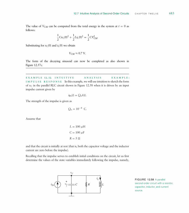
12.7 Intuitive Analysis of Second-Order Circuits C H A P T E R T W E L V E 683
The value of VCM can be computed from the total energy in the system at t = 0 asfollows:
1
2CvC(0)2 + 1
2LiL(0)2 = 1
2CV2
CM.
Substituting for vC(0) and iL(0) we obtain
VCM ≈ 0.7 V.
The form of the decaying sinusoid can now be completed as also shown inFigure 12.57c.
e x a m p l e 12.12 i n t u i t i v e a n a l y s i s e x a m p l e :
i m p u l s e r e s p o n s e In this example, we will use intuition to sketch the formof vC in the parallel RLC circuit shown in Figure 12.58 when it is driven by an inputimpulse current given by
iIN(t) = Qoδ(t).
The strength of the impulse is given as
Qo = 10−4 C.
Assume that
L = 100 µH
C = 100 µF
R = 5
and that the circuit is initially at rest (that is, both the capacitor voltage and the inductorcurrent are zero before the impulse).
Recalling that the impulse serves to establish initial conditions on the circuit, let us firstdetermine the values of the state variables immediately following the impulse, namely,
iIN
iL
vC
vC
+
-C LR
F IGURE 12.58 A parallelsecond-order circuit with a resistor,capacitor, inductor, and currentsource.

684 C H A P T E R T W E L V E t r a n s i e n t s i n s e c o n d - o r d e r c i r c u i t s
vC(0+) and iL(0+). The capacitor looks like an instantaneous short to the current pulse,and so the impulse passes entirely through the capacitor depositing a charge of Qo = 1C on it. Thus,
vC(0+) = Qo
C= 1 V
and iL(0+) = 0.
As we did in Section 12.7, we can now determine the following:
1. The initial value of the capacitor voltage is 1 V.
2. Since there is no drive, and since there is a dissipative element in the circuit, thefinal value of the capacitor voltage is given by
vC(∞) = 0 V.
3. The capacitor voltage will tend to decrease initially, since all the energy starts outin the capacitor. Since there is no drive, the maximum voltage across the capacitoris also 1 V.
4. Since we have a parallel RLC circuit,
α = 1
2RC= 103 rads/s
ωo = 1√LC
= 104 rads/s
and the ringing frequency is
ωd =√
ω2o − α2 ≈= 104 rads/s.
5. The quality factor
Q = ωo
2α= 5,
so the ringing will last for approximately 5 cycles.
The form of vC(t) can now be plotted as shown in Figure 12.59.
12.8 T W O - C A P A C I T O R O R T W O - I N D U C T O RC I R C U I T S
In the previous sections of this chapter, we focused on second-order circuitscontaining one capacitor and one inductor. It is also possible to construct a

12.8 Two-Capacitor or Two-Inductor Circuits C H A P T E R T W E L V E 685
|
0 1 2 3 4 5
|-1.0
|-0.5
|0.0
|0.5
|1.0
t (ms)
Ov C (
V)
VCM
-VCM
F IGURE 12.59 Sketching the form of vC for aparallel RLC circuit driven by an impulse current input.
v1 v2
R2 C2
R3
R1C1
F IGURE 12.60 A second-order circuitcontaining two independent capacitors.
second-order circuit from two capacitors or two inductors. In this section, wewill briefly examine the analysis and behavior of such circuits.
As an example of a two-capacitor circuit, consider the circuit shown inFigure 12.60. To analyze this circuit we again employ the node method begin-ning with Step 3, just as we have in previous sections. To do so, we write KCLat Nodes #1 and #2 in terms of v1 and v2. This yields
C1dv1(t)
dt+ 1
R1v1(t) + 1
R3(v1(t) − v2(t)) = 0 (12.238)
for Node #1, and
C2dv2(t)
dt+ 1
R2v2(t) + 1
R3(v2(t) − v1(t)) = 0 (12.239)
for Node #2. To treat these two equations simultaneously, we first use Equa-tion 12.238 to determine v2 in terms of v1, and then substitute the result intoEquation 12.239 to obtain a second-order differential equation in v1. This yields
v2(t) = R3C1dv1(t)
dt+
(1 + R3
R1
)v1(t) (12.240)
d2v1(t)
dt2+
(1
R1C1+ 1
R2C2+ 1
R3C1+ 1
R3C2
)dv1(t)
dt
+(
1
R1R2C1C2+ 1
R1R3C1C2+ 1
R2R3C1C2
)v1(t) = 0. (12.241)

686 C H A P T E R T W E L V E t r a n s i e n t s i n s e c o n d - o r d e r c i r c u i t s
Equation 12.241 is an ordinary second-order linear homogeneous differentialequation with constant coefficients similar to those derived in earlier sectionsof this chapter.To complete the node analysis, we complete Steps 4 and 5 by solving Equa-tion 12.241 for v1, and using it to determine v2 and any other branch variablesof interest. Given the form of Equation 12.241, we expect its solution to be asuperposition of two terms of the form Ae st. The substitution of this candidateterm into Equation 12.241 yields
s 2 + 2αs + ω2 = 0 (12.242)
as the characteristic equation of the circuit where
α ≡ 1
2
(1
R1C1+ 1
R2C2+ 1
R3C1+ 1
R3C2
)(12.243)
ω2 ≡ 1
R1R2C1C2+ 1
R1R3C1C2+ 1
R2R3C1C2. (12.244)
Except for the details of α and ω, Equation 12.242 is the same as every othercharacteristic equation seen so far in this chapter. Because Equation 12.242 is aquadratic equation it has two roots. Those roots are
s1 = −α +√
α2 − ω2 (12.245)
s2 = −α −√
α2 − ω2 . (12.246)
Therefore, the solution for v1 is a linear combination of the two functions e s1t
and e s2t, and takes the form
v1(t) = A1e s1t + A2e s2t (12.247)
where A1 and A2 are unknown constants that depend on the initial states ofthe two capacitors. To find A1 and A2, two equations are required. The firstequation comes from the evaluation of v1 in Equation 12.247 at the initial time.The second equation comes from the substitution of Equation 12.247 intoEquation 12.240 to determine v2 followed by the evaluation of v2 at the initialtime. The solution of the two equations yields A1 and A2; we will not carryout the details here.
On the surface, it appears that the analysis and behavior of a second-order circuit containing two independent capacitors is identical to that of asecond-order circuit containing one capacitor and one inductor. The sameconclusion is reached by examining a circuit containing two independent induc-tors. While this conclusion is largely true, there is one important difference
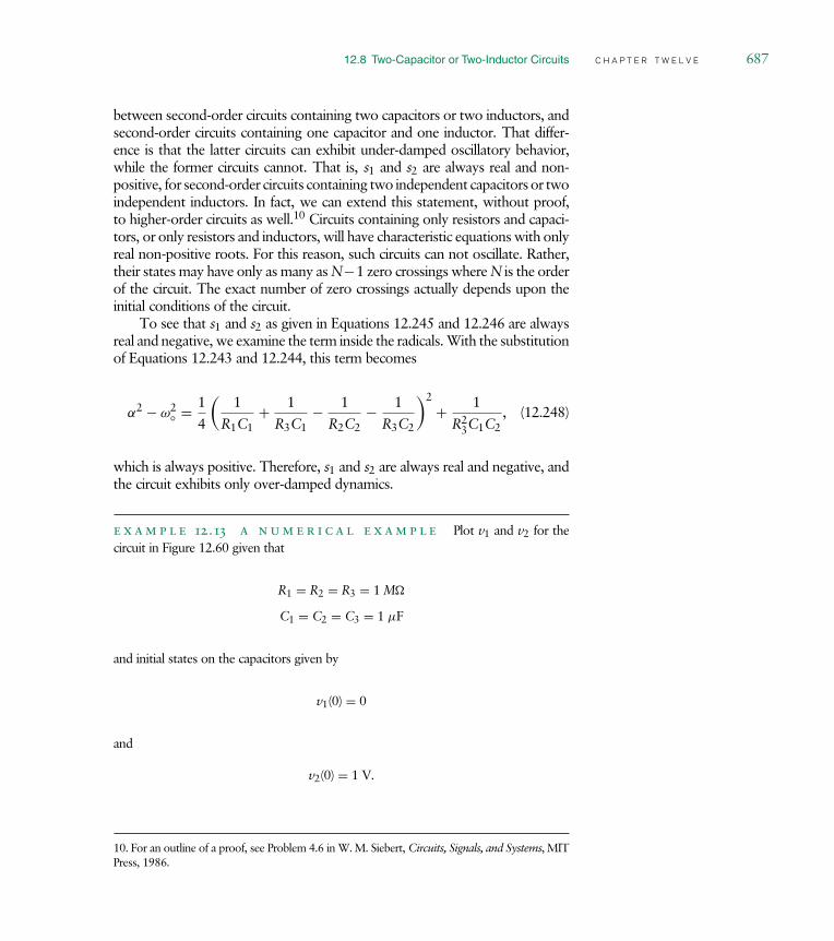
12.8 Two-Capacitor or Two-Inductor Circuits C H A P T E R T W E L V E 687
between second-order circuits containing two capacitors or two inductors, andsecond-order circuits containing one capacitor and one inductor. That differ-ence is that the latter circuits can exhibit under-damped oscillatory behavior,while the former circuits cannot. That is, s1 and s2 are always real and non-positive, for second-order circuits containing two independent capacitors or twoindependent inductors. In fact, we can extend this statement, without proof,to higher-order circuits as well.10 Circuits containing only resistors and capaci-tors, or only resistors and inductors, will have characteristic equations with onlyreal non-positive roots. For this reason, such circuits can not oscillate. Rather,their states may have only as many as N−1 zero crossings where N is the orderof the circuit. The exact number of zero crossings actually depends upon theinitial conditions of the circuit.
To see that s1 and s2 as given in Equations 12.245 and 12.246 are alwaysreal and negative, we examine the term inside the radicals. With the substitutionof Equations 12.243 and 12.244, this term becomes
α2 − ω2 = 1
4
(1
R1C1+ 1
R3C1− 1
R2C2− 1
R3C2
)2
+ 1
R23C1C2
, (12.248)
which is always positive. Therefore, s1 and s2 are always real and negative, andthe circuit exhibits only over-damped dynamics.
e x a m p l e 12.13 a n u m e r i c a l e x a m p l e Plot v1 and v2 for thecircuit in Figure 12.60 given that
R1 = R2 = R3 = 1 M
C1 = C2 = C3 = 1 µF
and initial states on the capacitors given by
v1(0) = 0
and
v2(0) = 1 V.
10. For an outline of a proof, see Problem 4.6 in W. M. Siebert, Circuits, Signals, and Systems, MITPress, 1986.

688 C H A P T E R T W E L V E t r a n s i e n t s i n s e c o n d - o r d e r c i r c u i t s
Substituting these values into Equation 12.241, we obtain the second-order differentialequation that must be solved to obtain v1:
d2v1(t)
dt2+ 4
dv1(t)
dt+ 3v1(t) = 0.
Substituting the candidate term Ae st into the preceding differential equation we get thecharacteristic equation
s 2 + 4s + 3 = 0.
Comparing corresponding terms with the standard form of the characteristic equationfor the following second-order circuits:
s 2 + 2αs + ω2 = 0
we can write
α = 2 rads/s
ω = √3 rads/s.
The two roots of the characteristic equation are
s1 = −1
s2 = −3.
Therefore, the solution for v1 is a linear combination of the two functions e−t and e−3t,and takes the form
v1(t) = A1e−t + A2e−3t.
The corresponding solution for v2 is related to that for v1 by Equation 12.240 and isgiven by
v2(t) = dv1(t)
dt+ 2v1(t) = A1e−t − A2e−3t.
Substituting the initial conditions (v1(0) = 0 and v2(0) = 1) into the expressions for v1
and v2, we get
A1 + A2 = 0
A1 − A2 = 1.
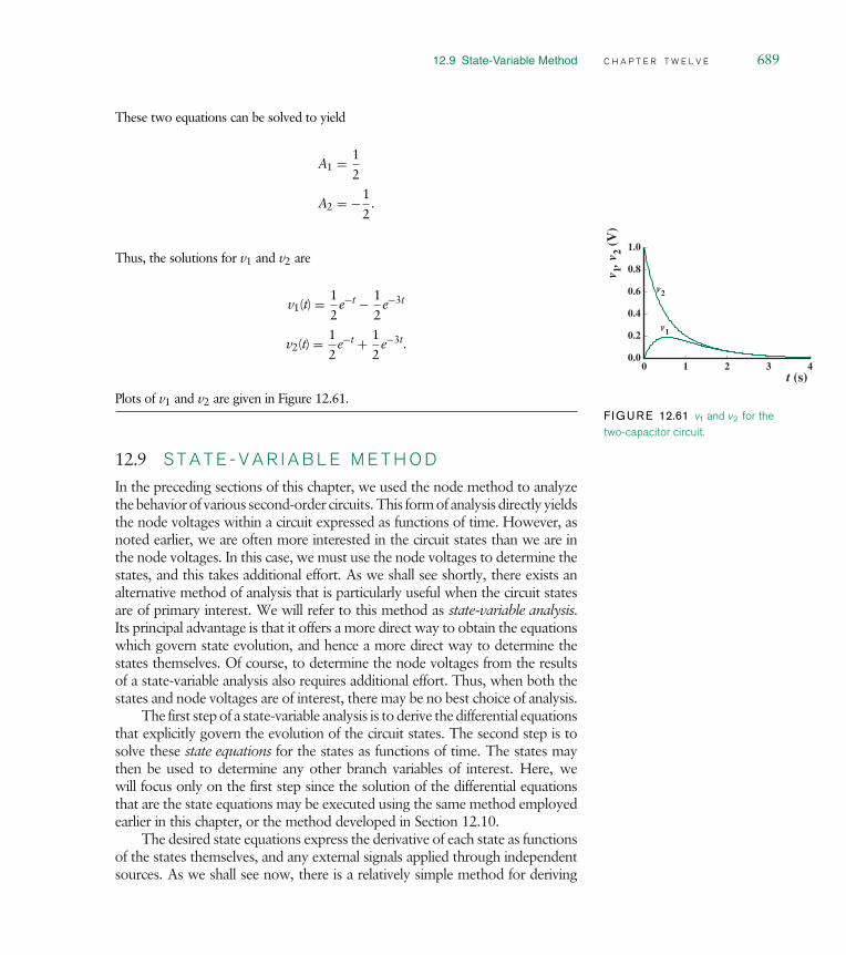
12.9 State-Variable Method C H A P T E R T W E L V E 689
These two equations can be solved to yield
A1 = 1
2
A2 = −1
2.
Thus, the solutions for v1 and v2 are
v1(t) = 1
2e−t − 1
2e−3t
v2(t) = 1
2e−t + 1
2e−3t.
Plots of v1 and v2 are given in Figure 12.61.
0 1 2 3 40.0
0.2
0.4
0.6
0.8
1.0
t (s)
v1,
v2
(V)
v2
v1
F IGURE 12.61 v1 and v2 for thetwo-capacitor circuit.
12.9 S T A T E - V A R I A B L E M E T H O D
In the preceding sections of this chapter, we used the node method to analyzethe behavior of various second-order circuits. This form of analysis directly yieldsthe node voltages within a circuit expressed as functions of time. However, asnoted earlier, we are often more interested in the circuit states than we are inthe node voltages. In this case, we must use the node voltages to determine thestates, and this takes additional effort. As we shall see shortly, there exists analternative method of analysis that is particularly useful when the circuit statesare of primary interest. We will refer to this method as state-variable analysis.Its principal advantage is that it offers a more direct way to obtain the equationswhich govern state evolution, and hence a more direct way to determine thestates themselves. Of course, to determine the node voltages from the resultsof a state-variable analysis also requires additional effort. Thus, when both thestates and node voltages are of interest, there may be no best choice of analysis.
The first step of a state-variable analysis is to derive the differential equationsthat explicitly govern the evolution of the circuit states. The second step is tosolve these state equations for the states as functions of time. The states maythen be used to determine any other branch variables of interest. Here, wewill focus only on the first step since the solution of the differential equationsthat are the state equations may be executed using the same method employedearlier in this chapter, or the method developed in Section 12.10.
The desired state equations express the derivative of each state as functionsof the states themselves, and any external signals applied through independentsources. As we shall see now, there is a relatively simple method for deriving

690 C H A P T E R T W E L V E t r a n s i e n t s i n s e c o n d - o r d e r c i r c u i t s
these equations. To motivate this method, consider the constitutive laws for thecapacitor and inductor, namely Equations 9.9 and 9.28. They can be written as
dvC(t)
dt= 1
CiC(t) (12.249)
diL(t)
dt= 1
LvL(t), (12.250)
respectively. From these equations we see that the derivative of the capacitorvoltage is proportional to the capacitor current, and that the derivative of theinductor current is proportional to the inductor voltage. Therefore, to determineexpressions for the state derivatives, we can equivalently find expressions for thecapacitor currents and inductor voltages. These expressions should be derivedin terms of the states and any independent external signals. This suggests amethod for deriving the state equations.
First, we replace each capacitor by an independent voltage source havinga voltage equal to the corresponding capacitor state. Additionally, we replaceeach inductor by an independent current source having a current equal to thecorresponding inductor state. Second, we analyze the new circuit, which nowcontains only sources and resistors, to find the capacitor currents and inductorvoltages. This analysis may be carried out using the node method developedin Chapter 3. It results in expressions that depend on the independent sourceswithin the new circuit, namely the original independent sources and the sourcesrepresenting the circuit states. Finally, we substitute the expressions for thecapacitor currents and inductor voltages into equations of the form of Equations12.249 and 12.250. This yields the desired state equations.
To illustrate the state-variable analysis of a circuit, consider the analysis ofthe circuit shown in W W W Figure 12.50. To analyze this circuit we replacethe capacitor by a voltage source and the inductor by a current source asshown in Figure 12.62. Next we analyze this circuit to determine iC and vL.This results in
iC(t) = iIN(t) − iL(t) − vC(t)
R(12.251)
vL(t) = vC(t). (12.252)
F IGURE 12.62 The equivalentcircuit used for the state-variableanalysis of the circuit shown inW W W Figure 12.50.
iIN
iC
vC R vL
+
-
+-
iL
12.9 State-Variable Method C H A P T E R T W E L V E 691
Finally, the substitution of Equations 12.251 and 12.252 into Equations 12.249and 12.250, respectively, yields
dvC(t)
dt= 1
CiIN(t) − 1
CiL(t) − 1
RCvC(t) (12.253)
diL(t)
dt= 1
LvC(t). (12.254)
Equations 12.253 and 12.254 are the desired state equations.It is important to emphasize that a state-variable analysis introduces no new
physics. Rather it offers only an alternative analysis of the same circuit. To seethis for the previous example, note that the substitution of Equation 12.254 intoEquation 12.253 to eliminate vC yields W W W Equation 12.201. Thus, the stateequations predicts the same circuit behavior as found previously in Section 12.6.
To close this section, it is valuable to identify the similarities and differencesof the node and state-variable analyses. To begin, it is again important toemphasize that both analyses predict the same behavior for any given circuit.The main difference is that they do so in terms of different sets of variables, andthrough different mathematical mechanics. A node analysis does so in terms ofthe node voltages, and often results in a single high-order differential equation.A state-variable analysis does so in terms of the states, and results in a set ofcoupled first-order differential equations. For this reason, if the initial conditionsfor a circuit analysis are expressed in terms of the states, then the state-variableanalysis will make easier use of that information. Further, a coupled set offirst-order differential equations is more likely to be compatible with typicalnumerical analysis packages. On the other hand, it is often the node voltages,defined with respect to a common ground, that are most easily measured in anexperiment. Thus, both sets of variables are useful.
W W W 12.10 S T A T E - S P A C E A N A L Y S I S *
W W W 12.10.1 N U M E R I C A L S O L U T I O N *
W W W 12.11 H I G H E R - O R D E R C I R C U I T S *

692 C H A P T E R T W E L V E t r a n s i e n t s i n s e c o n d - o r d e r c i r c u i t s
12.12 SUMMARY The primary goal of this chapter was to examine the behavior of second-
order circuits, primarily circuits containing at least one capacitor and oneinductor. To analyze these and other second-order circuits we again reliedon the node method of analysis. The mechanics of this analysis were essen-tially unchanged from Chapter 10, except for the details of the solution ofsecond-order, as opposed to first-order, differential equations.
Through our analysis of second-order circuits we observed that their behav-ior can be very different than the behavior of first-order circuits. Mostimportantly, a circuit containing one capacitor and one inductor can exhibitoscillations that correspond to an exchange of energy between the capaci-tor and inductor. Not surprisingly, these oscillations were found to decayin the presence of energy loss (for example, when a resistor is introduced inthe circuit). To characterize this oscillatory behavior we introduced severalkey parameters: the undamped natural frequency (or undamped resonancefrequency, or simply resonance frequency)
ω ≡ 1/√
LC
the damping factor α, the damped natural frequency
ωd ≡√
ω2 − α2
and the quality factor
Q ≡ ω/2α.
The details of α depend on the circuit topology. For a parallel resonantcircuit,
α = 1
2RC
and for a series resonant circuit,
α = R
2L.
The response of second-order systems can be classified as under-damped,critically-damped, or over-damped according to
α < ω ⇒ under-damped;α = ω ⇒ critically-damped;α > ω ⇒ over-damped.

12.12 Summary C H A P T E R T W E L V E 693
When the system is under-damped, the parameter ωd determines the rateat which the states oscillate, and α determines the rate at which the statesdecay. ω is the oscillation frequency in the absence of damping. Intuitively,Q determines the amount of ringing exhibited by the circuit, and is theapproximate number of cycles after which the energy in an RLC circuit canbe considered to have decayed to zero.
The zero-input response (ZIR) is the response of the system to the initialstored energy, assuming no drive.
The zero-state response (ZSR) is the the response to an applied drive signal,for no initial stored energy.
The zero-input response of under-damped second-order systems resemblesinusoids with amplitudes that decay with time. As an example, the ZIRfor an under-damped parallel resonant circuit, with Vo as the initial voltageon the capacitor and zero initial current through the inductor, is given by
vC(t) = Voωo
ωde−αt cos(ωdt + φ)
for the capacitor voltage, and
iL(t) = Vo
ωdLe−αt sin(ωdt)
for the inductor current, for t > 0. In the previous equation
φ = tan−1(
α
ωd
).
To facilitate the analysis of second-order circuits, we also introduced twonew methods of circuit analysis, namely state-variable analysis and state-space analysis. State-variable analysis was introduced as an alternative tonode analysis, which is particularly useful when the state variables of acircuit, as opposed to the node voltages, are of primary interest. State-space analysis was introduced as a means of solving the coupled first-orderdifferential equations that commonly result from a state-variable analysis.However, we also saw that it could be used as a means of solving thedifferential equations that naturally result from a node analysis. Finally, webriefly examined the analysis of higher-order circuits. The important findingfrom that examination was that the analysis of higher-order circuits can becarried out in a manner identical to the analysis of second-order circuits.
E X E R C I S E Se x e r c i s e 12.1
a) Is the zero input response of the circuit shown in Figure 12.64 under-damped, over-damped, or critically-damped?

694 C H A P T E R T W E L V E t r a n s i e n t s i n s e c o n d - o r d e r c i r c u i t s
F IGURE 12.64 VS
R
++
-L C
-vC
R = 15 Ω L = 1 µH
C = 0.01 µF
b) What is the form of the zero input response (vC) for the same circuit? Make a roughsketch.
c) Compare the envelope of the zero input response with the rate of decay of the zeroinput response of the RC circuit in Figure 12.65.
F IGURE 12.65 VS
R
++
-C
-vC
R = 15 Ω
C = 0.01 µF
How do they differ?
e x e r c i s e 12.2 For each of the circuits in Figure 12.66, find and sketch theindicated zero-input response corresponding to the indicated initial conditions
a) In Figure 12.66, find v2, assuming v1(0) = 1 V, v2(0) = 0
b) In Figure 12.67, find v, assuming i(0) = 0, v(0) = 1 V
c) Repeat (b), but with the resistor changed to 5 .
vS
8 kΩ
++
- -v1
v2
6 kΩ
124------ µF
118------ µF
+
-
F IGURE 12.66
vS
1 mH
+
-v 10 µF+
-
i
100 Ω
F IGURE 12.67

12.12 Summary C H A P T E R T W E L V E 695
e x e r c i s e 12.3 In the circuit in Figure 12.68, a constant voltage source of 10 Vis applied at t = 0. Find all branch voltages and all branch currents at t = 0+ and att = ∞ given iI(0−) = 2 A and v4(0−) = 4 V.
v4
L
R1+
-
i1
10 V+
-
i2+ -
R2 i3 C
i4v1
R2 = 1 ΩL = 1 HC = 0.5 FR1= 2 Ω F IGURE 12.68
e x e r c i s e 12.4 Is the zero-input response of the circuit in Figure 12.69 under-L
R1 R2
C+-vS
F IGURE 12.69
iLR1 = 1 Ω
vC
C = 4 FL = 3 H
R2 = 2 Ω
+ -
F IGURE 12.70
damped, over-damped, or critically-damped? (Provide some kind of justification for youranswer, either a calculation or a sentence of explanation.)
L − 1 µH C = 0.01 µF and R1 = R2 = 15
e x e r c i s e 12.5 In the circuit in Figure 12.70, the inductor current and capacitorvoltage have been constrained by some external magic to be iL = 5 A, vC = −6 volts.At t = 0, the external restraints are removed, and the natural response of the circuit isallowed to evolve. Find the initial slopes of the state variables.
e x e r c i s e 12.6
a) Write the differential equations for the circuit in Figure 12.71 in state-variable form.
LR
C+-vC(t)
F IGURE 12.71
b) Assuming vC(0) = 0, sketch vC(t) for a very short pulse of height vi. Don’t work itout: just show the form.
e x e r c i s e 12.7 Solve the following sets of coupled first-order state equationsfor t > 0 with the indicated inputs and initial values. Plot the positions of the naturalfrequencies in the complex plane. Sketch the state trajectories.
a)
dx1
dt= −3x1 + x2
dx2
dt= x1 − 3x2
x1(0) = 2
x2(0) = 0

696 C H A P T E R T W E L V E t r a n s i e n t s i n s e c o n d - o r d e r c i r c u i t s
b)dx1
dt= −4x2
dx2
dt= 4x1
x1(0) = 2
x2(0) = 0
e x e r c i s e 12.8 Find the roots of the characteristic polynomial (often called thenetwork natural frequencies) in each of the networks in Figure 12.72.
C
(a)
LvS
R1
+-
(b)
C
R2
+-vS
L
(c)
+-
vS
R1 R2
L L
(d)
iSR1 R2
L L
F IGURE 12.72
Numerical values: R1 = 10 , L = 10 µH, C = 10 µF, R2 = 2 .
P R O B L E M S p r o b l e m 12.1 Electrical networks are used to model physical systems governedby linear differential equations. The most important problems that arise in such modelingconcern the interplay of accuracy and simplicity. It is usually very important to knowwhen certain effects can safely be ignored in order to simplify the model and subsequentanalysis. Such knowledge can be obtained by understanding the consequences of makingthe simplifying assumptions.
Two networks that could be used to model an acoustic system are shown in Figure 12.73.It is known that the inductance L is small (specifically L << (R2C)/4) but it is not knownwhether a circuit model with no inductances will be adequate. You are to help answerthis problem by determining the difference in the responses of the capacitor voltage vC
for the two circuits. Specifically, assume:
iS(t) = Iu−1(t) (a step of amplitude I)
vC(0−) = 0
iL(0−) = 0.
Determine vC(t) for t > 0 for both circuits. You should identify the effects of theinductance on such characteristics of the response as the natural frequencies, approximatebehavior for small t, and asymptotic behavior.
You can greatly simplify the form of your results by making use of some assumptionsderived from Taylor’s theorem. For x << 1,
√1 − x 1 − 1/2x (12.297)
and
e−x 1 − x. (12.298)

12.12 Summary C H A P T E R T W E L V E 697
p r o b l e m 12.2 Capacitor C1 has an initial voltage v1(0) = V. Capacitor C2 isinitially uncharged, v2(0) = 0. The voltage across element A tends to zero as time tendsto infinity. At time t = 0, the switch is closed. Refer to Figure 12.74.
+
-vCRiS C
L
+
-vCRiS C
F IGURE 12.73
+
-v2C2
Ai
vA
+
-v1 C1
+ - Switch closesat t = 0
F IGURE 12.74
a) Compute the initial charge of the system.
b) Find the voltage across both capacitors a long time after the switch has been closed.Remember that the total charge of the system must be conserved.
c) Find the energy stored in the system after a long time.
d) Find the ratio of final stored energy to initial energy. Where did the rest of the energygo?
e) Assume element A is a resistor R. Find its voltage or current, and from that, find outthe energy lost in it.
f) Find the ratio of lost energy to initial energy. Is it what you expected? Does it dependon R?
g) What would happen if an inductor was placed in series with R? Sketch the behaviorof the current. (No calculations are needed.)
p r o b l e m 12.3 Shown in Figure 12.75 is one possible circuit model for a trans-former, for use where there can be a common ground between primary and secondary.Assume: L1 = 2.5 H, L2 = 0.025 H, M = k
√L1L2, where k < 1, R1 = 1 k,
R2 = 10 .
+
-
v2M
i1
+
-
v1
L1-M L2-M
+- v1
+
-
vS
R1 i1
v2
+
-R2
i2
Transformer
F IGURE 12.75
a) Write the state equations for this network using i1 and i2 as state variables, and usingthe given circuit model to represent the transformer.
b) Determine the behavior of the natural frequencies of the network as a function ofthe coupling constant k. In particular, what are the natural frequencies in the limit ofsmall k, and in the so-called tight-coupling limit, where k approaches unity?
c) Assume that vS is a 1-volt square pulse of length 5 msec. Find v2(t) for the casek = .98. Is the output a good replica of a square pulse, or are there obviousdepartures from the square pulse shape?
p r o b l e m 12.4 Assuming y(t) = Be st, for each differential equation, find theparticular solution and the general form of the homogeneous solution. Plot the naturalfrequencies in the complex plane.
Assume τ , α, ω0 are constants. Do not worry about the dimensions of the right-handside. Assume B always has the appropriate dimension.
1) dxdt
+ xτ
= y

698 C H A P T E R T W E L V E t r a n s i e n t s i n s e c o n d - o r d e r c i r c u i t s
2) dxdt
+ xτ
= dydt
3) xτ
= yτ
+ dydt
4) d2xdt2
+ ω20x = y
For 5) and 6), assume α and ω0 are both positive numbers.
5) d2xdt2
+ 2α dxdt
+ ω20x = y Assume α > ω0.
6) d2xdt2
+ 2α dxdt
+ ω20x = dy
dtAssume α < ω0.
p r o b l e m 12.5 The circuit in in Figure 12.76 is the electrical analogue of atemperature control system.
F IGURE 12.76 vA
RA
iSCA
+
-
+
-
CBvBRB
Assuming CA = 1 F, CB = 4 F, RA = 1 , RB = 4 .
iS = K(V0 − vB)2 where K = 25 A/V2, V0 = 1.1 V.
a) Write dynamical equations for this network in state form. Use vA and vB as statevariables.
(As a check on your state equations, the stable steady-state value of vB is 1 V. Thatis, you should have dvA/dt = dvB/dt = 0 for vB = 1 V.)
b) Now assume vA = VA + v0 and vB = VB + vb, where VA and VB are the steady-state values and va and vb are small variations. Determine a small-signal linear circuitmodel in which va and bb are the state variables.
c) Is the zero-input response of the small-signal circuit under-damped, over-damped,or critically-damped?
p r o b l e m 12.6 In the circuit in Figure 12.77, the switch has been in position 1for all t < 0. At t = 0, the switch is moved to position 2 (and remains there for t > 0).Find and sketch vC(t) and iL(t) for t > 0.
F IGURE 12.77 2iL
2 V +
-
+
-.01 FvC
1 H 10 Ω
1

12.12 Summary C H A P T E R T W E L V E 699
p r o b l e m 12.7 Figure 10.107 (Problem 10.8 in the chapter on first-order tran-sients) illustrated a parasitic inductance associated with VLSI package pins. Figure 12.78is a modification of Figure 10.107 and shows a lumped parasitic capacitor CP associatedwith the power node within the VLSI chip. In this problem, we will study the combinedeffect of the parasitic inductance LP and capacitance CP.
vP
C
VS
LP
R2R1
A B = 0W1
L1
------ W2
L2
------
CP
tt0
0 V
vA
5 V
F IGURE 12.78Assume that the input B is 0 V at all times. Assume further that the input A has 0 V appliedto it initially. At time t = t0, a 5-V step is applied at the input A. Plot the form of vP as afunction of time for the under-damped and over-damped cases, assuming that vP = VS
for t < t0. Clearly show the value of vP just prior to t0 and just after t0. Assume that theon resistance of a MOSFET is given by the relation (L/W)Rn and that the MOSFET’sthreshold voltage is VT < VS. Also assume that VT < 5 V. Compare this result withthat for the inductor acting alone as computed in Problem 10.8 (Figure 10.107) in thechapter on first-order transients.


c h a p t e r 13
13.1 I N T R O D U C T I O N
13.2 A N A L Y S I S U S I N G C O M P L E X E X P O N E N T I A L D R I V E
13.3 T H E B O X E S : I M P E D A N C E
13.4 F R E Q U E N C Y R E S P O N S E : M A G N I T U D E A N D P H A S E V E R S U S F R E Q U E N C Y
13.5 F I L T E R S
13.6 T I M E D O M A I N V E R S U S F R E Q U E N C Y D O M A I N A N A L Y S I S U S I N G V O L T A G E - D I V I D E R E X A M P L E
13.7 P O W E R A N D E N E R G Y I N A N I M P E D A N C E
13.8 S U M M A R Y
E X E R C I S E S
P R O B L E M S


s i nu so ida l s t eady s tate :
impedance and frequency
re s pon s e13
13.1 I N T R O D U C T I O N
This chapter represents a major change in point of view for circuit analysis,hence it is important to review where we have been and where we are going.The analysis method discussed in preceding chapters has four basic steps:
1. Draw a circuit model of the problem.
2. Formulate the differential equations.
3. Solve these equations. If the equations are linear, then find the homogene-ous solution and the particular solution. If the equations are nonlinear,then numerical methods often are required.
4. Use the initial conditions to evaluate the constants in the homogeneoussolution.
This approach, diagrammed in the top of Figure 13.1, is basic and power-ful, in that it can handle both linear and nonlinear problems, but often itinvolves substantial mathematical manipulations if the drive signals are otherthan simple impulses, steps, or ramps. Thus there is considerable incentive tolook for easier methods of solution, even if these methods are more restrictedin application. Simplified methods are indeed possible if the system is linearand time invariant, and we assume sinusoidal drive and focus on the steady-state behavior. Because in many design applications such as audio amplifiers,oscilloscope vertical amplifiers, and Op Amps linearity is a basic design con-straint, systems that are linear or at least incrementally linear represent a largeand important class, hence are worthy of special attention. Further, more com-plicated input signals such as square waves can be considered to be the sum ofmany sinusoids; hence the problem can be solved by superposition.
Equally important, we often characterize systems by their frequencyresponse (that is, sinusoidal response). Examples include our hearing, audioequipment, ultrasonic pest deterrents, and wireless network receivers. The fre-quency related behavior of such systems is as important as their time-domainbehavior. Therefore, the sinusoidal steady state response is useful because it isa natural and convenient way to describe the behavior of linear systems.
703

704 C H A P T E R T H I R T E E N s i n u s o i d a l s t e a d y s t a t e
F IGURE 13.1 Analysis methods.
Path for anyproblem:(Linear ornonlinear)
Circuitmodel
Differentialequation
Math:homogeneous solnparticular solnor other methods
Math:t = 0
Homogeneoussolution
Particularsolution
Initialconditions
Expressiontimeforwaveform
Path for linearproblem only
Linear problemsonly:impedance
est driveSolvealgebraicequation
H(s)
System function
Realpart
Impedancemodel
Solvealgebraicequation
Processequipment,circuit orproblemstatement
We wish to show in this chapter that the solution to linear circuit problemsis greatly simplified by assuming a drive of the form est as illustrated in the centerpanel of Figure 13.1, primarily because under this assumption the differentialequation is transformed into an algebraic equation, and because the responseto a sinusoidal drive can be directly obtained from the response to the est drive.This leads further to a shorthand solution method involving the concept ofimpedance, whereby the algebraic equation can be found directly from thecircuit model, without writing the differential equation at all, as diagrammed inthe lowermost panel of the Figure 13.1.
The insight behind the employment of a drive of the form est, where s = jω,is the following: Recall, we wish to find the system response in the steadystate1 to a sinusoidal input of the form cos(ωt). We will show that directlysolving system differential equations with a sinusoidal input leads to a tangle oftrigonometry and is very complicated. (You have already seen an example of adirect solution of an RL circuit for a sinusoidal drive in Section 10.6.7.) Instead,we employ the following mathematical trick: Realizing that
e jωt = cos(ωt) + j sin(ωt) (13.1)
(the Euler relation), we first obtain with relative ease the circuit response to anunrealizable drive of the form e jωt. The resulting response will contain a real
1. Interestingly, the substitution of s = jω will give us the response of the circuit in sinusoidalsteady state. Although not covered in this book, the use of Laplace Transforms where we substitutes = σ + jω will yield the total response.

13.1 Introduction C H A P T E R T H I R T E E N 705
RL
CGS
VS
RL
VS
vi
VI
vO2vO
-+-+
F IGURE 13.2 A two-stageMOSFET amplifier showing theMOSFET gate capacitor.
part and an imaginary part. For real linear systems, by superposition, the realpart of the response is due to the real part of the input (namely, cos(ωt)) andthe imaginary part of the response is due to the imaginary part of the input(namely, j sin(ωt)). Accordingly, by taking the real part of the response to e jωt,we obtain the response to a real sinusoidal input of the form cos(ωt). (Similarly,by taking the imaginary part of the response to e jωt, we obtain the response toan input of the form sin(ωt).)
To motivate the study of methods based on the sinusoidal steady state,let us present an example of the type of problem that can be solved with easeusing these methods. Suppose we construct the linear small-signal amplifiershown in Figure 13.2 by concatenating two single stage MOSFET amplifiersof the type studied in Chapter 8. The DC voltage VI is chosen to bias thefirst stage appropriately, and the DC value of the first stage output voltage VOprovides the bias for the second stage. Figure 13.2 further shows the presenceof a capacitor CGS at the input node of the second stage (for example, reflectingthe gate capacitance of the MOSFET in the second stage).
Suppose, now, that we wish to find the first-stage output voltage vo inresponse to vi, a small sinusoidal signal applied to the input of the amplifier. Inparticular, we are interested in determining how the presence of the capacitorCGS affects the amplification afforded by the first amplifier stage. Suppose,further, that we do not care about initial transients, rather, we are interestedin the steady-state behavior when all transients have died out. Experimentalapplication of a sinusoid to the input and measurement of the response vo willshow very different behavior as the frequency of the input is swept from a lowto a high value. We will observe that for low-frequency signals the gain of thefirst stage is no different from our earlier calculations in Chapter 8 in the absenceof the capacitor CGS. However, we will also observe that the presence of thecapacitor makes the gain of the amplifier fall off rapidly at high frequencies.
Analytical analysis based on the methods we learned in the previous chap-ters would suggest writing the differential equation for the circuit comprising theresistor RL and the capacitor CGS and finding the forced response to an appliedsinusoid. As demonstrated by the example in Section 10.6.7, this type of anal-ysis is very cumbersome. In contrast, the analysis methods that we will learn

706 C H A P T E R T H I R T E E N s i n u s o i d a l s t e a d y s t a t e
F IGURE 13.3 RC circuit withtone burst in. The amplitude of theinput waveform is Vi , where Viis real.
vr
-+
CR
vc-
+
-+
Vi
vi
tvi =Vi cos (ωIt)0for t 0≥
in this chapter will make this a trivial exercise. In particular, Section 13.3.4will analyze the circuit of Figure 13.2 in detail and explain the observedbehavior.
13.2 A N A L Y S I S U S I N G C O M P L E XE X P O N E N T I A L D R I V E
To illustrate this new approach, let us analyze the simple linear first-order RCcircuit shown in Figure 13.3, and presume that we wish to find the capacitorvoltage vc, in response to a cosine wave suddenly applied at t = 0, often calleda tone burst. The tone burst is mathematically represented as
vi = Vi cos (ω1t) for t ≥ 0,
where Vi is the amplitude of the cosine, and ω1 its frequency. (Note that we donot use ωo in the input signal to avoid confusion with the ωo used to representthe undamped natural frequency in a second order systems.)
The differential equation for the circuit is
vi = vc + RCdvc
dt. (13.2)
Let us attempt to solve this differential equation by summing its homogeneousand particular solutions. Recall, when dealing with circuit responses, the homo-geneous solution is also called the natural response, and the particular solutionis also called the forced response. Recall further that the forced response dependson the external inputs to the circuit. Let us denote the homogeneous solutionas vch and the particular or forced solution as vcp. Then, we know that the totalsolution is given by
vc = vch + vcp.
13.2.1 H O M O G E N E O U S S O L U T I O N
From Equation 13.2, the homogeneous solution can be derived by solving
RCdvch
dt+ vch = 0. (13.3)

13.2 Analysis Using Complex Exponential Drive C H A P T E R T H I R T E E N 707
As we have seen in Chapter 10, the homogeneous solution for this equation is
vch = K1e−t/RC (13.4)
where K1 is a constant to be determined from the initial conditions.
13.2.2 P A R T I C U L A R S O L U T I O N
The straightforward approach to finding the particular or forced solution vcpinvolves finding any solution to the differential equation
vi = vcp + RCdvcp
dt. (13.5)
Since the input vi is given by
vi = Vi cos (ω1t)
(where Vi is real), this amounts to finding any solution to
Vi cos (ω1t) = vcp + RCdvcp
dt. (13.6)
Obviously the forced response vcp must be some combination of sines andcosines, so we assume
vcp = K2 sin (ωt) + K3 cos (ωt) (13.7)
or, equivalently,
vcp = K4 cos (ωt + ). (13.8)
There is nothing wrong with this approach, except that it leads to a tangle oftrigonometry. So, we will abandon this path.
Instead, let us launch out in a slightly different direction. The Eulerrelation
e jωt = cos(ωt) + j sin(ωt) (13.9)
shows that e jωt contains the cosine term we want, in addition to an unwantedsine term. Hence, by a sort of inverted superposition argument, we replace the

708 C H A P T E R T H I R T E E N s i n u s o i d a l s t e a d y s t a t e
actual source vi with a source of the form
vi = Vi e s1t (13.10)
and return later to unscramble the cosine and sine parts. In this equation wehave used
s1 as a shorthand for jω1,
and have included a ‘‘˜’’ above vi to indicate that this is not the true drive voltage.For consistency, we will use the same notation for all variables related to thisfake drive voltage. The differential equation to find the particular solution to vinow becomes
vi = Vi e s1t = ˜vcp + RCd ˜vcp
dt. (13.11)
It is clear that a reasonable assumption for the particular solution is
˜vcp = Vc e st (13.12)
in which we must somehow find Vc and s. On substitution of the assumedparticular solution into Equation 13.11, we obtain
Vi e s1t = Vc e st + RCsVc e st. (13.13)
We note first that s must equal s1, otherwise Equation 13.13 cannot be satisfiedfor all time. Now, on the basis that e st can never be zero for finite values oft, the e s1t terms can be divided out, to yield an algebraic equation relating thecomplex amplitudes of the voltages rather than a differential equation relatingthe voltages as time functions:
Vi = Vc + VcRCs1 (13.14)
which can be solved to yield
Vc = Vi
1 + RCs1for s1 = − 1
RC(13.15)
a restriction clearly satisfied in this case because s1 = jω1 where ω1 is a realnumber. Thus Equation 13.15 becomes
Vc = Vi
1 + jω1RC(13.16)
or, from Equation 13.12, the particular solution for the fake input vi is
˜vcp = Vi
1 + jω1RCe jω1t. (13.17)

13.2 Analysis Using Complex Exponential Drive C H A P T E R T H I R T E E N 709
-+
C
R
-
+Vi cos(ω1t)
-+
(a) Circuit for exponential source
jVi sin(ω1t)
vi
vcp
Vi cos(ω1t) -+ C
R
-
+
(b) Subcircuit for cosine drive only
vi1vcp1
-+ C
R
-
+
jVi sin(ω1t)
(c) Subcircuit for sine drive only
jvi2jvcp2
F IGURE 13.4 RC circuit withexponential drive est .
At this point you should protest. No waveform measured in the labora-tory will have a ‘‘j ’’ associated with it. The problem arises because we haveused a complex rather than a real drive. That is, we have analyzed the cir-cuit shown in Figure 13.4a, rather than Figure 13.3. The complex exponentialdrive vi can be represented by the Euler relation as the sum of two sourcesas depicted in Figure 13.4a. If the circuit is linear, the two-source circuit canbe analyzed by superposition, as suggested in Figure 13.4b and 13.4c. Specifi-cally, the voltage ˜vcp can be found by summing the response to Vi cos(ωt), asobtained from Figure 13.4b with j times the response to Vi sin(ωt), as found fromFigure 13.4c:
˜vcp = vcp1 + jvcp2. (13.18)
From the perspective of Figure 13.3, we have calculated in Equation 13.18the response ˜vcp, and what we really want is vcp1. Notice that vcp1 is none otherthan the vcp that we had originally set out to find, namely, the solution to Equa-tion 13.6. So we want to ‘‘de-superimpose’’ the two sources in Figure 13.4a.This is a simple matter because of the j flag: vcp1 is the real part of ˜vcp.
The next task, then, is to find an easy way of calculating the real part of acomplex expression. (Those readers who are a little hazy about manipulationof complex numbers, and in particular the conversion between rectangular andpolar form, should review at this point Appendix C on complex numbers or asuitable math text.) In this specific problem, we must find the real part of the˜vcp expression, Equation 13.17. The difficulty is that the expression has two
factors, one in Cartesian or rectangular form, and the other in polar, whereasmultiplication is simpler if both factors are in polar form. Hence we rewriteEquation 13.17 in polar form as
˜vcp = Vi√1 + (ω1RC)2
e je jω1t (13.19)

710 C H A P T E R T H I R T E E N s i n u s o i d a l s t e a d y s t a t e
where
= tan−1(−ωRC
1
). (13.20)
Now, to find the real part of ˜vcp, we use the Euler relation to writeEquation 13.19 as
˜vcp = Vi√1 + (ω1RC)2
cos (ω1t + ) + jVi√
1 + (ω1RC)2sin (ω1t + )
from which the real part of ˜vcp is available by inspection,
vcp1 = Vi√1 + (ω1RC)2
cos (ω1t + ). (13.21)
This, finally, is the particular solution of Equation 13.6.
13.2.3 C O M P L E T E S O L U T I O N
The complete expression for the capacitor voltage in response to a cosine toneburst is the sum of this particular solution (vcp1) and the homogeneous solution(vch) previously found in Equation 13.4:
vc = K1e−t/RC + Vi√1 + (ω1RC)2
cos(ω1t +
). (13.22)
The one remaining unknown constant, K1, can be found from the initial condi-tions by setting t to zero in the usual manner. However, as we will see shortly,we usually do not care about the first term.
13.2.4 S I N U S O I D A L S T E A D Y - S T A T E R E S P O N S E
Under sinusoidal drive, we are almost always interested in the steady-state valueof the capacitor voltage, which can be readily obtained from Equation 13.22 byassuming t is very large. When t → ∞, Equation 13.22 reduces to
vc = Vi√1 + (ω1RC)2
cos(ω1t +
), (13.23)
which is simply the particular solution to a cosine input (compare with Equa-tion 13.21). For a cosine input, the steady-state response is often termedthe response to a cosine. The corresponding complete response is termed theresponse to a cosine burst, and includes both the homogeneous and particular
terms. In Equation 13.23, the Vi/√
1 + (ω1RC)2 factor gives the amplitude

13.2 Analysis Using Complex Exponential Drive C H A P T E R T H I R T E E N 711
(or magnitude) of the response, and is the phase. The phase is the angu-lar difference between the output and input sinusoids. Notice that both themagnitude and phase (see Equation 13.20) of the response are frequencydependent.
Equation 13.22 is really quite general, in that it gives the capacitor voltagefor any amplitude and any frequency of cosine tone burst. For example, it isobvious that at low frequencies, (that is, for ω1 small), and after the transienthas died away:
vc Vi cos(ω1t). (13.24)
Thus, after the transient has died away, the output looks almost like the input.We conclude that for ω1 small, the capacitor behaves like an open circuit.Further, for ω1 large, that is, at high frequencies, after the transient has diedaway
vc Vi
ω1RCcos(ω1t − 90) (13.25)
so the output will be sinusoidal, but 90 degrees out of phase with the input,and much smaller. At high frequencies then, the magnitude of the capacitorvoltage will get very small, so we can say that the capacitor begins to behavelike a short circuit.
There are four general conclusions to be drawn from this specific example:
1. The use of an e st drive reduces a differential equation to an algebraicequation, thereby simplifying the solution. This solution process replacestrigonometry with complex algebra, which is a wise trade.
2. The last couple of pages from Equation 13.17 to Equation 13.22,although necessary for completeness, did not add any new insight aboutthe circuit behavior. For example, the same information about the form ofvc in the steady state, or its value at low frequencies and high frequenciescould have been found from Equation 13.17, or even from the complexamplitude Vc, Equation 13.16, just as easily as from Equation 13.21,without the intervening ‘‘real part’’ calculation.2
For example, the steady state value of vc (or the particular or forcedresponse) can be determined from the value of Vc as
vc = Re[Vc e jω1t
](13.26)
2. Recall from Equation 13.16 that Vc is the complex amplitude of the forced response to our fakeinput vi = Vie jω1t.

712 C H A P T E R T H I R T E E N s i n u s o i d a l s t e a d y s t a t e
t
vi, vc
ViVc
∠Vcω---------
Vi cos(ωt)
Vc cos(ωt + ∠Vc)
0
F IGURE 13.5 The amplitude and phase ofthe response vc compared to the inputsinusoid vi .
-+ Vc
-
+
Vi1/Cs1
R
F IGURE 13.6 A circuit interpretation ofEquation 13.15.
or, equivalently,
vc = |Vc| cos(ω1t + ∠Vc). (13.27)
Figure 13.5 shows a sketch of the input cosine and the output responsewith the various magnitudes and phases marked. Notice that the complexamplitude Vc carries both the amplitude and phase information of theresponse (|Vc| and ∠Vc respectively) in an easily accessible manner. Thus,our analysis can stop at Equation 13.16.
3. The denominator of the Vc expression, Equation 13.15, has the sameform as the characteristic polynomial in the homogeneous solution,(see Chapter 10, Equation 10.9 for example) so the value of s in thehomogeneous solution could have been found from this denominatorwithout any formal solution of the homogeneous equation. That this isa general result can be shown by examining the two derivations.
4. The Vc expression, Equation 13.15, looks very much like a voltagedivider expression, especially if we divide through by Cs1.
Vc = 1/Cs1
R + 1/Cs1Vi. (13.28)
This suggests a very simple method for finding the complex amplitude Vcdirectly from the circuit: Redraw the circuit, replacing resistors with Rboxes, capacitors with 1/Cs1 boxes, and cosine sources by their ampli-tudes, in this case Vi, as shown in Figure 13.6. Now Vc can be found inone line. But what are these boxes? And what is Vc? The next section
-+ Cv
i
vi
+
-
L
v
i
+-
R
(a)
(b)
(c)
F IGURE 13.7 Impedancecalculations.
will provide the answers.
13.3 T H E B O X E S : I M P E D A N C E
To get a better idea of the meaning of the boxes in Figure 13.6, let us examinesome trivial cases, as sketched in Figure 13.7. In Figure 13.7a, a voltage source

13.3 The Boxes: Impedance C H A P T E R T H I R T E E N 713
Vi cos(ω1t) is connected across a capacitor, hence
i = Cdv
dt. (13.29)
On the basis of Section 13.1, assume the voltage and current are of the form
v = Ve st (13.30)
i = Ie st (13.31)
where, as before, we use s as a shorthand notation for jω.On substituting these relations in Equation 13.29, and dividing by e st
(never zero for finite s and t) we find
I = CsV (13.32)
or
V = 1
CsI. (13.33)
Similar calculations on the inductor and the resistor yield
V = LsI (13.34)
V = I R. (13.35)
These equations indicate that for linear R, L, or C, in each case the complexamplitude of the voltage is related to the complex amplitude of the currentby very simple algebraic expressions which are generalizations of Ohm’s Law.The constants relating V to I in Equations 13.33, 13.34, and 13.35 are calledimpedances, and these equations are the constituent relations for C, L, and Rexpressed in impedance form. The constituent relations for these elements andfor voltage and current sources are summarized in Figure 13.8.
Just as we used R to denote resistances, we commonly use the letter Z todenote impedances.
Thus, the impedances of an inductor, a capacitor, and a resistor are given by
ZL = sL = jωL (13.36)
ZC = 1
sC= 1
jωC(13.37)

714 C H A P T E R T H I R T E E N s i n u s o i d a l s t e a d y s t a t e
F IGURE 13.8 Constituentrelations for a voltage source, acurrent source, and R, L, and C inimpedance form. Note that Vo andIo are terminal variables, while Va
and Ia are element parameters.Note also that s = jω.
+
R Vo
+
-
Io
R Vo = RIo
Vo
+
-
Io
Vo = 1Cs------Io
Vo
+
-
Io
LsL Vo = LsIo
C 1Cs------
ia
va++-
Ia
Va Vo
+
-
Io
Vo = Va
Vo
+
-
Io
Io = Ia
Indu
ctor
Cap
acito
rR
esis
tor
Cur
rent
sou
rce
Vol
tage
sou
rce
-
+
and
ZR = R (13.38)
respectively.
Furthermore, just as the conductance was defined as the reciprocal of resistance,we define admittance as the reciprocal of impedance.
Impedances are complex numbers in general. They are also frequencydependent. Figure 13.9 plots the magnitude of the impedances of an inductor,a capacitor, and a resistor as a function of frequency. The curves in the figurereinforce the following intuition developed in Chapter 10 and summarized inSection 10.8:
Inductors behave like short circuits for DC (or very low frequencies) and likeopen circuits for very high frequencies. Capacitors behave like open circuits forDC (or very low frequencies) and like short circuits for very high frequencies.
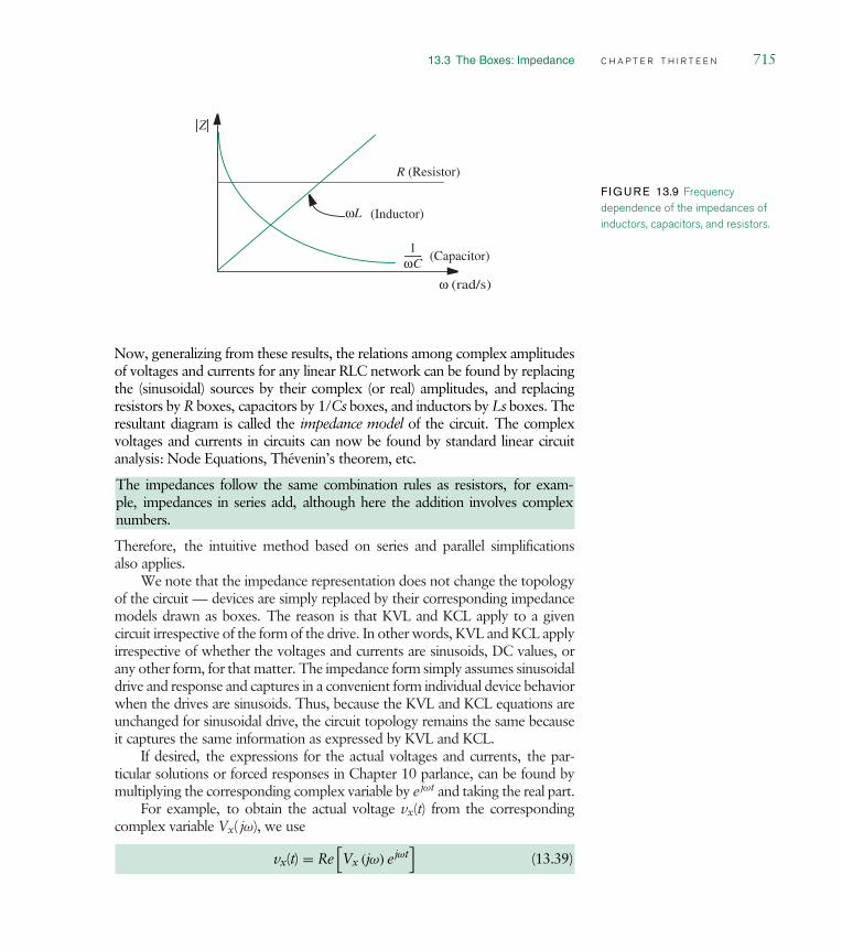
13.3 The Boxes: Impedance C H A P T E R T H I R T E E N 715
Z
(Inductor)
ω (rad/s)
ωL
(Capacitor)1
ωC--------
R (Resistor)
F IGURE 13.9 Frequencydependence of the impedances ofinductors, capacitors, and resistors.
Now, generalizing from these results, the relations among complex amplitudesof voltages and currents for any linear RLC network can be found by replacingthe (sinusoidal) sources by their complex (or real) amplitudes, and replacingresistors by R boxes, capacitors by 1/Cs boxes, and inductors by Ls boxes. Theresultant diagram is called the impedance model of the circuit. The complexvoltages and currents in circuits can now be found by standard linear circuitanalysis: Node Equations, Thévenin’s theorem, etc.
The impedances follow the same combination rules as resistors, for exam-ple, impedances in series add, although here the addition involves complexnumbers.
Therefore, the intuitive method based on series and parallel simplificationsalso applies.
We note that the impedance representation does not change the topologyof the circuit devices are simply replaced by their corresponding impedancemodels drawn as boxes. The reason is that KVL and KCL apply to a givencircuit irrespective of the form of the drive. In other words, KVL and KCL applyirrespective of whether the voltages and currents are sinusoids, DC values, orany other form, for that matter. The impedance form simply assumes sinusoidaldrive and response and captures in a convenient form individual device behaviorwhen the drives are sinusoids. Thus, because the KVL and KCL equations areunchanged for sinusoidal drive, the circuit topology remains the same becauseit captures the same information as expressed by KVL and KCL.
If desired, the expressions for the actual voltages and currents, the par-ticular solutions or forced responses in Chapter 10 parlance, can be found bymultiplying the corresponding complex variable by e jωt and taking the real part.
For example, to obtain the actual voltage vx(t) from the correspondingcomplex variable Vx( jω), we use
vx(t) = Re[Vx (jω) e jωt
](13.39)

716 C H A P T E R T H I R T E E N s i n u s o i d a l s t e a d y s t a t e
or equivalently,
vx(t) = |Vx| cos(ωt + ∠Vx). (13.40)
We emphasize again, however, that this step is usually not necessary, becausethe complex amplitude expression contains all the key information about circuitbehavior.
At this point it is necessary to explicitly introduce a notation for voltagesand currents to clearly differentiate complex amplitudes from time functions.We abide by the international standard in this matter:
DC or operating-point variables: uppercase symbols with uppercasesubscripts (for example, VA)
Total instantaneous variables: lowercase symbols with uppercasesubscripts (for example, vA)
Incremental instantaneous variables: lowercase symbols with lowercasesubscripts (for example, va)
Complex amplitudes or complex amplitudes of incremental components,and real amplitudes of sinusoidal input sources: uppercase symbols withlowercase subscripts (for example, Va)
Summarizing, the impedance method allows us to determine with ease thesteady-state response of any linear RLC network for a sinusoidal input. Themethod works with complex amplitudes of voltages and currents at its variablesand has the following general steps:
1. First, replace the (sinusoidal) sources by their complex (or real)amplitudes. For example, the input voltage vA = Va cos(ωt) is replacedby its real amplitude Va.
2. Replace circuit elements by their impedances, namely, resistors by Rboxes, inductors by Ls boxes, and capacitors by 1/Cs boxes. Here s = jω.The resulting diagram is called the impedance model of the network.
3. Now, determine the complex amplitudes of the voltages and currentsin the circuit by any standard linear circuit analysis technique Nodemethod, Thévenin method, intuitive method based on series and parallelsimplifications, etc.
4. Although this step is not usually not necessary, we can then obtain thetime variables from the complex amplitudes. For example, the timevariable corresponding to node variable Vo is given by
vO(t) = |Vo| cos(ωt + ∠Vo). (13.41)

13.3 The Boxes: Impedance C H A P T E R T H I R T E E N 717
e x a m p l e 13 .1 r e v i s i t i n g t h e r c e x a m p l e To illustratethe power of the method, let us revisit the RC circuit from Figure 13.3 (redrawnhere as Figure 13.10a for convenience) and analyze it using the impedance method justdescribed. As before, suppose that we wish to find the steady-state capacitor voltage vc in
-+
CR
vc-
+
vi = Vi cos(ω1t)
(a) Circuit
-+ Vc
-
+
Vi 1/Cs
R
(b) Impedance model
F IGURE 13.10 Impedancemodel of RC circuit with sinusoidalinput.
response to an input of the form vi = Vi cos ω1t.
Figure 13.10b shows the corresponding impedance model. In the model, notice that wehave replaced the input voltage vi with the real amplitude Vi, and the capacitor voltagevc with the complex amplitude Vc, according to the first step of the impedance method.Further, according to the second step of the method, we have replaced the resistor withan R box and the capacitor with a box with impedance 1/Cs. As before, s is a shorthandnotation for jω.
We can derive an expression for Vc by applying the generalized voltage divider relationin the impedance model in Figure 13.10b as
Vc = ZC
ZR + ZCVi (13.42)
where ZR and ZC are the impedances of the resistor and the capacitor, respectively.Substituting the actual impedance values, we obtain
Vc = 1/Cs
R + 1/CsVi = 1
RCs + 1Vi. (13.43)
Since s is a shorthand for jω, at a specific frequency ω1,
Vc = 1
1 + jω1RCVi. (13.44)
Having obtained the expression for Vc, the complex amplitude of the desired voltage,we have completed the third step of the impedance method. Amazingly, notice that wehave arrived at the same result as in Equation 13.16 in a few easy steps.
Although not always necessary, we will proceed with the fourth step of the impedancemethod and obtain the actual voltage vc as a function of time. We can do so by substitut-ing the magnitude and phase of Vc, and the frequency of our input into Equation 13.41as follows:
vc(t) = |Vc| cos(ω1t + ∠Vc)
= Vi√1 + (ω1RC)2
cos(
ω1t + tan−1 −ω1RC
1
).
Not surprisingly, this expression for vc(t) is the same as that in Equation 13.23, butderived with significantly less effort.

718 C H A P T E R T H I R T E E N s i n u s o i d a l s t e a d y s t a t e
F IGURE 13.11 Impedancemodel of LR circuit.
-+ vo
vi = Vi cos (ω1t)
L
-
+R
(a) Circuit
vi -+ Vo
-
+
(b) Impedance model
Vi
Ls
R
As a final note, this is the forced response for a cosine wave drive. If the excitation isa tone burst, then the homogeneous solution must be added to obtain the completesolution.
13.3.1 E X A M P L E : S E R I E S R L C I R C U I T
Next, as a further illustration of the concept of impedance, let us findthe voltage across the resistor in the RL circuit of Figure 13.11, assumingthat vi = Vi cos(ω1t). Figure 13.11b shows the corresponding impedancemodel.
The generalized voltage divider relation for Vo in the impedance model,Figure 13.11b, is
Vo = ZR
ZR + ZLVi (13.45)
where ZR and ZL are the impedances of the resistor and the inductor,respectively. Substituting the actual impedance values, we obtain
Vo = R
R + LsVi. (13.46)
Recall from Equation 13.10 that we have been using s as a shorthand for jω. Soat any frequency, ω1,
Vo = R
R + jω1LVi. (13.47)
The denominator on the right-hand side of Equation 13.47 is theimpedance Z seen by the voltage source at the frequency ω1. In other words,
Z( jω1) = R + jω1L.

13.3 The Boxes: Impedance C H A P T E R T H I R T E E N 719
To find vo, the actual output voltage as a time function, convert Equation 13.47to polar form, then substitute into Equation 13.39
Vo = R√R2 + ω2
1L2e jVi (13.48)
where
= tan−1 −ω1L/R. (13.49)
From Equation 13.39, the time function is
vo(t) = R√R2 + ω2
1L2Vi cos(ω1t + ). (13.50)
This is the forced response for a cosine wave drive. If the excitation is atone burst, then the homogeneous solution must be added to obtain the com-plete solution. By comparing Equation 13.50 to Equation 13.48, we concludethat the complex amplitude Vo in Equation 13.48 is a complex number con-taining information about both the amplitude and the phase of the sinusoidaloutput waveform vo(t) at any frequency.
Again it is easy to find vo(t) when the drive frequency ω1 is either low orhigh. At low frequencies, (ω1 small) we note from Equations 13.50 and 13.49that = 0 and
Vo = Vi (13.51)
so after the transient has died out, vo(t) vi(t). That is, the resistor voltagelooks just like the drive voltage. The inductor at low frequencies must behavelike a short circuit, because its impedance approaches zero for ω small.
At high frequencies, specifically, where ω1 is such that (ω1L)2 R2,
|Vo| R
ω1LVi (13.52)
and approaches −90. Thus in this frequency range vo(t) becomes smallerand smaller in amplitude with increasing frequency, and lags behind vi bynearly 90.
At this point, we can also look at the impedance of each component (ZLand ZR) in Figure 13.11 and develop the same qualitative intuition about thebehavior of the circuit from the voltage-divider relationship. For instance, whenω1 is small, the impedance of the inductor is small, and so Vo = Vi. Similarly,for high frequencies, the impedance of the inductor becomes much greater thanthat of the resistor and so Vo becomes very small.

720 C H A P T E R T H I R T E E N s i n u s o i d a l s t e a d y s t a t e
e x a m p l e 13 .2 r l e x a m p l e w i t h n u m b e r s Let us reworkthe example of Figure 13.11 and obtain the amplitude of vo using numbers this timearound. Suppose that
L = 1 mH
R = 1 k
vi = Vi cos(2π ft), where Vi = 10
where we will look at three values of the frequency f : 100 kHz, 1 MHz, and 10 MHz.
Using impedances and the voltage divider relation
Vo = ZR
ZR + ZLVi (13.53)
= 1000
1000 + 0.001sVi (13.54)
= 1000
1000 + 0.001s10 (13.55)
= 10
1 + 0.000001s(13.56)
where s = j2π f.
We can also write Equation 13.54 in the form of a transfer function H(s) relating thecomplex output voltage to the complex input voltage:
H(s) = Vo
Vi= 1000
1000 + 0.001s. (13.57)
Since
vo = |Vo| cos(2π f + ∠Vo)
using Equation 13.56, we get
Amplitude of vo = |Vo|
=∣∣∣∣ 10
1 + j 0.000001 × 2π f
∣∣∣∣
= 10√1 + 3.9 × 10⁻¹¹f 2
.

13.3 The Boxes: Impedance C H A P T E R T H I R T E E N 721
Let us now plug in the three values of f and obtain the amplitudes of the response atthose frequencies
f = 100 kHz:
Amplitude of vo = 10√1 + 3.9 × 10⁻¹¹(100000)2
= 8.5 Vf = 1 MHz:
Amplitude of vo = 10√1 + 3.9 × 10⁻¹¹(1000000)2
= 1.6 Vf = 10 MHz:
Amplitude of vo = 10√1 + 3.9 × 10⁻¹¹(10000000)2
= 0.16 V.
The numbers clearly show the increasing impedance of the inductor as the frequency isincreased. At the relatively low frequency of 100 kHz, the low impedance of the inductorcauses the amplitude of the response to be similar to that of the input signal (8.5 V versus10 V). Conversely, at the high frequency of 10 MHz, the amplitude of the response ismuch smaller than that of the input (0.16 V versus 10 V).
Thus far, in this example, we computed the amplitude of vo at three specific frequencies.In general, we can also graph any parameter of interest as a function of frequency.Commonly, we graph the form of the amplitude and the phase of the transfer functionVo/Vi as a function of frequency ω (Equation 13.57). Although this seems difficult to doby inspection, we will learn a technique for doing so in Section 13.4. A computergenerated plot of the magnitude and phase of Vo/Vi versus frequency is shown inFigure 13.12. The same magnitude graph plotted on a log-log scale in Figure 13.13
|
0 2000000 4000000 6000000 8000000 10000000
|0.0
0.2
0.4
0.6
0.8
1.0
Frequency (rad/s)
|Vo/
Vi|
0 2000000 4000000 6000000 8000000 10000000
-90
-80
-70
-60
-50
-40
-30
-20
-10
0
Frequency (rad/s) <V
o/V
i
F IGURE 13.12 Magnitude andphase of Vo/Vi versus frequency ω.

722 C H A P T E R T H I R T E E N s i n u s o i d a l s t e a d y s t a t e
F IGURE 13.13 Magnitude andphase of Vo/Vi versus frequency ω
on log scales.
0.001
0.010
0.100
1.000
Frequency (rad/s)104 105 106 107 108 109
|Vo/
Vi|
<V
o/V
i
-90
-80
-70
-60
-50
-40
-30
-20
-10
0
Frequency (rad/s)104 105 106 107 108 109
is much more revealing. The corresponding phase graph is also plotted on a log scale.Notice the interesting frequency related behavior of the magnitude and phase plots inFigure 13.13. The log plot instantly reveals that high frequencies are severely attenuatedwhile low frequencies are passed through unattenuated. We will have much more tosay about this variable frequency view of responses in Section 13.4.
13.3.2 E X A M P L E : A N O T H E R R C C I R C U I T
Let us now work another example with numerical quantities. Figure 13.14ashows an RC circuit driven by a sinusoidal voltage vi = 10 cos(1000 t) V. Findthe impedance Z seen by the voltage source at the frequency ω = 1000 rad/s.Also, find the voltage Vr across the resistor.
Figure 13.14b shows the impedance model for the circuit. Since the capaci-tor and the resistor are in series, the impedance Z seen by the source is givenby the sum of the impedances of the capacitor and the resistor as
Z = 500 × 103 + 1
1 × 10⁻⁹s
where, we have used the shorthand s = jω. Since ω = 1000 rad/s, we get
Z = 500 × 103 + 1
1 × 10⁻⁹j1000
F IGURE 13.14 Impedancemodel of RC circuit.
-+ vr
1 nF
-
+500 kΩ
(a) Circuit
-+ Vr
-
+
(b) Impedance model
500
kΩ
Z1/(1 nF)s
Vi = 10Vvi = 10 V cos (1000t)

13.3 The Boxes: Impedance C H A P T E R T H I R T E E N 723
or
Z = 0.5 − j M.
Next, let us determine Vr. Applying generalized voltage divider relation for Vrin the impedance model,
Vr = 500 × 103
500 × 103 + 11×10−9s
Vi. (13.58)
Substituting s = j1000 and Vi = 10 we get
Vr = 500 × 103
500 × 103 + 11×10−9j1000
10. (13.59)
Simplifying,
Vr = 0.5 M
0.5 M − j M10
or,
Vr = 5
0.5 − j.
Impedance analysis can end here, since the expression for Vr contains allthe information about the amplitude and the phase of the time function vr.However, let us take the extra step and determine vr by writing
vr = Re[
5
0.5 − je j1000t
].
Simplifying, and writing the previous expression in polar form
vr = Re[4.47e j1.1e j1000t
].
Taking the real part,
vr = 4.47 cos(1000t + 1.1) V.
Notice from Equation 13.59 that if the frequency of the input wereincreased from 1000 rad/s to, say, 106 rad/s, Vr ≈ 10 V. This says that

724 C H A P T E R T H I R T E E N s i n u s o i d a l s t e a d y s t a t e
vi(t)vo(t)
C1C2
R2
R1
+
-
+
-
va
(a) Circuit
ViVo
Z3 = R2
Z2 = R1
+
-
+
-
Va
Z1 = 1/C1s
Z4 = 1/C2s
(b) Impedance model
+
-
F IGURE 13.15 A second-ordercircuit example.
the capacitor offers very low impedance compared to that of the resistor athigh frequencies, and the entire input voltage falls across the resistor.
On the other hand, if the frequency of the input is decreased from1000 rad/s to, say, 1 rad/s, Vr ≈ 0 V. This says that the capacitor has a veryhigh impedance compared to that of the resistor at low frequencies. Therefore,nearly all of the input voltage falls across the capacitor, resulting in Vr ≈ 0.
13.3.3 E X A M P L E : R C C I R C U I T W I T H T W OC A P A C I T O R S
Consider the second-order circuit containing resistors and capacitors shown inFigure 13.15a. The impedance model of the circuit is shown in Figure 13.15b.
Suppose we are interested in deriving vo(t) for an input of the formvi(t) = Vi cos(ωt). Observing that
vi(t) = Re[Vie jωt
]
our usual method will be to find the output response Voe jωt to the input Vie jωt,and then to determine the actual output voltage vo(t) using
vo(t) = Re[Voe jωt
].
For convenience, as in the past, we will use the variable s as a substitute for jω.Let us first use the impedance method to derive the complex output voltage
amplitude Vo as a function of the input voltage amplitude Vi. We will use themethod of series and parallel simplification from Section 2.4 to do so. Noticethat the voltage Va can be obtained using a voltage-divider relationship between1/C1s and R1‖(R2 + 1/C2s). Then, observe that Vo can be obtained fromyet another voltage-divider relationship between R2 and 1/C2s. Accordingly,we have
Va =(
R2 + 1C2s
)‖R1(
R2 + 1C2s
)‖R1 + 1
C1s
Vi (13.60)

13.3 The Boxes: Impedance C H A P T E R T H I R T E E N 725
Vo =1
C2s
R2 + 1C2s
Va (13.61)
=
(R2 + 1
C2s
)‖R1(
R2 + 1C2s
)‖R1 + 1
C1s
1C2s
R2 + 1C2s
Vi. (13.62)
Simplifying, we get
Vo = R1C1s
R1R2C1C2s2 + (R1C1 + R1C2 + R2C2)s + 1Vi. (13.63)
Equation 13.63 written in the form of a transfer function H(s) relating thecomplex output voltage to the complex input voltage is
H(s) = Vo
Vi= R1C1s
R1R2C1C2s2 + (R1C1 + R1C2 + R2C2)s + 1. (13.64)
Let us assume the following set of parameters: R1 = 1 k, R2 = 1 k,C1 = 1 mF, and C2 = 1 mF. For these parameters, we get:
Vo = s
s2 + 3s + 1Vi. (13.65)
Factoring the denominator polynomial, we get
Vo = s(s − −3 − √
52
) (s − −3 + √
52
)Vi. (13.66)
Observe that the denominator polynomial has real roots at (−3 − √5) / 2 and
(−3 + √5) / 2.
Substituting s = jω, we obtain the complex amplitude Vo as a function ofVi for a given frequency ω:
Vo = jω(jω − −3 − √
52
) (jω − −3 + √
52
)Vi. (13.67)
In general, Vi and Vo are complex amplitudes.3 We can determine theactual time-varying voltage by multiplying the complex amplitude by e jωt
3. In this instance, we know that Vi is real since we chose
vi(t) = Re[Vie jωt
]= Vi cos(ωt).

726 C H A P T E R T H I R T E E N s i n u s o i d a l s t e a d y s t a t e
and taking the real part of the resulting expression. Therefore the complexamplitude Vo given by Equation 13.67 contains all the information about theamplitude and phase of the actual sinusoidal output vo(t). Therefore we couldvery well stop at this point. However, as an exercise, let us go ahead anddetermine the actual output voltage.
The actual output voltage vo(t) is given by
vo(t) = Re[Voe jωt
]= Re
jω(
jω − −3 − √5
2
) (jω − −3 + √
52
)Vie jωt
.
Simplifying,
vo(t) = Re[A1A2A3Vie j(φ1 − φ2 − φ3)e jωt
](13.68)
where
A1 = ω , A2 = 1√ω2 + 7 + 3
√5
2
, A3 = 1√ω2 + 7 − 3
√5
2
and
φ1 = π
2, φ2 = tan−1 2ω
3 + √5
, φ3 = tan−1 2ω
3 − √5
.
In the preceding equation, notice that the expression within the brackets exclud-ing the e jωt term is simply a polar representation of the complex amplitude Vo.In other words,
Vo = A1A2A3Vie j(φ1 − φ2 − φ3). (13.69)
In Equation 13.69, A1A2A3Vi is the magnitude of Vo and (φ1 − φ2 − φ3) is thephase.
Now, to obtain vo(t), we can simplify Equation 13.68 to get
vo(t) = A1A2A3Vi cos(ωt + φ1 − φ2 − φ3). (13.70)
The preceding expression for vo(t) is actually the particular solution for anexcitation given by vi(t) = Vi cos(ωt), and is the steady-state response of thecircuit for a cosine wave excitation. If we care to obtain the complete solution,we must add in the homogeneous solution as illustrated in Equation 13.22.
A computer generated plot of the magnitude and phase of Vo/Vi (Equa-tion 13.69) versus frequency is shown in Figure 13.16. The same magnitude

13.3 The Boxes: Impedance C H A P T E R T H I R T E E N 727
0 20 40 60 80 1000.00
0.04
0.08
0.12
0.16
0.20
0.24
0.28
0.32
0.36
Frequency (rad/s)
Mag
nitu
de
0 20 40 60 80 100
-90-80-70-60-50-40-30-20-10
0102030405060708090
Frequency (rad/s)
Pha
se (
degr
ees)
F IGURE 13.16 Magnitude andphase of Vo (assuming Vi is unity)versus frequency ω.
0.1 1.0 10.0 100.0
|0.01
0.10
1.00
Frequency (rad/s)
Mag
nitu
de
0.1 1.0 10.0 100.0
|-90
|-80
|-70
|-60
|-50
|-40
|-30
|-20
|-100
102030405060708090
Frequency (rad/s)
Pha
se (
degr
ees)
F IGURE 13.17 Magnitude andphase of Vo (assuming Vi is unity)versus frequency ω on log scales.
graph plotted on a log-log scale in Figure 13.17 is much more revealing. Thecorresponding phase graph is also plotted on a log scale. Notice the interestingfrequency related behavior of the magnitude and phase plots in Figure 13.17.The log plot reveals that both low and high frequencies are severelyattenuated.
e x a m p l e 13 .3 n o d e m e t h o d a n a l y s i s w i t h i m p e d -
a n c e s Consider again the circuit shown in Figure 13.15a and its impedance modelshown in Figure 13.15b. The node method applies equally well when impedances areused in place of resistances and complex amplitudes are used in place of time functions

728 C H A P T E R T H I R T E E N s i n u s o i d a l s t e a d y s t a t e
F IGURE 13.18 Using nodeanalysis with impedances.
Vi VoVa
Z3 = R2
Z2 = R1
Z1 = 1/C1s
Z4 = 1/C2s
for sources. Let’s use the node method to determine Vo as a function of the input voltageamplitude Vi.
As the first and second steps of node analysis, Figure 13.18 shows our choice of groundnode and the node voltages labeled with respect to this selection of a ground node.
As the third step of node analysis, let us write KCL for the nodes with unknown nodevoltages. For the node with voltage Va we have,
Vi − Va
Z1− Va
Z2− Va − Vo
Z3= 0.
Substituting for the impedance values,
Vi − Va1
C1s
− Va
R1− Va − Vo
R2= 0
or, simplifying,
Vi −(
1 + 1
R1C1s+ 1
R2C1s
)Va + 1
R2C1sVo = 0 (13.71)
and, for the node with voltage Vo we have,
Va − Vo
R2− Vo
1/C2s= 0.
Simplifying, we get
1
R2C2sVa −
(1 + 1
R2C2s
)Vo = 0. (13.72)
Eliminating Va from Equations 13.71 and 13.72 and solving for Vo in terms of Vi
we getVo
Vi= R1C1s
R1R2C1C2s2 + (R1C1 + R1C2 + R2C2)s + 1. (13.73)
It should come as no surprise that the solutions for Vo in Equations 13.73 and 13.64are the same.

13.3 The Boxes: Impedance C H A P T E R T H I R T E E N 729
13.3.4 E X A M P L E : A N A L Y S I S O F S M A L L - S I G N A LA M P L I F I E R W I T H C A P A C I T I V E L O A D
Consider the two-stage MOSFET amplifier shown in Figure 13.19. When biasedproperly, this circuit behaves as a linear amplifier for small signals. This examplewas used in Section 13.1 (Figure 13.2) to motivate the study of methods basedon the sinusoidal steady state. There we made the experimental observationthat the presence of the capacitor CGS makes the gain of the amplifier fall offrapidly at high frequencies. We now explain why.
Let us analyze the steady-state response of the first stage of the amplifierto a small sinusoid signal applied at its input when the output of the first stageis loaded with the gate capacitance CGS of the second stage. In other words,our goal is to find the relationship between vo and vi in the presence of thecapacitor CGS when vi = Vi cos(ωt).
We first construct the small-signal circuit model for the first stage includingthe load capacitor. We can ignore the loading of the second stage because theMOSFET has an infinite input resistance. It is easy to see that the small-signalcircuit model can be developed from the circuit in Figure 8.16 by adding theload capacitor CGS as illustrated in Figure 13.20.
If CGS were absent, we would get the usual amplifier response relation
vo = −K(VI − VT)RLvi
= −gmRLvi.
When vi = Vi cos(ωt), and CGS = 0, the output is simply an amplified versionof the input, and is given by
vo = −gmRLVi cos(ωt). (13.74)
RL
CGS
VS
RL
VS
vi
VI
vO2vO
-+-+
F IGURE 13.19 A two-stage MOSFET amplifier showingthe MOSFET gate capacitor.
+-
vi
vo
id = K(VI – VT)vi
RL CGS
= gmvi
F IGURE 13.20 Small-signal circuit model for a MOSFETamplifier including a load capacitor.

730 C H A P T E R T H I R T E E N s i n u s o i d a l s t e a d y s t a t e
+-
Vi
Vo
Id = gmVi
ZL
(a)
+-
Vi
Vo
Id = gmVi
RL
1sCGS------------
(b)
F IGURE 13.21 Impedancemodel. To find the relation between vo and vi in the presence of the capacitor, we first
draw the impedance model of the circuit as shown in Figure 13.21a, and replacethe load resistance RL with the effective load impedance ZL in the computationof the amplifier response. As illustrated in Figure 13.21b, the load impedanceZL is given by
ZL = RL ‖ 1
sCGS
= RL
1 + sRLCGS.
From the circuit in Figure 13.21a, we can write the following expression for thecomplex amplitude of the output:
Vo = −gmZLVi = −gmRL
1 + sRLCGSVi.
Substituting s = jω, the response becomes
Vo = −gmRL
1 + jωRLCGSVi. (13.75)
As usual, we can derive the time domain value vo of the output voltage bymultiplying the complex amplitude Vo by e jωt and taking the real part. In otherwords,
vo = Re[Vo( jω)e jωt
]. (13.76)
To simplify the analysis, let us first convert Vo to polar form:
Vo = −gmRL√
1 + (ωRLCGS)2Vie jφ where φ = tan−1(−ωRLCGS).

13.4 Frequency Response: Magnitude/Phase versus Frequency C H A P T E R T H I R T E E N 731
Substituting the polar form of Vo( jω) into Equation 13.76 we get
vo = Re
[−gm
RL√1 + (ωRLCGS)2
Vie j(ωt + φ)
](13.77)
= −gmRL√
1 + (ωRLCGS)2Vi cos(ωt + φ) (13.78)
where φ = tan−1(−ωRLCGS).Let us analyze the response at various frequencies. Equation 13.78 shows
that at low frequencies (ω → 0) the expression for vo is no different fromthat in Equation 13.74. Thus the response to a DC signal or a very low fre-quency sinusoid is similar to the response when the capacitor is absent. Thisis not surprising because the capacitor behaves as an open circuit at very lowfrequencies.
However, notice that as the frequency of the input sinusoid increases, theamplitude of the output sinusoid decreases. In fact, for very high frequencies(ω 1/RLCGS), the amplitude of vo tends to 0. The insight behind the highfrequency result is that the capacitor behaves as a short for high frequencies.The resulting zero impedance of the load reduces the amplifier gain to 0.
13.4 F R E Q U E N C Y R E S P O N S E : M A G N I T U D EA N D P H A S E V E R S U S F R E Q U E N C Y
We characterize the behavior of a network by its frequency response.
Frequency response A plot of the magnitude and the phase of the network’stransfer function as a function of frequency.
Transfer function Also known as a system function, is the ratio of the complexamplitude of the network output to the complex amplitude of the input.
Equation 13.57 is one example of a system function, and Figure 13.13, a plotof the magnitude and phase of the system function versus frequency, is thefrequency response.
The frequency response contains a lot of information about the system. Itincludes a magnitude plot and a phase plot, both as a function of frequency.The magnitude of the network’s transfer function is the ratio of the amplitudesof the output and the input, and indicates the gain of the system as a functionof frequency. The phase is the angular difference between the output and theinput sinusoids.
Observing the frequency response of networks represents a major differencein perspective from the preceding chapters. The earlier chapters presented time-domain analyses in which our focus was on finding an output signal value as a

732 C H A P T E R T H I R T E E N s i n u s o i d a l s t e a d y s t a t e
function of time for a given input signal also specified as a function of time. Forexample, as shown in Figure 10.2, the step response of an RC network plottedthe output voltage of an RC network as a function of time in response to astep input. In contrast, the frequency response represents a frequency domainanalysis in which output behavior is presented as a function of input frequency.In a frequency domain analysis our goal is to determine the magnitude and phaseof the output in response to an input sinusoidal signal of a given frequency insteady state.
Plotting the frequency response of a network with the aid of a computerfor arbitrary system transfer functions as illustrated in Figure 13.13 is quite easy.Nevertheless, it is still useful to be able to make approximate sketches of thefrequency response by inspection. We’ve already seen that obtaining insight intothe frequency response at low frequencies and high frequencies is a relativelysimple matter, as demonstrated by Equations 13.51 and 13.52 in Section 13.3.1.At intermediate frequencies, however, the relation between output and input issomewhat more complicated, especially for a network with several inductorsor capacitors. This section will show how the general shape of the frequencyresponse for first-order circuits can be sketched by inspection. Chapter 14 willdo the same for an important class of second-order circuits. We will resort tocomputer analysis for other circuits.4
Section 13.4.1 begins by reviewing the frequency response of resistors,capacitors, and inductors. This simple process will help us build some intuition,which will then be used in Section 13.4.2 to develop a more general method ofsketching by inspection the frequency response for circuits containing a singlestorage element and a resistor.
13.4.1 F R E Q U E N C Y R E S P O N S E O F C A P A C I T O R S ,I N D U C T O R S , A N D R E S I S T O R S
Resistors, inductors, and capacitors result in transfer functions of the form s,1/s, or a constant. Recall from Section 13.3 that the element laws for resis-tors, inductors, and capacitors in terms of complex amplitudes of voltages andcurrents are given by
Resistor: Vo = R Io
Inductor: Vo = sLIo = jωLIo
Capacitor: Vo = 1
sCIo = 1
jωCIo
4. There do exist methods for sketching frequency response plots for arbitrary circuits withoutthe use of a computer. One of these, the Bode plot method, is discussed in Section 13.4.2. Thepopularity of these methods, however, has waned in recent times due to the widespread use ofcomputers.

13.4 Frequency Response: Magnitude/Phase versus Frequency C H A P T E R T H I R T E E N 733
respectively. We can rewrite the preceding expressions in the form of Vo/Iotransfer functions that relate the complex voltage amplitudes to the complexcurrent amplitudes as a function of frequency as follows:
Resistor:Vo
Io= H( jω) = R
Inductor:Vo
Io= H( jω) = jωL
Capacitor:Vo
Io= H( jω) = 1
jωC.
Here each of the transfer functions is an impedance. These transfer functionsare complex numbers. They are also frequency dependent. The correspondingmagnitudes and phases are given by
Resistor:∣∣∣∣Vo
Io
∣∣∣∣ = R and ∠Vo
Io= 0
Inductor:∣∣∣∣Vo
Io
∣∣∣∣ = ωL and ∠Vo
Io= 90
Capacitor:∣∣∣∣Vo
Io
∣∣∣∣ = 1
ωCand ∠Vo
Io= −90.
Figure 13.22 plots the frequency response for the resistor, inductor, and thecapacitor using the following values for the elements:
R = 1
L = 1 µH
C = 1 µC.
As shown in Figure 13.22, the frequency response is a plot of the magnitudeand phase of the transfer function versus frequency.
Frequency response plots are commonly plotted using log scales. As we willsee shortly, log scales make the magnitudes of the responses due to capacitorsand inductors appear as straight lines in the graph. Log scales also allow us toobserve the response over many orders of magnitude variation in the frequencywithout necessarily compressing the low frequency behavior of the response(near zero rad/s) into the magnitude and phase axes. The frequency responsesfor the resistor, inductor, and the capacitor can be sketched on log scales by

734 C H A P T E R T H I R T E E N s i n u s o i d a l s t e a d y s t a t e
0 2000000 4000000 6000000 8000000 100000000
2
4
6
8
10
Frequency (rad/s)
| H
|
R
ωL
1/ωC
0 2000000 4000000 6000000 8000000 10000000
-90
-60
-30
0
30
60
90
Frequency (rad/s)
<H
(de
gree
s)
Resistor
Inductor
Capacitor
F IGURE 13.22 Frequencyresponse of inductors, capacitors,and resistors plotted on linearscales. using the following relations:5
Resistor: log∣∣∣∣Vo
Io
∣∣∣∣ = log R
Inductor: log∣∣∣∣Vo
Io
∣∣∣∣ = log ωL = log L + log ω
Capacitor: log∣∣∣∣Vo
Io
∣∣∣∣ = log1
ωC= − log C − log ω.
Figure 13.23 shows the corresponding plots. We can make several observationsabout the plots. The first set of observations relate to the nature of logarithmicplots in general.
If x is the variable being plotted using a log scale, x is multiplied by a fixedfactor for each fixed length increment along the axis. In contrast, on alinear scale, x is incremented by a fixed amount for each fixed lengthincrement along the axis. For example, equal length increments along thefrequency axis on a linear scale might correspond to the values 0, 2 × 106,4 × 106, 6 × 10⁶, 8 × 10⁶, and so on. On the other hand, equal length
5. In deriving the log relations here and in the future, we assume that both the left- and right-handsides of the equations are divided by appropriate unit constants before taking the logs so that thearguments to the log functions are unitless.

13.4 Frequency Response: Magnitude/Phase versus Frequency C H A P T E R T H I R T E E N 735
0.01
0.10
1.00
10.00
100.00
Frequency (rad/s) log scale
| H
| lo
g sc
ale
log Frequency5 6 7 8
log
| H |
-1.0
0.0
1.0
2.0
R
104 105 106 107 108
ωL
1/ωC
-90
-60
-30
0
30
60
90
Frequency (rad/s)
<H
(de
gree
s)
Resistor
Inductor
Capacitor
104 105 106 107 108
F IGURE 13.23 Frequencyresponse of inductors, capacitors,and resistors plotted on log scales.
increments along the frequency axis on a log scale might correspond tothe values 104, 105, 106, 107, and so on.6
There are two equivalent ways of plotting log functions:
1. Plot log x on a linear scale.
2. Plot x on a logarithmic scale.
In Figure 13.23, we have plotted the magnitude functions both ways. Inother words, for the abscissa, we plot both log ω on a linear scale and ω
on a logarithmic scale. For the ordinate, R, ωL, and 1/ωC are also plottedboth ways. In the future, we will choose to plot x on a logarithmic scale.7
On the phase plot, the horizontal scale is logarithmic, and the verticalscale is linear.
The function
|H| = ω
6. Historically, an octave is used to indicate a 2 times change in frequency. For example, 2 kHz isa 1-octave increase in frequency from 1 kHz. Similarly, 4 kHz is a 2-octave increase from 1 kHz,and 8 kHz is a 3-octave increase from 1 kHz. In like manner, 500 Hz is 1 octave below 1 kHz.
Another useful term is a decade. A decade is a range of frequencies in which the highestfrequency is 10 times the lowest frequency. For example, the range from 1 kHz to 10 kHz is1 decade, and that from 1 kHz to 100 kHz is 2 decades.
7. In the literature it is also common to plot the response magnitude in decibels (dB), defined as
Response ratio in dB = 20 log10 |H( jω)|. (13.79)

736 C H A P T E R T H I R T E E N s i n u s o i d a l s t e a d y s t a t e
plots as a straight line with slope of +1 in log space, given consistenthorizontal and vertical scales, because it changes by a factor of 10 fora factor of 10 increase in ω.
Correspondingly,
|H| = 1/ω
plots as a straight line with slope of −1 in log space. (Notice thatlog|H| = log 1/ω = − log ω.)
The value of L in |H| = ωL establishes the offset. Writing
log |H| = log L + log ω.
Thus, log |H| = 0 when log L = − log ω, or when ω = 1/L. Put anotherway, |H| = 1, when ω = 1/L.
The second set of observations relate to the specific magnitude and phase curvesfor our three transfer functions.
Notice in Figure 13.23 that the magnitude curve for the inductor appearsas a straight line with +1 slope on log-log scales. This implies that themagnitude of the transfer function (or the impedance of the inductor)increases with increasing frequency.
Because L = 1 µH, the magnitude curve for the inductor passes throughunity for ω = 1/L = 106 rad/s.
In contrast, the magnitude curve for the capacitor appears as a straightline with −1 slope on log-log scales. This implies that the magnitude ofthe transfer function decreases with increasing frequency.
Because C = 1 µF, the magnitude curve for the capacitor passes throughunity for ω = 1/C = 106 rad/s.
The magnitude plot for the resistor appears as a horizontal line.
The phase plot for the inductor shows that the inductor causes a fixedphase shift of 90, while that for the capacitor indicates a phase shift of−90. The resistor does not introduce any phase shift.
As we will see next, these simple plots for resistors, capacitors, and induc-tors provide much of the necessary insight to plot the frequency responses forcircuits containing a resistor and a storage element.
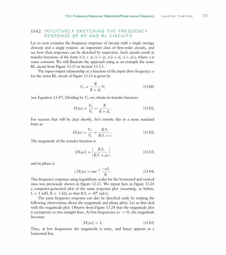
13.4 Frequency Response: Magnitude/Phase versus Frequency C H A P T E R T H I R T E E N 737
13.4.2 I N T U I T I V E L Y S K E T C H I N G T H E F R E Q U E N C YR E S P O N S E O F R C A N D R L C I R C U I T S
Let us now examine the frequency response of circuits with a single storageelement and a single resistor, an important class of first-order circuits, andsee how their responses can be sketched by inspection. Such circuits result intransfer functions of the form 1/(s + a), (s + a), s/(s + a), (s + a)/s, where a issome constant. We will illustrate the approach using as an example the seriesRL circuit from Figure 13.11 in Section 13.3.1.
The input-output relationship as a function of the input drive frequency ω
for the series RL circuit of Figure 13.11 is given by
Vo = R
R + sLVi (13.80)
(see Equation 13.47). Dividing by Vi, we obtain its transfer function:
H( jω) = Vo
Vi= R
R + sL. (13.81)
For reasons that will be clear shortly, let’s rewrite this in a more standardform as
H( jω) = Vo
Vi= R/L
R/L + s. (13.82)
The magnitude of the transfer function is
∣∣H( jω)∣∣ =
∣∣∣∣ R/L
R/L + jω
∣∣∣∣ (13.83)
and its phase is
∠H( jω) = tan−1 −ωL
R. (13.84)
This frequency response using logarithmic scales for the horizontal and verticalaxes was previously shown in Figure 13.13. We repeat here in Figure 13.24a computer-generated plot of the same response plot (assuming, as before,L = 1 mH, R = 1 k, so that R/L = 106 rad/s).
The same frequency response can also be sketched easily by making thefollowing observations about the magnitude and phase plots. Let us first dealwith the magnitude plot. Observe from Figure 13.24 that the magnitude plotis asymptotic to two straight lines. At low frequencies (ω → 0), the magnitudebecomes ∣∣H( jω)
∣∣ 1. (13.85)
Thus, at low frequencies the magnitude is unity, and hence appears as ahorizontal line.

738 C H A P T E R T H I R T E E N s i n u s o i d a l s t e a d y s t a t e
0.001
0.010
0.100
1.000
Frequency (rad/s)
1
104 105 106 107 108 109
|Vo
/ Vi|
R/(Lω)
-90
-80
-70
-60
-50
-40
-30
-20
-10
0
10
Frequency (rad/s)0
90
104 105 106 107 108 109
<V
o / V
i
F IGURE 13.24 Magnitude andphase of Vo/Vi versus frequency ω
on log scales.
At high frequencies (ω → ∞), the ω term dominates the expression in thedenominator and the magnitude becomes
∣∣H( jω)∣∣ = R/L
ω. (13.86)
From our observations on log plots in Section 13.4.1, we know that the logplot for the expression in Equation 13.86 will appear as a straight line with aslope of −1 for consistent horizontal and vertical scales, and passes through thepoint |H| = 1 when ω = R/L.
Clearly the two asymptotes intersect at
ω = R
L= 106 rad/s
called the break frequency or corner frequency. At the break frequency, the truemagnitude of H( jω) is
|H( jω)| = |106/(106 + j106)| = 1√2
= 0.707.
Thus the break frequency is also called the 0.707 frequency. At this frequency,the real and imaginary parts of the function are equal.8
8. Since 0.707 in decibels is 20 log 0.707 = −3 dB, the break frequency is also called a −3 dBfrequency. Since 0.7072 = 0.5, the break frequency is also called the half-power point. When themagnitude curve begins to dip after the break frequency, the break frequency is also called the cutofffrequency.

13.4 Frequency Response: Magnitude/Phase versus Frequency C H A P T E R T H I R T E E N 739
As is clear from Figure 13.24, the high- and low-frequency asymptotesapproximate the frequency response curve pretty well.
Let us now address the phase plot. Like the magnitude plot, the phasecurve can also be approximated by the low and high frequency asymptotes.At low frequencies the phase becomes
∠H( jω) 0 (13.87)
while at high frequencies the phase is
∠H( jω) = −90. (13.88)
Notice that the phase curve goes smoothly from 0 at ω = 0 to −90 at ω = ∞.At the break point, the real and imaginary parts of Equation 13.83 are equal,hence the angle of H( jω) is −45 at this frequency.
Examination of Equations 13.16 and 13.47 (or Equations 13.21 and 13.50for the corresponding time functions) shows that the RC circuit of Figure 13.3and the RL circuit of Figure 13.11 will have frequency response plots of the sameform: unit magnitude and zero phase at low frequencies, and magnitude fallingas 1/ω (slope of −1 in log-log plot) with −90 phase shift at high frequencies.These functions are called low-pass filters, because in signal-processing termsthey pass low frequencies and reject high frequencies. In other words, they donot affect low frequencies, while they provide a low gain for high frequencies.However, in many circuit applications the opposite effect is desired. We wishto get rid of low frequencies, and pass high frequencies. Decoupling amplifierstages so that the DC offset from one stage does not affect the next stage is acase in point. We will study these and other filters in more detail in Section 13.5.
To summarize, the frequency response of circuits containing a single stor-age element and a single (Thévenin ) resistor is of the form 1/(s + a), (s + a),s/(s + a), (s + a)/s, where a is some constant, and can be sketched intuitively asfollows:
Magnitude Plot
1. Sketch the low frequency asymptote.
2. Sketch the high frequency asymptote. The two asymptotes intersectat the break frequency a.
Phase Plot
1. Sketch the low frequency asymptote.
2. Sketch the high frequency asymptote.
740 C H A P T E R T H I R T E E N s i n u s o i d a l s t e a d y s t a t e
3. At the break frequency, the phase will be 45 or −45 asappropriate. Draw a smooth line starting with the low frequencyasymptote, passing through 45 or −45 as appropriate at the breakfrequency, and finishing off at the high frequency asymptote.
e x a m p l e 13 .4 i n t u i t i v e s k e t c h o f t h e f r e q u e n c y
r e s p o n s e o f r c c i r c u i t Let us sketch the frequency response for thetransfer function relating Vr to Vi for the RC circuit shown in Figure 13.14.
From Equation 13.58, we can immediately write the transfer function as
Vr
Vi= H(s) = 500 × 103
500 × 103 + 11×10−9s
. (13.89)
Simplifying,
H(s) = s
s + 2000.
Substituting, s = jω,
H( jω) = jω
jω + 2000. (13.90)
Since the transfer function is of the form s/(s + a), we can apply our intuitive method forsketching the frequency response:
Magnitude Plot
1. Sketch the low-frequency asymptote.
The low-frequency asymptote (ω 2000) is given by:
|H| = ω
2000.
2. Sketch the high-frequency asymptote. The two asymptotes intersect at thebreak frequency.
The high-frequency asymptote (ω 2000) is given by:
|H| = 1.
The two asymptotes intersect at the break frequency:
ω = 2000 rad/s.
The dashed lines in the magnitude plot in Figure 13.25 show these twoasymptotes. They intersect at ω = 2000 rad/s. A computer-generated plot of

13.4 Frequency Response: Magnitude/Phase versus Frequency C H A P T E R T H I R T E E N 741
0.01
0.10
1.00
Frequency (rad/s)
|H| 1
101 102 103 104 105
ω/20
00
-10
0
10
20
30
40
50
60
70
80
90
Frequency (rad/s)
<H
90
0
101 102 103 104 105
F IGURE 13.25 Frequencyresponse.
the magnitude versus frequency is also shown. Together, the asymptotes are afairly good approximation of the magnitude curve.
Phase Plot
1. Sketch the low-frequency asymptote.
The low-frequency asymptote for the phase is given by:
∠H = 90.
2. Sketch the high-frequency asymptote.
The high-frequency asymptote for the phase is given by:
∠H = 0.
The dashed lines in the phase plot in Figure 13.25 show these twoasymptotes.
3. The point (2000, 45) denoting the phase at the break frequency is alsomarked. The true phase curve is also shown, starting with the low-frequencyasymptote, passing through 45 at the break frequency, and finishing off atthe high-frequency asymptote.
W W W 13.4.3 T H E B O D E P L O T : S K E T C H I N G T H EF R E Q U E N C Y R E S P O N S E O F G E N E R A LF U N C T I O N S *

742 C H A P T E R T H I R T E E N s i n u s o i d a l s t e a d y s t a t e
W W W e x a m p l e 13 .5 b o d e p l o t f o r s e r i e s r l
c i r c u i t
W W W e x a m p l e 13 .6 a n o t h e r b o d e p l o t e x a m p l e
13.5 F I L T E R S
The frequency response of several of the circuits considered in the previ-ous sections indicated their frequency selective behavior (for example, theRL circuit in Figure 13.11 or the RC circuit in Figure 13.15). We can usesuch circuits to process signals according to their frequency. Circuits usedin this manner are called filters. Filters are a major application of frequencydomain analysis. The signal-processing property of filtering is fundamentalto the operation of all television, radio, and cellular phone receivers, whichmust select one transmitted signal from among many present at the receiverantenna.
The frequency response plots (see Figure 13.24) of the RL circuit inFigure 13.11 show that it rejects (that is, attenuates) high frequencies and passes(that is, does not affect) low frequencies, and therefore behaves like a low-passfilter. The RC circuit in Figure 13.15 behaves like a band-pass filter becauseit passes frequencies that fall within a certain band and rejects both very lowfrequencies and high frequencies (see Figure 13.17). In general, we can buildmany other types of filters as well. Figure 13.30 shows in abstract form themagnitude curves of the frequency response for several types of filters.
This section analyzes circuits from a filter point of view. Let us begin with adetailed analysis of a simple RC circuit with a view towards using it as a filter. Toillustrate the concept of filtering, let us find the voltage across the capacitor in thesimple RC circuit of Figure 13.31a, assuming that vi = Vi cos(ωt). In particular,we wish to find the amplitude of the output signal as the frequency ω of theinput signal is changed.
F IGURE 13.30 Various forms offilters.
Low passω0
1
High passω0
1
Band passω0
1
Band stopω0
1
|H(j
ω)|
|H(j
ω)|
|H(j
ω)|
|H(j
ω)|

13.5 Filters C H A P T E R T H I R T E E N 743
-+ vo
vi = Vi cos (ωt)-
+
R
(a) Circuit
vi -+ Vo
-
+
(b) Impendance model
Vi
R
1Cs------ F IGURE 13.31 A simple RC
filter circuit and its impedancemodel.
The generalized voltage divider relation for Vo in the impedance model,Figure 13.31b, is
Vo =1
Cs
R + 1Cs
Vi = 1/RC
s + 1/RCVi. (13.101)
Recall from Equation 13.10 that we have been using s as a shorthand for jω. Soat any frequency, ω, the complex output voltage is given by:
Vo = 1/RC
jω + 1/RCVi. (13.102)
The corresponding system function is
H( jω) = Vo
Vi= 1/RC
jω + 1/RC. (13.103)
It is easy to see that the magnitude of the system function at low frequen-cies is close to unity. At high frequencies, on the other hand, the magnitudeof the system function approaches 0. Because low frequencies are passed andhigh frequencies are rejected or attenuated, this circuit acts as a low pass filter.
Figure 13.32 plots the frequency response of the RC circuit assuming thatthe RC time constant of the circuit is RC = 1 / 20 seconds. The shape of the
0.1
.01
100010010
0.1
1
10
0.1
-90°
1000100101-45°
0°
ω
ω
Cutoff frequency 1/RC20
1
|H(j
ω)|
Log
sca
le
∠H( jω)
F IGURE 13.32 Frequencyresponse of the simple RC filtercircuit.

744 C H A P T E R T H I R T E E N s i n u s o i d a l s t e a d y s t a t e
magnitude plot is indicative of a low-pass filter. The break frequency is 20 rad/s.This says that the filter begins to reject input signals whose frequencies are in thevicinity of 20 rad/s. The level of attenuation increases as the frequency increasesbeyond the break frequency.
Frequency cutoff begins in the vicinity of the break frequency. Hence thebreak frequency is also called the cutoff frequency. Thus we can design our RClow-pass filter to have any cutoff frequency by an appropriate choice of the RCtime constant. As pictured in Figure 13.33, the higher the value of RC, thelower the cutoff frequency of the filter.
Finally, noting the similar forms of Equations 13.75 and 13.103, weconclude that Figure 13.32 reflects the frequency response of the circuit inFigure 13.21 as well. In fact, the circuit in Figure 13.21 is a Norton version ofthe circuit in Figure 13.31.
13.5.1 F I L T E R D E S I G N E X A M P L E :C R O S S O V E R N E T W O R K
Jeb is building a stereo amplifier system and needs some help. As illustratedin Figure 13.34, Jeb needs to take the output of his CD player and somehowsplit it into high and low frequencies, then pass each of the signals throughMOSFET amplifiers, and then send the amplified high and low signals to a
F IGURE 13.33 Designing thecutoff frequency (or breakfrequency) of a filter.
ω
1Increasing 1/RC
|H(j
ω)|
F IGURE 13.34 Crossoversystem for an amplifier.
Amp
Amp
Tweeter
Woofer
High frequencies
Low frequencies
Outputof CDplayer
Crossovernetwork

13.5 Filters C H A P T E R T H I R T E E N 745
-+
vl
L
-+
R
vi
-+ vr
Signal fromCD player
Crossover network
F IGURE 13.35 Crossover network circuit.
-+
Vl -+
Vi
-+ Vr
Signal fromCD player
Crossover network
Ls R
F IGURE 13.36 Impedance model of the crossovernetwork.
tweeter and a woofer, respectively. Together, the tweeter and woofer form thespeaker system.
Jeb asks his science teacher for help. The science teacher tells him, ‘‘Takea resistor and an inductor and connect them in series. Then take the highfrequencies off one element and the low frequencies of the other,’’ and thenrushes off to teach a class. Unfortunately, Jeb forgot to ask which elementto connect to the low-frequency woofer and which to connect to the high-frequency tweeter.
Jeb goes to one of his friends Nina for help, and sketches the networksuggested by the science teacher (see Figure 13.35). Nina has just read aboutfilters in her electronics class and is confident she can figure this out quickly.
As a first step, Nina draws the impedance model of the circuit as shown inFigure 13.36.
She then writes down the transfer functions corresponding to the inductorand resistor outputs as follows:
Vl
Vi= − Ls
Ls + R
Vr
Vi= − R
Ls + R.
Substituting, s = jω,
Vl
Vi= − jωL
jωL + R
Vr
Vi= − R
jωL + R.
By taking the limit as ω → 0, Nina observes that signal across the inductor,Vl, goes to zero. Similarly, Vl tends to Vi as ω → ∞. Thus Nina concludes

746 C H A P T E R T H I R T E E N s i n u s o i d a l s t e a d y s t a t e
F IGURE 13.37 The magnitudeof the transfer functions for the twosignals from the crossover network. ω
1
Breakfrequency
VrVi-----
RL---
ω
1
Breakfrequency
VlVi----
RL---
that the transfer function for the signal across the inductor resembles that ofa high-pass filter.
In contrast the signal across the resistor, Vr, tends to Vi as ω → 0. It tendsto zero as ω → ∞. Thus the transfer function for the signal across the resistorresembles that of a low-pass filter.
Nina plots the two transfer functions in Figure 13.37, and based on heranalysis, recommends that Jeb connect the signal from the inductor to thetweeter and the signal from the resistor to the woofer.
Jeb then asks Nina to walk down with him to an electronics store, eShackInc., so they can select an appropriate resistor and inductor. Since the humanear responds to frequencies up to 20 kHz,9 Nina decides that an appropriatebreak frequency for the filters is fbreak = 5 kHz. In radians, the break frequencyis given by:
ωbreak = 2π5000
or 31,416 radians. Thus, Nina begins to look for an inductor and a resistorwith values L and R such that R/L = 31416. She is able to find a resistorof value 100 and an inductor of value 3.2 mH, thus solving Jeb’s designproblem.
13.5.2 D E C O U P L I N G A M P L I F I E R S T A G E S
In this section, we will discuss an application of an RC filter. Recall the
RL
VS
vO
vI
(a)
+-
vi+-
VI
VO + vo
RL
VS
vI
(b)
VO + vo
RL
VS
vI
vi+-
VS
R1
R2
(c)
F IGURE 13.38 Amplifier circuitdiscussed in Chapter 8.
MOSFET amplifier circuit discussed in Chapter 8. The same circuit is shown inFigure 13.38a. The circuit has an input port and an output port. Figure 13.38b
9. In reality, only a young human ear responds to frequencies up to 20 kHz. Humans lose theirsensitivity to high frequencies as they grow older at the rate of roughly 1 Hz per day starting intheir teenage years. Loud music accelerates the sensitivity loss!

13.5 Filters C H A P T E R T H I R T E E N 747
shows the same amplifier circuit supplied with an input DC bias voltage VIand a small signal input vi. The bias voltage VI might be provided by a resistordivider circuit as in Figure 13.38c. Unlike the DC bias, the small signal input vi iscommonly a time-varying voltage, for example a sine wave. Correspondingly,the output voltage vO is the sum of a DC output bias VO and a small-signalvoltage vo.
A problem with the amplifier circuit shown in Figure 13.38a is that it
RLR1
R2
C
VS VS
(a)
+-
vI
RLR1
R2
vOC
VS VS
vGS
(b)
F IGURE 13.39 New amplifiercircuit with decoupling capacitor.
cannot be cascaded easily. In other words, the output port of an amplifierA cannot easily be coupled to the input of another amplifier B because thebiasing of one stage affects the biasing of all cascaded stages. This form ofcoupling might be useful if a designer wants to build an amplifier whose gainis greater than that of a single amplifier stage. Notice in Figure 13.38 that theoutput of the amplifier is the sum of a bias output voltage VO and a small-signal output vo. Notice further that the output of our amplifier in Figure 13.38(call it amplifier A) cannot be fed directly to the input of another amplifierB because of the biasing requirement for saturation operation of B. If theoutput of amplifier A is fed directly to the input of amplifier B, then the out-put bias voltage of A will become the input bias for B, and amplifier designrequirements often result in conflicting values for the output and input biasvoltages.
We will now discuss another implementation of the amplifier circuit basedon an input coupling capacitor as shown in Figure 13.39a. This circuit makes useof the fact that most small-signal inputs of interest are time-varying signals witha reasonably high-frequency content. As illustrated in Figure 13.39b, a small-signal input can be fed directly to the input port of the amplifier in Figure 13.39a,even if the small signal is superimposed over some DC bias voltage. As we willshow shortly, the capacitor C and the resistors R1 and R2 filter out any DCbias voltage over which the small signal is superimposed, and pass through thetime-varying small signal. Furthermore, we will show that the resistive dividerformed by R1 and R2 provides the necessary input bias voltage.
+
-
R1
R2
C
VS
vGS
vI
F IGURE 13.40 Subcircuit tocompute vGS .
Let us determine the voltage vGS at the gate of MOSFET as a function of theinput voltage vI for the amplifier in Figure 13.39b. We will use the impedancemethod to do so. Our goal is to determine vGS as a function of frequency sowe can see how the circuit behaves for DC for and time-varying signals. Sincethe gate input of the MOSFET is an open circuit, the subcircuit relevant to thecomputation of vGS is shown in Figure 13.40. The corresponding impedancemodel is shown in Figure 13.41.
Figure 13.41 shows that Vgs is a function of two inputs: Vi and VS. We willuse superposition to compute their combined effect. Let Vgsi be the componentdue to Vi and Vgss be the component due to VS.
To find the effect of VS acting alone, namely Vgss, we short out Vi, andobtain the equivalent circuit shown in Figure 13.42a. The MOSFET has infiniteinput impedance, so it does not figure in the calculation of Vgss. (We ignore theMOSFET’s gate capacitance for simplicity.) Vgss can now be found through a

748 C H A P T E R T H I R T E E N s i n u s o i d a l s t e a d y s t a t e
simple voltage divider relationship:
Vgss = 1/Cs ‖ R2
R1 + 1/Cs ‖ R2VS (13.104)
= R2
R1R2Cs + (R1 + R2)(13.105)
= R2
R1R2Cjω + (R1 + R2). (13.106)
Since VS is a DC voltage, we know that its frequency ω is 0. Therefore,
+
-Vi
R1
R2
VS
1/CsVgs
+
-
F IGURE 13.41 Impedancemodel relevant to the computationof Vgs .
Vgss = R2
R1 + R2VS. (13.107)
Notice that Vgss does not depend on C.Now let us short out VS and compute Vgsi. The relevant equivalent circuit
R1
R2
VS
1/CsVgss
+
-
(a)
+
-Vi
R1
R2
1/CsVgsi
+
-
(b)
F IGURE 13.42 (a) Equivalentcircuit to compute Vgss , thecomponent due to VS ; (b) equi-valent circuit to compute Vgsi , thecomponent due to Vi .
is shown in Figure 13.42b. The voltage Vgsi can again can be found through asimple voltage-divider relationship:
Vgsi = R1 ‖ R2
1/Cs + R1 ‖ R2Vi (13.108)
= Req
1/Cs + ReqVi (13.109)
= ReqCs
1 + ReqCsVi (13.110)
where Req = R1 ‖ R2. Substituting s = jω
Vgsi = ReqCjω
1 + ReqCjωVi. (13.111)
We can also write a transfer function H( jω) relating the complex input voltageto Vgsi as follows:
H( jω) = Vgsi
Vi= ReqCjω
1 + ReqCjω. (13.112)
Let us analyze Equation 13.112 at low and high frequencies:
When ω is small, H( jω) is close to 0. In particular, ω = 0 for DC signals,and H( jω) = 0. This implies that the circuit will filter out any DC biasover which the input signal is superimposed. Thus, any DC bias voltage

13.5 Filters C H A P T E R T H I R T E E N 749
ω1/ReqC
|H(j
ω)|
F IGURE 13.43 Frequencyresponse plot (magnitude only) forthe high-pass filter formed by C,R1, and R2.
carried by the input will not affect the node voltage vGS, which means thatthe biasing of the MOSFET in Figure 13.39 is independent of the appliedinput vI. We will discuss the issue of biasing in more detail shortly.
When ω is large, H( jω) is close to unity. Therefore high frequencies arepassed through without any attenuation.
The magnitude portion of the frequency response plot for the preceding systemfunction is shown in Figure 13.43. It is easy to see that the plot resembles thatfor a high-pass filter. Signals with frequencies significantly greater than the breakfrequency 1/ReqC will pass through, while signals with frequencies significantlylower than 1/ReqC will be attenuated.
Next, to study the impact of cascading, suppose the input Vi is composedof a DC component Vi0 and a time-varying component Viω, as might be thecase if the output of a previous amplifier stage is used as an input to the nextstage. In other words, suppose
Vi = Vi0 + Viω
then, from Equation 13.111,
Vgsi = ReqCjω
1 + ReqCjωVi (13.113)
= ReqCjω
1 + ReqCjωVi0 + ReqCjω
1 + ReqCjωViω. (13.114)
Since Vi0 is a DC signal, the first term in the preceding equation van-ishes, so
Vgsi = ReqCjω
1 + ReqCjωViω. (13.115)

750 C H A P T E R T H I R T E E N s i n u s o i d a l s t e a d y s t a t e
Therefore, if we choose ReqC to be large compared to the lowest frequencycomponent of interest in the input signal, (ω 1/ReqC), we get
Vgsi Viω. (13.116)
This completes our derivation of Vgsi. The expression for Vgsi demonstratesthat the DC component of the input signal does not influence Vgsi.
To complete the analysis, we obtain Vgs by adding the contributions dueto VS and Vi:
Vgs = Vgss + Vgsi = R2
R1 + R2VS + ReqCjω
1 + ReqCjωViω. (13.117)
Further, choosing a large value for ReqC so that the lowest frequency componentof the input signal (ω) is much greater than 1/ReqC, we get
Vgs = R2
R1 + R2VS + Viω. (13.118)
Equation 13.118 indicates that the voltage at the gate of the MOSFET is thesum of two components: a DC bias voltage, R2VS/(R1 + R2), and Viω, thetime-varying component of the input. The values of R1 and R2 can be chosento achieve a desired input DC bias. Thus, from the viewpoint of biasing theamplifiers, as shown in Figure 13.44, multiple amplifier stages can be designedindependently, and cascaded without the output bias of one stage impactingthe input bias of the next stage.10 The decoupling capacitor is instrumental in
F IGURE 13.44 Cascadingmultiple amplifiers together.
RLR1
R2
C
VS VS
RLR1
R2
C
VS VS
RLR1
R2
C
VS VS
10. Note, however, that the small-signal gain of each amplifier stage depends on the load offered bythe subsequent stage. Specifically, when computing the small-signal gain, assuming the capacitorC behaves as a short for the frequencies of interest, the load seen by each of the first and secondstages will not by RL alone, rather it will be RL in parallel with R1 and R2. We saw an example ofa loading effect, specifically a capacitive loading effect, in Section 13.3.4.

13.6 Time Domain versus Frequency Domain Analysis C H A P T E R T H I R T E E N 751
filtering out the DC bias component of the input, thereby allowing multipleamplifiers to be coupled directly.
13.6 T I M E D O M A I N V E R S U S F R E Q U E N C YD O M A I N A N A L Y S I S U S I N G V O L T A G E -D I V I D E R E X A M P L E
In this section, we compare frequency domain versus time domain analysis usingthe compensated attenuator (or compensated voltage divider) as an example.The simple voltage dividers discussed in Section 2.3.4 do not work very well athigh frequencies. In most circuits, some parasitic shunt capacitance is present,represented in Figure 13.45a by capacitor C2. If the drive is a low-frequency sinewave, the attenuation of the voltage divider is R2/(R1 + R2) as expected, but athigh frequencies the capacitance causes the attenuation to increase beyond thisdesired value. This effect can be readily shown by a frequency domain analysisof the voltage divider.
13.6.1 F R E Q U E N C Y D O M A I N A N A L Y S I S
The frequency domain analysis begins by constructing the impedance modelfor the circuit, Figure 13.45b. The generalized voltage divider relation is
Vo = R2 ‖ (1/C2s)
R1 + R2 ‖ (1/C2s)Vi, (13.119)
which simplifies to
Vo = R2
R1 + R2 + R1R2C2sVi. (13.120)
At high frequencies, (ω large, and s = jω), this expression reduces to
Vo 1
jωR1C2Vi (13.121)
so vo(t) becomes an increasingly small sinusoid, lagging 90 behind the inputsine wave. Thus the attenuation of the voltage divider is not fixed as desired,
-+
Vo
+
(b) Impedance model
Vi
R1
R2 1/C2s
--+ vo(t)
-
+R2
(a) Circuit
C2
R1
vi(t) F IGURE 13.45 Voltage dividerwith parasitic capacitance.

752 C H A P T E R T H I R T E E N s i n u s o i d a l s t e a d y s t a t e
F IGURE 13.46 Compensatedvoltage divider. -
+ vo(t)
-
+R2vi(t)
-+ Vo
+
(b) Impedance model
Vi
R1
R2
C2 1/C2s
-
R1
1/C1sC1
(a) Circuit
but increases with increasing frequency. This effect is readily observable if onetries to build a 2:1 divider at the input of an oscilloscope by using two one-megohm resistors for R1 and R2. (Such a divider circuit might be used in ascope probe, for example.) Two problems will arise. The input resistance ofthe scope will change the desired attenuation at low frequencies, and the scopeinput capacitance will cause the attenuation to change with frequency, as canbe seen from Equation 13.120.
To remedy the capacitance problem, it is necessary to add a small capacitorin parallel with the series resistor, as shown in Figure 13.46. This design is usedin all good oscilloscope probes. Analysis of the impedance model yields
Vo = R2 ‖ (1/C2s)
R1 ‖ (1/C1s) + R2 ‖ (1/C2s)Vi, (13.122)
which expands to
Vo = R2(R1C1s + 1)
R1(R2C2s + 1) + R2(R1C1s + 1)Vi. (13.123)
If we choose one particular value of C1 such that
R1C1 = R2C2, (13.124)
then Equation 13.123 reduces to
Vo = R2
R1 + R2Vi (13.125)
so the real output time function is
vo(t) = R2
R1 + R2vi(t) (13.126)

13.6 Time Domain versus Frequency Domain Analysis C H A P T E R T H I R T E E N 753
| | | | | | | ||| | | | | | | ||| | | | | | | ||| | | | | | | ||||0.01
||
||
||
|||0.10
||
||
||
|||
1.00 |H
|
100 101 102 103 104 ω
C1 small
C1 correct
C1 large
| | | | | | | ||| | | | | | | ||| | | | | | | ||| | | | | | | ||||-90
|-80
|-70
|-60
|-50
|-40
|-30
|-20
|-10
|0
|10
|20
|30
|40
|50
|60
|70
|80
|90
<H
100 101 102 103 104 ω
C1 small
C1 correct
C1 large
F IGURE 13.47 Magnitude andphase for compensated attenuator
independent of frequency! The voltage divider has now been compensated forthe effect of C2. Let us examine Equation 13.123 in more detail, and form thefrequency response plots for under-compensation, correct compensation, andover-compensation. For this purpose it is helpful to rearrange Equation 13.123,to obtain the system function in our standard form,
H(s) = Vo
Vi=
(C1
C1 + C2
) s + 1
R1C1
s + (R1+R2)R1R2(C1+C2)
. (13.127)
Let us assume that
C1
C1 + C2= 0.025
R1C1 = 1 ms
and
R1 + R2
R1R2(C1 + C2)= 100
and so that Equation 13.127 in our standard form becomes
H( jω) = Vo
Vi= 0.025(1000 + jω)
100 + jω. (13.128)
The frequency response for the under compensated case (C1 too small)is plotted with solid lines in Figure 13.47. The plots appropriate for

754 C H A P T E R T H I R T E E N s i n u s o i d a l s t e a d y s t a t e
F IGURE 13.48 Compensatedattenuator, step drive. -
+vo(t)-
+R2
vi(t)C2
R1
t
VS
vi
C1
under- and over-compensation are also shown in dashed lines. The circuitis properly compensated when the attenuation is constant, independent offrequency.
13.6.2 T I M E D O M A I N A N A L Y S I S
To relate back to the analysis methods used in Chapter 10, let us now calculatethe response of the attenuator to a voltage step, as shown in Figure 13.48. Notefirst that the system is still first order, in spite of the two capacitors. We knowthis because it is not possible to specify two independent initial conditions,only one.
Let us assume that the capacitor C2 is initially uncharged, so the initialcondition is
vo(t = 0 ) = 0. (13.129)
It follows that the initial voltage on C1 must also be zero, if we assume vi = 0for t < 0. A homogeneous solution of the form
vo = Ke st (13.130)
is appropriate. (Note that here s is not a shorthand notation for jω.) But asnoted in Section 13.2, we have already solved this problem: The character-istic polynomial is the denominator of the system function, in this case thedenominator of Equation 13.127. Setting the characteristic polynomial to zero,we find
s = −1
(R1 ‖ R2)(C1 + C2). (13.131)
By inspection, the particular solution, which will satisfy the differential equationafter the transient has died away, is
vo = R2
R1 + R2VS (13.132)

13.6 Time Domain versus Frequency Domain Analysis C H A P T E R T H I R T E E N 755
where VS is the height of the applied step. Thus the complete solution is ofthe form:
vo = Ke−t/(R1‖R2)(C1+C2) + R2
R1 + R2VS for t > 0. (13.133)
The constant K cannot be evaluated in the usual way (that is, setting vo = 0for t = 0 and solving for K), because the two capacitors form a loop facingthe voltage source. Thus when the step is applied, in theory infinite currentflows through the capacitors for an instant, and the capacitor voltages changeinstantaneously. Thus immediately after the step, at t = 0+, the initial conditionon vo will not be 0.
Instead, we can proceed as follows to find the initial condition at t = 0+.Because the same current flows through each capacitor, both capacitors receiveequal charge:
q = C1vc1 = C2vo. (13.134)
Also
vi = vc1 + vo; (13.135)
hence right after the step, at t = 0+,
vo = C1
C1 + C2VS. (13.136)
This, then, is the initial condition to use.Now K can be evaluated by setting t to zero in Equation 13.133, and
equating the voltage to that given in Equation 13.136
C1
C1 + C2VS = K + R2
R1 + R2VS (13.137)
whence
K =(
C1
C1 + C2− R2
R1 + R2
)VS. (13.138)
The complete solution is sketched in Figure 13.49 for C1 too small, correctlychosen, and too large. The correct choice is obviously the one that makes Kequal to zero in Equation 13.138, so that there is no transient. This is equivalentto making the capacitor voltage at t = 0+, Equation 13.136, equal to the final

756 C H A P T E R T H I R T E E N s i n u s o i d a l s t e a d y s t a t e
F IGURE 13.49 Time responseof compensated attenuator to astep input.
t
vo(t)
Over-compensated
Under-compensated
Step input
t
vi(t)
capacitor voltage derived from the particular solution, Equation 13.132. Theseconditions both require, as before:
R1C1 = R2C2. (13.139)
13.6.3 C O M P A R I N G T I M E D O M A I N A N D F R E Q U E N C YD O M A I N A N A L Y S E S
It is possible to tie together the time-domain solution with the previousfrequency-domain solution by assuming the driving waveform to be a squarewave. The time-domain solution for the over-compensated case (C1 is large)now looks like Figure 13.50. In particular, make a note of the relatively highervalues of the output signal at the transition points.
In terms of the frequency domain, the square-wave drive can be consideredas a sum of the sine waves:11 A sine wave with the same period as the squarewave, a sine wave at three times this frequency and one-third the amplitude,another at five times the frequency and one-fifth the amplitude, etc. The higherfrequency sine waves are called harmonics. It is relatively easy to visualize howeach of these components will be altered as they pass through the attenuatorby examining the appropriate frequency response plot. Again looking at theover-compensated case (C1 is large), the magnitude plot of Figure 13.47 shows
11. The theory behind such a decomposition of waveforms into sinusoids can be found in any textthat deals with Fourier Series, for example, Signals and Systems, Alan V. Oppenheim and Alan S.Willsky, 1996, Prentice Hall Publishers.

13.7 Power and Energy in an Impedance C H A P T E R T H I R T E E N 757
vi(t)
t
vo(t)
t
Square-wave input, over-compensated case
F IGURE 13.50 Time responseof compensated attenuator tosquare-wave input.
that the high-frequency harmonics will be larger than they are supposed to becompared to the low frequencies, and the phase plot of the same figure showsthat they will be shifted in phase.
We can correlate the larger amplitude of the high-frequency harmonicsin the output as observed in the frequency domain with the relatively largervalues of the square wave immediately following a signal transition in the timedomain.
The important conclusions from these two quite different analysis methodsare as follows:
The two analyses provide complementary views of the same circuit.
Often in an experimental situation it is easier to adjust C1 for perfectcompensation by the time-domain approach of looking at the responseto a square wave. The alternative technique more consistent with thefrequency-domain view is to apply first a low-frequency sine wave, andthen a high-frequency sine wave, and check that the response amplitudeis the same in both cases.
13.7 P O W E R A N D E N E R G Y I NA N I M P E D A N C E
In this section, we wish to address some of the issues of power and energyflow in RLC circuits. As discussed in Chapter 11, power and energy are criticalissues in the design of circuits. The size of the battery required by a device soit will function for a desired amount of time is related to the energy efficiency

758 C H A P T E R T H I R T E E N s i n u s o i d a l s t e a d y s t a t e
of the device. Similarly, the cooling requirements for a device depend on thepower dissipated by the device.
13.7.1 A R B I T R A R Y I M P E D A N C E
Let us examine first the power delivered to some arbitrary impedance Z =R + jX by a sinusoidal source, as depicted in Figure 13.51. The quantity X isusually referred to as the reactance of the circuit.
Vi
+
-R + jX
Ii
F IGURE 13.51 Powercalculations in an arbitraryimpedance.
A general sinusoidal drive can be written as:
vi(t) = |Vi| cos(ωt + φ). (13.140)
Hence the complex amplitudes of the voltage and current are
Vi = |Vi|e jφ (13.141)
Ii = Vi
Z= |Vi|e jφ
R + jX(13.142)
= |Vi|e j(φ−θ )√R2 + X2
(13.143)
= |Ii|e j(φ−θ ). (13.144)
where
θ = tan−1 X
R. (13.145)
The power delivered to the impedance is by definition the product of v(t)and i(t).
Because power is not a linear function of v and i, we must be cautious aboutusing impedance concepts in power calculations.
Thus we start with time expressions such as Equation 13.140 rather thancomplex amplitudes. From Equation 13.143, the current as a function oftime is
i(t) = Re[Iie jωt
](13.146)
= |Vi|√R2 + X2
cos (ωt + φ − θ ). (13.147)

13.7 Power and Energy in an Impedance C H A P T E R T H I R T E E N 759
Hence, from Equations 13.140 and 13.147 the instantaneous power is given by:
p(t) = vi = |Vi|2√R2 + X2
[cos(ωt + φ)][cos(ωt + φ − θ )] (13.148)
= 1
2
|Vi|2√R2 + X2
[cos(2ωt + 2φ − θ ) + cos θ ]. (13.149)
Thus, in general, the instantaneous power for sinusoidal drive has a sinusoidalcomponent at twice the frequency of the input signal, and the DC component.We will examine this expression for some simple cases shortly, but first let uscomplete the general derivation by calculating the average power, because thisis the quantity that determines your monthly bill from the power company.
Because the average value of cos(ωt
)is zero, the average power flowing
into an arbitrary impedance is just the DC term in Equation 13.149:
p = 1
2
|Vi|2√R2 + X2
cos θ . (13.150)
From Equations 13.141 and 13.143, this can be written as
p = 1
2|Vi ‖ Ii| cos θ (13.151)
where Vi and Ii are the complex amplitudes of the voltage and current respec-tively, and θ is the angle between them. The term cos θ is often called the powerfactor.
The average power in terms of complex amplitudes of voltages and currentsis one-half the product of the two magnitudes multiplied by the cosine of theangle between them.
The average power can also be written directly in terms of complex voltage andcomplex current. Again from Equations 13.141 and 13.143
p = 1
2Re[ViI∗i ] (13.152)
= 1
2Re[V∗
i Ii] (13.153)
where I∗i is the complex conjugate of Ii, and V∗ is the complex conjugate ofV. Using this notation, 1/2 VI∗ is often called complex power, whence thereal part of the complex power is the average power, the ‘‘real’’ power, as perEquation 13.151, and the imaginary part is called reactive power.

760 C H A P T E R T H I R T E E N s i n u s o i d a l s t e a d y s t a t e
F IGURE 13.52 Power flow in apure resistance.
p = Vi2/2R
t
0
vi
Vi
π /ω 2π /ω
t
p(t
)
0
Vi2 /R
π /ω 2π /ω
13.7.2 P U R E R E S I S T A N C E
To develop some insight concerning power and energy flow, let us examinea few special cases. First, assume that the impedance in Figure 13.51 is a pureresistance R. That is, X = 0. Further, we assume for simplicity that the timeorigin is selected to make the voltage drive a cosine wave, that is, φ = 0 inEquation 13.140. Then 13.149 is reduced to:
p(t) = V2i
2R(1 + cos 2(ωt)). (13.154)
Again we have a double-frequency term and a DC term. A plot of power asa function of time for the resistive case is shown in Figure 13.52. From thefigure or from Equation 13.154, the average power dissipated in the resistor forsinusoidal drive is
p = V2i
2R. (13.155)
Remember from Section 1.8.1, this is exactly one half of the power deliveredby the DC voltage of the same amplitude. Recall, also from Section 1.8.1, thevoltage unit called the root-mean-square voltage, abbreviated rms, which isrelated to the peak amplitude of the sinewave by the square root of two
Vrms = Vi√2
. (13.156)
In terms of the rms unit, average power is
p = (Vrms)2
R(13.157)
just as for DC power. For non-sinusoidal voltages, the general definition ofrms voltage is, as the name implies,
Vrms =√
(v(t))2. (13.158)

13.7 Power and Energy in an Impedance C H A P T E R T H I R T E E N 761
Most voltages related to the AC power line are quoted in terms of rms values,unless specifically designated as peak values. Thus the 115-V AC power froma wall socket is 115 volts rms, or 115 × √
2 = 162.6 volts peak.
13.7.3 P U R E R E A C T A N C E
Next, we examine the case where the impedance in Figure 13.51 consists onlyof inductors and/or capacitors, that is, R = 0. Regardless of the circuit con-figuration, at any given frequency the impedance must look like either a pureinductor or a pure capacitor (although it will change from one to the other asfrequency changes, when we go through a resonant frequency). If the circuit isinductive, then from Equation 13.145, θ = π/2. Again assuming a cosine drivevoltage (φ = 0), Equation 13.149 reduces to:
p(t) = V2i
2Xcos (2ωt − π/2) (13.159)
= V2i
2Xsin 2(ωt). (13.160)
If the circuit is capacitive at the frequency of interest, then X in Equation 13.143must equal −1/ωC, hence from Equation 13.145 with R = 0, θ = −π/2, and
p(t) = − V2i
2Xsin(2ωt). (13.161)
Power flow as a function of time for both of these cases is shown in Figure 13.53.Note that in both cases the average power is zero. Thus, circuits with inductorsand capacitors but no resistors do not dissipate any power. The L’s and C’sabsorb power for two quarters of each cycle, and deliver the power back to thesource during the other two quarter cycles. Power companies are not happyabout this state of affairs, because they still must supply the power depictedin Figure 13.53, even though they get it all back a few milliseconds later. Theproblem is that the current associated with this instantaneous power causes i2Rpower losses in the transmission lines, and the power company must pay forthis power loss, even though the customer is consuming zero power on theaverage.12
Although there is no average power supplied to this lossless circuit in thesinusoidal steady state, there is energy stored on the average. For example, for
12. Not surprisingly, it turns out that the customers pay for it eventually, because the rates assumea loss factor.

762 C H A P T E R T H I R T E E N s i n u s o i d a l s t e a d y s t a t e
F IGURE 13.53 Power flow ininductor and capacitor. Themaximum value of p(t) for both theinductor and capacitor is 1/2(V 2
i /X).
t
0
vi
Vi
π/ω 2π/ω
t
p(t
): I
nduc
tor
0π/ω 2π/ω
t
p(t
): C
apac
itor
0π/ω 2π/ω
a capacitor, the stored energy is, from Equation 9.18,
WC = 1
2Cv(t)2. (13.162)
For sinusoidal v(t),
WC = 1
2C(Vi cos(ωt))2 (13.163)
= 1
2CV2
i
(1
2+ 1
2cos (2ωt)
). (13.164)
Again a DC term and a double-frequency term. Hence the average stored energyis
WC = 1
4CV2
i . (13.165)
A similar derivation for an inductor yields
WL = 1
4LI2i (13.166)
for an inductor current of the form
iL(t) = Ii cos (ωt). (13.167)

13.7 Power and Energy in an Impedance C H A P T E R T H I R T E E N 763
t
0
v iVi
π/ω 2π/ω
t
p(t
)
p
0π/ω 2π/ω
F IGURE 13.54 Power flow in aninductive circuit. The averagepower is given byp = 1/2V 2
i /√
R2 + X 2 cos θ . Themaximum value of p(t) is1/2V 2
i /√
R 2 + X 2 (cos θ + 1), andthe minimum value is1/2V 2
i /√
R2 + X 2 (cos θ − 1).
For the general case when the network contains resistors, capacitors, and induc-tors, the power flow will have some intermediate form between Figure 13.52and Figure 13.53. Assuming that the circuit is net inductive at the frequency ofinterest, then θ is positive but less than π/2, and Equation 13.149 with φ = 0becomes
p(t) = 1
2
V2i√
R2 + X2[cos(2ωt − θ ) + cos θ ].
The power waveform is as depicted in Figure 13.54.
13.7.4 E X A M P L E : P O W E R I N A N R C C I R C U I T
Let us examine a specific circuit with both resistive and reactive components,the RC circuit of Figure 13.55. To calculate the average power from eitherEquation 13.151 or 13.152, we must find the complex amplitude of the current.By inspection of Figure 13.55:
Ii = Vi
Z= Vi
R + 1/jωC(13.168)
= Vi√R2 + (1/ωC)2
e−jθ (13.169)
where
θ = tan−1(
1
ωRC
)(13.170)
Now the average power dissipated in the circuit is, from Equation 13.151:
-
+ R
i(t)C
vi = Vi cos (ωt)
-+
ViR
1/jωCI
F IGURE 13.55 Series RCcircuit.p = 1
2
V2i√
R2 + (1/ωC)2cos(θ ) (13.171)
= 1
2
V2i
|Z| cos(θ ). (13.172)

764 C H A P T E R T H I R T E E N s i n u s o i d a l s t e a d y s t a t e
Note from Equation 13.171 that if we choose ω such that
R = 1
ωC(13.173)
that is, at the break frequency or corner frequency of the circuit, then
p = 1
2
V2i
2R. (13.174)
Hence the frequency ω = 1/RC is also called the half-power frequency ofthe impedance, because the average power is one half of the value found inEquation 13.151 for the capacitor being a short circuit. Note also that becausethere is no average power dissipated in the capacitor, the average power dis-sipated in the resistor must be identical to the average power supplied by thesource to the impedance.
W W W e x a m p l e 13 .7 m a x i m i z i n g p o w e r t r a n s f e r
u s i n g a t r a n s f o r m e r
W W W e x a m p l e 13 .8 n o n - i d e a l t r a n s f o r m e r s

13.8 Summary C H A P T E R T H I R T E E N 765
13.8 S U M M A R Y Sinusoidal steady state is an important characterization of a linear system.
It comprises a frequency response, which includes a gain plot and a phaseplot as a function of frequency.
The impedance approach provides an analysis of circuits for sinusoidalinputs, which complements the time-domain calculations of Chapter 12,by showing the behavior of the circuit as a function of frequency.
By assuming complex exponential drives instead of sinusoidal drives forlinear time-invariant circuits, the differential equations describing circuitbehavior reduce to algebraic equations.
These algebraic equations can be found directly by using impedance. Theconstituent relations for R, L, and C, relating complex amplitudes are
V = I R
V = Ls I
and
V = (1/Cs) I
where s is a shorthand notation for jω. Accordingly, the impedance of aninductor is sL, that for a capacitor is 1/sC and that for a resistor is R.
We extended our variable notation to distinguish between total variables,DC operating values, small-signal variables, and complex amplitudes.
We denote total variables with lowercase letters and uppercasesubscripts, for example, vD.
DC operating-point variables using all uppercase, for example, VD. Incremental values using all lowercase letters, for example, vd. Complex amplitudes use uppercase letters and lowercase subscripts,
for example, Vd.
Inductors behave like short circuits for DC (or very low frequencies) andlike open circuits for very high frequencies. Capacitors behave like opencircuits for DC (or very low frequencies) and like short circuits for very highfrequencies.
The steady state values of the real voltages or currents (functions oftime) can be found from their corresponding complex amplitudes by multi-plying the complex amplitude by e jωt and taking the real part. For example,

766 C H A P T E R T H I R T E E N s i n u s o i d a l s t e a d y s t a t e
the steady state value of vc can be determined from the value of Vc as
vc = Re[Vce jωt
]
or, equivalently,
vc = |Vc| cos(ωt + ∠Vc).
The impedance method allows us to determine with ease the steady-stateresponse of any linear RLC network for a sinusoidal input. The methodworks with complex amplitudes of voltages and currents at its variablesand has the following steps:
1. First, replace the (sinusoidal) sources by their complex (or real) ampli-tudes. For example, the input voltage vA = Va cos(ωt) is replaced by itsamplitude Va.
2. Replace resistors by R boxes, inductors by Ls boxes, and capacitors by1/Cs boxes. The resulting diagram is called the impedance model of thenetwork.
3. Now, determine the complex amplitudes of the voltages and currentsin the circuit by any standard linear circuit analysis technique Nodemethod, Thévenin method, etc.
4. Although this step is not usually not necessary, we can then obtain thetime variables from the complex amplitudes.
The frequency response characterizes the behavior of a network as a func-tion of frequency. Frequency domain analysis of a network is carried out byexamining the network’s system function, which is the ratio of the complexamplitude of the network output to the complex amplitude of the input.
A frequency response plot is a convenient way of summarizing how anetwork behaves as function of frequency. A frequency response plot hastwo graphics:
the log magnitude of the system function plotted against log frequency,and
the angle of the system function plotted against log frequency.
|H( jω)| = ω plots as a straight line with slope of +1 in log space, givenconsistent horizontal and vertical scales.
Correspondingly, |H( jω)| = 1/ω plots as a straight line with slope of −1in log space.
The frequency response for system functions arising from circuits contain-ing a single storage element and a single (Thévenin) resistor is of the form

13.8 Summary C H A P T E R T H I R T E E N 767
1/(s+a), (s+a), s/(s+a), (s+a)/s, where a is some constant. Such responsescan be intuitively graphed as follows:
The magnitude plot is sketched by drawing the low-frequency and thehigh-frequency asymptotes. The two asymptotes intersect at the breakfrequency a.
The phase plot can also be graphed by sketching the low-frequencyand the high-frequency asymptotes. At the break frequency, the phasewill be 45 or −45 as appropriate.
The average power in terms of complex amplitudes of voltages and currentsis one-half the product of the two magnitudes multiplied by the cosine ofthe angle between them.
E X E R C I S E Se x e r c i s e 13 .1 Find the magnitude and phase of each of the followingexpressions:
a) (8 + j 7)(5e j30)(e−j39
)(0.3 − j 0.1)
b)(8.5 + j 34)(20e−j25
)(60)(cos(10) + j sin(10))
(25e j20 )(37e j23 )
c) (25e j30)(10e j27
)(14 − j 13)/(1 − j 2)
d) (13e j30(15+j1.5))(6e(1−j30))
e x e r c i s e 13 .2 Find the real and imaginary parts of the following expressions:
a) (3 + j 5)(4e j50)(7e−j20
)
b) (10e j50)(e j20
)
c) (10e j50)(e jωt)
d) Ee jωt where E = |E|e j
e x e r c i s e 13 .3 Find the system function VL/I for the network shown in Figure13.62. Then find the response vl(t) for i(t) = I cos(ωt) under steady-state conditions.
e x e r c i s e 13 .4 Referring to Figure 13.63, given i(t) = I0 cos(ωt), where I0 =3 mA and ω = 106 rad/s, determine v(t) in the sinusoidal steady state. Assume R = 1 k
and L = 1 mH.
e x e r c i s e 13 .5 The two-terminal linear network in Figure 13.64 is known tocontain exactly two elements. The magnitude of the impedance function is as shown(log-log coordinates).

768 C H A P T E R T H I R T E E N s i n u s o i d a l s t e a d y s t a t e
R
+
-
vLi(t) L
F IGURE 13.62
R
+
-
v(t)i(t) L
F IGURE 13.63
F IGURE 13.64
ω
+
-v(t)
i(t)
100
Linearnetwork
70.7
104 rad/s
Slope = -1
|Z( jω)|
Draw a two-element circuit that has the impedance magnitude function indicated in yoursketch. Specify the numerical value of each element.
e x e r c i s e 13 .6 For each of the circuits shown in Figure 13.65, select the magni-tude of the frequency response for the system function (that is, impedance, admittance,
F IGURE 13.65
(1) (4)(3)(2)
-1 +1 -1+1
log ω log ω log ω log ωω1 ω1 ω1 ω2
(5)
+1
log ωω1 ω2
(6)
-1
log ωω1
(8)
None ofthe above
(7)
ωω1
C
C R
v1
+
-
v1
R
+
- C
i1
L
CR
v2+- R
+
-
v1
i1i1
L R2
+
-
v1
R1
Y( jω) ------------------= H( jω) ------------------= Z( jω) ------------------= Z( jω) = ------------------
(a) (b) (c) (d)
I1( jω)V1( jω)
V2( jω)V1( jω)
V1( jω)I1( jω)
V1( jω)I1( jω)

13.8 Summary C H A P T E R T H I R T E E N 769
or transfer function) from those given. It is not necessary to relate the critical frequenciesto the circuit parameters, and you may choose a magnitude response more than once.
Please note that the magnitude responses, except (7), are sketched on a log-log scale,with slopes labeled.
e x e r c i s e 13 .7 A linear network is excited with a sinusoidal voltage vI(t) =cos
(t − 5π/8
)for all time, as shown in Figure 13.66.
iI(t)
Z(s)+-vI(t) = t
5π8
------– cos F IGURE 13.66
The current observed under the sinusoidal steady-state conditions is iI(t) =√2 sin(t + π/8).
What is Z(s = j1), the impedance of the network at an excitation frequency of oneradian per second?
e x e r c i s e 13 .8 Find v2(t) in the sinusoidal steady state in Figure 13.67. AssumeL = 10 H, R1 = 120 , and R2 = 60 .
3 V cos(4t) v2R2L+
-
+-
R1
F IGURE 13.67
e x e r c i s e 13 .9 A sinusoidal test signal is applied to a linear network that isv(t)
i(t)
Network-
+
F IGURE 13.68
constructed from exactly two circuit elements as shown in Figure 13.68.
The magnitude portion of the Bode plot for the impedance Z( jω) = V( jω)/I( jω) isshown in Figure 13.69.
ω105 106 107 108
103
104
105
V jω( )I jω( )----------------
F IGURE 13.69
Draw the network and find the element values.
e x e r c i s e 13 .10 The circuit shown in Figure 13.70 is a highly simplified modelof a power transmission system.

770 C H A P T E R T H I R T E E N s i n u s o i d a l s t e a d y s t a t e
+-
v1(t)
L1 L2
vL(t) v2(t)+
-
1
2
+-
F IGURE 13.70
v1(t) and v2(t) are the voltages of two power generators:
v1 = V cos(ωt) v2 = V cos(ωt + |)
Find the Thévenin equivalent of this circuit at the terminals 1 2 in terms of a complexamplitude Voc and a complex Thévenin impedance Zth.
e x e r c i s e 13 .11 Write expressions for H( jω) = Vo/Vi, its magnitude |H( jω)|,
C
(a)
(b)
(c)
(d)
R
+-
+
-
vo
L
R
+-
+
-
vo
C = 1 µF = 10-6 F
+-
+
-
voR = 106 Ω
L = 1 H
+-
+
-
voR = 10 Ω
Vi = e jωt
Vi = 2 e jωt
Vi = 5 e jωt
Vi = 10 e jωt
F IGURE 13.71
and its phase angle ∠H( jω), as a function of ω in the four cases shown in Figure 13.71.
e x e r c i s e 13 .12 Plot the log magnitude and the phase angle, both as functionsof frequency (on a logarithmic scale), of the following complex quantity:
H( jω) = 1 − jω
1 + jω.
Label all significant asymptotes, slopes, and break points.
e x e r c i s e 13 .13 In the network shown in Figure 13.72,
C1
vo(t)+
-
+-
R
C2vi(t)
F IGURE 13.72
R = 1 k C1 = 20 µF C2 = 20 µF.
a) Determine the magnitude and phase of H( jω), the transfer function relating V0/Vi.
b) Given vi(t) = cos(100t) + cos(10000t), determine the sinusoidal steady state outputvoltage, vo(t).
e x e r c i s e 13 .14 Find v2(t) in the sinusoidal steady state for the circuit in Figure13.73.
L = 10 H R1 = 120 R2 = 60
e x e r c i s e 13 .15
a) Write the transfer function Vo(s)/Vi(s) for the circuit in Figure 13.74.
b) Write the transfer function Ia(s)/Vi(s).

13.8 Summary C H A P T E R T H I R T E E N 771
L3 cos4t+-
R2
+
-
v2
R1
F IGURE 13.73
vO(t)
+
-
vI(t)
iA(t)Z1
Z2
Z3
Z4+-
F IGURE 13.74
e x e r c i s e 13 .16 Write the transfer functions Vo(s)/Vi(s), Ia(s)/Vi(s) in the circuitin Figure 13.75.
vO(t)
+
-
CvI(t)
iA(t)
R1 L
R2+- F IGURE 13.75
e x e r c i s e 13 .17 Write the transfer function Ia(s)/Is(s) for the circuit inFigure 13.76.
iSY2
Y3
Y4
iA
Y1 F IGURE 13.76
e x e r c i s e 13 .18 Find Ia/Is in the circuit in Figure 13.77.
L
iA(t)
R (let G = 1/R)
C2iS(t) C1F IGURE 13.77
P R O B L E M Sp r o b l e m 13.1 For each of the networks shown in Figure 13.78:
a) Determine an expression for the indicated complex impedance or transferfunction.

772 C H A P T E R T H I R T E E N s i n u s o i d a l s t e a d y s t a t e
b) Sketch the magnitude and angle of the indicated quantity as a function of frequency.You may use either linear or log-log coordinates, but it is recommended that youlearn to use both kinds of axes.CRZ
LRZ
C2
RZ C1
F IGURE 13.78
p r o b l e m 13.2 Shown in Figure 13.79 is one possible circuit model for atransformer, for use where there can be a common ground between primary andsecondary.
+
-
v2M
i1
+-
v1
+
-
vS
R1 i1
v2
+
-
R2
i2
+
-
v1
L1-M L2-M
F IGURE 13.79
Assume:
L1 = 2.5 H, L2 = 0.025 H, M = k√
L1L2 where k < 1, R1 = 1 k, R2 = 10 .
a) Determine an expression for the sinusoidal steady-state transfer function V2/Vs.
b) In the tight-coupling limit, k → 1, the two natural frequencies are far apart. (SeeProblem 12.3 in the previous chapter.) For this specific case, sketch the magnitudeand angle of the transfer function on log-log scales.
p r o b l e m 13.3 An electrical system has the following transfer function:
H( jω) = Y( jω)
X( jω)= 105(10 + jω)(1000 + jω)
(1 + jω)(100 + jω)(10000 + jω).
a) Plot the magnitude of H( jω) in decibels versus the logarithm of frequency, labelingall 3dB points.
b) Sketch the phase of H( jω) versus the logarithm of frequency.
c) For what values of ω does the magnitude of H( jω) equal 0db? What is therelationship between the magnitudes of X( jω) and Y( jω) at these frequencies?
d) List the frequencies at which the phase of H( jω) equals −45 degrees.
p r o b l e m 13.4 Refer to Figure 13.80 for this problem. Assume R1 = 1 k andL1 = 10 mH.
a) Find the transfer function H( jω) = V1/Vo.

13.8 Summary C H A P T E R T H I R T E E N 773
V1
R1
+
-
R L
+-
L1
VoF IGURE 13.80
b) Find R so that the DC gain is 1/10.
c) Find a value of L so that the response at high frequencies is equal to response at DC.
d) Plot H( jω) (magnitude and phase) versus. log ω for the values of R and L foundpreviously.
p r o b l e m 13.5 This problem examines the simple doorbell circuit commonlyused in homes (see Figure 13.81).
+
-
V2M
I1
+-
V1
+
-
I1
V2
+
-
I2
+
-
V1
L1-M L2-M
Bell transformer Power line
Doorbell
Push-buttonswitchM I2
Circuit model forbell transformer
120 V AC, 60 Hz
F IGURE 13.81
Data for the transformer in Figure 13.81 is:
L1 = 2.5 H, L2 = .025 H, M = k√
L1L2, where k < 1.
a) In the limit k 1, what is the voltage V2 with the push-button switch not pressed(open)? You should use root-mean-square amplitudes for all quantities. The voltagesource is given as 120-V root-mean-square M = 0.25 H.
b) The doorbell operates by repetitive making and breaking of a contact and cannormally be modeled as a 10 resistance at 60 Hz. Determine the magnitude ofthe root-mean-square primary current I1 under normal doorbell operation (pushbutton closed, doorbell = 10 ) in the limit of k 1.
c) An important safety issue in such circuits is the prevention of fire in the event thatthe doorbell should accidently stick with its contact closed, thus becoming equal toa short circuit. This can be accomplished by adjusting the value of k. Find the value

774 C H A P T E R T H I R T E E N s i n u s o i d a l s t e a d y s t a t e
of k that will limit the root-mean-square primary current to 500 mA for the casewhere the push button is pressed and the doorbell acts like a short circuit.
p r o b l e m 13.6 In the circuit in Figure 13.82, the switch has been in Position (1)for a long time. At t = 0, the switch is moved instantly to Position (2). For the particularparameter values of this circuit, the complete output waveform for all time greater thanzero is
F IGURE 13.82 Vc(t)+
-
R
CVo
-+
(1)
(2)+
-v(t) = V1 cos (ωt)
vc(t) = |Vc| cos(ωt + )
a) Find |Vc| and in terms of V1, ω, R, and C.
b) Find Vo in terms of |Vc|, ω, R, and C required to produce the vc(t) waveform.

c h a p t e r 14
14.1 P A R A L L E L R L C , S I N U S O I D A L R E S P O N S E
14.2 F R E Q U E N C Y R E S P O N S E F O R R E S O N A N T S Y S T E M S
14.3 S E R I E S R L C
14.4 T H E B O D E P L O T F O R R E S O N A N T F U N C T I O N S *
14.5 F I L T E R E X A M P L E S
14.6 S T O R E D E N E R G Y I N A R E S O N A N T C I R C U I T
14.7 S U M M A R Y
E X E R C I S E S
P R O B L E M S


s i nu so ida l s t eady s tate :
r e sonance14
Chapter 12 showed that circuits containing an inductor and a capacitor coulddisplay oscillatory behavior when the circuit was under-damped. This chapterwill show that oscillatory behavior occurs when the system function has com-plex roots. Such systems are called resonant systems. The behavior of resonantcircuits was characterized by parameters such as their quality factor and reso-nant frequency. This chapter revisits resonant circuits from an impedance andfrequency point of view.
Resonant circuits are useful in analog design to build filters with high selec-tivity such as radio tuners and channel selectors in cell phones and wirelessnetworks. Resonant circuits are also used to build oscillators to produce sinu-soids of a given frequency. The same oscillators also form the basis of clockgenerators in digital design.
Many physical systems can also be modeled as second-order resonant cir-cuits. Because the injection of even miniscule amounts of energy at or nearthe resonant frequency of a second-order resonant circuit can cause a massiveand sustained response, physical structures such as buildings and bridges arecarefully modeled and designed to avoid such responses. In fact, resonatorsexcited at their resonance can be viewed as energy accumulators in the sensethat they continuously extract and store energy from their excitation. In thiscase, the only limit to the amplitude of their response is internal dissipationor nonlinear behavior resulting from the stresses of large amplitude responses.The most notorious case of such a response is the Tacoma Narrows Bridge dis-aster. Alternating winds injected enough energy into the bridge structure at itsresonant frequency that the entire bridge entered into resonance and began tosway back and forth and finally collapsed. Sections 14.5.2 and 14.6 will providemore insight into this type of resonant behavior.
14.1 P A R A L L E L R L C , S I N U S O I D A L R E S P O N S E
The response of a second-order system, specifically a parallel RLC system asin Figure 14.1, to a brief pulse and to a step was calculated in Chapter 12. Wenow wish to examine this same system from the impedance point of view, toshow how such circuits can be used as filters. In particular, we will discuss thefactors that affect the selectivity of the filter. To tie back to the calculations inChapter 12, let us first calculate the total time-domain response v(t), when the
777

778 C H A P T E R F O U R T E E N s i n u s o i d a l s t e a d y s t a t e : r e s o n a n c e
F IGURE 14.1 Parallel RLCcircuit.
Ri(t) CL
iL
v(t)
+
-
circuit is driven with a tone burst at some frequency ω1:
i(t) = Io cos(ω1t
)for t > 0. (14.1)
We acknowledge that the total response to a sinusoid is rarely necessary; weare more often interested in just the forced (or particular) response to sinusoids.Accordingly, you may skip directly to Section 14.1.2 and then to Section 14.2without loss of continuity. We, however, will plow through the total responsefor completeness.
Application of KCL to the top node gives
i(t) = Cdv
dt+ v
R+ iL (14.2)
and the constituent relation for the inductor is
v = LdiLdt
. (14.3)
Differentiating Equation 14.2, and substituting Equation 14.3, we obtain asecond-order differential equation describing the system:
1
C
di
dt= d2v
dt2+ 1
RC
dv
dt+ 1
LCv. (14.4)
As in the past, we will solve this differential equation by summing together thehomogeneous and particular solutions, vh and vp, respectively.
14.1.1 H O M O G E N E O U S S O L U T I O N
The homogeneous solution for this equation was worked out in detail inChapter 12, so will be only briefly reviewed here. The homogeneous equation is
d2v
dt2+ 1
RC
dv
dt+ 1
LCv = 0. (14.5)

14.1 Parallel RLC, Sinusoidal Response C H A P T E R F O U R T E E N 779
Assuming a homogeneous solution of the form:
vh = Ke st (14.6)
the characteristic equation is
s 2 + 1
RCs + 1
LC= 0 (14.7)
which, to simplify notation, is written in canonic form as
s 2 + 2αs + ω2o = 0 (14.8)
where
ω2o = 1
LC
and
α = 1
2RC.
We saw in Chapter 12 that the system is resonant, that is, displays oscillatorybehavior, when it is under-damped. As further discussed in Section 12.2.1,under-damped systems are characterized by the condition:
ωo > α. (14.9)
Since we are focusing on resonant systems in this chapter, we will assumethat the system is under-damped, that is, ωo > α. Under this assumption, thecharacteristic equation has these two roots:
sa = −α + jωd (14.10)
sb = −α − jωd (14.11)
where
ω2d = ω2
o − α2. (14.12)
It follows from our assumption (ωo > α) that the two roots identified in Equa-tions 14.10 and 14.11 are complex. Furthermore, the roots form a complexconjugate pair. In other words, resonant systems are characterized by a pair ofcomplex conjugate roots.

780 C H A P T E R F O U R T E E N s i n u s o i d a l s t e a d y s t a t e : r e s o n a n c e
Hence the homogeneous solution is
vh(t) = e−αt[Kae jωdt + Kbe−jωdt
](14.13)
= Ke−αt cos(ωdt + θ
)(14.14)
where K and θ are constants to be determined from the two initial conditions,the inductor current and the capacitor voltage before the tone burst, after theexpression for the total solution has been written.
14.1.2 P A R T I C U L A R S O L U T I O N
Now let us find the particular solution for this system using the impedanceapproach. One possible particular solution is the steady-state response of thesystem vp(t) to the cosine signal Io cos
(ω1t
). The impedance model derived
from the original circuit, Figure 14.1, is shown in Figure 14.2. The complexconstants Io and Vp in Figure 14.2 are related to the original time variables bythe expressions:
i(t) = Re[Ioe s1t
]= Io cos ω1t (14.15)
vp = Re[Vpe s1t
]. (14.16)
Direct application of KCL to the top node in the impedance model yields
Io = Vp
Ls1+ Vp
R+ Vp
1/Cs1. (14.17)
Solving for Vp we find
Vp = Io1/Ls1 + 1/R + Cs1
(14.18)
= Ios1/C
s21 + s1/RC + 1/LC
. (14.19)
F IGURE 14.2 Impedance model,parallel RLC.
RIo1/Cs1Ls1
+
-
Vp

14.1 Parallel RLC, Sinusoidal Response C H A P T E R F O U R T E E N 781
Note that we could have obtained the characteristic equation, Equation 14.7,without writing the differential equation by using the denominator of this systemfunction.
The particular solution for this system can now be found from Equa-tions 14.16 and 14.18:
vp(t) = |Vp| cos(ω1t + ∠Vp
). (14.20)
This example is continued in Section 14.1.3 where the homogeneous andparticular solutions are added to derive the total solution.
14.1.3 T O T A L S O L U T I O N F O R T H E P A R A L L E LR L C C I R C U I T
Now we are in a position to calculate the total solution, or the complete timefunction v(t), which is the capacitor voltage in response to the cosine toneburst. The complete solution for the cosine tone burst drive is the sum ofthe homogeneous solution vh (Equation 14.14), and the particular solution vp(Equation 14.20):
v(t) = Ke−αt cos(ωdt + θ
) + |Vp| cos(ω1t + ∠Vp
)(14.21)
where the constants K and θ are chosen to match the initial conditions for iLand vC.
Equation 14.21 gives the complete response for our parallel circuit for acosine tone burst of frequency ω1. As t becomes large, the first term dies away,and only the second cosine term with frequency ω1 remains. Accordingly, thesecond term is the steady-state response to a cosine of frequency ω1.
Equation 14.21 further shows that, in general, the two cosine terms inthis expression are not at the same frequency. The first term is the naturalresponse, at a frequency ωd, the damped natural frequency of the system. Thesecond term is the forced or driven response, at the frequency (ω1) of theinput signal. Thus one would expect interference or beating to occur betweenthese two components. Computer generated plots of v(t) (see Figure 14.3) fromEquation 14.21 show the interference effect clearly for ω1 ≈ ωd. Observationof the response of any high Q resonant circuit1 to a step cosine slightly off theresonant frequency will reveal such interference.
1. Those of you taken aback by the sudden reappearance of Q (introduced in Section 12.4.1,Equation 12.65) take heart from the fact that we will have a lot more to say about Q from afrequency point of view in Section 14.2. For now, it suffices to understand that for a high Qresonant circuit the value of the damping factor α is small, and therefore the natural response ofthe circuit will last for a long time.

782 C H A P T E R F O U R T E E N s i n u s o i d a l s t e a d y s t a t e : r e s o n a n c e
F IGURE 14.3 Computercalculation of the response v(t) to astep cosine: (a) drive at ωd ,(ω1 = ωd = 1 rad/s); (b) drive alittle below ωd , (ωd = 1 rad/s,ω1 = 0.9 rad/s); (c) drive frequencylower still, (ωd = 1 rad/s, ω1 = 0.8rad/s).
(a)
(b)
(c)
|
0 20 40 60 80 100 120 140 160 180 200
|-20-15-10
-505
101520
Time (s)
Am
plitu
de o
f v(
t) (
V)
|
0 20 40 60 80 100 120 140 160 180 200
|-20-15-10
-505
101520
Time (s)
Am
plitu
de o
f v(
t) (
V)
|
0 20 40 60 80 100 120 140 160 180 200
|-20-15-10
-505
101520
Time (s)
Am
plitu
de o
f v(
t) (
V)
Next, Figure 14.4 shows plots of v(t) when ω1 ωd and ω1 ωd. Whenthe drive frequency is very low (for example, Figure 14.4b), the response looksalmost like that for a step.
This section analyzed the total response of the resonant circuit. How-ever, as mentioned earlier, we tend to be less interested in the total response,and more concerned with the particular solution or the steady-state response.Accordingly, Section 14.2 will analyze the steady state response of Equa-tion 14.19 in more detail. It will also show how to draw the frequencyresponse plot for quadratic roots, and revisit the parameters Q, α, ωo,and ωd, the stalwarts of second-order systems, from a frequency point ofview. The frequency response plot of our parallel resonant circuit will showvividly the filtering that occurs when a signal is passed through the resonantcircuit.

14.2 Frequency Response for Resonant Systems C H A P T E R F O U R T E E N 783
0 20 40 60 80 100 120 140 160 180 200-20-15-10-505
101520
Time (s)
Am
plitu
de o
f v(
t) (
V)
(a)
(c)
(b)
0 20 40 60 80 100 120 140 160 180 200-20-15-10-505
101520
Time (s)
Am
plitu
de o
f v(
t) (
V)
|
0 20 40 60 80 100 120 140 160 180 200
|-20-15-10-505
101520
Time (s)
Am
plitu
de o
f v(
t) (
V)
F IGURE 14.4 Computercalculation of the response v(t) to astep cosine: (a) drive at a muchlower frequency than ωd , that is,ω1 ωd , (ωd = 1 rad/s, ω1 = 0.1rad/s); (b) drive near DC, (ωd =1rad/s, ω1 = 0.004 rad/s); (c) drivefrequency much greater than ωd ,(ωd = 0.1 rad/s, ω1 = 3 rad/s).
14.2 F R E Q U E N C Y R E S P O N S E F O R R E S O N A N TS Y S T E M S
The previous section determined the total response of a parallel RLC circuitfor a sinusoidal input by solving its differential equation, which tended to be afairly grungy calculation. But as noted previously, we tend to be more inter-ested in the steady-state response of circuits to sinusoidal inputs. As introducedin Chapter 13, plotting the frequency response is a convenient way of visu-alizing how the circuit responds in the steady state to sinusoids of variousfrequencies. The frequency response of a network is examined by plotting twographics:
the log magnitude of the system function of the network plotted againstlog frequency, and
the angle of the system function plotted against log frequency.

784 C H A P T E R F O U R T E E N s i n u s o i d a l s t e a d y s t a t e : r e s o n a n c e
F IGURE 14.5 Impedance model,parallel RLC.
RIo 1/CsLs
+
-
Vp
A network’s system function is the ratio of the complex amplitude of the outputto the complex amplitude of the input.
Let us study the frequency response of our parallel RLC resonant circuit.Its impedance model is shown in Figure 14.5. Its system function can be writtenby inspection using the impedance method as illustrated in Section 14.1.2.Referring to Figure 14.5, we can write the following expression relating theoutput Vp to the input Io:
Vp = Io1/Ls + 1/R + Cs
.
Thus, the system function is given by
H(s) = Vp
Io= 1
1/Ls + 1/R + Cs(14.22)
= s/C
s2 + s/RC + 1/LC.(14.23)
Notice that the denominator of Equation 14.23, which computes the steady-state response of our parallel RLC circuit, and is the characteristic equation,yields a pair of complex roots under certain conditions. From Equation 14.9,we know that the roots are complex when
ωo > α
or specifically, when √1
LC>
1
2RC
and we expect the frequency response to look substantially different from thosewe have seen thus far. The rest of this section will focus on the frequencyresponse of system functions with complex roots. This discussion will expandthe repertoire of system functions we have seen thus far, which included bothfirst- and second-order system functions with real roots (Chapter 13).

14.2 Frequency Response for Resonant Systems C H A P T E R F O U R T E E N 785
Frequency (rad/s)
|H|
R = 4
105 106 107 10810-2
10-1
100
101
-90-80-70-60-50-40-30-20-10
0102030405060708090
Frequency (rad/s)105 106 107 108
<H
c (d
egre
es)
F IGURE 14.6 Computer-generated plot of the magnitudeand phase of the frequencyresponse.
For concreteness, let us examine the frequency response of the circuit forthe following element values:
L = 0.5 µH
C = 0.5 µF
R = 4 .
For these element values, the system function becomes
H(s) = 2 × 10⁶s
s2 + 0.5 × 10⁶s + 4 × 10¹². (14.24)
For the element values that we have chosen, the denominator of Equation 14.24indeed yields a pair of complex roots, and hence the system is resonant.Figure 14.6 shows a computer-generated plot of the corresponding frequencyresponse. The magnitude plot clearly displays the frequency sensitive behaviorof the circuit: Both low and high frequencies are attenuated, giving this responsethe characteristics of a bandpass filter.
More interestingly, observe the behavior of both the magnitude and phaseplots at the frequency 2 × 10⁶ rads/sec. At this frequency, the magnitude plotdisplays a sharp peak and the phase plot shows an abrupt phase transition.The rest of this section will provide more insight into this response, and willdiscuss how we can quickly guess the form of the frequency response for systemfunctions with complex roots. Section 14.2.1 will further show that the sharptransitions of the magnitude and phase at the resonant frequency are directlyrelated to the complex roots. Section 14.4 goes on to show how we can sketchthe complete form of the response of resonant system functions without theuse of a computer.
786 C H A P T E R F O U R T E E N s i n u s o i d a l s t e a d y s t a t e : r e s o n a n c e
To obtain insight into resonant system functions, let us start by examiningthe system function from Equation 14.23, repeated here for convenience:
H(s) = Vp
Io= s/C
s2 + s/RC + 1/LC.
Observe that the denominator of the system function can be written in thefollowing standard form for second-order systems:
s2 + 2αs + ω2o (14.25)
where
ωo =√
1
LC(14.26)
and
α = 1
2RC(14.27)
which is the same as the characteristic polynomial for second-order systems(see Equation 12.85 from Chapter 12). Depending on the relative values ofα and ωo, the roots of this second-order polynomial will be real or complex.Shortly, we will show that the behavior of the system response depends heavilyon the nature of these roots, and that the values of ωo and α provide substantialinsight into the form of the frequency response plot. We will also study thecorrespondence between the frequency domain interpretation of α and ωo andour previous time-domain interpretation of Chapter 12.
As a first step towards obtaining some insight into the relationship betweenthe system function and the shape of the frequency response, we divideEquation 14.25 throughout by s/C and rewrite as
H(s) = 1
1/Ls + 1/R + Cs. (14.28)
To simplify further, we set G = 1/R in Equation 14.28 and write s as jω and1/jω as −j/ω, which yields
H( jω) = 1
G + j(ωC − 1/ωL
) . (14.29)
Certain features are already obvious without recourse to any complicated cal-culations. At one particular frequency, the L and C terms in the denominator

14.2 Frequency Response for Resonant Systems C H A P T E R F O U R T E E N 787
will cancel, and |H| will be maximum. This cancellation occurs where
ωC = 1/ωL. (14.30)
At this frequency,
ω = ωo = 1√LC
. (14.31)
This frequency is called the resonant frequency ωo of the system. In the contextof the homogeneous solution in the time domain developed in Chapter 12, thiswas called the undamped resonant frequency. Notice also that this resonantfrequency is none other than the ωo obtained by writing the system function instandard form as in Equation 14.25.
In our example, L = 0.5 µH and C = 0.5 µC, so
ωo =√
1
LC= 2 × 10⁶ rad/s.
The peak in the value of H(s) occurs at this frequency, as can be verified bylooking at the magnitude plot in Figure 14.6.
Next, let us focus on the behavior of the circuit at this resonant frequency.At the resonant frequency,
|H ( jωo) | = R (14.32)
so the complex amplitude of the capacitor voltage simplifies to
Vp = Io/G = IoR. (14.33)
The capacitor voltage (time function) at this particular frequency is thus
vp(t) = IoR cos(ωot
). (14.34)
Thus at resonance the effect of the inductor cancels out the effect of thecapacitor, and the circuit behaves like a pure resistor.
Put another way, the parallel connection of the inductor and capacitor offersinfinite impedance to an input signal whose frequency is ω = ωo.
Next, let us study the behavior of the circuit for very small and very largevalue frequencies. For ω very small, Equation 14.29 indicates that
H( jω) jωL (14.35)

788 C H A P T E R F O U R T E E N s i n u s o i d a l s t e a d y s t a t e : r e s o n a n c e
or that
Vp jωLIo (14.36)
and hence
vp(t) wLIo cos(ωt + π/2
). (14.37)
That is, the circuit behaves like an inductor. This is not surprising sincethe effect of the smallest impedance in a parallel circuit dominates. Relatingback to the frequency response, Equation 14.35 further implies that the low-frequency asymptote of the magnitude plot will resemble that of an inductor(see Figure 13.9).
Similarly, for ω very large, we find that
H( jω) 1
jωC(14.38)
or that
Vp IojωC
(14.39)
and
v(t) IoωC
cos(ωt − π/2
)(14.40)
and the circuit appears to contain only a capacitor. In terms of the frequencyresponse, Equation 14.38 implies that the high frequency asymptote of themagnitude plot will resemble that of a capacitor (see Figure 13.9).
At this point, although we do not as yet have a complete understand-ing of the frequency response (for example, the cause of the peakiness ofcertain second-order system functions), we know enough to develop theform of the response plot by identifying a few constraints. Specifically, Equa-tions 14.32, 14.35 and 14.38 establish the basic structure of the frequencyresponse, Figure 14.7. As illustrated in the figure, the system function mag-nitude has low-frequency and high-frequency asymptotes of ωL and 1/ωC,respectively. From Equations 14.29 and 14.30, these asymptotes intersect atωo, the resonant frequency. Further, we know at frequency ω = ωo, the sys-tem function H( jω) = R. These three constraints are shown in Figure 14.7.Together, the three constraints point to the form of the actual magnitude curveas shown in Figure 14.8.
The phase of H( jω) is also relatively easy to guess. From Equations 14.35and 14.38, it is easy to see that the low- and high-frequency asymptotes of the

14.2 Frequency Response for Resonant Systems C H A P T E R F O U R T E E N 789
R
R/10
R/100
0.01ωo 0.1ωo ωo 10ωoFrequency(rad/s)
0.707R
1/ωC
ωoL =1/ωoC
R
ωL
0
π ⁄ 2
–π ⁄ 2
+π ⁄ 2
0.1ωo ωo 10ωo Frequency(rad/s)π ⁄ 2–
<Vp / Io
0.01ωo
ωoL = 1/ωoC
Vp ⁄ Io (Ω)
F IGURE 14.7 Frequency response asymptotes for parallel RLC circuit.
R/10
0.01ωo 0.1ωo ωoFrequency(rad/s)
R/100
RR
10ωo
ωoL = 1/ωoC
ωL 1/ωC
0.707R
Frequency(rad/s)
0
π 2⁄
–π ⁄ 2
<Vp ⁄ Io
0.1ωo ωo 10ωoπ ⁄ 2–
+π ⁄ 2
0.01ωo
Vp ⁄ Io (Ω)
F IGURE 14.8 Form of the frequency response for parallel RLC circuit.
phase are +90 and −90, respectively. Furthermore, at resonance, since
H( jωo) = R
the angle is zero. These three phase constraints are shown in Figure 14.7.Compare the three phase constraints in Figure 14.7 with the actual curve drawnin Figure 14.8.
The process discussed here for guessing the form of the frequencyresponse for Equation 14.23 generalizes to other resonant systems and can

790 C H A P T E R F O U R T E E N s i n u s o i d a l s t e a d y s t a t e : r e s o n a n c e
be summarized as follows:
Magnitude Plot Constraints
1. Mark the low-frequency asymptote.
2. Mark the high-frequency asymptote.
3. Mark |H( jωo)|, the magnitude of the system function at thefrequency ωo. The frequency ωo can be determined by writing thesystem function in standard form (Equation 14.25).
Phase Plot Constraints
1. Mark the low-frequency asymptote.
2. Mark the high-frequency asymptote.
3. Mark ∠H( jωo), the angle of the system function at the frequency ωo.
e x a m p l e 14.1 t r a n s f e r f u n c t i o n f o r p a r a l l e l
r l c c i r c u i t Determine the transfer function Hc = Vc/I for the parallel RLCcircuit shown in Figure 14.9 given that
i(t) = 0.1 A cos(2π ft
)
L = 0.1 mH
C = 1 µF
R = 10
Sketch the asymptotes of the magnitude and phase of the frequency response. Determinethe values of Q, ωo, α, the two ω.707 frequencies, and the bandwidth. Write thetime-domain expression for the steady state value of vc for f = 1 MHz.
We can obtain Vc by multiplying the current I by the impedance of the parallel R, L, Ccombination as:
Vc = I1
1/Ls + 1/R + sC.
F IGURE 14.9 Parallel resonantcircuit example.
Ri(t) CL
iL
vc(t)
+
-

14.2 Frequency Response for Resonant Systems C H A P T E R F O U R T E E N 791
The transfer function is given by
Hc = Vc
I= 1
1/Ls + 1/R + sC
or in standard form,
Hc = s/C
1/LC + s/RC + s2.
Substituting the actual element values,
Hc = 106s
1010 + 105s + s2. (14.41)
The frequency response obtained by substituting s = jω is
Hc( jω) = j106ω
(1010 − ω2) + j105ω.
To determine the form of the magnitude plot of the frequency response, we mustfind the low- and high-frequency asymptotes and the value of the response at ωo. Thelow-frequency asymptote is given by
Hc( jω) = jω
104
and the high-frequency asymptote is
Hc( jω) = 106
jω.
Comparing the denominator of Equation 14.41 to the canonic form s2 + 2αs + ω2o ,
we get
ωo = 105
and
|Hc( jωo)| = 10.
The corresponding low- and high-frequency phase asymptotes are 90, and −90,respectively. The phase at ωo is 0.
The dashed lines in the plots in Figure 14.10 show the low- and high-frequency asymp-totes, and the X symbols mark the values at ωo. The solid lines show the actualplots.

792 C H A P T E R F O U R T E E N s i n u s o i d a l s t e a d y s t a t e : r e s o n a n c e
||
Frequency (rad/s)
X
103 104 105 106 10710-2
10-1
100
101
|H
c|
-90-80-70-60-50-40-30-20-10
01020304050607080
|90
Frequency (rad/s)
X
103 104 105 106 107
<H
c (d
egre
es)
F IGURE 14.10 Magnitude andphase of the frequency response.
Finally, to determine the time domain expression for vc, we know that
Vc = Hc I
where, since i(t) = 0.1 cos(2π ft
),
I = 0.1 A
Thus, the time-domain expression for vc in the steady state is given by:
vc(t) = |0.1Hc(ω)| cos(ωt + ∠Hc(ω)).
At f = 1 MHz, or ω = 2π106 rad/s, this expression becomes
vc(t) = 0.016 cos(2π106t − 89).
14.2.1 T H E R E S O N A N T R E G I O N O F T H E F R E Q U E N C YR E S P O N S E
We will now take a closer look at the resonant region of the frequency responsein Figure 14.6 where there are sharp transitions in the magnitude and phase. Inparticular, we would like to determine the width of the resonant peak and thefactors that affect its sharpness.
To obtain some indication of the width of the resonance in Figure 14.6, twopoints that are easy to calculate are the frequencies where |H( jω)| is down to0.707 (or 1/
√2) of its maximum value.2 These frequencies ω0.707 can be readily
2. A frequency at which |H( jω)| falls to 1/√
2 or 0.707 of its maximum value is called a 0.707frequency or ω0.707. As defined for first-order circuits in Chapter 13, such a frequency is also calleda half power frequency. Since 0.707 in decibels is 20 log(0.707) = −3dB, it is also called a −3dBfrequency.

14.2 Frequency Response for Resonant Systems C H A P T E R F O U R T E E N 793
calculated from Equation 14.29 because |H| will be at 0.707 of its maximumwhen the denominator becomes G(1 ± j1). (Notice that when the denomi-nator of H becomes G(1 ± j1), the magnitude |H| becomes 1/
√2G, which
is equivalent to 0.707/G.) In other words, for ω1 = ω0.707, |H| will be at0.707 of its maximum, and
G + j(ω0.707C − 1/ω0.707L
) = G(1 ± j1).
Simplifying,
G = ± (ω0.707C − 1/ω0.707L
). (14.42)
This is a quadratic in ω0.707:
ω20.707 ± G
Cω0.707 − 1
LC= 0. (14.43)
Solving for ω0.707
ω0.707 = ± G
2C±
√(G
2C
)2
+ 1
LC. (14.44)
The two positive roots, namely,
ω0.707 = + G
2C+
√(G
2C
)2
+ 1
LC(14.45)
and
ω0.707 = − G
2C+
√(G
2C
)2
+ 1
LC(14.46)
diagramed as in Figure 14.11a on a linear frequency scale, indicate that the widthof the curve between the two 0.707 frequencies, usually called the bandwidth,is G/C. In other words,
Bandwidth = G
C= 1
RC.
Comparing Equation 14.25 with the standard form for second ordercircuits, Equation 14.25, we can write
1
RC= 2α = Bandwidth.

794 C H A P T E R F O U R T E E N s i n u s o i d a l s t e a d y s t a t e : r e s o n a n c e
Vp Io⁄
R
ω0.707ωo ω0.707
Frequency(rad/s)
0.707R
(Linear scale)(b) High Q
Bandwidth
G2C
G2C
Vp Io
R
ω0.707ωo ω0.707
Frequency(rad/s)
0.707R
(Linear scale)G
2C-------
2ωo
2+
(a) Low Q
G2C--------------G
2C
Bandwidth
------- -------
F IGURE 14.11 Bandwidthcalculation; in the figure, G = 1/R.
Recall, we came across this same damping factor in Equation 12.85 in Chapter 12from a time-domain point of view. There, in the time domain view, the dampingfactor was an indication of how quickly the natural response died out. Noticethe presence of the decaying exponential term containing α in Equation 14.21,the time domain response for our parallel RLC circuit.
Notice also from Figure 14.11a that the 0.707 frequencies are not usuallysymmetric about ωo, rather they are symmetric about
√(G
2C
)2
+ 1
LC
or √α2 + ω2
o .
However, for low values of G, this value is close to the resonance fre-quency. Therefore, the terms center frequency and resonance frequency are usedinterchangeably.
A useful gauge of the sharpness of the resonance is the ratio of the resonancefrequency to the bandwidth:
Resonance frequency
Bandwidth= ωo
G/C= Q = ωoRC = R
ωoL. (14.47)
Again, this very Quality Factor was introduced in Chapter 12 (Equations 12.65and 12.66) from a quite different point of view. There, in the time domain view,Q indicated the length of time for which the circuit would ‘‘ring’’ when excitedby an input such as a step. If we know the quality factor Q and the frequencyωo, we can derive the bandwidth as:
Bandwidth = ωo
Q. (14.48)

14.2 Frequency Response for Resonant Systems C H A P T E R F O U R T E E N 795
The relative importance of the two terms under the radical in Equations 14.45and 14.46 can be assessed by noting from Equation 14.31 that
1
LC= ω2
o . (14.49)
By dividing out the ω2o from under the radical, and substituting from
Equation 14.47, we obtain
ω0.707 = + G
2C+ ωo
√1 + 1
4Q2(14.50)
and
ω0.707 = − G
2C+ ωo
√1 + 1
4Q2. (14.51)
For Q greater than five, the radicals in the expressions for the two 0.707 fre-quencies are within 1/2 percent of unity. In such a case, it is reasonable toneglect the small offset, and assume that the resonant curve is symmetric aboutωo, as illustrated Figure 14.11b, and as summarized in the following equations:
ω0.707 ≈ ωo + G
2C(14.52)
and
ω0.707 ≈ ωo − G
2C. (14.53)
Knowing the five constraints, namely the two 0.707 frequencies in additionto the resonance frequency ωo and the low- and high-frequency asymptotes,we can guess the form of the frequency response more accurately than that inFigure 14.8. The five constraints, along with the actual curve, are shown inFigure 14.12.
The phase of H( jω) is also relatively easy to sketch. At the 0.707 frequency,the real and imaginary parts of the denominator in Equation 14.29 are equal (seeEquation 14.42), so the phase must be +45 below resonance, and −45 above.These two constraints, along with the low- and high-frequency asymptotes at+90 and −90 respectively, and the phase at resonance of zero, form fiveconstraints that allow us to draw a fairly accurate phase plot as also shown inFigure 14.12.
At this point, a few observations are in order. Recall from Equation 14.47that Q = R/ωoL. Thus, it should be clear from this expression for Q and

796 C H A P T E R F O U R T E E N s i n u s o i d a l s t e a d y s t a t e : r e s o n a n c e
F IGURE 14.12 Sketch of thefrequency plot for parallel RLCcircuit along with the fiveconstraints, namely the two 0.707frequencies, the resonancefrequency ωo , and the low- andhigh-frequency asymptotes.
Vp Io⁄ Ω
R/10
0.01ωo 0.1ωo ωoFrequency(rad/s)
R/100
Vp Io
⁄
Frequency(rad/s)
0
RR
10ωo
ωoL = 1/ωoC
ωL 1/ωC
π 2⁄
π 2⁄–
<
0.1ωo ωo 10ωo
π 2⁄
π 2⁄–
+
0.707R
G2C-------
π 4⁄
π 4⁄–0.01ωo
Figure 14.12 that Q is the ratio of the peak height of the curve to the heightof the intersection point of the asymptotes. Thus, Q is an indication of the‘‘peakiness’’ of the frequency response curve. Several magnitude and phaseplots illustrating the relationship between the peakiness and Q are shown inFigures 14.13 and 14.14.
Next, relating to the time domain (see the discussion surroundingEquation 12.65 in Chapter 12), since
Q = ωo
2α(14.54)
a high value of Q means that the damping factor α is small compared toωo, and the circuit will ring for a long time when excited by a step or animpulse.3
3. In fact, it can be shown that Q itself is an approximate measure of the number of oscillations.

14.2 Frequency Response for Resonant Systems C H A P T E R F O U R T E E N 797
Vp ⁄ Io
R/10
0.01ωo 0.1ωo ωoFrequency (rad/s)
R/100
R
10ωo
High Q
Low Q
Moderate Q
(Ω)
F IGURE 14.13 High Q versus low Q circuits.
Vp ⁄Io
Frequency(rad/s)
0
π/2
–π/2
<
0.1ωo ωo 10ωo0.01ωo
High Q
Low QModerate Q
F IGURE 14.14 Phase of high Q and low Q circuits.
A high value of Q, which implies that ωo is large compared to α, alsomeans that the roots of the characteristic polynomial will be complex. Noticethat the roots of the characteristic polynomial (Equation 14.25) are given by
−α +√
α2 − ω2o and − α −
√α2 − ω2
o .
We can also see from Equation 14.54 that for Q > 0.5, the roots will be complexbecause
α < ωo.
Notice, further, from our observations in Section 12.4.1, that when α < ωothe circuit is under-damped. We now see the explicit correlation between com-plex roots, resonant circuits, under-damping, and peakiness in the frequencyresponse.
Finally, using the frequency response plot in Figure 14.11 or Figure 14.12,on the basis of Equation 14.20, it is relatively simple to visualize the filteringthat occurs when a signal is passed through the resonant circuit. Any frequencycomponents near the resonant frequency will pass through the system relativelyunattenuated, but all other frequency components will be substantially atten-uated and shifted in phase. If, for example the filter input is a 990-Hz squarewave, and the filter resonant frequency is 3000 Hz, the output will be nearlysinusoidal at 2970 Hz, because the filter will pass this third-harmonic compo-nent of the square wave and reject the fundamental and other harmonics. Asmentioned previously, this signal-processing property of filtering is fundamen-tal to the operation of all television, radio, and cellular phone receivers, whichmust select one transmitted signal from among many present at the receiverantenna.

798 C H A P T E R F O U R T E E N s i n u s o i d a l s t e a d y s t a t e : r e s o n a n c e
e x a m p l e 14.2 d e t e r m i n i n g c r i t i c a l p a r a m e t e r s
Determine the values of Q, ωo, α, the two ω0.707 frequencies, and the bandwidth, forthe circuit shown in Figure 14.9 in Example 14.1 given that
i(t) = 0.1 cos(2π ft)
L = 0.1 mH
C = 1 µF
R = 10 .
Plot the magnitude and phase curves on both log and linear scales for those elementvalues. Also, keeping the resonance frequency and the peak magnitude constant, showfrequency response plots for Q = 0.5, 0.75, 1, 2, 4, 8, and 16.
As worked in Example 14.1, the transfer function for the circuit in Figure 14.9 writtenin standard form is
Hc = s/C
1/LC + s/RC + s2= 106s
1010 + 105s + s2. (14.55)
Comparing the denominator of Equation 14.55 to the canonic form s2 + 2αs + ω2o ,
we get
ωo =√
1
LC= 105 rad/s
α = 1
2RC= 105
2rad/s
Q = ωo
2α= R
√C
L= 1. (14.56)
The two ω0.707 frequencies are given by Equations 14.45 and 14.46 as4
ω0.707 = + G
2C+
√(G
2C
)2+ 1
LC= 1.618 × 10⁵ rad/s
and
ω0.707 = − G
2C+
√(G
2C
)2+ 1
LC= 0.618 × 10⁵ rad/s.
4. where G = 1/R

14.2 Frequency Response for Resonant Systems C H A P T E R F O U R T E E N 799
|
Frequency (rad/s)
7.07
103 104 105 106 10710-2
10-1
100
101
|Hc|
ωo
ω0.707 ω0.707
F IGURE 14.15 Magnitude of the frequencyresponse on a log scale.
0 100000 200000 300000 4000000
2
4
6
8
10
12
Frequency (rad/s)
7.07
|Hc|
ωoω0.707 ω0.707
F IGURE 14.16 Magnitude of the frequencyresponse on a linear scale.
-90-80-70-60-50-40-30-20-10
0102030405060708090
Frequency (rad/s)103 104 105 106 107
<H
c
F IGURE 14.17 Phase of the frequencyresponse on a log scale.
|
0|
100000|
200000|
300000|
400000-90
|-80
|-70
|-60
|-50
|-40
|-30
|-20
|-10
|0
|10
|20
|30
|40
|50
|60
|70
|80
|90
Frequency (rad/s)
<H
c
F IGURE 14.18 Phase of the frequencyresponse on a linear scale.
The bandwidth is
1.618 × 10⁵ − 0.618 × 105 = 105 rad/s.
The bandwidth and the resonance frequency ωo are marked in Figure 14.15, whichshows the magnitude plot on a log scale. The bandwidth and resonance frequency arealso marked on the magnitude plot drawn on a linear scale in Figure 14.16. The phaseis plotted in Figures 14.17 and 14.18 on log and linear scales, respectively.

800 C H A P T E R F O U R T E E N s i n u s o i d a l s t e a d y s t a t e : r e s o n a n c e
|
Frequency (rad/s)
Q
168
421
0.750.5
103 104 105 106 10710-2
10-1
100
101 |
Hc|
ωo
F IGURE 14.19 Magnitude for different values of Q.
| | | | | | | | | | | | | | | | | | |-90
|-80
|-70
|-60
|-50
|-40
|-30
|-20
|-10
|0
|10
|20
|30
|40
|50
|60
|70
|80
|90
Frequency (rad/s)
16Q 8421
0.750.5
103 104 105 106 107
<H
c
F IGURE 14.20 Phase for different values of Q.
Figures 14.19 and 14.20 show the frequency response for different values of Q, keep-ing the resonance frequency and the peak magnitude constant. To keep the peakmagnitude the same, we keep R constant at 10 . Similarly, to keep the resonancefrequency the same we keep
√1/LC a constant at 105 rad/s. We obtain different values
of Q by choosing different C/L ratios (Equation 14.56), while keeping both R and LCconstant. Thus, for example,
L = 0.1 mH
C = 1 µF
R = 10
yield Q = 1, while
L = 0.05 mH
C = 2 µF
R = 10
yield Q = 2, and
L = 0.2 mH
C = 0.5 µF
R = 10
yield Q = 0.5.

14.3 Series RLC C H A P T E R F O U R T E E N 801
14.3 S E R I E S R L C
A second topology for RLC circuits is shown in Figure 14.21, the series resonantcircuit. Direct analysis of the impedance model, Figure 14.21b, yields
I = Vi
Rs + Ls + 1/Cs(14.57)
=(s/L
)Vi
s2 + sRs/L + 1/LC. (14.58)
Thus,
H(s) = I
Vi=
(s/L
)Vi
s2 + sRs/L + 1/LC. (14.59)
Again we obtain an expression identical in form to Equation 14.23, so this toois a resonant circuit. The difference this time is that the current is the outputvariable, so here the current is maximum at resonance, whereas for the parallelcircuit of Figure 14.1, the voltage was maximum. By comparing correspondingterms in the two derivations, for this series circuit,
Resonant frequency = ωo = 1√LC
(14.60)
Bandwidth = Rs
L. (14.61)
Comparing this expression for the bandwidth with the expression for the damp-ing factor α developed in our time-domain analysis for a series RLC circuit(see Section 12.12), we can write
Bandwidth = 2α.
-+
Rs
vi(t) C
(a) Circuit
L
i(t)
-+Vi
IRs Ls
(b) Impedance Model
1sC------
F IGURE 14.21 Series resonantcircuit.

802 C H A P T E R F O U R T E E N s i n u s o i d a l s t e a d y s t a t e : r e s o n a n c e
Furthermore, because Q is defined in this chapter as the ratio of resonancefrequency to bandwidth, for the series circuit,
Q = ωoL
Rs(14.62)
the same relation we found in Chapter 12 (Equation 12.109) by examining theresponse to a short pulse. Comparison with the corresponding expression forthe parallel RLC circuit indicates that for high Q in a parallel resonant circuit, Rshould be large, whereas in the series case, Rs should be small. Confusing, butcorrect.
The plots of the magnitude and phase of H ( jω) versus ω, Figure 14.12,again apply to this circuit, except now the system function is defined as
H ( jω) = I
Vi. (14.63)
e x a m p l e 14.3 t r a n s f e r f u n c t i o n o f s e r i e s r l c
c i r c u i t Determine the transfer function Hr = Vr/Vi for the series RLC circuitshown in Figure 14.22, given that
vi(t) = 0.1 cos(2π ft)
L = 0.1 mH
C = 1 µF
R = 5 .
Sketch the asymptotes of magnitude and phase of the frequency response. Determinethe values of Q, ωo, and α. Write the time-domain expression for the steady state valueof vr for f = 1 MHz.
From the impedance model, we get the transfer function
Hr = Vr
Vi= R
Ls + R + 1sC
. (14.64)
F IGURE 14.22 Series resonantcircuit example. -
+R
vi(t) C
L
-+ vr

14.3 Series RLC C H A P T E R F O U R T E E N 803
Multiplying the numerator and denominator by s/L we get
Hr =sRL
s2 + s RL
+ 1LC
.
Substituting the actual element values,
Hr = 5 × 10⁴s
s2 + 5 × 10⁴s + 1010. (14.65)
The frequency response obtained by substituting s = jω is
Hr( jω) = j5 × 104ω
(1010 − ω2) + j5 × 104ω.
To determine the form of the magnitude plot of the frequency response, we mustfind the low- and high-frequency asymptotes and the value of the response at ωo. Thelow-frequency asymptote is given by
Hr( jω) = jω
2 × 10⁵
and the high-frequency asymptote is
Hr( jω) = 5 × 10⁴
jω.
Comparing the denominator of Equation 14.65 to the canonic form s2 + 2αs + ω2o ,
we get
ωo = 105 rad/s
α = 2.5 × 10⁴ rad/s
and
Q = ωo
2α= 2.
At ω = ωo,
|Hr( jωo)| = 1.
The corresponding low- and high-frequency phase asymptotes are 90 and −90,respectively. The phase at ωo is 0.
The dashed lines in the plots in Figure 14.23 show the low- and high-frequency asymp-totes, and the X symbols mark the values at ωo. The solid lines show the actual plots.

804 C H A P T E R F O U R T E E N s i n u s o i d a l s t e a d y s t a t e : r e s o n a n c e
F IGURE 14.23 Magnitude andphase of the frequency response.
Frequency (rad/s)
X
X
103 104 105 106 10710-2
10-1
100
|H
c|
-90-80-70-60-50-40-30-20-10
01020304050607080
|90
Frequency (rad/s)103 104 105 106 107
<H
r (d
egre
es)
Finally, from
Vr = HrVi
where Vi = 0.1 V, we can obtain time domain expression for vr in the steady state as
vr(t) = |0.1Hr(ω)| cos(ωt + ∠Hr(ω)).
At f = 1 MHz, or ω = 2π106 rad/s, this expression becomes
vr(t) = 0.0008 cos(2π106t − 89.5).
e x a m p l e 14.4 m e t a l d e t e c t o r u s i n g a r e s o n a n t
c i r c u i t The circuit shown in Figure 14.24 can be used as a metal detector. Todo so, the inductor is wound as a large flat coil. In the presence of nearby metal, the+
-
vOUT50 Ω
+-
13 pF
L C
R
20 mH
1 cos(ωt)
F IGURE 14.24 A metaldetector circuit.
inductance of the coil changes, and so vOUT changes as well. Suppose that we candetect a 0.1-mV change in the amplitude of vOUT in the sinusoidal steady state. Whatis the corresponding minimum detectable change in inductance, and how should thefrequency ω be chosen to maximize the sensitivity of the metal detector?
To analyze the metal detector, we first compute Vout, the complex amplitude of vOUT
in the sinusoidal steady state. The magnitude of Vout is then the amplitude of vOUT inthe sinusoidal steady state. Thus, using impedances
|Vout| = ωRC√(1 − ω2LC)2 + (ωRC)2
1 V,
which is also the amplitude of vOUT. Next, we differentiate the amplitude of vOUT withrespect to L to determine the sensitivity. This yields
d|Vout|dL
= ω3RC2(1 − ω2LC)
((1 − ω2LC)2 + (ωRC)2)3/21 V.

14.3 Series RLC C H A P T E R F O U R T E E N 805
For the parameters given in Figure 14.24, the absolute value of the sensitivity ismaximized near 62.920 krad/s, or 10.014 kHz. This is slightly above the resonancefrequency:
ω = √1/LC = 62.017 krad/s.
At this frequency, the peak sensitivity is approximately −484.3 V/H. Therefore, given aminimum measurable change in voltage amplitude of 0.1 mV, the minimum measurablechange in inductance is approximately 0.2 µH, or about 0.001% of the coil inductance.
e x a m p l e 14.5 a n o t h e r r l c c i r c u i t e x a m p l e The inputvz in the second-order circuit in Figure 14.25 is a sinusoid. Determine the impedanceZ. Determine also ωo, α, ωd, and Q for the circuit. Show that the circuit is resonantfor the element values indicated in Figure 14.25. Plot the magnitude and phase of thesystem function Iz/Vz as a function of frequency, and sketch the low- and high-frequencyasymptotes.
Using the impedance model, the impedance Z is given by:
Z = 11
R+Ls+ sC
=sC
+ RLC
s2 + s RL
+ 1LC
.
The desired system function is the admittance Iz/Vz = 1/Z and is given by:
H(s) = IzVz
= 1
Z= s2 + s R
L+ 1
LCsC
+ RLC
(14.66)
Comparing
s2 + sR
L+ 1
LC
to the canonic form
s2 + 2αs + ω2o
ZC = 10 µFR = 1 Ω
L = 1 mH
+-
vz
iz
F IGURE 14.25 A second-ordercircuit.

806 C H A P T E R F O U R T E E N s i n u s o i d a l s t e a d y s t a t e : r e s o n a n c e
we get
ωo =√
1
LC
and
α = R
2L.
Thus, we can compute
ωd =√
ω2o − α2
andQ = ωo
2α.
For
L = 1 mH
C = 10 µF
R = 1
we get
ωo = 104 rad/s,
α = 500 rad/s,
ωd = 9988 rad/s,
andQ = 10.
Since Q > 0.5, or equivalently, since ωo > α, the roots of the characteristic equationare complex and therefore the circuit is resonant.
Substituting the numerical quantities into our system function, we get
H(s) = s2 + 1000s + 108
105s + 108. (14.67)
Let us now determine the the low- and high-frequency asymptotes, and the magnitudeand phase of the response at the resonant frequency. For low frequencies, the systemfunction in Equation 14.67 reduces to
H(s) = 1.
This directly yields the low-frequency asymptote for the magnitude. The correspondinglow-frequency phase asymptote is 0. This asymptote implies that the admittance issimilar to that of a 1- resistor.
For high frequencies, the system function becomes
H(s) = 10−5s,

14.3 Series RLC C H A P T E R F O U R T E E N 807
Frequency (rad/s)
|H|
O
101 102 103 104 105 106
Frequency (rad/s)101 102 103 104 105 106
10-2
10-1
100
101
|H|
10-2
10-1
100
101
F IGURE 14.26 Magnitudeversus frequency.
(b)(a)
-90-80-70-60-50-40-30-20-10
0102030405060708090
Frequency (rad/s)
<H
(de
gree
s)
O
101 102 103 104 105 610 -90-80-70-60-50-40-30-20-10
0102030405060708090
Frequency (rad/s)
<H
(de
gree
s)
101 102 103 104 105 610 F IGURE 14.27 Phase versusfrequency.
which gives us our high-frequency asymptote. This asymptote implies that at highfrequencies the admittance is similar to that of a 10-µF capacitor.
The magnitude and phase of the response at the resonance frequency ωo = 104 rad/sis obtained by substituting ω = 104 in Equation 14.67 as
|H( jωo)| ≈ 0.01
and
∠H( jωo) ≈ 6.
The three constraints for the magnitude and phase are sketched in Figures 14.26aand 14.27a, respectively. Figures 14.26b and 14.27b contain the corresponding com-puter generated plots for the magnitude and phase of the system function versusfrequency.

808 C H A P T E R F O U R T E E N s i n u s o i d a l s t e a d y s t a t e : r e s o n a n c e
W W W 14.4 T H E B O D E P L O T F O R R E S O N A N TF U N C T I O N S *
W W W e x a m p l e 14.6 b o d e p l o t e x a m p l e
14.5 F I L T E R E X A M P L E S
Depending on where the output is taken, the series and parallel RLC resonantcircuits can be used as highly selective filters of various types. The higher theQ, the higher the selectivity. Here, we revisit the series resonance circuit (seeFigure 14.32a) and demonstrate how various types of filters can be derived fromthe same basic circuit.
-+
R
vi(t) C
(a) Circuit
L
i(t)
-+Vi
IR Ls
(b) Impedance Model
+ -Vl+ -Vr
+
-Vc
+
-Vn
1sC-----
F IGURE 14.32 Resonant seriesRLC circuit.
Figure 14.32b shows the impedance model of the series RLC circuit. Apply-ing the impedance method, we obtain the following relation between thecomplex amplitude of the current I and the input voltage Vi:
I = Vi
R + Ls + 1/Cs(14.68)
= (s/L)Vi
s2 + sR/L + 1/LC. (14.69)
We can also rewrite the denominator of the expression for I in our generalform as
I = (s/L)Vi
s2 + 2αs + ω2o
(14.70)
where ωo and α for the series resonance circuit are given by
ωo =√
1
LC
α = R
2L.
The corresponding system function relating I and Vi is
H(s) = I
Vi(14.71)
= s/L
s2 + sR/L + 1/LC(14.72)

14.5 Filter Examples C H A P T E R F O U R T E E N 809
= s/L
s2 + 2αs + ω2o
. (14.73)
We will now show that the system function relating the voltage across each ofthe elements (see Figure 14.32b) to the input voltage represents different kindsof filters. For concreteness, we will plot our results using the following elementvalues:
L = 1 µH
C = 1 µF
R = 1 .
These element values result in
ωo = 106 rad/s.
In Hertz, the resonant frequency is 106/2π = 159, 154 Hz.The damping factor is
α = 5 × 10⁵ s
and the quality factor is
Q = ωo
2α= 1.
14.5.1 B A N D - P A S S F I L T E R
First, let us look at the behavior of the voltage across the resistor, Vr. Multiplyingthe expression for the current in Equation 14.70 by the impedance R, we get
Vr = I R =sRL
Vi
s2 + 2αs + ω2o
,
which leads to the following system function relating Vr to Vi:
Hr(s) = Vr(s)
Vi(s)= sR/L
s2 + 2αs + ω2o
.
Since α = R/2L, we can write the system function for the voltage across theresistor as
Hr(s) = 2αs
s2 + 2αs + ω2o
.
We can plot the frequency response for this system function by substitutings = jω and taking the magnitude and phase of Hr(s). The computer-generated

810 C H A P T E R F O U R T E E N s i n u s o i d a l s t e a d y s t a t e : r e s o n a n c e
F IGURE 14.33 Frequencyresponse of the bandpass filter.
Frequency (rad/s)104 105 106 107 108
10-2
10-1
100
|Hr|
-90-80-70-60-50-40-30-20-10
0102030405060708090
Frequency (rad/s)104 105 106 107 108
<H
r (d
egre
es)
frequency response corresponding to the preceding system function is shownin Figure 14.33.
It is clear from Figure 14.33 that Hr represents a bandpass filter as wediscussed in Section 14.2. As also discussed in Section 14.2, notice that themagnitude of the bandpass system function at ω = ωo = 106 rad/s is unity.
The bandwidth is
Bandwidth = ωo
Q= 106
1= 106 rad
as can also be verified from Figure 14.33 by taking the difference between thehigh- and low-frequencies at which the magnitude falls to 1/
√2 of the peak
value.It is instructive to plot the frequency response for a range of values of Q
by choosing different values for R (see Figure 14.34). For the series resonantcircuit, since
Q = ωoL
R
we can hold the values of L and C constant, and choose resistance values of2 , 1 , 0.1 , and 0.01 , to obtain Q’s of 0.5, 1, 10, and 100, respectively.It is easy to see from Figure 14.34 that higher the value of Q, the greater the‘‘peakiness’’ or selectivity of the curve. Notice also that the phase curves showa corresponding sharper transition as Q increases.
14.5.2 L O W - P A S S F I L T E R
Let us now look at the voltage across the capacitor, Vc. Multiplying the expres-sion for the current in Equation 14.70 by the impedance of the capacitor 1/sC,

14.5 Filter Examples C H A P T E R F O U R T E E N 811
Frequency (rad/s)
Q = 0.5
Q = 1
Q = 10
Q = 100
104 105 106 107 10810-2
10-1
100 |H
r|
| | | |
-90-80-70-60-50-40-30-20-10
|01020304050607080
|90
Frequency (rad/s)
Q = 0.5
Q = 1
Q = 10Q = 100
105104 106 107 108
<H
r (d
egre
es)
F IGURE 14.34 Frequencyresponse of the bandpass filter forseveral values of Q.
Frequency (rad/s)104 105 106 107 108
10-2
10-1
100
101
102
|H
c|
-180
-160
-140
-120
-100
-80
-60
-40
-20
|0
Frequency (rad/s)104 105 106 107 108
<H
c (d
egre
es)
F IGURE 14.35 Frequencyresponse of the lowpass filter forQ= 1.
we get
Vc = I
sC=
1LC
Vi
s2 + 2αs + ω2o
,
which leads to the following system function relating Vc to Vi:
Hc(s) = Vc(s)
Vi(s)=
1LC
s2 + 2αs + ω2o
.
Since ω2o = 1/LC, we can write the system function for the voltage across the
capacitor as
Hc(s) = ω2o
s2 + 2αs + ω2o
.
The frequency response plot corresponding to Hc is shown in Figure 14.35.Because it passes through low-frequency signals unattenuated, Hc represents alow-pass filter.

812 C H A P T E R F O U R T E E N s i n u s o i d a l s t e a d y s t a t e : r e s o n a n c e
F IGURE 14.36 The magnitudecurves of the frequency responsefor the low-pass filter for severalvalues of Q.
Frequency (rad/s)
Q = 0.5
Q = 10
Q = 100
104 105 106 107 10810-2
10-1
100
101
102
|Hc|
Q = 1
The magnitude curves of the frequency response for a range of values of Qare shown in Figure 14.36. As in our bandpass example, Q can be increased bydecreasing the value of the resistance R. Notice that the response curve displayssome very interesting behavior for values of the drive frequency ω that are closeto ωo. Specifically, the magnitude of the capacitor voltage for drive frequencyω = ωo can far exceed the input drive voltage for large values of Q. This is instark contrast to the magnitude of the voltage across the resistor, which neverexceeds the input drive voltage (see Figure 14.34). Furthermore, as with thebandpass filter, the higher the value of Q, the greater the ‘‘peakiness’’ of thecurve near ωo.
Let us now derive the relationship between Q and the magnitude of theresponse at ωo. We know that
Vc(s) = ω2oVi
s2 + 2αs + ω2o
.
To obtain the response for any frequency ω, we substitute s = jω as follows:
Vc = ω2oVi
( jω)2 + 2αjω + ω2o
Substituting ω = ωo and simplifying we obtain the following response atresonance:
Vc = jωoVi
2α.
Taking the magnitude and substituting Q = ωo/2α we get at resonance:
|Vc| = QVi. (14.74)

14.5 Filter Examples C H A P T E R F O U R T E E N 813
This tells us that the magnitude of the capacitor voltage in a series RLC circuitthat is driven at its resonance frequency is Q times the input voltage! If, forexample, a series resonant circuit with a Q of 100 is connected to a 10-Vsinusoidal source, then at resonance the capacitor voltage will be 1000-V! Putanother way, even small excitations can cause massive responses in second-order circuits when the excitation frequency is close to that of the circuit’sresonance frequency. This now sheds some insight into the Tacoma NarrowsBridge disaster. Because the frequency of alternating winds was close to thebridge’s resonant frequency, the bridge began to sway back and forth and finallycollapsed. We will have a lot more to say about Q and the response of resonantcircuits in Section 14.6.
e x a m p l e 14.7 r e s o n a n t r e s p o n s e o f a d r i v e n
h i g h - q c i r c u i t The circuit shown in Figure 14.37 is a resonant circuitdriven by a 1-Volt cosinusoidal voltage source. We wish to find: (a) the frequencyat which the capacitor voltage vC has its largest amplitude, and the value of that ampli-tude; (b) the undamped resonance frequency (or, simply, resonance frequency) of thecircuit, and the amplitude of vC at that frequency; (c) the damped resonance frequencyof the circuit, and the amplitude of vC at that frequency; (d) the amplitude of vC at thefrequency of 1 kHz; and (e) the amplitude of vC at the frequency of 100 kHz. To carryout the analysis, we first determine Vc, the complex amplitude of vC, and then take itsmagnitude. The magnitude of Vc is the amplitude of vC in sinusoidal steady state. Usingimpedances, the magnitude of the complex amplitude Vc is given by:
|Vc(ω)| = 1 V√(1 − ω2LC)2 + (ωRC)2
.
Again, this is also the amplitude of vC in sinusoidal steady state. The phase of vC is theangle of Vc.
(a) To find the maximum amplitude, we take the derivative and find ω for which thederivative goes to zero. Doing so, we find that the amplitude of vC is maximized when
ω =√
1
LC+ R2
2L2,
or when ω = 61.992 krad/s, or 9.8664 kHz, given the parameters shown in Figure 14.37.At this frequency, the amplitude of vC is 24.8120 V, considerably higher than themagnitude of the 1-Volt drive!
-+vi = 1 V cos (ωt)
+
-vC
R = 50 Ω L = 20 mH
C = 13 nF F IGURE 14.37 Series resonantcircuit.

814 C H A P T E R F O U R T E E N s i n u s o i d a l s t e a d y s t a t e : r e s o n a n c e
(b) Substituting the resonance frequency ω = √1/LC for ω in the preceding expression
for |Vc|, we obtain
|Vc(ωo)| = 1 V
ωoRC=
√L/C 1 V
R= Q × 1 V.
Recall that for a series resonant circuit Q = ωoL/R = (√
L/C)/R. Note from the previousequation that at the resonance frequency, the amplitude of the output is Q times theamplitude of the input. For the parameters in Figure 14.37, the resonance frequencyω = 62.017 krad/s, or 9.8074 kHz. At the resonance frequency, the amplitude of vC is24.8069 V, which is not the maximum amplitude, but is very close it. Note too thatQ = 24.8069.
(c) The damped resonant frequency is ωd =√
ω2o − α2 = √
(1/LC) − (R/2L)2. Thisis the oscillation frequency of the homogeneous response, and thus the oscillationfrequency of the response to initial conditions. For the parameters in Figure 14.37,ωd = 62.005 krad/s, or 9.8684 kHz. At this frequency, the amplitude of vC is24.8107 V, which is again very close to the maximum amplitude.
(d) At 1 kHz the amplitude of vC is 1.01 V. It is clear that at this frequency, the inputis being passed through without degradation to the output. However, the amplitude issignificantly lower than those near the resonance frequency, as derived previously.
(e) At the higher frequency of 100 kHz the amplitude of vC is 0.01 V, which issignificantly lower than that of the input.
Thus, this circuit is behaving like a low-pass filter as it passes low frequencies withoutdegradation, while it significantly attenuates high frequencies. However, since this circuithas a very high Q, it probably will not serve as a useful low-pass filter, as it can producevoltages that are significantly higher than the input when driven near its resonancefrequency. If a more or less flat response is desired at low frequencies (from DC toapproximately the resonance frequency) then the circuit designer must change the circuitparameters to obtain a lower value of Q, for example, Q = 1.
One final point is worth noting: The circuit parameters shown in Figure 14.37 makefor a high-Q circuit, with Q ≈ 25. In this case, the undamped resonance frequency, thedamped resonance frequency, and the frequency at which the circuit yields the maximumamplitude of vC are all very nearly equal. Further, the amplitudes at all three frequenciesare all very nearly equal to Q times the input amplitude.
14.5.3 H I G H - P A S S F I L T E R
The voltage across the inductor is obtained by multiplying the current I withthe impedance of the inductor sL:
Vl = I sL = s2Vi
s2 + 2αs + ω2o
,

14.5 Filter Examples C H A P T E R F O U R T E E N 815
0
20
40
60
80
100
120
140
160
180
104 105 106 107 108
<H
l (de
gree
s)
Frequency (rad/s) Frequency (rad/s)104 105 106 107 10810-3
10-2
10-1
100
101
102|H
l|
F IGURE 14.38 Frequencyresponse of the high-pass filter.
which leads to the following system function relating Vl to Vi:
Hl(s) = Vl(s)
Vi(s)= s2
s2 + 2αs + ω2o
.
The frequency response plot for Hl is shown in Figure 14.38. Because high-frequency signals pass through unattenuated, Hl represents a high-pass filter.
14.5.4 N O T C H F I L T E R
A notch filter is also called a bandstop filter. It eliminates a range of frequenciesabout a notch frequency. As shown here, the system function correspondingto the voltage Vn forms a notch filter. Multiplying I with the combined seriesimpedance of the inductor and the capacitor we have
Vn = I(sL + 1
sC) = (s2 + 1
LC)Vi
s2 + 2αs + ω2o
,
which leads to the following system function relating Vn to Vi:
Hn(s) = Vn(s)
Vi(s)= (s2 + 1
LC)
s2 + 2αs + ω2o
.
The frequency response plot for Hn as shown in Figure 14.39 clearly demon-strates that Hn behaves as a notch filter. In fact, at ωo, Hn goes to 0.
The four types of filters constructed using a resonant RLC circuit are sum-marized in Figure 14.40. The general behavior of each of the filters can bededuced quickly by observing the behavior of each circuit element within thefilter for low, moderate, and high frequencies. For example, because a capacitorbehaves like an open circuit for low frequencies, and a short circuit for high

816 C H A P T E R F O U R T E E N s i n u s o i d a l s t e a d y s t a t e : r e s o n a n c e
F IGURE 14.39 Frequencyresponse of the notch filter.
Frequency (rad/s)104 105 106 107 108
10-3
10-2
10-1
100
|Hn|
-90-80-70-60-50-40-30-20-10
0102030405060708090
Frequency (rad/s)104 105 106 107 108
<H
n (d
egre
es)
frequencies, it is easy to see that the circuit built by taking the output across thecapacitor is a low-pass filter.
-
+
R
vi C
L
vo
+
-
-
+
R
vi
C
Lvo
+
-
-
+ Rvi
CL
vo
+
-
-
+
R
vi
C
vo
+
-
L
LPF
HPF
BPF
BSF
F IGURE 14.40 Filters builtusing resonant RLC circuit. Thefilters include a low-pass filter(LPF), a high-pass filter (HPF), abandpass filter (BPF), and abandstop filter (BSF).
14.6 S T O R E D E N E R G Y I N A R E S O N A N TC I R C U I T
Let us examine the energy flow in a series resonant circuit such as Figure 14.32,and obtain further insight into its highly sensitive behavior for input frequenciesclose to its resonance, as suggested by Equation 14.74. Assuming a cosine wavefor the voltage source:
vi = Vi cos(ωt)
(where Vi is real), the complex amplitude of the current is
I = Vi
R + j(ωL − 1/ωC
) . (14.75)
If we assume that the circuit is being driven at its resonant frequency,
ω = ωo = 1√LC
, (14.76)
then
I = Vi
R. (14.77)
Therefore, if the series RLC circuit is driven at its resonant frequency, that is atω = ωo, we see that
Vc = I
jωoC= Vi
jωoRC= −jVi
(ωoL
R
)(14.78)

14.6 Stored Energy in a Resonant Circuit C H A P T E R F O U R T E E N 817
Vl = jωoLI = jVi
(ωoL
R
). (14.79)
Using the expression for the Q of a series resonant circuit, Equation 14.62,we find
|Vc| = |Vl| = QVi. (14.80)
That is, the voltage across either the capacitor or the inductor in a series reso-nant circuit is Q times the input voltage when the circuit is driven at its resonantfrequency.
However, notice from Equations 14.78 and 14.79 that the sum of the inductorand capacitor voltages is zero. Thus, the combination of the two elementsappears as a short. Any solace one obtains from this fact, however, shouldbe short lived because for high Q resonant circuits, the capacitor or inductorvoltage can still be massive, and can damage an element if its voltage rating isexceeded.5 On a more positive note, this principle is used in instruments formeasuring the Q of inductors.
Next, to better understand the goings on within the capacitor and inductor,let us examine the stored energy at resonance. From Equation 14.78
vC = Re[Vce jωot
](14.81)
= Re[−jViQe jωot
](14.82)
= ViQ sin ωt. (14.83)
Hence, from Equation 13.162, the stored energy is
wC = 1
2CV2
i Q2 sin2(ωot) (14.84)
= 1
4CV2
i Q2 (1 − cos(2ωot)
). (14.85)
For the inductor,
iL = Re[Ie jωot
](14.86)
= Vi
Rcos(ωot) (14.87)
5. Note that it is not strictly necessary for the circuit to be driven with a sinusoid at its resonantfrequency for a potentially harmful response, rather any signal that has even a miniscule componentat the resonant frequency can cause a huge and sustained response.
818 C H A P T E R F O U R T E E N s i n u s o i d a l s t e a d y s t a t e : r e s o n a n c e
wL = 1
4
L
R2V2
i(1 + cos(2ωot)
). (14.88)
By substituting both Equation 14.62 and 14.76 into Equation 14.85, the storedenergy in the capacitor can be written in a form closer to Equation 14.88:
wC = 1
4
L
R2V2
i(1 − cos(2ωot)
). (14.89)
Now it is obvious that at resonance, the total stored energy in the system isconstant:
wtotal = wL + wC = 1
2
L
R2V2
i . (14.90)
The energy is first stored in the inductor, then in the capacitor, shifting backand forth at twice the input frequency.
If the circuit is not driven at its resonant frequency, the stored energy willno longer be constant. wtotal will have a time dependence, requiring reactivepower from the source.
It is possible to define a quality factor Q based on stored and dissipatedenergy at resonance:
Q = Stored energy
Average energy dissipated per radian. (14.91)
Because at resonance I = Vi/R, the average power dissipated in the resistor is
p = V2i
2R. (14.92)
The average energy dissipated per radian is this quantity divided by the frequencyexpressed in radians per second,
wdiss = V2i
2Rωo. (14.93)
Substituting into Equation 14.91 from Equations 14.90 and 14.93, we obtain
Q = LV2i /2R2
V2i /2Rωo
= ωoL
R(14.94)
as before.

14.6 Stored Energy in a Resonant Circuit C H A P T E R F O U R T E E N 819
We have now seen three definitions for the quality factor Q of a resonantcircuit. The first, encountered in Chapter 12, was based on the ratio of theundamped resonant frequency to the damping factor for transient excitation(Equation 12.65):
Q = ωo
2α. (14.95)
The second, derived in this chapter (Equation 14.47), was based on the widthof the resonant peak in the frequency response for sinusoidal excitation:
Q = ωo
ω2 − ω1(14.96)
where ω2 − ω1 is the bandwidth, and ω1 and ω2 are the frequencies where theresponse magnitude is down to 0.707 of its peak value.
The third is the relation in terms of stored and dissipated energy atresonance, Equation 14.91:
Q = Stored energy
Average energy dissipated per radian. (14.97)
These definitions all reduce to the same value for second-order circuits, but theyyield slightly different values in higher order circuits.
e x a m p l e 14.8 t i m e - d o m a i n v e r s u s f r e q u e n c y -
d o m a i n b e h a v i o r f o r a h i g h - q r l c c i r c u i t Thisexample uses the quality factor Q for the circuit in Figure 14.37 to deduce the generalform of the frequency domain response and the time domain response (specifically, thezero input response) of the circuit. We will focus on vC and consider two cases: R = 50
and R = 500 .
Using the impedance method, the magnitude of the system function relating Vc to Vi isgiven by
|Hc(ω)| = 1√(1 − ω2LC)2 + (ωRC)2
.
Q for the series resonant circuit is given by
Q = 1
R
√L
C.
For R = 50 , Q = 25. For this high value of Q, following the discussion of Q inSection 14.5.2, we expect to see a peaky frequency response, as can be confirmed byobserving the magnitude plot of the frequency response of Hc in Figure 14.41a. Theplot in Figure 14.41a also shows that the peak value is 25.

820 C H A P T E R F O U R T E E N s i n u s o i d a l s t e a d y s t a t e : r e s o n a n c e
(a) (b)
103 104 105 106
Frequency (rad/s) log scale
10-1
100
101
102
| Hc
| log
sca
le
(c)
103 104 105 106
Frequency (rad/s) log scale
10-1
100
101
102
| Hc
| log
sca
le
0 1 2 3 4
-1.0
-0.5
0.0
0.5
1.0
t (ms)
v C (V
)
(d)
|
0|
1|
2|
3|
4
|-1.0
|-0.5
|0.0
|0.5|1.0
t (ms)
vC (
V)
F IGURE 14.41 Time-domainversus frequency-domain behaviorof an RLC circuit: (a) frequencyresponse for Q = 25, (R = 50 );(b) transient response Q = 25,(R = 50 ); (c) frequencyresponse for Q = 2.5, (R = 500 );(d) transient response for Q = 2.5,(R = 500 ).
In the time domain, according to the interpretation of Q discussed in Section 12.2.1,the high value of Q implies that the circuit will ring for many cycles if the input is setto 0 and an initial voltage is present on the capacitor. Figure 14.41b shows the zeroinput response for this circuit for vC(0) = 1 V. The time domain plot in Figure 14.41balso shows that the circuit oscillates for approximately 25 cycles before it decays to anunobservable level in the graph.
For R = 500 , Q = 2.5, a rather modest value. Thus, we do not expect tosee significant peakiness in the frequency response, as can be confirmed by observingFigure 14.41c.
Similarly, from a time-domain viewpoint, we do not expect the circuit to ring for manycycles. Rather, we expect the transients due to an initial voltage on the capacitor to dieout quickly. Figure 14.41d confirms this observation.

14.7 Summary C H A P T E R F O U R T E E N 821
14.7 SUMMARY Resonant systems are characterized by a quadratic expression of the form
s2 + 2α s + ω2o , with complex roots, in its system function. Systems with
complex roots in their system functions display oscillatory behavior.
The impedance approach provides an analysis of resonant circuits whichcomplements the time-domain calculations of Chapter 12, by showing thebehavior of the circuit as a highly selective filter. The selectivity of the filteris related to the quality factor Q of the circuit.
The performance of a resonant circuit is summarized by its frequencyresponse. The frequency response comprises plots of magnitude and phaseangle versus frequency.
The following constraints provide intuition into the shape of the frequencyresponse (including magnitude and phase) for resonant second-ordersystems:
1. the low-frequency asymptote,
2. the high-frequency asymptote, and
3. the magnitude and phase of the response at the resonant frequency.
The quality factor Q, the resonant frequency ωo, and the damping factor α
are three key parameters that characterize the behavior of resonant systems.These three parameters can be determined by inspection by writing theresonant system function in standard form, such that a quadratic expressionof the form s2+2αs+ω2
o is identifiable. The parameters α and ωo are directlyidentified from the quadratic term, while Q is obtained from:
Q = ωo
2α.
The bandwidth and damped resonant frequency ωd are two other impor-tant parameters in resonant systems and are given by:
Bandwidth = 2α
and
ωd =√
ω2o − α2,
respectively. ωd is the frequency at which a resonant circuit actuallyoscillates. The value of ωd is close to that of ω for high-Q circuits.

822 C H A P T E R F O U R T E E N s i n u s o i d a l s t e a d y s t a t e : r e s o n a n c e
For the parallel RLC resonant structure, the voltage across the parallelcombination reaches a maximum at
ωo = 1/√
LC, (14.98)
the resonant frequency. The damping factor is given by:
α = 1
2RC
and the quality factor Q is
Q = ωo
2α= R
√C
L.
The bandwidth for the parallel resonant structure is
Bandwidth = 2α = 1
RC.
In the series RLC resonant structure, the current through the elements ismaximum at the resonance frequency:
ωo = 1/√
LC.
The damping factor is given by:
α = R
2L
and the quality factor Q is
Q = ωo
2α= 1
R
√L
C.
The bandwidth for the series resonant structure is
Bandwidth = 2α = R
L.
The bandwidth is related to the resonant frequency by the quality factor:
Q = Resonant frequency
Bandwidth(14.99)
so high Q means narrow bandwidth (or high selectivity).

14.7 Summary C H A P T E R F O U R T E E N 823
Other equivalent definitions for Q are
Q = ωo
2α(14.100)
and
Q = Stored energy
Average energy dissipated per radian(14.101)
at resonance.
Using Q as the common parameter, the time-domain step response ofa circuit can be visualized from the circuit’s frequency response, and viceversa. For example, a ‘‘peaky’’ gain versus frequency plot implies ringing inthe step response, while the absence of peakiness implies a quick decay ofthe step response.
Resonant systems are the basis of second-order filters including the LPF,HPF, BPF, and BSF.
In later chapters, we will see many RC active filter topologies that exhibitresonance without requiring inductors.6
E X E R C I S E Se x e r c i s e 14.1
a) For the circuit in Figure 14.42, assume a sinusoidal steady state at a fixed frequencyω0. Determine an equivalent circuit for the R − L parallel combination (Z1) in termsof a resistor R′ in series with a suitable inductance L′.
Z ZL′
R′RL
Z2 Z1 Z2 Z1
F IGURE 14.42
b) Determine the impedance Z that must be added in series with Z1 such that the totalimpedance Z2 is equivalent to a pure resistance at frequency ω0. What is this valueof this resistance?
e x e r c i s e 14.2 For a parallel RLC network with R = 1 k, L = 1/12 H, C =1/3 µF, find ω0, f0, α, Q0, ωd, ω1, ω2, and β = ω2 − ω1. (ω1 and ω2 are the half-powerfrequencies.)
6. We care about this because inductors are hard to fabricate in integrated circuits.

824 C H A P T E R F O U R T E E N s i n u s o i d a l s t e a d y s t a t e : r e s o n a n c e
e x e r c i s e 14.3 A parallel resonant RLC circuit (see Figure 14.43) driven by acurrent source, 0.2 (cos ωt), (units of amperes) shows a maximum voltage responseamplitude of 80 V at ω = 2500 rad/s. and 40 V at 2200 rad/s. Find R, L, and C.
L v(t)
+
-
R Ci(t)
F IGURE 14.43Lv2
R CV cos (ωt) +
-
Rv1
F IGURE 14.44
e x e r c i s e 14.4 Find an expression for the value of L that will balance the bridge(see Figure 14.44) to make v1 − v2 = 0, for an input voltage V cos(ωt).
e x e r c i s e 14.5 One or two of the following statements made about the second-order RLC network in Figure 14.45 is/are inconsistent with the rest. Circle the
i(t)
vS+
-
RLCnetwork
F IGURE 14.45
jω
j12
j12
-5
x
x
σ
F IGURE 14.46
inconsistent statement(s):
a) The natural frequencies s1 and s2 of this circuit are as shown in the complex plane(see Figure 14.46).
b) Q = 1.2.
c) The admittance function Y( jω) = I( jω)/Vs( jω) = j2ω/[(169 − ω2) + j10ω].
d) The step response for t > 0 is of the form:
i(t) = Ae−5t cos(12t + φ). (14.102)
e) The steady-state response to vs(t) = B cos(25t) is of the form:
i(t) = C cos(25t + ). (14.103)
e x e r c i s e 14.6 Consider the network shown in Figure 14.47.
a) Show that by proper choice of the value of L, the impedance Vi(s)/Ii(s) = Zi(s) canbe made independent of s. What value of L satisfies this condition?
b) With L as determined in part (a), what is the value of Zi?
c) Assume that the capacitor voltage and the inductor current are both zero for t < 0.Determine iC(t) for t > 0 when vI(t) is a unit step.

14.7 Summary C H A P T E R F O U R T E E N 825
L1 FiC(t)vI(t)
1 Ω1 ΩiI(t)
iL(t)
+-
F IGURE 14.47
vO(t)C1vI(t)+-
R1+
C2
R2
-
F IGURE 14.48
e x e r c i s e 14.7 Each of the following parts makes a statement about a second-order system. Indicate whether the statement is true or false.
a) The network shown in Figure 14.48 (with both R’s and C’s positive) can exhibitnatural responses of the form e−αt sin ωt.
b) The natural response of an RLC network is given by: vO(t) = 25e−5t cos(12t+π/7).The Q of the network is 1.2.
c) For the circuit shown in Figure 14.49, the output voltage under sinusoidal steadystate conditions is zero.
d) The circuit shown in Figure 14.50 contains 3 energy storage elements and thus has3 natural frequencies.
vO(t)R
+
C
-
LIS
t
LC------------cos
F IGURE 14.49
iS(t) R CL1
L2
F IGURE 14.50
e x e r c i s e 14.8 The voltage-transfer ratio of a certain network is shown inFigure 14.51 in Bode-plot form.
This transfer ratio can be expressed in the form:
Vo(s)
Vi(s)= Ks
(s2 + sω0/Q + ω20)(τ s + 1)
. (14.104)
Determine the parameters K, Q, ω0, and τ .

826 C H A P T E R F O U R T E E N s i n u s o i d a l s t e a d y s t a t e : r e s o n a n c e
1 10
Slope = +15
1
Slope = -1
Slope = -2(log scale)
ω rad/s (log scale)
Vo
Vi------ jω( )
F IGURE 14.51
vo
R+
C
-
Lvi
+-
F IGURE 14.52
e x e r c i s e 14.9
a) In the circuit in Figure 14.52, find an expression for the complex amplitude Vo
as a function of Vi after transients have died out, assuming vi is a sinusoid: vi =Vi cos(ωt).
b) Find vo(t) at the frequency ω0 = 1/√
LC.Z( jω)
R
+
C
-
1 mH
R
F IGURE 14.53
e x e r c i s e 14.10 The impedance of the network shown in Figure 14.53 is foundto be 2 k and is purely real at all frequencies. The value of the inductor is one mH asshown. What are the values of R and C?
P R O B L E M S p r o b l e m 14.1 For the series-resonant circuit in Figure 14.54, draw theimpedance model, and find the transfer function Vo/Vi. Sketch the Bode plot of logmagnitude and phase of this function versus log frequency by sketching the asymptotes,then sketching the function. This is a second-order low-pass filter.
For this topology, the maximum amplitude does not occur at the resonant frequency
R+
C
-
L
+-vI(t) vO(t)
F IGURE 14.54
ω0 (prove this, but don’t work out all the math). However, this is a small effect for allbut very low Q. Find expressions for the resonant frequency (defined as the frequencywhere the s2 and the s0 terms cancel in the denominator) and the Q.
p r o b l e m 14.2 Consider the circuit in Figure 14.55.
a) Draw the Bode plot of |Z(w)| for R = L = C = 1. What is the resonantfrequency?
b) Draw the Bode plot of |Z(w)| for R = 1, L = C = 2. What is the resonantfrequency?
c) Comment on the results of part (a) and part (b).

14.7 Summary C H A P T E R F O U R T E E N 827
L C v(t)i(t)+
-R
F IGURE 14.55
VoVin
+
-
R sL
1sC
+-
F IGURE 14.56
p r o b l e m 14.3 The circuit shown in Figure 14.56 has an input voltage vin1(t) =V1 cos (120π t), and L = 500 mH, C = 80 µF, and R = 50 .
a) Compute the transfer function H(s) = Vo(s)/Vin1(s).
b) Set vin1(t) = 0. What is the equivalent complex impedance of the circuit evaluatedbetween Vo and ground?
c) Parts (a) and (b) might lead you to believe that Thévenin’s Theorem also applies tocomplex impedances. If this is true, then we can replace the circuit between Vo andground by a complex Thévenin impedance (Zth) and a complex open circuit voltage(Voc). Taking vin1(t) = 10 cos(120π t) compute Zth and Voc.
d) Having represented the circuit by its Thévenin’s equivalent, we wish to connect itto another circuit having vin2(t) = 10 cos(200t) as shown in Figure 14.57.
Vo
Voc
RsL
1sC
+-
Zth
Vin2+
-F IGURE 14.57
1) Are there any problems with this approach? If so state them explicitly.
2) Compute the complex Vo for this circuit.
3) Now let vin1 = vin2 = 10 cos(120π t). Evaluate Vo for this case.
4) If vin1(t) = vin2(t) = 10 cos(120π t) compute the real output voltage vo(t).
p r o b l e m 14.4
a) Determine ωo, α, ωd, and Q1 for each of the circuits in Figure 14.58 (Q1 = ωo/2α).
LR1 CZ1
L
R2C
Z2
F IGURE 14.58b) Assume L = 1 mH and C = 10 µF. Find values of R1 and R2 that will yield
Q1 = 10. What is the ratio of R1 to R2?

828 C H A P T E R F O U R T E E N s i n u s o i d a l s t e a d y s t a t e : r e s o n a n c e
c) Make a parallel L′ − R′ equivalent circuit for the L − R2 series combination (as inExercise 14.1) and use this equivalent circuit to calculate what the ratio of R1 andR2 in part (b) should be for Q1 = 10 in both circuits. How large is the discrepancy,if any?
d) Using the values for R1 and R2 found in part (b), make plots of |Z1| and |Z2| versusfrequency and ∠Z1 and ∠Z2 versus frequency. Identify the following features ofyour plot:
i) The maximum impedance, the frequency ωr at which this occurs, and thephase angle at ωr.
ii) The frequencies ω1 and ω2 at which |Z| is 1/√
2 smaller than the maximum,and the phase angles at ω1 and ω2. Calculate the quantity Q2 = ωr/(ω2 − ω1).
e) Now suppose that you have just been given a ‘‘parallel resonant’’ circuit Z, butyou don’t know whether it is of the Z1 form or the Z2 form. Suggest a step-by-step experimental procedure based on measurements of |Z| and perhaps ∠Z as afunction of frequency to determine the following:
i) which of the two forms of parallel resonant circuit is the best model, and
ii) specific values for the three elements, R, L, and C.
p r o b l e m 14.5
a) Write down the differential equation describing the circuit in Figure 14.59.
b) Write the transfer function Vo(s)/Vi(s).
c) Solve for iI(t) assuming vI(t) = cos(ωt) (let ω = 1).
d) Plot the roots of the characteristic polynomial from part (b) on the complex s-plane(assume R2C2 < 4CL).
p r o b l e m 14.6
a) In the circuit in Figure 14.60, given that vS = VS cos(ωt), where ω = 106 rad/s.Design a lossless coupling network containing one inductor and one capacitor thatwill maximize the power transferred to the antenna at frequency ω.
+
vI(t)+-
R
-
C
L vO(t)
iI(t)
F IGURE 14.59
vS+-
RL
RSLossless
coupling
network
RS = 50 Ω
RL = 1 Ω
Transmitter Antenna
F IGURE 14.60

14.7 Summary C H A P T E R F O U R T E E N 829
b) Now suppose that vS = VS cos(ωt) + ε cos(3ωt), where ε represents a smallamount of third-harmonic distortion introduced by nonlinearities somewhere in thetransmitter. Since the FCC forbids the broadcast of harmonics, it is important tocheck that coupling networks do not inadvertently favor the coupling of harmonicsto the transmitter. For your design in (a), calculate how much third harmonic reachesthe antenna.
p r o b l e m 14.7 Refer to Figure 14.61 for this problem.
RS
L
Simple model of aphysical inductor
RS
RP
More complex model
L
F IGURE 14.61
The Q of a physical energy storage element may be defined as
Q1 = Im(Z )
Re(Z )(14.105)
where Z is the terminal impedance of the element. The Q may also be defined in termsof energy as
Q2 = 2π < W >
Ediss/cycle(14.106)
where < W > is the average stored energy and Ediss/cycle is the energy dissipated percycle.
a) For the simple inductor model, calculate and compare Q1 and Q2 as functions offrequency.
b) For the more complex model, and assuming RP RS, sketch Q1 as a function ofω making reasonable approximations.
c) Suppose two inductors with the same Q1 and Q10 are connected in series. ExpressQ1 for the series combination in terms of Q10.
p r o b l e m 14.8 Communications receivers require high-Q circuits to separatesignals broadcast on adjacent channels. Due to losses, modeled by the parallel resistancer, there is a limit to the Q that can be achieved with passive components. In the amplifiercircuit in Figure 14.62, a variable resistor RF has been added which has the effect ofincreasing the Q of the passive tuned circuit.
RS
L
RF
Source
C r vO
+
-
i bivS+-
Amplifier Tuned circuit
F IGURE 14.62

830 C H A P T E R F O U R T E E N s i n u s o i d a l s t e a d y s t a t e : r e s o n a n c e
RS = 1 k, r = 10000 , L = 100π
µH, β = 11, RF and C variable.
a) Consider first the tuned circuit by itself, disconnected from the amplifier. If C ischosen so that the circuit has a 1-MHz resonant frequency, what is its Q?
b) Determine the overall transfer function H(s) = Vo/Vs.
c) Select values for C and RF so that the overall frequency response is peaked at afrequency 1 MHz and has a half-power band width of 2 kHz. (Note, the half-powerbandwidth = 2α.) What is the Q in this case?
p r o b l e m 14.9
a) Consider the two circuits in Figure 14.63.
F IGURE 14.63 LR
i1
iS C L
i2
iS C
Determine the following transfer functions:
H1(s) = I1/Is and H2(s) = I2/Is.
b) Given is(t) = u−1(t), draw the circuits as they would appear in steady state. (Recallthat u−1(t) represents a unit step at time t = 0.) What are the ‘‘forced responses’’i F1 and i F
2 ?
c) Calculate the ‘‘natural responses’’ i N1 and i N
2 . AssumeiL(0) = 0, vC(0) = 0, R √
L/4C.Why is i F
2 not the complete steady-state response of the second circuit?
d) Write the step response i1 = i F1 + i N
1 and i2 = i F2 + i N
2 in terms of ω0 and Q.Answer:
i1(t) = 1 − e−ωot/2Q(
1
2Qsin(ωoT ) + (cos ωot)
)
i2(t) = 1 − cos ωot.
e) i2(t) reaches maxima/minima at t = nπ
ωo, n = 0, 1, 2, . . . . For what value of n does
i N1 ( nπ
ωo) = 1
5i N2 ( nπ
ωo)?
For Q = 5, 50, and 500 calculate:
i N1 ( 2π
ωo)
i N2 ( 2π
ωo). (14.107)
Sketch i1(t) for Q = 50.

14.7 Summary C H A P T E R F O U R T E E N 831
L
R = 100 Ω vOiS(t)
C
+-
+
-
+ -vC
i
vS(t) = VS cos (ωt)
1
0.707
ωω− ωc ω+
ω
Vo
Vs------
<Vo
(a)
(b)
F IGURE 14.64
p r o b l e m 14.10 The circuit in Figure 14.64a is to be used as a bandpass filterhaving the magnitude-frequency curve shown in Figure 14.64b (linear coordinates). Theinput voltage is
vs(t) = Vs cos(ωt)
and
wc = 1 × 10⁶ rad/s
w+ = 1.05 × 10⁶
w− = 0.95 × 10⁶ (14.108)
a) Find the appropriate values of L and C. Using these values:
i) Sketch ∠Vo vs. ω.
ii) Let vS = 10 cos 106t. Calculate vC(t), i(t), and vO(t).
iii) For vS = 10 cos 106t, determine the total stored energy Ws and the time-averaged power dissipated.
p r o b l e m 14.11 An RLC circuit is shown in Figure 14.65.
The magnitude of Ii/Vi( jω) is measured and is as plotted in Figure 14.66 (on log-logcoordinates).

832 C H A P T E R F O U R T E E N s i n u s o i d a l s t e a d y s t a t e : r e s o n a n c e
R
vO(t)vI(t) C+-
iI(t) L = 1 mH
F IGURE 14.65
0.01 S
106 rad/s ω
Ii
Vi----- jω( )
∆ω
Slope = -1Slope =
+1
0.01 S 2
F IGURE 14.66
a) What is the value of C?
b) What is the value of R?
c) What is the value of ω?
d) The circuit is now excited with a unit step of voltage. The values of iI(t) and vO(t)are zero prior to time t = 0.Sketch the signal vO(t) for t greater than zero, labeling important features.
p r o b l e m 14.12 Refer to Figure 14.67 for this problem.
vA = A cos(400t) A = 141 kV, L = 0.25 H
This problem examines a simple model of an electric power system. The source vA
represents the generator in the power plant. The inductance L represents the net effectof all power lines and transformers. The customer’s load is represented by resistance RL
to which the capacitor C is added in parts (b) and (c).
a) No capacitor. RL = 100 . Find the magnitude of vB and the average powerdissipated in RL.
b) In an attempt to improve on the situation in part (a), the customer adds a capacitorin parallel with his load. He finds that a 25-µF capacitor works well. Find themagnitude of vB and the power dissipated in RL for RL = 100 and C = 25 µF.
F IGURE 14.67
vB
+
-RL
L
Power line Customerload
Powerplant
vA+- C

14.7 Summary C H A P T E R F O U R T E E N 833
c) The customer is now very happy. However, before going home for the night, heturns off 90% of his load (making RL = 1 k), at which point sparks and smokebegin to appear in the equipment still connected to the power line. The customercalls you in as a consultant to straighten things out:
i) Why did sparks appear when the customer tried to turn off 90% of the load?
ii Assuming a variable RL in the range 100 ≤ RL ≤ 1000 provide the customerwith a simple formula he can use to calculate the right value of C so that themagnitude of vB is always equal to 141 kV.
p r o b l e m 14.13 Refer to Figure 14.68 for this problem.
+
-
RL
vC(t)
+
- C
iL(t)
i(t) v(t)
F IGURE 14.68
R2L
= 5 1LC
= 16 R = 25 1RC
= 1.6
a) Assume that i(t) = 0 for t > 0, and that iL(0) = 0, vC(0) = Vo. Find vC(t) for t > 0.Simplify your answer, and make a rough sketch of vC(t) showing its behavior.
b) Find the transfer function (system function) relating V(s) to I(s).
c) When i(t) = 2e−3t, it is known that the voltage v(t) can be expressed as:
v(t) = Ae s1t + Be s2t + De−3t. (14.109)
Find s1, s2, and D. (You need not find A and B.)
p r o b l e m 14.14 Refer to Figure 14.69 for this problem.
VI+-
R
VS
vOvi
+-
L C
+
-
vI
+
-
F IGURE 14.69
VT = 1 V K = 1 mA/ V2
For vi(t) a small sinusoidal voltage, choose VI, R, L, and C to give a resonance atω = 105 rad/s, Q = 10, and an incremental gain vo/vi at resonance of −2. Usethe incremental model.
p r o b l e m 14.15 The two networks shown in Figure 14.70 are driven in sinu-
+
-
vO (t)
+
-
vI (t) LC
R
+
-
vO (t)
+
-
vI (t)
RL
C
F IGURE 14.70
soidal steady state by the voltage vI(t) = VI cos(ωt). Their outputs take the formvO(t) = VO cos(ωt + φ).
a) For both networks, find VO and φ as functions of VI and ω using impedancemethods.
b) For both networks, let R = 1000 , L = 47 mH, and C = 4.7 nF. Plot and clearlylabel VO/VI for 2π × 103 rad/s ≤ ω ≤ 2π × 105 rad/s; use a linear axis forVO/VI, and a logarithmic axis for ω. You need only plot enough points to outlinethe dependence of VO/VI on ω.
c) Describe the filtering function of each network, and how each network acts toperform its function.

834 C H A P T E R F O U R T E E N s i n u s o i d a l s t e a d y s t a t e : r e s o n a n c e
F IGURE 14.71 I(t) v(t)+
-C RLv(t)
+
-CL
Remainder of radio
Antenna
Tuner
p r o b l e m 14.16 This problem examines the very simple tuner for an AM radioshown in Figure 14.71. Here, the tuner is the parallel inductor and capacitor. Theinjection of radio signals into the tuner by the antenna is modeled by a current source,while the Norton resistance of the antenna in parallel with the remainder of the radiois modeled by a resistor. (You can learn more about antenna modeling in follow-oncourses in Electromagnetic Waves.) The AM radio band extends from 540 kHz through1600 kHz. The information transmitted by each radio station is constrained to be within±5 kHz of its center frequency. (You can learn more about AM radio transmission incourses in signals and systems.) To prevent frequency overlap of neighboring stations,the center frequency of each station is constrained to be a multiple of 10 kHz. Therefore,the purpose of the tuner is to pass all frequencies within 5 kHz of the center frequencyof the selected station, while attenuating all other frequencies.
a) Assume that I(t) = I cos(ωt). Find v(t) where v(t) = V cos(ωt + φ), and both V andφ are functions of ω. Note that v(t) is the output of the tuner, namely the signal thatis passed on to the remainder of the radio.
b) For a given combination of I, C, L, and R, at what frequency is V maximized?
c) Assume that L = 365 µH. Over what range of capacitance must C vary so thatthe frequency of maximum V/I may be tuned over the entire AM band? (Note thattuning the frequency of maximum V/I to the center frequency of a particular stationtunes in that station.)
d) As a compromise between passing all frequencies within 5 kHz of a center frequencyand rejecting all frequencies outside that band, let the design of R be such thatV(1 MHz ± 5 kHz)/V(1 MHz) ≈ 0.25 when the tuner is tuned to 1 MHz. Giventhis design criterion, determine R.
e) Given your design for R, determine V(1 MHz ± 10 kHz)/V(1 MHz). Also,determine Q for the tuner and its load resistor when the tuner is tuned to 1 MHz.

c h a p t e r 15
15.1 I N T R O D U C T I O N
15.2 D E V I C E P R O P E R T I E S O F T H E O P E R A T I O N A L A M P L I F I E R
15.3 S I M P L E O P A M P C I R C U I T S
15.4 I N P U T A N D O U T P U T R E S I S T A N C E S
15.5 A D D I T I O N A L E X A M P L E S
15.6 O P A M P R C C I R C U I T S
15.7 O P A M P I N S A T U R A T I O N
15.8 P O S I T I V E F E E D B A C K
15.9 T W O - P O R T S *
15.10 S U M M A R Y
E X E R C I S E S
P R O B L E M S


the operat ional
ampl i f i e r ab s tract ion 1515.1 I N T R O D U C T I O N
This chapter introduces a very powerful amplifier abstraction called the opera-tional amplifier or Op Amp. Much as the gate abstraction forms the foundationof most of digital electronics, the operational amplifier forms the basis for muchof electronic circuit design.
The Op Amp is a multistage two-input differential amplifier that is designedto be an almost ideal control device, specifically, a voltage-controlled volt-age source. An abstract representation of the operational amplifier shown inFigure 15.1 suggests it is a four-port device. The four ports are an input port,an output port, and a pair of power ports. A +VS-voltage (for example, 15 volts)is applied at the plus power port and a −VS-voltage (for example, −15 volts) isapplied at the minus power port. An input voltage (the control) applied acrossthe non-inverting and inverting input terminals of the Op Amp is amplified bya large amount and appears at the output port. In the operational amplifierabstraction, the input impedance across the input port is infinity, and the out-put impedance is zero. The gain, or the factor by which the input voltage isamplified, is also infinity.
This chapter uses the Op Amp to construct more complex circuits usingits simple, abstract model. Internally, the Op Amp itself is a moderately compli-cated circuit (see, for example, Figure 15.2) and its design is beyond the scope ofthis book. Briefly, it contains an input stage not unlike the differential amplifier
+
-Input port
Output port
+ Power supply port
- Power supply port
F IGURE 15.1 The operationalamplifier abstraction.
837

838 C H A P T E R F I F T E E N t h e o p e r a t i o n a l a m p l i f i e r a b s t r a c t i o n
F IGURE 15.2 A chipphotograph of the MAX406 OpAmp from Maxim IntegratedProducts. The chip is roughly 2mmon a side. (Photograph Courtesy ofMaxim Integrated Products)
discussed in Example 7.21 in Chapter 7, or Example 8.3 in Chapter 8. This dif-ferential input stage gives the Op Amp its high input resistance, and a high gain.It also converts the differential input voltage to a single-ended output.1 TypicalOp Amps also have a second stage similar to the second stage in Example 7.21in Chapter 7, which provides additional amplification and level shifts the outputvoltage to zero when both inputs are equal. Op Amps may also have an outputstage similar to the buffer illustrated in Figure 8.40 in Chapter 8, which givesthe Op Amp its low output impedance.
In this chapter, initially, our discussion will be in terms of circuits con-taining Op Amps and resistors. After the basic ideas of Op Amps used asdependent sources and negative feedback have become familiar, circuits withboth capacitors and resistors will be introduced.
15.1.1 H I S T O R I C A L P E R S P E C T I V E
The name operational amplifier originates from the bygone days of the ana-log computer (1940 1960), in which the constants in differential equationswere represented by the gains of amplifiers. Thus these amplifiers, con-structed from balanced pairs of specially manufactured vacuum tubes, hadto have reliable, known, fixed gains. Because transistors are inherently moretemperature-dependent than vacuum tubes, it was at first thought that satisfac-tory transistor Op Amps could not be built. But in 1964, it was discovered thatby fabricating balanced transistor pairs close together on a single silicon chip tominimize thermal gradients, the temperature problems could be overcome. Andthus were born in rapid succession the 703, the 709, and then the ubiquitous741. Op Amps are rarely used for analog computers now, but instead havebecome universal building blocks in all aspects of analog circuitry.
1. Op Amps with single-ended inputs are also useful. Example 15.1 discusses one such circuit.

15.2 Device Properties of the Operational Amplifier C H A P T E R F I F T E E N 839
15.2 D E V I C E P R O P E R T I E S O F T H EO P E R A T I O N A L A M P L I F I E R
The symbol and standard labeling for the operational amplifier are shown inFigure 15.3a. The two required external power supplies have been explicitlyshown in the diagram, although showing them is not the usual practice. All fivecurrents have been labeled, in addition to appropriate node voltages, referred tothe indicated common ground terminal. In this primitive circuit, the voltage viis used to control the output voltage vo. Let us examine this control function indetail to find out both the extent of the control, and the cost of the control; thatis, how much power must be applied from source vi to control a given amountof power at the vo terminal. To address the first problem, we set up the circuitexactly as in Figure 15.3, and measure the output voltage vo, both as a functionof time and as a function of vi, assuming vi is some low-frequency sinusoid.The results are shown in Figures 15.3b and 15.3c. Note the difference in scaleof the voltage axes, indicating that the output voltage is perhaps 300,000 timesas large as the input voltage. The plot of vo versus vi shows a region aroundthe origin where vo is fairly linearly related to vi, but much beyond this rangethe control becomes ineffective, and vo stays at a fixed voltage, or saturates, atroughly either +12 volts or −12 volts, depending on the polarity of vi. Thecurves will also differ for different samples of the same Op Amp type.
Separate measurements on the device, not illustrated in Figure 15.3, wouldindicate that the maximum output current io is about 10 mA for the 741, andthat the input currents i− and i+ are extremely small, of the order of 10−7 amps.Thus it is obvious without any formal calculation that the amount of inputpower required for the control function is orders of magnitude smaller than thepower that can be controlled at the output.
The curve of output voltage versus input voltage, Figure 15.3c, is nonlinear.But we also observe that the device has very large voltage gain, defined asvo/vi. We certainly would be willing to sacrifice substantial amounts of gainin return for a corresponding improvement in linearity. Fortunately, the additionof two resistors to the circuit results in precisely this trade-off. Figure 15.4 showsone possible circuit configuration, and the resulting relation between vo and vi.We will have more to say about this circuit in Section 15.3.1.
15.2.1 T H E O P A M P M O D E L
To gain some insight about how the circuit in Figure 15.4 is working, we firstneed a circuit model that approximates the Op Amp behavior illustrated in thedata in Figure 15.3. On the basis of the preceding chapters, we are led to assignnode voltages as in Figure 15.3a, and apply KCL to the circuit. The currentlaw equation turns out to be not very helpful, but it is important to understandwhy, so we proceed. From Figure 15.3a,
i+ + i− + ip1 + ip2 + io = 0. (15.1)

840 C H A P T E R F I F T E E N t h e o p e r a t i o n a l a m p l i f i e r a b s t r a c t i o n
F IGURE 15.3 Operationalamplifier characteristic. Asillustrated by the dashed lines in(c), different devices of the sametype might have differentcharacteristics. The characteristicsmight also depend on temperature.
ip2
12 V
vo
+
-v-
vi
ip1
RLi-
v+ i+
io
-
+
-
+12 V
vovi
+50 µV
t t
+12 V
-12 V
(a)
(b)
(c)
vo+12 V
-12 V
vi40 µV-40 µV
+-
-50 µV
F IGURE 15.4 Non-inverting OpAmp amplifier. The characteristic in(b) assumes R1/R2 = 11.
(a)
vo
+12 V
-12 V
-1 V +1 Vvi
(b)
vovi
-
-+
R1
R2
+
-
+
As noted in Equation 15.1, i+ and i− are about four orders of magnitude smallerthan io hence
io −ip1 − ip2. (15.2)

15.2 Device Properties of the Operational Amplifier C H A P T E R F I F T E E N 841
But ip1 and ip2 are both power supply currents, so Equation 15.2 merely statesthat the output current comes from the power supplies. Important, but notvery useful (except possibly for the calculation of power dissipation).
Figure 15.3c offers more insight. We see that in the center of the charac-teristic, the output voltage is approximately proportional to the input voltage,or, more precisely, to the difference between v+ and v−. (Note that v+ and v−are labels for voltages, and hence each can be positive or negative, dependingon the circuit.) If we idealize this relationship by making it linear, then the curveof Figure 15.5 results. The curve can now be expressed mathematically as
vo = A(v+ − v−). (15.3)
This is the mathematical representation of a voltage-dependent voltage source,
vo
+12 V
-12 V
40 µV(v+ - v-)
-40 µV
F IGURE 15.5 Linearizedcharacteristic.
controlled by (v+ − v−). For this particular device the constant A, the voltagegain, is 300,000.
The model in Figure 15.6 represents Equation 15.3 in circuit terms. Toclearly distinguish the dependent source from an independent source, as before,all dependent sources are represented by diamond-shaped symbols. The disem-bodied wires on the left of the diagram are distressing at first sight, but merelyindicate that the input current to this ideal voltage-controlled voltage source iszero by definition; that is, i+ = i− = 0.
The dependent source of Figure 15.6 by itself is clearly an imperfect modelof an Op Amp. The saturation so clearly present in Figure 15.3c is missingfrom Figure 15.5 and from the model of Figure 15.6, as is the temperaturedependence. To simplify the initial discussion, we shall ignore saturation effectsin Op Amps when discussing linear circuits by assuming that we always operatein the central linear part of the amplifier characteristic. We will specificallyexamine saturation behavior of Op Amps in Section 15.7.
As a summary, the idealized Op Amp model shown in Figure 15.6 has thefollowing properties:
The output voltage
vo = A(v+ − v−)
where the gain A → ∞. The output resistance is 0.
The input currents i+ = 0 and i− = 0. Accordingly, the input resistanceis infinite.
vo
A(v+ - v-)
v+
v-
+
-
i+ = 0
i- = 0
F IGURE 15.6 Voltage-controlled voltage source.

842 C H A P T E R F I F T E E N t h e o p e r a t i o n a l a m p l i f i e r a b s t r a c t i o n
15.3 S I M P L E O P A M P C I R C U I T S
15.3.1 T H E N O N - I N V E R T I N G O P A M P
Now we are in a position to find an analytical relation between vo and vi forthe circuit in Figure 15.4. We replace the Op Amp by the linear model inFigure 15.6, as shown in Figure 15.7, then analyze this linear circuit by themethods of Chapter 3. The voltage variables defined in Figure 15.7 are in factthe node variables for the circuit, so we can use the node method to derivethree independent expressions relating the three unknown voltages.
First, notice that
v+ = vi (15.4)
since vi is the branch voltage between v+ and the ground node.Next, recalling that the model specifically assumes no input current, that
is, i− 0, we write the node equation at the node with voltage v− as
v−
R2+ v− − vo
R1= 0.
or,
v− = R2
R1 + R2vo. (15.5)
The dependent-source relation yields our third equation:
vo = A(v+ − v−). (15.6)
Substituting and solving, we obtain
vo = Avi
1 + A R2R1+R2
. (15.7)
F IGURE 15.7 Model of anon-inverting Op Amp amplifier. vi
vo
R1
R2
A(v+ - v-)v+
v-
+
-+
-

15.3 Simple Op Amp Circuits C H A P T E R F I F T E E N 843
Recall that A is very large, 300,000 in our case, so if the voltage divider doesnot introduce too much attenuation,
AR2
R1 + R2 1 (15.8)
hence we can neglect the ‘‘1’’ term in the denominator of Equation 15.7 toobtain the approximate result:
vo R1 + R2
R2vi. (15.9)
This is an important result. It says that the relation between vo and vi, is almostindependent of the somewhat unreliable gain constant A of the original Op Amp.
In other words, because resistor values are stable, reliable and very insensi-tive to temperature, we expect vo in this circuit to be a stable reliable functionof vi. But this reliability has come at a price: The gain is now much less thanfor the Op Amp alone somewhere between 1 and 1,000 depending on thechoice of R1 and R2 (but not more than 1000, or the inequality, Equation 15.8,will no longer be valid).
Several important conclusions can be drawn from this simple example:
It is possible to construct from a high-gain Op Amp and a pair of resistorsa reliable amplifier with a known fixed gain. This particular configurationis called the non-inverting connection.
Negative feedback.
The basic structure of this circuit, in which some of the output signal isbrought back to the input of the circuit, and compared with the input signal,is called negative feedback.
For the feedback to be negative in simple Op Amp circuits, the attenuatedoutput signal must be fed back to the v− terminal. If the output signal isfed back only to the v+ input, very different behavior results, as we shallsee. The first-order consequences of these connections will be explored inthis chapter, but more complex issues of stability and oscillations are dealtwith in books on Signals and Systems.
We have chosen to model the Op Amp by the dependent source ofFigure 15.6, which is a voltage-controlled voltage source, for obviousreasons.
Although the +12 volt and −12 volt DC power supplies are obviouslynecessary for Op Amp operation, (they power the voltage-controlledvoltage source), their inclusion in the circuit model we use for analysis isnot very helpful, because the KCL calculation does not yield a

844 C H A P T E R F I F T E E N t h e o p e r a t i o n a l a m p l i f i e r a b s t r a c t i o n
useful relation. Calculating the current through a voltage source rarelyprovides useful insight, because a voltage source can support any current.
The use of feedback as a way of building stable reliable systems is so inter-twined with our daily lives that we are totally unaware of it. Familiar examplesare household furnace controls, and cruise controls and anti-lock brakes onautomobiles.
15.3.2 A S E C O N D E X A M P L E : T H E I N V E R T I N GC O N N E C T I O N
Another very common Op Amp circuit, the ‘‘inverting connection’’, is shownin Figure 15.8a. For negative feedback, the signal from the output must find itsway to the negative terminal of the Op Amp, as shown.
If we use the Op Amp model in Figure 15.6, hereafter referred to as theideal Op Amp model, then the circuit model for the inverting amplifier is asshown in Figure 15.8b. Following the same analysis method as before, we willderive three independent equations relating the three unknown node voltagesv+, v−, and vo. Accordingly, by inspection:
v+ = 0.
Summing the currents at the v− node, we find, assuming the v− terminal of theOp Amp draws no current:
(vi − v−)
Ra+ (vo − v−)
Rb= 0. (15.10)
Hence
v− = Rb
Ra + Rbvi + Ra
Ra + Rbvo.
F IGURE 15.8 Inverting Op Amp. vi
vo
Ra
Rb
+-
(a)
vi
A(v+ - v-)
Ra
Rb
+
-
(b)
v-
v+
-
+
-
+
vo

15.3 Simple Op Amp Circuits C H A P T E R F I F T E E N 845
The Op Amp output relation yields
vo = A(v+ − v−). (15.11)
Substituting and solving, we obtain
vo = −ARb/(Ra + Rb)
1 + ARa/(Ra + Rb)vi. (15.12)
As before, if we assume A is of the order of 105, and the resistor ratio Ra/(Ra +Rb) is not less than 0.001, then
ARa
Ra + Rb 1 (15.13)
and Equation 15.12 can be approximated as:
vo −Rb
Ravi. (15.14)
Again we have a relation between the input and the output voltage that isalmost independent of the unreliable gain A, and dependent only on resistorratios. But this time the output signal is inverted compared to the input signal,as indicated by the minus sign. Equation 15.14 for the inverting connectionand the corresponding equation for the non-inverting case, Equation 15.9, areencountered so frequently that they rapidly become primitives in our circuitanalysis repertoire, as with the voltage-divider and current-divider relations.
One might be tempted to use superposition on vi and the dependent sourceA(v+ − v−) in Figure 15.8b to find v−, but as discussed in Section 3.5.1 this isa hazardous approach. The problem is that the value of the dependent sourceis controlled by some other variable in the circuit, so we are not free to simplyset the source to zero.
The safest rule to follow is: Do not set dependent sources to zero insuperposition calculations.
e x a m p l e 15 .1 s i n g l e - e n d e d a m p l i f i e r Circuits containingsingle-input amplifiers can be analyzed in much the same way as circuits containingOp Amps, as this example shows. Consider the circuit shown in Figure 15.9, whichcontains a single-input inverting amplifier having gain −A. Except for its finite gain, theamplifier is assumed to be ideal. Thus, its input current is zero, it drives vOUT = −AvMID,and its negative feedback makes the circuit stable.

846 C H A P T E R F I F T E E N t h e o p e r a t i o n a l a m p l i f i e r a b s t r a c t i o n
F IGURE 15.9 A single-endedamplifier in a feedback loop. Notethat power supply and groundconnections to the Op Amp are notshown.
vIN
vOUT
R1
R2
-
+
-AvMID
Following the node method,
0 = vMID − vIN
R1+ vMID − vOUT
R2
with
vOUT = −AvMID.
Combining these two equations yields
vOUT = −A(R2/R1)
A + 1 + (R2/R1)vIN,
which is identical to the result obtained for the inverting amplifier constructed with anOp Amp. For example, with R1 = 1 k, R2 = 100 k, and A = 105, vOUT = 99.9vIN.
Further, in the limit A → ∞,
vOUT = −R2
R1vIN.
15.3.3 S E N S I T I V I T Y
It is helpful at this point to be more precise about just how ‘‘independent’’ voreally is to changes in the Op Amp gain A. Let G be the gain vo/vi of theOp Amp circuit. Then for the non-inverting connection, for example, we findfrom Equation 15.7:
G = vo
vi= A
1 + A R2R1+R2
. (15.15)
Taking the differential, assuming small changes in A and constant R1 and R2,we obtain
dG = 1
(1 + A R2R1+R2
)2dA. (15.16)

15.3 Simple Op Amp Circuits C H A P T E R F I F T E E N 847
The fractional change in circuit gain is then, from Equation 15.15,
dG
G=
1
1 + A R2R1+R2
dA
A. (15.17)
Thus with negative feedback a given percentage change in the Op Amp gain Aresults in a much smaller percentage change in the overall circuit gain G, smallerby a factor 1 + AR2/(R1 + R2). Note from Equation 15.7 that this is exactlythe factor by which the gain is reduced as a result of applying the feedback. Byinspection of Figure 15.7, the gain term AR2/(R1 + R2) represents the gain fora signal traveling all the way around the feedback loop: through the Op Ampwith its gain of A, then through the feedback resistor network with a ‘‘gain’’ ofR2/(R1 + R2), (hence called the loop gain). In general, for negative feedback,gain changes are suppressed by a factor 1 + (loop gain), and the overall gain isreduced by this same factor.
15.3.4 A S P E C I A L C A S E : T H E V O L T A G E F O L L O W E R
A useful circuit for isolating one electrical system from another is the voltagefollower shown in Figure 15.10. Comparison with Figure 15.4a indicates thatthis circuit is a degenerate case of the non-inverting connection, in which R1 = 0and R2 = ∞. Hence, from Equation 15.9, the input-output relation for thefollower is
vo vi. (15.18)
That is, within a part of 10−5 or so, the output voltage is equal to the inputvoltage. An obvious question: Why not just use a piece of copper wire toget the gain of one in Equation 15.18? To answer, we need only look at thecurrents. The current that must be supplied by the input source is i+, hence isa few nanoamps. The maximum current that can be supplied to some load bythe Op Amp output circuit is a few milliamperes. Thus for a one-volt signallevel, the circuit is drawing perhaps 10−8 watts from the signal source, but candeliver 10−3 watts to the load resistor RL. A piece of wire obviously producesno such power gain. Said in another way, the Op Amp is providing isolation
viRL
+-
+-
vo
F IGURE 15.10 Voltage follower.

848 C H A P T E R F I F T E E N t h e o p e r a t i o n a l a m p l i f i e r a b s t r a c t i o n
between the input and the output parts of the circuit, in the sense that theoutput resistor RL can be changed by many orders of magnitude, with a corre-sponding orders-of-magnitude change in output current, but the output voltageand the input current will be virtually unchanged. This isolation is referred to asbuffering.
15.3.5 A N A D D I T I O N A L C O N S T R A I N T : v+ − v− 0
In all preceding Op Amp calculations, we have made an approximation thatbecause the so-called loop gain in the denominator is much bigger than one, the‘‘one’’ term can be neglected. This approximation is almost always valid in OpAmp calculations. It is the factor 1+ (loop gain) that determines how insensitivethe circuit is to changes in the Op Amp gain constant A (see Equation 15.17,for example), hence large loop gain is clearly a desirable design goal. If the loopgain is almost always going to be large, it seems a bit clumsy (although clearlycorrect) to make the circuit calculations without taking this fact into accountuntil the last line. One would hope that with some hindsight, it might be possibleto make the ‘‘large loop gain’’ assumption at the start of the circuit calculation,thereby simplifying the math. Let us re-examine the circuit of Figure 15.8b withthis in mind.
We know that for most Op Amps, A will be 100,000 or larger, and themaximum allowed vo will be about 12 V (see Figure 15.3c). Hence the largestvalue of (v+ −v−) for linear operation will be around 120 mV, a voltage orders-of-magnitude smaller than either the input or the output voltage. On this basisit is reasonable to assume, as before, i+ 0, and i− 0, but include anadditional constraint:
v+ − v− 0. (15.19)
Not equal to zero, just small compared to other circuit voltages. When thesethree constraints are applied to the circuit in Fig 15.8b, we find
v+ = 0
v− 0.
Hence KCL at the v− node yields
vi
Ra+ vo
Rb 0 (15.20)
(compare with Equation 15.10). Solving for vo, we find
vo −Rb
Ravi (15.21)

15.4 Input and Output Resistances C H A P T E R F I F T E E N 849
as before, except this time the calculation is much simpler, because the combinedconstraints of approximately zero voltage and approximately zero current arequite powerful. For the non-inverting circuit of Figure 15.7, for example, wecan write, using the voltage-divider relation,
vi = v+ v− = R2
R1 + R2vo. (15.22)
Hence
vo R1 + R2
R2vi (15.23)
as before. The voltage constraint of Equation 15.19 is also called the virtualground constraint,2 and can be interpreted in physical terms by noting that theoutput of a circuit with negative feedback must adjust itself to force (v+ −v−) tobe nearly zero, because that nearly-zero voltage is in turn multiplied by 100,000to become the output voltage.
The v+ −v− 0 constraint can be applied only if the Op Amp is not saturatedand the feedback is negative; that is, the net feedback signal comes from theoutput back to the negative input terminal.
15.4 I N P U T A N D O U T P U T R E S I S T A N C E S
15.4.1 O U T P U T R E S I S T A N C E , I N V E R T I N G O P A M P
Negative feedback has a profound effect on the Thévenin-equivalent input andoutput resistances of circuits. To illustrate, we calculate first the Thévenin out-put resistance of the simple inverting Op Amp assumed to be operating in theactive (non-saturated) region, that is, the circuit in Figure 15.8b. Obviously ifwe model the Op Amp by the ideal Op Amp model, the Thévenin output resis-tance is by definition zero, with or without feedback. So to show any effect, wemust use a more accurate device model that includes some finite resistance inseries with the dependent source, as in Figure 15.11. One way of calculating theThévenin output resistance is to apply a test current it, at the output terminals,as shown in Figure 15.11, and calculate the resulting voltage vt, when all otherindependent sources, in this case vi, are set to zero.
2. Or more accurately, the virtual short constraint, or the virtual node constraint, since the invertingand non-inverting inputs need not always be at ground potential.

850 C H A P T E R F I F T E E N t h e o p e r a t i o n a l a m p l i f i e r a b s t r a c t i o n
F IGURE 15.11 Calculation ofoutput resistance. +
-
ri
Rs
Rf
+
-
+
-
it
rtvt
A(v+ - v-)
v+
v-
v = 0
In calculating the Thévenin resistance do not casually set dependent sources tozero, as their value is dictated by some other variable in the circuit which mayor may not be zero.
The calculation of vt is straightforward. We use the node method withconductances in place of resistances for convenience. In other words, we usegi = 1/ri, Gs = 1/Rs, Gf = 1/Rf, and gt = 1/rt. Applying KCL at the nodes withunknown node voltages, we get the following three independent equations:
v+ = 0 (15.24)
v− = Gf
Gf + Gs + givt (15.25)
it + [A
(v+ − v−) − vt
]gt + (
v− − vt)
Gf = 0. (15.26)
(15.27)
To simplify the mathematics, we now assume for this calculation that ri is infinite(gi = 0), because it is always much larger than Rs or Rf. Now, eliminating v+and v− from Equation 15.26,
itvt
= Go = AGf gt
Gf + Gs+ gt + Gf Gs
Gf + Gs. (15.28)
Thus the output conductance is the sum of three conductances. The first termis the effect of the feedback, the second term is the output conductance of theOp Amp alone, and the third term in resistance notation is Rf + Rs, hence isthe effect of the feedback resistors in the absence of the Op Amp. For largeA, this last term is not important, so the Thévenin output conductance with

15.4 Input and Output Resistances C H A P T E R F I F T E E N 851
feedback is
itvt
= Go gt
[1 + AGf
Gf + Gs
](15.29)
or, in more familiar terms
Go gt
[1 + A
Rs
Rs + Rf
]. (15.30)
Hence the Thévenin output resistance of the circuit is
Ro rt
1 + A RsRs+Rf
. (15.31)
For large loop gain
Ro rt
A RsRs+Rf
. (15.32)
The Thévenin output resistance rt for the Op Amp alone, without feedback istypically of the order of 1000 ohms, so for large A and reasonable Rs and Rf,the overall Thévenin output resistance Ro for this topology circuit is a fractionof an ohm.
Equation 15.31 is in fact a general result. For any linear circuit in which thefeedback resistor is sampling the output node voltage (rather than the outputcurrent), the Thévenin equivalent output resistance with feedback is equal to theoutput resistance without feedback, divided by a factor 1+ (loop gain), the samefactor involved in gain calculations and calculation of sensitivity to changes inthe gain constant A.
15.4.2 I N P U T R E S I S T A N C E , I N V E R T I N G C O N N E C T I O N
To calculate the Thévenin-equivalent input resistance of the inverting Op Ampcircuit, we apply a test source at the input, and measure the resulting response.(There are no internal independent sources to be set to zero.) In Figure 15.12we have chosen to drive with a test voltage vt, and calculate the resulting currentit. As before, it is equally valid to apply a test current source, and calculate theresulting voltage. The calculations are greatly simplified if the circuit topologyis taken into account. The input consists of two elements in series: the resistorRs, and a complicated circuit that will reduce to the Thévenin-equivalent inputresistance of the rest of the Op Amp circuit. Recognizing this, we can firstcalculate the resistance to the right of the Rs (just set Rs to zero in Figure 15.12)

852 C H A P T E R F I F T E E N t h e o p e r a t i o n a l a m p l i f i e r a b s t r a c t i o n
F IGURE 15.12 Input resistancecalculation.
ri
Rs
Rf
+
-
+
-
it
rt
voA(v+ - v-)v+
v-
vt -
+
and then add Rs to this calculated value to get the complete answer. We willdenote the resistance of the Op Amp circuit to the right of Rs as Ri, and thecomplete input resistance, including resistor Rs, as R′
i.Because we chose a test voltage, and Rs is zero for now, the control variable
is directly constrained:
v+ = 0 (15.33)
v− = vt. (15.34)
Now apply KCL at the input node:
it = vt
ri+ vt − A(v+ − v−)
Rf + rt. (15.35)
hence
itvt
= Gi = 1
ri+ 1
Rf + rt+ A
Rf + rt. (15.36)
Again we have the sum of three conductances. So the corresponding resis-tance expression, the Thévenin input resistance for the circuit, is the parallelcombination of three terms:
Ri = ri ‖ (Rf + rt)‖(
Rf + rt
A
)(15.37)
the Op Amp input resistance, the feedback resistor plus Op Amp output resistor,and an effective resistance generated by the feedback. For large A,
Ri Rf + rt
A(15.38)

15.4 Input and Output Resistances C H A P T E R F I F T E E N 853
that is, we expect the input resistance to be very low. For example, for a typicalcase of Rf = 10 k, rt = 1000 , A = 105, the input resistance measuredat the v− terminal will be 0.1 ohm. Simple physical reasoning serves to supportthis result. If we imagine applying a small voltage to the input, say 0.1 mV, thenthe Op Amp will immediately drive vo to -A times 0.1 mV, or -10 volts. Soresistor Rf has a large voltage across it, hence a large current will flow. This largecurrent must come from the input source, and is 105 times as large as one mightexpect for such a small input voltage. Large current for small voltage means theeffective input resistance will be very small, in fact roughly the feedback resistorRf divided by A.
In accordance with our initial assumptions, the complete input resistanceof the inverting Op Amp, including resistor Rs, is
R′i = Ri + Rs (15.39)
as can be verified by calculating the input resistance directly from Figure 15.12including Rs. Because Ri is so small,
R′i Rs. (15.40)
15.4.3 I N P U T A N D O U T P U T R F O R N O N - I N V E R T I N GO P A M P
The active-region output resistance of the non-inverting Op Amp circuit can becalculated in much the same way as for the inverting circuit. We set the indepen-dent source to zero and apply a test current source to the output terminals, asshown in Figure 15.13. Now calculate vt. As usual, we apply the node methodto find three independent equations. First find expressions for v+ and v−, andthen write KCL at the output node. Again we assume ri is much larger than R2to simplify the math:
v+ = 0 (15.41)
v− = vtR2
R1 + R2(15.42)
it − vt
R1 + R2− vt − A(v+ − v−)
rt= 0. (15.43)
Hence
itvt
= Go = 1
R1 + R2+ 1
rt+ AR2/(R1 + R2)
rt. (15.44)

854 C H A P T E R F I F T E E N t h e o p e r a t i o n a l a m p l i f i e r a b s t r a c t i o n
F IGURE 15.13 Outputresistance calculation,non-inverting circuit.
vi = 0
+
-ri
vt
+
-
A(v+ - v-)
R2
R1v+
v- it
rt
For large A and reasonable R1 and R2,
Ro rt
AR2/(R1 + R2). (15.45)
This is the Thévenin output resistance rt of the Op Amp alone, divided by theloop gain, or, more accurately, from Equation 15.44, 1 + (loop gain). As before,the output resistance is very low.
The input resistance for the active (nonsaturated) region can be found fromthe circuit in Figure 15.14. As before, we need expressions for v+ and v−, anda KCL equation involving it:
v+ = vt (15.46)
v− = vt − itri. (15.47)
KCL at Node 1 yields
it + A(v+ − v−) − v−
R1 + rt− v−
R2= 0. (15.48)
F IGURE 15.14 Input resistancecalculation, non-inverting Op Amp.
vt
+
-
riA(v+ - v-)
R2
R1
v+
v-
it
rt
Node 1
-
+

15.4 Input and Output Resistances C H A P T E R F I F T E E N 855
Substituting and solving, assuming A is large, we find
Ri = vt
it ri
[AR2
R1 + rt + R2
]. (15.49)
This expression shows that for the non-inverting connection, the effective inputresistance in the active region is very high, (roughly the Op Amp input resis-tance ri multiplied by the loop gain) in contrast to the result for the invertingcase, Equation 15.38. Reasoning physically, if we apply a voltage vt at theinput, the output voltage adjusts itself so that v− is very nearly equal to vt,so there is very little voltage across ri, hence much less current flowing in itthan we might expect. Hence the circuit input resistance is large. This prop-erty enables the non-inverting connection to be particularly useful in bufferingapplications.
This point of view suggests an alternative approach to the calculation. Ifwe assume at the outset that v+ − v− 0, then
vt A(v+ − v−)R2
R2 + R1 + rt. (15.50)
But v+ − v−, although small, must not be zero for finite rt:
v+ − v− = itri. (15.51)
When Equation 15.51 is substituted into Equation 15.50, we find Ri as before(Equation 15.49).
W W W 15.4.4 G E N E R A L I Z A T I O N O N I N P U TR E S I S T A N C E *
15.4.5 E X A M P L E : O P A M P C U R R E N T S O U R C E
We have shown that both the inverting and non-inverting Op Amp connectionshave very low output resistance, that is, they approximate ideal voltage sources.But in some circuit applications, we may want the Op Amp to look like acurrent source, that is, we want a very high output resistance. It follows fromthe discussion at the end of Section 15.4.1 that such a design can be realized bya change in the topology of the output circuit.
In the two circuits already discussed, the feedback network sends a signalback to the negative input terminal that is proportional to the output voltagevo. Thus the circuit tends to stabilize this variable, thereby creating a voltagesource. By analogy, to make a current source, we must arrange to feed backa signal proportional to the output current flowing in the circuit being drivenby the Op Amp. One possible topology is shown in Figure 15.15a. The circuitlooks, at first glance, like the non-inverting connection shown in Figure 15.15b,

856 C H A P T E R F I F T E E N t h e o p e r a t i o n a l a m p l i f i e r a b s t r a c t i o n
but there is an important difference. In the new topology, the resistor RL weare trying to drive is now part of the voltage divider feedback network. Thusin Figure 15.15a we are using the resistor Rs to sample the current throughRL, whereas in Figure 15.15b R1 and R2 sample the voltage across RL. Thedistinction seems trivial until we think in terms of RL varying in value, or evenbeing nonlinear. Then it is clear that there is a fundamental difference in thetwo topologies.
Once the topological issues are understood, the circuit analysis is trivial.Assuming v+ v−, we note from Figures 15.15a or 15.15c
v+ = vi (15.52)
v− = iLRs (15.53)
v+ v−. (15.54)
Therefore
iL vi
Rs(15.55)
independent of the value of RL.
vi
Circuit being driven
Rs
RLiL-
+by Op Amp, hereshown as resistor RL
viR1 RL
iL-
+
R2
(b) Standard non-inverting connection
(a) Current source connection
vi
i
-
+
(c)
A(v+-v-)
v+
v-
+
-
-
++
-
vo
F IGURE 15.15 Op Amp current source.

15.5 Additional Examples C H A P T E R F I F T E E N 857
vi = 0
vt it-
+
Rs
A(v+ - v-)v+
v-
ro
+
- F IGURE 15.16 Outputresistance of current source.
The fact that the current through RL is independent of the value of RLsuggests that the Op Amp circuit looks like a current source. It is a simplematter to verify this more formally: Replace RL by a test source, and find theThévenin output resistance of the circuit. In this case we choose a test currentsource it, as in Figure 15.16:
v− = −itRs (15.56)
v+ = 0 (15.57)
vt = A(v+ − v−) + itro − v− (15.58)
= (1 + A)itRs + itro (15.59)
Ro = vt
it= (1 + A)Rs + ro. (15.60)
For reasonable circuit parameters, Ro could well be many megohms.Again these results can be generalized to summarize the effect of negative
feedback on the effective output resistance of a circuit. If the Op Amp, the loadresistor RL and the feedback network appear to be connected in series, in aloop, hence sharing a common current, then the output resistance will be high.If the Op Amp, RL, and the feedback circuit all appear to be in parallel, tiedto a common node, sharing a common voltage, then the output resistance willbe low.
15.5 A D D I T I O N A L E X A M P L E S
This section contains a number of examples of Op Amp circuits. They areintended both to illustrate the versatility of the Op Amp as a circuit designbuilding block and to serve as a review and extension of analysis techniquesintroduced earlier in this chapter.

858 C H A P T E R F I F T E E N t h e o p e r a t i o n a l a m p l i f i e r a b s t r a c t i o n
F IGURE 15.17 Adder.
v2
+
-
v1
+
-+
-
+
R3R1
R2
vo
-
15.5.1 A D D E R
An Op Amp circuit for adding two signals together is shown in Figure 15.17.If we assume v+ v−, then application of KCL to the v− node yields
v1
R1+ v2
R2+ vo
R3 0. (15.61)
Therefore
vo −(
R3
R1v1 + R3
R2v2
), (15.62)
which represents the weighted sum of the two input signals.3 Note that withinthe accuracy of the voltage constraint v+ − v− 0, the two input signals donot cross-couple; that is, no current from v2 flows in R1, and vice versa. Thusthe circuit is an ideal adder.
15.5.2 S U B T R A C T E R
If we wish to take the difference between two signals, then the circuit ofFigure 15.18 is appropriate. Direct application of superposition to the inde-pendent sources yields the two subcircuits shown in Figures 15.18b and 15.18c.In Figure 15.18b, source v2 has been set to zero. On the assumption of i+ 0,there will be no current through R3 and R4, so v+ 0, and the topology isseen to be that of an inverting amplifier. Hence
voa = −R2
R1v1. (15.63)
3. Because the Op Amp model is linear, the same result can be derived using superposition.

15.6 Op Amp RC Circuits C H A P T E R F I F T E E N 859
v2+
-v1
+
-
+
-+
R2
R1
R3
vo
-
R4
(a)
v2 = 0v1
+
-
+
-+
R2
R1
R3
voa
-
R4
(b) Subcircuit for v1
+
-+
-
R1
R2R4 vob
v1 = 0
(c) Subcircuit for v2
v2+
-
R3
F IGURE 15.18 Subtracter.When source v1 is set to zero, and the circuit slightly rearranged, the non-inverting topology emerges, with a voltage divider at the input, as indicated inFigure 15.18c. Hence
vob =(
R1 + R2
R1
) (R4
R3 + R4
)v2. (15.64)
The total output voltage is the sum of the two voltages voa and vob. To makea subtracter, the resistor ratios in Equations 15.63 and 15.64 should be equal.This can be achieved by setting R3 = R1 and R4 = R2. Then
vo = R2
R1(v2 − v1). (15.65)
Now vo is proportional to the difference between the two input voltages.
15.6 O P A M P R C C I R C U I T S
15.6.1 O P A M P I N T E G R A T O R
The circuit in Figure 15.19 gives a much closer approximation to ideal inte-gration than the simple RC circuits discussed in Chapter 10. The analysis to

860 C H A P T E R F I F T E E N t h e o p e r a t i o n a l a m p l i f i e r a b s t r a c t i o n
+
-
+
R
vo
-
(a) Circuit
+
-
C
v+
v-
+
R
A (v+- v -)-
(b) Active region subcircuit
C
-vo
+
-
vi vi
+
F IGURE 15.19 Op AmpIntegrator. show this is quite straightforward. Assuming linear-region operation, we replace
the Op Amp by the dependent-source model, as in Figure 15.19b, and ana-lyze the resulting linear circuit using the node method. KCL at the v− nodeyields
vi − v−
R+ Cd(vo − v−)
dt= 0. (15.66)
If we assume at the outset that the Op Amp gain A is large enough to ensurethat
v+ v− (15.67)
then because v+ = 0, Equation 15.66 reduces to
vi
R+ Cdvo
dt 0 (15.68)
or,
vo − 1
RC
∫vidt. (15.69)
That is, the circuit calculates the (negative) integral of the input voltage.A more exact calculation involves substituting the Op Amp equation:
vo = A(v+ − v−) (15.70)

15.6 Op Amp RC Circuits C H A P T E R F I F T E E N 861
into Equation 15.66, again noting v+ = 0:
vi
R− v−
R− CA
dv−
dt− C
dv−
dt= 0. (15.71)
Hence
RC(1 + A)dv−
dt+ v− = vi. (15.72)
The effective time constant of the circuit (by analogy with Equation 10.150, forexample) is
τ = (1 + A)RC. (15.73)
Thus the time constant associated with the passive elements alone is multipliedby the gain of the Op Amp. This is often referred to as the Miller Effect, originallyin reference to the fact that a small input to output capacitance in early vacuumtubes seriously limited the frequency response of amplifier circuits. The timeconstant can be made very large for modest component values. For example, ifthe RC time constant is 1 second, and A is 105 or greater, the effective circuittime constant in measured in days. On this time scale almost any waveformlasting for less than a minute or so will seem like a ‘‘short pulse.’’ Thus theanalysis of Section 10.6.3 is applicable, and on the time scale of minutes, thecircuit acts like an integrator.
The ultimate test of an integrator is to apply a small voltage step, V, and seehow closely the integrator output conforms to a ramp. From Equations 15.70and 15.72,
(1 + A)RCdvo
dt+ vo = −AV. (15.74)
For vi a small fixed value V after t = 0, vo will follow the usual exponentialcharging curve toward (−AV), (see Equation 10.101, for example). That is,
vo = −AV(
1 − e−t/(1+A)RC)
. (15.75)
This curve is plotted in Figure 15.20 on the basis that the RC time constant(without the Op Amp) is roughly one second. Obviously on the time scale ofminutes, the circuit looks like an almost-perfect integrator, provided, of course,the Op Amp is always operating in the active region.

862 C H A P T E R F I F T E E N t h e o p e r a t i o n a l a m p l i f i e r a b s t r a c t i o n
F IGURE 15.20 Waveforms ofintegrator.
vi
V
t0
vo
t
-AV(1- e-t/(1+A)RC)
Heading toward -AV(on a time scale of days)
15.6.2 O P A M P D I F F E R E N T I A T O R
The Op Amp differentiator shown in Figure 15.21 complements the integrator.Because v− v+ and v+ = 0, we know that the current i1 through thecapacitor is given by:
i1 = Cdvi
dt.
Since virtually no current flows into the Op Amp, i1 = i2, and therefore
+
-vi
i1
CR
i2
vo
F IGURE 15.21 Differentiatorcircuit.
vo = −Ri1.
Eliminating i1 from the preceding two equations, we obtain
vo = −RCdvi
dt. (15.76)
That is, this circuit calculates the (negative) time derivative of the inputvoltage.
Sample input and output waveforms for the differentiator are shown inFigure 15.22. For the square-pulse input shown, the outputs are a pair ofspikes each at the time instant the input makes a transition. As illustrated in theexample, the differentiator circuit is often used in detecting shape transitions inwaveforms.
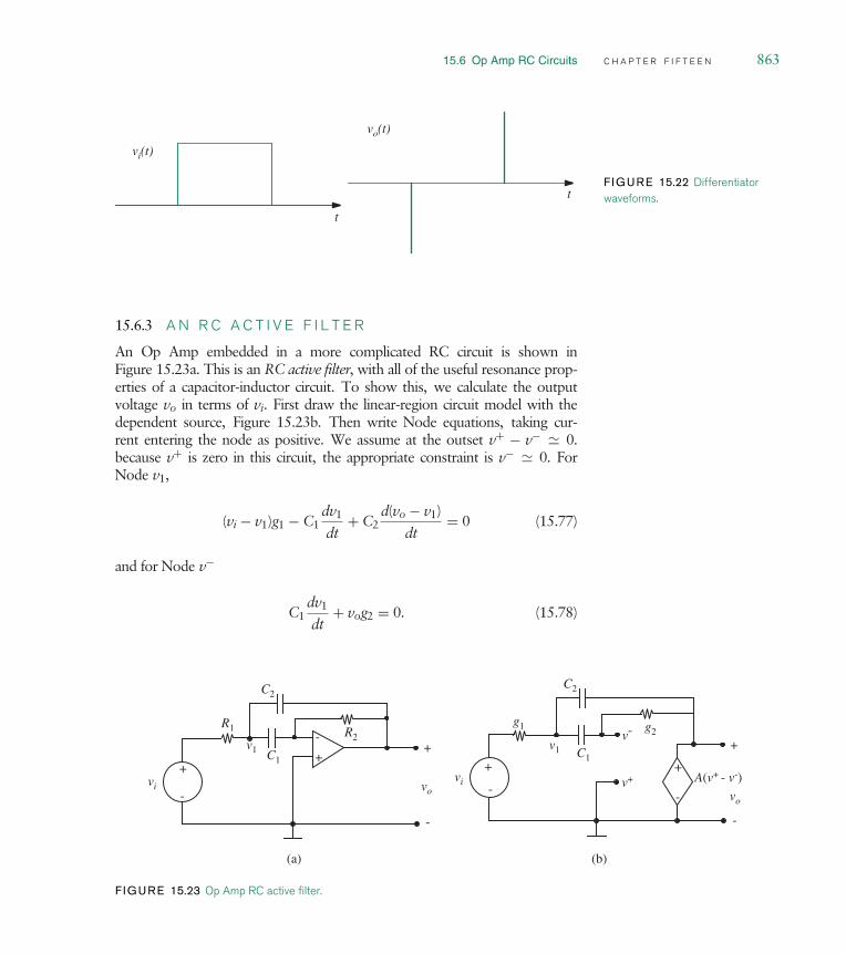
15.6 Op Amp RC Circuits C H A P T E R F I F T E E N 863
t
vi(t)
t
vo(t)
F IGURE 15.22 Differentiatorwaveforms.
15.6.3 A N R C A C T I V E F I L T E R
An Op Amp embedded in a more complicated RC circuit is shown inFigure 15.23a. This is an RC active filter, with all of the useful resonance prop-erties of a capacitor-inductor circuit. To show this, we calculate the outputvoltage vo in terms of vi. First draw the linear-region circuit model with thedependent source, Figure 15.23b. Then write Node equations, taking cur-rent entering the node as positive. We assume at the outset v+ − v− 0.because v+ is zero in this circuit, the appropriate constraint is v− 0. ForNode v1,
(vi − v1)g1 − C1dv1
dt+ C2
d(vo − v1)
dt= 0 (15.77)
and for Node v−
C1dv1
dt+ vog2 = 0. (15.78)
vi v+
v-
+
g1
A(v+ - v-)
-
(b)
+
-
C2
g2
v1 C1+
-
vo
vi
+
-+
R1
vo
-
(a)
+
-
C2
C1
R2v1
F IGURE 15.23 Op Amp RC active filter.

864 C H A P T E R F I F T E E N t h e o p e r a t i o n a l a m p l i f i e r a b s t r a c t i o n
Hence
vig1 = g1v1 + (C1 + C2)dv1
dt− C2
dvo
dt(15.79)
0 = C1dv1
dt+ vog2. (15.80)
These equations can be solved by taking the derivative of both sides of bothequations, and eliminating terms in v1 and its derivative by substitution fromEquation 15.80 and the derivative of Equation 15.80. By so doing we obtain asecond order differential equation for vo:
d2vo
dt2+ g2
C1 + C2
C1C2
dvo
dt+ g1g2
C1C2vo = − g1
C2
dvi
dt. (15.81)
This equation is identical in form to that of an RLC resonator (see Equation12.119), but this circuit contains no inductors. The effect of an inductor iscreated by an active element, in this case the Op Amp, and the capacitors,hence the name RC active filter. The advantages of an RC active filter (this isonly one realization; there are many others) are that it can provide a powergain unlike an RLC network and that it does not require inductors. Becauseinductors are difficult to fabricate in VLSI technology, this is an important designadvantage for integrated circuits. Furthermore, inductors are not very idealelements, especially for low-frequency applications (for example, for frequenciesbelow perhaps 100 kHz). Thus in this frequency range, resonant circuits areoften built out of Op Amps, resistors, and capacitors.
The properties of filter circuits were explored previously in Chapters 10and 13. As we did in Chapter 13, the circuit of Figure 15.23 can also beanalyzed using the impedance method by using impedance values 1/sC1 and1/sC2 for the capacitors (see Section 15.6.4). We will also see other examplesof impedance based analysis for Op Amps later in this chapter.
Since Equation 15.81 is identical in form to Equation 12.119 for the RLCcircuit, we can readily determine the behavior of our RC active filter. Noticethat the output response vo of the Op Amp RC active filter corresponds to thecapacitor voltage vC in Section 12.5. The equation corresponding to the seriesRLC circuit in Section 12.5 was
d2vC
dt2+ R
L
dvC
dt+ 1
LCvC = 1
LCvIN (15.82)
with the damping factor α = R/2L and the undamped resonant frequencyωo = 1/
√LC.
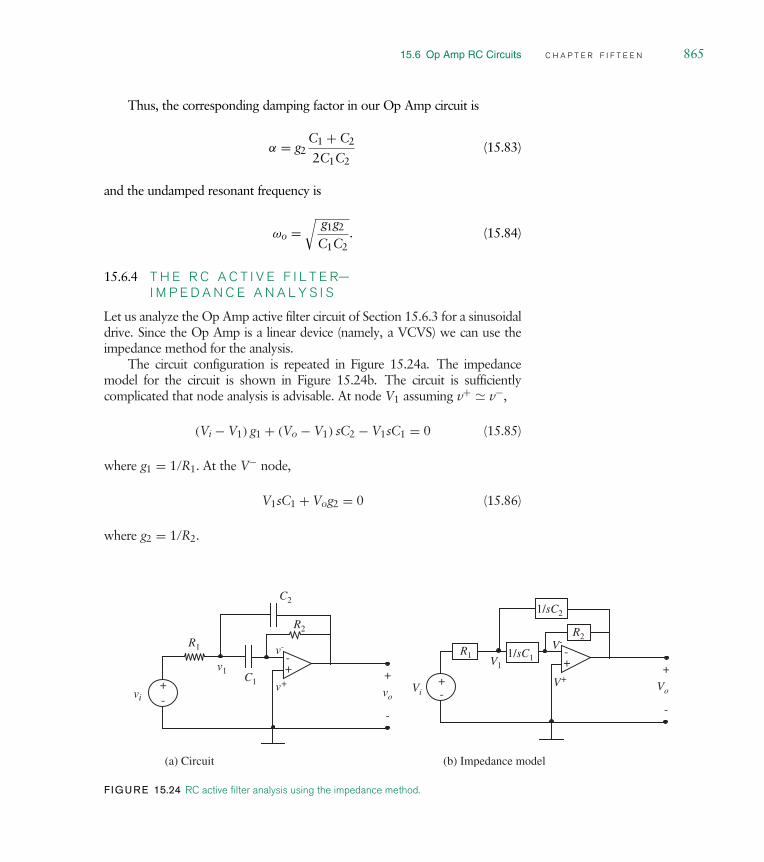
15.6 Op Amp RC Circuits C H A P T E R F I F T E E N 865
Thus, the corresponding damping factor in our Op Amp circuit is
α = g2C1 + C2
2C1C2(15.83)
and the undamped resonant frequency is
ωo =√
g1g2
C1C2. (15.84)
15.6.4 T H E R C A C T I V E F I L T E R—I M P E D A N C E A N A L Y S I S
Let us analyze the Op Amp active filter circuit of Section 15.6.3 for a sinusoidaldrive. Since the Op Amp is a linear device (namely, a VCVS) we can use theimpedance method for the analysis.
The circuit configuration is repeated in Figure 15.24a. The impedancemodel for the circuit is shown in Figure 15.24b. The circuit is sufficientlycomplicated that node analysis is advisable. At node V1 assuming v+ v−,
(Vi − V1) g1 + (Vo − V1) sC2 − V1sC1 = 0 (15.85)
where g1 = 1/R1. At the V− node,
V1sC1 + Vog2 = 0 (15.86)
where g2 = 1/R2.
-+
R1
C2
R2
C1
v-
v1
vi vo
-
+
-+
(a) Circuit
v+-+
V1
Vi Vo
-
+
-+
R1 1/sC1
1/sC2
R2
(b) Impedance model
V-
V+
F IGURE 15.24 RC active filter analysis using the impedance method.

866 C H A P T E R F I F T E E N t h e o p e r a t i o n a l a m p l i f i e r a b s t r a c t i o n
Now Vo can be found by Cramer’s Rule. First, rewrite with source termson the left
Vig1 = V1 [g1 + s (C1 + C2)] − VosC2 (15.87)
0 = V1sC1 + Vog2 (15.88)
(These equations should be compared to the corresponding differential equa-tions, Equations 15.79 and 15.80.) Solving for the complex amplitude Vo,
Vo = −g1sC1Vi
[g1 + s (C1 + C2)] g2 + s2C1C2(15.89)
= −g1sC1Vi
g1g2 + s (C1 + C2) g2 + s2C1C2(15.90)
= −s(g1/C2
)Vi
s2 + s C1+C2C1C2
g2 + g1g2C1C2
. (15.91)
Equation 15.91 has exactly the form of Equation 14.19 (except for the minussign), hence the circuit is equivalent to a parallel RLC filter. By comparingcorresponding terms we find, as in Chapter 12,
Resonant frequency = ωo =√
g1g2
C1C2(15.92)
Bandwidth = g2C1 + C2
C1C2. (15.93)
With these scaling factors, the frequency response plot of Figure 14.12 directlyapplies to this circuit (except for the additional 180 in the phase), along withall other properties discussed in Section 14.1.
W W W 15.6.5 S A L L E N - K E Y F I L T E R
15.7 O P A M P I N S A T U R A T I O N
Thus far we have used the Op Amp in its active region. In the active region, thevoltage-controlled voltage source model of the Op Amp shown in Figure 15.6applies. Furthermore, when negative feedback is applied, and the Op Amp isoperated in the active region, we can use the input voltage constraint givenby v− v+. However, the voltage-controlled voltage source model and theinput voltage constraint no longer apply when the Op Amp output reachessaturation. In saturation, the Op Amp output will be close to one of the powersupply voltages, +12 or −12 V. In positive saturation, the output will be closeto +12 V and in negative saturation the output will be close to −12 V.

15.7 Op Amp in Saturation C H A P T E R F I F T E E N 867
The Op Amp exits the active region and enters the saturation region whenthe external inputs are such that the Op Amp output is required to go above+12 or below −12 V. As an example, suppose the Op Amp has power supplyvoltages of +12 and −12, then if two volts are applied as the input to a non-inverting Op Amp amplifier circuit with a gain of 10, the Op Amp will be driveninto positive saturation. Similarly, if minus two volts are applied to the sameamplifier, the Op Amp will be driven into negative saturation.
How do we model the Op Amp when it is in saturation? When an Op Ampenters positive saturation, a near-short circuit forms between the Op Ampoutput and the positive power supply. Similarly, when the Op Amp entersnegative saturation, a near-short circuit forms between the Op Amp output andthe negative power supply. Accordingly, simple positive and negative saturationmodels for the Op Amp are illustrated in Figure 15.28. The normal dependent
vOv-
v+ -
+12
vOv-
v+
-
+12
Negative saturation
Positive saturation
F IGURE 15.28 Op Amp modelin saturation.
voltage source is not shown in the saturation models because its output getslimited by the power supply voltages and so it turns into a simple voltage source.
15.7.1 O P A M P I N T E G R A T O R I N S A T U R A T I O N
If the Op Amp integrator in Figure 15.19 is driven into negative saturation, thenthe appropriate subcircuit is shown in Figure 15.29. Our negative saturationmodel for the Op Amp says that vO is fixed at some voltage close to thenegative power supply voltage, say −12 V. Because of the 12-V battery assumedat the output when the Op Amp is in saturation, the dependent source is nolonger involved in the calculations, so the circuit reduces to a simple series RCconfiguration, as indicated in Figure 15.29b.
vi
V
t
v-+V
t
-VvO
-12 V
(c)
-V
R
vi+
-
+
-+
-
v-
vC
vO = -12 V
(b)C
+ -
vi+
-
RvOv- vC
v+ -+12 V
C
(a) -
+
F IGURE 15.29 Integrator Op Amp in saturation.

868 C H A P T E R F I F T E E N t h e o p e r a t i o n a l a m p l i f i e r a b s t r a c t i o n
Assuming a step input of vi as in Figure 15.29c, the solution for vC and v−can be found by inspection using the methods of Section 10.5.3. The voltageacross vC at the instant before entering saturation is
vinit = +12 V (15.104)
because v− at this point is almost zero due to the Op Amp constraint. If thetransient went to completion, the final capacitor voltage would be
vfinal = V + 12 V. (15.105)
Hence from Equation 10.62, assuming a time origin at the instant of enteringsaturation,
vC = 12e−t/RC + (V + 12)(1 − e−t/RC) (15.106)
= V(1 − e−t/RC) + 12. (15.107)
(This is a general result for fixed voltages in series with capacitors: By super-position such problems can be solved without the fixed voltage, then the fixedvoltage can be added back in. In other words, the transient part is unaffectedby the fixed voltage.) It follows that
v− = V(1 − e−t/RC) (15.108)
(a result that an experienced analyst of RC circuits would have written downdirectly). Waveforms appropriate to these equations are shown in Figure 15.29c.
An important issue of circuit performance is how long it takes the circuitto recover from the effects of saturation. To this end, assume that the inputstep is now reversed in polarity. The Op Amp will still be held in saturation bythe large positive voltage on the v− terminal, and will remain in saturation untilv− has decayed virtually to zero. Figure 15.29b remains the appropriate circuitrepresentation for this interval. Thus with vi = −V,
v− = −V + 2Ve−t/RC (15.109)
vO = −12 (15.110)
where the time origin is now defined to be at the instant of negative transitionof vi. Appropriate waveforms are shown in Figure 15.29c. As noted earlier, thissaturation state persists until v− has decayed almost to zero. Only then will theOp Amp come out of saturation, and integrate back toward zero, as shown inFigure 15.29c.
In summary, driving the Op Amp into saturation has two serious conse-quences on the performance of the integrator. First, the integration is truncated

15.8 Positive Feedback C H A P T E R F I F T E E N 869
+
-
vi+
-
+
-
R
R
vO
vO
vi
+12 V
-12 V
-6 V +6 V
(a) (b)
F IGURE 15.30 Positivefeedback.
when the Op Amp saturates. Second, when the input wave goes negative, thereis a substantial delay before the circuit recovers, and again acts as an integrator.
15.8 P O S I T I V E F E E D B A C K
In every Op Amp circuit discussed thus far, the feedback network has been con-nected from the Op Amp output to the negative input terminal of the Op Amp.Such a connection provides negative feedback, which tends to make the circuitmore linear, more temperature independent, more reliable. An obvious ques-tion: What happens if the feedback is connected to the positive input terminal,as in Figure 15.30a?
The complete relation between vO and vi, Figure 15.30b, shows bothsaturation and hysteresis. To understand the circuit action, assume that vO isinitially positive and vi is negative. Then, because of the feedback, v+ is stillat +6.
To get the Op Amp out of saturation, vi must be made positive enough tobring (v+−v−) approximately to zero, hence vi must be approximately +6 volts.If vi is slightly more positive than +6, vO will be driven negative, whereupon v+will be driven negative, driving v0 even more negative. Hence, vO undergoes aregenerative negative transition to −12 V. Now vi must be made more negativethan −6 volts to initiate a regenerative transition to +12 V. the width of thehysteresis region can be controlled by the ratio of the feedback resistors.
The circuit is obviously no longer a linear amplifier: The positive feedbackhas enhanced rather than suppressed the basic nonlinearity of the unadornedOp Amp. One application of this circuit is as a digital comparator, to convert acontinuous analog signal to a two-state signal.
15.8.1 R C O S C I L L A T O R
Shown in Figure 15.31 is another Op Amp circuit that uses positive feedback.Assume that the power supply voltages are VS and −VS. This circuit behaves
+
-C
R1R2
R3vO
v+
vC
v-
F IGURE 15.31 RC oscillatorcircuit.
as an oscillator, and uses positive feedback to saturate the Op Amp at bothpositive and negative values of VS. Let’s examine how this oscillator works.

870 C H A P T E R F I F T E E N t h e o p e r a t i o n a l a m p l i f i e r a b s t r a c t i o n
Let us first analyze the circuit qualitatively, referring to the waveforms forvC and vO in Figure 15.33. As depicted in Figure 15.33, let us assume that thesystem starts from rest so the capacitor voltage vC = 0. Thus the invertingterminal v− of the Op Amp is at 0 V. Let us also assume that the output is inpositive saturation initially, in other words at the positive power supply voltage,VS. Since the output is fed back to the positive input, we observe that
v+ = VSR1
R1 + R2.
This positive voltage at the non-inverting input terminal will result in a positivevoltage difference at the Op Amp input port (between v+ and v−), and conse-quently, the output will continue to be driven to the positive saturation voltage,namely VS. The equivalent circuit is as shown in Figure 15.32. The capacitor C
R3
+
-+
-
v-
vC
VS
vO
C
F IGURE 15.32 Equivalentcircuit for the RC oscillator whenthe Op Amp is in positivesaturation.
begins to charge up towards VS through the resistor R3. Since no current flowsinto the v− terminal, the charging dynamics are that of a simple RC circuit.
As the capacitor charges up, eventually its voltage vC crosses v+ =VSR1/(R1 + R2), resulting in an effective negative voltage across the Op Ampinput port, namely across the v+ and v− terminals. The Op Amp amplifies thisnegative voltage difference at its input to a large negative voltage at its output.Since the negative voltage at the output is fed back to the non-inverting terminalby the voltage divider formed by R1 and R2, the non-inverting terminal voltagebecomes negative, which makes the voltage difference at the Op Amp inputeven more negative, and which in turn makes the output voltage fall even more.This positive feedback process continues until the output reaches the negativesaturation voltage −VS. At this point, we have
v+ = −VSR1
R1 + R2.
Notice that the output voltage transitions from VS to −VS very quickly at themoment that the capacitor voltage vC crosses VSR1/(R1 + R2).
F IGURE 15.33 Oscillatorbehavior. t
vC
0
R1
R1 + R2--------------------- VS
–R1
R1 + R2--------------------- VS
(a)
VS
–VS
t
vO
0
(b)

15.8 Positive Feedback C H A P T E R F I F T E E N 871
Therefore, at the instant the output reaches −VS and v+ transitions to−VSR1/(R1 + R2), we can assume that the capacitor voltage is still at approx-imately VSR1/R1 + R2, since the voltage across the capacitor changes muchmore slowly.
Now, since the capacitor voltage vC is higher than the output voltage, thecapacitor begins to discharge through R3. Figure 15.34 shows that the equiva-lent circuit that applies. When the capacitor voltage falls below −VSR1/R1+R2,the voltage v− will be lower than v+ resulting in a positive voltage difference atthe Op Amp input. The Op Amp amplifies this positive difference to a positive
R3
+
-
+
-
v-
vC
VS
vO
C
F IGURE 15.34 Equivalentcircuit for the RC oscillator whenthe Op Amp is in negativesaturation.
voltage at its output, which when fed back to the non-inverting terminal causesa larger positive voltage to appear across the Op Amp input. The resulting pos-itive feedback causes the Op Amp output to go into positive saturation. Thus,the output voltage reaches VS and that at v+ will again be
v+ = VSR1
(R1 + R2).
As in the beginning, the capacitor voltage is now lower than the output andtherefore the capacitor begins to charge up. This cycle repeats and results in asquare wave at the output of the Op Amp.
Let us derive the time period of the oscillator in Figure 15.31. Assume thatat time T1, vO transitions from VS to −VS as illustrated in Figure 15.35. Weknow that at T −
1 , vO = VS and from the voltage-divider relationship, we knowthat v+ = R1VS/(R1 + R2). We also know that v− is lower than v+ at T −
1 , andthat the capacitor voltage is increasing.
At time T +1 , v− becomes slightly greater than v+. In other words, v− ≈
VSR1/(R1 + R2). Output vO transitions virtually instantaneously to −VS andv+ becomes −R1VS/(R1 + R2). The capacitor now begins to discharge and v−begins to decrease. We know that vO will transition from low to high when v−falls below v+ = −R1VS/(R1 + R2).
VS
-VS
R1
R1 + R2-------------------- VS
–R1
R1 + R2-------------------- VS
tvC
Tlow
(a) vC going from high to low
T1
vO
VS
-VS
R1
R1 + R2-------------------- VS
–R1
R1 + R2-------------------- VS
t
vC
Thigh
(b) vC going from low to high
T2
vO
F IGURE 15.35 Computing thetime period of the oscillator.

872 C H A P T E R F I F T E E N t h e o p e r a t i o n a l a m p l i f i e r a b s t r a c t i o n
Thus the interval Tlow is the time taken for the capacitor to discharge fromits initial value of VSR1/(R1 + R2) to its final value of −VSR1/(R1 + R2). Thecapacitor discharge dynamics are governed by a simple first-order differentialequation whose solution is given by
vC = −VS +(
R1
R1 + R2+ 1
)VSe−t/R3C. (15.111)
We need to find Tlow, the time taken for vC to drop below −R1VS/(R1 + R2)from Equation 15.111. In other words, we need to solve for the time thatsatisfies
vC = −VS +(
R1
R1 + R2+ 1
)VSe−t/R3C < − R1
R1 + R2VS. (15.112)
Thus,
−VS +(
R1
R1 + R2+ 1
)VSe−Tlow/R3C = − R1
R1 + R2VS,
which yields
Tlow = R3C ln(
1 + 2R1
R2
). (15.113)
It is easy to verify that the duration of the high period Thigh is exactly the sameas the low period. Thus, the period T of the oscillator is simply
T = 2R3C ln(
1 + 2R1
R2
).
W W W 15.9 T W O - P O R T S *

15.10 Summary C H A P T E R F I F T E E N 873
15.10 S U M M A R Y The Op Amp is a widely used amplifier abstraction that forms the founda-
tions of much of electronic circuit design. Op Amp devices are constructedusing primitive elements such as transistors and resistors.
The Op Amp is a four-ported device. The ports include an input portwith terminals usually labeled v+ and v−, an output port with one terminallabeled vo, and the other being ground, a positive power supply port with a+VS voltage applied with respect to ground, and a negative power supplyport with a −VS voltage applied with respect to ground. Although theground terminal is not explicitly shown in the Op Amp symbol, it is verymuch a part of all Op Amp circuits.
The Op Amp behaves like a voltage-dependent voltage source. Its input-output relationship can can be expressed mathematically as
vo = A(v+ − v−)
where A is a large number called the open loop gain of the amplifier. Inmost practical Op Amp applications, A is treated as infinity.
Most useful Op Amp circuits are built using the negative feedback connec-tion, in which a portion of the output signal of the Op Amp is fed back tothe v− input of the Op Amp. Examples of Op Amp circuits built this wayinclude inverting and non-inverting amplifiers, buffers, adders, integrators,and differentiators.
We commonly apply the constraint:
v+ ≈ v−
in analyzing Op Amp circuits, if the Op Amp is not saturated and thefeedback is negative.
Op Amp circuits are sometimes built using the positive feedback connec-tion, in which a portion of the output signal of the Op Amp is fed back tothe v+ input of the Op Amp. Examples of such Op Amp circuits includeoscillators and comparators.
E X E R C I S E Se x e r c i s e 15 .1 Find the Thévenin equivalent for the circuit in Figure 15.41. Thecircuit contains two resistors and a dependent current source.
e x e r c i s e 15 .2 Calculate vO in terms of I1, V1, and V2 in Figure 15.42. Youmay assume the operational amplifier has ideal characteristics.

874 C H A P T E R F I F T E E N t h e o p e r a t i o n a l a m p l i f i e r a b s t r a c t i o n
gv1
R1
v1 R2
i
v
+
-
+
-
F IGURE 15.41
+
-vO
+R1 V1V2
R3
R2 R4
I1-
+- +
-
F IGURE 15.42
e x e r c i s e 15 .3 Calculate the sensitivity of the gain, dG/G, as a function offractional change in Op Amp gain, dA/A for the inverting Op Amp connection shownin Figure 15.43.
F IGURE 15.43 Inverting OpAmp. vi
vo
Ra
Rb
+
-
(a)
vi
A(v+ - v-)
Ra
Rb
+
-
(b)
v-
v+
-
+
-
+
vo
e x e r c i s e 15 .4 The circuit in Figure 15.44 is called a differential amplifier.
a) Using the ideal Op Amp model, derive an expression for the output voltage vO interms of v1, v2, R1, R2, R3, and R4.
b) Does connecting a load resistor RL between the output and ground change theprevious expression for vO? Why?
c) Let v1 = v2 and R1 = 1 k, R2 = 30 k, and R3 = 1.5 k. Find R4 so thatvO = 0.
d) Let v2 = 0 and v1 = 1 V. Using the preceding resistor values (including thatcomputed for R4), find vO.
e x e r c i s e 15 .5 For the circuit shown in Figure 15.45, D is a silicon diode, where
i = IS(
e qv/nkT − 1)
, kT/q = 26 mV, and n is between 1 and 2.
a) Find vO in terms of v1 and R1.
b) Make a quick sketch of the answer to (a).

15.10 Summary C H A P T E R F I F T E E N 875
+
-
vO
+
v2
R1
R4
R2
+
+-
-
-
-15 V
+15 V
R3v1 741
F IGURE 15.44
+
-
vO
+
R1
v1
v
D
+ -
-
i
+-
F IGURE 15.45
-
+vO
R1
vS+-
R3
R2
+15 V
-15 V
F IGURE 15.46
+
-v2
R
vD
+15 V
-15 V
+ -
v1
iD
F IGURE 15.47
e x e r c i s e 15 .6 Refer to the figure in Figure 15.46 for this exercise.
Given that vS = 2 cos(ωt) (in volts), make a sketch of vO(t) through one complete cycle.Be sure to label the dimensions of the voltage and time axes and identify characteristicwaveform shapes with suitable expressions. (Make reasonable assumptions based onyour lab experience.)
e x e r c i s e 15 .7 Refer to Figure 15.47 for this exercise.
Diode data iD = IS(
e qvD/kt − 1)
where IS = 10−12 A
and kT/q = 25 mV.
For v1 in the range |v1| < 575 V, how should the value of R be chosen to keep the OpAmp in the linear region? Make reasonable approximations.
e x e r c i s e 15 .8 Find the Norton equivalent circuit to the left of terminal paira a′ in Figure 15.48.
e x e r c i s e 15 .9 In the circuits (a) and (b) shown in Figure 15.49 the operationalamplifiers are ideal and have infinite gain. If the input to each amplifier is v1 = I V, whatis the output voltage vO for (a) and for (b)?

876 C H A P T E R F I F T E E N t h e o p e r a t i o n a l a m p l i f i e r a b s t r a c t i o n
F IGURE 15.48 va
ia
100 Ω
a
5ia 100 Ω
100 Ω
+-
+-
a′
F IGURE 15.49 +
-vO
1 kΩ+
-vI = 1 V
1 kΩ
1 kΩ+
-vO
1 kΩ+
-vI = 1 V
1 kΩ
1 kΩ
(a) (b)
e x e r c i s e 15 .10 You may assume that the operational amplifiers used in theconnections shown in Figure 15.50 have very high gain and input resistance, and lowoutput resistance when operating in the linear region.
The input signals have the form shown in Figure 15.51.
a) Plot the output voltage vO for the circuit of Figure 15.50a for A = 1 V. Note: In allof your plots, be sure to clearly indicate peak values and times when signals changecharacter abruptly.
b) Plot the output voltage vO for the circuit of Figure 15.50a for A = 10 V.
c) Plot the output voltage vO for the circuit of Figure 15.50b for A = 10 V.
e x e r c i s e 15 .11 For the circuit shown in Figure 15.52 (which includes a voltage-controlled voltage source) determine:
a) The input resistance vI/iI.
b) The Thévenin equivalent resistance at the terminals a and b.
F IGURE 15.50 +
-vO
1 kΩ
+vI
3 kΩ
(a)
-
+15 V
-15 V
-
+vO
1 kΩ
+vI
3 kΩ
(b)
-
+15 V
-15 V

15.10 Summary C H A P T E R F I F T E E N 877
vI(t)
1
A
-A
32 4 t (s)
F IGURE 15.51
1 Ω
vI
a+
-+
iI
b
2 Ω
2 Ω 1 Ω
vA-
+ vA
2-----
-
+
F IGURE 15.52
i
R1v
R2
+
-
gv
F IGURE 15.53
-
+
R3
R2
v
R1i
R4
+-
F IGURE 15.54
e x e r c i s e 15 .12 Find and label clearly the Thévenin equivalent for the networkin Figure 15.53.
e x e r c i s e 15 .13 Find i in terms of v for the linear network in Figure 15.54.Assume an idealized operational amplifier.
e x e r c i s e 15 .14 Determine the Thévenin equivalent for the circuit shown inFigure 15.55, to the left of terminal pair a a′. The circuit contains a current-controlledvoltage source.
vS
ia
R1
a
aia+-
+-
a′
R2
R3
F IGURE 15.55
+
-
vo
R2
vi
R1
R4+-
R3
va +
-
v-
F IGURE 15.56

878 C H A P T E R F I F T E E N t h e o p e r a t i o n a l a m p l i f i e r a b s t r a c t i o n
e x e r c i s e 15 .15
a) Draw a circuit model for the Op Amp circuit in Figure 15.56.
b) Write the node equations for the va and the v− nodes, and enough more independentrelations to specify vo in terms of vi. Do not solve.
e x e r c i s e 15 .16 For the circuit in Figure 15.57 find vout as a function ofv1, v2, Ra, and Rb in the limit of very high Op Amp gain. Assume input resistance ri = ∞,output resistance rt = 0, and non-saturated operation.
F IGURE 15.57+
-v1
Ra Rbvout
Ra Rb
+-
-+v2
e x e r c i s e 15 .17 For the circuit in Figure 15.58 find i1 as a function of vi, R1, R2,and the Op Amp gain A. Assume input resistance ri = ∞ output resistance rt = 0, andnon-saturated operations.
-
+
R1vi
i1
R2
+-
F IGURE 15.58
+
-
R3
i2 R2
+
-
i1 R1 RL-VSS
+VSS
vO
F IGURE 15.59
e x e r c i s e 15 .18 Consider the circuit illustrated in Figure 15.59.
Assume that the operational amplifier is ideal with input resistance ri very large andoutput resistance rt negligibly small, so that i+ , i− 0, and vO = A
(v+ − v−)
, withA very large. Assume it is operating in its linear range.
a) Draw a linear equivalent circuit for this circuit valid for operation with the Op Ampin its linear range.
b) Derive an expression for vO as a function of i1,i2, and the resistors in the circuit.

15.10 Summary C H A P T E R F I F T E E N 879
e x e r c i s e 15 .19 In the circuit in Figure 15.60 determine the voltage gain G =vo/vi:
a) when terminal x is connected to terminal a.
b) when terminal x is connected to terminal b. Assume the Op Amp is ideal.
+
-
R
10R
vi
R
voR
+-
x
a
b
+
-
F IGURE 15.60
+
-
RF
isio
RO
F IGURE 15.61
e x e r c i s e 15 .20 For the amplifier shown in Figure 15.61, find the currenttransfer ratio io/is. Assume that the Op Amp is ideal.
e x e r c i s e 15 .21 Find the Thévenin output resistance of the circuit shown inFigure 15.62. That is, find the resistance seen looking in at the terminals X X, theterminals that drive the load resistance RL. (Resistor RL should not be included when youmake this calculation.) Do not assume v+ v−, as it leads to trouble here. Now, state acondition on the value of RS to ensure that the circuit acts as a current source driving RL.
+
-
RL
vi
RSX X- +vout
-+
F IGURE 15.62
+
-
R2
iin
R1
R3
+
-vout
F IGURE 15.63
e x e r c i s e 15 .22 For the Op Amp circuit in Figure 15.63:
a) Assume that the Op Amp is ideal (very large gain A, zero output resistance, infiniteinput resistance, operating in the linear region) and find vout as a function of iin, R1, R2,and R3.
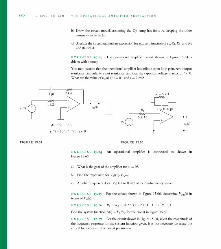
880 C H A P T E R F I F T E E N t h e o p e r a t i o n a l a m p l i f i e r a b s t r a c t i o n
b) Draw the circuit model, assuming the Op Amp has finite A, keeping the otherassumptions from (a).
c) Analyze the circuit and find an expression for vout as a function of iin, R1, R2, and R3
and (finite) A.
e x e r c i s e 15 .23 The operational amplifier circuit shown in Figure 15.64 isdriven with a ramp.
You may assume that the operational amplifier has infinite open-loop gain, zero outputresistance, and infinite input resistance, and that the capacitor voltage is zero for t < 0.What are the value of vO(t) at t = 0+ and t = 2 ms?
vI(t)
-+
vO(t)+
-
-+
1 µF
1 kΩ
2 kΩ
vI(t) = 0, t < 0
vI(t) = 103 s-1 t V, t < 0
F IGURE 15.64
vI
-
+
vO(t)+
-
-+
R1
500 Ω
C = 0.02 µF
R2 = 5 kΩ
F IGURE 15.65
e x e r c i s e 15 .24 An operational amplifier is connected as shown inFigure 15.65.
a) What is the gain of the amplifier for ω = 0?.
b) Find the expression for Vo(jω)/Vi(jω).
c) At what frequency does |Vo| fall to 0.707 of its low-frequency value?
e x e r c i s e 15 .25 For the circuit shown in Figure 15.66, determine Vout(s) interms of Vin(s).
e x e r c i s e 15 .26 R1 = R2 = 20 C = 2.4µF L = 0.25 mH
Find the system function H(s) = Vb/Va for the circuit in Figure 15.67.
e x e r c i s e 15 .27 For the circuit shown in Figure 15.68, select the magnitude ofthe frequency response for the system function given. It is not necessary to relate thecritical frequencies to the circuit parameters.
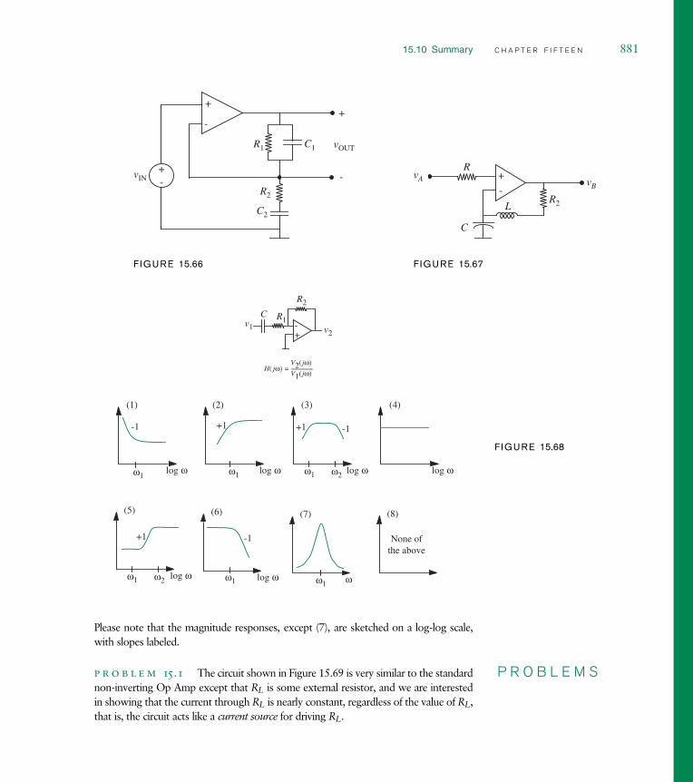
15.10 Summary C H A P T E R F I F T E E N 881
vIN -
+
vOUT
-
+
-+
R1 C1
R2
C2
F IGURE 15.66
vB
R
C
L
vA
R2
+-
F IGURE 15.67
v2
C
R2
+-
R1v1
H( jω) =V2( jω)V1( jω)------------------
(1) (4)(3)(2)
-1 +1 -1+1
log ωlog ωlog ω
log ω log ω
log ωω1 ω1 ω1 ω2
(5)
+1
ω1 ω2
(6)
-1
ω1
(8)
None ofthe above
(7)
ωω1
F IGURE 15.68
Please note that the magnitude responses, except (7), are sketched on a log-log scale,with slopes labeled.
P R O B L E M Sp r o b l e m 15.1 The circuit shown in Figure 15.69 is very similar to the standardnon-inverting Op Amp except that RL is some external resistor, and we are interestedin showing that the current through RL is nearly constant, regardless of the value of RL,that is, the circuit acts like a current source for driving RL.

882 C H A P T E R F I F T E E N t h e o p e r a t i o n a l a m p l i f i e r a b s t r a c t i o n
F IGURE 15.69
-
+
vI -+ RL
R2
iLA
A′
a) Using the ideal Op Amp assumption of large gain, zero output resistance, infiniteinput resistance, show that the expression for iL as a function of vI is independent(or weakly dependent) on RL.
b) To verify the ‘‘current source’’ action more directly, find the Thévenin equivalentresistance looking to the left of terminals AA′, with RL an open circuit.
p r o b l e m 15.2 Zener diodes are most often used to establish stable referencevoltages, independent of power supply variations, and independent of any lingering ACsignals that may be present in the power supply.
a) For the characteristics shown in Figure 15.70, find vO assuming vA is a clean DCvoltage of value 15 V.
F IGURE 15.70+
-vA R
10 kΩ
-15
-
+ iD
-vZvO
Zener diode
+15
Zener
vD
iD
vD
vZ = 6.2 V, RZ = 7 Ω
Slope~1/Rz
b) Determine the sensitivity of vO to changes in vA. That is, find dvO/dvA. If vA has0.1 V of DC drift or so of 120-Hz AC ripple, how much drift or ripple shows upon vO?
p r o b l e m 15.3 Consider the circuit in Figure 15.71.
Find vO assuming that all Op Amps are ideal and operating in the linear region.
p r o b l e m 15.4 You are faced with the problem of constructing a current trans-mitter, a circuit that forces a load current iL into a load under accurate control of a

15.10 Summary C H A P T E R F I F T E E N 883
vB
+
-
+
-+
-
vA
1 kΩ 10 kΩ
2 kΩ
10 kΩ
vO1 kΩ
1 kΩ F IGURE 15.71 vA = 0.1 V andvB = 0.2 V.
source voltage vS, independent of variations in load resistance. That is, you need avoltage-controlled current source.
The design requirements for your problem are to achieve
iL = −KvS
where K = 10 mA/V for the ranges |vS| < 1 V, RL < 1 k.
While looking through a handbook of practical circuits, you come across the schematicin Figure 15.72 as a proposed solution to your problem. The question is, will it work?
+
-
vS
R1
-+
R1
R2
R2 RL
iL
+15 V
-15 V
Control voltage Current transmitter Load
F IGURE 15.72
a) As a first step, analyze the basic principle of operation of the above circuit. Showexplicitly whether it is capable of performing the desired function.
b) Next, determine whether there will be any problems in selecting resistor values R1
and R2 to meet the specifications for your particular application. You should drawon experience with Op Amp limitations. Can you meet the specs?(Note: Part (a) is easy. Part (b) is endless, so look only for the larger issues, that is,major sources of error or failure.
p r o b l e m 15.5 Find the Norton equivalent of the circuit in Figure 15.73 lookinginto terminals A and A′.

884 C H A P T E R F I F T E E N t h e o p e r a t i o n a l a m p l i f i e r a b s t r a c t i o n
F IGURE 15.73
+
-
vI
R
-+
R
R
RA
A′
vO
F IGURE 15.74
-
+
v1
R2
-
+
R1
Rb
Ra
vOv2+-
+-
p r o b l e m 15.6 You are asked to design the circuit shown in Figure 15.74 sothat the output voltage vO is the weighted sum of v1 and v2; specifically:
vO = 3v1 + 5v2
It is known that the magnitudes of v1 and v2 are never larger than 1 volt.
a) Determine the values for R1, R2, Ra, and Rb that will make the circuit performthat sum.
b) Given that the op amp is powered from +15 and −15 V, and has output currentlimits of +1 mA and −1 mA, redesign if necessary to meet these additional designconstraints.
c) How would you change the design to perform the sum:
vO = −3v1 − 5v2
using only one Op Amp (given Figure 15.74, a two-op amp design is obviouslytrivial, but unnecessarily complicated)?

15.10 Summary C H A P T E R F I F T E E N 885
p r o b l e m 15.7 For the circuit in Figure 15.75, assuming an ideal Op Amp withlarge A:
a) Calculate vO in terms of vI and the resistor values.
b) Find i in terms of vI and the resistor values.
c) For what resistor values in (a) will the voltage gain become infinite? Explain whythis occurs (one sentence).
d) Find the limits on the solutions in the (a) and (b) imposed by using a real Op Amp.
-
+
vI
R1
-+
R2
R3
R4
+
-
vO
i
F IGURE 15.75
p r o b l e m 15.8 Choose values for R1 through R5 in Figure 15.76 so that
vO = +2v1 − 5v2 − v3 − 3v4.
+
-
R1R6
R2
R3
+
v3
v1
v2
v4
-
R4
R5
vO
F IGURE 15.76
You may assume the operational amplifier has ideal characteristics.
p r o b l e m 15.9 For the circuit in Figure 15.77, find vO in terms of vI. Ana-lyze with literal resistor values, then substitute numbers: R1 = R2 = R3 = 10 k,R4 = 100 .
p r o b l e m 15.10 This question concerns the circuit illustrated in Figure 15.78:
The operational amplifier is a high gain unit (A = 105) with high input resistance, ri,and negligibly low output resistance, rt. Assume that it is operating in its linear region.

886 C H A P T E R F I F T E E N t h e o p e r a t i o n a l a m p l i f i e r a b s t r a c t i o n
+
-
vI
R1
-+
R2
vO
R3
R4
F IGURE 15.77
-
+
vS -+
RLvO
i+
+
-
+Vss
-Vss
F IGURE 15.78
The following data is given:
vS = 1 V
i + = 10 pA = 10−11 A
RL = 1 k.
a) What is vO? (Accurate to within 1%.)
b) What is the power delivered by the source vS? What is the power dissipated in theload resistor, RL?
c) The power dissipated in the load resistor, RL, is much larger than the power suppliedby the source, vS. Where does this additional power come from?
p r o b l e m 15.11 The equivalent circuit of an amplifier is shown in Figure 15.79.
F IGURE 15.79 iS R1 i1vS R2
a
a′
+
-
b
b′
bi1
a) Find the input resistance seen by the current source iS at the input terminals a a′.
b) Find the output resistance seen at the output terminals b b′ (with the current sourceshut off).
p r o b l e m 15.12 For the circuit in Figure 15.80 find vO in terms of v1 and v2.You can use in your analysis the ideal Op Amp model.

15.10 Summary C H A P T E R F I F T E E N 887
+
-
v2
R3
R4
R7
R8
R5
R6
R2
v1
R1
-+
-+ vO
-
+
F IGURE 15.80
v1 -+
v2 -+
R
2R
2R
+
-
vO
R -
+
F IGURE 15.81
vI+vO-
+
R C
-
+
-
F IGURE 15.82
p r o b l e m 15.13 An operational amplifier circuit is shown in Figure 15.81.
You may assume that the operational amplifier has ideal characteristics, including zeroinput current and output resistance and further make the simplifying assumption thatits open-loop gain is infinite. Also, assume that the amplifier does not saturate.
a) With v2 = 0, what is the value of the gain vO/v1?
b) Voltage v2 is now made 3 volts. Plot the vO vs. v1 characteristics. Be sure to showimportant values and slopes.
p r o b l e m 15.14 By combining Op Amps with RC circuits, we can make circuitsthat perform elementary mathematical operations, such as integration and differentiation.The circuit in Figure 15.82 is, over some range, an integrator.
a) Use the ideal Op Amp model to determiner the ideal function performed by thiscircuit.

888 C H A P T E R F I F T E E N t h e o p e r a t i o n a l a m p l i f i e r a b s t r a c t i o n
b) Based on your knowledge of Op Amp limitations, indicate the constraints that mustbe placed on the component values R and C to achieve satisfactory operation, assum-ing that the input is a sine wave with angular frequency ω and peak amplitude A.Express your answer as a constraint on the RC product imposed by the voltagelimit, and a separate constraint imposed by the current limit.
c) For practical reasons, R usually should not be greater than 1 megohm. Calculatethe value of C required to meet the voltage constraint listed above for operation at20 Hz and above, and A = 1 V.
p r o b l e m 15.15 The capacitor you calculated in Problem 15.14c is (or shouldbe) much larger than the maximum capacitor that can be included on a VLSI chip. Forthis reason, the circuit in Figure 15.82 must usually be built of Op Amps, discrete R’sand C’s. To allow the circuit to be built on a chip, the resistor is replaced by a switchedcapacitor, which can produce a very large ‘‘effective resistor’’ with reasonable capacitorvalues. This circuit is shown in Figure 15.83.
F IGURE 15.83
-+
vI C1
C2
-
+
vO
1 2
+
-
At time t = t1, the switch moves to position (1), and C1 charges (instantly) to voltagev1(t1). Then at time t2, the switch moves to position (2), and C1 discharges into C2.Assuming that the usual Op Amp approximation of (v+ − v−) 0 can still be used,calculate the charge that is ‘‘dumped’’ at each cycle, hence the average current (a functionof both vI and the switching frequency fc), and hence the effective resistance of theswitched capacitor. Also, show that the overall system equation relating vO to vI is thesame as in Problem 5.14.
p r o b l e m 15.16 In Figure 15.83, what are the constraints on C1 and C2 set bythe Op Amp voltage and current limits? Calculate the appropriate values of C1, C2, andfc for operation at 20 Hz and above. Can the circuit now be built on an IC chip if wereplace the switch by MOS transistors, and Cmax = 100 pF?
p r o b l e m 15.17 Design a differentiator circuit out of RC circuits and Op Amps.
Calculate the constraints as in Problem 5.14b.

15.10 Summary C H A P T E R F I F T E E N 889
p r o b l e m 15.18 This problem deals with switched-capacitor circuits introducedin Problem 15.15. Referring to Figure 15.84, assume both S1 switches are closed fortime 1/2f0 with S2 open, and S2 closed for 1/2f0 with s1 open. Assume no overlap, thatis, and S1 and S2 switches are never both closed at the same time.
vA
S1
+
-
S2
S1
C2
C1
vB
F IGURE 15.84
a) For vA = A volts (constant), go through one complete clock cycle, identifying thecharge on each capacitor and the voltage at each node.
b) Now assume vA = A cos (ωt) where ω 2π f0. Sketch vB. In the circuit asconstructed, vB is zero half the time. During the other half cycles, vB and vA arerelated by a simple gain expression, just as in a normal inverting amplifier. What isthe ‘‘gain’’?
p r o b l e m 15.19 Figure 15.85 is a practical implementation of a switched capac-itor circuit (see Problem 15.15). As in the previous problem, it is useful to examine thebehavior of an ‘‘average vB’’ over a clock cycle.
a) Show that if vA = A volts (constant), the cycle-average of vB has a steady-state valueequal to −(C1/C2)A. In other words, for low-frequency signals, the circuit behaveslike a non-inverting amplifier with gain −(C1/C2).
b) Show, for vA a step of amplitude A volts, and assuming vB is initially zero, thatthe cycle average of vB ‘‘charges up’’ to its steady-state value with time constantτ = c3/f0C2. That is, show that the cycle-average of vB obeys a first-order lineardifferential equation with time constant C3/f0C2.
p r o b l e m 15.20
a) Use the ideal Op Amp model to determine the ideal function performed by thecircuit in Figure 15.86.
b) Based on your knowledge of Op Amp limitations, discuss the accuracy with whichthe circuit will perform the intended function, or indicate any constraints that must

890 C H A P T E R F I F T E E N t h e o p e r a t i o n a l a m p l i f i e r a b s t r a c t i o n
vA
S1
+
-
S2
S1
C1
vB
S2
C2
C3
F IGURE 15.85
v1
+
-v2
C
R
+15 V
-15 V
F IGURE 15.86
be placed on the component values R and C to achieve satisfactory operation,assuming that the input is as follows:
i: A sine wave with angular frequency ω and peak amplitude A.
ii: A triangle wave with period T and peak amplitude A.
iii: A square wave with period T and peak amplitude A.
c) The leakage of an actual capacitor can often be modeled by a large resistor in parallelwith an ideal capacitor. What effects on circuit performance would capacitor leakagehave?
p r o b l e m 15.21
a) Using the ‘‘ideal operational amplifier’’ assumption, that is, infinite gain, infiniteinput resistance, and zero output resistance, determine the relationship betweenvO(t) and vI(t) in Figure 15.87.
b) If the signal vI(t) is the rectangular pulse in Figure 15.88, sketch vO(t) for t > 0,assuming that vO(0) = 0.
vI +
-
vO
R = 10 kΩ
+-
C = 10 µF
+
-
F IGURE 15.87
0,0 100 ms t
10 VvI
F IGURE 15.88

15.10 Summary C H A P T E R F I F T E E N 891
p r o b l e m 15.22 An operational amplifier is connected as shown in Figure 15.89.
+
-+-
2 kΩ
2 kΩ
2 kΩ
2 kΩ 2 µF
+
-
vO
vIF IGURE 15.89
The voltage vI is 2 volts for 0 < t < 1 ms, and 0 otherwise. Assuming that vO = 0 fort < 0, sketch vO for t > 0.
p r o b l e m 15.23 Consider the two circuits in Figure 15.90.
vI +
-
vO
R1
+-
C1
+
-
vI +
-
vO
R1
+- C2
+
-
F IGURE 15.90
Use the Op Amp model to find the transfer function vO/vI for the two circuits.
Assume only moderate gain (say 100) for the Op Amp so you cannot assume v+ = v−.How large does C2 have to be compared to C1 in order for the two circuits to behavethe same? The increase in the effective size of C1 because of the gain of the amplifier iscalled the Miller Effect, and is used in Op Amp design.
p r o b l e m 15.24 Assuming an ideal Op Amp (large gain, v+ v−, rin infinite,rout zero, but including amplifier saturation effects).
a) Plot a curve of iIN versus vIN between −20 and +20 V for the circuit in Figure 15.91,assuming R2 = R3. Dimension your plot.
b) A capacitor is initially charged to 1 volt (switch in position (1)) in Figure 15.92, thenconnected to the circuit at t = 0 (switch in position (2)). Sketch and dimension thewaveform vC(t) for t greater than zero.
p r o b l e m 15.25 An operational amplifier is connected as shown in Figure 15.93.
a) Assuming that the amplifier has infinite gain and infinite input resistance and zerooutput resistance, determine the relationship between vO(t) and vI(t).

892 C H A P T E R F I F T E E N t h e o p e r a t i o n a l a m p l i f i e r a b s t r a c t i o n
R2
vO
R1
+-
+15 V
-15 V
R3
A
A
vIN
iIN -
+
F IGURE 15.91
R2 = R3
R1
+
-
+15 V
-15 V
R3
C vC
-
+
+
-1 V
1 2
F IGURE 15.92
vO(t)
vI(t)+
-
+-
10 kΩ
10 µF
F IGURE 15.93
0,0 100 ms t
10 V vI
F IGURE 15.94
b) The signal vI(t) is a rectangular pulse as Figure 15.94.Assuming that vO(0) = 0, draw vO(t), for t > 0.
c) The operational amplifier is now connected as in Figure 15.95.The voltage vO(t) is held at zero (by some means not shown) for t < 0. The switchis initially in the up position, connecting the 10 k resistor to a fixed voltage VF. Attime t = 100 ms, the switch is thrown to the down position. The observed voltagevO(t) is shown in Figure 15.96.
vO(t)10 kΩ
10 µF
VF
-10 V
+
-
F IGURE 15.95
vO(t)
100 ms
t
0,0
F IGURE 15.96

15.10 Summary C H A P T E R F I F T E E N 893
Determine the relationship between VF and τ , the time required for vO(t) to returnto zero volts.
p r o b l e m 15.26 We wish to show that the circuit shown in Figure 15.97behaves in a manner very similar to an RLC circuit.
v1
+
-v4
C2
R2
R1
C1
v3v2
F IGURE 15.97
a) Write the node equations for v2 and v3.
b) Simplify these equations by using the Op Amp assumption, that is, v− v+. Thisallows you to neglect v3 terms compared to v4 terms, and dv3/dt terms comparedto dv2/dt and dv4/dt terms, provided C1 and C2 are comparable. (You must latercheck on this last assumption.)
c) Find the characteristic equation. Compare with the RLC case.
d) For the following numerical values, is the circuit under-, over-, or critically-damped?What is the Q of the circuit, in literal form?
C1 = C2 = .01 µF
R1 = 10
R2 = 1 k
p r o b l e m 15.27 What is the differential equation relating to vO to vI in thenetwork in Figure 15.98? Assume that the Op Amps are ideal.
+-
vO
6 kΩ
+-
4 kΩ4 kΩ
+-
3 kΩ
250 kΩ
250 kΩ
vI
20 mH
8 kΩ
2 kΩ
F IGURE 15.98

894 C H A P T E R F I F T E E N t h e o p e r a t i o n a l a m p l i f i e r a b s t r a c t i o n
vI +
-vO
C2
R2
C1 vB
vAR2
F IGURE 15.99
vs
-
+
v1
+-
-+
R1
C1
R2
C2
+
-v2
R1 = 10 kΩ R2 = 1 kΩ
C1 = 1 µF C2 = 0.01 µF
F IGURE 15.100
p r o b l e m 15.28 The circuit in Figure 15.99 behaves in a manner very similar toan RLC circuit.
a) Write the node equations.
b) Assume vA = Vaest, vB = Vbest, and find the characteristic equation.
c) Find α and ωo in terms of C1, C2, G1, and G2.
p r o b l e m 15.29
a) Find H1(S) = V1/Vs in Figure 15.100. Plot and dimension log |H1| and ∠H1 vs.log ω.
b) Find H2(S) = V2/V1. Plot and dimension log |H2| and ∠H2 vs. log ω.
c) Find Ht(S) = V2/Vs = H1(S)H2(S). Plot and dimension log |Ht| and ∠Ht vs. log ω.Compare with the plots you obtained in parts (a) and (b).
p r o b l e m 15.30
a) Find the transfer function for the network in Figure 15.101.
F IGURE 15.101
vO
R1
C2
R2 C1
vIN+-

15.10 Summary C H A P T E R F I F T E E N 895
b) Synthesize the function Vo/Vin = −(s+4)/(s+6) using the circuit in Figure 15.101.That is, find values of R1, R2, C1, and C2 that satisfy Vo/Vin. You may use capacitorsof 1 µF.
p r o b l e m 15.31 The circuit shown in Figure 15.102 is a capacitance multi-plier. It may be incorporated into circuits that might otherwise require unrealisticallylarge physical capacitors. You may assume that the operational amplifier has idealcharacteristics.
AR1
R2
C
+-
R3
A′Z
BReq
Zeq
B′Ceq
F IGURE 15.102
a) Find the impedance Z looking into terminal A A′ for the circuit.
b) Show that the model on the right corresponds to an impedance equivalent to theresult obtained in part (a).
c) For R1 = R2 = 10 M, and R3 = 1 k, what is Ceq in terms of C?
p r o b l e m 15.32 Show that the Op Amp circuit in Figure 15.103 has the sameform of transfer function as the circuit in Problem 14.1 (shown on the left-hand side ofFigure 15.103). Find expressions for the resonant frequency and the Q.
R+
C
-
L
+-
vO(t)
R1
C2vI(t)
+-
-+
C1
R2
vI(t) vO(t)
+
-
F IGURE 15.103
p r o b l e m 15.33 The circuit in Figure 15.104 is a switched capacitor filter. Theswitches S1 and S2 are driven by nonoverlapping clocks as in Problem 15.15. Both S1
switches are closed for time 1/2fc with S2 open, and S2 closed for 1/2fc with S1 open.Vin = A cos(ωt), ω 2π f0.

896 C H A P T E R F I F T E E N t h e o p e r a t i o n a l a m p l i f i e r a b s t r a c t i o n
F IGURE 15.104
Op Amp 2
R
V3
-
C1
+-
+ -+
-+
-
+
C2
R
R
2RR
V2
V1
S2S1
S1 S2
Op Amp 3
Op Amp 1Vin
CR2
CR1
a) Find (in the sinusoidal steady state) the transfer functions V3/V2 and V2/V1. Referto Problem 15.15 to see how to handle the switches. Note that there are no switchesacross C1 and C2.
b) Now find a simple equation to describe the operation of Op Amp 1, that is, find anexpression for V1 in terms of V2, Vin, and V3. (Note that in all of our impedancecalculations, we have been implicitly assuming that the relation among V ’s for sucha circuit is the same as the relation among the time variables v(t).)
c) Now substitute from (a) into (b) to find the overall transfer function V2/Vin. Findexpressions for the resonant frequency ω0 and the bandwidth ω in terms of thecircuit constants. The easiest way to do this is to get the transfer function into theform:
Vo = KsVin
s2 + 2αs + ω20
(15.122)
and work by analogy to the parallel RLC case. How does the resonant frequencyω0 depend on the clock frequency fc?
p r o b l e m 15.34 The circuit shown in Figure 15.105 behaves like an RLC circuit.
a) Find the transfer function V4/V1. (You may assume that the Op Amp is ideal, thatis V+ = V− to simplify your calculations.)
b) Sketch the magnitude of the transfer function |V4/V1| versus frequency. Indicatethe frequency at which the peak occurs, the magnitude of the transfer function atthe peak, and the Q of the resonance. Use the following numerical values:
C1 = C2 = 0.01 µF R1 = 10 R2 = 1 k

15.10 Summary C H A P T E R F I F T E E N 897
V4
C1
-+
-
+
C2
V1
-+
R2
R1
F IGURE 15.105
Vo
C
-+
-
+
Vi
-+
R2
R1
F IGURE 15.106
c) This circuit is known as an RC active filter. Is it a low-pass, high-pass, or band-pass filter? What is the expression for bandwidth in terms at R1, C1, etc.? That is,B = ω2 − ω1 where ω1 and ω2 are the half power frequencies.
p r o b l e m 15.35
a) Find an expression for the complex amplitude ratio Vo/Vi for the active filter circuitin Figure 15.106, given that R2 = 10R1. Sketch the Bode plot, |Vo/Vi| versus ω
and Vo/Vi versus ω.
b) An equivalent filter can be made with the circuit shown in Figure 15.107. Find thevalue of C2 needed to make a filter equivalent to that in part (a), assuming that R1
and R2 are the same here as for part (a). How does the value of Cx here compareto that of C in the filter of part (a)?
Vo
Cx-+
-
+
Vi
-+
R2
1/2 R1 1/2 R1
F IGURE 15.107

898 C H A P T E R F I F T E E N t h e o p e r a t i o n a l a m p l i f i e r a b s t r a c t i o n
Vo
C1
-+
-
+
Vi
R2
+
-
C2
R1
Va
Vb
F IGURE 15.108
Vo
C1
Vi
R+
-L2
L1
C2
F IGURE 15.109
p r o b l e m 15.36 The circuit shown in Figure 15.108 behaves in a way verysimilar to an RLC circuit.
a) Write the sinusoidal steady state node equations for the complex amplitudes Va
and Vb.
b) Solve for Vo/Vi using the results in (a), and noting that Vo = Vb.
c) Assuming the circuit is under-damped, sketch the magnitude of the transfer function|Vo/Vi| versus frequency. Indicate the frequency at which the peak occurs, themagnitude of the transfer function at the peak, and the Q of the resonance.
p r o b l e m 15.37 Plot the frequency response (magnitude and phase) of the activefilter shown in Figure 15.109. Assume the Op Amp is ideal.
p r o b l e m 15.38 The circuit shown in Figure 15.110 has a resonance very similarto an RLC circuit.
a) Write the sinusoidal steady-state equations for V2 and V3.
b) Solve for V4/V1 using the results in (a), and noting that V3 = −V4/A, where theOp Amp gain A can be assumed to be very large.
F IGURE 15.110v4
C1
v1(t)
-
+v2
R1
C2
R2
v3+-

15.10 Summary C H A P T E R F I F T E E N 899
c) Assuming now that C1 = C2 = 0.1 µF, R1 = 10 , R2 = 1 k, sketch themagnitude of the transfer function |V4/V1| versus frequency. Indicate the frequencyat which the peak occurs, the magnitude of the transfer function at the peak, andthe Q of the resonance.
p r o b l e m 15.39 For the circuit in the figure in Figure 15.111
Vo
C1Vi
+
-C2
R2
+-
R1
+
-
F IGURE 15.111
a) Find a set of equations which, if solved, would give Vo/Vi.
b) Assuming that these equations, when solved, yield
Vo/Vi = (jωC1)(jωC2)
G1G2 + jω(C1 + C2)G2 + (jω)2C1C2. (15.123)
Find the expression for the undamped resonant frequency (ω0) of the circuit.
c) Find an expression for the low-frequency asymptote of Vo/Vi. (Zero is not anacceptable answer.)
d) Find an expression for the high-frequency asymptote of Vo/Vi. (Zero is not anacceptable answer.)
e) Assuming Q = 1/2, sketch the magnitude and phase of Vo/Vi versus ω. Specifycoordinates and dimension key features.
p r o b l e m 15.40 Tech Hi-Fi advertises a car stereo system that can deliver10 watts average power into a 4- speaker. Given your demonstrated proficiency inelectronics, you decide to build one using an (hefty) Op Amp. To save yourself the prob-lems associated with designing the receiver, you plan to use a small transistor AM-FMradio as the signal source.
You try the circuit shown in Figure 15.112.
In the following parts, you may assume that the hefty Op Amp has very high open-loopgain, zero output resistance, infinite input resistance, and other good features.
a) What is the operating-point value of the voltage at the output of the operationalamplifier?

900 C H A P T E R F I F T E E N t h e o p e r a t i o n a l a m p l i f i e r a b s t r a c t i o n
F IGURE 15.112+12 V
vI
-
+
Rf
+-
Ci
CL(Fromradio)
1 kΩ
1 kΩ
1 kΩ4 Ω speaker
12 V (Battery) Cf
b) Why is capacitor CL included?
c) Assume that the maximum signal from your radio is 1 volt peak to peak. What isthe maximum value of Rf that ensures the operational amplifier will remain in thelinear region?
d) What is the maximum average power that can be delivered to the 4- speaker withvI as a constant amplitude sinusoid?
e) In spite of your answers to parts (b) and (c), assume that you choose Rf = 10 k
and that capacitor CL is very large. In order to reduce low frequency noise, youdecide that you should make the lower half-power frequency 100 radians per second.What value of Ci should be selected? You also want to filter high-frequency noiseby making the upper half-power frequency 105 radians per second. What value ofCf should be selected?
p r o b l e m 15.41
a) Using the ideal Op Amp assumptions, write the node equations for the complexvoltage for the circuit in Figure 15.113. Solve for Vo.
F IGURE 15.113
Vo
C2
-+
-
+
Vi
-+
R2
R1Va VbC1

15.10 Summary C H A P T E R F I F T E E N 901
vO(t)
C2
-+
-
+
vI(t)
+-
R1
C1
vX(t)
R2
vY(t)
F IGURE 15.114
b) Assume Vo is of the form:
Vo = sKVi
s2 + 2αs + ω20
. (15.124)
If a short pulse is now applied to this circuit, the output voltage after the pulse is
vO(t) = 3e−100t sin(1000t + 20o). (15.125)
For K = 400(sec−1) find the response vO(t) in the steady state to a one-volt cosinewave at the resonant frequency:
vI(t) = 1 V cos(ω0t
). (15.126)
(Provide numbers for ω0, etc.)
c) Repeat (b), for a one-volt cosine wave at the lower 0.707 frequency ω1.
p r o b l e m 15.42
a) For the circuit in Figure 15.114 write the node equations needed to find Vo(s) interms of Vi(s). Your answer must be arranged with the source terms on the left, theunknown variables on the right, and must use conductances g(= 1/R).
b) Solving these equations, you should obtain for C1 = C2,
Vo(s) = s2Vi
s2 + s 2R2C
+ 1R1R2C2
. (15.127)
For R1 = 1 k, find the values of R2 and C that give a Q of 10 and a resonantfrequency, defined as the frequency where the s2 term and the s0 term cancel in thedenominator of Equation 15.127, of ωo = 1000 rad/s.

902 C H A P T E R F I F T E E N t h e o p e r a t i o n a l a m p l i f i e r a b s t r a c t i o n
p r o b l e m 15.43 For the network shown in Figure 15.115:
F IGURE 15.115 +
-
+-
+
-
R2
R1
vI vO
C
Find Vo/Vi
a) Determine an expression for the indicated transfer function.
b) Sketch the magnitude and angle of the indicated quantity as a function of frequency.You may use either linear or log-log coordinates, but it is recommended that youlearn to use both kinds of axes.

c h a p t e r 16
16.1 I N T R O D U C T I O N
16.2 S E M I C O N D U C T O R D I O D E C H A R A C T E R I S T I C S
16.3 A N A L Y S I S O F D I O D E C I R C U I T S
16.4 N O N L I N E A R A N A L Y S I S W I T H R L A N D R C
16.5 A D D I T I O N A L E X A M P L E S
16.6 S U M M A R Y
E X E R C I S E S
P R O B L E M S


d iode s 1616.1 I N T R O D U C T I O N
The diode was introduced in Chapter 4 as an example of a nonlinear device.We used its nonlinear v i characteristic to develop several methods of analyzingnonlinear circuits. It turns out that the diode is a particularly useful nonlineardevice, and merits closer examination. Figure 16.1 shows a few discrete diodes.This chapter explores several useful diode circuits, and develops additionalanalysis methods that are specific to diodes.
16.2 S E M I C O N D U C T O R D I O D EC H A R A C T E R I S T I C S
We will consider semiconductor diodes made out of silicon. Recall, we havepreviously seen an example of a silicon-based device, namely the MOSFET. Letus first review briefly the properties of silicon and semiconductors. Silicon is anelement in the cubic crystal class of Group IV in the periodic table (along withgermanium). In pure crystalline silicon, each atom forms covalent bonds withits nearest neighbors, so that at room temperature almost all valence electronsare involved in the structural bonding, and very few are free to move aboutthe crystal. Hence pure silicon at room temperature is a very poor conductorof electricity.
However, if minute amounts of impurities are added to the silicon by hightemperature diffusion, or by ion implantation, for example, then the electrical
F IGURE 16.1 Discrete diodes.( Photograph Courtesy of MaximIntegrated Products.)
905

906 C H A P T E R S I X T E E N d i o d e s
properties change dramatically. Add a part per million of a Group V element,such as phosphorus, to the Group IV element silicon, and we obtain a crystalthat has many ‘‘mobile’’ electrons not involved in covalent bonds. Hence thematerial is now a good conductor. We call this material n-type silicon (n stand-ing for negative, indicating mobile negative charge carriers, that is, electrons).Similarly, if we add small amounts of a Group III element such as aluminumto the pure silicon, the resulting crystal will have a large deficit of electrons inthe bonding structure. One useful way of visualizing the effect of this deficit isto imagine that we have created not a deficit of negative charges, but a surplusof positive charges, which we call holes. (A hole is thus a convenient way ofrepresenting the absence of an electron.) This is called p-type silicon, signifyingmobile positive charge carriers. Both n-type and p-type silicon are electricallyneutral, because the constituents were electrically neutral. But unlike pure sili-con, both are relatively good conductors of electricity. You may recall the useof both p-type and n-type silicon in the fabrication of MOSFETs.
One way to make a semiconductor diode is to metallurgically create awafer of silicon containing n-type material adjoining p-type material. In ann-channel MOSFET, for example, the n-type drain juxtaposed to the p-typechannel region forms a diode. The circuit symbol for the diode, shown inFigure 16.2, emphasizes this asymmetric structure by denoting the p regionwith an arrow, and the n region as a line. If a battery and a resistor are connectedto the diode to make the p region positive with respect to the n region, as inFigure 16.3a, large currents will flow. This is called forward bias. But if thebattery is connected in the opposite way (Figure 16.3b), to make the n regionmore positive than the p region to reverse bias the diode, almost no currentwill flow. This gross asymmetry in electrical behavior is the essence of thesemiconductor diode.
An analytical expression for the relation between the voltage vD and thecurrent iD for the diode can be derived from semiconductor physics:
iD = Is(e vD/VTH − 1). (16.1)
The parameter, VTH = kT/q, is called the thermal voltage, and the constant Isis the saturation current. For silicon Is is typically 10−12 amps. q is the charge
iD
vD-+
np
F IGURE 16.2 A semiconductor diode.
-+ R - + R(a) (b)
F IGURE 16.3 (a) Forward bias; (b) reverse bias.

16.2 Semiconductor Diode Characteristics C H A P T E R S I X T E E N 907
vD
10 pA
iD
vD
10 mA
iD
5 V(a) (b)0.5 V
F IGURE 16.4 v–i characteristicsof a silicon diode.
of an electron,1 k is the Boltzmann’s constant,2 and T is the temperature inkelvins.3 At room temperature, kT/q is approximately 0.025 volts.
Typical measured v i characteristics for a silicon diode are shownin Figure 16.4. If we plot on a current scale of pico-amps (10−12 amps), asin Figure 16.4a, then the expected exponential shape appears. But if we plot ona more typical scale of milliamps (Figure 16.4b), then the curve looks quitedifferent. The current appears to be zero until the diode voltage is almost0.6 volts, at which point the characteristic rises very sharply. This apparentknee is entirely due to the mathematical behavior of exponentials, rather thansome physically-related threshold in the device. Nonetheless, on the scale ofmilliamperes, silicon diodes appear to have a voltage threshold of 0.6 to 0.7 V,(0.2 V for germanium diodes). This threshold has important consequences forsemiconductor circuit design, some detrimental but others of great value. Forexample, recall that digital logic depends critically on the presence of such athreshold, as we saw in Chapter 6.
e x a m p l e 16.1 a n a l y s i s o f a d i o d e - b a s e d t e m p e r -
a t u r e m e a s u r e m e n t c i r c u i t To achieve the greatest possiblecomputational performance, microprocessors in notebook computers and serversoperate with a variable-frequency clock. The faster the clock, the more operations persecond a microprocessor can perform. However, as its clock frequency increases, amicroprocessor becomes hotter for reasons that are discussed in Chapter 11. Generally,the temperature of a microprocessor should be limited to about 110 C. To increaseits performance, the clock frequency of a microprocessor is increased until the thermallimit is reached. How does a microprocessor determine its temperature?
Diodes in a microprocessor can be used to sense temperature. For example, the MAXIMMAX1617 device measures temperature by forcing two different currents through a
1. The electron charge q = 1.602 × 10⁻¹⁹ C.
2. The Boltzmann’s constant k = 1.380 × 10⁻²³ J /K.
3. The temperature in kelvins can be obtained from the temperature in degrees Celsius as follows:
T [K] = T [C] + 273.15 [C].

908 C H A P T E R S I X T E E N d i o d e s
diode and comparing the resulting voltages. For sufficiently large voltages, the diodeequation can be approximated by:
iD ≈ Ise qvD/kT.
Therefore, the voltage vD across the diode is given approximately by:
vD = kT
qln
(iDIs
).
To measure temperature, the MAX1617 first forces the current iD1 through the diode,and next forces the current iD2 through the diode. The resulting voltages, vD1 and vD2,are then differenced to obtain
vD1 − vD2 = kT
qln
(iD1
iD2
).
This voltage difference is proportional only to absolute temperature in kelvins if the ratiobetween iD1 and iD2 is fixed.
Suppose iD1 = 100 µA and iD2 = 10 µA. Then, for T = 300 K, or 27 C, the volt-age difference is 59.5 mV. If the temperature rises to T = 383 K, or 110 C, the voltagedifference rises to 76.0 mV.
16.3 A N A L Y S I S O F D I O D E C I R C U I T S
Given the analytical expression for the diode characteristic, Equation 16.1, how
-
+R
-
+
-+
vD
iD
E
vR
F IGURE 16.5 Circuit with diode.
can we calculate the voltages and currents in a simple circuit such as Figure 16.5?Depending on our requirements, as discussed in Chapter 4, we can use oneof the four methods of analyzing nonlinear circuits developed previously: (1)analytical solutions, (2) graphical analysis, (3) piecewise-linear analysis, and (4)incremental analysis. However, circuits with multiple diodes and other elementsget algebraically complex quickly and become virtually impossible to analyzedirectly. Fortunately, it turns out that the dichotomous behavior of the diodeunder forward bias and reverse bias allows us to decompose more complexdiode circuits into simple subcircuits, each of which can be independently ana-lyzed using one of the four methods. This decomposition method is called themethod of assumed diode states.
16.3.1 M E T H O D O F A S S U M E D S T A T E S
Recall from the graphical construction illustrated in Figure 16.6 (as well asfrom the original definition of the ideal diode outlined in Equations 16.2 and
iD
vD
(a)
iD+
-
vD
(b)
Short
Opencircuit
circuit
F IGURE 16.6 Ideal diode model.
16.3), that the ideal diode has two mutually exclusive states: the ON state, forwhich the diode voltage vD is zero (the diode is a short circuit), and the OFF state,

16.3 Analysis of Diode Circuits C H A P T E R S I X T E E N 909
where the diode current iD is zero (the diode is an open circuit). This suggestsa very simple analysis technique: Draw two subcircuits corresponding to thetwo diode states, and analyze each subcircuit. Because in each subcircuit thediode is either a short or an open circuit, the subcircuits are linear. Hence linearanalysis methods can again be used to find the output voltage. Some insight isthen required to piece together a complete solution from these two parts.
Diode ON: v = 0 for all positive i. (16.2)
Diode OFF: i = 0 for all negative v. (16.3)
To illustrate, consider the half-wave rectifier circuit discussed in Chapter 4(redrawn in Figure 16.7). Let us analyze this circuit using the method of assumedstates and the ideal diode piecewise linear model depicted in Figure 16.6.
The two subcircuits for the half-wave rectifier corresponding to the twodiode states are shown in Figure 16.8a and 16.8b. One circuit applies whenever
+-
+
-R vr
E = Eo cos(ωt)F IGURE 16.7 Half-waverectifier circuit using the idealdiode model.
+
-
R vra
t
vrb
(a) Diode OFF
(b) Diode ON
(c)
+-
+
-R vrb
iD = 0
vi
vra
t
t
vr
vD = 0
+-
vi F IGURE 16.8 Analysis byassumed diode states.

910 C H A P T E R S I X T E E N d i o d e s
F IGURE 16.9 Diode modelcomprising an ideal diode, the0.6-volt source, and a resistor.
+
-
+
-0.6 V
iD
vD
Rd
iD
vD0.6 V
Slope = 1/Rd
the diode is OFF, the other when the diode is ON. Analysis of these twocircuits is trivial in this case: For the diode OFF, Figure 16.8a, vra = 0, andfor the diode ON, Figure 16.8b, vrb = vi. Now we must apply the diodeconstraints, Equations 4.34 and 4.35, to find which portions of these waveformsare valid. The ON circuit applies only for iD positive, hence only for vi positive,as indicated by the darker line segments. The OFF circuit applies only for vDnegative, hence vi negative, so the valid parts of the vr waveform here are againdarkened. The two parts of the solution can now be combined to yield thecomplete solution for the output wave, Figure 16.8c.
Generalizing from this simple example, to analyze a diode circuit by themethod of assumed states:
1. Draw a subcircuit for each possible state (ON or OFF) of the diodes. Forone diode there are two subcircuits. For n diodes there are 2n such states,and hence 2n subcircuits.
2. Analyze each resulting linear circuit to find an expression for the desiredoutput variable. Because in each subcircuit the diode is either a short oran open circuit, the subcircuits are linear. Hence linear analysis methodscan be used.
3. Establish the range of validity of each of the expressions in (2); thenassemble the appropriate segments to form the complete outputwaveform.
e x a m p l e 16.2 m e t h o d o f a s s u m e d s t a t e s w i t h
i m p r o v e d p i e c e w i s e l i n e a r d i o d e m o d e l The methodof assumed states can also be applied with other diode models and analysis methods.To illustrate, let us use the diode model comprising the ideal diode and both the0.6-volt source and the resistor Rd shown in Figure 16.9 (see Chapter 4.4.1 for details)to re-analyze the half-wave rectifier circuit of Figure 16.7.
An appropriate circuit model is shown in Figure 16.10a. The subcircuits for the ON andthe OFF states of the diode are shown in Figures 16.10b and 16.10c. As both subcircuitsare linear (by definition), analysis is easy.

16.3 Analysis of Diode Circuits C H A P T E R S I X T E E N 911
+
-R
(a) Circuit
vi vr
+ -0.6 V
Rd
+
-Rvi vra
+ -0.6 V
Rdv = 0
(b) ON subcircuit
+
-Rvi vrb
+ -0.6 V Rdi = 0
(c) OFF subcircuit
v
t
v
vvi
vi
vi
vr
vrb
vra
0
t
t
-0.6 V
+-
+-
+-
(d)
F IGURE 16.10 Analysis withmore accurate model.
For the ON state,
vra = (vi − 0.6)R
R + Rd(16.4)
and for the OFF state, vr = 0.
The regions of validity for these waveforms can be found from the constraint equationsfor the ideal diode, Equations 16.2 and 16.3. The ON subcircuit only applies for iDpositive, hence the valid regions of vra are the positive segments. The OFF subcircuitmust therefore fill in the gaps. More formally, the OFF circuit applies when the voltageacross the ideal diode is negative, hence for vi less than 0.6 V. The composite solution isshown in Figure 16.10d.

912 C H A P T E R S I X T E E N d i o d e s
16.4 N O N L I N E A R A N A L Y S I S W I T HR L A N D R C
Circuits that contain one energy-storage element (capacitor or inductor) andresistive nonlinearities such as diodes, Op Amps, and MOSFETs are verycommon in electronic systems: sweep circuits in oscilloscopes or televisionsets, rectifier circuits in all types of equipment. Fortunately, such circuits can beanalyzed and designed quite readily using a combination of two techniques wehave already discussed. If we represent each nonlinear element by a piecewiselinear model, then the circuit can be represented by two or more subcircuits,each representing one diode state. By definition each of these subcircuits islinear, and contains one L or one C, so can be solved by methods of Chapter 10.
16.4.1 P E A K D E T E C T O R
A simple example is shown in Figure 16.11, a circuit identical to the half-waverectifier already discussed, except for an added capacitor. The output waveformof this circuit will follow the positive peaks of the input wave, so is more efficientfor converting AC to DC. The node equation at the vC node is
iD = vC
R+ C
dvC
dt. (16.5)
F IGURE 16.11 Peak detector.
R
(a) Circuit
vi = Vp sin(ωt) vC
(b) Diode ON subcircuit
iD
C
+
-
vD+ -
Rvi vCC
+
-
vD = 0+ -
Rvi vCC
+
-
iD = 0
(c) Diode OFF subcircuit
+-
-+
-+

16.4 Nonlinear Analysis with RL and RC C H A P T E R S I X T E E N 913
The v i relation for the semiconductor diode can be written in terms of vC bynoting that
vD = vi − vC. (16.6)
Hence
iD = Is(
eq (vi−vC)/kT − 1)
. (16.7)
Substituting this into Equation 16.5 and recasting as a state equation we obtain
dvC
dt= − vC
RC+ Is
C
[eq (vi−vC)/kT − 1
]. (16.8)
This equation could be solved by standard numerical methods, but muchinsight can be obtained from a piecewise-linear solution.
If we model the diode as an ideal diode, then two linear RC subcircuitsresult, one for the diode ON, and the other for the OFF state, as shown inFigures 16.11b and 16.11c. For the diode ON,
vC = vi. (16.9)
For the diode OFF, the drive is disconnected from the capacitor, so vC is azero-input response, of the form:
vC = Ke−t/RC. (16.10)
The constraints which determine the range of validity of each of these solutionsare derived from the conditions on the diode states, repeated from Section 4.4:
Diode ON: iD positive, vD = 0 (16.11)
Diode OFF: vD negative, iD = 0. (16.12)
Applying Equation 16.12 to the OFF circuit, we find that to keep vD negative:
vi < vC. (16.13)
In the ON state, Equation 16.11 requires that iD be positive. From Equa-tion 16.5,
iD =[
vC
R+ C
dvC
dt
]> 0. (16.14)
The solution for a sine wave vi can now be sketched. As shown in Figure 16.12,during the first quarter cycle, the source is charging the capacitor, so iD ispositive, and the diode is ON. Now as the sine wave comes down from its

914 C H A P T E R S I X T E E N d i o d e s
F IGURE 16.12 Peak detectorwaveforms.
Voltage
0
Diode OFF Diode ON
vi
vCt
τ4--- τ
2--- 5τ
4-----3τ
4----- τ
peak, the capacitor starts to discharge, but from Equation 16.14 this forces iDto zero, and the diode changes to the OFF state. A simple exponential dischargefollows of the form given in Equation 16.10. At some later point in the cycle, theinput voltage rises up to the capacitor voltage, the constraint of Equation 16.13is no longer met, and the diode switches back to the ON state.
It is somewhat messy to calculate the exact voltages or times at which thediode switches state. But frequently in nonlinear circuit design the fundamentaldesign constraints of the circuit make exact calculations of this sort unneces-sary. For example, for rectifier applications, it is desirable to have the RC timeconstant much longer than the sine wave period, as we shall see. In this casethe diode switches to the OFF state only a few degrees beyond the peak of thewave. Hence the starting amplitude for vC in the diode OFF state is roughlythe peak of the input sine wave, and the OFF state waveform is
vC Vpe− (t−τ /4)
RC . (16.15)
Note that the peak of the size wave occurs at t = τ /4, where τ is the cycletime. For the very long time-constant case, this discharge will be approximatelylinear:
vC Vp
(1 − t − τ /4
RC
). (16.16)
The return to the ON state occurs when vi = vC, hence when
Vp sin(ωt) = Vp
(1 − t − τ /4
RC
), 2π < ωt ≤ 5π
2. (16.17)
This is still a transcendental equation, but it can be solved readily on a calculator.Often we are interested only in an upper bound on the size of the ripple on
the vC wave when the circuit is in the ‘‘steady state,’’ that is, when the waveformsbecome repetitive. In this case the first quarter cycle in Figure 16.12 is ignored,

16.4 Nonlinear Analysis with RL and RC C H A P T E R S I X T E E N 915
and attention is focused on the repeating waveform thereafter. This would bethe case if we were using the circuit as a rectifier to convert a 60-Hertz ACsignal to DC to supply DC power to Op Amps and MOSFETs. Rather thansolving Equation 16.17 for the turn-on time, and then calculating the capacitorvoltage at turn-on, we just assume the transient continues for the completeperiod of the sine wave. This gives a slightly larger ripple than the actual value,so designs based on this approximation will be conservative. We are in effectassuming that Equation 16.16 applies for the entire period τ of the input sinewave, and at the end of one cycle, vC instantly jumps to Vp, then decaysagain. Under this assumption the peak-to-peak value of the ripple will be, fromEquation 16.16,
Peak-to-peak ripple Vpτ
RC. (16.18)
If, for example, the RC time constant is chosen to be ten times the period of thesine wave, the peak-to-peak ripple will be 10% of Vp, the peak of the input sinewave. The DC voltage from the rectifier is the average value of vC. This can befound by inspection of the vC waveform in Figure 16.12, again, assuming thatthe transient continues for the complete period of the sine wave:
vC = 1
τ
∫ τ
0Vp
(1 − t
RC
)dt (16.19)
= VP(1 − τ /2RC
). (16.20)
For RC = 10τ , the DC is 0.95 Vp.
16.4.2 E X A M P L E : C L A M P I N G C I R C U I T
A simple diode clamping circuit is shown in Figure 16.13. Assuming that thediode can be modeled by an ideal diode, then the two subcircuits for the ONand OFF states have a very simple form, as shown in Figure 16.13b and c. Inthe ON state,
vC = vi (16.21)
vo = 0. (16.22)
Any time vi is less than vC, the circuit will be forced into the ON state. Thedegenerate nature of the circuit, which is modeled here as having zero resis-tance in this state, may be troublesome. Think of adding a small resistanceassociated with the source, or with the forward-biased diode. Now to keep thediode ON, the diode current iD must be positive, so
vi < vC. (16.23)

916 C H A P T E R S I X T E E N d i o d e s
F IGURE 16.13 Diode clampingcircuit.
Rvi vo
(b) Diode ON subcircuit
+
-
C
R vo
C +
-
vD = 0
+ -
R vovD
+
-
(c) Diode OFF subcircuit
iD
iD
vC
C
+ -vC
iD = 0+
-
+-
vi+-
vi+-
(a) Complete circuit
In the OFF state, the circuit reduces to the linear RC circuit discussed inChapter 10. If we assume vi is a square wave to simplify the problem, thenin this state vC will be
vC = Vinite−t/RC + Vfinal(1 − e−t/RC). (16.24)
The resistor voltage can be found from the capacitor voltage:
vo = iCR (16.25)
= RCdvC
dt. (16.26)
For the square-wave input case, this can be evaluated from Equation 16.24:
vo = [Vfinal − Vinit
]e−t/RC. (16.27)
To keep the circuit in the OFF state, vD must be negative, hence from KVL
vC − vi = vD < 0. (16.28)

16.4 Nonlinear Analysis with RL and RC C H A P T E R S I X T E E N 917
0-10
+10
t1 t2 t3 t4t
vi (V)
+10
t
vo (V)+20 V
+10
t
vC (V)
-10
0
0
F IGURE 16.14 Diode clampwaveforms.
Hence the circuit constraint is
vC < vi. (16.29)
Now the waveforms can be sketched. Assuming that the capacitor is ini-tially uncharged and the input voltage goes positive to +10 V on the firsthalf cycle, as suggested in Figure 16.14, then the initial circuit state is the OFFstate, from Equation 16.29. Hence the capacitor will charge toward +10 volts.Here Vinit = 0, and Vfinal = 10, so
vC = 10(
1 − e−t/RC)
. (16.30)
At the same time
vo = 10e−t/RC. (16.31)
The Figure 16.14 show these waveforms for the case where the transientsonly go part-way to completion, that is, for the RC time constant longcompared to the period of the square-wave.
The input waveform undergoes an abrupt transition at t1, at the end ofthe first half-cycle, dropping to −10 volts. Because vC had been positive, theconstraint of Equation 16.23 now applies, and the circuit is forced into the ONstate. Physically, the diode is ON, so the capacitor is connected directly acrossvi, and vo is zero. Note that for this over-idealized circuit the capacitor voltageis forced to change instantaneously from some positive voltage to −10 voltsin response to the input transition. A more realistic model which includedeither diode forward resistance or a resistance associated with the source wouldeliminate this anomaly, and produce a rapid transition in vC rather than aninstantaneous jump.
As noted in the waveforms, the ON state persists until the input waveundergoes a transition back to +10 volts. As soon as vi moves away from

918 C H A P T E R S I X T E E N d i o d e s
−10 volts, the constraint of Equation 16.29 will be satisfied, and the circuitwill be forced to the OFF state. The capacitor starts at −10 volts, and wouldcharge to +10 volts if the input remained at +10 for long enough, so fromEquation 16.24
vC = 10 − 20e−t/RC. (16.32)
Also, from Equation 16.27, the output voltage must be
vo = 20e−t/RC. (16.33)
Reasoning physically from the circuit, right after the transition the capaci-tor is still charged to −10 volts, and the source is at +10 volts, so the voltageacross the resistor at this point is 20 volts. If it were not for the interveningtransition, the resistor voltage would decay to zero; hence Equation 16.33.
At t3, vi moves abruptly to −10 V, and forces the diode to the ON state,as before. From here on, the waveform patterns repeat.
The waveforms in Figure 16.14 have been drawn for the case where thecapacitor discharges appreciably during each half-cycle. This case was chosenfor clarity rather than functionality. When the circuit is used as a DC restorer ina television set, the RC time constant would normally be chosen to be muchlonger than the period of the input wave. In such designs, the output wavehas the same shape as the input wave, except that the waveform is shifted soas to be always positive. The most negative value of the input voltage is nowclamped to 0 V.
W W W 16.4.3 A S W I T C H E D P O W E R S U P P L Y U S I N GA D I O D E
W W W 16.5 A D D I T I O N A L E X A M P L E SW W W 16.5.1 P I E C E W I S E L I N E A R E X A M P L E :
C L I P P I N G C I R C U I T
W W W 16.5.2 E X P O N E N T I A T I O N C I R C U I T
W W W 16.5.3 P I E C E W I S E L I N E A R E X A M P L E : L I M I T E R
W W W 16.5.4 E X A M P L E : F U L L - W A V E D I O D E B R I D G E
W W W 16.5.5 I N C R E M E N T A L E X A M P L E : Z E N E R - D I O D ER E G U L A T O R
W W W 16.5.6 I N C R E M E N T A L E X A M P L E :D I O D E A T T E N U A T O R

16.6 Summary C H A P T E R S I X T E E N 919
16.6 S U M M A R Y The following is an analytical expression for the relation between the
voltage vD and the current iD for the diode:
iD = Is(e vD/VTH − 1).
The parameter, VTH = kT/q, is called the thermal voltage. The constantIs for silicon is typically 10−12 amps. q is the charge of an electron, k isthe Boltzmann’s constant, and T is the temperature in kelvins. At roomtemperature, kT/q is approximately 0.025 V.
The ideal diode model approximates the v i characteristics of a diode usingtwo straight-line segments given by:
Diode ON: v = 0 for all positive i
Diode OFF: i = 0 for all negative v.
A more accurate diode model comprises an ideal diode in series with avoltage source, and can be summarized as:
Diode ON (vertical segment): vD = 0.6 V for iD > 0
Diode OFF (horizontal segment): iD = 0 for vD < 0.6 V.
An even more accurate diode model comprises an ideal diode in serieswith a voltage source and a resistor, and can be summarized as:
Diode ON (vertical segment): vD = 0.6 V + iDRd for iD > 0
Diode OFF (horizontal segment): iD = 0 for vD < 0.6 V.
The method of assumed states to analyze a diode circuit has the follow-ing steps:
1. Draw a subcircuit for each possible state (ON or OFF) of the diodes.For one diode there are two subcircuits. For n diodes there are 2n suchstates, and hence 2n subcircuits.
2. Analyze each resulting linear circuit to find an expression for the desiredoutput variable. Because in each subcircuit the diode is either a short oran open circuit, the subcircuits are linear. Hence linear analysis methodscan be used.
3. Establish the range of validity of each of the expressions in (2),then assemble the appropriate segments to form the complete outputwaveform.

920 C H A P T E R S I X T E E N d i o d e s
E X E R C I S E S e x e r c i s e 16.1 Determine and graph the v i relation imposed at its port by thenetwork shown in Figure 16.27. Assume that the diode is ideal.
e x e r c i s e 16.2 Consider the circuit shown in Figure 16.28. Determine and
+-3 V
+
-
v
1 kΩ
3 kΩ
i
F IGURE 16.27
+
-
vOUT
+
-
vIN
1 kΩ
4 kΩ
2 kΩ
F IGURE 16.28
graph vOUT as a function of vIN for the following two diode models. Clearly label thebreakpoints between neighboring piecewise-linear regions in the graph. In addition, indi-
+
-
+
-0.6 V
iD
vD
F IGURE 16.29
cate the regions of the graph that correspond to the different on/off state combinationsof the diodes.
a) Assume that each diode is ideal.
b) Model each diode as an ideal diode in series with a 0.6-V source, as shown inFigure 16.29.
e x e r c i s e 16.3 The diode in the circuit shown in Figure 16.30 is ideal. Assumingthat vIN(t) = 1 V sin(2π100 rad/s t), determine and graph vOUT for 0 ≤ t ≤ 20 ms.
e x e r c i s e 16.4 Determine and graph vOUT as a function of vIN for the circuitshown in Figure 16.31. In doing so, model the diode as shown in Figure 16.29, andassume that the Op Amp is ideal. Also, contrast the input-output behavior of the circuitshown in Figure 16.31 with that of the half-wave rectifier studied in the chapter onnonlinear analysis.
e x e r c i s e 16.5 This exercise explores the use of superposition to analyze net-works containing diodes. For this purpose, assume that the diodes in Figure 16.32 areall ideal.
a) Let vIN2 = 0. Determine vOUT as a function of vIN1.b) Let vIN1 = 0. Determine vOUT as a function of vIN2.c) Finally, determine vOUT for the general case in which both vIN1 and vIN2 are nonzero.d) Your answer to Part (c) should not be a superposition of your answers to Parts (a)
and (b). Why not?
vOUT+- vIN
10 kΩ
20 kΩ
20 kΩ
+
-+
-
F IGURE 16.30
vOUT
+-
vIN
+
-
R
F IGURE 16.31

16.6 Summary C H A P T E R S I X T E E N 921
P R O B L E M Sp r o b l e m 16.1 For the two circuits shown in Figure 16.33, determine andgraph vOUT as a function of vIN. Assume that all diodes and Op Amps are ideal.
vOUT+-
vIN2 R+-
vIN1
F IGURE 16.32
vOUT
vIN
+-
R3
vOUT
+-
vIN
+-
R1
R2
R1
R3
R2+-
F IGURE 16.33
p r o b l e m 16.2 The diodes in the networks shown in Figure 16.34 are ideal.Both networks are driven by a voltage source which produces a pulse of amplitude Vfor a duration T. Prior to t = 0, both networks are at rest.
a) Find vC(t) and iL(t) for 0 ≤ t ≤ T.b) Find vC(t) and iL(t) for T ≤ t.
+
-T
V(t)
Vo
0 tvC(t) C
V(t)
iL(t)
R2
LR1
V(t)R2
+-
+-
R1
F IGURE 16.34
p r o b l e m 16.3 The diodes in the networks shown in Figure 16.35 are ideal.Both networks are driven by a current source which produces a pulse of amplitude Ifor a duration T. Prior to t = 0, both networks are at rest.
a) Find vC(t) and iL(t) for 0 ≤ t ≤ T.b) Find vC(t) and iL(t) for T ≤ t.
+
-T
I(t)Io
0 t
C
I(t) R2
LR1
R1
I(t) R2
iL(t) vC(t)
F IGURE 16.35

922 C H A P T E R S I X T E E N d i o d e s
F IGURE 16.36 +
-vOUT1+
-vIN1
+-
R
+
-vOUT2+
-vIN2
+-
R
p r o b l e m 16.4 This problem studies the construction of multipliers, dividers,and exponentiators using diodes and Op Amps. Throughout this problem assume thatthe diodes exhibit the relation iD ≈ ISe qvD/kT, and that the Op Amps are ideal.
a) For both circuits shown in Figure 16.36, determine vOUT as a function of vIN. Also,in view of the approximation used to describe the behavior of the diodes, state therange of vIN over which the analysis holds.
b) Multiplication can be performed by adding logarithms. Using this fact, construct acircuit that produces an output voltage that is proportional to the product of twoinput voltages. State the input-output relation of the circuit, and state the range ofinput voltages over which the circuit will act as a multiplier.
c) Division can be performed by subtracting logarithms. Using this fact, construct acircuit that produces an output voltage that is proportional to the quotient of twoinput voltages. State the input-output relation of the circuit, and state the range ofinput voltages over which the circuit will act as a divider.
d) Exponentiation can be performed by scaling logarithms. Using this fact, con-struct circuits that produce an output voltage that is proportional to the squareand cube, respectively, of an input voltage. State the input-output relation of thecircuits, and state the range of input voltages over which the circuits will act asexponentiators.
p r o b l e m 16.5 Determine vOUT for the circuit shown in Figure 16.37 giventhat vIN is a 100-kHz square wave that switches between 0 V and 5 V. The buffer in
+
-
vOUT+-
vIN
1 kΩ
2 nF
F IGURE 16.37
the circuit produces an output of 0 V for an input of 2.5 V and below; it produces anoutput of 5 V for an input above 2.5 V. Assume that the diode is ideal.
p r o b l e m 16.6 The circuit shown in Figure 16.38 is a very simple power supplyfor a resistive load. With a sufficiently large value for C, it produces a reasonably constantvOUT from a 60-Hz input of the form vIN = 10 V cos(2π 60 rad/s t).
a) Also shown in Figure 16.38 is a graph of vIN and vOUT. Assume that C = 103 µF.Determine T1 and T2, the times at which vOUT breaks away from and returns to
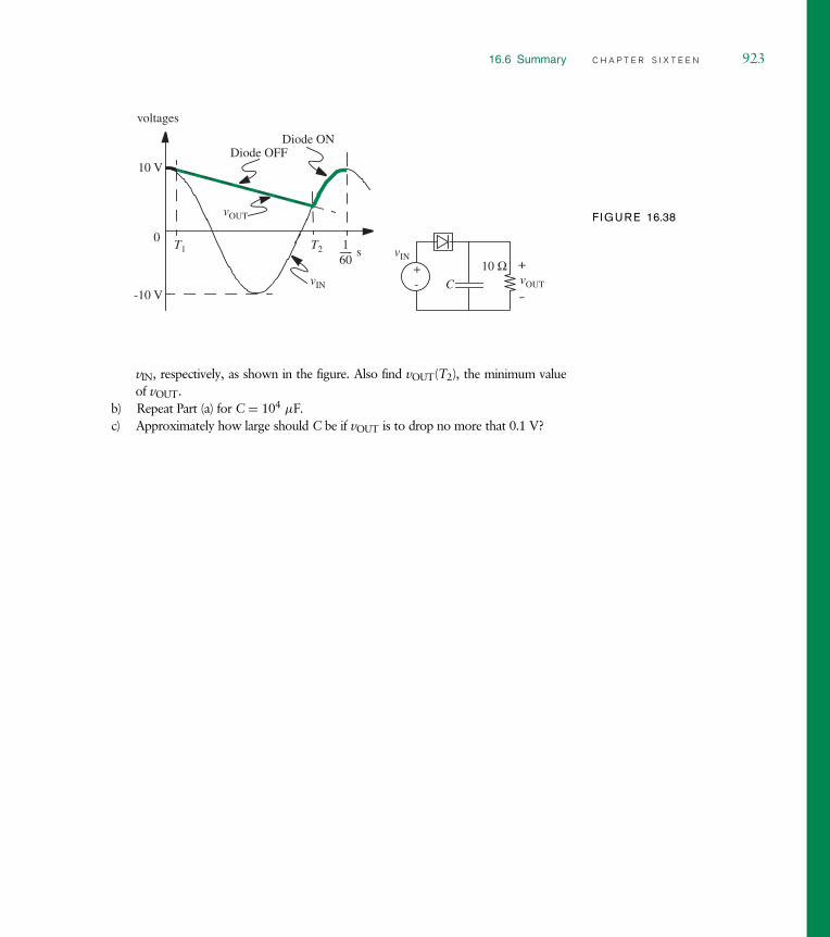
16.6 Summary C H A P T E R S I X T E E N 923
voltages
0
Diode OFFDiode ON
vIN
vOUT
10 V
-10 V
T1 T2 160------ s
C
vIN
+-
10 Ω +
-vOUT
F IGURE 16.38
vIN, respectively, as shown in the figure. Also find vOUT(T2), the minimum valueof vOUT.
b) Repeat Part (a) for C = 104 µF.c) Approximately how large should C be if vOUT is to drop no more that 0.1 V?


a p p e n d i x a
A.1 T H E L U M P E D M A T T E R D I S C I P L I N E
A.2 D E R I V I N G K I R C H H O F F ’ S L A W S
A.3 D E R I V I N G T H E R E S I S T A N C E O F A P I E C E O F M A T E R I A L


ap p end ix a
maxwel l ’ s equat ion s
and the lumped matter
d i s c i p l ine
This appendix develops the constraints of the lumped matter discipline anddemonstrates that the constraints result in a simplification of Maxwell’sEquations into algebraic equations.
I
V+ -
F IGURE A.1 A lumped circuitelement.A.1 T H E L U M P E D M A T T E R D I S C I P L I N E
Lumped circuits comprise lumped elements connected by ideal wires. A lumpedelement has the property that a unique terminal voltage V(t) and terminal currentI(t) can be defined for it. As depicted in Figure A.1, for a two-terminal element,V is the voltage across the terminals of the element, and I is the current through
a
l
F IGURE A.2 Resistive bulbfilament.
the element. As we will show shortly, the voltage and the current are definedfor an element or for points within a circuit only under certain constraints thatwe collectively call the lumped matter discipline.
Let us use our familiar lightbulb as an example and derive the conditionsunder which we can treat pieces of matter as lumped elements for inclusion
x
y
V
+
-
I
F IGURE A.3 Defining a voltageand current for the terminals of thefilament.
in electronic circuits. Suppose for the sake of discussion the lightbulb is madeout of a cylindrical piece of filament of length l and cross-sectional area a asdepicted in Figure A.2.
As shown in Figure A.3, let us assume that the terminals labeled x andy are attached to the end surfaces of the filament, and that the end faces areequipotential surfaces. Let us determine the set of conditions under which (1) aunique voltage V can be defined across x and y and (2) a unique current I canbe defined through x and y.
A.1.1 T H E F I R S T C O N S T R A I N T O F T H E L U M P E DM A T T E R D I S C I P L I N E
Let’s begin with the voltage. We define voltage as the line integral of the electricfield E according to1
Vyx = −∫ y
xE · dl.
1. Alternatively, observing that
qVyx = −∫ y
xqE · dl,
927

928 A P P E N D I X A m a x w e l l ’ s e q u a t i o n s a n d t h e l m d
d i f f e r e n t i a l i n t e g r a l p o p u l a r
f o r m f o r m n a m e
∇ · E = ρ
ε0
∮E · dS = q
ε0Gauss’s law for electricity
∇ · B = 0∮
B · dS = 0 Gauss’s law for magnetism
∇ × E = −∂B
∂t
∮E · dl = −∂B
∂tFaraday’s law of induction
∇ × B = µ0ε0∂E
∂t+ µ0J
∮B · dl = µ0ε0
∂E
∂t+ µ0i Ampere’s law (extended)
∇ · J = −∂ρ
∂t
∮J · dS = −∂q
∂tContinuity equation
TABLE A.1 Maxwell’s Equations(for a vacuum). The fifth equation isthe continuity equation implicit inMaxwell’s Equations. It can bederived by combining the timederivative of the first equation withthe divergence of the fourthequation. E is the electric field, Bthe magnetic flux density, ρ thecharge density (note that this ρ isdifferent from the resistivity used incomputing the resistance of anelement), J the current density, ε0the permittivity of free space, µ0the magnetic permeability of freespace, E the electric flux, andB the magnetic flux. E isdefined as the area integral of Eand B as the area integral of B.
Note that E is a vector. As illustrated in Figure A.4, the preceding equationindicates that the voltage depends on the path x → y. However, for ourlumped abstraction to apply, we require that we be able to assign a uniquevoltage between the x and y terminals. Clearly, this voltage cannot be a functionof the specific path between the x and y points. It seems we have already hit asnag in our attempt to create the abstraction of a lumped element to which thelumped parameters V and I apply.
x
y
x → y
F IGURE A.4 The voltagebetween the x and y terminals.
Put another way, we know from Maxwell’s Equations (summarized inTable A.1) that ∮
E · dl = −∂B
∂t
where E is the electric field and B is the magnetic flux which passes throughthe surface outlined by the closed path of the integral, as depicted in Figure A.5.We also know the preceding equation as Faraday’s law of induction. Notice
E dl•
∂ΦBt∂----------–
F IGURE A.5 Pictorial depictionof
∮E · dl.
that if we choose the two points x and y to be the same, then we can obtain anonzero value for
∫ yx E · dl = ∮
E · dl. Thus it appears our definition of potentialdifference or voltage has no useful meaning in this case. However, are thereconstraints that we can apply for which a unique voltage can be defined?
In the absence of a time-varying magnetic flux, we can write∮E · dl = 0.
the voltage Vyx at point y measured relative to point x can also be defined as the energy requiredto move a particle with unit charge against the force due to the electrical field from x to y.

A.1 The Lumped Matter Discipline A P P E N D I X A 929
The preceding equation says that integral of E over a closed circuit vanishesin the absence of a time-varying magnetic flux. Suppose we choose the closedcircuit to include the points x and y as shown in Figure A.6. We can then write
x
y
x ← yPath 2
x → yPath 1
F IGURE A.6 Line integral of Eover a closed circuit that includesthe points x and y.
∫ y
xE · dl+
∫ x
yE · dl = 0
Path 1 Path 2
or ∫ y
xE · dl = −
∫ x
yE · dl
Path 1 Path 2or ∫ y
xE · dl =
∫ y
xE · dl
Path 1 Path 2.
Notice that for this equality to hold even when Path 1 and Path 2 are chosenindependently, each integral must be independent of path. It follows from thisthat the computed voltage Vyx between any pair of points x and y given by− ∫ y
x E · dl is independent of the path.2 Thus, we have our desired outcome:We can ascribe a unique potential difference or voltage across the terminals xand y, provided
∂B
∂t= 0.
Additionally, we assume that the rate of change of flux is 0 for all time, so thatthe voltage can be a uniquely defined function of time. This directly leads tothe first constraint of our lumped matter discipline.
First constraint of the lumped discipline Choose lumped element bound-aries such that
∂B
∂t= 0
for all time, through any closed path outside the element.Since we have assumed that the rate of change of flux is 0 for all time, and
because any flux build up would require a non zero rate of change of flux, itfollows that the flux must also be 0.3
2. Notice that the internal behavior of the element can be arbitrarily complicated, but the spe-cific relationship between the voltage and current at the terminals will completely characterize itsbehavior to any circuit to which this element is connected.
3. We can arrive at the same property in a different way, as follows: A nonzero but constant fluxexternal to an element can be the result of a current flowing internal to the element, or producedby an external source.
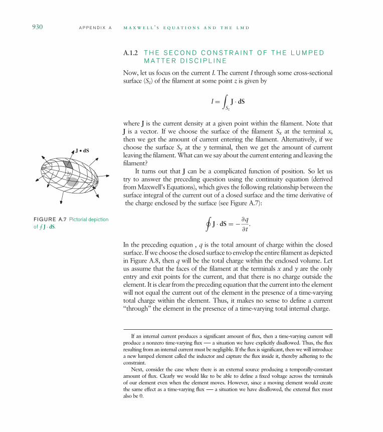
930 A P P E N D I X A m a x w e l l ’ s e q u a t i o n s a n d t h e l m d
A.1.2 T H E S E C O N D C O N S T R A I N T O F T H E L U M P E DM A T T E R D I S C I P L I N E
Now, let us focus on the current I. The current I through some cross-sectionalsurface (Sz) of the filament at some point z is given by
I =∫
Sz
J · dS
where J is the current density at a given point within the filament. Note thatJ is a vector. If we choose the surface of the filament Sx at the terminal x,then we get the amount of current entering the filament. Alternatively, if wechoose the surface Sy at the y terminal, then we get the amount of currentleaving the filament. What can we say about the current entering and leaving thefilament?
It turns out that J can be a complicated function of position. So let ustry to answer the preceding question using the continuity equation (derivedfrom Maxwell’s Equations), which gives the following relationship between thesurface integral of the current out of a closed surface and the time derivative ofthe charge enclosed by the surface (see Figure A.7):
J • dS
∂q∂q∂t----−
F IGURE A.7 Pictorial depictionof
∮J · dS.
∮J · dS = −∂q
∂t.
In the preceding equation , q is the total amount of charge within the closedsurface. If we choose the closed surface to envelop the entire filament as depictedin Figure A.8, then q will be the total charge within the enclosed volume. Letus assume that the faces of the filament at the terminals x and y are the onlyentry and exit points for the current, and that there is no charge outside theelement. It is clear from the preceding equation that the current into the elementwill not equal the current out of the element in the presence of a time-varyingtotal charge within the element. Thus, it makes no sense to define a current‘‘through’’ the element in the presence of a time-varying total internal charge.
If an internal current produces a significant amount of flux, then a time-varying current willproduce a nonzero time-varying flux a situation we have explicitly disallowed. Thus, the fluxresulting from an internal current must be negligible. If the flux is significant, then we will introducea new lumped element called the inductor and capture the flux inside it, thereby adhering to theconstraint.
Next, consider the case where there is an external source producing a temporally-constantamount of flux. Clearly we would like to be able to define a fixed voltage across the terminalsof our element even when the element moves. However, since a moving element would createthe same effect as a time-varying flux a situation we have disallowed, the external flux mustalso be 0.

A.1 The Lumped Matter Discipline A P P E N D I X A 931
y
x
Closed surface envelopingthe filament
Sx
Sy
F IGURE A.8 Integral of J over aclosed surface.
However, consider the situation in which there is no time-varying chargewithin the element. In other words, consider the situation in which
∂q
∂t= 0
for the element taken as a whole. With this situation, we derive the nice resultthat ∮
J · dS = 0.
Simply stated, when there is no total time-varying charge within an element,the total current into the element is 0. Returning to our filament example, ifthere is no current flow across the curved cylindrical surface of the filament, wecan rewrite the total current flowing into the element as the different betweenthe current flowing into the end surface at x and the current flowing out of theend surface at y:
∮J · dS = −
∫Sx
J · dS +∫
Sy
J · dS = 0.
Since the sum of the two components of the current must be 0, it follows theymust be equal. Thus we are able to define a meaningful current flowing throughthe element when there is no net time varying charge within the element.This outcome directly leads to the second constraint of the lumped matterdiscipline.

932 A P P E N D I X A m a x w e l l ’ s e q u a t i o n s a n d t h e l m d
Second constraint of the lumped discipline Choose the lumped elementboundaries so that there is no total time varying charge within the element. Inother words, choose element boundaries such that
∂q
∂t= 0
for all time, where q is the total charge within the element.Notice that we have assumed explicitly that the rate of change of charge is
zero for all time so that the current can be an arbitrary function of time. Sincewe have assumed that the rate of change of charge is zero for all time, andbecause any charge build up would require a nonzero rate of change of charge,it follows that the net charge within any element must also be zero.4
A.1.3 T H E T H I R D C O N S T R A I N T O F T H E L U M P E DM A T T E R D I S C I P L I N E
Finally, let us consider the practical matter of the propagation speeds of elec-tromagnetic waves. The lumped element approximation requires that we beable to define a voltage V between a pair of element terminals and a currentthrough the terminal pair. Defining a current through the element means thatthe current in must equal the current out. Now consider the following thoughtexperiment. Apply a current pulse at the terminal x of the filament at timeinstant t and observe both the current into terminal x and the current outof terminal y at a time instant t + dt very close to t. If the filament werelong enough or if dt were small enough, the finite speed of electromagneticwaves might result in our measuring different values for the current in and thecurrent out.
We fix the problem created by the finite propagation speeds of electro-magnetic waves by adding a third constraint. We include the constraint thatthe timescale of interest in our problem be much larger than electromagneticpropagation delays through our elements. Put another way, the size of ourlumped elements must be much smaller than the wavelength associated withthe V and I signals.5
Under the preceding speed constraints, electromagnetic waves can betreated as if they propagated instantly through a lumped element. By neglectingpropagation effects, the lumped element approximation becomes analogous to
4. If an element does store charge, then we will collect equal amounts of charges of oppositepolarities inside a new lumped element called a capacitor, so that there is no net charge inside theelement.
5. More precisely, the wavelength that we are referring to is that wavelength of the electromagneticwave launched by the signals.

A.1 The Lumped Matter Discipline A P P E N D I X A 933
the point-mass simplification, in which we are able to ignore many physicalproperties of elements such as their length, shape, size, and location.
Third constraint of the lumped discipline Operate in the regime in whichsignal timescales are much larger than the propagation delay of electromagneticwaves across the lumped elements.
A.1.4 T H E L U M P E D M A T T E R D I S C I P L I N E A P P L I E DT O C I R C U I T S
Circuits are sets of lumped elements connected by ideal wires. A node is formedat the junction point at which the terminals of two or more elements are con-nected. We choose the wires such that they obey the lumped matter discipline,so the wires themselves are also lumped elements. For their voltages and cur-rents to be meaningful, the constraints that apply to lumped elements apply toentire circuits as well. In other words, for voltages between any pair of pointsin the circuit and for currents through wires to be defined, any segment of thecircuit must obey a set of constraints similar to those imposed on each of thelumped elements.
Accordingly, the lumped matter discipline for circuits can be stated as:
1. The rate of change of magnetic flux linked with any portion of the circuitmust be 0 for all time.
2. The rate of change of the charge at any node in the circuit must be 0 forall time. A node is any point in the circuit at which two or more elementterminals are connected using wires.
3. The signal timescales must be much larger than the propagation delay ofelectromagnetic waves through the circuit.
Notice that the first two constraints follow directly from the correspondingconstraints applied to lumped elements. Remember that a node is simply ajunction point of a set of wires, which are themselves lumped elements. So, thefirst two constraints do not imply any new restrictions beyond those alreadyassumed for lumped elements.6 The third constraint for circuits, however,imposes a stronger restriction on signal timescales than for elements, because acircuit can have a much larger physical extent than a single element. The thirdconstraint says that the circuit must be much smaller in all its dimensions thanthe wavelength of light at the highest operating frequency of interest.
6. As seen in Chapter 9, it turns out that voltages and currents in circuits result in electric andmagnetic fields, thus appearing to violate the set of constraints to which we promised to adhere.In most cases these are negligible. However, when their effects cannot be ignored, we explicitlymodel them using elements called capacitors and inductors.

934 A P P E N D I X A m a x w e l l ’ s e q u a t i o n s a n d t h e l m d
A.2 D E R I V I N G K I R C H H O F F ’ S L A W S
This section uses the lumped matter discipline to derive Kirchhoff’s laws fromMaxwell’s Equations. To illustrate the basic ideas, let us suppose that we areinterested in deriving the voltages across and the currents through each of theelements in the circuit in Figure A.9.
i4V+-
a b
c
d
v4
+
-
F IGURE A.9 Simple resistivenetwork.
In general, we can resort to Maxwell’s Equations and the related continuityequation to solve the circuit. The relevant equations are:
∮E · dl = −∂B
∂t
and ∮J · dS = −∂q
∂t.
Recall that according to the lumped matter discipline we have agreed toconstrain ourselves to the circuit domain in which
∂B
∂t= 0
for closed circuit loops, and
∂q
∂t= 0
for circuit nodes. In this constrained domain, the general equations can besimplified to the following: ∮
E · dl = 0 (A.1)
and ∮J · dS = 0. (A.2)
Equation A.1 says the line integral of the field around any closed path mustequal 0. Similarly, Equation A.2 says that the surface integral of the currentover any surface must be 0. Of course, Equations A.1 and A.2 are valid onlyunder the lumped matter discipline.
Applying Equation A.1 to the closed loop defined by the three circuit edgesa → b, b → c, and c → a, as depicted in Figure A.10 we obtain
∮E · dl =
∫ b
aE · dl +
∫ c
bE · dl +
∫ a
cE · dl = 0.

A.2 Deriving Kirchhoff’s Laws A P P E N D I X A 935
i4
a b
c
+v1-
+v
4 -+ v
3 -
V+
-
d
F IGURE A.10 The line integral over a closed loop in thenetwork.
V+
- i4
ibia
ic
b
c
d
a
Sb
Sa
Sc
F IGURE A.11 The surface integral over a closed surfacein the network.
Since we know that∫
E ·dl = 0 along an ideal wire is 0, and since the potentialdifference Vxy across the xy terminals of an element is given by
Vxy =∫ y
xE · dl,
we can write
∫ b
aE · dl +
∫ c
bE · dl +
∫ a
cE · dl = v1 + v2 + v3 = 0.
In other words, the sum of the voltages along any closed path in the circuitmust equal 0. Accordingly, we can write Kirchhoff’s voltage law:
KVL The algebraic sum of the voltages around any closed path in a networkmust be zero.
We will now derive Kirchhoff’s current law. Let us apply Equation A.2 to theclosed box-like surface depicted in Figure A.11. We notice that there are currentsflowing only through surfaces Sa, Sb, and Sc. Therefore,
∮J · dS =
∫Sa
J · dS +∫
Sb
J · dS +∫
Sc
J · dS = 0.
Since our currents are confined to the wires entering the three surfaces weobtain ∫
Sa
J · dS +∫
Sb
J · dS +∫
Sc
J · dS = −ia − ib − ic = 0.

936 A P P E N D I X A m a x w e l l ’ s e q u a t i o n s a n d t h e l m d
In other words, the sum of the currents flowing into any closed surface mustbe zero. Simply put, the preceding statement is a statement of the conservationof charge. We can now write Kirchhoff’s current law:
KCL The current flowing out of any junction or node must equal the currentflowing in. That is, the algebraic sum of the currents flowing into any nodemust be zero.
A.3 D E R I V I N G T H E R E S I S T A N C E O F AP I E C E O F M A T E R I A L
The resistance of a piece of material depends on its geometry. As illustrated inFigure A.12, assume the resistor has a conducting channel with cross-sectional
E, J
Area a
i+ -v
l
ρ
F IGURE A.12 A cylindrical-wireshaped resistor.
area a, length l, and resistivity ρ. This channel is terminated at its extremes bytwo conducting plates that extend to form the two terminals of the resistor.
For lumped elements that both obey Ohm’s Law and satisfy the lumpedmatter discipline, we can obtain a lumped resistance value from the microscopicform of Ohm’s Law:
E = ρJ (A.3)
where J is the current density, ρ is the resistivity, and E is the electrical field atany point within the resistor.
As the current i enters the resistor through a terminal, it spreads out toconduct uniformly through the channel. This current is given by
i =∫
J · dS
evaluated at any cross-sectional surface.7
The voltage across the resistor8 is defined as
v =∫
E · dl.
We can substitute the expressions for v and i into Ohm’s Law to get
R = v
i=
∫E · dl∫J · dS
. (A.4)
For a cylindrical-wire shaped resistor with cross-sectional area a andlength l, with the terminals taken at the circular end surfaces (see Figure A.12),
7. We are able to obtain i in this fashion directly as a result of our second constraint.
8. We know this voltage is unique because of our first constraint.

A.3 Deriving the Resistance of a Piece of Material A P P E N D I X A 937
the Equation A.4 reduces to the following equation through cylindricalsymmetry:
R = El
Ja,
where E and J are the magnitudes of the electrical field E and current density J,respectively. From Equation A.3 we know that E/J = ρ, so we get
R = ρl
a. (A.5)
Similarly, the resistance of a cuboid shaped resistor with length l, width w, andheight h is given by
R = ρl
wh(A.6)
when the terminals are taken at the pair of surfaces with area wh.


a p p e n d i x b
B.1 N E G A T I V E A R G U M E N T S
B.2 P H A S E - S H I F T E D A R G U M E N T S
B.3 S U M A N D D I F F E R E N C E A R G U M E N T S
B.4 P R O D U C T S
B.5 H A L F - A N G L E A N D T W I C E - A N G L E A R G U M E N T S
B.6 S Q U A R E S
B.7 M I S C E L L A N E O U S
B.8 T A Y L O R S E R I E S E X P A N S I O N S
B.9 R E L A T I O N S T O e j θ


ap p end ix b
tr igonometr i c funct ion s
and ident i t i e s
This appendix briefly reviews the three trigonometric functions cos(θ ), sin(θ ),and tan(θ ), and various identities involving them. These functions are oftenencountered during the analysis of transients in second-order linear circuits,and during the analysis of any linear circuit in sinusoidal steady state.
Consider a point located on the unit circle in the x y plane. If the angularposition of the point around the circle is the angle θ measured from the x-axis,then the x and y coordinates of the point are cos(θ ) and sin(θ ), respectively. Thisdefines the functions cos(θ ) and sin(θ ), as shown in Figure B.1. Additionally, weconsider here the ratio of these two functions, namely tan(θ ) ≡ sin(θ )/cos(θ ).All three functions are shown in Figure B.2.
In the identities that follow, θ is treated as a constant angle, specified inradians.1 However, the identities hold whether θ is constant or not. It couldjust as well be a function of time or any other variable. In fact, it is often afunction of time.
sin(q)
cos(q)
q
Unitcircle
F IGURE B.1 The definitions ofcos(θ ) and sin(θ ) as the x and ycoordinates, respectively, of a pointon the unit circle in the x–y plane.
B.1 N E G A T I V E A R G U M E N T S
cos(−θ ) = cos(θ ) (B.1)
sin(−θ ) = − sin(θ ) (B.2)
tan(−θ ) = − tan(θ ) (B.3)
1. Angles measured in degrees can be converted into radians using
θrads = 2π
360θdegs
Notice, 2π radians is equivalent to 360 degrees, or one cycle.
941

942 A P P E N D I X B t r i g o n o m e t r i c f u n c t i o n s a n d i d e n t i t i e s
F IGURE B.2 The functionscos(θ ), sin(θ ), and tan(θ ).
|0
|2
|4
|6
|8
|10
|-2.0
|-1.5
|-1.0
|-0.5
|0.0
|0.5
|1.0
|1.5
|2.0
q (rad)
cos
q, s
in q
, tan
q
cosq
sin q
tan
q
π/2 π 3π/2 2π 5π/2 3π
B.2 P H A S E - S H I F T E D A R G U M E N T S
cos(
θ ± π
2
)= cos
(θ ∓ 3π
2
)= ∓ sin(θ ) (B.4)
sin(
θ ± π
2
)= sin
(θ ∓ 3π
2
)= ± cos(θ ) (B.5)
tan(
θ ± π
2
)= −1
tan(θ )(B.6)
cos(θ ± π ) = − cos(θ ) (B.7)
sin(θ ± π ) = − sin(θ ) (B.8)
tan(θ ± π ) = tan(θ ) (B.9)
cos(θ ± 2π ) = cos(θ ) (B.10)
sin(θ ± 2π ) = sin(θ ) (B.11)
tan(θ ± 2π ) = tan(θ ) (B.12)
B.3 S U M A N D D I F F E R E N C E A R G U M E N T S
cos(θ1 ± θ2) = cos(θ1) cos(θ2) ∓ sin(θ1) sin(θ2) (B.13)
sin(θ1 ± θ2) = sin(θ1) cos(θ2) ± cos(θ1) sin(θ2) (B.14)
tan(θ1 ± θ2) = tan(θ1) ± tan(θ2)
1 ∓ tan(θ1) tan(θ2)(B.15)
B.4 Products A P P E N D I X B 943
B.4 P R O D U C T S
cos(θ1) cos(θ2) = 1
2(cos(θ1 − θ2) + cos(θ1 + θ2)) (B.16)
sin(θ1) cos(θ2) = 1
2(sin(θ1 − θ2) + sin(θ1 + θ2)) (B.17)
sin(θ1) sin(θ2) = 1
2(cos(θ1 − θ2) − cos(θ1 + θ2)) (B.18)
B.5 H A L F - A N G L E A N D T W I C E - A N G L EA R G U M E N T S
cos(θ/2) = ±√
1 + cos(θ )
2(B.19)
sin(θ/2) = ±√
1 − cos(θ )
2(B.20)
tan(θ/2) = 1 − cos(θ )
sin(θ )= sin(θ )
1 + cos(θ )= S
√1 − cos(θ )
1 + cos(θ );
S = +1 for θ/2 in Q1 or Q3
−1 for θ/2 in Q2 or Q4 (B.21)
cos(2θ ) = cos2(θ ) − sin2(θ ) (B.22)
sin(2θ ) = 2 sin(θ ) cos(θ ) (B.23)
tan(2θ ) = 2 tan(θ )
1 − tan2(θ )(B.24)
B.6 S Q U A R E S
cos2(θ ) = 1
2(1 + cos(2θ )) (B.25)
sin2(θ ) = 1
2(1 − cos(2θ )) (B.26)
cos2(θ ) + sin2(θ ) = 1 (B.27)
B.7 M I S C E L L A N E O U S
The scaled sums and differences of sinusoidal functions are among the mostcommon identities we will use. Notice from the following equations that

944 A P P E N D I X B t r i g o n o m e t r i c f u n c t i o n s a n d i d e n t i t i e s
the scaled sums and differences of sinusoids (of the same frequency) are alsosinusoids:
A1 cos(θ ) + A2 sin(θ ) =√
A21 + A2
2 cos(
θ − tan−1(
A2
A1
))(B.28)
=√
A21 + A2
2 sin(
θ + tan−1(
A1
A2
))(B.29)
A1 cos(θ ) − A2 sin(θ ) =√
A21 + A2
2 cos(
θ + tan−1(
A2
A1
))(B.30)
=√
A21 + A2
2 sin(
θ − tan−1(
A1
A2
))(B.31)
B.8 T A Y L O R S E R I E S E X P A N S I O N S
cos(θ ) = 1 − θ2
2! + θ4
4! − θ6
6! · · · (B.32)
sin(θ ) = θ
1! − θ3
3! + θ5
5! − θ7
7! · · · (B.33)
tan(θ ) = θ + θ3
3+ 2θ5
15+ 17θ7
315+ 62θ9
2835· · · (B.34)
B.9 R E L A T I O N S T O e jθ
eθ = 1 + θ
1! + θ2
2! + θ3
3! + θ4
4! + θ5
5! · · · (B.35)
e jθ = 1 + jθ
1! − θ2
2! − jθ3
3! + θ4
4! + jθ5
5! · · ·
=(
1 − θ2
2! + θ4
4! · · ·)
+ j
(θ
1! − θ3
3! + θ5
5! · · ·)
= cos(θ ) + j sin(θ ) (B.36)
Equation B.36 is called the Euler relation.
cos(θ ) = e jθ + e−jθ
2(B.37)
sin(θ ) = e jθ − e−jθ
2(B.38)
tan(θ ) = e jθ + e−jθ
e jθ − e−jθ(B.39)

a p p e n d i x c
C.1 M A G N I T U D E A N D P H A S E
C.2 P O L A R R E P R E S E N T A T I O N
C.3 A D D I T I O N A N D S U B T R A C T I O N
C.4 M U L T I P L I C A T I O N A N D D I V I S I O N
C.5 C O M P L E X C O N J U G A T E
C.6 P R O P E R T I E S O F e j θ
C.7 R O T A T I O N
C.8 C O M P L E X F U N C T I O N S O F T I M E
C.9 N U M E R I C A L E X A M P L E S


ap p end ix c
complex number s
A complex number, z for example, takes the form:
z = a + jb (C.1)
where a and b are both real numbers, and j is the imaginary unit definedaccording to:
j2 = −1. (C.2)
Here, a is referred to as the real part of z, and b is referred to as the imaginarypart of z. These two parts can be extracted from z using the real-part function( ) and the imaginary-part function ( ), respectively. Thus, we write
a = (z) (C.3)
b = (z) (C.4)
and more generally,
z = (z) + j(z). (C.5)
If (z) = 0, then z is a purely real number. If (z) = 0, then z is a purelyimaginary number. Otherwise, z is a complex number.
C.1 M A G N I T U D E A N D P H A S E
A complex number can be viewed as a point in the two-dimensional complexRe(Z)
Im(Z)
b
a
r
q
(a, b)
F IGURE C.1 The location of thecomplex number z in the complexplane. The distance r is the mag-nitude of z, and the angle θ arereferred to as the angle, or phase,of z.
plane, as shown in Figure C.1 for z as given in Equation C.1. The distance rmeasured from the origin to the point is referred to as the magnitude of z, andthe angle θ measured from the real axis to the radius on which the point lies isreferred to as the angle, or phase, of z. Thus we write
r = |z| (C.6)
θ = ∠z. (C.7)
947

948 A P P E N D I X C c o m p l e x n u m b e r s
C.2 P O L A R R E P R E S E N T A T I O N
Similarly, a complex number can be viewed as a vector in the complex plane.In this case, its components are a and b, or (z) and (z), and its magnitudeand direction are r and θ , or |z| and ∠z.
From the geometry of Figure C.1 it is apparent that
r =√
a2 + b2 (C.8)
θ = tan−1(
b
a
). (C.9)
In Equation C.9, the tan−1( ) function is understood to be a two-argumentinverse having full range such that 0 ≤ ∠z < 2π or −π ≤ ∠z < π ; thechoice of range is a matter of convenience. From Equations C.8 and C.9 wecan identify the more general expressions:
|z| =√
(z)2 + (z)2 (C.10)
∠z = tan−1( (z)
(z)
). (C.11)
Equations C.10 and C.11 express |z| and ∠z in terms of (z) and (z). It isalso possible to invert these expressions. Again from the geometry of Figure C.1,this yields
a = r cos(θ ) (C.12)
b = r sin(θ ), (C.13)
from which we may identify the general expressions
(z) = |z| cos(∠z) (C.14)
(z) = |z| sin(∠z). (C.15)
In summary, (z) and (z) are the Cartesian coordinates of z in the com-plex plane while |z| and ∠z are the polar coordinates of z in the same plane.Correspondingly, Equations C.10 and C.11 are a Cartesian-to-polar coordi-nate transformation, while Equations C.14 and C.15 are a polar-to-Cartesiancoordinate transformation.
We can now use the polar coordinates |z| and ∠z to form an alter-native expression for a complex number. Beginning with z as presented inEquation C.1,
z = a + jb = r cos(θ ) + jr sin(θ ) = r(cos(θ ) + j sin(θ )) = re jθ . (C.16)
C.3 Addition and Subtraction A P P E N D I X C 949
The first equality in Equation C.16 follows from the substitution of EquationsC.12 and C.13. The last equality follows from the substitution of the Euleridentity:
cos(θ ) + j sin(θ ) ≡ e jθ , (C.17)
which is derived in Equation B.36 using Taylor Series expansions for the func-tions e( ), cos( ) and sin( ). From Equation C.16 we can identify the more generalexpression:
z = |z|e j∠z. (C.18)
Equation C.18 is the polar equivalent of Equation C.5. We will use these twoexpressions interchangeably. Which one is preferred depends on the application.For example, we shall see shortly that addition and subtraction are most easilycarried out using complex numbers in Cartesian form; while multiplication,division, and determining a magnitude are most easily carried out using complexnumbers in polar form.
C.3 A D D I T I O N A N D S U B T R A C T I O N
Mathematical operations are performed on complex numbers just as they areon purely real numbers. For example, the addition and subtraction of the twocomplex numbers (a1 + jb1) and (a2 + jb2) proceeds according to:
(a1 + jb1) + (a2 + jb2) = a1 + jb1 + a2 + jb2 = (a1 + a2) + j(b1 + b2)(C.19)
(a1 + jb1) − (a2 + jb2) = a1 + jb1 − a2 − jb2 = (a1 − a2) + j(b1 − b2).(C.20)
Thus, the real and imaginary parts of complex numbers add and subtractseparately, just like the components of a vector. This is because the realand imaginary parts are defined along orthogonal axes of the complex plane.Because of this the addition and subtraction of complex numbers in polar formis less convenient.
C.4 M U L T I P L I C A T I O N A N D D I V I S I O N
The multiplication and division of complex numbers proceeds as directly asdoes their addition and subtraction. The only difference is that we com-monly substitute −1 for each occurrence of j2, as permitted by Equation C.2.

950 A P P E N D I X C c o m p l e x n u m b e r s
For example, the multiplication and division of the two complex numbers(a1 + jb1) and (a2 + jb2) proceeds according to:
(a1 + jb1)(a2 + jb2) = a1a2 + ja1b2 + jb1a2 + j2b1b2
= (a1a2 − b1b2) + j(a1b2 + a2b1) (C.21)
a1 + jb1
a2 + jb2= a1 + jb1
a2 + jb2· a2 − jb2
a2 − jb2= (a1a2 + b1b2) + j(b1a2 − a1b2)
a22 + b2
2
= a1a2 + b1b2
a22 + b2
2
+ jb1a2 − a1b2
a22 + b2
2
. (C.22)
Note in particular the use of (a2−jb2) in Equation C.22 to clear the denominatorof terms involving j. While multiplication and division of complex numbers inCartesian form is not inconvenient, it is much more convenient using complexnumbers in polar form. For example,
r1e jθ1 r2e jθ2 = r1r2e j(θ1+θ2) (C.23)
r1e jθ1
r2e jθ2= r1
r2e j(θ1−θ2). (C.24)
Equations C.23 and C.24 demonstrate that magnitudes multiply and divide,and that angles add and subtract, during the multiplication and division ofcomplex numbers, respectively. Taking powers of complex numbers is equallyconvenient when the numbers are in polar form.
C.5 C O M P L E X C O N J U G A T E
The complex conjugate of z, denoted here by z∗ is defined such that
(z∗) = (z) (C.25)
(z∗) = −(z). (C.26)
For z as given in Equation C.1,
z∗ = a − jb (C.27)
while for z as given in Equation C.16,
z∗ = re−jθ . (C.28)
In general, z∗ can be derived from z by replacing each occurrence of j in z by −j.

C.6 Properties of e jθ A P P E N D I X C 951
By combining z with z∗, several useful relations can be expressed. Inparticular,
zz∗ = |z|2 (C.29)
z + z∗
2= (z) (C.30)
z − z∗
2j= (z) (C.31)
1
z= z∗
zz∗z∗
|z|2 . (C.32)
Each of these relations can be readily proven with the substitution of EquationsC.1 and C.27. Equation C.29 is a particularly useful means of computing |z|when z is expressed in Cartesian form. In fact, it was used in Equation C.22 toclear the denominator of terms involving j.
C.6 P R O P E R T I E S O F e jθ
In Equations C.16 and C.17 we introduced the complex number e jθ . As weshall see shortly, numbers of this form are very important for our purposes, andto this end it has several important properties. First,
|e jθ | = 1 (C.33)
∠e jθ = θ . (C.34)
This can be seen by comparing e jθ with Equation C.17, or by substitutingEquation C.18 into Equation C.29. Second,
(e jθ ) = cos(θ ) (C.35)
(e jθ ) = sin(θ ). (C.36)
These relations can be seen by comparing Equations C.18 and C.5.
C.7 R O T A T I O N
Finally, the multiplication of another complex number by e jθ acts to rotate thatnumber in the complex plane by the angle θ . To see this consider that:
(r1e jθ1
) (e jθ2
) = r1e j(θ1+θ2). (C.37)

952 A P P E N D I X C c o m p l e x n u m b e r s
Here, the multiplication of r1e jθ1 by e jθ2 preserves the magnitude r1 while addingθ2 to the angle θ1. Thus, the complex number r1e jθ1 is rotated in the complexplane by the angle θ2.
C.8 C O M P L E X F U N C T I O N S O F T I M E
Our discussion of complex numbers to this point has focused on constantcomplex numbers. However, none of the discussion has actually relied on zbeing constant. Indeed, the entire discussion applies to complex functions oftime, and in particular to the time function e jωt, in which the substitution θ = jωthas been made. This time function is central to our study of the sinusoidal steadystate operation of linear electronic circuits. Following Equations C.33 throughC.36, we see that:
|e jωt| = 1 (C.38)
∠e jωt = ωt (C.39)
(e jωt) = cos(ωt) (C.40)
(e jωt) = sin(ωt). (C.41)
Equations C.38 and C.39 show that e jωt is a unit vector in the complex plane thatrotates with the angular frequency ω. Equations C.40 and C.41 are projections ofthis vector onto the real and imaginary axes, respectively. An angular frequencyω measured in radians per second is equivalent to the angular frequency ω/2π
in cycles per second.
C.9 N U M E R I C A L E X A M P L E S
We close this appendix with a several numerical examples. For these exam-ples, let
z1 = −2 + j2 (C.42)
z2 = 1 + j√
3. (C.43)
We can find the complex conjugates of z1 and z2 using Equations C.25 andC.26. This yields
z∗1 = −2 − j2 (C.44)
z∗2 = 1 − j
√3. (C.45)

C.9 Numerical Examples A P P E N D I X C 953
We can find the real and imaginary parts of z1 and z2 by association withEquation C.5, or by using Equations C.30 and C.31. By either method,
(z1) = −2; (z1) = 2 (C.46)
(z2) = 1; (z2) = √3. (C.47)
We can find the magnitude and angle of z1 and z2 using Equations C.10 andC.11. This yields
|z1| = 2√
2 ; ∠z1 = 3π
4(C.48)
|z2| = 2 ; ∠z2 = π
3. (C.49)
We can find the polar form of z1 and z2 using Equation C.18. This yields
z1 = 2√
2ej 3π
4 (C.50)
z2 = 2ej π
3 . (C.51)
Following Equations C.19 and C.20, the sum and difference of z1 and z2 are
z1 + z2 = −1 + j(
2 + √3)
; z1 − z2 = −3 + j(
2 − √3)
. (C.52)
Following Equations C.21 and C.22, the product and ratio of z1 and z2 are
z1z2 = −(
2√
3 + 2)
− j(
2√
3 − 2)
;z1
z2=
(√3
2− 1
2
)+ j
(√3
2+ 1
2
).
(C.53)
Alternatively, following Equations C.23 and C.24, the product and ratio of z1and z2 are
z1z2 = 4√
2ej 13π
12 ;z1
z2= √
2ej 5π
12 . (C.54)


a p p e n d i x d


ap p end ix d
solv ing s imultaneous
l inear equat ion s
The need to solve a simultaneous set of linear algebraic equations is a commonoccurrence during the analysis of electronic circuits. Of course, such equationsare easily solved for special cases with numerical analysis packages, but at timesthe insight gained from an analytic solution is more valuable. To this end, thisappendix reviews the analytic solution of equations of the form:
Mx = y
where M is a known matrix, y is a known vector, and x is a vector ofunknowns.1 From the start, we assume that the equations have a uniquesolution, and so M is a square matrix with det(M) = 0.
Consider the case of two equations and two unknowns. In this case,
[M11 M12M21 M22
] [x1x2
]=
[y1y2
]. (D.1)
The solution to Equation D.1 is
[x1x2
]= 1
[M22 −M12
−M21 M11
] [y1y2
](D.2)
= M11M22 − M12M21; (D.3)
here, = det(M). The validity of Equation D.2 can be verified by directsubstitution into Equation D.1. Consider next the case of three equations and
1. For a more detailed treatment, the reader is referred to G. Strang, Linear Algebra and itsApplications, Academic Press 1988.
957

958 A P P E N D I X D s o l v i n g s i m u l t a n e o u s l i n e a r e q u a t i o n s
three unknowns. In this case,
M11 M12 M13
M21 M22 M23M31 M32 M33
x1
x2x3
=
y1
y2y3
. (D.4)
The solution to Equation D.4 is
x1
x2
x3
= 1
M22M33 − M23M32 M32M13 − M12M33 M12M23 − M22M13
M31M23 − M21M33 M11M33 − M31M13 M21M13 − M11M23
M21M32 − M31M22 M31M12 − M11M32 M11M22 − M21M12
y1
y2
y3
(D.5)
= M11M22M33 + M12M23M31 + M13M21M32 − M31M22M13
− M32M23M11 − M33M21M12; (D.6)
again, = det(M). The validity of Equation D.5 can be verified by directsubstitution into Equation D.4.
Finally, for higher-order cases, we can turn to an elimination process, or toCramer’s Rule,2 although the algebra may be excessive in either case. Cramer’sRule states that:
xn = det(Bn)
det(M)(D.7)
where Bn is the matrix formed by replacing the nth column of M with y.
2. Again, see G. Strang, Linear Algebra and its Applications, Academic Press 1988.

an swer s to s e l ected
problems
c h a p t e r 1
Ex1.1 R = 12
Ex1.3V2
DCR
c h a p t e r 2
Ex2.1 (a) 2.5 (b) 1 (c) 2R
Ex2.3 (a) 10 (b) 1 (c) 2 (d) 2
Ex2.5 (a) R1 + R2 + R3, (b)R1R2 + R3(R1 + R2)
R1 + R2(c)
R1(R2 + R3)R1 + R2 + R3
(d)R1R2
R1 + R2+ R3R4
R3 + R4(e)
(R1 + R2)(R3 + R4)R1 + R2 + R3 + R4
Ex2.7 R2 and R3
Ex2.9 (b) 2 (c) 3 (d) (Depending on your assignment of branch variables, your answer may be different.) KVL: VA + VE +VC + VB = 0, VC − VD = 0 KCL: iB − iC − iD = 0, iA − iB = 0, −iA + iE = 0 (e) iA = iB = iE = 0.2A iC = 1 AiD = −0.8 A (f) VD = −2 V, VC = −2 V, VE = 2 V, VB = 1 V, VA = −1 V
Pr2.1 0.5
Pr2.345
Pr2.5 (a) RT = R1 + R2 + R3 (b) RT = R1R2R3
R1R2 + R1R3 + R2R3(c) RT = R1R2 + R1R3
R1 + R2 + R3(d) RT = R1 + R2R3
R2 + R3
(e) RT = R1R3 + R1R4 + R2R3 + R2R4
R1 + R2 + R3 + R4
Pr2.7 i3 = − vR2
R1R2 + R1R3 + R2R3
Pr2.9 Power = 2 W
Pr2.13 (a) i1 = vAR2 + vAR3 − vBR2
R1R2 + R2R3 + R1R3, i2 = vAR3 + vBR1
R1R2 + R2R3 + R1R3, i3 = vBR2 + vBR1 − vAR2
R1R2 + R2R3 + R1R3
Pr2.15 v4 = vR2R4 + IR1R2R4 + IR1R3R4 + IR2R3R4
R1R2 + R1R3 + R1R4 + R2R3 + R2R4
Pr2.17 vC = 225 V
c h a p t e r 3
Ex3.1 8/53 A
Ex3.3 Left: VOC = ISR2, RT = R1 + R2, Right: VOC = ISR2R3
R1 + R2 + R3, RT = R3‖(R1 + R2)
959

960 answers to selected problems
Ex3.5 1/3 VEx3.7 ISC = 1 mA, and RT = 8 k
Ex3.9 (a) i(t) = 14
(v1(t) + v2(t)) (b) Energy = 116
∫ T2T1
(v1(t) + v2(t))2dt (c)∫ T2
T1v1 · v2 · dt ≡ 0
Ex3.11 RT = 2 and VOC = 6 VEx3.13 RT = R2 and vT = I3 · R2 + V3
Ex3.15 (1) ( g1 + g3 + g5) va − g3 · vb + 0 · vc = g1 · V, (2) −g3 · va + ( g3 + g4) vb − g4 · vc = I,(3) 0 · va − g4 · vb + ( g2 + g4 + g6) · vc = g2 · V
Ex3.17 RT = R1(R2 + R3)R1 + R2 + R3
, VOC = R1R2 · I + (R2 + R3) VR1 + R2 + R3
Ex3.19 RT = 100 , VOC = 1623
V, ISC = 1/6 A
Ex3.22 (a) RT = R6 + R7 + R8 and VOC = I · R6, (b) RT = R4‖(R1 + R3), and ISC = V/(R2 + R3)Ex3.24 RT = 5 k, VOC = 49 VEx3.26 V · g1 = va ( g1 + g2 + g4) − vb · g4, and V · g3 − I = +va (−g4) + vb ( g3 + g4)
Pr3.1 15 APr3.3 8.57 VPr3.5 (a) Req = R, (b) vTH = 0.125 V, RTH = 1
Pr3.7 (a) 0, b) i) V( R
R + R1− 1
2
), ii)
V(R − R1)3R + 5R1
, c) RTH = R, VTH = 0.
Pr3.9A0
2− 4 V
Pr3.13 (a) RTH = 100 k, vT = −10βVS (b) RL = RT
c h a p t e r 4
Ex4.3 iD = 4.7 mA, vD = 5.7 VEx4.5 (a) i = 2 · Is
(e q·VD/KT − 1
), (b) i = Is
(e q·VD/2KT − 1
)Ex4.7 Diode on: i(t) = (V1(t) + 5V )/R; Diode off: i(t) = 0
Pr4.1 (a) iA = 2Rc2vI + Rc1 + 1 − √(Rc1 + 1)2 − 4Rc2(Rc0 − vI)2R2c2
for vI ≥ Rc0; iA = 0 otherwise,
vA =√
(Rc1 + 1)2 − 4Rc2(Rc0 − vI) − (Rc1 + 1)2Rc2
for vI ≥ Rc0, VA = VI otherwise
(b) VA =√
(Rc1 + 1)2 − 4Rc2(Rc0 − VI) − (Rc1 + 1)2Rc2
, IA = 2Rc2VI + Rc1 + 1 − √(Rc1 + 1)2 − 4Rc2(Rc0 − VI)2R2c2
(c)iavi
= 1R
(1 − 1√
(Rc1 + 1)2 + 4R2c0c2 + 4Rc2VI
)(d) 1 − 1√
(Rc1 + 1)2 + 4R2c0c2 + 4Rc2VI
(e) iA = 11.02R
vI−
√(1.02Rc1+1)2−4.08Rc2(1.02Rc0−vI)−(1.02Rc1+1)
2c2(1.02R)2
− 1
R
vI−
√(Rc1+1)2−4Rc2(Rc0−vI)−(Rc1+1)
2c2R2

Answers to Selected Problems 961
(f)diAdvA
= 2c2VA + c1; VA ≥ 0 (g) rN = 12c2VA + c1
, ia = v0 cos ωt
R + R√(Rc1 + 1)2 − 4Rc2(Rc0 − VI) − 1
(h) (i) IA = 20Rc2 + Rc1 + 1 − √(Rc1 + 1)2 − 4Rc2(Rc0 − 10)2R2c2
(ii) ia = 1
R + R√(Rc1 + 1)2 − 4Rc2(Rc0 − 10) − 1
(iii) iA =20Rc2 + Rc1 + 1 − √(Rc1 + 1)2 − 4Rc2(Rc0 − 10)2R2c2
+ 1
R + R√(Rc1 + 1)2 − 4Rc2(Rc0 − 10) − 1
(iv) iA = 22Rc2 + Rc1 + 1 − √(Rc1 + 1)2 − 4Rc2(Rc0 − 11)2R2c2
(v) ia = 2Rc2 − √(Rc1 + 1)2 − 4Rc2(Rc0 − 11) + √
(Rc1 + 1)2 − 4Rc2(Rc0 − 10)2R2c2
(vi)1
R+ R√(Rc1+1)2−4Rc2(Rc0−10)−1
− 2Rc2−√(Rc1+1)2−4Rc2(Rc0−11)+√
(Rc1+1)2−4Rc2(Rc0−10)2R2c2
Pr4.3 (a) i ≈ 1.4 A; v ≈ 2.8 V (b) i ≈ 1.9 A; v ≈ 2.9 V (d) i ≈ 1 A; v ≈ 3 V
Pr4.5 (a) vo = 0.024v (b) DC: 4.5 V AC: 1.2 mV (c) 25
Pr4.7 Assume Ipss = 5 mA and Vp = 5 V. (a) i =2VS −
(V2
PRIDSS
+ 2VP
)+
√√√√(
V2P
RIDSS+ 2VP
)2
− 4V2PVS
RIDSS
2Rfor
VS < V P + IDSSR
(b) VS = 5 V; iaverage = 3.1 mA, VS = 10 V; iaverage = 5 mA, VS = 15 V; iaverage = 5 mA
Pr4.9 (a) ii; if S current source, i (b) 1 A
Pr4.11 (a) RTH = 0.5 k, VOC = 14
vI (b) vD = 0.6 V, iD = 0.8 mA (c) rd = VTH
ISexp
(−VD
VTH
)= 9.44 × 10⁻⁴
(d) vd = 7.55 × 10⁻⁹ cos(ωt)
Pr4.13 vout = RR + 500
10−3 sin(ωt)
c h a p t e r 5
Ex5.1 Z = X + Y
Ex5.3 Z = WXY
Ex5.5 100, 0100
Ex5.7 (c) B C D, BD, B + D, B CD (d) B C D, 0, 1, BCD
Ex5.9 (c) 0.5 V (d) 4.4 V (e) 1.5 V (f) 3.5 V (g) Yes. NM0 = 1 V and NM1 = 0.9 V

962 answers to selected problems
Pr5.1 (a) AB + CD (b) AB + CD (c) AB + BC (d) B + C (e) AB + AC + BC (f) 1
Pr5.3 OUT2 = ABCD, OUT1 = ACD + BCD + BCD + ABC + AB · CD + ABC · D, OUT0 = A · B · CD + A · BCD +ABC · D + ABCD + AB · C · D + ABCD + ABCD + ABCD
Pr5.5 OUT0 = IN · S1 · S2, OUT1 = IN · S1 · S0, OUT2 = IN · S1 · S0, OUT3 = IN · S1 · S0
Pr5.7 Z = A3 · A2 · A1 · A0 + A3 · A2 · A1 · A0 + A3 · A2 · A1 · A0 + A3 · A2 · A1 · A0 + A3 · A2 · A1 · A0 +A3 · A2 · A1 · A0 + A3 · A2 · A1 · A0 + A3 · A2 · A1 · A0
Pr5.9 OUT0 = IN0, OUT1 = IN0IN1 + IN0IN1
Pr5.11 C1 = A1A0B1B0 + A1A0B1B0 + A1B1 + B1B0C0 + A1A0C0 + A1B0C0 + A0B1C0
Pr5.13 (c) 0.5 V (d) 4.4 V (e) 1.6 V (f) 3.2 V (g) 8 (f) N M0 = 1.1 V, N M1 = 1.2 V, unchanged
c h a p t e r 6
Ex6.3 (b) yes (c) no (d) 2 (e) 2
Ex6.5 2.27 mW
Ex6.7 (b) 0.5 (c) 4.4 (d) 1.6 (e) 3.2 (f) 1.1 (g) 1.2 (h) 2.4
Pr6.1 (a) Z = A + B (b) Z = ABC
Pr6.3 N = 100k(Vs−1)RON
, PMAX = V2S
100k + N RON
Pr6.5 n ≤ VOLR(VS − VOL)RON
, m:any value, PMAX = V2S
Ras m becomes large
Pr6.7 Area = 1
12√
2+ 3
2√
2
c h a p t e r 7
Ex7.1 vO = VS − (RK)13
Ex7.3 vB = RBVS − KRA + RB
Ex7.5 (a) RON = 2K(5 − VT)
Ex7.7 (a) vO = VS − K RLv2I
2(b) 0 ≤ iDS ≤ 1 + K RLVS − √
1 + 2K RLVS
K R2L
(c) VI =√
1 + 2K RLVS − 12K RL
,
VO = 3K RLVS − 1 + √1 + 2K RLVS
4K RL, IDS = 1 + K RLVS − √
1 + 2K RLVS
4K R2L
Ex7.9 (b) vO = VS − iCRL (c) iC = βvI − 0.6 V
RI(d) iE = iB(β + 1) (e) vO = 6.2 − 2vI (f) vO = 4.8 V, iB = 0.2 µA,
iC = 20 µA and iE = 20.2 µA.
Pr7.1 VO = VA − VT −√
W2L1
L2W1(VB − VT)2
Pr7.3 (d)
√2VS
K R− 2VT
K R+ 2
K2 R2 −√
4K4 R4 + 8VS
K3 R3 ≤ vIN ≤ vT +√
2VS
K R− 2VT
K RPr7.5 VT ≤ vIN ≤ VS + VT

Answers to Selected Problems 963
Pr7.7 (a) vS = −VT −√
1K
, vO = VS − RLI2
(b)WL
= 2KKn
, VB = VT +√
IK
− VS
Pr7.9 (b)VS − VT
RC≥ I ≥ VS − VT − VL
RC − RL
Pr7.11 (b) iD = K2
(VS − vIN − VT)2 , vOUT = VS − K RD
2(VS − vIN − VT)2 (c) −VT ≤ vOUT ≤ VS
Pr7.15 vOUT = vIN − VT + 1K RS
−√
2(vIN + VS − VT)K RS
+ 1
K2R2S
Pr7.19 (b) β ′ = (β + 2)β (c) 1.2 V
c h a p t e r 8
Ex8.1 (a) VO = VS − K RL
2(VI − VT)2 (b)
dvO
dvI|vI=VI = −K RL (VI − VT)
Ex8.3 current source iDS = K2
so that the small signal model is an open circuit
Ex8.5 (a) vI−VT ≤VS− KRL
2(vI−VT)2 ,
√1+2KRL VS−1
KRI≤vO ≤VS (b) VI =VT+
√1+2KRL VS−1
2KRL,
VO = 3KRL VS+√1+2KRL VS−1
4KRL(c)
√1+2KRL VS−1
2KRL(d)
1−√1+2KRL VS
2
(e) vo = A2
(1 − √
1 + 2K RL VS)
sin(ωt
)
Ex8.7 (a) VO = 10 V (c) −50 (d) vO = −0.05 sin(ωt) (e) ri = 100 k and ro = 50 k (f)ioib
= −50 andvo
vi
ioib
= 1250
Pr8.1 (a) VMID =√
2(VS−VOUT)KR
+vT,VIN =√
2(VS−VMID)KR
+vT (b) Gm =K2R2 [VS− .5KR(VIN−vT)2−vT
](VIN−vT)
(c) 136
Pr8.3 −3R KV2IN
Pr8.5 (a)vo
vi= −βRL
RB(b)
vo
vi= −βRLR1
RB(R1 + R2)
Pr8.7√
2VSK R − 2VTK R
Pr8.9 (b) VOUT = 1K RS
+VI−VT−√
2K Rs
(VIN + VS − VT) + 1
K2R2S
(d)dVOUT
dVIN= 1−(
2K RS [VIN + VS − VT] + 1)− 1
2
(e)vtest
itest= RS (f) infinite
Pr8.11 (b) − RL RE
RL + REK(VIN − VT)
Pr8.13 (a) VO = VI − 0.6
1 + RI
(β + 1)RE
and IE = VI − 0.6
RE + RI
(β + 1)
(c)vo
vi= 1
1 + RI
(β + 1)RE
(d) ro = (RE‖RI)/(
1 + βRE‖RI
RI
)
and ri = RI + βRE (f)ioib
= (β + 1)RE
RE + ROand Power Gain = (β + 1)2
R2E
(RE + RO)21
RI + (β + 1)RE‖RO
964 answers to selected problems
c h a p t e r 9
Ex9.1 (a) 3/4 µF (b) 4 µF (c) 4/3 µF
c h a p t e r 1 0
Ex10.1 i1(t) = 43
(1 − e t/τ
)mA for t ≥ 0; τ = 1
3ms
Ex10.3 −5 voltsEx10.5 (a) v = 6 e−t/τ , τ = 500 µs (b) i = (6 × 10⁻³)e−t/τ , τ = 2 µs (c) v = 6e−t/τ , τ = 1 ms
(e) i = (6 × 10⁻³)e−t/τ , τ = 1 µs
Ex10.7 (a) For 0 ≤ t ≤ t0, v = RI0(
1 − e−t/RC)
, and for t > t0, v = RI0(
1 − e−t0/RC)
e−(t−t0)/RC
Ex10.9 2A
Ex10.11 vC = 2(
1 − e−t/τ)
, for τ = 203
ms
Ex10.13 vC = 1 + e−t/τ
Ex10.15 (a) CEQ = 1 µF (b) τ = 1 ms, v0(t) = 1 · e−t/τ (c) v0(t) =(
1 − e−t/τ)
; τ = 1 ms for t > 0
Ex10.17 v0(t) = I1R1
5
(1 − e−t/τ
), τ
R1C5
Ex10.19 (A) v0(t) = 10 V(
1 − e−t/τ)
; τ = R · C, (B) v0(t) = 10 V(
RR + R
) (1 − e−t/τ
); τ = R · C,
(C) v0(t) = 10(
1 − e−t/τ)
; τ = L/R, (D) v0 = −10RC
t
Ex10.21 (a) (i) τ = 1s (ii) v0 = 10e−t/τ ; τ = 1 s (b) (i) τ = 1 µ s (ii)v0(t) = 5(
1 − e−t/τ)
; τ = 1 µs
Ex10.23 (a) vc =[A(t−RC)+(V0+ARC)e−t/RC
]u−1(t) (b) vc =B
(1−e−t/RC
)
(c) vc(t) = AT +[ARC
(e−T/RC − 1
)]e−(t−T )/RC
Pr10.1 (a) trise =−τ ln
VS−VH
VS−VSRON
RON+RL
τ =RLCGS, tfall =−τ ln
VL−VSRON
RON+RL
VS−VSRON
RON+RL
τ =CGS
RONRL
RON+RL
(b) tpd =8.2µs
Pr10.3 (a) A, B, C, and E must all be high and D must be low (b) tfall =−τfall ln
VL−VS4RON
4RON+RL
VS−VS4RON
4RON+RL
τfall =CGS4RONRL
4RON+RL(c) trise =−τrise ln
VS−VH
VS−VS2RON
2RON+RL
Pr10.5 (a) trise =−τ ln
VS−VH
VS−VSRON
RON+RL
τ =nCGSRL (b) trise =n8.2µs (c) trise =−τ ln
VS−VH
VS−VSRON
RON+RL
τ = (CW+CGS)(nRL+RW) (d) trise = (0.9+n90.3)µs

Answers to Selected Problems 965
Pr10.9 v=−1 V for 2< t<3 and v=−1/2 V for 3< t<5
Pr10.11 0< t < t1 : vO(t)= VRC
t, t1 < t < t1 + t2 : vO(t)= Vt1RC
− Vt1(RC)2
(t−t1)
Pr10.13 (a) iAVG =CVA f0 (b) R= vA
iA= 1
Cf0
Pr10.17 vL =τK(1−e−t/τ ), vR =Kt−τK(
1−e−t/τ)
τ =L/R
Pr10.19 (a) not true (b) true
Pr10.21 First: vO = e−t/τ , Second: vO =1−e−t/τ , τ =0.5 ms
Pr10.23 (a) vB =vAR2
R1+R2
(1−e−t/τ
), τ = R1R2(C1+C2)
R1+R2(b) (i) vB(0−)=0 (ii) vB(t→∞)=vA
R2
R3+R2
Pr10.27 vR = (K2−K1)e−t/τ +K3τ(
1−e−t/τ)
Pr10.29 (a) VS (b) Tmin =−CM (RL+RON) ln(
1− VH
VS
)(c)
RON
RON+RLVS (d) Tmin =−CM
(RON+ RONRL
RON+RL
)
ln
VL− RON
RON+RLVS
RL
RON+RLVS
(e) −CMRP ln
(Vτ
VS
)
c h a p t e r 1 1
Ex11.1 (a) Psteady−state,0 = 0, (b) Psteady−state,1 = V2S
RON + RL, (c) Pstatic = V2
S2 (RL + RON)
, Pdynamic = V2SR2
LCL
(RL + RON)2 T,
(d)(i) halved, (ii) quartered, (iii) halved, (e) Maximize RL while looking out for dynamic constraints
Pr11.1 (b)V2
SRL
(−T1 + T2 + T4
T4
)(c)
V2S
T4(CG + 2CL) (d) Pstatic = 2.9 mW, Pdynamic = 87.5 µW, (e) 0.18 J (f) 51%
Pr11.3 (b) Pstatic = N2
· V2S
RL + RON
c h a p t e r 1 2
Ex12.1 (a) 2α = 1RC
, ω2o = 1
LC, since α < ωo, underdamped, (b) vC = Ke−αt cos
(ωdt + φ
), ωd =
√ω2
o − α2,
φ = tan−1(
α
ωd
), ωo = 10 × 106, α = 3.33 × 10⁶, (c) vC in RC circuit decays as e−t/RC, while vC in RLC circuit
decays with ‘‘envelope’’ e−t/2RC
Ex12.3 t = 0+ : i1 = 2A, v1 = 6V, i2 = 3A, v2 = 6V, i3 = 4A, v3 = 4V, i4 = 1A, v4 = 4V. At t = ∞ :i1 = 10A, v1 = 0, i2 = 0, v2 = 0, i3 = 10A, v3 = 10V, i4 = 0, v4 = 10V
Ex12.5dvC
dt|t=0+= 2V/s,
diLdt
= 13
A/s
Ex12.7 (a) x1 = e−2t + e−4t, x2 = e−2t − e−4t, (b) x1 = 2 cos(4t), x2 = 2 sin(4t)

966 answers to selected problems
Pr12.1 with small inductor: vC(t) = I R − LI RL − R2C
e−Rt
L + I R3CL − R2C
e−tRC , without inductor: vC(t) = I R
(1 − e
−tRC
).
Pr12.3 (a) i ′1 = L2
M2 − L1L2R1i1 −
(R2
M+ R2L1L2
M(M2 − L1L2)
)i2 − L2
M2 − L1L2vS, i ′2 = −M
M2 − L1L2R1i1 + R2L1
M2 − L1L2i2 +
MM2 − L1L2
vS, (c) v2(t) =(
0.05e−202 02t − 0.05e−20000t)
u(t) −(
0.05e−202 02(t−0.005) − 0.05e−20000(t−0.005))
×
u(t − 0.005)
Pr12.5 (a) CAdvA
dt+ vA − vB
RA= K(V0 − vB)2, CB
dvB
dt+ vB
RB= vA − vB
RA, (b)is = −2K(V0 − VB)vb, (c) Overdamped
c h a p t e r 1 3
Ex13.1 (a) M AG = 16.8, P H ASE = 13.75 deg, (b) M AG = 45.47, P H ASE = 18, (c) M AG = 2136,P H ASE = 78, (d) M AG = 47.3, P H ASE = −15
Ex13.3VL
I= RLs
Ls + R, vL(t) = RLI ω√
(L ω)2 + R2· cos( ωt + φ), φ = tan−1
(RωL
)
Ex13.5 Z = Rj ωRC + 1
,1
RC= 104rad/s, R = 100 , C = 1 µF
Ex13.7 Zs=j = 1√2
e−(π/4)j
Ex13.9RL
= 2 × 10⁶rad/s,v( j ω)I( j ω)
= R + L ωj
Ex13.11 (a)V0
Vi= 1√
( ωRC)2 + 1e jφ , φ = tan−1(−RC ω), (b)
V0
Vi= ωL√
( ωL)2 + R2e jφ , φ = tan−1
(RωL
),
(c)V0
Vi= RC ω√
(RC ω)2 + 1e jφ , φ = tan−1
(1
RC ω
), (d)
V0
Vi= R√
( ωL)2 + R2e jφ , φ = tan−1
(− ωL
R
)
Ex13.13 (a)V0
Vi= 1√
1 + ω2
1002
(12
)e jφ , φ = tan−1
(− ω
100
), (b) v0(t) = 1
2√
2cos(100t − 45) + 1
200.01cos(10,000t −
89.4)
Ex13.15 (a)V0
Vi= Z2 · Z4
(Z2 + Z3 + Z4) · Z1 + (Z3 + Z4) · Z2,
(b)Ia(s)Vi(s)
= Z3 + Z4
(Z3 + Z4)Z2 + Z1(Z2 + Z3 + Z4)
Ex13.17Ia(s)Is(s)
= Y‖Y‖ + Y1
; Y‖ = Y2(Y3 + Y4)Y2 + Y3 + Y4
Pr13.1 (a) (i) Z = R1 + j ωRC
(ii) Z = j ωRLR + j ωL
(iii) Z = j ωRC2 + 1j ωC1 − ω2C1C2R + jωC2
Pr13.3 (c) H( j ω) = 0 db at ω = 105 (d) 1; 10; 100; 1,000; 10,000
Pr13.5 (a) 12 (b) I =√
40925
(c) k =√
135

Answers to Selected Problems 967
c h a p t e r 1 4
Ex14.1 (a) L′ = R2L(L ωo)2 + R2 , R′ = ω2
oL2R(L ωo)2 + R2 , (b) C = R2 + ( ωoL)2
R2 ωo2LEx14.3 R = 400 , L = 23.7 mH, C = 6.7µF
Ex14.5 (b) is inconsistent with the other statements, Q = 1.3 actually
Ex14.7 (a) False (roots are real and negative), (b) False (Q = 1.3), (c) True (at s = j√LC
, | H( j ω) | = 0),
(d) False (system is second order)
Ex14.9 (a) V0(s) = 1 + LCs2
1 + RCs + LCs2 Vi(s), (b) v0(t) = 0
Pr14.1VO
VL= 1
(1 − ω2LC) + j ωRC, ω0 = 1√
LC, Q = 1
R
√LC
Pr14.3 (a)1
(1 − ω2LC) + j ωRC(b) Zeq = R + j ωL
(1 − ω2LC) + j ωRC(c) Voc = 2.03e j (120 π t + 0.311), Zth = 39.6e j (1.622)
Pr14.5 (a)1L
v ′I(t) = i ′′ + R
Li ′ + 1
LCi (b)
LCs2
LCs2 + RCs + 1(c) i(t) = C√
(1 − LC)2 + R2C2cos
[t + tan−1
(1 − LC
RC
)]
(d) − R2L
± i
√1
LC− R2
4L2
Pr14.7 (a) Q1 = Lω
RS, Q2 = Lω
2RS(b) Q1 ≈ RPLω
RSRP + L2ω2
Pr14.9 (a) H1(s) = RR + RLs + RLCs2 , H2(s) = 1
1 + LCs2 (b) i F1 = 1, i F
2 = 1 (c) i N1 = −e−αt
(1
2Qsin(ω0t)
)+
cos(ω0t), i N2 = − cos(ω0t) (d) i1(t) = 1 − e−ωot/2Q
(1
2Qsin(ωot)
)+ cos(ωot), i2(t) = 1 − cos(ωot)
Pr14.11 (a) C = 10−9 F (b) R = 100 (c) ω = 100,000rads
(d) vO(t) = 1−e−5000t [0.005 sin(988,749t) + cos(988,749t)]
Pr14.13 (a) vC = 4V0
3e−2t − V0
3e−8t (b)
RLCs2 + LsLCs2 + RCs + 1
(c) s1 = −2, s2 = −8, D = −42
Pr14.15 (a) (i) VO =(
1 − LCω2√(1 − LCω2)2 + (ωRC)2
)VI, φ − tan−1
(ωRC
1 − LCω2
)(ii) VO = |VO( jω)| =
(ωL√
R2(1 − LCω2)2 + (ωL)2
)VI, φ = ∠VO( j ω) = π
2− tan−1
(ωL
R(1 − LCω2)
)= tan−1
(R(1 − LCω2)
ωL
)
(c) (i) notch (ii) band-pass
c h a p t e r 1 5
Ex15.1 Rth = R2
gR2 + 1, vth = 0
Ex15.3dGG
= 11 + ARA/(RA + RB)
Ex15.5 vO = −nkTq
ln(
v1
ISR1+ 1
)
968 answers to selected problems
Ex15.7 R ≤ 1539
Ex15.9 (a) vO = −vI, (b) vO = −12
vI
Ex15.11 (a) 2 , (b) 2/3
Ex15.13 i = V(
R3
R1R3 − R2R4
)
Ex15.15 (vi − va)g1 + (v− − va)g3 + (vO − va)g2 = 0 and (va − v−)g3 + (0 − v−)g4 = 0, and either vO = A(v+ − v−) andv+ = 0, or v+ ≈ v− and v+ = 0
Ex15.17 i1 = AR1 + (1 + A)R2
vi
Ex15.19 (a) vo = −10vi, (b)vo = −103
vi
Ex15.21 RTH = (1 + A)RS, RS(1 + A) RL
Ex15.23 v0(t = 0+) = −2 V and v0(t = 1 ms) = −4 V
Ex15.25 Vout = R1C2s(R1C1s + 1)(R2C2s + 1)
· Vin
Ex15.27 (2)
Pr15.1 iL = AvI
AR2 + R2 + RL≈ vI
R2
Pr15.1 AR2
Pr15.3 1.5 V
Pr15.5 iN = vI
R, RTH = R
Pr15.7 (a) vOUT = vIN(R2)(R3 + R4)
−R1(R3 + R4) + R4(R1 + R2), b) i = vIN
R3
−R1(R3 + R4) + R4(R1 + R2), c) R1R3 = R2R4
Pr15.9VOUT
vIN= − (R2‖R4) + R3
R1= −1.9091.
Pr15.11 (a) RIN = R1
1 + β, (b) ROUT = R2
Pr15.13 (a)vO
v1= −2
Pr15.17 C <IL
A ω; RC <
VL
A ω
Pr15.21 (a) vO = −10∫
vIdt
Pr15.23 C2 = C1(A + 1).
Pr15.25 (c) τ = vF
100
Pr15.27 vO − 2 ∗ 10−6 dvO
dt= 7.5 ∗ 10−6 dvI
dt.
Pr15.33 (a)V2
V1= −1
R1C1s,
V3
V2= −1
R2C2s, (b) V1 = V2 − V3 − VIN, (c)
V2
VIN= R2C2s
R1R2C1s2 − R2C2s + 1,
ω = 1R1C1
, ω0 =√
1R1R2C1C2
.

Answers to Selected Problems 969
Pr15.35 (a)VO
VI= −10
10R1Cs + 1, (b) Cx = 40C.
Pr15.37 Vo = ViC2L2s2 + 1
C2L2s2 .
Pr15.39 (a)VO
VI= R1R2C1C2s2
R1R2C1C2s2 + R1(C1 + C2)s + 1, (b) ωo =
√G1G2
C1C2, (c)
∣∣∣∣Vo
Vi
∣∣∣∣ = 2(ω − ωo) + 1, (d)∣∣∣∣Vo
Vi
∣∣∣∣ = 1.
Pr15.41 (a)∣∣∣∣Vo
VI
∣∣∣∣= −R2C1sR1R2C1(C1+C2)s2+R1C2s+1
, (b) vO(t)=2 cos(1005t),
(c) vO(t)=1.3758 cos(1005t−47.5 degrees)
Pr15.43 (a)Vo
vi= −R2
jωR1R2C+R1


f i gure acknowledgement s
Figure 1.18 courtesy of Anant Agarwal, the Raw Group.
Figure 1.17 courtesy of Intel Corporation.
Figure 6.38, ‘‘Intel 0.13um generation logic transistor’’, courtesy of IntelCorporation.
Figures 1.2, 1.12, 1.16, 6.7, 6.32, 9.9, 9.10, 12.33, 12.34, 15.2, 16.1 courtesyof Maxim Integrated Products.
971


i n d e x
NOTE: Web-based material is listed by chapter and page range (W W W Chapter Number:Page Range).
Special characters (imaginary-part) function, 947 948δ(t), 485 488δ(t; T ), 485 487µ, 466µ0, 928
Numbers0.707 frequency (break frequency), 7381-V source, 1542-V source, 154 155741 Op Amp, 838
Aabsolute electric potential, 26abstract digital memory element, 562 563abstraction, circuit, see circuit abstractionabstract representations, 4A-B terminal pair, 93across variables, 36active pullups, W W W 6:321a 6:321gactive region, 371 372actual output voltage (vo(t)), 726adder circuit, 135addition, 949admittance, 714algebraic equations, 8, 59, 708, 765, 935Alpha microprocessor, 13α, 646alternative expressions, 948 949aluminum, 906ampere-hours, 16amperes, 9Ampere’s law, 928amplifier design, 353amplification, 318 319, 331 402, 705, see also
MOSFET amplifiercharacteristics, 335 340overview, 331review of dependent sources, 332 335signal amplification, 331 332switch-current source (SCS) MOSFET model,
340 344
amplifier gain, 346, 838amplifier response relation, 729 730amplifier transfer curve, 355amplitude, 41, 804analog computer, 838analog signals, 41analog transmission, 243analytical solutions, 197AND function, 256AND-OR configurations, 288angle (phase), 948, 951 952angular frequency, 952answers to selected problems, 959 969arbitrary nodes, 58associated variables, 25assumed states, 209, 909 910, 919asymmetric noise margins, 250attenuated output signal, 843attenuation requirement, 318attenuator response, 754average power, 597average stored energy, 762average value (DC offset), 41, 215 217averaging circuit, 149
Bband-pass filters, 742bandstop filter (notch filter), 815 816bandwidth, 793base-collector diode, 372 373base current, 370 371base-to-collector diode, 375basic circuit analysis method,
W W W 2:97a 2:97cbasic method of circuit analyses, 15 16batteries, two-terminal elements, 16 18battery model, 36 40battery power equation, 28 29beehive network, superposition applied to,
W W W 3:153a 3:145dbias current, 408 409biasing MOFSET amplifier, 349 352bias point, 217, 351bias voltage, 438bimodal gate voltage, 300binary digit, 244binary numbers, 269binary representation, 44 45, 244 245
binary signal, 245bipolar junction transistor (BJT), 370 381,
438 443, W W W 7:381a 7:381bbit, 268Bode plot, W W W 13:742a 13:742g
for resonant functions,W W W 14:808a 14:808e
for RL circuits, W W W 13:742a 13:742gBoltzmann’s constant, 907, 919boolean equation, 256boolean expression, 257boolean logic, 256boosting signal, 350 352branch currents, 55branch variables, 73 74, 92, 106 107, 121, 633
definitions, 102labeling, 67polarities of, 69 70
branch voltage, 55break frequency (0.707 frequency), 738bridge circuit, 173 174buffer, 565 566buffer circuit, 349buffer gate (identity gate), 259, 314 315buffering, 847 848buffer output stage, 838buffer transfer characteristics, 318 319
Ccanonic form (standard form), 261, 265 266canonic state equations, 539, 542capacitance, 14 15, 457 458, 471 472capacitive load, 729 731capacitor charges, 490capacitor charging dynamics, 596capacitor combinations, 472capacitor current, 690, 862capacitor discharge dynamics, 566 567,
872capacitor frequency response, 732 736capacitor-inductor circuit, 863capacitor leakage, 465, 566capacitors, 461 466, 471 472capacitor voltage (vC), 552 554, 602, 628,
638 639, 645, 672 673, 678 683, 706capacitor voltage waveform, 510 511carbon-core resistors, 19Cartesian coordinates, 948, 950 951
973

974 I N D E X
Cartesian-to-polar coordinatetransformation, 948
cascaded inverters, 664 671, 747CCCS (current-controlled current source), 101,
105 106, 141 142, 334, 479CCVS (current-controlled voltage source), 101center frequency (resonance frequency), 794CGS , 475 476channel geometry, 305channel length, 305, 474channel region, 303channel resistance, 305channel width, 305, 474characteristic equation, 507, 630, 641, 679 680,
686, 688, 779characteristic impedance, 635characteristic polynomial, 754, 786, 797charge, 482, 493charge conservation, 498charge leakage, 566charge pump, 637 638charge sharing, 491chip size, 14, 22 24circuit abstraction, 3 50
lumped circuit abstraction, 5 9lumped matter discipline, 9 13lumped matter discipline abstraction, 13 15modeling physical elements, 36 40overview, 3power of abstraction, 3 5signal representation, 40 50
analog signals, 41 43digital signals, 43 50native and non-native signal representation,
42 43, 45 50overview, 40 41
two-terminal elements, 15 36associated variables convention, 25 29batteries, 16 18current source, 33 36element laws, 32 33ideal voltage sources, wires, and
resistors, 30 32linear resistors, 18 25overview, 29 30
circuit analyses, 15 16circuit behavior, 677circuit constraint, 917, 933 934circuit delays, 457 458, 482 484circuit effects, 459circuit integral, 934 935circuit loops, 54circuit response, 663, 667 668, 704 705circuits, defined, 54circuit theory, 8circuit time constant, 515 517circuit topology, 132 133, 415clamping circuit, 918clipping, 351clipping circuit, W W W 16:918fCL (load capacitor), 604clock cycle time, 13 14clocked digital systems, 4clock frequency, 555 556clock period, 555 556clock signals and clock fanout, 554 558clock tree, 556, 558
CMOS (complementary MOS) logic, 611 618CMRR (common-mode rejection ratio), 431coil resistance, 470collapsing resistances, 90collapsing the circuit, 213collector current, 370 371collector diode, 373 374combinational gates, 258 261combinational logic, 294 295combination rules, 715combined current, 408common emitter amplifier, 376common ground, 125common-mode component signal, 430, 432common-mode gain, 431common-mode model, 433 435common-mode noise, 431common-mode rejection ratio (CMRR), 431common-mode signal, 431common representation, 245 248, 274common-source stage, 384, 445common voltage, 490complement, 261, 264, 275, 617complementary MOS (CMOS) logic, 611 618complement form input, 617complete solution, 542, 559, 675, 755 756complete time function v(t), 781 782complex amplitudes, 711complex conjugate, 779, 950 951complex constants, 780complex current, 759complex current amplitudes, 733complex input voltage, 748complex numbers, 947 953
addition and subtraction, 949complex conjugate, 950 951complex functions of time, 952magnitude and phase, 947multiplication and division, 949 950numerical examples, 952 953overview, 947polar representation, 948 949properties of e j θ , 951rotation, 951 952
complex plane, 947 949complex power, 759complex roots, 777, 784 786, 797, 806, 821complex voltage, 743, 759complex voltage amplitudes, 724, 733composability, 296, 315computing current, 6 7conductance, 127, 147conductance and source matrices,
W W W 3:145f 3:145hconductance matrix, 132conducting channel, 18 19, 936conservation of change, 56conservation of charge, 936conservation of energy, 109constant-coefficient, 100, 507, 629constant of proportionality, 220 221constituent relations, 32constitutive laws, 415, 461 470, 690
capacitors, 461 466inductors, 466 470overview, 461
constraint curve, 341 342, 363 364
constraintson lumped circuit elements, 9 12, 46on lumped circuits, 12 13, 46
continuity condition, 508, 520continuity equation, 930, 934control, 30control function, 839controlled source, 99controlled values, 98control port, 99, 322control terminal, 285corner frequency (0.707 frequency), 738correct compensation, 753 754cosine signal, 780cosine wave drive, 719, 760 761cos(θ ), 941 944
(power factor), 759cos θ (power factor), 759, 941 944cos(ωt) input, 705COX , 475 476Cramer’s Rule, 88critically-damped dynamics, 656cubic network, 92 93current, 7, 9, 12, 16 17, 25 26, 801, 930 931current capacity, increasing, 17 18current computation, 599current-controlled current source (CCCS), 101,
105 106, 141 142, 334, 479current-controlled voltage source (CCVS), 101current density, 930, 936 937current divider relation, 108, 148, 152, 287current equation, 6, 18, 28, 407 408current gain, 334current impulse, 554current law equation, 839current out, 11current ratio, 341current response, 523 524current sampling, 856current source, 33 36, 99, 168 170current source power, 34current step input, 486 487current transfer ratio, 101current waveform, 538curve-plotter configuration, 33cutoff frequency, 744cutoff region, 359, 371 372, 374, 422cutoff regions, 337cycle time, 41, 914cylindrical conductor, 477
Ddamped natural frequency, 646damped resonant frequency, 815, 821damping factor, 646 647DC bias, 351, 748 749DC current signal, 41 42DC input voltage, 409DC offset (average value), 41, 215 217DC offset voltage, 350 352, 365, 405, 413,
420 421DC operating values, 229, 765DC restorer, 918DC variables, 716DC voltage, 915

I N D E X 975
decade, 174, 735decaying behavior, 645, 657, 681 683decaying exponential, 626, 650, 794decibel, 735decimal number, 268 269, 275decimal representation, 269decimal system, 244decoupling amplifier stages, 739decoupling capacitor, 750 751deflection coil, 549 550degree of freedom, 546, 559delay, 569De Morgan’s laws, 263 265denominator, 146denominator polynomial, 725density of magnetic flux, 467dependent current source, 105dependent sources, 98, 332dependent voltage source, 101 102depletion-mode MOSFET, 611deposites integrated-circuit resistors, 18dielectric permittivity, 461difference amplifier (differential amplifier),
382 384, 429 430difference-mode component signal, 430 431difference-mode gain, 431, 435difference-mode model, 432 433difference-mode signal, 430, 433differences, 953differential amplifier (difference amplifier),
382 384, 429 430differential equations, 503, 510, 516, 518,
542, 546, 550, 556, 568, 655, 679,688
differential input stage, 837 838differentiation, 481, 484, 548, 569differentiator, 862 863diffusion, 302, 304, 905diffusion regions, 302digital abstraction, 43, 243 282, see also
propagation delay and digital abstractionboolean logic, 256 258combinational gates, 258 261number representation, 267 282overview, 243 245simplifying logic expressions, 262 267standard sum-of-products representation,
261 262voltage levels and static discipline, 245 256
digital calculator, 561digital circuits, 322. see also energy and power in
digital circuitsdigital gates, 322digital memory, 561 569
abstract digital memory element, 562 563concept of digital state, 561 562design of digital memory element, 563 567overview, 561static memory element, 567 569
digital signals, 43 50digital state variable, 562digital systems, 4digital systolic arrays, 4digital transmission, 243diode attenuator, W W W 16:918Ldiode based switched power supply, 671, 675diode constraints, 910 911, 913
diode current, 215, 909, 915diode equation, 201, 908diode example, 195 196diode regulator, W W W 4:228a 4:228bdiodes, 905 923
analysis of diode circuits, 908 911exercises, 920exponentiation circuit,
W W W 16:918f 16:918hfull-wave diode bridge example,
W W W 16:918j 16:918lincremental example,
W W W 16:918l 16:918mnonlinear analysis with RL and RC,
912 918overview, 905piecewise linear example, W W W 16:918fproblems, 921 923semiconductor diode characteristics, 905 908switched power supply using,
W W W 16:918a 16:918ediode voltage, 908 909discharge waveform, 552discipline, 4discontinuous steps, 484 486,discrete elements, 6 7, 9discrete representation, 243 244discrete resistors, 18discrete signals, 44discretization discipline, 4, 8discretization of voltage, 44discretization threshold, 44dissipated energy, 818 819, 822 823distributed circuit models, 14distributed connection, 54 55divide-and-conquer technique, 271dividers, 73 82division, 949 950D-latch, 567doping, 302doublet, 485, 574drain, 289drain current, 359, 445drain terminal, 417drain-to-source current, 344drain-to-source voltage, 417drain voltage, 336 337drive frequency, 781, 812driven, parallel RLC circuit, 678driven, series RLC circuit, 654 677
impulse response, 661 677falling transient, 668 669overview, 661 668rising transient, 669 677
overview, 654 657step response, 657 661
driven circuit, 813 814driven response (forced response), 781drive voltage, 708driving function, 506driving inverter, 666 667driving waveform, 756dual properties, 33 34duality, 80duals, 481, 483 484dynamic behavior, 644
dynamic D-latch (dynamic one-bit memoryelement), 567
dynamic memory, 567dynamic power (pdynamic), 603
Eedges, 54, 93, 934EECS (Electrical Engineering and Computer
Science), 5EE (Electrical Engineering) curriculum, 5effective resistance, 84, 852eight-bit adder, 273e j θ , 715, 726, 944, 951 952electrical circuits, 43electrical engineering, 3 4Electrical Engineering and Computer Science
(EECS), 5Electrical Engineering (EE) curriculum, 5electrical potentials, 25 26electrical signals, 41electrical switching analysis, 307electric field, 927 928, 936 937electromagnetic propagation delays, 11, 932electromagnetic waves, 11 12, 13 14electronic sound amplifier, 43electrons, 301 303element boundaries, 9 10, 932element laws, 32 33element properties, 26, 32 33element relation, 32element values, 785, 791, 803, 809eliminating currents, 137emitter current, 370 371emitter diode, 373 374energy, conservation of, 109energy and power in digital circuits, 595 622, see
also logic gates, power dissipation inaverage power in RC circuit, 597 603
energy dissipated during interval T1,599 601
energy dissipated during interval T2,601 602
overview, 597 599total energy dissipated, 603
CMOS logic, 611 618CMOS logic gate design, 616 618overview, 611 616
exercises, 618 619NMOS logic, 611overview, 595power and energy relations for simple RC
circuit, 595 597problems, 620 622
energy-based approaches, 71 72energy capacity of a battery, 17energy comparison, 17energy consumption, 602energy dissipation, 597 598, 646energy equation, 17, 27, 47energy in a capacitor, 465, 470, 496 497,
634, 762energy in an inductor, 470, 634energy loss, 491energy processing systems, 30

976 I N D E X
energy storage elements, 457 499constitutive laws, 461 470
capacitors, 461 466inductors, 466 470overview, 461
energy, charge, and flux conservation,489 494
exercises, 494 495overview, 457 461problems, 496 499series and parallel connections, 470 473
capacitors, 471 472inductors, 472 473overview, 470
simple circuit examples, 480 489impulse inputs, 488 489overview, 480 481role reversal, W W W 9:489asinusoidal inputs, W W W 9:482a 9:482cstep inputs, 482 487
special examples, 473 480IC wiring capacitance and inductance,
477 478MOSFET gate capacitance, 473 476overview, 473transformers, 478 480wiring loop inductance, 476 477
energy storage property, 465, 469 470,492 493, 597 598, 761 762
energy stored in batteries, 17engineering multipliers, 48enhancement-mode MOSFET, 611equation of motion, 637equivalent circuit, 320equivalent conductance, 77equivalent ratings, 17equivalent resistance, 159e st drive, 704, 711estimate of delay, 535Euler identity, 949Euler relation, 707, 944expanded view, 90expanding circuits, 213exponential changing curve, 861exponential decay, 652 653exponential drives, 765exponential functions, 648, 650external load resistance, 426extremum points, 248
Ffake drive voltage, 708falling transition, 667fall time, 527 528FALSE, 244 245fanout degree, 556Farad, 462feedback resistors, 850, 852filters, 742 751
bandpass filter, 809 810decoupling amplifier stages, 746 751design example: crossover network,
744 746high-pass filter, 814 815low-pass filter, 739, 742, 810 814
notch filter, 815 816overview, 742 744
filter selectivity, 821final value, 681finite current, 508first-order circuits, 625 626first-order differential equations, 504first-order resistor-inductor circuits, 634 635first-order transients in linear electrical networks,
503 592clock signals and clock fanout, 554 558digital memory, 561 569
an abstract digital memory element,562 563
concept of digital state, 561 562design of digital memory element, 563 567overview, 561static memory element, 567 569
effect of wire inductance indigital circuits, 545exercises, 569 575intuitive analysis, 520 525intuitive method for impulse response,
553 554overview, 503 504problems, 576 592propagation delay and digital abstraction,
525 537computing tpd from SRC MOSFET model,
529 537definitions of propagation delays, 527 529overview, 525 526
ramp inputs and linearity, 545 550RC circuits, 504 517, 517 520
overview, 504, 517parallel, step input, 504 509RC discharge transient, 509 511RC response to decaying exponential,
W W W 10:558a 10:558cresponse to short pulses and impulse
response, 550 553series, square-wave input, 515 517series, step input, 511 515, 517 520series, with sine-wave input, 558 561
state and state variables, 538 544computer analysis using state equation,
540 541concept of state, 538 539overview, 538solution by integrating factors,
W W W 10:544a 10:544bzero-input and zero-state response,
541 544first-stage output voltage (vo), 705fixed resistance model, 300fixed voltage, 868flat conductor, 477floating independent voltage sources, 126,
135 139floating voltage source, 135, 137flow, 30flux linkage, 467FO4 delay, 532foil-wound capacitors, 466forbidden region, 247 248forced response (forced solution), 506, 706,
719, 781forced response (driven response), 781
force equation, 3 4forward bias, 906four-port device, 837, 873Fourier Series, 756fractional ripple, 227frequency, 14 15frequency compensation, 753 754, 757frequency domain analysis, 732, 766frequency-domain behavior, 819 820frequency-impedance relationship, 721frequency response, 731 742
of capacitors, inductors, and resistors,732 736
of general functions, sketching,W W W 13:741a 13:741d
overview, 731 732of RC and RL circuits, intuitively sketching,
737 741frequency response plots, 742 744, 766,
815, 866full adder, 271 273full-wave diode bridge, 918functions. see also trigonometric functions and
identitiesfundamental method, 66 67, 108
Gg, 100G, 31gain, 837, 846 847, 860, 864gain constant, 843gain parameters, 431gate capacitance, 476, 536 537gate delay (propagation delay), 527gate lengths, 305gate-level implementation, 260 261gate oxide level, 303gate symbols, 259gate terminal, 417gate-to-channel capacitance, 474 475gate-to-source capacitance, 475, 483gate-to-source voltages, 290 291, 303 304,
336 337, 417, 474, 747, 750Guass’s law, 928general resistors, 24 25general solution, 506geometry of a material, 18 24germanium, 905, 907global time base, 554gm , 99graphical analysis, 203 206graphical interpretation, W W W 12:640agraphical method, 354 356ground, 119ground node, 94, 125 126ground plane, 477ground potential, 156ground-zero potential (zero V), 120
Hhalf-angle arguments, 943half-power frequency, 764, 792half power point, 738

I N D E X 977
half-wave rectifier, 205 206,W W W 4:214a 4:214b
half-wave rectifier circuit, 909 910harmonics, 756 757Henrys [H], 467higher-order circuits, W W W 12:691h 12:691jhigh frequency asymptote, 788, 790 791, 803,
806 807, 821high-pass filter, 814 815high-Q circuit, 813 814, 819 820high voltage threshold, 247holes, 301 302homogeneous equations, 506homogeneous response, 661homogeneous solution, 505 506, 628H(s), 720hysteresis, 869
IIC (integrated circuit), 477 478ideal adder, 858ideal circuit elements, 47ideal conductor, 31ideal current source, 34ideal diode, 206 209ideal inverter, 525 526idealized switched power supply, 637 639ideal linear resistor, 31ideal Op Amp model, 844 846ideal switch, 564ideal voltage source, 30 31, 34, 855ideal wire equation, 32ideal wires, 7, 9, 12identity gate (buffer gate), 259, 314 315iDS curve, 337, 340, 342iG , 289 290iL (inductor current), 628, 638, 645, 672imaginary denominator parts, 795imaginary input, 705imaginary part, 947, 949, 953imaginary-part () function, 947 948impedance method, 715 717impedance model, 715 718impedances, 712 731
analysis of small signal amplifier withcapacitive load example, 729 731
overview, 712 718series RL circuit examples, 718 728
impulse, 485 489, 553 554, 574, 657 658,661 664, 683 685, 796
impulse function, 485, 488impulse inputs, 488 489, 663impulse notation, 485impulse response, 683 684impulse sources, 489, 658incremental analysis (small-signal analysis), 214incremental change, 410 412, 415, 429, 439incremental current gain, 425, 442 443incremental energy storage, 465incremental input resistance, 424incremental input voltage, 410incremental instantaneous variables, 716incremental output current, 410incremental output resistance, 425incremental power gain, 427, 443
incremental signal responses, 413incremental subcircuit, 230incremental transconductance, 410independent capacitor-resistor circuit, 649independent current source, 139independent equations, 69independent inductor-resistor circuit, 649independent source, 103independent sources, 98, 690independent term, 220independent voltage source, 31, 68 69, 149inductance, 457 458, 467, 470, 472 473inductive effects, 14 15inductor combinations, 473inductor current (iL), 628, 638, 645, 672inductor-element law, 468inductor frequency response, 732 736inductors, 12, 457, 460 461, 466 470,
472 473, 503 504, 517 520,524, 539
inductor voltage, 690, 817infinite divisibility, 44infinite resistance, 100information levels, 44information processing systems, 30information sources, 30initial amplitude, 681initial condition, 506 509initial trajectory, 680initial value, 681initial voltage, 673, 754input and output resistances
current and power gain, 423 446common-mode model, 433 435difference-mode model, 432 433input resistance ri , 424 425MOSFET implementation of difference
amplifier, 431 432output resistance rout, 425 427overall behavior, 435 437overview, 423 424power gain, 427 431small-signal input and output resistances,
437 447operational amplifier abstraction, 849 857
generalization on input resistance,W W W 15:855a
input and output R for non-invertingOP Amp, 853 855
input resistance, inverting connection,851 853
OP Amp current source example, 855 857output resistance, inverting OP Amp,
849 851overview, 849
input bias voltage, 365 367input capacitance, 753input cosine, 712input coupling capacitor, 747input current, 81, 839 840, 842input drive voltage, 812 813input impedance, 837input-output relationships, 293, 345 348, 405,
412, 737, 847input-output transfer, 306input port, 99, 104, 837, 873
input power, 334input pulse area, 553input resistance, 424 425, 753, 841input signal, 331 332, 350 351input sinusoid, 355 356input terminal, 285input thresholds, 298input transition, 315 317input variables, 539input voltage, 250, 297, 345 349, 809, 817, 837input waveform, 917 918instantaneous power, 596 600instantaneous power equation, 27, 46instantaneous short circuit, 509, 524instantaneous terminal current, 24instantaneous terminal voltage, 24instantaneous voltage source, 524insulators, 13integrated circuit (IC), 477 478integrating factors, W W W 10:544aintegrator, 481, 860 862, 867 869, 873integration, 481, 488, 516 517, 548, 550intercept, 40interference effect, 781internal capacitances, 475 476internal resistance, 16, 36 37intuitive analysis of first-order circuit, 520 525intuitive analysis of second-order circuits,
678 684intuitive approach, 108intuitive method for impulse response, 553 554intuitive sequential approach, 106inverter, 291inverter behavior, 474 475inverter characteristic, 297inverter circuit, 292, 344, 525 527inverter design, 309 311inverter gate, 292, 314inverter pair, 530inverter transfer characteristics, 306inverting devices, 316 317inverting input, 429inverting Op Amp, 844 846Is , 193i−v relationship, 97 98
Jjoule ( J ), 16 17
KKCL, 55 60, 936Kirchhoff’s laws, 934 936
current law (KCL), 55 60, 936voltage law (KVL), 55 60, 935
Kn , 341, 385 386, 394, 444 445KVL, 55 60, 935
Llanguage of circuits, 8large loop gain, 848, 851large signal analysis, 377 380, 382 386, 390large-signal input-output behavior, 369 370

978 I N D E X
lightbulb circuit, 5 8Li-Ion (Lithium-Ion) battery, 17limiter, W W W 16:918hlinear amplifier, 351, 368, 405 406, 411,
729, 869linear, time-invariant capacitors, 463 464, 539linear, time-invariant inductors, 468 469linear, time-invariant resistors, 24, 42linear analysis, 909 910, 919linear applications, 405 407linear circuit techniques, 220linear conductance, 221linear dielectrics, 462linear electrical networks, see first-order transients
in linear electrical networkslinear equations, simultaneous, 957 958linearity, 146, 703 704linearization, 408 409, 414 415linearization technique, 408linear networks, 130, 148 149linear-region circuit model, 863linear resistance, 221linear resistors, 18 25, 221, 387linear scale, 734linear subcircuits, 287line integral, 934Lithium-Ion (Li-Ion) battery, 17LMD (lumped matter discipline), 8 9, 25, 46,
458 459, 462, 467, 492. see alsoMaxwell’s equations and lumped matterdiscipline
load capacitor (CL), 604load impedance (ZL), 730load line, 354, 363 364load resistance, 320, 730load resistors, 292, 676 677logarithmic plots, 734 736logarithmic scale, 734log frequency, 766, 783logical 0, 244 256logical 1, 244 255logical high value, 564logical low value, 564logic expressions, simplifying, 262 267logic gates, power dissipation in, 604 610
overview, 604static power dissipation, 604 605total power dissipation, 605 610
energy dissipated during interval T1,606 607
energy dissipated during interval T2, 607overview, 605 606total energy dissipated, 607 610
log magnitude, 766, 783log plots, 734log scale, 734long-time behavior, 660loop, 54loop current, 145, 177, 249loop gain, 848, 855, 873loop method, 177, W W W 3:145i 3:145lloss, 30lossless circuit, 761loss mechanisms, 640low-frequency asymptote, 788, 790 791, 803,
806, 821low-pass filters, 739, 742, 810 814
low voltage threshold, 247lumped circuit abstraction, 5 9, 46, 458 460lumped circuit elements, 9 12, 46, 54lumped circuit model, 8lumped circuits, 12 13, 46, 927lumped elements, 7, 9, 11 12, 492, 927, 929lumped matter discipline (LMD), 8 9, 25, 46,
458 459, 462, 467, 492. see alsoMaxwell’s equations and lumped matterdiscipline
lumped-parameter summary, 32lumping, 4L/W, 21 22, 305, 326 327, 536, 699,
W W W 6:321b
Mmagnetic flux, 9 10, 12, 466 467, 928 929, 933magnetic permeability, 466, 928magnitude, 947, 953magnitude curve, 736, 788, 812magnitude of complex numbers, 948magnitude of gain, 316 317magnitude of response, 812 813magnitude of slope, 319magnitude plot, 731, 736 740, 749, 766, 785,
790 791, 798 799, 803, 807, 819, 821mA-hours, 17mapping, 252mathematical grunge, 72mathematical solutions, 198MAX807L microprocessor supervisory circuit, 5MAXIM MAX1617 device, 907 908maximum amplitude, 814 815maximum current, 801, 847maximum input swing, 380 381maximum power dissipation (pmax), 38maximum power transfer, W W W 13:764cMaxwell’s equations and lumped matter
discipline, 927 937deriving Kirchhoff’s laws, 934 936deriving resistance of piece of material,
936 937first constraint of lumped matter discipline,
927 929lumped matter discipline applied to
circuits, 933overview, 927second constraint of lumped matter discipline,
930 932third constraint of lumped matter discipline,
932 933mechanical pressure, 288memory, 561 567memory element, 562 567memory property, 463 465, 468 469,
492 493, 538metal connections, 304 305metal detector, 804 805metal oxide semiconductor field-effect transistor,
see MOSFET amplifiermethod of assumed states, 209, 909 910, 919method of homogeneous and particular solutions,
505 508, 510 514, 519, 542 544,546 547, 559 560, 568, 628 629,655
micrometer, 301microphone model, 37microprocessors, 13 14, 614 615Miller Effect, 861milliamps, 907minimum sum-of-products form, 266MIPS microprocessor, 14model accuracy, 37modeling physical elements, 36 40modeling physical systems, 29model simplicity, 37MOSFET amplifier, 344 353
amplifier abstraction and saturation discipline,352 353
biasing, 349 352exercises, 390 394large-signal analysis of, 353 365
alternative method for valid input andoutput voltage ranges, 363 365
overview, 353valid input and output voltage ranges,
356 363vIN versus vOUT in saturation region,
353 356nonlinear input-output relationship, 405operating point selection, 365 386overview, 344 349problems, 394 402small-signal circuit for, 418 420switch unified (SU) MOSFET model, 386 390
MOSFET characteristics, 291, 300, 335 340,387
MOSFET drain, 289 291, 293, 300, 303 304,335 336, 340 345, 359 360, 371,373
MOSFET gate capacitance, 473 476MOSFET physical structure, 301 306, 341, 473MOSFET - S model, 289 293MOSFET - SCS model, 339 345MOSFET source, 289 291MOSFET - SR model, 300MOSFET - SRC model, 475MOSFET switch model, 289 293. see also
MOSFET -S modelMOSFET transconductance, 410, 420, 436, 444MOS inverter, 610motion detector circuit, 563motion detector logic, 257multiple-cell batteries, 16multiple-digit binary numbers, 268multiple sources, 199 201multiplication, 949 950multi-terminal devices, 99. see also MOSFET
amplifier‘‘mutual’’ conductances, 132
Nnatural frequencies, complex, 646n+ (n-type semiconductor), 302NAND function, 259NAND gate, 293 294, 311 313narrow operating range, 214, 446native and non-native signal representation,
42 43, 45 50

I N D E X 979
natural frequency, 507, 630, 642, 646, 781natural response, 506n-channel MOSFET (NFET), 289negative arguments, 941 942negative binary numbers, 268 269negative branch voltage, 61negative feedback, 843 844negative input terminal, 869negative number, 268 269negative power supply port, 873negative saturation, 866 867negative slope, 634negative voltage, 870net current, 56 57network resistance, 91network theorems, 119 189
loop method, W W W 3:145i 3:145lnode method, 125 145
conductance and source matrices,W W W 3:145f 3:145h
and dependent sources, 139 145floating independent voltage sources,
135 139overview, 125 130
Newton’s laws of physics, 4, 8NFET (n-channel MOSFET), 611 612Nickel-Cadmium battery, 17NM0, 251 252NM1, 251 252NMOS logic, 611, 618node, 54
node voltage, 119 125Norton equivalent network, 167 171
determining IN, 170 171determining RN, 171examples, 171 189overview, 167 170
overview, 119superposition, 145 157
1-V source acting alone, 1542-V source acting alone, 154 155applied to beehive network,
W W W 3:153a 3:145dfirst method, 150 151overview, 145 150rules for dependent sources, 153 154second method, 151 153v1 acting alone, 155 156v2 acting alone, 156 157
Thévenine quivalent network, 157 167determining RTH, 166 167determining vTH, 166examples, 171 189overview, 157 166
node analysis, 125 128, 135 138node charge, 933node equation, 132, 198, 202 203, 842,
863 864, 912node method, 125 145
conductance and source matrices,W W W 3:145f 3:145h
and dependent sources, 139 145floating independent voltage sources, 135 139overview, 125 130
node voltage, 119 127noise, 243 244, 248 249noise decoupling, 315
noise immunity, 248 249noise margins, 249 252nominal current capacity, 18nominal voltage, 16, 40non-electrical quantities, 43nonhomogeneous, first-order differential
equation, 503 507non-interaction, 10 11non-inverting connection, 843, 847, 859non-inverting input, 429non-inverting Op Amp, 842 843nonlinear analysis, 197 203nonlinear circuits, analysis of, 193 239
analytical solutions, 197 203graphical analysis, 203 206incremental analysis, 214 239introduction to nonlinear elements, 193 197overview, 193piecewise linear analysis, 206 214
improved piecewise linear models fornonlinear elements,W W W 4:214c 4:214h
overview, 206 214nonlinear device voltage regulator, 225 228nonlinear elements, 205nonlinear resistor, 24, 193, 387nonlinearity, 314 320nonzero noise margins, 315 316non-zero resistance, 7, 300NOR operation, 259, 267Norton equivalent network, 167 171
determining IN, 170 171determining RN, 171examples, 171 189overview, 167 170
notch filter (bandstop filter), 815 816notch frequency, 815NOT function, 257NOT gate, 259N-resistor current divider, W W W 2:83a 2:83bN resistors, 77 78n-type channel, 474n-type semiconductor (n+), 302n-type silicon, 906number representation, 267 282numbers. see also complex numbersnumerical analysis, 386numerical examples, 952 953numerical quantities, 720 724
Ooctave, 735OFF state, 908 911, 913 916, 919Ohm’s law, 18one-bit full adders, 271 273on-resistance, 301ON resistance, 567ON state, 908 911, 913 914, 917, 919OP Amp circuits, 842 849Op Amp current source, 855 857
non-inverting OP Amp, 842 844overview, 842second example : inverting connection,
844 846sensitivity, 846 847
special case : voltage follower, 847 848v+ − v− ∼= 0, 848 849
OP Amp RC circuits, 859 866OP Amp differentiator, 862 863OP Amp integrator, 859 862overview, 859an RC active filter, 863 865RC active filter impedance analysis,
865 866sallen-key filter, W W W 15:866a 15:866d
Op Amp saturation, 573, 841, 866 871open circuits, 24, 32, 146, 290, 415, 509, 616open circuit segment, 208open-circuit voltage, 174operating point, 217, 351, 380 381, 418 419,
431operating point selection, 365 386operating point variables, 716operational amplifier, 384 386, 443 446operational amplifier abstraction, 837 902
additional examples, 857 859device properties of operational amplifier,
839 841OP Amp model, 839 841overview, 839
exercises, 873 881input and output resistances, 849 857
generalization on input resistance,W W W 15:855a
input and output R for non-inverting OPAmp, 853 855
input resistance, inverting connection,851 853
OP Amp current source example, 855 857output resistance, inverting OP Amp,
849 851overview, 849
introduction, 837 838historical perspective, 838overview, 837 838
OP Amp in saturation, 866 869OP Amp integrator in saturation, 867 869overview, 866 867
OP Amp RC circuits, 859 866OP Amp differentiator, 862 863OP Amp integrator, 859 862overview, 859an RC active filter, 863 865RC active filter impedance analysis,
865 866sallen-key filter, W W W 15:866a 15:866d
overview, 837positive feedback, 869 872
overview, 869RC oscillator, 869 872
problems, 881 902simple OP Amp circuits, 842 849
non-inverting OP Amp, 842 844overview, 842second example : inverting connection,
844 846sensitivity, 846 847special case : voltage follower, 847 848v+ − v− ∼= 0, 848 849
two-ports, W W W 15:872a 15:872fopposite resistor, 81OR configuration, 288

980 I N D E X
OR function, 257, 261OR gate, 259oscillating voltage, 649oscillation, 634oscillation cycle, 654oscillation frequency, 637, 651, 680, 815oscillator model, 38oscillatory behavior, 645, 657, 777, 779, 821oscillatory waveform, 627output circuit topology, 855 856output conductance, 850output current, 839 841, 855output impedance, 837output port, 99, 322, 837, 873output power, 334output relation, 845output resistance rout, 425 427output response, 712, 864output signal, 331 332output terminal, 285output thresholds, 298output voltage (vo), 250, 297, 345 349,
365 367, 676, 719, 724, 730,747, 839
output waveform, 910, 919over-compensation, 753 754, 756 757over-damped dynamics, 656
Pp+ (p-type semiconductor), 302parallel conductances, 82parallel-connected elements, 62parallel connected switches, 288parallel connections, see series and parallel
connectionsparallel plate capacitor, 466parallel-plate capacitor, 474parallel RC circuits, 504 509, 511 515parallel RLC, sinusoidal response, 777 783
homogeneous solution, 778 780overview, 777 778particular solution, 780 781total solution for parallel RLC circuit,
781 783parallel resistors, 80, 82 84, 470parallel simplification, 724parasitic inductance, 664 666parasitic inductors, 545, 625 626parasitic resistances, 566parasitics, 459 460, 473, 492particular integral, 547, 549particular solution, 508, 510, 513 514, 542, 544path independence, 62p-channel MOSFET (PFET), 385 386, 611,
615 616peak amplitude, 42peak detector, 912 915peakiness, 796, 810, 823peak magnitude, 798, 800peak sensitivity, 805peak-to-peak swing, 41, 368, 422peak-to-peak value, 41, 915peak-to-peak voltage, 365peak values, 635 636Pentium chip, 23
Pentium II, 14, 24Pentium IV, 14, 23 24
chip photo, 23 24period, 41 42periodic voltage signal, 42permeability, 466, 470, 477, 928permittivity, 461, 466, 474, 477, 928PFET (p-channel MOSFET), 385 386, 611,
615 616phase (angle), 948, 951 952phase constraints, 789phase offset, 41phase plot, 731, 739 741, 766, 785, 788 789,
795, 798 799, 807, 821phase shift, 41phase-shifted arguments, 942phosphorus, 906physical device, 199physical quantities, 42 43physical signals, 43 44pico-amps, 907piecewise linear analysis, 206 214piecewise linear device model, 214piecewise linear diode model, 372 375, 910,
W W W 4:228c 4:228dpiecewise-linear graph, 209piecewise-linear modeling, 338, 374 375,
438 439, 446pipelining, 13 14planar layers, 301 302planar materials, 22 24planar resistance, 18, 20 23, 47, 84planar resistor, 84point-mass simplification, 12polar form, 709, 950, 953polar representation, 948 949polar-to-Cartesian coordinate
transformation, 948pole, definition, W W W 13:741apoly-crystalline silicon resistor, 19polysilicon, 18, 303, 461ports, 15, 35positive branch voltage, 61positive feedback, 870, 873positive input terminal, 869positive integer, 269positive power supply port, 873positive quantity, 25positive saturation, 866 867, 870 871positive slope, 634positive voltage, 871potential difference, 61, 120, 122, 125PO versus PI , 334power, 595 618power absorption, 28power and energy in impedances, 757 767
arbitrary impedance, 758 760overview, 757 758power in RC circuit example, 763 767pure reactance, 761 763pure resistance, 760 761
power dissipation, 17, 25, 28 29, 38, 42power equation, 16power factor (cos θ ), 759power gain, 331, 334, 427 431power in digital circuits, see energy and power in
digital circuits
power ports, 837power ratings, 29, 38power relation, 27power supply, 28primary sources of energy, 30primitive rules, 262 263primitives, 148printed-circuit-board trace, 478processing, 40 41process shrink, 22 24propagation delay, 10, 12, 545, 932 933propagation delay and digital abstraction,
525 537computing tpd from SRC MOSFET model,
529 537definitions of propagation delays, 527 529overview, 525 526
propagation delay (gate delay), 527propagation effects, 13propagation speeds, 932p-type semiconductor (p+), 302p-type silicon, 906p-type substrate, 302 304, 473 475pulldown circuit, 615 616pulldown network resistance, 320pulldowns, 611pullup circuit, 615 616pullups, 611pulse function, 485 489pulse voltage, 552purely imaginary number, 947purely real number, 947
QQ, 647quadratic equation, 686Quality Factor (Q), 647, 680, 794 797, 800,
802, 809 810, 812, 815, 817 820quasistatic operation, 12
Rramping, 861ramping unit step function, 484 487ramp function, 484 485ramp inputs and linearity, 545 550ramp notation, 485, 574range of resistivity, 20rate of change, 12rate of delivery of energy, 16 17ratio of resistances, 22 24ratio of resonance frequency to bandwidth, 794ratios, 953RC active filter, 863 865RC circuits, 517 520
average power in, 597 603energy dissipated during interval T1,
599 601energy dissipated during interval T2,
601 602overview, 597 599total energy dissipated, 603
frequency response of, intuitively sketching,737 741

I N D E X 981
OP Amp, 859 866OP Amp differentiator, 862 863OP Amp integrator, 859 862overview, 859an RC active filter, 863 865RC active filter impedance analysis,
865 866sallen-key filter, W W W 15:866a 15:866d
overview, 504, 517parallel, step input, 504 509RC discharge transient, 509 511RC response to decaying exponential,
W W W 10:558a 10:558cresponse to short pulses and impulse response,
550 553series, square-wave input, 515 517series, step input, 511 515, 517 520series, with sine-wave input, 558 561
RC oscillator, 869 871RC response to short pulse, 550 553, 568, 802,
861RC time constant, 507RC transient, 509 511. see also RC circuits:RC
discharge transientreactance, 758reactive power, 759real amplitudes, 716real denominator parts, 795real input, 705real part, 709 710, 947, 949, 953real roots, 687, 725, 784, 786receiving inverter, 307, 666reciprocal capacitances, 471reciprocal inductances, 473reciprocal resistance equation, 31reference direction, 25, 35reference ground connection, 331 332reference node, 119regenerative transition, 869relays, 484repetitive exchange of energy, 634reset signal, 563, 565resistance, 6 7, 18 23, 127 128, 146, 159 162,
166 167, 612resistance calculation, 851 853resistance equation, 6, 18 24, 42, 47resistance ratio, 7 8resistive networks, 53 115
circuit analysis: basic method, 66 89energy conservation, 71 73more complex circuit, 84 89overview, 66 67quick intuitive analysis of single - resistor
circuits, 70 71single - resistor circuits, 67 70voltage and current dividers, 73 84
dependent sources and control concept,98 107
circuits with dependent sources, 102 107overview, 98 102
formulation suitable for computer solution,W W W 2:107b 2:107c
intuitive method of circuit analysis: series andparallel simplification, 89 94
Kirchhoff’s laws, 55 66KCL, 56 60KVL, 60 66
overview, 55more circuit examples, 94 98overview, 53 54terminology, 54 55
resistivity, 936 937resistor-capacitor circuit, 568resistor-capacitor networks, 618resistor current, 168 170resistor current equation, 29resistor-inductor circuit, 568resistor power equation, 27resistor ratio, 845, 859resistor ratios, 93 94resistors, 18
adding, 640frequency response of, 732 736two-terminal elements, 30 32
resistors in parallel, 94, 108, 151. see also parallelresistors
resistors in series, 73, 76 80, 84, 108, 470resistor self-heating, 38resistor voltage, 916, 936resonance, see sinusoidal steady state: resonanceresonance frequency (center frequency), 787resonant circuits, 797, 804 805, 821resonant curve, 795resonant frequency, 777 788, 816 818resonant response, 813 814resonant RLC circuit filters, 815 816, 823resonant systems, frequency response for,
783 800overview, 783 792resonant region of frequency, 792 800
response amplitude, 711, 720 721response magnitude, 711response phase, 711restoring circuit, 565restricted range, 214result verification, 72 73reverse bias, 906reverse injection region, 374ringing, 627ripple-carry adder, 273rise time, 527 528rising transition, 667RLC circuits
driven, parallel, 678driven, series, 654 677
overview, 654 657step response, 657 661
parallel, sinusoidal response, 777 783homogeneous solution, 778 780overview, 777 778particular solution, 780 781total solution for parallel RLC circuit,
781 783stored energy in transient, series, 651 654undriven, parallel, W W W 12:654a 12:654h
critically-damped dynamics,W W W 12:654h
over-damped dynamics,W W W 12:654g 12:654h
under-damped dynamics,W W W 12:654d 12:654g
undriven, series, 640 651critically-damped dynamics, 649 651over-damped dynamics, 648 649
overview, 640 644under-damped dynamics, 644 648
RL circuitsBode plot for, W W W 13:742a 13:742gfrequency response of, intuitively sketching,
737 741series, impedance example, 718 728
RL transient, 511, 517, 545, 673 674rms (root mean square) value, 41 42rms (root-mean-square) voltage, 760 761Rn , 305RON, 301, 305 307RONpd , 609role reversal, W W W 9:489aroot mean square (rms) value, 41 42root-mean-square voltage (rms), 760 761roots of the characteristic equation, 507. see also
natural frequencyrotation, 951 952R square, 21 22, 47
SSallen-Key filter, W W W 15:866a 15:866dsaturation, 373, 839, 841saturation conditions, 361 363saturation current, 906saturation discipline, 352saturation region, 337 339scaled differences, 943 944scaled sums, 943 944scaling factors, 305SCS equation, 409SCS (switch current source) model, 338 339secondary sources of energy, 30second-order circuits, 724 727. see also
transients in second-order circuits‘‘self ’’ conductances, 132selectivity, 777, 808, 810, 821 822semiconductor diode, 463, 905 908, 913sequential approach to circuit analysis, 103 104,
108series and parallel connections, 470 473
capacitors, 471 472inductors, 472 473overview, 470
series-connected diodes, 202series connected switches, 288series impedance, 815series LC circuit, 664series-parallel reductions, 213series-parallel simplifications, 92 93, 108series RC circuits
square-wave input, 515 517step input, 517 520
series resistances, 76 78series resonant circuit, 801, 808 809series RLC, 801 807series RLC circuit, 650 651series RL circuit, 673, 718series simplification, 724sheet resistance, 536short-circuit current, 174 175short circuits, 24short pulse response, 550 553short pulse signal, 568

982 I N D E X
Siemens, 31, 48signal clipping, 357signal fanout, See clock signals and clock fanoutsignal representation, 40 50signal restoration, 314 318
analog signals, 41 43digital signals, 43 50native and non-native signal representation,
42 43, 45 50overview, 40 41
signal speeds, 13 14signal timescales, 10, 12, 933signal transmission, 332signal type, 43silicon dioxide, 13, 301, 303, 474, 46silicon properties, 905 906, 919simplifying logic expressions, 262 267simultaneous linear equations, 957 958sine wave, 14 15, 756, 913 915single-ended amplifier, 352, 845 846single-ended output, 838single-resistor circuit, 68 69sin(θ ), 941 944sinusoidal component, 759sinusoidal drive, 759sinusoidal equation, 41sinusoidal functions, 633sinusoidal inputs, 766, W W W 9:482a 9:482csinusoidal response, 650, 703, 777 782. see also
frequency responsesinusoidal signal, 41 42sinusoidal steady state
power and energy in impedances, 757 767arbitrary impedance, 758 760overview, 757 758power in RC circuit example, 763 767pure reactance, 761 763pure resistance, 760 761
problems, 771 774time domain vs. frequency domain analysis
using voltage divider example, 751 757sinusoidal steady state: impedance and frequency
response, 703 774analysis using complex exponential drive,
706 712complete solution, 710homogeneous solution, 706 707overview, 706particular solution, 707 710sinusoidal steady-state response, 710 712
exercises, 767 771filters, 742 751
decoupling amplifier stages, 746 751design example: crossover network,
744 746overview, 742 744
frequency response, 731 742of capacitors , inductors , and resistors,
732 736of general functions, sketching,
W W W 13:741a 13:741doverview, 731 732of RC and RL circuits, intuitively sketching,
737 741impedances, 712 731
analysis of small signal amplifier withcapacitive load example, 729 731
another RC circuit example, 722 724overview, 712 718RC circuit with two capacitors example,
724 728series RL circuit example, 718 722
overview, 703 706sinusoidal steady state: resonance, 777 834
bode plot for resonant functions,W W W 14:808a 14:808e
exercises, 823 826filter examples, 808 816
bandpass filter, 809 810high-pass filter, 814 815low-pass filter, 810 814notch filter, 815 816overview, 808 809
frequency response for resonant systems,783 800
overview, 783 792resonant region of frequency, 792 800
overview, 777parallel RLC, sinusoidal response, 777 783
homogeneous solution, 778 780overview, 777 778particular solution, 780 781total solution for parallel RLC circuit,
781 783problems, 826 834series RLC, 801 807stored energy in resonant circuit, 816 823
sinusoids, 943 944sin(ωt) input, 705slope, 40small-signal amplifier, 729 731small-signal analysis (incremental analysis), 214small signal circuit, 413 415small-signal discipline, 406small signal equivalent, 415 418, 423, 428, 440small-signal gain, 421, 436, 441, 443 445small signal input resistance, 423 425, 435 446,
747small signal method, 229small-signal model, 405 447small signal notation, 222 223, 229
circuit representation, 413 417exercises, 447 450input and output resistance, current and
power gain, 423 446common-mode model, 433 435difference-mode model, 432 433input resistance ri , 424 425MOSFET implementation of difference
amplifier, 431 432output resistance rout, 425 427overall behavior, 435 437overview, 423 424power gain, 427 431small-signal input and output resistances,
437 447overview, 405 413problems, 450 454selecting operating point, 420 423small-signal circuit for MOSFET amplifier,
418 420small signal output resistance, 423, 425 426,
435 446small-signal variables, 229, 765
small superimposed time-varying signal, 407S model, 289 293source-coupled pair, 431source current, 480 481source follower circuit, 361, 368 369, 436 438source matrix, 132source voltage, 480 481speed constraints, 932SPICE software package, 133spring-mass oscillator, 637square law device, 194 195, 223 225squares, 943square-wave case, 916square-wave drive, 756square-wave period, 515 516square wave power dissipation estimate, 605square wave signals, 41SRC (switch-resistor-capacitor) model, 300, 475SR model, 335 336, 339 340, 389stable-high clock discipline, 554 555standard form (canonic form), 261, 265 266standard sum-of-products representation,
261 262state and state variables, 538 544
computer analysis using state equation,540 541
concept of state, 538 539overview, 538solution by integrating factors,
W W W 10:544a 10:544bzero-input and zero-state response,
541 544state equations, 539, 689 690state of an inductor, 469, 487state of the capacitor, 464 465, 489state-space analysis, 693,
W W W 12:691a 12:691gstate-variable analysis, 693state-variable method, 689 691state variables, 539static discipline, 245 256, 296, 298 299static D-latch, 567static memory element, 567 569static power (pstatic), 603, 608 609, 610, 611,
618steady-state response, 726, 729, 766, 914 915,
952steady-state value, 710 712, 765 766steering logic, 288step function, 482, 484 485, 488, 506, 520,
659 660, 662step input, 545, 868step notation, 482, 484 485step response, 521stored energy, 651 654, 817 818, 822 823straight-line segments, 338 339subcircuits, 909 910, 919substrate, 302subtracter, 430, 858 859subtraction, 949sum and difference arguments, 942summing voltages, 65SU model, 389 390sum-of-products representation, standard,
261 262sum of resistance values, 77super node, 136 139

I N D E X 983
superposition, 145 157, 1771-V source acting alone, 154 1562-V source acting alone, 154 155, 156 157applied to beehive network,
W W W 3:153a 3:145dfirst method, 150 151overview, 145 150rules for dependent sources, 153 154second method, 151 153
superposition calculations, 845supply voltage, 608surface integral, 930SU (switch unified) MOSFET model, 386 390switch, 285 322, 888switch current source (SCS) model, 338 339switched power supply, 671 677,
W W W 16:918a 16:918eswitching analysis of inverter, 307switch-resistor-capacitor (SRC) model, 300, 475switch unified (SU) MOSFET model, 386 390symmetric noise, 244, 251symmetric peak-to-peak swings, 366system function denominator, 786 787system function (transfer function), 731 733system gain, 731
TTacoma Narrows Bridge disaster, 777, 813tan−1( ) function, 948tangent approximation, 410tan(θ ), 941 944Taylor series, See Taylor series expansionsTaylor series expansions, 215 218, 408 409,
413, 944, 949temperature measurement circuit, 907 908temperature variation, 75 76terminal current (I(t)), 9, 11, 932terminals, 15, 54terminal variables, 25 26, 32 33, 55terminal voltage (V(t)), 9, 17, 34, 39 40, 932test current source, 158tf , 556, 616theory-experiment discrepancy, 35 37thermal voltage, 906, 919Thévenin characterization, 423Thévenin equivalent circuit, 159 163, 174 178,
606Thévenin equivalent model, 433 435Thévenine quivalent network, 157 167
determining RTH, 166 167determining vTH, 166examples, 171 189overview, 157 166
Thévenin equivalent resistance, 158 159,199 201, 532
Thévenin equivalent voltage, 532Thévenin input resistance, 849 850,Thévenin output conductance, 850 851Thévenin output resistance, 849 851, 854, 857Thévenin source, 511 517three-ported devices, 331three-terminal device, 285 286, 322threshold voltage parameters, 251 252through variables, 36time, complex functions of, 952
time constant, 507, 568, 634 635, 861time derivative, 862, 930time discretization, 555time domain, 751 757, 792, 794, 796, 804time-domain behavior, 819 820time-domain calculations, 821time-domain response, 823time expressions, 758time functions, 716, 719, 952time integrals, 492time variables, 766time-varying change, 930 932time varying charge, 10time-varying component, 405, 750time-varying element, 24time-varying magnetic flux, 928 929time-varying signals, 14, 365, 605 610time-varying voltage source, 11tone burst, 706, 711, 719, 778, 781toroidal inductor, 470total ampere-turns, 479total charge, 10, 486total energy, 652total instantaneous variables, 716total output voltage, 410 411, 859total solution, 508, 629, 641, 657 658, 674total store of energy, 16total time-domain response v(t), 777 778total transient, 669 670total variables, 222, 229, 406, 765tpd , 526 527tpd,0→1, 526 527tpd,1→0, 526 527tr , 556 558transconductance, 100transducers, 43transfer curve, 319, 407transfer function (system function), 731 733transformers, 10, 478 480
maximizing power using,W W W 13:764a 13:764c
non-ideal, W W W 13:764d 13:764etransient behavior, 660 661transient excitation, 819transient response, 650transients in second-order circuits, 625 699
driven, parallel RLC circuit,W W W 12:678a 12:678j
impulse response, W W W 12:678g 12:678jstep response, W W W 12:678d 12:678g
driven, series RLC circuit, 654 677impulse response, 661 668overview, 654 657step response, 657 661
exercises, 693 696higher-order circuits, W W W 12:691h 12:691jintuitive analysis of second-order circuits,
678 684overview, 625 627problems, 696 699state-space analysis, W W W 12:691a 12:691gstate-variable method, 689 691stored energy in transient, series RLC circuit,
651 654two-capacitor or two-inductor circuits,
684 689
undriven, parallel RLC circuit,W W W 12:654a 12:654h
critically-damped dynamics,W W W 12:654h
over-damped dynamics,W W W 12:654g 12:654h
under-damped dynamics,W W W 12:654d 12:654g
undriven, series RLC circuit, 640 651critically-damped dynamics, 649 651over-damped dynamics, 648 649overview, 640 644under-damped dynamics, 644 648
undriven LC circuit, 627 639transient voltage, 666 667transistors, 288, 838transmission lines, 14transresistance, 101trickle switch, 567trigonometric functions and identities, 941 944
half-angle and twice-angle arguments, 943miscellaneous, 943 944negative arguments, 941 942overview, 941phase-shifted arguments, 942products, 943relations to e jθ , 944squares, 943sum and difference arguments, 942Taylor series expansions, 944
triode region, 337, 339, 341, 358, 386 389, 422TRUE form input, 617truth table, 257 258, 261 262, 615, 617turn-off transient, 509 511turns ratio, 479 480TV deflection system, 549 550twice-angle arguments, 943two-bit adder, 269 273two-bit positive integers, 269 273two-capacitor or two-inductor circuits, 684 689two independent sources, 95 96two-level representation, 44two-level signals, 244two-port network, 498two-terminal elements, 15 36, 24, 27
associated variables convention, 25 29batteries, 16 18current source, 33 36element laws, 32 33ideal voltage sources, wires, and resistors,
30 32linear resistors, 18 25overview, 15 16power delivered to, 595 596
two-terminal resistor, 24
Uu0(t) 485, 574u1(t) 485u−1(t) 485, 574u1(t) 574u−2(t) 485, 574undamped natural frequency, 646undamped resonant frequency, 787, 819,
864 865

984 I N D E X
under-compensation, 753 754under-damped dynamics, 651, 656, 668, 670,
675under-damped oscillatory behavior, 687under-damped systems, 779, 797undriven, parallel RLC circuit,
W W W 12:654a 12:654hcritically-damped dynamics, W W W 12:654hover-damped dynamics,
W W W 12:654g 12:654hunder-damped dynamics,
W W W 12:654d 12:654gundriven, series RLC circuit, 640 651
critically-damped dynamics, 649 651over-damped dynamics, 648 649overview, 640 644under-damped dynamics, 644 648
undriven LC circuit, 627 639unique potential difference, 928 929unique terminal current, 927unique terminal voltage, 927 929unique value, 10unit-area pulse function, 485unit current impulse, 488 489unit impulse function, 485unit step function (u), 659, 662unknown branch variables, 69unknown node voltages, 136u(t) 484 485, 487 488, 574, 657, 659 664u(t; T), 484 487
Vvalid high input voltage, 297, 317, 358 363valid low input voltage, 297valid output voltages, 318 319, 532, 556 558valid signals, 555value discretization, 243variables
across, 36associated, 25 29, 46, 66branch, 73 74, 92, 106 107, 121, 633
definitions, 102labeling, 67polarities of, 69 70
DC, 716vC (capacitor voltage), 552 554VCCS (voltage-controlled current source),
99 101, 333 335, 427 428VCVS (voltage-controlled voltage source), 101,
837, 843 844, 865 866
vDS curve, 340vectors, 948Very Large Scale Integration (VLSI), 23, 535 536very large value frequencies, 788very small value frequencies, 787 788vGS , 289 291VH , 247 248, 250VIH , 250 256VIL , 250 256v−i relationship, 32 34, 167, 194, 197 199,
223 225, 229violating static discipline, 254virtual ground constraint, 848 849virtual short constraint, 849VL , 247 248, 250VLSI (Very Large Scale Integration), 23,
535 536vo (first-stage output voltage), 705VOH , 250 256VOL , 250 256voltage follower, 847 848voltage, 7 8, 9, 10 11, 14 15, 18, 25, 166, 482,
927 928. see also capacitor voltage (vC)voltage amplitude, 708voltage-controlled current source (VCCS),
99 101, 333 335, 427 428voltage-controlled nonlinear resistor,
W W W 4:203bvoltage-controlled resistor, W W W 2:107avoltage-controlled voltage source (VCVS), 101,
837, 843 844, 865 866voltage-current nonlinear relation, 193voltage-current relation, 157 159, 906, 919voltage-dependent voltage source, 479, 841,
873voltage difference, 908voltage divider action, 149 150voltage-divider circuit, 134voltage divider expression, 712voltage divider feedback network, 856voltage-divider primitive, 146 147voltage-divider relation, 14, 74 75, 108, 147voltage drop, 37voltage follower, 847 848voltage gain, 334, 348, 426, 839voltage impulse response, 487voltage levels and static discipline, 245 256voltage measurement instruments, 125voltage polarities, 121voltage regulator, 225 228voltage sampling, 856voltage signal, 41, 43
voltage sources, 159 161floating independent voltage sources, 135 139two-terminal elements, 30 32
voltage step, 861voltage step input, 483, 754voltage-step inputs, 618voltage thresholds, 253 256, 274, 297 298,
308 312, 907voltage transfer ratio, 101, 317volt-ampere relation, 159voltmeter, 174volts, 9VT , 289 293VTH , 193
Wwafers, 23, 301watt-hours, 16watts, 16waveform plotting, 636 637waveforms, 709waveform shape, 862 863, 918waveguides, 14wavelength, 11wave phenomena, 13wave propagation delay, 14wave shaping, 515ωd, 644 647Weber [Wb], 467wire capacitance, 535 536wire inductance indigital circuits, 545wire length, 535 536wire resistance, 535 536wiring loop inductance, 476 477W/L ratio, 305, 307 308, 313worst-case power dissipation, 604 605, 609 610W-second, 17
ZZener diode regulator, 234, 882zero, 541, W W W 13:741bzero-input response (ZIR), 515, 541, 549, 568,
627, 650 651, 693, 820, 913zero-state response (ZSR), 515, 541, 546 548,
568 569, 657, 664, 693zero V (ground-zero potential), 120ZIR, See zero input response (ZIR)ZSR, See zero state response (ZSR)