Blue Gene/L compute chip: Synthesis, timing, and physical design
11
Blue Gene/L compute chip: Synthesis, timing, and physical design A. A. Bright R. A. Haring M. B. Dombrowa M. Ohmacht D. Hoenicke S. Singh J. A. Marcella R. F. Lembach S. M. Douskey M. R. Ellavsky C. G. Zoellin A. Gara As one of the most highly integrated system-on-a-chip application-specific integrated circuits (ASICs) to date, the Blue Genet/L compute chip presented unique challenges that required extensions of the standard ASIC synthesis, timing, and physical design methodologies. We describe the design flow from floorplanning through synthesis and timing closure to physical design, with emphasis on the novel features of this ASIC. Among these are a process to easily inject datapath placements for speed- critical circuits or to relieve wire congestion, and a timing closure methodology that resulted in timing closure for both nominal and worst-case timing specifications. The physical design methodology featured removal of the pre-physical-design buffering to improve routability and visualization of buses, and it featured strategic seeding of buffers to close wiring and timing and end up at 90% utilization of total chip area. Robustness was enhanced by using additional input/output (I/O) and internal decoupling capacitors and by increasing I/O-to-C4 wire widths. Introduction With the steady advance of integrated circuit chip technology to ever-smaller features, more devices per chip, and ever-higher operating frequencies, application- specific integrated circuit (ASIC) design faces many new challenges. The Blue Gene * /L (BG/L) compute chip is among the most highly integrated chips produced to date, incorporating a full complement of system- on-a-chip (SoC) features, including hard cores (PowerPC * processor cores [1], floating-point units [2]), soft cores (Ethernet interface, test access macro [3]), custom logic, synchronous random access memory chips (SRAMs), and embedded dynamic random access memory chips (DRAMs) [4, 5]. Architecturally, it holds two microprocessors, each with an attached floating- point coprocessor, a full L1/L2/L3 memory hierarchy, an interface to external double-data-rate (DDR) DRAM, and five different communications interfaces (Figure 1). The chip operates at up to 700 MHz, with some critical circuits running at 1.4 GHz. A system this complex necessarily puts significant demands on the ASIC technology and the design methodology used to create it. IBM 0.13-lm technology, CMOS 8SF, is used as the basis for the Cu-11 ASIC library [6]. The BG/L chip (BLC) takes full advantage of the technology and the features of the Cu-11 library to achieve its high level of integration. This paper describes the overall design approach used. Working within the framework of the standard IBM ASIC methodology and design tools, new techniques were devised to deal with the special challenges posed by this chip. Emphasis is placed on the features that represent extensions, enhancements, or significant new variations of existing ASIC methodologies. Floorplan Figure 2 is a photograph of the chip taken prior to the application of the wiring to enhance the visibility of the circuitry. The major regions of the chip are indicated. As discussed below, physical design of a chip with a ÓCopyright 2005 by International Business Machines Corporation. Copying in printed form for private use is permitted without payment of royalty provided that (1) each reproduction is done without alteration and (2) the Journal reference and IBM copyright notice are included on the first page. The title and abstract, but no other portions, of this paper may be copied or distributed royalty free without further permission by computer-based and other information-service systems. Permission to republish any other portion of this paper must be obtained from the Editor. IBM J. RES. & DEV. VOL. 49 NO. 2/3 MARCH/MAY 2005 A. A. BRIGHT ET AL. 277 0018-8646/05/$5.00 ª 2005 IBM
-
Upload
independent -
Category
Documents
-
view
5 -
download
0
Transcript of Blue Gene/L compute chip: Synthesis, timing, and physical design

Blue Gene/Lcompute chip:Synthesis,timing, andphysical design
A. A. BrightR. A. Haring
M. B. DombrowaM. OhmachtD. Hoenicke
S. SinghJ. A. Marcella
R. F. LembachS. M. DouskeyM. R. EllavskyC. G. Zoellin
A. Gara
As one of the most highly integrated system-on-a-chipapplication-specific integrated circuits (ASICs) to date, the BlueGenet/L compute chip presented unique challenges that requiredextensions of the standard ASIC synthesis, timing, and physicaldesign methodologies. We describe the design flow fromfloorplanning through synthesis and timing closure to physicaldesign, with emphasis on the novel features of this ASIC. Amongthese are a process to easily inject datapath placements for speed-critical circuits or to relieve wire congestion, and a timing closuremethodology that resulted in timing closure for both nominal andworst-case timing specifications. The physical design methodologyfeatured removal of the pre-physical-design buffering to improveroutability and visualization of buses, and it featured strategicseeding of buffers to close wiring and timing and end up at 90%utilization of total chip area. Robustness was enhanced by usingadditional input/output (I/O) and internal decoupling capacitorsand by increasing I/O-to-C4 wire widths.
Introduction
With the steady advance of integrated circuit chip
technology to ever-smaller features, more devices per
chip, and ever-higher operating frequencies, application-
specific integrated circuit (ASIC) design faces many new
challenges. The Blue Gene*/L (BG/L) compute chip
is among the most highly integrated chips produced
to date, incorporating a full complement of system-
on-a-chip (SoC) features, including hard cores
(PowerPC* processor cores [1], floating-point units
[2]), soft cores (Ethernet interface, test access macro
[3]), custom logic, synchronous random access memory
chips (SRAMs), and embedded dynamic random access
memory chips (DRAMs) [4, 5]. Architecturally, it holds
two microprocessors, each with an attached floating-
point coprocessor, a full L1/L2/L3 memory hierarchy, an
interface to external double-data-rate (DDR) DRAM,
and five different communications interfaces (Figure 1).
The chip operates at up to 700 MHz, with some critical
circuits running at 1.4 GHz.
A system this complex necessarily puts significant
demands on the ASIC technology and the design
methodology used to create it. IBM 0.13-lm technology,
CMOS 8SF, is used as the basis for the Cu-11 ASIC
library [6]. The BG/L chip (BLC) takes full advantage of
the technology and the features of the Cu-11 library to
achieve its high level of integration. This paper describes
the overall design approach used. Working within the
framework of the standard IBM ASIC methodology and
design tools, new techniques were devised to deal with the
special challenges posed by this chip. Emphasis is placed
on the features that represent extensions, enhancements,
or significant new variations of existing ASIC
methodologies.
Floorplan
Figure 2 is a photograph of the chip taken prior to the
application of the wiring to enhance the visibility of the
circuitry. The major regions of the chip are indicated.
As discussed below, physical design of a chip with a
�Copyright 2005 by International Business Machines Corporation. Copying in printed form for private use is permitted without payment of royalty provided that (1) eachreproduction is done without alteration and (2) the Journal reference and IBM copyright notice are included on the first page. The title and abstract, but no other portions,of this paper may be copied or distributed royalty free without further permission by computer-based and other information-service systems. Permission to republish any
other portion of this paper must be obtained from the Editor.
IBM J. RES. & DEV. VOL. 49 NO. 2/3 MARCH/MAY 2005 A. A. BRIGHT ET AL.
277
0018-8646/05/$5.00 ª 2005 IBM

combination of objects of mixed sizes is challenging, so it
was important to carefully plan the overall chip layout to
minimize placement and wiring problems later on. In
general, this meant placing the largest objects (embedded
DRAMs and processor cores) with the logical structure of
the chip in mind so that excessive wiring congestion
was avoided, while also placing these large objects
near the edges of the chip to maximize the amount of
uninterrupted space in the middle for random
logic placement. Similarly, the SRAM arrays were
preplaced near the edges of their respective functional
units and, where possible, near the edges of the
chip to allow a maximum of open space for the unit
logic.
Within this general guideline, the floorplan for the chip
was driven by three primary considerations. First, the
input/output (I/O) for the primary communications
networks—the collective1 and the torus [7] (see
Figure 1)—are 1.5-V differential drivers and receivers,
while the remaining I/O, primarily the DDR DRAM
interface, are 2.5 V. Cu-11 allows multiple I/O voltages,
but standard image configurations require that there
be only one voltage in each quadrant of the die. This
condition can be relaxed for custom images, but for
simplicity, it was decided to use the predefined quadrant
definitions. Therefore, the collective and torus and their
off-chip interfaces were placed in one quadrant, and the
remaining units with off-chip interfaces were placed in
the other three quadrants. The specific assignment of
the C4 contacts for each of these networks was driven
by packaging considerations, allowing for the easiest
wiring path considering the desired design of the first-
level package and circuit card.
Figure 1
Blue Gene/L compute (BLC) chip architecture. Yellow shading indicates off-the-shelf cores. ©2002 IEEE. Reprinted with permission from G. Almasi et al., “Cellular Supercomputing with System-on-a-Chip,” Digest of Technical Papers, 2002 IEEE International Solid-State Circuits Conference.
Processor local bus (4:1)2.7 GB/s
EthernetGbit
JTAGaccess
144-bit-wideDDR
256/512 MB
IEEE1149.1 (JTAG)
GigabitEthernet
440 CPUI/O
processor
Mul
tipor
ted
shar
ed S
RA
M b
uffe
r
TorusDDR
controlwith ECC
SharedL3
directoryfor
embeddedDRAM
Includeserror
correctioncontrol(ECC)
4-MBembedded
DRAM
L3 cacheor
memory
6 outand 6 in,each at
1.4 Gb/slink
25611 GB/s
25611 GB/s
1024
� 1
44 E
CC
22 G
B/s
256
128
128
32K/32K L1
32K/32K L1
Double- hummer
FPU
Double- hummer
FPU
256
Snoop
Collective
3 outand 3 in,each at
2.8 Gb/slink
Globalinterrupt/lockbox
4 globalbarriers
orinterrupts
128
440 central processing unit (CPU)
L2
pref
etch
buf
fer
L2
pref
etch
buf
fer
5.5
GB
/s
5.5 GB/sFigure 2
The Blue Gene/L compute chip, showing the twin PowerPC 440 processors (PU0 and PU1) and their associated floating-point units (FPU0 and FPU1), network interface controllers (collective, torus, JTAG, Eth), and the memory hierarchy (L1 caches internal to the processor units, L2, and L3). The four large arrays in the L3 region are the 4 MB of embedded DRAM. The small rectangles distributed throughout the L3 region and elsewhere are I/O cells and decoupling capacitors. ©2005 IEEE. Reprinted with permission from A. A. Bright et al., “Creating the Blue Gene/L Supercomputer from Low Power System-on-a-Chip ASICs,” Digest of Technical Papers, 2005 IEEE International Solid-State Circuits Conference.
FPU1FPU1
L2
L3
Perf
Torus
PU1PU0
JTA
G
FPU0
L2
L3
Perf
Torus
CollectiveCollective
PU1PU0
EthEth
JTA
G
FPU0
1D. Hoenicke, M. A. Blumrich, D. Chen, A. Gara, M. E. Giampapa, P. Heidelberger,L.-K. Liu, M. Lu, V. Srinivasan, B. D. Steinmacher-Burow, T. Takken, R. B.Tremaine, A. R. Umamaheshwaran, P. Vranas, and T. J. C. Ward, ‘‘Blue Gene/LGlobal Collective and Barrier Networks,’’ private communication.
A. A. BRIGHT ET AL. IBM J. RES. & DEV. VOL. 49 NO. 2/3 MARCH/MAY 2005
278

Second, the two PowerPC processor hard cores with
their associated double-wide floating-point units (FPUs)
operate at 700 MHz and must communicate with the L2
cache units at that speed and with low latency; the two L2
units must likewise have low latency between them. These
requirements were met by arranging the processor cores
face-to-face, with the L2 cache units and a shared SRAM
between them. Because of the shape and position of the
FPUs with respect to the processors to which they are
attached, the resulting processor cluster surrounds the L2
cache units. Figure 3 is a sketch of the final floorplan with
the major buses indicated. Although the L2 cache units
communicate at high bandwidth with several other units,
which requires a large number of wire crossings over the
FPU below them, the wiring capability of the technology
is high enough to accommodate these buses.
The third important floorplanning consideration
concerns the placement of the embedded DRAMs.
Because of the large number of wide buses and the need
to keep the controller logic compact for low latency, the
four embedded DRAM macros were arranged with two
on each side of the controller logic, even though this split
placement would make it necessary to duplicate certain
parts of the controller logic in order to meet timing
requirements. The high I/O count for the external DDR
DRAM interface required the use of most of the available
C4 locations in the lower half of the chip, including many
superimposed on the embedded DRAM macros. Detailed
I/O placement was also driven by the requirement that
prescribed locations for the 64 alternating current (ac) test
pins be included among the C4 locations used. The I/O
ports were placed as close as possible to their respective
C4 contacts to minimize wire resistance. The specific
assignments of the I/O cells and C4 contacts for the
external memory clock, data, data strobe, address, and
control signals were selected to ensure balanced timing
between signals and to facilitate the package design.
Die size is a major determinant of manufacturing cost.
The initial high-level design for the BG/L set ambitious
goals with respect to network bandwidths (I/O count) and
buffer sizes. Die size estimates from floorplanning
indicated the need for a 12.0-mm3 12.0-mm chip, which
was deemed too expensive. By revising the bandwidth and
buffering requirements to be in better balance with
processor performance and system hardware
limitations, it was possible to reduce the die size to
11.1 mm3 11.1 mm, which carried an acceptable cost
commensurate with the cost of other node components.
The utilization of chip area is illustrated in Figure 4.
More than half of the chip is consumed by the hard cores
and embedded DRAMs. Other fixed components, such
as I/O cells, decoupling capacitors, fuse macros, and
SRAMs, occupy another quarter. Only about 10% of
the area is used for custom logic. This high degree of
utilization of predesigned entities is the essence of SoC
design and makes it possible for a modest-sized team
to complete such a highly complex design.
Synthesis methodology
Starting from the Very high-speed integrated circuit
Hardware Description Language (VHDL) logic design,
Figure 3
Locations of the major buses where wiring congestion was a concern.
Hard macro
Soft macro
Array
DRAM
11.1-mm � 11.1-mm die
512-bit bus
256-bit bus
128-bit bus
pll
CaptureI/OTreeTreTre
GGJT
AGG
CaptureI/O TorusT ruoruTT/O ss
L2
Ethernetlink
L2
DRAM 8 MbDRAM 8 Mb
DRAM 8 Mb DRAM 8 Mbfusefuse
fusefuse
PPC440
PPC440
FPU
FPUfusefuse
RAMAMRAMSRSR M
rfrfrfpeer
Figure 4
Relative utilization of the Blue Gene/L chip area by different types of components. Only about 10% of the area is consumed by custom logic.
PPC440 + FPU
Embedded DRAMsI/O cellsDecoupling capacitors
Fuse/built-in self test
Deep-trench fill
Soft cores
SRAM + register array
Custom logic
IBM J. RES. & DEV. VOL. 49 NO. 2/3 MARCH/MAY 2005 A. A. BRIGHT ET AL.
279

the synthesis process consists of four basic steps: high-
level synthesis, technology mapping, timing correction,
and physical design. These operations are carried out
using the IBM electronic design automation (EDA)
toolset [8]: Hiasynth, BooleDozer*, EinsTimer*, and
ChipBench*, respectively. The IBM Engineering and
Technology Services Design Center has developed
an enhanced environment for the synthesis and timing
tools [9]. This environment consists of a set of standard
scripts for performing tasks such as unit-level synthesis,
‘‘stitching’’ or wiring together synthesized units, and
timing correction. The scripts are highly parameterized
to provide flexibility within a framework, which frees
designers from many of the subtle details of operation
of the synthesis tools. This allows them to focus simply
on what they want the tools to accomplish and specify
parameter values accordingly. By maintaining a standard
set of parameters at the project level, tool support is
simplified as well. The designer typically needs to
customize only a relatively few parameters for the specific
requirements of a particular unit.
It is worth noting that the presence of embedded
DRAM arrays in the design did not require significant
changes in the methodology. A strength of the IBM
embedded DRAM technology [4, 5] is that it is seamlessly
integrated into the ASIC libraries. Embedded DRAM
arrays are handled very much the same way as SRAMs.
The only exception is that the deep-trench process that
creates the embedded DRAM cell capacitors requires, for
process uniformity, a certain minimum density of deep-
trench shapes on the die. If, as often happens, that
minimum is not met by the deep trenches within the
embedded DRAMs, additional ‘‘deep-trench fill’’ cells
must be added to make up the difference. This
requirement can have an impact on the die size and,
to a lesser extent, on the floorplan, but is otherwise
transparent.
At all stages of the design process, it is important to
verify that the design remains functionally identical to
the original VHDL logic design. This is accomplished
using the IBM Verity tool [10], which verifies logical
equivalence between the different views of the design
which are produced by the synthesis tools at various
stages of the process.
Timing closure
In the usual ASIC approach to timing correction, the
timing specification and synthesis parameters are
based on worst-case conditions for technology process
parameters, voltage, and temperature. This approach is
designed to ensure that all parts free of manufacturing
defects will meet the timing specifications and be usable
by the customer.
The BG/L design uses a different approach. The
guaranteed worst-case performance of the Cu-11
PowerPC core design is less than the BG/L target of
700 MHz. Therefore, sorting parts by frequency is
required. A timing strategy is needed that maximizes the
yield of parts meeting the target frequency. For a high-
performance design such as BG/L, the standard ASIC
worst-case strategy has a significant shortcoming. In
advanced technologies such as CMOS 8SF, the reduced
dimensions of the wire interconnects and insulation
between wires result in higher wire resistance and
capacitance. As a consequence, wire delay has become
a significant contributor to overall circuit delay.
However, the variability of wire delay resulting from
process variations, from worst case to nominal to
best case, is much less than the variability of device
performance, so timing correction done at worst-case
conditions sees the effects of device degradation more
than wire degradation. Thus, the paths that are found
to be critical for timing closure are typically paths
with many stages of logic and not much wiring.
The effect of this on the performance distribution
of manufactured chips designed with worst-case
assumptions is that device performance improves as the
process moves away from worst-case conditions, but wire
delay remains relatively unchanged. For wire-intensive
paths, the low-frequency tail of the distribution is
inhibited from improving as much as it would if
wire delay were less severe, so a larger fraction of
manufactured chips may be expected to fall below
the sort criterion.
An alternative approach was used for the BLC.
The design was synthesized and timed using nominal
conditions, at a frequency target high enough to account
for various factors that are not taken into account by the
timing models. These factors include the variance
between the cycle time of functional circuits and the cycle
time measured by the on-chip ring oscillators used as
performance monitors, degradation of performance over
time due to aging, and variability of the voltage across the
chip. Under nominal timing conditions, device delay is
not exaggerated, so the balance between wire and logic
delays is less biased. The timing-critical paths include
proportionally more wire delay, so the low-frequency
tail of the performance distribution is less broadened
than in worst-case synthesis.
A different technique was reported [11] for helping the
timing analysis to better account for wire-delay-limited
paths by timing under worst-case conditions and
artificially increasing the wire resistance by 30%. In that
work, the concern was the improvement in worst-case
device performance as the process matures, allowing the
operating frequency to be increased. In effect, the early
process worst-case devices on wire-dominated paths are
A. A. BRIGHT ET AL. IBM J. RES. & DEV. VOL. 49 NO. 2/3 MARCH/MAY 2005
280

oversized, so that later in the process lifetime, the faster
worst-case devices on these paths will compensate for the
relatively unchanging wiring delays, making these paths
more likely to meet the higher target frequency timing. In
comparison, the method used on the BLC avoids the
arbitrariness of the 30% boost and uses the real nominal
timing rules to size devices for real wire loads. This results
in better accuracy, more efficient use of power, and
greater certainty that the timing goals are successfully
met.
BG/L synthesis and timing were done under nominal
conditions at a frequency sufficient to provide a guard
band above the 700-MHz target. Subsequent timing
analysis using worst-case timing models at the lower
frequency guaranteed for the PowerPC cores revealed
relatively few timing misses (paths that exceed the
specified cycle time). It was possible to correct these
paths during the physical design phase, resulting in the
achievement of timing closure under both nominal and
worst-case conditions. As a result, the probability of low-
performing parts was minimized, and confidence that the
design would work properly, whether manufactured
with nominal or worst-case process conditions, was
maximized.
Clock treeThe clock tree provides several functions. In addition to
creating, distributing, and buffering the functional and
scan clocks, the clock tree minimizes clock skew both
within a clock domain and between domains. It also
provides the structure and control signals to support
on-chip test and debug capabilities, such as array built-
in self test (ABIST), logic built-in self test (LBIST), and
debug access through the JTAG (IEEE 1149.1 standard
developed by the Joint Test Action Group) port.
The BG/L clock tree is described in detail in [3]. The
functional clock tree is shown schematically in Figure 5.
The oscillator signal is received at either 700 MHz or
350 MHz and is used in its raw form to clock the logic in
the high-speed data-recovery circuits [12] for the collective
and the torus. This was required after detailed timing
analysis of the bit serial links revealed insufficient margin
to allow a phase-locked loop (PLL), with its associated
long- and short-term jitter, to be used to clock these DDR
I/Os. After being divided down, the oscillator is used as
the reference signal for an on-chip PLL with an output
frequency of 1,400 MHz. The PLL output is divided
down to several frequencies, which therefore maintain
a well-defined frequency and phase relationship to one
another. The divided clock signals are distributed to the
various units on the chip.
Unlike the specialized clock distribution methodologies
used in custom processor design [13], the methodology
for BG/L was based on an ASIC clock distribution
methodology that efficiently routes low-skew trees to
latches as needed. The clock tree is designed and
maintained separately from the rest of the logic on the
chip. The clock gating signals, test control signals, and
frequency dividers are kept within the clock tree and drive
idealized clock splitters, which are considered to have
enough drive strength to power all of the latches and
registers to which they are attached, with ideal timing.
The details of the clock control logic are thus not
entangled with the functional logic, and the logic
designers see the clocks as simply B-clock and C-clock
pairs, without having to deal with the multitude of test
control and clock gating signals. It is not until the chip
reaches the physical design stages that the idealized
clock splitters are converted to real clock splitters and
propagated to the ends of the clock tree branches.
Balancing, resizing, and skew minimization are
performed within the physical design environment
as described below.
Datapath placement
The ASIC approach to physical design relies on
automated placement and wiring tools to achieve
reasonable performance and area with as little manual
intervention as possible. Some parts of the BLC design
demanded exceptional performance and timing
uniformity, and others required careful bus layout
to achieve high area utilization and efficient timing.
These requirements were met by assembling selected
components into ‘‘datapaths,’’ that is, clusters of custom-
placed components with carefully optimized placement
relationships to minimize wire loads and delays, ensure
uniform delays through multiple identical paths, or
guide the wiring and placement of other components.
Techniques and tools were developed that are used
within ChipBench to specify the datapath component
placements relationally so that structures can be
described in an easily visualized way and modifications
can be made with minimal effort. For example, rows or
columns are formed by simply listing the components and
any needed spaces between them in order. The rows or
columns are then easily stacked together into blocks
in the same way. To build up larger structures, it is
beneficial to take advantage of any hierarchy in the
design. The unit is synthesized without flattening the
hierarchy. Placement of individual cells or blocks
is done within the lowest hierarchical units, after
which these units are placed within their parent cells
by the same technique, and so on. The structure is
then flattened and is henceforth handled as a single
object.
Examples of three datapath assemblies on the BLC are
shown in Figure 6. The largest of these designs is part of
the high-speed data recovery circuits, which receive off-
IBM J. RES. & DEV. VOL. 49 NO. 2/3 MARCH/MAY 2005 A. A. BRIGHT ET AL.
281

chip signals and serialize them for the collective and torus
interfaces. The design is described in detail in [12]. Here it
is sufficient to note that the received signal has arbitrary
phase and is phase-aligned to the on-chip clock by means
of a delay line (chain of inverters). The signals at each
stage of the chain are sampled and analyzed to determine
the stage with optimum phase for error-free reception.
This circuit demands both high-speed operation and a
high degree of uniformity from stage to stage, including
not only the inverter chain itself but also the surrounding
logic. Both requirements were met by careful layout of
the components into a regular structure that could be
replicated to form the chain. The basic unit, consisting
of an inverter and the latches and logic around it, is
indicated in Figure 6. This unit is replicated 32 times
and stacked horizontally. Additional logic, such as
multiplexer trees, show somewhat less regularity while
still using multiple instances of similar cells. This logic
is also custom placed above and below the delay chain
using the hierarchical approach described above.
Before creating the datapath and using the IBM
PowerSpice circuit simulator, simple simulations
assuming reasonable wire loads were constructed to
choose logic cell strength, clock fan-out strategies, and
decoupling. After placement and wiring, timing-critical
and duty-cycle-critical areas of the clock and clocking
were analyzed by running PowerSpice simulations on the
extracted net lines. Correspondence between static timing
and PowerSpice results was close enough that no post-
wiring changes were required. The assemblage was
Figure 5
Blue Gene/L compute chip clock tree structure. ©2005 IEEE. Reprinted with permission. Adapted from A. A. Bright, “Creating the Blue Gene/L Supercomputer from Low Power System-on-a-Chip ASICs,” Digest of Technical Papers, 2005 IEEE International Solid-State Circuits Conference.
5J. Torus internal 175/87.5-MHz clock5K. Collective internal 175/87.5-MHz clock
IHSTLT
ILVDSD[T]High-speed serialdata input for torus/collective receiver
Delay line (coarse � fine)
System clock(700/350 MHz)
REFCLKDivBy
4
175/87.5 PLLOUTB� VCO/1
PLLOUTA � VCO/8 or VCO/16FBKCLK
1400 MHz
DivBy1
(to matchREFCLKdelay)
1A.,1B. 700/350-MHztorus/collective serialdata send and receive
REFCLKequivalent
to leaf cell ofcollective
receiveclock
FBKCLK equivalent to leaf cell of5K (collective internal clock)
PLL8SFLIBI
DivBy� (16�)
6A. Eye tracking torus6B. Eye tracking collective
DivBy2
2. 700 MHzA. PU0 [PPC440 and double hummer]B. 440 IcuRd
5. 350 MHzA1. PU0 440 Dcu R/WA2. PU1 440 Dcu R/WB. L2C. Perf ctrD. DCR, BICE. L3 Dir, CtlF. Ch_linkG. GlobIntH. Torus injectI. Collective inject
DivBy4
DivBy4/6
7. 350/233 MHz DDR controller
DivBy8/16
8. 175 MHzA. L3 embedded DRAMB. PLB 87.5 MHzC. EthMalD. EthOPBE. EthOPB_sleepI. Reset_sync (87.5 MHz ungated)
DivBy2
3. 700 MHzA. PU1 [PPC440 and double hummer]B. 440 IcuRd
DivBy2
4. 700 MHzB. L2 IcuRd
DivBy8
9. SCOM clock 175 MHz non-LBIST non-gated
VCO1.4 GHz
odd even
Programmabledivider
8F. EMACRx8G. EMAC Tx
Ethernet GMIIRx clock125 MHz
A. A. BRIGHT ET AL. IBM J. RES. & DEV. VOL. 49 NO. 2/3 MARCH/MAY 2005
282

treated as a single unit to be embedded into the physical
design and placed as required on the chip. Several
instances are visible in Figure 2 in both the collective
and torus regions on the left side of the chip.
The standard wiring tools in ChipBench were used to
wire the datapaths along with the surrounding logic.
Experience has shown that a well-designed datapath
placement is easy to wire without resorting to circuitous
paths that could adversely affect performance or
uniformity, so there is no need to use a custom wiring
methodology. The ability to use routine wiring allows full
placement flexibility, which could be impeded if custom
wiring were used.
The control logic in the L3 cache [14] has many wide
buses (512 bits plus ECC) that communicate with the
embedded DRAMs. Efficient, orderly placement was
essential to keep the wires from becoming entangled,
which could degrade both performance and area
utilization. Entanglement can result in excessive wire
lengths on paths that encounter wiring congestion. The
extra buffering and wire delay along these paths makes
timing closure challenging. Wiring congestion can also
make it necessary to spread the logic apart simply to
make room for the wires, which wastes chip area.
Custom placement of the entire L3 cache would be
clearly impractical, but with well-planned placement
of critical components, the wiring was guided into
a manageable configuration. Two 512-bit 3 5-way
multiplexers were assembled as datapaths on either side
of the generating logic, with the bits stacked in the same
order as the embedded DRAM ports. They are visible in
Figure 2 as the thin vertical shapes that extend nearly to
the bottom edge of the chip between the lower pair of
embedded DRAMs. These preplaced datapaths provided
a constraint on the wiring that eliminated much of the
randomness that would otherwise be unavoidable in
an unguided placement of this large unit. The area
utilization and timing of the L3 cache were significantly
improved, and the effort required to wire it was greatly
reduced.
Physical design
With 95 million transistors, the Blue Gene/L chip used
the IBM Blue Logic* Cu-11 ASIC technology and design
system [6] as the framework for physical design. To
manage the classical conflicting metrics of die size, timing,
routability, and schedule, several novel measures were
employed. These measures resulted in a relatively high
(90%) silicon area utilization at the top level of the chip
hierarchy. Any available space within hard cores was
protected against encroachment by top-level cells to allow
hard-core enhancements to continue concurrently with
physical design at the top level. Even with higher than
typical utilization, the residual area proved sufficient for
last-minute engineering changes.
As an SoC, the BG/L chip contains large objects,
including the PowerPC cores, custom FPUs, embedded
DRAMs, and various memory elements. In addition, it
includes more than one million Cu-11 library elements.
With area array I/O, the I/O circuits and their decoupling
circuits are positioned near their C4 pads among these
large and small objects (see Figure 2). This mixture of
object sizes is a floorplanning challenge, as discussed
earlier. To manage this challenge and to keep resources
low, the physical design was done in a simple flat manner.
Area constraints for each logical unit, use of datapaths,
and preplacement of critical circuitry maintained the
spirit of the logical hierarchy.
After the large objects and other critical circuitry were
positioned, the remaining top-level logic cells were placed.
Before executing this task, the netlist was modified in two
ways. First, all buffer cells present in the netlist were
removed. This buffering is created when synthesis is run
before physical design to get a rough idea of performance
and area. This removal resulted in a smaller number of
cells to be placed, and it eliminated arbitrary connectivity
that can frustrate placement algorithms. Second, if both
inverted and noninverted versions of a logic signal were
needed, the netlist was altered to propagate only one
version of the signal with any inversion accomplished by
adding a small inverter at sink pins. This eliminated the
Figure 6
Datapath for the high-speed data reception macro (yellow). The delay chain repeating unit is outlined in white. Two smaller datapaths are also visible (green and cerise). The red rectangles are regular decoupling capacitors. ©2005 IEEE. Reprinted with permission from A. A. Bright et al., “Creating the Blue Gene/L Supercomputer from Low Power System-on-a-Chip ASICs,” Digest of Technical Papers, 2005 IEEE International Solid-State Circuits Conference.
I/O pad
Decouplingcapacitor
Deep-trenchdecouplingcapacitor
IBM J. RES. & DEV. VOL. 49 NO. 2/3 MARCH/MAY 2005 A. A. BRIGHT ET AL.
283
possibility that both inverted and noninverted signals
might have to span long distances to potentially nearby
sinks. These measures served to rid the netlist of arbitrary
connectivity and create interconnect topologies conducive
to good cell placement.
Because BG/L is an SoC, the routing space is
fragmented by large objects (see Figure 3), each of which
has unique routing blockage characteristics. After cell
placement, routing congestion was found to be acceptable
as defined by completion of all connections and minimal
meandering of the routes. After the addition of nearly
500,000 buffers to aid in timing closure, routing
congestion was severe. The results from physical
synthesis, which involved running placement and timing
optimization concurrently, were even worse. The timing
optimizers continue to mature but, at the time, they
were blind to the routing congestion they created. To
circumvent this and guide the automatic buffer insertion
tools, a thousand buffers were strategically positioned
and not allowed to move. As seen in Figure 3, there is a
confluence of major buses traveling around the edge of
the PowerPC 440 (PPC440) from the collective to the link
regions and over the FPU from the L2 to the L3 regions.
By guiding arbitrary buffering away from these two
routing hot spots, acceptable routing congestion was
achieved. In addition, some low-speed paths were
elongated to further reduce routing congestion and
provide margin for new routes required by engineering
changes to the netlist. The small amount of manual buffer
placement was an inexpensive resource investment to
inoculate the design against routing congestion.
The clock tree distribution network was designed to
close timing with a zero-skew tree. Because of physical
design skew, process variation, and clock jitter, there is
always uncertainty surrounding a zero-skew goal. The
physical design skew was contained by building balanced
trees for all sinks. On the high-fan-out trees, structural
clock buffers (SCBs) were used. These are long, narrow
buffers with an output bus along the full length, suitable
for building large trees. The SCBs were hand-placed on
the basis of domain loading and domain area. Balanced
routing was done on SCB trees and all domains that had
low skew requirements. After balanced routing was
completed, the low-skew trees had physical design skews
below 100 ps for each group or domain. Process variation
skew within a domain was contained by minimizing the
latency on the largest tree. Similarly, process variation
between frequency domains was reduced by dividing
these domains in the center of the chip, rather than near
the PLL at the upper left corner, to maintain the highest
possible commonality. The IBM Clock Designer, a
splitter cloning tool, was used with load capacitance
targets set globally at 300 fF to drive splitter cloning,
placement, and connections. This cloning resulted in
splitters with matching loads. The low-skew domains
had targets set locally at 250 fF to allow for extra wire
capacitance when balance-routing these nets. The global
distribution finished with an average of 32 latches per
splitter cell, where all on-chip latches were driven directly
from a splitter.
Skew was accounted for in timing using standard
ASIC EinsTimer mechanisms. Physical design skew is
accounted for by looking for the absolute arrival times
at splitter outputs, which vary slightly on the basis of
mismatching loading and wiring within the tree. Process
variation skew is calculated from the late-mode and early-
mode arrival times on the basis of the technology timing
rules, taking account of both best-case and worst-case
timing. Common path credit is then checked on all paths
that have negative slacks, and credit is given where
data and clock have common clock paths.
Oscillator jitter was minimized as well. The input
oscillator, which drives the high-speed data-recovery
circuits, has a low period jitter of 40 ps worst case.
Additionally, the PLL was set up to minimize its period
jitter by using the fastest voltage-controlled oscillator
frequency along with no division. This caused only 50 ps
of worst-case period jitter for the majority of the on-chip
clocks. These minimization techniques allowed for more
available cycle time on latch-to-latch paths.
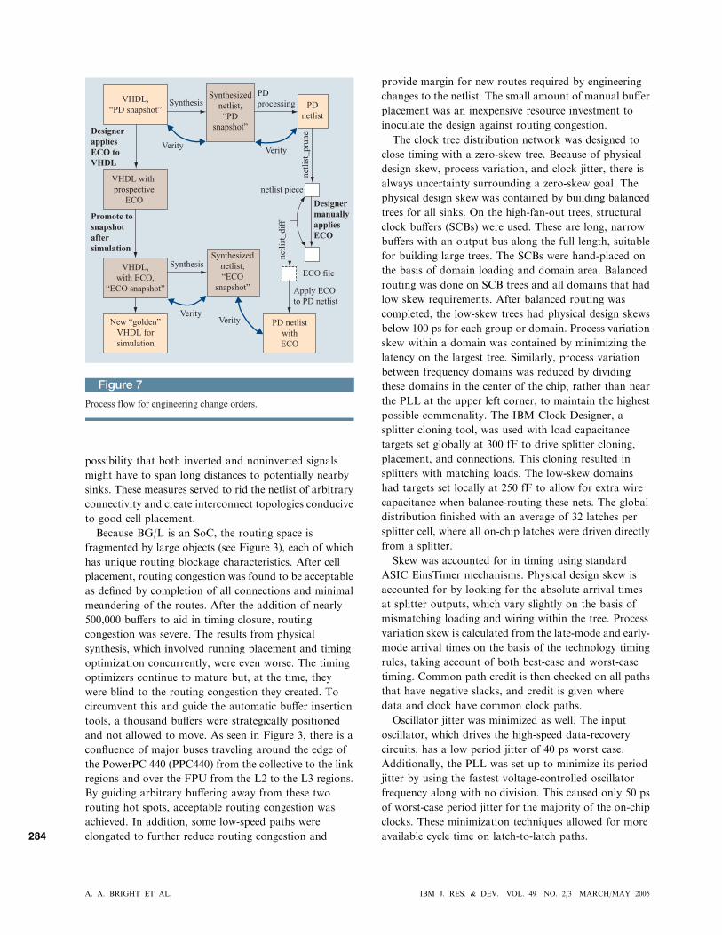
Figure 7
Process flow for engineering change orders.
Promote tosnapshotafter simulation
VHDL with prospective
ECO
VHDL,“PD snapshot”
Synthesizednetlist,“PD
snapshot”
PDnetlist
SynthesisPDprocessing
VHDL,with ECO,
“ECO snapshot”
Synthesizednetlist,“ECO
snapshot”
Synthesis
Verity
Verity
Verity
DesignerappliesECO toVHDL
netli
st_p
rune
DesignermanuallyappliesECO
netlist piece
netli
st_d
iff
Apply ECOto PD netlist
ECO file
PD netlistwithECO
VerityNew “golden”VHDL forsimulation
A. A. BRIGHT ET AL. IBM J. RES. & DEV. VOL. 49 NO. 2/3 MARCH/MAY 2005
284

Adding robustness in targeted areas can help protect
physical design schedules. On BG/L, our targeted areas
included enhanced power bus robustness, which avoided
rework as new substrate parasitics became available or
new analysis tools were added to the methodology.
Shielding and isolating of critical routes was performed.
Decoupling capacitors were added to reduce power-
supply noise near noise-generating and noise-sensitive
circuits, particularly around the hard cores and the
datapaths (see Figure 6), and were also added
ubiquitously into the chip.
Engineering changesAfter a chip design is frozen and released to physical
design, timing closure becomes the responsibility of the
physical design team. Timing fixes are inserted into
the physical design netlist by means of engineering
change orders, or ECOs. Logic bug fixes, including
fixes to solve self-test problems, may also be identified
and are handled by an extension of the same mechanism.
Figure 7 shows the process flow.
At the time the design is frozen, a ‘‘snapshot’’ is taken
that constitutes a definitive ‘‘golden’’ copy of the VHDL
and associated timing assertions and parameters. This
version of the design is the basis for simulation to verify
that it is functionally correct. The netlist provided to
physical design is synthesized from this snapshot. IBM
Verity is used to verify logical equivalence between the
VHDL and the pre-physical-design netlist, and between
the pre-physical-design and post-physical-design netlists.
When a logic bug is identified, the fix is applied to a
new working copy of the VHDL, which is simulated to
verify correctness. The new VHDL is then promoted
into a new snapshot, which becomes the new ‘‘golden’’
version. Concurrently, the physical design netlist is
updated manually as follows. The smallest portion of the
netlist that contains all of the logic requiring changes is
identified and pruned from the full netlist. The designer
makes the changes by editing the pruned section. A
command is run that compares the original and edited
versions of the pruned section and extracts the differences
into a file in a format that can be used to apply the
changes to the full physical design netlist. Verity is used in
two steps, as before, to verify that the new physical design
netlist is logically equivalent to the new ‘‘golden’’ VHDL.
This process provides a very manageable framework for
generating, tracking, and verifying ECOs.
ConclusionsThe Blue Gene/L chip is an advanced system-on-a-chip
design that placed new demands on the normal ASIC
methodology. Through careful floorplanning, an
innovative approach to timing closure, the use of custom-
placed datapath assemblies, and other novel physical
design techniques, the design challenges were successfully
met. The physical design integration was completed, and
chips were manufactured in a first-time-right manner
within the constraints of die size, routing, timing, and
schedule.
AcknowledgmentsThis work has benefited from the cooperation of many
individuals in IBM Research (Yorktown Heights, New
York), IBM Engineering and Technology Services
(Rochester, Minnesota), and IBM Microelectronics
(Burlington, Vermont). In particular, we thank Joel Earl,
Gay Eastman, Scott Mack, Craig Darsow, Adam Muff,
Bruce Winter, Don Eisenmenger, Cory Wood, Sean
Evans, Scott Bancroft, Todd Greenfield, Brian C. Wilson,
Daniel Beece, Dong Chen, Pavlos Vranas, Matthias
Blumrich, Laura Zumbrunnen, John Sheets, and Kurt
Carlsen. We also thank Greg Ulsh and Fariba
Kasemkhani for managing the implementation and
design release process of the BG/L chip.
The Blue Gene/L project has been supported and
partially funded by the Lawrence Livermore National
Laboratory on behalf of the United States Department of
Energy under Lawrence Livermore National Laboratory
Subcontract No. B517552.
*Trademark or registered trademark of International BusinessMachines Corporation.
References1. See http://www-3.ibm.com/chips/products/powerpc/cores/.2. C. D. Wait, ‘‘The PowerPC 440 FPU with Complex-
Arithmetic Extensions,’’ IBM J. Res. & Dev. 49, No. 2/3,249–254 (2005, this issue).
3. R. A. Haring, R. Bellofatto, A. A. Bright, P. G. Crumley,M. B. Dombrowa, S. M. Douskey, M. R. Ellavsky, B.Gopalsamy, D. Hoenicke, T. A. Liebsch, J. A. Marcella, andM. Ohmacht, ‘‘Blue Gene/L Compute Chip: Control, Test,and Bring-Up Infrastructure,’’ IBM J. Res. & Dev. 49, No. 2/3,289–301 (2005, this issue).
4. J. E. Barth, Jr., J. H. Dreibelbis, E. A. Nelson, D. L. Anand,G. Pomichter, P. Jakobsen, M. R. Nelms, J. Leach, and G. M.Belansek, ‘‘Embedded DRAM Design and Architecture forthe IBM 0.11-lm ASIC Offering,’’ IBM J. Res. & Dev. 46,No. 6, 675–689 (2002).
5. S. S. Iyer, J. E. Barth, Jr., P. C. Parries, J. P. Norum, J. P.Rice, L. R. Logan, and D. Hoyniak, ‘‘Embedded DRAM:Technology Platform for the Blue Gene/L Chip,’’ IBMJ. Res. & Dev. 49, No. 2/3, 333–350 (2005, this issue).
6. See http://www-3.ibm.com/chips/products/asics/products/cu-11.html.
7. N. R. Adiga, M. A. Blumrich, D. Chen, P. Coteus,A. Gara, M. E. Giampapa, P. Heidelberger, S. Singh,B. D. Steinmacher-Burow, T. Takken, M. Tsao, andP. Vranas, ‘‘Blue Gene/L Torus Interconnection Network,’’IBM J. Res. & Dev. 49, No. 2/3, 265–276 (2005, this issue).
8. See http://www-3.ibm.com/chips/products/asics/methodology/.9. L. Trevillyan, D. Kung, R. Puri, L. N. Reddy, and M. A.
Kazda, ‘‘An Integrated Environment for Technology Closureof Deep-Submicron IC Designs,’’ IEEE Design & TestComputers 21, No. 1, 14–22 (2004).
IBM J. RES. & DEV. VOL. 49 NO. 2/3 MARCH/MAY 2005 A. A. BRIGHT ET AL.
285

10. A. Kuehlmann, A. Srinivasan, and D. P. LaPotin, ‘‘Verity—A Formal Verification Program for Custom CMOS Circuits,’’IBM J. Res. & Dev. 39, No. 1/2, 149–165 (1995).
11. J. Schutz and C. Webb, ‘‘A Scalable X86 CPU Design for90nm Process,’’ IEEE International Solid-State CircuitsConference, Digest of Technical Papers, 2004, pp. 62–71.
12. P. Coteus, H. R. Bickford, T. M. Cipolla, P. G. Crumley, A.Gara, S. A. Hall, G. V. Kopcsay, A. P. Lanzetta, L. S. Mok,R. Rand, R. Swetz, T. Takken, P. La Rocca, C. Marroquin,P. R. Germann, and M. J. Jeanson, ‘‘Packaging the BlueGene/L Supercomputer,’’ IBM J. Res. & Dev. 49, No. 2/3,213–248 (2005, this issue).
13. P. J. Restle, T. G. McNamara, D. A. Webber, P. J.Camporese, K. F. Eng, K. A. Jenkins, D. H. Allen, M. J.Rohn, M. P. Quaranta, D. W. Boerstler, C. J. Alpert,C. A. Carter, R. N. Bailey, J. G. Petrovick, B. L. Krauter,and B. D. McCredie, ‘‘A Clock Distribution Network forMicroprocessors,’’ IEEE J. Solid-State Circuits 36, No. 5,792–799 (2001).
14. M. Ohmacht, R. A. Bergamaschi, S. Bhattacharya, A. Gara,M. E. Giampapa, B. Gopalsamy, R. A. Haring, D. Hoenicke,D. J. Krolak, J. A. Marcella, B. J. Nathanson, V. Salapura,and M. E. Wazlowski, ‘‘Blue Gene/L Compute Chip: Memoryand Ethernet Subsystem,’’ IBM J. Res. & Dev. 49, No. 2/3,255–264 (2005, this issue).
Received May 6, 2004; accepted for publicationJuly 19,
Arthur A. Bright IBM Research Division, Thomas J. WatsonResearch Center, P.O. Box 218, Yorktown Heights, New York10598 ([email protected]). Dr. Bright received B.A. and M.A.degrees in physics from Dartmouth College and a Ph.D. degree inphysics from the University of Pennsylvania. He previously workedat Union Carbide doing research on the properties of carbon fibers.He joined IBM in 1978, initially working on Josephson junctiontechnology and subsequently on plasma processing in silicontechnology. He served as president of the Thin Films Division ofthe American Vacuum Society from 1991 to 1992, and was on theeditorial board of the Journal of Vacuum Science and Technologyfrom 1992 to 1994. Upon becoming a circuit designer, he workedon custom microprocessor design and system-on-a-chip ASICs. In1999 Dr. Bright became involved in the Blue Gene/L project, wherehis focus has been on synthesis, timing, and physical design issues.He holds three patents.
Ruud A. Haring IBM Research Division, Thomas J. WatsonResearch Center, P.O. Box 218, Yorktown Heights, New York10598 ([email protected]). Dr. Haring is a Research Staff Memberat the IBM Thomas J. Watson Research Center. He received B.S.,M.S., and Ph.D. degrees in physics from Leyden University, theNetherlands, in 1977, 1979, and 1984, respectively. Upon joiningIBM in 1984, he initially studied surface science aspects of plasmaprocessing. Beginning in 1992, he became involved in electroniccircuit design on both microprocessors and application-specificintegrated circuits (ASICs). He is currently responsible for thesynthesis, physical design, and test aspects of the Blue Gene chipdesigns. Dr. Haring has received an IBM Outstanding TechnicalAchievement Award for his contributions to the z900 mainframe,and he holds several patents. His research interests include circuitdesign and optimization, design for testability, and ASIC design.Dr. Haring is a Senior Member of the IEEE.
Marc Boris Dombrowa IBM Research Division, Thomas J.Watson Research Center, P.O. Box 218, Yorktown Heights, NewYork 10598 ([email protected]). Mr. Dombrowa received hisDipl.-Ing. degree in electrical engineering from the University ofHannover, Germany, in 1997. He was a very large scale integration(VLSI) designer at the IBM VLSI Laboratory in Boeblingen,Germany, from 1997 to 1998, performing memory designverification and synthesis on S/390* Enterprise memory systems.From 1998 to 2000 he was assigned to the S/390 Server Division atthe IBM Poughkeepsie facility to perform custom circuit design.He moved to Blue Gene/L cellular systems chip developmentin 2001 and has been responsible for the high-level design,synthesis, timing, and verification of the test interfaceof the Blue Gene/L compute chips and design-for-testabilitytransformation for the entire chip, clock-tree verification, andsimulation setup for instruction program load for the chipverification teams. Mr. Dombrowa received an IBM OutstandingAchievement Award in 1998 for his S/390 contributions. He is co-inventor of one patent. His research interests include computerarchitecture, design for test, system bring-up, diagnostics, andASIC design. Mr. Dombrowa is currently working on themanufacturing diagnostic software and the system-level rackdiagnostic test suite and bring-up for the Blue Gene/L cluster.
Martin Ohmacht IBM Research Division, Thomas J. WatsonResearch Center, P.O. Box 218, Yorktown Heights, New York10598 ([email protected]). Dr. Ohmacht received his Dipl.-Ing. and Dr.-Ing. degrees in electrical engineering from theUniversity of Hannover, Germany, in 1994 and 2001, respectively.He joined the IBM Research Division in 2001 and has worked on
A. A. BRIGHT ET AL. IBM J. RES. & DEV. VOL. 49 NO. 2/3 MARCH/MAY 2005
286
2004; Internet publication March 31, 2005

memory subsystem architecture and implementation for the BlueGene project. His research interests include computer architecture,design and verification of multiprocessor systems, and compileroptimizations.
Dirk Hoenicke IBM Research Division, Thomas J. WatsonResearch Center, P.O. Box 218, Yorktown Heights, New York10598 ([email protected]). Mr. Hoenicke received a Dipl.Inform. (M.S.) degree in computer science from the Universityof Tuebingen, Germany, in 1998. Since then, he has worked on awide range of aspects of two prevalent processor architectures:ESA/390 and PowerPC. He is currently a member of the CellularSystems Chip Development Group, where he focuses on thearchitecture, design, verification, and implementation of the BlueGene system-on-a-chip (SoC) supercomputer family. In particular,he was responsible for the architecture, design, and verificationeffort of the collective network and defined and implementedmany other parts of the BG/L ASIC. Mr. Hoenicke’s areasof expertise include high-performance computer systems andadvanced memory and network architectures, as well as power-,area-, and complexity-efficient logic designs.
Sarabjeet Singh IBM Research Division, Thomas J. WatsonResearch Center, P.O. Box 218, Yorktown Heights, New York10598 ([email protected]). Mr. Singh is a Senior Research andDevelopment Engineer with the Engineering and TechnologyServices Division of IBM, currently on assignment at the IBMThomas J. Watson Research Center. He received a B.Tech. degreein electrical engineering from the Indian Institute of Technologyin 1996 and subsequently joined IBM, where he has worked onvarious research projects involving all aspects of ASIC and system-on-a-chip (SoC) design. Over the past seven years he has workedon many CMOS technologies (Blue Gene/L in Cu-11 technology),up to 700-MHz clock designs, asynchronous logic design, andSmall Computer System Interface (SCSI) drive controllers to HPCsystems. Mr. Singh is currently working on memory subsystemmicroarchitecture for an HPC system based on the STI cell.
James A. Marcella IBM Engineering and TechnologyServices, 3605 Highway 52 N., Rochester, Minnesota 55901([email protected]). Mr. Marcella is a Senior Engineerworking in the area of custom and system-on-a-chip designand implementation. His primary interest is in symmetricmultiprocessor (SMP) memory subsystem design. He joined IBMin 1980 after receiving his B.S.E.E. degree from the University ofMinnesota. He has received three IBM Outstanding TechnicalAchievement Awards for his work on memory controller designsfor the iSeries*, pSeries*, and xSeries* servers. Mr. Marcella has 11issued U.S. patents and 19 published disclosures.
Robert F. Lembach IBM Engineering and TechnologyServices, 3605 Highway 52 N., Rochester, Minnesota 55901([email protected]). Dr. Lembach is a Senior Technical StaffMember. He received a B.S. degree in electrical engineering summacum laude from Marquette University in 1975, and M.S. andPh.D. degrees in electrical engineering from Carnegie MellonUniversity in 1976 and 1979, respectively. He has led the physicalimplementation of several hundred chip designs since joining IBM,for both IBM clients and chips in the IBM zSeries*, iSeries,pSeries, and xSeries systems. Dr. Lembach has received three IBMOutstanding Technical Achievement Awards and an IBM
Invention Achievement Award. He is past chairman of the IBMElectronics Design Automation Interdivisional Technical Liaisonand a member of Eta Kappa Nu, Tau Beta Pi, and Alpha SigmaNu. He is currently working on the physical design for SoCs.
Steven M. Douskey IBM Engineering and TechnologyServices, 3605 Highway 52 N., Rochester, Minnesota 55901([email protected]). Mr. Douskey is a Senior Engineer. Hejoined the Advanced Systems Development Group in 1982 afterreceiving a B.S.E.E. degree from the University of Nebraska. Heis the team leader and architect for built-in self test (BIST) andsystem diagnostics structures on numerous IBM projects, recentlyincluding Blue Gene, Netfinity, and eSeries designs. Past IBMassignments have included AS/400* design for test (DFT), AS/400problem analysis and resolution (PAR), AS/400 processor busadapter interface hardware, and System/38* processor channelinterface hardware. Mr. Douskey holds 11 U.S. patents and haspublished 23 technical disclosures.
Matthew R. Ellavsky IBM Engineering and TechnologyServices, 3605 Highway 52 N., Rochester, Minnesota 55901([email protected]). Mr. Ellavsky received his B.S. degree inelectrical engineering from the University of Minnesota. He joinedthe IBM Server Group in 1999, and is currently a member of theEngineering and Technology Services organization. For the pastfive years Mr. Ellavsky has focused on clock distribution networksand clock control logic for a wide array of ASIC chips.
Christian G. Zoellin IBM Systems and Technology Group,IBM Deutschland Entwicklung GmbH, Schoenaicherstrasse 220,71032 Boeblingen, Germany ([email protected]). Mr. Zoellinreceived a Vordiplom degree in electrical engineering from theUniversity of Stuttgart in 2001. He joined IBM in 2002 at the IBMBoeblingen Development Laboratory as a co-op, and participatedin the Blue Gene project as a summer student at the IBM ThomasJ. Watson Research Center. Mr. Zoellin is currently working on hismaster’s thesis at IBM Boeblingen, focusing on logic built-in selftest (BIST) power reduction.
Alan Gara IBM Research Division, Thomas J. Watson ResearchCenter, P.O. Box 218, Yorktown Heights, New York 10598([email protected]). Dr. Gara is a Research Staff Member atthe IBM Thomas J. Watson Research Center. He received hisPh.D. degree in physics from the University of Wisconsin atMadison in 1986. In 1998 Dr. Gara received the GordonBell Award for the QCDSP supercomputer in the most cost-effective category. He is the chief architect of the Blue Gene/Lsupercomputer. Dr. Gara also led the design and verification of theBlue Gene/L compute ASIC as well as the bring-up of the BlueGene/L prototype system.
IBM J. RES. & DEV. VOL. 49 NO. 2/3 MARCH/MAY 2005 A. A. BRIGHT ET AL.
287