Beam secondary shower acquisition design for the CERN ...
225
CERN-THESIS-2018-172 12/12/2018 Beam secondary shower acquisition design for the CERN high accuracy wire scanner Memoria presentada para optar al grado de Doctor por la Universidad de Barcelona Programa de Doctorado en Ingeniería y Ciencias Aplicadas Autor: Jose Luis Sirvent Blasco Directores: Dr. Bernd Dehning Dr. Federico Roncarolo Tutor: Dr. Ángel Diéguez Barrientos Departamento de Electrónica y Bioingeniería Facultad de Física, Universidad de Barcelona Septiembre 2018
-
Upload
khangminh22 -
Category
Documents
-
view
2 -
download
0
Transcript of Beam secondary shower acquisition design for the CERN ...

CER
N-T
HES
IS-2
018-
172
12/1
2/20
18
Beam secondary shower acquisitiondesign for the CERN high accuracy
wire scanner
Memoria presentada para optar al grado deDoctor por la Universidad de Barcelona
Programa de Doctorado en Ingeniería y Ciencias Aplicadas
Autor:Jose Luis Sirvent Blasco
Directores:Dr. Bernd Dehning
Dr. Federico Roncarolo
Tutor:Dr. Ángel Diéguez Barrientos
Departamento de Electrónica y BioingenieríaFacultad de Física, Universidad de Barcelona
Septiembre 2018

2

3
Abstract
The LHC injectors upgrade (LIU) project aims to boost the LHC luminosity by doublingthe beam brightness with the construction of the new LINAC4, the first linear accelerator onthe LHC chain. The brighter beams require upgrades on the full injector chain to deliver lowemittance beams for the future High-Luminosity LHC (H-LHC). Thus, new and more precisebeam instrumentation is under development to operate on this new scenario. These upgradesinclude the development of a new beam wire scanners generation (LIU-BWS), interceptivebeam profile monitors used for the beam emittance calculation. Wire scanners determine thetransverse beam profile by crossing a carbon wire (30 µm) through the particle beam. Thebeam profile is inferred from the intensity of the shower of secondary particles, scattered frombeam-wire interaction, and the wire position.
The current BWS generation features high operational complexity and its performanceis partly limited by their secondary shower detectors and acquisition systems. They are tra-ditionally based on scintillators attached to a Photo-Multiplier tube (PMT) through opticalfilters. These detectors require tuning according to the beam energy and intensity prior to ameasurement to not saturate the readout electronics, located on the surface buildings. Underthese circumstances, many configurations lead to a poor SNR and very reduced resolution,directly affecting the measurement reliability. In addition, bunch-by-bunch profile measure-ments are degraded by the use of long coaxial lines, which reduce the system bandwidthleading to bunch pile-up.
This thesis covers the design of an upgraded secondary shower acquisition system forthe LIU-BWS. This includes the study of a novel detector technology for BWS, based onpolycrystalline Chemical Vapour Deposited (pCVD) diamond, and the implementation oftwo acquisition system prototypes.
This work reviews operational acquisition systems to identify their limitations and showsadvanced particle physics simulations with FLUKA for better understanding of the secondaryparticles shower behaviour around the beam pipe. Simulations, along with a study of thedifferent beams in each machine, leaded to the estimation of the required dynamics per ac-celerator, and an optimised placement of the upgraded detectors.
To cope with the injectors working points, the acquisition systems implemented performedhigh dynamic range signal acquisition and digitisation in the tunnel with a radiation-hardfront-end nearby the detector, digital data is afterwards transmitted to the counting roomthrough a 4.8Gbps optical link. This novel schema not only allowed low-noise measurements,but also avoided the bandwidth restrictions imposed by long coaxial lines, and greatly sim-plified the scanner operation.
The upgraded design investigates two approaches to cover a dynamic of about 6 orders ofmagnitude: a single-channel system, with logarithmic encoding, and a multi-channel system,with different gains per channel. Prototypes of both schemes were fully developed, char-acterised on laboratory and successfully tested on SPS and PSB under different operatingconditions.
The evaluation of the acquisition systems during beam tests allowed the study of the LIU-BWS mechanical performance and comparative the measurements with operational systems.
pCVD diamond detectors, with a typical active area of 1cm2, were systematically evaluatedas BWS detectors. This document analyses the results from several measurement campaignson SPS over its energy and intensity boundaries (5 · 109− 1.1 · 1011 protons per bunch and 26- 450 GeV). The SPS results suggest a potential application on LHC beam wire scanners.

4

5
Acknowledgements
This thesis wouldn’t have been possible without the help, advice, collaboration and supportof many people who directly or indirectly have contributed on its development.
Firstly I’d like to express my gratitude to Bernd Dehning, he gave me the opportunityto join CERN as a engineering technical student, on the BE-BI-BL section, and trusted meas doctoral student to undertake this project. Tireless and friendly supervisor, he always hada gap for discussions and was willing to help on the accelerators interventions independentlyof his work load. His wise advice and support were essential in many points of this thesis.Unfortunately, Bernd passed away during the thesis development.
A very special thanks goes to Federico Roncarolo, who kindly took over the projectsupervision and the revision of this document. He welcomed me on the BE-BI-PM sectionand followed closely the progress of this theis always with good suggestions. A great thanksto Angel Dieguez for accepting the academic supervision of this work and being my linkwith the University of Barcelona, I really appreciate his help with the university paperwork,which eased a lot the development of a thesis done abroad.
Everyday work wouldn’t be the same without the implication of many colleagues fromBE-BI-PM and BE-BI-BL, that in some way are a source of inspiration. Thanks JonathanEmery who followed the project very closely and always provided good advice (and sugges-tions to improve the quality of the research carried out), also to Patrik Samuelsson for hishelp on installations and to Georges Trad for his great ideas and visits to my office. Lotsof thanks to Sune Jacobsen for his help on the detectors design and construction, I had thechance to learn a lot from our conversations. Many thanks to Emiliano Piselli, without himmany of the first measurements wouldn’t had been possible, he operated wire scanners untilvery late in the night for data taking. In general, I would like to thank all members of bothsections (PM and BL) who really made me feel like at home from the very first day and madedaily work a delight.
Many thanks to Tullio Grassi and Stephen Groadhouse from CMS for their collabo-ration on the GBT implementation on Igloo2 FPGAs, it was great to work with them. Here,I would like to acknowledge as well Manoel Barros and Sophie Baron for their adviceduring our long conversations about the GBT code migration and constant support.
I had the opportunity to contact some institutes in search of collaboration, I want to thankProf. Ulrich Heintz and his Fermilab contacts for providing some QIE10 samples, also toEduardo Picatoste and David Gascon the ICECAL designers, and my link with theLHCb collaboration. They kindly provided ICECAL samples and received me as a memberof their team while fixing of one of the ICECAL mezzanine boards in the UB.
I’d like to thank Raymond Veness, William Andreazza, Dmitry Gudkov andMorad Hamani from BE-BI-ML for their commitment on the procurement of mechanicalcomponents required for the detectors construction and their advice for its installation.
On the personal side, my biggest thanks goes to my girlfriend Angela, companion duringthis adventure working at CERN, who did not hesitated in being with me from the very firstday (and it’s been 7 years since then...). She was always there on those frustrating periodscheering me and and giving the extra kick (many actually) of motivation needed to completethis document. I need to thank her infinite patience in the difficult task of living with agrumpy doctoral student. I also appreciate a lot her help formatting in LATEXa big part ofthe present document. But above all, thanks for that smile and her daily complicity.
I couldn’t forget to acknowledge my parents who, during my lifetime, gave me the valuesand encouraged me to give the best of myself when facing a challenge, they always provideunconditional support no matter the distance. Finally, a big thanks goes to all those relatives(Angela’s and mine) and friends who supported me during the project.

6

Contents
Abstract 2
Acknowledgements 4
1. Introduction 111.1. LHC and injectors chain . . . . . . . . . . . . . . . . . . . . . . . . . . . . . . 121.2. Accelerator physics overview . . . . . . . . . . . . . . . . . . . . . . . . . . . . 14
1.2.1. Particle accelerator basic concepts . . . . . . . . . . . . . . . . . . . . 141.2.2. Transverse beam dynamics . . . . . . . . . . . . . . . . . . . . . . . . 161.2.3. Transverse emittance and beam size . . . . . . . . . . . . . . . . . . . 18
1.2.3.1. Momentum spread . . . . . . . . . . . . . . . . . . . . . . . . 191.2.4. Luminosity . . . . . . . . . . . . . . . . . . . . . . . . . . . . . . . . . 20
1.3. Transverse beam profile monitors . . . . . . . . . . . . . . . . . . . . . . . . . 201.3.1. Non-Interceptive devices . . . . . . . . . . . . . . . . . . . . . . . . . . 211.3.2. Interceptive devices . . . . . . . . . . . . . . . . . . . . . . . . . . . . . 22
2. CERN beam wire scanners and upgrade programme 252.1. Operational systems . . . . . . . . . . . . . . . . . . . . . . . . . . . . . . . . 252.2. Mechanical designs . . . . . . . . . . . . . . . . . . . . . . . . . . . . . . . . . 252.3. Wire scanners calibration . . . . . . . . . . . . . . . . . . . . . . . . . . . . . 262.4. Operational secondary particles acquisition system . . . . . . . . . . . . . . . 282.5. Ugrade motivations . . . . . . . . . . . . . . . . . . . . . . . . . . . . . . . . . 30
2.5.1. Mechanical point of view . . . . . . . . . . . . . . . . . . . . . . . . . . 302.5.2. Secondaries acquisition system point of view . . . . . . . . . . . . . . . 31
2.6. LIU-BWS Design . . . . . . . . . . . . . . . . . . . . . . . . . . . . . . . . . . 322.6.1. Optical position sensor . . . . . . . . . . . . . . . . . . . . . . . . . . . 33
2.6.1.1. Optical signal stability . . . . . . . . . . . . . . . . . . . . . . 342.6.1.2. Resolution and accuracy . . . . . . . . . . . . . . . . . . . . . 352.6.1.3. On-axis self-calibration and performance . . . . . . . . . . . 37
2.6.2. Performance on calibration bench . . . . . . . . . . . . . . . . . . . . . 38
3. Radiation detection in high energy physics 413.1. The passage of particles through matter . . . . . . . . . . . . . . . . . . . . . 41
3.1.1. Heavy charged particles . . . . . . . . . . . . . . . . . . . . . . . . . . 413.1.2. Electrons and Positrons . . . . . . . . . . . . . . . . . . . . . . . . . . 423.1.3. Fluctuations on energy loss . . . . . . . . . . . . . . . . . . . . . . . . 44
3.2. Light based detectors . . . . . . . . . . . . . . . . . . . . . . . . . . . . . . . . 443.2.1. Organic scintillators . . . . . . . . . . . . . . . . . . . . . . . . . . . . 443.2.2. Inorganic scintillators . . . . . . . . . . . . . . . . . . . . . . . . . . . 453.2.3. Cherenkov detectors . . . . . . . . . . . . . . . . . . . . . . . . . . . . 473.2.4. Photon detection systems . . . . . . . . . . . . . . . . . . . . . . . . . 48
3.2.4.1. Photo-Multiplier tubes (PMT) . . . . . . . . . . . . . . . . . 483.2.4.2. Hybrid Photo-Detectors (HPD) . . . . . . . . . . . . . . . . . 49
7

8 CONTENTS
3.2.4.3. Solid state photo detectors . . . . . . . . . . . . . . . . . . . 503.3. Solid state particle detectors theory . . . . . . . . . . . . . . . . . . . . . . . . 50
3.3.1. Semiconductor detectors . . . . . . . . . . . . . . . . . . . . . . . . . . 523.3.2. Diamond detectors . . . . . . . . . . . . . . . . . . . . . . . . . . . . . 54
3.3.2.1. Signal formation . . . . . . . . . . . . . . . . . . . . . . . . . 543.3.2.2. Pumping effect and polarisation . . . . . . . . . . . . . . . . 563.3.2.3. Radiation hardness . . . . . . . . . . . . . . . . . . . . . . . . 573.3.2.4. Diamond detectors in high energy physics . . . . . . . . . . . 58
4. Beam wire scanner acquisition system studies 614.1. Beams characteristics on the LHC and injector chain . . . . . . . . . . . . . . 61
4.1.1. Beam distributions on the profile monitor locations . . . . . . . . . . . 614.1.2. The LHC Injectors Upgrade (LIU) program and HL-LHC beams . . . 71
4.2. Secondary particles shower simulations . . . . . . . . . . . . . . . . . . . . . . 724.2.1. Proton Synchrotron Booster (PSB) . . . . . . . . . . . . . . . . . . . . 744.2.2. Proton Synchrotron (PS) . . . . . . . . . . . . . . . . . . . . . . . . . 774.2.3. Super Proton Synchrotron (SPS) . . . . . . . . . . . . . . . . . . . . . 794.2.4. Large Hadron Collider (LHC) . . . . . . . . . . . . . . . . . . . . . . . 81
4.3. Beam profile signal degradation on long transmission lines . . . . . . . . . . . 834.3.1. Transmission lines theory overview . . . . . . . . . . . . . . . . . . . . 834.3.2. Loses on transmission lines . . . . . . . . . . . . . . . . . . . . . . . . 844.3.3. Coaxial cable CK50 parametrisation . . . . . . . . . . . . . . . . . . . 854.3.4. Impact of long cables on bunch-by-bunch beam profiles . . . . . . . . . 864.3.5. Models validation and CK50 cable measurements . . . . . . . . . . . . 89
4.3.5.1. Frequency analysis . . . . . . . . . . . . . . . . . . . . . . . . 894.3.5.2. Temporal analysis . . . . . . . . . . . . . . . . . . . . . . . . 904.3.5.3. Pick-up noise . . . . . . . . . . . . . . . . . . . . . . . . . . . 93
4.4. Error sources on beam profile determination . . . . . . . . . . . . . . . . . . . 944.4.1. Considerations . . . . . . . . . . . . . . . . . . . . . . . . . . . . . . . 944.4.2. Simulation algorithm . . . . . . . . . . . . . . . . . . . . . . . . . . . . 974.4.3. Simulation results . . . . . . . . . . . . . . . . . . . . . . . . . . . . . 98
4.4.3.1. Imaging systems . . . . . . . . . . . . . . . . . . . . . . . . . 984.4.3.2. Wire Scanners . . . . . . . . . . . . . . . . . . . . . . . . . . 99
5. Secondary shower acquisition system design 1035.1. Acquisition system architecture . . . . . . . . . . . . . . . . . . . . . . . . . . 103
5.1.1. Electronics exposure to radiation . . . . . . . . . . . . . . . . . . . . . 1045.1.2. The VME FMC Carrier Board (VFC) and GBT-Based Expandable
Front-End (GEFE) . . . . . . . . . . . . . . . . . . . . . . . . . . . . . 1055.1.3. Readout ASICs . . . . . . . . . . . . . . . . . . . . . . . . . . . . . . . 106
5.1.3.1. QIE10 . . . . . . . . . . . . . . . . . . . . . . . . . . . . . . . 1065.1.3.2. ICECAL V3 . . . . . . . . . . . . . . . . . . . . . . . . . . . 109
5.1.4. Radiation Hard Optical Link . . . . . . . . . . . . . . . . . . . . . . . 1115.1.4.1. The GBT frame . . . . . . . . . . . . . . . . . . . . . . . . . 111
5.2. Proof-of-concept prototypes . . . . . . . . . . . . . . . . . . . . . . . . . . . . 1125.2.1. Front-End implementation . . . . . . . . . . . . . . . . . . . . . . . . . 113
5.2.1.1. The GBT core on an Igloo2 Flash-Based FPGA . . . . . . . 1145.2.1.2. QIE10 mezzanine board . . . . . . . . . . . . . . . . . . . . . 1295.2.1.3. ICECAL V3 mezzanine board . . . . . . . . . . . . . . . . . 130
5.2.2. Back-End implementation . . . . . . . . . . . . . . . . . . . . . . . . . 1315.2.2.1. Firmware organisation . . . . . . . . . . . . . . . . . . . . . . 1325.2.2.2. Memory mapping and storage capabilities . . . . . . . . . . . 1345.2.2.3. Expert application . . . . . . . . . . . . . . . . . . . . . . . . 134

CONTENTS 9
6. Laboratory evaluation and beam test results 1376.1. Front-End prototypes laboratory evaluation . . . . . . . . . . . . . . . . . . . 137
6.1.1. QIE10 Front-End . . . . . . . . . . . . . . . . . . . . . . . . . . . . . . 1376.1.2. ICECAL V3 Front-End . . . . . . . . . . . . . . . . . . . . . . . . . . 139
6.1.2.1. ICECAL V3 Preliminary testing . . . . . . . . . . . . . . . . 1396.1.3. Performance Test ICECAL V3 and AD41240 Readout . . . . . . . . . 1406.1.4. Performance Test ICECAL V3 and AD6645 Readout . . . . . . . . . . 142
6.2. Diamond detector and acquisition system tests with beam . . . . . . . . . . . 1456.2.1. Diamond detector set-up and tests on laboratory . . . . . . . . . . . . 1456.2.2. Test with an operational linear beam wire scanner in SPS . . . . . . . 146
6.2.2.1. Installation in SPS tunnel and test set-up . . . . . . . . . . . 1466.2.2.2. Loses detection . . . . . . . . . . . . . . . . . . . . . . . . . . 1476.2.2.3. Diamond detectors tests with nominal intensity beams at 26
GeV . . . . . . . . . . . . . . . . . . . . . . . . . . . . . . . 1496.2.2.4. QIE10 FE and diamonds performance for different beam in-
tensities (450GeV) . . . . . . . . . . . . . . . . . . . . . . . . 1516.2.2.5. QIE10 FE and diamonds performance for different beam en-
ergies (1e11 PpB) . . . . . . . . . . . . . . . . . . . . . . . . 1546.2.3. Tests with a pre-series LIU beam wire scanner prototype . . . . . . . . 156
6.2.3.1. Detector system assembly . . . . . . . . . . . . . . . . . . . . 1576.2.3.2. Lead Ions beam profile measurements with diamonds . . . . 1596.2.3.3. SPS LIU-BWS prototype performance and comparison with
operational systems . . . . . . . . . . . . . . . . . . . . . . . 1616.2.3.3.1. COAST Beam #1: . . . . . . . . . . . . . . . . . . . 1616.2.3.3.2. AWAKE Beam: . . . . . . . . . . . . . . . . . . . . . 1666.2.3.3.3. COAST Beam #2: . . . . . . . . . . . . . . . . . . . 169
6.2.4. Conclusions on diamond detectors for secondary shower detection . . . 1716.2.5. Conclusions QIE10 Front End operation . . . . . . . . . . . . . . . . . 173
6.3. Multi-PMT detector and ICECAL FE tests in the PSB . . . . . . . . . . . . . 1746.3.1. Scintilator light yield estimations and Multi-PMT system construction 1756.3.2. Photo-Multipliers characterisation . . . . . . . . . . . . . . . . . . . . 1796.3.3. Beam Tests with LHC 25ns and ISOLDE beams . . . . . . . . . . . . 182
6.3.3.1. Scanners beam width measurement precision comparison . . 1826.3.3.2. ICECAL V3 front-end acquisitions . . . . . . . . . . . . . . . 184
6.3.4. Impact of scintillator geometry . . . . . . . . . . . . . . . . . . . . . . 188
7. Conclusions and Outlook 1937.1. Conclusions . . . . . . . . . . . . . . . . . . . . . . . . . . . . . . . . . . . . . 1937.2. Outlook . . . . . . . . . . . . . . . . . . . . . . . . . . . . . . . . . . . . . . . 195
A. Appendix: Resumen en Español 197A.1. Beam wire scanners en el CERN y su actualización . . . . . . . . . . . . . . . 198A.2. Estimación del rango dinámico y consideraciones de diseño . . . . . . . . . . . 200A.3. Diseño del sistema de adquisición de partículas secundarias . . . . . . . . . . 205A.4. Evaluación en laboratorio y pruebas con haz . . . . . . . . . . . . . . . . . . . 209A.5. Conclusiones . . . . . . . . . . . . . . . . . . . . . . . . . . . . . . . . . . . . 215

10 CONTENTS

Chapter 1
Introduction
CERN, the European Organisation for Nuclear Research (Conseil Europèen pour la RechercheNucléaire, in french), located in the Franco-Swiss border near Geneva is one of the leadinginstitutes in particle physics worldwide. It was founded in 1954 with the mandate of estab-lishing a world-class fundamental physics research organisation in Europe. This was one ofthe Europe’s first joint ventures, originally founded with 12 countries nowadays it counts with22 member states. Since its foundation it has been an example of international collabora-tion and has achieved major contributions to fundamental questions of physics, including theremarkable discovery of the Higgs-Bosson announced on July 2012.
CERN provides the particle accelerators and other infrastructures required for high energyphysics research, including its flagship accelerator, the Large Hadron Collider (LHC), thelargest accelerator ever built with 27Km of circumference, which lies 100 metres underground.The LHC is designed to provide high energy (7TeV) protons or heavy ions collisions on itsinteraction points, where the experiments ATLAS, CMS, LHCb and ALICE are located. Thepurpose of the LHC and its experiments is to analyse the products of the collisions in orderto answer unresolved fundamental particle physics questions such as the determination of theprimary building blocks of the matter and the origin of the particles mass.
The CERN accelerator complex (see Fig.1.1) counts with several linear and circular accel-erators employed to gradually accelerate the particles prior to injection on the LHC. These arethe linears LINAC2, LINAC3 and soon LINAC4, and circulars Low Energy Ion Ring (LEIR),Proton Synchrotron Booster (PSB), Protron Synchrotron (PS) and Super Proton Synchrotron(SPS).
The injector chain apart of feeding the LHC is also used to deliver particles to a numberof other experiments carried out at CERN, including:
Antimatter research with experiments hosted on the Antiproton Decelerator (AD) andExtra Low ENergy Antiproton (ELENA) decelerator rings.
Radioactive ion beams research with experiments hosted on the Isotope Separator On-Line Device (ISOLDE).
Research on neutron-nucleus interaction for a wide range of neutron energies on theNeutron Time-of-Flight (N_TOF) facility.
Research on radiation induced damage on materials in the High-radiation to Materials(HiRadMat) facility.
Study on the use of proton-driven plasma wakefields for charged particles accelerationin the Advanced WAKefield Experiment (AWAKE).
11

12 CHAPTER 1. INTRODUCTION
Figure 1.1 – LHC injector chain and experiments at CERN [1].
1.1. LHC and injectors chain
In order to reach the nominal collision energies at LHC, the proton beam must travelthroughout the injector chain progressively acquiring energy. This chain is comprised by theLINAC2, PSB, PS, SPS and finally the LHC itself. This section describes the different stagesof the proton acceleration for a standard 25 ns LHC fill [2].
The proton source consists in hydrogen gas injected into a plasma chamber. A strongelectric field ionises the gas atoms and strips off its electrons, leaving only protons at 100KeVto enter the LINAC2 accelerator.
LINAC2 is an 80m long linear accelerator that compresses the protons into packets oftenlabeled as "bunches" and accelerates them to 50MeV kinetic energy, at this point particlestravel at about one third of the speed of light (c). LINAC2 delivers high intensity protonbunches to the first circular accelerator, the PSB.
The PSB is the first, and smallest, circular accelerator at CERN (50m diameter) and it iscomposed by four superimposed synchrotron rings. The particle bunches are accelerated from50MeV to 1.4GeV (91.6% of c). This process lasts about 530ms and the beam revolutionperiod varies from 1 µs to 0.6 µs. Each PSB ring is capable of hosting up to 2 bunches, meaningthat up to 8 bunches can be accelerated simultaneously. For a nominal LHC filling only 3rings are used, a total of 6 PSB bunches. All the 4 rings can be operated in parallel for otherLHC filling schemes or to feed the ISOLDE experiments.
The protons are then transferred to the PS (628m of circumference) and accelerated upto an energy of 26 GeV (99.9% of c). During the energy ramp in the PS, the particles undergothe so-called "γ-transition", after which the added energy on the protons by the acceleratingelectrical field is not translated into increase of velocity but into an increase of mass.

1.1. LHC AND INJECTORS CHAIN 13
Throughout different RF cavities manipulations, the 6 long and high intensity PSB bunchesare split into 72 shorter and lower intensity bunches, thus defining the ultimate LHC longi-tudinal structure with 25 ns bunch spacing. The PS cycle and RF manipulations take about1.1 s. Once the beam reaches the extraction energy, it is transferred to the SPS for furtherenergy increase. When not serving the SPS, the PS can deliver beams to the EAST area,n_TOF and AD.
The SPS is the second largest machine in the CERN accelerator complex with nearly7Km of circumference. It requires 4 PS injections of 72 bunches to accumulate 288 bunchesin the ring, each injection corresponds to a batch (group of bunches). Once completed, the26GeV beams are then accelerated to the LHC injection energy (450GeV), during 4.3 s. Atthis point particles are highly relativistic, the nominal 23µs revolution period on this machineonly varies by 800 parts per million (ppm) during the cycle. The beam is delivered to the LHCthrough two different transfer lines that allow to fill each of the LHC rings in clockwise andanticlockwise direction. In the past, the SPS was used as a proton/anti-protons collider and aselectrons/positrons injector for the Large Electron Positron collider (LEP). Nowadays, apartfrom feeding the LHC, it is used to deliver beams to the North Area fix target experiments,to the HiRadMat facility and to the AWAKE experiment.
A nominal LHC fill consists of 39 batches of 72 bunches each (a total of 2808 bunches perring), that corresponds to 12 SPS injections according to the 234 334 334 334 schema shown onFig. 1.2. The LHC filling can take more than 30 minutes. Afterwards, the LHC itself providesthe last energy boost, accelerating the beam in each ring from 450GeV up to its top energy(6.5TeV today, the design 7TeV is expected to be reached in 2020). After a short period attop energy necessary to prepare the LHC optics parameters and the LHC experiments, theLHC collision physics starts and the experiments record data. If not stopped by unexpectedaccelerator faults, the physics period is kept as long as considered efficient, which depends onmany factors, like the beam intensity deterioration by the collisions themselves (also namedburnout).
Figure 1.2 – Nominal LHC filling with 25ns separation bunches [2].
The LHC operates in "Runs" lasting several years. During a Run, and on the long shutdown periods (1-2 years) that are normally scheduled between runs, the LHC and the injectorssmoothly increase their performance. During Run 1 (2010-2013), the LHC was operated onlyup to 3.5 and 4TeV (being 7TeV the design top energy), with bunch spacing decreasing

14 CHAPTER 1. INTRODUCTION
from 150 to 50 ns (w.r.t the nominal design for 25 ns). Despite this, the LHC achieved manyrecords, in terms of maximum beam intensity, energy stored and luninosity, never reached inthe world before. The Run 1 yielded to the historical discovery of the Higgs boson and to thefirst measurement of its mass, around 126GeV, consistent with the Standard Model.
During the first long shutdown (LS1 2013-2014), intended for maintenance and consoli-dation, the accelerators were prepared to reach 6.5TeV per beam, thus for collisions at theunprecedented energy of 13TeV, and for operation at the nominal 25ns bunch structure. Run2 (2015-2018) opens a new frontier for high energy physics research, where the LHC keepsaccumulating records. The 26th June 2016 the LHC reached its design luminosity for thefirst time in a fill that was kept on the machine during 37 hours. Table 1.1 shows how keyparameters of the LHC accelerator now approach the design values.
Table 1.1 – Overview of the LHC performance parameters during the LHC Run 1 and 2
Parameter 2011 2012 2015 2016 DesignBeam Energy [TeV] 3.5 4 6.5 6.5 7Bunch Spacing [ns] 150 75/50 50 25 25β∗ IP [m] 1.5/1.0 0.6 0.8 0.4 0.55ε∗ at Injection [mm mrad] 2.4 2.5 3.5 2.0 3.75Bunch Population [1010 p/bunch] 1.45 1.6 1.15 1.15 1.15Max num of bunches 1380 1380 2244/2232 2220/2208 2808Max Stored Energy [MJ] 110 140 270 265 362Peak Luminosity [cm−2s−1] 3.7 · 1033 7.7 · 1033 5 · 1033 1.4 · 1034 1034
1.2. Accelerator physics overview
1.2.1. Particle accelerator basic concepts
The acceleration and guiding (bending and focusing) of a particle beam in High EnergyPhysics (HEP) is in first instance governed by the Lorentz force experienced by chargedparticles travelling through electromagnetic fields. Lorentz law is expressed as on Eq. 1.1:
~F = q[ ~E + (~v × ~B)] (1.1)
where q is the charge of a particle with velocity ~v passing through an electric field ~E anda magnetic field ~B.
The first term in the equation correspond to the effect of the electric field, providingacceleration, and the second to the magnetic force, providing bending or focusing.
A charged particle, with a defined initial velocity, in the presence of a magnetic fieldperpendicular to the velocity itself, experiences a transverse kick, while keeping its tangentialvelocity unchanged. This principle is used in particle accelerators to guide and contain particlebeams around a reference trajectory. A practical example of this principle are cyclotrons,where the circular trajectory of the particles is defined by a well controlled perpendicularmagnetic field (see Fig. 1.3). Cyclotrons accelerate their beams through the application ofan alternating electric field in synchronisation with the particles passage in-between its twoD shaped sectors. As a consequence, particles acquire kinetic energy and become heavier,thus requiring of a stronger magnetic field to keep a circular trajectory. This effect is usedin cyclotrons to make particles travel in spiral as they acquire energy until they reach theextraction point.

1.2. ACCELERATOR PHYSICS OVERVIEW 15
Figure 1.3 – Cyclotron working principle [3].
In larger circular accelerators, such as those at CERN, the particles acceleration is providedby RF cavities, whereas dipoles and quadruples guide and confine the beam through a referenceorbit.
RF cavities are a series of hollow structures and gaps that feature alternating electricfields that change polarity as charged particles go through. The sinusoidal and synchronisedmodulation of the RF cavities with respect to the revolution frequency and the particlespassage, allow the creation of stationary trap regions used to group particles in well definedtime slots. These are known as buckets that could (or could not) be filled with particles.Filled buckets are known as bunches.
Dipole magnets, featuring a magnetic field By normal to the beam direction, are used tobend the beam trajectory and guide it along the accelerator. The radius of curvature ρ of aparticle with charge q and momentum p = mv travelling in the horizontal plane is derivedfrom the equilibrium between the centrifugal force and the centripetal Lorentz force:
ρ =p
qBy(1.2)
To keep the same trajectory along the acceleration cycle, dipole magnets are “ramped”(raising their supply current) as the beam is accelerated to increase the strength of theirmagnetic field.
When two particles go through the same dipole magnet with different initial angles, theyexperience the same deflection, but each of them exits with a different trajectory. This isillustrated on Fig. 1.4, which also shows the case of two particles immersed in a uniformmagnetic field.
Figure 1.4 – Trajectory of particles with different initial conditions through a dipole magnet(left) and when immersed in a uniform magnetic field (right).

16 CHAPTER 1. INTRODUCTION
Normally, in circular accelerators the dipole magnets are designed to curve the parti-cle beam in the horizontal plane whereas no force is experienced on the vertical plane.Quadrupoles are required to confine the beam and compensate for the dipoles exit angledifference, i.e. they are used for beam focusing in both horizontal and vertical planes.
The force that a particle experiences when traversing a quadrupole magnet depend onthe particle position (being stronger for the particles with higher offset from the quadrupolecentre) and its momentum. The focusing capability of a quadrupole only applies on onetransverse plane, whereas on the other particles experience a defocusing effect (see Fig. 1.5).The focusing effect of a quadrupole can be seen as the one of a focal lens in optics.
Figure 1.5 – Quadrupole configuration and force vectors experienced by charged particles onfront view [4] (left) and one plane focusing effect on side view (right).
For a net focusing in both transverse planes, consecutive quadrupoles with opposite polar-ities are required. Structures based on this concept are known as FODO cells, and they con-sist in a horizontal focusing quadrupole (F), a drift space (O), a vertical focusing quadrupole(D) and another drift space (O). The configuration of dipoles and quadrupoles in a circu-lar accelerator is what defines the accelerator "optics" (or lattice) in both transverse planes."Chromatic" focusing effects derived by particles momentum dispersion are compensated withhigher order magnetic elements such as sextupole magnets.
1.2.2. Transverse beam dynamics
As a particle travels along the accelerator it perform oscillations (as a pendulum) arounda reference circular orbit as a consequence of its passage through dipoles and quadrupoles.These oscillations (known as Betatron oscillations) are experienced in both transverse planesand are characterised by the instantaneous offset from the central path (x) and its angle (x′)(see Fig. 1.6). The number of Betatron oscillations per turn in each plane is defined as tune(Qh, Qv).
Figure 1.6 – Transverse position and angle displacement for a circulating particle in an accel-erator [5].

1.2. ACCELERATOR PHYSICS OVERVIEW 17
The transverse motion of particles in a storage ring is described by Hill’s equation [6]:
d2x
ds+K(s)x = 0 (1.3)
that defines the particles transverse dynamics as a pseudo harmonic oscillator with aharmonic constant K(s) varying with the quadrupoles magnetic fields strength, dependent onthe ring position (s).
The general solution for Hill’s equation is:
x =√εβ(s) cos (Ψ(s) + Φ)
x′
=
√ε
β(s)sin (Ψ(s) + Φ)
(1.4)
where ε (defined later) and Φ are constants dependent on the particle’s initial conditions,β(s) is the amplitude of the modulation due to changing focusing strength (beta function).Ψ(s) is the phase advance experienced by particles along the trajectory, dependent on thefocusing strength and therefore on β as:
Ψ(s) =
∫ s
0
1
β(s)ds (1.5)
The tune is obtained by calculating the phase advance of the particles in a completerevolution (∆Ψ) (i.e number of complete oscillations).
Q =∆Ψ
2π(1.6)
The particles transverse dynamics is often described by their distribution in phase space(position x and angle x′) at each location on the ring s. By passing turn after turn at thelocation s, each particle describes a phase space ellipse. Liouville’s theorem states that underthe influence of conservative forces, the shape and orientation of the ellipse varies for eachlocation s, but it’s area remains constant.
The ensemble of particles (populating a particle beam) is normally described by an en-velope ellipse containing a well defined fraction of the single particle ones. For Gaussiandistributed particles (in position and angle) it is conventional to set such a fraction to 68%,correspondent to considering all particles within ±1σ of the Gaussian distribution.
Figure 1.7 – Beam Phase-Space ellipse.

18 CHAPTER 1. INTRODUCTION
The area of the beam ellipse in phase-space, linked with the constant factor π, is definedas the transverse beam emittance ε:
∫ellipse
dxdx′
= πε (1.7)
The beam emittance can also be expressed as:
ε = γx2 + 2αxx′+ βx
′2 (1.8)
where γ, α and β (Betatron function) are the ellipse parameters (also known as Twiss orCourant-Snyder parameters) that determine its shape and orientation, while also satisfyingthe following mathematical dependencies:
α = −β′
2, γ =
1 + α2
β(1.9)
Through the knowledge of Twiss parameters variation along the accelerator ring it ispossible to predict the shape and orientation of the beam phase-space ellipse in every locationof the machine.
1.2.3. Transverse emittance and beam size
The beam size and its divergence can be extracted from the beam emittance and the Twissparameters as:
σx,y =√εx,yβx,y(s)
σx′ ,y′ =√εx,yγx,y(s)
(1.10)
where σx,y is defined as horizontal/vertical beam size and σx′ ,y′ is its divergence. Theseare essentially the projected values of the beam phase-space ellipse on the space axis (x) andon the phase axis (x′) (see Fig. 1.7). Typically particles in the accelerator have a Gaussiandistribution in position and angle, thus the beam size and divergence are defined as theirGaussian sigma values.
As the beam crosses focusing and defocusing quadrupoles, its dimension in horizontal andvertical planes is being modulated by the corresponding Betatron function (βx(s) or βy(s)).The transverse linear motion on both planes is considered decoupled and without cross talk,however, as the beam is focused in one plane it is being defocused on the other (see Fig. 1.8).

1.2. ACCELERATOR PHYSICS OVERVIEW 19
Figure 1.8 – Horizontal (left) and Vertical (right) beam size variations through quadrupolesalong with their corresponding phase ellipse. QF and QD stands for focusing and defocusigquadrupoles.
The transverse size of the beam experiences a shrinking inversely proportional to themomentum increase since the beam emittance varies with energy. This phenomenon is knownas adiabatic damping. In high energy physics, normalized emittance (ε∗) is widely used toaccount for emittance variation with beam momentum [7]:
ε∗x,y = (γLβr)εx,y
ε∗x,y = (γLβr)σ2x,y
βx, y
(1.11)
where (γLβr) are relativistic functions dependent on the beam energy.The Lorentz factor (γr) is the ratio between the particles energy and their rest mass, and
the relativistic factor βr scales with their velocity to the speed of light.
γL =E
m0c2, βr =
v
c(1.12)
The normalized emittance is invariant at every location of the ring and independent fromthe beam energy. This provides a great advantage for beam diagnostics, where one canevaluate the beam emittance at collision energy and estimate its impact on the acceleratorluminosity, described in following sections.
1.2.3.1. Momentum spread
In a particle beam, off-momentum particles follow shifted trajectories with respect to thenominal path. In a dipole field, heavier (higher energy) particles follow a bigger radius ofcurvature than those particles with a lower energy.
The dynamics of the off-momentum particles result in shifted transverse phase-space el-lipses that ultimately contribute to an effective beam profile widening, as shown in Eq. 1.13:
σ2 = σ2β + σ2
D = ε∗β(s) + (δD(s))2 (1.13)
The first term of the beam size definition correspond to the accelerator optics and thebeam emittance, the second is the beam widening due to momentum dispersion. D(s) is the

20 CHAPTER 1. INTRODUCTION
dispersion function, dependent on the ring position and created by the dipole and quadrupolemagnets.
The beam momentum spread is defined as:
δ =p− p0
p0(1.14)
Momentum spread and the dispersion function must be carefully taken into considerationwhen reconstructing the beam emittance from a beam profile measurement. In general, thiseffect is more significant on the horizontal plane and usually neglected on the vertical plane.
1.2.4. Luminosity
The figure of merit of particle colliders is their event production capability (proton-protoncollisions on the LHC) and the frequency at which those events are produced. A very highevent rate is required to observe rare events and increase the machines discovery potential.The luminosity is considered as one of the most important parameters of a collider, since itdefines its ability to produce a required number of interactions when colliding two particlebeams. The luminosity (L) is a proportionality factor, used to calculate the event rate dR
dt(number of events per second) from the interaction cross section σint.
dR
dt= Lσint (1.15)
The luminosity of two head-on colliding Gaussian beams is dependent on the number ofparticles per bunch and the transverse beam size at the interaction point:
L = fN1N2Nb
4πσHσV(1.16)
where f is the collider revolution frequency, N1 and N2 are the number particles in eachcolliding bunch, Nb the total number of bunches on the ring and σH,V the horizontal andvertical transverse beam dimensions at the collision point.
Given the impossibility to measure the beam size at the interaction point (IP), the beamwidth at this location is derived from the calculated beam emittance, provided by beam profilemonitors (i.e. wire scanners), and the known Betatron function on the IP, see Eq. 1.17.
L = fN1N2Nb
4√εHβ∗HεV β
∗H
(1.17)
where β∗H,V are the horizontal and vertical Betatron function values on the IP, defined bythe collider optics. Design parameters on the LHC specify β∗H,V ≈ 50cm at the IP which,together with the design normalized emittance, leads to colliding beams with a nominal trans-verse RMS size in the order of 10 µm.
The maximum number of bunches in the LHC ring and its revolution frequency are fixedby design. Therefore, to achieve maximum performance, the LHC injector chain needs toproduce high intensity beams with a very small normalized emittance. In addition, theseconditions must be preserved during the acceleration cycle.
The luminosity might be affected afterwards by a number of effects that contribute on itsreduction, such as the crossing angle, offset between the colliding beams and the hourglassfactor [8].
1.3. Transverse beam profile monitors
This section aims to provide a general overview of beam profile monitors used in highenergy physics, with special focus on those employed at the CERN circular accelerator chain.Beam profile monitors are categorised into two types, interceptive and non-interceptive infunction of their measurement technique.

1.3. TRANSVERSE BEAM PROFILE MONITORS 21
1.3.1. Non-Interceptive devices
These monitors require of no interaction (or minimal) with the beam. However given thenature of their detecting mechanism, they require of an absolute calibration or correcting pa-rameters. They feature, in general, lower accuracy than interceptive methods. Measurementcampaigns in parallel with interceptive devices (i.e, wire scanners) are usually performed forcalibration purposes.
Synchrotron light monitors (BSRT)
These monitors profit from the light produced on dipole magnets when highly relativisticparticles are deflected by a magnetic field. Synchotron monitors are usually placed to makeuse of this parasitic light after a dipole and behind an "undulator" magnet, where the beamis deflected several times to enhance the photon emission. A total of three synchrotron lightmonitors are installed at CERN, two in the LHC (one per beam) and one on SPS. To obtainbeam profile information, from synchrotron radiation, direct imaging with intensified camerasare typically used with traditional optics and a mirrors system [9], see Fig.1.9.
Figure 1.9 – Simplified schematic of the BSRT monitor with direct beam imaging. [9]
The resolution of such systems is mainly limited by optical diffraction given the smallsize of the beam for high energies (200-300 µm in LHC at 7TeV). For this reason, differentmethods based on interferometry are under investigation [10] [11].
Beam Gas Ionisation Profile Monitor (BGI)
These beam profile monitors are also known as Ionisation Profile Monitors (IPM). Theirworking principle consists on the ionisation of the rest gas (or injected gas) on the vacuumchamber, the electrons generated by ionisation are accelerated by a strong electric field towardsone side of the chamber, where they are detected. The footprint of the electron distributionon the detector represents the beam dimensions in one plane. Traditional BGI monitorsuse a multi-channel plate (MCP) to provide electron multiplication and a phosphor screen,where the electrons distribution is illuminated, an optical system directs the image from thephosphor to a CCD camera [12], see Fig. 1.10 left. This architecture is currently being usedon SPS and LHC. Both spatial and temporal resolution are limited by the performance of thecamera to tens of micrometers and tens of nanoseconds. A new BGI generation was evaluatedon the PS ring by using pixelated silicon detectors placed directly into the chamber [13], seeFig. 1.10 right. This approach ensures a higher electron detection efficiency and enhancedperformance.

22 CHAPTER 1. INTRODUCTION
Figure 1.10 – Simplified schematics of Beam Gas Ionisation Profile Monitors at SPS and LHC(left). Upgraded architecture tested on PS shown (right) [13].
Beam Gas Vertex Detector (BGV)The BGV is a beam-gas interaction device, its beam profile measurement method is based
on reconstructing the track of secondary particles, produced by inelastic beam-gas collisions,exiting the beam pipe. Through the track reconstruction, the position of the interaction(vertex), and therefore the beam size, can be determined. This method was firstly used atLHCb and currently a demonstrator set-up is installed on the LHC [14], it employs severalmatrices of scintillating fibres (250µm diameter) with silicon photo-multiplier (SiPM) readoutto obtain bi-dimensional information of the interactions. The expected accuracy of this deviceis <10%, however it requires of long integration times (>5minutes).
Figure 1.11 – Schematic of the Beam Gas Vertex detector (left) and picture of installation onLHC (right) [14].
1.3.2. Interceptive devices
These monitors use methods requiring of a direct interaction with the beam, which couldpotentially degrade its properties, i.e emittance blow-up. They are subject to deteriorationor critical failure due to direct energy deposition on the materials exposed to the beam. Onthe other hand, they offer high accuracy in the absolute beam profile measurement.
Secondary Emission Grids (SEM-Grids)SEM-grids consists on a series of thin filaments arranged in parallel. Typical wire diameters
are 40µm if made of tungsten or 30µm if made of carbon. On their construction, the wirespacing can vary from 300µm to 500µm [15]. A pneumatic mobile mechanism allows to placethe grid directly onto the beam. When the beam crosses the grid, a current is generated in eachof its filaments by secondary electron emission. The current in each filament is proportionalto the beam intensity in the wire position, thus each wire requires a dedicated acquisition

1.3. TRANSVERSE BEAM PROFILE MONITORS 23
channel. By combining the information of all wires, the beam dimensions in one plane canbe determined with a single shot. Their measurable beam intensities are limited by the wiresheating, and their measurement resolution is linked to the number of wires used (channels)and the space between them.
Figure 1.12 – SEM Grids used at CERN (left) and beam profiles with SEM-grids on theCERN’s BTM transfer line from PSB [15].
With an arrangement of three consecutive SEM-grids, and knowing the lattice of theelements in-between, one can fully characterise the normalised emittance in phase-spacs. Thisis known as the three-profiles method it is also applied in LINAC4 [16].
Given their simple construction, radiation hardness and single shot measuring capabilitySEM-grids are widely used for beam diagnostics on linear accelerators and transfer lines. Asimilar approach is currently being implemented on new beam profile monitors for the SPSexperimental areas, consisting on an arrangement of parallel plastic scintillating fibres withmulti-channel readout based on silicon photomultipliers (SiPM) [17].
Optical Transition Radiation (OTR) screens
These monitors are also known as "betatron matching monitors". Their detection methodis based on optical transition radiation (OTR) produced in thin screens, directly exposed intothe primary beam with an angle of 45 degrees. OTR is emitted when a charged particlebeam goes through an interface with different dielectric constant. A luminous image with thefootprint of the beam is generated on the material, thus, offering bi-dimensional informationof the beam in a single shot. The beam footprint is captured with a CCD camera through animage intensifier and a system of lenses (see Fig. 1.13). These screens are typically made ofAlumina, Titanium or Carbon depending the beam intensity to measure, the usual configura-tion of an OTR monitor features the three materials to cover a wide dynamic range, either byswitching between screens or building a hybrid screen. The fast timing response of OTR alsoallows bunch length measurements, limited in many cases by the performance of the cameras.

24 CHAPTER 1. INTRODUCTION
Figure 1.13 – OTR monitor working principle (left) and first beam observations with OTRson the LHC (right) [18]
The attractiveness of such method resides in its simplicity. However, the radiation hard-ness of the cameras used is a major concern, research is ongoing to provide alternative digi-talization strategies, such as the use of linear CMOS image sensors [19].
Wire ScannersThese are the beam profile monitors on the scope of this work. The working principle
of wire scanners consists on the passage of a very thin carbon wire (≈30µm) through thecirculating particle beam. A shower of secondary particles is generated by the beam/wireinteraction. The secondaries shower is detected outside of the beam pipe, with a scintillator,and transformed into an electrical current through a photo-multiplier tube. During the mea-surement, the wire position is monitored. Since the shower intensity is proportional to thebeam intensity at a given wire position, the beam profile in a single plane can be obtained bycorrelating the wire position with the secondaries shower intensity, see Fig. 1.14.
For low energy machines where very few secondaries escape the beam pipe (i.e. PSBat injection energy), the beam profile amplitude is acquired from the secondary electronemission on the wire (as SEM-grids). A detailed description of operational scanner mechanicsand acquisition systems is provided on Chapter 2.
Figure 1.14 – Schematic of the wire scanner working principle.
This method is capable of bunch by bunch beam profile monitoring on cyclic machines,however the bunch profile measurement resolution is determined by the accelerator revolutionfrequency and the scanner speed.

Chapter 2
CERN beam wire scanners andupgrade programme
The beam wire scanners upgrade is part of the LHC injectors upgrade (LIU) program,meant to provide higher luminosity beams for collision in the HL-LHC. This chapter definesthe wire scanners upgrade requirements, by identifying the operational systems performancelimits and, consequently, the items to address for a successful upgrade. A detailed descriptionof the existing wire scanners at CERN, as well as their related acquisition electronics, isprovided for understanding. The requirements and general specifications for the upgradedsecondaries acquisition systems are detailed. The upgraded prototypes mechanical designsare presented, including a detailed description of its optical position sensor.
2.1. Operational systems
Fast wire scanners are installed in all CERN synchrotrons and are based on different me-chanical designs for both historical reasons and different requirements for different machines.They are typically considered as the most accurate beam profile monitors and used for thecalibration of other instruments, such as synchrotron light or beam-gas monitors. Wire scan-ners are used on a daily basis to diagnose the beams emittance, for which their accuracy andavailability are a key factor for the accelerators operation. At the moment of writing, a totalof 31 scanners are installed at CERN, distributed as shown in Table 2.1.
Table 2.1 – Operational beam wire scanners installed at CERN
Operational CERN Beam Wire Scanners: Location and Types (2016)Location # of Scanners Type Max. Speed (m/s)
PSB 4H + 4V Rotational Fast 15PS 3H + 2V Rotational Fast 15SPS 5H + 5V Linear, Rotational 1, 6
LHC 2H + 2V (B1)2H + 2V (B2) Linear 1
2.2. Mechanical designs
The operational scanner mechanics can be categorised into two main families, linear androtational. Both types share a similar working principle, based on bellows for the movementtransfer from air to vacuum and potentiometers for position measurement.
The architecture of linear scanners (installed in the SPS and LHC) limits their scan speedto 1m/s, which also limits the intensity of safely scanned beams [20]. The direct linear move-
25

26 CHAPTER 2. CERN BEAM WIRE SCANNERS AND UPGRADE PROGRAMME
ment transmission and measurement allows a relatively precise wire position determination(mainly limited by electronic noise on the potentiometer reading).
There are two rotational operational architectures. The first is commonly known as purely"rotational" (SPS) in which the scanner shaft is shared with the motor, the second is knownas "rotational fast" (PS and PSB), and uses a lever arm mechanism. These models can reachspeeds of 6 and 15m/s respectively due to the low mass of the mobile parts. "Rotational fast"type feature a more complex mechanics for motion transfer, which generates in some casesmechanical play [21]. Furthermore, the strong acceleration at which the system is exposedgenerate vibrations on the moving elements, which increases the measurement incertitude [22].Figure 2.1 gives an overview of the scanner types used at CERN.
Figure 2.1 – Beam wire scanners architectures at CERN: Linear (left), Rotational (centre)and Rotational fast (right).
As mentioned above, air to vacuum motion transfer is ensured by bellows. A thin flexiblemetallic structure preserves vacuum, allowing to move an object in vacuum from the out-side. Due to the extensive usage of beam wire scanners, bellows age relatively quickly and anexchange might be required every few years of operation. The breakage of one of these com-ponents might compromise the accelerator vacuum. The mechanical design of the "rotatingfast" scanners is shown in Fig. 2.2.
Figure 2.2 – Rotational Fast mechanics schematic (right) and bellows detail (left).
2.3. Wire scanners calibration
Rotational wire scanners need to be periodically calibrated in order to correct any po-tential system non-linearity and infer the accurate projected wire position from the angularinformation provided by the potentiometer [23].
The calibration process is based on a laser beam that emulates the proton beam. Thelaser system is mounted on precise micrometric mobile stages that displace the beam onthe scan axis, this makes the wire to interact with the laser beam at different locations onthe calibration region (100mm). Each laser-wire crossing results in a missing laser power asmeasured by a photodiode. The potentiometer position corresponding to such laser power dipsis correlated to the mobile stages position at the different interaction points and a calibration

2.3. WIRE SCANNERS CALIBRATION 27
table is generated. Different tables are generated for each operating speed. Each set of data isfitted with a polynomial function reproducing the transverse wire position versus the angularfork position, as expected by the system geometry (see Fig. 2.3). The fit residuals can be usedto assess the level of accuracy/reproducibility.
Figure 2.3 – Calibration curve of obtained for a PS BWS (left) and residuals of a 9th orderpolynomial fit (right).
Figure 2.4 shows the PS and PSB calibration systems working principle. In the PS casethere are two mobile stages for the displacement of the laser and photodiode systems, thisallows the calibration of scanners in a single plane. For the PSB scanners, there is a singlemobile stage hosting optics, a mirror is placed on the opposite side of the tank and a beamsplitter is used to direct the reflected light to the photodiode. The PSB calibration tankallows the installation of beam wire scanners on vertical and horizontal position (as they aremounted during normal operation), this last design allows the optics to rotate by 90 degreesto select the calibration plane.
The alignment of the optics is a critical factor, a small misalignment during calibrationcan introduce a measurement offset on the proton beam position and a scaling error on thebeam size determination [24].
Figure 2.4 – PS (top) and PSB (bottom) calibration benches schematics and PD signal de-tected in a scan (right).

28 CHAPTER 2. CERN BEAM WIRE SCANNERS AND UPGRADE PROGRAMME
2.4. Operational secondary particles acquisition system
Although different scanner mechanics are used in each machine, in all cases an organic scin-tillator is used to detect the secondary particle shower. The light produced by the scintillatingmaterial is transported by a lightguide and attenuated with a settable neutral density filterfrom a wheel of filters. The scintillator light is detected with a photomultiplier tube (PMT)and transformed into a current signal. Finally the detector signal is transported through longcoaxial cables and digitised on surface. Figure 2.5 shows an operational detector system inSPS.
Figure 2.5 – Operational SPS secondaries acquisition system.
Filter selection and PMT gain are set by operators according the beam characteristicspresent on the machine prior to a measurement, in order not to saturate the acquisitionelectronics. Very often several scans are required to set properly the system working point.The geometry of the scintillator and light guide, the size of the PMT and the filters placedon the wheel are specific of each machine. Table 2.2 collects details of the assemblies for eachspecific machine.
Table 2.2 – Detailed description of scintillators and PMT systems used at CERN
Scintillator and PMT systems details for the BWS used at CERNPSB PS SPS LHC
Scintillator BC-408 (EJ-200) BC-412 (NE110)Geometry Cilindrical (30x30mm) Flat(250x150x20mm)Waveguide Cylindrical tube with reflective walls Wrapped PMMA Fishtail
Photocathode 8 mm 40mmDinodes 8 Metal Channel 10 Focused 6 Focused
Typical Gain 6e3 to 3e6 2e4 to 2e6 1e3 to 1e6HV Range 400-1000V 800-1700V 800-2250V
PMT readout and digitalization electronics are also common in all systems. The signalscoming from the detectors can be read in two different modes. In "turn mode" (low band-width), the scan signal is low pass filtered to obtain the general profile of the beam containingall bunches, low bandwidth cables are used for this mode. In "bunch by bunch" mode (highbandwidth), a transimpedance amplifier (TIA), with a fixed gain, attached at the end of the

2.4. OPERATIONAL SECONDARY PARTICLES ACQUISITION SYSTEM 29
Figure 2.6 – IBMS Mezzanine simplified schematic (left) and fast integrator ASIC detail(right)[26].
PMT is used for fast current to voltage signal conversion and line impedance matching. Theanalog signal is transported to surface with long CK50 coaxial cables (distance vary depend-ing scanner location from approximately 70m to 250m). Bunch by bunch mode allows singlebunch profile measurements.
The digitization electronics are placed on surface, they are based on a VME digital carrierboard (DAB64x) [25] and a digitization mezzanine board (IBMS) [26].
The IBMS mezzanine allows the integration of individual bunch signals at 40MHz (21 nsintegration windows with 4 ns dead time). This board uses a fast integration ASIC originallydeveloped for LHCb preshower detector [27] and a 14bits ADC working at 40MSPS(AD8138).The integrator ASIC accepts bipolar voltage signals (±2.5V max) and contains 8 channels.Each channel is composed of two independent integrators followed by track and hold circuitryworking at 20MHz, as one integrator integrates the other discharges in alternating cycles. Thetrack and hold outputs of each sub-channel are multiplexed, providing an effective integrationfrequency of 40MHz. The input impedance is matched to 50Ω and the input swing is ±3 nVs.Figure 2.6 shows schematics of the IBMS board and its main ASIC.
Given the unipolar nature of PMT signals, only half of the ASIC input range is actuallybeing used. In addition, characterisation studies have demonstrated the need of electronicscalibration prior to operation [28]. Calibration parameters include linear correction and offsetcompensation between the two sub-channels. Calibrated performance shows a linearity errorbelow 1% and a spurious free dynamic range (SFDR) of 54 dB. The digital acquisition noiseof this system results in 5 ADC bins, which translates to a relative error of 0.25% in amplitudefor full scale signals.
The DAB64x is a standard digital board used on the different systems managed by theCERN Beam Instrumentation (BI) group. Beam loss monitors (BLMs), fast beam currenttransformers (FBCTs), and beam wire scanners (BWS) among other systems use this boardto store and pre-process data. All logic is compiled in a large Altera Stratix EP1S40 FPGA,the board features the VME64 specifications for bus interface communications, a SRAM (512kx 32bit), timing interfaces for synchronisation with the accelerator and GPIO connectors fortwo mezzanines. The storage capability of the memory limits the amount turns that can bestored for a whole LHC fill (2808 bunches) to a total of 512k/2808 = 182 turns. A typicallylarge LHC25ns beam at injection with beam σ = 1.7mm scanned at 1m/s it would requireabout 76 turns (89 us per turn) to acquire 4σ. To properly capture the full beam profile theacquisition gate has to be synchronised accurately (within the millisecond range).
Secondary shower acquisitions must be performed with beam synchronous timing (BST)to properly resolve bunch profiles. Machines synchronisation is provided by the CERN timingtrigger and control (TTC) distribution network, which delivers the required 40MHz bunchclocks (SPS and LHC) and the orbit turn clocks for the different accelerators. The beamsynchronous timing receiver interface for the beam observation system (BOBR) is a VME

30 CHAPTER 2. CERN BEAM WIRE SCANNERS AND UPGRADE PROGRAMME
Figure 2.7 – DAB64x simplified schematic (left) and board picture (right).
board required to translate the TTC signals (distributed through optical fiber to the monitorlocation) into TTL clock signals.
2.5. Ugrade motivations
The requirements of the LIU [29], in terms of beam profile monitoring, highlights the needof upgraded beam wire scanners to overcome the limitations of current systems.
2.5.1. Mechanical point of view
Linear scanners such as LHC and SPS type feature a strong limitation on beam intensitymeasurement. Due to the speed of linear scanners (1m/s), the carbon wire may sublimatewhen measuring nominal beams (1e11p/bunch) by RF heating and beam energy transfer.Studies on wire/beam interaction determined a limit of 2-3e13 charges/mm as threshold forwire sublimation. This approximation would correspond to around 240 LHC nominal bunchesat 450GeV (a total of 2.7e13 p crossing the wire), or around 2 nominal bunches at 6.5TeV(a total of 1.2e12p crossing the wire) while scanning at 1m/s [30]. Loses produced by BWSon LHC should also be limited nearby super-conducting magnets to avoid magnets quench[31]. In practical terms, only low intensity beams are used to measure the beam emittanceevolution during the acceleration cycle with such scanners.
Concerning accuracy, repeatability studies on linear SPS scanners (BWS517V-BWS521V)yielded to 6-10µm uncertainty on beam size for TOTEM beams at 26GeV (<1.5% uncertaintyon emittance)[32]. Studies on the LHC linear scanners showed around 4.5% systematic erroron beam profile measurement which would be translated into ≈ 9% in emittance, these studiesshown that a statistical error ≈ 6% on emittance remained independently of the beam sizeand correction techniques employed [33].
The position precision of current systems is strongly influenced by electronic noise on thepotentiometer reading. Position uncertainty only by electronic noise was determined to be ±18 µm for linear scanners (after applying correction algorithms), ±33µm for SPS rotationaland ±90µm for PS rotational [34]. The wire position incertitude of PSB "fast rotational"scanners was studied on a calibration bench, these systems featured a wire measurementprecision of ±100µm which is a combined effect of potentiometer noise, mechanical play andvibrations [23] [24].
For LHC, the number of nominal bunches measurable by current systems would be stronglyreduced with the higher intensity post-LIU beams. A factor 10 increase on nominal scanningspeed is therefore required to minimise the wire/beam interaction to be able to measure fullLHC nominal fills of 2080 bunches at injection, while at the same time reducing the lossesper scan (thus the risk of a quench).

2.5. UGRADE MOTIVATIONS 31
Figure 2.8 – Wire Scanner profile measurements showing two typical cases of degraded mea-surements.
The required emittance measurement incertitude for upgraded systems is specified to<5%. For the most critical location at LHC this translates into a required position incertitudeof 1-5µm.
2.5.2. Secondaries acquisition system point of view
One of the most complicated tasks for the operators when performing wire scanner mea-surements is to define the settings of the secondaries acquisition system. The different beamconditions in the accelerators (width, intensity and energy) strongly impacts on the secondaryshower fluence, thus the detector signal amplitude. This situation obliges the operators toset a popper working point according the beam present on the machine to adapt the PMToutput range to the acquisition electronics input range.
The main limitation of the detector assembly is that under certain circumstances, thePMT is forced to work out of its specifications. A very high photon flux in its cathode perbunch might compromise the anode linearity due to space-charge effects, this effect can bepresent on measurements before it becomes evident on the beam profile, by slightly distortingthe Gaussian shape (providing a beam size measurement systematically wider). This effect,dependent on the input photon flux (cathode linearity) and output current (anode linear-ity), in practice places a limit on the maximum output pulsed current amplitude for a givenconfiguration.
In other cases, even if the PMT is operating on its pulsed linear region and no space-chargeeffects are present, it may happen that the local charges available on the PMT base are notenough for the formation of the full scan signal. This effect, known as "PMT saturation"(base discharge), it leads to an unbalance on the dynodes voltage distribution and changeson the whole PMT gain during the measurement. Profiles highly affected by PMT saturationfeature a sudden drop on amplitude. This type of saturation is linked to the total charge perscan demanded to the PMT.
The Fig. 2.8 shows measurements with both effects discussed previously. On the left (basedischarge), the sudden signal drop can be easily identified. On the right (anode linearity),the PMT signal is not able to follow the beam profile due to space-charge effects. In generalboth effects are palliated with a change of ND filter (to attenuate the incoming light) or byreducing the PMT gain (to reduce the output current pulses amplitude).
PMT base discharge palliation was a topic under research during the last few years, thiseffect has been identified as a stopper in some beam measurement campaigns [35]. Previouscontributions have deeply investigated on the topic [36] [37], and experimental knowledgehave leaded the usage of custom PMT bases, including bigger capacitors on the last dynodestages [38] to allow the PMTs provide the required charge during a scan.

32 CHAPTER 2. CERN BEAM WIRE SCANNERS AND UPGRADE PROGRAMME
In addition to the inherent limitations of PMTs, beam profile measurements are degradedby the use of long coaxial cables for analog signal transmission. Such a long copper link(up to 250m) limits the system bandwidth inducing bunch pile-up in 25 ns structures, thuscompromising the bunch by bunch beam profile measurement reliability. Given the harshelectro-magnetic (EM) environment of tunnel areas, these long transmission lines also exposethe signal to a high RF and EM noise coupling, reducing the measurement SNR and directlyaffecting the beam profile determination.
The main topic of this work is to investigate on upgraded secondaries detector and acqui-sition systems for the LIU-BWS. It is required to cover a very high dynamic range to copewith the different machine configurations and allow Gaussian far-tail visualisation avoiding,where possible, the need of configurable parameters to ease operation. On the context of thiswork, an alternative detection mechanism, based on solid state pCVD diamond detectors willbe evaluated to overcome the limits of PMTs.
2.6. LIU-BWS Design
Given the various issues discussed above for the present scanners, the development of anew scanner type for the LIU is motivated by the need to provide a faster, more robust,reliable and accurate instrument, featuring a high dynamic range for the secondary showersacquisition. The expected need to measure smaller beam sizes at higher beam intensitiesin the future is another driving reason for the upgrade. The basic concept is to combine ahigh scan velocity, nominally 20ms−1 to avoid wire damage, with an accurate and direct wireposition determination. The specified precision on the wire position measurement is set to±2-5µm based on the LIU requirements.
The upgraded system places all mobile parts in vacuum and is developed around a frame-less permanent magnet synchronous motor (PMSM). The rotor is placed in vacuum whereasthe stator is outside the chamber. A thin non-magnetic stainless-steel wall between bothparts preserves the vacuum. The motion transfer is performed through magnetic coupling,avoiding the need of bellows. The scanner shares the motor shaft for all components, includ-ing the forks, a high accuracy optical position sensor, a solid rotor resolver and a magneticbrake. Such a design avoids any mechanical play and offers a direct fork angular positionmeasurement.
The motor is controlled through PWM by using position information from a resolver.Custom electronics were developed to drive the motor control from the surface [39]. As asafety feature, a passive magnetic brake is included on the design to allow the fork to returnto a safe position in case of a power cut or control loss [40]. Finally, the position informationfrom a high accuracy optical position sensor is used to precisely obtain the wire positionduring the scan for the beam profile reconstruction [41].
Wire vibrations during a scan are a source of uncertainty, IN and OUT scans must beperformed with a specific movement profile divided in three phases (acceleration, constantspeed and deceleration) during the 180 degrees stroke of a scan. To minimise wire vibrations,a careful tuning speed/acceleration profile is required [22], as well as optimisation of thedifferent mechanical parts [42].

2.6. LIU-BWS DESIGN 33
Figure 2.9 – PSB Beam Wire Scanner prototype for LIU.
The BWS upgrade for LIU at the moment of this work resulted in two mechanical designs.The first design iteration, shown on [43], was installed in the SPS on January 2015. Thesecond iteration, motivated by integration challenges in the PSB, resulted in a lighter andmore compact system. The last was installed in the PSB on March 2017 and is the baselinedesign for the rest of the accelerators, see Fig. 2.9.
2.6.1. Optical position sensor
The optical position sensor for the wire position determination, schematically shown inFig. 2.10, is a critical part of the LIU-BWS design. It consist of a custom passive detectorbased on fibre optic incremental encoders. Surface electronics drive a laser diode and pho-todiode. The laser is operated in continuous mode and connected to an optical circulator.The continuous laser signal is transmitted through a radiation hard single mode optical fibre(SMF) to the tunnel, where the scanner is located. A couple of aspheric lenses focus thelight, exiting the fibre, on a disk attached to the scanner shaft. Such a disk contains a trackwith a pattern composed by alternating slits of reflective and non-reflective areas. As thedisk rotates, the reflections from the reflective areas are collected by lenses and coupled backonto the fibre. The “pseudo-sinusoidal” signal from the disk rotation is then directed to thephotodiode by the optical circulator.
Figure 2.10 – LIU-BWS optical system schematic (left) and signal example showing a countingreference (right).
The fibre used is a SMF 9/125µm designed for 1310 nm (laser operating wavelength), thefibre output beam can be considered as a Gaussian with 9.2µm mode field diameter (MFD).The source divergence is defined by the fibre numerical aperture (NA=0.14). The focusinglenses apply a magnification factor of 2 (M=2) on the focal plane, i.e. the disk surface,meaning that the disk track is scanned with a Gaussian spot of 20µm 1/e2 diameter. Theencoder disk consists of a glass substrate with a highly reflective chrome pattern applied byphotolithography, the pattern pitch 20µm, with 10µm of chrome and 10µm of glass areas.Longer reflective slits are placed on strategic locations so that the sensor detects one countingreference at the beginning of the scan and another one at the end. Investigations are ongoingto include metallic discs.

34 CHAPTER 2. CERN BEAM WIRE SCANNERS AND UPGRADE PROGRAMME
Details of the optical sensor design on the first LIU-BWS iteration can be found in [41]and [44]. The final design is detailed in [45].
2.6.1.1. Optical signal stability
Optical signal amplitude is desired as constant as possible, any change on signal amplitudecould potentially lead to position errors, i.e. loss counts. If the disk surface displaces axiallyrespect to the focal point during the rotation, the optical signal can be affected by two effects:modulation by interferometry and coupling efficiency loss.
The interferometry modulation is produced by two wavefronts travelling on the samedirection with a variable phase relationship. The first wavefront is produced by the back-reflection on the interface silica-air on the tip of the fibre (with a fixed phase), the secondcomes from the disk reflections. Little axial movements that vary the distance fibre-diskand produce a phase the shift between these two waveforms, leading to constructive anddestructive interferences on the light signal travelling to the PD according. These interferencesare explained by Eq. 2.1:
I = I0[R1 +R(1−R1)2 + 2(1−R1)√RR1
sin(ε)
εcos(4π
x0
λ)] (2.1)
where I0 is the laser diode radiation, R1 is the reflectivity at the end of the fibre, R thereflectivity of the disk reflective areas, x0 the wavefronts path difference, λ the light wavelengthand ε considers the effect of the coherence length.
Axial displacements on the order or half of the laser wavelength (1310nm/2 = 655nm)change the path length difference by 2π, which modulates the optical signal with a sinusoidalcomplete period. This effect makes the system very sensitive to vibrations, even if R1 << R.Angled physical contact (APC) fibre ending is used on the fibre connector to minimise R1,and therefore reduce the depth of the interferometry modulation. APC ending palliates thesensitivity to vibrations and enhances the robustness of the system, see Fig. 2.11.
Figure 2.11 – Optical signal envelope produced by interferometry due to small disk-lens vari-ation during the disk rotation, signals using PC (left) and APC (right) fibre termination arecompared.
Coupling efficiency loss occurs when the disk surface is displaced w.r.t the system focalpoint, in this case the optical signal is not properly coupled back on the fibre, leading tooptical signal loss. Optical simulations, as well as practical verification, determined an opticalpower loss of 20% for focal distance variations of ±100µm, see Fig. 2.12.

2.6. LIU-BWS DESIGN 35
Figure 2.12 – Optical simulation schematic and tolerance for PSB.
By changing the lens configuration to bigger magnifications, the focal distance tolerancecan be increased, however since the scanning dot is also increased, signal transitions aresmoother. See practical tolerance measurements with different magnifications in Fig. 2.13).
Figure 2.13 – Measured normalised coupling efficiency VS distance from focal point for dif-ferent magnification factors.
2.6.1.2. Resolution and accuracy
According to the geometrical considerations (see Fig. 2.14). The encoder angular resolutionand uncertainty can be approximated as on Eq. 2.2:
∆α± σα =2π
( 2πRtPt±σpt )
=Pt ± σptRt
(2.2)
which translated into projected position:
∆Py ± σpy = FL(∆α± σαcos(αc)) (2.3)
where ∆α±σα and ∆Py±σpy are the angular and projected resolutions with their respec-tive accuracy, Rt is the track diameter, Pt±σpt represent the track pitch and its accuracy, αcis the fork-beam crossing angle respect to the horizontal and FL is the fork length.

36 CHAPTER 2. CERN BEAM WIRE SCANNERS AND UPGRADE PROGRAMME
Figure 2.14 – Schematic of the geometry for PSB scanner and optical position sensor, showingbeam crossing angle (left) and resolution for different track pitch (right).
The disk provider specifies 10µm reflective slits with 20 µm pitch and a placement in-certitude of 1µm in 100mm. Wire/beam crossing angle is set to 34 degrees respect to thehorizontal axis. The main specifications of SPS and PSB LIU-BWS are summarised in Ta-ble 2.3
Table 2.3 – Main parameters of SPS and PSB BWS optical position sensors
Main characteristics of the optical position sensor for the different prototypes
System ForkLength(mm)
TrackDiameter(mm)
TrackPitch(um)
CrossingAngle(deg.)
Agular ProjectedRes.(urad)
Error(urad)
Res.(µm)
Error(µm)
SPS 182.5 135.5 21± 1 34 314 14.7 47.5 2.22PSB 150.0 187.0 20±1 34 214 10.7 26.6 1.33
On encoder systems, the position error is determined by the quality of the encoder diskand by graduation tolerances, detection errors, and ultimately installation misalignment.
Installation errors are the dominant uncertainty source on the LIU-BWS optical positionsystems. Due to a number of design constraints, it is not possible use traditional opticalaliment techniques. A metallic holder fix the glass disk in the scanner shaft. The misalignmentof the track centre with respect to the scanner centre of rotation leads to a sinusoidal angularposition error (eccentricity error). This error is cyclic in each revolution, see Fig. 2.15.
Figure 2.15 – Position error induced by disk mounting eccentricity.
It is important to note that a mounting eccentricity of only 100µm leads to systematicangular errors up to ±1mRad (resulting in a projected systematic beam position error upto ± 124µm). This error would also induce a systematic beam width error. Such positionincertitude is unacceptable given the system specifications and mounting errors must be com-pensated by self-calibration.

2.6. LIU-BWS DESIGN 37
2.6.1.3. On-axis self-calibration and performance
Self-calibration of optical encoders is possible through several reading heads [46]. Such acalibration technique is suitable to correct eccentricity errors and other systematic positionerrors linked to the disk graduation lines arrangement. The technique used to cancel LIU-BWS encoder mounting error is based on the use of two detectors displaced by π radians. Thesinusoidal position error seen by each of the sensors is also displaced by π radians.
Figure 2.16 – On-axis calibration strategy for eccentricity error compensation
The position measured by each sensor contains the real position ∆θ (relative to a ref-erence) plus an error of eccentricity with a different sign on each sensor (Fig. 2.16). Theresulting error introduced by assembly misalignment is obtained by subtracting and dividingby two he position information of both sensors. This information is used afterwards to removeeccentricity error from the position reading.
The performance of this calibration method and its repeatability was tested for the SPSprototype resulting in 18µrad incertitude. An improved processing algorithm was employedfor evaluation on PSB prototype to compensate the optical signal modulation produced byresidual interferometry, out-of-focus disk displacements and impurities on the surface. Theprocessing algorithm detects the local signal peaks and valleys, determines the amplitude atthose local regions and applies a threshold on the 50% of the amplitude for each transition.The position information is extracted by counting only the signal threshold crossing pointson the rising edges after a reference is detected (see Fig. 2.17).
Figure 2.17 – On-axis calibration strategy for eccentricity error compensation
The PSB BWS optical disk and holder were placed in a test bench with the two sensorsaligned as shown in Fig. 2.16 left. A DC motor rotated the disk at an approximated constantspeed of 13rad/s (nominal LIU-BWS angular speed for scans at 20m/s is ≈ 110 rad/s).

38 CHAPTER 2. CERN BEAM WIRE SCANNERS AND UPGRADE PROGRAMME
Figure 2.18 – On-axis calibration strategy for eccentricity error compensation
The Figure 2.18 shows an eccentricity error with ±2.25mRad amplitude (disk off-centreby 210µm) this information is used as calibration look-up table for position corrections.
The repeatability of this calibration procedure can be inferred by subtracting one of theseerror traces to the rest of them. A Gaussian fit on the resulting residuals determines aposition incertitude of 4.47µRad (0.5 µm projected) after calibration. Different results maybe obtained with nominal scans, vibrations due to strong accelerations might influence thecalibration precision.
The strength of this calibration mechanism resides on the following points:
If a single sensor is used for position recording, a single scan (or turn) with both sensorsis required to extract a calibration table.
In case of a failure of one of the sensors the system can still work with the other sensorby applying a corrected calibration table.
On-line calibration is possible if both sensors are working in parallel during a mea-surement, the position information of both sensors for the same scan can be used tocompensate mounting errors.
Calibration can be performed on the device once mounted on the accelerator tank,moreover the study of different calibration curves over time can identify unexpectedbehaviours on the assembly.
2.6.2. Performance on calibration bench
The performance of the LIU-BWS assembly was studied with a calibration bench similar tothose used on operational systems. The upgraded scanners featured a wire position precisionof about 11 µm when operated at nominal speed (20ms-1). This is close to 10 times betterthan operational PSB scanners, which typically feature≈ 100 µm precision on the wire positiondetermination.

2.6. LIU-BWS DESIGN 39
Figure 2.19 – Calibration bench schematic (left) and calibration results analysis (right)
As shown on 2.19, the scanner performance is studied from the fit residuals of the datapoints against the projected analytic equation. The analytic equation is determined by thescanner mechanical assembly and only three free parameters are adjusted by the fitting rou-tine, these are: the distance from the beam centre to the rotation axis (Co), the fork length(FL) and the angle between the disk reference and the fork (Phase). Additional details onthe LIU-BWS scanners characterisation can be found in [47] and [48].

40 CHAPTER 2. CERN BEAM WIRE SCANNERS AND UPGRADE PROGRAMME

Chapter 3
Radiation detection in high energyphysics
The detection of particles is possible through their energy loss while crossing the detec-tor. There is a rich variety of processes that describe this energy loss mechanism and, asconsequence, a large number of detector devices are employed in high energy physics.
This chapter provides a brief introduction and theoretical background on particles inter-action with matter, paying special attention to typical energy loss mechanisms of chargedparticles. A general review on radiation detectors and their operation theory is here provided.
3.1. The passage of particles through matter
When a charged particle pass through matter, it losses part of its energy and is deflectedfrom its initial direction. The process underlying the energy loss of a particle is dependenton the nature of the particles, being different for electrons and positrons, heavy chargedparticles and neutrons (which in general barely interact). The processes causing these effectsare inelastic collision with the atomic electrons of the material and elastic scattering of nuclei(Coulomb scattering), other process also cause energy loss such as Bremsstrahlung, emissionof Cherenkov radiation, and nuclear reactions, the last ones have a very low probability.
3.1.1. Heavy charged particles
Heavy charged particles (elementary particles with a mass equal or greater than that of aproton) lose their energy mainly by ionising or exciting the atoms of the media. The ionisingenergy loss of charged particles, other than electrons or positrons, is defined by the Bethe-Bloch formula (Eq. 3.1) [49]. This is the mean rate of energy loss, or stopping power, inMeV g−1cm2, that a charged particle with velocity v = βc and charge z loses on the material.
− 1
ρ
dE
dx= Kz2Z
A
1
β2(1
2ln
2mec2β2γ2TmaxI2
− β2 − δ(βγ)
2) (3.1)
where K ≈ 0.307MeV cm2/mol is a constant defined from the Abogadro’s number (NA),the electron mass (me), its classical radius (re) and the speed of light (c). Z, A and Iare absorber material dependent (atomic number, atomic mass and mean excitation energyrespectively). δ(βγ) is the relativistic density effect and corrects for the shielding of theparticle’s electric field by the atomic electrons. γ and β are relativistic quantities that can beexpressed as:
γ =1√
1 + β2=
E
Mc2(3.2)
where E is the kinetic energy of the particle and M its mass.
41

42 CHAPTER 3. RADIATION DETECTION IN HIGH ENERGY PHYSICS
Figure 3.1 – Mean energy loss rate in liquid hydrogen, gaseous helium, carbon, aluminium,iron, tin and lead [49].
Tmax is the maximum energy transfer in a single collision of a heavy particle with anelectron of the material:
Tmax =2mec
2β2γ2
1 + 2γmeM + (meM )2
≈ 2mec2β2γ2 : M >> me (3.3)
This approximation is valid for moderately relativistic particles within the region 0.1<βγ<1000,and for intermediate Z materials. Above this region radiative effects dominate the particleenergy loss. The loss rate given by Bethe-Bloch can be split in three regions in function ofthe particle velocity.
0.1 < βγ < 1: There is a large dependency of the term β−2, at this point the particleenergy deposition strongly decreases with its velocity.
1 < βγ < 4: Within this region there is a tendency change and the energy depositionrate reaches its minimum. Particles within this range are known as minimum ionisingparticles (MIPs).
4 < βγ< 1000: As the particle momentum increases (β closer to 1), the term β−2 isalmost constant and the term βγ becomes dominant. This ultimately results in a slowenergy deposition increase proportional to lnβγ, this slope is known as “relativistic rise”and the density effect correction is applicable at this point.
In practical terms, slow particles deposit more energy, and as the particle momentumincreases, with its maximum velocity saturating at c, dEdx flattens its behaviour, reaching theMIP threshold. From this point, the relativistic rise hardly exceeds 50%, hence, particles withvelocities corresponding to βγ>3 are usually considered MIPs. Figure 3.1 hows an exampleof energy loss rate for Muons, Pions and Protons at different energies for different materials.
3.1.2. Electrons and Positrons
As heavy charged particles, electrons and positrons also loss energy due to ionisation atlow energies. Their ionisation loss is explained with a modified version of the Bethe-Blochformula, where incident and target electrons have the same mass. Since the scattering of

3.1. THE PASSAGE OF PARTICLES THROUGH MATTER 43
Figure 3.2 – Critical energy definition for electrons traversing Copper [49].
target and projectile particles are the same, they are considered as indistinguishable particles.For ionisation loss, the mean energy transfer for a single electron-electron collision is definedas half of the projectile electron energy (Tmax = mec2γ
2 ) [50].Ionisation loss is dominant for low electron/positron energies along with minor contribu-
tions of other processes such as Moller and Bhabha scattering and Positron annihilation. Athigh energies, Bremsstrahlung (Brems) emission is the main energy loss contribution. Theboundary energy between these two mechanisms is normally within E ≈ 10− 30MeV , and isdefined as the point where the differential energy deposition per unit of length by Ionisationand Brems is equal. The transition point is known as critical energy (Ec) and it is materialdependent (see Eq. 3.4).
− dE
dx(Ec)
⟩ionisation
= −dEdx
(Ec)⟩bremsstrahlung
(3.4)
Figure 3.2 shows the transition between ionisation and Bremsstrahlung on copper and thecontribution of both processes.
Bremsstrahlung (or braking radiation) is produced when charged particles loss energy byinteractions with the coulomb field of the nuclei of the traversed medium. As the chargedparticles are decelerated in the Coulomb field, a fraction of their kinetic energy is emitted asphotons, thus satisfying the law of conservation of energy. It can be described by:
dE
dx= 4αNa
z2Z2
A(
1
4πε0
e2
mc2)E ln
183
Z13
(3.5)
Bremsstrahlung is especially important for light particles, such as electrons and positrons,since the energy loss is proportional to 1
m2 . For the specific case of electrons the Eq. 3.5 canbe re-formulated in terms of radiation length as:
− dE
dx=dE
X0(3.6)
where E is the energy of the incident particle and X0 is the radiation length, defined as:
X0 =A
4αNAZ(Z + 1)re2 ln 183Z−13
(3.7)
The radiation length is the mean distance over which a high energy electron loses all but1e of its initial energy. In contrast with ionisation loss, that features a logarithmic depen-dence on the energy beyond the MIP threshold, the energy loss by Bremsstrahlung shows aproportionality with energy.

44 CHAPTER 3. RADIATION DETECTION IN HIGH ENERGY PHYSICS
3.1.3. Fluctuations on energy loss
The energy loss mechanisms previously detailed are statistical processes, the energy lossequations only describe the average value. The amount of energy that a particle losses ona material fluctuates with the number of collisions that the incident particle performs withthe atomic structure of the detector material as the particle goes through. The Landaudistribution describes the probabilistic distribution of energy loss for particles with samemomentum through thin detectors. On this case the particle loses very few energy, andfluctuations are present around the calculated value (this would be the case of a single MIP).As the absorber gets thicker ( dE
dx x 2mec2β2γ2), the probability distribution turns into a
Gaussian-like form. For thin detectors, corrections are applied on the general formulas for thecalculation of the most probable energy loss.
3.2. Light based detectors
The detection of ionising radiation by scintillation or Cherenkov light is one of the oldesttechniques on record. These detectors transform the energy deposited in the materials into aproportional detectable photon yield. The scintillation process remains one of the most usefulmethods available for the detection and spectrometry of a wide assortment of radiations.
3.2.1. Organic scintillators
Organic scintillators can be found as polymerised plastics, liquids or crystals. Plasticscintillators are the most widely used detectors in high energy physics (HEP)[51] given theirlow cost, shape versatility, fast response and light yield. The most distinguishing feature oforganic plastic scintillators is a very fast decay time, in the order of ns with a much fasterrise time. This fast response allows the possibility of sub-ns timing resolution.
The process underlying on light production of organic scintillators is fluorescence. Thisprocess arises in organics from transitions in the energy level (vibrational status) on thestructure of a single molecule. On this structure, the kinetic energy loss of charged particlesthrough the scintillator bulk (ionisation) leads to a quick excitation of the electronic structure,changing the vibrational status to superior excited states. The primary scintillation photons(or prompt fluorescence) are emitted in the natural transition between an excited statusto the ground electronic state through de-excitation [51]. Primary photons are emitted inthe UV range, where the plastic absorption length is typically a few mm. For improvingtransmission efficiency and match the maximum-sensitivity-wavelength range of photodetectorsystems, fluorescent agents are added to the material acting as wavelength shifters. In thesecompounds, the photons generated by the primary scintillator are absorbed by the first fluoragent, the de-excitation of this fluorescent compound produces photons isotropically at alonger wavelength, for further wavelength shift, a second fluorescent agent may be added[50]. Figure 3.3 shows the different processes involved on the final light emission in organicscintillators due to ionising radiation.
Plastic scintillators densities vary from 1.03 to 1.2 g/cm−3 and typical photon yields areabout 1 photon per 100 eV of deposited energy [49].
With the previous considerations, a one-cm-thick plastic scintillator traversed by a MIPwould yield about 2x10⁴ photons. This photon yield is subject later to the wavelength shifter,material collection and transport efficiencies. In terms of linearity, all organic scintillators arecharacterised by a non-linear response with energy deposition at very high ionisation densities,which also depended on the particle type. In general the organic scintillators response is linearfor electrons above ≈125KeV, however for heavy charged particles such as protons or alphaparticles, the non-linear response is still observed for higher initial energies ( ≈ few MeV). Themodel describing the light output degradation at high ionisation densities (dEdx ) is explainedby a semi-empirical model [53] [54] as follows:

3.2. LIGHT BASED DETECTORS 45
Figure 3.3 – Left: Operation mechanism of organic scintillators. Approximate fluor concen-trations and energy transfer distances [49]. Right: Plastic scintillators with different sizes andgeometries [52].
dL
dx=
S dEdx1 + kB dE
dx + C(dEdx )2(3.8)
Where dLdx is the fluorescent energy emitted per unit of length, kB and C are empirically
fitted parameters for specific scintillators, S is the normal scintillation efficiency and dEdx is
the specific energy loss for the charged particle type crossing the scintillator.The radiation-induced efficiency loss (radiation damage) on organic scintillators is a com-
plex mechanism since it depends of many variables including the dose rate, the presenceof oxygen or the nature of the radiation source. According to [55], typical plastic scintilla-tors, such as BC-404 and BC-408 starts to show degradation (10% loss) after 0.5kGy and itsproperties may be completely degraded around 10kGy. On the other hand, [56], [57] showattenuations of 40-60% for TIDs ≈ 100kGy. The usage of such scintillators should be thereforelimited for maximum doses 103 - 104 Gy. The optical power loss on scintillators is caused bydamage to the fluorescent component, a decrease in light transport efficiency due to materialdarkening or the creation of optical absorption centres (colour centres), see Fig. 3.4. Timingcharacteristics as well as emission spectra seem to be unaffected by radiation damage.
Figure 3.4 – Typical organic scintillator detector assembly (left) and detailed view of damagedue to darkening and colour centre formation for long exposure to ionising radiation (right).
3.2.2. Inorganic scintillators
Inorganic scintillators are mainly crystals, pure, or doped with small amounts of other ma-terials. The advantage of inorganic crystal scintillator lies in their greater stopping power, theyhave a higher density and atomic number. They feature higher light yield (better efficiency)

46 CHAPTER 3. RADIATION DETECTION IN HIGH ENERGY PHYSICS
than organic scintillators, which is directly translated into a better energy resolution. On theother hand, their scintillation process features a slower response that could vary between tensof ns up to few µs.
Their light emission process is characteristic of the electronic band structure of the ma-terial. The absorption of energy when charged particles cross the material, results in theelevation of electrons from its nominal position in the valence band across the gap into theconduction band, leaving a hole in the valence band (electron-hole). In pure crystals, theemission of a photons during the de-excitation is an inefficient process at room temperature.To enhance the scintillator efficiency, impurities, called activators (in general Thallium, TI,or Cerium, CE), are deliberately added to modify the crystal structure, creating energy stateswithin the forbidden gap through which an electron can be de-excited back to the valenceband, this process gives rise to visible photons and therefore serve as the basis of the scintil-lation process [58].
Figure 3.5 – Left: Energy bands in a pure (L) and doped (R) crystal [50]. Right: InorganicScintillator example [59].
Concerning scintillation efficiency, 3 times the band-gap energy of the material is requiredto create one electron-hole pair, in a typical inorganic scintillator based on sodium iodide,meaning that a charged particle must deposit about 20 eV to generate a photon. For 1MeVof energy deposited on this crystal, around 5x10⁴ electron-hole pairs would be generated.Experimental analysis shown that the absolute scintillation efficiency of thallium-activatedsodium iodide is about 12%, therefore 0.12 MeV would be translated into light energy, beingabout 4x10⁴ photons at 3 eV (λ ≈ 400nm) per 1Mev of deposited energy [51]. This representsabout 4 times higher light yield than organic plastic scintillators and about 1 photon perelectron-hole pair.
As organic scincillators, long exposure to ionising radiation may damage inorganic scintil-lators by reducing its light yield through colour centre formations and material darkening. Itis widely assumed that inorganic scintillators show a better radiation tolerance than organicscintillators, however this is strongly dependent on the crystal material and the activator used.Temperature affects their scintillation light yield, and in the case of NaI(TI) also their signaltiming [60], see Figure 3.6
Figure 3.6 – Temperature dependence on light output and decay time for NaI (TI) [59].

3.2. LIGHT BASED DETECTORS 47
3.2.3. Cherenkov detectors
Charged particles crossing a dielectric medium, with refractive index n, can reach a velocityv that exceeds the phase velocity of light into that medium Vp = c
n . When this happens, theparticle emits electromagnetic radiation, known as Cherenkov radiation, visible in transparentmediums as blue glow emission.
The Cherenkov radiation is the result of the dipole field created as a charged particlepolarises local atoms or molecules in the medium. When the particle velocity is slower thanthe local velocity of light, the dipoles are arranged symmetrically around the particle track,in this case, the resulting integrated dipole field is zero. However, when v > c
n , this symmetryis broken and there is a dipole field resulting in the emission of electromagnetic radiation (seeFig. 3.7 left). This can be defined as the creation of an electromagnetic shock wave, in analogyas sonic shock waves, created when objects travel faster than speed of sound in the air. Thecoherent waveform is formed in a conical shape and photons are emitted at a well-definedangle, dependent on the particle velocity (energy) and type [61].
Figure 3.7 – Left: Polarisation of a medium due to charged particles traversing faster or slowerthan the velocity of light. Right: Direction of the emitted photons and Cherenkov wavefrontrespect to the particle track.
The characteristic emission angle θc (see Fig. 3.7 right) of the Cherenkov light with respectto the particle direction is strongly dependent on the particle energy and it is defined by thepositive interference of photons at certain angle as:
cos(θc) =1
βn(3.9)
where β = vc . The Cherenkov photons are emitted at a fixed angle with equal probability in
the azimuthal direction, therefore they propagate around the direction of the charged particlein a conic distribution. The threshold value βth for the production of Cherenkov radiationfollows from Equation 3.9 setting the emission angle to zero, whereas the maximum emissionangle θcmax takes its value at β = 1:
βth =1
n=⇒ θcmax = acos(
1
n) (3.10)
Due to the nature of the light emission in Cherenkov detectors, they can be built with manydifferent materials: liquid (such water-based), gaseous (CO2), crystals (quartz or fused silica),or as silica aerogel. The emission of Cherenkov light is in general a very small contributionto the total energy loss of a charged particle through a medium. In the case of Quartz, for aparticle with β ≈ 1 about 1KeV/cm correspond to Cherenkov emission, whereas for a MIPthe ionisation energy deposited would be 4.5MeV/cm.
With regard to light yield, this type of detectors are characterised by a small number ofphotons per unit of length (in comparison with scintillators), but with a very large emissionspectra that decays with the wavelength (normally on the 200-800 nm range). The Cherenkovphoton light yield is defined as:

48 CHAPTER 3. RADIATION DETECTION IN HIGH ENERGY PHYSICS
d2N
dλdx=
2πz2α
λ2(1− 1
β2n2λ) (3.11)
Where dNdx is the photon yield per unit of distance given in ph/cm, z is the atomic number,
α is the fine structure constant (7.297x10⁻³) and λ the emission wavelength. Integrating theprevious equation over the typical sensitivity range of PMTs (350-550 nm) photon yield canbe compared with scintillator materials.
dN
dλ= 2πz2α(sin θc)
2
∫ λ2
λ1
dλ
λ2= 475z2 sin2 θc (3.12)
Assuming a relativistic particle β ≈ 1 crossing a quartz detector, the Cherenkov light yieldwould be about 2500 ph/cm, an order of magnitude less than plastic scintillators.
Cherenkov detectors are widely used for particle identification, such as RICH [62] atCERN, its use is extended as well for fast particle counters (BaBar [63]) and tracking detectors(Super-Kamiokande [64]). In recent investigations Cherenkov detectors are proposed for beamwire scanners applications [65] and for an optical fibre-based beam loss monitor system forCLIC [66].
3.2.4. Photon detection systems
Photon-detectors are used to transform the photon signal of a light-based radiation detec-tor into a measurable current. There is a large selection of devices, especially PMT types, andtechnologies for such purpose in function of the application and features (timing resolution,dynamic range, position resolution . . . ).
3.2.4.1. Photo-Multiplier tubes (PMT)
Photo-Multiplier tubes (PMTs) are the most widely used photon-detectors for radiationmonitoring. They are composed by a vacuum tube consisting of an input window, knownas photo-cathode, a set of focusing electrodes, electron multipliers, and finally an anode forcharge collection.
As photons impact on the photo-cathode electrons are emitted into the vacuum, thiseffect is known as external photoelectric effect, photo-cathode efficiency range 25-30% (i.e.about 1 e− produced for each 3 photons impacting). The electrons generated are acceleratedand focused, through an electric field, into the first dynode. When impacting the dynode,electrons are multiplied by secondary emission. Such process is repeated on successive dynodestages. The multiplied electrons emitted form the last dynode are collected on the anode formeasurement. With a typical dynode electron multiplication factor, γ ≈ 10, dependent on theprimary electrons acceleration field and therefore the voltage between dynodes, the overallgain a PMT varies in function of the number of stages, the high voltage applied and thequantum efficiency of its elements (photo-cathode and dynodes).
Figure 3.8 – PMT structures with main components. Linear-focused PMT (left) and Circular-cage PMT (right) [67].

3.2. LIGHT BASED DETECTORS 49
PMTs are fast detectors, typical pulse width ranges 1-4ns FWHM. Timing characteristicsare strongly dependent on the dynode structure type and the high voltage applied, pulsestend to be shorter at higher voltages. PMTs require a typical high voltages ≈ 700-2000Vfor operation. Their dynamic range is limited on the low-end by dark current (thermionicemission, leakage current, field emission. . . etc), and in the high-end by photo-cathode linearityand by anode space-charge effects.
One can get spatial resolution from a PMT with special dynode structures and a multi-anode configuration. This is the case of metal package PMTs or Multi-Chanel Plate PMT(MCP-PMT). Metal package PMTs, features a thin dynode structure stacked in a way thatallows multiplication with minimum electron trajectory spread. By using several anodes thephoton impacting position on the photo-cathode can be determined. MCP-PMTs employs atwo dimensional array with a great number of capillaries (channels) bundled in parallel andformed into the shape of a thin disk that substitutes the discrete chain of dynodes. In MCP-PMTs, each channel acts as an independent electron multiplier, when a primary electronsimpinges the inner wall of the channel, an electric field accelerates the produced electrons toimpact again the wall several times as the electrons travel through the channel, resulting in alarge number of electrons released from the output end.
Given fine structure and short length of metal package PMT and MCP-PMTs, they featurea much faster response than traditional glass tube PMTs. Typical MCP-PMTs gains are≈ 104,concerning metal package PMTs, they can reach gains comparable to traditional PMTs ≈ 106.
3.2.4.2. Hybrid Photo-Detectors (HPD)
Hybrid photon-detectors consist on an entry photo-cathode window (as PMTs) and avacuum volume, were the generated photo-electrons are accelerated with a strong electricalfield, and focused to impact on a semiconductor element such as PIN diodes or avalanchephoto-diodes (APD). Spatial resolution is possible by using a multi-pixel detector. Their gainis about 103 and is defined by the electrical field applied to accelerate electrons and by theinternal gain of the photo-diode (APD). The HV required to reach such gain varies in functionof the silicon photo-detector used, being ≈ 10-20KV for PIN type and ≈ 4-10KV for APDtype. Since this architecture is much simpler than PMTs and there are no multiplicationstages (PIN type) it does not suffer from multiplicative noise intrinsic on PMTs. HPDs showa cleaner and more stable response [68]. Timing characteristics are comparable to PMTs withpulses of ≈ 4 ns FWHM .
Figure 3.9 – HPD schematic and principle.
Given their low noise and dark count rate levels, they allow single photo-electron detectionand feature a large dynamic range, extended up to 6 orders of magnitude, with an excellentlinearity. On the other hand, their low gain requires of low noise electronics for operation.

50 CHAPTER 3. RADIATION DETECTION IN HIGH ENERGY PHYSICS
3.2.4.3. Solid state photo detectors
This group covers standard silicon photodiodes (PIN), avalanche photodiodes (APD) andsilicon photomultipliers (SiPM, also known as Multi-Pixel Photon Counters, MPPC).
PIN Photodiode: They feature a detection speed dependent on their capacitance, andtherefore their size, with no amplification. A large number of photons is required for detection> 104.
APD Photodiode: Share common characteristics with the PIN photodiode but featuresan internal gain mechanism (up to 1000), lower light levels can be detected with such sensorsbut they are still far from single photon detection capabilities.
Silicon Photo-Multiplier (SiPM): They are built as a matrix of a high number ofAPDs pixels operated in Geiger-Mode with all cells connected in parallel to a single output.This device is capable of single photon detection with a very good resolution. When a singlephoton impacts on any cell it goes to breakdown and produces a well-known signal, whenmany cells are fired at the same time, the output signal is the sum of the single cells signal,thus featuring discrete increments. These devices provide gains ranging from 105 to 106, theirdynamic range is defined by the number of pixels of the detector. As the number of receivedphotons approaches the number of pixels, their linearity starts to saturate, this is due tothe fact that when a single cell receives two or more photons at the same time, the signalproduced is that of a single photon. The SiPM signals feature a fast rise time (≈1ns) witha slowly decaying tail (up to 50-70ns) characteristic of the APD diffusion process. In someapplications cooling is required to avoid dark counts thermally generated.
3.3. Solid state particle detectors theory
Solid state detectors operate with the same principle as ionisation chambers, the energyabsorbed by ionising radiation on the detector produces mobile charge carriers (electron-hole pairs) on the detector bulk. An electric field is induced on the material by applying avoltage difference between two electrodes to separate and collect the charges generated by thecrossing particle. This process generates electrical current on the detector, detectable withan external circuit, see Figure 3.10. This re-distribution of charges on the material is seenby the electronics as a short current pulses that are typically amplified to measurable levels.The number of electron-hole pairs generated on the material is proportional to the depositedenergy and therefore to the number of crossing particles.
Figure 3.10 – Basic solid state detector working principle, architecture, biasing circuit andreadout electronics.
Solid state detectors are usually based on Silicon (Si) Germanium (Ge), GaAs and Dia-monds (C). The detector response to ionising radiation of each detector technology is linkedto the electronic structure of the material and electrical properties. Table 3.1 shows a com-prehensive summary of the material properties for silicon and diamond [69].

3.3. SOLID STATE PARTICLE DETECTORS THEORY 51
Table 3.1 – Atomic and electrical properties silicon and diamond materials for radiation de-tection in high energy physics.
Property Units Silicon DiamondAtomic Number 14 6Mass Density [g/cm3] 2.329 3.52Band Gap [eV] 1.12 5.5Dielectric Constant 11.9 5.7Resistivity [Ω cm] 2.3 x 10⁵ 1016
Breackdown Field [V/cm] 3 x 10⁵ 106 − 107
Electron Mobility [cm2/Vs] 1400 2200Hole Mobility [cm2/Vs] 450 1800Thermal Conductivity [W/K cm] 1.3 6 - 20Ionization Energy [eV] 3.6 13# of eh-pairs per MIP [e/µm] 80 36Displacement Energy [eV] 13 - 20 37 - 47
The total signal charge of the detector when energy is deposited on its volume depends ofthe number of charges generated and is calculated as:
Qs =E
EiQe (3.13)
Where E is the absorbed energy on the material, Qe the electron charge (1.6e−19C) andEi the material ionisation energy (energy required to generate an electron-hole pair).
The signal charge (Qs) increases with the energy deposited (E) and is inversely propor-tional to its ionisation energy (Ei), thus, the signal charge increases with the thickness of thedetector and decreases with the material bandgap.
As an illustrative example, a 300µm thick silicon detector (Ei=3.6 eV,Emip=1.66MeV g−1cm2,ρ=2.32 gcm−3) would exhibit about 3.2e4 charges per crossing MIP. A single crystal dia-mond detector with the same thickness, and given its higher ionisation energy, (Ei=13 eV,Emip = 1.72MeV g−1cm2, ρ = 3.5gcm−3) would generate about 1.3e4 charges for a MIP.
The ionisation energy is roughly proportional to the material bandgap energy (Eg). Forthe generation of mobile charges, the energy deposited must exceed Eg. The proportionalitybetween Eg and Ei is approximated as [70]:
Ei ≈ 2.8Eg + 0.6eV (3.14)
This approximation shows that, for charged particles, about 30% of the energy depositedactually is dedicated to signal generation, whereas the remaining is dedicated to phononexcitation.
The timing on the signal formation is defined by the carriers velocity, which is determinedby the carriers mobility and the strength of the electric field applied:
V (x) = µE(x) (3.15)
where µ is the carrier mobility and E(x) the electric field strength.For fast responses and an efficient charge collection, a strong electric field must be applied
between the electrodes. In addition, quiescent (leakage) current with such electric field mustremain low, a high resistivity is therefore of interest. In solids, the resistivity depends expo-nentially on the bandgap and it is linked to its intrinsic carriers density. The Intrinsic carriersdensity is temperature dependent and calculated as:
ni =√nvnce
− Eg2kBT (3.16)

52 CHAPTER 3. RADIATION DETECTION IN HIGH ENERGY PHYSICS
where kB is the Boltzmann constant, T the temperature in K, nv the effective density ofstates in valence band and nc the effective density of states in conduction band.
This is the number of electrons in the conduction band (and holes in the valence band)derived from thermal generation of e-h pairs, a higher carrier density increases the materialconductivity.
Considering an intrinsic Silicon detector (ni=1.5e10cm3) with a volume of 300e−4cm3 (1cm x 1 cm x 300µm) at room temperature (≈ 300K) one obtains about 4.5e8 free carriers.Such level strongly hides the detection of a MIP event (3.2e4 carriers). The power dissipationlinked to the bias voltage and the material resistivity is another factor to consider. Our silicondetector example with a resistivity of 104Ωcm and 30V bias voltage would lead to leakagecurrents ≈ 10mA and thermally dissipate about 0.3W.
On Si-based semiconductor detectors, the conductivity and carrier density is controlledthrough the silicon doping and the creation of PN junctions. These junctions act as diodestructures and are reverse-biased, generating a depleted region that acts as the detector vol-ume.
The crystal lattice of the detector material also defines the charge collection efficiency. De-fects and impurities during the crystal growth can form trapping sites for the charge carriers.Trapping removes mobile charges available for signal formation, i.e. reduces signal amplitude.The probability of a carrier being trap is proportional to its travelling time, which leads toa carrier lifetime. If charges are swept rapidly from the crystal (with a high electric field),trapping probability is reduced. Depending the nature of the trap, the externally appliedelectric field can release the carrier from the trap, leading to a delayed charge collection. Asa result, charge collection efficiency is generally improved with high electric fields.
The efficiency of pn-junction silicon detectors is close to 100%, virtually all charges reachthe electrodes and no trapping is appreciated, this is due to high purity of the materialduring its fabrication process. However, after heavy irradiation, charge traps progressivelyemerge on the material and the mean travel distance of ionising particles shrink. In the caseof diamond detectors (poly-crystalline) charge traps are always present resulting in a meantravel distance shorter than the detector thickness. The charge collection efficiency (ηc) isexpressed by the mean travel distance, drift length or “charge collection distance” (CCD),divided by the detector thickness (D).
ηc =CCD
D(3.17)
3.3.1. Semiconductor detectors
The traditional structures of semiconductor radiation detectors are the PN diodes reversebiased. This structure is built with silicon artificially doped with impurities to tailor itsconductivity.
The PN junction is a combination on n-type and p-type silicon. Due to the gradientof electrons and holes density, charges migrate by diffusion (electrons from n- to p-region).When thermal equilibrium is reached, a potential on the junction (Vbi) is built-in, see Figure3.11. This charge diffusion generates a “depletion region”, virtually free of mobile charges. Asin a standard diode structure, the depletion width can be artificially modified. When reversebiased the depletion region is increased as:
ω =
√2ε(Vb + Vbi)
e(
1
Na
1
Nd) (3.18)
where Na and Nd are dopants concentration, ε is the material dielectric permeability, Vbithe built-in voltage and Vb the applied bias voltage. When the depletion width (ω) is as bigas the detector thickness (d) the detector is “fully depleted”.

3.3. SOLID STATE PARTICLE DETECTORS THEORY 53
Figure 3.11 – A PN junction showing the depletion region in thermal equilibrium (top) andPN energy bands with forward, zero and reverse bias voltages [71].
The electric field in the depleted region sweep mobile carriers to the electrodes whentraversed by charged particles, thus forming an ionisation chamber where the depletion regionis the active detector volume. On this configuration, the detector forms a capacitor where thedepleted region is considered as dielectric and the un-depleted P and N the electrodes. Thedetector capacitance can be calculated as:
Cd =εA
ω(3.19)
where A is the detector area.When coupled to an amplifier, the capacitance of the detector influence on the signal
electronic noise. Considering the noise current (In) negligible, by cooling the detector, theequivalent charge noise (Qn) is calculated as:
Qn ≈ enCd (3.20)
Here en is the amplifier input voltage noise. For low noise it is desired to keep the detectorcapacitance (and dielectric constant) as low as possible.
Silicon is the dominant technology on particle detection, purity, cost, good understandingof the material, and availability are the main driving reasons, however they are prone radiationdamage. The bibliography distinguish in two types of radiation damage [72]:
Bulk damage: A traversing particle can produce defects in the lattice of the semi-conductor when interacting with the material atoms. If the collision recoil energy ishigher than the lattice binding energy, an atom can be displaced from its site. Thisdisplacement produces defects on the material structure and new types of atoms, whichcan be considered as undesired dopants.
Surface damage: This term summarises all defects in produced on the oxides (pn-dopants on Si detectors). Ionising radiation on oxides is not a fully reversible processand can cause steady changes on the material properties. Surface damage affects thedetectors capacity, the internal electric field and the breakdown behaviour.
On silicon detectors, based on PN junctions, the radiation damage increases the leakagecurrent (higher noise) and changes the full depletion voltage of the detector (lower signal).The effective symptom is a decrease in the detector SNR.

54 CHAPTER 3. RADIATION DETECTION IN HIGH ENERGY PHYSICS
3.3.2. Diamond detectors
Diamond detectors, developed and deeply investigated by the RD42 collaboration [73] fromthe early 1990s, are of interest on high energy physics due to their high radiation toleranceand attractive material properties in comparison to silicon detectors, see Table 3.1.
With Eg =5.5eV it is regarded as an excellent insulator. Its very low intrinsic chargecarrier concentration allows intrinsic operation without pn-junction.
Given its high resistivity they operate with very low leakage current.
No cooling is required due to its excellent thermal conductivity.
Its small dielectric constant is translated into a lower detector capacitance and thereforelow noise performance for subsequent electronics.
A higher carrier mobility ensures faster signals and better temporal resolution thansilicon.
They feature a much higher radiation tolerance and with a higher displacement energy.
Detector leakage current remains very low even after large irradiation doses.
The diamond material used for this detectors is grown in a complex Chemical VapourDeposition (CVD) process, details can be found in [74] and [75]. Depending the substrateused for the diamond growth, these detectors can be divided in two types; single crystal(sCVD) and poly-crystalline (pCVD) diamonds. The type of diamond, as well as its size, aredependent on the seed used for its growth. Whereas for sCVD diamonds employ high pressureand high temperature (HPHT) diamond crystals as seed, pCVD diamond uses non-diamondsubstrates, or diamond powder. The main difference between these two types of syntheticdiamond is their structural crystal purity (much better on sCVD), which has a direct impacton their charge collection efficiency. sCVD diamonds are in general fabricated in smaller sizesand at a significantly higher cost.
3.3.2.1. Signal formation
With an average energy to produce an electron/hole pair (ionisation energy) ≈13eV, theaverage of charges produced by a MIP per micrometre, calculated with the Bethe Blochequation (3.1), results in q0 = 36e/µm, a particle traversing the whole detector thickness twould produce Qo = tq0 charges. These carriers drift to the electrodes within the appliedelectric field. As discussed on section 3.3.1, charge traps can reduce the effective charge duringthe drift. The response of diamond detectors is characterised by the charge collection distance(CCD), which is defined as an equivalent detector thickness without any charge loses.
CCD =Qmq0
(3.21)
where Qm is the charge measured in the front-end electronics for a MIP. This correspondto the average drift distance of an electron (or hole) under the influence of the electric field.The quality of a diamond detector is described with the CCD and the detector thickness [69].
pCVD diamonds feature grain-boundaries which act as charge trapping centres, thus in-fluencing the charge collection distance. pCVD detectors show optimal performance withelectric field densities 1-1.5V/µm, reaching a charge collection distance smaller than the de-tector thickness [76]. The quality of pCVD diamond detectors has improved over the leastyears, their CCD is reaching 275-300µm (for 500µm thickness). sCVD diamonds feature ahigh purity and close to 100% charge collection efficiency (as silicon) at low electric field den-sities ( 0.2V/µm) [77]. Figure 3.12 shows the CCD evolution with bias voltage for both typesof diamond detectors.

3.3. SOLID STATE PARTICLE DETECTORS THEORY 55
Figure 3.12 – Left: CCD for 530µm thick pCVD diamond detectors versus high voltage [76].Right: CCD for a 440µm thick sCVD diamond detector versus electric field [77].
The better charge collection efficiency of sCVD diamond detectors (compared to pCVD) istranslated into a higher signal for a MIP with a lower amplitude spread, thus better resolution.The detector response for a MIP is shown in Fig. 3.13 for both types of diamond detectors.
Figure 3.13 – Response of a 400um thick sCVD and 525um thick pCVD diamond detectorsfor a MIP [76].
Considering the charge collection distance, the approximated charge that arrives to theelectrodes (Qd) of a diamond detector can be calculated from the deposited energy (E) on itsvolume as:
Qd =E
EiQe
CCD
t(3.22)
For a MIP on a pCVD with a CCD = 300µm and 500µm thickness (t) the equivalentcharge is ≈ 1.6 fC [78]. The width of the current pulse (τ) is also defined by the CCD, thecharges mobility and the applied electric field, this is also known as carrier lifetime.
τ =CCD
µVbiast(3.23)
where µ is the carriers mobility and Vbias the applied voltage on the electrodes. Withan electric field density of 1V/µm and an electron mobility 2200 cm2/V s of the pulse width

56 CHAPTER 3. RADIATION DETECTION IN HIGH ENERGY PHYSICS
observed on this detector would be about 1.5 ns. On this case, the approximated amplitudeof the current pulse results ≈ 1µA and is calculated as:
Id =Qdτ
(3.24)
3.3.2.2. Pumping effect and polarisation
The charge collection distance, and signal amplitude, of a pCVD diamond detectors canincrease by more than 40% after a moderate irradiation. During irradiation, the charge trapspresent on pCVD diamond detectors are filled and made inactive (passivated), hence theyno longer absorb free electrons or holes. When the charge traps have been passivated, thedetector state is called “pumped” and remains in this state for long periods of time (typicallymonths). The detectors can return to the original “un-pumped” state if they are exposedto ultra-violet (UV) light. Diamond pumping is an extended practice to improve the pCVDdiamond detectors efficiency. To fully pump a diamond detector a dose of 3-10KRad isconsidered enough [79], in general irradiation is done with β particles from a 90Sr sourceduring long exposition times (10-60h).
Figure 3.14 – CCD as function of exposure time to 90Sr β particles of a pCVD diamonddetector [73].
Pumped pCVD diamond detectors require of a stabilisation period after a bias voltagechange, this effect is known as “polarization” and it is characterised as a variation on theCCD with time after a bias voltage change (see Fig. 3.15). Polarisation is strongly related tothe presence of defects and charge traps on the diamond bulk. The trapped charges inside thediamond create an internal electric field that counteracts the external bias, modifying thereforethe detector signal amplitude and the equivalent CCD [80]. Since this effect is linked to thepresence of charge traps, its study is proposed for the characterisation of radiation-induceddamage on pCVD and sCVD diamond detectors [81] [82].

3.3. SOLID STATE PARTICLE DETECTORS THEORY 57
Figure 3.15 – CCD versus time showing a polarisation (left) and de-polarisation (right) eachtime bias is increased for a 300um thick pCVD diamond detector [80].
3.3.2.3. Radiation hardness
The performance degradation of diamond detectors with incident radiation is mainly linkedto bulk damage, they feature a higher displacement energy (43eV) than silicon, thus, theyare more radiation-hard. The vacancies generated by the atom displacement act as trapsfor mobile charges generated by ionisation. The number of displacements per atoms (DPA)of a material is a measurement of the radiation damage, it explains in average how manyatoms are displaced due to impacting particles, and quantifies the crystallographic defectsof the material. Recent FLUKA DPA simulations have been carried out on silicon and dia-mond materials with Neutrons, Protons and Pions from Kinetic energies ranging from 1MeV- 100GeV, displacement damage results about a an order of magnitude lower for diamond [83](see Fig. 3.16).
Figure 3.16 – Simulated DPA as a function of momentum of the impinging particle for silicon(d), diamond (e) and their ratio (f) [83].
Radiation damage on diamond detectors has been deeply investigated with irradiationcampaigns using different types of particles including Pions [84], Alpha particles [85], Protons[86] and Neutrons [87] among others. Irradiations on the CERN’s PS with 24GeV protonsallowed to determine an empirical model for the induced degradation of pCVD and sCVDdiamond detectors in function of the Proton fluence, see Fig. 3.17)

58 CHAPTER 3. RADIATION DETECTION IN HIGH ENERGY PHYSICS
Figure 3.17 – CCD evolution for pCVD (blue) and sCVD (red) diamond detectors with 24GeVproton fluence with an analytic model (in black). All points measured with electric fielddensity of 1 V/µm [88].
On diamond detectors, bulk damage generates charge traps that reduce the detector CCD.The data of sCVD detectors in Fig. 3.17 is shifted by −3.8e15 p/cm2 for parametrisation ofboth types with a single curve. This curve is explained with the following equation:
CCD =CCD0
1 +KΦCCD0(3.25)
where CCD0 is the initial charge collection distance and k is the damage constant. Thedata indicates that a single damage constant k properly characterises both detector types.
A 24GeV proton irradiation fluence of 20e15p/cm2 for CVD diamond roughly correspondsto a dose of 5MGy, at this point signal amplitude is decreased to a 25% of its initial value[86]. In contrast to silicon detectors, were current leakage drastically increased with radiationdamage, on diamonds it remained very low even after large doses of irradiation. SNR degra-dation on diamonds is mainly linked to a decrease on the signal amplitude and not due tonoise increase.
3.3.2.4. Diamond detectors in high energy physics
The outstanding radiation hardness, dynamic range and linearity of diamond detectorsmakes them suitable for use under hash radiation environments such as the LHC experimentsand for machine radiation protection. The HL-LHC and the next generation of particle physicswith enhanced luminosity will increase the particle fluence and therefore enhance the radiationlevels close to the interaction points (IP). Under this scenario, it is highly desirable the useof new technologies for monitoring and tracking detectors as alternative to silicon detectors.
Diamond detectors are now considered a mature technology and it is widely used in itssimplest configuration (single pixel) as Beam Conditions Monitor (BCM). Diamond detectorsare installed in LHCb [89], Atlas [90] and CMS [91]. The BCMs are machine protection de-vices that monitors fast increments on particle fluxes near the IPs and generates beam dumptriggers in case of unexpected loses, CMS and ATLAS BCMs are also used for instantaneousluminosity monitoring. To avoid luminosity measurement saturation, Atlas BCM was up-graded with the Diamond Beam Monitor (DBM), which uses pixelated diamond detectors ina telescope configuration that allows segmentation and particle tracking (see Fig. 3.18). Asimilar approach was foreseen for CMS with its Pixel Luminosity Telescopes (PLT), initiallyimplemented with Si detectors for schedule reasons [92].

3.3. SOLID STATE PARTICLE DETECTORS THEORY 59
Figure 3.18 – Left: Atlas Diamond Beam Conditions Monitor (BCM) [90], Right: AtlasDiamond Bean Monitor (DBM) [92].
The Beam Loss Monitor (BLM) systems of the LHC and its injector chain are traditionallyimplemented with slow ionisation chambers, this is a critical protection system installed alongthe CERN accelerators that triggers a beam dump when the loss in a section is above a pre-defined threshold. The BLM system implementing commercial diamond detector modules,pCVD, for fast loss detection with ns resolution (dBLMs) [93] [94] (Fig. 3.19). Diamonddetectors as BLM allow a better understanding of the loss mechanism, they allow to determinethe loss structure and identify single bunch losses. The detector timing resolution and machinesynchronisation also allows to use the dBLMs as beam tune measurement devices. Monolithicdiamond detectors also allow operation in cryogenic temperatures, placement of into the LHCsuperconducting magnets is foreseen for a more reliable measurement and prevent magnetquenches [95].
Figure 3.19 – Diamond Beam Loss Monitor (dBLM) based on commercial modules used atLHC, SPS and PS [93].
As silicon detectors, pixelated diamonds can be used as beam profile monitors when putdirectly into the particle beam. This concept was firstly tested for 1D ion beam profileson TESLA with a fix diamond strip detector [96]. A similar principle was used at ATF2,evaluating a mobile diamond strip to scan electron beams and determine their profile and halo.It demonstrated a very high dynamic range (106) and validated the concept for other electronaccelerators such as ILC or CLIC [97]. Pixelated diamond detectors are also being investigatedfor medical applications such x-ray detectors [98] and x-ray beam position monitors (BPM)[99].
In the search of detector operation at a lower bias voltage, the RD42 collaboration isinvestigating 3D diamond detectors. The idea behind this technology, is to use electrodesseparations of 25-50 µm with graphitic carbon vias growth into the diamond, these pillarsare alternatively biased with HV and ground. The 3D structure allows diamond detectors tooperate at a much lower applied voltage. Whereas typical diamond strip detectors require≈500V, 3D detectors can operate at 25V with an equivalent performance [69], see Fig.3.20.

60 CHAPTER 3. RADIATION DETECTION IN HIGH ENERGY PHYSICS
Figure 3.20 – Diamond detector tested by the RD42 collaboration with a 3D electrode struc-ture [69].

Chapter 4
Beam wire scanner acquisition systemstudies
This chapter studies the acquisition dynamic range per machine from beam/wire interac-tion point of view by using characteristic beams, intensities and sizes. In addition, FLUKAsimulations characterise the secondary particles shower fluence distribution (and energy de-position) around the beam pipe, as well as its variation with the primary beam energy. Thesestudies will approximate the required dynamic range per machine for operational and post-LIUbeams.
Operational secondaries acquisition systems transport high frequency signals from theparticle detectors over long coaxial lines, which limits the system bandwidth and degradesthe signal. The bandwidth reduction impact on bunch by bunch beam profile reconstructionhas been evaluated by simulations and validated later by measurements. Finally, differentaspects contributing on the beam width measurement error were evaluated to identify thedetector system specifications, and measurement conditions, that minimise the beam profileincertitude.
4.1. Beams characteristics on the LHC and injector chain
The following subsections show the specifications of the CERN accelerators, the beamsused during operation on 2016 (and the expected performance after the LHC Injectors Up-grade) and the required calculations to estimate the beam/wire interaction dynamics on op-erational beam wire scanner locations.
4.1.1. Beam distributions on the profile monitor locations
The maximum and minimum signal values visible by a beam profile monitor are depen-dent on the beam characteristics, i.e. beam intensity, energy, size and beam profile monitorlocation. For the calculation of the dynamic range required in each machine, horizontal andvertical bunch densities are used to estimate the scanner beam/wire interaction. Variation onbunch densities lead to variations in beam-wire interaction and therefore secondary particlesproduction. Bunch densities are given in # protons/mm and are defined as:
HDBunch =Nb√2πσh
, V DBunch =Nb√2πσv
(4.1)
Where Nb are the number of protons per bunch, and σ(h,v) is the beam width in mm.The beam size (or beam sigma) at the monitor location can be calculated from the beam
emittance and the local beta function value. Since the beam emittance, and therefore the beamwidth, vary inversely proportional to the particles momentum during the ramp, normalised
61

62 CHAPTER 4. BEAM WIRE SCANNER ACQUISITION SYSTEM STUDIES
emittance is used to characterise the different beams of the machine. Normalized emittanceremains constant with energy and is generally defined as:
ε∗h,v = γLβrεh,v = γLβr1
βh,v[σ2h,v(Dh
dp
p)2] (4.2)
βh,v and Dh are the h/v beta and dispersion functions at the monitor location respectively.dpp is the momentum spread. γL and βr are the Lorentz factor, and the relativistic factor,defined as:
γL = E0 +Ekinm0c2
=
√1
1− u2
v2
=
√1
1− β2r
(4.3)
Where E0 is the protons rest energy (E0= 938 MeV = 1.5 e−10 J), Ekin is the addedenergy during acceleration and mo is the protons rest mass (mo = 1.67e−27Kg). From theprevious equation, the relativistic factor βr can be calculated as:
βr =v
c=
√1− 1
γ2L
(4.4)
Considering the previous factors, the transverse beam profile is finally obtained as:
σh =
√ε∗hβhγLβr
+ (Ddp
p)2, σv =
√ε∗vβvγLβr
(4.5)
Note that, due to the momentum dispersion, there is an enlargement on the on the hori-zontal beam width. For the vertical plane this contribution is in general negligible, and willnot be considered in our estimations.
Calculating the boundary values of the product γLβr it is possible to estimate, for a givenbeam, the transverse beam size variation during the acceleration cycle. The Fig. 4.1 andTable 4.1 show the variation with energy of the Beta Gamma product for protons and theenergy boundaries of the different CERN machines.
Figure 4.1 – Product γLβr value Vs beam energy for protons on the CERN accelerator chain.
Table 4.1 – Product γLβr values for LHC injector chain boundary energies
Beta Gamma product at Energies boundaries for the LHC injector ChainEnergy 50 MeV 1.4GeV 26 GeV 450 GeV 7 TeV
γrβr 0.33 2.28 28.65 479.47 7443.85

4.1. BEAMS CHARACTERISTICS ON THE LHC AND INJECTOR CHAIN 63
The following sections estimates the horizontal/vertical bunch density boundaries permachine. In each machine the beams used during 2016 are detailed [100] [101] with all theircharacteristics as well as the accelerator optics at the scanners location [102]. Considering thecalculated horizontal and vertical beam widths for the boundary energies of each acceleratorand the beam intensity values, the bunch density limits are obtained.

64 CHAPTER 4. BEAM WIRE SCANNER ACQUISITION SYSTEM STUDIES
Proton Synchrotron Booster (PSB):
Table 4.2 – PSB Operational beams on 2016 and main characteristics.
PSB BEAM OPERATIONS SPECIFICATIONS FROM 2016Intensity H.Emit.* V.Emit.* Rings B.Lenght Mom.Spread Kin. Energy[e11 p/ring] [mm mrad] [mm mrad] Used [ns] [∆p/p] e3 [GeV]
ISOLDE NORMGPS 90 15 8 1,2,3,4 230 1,10E+00 1,4BEAMS STAGISO 20 - 35 5 4 2,3,4 230 1,40E+00 1,4PS AD 40 9 5 1,2,3,4 170 1,00E+00 1,4BEAMS EAST1 5 1,5 1,5 3 170 1,00E+00 1,4
EAST2 5 1,1 1,1 3 170 1,00E+00 1,4STFPRO 240 12 7 1,2,3,4 160 1,00E+00 1,4
TOF 90 12 9 2 210 1,00E+00 1,4LHC BCM25 8,5 1,1 1,8 1,2,3,4 150 8,00E-01 1,4BEAMS LHC25NS 16,5 3 2 1,2,3,4 180 1,00E+00 1,4
LHC50NS 8 1,5 1 1,2,3,4 85 1,00E+00 1,4LHCINDIV 0.2 - 1.2 2 1,5 3 85 5,50E-01 1,4
LHCPROBE 0.05 - 0.2 0,8 0,8 3 70 4,50E-01 1,4
Figure 4.2 – PSB Orbit Lattice with BWS locations highlighted.
Table 4.3 – Optics parameters for the PSB beam wire scanner positions.
Optics parameters on PSB Beam Wire ScannersScanner Name Location / s[m] βh[m] βv[m] D[m]
4 x BR.BWS.2L1.V_ROT 2L1 / 10.735 5,71 4,25 1,464 x BR.BWS.2L1.H_ROT 2L1 / 10.833 5,69 4,23 1,464 x BR.BWS.4L1.H_ROT 4L1 /30.34 5,72 4,26 1,464 x BR.BWS.11L1.V_ROT 11L1 / 99.06 5,71 4,25 1,46

4.1. BEAMS CHARACTERISTICS ON THE LHC AND INJECTOR CHAIN 65
Table 4.4 – Beam profiles and bunch intensities for PSB beam wire scanners per beam type.
Beam profiles and Bunch densities for PSB Beam Wire Scanners per Beam typeσh σv HD Bunch VD Bunch
[mm] [mm] [1011/mm] [1011/mm]ISOLDE NORMGPS/HRS 6.36 13.5 3.9 8.5 2.65 5.65 4.23 9.27BEAMS STAGISO 4.10 8.0 2.7 6.0 0.99 3.41 1.33 5.10PS AD 4.98 10.5 3.1 6.7 1.52 3.20 2.38 5.21BEAMS EAST1 2.43 4.5 1.7 3.7 0.44 0.82 0.54 1.19
EAST2 2.22 3.9 1.4 3.1 0.51 0.90 0.63 1.39STFPRO 5.69 12.1 3.6 7.9 7.90 16.82 12.06 26.43TOF 5.69 12.1 4.1 9.0 2.96 6.31 3.99 8.74
LHC BCMS 25 2.03 3.8 1.8 4.0 0.89 1.67 0.84 1.85BEAMS LHC 25NS 3.11 6.2 1.9 4.2 1.06 2.11 1.55 3.40
LHC50NS 2.43 4.5 1.4 3.0 0.71 1.31 1.06 2.33LHCINDIV 2.39 5.0 1.7 3.7 0.02 0.20 0.02 0.29LHCPROBE 1.57 3.2 1.2 2.7 0.01 0.05 0.01 0.07
Total Dynamics 1.57 13.5 1.2 9.0 0.01 16.82 0.01 26.43

66 CHAPTER 4. BEAM WIRE SCANNER ACQUISITION SYSTEM STUDIES
Proton Synchrotron (PS)
Table 4.5 – PS Operational beams on 2016 and main characteristics.
PS BEAMS SPECIFICATIONS FROM OPERATIONS 2016Intensity H.Emit.* V.Emit.* B.Lenght E.Spread Energy
[e11 p/bunch] [mm mrad] [mm mrad] [ns] [∆p/p] [GeV]PS AD 40 11.6 5 180 1.56 e-3 1.4BEAMS 33 0.74 e-3 26
EAST 1 2 2 - 5 1.5 1 160 1.50 e-3 1.4Deb. 0.40 e-3 23
EAST TOF 30 7 4.5 180 1.70 1.47 25 3.80 e-1 19.4
STFPRO MTE 20 7 5 155 1.23 e-3 1.3813.1
TOF 70 - 85 14.7 8 210 1.70 e-3 1.3821.6 7.7 27 7.80 e-4 19.4
LHC LHC25NS 1.2 < 2.5 < 2.5 170 1.00 e-3 1.38BEAMS < 3 < 3 < 4.2 25.4
LHC25NS(BCMS) 0.7 1.4 1.1 160 0.90 e-3 1.41.15 1.6 1.4 4.2 0.40 e-3 26
LHC50NS 1.2 < 2.5 < 2.5 170 1.00 e-3 1.38< 3 < 3 <4.2 25.4
LHCINDIV 0.2 - 1.5 <2 <2 90 0.50 e-3 1.384 0.25 e-3 25.4
LHCPROBE 0.1 < 1 < 1 90 0.61 e-3 1.380.8 0.63 4 0.25 e-3 25.4
ION LHC ION Early Ar11 0.24 1 1 205 4.50 e-1 0.072BEAMS 4 3.70 e-1 5.9
LHC ION Early Pb54 0.05 1 1 160 4.30 e-1 0.0723 3.70 e-1 5.9
LHC ION Nom. Pb54 0.3 1 1 160 0.50 0.0724 0.50 5.9
Figure 4.3 – PS Orbit Lattice with BWS locations highlighted.
Table 4.6 – Optics parameters for the PS beam wire scanners position.
Optics parameters on PS Beam Wire ScannersScanner Name Location / s[m] βh[m] βv[m] Dh[m]PR.BWSH54 PR.SD54 / 334.2 12.6 22.06 2.29PR.BWSV64 PR.SD65 / 396.5 12.6 22.06 2.29PR.BWSH65 PR.SD65 / 402.0 22.3 11.8 3.023PR.BWSH68 PR.SD68 / 422.5 12.59 22.1 2.29PR.BWSV85 PR.SD85 / 528.0 22.32 11.83 3.023

4.1. BEAMS CHARACTERISTICS ON THE LHC AND INJECTOR CHAIN 67
Table 4.7 – Beam profiles and bunch densities for PS beam wire scanners per beam type.
Beam profiles and Bunch densities for PS Beam Wire Scanners per Beam typeσh σv HD Bunch VD Bunch
[mm] [mm] [1011] [1011]PS AD 2.8 9.2 1.4 7.0 1.73 5.65 2.29 11.12BEAMS EAST 1 2 1.2 5.9 0.6 3.1 0.13 1.62 0.26 3.07
EAST TOF 2.2 9.7 1.6 6.6 1.23 5.44 1.81 7.63SFTPRO MTE 3.7 9.1 2.0 7.0 0.88 2.14 1.15 4.01
TOF 4.0 13.0 2.1 8.8 2.14 8.53 3.17 16.54LHC LHC25NS 2.6 5.8 1.1 4.9 0.08 0.19 0.10 0.43BEAMS LHC50NS 2.6 5.8 1.1 4.9 0.08 0.19 0.10 0.43
LHCINDIV 1.1 4.7 0.9 4.4 0.02 0.54 0.02 0.65LHCPROBE 0.8 3.6 0.5 3.1 0.01 0.05 0.01 0.08
ION LHC ION Ear. Ar11 1.6 7.6 1.3 7.4 0.01 0.06 0.01 0.07BEAMS LHC ION Ear. Pb54 1.6 7.6 1.3 7.4 0.003 0.01 0.003 0.02
LHC ION Nom. Pb54 1.7 7.6 1.3 7.4 0.016 0.07 0.016 0.09Total Dynamics (only Pr.) 0.8 13.0 0.5 8.8 0.01 8.53 0.01 16.54
Total Dynamics (With Ions) 0.8 13.0 0.5 8.8 0.003 8.53 0.003 16.54

68 CHAPTER 4. BEAM WIRE SCANNER ACQUISITION SYSTEM STUDIES
Super Proton Synchrotron (SPS)
Table 4.8 – SPS Operational beams on 2016 and main characteristics.
SPS BEAMS SPECIFICATIONS FROM OPERATIONS 2015-2016Intensity H.Emit.* V.Emit.* B.Lenght E. Spread Energy[e11 p/bunch] [mm mrad] [mm mrad] [ns] [∆p/p] [GeV]
LHC NOMINAL 1.3 3.0 3.0 4 1.07e-3 26BEAMS + 3.5 3.5 2 0.28e-3 450
LHC25 NOMINAL 1.9 3.0 3.0 4 1.07e-3 26+ 1.7 3.5 3.5 2 0.28e-3 450
TOTEM 0.3 0.8 0.8 4 1.07e-3 26+ 0.9 0.9 2 0.28e-3 450
PILOT/LHC PROBE 0.05 - 0.2 1 - 2 1 - 2 4 1.07e-3 26++ 2 0.28e-3 450
LHC25 STD (2016) 1.2 2.6 2.6 4 1.07e-3 26++ 2 0.28e-3 450
LHC25 BCMS(2016) 1.15 - 1.7 1.3 - 1.4 1.3 - 1.4 4 1.07e-3 26++ 2 0.28e-3 450
LHCINDIV 0.2 - 3 <2.5 <2.5 4 1.07e-3 26++ 2 0.28e-3 450
SFTPRO/FT 0.2 8-12 5-7 1.25 3.05e-3 14+++ 0.5 0.4e-3 400
* Normalized Emittance, + SPS specifications from [103]++ From LHC Performance Workshop 2016 [104], +++ SPS Optics database
Figure 4.4 – SPS Orbit Lattice with BWS locations highlighted.
Table 4.9 – Optics parameters for the SPS beam wire scanners position.
Optics parameters on SPS Beam Wire ScannersScanner Name Location / s[m] Optics βh[m] βv[m] Dh[m]BWSA.41420 41420 / 3907.6 LHC 100.7 33.1 3.01
F.Target 100.1 20.9 3.5BWSB.41677 41677 / 3989.6 LHC 49.2 71.0 -0.46
F.Target 37.7 64.1 0.08BWSD.51731 51731 / 5155.1 LHC 32.5 102.7 -0.49
F.Target 21.0 103.1 -0.51BWSE.51740 51740 / 5161.8 LHC 43.0 79.8 -0.61
F.Target - - -BWSA.51995 51995 / 5242.5 LHC 86.79 39.6 -0.36
F.Target 81.7 26.9 0.53BWSD.52171 52171 / 5296.6 LHC 57.74 60.5 1.97
F.Target 47.8 50.9 2.35

4.1. BEAMS CHARACTERISTICS ON THE LHC AND INJECTOR CHAIN 69
Table 4.10 – Beam profiles and bunch densities for SPS beam wire scanners per beam type.
Beam profiles and Bunch densities for SPS Beam Wire Scanners per Beam typeσh σv HD Bunch VD Bunch
[mm] [mm] [1011/mm] [1011/mm]LHC NOMINAL 0.5 3.2 0.5 3.3 0.16 1.07 0.16 1.05BEAMS LHC25 NOMINAL 0.5 3.2 0.5 3.3 0.21 1.56 0.21 1.54
TOTEM 0.2 1.7 0.3 1.7 0.07 0.49 0.07 0.48PILOT/LHC PROBE 0.3 2.7 0.3 2.7 0.01 0.31 0.01 0.30
LHC25 STD (2016) 0.4 3.0 0.4 3.1 0.16 1.14 0.16 1.13LHC25 BCMS(2016) 0.3 2.2 0.3 2.2 0.21 2.29 0.20 2.25
LHCINDIV 0.4 3.0 0.4 3.0 0.03 2.91 0.03 2.87SFTPRO/FT 0.8 8.7 0.6 6.7 0.01 0.10 0.01 0.13
Total Dynamics 0.2 8.7 0.3 6.7 0.01 2.91 0.01 2.87

70 CHAPTER 4. BEAM WIRE SCANNER ACQUISITION SYSTEM STUDIES
Large Hadron Collider (LHC):
Table 4.11 – LHC beams and main characteristics.
LHC BEAMS SPECIFICATIONS FROM OPERATIONS 2015-2016Intensity H.Emit* V.Emit* B.Lenght E. Spread Energy
[e11 p/bunch] [mm mrad] [mm mrad] [ns] [∆p/p] [GeV]LHC NOMINAL 1.15 - 1.7 3.5 3.5 1.7 0.306 450BEAMS + 3.75 3.75 1 0.11 7000
LHC25NS 1.3 2.7 2.7 1.25 450++ 3.4 3.4 6500
LHC25NS(BCMS) 1.3 1.9 1.9 1.25 450++ 2.4 2.4 6000
LHCPROBE/PILOT 0.05 - 0.2 1 1 1.25 450+++ 6500
LHCINDIV 0.2 - 3 <2.5 <2.5 1.25 450+++ 6500
* Normalized Emittance, +LHC specifications from [103]++ From LHC performance workshop 2016 [105] , +++ From LHC performance workshop 2014 [106]
Figure 4.5 – LHC IR4 Lattice and wire scanners location for Beam 1 (left) and Beam 2 (Right).
Table 4.12 – Optics parameters for the LHC wire scanners locations.
Optics parameters on LHC Beam Wire ScannersScanner Name Location / s[m] Optics σh[m] σv[m] Dh[m]
BWS.5R4.B1 (V/H) 5R4.B2 / 10629.1 Injection (450GeV) 194.1 368.1 -0.027Collision (6.5TeV) 194.7 368.3 -0.52
BWS.5L4.B2 (V/H) 5L4.B2 / 10459.5 Injection (450GeV) 188.6 411.6 0.083Collision (6.5TeV) 188.9 411.4 0.4
Table 4.13 – Beam profiles and bunch densities for LHC beam wire scanners per beam type.
Beam profiles and Bunch densities for LHC Beam Wire Scanners per Beam typeσh σh HD Bunch VD Bunch
[mm] [mm] [1011/mm] [1011/mm]LHC NOMINAL 0.31 1.19 0.43 1.79 0.385 2.176 0.256 1.574BEAMS LHC25NS 0.25 1.19 0.35 1.73 0.436 2.693 0.299 1.928
LHC25NS (BCMS) 0.26 1.03 0.36 1.49 0.506 2.640 0.347 1.891LHC PROBE/PILOT 0.16 0.64 0.22 0.93 0.031 0.501 0.022 0.359
LHC INDIV 0.25 1.01 0.35 1.46 0.079 4.752 0.054 3.403Total Dynamics 0.16 1.19 0.22 1.79 0.031 4.752 0.022 3.403

4.1. BEAMS CHARACTERISTICS ON THE LHC AND INJECTOR CHAIN 71
Table 4.14 – Beam sigma and bunch densities summary for the BWS on the CERN accelera-tors.
Beam profiles and Bunch densities for the CERN accelerators at the Beam Wire Scanners locationσh σv HD Bunch ∆HD VD Bunch ∆VD
[mm] [mm] [1011/mm] Bunch [1011/mm] BunchProton Synchrotron Booster (PSB) 1.57 13.5 1.2 9.0 0.01 16.82 1.6e3 0.01 26.43 2.6e3
Proton Synchrotron (PS) 0.8 13.0 0.5 8.8 0.01 8.53 8.5e2 0.01 16.54 1.6e3Super Proton Synchrotron (SPS) 0.2 8.7 0.3 6.7 0.01 2.91 2.9e2 0.01 2.87 2.8e2
Large Hadron Collider (LHC) 0.16 1.19 0.22 1.79 0.031 4.752 1.5e2 0.022 3.403 1.5e2
Table 4.14 shows a summary of the dynamic range estimations in terms of bunch densitiesfor each machine. Due to the different beam types and acceleration cycle there is near fourorders of magnitude variation for the PSB bunch densities. This factor is reduced to abouttwo orders of magnitude on the LHC.
4.1.2. The LHC Injectors Upgrade (LIU) program and HL-LHC beams
The performance of the injector chain will be pushed forward to meet the requirementsof the High Luminosity LHC project (HL-LHC) scheduled for the Run4 beyond 2024. TheHL-LHC aims a luminosity of 5e34 cm2s−1. To reach this target, the injected beam intensityhas to be doubled, and its brightness multiplied by a factor 2.5 (2.3e11 p/b with 25ns bunchspacing with emittances 2.1µm).
The ultimate goal of the LHC Injectors Upgrade (LIU) project is to make the injectorscapable of delivering the beams required by the HL-LHC. The upgrade project includes theLinac4, PSB, PS and SPS injectors.
LIU-PSB: The upgrade covers the injection ejection lines and energy regions. Theinjection line will be exchanged from Linac2 (50MeV) to Linac4 (160MeV). With regardto the upgrade on energy, the extraction energy to the PS would increase from 1.4GeVto 2GeV. In terms of beam intensity it is expected to be doubled, providing higherintensity beams which increases the beam brilliance for the LHC.
LIU-PS: The Injection energy of the PS will be upgraded from 1.4GeV to 2Gev, theRF systems need to cope with the new beam characteristics.
LIU-SPS: It covers the required systems modifications and upgrades to cope with ahigher intensity and lower emittance beams.
The upgrades of the machines also concern upgrades on beam instrumentation, such asthe case of beam wire scanners. The secondary particles acquisition system designed on thisthesis should, not only cope with the current operational machine specifications detailed onthe previous section, but also with narrower and more intense beams expected after the LIU.The Table 4.15 specifies the requirements for the HL-LHC [107] and the expected performanceof the injectors after the baseline LIU implementations as detailed on [29].

72 CHAPTER 4. BEAM WIRE SCANNER ACQUISITION SYSTEM STUDIES
Table 4.15 – Proton beams (25ns) after LIU and HL-LHC required characteristics at Injectionenergy [29] [107].
25ns Proton beams after LIU and HL-LHC required characteristics at injection energyInjection Bunch Transverse Longitudinal Number Bunches Bunch EnergyEngergy Intensity Emittance Emittance of Separation Length Spread[GeV] [1011p/b] [m] [m] Bunches [ns] [ns] [∆p/p]
PSB LIU 0.16 29.6 1.55 1.4 1/ring 650 1.8e-3HL-LHC 0.16 34.21 1.72 1.4 1/ring 650 1.8e-3
PS LIU 2 28.1 1.63 3 4+2 284 205 1.5e-3HL-LHC 2 32.5 1.8 3 4+2 284 205 1.5e-3
SPS LIU 26 2.2 1.71 0.35 4x72 25 4.2 1.5e-3HL-LHC 26 2.57 1.89 0.42 4x72 25 3 1.5e-3
LIU 450 2 1.88 0.65 10 x 288 25 1.65LHC HL-LHC 450 2.32 2.08 0.65 10 x 288 25 1.65
The previous calculations have been performed for the same monitors considering thistime the 25ns beams after LIU. For ultimate parameters, the HL-LHC beams (with higherintensities) have been used for Table 4.16.
Table 4.16 – Bunch profiles and densities estimations for HL-LHC 25ns beams at the CERNBWS locations.
Beam profiles and bunch densities for HL-LHC 25ns beams on the BWS locationsσh σh HD Bunch VD Bunch
[mm] [mm] [1011/mm] [1011/mm]Proton Synchrotron Booster (PSB) 3.20 4.81 1.57 3.47 2.840 4.271 3.930 8.708
Proton Synchrotron (PS) 3.55 5.84 0.86 3.66 2.220 3.654 3.541 15.052Super Proton Synchrotron (SPS) 0.82 4.56 0.29 2.61 0.225 1.254 0.393 3.572
Large Hadron Collider (LHC) 0.23 0.92 0.32 1.34 1.009 4.029 0.693 2.885
Roughly, factor 2 in bunch densities can be observed on these results when compared withthe standard 25ns beams of the different machines on Table 4.4 (PSB), Table 4.7 (PS), Table4.10 (SPS) and Table 4.13 (LHC). This factor 2 in signal intensity will be taken into accountfor the dynamic range calculations with respect to the nominal beams.
4.2. Secondary particles shower simulations
The solid angle in which the secondary particles are scattered when the proton beaminteracts with the carbon wire is strongly dependent on the beam energy and the wire cross-section [108]. At CERN, each machine in the injector chain is characterised by a differentbeam pipe geometry and energy range. Under these circumstances, the point where the energydeposition is maximised in each machine varies with the beam energy. Table 4.17 collects asummary the CERN accelerators characteristics used later for simulations.
Table 4.17 – Energies and beam pipe sizes for the different circular accelerators at CERN.
Accelerator Injection Extraction Beam Beam Pipe Wire WireEnergy Energy Internal External Material Diam. Material
PSB 50 MeV 1.4 GeV 120 123
StainlessSteel 30 µm Carbon
PS 1.4 GeV 26 GeV Elliptical 70 x 146 x 2
SPS 26GeV 450 GeV 156 159Elliptical 55 x 130.5 x 1.5
LHC 450 GeV 7 TeV 80 84
The analysis of the secondary particles created and scattered by elastic-inelastic interac-tions when a proton beam impacts a very thin carbon wire is a complex mechanism to describe

4.2. SECONDARY PARTICLES SHOWER SIMULATIONS 73
analytically. Monte Carlo simulations with FLUKA code [109] were done to analyse the dosedeposition and the secondary particle composition in the vicinity of the beam pipe. The studywas done for different energies and beam pipe geometries. The results on the dose depositionand particle spectra evolution over distance allows the identification of optimal locations fordetectors placement. These simulations also provide valuable information to estimate the en-ergy absorbed by a detector i.e. scintillator or pCVD diamond, at a given location. A reportfrom the CERN FLUKA group was used as a baseline for these simulations [110].
The subsequent simulations define the system geometry as:
A stainless steel beam pipe with vacuum in the internal volume and air outside.
The vacuum volume includes a carbon wire (2 g/cm3) with 30µm diameter placedhorizontally (along the x axis).
The proton beam is defined as a pencil beam with a Gaussian profile on the x axis(2.9mm FWHM) and flat on the y axis (30µm). The beam is placed 1mm before thecarbon wire and directed along z. This configuration assures that every primary protoncrosses the wire.
For the different simulations, the proton beam was specified the related energy with noenergy spread, the beam pipe geometries were defined as shown on Table 4.17. Figure 4.6shows the specific geometry used for LHC simulations.
Figure 4.6 – Geometry definition for LHC FLUKA simulation.
The dose scoring around the beam pipe was estimated through the energy deposited onthe air volume around the beam pipe in a mesh matrix of 100x100x1000 pixels, covering adifferent volume for each machine (USRBIN card). These volumes were 60x60x250 cm forPSB, 60x60x800 cm for PS, 60x60x1600 cm for SPS and 60x60x2600 cm for LHC. The energydistribution on these volumes was studied on the longitudinal and transverse plane to checkthe energy decay with distance. Some of the most important secondary particles produced bythe interaction are analysed at two different volumes per machine, these volumes were locatedaround the maximum energy deposition points found per machine at injection-extractionenergies. The particles fluency scoring volumes were defined as air rings of 5cm around thebeam pipe with 10 cm thickness. The energy spectrum of the secondary particles and theindividual particle type fluence (per primary proton) allows to identify the main contributorsto the secondary shower and their energy.

74 CHAPTER 4. BEAM WIRE SCANNER ACQUISITION SYSTEM STUDIES
4.2.1. Proton Synchrotron Booster (PSB)
The energy boundaries of the protons travelling on this quad ring accelerator are 50MeVat injection and 1.4GeV at extraction, PSB features a stainless steel circular beam pipegeometry (external diameter 123mm, 1.5mm thickness). In low energy scans (50-10MeV )almost no secondaries overcome the thin stainless steel layer of the beam pipe, thus a veryweak signal is produced on the current scintillators, measurements in this case are dominatedby noise. In practice, the scintillator and photomultiplier system starts showing acceptableprofiles from 100-200MeV . In order to properly measure injection beams (50MeV ) a secondreadout system, based on secondary emission current (SEM) on the wire, is employed [21].
Figure 4.7 – Secondary shower dose deposition around the PSB beam pipe for 100MeV and1.4GeV beams.
The simulations were run for 10MeV and 1.4GeV to observe the secondaries showerevolution with energy. As seen on Fig. 4.7 (top), for 100MeV particles are mostly stoppedby the beam pipe (high energy deposition on the stainless steel wall), almost no energy isdeposited on the air volume, except for a small region near the interaction point. On theenergy distribution at 1.4GeV (bottom), a much higher number of secondaries escape fromthe beam pipe.
Figure 4.8 – Cross Section of dose deposition around the PSB beam pipe in Y and Z.

4.2. SECONDARY PARTICLES SHOWER SIMULATIONS 75
Figure 4.9 – Isolethargic energy spectrum of the most significant secondaries for the PSB atinjection and extraction energies for 5 cm and 15 cm from the interaction point.
Table 4.18 – Secondary particles total fluence on the PSB scoring volumes.
PARTICLE FLUENCE FOR PSB AT INJECTION AND EXTRACTION ENERGIES
Particle TypeFluence @ 5 cm Fluence @ 15cm
(Particles/[cm2*primary]) (Particles/[cm2*primary])100MeV 1.4GeV 100MeV 1.4GeV
Protons (p) 7.86E-16 5.99E-08 1.99E-15 7.55E-08Antiprotons (p) 0 0 0 0
Neutrons (n) 2.44E-10 6.41E-08 5.92E-11 4.80E-08Antineutrons (n) 0 0 0 0
Charged Pions (π + / -) 0 1.14E-08 0 5.58E-09Charged Kaons (k + / -) 0 0 0 0
KaonZero 0 0 0 0Electrons (e−) 2.89E-10 3.44E-09 4.87E-11 3.92E-09Positrons (e+) 4.04E-11 9.07E-10 6.68E-12 7.01E-10
Muons (µ) 0 1.07E-10 0 7.54E-11All Charged Part 3.29E-10 7.66E-08 5.54E-11 8.58E-08
Table 4.19 – Secondary particles total dose deposited on the PSB scoring volumes.
DOSE DEPOSITION FOR PS AT INJECTION AND EXTRACTION ENERGIESDose @ 5 cm (Gy/primary) Dose @ 15 cm (Gy/primary)
100MeV 1.4GeV 100MeV 1.4GeV8.46e−20 1.01e−16 1.49e−20 5.34e−17
Figure 4.8 shows the average radial dose deposition around the beam pipe for -50<Z<200 cm(left) and the longitudinal dose deposition at 3 cm from the beam pipe (right), both obtainedfrom the volume studied on Fig. 4.7. This plot shows three orders of magnitude difference indose deposition between the two energies and locates the maximal energy deposition pointsat 5 cm for 100MeV and 15 cm for 1.4GeV downstream respect to the wire. With regard tothe dose extinction ratio, at 100MeV only 20 cm displacement features a dose reduction of1/10; this distance is increased up to 50 cm for 1.4GeV .

76 CHAPTER 4. BEAM WIRE SCANNER ACQUISITION SYSTEM STUDIES
Table 4.18, 4.19 and Fig. 4.9 show the results of the particle scoring volumes (placed at 5and 15 cm).

4.2. SECONDARY PARTICLES SHOWER SIMULATIONS 77
4.2.2. Proton Synchrotron (PS)
The PS beam pipe is characterised for being mainly elliptical, 70x146mm and 2mm thick-ness, a rectangular section will be considered in simulation and for simplicity. For PS energies,the secondary particles produced by the beam-wire interaction can escape from the beam pipeand only scintillator systems are used for beam profile reconstruction with BWS. Figures 4.10and 4.11 show the evolution with distance of the energy deposited by the secondaries showeroutside of the beam pipe. For the boundary energies, there is around one order of magnitudedifference in dose deposition, and as expected, for a higher primary beam energy the maximaldose deposition is located further and shows a smoother decay with distance. The maximalenergy preposition point for 1.4GeV was found to be 10 cm downstream the interaction pointand about 1m for 26Gev.
Figure 4.10 – Secondary shower dose deposition around the PS beam pipe for 1.4GeV and26GeV beams.
As previously the scoring volumes have been placed on the points were the energy depo-sition was maximised for injection-extraction energies (10 cm - 1m). The secondary particlesenergy spectres are shown on Fig. 4.12. Table 4.20 details the total fluence per primary protonimpacting the wire. The main secondary particles contribution for injection energy beams areprotons and neutrons (as on PSB for extraction), however for 26GeV beams other particlessuch as pions, electrons and positrons appear to be the main contributors to the secondaryparticle rain.
Figure 4.11 – Cross Section of dose deposition around the PS beam pipe in Y and Z.

78 CHAPTER 4. BEAM WIRE SCANNER ACQUISITION SYSTEM STUDIES
Figure 4.12 – Isolethargic particles energy spectrum of the most significant secondaries forthe PS at injection and extraction energies for 10cm and 1m from the interaction point.
Table 4.20 – Secondary particles total fluence and deposited dose on the PS scoring volumes.
PARTICLE FLUENCE FOR PS AT INJECTION AND EXTRACTION ENERGIESParticle Type Fluence @ 10 cm Fluence @ 1m
(Particles/[cm2*primary]) (Particles/[cm2*primary])1.4GeV 26GeV 1.4GeV 26GeV
Protons (p) 7.52E-08 7.12E-08 5.53E-09 4.69E-08Antiprotons (p) 0 1.26E-10 0 3.76E-10
Neutrons (n) 6.80E-08 1.25E-07 5.06E-09 6.34E-08Antineutrons (n) 0 9.97E-11 0 4.41E-10
Charged Pions (π +/-) 1.00E-08 1.49E-07 2.40E-10 9.69E-08Charged Kaons (k +/-) 0 4.41E-09 0 5.72E-09
KaonZero 0 1.56E-09 0 1.72E-09Electrons (e−) 5.44E-09 1.30E-07 3.76E-10 2.09E-07Positrons (e+) 1.43E-09 3.45E-08 6.59E-11 1.45E-07
Muons (µ) 9.10E-11 1.08E-09 8.42E-12 1.20E-09All Charged Part 9.26E-08 3.91E-07 6.25E-09 5.03E-07
Table 4.21 – Secondary particles total dose deposited on the PS scoring volumes.
DOSE DEPOSITION FOR PS AT INJECTION AND EXTRACTION ENERGIESDose @ 10 cm (Gy/primary) Dose @ 1 m (Gy/primary)1.4GeV 26GeV 1.4GeV 26GeV
7.956e−17 1.7e−16 3.44e−18 1.60e−16

4.2. SECONDARY PARTICLES SHOWER SIMULATIONS 79
4.2.3. Super Proton Synchrotron (SPS)
The SPS takes the beam from the PS at 26GeV and accelerates it to 480GeV beforeinjection in the LHC. The SPS features two types of stainless-steel beam pipes: circular withan external diameter of 159mm and elliptical 55x130.5mm both with 1.5mm thickness. Onlythe elliptical pipe is considered for simulations. As previously, the longitudinal distance wherethe energy deposition is maximised strongly depends on the primary proton beam energy. Forthe SPS a longitudinal distance up to 15m from the interaction point has been consideredfor the study. As shown on Fig. 4.13 and 4.14, the maximal energy deposition for 26GeVwith this geometry is located around 1m from the interaction point, whereas for 450GeVthis distance is increased to 3m.
Figure 4.13 – Secondary shower dose deposition around the SPS beam pipe for 26GeV and450GeV beams.
The energy spectra of the secondaries crossing the scoring volumes (placed at 1m and 3m)is shown in Fig. 4.15, whereas the total secondary fluence per square centimetre is summarisedon Table 4.22. A higher proton beam energy produces more energetic secondaries and a higherquantity when interacting with the wire, this effect is especially visible on the spectra of kaonsand pions. With regard to the secondary particle shower composition, for both energies itseems that electrons, positrons, and pions are the main contributors.
Figure 4.14 – Radial and longitudinal cross-section of the SPS dose deposition around thebeam pipe.

80 CHAPTER 4. BEAM WIRE SCANNER ACQUISITION SYSTEM STUDIES
Figure 4.15 – Isolethargic particles energy spectrum of the most significant secondaries forthe SPS at injection and extraction energies for 1m and 3m from the interaction point.
Table 4.22 – Secondary particles total fluence on the SPS scoring volumes.
PARTICLE FLUENCE FOR SPS AT INJECTION AND EXTRACTION ENERGIESParticle Type Fluence @ 1 m Fluence@ 3 m
(Particles/[cm2*primary]) (Particles/[cm2*primary])26 GeV 450 GeV 26 GeV 450 GeV
Protons (p) 6.05E-08 5.76E-08 2.98E-08 4.87E-08Antiprotons (p) 4.66E-10 6.98E-09 8.73E-11 6.64E-09
Neutrons (n) 7.02E-08 1.21E-07 2.71E-08 1.03E-07Antineutrons (n) 5.18E-10 7.00E-09 9.82E-11 6.91E-09
Charged Pions (π +/-) 1.13E-07 3.93E-07 2.57E-08 3.26E-07Charged Kaons (k +/-) 6.77E-09 3.40E-08 1.40E-09 3.07E-08
KaonZero 2.13E-09 9.82E-09 3.92E-10 8.72E-09Electrons (e−) 2.20E-07 1.30E-06 5.96E-08 2.82E-06Positrons (e+) 1.53E-07 8.29E-07 4.02E-08 1.91E-06
Muons (µ) 1.14E-09 3.12E-09 5.31E-10 3.05E-09All Charged Part 5.55E-07 2.62E-06 1.57E-07 5.14E-06
Table 4.23 – Secondary particles total dose deposited on the SPS scoring volumes.
DOSE DEPOSITION FOR SPS AT INJECTION AND EXTRACTION ENERGIESDose @ 1 m (Gy/primary) Dose @ 3 m (Gy/primary)26GeV 450GeV 26GeV 450GeV
1.816e−16 8.20e−16 5.18e−17 1.54e−15

4.2. SECONDARY PARTICLES SHOWER SIMULATIONS 81
4.2.4. Large Hadron Collider (LHC)
The simulation geometry used this time is a circular stainless steel beam pipe with 84mmexternal diameter and 2mm thickness. A longitudinal distance of 25m has been consideredfor the energy deposition study.
Due to the high energy of the proton beam, the small beam size (≈ 100µm sigma) and thenominal bunch intensity (1e11 protons per bunch) on this machine, the LHC beam wire scan-ners produce losses that can be detected well downstream the interaction point. Secondariesproduced by LHC wire scanners can be clearly measured by the LHC beam loss monitorsplaced >10m downstreams. Other works have contributed to understand and quantify thelosses produced by wire scanners on LHC, such as [31], where wire scanners performed con-trolled losses for testing and understanding the LHC super-conducting magnets quench levels.A baseline study on [110] shows previous simulations done by the CERN FLUKA team onthe scope of this project, with results consistent to those on this section.
Figure 4.16 – Secondary shower dose deposition around the LCH beam pipe 450GeV and7GeV beams.
Figure 4.17 – Radial and longitudinal cross-section of the LHC dose deposition around thebeam pipe.

82 CHAPTER 4. BEAM WIRE SCANNER ACQUISITION SYSTEM STUDIES
Figure 4.18 – Isolethargic particles energy spectrum of the most significant secondaries forthe LHC at injection and collision energies for 3m and 7m from the interaction point.
Table 4.24 – Secondary particles total fluence on the LHC scoring volumes.
PARTICLE FLUENCE FOR LHC AT INJECTION AND EXTRACTION ENERGIESParticle Type Fluence @ 3 cm Fluence @ 7 m
(Particles/[cm2*primary]) (Particles/[cm2*primary])450 GeV 7 TeV 450 GeV 7 TeV
Protons (p) 5.91E-08 1.03E-07 6.01E-08 1.02E-07Antiprotons (p) 7.24E-09 1.45E-08 4.26E-09 1.35E-08
Neutrons (n) 1.39E-07 2.40E-07 1.30E-07 2.66E-07Antineutrons (n) 8.86E-09 1.43E-08 5.15E-09 1.52E-08
Charged Pions (π +/-) 3.87E-07 6.75E-07 2.86E-07 6.35E-07Charged Kaons (k +/-) 3.67E-08 6.22E-08 2.73E-08 6.79E-08
KaonZero 1.11E-08 1.85E-08 8.46E-09 1.79E-08Electrons (e−) 3.11E-06 6.17E-06 2.46E-06 6.61E-06Positrons (e+) 2.11E-06 4.14E-06 1.59E-06 4.28E-06
Muons (µ) 4.25E-09 7.24E-09 3.97E-09 7.56E-09All Charged Part 5.71E-06 1.12E-05 4.43E-06 1.17E-05
Table 4.25 – Secondary particles total dose deposited on the LHC scoring volumes.
DOSE DEPOSITION FOR SPS AT INJECTION AND EXTRACTION ENERGIESDose @ 3 m (Gy/primary) Dose @ 7 m (Gy/primary)
450GeV 7TeV 450GeV 7TeV1.71e−15 3.32e−15 1.32e−15 3.43e−15

4.3. BEAM PROFILE SIGNAL DEGRADATION ON LONG TRANSMISSION LINES 83
4.3. Beam profile signal degradation on long transmission lines
Beam wire scanners placed on the tunnel are relatively far away from control and readoutelectronics, typically 100-250m. High frequency signals coming from PMT detectors aretypically 2-4 ns full with half maximum (FWHM) pulses spaced by 25 ns for nominal SPS/LHCbeams. Fast analog signals may be degraded after transport with long coaxial lines. Toevaluate such degradation, it is important to properly characterise the behaviour of the cableused (CK50 in this case). Cable modelling will allow to study the effect of bunch pile-up onbunch-by-bunch beam profiles, and determine the impact on the bunch profiles accuracy.
4.3.1. Transmission lines theory overview
Coaxial cables, microstript lines, twisted pairs and waveguides are a few examples oftransmission lines used to transmit high frequency signals. The signal transmission over thesemedia and its degradation (attenuation and dispersion) with distance and frequency can bestudied from the circuit analysis point of view with lumped circuit model as shown on Fig. 4.19.
Figure 4.19 – Transmission line model as sequence of lumped circuit elements.
For a simplified analysis, a symmetric incremental length of line and wave propagationover the z direction can be considered. The different values of such model: Rs, Ls, Rp andCp, are characterised with the transmission line physical properties per unit of length. Thismodel contains the inductance, capacitance, shunt conductance and series resistance [111].Since the selection of line looks the same from either end, the series elements will be dividedin half of the resistance and inductance at each end (see Fig. 4.20).
Figure 4.20 – An incremental length of a uniform transmission line. R, G, L, and C arefunctions of the transmission line configuration and materials given per unit of length.
Analysing the voltage equation around the perimeter of the circuit from Fig. 4.20 one canobtain:
Vz(z) = (1
2R∆z + j
1
2ωL∆z)Is + (
1
2R∆z + j
1
2ωL∆z)(Is + ∆Is) + Vs + ∆Vs (4.6)
That can be simplified as:
∆Vs∆z
= −(R+ jωL)Is − (1
2R+ j
1
2ωL)∆Is (4.7)

84 CHAPTER 4. BEAM WIRE SCANNER ACQUISITION SYSTEM STUDIES
Taking into account that as ∆z approach to zero ∆Is also approaches to zero, the secondterm on the right vanishes. Then the voltage value in the limit would be:
dVsdz
= −(R+ jωL)Is (4.8)
For the current expression, second-order effects are neglected and the voltage across thecentral branch is approximated as Vs, obtaining the following equation.
dIsdz
= −(G+ jωC)Vs (4.9)
For a uniform plane wave in a conducting medium, it is possible to extract the generalisedsolution for voltages and currents as:
V (z) = Vfe−γz + Vre
γz
I(z) = Ife−γz + Ire
γz (4.10)
Where Vf and If are the forward waves for voltage and current, Vr and Ir are the reflectedwaves due to impedance mismatching on the load, z the position on the transmission line andγ is the complex propagation constant which is defined as follows:
γ = α+ jβ =√
(R+ jωL)(G+ jωC)
α =RZ0
+GZ0
2and β = ω
√LC
(4.11)
On these equations α is known as the attenuation constant and β as the phase shift perunit of length.
For the generalised equations, the characteristic impedance (Z0) of the medium and thereflection coefficient (Γ) at the end of the line with a ZL load are defined as:
Z0 =
√R+ jωL
G+ jωCand Γ =
ZL − Z0
ZL + Z0(4.12)
Therefore the generalised solution for a voltage wave with an arbitrary load on the trans-mission line would be:
V (z) = V0e−γz(1 + Γe2γz) (4.13)
For a loss-less transmission line (where R=0, G=0), and an adapted load, ZL = Z0 (Γ = 0),these analysis can be simplified:
V (z) = V0e−jω√LCz = V0e
−jωtd (4.14)
This shows that at the end of the transmission line we will have the same signal that wasintroduced at the input but with a delay dependent on line length and its L and C parameters.
4.3.2. Loses on transmission lines
The previous simplification is acceptable for many analysis, however in real systems, asthe signal frequency to be transmitted increases, the current density tends to concentrate onthe conductors surface, meaning a reduction on the effective cross-section of the conductorand an frequency dependent Ohmic loss. This effect is known as “skin effect” and defines “skindepth” (δ) as the superficial layer of the conducting material where the current flows [112].
δc =1√πfµσ
(4.15)
Were µ and σ are the magnetic permeability and the conductivity of the material.

4.3. BEAM PROFILE SIGNAL DEGRADATION ON LONG TRANSMISSION LINES 85
As an example to illustrate this effect, for copper lines (µcu = 1.2x10⁻⁶h/m, σ =5.8x10⁷s/m) and at frequencies near 10MHz, the skin depth is in the order of 20µm. Con-sidering that the conducting region is equivalent to that of a thin shell with a depth of δ ina cylindrical conductor of diameter d, the frequency dependent resistance per unit of lengthcan be calculated as:
Rac =1
σ(πdδc)=
1
σ( πd2√πωµσ )
=1
πd
√ωµ
2σ (4.16)
Note that now the conductor’s series resistance per unit of length has a square root de-pendency on the frequency (Rac ∝
√ω ∝
√f). For high frequencies the skin effect is the
dominating source or losses since Rac Rdc, therefore Rdc can be neglected.The dielectric used on the transmission line construction also influences on frequency-
dependent losses. The “dielectric loss” appears due to the displacement current in the trans-mission line dielectric. If we describe the frequency dependent complex dielectric constantas:
ε = ε′ + jε′′ (4.17)
The current through the equivalent capacitor formed by the transmission line in the di-electric with dielectric constant ε can be described as:
I = CdV
dt+GdV (4.18)
Where I is the current through the transmission line, V is the voltage applied, C is thecapacitance per unit of length and Gd is the dielectric conductance per unit of length.
The dielectric conductance can be described using a factor known as dielectric loss tangentor tan δd:
Gd = ωC tan δd where : tan δd =ε′
ε′′(4.19)
Typically tan δd is considered constant within a specified frequency range of interest forcommon dielectrics used in transmission lines. However, it must be noted that in generaltan δd is frequency independent, thus, the line dielectric conductivity increases linearly withfrequency (Gd ∝ ω ∝ f).
Taking into consideration the “skin effect” and the “dielectric loss” for a given transmissionline, the general solution for a voltage wave travelling on the z direction and with a perfectimpedance matching (ZL = Zo) for a lossy transmission line can be expressed as:
V (z) = V0e(−α+jβ)z (4.20)
α(ω) = αc + αd =1
2
Rdc + 1πd
√ωµ2σ
Z0+
1
2(ωC tan δdZ0) (4.21)
Where αc is the loss from the conductors due to the skin effect and αd is the dielectricloss, expressed in Nepers per metre (Np/m). On transmission lines, the skin effect dominatesthe loss at frequencies bellow the Ghz region, whereas the dielectric loss is the dominantcontributor above this region.
4.3.3. Coaxial cable CK50 parametrisation
For coaxial transmission lines, the characteristic parameters (R, G, C and L) per unitsof length can be extracted by its physical dimensions and material properties as follows onFig. 4.21:

86 CHAPTER 4. BEAM WIRE SCANNER ACQUISITION SYSTEM STUDIES
Figure 4.21 – Left: Coaxial transmission line simplified construction schematic. Right: Coax-ial transmission line parameters given per units of length based on physical properties.
Details about the physical properties of the CK50 cables under evaluation can be found,on [113].
4.3.4. Impact of long cables on bunch-by-bunch beam profiles
A cable model was developed on Matlab to evaluate the cable output signal resulting fromarbitrary input signals, such as artificially generated beam profiles. Thus, bunch by bunchprofiles degradation can be evaluated as a function of the cable length.
For the model extraction, the calculations from the previous section (that determine L,C, Rac and Gac) are used to build a transfer function (TF) as:
Vout(z, ω) = Vine−(α+jβ)z
Vout(z, ω) = Vine−( 1
2Rac√ω
Z0+Gac|ω|Z0)z
e−jω√LCz
TF (ω) = ef(ω)ejωtd
(4.22)
The model was obtained by using the IIRLPNORM Matlab function. This function isable to build an IIR filter with order “n” for the numerator and “d” for the denominatorthat approaches as much as possible to a given arbitrary frequency response. From ourtransfer function it is possible to get the Bode plot (magnitude and phase response) forthe frequencies of interest by evaluating TF(ω) for a known cable length. An order 10 fornumerator and denominator was found suitable for the model approximation. On Fig. 4.22 themagnitude response of two models obtained with Matlab and Pspice are plotted and againstthe attenuation data provided on the cable datasheet.
Figure 4.22 – Magnitude Response of the different models for comparison with datasheetinformation (cable length 100m).
A first model evaluation shows the bunch signal degradation over long cable distancesin see Fig. 4.23. Here, the model response is evaluated for different cable length using a
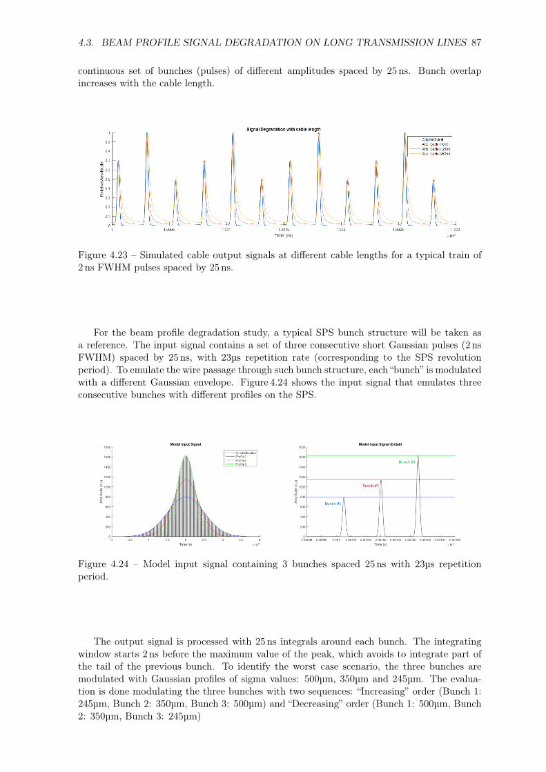
4.3. BEAM PROFILE SIGNAL DEGRADATION ON LONG TRANSMISSION LINES 87
continuous set of bunches (pulses) of different amplitudes spaced by 25 ns. Bunch overlapincreases with the cable length.
Figure 4.23 – Simulated cable output signals at different cable lengths for a typical train of2 ns FWHM pulses spaced by 25 ns.
For the beam profile degradation study, a typical SPS bunch structure will be taken asa reference. The input signal contains a set of three consecutive short Gaussian pulses (2 nsFWHM) spaced by 25 ns, with 23µs repetition rate (corresponding to the SPS revolutionperiod). To emulate the wire passage through such bunch structure, each “bunch” is modulatedwith a different Gaussian envelope. Figure 4.24 shows the input signal that emulates threeconsecutive bunches with different profiles on the SPS.
Figure 4.24 – Model input signal containing 3 bunches spaced 25 ns with 23µs repetitionperiod.
The output signal is processed with 25 ns integrals around each bunch. The integratingwindow starts 2 ns before the maximum value of the peak, which avoids to integrate part ofthe tail of the previous bunch. To identify the worst case scenario, the three bunches aremodulated with Gaussian profiles of sigma values: 500µm, 350µm and 245µm. The evalua-tion is done modulating the three bunches with two sequences: “Increasing” order (Bunch 1:245µm, Bunch 2: 350µm, Bunch 3: 500µm) and “Decreasing” order (Bunch 1: 500µm, Bunch2: 350µm, Bunch 3: 245µm)

88 CHAPTER 4. BEAM WIRE SCANNER ACQUISITION SYSTEM STUDIES
Figure 4.25 – Consecutive bunches profile determination in decreasing (top) and increasing(bottom) width over different CK50 cable length.
Figure 4.25 shows the processing results of the test signals after different cable lengths(10m, 120m and 250m). The first bunch of the set is never going to be degraded on thisconfiguration, the tail of the third bunch has more than enough time to recover the base lineon the 23 µs SPS revolution period. With regard to the second and third bunches, they aredegraded due to bunch pile-up, which ultimately leads to beam width determination errors.
On the specific case shown here as example, (with a ratio of 30% between profiles widths)the systematic error on beam width determination reaches up to 2.5% for the second bunchand 4.3% in for the third with 250m of cable. The beam width determination error due tothe cable does not only depend on the cable length, it also depends on the profiles like-hood.This is highlighted in Fig. 4.26 where the beam profiles are determined for different widths inincreasing order for a constant cable length (120m).
Figure 4.26 – Bunch profiles error variation with profiles like-hood for a fixed cable length(120m).
A bi-dimensional sweep provides a complete picture of the influence of the pile-up onthe beam profile error. The cable length and the sigma ratios are varied during consecutivesimulations. The Gaussian SSE and beam sigma errors collected for bunches #2 and #3 inFig. 4.27. The Gaussian goodness-of-fit is also shown for completeness, it states an artificialdeformation of the measured bunch profiles due to pile-up.

4.3. BEAM PROFILE SIGNAL DEGRADATION ON LONG TRANSMISSION LINES 89
Figure 4.27 – Profiles degradation evolution over cable length and consecutive sigma ratios.(Left: Beam profile relative error. Right: Gaussian fit SSE).
4.3.5. Models validation and CK50 cable measurements
Direct measurements of long CK50 cables where done to assess the accuracy of the previousmodel. Two cables (around 88m each) installed in the location of a SPS Beam Wire Scannerprototype (BA5) were used for tests here presented. The cables had one side on the tunneland the other on the surface building. The cables were looped in the tunnel, allowing signalinjection and measurements to be done on surface. The total cable length under study wasabout 176m.
Three different features of the cable were studied, frequency response, the distortionof short pulses, and the induced noise.
4.3.5.1. Frequency analysis
The cable attenuation versus frequency was determined by emulating the behaviour ofa network analyser with a scope and a function generator (see Fig. 4.28). The characterisa-tion consisted in injecting a pure sinusoidal signal at different frequencies on the cable link.The RMS amplitude ratio and the phase relationship of input/output waves were measured,obtaining the cable attenuation on dB and its phase shift on degrees (source and load wereadapted to 50Ω.
On Fig. 4.28, right, the amplitude of the output signal (in pink) decreases as the frequencyincreases, showing that the cutoff frequency of the cable was reached. The RMS values of thesignals amplitude were calculated by the scope as well as its ratio and phase shift.
Figure 4.28 – Set-up for cable practical transfer function extraction (left) and scope measure-ments (right)

90 CHAPTER 4. BEAM WIRE SCANNER ACQUISITION SYSTEM STUDIES
Figure 4.29 shows the attenuation and phase shift values practically obtained (blue dots)against the transfer function of cable models obtained from PSpice (black line) and Matlab(blue line) for the same cable distance, 176m. Measured and simulation model shown a goodagreement, which demonstrates that the model was reliable from the frequency domain pointof view.
Figure 4.29 – Bode plot for 176m CK50 cable: Measurements (blue dots), PSpice (black) andMatlab (blue line).
4.3.5.2. Temporal analysis
The temporal validation of the model was checked practically verifying how parameterssuch as rise time, falling time and pulse width vary with cable distance. The setup used forthe test is shown in the Fig. 4.30 (left), fast pulse generator a was used to provide short pulseslasting from 1ns to 100 ns with a repetition rate between 1KHz to 100KHz. Source and loadwere impedance matched with the line (50Ω).
Figure 4.30 – Set-up for cable practical transfer function extraction (left) and scope measure-ments (right).
Evaluation on laboratory demonstrated that the setup and connections used had no impacton the system bandwidth or pulse distortion (Fig. 4.30 right).
To determine numerically the enlargement of a pulse on long CK50 cables, a couple ofpulses (≈ 4 and 1.5 ns) were injected. Figure 4.31 shows the pulse distortion for both excitationsignals with the same scope settings.

4.3. BEAM PROFILE SIGNAL DEGRADATION ON LONG TRANSMISSION LINES 91
Figure 4.31 – Cable Input (yellow) and output (red) signals for 4 ns (left) and 1.5 ns (right)FWHM pulses.
Rise time, falling time (both defined for transitions from 10% - 90% of the signal maximumvalue), FWHM and attenuation were studied to evaluate the pulse degradation. Table 4.26summarises these parameters for input/output pulses. Falling times were increased up to 5times at the cable output, such long “bunch tails” are responsible of the bunch overlap.
Table 4.26 – Numeric summary of pulse parameters for input and output signals.
Pulsed signals degradation on long CK50Rise Time (ps) Fall Time (ns) Pulse FWHM (ns) Att. (dB)
Cable Length (m) 0 m 176 m 0 m 176 m 0 m 176 m 176 mLong Pulse (4ns) 407 596 876 3436 2464 3298 4.68Short Pulse (1.5 ns) 378 606 860 4375 763 1369 8.7
Several Input/Output measurement windows were recorded to evaluate the Matlab model.Each dataset contained excitation and response signals for different pulse lengths (1, 2, 3 and5 ns FWHM). The recorded signals from the fast pulse generator were used as an input forthe model. Later, the output of the model was compared with the cable measured responseon the temporal domain. The normalised root mean squared errors (NRMSE), defined onEq. 4.23, is used to assess the quality of the model fit (Fig. 4.32).
RMSE =
√∑nt=1(y′t − y)2
n, NRMSE =
RMSE
ymax − ymin(%) (4.23)
where n is the number of samples in the acquired temporal window, y′t is the value predictedby the model for the sample t and y the actual cable output for the same sample. NRMSEnormalises the root mean squared errors by the amplitude of the signal, thus it is presentedas a percentage.

92 CHAPTER 4. BEAM WIRE SCANNER ACQUISITION SYSTEM STUDIES
Figure 4.32 – Cable input (blue) and output (red) with model response overlapped (green)for short pulses 1-10ns.
The model NRMSE shown an agreement w.r.t the real cable response about 84 to 96%.Note that model output (green) and cable response (red) are practically overlapped.
A step response was simulated with a long pulse (100 ns), see Fig. 4.33. As previously, themodel was accurately predicting the cable response with an agreement close to 96%. Thissuccessful model validation reinforces the conclusions on the cable impact for bunch profilemeasurements.
Figure 4.33 – Cable input (blue) and output (red) with model response overlapped (green)for a 100 ns pulse.
On operational systems, the bunch pile-up observed is not only linked to the cable length(which is location dependent), but to a combination of other factors including the detectorsignal length (FWHM) and the associated transmittance amplifier (TIA) bandwidth. Figure4.34 shows the response of operational detector systems on SPS to particle bunch losses. Onthe figure belonging to a single bunch (left), the tail of the signal extends to the followingbunch producing the pile-up observed on the right.

4.3. BEAM PROFILE SIGNAL DEGRADATION ON LONG TRANSMISSION LINES 93
Figure 4.34 – Signals from two operational BWS acquisition systems corresponding to singlebunch (left) and bunch train losses (right) produced by beam wire scanners.
Note the higher pile-up on the complete system (Fig. 4.34) compared to simulationswhen only considering the cable and short pulses (Fig. 4.23) or the empirical cable response(Fig. 4.32).
4.3.5.3. Pick-up noise
Studies carried out on operational systems in SPS demonstrated the presence of a signif-icant noise coupled on the signal from the detectors. The Fig 4.35 shows scope traces fromoperational systems while the scanners were not being operated. The noise coupled on thelines featured two components. The first corresponded to the presence of particle bunches onthe accelerator (bunch noise ≈ 80Mhz) with an amplitude dependent on the beam intensity.The second contribution is independent of the bunch structure and is synchronous with theaccelerator revolution frequency (turn noise ≈ 43KHz).
Figure 4.35 – Scope traces showing noise recorded for scanners 517(left) and 521(right) witha LHC25ns beam with 48 bunches at 26 GeV
Both noise types are present during the beam profile measurement and overlapped onthe signal. The noise falls within the signal frequency of interest, which makes difficult tofilter out without degrading the measurement. Such a noise is directly influencing on theprofile measurement lowering the SNR and the bunch by bunch profiles quality. The noiseamplitude is typically around 20mVpp - 40mVpp and depends on the location, which suggestsome relationship with the cable routing or grounding strategy.
Figure 4.36 shows the analog signal from an operational BWS photo-multiplier tube recordedon surface being influenced by noise.

94 CHAPTER 4. BEAM WIRE SCANNER ACQUISITION SYSTEM STUDIES
Figure 4.36 – Beam profile measurement (BWS.414) recorded with a scope on surface.
4.4. Error sources on beam profile determination
The beam size is strongly dependent on the monitor location, the accelerator and beamtype. For instance, LHC beams with typical transverse emittances ranging 1-3.5µm, variesin terms of beam sigma, from injection (450GeV) to collision energies (7TeV), from about1.19mm to 0.16mm (beam sigma). Beam profile monitors used at CERN are image-based(as ionization profile monitors or synchrotron light monitors), and interceptive (as beam wirescanners or SEM grids), for both methods, the accuracy of the measurement is limited bysystematic and statistical errors contributions, typical of the instrument and measurementconditions.
The main sources that affect the beam profile accuracy are related with the spatial resolu-tion of the monitor, the number of primary events detected (i.e. number of secondary particlescrossing the detector, or photons detected) and the measurement noise in both axis, positionand amplitude. Next sections analyse the contribution of the different error sources to thebeam size uncertainty through simulations. These studies consider image based monitors andwire scanners.
For the simulations, we will refer to the relative beam size error (δrel), which is composedby a systematic (µσ) and statistical (σσ) contributions, defined as:
δrel =σmeasured − σbeam
σbeam= µσ ± σsigma (4.24)
The simulations contained on the following sections reproduce the procedure indicated in[4], and will provide valuable information for the specifications of the upgraded acquisitionsystem.
4.4.1. Considerations
A different measurement simulation approach will be used for interceptive and imagingsystems concerning the beam Gaussian distribution sampling. The beam distribution usedfor simulations is defined as:
G(x) =Npart
σ√
2πe−
12
( xσ
)2∫G(x)dx = Npart
(4.25)
where Npart is the total number of events that form the complete Gaussian profile, i.e.total number of photons illuminating the imaging detector area for imaging systems, or totalnumber of particles crossing the detector surface for BWS.

4.4. ERROR SOURCES ON BEAM PROFILE DETERMINATION 95
Imaging systems:
These systems are limited mainly by the measurement resolution (determined by the pixelsize) and the magnification given by the optical path. Imaging systems capture a completeand continuous picture of the beam, however each pixel is integrating the photons distributedon their surface (see Fig 4.37 and Fig 4.38 left). For imaging systems with k pixels in onedimension, the measured Gaussian distribution would contain K points (pixels) with a valueper pixel defined as:
yi =
∫ xi
xi−1
G(x)dx (4.26)
On this case, if the sensor pixel size is comparable with the beam sigma value, thesemonitors will show a systematic error contribution on beam size determination.
Taking one coordinate for one pixel (x) and assuming that N photons are uniformly dis-tributed along the pixel extension in that dimension (d), the normalized uniform distributionof the photons can be defined as:
f(x) =
1d , for − d
2 < x < d2
0, for x < −d2 , x >
d2
(4.27)
The mean value and the variance of the photon locations can be obtained as for a uniformdistribution:
µpixel =
∫ inf
− inff(x)dx = 0
σ2pixel =
∫ inf
− infx2f(x)dx =
d2
12
(4.28)
The mean µpixel defines the pixel centre, the standard deviation σ2pixel represents the un-
certainty on the location of a photon illuminating the pixel. When using imaging detectors forbeam profile reconstruction, the uncertainty of each photon location propagates to the deter-mination on the beam size. The measured beam width has a contribution from the particlesdistribution (σbeam) and the pixel width determined by the detector resolution (σpixel). Withthe consideration of uniform photon distribution on each pixel, both terms are independent,and the resulting beam size from the measurement is:
σmeasured =√σ2beam + σ2
pixel (4.29)
Then, the systematic error introduced by these systems can be calculated as follows:
µ0 =σmeasured − σbeam
σbeam=
√1 +
1
12η2− 1 (4.30)
where η is the relationship between the beam size and the pixel size (bins/sigma).
Wire Scanner Systems:
The previous conclusions can be extrapolated to beam wire scanners, the relationshipbetween beam sigma and wire diameter introduces a small systematic error contribution tothe measurement, especially if the wire is comparable with the beam size. The instantaneousrain of secondaries is produced by the integrated surface of the wire over the beam. The beamprofiles measured with wire scanners and K number of points are defined as:
yi =
∫ xi+Dw2
xi−Dw2G(x)dx,where i=1. . . k (4.31)

96 CHAPTER 4. BEAM WIRE SCANNER ACQUISITION SYSTEM STUDIES
where Dw is the carbon wire diameter.
The profile measurement of a single bunch is reconstructed from several turns while thewire is crossing through the beam at constant speed. Thus, no profile information is availablebetween two consecutive bunch-wire interceptions, this makes a bunch wire scanner profile anon-continuous measurement (see Fig. 4.37 and 4.38 right). The measurement resolution, inpoints per sigma (PpS), for a single bunch is determined by the scan speed (Vscan), the beamwidth (σbeam) and the machine revolution frequency (frev) as:
PpS =σbeamVscan
frev (4.32)
On wire scanners, the distance between consecutive measurement points varies, beingsmaller or bigger than the wire diameter itself (30µm) in function of the scan speed and themachine revolution frequency.
Table 4.27 collects a summary the reachable bunch profile resolutions for wire scanners atdifferent speeds and accelerators.
Table 4.27 – Bunch profile resolutions for wire scanners working at 1 and 20 m/s for theCERN accelerators.
Wire Scanner Resolution as function of Speed and AcceleratorPSB PS SPS LHC
Rev. Period 1.67 - 0.53 µs 2.2 µs 23 µs 89 µsRes. @ 1m/s 1.67 - 0.53 µm 2.2 µm 23 µm 89 µm
Res. @ 20m/s 33.4 - 10.6 µm 66 µm 460 µm 1.78 mm
A common technique to increase the measurement resolution for a given bunch, is toperform several scans during the same cycle time with a programmable delay respect to thebunch phase. This way, the wire intercepts the bunch profile in different locations on eachscan.
Figure 4.37 – Image-based (left) and Interceptive-based (right) acquisition considerations (thisexample shows 0.5 Bins/sigma and profile peak on bin centre).

4.4. ERROR SOURCES ON BEAM PROFILE DETERMINATION 97
Figure 4.38 – Image-based (left) and Interceptive-based (right) acquisition considerations (thisexample shows 0.5 Bins/sigma and profile peak on bin side).
4.4.2. Simulation algorithm
To evaluate the different sources of error on the beam profile reconstruction and theirrandom or systematic contribution to the measurement error, a set of numerical simulationswere performed. The influence on the number of events and spatial resolution (bin width) willbe evaluated for wire scanners and for imaging systems. For wire scanners also the influenceof the wire diameter respect to the beam size will be studied.
The simulation script generates an ideal beam profile with a defined number of total eventsand size (sigma) as on Eq,4.25, this profile will be used as a reference. For each of the Kmeasurement points (Eq. 4.26 or Eq. 4.31), the script generates a set of 500 random valuesfollowing a normal distribution with µi = yi and σi =
√yi. This sigma error estimation corre-
sponds to the assumption of a Poisson distribution of the primary events along the integratedregion (photons for imaging systems or secondaries crossing the detector and produced by thewire section).
The code generates, a set of 500 beam profiles (entries) with K points. The 500 profilesare fitted with a Gaussian distribution to obtain the measured beam sizes. Afterwards, the fitresults (sigma values) are fed into a histogram, with a sufficiently large number of entries thehistogram will result in a Gaussian distribution. The histogram collects the measured beamsize of 500 repeated acquisitions with the profile monitor, and its distribution is fitted againto extract the mean value (µσ) and sigma (σσ) of the histogram. The difference between theoriginal beam size (σbeam), given as an input to the simulation, and the mean value of themeasurements (µσ) represents the systematic error, whereas the standard deviation of thefitted histogram (σσ) provides the statistical or random error, see Eq. 4.33. Figure 4.39 showsan example of the processing algorithm for better understanding.
εsystematic =σbeam − µσσbeam
εstatistic =σσ
σbeam
(4.33)
Other effects will be studied as well to check their contribution to the beam size error,such as the relative beam position respect the measurement points and the effect of randomnoise on X and Y axis.

98 CHAPTER 4. BEAM WIRE SCANNER ACQUISITION SYSTEM STUDIES
Figure 4.39 – The left plot is showing the ideal beam profile in black, and a set of 500simulations (profiles) with 100 primary events (the original Gaussian integral), a Gaussianfit has been done in three random distributions. The plot on the left is a histogram of thesigma values obtained in each of the 500 fits on the left. A Fit on the histogram provides themonitor statistical (σσ) and systematic (µσ) errors on the beam size determination.
4.4.3. Simulation results
4.4.3.1. Imaging systems
The simulations performed have successfully reproduced the results obtained in [4] forimaging systems. The systematic error in due to the pixel size respect to the beam sigma(bins/sigma), in Fig 4.40, shows a good agreement with the analytic expression on Eq. 4.30(black line).
Figure 4.40 – Imaging monitors systematic error as function of pixels per sigma and numberof primary events for beam peak at the bin centre (left) and at the bin edge (right).
On the other hand, the random error is showing to be only dependent on number of events.No significant improvement is observed as more bins per sigma are taken. In addition, for lowresolutions (<1bin/sigma), the Gaussian fit is biased by the relative position of the Gaussianpeak respect to the bin.

4.4. ERROR SOURCES ON BEAM PROFILE DETERMINATION 99
Figure 4.41 – Imaging monitors random error as function of pixels per sigma and number ofprimary events for beam peak at the bin centre (left) and at the bin edge (right).
4.4.3.2. Wire Scanners
Fig. 4.42 shows, that for wire scanners, systematic errors are practically uncorrelated tothe number of events and number of points measured per sigma (wire diameter consideredmuch smaller than the beam width). This is not the case when the wire diameter approachesthe the beam width (see Fig. 4.44). As previously observed with the pixel size, the smallerthe wire diameter is respect to the beam, the smaller is the systematic contribution accordingto Equation 4.30. The simulation results on Fig. 4.44 shows a match on the systematic errorintroduced by the wire diameter and the prediction from Eq. 4.30. Systematic errors on wirescanner are only dependent on the wire diameter and beam size relationship, and not on thenumber of points per sigma or number of number of events. A nominal beam on the LHCwith 100µm sigma and being scanned with a 30µm carbon wire (Sigma/Wire diam = 3.3) willfeature a systematic error in the order of 0.5% (0.5µm) independently of how many point persigma are taken.
With regard to the random error contributions, there is a strong dependency on the numberof events and to the number of points per sigma as shown on Figure 4.43. As a differencerespect to the imaging sensors, on wire scanners there is an improvement on the random errorwhen more points per sigma are used for beam profile reconstruction (assuming wire diameter« beam sigma). The results of these simulations suggest that for an accurate and precise beamprofile measurement (<1% beam sigma total error), a high number of total events is required(> 12000), the wire needs to be at least 3 times smaller than the beam sigma and the scanmust record more than 1 point per sigma. For low resolutions (< 1 bin/sigma) the profilewidth error is biased by the position of the sampling points w.r.t the Gaussian peak (seeFig. 4.42 and 4.42).

100 CHAPTER 4. BEAM WIRE SCANNER ACQUISITION SYSTEM STUDIES
Figure 4.42 – Beam Wire Scanner systematic error as function of points per sigma and num-ber of primary events for beam peak at the bin centre (left) and at the bin edge (right).Wirediameter is 10 times smaller than beam sigma.
Figure 4.43 – Beam Wire Scanner random error as function of points per sigma and numberof primary events for beam peak at the bin centre (left) and at the bin edge (right). Wirediameter is 10 times smaller than beam sigma.
From the previous measurements, an analytical expression can be extracted to evaluatethe random error dependency with the measurement resolution (PpS) and the number ofevents (NTE). This parametrization is adjusted for resolutions bigger than 1 bin/sigma andis shown in continuous lines in Fig. 4.43. The analytical approximation is as follow:
εstatistic(NTE , PpS) =1.1√
NTEPpS(4.34)

4.4. ERROR SOURCES ON BEAM PROFILE DETERMINATION 101
Figure 4.44 – Systematic (left) and random (right) errors associated to the number of pointsper sigma and Beam/Wire size relationship.
The effect noise on the amplitude axis is evaluated through the profile SNRy, defined asthe ratio between the Gaussian amplitude and the noise RMS value (σi).
σi = c =max(G(x))
SNRy(4.35)
To isolate the contribution on the number of events a very high number was used (1e8
events). Each of the K points of the 500 simulated Gaussians is defined as (xi, yi ), where xiis the measurement position and yi is a random value with mean yi and standard deviationσi = c. The error assigned per point is set as on Eq. 4.35. The results on Fig. 4.45 explainhow the noise on Y axis affects the measurement uncertainty.
Figure 4.45 – Beam Wire scanner Random error versus amplitude SNR and points per sigma(PpS). Sweep on PpS (left) and SNR (right).
The influence SNRy on the random beam width error was adjusted as previously with ananalytical expression (Eq. 4.36), shown as continuous lines on Fig. 4.45 (right):
εstatistic(SNRy, PpS) =1
SNRy√PpS
(4.36)
The impact on the error due to the wire position incertitude is studied in a similar way aswith the SNR in amplitude. This time the 500 Gaussians with K points have only incertitudeon the x axis, defining each point as (xi, yi), where yi is the measurement amplitude and xiis a position value with mean xi and standard deviation σi = c. The incertitude in positionis considered as a relationship with the beam sigma, defined as:
σi = c =σbeamSNRx
(4.37)

102 CHAPTER 4. BEAM WIRE SCANNER ACQUISITION SYSTEM STUDIES
Figure 4.46 – Beam Wire scanner Random error versus amplitude SNR and points per sigma(Pps). Sweep on PpS (left) and SNR (right).
The results shown on Fig. 4.46 for SNRx (or position uncertainty) are similar to thoseshown for SNRy. The wire incertitude contribution to the statistical error has been adjustedthe analytic approximation on Eq. 4.38:
εstatistic(SNRx, PpS) =0.4
SNRx√PpS
(4.38)
The simulations for the SNR in X and Y axis assumed a wire diameter 10 times smallerthan the beam sigma, and give an approximated idea of the wire scanner and secondariesacquisitions system requirements for low beam width determination errors.
These simulations and analitic equations allow to obtain the beam size uncertainty as acombination of the three sources of error:
εbeamWidth =√ε2NTE + ε2SNRx + ε2SNRy (4.39)
As an example, to measure a 100µm sigma LHC beam with an incertitude below 1%, theprecision in the wire position measurement must be better than 4µm and more than 3 pointsper sigma must be taken. Regarding uncertainty on Y axis, SNRy should remain avobe 100and more than 10000 particles need to be detected at the Gaussian centre.

Chapter 5
Secondary shower acquisition systemdesign
This chapter defines the proposed architecture for the BWS acquisition system and itsmain components, including details on the integrator ASICs selected for evaluation on thisthesis. The development of a proof-of-concept prototype, including hardware and firmware,is also detailed here.
5.1. Acquisition system architecture
An upgraded electronics scheme for secondary particles readout is motivated by the find-ings detailed on Chapter 4. The scanner measurement can be degraded by the impact oflong coaxial cable lines, which leads to bunch pile-up and therefore beam profile cross-talkon bunch by bunch measurements for cable lengths >100m. The high frequency nature ofBWS detector signals (>250Mhz) and the low noise requirements (in the order of single par-ticle detection) suggest the need of digitalization close to the detector to avoid capacitiveeffects of the cable. In addition, long copper links degrade the signal SNR by the presence ofelectromagnetic interference (EMI) produced by RF equipment or power lines nearby.
The architecture proposed on this thesis for the BWS secondary shower acquisition followsa modular design approach standardised by the CERN’s beam instrumentation (BI) groupfor new developments, such as the Multi Orbit Position System (MOPOS) and Beam LossMonitor (BLM) upgrades [114]. This architecture is based on the placement of a radiation hardfront-end responsible of digitalization close to a detector and optical digital communicationwith a back-end system where the data is stored and processed.
Figure 5.1 – Secondary shower acquisition system architecture for pCVD diamond detectorsreadout.
The system architecture employs a standard radiation-hard front-end board (GEFE [115]),
103

104 CHAPTER 5. SECONDARY SHOWER ACQUISITION SYSTEM DESIGN
equipped with a custom mezzanine and an integrator ASIC capable of charge integration at40MHz. Bunch synchronous acquisitions are needed to provide bunch by bunch profiles, andhigh dynamic range to cope with the accelerator dynamics. The GEFE Board is responsibleto collect the digital data, from the detector readout mezzanine, and send it through a singlemode optical fibre at 4.8Gbps using the GBT protocol to the back-end system. The front-endcontrol and synchronisation are managed through the optical link by a VFC-HD board (back-end), which is responsible as well for the data reception and storage. With each front-endrequiring a single GBT bridge, a single VFC-HD would be capable of driving up 4 acquisitionsystems.
5.1.1. Electronics exposure to radiation
Radiation affects electronics by cumulative and single event effects (SSE). Cumulativeeffects degrade the electronics performance as radiation dose is absorbed up to a final fatalfailure, this effect is measurable and degradation parameters are provided when qualifyingequipment up to certain radiation level in terms of total ionising dose (TID), expressed inRad or Gy. The SSE are stochastic processes produced by nuclear interaction in the electronicsfrom the direct ionisation of a single particle, these interactions may deposit enough energyin an electronic device to perturb its operation, i.e. flipping a bit on a memory. SSE arecharacterised only in terms of probability, and they are related to the particle type, fluenceand electronics cross-section. SSE can be minimised with mitigation techniques such as TripleModular Redundancy (TMR) or error detection and correction techniques on digital logic.
Tunnel electronics are specified for an operational life of 10 years, considering a radioactiveenvironment it is expected a total ionising dose (TID) of 100 Gy per year (on SPS and LHC).General specifications for such type of electronics are about 1KGy during its operational life,same specifications as MOPOS project given the developments and environment similarities[116]. Such limit is constrained by the radioactive conditions of tunnel areas, deeply studiedby the R2E group for the LHC injector chain [117] [118]. Radiation extinction ratio is veryfast with distance, according to R2E surveys, readout electronics might be placed on thefloor ≈70 cm from the beam pipe with moderate radiation levels. SPS measurements specifyradiation levels in general <100Gy/y on the cable trays (≈50 cm from beam pipe) except insome very specific locations (see Fig. 5.2).
Figure 5.2 – Radiation levels for the six SPS sextants between 2009 and 2011, measurementfrom dosimeters placed on beam pipe (blue) and cable tray (red) are shown [118].
Radiation exposure in lower energy accelerators such as PS and PSB is more critical andelectronics must be placed further away from the beam pipe or in shielded areas to survive theexpected operational life. For these accelerators, surveys specify >1KGy/y in the close vicinityof the beam pipe (≈5 cm). Particular simulation campaigns for electronics placements studyon PS the dose reduction with shielding and distance[119], a moderate exposure <10Gy/y

5.1. ACQUISITION SYSTEM ARCHITECTURE 105
can be reached if electronics are properly protected bellow floor level (see Fig. 5.3), theseassumptions can be extrapolated to the PSB case.
Figure 5.3 – Dose exposure FLUKA simulations for the PS and attenuation with distance andshielding [119].
5.1.2. The VME FMC Carrier Board (VFC) and GBT-Based ExpandableFront-End (GEFE)
The architecture shown on Fig. 5.4 depicts the standard approach used on beam instru-mentation developments and upgrades at CERN.
Figure 5.4 – GEFE board (left) and VFC-HD board communication as front-end and back-endsystems respectively.
The VFC-HD board (Fig. 5.4 right) is conceived as a general purpose digital VME boardfor beam instrumentation, it is designed to replace the obsolete DABx64 boards detailed onChapter 2. This is a FPGA-based (ARRIA V GX) 6U VME 64 module featuring a high pincount FMC slot that follows the FMC VITA57 standard for compatibility with commercialFMC modules. The FMC slot is foreseen for user specific applications. The board offers thepossibility to connect to custom VME rear transition modules (RTM). It features 6 small formfactor pluggable (SFP+) slots, from which 2 are dedicated to Ethernet and Beam SynchronousTiming (BST) interfaces, and 4 for user applications. Concerning memory, it is equipped withtwo 8Gb DDR3 memories, offering high storage capabilities (14Gb) intended for long datasetsof raw data. The VFC is capable of receiving and decoding itself the BST signals distributedvia optical link, avoiding the need of external equipment for such purpose. The board isfully compatible with the GBT standard for back-end systems and it is capable to offer highbandwidth and latency deterministic links with its front-ends (GEFE) through commercialoptical transceivers on its user SFP+ sockets.
The GBT-based Expandable Front-End (GEFE) board is another general purpose digitalboard designed to be the standard FMC carrier board for beam instrumentation front-ends.

106 CHAPTER 5. SECONDARY SHOWER ACQUISITION SYSTEM DESIGN
It is designed to operate close to beam lines in fast data acquisition systems (see Fig. 5.4 left).GEFE is conceived to work together with the VFC-HD board through a GBT link. Thisis a radiation-tolerant board that features the GBTx ASIC and VTRx transceiver followingthe Rad-hard optical link standard for GBT links. It is equipped with a ProAsic3 FPGA,mainly used as an interface between the FMC connector and the GBTx ASIC. The boardcontains the minimum active components possible and has been fully designed with radiation-tolerant components by design (as the GBT chipset or FEASTMP regulators) and radiation-characterised Commercial Off-The-Shelf (COTS) components. The radiation hardness of thisboard is limited by the FPGA, specified for TID up to 750Gy [115].
5.1.3. Readout ASICs
The acquisition system performance would be strongly linked to the readout ASIC respon-sible of detector digitisation and the dynamic range coverage technique on scope. Estimationsfor pCVD diamond detectors based on previous simulations specify a required dynamic rangeof 1-1e6 MIPs, translated into charge results in 3fC to 3nC per bunch. The fast timingof diamond detector pulsed signals (2 ns FWHM) and the repetition frequency determinedby nominal LHC beams (40Mhz) suggest analog signal integration with 25ns periods as themost optimal strategy in terms of data compression w.r.t direct ADC digitisation. Thislast approach would require very fast data conversion rates (>1GSPS) to properly recon-struct the pulses signal, or the use of pulse shaping techniques for reduced acquisition rates(≈650MSPS), which may lead to undesired bunch overlap and therefore bunch profile cross-talk.
The large dynamic range coverage strategies under evaluation are focused on two differentapproaches: a single channel readout with logarithmic encoding, or a multi-channel readoutsplitting the detector signal dynamics on several linear channels with different gain/attenuationlevels. The readout ASICS required must be radiation-hard (up to TID=1KGy) linear/logarithmicintegrators, working at 40 MHz with no dead-time and able to resolve at least signals in theorder of 1-7fC. QIE10 and ICECAL V3 detailed on this section were found as the most suit-able readout ASICs candidates to evaluate for diamond detector readout matching the systemrequirements while at the same time kept compatibility with traditional PMTs.
5.1.3.1. QIE10
The QIE10 (Charge Integrator and Encoder) is an ASIC from the family of devices de-signed at Fermilab for measuring signals from photo-detectors. Its development is motivatedby the phase 1 and 2 of the CMS hadronic calorimeter and Atlas TileCal detectors upgrade[120] [121]. The QIE10 integrates and digitalizes negative input current pulses with an ef-fective rate of 25 ns periods. This is accomplished by using 4 integrator circuits operatingin parallel with a different phase, each integrator circuit requires 100 ns to process its 25 nsintegral.

5.1. ACQUISITION SYSTEM ARCHITECTURE 107
Figure 5.5 – QIE10 Schematic of main parts and pipelined operations [122].
Each QIE10 contains a single channel with 17 bits dynamic range, 3.2fC sensitivity andsaturation at 340pC, logarithmically encoded into 8 bits (6 bits of mantissa and 2 rangebits). This scheme provides a floating point dead-timeless integration and digitalization ofthe input charge at an effective rate of 40 MHz. Its logarithmic behaviour guarantees aconstant quantification error 1%. The acquisition dynamics are covered by automaticallyswitching between 16 linear resolution levels (spitted in a total of 4 ranges with 4 sub-rangesin each). This logarithmic response is accomplished by two parts. First, the input current isspitted into four logarithmically weighted ranges by means of a current splitter, each rangeintegrates the resulting current fractions into separate capacitors by using gated integrators.The second part of the response is due to a nonlinear fast 6 bit ADC whose transfer functionconsists in 4 linear slopes. Different internal parameters can be set-up by means of a 64 bitsprogrammable register. The ASIC ADC charge and TDC data is given digitally through 8DDR LVDS lines at 40Mhz (80Mhz effective rate) and a LVDS clock line. Figure 5.5 showsa schematic of the QIE10 structure.
The QIE10 is fabricated in a 350 nm SiGe process, providing intrinsic hardness againstionising radiation. First irradiations showed no degradation on the ASIC performance upto a total ionisation dose (TID) of 520Gy with only 2 single events upsets (SEU) observedwhen the board was exposed to 6e12 p/cm2 [123]. Further studies detected radiation-inducedpedestal drift at a TID ≈ 2.50KGy and critical failure about 2.70 kGy [124].
The nominal 8 bits response the QIE10 for its input dynamics is shown in Fig. 5.6, togetherwith a simulated digitalization of a Gaussian profile (digitalization slope changes with signalamplitude). Both cases show the associated quantization error δ, defined as:
δ =1√12
(Siqi
) (5.1)
where Si is the bin sensitivity and qi is the central value of the bin, expressed in charge.

108 CHAPTER 5. SECONDARY SHOWER ACQUISITION SYSTEM DESIGN
Figure 5.6 – Theoretical QIE10 Digitisation scheme and quantization error (left top andbottom) and a QIE10 digitised Gaussian profile with its quantization error (right top andbottom) with the different ranges highlighted in colours.
The impact of the QIE10 logarithmic encoding was evaluated to check for systematicor random error contributions on the beam width determination. The simulations shownin section 4.4.2 were reproduced by considering the theoretical QIE10 digitisation scheme.As depicted on Fig. 5.7, the results under same circumstances shows different results whenincluding the QIE10 behaviour (note an increase of both, systematic and random errors).
Figure 5.7 – Comparison of statistical and systematic errors obtained for 500 simulationprofiles at 10 bins/sigma and 48000 events, nominal results on top and results with QIE10digitisation scheme on bottom.

5.1. ACQUISITION SYSTEM ARCHITECTURE 109
Figure 5.8 – QIE10 digitalization algorithm impact on Beam Wire Scanner random error asfunction of number of points per sigma and primary events for beam at the bin centre (left)and bin edge (right). Nominal results (points) versus results with QIE10 (squares).
Figure 5.9 – QIE10 digitalization algorithm impact on Beam Wire Scanner systematic erroras function of number of points per sigma and primary events for beam at the bin centre.Nominal results (left) versus QIE10 (right).
An analysis of the simulation results is provided in Fig. 5.8 and 5.9. The results suggestthat, as expected, when the amplitude uncertainty due to the number of events is small enoughthe quantization effect of the QIE10 dominates on the amplitude incertitude (12000 or 48000events on Fig. 5.8). On smaller number of events the quantization impact remains negligible(120, 480 and 3000 events). Independently of the number of events, the systematic beamwidth error induced by the QIE10 is in the order of 0.5% within the range 1-6 bins per sigma.The encoding algorithm is also degrading the expected random error, increasing it in somecases up to another 0.5% for the range under study. With such random/systematic errorsthis ASIC is on the limit of the specifications given for the LIU-BWS highlighted on chapter4. With a beam sigma incertitude in the order of 0.5%, emittance determination incertitudewould be translated into 1%. However, due to the high dynamic range coverage this ASICremains as a very attractive candidate for evaluation with pCVD diamond detectors.
5.1.3.2. ICECAL V3
The ICECAL V3 is a radiation hard dead-timeless integrator ASIC developed by theuniversity of Barcelona intended to be used for PMT readout in the framework of the LHCbcalorimeters upgrade [125]. Each ICECAL V3 features 4 analog channels with 12 bits dynamicrange each, 4fc sensitivity and saturation around 16pC. Its output signal is a differentialvoltage proportional to the integrated current over 25 ns windows that must be digitalized

110 CHAPTER 5. SECONDARY SHOWER ACQUISITION SYSTEM DESIGN
with an external ADC. This ASIC is designed with the same technology as the QIE10 (AMS0.35µm SiGe BiCMOS) for enhanced radiation hardness.
For dead-timeless operation, each of the channels consists of two fully differential inter-leaved sub-channels with switched integrators. A 50 ns refresh cycle is required for eachsub-channel while working in opposite phases (as one integrates the other discharges). Af-ter multiplexing the sub-channels output, the ASIC provides an effective 25 ns output rate.This technique was successfully applied in the current BWS generation, with an integratorASIC from the LHCb pre-shower [126]. ICECAL V3 also includes dedicated delay lockedloops (DLLs) capable of phase shifting in steps of 1 ns for channels synchronization and triplemodular redundancy configuration registers, accessible through a SPI interface to adjust keyparameters of its operation. The detailed ASIC schematic is shown on Fig. 5.10.
Figure 5.10 – ICECAL V3 architecture schematic and connectivity interfaces [127].
An active cooled input termination with 50Ω impedance and a differential internal archi-tecture are used for low noise operation. The input stage includes pole zero filters to shapethe input current pulses. Its analog outputs are differential, with a maximum voltage swingVdiff = 2Vpp and a common mode voltage Vcm = 1.5V .
Table 5.1 collects a summary of the main parameters of the ASICs under study:
Table 5.1 – QIE10 and ICECAL V3 main specifications
ASICs SPECIFICATIONSQIE10 ICECAL V3
Dynamic Range 3.2fC - 340pC (105) 4fC - 16pC (103)Integration Window 25ns (40Mhz)Channels per ASIC 1 4Input Impedance 50ΩDead-timeless YesNumber of bits 8 12 (ADC Dependent)Quantification Error ≈ 1% «1% (ADC Dependent)Linearity Error ≈ 1% (Logarithmic) <1%TDC Capability Yes NoRadiation Resistance (TID) ≈ 0.5kGy *ASIC Technology AMS SiGeBiCMOS 0.35µmDesigner Entity Fermilab for CMS/ATLAS U.Barcelona for LHCb

5.1. ACQUISITION SYSTEM ARCHITECTURE 111
5.1.4. Radiation Hard Optical Link
The CERN’s "Radiation Hard Optical Link project" aims the standardisation of a bi-directional optical link with a deterministic latency for use on the LHC and injectors upgradeprograms. The link is capable of providing data transmission, timing distribution, triggerand control between on-detector and off-detector electronics. The project is divided in severaldifferent parts (the GBT, Versatile Link and GBT-FPGA projects) that provide the requiredinfrastructure for the development of the optical link. Radiation hardness the link is specifiedto be ≈1MGy.
Custom rad-hard chipset developed in the GBT project drive optical receivers/ trans-mitters, protocol encoding and communication with the LHC experiments readout ASICS.Opto-electronic transceiver modules and radiation hard optical fibres are procured by theVersatile Link project. On counting room (radiation free environment) the link implementa-tion is based on with COTS components and FPGAs for protocol encoding/decoding. TheGBT-FPGA project procures the FPGA firmware to implement the GBT core. Figure 5.11shows the link architecture.
Figure 5.11 – Radiation-Hard optical link architecture.
The radiation-hard chipset developed by GBT project includes GBTIA (a transimpedaceamplifier for optical receiver), GBTLD (a laser driver), GBT-SCA (a slow control adapterASIC), and the core component of the whole radiation-hard optical link, the GBTx ASIC.
GBTx is a radiation-hard 4.8Gbps serializer/deserializer able to encode/decode data intothe GBT protocol. This ASIC uses TMR techniques to palliate SSE and converts the in-put data received from front-end electronics (experiments readout ASICS) into a serial datastream with a selectable format (GBT, 8b/10b or Wide frame), allowing 3.2-4.48Gb/s ofuser bandwidth. It also de-serializes the incoming data transmitted form the counting roomto perform control actions on the front-end electronics. The ASIC Clock and Data Recovery(CDR) system recovers the main link clock frequency with deterministic phase and latency. Itis capable of providing different clocks to the front-end (40, 80, 160Mhz), in synchronizationwith the main LHC/SPS 40Mhz. GBTx interfacing with front-end readout logic is performedthrough bi-directional ports called "e-links". The e-links transmit/receive data in DDR fash-ion at three possible data rates 80,160 and 320Mbps. The GBTx ASIC would be the onlypiece of digital logic actually needed to operate a front-end (apart of readout electronics),minimising the need of FPGAs under radiation.
5.1.4.1. The GBT frame
The GBT format is the preferred standard on the Radiation hard optical link, it consistson frames of 120 bits transmitted every 25 ns (40MHz), meaning 4.8Gbps effective link speed.This frame consist of a header, control bits (IC and EC), user data and forward error cor-rection (FEC) fields distributed as shown in Fig. 5.12. GBT mode allows 3.2Gbps for userbandwidth, that can be extended to 3.36Gbps using EC and IC fields for data transmission.

112 CHAPTER 5. SECONDARY SHOWER ACQUISITION SYSTEM DESIGN
SSE happening on the GBTx itself are palliated by its TMR logic design, however, SEE pro-duced on the transceiver modules might still introduce errors on the GBT frames. Amongthe different transmission modes, the GBT mode is the most attractive in terms of securityand SEE immunity since FEC field allows error correction. Wide frame sacrifices the FECfield to provide a higher effective user data bandwidth (4.48Gbps), allowing 112 bits for userdata per frame.
Figure 5.12 – GBT frame structure.
Data is transmitted over the optical fibre DC-balanced, this is ensured by scrambling thedata contained on the “slow control” and “user data” fields. To obtain forward error correctioncodes, the scrambled data and the header are Red-Solomon encoded before serialisation. Theprocess of line encoding-decoding is shown on Fig. 5.13
Figure 5.13 – GBT mode encoding-decoding schematic
5.2. Proof-of-concept prototypes
A couple of prototypes were developed to proof the concept with the main purpose to val-idate the improvements on signal integrity, noise reduction and dynamic range coverage withupgraded electronics. Unfortunately, many of the main components, that define the systemarchitecture, were in a very early stage of development or unavailable for users at the momentof this thesis developments. The only parts available were the VTRx transceiver, GBT-FPGAfirmware for some supported SRAM-based FPGAs and pre-series ASIC samples of QIE10 andICECAL V3, kindly provided by Fermilab and University of Barcelona respectively.
To bypass the lack of components, and procure a functional front-end prototype, it wasdecided to emulate the GBTx. The base-line solution consisted on using an FPGA, withembedded gigabit transceivers, and the firmware implementation of the GBT core.
Tunnel environmental conditions require a radiation-tolerant design and careful FPGAtechnology choice. The prototype architecture is shown in Fig. 5.14, where a custom front-end is placed on radiation areas and a FPGA development kit acts as back-end system.

5.2. PROOF-OF-CONCEPT PROTOTYPES 113
Figure 5.14 – Proof-of-concept system architecture schematic
5.2.1. Front-End implementation
The trends in high energy physics (HEP) concerning FPGA usage (SRAM and Flash-Based) consist on the characterisation of commercial devices under radiation, and the imple-mentation of scrubbing and TMR logic design for SEE mitigation [128]. The power and ca-pabilities that newer technologies offer on such re-programmable devices (high speed links forincreased data readout, PLLs for clock management, DSP blocks for data compression. . . etc.)is increasing the interest of using FPGAs for front-end systems in particle physics. CERNexperiments already feature FPGAs in radiation areas and their number is foreseen to increasewith upgrade plans [129].
FPGA technology choice for operation under radiation is strongly dependent on the ap-plication, radiation levels and mitigation techniques implemented. The characteristics offlash-based cells on FPGAs offers a much higher radiation-induced SEE immunity in theconfiguration memory when compared with SRAM based FPGAs [130] [131]. The implemen-tation of mitigation techniques on Flash-based FPGAs is not as critical as on SRAM-based.Irradiation campaigns with Flash-based FPGAS, such as ProAsic3 and Igloo families fromMicrosemi (formerly ACTEL), asses the usage of this technology when exposed to moderateradiation levels around 200-900Gy [132] [133].
The Microsemi Igloo2 was the chosen FPGA for front-end developments, this is the firstFlash-based FPGA with embedded gigabit transceivers available on the market. CMS alsochose this specific FPGA family for the CMS Hadron Calorimeter (HCAL) electronics upgrade,including HF and HB/HE detector acquisition systems [134].

114 CHAPTER 5. SECONDARY SHOWER ACQUISITION SYSTEM DESIGN
Figure 5.15 – Igloo2 Umd Mezzanine (left) and schematic (right).
The Igloo2 UMd mezzanine board, intended for the CMS HCAL upgrade, was the boardused in our project as substitute of GEFE (see Fig.,5.15). This is a radiation tolerant boardintended to work joint with the CMS HCAL ngCCM and it is designed to provide a bi-directional GBT link for slow control and LHC 40MHz timing distribution [135]. A collabora-tion started this way between CMS and BE-BI concerning design reviews, board procurementand a common firmware development.
Irradiation tests performed on Igloo2 shown critical FPGA logic failure at 1KGy [136], noeffects were observed for a TID ≈ 100Gy on the high speed serializer/deserializer (SERDES),however at this level the programming circuitry was seriously damaged [137]. Critical SERDESfailure was found to be around 200Gy [138]. Being still far from the final system specifications(1 kGy), and with the total TID constrained by the FPGA SERDES (<200Gy), this valuewas considered acceptable for a proof-of-concept prototype envisaging a next iteration withfinal components (GEFE + VFC).
The front-end electronic developments covered in this work were developed around theIgloo2 UMD board. Two mezzanine boards were designed and fabricated for testing theICECAL and QIE10 readout ASICS and the GBT-FPGA code was migrated from XilinxFPGA to this specific Microsemi model. This work allowed, for the first time, to drive theGBT link with a flash-based FPGA. The new GBT core was later distributed to CMS andadapted for use in their application.
5.2.1.1. The GBT core on an Igloo2 Flash-Based FPGA
The GBT-FPGA core provides a custom physical coding sub-layer (PCS) to drive theGBT protocol in FPGAs. The code is available and officially supported by CERN for differ-ent FPGAs from Xilinx and Altera families in two different flavours, “Standard” (STD) and“Latency-Optimized” (LATOP). The STD implementation is targeted for non-time criticalapplications. The LATOP version ensures a fixed and deterministic latency on the link [139],its use is intended for Timing Trigger and Control (TTC) on HEP experiments. The deter-minism of clock phase and data delay is provided through a careful design of clock domaincrossings and by using clock alignment techniques. Figure 5.16 shows a schematic of the GBTcore.

5.2. PROOF-OF-CONCEPT PROTOTYPES 115
Figure 5.16 – Schematic of a GBT core implementation with critical components for latencydeterministic highlighted in green [140].
The GBT core consists of three main blocks: Transmitter (GBT_TX that scramblesand encodes the transmitted parallel data), Multi-gigabit transceiver (MGT that serializes,transmits, receives and de-serializes the data) and Receiver (GBT_RX that aligns, decodesand de-scrambles the incoming data stream). The GBT core is distributed as generic VHDLmodules with some vendor and device specific modules (specific IP cores for transceivers,PLLs, memories. . . etc).
Figure 5.17 – Simplified clocking schemes of the GBT core for STD (left) and LATOP (right)versions [139].
The LATOP version features four different clock domains (see Fig. 5.17 right), two areTX/RX frame clocks (40MHz) and other two are TX/Rx word clocks (240 or 120MHz).For the STD version there are three clock domains, TX and RX frame clocks can be sharedsince clock domain crossing are implemented with elastic FIFOs. On the transmitter part,scrambled GBT frames (120 bits) are generated at 40Mhz with the TX_FRAMECLK domain(40Mhz bunch clock in LHC experiments). The GBT frame need to be split in smaller wordsto match the size of the FPGA gigabit transceivers parallel bus, and transmitted at a higherrate (TX_WORDCLK) to keep the effective 4.8Gbps.
Clock domain crossing between frame/word clocks (and vice-versa) are managed by the“Gearbox” modules. On GBT STD version the TX and RX Gearboxes are implemented witha dual port RAM memories (vendor specific). On the LATOP version this component isregister-based, this way the latency is minimised, and the number of clock cycles for the datato go through is constant. On the other hand, metastability problems may be faced, so thephase of frame and word clocks needs to be properly constrained and extra logic added toimplement a phase alignment mechanism for calibration purposes.
In our design, the front-end will be continuously performing acquisitions and sending datato the back-end system (Back-End ← Front-End, upstreams) at 40Mhz. Control actionsare received through the link (Back-End → Front-End, downstreams) to set-up some ASIC

116 CHAPTER 5. SECONDARY SHOWER ACQUISITION SYSTEM DESIGN
parameters and for Front-End (FE) synchronisation. The 40 Mhz LHC/SPS clock is feedon the Back-end (BE) system, propagated “downstreams” through the GBT link and finallyrecovered on the FE system. The recovered clock (RX_FRAME_CLK) will be used as adigitalization clock for the FE ASIC, in synchronisation with the bunch crossing frequency.On this scenario, every time the link is established, the recovered clock on the front-end mustalways be on the phase respect the bunch crossing to place the ASICs integrating windows atthe same location respect to the bunch. From the back-end point of view it is also requiredthat the data arrives with a deterministic latency to properly tag the incoming data frameswith their corresponding bunch identifier. Thus, the LATOP version is targeted for both sidesof the link.
Implementation on Igloo2
Igloo2 evaluation kits, as shown in Fig. 5.18, were used for the migration of the GBT core.The FPGA included on this board contains a couple of clock conditioning circuits (CCC orPLLs) for user applications and a single SERDES with its 4 lanes configured as shown inFig. 5.18 right. Loopback tests and connection with optical transceivers is possible on Lane2 through SMA connectors. The GBT-FPGA code distributed for Xilinx Virtex6 FPGA wastaken for migration given the similarities with the Igloo2 serializers.
Figure 5.18 – Microsemi Igloo2 Evaluation Kit (left) and SERDES clocking and lanes con-nections (right) [141].
The migration process started with the STD version and incrementally adapted to reachthe LATOP version.
GBT STD version
Minor modifications were required on the GBT_TX and GBT_RX "Gearbox" modules forcompatibility with Igloo2. These clock domain crossings are based on dual SRAM memories.Figure 5.19 shows the schematic structure of the TX_Gearbox along with the Igloo2 dualport RAM memory configuration used for the GBT_TX.

5.2. PROOF-OF-CONCEPT PROTOTYPES 117
Figure 5.19 – Schematic of TX_Gearbox in GBT STD version (left) and Igloo2 Dual PortSRAM used.
The modifications where tested in simulation and hardware. The GBT_TX and GBT_RXmodules where tied together, emulating a loopback test where the MGT was bypassed. Testdata was provided through a pattern generator, which can generate dynamic or static dataframes (84 bits). On this design an error checker looks for data corruption. In “dynamic datamode” the error checker predicts the expected data frame to be received based on previousframes. A couple of modules monitor the data bus and sets a flag (TX_Match_Flag andRX_Match_Flag) to 1 during a clock cycle when a specific data frame is detected. Thedelay between these flags provides an estimation of the system latency. The first tests usedshared "Frame" and "Word" clocks on TX and RX domains. A schematic view of the testimplementation is shown in Fig. 5.20.
Figure 5.20 – Evaluation of the GBT_TX and GBT_RX modifications for Igloo2 compati-bility (STD version).
The simulations shown successfully recovered frames with no errors and with an estimatedlatency around 314 ns, see Fig. 5.21.

118 CHAPTER 5. SECONDARY SHOWER ACQUISITION SYSTEM DESIGN
Figure 5.21 – Simulations on Mentor Graphics ModelSim for the test design shown on Figure5.20.
In the hardware evaluation, TX_Match_Flag and RX_Match_Flag were routed to gen-eral purpose Input/Output pins (GPIO) and connected to a scope. Measurements agreed sim-ulations, showing a data latency about 320 ns. The error counter was also checked through theJTAG programmer with Microsemi “Idenfity Debug Design”, no errors were detected duringdata transmission.
The MGT inclusion required a deep understanding of the Igloo2 SERDES module to pro-vide a proper configuration and integration with the GBT core. This module has integratedfunctions to support multiple protocols within the Igloo2 FPGA. The possible protocols in-clude peripheral component interconnect express (PCIe) and ten gigabits attachment unitinterface (XAUI). The user can implement custom high speed serial protocols bypassing thesemodules and directly accessing to the physical media attachment layer (PMA), this is doneconfiguring the SERDES in external physical coding sublayer (EPCS) mode (see Fig. 5.22).
The Igloo2 SERDES is configured by a large number of internal registers. These registerscan be dynamically accessed and configured while in operation through an advanced peripheralbus (APB) interface. Igloo2 FPGAs employ a dedicated module to initialise peripheralsthrough APB and access the system controller. This module is known as High PerformanceMemory Subsystem (HPMS) and it is used for the SERDES initialisation after start-up.

5.2. PROOF-OF-CONCEPT PROTOTYPES 119
Figure 5.22 – Igloo2 SERDES data-path schematic (left) and contained functions in eachconfiguration (right) [142].
The SERDES offers a total of 4 EPCS input-output interfaces, 4 differential pairs for highspeed data transmission and another 4 for data reception corresponding to the 4 EPCS avail-able lanes. APB interface is exposed to the fabric for connection with the HPMS. Figure 5.23shows the input-output ports as well as high speed lines for Lane0.
Figure 5.23 – SERDES interface ports when configured in EPCS mode.
At start-up, the SERDES module needs to be initialised with suitable register values, af-terwards a specific initialization sequence is required. Initialization comprises a reset sequence,TX and RX PLLs clock locking and PMA impedance calibration on high speed lines.

120 CHAPTER 5. SECONDARY SHOWER ACQUISITION SYSTEM DESIGN
Figure 5.24 – SERDES Start-up sequence, TX PLL lock and RX CDR lock.
During data transmission, the data from the TX_DATA bus (20 bits) must be generatedon the rising edge of TX_CLK, validity is notified with TX_DATA_VAL. Concerning datareception, RX_IDLE notifies if there is not data streaming on the bus (idle status). Whenthe PMA macro detects incoming data on the bus, and the CDR PLL locks on the bit streamand RX_VAL is asserted, this condition is matched at the end of the simulation on Fig 5.24and confirms a correct initialisation. On reading operations, RX_DATA must be sampled onthe rising edge of RX_CLK while RX_VAL flag is asserted. Timing diagrams for TX/RXparallel bus shown in Fig. 5.25.
Figure 5.25 – EPCS Transmitter (left) and receiver (right) interfaces timing diagrams.
Timing closure is critical to interface the Igloo2 SERDES with the rest of the user logic(GBT_TX and GBT_RX), specially when running the transceiver at high speeds (>3Gbps).A careful floor planning, interface design and clock constraints are needed to achieve goodperformance. On the RX interface, the RX_CLK incurs in a significant delay when routedto the FPGA main clock tree and back to the fabric flip flops. The same happens on the TXinterface. On this large clock delays, setup and hold times might be violated. For a properinterface, clock and data delay must be correctly matched as in Fig. 5.25.
Figure 5.26 – Igloo2 SERDES interface with user logic for high speed designs.

5.2. PROOF-OF-CONCEPT PROTOTYPES 121
To run the transceiver at 4.8Gbps, SERDES data lines, TX_Data and RX_Data, must beinterfaced by means of a couple of flip-flops (FF) to pipeline the design. This allows placementflexibility to match timing constraints. High fan-out clock nets are automatically routed bythe synthesis tool to the FPGA clock trees (clock buffers) in order to avoid data skew. Howeveron this specific FPGA SERDES interface, clocks routing must be controlled given the internalFPGA structure and delays introduced by the clock tree. The synchronisation interface withdata and clock routing is shown in Fig. 5.26.
The Igloo2 FPGA on the Dev.Kit (and on the Igloo2 UMd board) featured only two PLL.The GBT latency optimised version needs both PLL (one for transmitter another for receiverparts) in order to derive the frame clocks from the word clocks and perform clock alignment.If the HPMS is included, for SERDES initialisation, one of the user PLLs is assigned tothe HPMS logic. To leave both PLL available for the GBT core, a custom APB interfacewas implemented to manage the SERDES initialisation. For debugging purposes, a universalAsynchronous Receiver-Transmitter (UART) interface was included and an expert applicationwas developed. This way the status of critical GBT flags could be easily checked and controlactions on the link were possible.
The SERDES initialiser module was simulated including the SERDES itself with a loop-back on its high speed TX and RX lines. Transmission-reception operations were successfullysimulated at 4.8Gbps. Simulations (Fig. 5.27), and hardware tests confirmed the desiredSERDES behaviour.
Figure 5.27 – Post-Synthesis simulations for SERDES initialization through custom APBinterface.
The final implementation of the STD GBT core is shown in Fig. 5.28. All clocks interactingwith the GBT core are derived from the SERDES REF_CLK (nominally 120 MHz). Frameand word clocks for transmitter and receiver remain independent, having 4 clock domains inprevision for the LATOP version. When a transmission is active between two boards, eachof the TX_Word_CLK will continue synchronous with their local REF_CLK, however thereceiver parts will lock on the bitstream present on the link, coming from the transmitterof the other board, thus RX_WORD_CLK will not be synchronous anymore with its localREF_CLK but with the REF_CLK from the other board.

122 CHAPTER 5. SECONDARY SHOWER ACQUISITION SYSTEM DESIGN
Figure 5.28 – GBT STD Core Implementation on Igloo2.
Hardware tests are shown in Fig. 5.29. Two Dev.Kits were tied together through thedifferential TX and RX high speed lines of the SERDES lane2 (side SMA connectors). Theywere physically connected to a PC with a USB to allow monitoring and control actions withthe expert application. The link ran smoothly and the GBT STD core migration finishedsuccessfully.
Figure 5.29 – Two Igloo2 Development Kits running the GBT STD core (right) and connectedto a PC through UART_to_USB interface. Expert application (left) shows communicationstatus, GBT and SERDES status registers.
The expert application monitors on the two boards the PLLs status, key flags and on theGBT_RX parts (such as bitslip_nbr, header_flag_lock or rx_isdata_flag) and the status ofinternal SERDES registers. Received data frames and error counter values are monitored tocheck data integrity. Control actions performed by the user include: start/stop the transmis-sion, select the transmission pattern (fixed or counter), lane selection, reset the error counterand manual reset operations on the GBT core or the SERDES.
Several tests were performed with a scope and the expert application to study the phaseof the different clock domains (all clocks were routed to GPIOs for debugging). Link latency

5.2. PROOF-OF-CONCEPT PROTOTYPES 123
variations (using TX and RX match flags) were also measured every time the link was re-stablished. All measurements were taken after a GBT link reset.
Figure 5.30 – Word_CLK phase relationship studies using scope cursors for TX (board 1)and RX (board 2) word clocks (left). Phase measurement results compared with the board 2bitslip_nbr (right).
Figure 5.31 – Frame_CLK phase relationship studies using scope cursors for TX (board 1)and RX (board 2) frame clocks (left). Phase measurement results compared with the board2 bitslip_nbr (right).
Figure 5.32 – Link latency studies for GBT STD version using scope cursors on TX (board 1)and RX (board 2) match flag (left), latency measurement results (right) compared with theboard 2 bitslip_nbr.
The phase alignment between TX_WORD_CLK from board 1 and RX_WORD_CLKfrom board 2 shows a correlation with bitslip number (number of bit displacements for dataheader alignment), see Fig. 5.30. This shows that the data aligner provides a reliable indicatorof the clocks phase difference for later clock alignment. When the RX CDR PLL is locked

124 CHAPTER 5. SECONDARY SHOWER ACQUISITION SYSTEM DESIGN
of any possible bit of a word on the bitstream, the received data might be shifted, the dataaligner shifts the data words on the positions specified by bitslip_nbr for a correct alignment.
No correlation with bitslip number is shown on the FRAME_CLK domains (see Fig. 5.31),the phase relationship is fully random, as expected since no clock alignment techniques wereimplemented. The RX_FRAME_CLK corresponds to the LHC clock recovered on the front-end, with the GBT STD version, its phase with respect to the clock on surface varies randomlyevery time the link is stablished.
Regarding data latency, the elasticity of the “Gearbox” SRAM memories, and the lack ofclock alignment techniques leads to a random variation of data latency after each link start-up. Measurements nicely fit with the simulations previously presented, with a mean latencyof 351 ns (simulations without MGT showed 320 ns). The data latency varied from 340 ns to375 ns (35 ns incertitude) on the 20 measurements taken after a link restart (see Fig. 5.32).
GBT LATOP Version
The register-based “Gearboxes” of the GBT LATOP version were included on the designas well as modifications on the clocking structure to provide a proper and deterministic LHCclock recovery.
The LHC/SPS clock propagation and the deterministic phase recovery on the FE systemis FPGA dependent, given the specific clocking resources and MGT architecture. On thesupported FPGAs of the GBT-FPGA project, the phase tuning of word_clks was possible,however this is not possible on the Igloo2 SERDES. The strategy followed for a deterministicclock recovery, based on rx_frame_clk alignment, is detailed on Figure 5.33.
Figure 5.33 – LHC/SPS Clock propagation through GBT link and phase deterministic recoveryon Front-End.
For the LATOP implementation, every clock is derived from a single source, in this casethe LHC or SPS bunch 40Mhz clocks. On the transmitter part of the back-end, the LHC clockis used for the 40MHz TX_FRAME_CLK, and multiplied to provide a 120MHz referenceclock to the MGT. The MGT itself multiplies its reference clock by two to obtain the 240MHzTX_WORD_CLK, used by the MGT serializer and part of the GBT_TX register-based“Gearbox” logic. The phase alignment of the transmitter clocks is automatically managedby the different PLLs of the design. The data deterministic latency on the GBT_TX isguaranteed by the LATOP “Gearbox”.
The critical part is located on the FE system clock recovery. The MGT clock and datarecovery (CDR) system recovers the 240 MHz (RX_WORD_CLOCK) from the 4.8Gbpsbit stream, this clock is used for the de-serializer and the 240 MHz logic of the GBT_RX.The RX_WORDCLOCK can be randomly locked in any of the 20 possible bits of a word(as seen previously on the STD implementation). If a single PLL were used to derive theRX_FRAMECLK (40 MHz) from the RX_WORDCLK (240 MHz), its phase would be linkedwith the 20 possible phases of the RX_WORDCLK. In addition, the RX_FRAMECLK risingedge might fall in any of the 6 possible rising edges of the RX_WORDCLK per frame. On thissituation, the recovered clock is synchronous with the original LHC clock but with 120 possiblerandom phases every time the link is re-started. This situation was previously observed on

5.2. PROOF-OF-CONCEPT PROTOTYPES 125
Figure 5.34 – GBT TX and RX Data and clocks schemes. RX_WORD_CLK andRX_HEADER_FLAG are shown for different BITSLIP_NBRs.
Fig. 5.31 and is not acceptable for our acquisition system. For a proper RX_FRAME_CLKphase alignment, the frame aligner module of the GBT_RX provides a couple of signals neededfor a custom “Phase Aligner” module, these are RX_HEADER_FLAG and BITSLIP_NBR.
The RX_HEADER_FLAG signal is only active during a RX_WORDCLK clock cycleonce the header word is detected. This signal can be used for PLL as a reference to setthe 40MHz RX_FRAMECLK rising edge in the correct RX_WORDCLK rising edge (out ofthe 6 possible words). The BITSLIP_NBR is a 5 bits signal that notifies the performed bitdisplacement when aligning the word to match properly the header (0 to 19), this numberis directly related with the phase of the RX_WORD_CLK w.r.t the first bit of the header.BitSlip_nbr can be used for a fine phase tuning of the RX_FRAME_CLK (delaying theclock) in order place its rising edge always on the same “GBT frame” bit. Figure 5.34 providesa clock and data schematic for a better understanding of the RX_WORD_CLK phase rela-tionship with BITSLIP_NBR and RX_HEADER_FLAG behaviour, and the required delayon RX_FRAME_CLK to correctly place its rising edge.
The RX_FRAME_CLK phase aligner is implemented with a PLL, where RX_HEADER_FLAGis used as a 40MHZ reference. The fine tuning of the output RX_FRAME_CLK clock is per-formed through programmable delay lines available on the clock conditioning circuit (CCC).The delay lines can be programmed through an APB interface, and allow a clock delay or ad-vance up to 6.3 ns (total adjustment range 12.6 ns) in steps of 100 ps. The required adjustmentrange was 0-4 ns corresponding to one word_clk period.
Considering the usage of a register-based “Gearbox” for the RX clock domain crossing(CDC) on the receiver part, the code might face metastability issues, for certain bitslip_nbr,given the variable phase of RX_FRAME_CLK w.r.t RX_WORD_CLK. A workaround so-lution to avoid metastability and keep a deterministic clock phase and link latency was basedon forcing the GBT_RX to always work on the same bitslip_nbr by resetting the GBT_RXand MGT until the desired value is matched. For this schema the rx_header_flag is still usedas PLL reference and fine phase tuning avoided.
The front-end ASIC acquisitions follows the recovered LHC/SPS clock (RX_FRAME_CLK)in synchronization with the machine. Data entering the FPGA will follow the RX_FRAME_CLKclock domain, thus, to maintain uplink synchronization without elastic buffers, TX_FRAME_CLKmust be derived from RX_FRAME_CLK. On the current design, TX_FRAME_CLK andRX_FRAME_CLK are the same physical clock (which simplifies front-end clocking schema).Provided that the GBT_TX LATOP “Gearbox” is register based, TX_WORD_CLK must

126 CHAPTER 5. SECONDARY SHOWER ACQUISITION SYSTEM DESIGN
Figure 5.35 – Phase aligner for the RX_FRAME_CLK on Igloo2 for GBT LATOP version.
also be in synchronization with RX_WORD_CLK to keep data integrity. By default theMGT transmitter part uses the REF_CLK as reference for the TX_PLL, being asynchronousto the RX CDR PLL when locked on the bitstream. The SEREDES initializer module wasconfigured to use the CDR PLL as reference for the TX PLL once the CDR is locked on thebitstream, which forces synchronization on the different clock domains.
For our GBT LATOP implementation schema, different clocking schemes are needed forFE and BE systems. Link synchronization is managed by the BE system downstreams byusing the LHC/SPS clock as TX_FRAME_CLK and deriving the MGT REF_CLK from itto properly propagate the LHC/SPS through the link. On the FE system, clock is recoveredand properly aligned to a deterministic phase, the transmitter part is forced to be synchronizedwith FE receiver when the MGT RX is locked on the bitstream. Finally, acquisitions are sendupstreams in a latency deterministic fashion. The implementations for BE and FE systemsare shown in Fig,5.36 and 5.37 respectively.
Figure 5.36 – GBT LATOP core implementation for an Igloo2-based Back-End System.

5.2. PROOF-OF-CONCEPT PROTOTYPES 127
Figure 5.37 – GBT LATOP core implementation for an Igloo2-based Front-End System.
The final effects on a back-end / front-end system with the GBT LATOP version imple-mented on both systems are the following:
No dedicated turn and bunch clocking cables are needed on the tunnel for the FE system(LHC clock is propagated through the GBT link).
Data received on surface keeps a constant delay w.r.t the turn SPS/LHC reference andis in synchronization with the LHC/SPS 40MHz clock.
After a single calibration, the received data can be identified and tagged on surface withits corresponding bunch number based on the constant delay w.r.t. the SPS/LHC turnclock.
Both schemes were successfully implemented on development kits. While one boardoperated as BE system (Board 1) the other was configured as a FE system (Board 2).LHC Clock recovery was practically evaluated by studying the phase difference betweenTX_FRAME_CLK from board 1 (injected as LHC clock on BE) and RX_FRAME_CLKfrom board 2 (recovered LHC clock on FE) in correlation with bistlip_nbr.
Figure 5.38 – Phase alignment between TX_FRAME_CLK (Board 1) andRX_FRAME_CLK (Board 2) compared with bitslip_nbr from board 2. RX_FRAME_CLKaligned only with RX_HEADER_FLAG (left), and with fine phase tuning (right)
The first implementation (see Fig,5.38 left) only aligned the RX_FRAME_CLK us-ing RX_HEADER_FLAG, with no fine phase tuning. On this case, the phase of the

128 CHAPTER 5. SECONDARY SHOWER ACQUISITION SYSTEM DESIGN
RX_FRAME_CLK varied linearly with bitslip_nbr in 20 possible phases (0-20), with atotal phase incertitude of 4 ns (a complete WORD_CLK period), 16% incertitude for a 25 nsclock. The fine phase alignment mechanism was implemented for the second measurement(Fig. 5.38 right), the fine clock alignment reduces the phase variation from 4ns to 1.3 ns, 5.6%phase incertitude.
As expected, link latency was drastically reduced with the LATOP “Gearbox” up to around100ns (STD was ≈ 300 ns), the incertitude on latency was measured to be near 1.4ns, matchingwith the recovered clock incertitude (see Fig. 5.39).
Figure 5.39 – Link latency studies for GBT LATOP version using scope cursors on TX (board1 in yellow) and RX (board 2 in blue) match flag (left), latency measurement results (right)compared with the board 2 bitslip_nbr.
During the LHC and SPS acceleration cycle the bunch clock changes its frequency as thebeam is accelerated. Bunch clock frequency variation on LHC cycle varies 2.5ppm, howeverin SPS this variation is about 800ppm. The optical link between BE-FE must remain stableduring the acceleration cycle and follow the frequency variations of the reference clock tomaintain synchronism with the machine.
Figure 5.40 – Set-up to check link stability versus MGT reference clocks difference
From the clocking scheme point of view, the BE MGT reference clock (derived from BunchClock) will vary, whereas the MGT reference clock of the FE (provided by a local oscillator)will remain static. To ensure link stability during the acceleration cycle, the link was testedwith different MGT clock frequencies on BE and FE systems. The reference clock of theBE was varied from 123.5MHz up to 126.5MHz in steps of 250Khz while keeping the FEreference clock static at 125MHz. After every change the link was manually reset. On thisconfiguration the nominal link speed was 5GBPS. The link status for the receiver part ofboth boards is collected on the Table 5.2. The test showed the link runs successfully with amaximum difference of ±0.5MHz on FE and BE reference clocks. The 1MHz window in whichthe link can operate properly represents 8000 ppm on reference clocks difference, much biggerthan LHC and SPS variations so the link is expected to remain stable during the acceleratorsramp.

5.2. PROOF-OF-CONCEPT PROTOTYPES 129
Table 5.2 – Optical link stability versus MGT reference clocks frequency difference on BE andFE systems
5.2.1.2. QIE10 mezzanine board
A radiation-tolerant mezzanine board was designed to host a couple of QIE10 ASICs andfor interfacing with the Igloo2 UMd board. The board designed features a 6 layer stack-up.The QIE10 provides its digital output through 8 LVDS pairs in DDR fashion at 40MHz(80Mbps per line), meaning an effective rate of 640Mbps per ASIC, a total data throughputof 1.28Gbps for both QIE10. The data stream provides 16 bits of data containing TDCand ADC information every 40MHz clock cycle per ASIC. Clock input/output lines as wellas reset digital input are driven by LVDS pairs. The inputs/outputs interfacing the 64 bits“serial shift register” configuration are single ended lines working at CMOS levels.
The front-end continuously sends the raw QIE10 data packed on GBT frames, no servicesare build on top of the GBT protocol. Concerning ASIC control and re-configuration, serialshift register lines, as well as control lines, are directly mapped to bits of the received GBTframes. With this configuration, the back-end system uses the GBT link as a transparentbridge from the data acquisition and front-end control point of view.
On the Igloo2 UMd mezzanine board all Inputs/Outputs on the HSMC connector are con-figured as LVDS pairs for consistency with the GBTx ASIC interfaces. LVDS drivers and re-ceivers were included for the QIE10 CMOS interfaces. Drivers and receivers were DS90LV047Aand DS90LV048A respectively, characterised under radiation up to a TID=0.7KGy [143]. TheIgloo2 UMd board and QIE10 supplies (3.3V, 2.5V and 5V) are distributed with TL1963Alow-dropout (LDO) regulators, characterised under radiation up to a TID=1KGy [144].
Figure 5.41 – QIE10 complete front-end (left) and QIE10 mezzanine simplified schematic(right).
The QIE10 analog input stage is configured as differential, one pad is the signal inputand the other acts as a reference. Ideally for operation, an open cable can be included on

130 CHAPTER 5. SECONDARY SHOWER ACQUISITION SYSTEM DESIGN
the reference input parallel to the signal cable for common mode noise rejection. The boardfeatures identical layout for signal and reference pins including SMA connectors. The analoginput stage is protected against overcurrents by means of clipping diodes BAV99W to thesupply and ground rails.
To estimate the power dissipation in each regulator, the current drawn by all the LDOwas measured once connected to the Igloo2 UMd board. The board was powered at 6V toguarantee at least a minimum voltage drop of 1V on the 5V regulator. The TL1963A junctiontemperature, related to power dissipation, must remain <125C to meet part specifications.The junction temperature can be calculated as follows:
Pdisip = Iout(max)(Vin_max − Vout_max) + Ignd(Vin_max) (5.2)
Tj = Pdisipθj (5.3)
Tj_max = Tj + Ta (5.4)
Where Pdisip is the power dissipation on the regulator, Ignd is the GND pin current, Tais the ambient temperature, θj is the junction-to-ambient thermal resistance and Tj is thejunction temperature.
The current drawn by each power supply and the maximum junction temperature per reg-ulator is detailed in Table 5.3, considering a worst case scenario with an ambient temperatureof 50C.
Table 5.3 – Current drawn per supply rail and calculated junction temperature per regulator
QIE10 LDO regulators current drawn and Junction TemperatureSource Current (mA) Tj_max (C) *2.5V 535 105.83.3V 735 107.25.0V 55 53.24Total Current: 1.344 ABoard power consumption: 8.064W (powered at 6V)* Tj_max calculated with θj=28 deg/W, Ta = 50 C and Ignd = 10mA
Under the circumstances detailed previously the max junction temperature is not reached.The metal pad on the back of the regulator is soldered to a big ground plane that acts asheatsink helping on the heat dissipation. For further safety, forced ventilation was addedwhen installed on tunnel.
5.2.1.3. ICECAL V3 mezzanine board
Another mezzanine was developed to host an ICECAL V3 and associated digitalizationcircuitry. As with QIE10, radiation-characterised components were used on its design. ICE-CAL V3 required a single 3.3V power supply and some complementary reference and biasvoltages (Vcm, Vcontrol and Vref). The 2.5V and 3.3V supplies are distributed by a coupleof FEASTMP modules, a CERN radiation hard development designed for operation up toTID > 2MGy [145]. FEASTMP are buck or step-down switched DC-DC converters, theyare suited to work with a wide voltage supply range (from 5V to 12V), its switched topologyminimises power/heat dissipation.
The reference and bias voltages for ICECAL are generated from the 3.3V source by aMCP1826 (Vref), and a couple of LM4121 (for Vcm and Vcontrol), characterised under radi-ation up to TID≈ 1kGy [146] and TID≈ 300Gy [147] respectively.
ICECAL V3 provides four differential analog voltages every 40MHz clock cycle propor-tional to the integrated current seen in each channel input. The ICECAL differential outputsfeature 1.5Vcm with a maximum amplitude of 2Vpp. Two different quad channel ADCs

5.2. PROOF-OF-CONCEPT PROTOTYPES 131
were evaluated on this board for digitalization (AD41240 and ADS6445). The AD41240 is aradiation hard 4 channels 12 bits ADC developed at CERN, tested up to 100 kGy [148]. TheADS6445 is a commercial radiation-characterised 14 bits ADC with 4 channels tested up to2.1 KGy [149]. The digitalization circuitry to use with ICECAL is settable by soldering/de-soldering a set of 0Ω resistors. The LVDS digital data interfaces of both ADCs is compatiblewith GBTx E-ports in terms of data rates.
Figure 5.42 – ICECALV V3 complete front-end (right) and ICECAL V3 mezzanine simplifiedschematic (right).
The analog interface between the ICECAL and the AD6445 is straightforward, only usinglow value resistors (10Ω) in series with each input pin to damp out ringing caused switchingcurrents, common mode and differential swing voltages are compatible. The digital outputof this ADC is provided through serial DDR LVDS interfaces, two LVDS pairs are used perchannel with an effective data rate of 320Mbps per pair. This ADC also provides LVDS bitand frame clocks for correct data sampling.
A buffer stage is required to interface in DC the ICECAL outputs with the AD41240.The input common mode voltage for AD41240 is 1.25V, differential buffers are used to simplyshift the ICECAL 1.5V common mode voltage to 1.25V. These level shifters are based on fullydifferential amplifiers THS4521, qualified under radiation up to a max TID=1kGy. AD41240provides the digital data for its four channels in parallel through a total of 24 DDR LVDSpairs with an effective rate of 80Mbps each.
Concerning the board clock scheme, a 40 MHz clock is provided to the ICECAL throughthe HSMC connector, ICECAL generates independent 40 MHz clocks per channel intendedfor digitalization circuitry, configuration through SPI allows to tune the phase of these clocksw.r.t. the ICECAL input clock in order to match data lines delay. Each ADC on this boardis using the clock of different ICECAL channels, AD41240 uses ADC clock from CH2 whereasADS6445 uses the ADC clock from CH3. Finally each ADC is responsible of providingbit/frame clocks for sampling digital data lines.
To keep LVDS standard in all I/O interface with the HSMC connector, LVDS drivers andreceivers are to interface the ICECAL SPI lines.
5.2.2. Back-End implementation
The back-end was implemented by means of commercial boards. An Igloo2 Developmentkit with the GBT firmware is the core of the system. An external PLL evaluation board isused to generate the required SERDES 120MHz from the 40Mhz LHC/SPS bunch clock. ASMA-to-SFP+ module allows optical transmission with gigabit optical transceivers. Externalconnectivity includes: “turn clock” and trigger signals, fed into the FPGA GPIOS through50Ω single ended to differential buffers, a couple of USB ports (one for the PLL board and

132 CHAPTER 5. SECONDARY SHOWER ACQUISITION SYSTEM DESIGN
another one for the FPGA) and E2000 SMF connectors (for the GBT link). The back-endsystem also provides +12V,-12V and the 10V power supplies used by the front-end. A relayconnected to the FPGA allows to remotely perform power cycles on FE from the expertapplication.
All electronics and associated power supplies were integrated into a 6U Eurocard Subrackchassis to ease transport and installation on existing infrastructure. Figures 5.43 and 5.44shows a schematic of the back-end and the chassis front-panel respectively.
Figure 5.43 – Back-End prototype system schematic.
Figure 5.44 – Back-End prototype integration into a 6U EuroCard subrack chassis.
As previously detailed, the back-end (BE) propagates the LHC clock to the front-endand performs control actions through GBT link (i.e. reset and acquisition ASICs registersprogramming). The BE system is also responsible to store the data contained on the GBT linkwhile a scan is being performed. A trigger signal is used to inform when a scan starts so datacan be stored. The latency deterministic implementation in both directions of the link, allowsto set an identifier to each 25ns acquisition window, this way bunches can be identified andprofiles from single bunches re-constructed. Communication with a PC is performed througha UART interface and an expert application provides feedback to the user about the GBTlink status and control over the complete system. Through the expert application the systemcan be configured and the acquisition data, contained on the back-end memory, downloadedto a PC for analysis.
5.2.2.1. Firmware organisation
The firmware on the BE system is developed around the GBT LATOP implementation.The data acquisition system has been completed with data storage capabilities and data

5.2. PROOF-OF-CONCEPT PROTOTYPES 133
transmission through the UART interface. The full implementation is organised in six partsas shown in Fig. 5.45:
GBT Core: Manages the GBT link protocol physical layer and the clocking delivery.
Memory Write management: Received GBT data frames are identified with theirrespective bunch identifier by the “Bunch Tagger”. When the system initiates an acqui-sition (trigger received from “Trigger manager”), the “Data acquisition status machine”starts data transactions to the “Memory Access Module” through an elastic FIFO. TheFIFO is used for data buffering prior to memory storage, this eases the memory accessand ensures no frames lost.
Memory Access module: The physical access to the memory is done through theIgloo2 “High performance memory subsystem” (HPMS). This IP core deals with thememory initialisation and the required MDDR bus protocol for memory read/writeoperations. HPMS is interfaced with the FPGA fabric through an AXI bus and requiresof an “AXI master” to interact with the rest of the logic. Memory access works in 80Mhzclock domain, data transmission is performed with 16 word bursts of 64 bits each.
Memory read management: This module is designed to interface the “memory ac-cess module” with the “PC Communication Module”, this way data contained on thememory can be transmitted through UART. The read data bursts from the memoryare temporally stored in a “two port dual ram”, the data of this memory is read after-wards by the “PC communication module” for transmission to the PC. When all datacontained on the dual Ram memory has been transmitted a new read burst is requestedto the “Memory access module”.
PC Communication module: The Igloo2 UART IP core is the physical link withthe UART to USB converter on the Igloo2 Development kit, communication is set-upat 921.6KBaud. The “UART interface” module is used to interact with the rest of thelogic and manages the transmission of system supervision data and memory acquisitiondata, it also checks for incoming data or commands from the PC in order to set systemconfiguration registers.
Back-End control and supervision: This is a set of registers used for configurationand supervision of the modules in the design. Supervision registers monitors the GBTlink status and the data acquisition status. Control registers set the different configura-tions of the GBT link (Test/DAQ mode, Manual resets. . . etc), manages the acquisitionprocedure (system arming, software trigger, acquisition delays. . . etc) and also sets theconfiguration for memory data transmission (starting address, number of words. . . etc).
Figure 5.45 – Simplified schematic of the BE firmware implementation.

134 CHAPTER 5. SECONDARY SHOWER ACQUISITION SYSTEM DESIGN
5.2.2.2. Memory mapping and storage capabilities
The back end memory management is supported by the on-board 512 Mb LPDDR SDRAMincluded on the Igloo2 Dev. Kit. On the FPGA firmware implementation, half of the memoryaddresses are reserved for IN scan data whereas other half is reserved for OUT scan. Thestorage limit is set to 256Mb per scan. Data frames are 64 bits width and consist on 1 bit as“turn marker”, 12 bits for “bunch identifier”, to cover a complete LHC fill with 2808 bunches,and 51 bits for “DAC payload”. This data format limits memory storage to 4e6 acquisitionsper scan. In order to optimize data storage, several acquisition modes were implemented:
Continuous Recording: After trigger reception the system records data in a contin-uous fashion, with 4e6 acquisitions per IN or OUT scan at 40MHz, maximum storagetime is 100ms for each.
Selected Bunches: Single, or a window of consecutive bunches can be selected forstorage. Bunches are recognized by their identifier and only the identifiers selected arestored. Boundary values goes from a single bunch up to 2808 consecutive bunches,meaning a maximum storage from 4e6 or 1424 turns respectively.
Selected Turns: It is also possible to store data in alternating turns, meaning thatacquisitions of selected bunches are only stored each x number of turns, x ranges from0 to 255.
The data frames format on memory and detailed payload for each of the mezzanine boardsis shown in Fig. 5.46. The data payload corresponds to the 50:0 bits of the 80 bits data payloadfrom the received GBT frames, the data acquisition manager remains this way “generic” toreceive ICECAL or QIE10 data frames.
Figure 5.46 – Data frames format on memory with detailed payload for ICECAL (top) andQIE10 (bottom) mezzanines
5.2.2.3. Expert application
AMatlab-based expert application is executed on the computer attached to the BE system.Instrument control toolbox was used for communication at 921.6 KBaud, the maximal speedreachable by the Igloo2 UART IP core. Through the application the user has full control overthe system and real-time information of the optical link status. Application GUI is shown inFig. 5.47.

5.2. PROOF-OF-CONCEPT PROTOTYPES 135
Figure 5.47 – Matlab based expert application for acquisition system control.
The BE is continuously sending status information that updates the different status “in-dicators”. BE also checks for any input command to react in consequence.
Status indicators and actions present on the “Optical Link Status” and “Transmissionmode” blocks are mainly used to check the GBT link health status.
Button Start_Stop FE: Power cycles (hardware reset) on the front-end (FE) systemare possible by changing the status of the 10V relay.
Button Start_Stop Link: The BE GBT TX and RX can be started-stopped withthis button. When the link is stopped, the SERDES TX and RX parts are hold in resetstatus, no data is sent on the link which obliges the FE to enter in bit lock status untilthe link is re-started and data is present.
Button SW Reset: Completely resets the BE SERDES, this forces a complete BEinitialization.
PLL Status Block: Information on the BE GBT_TX and GBT_RX PLLs lock status.
GBT_RX Status Block: Information on the BE GBT core RX status. It showsframe type received (RX_IS_DATA_FLAG), if the RX is locked on the header flag(RX_HEADER_FLAG_LOCK) and the link was lost at some point “GBT_RX_READY_LOST”.This block also shows the BE RX Bit_Slip number.
SERDES Status Block: Shows key SERDES native status signals, they asses thatthe BE SERDES RX is locked on the incoming FE data stream (ECPS_RX_VAL),and the correct SERDES Initialization and configuration (EPCS_READY).
Transmission Mode Block: The GBT link can be operated bi-directionally in twodifferent modes. One of the bit of GBT frame is assigned to inform of the transmissionmode.
• DAC Mode: This is the data acquisition mode, BE sends GBT frames (dummy,idle or control) to keep the FE synchronisation. On this mode, the FE is sendingdata frames containing ASICs acquisitions.
• Test Mode: BE and FE system are set in test mode, both are sending test patternframes. The BE can check the received frames and determine if errors have beenreceived on the data frame (not corrected by the FEC mechanism), an error counteris shown in this block.
“Acquisition Configuration” and “Data Acquisition” blocks manage the acquisitionsettings and data taking process.

136 CHAPTER 5. SECONDARY SHOWER ACQUISITION SYSTEM DESIGN
Acquisition Mode Block: Sets the data storage configuration as detailed on section5.2.2.2
Data Alignment Block: It is possible to specify an offset on the bunch identifierreset, based on the LHC/SPS turn clock received on the BE. This way the system canbe tuned to properly tag bunches with their corresponding ID number.
Trigger modes Block: Acquisitions can be triggered manually from firmware (SW_Trigger)or externally from the “Trigger” hardware input. In both cases it is possible to specifya delay after trigger detection to start data storage, this delay helps to optimise theacquisition window placement. An automatic delay calculation feature was added toassist on the trigger delay setting. By applying a threshold on the acquisition datareceived, the BE system provides the delay from the trigger detection up to the datathreshold crossing detection.
Acquisition Control and Status block: Prior to an acquisition, the system must bemanually armed. “Arm” and “SW Trigger” buttons are available here, the acquisitionstatus is also show on the coloured indicators to provide user feedback and check thatIN & OUT triggers are correctly detected.
Data Scan Recovery Block: Data on the BE memory can be recovered and stored onthe computer with this block. The data format (QIE10 or ICECAL), as well as the totalnumber of measurement points (up to 4e6) have to be specified. When pushing IN/OUTscan the transmission of data from the memory starts on the address associated to INor OUT scans. Received data is locally stored on “*.mat” files and displayed on theavailable dataset list box.
Available dataset Block: : Local files stored on the application directory are shownon the list box with their associated timestamp as filename. Double click on an item onthe list displays a plot showing the data.
Scope mode Button: Pushing this button the “Scope Mode” is set to active. On thismode the BE arming, triggering, data recovery and plotting is automatically managedby the application in a continuous way. This mode shows a plot with “online” datacoming from the FE, this is especially useful to check changes on the incoming datastream while tuning ASICS parameters (offset, gain changes. . . etc.).
“QIE10 Configuration” and “ICECAL Configuration” blocks are used to set valueson the configuration registers of the two possible front-end ASICs. The application showsthe default register values at start-up, new values are assigned on the FE ASICS once “Sendconfiguration” is pushed. At this point the BE receives the specific ASIC configuration, andpropagates it through the GBT link.

Chapter 6
Laboratory evaluation and beam testresults
This chapter details the evaluation of the proof-of concept prototype in laboratory aswell as with beam in SPS and PSB accelerators. In addition, the beam-test presented onthis chapter shows the LIU-BWS evaluation and performance comparison with operationalsystems.
6.1. Front-End prototypes laboratory evaluation
6.1.1. QIE10 Front-End
A full prototype set-up was used for the first laboratory measurements with the QIE10front-end. The front-end evaluation consisted in the injection of known DC currents (andtherefore a known charge in 25ns timeslots) in the inputs of both QIE10 in the front-endmezzanine. Applying DC current sweeps, the ASICs linearity can be studied. The expertapplication was adapted to perform automatised test by controlling a sub-femtoamp currentsource (Keithley 6430) through a general purpose instrumentation bus (GPIB).
As in nominal operation, the FE is continuously sampling and sending data at 40MHzto the BE system in synchronised with an external clock (SPS/LHC bunch clock). Whenthe BE receives a software trigger from expert application, the data from the optical link istemporally stored on the BE, afterwards the memory content is downloaded in the PC throughan UART. The data taking process consisted on setting the current source to a known valueand increase it by a known step for subsequent triggers. For each current value, a temporalwindow of 25 µs was recorded. The laboratory set-up is shown in Fig. 6.1.
137

138 CHAPTER 6. LABORATORY EVALUATION AND BEAM TEST RESULTS
Figure 6.1 – Laboratory Set-up for QIE10 front-end evaluation.
Figure 6.2 – QIE10 mezzanine logarithmic response check for both QIE10 and comparisonwith nominal response. QIE10_A (left) and QIE10_B (right).
Figure 6.3 – QIE10 linearity residuals w.r.t nominal response. QIE10_A (left) and QIE10_B(right).

6.1. FRONT-END PROTOTYPES LABORATORY EVALUATION 139
Figure 6.4 – QIE10 Mezzanine sub-Ranges sensitivities tests for QIE10_A (left) and QIE10_B(right).
To be able to provide a measurement every 25 ns, QIE10 works in a pipelined fashionby using 4 parallel integrator circuits. Consecutive 25 ns integrations are performed with adifferent integrator capacitor (0, 1, 2, 3, 0, 1. . . ). In order to compensate possible differencesbetween integrator circuit, and allow calibration for each of the 4 sub channels independently,QIE10 provides an integrator identifier along with the data.
Figure 6.2 shows the digital QIE10 output values (0-256) corresponding to an input chargesweep ranging from 10 fC to 340 pC (DC currents from 400 nA up to 13.6mA), for both ASICSon the front-end. A uniform logarithmic behaviour is measured for all integrator capacitors.The response properly follows the expected QIE10 ASIC digitalization schema shown as purplepoints, over its 5 orders of magnitude dynamic range.
The relative residuals w.r.t the nominal response is shown in Fig. 6.3. There is a cleardivision between the 4 ranges in which the ASIC splits its dynamics (see the little spikes inthe residual error). The measured values in the prototype shown a good agreement w.r.t theASIC nominal response and non-linearities lied below 5%, except for a small portion of thefirst range.
The 16 QIE10 sensitivity levels (4 per range) are shown in Fig. 6.4, where the input chargeversus mantissa bits are displayed in a linear scale. The sensitivity levels are seen as the slopeof the linear fits performed in each sub-range.
Both of the QIE10 ASICs contained on the front-end board shown a identical behaviour,the data collected during these studies was used later for calibration. The tests shown thatthe complete front-end performed according to specification, which qualified the electronicsin terms of functionality and accuracy for installation in the SPS tunnel for further testing.
6.1.2. ICECAL V3 Front-End
This board features two possible digitalization circuits for the ICECAL V3 signals. Selec-tion between the 12 Bits ADC AD41240 or 14 Bits ADC AD6445 is possible by means of 0Ωresistors. The laboratory tests qualified both acquisition branches separately, the best onewas selected for a final configuration.
6.1.2.1. ICECAL V3 Preliminary testing
Functional tests on the ICECAL V3 mezzanine checked that the conditioning circuitryand the ASIC itself were fully operational. A function generator AFG3252 generated testsignals and the 40MHz system clock. The system clock was provided to the back-end andrecovered on the front-end through the optical link, the input test pulses were attenuatedand AC coupled to the readout ASIC. Finally, the analog output was monitored with an AC

140 CHAPTER 6. LABORATORY EVALUATION AND BEAM TEST RESULTS
coupled differential probe connected to a scope. The set-up and readout ASIC response isshown in Fig. 6.5.
Figure 6.5 – ICECAL V3 mezzanine functional tests setup (left) and corresponding scopesignals (right).
On the scope signal, Fig. 6.5 right, the system clock (blue), the input tests pulse (red) andthe ICECAL response (green) are shown. The ASIC shown a correct operation, its outputsignals (square pulses) shown an amplitude proportional to the input charge.
6.1.3. Performance Test ICECAL V3 and AD41240 Readout
The ICECAL linearity was studied with short current pulses and AC coupling in theICECAL inputs. The input pulse signals were synchronised with respect to the ICECALintegrators and ADC acquisition clocks. Synchronisation was provided with a single TektronixAFG3252 function generator, where one channel provided test signals and another the systemclock (40MHz). The system clock was propagated through the optical link, allowing the front-end to be in synchronisation with the generator. The 50 ns test pulses were generated every25µs, in synchronisation with the main 40MHz clock. This configuration ensured that theinput signal and the ICECAL acquisition and digitisation clocks had no phase drift. Figure 6.6shows the test set-up and the related parts of the board under test on this section. The datataking process was similar as previously, controlling this time the function generator throughGPIB.
The ICECAL outputs (with a differential swing of 2Vpp) were AC coupled to the ADCbuffers while the buffers outputs are DC coupled to the ADC. With this configuration, andwhen no signal is present, the ADC buffers set Vcm on both differential pins (Vdiff = 0 V),thus making the ADC work at half of its scale (2048 ADC counts).
Figure 6.6 – Test set-up and components under evaluation for ICECAL V3 board characteri-sation with AD41240 readout.
Linearity
The linearity measurements were done with an amplitude sweep of short negative pulses.The test pulses were 50 ns long with a repetition frequency of 40KHz. Such configuration

6.1. FRONT-END PROTOTYPES LABORATORY EVALUATION 141
allowed two consecutive acquisitions (25 ns each) performed every 1000 samples (25µs), thusthe characterisation of both ICECAL sub-channels was possible with a single sweep.
The generator pulses amplitude varied between 50mV-800mV, a 30dB attenuator wasplaced just after the function generator. With the inputs AC coupled (100 nf), the chargesweep seen by the ICECAL (in 25 ns slots) was 790 fC-12.6 pC. The amplitude of the testspulses remained constant during each measurement window. Prior to data acquisition, theICECAL configuration registers were tuned to correct for any gain or offset offset deviationin all the ASIC channels and subchannels.
Figure 6.7 shows the outcome of the linearity measurements for the four ICECAL chan-nels, subchannels are identified with different colours. The typical slope for all the ICECALchannels (in default configuration) together with the ADC and drivers is translated into ap-proximately 6.25 fC/LSB. The acquisitions shown an estimated saturation around 24 pC. TheASIC linearity was studied by applying a linear fit on the measured data and studying the fitresiduals, sub-channels were fitted independently. Systematic linearity deviations are observedin the data for every subchannel, leading to non-linearities >1%. Further studies identifiedthe THS4521 ADC buffers as the source of the non-linearities due to an asymmetric poweringsupply 0-3.3V, the low output Vcm (1.25V) and the required differential swing (2Vpp).
Figure 6.7 – Linearity test results for the four ICECAL Channels (top) and residual nonlinearity (bottom) with AD41240 readout. Subchannels studied independently.
Noise
The noise distribution of the whole readout assembly was measured by loading the ICE-CAL mezzanine inputs with 50Ω (while keeping the AC input coupling). Temporal windowsof 2.5ms were taken with no signal injection (1.000.000 Samples at 40MSPS), finally a his-togram was applied on the raw ADC data. To obtain the noise level, a Gaussian fit wasapplied on the histogram and the noise sigma value extracted in ADC counts.
As seen in Fig. 6.8, each subchannel has a different offset, which can be minimised byinternal registers configuration. However, even under the best possible configuration, a smalloffset difference between subchannels is practically unavoidable.
The noise (histogram sigma) for all channels and subchannels remained below 1.7 ADCCounts, this value varied when the function generator was connected to the ASIC inputs upto 2-3 ADC counts.

142 CHAPTER 6. LABORATORY EVALUATION AND BEAM TEST RESULTS
Figure 6.8 – Noise distributions for the four ICECAL channels with AD41240 readout, eachsubchannel is studied independently (first two rows), and raw ADC data (bottom row).
Characterisation outcome
The ICECAL readout with the AD41240 branch resulted in a noise sigma ≈ 2ADC countswith 6.25 fC/ADC_count slope. This sets the detection threshold around 25 fC pulses (2 xnoise sigma) with ADC saturation about 24 pC (1e3 dynamics per channel). The linearitystudy showed serious deviations >1% linked to the buffers working point. A numeric summaryis collected in Table 6.1.
Table 6.1 – Performance summary for ICECAL with AD41240 digitalization
ICECAL & AD41240 PERFORMANCE SUMMARYSensitivity Slope Saturation Dynamics Linearity deviation
25fC 6.25fC/LSB 24pC 1e3 >1%
6.1.4. Performance Test ICECAL V3 and AD6645 Readout
The AD6645 is a 14 bits quad ADC, its input specifications match the ICECAL outputcharacteristics in terms of Vcm (1.5V) and differential swing (2Vpp). The interface betweenthe ICECAL and the ADC was DC coupled passively through a set of resistors. In addi-tion, both ICECAL and the AD6645 were powered by the same 3.3V supply. Readout withthis ADC highly optimised the board design by reducing the complexity and the number ofcomponents.
Measurements on this branch were done as detailed on the previous section, test set-upand board parts under tests are shown on Fig. 6.9. The Igloo2 FPGA firmware was adaptedto sample and de-serialize the digital data from the AD6645 (two LVDS DDR lines pairs at320Mbps per ADC channel).

6.1. FRONT-END PROTOTYPES LABORATORY EVALUATION 143
Figure 6.9 – Test set-up and components under evaluation for ICECAL V3 board characteri-sation with AD6645 readout.
System Linearity
The ICECAL analog inputs were AC coupled (100 nF) with the function generator, where a30 dB attenuator was attached. The DC coupling between the ICECAL outputs and the ADCallows to use the full ADC dynammics. This time, the pulses amplitude sweep was performedbetween 50mV-1.4V, considering the attenuator influence and 25 ns integrating windows,the charge seen by ICECAL was 790 fC-22 pC. As previously, delay lines and subchannelintegrators were set to properly match the signal and acquisition window phase into twoconsecutive subchannels, a minimum offset and gain difference was set between subchannels.
As shown in Fig. 6.10, default ASIC configuration, the readout chain shows a slope of1.3 fC/LSB with saturation around 22 pC, linearity remained <1% for the complete readoutdynamics. The study was repeated for the maximum and minimum programmable integra-tor capacitor values in order to check the slope range or sensitivity levels of the ASIC, seeFig. 6.11. All configurations showed a similar linearity performance, < 1% deviations ex-cept for a small portion of the low end. The programmable slope boundaries ranged from0.8 fC/LSB to 1.9 fC/LSB, leading to saturation ranging from 14 pC to 30.3 pC respectively.The discontinuity jumps observed on the residual plots correspond to changes of scale of thefunction generator, thus linearity results seems to be biased by the generator performance.
Figure 6.10 – Linearity test results for the four ICECAL channels (top) and residual nonlinearity (bottom) with AD6645 readout branch (ICECAL in default configuration).

144 CHAPTER 6. LABORATORY EVALUATION AND BEAM TEST RESULTS
Figure 6.11 – Linearity results for three programmable integrator capacitors (Cint), minimum,nominal and maximum values are displayed.
System Noise
By studying every subchannel independently, see Fig. 6.12, the RMS noise level was de-termined to be below 6 ADC Counts.
Figure 6.12 – Noise distributions for the four ICECAL channels with ADS6645 readout (firsttwo rows), and raw ADC data (bottom row).
Outcome
This readout branch featured a total dynamics of 1.3e3 given the 14 bits ADC scale(16384 counts) and a noise level 6 LSB RMS. The system linearity shown a more consistentbehaviour (in comparison with the AD41240), with non-linearities below 1% on all its acqui-sition dynamics. This was the readout branch selected for evaluation in the PSB tunnel. Thecharacteristics of the different working points of the ASIC are summarised in Table 6.2.

6.2. DIAMOND DETECTOR AND ACQUISITION SYSTEM TESTS WITH BEAM 145
Table 6.2 – Performance summary of different ICECAL integrator capacitor values withADS6645 digitalization.
ICECAL & ADS6645 PERFORMANCE SUMMARYConfiguration Sensitivity Slope Saturation Dynamics Linearity deviationMax Sensitivity 10.4 fC 0.8fC/LSB 14pC 1.3e3 <1%
Default 16.8 fC 1.3fC/LSB 22pC 1.3e3 <1%Max Input Charge 22.8 fC 1.9fC/LSB 30pC 1.3e3 <1%
6.2. Diamond detector and acquisition system tests with beam
This section shows the results obtained with diamond detectors as beam profile monitorsfor BWS application in SPS. Beam profiles with different operating scenarios could be recordedand the performance commercial pCVD diamond detector modules from CIVIDEC (area1cm2) evaluated. The QIE10 FE version was also tested in operational conditions with suchdetectors.
6.2.1. Diamond detector set-up and tests on laboratory
An analog front-end was prepared and tested with an alpha source (241Am) prior instal-lation on the SPS tunnel. To properly drive the detector signal into adapted 50Ω lines andenhance the signal-to-noise ratio (SNR), the current signal from the detector was transformedinto a voltage by a fast transimpedance amplifier (TIA). The amplifier module matches in-put/output impedance to the transmission line while providing a transfer function as shownon Eq. 6.1. Figure 6.13 shows the electrical model of the set-up.
Vout(Rl 50Ω) = Iin ∗Rf/2 (6.1)
Figure 6.13 – Set-up for diamond detector testing including a THS3001 TIA.
The pCVD diamond detectors were biased with positive and negative high voltages toassess the bi-polar nature of these detectors. The signal out the custom TIA was comparedwith the response of a commercial AC-coupled module from CIVIDEC, widely used by theCERN’s diamond beam loss monitors (DBLMs). The signal from the amplifiers were sampledwith a fast oscilloscope at 5GSPS. The typical detector response for such radiation source,with the THS3001 TIA, resulted on pulses of 4.5mV amplitude with an approximate durationof 8 ns (FWHM) and a little undershoot (due to the amplifier response). This amplifier was set-up in inverting configuration, thus, negative HV on the detector provided a positive responseout of the amplifier. The signal baseline was recovered in around 13 ns, adequate to reachthe 25 ns resolution with no pile-up. Concerning the commercial CIVIDEC 40 dB module, itfeatured a non-inverting configuration with a much faster signal (3.5 ns FWHM) and a higheramplification (40mV pulses), however the AC-coupling made it not suitable for our BWSapplications. The high pass time constant may degrade the beam profile.

146 CHAPTER 6. LABORATORY EVALUATION AND BEAM TEST RESULTS
Figure 6.14 – pCVD Diamond detector signal resulting from single Alpha particles (using a241Am source) at different high voltages (up/down) and front-end amplifiers (left/right).
The charge created in the detector by a single Alpha particle was determined to be around90 fC. In contrast with other charged particles typical on secondaries shower, such as pions,electrons (>400kEv) or protons (>10MeV) that fully cross the detector and deposit a MIPequivalent charge (1.6fC), Alpha particles are stopped after travelling through a few tens ofum in the material and are fully stopped on the diamond bulk. Alphas deposit all their chargeon the detector and the signal observed is much higher than a MIP equivalent.
6.2.2. Test with an operational linear beam wire scanner in SPS
6.2.2.1. Installation in SPS tunnel and test set-up
A test system was installed in the SPS cavern, close to a linear BWS (BWS.51731). Thesystem consisted on a set of four diamond detectors placed in pairs above and below thebeam pipe at about 1.6m from the BWS. The test acquisition system was placed close tothe operational system, based on a scintillator and a photomultiplier. A set of two diamonddetectors (above and below) were connected to TIAs with analog signal transmission throughlong C50 coaxial cables (≈80m), on surface where a scope performed digitalization. The otherpair of diamond detectors were attached to the QIE10 Front-End for tunnel digitalizaton. Thefull front-end was powered and controlled from the surface by the back-end system includedon a 6U Europa sub-rack.
The test system allowed to acquire the secondary shower produced by a single scan withthree different systems:
1. Two diamond detectors digitalized on surface with a high speed (2.5 GSPS) and band-width (500MHz) LeCroy scope.
2. Two diamonds digitalized on tunnel with the QIE10 Front-End prototype.
3. Operational system acquired with existing infrastructure (IBMS card) or with a scope.
Subsequent figures show the system installed on tunnel and surface infrastructure (seeFig. 6.15, 6.16 and 6.17).

6.2. DIAMOND DETECTOR AND ACQUISITION SYSTEM TESTS WITH BEAM 147
Figure 6.15 – Diamond and operational detector systems placement with respect toBWS51731.
Figure 6.16 – Test set-up installed in the SPS tunnel close to BWS.51731 (left) and connec-tivity schematic (right).
Figure 6.17 – Set-up installed on surface for diamond detector and acquisition system tests.
6.2.2.2. Loses detection
The diamond detectors were tested with the natural loses produced on the accelerator.The loses shown in Fig. 6.18 correspond to a LHC filling with consecutive bunches spaced by25ns.

148 CHAPTER 6. LABORATORY EVALUATION AND BEAM TEST RESULTS
Figure 6.18 – Losses measured by diamond detectors, placed on top and bottom of the beampipe, during a SPS fill with a nominal 25ns structure (06/10/2015).
Figure 6.19 – Long injection loses measured with diamond detectors, placed on above andbelow the beam pipe, in SPS (06/10/2015).
The first signals from the front-end could be recorded with a scope and some highlightswere extracted from these measurements:
The bottom diamond detector systematically shown a higher signal. This could beexplained by the directivity of the losses or by the presence of any shielding in theparticles trajectory up to the top diamond. It could be also related to differences onthe detectors response or amplifiers gain.
Whereas the general behaviour of both detectors seems to be consistent, there are sig-nificant differences between them. The amplitude relationship of both detectors for thesame bunch is not constant over subsequent bunches, which suggest a difference in thenumber of particles crossing each detector.
On the long losses in Fig. 6.19, both previous effects are present, the spikes on bothdetectors and their non-coincidence in time can be also explained by different numberof particles crossing each detector or by the presence of less energetic particles amongthe cocktail of secondary particles forming the loss, that are stopped by the diamondbulk and deposit higher energy, producing therefore a much higher amplitude than moreenergetic particles.
It worth mention that in some cases loses were only detected by one detector.

6.2. DIAMOND DETECTOR AND ACQUISITION SYSTEM TESTS WITH BEAM 149
6.2.2.3. Diamond detectors tests with nominal intensity beams at 26 GeV
A first measurement campaign was initiated in 2015 after the long shutdown 1 (LS1)and allowed to study the performance of diamond detectors as beam profile monitors withSPS beams at injection energy. The measurements were taken on surface with the set-uppreviously shown, a fast scope performed digitalization at 1GSPS on the signal from twodiamond detectors and from the operational scintillator-PMT system for comparison.
The beam test were done in 09/10/2015 with a single bunch at nominal intensity, 1e11
protons per bunch (PpB). The linear scanner BWS.51731_H was used to perform scans at1ms−1 at the beginning of the acceleration cycle (26GeV). The signals recorded by the scopewere later processed in Matlab by performing digital signal integrals of 25 ns around the signalgenerated by the only bunch on the machine, thus, extracting single bunch profiles. Processingresults for the three detectors and the combination of both diamond detectors are shown inFig. 6.20, every point on the profiles correspond to a single beam/bunch interaction, and theirseparation correspond to the SPS revolution period, ≈23µs.
Figure 6.20 – Beam profiles from top to bottom: PMT, diamond detector top, diamonddetector bottom and diamonds combination. Beam conditions: Single bunch 1e11 PpB at26GeV.
There is a clear difference on the detectors signal concerning amplitude spread. While the

150 CHAPTER 6. LABORATORY EVALUATION AND BEAM TEST RESULTS
operational system shows a smooth Gaussian-like shape, the diamonds feature a big spreadaround profile. This signal spread is not linked to noise on the scope trace. As shown inFig. 6.21, the amplitude of the pulsed signal is varying randomly with an amplitude one orderof magnitude bigger than the noise present on the diamond signal (≈10mV). These resultssuggest that whether there is a significant difference on the number of particles crossing thedetectors surface turn after turn, or certain particles of the shower are fully being stopped bythe diamond bulk.
Figure 6.21 – Raw scope traces (blue) with processing results showing bunch integrals over-lapped (red dots). PMT signal (left) and pCVD diamond detector (right).
The limited beam time only allowed to capture a set of 5 scans under with this specificbeam configuration. The processing results were analysed with the parameters extracted fromthe Gaussian fit: sigma, centre, sum of square errors (SSE) and standard variation of residuals(normalised to the Gaussian amplitude). The results are summarised in Fig. .6.22.
Figure 6.22 – Graphical summary of beam profiles fitting parameters acquired by diamonddetectors and PMT.
Given the beam size (σ ≈ 1mm), the scan speed (1m/s) and the SPS revolution period

6.2. DIAMOND DETECTOR AND ACQUISITION SYSTEM TESTS WITH BEAM 151
(23µs) the measures featured approximately 43 points per sigma. Under these circumstances,the beam size measured by diamond detectors seems to be systematically smaller (2-6%)than those measured by the PMT, which could be an effect of the Gausian fit routine giventhe spread of the diamond measurement. Concerning the goodness of fit (SSE and STD ofresiduals) the PMT system is showing a much better fitting quality than diamonds. Thediamond detectors spread can be slightly reduced by averaging profiles of both diamonds, thisemulates an increase on detector area.
Table 6.3 – Numeric summary of beam profile measurements with diamonds detectors andPMT system on SPS for a single proton bunch scanned at 1ms−1 with 1.1e11PpB and 26GeV.
Mean Beam Beam Sigma Error w.r.t PMT Fit SSE STD Fit ResidualsSigma Systematic Random (% Amplitude)
pCVD Top 1030 µm 6.2 % 2.6 % 4.9 10.6 %pCVD Bot 1070 µm 2.5 % 1.6 % 3.8 9.4 %pCVD Comb 1054 µm 4.1 % 1.5 % 2.2 7.1 %
PMT 1098 µm - - 0.3 2.4 %
These measurements were confirmed in a second iteration with the same beam conditions,the performance of diamonds compared with the PMT system shown similar results.
6.2.2.4. QIE10 FE and diamonds performance for different beam intensities(450GeV)
The detector assembly and the QIE10 Front-End were tested on 23/10/2015 at higherenergy. Scans were performed at extraction energy (450GeV) with a single bunch in theaccelerator at two different beam intensities (nominal at 1.1e11 PpB and low intensity at5.2e9 PpB). As previously, two diamond detectors and the PMT signal were digitalized onsurface with a fast scope. In addition, the signals of another two diamond detectors weredigitalized with the QIE10 FE in the tunnel. This configuration allowed to correlate the dataof all acquisition systems for the same scan. Position data from the scanner was not recordedand a constant speed of 1m/s was considered. Figures 6.23 and 6.24 show measurements withall acquisition systems for the same scan at a two different intensities.
Table 6.4 – Beam Tests conditions for measurements at different intensities.
Testing ConditionsScan Speed HV for pCVD D.D. C. Wire Diam # of Bunches Bunch Lengh FWHM PpB Energy
1 m/s -500 V 30 µm 1 4ns 5.2e9-1.1e11 450 GeV

152 CHAPTER 6. LABORATORY EVALUATION AND BEAM TEST RESULTS
Figure 6.23 – Beam profile measurements from diamond detector (top) and PMT(bottom)digitalized on surface, and from a diamond detector acquired in the tunnel with the QIE10FE prototype (centre). Beam conditions: Single bunch 5.2e9 PpB at 450GeV.
Figure 6.24 – Beam profile measurements from diamond detector (top) and PMT(bottom)digitalized on surface, and from a diamond detector acquired in the tunnel with the QIE10FE prototype (centre). Beam conditions: Single bunch 1.1e11 PpB at 450GeV.
Whereas the scope was freely performing acquisitions at a 2.5GSPS, the front-end wasoperated synchronously with the SPS bunch clock to avoid phase drift on the QIE10 integrat-ing windows w.r.t the bunch crossing. A total of 5 scans were possible with all acquisitionsystems working in parallel (three at 5.2e9 and two at 1.1e11PpB). Unfortunately, the PMTworking point was not correctly set during the whole campaign, the signal from the PMTpre-amplifier was being clipped by a protection diode (see PMT signal shape in Fig. 6.23).
A graphical summary of the processing results is shown in Fig. 6.25.

6.2. DIAMOND DETECTOR AND ACQUISITION SYSTEM TESTS WITH BEAM 153
Figure 6.25 – Graphical summary of beam test at different beam intensities for all acquisitionsystems. Low intensity measurements correspond to sample number 1-5 and high intensity to6-8.
The large scan-to-scan beam size variations are explained by the fact of doing the measure-ments during acceleration cycles (injection, acceleration and extraction), each measurementshown in Fig. 6.25 corresponds to a physically different beam. In addition, the lack of atriggering system did not allow to correlate the scanner position with the secondaries acqui-sition, the beam size calculated might be biased by scan-to-scan speed variations and by thesystematic speed difference that the scanner features for IN/OUT scans.
The beam profiles were analysed as previously and the fit quality of the three acquisitionsystems was studied through the determination coefficient of the fit (R2) and the standard de-viation of the fit residuals (expressed in percentage of the Gaussian amplitude). See Fig. 6.25,note the PMT system was only set in a proper working point for measurements #7 and #8.
With a factor 20 in beam intensity increase (5.2e9 → 1.1e11), the profiles amplitude mea-sured by diamond detectors shown a factor 10 increase (0.7pC → 7pC) and a significantimprovement on the measured spread around the general Gaussian shape. Concerning fitquality, the plots for fit “Rsquare” and “STD of Residuals” show that the performance of dia-mond detectors is comparable with the PMT system only with high intensity beams (R2>0.99and STD < 2%), where the diamond statistical amplitude fluctuations were smaller in com-parison with the Gaussian amplitude.
The signals recorded with the QIE10 FE featured a higher SNR than the signals acquiredby the scope. Surface acquisitions were influenced by pick-up noise and the limited resolutionof the scope (see the tails of the residuals in Fig. 6.23 and 6.24).
The beam size error for diamond detectors was determined based on the beam size differ-ence between top and bottom detectors, calculated as:
Eσ =100
N
N∑i=1
σσiµσi
(6.2)
where σσi is the standard deviation of the beam width measured by top /bottom detectoron the scan i, µσi is the mean value measured by the detectors and N is the number of scansat each intensity.
The Table 6.5 shows a numeric summary of the measurements analysis.
Table 6.5 – Numeric summary of the beam profile measurement performance of diamonddetectors by using QIE10 FE and Scope readout.
Beam profile measurements summary for the different detectors and readout for Low and High Intensity beamsLow intensity High Intensity
Mean Sigma R2 Res. Std. Width. Err. Mean Sigma R2 Res.Std Width. Err.QIE10_FE IN 230 µm 0.967 4.8 % 4.0 % 313 µm 0.995 2.0 % 0.5 %QIE10_FE OUT 223 µm 0.969 4.4 % 1.3 % 301 µm 0.996 1.9 % 1.1 %SCOPE Diamonds 242 µm 0.955 4.5 % 3.1% 308 µm 0.995 1.9 % 0.4 %SCOPE PMT - - - - 300 µm 0.997 1.6 % -

154 CHAPTER 6. LABORATORY EVALUATION AND BEAM TEST RESULTS
The measurements shown that diamond detectors featured a beam size error within 1-4%for low intensity beams and 0.4-1.1% for high intensity beams at 450GeV. Digitalization withQIE10 FE featured enhanced SNR, see Fig.6.26, and its logarithmic behaviour seem not toimpact on the beam profile measurements. The diamond profiles were, in all cases, dominatedby statistical amplitude fluctuations.
Figure 6.26 – One-to-One comparison of single bunch profiles acquired by QIE10 (left) andby a scope on surface (right) for 1m/s scans performed with BWS.51731.H at 1.1e11PpB and450GeV. Lineal (top) and lotarithmic (bottom) representation.
6.2.2.5. QIE10 FE and diamonds performance for different beam energies (1e11PpB)
The test detailed on this section kept the beam intensity constant (1e11PpB) and aimed tostudy the performance variation over the SPS beam energy boundaries. The SPS performedacceleration cycles with a single bunch (bunch # 45 21:00-21:36) and with two bunches (bunch#45 and #85 21:36-23:30). The beam intensity during the campaign is shown in Fig. 6.27,increase at 21:36 indicates the injection of a second bunch. Acquisitions were performed onlywith the QIE10 FE digitalizing diamond detectors (one above and other below the beampipe). Table 6.6 details the testing conditions.
Table 6.6 – Beam Tests conditions for measurements at different energies.
Testing ConditionsScan Speed HV for pCVD D.D. C. Wire Diam # of Bunches Bunch Lengh FWHM PpB Energy
1 m/s -500 V 30 µm 1 - 2 4ns 1.1e11 26 → 450 GeV

6.2. DIAMOND DETECTOR AND ACQUISITION SYSTEM TESTS WITH BEAM 155
Figure 6.27 – Measured beam intensity by beam current transformer SPS.BCTDC41435 dur-ing tests
As previously fitting parameters were extracted from the measurements to study the per-formance of the diamond profiles. The beam size difference measured between top and bot-tom detectors was used to estimate the beam with error in each configuration as detailed onEq. 6.2. In and Out scans, as well as each of the two bunches in the machine, were treatedindependently on the analysis.
Figure 6.28 – Beam profiles measured with diamond detectors and acquired by the QIE10 FEat SPS extraction energy (top) and injection energy (bottom).
Three important observations can be extracted from Fig. 6.28. The Gaussian amplitudeis 20 times bigger, 4.7 times narrower and the profiles looks much better at extraction energy.The amplitude increase on the detector signal is explained as a combined effect of the increasein beam energy and bunch density. A factor 4.5 energy deposition on the diamond wasexpected between 26GeV and 450GeV based on the FLUKA simulations presented on Chapter2, combined with a 4.7 bunch density increase derived by the narrowing of the beam leads tothis factor 20 in amplitude.
A total of 10 scans were measured, 9 of them at low energy and the last one at highenergy, limited beam time did not allow to record more data for analysis. Fig. 6.29 (left)shows the beam size measurements analysis of both diamond detectors (top and bottom). Themeasurements of both detectors were averaged to extract the mean value and the standarddeviation of the beam size per scan and bunch. The fit Rsquare was used to evaluate thegoodness of the Gaussian fit.

156 CHAPTER 6. LABORATORY EVALUATION AND BEAM TEST RESULTS
Figure 6.29 – Graphical summary of beam test at different beam energies for diamond de-tectors acquired with QIE10 FE. Injection energy measurements (1-9) and extraction energy(10) results are shown.
On the measurements performed at injection energy the diamonds showed a beam pro-file measurement error of 6-10% and a very poor Gaussian fit quality (R2 < 0.89). Themeasurement at extraction energy for both bunches in the machines shown a beam widthdetermination error <1% and a good fitting quality (R>0.995). The Table 6.7 collects anumeric summary of the analysis of the results at the two beam energies.
Table 6.7 – Numeric summary of the beam profile measurement performance for QIE10 read-out of diamond detectors for different beam energies.
Beam profile measurements summary for the different detectors and readout for Low and High Intensity beamsInjection Energy (26 GeV) Extraction Energy (450 GeV)
Mean Sigma R2 Width. Err. Mean Sigma R2 Width. Err.QIE10_FE IN (45) 1453 µm 0.905 8.0 % 316 µm 0.998 0.14 %QIE10_FE IN (85) 1417 µm 0.886 8.5 % 281 µm 0.996 0.81 %QIE10_FE OUT(45) 1400 µm 0.893 9.7 % - - -QIE10_FE OUT(85) 1469 µm 0.873 5.9 % - - -
The results on previous table and the comparison w.r.t the previous tests suggest thatdiamond detectors perform better with pilot beams (1-5e9 PpB) at SPS extraction energy(450GeV) than nominal beams (1e11PpB) at injection energy (26GeV). It can be concludedtherefore that, on the SPS context, the performance of diamonds as beam profile monitors ishighly affected by both factors, intensity and energy.
6.2.3. Tests with a pre-series LIU beam wire scanner prototype
The full detector assembly was displaced at to a new location in SPS to operate with a LIU-BWS prototype. The Scanner was installed in the SPS location 51740 and the set-up was usedfor the initial evaluations of the LIU-BWS with particle beam under operational conditions.The presence of other equipment constrained the detector placement to be approximatelyat 3 metres from the interaction point. The connectivity schematic and configuration withdiamonds was maintained as previously. Figure 6.30 shows the location of the BWS prototypesystem and the placement of the diamond detectors.
According to the FLUKA simulations presented earlier, at this distance the dose depositedby the rain secondaries with a primary beam of 450GeV is in its maximum. Concerningbeams at 26GeV, it is two meter away from its maximum; the energy deposition on thedetector at this distance is one third of that deposited in the optimal point. The shieldingeffect of the magnets in-between was not considered on simulations and may influence on themeasurements.

6.2. DIAMOND DETECTOR AND ACQUISITION SYSTEM TESTS WITH BEAM 157
Figure 6.30 – Location secondary particles readout system w.r.t SPS BWS Prototype.
6.2.3.1. Detector system assembly
After some tests, the system was complemented with a PMT and Scintillator system. Thissystem was equipped with a wheel of neutral density filters controlled by a stepper motor.The aim was firstly to have a reference acquisition system for comparison with diamonds andsecondly to assess the LIU-BWS precision. The scintillator chosen was a 100x100x10mm blockof scintillator BC-408 (or EJ-200) type, coupled with a fishtail ligthguide and a cylindricalsection (Φ=40mm) that matches the PMT photo-cathode diameter. The PMT is the modelPhilips XP-2243 whose photo-cathode spectral characteristics matches the scintillator lightspectra. The PMT is operated with negative voltage and it was shielded against magneticfields with a layer of Mu-metal, and electrostatically with a HV shield connected to thephoto-cathode potential through 1Mohm resistor.
Figure 6.31 – Main parts of the detector in detail (right) and assembled detector installed infront of diamond detectors in SPS tunnel.
Modifications and tests prior to installation
Prior to installation, several modifications on the default HV resistive network were re-

158 CHAPTER 6. LABORATORY EVALUATION AND BEAM TEST RESULTS
quired to palliate the effect known as “PMT Saturation”. This effect is linked to the demandof a high amount of charge during a scan.
It is known that DC current linearity of a PMT is limited to a small portion of the HVdivider current, this is also applied to pulsed operation. The performance limitation of PMTsis mainly linked to voltage re-distribution on the dynode chain while the signal is being formed.To enhance pulsed linearity, decoupling capacitors are normally added between dynodes torestrain the resistors voltage drop during the measurement. Pulsed anode current is limitedby space-charge effects present on the PMT dynodes only if the base is equipped with suitabledecoupling capacitors, the light pulses are short enough and they feature a very small dutycycle. Under these conditions, the max amplitude of a current pulse can be up to thousandtimes higher than the HV divider current (XP2243 specifies an anode linearity due to space-charge up to 200mA with 2ns FWHM pulses). Standard bases are intended for very low dutycycle signals and require to be adapted for operation on BWS applications.
The correct operation of a PMT during a measurement when operating bellow the space-charge limit is a matter of total charge per measurement and the value of the capacitorsincluded on the HV resistive chain. Bibliography suggest that to keep linearity < 3% thecapacitors of the last stages are the most critical (those that should deliver more charge), andtheir values should be calculated as:
CD4−D5 = 25Qo
VD4−D5, CD5−D6 = 50
QoVD5−D6
, CD6−A = 100Qo
VD6−A(6.3)
Where Qo is the total desired output charge, VDx−Dx+1 is the voltage drop between twodynodes and CDx−Dy is the value of the capacitor value.
The specifications for SPS/LHC BWS state that the PMT should respond to light pulsesof 4ns FWHM with a repetition period of 25ns (according the bunch structure), this is a 16%duty cycle. The biggest nominal LHC beams on these accelerators oscillate around σ=2mm,translated in measurement time (4σ), this is about 8ms when the scan is operated at 1,m/s or0.4ms at 20m/s. The maximal desired voltage on 50Ω out of the PMT is 1V, corresponding toa maximal current amplitude 20mA. By approximating the Gaussian shape to a square signallasting 4σ, the max Qo required is ≈ 26µC (8ms * 16% * 20mA). The provider recommendsa maximum HV supply voltage of 1600V for operation (even if maximum ratings are 2200V),with this supply, the voltage drop on the last stage is about 250V. Under this circumstances,according Eq. 6.3 the last capacitor should be bigger than 10.4µF (C=100* 26µF/250).
Figure 6.32 – LHC HV base for PMT XP-2243 with modifications in red (left) and saturationeffect test set-up (right).
Figure 6.32 (left) shows a standard HV base used on LHC BWS with original componentson black and modifications performed on red. For simplicity and according the previous

6.2. DIAMOND DETECTOR AND ACQUISITION SYSTEM TESTS WITH BEAM 159
calculations, 15µF capacitors were included on the last three stages. A couple of resistorswere changed to match the provider recommendation on the HV network and reach the bestcompromise on timing, linearity and gain.
The detector response was tested for different output charges before and after modificationswith the set-up shown in Fig. 6.32 (right). A function generator was used to drive a coupleof UV LEDs in contact with the scintillator surface (inside the black wrapping), the PMToutput signal was supervised with a scope. The detector HV was set to 1600V and itsphoto-cathode excited with square light pulses of different lengths and amplitudes with 1Hzrepetition frequency.
Figure 6.33 – PMT responses to different light input pulses before and after HV base modifi-cations.
As Fig. 6.33 shows, the PMT response is not able to keep the square shape of the pulse forany of the input stimulus (400nC, 1.6µC or 3.5µC) without the last capacitors. This indicatesa voltages re-distribution on the HV base that is dynamically changing the gain characteristicsof the PMT as the signal is being formed. When the capacitors are included, the PMT candeliver a much higher charge with no apparent saturation. This configuration guarantees thatunder the SPS beam conditions, the PMT linearity is only limited by space charge effects.
The technique here described was successfully applied on LHC BWS PMTs to virtuallyeliminate the saturation effect observed in some measurement campaigns.
6.2.3.2. Lead Ions beam profile measurements with diamonds
A lead ion beam containing a single batch of 24 bunches, spaced by 100 ns, was used totest the BWS mechanics and control system (08/12/2015). The scanner was operated at aspeed of 10ms−1 (half of the nominal speed). These tests also served to study the behaviourof diamond detectors profiles with ion beam. At the moment of the tests, the detectors wereplaced at 1m from the interaction point, just before the blue magnets, see Fig. 6.30. A setof 11 scans were recorded, 4 at injection and 7 at extraction energy. Only scopes were usedto record both the optical position signals and diamond detector signals. The QIE10 FE andthe PMT system were not operated.

160 CHAPTER 6. LABORATORY EVALUATION AND BEAM TEST RESULTS
Figure 6.34 – Raw scan signal of a diamond detector seen on scope (left) and zoom in onebatch containing the 24 bunches spaced by 100ns (right).
The profiles of the 24 bunches were extracted for each scan, correlated with the scannerposition an fitted with a Gaussian. A diamond detector scan signal and bunch structure areshown on Fig. 6.35. The fitting parameters were used to determine the beam sigma incertitudefor the different energies, and the determination coefficient (R2) to assess the goodness of thefit. The fitting parameters per bunch were averaged over all the scans at the same energy,the mean values and standard deviations calculated for the Gaussian amplitude, beam sigmaand R2 .
Figure 6.35 – Lead Ion beam profiles measured with BWS SPS prototype and pCVD Diamonddetector at SPS injection energy (left) and SPS extraction energy (right).
The Fig. 6.35 shows the processing results for all measurements at each energy, the profilesof a single bunch are also displayed. As seen on the Fig. 6.34 (left) the analysis shows that, forboth energies, subsequent bunches feature an increasing amplitude. Concerning beam width,the last bunches show a slightly narrower profile.
As expected, the increase on energy leads to an increase on signal amplitude and a reduc-tion on beam size characteristic of the acceleration cycle. At both energies the beam sigmaincertitude is dominated by the statistical fluctuations on the profile amplitude. In relativeterms, the sigma incertitude remains ≈6.4% for 26GeV and ≈6.1% for 450GeV of the sigmamean value, in absolute terms this corresponds to ≈60µm and ≈30µm respectively. The in-certitude on amplitude of the Gaussian fits per bunch varies from 8.7% to 5% between thetwo energies. Higher energies feature R2 values closer to 1, showing that the data has a lowerspread around the fit.

6.2. DIAMOND DETECTOR AND ACQUISITION SYSTEM TESTS WITH BEAM 161
In contrast with the diamond detector signal difference for proton beams during the ac-celeration cycle (20 times higher amplitude and 4 times narrower beams), lead ions featuredonly a factor 2 increase on the signal amplitude between 26GeV and 450Gev, and a factor 2reduction on beam size. The clear improvement observed on the proton beam profiles withthe energy increase cannot be extrapolated to lead ions.
6.2.3.3. SPS LIU-BWS prototype performance and comparison with operationalsystems
6.2.3.3.1. COAST Beam #1: The precision validation of a pre-series BWS prototypeon SPS was done by using a COAST beam with a single bunch at 270GeV and 0.17e11 to0.41e11 protons per bunch (07/12/2016). This beam consist on keeping a circulating bunch ata fixed energy during long periods of time, consecutive measurements can be done physicallywith the same beam. This type of beam remains stable in terms of intensity and energy, andonly features a little emittance growth with time during the measurements.
For this measurement campaign a total of three scanners were used, a linear scannerat 1m/s (BWS.517.V), a rotational scanner at 6m/s (BWS.416.V) and the LIU pre-seriesprototype (BWS.PROT.V) at its nominal 20m/s, all of them on the vertical plane. The datafrom operational scanners was taken from the CERN’s logging database. For the prototypesystem, the signals from the optical position sensors, the PMT system and a diamond detectorwere acquired with scopes on surface, the QIE10 FE was operated also for diamond detectorsdigitalization in the tunnel. The data of all systems was processed and fitted with Matlab tocalculate the beam width measured by each monitor. Figure 6.36 shows beam profiles fromoperational systems (BWS.517.V and BWS.416.V) as well as profiles from the LIU-BWSscanner acquired with a diamond detector and the PMT system.
Figure 6.36 – Beam profiles overview from the different scanners, from left to right:BWS.517.V, BWS.416.V, BWS.PROTO.V with Diamond readout and BWS.PROTO.V withScintillator and PMT readout.
As seen on the previous figure, by increasing the speed of the scan, the number of points persigma for the Gaussian fitting routine is reduced, potentially increasing the fitting incertitude.In this beam configuration (intensity/energy) the diamond detectors were showing degradedprofiles.
The data taking was divided in three periods where beam was dumped and re-injected.The scanners were triggered periodically during each period and the data recorded for post-processing. The beam sigmas, emittances and centroids were calculated for each BWS.
The precision of a wire scanner can be determined with a COAST beam through repet-itive measurements over time. By studying the residuals of the beam width measurementsw.r.t a linear fit performed on the data (to compensate for emittance/sigma increase) themeasurement spread can be estimated. This process was done on the data acquired by thethree systems as shown in Fig. 6.37 and 6.38. The Gaussian sigma of the residuals histogram

162 CHAPTER 6. LABORATORY EVALUATION AND BEAM TEST RESULTS
is defined as the measurement incertitude.
Figure 6.37 – Sigma measurements and evolution for the scanners under test during COAST2016.12.07, linear fits for emittance growth correction (top), and measurement spread aftercorrection for the different scanners (bottom).
Figure 6.38 – Zoom on beam sigma measurements (17:30-18:00) and evolution for the scannersunder test during COAST 2016.12.07, linear fit for emittance growth correction (top), andmeasurement spread after correction for the different scanners (bottom).
The previous plots are showing the beam sigma measured by each scan as a function oftime. The optics of the accelerator (beta parameter) are different at the location of eachscanner, so the beam width measured by each scanner is also different. Note that there isan important difference on the measurements provided by the diamond and PMT for theprototype scanner, especially during the first two periods (12:00-14:20 and 14:24-17:00). Atthis point the PMT system was not equipped with a filter wheel, the photon yield provided bythe scintillator was too strong, and the PMT had to be operated with very low HV. Under thisconditions, beam profiles linearity was compromised by the presence of space-charge effectson the PMT, leading as a result an apparent wider beam. On the second period this effectis slowly being palliated, the emittance growth leads to a lower beam density and therefore

6.2. DIAMOND DETECTOR AND ACQUISITION SYSTEM TESTS WITH BEAM 163
a smaller amplitude on the PMT signal, so progressively the PMT was exiting from its non-linear region and measurements were getting closer to the values determined by diamonddetectors. This was not applicable to the first period where the intensity was four timeshigher (0.4e11PpB). On the third period the PMT was fully out of the non-linear region andthe measurement slope was closer to operational systems (see Fig. 6.38).
The data analysis (see Fig. 6.37) resulted in a beam sigma measurement incertitude of24µm for the linear BWS.517 and 19µm for the rotational BWS.416. Concerning the LIU-BWS, the measurement incertitude was 36µm when using diamond detectors and 12µm withthe PMT system. These numbers were consistent when the analysis only covered the lastmeasurement period (see Fig. 6.38), where the PMT was operating correctly.
Figures 6.39 and 6.40 show the beam emittance calculated for all scanners, dispersion onthe vertical plane was neglected. A systematic difference is clearly shown between BWS517and BWS416 were emittance is overestimated and underestimated w.r.t to the LIU-BWSprototype. Emittance incertitude resulted on ≈123 nm (6.1%) for BWS517, ≈107 nm (5.4%)for BWS416, ≈44 nm (2.2%) for the LIU-BWS prototype using the PMT system and ≈140 nm(7%) with a diamond detector.
Figure 6.39 – Normalized emittance measurements and evolution for the scanners under testduring COAST 2016.12.07, linear fit for emittance growth correction (top), and sigma mea-surement spread after correction for the different scanners (bottom).

164 CHAPTER 6. LABORATORY EVALUATION AND BEAM TEST RESULTS
Figure 6.40 – Zoom on normalized emittance (17:30-18:00) measurements and evolution forthe scanners under test during COAST 2016.12.07, linear fit for emittance growth correction(top), and sigma measurement spread after correction for the different scanners (bottom).
Figure 6.41 – Systematic IN/OUT beam positions measurement error. Measured beam po-sition for IN/OUT scans (Top), IN/OUT position difference (Middle) and histogram of theposition difference for the scans under test.

6.2. DIAMOND DETECTOR AND ACQUISITION SYSTEM TESTS WITH BEAM 165
Figure 6.42 – Beam position measurement spread (top) and histograms for IN scans.
Figure 6.43 – Beam position measurement spread (top) and histograms for OUT scans
The Figs. 6.41, 6.42 and 6.43 show a detailed analysis of the beam centroid determination.Operational scanners feature a systematic beam position difference for IN and OUT scans inthe order of 100-200µm, this is reduced to ≈20µm on the prototype scanner with the useof the optical position sensor. In addition, the prototype scanner featured around 2 timessmaller spread on the beam position measurement independently of the detector used. Aglobal summary the campaing resutls is collected in Table 6.8.
Table 6.8 – Numeric summary of BWS performance test with a COAST beam 07/12/2016.
Numeric summary COAST 2016.12.07 (Operational scanners performance VS Prototype)
Scanner Name ScanSpeed(m/s)
Pointsper
Sigma
SigmaIncertitude
(µm)
EmittanceIncertitude
(nm)
Beam PositionSyst. DiffIN - OUT
(µm)
IncertitudeIN
(µm)
IncertitudeOUT(µm)
BWS.517.V LIN 1 37 24.3 123 (6.1%) 186±55 54 71BWS.416.V ROT 6 4 19.4 107 (5.4%) 292± 83 81 65
BWS.PROT.V DIAM 20 1.5 28.6 140 (7%) 32±41 44 33PMT 12.6 44 (2.2%) 29±9 41 26
During the second measurement period (14:20 - 16:50) the QIE10 FE was operated inparallel to digitalize the signal of one diamond detector in the tunnel at the same time thatanother was being acquired on surface. With both systems it was possible to acquire not only

166 CHAPTER 6. LABORATORY EVALUATION AND BEAM TEST RESULTS
secondaries produced by the LIU-BWS prototype but also the ones coming from BWS517,located approximately 5 meters upstreams. Figure 6.44 shows a one-to-one comparison of theprofiles acquired in each case, an improvement in terms of noise can be noted for the QIE10FE profiles.
The normalised emittance was calculated for both scanners and acquisition systems (seeFig. 6.45). Both acquisition system shown a very good agreement, especially on the profilesfrom BWS517 that featured a higher number of points per sigma due to the scan speed,however, despite the QIE10 noise improvements, profiles were still strongly influenced by thetypical amplitude statistics from diamond detectors.
Figure 6.44 – Diamond detectors beam profiles acquired with QIE10 and by a scope on surfacefor scans from BWS Prototype (left) and BWS517 (right).
Figure 6.45 – Normalised emittance measured with pCVD diamond detectors with QIE10front-end prototype and scope.
6.2.3.3.2. AWAKE Beam: The AWAKE beam was used to further test the LIU-BWSaccuracy and diamond detectors performance (09/12/2016). The beam consisted of a singlebunch in the accelerator with 1.1e11 PpB at 400GeV. As previously, prototype scanner mea-surements were compared with the linear BWS517 in terms of beam size and centroid spread.Only a single pCVD diamond detector acquired on surface was used to measure the beamprofiles of the LIU-BWS. The PMT system could not operate within its linear region sincethe filter wheel was not yet mounted and the scintillator photon yield was too strong, thusPMT profiles were strongly influenced by space-charge effects.
As shown in Fig. 6.46, and on previous tests with similar beam conditions, the diamonddetectors profiles shown clean profiles. The maximal charge generated on the diamond de-tector by the secondaries at the centre of the Gaussian reached 8pC, at this point amplitudestatistics were negligible (≈5000MIPS).

6.2. DIAMOND DETECTOR AND ACQUISITION SYSTEM TESTS WITH BEAM 167
Figure 6.46 – Beam profiles obtained with linear BWS.517 at 1ms-1 with potentiome-ter position reading and scintillator-PMT for secondaries acquisition (left) and rotationalBWS.SPS.Prototype at 20ms−1 (right) with optical encoder position reading and pCVD di-amond detector secondaries acquisition.
These beam conditions enhance the performance of diamond detectors for profile mon-itoring, in Fig. 6.47 the beam sigma measured with the LIU-BWS system and BWS517 isshown, as well as the spread around a linear fit. The smaller spread of the LIU-BWS profileswith diamond detectors, allows the identification of potential shot-by-shot emittance growth,hidden behind the measurement incertitude on the case of BWS517. The reproducibility ofthe new scanner and the clean profiles acquired with diamond detectors leaded to a factor 2improvement on beam sigma measurement precision w.r.t linear scanners (20µm incertitudefor the LIU-BWS prototype and 40µm incertitude for BWS517). Emittance calculation andbeam centroid analysis are shown in Fig. 6.48 and 6.49 respectively.
Figure 6.47 – Beam Sigma measured with BWS517 and BWS.SPS.Prototype with pCVDDiamond Detectors

168 CHAPTER 6. LABORATORY EVALUATION AND BEAM TEST RESULTS
Figure 6.48 – Normalized Beam emittance measured with BWS517 and BWS.SPS.Prototypewith pCVD Diamond Detectors
Figure 6.49 – Relative beam centre position measurements for BWS.517.LIN andBWS.PROTOTYPE.ROT and histograms for IN and OUT spread on each scanner
Table 6.9 – BWS measurements summary with AWAKE beam
BWS test beam,summary (AWAKE Beam Single bunch 1.1e11p @ 400GeV)
Scanner ScanSpeed(m/s)
Pointsper
Sigma
Beam Sigma Beam CentroidMean Sigma
(um)Sigma Spread
(um, %)In Spread
(um)Out Spread
(um)I/O Difference
(um)BWS.517 1 25 572.2 38.7, 6.8% 71.2 34.3 143.0BWS.PRO 20 1.1 501.0 20.9, 4.2% 12.4 11.7 18.9
The LIU-BWS prototype featured an improvement not only on absolute sigma precision,but also on the systematic IN/OUT beam centroid position difference and on the beam cen-troid position precision. Considering the scanners speed, the linear BWS.517 scanner providesa total of 25 point per sigma (PpS) for beam profile fitting (1m/s), this number is drasticallyreduced on the prototype scanner (20m/s) to about 1PpS. Which is translated in fewer points

6.2. DIAMOND DETECTOR AND ACQUISITION SYSTEM TESTS WITH BEAM 169
on the prototype measurements to perform profile Gaussian fitting, and therefore a higherincertitude on the fitting results. Even under these circumstances the prototype scanner isshown to perform better.
The result of this test confirmed the usability of diamond detectors for BWS with nominalintensity beams at high energies (> 400 GeV). Whereas their performance seems not suitablefor SPS energy boundaries (specially on the low end), they could be good candidates for theLHC BWS.
6.2.3.3.3. COAST Beam #2: Another beam tests with a COAST (0.23e11 PpB at270GeV) was done to assess the scanner and diamond detector performance with the PMTdetector system working properly (10/05/2017) for comparison, a filter wheel was includedon the PMT assembly. On this campaign only data from BWS517 (scan speed = 1m/s) andBWSProto (scan speed = 20m/s) were considered. The detectors signals from the BWSProto(PMT and diamond detector) were digitalized on surface with a scope as well as those fromthe optical position sensors. For these measurements, BWS517 was set up in bunch-by-bunchmode to avoid known issues on the turn-by-turn acquisition mode, such as the over estimationof beam width.
The beam sigma determined by both detectors form the LIU-BWS prototype shown con-sistent results, which indicates that PMT was operating properly (see Fig. 6.50). Diamonddetector profile measurements featured a lower precision given the impact of amplitude statis-tics.
Figure 6.50 – Beam width determination and fit residuals for BWS517 (blue) and BWSprototype with a pCVD diamond detector (green) and a PMT system (magenta).
The beam size incertitude based on the fit residuals was determined to be 28.2µm (3% ofsigma) for BWS517, 35.2µm (4.3% of sigma) for BWS proto with pCVD diamond detectorreadout, and 18µm (2.3% of sigma) with PMT readout. These numbers are consistent to thosecalculated on the previous COAST and confirms the measurement precision improvement(around a factor 2) with the new scanner mechanics, despite measuring a lower number ofpoints per sigma.
Figure 6.51 shows the normalized emittance calculated by both scanners. The previousCOAST determined that the scanner BWS517 was over-estimating the beam emittance w.r.tthe BWS prototype. This effect might be linked to the strong low pass filtering effect ofthe turn-by-turn mode, which distorts the measured beam profile. In bunch-by-bunch mode,and after applying a 5% downscaling on the potentiometer position reading of BWS517,the linear fits and data points of both scanners are practically overlapped. The beta pa-rameters were taken from the optics database for the LHC beams (ByBWS517=101.5 and

170 CHAPTER 6. LABORATORY EVALUATION AND BEAM TEST RESULTS
ByBWSProto=73.5) and no dispersion was considered for the scanning plane (vertical). Theincertitude on beam sigma was translated into the following precisions on emittance: 119 nm(4.7% of emittance) for BWS517, 219 nm (8.7% of emittance) for LIU-BWS prototype withdiamond detectors and 76 nm (3% of emittance) for LIU-BWS prototype with PMT readout.
Figure 6.51 – Normalized emittance determination and fit residuals for BWS517 (blue) andBWS prototype with a pCVD diamond detector (green) and a PMT system (magenta).
Concerning the beam centroid detection, the linear BWS517 features, on this specificconfiguration, a systematic difference on the beam centroid position measurement ≈1mm,much higher as the one shown on the previous tests. Figure 6.52 shows the relative beamcentroids measured by both scanners, the prototype scanner featured negligible systematicson beam position for in/out scans, the spread histograms on the bottom of the figure alsoshow that the beam centroid was measured with a higher precision with the prototype scanner(30% better with a diamond detector and 46% with a PMT readout).
Figure 6.52 – Relative beam centroid measured for BWS517 (blue) and BWS prototype witha pCVD diamond detector (green) and a PMT system (magenta).

6.2. DIAMOND DETECTOR AND ACQUISITION SYSTEM TESTS WITH BEAM 171
The outcome of the measurements is summarized in Table 6.10. In agreement with previouscampaigns, the LIU-BWS featured a higher measurement reproducibility (2.3% incertitudecompared to 3% for BWS517), when the secondaries are acquired with the PMT system. Thisis a remarkable improvement considering that the prototype scanner works with a lower (22times) number of points per sigma at its nominal speed. In addition, the upgraded scannerfeatured a factor two improvement on precision for the beam centroid determination.
Table 6.10 – BWS measurements summary with COAST beam #2.
BWS test beam,summary (COAST Beam Single bunch 0.23e11p @ 270GeV)
Scanner ScanSpeed(m/s)
Pointsper
Sigma
Beam Sigma Beam Emittance Beam CentroidSpread(µm)
Mean(µm)
Spread(µm, %)
Mean(µm)
Spread(nm, %)
BWS.517 1 39 900 28, 3.0% 2.5 119, 4.7% 94BWS.PRO (D) 20 1.7 800 35, 4.3% 2.5 219, 8.7% 66BWS.PRO (P) 18, 2.3% 2.5 76, 3.0% 48
6.2.4. Conclusions on diamond detectors for secondary shower detection
The performance of diamond detectors for beam profile monitoring in wire scanner appli-cations is strongly linked to the geometry and fluence of the secondary shower produced bythe wire/beam interaction.
The observations collected in this work determined that, the intensity and energy of thesecondary shower defines the random amplitude variations on the detector signal around thegeneral Gaussian shape. The performance of diamond detectors were only comparable withPMT systems with high energy (> 400GeV) and intensity beams (>1e11 PpB). This factsuggest that such small detectors (with an area of 1 cm2) suffer from the stochastic natureof the secondary shower, linked to the number of particles crossing the detector surface perbunch. This effect is practically negligible on the operational scintillator-PMT systems, sincescintillators feature about 2 orders of magnitude bigger area (> 100 cm2).
To understand the diamond detector profiles, we can reconstruct an estimated beam profilewith different number of particles crossing the detector on the top of the Gaussian. Thesecondary shower can be considered as a stochastic process, where in each bunch crossingthere is an average number of particles crossing the diamond (µ) normally distributed andwith standard deviation defined as the square root of the mean (σ =
õ ). Figure 6.53 shows
beam profile simulations with different number of particles.
Figure 6.53 – Beam profile simulations considering a different amplitude in terms of numberof particles crossing the detector (MIPS).
As Fig. 6.53 shows, the measurement incertitude decreases as the number of crossing par-ticles (or events increase). In relative terms, the standard deviation of the amplitude w.r.tits mean value varies as as σ% = 100/
õ. Taking a mobile window on a simulated profile,
we can determine local mean values and standard deviations to check if the spread varies asexpected in function of the mean value (or amplitude in MIPS). The figure 6.54 shows theresult of the analysis for a simulated beam profile.

172 CHAPTER 6. LABORATORY EVALUATION AND BEAM TEST RESULTS
Figure 6.54 – Amplitude spread analysis on a simulated beam profile (blue points) in functionof the number of events (MIPs) and expected evolution (red line)
This analysis was extrapolated measured beam profiles with diamonds. The charge perbunch was normalised to number of MIPs. For a 500µm diamond detector biased at -700Vthe charge per MIP was estimated to be 1.6fC. Figure 6.55 shows this analysis consideringmeasurements at two different energies.
Figure 6.55 – Amplitude spread analysis on diamond detector beam profiles.
In general, beam profiles measured at injection energy (26GeV), or with low intensity, fea-tured an amplitude of a few hundred MIPs per bunch crossing, meaning about 10% amplitudeincertitude at the Gaussian peak. For profiles measured at extraction energy (450GeV), thenumber of MIPs crossing the detector at the center of the Gaussian reached several thousandMIPS, which reduced the amplitude incertitude to about 1%. The analysis in Fig. 6.55 showshow the spread of the profiles follow the expected behaviour.
The analysis of the measurement campaigns here reported shows that, in spite of the

6.2. DIAMOND DETECTOR AND ACQUISITION SYSTEM TESTS WITH BEAM 173
high efficiency of diamond detectors, linearity and radiation hardness, their performance forthis application is highly limited by their reduced area. A slightly improvement was reachedwhen combining the measurements of two diamonds (doubling the detector area), howevertheir performance was still far from traditional scintillators and PMTs. The high amplitudeincertitude linked to the schocastic nature of the secondary shower and the detector smallcross-section ultimately leads to statistical errors on the beam width determination, whichcompromises the accuracy of the whole beam wire scanner instrument.
Wire scanner systems must provide a beam width measurement within 1-2% precisionwhen measuring more than 2-3 points per sigma. According to the analytic equation previ-ously from chapter 4, to estimate the beam width random error:
εStatistic(NTE , PpS) =1.1√
NTEPpS(6.4)
Where PpS is number of points per sigma and NTE is defined as the total number ofevents that forms the Gaussian.
The specified incertitude (1%) with 2 PpS is only reached with NTE > 6000 events.The Gaussian amplitude must be higher than 2000 events (MIPs) considering the followingrelationship:
AmplitMIPs =NTE√
2π(6.5)
This condition was only accomplished at extraction energy (450GeV) and with a nominalbeam intensity (1.1e11 PpB). We can conclude that these detectors are not suitable to accu-rately measure bunch-by-bunch beam profiles over all the SPS dynamics, but show a goodpotential for LHC BWS applications.
6.2.5. Conclusions QIE10 Front End operation
During operation with diamond detectors, the signal amplitude incertitude was dominatedby the detector statistics. The impact of the QIE10 quantization effect, induced by its log-arithmic digitalization scheme, could not be appreciated in the beam profile measurements.The tunnel readout featured higher SNR than scope acquisitions on surface reaching an equiv-alent noise of 2.6 fC (in the order of the QIE10 sensitivity), no noise degradation was observedin the different testing campaigns carried out along 1.5 years (see Fig. 6.56).
The noise improvement with the QIE10 FE might be linked to two facts, firstly the lim-ited resolution of the scopes used for tests, and secondly the small amplitude of the signalarriving to surface and the pick up noise on cables. The diamond detector signal amplitudeafter the TIA was around 60-400mV for the different machine configurations. The front-enddemonstrated to properly synchronise with the accelerator, showing no drift on single bunchmeasurements turn after turn.
The ASIC has successfully demonstrated to exploit the pCVD diamond detector propertiesgiven its high dynamic range and resolution, being able to resolve from 6 to 0.2e6 MIPs.

174 CHAPTER 6. LABORATORY EVALUATION AND BEAM TEST RESULTS
Figure 6.56 – QIE10 Front-End noise distribution in the SPS tunnel, 10/2015 (top) and05/2017 (bottom).
6.3. Multi-PMT detector and ICECAL FE tests in the PSB
The installation of a new LIU-BWS prototype in one of the PSB rings (BR3.BWSH.4L1)provided the infrastructure to evaluate the ICECAL front-end system joint with a seconddetector alternative. The baseline of this detector consists on the combination of traditionalscintillators, to overcome the area limitations of pCVD diamond detectors, with a multi PMTreadout system, where the system dynamics is split in several linear ranges by using differentfix neutral density (ND) filters on the photocathode of each PMT.
As the schematic on Fig. 6.57 shows, the PSB LIU-BWS was equipped with two acquisitionsystems:
A standard detector similar to those installed on operational PSB scanners, featuringa single PMT (R9880U Series from Hamamatsu) with its output signal routed to surface.It is intended for scanner accuracy validation and as reference monitor.
A prototype system built with same mechanics and housing as the previous systembut equipped with four PMTs (1 x R7600U and 3 x R9880). The four outputs areconnected to a relay bank so they can be acquired on tunnel with the ICECAL V3 FEor on surface. This assembly is intended to be used for testing purposes.
Both detector systems are based on little cylindrical BC-408 scintillator blocks (30 x 30mm), wrapped with aluminium foil, and followed by a 240x30mm air lightguide with reflectivematerial on its internal walls. The lightguide is connected to an eight positions filter wheelwith different ND filters. The PMTs selected were small metal package type with a 10 stagemetal channel dynode structure. To avoid radiation damage on the PMTs, they are placed

6.3. MULTI-PMT DETECTOR AND ICECAL FE TESTS IN THE PSB 175
Figure 6.57 – Secondary shower acquisition systems installed on PSB for the BR3.BWSH.4L1wire scanner prototype.
at 30cm from the beam pipe and shielded with a thick lead layer (5cm). Ultra-Violet (UV)LEDs were included on the scintillator housing for diagnostics.
6.3.1. Scintilator light yield estimations and Multi-PMT system construc-tion
The light yield generated from the scintillator was analytically estimated to properly scalethe photomultiplier set-up. The number of photons excited on the scintillator per bunchcrossing is dependent on the material properties and the energy deposited by the rain ofsecondaries. The energy deposition can be calculated from the number of particles impactingthe wire (or primaries), the detector properties and the dose deposition per proton impactingon the wire (estimated by FLUKA simulations).
The maximum number of protons impacting on the wire for an arbitrary beam is dependenton the bunch intensity, its transversal width and the wire diameter. It is calculated as thetransversal bunch integral over the wire diameter, locating the wire on the centre of theGaussian as:
γ =
∫ +DW2
−DW2
g(x)dx (6.6)
where γ is the amount of impacting particles, DW is the carbon wire diameter and g(x)is the transversal distribution of the protons on one dimension.
Considering the DW much smaller than the beam sigma, this expression can be simplifiedto:
γ = DWNp
σ√
2π(6.7)
Where Np is the number of particles per bunch and σ is the beam transversal sigma.The energy, in MeV, deposited on the scintillator is calculated as:

176 CHAPTER 6. LABORATORY EVALUATION AND BEAM TEST RESULTS
Figure 6.58 – Beam wire scanner prototype on PSB (left) and standard detector mechanics(right).
E(MeV ) = Dprim ∗ γ ∗m (6.8)
Where Dprim is the energy deposited per primary particle (from FLUKA simulations) inGy and m is the detector mass in Kg (for our geometry m = 0.02Kg).
The photon yield can be calculated from the deposited energy on the scintillator. For theBC-408 type, light yield is 11136 ph/MeV.
To estimate the number of MIPS crossing the detector from the total energy deposited,it is needed firstly to calculate the energy deposited by a single MIP on this particulardetector. The BC-408 its mainly composed by PMMA whose stopping power (dE/dx) is1.96MeV cm2/g, the energy deposited by a MIP is calculated from the product dE/dx andthe material density (1.032 g/cm3), resulting on 2.02MeV per cm. Considering a cylindricaldetector geometry of θ = 30mm and h= 30mm, the mean path of a particle impacting per-pendicular to the cylinder volume is 1.5 cm, which leads to 3.03MeV per MIP crossing thedetector. Photon yield per MIP results in 3.37e4 photons. Table 6.11 shows a summary of thedetector properties and geometry, along with the calculations for energy deposition, photonyield and crossing MIPs for a typical LHC pilot beam at 1.4GeV on PSB.
Table 6.11 – Detector properties and estimations for energy deposition, number of crossingMIPs and photon yield for a typical scan of a LHC Probe beam on PSB at 1.4GeV.
Considering the different PSB beams, the crossing MIPs estimations results in an ex-

6.3. MULTI-PMT DETECTOR AND ICECAL FE TESTS IN THE PSB 177
pected dynamics on secondary particles fluence and photon yield of 4 orders of magnitude,see Fig. 6.59. On this estimations, the lowest intensity beam (LHCProbe) would be detectedwith a Gaussian amplitude of 100 MIPs. A bigger detector surface would be required toresolve low intensity beams with higher resolution in terms of crossing particles, the resultsapproximately scale down for injection energy with the dose simulated in FLUKA.
Figure 6.59 – Estimation of number of crossing MIPs (left) and photon yield (right) per bunchin a cylindrical 30x30mm scintillator for the different PSB beams
From the photon yield generated on the scintillator, only a small portion will be capturedby the PMTs. Zemax simulations on our detector geometry allowed to estimate that about20% of the optical power generated on the scintillator is propagated up to the detector planewith a Gaussian image. The simulations considered the scintillator as PMMA cylindricalblock wrapped with aluminium foil, the waveguide was modelled as an empty tube madeof reflective aluminium. To emulate the scintillator excitation, an isotropic light source wasrandomly located in the scintillator volume with a total power of 1 Watt.
Figure 6.60 – Light transport efficiency optical simulations on Zemax.
On PSB operational systems, a little R7400 metal package PMT is located at about 25mmfrom the end of the light-guide, this distance is imposed by the filter wheel located in-between.These PMTs have an active area of 0.5 cm2 with a round photocathode of 8mm diameter. Onthis configuration the detectors only capture about a 10% light exiting the lightguide exiting,thus, 2% of the photons generated in the scintillator.

178 CHAPTER 6. LABORATORY EVALUATION AND BEAM TEST RESULTS
Figure 6.61 – Transport efficiency VS PMT photo-cathode area at 25mm from light guide
The multi-detector system (M-PMT) is built with two PMT types, a square type (R7600U-M4) located at the centre with 0.81 cm2 active area (9x9mm) surrounded with three roundtypes (R9880) with 0.5 cm2 active area. On this new configuration the detector plane mustbe pushed backwards to properly illuminate all detectors after the housing aperture. Eachdetector works in a different range given their photocathode size, location and the use ofneutral density (ND) filters. On the configuration shown in Fig. 6.62, the central PMT (A)captures about 2% of the scintillator photons (equivalent to operational systems), detector Breceives about 0.15% due to the Gaussian decay of the optical power, its off-centre locationand smaller photocathode. The illumination level is similar for detectors C and D, whereneutral density filters are added to still attenuate the photon yield up to 0.028 and 0.0028%.
The detector assembly sensitivity level is set to single MIP level. With a 2% transportefficiency to the central PMT this is translated into 700 photons (35e3 ph/MIP * 2%). Thetypical photocathode quantum efficiency is 25%, meaning 175 photo-electrons on the tube perMIP. The PMT will operate with a 1e4 gain, the expected output charge is per MIP is therefore280e−15 C, with 4ns FWHM pulse response, the estimated output peak current per MIP is70µA. On this design, each PMT aims to reach 1e3 dynamics ranging from 1µA to 1mApeak currents (matching this way the ICECAL V3 dynamics). According this estimations, toproperly profit the ASIC input dynamics, a 10% transmission ND filter would be required.The detectors working point would lead to: Detector A 1-1e3 MIPS, Detector B 1e1-1e4 MIPS,Detector C 1e2-1e5 MIPS, Detector D 1e3-1e6 MIPS. In any case, a filter wheel was includedon this detector for configuration flexibility.

6.3. MULTI-PMT DETECTOR AND ICECAL FE TESTS IN THE PSB 179
Figure 6.62 – Zemax simulations to estimate the photon yield received by each PMT anddetector assembly.
6.3.2. Photo-Multipliers characterisation
The photomultipliers where characterised to study their linearity and HV saturation limits.The M-PMT system was assmbled in a custom HV base, build with the nominal resistor valuesspecified on their respective datasheet and with extra capacitors to provide the requiredcharge during a scan. The standard detector was equipped with a commercial HV base. Thischaracterisation is essential to properly determine the working point of the photomultipliers.
Anode Linearity in pulse mode (Space - Charge limit):
The pulsed linearity determines the maximum output current peak due to the PMT spacecharge effects. This characterisation was done with a LED operated in double-pulsed mode,providing a high and low pulse amplitudes alternately. The pulse amplitude ratio is fixed(1:4) and the PMT is set at a distance from the light source so the amplitude of the currentpulses is very small (≈10µA) and their ratio is as specified. As the light source is approachedto the PMT the received light intensity, and pulses amplitude, increase. By studying thepulses amplitude ratio, at different distances, the PMT linearity can be determined for agiven output peak current. The Eq. 6.9 is used to evaluate the PMT pulsed linearity.
L =(Ip2Ip1− Ip02
Ip01)
(Ip02Ip01
)x100% (6.9)
Where Ip2Ip1
is the pulses ratio at an arbitrary distance and Ip02Ip01
is the initial pulses ratio.

180 CHAPTER 6. LABORATORY EVALUATION AND BEAM TEST RESULTS
Figure 6.63 – Measurement method schematic (left) and set-up (right) for PMTs linearitycharacterization.
A schematic of the measurement process as well as the set-up used is shown in Fig. 6.63.Both PMT types were characterized with different high voltages to check for any dependency.The pulsed linearity of the PMTs under test is displayed on Fig. 6.64, the data from theMaPMT R7600U-M4 shows only a single channel.
Figure 6.64 – Pulsed linearity characterization for R9880-U (left) and one channel of R7600U-M4 (right).
As expected, the PMTs anode is capable of delivering more charges per pulse with nolinearity deviation when applying higher voltages. By setting the linearity deviation limitat 5%, the R9880-U can deliver current pulses (100 ns FWHM) of 15, 50 and 70mA whenapplying 500, 800 and 1100V respectively. Concerning one channel of R7600U-M4 the linearitylimit is set to 5, 17 and 30mA when applying 400, 650 and 900V respectively, however, sinceits four channels will be shortcut in our application these limits are extended to 20, 68 and120mA pulses.
Total charge per scan (base discharge):
The saturation effect due to the re-distribution of the voltage on the dynodes is linkedto the discharge of the capacitors on the last stages. This effect is present on the beamprofile, distorting the measurement, before it becomes evident. The aparison of this effectand the maximum allowable charge per scan was empirically determined for the R9880U. Thecharacterization used the previous set-up, the LED was in a fixed position and modulatedwith a burst of 100ns FWHM pulses spaced by 1µs. Each burst consisted on a train of 1000pulses with a repetition period of 1 second. The radio between the charge of the first pulseand the charge of the complete train was measured for a fixed amplitude, when no saturationis present this ratio must be 1:1000. Subsequent measurements increased the power of thelaser and determined the deviation w.r.t the ideal ratio as:

6.3. MULTI-PMT DETECTOR AND ICECAL FE TESTS IN THE PSB 181
S =(QTrainQp1
)− (Q0TrainQ0p1
)
(Q0TrainQ0p1
)x100% (6.10)
As with the anode linearity, the PMT R9880U saturation was determined for different HV.Both versions of the HV base were tested, standard (as shown in Fig. 6.65, left) and custom(with 100 nF capacitors on the last stages instead of the standard 10 nF).
Figure 6.65 – Standard HV bases for the two PMTs under study, R9880U (left) and R7600U-M4 (right).
The results for R9880U are summarized on the plots from Fig. 6.66. The maximum al-lowable charge per scan was set to 0.1-0.4µC for the standard base and 1µC for the customversion when applying a HV>800V. However, this limit seems to vary when very low voltagesare applied. Similar results were obtained for the R7600 model.
Figure 6.66 – Maximum charge per scan allowable with standard (left) and custom (right)HV bases.
For both PMTs under study, the following limits are to be respected for proper operationon beam profile monitoring:
Maximum current pulse amplitude per bunch < 10mA.
Maximum allowable charge per scan: 1µC for the custom base operating at HV>700and 0.1-0.4µC for the standard base.
As an example, such configuration allows each PMT to provide reliable measurementsfor: a beam profile lasting 1ms (2 x sigma) with a maximum bunch amplitude of 3mA whenmeasuring a typical PSB bunch structure of 200ns pulses width and 600ns repetition period.On this case neither total charge nor maximum amplitude limitations are violated. Biggercapacitors can be included to still push the saturation limit to a higher charge.

182 CHAPTER 6. LABORATORY EVALUATION AND BEAM TEST RESULTS
6.3.3. Beam Tests with LHC 25ns and ISOLDE beams
A beam test was carried out on 28/06/2017 to evaluate the scanner mechanics, its precisioncompared to a operational system, and the performance of the M-PMT detector with theICECAL V3 front-end. The beams used were LHC 25 (180e10 PpB) with scans performedat 1.4GeV and ISOLDE beams (820e10 PpB) with scans done at different beam energies. Anoperational scanner on the same PSB ring (BR3.BWS.2L1.H) was operated in parallel to serveas a basis for comparison.
PSB beams consisted on a single circulating bunch with 100-180 ns FWHM and 0.6-1µsrevolution period. Typical beam sigma was 2-5mm; with scans performed at 15-20m/s thetotal number of beam/wire interactions per sigma oscillates from 200 to 700 (points per sigma).To recover the beam profile, operational scanners in PSB operate in turn-by-turn (TbT) mode,a low bandwidth acquisition mode that low-pass filters the PMT signal and performs directdigitisation on the filtered data. The effect is an averaging on the beam profile over severalturns that prevents from big turn-to-turn amplitude variations on the profile.
6.3.3.1. Scanners beam width measurement precision comparison
Only the “standard” PMT assembly was used for the mechanical validation of the LIU-BWS PSB prototype. The detector signal was acquired on surface (at 65m distance) with ascope at 650MSPS, the optical position sensors were acquired with another scope at 20MSPS.A common trigger was used for the BWS control and acquisition electronics for synchro-nisation. The data taking process was automatised with a Matlab application capable ofcontrolling the scopes and performing online data analysis (see Fig. 6.67).
Figure 6.67 – Beam wire scanner testing application. The application is displaying processedbeam profiles and scanner speeds for IN and OUT scans.
To emulate the TbT mode of the operational systems, the profiles were low-pass filteredat 500KHz with a 5th order Butterworth filter applied on the digital data. Figure 6.68 showsa profile measurement with different filtering cut-off frequencies. During measurements, thePMT HV was fixed at 750V and its signal adapted through ND filter selection. The filtersused during the campaign were 2, 5 and 20% transmittance.

6.3. MULTI-PMT DETECTOR AND ICECAL FE TESTS IN THE PSB 183
Figure 6.68 – PSB LHC25ns beam profile at 1.4GeV with prototype scanner. Different levelsof filtering are applied to show the impact on the beam profile.
On the LHC25 beam, operational and prototype scanner performed scans over consecutiveinjections at 776 and 785ms of the cycle (1.4GeV flat top). The data taking was split on 5periods to check for emittance blow-up induced by one scanner that could be potentially seenon the other (see Fig. 6.69). On the first and fifth periods only the LIU-BWS was operated,on the second and fourth periods both scanners worked at the same time, with operationaland prototype scanning first respectively. The operational scanner measured alone duringtime-slot number 3.
Figure 6.69 – Beam sigma values measured by prototype (BR3.BWS.4L1.H) and operational(BR3.BWS.2L1.H) scanners on PSB for a LHC25 beam at 1.4GeV with measurement spreadhistograms
The results shown on the 2nd and 4th time-slots shows what it seems emittance blow-up produced by the first scanner and seen on the second one. Some red dots show biggerbeams than the rest on the second period, the situation is similar with the blue dots onthe fourth period. Further studies are required to confirm and quantify this effect. Bothscanners measured similar sigma values due to the close optics of their locations. Concerningthe measurement spread that defines the scanner precision, both scanners shown ≈1.2 - 1.4%precision in beam width.
On the measurements during the ISOLDE cycle, in Fig. 6.70, the prototype scanner shownbetter overall performance with a sigma error determination ≈0.7%, the operational scannerleaded to ≈1.2% error. A comparative summary is provided in Table 6.12. These numbersmust be considered carefully, successive scans were performed over different injected beams

184 CHAPTER 6. LABORATORY EVALUATION AND BEAM TEST RESULTS
and measurements are subject to shot-by-shot beam profile variations.
Figure 6.70 – Beam sigma values measured by prototype (BR3.BWS.4L1.H) and operational(BR3.BWS.2L1.H) scanners on PSB for an ISOLDE beam at different energies. Spread his-tograms correspond to the first period.
Table 6.12 – Measurement precision summary for operational (BR3.BWS.2L1) and prototype(BR3.BWS.4L1) scanners on PSB for LHC25 and ISOLDE beams
Beam Type Cycle Time(ms)
Momentum(GeV/c)
BR3.BWS.2L1 BR3.BWS.4L1Sigma (µm) Error (%) Sigma (µm) Error (%)
LHC25 785 1.4 2559 ± 31 1.2 2569 ± 37 1.4
ISOLDE
685 1.92 4880 ± 53 1.1 5025 ± 34 0.7585 1.39 5302 ± 44 0.8 5538 ± 38 0.7485 0.86 6354 ± 88 1.4 6571 ± 46 0.7405 0.58 8021 ± 125 1.6 8245 ± 52 0.6
6.3.3.2. ICECAL V3 front-end acquisitions
The ICECAL V3 front-end prototype was automatically acquiring the quad-PMT detec-tor signals during the previous campaign. The Figure 6.71 shows processed acquisitions onthe four channels of the front-end, where each features a different dynamics. The ICECALchannels 1, 2, 3 and 4 are assigned to PMTs A, B, C and D respectively. The signal form thePMT with higher signal and no ADC saturation was used for the beam profile processing, inaddition, a combination of different channels would be possible to enhance resolution on theGaussian tails.
The ICECAL acquisitions were digitally low pass filtered (500 KHz) prior to a Gaussianfit for comparative measurements with operational systems.
Whereas the standard acquisition system required parameter tuning (ND filter change),the settings of the M-PMT were kept static during the campaign. The HV was fixed at 400and 500 volts for the R7600 (central) and R9880 (satellite) PMTs, meaning an equivalentgain of 1e4. The ND filter used was T=20% at the beginning of the campaign (up to 12:55),to not reach ADC saturation in any ICECAL channel, no filter was used for the rest of themeasurements. For comparison with the standard system, position information was not used.

6.3. MULTI-PMT DETECTOR AND ICECAL FE TESTS IN THE PSB 185
Figure 6.71 – Raw (top) and Processed (bottom) ICECAL V3 front-end acquisition from thequad-PMT detector system for a LHC25 beam at 1.4GeV.
Gaussian fits on the profiles were performed on the temporal domain. The ICECAL Gaussianfit amplitudes, sigma values and estimated total charge delivered by the PMTs per scan werecalculated. Figure 6.72 shows a graphical summary of the beam profile measurements takenby the M-PMT and ICECAL, data from standard system is presented with a track of changesand remarks on the measurements.
The standard system had to be adapted to respect the anode pulsed linearity (Ipulse<10mA) and avoid PMT base saturation. As shown on the magenta sigma values (especiallyduring the LHC25 cycle), in some cases the PMT signal was too weak and had to be enhancedby changing to a lower attenuation filter. In other measurements, the light yield was toostrong and the PMT base was discharged, showing an evident effect on the profile, “strongPMT saturation”. Before being evident on the profile the PMT base saturation influences onthe beam width measurement, “weak PMT saturation”, this type of saturation is not trivialto identify without reference measurements or a proper PMT characterization.
A weak PMT saturation appears on the standard system around 15:19, measured beamprofiles are systematically narrower than those from ICECAL. Note that the standard PMTbase was not modified and its typical saturation at 800V appeared after delivering a charge of≈0.4µC (see Fig. 6.66, left). The central plot from Fig. 6.72 shows that this PMT (magenta)was delivering > 0.1µC during all the campaign, when the total charge of this system exceeds0.4µC the measured profiles are distorted.
Due to the custom HV base and the working regime of the ICECAL inputs, its measure-ments are virtually free of PMT base saturation. Measurements within the ICECAL ADCscale featured a charge lower than 0.2µC. An ICECAL channel measurement only divergesfrom the rest when its ADC is saturated (see sigma values from Fig. 6.72, top, and ADC sat-uration limit, middle). The Gaussian amplitudes of the four ICECAL channels show aboutan order of magnitude difference. Since the gains of all PMT were equal, this was a directeffect of the received photon yield.
During the test campaign the amplitude of the PMTs signal varied up to 4 orders ofmagnitude, firstly due to the different characteristics of the beams (intensity and energy)and secondly due a HV sweep performed at the end measurements (from 15:25) to emulatethe signal of higher intensity beams. Beam profiles under all circumstances could be prop-erly determined with the ICECAL using a dynamic channel selection in post-processing (seeFig. 6.74). This approach is especially useful to avoid parameter tuning while performing scans

186 CHAPTER 6. LABORATORY EVALUATION AND BEAM TEST RESULTS
Figure 6.72 – Graphical summary of ICECAL measurements and comparison with standardacquisition system
Figure 6.73 – PMT saturation observed on the standard system.

6.3. MULTI-PMT DETECTOR AND ICECAL FE TESTS IN THE PSB 187
over the acceleration cycle. The signal amplitude during the LHC25ns cycle (300-750ms) var-ied by a factor 500, whereas for the ISOLDE cycle (405-780ms) the amplitude change wasabout a factor 20.
Figure 6.74 – Beam profiles determined by Standard system (with no strong saturation) andM-PMT with ICECAL readout. Dynamic ICECAL channel selection was applied to coverthe beam dynamics.
Comparative profile measurements are shown in Fig.6.75 for the standard system, acquiredon surface with a scope, and M-PMT system (CH2), acquired in the tunnel with the ICECALFE. Both measurements correspond to the same scan and PMT type, configured in a differentworking point (Filter-PMT Gain). Both PMTs were operating on their linear range (Ip<10mAand Qo < 0.4µC).
Figure 6.75 – Comparison of PSB beam profiles acquired on surface with standard system(left) and M-PMT acquired on tunnel with ICECAL Front-End (right) for a LHC25ns beamat 1.4GeV. Linear scale on top and logarithmic on bottom.

188 CHAPTER 6. LABORATORY EVALUATION AND BEAM TEST RESULTS
The equivalent charge noise (for 25ns buckets) for ICECAL was about 0.01pC, surfaceacquisition featured an order of magnitude higher charge noise (0.1pC). With a similar peakcharge for both detectors, 10-30 pC, this effect leads to roughly an order of magnitude betterSNR for acquisitions performed on the tunnel. With regard to the signals timing, the ICECALprofile featured faster pulses, with slightly shorter tails. The signal acquired on surface suffersfrom the inherent bandwidth reduction associated to the cable length. Despite the relaxedPSB bunch structure compared to other accelerators (single bunch with 200ns FWHM pulsesand ≈600ns repetition period), some bunch pile-up can be observed on the profiles acquired onsurface, note the baseline drift at the centre of the Gaussian on the logarithmic representationfor both profiles. Same filtering and processing algorithm was applied in both traces on Fig.6.75.
In addition, the SNR can be further enhanced with the use of clipped ADC channels forthe Gausian tails. In the specific example shown on Fig. 6.76 SNR reaches up to 1e4 bycombining CH1 and CH2 whereas only CH2 featured a SNR about 1e3. This is speciallyhelpful for measuring the beam halo.
Figure 6.76 – PSB LHC25ns beam profile reconstructed by a combination of different acqui-sition channels.
6.3.4. Impact of scintillator geometry
Tests in section 6.3.3 resulted on a similar beam size precision for LIU-BWS prototypeagainst an operational scanner. Given the high number of points per sigma (200-700), therelatively big beams (σ =2-5mm) and the little incertitude on the position information forthe prototype (≈11µm), the dominant factor for the profile incertitude could either be relatedto shot-by-shot beam variations or to statistics on the secondaries crossing the detectors (aspreviously with the diamond detector).
An issue detected on the optical position sensor lead to the exchange of scanner andanother measurement campaign was carried out on 29/09/2017. During the replacement ofthe scanner, the detector systems were upgraded with bigger scintillators featuring differentgeometry, the idea behind was to decrease the profiles amplitude uncertainty by increasingthe detector area, thus allowing more particles to cross its surface. The 3x3 cm cylindricalscintillators were replaced by 10x10x1 cm square section scintillators, see Fig. 6.77.

6.3. MULTI-PMT DETECTOR AND ICECAL FE TESTS IN THE PSB 189
Figure 6.77 – Detector system before and after the scintillator change.
Comparative beam profile measurements under the same machine and PMT configurations(Beam: LHC25ns with 144e10p at 1.4GeV, PMT: 700V and 2% ND filter) are shown onFig. 6.78. The detector change resulted in a 30% lower amplitude uncertainty which wouldcorrespond to about twice more particles crossing the detector surface.
Figure 6.78 – Beam profiles under same beam and PMT configuration with different scintillatorgeometries. Cylindrical scintillator (left) versus squared scintillator (right).
The improved scintillator geometry, along with other mechanical and control improvementson the scanner leaded to a significant reduction on beam profile measurement uncertainty. OnFig. 6.79, it is shown that under the same circumstances the operational scanner is showinga consistent RMSe ≈ 1.6%, whereas the prototype scanner reduced this error from a RMSe

190 CHAPTER 6. LABORATORY EVALUATION AND BEAM TEST RESULTS
≈ 1.6% to about 1%.
Figure 6.79 – Beam profile measurements for a LHC25 at 1.4GeV for both measurementcampagins.
To eliminate potential influence of shot-by-shot variations, the beam profile measurementswere correlated to the intensity measured by a beam current transformers (BCT) on thesame PSB ring. By analysing the residuals of a linear fit applied on each data-set, intensitydependence can be eliminated from both scanners. Figure 6.80 shows this process, a finalprecision of ≈ 1.4% is reached on operational scanners versus ≈ 0.9% for the LIU-BWSprototype.
Figure 6.80 – Beam profile measurements for a LHC25 at 1.4GeV correlated with their cor-responding beam intensities.
The ICECAL front-end was also operated in parallel with the standard system. As pre-viously, measurements were carried out at different moments of the cycle (beam energy) and

6.3. MULTI-PMT DETECTOR AND ICECAL FE TESTS IN THE PSB 191
Figure 6.81 – Top: Beam profiles measured by standard and M-PMT + ICECAL Front-End.Middle: Filter and HV changes requied on standard systems. Bottom: Cycle time.
with different beam intensities (LHC25 and ISOLDE), the front-end featured a static con-figuration and dynamic channel selection was done in post-processing. The standard systemrequired of many filter changes and high voltage adjustments to accommodate the PMTworking point to the beam dynamics, see Fig. 6.81.
The beam profile measurements of both datasets were consistent with a disagreement <1%, demonstrating the feasibility of a M-PMT system for high dynamic range coverage.

192 CHAPTER 6. LABORATORY EVALUATION AND BEAM TEST RESULTS

Chapter 7
Conclusions and Outlook
7.1. Conclusions
This thesis covers the design of a bunch-by-bunch, low-noise and high dynamic rangeacquisition system for the detection of the secondary particles shower produced by beamwire scanners. In addition, solid state detectors based on poly-crystalline chemical vapourdeposition (pCVD) diamond are firstly evaluated here for wire scanner applications. Theproject has been developed in the framework of the LHC Injectors Upgrade and aims toovercome the current acquisition limitations. Joint with the wire position determinationuncertainty, the quality of the secondary shower acquisitions is a determinant factor thatconstraints the beam profile measurement precision of the upgraded instrument.
The performance and limitations of operational scanner systems at CERN were reviewedwith special focus on its secondaries acquisition systems in Sec. 2.4. In addition to theiroperational complexity and reduced dynamics, the impact of long coaxial lines (CK50) inbunch-by-bunch beam profile determination was identified as one of the weak points of thecurrent acquisition schema. A simulation model of the employed cable was used to quantifythis effect under different scenarios, demonstrating that, for typical 25ns bunch structures,pile-up due to long cables (100-250m) could potentially induce beam profile errors > 1% (fulldiscussion on Sec. 4.3).
A set of analyses and powerful simulations allowed scaling the required dynamic rangefor the upgraded detector and associated electronics. These analyses included, the study ofthe particle bunches density for different beams, and advanced particle physics simulations tocharacterise the secondary particles generated by a wire scan (Sec. 4.1 and Sec. 4.2). Thishighlighted the need to resolve up to 6 orders of magnitude, being the Proton SynchrotronBooster the most critical accelerator. The simulations provided comprehensive models ofthe secondary shower geometry, its main composition and the dose deposition around thebeam pipe. Further simulations shown on Sec. 4.4 derived the beam profile uncertainty fromthe measurement conditions, essential information to determine the scanner and acquisitionsystem specifications.
To fulfil the system requirements, the design proposed was a Front-End/Back-End (FE/BE)architecture based on standard beam instrumentation boards used at CERN (VFC andGEFE). Data transmission, FE control and synchronisation are performed through a 4.8Gboptical link running the CERN GBT protocol (Chapter 5). This architecture allows per-forming low-noise and high dynamic range acquisitions close to the detector in the tunnel,without the inherent bandwidth reduction imposed by long cables, thus ensuring bunch-by-bunch beam profile isolation. Two 40MHz integrator ASICs were selected to evaluate differentacquisition strategies for wide dynamic range coverage, these were: ICECAL for multi-channelparallel acquisition and QIE10 for single-channel acquisition with logarithmic encoding. Theearly development state of the final boards leaded to the development of a proof-of-conceptprototype based on rad-hard boards from CMS (Igloo2UMD as tunnel Front-End) and FPGA
193

194 CHAPTER 7. CONCLUSIONS AND OUTLOOK
development boards (for the surface Back-End). In addition, rad-tolerant mezzanine boardswere designed and fabricated for the evaluation of both readout ASICs.
The FPGA firmware for the latency-optimised version of the GBT link was successfullyimplemented and tested for the first time with flash-based FPGAs. The LHC/SPS 40Mhzclock propagation and recovery technique implemented resulted in a recovered clock synchro-nised with the bunch-crossing with a deterministic phase and an uncertainty < 1.3ns, capableof maintaining synchronisation during the accelerator ramp.
Laboratory qualifications, shown on Section 6.1, fully characterised both front-end pro-totypes using the complete acquisition chain. QIE10 version demonstrated up to 5 ordersof magnitude dynamics coverage (charge sensitivity of 3.2fC and saturation about 340pC)while keeping non-linearities bellow 5%. For the ICECAL version, each of its four channelsfeatured 3 orders of magnitude dynamics with settable slopes (with 16fC sensitivity and 14pCsaturation in its default configuration), non-linearities lied below 1% in any configuration.
Despite the fast response, excellent linearity and dynamic range that diamond detectorsfeature, the results of extensive beam tests campaigns on SPS concluded that their smallavailable area (1cm2) was a strong limitation for their application with BWS on the LHCinjectors. Diamond profiles showed amplitude statistics, associated to the number of particlescrossing its surface, which directly impacted on the beam profile determination uncertainty(Sec. 6.2.4). Statistical noise was especially dominant for SPS beams at injection energy(1× 10¹¹ protons per bunch at 26GeV), where only ≈ 100− 200 particles per bunch crossedthe detector at the Gaussian centre. The more intense secondary shower at 450GeV (with≈ 2000−5000 crossing MIPs), significantly reduced the amplitude statistics and beam profiles,on this configuration profiles were comparable to those obtained with operational systems.These promising results suggest the application of such detectors on the LHC wire scannerswith nominal proton beams. Studies with lead ions beams on SPS allowed recording profileswith diamond detectors. However the improvement with beam energy was not as remarkableas with protons, and statistical noise still remained an issue for 450GeV Ion beams.
On this thesis, the mechanical performance of the upgraded BWS instruments was alsostudied and compared to operational scanners during the beam tests shown on Chapter 6.The LIU-BWS scanning at 20ms-1 on SPS with an AWAKE beam (1.1e11 at 400GeV) demon-strated a precision in the beam centroid ≈ 10 µm with a beam sigma uncertainty ≈ 4.2%using a diamond detector (with 1.1 points per sigma). On this configuration, linear scanners,at 1ms-1, showed uncertainties ≈ 30µm and ≈ 6% on centroid and beam sigma respectively(with 17 points per sigma). Measurements on SPS with a COAST beam (0.23e11 at 200GeV)resulted in LIU-BWS uncertainties of 48µm for beam centroid and ≈ 2.3% for beam profile(using scintillator-PMT readout), whereas linear scanners resulted in uncertainties of 94µmfor centroid and ≈ 3% on beam profile. The required 1% beam size uncertainty specified forSPS can be reached by the LIU-BWS by reducing the scanner speed to increase the numberof points per sigma of the measurement. Test results with the PSB LIU-BWS initially showedsimilar beam profile uncertainty compared to operational systems (≈ 1.5%), with both op-erating at 20ms-1 (LIU-BWS) and 15ms-1 (Operational) and with a similar detector set-up,based on 3x3cm cylindrical scintillators. The beam profile measurement uncertainty was re-duced for PSB LIU-BWS prototype to about 0.8% by using a bigger scintillator geometry,which demonstrated that, given the high number of points per sigma on PSB (200-700), thebeam profile uncertainty on this specific accelerator was dominated by amplitude statistics.
Both remote readout schemas within the scope of this work (QIE10 and ICECAL based)were successfully evaluated on several test campaigns carried out in SPS and PSB acceler-ators. The QIE10 version used for pCVD diamond detector readout in tunnel, featured asignificant noise reduction and much cleaner Gaussian tails when compared to surface acqui-sition. Simulations demonstrated that the constant 1% quantisation error of this ASIC couldpotentially influence profile measurement incertitude, especially for few points per sigma (<3).Nevertheless, this effect could not be practically verified given the diamonds statistical noise.

7.2. OUTLOOK 195
The QIE10 front-end demonstrated no performance degradation in terms of noise during 1.5years of operation, which remained bellow 4fC (3 MIPS on diamond). The ICECAL front-endversion was evaluated in the PSB tunnel with a novel detector schema based on a scintilla-tor with multiple PMT for parallel readout. Such detector allowed to perform beam profilemeasurements with a single configuration for the PSB energy boundaries on different beamtypes. This configuration represents a significant improvement with respect to the existingsystems, simplifying their operation and avoiding parameters settings for the different accel-erator working points. In addition, the new detector configuration offered lower noise andredundant measurements with enhanced resolution, to properly resolve the far-tails of thebeam profile distribution.
7.2. Outlook
The Multi-PMT (M-PMT) schema will be evaluated in the rest of the injectors (PS, SPS)after the End of the Year Technical Stop 2017 (EYETS2017). The initial evaluation will uselong coaxial cables up to surface and fast digitisation (>500MSPS) allowing the applicationof baseline recovery algorithms during data processing. This novel detector configuration forbeam wire scanner applications will work in a static configuration and aims to substitute thetraditional filter wheel and HV adjustments required up to now during the scanners operation.New detector PCB boards and assemblies based on scintillators and M-PMT geometries arecurrently under construction for the BWS upgrade commissioning.
Figure 7.1 – Multi-PMT printed circuit board design.
On low energy accelerators, such as PS and PSB, commissioning electronics will be basedon VFC boards with fast FMC ADC mezzanines. On these machines, ionising radiation caneasily surpass 10kGy/year and compromise systems operation. Space constrains in some areasof these machines does not allow electronics shielding. Concerning LHC and SPS accelera-tors, where radiation levels are moderated (≤ 1 kGy/year) and cable lengths much longer,remote acquisition systems as the evaluated on this work, can fully profit from close-detectoracquisition.

196 CHAPTER 7. CONCLUSIONS AND OUTLOOK

Apéndice A
Appendix: Resumen en Español
El proyecto LHC Injectors Upgrade (LIU) tiene como objetivo incrementar la luminosidaddel LHC doblando el brillo del haz de partículas a través de la construcción del nuevo LINAC4,el primer acelerador linear en la cadena del LHC. Con el fin de producir haces de baja emitanciay mayor intensidad para el High Luminosity LHC (HL-LHC), se requieren actualizaciones entoda la cadena de inyectores, incluyendo nueva instrumentación de diagnósticos de mayorprecisión. En este contexto, una nueva generación de beam wire scanners (LIU-BWS) seencuentra en desarrollo para una medida precisa de la emitancia. Estos monitores obtienenel perfil transversal del haz cruzando un fino filamento de carbono (30um) a través del hazde partículas. El perfil del haz se obtiene a través de la correlación entre la intensidad de lalluvia de partículas secundarias producida por la interacción haz-filamento y la posición delhilo de carbono.
La operación de la actual generación de beam wire scanners (BWS) en el CERN es com-pleja y la precisión de su medida está parcialmente limitada por sus detectores de partículassecundarias y sistemas de adquisición. Estos detectores se basan en centelladores orgánicos,filtros de densidad neutra seleccionables y tubos foto-multiplicadores. Antes de cada medi-da se debe acomodar el punto de trabajo del detector en función de las condiciones del haz(intensidad, tamaño estimado y energía) para evitar saturar la electrónica de adquisición, lo-calizada en superficie. En esta situación, muchas configuraciones implican una pobre relaciónseñal ruido (SNR) y una resolución limitada, lo que afecta directamente a la fiabilidad de sumedida. Además, la restricción en el ancho de banda, impuesto por los largos cables (hasta250m) empleados para la transmisión de señal analógica, provoca el solape de los pulsos pro-venientes de cada bunch separados por 25ns, y compromete la medida del perfil de bunchesindividuales.
Esta tesis cubre el diseño de nuevos sistemas de adquisición de partículas secundariaspara la nueva generación de BWS en el CERN. Este trabajo revisa los sistemas de adquisiciónoperacionales para identificar sus limitaciones y muestra avanzadas simulaciones de físicade partículas que caracterizan la lluvia de partículas secundarias alrededor del escáner endiferentes escenarios operacionales. Las simulaciones proporcionan una localización óptimapara los nuevos detectores y, junto con un estudio de los haces empleados en cada acelerador,determinan un rango dinámico requerido de hasta 1e6 para la adquisición de la lluvia desecundarias.
El nuevo diseño investiga el uso de una innovadora tecnología para la detección de partí-culas basada en detectores de diamante poli-cristalino (pCVD), y propone el uso de sistemasde adquisición de alto rango dinámico en las inmediaciones de los detectores. Este nuevo es-quema emplea ASICs integradores a 40Mhz para la digitalización de la señal del detector enel túnel. La información digital se transmite a través de un link óptico a 4.8Gbps hasta laelectrónica de superficie. Se contemplan dos estrategias para cubrir un alto rango dinámico:un sistema mono-canal con codificación logarítmica o un sistema multi-canal con diferentesganancias por canal. Prototipos de ambos esquemas han sido completamente desarrollados,
197

198 APÉNDICE A. APPENDIX: RESUMEN EN ESPAÑOL
Figura A.1 – Principio de funcionamiento de un Wire Scanner.
caracterizados en laboratorio y evaluados en PSB y SPS con diferentes haces. El uso de estossistemas no solo permite medidas de bajo ruido, sino que también evita el solape de la señalpulsada proveniente de cada bunch y simplifica significativamente la operación del escáner.
A.1. Beam wire scanners en el CERN y su actualización
Los beam wire scanners son una parte esencial de la instrumentación de diagnostico em-pleada diariamente por los operadores de los aceleradores del CERN. Estos son monitoresinterceptivos que determinan del perfil transversal del haz, medida necesaria para el cálcu-lo de la emitancia. La emitancia es uno de los parámetros mas importantes de un haz departículas, y tiene impacto directo en el cálculo de la luminosidad del LHC. La precisión ydisponibilidad de estos instrumentos es fundamental, ya que también se emplean para la cali-bración de otros sistemas. Los wire scanners son capaces de obtener el perfil individual de cadabunch en aceleradores circulares, con una resolución espacial dependiente de la frecuencia derevolución del acelerador y la velocidad del escáner. En el caso de SPS y LHC, la separa-ción entre bunches es de 25ns y su periodo de revolución es 23µs y 89µs respectivamente. Elprincipio de funcionamiento de estos dispositivos se muestra esquemáticamente en la Fig.A.1.
En la actualidad se emplean diferentes diseños mecánicos optimizados para cada acele-rador. Estos son conocidos como lineares, rotativos y rotativos rápidos, con velocidades deescaneo limitadas a 1, 6, y 15ms-1 respectivamente. En todos ellos se emplean fuelles parala transferencia de movimiento aire-vacío y potenciómetros para la lectura de la posición delescáner. La incertidumbre en la medida de posición es altamente susceptible a ruido en lalectura del potenciómetro y a juego mecánico de sus componentes, llegando en algunos casosa incertidumbres en el orden de 90-100µm [34] [23]. Una fractura por fatiga en uno de susfuelles puede comprometer el vacío de los aceleradores.
Respecto a los sistemas operacionales de adquisición de secundarias, sus parámetros con-figurables dificultan la operación del escáner. Los largos cables empleados (hasta 250m) parala transmisión de señal implican su degradación en términos de ancho de banda (produciendobunch pile-up), además de una reducción en la relación señal-ruido (SNR) debido a un en-torno hostil (RF, EMI, lineas de potencia). En determinadas configuraciones, estos detectoressufren de un efecto conocido como "saturación de PMT", que limita la carga total extraídadel PMT en cada medida y afecta directamente la determinación del perfil del haz.
En previsión a los haces destinados al High-Luminosity LHC (HL-LHC), el proyecto LHCInjectors Upgrade (LIU) contempla el reemplazo de sistemas obsoletos, el diseño de una nueva

A.1. BEAM WIRE SCANNERS EN EL CERN Y SU ACTUALIZACIÓN 199
Figura A.2 – Esquemático de la nueva generación de BWS (LIU-BWS)
generación de wire scanners con menor incertidumbre en la medida del hilo y sistemas deadquisición de secundarias de alto rango dinámico. Con esta nueva generación se pretendeuna alta velocidad de escaneo para evitar la rotura del hilo en medidas de haces nominalescon un gran número de bunches [20] y una incertidumbre menor de 5% en la medida dela emitancia. La actualización de sistemas implica un nuevo diseño mecánico, electrónica decontrol, detectores de posición, detectores de secundarias y sistemas de adquisición.
La nueva generación (LIU-BWS) esta diseñada para una velocidad nominal de 20ms-1 yes mecánicamente compatible con todos los inyectores del CERN, ver Fig.A.2. Su principalcaracterística es el uso de un solo eje para el montaje de todas las piezas móviles y la ausenciade interfaz mecánica para la transmisión de movimiento aire-vacío. El sistema está diseñadoalrededor de un motor cuyo estátor se encuentra en el exterior de la cámara de vacío mientrasque el rotor se encuentra en el interior. Una fina lamina de acero separa estas dos partes ypreserva el vacío. Para el control del escáner, su posición se determina con un resolver. Laposición precisa del hilo para la medida del perfil del haz se obtiene a través de un encoderincremental pasivo de fibra óptica, formado por un disco encoder instalado en el eje delescáner (en vacío) y dos las cabezas lectoras en el exterior de la cámara [41]. Tanto el diseñodel instrumento como su perfil de movimiento están optimizados para evitar deformacionesmecánicas y vibraciones que puedan afectar a la precisión de su medida [22] [42]. Este sistemaha sido caracterizado en un banco de calibración, resultando en una exactitud de 10µm en lamedida de la posición del hilo con una precisión de 6µm a su velocidad nominal [47].
Esta tesis cubre la investigación, diseño e implementación de nuevos detectores y sistemasde adquisición de partículas secundarias para la nueva generación LIU-BWS, con el objetivo deabordar las limitaciones de los sistemas existentes. Para ello se estudia la dinámica requeridapor cada acelerador a través de simulaciones de física de partículas y las características desus haces. Para evitar los efectos asociados a largos cables coaxiales, se propone el uso desistemas de adquisición de alto rango dinámico en las proximidades del detector. Con el fin deevitar parámetros configurables, se contemplan diferentes tipos y arquitecturas de detectores:uno basado en centelladores con múltiples tubos fotomultiplicadores (M-PMT) y otro basadoen detectores estado solido (diamante poli-cristalino pCVD). Por primera vez estos tipos dedetectores se estudian de forma sistemática en condiciones operacionales para su aplicación conbeam wire scanners. Este trabajo desarrolla y evalúa dos prototipos de sistemas de adquisicióncon digitalización en túnel, basada en Front-Ends resistentes a la radiación que emplean ASICsintegradores a 40Mhz para la lectura de detectores y un link óptico basado en el estándarGBT para transmisión digital de datos. Estos innovadores esquemas demostraron facilitarla operación del escáner, un menor ruido y la ausencia de pile-up, lo que garantiza medidasfiables del perfil de bunches individuales.

200 APÉNDICE A. APPENDIX: RESUMEN EN ESPAÑOL
Cuadro A.1 – Beam sigma and bunch densities summary for the BWS on the CERN accele-rators.
Beam profiles and Bunch densities for the CERN accelerators at the Beam Wire Scanners locationσh σv HD Bunch ∆HD VD Bunch ∆VD
[mm] [mm] [1011/mm] Bunch [1011/mm] BunchProton Synchrotron Booster (PSB) 1.57 13.5 1.2 9.0 0.01 16.82 1.6e3 0.01 26.43 2.6e3
Proton Synchrotron (PS) 0.8 13.0 0.5 8.8 0.01 8.53 8.5e2 0.01 16.54 1.6e3Super Proton Synchrotron (SPS) 0.2 8.7 0.3 6.7 0.01 2.91 2.9e2 0.01 2.87 2.8e2
Large Hadron Collider (LHC) 0.16 1.19 0.22 1.79 0.031 4.752 1.5e2 0.022 3.403 1.5e2
A.2. Estimación del rango dinámico y consideraciones de dise-ño
Dinámica de los haces en los aceleradores:
La producción de partículas secundarias a partir de la interacción del haz con el hilo delescáner, para una energía determinada, es dependiente de la geometría e intensidad del hazde partículas. Bunches más intensos y estrechos (más densos) producirán más secundarias enuna interacción que aquellos con menor intensidad y mas amplios. La dinámica de adquisiciónde secundarias basada en este concepto se ha estudiado para los aceleradores del CERN através de la densidad de bunch, definida como:
HDBunch =Nb√2πσh
, V DBunch =Nb√2πσv
(A.1)
donde Nb es el número de protones por bunch y σh/v es su tamaño en un plano.Además, la dimensión transversal de cualquier haz (σh/v), depende a su vez de su emitancia
normalizada (ε∗), la óptica del acelerador para una localización en el determinada (β) y laenergía del haz (γLβr). Debido al fenómeno conocido como Adiabatic Damping los haces seestrechan al ganar energía. En el plano horizontal, su distribución depende también de ladispersión en energía ((D dp
p )2).
σh =
√ε∗hβhγLβr
+ (Ddp
p)2, σv =
√ε∗vβvγLβr
(A.2)
Considerando todos estos efectos, y los haces típicos de cada acelerador, se ha determinadola máxima y mínima densidad de bunch para cada caso en la localización de los wire scannersoperacionales (ver Tabla A.1).
Dado los diferentes haces, ciclos de aceleración y manipulaciones RF, hay una variaciónde cerca de 3 ordenes de magnitud para las densidades de bunch del PSB, mientras que parael caso del LHC esta variación es de aproximadamente 2 ordenes de magnitud. Además decaracterísticas geométricas para estimar el rango dinámico requerido por el detector y siste-ma de adquisición, se debe considerar también la variación en la producción de secundariasasociada a la energía del haz primario en cada máquina, detallado en la sección siguiente.

A.2. ESTIMACIÓN DEL RANGO DINÁMICO Y CONSIDERACIONES DE DISEÑO 201
Figura A.3 – Simulaciones FLUKA mostrando energía depositada alrededor del punto deinteracción con el escáner para los diferentes aceleradores del CERN y energías del haz. Laslineas horizontales rojas representan la cámara del acelerador.
Cuadro A.2 – Resumen numérico de simulaciones. Energía depositada por secundarias a di-ferentes energías del haz y distancias del punto de interacción.
BWS Secondaries dose deposition for CERN accelerators
PSBDose at 5cm (Gy/Primary) Dose at 15cm (Gy/Primary)100MeV 1.4GeV 100MeV 1.4GeV8.46e-20 1.01e-16 1.49e-20 5.34e-17
PSDose at 10cm (Gy/Primary) Dose at 1m (Gy/Primary)1.4GeV 26GeV 1.4GeV 16GeV7.95e-17 1.70e-16 3.44e-18 1.60e-16
SPSDose at 1m (Gy/Primary) Dose at 1m (Gy/Primary)26GeV 450GeV 26GeV 450GeV1.82e-16 8.2e-16 5.18e-17 1.54e-15
LHCDose at 3m (Gy/Primary) Dose at 7m (Gy/Primary)450GeV 7TeV 450GeV 7TeV1.71e-15 3.32e-15 1.32e-15 3.43e-15
Simulaciones de lluvia de partículas secundarias:
La distribución geométrica de la lluvia secundarias producida por la interacción del haz conel hilo del escáner, así como su cantidad, está relacionada con la energía del haz y la seccióny material del hilo [108]. Aquí se muestran simulaciones de física de partículas (FLUKA)para caracterizar la energía depositada alrededor del punto de interacción en cada uno de losaceleradores del CERN a diferentes energías. Los resultados se muestran normalizados porprotón primario impactando en el hilo (ver Fig.A.3). La señal generada por el detector estáíntimamente relacionada con la energía depositada en su volumen. De esta manera se puedeestudiar el rango dinámico requerido para el sistema de adquisición solo dependiente de laenergía del haz.
La Tabla A.2 muestra aproximadamente una variación en energía depositada de aproxi-madamente de 3 ordenes de magnitud para el caso de PSB, 2 ordenes de magnitud para PS, 1orden de magnitud para SPS y aproximadamente un factor 2 para LHC. Esta dinámica, com-binada con las estimaciones de la sección anterior determinan un rango dinámico requeridode aproximadamente 6 ordenes de magnitud, siendo el PSB la máquina más exigente.

202 APÉNDICE A. APPENDIX: RESUMEN EN ESPAÑOL
Figura A.4 – Diagrama Bode del modelo del cable (linea continua) y medidas (puntos).
Figura A.5 – Simulación mostrando la señal de salida del modelo del cable para diferentesdistancias con señales típicas de LHC/SPS (pulsos de 2ns FWHM separados por 25ns).
Degradación de señal en largos cables CK50 e impacto en perfiles:
La principal característica de los sistemas actuales es la transmisión de señal analógica através de largos cables CK50. Su longitud alcanza hasta 250m en algunos sistemas. Para cuan-tificar como la degradación de la señal impacta en la medida del perfil del haz, se realizaronsimulaciones con un detallado modelo analítico de este cable. La respuesta en frecuencia delmodelo para 175m se muestra en Fig.A.4, su respuesta se aproxima correctamente a medidasrealizadas para esa misma longitud.
En Fig.A.5 se aprecia como para señales típicas de detectores LHC/SPS, existe solape enpulsos consecutivos para distancias de cable mayores a 100m.
El error en la determinación del perfil de un bunch debido al solape con bunches previos sepuede estimar simulando un haz de SPS, consistente de un tren de tres bunches consecutivoscon diferentes anchuras (Fig.A.6). Usando el modelo del cable y reconstruyendo cada perfila través de integrales alrededor de cada bunch (como se hace en sistemas operacionales), sepuede determinar el error inducido en función de la similitud entre perfiles así como de lalongitud del cable (ver Fig.A.7).
Este efecto, conocido como "bunch pile-up", puede llegar a producir fácilmente errores dehasta 2.5% en trenes de bunches con perfiles relativamente similares (Sigma ratios 80%) paralongitudes de cable >200m, esto es inaceptable para los LIU-BWS.

A.2. ESTIMACIÓN DEL RANGO DINÁMICO Y CONSIDERACIONES DE DISEÑO 203
Figura A.6 – Señal de entrada al modelo del cable consistente en tres bunches separados por25ns con un periodo de repetición de 23µs, zoom en la derecha.
Figura A.7 – Error en la determinación del perfil (arriba), y error del ajuste Gausiano (abajo)para bunches 2 (izquierda) y 3 (derecha) en función de la distancia del cable y similitud deperfiles.

204 APÉNDICE A. APPENDIX: RESUMEN EN ESPAÑOL
Figura A.8 – Error en la medida del perfil de bunches individuales debido a: el número departículas cruzando el detector (izquierda), incertidumbre de la posición del hilo (centro) yruido en la adquisición de partículas secundarias (derecha).
Fuentes de incertidumbre en la determinación el perfil del haz:
Una serie de análisis y simulaciones determinaron la manera en que la precisión del per-fil Gausiano de bunches individuales viene condicionada por tres fuentes de incertidumbreprincipales:
Número de interacciones por sigma: Determinado por la frecuencia de revolución delacelerador, el tamaño del haz y la velocidad del escáner. Esta unidad se expresa enpuntos por sigma (PpS).
Incertidumbre en el eje X: Es la incertidumbre en la medida de la posición del hilo,expresada en simulaciones en relación con el tamaño del haz como SNRx.
Incertidumbre en el eje Y: Incertidumbre asociada al sistema de lectura de partículassecundarias. Este componente está compuesto por dos contribuciones. La primera debidoa ruido electrónico, expresado como SNRy. La segunda relacionada con el error asociadoal numero de eventos (NTE). Cuando en una interacción hilo-bunch el promedio departículas que cruza el detector es x, su error asociado es 1/
√x. En la detección media
de 100 partículas, su error asociado en amplitud puede llegar hasta un 10%.
Los resultados de las simulaciones se muestran en Fig.A.8 y permitieron la obtención defórmulas analíticas (en líneas solidas), mostradas en Eq.A.3.
ε(NTE,PpS) =1,1√
NTEPpS, ε(SNRx,PpS) =
0,4
SNRx√PpS
, ε(SNRy,PpS) =1
SNRy√PpS(A.3)
La incertidumbre en la medida del perfil del haz viene determinada por la combinación deestos errores:
εbeamWidth =√ε2NTE + ε2SNRx + ε2SNRy (A.4)
De esta manera se pueden obtener las condiciones de medida necesarias para alcanzaruna precisión determinada en el perfil de los diferentes bunches del haz. Como ejemplo, parala medida de un haz típico del LHC, sigma = 100um, con una incertidumbre menor de1%, la velocidad del escáner debe ser adaptada para medir más de 3 puntos por sigma y laincertidumbre en la medida de la posición del hilo debe ser menor de 4µm. Respecto al eje Y,SNRy debe ser mayor de 100 y se requieren más de 10000 partículas cruzando el detector enel centro del perfil.

A.3. DISEÑO DEL SISTEMA DE ADQUISICIÓN DE PARTÍCULAS SECUNDARIAS205
Figura A.9 – Arquitectura del sistema de adquisición de secundarias para la lectura de detec-tores de diamante pCVD.
A.3. Diseño del sistema de adquisición de partículas secunda-rias
Arquitectura del sistema:
Las medidas del escáner pueden quedar degradadas por el uso de largas lineas coaxiales(>100m) dando lugar a "bunch pile-up", esto degenera en el acople de perfiles de bunchesconsecutivos. Dada la rápida naturaleza de los detectores empleados (>250Mhz), el bajo ruidorequerido y capacidad de detección de partículas individuales en detectores de diamante (1.6-3fC), se requiere de digitalización lo mas cercana posible al detector.
Esta tesis propone el uso de una arquitectura modular estandarizada en el grupo de ins-trumentación del CERN (BE-BI). Un front-end se encarga de digitalizar la señal en las pro-ximidades del detector, en el túnel, posteriormente la información se transmite a través delink óptico digital a 4.8Gbps a un sistema back-End. En superficie los datos son almacenadosy procesados. El sincronismo entre ambas partes del sistema, así como acciones de control,son posibles a través del link óptico bi-direccional, implementado con el protocolo GBT [140].El front-end quedaría formado por una placa madre (GEFE [115]) resistente a la radiación,encargada de la gestión del link óptico, y una placa hija, responsable de la adquisición. Laplaca hija debe garantizar adquisiciones síncronas con los aceleradores, para proveer señalesbunch a bunch, así como un alto rango dinámico para operar con los diferentes haces y ener-gías de cada acelerador. Por otro lado, el back-end del sistema está compuesto por una placaVME multi-propósito diseñada en BE-BI (VFC-HD [114]). Esta configuración permite a unBack-End gestionar múltiples Front-Ends. La arquitectura propuesta se muestra en Fig.A.9.
ASICs de lectura:
Las rápidas señales de los detectores de diamante (o tubos foto-multiplicadores) (2-4nsFWHM), así como su periodo de repetición (25ns para SPS/LHC), sugiere como mejor estra-tegia en términos de compresión de datos y precisión de la medida, la integración de la señalen periodos de 25 ns. Digitalización directa implicaría frecuencias de conversión muy altas (>1GSPS) para la adecuada reconstrucción de los pulsos o el uso de técnicas de ensanchamientode pulso para frecuencias de adquisición mas bajas (≈ 500MSPS) que podrían desembocar enbunch pile-up. Esto implicaría, además, la incorporación de lógica de compresión de datos enel Front-End. Un único link GBT, con un ancho de banda de 3.2 Gbps, no es suficiente parala transmisión directa de muestras ADC (650MSPS * 12bits = 7.8Gbps).
Esta tesis evalúa dos posibles esquemas de lectura para la cobertura de un alto rangodinámico, mono-canal logarítmico o multi-canal lineal, cada esquema se centra en uno de los

206 APÉNDICE A. APPENDIX: RESUMEN EN ESPAÑOL
siguientes ASIC integradores:
QIE10: Este ASIC [123], destinado para la lectura de tubos foto-multiplicadores enCMS, integra y digitaliza pulsos de corriente negativa con un periodo efectivo de 25ns.Esta función se realiza empleando 4 circuitos integradores operando en paralelo y endiferente fase. Cada circuito integrador requiere 100ns para procesar su integral de25ns. Cada ASIC contiene un canal con un rango dinámico de 17 bits (sensibilidad3.2fC y saturación 340pC), con codificación logarítmica en 8 bits (6 bits para mantisay 2 de rango). Su comportamiento logarítmico se basa en la selección automática de 16resoluciones (divididas en 4 rangos con 4 sub-rangos cada uno). Este esquema garantizaun error constante de cuantificación de 1% en todo su rango dinámico. Su interfaz conlógica digital se realiza a través de 8 lineas DDR LVDS a 40Mbps, y otra linea LVDSde reloj. Su resistencia a la radiación está asegurada gracias a su proceso de fabricación(AMS 350nm SiGe BiCMOS). QIE10 ha sido caracterizado hasta TID = 2.5KGy [124].
ICECAL: Destinado para lectura de tubos foto-multiplicadores en LHCb, este ASICintegrador consta de 4 canales analógicos con un rango dinámico de 12 bits cada uno(sensibilidad en 4fC y saturación alrededor de 16pC) [127]. Cada canal lo componendos sub-canales con un ciclo de refresco de 50ns cada uno, gracias a su multiplexaciónel ASIC opera con un periodo efectivo de 25ns. Este ASIC ofrece una salida analógicadiferencial, cuya amplitud es proporcional a la integral de la corriente de entrada enperiodos de 25ns, que debe ser digitalizada con un ADC externo. Para operación enentornos radioactivos, ICECAL emplea el mismo proceso de fabricación que QIE10.
Prototipo de prueba de concepto:
En esta tesis se desarrollan dos prototipos para validar el concepto de lectura local deldetector con transmisión digital a superficie. El temprano estado de desarrollo de las placasfinales (GEFE y VFC-HD), y chipset asociado a la gestión el link óptico GBT (ASIC GBTx),motivó el desarrollo de una infraestructura propia para la implementación estos prototipos.En los sistemas desarrollados, el Front-End lo forman una placa madre ’Igloo2 UMD’ (desa-rrollada por CMS), donde una FPGA Flash Igloo2 se encarga de la gestión del link óptico.La evaluación de ambos ASICs de lectura ha sido posible gracias al diseño de placas hijascompatibles y tolerantes a la radiación. El back-End del sistema está compuesto por un kit dedesarrollo Igloo2, donde las adquisiciones son temporalmente almacenadas y posteriormentetransmitidas a un ordenador para su análisis. Las diferentes placas para ambas versiones deFront-End, así como la implementación del Back-End se muestran en Fig.A.10 y Fig.A.11.
Gran parte de la complejidad de este prototipo reside en la implementación del linkóptico para esta FPGA. Para que el Front-end realice adquisiciones síncronas con el ace-lerador (SPS/LHC 40Mhz) se necesita propagar este reloj de forma determinista desde elBack-end(BE) hasta el Front-End (FE) a través del link. Esto permite ubicar las ventanasde integración del FE siempre con la misma fase respecto al paso del bunch. De la mismamanera, para la correcta identificación de cada bunch, los datos adquiridos deben llegar alBE con una latencia constante. Ambas condiciones implican la necesidad de un link ópticocon latencia determinista en ambos lados y una única fuente de reloj, basada en los 40Mhzde cada acelerador.
Implementación del link óptico:
El link óptico GBT para esta especifica FPGA se realizó en colaboración con CMS HCAL.La implementación consistió en la migración y adaptación de código existente del proyectoGBT-FPGA [139] para Virtex 6 de Xilinx a Igloo2 de Microsemi, ambos modelos compartensimilitudes en sus transceivers.

A.3. DISEÑO DEL SISTEMA DE ADQUISICIÓN DE PARTÍCULAS SECUNDARIAS207
Figura A.10 – Placas desarrolladas para los dos los prototipos FE ICECAL y QIE10 (izquierday centro respectivamente) y placa madre Igloo2 UMD (derecha) junto con sus correspondientesesquemáticos simplificados.
Figura A.11 – Esquemático del prototipo Back-end.

208 APÉNDICE A. APPENDIX: RESUMEN EN ESPAÑOL
Figura A.12 – Estructura de un frame GBT.
Figura A.13 – Esquemático del core GBT con componentes críticos para latencia deterministadestacados en verde.
El protocolo GBT consiste en frames de 120 bits transmitidos cada 25ns (40Mhz), a unavelocidad efectiva de 4.8Gbps, donde 3.2Gbps está dedicado exclusivamente para datos deusuario. El frame comprende bits de cabecera y de control (IC y EC) así como datos deusuario y un campo para detección y corrección de errores (FEC), ver Fig.A.12.
Esquemáticamente la implementación del protocolo GBT en FPGAs consta de los módulosmostrados en la Fig.A.13.
Tras una compleja migración, dado los limitados recursos de esta especifica FPGA (solocuenta con 2 PLLs), la versión determinista del link GBT fue exitosamente implementadaen ambos lados del link gracias a estrategias especificas de alineamiento de datos y reloj.Caracterizaciones en laboratorio determinaron una incertidumbre en latencia de datos, asícomo en la fase del reloj recuperado de 40Mhz, de unos 1.3ns tras cada reinicio del link. Estedesplazamiento es sistemático y varia en función del desplazamiento en bits del frame para sucorrecto alineamiento (ver medidas en Fig.A.14).
De la misma manera se pudo comprobar en laboratorio la estabilidad del link duran-te la rampa de aceleración de SPS y LHC, donde las frecuencias de los relojes principales(40Mhz bunch clock) varían 800 y 2.5 ppm respectivamente. El link fue capaz de seguir estasvariaciones y continuar sincronizado sin pérdida de datos.
Figura A.14 – Estudios de la latencia del link GBT de latencia determinista en función delalineamiento del frame.

A.4. EVALUACIÓN EN LABORATORIO Y PRUEBAS CON HAZ 209
Figura A.15 – Estudios la respuesta (izquierda) y niveles de sensibilidad (derecha) de uno delos QIE10 del Front-End.
A.4. Evaluación en laboratorio y pruebas con haz
Test funcionales en laboratorio:Ambas versiones del Front-End se probaron en laboratorio empleando la cadena de lectura
completa, con transmisión de datos a través del link GBT, almacenamiento temporal en elBack-End y transmisión a un PC para su análisis.
La versión QIE10 pudo demostrar la correcta cobertura de 5 ordenes de magnitud (3.2fc-340pC) en un barrido de carga con un generador de corriente DC de precisión. Ambos canalesdel Front-End mostraron un comportamiento similar y acorde a sus especificaciones. Las no-linealidades de su respuesta quedaron por debajo del 5% y los 16 niveles de sensibilidad de sucodificación logarítmica pudieron ser claramente identificados (ver Fig.A.15). No se apreciódiferencia en sus 4 subcircuitos de integración.
La versión ICECAL con digitalización basada en AD6645 demostró un rango dinámicopor canal de 3 ordenes de magnitud (12bits) con no-linealidades por debajo del 1% (verFig. A.16). Para caracterizar su respuesta se empleó un generador de pulsos acoplado enAC, correctamente sincronizado con las ventanas de integración del ASIC. La sensibilidad delFront-End está limitada por un ruido de digitalización de 6 cuentas ADC, traducido en carga10fC. La saturación del ASIC con la menor ganancia programable se alcanza alrededor de30pC.
Estos resultados cualificaron ambos protoipos de FE para su posterior instalación en losaceleradores SPS y PSB.

210 APÉNDICE A. APPENDIX: RESUMEN EN ESPAÑOL
Figura A.16 – Estudios de linealidad del Font-End Icecal. Se muestra la respuesta de sus dossubcanales en diferente color para tres ganancias programables.
Figura A.17 – Instalación experimental en SPS.
Pruebas y resultados en SPS con detectores de diamante y Front-End QIE10:
El Front-End QIE10 evaluó para la lectura de detectores de diamante poli-cristalino(pCVD) gracias a una instalación experimental en SPS. Esta instalación consiste en 4 de-tectores de diamante y un sistema centellador-PMT estándar. La instalación se empleo conescáneres lineares y un prototipo LIU-BWS (ver Fig.A.17). Dos de los detectores de diamantese emplearon para digitalización en superficie (80m) y otros dos para digitalización en túnelcon el FE QIE10.
Varias pruebas en diferentes configuraciones del haz con detectores de diamante determi-naron que, a pesar de sus excelentes propiedades (linealidad, rango dinámico, rápida respuesta,resistencia a la radiación...) su pequeño tamaño (1cm2) representa una gran limitación parasu aplicación con BWS en SPS. Dada su reducida sección, muy pocas partículas secundariascruzan el detector en haces de baja intensidad (LHCPILOT con 5e9 protones por bunch),o haces a energía de inyección 26GeV. En estas condiciones el perfil medido por el detectorestá dominado por factores estadísticos en el eje Y relacionados con el número de partículasdetectado (ver Fig.A.18).

A.4. EVALUACIÓN EN LABORATORIO Y PRUEBAS CON HAZ 211
Figura A.18 – Perfiles medidos con detectores de diamante para diferentes intensidades yenergías del haz, perfil medido con centellador para comparación.
Figura A.19 – Simulación de perfiles para diferente número de partículas cruzando el detectoren el centro de la distribución Gausiana.
Este efecto estadístico pudo ser confirmado por simulaciones (ver Fig.A.19). La figuraA.20 muestra la evolución del tamaño de un haz COAST (un bunch con 0.2e11 partículas a270 Gev) con el tiempo medido con dos escáneres, uno operacional lineal (azul) y LIU-BWScon adquisición basada en detectores de diamante (verde) y centellador + PMT (violeta). Sepuede apreciar como para LIU-BWS la dispersión de la medida es significativamente mayoren con el uso con detectores de diamante, efecto directo de la incertidumbre en la amplituddel perfil.
Estas campañas también cualificaron y compararon la precisión del nuevo diseño respectoa sistemas operacionales. A pesar de un menor número de puntos por sigma, el nuevo sistemamejora en un factor 2 tanto en la precisión de la medida del perfil como de la localización desu centroide.
El FE QIE10 se pudo operar exitosamente y sus perfiles resultaron en un menor ruido,especialmente notable en las colas de las distribuciones, ver Fig.A.21 y Fig.A.22.
QIE10 demostró explotar las cualidades de los detectores de diamante, sin llegar a la satu-ración en ninguna de las configuraciones estudiadas. Además, durante 1.5 años de operación,no se observó degradación en su nivel de ruido, permaneciendo siempre cerca de la sensibilidaddel ASIC (3-4fC).

212 APÉNDICE A. APPENDIX: RESUMEN EN ESPAÑOL
Figura A.20 – Evolución de la anchura del haz con el tiempo (arriba) e histograma de losresiduos del fit linear (abajo) para escáner BWS517 (azul) y el prototipo LIU-BWS condetectores de diamante pCVD (verde) y centellador + PMT (violeta).
Figura A.21 – Perfiles con detectores de diamante para un haz LHC25 (1.1e11 PpB a 450GeV)adquiridos en superficie (arriba) y en túnel con el FE QIE10 (abajo)

A.4. EVALUACIÓN EN LABORATORIO Y PRUEBAS CON HAZ 213
Figura A.22 – Comparación directa del perfil de un bunch adquirido con detectores de dia-mante en superficie (derecha) y por el FE QIE10 en el túnel (izquierda) para un haz LHC(1.1e11PpB a 450GeV). Medidas con representación lineal (arriba) y logarítmica (abajo).
Pruebas y resultados en PSB con detector Multi-PMT y Front-End ICECAL:
La instalación de un nuevo LIU-BWS en PSB permitió la evaluación del Front-End ICE-CAL junto con un nuevo detector basado en un sistema Multi-PMT. El objetivo es emplearlos cuatro canales del Front-End para la lectura de PMTs. Estos PMTs reciben fotones deun mismo centellador y tienen diferentes tamaños de foto-cátodo y filtros para cubrir un altorango dinámico dividido en 4 rangos lineales. Un sistema estándar (operacional) con digitali-zación en superficie actuó como sistema de referencia. La Fig.A.23 muestra la instalación delLIU-BWS junto con detalles de los detectores.
El FE ICECAL se encarga de la digitalización en paralelo de los cuatro detectores del M-PMT, posteriormente se selecciona off-line el primer canal no saturado para su procesamiento.De esta manera el sistema puede trabajar en una configuración fija y asegurar el correcto punto
Figura A.23 – Instalación en PSB (izquierda) junto con detalles del detector completo estándar(centro) y configuración M-PMT (derecha).

214 APÉNDICE A. APPENDIX: RESUMEN EN ESPAÑOL
Figura A.24 – Adquisición de los 4 canales del FE ICECAL para un haz LHC25 a 1.4GeV enPSB.
de trabajo de al menos un PMT en cualquier configuración del acelerador.El FE ICECAL y el detector M-PMT se evaluaron en campañas de medidas con diferentes
tipos de haces y energías. La figura A.25 muestra como el nuevo sistema es capaz de trabajaren una única configuración durante una campaña de medidas con haces LHC25 (intensidad144e10 protones por bunch) e ISOLDE (intensidad 800e10 protones por bunch) a lo largo desus ciclos de aceleración. El sistema estándar necesita acomodar su punto de trabajo (filtroy ganancia del PMT) para mantener la señal en el rango de adquisición del osciloscopio yevitar la saturación de su base. La variación en amplitud del perfil Gausiano para un hazLHC25 durante su aceleración es de un factor 500, en el caso de ISOLDE es de un factor 20.La operación del sistema sin parámetros configurables representa una significativa mejora enla operación y fiabilidad del instrumento.
Figura A.25 – Arriba: Medidas del perfil del haz en el dominio temporal del FE ICECAL conselección dinámica de canal (puntos) y del sistema estándar (linea continua). Centro: Cambiosen HV y filtro requeridos para sistema estándar. Abajo: Momento del ciclo donde se realizala medida de ambos sistemas.

A.5. CONCLUSIONES 215
Figura A.26 – Perfiles de un haz LHC25 a 1.4GeV adquiridos en superficie (izquierda) y entúnel (derecha). Medidas con representación lineal (arriba) y logarítmica (abajo).
Las ventajas de adquisición cercana al detector en el caso de PSB se puede apreciaren Fig.A.26, donde se muestran las diferencias entre los dos sistemas de adquisición parauna misma geometría de centellador y tipo de detector. Para comparación directa, la señaladquirida en superficie ha sido procesada mediante integraciones digitales en slots de 25ns,imitando el comportamiento de ICECAL.
El nivel de ruido en túnel (10fC, cerca de la sensibilidad del Front-End) es un orden demagnitud menor que en superficie (100fC). Aunque este efecto puede estar condicionado porla diferencia de resolución en ambos sistemas, supone a priori una significativa mejora enSNR. Respecto al ancho de banda se puede apreciar que, a pesar del relajado timming dePSB (pulsos 200ns FWHM separados por 600ns), en superficie se observa el efecto del cablecon un pile-up cercano al 1%. Este nuevo concepto, además de ofrecer redundancia en lamedida del perfil, posibilita la combinación de canales para una mayor resolución (y por tantoSNR), empleando canales saturados para la lectura de la colas Gausianas.
En estas campañas se pudo comprobar la importancia de la geometría del centellador y suimpacto en la precisión de la medida del instrumento. El prototipo LIU-BWS demostró unaprecisión de 1.6%, similar a sistemas operacionales, en la medida de un haz LHC25 a 1.4GeVcon centelladores operacionales (cilíndricos de altura 3cm y diámetro 3cm). Tras sustituir elcentellador por uno de sección rectangular (10x10x1 cm) la precisión del instrumento alcanzó1% para las mismas condiciones.
A.5. Conclusiones
Esta tesis cubre el diseño de sistemas de adquisición bunch a bunch de alto rango dinámicopara la detección de lluvias de partículas secundarias producidas por beam wire scanners.El proyecto se desarrolla en el marco del proyecto LHC Injectors Upgrade (LIU) y es unaparte fundamental del diseño de una nueva generación de Beam Wire scanners. Junto con laincertidumbre en la medida de la posición del hilo, la relación señal ruido y resolución en laadquisición de secundarias definen la precisión de estos instrumentos.
El pile-up inducido por largas lineas de cable coaxial (CK50) en estructuras de 25ns ysu impacto en la medida del perfil de bunch individuales se evaluó a través de simulaciones.Estos estudios demostraron que, en los sistemas operacionales, el error en la determinación

216 APÉNDICE A. APPENDIX: RESUMEN EN ESPAÑOL
del perfil por pile-up puede llegar fácilmente al 1% en distancias mayores de 100m. Además,simulaciones de física de partículas, junto con un estudio detallado de las características dediferentes haces, determinó la necesidad de un rango dinámico de adquisición de hasta 6ordenes de magnitud.
Para satisfacer las especificaciones de LIU-BWS esta tesis evalúa un nuevos sistemas dedetección, basados en detectores de diamante de estado solido (pCVD) y sistemas tradiciona-les basados en PMTs y centelleadores con varios canales y filtros. Los sistemas de adquisiciónde alto rango dinámico aquí desarrollados se basan en ASICs integradores a 40Mhz (QIE10 eICECAL) para la lectura de detectores en la proximidad del detector y transmisión digital dedatos a través de un link óptico. Estos prototipos emplean FPGAs Igloo2 donde el protocoloGBT con latencia determinista fue exitosamente implementado, la sincronización de las ad-quisiciones se garantiza propagando el reloj principal del acelerador a través del link óptico,algoritmos de recuperación y alineamiento de reloj (40Mhz) en el front-end permiten unaincertidumbre en datos y fase <1.3ns y capacidad de transmisión sin interrupciones duranteel ciclo de aceleración de SPS o LHC.
El Front-End QIE10 demostró en laboratorio la cobertura de 5 ordenes de magnitud conno-linearidades por debajo del 5%. Su codificación logarítmica en 8 bits mantuvo un errorde cuantificación del 1% constante sobre toda su dinámica. La evaluación del front-end encondiciones operacionales para la lectura de detectores de diamante, en SPS, resulto en unareducción en ruido cercano a orden de magnitud comparado con adquisiciones en la superficie.Estudios sistemáticos sobre el uso de detectores de diamante pCVD en SPS determinaronque su reducida área (1cm2) es una fuerte limitación para su uso con wire scanners en esteacelerador. En el caso de haces nominales (1e11PpB) a 26GeV únicamente 100-200 partículascruzan el detector en el centro de la distribución Gausiana, lo que deriva en una incertidumbreen amplitud del 10%. Este efecto se reduce drásticamente para haces nominales a 450GeV,donde 2000-5000 partículas cruzan el detector en el centro de la distribución, esto sugiere suaplicación en wire scanners en LHC.
El Front-End ICECAL demostró en laboratorio una cobertura de 3 ordenes de magnitudpor canal para cualquier configuración de ganancia, sus no-linearidades permanecieron siemprepor debajo del 1%. La evaluación en PSB se realizó con un detector formado por varios PMTcon diferentes filtros de densidad neutra y tamaños de foto-cátodo. El front-End ICECAL,junto con este detector permite la cobertura de 6 ordenes de magnitud. Gracias a la seleccióndinámica de canal, una configuración estática permite la medida de todo el ciclo de aceleraciónde haces LHC nominales y de alta intensidad (ISOLDE). Este diseño garantiza la ausenciade saturación de PMT en la dinámica de adquisición de ICECAL. Medidas comparativasen superficie demostraron una mejora significativa en SNR y la ausencia de bunch pile-upinducido por largos cables.

Bibliografía
[1] CERN. The CERN accelerator complex. https://cds.cern.ch/record/2197559 [Online; Ac-cessed 11-November-2017]
[2] R. Bailey, P. Collier. Standard Filling Schemes for Various LHC Operation Modes. LHC-Project Note 323 Revised
[3] Cyclotron. (n.d.). The American Heritage®Science Dictionary. Retrieved September 18,2017 from Dictionary.com website http://www.dictionary.com/browse/cyclotron
[4] F. Roncarolo. Accuracy of the transverse emittance Measurements of the CERN LargeHadron Collider. PhD. Thesis Ecole Polytechnique Federale de Lausanne (EPFL), 2005.
[5] S. Baird. Accelerators for Pedestrians. AB-Note-2007-014 OP, CERN. February 2017.
[6] S. Peggs, T. Satogata. Introduction to Accelerator Dynamics. Cambridge: CambridgeUniversity Press. doi:10.1017/9781316459300
[7] H. Wiedelmann. Particle accelerator physics. vol. 1. Springer, 2003
[8] W. Herr and B. Muratori. Concept of Luminosity. CERN, Geneva, Switzerland, 2006.
[9] E. Bravin, G. Burtin, A.S. Fisher, A. Guerrero, A. Jeff, T. Lefèvre, A. Rabiller, F. Ron-carolo. First Beam Measurements with the LHC Synchrotron Light Monitors. 1st Inter-national Particle Accelerator Conference, Kyoto, Japan, 23 - 28 May 2010. CERN-BE-2010-019
[10] G.Trad, E.Bravin, A. Goldblat, S.Mazzon, F.Roncarolo, T. Mitsuhashi. Performanceof the upgraded synchrotron radiation diagnostics at the LHC. Proceedings of IPAC2016,Busan, Korea
[11] G. Trad. Development and Optimisation of the SPS and LHC Beam Diagnostics. PhD.Thesis, Laboratoire de Physique Subatomique et de Cosmologie (LPSC)/CERN, Grenoble,France, May 2015.
[12] M. Sapinski et al,. The first experience with LHC beam gas ionization monitor. Proceed-ings of IBIC2012, Tsukuba, Japan.
[13] J.W. Storey et al. First results from the operation of a rest gas ionisation profile monitorbased on a hybrid pixel detector. Proceedings of IBIC2017, Grand Rapids, MI, USA.
[14] P.Hopchev et al.; A beam gas vertex detector for beam size measurement in the LHC.Proceedings of IPAC2014, Dresden, Germany
[15] A. Navarro. Characterization and optimization of CERN Secondary Emission Monitors(SEM) used for beam diagnostics. Bachelor Thesis, Universitat Politecnica de Catalunya.
[16] J.B. Lallement, A. Lombardi and P.A. Posocco. Emittance reconstruction technique forthe Linac4 high energy commissioning. Technical report CERN, 2012. CERN-ATS-Note-2012-079 MD
217

218 BIBLIOGRAFÍA
[17] I. Ortega et al.; A scintillating fibre beam profile monitor for the experimental areas ofthe SPS at CERN. Journal of Physics Conference Series 763(1):012012 · October 2016
[18] R. Jones.Introduction to LHC beam instrumentation: Beam Profile Measurements.CERN Academic Lectures 2014.
[19] S.Burger, A.Boccardi, E.Bravin, A.Goldblatt, A.Ravni, F.Roncarolo and S.Sautier. Turnby turn profile monitors for the CERN SPS and LHC. Proceedings of IBIC2013, Oxford,UK
[20] M. Sapinski, B. Dehning, A. Guerrero, M. Meyer, T. Kroyer. Carbon fiber damage inparticle beam. Proceedings of HB2010, Morschach, Switzerland.
[21] S.Burger, C. Carli, M. Ludwig, K Priestnall, U. Raich. The PS Booster fast wire scanner.Proceedings DIPAC 2003, Mainz, Germany. 2003. CERN-AB-2003-060-BDI.
[22] J. Herranz. Minimisation of the wire position uncertainties of the new CERN vacuumwire scanner. UPC PhD. Thesis, 2016.
[23] A. Guerrero, J. Koopman, A. Lokhovitskiy. Fast wire scanner calibration. Proceedingsof DIPAC 2009. 25-27 May 2009, Basel, Switzerland. CERN-BE-2009-020 BI
[24] E. Piselli. PSB Wire scanners in Operation. Emittance Working Group meeting(13/08/2014)
[25] AB/BI. VME64x Digital acquisition board for the LHC trajectory and closed orbit system.Functional Specification. 2003. EDMS 410295.
[26] AB/BI. IBMS An Individual Bunch Measurement System for LHC Beam Instrumenta-tion. Engineering Specification. 2005. EDMS 624344.
[27] G. Bohner et al. Very front-end electronics for the LHCb preshower.CERN, LHCb-2000-047, 2000.
[28] B. Dehning, E. Garcia, J. Koopman. Distorsion and Noise Measurements on the IBMS.Technical note, CERN 2007.
[29] CERN. LHC Injectors Upgrade: Technical Design Report - Volume I: Protons. ACC-2014-0337, 2014.
[30] M. Sapinski. Beam Interaction with thin materials: heat dissipation, cooling phenomenaand damage limits. Proceedings Beam Instrumentation Workshop 2012.
[31] M. Sapinski. LHC magnet quench test with beam loss generated by wire scan. Proceedingsof IPAC2011, San Sebastian, Spain 4-9 Sept 2011.
[32] F. Roncarolo, B. Dehning, C. Fischer, J. Koopman. Accuracy of the SPS transverseemittance monitors. Proceedings of DIPAC 2005, Lyon, France.
[33] M. Kuhn. Transverse emittance measurement and preservation at LHC. PhD. ThesisUniversity of Hamburg, 2016.
[34] G. Baud, B. Dehning, J. Emery, J-J. Gras, A. Guerrero, E. Piselli. Performance assess-ment of wire scanners at CERN. Proceedings of IBIC2013, Oxford, UK, 16-19 September2013. CERN-ACC-2013-0308
[35] M. Kuhn et al,. LHC Emittance preservation during the 2012 run. LHC Beam OperationWorkshop. Evian 2012.
[36] P. Blondel. Rapport d’estage. CERN, Geneve, 2012.

BIBLIOGRAFÍA 219
[37] J. Emery. BWS Photomultiplier Saturation: Hardware Knowledge. CERN Emittanceworking group meeting 26/06/2012.
[38] E.Piselli, L. Timeo, J. Emery. LHC Photomultiplier Studies. CERN Emittance workinggroup meeting 25/02/2015.
[39] J. Emery. Beam Wire Scanner Control, monitoring and Supplies part. EngineeringSpecification. EDMS 1318827. CERN, 2015.
[40] C. Grosjean. Motorisation d’un scanner du CERN. Haute Ecole Specialisee de SuisseOccidentale (HES-SO), Bachelor Thesis 2014.
[41] J.L. Sirvent. Design of an optical fibre based angular position sensor for wire scan-ners complying with ultra-high vacuum, high temperature and radiation conditions for theCERN’s accelerators. Master Thesis, University Miguel Hernandez, Elche, Spain, 2012.
[42] S. Samuelsson. Mechanical optimisation of a high-precision fast wire scanner at CERN.Master Thesis Chalmers University of Technology, 2013.
[43] R.Veness et al,. Experience from the Construction of a New Fast Wire ScannerPrototype for the CERN-SPS and its Optimization for Installation in the CERN-PSBooster.IBIC2015, International Beam Instrumentation Conference 2015. 13-17 Septem-ber 2015. Melbourne (Australia).
[44] J.L. Sirvent. Position sensor and secondary particle shower acquisition. 9th. DITANETworkshop, 2013.
[45] J.L. Sirvent. Optical Position Sensors. Review of the PSB BeamWire Scanner Prototypedesign, 2016.
[46] T. Watanabe, H. Fujimoto, T. Masuda. Self-calibratable rotary encoder.Journal ofPhysics: Conference Series, National Metrology Institute of Japan, Tsukuba, Japan, 2005.
[47] J.L. Sirvent et al,. Performance Assessment of Pre-Series Fast Beam Wire ScannerPrototypes for the Upgrade of the CERN LHC Injector Complex. IBIC 2017 InternationalBeam Instrumentation Conference, 20-24 August 2017 Grand Rapids, Michigan (USA).
[48] L.Garcia. Performance assesment of pre-series beam wire scanner prototypes for the LHCinjectors upgrade. Master Thesis, Institut d’optique ParisTech, Université de Bordeaux.
[49] Particle Data Group.Review of Particle Physics. Chin. Phys. C 38 (2014) 090001.
[50] C. Grupen and B. Schwartz. Particle Detectors. Cambridge University Press, 2008.
[51] G.G. Knoll. Radiation detection and measurement. 4th Edition, Wiley, 2010.
[52] Eljen Technology. Plastic Scintillators Catalogue. Eljen, 2016.
[53] J. Birks. The Theory and Practrice of Scintillation Counting. Pergamon Press, Oxford,1967.
[54] R. Craun and D. Smith. Analysis of response data for several organic scintillators.Nuclear Instruments and Methods, vol. 80, no. 2, pp. 239-244, 1970.
[55] Z. Li. Properties of plastic scintillators after irradiation. Nuclear Instruments and Meth-ods, vol. 552, no. 3, pp. 449-455, 2005.
[56] Y. Protopopov and V. Vasil’chenko. Radiation damage in plastic scintillators and opticalfibers. Nuclear Instruments and Methods, vol. 4, no. 4, pp. 496-500, 1995.

220 BIBLIOGRAFÍA
[57] S. Afanasiev and S. Borzakov. Experimental study of the plastic scintillator damagecaused by radiation on IREN at JINR. CMS Note - 2014/003, Geneva (Switzerland),2014.
[58] W. Leo. Techniques for Nuclear and Particle Physics Experiments. Springer-Verlag,1993.
[59] Saint Gobain Crystals. Scintillation materials and assemblies catalog.
[60] K. Ianakiev, B. Alexandrov and M. Browne.Temperature behavior of NaI(TI) scintillatordetectors. Nuclear Instruments and Methods in Physics research A, vol. 607, no. 2, pp.432-438, 2009.
[61] J. Jelley. Cerenkov Radiation and its applications. Pergamon Press, 1958.
[62] C. Ambrosio. Commisioning of the LHCb RICH detectors Nuclear Instruments andMethods in Physics, vol. 595, no. 1, pp. 36-39, 2008.
[63] S.Ecklund and C. Field. A fast luminosity monitor system for PEP II. Nuclear Instru-ments and Methods in Physics, vol. 463, no. 1-2, pp. 68-76, 2001.
[64] M. Shiozawa. Reconstruction algorithms in the Super-Kamiokande large water Cherenkovdetector. Nuclear Instruments and Methods in Physics Research, vol. 433, no. 1-2, pp.240-246, 1999.
[65] J. Gubeli and P. Evtushenko. Cherenkov converter for large dynamic range, high sensi-tivity detectors for use on wire scanners.Proceedings of IBIC2015, Melbourne (Australia),2015.
[66] M. Kastriotou, S. Dobert, E. B. Holzer, E. Nebot del Busto, F. Tecker and C. Welsch. Aversatile beam loss monitoring system for CLIC. Proceedings of IPAC2016, Busan (Korea),2016.
[67] Hamamatsu. Photomultiplier Tubes: Basics and applications. Hamamatsu Photonics,2007.
[68] R. DeSalvo.Why people like the Hybrid PhodoDiode. Nuclear Instruments and Methodsin Physics Research A, vol. 387, pp. 92-97, 1997.
[69] F. Bachmair CVD Diamond Sensors in Detectors for High Energy Physics. PhD. thesis,Institute for Particle Physics, Department of Physics, ETH Zurich, 2016.
[70] A. Owens and A. Peacock. Compound Semiconductor radiation detectors. Nucl. Instr.and Meth., vol. A531, pp. 18-37, 2004.
[71] Hyperphysics. The PN Junction. Department of physics and Astronomy, Georgia StateUniversity, 2017.
[72] M. Mikestikova, Z. Kotek and J. Stastny. Evaluation of Bulk and Surface RadiationDamage of Silicon Sensors for the ATLAS upgrade. 23rd International Workshop onVertex Detectors, Macha Lake, The Czech Republic, 2014.
[73] The RD42 Collaboration. CVD diamond detectors for ionizing radiation. Nuclear In-struments and Methods in Physics Research, vol. A 435, pp. 194 - 201, 1999.
[74] P. May, Diamond thin films: a 21st-century material. Philosophical Transactions of theRoyal Society A, vol. 358, no. 1766, 2000.

BIBLIOGRAFÍA 221
[75] M. Schwander and K. Partes. A review of diamond synthesis by CVD processes. Diamondand Related Materials, vol. 20, p. 1287 - 1301, 2011.
[76] F. Bachmair. Diamond sensors for future high energy experiments. Nuclear Instrumentsand Methods in Physics Research A, vol. 831, p. 370 - 377, 2016.
[77] H. Kagan. Recent advances in diamond detector development. Nuclear Instruments andMethods in Physics Research A, vol. 541, p. 221 - 227, 2005.
[78] E.Griesmayer and B. Dehning. Diamonds for Beam Instrumentation. Presentation andproceedings for TIPP2011 - Technology and Instrumentation in Particle Pysics 2011.Physics Procedia 37 ( 2012 ) 1997 – 2004
[79] M. Marinelli, E. Milani, A. Paoletti, A. Tucciarone, G. Verona, M. Angelone and M.Pillon. Systematic study of pre-irradiation effects in high efficiency CVD diamond nuclearparticle detectors. Nuclear Instruments and Methods in Physics Research, vol. A 476, p.701 - 705, 2002.
[80] J. Fernandez.Development of a Beam Condition Monitor system for the ExperimantalAreas of the LHC using CVD Diamond. PhD. thesis, Universitat Politecnica de Catalunya,2004.
[81] F. Kassel, M. Guthoff, A. Dabrowski and W. de Boer. Description of radiation damagein diamond sensors using an effective defect model. arXiv:1705.09324v1 [physics.ins-det],2017.
[82] M. Guthoff. Performance and perspectives of the diamond ased Beam Condition Monitorfor beam loss monitoring at CMS. International Conference on Technology and Instrumen-tation in Particle Physics 2014, Amsterdam, Netherlands, 2014.
[83] M. Guthoff, W. de Boer and S. Muller. Simulation of beam induced lattice defects ofdiamond detectors using FLUKA. Nuclear Instruments and Methods in Physics ResearchA, vol. 735, pp. 223-228, 2014.
[84] The RD42 Collaboration. CVD Sensors for Charged Particle Detection. Diamond andRelated Materials, vol. 10, pp. 1778-1782, 2001.
[85] C. Bauer. Radiation hardness studies of CVD diamond detectors. Nuclear Instrumentsand Methods in Physics Research A, vol. 367, no. 1, pp. 2007 - 2011, 1995.
[86] The RD42 Collaboration. Depelopment of Diamond Tracking Detectors for High Lumi-nosity Experiments at the LHC: Status Report. CERN/LHCC 2007-002, Geneve (Switzer-land), 2007.
[87] S. Schnetzer. Tracking with CVD diamond radiation sensors at high luminosity colliders.IEEE Transactions on Nuclear Science, vol. 46, no. 3, pp. 193-200, 1999.
[88] W. Trischuk. Recent Advances in Diamond Detectors. Department of Physics, Universityof Toronto, Toronto, ON, M5S 1A7, Canada, 2008.
[89] C. Ilgner, M. Domke, M. Lieng, M. Nedos, J. Sauerbrey, S. Schleich, B. Spaan, K.Warda and J. Wishahi. The Beam Conditions Monitor of the LHCb Experiment. IEEETransactions on Nuclear Science, 2009.
[90] V. Cindro, et al. The ATLAS Beam Conditions Monitor. Journal of Instrumentation,vol. 3, 2008.
[91] E. Castro, et al. The CMS Beam Conditions and Radiation Monitoring System. Tech-nology and Instrumentation in Particle Physics , Chicago (USA), 2011.

222 BIBLIOGRAFÍA
[92] K.K. and Gan. Diamond Particle Detector Systems in High Energy Physics. in Technol-ogy and Instrumentation in Particle Physics, Amsterdam (Netherlands), 2014
[93] E. Effinger, B. Dehning, T. Baer, R. Schmidt, H. Frais-Kolbl, E. Griesmayer and P.Kavrigin. A Prototype Readout System for the Diamond Beam Loss Monitors at LHC.International Beam Instrumentaion Conference (IBIC), Oxford (UK), 2013.
[94] F. Burkart, W. Wartmann, B. Dehning, E. Effinger, M. Fraser, B. Goddart, V. Kain, O.Stein and E. Griesmayer. Beam Losses at CERN’s PS and SPS Measured with DiamondParticle Detectors. International Particle Accelerator Conference (IPAC), Busan (Korea),2016.
[95] C. Kurfurst. Cryogenic Beam Loss Monitoring for the LHC. CERN-THESIS-2013-232,Viena (Austria), 2013.
[96] J. Bol, E. Berdermann, W. deBoer, W. Grigoriev, F. Hauler and L. Jungermann. BeamMonitors for TESLA Based on Diamond Strip Detectors. IEEE Transactions on nuclearscience, vol. 51, no. 6, pp. 2999-3005, 2004.
[97] S. Liu. et al. In Vacuum diamond sensor scanner for beam halo measurements in thebeam line at the KEK Accelerator Test Facility. Nuclear Instruments and Methods inPhysics Research A, vol. 832, pp. 231-242, 2016.
[98] T. Zhou, W. Ding, M. Gaowei, G. DeGeronimo, J. Boron, J. Smedley and E. Muller.Pixelated transmission-mode diamond X-ray detector. Journal of Synchrotron Radiation,vol. 22, pp. 1396-1402, 2015.
[99] J. Smedley, A. Heroux, J. Keister, M. Gaowei, E. Muller, J. Bohon, K. Attenkofer andJ. Distel. Diamond X-ray beam position monitors. Particle Accelerator Conference, NewYork (USA), 2011.
[100] C. Bidaut and F. Chapuiss. PSB Operation Space: Beam Docs 2016. CERN, 2016.[Online]. Available: https://wikis.cern.ch/display/PSBOP/Beam+Docs+2016.
[101] C. Kittel and M. Delrieux PS Operations Space: Beam Doc 2015. CERN, 2016. [Online].Available: https://wikis.cern.ch/display/PSOP/Beam+Doc+2015.
[102] O. Berring. CERN Accelerator Optics. CERN, 2016. [Online]. Available: http://cern-accelerators-optics.web.cern.ch/cern-accelerators-optics/.
[103] CERN. The LHC design report. CERN, Geneve (Switzerland), 2004.
[104] R. Steerenberg. Beams from Injectors in 2016. LHC Performance Workshop, Chamonix,2016.
[105] R. Bruce. LHC Machine configuration in the 2016 proton run. in LHC PerformanceWorkshop, Chamonix 2016, Chamonix, 2016.
[106] H. Bartosik. Operational Beams fot the LHC. in LHC Performance workshop, Cha-monix, 2014.
[107] H. Bartosik. Can we ever reach che HL-LHC requirements with the injectors?. inReview of LHC and Injector Upgrade Plans Workshop (RLIUP), Centre de Convention,Archamps, 2013.
[108] P. Elmfors. Wire Scanners in low energy Accelerators. Nucl.Instrum.Meth, vol. A396,pp. 13-22, 1997.

BIBLIOGRAFÍA 223
[109] A. Ferrari, P. R. Sala, A. Fasso, J. Ranft. FLUKA: a multi-particle transport code.CERN 2005-10, INFN/TC-05/11, SLAC-R-773, 2005.
[110] A. Lechner. LHC beam wire scanner: dose and particle spectra in the vicinity of thebeam pipe. Fluka Team Internal Report, 2013.
[111] John A. Buck and William H. Hayt (2000).Engineering Electromagnetics. 6th Edition.Mc. Graw Hill.
[112] Murray Thompson (1999). Transmission lines. Physics 623 notes.
[113] Draka. 02Y(St)C(St)H 4.2/11.5AF (CK50).Coaxial according to CERN specification461 REV. 6
[114] A. Boccardi, M. Barros, T. Levens, B. Szuk, W. Vigano and C. Zamantas. A modularapproach to acquisition systems for the future CERN Beam Instrumentation developments.Vols. Proceedings of ICALEPCS2015, Melbourne, Australia, 2015.
[115] M. Barros, A. Boccardi, C. Donat, J. Gonzalez, T. Lefevre, T. Levens and B. Szuk.The Giga Bit Transceiver based Expandable Front-End (GEFE) - a new radiation tolerantacquisition system for beam instrumentation. Journal of Instrumentation, vol. 2016 JINST11 C02062, 2016.
[116] J. Gonzalez, T. Botey, C. Delplano and J. Savioz. Development of a high dynamic rangebeam position measurement system using logarithmic amplifiers for the SPS at CERN.Proceedings of IBIC 2013, Oxford, UK, 2013.
[117] I. Brunner, F. Jaquenod, J. Trummer and H. Vincke. High-level dosimetry results forthe CERN high-energy accelerators: Annual report for 2007 and 2008. CERN-DGS-2012-026-RP-TN, EDMS Id: 1213583, 2012.
[118] I. Brunner, F. Jaquenod, J. Trummer and H. Vincke. High-level dosimetry results forthe CERN high-energy accelerators: Annual report for 2009-2010. CERN-DGS-2012-027-RP-TN, EDMS Id: 1213585, 2012.
[119] J. Saraiva and M. Brugger. Radiation levels at CERN’s injectors and their impact onelectronic equipment. AccApp13 - Eleventh International Topical Meeting on NuclearApplications of Accelerators, Bruges, Belgium, 2013.
[120] C. Collaboration. CMS Technical Design Report for the Phase 1 Upgrade of the HadronCalorimeter. CERN-LHCC-2012-015, CMS-TDR-010, Geneve (Switzerland), 2012.
[121] G. Usai. Upgrade of the ATLAS Tile Calorimeter for the High Luminosity LHC. ATL-TILECAL-PROC-2015-009, Geneve (Switzerland), 2015.
[122] T. Zimmerman. QIE10P5 Specifications. Fermilab, 2012.
[123] A. Baumbaugh, L. Dal Monte, G. Drake, J. Freeman, D. Hare, H. Hernandez, E. Hughes,S. Los, D. Mendez and J. Proudfoot. QIE10: a new front-end custom integrated circuitfor high rate experiments. JINST, vol. 2014 JINST 9 C01062, 2014.
[124] J. Hirschauer. QIE Radiation Testing. HCAL Phase 1 Upgrades Meeting (13/02/2014),2014.
[125] E. Picatoste. LHCb Calorimeter electronics upgrade. vol. Proceedings of CHEF 2013,2013.
[126] G. Bohner and e. al. Very front-end electronics for the LHCb preshower. CERN LHCb-2000-047, 2000.

224 BIBLIOGRAFÍA
[127] E. Picatoste, C. Bigbeder-Beau, O. Duarte, L. Garrido, D. Gascon, E. Grauges, J.Lefrancois, F. Machefert, J. Mauricio and X. Vilasis. Low noise 4-channel front end ASICwith on-chip DLL for the upgrade of the LHCb calorimeter. vol. 2015 JINST 10 C04017,2015.
[128] M. Wirthlin. Using FPGAs in a Radiation Environment. ATLAS CMS ElectronicsWorkshop for LHC updates (ACES2014), Geneve (Switzerland), 2014.
[129] T. Grassi. FPGA Use within the detector volume. ECFA High Luminosity LHC Exper-iments Workshop, Aix-Les-Bains, 2014.
[130] D. Dsilva, J. Wang, N. Rezzak and N. Jat. Neutron SEE testing of the 65nm Smart-Fustion2 flash-based FPGA. IEEE Radiation Effects Data Workshop (REDW), 2015.
[131] Microsemi. Understanding Single Event Effects (SEEs) in FPGAs. Microsemi, 2011.
[132] C. Poivey, M. Grandjean and F. Guerre. Radiation Characterization of MicrosemiProASIC3 Flash FPGA Family. IEEE Radiation Effects Data Workshop (REDW) , 2011.
[133] R. Mountain, B. Gui, J. Wang and M. Artuso. FPGA Irradiation @ NPTC-MGH.LHCb FPGA Irradiations (16/11/2010), Geneve (Switzerland), 2010.
[134] A. Whitbeck and J. Hirschauer. The CMS central hadron calorimeter DAQ systemupgrade. Topical Workshop on Electronics for Particle Physics (TWEPP2014) , Aix enProvence (France), 2014.
[135] S. Groadhouse, T. Grassi and T. O’Bannon. The CMS HCAL FEE Control Module.Topical Workshop on Electronics for Particle Physics (TWEPP2014), Aix-En-Provence(France), 2014.
[136] A. Finkel, J. Mans and J. Turkewitz. Ratiation Testing of an Igloo2 FPGA. Universityof Minnesota, Minnesota, 2014.
[137] J. Mariano. ngCCM IGLOO2 Mezzanine irradiation tests at Unversity of Maryland.University of Maryland, Maryland, 2015.
[138] Y. Sano, Y. Horii, M. Ikeno, T. Kawaguchi, K. Mizukoshi, O. Sasaki, K. Shukutaniand M. Tomoto. Application of flash-based field-programmable gate arrays in high energyphysics. Topical Workshop on Electronics for Particle Physics (TWEPP2016), Karlsruhe(Germany), 2016.
[139] S. Baron and J. Mendez. GBT-FPGA User Guide. EP-ESE-BE, Geneve (Switzerland),2016.
[140] M. Barros and S. Baron. The GBT-FPGA Project (One unified core for multiple users).Fourth Common ATLAS CMS Electronics Workshop for LHC Upgrades (ACES2014),Geneve (Switzerland), 2014.
[141] Microsemi. IGLOO2 FPGA Evaluation Kit: User Guide. Microsemi.
[142] Microsemi. IGLOO2 FPGA High Speed Serial Interfaces: User guide. Microsemi.
[143] G. Di Mattia. Test del funzionamento e della resistenza alle radiazione del l’elettronicaper il trigger di primo livello dell’ esperimento ATLAS. Universita degli Studi di Roma LaSapenza, 2003.
[144] J. Albertone, T. Bogey, C. Delplano and J. Gonzelez. Logarithmic Amplifiers, ADCdrivers and Voltage Regulators: Radiation Test Report at PSI-PIF. CERN, Geneve, 2013.

BIBLIOGRAFÍA 225
[145] CERN. FEASTMP Datasheet: Radiation and magnetic field tolerant 10W DC/DC con-verter module.
[146] P. Oser and G. Spiezia. Radiation Test Report VMO1200 / MCP1824 / UCC3895. PaulScherrer Institute Proton Irradiation Facility (EDMS 1404940), 2014.
[147] J. Gilmore, J. Haley, V. Khotilovich, J. Roe and A. Safonov. Very forward muon triggerand data acquisition electronics for CMS: design and radiation. vol. 2013 JINST 8 C02040,2013.
[148] K. Kloukinas, S. Bonacini and A. Marchioro. Characterization and production test-ing of a quad 12 bit 40 Ms/sec A/D converter with automatic digital range selection forcalorimetry. 11th Workshop on Electronics for LHC and Future Experiments, Heidelberg,Germany, 12 - 16 Sep 2005, pp.241-245, 2005.
[149] H. Takai, J. Kierstead, H. Chen, K. Chen, F. Lanni and S. Rescia. Characterizationof COTS ADC radiation properties for ATLAS LAr calorimeter readout upgrade. in Top-ical Workshop on Electronics for Particle Physics 2013 (TWEPP2013), Perugia, Italy,September 23-27, 2013, 2013.