Transapical Transcatheter Aortic Valve Implantation in Humans
Upload
independentCategory
view
0download
0
Atomic scale models of ion implantation and dopant diffusion in silicon
Silva K. Theiss*, M.J. Caturla, M.D. Johnson1, J. Zhu2, T. Lenosky,B. Sadigh, T. Diaz de la Rubia
Lawrence Livermore National Laboratory, University of California, Livermore, CA 94550, USA
Abstract
We review our recent work on an atomistic approach to the development of predictive process simulation tools. First-principles methods,
molecular dynamics simulations, and experimental results are used to construct a database of defect and dopant energetics in Si. This is used
as input for kinetic Monte Carlo simulations. C and B trapping of the Si self-interstitial is shown to help explain the enormous disparity in its
measured diffusivity. Excellent agreement is found between experiments and simulations of transient enhanced diffusion following 20±80
keV B implants into Si, and with those of 50 keV Si implants into complex B-doped structures. Our simulations predict novel behavior of the
time evolution of the electrically active B fraction during annealing. q 2000 Published by Elsevier Science S.A. All rights reserved.
Keywords: Ion implantation; Dopant diffusion; Silicon; Atomic scale model; Trapping
1. Introduction
To reduce development time and costs, the semiconduc-
tor industry makes extensive use of technology computer-
aided design (TCAD) models aimed at predicting and opti-
mizing the outcome of both front- and back-end-of-line
manufacturing processes. Thus, continuum-level phenom-
enological models of dopant implantation and defect
annealing, and of etching and ®lm deposition have been
developed. However, the Semiconductor Industry Associa-
tion projects continued device scaling over the next few
years to gate lengths less than 100 nm [1]. At this scale,
atomic-level control of the manufacturing process becomes
critical to continued success. Moreover, new materials and
processes will probably be required for source/drain engi-
neering, gate electrodes, insulators, contacts, and intercon-
nects. Clearly, a solid fundamental understanding of
materials properties and behavior during processing and
operation will be essential to success.
The prospect of developing physically-based predictive
process simulation tools for semiconductor manufacturing
has been a beckoning, yet elusive goal. However, progress
in the development of more accurate interatomic potential
descriptions of materials, coupled with vast improvements
in computational power and speed, have made this goal an
attainable reality. Over the last few years, several research
groups worldwide in academia, industry, and the National
Laboratories have confronted this challenge. As a result, a
¯urry of activity aimed at developing increasingly sophisti-
cated modeling and simulation tools, based on the connec-
tion of experimental data and ®rst principles calculations to
kinetic models of material evolution, has taken place. In this
paper we review results of recent efforts at Lawrence Liver-
more National Laboratory to develop a ®rst-principles-
based atomistic process simulation tool for modeling ion
implantation and rapid thermal annealing (RTA) in Si.
Ion implantation is currently the most widely used
method for semiconductor doping. It requires a subsequent
thermal treatment of the material in order to eliminate the
induced crystal damage and to electrically activate the
dopant atoms. During this thermal treatment, dopants can
diffuse. While the implantation-induced excess defects are
present, the dopant diffusivity can be orders of magnitude
larger than it is at equilibrium defect concentrations. This
phenomenon is known as transient enhanced diffusion
(TED) [2±5]. So far, TED has not been a major problem
in the development of semiconductor devices. However, as
transistors evolve from one generation to the next, the gate
length is reduced in order to improve performance.
Problems arise when the gate size approaches the diffusion
length of the dopant by TED. A fundamental understanding
of TED, and the development of predictive models for the
defect distribution under different annealing and implanta-
tion conditions, are necessary for the design of future
devices.
Thin Solid Films 365 (2000) 219±230
0040-6090/00/$ - see front matter q 2000 Published by Elsevier Science S.A. All rights reserved.
PII: S0040-6090(00)00757-4
www.elsevier.com/locate/tsf
* Corresponding author.1 Present address: Avant! TCAD Engineering, 46871 Bayside Pkwy,
Fremont, CA 94538, USA.2 Present address: Visto Corp., 1937 Landings Drive, Mountain View,
CA 94043, USA.
During ion implantation and annealing, the energy and
dose of the implant, the highest temperature achieved, and
the detailed thermal history (e.g. temperature ramp rates) all
in¯uence the ®nal dopant pro®le. Thus it is important to
know what combination of these variables leads to the
most favorable ®nal dopant pro®le with a minimum of resi-
dual crystal damage. However, experiments to evaluate the
in¯uence of each variable for each new generation of tech-
nology are expensive and time-consuming. The ultimate
goal of our work is to develop a truly predictive model of
dopant TED. Given the implant species, energy, dose, and
dose rate, the detailed thermal history, and the impurity
concentration, the model would produce the correct three-
dimensional ®nal dopant pro®le, as well as the degree of
activation of the dopant and the damage remaining in the Si
lattice.
Thus far, models based on rate theory have been most
commonly used to investigate diffusion of dopants in semi-
conductors [6]. These models are based on mean ®eld theory
and solve a coupled set of partial differential equations to
provide the time evolution of diffusion in the defect and
dopant system. However, most of these models have relied
on a set of parameters that had to be ®tted in order to repro-
duce particular experimental observations, limiting their
predictive capabilities. In addition, the use of reaction-diffu-
sion equations creates dif®culties with the proper descrip-
tion of the nucleation and growth of defect and dopant
clusters of all possible sizes. This limits the available kinetic
paths of the system. In order to be fully predictive, more
fundamental models are necessary which include the
atomic-scale details of the underlying physical phenomena
that occur during irradiation and annealing.
The simulation of phenomena such as dopant diffusion
requires long time scales, on the order of seconds to hours,
and relatively large length scales, on the order of microns.
However, during ion implantation a dopant atom deposits its
energy in the crystal in just a few picoseconds, and the
fundamental diffusive jumps are but a fraction of a
nanometer. Therefore it is necessary to use a model that
can link microscopic times and length scales, such as
those required for defect production, with those of macro-
scopic phenomena, such as the dopant pro®le evolution. We
bridge these time scales using a kinetic Monte Carlo (kMC)
model, which takes as input a database of diffusion and
binding energies obtained from fundamental experimental
and theoretical methods, and which can produce as output
three dimensional dopant and defect distributions over the
course of hours of annealing.
2. Method
In our approach, fundamental diffusion and reaction
barriers are obtained from ab initio planewave pseudopoten-
tial calculations or molecular dynamics (MD) simulations
with tight binding or empirical interatomic potentials. These
numbers are combined with experimental data to extract
pre-exponential factors, and hence diffusion and reaction
rates. The cascade of vacancies (Vs) and interstitials (Is)
created by each energetic ion implanted into a Si crystal is
simulated with the extended binary collision approximation
model, UT Marlowe [7]. Our kMC simulator uses these
inputs to produce a three dimensional, atomic-scale descrip-
tion of dopant, defect, and impurity diffusion and clustering,
on laboratory time and length scales.
In the following subsections, we ®rst describe the kMC
simulator in some detail, and then discuss the origin of the
input parameters it requires.
2.1. Kinetic Monte Carlo simulation
The kMC simulations of damage accumulation and defect
and dopant diffusion in Si described below were performed
using the BIGMAC code developed by Johnson, Caturla and
Diaz de la Rubia. The use of kMC to model defect diffusion
during irradiation of materials has been rather sparse in the
past, but the technique dates back over 30 years and has
been discussed extensively by Beeler [8]. The earliest refer-
ence to this method is the work of Besco in 1967 [9]. Doran
[10] and Doran and Burnett [11] carried out short-term
annealing simulations of displacement cascades in fcc and
bcc Fe, respectively, using a Beckman 2133 analog compu-
ter and a PDP-7 with 8 K of memory. More recently,
Heinisch et al. [12±15] used a Monte Carlo code named
ALSOME to model the migration, agglomeration and disso-
ciation of the defects produced by 25 keV Cu self-irradia-
tion at different temperatures. Within our own group, we
have used the BIGMAC code to model defect escape from
cascades in Fe [16] and Au [17], and as we shall show
below, dopant implantation and diffusion in Si [18±21].
The ®rst application of the kMC method to model defect
diffusion in Si was reported by Jaraiz et al. [22], and the
method has since been used extensively by that group to
model implantation and diffusion of defects and dopants
in Si [23,24].
BIGMAC is a computationally ef®cient kMC program
based on that of Heinisch et al. [12±15]. As a function of
time, it tracks the locations of defects, dopants, impurities,
and clusters thereof. These various species are all treated as
point particles with basic attributes such as size, diffusivity,
and dissociation rates. Additionally, we can include micro-
structural features such as dislocations, surfaces and grain
boundaries, which are treated as sinks of differing strengths.
The data required to carry out these simulations are quan-
tities such as the temperature-dependent diffusivities of
defects, dopants, and impurities; the binding energies of
clusters; the spontaneous recombination volume of vacan-
cies and interstitials; the capture radius of point defects at
clusters and extended defects; and the jump distance.
The temperature dependence of the diffusivity can be
written as
D � D0exp�2Em=kT� �1�
S.K. Theiss et al. / Thin Solid Films 365 (2000) 219±230220
where D is the diffusivity, D0 is the pre-exponential factor,
Em is the migration energy, T is the temperature of the
crystal, and k is the Boltzmann's constant. A similar form
applies for dissociation rates from clusters, with Em replaced
by a dissociation energy that includes the binding energy,
Eb, of a particle to the cluster. Speci®cally, the effective
diffusivity for a free particle leaving a cluster is taken as
D � D0exp�2�Eb 1 Em�=kT� �2�because the particle must migrate one jump distance away
from the cluster to be free. The BIGMAC program requires
input tables of D0 and Em for all mobile species, as well as
the prefactors and binding energies for all possible clusters.
The input tables can become rather large, but the program is
very ¯exible, as only the input tables need to be changed to
study another set of conditions or even another material
system.
During the simulation various kinetic processes are
allowed to take place. The possible events are: (i) the disso-
ciation of a particle from a cluster; (ii) the diffusive jump of
a particle; and (iii) the introduction of a new cascade, that is,
a new energetic dopant and all its associated Vs and Is. The
dissociation and migration rates are given by
R � �6D=d2� �3�where d is the jump distance set by the lattice, and the
appropriate value of D from Eqs. (1) and (2) above are
used. The rate of cascade introduction is the dose rate of
the simulated implantation. At each time step, we randomly
choose among all possible events, ensuring that events
occur at the proper rate by assigning each event a probabil-
ity proportional to its rate. Following each chosen event, we
perform all events that occur spontaneously as a result of
that event. For example, an I which jumps within the capture
radius of an I cluster will then spontaneously join the clus-
ter. The simulation time is then incremented by the inverse
of the sum of the rates for all possible events in the simula-
tion box
Dt � x�SiNiRi�21 �4�where the sum is over all possible events which can occur in
the simulation box, Ni is the number of particles in the box
that can take part in event i, and Ri is the rate of event i from
Eq. (3). x is a random deviate that gives a Poisson distribu-
tion in the time steps, so that they take a randomly distrib-
uted amount of time, but the average time for any event is
given by the inverse of its rate. The time step increases when
the number of possible events decreases or the event rate is
slower. Because a kinetic process occurs for every Monte
Carlo step during a kMC run, time scales of hours can be
reached with these simulations. Clearly, care must be taken
to completely enumerate the relevant particles and events. A
schematic diagram of the operation of the kMC simulation
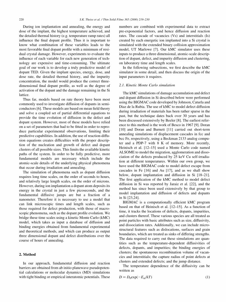
is shown in Fig. 1.
2.2. Input to kMC
The kMC simulations will not properly re¯ect reality
unless the input ®les accurately represent the important
physical phenomena underlying the effect of interest. The
values used for the migration and clustering of B, C, and Si
Is and Vs are discussed in the next subsection. Then the
origin of the input ®les necessary to match ion implantation
experiments are presented.
2.2.1. Parameter ®les
The basic input data necessary for the simulation of
dopant diffusion are migration energies and binding ener-
gies of Vs, Is, dopants, and impurities. Additionally, we
must know the pre-exponential factors in order to determine
the migration and dissociation rates. The required values
can be obtained from different sources, both theoretical
and, in some cases, experimental. The origin of the values
used as input to our kMC simulation are shown in Table 1
and discussed in detail below.
Recent computer simulations have provided a better
understanding of defect production, diffusion, and cluster-
ing in Si. V and I formation and migration energies have
been obtained using ab initio simulations [25±27], tight
binding molecular dynamics [28], and empirical-potential
molecular dynamics [29]. These quantities have not been
independently determined experimentally, and controversy
exists regarding their values. The cause of the wide range of
S.K. Theiss et al. / Thin Solid Films 365 (2000) 219±230 221
Fig. 1. Schematic diagram of the operation of our kinetic Monte Carlo
simulator, BIGMAC. The determination of rates and time steps is discussed
fully in the text.
Table 1
Origin of values for mobile species required as input to our kMC simula-
tions
Species Migration energy Prefactor
Value (eV) Source Value (cm2/s) Source
I 0.9 MD/ab initio 2 Fit to exp. [26]
V 0.43 MD 5 £ 1026 Fit to exp. [26]
Bi 0.3 Ab initio 2 £ 1025 Fit to exp. [33]
CI 0.8 Exp./ab initio 5 £ 1025 Fit to exp. [38]
experimentally determined values for the diffusivity of the
Si self-interstitial will be discussed further below. Prefactors
for V and I diffusion have been obtained from MD simula-
tions. However, in recent experiments, Coffa and Libertino
were able to separately determine the V and I components of
Si diffusivity at room temperature [30]. Based on these data
and calculated migration energies, we have extracted
prefactors for V and I migration.
When the implantation-induced defect supersaturation is
large enough, Vs and Is form clusters. Values for the bind-
ing energies of small V and I clusters have been determined
by tight binding and empirical potential MD simulations
[29,31±33]. The binding energy for an in®nitely large
vacancy cluster was taken as the (calculated) formation
energy of a vacancy, and the binding energy of an in®nitely
large interstitial cluster was determined from the experi-
mentally measured binding energy for large {311} defects,
which are extended clusters of Si interstitials [34]. Clusters
of intermediate sizes were assumed to lie on a smooth inter-
polation between the small cluster energies and the in®nite
cluster energies. The prefactors for cluster dissolution were
taken to be the same as those for the migration of the free
species.
The energetics of dopants and impurities (e.g. C) have
also been studied using ab initio calculations. These can
provide accurate information about the migration paths for
dopants such as B and P [25,27] and about the binding
energies of Vs and Is with dopant or impurity atoms [35±
37]. B is a pure interstitial-type diffuser [38]. It diffuses via a
`kick-out' mechanism, with the aid of Si interstitials
[25,39,40]. An I binds with a substitutional B, forming the
immobile cluster BI. Then there is some probability for the
Si atom to `kick' the B atom off of its lattice site, creating
interstitial B, Bi. Although it is in a higher energy state than
the immobile BI, Bi can diffuse very rapidly. There is an
energy barrier for `kick-in', when it returns to its substitu-
tional state by displacing a Si atom into an interstitial site. A
Bi may bind to B to form B2I, and a mobile I may join a BI
pair to form B12. These clusters in turn can grow with the
addition of more Is and Bis. Thus we need the binding
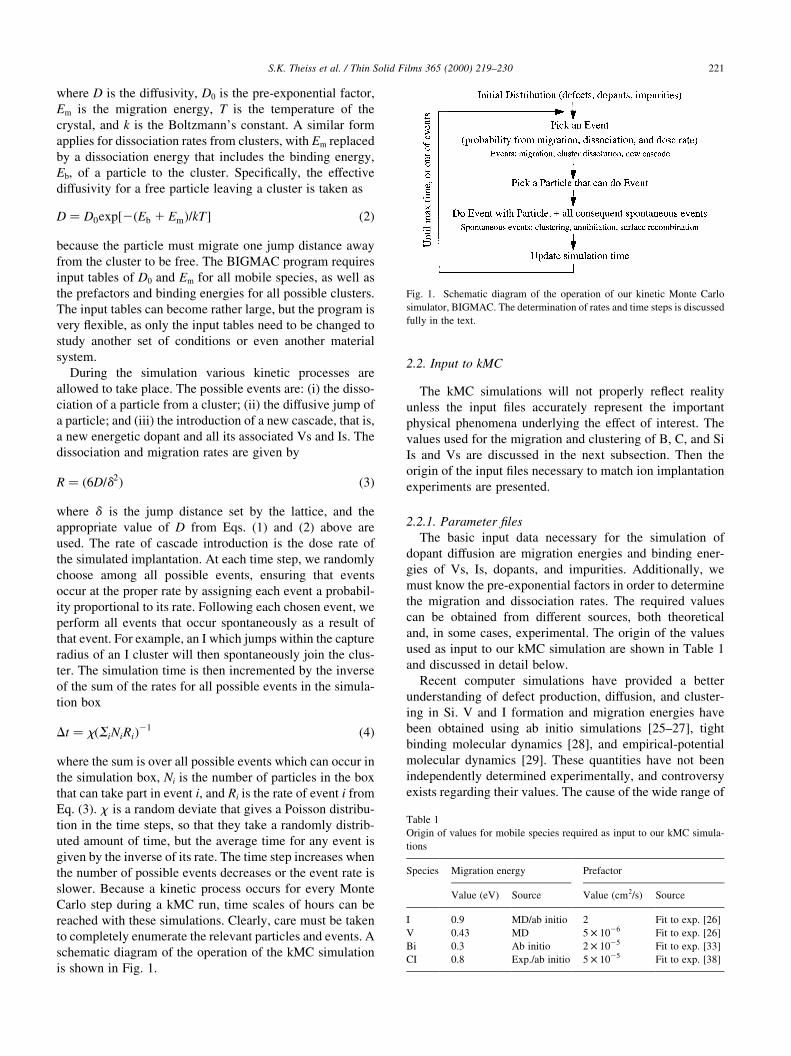
energies for clusters of B atoms and Si interstitials. Values
for such B clusters from ab initio calculations are shown in
Fig. 2. These are complex calculations, and the values in the
table are continually being updated as ®rst principles meth-
ods and algorithms advance.
Prefactors for B migration were obtained from a combi-
nation of experimental data and kMC simulations. Because
of the kick-out mechanism, there are ®ve events that occur
during the migration of a B atom from one substitutional site
to another:
1. B 1 I ! BI
2. BI ! Bi (`kick out')
3. Bi migrates
4. Bi ! BI (`kick in')
5. BI ! B 1 I
Event 1 is assumed to occur spontaneously any time an I
approaches within a capture radius (0.235 nm) of B, and
thus we are not concerned with its prefactor. The experi-
mentally determined prefactor for equilibrium B diffusion is
a complicated, temperature-dependent function of the
prefactors for the remaining four reactions. Therefore we
assume a prefactor based on the Debye frequency in Si for
all four reactions (D0 � nDd2=6 � 1 £ 1023 cm2/s), and
monitor a kMC cell with periodic boundary conditions in
which we originally have one substitutional B and one I.
Based on the number of hops taken by the B atom (as Bi) as
a function of temperature, and adjusting for box size effects
and interstitial concentration, we obtain a value for the equi-
librium B diffusivity. The prefactor for Bi migration is
adjusted until the temperature dependent diffusivity in the
simulation matched that determined experimentally [41].
The prefactors for the dissolution of B±I clusters are
assumed to be determined by the prefactor for migration
of the departing species. That is, the prefactor for the reac-
tion B21! BI 1 I is taken to be that for I migration, while
that for B21! B 1 Bi is taken to be that for Bi migration.
These values are not independently determined, and may be
adjusted (within limits) to change the time for dissolution of
the B clusters.
Energetics for the trapping of Is by C have also been
determined by ab initio calculations. This interaction can
be summed up as follows:
C 1 I$ CI
CI 1 C$ CIC
Thus there are two types of traps for the Si interstitial: a
mobile trap with a single C, CI, formed by the Watkins
replacement mechanism [42,43], and an immobile complex,
CIC, formed when a mobile CI interacts with a substitu-
S.K. Theiss et al. / Thin Solid Films 365 (2000) 219±230222
Fig. 2. B clustering reactions considered in the simulations presented in this
review, with energies in eV from ab initio calculations. Adding an I (Si
interstitial) transforms a cluster to the one below it to the left; adding a Bi
(mobile B interstitial) transforms it to the one below and to the right, and
adding a vacancy transforms it to the cluster above and to the right. These
clustering or annihilation reactions all occur spontaneously. Additionally,
B2I321 and B3I21 each spontaneously emit an I21, to form B2I28 and B3I2,
respectively. The energies given are those used for dissolution in our simu-
lations, and include both the cluster binding energy and the migration
energy for the emitted species.
tional C atom [44,45]. It is possible for the CI pair to
dissolve, releasing a free self-interstitial I. This interaction
leads to an effective diffusivity for the self interstitial which
is higher than one would obtain for a simple ®xed trap but
far less than the bare I diffusivity ± even for modest concen-
trations of C. The prefactor for CI migration was obtained
by a ®tting to experimental measurements of C diffusivity
[46], similar to the technique described above for obtaining
the factor for Bi migration.
These reaction rates are fundamental parameters for any
Monte Carlo simulation of defect and dopant diffusion in Si.
The initial conditions or boundary conditions will change
depending on the type of experiment to be simulated: ion
implantation, oxidation enhanced diffusion (OED), etc. In
particular, for ion implantation it is necessary to obtain the
initial con®guration of the Vs and Is created in the Si lattice
by the energetic ions, as discussed next.
2.2.2. Ion implantation: cascades
The distribution of the dopant atoms after implantation
can be accurately modeled by binary collision codes, such as
UT Marlowe [7]. UT Marlowe was developed by A.F. Tasch
and co-workers at the University of Texas and is based on
the original code of M.T. Robinson at Oak Ridge National
Laboratory [47±51]. This code has been discussed exten-
sively elsewhere and will therefore not be described in detail
here. In essence, it allows simulation of different implanted
species, energies, angles and doses in Si. In the binary colli-
sion approximation, two atoms interact according to a
simple repulsive interatomic potential, and it is assumed
that collisions occur between a moving and a stationary
atom only. Many-body effects that arise in dense collision
cascades are ignored. The implanted ion undergoes a series
of binary collisions with the lattice atoms. The recoiling
lattice atoms collide with other lattice atoms, and so on.
Thus the simulation also provides information about the
cascade of defects produced by each implanted ion; that
is, the location of all the Vs and Is produced during the
irradiation. The defect distribution obtained from this
model is valid for irradiation with light ions, when the
damage is primarily in the form of V±I pairs (Frenkel
pairs) and no direct amorphization is produced by the
implanted ions.
3. Results
3.1. Diffusivity of the Si interstitial
3.1.1. C trapping
One of the most important parameters in a microscopic
model for dopant TED in Si is the diffusivity of the Si self-
interstitial. Unfortunately, values for the interstitial diffusiv-
ity reported in the literature vary over at least ®ve orders of
magnitude at typical dopant activation annealing tempera-
tures (800±10008C) [52±54]. It has been suggested that trap-
ping of sel®nterstitials by different concentrations of C
impurities may play a role in the differences reported.
In order to examine the effect of C on self interstitial
diffusion, we performed kMC simulations in which we
®xed the I population at the surface, C(I,0), and monitored
the evolution of the I depth pro®le with time. For pure I
diffusion the concentration pro®le should follow
C�I; x� � C�I; 0�erfc{x=���������4D1t�p
}
where D1 is the effective I diffusivity and x is depth. In the
simulations, the I surface concentration was maintained at
1 £ 1012 cm23 and the C concentration was varied from 0 to
1 £ 1018 cm23. In the presence of C, the I pro®le is not
expected to be a pure complementary error function;
however, we ®nd that the data can be closely ®t with this
function, and it allows us to calculate a diffusivity. By
performing simulations at temperatures between 700 and
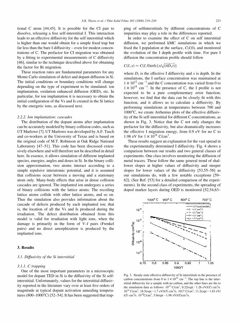
10008C, we create Arrhenius plots of the effective diffusiv-
ity of the Si self-interstitial for different C concentrations, as
shown in Fig. 3. Notice that the C not only changes the
prefactor for the diffusivity, but also dramatically increases
the effective I migration energy, from 0.9 eV for no C to
1.98 eV for 1 £ 1018 C/cm3.
These results suggest an explanation for the vast spread in
the experimentally determined I diffusivity. Fig. 4 shows a
comparison between our results and two general classes of
experiments. One class involves monitoring the diffusion of
metal tracers. These follow the same general trend of shal-
lower slopes at higher values of diffusivity and steeper
slopes for lower values of the diffusivity [53,55±58] as
our simulations do, with a few notable exceptions [59±
62]. (See Ref. [53] for a detailed comparison of the experi-
ments). In the second class of experiments, the spreading of
doped marker layers during OED is monitored [52,54,63±
S.K. Theiss et al. / Thin Solid Films 365 (2000) 219±230 223
Fig. 3. Steady-state effective diffusivity of Si interstitials in the presence of
carbon concentrations from 0 to 1 £ 1018 cm23. The top line is the inter-
stitial diffusivity for a sample with no carbon, and the other lines are ®ts to
the simulation data as follows: 1015 C/cm3, 0.22exp(21.26 eV/kT) cm2/s.
1016 C/cm3, 18.5exp(21.7 eV/kT) cm2/s. 1017 C/cm3, 11.2exp(21.83 eV/
kT) cm2/s. 1018C/cm3, 5.8exp(21.98 eV/kT)cm2/s.

65]. In this case, a much lower diffusivity has been
measured and activation energies for migration were deter-
mined to be in the range of 3.1 eV. These results cannot be
explained only by C trapping of Is. In order to understand
these data, we must also include the effect of B as an I trap,
as discussed next.
3.1.2. B trapping
In order to understand and help interpret the results of the
B-spike OED experiments, we have used our kMC code to
simulate the spreading of B spikes during OED and under
the same conditions as the experiments of Gossmann et al.
[63]. The OED simulations were carried out as described
above, but in this case the starting bulk consisted of a set of
B delta-doped spikes within a Si matrix, see Fig. 5. A back-
ground concentration of 5 £ 1017cm23 C was included,
which is about the level to be expected in epitaxially
grown Si. The surface concentration of Si self-interstitials
was maintained at 2 £ 1010 cm23 and the annealing
temperature was 8108C. Simulations were carried out for
samples with six spikes with a maximum B concentration
of 1 £ 1018 and 1 £ 1019 cm23. For the case of low B
concentration, the agreement between the experiments and
the simulations is excellent. However, this is not the case for
the simulations on the high B concentration spikes. We will
return to the disparity in the high concentration case at the
end of the section. First, we use the low concentration simu-
lations to extract the effective diffusivity of the Si self inter-
stitial by two different ways.
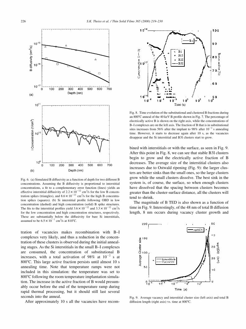
The ®rst method to determine the diffusivity of the Si self
interstitial is to measure the width of the as-deposited and
annealed spikes to calculate A the B diffusivities. The diffu-
sivity of the Si self-interstitial is extracted from the B diffu-
sivity pro®les by ®tting the spreading of the peaks with a
Gaussian and assuming that the B diffusivity is proportional
to the self-interstitial concentration. This is the method that
would be used in an experiment. The depth dependent B
diffusivity extracted from these simulations is shown in Fig.
6a. This method gives similar results to Gossmann's analy-
sis for low B concentrations where a simple diffusion model
with traps is used to ®t the diffusivity. B±I clusters are a
small fraction of the total B, so the spreading of the peaks is
expected to give a good measure of the effective diffusivity.
Fig. 6 shows the results of such a procedure on the simulated
pro®les. The agreement between the simulations and the
experimental data for the low B concentration case is excel-
lent.
The second method to determine the diffusivity of the Si
interstitial was to examine directly the simulated interstitial
concentration pro®le in the low concentration spike spread-
S.K. Theiss et al. / Thin Solid Films 365 (2000) 219±230224
Fig. 5. Experiment and simulation of B diffusion during OED of two
different structures with six B spikes. Initial peak B concentrations were
(a) 1 £ 1018 cm23, and (b) 1 £ 1019 cm23. The as-deposited pro®les (dotted
lines) were used as the starting point for kMC simulations. The experimen-
tal pro®les after 15 mm. annealing at 8108C are shown by the solid lines.
The simulated results (diamonds) are obtained with a surface Si interstitial
concentration of 2 £ 1010 cm23 and a uniform C concentration of 5 £ 1017
cm23. Signi®cant B±I clustering (dashed line) was observed only in the
high B concentration case. Fermi level effects, which are not included in
these simulations, are the probable cause of the discrepancy in b between
the experiments and the simulations.
Fig. 4. Comparison between the experimentally measured (dashed lines,
open symbols) and the simulated (solid lines, closed symbols) Si self-inter-
stitial diffusivities. Results labeled 1±13 correspond to Refs. [53±55],
respectively.
ing experiment. We ®nd that the spike-spreading method
gives a diffusivity of 2:2 £ 10212 cm2/s while a ®t to the
interstitial concentration pro®le yields an effective diffusiv-
ity of 3:6 £ 10212 cm2/s. The difference is within the accu-
racy of the simulation, and the result supports the idea that B
spike width spreading measures the interstitial pro®le.
However, both of these methods give a Si self-interstitial
diffusivity which is orders of magnitude smaller than the
diffusivity we measure for a system with no B, only C
(~1 £ 1028 cm2/s, see Fig. 3). Yet B comprises only about
25% of the total number of traps within the delta-doped
region. The effect is due to the fact that the ®rst order C
trap, CI, is still mobile, with a diffusivity of about 2 £ 1029
cm2/s at 8108C, while the BI complex is immobile. Thus a
combination of C and B trapping of Si interstitials can
reconcile the large differences in diffusivity obtained from
the different experiments designed to measure the diffusiv-
ity of the Si self-interstitial.
Next we consider the high concentration B spikes. For
this case, the spreading of the B markers is much less in the
simulations than is observed in the experiments. The simu-
lations show a lower effective diffusivity for the high
concentration spikes due to the trapping of self-interstitials
in B-I complexes and clusters. The dashed line in Fig. 5b
shows the population of interstitials which are in immobile
species for the high B concentration spikes. For comparison,
the low concentration spikes had a peak cluster concentra-
tion of about 1 £ 1011 cm23 almost four orders of magnitude
less than the high concentration spikes. The concentration
pro®le of freely diffusing self-interstitials is shown in Fig.
6b. Clearly the high concentration B spikes strongly perturb
the I population, but no reduction in B diffusivity was
observed in the experiments. We believe that the discre-
pancy is a result of the fact that at high B concentrations
the diffusivity of B increases [66±68] due to the increased
concentration of charged Is and Bis, which have a different
migration and formation energy than their neutral counter-
parts. This effect is not yet included in our model. Thus the
higher diffusivity of B in extrinsic material could offset the
reduction in diffusivity due to increased trapping.
3.2. keV B implantation
We have done a series of simulations of the TED of
implanted B as a function of temperature and time, and as
a function of the energy of the implanted B. A constant dose
of 2 £ 1014 cm22 was used in all cases.
3.2.1. Temperature dependence
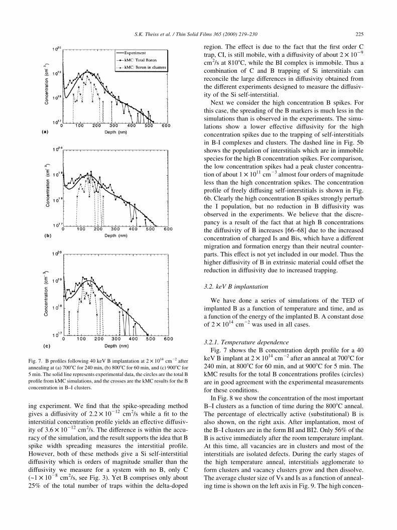
Fig. 7 shows the B concentration depth pro®le for a 40
keV B implant at 2 £ 1014 cm22 after an anneal at 7008C for
240 min, at 8008C for 60 min, and at 9008C for 5 min. The
kMC results for the total B concentrations pro®les (circles)
are in good agreement with the experimental measurements
for these conditions.
In Fig. 8 we show the concentration of the most important
B±I clusters as a function of time during the 8008C anneal.
The percentage of electrically active (substitutional) B is
also shown, on the right axis. After implantation, most of
the B±I clusters are in the form BI and BI2. Only 56% of the
B is active immediately after the room temperature implant.
At this time, all vacancies are in clusters and most of the
interstitials are isolated defects. During the early stages of
the high temperature anneal, interstitials agglomerate to
form clusters and vacancy clusters grow and then dissolve.
The average cluster size of Vs and Is as a function of anneal-
ing time is shown on the left axis in Fig. 9. The high concen-
S.K. Theiss et al. / Thin Solid Films 365 (2000) 219±230 225
Fig. 7. B pro®les following 40 keV B implantation at 2 £ 1014 cm22 after
annealing at (a) 7008C for 240 min, (b) 8008C for 60 min, and (c) 9008C for
5 min. The solid line represents experimental data, the circles are the total B
pro®le from kMC simulations, and the crosses are the kMC results for the B
concentration in B±I clusters.
tration of vacancies makes recombination with B±I
complexes very likely, and thus a reduction in the concen-
tration of these clusters is observed during the initial anneal-
ing stages. As the Si interstitials in the small B±I complexes
are consumed, the concentration of substitutional B
increases, with a total activation of 98% at 1022 s at
8008C. This large active fraction persists until almost 10 s
annealing time. Note that temperature ramps were not
included in this simulation: the temperature was set to
8008C following the room temperature implantation simula-
tion. The increase in the active fraction of B would presum-
ably occur before the end of the temperature ramp during
rapid thermal processing, but it should still last several
seconds into the anneal.
After approximately 10 s all the vacancies have recom-
bined with interstitials or with the surface, as seen in Fig. 9.
After this point in Fig. 8, we can see that stable B3I clusters
begin to grow and the electrically active fraction of B
decreases. The average size of the interstitial clusters also
increases due to Ostwald ripening (Fig. 9): the larger clus-
ters are better sinks than the small ones, so the large clusters
grow while the small clusters dissolve. The best sink in the
system is, of course, the surface, so when enough clusters
have dissolved that the spacing between clusters becomes
greater than the cluster-surface distance, all the clusters will
tend to shrink.
The magnitude of B TED is also shown as a function of
time in Fig. 9. Interestingly, of the 48 nm of total B diffusion
length, 8 nm occurs during vacancy cluster growth and
S.K. Theiss et al. / Thin Solid Films 365 (2000) 219±230226
Fig. 8. Time evolution of the substitutional and clustered B fractions during
an 8008C anneal of the 40 keV B pro®le shown in Fig. 7. The percentage of
electrically active B is shown on the right axis, while the concentrations of
B±I complexes are on the left axis. The fraction of B that is in substitutional
sites increases from 56% after the implant to 98% after 1022 s annealing
time. However, it starts to decrease again after 10 s, as the vacancies
disappear and the Si interstitial and B3I clusters start to grow.
Fig. 9. Average vacancy and interstitial cluster size (left axis) and total B
diffusion length (right axis) vs. time at 8008C.
Fig. 6. (a) Simulated B diffusivity as a function of depth for two different B
concentrations. Assuming the B diffusivity is proportional to interstitial
concentrations, a ®t to a complementary error function (lines) yields an
effective interstitial diffusivity of 2:2 £ 10212 cm2/s for the low B concen-
tration spikes (triangles), and 8:6 £ 10213 cm2/s for the high B concentra-
tion spikes (squares). (b) Si interstitial pro®le following OBD in low
concentration (dashed) and high concentration (solid) B spike structures.
The ®ts to the interstitial pro®les yield 3:6 £ 10212 and 3:3 £ 10212 cm2/s
for the low concentration and high concentration structures, respectively.
These are substantially below the diffusivity for bare Si interstitials,
assumed to be 6:5 £ 1027 cm2/s at 8108C.
dissolution, 36 nm during interstitial cluster ripening, and
only 4 nm during the ®nal I cluster (i.e. {311} defect) disso-
lution.
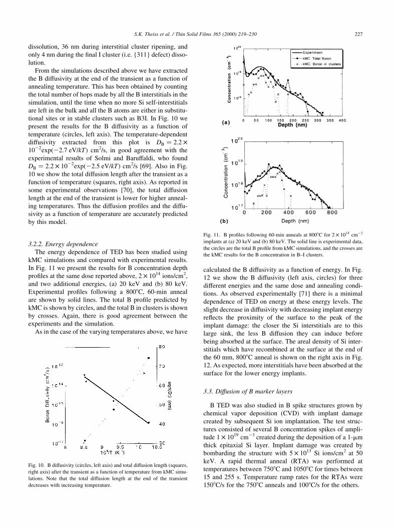
From the simulations described above we have extracted
the B diffusivity at the end of the transient as a function of
annealing temperature. This has been obtained by counting
the total number of hops made by all the B interstitials in the
simulation, until the time when no more Si self-interstitials
are left in the bulk and all the B atoms are either in substitu-
tional sites or in stable clusters such as B3I. In Fig. 10 we
present the results for the B diffusivity as a function of
temperature (circles, left axis). The temperature-dependent
diffusivity extracted from this plot is DB � 2:2 £1022exp�22:7 eV=kT� cm2/s, in good agreement with the
experimental results of Solmi and Baruffaldi, who found
DB � 2:2 £ 1022exp�22:5 eV=kT� cm2/s [69]. Also in Fig.
10 we show the total diffusion length after the transient as a
function of temperature (squares, right axis). As reported in
some experimental observations [70], the total diffusion
length at the end of the transient is lower for higher anneal-
ing temperatures. Thus the diffusion pro®les and the diffu-
sivity as a function of temperature are accurately predicted
by this model.
3.2.2. Energy dependence
The energy dependence of TED has been studied using
kMC simulations and compared with experimental results.
In Fig. 11 we present the results for B concentration depth
pro®les at the same dose reported above, 2 £ 1014 ions/cm2,
and two additional energies, (a) 20 keV and (b) 80 keV.
Experimental pro®les following a 8008C, 60-min anneal
are shown by solid lines. The total B pro®le predicted by
kMC is shown by circles, and the total B in clusters is shown
by crosses. Again, there is good agreement between the
experiments and the simulation.
As in the case of the varying temperatures above, we have
calculated the B diffusivity as a function of energy. In Fig.
12 we show the B diffusivity (left axis, circles) for three
different energies and the same dose and annealing condi-
tions. As observed experimentally [71] there is a minimal
dependence of TED on energy at these energy levels. The
slight decrease in diffusivity with decreasing implant energy
re¯ects the proximity of the surface to the peak of the
implant damage: the closer the Si interstitials are to this
large sink, the less B diffusion they can induce before
being absorbed at the surface. The areal density of Si inter-
stitials which have recombined at the surface at the end of
the 60 mm, 8008C anneal is shown on the right axis in Fig.
12. As expected, more interstitials have been absorbed at the
surface for the lower energy implants.
3.3. Diffusion of B marker layers
B TED was also studied in B spike structures grown by
chemical vapor deposition (CVD) with implant damage
created by subsequent Si ion implantation. The test struc-
tures consisted of several B concentration spikes of ampli-
tude 1 £ 1019 cm23 created during the deposition of a 1-mm
thick epitaxial Si layer. Implant damage was created by
bombarding the structure with 5 £ 1013 Si ions/cm2 at 50
keV. A rapid thermal anneal (RTA) was performed at
temperatures between 7508C and 10508C for times between
15 and 255 s. Temperature ramp rates for the RTAs were
1508C/s for the 7508C anneals and 1008C/s for the others.
S.K. Theiss et al. / Thin Solid Films 365 (2000) 219±230 227
Fig. 10. B diffusivity (circles, left axis) and total diffusion length (squares,
right axis) after the transient as a function of temperature from kMC simu-
lations. Note that the total diffusion length at the end of the transient
decreases with increasing temperature.
Fig. 11. B pro®les following 60-min anneals at 8008C for 2 £ 1014 cm22
implants at (a) 20 keV and (b) 80 keV. The solid line is experimental data,
the circles are the total B pro®le from kMC simulations, and the crosses are
the kMC results for the B concentration in B±I clusters.
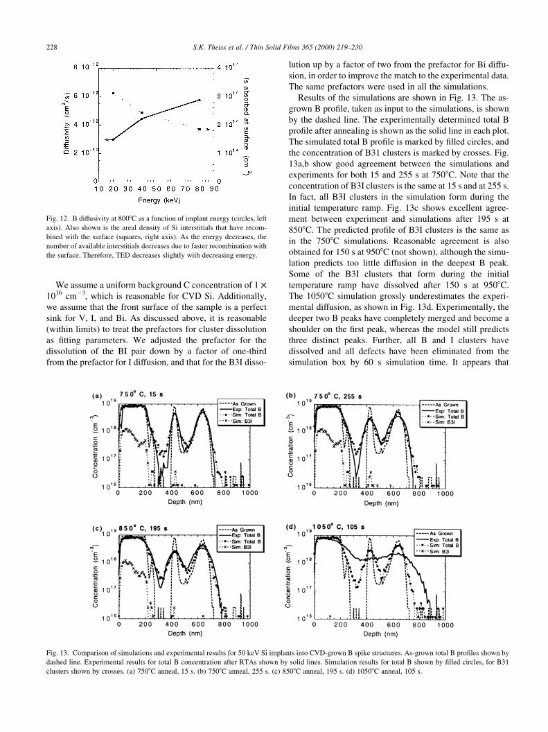
We assume a uniform background C concentration of 1 £1016 cm23, which is reasonable for CVD Si. Additionally,
we assume that the front surface of the sample is a perfect
sink for V, I, and Bi. As discussed above, it is reasonable
(within limits) to treat the prefactors for cluster dissolution
as ®tting parameters. We adjusted the prefactor for the
dissolution of the BI pair down by a factor of one-third
from the prefactor for I diffusion, and that for the B3I disso-
lution up by a factor of two from the prefactor for Bi diffu-
sion, in order to improve the match to the experimental data.
The same prefactors were used in all the simulations.
Results of the simulations are shown in Fig. 13. The as-
grown B pro®le, taken as input to the simulations, is shown
by the dashed line. The experimentally determined total B
pro®le after annealing is shown as the solid line in each plot.
The simulated total B pro®le is marked by ®lled circles, and
the concentration of B31 clusters is marked by crosses. Fig.
13a,b show good agreement between the simulations and
experiments for both 15 and 255 s at 7508C. Note that the
concentration of B3I clusters is the same at 15 s and at 255 s.
In fact, all B3I clusters in the simulation form during the
initial temperature ramp. Fig. 13c shows excellent agree-
ment between experiment and simulations after 195 s at
8508C. The predicted pro®le of B3I clusters is the same as
in the 7508C simulations. Reasonable agreement is also
obtained for 150 s at 9508C (not shown), although the simu-
lation predicts too little diffusion in the deepest B peak.
Some of the B3I clusters that form during the initial
temperature ramp have dissolved after 150 s at 9508C.
The 10508C simulation grossly underestimates the experi-
mental diffusion, as shown in Fig. 13d. Experimentally, the
deeper two B peaks have completely merged and become a
shoulder on the ®rst peak, whereas the model still predicts
three distinct peaks. Further, all B and I clusters have
dissolved and all defects have been eliminated from the
simulation box by 60 s simulation time. It appears that
S.K. Theiss et al. / Thin Solid Films 365 (2000) 219±230228
Fig. 12. B diffusivity at 8008C as a function of implant energy (circles, left
axis). Also shown is the areal density of Si interstitials that have recom-
bined with the surface (squares, right axis). As the energy decreases, the
number of available interstitials decreases due to faster recombination with
the surface. Therefore, TED decreases slightly with decreasing energy.
Fig. 13. Comparison of simulations and experimental results for 50 keV Si implants into CVD-grown B spike structures. As-grown total B pro®les shown by
dashed line. Experimental results for total B concentration after RTAs shown by solid lines. Simulation results for total B shown by ®lled circles, for B31
clusters shown by crosses. (a) 7508C anneal, 15 s. (b) 7508C anneal, 255 s. (c) 8508C anneal, 195 s. (d) 10508C anneal, 105 s.

some additional mechanism which is not accounted for in
the model is having a profound effect.
This additional mechanism is not equilibrium B diffusion.
The equilibrium diffusion length of B was calculated to be
only 20 nm after 100 s at 10508C. Additionally, we checked
the effect of an equilibrium concentration of Si interstitials
in our kMC simulation. The equilibrium number of Si inter-
stitials in a sample the size of our simulation box was calcu-
lated to be about 0.1. We added a Si interstitial in a random
position after the end of the transient, and set both the front
and back surfaces re¯ecting. The interstitial had a minimal
effect on the B pro®le after 10 s additional simulation.
The effect may turn out to be due to unexpected OED.
Felch and co-workers have shown that adding 300 ppm O2
to the RTA gas can increase the junction depth more than 30
nm in 10 s at 10508C [72]. Further, it has been shown that
hundreds of ppm of O2 can outgas from the surface of a
nominally oxide-free wafer at these temperatures [73],
which might then cause OED. Further experimental work
is required to identify the time scale and source of the
observed diffusion.
4. Conclusions
We have described some recent simulations of defect and
dopant diffusion using a kinetic Monte Carlo approach. We
have shown that the trapping of Si interstitials by both C and
B can help explain the enormous variation in their measured
diffusivity. Excellent agreement was found between experi-
ments and simulations for TED at temperatures between
7008C and 9008C following medium energy B implants
(20±80 keV). Our simulations produced novel predictions
of the time evolution of the electrically active B fraction
during annealing, which provide an intriguing possibility for
experimental veri®cation. Good agreement was also found
between experiments and simulations of TED following 50
keV Si ion implantation into CVD-grown B spike structures
at temperatures up to 9508C. For anneals above 9508C, our
simulations do not correctly predict the amount of diffusion.
This may be due to unexpected processes, such as OED,
occurring in the experiment, or it may be due to a heretofore
unexplored limitation of the physics in the model. Addi-
tional ®rst-principles calculations are under way with the
expectation that improving the accuracy of the input para-
meters for the initial stages of B±I clustering and mobile Bi
formation will improve the results of these simulations.
Another area requiring further investigation for predicting
the properties of future devices is the recombination ef®-
ciency of defects and dopants at surfaces, since the interac-
tions of defects with the Si/SiO2 interface is not fully
understood. This is a critical issue when the implantation
energies are reduced, so that most of the damage is concen-
trated near the surface. Additionally, Fermi level effects on
dopant diffusion will become even more important as peak
dopant concentrations approach 1020 cm23 and beyond. We
are in the process of including such effects in our model.
Acknowledgements
Martin Giles of Intel Corporation and Peter Grif®n and
Ant Ural of Stanford University respectively provided us
with 40 keV B implant and the 50 keV Si implant experi-
mental data. Martin Giles also provided us with invaluable
advice and encouragement during the development of the
kMC simulator, as did Majeed Foad of Applied Materials
Corporation. Interactions with Mark Law, Kevin Jones, and
Aaron Lilak at the University of Florida throughout the life-
time of the project were most valuable and served to keep us
grounded in reality. Many fruitful discussions and interac-
tions with George Gilmer, Lourdes Pelaz, David Eagle-
sham, Martin Jaraiz, and Hans Gossmann of Lucent
Technologies Bell Laboratories are gratefully acknowl-
edged. This work was performed under the auspices of the
U.S. Department of Energy by Lawrence Livermore
National Laboratory under contract W-7405-Eng-48.
References
[1] Semiconductor Industry Association, The National Technology
Roadmap for Semiconductors, SEMATECH, 1997.
[2] A.E. Michel, Appl. Phys. Lett. 50 (1987) 416.
[3] N.E.B. Cowern, J. Appl. Phys. 64 (1988) 4484.
[4] S. Solmi, F. Baruffaldi, J. Appl. Phys. 69 (1988) 3384.
[5] K.S. Jones, H.G. Robinson, J. Listebarger, et al., Nucl. Instrum. Meth-
ods Phys. Res. B 96 (1995) 196.
[6] P.M. Fahey, P.B. Grif®n, J.D. Plummer, Rev. Mod. Phys. 61 (1989)
289.
[7] S. Tian, S.J. Morris, B. Obradovic, et al., UT-Marlowe, Version 4.0,
1996.
[8] J.R. Beeler Jr., Radiation Effects Computer Experiments, North
Holland, Amsterdam, 1983.
[9] D.G. Besco, Computer Simulation of point defect annealing in metals,
USA-AEC report GEMP-644, 1967.
[10] D.G. Doran, Rad. Eff. 2 (1970) 249.
[11] D.G. Doran, R.A. Burnett, in: P.C. Gehlen, J.R. Beeler Jr., R.I. Jaffee
(Eds.), Interatomic Potentials and Simulations of Lattice Defects,
Plenum Press, New York, 1972, p. 403.
[12] H. Heinisch, J. Nucl. Mater. 117 (1983) 46.
[13] H. Heinisch, B.N. Singh, T. Diaz de la Rubia, J. Nucl. Mater. 212±215
(1994) 127.
[14] H. Heinisch, B.N. Singh, J. Nucl. Mater. 191±194 (1992) 125.
[15] H. Heinisch, B.N. Singh, J. Nucl. Mater. 251 (1997) 77.
[16] N. Soneda, T. Diaz de la Rubia, Philos. Mag. A 78 (1998) 995.
[17] T. Diaz de la Rubia, N. Soneda, M.J. Caturla, E. Alonso, J. Nucl.
Mater. 251 (1997) 13.
[18] M.D. Johnson, M.-J. Caturia, T. Diaz de la Rubia, J. Appl. Phys. 84
(1998) 1963.
[19] M.-J. Caturla, M.D. Johnson, T. Diaz de la Rubia, Appl. Phys. Lett. 72
(1998) 2736.
[20] M.-J. Caturla, Comp. Mater. Sci. 12 (1998) 319.
[21] S.K. Theiss, M.-J. Caturla, T. Diaz de la Rubia, M.D. Johnson, A.
Ural, P.B. Grif®n, MRS Symp. Proc. (2000) 538 in press.
[22] M. Jaraiz, G.H. Gilmer, J.M. Poate, T. Diaz de la Rubia, Appl. Phys.
Lett. 68 (1996) 409.
S.K. Theiss et al. / Thin Solid Films 365 (2000) 219±230 229
[23] L. Pelaz, M. Jaraiz, G.H. Gilmer, H.-J. Gossmann, Appl. Phys. Lett.
70 (1997) 2285.
[24] L. Pelaz, G.H. Gilmer, M. Jaraiz, et al., Appl. Phys. Lett. 73 (1998)
1421.
[25] C.S. Nichols, C.G. Van de Walle, S.T. Pantelides, Phys. Rev. B 40
(1989) 5458.
[26] W.A. Harrison, MRS Symp. Proc. 469 (1997) 211.
[27] J. Zhu, T. Diaz de la Rubia, L.H. Yang, C. Malihiot, G.H. Gilmer,
Phys. Rev. B 54 (1996) 4741.
[28] M. Tang, L. Colombo, J. Zhu, T. Diaz de la Rubia, Phys. Rev. B 55
(1997) 1.
[29] G.H. Gilmer, T. Diaz de la Rubia, D.M. Stock, M. Jaraiz, Nucl.
Instrum. Methods B 102 (1995) 247.
[30] S. Coffa, S. Libertino, Appl. Phys. Lett. 73 (1998) 3369.
[31] A. Bongiorno, L. Colombo, T. Diaz de la Rubia, Europhys. Lett. 43
(1998) 695.
[32] L. Colombo, A. Bongiorno, F. Cargnoni, C. Gatti, M. Rosati, MRS
Symp. Proc. (2000) 538 in press.
[33] A. Bongiorno, L. Colombo, F. Cargnoni, C. Gatti, M. Rosati,
submitted for publication (1999)
[34] P.A. Stolk, H.-J. Gossmann, D.J. Eaglesham, et al., J. Appl. Phys. 81
(1997) 6031.
[35] J. Zhu, Mater. Res. Soc. Symp. Proc. 469 (1997) 151.
[36] O. Pankratov, H. Huang, T. Diaz de la Rubia, C. Mailhiot, Phys. Rev.
B 56 (1997) 13172.
[37] J.S. Nelson, P.A. Schultz, A.F. Wright, Appl. Phys. Lett. 73 (1998)
247.
[38] H.-J. Gossmann, T.E. Haynes, P.A. Stolk, et al., Appl. Phys. Lett. 71
(1997) 3862.
[39] C.S. Nichols, C.G. Van de Walle, S.T. Pantelides, Phys. Rev. Lett. 62
(1989) 1049.
[40] N.E.B. Cowern, G.F.A. van de Walle, D.J. Gravesteijn, C.J. Vrei-
zema, Phys. Rev. Lett. 67 (1991) 212.
[41] A.D. Kurtz, R. Yee, J. Appl. Phys. 31 (1960) 303.
[42] G.D. Watkins, K.L. Brower, Phys. Rev. Lett. 36 (1976) 1329.
[43] L.W. Song, G.D. Watkins, Phys. Rev. B 42 (1990) 5759.
[44] L.W. Song, X.D. Zhan, B.W. Benson, G.D. Watkins, Phys. Rev. B 42
(1990) 5765.
[45] G. Davies, K.T. Kun, T. Reade, Phys. Rev. B 44 (1991) 12146.
[46] F. Rollert, N.A. Stolwijk, H. Mehrer, Proc. 15th Conf.: Defects in
Semiconductors, Budapest, 1988.
[47] M.T. Robinson, I.M. Torrens, Phys. Rev. B 9 (1974) 5008.
[48] M. Hou, M.T. Robinson, Nucl. Instrum. Methods 132 (1976) 641.
[49] S. Oen, M.T. Robinson, Nucl. Instrum. Methods 132 (1976) 647.
[50] M.T. Robinson, J. Appl. Phys. 54 (1983) 2650.
[51] M.T. Robinson, Phys. Rev. B 27 (1983) 5347.
[52] K.J. van Oostrum, P.C. Zalm, W.B. deBoer, D.J. Gravesteijn, J.W.F.
Maes, Appl. Phys. Lett. 70 (1997) 2285.
[53] H. Bracht, N.A. Stolwijk, H. Mehrer, Proc. Electrochem. Soc. 94
(1994) 593.
[54] H.-J. Gossmann, C.S. Rafferty, H.S. Luftman, F.C. Unterwald, T.
Boone, J. Poate, Appl. Phys. Lett. 63 (1993) 639.
[55] F.F. Morehead, MRS Symp. Proc. 104 (1988) 99.
[56] H. Zimmermann, H. Ryssel, Appl. Phys. A 55 (1992) 121.
[57] W. Wijaranakula, J. Appl. Phys. 67 (1990) 7624.
[58] G.B. Bronner, J.D. Plummer, J. Appl. Phys. 61 (1987) 5286.
[59] T.Y. Tan, U. Gosele, Appl. Phys. A 37 (1985) 1.
[60] C. Boit, F. Lau, R. Sittig, Appl. Phys. A 50 (1990) 197.
[61] K. Tanihuchi, D.A. Antonaiadis, Y. Matsushita, Appl. Phys. Lett. 42
(1983) 961.
[62] K. Ghaderi, G. Hobler, M. Budil, L. Mader, H.J. Schuize, J. Appl.
Phys. 77 (1995) 1320.
[63] H.-J. Gossmann, G.H. Gilmer, C.S. Rafferty, et al., J. Appl. Phys. 77
(1995) 1948.
[64] A.M. Agarwal, S.T. Dunham, Appl. Phys. Lett. 63 (1993) 800.
[65] P.B. Grif®n, P.M. Fahey, J.D. Plummer, R.W. Dutton, Appl. Phys.
Lett. 47 (1985) 319.
[66] R.K. Jain, R.V. Overstraeten, J. Appl. Phys. 44 (1973) 2437.
[67] N.D. Thai, J. Appl. Phys. 41 (1970) 2859.
[68] M.D. Giles, IEEE Trans. Comput.-Aided Des. 8 (1989) 466.
[69] S. Solmi, F. Baruffaldi, J. Appl. Phys. 69 (1991) 2135.
[70] P.A. Packan, J.D. Plummer, Appl. Phys. Lett. 56 (1990) 1787.
[71] H.S. Chao, P.B. Grif®n, J.D. Plummer, C.S. Rafferty, Appl. Phys.
Lett. 69 (1996) 2113.
[72] S.B. Felch, Greater Silicon Valley Implant Users Group. Ann. Symp.
Proc., Sunnyvale, CA, 1999.
[73] M.A. Foad, Greater Silicon Valley Implant Users Group. Ann. Symp.
Proc., Sunnyvale, CA, 1999.
S.K. Theiss et al. / Thin Solid Films 365 (2000) 219±230230
Copyright © 2022 FDOKUMEN