ARM1136JF-S and ARM1136J-S Technical Reference Manual
840
Copyright © 2002-2007, 2009 ARM Limited. All rights reserved. ARM DDI 0211K ARM1136JF-S ™ and ARM1136J-S ™ Revision: r1p5 Technical Reference Manual
-
Upload
khangminh22 -
Category
Documents
-
view
0 -
download
0
Transcript of ARM1136JF-S and ARM1136J-S Technical Reference Manual

ARM1136JF-S™ and ARM1136J-S™
Revision: r1p5
Technical Reference Manual
Copyright © 2002-2007, 2009 ARM Limited. All rights reserved.ARM DDI 0211K

ARM1136JF-S and ARM1136J-STechnical Reference Manual
Copyright © 2002-2007, 2009 ARM Limited. All rights reserved.
Release Information
The following changes have been made to this manual.
Proprietary Notice
Words and logos marked with ® or ™ are registered trademarks or trademarks of ARM Limited in the EU and other countries, except as otherwise stated below in this proprietary notice. Other brands and names mentioned herein may be the trademarks of their respective owners.
Neither the whole nor any part of the information contained in, or the product described in, this document may be adapted or reproduced in any material form except with the prior written permission of the copyright holder.
The product described in this document is subject to continuous developments and improvements. All particulars of the product and its use contained in this document are given by ARM in good faith. However, all warranties implied or expressed, including but not limited to implied warranties of merchantability, or fitness for purpose, are excluded.
Change History
Date Issue Confidentiality Change
December 2002 A Non-Confidential First Release for r0p0
February 2003 B Non-Confidential Internal release for r0p1
February 2003 C Non-Confidential First release for r0p1
August 2003 D Non-Confidential First release for r0p2
11 May 2004 E Non-Confidential Second release for r0p2
11 March 2005 F Non-Confidential First release for r1p0.
Adds ARMv6k features, see Product revisions on page 1-57.
27 July 2005 G Non-Confidential First release for r1p1.
System control coprocessor and parts of Debug chapters re-organized.
Minor corrections and enhancements.
ID information updated to r1p1.
14 October 2005 H Non-Confidential Second release for r1p1.
01 December 2006 I Non-Confidential First release for r1p3.
No change to technical content.
06 July 2007 J Non-Confidential First release for r1p5.
20 February 2009 K Non-Confidential Unrestricted Access Second release for r1p5.
ii Copyright © 2002-2007, 2009 ARM Limited. All rights reserved. ARM DDI 0211KNon-Confidential Unrestricted Access

This document is intended only to assist the reader in the use of the product. ARM Limited shall not be liable for any loss or damage arising from the use of any information in this document, or any error or omission in such information, or any incorrect use of the product.
Where the term ARM is used it means “ARM or any of its subsidiaries as appropriate”.
Figure 14-1 on page 14-2 reprinted with permission from IEEE Std. 1149.1-2001, IEEE Standard Test Access Port and Boundary-Scan Architecture, copyright 2001 by IEEE. The IEEE disclaims any responsibility or liability resulting from the placement and use in the described manner.
Confidentiality Status
This document is Non-Confidential. The right to use, copy and disclose this document may be subject to license restrictions in accordance with the terms of the agreement entered into by ARM and the party that ARM delivered this document to.
Unrestricted Access is an ARM internal classification.
Product Status
The information in this document is final, that is for a developed product.
Web Address
http://www.arm.com
ARM DDI 0211K Copyright © 2002-2007, 2009 ARM Limited. All rights reserved. iiiUnrestricted Access Non-Confidential

iv Copyright © 2002-2007, 2009 ARM Limited. All rights reserved. ARM DDI 0211KNon-Confidential Unrestricted Access

ContentsARM1136JF-S and ARM1136J-S Technical Reference Manual
PrefaceAbout this manual ....................................................................................... xxxFeedback ................................................................................................. xxxvi
Chapter 1 Introduction1.1 About the ARM1136JF-S processor ........................................................... 1-21.2 Components of the processor ..................................................................... 1-31.3 Power management .................................................................................. 1-231.4 Configurable options ................................................................................. 1-251.5 Pipeline stages .......................................................................................... 1-261.6 Typical pipeline operations ....................................................................... 1-281.7 ARM1136JF-S architecture with Jazelle technology ................................. 1-341.8 ARM1136JF-S instruction sets summaries ............................................... 1-361.9 Product revisions ...................................................................................... 1-57
Chapter 2 Programmer’s Model2.1 About the programmer’s model ................................................................... 2-22.2 Processor operating states ......................................................................... 2-32.3 Instruction length ......................................................................................... 2-42.4 Data types ................................................................................................... 2-5
ARM DDI 0211K Copyright © 2002-2007, 2009 ARM Limited. All rights reserved. vUnrestricted Access Non-Confidential

Contents
2.5 Memory formats .......................................................................................... 2-62.6 Addresses in an ARM1136JF-S system ..................................................... 2-82.7 Operating modes ........................................................................................ 2-92.8 Registers .................................................................................................. 2-102.9 The program status registers .................................................................... 2-162.10 Additional instructions ............................................................................... 2-242.11 Exceptions ................................................................................................ 2-34
Chapter 3 System Control Coprocessor3.1 About the system control coprocessor ....................................................... 3-23.2 System control coprocessor registers overview ....................................... 3-173.3 System control coprocessor register descriptions .................................... 3-25
Chapter 4 Unaligned and Mixed-Endian Data Access Support4.1 About unaligned and mixed-endian support ............................................... 4-24.2 Unaligned access support .......................................................................... 4-34.3 Unaligned data access specification .......................................................... 4-74.4 Operation of unaligned accesses ............................................................. 4-174.5 Mixed-endian access support ................................................................... 4-224.6 Instructions to reverse bytes in a general-purpose register ...................... 4-264.7 Instructions to change the CPSR E bit ..................................................... 4-27
Chapter 5 Program Flow Prediction5.1 About program flow prediction .................................................................... 5-25.2 Branch prediction ........................................................................................ 5-45.3 Return stack ............................................................................................... 5-75.4 Instruction Memory Barrier (IMB) instruction .............................................. 5-85.5 ARM1020T or later IMB implementation .................................................... 5-9
Chapter 6 Memory Management Unit6.1 About the MMU ........................................................................................... 6-26.2 TLB organization ........................................................................................ 6-46.3 Memory access sequence .......................................................................... 6-76.4 Enabling and disabling the MMU ................................................................ 6-96.5 Memory access control ............................................................................. 6-116.6 Memory region attributes .......................................................................... 6-156.7 Memory attributes and types .................................................................... 6-246.8 MMU aborts .............................................................................................. 6-346.9 MMU fault checking .................................................................................. 6-366.10 Fault status and address .......................................................................... 6-426.11 Hardware page table translation ............................................................... 6-456.12 MMU descriptors ...................................................................................... 6-536.13 MMU software-accessible registers .......................................................... 6-666.14 MMU and write buffer ............................................................................... 6-68
vi Copyright © 2002-2007, 2009 ARM Limited. All rights reserved. ARM DDI 0211KNon-Confidential Unrestricted Access

Contents
Chapter 7 Level One Memory System7.1 About the level one memory system ........................................................... 7-27.2 Cache organization ..................................................................................... 7-37.3 Tightly-coupled memory .............................................................................. 7-87.4 DMA .......................................................................................................... 7-117.5 TCM and cache interactions ..................................................................... 7-137.6 Cache debug ............................................................................................. 7-177.7 Write buffer ............................................................................................... 7-18
Chapter 8 Level Two Interface8.1 About the level two interface ....................................................................... 8-28.2 Synchronization primitives .......................................................................... 8-78.3 AHB-Lite control signals in the ARM1136JF-S processor ......................... 8-108.4 Instruction Fetch Interface AHB-Lite transfers .......................................... 8-228.5 Data Read Interface AHB-Lite transfers .................................................... 8-268.6 Data Write Interface AHB-Lite transfers .................................................... 8-538.7 DMA Interface AHB-Lite transfers ............................................................. 8-708.8 Peripheral Interface AHB-Lite transfers .................................................... 8-738.9 AHB-Lite .................................................................................................... 8-76
Chapter 9 Clocking and Resets9.1 Clocking ...................................................................................................... 9-29.2 Reset ........................................................................................................... 9-69.3 Reset modes ............................................................................................... 9-7
Chapter 10 Power Control10.1 About power control .................................................................................. 10-210.2 Power management .................................................................................. 10-3
Chapter 11 Coprocessor Interface11.1 About the coprocessor interface ............................................................... 11-211.2 Coprocessor pipeline ................................................................................ 11-311.3 Token queue management ..................................................................... 11-1011.4 Token queues ......................................................................................... 11-1411.5 Data transfer ........................................................................................... 11-1811.6 Operations .............................................................................................. 11-2311.7 Multiple coprocessors ............................................................................. 11-27
Chapter 12 Vectored Interrupt Controller Port12.1 About the PL192 Vectored Interrupt Controller ......................................... 12-212.2 About the ARM1136JF-S VIC port ............................................................ 12-312.3 Timing of the VIC port ............................................................................... 12-612.4 Interrupt entry flowchart ............................................................................ 12-9
ARM DDI 0211K Copyright © 2002-2007, 2009 ARM Limited. All rights reserved. viiUnrestricted Access Non-Confidential

Contents
Chapter 13 Debug13.1 Debug systems ......................................................................................... 13-213.2 About the debug unit ................................................................................ 13-413.3 Debug registers ........................................................................................ 13-713.4 CP14 registers reset ............................................................................... 13-4313.5 CP14 debug instructions ........................................................................ 13-4413.6 Debug events ......................................................................................... 13-4713.7 Debug exception ..................................................................................... 13-5113.8 Debug state ............................................................................................ 13-5313.9 Debug communications channel ............................................................ 13-5713.10 Debugging in a cached system .............................................................. 13-5813.11 Debugging in a system with TLBs .......................................................... 13-5913.12 Monitor debug-mode debugging ............................................................. 13-6013.13 Halting debug-mode debugging ............................................................. 13-6613.14 External signals ...................................................................................... 13-68
Chapter 14 Debug Test Access Port14.1 Debug Test Access Port and Halting debug-mode .................................. 14-214.2 Synchronizing RealView™ ICE ................................................................ 14-314.3 Entering Debug state ................................................................................ 14-414.4 Exiting Debug state .................................................................................. 14-514.5 The DBGTAP port and debug registers .................................................... 14-614.6 Debug registers ........................................................................................ 14-814.7 Using the Debug Test Access Port ......................................................... 14-2414.8 Debug sequences ................................................................................... 14-3414.9 Programming debug events ................................................................... 14-4814.10 Monitor debug-mode debugging ............................................................. 14-50
Chapter 15 Trace Interface Port15.1 About the ETM interface ........................................................................... 15-2
Chapter 16 Cycle Timings and Interlock Behavior16.1 About cycle timings and interlock behavior .............................................. 16-316.2 Register interlock examples ..................................................................... 16-916.3 Data processing instructions .................................................................. 16-1016.4 QADD, QDADD, QSUB, and QDSUB instructions ................................. 16-1316.5 ARMv6 media data processing ............................................................... 16-1416.6 ARMv6 Sum of Absolute Differences (SAD) .......................................... 16-1616.7 Multiplies ................................................................................................. 16-1716.8 Branches ................................................................................................ 16-1916.9 Processor state updating instructions ..................................................... 16-2016.10 Single load and store instructions ........................................................... 16-2116.11 Load and store double instructions ......................................................... 16-2416.12 Load and store multiple instructions ....................................................... 16-2616.13 RFE and SRS instructions ...................................................................... 16-2916.14 Synchronization instructions ................................................................... 16-30
viii Copyright © 2002-2007, 2009 ARM Limited. All rights reserved. ARM DDI 0211KNon-Confidential Unrestricted Access

Contents
16.15 Coprocessor instructions ......................................................................... 16-3116.16 No operation instruction .......................................................................... 16-3216.17 SWI, BKPT, Undefined, and Prefetch Aborted instructions .................... 16-3316.18 Thumb instructions .................................................................................. 16-34
Chapter 17 AC Characteristics17.1 ARM1136JF-S timing diagrams ................................................................ 17-217.2 ARM1136JF-S timing parameters ............................................................. 17-3
Appendix A Signal DescriptionsA.1 Global signals ............................................................................................. A-2A.2 Static configuration signals ......................................................................... A-3A.3 Interrupt signals, including the VIC interface ............................................... A-4A.4 AHB interface signals .................................................................................. A-5A.5 Coprocessor interface signals ................................................................... A-14A.6 Debug interface signals, including JTAG .................................................. A-16A.7 ETM interface signals ............................................................................... A-17A.8 Test signals ............................................................................................... A-18
Appendix B Functional changes in the rev1 (r1pn) releasesB.1 New instructions .......................................................................................... B-2B.2 Changes to unaligned access support ........................................................ B-3B.3 Memory system architecture changes ........................................................ B-4B.4 Debug changes ........................................................................................... B-7B.5 VFP changes, ARM1136JF-S only ............................................................. B-8B.6 Effects on coprocessor CP15 ..................................................................... B-9
Appendix C Revisions
Glossary
ARM DDI 0211K Copyright © 2002-2007, 2009 ARM Limited. All rights reserved. ixUnrestricted Access Non-Confidential

Contents
x Copyright © 2002-2007, 2009 ARM Limited. All rights reserved. ARM DDI 0211KNon-Confidential Unrestricted Access

List of TablesARM1136JF-S and ARM1136J-S Technical Reference Manual
Change History ............................................................................................................. iiTable 1-1 Double-precision VFP operations ........................................................................... 1-19Table 1-2 Flush-to-zero mode ................................................................................................. 1-20Table 1-3 Configurable options ............................................................................................... 1-25Table 1-4 ARM1136JF-S processor default configurations ..................................................... 1-25Table 1-5 Key to instruction set tables .................................................................................... 1-36Table 1-6 ARM instruction set summary ................................................................................. 1-38Table 1-7 Addressing mode 2 ................................................................................................. 1-47Table 1-8 Addressing mode 2P, post-indexed only ................................................................. 1-49Table 1-9 Addressing mode 3 ................................................................................................. 1-49Table 1-10 Addressing mode 4L, for load operations ............................................................... 1-50Table 1-11 Addressing mode 4S, for store operations .............................................................. 1-50Table 1-12 Addressing mode 5 ................................................................................................. 1-50Table 1-13 Operand2 ................................................................................................................ 1-51Table 1-14 Fields ....................................................................................................................... 1-51Table 1-15 Condition codes ...................................................................................................... 1-52Table 1-16 Thumb instruction set summary .............................................................................. 1-53Table 2-1 Address types in an ARM1136JF-S system .............................................................. 2-8Table 2-2 Register mode identifiers ........................................................................................ 2-11Table 2-3 GE[3:0] settings ....................................................................................................... 2-19Table 2-4 PSR mode bit values ............................................................................................... 2-21
ARM DDI 0211K Copyright © 2002-2007, 2009 ARM Limited. All rights reserved. xiUnrestricted Access Non-Confidential

List of Tables
Table 2-5 Exception entry and return ...................................................................................... 2-36Table 2-6 Configuration of exception vector address locations .............................................. 2-50Table 2-7 Exception vectors ................................................................................................... 2-51Table 3-1 System control coprocessor register functions ......................................................... 3-3Table 3-2 Summary of CP15 registers and operations ........................................................... 3-18Table 3-3 Summary of CP15 MCRR operations ..................................................................... 3-24Table 3-4 Main ID Register field descriptions ......................................................................... 3-25Table 3-5 Results of accesses to the Main ID Register .......................................................... 3-26Table 3-6 Cache Type Register field descriptions .................................................................. 3-27Table 3-7 Ctype field encoding ............................................................................................... 3-28Table 3-8 Dsize and Isize field summary ................................................................................ 3-28Table 3-9 Cache size encoding (M=0) .................................................................................... 3-29Table 3-10 Cache associativity encoding (M=0) ....................................................................... 3-29Table 3-11 Line length encoding ............................................................................................... 3-30Table 3-12 Results of accesses to the Cache Type Register 0 ................................................ 3-30Table 3-13 Example Cache Type Register format .................................................................... 3-31Table 3-14 TCM Status Register field descriptions ................................................................... 3-32Table 3-15 Results of accesses to the TCM Status Register ................................................... 3-33Table 3-16 TLB Type Register field descriptions ...................................................................... 3-34Table 3-17 Results of accesses to the TCM Status Register ................................................... 3-34Table 3-18 Processor Feature Register 0 bit functions ............................................................. 3-36Table 3-19 Results of accesses to the Processor Feature Register 0 ...................................... 3-36Table 3-20 Processor Feature Register 1 bit functions ............................................................. 3-37Table 3-21 Results of accesses to the Processor Feature Register 1 ...................................... 3-38Table 3-22 Debug Feature Register 0 bit functions .................................................................. 3-39Table 3-23 Results of accesses to the Debug Feature Register 0 ........................................... 3-40Table 3-24 Results of accesses to the Auxiliary Feature Register 0 ........................................ 3-40Table 3-25 Memory Model Feature Register 0 bit functions ..................................................... 3-42Table 3-26 Results of accesses to the Memory Model Feature Register 0 .............................. 3-42Table 3-27 Memory Model Feature Register 1 bit functions ..................................................... 3-44Table 3-28 Results of accesses to the Memory Model Feature Register 1 .............................. 3-45Table 3-29 Memory Model Feature Register 2 bit functions ..................................................... 3-47Table 3-30 Results of accesses to the Memory Model Feature Register 2 .............................. 3-48Table 3-31 Memory Model Feature Register 3 bit functions ..................................................... 3-49Table 3-32 Results of accesses to the Memory Model Feature Register 3 .............................. 3-50Table 3-33 Instruction Set Attributes Register 0 bit functions ................................................... 3-51Table 3-34 Results of accesses to the Instruction Set Attributes Register 0 ............................ 3-52Table 3-35 Instruction Set Attributes Register 1 bit functions ................................................... 3-54Table 3-36 Results of accesses to the Instruction Set Attributes Register 1 ............................ 3-55Table 3-37 Instruction Set Attributes Register 2 bit functions ................................................... 3-56Table 3-38 Results of accesses to the Instruction Set Attributes Register 2 ............................ 3-57Table 3-39 Instruction Set Attributes Register 3 bit functions ................................................... 3-58Table 3-40 Results of accesses to the Instruction Set Attributes Register 3 ............................ 3-59Table 3-41 Instruction Set Attributes Register 4 bit functions ................................................... 3-60Table 3-42 Results of accesses to the Instruction Set Attributes Register 4 ............................ 3-61Table 3-43 Results of accesses to the Instruction Set Attributes Register 5 ............................ 3-62Table 3-44 Control Register bit functions .................................................................................. 3-64
xii Copyright © 2002-2007, 2009 ARM Limited. All rights reserved. ARM DDI 0211KNon-Confidential Unrestricted Access

List of Tables
Table 3-45 B bit, U bit, and EE bit settings, and Control Register reset value .......................... 3-68Table 3-46 Results of accesses to the Control Register ........................................................... 3-68Table 3-47 Auxiliary Control Register field descriptions ............................................................ 3-70Table 3-48 Results of accesses to the Auxiliary Control Register ............................................. 3-71Table 3-49 Coprocessor Access Control Register field descriptions ......................................... 3-72Table 3-50 Coprocessor access rights encodings .................................................................... 3-73Table 3-51 Results of accesses to the Coprocessor Access Control Register ......................... 3-73Table 3-52 Translation Table Base Register 0 field descriptions .............................................. 3-75Table 3-53 Results of accesses to the Translation Table Base Register 0 ............................... 3-75Table 3-54 Translation Table Base Register 1 field descriptions .............................................. 3-77Table 3-55 Results of accesses to the Translation Table Base Register 1 ............................... 3-77Table 3-56 Values of N for Translation Table Base Register 0 ................................................. 3-79Table 3-57 Results of accesses to the Translation Table Base Control Register ..................... 3-79Table 3-58 Domain Access Control Register field descriptions ................................................. 3-81Table 3-59 Encoding of domain access control fields in the Domain Access Control Register 3-81Table 3-60 Results of accesses to the Domain Access Control Register ................................. 3-81Table 3-61 Data Fault Status Register bits ............................................................................... 3-83Table 3-62 DFSR fault status encoding .................................................................................... 3-84Table 3-63 Results of accesses to the Data Fault Status Register ........................................... 3-85Table 3-64 Instruction Fault Status Register bits ...................................................................... 3-86Table 3-65 IFSR fault status encoding ...................................................................................... 3-86Table 3-66 Results of accesses to the Instruction Fault Status Register .................................. 3-87Table 3-67 Results of accesses to the Fault Address Register ................................................. 3-88Table 3-68 Results of accesses to the Watchpoint Fault Address Register .............................. 3-89Table 3-69 Results of attempting privileged mode, write-only CP15 c7 instructions ................. 3-93Table 3-70 Results of attempting privileged mode, read-only CP15 c7 instruction ................... 3-93Table 3-71 Results of attempting user mode, write-only CP15 c7 instructions ......................... 3-94Table 3-72 Results of attempting user mode, read-only CP15 c7 instruction ........................... 3-94Table 3-73 Bit fields for Set/Way operations using CP15 c7 ..................................................... 3-96Table 3-74 Cache size and S value dependency ...................................................................... 3-97Table 3-75 Bit fields for MVA operations using CP15 c7 .......................................................... 3-98Table 3-76 Cache operations for entire cache .......................................................................... 3-99Table 3-77 Cache operations for single lines .......................................................................... 3-100Table 3-78 Cache operations for address ranges ................................................................... 3-101Table 3-79 CP15 c7 block transfer operations ........................................................................ 3-102Table 3-80 Cache Dirty Status Register bit functions .............................................................. 3-104Table 3-81 Results of accesses to the Cache Dirty Status Register ....................................... 3-104Table 3-82 Cache operations flush functions .......................................................................... 3-105Table 3-83 Results of accesses to the Data Synchronization Barrier operation ..................... 3-106Table 3-84 Results of accesses to the Data Memory Barrier operation .................................. 3-107Table 3-85 Results of accesses to the Wait For Interrupt operation ....................................... 3-108Table 3-86 CP15 Register c7 block transfer control MCR/MRC operations ............................ 3-109Table 3-87 Block Transfer Status Register bit functions ......................................................... 3-110Table 3-88 Results of accesses to the Block Transfer Status Register ................................... 3-110Table 3-89 Results of accesses to the Stop Prefetch Range operation .................................. 3-110Table 3-90 Results of accesses to the TLB Operations Register ............................................ 3-111Table 3-91 Instruction and data cache lockdown register bit functions ................................... 3-114
ARM DDI 0211K Copyright © 2002-2007, 2009 ARM Limited. All rights reserved. xiiiUnrestricted Access Non-Confidential

List of Tables
Table 3-92 Results of accesses to the Cache Lockdown Registers ....................................... 3-115Table 3-93 Data TCM Region Register bit functions .............................................................. 3-117Table 3-94 Size field encoding for Data TCM Region Register .............................................. 3-117Table 3-95 Results of accesses to the Data TCM Region Register ........................................ 3-118Table 3-96 Instruction TCM Region Register bit functions ..................................................... 3-119Table 3-97 Size field encoding for Instruction TCM Region Register ..................................... 3-120Table 3-98 Results of accesses to the Instruction TCM Region Register ............................... 3-120Table 3-99 TLB Lockdown Register bit functions ................................................................... 3-121Table 3-100 Results of accesses to the Data TLB Lockdown Register .................................... 3-122Table 3-101 Primary Region Remap Register bit functions ...................................................... 3-125Table 3-102 Encoding for the remapping of the primary memory type ..................................... 3-126Table 3-103 Normal Memory Remap Register bit functions ..................................................... 3-127Table 3-104 Remap encoding for Inner or Outer cacheable attributes ..................................... 3-128Table 3-105 Results of access to the memory region remap registers ..................................... 3-128Table 3-106 Page table format TEX[0], C and B bit encodings when TRE=1 .......................... 3-129Table 3-107 DMA registers ....................................................................................................... 3-130Table 3-108 DMA identification and status register bit functions .............................................. 3-132Table 3-109 DMA Identification and Status Register functions ................................................. 3-133Table 3-110 Results of accesses to the DMA Identification and Status Registers ................... 3-133Table 3-111 DMA User Accessibility Register bit functions ...................................................... 3-135Table 3-112 Results of accesses to the DMA User Accessibility Register ............................... 3-136Table 3-113 DMA Channel Number Register bit functions ....................................................... 3-137Table 3-114 Results of accesses to the DMA Channel Number Register ................................ 3-137Table 3-115 Results of accesses to the DMA Enable Registers .............................................. 3-139Table 3-116 DMA Enable Register selection ............................................................................ 3-140Table 3-117 DMA Control Register bit functions ....................................................................... 3-142Table 3-118 Results of accesses to the DMA Control Registers .............................................. 3-144Table 3-119 Results of accesses to a DMA Internal Start Address Register ............................ 3-145Table 3-120 Results of accesses to a DMA External Start Address Register .......................... 3-147Table 3-121 Results of accesses to a DMA Internal End Address Register ............................. 3-149Table 3-122 DMA Channel Status Register bit functions .......................................................... 3-151Table 3-123 Results of accesses to a DMA Channel Status Register ...................................... 3-153Table 3-124 DMA Context ID Register bit functions ................................................................. 3-154Table 3-125 Results of accesses to the DMA Context ID Register .......................................... 3-155Table 3-126 FCSE PID Register bit functions ........................................................................... 3-156Table 3-127 Results of accesses to the FCSE PID Register .................................................... 3-157Table 3-128 Context ID Register bit functions .......................................................................... 3-159Table 3-129 Results of accesses to the Context ID Register ................................................... 3-159Table 3-130 Results of access to the thread and process ID registers .................................... 3-161Table 3-131 Instruction, Data and DMA Memory Remap Register bit functions ...................... 3-163Table 3-132 Memory remap registers - outer region remap encoding ...................................... 3-164Table 3-133 Memory remap registers - inner region remap encoding ...................................... 3-164Table 3-134 Peripheral Port Memory Remap Register bit functions ......................................... 3-165Table 3-135 Peripheral Port Memory Remap Register Size field encoding .............................. 3-165Table 3-136 Results of accesses to the Memory Remap Registers ......................................... 3-166Table 3-137 Default memory regions when MMU is disabled .................................................. 3-167Table 3-138 Performance Monitor Control Register bit functions ............................................. 3-169
xiv Copyright © 2002-2007, 2009 ARM Limited. All rights reserved. ARM DDI 0211KNon-Confidential Unrestricted Access

List of Tables
Table 3-139 PMNC flag values ................................................................................................. 3-171Table 3-140 Results of accesses to the Performance Monitor Control Register ....................... 3-171Table 3-141 Performance monitoring events ............................................................................ 3-172Table 3-142 Results of accesses to the Cycle Count Register ................................................. 3-174Table 3-143 Results of accesses to the Count Register 0 ........................................................ 3-175Table 3-144 Results of accesses to the Count Register 1 ........................................................ 3-176Table 3-145 Cache debug CP15 operations ............................................................................. 3-178Table 3-146 Cache Debug Control Register bit functions ......................................................... 3-179Table 3-147 Results of accesses to the Cache Debug Control Register .................................. 3-179Table 3-148 Construction of the Tag address ........................................................................... 3-181Table 3-149 Results of accesses to the Instruction and Data Debug Cache Registers ............ 3-181Table 3-150 Results of accesses to the Instruction and Data Debug Cache Registers ............ 3-184Table 3-151 Cache debug CP15 operations ............................................................................. 3-186Table 3-152 Cache and Main TLB Master Valid Registers summary ........................................ 3-186Table 3-153 Results of accesses to the Instruction Cache and Instruction
SmartCache Master Valid Registers ..................................................................... 3-188Table 3-154 Results of accesses to the Data Cache and Data SmartCache
Master Valid Registers .......................................................................................... 3-189Table 3-155 Results of accesses to the Main TLB Master Valid Registers ............................... 3-191Table 3-156 MicroTLB Index Registers bit functions ................................................................. 3-193Table 3-157 Results of accesses to the Instruction MicroTLB and Data
MicroTLB Index Registers ..................................................................................... 3-193Table 3-158 Main TLB Entry Registers bit functions ................................................................. 3-195Table 3-159 Results of accesses to the Main TLB Entry Registers .......................................... 3-195Table 3-160 TLB VA Registers bit functions ............................................................................. 3-197Table 3-161 TLB VA Register Index bits ................................................................................... 3-197Table 3-162 Results of accesses to the Data MicroTLB VA and Instruction
MicroTLB VA Registers ......................................................................................... 3-198Table 3-163 Results of accesses to the Main TLB VA Register ................................................ 3-198Table 3-164 TLB PA Registers bit functions ............................................................................. 3-200Table 3-165 TLB PA Registers SZ field encoding ..................................................................... 3-200Table 3-166 TLB PA Registers XRGN field encoding ............................................................... 3-201Table 3-167 TLB PA Registers AP field encoding ..................................................................... 3-201Table 3-168 Results of accesses to the Data MicroTLB PA and Instruction
MicroTLB PA Registers ......................................................................................... 3-201Table 3-169 Results of accesses to the Main TLB PA Register ................................................ 3-202Table 3-170 TLB Attribute Registers bit functions ..................................................................... 3-204Table 3-171 Upper subpage access permission field encoding ................................................ 3-205Table 3-172 RGN field encoding ............................................................................................... 3-205Table 3-173 Results of accesses to the Data MicroTLB Attribute and Instruction
MicroTLB Attribute Registers ................................................................................ 3-206Table 3-174 Results of accesses to the Main TLB Attribute Register ....................................... 3-206Table 3-175 TLB Debug Control Register bit functions ............................................................. 3-207Table 3-176 Results of accesses to the TLB Debug Control Register ...................................... 3-208Table 3-177 MicroTLB and main TLB debug operations ........................................................... 3-211Table 4-1 Unaligned access handling ....................................................................................... 4-4Table 4-2 Access type descriptions ......................................................................................... 4-17
ARM DDI 0211K Copyright © 2002-2007, 2009 ARM Limited. All rights reserved. xvUnrestricted Access Non-Confidential
List of Tables
Table 4-3 Alignment fault occurrence when access behavior is architecturally unpredictable 4-18Table 4-4 Word-invariant endianness using CP15 c1 ............................................................. 4-22Table 4-5 Mixed-endian configuration ..................................................................................... 4-25Table 4-6 B bit, U bit, and EE bit settings ............................................................................... 4-25Table 6-1 Access permission bit encoding ............................................................................. 6-12Table 6-2 Access permission encodings when S and R bits are used ................................... 6-14Table 6-3 Page table format TEX[2:0], C and B bit encodings when TRE=0 ......................... 6-16Table 6-4 Cache policy bits ..................................................................................................... 6-17Table 6-5 Inner and Outer cache policy implementation options ............................................ 6-18Table 6-6 Page table format TEX[0], C and B bit encodings when TRE=1 ............................ 6-19Table 6-7 Primary region memory type encodings ................................................................. 6-20Table 6-8 Cache attribute encodings for remapped regions ................................................... 6-21Table 6-9 Remapping of the shareable attribute ..................................................................... 6-22Table 6-10 Memory attributes ................................................................................................... 6-24Table 6-11 Memory ordering restrictions .................................................................................. 6-30Table 6-12 Memory region backwards compatibility ................................................................. 6-33Table 6-13 Fault Status Register encoding ............................................................................... 6-42Table 6-14 Summary of aborts ................................................................................................. 6-43Table 6-15 Translation table size .............................................................................................. 6-53Table 6-16 Access types from first-level descriptor bit values .................................................. 6-56Table 6-17 Access types from second-level descriptor bit values ............................................ 6-59Table 6-18 CP15 register functions .......................................................................................... 6-66Table 7-1 Summary of data accesses to TCM and caches .................................................... 7-15Table 7-2 Summary of instruction accesses to TCM and caches ........................................... 7-16Table 8-1 HTRANS[1:0] settings ............................................................................................. 8-10Table 8-2 HSIZE[2:0] encoding ............................................................................................... 8-11Table 8-3 HBURST[2:0] settings ............................................................................................. 8-11Table 8-4 HPROT[1:0] encoding ............................................................................................. 8-12Table 8-5 HPROT[4:2] encoding ............................................................................................. 8-12Table 8-6 HRESP[2:0] mnemonics ......................................................................................... 8-15Table 8-7 Mapping of HBSTRB to HWDATA bits for a 64-bit interface .................................. 8-17Table 8-8 Byte lane strobes for example ARMv6 transfers .................................................... 8-18Table 8-9 AHB-Lite signals for Cacheable fetches ................................................................. 8-22Table 8-10 AHB-Lite signals for Noncacheable fetches ........................................................... 8-23Table 8-11 HPROTI[4:2] encoding ............................................................................................ 8-24Table 8-12 HPROTI[1] encoding ............................................................................................... 8-25Table 8-13 HSIDEBANDI[3:1] encoding ................................................................................... 8-25Table 8-14 Linefills .................................................................................................................... 8-27Table 8-15 LDRB ...................................................................................................................... 8-28Table 8-16 LDRH ...................................................................................................................... 8-29Table 8-17 LDR or LDM1 .......................................................................................................... 8-30Table 8-18 LDRD or LDM2 from word 0 ................................................................................... 8-31Table 8-19 LDRD or LDM2 from word 1 ................................................................................... 8-31Table 8-20 LDRD or LDM2 from word 2 ................................................................................... 8-31Table 8-21 LDRD or LDM2 from word 3 ................................................................................... 8-31Table 8-22 LDRD or LDM2 from word 4 ................................................................................... 8-32Table 8-23 LDRD or LDM2 from word 5 ................................................................................... 8-32
xvi Copyright © 2002-2007, 2009 ARM Limited. All rights reserved. ARM DDI 0211KNon-Confidential Unrestricted Access

List of Tables
Table 8-24 LDRD or LDM2 from word 6 .................................................................................... 8-32Table 8-25 LDRD or LDM2 from word 7 .................................................................................... 8-32Table 8-26 LDM3 from word 0, Strongly Ordered or Device memory ....................................... 8-33Table 8-27 LDM3 from word 0, Noncacheable memory or cache disabled ............................... 8-33Table 8-28 LDM3 from word 1, Strongly Ordered or Device memory ....................................... 8-33Table 8-29 LDM3 from word 1,Noncacheable memory or cache disabled ................................ 8-33Table 8-30 LDM3 from word 2,Strongly Ordered or Device memory ........................................ 8-34Table 8-31 LDM3 from word 2, Noncacheable memory or cache disabled ............................... 8-34Table 8-32 LDM3 from word 3, Strongly Ordered or Device memory ....................................... 8-34Table 8-33 LDM3 from word 3, Noncacheable memory or cache disabled ............................... 8-35Table 8-34 LDM3 from word 4, Strongly Ordered or Device memory ....................................... 8-35Table 8-35 LDM3 from word 4, Noncacheable memory or cache disabled ............................... 8-35Table 8-36 LDM3 from word 5, Strongly Ordered or Device memory ....................................... 8-35Table 8-37 LDM3 from word 5, Noncacheable memory or cache disabled ............................... 8-36Table 8-38 LDM3 from word 6 or 7, Noncacheable memory or cache disabled ....................... 8-36Table 8-39 LDM4 from word 0 ................................................................................................... 8-36Table 8-40 LDM4 from word 1, Strongly Ordered or Device memory ....................................... 8-37Table 8-41 LDM4 from word 1, Noncacheable memory or cache disabled ............................... 8-37Table 8-42 LDM4 from word 2 ................................................................................................... 8-37Table 8-43 LDM4 from word 3, Strongly Ordered or Device memory ....................................... 8-38Table 8-44 LDM4 from word 3, Noncacheable memory or cache disabled ............................... 8-38Table 8-45 LDM4 from word 4 ................................................................................................... 8-38Table 8-46 LDM4 from word 5, 6, or 7 ...................................................................................... 8-39Table 8-47 LDM5 from word 0, Strongly Ordered or Device memory ....................................... 8-39Table 8-48 LDM5 from word 0, Noncacheable memory or cache disabled ............................... 8-39Table 8-50 LDM5 from word 1, Noncacheable memory or cache disabled ............................... 8-40Table 8-51 LDM5 from word 2, Strongly Ordered or Device memory ....................................... 8-40Table 8-49 LDM5 from word 1, Strongly Ordered or Device memory ....................................... 8-40Table 8-53 LDM5 from word 3, Strongly Ordered or Device memory ....................................... 8-41Table 8-54 LDM5 from word 3, Noncacheable memory or cache disabled ............................... 8-41Table 8-52 LDM5 from word 2, Noncacheable memory or cache disabled ............................... 8-41Table 8-55 LDM5 from word 4, 5, 6, or 7 .................................................................................. 8-42Table 8-56 LDM6 from word 0 ................................................................................................... 8-42Table 8-57 LDM6 from word 1, Strongly Ordered or Device memory ....................................... 8-42Table 8-59 LDM6 from word 2 ................................................................................................... 8-43Table 8-60 LDM6 from word 3, 4, 5, 6, or 7 .............................................................................. 8-43Table 8-58 LDM6 from word 1, Noncacheable memory or cache disabled ............................... 8-43Table 8-61 LDM7 from word 0, Strongly Ordered or Device memory ....................................... 8-44Table 8-62 LDM7 from word 0, Noncacheable memory or cache disabled ............................... 8-44Table 8-65 LDM7 from word 2, 3, 4, 5, 6, or 7 .......................................................................... 8-45Table 8-63 LDM7 from word 1, Strongly Ordered or Device memory ....................................... 8-45Table 8-64 LDM7 from word 1, Noncacheable memory or cache disabled ............................... 8-45Table 8-66 LDM8 from word 0 ................................................................................................... 8-46Table 8-67 LDM8 from word 1, 2, 3, 4, 5, 6, or 7 ...................................................................... 8-46Table 8-68 LDM9 ....................................................................................................................... 8-47Table 8-69 LDM10 ..................................................................................................................... 8-47Table 8-70 LDM11 ..................................................................................................................... 8-48
ARM DDI 0211K Copyright © 2002-2007, 2009 ARM Limited. All rights reserved. xviiUnrestricted Access Non-Confidential

List of Tables
Table 8-71 LDM12 .................................................................................................................... 8-48Table 8-72 LDM13 .................................................................................................................... 8-49Table 8-73 LDM14 .................................................................................................................... 8-49Table 8-74 LDM15 .................................................................................................................... 8-50Table 8-75 LDM16 .................................................................................................................... 8-50Table 8-76 Cacheable swap ..................................................................................................... 8-51Table 8-77 Noncacheable swap ............................................................................................... 8-51Table 8-78 Page table walks ..................................................................................................... 8-51Table 8-79 HSIDEBAND[3:1] encoding .................................................................................... 8-52Table 8-80 STRB ...................................................................................................................... 8-53Table 8-81 STRH ...................................................................................................................... 8-54Table 8-82 STR or STM1 .......................................................................................................... 8-55Table 8-83 STRD or STM2 to words 0, 1, 2, 3, 4, 5, or 6 ......................................................... 8-56Table 8-84 STRD or STM2 to word 7 ....................................................................................... 8-56Table 8-86 STM3 to words 6 or 7 ............................................................................................. 8-57Table 8-85 STM3 to words 0, 1, 2, 3, 4, or 5 ............................................................................ 8-57Table 8-88 STM4 to word 5, 6, or 7 .......................................................................................... 8-58Table 8-87 STM4 to word 0, 1, 2, 3, or 4 .................................................................................. 8-58Table 8-89 STM5 to word 0, 1, 2, or 3 ...................................................................................... 8-59Table 8-91 STM6 to word 0, 1, or 2 .......................................................................................... 8-60Table 8-90 STM5 to word 4, 5, 6, or 7 ...................................................................................... 8-60Table 8-92 STM6 to word 3, 4, 5, 6, or 7 .................................................................................. 8-61Table 8-93 STM7 to word 0 or 1 ............................................................................................... 8-61Table 8-95 STM8 to word 0 ...................................................................................................... 8-62Table 8-96 STM8 to word 1, 2, 3, 4, 5, 6, or 7 .......................................................................... 8-62Table 8-94 STM7 to word 2, 3, 4, 5, 6, or 7 .............................................................................. 8-62Table 8-98 STM10 .................................................................................................................... 8-63Table 8-97 STM9 ...................................................................................................................... 8-63Table 8-99 STM11 .................................................................................................................... 8-64Table 8-100 STM12 .................................................................................................................... 8-64Table 8-102 STM14 .................................................................................................................... 8-65Table 8-101 STM13 .................................................................................................................... 8-65Table 8-103 STM15 .................................................................................................................... 8-66Table 8-104 STM16 .................................................................................................................... 8-66Table 8-105 Half-line write-back ................................................................................................. 8-67Table 8-106 Full-line write-back .................................................................................................. 8-68Table 8-107 HSIDEBANDW[3:1] encoding ................................................................................. 8-69Table 8-108 HPROTD[4:2] encoding .......................................................................................... 8-70Table 8-109 HPROTD[1] encoding ............................................................................................. 8-71Table 8-110 HPROTD[0] encoding ............................................................................................. 8-71Table 8-111 HSIDEBANDD[3:1] encoding .................................................................................. 8-72Table 8-112 Example Peripheral Interface reads and writes ...................................................... 8-73Table 8-113 HPROTP[4:2] encoding .......................................................................................... 8-74Table 8-114 HPROTP[1] encoding ............................................................................................. 8-75Table 8-115 AHB-Lite interchangeability .................................................................................... 8-77Table 9-1 Clock domains .......................................................................................................... 9-2Table 9-2 AHB clock domain control signals ............................................................................ 9-3
xviii Copyright © 2002-2007, 2009 ARM Limited. All rights reserved. ARM DDI 0211KNon-Confidential Unrestricted Access

List of Tables
Table 9-3 Synchronous mode clock enable signals .................................................................. 9-5Table 9-4 Reset modes ............................................................................................................. 9-7Table 11-1 Coprocessor instructions ......................................................................................... 11-3Table 11-2 Coprocessor control signals .................................................................................... 11-4Table 11-3 Pipeline stage update .............................................................................................. 11-8Table 11-4 Addressing of queue buffers ................................................................................. 11-11Table 11-5 Coprocessor instruction retirement conditions ...................................................... 11-26Table 12-1 VIC port signals ....................................................................................................... 12-4Table 13-1 CP14 debug register map ....................................................................................... 13-7Table 13-2 Terms used in register descriptions ........................................................................ 13-9Table 13-3 List of CP14 debug registers ................................................................................... 13-9Table 13-4 Debug ID Register bit field definitions ................................................................... 13-11Table 13-5 Results of accesses to the Debug ID Register ...................................................... 13-12Table 13-6 Debug Status and Control Register bit field definitions ......................................... 13-14Table 13-7 Entry field values, DSCR ....................................................................................... 13-17Table 13-8 Results of accesses to the Debug Status and Control Register ........................... 13-19Table 13-9 Read Data Transfer Register bit field definitions ................................................... 13-20Table 13-10 Write Data Transfer Register bit field definitions ................................................... 13-21Table 13-11 Results of accesses to the Data Transfer Registers ............................................. 13-21Table 13-12 Vector Catch Register bit field definitions ............................................................. 13-22Table 13-13 Results of accesses to the Vector Catch Register ................................................ 13-23Table 13-14 ARM1136JF-S breakpoint and watchpoint registers ............................................. 13-24Table 13-15 Breakpoint Value Registers BVR0 to BVR3, bit field definitions ........................... 13-26Table 13-16 Breakpoint Value Registers BVR4 and BVR5, bit field definitions ........................ 13-26Table 13-17 Results of accesses to the Breakpoint Value Registers ........................................ 13-26Table 13-18 Breakpoint Control Registers, bit field definitions .................................................. 13-28Table 13-19 Byte address select field values, bits[8:5], in the BCRs ........................................ 13-31Table 13-20 Meaning of BCR[21:20] bits in a BCR ................................................................... 13-32Table 13-21 Results of accesses to the Breakpoint Control Registers ..................................... 13-36Table 13-22 Watchpoint Value Registers, bit field definitions ................................................... 13-37Table 13-23 Results of accesses to the Watchpoint Value Registers ....................................... 13-37Table 13-24 Watchpoint Control Registers, bit field definitions ................................................. 13-39Table 13-25 L/S field values, bits[4:3], in the WCRs ................................................................. 13-41Table 13-26 Interpretation of the L/S field in the WCR for different operations ......................... 13-42Table 13-27 Results of accesses to the Watchpoint Control Registers ..................................... 13-42Table 13-28 CP14 debug instructions ....................................................................................... 13-44Table 13-29 Debug instruction execution .................................................................................. 13-46Table 13-30 Processor behavior on software debug events ..................................................... 13-49Table 13-31 Setting of CP15 registers on debug events ........................................................... 13-50Table 13-32 Values in the link register after exceptions ............................................................ 13-52Table 13-33 Read PC value after Debug state entry ................................................................ 13-55Table 14-1 Supported public instructions .................................................................................. 14-6Table 14-2 Scan chain 7 register map .................................................................................... 14-21Table 15-1 Instruction interface signals ..................................................................................... 15-2Table 15-2 ETMIACTL[17:0] ..................................................................................................... 15-3Table 15-3 Data address interface signals ................................................................................ 15-4Table 15-4 ETMDACTL[17:0] .................................................................................................... 15-5
ARM DDI 0211K Copyright © 2002-2007, 2009 ARM Limited. All rights reserved. xixUnrestricted Access Non-Confidential

List of Tables
Table 15-5 Data value interface signals .................................................................................... 15-6Table 15-6 ETMDDCTL[3:0] ..................................................................................................... 15-6Table 15-7 ETMPADV[2:0] ....................................................................................................... 15-7Table 15-8 Coprocessor interface signals ................................................................................ 15-8Table 15-9 Other connections ................................................................................................... 15-9Table 16-1 Definition of cycle timing terms ............................................................................... 16-5Table 16-2 Pipeline stages ....................................................................................................... 16-5Table 16-3 Register interlock examples .................................................................................... 16-9Table 16-4 Data Processing instruction cycle timing behavior if destination is not PC ........... 16-10Table 16-5 Data processing instruction cycle timing behavior if destination is the PC ........... 16-11Table 16-6 QADD, QDADD, QSUB, and QDSUB instruction cycle timing behavior .............. 16-13Table 16-7 ARMv6 media data processing instructions cycle timing behavior ....................... 16-14Table 16-8 ARMv6 sum of absolute differences instruction timing behavior .......................... 16-16Table 16-9 Example interlocks ................................................................................................ 16-16Table 16-10 Example multiply instruction cycle timing behavior ............................................... 16-17Table 16-11 Branch instruction cycle timing behavior .............................................................. 16-19Table 16-12 Processor state updating instructions cycle timing behavior ................................ 16-20Table 16-13 Cycle timing behavior for stores and loads, other than loads to the PC ............... 16-22Table 16-14 Cycle timing behavior for loads to the PC ............................................................. 16-22Table 16-15 <addr_md_1cycle> and <addr_md_2cycle> LDR example instruction ................ 16-23Table 16-16 Load and store double instructions cycle timing behavior .................................... 16-24Table 16-17 <addr_md_1cycle> and <addr_md_2cycle> LDRD example instruction .............. 16-25Table 16-18 Load and store multiples, other than load multiples including the PC .................. 16-26Table 16-19 Cycle timing behavior of load multiples, where the PC is in the register list ......... 16-28Table 16-20 RFE and SRS instructions cycle timing behavior ................................................. 16-29Table 16-21 Synchronization instructions cycle timing behavior .............................................. 16-30Table 16-22 Coprocessor instructions cycle timing behavior .................................................... 16-31Table 16-23 SWI, BKPT, Undefined, Prefetch Aborted instructions cycle timing behavior ...... 16-33Table 17-1 AHB-Lite bus interface timing parameters .............................................................. 17-3Table 17-2 Coprocessor port timing parameters ...................................................................... 17-4Table 17-3 ETM interface port timing parameters .................................................................... 17-5Table 17-4 Interrupt port timing parameters ............................................................................. 17-5Table 17-5 Debug timing parameters ....................................................................................... 17-5Table 17-6 test port timing parameters ..................................................................................... 17-6Table 17-7 Static configuration signal port timing parameters .................................................. 17-6Table 17-8 Reset port timing parameters ................................................................................. 17-7Table A-1 Global signals ........................................................................................................... A-2Table A-2 Static configuration signals ....................................................................................... A-3Table A-3 Interrupt signals ........................................................................................................ A-4Table A-4 Port signal name suffixes .......................................................................................... A-5Table A-5 Instruction fetch port signals ..................................................................................... A-6Table A-6 Data read port signals ............................................................................................... A-7Table A-7 Data write port signals .............................................................................................. A-9Table A-8 Peripheral port signals ............................................................................................ A-10Table A-9 DMA port signals .................................................................................................... A-12Table A-10 Core to coprocessor signals ................................................................................... A-14Table A-11 Coprocessor to core signals ................................................................................... A-15
xx Copyright © 2002-2007, 2009 ARM Limited. All rights reserved. ARM DDI 0211KNon-Confidential Unrestricted Access

List of Tables
Table A-12 Debug interface signals ........................................................................................... A-16Table A-13 ETM interface signals .............................................................................................. A-17Table A-14 Test signals ............................................................................................................. A-18Table C-1 Differences between issue J and issue K ................................................................ C-1
ARM DDI 0211K Copyright © 2002-2007, 2009 ARM Limited. All rights reserved. xxiUnrestricted Access Non-Confidential

List of Tables
xxii Copyright © 2002-2007, 2009 ARM Limited. All rights reserved. ARM DDI 0211KNon-Confidential Unrestricted Access

List of FiguresARM1136JF-S and ARM1136J-S Technical Reference Manual
Key to timing diagram conventions ........................................................................ xxxivFigure 1-1 ARM1136JF-S processor block diagram .................................................................. 1-4Figure 1-2 ARM1136 pipeline stages ....................................................................................... 1-26Figure 1-3 Typical operations in pipeline stages ...................................................................... 1-28Figure 1-4 Pipeline for a typical ALU operation ........................................................................ 1-29Figure 1-5 Pipeline for a typical multiply operation ................................................................... 1-30Figure 1-6 Pipeline progression of an LDR or STR operation .................................................. 1-31Figure 1-7 Pipeline progression of an LDM or STM operation ................................................. 1-32Figure 1-8 Pipeline progression of an LDR that misses ........................................................... 1-33Figure 2-1 Big-endian addresses of the bytes in words ............................................................. 2-6Figure 2-2 Little-endian addresses of the bytes in words ........................................................... 2-7Figure 2-3 Register organization in ARM state ......................................................................... 2-12Figure 2-4 ARM core register set showing register banking ..................................................... 2-13Figure 2-5 Register organization in Thumb state ..................................................................... 2-14Figure 2-6 ARM state and Thumb state registers relationship ................................................. 2-15Figure 2-7 Program Status Register format .............................................................................. 2-16Figure 2-8 LDREXB instruction ................................................................................................ 2-24Figure 2-9 STREXB instructions ............................................................................................... 2-25Figure 2-10 LDREXH instruction ................................................................................................ 2-27Figure 2-11 STREXH instruction ................................................................................................ 2-28Figure 2-12 LDREXD instruction ................................................................................................ 2-30
ARM DDI 0211K Copyright © 2002-2007, 2009 ARM Limited. All rights reserved. xxiiiUnrestricted Access Non-Confidential

List of Figures
Figure 2-13 STREXD instruction ................................................................................................ 2-31Figure 2-14 CLREX instruction .................................................................................................. 2-32Figure 2-15 NOP instruction ....................................................................................................... 2-33Figure 3-1 System control and configuration registers ............................................................... 3-7Figure 3-2 MMU control and configuration registers .................................................................. 3-9Figure 3-3 Cache control and configuration registers .............................................................. 3-10Figure 3-4 TCM control and configuration registers ................................................................. 3-11Figure 3-5 Debug access to caches and TLB registers ........................................................... 3-12Figure 3-6 DMA control and configuration registers ................................................................. 3-13Figure 3-7 System performance monitor registers ................................................................... 3-14Figure 3-8 CP15 MRC and MCR bit pattern ............................................................................ 3-15Figure 3-9 Main ID Register format .......................................................................................... 3-25Figure 3-10 Cache Type Register format ................................................................................... 3-27Figure 3-11 Dsize and Isize field format ..................................................................................... 3-28Figure 3-12 TCM Status Register format ................................................................................... 3-32Figure 3-13 TLB Type Register format ....................................................................................... 3-33Figure 3-14 Processor Feature Register 0 format ...................................................................... 3-35Figure 3-15 Processor Feature Register 1 format ...................................................................... 3-37Figure 3-16 Debug Feature Register 0 format ........................................................................... 3-39Figure 3-17 Memory Model Feature Register 0 format .............................................................. 3-41Figure 3-18 Memory Model Feature Register 1 format .............................................................. 3-43Figure 3-19 Memory Model Feature Register 2 format .............................................................. 3-46Figure 3-20 Memory Model Feature Register 3 format .............................................................. 3-49Figure 3-21 Instruction Set Attributes Register 0 format ............................................................ 3-51Figure 3-22 Instruction Set Attributes Register 1 format ............................................................ 3-53Figure 3-23 Instruction Set Attributes Register 2 format ............................................................ 3-56Figure 3-24 Instruction Set Attributes Register 3 format ............................................................ 3-58Figure 3-25 Instruction Set Attributes Register 4 format ............................................................ 3-60Figure 3-26 Control Register format ........................................................................................... 3-63Figure 3-27 Auxiliary Control Register format ............................................................................ 3-69Figure 3-28 Coprocessor Access Control Register format ......................................................... 3-72Figure 3-29 Translation Table Base Register 0 format .............................................................. 3-74Figure 3-30 Translation Table Base Register 1 format .............................................................. 3-76Figure 3-31 Translation Table Base Control Register format ..................................................... 3-78Figure 3-32 Domain Access Control Register format ................................................................. 3-80Figure 3-33 Data Fault Status Register format .......................................................................... 3-83Figure 3-34 Instruction Fault Status Register format ................................................................. 3-86Figure 3-35 Cache Operations Register operations using MCR or MRC instructions ............... 3-91Figure 3-36 Cache Operations Register operations using MCRR instructions .......................... 3-92Figure 3-37 CP15 c7 Register format for Set/Way operations ................................................... 3-96Figure 3-38 Usual CP15 c7 Register format for MVA operations .............................................. 3-98Figure 3-39 CP15 c7 register MVA format for Flush Branch Target Cache Entry operation ..... 3-98Figure 3-40 Block address format ............................................................................................ 3-102Figure 3-41 Cache Dirty Status Register format ...................................................................... 3-104Figure 3-42 Block Transfer Status Register format .................................................................. 3-109Figure 3-43 TLB Operations Register format for Invalidate Entry by MVA .............................. 3-113Figure 3-44 TLB Operations Register format for Invalidate Entry on ASID Match ................... 3-113
xxiv Copyright © 2002-2007, 2009 ARM Limited. All rights reserved. ARM DDI 0211KNon-Confidential Unrestricted Access

List of Figures
Figure 3-45 Instruction and Data Cache Lockdown Registers format ...................................... 3-114Figure 3-46 Data TCM Region Register format ........................................................................ 3-117Figure 3-47 Instruction TCM Region Register format ............................................................... 3-119Figure 3-48 TLB Lockdown Register format ............................................................................. 3-121Figure 3-49 Primary Region Remap Register format ............................................................... 3-125Figure 3-50 Normal Memory Remap Register format ............................................................... 3-127Figure 3-51 DMA Identification and Status Registers format ................................................... 3-132Figure 3-52 DMA User Accessibility Register format ................................................................ 3-134Figure 3-53 DMA Channel Number Register format ................................................................ 3-136Figure 3-54 DMA Control Register format ................................................................................ 3-141Figure 3-55 DMA Channel Status Register format ................................................................... 3-150Figure 3-56 DMA Context ID Register format ........................................................................... 3-154Figure 3-57 FCSE PID Register format .................................................................................... 3-156Figure 3-58 Address mapping using CP15 c13 ........................................................................ 3-158Figure 3-59 Context ID Register format .................................................................................... 3-159Figure 3-60 Instruction, Data, and DMA Memory Remap Registers format ............................. 3-163Figure 3-61 Peripheral Port Memory Remap Register format .................................................. 3-164Figure 3-62 Performance Monitor Control Register format ....................................................... 3-169Figure 3-63 Cache debug operations registers ........................................................................ 3-178Figure 3-64 Cache Debug Control Register format .................................................................. 3-179Figure 3-65 Instruction and Data Debug Cache Register format ............................................. 3-180Figure 3-66 Instruction Cache Data RAM Read Operation Register format ............................. 3-183Figure 3-67 Tag RAM Read Operation Register format ........................................................... 3-183Figure 3-68 Cache and Main TLB Master Valid Registers ....................................................... 3-185Figure 3-69 Registers for MMU debug operations ................................................................... 3-192Figure 3-70 MicroTLB Index Register format ........................................................................... 3-193Figure 3-71 Main TLB Index Register format ........................................................................... 3-194Figure 3-72 TLB VA Registers format ...................................................................................... 3-196Figure 3-73 TLB VA Registers memory space identifier format ............................................... 3-197Figure 3-74 TLB PA Registers format ...................................................................................... 3-199Figure 3-75 Main TLB Attribute Register format ....................................................................... 3-203Figure 3-76 MicroTLB Attribute Registers format ..................................................................... 3-203Figure 3-77 TLB Debug Control Register format ...................................................................... 3-207Figure 4-1 Load unsigned byte ................................................................................................... 4-7Figure 4-2 Load signed byte ....................................................................................................... 4-8Figure 4-3 Store byte .................................................................................................................. 4-8Figure 4-4 Load unsigned halfword, little-endian ........................................................................ 4-9Figure 4-5 Load unsigned halfword, big-endian ......................................................................... 4-9Figure 4-6 Load signed halfword, little-endian .......................................................................... 4-10Figure 4-7 Load signed halfword, big-endian ........................................................................... 4-10Figure 4-8 Store halfword, little-endian ..................................................................................... 4-11Figure 4-9 Store halfword, big-endian ...................................................................................... 4-11Figure 4-10 Load word, little-endian ........................................................................................... 4-12Figure 4-11 Load word, big-endian ............................................................................................. 4-13Figure 4-12 Store word, little-endian .......................................................................................... 4-14Figure 4-13 Store word, big-endian ............................................................................................ 4-15Figure 6-1 Translation table managed TLB fault checking sequence, part 1 ........................... 6-37
ARM DDI 0211K Copyright © 2002-2007, 2009 ARM Limited. All rights reserved. xxvUnrestricted Access Non-Confidential
List of Figures
Figure 6-2 Descriptor checking for Translation table managed TLB fault checking, level 1 and level 2 .............................................................................................................................. 6-38
Figure 6-3 Translation table managed TLB fault checking sequence, part 2 ........................... 6-39Figure 6-4 Backwards-compatible first-level descriptor format ................................................ 6-46Figure 6-5 Backwards-compatible second-level descriptor format .......................................... 6-47Figure 6-6 Backwards-compatible section, supersection, and page translation ...................... 6-48Figure 6-7 ARMv6 first-level descriptor formats with subpages enabled ................................. 6-49Figure 6-8 ARMv6 first-level descriptor formats with subpages disabled ................................ 6-49Figure 6-9 ARMv6 second-level descriptor format ................................................................... 6-50Figure 6-10 ARMv6 section, supersection, and page translation ............................................... 6-51Figure 6-11 Generating a first-level descriptor address ............................................................. 6-55Figure 6-12 Translation for a 1MB section, ARMv6 format ........................................................ 6-57Figure 6-13 Translation for a 1MB section, backwards-compatible format ................................ 6-58Figure 6-14 Generating a second-level page table address ...................................................... 6-59Figure 6-15 Large page table walk, ARMv6 format .................................................................... 6-61Figure 6-16 Large page table walk, backwards-compatible format ............................................ 6-62Figure 6-17 4KB small page or 1KB small subpage translations, backwards-compatible ......... 6-63Figure 6-18 4KB extended small page translations, ARMv6 format .......................................... 6-64Figure 6-19 4KB extended small page or 1KB extended small subpage translations,
backwards-compatible ............................................................................................ 6-65Figure 7-1 Level one cache block diagram ................................................................................ 7-4Figure 8-1 Level two interconnect interfaces ............................................................................. 8-2Figure 8-2 Synchronization penalty ............................................................................................ 8-3Figure 8-3 Exclusive access read and write with Okay response ............................................ 8-19Figure 8-4 Exclusive access read and write with Xfail response ............................................. 8-20Figure 8-5 Exclusive access read and write with Xfail response and following transfer .......... 8-21Figure 8-6 AHB-Lite single-master system .............................................................................. 8-76Figure 8-7 AHB-Lite block diagram .......................................................................................... 8-79Figure 9-1 Synchronization between AHB and core clock domains .......................................... 9-4Figure 9-2 Synchronization between core and AHB clock domains .......................................... 9-4Figure 9-3 Read latency for synchronous 1:1 clocking .............................................................. 9-5Figure 9-4 Power-on reset ......................................................................................................... 9-8Figure 11-1 Core and coprocessor pipelines ............................................................................. 11-5Figure 11-2 Coprocessor pipeline and queues .......................................................................... 11-6Figure 11-3 Coprocessor pipeline .............................................................................................. 11-7Figure 11-4 Token queue buffers ............................................................................................. 11-10Figure 11-5 Queue reading and writing .................................................................................... 11-12Figure 11-6 Queue flushing ...................................................................................................... 11-13Figure 11-7 Instruction queue .................................................................................................. 11-14Figure 11-8 Coprocessor data transfer .................................................................................... 11-18Figure 11-9 Instruction iteration for loads ................................................................................. 11-19Figure 11-10 Load data buffering ............................................................................................... 11-20Figure 12-1 Connection of a PL192 VIC to an ARM1136 processor ......................................... 12-3Figure 12-2 VIC port timing example ......................................................................................... 12-6Figure 12-3 Interrupt entry sequence ......................................................................................... 12-9Figure 13-1 Typical debug system ............................................................................................. 13-2Figure 13-2 Debug registers ...................................................................................................... 13-7
xxvi Copyright © 2002-2007, 2009 ARM Limited. All rights reserved. ARM DDI 0211KNon-Confidential Unrestricted Access

List of Figures
Figure 13-3 Debug ID Register format ..................................................................................... 13-10Figure 13-4 Debug Status and Control Register format ........................................................... 13-13Figure 13-5 Core restarted and Core halted bits ...................................................................... 13-18Figure 13-6 Data Transfer Registers format ............................................................................. 13-20Figure 13-7 Vector Catch Register format ................................................................................ 13-22Figure 13-8 Breakpoint Value Registers BVR0 to BVR3 format ............................................... 13-25Figure 13-9 Breakpoint Value Registers BVR4 and BVR5 format ............................................ 13-26Figure 13-10 Breakpoint Control Registers format ..................................................................... 13-27Figure 13-11 Watchpoint Value Registers format ....................................................................... 13-37Figure 13-12 Watchpoint Control Registers format .................................................................... 13-38Figure 14-1 JTAG DBGTAP state machine diagram .................................................................. 14-2Figure 14-2 RealView ICE clock synchronization ....................................................................... 14-3Figure 14-3 Bypass register operation ....................................................................................... 14-8Figure 14-4 Device ID code register operation ........................................................................... 14-9Figure 14-5 Instruction Register operation ............................................................................... 14-10Figure 14-6 Scan Chain Select Register operation .................................................................. 14-11Figure 14-7 Scan chain 0 operation ......................................................................................... 14-12Figure 14-8 Scan chain 1 operation ......................................................................................... 14-13Figure 14-9 Scan chain 4 operation ......................................................................................... 14-15Figure 14-10 Scan chain 5 operation, EXTEST selected ........................................................... 14-16Figure 14-11 Scan chain 5 operation, INTEST selected ............................................................ 14-17Figure 14-12 Scan chain 6 operation ......................................................................................... 14-19Figure 14-13 Scan chain 7 operation ......................................................................................... 14-20Figure 14-14 Behavior of the ITRsel IR instruction ..................................................................... 14-26Figure 15-1 ETMCPADDRESS encoding ................................................................................... 15-9
ARM DDI 0211K Copyright © 2002-2007, 2009 ARM Limited. All rights reserved. xxviiUnrestricted Access Non-Confidential

List of Figures
xxviii Copyright © 2002-2007, 2009 ARM Limited. All rights reserved. ARM DDI 0211KNon-Confidential Unrestricted Access

Preface
This preface introduces the ARM1136JF-S and ARM1136J-S Technical Reference Manual. It contains the following sections:
• About this manual on page xxx
• Feedback on page xxxvi.
ARM DDI 0211K Copyright © 2002-2007, 2009 ARM Limited. All rights reserved. xxixUnrestricted Access Non-Confidential

Preface
About this manual
This document is the Technical Reference Manual for the ARM1136JF-S and ARM1136J-S processors. Because the ARM1136JF-S and ARM1136J-S processors are similar, only the ARM1136JF-S processor is described. Any differences are described where necessary.
Product revision status
The rnpn identifier indicates the revision status of the product described in this manual, where:
rn Identifies the major revision of the product.
pn Identifies the minor revision or modification status of the product.
Intended audience
This document has been written for hardware and software engineers implementing ARM1136JF-S processor system designs. It provides information to enable designers to integrate the processor into a target system as quickly as possible.
Using this manual
This manual is organized into the following chapters:
Chapter 1 Introduction
Read this chapter for an introduction to the ARM1136JF-S processor and descriptions of the major functional blocks.
Chapter 2 Programmer’s Model
Read this chapter for a description of the ARM1136JF-S registers and programming details.
Chapter 3 System Control Coprocessor
Read this chapter for a description of the ARM1136JF-S control coprocessor CP15 registers and programming details.
Chapter 4 Unaligned and Mixed-Endian Data Access Support
Read this chapter for a description of the ARM1136JF-S processor support for unaligned and mixed-endian data accesses.
xxx Copyright © 2002-2007, 2009 ARM Limited. All rights reserved. ARM DDI 0211KNon-Confidential Unrestricted Access

Preface
Chapter 5 Program Flow Prediction
Read this chapter for a description of the functions of the ARM1136JF-S Prefetch Unit, including static and dynamic branch prediction and the return stack.
Chapter 6 Memory Management Unit
Read this chapter for a description of the ARM1136JF-S Memory Management Unit (MMU) and the address translation process.
Chapter 7 Level One Memory System
Read this chapter for a description of the ARM1136JF-S level one memory system, including caches, TCM, DMA, SmartCache, TLBs, and Write Buffer.
Chapter 8 Level Two Interface
Read this chapter for a description of the ARM1136JF-S level two memory interface and the peripheral port.
Chapter 9 Clocking and Resets
Read this chapter for a description of the ARM1136JF-S clocking modes and the reset signals.
Chapter 10 Power Control
Read this chapter for a description of the ARM1136JF-S power control facilities.
Chapter 11 Coprocessor Interface
Read this chapter for details of the ARM1136JF-S coprocessor interface.
Chapter 12 Vectored Interrupt Controller Port
Read this chapter for a description of the ARM1136JF-S Vectored Interrupt Controller interface.
Chapter 13 Debug
Read this chapter for a description of the ARM1136JF-S debug support.
Chapter 14 Debug Test Access Port
Read this chapter for a description of the JTAG-based ARM1136JF-S Debug Test Access Port.
Chapter 15 Trace Interface Port
Read this chapter for a description of the trace interface port.
ARM DDI 0211K Copyright © 2002-2007, 2009 ARM Limited. All rights reserved. xxxiUnrestricted Access Non-Confidential

Preface
Chapter 16 Cycle Timings and Interlock Behavior
Read this chapter for a description of the ARM1136JF-S instruction cycle timing and for details of the interlocks.
Chapter 17 AC Characteristics
Read this chapter for a description of the timing parameters applicable to the ARM1136JF-S processor.
Appendix A Signal Descriptions
Read this appendix for a description of the ARM1136JF-S signals.
Appendix B Functional changes in the rev1 (r1pn) releases
Read this appendix for a description of the changes made in the rev1 release of the ARM1136JF-S and ARM1136J-S processors.
Appendix C Revisions
Read this appendix for a description of the changes specific to this issue of the book.
Glossary Read the Glossary for definitions of terms used in this manual.
Conventions
This section describes the conventions that this manual uses:
• Typographical
• Timing diagrams on page xxxiv
• Signals on page xxxiv.
Typographical
This manual uses the following typographical conventions:
italic Highlights important notes, introduces special terminology, denotes internal cross-references, and citations.
bold Highlights interface elements, such as menu names. Denotes ARM processor signal names. Also used for terms in descriptive lists, where appropriate.
monospace Denotes text that you can enter at the keyboard, such as commands, file and program names, and source code.
xxxii Copyright © 2002-2007, 2009 ARM Limited. All rights reserved. ARM DDI 0211KNon-Confidential Unrestricted Access

Preface
monospace Denotes a permitted abbreviation for a command or option. You can enter the underlined text instead of the full command or option name.
monospace italic Denotes arguments to monospace text where the argument is to be replaced by a specific value.
monospace bold Denotes language keywords when used outside example code.
< and > Enclose replaceable terms for assembler syntax where they appear in code or code fragments. For example:
MRC p15, 0 <Rd>, <CRn>, <CRm>, <Opcode_2>
ARM DDI 0211K Copyright © 2002-2007, 2009 ARM Limited. All rights reserved. xxxiiiUnrestricted Access Non-Confidential

Preface
Timing diagrams
The figure named Key to timing diagram conventions explains the components used in timing diagrams. Variations, when they occur, have clear labels. You must not assume any timing information that is not explicit in the diagrams.
Shaded bus and signal areas are undefined, so the bus or signal can assume any value within the shaded area at that time. The actual level is unimportant and does not affect normal operation.
Key to timing diagram conventions
Signals
The signal conventions are:
Signal level The level of an asserted signal depends on whether the signal is active-HIGH or active-LOW. Asserted means:
• HIGH for active-HIGH signals
• LOW for active-LOW signals.
Lower-case n Denotes an active-LOW signal.
Prefix A Denotes global Advanced eXtensible Interface (AXI) signals.
Prefix AR Denotes AXI read address channel signals.
Prefix AW Denotes AXI write address channel signals.
Prefix B Denotes AXI write response channel signals.
Prefix C Denotes AXI low-power interface signals.
Prefix H Denotes Advanced High-performance Bus (AHB) signals.
Clock
HIGH to LOW
Transient
HIGH/LOW to HIGH
Bus stable
Bus to high impedance
Bus change
High impedance to stable bus
xxxiv Copyright © 2002-2007, 2009 ARM Limited. All rights reserved. ARM DDI 0211KNon-Confidential Unrestricted Access

Preface
Prefix P Denotes Advanced Peripheral Bus (APB) signals.
Prefix R Denotes AXI read data channel signals.
Prefix W Denotes AXI write data channel signals.
Further reading
This section lists publications by ARM and by third parties.
See http://infocenter.arm.com for access to ARM documentation.
ARM publications
This manual contains information that is specific to the ARM1136JF-S processor. See the following documents for other relevant information:
• Embedded Trace Macrocell Architecture Specification (ARM IHI 0014)
• ARM1136JF-S and ARM1136J-S Implementation Guide (ARM DII 0022)
• ARM1136 Supplementary Datasheet (ARM DVI 0059)
• AMBA® Specification (ARM IHI 0011)
• ARM Architecture Reference Manual, ARMv7-A and ARMv7-R edition (ARM DDI 0406)
• VFP11™ Vector Floating-point Coprocessor Technical Reference Manual (ARM DDI 0274)
• RealView Compilation Tools Developer Guide (ARM DUI 0203)
• ARM PrimeCell® Vectored Interrupt Controller (PL192) Technical Reference Manual (ARM DDI 0273).
Other publications
• IEEE Std. 1149.1-2001, IEEE Standard Test Access Port and Boundary-Scan Architecture.
ARM DDI 0211K Copyright © 2002-2007, 2009 ARM Limited. All rights reserved. xxxvUnrestricted Access Non-Confidential

Preface
Feedback
ARM Limited welcomes feedback on this product and its documentation.
Feedback on the product
If you have any comments or suggestions about this product, contact your supplier giving:
• The product name.
• The product revision or version.
• An explanation with as much information as you can provide. Include symptoms if appropriate.
Feedback on this manual
If you have any comments on this manual, send email to [email protected] giving:
• the title
• the document number
• the page number(s) to which your comments apply
• a concise explanation of your comments.
ARM also welcomes general suggestions for additions and improvements.
xxxvi Copyright © 2002-2007, 2009 ARM Limited. All rights reserved. ARM DDI 0211KNon-Confidential Unrestricted Access

Chapter 1 Introduction
This chapter introduces the ARM1136JF-S processor and its features. It contains the following sections:
• About the ARM1136JF-S processor on page 1-2
• Components of the processor on page 1-3
• Power management on page 1-23
• Configurable options on page 1-25
• Pipeline stages on page 1-26
• Typical pipeline operations on page 1-28
• ARM1136JF-S architecture with Jazelle technology on page 1-34
• ARM1136JF-S instruction sets summaries on page 1-36
• Product revisions on page 1-57.
ARM DDI 0211K Copyright © 2002-2007, 2009 ARM Limited. All rights reserved. 1-1Unrestricted Access Non-Confidential

Introduction
1.1 About the ARM1136JF-S processor
The ARM1136JF-S processor incorporates an integer unit that implements the ARM architecture v6. It supports the ARM and Thumb instruction sets, Jazelle technology to enable direct execution of Java bytecodes, and a range of SIMD DSP instructions that operate on 16-bit or 8-bit data values in 32-bit registers.
The ARM1136JF-S processor is a high-performance, low-power, ARM cached processor macrocell that provides full virtual memory capabilities.
The ARM1136JF-S processor features:
• an integer unit with integral EmbeddedICE-RT logic
• an eight-stage pipeline
• branch prediction with return stack
• low interrupt latency
• external coprocessor interface and coprocessors 14 and 15
• Instruction and Data Memory Management Units (MMUs), managed using MicroTLB structures backed by a unified Main TLB
• Instruction and data caches, including a non-blocking data cache with Hit-Under-Miss (HUM)
• the caches are virtually indexed and physically addressed
• 64-bit interface to both caches
• a bypassable write buffer
• level one Tightly-Coupled Memory (TCM) that can be used as a local RAM with DMA, or as SmartCache
• high-speed Advanced Microprocessor Bus Architecture (AMBA) level two interfaces supporting prioritized multiprocessor implementations
• Vector Floating-Point (VFP) coprocessor support
• external coprocessor support
• trace support
• JTAG-based debug.
Note • The only difference between the ARM1136JF-S and ARM1136J-S processor is
that the ARM1136JF-S processor includes a Vector Floating-Point (VFP) coprocessor.
1-2 Copyright © 2002-2007, 2009 ARM Limited. All rights reserved. ARM DDI 0211KNon-Confidential Unrestricted Access

Introduction
1.2 Components of the processor
The following sections describe the main blocks of the ARM1136JF-S processor:
• Core on page 1-4
• Load Store Unit (LSU) on page 1-9
• Prefetch unit on page 1-9
• Memory system on page 1-9
• Level one memory system on page 1-13
• AMBA interface on page 1-13
• Coprocessor interface on page 1-15
• Debug on page 1-16
• Instruction cycle summary and interlocks on page 1-18
• Vector Floating-Point (VFP) on page 1-18
• System control on page 1-20
• Interrupt handling on page 1-20.
Figure 1-1 on page 1-4 shows the structure of the ARM1136JF-S processor.
ARM DDI 0211K Copyright © 2002-2007, 2009 ARM Limited. All rights reserved. 1-3Unrestricted Access Non-Confidential

Introduction
Figure 1-1 ARM1136JF-S processor block diagram
1.2.1 Core
The ARM1136JF-S processor is built around the ARM11 core in an ARMv6 implementation that runs the 32-bit ARM, 16-bit Thumb, and 8-bit Jazelle instruction sets. The processor contains EmbeddedICE-RT logic and a JTAG debug interface to enable hardware debuggers to communicate with the processor. The core is described in more detail in the following sections:
• Instruction set categories on page 1-5
• Conditional execution on page 1-5
Level one instruction sidecache controller
Vector Floating Point
(ARM1136JF-S only)
External coprocessorinterfaceVICETM
Debug/JTAG
ARM1136JF-S
Instruction Cache/TCRAM
Systemmetrics
MainTranslation Lookaside
Buffer
DMA
Load Store Unit
DataCache/TCRAM
PrefetchUnit
Level one data sidecache controller
Core
Instruction fetch Data ReadData Write
PeripheralDMA
1-4 Copyright © 2002-2007, 2009 ARM Limited. All rights reserved. ARM DDI 0211KNon-Confidential Unrestricted Access

Introduction
• Registers
• Modes and exceptions on page 1-6
• Thumb instruction set on page 1-6
• DSP instructions on page 1-6
• Media extensions on page 1-6
• Datapath on page 1-7
• Branch prediction on page 1-8
• Return stack on page 1-8.
Instruction set categories
The instruction sets are divided into four categories:
• data processing instructions
• load and store instructions
• branch instructions
• coprocessor instructions.
Note Only load, store, and swap instructions can access data from memory.
Conditional execution
All ARM instructions are conditionally executed and can optionally update the four condition code flags, Negative, Zero, Carry, and Overflow, according to their result.
Registers
The ARM1136JF-S core contains:
• 31 general-purpose 32-bit registers
• seven dedicated 32-bit registers.
Note At any one time, 16 registers are visible. The remainder are banked registers used to speed up exception processing.
ARM DDI 0211K Copyright © 2002-2007, 2009 ARM Limited. All rights reserved. 1-5Unrestricted Access Non-Confidential

Introduction
Modes and exceptions
The core provides a set of operating and exception modes, to support systems combining complex operating systems, user applications, and real-time demands. There are seven operating modes, five of which are exception processing modes:
• User mode
• Supervisor mode
• fast interrupt
• normal interrupt
• memory aborts
• software interrupts
• Undefined instruction.
Thumb instruction set
Thumb is an extension to the ARM architecture. It contains a subset of the most commonly-used 32-bit ARM instructions that has been encoded into 16-bit wide opcodes, to reduce memory requirements.
DSP instructions
The ARM DSP instruction set extensions provide the following:
• 16-bit data operations
• saturating arithmetic
• MAC operations.
Multiply instructions are processed using a single-cycle 32x16 implementation. There are 32x32, 32x16, and 16x16 multiply instructions (MAC).
Media extensions
The ARMv6 instruction set provides media instructions to complement the DSP instructions. The media instructions are divided into the following main groups:
• Additional multiplication instructions for handling 16-bit and 32-bit data, including dual-multiplication instructions that operate on both 16-bit halves of their source registers.
This group includes an instruction that improves the performance and size of code for multiword unsigned multiplications.
1-6 Copyright © 2002-2007, 2009 ARM Limited. All rights reserved. ARM DDI 0211KNon-Confidential Unrestricted Access

Introduction
• Instructions to perform Single Instruction Multiple Data (SIMD) operations on pairs of 16-bit values held in a single register, or on quadruplets of 8-bit values held in a single register. The main operations supplied are addition and subtraction, selection, pack, and saturation.
• Instructions to extract bytes and halfwords from registers and zero-extend or sign-extend them. These include a parallel extraction of two bytes followed by extension of each byte to a halfword.
• Instructions to perform the unsigned Sum-of-Absolute-Differences (SAD) operation. This is used in MPEG motion estimation.
Datapath
The datapath consists of three pipelines:
• ALU/shift pipe
• MAC pipe
• load-store pipe, see Load Store Unit (LSU) on page 1-9.
ALU/shift pipe
The ALU/shift pipeline executes most of the ALU operations, and includes a 32-bit barrel shifter. It consists of three pipeline stages:
Shift The Shift stage contains the full barrel shifter. All shifts, including those required by the LSU, are performed in this stage.
The saturating left shift, which doubles the value of an operand and saturates it, is implemented in the Shift stage.
ALU The ALU stage performs all arithmetic and logic operations, and generates the condition codes for instructions that set these operations.
The ALU stage consists of a logic unit, an arithmetic unit, and a flag generator. Evaluation of the flags is performed in parallel with the main adder in the ALU. The flag generator is enabled only on flag-setting operations.
To support the DSP instructions, the carry chains of the main adder are divided to enable 8 and 16-bit SIMD instructions.
Sat The Sat stage implements the saturation logic required by the various classes of DSP instructions.
ARM DDI 0211K Copyright © 2002-2007, 2009 ARM Limited. All rights reserved. 1-7Unrestricted Access Non-Confidential

Introduction
MAC pipe
The MAC pipeline executes all of the enhanced multiply, and multiply-accumulate instructions.
The MAC unit consists of a 32x16 multiplier plus an accumulate unit, which is configured to calculate the sum of two 16x16 multiplies. The accumulate unit has its own dedicated single register read port for the accumulate operand.
To minimize power consumption, each of the MAC and ALU stages is only clocked when required.
Branch prediction
The core uses both static and dynamic branch prediction. All branches are predicted where the target address is an immediate address, or fixed-offset PC-relative address.
The first level of branch prediction is dynamic, through a 128-entry Branch Target Address Cache (BTAC). If the PC of a branch matches an entry in the BTAC, the branch history and the target address are used to fetch the new instruction stream.
Dynamically predicted branches might be removed from the instruction stream, and might execute in zero cycles.
If the address mappings are changed, the BTAC must be flushed. A BTAC flush instruction is provided in the CP15 coprocessor.
Static branch prediction is used to handle branches not matched in the BTAC. The static predictor makes a prediction based on the direction of the branches.
Return stack
A three-entry return stack is included to accelerate returns from procedure calls. For each procedure call, the return address is pushed onto a hardware stack. When a procedure return is recognized, the address held in the return stack is popped, and is used by the prefetch unit as the predicted return address.
Note See Pipeline stages on page 1-26 for details of the pipeline stages and instruction progression.
See Chapter 3 System Control Coprocessor for system coprocessor programming information.
1-8 Copyright © 2002-2007, 2009 ARM Limited. All rights reserved. ARM DDI 0211KNon-Confidential Unrestricted Access

Introduction
1.2.2 Load Store Unit (LSU)
The Load Store Unit (LSU) manages all load and store operations. The load-store pipeline decouples loads and stores from the MAC and ALU pipelines.
When LDM and STM instructions are issued to the LSU pipeline, other instructions run concurrently, subject to the requirements of supporting precise exceptions.
1.2.3 Prefetch unit
The prefetch unit fetches instructions from the Instruction Cache, Instruction TCM, or from external memory and predicts the outcome of branches in the instruction stream. See Chapter 5 Program Flow Prediction for more details.
1.2.4 Memory system
The core provides a level-one memory system with the following features:
• separate instruction and data caches
• separate instruction and data RAMs
• 64-bit datapaths throughout the memory system
• virtually indexed, physically tagged caches
• complete memory management
• support for four sizes of memory page
• two-channel DMA into TCMs
• separate I-fetch, D-read, D-write interfaces, compatible with multi-layer AHB-Lite
• 32-bit dedicated peripheral interface
• export of memory attributes for second-level memory system.
The memory system is described in more detail in the following sections:
• Instruction and data caches on page 1-10
• Cache power management on page 1-10
• Instruction and data TCM on page 1-10
• TCM DMA engine on page 1-11
• DMA features on page 1-11
• Memory Management Unit on page 1-11.
ARM DDI 0211K Copyright © 2002-2007, 2009 ARM Limited. All rights reserved. 1-9Unrestricted Access Non-Confidential

Introduction
Instruction and data caches
The core provides separate instruction and data caches. The cache has the following features:
• The instruction and data cache can be independently configured during synthesis to sizes between 4KB and 64KB.
• Both caches are 4-way set-associative. Each way can be locked independently.
• Cache replacement policies are pseudo-random or round-robin.
• The cache line length is eight words.
• Cache lines can be either write-back or write-through, determined by the MicroTLB entry.
• Each cache can be disabled independently, using the system control coprocessor.
• Data cache misses are non-blocking with up to three outstanding data cache misses being supported.
• Support is provided for streaming of sequential data from LDM and LDRD operations, and for sequential instruction fetches.
• On a cache-miss, critical word first filling of the cache is performed.
• For optimum area and performance, all of the cache RAMs, and the associated tag and valid RAMs, are designed to be implemented using standard ASIC RAM compilers.
Cache power management
To reduce power consumption, the number of full cache reads is reduced by taking advantage of the sequential nature of many cache operations. If a cache read is sequential to the previous cache read, and the read is within the same cache line, only the data RAM set that was previously read is accessed. In addition, the tag RAM is not accessed during this sequential operation.
To further reduce unnecessary power consumption, only the addressed words within a cache line are read at any time.
Instruction and data TCM
Because some applications might not respond well to caching, configurable memory blocks are provided for Instruction and Data Tightly Coupled Memories (TCMs). These ensure high-speed access to code or data.
1-10 Copyright © 2002-2007, 2009 ARM Limited. All rights reserved. ARM DDI 0211KNon-Confidential Unrestricted Access

Introduction
An Instruction TCM is typically used to hold interrupt or exception code that must be accessed at high speed, without any potential delay resulting from a cache miss.
A Data TCM is typically used to hold a block of data for intensive processing, such as audio or video processing.
TCM DMA engine
To support use of the TCMs by data-intensive applications, the core provides two DMA channels to transfer data to or from the Instruction or Data TCM blocks. DMA can proceed in parallel with CPU accesses to the TCM blocks. Arbitration is on a cycle-by-cycle basis. The DMA channels connect with the System-on-Chip (SoC) backplane through a dedicated 64-bit AMBA AHB-Lite port.
The DMA controller is programmed using the CP15 system-control coprocessor. DMA accesses can only be to or from the TCM, and an external memory. No coherency support with the caches is provided.
Note Only one of the two DMA channels can be active at any time.
DMA features
The DMA has the following features:
• runs in background of CPU operations
• CPU has priority access to TCM during DMA
• DMA programmed with Virtual Addresses
• DMA to either the instruction or data TCM
• allocated by a privileged process (OS)
• DMA progress accessible from software
• interrupt on DMA event.
Memory Management Unit
The Memory Management Unit (MMU) has a single Translation Lookaside Buffer (TLB) for both instructions and data. The MMU includes a 4KB page mapping size to enable a smaller RAM and ROM footprint for embedded systems and operating systems such as WindowsCE that have many small mapped objects. The ARM1136JF-S processor implements the Fast Context Switch Extension (FCSE) and high vectors extension that are required to run Microsoft WindowsCE. See Chapter 6 Memory Management Unit for more details.
ARM DDI 0211K Copyright © 2002-2007, 2009 ARM Limited. All rights reserved. 1-11Unrestricted Access Non-Confidential

Introduction
The MMU is responsible for protection checking, address translation, and memory attributes, some of which can be passed to an external level two memory system. The memory translations are cached in MicroTLBs for each of the instruction and data caches, with a single Main TLB backing the MicroTLBs.
The MMU has the following features:
• matching of Virtual Address and ASID
• checking of domain access permissions
• checking of memory attributes
• virtual-to-physical address translation
• support for four page (region) sizes
• mapping of accesses to cache, TCM, peripheral port, or external memory
• TLB loading for hardware and software.
Paging
Four page sizes are supported:
• 16MB super sections
• 1MB sections
• 64KB large pages
• 4KB small pages.
Domains
Sixteen access domains are supported.
TLB
A two-level TLB structure is implemented. Entries in the main eight-way TLB are lockable. Hardware TLB loading is supported, and is backwards compatible with previous versions of the ARM architecture.
ASIDs
TLB entries can be global, or can be associated with particular processes or applications using Address Space IDentifiers (ASIDs). ASIDs enable TLB entries to remain resident during context switches, avoiding the requirement of reloading them subsequently, and also enable task-aware debugging.
1-12 Copyright © 2002-2007, 2009 ARM Limited. All rights reserved. ARM DDI 0211KNon-Confidential Unrestricted Access

Introduction
System control coprocessor
Cache, TCM, and DMA operations are controlled through a dedicated coprocessor, CP15, integrated within the core. This coprocessor provides a standard mechanism for configuring the level one memory system, and also provides functions such as memory barrier instructions. See System control on page 1-20 for more details.
1.2.5 Level one memory system
You can individually configure the Instruction TCM (ITCM) and Data TCM (DTCM) sizes with sizes of 0KB, 4KB, 8KB, 16KB, 32KB, or 64KB anywhere in the memory map. For flexibility in optimizing the TCM subsystem for performance, power, and RAM type, the TCMs are external to the processor. The INITRAM pin enables booting from the ITCM. Both the ITCM and DTCM support DMA activity. See Chapter 7 Level One Memory System for more details.
1.2.6 AMBA interface
The bus interface provides high bandwidth between the processor, second level caches, on-chip RAM, peripherals, and interfaces to external memory.
Separate bus interfaces are provided for:
• instruction fetch, 64-bit data
• data read, 64-bit data
• data write, 64-bit data
• peripheral access, 32-bit data
• DMA, 64-bit data.
All buses are multi-layer AHB-Lite compatible, enabling them to be merged in smaller systems. Additional signals are provided on each port to support:
• shared-memory synchronization primitives
• second-level cache
• bus transactions.
The ports support the following bus transactions:
Instruction fetch
Servicing instruction cache misses and uncacheable instruction fetches.
Data read Servicing data cache misses, hardware handled TLB misses, and uncacheable data reads.
Data write Servicing cache write-backs (including cache cleans), write-through, and uncacheable data.
ARM DDI 0211K Copyright © 2002-2007, 2009 ARM Limited. All rights reserved. 1-13Unrestricted Access Non-Confidential
Introduction
DMA Servicing the DMA engine for writing and reading the TCMs. This behaves as a single bidirectional port.
These ports enable several simultaneous outstanding transactions, providing high performance from second-level memory systems that support parallelism, and for high use of pipelined and multi-page memories such as SDRAM.
The AMBA interface is described in more detail in the following sections:
• Bus clock speeds
• Unaligned accesses
• Mixed-endian support
• Write buffer
• Peripheral port on page 1-15.
Bus clock speeds
The bus interface ports can operate either synchronously or asynchronously to the CPU clock, enabling the choice of CPU and bus clock frequencies.
Unaligned accesses
The core supports unaligned data access. Words and halfwords can be aligned to any byte boundary, enabling access to compacted data structures with no software overhead. This is useful for multi-processor applications, 32-bit word-invariant big-endian code support, and reducing memory space requirements.
The BIU automatically generates multiple bus cycles for unaligned accesses.
Mixed-endian support
The core provides the option of switching between big and little-endian data access modes. This supports the sharing of data with big-endian systems, and improves handling of certain types of data.
Write buffer
All memory writes take place through the write buffer. The write buffer decouples the CPU pipeline from the system bus for external memory writes. Memory reads are checked for dependency against the write buffer contents.
1-14 Copyright © 2002-2007, 2009 ARM Limited. All rights reserved. ARM DDI 0211KNon-Confidential Unrestricted Access

Introduction
Peripheral port
The peripheral port is a 32-bit AHB-Lite interface that provides direct access to local, Non-Shared peripherals without using bandwidth on the main AHB bus system. Accesses to regions of memory that are marked as Device and Non-Shared are routed to the peripheral port instead of to the data read or data write ports.
See Chapter 8 Level Two Interface for more details.
1.2.7 Coprocessor interface
The ARM1136JF-S processor supports the connection of external coprocessors through the coprocessor interface. This interface supports all ARM coprocessor instructions:
• LDC
• LDCL
• STC
• STCL
• MRC
• MRRC
• MCR
• MCRR
• CDP.
Data for all loads to coprocessors is returned by the memory system in the order of the accesses in the program. HUM operation of the cache is suppressed for coprocessor instructions.
The external coprocessor interface assumes that all coprocessor instructions are executed in order.
Externally-connected coprocessors follow the early stages of the core pipeline to enable instructions and data to be passed between the two pipelines. The coprocessor runs one pipeline stage behind the core pipeline.
To prevent the coprocessor interface introducing critical paths, wait states can be inserted in external coprocessor operations. These wait states enable critical signals to be re-timed.
The VFP unit connects to the internal coprocessor interface, which has different timings and behavior, using controlled internal interconnection delays.
Chapter 11 Coprocessor Interface describes the interface for on-chip coprocessors such as floating-point or other application-specific hardware acceleration units.
ARM DDI 0211K Copyright © 2002-2007, 2009 ARM Limited. All rights reserved. 1-15Unrestricted Access Non-Confidential

Introduction
1.2.8 Debug
The debug coprocessor, CP14, implements a full range of debug features described in Chapter 13 Debug and Chapter 14 Debug Test Access Port.
The core provides extensive support for real-time debug and performance profiling.
Debug is described in more detail in the following sections:
• System performance monitoring
• ETM interface
• ETM trace buffer
• Software access to trace buffer on page 1-17
• Real-time debug facilities on page 1-17
• Debug and trace Environment on page 1-18
• ETM interface logic on page 1-18.
System performance monitoring
This is a group of counters that can be configured to gather statistics on the operation of the processor and memory system. See c15, Performance Monitor Control Register (PMNC) on page 3-168 for more details.
ETM interface
The core supports the connection of an external Embedded Trace Macrocell (ETM) unit to provide real-time code tracing of the core in an embedded system.
Various processor signals are collected and driven out from the core as the ETM interface. The interface is unidirectional and runs at the full speed of the core. The ETM interface is designed for direct connection to the external ETM unit without any additional glue logic, and can be disabled for power saving. See Chapter 15 Trace Interface Port for more details.
ETM trace buffer
You can extend the functionality of the ETM by adding an on-chip trace buffer. The trace buffer is an on-chip memory area where trace information is stored during capture instead of being exported immediately through the trace port at the operating frequency of the core.
This information can then be read out at a reduced clock rate from the trace buffer when capture is complete. This is done through the JTAG port of the SoC instead of through a dedicated trace port.
1-16 Copyright © 2002-2007, 2009 ARM Limited. All rights reserved. ARM DDI 0211KNon-Confidential Unrestricted Access
Introduction
This two-step process avoids the requirement for a wide trace port that uses many high-speed device pins to implement. In effect, a zero-pin trace port is created where the device already has a JTAG port and associated pins.
Software access to trace buffer
The buffered trace information can be accessed through an AHB slave-based memory-mapped peripheral included as part of the trace buffer. This information can be used to carry out internal diagnostics on a closed system where a JTAG port is not normally brought out.
Real-time debug facilities
The ARM1136JF-S processor contains an EmbeddedICE-RT logic unit to provide real-time debug facilities. It has the following capabilities:
• up to six breakpoints
• thread-aware breakpoints
• up to two watchpoints
• Debug Communications Channel (DCC).
The EmbeddedICE-RT logic is connected directly to the core and monitors the internal address and data buses. You can access the EmbeddedICE-RT logic in one of two ways:
• executing CP14 instructions
• through a JTAG-style interface and associated TAP controller.
The EmbeddedICE-RT logic supports two modes of debug operation:
Halting debug-mode
On a debug event, such as a breakpoint or watchpoint, the core is stopped and forced into Debug state. This enables the internal state of the core, and the external state of the system, to be examined independently from other system activity. When the debugging process has been completed, the core and system state is restored, and normal program execution resumed.
Monitor debug-mode
On a debug event, a debug exception is generated instead of entering Debug state, as in Halting debug-mode. A debug monitor program is activated by the exception entry and it is then possible to debug the processor while enabling the execution of critical interrupt service routines. The debug monitor program communicates with the debug host over the DCC.
ARM DDI 0211K Copyright © 2002-2007, 2009 ARM Limited. All rights reserved. 1-17Unrestricted Access Non-Confidential

Introduction
Debug and trace Environment
Several external hardware and software tools are available to enable real-time debugging using the EmbeddedICE-RT logic and execution trace using the ET.
ETM interface logic
You can connect an optional external ETM to the core to provide real-time tracing of instructions and data in an embedded system. The core includes the logic and interface to enable you to trace program execution and data transfers using ETM11RV. Further details are in the Embedded Trace Macrocell Architecture Specification. See Appendix A Signal Descriptions for details of ETM-related signals.
1.2.9 Instruction cycle summary and interlocks
Chapter 16 Cycle Timings and Interlock Behavior describes instruction cycles and gives examples of interlock timing.
1.2.10 Vector Floating-Point (VFP)
The ARM1136J-S processor does not include a Vector Floating-Point (VFP) coprocessor.
The VFP coprocessor within the ARM1136JF-S processor supports floating point arithmetic. The VFP is implemented as a dedicated functional block, and is mapped as coprocessor numbers 10 and 11. Software can use the Coprocessor Access Control Register to determine whether the VFP is present, see c1, Coprocessor Access Control Register on page 3-72.
The VFP implements the ARM VFPv2 floating point coprocessor instruction set. It supports single and double-precision arithmetic on vector-vector, vector-scalar, and scalar-scalar data sets. Vectors can consist of up to eight single-precision, or four double-precision elements.
The VFP has its own bank of 32 registers for single-precision operands, which can be used in pairs for double-precision operands. Loads and stores of VFP registers can operate in parallel with arithmetic operations.
1-18 Copyright © 2002-2007, 2009 ARM Limited. All rights reserved. ARM DDI 0211KNon-Confidential Unrestricted Access

Introduction
The VFP supports a wide range of single and double precision operations, including ABS, NEG, COPY, MUL, MAC, DIV, and SQRT. Most of these are effectively executed in a single cycle. Table 1-1 lists the exceptions. These issue latencies also apply to individual elements in a vector operation.
See VFP11 Vector Floating-point Coprocessor Technical Reference Manual for more details.
IEEE754 compliance
The VFP supports all five floating point exceptions defined by IEEE754:
• invalid operation
• divide by zero
• overflow
• underflow
• inexact.
Trapping of these exceptions can be individually enabled or disabled. If disabled, the IEEE754-defined default results are returned. All rounding modes are supported, and basic single and basic double formats are used.
For full compliance, support code is required to handle arithmetic where operands or results are de-norms. This support code is normally installed on the Undefined Instruction exception handler.
Table 1-1 Double-precision VFP operations
Instruction types Issue latency
DP MUL and MAC 2 cycle
SP DIV and SQRT 14 cycles
DP DIV and SQRT 28 cycles
All other instructions 1 cycle
ARM DDI 0211K Copyright © 2002-2007, 2009 ARM Limited. All rights reserved. 1-19Unrestricted Access Non-Confidential

Introduction
Flush-to-zero mode
A flush-to-zero mode is provided where a default treatment of de-norms is applied. Table 1-2 shows the default behavior in flush-to-zero mode.
Operations not supported
The following operations are not directly supported by the VFP:
• remainder
• binary (decimal) conversions
• direct comparisons between single and double-precision values.
These are normally implemented as C library functions.
1.2.11 System control
The control of the memory system and its associated functionality, and other system-wide control attributes are managed through a dedicated system control coprocessor, CP15. See Chapter 3 System Control Coprocessor for more details.
1.2.12 Interrupt handling
Interrupt handling in the ARM1136JF-S processor is compatible with previous ARM architectures, but has several additional features to improve interrupt performance for real-time applications.
Interrupt handling is described in more detail in the following sections:
• VIC port on page 1-21
• Low interrupt latency configuration on page 1-21
• Configuration on page 1-21
• Exception processing enhancements on page 1-22.
Note The nIRQ and nFIQ signals must be held LOW until an appropriate interrupt response is received from the processor.
Table 1-2 Flush-to-zero mode
Operation Flush-to-zero
De-norm operand(s) Treated as 0 + Inexact flag set
De-norm result Returned as 0 + Inexact Flag set
1-20 Copyright © 2002-2007, 2009 ARM Limited. All rights reserved. ARM DDI 0211KNon-Confidential Unrestricted Access

Introduction
VIC port
The core has a dedicated port that enables an external interrupt controller, such as the ARM Vectored Interrupt Controller (VIC), to supply a vector address along with an interrupt request (IRQ) signal. This provides faster interrupt entry but can be disabled for compatibility with earlier interrupt controllers.
Low interrupt latency configuration
This mode minimizes the worst-case interrupt latency of the processor, with a small reduction in peak performance, or instructions-per-cycle. You can tune the behavior of the core to suit the application requirements.
The low-latency configuration disables HUM operation of the cache. In low-latency mode, on receipt of an interrupt, the ARM1136JF-S processor:
• abandons any pending restartable memory operations
• on return from the interrupt, the memory operations are then restarted.
In low interrupt latency configuration, software must only use multiword load/store instructions that are fully restartable. They must not be used on memory locations that produce side-effects for the type of access concerned.
The instructions that this applies to are:
ARM LDC, all forms of LDM, LDRD, and STC, and all forms of STM and STRD.
Thumb LDMIA, STMIA, PUSH, and POP.
To achieve optimum interrupt latency, memory locations accessed with these instructions must not have large numbers of wait-states associated with them. To minimize the interrupt latency, the following is recommended:
• multiple accesses to areas of memory marked as Device or Strongly Ordered must not be performed
• areas of memory marked as Device or Strongly Ordered must not be performed to slow areas of memory, that is, those that take many cycles in generating a response
• SWP operations must not be performed to slow areas of memory.
Configuration
Configuration is through the system control coprocessor. To ensure that a change between normal and low interrupt latency configurations is synchronized correctly, you must use software systems that only change the configuration while interrupts are disabled.
ARM DDI 0211K Copyright © 2002-2007, 2009 ARM Limited. All rights reserved. 1-21Unrestricted Access Non-Confidential

Introduction
Exception processing enhancements
The ARMv6 architecture contains several enhancements to exception processing, to reduce interrupt handler entry and exit time:
SRS Save return state to a specified stack frame.
RFE Return from exception.
CPS Directly modify the CPSR.
1-22 Copyright © 2002-2007, 2009 ARM Limited. All rights reserved. ARM DDI 0211KNon-Confidential Unrestricted Access

Introduction
1.3 Power management
The ARM1136JF-S processor includes several micro-architectural features to reduce energy consumption:
• Accurate branch and return prediction, reducing the number of incorrect instruction fetch and decode operations.
• Use of physically tagged caches, which reduce the number of cache flushes and refills, to save energy in the system.
• The use of MicroTLBs reduces the power consumed in translation and protection look-ups for each memory access.
• The caches use sequential access information to reduce the number of accesses to the Tag RAMs and to unmatched data RAMs.
• Extensive use of gated clocks and gates to disable inputs to unused functional blocks. Because of this, only the logic actively in use to perform a calculation consumes any dynamic power.
The ARM1136JF-S processor support four levels of power management:
Run mode This mode is the normal mode of operation in which all of the functionality of the ARM1136JF-S processor is available.
Standby mode
This mode disables most of the clocks of the device, while keeping the device powered up. This reduces the power drawn to the static leakage current, plus a tiny clock power overhead required to enable the device to wake up from the standby state. The transition from the standby mode to the run mode is caused by one of the following:
• an interrupt, either masked or unmasked
• a debug request, regardless of whether debug is enabled
• reset.
Shutdown mode
This mode has the entire device powered down. All state, including cache and TCM state, must be saved externally. The part is returned to the run state by the assertion of reset. This state saving is performed with interrupts disabled, and finishes with a Drain Write Buffer operation. The ARM1136JF-S processor then communicates with the power controller that it is ready to be powered down.
ARM DDI 0211K Copyright © 2002-2007, 2009 ARM Limited. All rights reserved. 1-23Unrestricted Access Non-Confidential

Introduction
Dormant mode
This mode enables the ARM1136JF-S processor to be powered down, while leaving the state of the caches and the TCM powered up and maintaining their state. Although software visibility of the valid bits is provided to enable implementation of dormant mode, the following are required for full implementation of dormant mode:
• modification of the RAMs to include an input clamp
• implementation of separate power domains.
Power management features are described in more detail in Chapter 10 Power Control.
1-24 Copyright © 2002-2007, 2009 ARM Limited. All rights reserved. ARM DDI 0211KNon-Confidential Unrestricted Access

Introduction
1.4 Configurable options
Table 1-3 shows the ARM1136JF-S processor configurable options.
The number of TCM blocks and the number of TCM blocks supporting SmartCache are restricted to a minimum to reduce the impact on performance.
In addition, the form of the BIST solution for the RAM blocks in the ARM1136JF-S design is determined when the processor is implemented. For details, see the ARM1136JF-S and ARM1136J-S Implementation Guide.
Table 1-4 shows the default configuration of ARM1136JF-S processor.
Table 1-3 Configurable options
Feature Range of options
Cache way size 1KB, 2KB, 4KB, 8KB, or 16KB
TCM block size 0KB, 4KB, 8KB, 16KB, 32KB, or 64KB
Table 1-4 ARM1136JF-S processor default configurations
Feature Default value
Cache way size 4KB
TCM block size 16KB
VFP Included in the ARM1136JF-S processor.
The ARM1136J-S processor does not include a VFP.
ARM DDI 0211K Copyright © 2002-2007, 2009 ARM Limited. All rights reserved. 1-25Unrestricted Access Non-Confidential

Introduction
1.5 Pipeline stages
Figure 1-2 shows:
• the two Fetch stages
• a Decode stage
• an Issue stage
• the four stages of the ARM1136JF-S integer execution pipeline.
These eight stages make up the ARM1136JF-S pipeline.
Figure 1-2 ARM1136 pipeline stages
The pipeline stages are:
Fe1 First stage of instruction fetch and branch prediction.
Fe2 Second stage of instruction fetch and branch prediction.
De Instruction decode.
Iss Register read and instruction issue.
Sh Shifter stage.
ALU Main integer operation calculation.
Sat Pipeline stage to enable saturation of integer results.
WBex Write back of data from the multiply or main execution pipelines.
MAC1 First stage of the multiply-accumulate pipeline.
MAC2 Second stage of the multiply-accumulate pipeline.
MAC3 Third stage of the multiply-accumulate pipeline.
1st fetchstage
2nd fetchstage
Instructiondecode
Reg. readand issue
Shifterstage
ALUoperation
Saturation stage
WritebackMul/ALU
Fe1 Fe2 De Iss Sh ALU Sat WBex
1st multiplyacc. stage
2nd multiplyacc. stage
MAC1 MAC2 MAC3
Addressgeneration
Datacache 1
Datacache 2
Writebackfrom LSU
ADD DC1 DC2 WBls
3rd multiplyacc. stage
1-26 Copyright © 2002-2007, 2009 ARM Limited. All rights reserved. ARM DDI 0211KNon-Confidential Unrestricted Access
Introduction
ADD Address generation stage.
DC1 First stage of Data Cache access.
DC2 Second stage of Data Cache access.
WBls Write back of data from the Load Store Unit.
By overlapping the various stages of operation, the ARM1136JF-S processor maximizes the clock rate achievable to execute each instruction. It delivers a throughput approaching one instruction for each cycle.
The Fetch stages can hold up to four instructions, where branch prediction is performed on instructions ahead of execution of earlier instructions.
The Issue and Decode stages can contain any instruction in parallel with a predicted branch.
The Execute, Memory, and Write stages can contain a predicted branch, an ALU or multiply instruction, a load/store multiple instruction, and a coprocessor instruction in parallel execution.
ARM DDI 0211K Copyright © 2002-2007, 2009 ARM Limited. All rights reserved. 1-27Unrestricted Access Non-Confidential

Introduction
1.6 Typical pipeline operations
Figure 1-3 shows all the operations in each of the pipeline stages in the ALU pipeline, the load/store pipeline, and the HUM buffers.
Figure 1-3 Typical operations in pipeline stages
MAC1
1st multiplystage
Sh
Shifter operation
Ex1
1st fetchstage
Fe1 Fe2 De Iss WBex
DC1 DC2
2nd fetchstage
Instruction decode
Register read and
instruction issue
Base register
writeback
Data address
calculation
First stage of data cache access
Second stage of
data cache access
Writeback from LSU
Load miss waits
ADD WBls
Common decode pipeline
MAC2
2nd multiply stage
ALU
Calculate writeback
value
Ex2
MAC3
3rd multiply stage
Sat
Saturation
Ex3
ALU pipeline
Load/store pipeline
Hit under miss
Multiplypipeline
1-28 Copyright © 2002-2007, 2009 ARM Limited. All rights reserved. ARM DDI 0211KNon-Confidential Unrestricted Access

Introduction
Figure 1-4 shows a typical ALU data processing instruction. The processor does not use the load/store pipeline or the HUM buffer are not used.
Figure 1-4 Pipeline for a typical ALU operation
MAC3
Not used
Sat
Saturation
Ex3
MAC2
Not used
ALU
Calculate writeback
value
Ex2
MAC1
Not used
Sh
Shifter operation
Ex1
1st fetchstage
Fe1 Fe2 De Iss WBex
2nd fetchstage
Instruction decode
Register read and
instruction issue
Base register
writeback
Not used
Common decode pipeline
Not used
ADD DC1
Not used
DC2
Not used Not used
WBls
ALU pipeline
Load/store pipeline
Hit under miss
Multiplypipeline
ARM DDI 0211K Copyright © 2002-2007, 2009 ARM Limited. All rights reserved. 1-29Unrestricted Access Non-Confidential

Introduction
Figure 1-5 shows a typical multiply operation. The MUL instruction can loop in the MAC1 stage until it has passed through the first part of the multiplier array enough times. Then it progresses to MAC2 and MAC3 where it passes once through the second half of the array to produce the final result.
Figure 1-5 Pipeline for a typical multiply operation
MAC3
3rd multiply stage
Sat
Not used
Ex3
MAC2
2nd multiply stage
ALU
Not used
Ex2
MAC1
1st multiplystage
Sh
Not used
Ex1
1st fetchstage
Fe1 Fe2 De Iss
2nd fetchstage
Instruction decode
Register read and
instruction issue
Not used
Common decode pipeline
WBex
Base register
writeback
Not used
ADD DC1
Not used
DC2
Not used Not used
WBls
ALU pipeline
Load/store pipeline
Hit under miss
Multiplypipeline
1-30 Copyright © 2002-2007, 2009 ARM Limited. All rights reserved. ARM DDI 0211KNon-Confidential Unrestricted Access

Introduction
1.6.1 Instruction progression
Figure 1-6 shows an LDR or STR operation that hits in the Data Cache.
Figure 1-6 Pipeline progression of an LDR or STR operation
Figure 1-7 on page 1-32 shows the progression of an LDM or STM operation using the load/store pipeline to complete. Other instructions can use the ALU pipeline at the same time as the LDM or STM completes in the load/store pipeline.
MAC3
Not used
Sat
Saturation
Ex3
MAC2
Not used
ALU
Calculate writeback
value
Ex2
MAC1
Not used
Sh
Shifter operation
Ex1
1st fetchstage
Fe1 Fe2 De Iss
2nd fetchstage
Instruction decode
Register read and
instruction issue
Not used
Common decode pipeline
Data address
calculation
ADD DC1First stage
of data cache access
DC2Second stage of
data cache access
Writeback from LSU
WBls
WBex
Base register
writeback
ALU pipeline
Load/store pipeline
Hit under miss
Multiplypipeline
ARM DDI 0211K Copyright © 2002-2007, 2009 ARM Limited. All rights reserved. 1-31Unrestricted Access Non-Confidential

Introduction
Figure 1-7 Pipeline progression of an LDM or STM operation
Figure 1-8 on page 1-33 shows the progression of an LDR that misses. When the LDR is in the HUM buffers, other instructions, including independent loads that hit in the cache, can run under it.
MAC3
Not used
Sat
Saturation
Ex3
MAC2
Not used
ALU
Calculate writeback
value
Ex2
MAC1
Not used
Sh
Shifter operation
Ex1
1st fetchstage
Fe1 Fe2 De Iss
2nd fetchstage
Instruction decode
Register read and
instruction issue
Not used unless a
miss occurs
Common decode pipeline
WBex
Base register
writeback
Data address
calculation
ADD DC1First stage
of data cache access
DC2Second stage of
data cache access
Writeback from LSU
WBls
ALU pipeline
Load/store pipeline
Hit under miss
Multiplypipeline
1-32 Copyright © 2002-2007, 2009 ARM Limited. All rights reserved. ARM DDI 0211KNon-Confidential Unrestricted Access

Introduction
Figure 1-8 Pipeline progression of an LDR that misses
See Chapter 16 Cycle Timings and Interlock Behavior for details of instruction cycle timings.
MAC3
Not used
Sat
Saturation
Ex3
MAC2
Not used
ALU
Calculate writeback
value
Ex2
MAC1
Not used
Sh
Shifter operation
Ex1
1st fetchstage
Fe1 Fe2 De Iss WBex
DC1 DC2
2nd fetchstage
Instruction decode
Register read and
instruction issue
Base register
writeback
Data address
calculation
Writeback from LSU
ADD WBls
ALU pipeline
Load/store pipeline
Hit under miss
Common decode pipeline
Multiplypipeline
1 2 3 4
5
5
6
First stage of data cache access
6
Second stage of
data cache access
11
7
12
8
Load
,
2 Likely sequence in which the stages are active
109 ,
ARM DDI 0211K Copyright © 2002-2007, 2009 ARM Limited. All rights reserved. 1-33Unrestricted Access Non-Confidential

Introduction
1.7 ARM1136JF-S architecture with Jazelle technology
The ARM1136JF-S processor has three instruction sets:
• the 32-bit ARM instruction set used in ARM state, with media instructions
• the 16-bit Thumb instruction set used in Thumb state
• the 8-bit Java bytecodes used in Jazelle state.
For details of both the ARM and Thumb instruction sets, see the ARM Architecture Reference Manual.
1.7.1 Instruction compression
A typical 32-bit architecture can manipulate 32-bit integers with single instructions, and address a large address space much more efficiently than a 16-bit architecture. When processing 32-bit data, a 16-bit architecture takes at least two instructions to perform the same task as a single 32-bit instruction.
When a 16-bit architecture has only 16-bit instructions, and a 32-bit architecture has only 32-bit instructions, overall the 16-bit architecture has higher code density, and greater than half the performance of the 32-bit architecture.
Thumb implements a 16-bit instruction set on a 32-bit architecture, giving higher performance than on a 16-bit architecture, with higher code density than a 32-bit architecture.
The ARM1136JF-S processor gives you the choice of running in ARM state, or Thumb state, or a mix of the two. This enables you to optimize both code density and performance to best suit your application requirements.
1.7.2 The Thumb instruction set
The Thumb instruction set is a subset of the most commonly used 32-bit ARM instructions. Thumb instructions are 16 bits long, and have a corresponding 32-bit ARM instruction that has the same effect on the processor model. Thumb instructions operate with the standard ARM register configuration, enabling excellent interoperability between ARM and Thumb states.
Thumb has all the advantages of a 32-bit core:
• 32-bit address space
• 32-bit registers
• 32-bit shifter and Arithmetic Logic Unit (ALU)
• 32-bit memory transfer.
1-34 Copyright © 2002-2007, 2009 ARM Limited. All rights reserved. ARM DDI 0211KNon-Confidential Unrestricted Access

Introduction
Thumb therefore offers a long branch range, powerful arithmetic operations, and a large address space.
The availability of both 16-bit Thumb and 32-bit ARM instruction sets, gives you the flexibility to emphasize performance or code size on a subroutine level, according to the requirements of their applications. For example, critical loops for applications such as fast interrupts and DSP algorithms can be coded using the full ARM instruction set, and linked with Thumb code.
1.7.3 Java bytecodes
ARM architecture v6 with Jazelle technology executes variable length Java bytecodes. Java bytecodes fall into two classes:
Hardware execution
Bytecodes that perform stack-based operations.
Software execution
Bytecodes that are too complex to execute directly in hardware are executed in software. An ARM register is used to access a table of exception handlers to handle these particular bytecodes.
For more information see the ARM Architecture Reference Manual, ARMv7-A and ARMv7-R edition.
ARM DDI 0211K Copyright © 2002-2007, 2009 ARM Limited. All rights reserved. 1-35Unrestricted Access Non-Confidential

Introduction
1.8 ARM1136JF-S instruction sets summaries
The following sections summarize the ARM1136 instruction sets:
• Extended ARM instruction set summary on page 1-38
• Thumb instruction set summary on page 1-53.
Table 1-5 is a key to the ARM and Thumb instruction set tables.
The ARM1136JF-S processor is an implementation of the ARM architecture v6 with ARM Jazelle technology. For a description of the ARM and Thumb instruction sets, see the ARM Architecture Reference Manual. Contact ARM for complete descriptions of all instruction sets.
Table 1-5 Key to instruction set tables
Symbol Description
{!} Update base register after operation if ! present.
{^} For all STMs and LDMs that do not load the PC, stores or restores the User mode banked registers instead of the current mode registers if ^ present, and sets the S bit.
For LDMs that load the PC, indicates that the CPSR is loaded from the SPSR.
B Byte operation.
H Halfword operation.
T Forces execution to be handled as having User mode privilege.
Cannot be used with pre-indexed addresses.
x Selects HIGH or LOW 16 bits of register Rm.
T selects the HIGH 16 bits. (T = top) and B selects the LOW 16 bits (B = bottom).
y Selects HIGH or LOW 16 bits of register Rs.
T selects the HIGH 16 bits. (T = top) and B selects the LOW 16 bits (B = bottom).
{cond} Updates condition flags if cond present. See Table 1-15 on page 1-52.
{field} See Table 1-14 on page 1-51.
{S} Sets condition codes (optional).
<a_mode2> See Table 1-7 on page 1-47.
<a_mode2P> See Table 1-8 on page 1-49.
<a_mode3> See Table 1-9 on page 1-49.
<a_mode4> See Table 1-10 on page 1-50.
1-36 Copyright © 2002-2007, 2009 ARM Limited. All rights reserved. ARM DDI 0211KNon-Confidential Unrestricted Access

Introduction
<a_mode5> See Table 1-12 on page 1-50.
<cp_num> One of the coprocessors p0 to p15.
<effect> Specifies what effect is wanted on the interrupt disable bits, A, I, and F in the CPSR:
IE = Interrupt enable
ID = Interrupt disable.
If <effect> is specified, the bits affected are specified in <iflags>.
<endian_specifier> BE = Set E bit in instruction, set CPSR E bit.
LE = Reset E bit in instruction, clear CPSR E bit.
<HighReg> One of the registers R8 to R15.
<iflags> A sequence of one or more of the following:
a = Set A bit
i = Set I bit
f = Set F bit.
If <effect> is specified, the sequence determines which interrupt flags are affected.
<immed_8*4> A 10-bit constant, formed by left-shifting an 8-bit value by two bits.
<immed_8> An 8-bit constant.
<immed_8r> A 32-bit constant, formed by right-rotating an 8-bit value by an even number of bits.
<label> The target address to branch to.
<LowReg> One of the registers R0 to R7.
<mode> The new mode number for a mode change. See Mode bits on page 2-21.
<op1>, <op2> Specify, in a coprocessor-specific manner, which coprocessor operation to perform.
<operand2> See Table 1-13 on page 1-51.
<option> Specifies additional instruction options to the coprocessor. An integer in the range 0 to 255 surrounded by { and }.
<reglist> A comma-separated list of registers, enclosed in braces {and}.
<rotation> One of ROR #8, ROR #16, or ROR #24.
<shift> 0 = LSL #N for N= 0 to 31
1 = ASR #N for N = 1 to 32.
Table 1-5 Key to instruction set tables (continued)
Symbol Description
ARM DDI 0211K Copyright © 2002-2007, 2009 ARM Limited. All rights reserved. 1-37Unrestricted Access Non-Confidential

Introduction
1.8.1 Extended ARM instruction set summary
Table 1-6 summarizes the extended ARM instruction set.
Table 1-6 ARM instruction set summary
Operation Assembler
Data processing instructions
Add and subtract
Add ADD{cond}{S} <Rd>, <Rn>, <operand2>
Add with carry ADC{cond}{S} <Rd>, <Rn>, <operand2>
Subtract SUB{cond}{S} <Rd>, <Rn>, <operand2>
Subtract with carry SBC{cond}{S} <Rd>, <Rn>, <operand2>
Reverse subtract RSB{cond}{S} <Rd>, <Rn>, <operand2>
Reverse subtract with carry RSC{cond}{S} <Rd>, <Rn>, <operand2>
Saturating add QADD{cond} <Rd>, <Rm>, <Rn>
Saturating add with double QDADD{cond} <Rd>, <Rm>, <Rn>
Saturating subtract QSUB{cond} <Rd>, <Rm>, <Rn>
Saturating subtract with double QDSUB{cond} <Rd>, <Rm>, <Rn>
Compare Compare CMP{cond} <Rn>, <operand2>
Compare negative CMN{cond} <Rn>, <operand2>
Logical Move MOV{cond}{S} <Rd>, <operand2>
Move NOT MVN{cond}{S} <Rd>, <operand2>
Test TST{cond} <Rn>, <operand2>
Test equivalence TEQ{cond} <Rn>, <operand2>
AND AND{cond}{S} <Rd>, <Rn>, <operand2>
XOR EOR{cond}{S} <Rd>, <Rn>, <operand2>
OR ORR{cond}{S} <Rd>, <Rn>, <operand2>
Bit clear BIC{cond}{S} <Rd>, <Rn>, <operand2>
1-38 Copyright © 2002-2007, 2009 ARM Limited. All rights reserved. ARM DDI 0211KNon-Confidential Unrestricted Access
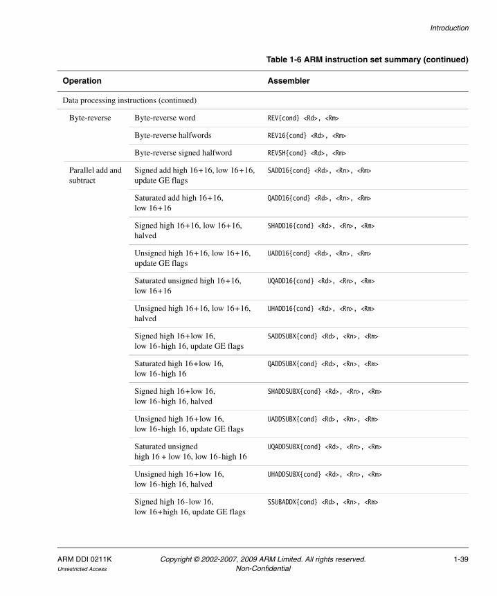
Introduction
Data processing instructions (continued)
Byte-reverse Byte-reverse word REV{cond} <Rd>, <Rm>
Byte-reverse halfwords REV16{cond} <Rd>, <Rm>
Byte-reverse signed halfword REVSH{cond} <Rd>, <Rm>
Parallel add and subtract
Signed add high 16+16, low 16+16, update GE flags
SADD16{cond} <Rd>, <Rn>, <Rm>
Saturated add high 16+16, low 16+16
QADD16{cond} <Rd>, <Rn>, <Rm>
Signed high 16+16, low 16+16, halved
SHADD16{cond} <Rd>, <Rn>, <Rm>
Unsigned high 16+16, low 16+16, update GE flags
UADD16{cond} <Rd>, <Rn>, <Rm>
Saturated unsigned high 16+16, low 16+16
UQADD16{cond} <Rd>, <Rn>, <Rm>
Unsigned high 16+16, low 16+16, halved
UHADD16{cond} <Rd>, <Rn>, <Rm>
Signed high 16+low 16, low 16-high 16, update GE flags
SADDSUBX{cond} <Rd>, <Rn>, <Rm>
Saturated high 16+low 16, low 16-high 16
QADDSUBX{cond} <Rd>, <Rn>, <Rm>
Signed high 16+low 16, low 16-high 16, halved
SHADDSUBX{cond} <Rd>, <Rn>, <Rm>
Unsigned high 16+low 16, low 16-high 16, update GE flags
UADDSUBX{cond} <Rd>, <Rn>, <Rm>
Saturated unsigned high 16 + low 16, low 16-high 16
UQADDSUBX{cond} <Rd>, <Rn>, <Rm>
Unsigned high 16+low 16, low 16-high 16, halved
UHADDSUBX{cond} <Rd>, <Rn>, <Rm>
Signed high 16-low 16, low 16+high 16, update GE flags
SSUBADDX{cond} <Rd>, <Rn>, <Rm>
Table 1-6 ARM instruction set summary (continued)
Operation Assembler
ARM DDI 0211K Copyright © 2002-2007, 2009 ARM Limited. All rights reserved. 1-39Unrestricted Access Non-Confidential

Introduction
Data processing instructions (continued)
Parallel add and subtract
(continued)
Saturated high 16-low 16, low 16+high 16
QSUBADDX{cond} <Rd>, <Rn>, <Rm>
Signed high 16-low 16, low 16+high 16, halved
SHSUBADDX{cond} <Rd>, <Rn>, <Rm>
Unsigned high 16-low 16, low 16+high 16, update GE flags
USUBADDX{cond} <Rd>, <Rn>, <Rm>
Saturated unsigned high 16-low 16, low 16+high 16
UQSUBADDX{cond} <Rd>, <Rn>, <Rm>
Unsigned high 16-low 16, low 16+high 16, halved
UHSUBADDX{cond} <Rd>, <Rn>, <Rm>
Signed high 16-16, low 16-16, update GE flags
SSUB16{cond} <Rd>, <Rn>, <Rm>
Saturated high 16-16, low 16-16 QSUB16{cond} <Rd>, <Rn>, <Rm>
Signed high 16-16, low 16-16, halved
SHSUB16{cond} <Rd>, <Rn>, <Rm>
Unsigned high 16-16, low 16-16, update GE flags
USUB16{cond} <Rd>, <Rn>, <Rm>
Saturated unsigned high 16-16, low 16-16
UQSUB16{cond} <Rd>, <Rn>, <Rm>
Unsigned high 16-16, low 16-16, halved
UHSUB16{cond} <Rd>, <Rn>, <Rm>
Four signed 8+8, update GE flags SADD8{cond} <Rd>, <Rn>, <Rm>
Four saturated 8+8 QADD8{cond} <Rd>, <Rn>, <Rm>
Four signed 8+8, halved SHADD8{cond} <Rd>, <Rn>, <Rm>
Four unsigned 8+8, update GE flags UADD8{cond} <Rd>, <Rn>, <Rm>
Four saturated unsigned 8+8 UQADD8{cond} <Rd>, <Rn>, <Rm>
Four unsigned 8+8, halved UHADD8{cond} <Rd>, <Rn>, <Rm>
Four signed 8-8, update GE flags SSUB8{cond} <Rd>, <Rn>, <Rm>
Table 1-6 ARM instruction set summary (continued)
Operation Assembler
1-40 Copyright © 2002-2007, 2009 ARM Limited. All rights reserved. ARM DDI 0211KNon-Confidential Unrestricted Access

Introduction
Data processing instructions (continued)
Parallel add and subtract
(continued)
Four saturated 8-8 QSUB8{cond} <Rd>, <Rn>, <Rm>
Four signed 8-8, halved SHSUB8{cond} <Rd>, <Rn>, <Rm>
Four unsigned 8-8, update GE flags USUB8{cond} <Rd>, <Rn>, <Rm>
Four saturated unsigned 8-8 UQSUB8{cond} <Rd>, <Rn>, <Rm>
Four unsigned 8-8, halved UHSUB8{cond} <Rd>, <Rn>, <Rm>
Sum of absolute differences USAD8{cond} <Rd>, <Rm>, <Rs>
Sum of absolute differences and accumulate
USADA8{cond} <Rd>, <Rm>, <Rs>, <Rn>
Sign or zero extend and add
Two low 8/16, sign extend to 16, +16 SADD8TO16{cond} <Rd>, <Rn>, <Rm>{, <rotation>}
Low 8/32, sign extend to 32, +32 SADD8TO32{cond} <Rd>, <Rn>, <Rm>{, <rotation>}
Low 16/32, sign extend to 32, +32 SADD16TO32{cond} <Rd>, <Rn>, <Rm>{, <rotation>}
Two low 8/16, zero extend to 16, +16 UADD8TO16{cond} <Rd>, <Rn>, <Rm>{, <rotation>}
Low 8/32, zero extend to 32, +32 UADD8TO32{cond} <Rd>, <Rn>, <Rm>{, <rotation>}
Low 16/32, zero extend to 32, +32 UADD16TO32{cond} <Rd>, <Rn>, <Rm>{, <rotation>}
Two low 8, sign extend to 16, packed 32
SUNPK8TO16{cond} <Rd>, <Rm>{, <rotation>}
Low 8, sign extend to 32 SUNPK8TO32{cond} <Rd>, <Rm>{, <rotation>}
Low 16, sign extend to 32 SUNPK16TO32{cond} <Rd>, <Rm>{, <rotation>}
Two low 8, zero extend to 16, packed 32
UUNPK8TO16{cond} <Rd>, <Rm>,{, <rotation>}
Low 8, zero extend to 32 UUNPK8TO32{cond} <Rd>, <Rm>{, <rotation>}
Low 16, zero extend to 32 UUNPK16TO32{cond} <Rd>, <Rm>{, <rotation>}
32x32 multiply and multiply- accumulate
32x32 to 32 MUL{cond}{S} <Rd>, <Rm>, <Rs>
32+32x32 MLA{cond}{S} <Rd>, <Rm>, <Rs>, <Rn>
Unsigned 32x32 to 64 UMULL{cond}{S} <RdLo>, <RdHi>, <Rm>, <Rs>
Table 1-6 ARM instruction set summary (continued)
Operation Assembler
ARM DDI 0211K Copyright © 2002-2007, 2009 ARM Limited. All rights reserved. 1-41Unrestricted Access Non-Confidential

Introduction
Data processing instructions (continued)
32x32 multiply and multiply- accumulate (continued)
Unsigned 64+32x32 UMLAL{cond}{S} <RdLo>, <RdHi>, <Rm>, <Rs>
Unsigned 32x32, +two 32, to 64 UMAAL{cond} <RdLo>, <RdHi>, <Rm>, <Rs>
Signed 32x32 to 64 SMULL{cond}{S} <RdLo>, <RdHi>, <Rm>, <Rs>
Signed 64+32x32 SMLAL{cond}{S} <RdLo>, <RdHi>, <Rm>, <Rs>
Signed truncated high 32 (32x32) SMMUL{cond} <Rd>, <Rm>, <Rs>
Signed rounded high 32 (32x32) SMMULR{cond} <Rd>, <Rm>, <Rs>
Signed 32+truncated high 32 (32x32)
SMMLA{cond} <Rd>, <Rm>, <Rs>, <Rn>
Signed 32+rounded high 32 (32x32) SMMLAR{cond} <Rd>, <Rm>, <Rs>, <Rn>
Signed 32-truncated high 32 (32x32)
SMMLS{cond} <Rd>, <Rm>, <Rs>, <Rn>
Signed 32-rounded high 32 (32x32) SMMLSR{cond} <Rd>, <Rm>, <Rs>, <Rn>
32x16 multiply and multiply- accumulate
Signed truncated high 32 (32x16) to 32
SMULWy{cond} <Rd>, <Rm>, <Rs>
Signed 32+truncated high 32 (32x16)
SMLAWy{cond} <Rd>, <Rm>, <Rs>, <Rn>
16x16 multiply and multiply- accumulate
Signed 16x16 to 32 SMULxy{cond} <Rd>, <Rm>, <Rs>
Signed 32+16x16 SMLAxy{cond} <Rd>, <Rm>, <Rs>, <Rn>
Signed 64+16x16 SMLALxy{cond} <RdLo>, <RdHi>, <Rm>, <Rs>
Dual 16x16 multiply and multiply- accumulate
Signed (low 16x16)+(high 16x16), and update Q flag
SMUAD{cond} <Rd>, <Rm>, <Rs>
As SMUAD, but lowxhigh, highxlow SMUADX{cond} <Rd>, <Rm>, <Rs>
Signed (low 16x16)+(high 16x16)+32, and update Q flag
SMLAD{cond} <Rd>, <Rm>, <Rs>, <Rn>
As SMLAD, but lowxhigh, highxlow SMLADX{cond} <Rd>, <Rm>, <Rs>, <Rn>
Table 1-6 ARM instruction set summary (continued)
Operation Assembler
1-42 Copyright © 2002-2007, 2009 ARM Limited. All rights reserved. ARM DDI 0211KNon-Confidential Unrestricted Access

Introduction
Data processing instructions (continued)
Dual 16x16 multiply and multiply- accumulate (continued)
Signed (low 16x16)+(high 16x16) +64
SMLALD{cond} <RdLo>, <RdHi>, <Rm>, <Rs>
As SMLALD, but lowxhigh, highxlow SMLALDX{cond} <RdLo>, <RdHi>, <Rm>, <Rs>
Signed (low 16x16)-(high 16x16) SMUSD{cond} <Rd>, <Rm>, <Rs>
As SMUSD, but lowxhigh, highxlow SMUSDX{cond} <Rd>, <Rm>, <Rs>
Signed (low 16x16)-(high 16x16) +32, and update Q flag
SMLSD{cond} <Rd>, <Rm>, <Rs>, <Rn>
As SMLSD, but low x high, high x low SMLSDX{cond} <Rd>, <Rm>, <Rs>, <Rn>
Signed (low 16x16)-(high 16x16) +64
SMLSLD{cond} <RdLo>, <RdHi>, <Rm>, <Rs>
As SMLSLD, but lowxhigh, highxlow SMLSLDX{cond} <RdLo>, <RdHi>, <Rm>, <Rs>
Saturate Signed saturation at bit position n SSAT{cond} <Rd>, #<immed_5>, <Rm>{, <shift>}
Two 16 signed saturation at bit position n
SSAT16{cond} <Rd>, #<immed_4>, <Rm>
Unsigned saturation at bit position n USAT{cond} <Rd>, #<immed_5>, <Rm>{, <shift>}
Two 16 unsigned saturation at bit position n
USAT16{cond} <Rd>, #<immed_4>, <Rm>
Miscellaneous Count leading zeros CLZ{cond} <Rd>, <Rm>
No Operationa NOP{cond} {<hint>}
Pack low 16/32, high 16/32 PKHBT{cond} <Rd>, <Rn>, <Rm>{, LSL #<immed_5>}
Pack high 16/32, low 16/32 PKHTB{cond} <Rd>, <Rn>, <Rm>{, ASR #<immed_5>}
Select bytes from Rn/Rm based on GE flags
SEL{cond} <Rd>, <Rn>, <Rm>
Table 1-6 ARM instruction set summary (continued)
Operation Assembler
ARM DDI 0211K Copyright © 2002-2007, 2009 ARM Limited. All rights reserved. 1-43Unrestricted Access Non-Confidential
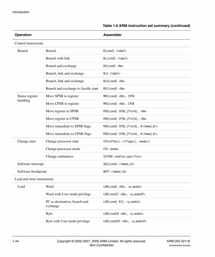
Introduction
Control instructions
Branch Branch B{cond} <label>
Branch with link BL{cond} <label>
Branch and exchange BX{cond} <Rm>
Branch, link and exchange BLX <label>
Branch, link and exchange BLX{cond} <Rm>
Branch and exchange to Jazelle state BXJ{cond} <Rm>
Status register handling
Move SPSR to register MRS{cond} <Rd>, SPSR
Move CPSR to register MRS{cond} <Rd>, CPSR
Move register to SPSR MSR{cond} SPSR_{field}, <Rm>
Move register to CPSR MSR{cond} CPSR_{field}, <Rm>
Move immediate to SPSR flags MSR{cond} SPSR_{field}, #<immed_8r>
Move immediate to CPSR flags MSR{cond} CPSR_{field}, #<immed_8r>
Change state Change processor state CPS<effect> <iflags>{, <mode>}
Change processor mode CPS <mode>
Change endianness SETEND <endian_specifier>
Software interrupt SWI{cond} <immed_24>
Software breakpoint BKPT <immed_16>
Load and store instructions
Load Word LDR{cond} <Rd>, <a_mode2>
Word with User mode privilege LDR{cond}T <Rd>, <a_mode2P>
PC as destination, branch and exchange
LDR{cond} R15, <a_mode2>
Byte LDR{cond}B <Rd>, <a_mode2>
Byte with User mode privilege LDR{cond}BT <Rd>, <a_mode2P>
Table 1-6 ARM instruction set summary (continued)
Operation Assembler
1-44 Copyright © 2002-2007, 2009 ARM Limited. All rights reserved. ARM DDI 0211KNon-Confidential Unrestricted Access

Introduction
Load and store instructions (continued)
Load (continued)
Byte signed LDR{cond}SB <Rd>, <a_mode3>
Halfword LDR{cond}H <Rd>, <a_mode3>
Halfword signed LDR{cond}SH <Rd>, <a_mode3>
Two words LDR{cond}D <Rd>, <Rd2>, <a_mode3>
Return from exception RFE<a_mode4L> <Rn>{!}
Load multiple Load multiple registers LDM{cond}<a_mode4L> <Rn>{!}, <reglist-pc>
Load multiple registers and PC, branch and exchange
LDM{cond}<a_mode4L> <Rn>{!}, <reglist+pc>
Load multiple registers and return from exception, restoring CPSR
LDM{cond}<a_mode4L> <Rn>{!}, <reglist+pc>^
Load multiple User mode registers LDM{cond}<a_mode4L> <Rn>{!}, <reglist-pc>^
Preload Memory system hint PLD <a_mode2>
Store Word STR{cond} <Rd>, <a_mode2>
Word with User mode privilege STR{cond}T <Rd>, <a_mode2P>
Byte STR{cond}B <Rd>, <a_mode2>
Byte with User mode privilege STR{cond}BT <Rd>, <a_mode2P>
Halfword STR{cond}H <Rd>, <a_mode3>
Two words STR{cond}D <Rd>, <Rd2>, <a_mode3>
Store return state SRS<a_mode4S> <mode>{!}
Store multiple Store multiple registers STM{cond}<a_mode4S> <Rn>{!}, <reglist>
Store multiple User mode registers STM{cond}<a_mode4S> <Rn>{!}, <reglist>^
Swap Word SWP{cond} <Rd>, <Rm>, [<Rn>]
Byte SWP{cond}B <Rd>, <Rm>, [<Rn>]
Table 1-6 ARM instruction set summary (continued)
Operation Assembler
ARM DDI 0211K Copyright © 2002-2007, 2009 ARM Limited. All rights reserved. 1-45Unrestricted Access Non-Confidential

Introduction
Load and store instructions (continued)
Synchronizationprimitives
Clear exclusivea CLREX
Load exclusive LDREX{cond} <Rd>, [<Rn>]
Load Byte exclusivea LDREXB{cond} <Rd>, [<Rn>]
Load Doubleword exclusivea LDREXD{cond} <Rd>, <Rd2>, [<Rn>]
Load Halfword exclusivea LDREXH{cond} <Rd>, [<Rn>]
Store exclusive STREX{cond} <Rd>, <Rm>, [<Rn>]
Store Byte exclusivea STREXB{cond} <Rd>, <Rm>, [<Rn>]
Store Doubleword exclusivea STREXD{cond} <Rd>, <Rm>, <Rm2>, [<Rn>]
Store Halfword exclusivea STREXH{cond} <Rd>, <Rm>, [<Rn>]
Coprocessor instructions
Coprocessor Data operations CDP{cond} <cp_num>, <op1>, <CRd>, <CRn>, <CRm>{, <op2>}
Move to ARM register from coprocessor
MRC{cond} <cp_num>, <op1>, <Rd>, <CRn>, <CRm>{, <op2>}
Move to coprocessor from ARM register
MCR{cond} <cp_num>, <op1>, <Rd>, <CRn>, <CRm>{, <op2>}
Move two words to ARM registers from coprocessor
MRRC{cond} <cp_num>, <op1>, <Rd>, <Rn>, <CRm>
Move two words to coprocessor from ARM registers
MCRR{cond} <cp_num>, <op1>, <Rd>, <Rn>, <CRm>
Load LDC{cond} <cp_num>, <CRd>, <a_mode5>
Store STC{cond} <cp_num>, <CRd>, <a_mode5>
Table 1-6 ARM instruction set summary (continued)
Operation Assembler
1-46 Copyright © 2002-2007, 2009 ARM Limited. All rights reserved. ARM DDI 0211KNon-Confidential Unrestricted Access

Introduction
Table 1-7 summarizes Addressing mode 2.
Coprocessor instructions (continued)
Alternative coprocessor
Data operations CDP2 <cp_num>, <op1>, <CRd>, <CRn>, <CRm>{, <op2>}
Move to ARM register from coprocessorb
MRC2 <cp_num>, <op1>, <Rd>, <CRn>, <CRm>{, <op2>}
Move to coprocessor from ARM registerb
MCR2 <cp_num>, <op1>, <Rd>, <CRn>, <CRm>{, <op2>}
Move two words to ARM registers from coprocessorb
MRRC2 <cp_num>, <op1>, <Rd>, <Rn>, <CRm>
Move two words to coprocessor from ARM registerb
MCRR2 <cp_num>, <op1>, <Rd>, <Rn>, <CRm>
Load LDC2 <cp_num>, <CRd>, <a_mode5>
Store STC2 <cp_num>, <CRd>, <a_mode5>
a. The CLREX, LDREXB, STREXB, LDREXH, STREXH, LDREXD, STREXD and NOP operations are only available from the rev1 (r1p0) release of the ARM1136JF-S processor.
b. The MCR2, MRC2, MCRR2 and MRRC2 instructions are not supported for operations to or from the CP15 coprocessor.
Table 1-6 ARM instruction set summary (continued)
Operation Assembler
Table 1-7 Addressing mode 2
Addressing mode Assembler
Offset addressing -
Immediate offset [<Rn>, #+/-<immed_12>]
Zero offset [<Rn>]
Register offset [<Rn>, +/-<Rm>]
Scaled register offset [<Rn>, +/-<Rm>, LSL #<immed_5>]
[<Rn>, +/-<Rm>, LSR #<immed_5>]
[<Rn>, +/-<Rm>, ASR #<immed_5>]
[<Rn>, +/-<Rm>, ROR #<immed_5>]
[<Rn>, +/-<Rm>, RRX]
ARM DDI 0211K Copyright © 2002-2007, 2009 ARM Limited. All rights reserved. 1-47Unrestricted Access Non-Confidential
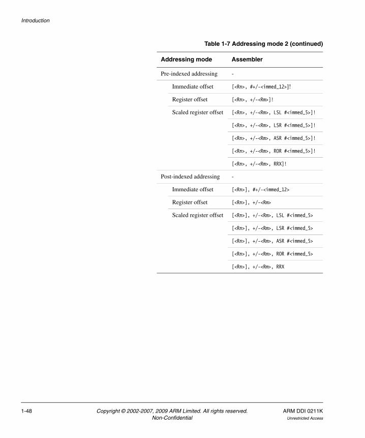
Introduction
Pre-indexed addressing -
Immediate offset [<Rn>, #+/-<immed_12>]!
Register offset [<Rn>, +/-<Rm>]!
Scaled register offset [<Rn>, +/-<Rm>, LSL #<immed_5>]!
[<Rn>, +/-<Rm>, LSR #<immed_5>]!
[<Rn>, +/-<Rm>, ASR #<immed_5>]!
[<Rn>, +/-<Rm>, ROR #<immed_5>]!
[<Rn>, +/-<Rm>, RRX]!
Post-indexed addressing -
Immediate offset [<Rn>], #+/-<immed_12>
Register offset [<Rn>], +/-<Rm>
Scaled register offset [<Rn>], +/-<Rm>, LSL #<immed_5>
[<Rn>], +/-<Rm>, LSR #<immed_5>
[<Rn>], +/-<Rm>, ASR #<immed_5>
[<Rn>], +/-<Rm>, ROR #<immed_5>
[<Rn>], +/-<Rm>, RRX
Table 1-7 Addressing mode 2 (continued)
Addressing mode Assembler
1-48 Copyright © 2002-2007, 2009 ARM Limited. All rights reserved. ARM DDI 0211KNon-Confidential Unrestricted Access

Introduction
Table 1-8 summarizes Addressing mode 2P, post-indexed addressing only.
Table 1-9 summarizes Addressing mode 3.
Table 1-8 Addressing mode 2P, post-indexed only
Addressing mode Assembler
Immediate offset [<Rn>], #+/-<immed_12>
Zero offset [<Rn>]
Register offset [<Rn>], +/-<Rm>
Scaled register offset [<Rn>], +/-<Rm>, LSL #<immed_5>
[<Rn>], +/-<Rm>, LSR #<immed_5>
[<Rn>], +/-<Rm>, ASR #<immed_5>
[<Rn>], +/-<Rm>, ROR #<immed_5>
[<Rn>], +/-<Rm>, RRX
Table 1-9 Addressing mode 3
Addressing mode Assembler
Offset addressing -
Immediate offset [<Rn>, #+/-<immed_8>]
Zero offset [<Rn>]
Register offset [<Rn>, +/-<Rm>]
Pre-indexed addressing -
Immediate offset [<Rn>, #+/-<immed_8>]!
Register offset [<Rn>, +/-<Rm>]!
Post-indexed addressing -
Immediate offset [<Rn>], #+/-<immed_8>
Register offset [<Rn>], +/-<Rm>
ARM DDI 0211K Copyright © 2002-2007, 2009 ARM Limited. All rights reserved. 1-49Unrestricted Access Non-Confidential
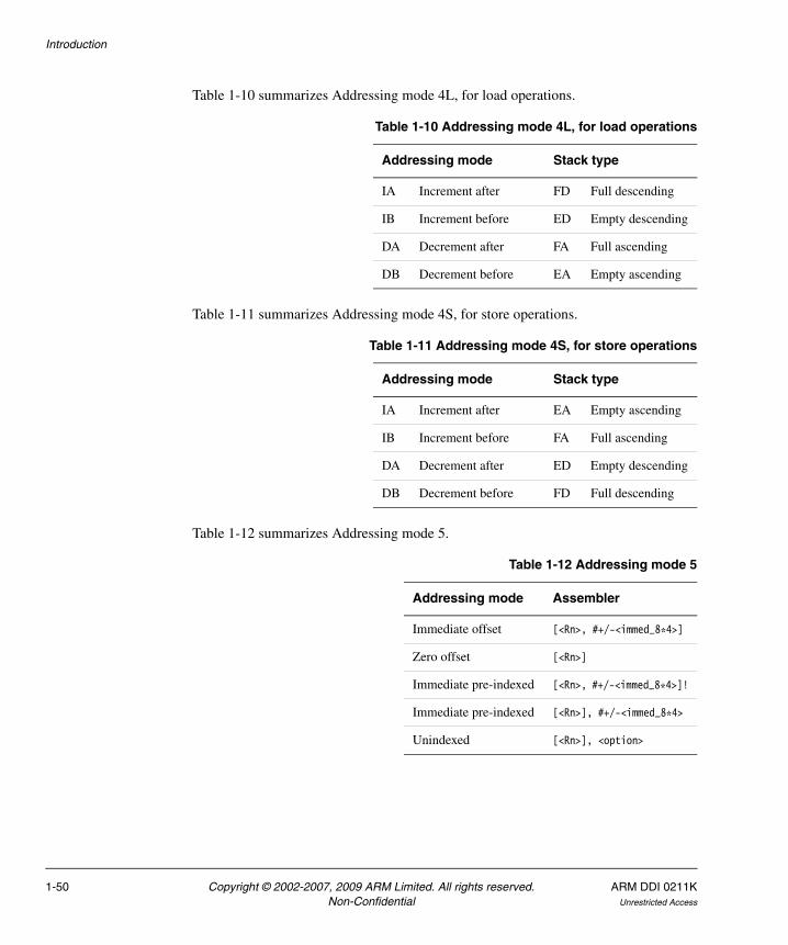
Introduction
Table 1-10 summarizes Addressing mode 4L, for load operations.
Table 1-11 summarizes Addressing mode 4S, for store operations.
Table 1-12 summarizes Addressing mode 5.
Table 1-10 Addressing mode 4L, for load operations
Addressing mode Stack type
IA Increment after FD Full descending
IB Increment before ED Empty descending
DA Decrement after FA Full ascending
DB Decrement before EA Empty ascending
Table 1-11 Addressing mode 4S, for store operations
Addressing mode Stack type
IA Increment after EA Empty ascending
IB Increment before FA Full ascending
DA Decrement after ED Empty descending
DB Decrement before FD Full descending
Table 1-12 Addressing mode 5
Addressing mode Assembler
Immediate offset [<Rn>, #+/-<immed_8*4>]
Zero offset [<Rn>]
Immediate pre-indexed [<Rn>, #+/-<immed_8*4>]!
Immediate pre-indexed [<Rn>], #+/-<immed_8*4>
Unindexed [<Rn>], <option>
1-50 Copyright © 2002-2007, 2009 ARM Limited. All rights reserved. ARM DDI 0211KNon-Confidential Unrestricted Access

Introduction
Table 1-13 summarizes the possible Operand2 values.
Table 1-14 summarizes the possible Fields values.
Table 1-13 Operand2
Operation Assembler
Immediate value #<immed_8r>
Logical shift left <Rm>, LSL #<immed_5>
Logical shift right <Rm>, LSR #<immed_5>
Arithmetic shift right <Rm>, ASR #<immed_5>
Rotate right <Rm>, ROR #<immed_5>
Register <Rm>
Logical shift left <Rm>, LSL <Rs>
Logical shift right <Rm>, LSR <Rs>
Arithmetic shift right <Rm>, ASR <Rs>
Rotate right <Rm>, ROR <Rs>
Rotate right extended <Rm>, RRX
Table 1-14 Fields
Suffix Function Enables writing of CPSR bits
c Control field mask bit [7:0]
x Extension field mask bit [15:8]
s Status field mask bit [23:16]
f Flags field mask bit [31:24]
ARM DDI 0211K Copyright © 2002-2007, 2009 ARM Limited. All rights reserved. 1-51Unrestricted Access Non-Confidential

Introduction
Table 1-15 summarizes the Condition codes.
Table 1-15 Condition codes
Suffix Description Alternative description
EQ Equal -
NE Not equal -
HS or CS Unsigned higher or same Carry
LO or CC Unsigned lower No carry
MI Negative -
PL Positive or zero -
VS Overflow -
VC No overflow -
HI Unsigned higher -
LS Unsigned lower or same -
GE Greater or equal -
LT Less than -
GT Greater than -
LE Less than or equal -
AL Always -
1-52 Copyright © 2002-2007, 2009 ARM Limited. All rights reserved. ARM DDI 0211KNon-Confidential Unrestricted Access

Introduction
1.8.2 Thumb instruction set summary
Table 1-16 summarizes the Thumb instruction set.
Table 1-16 Thumb instruction set summary
Operation Assembler
Move Immediate, update flags MOV <Rd>, #<immed_8>
LowReg to LowReg, update flags MOV <Rd>, <Rm>
HighReg to LowReg MOV <Rd>, <Rm>
LowReg to HighReg MOV <Rd>, <Rm>
HighReg to HighReg MOV <Rd>, <Rm>
Arithmetic Add immediate, update flags ADD <Rd>, <Rn>, #<immed_3>
Add immediate, update flags ADD <Rd>, #<immed_8>
Add LowReg and LowReg, update flags ADD <Rd>, <Rn>, <Rm>
Add HighReg to LowReg ADD <Rd>, <Rm>
Add LowReg to HighReg ADD <Rd>, <Rm>
Add HighReg to HighReg ADD <Rd>, <Rm>
Add immediate to PC ADD <Rd>, PC, #<immed_8*4>
Add immediate to SP ADD <Rd>, SP, #<immed_8*4>
Increment SP by immediate ADD SP, #<immed_7*4>
Add with carry, update flags ADC <Rd>, <Rs>
Subtract immediate, update flags SUB <Rd>, <Rn>, #<immed_3>
Subtract immediate, update flags SUB <Rd>, #<immed_8>
Subtract, update flags SUB <Rd>, <Rn>, <Rm>
Decrement SP by immediate SUB SP, #<immed_7*4>
Subtract with carry, update flags SBC <Rd>, <Rm>
Negate, update flags NEG <Rd>, <Rm>
Multiply, update flags MUL <Rd>, <Rm>
ARM DDI 0211K Copyright © 2002-2007, 2009 ARM Limited. All rights reserved. 1-53Unrestricted Access Non-Confidential

Introduction
Compare Compare immediate CMP <Rn>, #<immed_8>
Compare LowReg and LowReg CMP <Rn>, <Rm>
Compare LowReg and HighReg CMP <Rn>, <Rm>
Compare HighReg and LowReg CMP <Rn>, <Rm>
Compare HighReg and HighReg CMP <Rn>, <Rm>
Compare negative CMN <Rn>, <Rm>
Logical AND, update flags AND <Rd>, <Rm>
XOR, update flags EOR <Rd>, <Rm>
OR, update flags ORR <Rd>, <Rm>
Bit clear, update flags BIC <Rd>, <Rm>
Move NOT, update flags MVN <Rd>, <Rm>
Test bits TST <Rd>, <Rm>
Shift or rotate Logical shift left by immediate, update flags LSL <Rd>, <Rm>, #<immed_5>
Logical shift left, update flags LSL <Rd>, <Rs>
Logical shift right by immediate, update flags LSR <Rd>, <Rm>, #<immed_5>
Logical shift right, update flags LSR <Rd>, <Rs>
Arithmetic shift right by immediate, update flags ASR <Rd>, <Rm>, #<immed_5>
Arithmetic shift right, update flags ASR <Rd>, <Rs>
Rotate right, update flags ROR <Rd>, <Rs>
Byte-reverse Byte-reverse word REV <Rd>, <Rm>
Byte-reverse halfword REV16 <Rd>, <Rm>
Byte-reverse signed halfword REVSH <Rd>, <Rm>
Table 1-16 Thumb instruction set summary (continued)
Operation Assembler
1-54 Copyright © 2002-2007, 2009 ARM Limited. All rights reserved. ARM DDI 0211KNon-Confidential Unrestricted Access

Introduction
Sign or zero extend Sign extend 16 to 32 SEXT16 <Rd>, <Rm>
Sign extend 8 to 32 SEXT8 <Rd>, <Rm>
Zero extend 16 to 32 UEXT16 <Rd>, <Rm>
Zero extend 8 to 32 UEXT8 <Rd>, <Rm>
Branch Conditional B{cond} <label>
Unconditional B <label>
Branch with link BL <label>
Branch, link and exchange BLX <label>
Branch, link and exchange BLX <Rm>
Branch and exchange BX <Rm>
Change state Change processor state CPS <effect> <iflags>
Change endianness SETEND <endian_specifier>
Software interrupt SWI <immed_8>
Software breakpoint BKPT <immed_8>
Load With immediate offset -
Word LDR <Rd>, [<Rn>, #<immed_5>]
Halfword LDRH <Rd>, [<Rn>, #<immed_5*2>]
Byte LDRB <Rd>, [<Rn>, #<immed_5*4>]
Word, PC-relative LDR <Rd>, [PC, #<immed_8*4>]
Word, SP-relative LDR <Rd>, [SP, #<immed_8*4>]
Table 1-16 Thumb instruction set summary (continued)
Operation Assembler
ARM DDI 0211K Copyright © 2002-2007, 2009 ARM Limited. All rights reserved. 1-55Unrestricted Access Non-Confidential
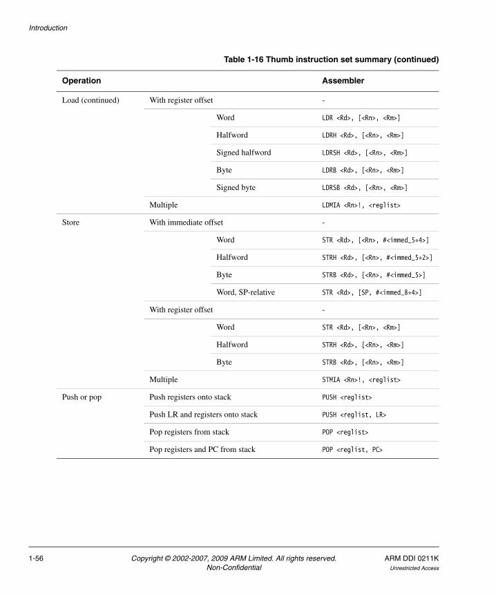
Introduction
Load (continued) With register offset -
Word LDR <Rd>, [<Rn>, <Rm>]
Halfword LDRH <Rd>, [<Rn>, <Rm>]
Signed halfword LDRSH <Rd>, [<Rn>, <Rm>]
Byte LDRB <Rd>, [<Rn>, <Rm>]
Signed byte LDRSB <Rd>, [<Rn>, <Rm>]
Multiple LDMIA <Rn>!, <reglist>
Store With immediate offset -
Word STR <Rd>, [<Rn>, #<immed_5*4>]
Halfword STRH <Rd>, [<Rn>, #<immed_5*2>]
Byte STRB <Rd>, [<Rn>, #<immed_5>]
Word, SP-relative STR <Rd>, [SP, #<immed_8*4>]
With register offset -
Word STR <Rd>, [<Rn>, <Rm>]
Halfword STRH <Rd>, [<Rn>, <Rm>]
Byte STRB <Rd>, [<Rn>, <Rm>]
Multiple STMIA <Rn>!, <reglist>
Push or pop Push registers onto stack PUSH <reglist>
Push LR and registers onto stack PUSH <reglist, LR>
Pop registers from stack POP <reglist>
Pop registers and PC from stack POP <reglist, PC>
Table 1-16 Thumb instruction set summary (continued)
Operation Assembler
1-56 Copyright © 2002-2007, 2009 ARM Limited. All rights reserved. ARM DDI 0211KNon-Confidential Unrestricted Access

Introduction
1.9 Product revisions
This is the Technical Reference Manual for ARM1136J-S and ARM1136JF-S processors. This section summarizes the differences in functionality between the releases of these processors.
r0p0 - r1p0 The r1p0 release includes some significant changes in architecture and functionality, to provide ARM v6k support. These changes are described in Appendix B Functional changes in the rev1 (r1pn) releases. In summary, this release:
• Adds new byte, halfword and doubleword exclusive instructions.
• Adds new CLREX and true NOP instructions.
• Adds two new CP15 MMU remap registers, and provides an additional TEX remapping option.
• Adds new CP15 thread and process ID registers.
• Changes the MMU access permission encodings.
• Adds the ability to limit the apparent size of the implemented caches. This allows you to avoid the ARMv6 software page coloring restriction.
• Allows you to redefine AP[0] for use as a software-controlled Access Flag, and provides a TLB-generated Access Flag fault.
• Adds a set of feature registers to coprocessor 15 register 0.
r1p0 - r1p1 Maintenance upgrade to fix errata. No changes to the functionality described in this TRM.
r1p1- r1p3 Maintenance upgrade to fix errata. No changes to the functionality described in this TRM.
r1p3 - r1p5 Maintenance upgrade to fix errata. No changes to the functionality described in this TRM.
Note Releases r1p2 and r1p4 were not generally available
ARM DDI 0211K Copyright © 2002-2007, 2009 ARM Limited. All rights reserved. 1-57Unrestricted Access Non-Confidential

Introduction
1-58 Copyright © 2002-2007, 2009 ARM Limited. All rights reserved. ARM DDI 0211KNon-Confidential Unrestricted Access

Chapter 2 Programmer’s Model
This chapter describes the ARM1136JF-S registers and provides information for programming the microprocessor. It contains the following sections:
• About the programmer’s model on page 2-2
• Processor operating states on page 2-3
• Instruction length on page 2-4
• Data types on page 2-5
• Memory formats on page 2-6
• Addresses in an ARM1136JF-S system on page 2-8
• Operating modes on page 2-9
• Registers on page 2-10
• The program status registers on page 2-16
• Additional instructions on page 2-24
• Exceptions on page 2-34.
ARM DDI 0211K Copyright © 2002-2007, 2009 ARM Limited. All rights reserved. 2-1Unrestricted Access Non-Confidential

Programmer’s Model
2.1 About the programmer’s model
The ARM1136JF-S processor implements ARM architecture v6 with Jazelle extensions. This includes the ARM instruction set, Thumb instruction set, and support for the execution of Java bytecodes. For details of both the ARM and Thumb instruction sets, see the ARM Architecture Reference Manual, ARMv7-A and ARMv7-R edition.
2-2 Copyright © 2002-2007, 2009 ARM Limited. All rights reserved. ARM DDI 0211KNon-Confidential Unrestricted Access

Programmer’s Model
2.2 Processor operating states
The ARM1136JF-S processor has three operating states:
ARM state 32-bit, word-aligned ARM instructions are executed in this state.
Thumb state 16-bit, halfword-aligned Thumb instructions.
Jazelle state Variable length, byte-aligned Java bytecodes.
In Thumb state, the Program Counter (PC) uses bit 1 to select between alternate halfwords. In Jazelle state, all instruction fetches are in words.
Note Transition between ARM and Thumb states does not affect the processor mode or the register contents. For more information about entering and leaving Jazelle state, see the ARM Architecture Reference Manual, ARMv7-A and ARMv7-R edition.
2.2.1 Switching state
You can switch the operating state of the ARM1136JF-S processor between:
• ARM state and Thumb state using the BX and BLX instructions, and loads to the PC. Switching state is described in the ARM Architecture Reference Manual, ARMv7-A and ARMv7-R edition.
• ARM state and Jazelle state using the BXJ instruction.
All exceptions are entered, handled, and exited in ARM state. If an exception occurs in Thumb state or Jazelle state, the processor reverts to ARM state. Exception return instructions restore the Saved Program Status Register (SPSR) to the Current Program Status Register (CPSR), which can also cause a transition back to Thumb state or Jazelle state.
2.2.2 Interworking ARM and Thumb state
The ARM1136JF-S processor enables you to mix ARM and Thumb code. For details see the chapter about interworking ARM and Thumb in the RealView Compilation Tools Developer Guide.
ARM DDI 0211K Copyright © 2002-2007, 2009 ARM Limited. All rights reserved. 2-3Unrestricted Access Non-Confidential

Programmer’s Model
2.3 Instruction length
Instructions are one of:
• 32 bits long, in ARM state
• 16 bits long, in Thumb state
• variable length, multiples of 8 bits, in Jazelle state.
2-4 Copyright © 2002-2007, 2009 ARM Limited. All rights reserved. ARM DDI 0211KNon-Confidential Unrestricted Access

Programmer’s Model
2.4 Data types
The ARM1136JF-S processor supports the following data types:
• word (32-bit)
• halfword (16-bit)
• byte (8-bit).
Note • When any of these types are described as unsigned, the N-bit data value represents
a non-negative integer in the range 0 to +2N-1, using normal binary format.
• When any of these types are described as signed, the N-bit data value represents an integer in the range -2N-1 to +2N-1-1, using two’s complement format.
For best performance you must align these as follows:
• word quantities must be aligned to four-byte boundaries
• halfword quantities must be aligned to two-byte boundaries
• byte quantities can be placed on any byte boundary.
ARM1136JF-S processor introduces mixed-endian and unaligned access support. For details see Chapter 4 Unaligned and Mixed-Endian Data Access Support.
Note You cannot use LDRD, LDM, LDC, STRD, STM, or STC instructions to access 32-bit quantities if they are unaligned.
ARM DDI 0211K Copyright © 2002-2007, 2009 ARM Limited. All rights reserved. 2-5Unrestricted Access Non-Confidential

Programmer’s Model
2.5 Memory formats
The ARM1136JF-S processor views memory as a linear collection of bytes numbered in ascending order from zero. Bytes 0-3 hold the first stored word, and bytes 4-7 hold the second stored word, for example.
The ARM1136JF-S processor can treat words in memory as being stored in either:
• 32-bit word-invariant big-endian format
• Little-endian format.
Additionally, the ARM1136JF-S processor supports mixed-endian and unaligned data accesses. For details see Chapter 4 Unaligned and Mixed-Endian Data Access Support.
2.5.1 32-bit word-invariant big-endian format
In 32-bit word-invariant big-endian format, the ARM1136JF-S processor stores the most significant byte of a word at the lowest-numbered byte, and the least significant byte at the highest-numbered byte. Therefore, byte 0 of the memory system connects to data lines 31-24. Figure 2-1 shows this.
Figure 2-1 Big-endian addresses of the bytes in words
2.5.2 Little-endian format
In little-endian format, the lowest-numbered byte in a word is the least significant byte of the word and the highest-numbered byte is the most significant. Therefore, byte 0 of the memory system connects to data lines 7-0. Figure 2-2 on page 2-7 shows this.
31 24 23 16 15 8 7 0
4
0
8Higher address
Lower address
• Most significant byte is at lowest address• Word is addressed by byte address of most significant byte
Bit
111098
7654
3210
Word address
2-6 Copyright © 2002-2007, 2009 ARM Limited. All rights reserved. ARM DDI 0211KNon-Confidential Unrestricted Access

Programmer’s Model
Figure 2-2 Little-endian addresses of the bytes in words
31 24 23 16 15 8 7
Word address
0
Higher address
Lower address
• Least significant byte is at lowest address• Word is addressed by byte address of least significant byte
Bit
891011
4567
0123
4
0
8
ARM DDI 0211K Copyright © 2002-2007, 2009 ARM Limited. All rights reserved. 2-7Unrestricted Access Non-Confidential

Programmer’s Model
2.6 Addresses in an ARM1136JF-S system
Three distinct types of address exist in an ARM1136JF-S system:
• Virtual Address (VA)
• Modified Virtual Address (MVA)
• Physical Address (PA).
Table 2-1 shows the address types in an ARM1136JF-S system.
This is an example of the address manipulation that occurs when the ARM1136JF-S processor requests an instruction (see Figure 1-1 on page 1-4):
1. The VA of the instruction is issued by the ARM1136JF-S processor.
2. The Instruction Cache is indexed by the lower bits of the VA. The VA is translated using the ProcID to the MVA, and then to PA in the Translation Lookaside Buffer (TLB). The TLB performs the translation in parallel with the cache lookup.
3. If the protection check carried out by the TLB on the MVA does not abort and the PA tag is in the Instruction Cache, the instruction data is returned to the ARM1136JF-S processor.
4. The PA is passed to the AMBA bus interface to perform an external access, in the event of a cache miss.
Table 2-1 Address types in an ARM1136JF-S system
ARM1136 processor Caches TLBs AMBA bus
Virtual Address Virtual index Physical Address Translates Virtual Address (VA) to Physical Address (PA)
Physical Address
2-8 Copyright © 2002-2007, 2009 ARM Limited. All rights reserved. ARM DDI 0211KNon-Confidential Unrestricted Access

Programmer’s Model
2.7 Operating modes
In all states there are seven modes of operation:
• User mode is the usual ARM program execution state, and is used for executing most application programs
• Fast interrupt (FIQ) mode is used for handling fast interrupts
• Interrupt (IRQ) mode is used for general-purpose interrupt handling
• Supervisor mode is a protected mode for the operating system
• Abort mode is entered after a data or instruction Prefetch Abort
• System mode is a privileged user mode for the operating system
• Undefined mode is entered when an Undefined Instruction exception occurs.
Modes other than User mode are collectively known as privileged modes. Privileged modes are used to service interrupts or exceptions, or to access protected resources.
ARM DDI 0211K Copyright © 2002-2007, 2009 ARM Limited. All rights reserved. 2-9Unrestricted Access Non-Confidential

Programmer’s Model
2.8 Registers
The ARM1136JF-S processor has a total of 37 registers:
• 31 general-purpose 32-bit registers
• six 32-bit status registers.
These registers are not all accessible at the same time. The processor state and operating mode determine which registers are available to the programmer.
2.8.1 The core register set in ARM state
In ARM state, 16 general registers and one or two status registers are accessible at any time. In privileged modes, mode-specific banked registers become available. Figure 2-3 on page 2-12 shows which registers are available in each mode.
The ARM state register set contains 16 directly-accessible registers, R0-R15. Another register, the Current Program Status Register (CPSR), contains condition code flags, status bits, and current mode bits. Registers R0-R12 are general-purpose registers used to hold either data or address values. Registers R13, R14, R15, and the Saved Program Status Register (SPSR) have the following special functions:
Stack Pointer Register R13 is used as the Stack Pointer (SP).
R13 is banked for the exception modes. This means that an exception handler can use a different stack to the one in use when the exception occurred.
In many instructions, you can use R13 as a general-purpose register, but the architecture deprecates this use of R13 in most instructions. For more information see the ARM Architecture Reference Manual.
Link Register Register R14 is used as the subroutine Link Register (LR).
Register R14 receives the return address when a Branch with Link (BL or BLX) instruction is executed.
You can treat R14 as a general-purpose register at all other times. The corresponding banked registers R14_svc, R14_irq, R14_fiq, R14_abt, and R14_und are similarly used to hold the return values when interrupts and exceptions arise, or when BL or BLX instructions are executed within interrupt or exception routines.
Program Counter Register R15 holds the PC:
• in ARM state this is word-aligned
• in Thumb state this is halfword-aligned
• in Jazelle state this is byte-aligned.
2-10 Copyright © 2002-2007, 2009 ARM Limited. All rights reserved. ARM DDI 0211KNon-Confidential Unrestricted Access

Programmer’s Model
Saved Program Status Register
In privileged modes, another register, the Saved Program Status Register (SPSR), is accessible. This contains the condition code flags, status bits, and current mode bits saved as a result of the exception that caused entry to the current mode.
Banked registers have a mode identifier that indicates which mode they relate to. These mode identifiers are listed in Table 2-2.
FIQ mode has seven banked registers mapped to R8–R14 (R8_fiq–R14_fiq). As a result many FIQ handlers do not have to save any registers.
The Supervisor, Abort, IRQ, and Undefined modes each have alternative mode-specific registers mapped to R13 and R14, permitting a private stack pointer and link register for each mode.
Figure 2-3 on page 2-12 shows the core registers in ARM state.
Table 2-2 Register mode identifiers
Mode Mode identifier
User usra
a. The usr identifier is usually omitted from register names. It is only used in descriptions where the User or System mode register is specifically accessed from another operating mode.
Fast interrupt fiq
Interrupt irq
Supervisor svc
Abort abt
System usra
Undefined und
ARM DDI 0211K Copyright © 2002-2007, 2009 ARM Limited. All rights reserved. 2-11Unrestricted Access Non-Confidential

Programmer’s Model
Figure 2-3 Register organization in ARM state
Figure 2-4 on page 2-13 shows an alternative view of core registers in ARM state.
ARM core registers in ARM state
System and User
Program Status Registers
= banked register
Supervisor Abort IRQ Undefined
R0
R1
R2
R3
R4
R5
R6
R7
R8
R9
R10
R11
R12
R13 (SP)
R14 (LR)
R15 (PC)
FIQ
R0
R1
R2
R3
R4
R5
R6
R7
R8_fiq
R9_fiq
R10_fiq
R11_fiq
R12_fiq
R13_fiq
R14_fiq
R15 (PC)
R0
R1
R2
R3
R4
R5
R6
R7
R8
R9
R10
R11
R12
R13_svc
R14_svc
R0
R1
R2
R3
R4
R5
R6
R7
R8
R9
R10
R11
R12
R13_abt
R14_abt
R0
R1
R2
R3
R4
R5
R6
R7
R8
R9
R10
R11
R12
R13_irq
R14_irq
R0
R1
R2
R3
R4
R5
R6
R7
R8
R9
R10
R11
R12
R13_und
R14_und
CPSR CPSR CPSR CPSR CPSR CPSR
SPSR_fiq SPSR_svc SPSR_abt SPSR_irq SPSR_und
R15 (PC) R15 (PC) R15 (PC) R15 (PC)
2-12 Copyright © 2002-2007, 2009 ARM Limited. All rights reserved. ARM DDI 0211KNon-Confidential Unrestricted Access

Programmer’s Model
Figure 2-4 ARM core register set showing register banking
2.8.2 The Thumb state register set
The Thumb state register set is a subset of the ARM state set. The programmer has direct access to:
• Eight general registers, R0–R7. For details of high register access in Thumb state see Accessing high registers in Thumb state on page 2-14.
• the PC, R15
• a stack pointer, SP, R13
• an LR, R14
• the CPSR.
The SP, LR, and SPSR are banked for each privileged mode. Figure 2-5 on page 2-14 shows the organization of the registers in Thumb state.
16 general-purpose registers + 1 status
register
R0
R1
R2
R3
R4
R5
R6
R7
R8
R9
R10
R11
R12
R13 (SP)
R14 (LR)
R8_fiq
R9_fiq
R10_fiq
R11_fiq
R12_fiq
R13_fiq
R14_fiq
R15 (PC)
R13_svc
R14_svc
R13_abt
R14_abt
R13_irq
R14_irq
R13_und
R14_und
CPSR SPSR_fiq SPSR_svc SPSR_abt SPSR_irq SPSR_und
31 g
ener
al-p
urpo
se re
gsite
rs 20 mode-specific replacement registers (banked registers)15 banked general-purpose registers + 5 banked status registers
6 st
atus
regi
ster
s
ARM DDI 0211K Copyright © 2002-2007, 2009 ARM Limited. All rights reserved. 2-13Unrestricted Access Non-Confidential

Programmer’s Model
Figure 2-5 Register organization in Thumb state
2.8.3 Accessing high registers in Thumb state
In Thumb state, the high registers, R8–R15, are not part of the standard register set. You can use special variants of the MOV instruction to transfer a value from a low register, in the range R0–R7, to a high register, and from a high register to a low register. The CMP instruction enables you to compare high register values with low register values. The ADD instruction enables you to add high register values to low register values. For more details, see the ARM Architecture Reference Manual.
2.8.4 ARM state and Thumb state registers relationship
Figure 2-6 on page 2-15 shows the relationship between the Thumb state and ARM state registers.
ARM core registers in Thumb state
System and User
Program Status Registers
= banked register
Supervisor Abort IRQ Undefined
R0
R1
R2
R3
R4
R5
R6
R7
SP (R13)
LR (R14)
PC (R15)
FIQ
R0
R1
R2
R3
R4
R5
R6
R7
SP_fiq
LR_fiq
PC (R15)
R0
R1
R2
R3
R4
R5
R6
R7
SP_svc
LR_svc
PC (R15)
R0
R1
R2
R3
R4
R5
R6
R7
SP_abt
LR_abt
PC (R15)
R0
R1
R2
R3
R4
R5
R6
R7
SP_irq
LR_irq
PC (R15)
R0
R1
R2
R3
R4
R5
R6
R7
SP_und
LR_und
PC (R15)
CPSR CPSR CPSR CPSR CPSR CPSR
SPSR_fiq SPSR_svc SPSR_abt SPSR_irq SPSR_und
2-14 Copyright © 2002-2007, 2009 ARM Limited. All rights reserved. ARM DDI 0211KNon-Confidential Unrestricted Access

Programmer’s Model
Figure 2-6 ARM state and Thumb state registers relationship
Note Registers R0–R7 are known as the low registers. Registers R8–R15 are known as the high registers.
Thumb state ARM state
R0R1R2R3R4R5R6R7R8R9R10R11R12
Stack pointer (R13)Link register (R14)
Program counter (R15)CPSRSPSR
Stack pointer (SP, R13)Link register (LR, R14)
Program counter (PC, R15)CPSRSPSR
R0R1R2R3R4R5R6R7
Low
regi
ster
sH
igh
regi
ster
s
ARM DDI 0211K Copyright © 2002-2007, 2009 ARM Limited. All rights reserved. 2-15Unrestricted Access Non-Confidential

Programmer’s Model
2.9 The program status registers
The ARM1136JF-S processor contains one CPSR, and five SPSRs for exception handlers to use. The program status registers:
• hold information about the most recently performed ALU operation
• control the enabling and disabling of interrupts
• set the processor operating mode.
Figure 2-7 shows the arrangement of bits in the status registers. These are described in the sections from The condition code flags to Reserved bits on page 2-23 inclusive.
Figure 2-7 Program Status Register format
Note The bits identified in Figure 2-7 as Do Not Modify (DNM) (Read As Zero (RAZ)) must not be modified by software. These bits are:
• Readable, to enable the processor state to be preserved (for example, during process context switches)
• Writable, to enable the processor state to be restored. To maintain compatibility with future ARM processors, and as good practice, you are strongly advised to use a read-modify-write strategy when changing the CPSR.
2.9.1 The condition code flags
The N, Z, C, and V bits are the condition code flags. You can set them by arithmetic and logical operations, and also by MRS and LDM instructions. The ARM1136JF-S processor tests these flags to determine whether to execute an instruction.
N
31 30 29 28 27 26 25 24 23 20 19 16 15 10 9 8 7 6 5 4 0
Z C V Q DNM(RAZ) J DNM
(RAZ) GE[3:0] DNM(RAZ) E A I F T M[4:0]
Greater thanor equal toJava bitSticky overflowOverflowCarry/Borrow/ExtendZeroNegative/Less than
Mode bitsState bitFIQ disableIRQ disableImprecise abort bitData endianess bit
2-16 Copyright © 2002-2007, 2009 ARM Limited. All rights reserved. ARM DDI 0211KNon-Confidential Unrestricted Access
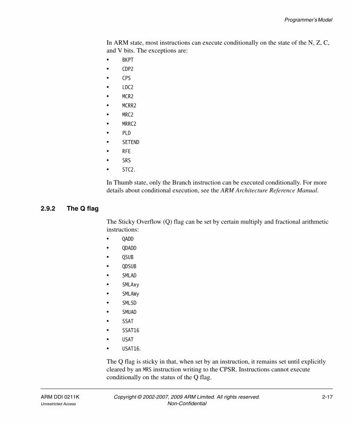
Programmer’s Model
In ARM state, most instructions can execute conditionally on the state of the N, Z, C, and V bits. The exceptions are:
• BKPT
• CDP2
• CPS
• LDC2
• MCR2
• MCRR2
• MRC2
• MRRC2
• PLD
• SETEND
• RFE
• SRS
• STC2.
In Thumb state, only the Branch instruction can be executed conditionally. For more details about conditional execution, see the ARM Architecture Reference Manual.
2.9.2 The Q flag
The Sticky Overflow (Q) flag can be set by certain multiply and fractional arithmetic instructions:
• QADD
• QDADD
• QSUB
• QDSUB
• SMLAD
• SMLAxy
• SMLAWy
• SMLSD
• SMUAD
• SSAT
• SSAT16
• USAT
• USAT16.
The Q flag is sticky in that, when set by an instruction, it remains set until explicitly cleared by an MRS instruction writing to the CPSR. Instructions cannot execute conditionally on the status of the Q flag.
ARM DDI 0211K Copyright © 2002-2007, 2009 ARM Limited. All rights reserved. 2-17Unrestricted Access Non-Confidential

Programmer’s Model
To determine the status of the Q flag you must read the PSR into a register and extract the Q flag from this. For details of how the Q flag is set and cleared, see individual instruction definitions in the ARM Architecture Reference Manual.
2.9.3 The J bit
The J bit in the CPSR indicates when the ARM1136JF-S processor is in Jazelle state.
When:
J = 0 The processor is in ARM or Thumb state, depending on the T bit.
J = 1 The processor is in Jazelle state.
Note • The combination of J = 1 and T = 1 causes similar effects to setting T=1 on a non
Thumb-aware processor. That is, the next instruction executed causes entry to the Undefined Instruction exception. Entry to the exception handler causes the processor to re-enter ARM state, and the handler can detect that this was the cause of the exception because J and T are both set in SPSR_und.
• MRS cannot be used to change the J bit in the CPSR.
• The placement of the J bit avoids the status or extension bytes in code running on ARMv5TE or earlier processors. This ensures that OS code written using the deprecated CPSR, SPSR, CPSR_all, or SPSR_all syntax for the destination of an MRS instruction continues to work.
2.9.4 The GE[3:0] bits
Some of the SIMD instructions set GE[3:0] as greater-than-or-equal bits for individual halfwords or bytes of the result. Table 2-3 on page 2-19 shows this.
2-18 Copyright © 2002-2007, 2009 ARM Limited. All rights reserved. ARM DDI 0211KNon-Confidential Unrestricted Access

Programmer’s Model
Note The GE bit is 1 if A op B ≥ C, otherwise 0.
The SEL instruction uses GE[3:0] to select which source register supplies each byte of its result.
Note • For unsigned operations, the GE bits are determined by the usual ARM rules for
carries out of unsigned additions and subtractions, and so are carry-out bits.
Table 2-3 GE[3:0] settings
GE[3] GE[2] GE[1] GE[0]
Instruction A op B > C A op B > C A op B > C A op B > C
Signed
SADD16 [31:16] + [31:16] ≥ 0 [31:16] + [31:16] ≥ 0 [15:0] + [15:0] ≥ 0 [15:0] + [15:0] ≥ 0
SSUB16 [31:16] - [31:16] ≥ 0 [31:16] - [31:16] ≥ 0 [15:0] - [15:0] ≥ 0 [15:0] - [15:0] ≥ 0
SADDSUBX [31:16] + [15:0] ≥ 0 [31:16] + [15:0] ≥ 0 [15:0] - [31:16] ≥ 0 [15:0] - [31:16] ≥ 0
SSUBADDX [31:16] - [15:0] ≥ 0 [31:16] - [15:0] ≥ 0 [15:0] + [31:16] ≥ 0 [15:0] + [31:16] ≥ 0
SADD8 [31:24] + [31:24] ≥ 0 [23:16] + [23:16] ≥ 0 [15:8] + [15:8] ≥ 0 [7:0] + [7:0] ≥ 0
SSUB8 [31:24] - [31:24] ≥ 0 [23:16] - [23:16] ≥ 0 [15:8] - [15:8] ≥ 0 [7:0] - [7:0] ≥ 0
Unsigned
UADD16 [31:16] + [31:16] ≥ 216 [31:16] + [31:16] ≥ 216 [15:0] + [15:0] ≥ 216 [15:0] + [15:0] ≥ 216
USUB16 [31:16] - [31:16] ≥ 0 [31:16] - [31:16] ≥ 0 [15:0] - [15:0] ≥ 0 [15:0] - [15:0] ≥ 0
UADDSUBX [31:16] + [15:0] ≥ 216 [31:16] + [15:0] ≥ 216 [15:0] - [31:16] ≥ 0 [15:0] - [31:16] ≥ 0
USUBADDX [31:16] - [15:0] ≥ 0 [31:16] - [15:0] ≥ 0 [15:0] + [31:16] ≥ 216 [15:0] + [31:16] ≥216
UADD8 [31:24] + [31:24] ≥ 28 [23:16] + [23:16] ≥ 28 [15:8] + [15:8] ≥ 28 [7:0] + [7:0] ≥ 28
USUB8 [31:24] - [31:24] ≥ 0 [23:16] - [23:16] ≥ 0 [15:8] - [15:8] ≥ 0 [7:0] - [7:0] ≥ 0
ARM DDI 0211K Copyright © 2002-2007, 2009 ARM Limited. All rights reserved. 2-19Unrestricted Access Non-Confidential

Programmer’s Model
• For signed operations, the rules for setting the GE bits are chosen so that they have the same sort of greater than or equal functionality as for unsigned operations.
2.9.5 The E bit
ARM and Thumb instructions are provided to set and clear the E-bit. The E bit controls load/store endianness. For details of where the E bit is used see Chapter 4 Unaligned and Mixed-Endian Data Access Support.
Architecture versions prior to ARMv6 specify this bit as SBZ. This ensures no endianness reversal on loads or stores.
2.9.6 The A bit
The A bit is set automatically. It is used to disable imprecise Data Aborts. For details of how to use the A bit see Imprecise Data Abort mask in the CPSR/SPSR on page 2-48.
2.9.7 The control bits
The bottom eight bits of a PSR are known collectively as the control bits. They are the:
• Interrupt disable bits
• T bit on page 2-21
• Mode bits on page 2-21.
The control bits change when an exception occurs. When the processor is operating in a privileged mode, software can manipulate these bits.
Interrupt disable bits
The I and F bits are the interrupt disable bits:
• when the I bit is set, IRQ interrupts are disabled
• when the F bit is set, FIQ interrupts are disabled.
2-20 Copyright © 2002-2007, 2009 ARM Limited. All rights reserved. ARM DDI 0211KNon-Confidential Unrestricted Access

Programmer’s Model
T bit
The T bit reflects the operating state:
• when the T bit is set, the processor is executing in Thumb state
• when the T bit is clear, the processor is executing in ARM state, or Jazelle state depending on the J bit.
Note Never use an MRS instruction to force a change to the state of the T bit in the CPSR. If an MRS instruction does try to modify this bit the result is architecturally Unpredictable. In the ARM1136JF-S processor this bit is not affected.
Mode bits
Caution An illegal value programmed into M[4:0] causes the processor to enter an unrecoverable state. If this occurs, you must apply reset. Not all combinations of the mode bits define a valid processor mode, so take care to use only those bit combinations shown.
Table 2-4 shows the M[4:0] mode bits that are used to determine the processor operating mode.
Table 2-4 PSR mode bit values
M[4:0] ModeVisible state registers
Thumb ARM
b10000 User R0–R7, R8-R12a, SP, LR, PC, CPSR R0–R14, PC, CPSR
b10001 FIQ R0–R7, R8_fiq-R12_fiqa, SP_fiq, LR_fiq PC, CPSR, SPSR_fiq
R0–R7, R8_fiq–R14_fiq, PC, CPSR, SPSR_fiq
b10010 IRQ R0–R7, R8-R12a, SP_irq, LR_irq, PC, CPSR, SPSR_irq
R0–R12, R13_irq, R14_irq, PC, CPSR, SPSR_irq
b10011 Supervisor R0–R7, R8-R12a, SP_svc, LR_svc, PC, CPSR, SPSR_svc
R0–R12, R13_svc, R14_svc, PC, CPSR, SPSR_svc
ARM DDI 0211K Copyright © 2002-2007, 2009 ARM Limited. All rights reserved. 2-21Unrestricted Access Non-Confidential

Programmer’s Model
2.9.8 Modification of PSR bits by MSR instructions
In previous architecture versions, MRS instructions can modify the flags byte, bits [31:24], of the CPSR in any mode, but the other three bytes are only modifiable in privileged modes.
After the introduction of ARM architecture v6, however, each CPSR bit falls into one of the following categories:
• Bits that are freely modifiable from any mode, either directly by MRS instructions or by other instructions whose side-effects include writing the specific bit or writing the entire CPSR.
Bits in Figure 2-7 on page 2-16 that are in this category are N, Z, C, V, Q, GE[3:0], and E.
• Bits that must never be modified by an MRS instruction, and so must only be written as a side-effect of another instruction. If an MRS instruction does try to modify these bits the results are architecturally Unpredictable. In the ARM1136JF-S processor these bits are not affected.
Bits in Figure 2-7 on page 2-16 that are in this category are J and T.
• Bits that can only be modified from privileged modes, and that are completely protected from modification by instructions while the processor is in User mode. The only way that these bits can be modified while the processor is in User mode is by entering a processor exception, as described in Exceptions on page 2-34.
Bits in Figure 2-7 on page 2-16 that are in this category are A, I, F, and M[4:0].
b10111 Abort R0–R7, R8-R12a, SP_abt, LR_abt, PC, CPSR, SPSR_abt
R0–R12, R13_abt, R14_abt, PC, CPSR, SPSR_abt
b11011 Undefined R0–R7, R8-R12a, SP_und, LR_und, PC, CPSR, SPSR_und
R0–R12, R13_und, R14_und, PC, CPSR, SPSR_und
b11111 System R0–R7, R8-R12a, SP, LR, PC, CPSR R0–R14, PC, CPSR
a. Access to these registers is limited in Thumb state.
Table 2-4 PSR mode bit values (continued)
M[4:0] ModeVisible state registers
Thumb ARM
2-22 Copyright © 2002-2007, 2009 ARM Limited. All rights reserved. ARM DDI 0211KNon-Confidential Unrestricted Access

Programmer’s Model
2.9.9 Reserved bits
The remaining bits in the PSRs are unused, but are reserved. When changing a PSR flag or control bits, make sure that these reserved bits are not altered. You must ensure that your program does not rely on reserved bits containing specific values because future processors might use some or all of the reserved bits.
ARM DDI 0211K Copyright © 2002-2007, 2009 ARM Limited. All rights reserved. 2-23Unrestricted Access Non-Confidential
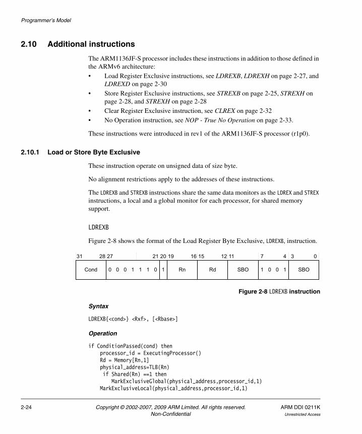
Programmer’s Model
2.10 Additional instructions
The ARM1136JF-S processor includes these instructions in addition to those defined in the ARMv6 architecture:
• Load Register Exclusive instructions, see LDREXB, LDREXH on page 2-27, and LDREXD on page 2-30
• Store Register Exclusive instructions, see STREXB on page 2-25, STREXH on page 2-28, and STREXH on page 2-28
• Clear Register Exclusive instruction, see CLREX on page 2-32
• No Operation instruction, see NOP - True No Operation on page 2-33.
These instructions were introduced in rev1 of the ARM1136JF-S processor (r1p0).
2.10.1 Load or Store Byte Exclusive
These instruction operate on unsigned data of size byte.
No alignment restrictions apply to the addresses of these instructions.
The LDREXB and STREXB instructions share the same data monitors as the LDREX and STREX instructions, a local and a global monitor for each processor, for shared memory support.
LDREXB
Figure 2-8 shows the format of the Load Register Byte Exclusive, LDREXB, instruction.
Figure 2-8 LDREXB instruction
Syntax
LDREXB{<cond>} <Rxf>, [<Rbase>]
Operation
if ConditionPassed(cond) thenprocessor_id = ExecutingProcessor()Rd = Memory[Rn,1]physical_address=TLB(Rn) if Shared(Rn) ==1 then
MarkExclusiveGlobal(physical_address,processor_id,1)MarkExclusiveLocal(physical_address,processor_id,1)
SBOCond
31 28 27 21 20 19 15 12 11 7 4 3 0
0 0 0 1 1 1 0 1 Rn Rd SBO 1 0 0 1
16
2-24 Copyright © 2002-2007, 2009 ARM Limited. All rights reserved. ARM DDI 0211KNon-Confidential Unrestricted Access

Programmer’s Model
Notes
• The result of the LDREXB operation is Unpredictable if you specify register 15 for <Rd> or <Rn>.
• If a data abort occurs during an LDREXB operation it is Unpredictable whether the MarkExclusiveGlobal() or the MarkExclusiveLocal() operation is executed. However, Rd is not updated.
• In regions of shared memory which do not support exclusives, the behavior of LDREXB is Unpredictable. This applies to regions of memory which do not have an exclusives monitor implemented.
• This command is only available from the rev1 (r1p0) release of the ARM1136JF-S processor.
STREXB
Figure 2-9 shows the format of the Store Register Byte Exclusive, STREXB, instruction.
Figure 2-9 STREXB instructions
Syntax
STREXB{<cond>} <Rd>, <Rm>, [<Rn>]]
Operation
if ConditionPassed(cond) thenprocessor_id = ExecutingProcessor()physical_address=TLB(Rn)if IsExclusiveLocal(physical_address,processor_id,1) then
if Shared(Rn)==1 thenif IsExclusiveGlobal(physical_address,processor_id,1) then
Memory[Rn,1] = RmRd = 0ClearByAddress(physical_address,1)
elseRd =1
else Memory[Rn,1] = RmRd = 0
elseRd = 1
RmCond
31 28 27 21 20 19 15 12 11 7 4 3 0
0 0 0 1 1 1 0 0 Rn Rd SBO 1 0 0 1
16 8
ARM DDI 0211K Copyright © 2002-2007, 2009 ARM Limited. All rights reserved. 2-25Unrestricted Access Non-Confidential

Programmer’s Model
ClearExclusiveLocal(processor_id)
Notes
• There is a register restriction that Rd != Rm and Rd != Rn.
• The result of the STREXB operation is Unpredictable if you specify register 15 for <Rd>, <Rn> or <Rm>.
• If a data abort occurs during a STREXB operation:
— Memory is not updated
— <Rd> is not updated
— it is Unpredictable whether the ClearExclusiveLocal() or the ClearByAddress() operation is executed.
• In regions of shared memory which do not support exclusives, the behavior of STREXB is Unpredictable. This applies to regions of memory which do not have an exclusives monitor implemented.
• This command is only available from the rev1 (r1p0) release of the ARM1136JF-S processor.
2-26 Copyright © 2002-2007, 2009 ARM Limited. All rights reserved. ARM DDI 0211KNon-Confidential Unrestricted Access

Programmer’s Model
2.10.2 Load or Store Halfword Exclusive
These instructions operate on naturally aligned, unsigned data of size halfword:
• The address in memory must be 16-bit aligned, address[0] == b0
— The instruction generates an alignment fault if this condition is not met.
For more information, see Operation of unaligned accesses on page 4-17.
• The transaction must be a single access, or an indivisible burst if the bus width is less than 16 bits.
The LDREXH and STREXH instructions share the same data monitors as the LDREX and STREX instructions, a local and a global monitor for each processor, for shared memory support.
LDREXH
Figure 2-10 shows the format of the Load Register Halfword Exclusive, LDREXH, instruction.
Figure 2-10 LDREXH instruction
Syntax
LDREXH{<cond>} <Rd>, [<Rn>]
Operation
if ConditionPassed(cond) thenprocessor_id = ExecutingProcessor()Rd = Memory[Rn,2]physical_address=TLB(Rn)if Shared(Rn) ==1 then
MarkExclusiveGlobal(physical_address,processor_id,2)MarkExclusiveLocal(physical_address,processor_id,2)
Notes
• The result of the LDREXH operation is Unpredictable if you specify register 15 for <Rd> or <Rn>
SBOCond
31 28 27 21 20 19 15 12 11 7 4 3 0
0 0 0 1 1 1 1 1 Rn Rd SBO 1 0 0 1
16
ARM DDI 0211K Copyright © 2002-2007, 2009 ARM Limited. All rights reserved. 2-27Unrestricted Access Non-Confidential
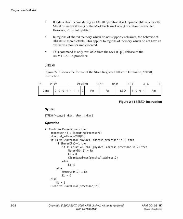
Programmer’s Model
• If a data abort occurs during an LDREXH operation it is Unpredictable whether the MarkExclusiveGlobal() or the MarkExclusiveLocal() operation is executed. However, Rd is not updated.
• In regions of shared memory which do not support exclusives, the behavior of LDREXH is Unpredictable. This applies to regions of memory which do not have an exclusives monitor implemented.
• This command is only available from the rev1 (r1p0) release of the ARM1136JF-S processor.
STREXH
Figure 2-11 shows the format of the Store Register Halfword Exclusive, STREXH, instruction.
Figure 2-11 STREXH instruction
Syntax
STREXH{<cond>} <Rd>, <Rm>, [<Rn>]
Operation
if ConditionPassed(cond) thenprocessor_id = ExecutingProcessor()physical_address=TLB(Rn)if IsExclusiveLocal(physical_address,processor_id,2) then
if Shared(Rn)==1 thenif IsExclusiveGlobal(physical_address,processor_id,2) then
Memory[Rn,2] = RmRd = 0ClearByAddress(physical_address,2)
elseRd =1
elseMemory[Rn,2] = RmRd = 0
elseRd = 1
ClearExclusiveLocal(processor_id)
RmCond
31 28 27 21 20 19 15 12 11 7 4 3 0
0 0 0 1 1 1 1 0 Rn Rd SBO 1 0 0 1
16 8
2-28 Copyright © 2002-2007, 2009 ARM Limited. All rights reserved. ARM DDI 0211KNon-Confidential Unrestricted Access

Programmer’s Model
Notes
• There is a register restriction that Rd != Rm and Rd != Rn.
• The result of the STREXH operation is Unpredictable if you specify register 15 for <Rd>, <Rn> or <Rm>.
• If a data abort occurs during a STREXH operation:
— Memory is not updated
— <Rd> is not updated
— it is Unpredictable whether the ClearExclusiveLocal() or the ClearByAddress() operation is executed.
• In regions of shared memory which do not support exclusives, the behavior of STREXH is Unpredictable. This applies to regions of memory which do not have an exclusives monitor implemented.
• This command is only available from the rev1 (r1p0) release of the ARM1136JF-S processor.
2.10.3 Load or Store Doubleword
The LDREXD and STREXD instructions behave as follows:
• The address in memory must be 64-bit aligned, address[2:0] == b000
— An alignment fault is generated if this condition is not met.
For more information, see Operation of unaligned accesses on page 4-17.
• The transaction must be a single access, or an indivisible burst if the bus width is less than 64 bits.
The LDREXD and STREXD instructions share the same data monitors as the LDREX and STREX instructions, a local and a global monitor for each processor, for shared memory support.
ARM DDI 0211K Copyright © 2002-2007, 2009 ARM Limited. All rights reserved. 2-29Unrestricted Access Non-Confidential
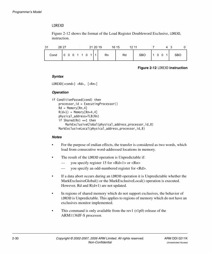
Programmer’s Model
LDREXD
Figure 2-12 shows the format of the Load Register Doubleword Exclusive, LDREXD, instruction.
Figure 2-12 LDREXD instruction
Syntax
LDREXD{<cond>} <Rd>, [<Rn>]
Operation
if ConditionPassed(cond) thenprocessor_id = ExecutingProcessor()Rd = Memory[Rn,4]R(d+1) = Memory[Rn+4,4]physical_address=TLB(Rn)if Shared(Rn) ==1 then
MarkExclusiveGlobal(physical_address,processor_id,8)MarkExclusiveLocal(physical_address,processor_id,8)
Notes
• For the purpose of endian effects, the transfer is considered as two words, which load from consecutive word-addressed locations in memory.
• The result of the LDREXD operation is Unpredictable if:
— you specify register 15 for <Rd+1> or <Rn>
— you specify an odd-numbered register for <Rd>.
• If a data abort occurs during an LDREXD operation it is Unpredictable whether the MarkExclusiveGlobal() or the MarkExclusiveLocal() operation is executed. However, Rd and R(d+1) are not updated.
• In regions of shared memory which do not support exclusives, the behavior of LDREXD is Unpredictable. This applies to regions of memory which do not have an exclusives monitor implemented.
• This command is only available from the rev1 (r1p0) release of the ARM1136JF-S processor.
SBOCond
31 28 27 21 20 19 15 12 11 7 4 3 0
0 0 0 1 1 0 1 1 Rn Rd SBO 1 0 0 1
16
2-30 Copyright © 2002-2007, 2009 ARM Limited. All rights reserved. ARM DDI 0211KNon-Confidential Unrestricted Access
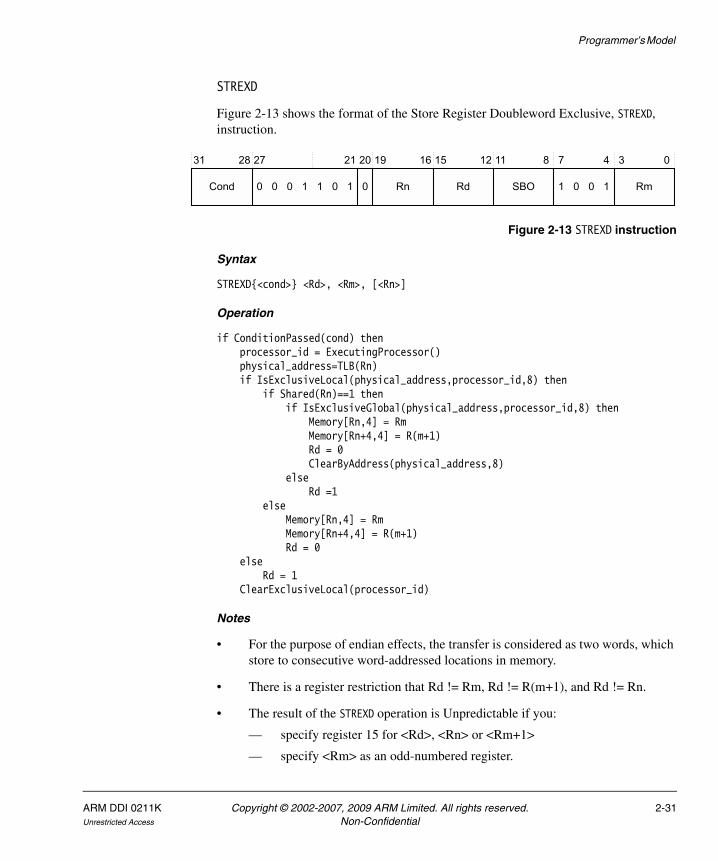
Programmer’s Model
STREXD
Figure 2-13 shows the format of the Store Register Doubleword Exclusive, STREXD, instruction.
Figure 2-13 STREXD instruction
Syntax
STREXD{<cond>} <Rd>, <Rm>, [<Rn>]
Operation
if ConditionPassed(cond) thenprocessor_id = ExecutingProcessor()physical_address=TLB(Rn)if IsExclusiveLocal(physical_address,processor_id,8) then
if Shared(Rn)==1 thenif IsExclusiveGlobal(physical_address,processor_id,8) then
Memory[Rn,4] = RmMemory[Rn+4,4] = R(m+1)Rd = 0ClearByAddress(physical_address,8)
elseRd =1
elseMemory[Rn,4] = RmMemory[Rn+4,4] = R(m+1)Rd = 0
elseRd = 1
ClearExclusiveLocal(processor_id)
Notes
• For the purpose of endian effects, the transfer is considered as two words, which store to consecutive word-addressed locations in memory.
• There is a register restriction that Rd != Rm, Rd != R(m+1), and Rd != Rn.
• The result of the STREXD operation is Unpredictable if you:
— specify register 15 for <Rd>, <Rn> or <Rm+1>
— specify <Rm> as an odd-numbered register.
RmCond
31 28 27 21 20 19 15 12 11 7 4 3 0
0 0 0 1 1 0 1 0 Rn Rd SBO 1 0 0 1
16 8
ARM DDI 0211K Copyright © 2002-2007, 2009 ARM Limited. All rights reserved. 2-31Unrestricted Access Non-Confidential
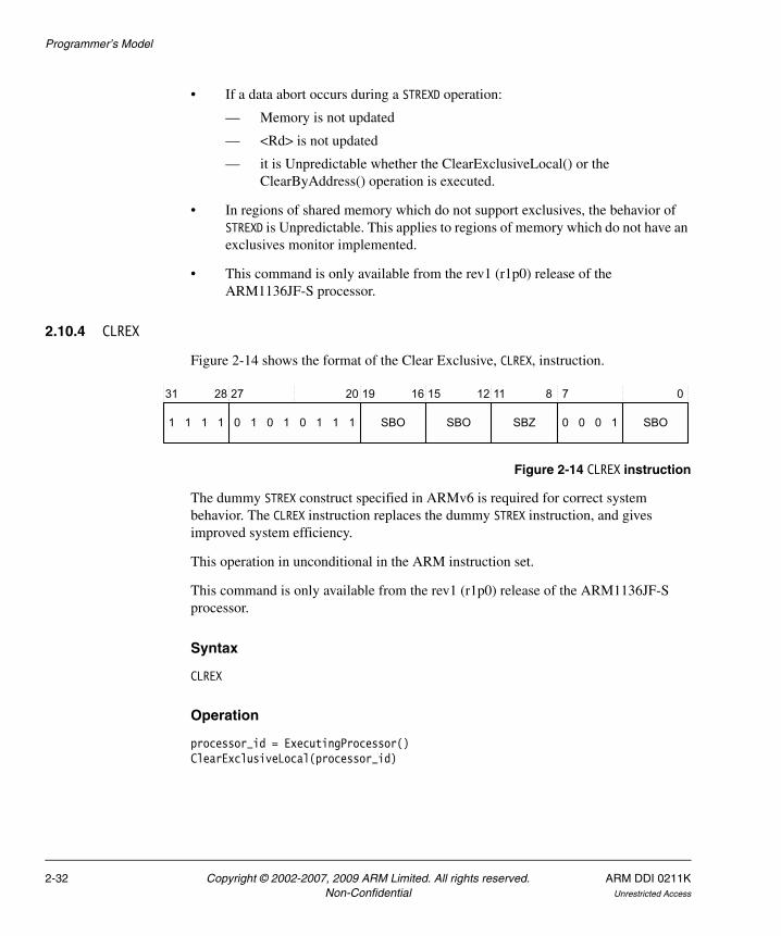
Programmer’s Model
• If a data abort occurs during a STREXD operation:
— Memory is not updated
— <Rd> is not updated
— it is Unpredictable whether the ClearExclusiveLocal() or the ClearByAddress() operation is executed.
• In regions of shared memory which do not support exclusives, the behavior of STREXD is Unpredictable. This applies to regions of memory which do not have an exclusives monitor implemented.
• This command is only available from the rev1 (r1p0) release of the ARM1136JF-S processor.
2.10.4 CLREX
Figure 2-14 shows the format of the Clear Exclusive, CLREX, instruction.
Figure 2-14 CLREX instruction
The dummy STREX construct specified in ARMv6 is required for correct system behavior. The CLREX instruction replaces the dummy STREX instruction, and gives improved system efficiency.
This operation in unconditional in the ARM instruction set.
This command is only available from the rev1 (r1p0) release of the ARM1136JF-S processor.
Syntax
CLREX
Operation
processor_id = ExecutingProcessor()ClearExclusiveLocal(processor_id)
0 0 0 1 SBOSBO1 1 1 1 SBZ
31 28 27 20 19 16 15 12 11 8 7 0
0 1 0 1 0 1 1 1 SBO
2-32 Copyright © 2002-2007, 2009 ARM Limited. All rights reserved. ARM DDI 0211KNon-Confidential Unrestricted Access

Programmer’s Model
2.10.5 NOP - True No Operation
Figure 2-15 shows the format of the No Operation, NOP, instruction.
Figure 2-15 NOP instruction
This command is only available from the rev1 (r1p0) release of the ARM1136JF-S processor.
Syntax
NOP {<cond>} <hint>
<cond> Is the condition under which the instruction executes. The ‘execute always’ condition is the only useful form of the command. Other forms produce no useful change in functionality, but are provided to ensure disassembly followed by reassembly always regenerates the original code.
<hint> Defaults to zero
On the ARM1136JF-S r1p0, the <hint> field has no effect.
Note True NOPs are architecturally defined for alignment reasons and do not have any timing guarantees with respect to their neighboring instructions.
Operation
The instruction will act as a NOP irrespective of whether the condition passes or fails, so effectively the command treats <Cond> as the ALWAYS condition, regardless of the value entered in the field.
SBZ HintCond
31 28 27 20 19 16 15 12 11 8 7 0
0 0 1 1 0 0 1 0 0 0 0 0 SBO
ARM DDI 0211K Copyright © 2002-2007, 2009 ARM Limited. All rights reserved. 2-33Unrestricted Access Non-Confidential

Programmer’s Model
2.11 Exceptions
Exceptions occur whenever the normal flow of a program has to be halted temporarily. For example, to service an interrupt from a peripheral. Before attempting to handle an exception, the ARM1136JF-S processor preserves the current processor state so that the original program can resume when the handler routine has finished.
If two or more exceptions occur simultaneously, the exceptions are dealt with in the fixed order given in Exception priorities on page 2-51.
This section provides details of the ARM1136JF-S exception handling:
• Exception entry and exit summary on page 2-36
• Entering an ARM exception on page 2-37
• Leaving an ARM exception on page 2-37.
Several enhancements are made in ARM architecture v6 to the exception model, mostly to improve interrupt latency, as follows:
• New instructions are added to give a choice of stack to use for storing the exception return state after exception entry, and to simplify changes of processor mode and the disabling and enabling of interrupts.
• The interrupt vector definitions on ARMv6 are changed to support the addition of hardware to prioritize the interrupt sources and to look up the start vector for the related interrupt handling routine.
• A low interrupt latency configuration is added in ARMv6. In terms of the instruction set architecture, it specifies that multi-access load/store instructions (ARM LDC, LDM, LDRD, STC, STM, and STRD, and Thumb LDMIA, POP, PUSH, and STMIA) can be interrupted and then restarted after the interrupt has been processed.
• Support for an imprecise Data Abort that behaves as an interrupt rather than as an abort, in that it occurs asynchronously relative to the instruction execution. Support involves the masking of a pending imprecise Data Abort at times when entry into Abort mode is deemed unrecoverable.
2.11.1 Changes to existing interrupt vectors
In ARMv5, the IRQ and FIQ exception vectors are fixed unless high vectors are enabled. Interrupt handlers typically have to start with an instruction sequence to determine the cause of the interrupt and branch to a routine to handle it.
On ARM1136JF-S processors the IRQ exception can be determined directly from the value presented on the Vectored Interrupt Controller (VIC) port. The vector interrupt behavior is explicitly enabled when the VE bit in CP15 c1 is set. See Chapter 12 Vectored Interrupt Controller Port.
2-34 Copyright © 2002-2007, 2009 ARM Limited. All rights reserved. ARM DDI 0211KNon-Confidential Unrestricted Access

Programmer’s Model
An example of a hardware block that can interface to the VIC port is the PrimeCell VIC (PL192), which is available from ARM. This takes a set of inputs from various interrupt sources, prioritizes them, and presents the interrupt type of the highest-priority interrupt being requested and the address of its handler to the processor core. The VIC also masks any lower priority interrupts. Such hardware reduces the time taken to enter the handling routine for the required interrupt.
2.11.2 New instructions for exception handling
This section describes the instructions added to accelerate the handling of exceptions. Full details of these instructions are given in the ARM Architecture Reference Manual.
Store Return State (SRS)
This instruction stores R14_<current_mode> and spsr_<current_mode> to sequential addresses, using the banked version of R13 for a specified mode to supply the base address (and to be written back to if base register write-back is specified). This enables an exception handler to store its return state on a stack other than the one automatically selected by its exception entry sequence.
The addressing mode used is a version of ARM addressing mode 4, modified to assume a {R14,SPSR} register list, rather than using a list specified by a bit mask in the instruction. This enables the SRS instruction to access stacks in a manner compatible with the normal use of STM instructions for stack accesses. For more information about addressing see the ARM Architecture Reference Manual.
Return From Exception (RFE)
This instruction loads the PC and CPSR from sequential addresses. This is used to return from an exception that has had its return state saved using the SRS instruction (see Store Return State (SRS)), and again uses a version of ARM addressing mode 4, modified this time to assume a {PC,CPSR} register list.
Change Processor State (CPS)
This instruction provides new values for the CPSR interrupt masks, mode bits, or both, and is designed to shorten and speed up the read/modify/write instruction sequence used in ARMv5 to perform such tasks. Together with the SRS instruction, it enables an exception handler to save its return information on the stack of another mode and then switch to that other mode, without modifying the stack belonging to the original mode or any registers other than the new mode stack pointer.
ARM DDI 0211K Copyright © 2002-2007, 2009 ARM Limited. All rights reserved. 2-35Unrestricted Access Non-Confidential

Programmer’s Model
This instruction also streamlines interrupt mask handling and mode switches in other code. In particular it enables short code sequences to be made atomic efficiently in a uniprocessor system by disabling interrupts at their start and re-enabling interrupts at their end. A similar Thumb instruction is also provided. However, the Thumb instruction can only change the interrupt masks, not the processor mode as well, to avoid using too much instruction set space.
2.11.3 Exception entry and exit summary
Table 2-5 summarizes the PC value preserved in the relevant R14 on exception entry, and the recommended instruction for exiting the exception handler.
Table 2-5 Exception entry and return
Exception or entry
Return instruction
Previous state
NotesARMR14_x
ThumbR14_x
JazelleR14_x
SWI MOVS PC, R14_svc PC + 4 PC+2 - Where the PC is the address of the SWI or Undefined instruction.
Not used in Jazelle state.UNDEF MOVS PC, R14_und PC + 4 PC+2 -
PABT SUBS PC, R14_abt, #4 PC + 4 PC+4 PC+4 Where the PC is the address of instruction that had the Prefetch Abort.
FIQ SUBS PC, R14_fiq, #4 PC + 4 PC+4 PC+4 Where the PC is the address of the instruction that was not executed because the FIQ or IRQ took priority.IRQ SUBS PC, R14_irq, #4 PC + 4 PC+4 PC+4
DABT SUBS PC, R14_abt, #8 PC + 8 PC+8 PC+8 Where the PC is the address of the Load or Store instruction that generated the Data Abort.
RESET n/a - - - The value saved in R14_svc on reset is Unpredictable.
BKPT SUBS PC, R14_abt, #4 PC + 4 PC+4 PC+4 Software breakpoint.
2-36 Copyright © 2002-2007, 2009 ARM Limited. All rights reserved. ARM DDI 0211KNon-Confidential Unrestricted Access

Programmer’s Model
2.11.4 Entering an ARM exception
When handling an ARM exception the ARM1136JF-S processor:
1. Preserves the address of the next instruction in the appropriate LR. When the exception entry is from:
ARM and Jazelle states: The ARM1136JF-S processor writes the value of the PC into the LR, offset by a value (current PC + 4 or PC + 8 depending on the exception) that causes the program to resume from the correct place on return
Thumb state: The ARM1136JF-S processor writes the value of the PC into the LR, offset by a value (current PC + 2, PC + 4 or PC + 8 depending on the exception) that causes the program to resume from the correct place on return.
The exception handler does not have to determine the state when entering an exception. For example, in the case of a SWI, MOVS PC, R14_svc always returns to the next instruction regardless of whether the SWI was executed in ARM or Thumb state.
2. Copies the CPSR into the appropriate SPSR.
3. Forces the CPSR mode bits to a value that depends on the exception.
4. Forces the PC to fetch the next instruction from the relevant exception vector.
The ARM1136JF-S processor can also set the interrupt disable flags to prevent otherwise unmanageable nesting of exceptions.
Note Exceptions are always entered, handled, and exited in ARM state. When the processor is in Thumb state or Jazelle state and an exception occurs, the switch to ARM state takes place automatically when the exception vector address is loaded into the PC.
2.11.5 Leaving an ARM exception
When an exception has completed, the exception handler must move the LR, minus an offset to the PC. Table 2-5 on page 2-36 shows the type of exception and the offsets associated with it.
Typically the return instruction is an arithmetic or logical operation with the S bit set and Rd = R15, so the core copies the SPSR back to the CPSR.
ARM DDI 0211K Copyright © 2002-2007, 2009 ARM Limited. All rights reserved. 2-37Unrestricted Access Non-Confidential
Programmer’s Model
Note The action of restoring the CPSR from the SPSR automatically resets the T bit and J bit to the values held immediately prior to the exception. The A, I, and F bits are also automatically restored to the value they held immediately prior to the exception.
2.11.6 Reset
When the nRESETIN signal is driven LOW a reset occurs, and the ARM1136JF-S processor abandons the executing instruction.
When nRESETIN is driven HIGH again the ARM1136JF-S processor:
1. Forces CPSR M[4:0] to b10011 (Supervisor mode), sets the A, I, and F bits in the CPSR, and clears the CPSR T bit and J bit. The E bit is set based on the state of the BIGENDINIT and UBITINIT pins. Other bits in the CPSR are indeterminate.
2. Forces the PC to fetch the next instruction from the reset vector address.
3. Reverts to ARM state, and resumes execution.
After reset, all register values except the PC and CPSR are indeterminate.
See Chapter 9 Clocking and Resets for more details of the reset behavior for the ARM1136JF-S processor.
2.11.7 Fast interrupt request
The Fast Interrupt Request (FIQ) exception supports fast interrupts. In ARM state, FIQ mode has eight private registers to reduce, or even remove the requirement for register saving (minimizing the overhead of context switching).
An FIQ is externally generated by taking the nFIQ signal input LOW. The nFIQ input is registered internally to the ARM1136JF-S processor. It is the output of this register that is used by the ARM1136JF-S processor control logic.
Irrespective of whether exception entry is from ARM state, Thumb state, or Jazelle state, an FIQ handler returns from the interrupt by executing:
SUBS PC,R14_fiq,#4
You can disable FIQ exceptions within a privileged mode by setting the CPSR F flag. When the F flag is clear, the ARM1136JF-S processor checks for a LOW level on the output of the nFIQ register at the end of each instruction.
2-38 Copyright © 2002-2007, 2009 ARM Limited. All rights reserved. ARM DDI 0211KNon-Confidential Unrestricted Access

Programmer’s Model
FIQs and IRQs are disabled when an FIQ occurs. You can use nested interrupts but it is up to you to save any corruptible registers and to re-enable FIQs and interrupts.
2.11.8 Interrupt request
The IRQ exception is a normal interrupt caused by a LOW level on the nIRQ input. IRQ has a lower priority than FIQ, and is masked on entry to an FIQ sequence.
Irrespective of whether exception entry is from ARM state, Thumb state, or Jazelle state, an IRQ handler returns from the interrupt by executing:
SUBS PC,R14_irq,#4
You can disable IRQ exceptions within a privileged mode by setting the CPSR I flag. When the I flag is clear, the ARM1136JF-S processor checks for a LOW level on the output of the nIRQ register at the end of each instruction.
IRQs are disabled when an IRQ occurs. You can use nested interrupts but it is up to you to save any corruptible registers and to re-enable IRQs.
2.11.9 Low interrupt latency configuration
The FI bit, bit 21, in CP15 register 1 enables a low interrupt latency configuration. This mode reduces the interrupt latency of the ARM1136JF-S processor. This is achieved by:
• disabling Hit-Under-Miss (HUM) functionality
• abandoning restartable external accesses so that the core can react to a pending interrupt faster than is normally the case
• recognizing low-latency interrupts as late as possible in the main pipeline.
To ensure that a change between normal and low interrupt latency configurations is synchronized correctly, you must only change the FI bit using the sequence:
1. Drain the Write Buffer.
2. Change the FI Bit.
3. Drain the Write Buffer with interrupt disabled.
You must ensure that software systems only change the FI bit shortly after Reset, while interrupts are disabled.
To minimize the interrupt latency when using low interrupt latency mode, avoid using multiword load/store instructions to memory locations that are marked as Device or Strongly Ordered. Multiword accesses to Device or Strongly Ordered memory are not restartable and therefore must be completed before an interrupt can be taken.
ARM DDI 0211K Copyright © 2002-2007, 2009 ARM Limited. All rights reserved. 2-39Unrestricted Access Non-Confidential

Programmer’s Model
This enables these instructions to be interruptible when in low interrupt latency configuration. If the instruction is interrupted before it is complete, the result might be that one or more of the words are accessed twice, but the idempotency of the side-effects, if any, of the memory accesses ensures that this does not matter.
Note There is a similar existing requirement with unaligned and multiword load/store instructions that access memory locations that can abort in a recoverable way. An abort on one of the words accessed can cause a previously-accessed word to be accessed twice, once before the abort and again after the abort handler has returned. The requirement in this case is either:
• all side-effects are idempotent
• the abort must either occur on the first word accessed or not at all.
The instructions that this rule currently applies to are:
• ARM instructions LDC, all forms of LDM, LDRD, STC, all forms of STM, STRD, and unaligned LDR, STR, LDRH, and STRH
• Thumb instructions LDMIA, PUSH, POP, and STMIA, and unaligned LDR, STR, LDRH, and STRH.
System designers are also advised that memory locations accessed with these instructions must not have large numbers of wait-states associated with them if the best possible interrupt latency is to be achieved.
2.11.10 Interrupt latency example
This section gives an extended example to show how the combination of new facilities improves interrupt latency. The example is not necessarily entirely realistic, but illustrates the main points.
The assumptions made are:
1. Vector Interrupt Controller (VIC) hardware exists to prioritize interrupts and to supply the address of the highest priority interrupt to the processor core on demand.
In the ARMv5 system, the address is supplied in a memory-mapped I/O location, and loading it acts as an entering interrupt handler acknowledgement to the VIC. In the ARMv6 system, the address is loaded and the acknowledgement given automatically, as part of the interrupt entry sequence. In both systems, a store to a memory-mapped I/O location is used to send a finishing interrupt handler acknowledgement to the VIC.
2-40 Copyright © 2002-2007, 2009 ARM Limited. All rights reserved. ARM DDI 0211KNon-Confidential Unrestricted Access

Programmer’s Model
2. The system has the following layers:
Real-time layer Contains handlers for a number of high-priority interrupts. These interrupts can be prioritized, and are assumed to be signaled to the processor core by means of the FIQ interrupt. Their handlers do not use the facilities supplied by the other two layers. This means that all memory they use must be locked down in the TLBs and caches. (It is possible to use additional code to make access to nonlocked memory possible, but this is not discussed in this example.)
Architectural completion layer Contains Prefetch Abort, Data Abort and Undefined instruction handlers whose purpose is to give the illusion that the hardware is handling all memory requests and instructions on its own, without requiring software to handle TLB misses, virtual memory misses, and near-exceptional floating-point operations, for example. This illusion is not available to the real-time layer, because the software handlers concerned take a significant number of cycles, and it is not reasonable to have every memory access to take large numbers of cycles. Instead, the memory concerned has to be locked down.
Non real-time layer Provides interrupt handlers for low-priority interrupts. These interrupts can also be prioritized, and are assumed to be signaled to the processor core using the IRQ interrupt.
3. The corresponding exception priority structure is as follows, from highest to lowest priority:
a. FIQ1 (highest priority FIQ)
b. FIQ2
c. ...
d. FIQm (lowest priority FIQ)
e. Data Abort
f. Prefetch Abort
g. Undefined instruction
h. SWI
i. IRQ1 (highest priority IRQ)
j. IRQ2
k. ...
ARM DDI 0211K Copyright © 2002-2007, 2009 ARM Limited. All rights reserved. 2-41Unrestricted Access Non-Confidential

Programmer’s Model
l. IRQn (lowest priority IRQ)
The processor core prioritization handles most of the priority structure, but the VIC handles the priorities within each group of interrupts.
Note This list reflects the priorities that the handlers are subject to, and differs from the
priorities that the exception entry sequences are subject to. The difference occurs because simultaneous Data Abort and FIQ exceptions result in the sequence:
a. Data Abort entry sequence executed, updating R14_abt, SPSR_abt, PC, and CPSR.
b. FIQ entry sequence executed, updating R14_fiq, SPSR_fiq, PC, and CPSR.
c. FIQ handler executes to completion and returns.
d. Data Abort handler executes to completion and returns.
For more information, see the ARM Architecture Reference Manual.
4. Stack and register usage is:
• The FIQ1 interrupt handler has exclusive use of R8_fiq to R12_fiq. In ARMv5, R13_fiq points to a memory area, that is mainly for use by the FIQ1 handler. However, a few words are used during entry for other FIQ handlers. In ARMv6, the FIQ1 interrupt handler has exclusive use of R13_fiq.
• The Undefined instruction, Prefetch Abort, Data Abort, and non-FIQ1 FIQ handlers use the stack pointed to by R13_abt. This stack is locked down in memory, and therefore of known, limited depth.
• All IRQ and SWI handlers use the stack pointed to by R13_svc. This stack does not have to be locked down in memory.
• The stack pointed to by R13_usr is used by the current process. This process can be privileged or unprivileged, and uses System or User mode accordingly.
5. Timings are roughly consistent with ARM10 timings, with the pipeline reload penalty being three cycles. It is assumed that pipeline reloads are combined to execute as quickly as reasonably possible, and in particular that:
• If an interrupt is detected during an instruction that has set a new value for the PC, after that value has been determined and written to the PC but before the resulting pipeline refill is completed, the pipeline refill is abandoned and the interrupt entry sequence started as soon as possible.
2-42 Copyright © 2002-2007, 2009 ARM Limited. All rights reserved. ARM DDI 0211KNon-Confidential Unrestricted Access

Programmer’s Model
• Similarly, if an FIQ is detected during an exception entry sequence that does not disable FIQs, after the updates to R14, the SPSR, the CPSR, and the PC but before the pipeline refill has completed, the pipeline refill is abandoned and the FIQ entry sequence started as soon as possible.
FIQs in the example system in ARMv5
In ARMv5, all FIQ interrupts come through the same vector, at address 0x0000001C or 0xFFFF001C. To implement the above system, the code at this vector must get the address of the correct handler from the VIC, branch to it, and transfer to using R13_abt and the Abort mode stack if it is not the FIQ1 handler. The following code does this, assuming that R8_fiq holds the address of the VIC:
FIQhandlerLDR PC, [R8,#HandlerAddress]
...FIQ1handler... Include code to process the interrupt ...
STR R0, [R8,#AckFinished]SUBS PC, R14, #4
...
FIQ2handlerSTMIA R13, {R0-R3}MOV R0, LRMRS R1, SPSRADD R2, R13, #8MRS R3, CPSRBIC R3, R3, #0x1FORR R3, R3, #0x1B ; = Abort mode numberMSR CPSR_c, R3STMFD R13!, {R0,R1}LDMIA R2, {R0,R1}STMFD R13!, {R0,R1}LDMDB R2, {R0,R1}BIC R3, R3, #0x40 ; = F bitMSR CPSR_c, R3
... FIQs are now re-enabled, with original R2, R3, R14, SPSR on stack
... Include code to stack any more registers required, process the interrupt
... and unstack extra registersADR R2, #VICaddressMRS R3, CPSRORR R3, R3, #0x40 ; = F bitMSR CPSR_c, R3STR R0, [R2,#AckFinished]LDR R14, [R13,#12] ; Original SPSR valueMSR SPSR_fsxc, R14LDMFD R13!, {R2,R3,R14}
ARM DDI 0211K Copyright © 2002-2007, 2009 ARM Limited. All rights reserved. 2-43Unrestricted Access Non-Confidential

Programmer’s Model
ADD R13, R13, #4SUB SPC, R14, #4
...
The major problem with this is the length of time that FIQs are disabled at the start of the lower priority FIQs. The worst-case interrupt latency for the FIQ1 interrupt occurs if a lower priority FIQ2 has fetched its handler address, and is approximately:
• 3 cycles for the pipeline refill after the LDR PC instruction fetches the handler address
• + 24 cycles to get to and execute the MRS instruction that re-enables FIQs
• + 3 cycles to re-enter the FIQ exception
• + 5 cycles for the LDR PC instruction at FIQhandler
• = 35 cycles.
Note FIQs must be disabled for the final store to acknowledge the end of the handler to the VIC. Otherwise, more badly timed FIQs, each occurring close to the end of the previous handler, can cause unlimited growth of the locked-down stack.
FIQs in the example system in ARMv6
Using the VIC and the new instructions, there is no longer any requirement for everything to go through the single FIQ vector, and the changeover to a different stack occurs much more smoothly. The code is:
FIQ1handler... Include code to process the interrupt ...
STR R0, [R8,#AckFinished]SUBS PC, R14, #4
...FIQ2handler
SUB R14, R14, #4SRSFD R13_abt!CPSIE f, #0x1B ; = Abort modeSTMFD R13!, {R2,R3}
... FIQs are now re-enabled, with original R2, R3, R14, SPSR on stack
... Include code to stack any more registers required, process the interrupt
... and unstack extra registersLDMFD R13!, {R2,R3}ADR R14, #VICaddressCPSID fSTR R0, [R14,#AckFinished]
2-44 Copyright © 2002-2007, 2009 ARM Limited. All rights reserved. ARM DDI 0211KNon-Confidential Unrestricted Access

Programmer’s Model
RFEFD R13!...
The worst-case interrupt latency for a FIQ1 now occurs if the FIQ1 occurs during an FIQ2 interrupt entry sequence, after it disables FIQs, and is approximately:
• 3 cycles for the pipeline refill for the FIQ2 exception entry sequence
• + 5 cycles to get to and execute the CPSIE instruction that re-enables FIQs
• + 3 cycles to re-enter the FIQ exception
• = 11 cycles.
Note In the ARMv5 system, the potential additional interrupt latency caused by a long LDM or STM being in progress when the FIQ is detected was only significant because the memory system could stretch its cycles considerably. Otherwise, it was dwarfed by the number of cycles lost because of FIQs being disabled at the start of a lower-priority interrupt handler. In ARMv6, this is still the case, but it is a lot closer.
Alternatives to the example system
Two alternatives to the design in FIQs in the example system in ARMv6 on page 2-44 are:
• The first alternative is not to reserve the FIQ registers for the FIQ1 interrupt, but instead either to:
— share them out among the various FIQ handlers
The first restricts the registers available to the FIQ1 handler and adds the software complication of managing a global allocation of FIQ registers to FIQ handlers. Also, because of the shortage of FIQ registers, it is not likely to be very effective if there are many FIQ handlers.
— require the FIQ handlers to treat them as normal callee-save registers.
The second adds a number of cycles of loading important addresses and variable values into the registers to each FIQ handler before it can do any useful work. That is, it increases the effective FIQ latency by a similar number of cycles.
ARM DDI 0211K Copyright © 2002-2007, 2009 ARM Limited. All rights reserved. 2-45Unrestricted Access Non-Confidential

Programmer’s Model
• The second alternative is to use IRQs for all but the highest priority interrupt, so that there is only one level of FIQ interrupt. This achieves very fast FIQ latency, 5-8 cycles, but at a cost to all the lower-priority interrupts that every exception entry sequence now disables them. You then have the following possibilities:
— None of the exception handlers in the architectural completion layer re-enable IRQs. In this case, all IRQs suffer from additional possible interrupt latency caused by those handlers, and so effectively are in the non real-time layer. In other words, this results in there only being one priority for interrupts in the real-time layer.
— All of the exception handlers in the architectural completion layer re-enable IRQs to permit IRQs to have real-time behavior. The problem in this case is that all IRQs can then occur during the processing of an exception in the architectural completion layer, and so they are all effectively in the real-time layer. In other words, this effectively means that there are no interrupts in the non real-time layer.
— All of the exception handlers in the architectural completion layer re-enable IRQs, but they also use additional VIC facilities to place a lower limit on the priority of IRQs that is taken. This permits IRQs at that priority or higher to be treated as being in the real-time layer, and IRQs at lower priorities to be treated as being in the non real-time layer. The price paid is some additional complexity in the software and in the VIC hardware.
Note For either of the last two options, the new instructions speed up the IRQ
re-enabling and the stack changes that are likely to be required.
2.11.11 Aborts
An abort can be caused by either:
• the MMU signalling an internal abort
• an External Abort being raised from the AHB interfaces, by an AHB Error response.
There are two types of abort:
• Prefetch Abort on page 2-47
• Data Abort on page 2-47.
IRQs are disabled when an abort occurs.
2-46 Copyright © 2002-2007, 2009 ARM Limited. All rights reserved. ARM DDI 0211KNon-Confidential Unrestricted Access

Programmer’s Model
Prefetch Abort
This is signaled with the Instruction Data as it enters the pipeline Decode stage.
When a Prefetch Abort occurs, the ARM1136JF-S processor marks the prefetched instruction as invalid, but does not take the exception until the instruction is to be executed. If the instruction is not executed, for example because a branch occurs while it is in the pipeline, the abort does not take place.
After dealing with the cause of the abort, the handler executes the following instruction irrespective of the processor operating state:
SUBS PC,R14_abt,#4
This action restores both the PC and the CPSR, and retries the aborted instruction.
Data Abort
Data Abort on the ARM1136JF-S processor can be precise or imprecise. Precise Data Aborts are those generated after performing an instruction side CP15 operation, and all those generated by the MMU:
• alignment faults
• translation faults
• domain faults
• permission faults.
Data Aborts that occur because of watchpoints are imprecise in that the processor and system state presented to the abort handler is the processor and system state at the boundary of an instruction shortly after the instruction that caused the watchpoint (but before any following load/store instruction). Because the state that is presented is consistent with an instruction boundary, these aborts are restartable, even though they are imprecise.
Errors that cause externally generated Data Aborts, signaled by HRESPR[0], HRESPW[0] or HRESPP[0], might be precise or imprecise. Two separate FSR encodings indicate if the External Abort is precise or imprecise. External Data Aborts are precise if:
• all External Aborts to loads when the CP15 Register 1 FI bit, bit 21, is set are precise
• all aborts to loads or stores to Strongly Ordered memory are precise
• all aborts to loads to the Program Counter or the CSPR are precise
• all aborts on the load part of an SWP are precise
• all other External Aborts are imprecise.
ARM DDI 0211K Copyright © 2002-2007, 2009 ARM Limited. All rights reserved. 2-47Unrestricted Access Non-Confidential

Programmer’s Model
External aborts are supported on cacheable locations. The abort is transmitted to the processor only if a word requested by the processor had an External Abort.
Precise Data Aborts
A precise Data Abort is signaled when the abort exception enables the processor and system state presented to the abort handler to be consistent with the processor and system state when the aborting instruction was executed. With precise Data Aborts, the restarting of the processor after the cause of the abort has been rectified is straightforward.
The ARM1136JF-S processor implements the base restored Data Abort model, which differs from the base updated Data Abort model implemented by the ARM7TDMI-S.
With the base restored Data Abort model, when a Data Abort exception occurs during the execution of a memory access instruction, the base register is always restored by the processor hardware to the value it contained before the instruction was executed. This removes the requirement for the Data Abort handler to unwind any base register update, which might have been specified by the aborted instruction. This simplifies the software Data Abort handler. See the ARM Architecture Reference Manual for more details.
After dealing with the cause of the abort, the handler executes the following return instruction irrespective of the processor operating state at the point of entry:
SUBS PC,R14_abt,#8
This restores both the PC and the CPSR, and retries the aborted instruction.
Imprecise Data Aborts
An imprecise Data Abort is signaled when the processor and system state presented to the abort handler cannot be guaranteed to be consistent with the processor and system state when the aborting instruction was issued.
2.11.12 Imprecise Data Abort mask in the CPSR/SPSR
An imprecise Data Abort caused, for example, by an external error on a write that has been held in a Write Buffer, is asynchronous to the execution of the causing instruction and can occur many cycles after the instruction that caused the memory access has retired. For this reason, the imprecise Data Abort can occur at a time that the processor is in Abort mode because of a precise Data Abort, or can have live state in Abort mode, but be handling an interrupt.
2-48 Copyright © 2002-2007, 2009 ARM Limited. All rights reserved. ARM DDI 0211KNon-Confidential Unrestricted Access

Programmer’s Model
To avoid the loss of the Abort mode state (R14 and SPSR_abt) in these cases, which leads to the processor entering an unrecoverable state, the existence of a pending imprecise Data Abort must be held by the system until a time when the Abort mode can safely be entered.
A mask is added into the CPSR to indicate that an imprecise Data Abort can be accepted. This bit is the A bit. The imprecise Data Abort causes a Data Abort to be taken when imprecise Data Aborts are not masked. When imprecise Data Aborts are masked, then the implementation is responsible for holding the presence of a pending imprecise Data Abort until the mask is cleared and the abort is taken.
The A bit is set automatically on entry into Abort Mode, IRQ, and FIQ Modes, and on Reset.
2.11.13 Software interrupt instruction
You can use the software interrupt (SWI) instruction to enter Supervisor mode, usually to request a particular supervisor function. The SWI handler reads the opcode to extract the SWI function number. A SWI handler returns by executing the following instruction, irrespective of the processor operating state:
MOVS PC, R14_svc
This action restores the PC and CPSR, and returns to the instruction following the SWI.
IRQs are disabled when a software interrupt occurs.
2.11.14 Undefined instruction
When an instruction is encountered that neither the ARM1136JF-S processor, nor any coprocessor in the system, can handle the ARM1136JF-S processor takes the Undefined instruction trap. Software can use this mechanism to extend the ARM instruction set by emulating Undefined coprocessor instructions.
After emulating the failed instruction, the trap handler executes the following instruction, irrespective of the processor operating state:
MOVS PC,R14_und
This action restores the CPSR and returns to the next instruction after the Undefined instruction.
IRQs are disabled when an Undefined instruction trap occurs. For more details about Undefined instructions, see the ARM Architecture Reference Manual.
ARM DDI 0211K Copyright © 2002-2007, 2009 ARM Limited. All rights reserved. 2-49Unrestricted Access Non-Confidential

Programmer’s Model
2.11.15 Breakpoint instruction (BKPT)
A breakpoint (BKPT) instruction operates as though the instruction causes a Prefetch Abort.
A breakpoint instruction does not cause the ARM1136JF-S processor to take the Prefetch Abort exception until the instruction reaches the Execute stage of the pipeline. If the instruction is not executed, for example because a branch occurs while it is in the pipeline, the breakpoint does not take place.
After dealing with the breakpoint, the handler executes the following instruction irrespective of the processor operating state:
SUBS PC,R14_abt,#4
This action restores both the PC and the CPSR, and retries the breakpointed instruction.
Note If the EmbeddedICE-RT logic is configured into Halting debug-mode, a breakpoint instruction causes the ARM1136JF-S processor to enter Debug state. See Halting debug-mode debugging on page 13-66.
2.11.16 Exception vectors
Table 2-6 shows the CP15 c1 Control Register V bit settings for configuring the location of the exception vector addresses.
Table 2-6 Configuration of exception vector address locations
Value of V bit Exception vector base location
0 0x00000000
1 0xFFFF0000
2-50 Copyright © 2002-2007, 2009 ARM Limited. All rights reserved. ARM DDI 0211KNon-Confidential Unrestricted Access

Programmer’s Model
Table 2-7 shows the exception vector addresses and entry conditions for the different exception types.
2.11.17 Exception priorities
When multiple exceptions arise at the same time, a fixed priority system determines the order that they are handled:
1. Reset (highest priority).
2. Precise Data Abort.
3. FIQ.
4. IRQ.
5. Imprecise Data Aborts.
6. Prefetch Abort.
7. BKPT, Undefined instruction, and SWI (lowest priority).
Some exceptions cannot occur together:
• The BKPT, or Undefined instruction, and SWI exceptions are mutually exclusive. Each corresponds to a particular, non-overlapping, decoding of the current instruction.
• When FIQs are enabled, and a precise Data Abort occurs at the same time as an FIQ, the ARM1136JF-S processor enters the Data Abort handler, and proceeds immediately to the FIQ vector.
A normal return from the FIQ causes the Data Abort handler to resume execution.
Table 2-7 Exception vectors
ExceptionOffset from vector base
Mode on entry
A bit on entry
F bit on entry
I bit on entry
Reset 0x00 Supervisor Disabled Disabled Disabled
Undefined instruction 0x04 Undefined Unchanged Unchanged Disabled
Software interrupt 0x08 Supervisor Unchanged Unchanged Disabled
Prefetch Abort 0x0C Abort Disabled Unchanged Disabled
Data Abort 0x10 Abort Disabled Unchanged Disabled
Reserved 0x14 Reserved - - -
IRQ 0x18 IRQ Disabled Unchanged Disabled
FIQ 0x1C FIQ Disabled Disabled Disabled
ARM DDI 0211K Copyright © 2002-2007, 2009 ARM Limited. All rights reserved. 2-51Unrestricted Access Non-Confidential

Programmer’s Model
Precise Data Aborts must have higher priority than FIQs to ensure that the transfer error does not escape detection. You must add the time for this exception entry to the worst-case FIQ latency calculations in a system that uses aborts to support virtual memory.
The FIQ handler must not access any memory that can generate a Data Abort, because the initial Data Abort exception condition is lost if this happens.
2-52 Copyright © 2002-2007, 2009 ARM Limited. All rights reserved. ARM DDI 0211KNon-Confidential Unrestricted Access
Chapter 3 System Control Coprocessor
This chapter describes the purpose of the system control coprocessor, its structure, operation, and how to use it. It contains the following sections:
• About the system control coprocessor on page 3-2
• System control coprocessor registers overview on page 3-17
• System control coprocessor register descriptions on page 3-25.
ARM DDI 0211K Copyright © 2002-2007, 2009 ARM Limited. All rights reserved. 3-1Unrestricted Access Non-Confidential

System Control Coprocessor
3.1 About the system control coprocessor
The section gives an overall view of the system control coprocessor. For details of the registers in the system control coprocessor, see System control coprocessor register descriptions on page 3-25.
The purpose of the system control coprocessor, CP15, is to control and provide status information for the functions implemented in the ARM1136JF-S processor. The main functions of the system control coprocessor are:
• overall system control and configuration of the ARM1136JF-S processor
• cache configuration and management
• Tightly-Coupled Memory (TCM) configuration and management
• Memory Management Unit (MMU) configuration and management
• DMA control
• debug accesses to the caches and Translation Lookaside Buffer (TLB)
• system performance monitoring.
The system control coprocessor does not exist as a single distinct physical block of logic.
3.1.1 Terms used in this chapter
For definitions of the terms used in the register descriptions in this chapter refer to the Glossary on page Glossary-1.
3.1.2 System control coprocessor functional groups
The system control coprocessor appears as a set of 32-bit registers. In general you can write to and read from these registers, although access to many registers is limited:
• some registers are read-only
• some registers are write-only
• many registers can only be accessed from secure mode.
The functional groups for the registers are summarized in the following sections:
• System control and configuration on page 3-7
• MMU control and configuration on page 3-8
• Cache control and configuration on page 3-10
• TCM control and configuration on page 3-11
• Debug access to caches and TLB on page 3-11
• DMA control on page 3-13
• System performance monitoring on page 3-14.
3-2 Copyright © 2002-2007, 2009 ARM Limited. All rights reserved. ARM DDI 0211KNon-Confidential Unrestricted Access

System Control Coprocessor
Table 3-1 shows the overall functionality for the system control coprocessor as it relates to its registers.
Table 3-2 on page 3-18 lists the registers in the system control coprocessor in register order and gives their reset values.
Table 3-1 System control coprocessor register functions
Function Register Reference to description
System control and configuration
Main IDa See c0, Main ID Register on page 3-25
Feature IDb See c0, Core feature ID registers on page 3-35
Control See c1, Control Register on page 3-63
Auxiliary Control See c1, Auxiliary Control Register on page 3-69
Coprocessor Access Control See c1, Coprocessor Access Control Register on page 3-72
MMU control and configuration
TLB Type See c0, TLB Type Register on page 3-33
Translation Table Base Control See c2, Translation Table Base Control Register, TTBCR on page 3-78
Translation Table Base 0 See c2, Translation Table Base Register 0, TTBR0 on page 3-74
Translation Table Base 1 See c2, Translation Table Base Register 1, TTBR1 on page 3-76
Domain Access Control See c3, Domain Access Control Register on page 3-80
Data Fault Status See c5, Data Fault Status Register, DFSR on page 3-83
Instruction Fault Status See c5, Instruction Fault Status Register, IFSR on page 3-86
Fault Address See c6, Fault Address Register, FAR on page 3-88
Watchpoint Fault Address See c6, Watchpoint Fault Address Register, WFAR on page 3-89
TLB Operations See c8, TLB Operations Register (invalidate TLB operation) on page 3-111
TLB Lockdown See c10, TLB Lockdown Register on page 3-121
TEX Remapb See c10, TEX remap registers on page 3-124
ARM DDI 0211K Copyright © 2002-2007, 2009 ARM Limited. All rights reserved. 3-3Unrestricted Access Non-Confidential

System Control Coprocessor
MMU control and configuration (continued)
Context ID See c13, Context ID Register on page 3-159
FCSE PID See c13, FCSE PID Register on page 3-156
Thread and Process IDb See c13, Thread and process ID registers on page 3-160
Memory Remap See c15, Memory remap registers on page 3-162
Cache control and configuration
Cache Type See c0, Cache Type Register on page 3-27
Cache Operations See c7, Cache Operations Register on page 3-90
Data Cache Lockdown See c9, Data and Instruction Cache Lockdown Registers on page 3-113
Instruction Cache Lockdown See c9, Data and Instruction Cache Lockdown Registers on page 3-113
TCM control and configuration
TCM Status See c0, TCM Status Register on page 3-32
Data TCM Region See c9, Data TCM Region Register on page 3-116
Instruction TCM Region See c9, Instruction TCM Region Register on page 3-118
Debug access to caches and TLB
Cache Debug Control See c15, Cache Debug Control Register on page 3-178
Data Tag RAM Read Operation See c15, Cache debug operations registers on page 3-177
Instruction Cache Data RAM Read Operation
See c15, Cache debug operations registers on page 3-177
Instruction Tag RAM Read Operation See c15, Cache debug operations registers on page 3-177
Data Tag RAM Read Operation See c15, Cache debug operations registers on page 3-177
Instruction Debug Cache See c15, Cache debug operations registers on page 3-177
Data Debug Cache See c15, Cache debug operations registers on page 3-177
Instruction Cache Master Valid See c15, Cache and Main TLB Master Valid Registers on page 3-184
Data Cache Master Valid See c15, Cache and Main TLB Master Valid Registers on page 3-184
Instruction SmartCache Master Valid See c15, Cache and Main TLB Master Valid Registers on page 3-184
Table 3-1 System control coprocessor register functions (continued)
Function Register Reference to description
3-4 Copyright © 2002-2007, 2009 ARM Limited. All rights reserved. ARM DDI 0211KNon-Confidential Unrestricted Access
System Control Coprocessor
Debug access to caches and TLB (continued)
Data SmartCache Master Valid See c15, Cache and Main TLB Master Valid Registers on page 3-184
Main TLB Master Valid See c15, Cache and Main TLB Master Valid Registers on page 3-184
Data MicroTLB Index See c15, MMU debug operations overview on page 3-192
Data MicroTLB Attribute See c15, MMU debug operations overview on page 3-192
Data MicroTLB Entry See c15, MMU debug operations overview on page 3-192
Data MicroTLB PA See c15, MMU debug operations overview on page 3-192
Data MicroTLB VA See c15, MMU debug operations overview on page 3-192
Instruction MicroTLB Index See c15, MMU debug operations overview on page 3-192
Instruction MicroTLB Attribute See c15, MMU debug operations overview on page 3-192
Instruction MicroTLB Entry See c15, MMU debug operations overview on page 3-192
Instruction MicroTLB PA See c15, MMU debug operations overview on page 3-192
Instruction MicroTLB VA See c15, MMU debug operations overview on page 3-192
Main TLB Attribute See c15, MMU debug operations overview on page 3-192
Main TLB Entry See c15, MMU debug operations overview on page 3-192
Main TLB PA See c15, MMU debug operations overview on page 3-192
Main TLB VA See c15, MMU debug operations overview on page 3-192
TLB Debug Control See c15, MMU debug operations overview on page 3-192
Table 3-1 System control coprocessor register functions (continued)
Function Register Reference to description
ARM DDI 0211K Copyright © 2002-2007, 2009 ARM Limited. All rights reserved. 3-5Unrestricted Access Non-Confidential

System Control Coprocessor
DMA control DMA Channel Number See c11, DMA Channel Number Register on page 3-136
DMA Channel Status See c11, DMA Channel Status Registers on page 3-150
DMA Context ID See c11, DMA Context ID Registers on page 3-154
DMA Control See c11, DMA Control Registers on page 3-141
DMA Enable See c11, DMA Enable Registers on page 3-138
DMA External Start Address See c11, DMA External Start Address Registers on page 3-146
DMA Identification and Status See c11, DMA Identification and Status Registers on page 3-132
DMA Internal End Address See c11, DMA Internal End Address Registers on page 3-148
DMA Internal Start Address See c11, DMA Internal Start Address Registers on page 3-145
DMA User Accessibility See c11, DMA User Accessibility Register on page 3-134
System performance monitoring
Performance Monitor Control See c15, Performance Monitor Control Register (PMNC) on page 3-168
Count 0 (PMN0) See c15, Count Register 0 (PMN0) on page 3-175
Count 1 (PMN1) See c15, Count Register 1 (PMN1) on page 3-176
Cycle Counter (CCNT) See c15, Cycle Counter Register (CCNT) on page 3-173
a. Before the rev1 (r1p0) release of the ARM1136JF-S processor, the Main ID register was called the ID Code Register.b. These registers are only implemented from the rev1 (r1p0) release of the ARM1136JF-S processor.
Table 3-1 System control coprocessor register functions (continued)
Function Register Reference to description
3-6 Copyright © 2002-2007, 2009 ARM Limited. All rights reserved. ARM DDI 0211KNon-Confidential Unrestricted Access

System Control Coprocessor
3.1.3 System control and configuration
The purpose of the system control and configuration registers is to provide overall management of:
• memory functionality
• interrupt behavior
• exception handling
• program flow prediction
• coprocessor access rights for CP0-CP13.
The system control and configuration registers also provide the processor ID, and information about the processor features, including its supported instruction set.
The system control and configuration registers consist of 15 32-bit read only registers and three 32-bit read/write registers. All of these registers can only be accessed in privileged mode. Figure 3-1 shows the arrangement of the registers in this functional group.
Figure 3-1 System control and configuration registers
To use the system control and configuration registers you read or write individual registers that make up the group, see Use of the system control coprocessor on page 3-15.
Some of the functionality depends on how you set external signals at reset.
System control and configuration behaves in these ways:
• as a set of flags or enables for specific functionality
• as a set of numbers, with values that indicate system functionality.
The System control and configuration section of Table 3-1 on page 3-3 refers you to the full descriptions of the registers in this functional group.
CRn Opcode_2CRmOpcode_1c0 Main ID Register0c00
Instruction Set Attribute Registersc1 Feature ID Registersc2 {0-5}
Coprocessor Access Control Register
c1Auxiliary Control RegisterControl Register
12
0c00
Shown for rev1 (r1p1) release, see register summary tables for changes from rev0.
Accessible in User modeRead-only Read/write Write-only
{0-7}
ARM DDI 0211K Copyright © 2002-2007, 2009 ARM Limited. All rights reserved. 3-7Unrestricted Access Non-Confidential

System Control Coprocessor
3.1.4 MMU control and configuration
The purpose of the MMU control and configuration registers is to:
• allocate physical address locations to the Virtual Addresses (VAs) that the processor generates
• control program access to memory
• designate memory region attributes
• detect MMU faults and external aborts
• hold thread and process IDs.
The MMU control and configuration registers consist of one 32-bit read-only register, nine 32-bit write-only registers, and 20 32-bit read/write registers. Figure 3-2 on page 3-9 shows the arrangement of registers in this functional group, and the modes from which they can be accessed.
3-8 Copyright © 2002-2007, 2009 ARM Limited. All rights reserved. ARM DDI 0211KNon-Confidential Unrestricted Access

System Control Coprocessor
Figure 3-2 MMU control and configuration registers
To use the MMU control and configuration registers you read or write individual registers that make up the group, see Use of the system control coprocessor on page 3-15.
MMU control and configuration behaves in these ways:
• as a set of numbers, with values that describe aspects of the MMU or determine its current state
• as a set of addresses for tables in memory
• as a set of operations that act on the MMU.
The MMU control and configuration section of Table 3-1 on page 3-3 refers you to the full descriptions of the registers in this functional group.
c0 3c00c2
12
0c00
c510c00
c610c00
c8
c10
c3 0c00
0
c15 00 c2
c0
TLB Type Register
Translation Table Base Control RegisterTranslation Table Base Register 1 Translation Table Base Register 0
Instruction Fault Status RegisterData Fault Status Register
Watchpoint Fault Address RegisterData Fault Address Register
TLB Lockdown Register
Domain Access Control Register
Peripheral Port Memory Remap Register
CRn CRmOpcode_1 Opcode_2
c13 0
4
c0 FCSE PID Register Context ID Register
01 Normal Memory Remap Register0c2 Primary Region Remap Register
321
User Read/Write Thread and Process ID RegisterUser Read Only Thread and Process ID RegisterPrivileged Only Thread and Process ID Register
TEX remap registers
Thread and process ID registers
{0-2}c50{0-2}c6{0-2}c7
Invalidate Instruction TLBInvalidate Data TLBInvalidate Unified TLB
1
42 DMA Memory Remap Register
Instruction Memory Remap Register Data Memory Remap Register
Memory remap registers
Shown for rev1 (r1p1) release, see register summary tables for changes from rev0.
Accessible in User modeRead-only Read/write Write-only
TLB OperationsRegister
ARM DDI 0211K Copyright © 2002-2007, 2009 ARM Limited. All rights reserved. 3-9Unrestricted Access Non-Confidential

System Control Coprocessor
3.1.5 Cache control and configuration
The purpose of the cache control and configuration registers is to:
• provide information on the size and architecture of the instruction and data caches
• control instruction and data cache lockdown
• control cache maintenance operations that include clean and invalidate caches, drain and flush buffers.
The cache control and configuration registers consist of one 32-bit read only register and three 32-bit read/write registers. Figure 3-3 shows the arrangement of the registers in this functional group.
Figure 3-3 Cache control and configuration registers
To use the cache control and configuration registers you read or write individual registers that make up the group, see Use of the system control coprocessor on page 3-15.
Cache control and configuration registers behave in these ways:
• as a set of numbers, with values that describe aspects of the caches, or determine the current status
• as a set of operations that act on the caches.
The Cache control and configuration section of Table 3-1 on page 3-3 refers you to the full descriptions of the registers in this functional group.
Instruction Cache Lockdown RegisterData Cache Lockdown Registerc9 c0
10 0
Opcode_2CRmOpcode_1
c7 01c0 0 c0
Cache Operations Register ‡Cache Type Register
CRn
‡ Permitted access depends on the operation, see the register description for details.
Accessible in User modeRead-only Read/write Write-only
Shown for rev1 (r1p1) release, see register summary tables for changes from rev0.
3-10 Copyright © 2002-2007, 2009 ARM Limited. All rights reserved. ARM DDI 0211KNon-Confidential Unrestricted Access

System Control Coprocessor
3.1.6 TCM control and configuration
The purpose of the TCM control and configuration registers is to:
• inform the processor about the status of the TCM regions
• define TCM regions.
The TCM control and configuration registers consist of one 32-bit read-only register and two 32-bit read/write registers. All of these registers can only be accessed in privileged mode. Figure 3-4 shows the arrangement of registers.
Figure 3-4 TCM control and configuration registers
To use the TCM control and configuration registers you read or write individual registers that make up the group, see Use of the system control coprocessor on page 3-15.
TCM control and configuration behaves in three ways:
• as a set of bits that enable specific TCM functionality
• as a set of numbers, with values that describe aspects of the TCMs
• as a set of addresses for the memory locations of data stored in the TCMs.
The TCM control and configuration section of Table 3-1 on page 3-3 refers you to the full descriptions of the registers in this functional group.
3.1.7 Debug access to caches and TLB
The purpose of the debug access to caches and TLB registers is to control the debugging of caches and TLBs. This group includes registers that hold the state of the Master Valid bits of the instruction and data caches and SmartCaches.
For some of the registers in this group, such as the Instruction Cache Master Valid Registers, the number of registers instantiated is implementation-dependent, and depends on the size of the cache. More information is included in the detailed register descriptions.
Instruction TCM Region Register1c9 c1c0 2
000
c0Data TCM Region RegisterTCM Status Register
CRn CRmOpcode_1 Opcode_2
Shown for rev1 (r1p1) release, see register summary tables for changes from rev0.
Accessible in User modeRead-only Read/write Write-only
ARM DDI 0211K Copyright © 2002-2007, 2009 ARM Limited. All rights reserved. 3-11Unrestricted Access Non-Confidential
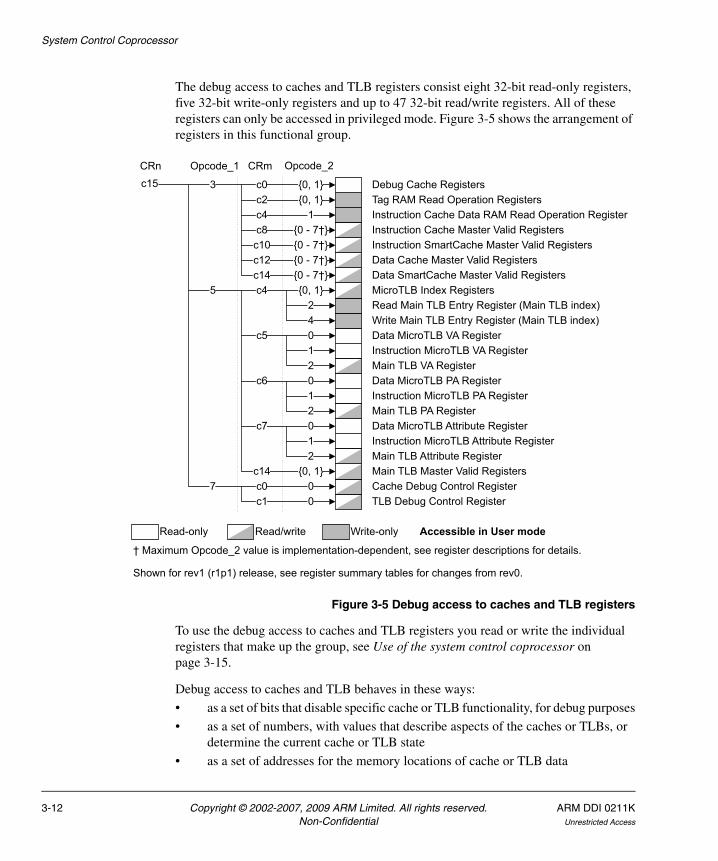
System Control Coprocessor
The debug access to caches and TLB registers consist eight 32-bit read-only registers, five 32-bit write-only registers and up to 47 32-bit read/write registers. All of these registers can only be accessed in privileged mode. Figure 3-5 shows the arrangement of registers in this functional group.
Figure 3-5 Debug access to caches and TLB registers
To use the debug access to caches and TLB registers you read or write the individual registers that make up the group, see Use of the system control coprocessor on page 3-15.
Debug access to caches and TLB behaves in these ways:
• as a set of bits that disable specific cache or TLB functionality, for debug purposes
• as a set of numbers, with values that describe aspects of the caches or TLBs, or determine the current cache or TLB state
• as a set of addresses for the memory locations of cache or TLB data
c15 {0, 1}c03{0, 1}c2
2{0, 1}c45
Debug Cache Registers
Instruction Cache Master Valid RegistersInstruction Cache Data RAM Read Operation RegisterTag RAM Read Operation Registers
Read Main TLB Entry Register (Main TLB index)MicroTLB Index Registers
Data MicroTLB VA Register
Cache Debug Control Register
CRn CRmOpcode_1 Opcode_2
4 Write Main TLB Entry Register (Main TLB index)
1c4{0 - 7†}c8
Instruction SmartCache Master Valid Registers{0 - 7†}c10Data Cache Master Valid RegistersData SmartCache Master Valid Registers
{0 - 7†}{0 - 7†}
c12c14
0c512
Instruction MicroTLB VA RegisterMain TLB VA RegisterData MicroTLB PA RegisterInstruction MicroTLB PA RegisterMain TLB PA Register
012
c6
Data MicroTLB Attribute RegisterInstruction MicroTLB Attribute RegisterMain TLB Attribute Register
012
c7
{0, 1}c14 Main TLB Master Valid Registers07 c0
TLB Debug Control Register0c1
† Maximum Opcode_2 value is implementation-dependent, see register descriptions for details.
Accessible in User modeRead-only Read/write Write-only
Shown for rev1 (r1p1) release, see register summary tables for changes from rev0.
3-12 Copyright © 2002-2007, 2009 ARM Limited. All rights reserved. ARM DDI 0211KNon-Confidential Unrestricted Access

System Control Coprocessor
• as a set of operations that perform Tag RAM and Cache Data RAM reads, for debug purposes.
The Debug access to caches and TLB section of Table 3-1 on page 3-3 refers you to the full descriptions of the registers in this functional group.
3.1.8 DMA control
The purpose of the DMA control registers is to:
• enable software to control DMA
• transfer large blocks of data between the TCM and an external memory
• determine accessibility
• select DMA channel.
The Enable, Control, Internal Start Address, External Start Address, Internal End Address, Channel Status, and Context ID Registers are multiple registers with one register of each for each channel that is implemented.
The DMA control registers consist of five 32-bit read-only registers, three 32-bit write-only registers and seven 32-bit read/write registers. Figure 3-6 shows the arrangement of registers, and the modes from which they can be accessed.
Figure 3-6 DMA control and configuration registers
DMA Context ID Register
c11 c0
DMA Internal End Address Register †DMA Channel Status Register †
DMA External Start Address Register †DMA Internal Start Address Register †
Present
DMA User Accessibility RegisterDMA Channel Number Register
DMA Control Register †
QueuedRunningInterrupting
Stop †Start †Clear †
c3c2c1
c4c5c6c7c8
3
12
21
0
000
00000
0c15
0
Opcode_2Opcode_1 CRmCRn
DMA Identificationand Status Registers
DMA Enable Registers
One register per channel,
selected by the DMA Channel
Number Register
† User accessibility depends on the state of the DMA User Accessibility Register.
Accessible in User modeRead-only Read/write Write-only
Shown for rev1 (r1p1) release, see register summary tables for changes from rev0.
ARM DDI 0211K Copyright © 2002-2007, 2009 ARM Limited. All rights reserved. 3-13Unrestricted Access Non-Confidential

System Control Coprocessor
To use the DMA control registers you read or write the individual registers that make up the group, see Use of the system control coprocessor on page 3-15.
Code can execute several DMA operations while in User mode if these operations are enabled by the DMA User Accessibility Register.
If DMA control registers attempt to execute a privileged operation in User mode the processor takes an Undefined Instruction trap.
The DMA control registers operation specifies the block of data for transfer, the location of where the transfer is to, and the direction of the DMA. For more details on the operation see DMA on page 7-11.
DMA control registers behave in these ways:
• as a set of bits that enable specific DMA functionality
• as a set of numbers, with values that describe aspects of the DMA channels or determine their current state
• as a set of addresses for the memory locations of data for transfer
• as a set of operations that act on the DMA channels.
3.1.9 System performance monitoring
The purpose of the system performance monitoring registers is to:
• control the monitoring operation
• count events.
The system performance monitor consist of four 32-bit read/write registers. All of these registers can only be accessed in privileged mode. Figure 3-7 shows the arrangement of registers in this functional group.
Figure 3-7 System performance monitor registers
Opcode_2CRmCRn Opcode_1
c15
3
12
0 c12 0
Count Register 1
Cycle Counter RegisterCount Register 0
Performance Monitor Control Register
Shown for rev1 (r1p1) release, see register summary tables for changes from rev0.
Accessible in User modeRead-only Read/write Write-only
3-14 Copyright © 2002-2007, 2009 ARM Limited. All rights reserved. ARM DDI 0211KNon-Confidential Unrestricted Access

System Control Coprocessor
To use the system performance monitor registers you read or write individual registers that make up the group, see Use of the system control coprocessor.
System performance monitoring behaves in these ways:
• as a set of bits that enable specific system monitoring functionality
• as a set of numbers, with values that describe aspects of system performance, or determine the current monitoring state.
System performance monitoring counts system events, such as cache misses, TLB misses, pipeline stalls, and other related features to enable system developers to profile the performance of their systems. It can generate interrupts when the number of events reaches a given value.
3.1.10 Use of the system control coprocessor
This section describes the general method for using the system control coprocessor.
You can access the system control coprocessor CP15 registers with MRC and MCR instructions:
MCR{cond} p15,<Opcode_1>,<Rd>,<CRn>,<CRm>,<Opcode_2>MRC{cond} p15,<Opcode_1>,<Rd>,<CRn>,<CRm>,<Opcode_2>
Figure 3-8 shows the instruction bit pattern of MRC and MCR instructions.
Figure 3-8 CP15 MRC and MCR bit pattern
The CRn field of MRC and MCR instructions specifies the coprocessor register to access. The CRm field and Opcode_2 fields specify a particular operation when addressing registers. The L bit distinguishes between the MRC (L=1) and MCR (L=0) instructions.
Instructions CDP, LDC, and STC, together with unprivileged MRC and MCR instructions to privileged-only CP15 locations, cause the Undefined Instruction trap to be taken. The CRn field of MRC and MCR instructions specifies the coprocessor register to access. The CRm field and Opcode_2 fields specify a particular action when addressing registers.
Cond
31 28 27 24 23 21 20 19 16 15 12 11 8 7 5 4 3 0
1 1 1 0 L CRn Rd 1 1 1 1 1 CRm
Opcode_1 Opcode_2
ARM DDI 0211K Copyright © 2002-2007, 2009 ARM Limited. All rights reserved. 3-15Unrestricted Access Non-Confidential
System Control Coprocessor
Note Attempting to read from a non-readable register, or to write to a non-writable register causes Undefined Instruction exceptions.
The Opcode_1, Opcode_2, and CRm fields Should Be Zero in all instructions that access CP15, except when the values specified are used to select desired operations. Using other values results in Undefined Instruction exceptions or Unpredictable behavior.
In all cases, reading from or writing any data values to any CP15 registers, including those fields specified as Unpredictable (UNP), Should Be One (SBO), or Should Be Zero (SBZ), does not cause any physical damage to the chip.
3-16 Copyright © 2002-2007, 2009 ARM Limited. All rights reserved. ARM DDI 0211KNon-Confidential Unrestricted Access

System Control Coprocessor
3.2 System control coprocessor registers overview
This section gives details of all the registers in the system control coprocessor. The section presents a summary of the registers and detailed descriptions in register order of CRn, Opcode_1, CRm, Opcode_2.
You can access CP15 registers with MRC and MCR instructions, as described in Use of the system control coprocessor on page 3-15:
MCR{cond} p15,<Opcode_1>,<Rd>,<CRn>,<CRm>,<Opcode_2>MRC{cond} p15,<Opcode_1>,<Rd>,<CRn>,<CRm>,<Opcode_2>
3.2.1 Register allocation
Table 3-2 on page 3-18 lists the registers and operations described in this section, arranged numerically, and gives the register reset values. In this table:
• CRn is the register number within CP15
• Op1 is the Opcode_1 value for the register
• CRm is the operational register
• Op2 is the Opcode_2 value for the register
• The Type column holds one or more of these abbreviations:
NA No access
RO Read-only access from user and privileged modes
RO Read-only access from privileged mode only
R/W Read/write access from user and privileged modes
R/W Read/write access from privileged mode only
WO Write-only access from user and privileged modes
WO Write-only access from privileged mode only
X Access depends on another register or external signal.
ARM DDI 0211K Copyright © 2002-2007, 2009 ARM Limited. All rights reserved. 3-17Unrestricted Access Non-Confidential

System Control Coprocessor
Table 3-2 Summary of CP15 registers and operations
CRn Op1 CRm Op2 Register/operation name Type Reset value Description
c0 0 c0 0 Main IDa RO 0x41x7B36xb page 3-25
1 Cache Type RO Implementation definedc
page 3-27
2 TCM Status RO 0x00010001 page 3-32
3 TLB Type RO 0x00000800 page 3-33
c1 0 Processor Feature 0d RO 0x00000111 page 3-35
1 Processor Feature 1d RO 0x00000001 page 3-37
2 Debug Feature 0d RO 0x00000002 page 3-38
3 Auxiliary Feature 0d RO 0x00000000 page 3-40
4 Memory Model Feature 0d RO 0x01130003 page 3-41
5 Memory Model Feature 1d RO 0x10030302 page 3-43
6 Memory Model Feature 2d RO 0x01222110 page 3-46
7 Memory Model Feature 3d RO 0x00000000 page 3-49
c2 0 Instruction Set Attributes 0d RO 0x00140011 page 3-51
1 Instruction Set Attributes 1d RO 0x12002111 page 3-53
2 Instruction Set Attributes 2d RO 0x11231111 page 3-55
3 Instruction Set Attributes 3d RO 0x01102131 page 3-57
4 Instruction Set Attributes 4d RO 0x00000141 page 3-59
5 Instruction Set Attributes 5d RO 0x00000000 page 3-62
c1 0 c0 0 Control R/W 0x0xx5x0x8e page 3-63
1 Auxiliary Control R/W 0x00000007 page 3-69
2 Coprocessor Access Control R/W 0x00000000 page 3-72
c2 0 c0 0 Translation Table Base 0 R/W 0x00000000 page 3-74
1 Translation Table Base 1 R/W 0x00000000 page 3-76
2 Translation Table Base Control R/W 0x00000000 page 3-78
3-18 Copyright © 2002-2007, 2009 ARM Limited. All rights reserved. ARM DDI 0211KNon-Confidential Unrestricted Access

System Control Coprocessor
c3 0 c0 0 Domain Access Control R/W 0x00000000 page 3-80
c4 - - - Not used - - -
c5 0 c0 0 Data Fault Status R/W 0x00000000 page 3-83
1 Instruction Fault Status R/W 0x00000000 page 3-86
c6 0 c0 0 Data Fault Address R/W 0x00000000 page 3-88
1 Watchpoint Fault Address R/W 0x00000000 page 3-89
c7 0 c0 4 Wait For Interrupt WO - page 3-90
c5 0 Invalidate Entire Instruction Cache WO - page 3-90
1 Invalidate Instruction Cache, using MVA
WO - page 3-90
2 Invalidate Instruction Cache, using Set/Way
WO - page 3-90
4 Flush Prefetch Buffer WOf - page 3-90
6 Flush Entire Branch Target Cache WO - page 3-90
7 Flush Branch Target Cache Entry WO - page 3-90
c6 0 Invalidate Entire Data Cache WO - page 3-90
1 Invalidate Data Cache Line, using MVA
WO - page 3-90
2 Invalidate Data Cache Line, using Set/Way
WO - page 3-90
c7 0 Invalidate Both Caches WO - page 3-90
c10 0 Clean Entire Data Cache WO - page 3-90
1 Clean Data Cache Line, using MVA WO - page 3-90
2 Clean Data Cache Line, using Set/Way
WO - page 3-90
4 Data Synchronization Barrier WOf - page 3-90
5 Data Memory Barrier WOf - page 3-90
Table 3-2 Summary of CP15 registers and operations (continued)
CRn Op1 CRm Op2 Register/operation name Type Reset value Description
ARM DDI 0211K Copyright © 2002-2007, 2009 ARM Limited. All rights reserved. 3-19Unrestricted Access Non-Confidential

System Control Coprocessor
c7 0 c10 6 Read Cache Dirty Status Register RO 0x00000000 page 3-90
c12 4 Read Block Transfer Status Register ROf 0x00000000 page 3-90
5 Stop Prefetch Range WOf - page 3-90
c13 1 Prefetch Instruction Cache Line WO - page 3-90
c14 0 Clean and Invalidate Entire Data Cache
WO - page 3-90
1 Clean and Invalidate Data Cache Line, using MVA
WO - page 3-90
2 Clean and Invalidate Data Cache Line, using Set/Way
WO - page 3-90
c8 0 c5 0 Invalidate Instruction TLB WO - page 3-111
1 Invalidate Instruction TLB Single Entry
WO - page 3-111
2 Invalidate Instruction TLB Entry on ASID match
WO - page 3-111
c6 0 Invalidate Data TLB WO - page 3-111
1 Invalidate Data TLB Single Entry WO - page 3-111
2 Invalidate Data TLB Entry on ASID match
WO - page 3-111
c7 0 Invalidate Unified TLB WO - page 3-111
1 Invalidate Unified TLB Single Entry WO - page 3-111
2 Invalidate Unified TLB Entry on ASID match
WO - page 3-111
c9 0 c0 0 Data Cache Lockdown R/W 0xFFFFFFF0 page 3-113
1 Instruction Cache Lockdown R/W 0xFFFFFFF0 page 3-184
c1 0 Data TCM Region R/W Implementation-definedg
page 3-116
c9 0 c1 1 Instruction TCM Region R/W Implementation-definedg
page 3-118
Table 3-2 Summary of CP15 registers and operations (continued)
CRn Op1 CRm Op2 Register/operation name Type Reset value Description
3-20 Copyright © 2002-2007, 2009 ARM Limited. All rights reserved. ARM DDI 0211KNon-Confidential Unrestricted Access

System Control Coprocessor
c10 0 c0 0 TLB Lockdown R/W 0x00000000 page 3-121
c2 0 Primary Region Remap (PMRR)d R/W 0x00098AA4 page 3-125
1 Normal Memory Remap (NMRR)d R/W 0x44E048E0 page 3-127
c11 0 c0 0 DMA Identification and Status (Present)
RO 0x00000003 page 3-132
1 DMA Identification and Status (Queued)
RO 0x00000000 page 3-132
2 DMA Identification and Status (Running)
RO 0x00000000 page 3-132
3 DMA Identification and Status (Interrupting)
RO 0x00000000 page 3-132
c1 0 DMA User Accessibility R/W 0x00000000 page 3-134
c2 0 DMA Channel Number R/Wf 0x00000000 page 3-136
c3 0 DMA Enable (Stop) WOf, Xh - page 3-138
1 DMA Enable (Start) WOf, Xh - page 3-138
2 DMA Enable (Clear) WOf, Xh - page 3-138
c4 0 DMA Control R/Wf, Xh 0x00000000 page 3-141
c5 0 DMA Internal Start Address R/Wf, Xh 0x00000000 page 3-145
c6 0 DMA External Start Address R/Wf, Xh 0x00000000 page 3-146
c7 0 DMA Internal End Address R/Wf, Xh 0x00000000 page 3-148
c8 0 DMA Channel Status ROf, Xh 0x00000000 page 3-150
c15 0 DMA Context ID R/W 0x00000000 page 3-154
c12 - - - Not used - - -
c13 0 c0 0 FCSE PID R/W 0x00000000 page 3-156
1 Context ID R/W 0x00000000 page 3-159
Table 3-2 Summary of CP15 registers and operations (continued)
CRn Op1 CRm Op2 Register/operation name Type Reset value Description
ARM DDI 0211K Copyright © 2002-2007, 2009 ARM Limited. All rights reserved. 3-21Unrestricted Access Non-Confidential

System Control Coprocessor
c13 0 c0 2 User Read/Write Thread and Process IDd
R/Wf 0x00000000 page 3-160
3 User Read-only Thread and Process IDd
R/Wf 0x00000000 page 3-160
4 Privileged Only Thread and Process IDd
R/W 0x00000000 page 3-160
c14 - - - Not used - - -
c15 0 c2 0 Data Memory Remap R/W 0x01C97CC8 page 3-162
1 Instruction Memory Remap R/W 0x01C97CC8 page 3-162
2 DMA Memory Remap R/W 0x01C97CC8 page 3-162
4 Peripheral Port Memory Remap R/W 0x00000000 page 3-162
c12 0 Performance Monitor Control R/W 0x00000000 page 3-168
1 Cycle Counter (CCNT) R/W Unpredictable page 3-173
2 Count 0 (PMN0) R/W 0x00000000 page 3-175
3 Count 1 (PMN1) R/W 0x00000000 page 3-176
3 c0 0 Data Debug Cache RO 0x00000000 page 3-177
1 Instruction Debug Cache RO 0x00000000 page 3-177
c2 0 Data Tag RAM Read Operation WO - page 3-177
1 Instruction Tag RAM Read Operation
WO - page 3-177
c4 1 Instruction Cache Data RAM Read Operation
WO - page 3-177
c8 <R>i Instruction Cache Master Valid R/W 0x00000000 page 3-184
c10 <R>i Instruction SmartCache Master Valid
R/W 0x00000000 page 3-184
c12 <R>i Data Cache Master Valid R/W 0x00000000 page 3-184
c14 <R>i Data SmartCache Master Valid R/W 0x00000000 page 3-184
Table 3-2 Summary of CP15 registers and operations (continued)
CRn Op1 CRm Op2 Register/operation name Type Reset value Description
3-22 Copyright © 2002-2007, 2009 ARM Limited. All rights reserved. ARM DDI 0211KNon-Confidential Unrestricted Access

System Control Coprocessor
c15 5 c4 0 Data MicroTLB Index R/W 0x00000000 page 3-192
1 Instruction MicroTLB Index R/W 0x00000000 page 3-192
2 Read Main TLB Entry WO 0x00000000 page 3-194
4 Write Main TLB Entry WO 0x00000000 page 3-194
c5 0 Data MicroTLB VA RO 0x00000000 page 3-196
1 Instruction MicroTLB VA RO 0x00000000 page 3-196
2 Main TLB VA R/W 0x00000000 page 3-196
c6 0 Data MicroTLB PA RO 0x00000000 page 3-199
1 Instruction MicroTLB PA RO 0x00000000 page 3-199
2 Main TLB PA R/W 0x00000000 page 3-199
c7 0 Data MicroTLB Attribute RO 0x00000000 page 3-202
1 Instruction MicroTLB Attribute RO 0x00000000 page 3-202
2 Main TLB Attribute R/W 0x00000000 page 3-202
c14 <R>i Main TLB Master Valid R/W 0x00000000 page 3-184
7 c0 0 Cache Debug Control R/W 0x00000000 page 3-178
c1 0 TLB Debug Control R/W 0x00000000 page 3-207
a. Before the r1p0 release, the Main ID register was called the ID Code Register.b. See c0, Main ID Register on page 3-25 for the values of bits [23:20] and bits [3:0].c. The cache type reset value is determined by the size of the caches implemented.d. These registers are only implemented from the rev1 (r1p0) release of the ARM1136JF-S processor.e. On reset, the values of bits 25, 22, and 7 depend on the value of macrocell input signals BIGENDINIT and UBITINIT, and
the value of bit 13 depends on the value of the VINITHI signal. See Control Register reset value on page 3-68.f. Bold text denotes that the register can be accessed in User mode.g. See register description for details.h. User accessibility depends on the state of the DMA User Accessibility Register.i. <R> = register number.
Table 3-2 Summary of CP15 registers and operations (continued)
CRn Op1 CRm Op2 Register/operation name Type Reset value Description
ARM DDI 0211K Copyright © 2002-2007, 2009 ARM Limited. All rights reserved. 3-23Unrestricted Access Non-Confidential

System Control Coprocessor
Operations available using MCRR instructions
A limited number of operations are available using MCRR instructions. These are accessed as shown:
MCRR{cond} p15,<Opcode_1>,<End Address>,<Start Address>,<CRm>
The operations available in this way are shown in Table 3-3:
Table 3-3 Summary of CP15 MCRR operations
Op1 CRm Register or operation Typea Reset value Description
0 c5 Invalidate Instruction Cache Range WO - page 3-101
c6 Invalidate Data Cache Range WO - page 3-101
c12 Clean Data Cache Range WOa - page 3-101
c14 Clean and Invalidate Data Cache Range WO - page 3-101
1 c12 Prefetch Instruction Cache Range WOa - page 3-101
2 c12 Prefetch Data Cache Range WOa - page 3-101
a. Bold text denotes that the register can be accessed in User mode.
3-24 Copyright © 2002-2007, 2009 ARM Limited. All rights reserved. ARM DDI 0211KNon-Confidential Unrestricted Access

System Control Coprocessor
3.3 System control coprocessor register descriptions
This section contains descriptions of all the CP15 registers arranged in numerical order, as shown in Table 3-2 on page 3-18.
3.3.1 c0, Main ID Register
The purpose of the Main ID Register is to return the device ID code that contains information about the processor.
The Main ID Register is:
• in CP15 c0
• a 32 bit read-only register
• accessible in privileged mode only.
Note Before the r1p0 release, this register was called the ID Code Register.
Figure 3-9 shows the arrangement of bits in the register.
Figure 3-9 Main ID Register format
The contents of the Main ID Register depend on the specific implementation. Table 3-4 lists the bit functions of the Main ID Register.
Implementer
31 24 23 20 19 16 15 4 3 0
Variantnumber Primary part number Revision
number
Architecture
Table 3-4 Main ID Register field descriptions
Bit range Field name Function Value
[31:24] Implementer Indicates the implementer, ARM Limited. 0x41
[23:20] Variant number The major revision number n of the rnpn revision status, see Product revision status on page xxx.
0x1a
ARM DDI 0211K Copyright © 2002-2007, 2009 ARM Limited. All rights reserved. 3-25Unrestricted Access Non-Confidential

System Control Coprocessor
Note If the processor encounters an Opcode_2 value corresponding to an unimplemented or reserved ID register with CRm = c0 and Opcode_1 = 0, the system control coprocessor returns the value of the Main ID Register.
Table 3-5 shows the results of attempted accesses to the Main ID Register for each mode.
Accessing the Main ID Register
To access the Main ID Register you read CP15 with:
• Opcode_1 set to 0
• CRn set to c0
• CRm set to c0
• Opcode_2 set to 0.
For example:
MRC p15,0,<Rd>,c0,c0,0 ; Read Main ID Register
For more information about the processor features, see c0, Core feature ID registers on page 3-35.
[19:16] Architecture ARMv6 0x7
[15:4] Primary part number Implementation-defined.
Part number for ARM1136JF-S and ARM1136J-S
0xB36
[3:0] Revision number The minor revision number n of the rnpn revision status, see Product revision status on page xxx.
-b
a. Value given is for the rev1 (r1pn) releases of the ARM1136JF-S processor. For rev0 (r0pn) releases, the Variant number is 0x0.b. For example, for the r1p5 release of the ARM1136 processors, this value is 0x5.
Table 3-4 Main ID Register field descriptions (continued)
Bit range Field name Function Value
Table 3-5 Results of accesses to the Main ID Register
Privileged read Privileged write User read or write
Data read Undefined Instruction exception Undefined Instruction exception
3-26 Copyright © 2002-2007, 2009 ARM Limited. All rights reserved. ARM DDI 0211KNon-Confidential Unrestricted Access

System Control Coprocessor
3.3.2 c0, Cache Type Register
The purpose of the Cache Type Register is to provide information about the size and architecture of the caches. This enables the operating system to establish how to perform such operations as cache cleaning and lockdown. All ARMv4T and later cached processors contain this register, enabling RTOS vendors to produce future-proof versions of their operating systems.
The Cache Type Register is:
• in CP15 c0
• a 32-bit read only register
• accessible in privileged mode only.
Figure 3-10 shows the arrangement of bits in the register.
Figure 3-10 Cache Type Register format
Table 3-6 lists the bit functions of the Cache Type Register.
0
31 30 29 28 25 24 23 12 11 0
0 0 Ctype S Dsize Isize
Table 3-6 Cache Type Register field descriptions
BitsField name
Description
[31:29] - Always 0.
[28:25] Ctype Specifies if the cache supports lockdown or not, and how it is cleaned. See Table 3-7 on page 3-28.
For ARM1136JF-S processor Ctype = b1110.
[24] S bit Specifies whether the cache is a Unified Cache (S=0), or separate instruction and data caches (S=1).
For ARM1136JF-S processors S = 1.
[23:12] Dsize Specifies the size, line length, and associativity of the Data Cache. See Figure 3-11 on page 3-28 for the format of this field.
[11:0] Isize Specifies the size, line length, and associativity of the Instruction Cache. See Figure 3-11 on page 3-28 for the format of this field.
ARM DDI 0211K Copyright © 2002-2007, 2009 ARM Limited. All rights reserved. 3-27Unrestricted Access Non-Confidential

System Control Coprocessor
Table 3-7 shows the encoding of the Ctype field for ARM1136JF-S processors.
Figure 3-11 shows how the Dsize and Isize fields in the Cache Type Register have the same format.
Figure 3-11 Dsize and Isize field format
Table 3-8 shows a summary of Dsize and Isize fields shown in Figure 3-11.
Table 3-7 Ctype field encoding
Value Method Cache cleaning Cache lockdown
b1110 Write-back Register 7 operations Format C
11 10 9 6 5 3 2 1 0
P 0 0 Size Assoc M Len
23 22 21 18 17 15 14 13 12
Isize
Dsize
8
20
Table 3-8 Dsize and Isize field summary
Field Description
P bit The P bit indicates if there is a restriction on page allocation for bits [13:12] of the Virtual Address:
0 = no restriction
1 = restriction applies to bits [13:12] of the Virtual Address.
For ARM1136JF-S processors, the P bit is set if the cache size is greater than 16KB. For more details see Restrictions on page table mappings (page coloring) on page 6-51.
Size The Size field determines the cache size in conjunction with the M bit.
Assoc The Assoc field determines the cache associativity in conjunction with the M bit.
For ARM1136JF-S processor Assoc = b010.
M bit The multiplier bit. Determines the cache size and cache associativity values in conjunction with the Size and Assoc fields.
In the ARM1136JF-S processor the M bit is set to 0 for the Data and Instruction Caches.
Len The Len field determines the line length of the cache.
For ARM1136JF-S processor Len = b10.
3-28 Copyright © 2002-2007, 2009 ARM Limited. All rights reserved. ARM DDI 0211KNon-Confidential Unrestricted Access

System Control Coprocessor
The size of the cache is determined by the Size field and the M bit. The M bit is 0 for the Data and Instruction Caches. Bits [20:18] for the Data Cache and bits [8:6] for the Instruction Cache are the Size fields. Table 3-9 shows the cache size encoding.
The associativity of the cache is determined by the Assoc field and the M bit. The M bit is 0 for the Data and Instruction Caches. Bits [17:15] for the Data Cache and bits [5:3] for the Instruction Cache are the Assoc field. Table 3-10 shows the cache associativity encoding.
Table 3-9 Cache size encoding (M=0)
Size field Cache size
b000 0.5KB
b001 1KB
b010 2KB
b011 4KB
b100 8KB
b101 16KB
b110 32KB
b111 64KB
Table 3-10 Cache associativity encoding (M=0)
Assoc field Associativity
b000 Reserved
b001
b010 4-way
b011 Reserved
b100
b101
b110
b111
ARM DDI 0211K Copyright © 2002-2007, 2009 ARM Limited. All rights reserved. 3-29Unrestricted Access Non-Confidential

System Control Coprocessor
The line length of the cache is determined by the Len field. Bits [13:12] for the Data Cache and bits [1:0] for the Instruction Cache are the Len field. Table 3-11 shows the line length encoding.
Accessing the Cache Type Register
Table 3-12 shows the results of attempted accesses to the Cache Type Register for each mode.
To access the Cache Type Register you read CP15 with:
• Opcode_1 set to 0
• CRn set to c0
• CRm set to c0
• Opcode_2 set to 1.
For example:
MRC p15,0,<Rd>,c0,c0,1 ; returns cache details
Cache Type Register read example
Table 3-13 on page 3-31 shows the Cache Type Register values for an ARM1136JF-S processor with the following configuration:
• separate instruction and data caches
• cache size = 16KB
• associativity = 4-way
• line length = eight words
Table 3-11 Line length encoding
Len field Cache line length
b00 Reserved
b01 Reserved
b10 8 words (32 bytes)
b11 Reserved
Table 3-12 Results of accesses to the Cache Type Register 0
Privileged read Privileged write User read or write
Data read Undefined Instruction exception Undefined Instruction exception
3-30 Copyright © 2002-2007, 2009 ARM Limited. All rights reserved. ARM DDI 0211KNon-Confidential Unrestricted Access

System Control Coprocessor
• caches use write-back, CP15 c7 for cache cleaning, and Format C for cache lockdown.
Table 3-13 Example Cache Type Register format
Function Register bits Value
Reserved [31:29] b000
Ctype [28:25] b1110
S [24] b1 = Harvard cache
Dsize P [23] b0
Reserved [22, 21] b00
Size [20:18] b101 = 16KB
Assoc [17:15] b010 = 4-way
M [14] b0
Len [13:12] b10 = 8 words per line (32 bytes)
Isize P [11] b0
Reserved [10:9] b00
Size [8:6] b101 = 16KB
Assoc [5:3] b010 = 4-way
M [2] b0
Len [1:0] b10 = 8 words per line (32 bytes)
ARM DDI 0211K Copyright © 2002-2007, 2009 ARM Limited. All rights reserved. 3-31Unrestricted Access Non-Confidential

System Control Coprocessor
3.3.3 c0, TCM Status Register
The purpose of the TCM Status Register is to inform the system about the number of Instruction and Data TCMs available in the processor.
Note The ARM1136JF-S processor implements only one Instruction TCM and one Data TCM.
The TCM Status Register is:
• in CP15 c0
• a 32-bit read-only register
• accessible in privileged mode only.
Figure 3-12 shows the arrangement of bits in the register.
Figure 3-12 TCM Status Register format
Table 3-14 lists the bit functions of the TCM Status Register.
0
31 30 29 28 19 18 16 15 3 2 0
0 0 SBZ/UNP DTCM SBZ/UNP ITCM
Table 3-14 TCM Status Register field descriptions
Bits Field name Description
[31:29] - Always 0.
[28:19] - SBZ/UNP.
[18:16] DTCM Specifies the number of Data TCMs implemented.
For ARM1136JF-S processors this value is 1.
[15:3] - SBZ/UNP.
[11:0] ITCM Specifies the number of Instruction TCMs implemented.
For ARM1136JF-S processors this value is 1.
3-32 Copyright © 2002-2007, 2009 ARM Limited. All rights reserved. ARM DDI 0211KNon-Confidential Unrestricted Access
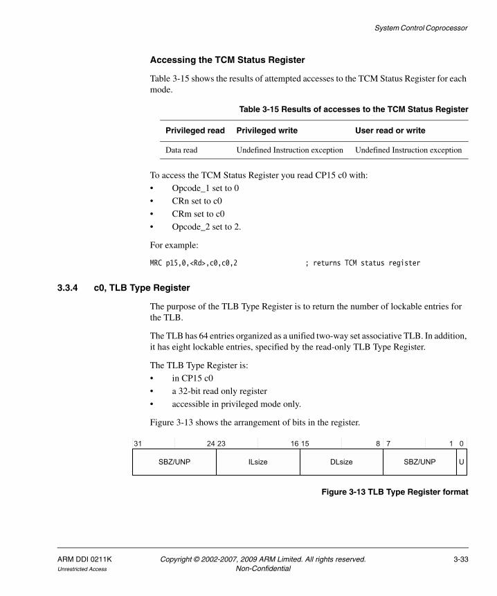
System Control Coprocessor
Accessing the TCM Status Register
Table 3-15 shows the results of attempted accesses to the TCM Status Register for each mode.
To access the TCM Status Register you read CP15 c0 with:
• Opcode_1 set to 0
• CRn set to c0
• CRm set to c0
• Opcode_2 set to 2.
For example:
MRC p15,0,<Rd>,c0,c0,2 ; returns TCM status register
3.3.4 c0, TLB Type Register
The purpose of the TLB Type Register is to return the number of lockable entries for the TLB.
The TLB has 64 entries organized as a unified two-way set associative TLB. In addition, it has eight lockable entries, specified by the read-only TLB Type Register.
The TLB Type Register is:
• in CP15 c0
• a 32-bit read only register
• accessible in privileged mode only.
Figure 3-13 shows the arrangement of bits in the register.
Figure 3-13 TLB Type Register format
Table 3-15 Results of accesses to the TCM Status Register
Privileged read Privileged write User read or write
Data read Undefined Instruction exception Undefined Instruction exception
USBZ/UNP
31 24 23 16 15 8 7 1 0
ILsize DLsize SBZ/UNP
ARM DDI 0211K Copyright © 2002-2007, 2009 ARM Limited. All rights reserved. 3-33Unrestricted Access Non-Confidential

System Control Coprocessor
Table 3-16 lists the bit functions of the TLB Type Register.
Accessing the TLB Type Register
Table 3-17 shows the results of attempted accesses to the TLB Type Register for each mode.
To access the TLB Type Register you read CP15 c0 with:
• Opcode_1 set to 0
• CRn set to c0
• CRm set to c0
• Opcode_2 set to 3.
For example:
MRC p15,0,<Rd>,c0,c0,3 ; returns TLB details
Table 3-16 TLB Type Register field descriptions
Bits Field Description
[31:24] - SBZ/UNP.
[23:16] ILsize Specifies the number of instruction TLB lockable entries.
For ARM1136JF-S processors this is 0.
[15:8] DLsize Specifies the number of unified or data TLB lockable entries.
For ARM1136JF-S processors this is 8.
[7:1] - SBZ/UNP.
[0] U Specifies if the TLB is unified (0), or if there are separate instruction and data TLBs (1).
For ARM1136JF-S processors this is 0.
Table 3-17 Results of accesses to the TCM Status Register
Privileged read Privileged write User read or write
Data read Undefined Instruction exception Undefined Instruction exception
3-34 Copyright © 2002-2007, 2009 ARM Limited. All rights reserved. ARM DDI 0211KNon-Confidential Unrestricted Access

System Control Coprocessor
3.3.5 c0, Core feature ID registers
The section describes the core feature ID registers. These registers were added in the r1p0 release. They are all read-only registers, which can only be accessed in privileged mode. The registers are described in the following sections:
• c0, Processor Feature Register 0
• c0, Processor Feature Register 1 on page 3-37
• c0, Debug Feature Register 0 on page 3-38
• c0, Auxiliary Feature Register 0 on page 3-40
• c0, Memory Model Feature Register 0 on page 3-41
• c0, Memory Model Feature Register 1 on page 3-43
• c0, Memory Model Feature Register 2 on page 3-46
• c0, Memory Model Feature Register 3 on page 3-49
• c0, Instruction Set Attributes Register 0 on page 3-51
• c0, Instruction Set Attributes Register 1 on page 3-53
• c0, Instruction Set Attributes Register 2 on page 3-55
• c0, Instruction Set Attributes Register 3 on page 3-57
• c0, Instruction Set Attributes Register 4 on page 3-59
• c0, Instruction Set Attributes Register 5 on page 3-62.
c0, Processor Feature Register 0
The purpose of the Processor Feature Register 0 is to provide information about the execution state support and programmer’s model for the processor.
Processor Feature Register 0 is:
• in CP15 c0
• a 32-bit read-only register
• accessible in privileged mode only
• only available from the rev1 (r1p0) release of the ARM1136JF-S processor.
Figure 3-14 shows the bit arrangement for Processor Feature Register 0.
Figure 3-14 Processor Feature Register 0 format
ReservedRAZ
ReservedRAZ
ReservedRAZ 10 0 0 0 0 0 0 1 0 0 0 1 0 0 0Reserved
RAZ
31 16 15 12 11 8 7 4 3 0
State3 State2 State1 State0
28 27 24 23 20 19
ARM DDI 0211K Copyright © 2002-2007, 2009 ARM Limited. All rights reserved. 3-35Unrestricted Access Non-Confidential

System Control Coprocessor
Table 3-18 lists the bit functions of the Processor Feature Register 0.
Accessing the Processor Feature Register 0
Table 3-19 shows the results of attempted accesses to the Processor Feature Register 0 for each mode.
To access the Processor Feature Register 0 you read CP15 with:
• Opcode_1 set to 0
• CRn set to c0
• CRm set to c1
• Opcode_2 set to 0.
For example:
MRC p15, 0, <Rd>, c0, c1, 0 ; Read Processor Feature Register 0
Table 3-18 Processor Feature Register 0 bit functions
Bit range Field name Function
[31:28] - Reserved. RAZ.
[27:24] - Reserved. RAZ.
[23:20] - Reserved. RAZ.
[19:16] - Reserved. RAZ.
[15:12] State3 Indicates support for ThumbEE instruction set.
0x0, ARM1136JF-S processors do not support ThumbEE.
[11:8] State2 Indicates support for Jazelle extension interface.
0x1, ARM1136JF-S processors support Jazelle.
[7:4] State1 Indicates type of Thumb encoding that the processor supports.
0x1, ARM1136JF-S processors support Thumb without the Thumb-2 technology extensions.
[3:0] State0 Indicates support for 32-bit ARM instruction set.
0x1, ARM1136JF-S processors support 32-bit ARM instructions.
Table 3-19 Results of accesses to the Processor Feature Register 0
Privileged read Privileged write User read or write
Data read Undefined Instruction exception Undefined Instruction exception
3-36 Copyright © 2002-2007, 2009 ARM Limited. All rights reserved. ARM DDI 0211KNon-Confidential Unrestricted Access

System Control Coprocessor
c0, Processor Feature Register 1
The purpose of the Processor Feature Register 1 is to provide information about the execution state support and programmer’s model for the processor.
Processor Feature Register 1 is:
• in CP15 c0
• a 32-bit read-only register
• accessible in privileged mode only
• only available from the rev1 (r1p0) release of the ARM1136JF-S processor.
Figure 3-15 shows the bit arrangement for Processor Feature Register 1.
Figure 3-15 Processor Feature Register 1 format
Table 3-20 lists the bit functions of the Processor Feature Register 1.
0 0 0 0ReservedRAZ
ReservedRAZ
ReservedRAZ
ReservedRAZ
ReservedRAZ 10 0 0 0 0 0 0
31 8 7 4 3 0
Security extensionProgrammer's model
28 27 24 23 20 19 16 15 12 11
Microcontroller programmer's model
Table 3-20 Processor Feature Register 1 bit functions
Bit range
Field name Function
[31:12] - Reserved. RAZ.
[11:8] Microcontroller programmer’s model
Indicates support for the ARM microcontroller programmer’s model.
0x0, Not supported by ARM1136JF-S processors.
[7:4] Security extension Indicates support for Security Extensions Architecture v1.
0x0, ARM1136JF-S processors do not support Security Extensions Architecture v1.
[3:0] Programmer’s model Indicates support for standard ARMv4 programmer’s model.
0x1, ARM1136JF-S processors support the ARMv4 model.
ARM DDI 0211K Copyright © 2002-2007, 2009 ARM Limited. All rights reserved. 3-37Unrestricted Access Non-Confidential

System Control Coprocessor
Accessing the Processor Feature Register 1
Table 3-21 shows the results of attempted accesses to the Processor Feature Register 1 for each mode.
To access the Processor Feature Register 1 you read CP15 with:
• Opcode_1 set to 0
• CRn set to c0
• CRm set to c1
• Opcode_2 set to 1.
For example:
MRC p15, 0, <Rd>, c0, c1, 1 ; Read Processor Feature Register 1
c0, Debug Feature Register 0
The purpose of the Debug Feature Register 0 is to provide information about the debug system for the processor.
Debug Feature Register 0 is:
• in CP15 c0
• a 32-bit read-only register
• accessible in privileged mode only
• only available from the rev1 (r1p0) release of the ARM1136JF-S processor.
Figure 3-16 on page 3-39 shows the bit arrangement for Debug Feature Register 0.
Table 3-21 Results of accesses to the Processor Feature Register 1
Privileged read Privileged write User read or write
Data read Undefined Instruction exception Undefined Instruction exception
3-38 Copyright © 2002-2007, 2009 ARM Limited. All rights reserved. ARM DDI 0211KNon-Confidential Unrestricted Access

System Control Coprocessor
Figure 3-16 Debug Feature Register 0 format
Table 3-22 lists the bit functions of the Debug Feature Register 0.
ReservedRAZ 0 0 1 00 0 0 00 0 0 00 0 0 00 0 0 00 0 0 0Reserved
RAZ
31 12 11 8 7 4 3 024 23 20 19 16 15
Microcontroller, memory mapped
Debugmodels
Trace debug, memory mappedTrace debug, coprocessor based
Core debug, memory mappedSecure debug, coprocessor based
Core debug, coprocessor based
28 27
Table 3-22 Debug Feature Register 0 bit functions
Bit range
Field name
Function
[31:28] - Reserved. RAZ.
[27:24] - Reserved. RAZ.
[23:20] - Indicates the type of memory-mapped microcontroller debug model that the processor supports.
0x0, ARM1136JF-S processors do not support this debug model.
[19:16] - Indicates the type of memory-mapped Trace debug model that the processor supports.
0x0, ARM1136JF-S processors do not support this debug model.
[15:12] - Indicates the type of coprocessor-based Trace debug model that the processor supports.
0x0, ARM1136JF-S processors do not support this debug model.
[11:8] - Indicates the type of embedded processor debug model that the processor supports.
0x0, ARM1136JF-S processors do not support this debug model.
[7:4] - Indicates the type of Secure debug model that the processor supports.
0x0, ARM1136JF-S processors do not support a v6.1 Secure debug architecture model.
[3:0] - Indicates the type of applications processor debug model that the processor supports.
0x2, ARM1136JF-S processors support the v6 debug model (CP 14-based).
ARM DDI 0211K Copyright © 2002-2007, 2009 ARM Limited. All rights reserved. 3-39Unrestricted Access Non-Confidential

System Control Coprocessor
Accessing the Debug Feature Register 0
Table 3-23 shows the results of attempted accesses to the Debug Feature Register 0 for each mode.
To access the Debug Feature Register 0 you read CP15 with:
• Opcode_1 set to 0
• CRn set to c0
• CRm set to c1
• Opcode_2 set to 2.
For example:
MRC p15, 0, <Rd>, c0, c1, 2 ; Read Debug Feature Register 0
c0, Auxiliary Feature Register 0
The purpose of the Auxiliary Feature Register 0 is to provide additional information about the features of the processor.
The Auxiliary Feature Register 0 is:
• in CP15 c0
• a 32-bit read-only register
• accessible in privileged mode only
• only available from the rev1 (r1p0) release of the ARM1136JF-S processor.
The contents of the Auxiliary Feature Register 0 are Implementation-defined. In the ARM1136JF-S processor, the Auxiliary Feature Register 0 reads as 0x00000000.
Accessing the Auxiliary Feature Register 0
Table 3-24 shows the results of attempted accesses to the Auxiliary Feature Register 0 for each mode.
Table 3-23 Results of accesses to the Debug Feature Register 0
Privileged read Privileged write User read or write
Data read Undefined Instruction exception Undefined Instruction exception
Table 3-24 Results of accesses to the Auxiliary Feature Register 0
Privileged read Privileged write User read or write
Data read Undefined Instruction exception Undefined Instruction exception
3-40 Copyright © 2002-2007, 2009 ARM Limited. All rights reserved. ARM DDI 0211KNon-Confidential Unrestricted Access

System Control Coprocessor
To access the Auxiliary Feature Register 0 you read CP15 with:
• Opcode_1 set to 0
• CRn set to c0
• CRm set to c1
• Opcode_2 set to 3.
For example:
MRC p15, 0, <Rd>, c0, c1, 3 ; Read Auxiliary Feature Register 0.
c0, Memory Model Feature Register 0
The purpose of the Memory Model Feature Register 0 is to provide information about the memory model, memory management, cache support, and TLB operations of the processor.
The Memory Model Feature Register 0 is:
• in CP15 c0
• a 32-bit read-only register
• accessible in privileged mode only
• only available from the rev1 (r1p0) release of the ARM1136JF-S processor.
Figure 3-17 shows the bit arrangement for Memory Model Feature Register 0.
Figure 3-17 Memory Model Feature Register 0 format
10 0 0 10 0 0 10 0 1 00 0 0 00 0 0 00 0 0 10 0 1ReservedRAZ
31 28 27 24 23 20 19 16 15 12 11 8 7 4 3 0
VMSA supportPMSA support
FCSE supportAuxiliary register supportTCM and associated DMA support
Cache coherence supportCPU agent, shared memoryDMA agent, shared memory
ARM DDI 0211K Copyright © 2002-2007, 2009 ARM Limited. All rights reserved. 3-41Unrestricted Access Non-Confidential

System Control Coprocessor
Table 3-25 lists the bit functions of the Memory Model Feature Register 0.
Accessing the Memory Model Feature Register 0
Table 3-26 shows the results of attempted accesses to the Memory Model Feature 0 register for each mode.
To access the Memory Model Feature Register 0 you read CP15 with:
• Opcode_1 set to 0
• CRn set to c0
• CRm set to c1
Table 3-25 Memory Model Feature Register 0 bit functions
Bit range Field name Function
[31:28] - Reserved. RAZ.
[27:24] - Indicates support for FCSE.
0x1, ARM1136JF-S processors support FCSE.
[23:20] - Indicates support for the ARMv6 Auxiliary Control Register.
0x1, ARM1136JF-S processors support the Auxiliary Control Register.
[19:16] - Indicates support for TCM and associated DMA.
0x3, ARM1136JF-S processors support ARMv6 TCM and DMA.
[15:12] - Indicates support for cache coherency with DMA agent, shared memory.
0x0, ARM1136JF-S processors do not support this model.
[11:8] - Indicates support for cache coherency support with CPU agent, shared memory.
0x0, ARM1136JF-S processors do not support this model.
[7:4] - Indicates support for PMSA.
0x0, ARM1136JF-S processors do not support PMSA
[3:0] - Indicates support for Virtual Memory System Architecture (VMSA).
0x3, ARM1136JF-S processors support:
• VMSA v6 including cache and TLB type register
• Extensions to ARMv6.
Table 3-26 Results of accesses to the Memory Model Feature Register 0
Privileged read Privileged write User read or write
Data read Undefined Instruction exception Undefined Instruction exception
3-42 Copyright © 2002-2007, 2009 ARM Limited. All rights reserved. ARM DDI 0211KNon-Confidential Unrestricted Access

System Control Coprocessor
• Opcode_2 set to 4.
For example:
MRC p15, 0, <Rd>, c0, c1, 4 ; Read Memory Model Feature Register 0.
c0, Memory Model Feature Register 1
The purpose of the Memory Model Feature Register 1 is to provide information about the memory model, memory management, cache support, and TLB operations of the processor.
The Memory Model Feature Register 1 is:
• in CP15 c0
• a 32-bit read-only register
• accessible in privileged mode only
• only available from the rev1 (r1p0) release of the ARM1136JF-S processor.
Figure 3-18 shows the arrangement of bits in the register.
Figure 3-18 Memory Model Feature Register 1 format
10 0 0 00 0 0 00 0 0 10 0 1 00 0 0 10 0 1 00 0 0 00 0 1
31 28 27 24 23 20 19 16 15 12 11 8 7 4 3 0
Branch target bufferL1 test and clean, Harvard or unified
L1 cache maintenance, unifiedL1 cache maintenance, Harvard
L1 cache line maintenance by Set/Way, unifiedL1 cache line maintenance by Set/Way, Harvard
L1 cache line maintenance by VA, unifiedL1 cache line maintenance by VA, Harvard
ARM DDI 0211K Copyright © 2002-2007, 2009 ARM Limited. All rights reserved. 3-43Unrestricted Access Non-Confidential

System Control Coprocessor
Table 3-27 lists the bit functions of the Memory Model Feature Register 1.
Table 3-27 Memory Model Feature Register 1 bit functions
Bit range
Field name
Function
[31:28] - Indicates support for branch target buffer.
0x1, ARM1136JF-S processors require flushing of branch target buffer on:
• enabling or disabling the MMU
• writing new data to instruction locations
• writing new mappings to the page tables
• any changes to the TTBR0, TTBR1, or TTBCR registers
• any change of the FCSE ProcessID or ContextID.
[27:24] - Indicates support for test and clean operations on data cache, Harvard or unified architecture.
0x0, no support in ARM1136JF-S processors.
[23:20] - Indicates support for level one cache, all maintenance operations, unified architecture.
0x0, no support in ARM1136JF-S processors.
[19:16] - Indicates support for level one cache, all maintenance operations, Harvard architecture.
0x3, ARM1136JF-S processors support:
• invalidate instruction cache including branch target buffer
• invalidate data cache
• invalidate instruction and data cache including branch target buffer
• clean data cache, recursive model using cache dirty status bit
• clean and invalidate data cache, recursive model using cache dirty status bit.
[15:12] - Indicates support for level one cache line maintenance operations by Set/Way, unified architecture.
0x0, no support in ARM1136JF-S processors.
3-44 Copyright © 2002-2007, 2009 ARM Limited. All rights reserved. ARM DDI 0211KNon-Confidential Unrestricted Access
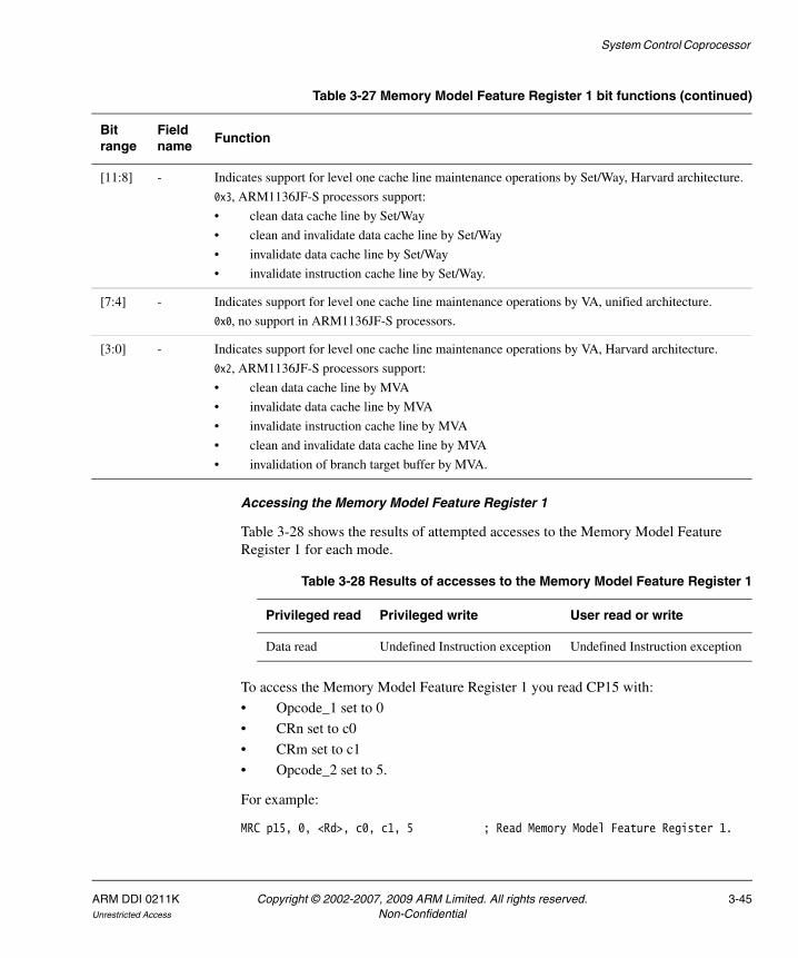
System Control Coprocessor
Accessing the Memory Model Feature Register 1
Table 3-28 shows the results of attempted accesses to the Memory Model Feature Register 1 for each mode.
To access the Memory Model Feature Register 1 you read CP15 with:
• Opcode_1 set to 0
• CRn set to c0
• CRm set to c1
• Opcode_2 set to 5.
For example:
MRC p15, 0, <Rd>, c0, c1, 5 ; Read Memory Model Feature Register 1.
[11:8] - Indicates support for level one cache line maintenance operations by Set/Way, Harvard architecture.
0x3, ARM1136JF-S processors support:
• clean data cache line by Set/Way
• clean and invalidate data cache line by Set/Way
• invalidate data cache line by Set/Way
• invalidate instruction cache line by Set/Way.
[7:4] - Indicates support for level one cache line maintenance operations by VA, unified architecture.
0x0, no support in ARM1136JF-S processors.
[3:0] - Indicates support for level one cache line maintenance operations by VA, Harvard architecture.
0x2, ARM1136JF-S processors support:
• clean data cache line by MVA
• invalidate data cache line by MVA
• invalidate instruction cache line by MVA
• clean and invalidate data cache line by MVA
• invalidation of branch target buffer by MVA.
Table 3-27 Memory Model Feature Register 1 bit functions (continued)
Bit range
Field name
Function
Table 3-28 Results of accesses to the Memory Model Feature Register 1
Privileged read Privileged write User read or write
Data read Undefined Instruction exception Undefined Instruction exception
ARM DDI 0211K Copyright © 2002-2007, 2009 ARM Limited. All rights reserved. 3-45Unrestricted Access Non-Confidential
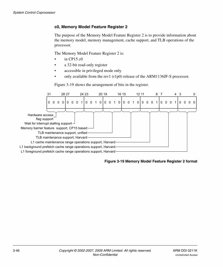
System Control Coprocessor
c0, Memory Model Feature Register 2
The purpose of the Memory Model Feature Register 2 is to provide information about the memory model, memory management, cache support, and TLB operations of the processor.
The Memory Model Feature Register 2 is:
• in CP15 c0
• a 32-bit read-only register
• accessible in privileged mode only
• only available from the rev1 (r1p0) release of the ARM1136JF-S processor.
Figure 3-19 shows the arrangement of bits in the register.
Figure 3-19 Memory Model Feature Register 2 format
00 0 0 10 0 0 00 0 1 00 0 1 00 0 1 10 0 0 10 0 0 00 0 0
31 28 27 24 23 20 19 16 15 12 11 8 7 4 3 0
Wait for interrupt stalling supportMemory barrier feature support, CP15 based
TLB maintenance support, unifiedTLB maintenance support, Harvard
L1 cache maintenance range operations support, HarvardL1 background prefetch cache range operations support, HarvardL1 foreground prefetch cache range operations support, Harvard
Hardware accessflag support
3-46 Copyright © 2002-2007, 2009 ARM Limited. All rights reserved. ARM DDI 0211KNon-Confidential Unrestricted Access

System Control Coprocessor
Table 3-29 lists the bit functions of the Memory Model Feature Register 2.
Table 3-29 Memory Model Feature Register 2 bit functions
Bit range Field name Function
[31:28] - Indicates support for a Hardware access flag.
0x0, Hardware access flag not supported by ARM1136JF-S processors.
[27:24] - Indicates support for wait for interrupt stalling.
0x1, ARM1136JF-S processors support wait for interrupt.
[23:20] - Indicates support for memory barrier operations.
0x2, ARM1136JF-S processors support:
• data synchronization barrier (drain write buffer)
• prefetch flush
• data memory barrier.
[19:16] - Indicates support for TLB maintenance operations, unified architecture.
0x2, ARM1136JF-S processors support:
• invalidate all entries
• invalidate TLB entry by MVA
• invalidate TLB entries by ASID match.
[15:12] - Indicates support for TLB maintenance operations, Harvard architecture.
0x2, ARM1136JF-S processors support:
• invalidate instruction and data TLB, all entries
• invalidate instruction TLB, all entries
• invalidate data TLB, all entries
• invalidate instruction TLB by MVA
• invalidate data TLB by MVA
• invalidate instruction and data TLB entries by ASID match
• invalidate instruction TLB entries by ASID match
• invalidate data TLB entries by ASID match.
ARM DDI 0211K Copyright © 2002-2007, 2009 ARM Limited. All rights reserved. 3-47Unrestricted Access Non-Confidential

System Control Coprocessor
Accessing the Memory Model Feature Register 2
Table 3-30 shows the results of attempted accesses to the Memory Model Feature Register 2 for each mode.
To access the Memory Model Feature Register 2 you read CP15 with:
• Opcode_1 set to 0
• CRn set to c0
• CRm set to c1
• Opcode_2 set to 6.
For example:
MRC p15, 0, <Rd>, c0, c1, 6 ; Read Memory Model Feature Register 2.
[11:8] - Indicates support for cache maintenance range operations, Harvard architecture.
0x1, ARM1136JF-S processors support:
• invalidate data cache range by VA
• invalidate instruction cache range by VA
• clean data cache range by VA
• clean and invalidate data cache range by VA.
[7:4] - Indicates support for background prefetch cache range operations, Harvard architecture.
0x1, ARM1136JF-S processors support:
• prefetch data cache range by VA
• prefetch instruction cache range by VA.
[3:0] - Indicates support for foreground prefetch cache range operations, Harvard architecture.
0x0, no support in ARM1136JF-S processors.
Table 3-29 Memory Model Feature Register 2 bit functions (continued)
Bit range Field name Function
Table 3-30 Results of accesses to the Memory Model Feature Register 2
Privileged read Privileged write User read or write
Data read Undefined Instruction exception Undefined Instruction exception
3-48 Copyright © 2002-2007, 2009 ARM Limited. All rights reserved. ARM DDI 0211KNon-Confidential Unrestricted Access
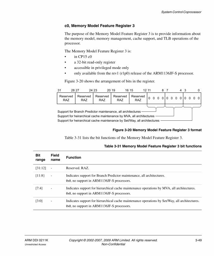
System Control Coprocessor
c0, Memory Model Feature Register 3
The purpose of the Memory Model Feature Register 3 is to provide information about the memory model, memory management, cache support, and TLB operations of the processor.
The Memory Model Feature Register 3 is:
• in CP15 c0
• a 32-bit read-only register
• accessible in privileged mode only
• only available from the rev1 (r1p0) release of the ARM1136JF-S processor.
Figure 3-20 shows the arrangement of bits in the register.
Figure 3-20 Memory Model Feature Register 3 format
Table 3-31 lists the bit functions of the Memory Model Feature Register 3.
00 0 0ReservedRAZ
ReservedRAZ
ReservedRAZ
ReservedRAZ 00 0 0 00 0 0Reserved
RAZ
31 28 27 24 23 20 19 16 15 12 11 8 7 4 3 0
Support for heirarchical cache maintenance by Set/Way, all architecturesSupport for heirarchical cache maintenance by MVA, all architecturesSupport for Branch Predictor maintenance, all architectures
Table 3-31 Memory Model Feature Register 3 bit functions
Bit range
Field name
Function
[31:12] - Reserved. RAZ.
[11:8} - Indicates support for Branch Predictor maintenance, all architectures.
0x0, no support in ARM1136JF-S processors.
[7:4] - Indicates support for hierarchical cache maintenance operations by MVA, all architectures.
0x0, no support in ARM1136JF-S processors.
[3:0] - Indicates support for hierarchical cache maintenance operations by Set/Way, all architectures.
0x0, no support in ARM1136JF-S processors.
ARM DDI 0211K Copyright © 2002-2007, 2009 ARM Limited. All rights reserved. 3-49Unrestricted Access Non-Confidential

System Control Coprocessor
Accessing the Memory Model Feature Register 3
Table 3-32 shows the results of attempted accesses to the Memory Model Feature Register 3 for each mode.
To access the Memory Model Feature Register 3 you read CP15 with:
• Opcode_1 set to 0
• CRn set to c0
• CRm set to c1
• Opcode_2 set to 7.
For example:
MRC p15, 0, <Rd>, c0, c1, 7 ; Read Memory Model Feature Register 3.
Table 3-32 Results of accesses to the Memory Model Feature Register 3
Privileged read Privileged write User read or write
Data read Undefined Instruction exception Undefined Instruction exception
3-50 Copyright © 2002-2007, 2009 ARM Limited. All rights reserved. ARM DDI 0211KNon-Confidential Unrestricted Access

System Control Coprocessor
c0, Instruction Set Attributes Register 0
The purpose of the Instruction Set Attributes Register 0 is to provide information about the instruction set that the processor supports beyond the basic set.
The Instruction Set Attributes Register 0 is:
• in CP15 c0
• a 32-bit read-only register
• accessible in privileged mode only
• only available from the rev1 (r1p0) release of the ARM1136JF-S processor.
Figure 3-21 shows the arrangement of bits in the register.
Figure 3-21 Instruction Set Attributes Register 0 format
Table 3-33 lists the bit functions of the Instruction Set Attributes Register 0.
0 0 0 0 0 0 0 10 0 0 10 0 0 00 0 0 00 1 0 00 0 0 1ReservedRAZ
31 12 11 8 7 4 3 024 23 20 19 16 15
Debug instructionsCoprocessor instructionsCmpBranch instructions
BitField instructionsBitCount instructions
Atomic instructions
Divide instructions
28 27
Table 3-33 Instruction Set Attributes Register 0 bit functions
Bit range Field name Function
[31:28] - Reserved. RAZ.
[27:24] Divide_instrs Indicates support for divide instructions.
0x0, no support in ARM1136JF-S processors.
[23:20] Debug_instrs Indicates support for debug instructions.
0x1, ARM1136JF-S processors support BKPT.
ARM DDI 0211K Copyright © 2002-2007, 2009 ARM Limited. All rights reserved. 3-51Unrestricted Access Non-Confidential

System Control Coprocessor
Accessing the Instruction Set Attributes Register 0
Table 3-34 shows the results of attempted accesses to the Instruction Set Attributes Register 0 for each mode.
To access the Instruction Set Attributes Register 0 you read CP15 with:
• Opcode_1 set to 0
• CRn set to c0
• CRm set to c2
• Opcode_2 set to 0.
For example:
MRC p15, 0, <Rd>, c0, c2, 0 ; Read Instruction Set Attributes Register 0
[19:16] Coproc_instrs Indicates support for coprocessor instructions.
0x4, ARM1136JF-S processors support:
• CDP, LDC, MCR, MRC, STC
• CDP2, LDC2, MCR2, MRC2, STC2
• MCRR, MRRC
• MCRR2, MRRC2.
[15:12] CmpBranch_instrs Indicates support for combined compare and branch instructions.
0x0, no support in ARM1136JF-S processors.
[11:8] Bitfield_instrs Indicates support for bitfield instructions.
0x0, no support in ARM1136JF-S processors.
[7:4] BitCount_instrs Indicates support for bit counting instructions.
0x1, ARM1136JF-S processors support CLZ.
[3:0] Atomic_instrs Indicates support for atomic load and store instructions.
0x1, ARM1136JF-S processors support SWP and SWPB.
Table 3-33 Instruction Set Attributes Register 0 bit functions (continued)
Bit range Field name Function
Table 3-34 Results of accesses to the Instruction Set Attributes Register 0
Privileged read Privileged write User read or write
Data read Undefined Instruction exception Undefined Instruction exception
3-52 Copyright © 2002-2007, 2009 ARM Limited. All rights reserved. ARM DDI 0211KNon-Confidential Unrestricted Access

System Control Coprocessor
c0, Instruction Set Attributes Register 1
The purpose of the Instruction Set Attributes Register 1 is to provide information about the instruction set that the processor supports beyond the basic set.
The Instruction Set Attributes Register 1 is:
• in CP15 c0
• a 32-bit read-only register
• accessible in privileged mode only
• only available from the rev1 (r1p0) release of the ARM1136JF-S processor.
Figure 3-22 shows the arrangement of bits in the register.
Figure 3-22 Instruction Set Attributes Register 1 format
0 0 0 1 0 0 1 0 0 0 0 10 0 0 10 0 0 10 0 1 00 0 0 00 0 0 0
31 12 11 8 7 4 3 024 23 20 19 16 15
Interwork instructionsImmediate instructions
IfThen instructionsExtend instructions
Exception2 instructionsException1 instructions
Jazelle extension instructions
Endian instructions
28 27
ARM DDI 0211K Copyright © 2002-2007, 2009 ARM Limited. All rights reserved. 3-53Unrestricted Access Non-Confidential

System Control Coprocessor
Table 3-35 lists the bit functions of the Instruction Set Attributes Register 1.
Table 3-35 Instruction Set Attributes Register 1 bit functions
Bit range
Field name Function
[31:28] Jazelle_instrs Indicates support for Jazelle instructions.
0x1, ARM1136JF-S processors support BXJ and J bit in PSRs.
[27:24] Interwork_instrs Indicates support for interworking instructions.
0x2, ARM1136JF-S processors support:
• BX, and T bit in PSRs
• BLX, and PC loads have BX behavior.
[23:20] Imediate_instrs Indicates support for immediate instructions.
0x0, no support in ARM1136JF-S processors.
[19:16] IfThen_instrs Indicates support for If … Then instructions.
0x0, no support in ARM1136JF-S processors.
[15:12] Extend_instrs Indicates support for sign or zero extend instructions.
0x2, ARM1136JF-S processors support:
• SXTB, SXTB16, SXTH, UXTB, UXTB16, and UXTH
• SXTAB, SXTAB16, SXTAH, UXTAB, UXTAB16, and UXTAH.
Shift operations on these instructions are also controlled by the WithShifts_instrs field, see c0, Instruction Set Attributes Register 4 on page 3-59.
[11:8] Except2_instrs Indicates support for exception 2 instructions.
0x1, ARM1136JF-S processors support SRS, RFE, and CPS.
[7:4] Except1_instrs Indicates support for exception 1 instructions.
0x1, ARM1136JF-S processors support LDM(2), LDM(3) and STM(2).
[3:0] Endian_instrs Indicates support for endianness control instructions.
0x1, ARM1136JF-S processors support SETEND and E bit in PSRs.
3-54 Copyright © 2002-2007, 2009 ARM Limited. All rights reserved. ARM DDI 0211KNon-Confidential Unrestricted Access

System Control Coprocessor
Accessing the Instruction Set Attributes Register 1
Table 3-36 shows the results of attempted accesses to the Instruction Set Attributes Register 1 for each mode.
To access the Instruction Set Attributes Register 1 you read CP15 with:
• Opcode_1 set to 0
• CRn set to c0
• CRm set to c2
• Opcode_2 set to 1.
For example:
MRC p15, 0, <Rd>, c0, c2, 1 ; Read Instruction Set Attributes Register 1
c0, Instruction Set Attributes Register 2
The purpose of the Instruction Set Attributes Register 2 is to provide information about the instruction set that the processor supports beyond the basic set.
The Instruction Set Attributes Register 2 is:
• in CP15 c0
• a 32-bit read-only register
• accessible in privileged mode only
• only available from the rev1 (r1p0) release of the ARM1136JF-S processor.
Figure 3-23 on page 3-56 shows the arrangement of bits in the register.
Table 3-36 Results of accesses to the Instruction Set Attributes Register 1
Privileged read Privileged write User read or write
Data read Undefined Instruction exception Undefined Instruction exception
ARM DDI 0211K Copyright © 2002-2007, 2009 ARM Limited. All rights reserved. 3-55Unrestricted Access Non-Confidential

System Control Coprocessor
Figure 3-23 Instruction Set Attributes Register 2 format
Table 3-37 lists the bit functions of the Instruction Set Attributes Register 2.
0 0 0 1 0 0 0 1 0 0 0 10 0 0 10 0 0 10 0 0 10 0 1 10 0 1 0
31 12 11 8 7 4 3 024 23 20 19 16 15
PSR instructionsMultiply instructions, advanced unsigned
Multi-Access interruptible instructionsMemoryHint instructions
Reversal instructions
LoadStore instructions
Multiply instructions, advanced signedMultiply instructions
28 27
Table 3-37 Instruction Set Attributes Register 2 bit functions
Bit range
Field name Function
[31:28] Reversal_instrs Indicates support for reversal instructions.
0x1, ARM1136JF-S processors support REV, REV16, and REVSH.
[27:24] PSR_instrs Indicates support for PSR instructions.
0x1, ARM1136JF-S processors support MRS and MRS exception return instructions for data-processing.
[23:20] MultU_instrs Indicates support for advanced unsigned multiply instructions.
0x2, ARM1136JF-S processors support:
• UMULL and UMLAL
• UMAAL.
[19:16] MultS_instrs Indicates support for advanced signed multiply instructions.
0x3, ARM1136JF-S processors support:
• SMULL and SMLAL
• SMLABB, SMLABT, SMLALBB, SMLALBT, SMLALTB, SMLALTT, SMLATB, SMLATT, SMLAWB, SMLAWT, SMULBB, SMULBT, SMULTB, SMULTT, SMULWB, SMULWT, and Q flag in PSRs
• SMLAD, SMLADX, SMLALD, SMLALDX, SMLSD, SMLSDX, SMLSLD, SMLSLDX, SMMLA, SMMLAR, SMMLS, SMMLSR, SMMUL, SMMULR, SMUAD, SMUADX, SMUSD, and SMUSDX.
[15:12] Mult_instrs Indicates support for multiply instructions.
0x1, ARM1136JF-S processors support MLA.
3-56 Copyright © 2002-2007, 2009 ARM Limited. All rights reserved. ARM DDI 0211KNon-Confidential Unrestricted Access

System Control Coprocessor
Accessing the Instruction Set Attributes Register 2
Table 3-38 shows the results of attempted accesses to the Instruction Set Attributes Register 2 for each mode.
To access the Instruction Set Attributes Register 2 you read CP15 with:
• Opcode_1 set to 0
• CRn set to c0
• CRm set to c2
• Opcode_2 set to 2.
For example:
MRC p15, 0, <Rd>, c0, c2, 2 ; Read Instruction Set Attributes Register 2
c0, Instruction Set Attributes Register 3
The purpose of the Instruction Set Attributes Register 3 is to provide information about the instruction set that the processor supports beyond the basic set.
The Instruction Set Attributes Register 3 is:
• in CP15 c0
• a 32-bit read-only register
• accessible in privileged mode only
• only available from the rev1 (r1p0) release of the ARM1136JF-S processor.
[11:8] MultiAccessInt_instrs Indicates support for multi-access interruptible instructions.
0x1, ARM1136JF-S processors support restartable LDM and STM.
[7:4] MemHint_instrs Indicates support for memory hint instructions.
0x1, ARM1136JF-S processors support PLD.
[3:0] LoadStore_instrs Indicates support for load and store instructions.
0x1, ARM1136JF-S processors support LDRD and STRD.
Table 3-37 Instruction Set Attributes Register 2 bit functions (continued)
Bit range
Field name Function
Table 3-38 Results of accesses to the Instruction Set Attributes Register 2
Privileged read Privileged write User read or write
Data read Undefined Instruction exception Undefined Instruction exception
ARM DDI 0211K Copyright © 2002-2007, 2009 ARM Limited. All rights reserved. 3-57Unrestricted Access Non-Confidential
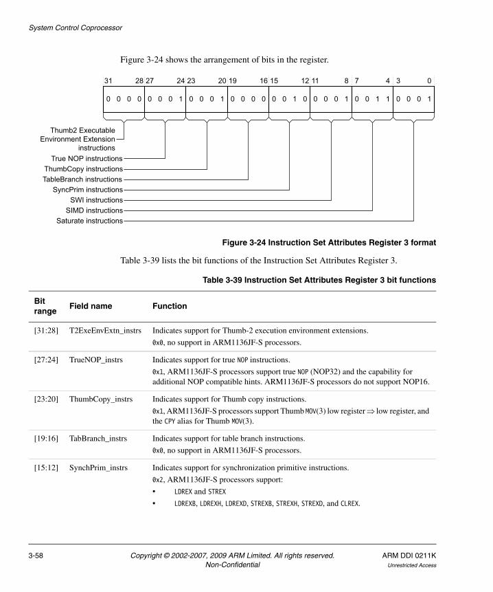
System Control Coprocessor
Figure 3-24 shows the arrangement of bits in the register.
Figure 3-24 Instruction Set Attributes Register 3 format
Table 3-39 lists the bit functions of the Instruction Set Attributes Register 3.
0 0 0 0 0 0 0 1 0 0 0 10 0 1 10 0 0 10 0 1 00 0 0 00 0 0 1
31 12 11 8 7 4 3 024 23 20 19 16 15
True NOP instructionsThumbCopy instructions
SWI instructionsSIMD instructions
Thumb2 Executable Environment Extension
instructions
Saturate instructions
TableBranch instructionsSyncPrim instructions
28 27
Table 3-39 Instruction Set Attributes Register 3 bit functions
Bit range
Field name Function
[31:28] T2ExeEnvExtn_instrs Indicates support for Thumb-2 execution environment extensions.
0x0, no support in ARM1136JF-S processors.
[27:24] TrueNOP_instrs Indicates support for true NOP instructions.
0x1, ARM1136JF-S processors support true NOP (NOP32) and the capability for additional NOP compatible hints. ARM1136JF-S processors do not support NOP16.
[23:20] ThumbCopy_instrs Indicates support for Thumb copy instructions.
0x1, ARM1136JF-S processors support Thumb MOV(3) low register ⇒ low register, and the CPY alias for Thumb MOV(3).
[19:16] TabBranch_instrs Indicates support for table branch instructions.
0x0, no support in ARM1136JF-S processors.
[15:12] SynchPrim_instrs Indicates support for synchronization primitive instructions.
0x2, ARM1136JF-S processors support:
• LDREX and STREX
• LDREXB, LDREXH, LDREXD, STREXB, STREXH, STREXD, and CLREX.
3-58 Copyright © 2002-2007, 2009 ARM Limited. All rights reserved. ARM DDI 0211KNon-Confidential Unrestricted Access
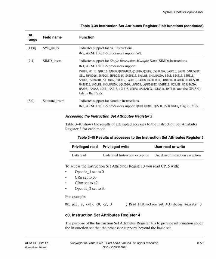
System Control Coprocessor
Accessing the Instruction Set Attributes Register 3
Table 3-40 shows the results of attempted accesses to the Instruction Set Attributes Register 3 for each mode.
To access the Instruction Set Attributes Register 3 you read CP15 with:
• Opcode_1 set to 0
• CRn set to c0
• CRm set to c2
• Opcode_2 set to 3.
For example:
MRC p15, 0, <Rd>, c0, c2, 3 ; Read Instruction Set Attributes Register 3
c0, Instruction Set Attributes Register 4
The purpose of the Instruction Set Attributes Register 4 is to provide information about the instruction set that the processor supports beyond the basic set.
[11:8] SWI_instrs Indicates support for SWI instructions.
0x1, ARM1136JF-S processors support SWI.
[7:4] SIMD_instrs Indicates support for Single Instruction Multiple Data (SIMD) instructions.
0x3, ARM1136JF-S processors support:
PKHBT, PKHTB, QADD16, QADD8, QADDSUBX, QSUB16, QSUB8, QSUBADDX, SADD16, SADD8, SADDSUBX, SEL, SHADD16, SHADD8, SHADDSUBX, SHSUB16, SHSUB8, SHSUBADDX, SSAT, SSAT16, SSUB16, SSUB8, SSUBADDX, SXTAB16, SXTB16, UADD16, UADD8, UADDSUBX, UHADD16, UHADD8, UHADDSUBX, UHSUB16, UHSUB8, UHSUBADDX, UQADD16, UQADD8, UQADDSUBX, UQSUB16, UQSUB8, UQSUBADDX, USAD8, USADA8, USAT, USAT16, USUB16, USUB8, USUBADDX, UXTAB16, UXTB16, and the GE[3:0] bits in the PSRs.
[3:0] Saturate_instrs Indicates support for saturate instructions.
0x1, ARM1136JF-S processors support QADD, QDADD, QDSUB, QSUB and Q flag in PSRs.
Table 3-39 Instruction Set Attributes Register 3 bit functions (continued)
Bit range
Field name Function
Table 3-40 Results of accesses to the Instruction Set Attributes Register 3
Privileged read Privileged write User read or write
Data read Undefined Instruction exception Undefined Instruction exception
ARM DDI 0211K Copyright © 2002-2007, 2009 ARM Limited. All rights reserved. 3-59Unrestricted Access Non-Confidential

System Control Coprocessor
The Instruction Set Attributes Register 4 is:
• in CP15 c0
• a 32-bit read-only register
• accessible in privileged mode only
• only available from the rev1 (r1p0) release of the ARM1136JF-S processor.
Figure 3-25 shows the arrangement of bits in the register.
Figure 3-25 Instruction Set Attributes Register 4 format
Table 3-41 lists the bit functions of the Instruction Set Attributes Register 4.
0 0 0 0ReservedRAZ 0 0 0 10 1 0 00 0 0 10 0 0 00 0 0 0Reserved
RAZ
31 12 11 8 7 4 3 020 19 16 1528 27 24 23
Fractional support forsynchronization primitive instructions
Writeback instructionsWithShift instructions
Unprivileged instructions
Barrier instructionsSMI instructions
Table 3-41 Instruction Set Attributes Register 4 bit functions
Bit range
Field name Function
[31:28] - Reserved. RAZ.
[27:24] - Reserved. RAZ.
[23:20] Syncprim_instrs_frac Indicates fractional support for synchronization primitive instructions.
0x0, ARM1136JF-S processors do not have fractional support.
The SynchPrim_instrs field indicates the support for synchronization primitive instructions, see c0, Instruction Set Attributes Register 3 on page 3-57.
[19:16] Barrier_instrs Indicates support for barrier instructions.
0x0, ARM1136JF-S processors use CP15 operations for all barrier instructions.
[15:12] SMI_instrs Indicates support for SMI instructions.
0x0, ARM1136JF-S processors do not support SMI.
3-60 Copyright © 2002-2007, 2009 ARM Limited. All rights reserved. ARM DDI 0211KNon-Confidential Unrestricted Access

System Control Coprocessor
Accessing the Instruction Set Attributes Register 4
Table 3-42 shows the results of attempted accesses to the Instruction Set Attributes Register 4 for each mode.
To access the Instruction Set Attributes Register 4 you read CP15 with:
• Opcode_1 set to 0
• CRn set to c0
• CRm set to c2
• Opcode_2 set to 4.
For example:
MRC p15, 0, <Rd>, c0, c2, 4 ; Read Instruction Set Attributes Register 4
[11:8] Writeback_instrs Indicates support for writeback instructions.
0x1, ARM1136JF-S processors support all defined writeback addressing modes.
[7:4] WithShifts_instrs Indicates support for with shift instructions.
0x4, ARM1136JF-S processors support:
• shifts of loads and stores over the range LSL 0-3
• constant shift options
• register controlled shift options.
[3:0] Unpriv_instrs Indicates support for Unprivileged instructions.
0x1, ARM1136JF-S processors support LDRBT, LDRT, STRBT, and STRT.
Table 3-41 Instruction Set Attributes Register 4 bit functions (continued)
Bit range
Field name Function
Table 3-42 Results of accesses to the Instruction Set Attributes Register 4
Privileged read Privileged write User read or write
Data read Undefined Instruction exception Undefined Instruction exception
ARM DDI 0211K Copyright © 2002-2007, 2009 ARM Limited. All rights reserved. 3-61Unrestricted Access Non-Confidential

System Control Coprocessor
c0, Instruction Set Attributes Register 5
The purpose of the Instruction Set Attributes Register 5 is to provide additional information about the properties of the processor.
The Instruction Set Attributes Register 5 is:
• in CP15 c0
• a 32-bit read-only register
• accessible in privileged mode only
• only available from the rev1 (r1p0) release of the ARM1136JF-S processor.
In the ARM1136JF-S processor, Instruction Set Attributes Register 5 reads as 0x00000000.
Accessing the Instruction Set Attributes Register 5
Table 3-43 shows the results of attempted accesses to the Instruction Set Attributes Register 5 for each mode.
To access the Instruction Set Attributes Register 5 you read CP15 with:
• Opcode_1 set to 0
• CRn set to c0
• CRm set toc2
• Opcode_2 set to 5.
For example:
MRC p15, 0, <Rd>, c0, c2, 5 ; Read Instruction Set Attribute Register 5.
Table 3-43 Results of accesses to the Instruction Set Attributes Register 5
Privileged read Privileged write User read or write
Data read Undefined Instruction exception Undefined Instruction exception
3-62 Copyright © 2002-2007, 2009 ARM Limited. All rights reserved. ARM DDI 0211KNon-Confidential Unrestricted Access

System Control Coprocessor
3.3.6 c1, Control Register
The purpose of the Control Register is to provide control and configuration of:
• memory alignment, endianness, protection, and fault behavior
• MMU and cache enables and cache replacement strategy
• interrupts and the behavior of interrupt latency
• the location for exception vectors
• program flow prediction.
The Control Register is:
• in CP15 c1
• a 32 bit register
— Table 3-44 on page 3-64 describes read and write access to individual bits
• accessible in privileged mode only.
Figure 3-26 shows the arrangement of bits in the register.
Figure 3-26 Control Register format
Table 3-44 on page 3-64 lists the bit functions of the Control Register.
MRAZ
31 30 29 28 27 26 25 24 23 22 21 20 19 18 17 16 15 14 13 12 11 10 9 8 7 6 4 3 2 1 0
RAZ U RAZ 1 0 1 V I Z F R S B SBO 1 C A
AFETRE
EEVEXP
FI ITRAZ
DT
WRRL4
ARM DDI 0211K Copyright © 2002-2007, 2009 ARM Limited. All rights reserved. 3-63Unrestricted Access Non-Confidential
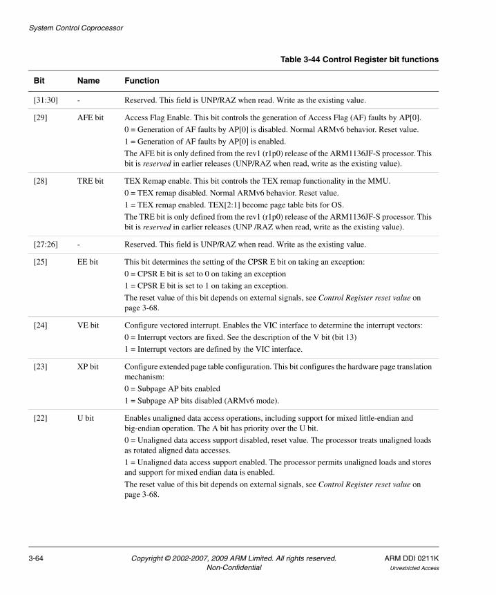
System Control Coprocessor
Table 3-44 Control Register bit functions
Bit Name Function
[31:30] - Reserved. This field is UNP/RAZ when read. Write as the existing value.
[29] AFE bit Access Flag Enable. This bit controls the generation of Access Flag (AF) faults by AP[0].
0 = Generation of AF faults by AP[0] is disabled. Normal ARMv6 behavior. Reset value.
1 = Generation of AF faults by AP[0] is enabled.
The AFE bit is only defined from the rev1 (r1p0) release of the ARM1136JF-S processor. This bit is reserved in earlier releases (UNP/RAZ when read, write as the existing value).
[28] TRE bit TEX Remap enable. This bit controls the TEX remap functionality in the MMU.
0 = TEX remap disabled. Normal ARMv6 behavior. Reset value.
1 = TEX remap enabled. TEX[2:1] become page table bits for OS.
The TRE bit is only defined from the rev1 (r1p0) release of the ARM1136JF-S processor. This bit is reserved in earlier releases (UNP /RAZ when read, write as the existing value).
[27:26] - Reserved. This field is UNP/RAZ when read. Write as the existing value.
[25] EE bit This bit determines the setting of the CPSR E bit on taking an exception:
0 = CPSR E bit is set to 0 on taking an exception
1 = CPSR E bit is set to 1 on taking an exception.
The reset value of this bit depends on external signals, see Control Register reset value on page 3-68.
[24] VE bit Configure vectored interrupt. Enables the VIC interface to determine the interrupt vectors:
0 = Interrupt vectors are fixed. See the description of the V bit (bit 13)
1 = Interrupt vectors are defined by the VIC interface.
[23] XP bit Configure extended page table configuration. This bit configures the hardware page translation mechanism:
0 = Subpage AP bits enabled
1 = Subpage AP bits disabled (ARMv6 mode).
[22] U bit Enables unaligned data access operations, including support for mixed little-endian and big-endian operation. The A bit has priority over the U bit.
0 = Unaligned data access support disabled, reset value. The processor treats unaligned loads as rotated aligned data accesses.
1 = Unaligned data access support enabled. The processor permits unaligned loads and stores and support for mixed endian data is enabled.
The reset value of this bit depends on external signals, see Control Register reset value on page 3-68.
3-64 Copyright © 2002-2007, 2009 ARM Limited. All rights reserved. ARM DDI 0211KNon-Confidential Unrestricted Access

System Control Coprocessor
[21] FI bit Configure fast interrupt configuration:
0 = All performance features enabled
1 = Low interrupt latency configuration enabled.
This bit enables low interrupt latency features, see Low interrupt latency configuration on page 2-39.
[20:19] - Reserved. This field is UNP/RAZ when read. Write as the existing value.
[18] IT bit Global Instruction TCM enable/disable bit. This bit is used in ARM946 and ARM966 processors to enable the Instruction TCM. In ARMv6, the TCM blocks have individual enables that apply to each block. As a result, this bit is now redundant.
This bit Should Be One on writes, and returns one on reads.
See c9, Instruction TCM Region Register on page 3-118 for a description of the ARM1136JF-S TCM enables.
[17] - Reserved. This field is UNP/RAZ when read. Write as the existing value.
[16] DT bit Global Data TCM enable/disable bit. This bit is used in ARM946 and ARM966 processors to enable the Data TCM. In ARMv6, the TCM blocks have individual enables that apply to each block. As a result, this bit is now redundant.
This bit Should Be One on writes, and returns one on reads.
See c9, Instruction TCM Region Register on page 3-118 for a description of the ARM1136JF-S TCM enables.
[15] L4 bit Configure if load instructions to PC set the T bit:
0 = Loads to PC set the T bit
1 = Loads to PC do not set the T bit (ARMv4 behavior).
For more details see the ARM Architecture Reference Manual.
[14] RR bit Replacement strategy for the instruction and data caches:
0 = Normal replacement strategy (Random replacement)
1 = Predictable replacement strategy (Round-Robin replacement).
[13] V bit Location of exception vectors:
0 = Normal exception vectors selected, address range = 0x00000000-0x0000001C
1 = High exception vectors selected, address range = 0xFFFF0000-0xFFFF001C.
The reset value of this bit depends on the external VINITHI signal, see Control Register reset value on page 3-68.
[12] I bit Level one Instruction Cache enable/disable:
0 = Instruction Cache disabled
1 = Instruction Cache enabled.
Table 3-44 Control Register bit functions (continued)
Bit Name Function
ARM DDI 0211K Copyright © 2002-2007, 2009 ARM Limited. All rights reserved. 3-65Unrestricted Access Non-Confidential

System Control Coprocessor
[11] Z bit Program flow prediction:
0 = Program flow prediction disabled
1 = Program flow prediction enabled.
Program flow prediction includes static and dynamic branch prediction and the return stack. This bit enables all three forms of program flow prediction. You can enable or disable each form individually, see c1, Auxiliary Control Register on page 3-69.
[10] F bit The meaning of this bit is Implementation-defined.
For ARM1136JF-S processors, this bit Should Be Zero on writes and Reads As Zero on reads.
[9] R bit ROM protection. This bit modifies the ROM protection system:
0 = ROM protection disabled
1 = ROM protection enabled.
Modifying the R bit does not affect the access permissions of entries already in the TLB. See MMU software-accessible registers on page 6-66.
[8] S bit System protection. This bit modifies the MMU protection system:
0 = MMU protection disabled
1 = MMU protection enabled.
Modifying the S bit does not affect the access permissions of entries already in the TLB.
[7] B bit Determines operation as little-endian or big-endian word invariant memory system and the names of the low four-byte addresses within a 32-bit word:
0 = Little-endian memory system
1 = Big-endian word-invariant memory system.
The reset value of this bit depends on external signals, see Control Register reset value on page 3-68.
[6:4] - When read returns one and when written Should Be One.
[3] W bit Write buffer enable/disable. Not implemented in the ARM1136JF-S processor because all memory writes take place through the Write Buffer. This bit reads as 1 and ignores writes.
Table 3-44 Control Register bit functions (continued)
Bit Name Function
3-66 Copyright © 2002-2007, 2009 ARM Limited. All rights reserved. ARM DDI 0211KNon-Confidential Unrestricted Access

System Control Coprocessor
[2] C bit Level one Data Cache enable/disable:
0 = Data cache disabled
1 = Data cache enabled.
[1] A bit Strict data address alignment fault enable/disable:
0 = Strict alignment fault checking disabled
1 = Strict alignment fault checking enabled.
The A bit setting takes priority over the U bit. The Data Abort trap is taken if strict alignment is enabled and the data access is not aligned to the width of the accessed data item.
[0] M bit MMU enable/disable:
0 = MMU disabled
1 = MMU enabled.
Table 3-44 Control Register bit functions (continued)
Bit Name Function
ARM DDI 0211K Copyright © 2002-2007, 2009 ARM Limited. All rights reserved. 3-67Unrestricted Access Non-Confidential

System Control Coprocessor
Control Register reset value
All defined bits in the Control Register are set to zero on Reset except:
• The V bit (bit[13]) is set to zero at Reset if the VINITHI signal is LOW, or one if the VINITHI signal is HIGH.
• The B bit (bit[7]), U bit (bit[22]), and EE bit (bit[25]) are set according to the state of the BIGENDINIT and UBITINIT inputs. Table 3-45 shows these settings.
Accessing the Control Register
Table 3-46 shows the results of attempted accesses to the Control Register for each mode.
To access the Control Register you read or write CP15 c1 with the CRm and Opcode_2 fields set to 0:
• Opcode_1 set to 0
• CRn set to c1
• CRm set to c0
• Opcode_2 set to 0.
For example:
MRC p15, 0, <Rd>, c1, c0, 0 ; Read Control Register configuration dataMCR p15, 0, <Rd>, c1, c0, 0 ; Write Control Register configuration data
Table 3-45 B bit, U bit, and EE bit settings, and Control Register reset value
CFGEND[1:0]EE U B
Control Register reset value
UBITINIT BIGENDINIT VINITHI = 0 VINITHI = 1
0 0 0 0 0 0x00050078 0x00052078
0 1 0 0 1 0x000500F8 0x000520F8
1 0 0 1 0 0x00450078 0x00452078
1 1 1 1 0 0x02450078 0x02452078
Table 3-46 Results of accesses to the Control Register
Privileged read Privileged write User read or write
Data read Data write Undefined Instruction exception
3-68 Copyright © 2002-2007, 2009 ARM Limited. All rights reserved. ARM DDI 0211KNon-Confidential Unrestricted Access
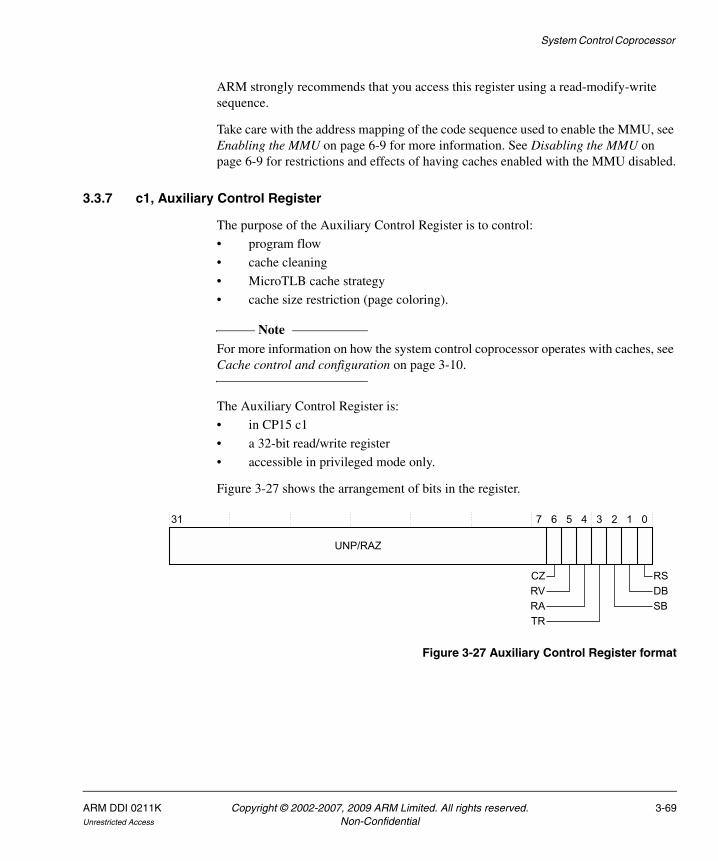
System Control Coprocessor
ARM strongly recommends that you access this register using a read-modify-write sequence.
Take care with the address mapping of the code sequence used to enable the MMU, see Enabling the MMU on page 6-9 for more information. See Disabling the MMU on page 6-9 for restrictions and effects of having caches enabled with the MMU disabled.
3.3.7 c1, Auxiliary Control Register
The purpose of the Auxiliary Control Register is to control:
• program flow
• cache cleaning
• MicroTLB cache strategy
• cache size restriction (page coloring).
Note For more information on how the system control coprocessor operates with caches, see Cache control and configuration on page 3-10.
The Auxiliary Control Register is:
• in CP15 c1
• a 32-bit read/write register
• accessible in privileged mode only.
Figure 3-27 shows the arrangement of bits in the register.
Figure 3-27 Auxiliary Control Register format
UNP/RAZ
31 7 6 5 4 3 2 1 0
CZ RSRVRA
DBSB
TR
ARM DDI 0211K Copyright © 2002-2007, 2009 ARM Limited. All rights reserved. 3-69Unrestricted Access Non-Confidential
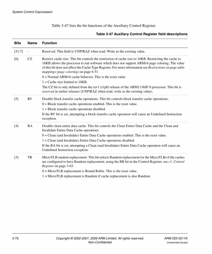
System Control Coprocessor
Table 3-47 lists the bit functions of the Auxiliary Control Register.
Table 3-47 Auxiliary Control Register field descriptions
Bits Name Function
[31:7] - Reserved. This field is UNP/RAZ when read. Write as the existing value.
[6] CZ Restrict cache size. This bit controls the restriction of cache size to 16KB. Restricting the cache to 16KB allows the processor to run software which does not support ARMv6 page coloring. The value of this bit does not affect the Cache Type Register. For more information see Restrictions on page table mappings (page coloring) on page 6-51.
0 = Normal ARMv6 cache behavior. This is the reset value.
1 = Cache size limited to 16KB.
The CZ bit is only defined from the rev1 (r1p0) release of the ARM1136JF-S processor. This bit is reserved in earlier releases (UNP/RAZ when read, write as the existing value).
[5] RV Disable block transfer cache operations. This bit controls block transfer cache operations:
0 = Block transfer cache operations enabled. This is the reset value.
1 = Block transfer cache operations disabled.
If the RV bit is set, attempting a block transfer cache operation will cause an Undefined Instruction exception.
[4] RA Disable clean entire data cache. This bit controls the Clean Entire Data Cache and the Clean and Invalidate Entire Data Cache operations:
0 = Clean (and Invalidate) Entire Data Cache operations enabled. This is the reset value.
1 = Clean (and Invalidate) Entire Data Cache operations disabled.
If the RA bit is set, attempting a Clean (and Invalidate) Entire Data Cache operation will cause an Undefined Instruction exception.
[3] TR MicroTLB random replacement. This bit selects Random replacement for the MicroTLBs if the caches are configured to have Random replacement, using the RR bit in the Control Register, see c1, Control Register on page 3-63.
0 = MicroTLB replacement is Round Robin. This is the reset value.
1 = MicroTLB replacement is Random if cache replacement is also Random.
3-70 Copyright © 2002-2007, 2009 ARM Limited. All rights reserved. ARM DDI 0211KNon-Confidential Unrestricted Access

System Control Coprocessor
Accessing the Auxiliary Control Register
Table 3-48 shows the results of attempted accesses to the Auxiliary Control Register for each mode.
Note You must access this register using a read-modify-write sequence. This enables you to write reserved register bits with their original values.
To access the Auxiliary Control Register you read or write CP15 with:
• Opcode_1 set to 0
• CRn set to c1
• CRm set to c0
• Opcode_2 set to 1.
For example:
[2] SB Static branch prediction enable. This bit enables the use of static branch prediction if program flow prediction is enabled, using the Z bit of the Control Register, see c1, Control Register on page 3-63.
0 = Static branch prediction is disabled.
1 = Static branch prediction is enabled. This is the reset value.
[1] DB Dynamic branch prediction enable. This bit enables the use of dynamic branch prediction if program flow prediction is enabled, using the Z bit of the Control Register, see c1, Control Register on page 3-63.
0 = Dynamic branch prediction is disabled.
1 = Dynamic branch prediction is enabled. This is the reset value.
[0] RS Return stack enable. This bit enables the use of the return stack if program flow prediction is enabled, using the Z bit of the Control Register, see c1, Control Register on page 3-63.
0 = Return stack is disabled.
1 = Return stack is enabled. This is the reset value.
Table 3-47 Auxiliary Control Register field descriptions (continued)
Bits Name Function
Table 3-48 Results of accesses to the Auxiliary Control Register
Privileged read Privileged write User read or write
Data read Data write Undefined Instruction exception
ARM DDI 0211K Copyright © 2002-2007, 2009 ARM Limited. All rights reserved. 3-71Unrestricted Access Non-Confidential
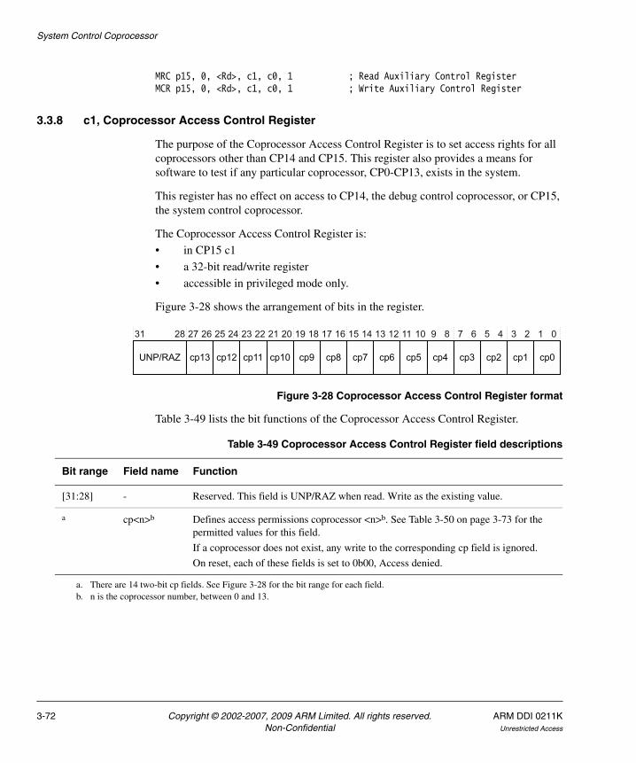
System Control Coprocessor
MRC p15, 0, <Rd>, c1, c0, 1 ; Read Auxiliary Control RegisterMCR p15, 0, <Rd>, c1, c0, 1 ; Write Auxiliary Control Register
3.3.8 c1, Coprocessor Access Control Register
The purpose of the Coprocessor Access Control Register is to set access rights for all coprocessors other than CP14 and CP15. This register also provides a means for software to test if any particular coprocessor, CP0-CP13, exists in the system.
This register has no effect on access to CP14, the debug control coprocessor, or CP15, the system control coprocessor.
The Coprocessor Access Control Register is:
• in CP15 c1
• a 32-bit read/write register
• accessible in privileged mode only.
Figure 3-28 shows the arrangement of bits in the register.
Figure 3-28 Coprocessor Access Control Register format
Table 3-49 lists the bit functions of the Coprocessor Access Control Register.
UNP/RAZ
31 28 27 26 25 24 23 22 21 20 19 18 17 16 15 14 13 12 11 10 9 8 7 6 5 4 3 2 1 0
cp13 cp12 cp11 cp10 cp9 cp8 cp7 cp6 cp5 cp4 cp3 cp2 cp1 cp0
Table 3-49 Coprocessor Access Control Register field descriptions
Bit range Field name Function
[31:28] - Reserved. This field is UNP/RAZ when read. Write as the existing value.
a cp<n>b Defines access permissions coprocessor <n>b. See Table 3-50 on page 3-73 for the permitted values for this field.
If a coprocessor does not exist, any write to the corresponding cp field is ignored.
On reset, each of these fields is set to 0b00, Access denied.
a. There are 14 two-bit cp fields. See Figure 3-28 for the bit range for each field.b. n is the coprocessor number, between 0 and 13.
3-72 Copyright © 2002-2007, 2009 ARM Limited. All rights reserved. ARM DDI 0211KNon-Confidential Unrestricted Access

System Control Coprocessor
Table 3-50 shows the possible bit-pair access rights encodings for each coprocessor connected to the ARM1136JF-S processor.
Accessing the Coprocessor Access Control Register
Table 3-51 shows the results of attempted accesses to the Coprocessor Access Control Register for each mode.
To access the Coprocessor Access Control Register you read or write CP15 with:
• Opcode_1 set to 0
• CRn set to c1
• CRm set to c0
• Opcode_2 set to 2.
For example:
MRC p15, 0, <Rd>, c1, c0, 2 ; Read Coprocessor Access Control RegisterMCR p15, 0, <Rd>, c1, c0, 2 ; Write Coprocessor Access Control Register
You must execute an Instruction Memory Barrier (IMB) sequence immediately after updating the Coprocessor Access Control Register, see Instruction Memory Barrier (IMB) instruction on page 5-8. When you update the Coprocessor Access Control Register you must not attempt to execute any instructions that are affected by the change of access rights until you have executed the IMB sequence.
Table 3-50 Coprocessor access rights encodings
Bits Meaning
b00 Access denied.
Attempts to access the corresponding coprocessor generate an Undefined Instruction exception.
b01 Privileged mode (Supervisor) access only.
b10 Reserved.
b11 Full access.
Table 3-51 Results of accesses to the Coprocessor Access Control Register
Privileged read Privileged write User read or write
Data read Data write Undefined Instruction exception
ARM DDI 0211K Copyright © 2002-2007, 2009 ARM Limited. All rights reserved. 3-73Unrestricted Access Non-Confidential

System Control Coprocessor
Note ARM recommends that you access this register using a read-modify-write sequence.
You can use the Coprocessor Access Control Register to find whether a particular coprocessor exists in the system by:
• Writing a permitted value other than 0b00 to the access permissions field of the coprocessor you are interested in.
• Read back the Coprocessor Access Control Register. If the coprocessor does not exist in the system field then its access rights remain set to 0b00.
After a system reset, all coprocessor access rights are set to 0b00, access denied.
3.3.9 c2, Translation Table Base Register 0, TTBR0
The purpose of the Translation Table Base Register 0 is to hold the physical address of the first-level translation table.
You use Translation Table Base Register 0 for process-specific addresses, where each process maintains a separate first-level page table. On a context switch you must modify both Translation Table Base Register 0 and the Translation Table Base Control Register, if appropriate.
The Translation Table Base Register 0 is:
• in CP15 c2
• a 32 bit read/write register
• accessible in privileged mode only.
Figure 3-29 shows the bit functions of the register.
Figure 3-29 Translation Table Base Register 0 format
S CTranslation table base 0
31 14-N 13-N 0
UNP/SBZ
123
RGN
45
‡
‡ The value of N is defined in the Translation Table Base Control Register.SBZP
3-74 Copyright © 2002-2007, 2009 ARM Limited. All rights reserved. ARM DDI 0211KNon-Confidential Unrestricted Access

System Control Coprocessor
Table 3-52 lists the bit functions of the Translation Table Base Register 0.
Accessing the Translation Table Base Register 0
Table 3-53 shows the results of attempted accesses to the Translation Table Base Register 0 for each mode.
To access the Translation Table Base Register 0 you read or write CP15 with:
• Opcode_1 set to 0
• CRn set to c2
• CRm set to c0
Table 3-52 Translation Table Base Register 0 field descriptions
Bits Name Function
[31:(14-N)]a Translation table base 0
Pointer to the level one translation table.
[(13-N):5]a - UNP/SBZ.
[4:3] RGN Outer cacheable attributes for page table walking:
b00 = Outer Noncacheable
b01 = Outer Cacheable Write-Back cached, Write Allocate
b10 = Outer Cacheable Write-Through, No Allocate on Write
b11 = Outer Cacheable Write-Back, No Allocate on Write.
[2] - Reserved, SBZP.
[1] S Indicates whether the page table walk is to Shared or Non-Shared memory.
0 = Non-Shared. This is the reset value.
1 = Shared.
[0] C Indicates whether the page table walk is Inner Cacheable or Inner Noncacheable.
0 = Inner noncacheable. This is the reset value.
1 = Inner cacheable.
a. The value of N is defined in the Translation Table Base Control Register, see c2, Translation Table Base Control Register, TTBCR on page 3-78.
Table 3-53 Results of accesses to the Translation Table Base Register 0
Privileged read Privileged write User read or write
Data read Data write Undefined Instruction exception
ARM DDI 0211K Copyright © 2002-2007, 2009 ARM Limited. All rights reserved. 3-75Unrestricted Access Non-Confidential
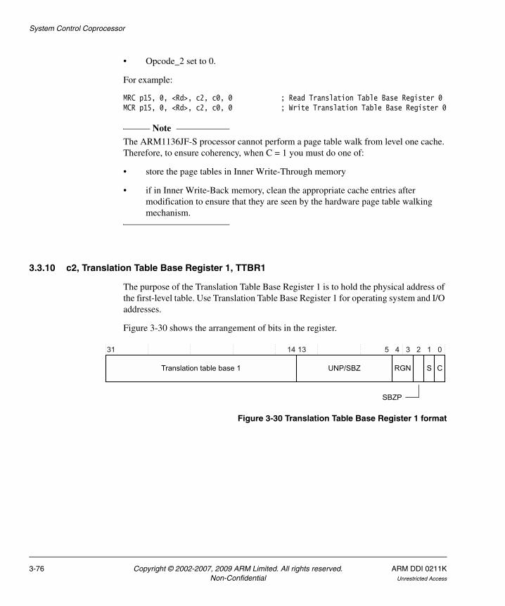
System Control Coprocessor
• Opcode_2 set to 0.
For example:
MRC p15, 0, <Rd>, c2, c0, 0 ; Read Translation Table Base Register 0MCR p15, 0, <Rd>, c2, c0, 0 ; Write Translation Table Base Register 0
Note The ARM1136JF-S processor cannot perform a page table walk from level one cache. Therefore, to ensure coherency, when C = 1 you must do one of:
• store the page tables in Inner Write-Through memory
• if in Inner Write-Back memory, clean the appropriate cache entries after modification to ensure that they are seen by the hardware page table walking mechanism.
3.3.10 c2, Translation Table Base Register 1, TTBR1
The purpose of the Translation Table Base Register 1 is to hold the physical address of the first-level table. Use Translation Table Base Register 1 for operating system and I/O addresses.
Figure 3-30 shows the arrangement of bits in the register.
Figure 3-30 Translation Table Base Register 1 format
Translation table base 1
31 14 13
S C
0
UNP/SBZ
123
RGN
45
SBZP
3-76 Copyright © 2002-2007, 2009 ARM Limited. All rights reserved. ARM DDI 0211KNon-Confidential Unrestricted Access
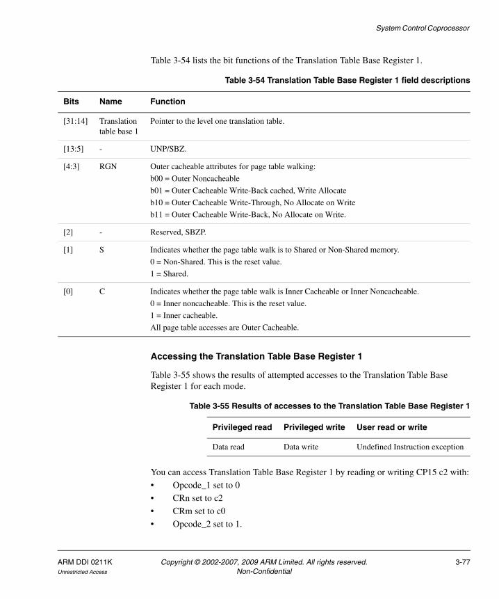
System Control Coprocessor
Table 3-54 lists the bit functions of the Translation Table Base Register 1.
Accessing the Translation Table Base Register 1
Table 3-55 shows the results of attempted accesses to the Translation Table Base Register 1 for each mode.
You can access Translation Table Base Register 1 by reading or writing CP15 c2 with:
• Opcode_1 set to 0
• CRn set to c2
• CRm set to c0
• Opcode_2 set to 1.
Table 3-54 Translation Table Base Register 1 field descriptions
Bits Name Function
[31:14] Translation table base 1
Pointer to the level one translation table.
[13:5] - UNP/SBZ.
[4:3] RGN Outer cacheable attributes for page table walking:
b00 = Outer Noncacheable
b01 = Outer Cacheable Write-Back cached, Write Allocate
b10 = Outer Cacheable Write-Through, No Allocate on Write
b11 = Outer Cacheable Write-Back, No Allocate on Write.
[2] - Reserved, SBZP.
[1] S Indicates whether the page table walk is to Shared or Non-Shared memory.
0 = Non-Shared. This is the reset value.
1 = Shared.
[0] C Indicates whether the page table walk is Inner Cacheable or Inner Noncacheable.
0 = Inner noncacheable. This is the reset value.
1 = Inner cacheable.
All page table accesses are Outer Cacheable.
Table 3-55 Results of accesses to the Translation Table Base Register 1
Privileged read Privileged write User read or write
Data read Data write Undefined Instruction exception
ARM DDI 0211K Copyright © 2002-2007, 2009 ARM Limited. All rights reserved. 3-77Unrestricted Access Non-Confidential

System Control Coprocessor
For example:
MRC p15, 0, <Rd>, c2, c0, 1 ; Read Translation Table Base Register 1MCR p15, 0, <Rd>, c2, c0, 1 ; Write Translation Table Base Register 1
Writing to CP15 c2 updates the pointer to the first-level translation table, using the value in bits [31:14] of the register write. Bits [13:5] Should Be Zero.
Translation Table Base Register 1 must reside on a 16KB page boundary.
Note The ARM1136JF-S processor cannot perform a page table walk from level one cache. Therefore, to ensure coherency, when C = 1 you must do one of:
• store the page tables in Inner Write-Through memory
• if in Inner Write-Back memory, clean the appropriate cache entries after modification to ensure that they are seen by the hardware page table walking mechanism.
3.3.11 c2, Translation Table Base Control Register, TTBCR
The purpose of the Translation Table Base Control Register is to determine whether a page table miss for a specific Virtual Address uses Translation Table Base Register 0 or Translation Table Base Register 1.
• Use of Translation Table Base Register 0 is recommended for task-specific addresses.
• Use of Translation Table Base Register 1 is recommended use for operating system and I/O addresses.
The Translation Table Base Control Register is:
• in CP15 c2
• a 32 bit read/write register
• accessible in privileged mode only.
Figure 3-31 shows the arrangement of bits in the register.
Figure 3-31 Translation Table Base Control Register format
UNP/SBZ
31 3 2 0
N
3-78 Copyright © 2002-2007, 2009 ARM Limited. All rights reserved. ARM DDI 0211KNon-Confidential Unrestricted Access

System Control Coprocessor
Figure 3-31 on page 3-78 shows that there is a single bit field in the register. This holds a three-bit value, N. When N is greater than zero it specifies the boundary size of the Transition Table Base Register 0, see c2, Translation Table Base Register 0, TTBR0 on page 3-74. Table 3-56 shows the meaning of different values of N.
Accessing the Translation Table Base Control Register
Table 3-57 shows the results of attempted accesses to the Translation Table Base Control Register for each mode.
To access the Translation Table Base Control Register you read or write CP15 with:
• Opcode_1 set to 0
• CRn set to c2
• CRm set to c0
• Opcode_2 set to 2.
For example:
MRC p15, 0, <Rd>, c2, c0, 2 ; Read Translation Table Base Control RegisterMCR p15, 0, <Rd>, c2, c0, 2 ; Write Translation Table Base Control Register
Table 3-56 Values of N for Translation Table Base Register 0
N Translation Table Base Register 0 page table boundary size
0 16KB
1 8KB
2 4KB
3 2KB
4 1KB
5 512-byte
6 256-byte
7 128-byte
Table 3-57 Results of accesses to the Translation Table Base Control Register
Privileged read Privileged write User read or write
Data read Data write Undefined Instruction exception
ARM DDI 0211K Copyright © 2002-2007, 2009 ARM Limited. All rights reserved. 3-79Unrestricted Access Non-Confidential

System Control Coprocessor
Reading from CP15 c2 returns the size of the page table boundary for Translation Table Base Register 0. Bits [31:3] Read As Zero.
Writing to CP15 c2 updates the size, N, of the first-level translation table base boundary for Translation Table Base Register 0.
Selecting which Translation Table Base Register is used
The Translation Table Base Register is selected as follows:
1. If N = 0, always use Translation Table Base Register 0.
This is the default case at reset. It is backwards compatible with ARMv5 or earlier processors.
2. If N is greater than 0, then:
• if bits [31:32-N] of the Virtual Address are all 0, use Translation Table Base Register 0
• otherwise use Translation Table Base Register 1.
Note N must be in the range 0 to 7.
3.3.12 c3, Domain Access Control Register
The purpose of the Domain Access Control Register is to hold the access permissions for a maximum of 16 domains, D15 to D0.
The Domain Access Control Register is:
• in CP15 c3
• a 32-bit read/write register
• accessible in privileged mode only.
Figure 3-32 shows the two-bit domain access permission fields of the register.
Figure 3-32 Domain Access Control Register format
D15
31 30 29 28 27 26 25 24 23 22 21 20 19 18 17 16 15 14 13 12 11 10 9 8 7 6 5 4 3 2 1 0
D14 D13 D12 D11 D10 D9 D8 D7 D6 D5 D4 D3 D2 D1 D0
3-80 Copyright © 2002-2007, 2009 ARM Limited. All rights reserved. ARM DDI 0211KNon-Confidential Unrestricted Access
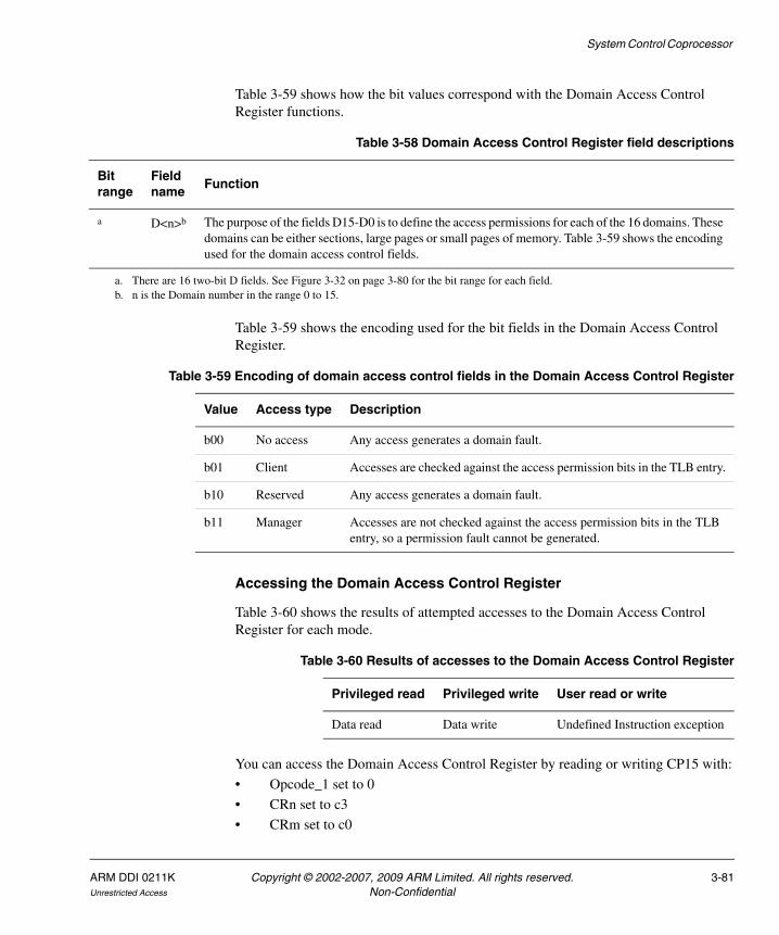
System Control Coprocessor
Table 3-59 shows how the bit values correspond with the Domain Access Control Register functions.
Table 3-59 shows the encoding used for the bit fields in the Domain Access Control Register.
Accessing the Domain Access Control Register
Table 3-60 shows the results of attempted accesses to the Domain Access Control Register for each mode.
You can access the Domain Access Control Register by reading or writing CP15 with:
• Opcode_1 set to 0
• CRn set to c3
• CRm set to c0
Table 3-58 Domain Access Control Register field descriptions
Bit range
Field name
Function
a D<n>b The purpose of the fields D15-D0 is to define the access permissions for each of the 16 domains. These domains can be either sections, large pages or small pages of memory. Table 3-59 shows the encoding used for the domain access control fields.
a. There are 16 two-bit D fields. See Figure 3-32 on page 3-80 for the bit range for each field.b. n is the Domain number in the range 0 to 15.
Table 3-59 Encoding of domain access control fields in the Domain Access Control Register
Value Access type Description
b00 No access Any access generates a domain fault.
b01 Client Accesses are checked against the access permission bits in the TLB entry.
b10 Reserved Any access generates a domain fault.
b11 Manager Accesses are not checked against the access permission bits in the TLB entry, so a permission fault cannot be generated.
Table 3-60 Results of accesses to the Domain Access Control Register
Privileged read Privileged write User read or write
Data read Data write Undefined Instruction exception
ARM DDI 0211K Copyright © 2002-2007, 2009 ARM Limited. All rights reserved. 3-81Unrestricted Access Non-Confidential

System Control Coprocessor
• Opcode_2 set to 0.
For example:
MRC p15, 0, <Rd>, c3, c0, 0 ; Read Domain Access Control RegisterMCR p15, 0, <Rd>, c3, c0, 0 ; Write Domain Access Control Register
3-82 Copyright © 2002-2007, 2009 ARM Limited. All rights reserved. ARM DDI 0211KNon-Confidential Unrestricted Access

System Control Coprocessor
3.3.13 c5, Data Fault Status Register, DFSR
The purpose of the Data Fault Status Register (DFSR) is to hold the source of the last data fault. The Data Fault Status Register indicates the domain and type of access being attempted when an abort occurred.
The Data Fault Status Register is:
• in CP15 c5
• a 32-bit read/write register
• accessible in privileged mode only.
Figure 3-33 shows the arrangement of bits in the register.
Figure 3-33 Data Fault Status Register format
Table 3-61shows the bit functions of the Data Fault Status Register.
0UNP/SBZ
31 8 7 4 3 0
Domain Status[3:0]
9
0
101112
RWStatus[4]
Table 3-61 Data Fault Status Register bits
Bit range
Field name
Function
[31:12] - UNP/SBZ.
[11] RW Not Read/Write.
Indicates which type of access caused the abort:
0 = Read
1 = Write
When a CP15 cache maintenance operation fault causes an abort, the value returned is 1.
[10] Status[4] Part of the Status field, see Bits[3:0] in this table.
[9:8] - Always read as 0. Writes to these bits are ignored.
[7:4] Domain Specifies which of the 16 domains (D15-D0) was being accessed when a data fault occurred. Possible values are 0 to 15. Reset value is 0.
[3:0] Status[3:0] Type of fault generated. See Table 3-62 on page 3-84 for a list of the fault encodings, and Fault status and address on page 6-42 for full details of Domain and FAR validity.
ARM DDI 0211K Copyright © 2002-2007, 2009 ARM Limited. All rights reserved. 3-83Unrestricted Access Non-Confidential

System Control Coprocessor
The fault status field bit encodings are shown in Table 3-62.
Table 3-62 DFSR fault status encoding
Status[4:0]a
a. Bits[10,3:0] of the DFSR register.
Fault source
b00000 No function, reset value
b00001 Alignment fault
b00010 Debug event fault
b00011 Access Flag fault on Section
b00100 Cache maintenance operation faultb
b. Can only occur on the Data side. On the IFSR, the corresponding encoding (b0100) has no function.
b00101 Translation fault on Section
b00110 Access Flag fault on Page
b00111 Translation fault on Page
b01000 Precise External Abort
b01001 Domain fault on Section
b01010 No function
b01011 Domain fault on Page
b01100 External abort on translation, first level
b01101 Permission fault on Section
b01110 External abort on translation, second level
b01111 Permission fault on Page
b100xx No function
b1010x No function
b10110 Imprecise External Abort
b10111 No function
b11xxx No function
3-84 Copyright © 2002-2007, 2009 ARM Limited. All rights reserved. ARM DDI 0211KNon-Confidential Unrestricted Access
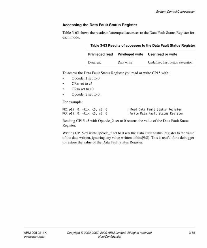
System Control Coprocessor
Accessing the Data Fault Status Register
Table 3-63 shows the results of attempted accesses to the Data Fault Status Register for each mode.
To access the Data Fault Status Register you read or write CP15 with:
• Opcode_1 set to 0
• CRn set to c5
• CRm set to c0
• Opcode_2 set to 0.
For example:
MRC p15, 0, <Rd>, c5, c0, 0 ; Read Data Fault Status RegisterMCR p15, 0, <Rd>, c5, c0, 0 ; Write Data Fault Status Register
Reading CP15 c5 with Opcode_2 set to 0 returns the value of the Data Fault Status Register.
Writing CP15 c5 with Opcode_2 set to 0 sets the Data Fault Status Register to the value of the data written, ignoring any value written to bits[9:8]. This is useful for a debugger to restore the value of the Data Fault Status Register.
Table 3-63 Results of accesses to the Data Fault Status Register
Privileged read Privileged write User read or write
Data read Data write Undefined Instruction exception
ARM DDI 0211K Copyright © 2002-2007, 2009 ARM Limited. All rights reserved. 3-85Unrestricted Access Non-Confidential

System Control Coprocessor
3.3.14 c5, Instruction Fault Status Register, IFSR
The purpose of the Instruction Fault Status Register (IFSR) is to hold the source of the last instruction fault. The IFSR indicates the type of access being attempted when an abort occurred.
The Instruction Fault Status Register is:
• in CP15 c5
• a 32-bit read/write register
• accessible in privileged mode only.
Figure 3-34 shows the arrangement of bits in the register.
Figure 3-34 Instruction Fault Status Register format
Table 3-64 shows the bit functions of the Instruction Fault Status Register.
The fault status field bit encodings are shown in Table 3-65.
UNP/SBZ
31 3 0
StatusUNP/SBZ
491011
0
Table 3-64 Instruction Fault Status Register bits
Bit range
Field name
Meaning
[31:11] - UNP/SBZ.
[10] - Always 0.
[9:4] - UNP/SBZ.
[3:0] Status Type of fault generated. See Table 3-65 for a list of the fault encodings, and Fault status and address on page 6-42 for full details of Domain and FAR validity.
Table 3-65 IFSR fault status encoding
Status[3:0]a Fault source
b0000 No function, reset value
b0001 Alignment fault
b0010 Debug event fault
3-86 Copyright © 2002-2007, 2009 ARM Limited. All rights reserved. ARM DDI 0211KNon-Confidential Unrestricted Access

System Control Coprocessor
Accessing the Instruction Fault Status Register
Table 3-66 shows the results of attempted accesses to the Instruction Fault Status Register for each mode.
To access the Instruction Fault Status Register you read or write CP15 with:
• Opcode_1 set to 0
• CRn set to c5
• CRm set to c0
b0011 Access Flag fault on Section
b0100 No functionb
b0101 Translation fault on Section
b0110 Access Flag fault on Page
b0111 Translation fault on Page
b1000 Precise External Abort
b1001 Domain fault on Section
b1010 No function
b1011 Domain fault on Page
b1100 External abort on translation, first level
b1101 Permission fault on Section
b1110 External abort on translation, second level
b1111 Permission fault on Page
a. Bits[3:0] of the IFSR register.b. On the DFST, the corresponding encoding (0b00100) indicates a cache
maintenance operation fault. These faults cannot occur on the instruction side.
Table 3-66 Results of accesses to the Instruction Fault Status Register
Privileged read Privileged write User read or write
Data read Data write Undefined Instruction exception
Table 3-65 IFSR fault status encoding (continued)
Status[3:0]a Fault source
ARM DDI 0211K Copyright © 2002-2007, 2009 ARM Limited. All rights reserved. 3-87Unrestricted Access Non-Confidential

System Control Coprocessor
• Opcode_2 set to 1.
For example:
MRC p15, 0, <Rd>, c5, c0, 1 ; Read Instruction Fault Status RegisterMCR p15, 0, <Rd>, c5, c0, 1 ; Write Instruction Fault Status Register
Reading CP15 c5 with the Opcode_2 field set to 1 returns the value of the IFSR.
Writing CP15 c5 with the Opcode_2 field set to 1 sets the IFSR to the value of the data written. This is useful for a debugger to restore the value of the IFSR. Bits [31:4] Should Be Zero.
3.3.15 c6, Fault Address Register, FAR
The purpose of the Fault Address Register (FAR) is to hold the Modified Virtual Address (MVA) of the access being attempted when a fault occurred.
The Fault Address Register is:
• in CP15 c6
• a 32-bit read/write register
• accessible in privileged mode only.
The FAR is only updated for precise data faults, not for imprecise data faults or prefetch faults. Register bits[31:0] contain the MVA on which the precise abort occurred. The register reset value is 0.
Accessing the Fault Address Register
Table 3-67 shows the results of attempted accesses to the Fault Address Register for each mode.
To access the Fault Address Register (FAR) you read or write CP15 with:
• Opcode_1 set to 0
• CRn set to c6
• CRm set to c0
• Opcode_2 set to 0.
For example:
Table 3-67 Results of accesses to the Fault Address Register
Privileged read Privileged write User read or write
Data read Data write Undefined Instruction exception
3-88 Copyright © 2002-2007, 2009 ARM Limited. All rights reserved. ARM DDI 0211KNon-Confidential Unrestricted Access

System Control Coprocessor
MRC p15, 0, <Rd>, c6, c0, 0 ; Read Fault Address RegisterMCR p15, 0, <Rd>, c6, c0, 0 ; Write Fault Address Register
Writing CP15 c6 with Opcode_2 set to 0 sets the FAR to the value of the data written. This is useful for a debugger to restore the value of the FAR.
The ARM1136JF-S processor also updates the FAR when a watchpoint causes a debug exception entry. This is architecturally Unpredictable. See Effect of a debug event on CP15 registers on page 13-49 for more details.
3.3.16 c6, Watchpoint Fault Address Register, WFAR
The purpose of the Watchpoint Fault Address Register (WFAR) is to hold the Virtual Address of the instruction that triggered the watchpoint.
The Watchpoint Fault Address Register is:
• in CP15 c6
• a 32-bit read/write register
• accessible in privileged mode only.
The contents of the WFAR are Unpredictable after a precise Data Abort or Instruction Abort occurs.
Register bits[31:0] contain the virtual address that indicates the instruction that triggered the watchpoint. The register reset value is 0.
Accessing the Watchpoint Fault Address Register
Table 3-67 on page 3-88 shows the results of attempted accesses to the Watchpoint Fault Address Register for each mode.
To access the Watchpoint Fault Address Register you read or write CP15 with:
• Opcode_1 set to 0
• CRn set to c6
• CRm set to c0
• Opcode_2 set to 1.
For example:
Table 3-68 Results of accesses to the Watchpoint Fault Address Register
Privileged read Privileged write User read or write
Data read Data write Undefined Instruction exception
ARM DDI 0211K Copyright © 2002-2007, 2009 ARM Limited. All rights reserved. 3-89Unrestricted Access Non-Confidential

System Control Coprocessor
MRC p15, 0, <Rd>, c6, c0, 1 ; Read Watchpoint Fault Address RegisterMCR p15, 0, <Rd>, c6, c0, 1 ; Write Watchpoint Fault Address Register
If the watchpoint is taken when in ARM state, the WFAR contains the address of the instruction that triggered it plus 0x8. If the watchpoint is taken while in Thumb state, the WFAR contains the address of the instruction that triggered it plus 0x4. If the watchpoint is taken while in Jazelle state, the WFAR contains the address of the instruction causing it.
Writing CP15 c6 with Opcode_2 set to 1 sets the WFAR to the value of the data written. This is useful for a debugger to restore the value of the WFAR.
3.3.17 c7, Cache Operations Register
The purpose of the Cache Operations Register, c7, is to:
• control these operations:
— clean and invalidate instruction and data caches, including range operations
— prefetch instruction cache line
— flush prefetch buffer
— flush branch target address cache
— data synchronization barrier
— stop prefetch range
• access these registers:
— Cache Dirty Status Register
— Block Transfer Status Register
• implement the Data Memory Barrier (DMB) operation
• implement the Wait For Interrupt clock control function
• perform block transfers operations, using the MCRR operation.
Note Cache operations also depend on:
• the C, I and RR bits, see c1, Control Register on page 3-63
• the RA and RV bits, see c1, Auxiliary Control Register on page 3-69.
The Cache Operations Register, c7, consists of one 32-bit register that performs 29 functions, including providing access to two other registers.
• Figure 3-35 on page 3-91 shows the arrangement of the 23 functions in this group that operate with the MCR and MRC instructions.
• Figure 3-36 on page 3-92 shows the arrangement of the 6 functions in this group that operate with the MCRR instruction.
3-90 Copyright © 2002-2007, 2009 ARM Limited. All rights reserved. ARM DDI 0211KNon-Confidential Unrestricted Access

System Control Coprocessor
Figure 3-35 Cache Operations Register operations using MCR or MRC instructions
c7
c6
c7
c0 4c5 0
124670120
c10
c12
c14
0124564
012
SBZSBZMVAIndxSBZSBZMVASBZMVAIndxSBZSBZMVAIndxSBZSBZ
SBZMVAIndx
0
Invalidate Data Cache Line, using Set/WayInvalidate Both Caches
Invalidate Data Cache Line, using MVAInvalidate Entire Data Cache
Flush Entire Branch Target Cache
Wait For Interrupt
Flush Prefetch Buffer
Flush Branch Target Cache Entry
Invalidate Entire Instruction CacheInvalidate Instruction Cache Line, using MVAInvalidate Instruction Cache Line, using Set/Way
Read Cache Dirty Status Register
Clean Entire Data Cache ‡Clean Data Cache Line, using MVAClean Data Cache Line, using Set/WayData Synchronization BarrierData Memory Barrier
Clean and Invalidate Entire Data Cache ‡
Read Block Transfer Status Register
Clean and Invalidate Data Cache Line, using MVAClean and Invalidate Data Cache Line, using Set/Way
Opcode_2CRmCRn Opcode_1
Accessible in User modeRead-only Write onlyRead/write
c13 1 MVA Prefetch Instruction Cache LineSBZ Stop Prefetch Range5
‡ Only if bit[4] of the Auxiliary Control Register is b0
SBZ: Should Be Zero MVA: Using MVA Indx: Using Set and Way
ARM DDI 0211K Copyright © 2002-2007, 2009 ARM Limited. All rights reserved. 3-91Unrestricted Access Non-Confidential

System Control Coprocessor
Figure 3-36 Cache Operations Register operations using MCRR instructions
Accesses to CP15 c7 operations
Most of the CP15 c7 operations are write-only, and can only be performed when in privileged mode. Full details of the results of attempting to perform the CP15 c7 operations from each mode are given in the following sections:
• Privileged mode only, write-only operations
• Privileged mode only, read-only operation on page 3-93
• User mode, write-only operation on page 3-93
• User mode, read-only operation on page 3-94
• Undefined operations on page 3-94.
Privileged mode only, write-only operations
The following operations are write-only, and can only be performed when in privileged mode:
• Wait For Interrupt
• Invalidate Entire Instruction Cache
• Invalidate Instruction Cache Line, using MVA
• Invalidate Instruction Cache Line, using Set/Way
• Flush Entire Branch Target Cache
• Flush Branch Target Cache Entry
• Invalidate Entire Data Cache
• Invalidate Data Cache Line, using MVA
• Invalidate Data Cache Line, using Set/Way
• Invalidate Both Caches
• Clean Entire Data Cache
c14
c5
c12
VA0 Invalidate Instruction Cache Range ‡
CRmOpcode_1
c6 VAVAVA
Invalidate Data Cache Range ‡Clean Data Cache Range ‡Clean and Invalidate Data Cache Range ‡
VA Prefetch Instruction Cache Range ‡VA Prefetch Data Cache Range ‡
Accessible in User mode
VA: Using VA
Read-only Write onlyRead/write
c7
CRn
c121c122
‡ Only if bit[5] of the Auxiliary Control Register is b0
3-92 Copyright © 2002-2007, 2009 ARM Limited. All rights reserved. ARM DDI 0211KNon-Confidential Unrestricted Access

System Control Coprocessor
• Clean Data Cache Line, using MVA
• Clean Data Cache Line, using Set/Way
• Prefetch Instruction Cache Line
• Clean and Invalidate Entire Data Cache
• Clean and Invalidate Data Cache Line, using MVA
• Clean and Invalidate Data Cache Line, using Set/Way
• Invalidate Instruction Cache Range
• Invalidate Data Cache Range
• Clean and Invalidate Data Cache Range.
Table 3-69 shows the results of attempting these operations for each mode.
Privileged mode only, read-only operation
There is one read-only privileged mode operation:
• Read Cache Dirty Status Register.
Table 3-70 shows the results of attempting this operation for each mode.
User mode, write-only operation
The following write-only operations can be executed in User mode:
• Flush Prefetch Buffer
• Data Synchronization Barrier
• Data Memory Barrier
• Stop Prefetch Range
• Clean Data Cache Range
• Prefetch Instruction Cache Range
• Prefetch Data Cache Range.
Table 3-69 Results of attempting privileged mode, write-only CP15 c7 instructions
Privileged read Privileged write User read or write
Undefined Instruction Instruction is executed Undefined Instruction
Table 3-70 Results of attempting privileged mode, read-only CP15 c7 instruction
Privileged read Privileged write User read or write
Data read Undefined Instruction Undefined Instruction
ARM DDI 0211K Copyright © 2002-2007, 2009 ARM Limited. All rights reserved. 3-93Unrestricted Access Non-Confidential

System Control Coprocessor
Table 3-71 shows the results of attempting these operations for each mode.
User mode, read-only operation
There is one read-only operation that can be executed in User mode:
• Read Block Transfer Status Register.
Table 3-72 shows the results of attempting this operation for each mode.
Undefined operations
Attempting to access c7 with a Opcode_1, CRm and Opcode_2 combinations not shown in Figure 3-35 on page 3-91 or Figure 3-36 on page 3-92 results in an Undefined Instruction exception, except for the following operations in privileged mode:
• MCR p15,0,<Rd>,c7,c7,{1-7}
• MCR p15,0,<Rd>,c7,c11,{0-7}
• MCR p15,0,<Rd>,c7,c15,{0-7}.
These operations are architecturally defined as unified cache operations. The ARM1136JF-S processor has separate caches, and unified cache operations are treated as NOPs.
Note Attempting to perform these operations from User mode will result in an Undefined Instruction exception.
Performing CP15 c7 operations
There are three ways to use c7:
• If you want to access the Cache Dirty Status Register or the Block Transfer Status Register, you use the MRC instruction to read c7.
Table 3-71 Results of attempting user mode, write-only CP15 c7 instructions
Privileged read Privileged write User read User write
Undefined Instruction Instruction is executed Undefined Instruction Instruction is executed
Table 3-72 Results of attempting user mode, read-only CP15 c7 instruction
Privileged read Privileged write User read User write
Data read Undefined Instruction exception Data read Undefined Instruction exception
3-94 Copyright © 2002-2007, 2009 ARM Limited. All rights reserved. ARM DDI 0211KNon-Confidential Unrestricted Access

System Control Coprocessor
Note These registers are both read-only.
• To perform a range operation you use the MCRR instruction to write to c7, with Opcode_1 and CRm set to the values needed to select the required operation.
• To perform any other operation you use the MCR instruction, with Opcode_1 = 0, to write to c7. You set CRm and Opcode_2 to select the required operation.
For write operations using MCR, <Rd> will be one of:
• a Virtual Address (VA)
• a Modified Virtual Address (MVA)
• Way and Set
• zero, for Should Be Zero (SBZ) operations.
Figure 3-35 on page 3-91 shows the type of argument needed by each of the c7 operations.
For write operations using MCRR, <Rd> and <Rn> will both be virtual addresses, as shown in Figure 3-36 on page 3-92.
More information about the CP15 c7 operations is given in the following sections:
• Invalidate, Clean, and Prefetch operations
• The Cache Dirty Status Register on page 3-104
• Flush operations on page 3-105
• The Data Synchronization Barrier operation on page 3-105
• The Data Memory Barrier operation on page 3-107
• The Wait For Interrupt operation on page 3-108
• Block transfer control operations on page 3-109.
Invalidate, Clean, and Prefetch operations
The purposes of the invalidate, clean, and prefetch operations that c7 provides are to:
• Invalidate part or all of the Data or Instruction caches
• Clean part or all of the Data cache
• Clean and Invalidate part or all of the Data cache
• Prefetch code into the Instruction cache.
ARM DDI 0211K Copyright © 2002-2007, 2009 ARM Limited. All rights reserved. 3-95Unrestricted Access Non-Confidential

System Control Coprocessor
Note For more information about the invalidate, clean, and prefetch operations, see the ARM Architecture Reference Manual.
When it controls invalidate, clean, and prefetch operations, c7 appears as a 32-bit write only register. There are three possible formats for the data that you write to the register. The format you need depends on the specific operation:
• Way and Set format, described in the section Way and Set format
• MVA, described in the section MVA format on page 3-98
• SBZ.
Way and Set format
Way and Set format is used for these c7 operations:
• Invalidate Instruction Cache Line, using Set/Way
• Invalidate Data Cache Line, using Set/Way
• Clean Data Cache Line, using Set/Way
• Clean and Invalidate Data Cache Line, using Set/Way.
Figure 3-37 shows the Set/Way tag format you use to specify the line in the cache that you want to access.
Figure 3-37 CP15 c7 Register format for Set/Way operations
Table 3-73 shows the bit fields for Set/Way operations using CP15 c7, and their meanings.
Way
31 30 29 S+5 S+4 1 0
SBZ/UNP Set SBZ/UNP
45
TC
Table 3-73 Bit fields for Set/Way operations using CP15 c7
Bits Name Description
[31:30] Way Way in set being accessed
[29:S+5] - SBZ/UNP
[S+4:5] Set Set being accessed
3-96 Copyright © 2002-2007, 2009 ARM Limited. All rights reserved. ARM DDI 0211KNon-Confidential Unrestricted Access

System Control Coprocessor
When using Set/Way format, the size of the Set field in the register, and so the value of S in Table 3-73 on page 3-96, depends on the cache size. Table 3-74 shows the relationship of the S parameter value to the cache size.
The value of S is derived from the following equation:
See c0, Cache Type Register on page 3-27 for more information about instruction and data cache size.
Note Figure 3-35 on page 3-91 identifies which c7 operations require you to use the Way and Set register format. In these operations, the register identifies the cache line to which the operation applies by specifying:
• which cache Set it belongs to
• its Way number within that Set.
[4:1] - SBZ/UNP
[0] TC Tightly-Coupled memory operation:
0 = Cache operation
1 = TCM operation
Table 3-74 Cache size and S value dependency
Cache size S value
4KB 7
8KB 8
16KB 9
32KB 10
64KB 11
Table 3-73 Bit fields for Set/Way operations using CP15 c7 (continued)
Bits Name Description
line length in bytescache size
S = log 2 ( )
ARM DDI 0211K Copyright © 2002-2007, 2009 ARM Limited. All rights reserved. 3-97Unrestricted Access Non-Confidential

System Control Coprocessor
MVA format
The MVA format is used to flush a particular address or range of addresses in the caches. It is used for the following operations:
• Invalidate Instruction Cache Line, using MVA
• Invalidate Data Cache Line, using MVA
• Clean Data Cache Line, using MVA
• Prefetch Instruction Cache Line
• Clean and Invalidate Data Cache Line, using MVA.
• Flush Branch Target Cache Entry.
Figure 3-38 shows the MVA format for these operations other than Flush Branch Target Cache Entry, and Figure 3-39 shows the MVA format for the c7 Flush Branch Target Cache Entry operation.
Figure 3-38 Usual CP15 c7 Register format for MVA operations
Figure 3-39 CP15 c7 register MVA format for Flush Branch Target Cache Entry operation
Table 3-75 shows the bit fields for the MVA CP15 c7 operations, and their meanings.
Note For the cache control operations, the MVAs that are passed to the cache are not translated by the FCSE extension.
MVAModified Virtual Address
31 5 4 0
Ignored/SBZ
MVAModified Virtual Address
31 0
Ignored/SBZ
3 2
Table 3-75 Bit fields for MVA operations using CP15 c7
Bits Name Description
[31:N]a MVA Specifies address to invalidate, clean, flush, or prefetch. Holds the MVA of the cache line.b
[N-1:0]a - SBZ/UNP.
a. N is 3 for the Flush Branch Target Cache Entry operation and 5 for all other operations.b. The Flush Branch Target Cache Entry operation ignores bits [31:10] of the MVA.
3-98 Copyright © 2002-2007, 2009 ARM Limited. All rights reserved. ARM DDI 0211KNon-Confidential Unrestricted Access

System Control Coprocessor
Invalidate and Clean operations for an entire cache
Table 3-76 shows the instructions and operations that you can use to clean and invalidate an entire cache. For all of these operations the value in c7 SBZ.
The operations for cleaning the entire Data Cache, and also for performing a clean and invalidate of the entire Data Cache, are blocking operations that can be interrupted. If they are interrupted, the R14 value that is captured on the interrupt is:
(address of the instruction that launched the cache clean operation) + 4
This enables the standard return mechanism for interrupts to restart the operation.
If it is essential that the cache is clean for a particular operation, the sequence of instructions for cleaning the cache for that operation must handle the arrival of an interrupt at any time when interrupts are not disabled. This requirement also applies to cache clean and invalidate, and is because interrupts can write to a previously clean cache. You can interrogate the Cache Dirty Status Register to determine if the cache is clean. If you do this with interrupts disabled, and the returned value shows the cache to be clean, the following operation can rely on having a clean cache.
Example 3-1 shows this approach.
Example 3-1 Ensuring the cache is clean
; interrupts are assumed to be enabled at this pointLoop1 MOV R1, #0
MCR p15, 0, R1, c7, c10, 0 ; Clean (or Clean & Invalidate) CacheMRS R2, CPSRCPSID iaf ; Disable interruptsMRC p15, 0, R1, c7, c10, 6 ; Read Cache Dirty Status Register
Table 3-76 Cache operations for entire cache
Instruction Data Function
MCR p15, 0, <Rd>, c7, c5, 0 SBZ Invalidate Entire Instruction Cache.
Also flushes the branch target cache.
MCR p15, 0, <Rd>, c7, c6, 0 SBZ Invalidate Entire Data Cache.
MCR p15, 0, <Rd>, c7, c7, 0 SBZ Invalidate Both Caches.
Also flushes the branch target cache.
MCR p15, 0, <Rd>, c7, c10, 0 SBZ Clean Entire Data Cache.
MCR p15, 0, <Rd>, c7, c14, 0 SBZ Clean and Invalidate Entire Data Cache.
ARM DDI 0211K Copyright © 2002-2007, 2009 ARM Limited. All rights reserved. 3-99Unrestricted Access Non-Confidential

System Control Coprocessor
ANDS R1, R1, #01 ; Check if it is cleanBEQ UseCleanMSR CPSR, R2 ; Re-enable interruptsB Loop1 ; - clean the cache again
UseClean Do_Clean_Operations ; Perform whatever operation relies on; the cache being clean/invalid. ; To reduce impact on interrupt; latency, this sequence should be; short
MSR CPSR, R2 ; Re-enable interrupts
The long cache clean operation is performed with interrupts enabled throughout this routine.
The Clean Entire Data Cache operation and Clean and Invalidate Entire Data Cache operation have no effect on TCMs operating as SmartCache.
Invalidate, Clean, and Prefetch operations for a single cache line
There are two ways to perform invalidate or clean operations on cache lines:
• by use of Way and Set format
• by use of MVA format.
Table 3-77 shows the instructions and operations that you can use for single cache lines.
Table 3-77 Cache operations for single lines
Instruction Data Function
MCR p15, 0, <Rd>, c7, c5, 1 MVA Invalidate Instruction Cache Line, using MVA.
MCR p15, 0, <Rd>, c7, c5, 2 Set/Way Invalidate Instruction Cache Line, using Set/Way.
MCR p15, 0, <Rd>, c7, c6, 1 MVA Invalidate Data Cache Line, using MVA.
MCR p15, 0, <Rd>, c7, c6, 2 Set/Way Invalidate Data Cache Line, using Set/Way.
MCR p15, 0, <Rd>, c7, c10, 1 MVA Clean Data Cache Line, using MVA.
MCR p15, 0, <Rd>, c7, c10, 2 Set/Way Clean Data Cache Line, using Set/Way.
MCR p15, 0, <Rd>, c7, c13, 1 MVA Prefetch Instruction Cache Line.
MCR p15, 0, <Rd>, c7, c14, 1 MVA Clean and Invalidate Data Cache Line, using MVA.
MCR p15, 0, <Rd>, c7, c14, 2 Set/Way Clean and Invalidate Data Cache Line, using Set/Way.
3-100 Copyright © 2002-2007, 2009 ARM Limited. All rights reserved. ARM DDI 0211KNon-Confidential Unrestricted Access

System Control Coprocessor
Example 3-2 shows how to use Clean and Invalidate Data Cache Line with Way and Set to clean and invalidate one whole cache way, in this example, way 3. The example works with any cache size because it reads the cache size from the Cache Type Register.
Example 3-2 Clean and Invalidate Data Cache Line, using Way and Set
MRC p15,0,R0,c0,c0,1 ; Read cache type regAND R0,R0,#0x1C0000 ; Extract D cache sizeMOV R0,R0, LSR #18 ; Move to bottom bitsADD R0,R0,#7 ; Get Index loop maxMOV R1,#3:SHL:30 ; Set up Set = 3MOV R2,#0 ; Set up Index counterMOV R3,#1MOV R3,R3, LSL R0 ; Set up Index loop max
index_loopORR R4,R2,R1 ; Way and Set formatMCR p15,0,R4,c7,c14,2 ; Clean&inval D cache lineADD R2,R2,#1:SHL:5 ; Increment IndexCMP R2,R3 ; Done all index values?BNE index_loop ; Loop until done
Invalidate, Clean and Prefetch cache operations for address ranges
Table 3-78 shows the operations that you can use to clean and invalidate the address ranges in cache, and to prefetch to the instruction or data cache. These operations are performed using an MCRR instruction. All other MCRR accesses to CP15 are ignored.
Table 3-78 Cache operations for address ranges
Instruction Data Function
MCRR p15,0,<End Address>,<Start Address>,c5 VA Invalidate Instruction Cache Range.
MCRR p15,0,<End Address>,<Start Address>,c6 VA Invalidate Data Cache Range.
MCRR p15,0,<End Address>,<Start Address>,c12 VA Clean Data Cache Rangea.
MCRR p15,0,<End Address>,<Start Address>,c14 VA Clean and Invalidate Data Cache Range.
MCRR p15,1,<End Address>,<Start Address>,c12 VA Prefetch Instruction Cache Rangea.
MCRR p15,2,<End Address>,<Start Address>,c12 VA Prefetch Data Cache Rangea.
a. These operations are accessible in both User and privileged mode of operation. The other operations listed here are only accessible in privileged mode.
ARM DDI 0211K Copyright © 2002-2007, 2009 ARM Limited. All rights reserved. 3-101Unrestricted Access Non-Confidential
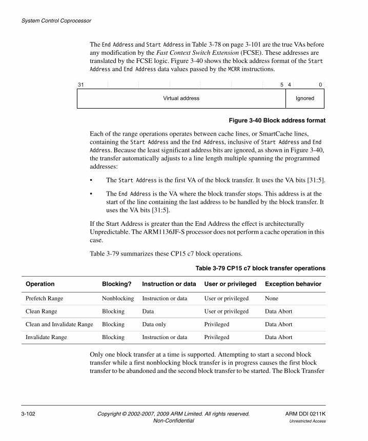
System Control Coprocessor
The End Address and Start Address in Table 3-78 on page 3-101 are the true VAs before any modification by the Fast Context Switch Extension (FCSE). These addresses are translated by the FCSE logic. Figure 3-40 shows the block address format of the Start Address and End Address data values passed by the MCRR instructions.
Figure 3-40 Block address format
Each of the range operations operates between cache lines, or SmartCache lines, containing the Start Address and the End Address, inclusive of Start Address and End Address. Because the least significant address bits are ignored, as shown in Figure 3-40, the transfer automatically adjusts to a line length multiple spanning the programmed addresses:
• The Start Address is the first VA of the block transfer. It uses the VA bits [31:5].
• The End Address is the VA where the block transfer stops. This address is at the start of the line containing the last address to be handled by the block transfer. It uses the VA bits [31:5].
If the Start Address is greater than the End Address the effect is architecturally Unpredictable. The ARM1136JF-S processor does not perform a cache operation in this case.
Table 3-79 summarizes these CP15 c7 block operations.
Only one block transfer at a time is supported. Attempting to start a second block transfer while a first nonblocking block transfer is in progress causes the first block transfer to be abandoned and the second block transfer to be started. The Block Transfer
Virtual address
31 4 0
Ignored
5
Table 3-79 CP15 c7 block transfer operations
Operation Blocking? Instruction or data User or privileged Exception behavior
Prefetch Range Nonblocking Instruction or data User or privileged None
Clean Range Blocking Data User or privileged Data Abort
Clean and Invalidate Range Blocking Data only Privileged Data Abort
Invalidate Range Blocking Instruction or data Privileged Data Abort
3-102 Copyright © 2002-2007, 2009 ARM Limited. All rights reserved. ARM DDI 0211KNon-Confidential Unrestricted Access
System Control Coprocessor
Status Register indicates if a block transfer is in progress. Block transfers must be stopped on a context switch. You can stop a prefetch range operation using the Stop Prefetch Range operation, as listed in Figure 3-35 on page 3-91.
All block transfers are interruptible. When blocking transfers are interrupted, the R14 value that is captured is: (address of the instruction that launched the block operation) + 4 This enables the standard return mechanism for interrupts to restart the operation.
ARM1136JF-S processors enable following instructions to be executed while a nonblocking Prefetch Range instruction is being executed. The R14 value captured on an interrupt is determined by the execution state presented to the interrupt in following instruction stream.
If the FCSE PID is changed while a Prefetch Range operation is running, it is Unpredictable at which point this change is seen by the Prefetch Range.
Exception behavior on block transfer (MCRR) operations
The blocking block transfers cause a Data Abort on a translation fault if a valid page table entry cannot be fetched. The FAR indicates the address that caused the fault, and the DFSR indicates the reason for the fault.
Any fault on a Prefetch Range operation results in the operation failing without signaling an error.
Cache cleaning and invalidating operations for TCM configured as SmartCache
All cache line and block cleaning and invalidation operations based on Virtual Address, as defined in CP15 c7, include TCM regions that are configured as SmartCache.
The Set/Way operations are supported for the TCMs operating as SmartCache. In this case, the Way number is taken to be the TCM number, and the meaning of the set number is unchanged. Figure 3-37 on page 3-96 shows how the bottom bit of the Set/Way is used to distinguish between Set/Way operations applied to the cache and Set/Way operations applied to TCM.
The line length of the TCM operating as SmartCache must be the same as the cache line length, defined in the Cache Type Register.
The TC bit, bit 0, indicates if this register refers to the TCMs rather than the cache:
TC = 0 Register refers to the cache.
TC = 1 Register refers to the TCM.
Invalidate and Clean Entire Cache operations do not affect the TCMs.
ARM DDI 0211K Copyright © 2002-2007, 2009 ARM Limited. All rights reserved. 3-103Unrestricted Access Non-Confidential
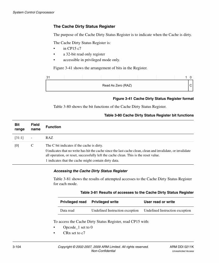
System Control Coprocessor
The Cache Dirty Status Register
The purpose of the Cache Dirty Status Register is to indicate when the Cache is dirty.
The Cache Dirty Status Register is:
• in CP15 c7
• a 32-bit read only register
• accessible in privileged mode only.
Figure 3-41 shows the arrangement of bits in the Register.
Figure 3-41 Cache Dirty Status Register format
Table 3-80 shows the bit functions of the Cache Dirty Status Register.
Accessing the Cache Dirty Status Register
Table 3-81 shows the results of attempted accesses to the Cache Dirty Status Register for each mode.
To access the Cache Dirty Status Register, read CP15 with:
• Opcode_1 set to 0
• CRn set to c7
CRead As Zero (RAZ)
31 1 0
Table 3-80 Cache Dirty Status Register bit functions
Bit range
Field name
Function
[31:1] - RAZ
[0] C The C bit indicates if the cache is dirty.
0 indicates that no write has hit the cache since the last cache clean, clean and invalidate, or invalidate all operation, or reset, successfully left the cache clean. This is the reset value.
1 indicates that the cache might contain dirty data.
Table 3-81 Results of accesses to the Cache Dirty Status Register
Privileged read Privileged write User read or write
Data read Undefined Instruction exception Undefined Instruction exception
3-104 Copyright © 2002-2007, 2009 ARM Limited. All rights reserved. ARM DDI 0211KNon-Confidential Unrestricted Access

System Control Coprocessor
• CRm set to c10
• Opcode_2 set to 6.
For example:
MRC p15, 0, <Rd>, c7, c10, 6 ; Read Cache Dirty Status Register
Flush operations
Table 3-82 shows the flush operations and instructions available through c7.
Note For the Flush Branch Target Cache Entry operation, the MVA does not have to be cache line aligned. See MVA format on page 3-98 for details of the MVA format needed for the c7 entry for this operation.
Flushing the prefetch buffer has the effect that all instructions occurring in program order after this instruction are fetched from the memory system after the execution of this instruction, including the level one cache or TCM. This operation is useful for ensuring the correct execution of self-modifying code. See Explicit Memory Barriers on page 6-31.
The Data Synchronization Barrier operation
The purpose of the Data Synchronization Barrier operation is to ensure that all outstanding explicit memory transactions complete before any following instructions begin. This ensures that data in memory is up-to-date before the processor executes any more instructions.
Table 3-82 Cache operations flush functions
Instruction Data Function
MCR p15, 0, <Rd>, c7, c5, 4 SBZ Flush Prefetch Buffera.
a. This operation is accessible in both User and privileged modes of operation. The other operations are normally only accessible in privileged mode, but see footnote b.
MCR p15, 0, <Rd>, c7, c5, 6 SBZ Flush Entire Branch Target Cacheb.
b. When in Debug state, this operation is accessible in both privileged and User modes of operation.
MCR p15, 0, <Rd>, c7, c5, 7 MVAc
c. As explained in MVA format on page 3-98, the range of MVA bits used in this function is different to the range of bits used in other functions that have MVA data.
Flush Branch Target Cache Entry, using MVA.
ARM DDI 0211K Copyright © 2002-2007, 2009 ARM Limited. All rights reserved. 3-105Unrestricted Access Non-Confidential

System Control Coprocessor
Note Historically, this operation has been referred to as Drain Write Buffer or Data Write Barrier (DWB). From ARMv6, these names, and the use of DWB, are deprecated in favor of the new Data Synchronization Barrier name (DSB). DSB better reflects the functionality provided in ARMv6; it is architecturally defined to include all cache, TLB and branch prediction maintenance operations as well as explicit memory operations.
The Data Synchronization Barrier operation is:
• accessed through CP15 c7
• a 32-bit write-only operation
• accessible in both User and privileged modes.
This operation acts as an explicit memory barrier. The instruction completes when all explicit memory transactions occurring in program order before this instruction are completed. No instructions occurring in program order after this instruction are executed until this instruction completes. Therefore, no explicit memory transactions occurring in program order after this instruction are started until this instruction completes. See Explicit Memory Barriers on page 6-31.
It can be used instead of Strongly Ordered memory when the timing of specific stores to the memory system has to be controlled. For example, when a store to an interrupt acknowledge location must be completed before interrupts are enabled.
The Data Synchronization Barrier operation can be executed in both privileged and User modes of operation.
Accessing the Data Synchronization Barrier operation
Table 3-83 shows the results of attempted accesses to the Data Synchronization Barrier operation for each mode.
To use the Data Synchronization Barrier operation you write CP15 with:
• <Rd> SBZ
• Opcode_1 set to 0
• CRn set to c7
• CRm set to c10
• Opcode_2 set to 4.
Table 3-83 Results of accesses to the Data Synchronization Barrier operation
Privileged read Privileged write User read User write
Undefined Instruction exception Operation executes Undefined Instruction exception Operation executes
3-106 Copyright © 2002-2007, 2009 ARM Limited. All rights reserved. ARM DDI 0211KNon-Confidential Unrestricted Access

System Control Coprocessor
For example:
MCR p15,0,<Rd>,c7,c10,4 ; Data Synchronization Barrier operation
For more information, see Explicit Memory Barriers on page 6-31.
Note The W bit that normally enables the Write Buffer is not implemented in ARM1136JF-S processors, see c1, Control Register on page 3-63.
The Data Memory Barrier operation
The purpose of the Data Memory Barrier operation is to ensure that all outstanding explicit memory transactions complete before any following explicit memory transactions begin. This ensures that data in memory is up-to-date before any memory transaction that depends on it.
The Data Memory Barrier operation is:
• accessed through CP15 c7
• a 32-bit write-only operation
• accessible in both User and privileged modes.
Accessing the Data Memory Barrier operation
Table 3-84 shows the results of attempted accesses to the Data Memory Barrier operation for each mode.
To use the Data Memory Barrier operation you write CP15 with:
• <Rd> SBZ
• Opcode_1 set to 0
• CRn set to c7
• CRm set to c10
• Opcode_2 set to 5.
For example:
MCR p15,0,<Rd>,c7,c10,5 ; Data Memory Barrier operation
Table 3-84 Results of accesses to the Data Memory Barrier operation
Privileged read Privileged write User read User write
Undefined Instruction exception Operation executes Undefined Instruction exception Operation executes
ARM DDI 0211K Copyright © 2002-2007, 2009 ARM Limited. All rights reserved. 3-107Unrestricted Access Non-Confidential

System Control Coprocessor
For more information, see Explicit Memory Barriers on page 6-31.
The Wait For Interrupt operation
The purpose of the Wait For Interrupt operation is to put the processor in to a low power state, see Standby mode on page 10-3.
The Wait For Interrupt operation is:
• accessed through CP15 c7
• a 32-bit write only operation
• accessible in privileged mode only.
Accessing the Wait For Interrupt operation
Table 3-85 shows the results of attempted accesses to the Wait For Interrupt operation for each mode.
To access the Wait For Interrupt operation you write CP15 with:
• <Rd> SBZ
• Opcode_1 set to 0
• CRn set to c7
• CRm set to c0
• Opcode_2 set to 4.
For example:
MCR p15,0,<Rd>,c7,c0,4 ; Wait For Interrupt
This puts the processor into a low-power state and stops it executing following instructions until an interrupt, an imprecise external abort, or a debug request occurs, regardless of whether the interrupts or external imprecise aborts are disabled by the masks in the CPSR. When an interrupt does occur, the MCR instruction completes. If interrupts are enabled, the IRQ or FIQ handler is entered as normal. The return link in R14_irq or R14_fiq contains the address of the MCR instruction plus 8, so that the normal instruction used for interrupt return (SUBS PC,R14,#4) returns to the instruction following the MCR.
Table 3-85 Results of accesses to the Wait For Interrupt operation
Privileged read Privileged write User read or write
Undefined Instruction exception Operation executes Undefined Instruction exception
3-108 Copyright © 2002-2007, 2009 ARM Limited. All rights reserved. ARM DDI 0211KNon-Confidential Unrestricted Access

System Control Coprocessor
Block transfer control operations
The use of MCRR instructions for block transfer operations is described in Invalidate, Clean and Prefetch cache operations for address ranges on page 3-101. CP15 register c7 includes two additional operations that provide control of MCRR block transfer operations:
• the read-only Read Block Transfer Register enables you to find out whether a block transfer operation is in progress
• the write-only Stop Prefetch Range operation stops any prefetch range operation that is in progress.
Table 3-86 shows these CP15 register c7 operations.
The Block Transfer Status Register
The purpose of the Block Transfer Status Register is to show whether a CP15 c7 block transfer operation is active.
The Block Transfer Status Register is:
• in CP15 c7
• a 32 bit read-only register
• accessible in User and privileged modes.
Figure 3-42 shows the arrangement of bits in the register.
Figure 3-42 Block Transfer Status Register format
Table 3-86 CP15 Register c7 block transfer control MCR/MRC operations
Function Data Instruction
Read Block Transfer Status Registera Data MRC p15,0,<Rd>,c7,c12,4
Stop Prefetch Rangea
a. These operations are accessible in both User and privileged modes of operation (see Accesses to CP15 c7 operations on page 3-92).
SBZ MCR p15,0,<Rd>,c7,c12,5
RRead As Zero (RAZ)
31 1 0
ARM DDI 0211K Copyright © 2002-2007, 2009 ARM Limited. All rights reserved. 3-109Unrestricted Access Non-Confidential

System Control Coprocessor
Table 3-87 shows the bit functions of the Block Transfer Status Register.
Accessing the Block Transfer Status Register
Table 3-88 shows the results of attempted accesses to the Block Transfer Status Register for each mode.
To access the Block Transfer Status Register you read CP15 with:
• Opcode_1 set to 0
• CRn set to c7
• CRm set to c12
• Opcode_2 set to 4.
For example:
MRC p15,0,<Rd>,c7,c12,4 ; Read Block Transfer Status Register
Accessing the Stop Prefetch Range operation
Table 3-89 shows the results of attempted accesses to the Stop Prefetch Range operation for each mode.
To access the Stop Prefetch Range operation you write CP15 with:
• <Rd> SBZ
Table 3-87 Block Transfer Status Register bit functions
Bit range Field name Function
[31:1] - RAZ
[0] R The R bit indicates if there is a block prefetch operation in progress.
0 indicates that no block prefetch operation is in progress. This is the reset value.
1 indicates that a block prefetch operation is in progress.
Table 3-88 Results of accesses to the Block Transfer Status Register
Privileged read Privileged write User read User write
Data read Undefined Instruction exception Data read Undefined Instruction exception
Table 3-89 Results of accesses to the Stop Prefetch Range operation
Privileged read Privileged write User read User write
Undefined Instruction exception Operation executes Undefined Instruction exception Operation executes
3-110 Copyright © 2002-2007, 2009 ARM Limited. All rights reserved. ARM DDI 0211KNon-Confidential Unrestricted Access
System Control Coprocessor
• Opcode_1 set to 0
• CRn set to c7
• CRm set to c12
• Opcode_2 set to 5.
For example:
MCR p15,0,<Rd>,c7,c12,5 ; Stop Prefetch Range
3.3.18 c8, TLB Operations Register (invalidate TLB operation)
The purpose of the TLB Operations Register is to manage the Translation Lookaside Buffer (TLB). It is used to invalidate TLB entries, and you use it to do one of:
• invalidate all the unlocked entries in the TLB
• invalidate all TLB entries for an area of memory, before the MMU remaps it
• invalidate all TLB entries that match an ASID value.
In general, when you access the TLB Operations Register, you choose whether to operate on:
• Instruction TLB
• Data TLB
• Unified TLB.
Note The ARM1136JF-S processor has a unified TLB. Any TLB operations specified for the Instruction or Data TLB perform the equivalent operation on the unified TLB.
The TLB Operations Register is:
• in CP15 c8
• a 32-bit write-only register
• accessible in privileged mode only.
Accessing the TLB Operations Register
Table 3-90 shows the results of attempted accesses to the TLB Operations Register for each mode.
Table 3-90 Results of accesses to the TLB Operations Register
Privileged read Privileged write User read or write
Undefined Instruction exception Data write Undefined Instruction exception
ARM DDI 0211K Copyright © 2002-2007, 2009 ARM Limited. All rights reserved. 3-111Unrestricted Access Non-Confidential

System Control Coprocessor
To access the TLB Operations Register you write CP15 with:
• Opcode_1 set to 0
• CRn set to c8
• CRm set to:
— c5, Instruction TLB
— c6, Data TLB
— c7, Unified TLB
• Opcode_2 set to:
— 0, Invalidate TLB unlocked entries
— 1, Invalidate TLB Entry by MVA
— 2, Invalidate TLB Entry on ASID Match.
For example, to invalidate all the unlocked entries in the Instruction TLB:
MCR p15,0,<Rd>,c8, c5, 0 ; Write TLB Operations Register
Functions that update the contents of the TLB are executed in program order. Therefore, an explicit data access before the TLB Operations Register access uses the old TLB contents, and an explicit data access after the TLB Operations Register access uses the new TLB contents. For instruction accesses, TLB updates are guaranteed to have taken effect before the next pipeline flush. This includes flush prefetch buffer operations and exception return sequences.
Invalidate TLB unlocked entries
Invalidate TLB unlocked entries invalidates all the unlocked entries in the TLB. This function causes a flush of the prefetch buffer. Therefore, all instructions that follow are fetched after the TLB invalidation.
When you invalidate TLB unlocked entries, c8 register bits[31:0] SBZ.
Invalidate TLB Entry by MVA
You can use Invalidate TLB Entry by MVA to invalidate all TLB entries for an area of memory before you remap.
You must perform an Invalidate TLB Entry by MVA of an MVA in each area you want to remap (section, small page, or large page).
This function invalidates a TLB entry that matches the provided MVA and ASID, or a global TLB entry that matches the provided MVA.
This function invalidates a matching locked entry.
3-112 Copyright © 2002-2007, 2009 ARM Limited. All rights reserved. ARM DDI 0211KNon-Confidential Unrestricted Access

System Control Coprocessor
The Invalidate TLB Entry by MVA operation uses an MVA and ASID as an argument. Figure 3-43 shows the c8 register format for this.
Figure 3-43 TLB Operations Register format for Invalidate Entry by MVA
Invalidate TLB Entry on ASID Match
This is a single interruptible operation that invalidates all TLB entries that match the provided ASID value.
This function invalidates locked entries but does not invalidate entries marked as global.
In this processor this operation takes several cycles to complete and the instruction is interruptible. When interrupted the R14 state is set to indicate that the MCR instruction has not executed. Therefore, R14 points to the address of the MCR + 4. The interrupt routine then automatically restarts at the MCR instruction.
If the processor interrupts and later restarts this operation, any entries fetched into the TLB by the interrupt that uses the provided ASID are invalidated by the restarted invalidation.
The Invalidate TLB Entry on ASID Match function requires an ASID as an argument. Figure 3-44 shows the c8 register format for this.
Figure 3-44 TLB Operations Register format for Invalidate Entry on ASID Match
3.3.19 c9, Data and Instruction Cache Lockdown Registers
There are two cache lockdown registers:
• Data Cache Lockdown Register
• Instruction Cache Lockdown Register.
The purpose of the data and instruction cache lockdown registers is to provide a means to lock down the caches and therefore provide some control over pollution that applications might cause. With these registers you can lock down each cache way independently.
Modified Virtual Address (MVA)
31 8 7 0
SBZ ASID
1112
31 8 7 0
SBZ ASID
ARM DDI 0211K Copyright © 2002-2007, 2009 ARM Limited. All rights reserved. 3-113Unrestricted Access Non-Confidential

System Control Coprocessor
The cache lockdown registers are:
• in CP15 c9
• two 32-bit read/write registers
• accessible in privileged mode only.
Figure 3-45 shows the arrangement of bits in these registers.
Figure 3-45 Instruction and Data Cache Lockdown Registers format
Table 3-91 shows the bit functions of the Cache Lockdown Registers.
ARM1136JF-S processors only support one method of using cache lockdown registers, called Format C. This is a cache way based scheme that gives a traditional lockdown function to lock critical regions in the cache.
A locking bit for each cache way determines if the normal cache allocation mechanism is able to access that cache way. Bit[14] of the Control Register, the RR bit, controls whether a random or a round-robin cache allocation policy is used, see c1, Control Register on page 3-63 for more information.
ARM1136JF-S processors have an associativity of 4. If all ways are locked, the ARM1136JF-S processor behaves as if only ways 3 to 1 are locked and way 0 is unlocked.
SBO
31 4 3 0L bit
for eachcache way
Table 3-91 Instruction and data cache lockdown register bit functions
Bit range
Field name Function
[31:4] SBO UNP on reads, SBO on writes.
[3:0] L bit for each cache way
Locks each cache way individually. The L bits for cache ways 3 to 0 are bits [3:0] respectively. On a line fill to the cache, data is allocated to unlocked cache ways as determined by the standard replacement algorithm. Data is not allocated to locked cache ways.
If a cache way is not implemented, then the L bit for that way is hardwired to 1, and writes to that bit are ignored.
0 indicates that this cache way is not locked. Allocation to this cache way is determined by the standard replacement algorithm. This is the reset state.
1 indicates that this cache way is locked. No allocation is performed to this cache way.
3-114 Copyright © 2002-2007, 2009 ARM Limited. All rights reserved. ARM DDI 0211KNon-Confidential Unrestricted Access

System Control Coprocessor
Accessing the Cache Lockdown Registers
Table 3-92 shows the results of attempted accesses to the Cache Lockdown Registers for each mode.
To access the Cache Lockdown Registers you read or write CP15 with:
• Opcode_1 set to 0
• CRn set to c9
• CRm set to c0
• Opcode_2 set to:
— 0 to access the Data Cache Lockdown Register
— 1 to access the Instruction Cache Lockdown Register.
For example:
MRC p15, 0, <Rd>, c9, c0, 0 ; Read Data Cache Lockdown RegisterMCR p15, 0, <Rd>, c9, c0, 0 ; Write Data Cache Lockdown RegisterMRC p15, 0, <Rd>, c9, c0, 1 ; Read Instruction Cache Lockdown RegisterMCR p15, 0, <Rd>, c9, c0, 1 ; Write Instruction Cache Lockdown Register
Using the Cache Lockdown Registers
The system must only change a cache lockdown register when it is certain that all outstanding accesses that might cause a cache line fill are complete. For this reason, the processor must execute a Data Synchronization Barrier instruction before the cache lockdown register changes, see Accessing the Data Synchronization Barrier operation on page 3-106.
The following procedure for lock down into a data or instruction cache way i, with N cache ways, using Format C, ensures that only the target cache way i is locked down.
This is the architecturally defined method for locking data into caches:
1. Ensure that no processor exceptions can occur during the execution of this procedure, by disabling interrupts. If this is not possible, all code and data used by any exception handlers that can be called must be treated as code and data prior to step 2.
Table 3-92 Results of accesses to the Cache Lockdown Registers
Privileged read Privileged write User read or write
Data read Data write Undefined Instruction exception
ARM DDI 0211K Copyright © 2002-2007, 2009 ARM Limited. All rights reserved. 3-115Unrestricted Access Non-Confidential

System Control Coprocessor
2. Ensure that all data used by the following code, apart from the data that is to be locked down, is either:
• in an uncacheable area of memory, including the TCM
• in an already locked cache way.
3. Ensure that the data to be locked down is in a Cacheable area of memory.
4. Ensure that the data to be locked down is not already in the cache, using cache Clean and/or Invalidate instructions as appropriate.
5. Enable allocation to the target cache way by writing to CP15 c9, with the CRm field set to 0, setting L equal to 0 for bit i and L equal to 1 for all other ways.
6. Ensure that the memory cache line is loaded into the cache by using an LDR instruction to load a word from the memory cache line, for each of the cache lines to be locked down in cache way i.
7. Write to CP15 c9, CRm = c0, setting L to 1 for bit i and restore all the other bits to the values they had before this routine was started.
3.3.20 c9, Data TCM Region Register
The purpose of the Data TCM Region Register is to describe the physical base address and size of the Data TCM region and to provide a mechanism to enable it.
The Data TCM Region Register is:
• in CP15 c9
• a 32-bit read/write register
• accessible in privileged mode only.
Note ARM1136JF-S processors have a single TCM on each side, Data and Instruction. See c9, Instruction TCM Region Register on page 3-118 for details of configuring the Instruction TCM region.
Figure 3-46 on page 3-117 shows the arrangement of bits in the Data TCM Region Register.
3-116 Copyright © 2002-2007, 2009 ARM Limited. All rights reserved. ARM DDI 0211KNon-Confidential Unrestricted Access

System Control Coprocessor
Figure 3-46 Data TCM Region Register format
Table 3-93 shows the bit functions of the Data TCM Region Register.
Table 3-94 shows the Size field encoding value for each memory size. All other values are reserved.
Base address (physical address)
31 12 11 7 6 2 1 0
SBZ/UNP Size
SC En
Table 3-93 Data TCM Region Register bit functions
Bit range Field name Function
[31:12] Base address The physical base address of the TCM. The base address must be aligned to the size of the TCM. Any bits in the range [(log2(RAMSize)-1):12] are ignored.
The base address is 0 at Reset.
[11:7] - UNP/SBZ.
[6:2] Size On reads, the Size field indicates the size of the TCM, see Table 3-94.a
[1] SC Indicates if the TCM is enabled as SmartCache:
0 = Local RAM. This is the reset value.
1 = SmartCache.
[0] En The En bit indicates if the TCM is enabled:
0 = TCM disabled. This is the reset value.
1 = TCM enabled.
a. On writes this field is ignored. For more details see Tightly-coupled memory on page 7-8.
Table 3-94 Size field encoding for Data TCM Region Register
Size field Memory size
b00000 0KB
b00011 4KB
b00100 8KB
ARM DDI 0211K Copyright © 2002-2007, 2009 ARM Limited. All rights reserved. 3-117Unrestricted Access Non-Confidential

System Control Coprocessor
Accessing the Data TCM Region Register
Table 3-95 shows the results of attempted accesses to the Data TCM Region Register for each mode.
To access the Data TCM Region Register you read or write CP15 with:
• Opcode_1 set to 0
• CRn set to c9
• CRm set to c1
• Opcode_2 set to 0.
For example:
MRC p15, 0, <Rd>, c9, c1, 0 ; Read Data TCM Region RegisterMCR p15, 0, <Rd>, c9, c1, 0 ; Write Data TCM Region Register
Changing the Data TCM Region Register while a Prefetch Range or DMA operation is running has Unpredictable effects.
3.3.21 c9, Instruction TCM Region Register
The purpose of the Instruction TCM Region Register is to describe the physical base address and size of the Instruction TCM region and to provide a mechanism to enable it.
The Instruction TCM Region Register is:
• in CP15 c9
• a 32-bit read/write register
• accessible in privileged mode only.
b00101 16KB
b00110 32KB
b00111 64KB
Table 3-95 Results of accesses to the Data TCM Region Register
Privileged read Privileged write User read or write
Data read Data write Undefined Instruction exception
Table 3-94 Size field encoding for Data TCM Region Register (continued)
Size field Memory size
3-118 Copyright © 2002-2007, 2009 ARM Limited. All rights reserved. ARM DDI 0211KNon-Confidential Unrestricted Access

System Control Coprocessor
Note ARM1136JF-S processors have a single TCM on each side, Data and Instruction. See c9, Data TCM Region Register on page 3-116 for details of configuring the Data TCM region.
Figure 3-47 shows the arrangement of bits in the Instruction TCM Region Register.
Figure 3-47 Instruction TCM Region Register format
Table 3-96 shows the bit functions of the Instruction TCM Region Register.
Base address (physical address)
31 12 11 7 6 2 1 0
SBZ/UNP Size
SC En
Table 3-96 Instruction TCM Region Register bit functions
Bit range Field name Function
[31:12] Base address The physical base address of the TCM. The base address must be aligned to the size of the TCM. Any bits in the range [(log2(RAMSize)-1):12] are ignored.
The base address is 0 at Reset.
[11:7] - UNP/SBZ.
[6:2] Size On reads, the Size field indicates the size of the TCM, see Table 3-97 on page 3-120.a
[1] SC Indicates if the TCM is enabled as SmartCache:
0 = Local RAM. This is the reset value.
1 = SmartCache.
[0] En The En bit indicates if the TCM is enabled:
0 = TCM disabled. This is the reset value.
1 = TCM enabled.
On reset, the value of the TCM enable bit is determined by the pin INITRAM:
• INITRAM LOW sets En to 0
• INITRAM HIGH sets En to 1.b
a. On writes this field is ignored. For more details see Tightly-coupled memory on page 7-8.b. When INITRAM is HIGH the Instruction TCM is enabled directly from reset, with a Base address of 0x00000. When the
processor comes out of reset, it executes the instructions in the Instruction TCM instead of fetching instructions from external memory, except when the processor uses high vectors.
ARM DDI 0211K Copyright © 2002-2007, 2009 ARM Limited. All rights reserved. 3-119Unrestricted Access Non-Confidential

System Control Coprocessor
Table 3-97 shows the Size field encoding value for each memory size. All other values are reserved.
Accessing the Instruction TCM Region Register
Table 3-98 shows the results of attempted accesses to the Instruction TCM Region Register for each mode.
To access the Instruction TCM Region Register you read or write CP15 with:
• Opcode_1 set to 0
• CRn set to c9
• CRm set to c1
• Opcode_2 set to 1.
For example:
MRC p15, 0, <Rd>, c9, c1, 1 ; Read Instruction TCM Region RegisterMCR p15, 0, <Rd>, c9, c1, 1 ; Write Instruction TCM Region Register
Changing the Instruction TCM Region Register while a Prefetch Range or DMA operation is running has Unpredictable effects.
Table 3-97 Size field encoding for Instruction TCM Region Register
Size field Memory size
b00000 0KB
b00011 4KB
b00100 8KB
b00101 16KB
b00110 32KB
b00111 64KB
Table 3-98 Results of accesses to the Instruction TCM Region Register
Privileged read Privileged write User read or write
Data read Data write Undefined Instruction exception
3-120 Copyright © 2002-2007, 2009 ARM Limited. All rights reserved. ARM DDI 0211KNon-Confidential Unrestricted Access
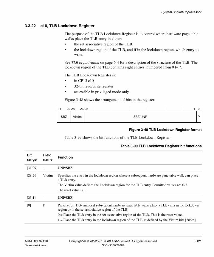
System Control Coprocessor
3.3.22 c10, TLB Lockdown Register
The purpose of the TLB Lockdown Register is to control where hardware page table walks place the TLB entry in either:
• the set associative region of the TLB.
• the lockdown region of the TLB, and if in the lockdown region, which entry to write.
See TLB organization on page 6-4 for a description of the structure of the TLB. The lockdown region of the TLB contains eight entries, numbered from 0 to 7.
The TLB Lockdown Register is:
• in CP15 c10
• 32-bit read/write register
• accessible in privileged mode only.
Figure 3-48 shows the arrangement of bits in the register.
Figure 3-48 TLB Lockdown Register format
Table 3-99 shows the bit functions of the TLB Lockdown Register.
PSBZ
31 29 28 26 25 1 0
Victim SBZ/UNP
Table 3-99 TLB Lockdown Register bit functions
Bit range
Field name
Function
[31:29] - UNP/SBZ.
[28:26] Victim Specifies the entry in the lockdown region where a subsequent hardware page table walk can place a TLB entry.
The Victim value defines the Lockdown region for the TLB entry. Permitted values are 0-7.
The reset value is 0.
[25:1] - UNP/SBZ.
[0] P Preserve bit. Determines if subsequent hardware page table walks place a TLB entry in the lockdown region or in the set associative region of the TLB.
0 = Place the TLB entry in the set associative region of the TLB. This is the reset value.
1 = Place the TLB entry in the lockdown region of the TLB as defined by the Victim bits [28:26].
ARM DDI 0211K Copyright © 2002-2007, 2009 ARM Limited. All rights reserved. 3-121Unrestricted Access Non-Confidential

System Control Coprocessor
TLB entries in the lockdown region are preserved:
• Invalidate TLB operations only invalidate the unpreserved entries in the TLB. This means they only invalidate entries in the set-associative region.
• Invalidate TLB Single Entry operations invalidate any TLB entry corresponding to the Modified Virtual Address given in Rd, regardless of the preserved state of the entry. This means that they invalidate the specified entry regardless of whether it is in the lockdown region or in the set-associative region of the TLB.
See c8, TLB Operations Register (invalidate TLB operation) on page 3-111 for a description of the TLB invalidate operations.
The victim automatically increments after any table walk that results in an entry being written into the lockdown part of the TLB.
Accessing the TLB Lockdown Register
Table 3-100 shows the results of attempted accesses to the TLB Lockdown Register for each mode.
To access the TLB Lockdown Register you read or write CP15 with:
• Opcode_1 set to 0
• CRn set to c10
• CRm set to c0
• Opcode_2 set to 0.
For example:
MRC p15, 0, <Rd>, c10, c0, 0 ; Read TLB Lockdown RegisterMCR p15, 0, <Rd>, c10, c0, 0 ; Write TLB Lockdown Register.
Example 3-3 is a code sequence that locks down an entry to the current victim.
Example 3-3 Lock down an entry to the current victim
ADR R1,LockAddr ; set R1 to the value of the address to be locked downMCR p15,0,R1,c8,c7,1 ; invalidate TLB single entry to ensure that
; LockAddr is not already in the TLB
Table 3-100 Results of accesses to the Data TLB Lockdown Register
Privileged read Privileged write User read or write
Data read Data write Undefined Instruction exception
3-122 Copyright © 2002-2007, 2009 ARM Limited. All rights reserved. ARM DDI 0211KNon-Confidential Unrestricted Access

System Control Coprocessor
MRC p15,0,R0,c10,c0,0 ; read the lockdown registerORR R0,R0,#1 ; set the preserve bitMCR p15,0,R0,c10,c0,0 ; write to the lockdown registerLDR R1,[R1] ; TLB will miss, and entry will be loadedMRC p15,0,R0,c10,c0,0 ; read the lockdown register (victim will have
; incremented)BIC R0,R0,#1 ; clear preserve bitMCR p15,0,R0,c10,c0,0 ; write to the lockdown register
ARM DDI 0211K Copyright © 2002-2007, 2009 ARM Limited. All rights reserved. 3-123Unrestricted Access Non-Confidential

System Control Coprocessor
3.3.23 c10, TEX remap registers
The purpose of the TEX remap registers is to remap memory region attributes encoded by the TEX[2:0], C, and B bits in the page tables that are used by the MMU. For details of memory remap, see Memory region attributes on page 6-15.
Note In addition to these TEX memory region remap registers, for other memory remap register descriptions see c15, Memory remap registers on page 3-162.
The TEX remap registers are:
• in CP15 c10
• two 32-bit read/write registers, described in the following sections:
— the Primary Region Remap Register, see Primary Region Remap Register (PRRR) on page 3-125
— the Normal Memory Remap Register, see Normal Memory Remap Register (NMRR) on page 3-127
see Accessing the TEX remap registers on page 3-128 for more information about these registers
• accessible in privileged mode only
• only available from the rev1 (r1p0) release of the ARM1136JF-S processor.
These registers apply to all memory accesses and this includes accesses from the Data side, Instruction side, and DMA. Table 3-101 on page 3-125 shows the purposes of the individual bits in the Primary Region Remap Register. Table 3-103 on page 3-127 shows the purposes of the individual bits in the Normal Memory Remap Register.
Note The behavior of the memory region remap registers depends on the TEX Remap Enable (TRE) bit, see c1, Control Register on page 3-63. If this bit is clear these registers do not have any effect. The TRE bit, and TEX remapping, are only implemented from the rev1 (r1p0) release of the ARM1136JF-S processor.
3-124 Copyright © 2002-2007, 2009 ARM Limited. All rights reserved. ARM DDI 0211KNon-Confidential Unrestricted Access

System Control Coprocessor
Primary Region Remap Register (PRRR)
This register is only available from the rev1 (r1p0) release of the ARM1136JF-S processor.
Figure 3-49 shows the arrangement of the bits in the register.
Figure 3-49 Primary Region Remap Register format
Table 3-101 shows the bit functions of the Primary Region Remap Register.
Remap shareable attribute, S=1, Normal regions
01 0 0 1 1 0 0 0 1 0 1 0 1 0 1 0 0 1 0
31 20 19 18 17 16 15 14 13 12 11 10 9 8 7 6 5 4 3 2 1 0
UNP/SBZ
Remap shareable attribute, S=0, Normal regions
Remap shareable attribute, S=1, Device regions
Remap shareable attribute, S=0, Device regions
Remap for given (binary) value of {TEX[0],C,B}110 101 100 011 010 001111 000
Register values shown are the reset values
Table 3-101 Primary Region Remap Register bit functions
Bit range Field name Reset valuea Function
[31:20] - UNP/SBZ
[19] - 1 Remaps shareable attribute when S=1 for Normal regionsb.
[18] - 0 Remaps shareable attribute when S=0 for Normal regionsb
[17] - 0 Remaps shareable attribute when S=1 for Device regionsb
[16] - 1 Remaps shareable attribute when S= 0 for Device regionsb
[15:14] - b10 Remaps {TEX[0],C,B} = b111
[13:12] - b00 Remaps {TEX[0],C,B} = b110
[11:10] - b10 Remaps {TEX[0],C,B} = b101
[9:8] - b10 Remaps {TEX[0],C,B} = b100
[7:6] - b10 Remaps {TEX[0],C,B} = b011
[5:4] - b10 Remaps {TEX[0],C,B} = b010
[3:2] - b01 Remaps {TEX[0],C,B} = b001
[1:0] - b00 Remaps {TEX[0],C,B} = b000
ARM DDI 0211K Copyright © 2002-2007, 2009 ARM Limited. All rights reserved. 3-125Unrestricted Access Non-Confidential
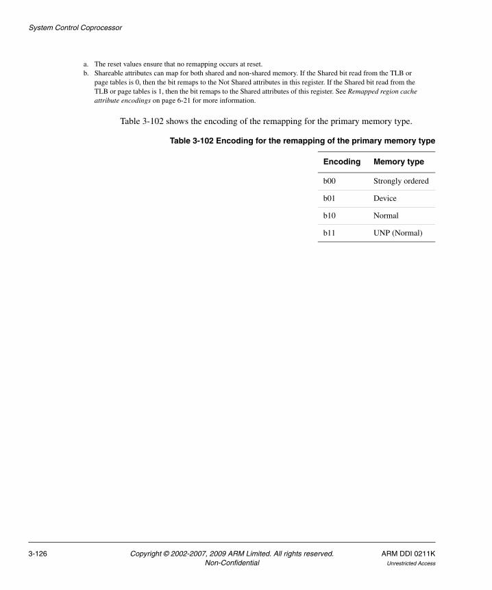
System Control Coprocessor
Table 3-102 shows the encoding of the remapping for the primary memory type.
a. The reset values ensure that no remapping occurs at reset.b. Shareable attributes can map for both shared and non-shared memory. If the Shared bit read from the TLB or
page tables is 0, then the bit remaps to the Not Shared attributes in this register. If the Shared bit read from the TLB or page tables is 1, then the bit remaps to the Shared attributes of this register. See Remapped region cache attribute encodings on page 6-21 for more information.
Table 3-102 Encoding for the remapping of the primary memory type
Encoding Memory type
b00 Strongly ordered
b01 Device
b10 Normal
b11 UNP (Normal)
3-126 Copyright © 2002-2007, 2009 ARM Limited. All rights reserved. ARM DDI 0211KNon-Confidential Unrestricted Access

System Control Coprocessor
Normal Memory Remap Register (NMRR)
This register is only available from the rev1 (r1p0) release of the ARM1136JF-S processor.
Figure 3-50 shows the arrangement of the bits in the register.
Figure 3-50 Normal Memory Remap Register format
Table 3-103 shows the bit functions of the Normal Memory Remap Register.
0 1 0 0 0 1 0 0 1 1 1 0 0 0 0 0
Remap Inner attribute for given (binary) value of {TEX[0],C,B}
110 101 100 011 010 001111 000
Register values shown are the reset values
00 1 0 0 1 0 0 0 1 1 1 0 0 0 0
31 30 29 28 27 26 25 24 23 22 21 20 19 18 17 16 15 14 13 12 11 10 9 8 7 6 5 4 3 2 1 0
110 101 100 011 010 001111 000
Remap Outer attribute for given (binary) value of {TEX[0],C,B}
Table 3-103 Normal Memory Remap Register bit functions
Bit range Field name Reset valuea Function
[31:30] - b01 Remaps Outer attribute for {TEX[0],C,B} = b111
[29:28] - b00 Remaps Outer attribute for {TEX[0],C,B} = b110
[27:26] - b01 Remaps Outer attribute for {TEX[0],C,B} = b101
[25:24] - b00 Remaps Outer attribute for {TEX[0],C,B} = b100
[23:22] - b11 Remaps Outer attribute for {TEX[0],C,B} = b011
[21:20] - b10 Remaps Outer attribute for {TEX[0],C,B} = b010
[19:18] - b00 Remaps Outer attribute for {TEX[0],C,B} = b001
[17:16] - b00 Remaps Outer attribute for {TEX[0],C,B} = b000
[15:14] - b01 Remaps Inner attribute for {TEX[0],C,B} = b111
[13:12] - b00 Remaps Inner attribute for {TEX[0],C,B} = b110
[11:10] - b10 Remaps Inner attribute for {TEX[0],C,B} = b101
[9:8] - b00 Remaps Inner attribute for {TEX[0],C,B} = b100
ARM DDI 0211K Copyright © 2002-2007, 2009 ARM Limited. All rights reserved. 3-127Unrestricted Access Non-Confidential

System Control Coprocessor
Table 3-104 shows the encoding for the Inner or Outer cacheable attribute bit fields I0 to I7 and O0 to O7.
Accessing the TEX remap registers
Table 3-105 shows the results of attempted accesses to the TEX remap registers for each mode.
To access the TEX remap registers you read or write CP15 with:
• Opcode_1 set to 0
• CRn set to c10
• CRm set to c2
[7:6] - b11 Remaps Inner attribute for {TEX[0],C,B} = b011
[5:4] - b10 Remaps Inner attribute for {TEX[0],C,B} = b010
[3:2] - b00 Remaps Inner attribute for {TEX[0],C,B} = b001
[1:0] - b00 Remaps Inner attribute for {TEX[0],C,B} = b000
a. The reset values ensure that no remapping occurs at reset.
Table 3-103 Normal Memory Remap Register bit functions (continued)
Bit range Field name Reset valuea Function
Table 3-104 Remap encoding for Inner or Outer cacheable attributes
Encoding Cacheable attribute
b00 Noncacheable
b01a
a. Not permitted for inner cache attributes. The ARM1136JF-S processor does not support write-allocate on inner caches.
Write-back, allocate on write
b10 Write-through, no allocate on write
b11 Write-back, no allocate on write
Table 3-105 Results of access to the memory region remap registers
Privileged read Privileged write User
Data read Data write Undefined Instruction exception
3-128 Copyright © 2002-2007, 2009 ARM Limited. All rights reserved. ARM DDI 0211KNon-Confidential Unrestricted Access
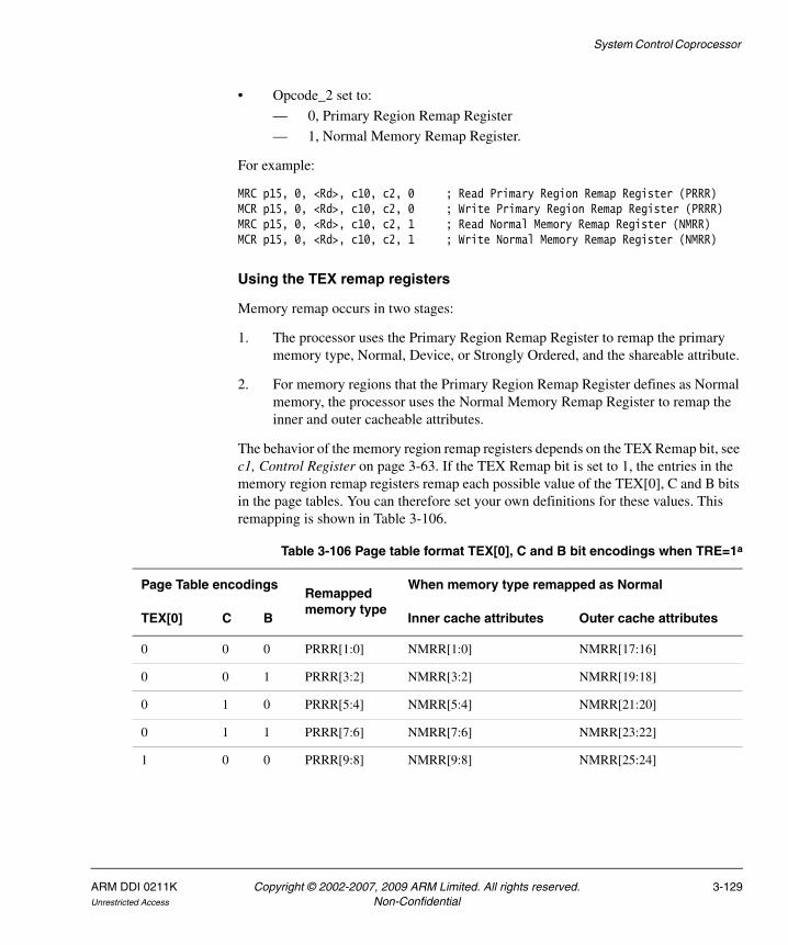
System Control Coprocessor
• Opcode_2 set to:
— 0, Primary Region Remap Register
— 1, Normal Memory Remap Register.
For example:
MRC p15, 0, <Rd>, c10, c2, 0 ; Read Primary Region Remap Register (PRRR)MCR p15, 0, <Rd>, c10, c2, 0 ; Write Primary Region Remap Register (PRRR)MRC p15, 0, <Rd>, c10, c2, 1 ; Read Normal Memory Remap Register (NMRR)MCR p15, 0, <Rd>, c10, c2, 1 ; Write Normal Memory Remap Register (NMRR)
Using the TEX remap registers
Memory remap occurs in two stages:
1. The processor uses the Primary Region Remap Register to remap the primary memory type, Normal, Device, or Strongly Ordered, and the shareable attribute.
2. For memory regions that the Primary Region Remap Register defines as Normal memory, the processor uses the Normal Memory Remap Register to remap the inner and outer cacheable attributes.
The behavior of the memory region remap registers depends on the TEX Remap bit, see c1, Control Register on page 3-63. If the TEX Remap bit is set to 1, the entries in the memory region remap registers remap each possible value of the TEX[0], C and B bits in the page tables. You can therefore set your own definitions for these values. This remapping is shown in Table 3-106.
Table 3-106 Page table format TEX[0], C and B bit encodings when TRE=1a
Page Table encodingsRemappedmemory type
When memory type remapped as Normal
TEX[0] C B Inner cache attributes Outer cache attributes
0 0 0 PRRR[1:0] NMRR[1:0] NMRR[17:16]
0 0 1 PRRR[3:2] NMRR[3:2] NMRR[19:18]
0 1 0 PRRR[5:4] NMRR[5:4] NMRR[21:20]
0 1 1 PRRR[7:6] NMRR[7:6] NMRR[23:22]
1 0 0 PRRR[9:8] NMRR[9:8] NMRR[25:24]
ARM DDI 0211K Copyright © 2002-2007, 2009 ARM Limited. All rights reserved. 3-129Unrestricted Access Non-Confidential

System Control Coprocessor
If the TEX Remap bit is set to 0, the memory region remap registers are not used and no memory remapping takes place. For more information see Memory region attributes on page 6-15.
The memory region remap registers are expected to remain static during normal operation. When you write to the memory region remap registers, you must invalidate the TLB and perform an IMB operation before you can rely on the new written values. You must also stop the DMA if it is running or queued.
3.3.24 c11, DMA registers overview
CP15 register c11 accesses the DMA registers. The value of the CRm field determines which register is accessed. Table 3-107 shows the values of CRm that are used to access the available DMA registers.
1 0 1 PRRR[11:10] NMRR[11:10] NMRR[27:26]
1 1 0 PRRR[13:12] NMRR[13:12] NMRR[29:28[
1 1 1 PRRR[15:14] NMRR[15:14] NMRR[31:30]
a. In this table, PRRR[B:A] indicates a field in the Primary Region Remap Register, and NMRR[B:A] indicates a field in the Normal Memory Remap Register. See Primary Region Remap Register (PRRR) on page 3-125 and Normal Memory Remap Register (NMRR) on page 3-127.
Table 3-106 Page table format TEX[0], C and B bit encodings when TRE=1a (continued)
Page Table encodingsRemappedmemory type
When memory type remapped as Normal
TEX[0] C B Inner cache attributes Outer cache attributes
Table 3-107 DMA registers
Register CRm Opcode_2 Access Notes Description
DMA Identification and Status Registers
c0 Present, Queued, Running, or Interrupting
Privileged only, Read-only
- page 3-132
DMA User Accessibility Register
c1 0 Privileged only, Read/write
- page 3-134
DMA Channel Number Register
c2 0 Read/write - page 3-136
DMA Enable Register c3 Stop, Start, or Clear
Write-only One register per channel page 3-138
3-130 Copyright © 2002-2007, 2009 ARM Limited. All rights reserved. ARM DDI 0211KNon-Confidential Unrestricted Access

System Control Coprocessor
The Enable, Control, Internal Start Address, External Start Address, Internal End Address, Channel Status, and Context ID registers are multiple registers, with one register of each for each channel that is implemented. The register accessed is determined by the DMA Channel Number Register, as described in c11, DMA Channel Number Register on page 3-136.
User Access to CP15 c11 operations
As shown in Table 3-107 on page 3-130, most CP15 c11 operations can be executed by code while in User mode. The detailed register descriptions which follow include the results of attempted accesses for each mode.
Attempting to execute a privileged operation in User mode using CP15 c11 results in the Undefined Instruction trap being taken.
DMA Control Register c4 0 Read/write One register per channel page 3-141
DMA Internal Start Address Register
c5 0 Read/write One register per channel page 3-145
DMA External Start Address Register
c6 0 Read/write One register per channel page 3-146
DMA Internal End Address Register
c7 0 Read/write One register per channel page 3-148
DMA Channel Status Register
c8 0 Read-only One register per channel page 3-150
Reserved (SBZ/UNP) c9-c14 - Read/write -
DMA Context ID Register
c15 0 Privileged only, Read/write
One register per channel page 3-154
Table 3-107 DMA registers (continued)
Register CRm Opcode_2 Access Notes Description
ARM DDI 0211K Copyright © 2002-2007, 2009 ARM Limited. All rights reserved. 3-131Unrestricted Access Non-Confidential

System Control Coprocessor
3.3.25 c11, DMA Identification and Status Registers
The purpose of the DMA identification and status registers is to define:
• the DMA channels that are physically implemented on the particular device
• the current status of the DMA channels.
Processes that handle DMA can read these registers to determine the physical resources implemented and their availability.
The DMA Identification and Status Registers are:
• in CP15 c11
• four 32-bit read-only registers
• accessible in privileged mode only.
Figure 3-51 shows the arrangement of bits in the DMA Identification and Status Registers 0 to 3.
Figure 3-51 DMA Identification and Status Registers format
Table 3-108 shows the bit functions of the DMA Identification and Status Registers.
UNP
31 2 1 0
Channel bitsCH1CH0
Table 3-108 DMA identification and status register bit functions
Bit range Field name Function
[31:2] - UNP/SBZ.
[1] CH1 Provides information on DMA Channel 1 functions.
0 = DMA Channel 1 functiona disabled
1 = DMA Channel 1 functiona enabled.
a. Table 3-109 on page 3-133 lists the channel functions that correspond to different values of Opcode_2 in the MRC instruction.
[0] CH0 Provides information on DMA Channel 0 functions.
0 = DMA Channel 0 functiona disabled
1 = DMA Channel 0 functiona enabled.
3-132 Copyright © 2002-2007, 2009 ARM Limited. All rights reserved. ARM DDI 0211KNon-Confidential Unrestricted Access
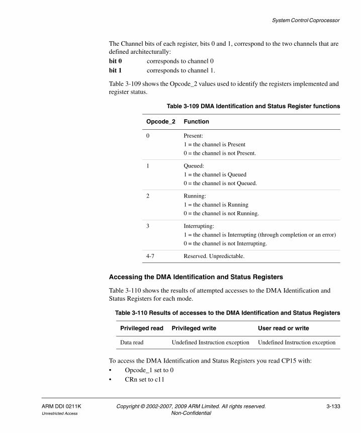
System Control Coprocessor
The Channel bits of each register, bits 0 and 1, correspond to the two channels that are defined architecturally:
bit 0 corresponds to channel 0
bit 1 corresponds to channel 1.
Table 3-109 shows the Opcode_2 values used to identify the registers implemented and register status.
Accessing the DMA Identification and Status Registers
Table 3-110 shows the results of attempted accesses to the DMA Identification and Status Registers for each mode.
To access the DMA Identification and Status Registers you read CP15 with:
• Opcode_1 set to 0
• CRn set to c11
Table 3-109 DMA Identification and Status Register functions
Opcode_2 Function
0 Present:
1 = the channel is Present
0 = the channel is not Present.
1 Queued:
1 = the channel is Queued
0 = the channel is not Queued.
2 Running:
1 = the channel is Running
0 = the channel is not Running.
3 Interrupting:
1 = the channel is Interrupting (through completion or an error)
0 = the channel is not Interrupting.
4-7 Reserved. Unpredictable.
Table 3-110 Results of accesses to the DMA Identification and Status Registers
Privileged read Privileged write User read or write
Data read Undefined Instruction exception Undefined Instruction exception
ARM DDI 0211K Copyright © 2002-2007, 2009 ARM Limited. All rights reserved. 3-133Unrestricted Access Non-Confidential

System Control Coprocessor
• CRm set to c0
• Opcode_2 set to:
— 0, for the Present function
— 1, for the Queued function
— 2, for the Running function
— 3, for the Interrupting function.
For example:
MRC p15, 0, <Rd>, c11, c0, 0 ; Read DMA Identification and Status Register presentMRC p15, 0, <Rd>, c11, c0, 1 ; Read DMA Identification and Status Register queuedMRC p15, 0, <Rd>, c11, c0, 2 ; Read DMA Identification and Status Register runningMRC p15, 0, <Rd>, c11, c0, 3 ; Read DMA Identification and Status Register interrupting
3.3.26 c11, DMA User Accessibility Register
The purpose of the DMA User Accessibility Register is to determine if a User mode process can access the DMA registers for each channel.
The register holds a U bit for each channel, that indicates if the registers for that channel can be accessed by a User mode process.
The DMA User Accessibility Register is:
• in CP15 c11
• a 32-bit read/write register
• accessible in privileged mode only.
Figure 3-52 shows the arrangement of bits in the register.
Figure 3-52 DMA User Accessibility Register format
UNP/SBZ
31 2 1 0
U1 U0
3-134 Copyright © 2002-2007, 2009 ARM Limited. All rights reserved. ARM DDI 0211KNon-Confidential Unrestricted Access

System Control Coprocessor
Table 3-111 shows the bit functions of the DMA User Accessibility Register.
The following sections describe the registers that can be accessed from User mode if the U bit for that channel is 1:
• c11, DMA Channel Status Registers on page 3-150
• c11, DMA Control Registers on page 3-141
• c11, DMA Enable Registers on page 3-138
• c11, DMA External Start Address Registers on page 3-146
• c11, DMA Internal Start Address Registers on page 3-145
• c11, DMA Internal End Address Registers on page 3-148.
The contents of these registers must be preserved on a task switch if the registers are User-accessible.
You can access the DMA channel Number Register in User mode when the U bit for any channel is 1. For more information see c11, DMA Channel Number Register on page 3-136.
If the U bit for a channel is set to 0, then attempting to access the registers for that channel from a User process results in an Undefined Instruction trap.
Table 3-111 DMA User Accessibility Register bit functions
Bit range
Field name
Function
[31:2] - UNP/SBZ
[1] U1 Indicates if a User mode process can access the registers for channel 1:
0 = User mode cannot access channel 1 registers. The DMA transfer type is privileged, indicated by HPROTD[1] asserted. This is the reset value.
1 = User mode can access channel 1 registers. The DMA transfer type is User, indicated by HPROTD[1] deasserted.
[0] U0 Indicates if a User mode process can access the registers for channel 0:
0 = User mode cannot access channel 0 registers. The DMA transfer type is privileged, indicated by HPROTD[1] asserted. This is the reset value.
1 = User mode can access channel 0 registers. The DMA transfer type is User, indicated by HPROTD[1] deasserted.
ARM DDI 0211K Copyright © 2002-2007, 2009 ARM Limited. All rights reserved. 3-135Unrestricted Access Non-Confidential

System Control Coprocessor
Accessing the DMA User Accessibility Register
Table 3-112 shows the results of attempted accesses to the DMA User Accessibility Register for each mode.
To access the DMA User Accessibility Register you read or write CP15 with:
• Opcode_1 set to 0
• CRn set to c11
• CRm set to c1
• Opcode_2 set to 0.
For example:
MRC p15, 0, <Rd>, c11, c1, 0 ; Read DMA User Accessibility RegisterMCR p15, 0, <Rd>, c11, c1, 0 ; Write DMA User Accessibility Register
3.3.27 c11, DMA Channel Number Register
The purpose of the DMA Channel Number Register is to select a DMA channel, or to find which DMA channel is currently selected.
The DMA Channel Number Register is:
• in CP15 c11
• a 32-bit read/write register
• accessible in User and privileged modes
— the register is only accessible in User mode if at least one of the U bits is set in the DMA User Accessibility Register, see c11, DMA User Accessibility Register on page 3-134 for details.
Figure 3-53 shows the arrangement of bits in the register.
Figure 3-53 DMA Channel Number Register format
Table 3-112 Results of accesses to the DMA User Accessibility Register
Privileged read Privileged write User read or write
Data read Data write Undefined Instruction exception
UNP/SBZ
31 1 0
Channel number
3-136 Copyright © 2002-2007, 2009 ARM Limited. All rights reserved. ARM DDI 0211KNon-Confidential Unrestricted Access

System Control Coprocessor
Table 3-113 shows the bit functions of the DMA Channel Number Register.
The Enable, Control, Internal Start Address, External Start Address, Internal End Address, Channel Status, and Context ID registers are multiple registers with one instance of each register for each DMA channel that is implemented. The value contained in the DMA Channel Number Register determines which of the multiple registers is accessed when one of these registers is specified.
Accessing the DMA Channel Number Register
Table 3-114 shows the results of attempted accesses to the DMA Channel Number Register for each mode.
To access the DMA Channel Number Register you read or write CP15 with:
• Opcode_1 set to 0
• CRn set to c11
• CRm set to c2
• Opcode_2 set to 0.
For example:
MRC p15, 0, <Rd>, c11, c2, 0 ; Read DMA Channel Number RegisterMCR p15, 0, <Rd>, c11, c2, 0 ; Write DMA Channel Number Register
Table 3-113 DMA Channel Number Register bit functions
Bit range Field name Function
[31:1] - UNP/SBZ.
[0] CN Channel Number: Indicates DMA Channel selected:
0 = DMA Channel 0 selected, reset value
1 = DMA Channel 1 selected.
Table 3-114 Results of accesses to the DMA Channel Number Register
Privileged read Privileged write User read User write
Data read Data write Data reada
a. Accesses from User mode will succeed if at least one of the U bits is set in the DMA User Accessibility Register. If no U bit is set these operations will result in an Undefined Instruction Trap. See c11, DMA User Accessibility Register on page 3-134 for more information.
Data writea
ARM DDI 0211K Copyright © 2002-2007, 2009 ARM Limited. All rights reserved. 3-137Unrestricted Access Non-Confidential

System Control Coprocessor
3.3.28 c11, DMA Enable Registers
The purpose of the DMA Enable Registers is to start, stop or clear DMA transfers for each channel implemented.
The DMA enable registers are:
• in CP15 c11
• three 32-bit write only registers for each DMA channel. For each channel, the three registers provide the following three commands:
— Stop (Opcode_2 = 0)
— Start (Opcode_2 = 1)
— Clear (Opcode_2 = 2)
• accessible in User and privileged modes
— the registers are only accessible in User mode if the U bit of the currently selected DMA channel is set to 1 in the DMA User Accessibility Register, see c11, DMA User Accessibility Register on page 3-134 for details.
The commands provided by these registers are:
Stop The DMA channel ceases to do memory accesses as soon as possible after the level one DMA issues the Stop instruction. This acceleration approach cannot be used for DMA transactions to or from memory regions marked as Device. The DMA can issue a Stop command when the channel status is Running.
The DMA channel can take several cycles to stop after the DMA issues a Stop instruction. The channel status remains at Running until the DMA channel stops. The channel status is set to Complete or Error at the point when all outstanding memory accesses complete. When the channel stops, the Start Address Registers contain the addresses the DMA requires to restart the operation.
If the Stop command occurs when the channel status is Queued, the channel status changes to Idle. The Stop command has no effect if the channel status is not Running or Queued.
c11, DMA Channel Status Registers on page 3-150 describes the DMA channel status.
Start The Start command causes the channel to start DMA transfers. If the other DMA channel is not in operation the channel status is set to Running on the execution of a Start command. If the other DMA channel is in operation the channel status is set to Queued.
A channel is in operation if any of the following apply:
• its channel status is Queued
3-138 Copyright © 2002-2007, 2009 ARM Limited. All rights reserved. ARM DDI 0211KNon-Confidential Unrestricted Access

System Control Coprocessor
• its channel status is Running
• its channel status is Complete or Error, with either the Internal or External Address Error Status indicating an Error.
c11, DMA Channel Status Registers on page 3-150 describes DMA channel status.
Clear The Clear command causes the channel status to change from Complete or Error to Idle. It also clears:
• all the Error bits for that DMA channel
• the interrupt that is set by the DMA channel as a result of an error or completion, see c11, DMA Control Registers on page 3-141 for more details.
The Clear command does not change the contents of the Internal and External Start Address Registers. A Clear command has no effect when the channel status is Running or Queued.
Accessing the DMA Enable Registers
The value held in the DMA Channel Number Register determines whether the channel 0 or the channel 1 DMA Enable Registers will be accessed. See c11, DMA Channel Number Register on page 3-136 for details.
Table 3-115 shows the results of attempted accesses to the DMA Enable Registers for each mode.
To access the DMA Enable Registers you:
• Write to the DMA Channel Number Register to select the DMA channel you want to access, see c11, DMA Channel Number Register on page 3-136.
Table 3-115 Results of accesses to the DMA Enable Registers
U bita Privileged read Privileged write User read User write
0 Undefined Instruction exception
Data write Undefined Instruction exception
Undefined Instruction exception
1 Undefined Instruction exception
Data write Undefined Instruction exception
Data write
a. In the DMA User Accessibility Register. See c11, DMA User Accessibility Register on page 3-134 for details. The values given are for the U bit of the currently selected DMA channel, see c11, DMA Channel Number Register on page 3-136 for more information.
ARM DDI 0211K Copyright © 2002-2007, 2009 ARM Limited. All rights reserved. 3-139Unrestricted Access Non-Confidential

System Control Coprocessor
• Write CP15 with:
— Opcode_1 set to 0
— CRn set to c11
— CRm set to c3
— Opcode_2 set to select the register for the required operation, see Table 3-116.
For example:
MCR p15, 0, <Rd>, c11, c3, 0 ; Stop DMA Enable RegisterMCR p15, 0, <Rd>, c11, c3, 1 ; Start DMA Enable RegisterMCR p15, 0, <Rd>, c11, c3, 2 ; Clear DMA Enable Register
Table 3-116 shows the Opcode_2 values used to select the appropriate DMA Enable Register for the required operation.
Debug implications for the DMA
The level one DMA behaves as a separate engine from the processor core, and when started works autonomously. As a result, if the level one DMA has channels with the status of Running or Queued, then these channels continue to run, or start running, even if the processor is stopped by debug mechanisms. This results in the contents of the TCM changing while the processor is stopped in debug. The DMA channels must be stopped by a Stop operation to avoid this situation.
Table 3-116 DMA Enable Register selection
Opcode_2 Operation
0 Stop
1 Start
2 Clear
3-7 Reserved
3-140 Copyright © 2002-2007, 2009 ARM Limited. All rights reserved. ARM DDI 0211KNon-Confidential Unrestricted Access

System Control Coprocessor
3.3.29 c11, DMA Control Registers
Each implemented DMA channel has its own DMA Control Register. The purpose of each DMA Control Register is to control the operation of that DMA channel.
The DMA Control Registers are:
• in CP15 c11
• one 32-bit read/write register for each DMA channel
• accessible in user and privileged modes
— a DMA Control Register is only accessible in User mode if the U bit of the currently selected DMA channel is set to 1 in the DMA User Accessibility Register, see c11, DMA User Accessibility Register on page 3-134 for details.
Figure 3-9 on page 3-25 shows the arrangement of bits in the registers.
Figure 3-54 DMA Control Register format
31 30 29 28 27 26 25 20 19 8 7 2 1 0
UNP/SBZ ST UNP/SBZ TS
TR UMDTIC
FTIE
ARM DDI 0211K Copyright © 2002-2007, 2009 ARM Limited. All rights reserved. 3-141Unrestricted Access Non-Confidential

System Control Coprocessor
Table 3-117 shows the bit functions of the DMA Control Registers.
Table 3-117 DMA Control Register bit functions
Bit range
Field name
Function
[31] TR TaRget. Indicates target TCM:
0 = Data TCM. This is the reset value
1 = Instruction TCM.
[30] DT Direction of Transfer:
0 = Transfer from level two memory to the TCM. This is the reset value
1 = Transfer from the TCM to the level two memory.
[29] IC Interrupt on Completion. Indicates whether the DMA channel must assert an interrupt on completion of the DMA transfer, or if the DMA is stopped by a Stop command, see c11, DMA Enable Registers on page 3-138.
The interrupt is deasserted, from this source, if the processor performs a Clear operation on the channel that caused the interrupt. For more details see c11, DMA Enable Registers on page 3-138.
The U bita has no effect on whether an interrupt is generated on completion.
0 = No Interrupt on Completion, reset value.
1 = Interrupt on Completion.
[28] IE Interrupt on Error. Indicates that the DMA channel must assert an interrupt on an error.
The interrupt is deasserted (from this source) when the channel is set to Idle with a Clear operation, see c11, DMA Enable Registers on page 3-138.
0 = No Interrupt on Error, if the U bit is 0, reset value.
1 = Interrupt on Error, regardless of the U bita. All DMA transactions on channels that have the U bit set to 1 Interrupt on Error regardless of the value written to this bit.
[27] FT Full Transfer. Indicates that the DMA transfers all words of data as part of the DMA that is transferring data from the TCM to the external memory:
0 = Transfer at least those locations in the address range of the DMA in the TCM that have been changed by a store operation since the location was written to or read from by an earlier DMA
1 = Transfer all locations in the address range of the DMA, regardless of whether or not the locations have been changed by a store.
3-142 Copyright © 2002-2007, 2009 ARM Limited. All rights reserved. ARM DDI 0211KNon-Confidential Unrestricted Access

System Control Coprocessor
Note Setting the FT bit to 0 causes the DMA to look for dirty information, at a granularity of four words, for the data TCM. That is, if any word/byte within a four-word range (aligned to a four-word boundary) has been written to, then these four words are written back. The FT bit has no effect for transfers from the Instruction TCM.
[26] UM User Mode. Indicates whether the permission checks are based on the DMA being in User mode or in a privileged mode.
The UM bit is provided so that a privileged mode process can emulate User mode accesses. For a User mode process the processor ignores the setting of the UM bit and behaves as if it is set to 1.
0 = Transfer is a privileged transfer, reset value.
1 = Transfer is a User mode transfer.
If the U bit for a channel is set to 1 in the DMA User Accessibility Register, the processor ignores the UM bit value, and the channel behaves as if UM is set to 1. See c11, DMA User Accessibility Register on page 3-134 for more information.
[25:20] - UNP/SBZ.
[19:8] ST STride (in bytes). Indicates the increment on the external address between each consecutive access of the DMA. A Stride of zero, reset value, indicates that the external address is not to be incremented. This is designed to facilitate the accessing of volatile locations such as a FIFO.
The Stride is interpreted as a positive number (or zero), and he STride value is in bytes.
The internal address increment is not affected by the Stride, but is fixed at the transaction size.
The value of the Stride must be aligned to the Transaction Size, otherwise this results in a bad parameter error, see c11, DMA Channel Status Registers on page 3-150.
[7:2] - UNP/SBZ.
[1:0] TS Transaction Size. Indicates the size of the transactions that the DMA channel performs. This is particularly important for Device or Strongly Ordered memory locations because it ensures that accesses to such memory occur at their programmed size.
b00 = Byte. This is the reset value.
b01 = Halfword.
b10 = Word.
b11 = Doubleword, 8 bytes.
a. See c11, DMA User Accessibility Register on page 3-134
Table 3-117 DMA Control Register bit functions (continued)
Bit range
Field name
Function
ARM DDI 0211K Copyright © 2002-2007, 2009 ARM Limited. All rights reserved. 3-143Unrestricted Access Non-Confidential

System Control Coprocessor
Accessing the DMA Control Registers
The value held in the DMA Channel Number Register determines whether the channel 0 or the channel 1 DMA Control Register will be accessed. See c11, DMA Channel Number Register on page 3-136 for details.
Table 3-115 on page 3-139 shows the results of attempted accesses to the DMA Control Registers for each mode.
To access a DMA Control Register you:
• Write to the DMA Channel Number Register to select the DMA channel you want to access, see c11, DMA Channel Number Register on page 3-136.
• Write CP15 with:
— Opcode_1 set to 0
— CRn set to c11
— CRm set to c4
— Opcode_2 set to 0.
For example:
MRC p15, 0, <Rd>, c11, c4, 0 ; Read DMA Control RegisterMCR p15, 0, <Rd>, c11, c4, 0 ; Write DMA Control Register
While the currently selected channel has the status of Running or Queued, any attempt to write to the DMA Control Register results in architecturally Unpredictable behavior. For ARM1136JF-S processors writes to the DMA Control Register have no effect when the DMA channel is running or queued.
Table 3-118 Results of accesses to the DMA Control Registers
U bita Privileged read Privileged write User read User write
0 Data read Data write Undefined Instruction exception
Undefined Instruction exception
1 Data read Data write Data read Data write
a. In the DMA User Accessibility Register. See c11, DMA User Accessibility Register on page 3-134 for details. The values given are for the U bit of the currently selected DMA channel, see c11, DMA Channel Number Register on page 3-136 for more information.
3-144 Copyright © 2002-2007, 2009 ARM Limited. All rights reserved. ARM DDI 0211KNon-Confidential Unrestricted Access

System Control Coprocessor
3.3.30 c11, DMA Internal Start Address Registers
Each implemented DMA channel has its own DMA Internal Start Address Register. The purpose of each DMA Internal Start Address Register is to define the first address in the TCM for that channel. That is, it defines the first address that data transfers go to or from.
The DMA Internal Start Address Registers are:
• in CP15 c11
• one 32-bit read/write register for each DMA channel
• accessible in User and privileged modes
— a DMA Internal Start Address Register is only accessible in User mode if the U bit of the currently selected DMA channel is set to 1 in the DMA User Accessibility Register, see c11, DMA User Accessibility Register on page 3-134 for details.
The DMA Internal Start Address Register bits [31:0] contain the Internal Start Virtual Address (VA).
Accessing the DMA Internal Start Address Registers
The value held in the DMA Channel Number Register determines whether the channel 0 or the channel 1 DMA Internal Start Address Register will be accessed. See c11, DMA Channel Number Register on page 3-136 for details.
Table 3-115 on page 3-139 shows the results of attempted accesses to a DMA Internal Start Address Register for each mode.
To access a DMA Internal Start Address Register you:
• Write to the DMA Channel Number Register to select the DMA channel you want to access, see c11, DMA Channel Number Register on page 3-136.
Table 3-119 Results of accesses to a DMA Internal Start Address Register
U bita Privileged read Privileged write User read User write
0 Data read Data write Undefined Instruction exception
Undefined Instruction exception
1 Data read Data write Data read Data write
a. In the DMA User Accessibility Register. See c11, DMA User Accessibility Register on page 3-134 for details. The values given are for the U bit of the currently selected DMA channel, see c11, DMA Channel Number Register on page 3-136 for more information.
ARM DDI 0211K Copyright © 2002-2007, 2009 ARM Limited. All rights reserved. 3-145Unrestricted Access Non-Confidential

System Control Coprocessor
• Write CP15 with:
— Opcode_1 set to 0
— CRn set to c11
— CRm set to c5
— Opcode_2 set to 0.
For example:
MRC p15, 0, <Rd>, c11, c5, 0 ; Read DMA Internal Start Address RegisterMCR p15, 0, <Rd>, c11, c5, 0 ; Write DMA Internal Start Address Register
Using the DMA Internal Start Address Registers
The Internal Start Address is a Virtual Address (VA). Page tables describe the physical mapping of the VA when the channel starts.
The memory attributes for that Virtual Address are used in the transfer, so memory permission faults might be generated. The Internal Start Address must lie within a TCM, otherwise an error is reported in the DMA Channel Status Register. The marking of memory locations in the TCM as being Device results in Unpredictable effects.
The contents of this register are Unpredictable while the DMA channel is Running. When the channel is stopped because of a Stop command, or an error, it contains the address required to restart the transaction. On completion, it contains the address equal to the Internal End Address.
The Internal Start Address must be aligned to the transaction size set in the DMA Control Register or the effects are Unpredictable.
Attempting to write a DMA Internal Start Address Register while the currently selected DMA channel is Running or Queued has no effect. That is, the operation fails without issuing an error.
3.3.31 c11, DMA External Start Address Registers
Each implemented DMA channel has its own DMA External Start Address Register. The purpose of each DMA External Start Address Register is to define the first address in external memory for that DMA channel. That is, it defines the first address that data transfers go to or from.
The DMA External Start Address Registers are:
• in CP15 c11
• one 32-bit read/write register for each DMA channel
3-146 Copyright © 2002-2007, 2009 ARM Limited. All rights reserved. ARM DDI 0211KNon-Confidential Unrestricted Access
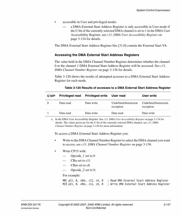
System Control Coprocessor
• accessible in User and privileged modes
— a DMA External Start Address Register is only accessible in User mode if the U bit of the currently selected DMA channel is set to 1 in the DMA User Accessibility Register, see c11, DMA User Accessibility Register on page 3-134 for details.
The DMA External Start Address Register bits [31:0] contain the External Start VA.
Accessing the DMA External Start Address Registers
The value held in the DMA Channel Number Register determines whether the channel 0 or the channel 1 DMA External Start Address Register will be accessed. See c11, DMA Channel Number Register on page 3-136 for details.
Table 3-120 shows the results of attempted accesses to a DMA External Start Address Register for each mode.
To access a DMA External Start Address Register you:
• Write to the DMA Channel Number Register to select the DMA channel you want to access, see c11, DMA Channel Number Register on page 3-136.
• Write CP15 with:
— Opcode_1 set to 0
— CRn set to c11
— CRm set to c6
— Opcode_2 set to 0.
For example:
MRC p15, 0, <Rd>, c11, c6, 0 ; Read DMA External Start Address RegisterMCR p15, 0, <Rd>, c11, c6, 0 ; Write DMA External Start Address Register
Table 3-120 Results of accesses to a DMA External Start Address Register
U bita Privileged read Privileged write User read User write
0 Data read Data write Undefined Instruction exception
Undefined Instruction exception
1 Data read Data write Data read Data write
a. In the DMA User Accessibility Register. See c11, DMA User Accessibility Register on page 3-134 for details. The values given are for the U bit of the currently selected DMA channel, see c11, DMA Channel Number Register on page 3-136 for more information.
ARM DDI 0211K Copyright © 2002-2007, 2009 ARM Limited. All rights reserved. 3-147Unrestricted Access Non-Confidential

System Control Coprocessor
Using the DMA External Start Address Registers
The External Start Address is a Virtual Address (VA), whose physical mapping must be described in the page tables at the time that the channel is started. The memory attributes for that Virtual Address are used in the transfer, so memory permission faults might be generated.
The External Start Address must lie in the external memory beyond the level one memory system otherwise the results are Unpredictable.
The contents of this register are Unpredictable while the DMA channel is Running. When the channel is stopped because of a Stop command, or an error, it contains the address required to restart the transaction. On completion, it contains the address equal to the final address that was accessed plus the Stride.
The External Start Address must be aligned to the transaction size set in the control register, otherwise the effects are Unpredictable.
Attempting to write this register while the DMA channel is Running or Queued has no effect. That is, the operation fails without issuing an error.
3.3.32 c11, DMA Internal End Address Registers
Each implemented DMA channel has its own DMA Internal End Address Register. The purpose of each DMA Internal End Address Register is to define the final internal address for that channel. This is, the end address of the data transfer.
The DMA Internal End Address Registers are:
• in CP15 c11
• one 32-bit read/write register for each DMA channel
• accessible in user and privileged modes
— a DMA Internal End Address Register is only accessible in User mode if the U bit of the currently selected DMA channel is set to 1 in the DMA User Accessibility Register, see c11, DMA User Accessibility Register on page 3-134 for details.
The DMA Internal End Address Register bits [31:0] contain the Internal End VA.
Accessing the DMA Internal End Address Registers
The value held in the DMA Channel Number Register determines whether the channel 0 or the channel 1 DMA Internal End Address Register will be accessed. See c11, DMA Channel Number Register on page 3-136 for details.
3-148 Copyright © 2002-2007, 2009 ARM Limited. All rights reserved. ARM DDI 0211KNon-Confidential Unrestricted Access

System Control Coprocessor
Table 3-115 on page 3-139 shows the results of attempted accesses to a DMA Internal End Address Register for each mode.
To access a DMA Internal End Address Register you:
• Write to the DMA Channel Number Register to select the DMA channel you want to access, see c11, DMA Channel Number Register on page 3-136.
• Write CP15 with:
— Opcode_1 set to 0
— CRn set to c11
— CRm set to c7
— Opcode_2 set to 0.
For example:
MRC p15, 0, <Rd>, c11, c7, 0 ; Read DMA Internal End Address RegisterMCR p15, 0, <Rd>, c11, c7, 0 ; Write DMA Internal End Address Register
Using the DMA Internal End Address Registers
This register defines the Internal End Address. The Internal End Address is the final internal address, modulo the transaction size, that the DMA is to access plus the transaction size. Therefore the Internal End Address is the first (incremented) address that the DMA does not access.
If the Internal End Address is the same of the Internal Start Address, the DMA transfer completes immediately without performing transactions.
When the transaction associated with the final internal address has completed, the whole DMA transfer is complete.
The Internal End Address is a VA. Page tables describe the physical mapping of the VA when the channel starts. The memory attributes for that VA are used in the transfer, so memory permission faults might be generated. The Internal End Address must lie
Table 3-121 Results of accesses to a DMA Internal End Address Register
U bita Privileged read Privileged write User read User write
0 Data read Data write Undefined Instruction exception
Undefined Instruction exception
1 Data read Data write Data read Data write
a. In the DMA User Accessibility Register. See c11, DMA User Accessibility Register on page 3-134 for details. The values given are for the U bit of the currently selected DMA channel, see c11, DMA Channel Number Register on page 3-136 for more information.
ARM DDI 0211K Copyright © 2002-2007, 2009 ARM Limited. All rights reserved. 3-149Unrestricted Access Non-Confidential
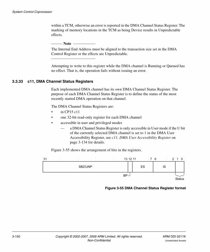
System Control Coprocessor
within a TCM, otherwise an error is reported in the DMA Channel Status Register. The marking of memory locations in the TCM as being Device results in Unpredictable effects.
Note The Internal End Address must be aligned to the transaction size set in the DMA Control Register or the effects are Unpredictable.
Attempting to write to this register while the DMA channel is Running or Queued has no effect. That is, the operation fails without issuing an error.
3.3.33 c11, DMA Channel Status Registers
Each implemented DMA channel has its own DMA Channel Status Register. The purpose of each DMA Channel Status Register is to define the status of the most recently started DMA operation on that channel.
The DMA Channel Status Registers are:
• in CP15 c11
• one 32-bit read-only register for each DMA channel
• accessible in user and privileged modes
— a DMA Channel Status Register is only accessible in User mode if the U bit of the currently selected DMA channel is set to 1 in the DMA User Accessibility Register, see c11, DMA User Accessibility Register on page 3-134 for details.
Figure 3-55 shows the arrangement of bits in the registers.
Figure 3-55 DMA Channel Status Register format
SBZ/UNP
31 13 12 7 6 2 1 0
ES IS
11
BPStatus
3-150 Copyright © 2002-2007, 2009 ARM Limited. All rights reserved. ARM DDI 0211KNon-Confidential Unrestricted Access

System Control Coprocessor
Table 3-122 shows the bit functions of the DMA Channel Status Registers.
Table 3-122 DMA Channel Status Register bit functions
Bit range Field name Function
[31:13] - UNP/SBZ.
[12] BP Indicates whether the DMA parameters are acceptable, or are conditioned inappropriately:
0 = DMA parameters are acceptable. This is the reset value
1 = DMA parameters are conditioned inappropriately.
The external start and end addresses, and the Stride must all be multiples of the transaction size. If this is not the case, the BP bit is set to 1, and the DMA channel does not start.
ARM DDI 0211K Copyright © 2002-2007, 2009 ARM Limited. All rights reserved. 3-151Unrestricted Access Non-Confidential

System Control Coprocessor
[11:7] ES External address error Status. Indicates the status of the External Address Error:
b00000 = No error. This is the reset value.
b00xxx = No error.
b01001 = Unshared data error.
b10011 = Access Flag fault, section.
b10110 = Access Flag fault, page.
b11010 = External Abort (can be imprecise).
b11100 = External Abort on translation of first-level page table.
b11110 = External Abort on translation of second-level page table.
b10101 = Translation fault, section.
b10111 = Translation fault, page.
b11001 = Domain fault, section.
b11011 = Domain fault, page.
b11101 = Permission fault, section.
b11111 = Permission fault, page.
All other encodings are Reserved.
[6:2] IS Internal address error Status. Indicates the status of the Internal Address Error:
b01000 = TCM out of range
b10011 = Access Flag fault, section
b10110 = Access Flag fault, page
b11100 = External Abort on translation of first-level page table
b11110 = External Abort on translation of second-level page table
b10101 = Translation fault, section
b10111 = Translation fault, page
b11001 = Domain fault, section
b11011 = Domain fault, page
b11101 = Permission fault, section
b11111 = Permission fault, page.
All other encodings are Reserved.
[1:0] Status Indicates the status of the DMA channel:
b00 = Idle. This is the reset value.
b01 = Queued.
b10 = Running.
b11 = Complete or Error.
Table 3-122 DMA Channel Status Register bit functions (continued)
Bit range Field name Function
3-152 Copyright © 2002-2007, 2009 ARM Limited. All rights reserved. ARM DDI 0211KNon-Confidential Unrestricted Access

System Control Coprocessor
Accessing the DMA Channel Status Registers
The value held in the DMA Channel Number Register determines whether the channel 0 or the channel 1 DMA Channel Status Register will be accessed. See c11, DMA Channel Number Register on page 3-136 for details.
Table 3-115 on page 3-139 shows the results of attempted accesses to a DMA Internal End Address Register for each mode.
To access a DMA Channel Status Register you:
• Write to the DMA Channel Number Register to select the DMA channel you want to access, see c11, DMA Channel Number Register on page 3-136.
• Read CP15 with:
— Opcode_1 set to 0
— CRn set to c11
— CRm set to c8
— Opcode_2 set to 0.
For example:
MRC p15, 0, <Rd>, c11, c8, 0 ; Read DMA Channel Status Register
Using the DMA Channel Status Registers
In the event of an error, the appropriate Start Address Register contains the address that faulted, unless the error is an external error that is set to b11010 by bits[11:7].
A channel with the state of Queued changes to Running automatically if the other channel (if implemented) changes to Idle, or Complete or Error, with no error.
Table 3-123 Results of accesses to a DMA Channel Status Register
U bita Privileged read Privileged write User read User write
0 Data read Undefined Instruction exception
Undefined Instruction exception
Undefined Instruction exception
1 Data read Undefined Instruction exception
Data read Undefined Instruction exception
a. In the DMA User Accessibility Register. See c11, DMA User Accessibility Register on page 3-134 for details. The values given are for the U bit of the currently selected DMA channel, see c11, DMA Channel Number Register on page 3-136 for more information.
ARM DDI 0211K Copyright © 2002-2007, 2009 ARM Limited. All rights reserved. 3-153Unrestricted Access Non-Confidential

System Control Coprocessor
When a channel has completed all of the transfers of the DMA, so that all changes to memory locations caused by those transfers are visible to other observers, its status is changed from Running to Complete or Error. This change does not happen before the external accesses from the transfer have completed.
If the processor attempts to access memory locations that are not marked as shared, then the ES bits signal an Unshared error for either:
• a DMA transfer in User mode
• a DMA transfer that has the UM bit set in the DMA Control Register.
A DMA transfer where the external address is within the range of the TCM also results in an Unshared data error.
3.3.34 c11, DMA Context ID Registers
Each implemented DMA channel has its own DMA Context ID Register. The purpose of each DMA Context ID Register is to contain the processor 32-bit Context ID of the process that is using that channel.
The DMA Context ID Registers are:
• in CP15 c11
• a 32-bit read/write register for each DMA channel
• accessible in privileged mode only.
Figure 3-56 shows the arrangement of bits in the register.
Figure 3-56 DMA Context ID Register format
Table 3-124 shows the bit functions of the DMA Context ID Registers.
ASIDPROCID
31 08 7
ContextID
Table 3-124 DMA Context ID Register bit functions
Bit range Field name Function
[31:8] PROCID Extends the ASID to form the process ID and identify the current process.
Holds the process ID value.
[8:0] ASID Holds the ASID of the current process and identifies the current ASID.
3-154 Copyright © 2002-2007, 2009 ARM Limited. All rights reserved. ARM DDI 0211KNon-Confidential Unrestricted Access

System Control Coprocessor
Accessing the DMA Context ID Registers
Table 3-125 shows the results of attempted accesses to a DMA Context ID Register for each mode.
To access a DMA Context ID Register you:
• Write to the DMA Channel Number Register to select the DMA channel you want to access, see c11, DMA Channel Number Register on page 3-136.
• Read or write CP15 with:
— Opcode_1 set to 0
— CRn set to c11
— CRm set to c15
— Opcode_2 set to 0.
For example:
MRC p15, 0, <Rd>, c11, c15, 0 ; Read DMA Context ID RegisterMCR p15, 0, <Rd>, c11, c15, 0 ; Write DMA Context ID Register
Using the DMA Context ID Registers
The DMA Context ID Register must be written with the processor Context ID of the process using the channel as part of the initialization of that channel. Where the channel is designated as a User-accessible channel, the Context ID must be written by the privileged process that initializes the channel for User use at the same time that the U bit for the channel is written to.
The bottom eight bits of the Context ID register are used in the address translation from virtual to physical addresses to enable different Virtual Address maps to co-exist. Attempting to write this register while the DMA channel is Running or Queued has no effect.
The bottom eight bits of the Context ID register are accessible to the AHB memory on DMAASID[7:0].
Table 3-125 Results of accesses to the DMA Context ID Register
Privileged read Privileged write User read or write
Data read Data write Undefined Instruction exception
ARM DDI 0211K Copyright © 2002-2007, 2009 ARM Limited. All rights reserved. 3-155Unrestricted Access Non-Confidential

System Control Coprocessor
This register can only be read by a privileged process. This provides anonymity of the DMA channel usage from User processes. It can only be written by a privileged process for security reasons. On a context switch, where the state of the DMA is being stacked and restored, you must include this register in the saved state.
3.3.35 c13, FCSE PID Register
The Context ID Register replaces the FCSE PID register, and use of the FCSE PID Register is deprecated. For more information see c13, Context ID Register on page 3-159.
The FCSE PID Register is:
• in CP15 c13
• a 32-bit read/write register
• accessible in privileged mode only.
Figure 3-57 shows the arrangement of bits in the register.
Figure 3-57 FCSE PID Register format
Table 3-126 shows the bit functions of the FCSE PID Register.
The FCSE PID Register provides the ProcID for fast context switch memory mappings. The MMU uses the contents of this register to map memory addresses in the range 0-32MB.
FCSE PID
31 25 24 0
UNP/SBZ
Table 3-126 FCSE PID Register bit functions
Bit range Field name Function
[31:25] FCSE PID Identifies a specific process for fast context switch.
Holds the ProcID. The reset value is 0.
[24:0] - Reserved. SBZ.
3-156 Copyright © 2002-2007, 2009 ARM Limited. All rights reserved. ARM DDI 0211KNon-Confidential Unrestricted Access

System Control Coprocessor
Accessing the FCSE PID Register
Table 3-127 shows the results of attempted accesses to the FCSE PID Register for each mode.
To access the FCSE PID Register you read or write CP15 with:
• Opcode_1 set to 0
• CRn set to c0
• CRm set to c0
• Opcode_2 set to 0.
For example:
MRC p15, 0, <Rd>, c13, c0, 0 ; Read FCSE PID RegisterMCR p15, 0, <Rd>, c13, c0, 0 ; Write FCSE PID Register
Use of the FCSE PID Register
Reading from the FCSE PID Register returns the value of the process identifier.
Writing the FCSE PID Register updates the process identifier to the value in bits[31:25]. Bits[24:0] Should Be Zero. Writing the register globally flushes the BTAC.
Addresses issued by the ARM1136JF-S processor in the range 0-32MB are translated by the ProcID. Address A becomes A + (ProcID x 32MB). This translated address is used by the MMU. Addresses above 32MB are not translated. The ProcID is a seven-bit field, enabling 128 x 32MB processes to be mapped.
Note If ProcID is 0, as it is on Reset, then there is a flat mapping between the ARM1136JF-S processor and the MMU.
Figure 3-58 on page 3-158 shows how addresses are mapped using CP15 c13.
Table 3-127 Results of accesses to the FCSE PID Register
Privileged read Privileged write User read or write
Data read Data write Undefined Instruction exception
ARM DDI 0211K Copyright © 2002-2007, 2009 ARM Limited. All rights reserved. 3-157Unrestricted Access Non-Confidential
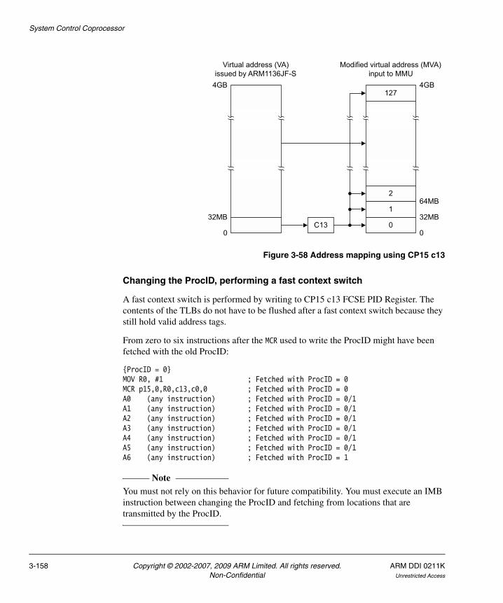
System Control Coprocessor
Figure 3-58 Address mapping using CP15 c13
Changing the ProcID, performing a fast context switch
A fast context switch is performed by writing to CP15 c13 FCSE PID Register. The contents of the TLBs do not have to be flushed after a fast context switch because they still hold valid address tags.
From zero to six instructions after the MCR used to write the ProcID might have been fetched with the old ProcID:
{ProcID = 0}MOV R0, #1 ; Fetched with ProcID = 0MCR p15,0,R0,c13,c0,0 ; Fetched with ProcID = 0A0 (any instruction) ; Fetched with ProcID = 0/1A1 (any instruction) ; Fetched with ProcID = 0/1A2 (any instruction) ; Fetched with ProcID = 0/1A3 (any instruction) ; Fetched with ProcID = 0/1A4 (any instruction) ; Fetched with ProcID = 0/1A5 (any instruction) ; Fetched with ProcID = 0/1A6 (any instruction) ; Fetched with ProcID = 1
Note You must not rely on this behavior for future compatibility. You must execute an IMB instruction between changing the ProcID and fetching from locations that are transmitted by the ProcID.
C13
1
0
4GB
Modified virtual address (MVA)input to MMU
Virtual address (VA)issued by ARM1136JF-S
32MB
0
32MB
0
64MB
4GB
2
127
3-158 Copyright © 2002-2007, 2009 ARM Limited. All rights reserved. ARM DDI 0211KNon-Confidential Unrestricted Access

System Control Coprocessor
3.3.36 c13, Context ID Register
The purpose of the Context ID Register is to provide information on the current ASID and process ID, for example for the ETM and debug logic. Debug logic uses the ASID information to enable process-dependent breakpoints and watchpoints.
The Context ID Register is:
• in CP15 c13
• a 32-bit read/write register
• accessible in privileged mode only.
Figure 3-59 shows the arrangement of bits in the register.
Figure 3-59 Context ID Register format
Table 3-128 shows the bit functions of the Context ID Register.
The bottom eight bits of the Context ID Register contain the ASID that is currently running. This current ASID value is exported to the MMU core bus, COREASID[7:0]. The top bits of the register extend the ASID.
Accessing the Context ID Register
Table 3-129 shows the results of attempted accesses to the Context ID Register for each mode.
PROCID
31 8 7 0
ASID
Table 3-128 Context ID Register bit functions
Bit range Field name Function
[31:8] PROCID Extends the ASID to form the process ID and identify the current process.
The value is the Process ID. The reset value is 0.
[8:0] ASID Holds the ASID of the current process to identify the current ASID.
The value is the ASID. The reset value is 0.
Table 3-129 Results of accesses to the Context ID Register
Privileged read Privileged write User read or write
Data read Data write Undefined Instruction exception
ARM DDI 0211K Copyright © 2002-2007, 2009 ARM Limited. All rights reserved. 3-159Unrestricted Access Non-Confidential

System Control Coprocessor
To access the Context ID Register you read or write CP15 with:
• Opcode_1 set to 0
• CRn set to c13
• CRm set to c0
• Opcode_2 set to 1.
For example:
MRC p15, 0, <Rd>, c13, c0, 1 ; Read Context ID RegisterMCR p15, 0, <Rd>, c13, c0, 1 ; Write Context ID Register
Using the Context ID Register
To ensure that all accesses are related to the correct context ID, you must ensure that software executes a Data Synchronization Barrier operation before changing this register.
Writing to this register globally flushes the BTAC.
The whole of this register is used by both the Embedded Trace Macrocell (ETM) and by the debug logic. It is used by ETM to determine how virtual memory is mapped to physical memory. Its value can be broadcast by the ETM to indicate the currently running process. You must program each process with a unique number to ensure that ETM and debug logic can correctly distinguish between processes.
The Context ID Register value can also be used to enable process-dependent breakpoints and watchpoints.
After changing this register, an IMB sequence must be executed before any instructions are executed that are from an ASID-dependent memory region. Code that updates the ASID must be executed from a global memory region.
3.3.37 c13, Thread and process ID registers
The purpose of the thread and process ID registers is to provide locations to store the IDs of software threads and processes for OS management purposes.
The thread and process ID registers are:
• in CP15 c13
• three 32-bit read/write registers:
— User Read/Write Thread and Process ID Register
— User Read Only Thread and Process ID Register
— Privileged Only Thread and Process ID Register
• only available from the rev1 (r1p0) release of the ARM1136JF-S processor.
3-160 Copyright © 2002-2007, 2009 ARM Limited. All rights reserved. ARM DDI 0211KNon-Confidential Unrestricted Access

System Control Coprocessor
The register names indicate the modes from which they can be accessed, and Table 3-130 shows the results of attempted accesses to each register for each mode.
Reading or writing the thread and process ID registers has no effect on processor state or operation. These registers provide OS support and must be managed by the OS.
You must clear the contents of all thread and process ID registers on process switches to prevent data leaking from one process to another. The reset value of these registers is 0.
Accessing the Thread and process ID registers
Table 3-130 shows the results of attempted accesses to each register for each mode.
To access the Thread and process ID registers you read or write CP15 with:
• Opcode_1 set to 0
• CRn set to c13
• CRm set to c0
• Opcode_2 set to:
— 2, User Read/Write Thread and Process ID Register
— 3, User Read Only Thread and Process ID Register
— 4, Privileged Only Thread and Process ID Register.
For example:
MRC p15, 0, <Rd>, c13, c0, 2 ; Read User Read/Write Thread and Proc. ID RegisterMCR p15, 0, <Rd>, c13, c0, 2 ; Write User Read/Write Thread and Proc. ID RegisterMRC p15, 0, <Rd>, c13, c0, 3 ; Read User Read Only Thread and Proc. ID RegisterMCR p15, 0, <Rd>, c13, c0, 3 ; Write User Read Only Thread and Proc. ID RegisterMRC p15, 0, <Rd>, c13, c0, 4 ; Read Privileged Only Thread and Proc. ID RegisterMCR p15, 0, <Rd>, c13, c0, 4 ; Write Privileged Only Thread and Proc. ID Register
Table 3-130 Results of access to the thread and process ID registers
RegisterPrivileged User
Read Write Read Write
User Read/Write Thread and Process ID Register
Data read Data write Data read Data write
User Read Only Thread and Process ID Register
Data read Data write Data read Undefined Instruction exception
Privileged Only Thread and Process ID Register
Data read Data write Undefined Instruction exception
Undefined Instruction exception
ARM DDI 0211K Copyright © 2002-2007, 2009 ARM Limited. All rights reserved. 3-161Unrestricted Access Non-Confidential

System Control Coprocessor
3.3.38 c15, Memory remap registers
The purpose of the memory remap registers is to remap memory region types. The remapping takes place on the outputs of the MMU, and overrides the settings specified in the MMU page tables, or the default behavior when the MMU is disabled.
You can use these registers to remap both Inner and Outer attributes.
The c15 memory remap registers are:
• in CP15 c15
• four 32-bit read/write registers
— the Opcode_2 value controls which memory remap registers is accessed
• accessible in privileged modes only.
The four memory remap registers are:
• the Data Memory Remap Register, accessed when Opcode_2 = 0
• the Instruction Memory Remap Register, accessed when Opcode_2 = 1
• the DMA Memory Remap Register, accessed when Opcode_2 = 2
• the Peripheral Port Memory Remap Register, accessed when Opcode_2 = 4.
Note In addition to the c15 memory remap registers, additional memory remapping can occur because of remapping of the memory region attributes encoded by the TEX[2:0], C, and B bits in the MMU page tables. See c10, TEX remap registers on page 3-124 for more information.
Format of the Instruction, Data and DMA Memory Remap Registers
Figure 3-60 on page 3-163 shows the arrangement of bits in these registers.
3-162 Copyright © 2002-2007, 2009 ARM Limited. All rights reserved. ARM DDI 0211KNon-Confidential Unrestricted Access

System Control Coprocessor
Figure 3-60 Instruction, Data, and DMA Memory Remap Registers format
Table 3-131 shows the bit functions of the Instruction, Data, and DMA Memory Remap Registers.
The reset value for each field ensures that by default no remapping occurs.
31 25 24 23 20 19 16 15 9 8 6 5 0
Outer Write-Back,No Write on Allocate
Inner Write-Through
Inner Noncachable
SBZ/UNP
2122 1718 111214 23
Outer Noncachable
Shared attribute
Outer Write-Through, No Write on Allocate
Outer Write-Back, Write on Allocate
Not Shared attribute
Strongly Ordered
Device
Inner Write-Back
Remaps of outer regions Remaps of inner regions
Table 3-131 Instruction, Data and DMA Memory Remap Register bit functions
Bit range Remapped region Permitted encodings Reset value
[31:25] SBZ/UNP - -
[24:23] Outer Write-Back, No Write on Allocate See Table 3-132 on page 3-164.
b11
[22:21] Outer Write-Through, No Write on Allocate b10
[20:19] Outer Write-Back, Write on Allocate b01
[18:17] Outer Noncacheable b00
[16] Shared attribute remapping if Shared bit = 1 (shared) n/a b1
[15] Shared attribute remapping if Shared bit = 0 (not shared) n/a b0
[14:12] Inner Write-Back See Table 3-133 on page 3-164.
b111
[11:9] Inner Write-Through b110
[8:6] Device b011
[5:3] Strongly Ordered b001
[2:0] Inner Noncacheable b000
ARM DDI 0211K Copyright © 2002-2007, 2009 ARM Limited. All rights reserved. 3-163Unrestricted Access Non-Confidential

System Control Coprocessor
Table 3-132 show the encoding used for Outer regions.
Table 3-133 shows the encoding used for Inner regions.
Format of the Peripheral Port Memory Remap Register
Figure 3-61 shows the arrangement of bits in the register.
Figure 3-61 Peripheral Port Memory Remap Register format
Table 3-132 Memory remap registers - outer region remap encoding
Outer region Encoding
Noncacheable b00
Write-Back, Write on Allocate b01
Write-Through, No Write on Allocate b10
Write-Back, No Write on Allocate b11
Table 3-133 Memory remap registers - inner region remap encoding
Inner region Encoding
Noncacheable b000
Strongly Ordered b001
Reserved b010
Device b011
Reserved b100
Reserved b101
Write-Through b110
Write-Back b111
Base address
31 12 11 5 4 0
UNP/SBZ Size
3-164 Copyright © 2002-2007, 2009 ARM Limited. All rights reserved. ARM DDI 0211KNon-Confidential Unrestricted Access

System Control Coprocessor
Table 3-134 shows the shows the bit functions of the Peripheral Port Memory Remap Register.
Table 3-135 shows the encoding of the Size field for different remap region sizes.
Table 3-134 Peripheral Port Memory Remap Register bit functions
Bits Field name Function
[31:12] Base Address Gives the physical base address of the region of memory to be remapped to the peripheral port. If the Peripheral Port Memory Remap Register is used while the MMU is disabled, the virtual base address is equal to the physical base address that is used.
The Base Address is assumed to be aligned to the size of the remapped region. Any bits in the range [(log2(Region size)-1):12] are ignored.
The Base Address is 0 at Reset.
[11:5] UNP/SBZ -
[4:0] Size Indicates the size of the memory region that is to be remapped to be used by the peripheral port.
Size is 0 at Reset, indicating that no remapping is to take place.
Table 3-135 shows the region size encoding of the Size field.
Table 3-135 Peripheral Port Memory Remap Register Size field encoding
Size field Region Size
b00000 0KB
b00011 4KB
b00100 8KB
b00101 16KB
b00110 32KB
b00111 64KB
b01000 128KB
b01001 256KB
b01010 512KB
b01011 1MB
b01100 2MB
ARM DDI 0211K Copyright © 2002-2007, 2009 ARM Limited. All rights reserved. 3-165Unrestricted Access Non-Confidential

System Control Coprocessor
Accessing the memory remap registers
Table 3-127 on page 3-157 shows the results of attempted accesses to the memory remap registers for each mode.
To access the memory remap registers you read or write CP15 with:
• Opcode_1 set to 0
• CRn set to c15
• CRm set to c2
• Opcode_2 set to indicate the required memory remap register:
— Opcode_2 = 0 for the Data Memory Remap Register
— Opcode_2 = 1 for the Instruction Memory Remap Register
— Opcode_2 = 2 for the DMA Memory Remap Register
— Opcode_2 = 4 for the Peripheral Port Memory Remap Register.
For example:
b01101 4MB
b01110 8MB
b01111 16MB
b10000 32MB
b10001 64MB
b10010 128MB
b10011 256MB
b10100 512MB
b10101 1GB
b10110 2GB
Table 3-136 Results of accesses to the Memory Remap Registers
Privileged read Privileged write User read or write
Data read Data write Undefined Instruction exception
Table 3-135 Peripheral Port Memory Remap Register Size field encoding
Size field Region Size
3-166 Copyright © 2002-2007, 2009 ARM Limited. All rights reserved. ARM DDI 0211KNon-Confidential Unrestricted Access
System Control Coprocessor
MRC p15, 0, <Rd>, c15, c2, 0 ; Read the Data Memory Remap RegisterMCR p15, 0, <Rd>, c15, c2, 0 ; Write the Data Memory Remap RegisterMRC p15, 0, <Rd>, c15, c2, 1 ; Read the Instruction Memory Remap RegisterMCR p15, 0, <Rd>, c15, c2, 1 ; Write the Instruction Memory Remap RegisterMRC p15, 0, <Rd>, c15, c2, 2 ; Read the DMA Memory Remap RegisterMCR p15, 0, <Rd>, c15, c2, 2 ; Write the DMA Memory Remap RegisterMRC p15, 0, <Rd>, c15, c2, 4 ; Read Peripheral Port Memory Remap RegisterMCR p15, 0, <Rd>, c15, c2, 4 ; Write Peripheral Port Memory Remap Register
Using the Instruction, Data and DMA Memory Remap Registers
Each memory region register is split into two parts covering the Inner and Outer attributes respectively. The Inner attributes are covered by five three bit fields, and the Outer attributes are covered by four two bit fields.
The Shared bit can also be remapped. If the Shared bit as read from the TLB or page tables is 0, then it is remapped to bit 15 of this register. If the Shared bit as read from the TLB or page tables is 1, then it is remapped to bit 16 of this register.
Remapping when the MMU is disabled
Table 3-137 shows the default values of the memory regions, or region types, when the MMU is disabled.
These region types apply before any remapping. However, any remappings specified in the Remap Registers will be applied to these settings. For example, when the Instruction Cache is enabled, the final region type will depend on any remapping of Write-Through that is specified in the Instruction Region Remap Register.
This remapping enables different mappings to be selected with the MMU disabled, that cannot be done using only the I, C, and M bits in CP15 c1.
Table 3-137 Default memory regions when MMU is disabled
Conditiona
a. As set in the Control Register, see c1, Control Register on page 3-63.Bit[12], the I bit, enables or disables the Instruction Cache,Bit[2], the C bit, enables or disables the Data Cache.
Default region type, MMU disabled
Data Cache enabled Data, Strongly Ordered
Data Cache disabled Data, Strongly Ordered
Instruction Cache enabled Instruction, Write-Through
Instruction Cache disabled Instruction, Strongly Ordered
ARM DDI 0211K Copyright © 2002-2007, 2009 ARM Limited. All rights reserved. 3-167Unrestricted Access Non-Confidential

System Control Coprocessor
Using the Peripheral Port Memory Remap Register
You use this register to remap the peripheral port.
The peripheral port is accessed by memory locations whose page table attributes are Non-Shared Device. You can program a region of memory to be remapped to being Non-Shared Device while the MMU is disabled to provide access to the peripheral port when the MMU is disabled. In addition, the same mechanism will override the page table entries, providing an additional mechanism for accessing the peripheral port. This mechanism is suitable for operating systems where access to the page table formats is not readily available.
The use of the remapping of the peripheral port will change the memory region used for those memory locations that are remapped to be Non-Shared Device, regardless of what has been programmed in the page tables.
If the region of memory mapped by this mechanism overlaps with the regions of memory that are contained within the TCMs not marked as SmartCache, then the memory locations that are mapped as both TCM and Non-Shared Device are treated as TCM. Therefore, the overlapping region does not access the peripheral port.
If the region of memory mapped by this mechanism overlaps with the regions of memory that are contained within the TCMs marked as SmartCache, then the memory locations that are mapped as both TCM and Non-Shared Device are treated as Non-Shared Device, and the SmartCache functionality is not used enabled for those addresses.
The peripheral port is only used by data accesses. Unaligned accesses and exclusive accesses are not supported by the peripheral port (because they are not supported in Device memory), and attempting to perform such accesses has Unpredictable results when using the peripheral port as a result of the Peripheral Port Memory Remap Register.
Any remapping on Non-Shared Device memory by the Data Memory Remap Register has no effect on regions mapped to Non-Shared Device by the Peripheral Port Memory Remap Register.
To entirely disable the peripheral port, the Peripheral Port Memory Remap Register must be programmed to 0 size and page table entries of type Non-Shared Device must be avoided.
3.3.39 c15, Performance Monitor Control Register (PMNC)
The purpose of the Performance Monitor Control Register is to control the operation of:
• the Cycle Counter Register (CCNT)
• the Count Register 0 (PMN0)
3-168 Copyright © 2002-2007, 2009 ARM Limited. All rights reserved. ARM DDI 0211KNon-Confidential Unrestricted Access

System Control Coprocessor
• the Count Register 1 (PMN1).
The Performance Monitor Control Register is:
• in CP15 c15
• a 32-bit read/write register
• accessible in privileged mode only.
Figure 3-62 shows the arrangement of bits in the register.
Figure 3-62 Performance Monitor Control Register format
Table 3-138 shows the bit functions of the Performance Monitor Control Register.
ESBZ/UNP
31 28 27 20 19 12 11 10 8 7 6 4 3 2 1 0
EvtCount0 EvtCount1 X D C P
SBZ/UNP
9 5
Flag IntEnCCRCR1CR0
EC0EC1ECC
Table 3-138 Performance Monitor Control Register bit functions
Bit range
Field name
Function
[31:28] - UNP/SBZ.
[27:20] EvtCount0 Identifies the source of events for Count Register 0, as defined in Table 3-141 on page 3-172.
[19:12] EvtCount1 Identifies the source of events for Count Register 1, as defined in Table 3-141 on page 3-172.
[11] X Enable Export of the events to the event bus. This enables an external monitoring block, such as the ETM to trace events:
0 = Export disabled, EVNTBUS held at 0x0. This is the reset value.
1 = Export enabled, EVNTBUS driven by the events.
[10] CCR Cycle Count Register overflow flag. See Table 3-139 on page 3-171 for the meaning of the flag values.
[9] CR1 Count Register 1 overflow flag. See Table 3-139 on page 3-171 for the meaning of the flag values.
[8] CR0 Count Register 0 overflow flag. See Table 3-139 on page 3-171 for the meaning of the flag values.
[7] - UNP/SBZ.
ARM DDI 0211K Copyright © 2002-2007, 2009 ARM Limited. All rights reserved. 3-169Unrestricted Access Non-Confidential
System Control Coprocessor
[6] ECC Enable Cycle Counter interrupt.
0 = Disable interrupt. This is the reset value.
1 = Enable interrupt.
[5] EC1 Enable Counter Register 1 interrupt.
0 = Disable interrupt. This is the reset value.
1 = Enable interrupt.
[4] EC0 Enable Counter Register 0 interrupt.
0 = Disable interrupt. This is the reset value.
1 = Enable interrupt.
[3] D Cycle count divider:
0 = Cycle Counter Register counts every processor clock cycle.
1 = Cycle Counter Register counts every 64th processor clock cycle.
[2] C Cycle Counter Register Reset on Write, UNP on Read:
Write 0 = no action
Write 1 = reset the Cycle Counter Register to 0x0.
[1] P Count Register Reset on Write, UNP on Read:
Write 0 = no action
Write 1 = reset both Count Registers to 0x0.
[0] E Enable:
0 = all three counters disabled
1 = all three counters enabled.
The PMUIRQ signal can only be cleared when this bit is set to 1. This signal is the mechanism by which a Performance Monitor Unit interrupt is signaled to the core, see Using the Performance Monitor Control Register on page 3-171 for more information.
Table 3-138 Performance Monitor Control Register bit functions (continued)
Bit range
Field name
Function
3-170 Copyright © 2002-2007, 2009 ARM Limited. All rights reserved. ARM DDI 0211KNon-Confidential Unrestricted Access

System Control Coprocessor
The meaning of the flags in the Performance Monitor Control Register, for read and write operations, are shown in Table 3-139:
Accessing the Performance Monitor Control Register
Table 3-140 shows the results of attempted accesses to the Performance Monitor Control Register for each mode.
To access the Performance Monitor Control Register you read or write CP15 with:
• Opcode_1 set to 0
• CRn set to c15
• CRm set to c12
• Opcode_2 set to 0.
For example:
MRC p15, 0, <Rd>, c15, c12, 0 ; Read Performance Monitor Control RegisterMCR p15, 0, <Rd>, c15, c12, 0 ; Write Performance Monitor Control Register
Using the Performance Monitor Control Register
The Performance Monitor Control Register:
• controls which events PMN0 and PMN1 monitor
• detects which counter overflowed
• enables and disables interrupt reporting
• extends CCNT counting by six more bits (cycles between counter rollover = 238)
• resets all counters to zero
• enables the entire performance monitoring mechanism.
Table 3-139 PMNC flag values
Flag value On reads On write
0 No overflow has occurred. This is the reset value.
No effect.
1 An overflow has occurred. Clear this bit.
Table 3-140 Results of accesses to the Performance Monitor Control Register
Privileged read Privileged write User read or write
Data read Data write Undefined Instruction exception
ARM DDI 0211K Copyright © 2002-2007, 2009 ARM Limited. All rights reserved. 3-171Unrestricted Access Non-Confidential

System Control Coprocessor
If an interrupt is generated by this unit, the ARM1136JF-S processor pin PMUIRQ is asserted. This output pin can then be routed to an external interrupt controller for prioritization and masking. This is the only mechanism by which the interrupt is signaled to the core. When asserted, the PMUIRQ signal can only be cleared if bit[0] of the register, the E bit, is HIGH.
There is a delay of three cycles between enabling the counter and the counter starting to count events. In addition, the information used to count events is taken from various pipeline stages. This means that the absolute counts recorded might vary because of pipeline effects. This has a negligible effect except in case where the counters are enabled for a very short time.
Table 3-141 shows the events that can be monitored using the Performance Monitor Control Register.
Table 3-141 Performance monitoring events
Event number
EVNTBUS bit position
Event definition
0x0 [0] Instruction cache miss to a cacheable location requires fetch from external memory.
0x1 [1] Stall because instruction buffer cannot deliver an instruction. This could indicate an Instruction Cache miss or an Instruction MicroTLB miss.
This event occurs every cycle in which the condition is present.
0x2 [2] Stall because of a data dependency.
This event occurs every cycle in which the condition is present.
0x3 [3] Instruction MicroTLB miss.
0x4 [4] Data MicroTLB miss.
0x5 [6:5] Branch instruction executed, branch might or might not have changed program flow.
0x6 [7] Branch mis-predicted.
0x7 [9:8] Instruction executed.
0x9 [10] Data cache access, not including Cache operations.
This event occurs for each nonsequential access to a cache line, for cacheable locations.
0xA [11] Data cache access, not including Cache Operations.
This event occurs for each nonsequential access to a cache line, regardless of whether or not the location is cacheable.
0xB [12] Data cache miss, not including Cache Operations.
3-172 Copyright © 2002-2007, 2009 ARM Limited. All rights reserved. ARM DDI 0211KNon-Confidential Unrestricted Access

System Control Coprocessor
In addition to the two counters within ARM1136JF-S processors, each of the events shown in Table 3-141 on page 3-172 is available on an external bus, EVNTBUS. You can connect this bus to the ETM unit or other external trace hardware to enable the events to be monitored. If this functionality is not required, you must set the X bit in the Performance Monitor Control Register to the 0.
3.3.40 c15, Cycle Counter Register (CCNT)
The purpose of the Cycle Counter Register is to count the core clock cycles.
0xC [13] Data cache write-back.
This event occurs once for each half line of four words that are written back from the cache.
0xD [15:14] Software changed the PC.
This event occurs any time the PC is changed by software and there is not a mode change. For example, a MOV instruction with PC as the destination triggers this event.
Executing a SWI from User mode does not trigger this event, because it incurs a mode change.
0xF [16] Main TLB miss.
0x10 [17] Explicit external data access.
This includes Cache Refill, Noncacheable and Write-Through accesses. It does not include Write-Backs, instruction cache line fills, and page table walks.
0x11 [18] Stall because of Load Store Unit request queue being full.
This event occurs each clock cycle in which the condition is met.
A high incidence of this event indicates the BCU is often waiting for transactions to complete on the external bus.
0x12 [19] The number of times the Write Buffer was drained because of a Data Synchronization Barrier command or Strongly Ordered operation.
0x20 - ETMEXTOUT[0] signal was asserted for a cycle.
0x21 - ETMEXTOUT[1] signal was asserted for a cycle.
0x22 - If both ETMEXTOUT[0] and ETMEXTOUT[1] signals are asserted then the count is incremented by two.
0xFF - An increment each cycle.
All other values
- Reserved. Unpredictable behavior.
Table 3-141 Performance monitoring events (continued)
Event number
EVNTBUS bit position
Event definition
ARM DDI 0211K Copyright © 2002-2007, 2009 ARM Limited. All rights reserved. 3-173Unrestricted Access Non-Confidential

System Control Coprocessor
The Cycle Counter Register:
• is in CP15 c15
• is a 32-bit read/write register
• is accessible only in privileged mode
• counts up, and can trigger an interrupt on overflow.
The Cycle Counter Register bits[31:0] contain the count value. The value in the register is Unpredictable at Reset.
Accessing the Cycle Counter Register
Table 3-142 shows the results of attempted accesses to the Cycle Count Register for each mode.
To access the Cycle Counter Register you read or write CP15 with:
• Opcode_1 set to 0
• CRn set to c15
• CRm set to c12
• Opcode_2 set to 1.
For example:
MRC p15, 0, <Rd>, c15, c12, 1 ; Read Cycle Counter RegisterMCR p15, 0, <Rd>, c15, c12, 1 ; Write Cycle Counter Register
Using the Cycle Counter Register
You can use the Cycle Counter Register in conjunction with the Performance Monitor Control Register and the two Counter Registers to provide a variety of useful metrics that enable you to optimize system performance.
The Performance Monitor Control Register can be used to:
• set the Cycle Counter Register to zero
• configure the Cycle Counter Register to count every 64th clock cycle
• enable the generation of an interrupt when the Cycle Counter Register overflows.
Table 3-142 Results of accesses to the Cycle Count Register
Privileged read Privileged write User read or write
Data read Data write Undefined Instruction exception
3-174 Copyright © 2002-2007, 2009 ARM Limited. All rights reserved. ARM DDI 0211KNon-Confidential Unrestricted Access

System Control Coprocessor
Note From release r1p0, the Cycle Counter Register is not incremented while the processor is in Halting debug-mode.
3.3.41 c15, Count Register 0 (PMN0)
The purpose of the Count Register 0 is to count instances of the event that is specified in the Performance Monitor Control Register.
The Count Register 0:
• is in CP15 c15
• is a 32-bit read/write register
• is accessible only in privileged mode
• counts up, and can trigger an interrupt on overflow.
Count Register 0 bits[31:0] contain the count value. The reset value is 0.
Accessing Count Register 0
Table 3-143 shows the results of attempted accesses to the Count Register 0 for each mode.
To access Count Register 0 you read or write CP15 with:
• Opcode_1 set to 0
• CRn set to c15
• CRm set to c12
• Opcode_2 set to 2.
For example:
MRC p15, 0, <Rd>, c15, c12, 2 ; Read Count Register 0MCR p15, 0, <Rd>, c15, c12, 2 ; Write Count Register 0
Table 3-143 Results of accesses to the Count Register 0
Privileged read Privileged write User read or write
Data read Data write Undefined Instruction exception
ARM DDI 0211K Copyright © 2002-2007, 2009 ARM Limited. All rights reserved. 3-175Unrestricted Access Non-Confidential

System Control Coprocessor
Using Count Register 0
You can use Count Register 0 in conjunction with the Performance Monitor Control Register, the Cycle Count Register, and Count Register 1 to provide a variety of useful metrics that enable you to optimize system performance.
The Performance Monitor Control Register can be used to:
• set Count Register 0 to zero
• specify the event which increments Count Register 0
• enable the generation of an interrupt when Count Register 0 overflows.
Note From release r1p0, this register is not incremented while the processor is in Halting debug-mode.
3.3.42 c15, Count Register 1 (PMN1)
The purpose of the Count Register 1 is to count instances of the event that is specified in the Performance Monitor Control Register.
The Count Register 1:
• is in CP15 c15
• is a 32-bit read/write register
• is accessible only in privileged mode
• counts up, and can trigger an interrupt on overflow.
Count Register 1 bits[31:0] contain the count value. The reset value is 0.
Accessing Count Register 1
Table 3-143 on page 3-175 shows the results of attempted accesses to the Count Register 1 for each mode.
To access Count Register 1 you read or write CP15 with:
• Opcode_1 set to 0
• CRn set to c15
Table 3-144 Results of accesses to the Count Register 1
Privileged read Privileged write User read or write
Data read Data write Undefined Instruction exception
3-176 Copyright © 2002-2007, 2009 ARM Limited. All rights reserved. ARM DDI 0211KNon-Confidential Unrestricted Access

System Control Coprocessor
• CRm set to c12
• Opcode_2 set to 3.
For example:
MRC p15, 0, <Rd>, c15, c12, 3 ; Read Count Register 1MCR p15, 0, <Rd>, c15, c12, 3 ; Write Count Register 1
Using Count Register 1
You can use Count Register 1 in conjunction with the Performance Monitor Control Register, the Cycle Count Register, and Count Register 0 to provide a variety of useful metrics that enable you to optimize system performance.
The Performance Monitor Control Register can be used to:
• set Count Register 1 to zero
• specify the event which increments Count Register 1
• enable the generation of an interrupt when Count Register 1 overflows.
Note From release r1p0, this register is not incremented while the processor is in Halting debug-mode.
3.3.43 c15, Cache debug operations registers
The purpose of the cache debug operations registers is to provide debug access to cache operations.
The cache debug operations registers are:
• In CP15 c15.
• Six 32-bit registers. Two of these are read-only registers, three are write-only, and one is read/write:
— the Data Debug Cache Register (read-only)
— the Instruction Debug Cache Register (read-only)
— the Data Tag RAM Read Operation Register (write-only)
— the Instruction Tag RAM Read Operation Register (write-only)
— the Instruction Cache Data RAM Read Operation Register (write-only)
— the Cache Debug Control Register (read/write).
• Accessible in privileged mode only.
Figure 3-63 shows the arrangement of the CP15 cache debug operations registers.
ARM DDI 0211K Copyright © 2002-2007, 2009 ARM Limited. All rights reserved. 3-177Unrestricted Access Non-Confidential

System Control Coprocessor
Figure 3-63 Cache debug operations registers
Table 3-145 shows the instructions used to access the cache debug operations registers, and the format of the data supplied to or returned by the accesses.
For debug operations, the cache refill operations can be disabled, while keeping the caches themselves enabled. This enables the debugger to access the system without unsettling the state of the processor. You can use the Cache Debug Control Register to disable the cache refill operations.
c15, Cache Debug Control Register
The purpose of the Cache Debug Control Register is to control cache debug operations. The register is included in the registers listed under c15, Cache debug operations registers on page 3-177.
Figure 3-64 shows the arrangement of bits in the Cache Debug Control Register.
c15 0c03
0c2
Data Debug Cache Register
Data Tag RAM Read Operation Registers
Cache Debug Control Register
CRn CRmOpcode_1 Opcode_2
1c407 c0
Accessible in User modeRead-only Read/write Write-only
Instruction Cache Data RAM Read Operation Register
1
1 Instruction Tag RAM Read Operation Registers
Instruction Debug Cache Register
Table 3-145 Cache debug CP15 operations
Function Data Instruction
Read Debug Data Cache Register Data MRC p15, 3, <Rd>, c15, c0, 0
Read Debug Instruction Cache Register Data MRC p15, 3, <Rd>, c15, c0, 1
Write Data Tag RAM Read Operation Register Set/Way MCR p15, 3, <Rd>, c15, c2, 0
Write Instruction Tag RAM Read Operation Register Set/Way MCR p15, 3, <Rd>, c15, c2, 1
Write Instruction Cache Data RAM Read Operation Register Set/Way/Word MCR p15, 3, <Rd>, c15, c4, 1
Write Cache Debug Control Register Data MCR p15, 7, <Rd>, c15, c0, 0
Read Cache Debug Control Register Data MRC p15, 7, <Rd>, c15, c0, 0
3-178 Copyright © 2002-2007, 2009 ARM Limited. All rights reserved. ARM DDI 0211KNon-Confidential Unrestricted Access

System Control Coprocessor
Figure 3-64 Cache Debug Control Register format
Table 3-146 shows the bit functions of the Cache Debug Control Register.
Accessing the Cache Debug Control Register
Table 3-147 shows the results of attempted accesses to the Cache Debug Control Register for each mode.
To access the Cache Debug Control Register you read or write CP15 with:
• Opcode_1 set to 7
• CRn set to c15
UNP/SBZ
31 3 2 1 0
DLILWT
Table 3-146 Cache Debug Control Register bit functions
Bit range Field name Description
[31:3] - UNP/SBZ.
[2] WT Write-Through enable flag:
1 = force write-through behavior for regions marked as write-back.
0 = do not force write-through for regions marked as write-back (normal operation).
The reset value is 0.
[1] IL Instruction cache Linefill disable flag:
1 = Instruction Cache linefill disabled.
0 = cache linefill enabled (normal operation). This is the reset value.
[0] DL Data cache Linefill disable flag:
1 = Data Cache linefill disabled.
0 = linefill enabled (normal operation). This is the reset value.
Table 3-147 Results of accesses to the Cache Debug Control Register
Privileged read Privileged write User read or write
Data read Data write Undefined Instruction exception
ARM DDI 0211K Copyright © 2002-2007, 2009 ARM Limited. All rights reserved. 3-179Unrestricted Access Non-Confidential
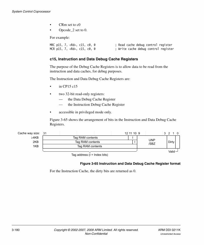
System Control Coprocessor
• CRm set to c0
• Opcode_2 set to 0.
For example:
MRC p15, 7, <Rd>, c15, c0, 0 ; Read cache debug control registerMCR p15, 7, <Rd>, c15, c0, 0 ; Write cache debug control register
c15, Instruction and Data Debug Cache Registers
The purpose of the Debug Cache Registers is to allow data to be read from the instruction and data caches, for debug purposes.
The Instruction and Data Debug Cache Registers are:
• in CP15 c15
• two 32-bit read-only registers:
— the Data Debug Cache Register
— the Instruction Debug Cache Register
• accessible in privileged mode only.
Figure 3-65 shows the arrangement of bits in the Instruction and Data Debug Cache Registers.
Figure 3-65 Instruction and Data Debug Cache Register format
For the Instruction Cache, the dirty bits are returned as 0.
Tag RAM contentsTag RAM contents I
ITag RAM contents31 3 2 1 0
UNP/SBZ Dirty
12 11 10 9
Tag address (I = Index bits)
Cache way size:
Valid
2KB1KB
4KB
3-180 Copyright © 2002-2007, 2009 ARM Limited. All rights reserved. ARM DDI 0211KNon-Confidential Unrestricted Access

System Control Coprocessor
As shown in Figure 3-65 on page 3-180, the formation of the Tag address depends on the cache way size. The returned address consists of Tag RAM contents data, and possibly some Tag Index data. This is described more fully in Table 3-148.
Constructing the Tag address in this way ensures that the data format returned is consistent regardless of cache size.
Accessing the Instruction and Data Debug Cache Registers
Table 3-149 shows the results of attempted accesses to the Instruction and Data Debug Cache Registers for each mode.
To access the Instruction and Data Debug Cache Registers you read CP15 with:
• Opcode_1 set to 3
• CRn set to c15
• CRm set to c0
• Opcode_2 set to select the Debug Cache Register you want to read:
— Opcode_2 = 0 for the Data Debug Cache Register
— Opcode_2 = 1 for the Instruction Debug Cache Register.
For example:
MRC p15, 3, <Rd>, c15, c0, 0 ; Read Data Debug Cache RegisterMRC p15, 3, <Rd>, c15, c0, 1 ; Read Instruction Debug Cache Register
Table 3-148 Construction of the Tag address
Cache way sizeDebug Cache Register bits returned, as part of Tag address
Tag RAM contents Tag Index
4KB or larger Bits[31:12] Bits[11:10]
2KB Bits[31:11] Bit[10]
1KB Bits[31:10] -
Table 3-149 Results of accesses to the Instruction and Data DebugCache Registers
Privileged read Privileged write User read or write
Data read Undefined Instruction exception Undefined Instruction exception
ARM DDI 0211K Copyright © 2002-2007, 2009 ARM Limited. All rights reserved. 3-181Unrestricted Access Non-Confidential

System Control Coprocessor
Using the Instruction and Data Debug Cache Registers
Reading one of these registers reads a single entry from the instruction or data cache. Usually, the debugger will do this immediately after performing one of the following, by using the appropriate MCR operations:
• Write to the Data Tag RAM Read Operation Register, to transfer Way and Set information to the data cache. This causes a read of this word in the data Tag RAM into the Data Debug Cache Register.
• Write to the Instruction Tag RAM Read Operation Register, to transfer Way and Set information to the instruction cache. This causes a read of this word in the instruction Tag RAM into the Instruction Debug Cache Register.
• Write to the Instruction Cache Data RAM Read Operation Register, to transfer Set, Way and word information to the instruction cache. This causes a read of this word in the instruction cache into the Instruction Debug Cache Register.
Table 3-145 on page 3-178 lists the MCR instructions required for each of these operations, and the format of the Read Operation Register data is described in The Read Operation Registers.
The MCR operation is then followed by an MRC operation to read the appropriate Debug Cache Register.
The debugger can use the addresses generated from the Tag to access memory, including the cache.
For SmartCache debug:
• the base address register can be read to determine the addresses that are covered by the SmartCache
• linefill operation must be disabled, using the Cache Debug Control Register, to avoid the process of reading data for debug purposes bringing data into the SmartCache.
The Read Operation Registers
The purpose of the Read Operation Registers is to permit a debugger to cause a Tag RAM or data RAM read operation, as described in Using the Instruction and Data Debug Cache Registers.
The Read Operation Registers are:
• in CP15 c15
• three 32 bit write-only registers:
— the Data Tag RAM Read Operation Register
3-182 Copyright © 2002-2007, 2009 ARM Limited. All rights reserved. ARM DDI 0211KNon-Confidential Unrestricted Access

System Control Coprocessor
— the Instruction Tag RAM Read Operation Register
— the Instruction Cache Data RAM Read Operation Register
• accessible in privileged mode only.
The Instruction Cache Data RAM Read Operation Register format
When you write to the Instruction Cache Data RAM Read Operation Register you have to provide Set, Way and Word data. The arrangement of bits in the register is shown in Figure 3-66.
Figure 3-66 Instruction Cache Data RAM Read Operation Register format
In this register format:
• A = log2(Associativity) rounded up to the next integer
• S = log2(N Set)
Associativity and N set are cache size parameters, and can be found in the Cache Type register. For more information, see c0, Cache Type Register on page 3-27.
The Data and Instruction Tag RAM Read Operation Register formats
The Tag RAM Read Operations register require Way and Set data. The arrangement of bits in the register is shown in Figure 3-67. The A and S values are defined in the same way as they are for Figure 3-66.
Figure 3-67 Tag RAM Read Operation Register format
Way
3132-A
31-AS+5
S+4
5 4 2 1 0
SBZ/UNP Set Word in line
SBZ/UNP
Way
3132-A
31-AS+5
S+4
5 4 0
SBZ/UNP Set SBZ/UNP
ARM DDI 0211K Copyright © 2002-2007, 2009 ARM Limited. All rights reserved. 3-183Unrestricted Access Non-Confidential

System Control Coprocessor
Accessing the Read Operation Registers
Table 3-150 shows the results of attempted accesses to the Read Operation Registers for each mode.
To access the Read Operation Registers you write CP15 with:
• Opcode_1 set to 3
• CRn set to c15
• CRm set to select between the Tag RAM and the Instruction Cache Data RAM Read Operations Registers:
— CRm = c2 for the Tag RAM Read Operation Registers
— CRm = c4 for the Instruction Cache Data RAM Read Operations Register
• Opcode_2 set to select the Read Operation Registers you want to access:
— Opcode_2 = 0 for the Data Tag RAM Read Operation Register
— Opcode_2 = 1 for the Instruction Tag RAM Read Operation Register
— Opcode_2 = 1 for the Instruction Cache Data RAM Read Operations Register.
For example:
MCR p15, 3, <Rd>, c15, c2, 0 ; Write Data Tag RAM Read Operation RegisterMCR p15, 3, <Rd>, c15, c2, 1 ; Write Instruction Tag RAM Read Operation RegisterMCR p15, 3, <Rd>, c15, c4, 1 ; Write Instruction Cache Data RAM Read Operations Register
3.3.44 c15, Cache and Main TLB Master Valid Registers
The purpose of the Cache and Main TLB Master Valid Registers is to hold the state of the Master Valid bits of the instruction and data caches, SmartCaches and main TLBs.
The Master Valid bits enable the Valid bits held in the Instruction and Data Valid RAM for the cache and SmartCache to be masked, so that a single cycle invalidation of the cache can be performed without requiring special resettable RAM cells.
Table 3-150 Results of accesses to the Instruction and Data DebugCache Registers
Privileged read Privileged write User read or write
Undefined Instruction exception Data read Undefined Instruction exception
3-184 Copyright © 2002-2007, 2009 ARM Limited. All rights reserved. ARM DDI 0211KNon-Confidential Unrestricted Access

System Control Coprocessor
The Cache and Main TLB Master Valid Registers are:
• In CP15 c15.
• 32-bit read/write registers. In most cases, the number of registers depends on the cache size:
— up to eight Instruction Cache Master Valid Registers, depending on the instruction cache size
— up to eight Instruction SmartCache Master Valid Registers, depending on the instruction SmartCache size
— up to eight Data Cache Master Valid Registers, depending on the data cache size
— up to eight Data SmartCache Master Valid Registers, depending on the data SmartCache size
— two Main TLB Master Valid Registers.
• Accessible in privileged mode only.
Figure 3-68 shows the arrangement of the CP15 Cache and Main TLB Master Valid Registers.
Figure 3-68 Cache and Main TLB Master Valid Registers
c15 {0 - 7†}c83{0 - 7†}c10
Instruction Cache Master Valid Registers
Data Cache Master Valid Registers
CRn CRmOpcode_1 Opcode_2
{0 - 7†}c12
{0, 1}5 c14
Accessible in User modeRead-only Read/write Write-only
Main TLB Master Valid RegistersData SmartCache Master Valid Registers
Instruction SmartCache Master Valid Registers
† Maximum Opcode_2 value is implementation-dependent, see register descriptions for details.
{0 - 7†}c14
ARM DDI 0211K Copyright © 2002-2007, 2009 ARM Limited. All rights reserved. 3-185Unrestricted Access Non-Confidential

System Control Coprocessor
Table 3-151 shows the instructions used to access the Cache and Main TLB Master Valid Registers.
The cache and Main TLB Master Valid Registers are summarized in Table 3-152.
Table 3-151 Cache debug CP15 operations
Function Instruction
Read Instruction Cache Master Valid Register MRC p15, 3, <Rd>, c15, c8, <Register Number>
Write Instruction Cache Master Valid Register MCR p15, 3, <Rd>, c15, c8, <Register Number>
Read Instruction SmartCache Master Valid Register MRC p15, 3, <Rd>, c15, c10, <Register Number>
Write Instruction SmartCache Master Valid Register MCR p15, 3, <Rd>, c15, c10, <Register Number>
Read Data Cache Master Valid Register MRC p15, 3, <Rd>, c15, c12, <Register Number>
Write Data Cache Master Valid Register MCR p15, 3, <Rd>, c15, c12, <Register Number>
Read Data SmartCache Master Valid Register MRC p15, 3, <Rd>, c15, c14, <Register Number>
Write Data SmartCache Master Valid Register MCR p15, 3, <Rd>, c15, c14, <Register Number>
Read Main TLB Master Valid Register MRC p15, 5, <Rd>, c15, c14, <Register Number>
Write Main TLB Master Valid Register MCR p15, 5, <Rd>, c15, c14, Register Number>
Table 3-152 Cache and Main TLB Master Valid Registers summary
Register CRmaNumberb
of registersDescription
Instruction Cache Master Valid Register c8 8 See Instruction Cache and Instruction SmartCache Master Valid Registers on page 3-187Instruction SmartCache Master Valid Register c10 8
Data Cache Master Valid Register c12 8 See Data Cache and Data SmartCache Master Valid Registers on page 3-188
Data SmartCache Master Valid Register c14 8
Main TLB Master Valid Register c14 2 See Main TLB Master Valid Registers on page 3-190
a. See Figure 3-68 on page 3-185 for the complete access functions for each register.b. There are always two Main TLB Master Valid Registers. The number of Instruction and Data Cache and SmartCache Master
Valid Registers depends on the cache sizes, and the numbers given here are the maximum numbers possible.
3-186 Copyright © 2002-2007, 2009 ARM Limited. All rights reserved. ARM DDI 0211KNon-Confidential Unrestricted Access

System Control Coprocessor
Instruction Cache and Instruction SmartCache Master Valid Registers
The purpose of the Instruction Cache and Instruction SmartCache Master Valid Registers is to permit the master valid bits for the instruction cache and the instruction SmartCache to be saved and restored. The reasons you might want to do this are:
• to save the cache master valid bits immediately before entering Dormant mode, and to restore the cache master valid bits on leaving Dormant mode
• for debug purposes.
The Instruction Cache and Instruction SmartCache Master Valid Registers are:
• in CP15 c15
• 32-bit read/write registers
• accessible in privileged mode only.
The number of Instruction Cache Master Valid Registers implemented depends on the size of the instruction cache, and the number of Instruction SmartCache Master Valid Registers implemented depends on the size of the instruction SmartCache. There is one master valid bit for each 8 cache lines, or for each 8 SmartCache lines:
For example, there are 64 master valid bits for a 16KB cache or SmartCache. Each Master Valid Register holds 32 master valid bits. In this way, the total number of master valid bits determines the number of Master Valid Registers.
For the Instruction Cache and Instruction SmartCache Master Valid Registers:
• the maximum cache or SmartCache size of 64KB gives 256 master valid bits, requiring eight Master Valid Registers
• the Master Valid Registers number up from 0
• the master valid bits fill the registers from the LSB of the Master Valid Register 0
• reads of unimplemented master valid bits are Unpredictable, and writes to unimplemented bits are Should Be Zero or Preserved (SBZP)
• the reset value of all Master Valid Registers is 0.
line length in bytes x 8cache size
Number of master valid bits = ( )
ARM DDI 0211K Copyright © 2002-2007, 2009 ARM Limited. All rights reserved. 3-187Unrestricted Access Non-Confidential
System Control Coprocessor
Accessing the Instruction Cache and Instruction SmartCache Master Valid Registers
Table 3-153 shows the results of attempted accesses to the Instruction Cache and Instruction SmartCache Master Valid Registers for each mode.
To access the Instruction Cache and Instruction SmartCache Master Valid Registers you read or write CP15 with:
• Opcode_1 set to 3
• CRn set to c15
• CRm set to:
— c8 to access the Instruction Cache Master Valid Registers
— c10 to access the Instruction SmartCache Master Valid Registers
• Opcode_2 set to the number of the Master Valid Registers you want to access. The numbering of the registers was described earlier. The value of Opcode_2 is always in the range 0 to 7.
For example:
MRC p15, 3, <Rd>, c15, c8, 1 ; Read Instruction Cache Master Valid Register 1MCR p15, 3, <Rd>, c15, c8, 1 ; Write Instruction Cache Master Valid Register 1MRC p15, 3, <Rd>, c15, c10, 0 ; Read Instruction SmartCache Master Valid Register 0MCR p15, 3, <Rd>, c15, c10, 0 ; Write Instruction SmartCache Master Valid Register 0
The command examples show accesses to Instruction Cache Master Valid Register 1 and to Instruction SmartCache Master Valid Register 0. The general forms of the instructions are as shown, with <CRm> set to c8 or c10:
MRC p15, 3, <Rd>, c15, <CRm>, <Register Number> ; Read Instruction (Smart)Cache Master Valid RegisterMCR p15, 3, <Rd>, c15, <CRm>, <Register Number> ; Write Instruction (Smart)Cache Master Valid Register
Data Cache and Data SmartCache Master Valid Registers
The purpose of the Data Cache and Data SmartCache Master Valid Registers is to permit the master valid bits for the data cache and the data SmartCache to be saved and restored. The reasons you might want to do this are:
• to save the cache master valid bits immediately before entering Dormant mode, and to restore the cache master valid bits on leaving Dormant mode
Table 3-153 Results of accesses to the Instruction Cache and InstructionSmartCache Master Valid Registers
Privileged read Privileged write User read or write
Data read Data write Undefined Instruction exception
3-188 Copyright © 2002-2007, 2009 ARM Limited. All rights reserved. ARM DDI 0211KNon-Confidential Unrestricted Access

System Control Coprocessor
• for debug purposes.
The Data Cache and Data SmartCache Master Valid Registers are:
• in CP15 c15
• 32-bit read/write registers
• accessible in privileged mode only.
The number of Data Cache Master Valid Registers implemented depends on the size of the data cache, and the number of Data SmartCache Master Valid Registers implemented depends on the size of the data SmartCache. There is one master valid bit for each 8 cache lines, or for each 8 SmartCache lines:
For example, there are 64 master valid bits for a 16KB cache or SmartCache. Each Master Valid Register holds 32 master valid bits. In this way, the total number of master valid bits determines the number of Master Valid Registers.
For the Data Cache and Data SmartCache Master Valid Registers:
• the maximum cache or SmartCache size of 64KB gives 256 master valid bits, requiring eight Master Valid Registers
• the Master Valid Registers number up from 0
• the master valid bits fill the registers from the LSB of the Master Valid Register 0
• reads of unimplemented master valid bits are Unpredictable, and writes to unimplemented bits are Should Be Zero or Preserved (SBZP)
• the reset value of all Master Valid Registers is 0.
Accessing the Data Cache and Data SmartCache Master Valid Registers
Table 3-153 on page 3-188 shows the results of attempted accesses to the Data Cache and Data SmartCache Master Valid Registers for each mode.
Table 3-154 Results of accesses to the Data Cache and Data SmartCacheMaster Valid Registers
Privileged read Privileged write User read or write
Data read Data write Undefined Instruction exception
line length in bytes x 8cache size
Number of master valid bits = ( )
ARM DDI 0211K Copyright © 2002-2007, 2009 ARM Limited. All rights reserved. 3-189Unrestricted Access Non-Confidential

System Control Coprocessor
To access the Data Cache and Data SmartCache Master Valid Registers you read or write CP15 with:
• Opcode_1 set to 3
• CRn set to c15
• CRm set to:
— c12 to access the Data Cache Master Valid Registers
— c14 to access the Data SmartCache Master Valid Registers
• Opcode_2 set to the number of the Master Valid Registers you want to access. The numbering of the registers was described earlier. The value of Opcode_2 is always in the range 0 to 7.
For example:
MRC p15, 3, <Rd>, c15, c12, 2 ; Read Data Cache Master Valid Register 2MCR p15, 3, <Rd>, c15, c12, 2 ; Write Data Cache Master Valid Register 2MRC p15, 3, <Rd>, c15, c14, 1 ; Read Data SmartCache Master Valid Register 1MCR p15, 3, <Rd>, c15, c14, 1 ; Write Data SmartCache Master Valid Register 1
The command examples show accesses to Data Cache Master Valid Register 2 and to Data SmartCache Master Valid Register 1. The general forms of the instructions are as shown, with <CRm> set to c12 or c14:
MRC p15, 3, <Rd>, c15, <CRm>, <Register Number> ; Read Data (Smart)Cache Master Valid RegisterMCR p15, 3, <Rd>, c15, <CRm>, <Register Number> ; Write Data (Smart)Cache Master Valid Register
Main TLB Master Valid Registers
The purpose of the Main TLB Master Valid Registers is to permit the master valid bits for the main TLB to be saved and restored. The reasons you might want to do this are:
• to save the main TLB master valid bits immediately before entering Dormant mode, and to restore the main TLB master valid bits on leaving Dormant mode
• for debug purposes.
Note Although you can safely read the Main TLB Master Valid Registers to read the main TLB master valid bits, writing the Main TLB Master Valid Registers to modify the values of these bits can be Unpredictable. You must only write to the Main TLB Master Valid Registers when the cache and main TLB are disabled, and you must only write back the values which you have previously read from the Main TLB Master Valid Registers.
3-190 Copyright © 2002-2007, 2009 ARM Limited. All rights reserved. ARM DDI 0211KNon-Confidential Unrestricted Access

System Control Coprocessor
The Main TLB Master Valid Registers are:
• in CP15 c15
• two 32-bit read/write registers
• accessible in privileged mode only.
Accessing the Main TLB Master Valid Registers
Table 3-153 on page 3-188 shows the results of attempted accesses to the Main TLB Master Valid Registers for each mode.
To access the Main TLB Master Valid Registers you read or write CP15 with:
• Opcode_1 set to 5
• CRn set to c15
• CRm set to c14
• Opcode_2 set to the number of the Main TLB Master Valid Register you want to access. This will be 0 or 1.
For example:
MRC p15, 5, <Rd>, c15, c14, 0 ; Read Main TLB Master Valid Register 0MCR p15, 5, <Rd>, c15, c14, 1 ; Write Main TLB Master Valid Register 1
Table 3-155 Results of accesses to the Main TLB Master Valid Registers
Privileged read Privileged write User read or write
Data read Data write Undefined Instruction exception
ARM DDI 0211K Copyright © 2002-2007, 2009 ARM Limited. All rights reserved. 3-191Unrestricted Access Non-Confidential

System Control Coprocessor
3.3.45 c15, MMU debug operations overview
Figure 3-69 shows the arrangement of the CP15 registers provided for MMU debug operations. You can also use these registers to read state information before you enter Dormant mode, and to restore state information on returning from Dormant mode.
Figure 3-69 Registers for MMU debug operations
These registers are described in the following sections:
• c15, Instruction MicroTLB and Data MicroTLB Index Registers
• c15, Main TLB Entry Registers (Main TLB Index Registers) on page 3-194
• c15, TLB VA Registers on page 3-196
• c15, TLB PA Registers on page 3-199
• c15, TLB Attribute Registers on page 3-202
• c15, TLB Debug Control Register on page 3-207.
MMU debugging on page 3-209 describes using these registers to perform MMU debug.
c15, Instruction MicroTLB and Data MicroTLB Index Registers
The purpose of the MicroTLB Index Registers is to provide access to the Instruction and Data MicroTLB entries.
c15 0c45
2 Read Main TLB Entry Register (Main TLB index)
Data MicroTLB Index Register
Data MicroTLB VA Register
CRn CRmOpcode_1 Opcode_2
4 Write Main TLB Entry Register (Main TLB index)0c512
Instruction MicroTLB VA RegisterMain TLB VA RegisterData MicroTLB PA RegisterInstruction MicroTLB PA RegisterMain TLB PA Register
012
c6
Data MicroTLB Attribute RegisterInstruction MicroTLB Attribute RegisterMain TLB Attribute Register
012
c7
07 c1 TLB Debug Control Register
Accessible in User modeRead-only Read/write Write-only
Shown for rev1 (r1pX) releases, see register summary tables for changes from rev0.
Instruction MicroTLB Index Register1
3-192 Copyright © 2002-2007, 2009 ARM Limited. All rights reserved. ARM DDI 0211KNon-Confidential Unrestricted Access

System Control Coprocessor
The MicroTLB Index Registers are:
• in CP15 c15
• two 32 bit read/write registers
— the Instruction MicroTLB Index Register
— the Data MicroTLB Index Register
• accessible in privileged mode only.
Figure 3-70 shows the arrangement of bits in the registers.
Figure 3-70 MicroTLB Index Register format
Table 3-156 shows the bit functions of the MicroTLB Index Registers.
Note MicroTLB index values greater than 10 do not access any MicroTLB entry.
Accessing the MicroTLB Index Registers
Table 3-157 shows the results of attempted accesses to the Instruction MicroTLB and Data MicroTLB Index Registers for each mode.
To access the MicroTLB Index Registers you read or write CP15 with:
• Opcode_1 set to 5
SBZ
31 3 0
Index
4
Table 3-156 MicroTLB Index Registers bit functions
Bit range Field name Function
[31:4] SBZ/UNP.
[3:0] Index Indicates which entry in the MicroTLB is accessed.
Permitted values are b0000 to b1010, decimal 0 to 10.
Table 3-157 Results of accesses to the Instruction MicroTLB and DataMicroTLB Index Registers
Privileged read Privileged write User read or write
Data read Data write Undefined Instruction exception
ARM DDI 0211K Copyright © 2002-2007, 2009 ARM Limited. All rights reserved. 3-193Unrestricted Access Non-Confidential

System Control Coprocessor
• CRn set to c15
• CRm set to c4
• Opcode_2 set to:
— 0 to access the Data MicroTLB Index Register
— 1 to access the Instruction MicroTLB Index Register.
For example:
MRC p15, 5, <Rd>, c15, c4, 0 ; Read Data MicroTLB Index RegisterMCR p15, 5, <Rd>, c15, c4, 0 ; Write Data MicroTLB Index RegisterMRC p15, 5, <Rd>, c15, c4, 1 ; Read Instruction MicroTLB Index RegisterMCR p15, 5, <Rd>, c15, c4, 1 ; Write Instruction MicroTLB Index Register
See MicroTLB debug on page 3-209 for a description of using the MicroTLB Index Registers for debugging the MicroTLBs.
c15, Main TLB Entry Registers (Main TLB Index Registers)
The purpose of the Main Entry Registers is to provide access to main TLB read and write entries. The registers are also referred to as the Main TLB Index Registers.
The Main TLB Entry Registers are:
• in CP15 c15
• two 32 bit write-only registers
— the Read Main TLB Entry Register
— the Write Main TLB Entry Register
• accessible in privileged mode only.
Figure 3-71 shows the arrangement of bits in the registers.
Figure 3-71 Main TLB Index Register format
L
31 30 6 5 0
SBZ Index
3-194 Copyright © 2002-2007, 2009 ARM Limited. All rights reserved. ARM DDI 0211KNon-Confidential Unrestricted Access

System Control Coprocessor
Table 3-158 shows the bit functions of the Main TLB Entry Registers.
Accessing the Main TLB Entry Registers
Table 3-159 shows the results of attempted accesses to the Main TLB Entry Registers for each mode.
To access the Main TLB Entry Registers you write CP15 with:
• Opcode_1 set to 5
• CRn set to c15
• CRm set to c4
• Opcode_2 set to:
— 2 to access the Read Main TLB Entry Register
— 4 to access the Write Main TLB Entry Register.
For example:
MCR p15, 5, <Rd>, c15, c4, 2 ; Write to Read Main TLB Entry RegisterMCR p15, 5, <Rd>, c15, c4, 4 ; Write to Write Main TLB Entry Register
Table 3-158 Main TLB Entry Registers bit functions
Bit range
Name Meaning
[31] L Lockable region. Indicates whether the index refers to the lockable region or the set-associative region:
0 = Index refers to the set-associative region
1 = Index refers to the lockable region.
[30:6] - SBZ.
[5:0] Index Indicates which entry in the main TLB is accessed. The meaning of this field depends on the setting of the L bit:
L = 0 Index[5] indicates which Way of the main TLB set-associative region is being accessed.
Index[4:0] indexes the Set of the RAM.
L = 1 Index[5:3] SBZ.
Index[2:0] indicates which entry in the lockable region is being accessed.
Table 3-159 Results of accesses to the Main TLB Entry Registers
Privileged read Privileged write User read or write
Undefined Instruction exception Data write Undefined Instruction exception
ARM DDI 0211K Copyright © 2002-2007, 2009 ARM Limited. All rights reserved. 3-195Unrestricted Access Non-Confidential

System Control Coprocessor
See Main TLB debug on page 3-210 for a description of using the Main TLB Entry Registers for debugging the main TLBs.
3.3.46 Registers for MMU debug operations
The arrangement of the registers for MMU debug operations is shown in Figure 3-69 on page 3-192. The registers are described in the following sections:
• c15, Instruction MicroTLB and Data MicroTLB Index Registers on page 3-192
• c15, Main TLB Entry Registers (Main TLB Index Registers) on page 3-194
• c15, TLB VA Registers
• c15, TLB PA Registers on page 3-199
• c15, TLB Attribute Registers on page 3-202
• c15, TLB Debug Control Register on page 3-207.
c15, TLB VA Registers
The purpose of the TLB VA Registers is to provide access to TLB Virtual Address (VA) information. The registers enable you to:
• Read VA information for the Data and Instruction MicroTLBs
• Read or write VA information for the main TLB.
The TLB VA Registers are:
• in CP15 c15
• two 32 bit read-only registers and one 32 bit read/write register:
— the Data MicroTLB VA Register (read-only)
— the Instruction MicroTLB VA Register (read-only)
— the Main TLB VA Register (read/write)
• accessible in privileged mode only.
Figure 3-72 shows the arrangement of bits in the registers.
Figure 3-72 TLB VA Registers format
VA
31 10 9 0
Process
3-196 Copyright © 2002-2007, 2009 ARM Limited. All rights reserved. ARM DDI 0211KNon-Confidential Unrestricted Access

System Control Coprocessor
Table 3-160 shows the bit functions of the TLB VA Registers.
Table 3-161 shows the TLB VA Register Index bits.
Figure 3-73 shows the format of the memory space identifier.
Figure 3-73 TLB VA Registers memory space identifier format
Table 3-160 TLB VA Registers bit functions
Bit range Name Function
[31:10] VA Virtual Address.
Bits of the virtual address that are not translated as part of the page table translation, because of the region size, are Unpredictable when read, and Should Be Zero when writtena. For writes to the Main TLB VA Register, when the L bit of the Main TLB entry register is set to 0, some bits of the virtual address must equal bits [4:0] of the Index field of that register, see c15, Main TLB Entry Registers (Main TLB Index Registers) on page 3-194. Table 3-161 shows the bits affected for each region size.
[9:0] PROCESS Memory space identifier that determines if the entry is a global mapping, or an ASID dependent entry. See Figure 3-73 for the format of this field.
a. MicroTLB PA Registers cannot be written; see Accessing the TLB VA Registers on page 3-198.
Table 3-161 TLB VA Register Index bits
Region size Bits of the TLB VA Register that must equal Index[4:0]a
a. Bits [4:0] of the Index field of the Main TLB Entry Register.
4KB page [16:12]
64KB page [20:16]
1MB section [24:20]
16MB supersection [28:24]
9 8 7 0
1 SBZ
0 ASID
Global entries
ASID entries
SBZ
ARM DDI 0211K Copyright © 2002-2007, 2009 ARM Limited. All rights reserved. 3-197Unrestricted Access Non-Confidential

System Control Coprocessor
Accessing the TLB VA Registers
Table 3-162 shows the results of attempted accesses to the Data MicroTLB VA and Instruction MicroTLB VA Registers for each mode.
Table 3-163 shows the results of attempted accesses to the Main TLB VA Register for each mode.
To access the Data MicroTLB VA Register or the Instruction MicroTLB VA Register you read CP15 with:
• Opcode_1 set to 5
• CRn set to c15
• CRm set to c5
• Opcode_2 set to
— 0 to access the Data MicroTLB VA Register
— 1 to access the Instruction MicroTLB VA Register.
For example:
MRC p15, 5, <Rd>, c15, c5, 0 ; Read Data MicroTLB VA RegisterMRC p15, 5, <Rd>, c15, c5, 1 ; Read Instruction MicroTLB VA Register
To access the Main TLB VA Register you read or write CP15 with:
• Opcode_1 set to 5
• CRn set to c15
• CRm set to c5
• Opcode_2 set to 2.
For example:
MRC p15, 5, <Rd>, c15, c5, 2 ; Read Main TLB VA RegisterMCR p15, 5, <Rd>, c15, c5, 2 ; Write Main TLB VA Register
Table 3-162 Results of accesses to the Data MicroTLB VA and InstructionMicroTLB VA Registers
Privileged read Privileged write User read or write
Data read Undefined Instruction exception Undefined Instruction exception
Table 3-163 Results of accesses to the Main TLB VA Register
Privileged read Privileged write User read or write
Data read Data write Undefined Instruction exception
3-198 Copyright © 2002-2007, 2009 ARM Limited. All rights reserved. ARM DDI 0211KNon-Confidential Unrestricted Access

System Control Coprocessor
See MicroTLB debug on page 3-209 for a description of using the MicroTLB VA Registers for debugging the MicroTLBs, and Main TLB debug on page 3-210 for a description of using the Main TLB VA Register for debugging the main TLBs.
c15, TLB PA Registers
The purpose of the TLB PA Registers is to provide access to TLB Physical Address (PA) information. The registers enable you to:
• Read PA information for the Data and Instruction MicroTLBs
• Read or write PA information for the main TLB.
The TLB PA Registers are:
• in CP15 c15
• two 32 bit read-only registers and one 32 bit read/write register:
— the Data MicroTLB PA Register (read-only)
— the Instruction MicroTLB PA Register (read-only)
— the Main TLB PA Register (read/write)
• accessible in privileged mode only.
Figure 3-74 shows the arrangement of bits in the registers.
Figure 3-74 TLB PA Registers format
VPA
31 10 9 6 5 4 3 1 0
SZ AP
XRGN
ARM DDI 0211K Copyright © 2002-2007, 2009 ARM Limited. All rights reserved. 3-199Unrestricted Access Non-Confidential

System Control Coprocessor
Table 3-164 describes the functions of the TLB PA Register bits.
Table 3-165 shows the encoding of the SZ field.
Table 3-164 TLB PA Registers bit functions
Bit range Name Function
[31:10] PA Physical Address.
Bits of the physical address that are not translated as part of the page table translation are Unpredictable when read and Should Be Zero when writtena.
[9:6] SZ Region size. Table 3-165 shows the format of the SZ field.
The region size that is contained in the MicroTLB might be smaller than specified in the page tables. The MicroTLB can split main TLB entries that cover regions which cover areas of memory contained in the TCM into smaller sizes. In addition, subpages are reported as separate pages in the MicroTLBs.
[5:4] XRGN Extended Region Type. Table 3-166 on page 3-201 shows the region type bits used to determine the attributes for the memory region.
[3:1] AP Access Permissions. Table 3-167 on page 3-201 shows the format of the AP field:
• for MicroTLB entries this field contains the access permissions for the subpage that is contained in that MicroTLB entry
• for main TLB entries, this register contains the access permission fields for the first subpage, or for the entire page/section if the page does not support subpages.
[0] V Valid bit. Indicates that this TLB entry is valid.
a. MicroTLB PA Registers cannot be written; see Accessing the TLB PA Registers on page 3-201.
Table 3-165 TLB PA Registers SZ field encoding
SZ Description Note
b1111 1KB subpage Used by MicroTLB only
b1110 4KB page -
b1100 16KB subpage Used by MicroTLB only
b1000 64KB page -
b0000 1MB section For a MicroTLB, part of 16MB supersection
b0001 16MB supersection Used by main TLB only
All other values Reserved -
3-200 Copyright © 2002-2007, 2009 ARM Limited. All rights reserved. ARM DDI 0211KNon-Confidential Unrestricted Access
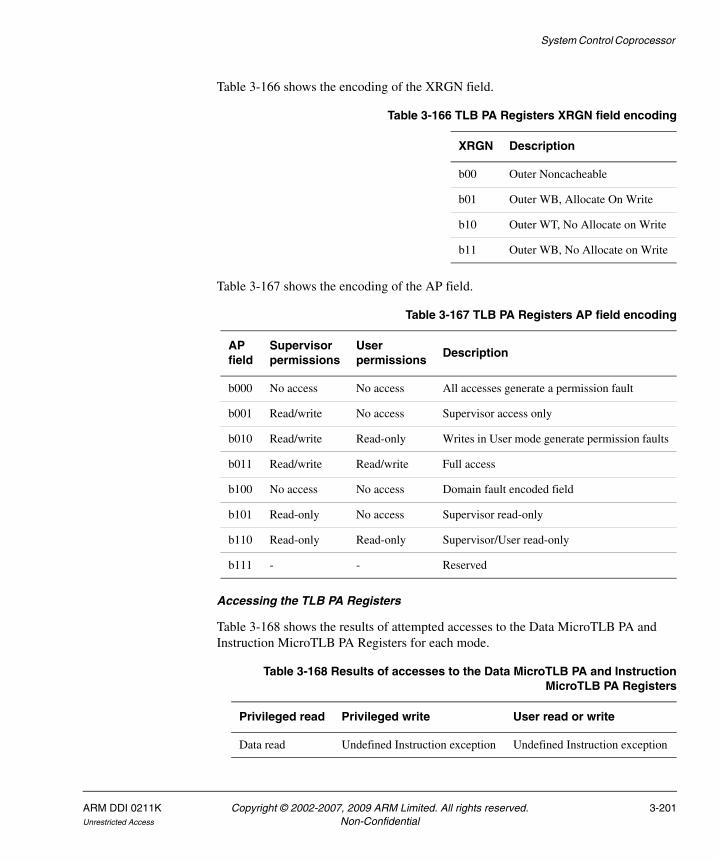
System Control Coprocessor
Table 3-166 shows the encoding of the XRGN field.
Table 3-167 shows the encoding of the AP field.
Accessing the TLB PA Registers
Table 3-168 shows the results of attempted accesses to the Data MicroTLB PA and Instruction MicroTLB PA Registers for each mode.
Table 3-166 TLB PA Registers XRGN field encoding
XRGN Description
b00 Outer Noncacheable
b01 Outer WB, Allocate On Write
b10 Outer WT, No Allocate on Write
b11 Outer WB, No Allocate on Write
Table 3-167 TLB PA Registers AP field encoding
AP field
Supervisor permissions
User permissions
Description
b000 No access No access All accesses generate a permission fault
b001 Read/write No access Supervisor access only
b010 Read/write Read-only Writes in User mode generate permission faults
b011 Read/write Read/write Full access
b100 No access No access Domain fault encoded field
b101 Read-only No access Supervisor read-only
b110 Read-only Read-only Supervisor/User read-only
b111 - - Reserved
Table 3-168 Results of accesses to the Data MicroTLB PA and InstructionMicroTLB PA Registers
Privileged read Privileged write User read or write
Data read Undefined Instruction exception Undefined Instruction exception
ARM DDI 0211K Copyright © 2002-2007, 2009 ARM Limited. All rights reserved. 3-201Unrestricted Access Non-Confidential

System Control Coprocessor
Table 3-169 shows the results of attempted accesses to the Main TLB PA Register for each mode.
To access the Data MicroTLB PA Register or the Instruction MicroTLB PA Register you read CP15 with:
• Opcode_1 set to 5
• CRn set to c15
• CRm set to c6
• Opcode_2 set to
— 0 to access the Data MicroTLB PA Register
— 1 to access the Instruction MicroTLB PA Register.
For example:
MRC p15, 5, <Rd>, c15, c6, 0 ; Read Data MicroTLB PA RegisterMRC p15, 5, <Rd>, c15, c6, 1 ; Read Instruction MicroTLB PA Register
To access the Main TLB PA Register you read or write CP15 with:
• Opcode_1 set to 5
• CRn set to c15
• CRm set to c6
• Opcode_2 set to 2.
For example:
MRC p15, 5, <Rd>, c15, c6, 2 ; Read Main TLB PA RegisterMCR p15, 5, <Rd>, c15, c6, 2 ; Write Main TLB PA Register
See MicroTLB debug on page 3-209 for a description of using the MicroTLB PA Registers for debugging the MicroTLBs, and Main TLB debug on page 3-210 for a description of using the Main TLB PA Register for debugging the main TLBs.
c15, TLB Attribute Registers
The purpose of the TLB Attribute Registers is to provide access to the TLB attributes. The registers enable you to:
• Read attribute information for the Data and Instruction MicroTLBs
• Read or write attribute information for the main TLB.
Table 3-169 Results of accesses to the Main TLB PA Register
Privileged read Privileged write User read or write
Data read Data write Undefined Instruction exception
3-202 Copyright © 2002-2007, 2009 ARM Limited. All rights reserved. ARM DDI 0211KNon-Confidential Unrestricted Access

System Control Coprocessor
The TLB Attribute Registers are:
• in CP15 c15
• two 32 bit read-only registers and one 32 bit read/write register:
— the Data MicroTLB Attribute Register (read-only)
— the Instruction MicroTLB Attribute Register (read-only)
— the Main TLB PA Attribute Register (read/write)
• accessible in privileged mode only.
Figure 3-75 shows the arrangement of bits in the Main TLB Attribute Register, and Figure 3-76 shows the arrangement of bits in the MicroTLB Attribute Registers.
Figure 3-75 Main TLB Attribute Register format
Figure 3-76 MicroTLB Attribute Registers format
SPV
SAP3
31 30 29 28 27 26 25 24 9 8 5 4 3 1 0
AP2 AP1 SBZ Domain RGN
XN
SPV
SUNP
31 26 25 24 9 8 5 4 3 1 0
0 SBZ Domain RGN
XN
ARM DDI 0211K Copyright © 2002-2007, 2009 ARM Limited. All rights reserved. 3-203Unrestricted Access Non-Confidential

System Control Coprocessor
Table 3-170 shows the bit functions of the TLB Attribute Registers.
Table 3-170 TLB Attribute Registers bit functions
Bit range Name Function
[31:30] AP3 Main TLB Attributes register only.
Subpage access permissions for the fourth subpage if the page or section supports subpages. Unpredictable on read and Should Be Zero on a write if the entry does not support subpages. The format for the permissions is shown as the upper subpage permissions in Table 3-171 on page 3-205.
This field is Unpredictable for reads from the MicroTLB.
[29:28] AP2 Main TLB Attributes register only.
Subpage access permissions for third subpage if the page or section supports subpages. Unpredictable on read and Should Be Zero on a write if the entry does not support subpages. The format for the permissions is shown as the upper subpage permissions in Table 3-171 on page 3-205.
This field is Unpredictable for reads from the MicroTLB.
[27:26] AP1 Main TLB Attributes register only.
Subpage access permissions for second subpage if the page or section supports subpages. Unpredictable on read and Should Be Zero on a write if the entry does not support subpages. The format for the permissions is shown as the upper subpage permissions in Table 3-171 on page 3-205.
This field is Unpredictable for reads from the MicroTLB.
[25] SPV Subpage Valid. Indicates that the page or section supports subpages. Pages that support subpages must be marked as Global. Attempting to use subpages with non-global pages has Unpredictable results:
0 = Subpages are not supported
1 = Subpages are supported.
This field is 0 for reads from the MicroTLB.
[24:9] - Should Be Zero.
[8:5] Domain Domain number of the TLB entry.
[4] XN Execute Never attribute.
This field is Unpredictable for a read from the Data MicroTLB Attribute Register.
[3:1] RGN Region type. Table 3-172 on page 3-205 shows the format of the extended region field.
[0] S Shared attribute.
3-204 Copyright © 2002-2007, 2009 ARM Limited. All rights reserved. ARM DDI 0211KNon-Confidential Unrestricted Access
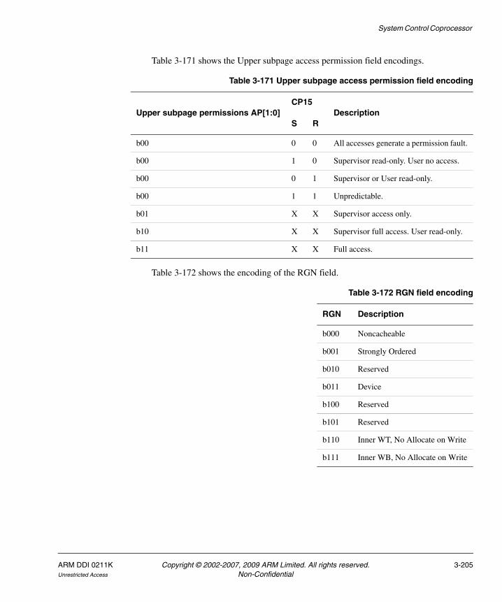
System Control Coprocessor
Table 3-171 shows the Upper subpage access permission field encodings.
Table 3-172 shows the encoding of the RGN field.
Table 3-171 Upper subpage access permission field encoding
Upper subpage permissions AP[1:0]CP15
DescriptionS R
b00 0 0 All accesses generate a permission fault.
b00 1 0 Supervisor read-only. User no access.
b00 0 1 Supervisor or User read-only.
b00 1 1 Unpredictable.
b01 X X Supervisor access only.
b10 X X Supervisor full access. User read-only.
b11 X X Full access.
Table 3-172 RGN field encoding
RGN Description
b000 Noncacheable
b001 Strongly Ordered
b010 Reserved
b011 Device
b100 Reserved
b101 Reserved
b110 Inner WT, No Allocate on Write
b111 Inner WB, No Allocate on Write
ARM DDI 0211K Copyright © 2002-2007, 2009 ARM Limited. All rights reserved. 3-205Unrestricted Access Non-Confidential

System Control Coprocessor
Table 3-173 shows the results of attempted accesses to the Data MicroTLB Attribute and Instruction MicroTLB Attribute Registers for each mode.
Table 3-174 shows the results of attempted accesses to the Main TLB Attribute Register for each mode.
To access the Data MicroTLB Attribute Register or the Instruction MicroTLB Attribute Register you read CP15 with:
• Opcode_1 set to 5
• CRn set to c15
• CRm set to c7
• Opcode_2 set to
— 0 to access the Data MicroTLB Attribute Register
— 1 to access the Instruction MicroTLB Attribute Register.
For example:
MRC p15, 5, <Rd>, c15, c7, 0 ; Read Data MicroTLB Attribute RegisterMRC p15, 5, <Rd>, c15, c7, 1 ; Read Instruction MicroTLB Attribute Register
To access the Main TLB Attribute Register you read or write CP15 with:
• Opcode_1 set to 5
• CRn set to c15
• CRm set to c7
• Opcode_2 set to 2.
For example:
MRC p15, 5, <Rd>, c15, c7, 2 ; Read Main TLB Attribute RegisterMCR p15, 5, <Rd>, c15, c7, 2 ; Write Main TLB Attribute Register
Table 3-173 Results of accesses to the Data MicroTLB Attribute and InstructionMicroTLB Attribute Registers
Privileged read Privileged write User read or write
Data read Undefined Instruction exception Undefined Instruction exception
Table 3-174 Results of accesses to the Main TLB Attribute Register
Privileged read Privileged write User read or write
Data read Data write Undefined Instruction exception
3-206 Copyright © 2002-2007, 2009 ARM Limited. All rights reserved. ARM DDI 0211KNon-Confidential Unrestricted Access

System Control Coprocessor
See MicroTLB debug on page 3-209 for a description of using the MicroTLB Attribute Registers for debugging the MicroTLBs, and Main TLB debug on page 3-210 for a description of using the Main TLB Attribute Register for debugging the main TLBs.
c15, TLB Debug Control Register
The purpose of the TLB Debug Control Register is to provide control of TLB operations for debug purposes.
The TLB Debug Control Register is:
• in CP15 c15
• a 32 bit read/write register
• accessible in privileged mode only.
Figure 3-77 shows the arrangement of bits in the register.
Figure 3-77 TLB Debug Control Register format
Table 3-175 shows the bit functions of the TLB Debug Control Register.
UNP/SBZ
31 8 7 6 5 4 3 2 1 0
IMMDMM
IMLDML
DULIULDUMIUM
Table 3-175 TLB Debug Control Register bit functions
Bit range Name Description
[31:8] - Reserved. UNP/SBZ.
[7] IMM Instruction Main TLB Match:
0 = Instruction main TLB match enabled. This is the reset value.
1 = Instruction main TLB match disabled.
[6] DMM Data Main TLB Match:
0 = Data main TLB match enabled. This is the reset value.
1 = Data main TLB match disabled.
[5] IML Instruction Main TLB Load:
0 = Instruction main TLB load enabled. This is the reset value.
1 = Instruction main TLB load disabled.
ARM DDI 0211K Copyright © 2002-2007, 2009 ARM Limited. All rights reserved. 3-207Unrestricted Access Non-Confidential

System Control Coprocessor
Note Because the ARM1136JF-S processor has a unified main TLB, you must always set the IMM bit to the same value as the DMM bit, and the IML bit to the same value as the DML bit. If you do not do this the result of TLB operations is Unpredictable.
Accessing the TLB Debug Control Register
Table 3-176 shows the results of attempted accesses to the TLB Debug Control Register for each mode.
To access the TLB Debug Control Register you read or write CP15 with:
• Opcode_1 set to 7
• CRn set to c15
[4] DML Data Main TLB Load:
0 = Data main TLB load enabled. This is the reset value.
1 = Data main TLB load disabled.
[3] IUM Instruction Unit Match (Instruction MicroTLB match):
0 = Instruction MicroTLB match enabled. This is the reset value.
1 = Instruction MicroTLB match disabled.
[2] DUM Data Unit Match (Data MicroTLB match):
1 = Data MicroTLB match disabled.
0 = Data MicroTLB match enabled. This is the reset value.
[1] IUL Instruction Unit Load (Instruction MicroTLB load):
1 = Instruction MicroTLB load and flush disabled.
0 = Instruction MicroTLB load and flush enabled. This is the reset value.
[0] DUL Data Unit Load (Data MicroTLB load):
1 = Data MicroTLB load and flush disabled.
0 = Data MicroTLB load and flush enabled. This is the reset value.
Table 3-175 TLB Debug Control Register bit functions (continued)
Bit range Name Description
Table 3-176 Results of accesses to the TLB Debug Control Register
Privileged read Privileged write User read or write
Data read Data write Undefined Instruction exception
3-208 Copyright © 2002-2007, 2009 ARM Limited. All rights reserved. ARM DDI 0211KNon-Confidential Unrestricted Access

System Control Coprocessor
• CRm set to c1
• Opcode_2 set to 0.
For example:
MRC p15, 7, <Rd>, c15, c1, 0 ; Read TLB Debug Control RegisterMCR p15, 7, <Rd>, c15, c1, 0 ; Write to TLB Debug Control Register
See MicroTLB debug for a description of using the TLB Debug Control Register when debugging the MicroTLBs, and Main TLB debug on page 3-210 for a description of using the TLB Debug Control Register when debugging the main TLBs.
3.3.47 MMU debugging
Chapter 13 Debug describes the debug architecture for the ARM1136JF-S processor. The External Debug Interface is based on JTAG, and is described in Chapter 14 Debug Test Access Port. The following subsection summarize the debugging of the TLBs, using CP15 c15 registers:
• MicroTLB debug
• Main TLB debug on page 3-210
• Control of main TLB and MicroTLB loading and matching on page 3-211
• Operations for TLB debug control on page 3-211
MicroTLB debug
You can use the debugger to read MicroTLB entries using CP15 c15 operations to specify the index in the MicroTLB to determine which entry you want to read, and then using further CP15 c15 operations to read the required values.
Note It is possible for the microTLBs to be updated during this process. In this case the returned results will be a mixture of values from two microTLB entries. To avoid this possibility, you must disable microTLB load and flush before performing a debug read of the required microTLB.
The process for reliable debug access to the microTLBs is:
1. Disable microTLB load and flush by setting the appropriate bit of the TLB Debug Control Register, bit[1] for instruction microTLBs, bit[0] for data microTLBs. See Control of main TLB and MicroTLB loading and matching on page 3-211 for more information.
ARM DDI 0211K Copyright © 2002-2007, 2009 ARM Limited. All rights reserved. 3-209Unrestricted Access Non-Confidential

System Control Coprocessor
2. Specify the microTLB entry you want to read by writing the microTLB index number to the Instruction microTLB Index Register or the Data microTLB Index Register.
3. Read the contents of the microTLB from these registers:
• MicroTLB VA Register
• MicroTLB PA Register
• MicroTLB Attributes Register.
4. When you have finished debugging, re-enable normal operation of the microTLBs by clearing the appropriate bit in the TLB Debug Control Register.
The following sections describe the format of the VA, PA, and Attributes registers for the main TLB and MicroTLB entries:
• c15, TLB VA Registers on page 3-196
• c15, TLB PA Registers on page 3-199
• c15, TLB Attribute Registers on page 3-202.
This mechanism cannot be used to write the microTLB entries. The debugger cannot write microTLB entries.
Main TLB debug
The debugger can read or write the individual entries of the main TLB using CP15 c15 operations that specify the index of the main TLB entry to be written or read. This enables a debugger to determine the individual entries within the main TLB. When a Read Main TLB Entry Register command is issued the operation reads the requested main TLB entry into the following registers:
• Main TLB VA Register
• Main TLB PA Register
• Main TLB Attributes Register.
In a similar manner, a Write Main TLB Entry Register operation copies these registers into the main TLB.
The following sections describe the format of the VA, PA, and Attributes registers for the main TLB and MicroTLB entries:
• c15, TLB VA Registers on page 3-196
• c15, TLB PA Registers on page 3-199
• c15, TLB Attribute Registers on page 3-202.
3-210 Copyright © 2002-2007, 2009 ARM Limited. All rights reserved. ARM DDI 0211KNon-Confidential Unrestricted Access

System Control Coprocessor
Control of main TLB and MicroTLB loading and matching
You can disable the MicroTLB automatic loading from the main TLB, the loading of the main TLB after a hardware page table walk, and the matching of entries in either the main TLB or the MicroTLB using the TLB Debug Control Register in CP15 c15.
When the automatic loading from the MicroTLB is disabled, all MicroTLB misses are serviced from the main TLB, and do not update the MicroTLB. When the loading of the main TLB is disabled, then misses do not result in the main TLB being updated. This has a significant impact on performance, but enables debug operations to be performed in as unobtrusive a manner as possible.
Disabling matches:
• in the MicroTLB causes all accesses to be serviced from the main TLB
• in the main TLB causes all accesses to be serviced by doing a page table walk.
This enables alternative page mappings to be created without having to change the TLB contents. This enables debugging to be performed in as unobtrusive a manner as possible. Disabling matches without also disabling the loading of the corresponding TLB can have Unpredictable effects.
Operations for TLB debug control
Table 3-177 shows the CP15 c15 operations used for the debug of the main TLB and MicroTLBs.
Table 3-177 MicroTLB and main TLB debug operations
Function Data Instruction Register Description
Read Data MicroTLB Index Register
MicroTLB index
MRC p15, 5, <Rd>, c15, c4, 0 c15, Instruction MicroTLB and Data MicroTLB Index Registers on page 3-192
Write Data MicroTLB Index Register
MicroTLB index
MCR p15, 5, <Rd>, c15, c4, 0
Read Instruction MicroTLB Index Register
MicroTLB index
MRC p15, 5, <Rd>, c15, c4, 1
Write Instruction MicroTLB Index Register
MicroTLB index
MCR p15, 5, <Rd>, c15, c4, 1
ARM DDI 0211K Copyright © 2002-2007, 2009 ARM Limited. All rights reserved. 3-211Unrestricted Access Non-Confidential

System Control Coprocessor
Read Main TLB Entry Register
Main TLB index
MRC p15, 5, <Rd>, c15, c4, 4 c15, Main TLB Entry Registers (Main TLB Index Registers) on page 3-194
Write Main TLB Entry Register
Main TLB index
MCR p15, 5, <Rd>, c15, c4, 4
Read Data MicroTLB VA Register
Data MRC p15, 5, <Rd>, c15, c5, 0 c15, TLB VA Registers on page 3-196
Read Data MicroTLB PA Register
Data MRC p15, 5, <Rd>, c15, c6, 0 c15, TLB PA Registers on page 3-199
Read Data MicroTLB Attribute Register
Data MRC p15, 5, <Rd>, c15, c7, 0 c15, TLB Attribute Registers on page 3-202
Read Instruction MicroTLB VA Register
Data MRC p15, 5, <Rd>, c15, c5, 1 c15, TLB VA Registers on page 3-196
Read Instruction MicroTLB PA Register
Data MRC p15, 5, <Rd>, c15, c6, 1 c15, TLB PA Registers on page 3-199
Read Instruction MicroTLB Attribute Register
Data MRC p15, 5, <Rd>, c15, c7, 1 c15, TLB Attribute Registers on page 3-202
Read Main TLB VA Register
Data MRC p15, 5, <Rd>, c15, c5, 2 c15, TLB VA Registers on page 3-196
Write Main TLB VA Register
Data MCR p15, 5, <Rd>, c15, c5, 2
Read Main TLB PA Register
Data MRC p15, 5, <Rd>, c15, c6, 2 c15, TLB PA Registers on page 3-199
Write Main TLB PA Register
Data MCR p15, 5, <Rd>, c15, c6, 2
Table 3-177 MicroTLB and main TLB debug operations (continued)
Function Data Instruction Register Description
3-212 Copyright © 2002-2007, 2009 ARM Limited. All rights reserved. ARM DDI 0211KNon-Confidential Unrestricted Access
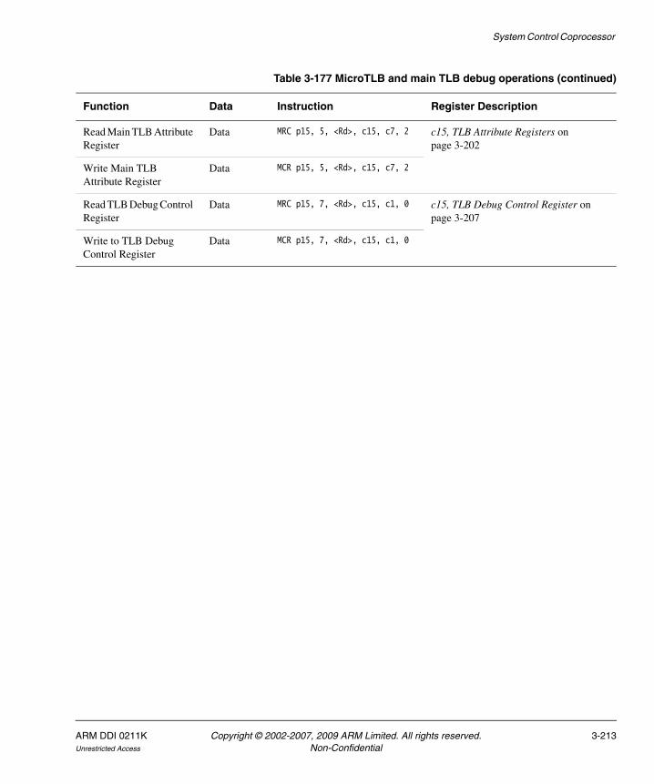
System Control Coprocessor
Read Main TLB Attribute Register
Data MRC p15, 5, <Rd>, c15, c7, 2 c15, TLB Attribute Registers on page 3-202
Write Main TLB Attribute Register
Data MCR p15, 5, <Rd>, c15, c7, 2
Read TLB Debug Control Register
Data MRC p15, 7, <Rd>, c15, c1, 0 c15, TLB Debug Control Register on page 3-207
Write to TLB Debug Control Register
Data MCR p15, 7, <Rd>, c15, c1, 0
Table 3-177 MicroTLB and main TLB debug operations (continued)
Function Data Instruction Register Description
ARM DDI 0211K Copyright © 2002-2007, 2009 ARM Limited. All rights reserved. 3-213Unrestricted Access Non-Confidential

System Control Coprocessor
3-214 Copyright © 2002-2007, 2009 ARM Limited. All rights reserved. ARM DDI 0211KNon-Confidential Unrestricted Access

Chapter 4 Unaligned and Mixed-Endian Data Access Support
This chapter describes the unaligned and mixed-endianness data access support for the ARM1136JF-S processor. It contains the following sections:
• About unaligned and mixed-endian support on page 4-2
• Unaligned access support on page 4-3
• Unaligned data access specification on page 4-7
• Operation of unaligned accesses on page 4-17
• Mixed-endian access support on page 4-22
• Instructions to reverse bytes in a general-purpose register on page 4-26
• Instructions to change the CPSR E bit on page 4-27.
ARM DDI 0211K Copyright © 2002-2007, 2009 ARM Limited. All rights reserved. 4-1Unrestricted Access Non-Confidential

Unaligned and Mixed-Endian Data Access Support
4.1 About unaligned and mixed-endian support
The ARM1136JF-S processor executes the ARM architecture v6 instructions that support mixed-endian access in hardware, and assist unaligned data accesses. The extensions to ARMv6 that support unaligned and mixed-endian accesses include the following:
• CP15 register c1 has a U bit that enables unaligned support. This bit was specified as zero in previous architectures, and resets to zero for backwards compatibility.
• Architecturally defined unaligned word and halfword access specification for hardware implementation.
• Byte reverse instructions that operate on general-purpose register contents to support signed/unsigned halfword data values.
• Separate instruction and data endianness, with instructions fixed as little-endian format, naturally aligned, but with support for 32-bit word-invariant binary images and ROM.
• A PSR endian control flag, the E-bit, cleared on reset and exception entry, that adds a byte-reverse operation to the entire load and store instruction space as data is loaded into and stored back out of the register file. In previous architectures this Program Status Register bit was specified as zero. It is not set in code written to conform to architectures prior to ARMv6.
• ARM and Thumb instructions to set and clear the E-bit explicitly.
• A byte-invariant addressing scheme to support fine-grain big-endian and little-endian shared data structures, to conform to a shared memory standard.
The original ARM architecture was designed as little-endian. This provides a consistent address ordering of bits, bytes, words, cache lines, and pages, and is assumed by the documentation of instruction set encoding and memory and register bit significance. Subsequently, big-endian support was added to enable big-endian byte addressing of memory. A little-endian nomenclature is used for bit-ordering and byte addressing throughout this manual.
4-2 Copyright © 2002-2007, 2009 ARM Limited. All rights reserved. ARM DDI 0211KNon-Confidential Unrestricted Access

Unaligned and Mixed-Endian Data Access Support
4.2 Unaligned access support
Instructions must always be aligned as follows:
• ARM 32-bit instructions must be word boundary aligned (Address [1:0] = b00)
• Thumb 16-bit instructions must be halfword boundary aligned (Address [0] = 0).
Unaligned data access support is described in:
• Word-invariant mode support
• ARMv6 extensions
• Word-invariant mode and ARMv6 configurations on page 4-4
• Word-invariant data access in ARMv6 (U=0) on page 4-4
• Support for unaligned data access in ARMv6 (U=1) on page 4-5
• ARMv6 unaligned data access restrictions on page 4-5.
4.2.1 Word-invariant mode support
For ARM architectures prior to ARM architecture v6, data access to non-aligned word and halfword data was treated as aligned from the memory interface perspective. That is, the address is treated as truncated with Address[1:0] treated as zero for word accesses, and Address[0] treated as zero for halfword accesses.
Load single word ARM instructions are also architecturally defined to rotate right the word aligned data transferred by a non word-aligned access, see the ARM Architecture Reference Manual.
Alignment fault checking is specified for processors with architecturally compliant Memory Management Units (MMUs), under control of CP15 Register c1 A bit, bit 1. When a transfer is not naturally aligned to the size of data transferred a Data Abort is signaled with an Alignment fault status code, see the ARM Architecture Reference Manual for more details.
4.2.2 ARMv6 extensions
ARMv6 adds unaligned word and halfword load and store data access support. When enabled, one or more memory accesses are used to generate the required transfer of adjacent bytes transparently, apart from a potentially greater access time where the transaction crosses a word-boundary.
The memory management specification defines a programmable mechanism to enable unaligned access support. This is controlled and programmed using the CP15 register c1 U bit, bit 22.
ARM DDI 0211K Copyright © 2002-2007, 2009 ARM Limited. All rights reserved. 4-3Unrestricted Access Non-Confidential
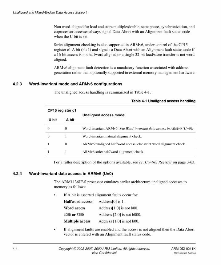
Unaligned and Mixed-Endian Data Access Support
Non word-aligned for load and store multiple/double, semaphore, synchronization, and coprocessor accesses always signal Data Abort with an Alignment fault status code when the U bit is set.
Strict alignment checking is also supported in ARMv6, under control of the CP15 register c1 A bit (bit 1) and signals a Data Abort with an Alignment fault status code if a 16-bit access is not halfword aligned or a single 32-bit load/store transfer is not word aligned.
ARMv6 alignment fault detection is a mandatory function associated with address generation rather than optionally supported in external memory management hardware.
4.2.3 Word-invariant mode and ARMv6 configurations
The unaligned access handling is summarized in Table 4-1.
For a fuller description of the options available, see c1, Control Register on page 3-63.
4.2.4 Word-invariant data access in ARMv6 (U=0)
The ARM1136JF-S processor emulates earlier architecture unaligned accesses to memory as follows:
• If A bit is asserted alignment faults occur for:
Halfword access Address[0] is 1.
Word access Address[1:0] is not b00.
LDRD or STRD Address [2:0] is not b000.
Multiple access Address [1:0] is not b00.
• If alignment faults are enabled and the access is not aligned then the Data Abort vector is entered with an Alignment fault status code.
Table 4-1 Unaligned access handling
CP15 register c1Unaligned access model
U bit A bit
0 0 Word-invariant ARMv5. See Word-invariant data access in ARMv6 (U=0).
0 1 Word-invariant natural alignment check.
1 0 ARMv6 unaligned half/word access, else strict word alignment check.
1 1 ARMv6 strict half/word alignment check.
4-4 Copyright © 2002-2007, 2009 ARM Limited. All rights reserved. ARM DDI 0211KNon-Confidential Unrestricted Access

Unaligned and Mixed-Endian Data Access Support
• If no alignment fault is enabled, that is, if bit 1 of CP15 register c1, the A bit, is not set:
Byte access Memory interface uses full Address [31:0].
Halfword access Memory interface uses Address [31:1]. Address [0] asserted as 0.
Word access Memory interface uses Address [31:2]. Address [1:0] asserted as 0.
— ARM load data rotates the aligned read data and rotates this right by the byte-offset denoted by Address [1:0], see the ARM Architecture Reference Manual.
— ARM and Thumb load-multiple accesses always treated as aligned. No rotation of read data.
— ARM and Thumb store word and store multiple treated as aligned. No rotation of write data.
— ARM load and store doubleword operations treated as 64-bit aligned.
— Thumb load word data operations are Unpredictable if not word aligned.
— ARM and Thumb halfword data accesses are Unpredictable if not halfword aligned.
4.2.5 Support for unaligned data access in ARMv6 (U=1)
The ARM1136JF-S processor memory interfaces can generate unaligned low order byte address offsets only for halfword and single word load and store operations, and byte accesses unless the A bit is set. These accesses produce an alignment fault if the A bit is set, and for some of the cases described in ARMv6 unaligned data access restrictions.
If alignment faults are enabled and the access is not aligned then the Data Abort vector is entered with an Alignment Fault status code.
4.2.6 ARMv6 unaligned data access restrictions
The following restrictions apply for ARMv6 unaligned data access:
• Accesses are not guaranteed atomic. They might be synthesized out of a series of aligned operations in a shared memory system without guaranteeing locked transaction cycles.
• Unaligned accesses loading the PC produce an alignment trap.
ARM DDI 0211K Copyright © 2002-2007, 2009 ARM Limited. All rights reserved. 4-5Unrestricted Access Non-Confidential
Unaligned and Mixed-Endian Data Access Support
• Accesses typically take a number of cycles to complete compared to a naturally aligned transfer. The real-time implications must be carefully analyzed and key data structures might require to have their alignment adjusted for optimum performance.
• Accesses can abort on either or both halves of an access where this occurs over a page boundary. The Data Abort handler must handle restartable aborts carefully after an Alignment fault status code is signaled.
As a result, shared memory schemes must not rely on seeing monotonic updates of non-aligned data of loads, stores, and swaps for data items greater than byte width.
Unaligned access operations must not be used for accessing Device memory-mapped registers, and must be used with care in Shared memory structures that are protected by aligned semaphores or synchronization variables.
An Alignment fault occurs if unaligned accesses to Strongly Ordered or Device memory are attempted when both:
• the MMU is enabled, that is CP15 c1 bit 0, M bit, is 1
• the Subpage AP bits are disabled, that is CP15 c1 bit 23, XP bit, is 1.
Unaligned accesses to Non-shared Device memory when subpage AP bits are enabled, that is CP15 c1 bit 23, XP bit, is 0, have Unpredictable results.
Swap and synchronization primitives, multiple-word or coprocessor access produce an alignment fault regardless of the setting of the A bit.
4-6 Copyright © 2002-2007, 2009 ARM Limited. All rights reserved. ARM DDI 0211KNon-Confidential Unrestricted Access

Unaligned and Mixed-Endian Data Access Support
4.3 Unaligned data access specification
The architectural specification of unaligned data representations is defined in terms of bytes transferred between memory and register, regardless of bus width and bus endianness.
Little-endian data items are described using lower-case byte labeling bX ... b0 (byteX to byte 0) and a pointer is always treated as pointing to the least significant byte of the addressed data.
Big-endian data items are described using upper-case byte labeling B0 ... BX (BYTE0 to BYTEX) and a pointer is always treated as pointing to the most significant byte of the addressed data.
4.3.1 Load unsigned byte, endian independent
The addressed byte is loaded from memory into the low eight bits of the general-purpose register and the upper 24 bits are zeroed. Figure 4-1 shows this.
Figure 4-1 Load unsigned byte
Memory RegisterAddressA[31:0]
b0x000x00 0x00
31 2423 1615 8 7 0
b
07
ARM DDI 0211K Copyright © 2002-2007, 2009 ARM Limited. All rights reserved. 4-7Unrestricted Access Non-Confidential

Unaligned and Mixed-Endian Data Access Support
4.3.2 Load signed byte, endian independent
The addressed byte is loaded from the memory into the low eight bits of the general-purpose register and the sign bit is extended into the upper 24 bits of the register. Figure 4-2 shows this.
Figure 4-2 Load signed byte
In Figure 4-2, se means b (bit 7) sign extension.
4.3.3 Store byte, endian independent
The low eight bits of the general-purpose register are stored into the addressed byte in memory. Figure 4-3 shows this.
Figure 4-3 Store byte
Memory RegisterAddressA[31:0]
bsese se
31 2423 1615 8 7 0
b
07
Register MemoryAddressA[31:0]
bxx x
31 2423 1615 8 7 0
b
07
4-8 Copyright © 2002-2007, 2009 ARM Limited. All rights reserved. ARM DDI 0211KNon-Confidential Unrestricted Access
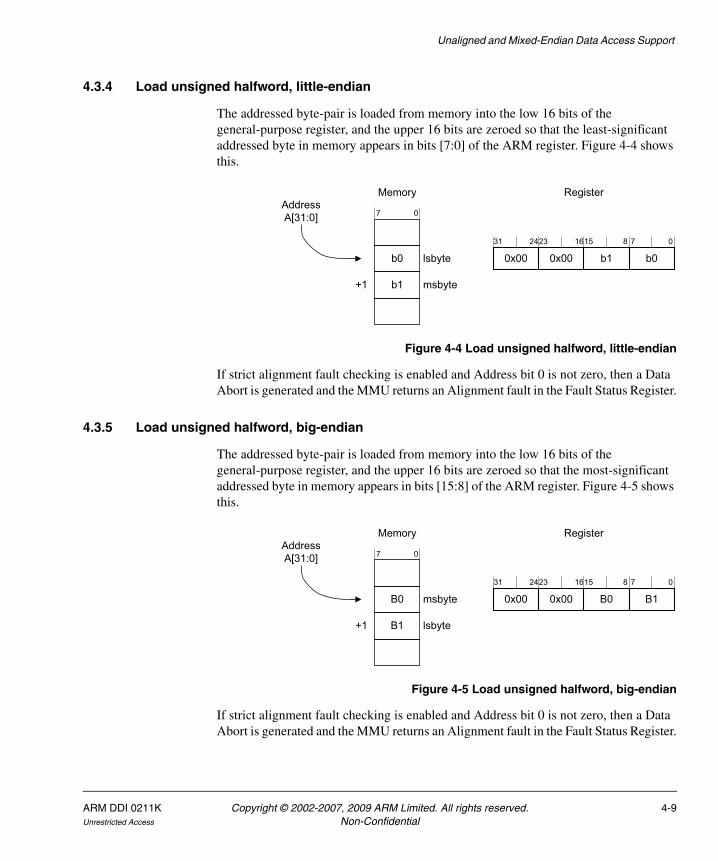
Unaligned and Mixed-Endian Data Access Support
4.3.4 Load unsigned halfword, little-endian
The addressed byte-pair is loaded from memory into the low 16 bits of the general-purpose register, and the upper 16 bits are zeroed so that the least-significant addressed byte in memory appears in bits [7:0] of the ARM register. Figure 4-4 shows this.
Figure 4-4 Load unsigned halfword, little-endian
If strict alignment fault checking is enabled and Address bit 0 is not zero, then a Data Abort is generated and the MMU returns an Alignment fault in the Fault Status Register.
4.3.5 Load unsigned halfword, big-endian
The addressed byte-pair is loaded from memory into the low 16 bits of the general-purpose register, and the upper 16 bits are zeroed so that the most-significant addressed byte in memory appears in bits [15:8] of the ARM register. Figure 4-5 shows this.
Figure 4-5 Load unsigned halfword, big-endian
If strict alignment fault checking is enabled and Address bit 0 is not zero, then a Data Abort is generated and the MMU returns an Alignment fault in the Fault Status Register.
Memory RegisterAddressA[31:0]
+1 msbyte
lsbyte b0b10x00 0x00
31 2423 1615 8 7 0
b0
07
b1
Memory RegisterAddressA[31:0]
+1 lsbyte
msbyte B1B00x00 0x00
31 2423 1615 8 7 0
B0
07
B1
ARM DDI 0211K Copyright © 2002-2007, 2009 ARM Limited. All rights reserved. 4-9Unrestricted Access Non-Confidential
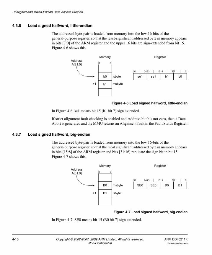
Unaligned and Mixed-Endian Data Access Support
4.3.6 Load signed halfword, little-endian
The addressed byte-pair is loaded from memory into the low 16-bits of the general-purpose register, so that the least-significant addressed byte in memory appears in bits [7:0] of the ARM register and the upper 16 bits are sign-extended from bit 15. Figure 4-6 shows this.
Figure 4-6 Load signed halfword, little-endian
In Figure 4-6, se1 means bit 15 (b1 bit 7) sign extended.
If strict alignment fault checking is enabled and Address bit 0 is not zero, then a Data Abort is generated and the MMU returns an Alignment fault in the Fault Status Register.
4.3.7 Load signed halfword, big-endian
The addressed byte-pair is loaded from memory into the low 16-bits of the general-purpose register, so that the most significant addressed byte in memory appears in bits [15:8] of the ARM register and bits [31:16] replicate the sign bit in bit 15. Figure 4-7 shows this.
Figure 4-7 Load signed halfword, big-endian
In Figure 4-7, SE0 means bit 15 (B0 bit 7) sign extended.
Memory RegisterAddressA[31:0]
+1 msbyte
lsbyte b0b1se1 se1
31 2423 1615 8 7 0
b0
07
b1
Memory RegisterAddressA[31:0]
+1 lsbyte
msbyte B1B0SE0 SE0
31 2423 1615 8 7 0
B0
07
B1
4-10 Copyright © 2002-2007, 2009 ARM Limited. All rights reserved. ARM DDI 0211KNon-Confidential Unrestricted Access

Unaligned and Mixed-Endian Data Access Support
If strict alignment fault checking is enabled and Address bit 0 is not zero, then a Data Abort is generated and the MMU returns an Alignment fault in the Fault Status Register.
4.3.8 Store halfword, little-endian
The low 16 bits of the general-purpose register are stored into the memory with bits [7:0] written to the addressed byte in memory, bits [15:8] to the incremental byte address in memory. Figure 4-8 shows this.
Figure 4-8 Store halfword, little-endian
If strict alignment fault checking is enabled and Address bit 0 is not zero, then a Data Abort is generated and the MMU returns an Alignment fault in the Fault Status Register.
4.3.9 Store halfword, big-endian
The low 16 bits of the general-purpose register are stored into the memory with bits [15:8] written to the addressed byte in memory, bits [7:0] to the incremental byte address in memory. Figure 4-9 shows this.
Figure 4-9 Store halfword, big-endian
If strict alignment fault checking is enabled and Address bits [1:0] is not zero, then a Data Abort is generated and the MMU returns an Alignment fault in the Fault Status Register.
Register MemoryAddressA[31:0]
+1 msbyte
lsbyteb0b1x x
31 2423 1615 8 7 0
b0
07
b1
Register MemoryAddressA[31:0]
+1
msbyte
lsbyte
B1B0x x
31 2423 1615 8 7 0
B0
07
B1
ARM DDI 0211K Copyright © 2002-2007, 2009 ARM Limited. All rights reserved. 4-11Unrestricted Access Non-Confidential

Unaligned and Mixed-Endian Data Access Support
4.3.10 Load word, little-endian
The addressed byte-quad is loaded from memory into the 32-bit general-purpose register so that the least-significant addressed byte in memory appears in bits [7:0] of the ARM register. Figure 4-10 shows this.
Figure 4-10 Load word, little-endian
If strict alignment fault checking is enabled and Address bits [1:0] is not zero, then a Data Abort is generated and the MMU returns an Alignment fault in the Fault Status Register.
Memory RegisterAddressA[31:0]
+1
msbyte
lsbyte
+2
+3
b0
07
b1
b0b1b3 b2
31 2423 1615 8 7 0
b2
b3
4-12 Copyright © 2002-2007, 2009 ARM Limited. All rights reserved. ARM DDI 0211KNon-Confidential Unrestricted Access
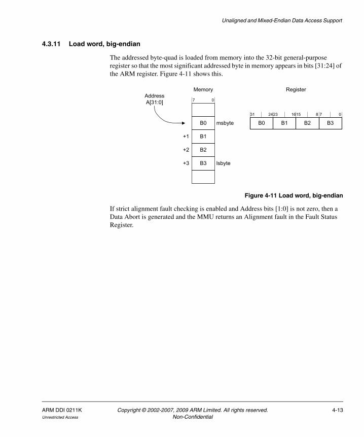
Unaligned and Mixed-Endian Data Access Support
4.3.11 Load word, big-endian
The addressed byte-quad is loaded from memory into the 32-bit general-purpose register so that the most significant addressed byte in memory appears in bits [31:24] of the ARM register. Figure 4-11 shows this.
Figure 4-11 Load word, big-endian
If strict alignment fault checking is enabled and Address bits [1:0] is not zero, then a Data Abort is generated and the MMU returns an Alignment fault in the Fault Status Register.
Memory RegisterAddressA[31:0]
+1
msbyte
lsbyte
+2
+3
B0
07
B1
B3B2B0 B1
31 2423 1615 8 7 0
B2
B3
ARM DDI 0211K Copyright © 2002-2007, 2009 ARM Limited. All rights reserved. 4-13Unrestricted Access Non-Confidential

Unaligned and Mixed-Endian Data Access Support
4.3.12 Store word, little-endian
The 32-bit general-purpose register is stored to four bytes in memory where bits [7:0] of the ARM register are transferred to the least-significant addressed byte in memory. Figure 4-12 shows this.
Figure 4-12 Store word, little-endian
If strict alignment fault checking is enabled and Address bits [1:0] are not zero, then a Data Abort is generated and the MMU returns an Alignment fault in the Fault Status Register.
Register MemoryAddressA[31:0]
+1
msbyte
lsbyte
+2
+3
b0b1b3 b2
31 2423 1615 8 7 0
b0
07
b1
b2
b3
4-14 Copyright © 2002-2007, 2009 ARM Limited. All rights reserved. ARM DDI 0211KNon-Confidential Unrestricted Access

Unaligned and Mixed-Endian Data Access Support
4.3.13 Store word, big-endian
The 32-bit general-purpose register is stored to four bytes in memory where bits [31:24] of the ARM register are transferred to the most-significant addressed byte in memory. Figure 4-13 show this.
Figure 4-13 Store word, big-endian
If strict alignment fault checking is enabled and Address bits [1:0] are not zero, then a Data Abort is generated and the MMU returns an Alignment fault in the Fault Status Register.
4.3.14 Load double, load multiple, load coprocessor (little-endian, E = 0)
The access is treated as a series of incrementing aligned word loads from memory. The data is treated as load word data (see Load word, little-endian on page 4-12) where the lowest two address bits are zeroed.
If strict alignment fault checking is enabled and effective Address bits[1:0] are not zero, then a Data Abort is generated and the MMU returns an Alignment fault in the Fault Status Register.
4.3.15 Load double, load multiple, load coprocessor (big-endian, E=1)
The access is treated as a series of incrementing aligned word loads from memory. The data is treated as load word data (see Load word, big-endian on page 4-13) where the lowest two address bits are zeroed.
If strict alignment fault checking is enabled and effective Address bits[1:0] are not zero, then a Data Abort is generated and the MMU returns an Alignment fault in the Fault Status Register.
Register MemoryAddressA[31:0]
+1
msbyte
lsbyte
+2
+3
B3B2B0 B1
31 2423 1615 8 7 0
B0
07
B1
B2
B3
ARM DDI 0211K Copyright © 2002-2007, 2009 ARM Limited. All rights reserved. 4-15Unrestricted Access Non-Confidential

Unaligned and Mixed-Endian Data Access Support
4.3.16 Store double, store multiple, store coprocessor (little-endian, E=0)
The access is treated as a series of incrementing aligned word stores to memory. The data is treated as store word data (see Store word, little-endian on page 4-14) where the lowest two address bits are zeroed.
If strict alignment fault checking is enabled and effective Address bits[1:0] are not zero, then a Data Abort is generated and the MMU returns an Alignment fault in the Fault Status Register.
4.3.17 Store double, store multiple, store coprocessor (big-endian, E=1)
The access is treated as a series of incrementing aligned word stores to memory. The data is treated as store word data (see Store word, big-endian on page 4-15) where the lowest two address bits are zeroed.
If strict alignment fault checking is enabled and effective Address bits[1:0] are not zero, then a Data Abort is generated and the MMU returns an Alignment fault in the Fault Status Register.
4-16 Copyright © 2002-2007, 2009 ARM Limited. All rights reserved. ARM DDI 0211KNon-Confidential Unrestricted Access

Unaligned and Mixed-Endian Data Access Support
4.4 Operation of unaligned accesses
This section describes alignment faults and the operation of non-faulting accesses of the ARM1136JF-S processor.
The mechanism for the support of unaligned loads or stores is as follows:
• if either the Base register or the index offset of the address is misaligned, then:
— the processor takes two cycles to issue the instruction
— if the resulting address is misaligned, then the instruction performs multiple memory accesses in ascending order of address.
There is no support for misaligned accesses being atomic, and misaligned accesses to Device memory might result in Unpredictable behavior.
Table 4-3 on page 4-18 gives details of when an Alignment fault must occur for an access, and of when the behavior of an access is architecturally Unpredictable. When an access does not generate an Alignment fault and is not Unpredictable, the table gives details of precisely which memory locations are accessed.
Table 4-2 relates the access type descriptions used in the Table 4-3 on page 4-18 to the ARM load/store instructions.
Table 4-2 Access type descriptions
Access type ARM instructions Thumb instructions
Byte LDRB, LDRBT, LDRSB, STRB, STRBT, SWPB (either access) LDRB, LDRSB, STRB
BSynca SWPB, LDREXBa, STREXBa –
Halfword LDRH, LDRSH, STRH LDRH, LDRSH, STRH
HWSynca LDREXHa, STREXHa –
WLoad LDR, LDRT, SWP (load access, if U is set to 0) LDR
WStore STR, STRT, SWP (store access, if U is set to 0) STR
WSync LDREX, STREX, SWP (either access, if U is set to 1) –
Multiword LDC, LDM, RFE, SRS, STC, STM LDMIA, POP, PUSH, STMIA
Doubleword LDRD, STRD –
DWSynca LDREXDa, STREXDa –
a. The LDREXB, LDREXH, LDREXD, STREXB, STREXH, and STREXD instructions are only available from the rev1 (r1p0) release of the ARM1136JF-S processor. The BSync, HWSync and DWSync access types are only defined from the rev1 (r1p0) release.
ARM DDI 0211K Copyright © 2002-2007, 2009 ARM Limited. All rights reserved. 4-17Unrestricted Access Non-Confidential

Unaligned and Mixed-Endian Data Access Support
The following terminology is used to describe the memory locations accessed:
Byte[X] This means the byte whose address is X in the current endianness model. The correspondence between the endianness models is that Byte[A] in the LE endianness model, Byte[A] in the BE-8 endianness model, and Byte[A EOR 3] in the BE-32 endianness model are the same actual byte of memory.
Halfword[X] This means the halfword consisting of the bytes whose addresses are X and X+1 in the current endianness model, combined to form a halfword in little-endian order in the LE endianness model or in big-endian order in the BE-8 or BE-32 endianness model.
Word[X] This means the word consisting of the bytes whose addresses are X, X+1, X+2, and X+3 in the current endianness model, combined to form a word in little-endian order in the LE endianness model or in big-endian order in the BE-8 or BE-32 endianness model.
Note These definitions mean that, if X is word-aligned, Word[X] consists of
the same four bytes of actual memory in the same order in the LE and BE-32 endianness models.
Align(X) This means X AND 0xFFFFFFFC. That is, X with its least significant two bits forced to zero to make it word-aligned.
On lines where Addr[1:0] is set to b00 there is no difference between Addr and Align(Addr). You can use this to simplify the control of when the least significant bits are forced to zero.
For the Two-word and Multiword access types, the memory accessed column only specifies the lowest word accessed. Subsequent words have addresses constructed by successively incrementing the address of the lowest word by four, and are constructed using the same endianness model as the lowest word.
Table 4-3 Alignment fault occurrence when access behavior is architecturally unpredictable
A U Addr [2:0]Accesstype
Architecturalbehavior
Memory accessed Notes
0 0 – – – – Legacy, no alignment faulting
0 0 bxxx Byte, BSynca Normal Byte[Addr] –
0 0 bxx0 Halfword Normal Halfword[Addr] –
4-18 Copyright © 2002-2007, 2009 ARM Limited. All rights reserved. ARM DDI 0211KNon-Confidential Unrestricted Access

Unaligned and Mixed-Endian Data Access Support
0 0 bxx1 Halfword Unpredictable – Halfword[Align16(Addr)].Operation unaffected by Addr[0]
0 0 bxx0 HWSynca Normal Halfword[Addr]
0 0 bxx1 HWSynca Unpredictable – Halfword[Align16(Addr)].Operation unaffected by Addr[0]
0 0 bxxx WLoad Normal Word[Align32(Addr)] Loaded data rotated right by 8 * Addr[1:0] bits
0 0 bxxx WStore Normal Word[Align32(Addr)] Operation unaffected by Addr[1:0]
0 0 bx00 WSync Normal Word[Addr] –
0 0 bxx1,b x1x
WSync Unpredictable – Word[Align32(Addr)]
0 0 bxxx Multiword Normal Word[Align32(Addr)] Operation unaffected by Addr[1:0]
0 0 b000 Doubleword Normal Word[Addr] –
0 0 bxx1,bx1x,b1xx
Doubleword Unpredictable – Same as LDM2 or STM2
0 0 b000 DWSynca Normal Word[Addr] –
0 0 bxx1,bx1x,b1xx
DWSynca Unpredictable – DWord[Align64(Addr)].
Operation unaffected by Addr[2:0]
0 1 – – – – ARMv6 unaligned support
0 1 bxxx Byte,BSynca
Normal Byte[Addr] –
0 1 bxxx Halfword Normal Halfword[Addr] –
0 1 bxx0 HWSynca Normal Halfword[Addr] –
0 1 bxx1 HWSynca Alignment fault – –
Table 4-3 Alignment fault occurrence when access behavior is architecturally unpredictable (continued)
A U Addr [2:0]Accesstype
Architecturalbehavior
Memory accessed Notes
ARM DDI 0211K Copyright © 2002-2007, 2009 ARM Limited. All rights reserved. 4-19Unrestricted Access Non-Confidential

Unaligned and Mixed-Endian Data Access Support
0 1 bxxx WLoad,WStore
Normal Word[Addr] –
0 1 bx00 WSync,Multiword,Doubleword
Normal Word[Addr] –
0 1 bxx1,bx1x
WSync,Multiword,Doubleword
Alignment fault – –
0 1 b000 DWSynca Normal Word[Addr] –
0 1 bxx1,bx1x,b1xx
DWSynca Alignment fault – –
1 x – – – – Full alignment faulting
1 x bxxx Byte,BSynca
Normal Byte[Addr] –
1 x bxx0 Halfword,HWSynca
Normal Halfword[Addr] –
1 x bxx1 Halfword,HWSynca
Alignment fault – –
1 x bx00 WLoad,WStore,WSync,Multiword
Normal Word[Addr] –
1 x bxx1,b x1x
WLoad,WStore,WSync,Multiword
Alignment fault – –
1 x b000 Doubleword Normal Word[Addr] –
1 0 b100 Doubleword Alignment fault – –
1 1 b100 Doubleword Normal Word[Addr] –
Table 4-3 Alignment fault occurrence when access behavior is architecturally unpredictable (continued)
A U Addr [2:0]Accesstype
Architecturalbehavior
Memory accessed Notes
4-20 Copyright © 2002-2007, 2009 ARM Limited. All rights reserved. ARM DDI 0211KNon-Confidential Unrestricted Access

Unaligned and Mixed-Endian Data Access Support
The following causes override the behavior specified in the Table 4-3 on page 4-18:
• An LDR instruction that loads the PC, has Addr[1:0] != b00, and is specified in the table as having Normal behavior instead has Unpredictable behavior.
The reason why this applies only to LDR is that most other load instructions are Unpredictable regardless of alignment if the PC is specified as their destination register.
The exceptions are the ARM LDM and RFE instructions, and the Thumb POP instruction. If the instruction for them is Addr[1:0] != b00, the effective address of the transfer has its two least significant bits forced to 0 if A is set 0 and U is set to 0. Otherwise the behavior specified in Table 4-3 on page 4-18 is either Unpredictable or an Alignment fault regardless of the destination register.
• Any WLoad, WStore, WSync, Doubleword, or Multiword instruction that accesses device memory, has Addr[1:0] != b00, and is specified in Table 4-3 on page 4-18 as having Normal behavior instead has Unpredictable behavior.
• Any Halfword instruction that accesses device memory, has Addr[0] != 0, and is specified in Table 4-3 on page 4-18 as having Normal behavior instead has Unpredictable behavior.
1 x bxx1,bx1x
Doubleword Alignment fault – –
1 x b000 DWSynca Normal Word[Addr] –
1 x bxx1,bx1x,b1xx
DWSynca Alignment fault – –
a. The BSync, HWSync and DWSync access types are only defined from the rev1 (r1p0) release of the ARM1136JF-S processor.
Table 4-3 Alignment fault occurrence when access behavior is architecturally unpredictable (continued)
A U Addr [2:0]Accesstype
Architecturalbehavior
Memory accessed Notes
ARM DDI 0211K Copyright © 2002-2007, 2009 ARM Limited. All rights reserved. 4-21Unrestricted Access Non-Confidential
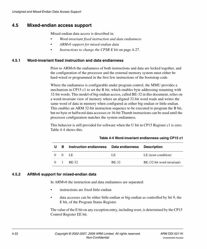
Unaligned and Mixed-Endian Data Access Support
4.5 Mixed-endian access support
Mixed-endian data access is described in:
• Word-invariant fixed instruction and data endianness
• ARMv6 support for mixed-endian data
• Instructions to change the CPSR E bit on page 4-27.
4.5.1 Word-invariant fixed instruction and data endianness
Prior to ARMv6 the endianness of both instructions and data are locked together, and the configuration of the processor and the external memory system must either be hard-wired or programmed in the first few instructions of the bootstrap code.
Where the endianness is configurable under program control, the MMU provides a mechanism in CP15 c1 to set the B bit, which enables byte addressing renaming with 32-bit words. This model of big-endian access, called BE-32 in this document, relies on a word-invariant view of memory where an aligned 32-bit word reads and writes the same word of data in memory when configured as either big-endian or little-endian. This enables an ARM 32-bit instruction sequence to be executed to program the B bit, but no byte or halfword data accesses or 16-bit Thumb instructions can be used until the processor configuration matches the system endianness.
This behavior is still provided for software when the U bit in CP15 Register c1 is zero. Table 4-4 shows this.
4.5.2 ARMv6 support for mixed-endian data
In ARMv6 the instruction and data endianness are separated:
• instructions are fixed little-endian
• data accesses can be either little-endian or big-endian as controlled by bit 9, the E bit, of the Program Status Register.
The value of the E bit on any exception entry, including reset, is determined by the CP15 Control Register EE bit.
Table 4-4 Word-invariant endianness using CP15 c1
U B Instruction endianness Data endianness Description
0 0 LE LE LE (reset condition)
0 1 BE-32 BE-32 BE (32-bit word-invariant)
4-22 Copyright © 2002-2007, 2009 ARM Limited. All rights reserved. ARM DDI 0211KNon-Confidential Unrestricted Access

Unaligned and Mixed-Endian Data Access Support
Fixed little-endian Instructions
Instructions must be naturally aligned and are always treated as being stored in memory in little-endian format. That is, the PC points to the least-significant-byte of the instruction.
Instructions have to be treated as data by exception handlers (decoding SWI calls and Undefined instructions, for example).
Instructions can also be written as data by debuggers, Just-In-Time compilers, or in operating systems that update exception vectors.
Mixed-endian data access
The operating-system typically has a required endian representation of internal data structures, but applications and device drivers have to work with data shared with other processors (DSP or DMA interfaces) that might have fixed big-endian or little-endian data formatting.
A byte-invariant addressing mechanism is provided that enables the load/store architecture to be qualified by the CPSR E bit that provides byte reversing of big-endian data in to, and out of, the processor register bank transparently. This byte-invariant big-endian representation is called BE-8 in this document.
The effect on byte, halfword, word, and multiword accesses of setting the CPSR E bit when the U bit enables unaligned support is described in Mixed-endian configuration supported on page 4-25.
Byte data access
The same physical byte in memory is accessed whether big-endian or little-endian:
• Unsigned byte load as described in Load unsigned byte, endian independent on page 4-7.
• Signed byte load as described in Load signed byte, endian independent on page 4-8.
• Byte store as described in Store byte, endian independent on page 4-8.
ARM DDI 0211K Copyright © 2002-2007, 2009 ARM Limited. All rights reserved. 4-23Unrestricted Access Non-Confidential

Unaligned and Mixed-Endian Data Access Support
Halfword data access
The same two physical bytes in memory are accessed whether big-endian or little-endian. Big-endian halfword load data is byte-reversed as read into the processor register to ensure little-endian internal representation, and similarly is byte-reversed on store to memory:
• Unsigned halfword load as described in Load unsigned halfword, little-endian on page 4-9 (LE), and Load unsigned halfword, big-endian on page 4-9 (BE-8).
• Signed halfword load as described in Load signed halfword, little-endian on page 4-10 (LE), and Load signed halfword, big-endian on page 4-10 (BE-8).
• Halfword store as described in Store halfword, little-endian on page 4-11 (LE), and Store halfword, big-endian on page 4-11 (BE-8).
Load Word
The same four physical bytes in memory are accessed whether big-endian or little-endian. Big-endian word load data is byte reversed as read into the processor register to ensure little-endian internal representation, and similarly is byte-reversed on store to memory:
• Word load as described in Load word, little-endian on page 4-12 (LE), and Load word, big-endian on page 4-13 (BE-8).
• Word store as described in Store word, little-endian on page 4-14 (LE), and Store word, big-endian on page 4-15 (BE-8).
4-24 Copyright © 2002-2007, 2009 ARM Limited. All rights reserved. ARM DDI 0211KNon-Confidential Unrestricted Access
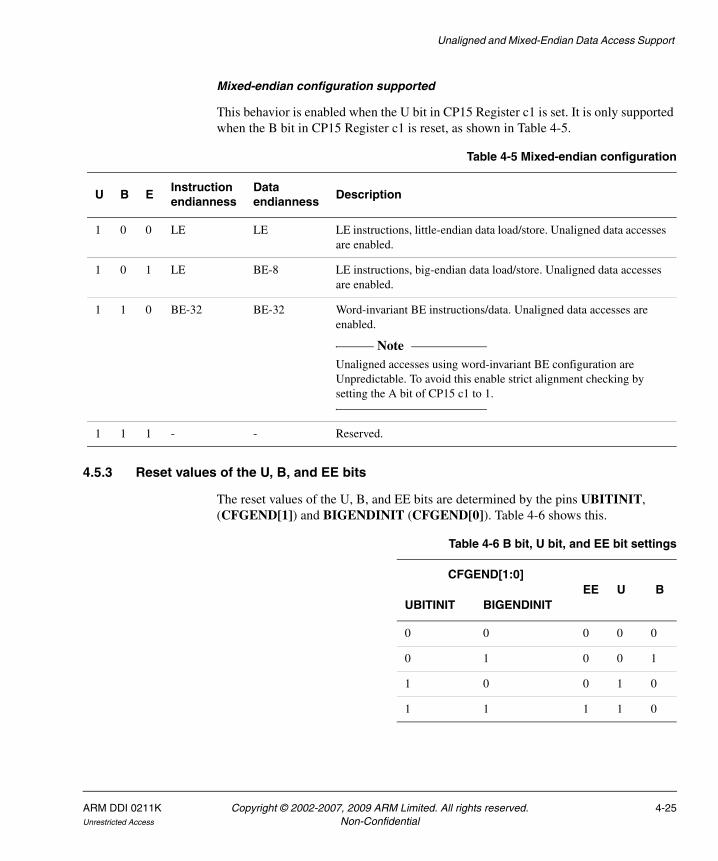
Unaligned and Mixed-Endian Data Access Support
Mixed-endian configuration supported
This behavior is enabled when the U bit in CP15 Register c1 is set. It is only supported when the B bit in CP15 Register c1 is reset, as shown in Table 4-5.
4.5.3 Reset values of the U, B, and EE bits
The reset values of the U, B, and EE bits are determined by the pins UBITINIT, (CFGEND[1]) and BIGENDINIT (CFGEND[0]). Table 4-6 shows this.
Table 4-5 Mixed-endian configuration
U B EInstruction endianness
Data endianness
Description
1 0 0 LE LE LE instructions, little-endian data load/store. Unaligned data accesses are enabled.
1 0 1 LE BE-8 LE instructions, big-endian data load/store. Unaligned data accesses are enabled.
1 1 0 BE-32 BE-32 Word-invariant BE instructions/data. Unaligned data accesses are enabled.
Note Unaligned accesses using word-invariant BE configuration are Unpredictable. To avoid this enable strict alignment checking by setting the A bit of CP15 c1 to 1.
1 1 1 - - Reserved.
Table 4-6 B bit, U bit, and EE bit settings
CFGEND[1:0]EE U B
UBITINIT BIGENDINIT
0 0 0 0 0
0 1 0 0 1
1 0 0 1 0
1 1 1 1 0
ARM DDI 0211K Copyright © 2002-2007, 2009 ARM Limited. All rights reserved. 4-25Unrestricted Access Non-Confidential

Unaligned and Mixed-Endian Data Access Support
4.6 Instructions to reverse bytes in a general-purpose register
When an application or device driver has to interface to memory-mapped peripheral registers or shared-memory DMA structures that are not the same endianness as that of the internal data structures, or the endianness of the Operating System, an efficient way of being able to explicitly transform the endianness of the data is required.
The following new instructions are added to the ARM and Thumb instruction sets to provide this functionality:
• reverse word (4 bytes) register, for transforming big and little-endian 32-bit representations
• reverse halfword and sign-extend, for transforming signed 16-bit representations
• Reverse packed halfwords in a register for transforming big- and little-endian 16-bit representations.
These instructions are described in ARM1136JF-S instruction sets summaries on page 1-36.
4.6.1 All load and store operations
All load and store instructions take account of the CPSR E bit. Data is transferred directly to registers when E = 0, and byte reversed if E = 1 for halfword, word, or multiple word transfers.
Operation:
When CPSR[<E-bit>] = 1 then byte reverse load/store data
4-26 Copyright © 2002-2007, 2009 ARM Limited. All rights reserved. ARM DDI 0211KNon-Confidential Unrestricted Access

Unaligned and Mixed-Endian Data Access Support
4.7 Instructions to change the CPSR E bit
ARM and Thumb instructions are provided to set and clear the E-bit efficiently:
SETEND BE Sets the CPSR E bit
SETEND LE Resets the CPSR E bit.
These are specified as unconditional operations to minimize pipelined implementation complexity.
These instructions are described in ARM1136JF-S instruction sets summaries on page 1-36.
ARM DDI 0211K Copyright © 2002-2007, 2009 ARM Limited. All rights reserved. 4-27Unrestricted Access Non-Confidential

Unaligned and Mixed-Endian Data Access Support
4-28 Copyright © 2002-2007, 2009 ARM Limited. All rights reserved. ARM DDI 0211KNon-Confidential Unrestricted Access

Chapter 5 Program Flow Prediction
This chapter outlines how program flow prediction locates branches in the instruction stream and the strategies used for determining if a branch is likely to be taken or not. It also describes the two architecturally-defined SWI functions required for backwards-compatibility with earlier architectures for flushing the Prefetch Unit (PU) buffers. It contains the following sections:
• About program flow prediction on page 5-2
• Branch prediction on page 5-4
• Return stack on page 5-7
• Instruction Memory Barrier (IMB) instruction on page 5-8
• ARM1020T or later IMB implementation on page 5-9.
ARM DDI 0211K Copyright © 2002-2007, 2009 ARM Limited. All rights reserved. 5-1Unrestricted Access Non-Confidential

Program Flow Prediction
5.1 About program flow prediction
Program flow prediction in ARM1136JF-S processors is carried out by:
The core The core implements static branch prediction and the Return Stack.
The Prefetch Unit The PU implements dynamic branch prediction.
The ARM1136JF-S processor is responsible for handling branches the first time they are executed, that is, when no historical information is available for dynamic prediction by the PU.
The core makes static predictions about the likely outcome of a branch early in its pipeline and then resolves those predictions when the outcome of conditional execution is known. Condition codes are evaluated at three points in the core pipeline, and branches are resolved as soon as the flags are guaranteed not to be modified by a preceding instruction.
When a branch is resolved, the core passes information to the PU so that it can make a Branch Target Address Cache (BTAC) allocation or update an existing entry as appropriate. The core is also responsible for identifying likely procedure calls and returns to predict the returns. It can handle nested procedures up to three deep.
The core includes:
• a Static Branch Predictor (SBP)
• a Return Stack (RS)
• branch resolution logic
• a BTAC update interface to the PU.
The ARM1136JF-S PU is responsible for fetching instructions from the memory system as required by the integer unit, and coprocessors. The PU buffers up to three instructions in its FIFO to:
• detect branch instructions ahead of the integer unit requirement
• dynamically predict those that it considers are to be taken
This reduces the cycle time of the branch instructions, so increasing processor performance.
The PU includes:
• a BTAC
• branch update and allocate logic
• a Dynamic Branch Predictor (DBP), and associated update mechanism
5-2 Copyright © 2002-2007, 2009 ARM Limited. All rights reserved. ARM DDI 0211KNon-Confidential Unrestricted Access

Program Flow Prediction
It is responsible for providing the core with instructions, and for requesting cache accesses. The pattern of cache accesses is based on the predicted instruction stream as determined by the dynamic branch prediction mechanism or the core flush mechanism.
The BTAC can:
• be globally flushed by a CP15 instruction
• have individual entries flushed by a CP15 instruction
• be enabled or disabled by a CP15 instruction.
For details of CP15 instructions see Chapter 3 System Control Coprocessor.
The BTAC is globally flushed for:
• main TLB FCSE PID changes
• main TLB context ID changes
• global instruction cache invalidation.
The PU handles the cache access multiplexing for CP15 instruction handling.
The PU prefetches all instruction types regardless of the core state. That is, it prefetches instructions in ARM state, Thumb state and Jazelle state. However the rate at which the PU is drained is state-dependent, and the functioning of the branch prediction hardware is a function of the state. Branch prediction is performed in all three states.
The PU is responsible for fetching the instruction stream as dictated by:
• the Program Counter
• the dynamic branch predictor
• static prediction results in the core
• procedure calls and returns signaled by the Return Stack residing in the core
• exceptions, instruction aborts, and interrupts signaled by the core.
ARM DDI 0211K Copyright © 2002-2007, 2009 ARM Limited. All rights reserved. 5-3Unrestricted Access Non-Confidential
Program Flow Prediction
5.2 Branch prediction
In ARM processors that have no PU, the target of a branch is not known until the end of the Execute stage. At the Execute stage it is known whether or not the branch is taken. The best performance is obtained by predicting all branches as not taken and filling the pipeline with the instructions that follow the branch in the current sequential path. In ARM processors without a PU, an untaken branch requires one cycle and a taken branch requires three or more cycles.
Branch prediction enables the detection of branch instructions before they enter the integer unit. This permits the use of a branch prediction scheme that closely models actual conditional branch behavior.
The increased pipeline length of the ARM1136JF-S processor makes the performance penalty of any changes in program flow, such as branches or other updates to the PC, more significant than was the case on the ARM9TDMI or ARM1020T cores. Therefore, a significant amount of hardware is dedicated to prediction of these changes. Two major classes of program flow are addressed in the ARM1136JF-S prediction scheme:
1. Branches (including BL, and BLX immediate), where the target address is a fixed offset from the program counter. The prediction amounts to an examination of the probability that a branch passes its condition codes. These branches are handled in the Branch Predictors.
2. Loads, Moves, and ALU operations writing to the PC, which can be identified as being likely to be a return from a procedure call. Two identifiable cases are Loads to the PC from an address derived from R13 (the stack pointer), and Moves or ALU operations to the PC derived from R14 (the Link Register). In these cases, if the calling operation can also be identified, the likely return address can be stored in a hardware implemented stack, termed a Return Stack (RS). Typical calling operations are BL and BLX instructions. In addition Moves or ALU operations to the Link Register from the PC are often preludes to a branch that serves as a calling operation. The Link Register value derived is the value required for the RS. This was most commonly done on ARMv4T, before the BLX <register> instruction was introduced in ARMv5T.
Branch prediction is required in the design to reduce the core CPI loss that arises from the longer pipeline. To improve the branch prediction accuracy, a combination of static and dynamic techniques is employed. It is possible to disable the predictors.
5-4 Copyright © 2002-2007, 2009 ARM Limited. All rights reserved. ARM DDI 0211KNon-Confidential Unrestricted Access

Program Flow Prediction
5.2.1 Enabling program flow prediction
The enabling of program flow prediction is controlled by the CP15 Register c1 Z bit (bit 11), which is set to 0 on Reset. See c1, Control Register on page 3-63. The return stack, dynamic predictor, and static predictor can also be individually controlled using the Auxiliary Control Register. See c1, Auxiliary Control Register on page 3-69.
5.2.2 Dynamic branch predictor
The first line of branch prediction in the ARM1136JF-S processor is dynamic, through a simple BTAC. It is virtually addressed and holds virtual target addresses. In addition, a two bit value holds the predicted direction of the branch. If the address mappings change, this cache must be flushed. A dynamic branch predictor flush is included in the CP15 coprocessor control instructions.
A BTAC works by storing the existence of branches at particular locations in memory. The branch target address and a prediction of whether or not it might be taken is also stored.
The BTAC provides dynamic prediction of branches, including BL and BLX instructions in ARM, Thumb, and Jazelle states. The BTAC is a 128-entry direct-mapped cache structure used for allocation of Branch Target Addresses for resolved branches. The BTAC uses a 2-bit saturating prediction history scheme to provide the dynamic branch prediction. When a branch has been allocated into the BTAC, it is only evicted in the case of a capacity clash. That is, by another branch at the same index.
The prediction is based on the previous behavior of this branch. The four possible states of the prediction bits are:
• strongly predict branch taken
• weakly predict branch taken
• weakly predict branch not taken
• strongly predict branch not taken.
The history is updated for each occurrence of the branch. This updating is scheduled by the core when the branch has been resolved.
Branch entries are allocated into the BTAC after having been resolved at Execute. BTAC hits enable branch prediction with zero cycle delay. When a BTAC hit occurs, the Branch Target Address stored in the BTAC is used as the Program Counter for the next Fetch. Both branches resolved taken and not taken are allocated into the BTAC. This enables the BTAC to do the most useful amount of work and improves performance for tight backward branching loops.
ARM DDI 0211K Copyright © 2002-2007, 2009 ARM Limited. All rights reserved. 5-5Unrestricted Access Non-Confidential
Program Flow Prediction
5.2.3 Static branch predictor
The second level of branch prediction in the ARM1136JF-S processor uses static branch prediction that is based solely on the characteristics of a branch instruction. It does not make use of any history information. The scheme used in the ARM1136JF-S processor predicts that all forward conditional branches are not taken and all backward branches are taken. Around 65% of all branches are preceded by enough non-branch cycles to be completely predicted.
Branch prediction is performed only when the Z bit in CP15 Register c1 is set to 1. See c1, Control Register on page 3-63 for details of this register. Dynamic prediction works on the basis of caching the previously seen branches in the BTAC, and like all caches suffers from the compulsory miss that exists on the first encountering of the branch by the predictor. A second, static predictor is added to the design to counter these misses, and to mop-up any capacity and conflict misses in the BTAC. The static predictor amounts to an early evaluation of branches in the pipeline, combined with a predictor based on the direction of the branches to handle the evaluation of condition codes that are not known at the time of the handling of these branches. Only items that have not been predicted in the dynamic predictor are handled by the static predictor.
The static branch predictor is hard-wired with backward branches being predicted as taken, and forward branches as not taken. The SBP looks at the MSB of the branch offset to determine the branch direction. Statically predicted taken branches incur a one-cycle delay before the target instructions start refilling the pipeline. The SBP works in both ARM and Thumb states. The SBP does not function in Jazelle state. It can be disabled using CP15 Register c1. See c1, Control Register on page 3-63.
5.2.4 Incorrect predictions and correction
Branches are resolved at or before the Ex3 stage of the core pipeline. A misprediction causes the pipeline to be flushed, and the correct instruction stream to be fetched. Whenever a potentially incorrect prediction is made, the following information, necessary for recovering from the error, is stored:
• a fall-through address in the case of a predicted taken branch instruction
• the branch target address in the case of a predicted not taken branch instruction.
The PU passes the conditional part of any optimized branch into the integer unit. This enables the integer unit to compare these bits with the processor flags and determine if the prediction was correct or not. If the prediction was incorrect, the integer unit flushes the PU and requests that prefetching begins from the stored recovery address.
5-6 Copyright © 2002-2007, 2009 ARM Limited. All rights reserved. ARM DDI 0211KNon-Confidential Unrestricted Access

Program Flow Prediction
5.3 Return stack
A return stack is used for predicting the class of program flow changes that includes loads, moves, and ALU operations, writing to the PC that can be identified as being likely to be a procedure call or return.
The return stack is a three-entry circular buffer used for the prediction of procedure calls and procedure returns. Only unconditional procedure returns are predicted.
When a procedure call instruction is predicted, the return address is taken from the Execute stage of the pipeline and pushed onto the return stack. The instructions recognized as procedure calls are:
• BL <dest>
• BLX <dest>
• BLX <reg>
The first two instructions are predicted by the BTAC, unless they result in a BTAC miss. The third instruction is not predicted. The SBP predicts unconditional procedure calls as taken, and conditional procedure calls as not taken.
When a procedure return instruction is predicted, an instruction fetch from the location at the top of the return stack occurs, and the return stack is popped. The instructions recognized as procedure returns are:
• BX R14
• LDM sp!, {...,pc}
• LDR pc, [sp...]
The SBP only predicts procedure returns that are always predicted as taken.
Two classes of return stack mispredictions can exist:
• condition code failures of the return operation
• incorrect return location.
In addition, an empty return stack gives no prediction.
ARM DDI 0211K Copyright © 2002-2007, 2009 ARM Limited. All rights reserved. 5-7Unrestricted Access Non-Confidential
Program Flow Prediction
5.4 Instruction Memory Barrier (IMB) instruction
In some circumstances it is likely that the prefetch unit pipeline and the core pipeline contain out-of-date instructions. In these circumstances the prefetch buffer must be flushed. The Instruction Memory Barrier (IMB) instruction provides a way to do this for the ARM1020T processor. The ARM1136JF-S processor maintains this capability for backwards compatibility with the ARM1020T.
To implement the two IMB instructions, you must include processor-specific code in the SWI handler:
IMB The IMB instruction flushes all information about all instructions.
IMBRange When only a small area of code is altered before being executed the IMBRange instruction can be used to efficiently and quickly flush any stored instruction information from addresses within a small range. By flushing only the required address range information, the rest of the information remains to provide improved system performance.
These instructions are implemented as calls to specific SWI numbers:
IMB SWI 0xF00000
IMBRange SWI 0xF00001
5.4.1 Generic IMB use
Use SWI functions to provide a well-defined interface between code that is:
• independent of the ARM processor implementation it is running on
• specific to the ARM processor implementation it is running on.
The implementation-independent code is provided with a function that is available on all processor implementations using the SWI interface, and that can be accessed by privileged and, where appropriate, non-privileged (User mode) code.
Using SWIs to implement the IMB instructions means that any code that is written now is compatible with any future processors, even if those processors implement IMB in different ways. This is achieved by changing the operating system SWI service routines for each of the IMB SWI numbers that differ from processor to processor.
5-8 Copyright © 2002-2007, 2009 ARM Limited. All rights reserved. ARM DDI 0211KNon-Confidential Unrestricted Access

Program Flow Prediction
5.5 ARM1020T or later IMB implementation
For ARM1020T or later processors, executing the SWI instruction is sufficient in itself to cause IMB operation. Also, for ARM1020T or later, both the IMB and the IMBRange instructions flush all stored information about the instruction stream.
This means that all IMB instructions can be implemented in the operating system by returning from the IMB or IMBRange service routine and that the service routines can be exactly the same. The following service routine code can be used:
IMB_SWI_handler IMBRange_SWI_handler
MOVS PC, R14_svc ; Return to the code after the SWI call
Note • In new code, you are strongly encouraged to use the IMBRange instruction
whenever the changed area of code is small, even if there is no distinction between it and the IMB instruction on ARM1020T or ARM1136JF-S processors. Future processors might implement the IMBRange instruction in a much more efficient and faster manner, and code migrated from the ARM920T core is likely to benefit when executed on these processors.
• ARM1136JF-S processors implement a Flush Prefetch Buffer operation that is user-accessible and acts as an IMB. For more details see c7, Cache Operations Register on page 3-90.
5.5.1 Execution of IMB instructions
This section comprises three examples that show what can happen during the execution of IMB instructions. The pseudo code in the square brackets shows what happens to execute the IMB instruction (or IMBRange) in the SWI handler.
Example 5-1 shows how code that loads a program from a disk, and then branches to the entry point of that program, must execute an IMB instruction between loading the program and trying to execute it.
Example 5-1 Loading code from disk
IMB EQU 0xF00000..; code that loads program from disk.
ARM DDI 0211K Copyright © 2002-2007, 2009 ARM Limited. All rights reserved. 5-9Unrestricted Access Non-Confidential

Program Flow Prediction
.SWI IMB
[branch to IMB service routine][perform processor-specific operations to execute IMB][return to code].
MOV PC, entry_point_of_loaded_program..
Compiled BitBlt routines optimize large copy operations by constructing and executing a copying loop that has been optimized for the exact operation wanted. When writing such a routine an IMB is required between the code that constructs the loop and the actual execution of the constructed loop. Example 5-2 shows this.
Example 5-2 Running BitBlt code
IMBRange EQU 0xF00001..; code that constructs loop code; load R0 with the start address of the constructed loop; load R1 with the end address of the constructed loopSWI IMBRange
[branch to IMBRange service routine][read registers R0 and R1 to set up address range parameters][perform processor-specific operations to execute IMBRange][within address range][return to code]
; start of loop code...
When writing a self-decompressing program, an IMB must be issued after the routine that decompresses the bulk of the code and before the decompressed code starts to be executed. Example 5-3 shows this.
Example 5-3 Self-decompressing code
IMB EQU 0xF00000..
; copy and decompress bulk of code
5-10 Copyright © 2002-2007, 2009 ARM Limited. All rights reserved. ARM DDI 0211KNon-Confidential Unrestricted Access

Program Flow Prediction
SWI IMB; start of decompressed code...
ARM DDI 0211K Copyright © 2002-2007, 2009 ARM Limited. All rights reserved. 5-11Unrestricted Access Non-Confidential

Program Flow Prediction
5-12 Copyright © 2002-2007, 2009 ARM Limited. All rights reserved. ARM DDI 0211KNon-Confidential Unrestricted Access
Chapter 6 Memory Management Unit
This chapter describes the Memory Management Unit (MMU) and how it is used. It contains the following sections:
• About the MMU on page 6-2
• TLB organization on page 6-4
• Memory access sequence on page 6-7
• Enabling and disabling the MMU on page 6-9
• Memory access control on page 6-11
• Memory region attributes on page 6-15
• Memory attributes and types on page 6-24
• MMU aborts on page 6-34
• MMU fault checking on page 6-36
• Fault status and address on page 6-42
• Hardware page table translation on page 6-45
• MMU descriptors on page 6-53
• MMU software-accessible registers on page 6-66
• MMU and write buffer on page 6-68.
ARM DDI 0211K Copyright © 2002-2007, 2009 ARM Limited. All rights reserved. 6-1Unrestricted Access Non-Confidential

Memory Management Unit
6.1 About the MMU
The ARM1136JF-S MMU works with the cache memory system to control accesses to and from external memory. The MMU also controls the translation of Virtual Addresses to physical addresses.
The ARM1136JF-S processor implements an ARMv6 MMU to provide address translation and access permission checks for the instruction and data ports of the ARM1136JF-S processor. The MMU controls table-walking hardware that accesses translation tables in main memory. A single set of two-level page tables stored in main memory controls the contents of the instruction and data side Translation Lookaside Buffers (TLBs). The finished Virtual Address to physical address translation is put into the TLB. The TLBs are enabled from a single bit in CP15 Control Register c1, providing a single address translation and protection scheme from software.
The MMU features are:
• Standard ARMv6 MMU mapping sizes, domains, and access protection scheme.
• Mapping sizes are 4KB, 64KB, 1MB, and 16MB.
• You specify access permissions for 1MB sections and 16MB supersections for the entire section.
• You can specify access permissions for 64KB large pages and 4KB small pages separately for each quarter of the page. These quarters are called subpages.
• 16 domains.
• One 2-way associative unified TLB with a total of 64 entries, organized as 2 x 32 entries, and an additional lockdown region with eight entries.
• You can mark entries as a global mapping, or associated with a specific Address Space Identifier (ASID) to eliminate the requirement for TLB flushes on most context switches.
• Access permissions are extended to enable supervisor read-only and supervisor/user read-only modes to be simultaneously supported
• Memory region attributes to mark pages shared by multiple processors.
• Hardware page table walks.
• Round-robin replacement algorithm.
6-2 Copyright © 2002-2007, 2009 ARM Limited. All rights reserved. ARM DDI 0211KNon-Confidential Unrestricted Access

Memory Management Unit
The MMU memory system architecture enables fine-grained control of a memory system. This is controlled by a set of virtual to physical address mappings and associated memory properties held within one or more structures known as TLBs within the MMU. The contents of the TLBs are managed through hardware translation lookups from a set of translation tables in memory.
To prevent requiring a TLB invalidation on a context switch, you can mark each virtual to physical address mapping as being associated with a particular address space, or as global for all address spaces. Only global mappings and those for the current address space are enabled at any time. By changing the Address Space IDentifier (ASID) you can alter the enabled set of virtual to physical address mappings. The set of memory properties associated with each TLB entry include:
Memory access permission control
This controls if a program has no-access, read-only access, or read/write access to the memory area. When an access is attempted without the required permission, a memory abort is signaled to the processor. The level of access possible can also be affected by whether the program is running in User mode, or a privileged mode, and by the use of domains. See Memory access control on page 6-11 for more details.
Memory region attributes
These describe properties of a memory region. Examples include Device, Noncacheable, Write-Through, and Write-Back. If an entry for a Virtual Address is not found in a TLB then a set of translation tables in memory are automatically searched by hardware to create a TLB entry. This process is known as a translation table walk. If the ARM1136JF-S processor is in ARMv5 backwards-compatible mode some new features, such as ASIDs, are not available. The MMU architecture also enables specific TLB entries to be locked down in a TLB. This ensures that accesses to the associated memory areas never require looking up by a translation table walk. This minimizes the worst-case access time to code and data for real-time routines.
ARM DDI 0211K Copyright © 2002-2007, 2009 ARM Limited. All rights reserved. 6-3Unrestricted Access Non-Confidential

Memory Management Unit
6.2 TLB organization
The TLB organization is described in:
• MicroTLB
• Main TLB on page 6-5
• TLB control operations on page 6-5
• Page-based attributes on page 6-6
• Supersections on page 6-6.
6.2.1 MicroTLB
The first level of caching for the page table information is a small MicroTLB of ten entries that is implemented on each of the instruction and data sides. These entities are implemented in logic, providing a fully associative lookup of the Virtual Addresses in a cycle. This means that a MicroTLB miss signal is returned at the end of the DC1 cycle. In addition to the Virtual Address, an Address Space IDentifier (ASID) is used to distinguish different address mappings that might be in use.
The current ASID is a small identifier, eight bits in size, that is programmed using CP15 when different address mappings are required. A memory mapping for a page or section can be marked as being global or referring to a specific ASID. The MicroTLB uses the current ASID in the comparisons of the lookup for all pages for which the global bit is not set.
The MicroTLB returns the physical address to the cache for the address comparison, and also checks the protection attributes in sufficient time to signal a Data Abort in the DC2 cycle. A additional set of attributes, to be used by the cache line miss handler, are provided by the MicroTLB. The timing requirements for these are less critical than for the physical address and the abort checking.
You can configure MicroTLB replacement to be round-robin or random replacement. By default the round-robin replacement algorithm is used. The random replacement algorithm is designed to be selected for rare pathological code that causes extreme use of the MicroTLB. With such code, you can often improve the situation by using a random replacement algorithm for the MicroTLB. You can only select random replacement of the MicroTLB if random cache selection is in force, as set by the Control Register RR bit. If the RR bit is 0, then you can select random replacement of the MicroTLB by setting the Auxiliary Control Register bit 3.
All Main TLB maintenance operations affect both the instruction and data MicroTLBs, causing them to be flushed.
6-4 Copyright © 2002-2007, 2009 ARM Limited. All rights reserved. ARM DDI 0211KNon-Confidential Unrestricted Access

Memory Management Unit
The Virtual Addresses held in the MicroTLB include the FCSE translation from Virtual Address (VA) to Modified Virtual Address (MVA). For more information see the ARM Architecture Reference Manual. The process of loading the MicroTLB from the Main TLB includes the FCSE translation if appropriate. The MicroTLB has 10 entries.
6.2.2 Main TLB
The Main TLB is the second layer in the TLB structure that catches the cache misses from the MicroTLBs. It provides a centralized source for lockable translation entries.
Misses from the instruction and data MicroTLBs are handled by a unified Main TLB, that is accessed only on MicroTLB misses. Accesses to the Main TLB take a variable number of cycles, according to competing requests between each of the MicroTLBs and other implementation-dependent factors. Entries in the lockable region of the Main TLB are lockable at the granularity of a single entry, as described in c10, TLB Lockdown Register on page 3-121.
Main TLB implementation
The Main TLB is implemented as a combination of two elements:
• a fully-associative array of eight elements, which is lockable
• a low-associativity Tag RAM and DataRAM structure similar to that used in the cache.
The implementation of the low-associativity region is a 2-way associative structure with a total of 64 entries, organized as 2 x 32 entries. Depending on the RAMs available, you can implement this as either:
• four 32-bit wide RAMs
• two 64-bit wide RAMs
• a single 128-bit wide RAM.
Main TLB misses
Main TLB misses are handled in hardware by the level two page table walk mechanism, as used on previous ARM processors. See c8, TLB Operations Register (invalidate TLB operation) on page 3-111.
6.2.3 TLB control operations
The TLB control operations are described in c8, TLB Operations Register (invalidate TLB operation) on page 3-111 and c10, TLB Lockdown Register on page 3-121.
ARM DDI 0211K Copyright © 2002-2007, 2009 ARM Limited. All rights reserved. 6-5Unrestricted Access Non-Confidential

Memory Management Unit
6.2.4 Page-based attributes
The page-based attributes for access protection are described in Memory access control on page 6-11. The memory types and page-based cache control attributes are described in Memory region attributes on page 6-15 and Memory attributes and types on page 6-24. The ARM1136JF-S processor interprets the Shared bit in the MMU for regions that are cacheable as making the accesses Noncacheable. This ensures memory coherency without incurring the cost of dedicated cache coherency hardware. The behavior of memory system when the MMU is disabled is described in Enabling and disabling the MMU on page 6-9.
6.2.5 Supersections
In addition to the ARMv6 page types, ARM1136JF-S processors support 16MB pages, which are known as supersections. These are designed for mapping large expanses of the memory map in a single TLB entry.
Supersections are defined using a first level descriptor in the page tables, similar to the way a Section is defined. Because each first level page table entry covers a 1MB region of virtual memory, the 16MB supersections require that 16 identical copies of the first level descriptor of the supersection exist in the first level page table.
Every supersection is defined to have its Domain as 0.
Supersections can be specified regardless of whether subpages are enabled or not, as controlled by the CP15 Control Register XP bit (bit 23). The page table formats of supersections are shown in Figure 6-6 on page 6-48 and Figure 6-10 on page 6-51.
6-6 Copyright © 2002-2007, 2009 ARM Limited. All rights reserved. ARM DDI 0211KNon-Confidential Unrestricted Access

Memory Management Unit
6.3 Memory access sequence
When the ARM1136JF-S processor generates a memory access, the MMU:
1. Performs a lookup for a mapping for the requested Virtual Address and current ASID in the relevant Instruction or Data MicroTLB.
2. If step 1 misses then a lookup for a mapping for the requested Virtual Address and current ASID in the Main TLB is performed.
If no global mapping, or mapping for the currently selected ASID, for the Virtual Address can be found in the TLBs then a translation table walk is automatically performed by hardware. See Hardware page table translation on page 6-45.
If a matching TLB entry is found then the information it contains is used as follows:
1. The access permission bits and the domain are used to determine the access privileges for the attempted access. If the privileges are valid the access is enabled to proceed. Otherwise the MMU signals a memory abort. Memory access control on page 6-11 describes how this is done.
2. The memory region attributes are used to control the Cache and Write Buffer, and to determine if the access is cached, uncached, or Device, and if it is Shared, as described in Memory region attributes on page 6-15.
3. The physical address is used for any access to external or tightly coupled memory to perform Tag matching for cache entries.
6.3.1 TLB match process
Each TLB entry contains a Virtual Address, a page size, a physical address, and a set of memory properties. Each is marked as being associated with a particular address space, or as global for all address spaces. Register c13 in CP15 determines the currently selected address space. A TLB entry matches if bits [31:N] of the Virtual Address match, where N is log2 of the page size for the TLB entry. It is either marked as global, or the Address Space IDentifier (ASID) matches the current ASID. The behavior of a TLB if two or more entries match at any time, including global and ASID-specific entries, is Unpredictable. The operating system must ensure that, at most, one TLB entry matches at any time. A TLB can store entries based on the following four block sizes:
Supersections Consist of 16MB blocks of memory.
Sections Consist of 1MB blocks of memory.
Large pages Consist of 64KB blocks of memory.
ARM DDI 0211K Copyright © 2002-2007, 2009 ARM Limited. All rights reserved. 6-7Unrestricted Access Non-Confidential

Memory Management Unit
Small pages Consist of 4KB blocks of memory.
Supersections, sections, and large pages are supported to permit mapping of a large region of memory while using only a single entry in a TLB. If no mapping for an address is found within the TLB, then the translation table is automatically read by hardware and a mapping is placed in the TLB. See Hardware page table translation on page 6-45 for more details.
6.3.2 Virtual to physical translation mapping restrictions
You can use the ARM1136JF-S MMU architecture in conjunction with virtually indexed physically tagged caches. For details of any mapping page table restrictions for virtual to physical addresses see Restrictions on page table mappings (page coloring) on page 6-51.
6.3.3 Tightly-Coupled Memory
There are no page table restrictions for mappings to the Tightly-Coupled Memory (TCM). For details of the TCM see Tightly-coupled memory on page 7-8.
6-8 Copyright © 2002-2007, 2009 ARM Limited. All rights reserved. ARM DDI 0211KNon-Confidential Unrestricted Access
Memory Management Unit
6.4 Enabling and disabling the MMU
You can enable and disable the MMU by writing the M bit, bit 0, of the CP15 Control Register c1. On reset, this bit is cleared to 0, disabling the MMU.
6.4.1 Enabling the MMU
Before you enable the MMU you must:
1. Program all relevant CP15 registers. This includes setting up suitable translation tables in memory.
2. Disable and invalidate the Instruction Cache. You can then re-enable the Instruction Cache when you enable the MMU.
To enable the MMU proceed as follows:
1. Program the Translation Table Base and Domain Access Control Registers.
2. Program first-level and second-level descriptor page tables as required.
3. Enable the MMU by setting bit 0 in the CP15 Control Register c1.
6.4.2 Disabling the MMU
To disable the MMU proceed as follows:
1. Clear bit 2 in the CP15 Control Register c1. The Data Cache must be disabled prior to, or at the same time as the MMU being disabled, by clearing bit 2 of the Control Register.
Note If the MMU is enabled, then disabled, and subsequently re-enabled, the contents
of the TLBs are preserved. If these are now invalid, you must invalidate the TLBs before the MMU is re-enabled (see TLB Operations Register c8 on page 2-23).
2. Clear bit 0 in the CP15 Control Register c1.
When the MMU is disabled, memory accesses are treated as follows:
• All data accesses are treated as Noncacheable. The value of the C bit, bit 2, of the CP15 Control Register c1 Should Be Zero.
• All instruction accesses are treated as Cacheable if the I bit, bit 12, of the CP15 Control Register c1 is set to 1, and Noncacheable if the I bit is set to 0.
ARM DDI 0211K Copyright © 2002-2007, 2009 ARM Limited. All rights reserved. 6-9Unrestricted Access Non-Confidential
Memory Management Unit
• All explicit accesses are Strongly Ordered. The value of the W bit, bit 3, of the CP15 Control Register c1 is ignored.
• No memory access permission checks are performed, and no aborts are generated by the MMU.
• The physical address for every access is equal to its Virtual Address. This is known as a flat address mapping.
• The FCSE PID Should Be Zero when the MMU is disabled. This is the reset value of the FCSE PID. If the MMU is to be disabled the FCSE PID must be cleared.
• All CP15 MMU and cache operations work as normal when the MMU is disabled.
• Instruction and data prefetch operations work as normal. However, the Data Cache cannot be enabled when the MMU is disabled. Therefore a data prefetch operation has no effect. Instruction prefetch operations have no effect if the Instruction Cache is disabled. No memory access permissions are performed and the address is flat mapped.
• Accesses to the TCMs work as normal if the TCMs are enabled.
Note When the MMU is disabled you can still enable program flow prediction. If you do, there is no memory protection and speculative fetches from read-sensitive locations can occur.
6-10 Copyright © 2002-2007, 2009 ARM Limited. All rights reserved. ARM DDI 0211KNon-Confidential Unrestricted Access

Memory Management Unit
6.5 Memory access control
Access to a memory region is controlled by
• Domains
• Access permissions on page 6-12
• Execute never bits in the TLB entry on page 6-14.
6.5.1 Domains
A domain is a collection of memory regions. The ARM architecture supports 16 domains. Domains provide support for multi-user operating systems. All regions of memory have an associated domain.
A domain is the primary access control mechanism for a region of memory and defines the conditions in which an access can proceed. The domain determines whether:
• access permissions are used to qualify the access
• the access proceeds unconditionally
• the access is aborted unconditionally.
In the latter two cases, the access permission attributes are ignored.
Each page table entry and TLB entry contains a field that specifies which domain the entry is in. Access to each domain is controlled by a 2-bit field in the Domain Access Control Register, CP15 c3. Each field enables very quick access to be achieved to an entire domain, so that whole memory areas can be efficiently swapped in and out of virtual memory. Two kinds of domain access are supported:
Clients Clients are users of domains in that they execute programs and access data. They are guarded by the access permissions of the TLB entries for that domain.
A client is a domain user, and each access has to be checked against the access permission settings for each memory block and the system protection bit, the S bit, and the ROM protection bit, the R bit, in CP15 Control Register c1. Table 6-1 on page 6-12 shows the access permissions.
Managers Managers control the behavior of the domain, the current sections and pages in the domain, and the domain access. They are not guarded by the access permissions for TLB entries in that domain.
Because a manager controls the domain behavior, each access has only to be checked to be a manager of the domain.
ARM DDI 0211K Copyright © 2002-2007, 2009 ARM Limited. All rights reserved. 6-11Unrestricted Access Non-Confidential

Memory Management Unit
One program can be a client of some domains, and a manager of some other domains, and have no access to the remaining domains. This enables flexible memory protection for programs that access different memory resources.
6.5.2 Access permissions
The access permission bits control access to the corresponding memory region. If an access is made to an area of memory without the required permissions, then a permission fault is raised.
The access permissions are determined by a combination of the AP and APX bits in the page table, and the S and R bits in CP15 Control Register c1. For page tables not supporting the APX bit, the entries in Table 6-1 for APX=0 apply.
Changes to the S and R bits do not affect the access permissions of entries already in the TLB. You must flush the TLB to enable the updated S and R bits to take effect.
Note The use of the S and R bits is deprecated. For reference, information about the use of these bits is given in the section Use of the S and R bits (deprecated) on page 6-14.
The encoding of the access permission bits, for cases where S=R=0, is shown in Table 6-1.
Table 6-1 Access permission bit encoding
APX AP[1:0]Privileged permissions
User permissions
Description
0 b00 No access No access All accesses generate a permission fault
0 b01 Read/write No access Privileged access only
0 b10 Read/write Read-only Writes in User mode generate permission faults
0 b11 Read/write Read/write Full access
1 b00 – – Reserved
1 b01 Read-only No access Privileged read-only
1 b10 Read-only Read-only Privileged and User read-only
1 b11 Read-only Read-only Privileged and User read-only
6-12 Copyright © 2002-2007, 2009 ARM Limited. All rights reserved. ARM DDI 0211KNon-Confidential Unrestricted Access

Memory Management Unit
Note The encoding for APX=1, AP[1:0]=b11 has changed from the rev1 (r1p0) release of the ARM1136JF-S processor. Previously, this encoding was Reserved. The reason for this change is explained in Restricted access permissions and the Access Flag.
Restricted access permissions and the Access Flag
Some memory management algorithms require a restricted set of access permissions, with control of RO/RW access independent of the control of User/Kernel (unprivileged/privileged) access. This encoding allows four access combinations:
• APX=1, AP[1:0]=b11: RO access by both privileged and unprivileged code
• APX=0, AP[1:0]=b11: RW access by both privileged and unprivileged code
• APX=1, AP[1:0]=b01: RO access by privileged code, no access by unprivileged code
• APX=0, AP[1:0]=b01: RW access by privileged code, no access by unprivileged code.
This means that:
• APX becomes a flag for User/!Kernel (unprivileged/privileged) access
• AP[1] becomes a flag for RO/!RW access.
With this restricted set of access permissions, AP[0] is not required for access permission encoding and can be used to provide an Access Flag, allowing software to optimize the memory management algorithm. For full details see Access Flag fault on page 6-40.
From the rev1 (r1p0) release of the ARM1136JF-S processor, AP[0] can be used in this way, as an access flag, except in the deprecated case that uses the S and R bits, when S != R and when APX = 0 and AP[1:0] = b00.
Note This alternative use of AP[0], and the restricted set of access permissions with control of RO/RW access independent of the control of User/Kernel (unprivileged/privileged) access, is not supported in the rev0 releases of the ARM1136JF-S processor.
ARM DDI 0211K Copyright © 2002-2007, 2009 ARM Limited. All rights reserved. 6-13Unrestricted Access Non-Confidential

Memory Management Unit
Use of the S and R bits (deprecated)
Use of the S and R bits is deprecated. However you may have used them on legacy systems, and therefore Table 6-2 lists the cases where non-zero values of S and R change the access permission decodings given in Table 6-1 on page 6-12. This information is given for reference only.
6.5.3 Execute never bits in the TLB entry
Each memory region can be tagged as not containing executable code. If the Execute Never, XN, bit of the TLB Attributes Entry Register, CP15 c10, is set to 1, then any attempt to execute an instruction in that region results in a permission fault. If the XN bit is cleared to 0, then code can execute from that memory region. see c15, TLB Attribute Registers on page 3-202 for more details.
Note If the processor MMU is not operating in ARMv6 mode then the TLB entry descriptors do not include an XN bit, and all pages are executable. You select ARMv6 mode by setting the XP bit in the CP15 System Control Register, see c1, Control Register on page 3-63. The format of the ARMv6 descriptors is shown in Figure 6-8 on page 6-49 and Figure 6-10 on page 6-51.
Table 6-2 Access permission encodings when S and R bits are used
S R APX AP[1:0] Privileged permissions User permissions Description
0 1 0 b00 Read-only Read-only Privileged/User read-only
1 0 0 b00 Read-only No access Privileged read-only
1 1 0 b00 – – Reserved
0 1 1 xx – – Reserved
1 0 1 xx – – Reserved
1 1 1 xx – – Reserved
6-14 Copyright © 2002-2007, 2009 ARM Limited. All rights reserved. ARM DDI 0211KNon-Confidential Unrestricted Access
Memory Management Unit
6.6 Memory region attributes
Each TLB entry has an associated set of memory region attributes. These control:
• accesses to the caches
• how the write buffer is used
• if the memory region is shareable. A shareable region must be kept coherent.
6.6.1 C and B bit, and type extension field encodings
The ARMv6 architecture defines five bits to describe the MMU options for inner and outer cachability. These are:
• the Type EXtension field, TEX[2:0]• the Cacheable bit, C
• the Bufferable bit, B.
These bits are set in the MMU descriptors.
Note In this manual, the terms inner and outer refer to levels of cache that can be built in a system. Inner refers to the innermost caches, including level one caches, and outer refers to the outermost caches. The boundary between inner and outer caches is defined in the implementation of a cached system, although inner must always include level one caches. For example, a system with three levels of caches could have the inner attributes applying to level one and level two caches, and the outer attributes applying to the level three caches. In a two-level system, we expect that inner always applies to level one and outer to level two.
In the ARM1136JF-S processor:
• the inner cacheable values apply to level one caches
• the HSIDEBAND signals show the Inner Cacheable values
• the HPROT signals show the Outer Cacheable values.
Most applications will not need to use all of these options simultaneously. For this reason, from release r1p0, an alternative mapping scheme is also provided. This scheme supports a smaller number of options, but permits you to configure which options are supported. Under this alternative mapping scheme:
• only three bits are used to describe the cachability options
— these are the TEX[0], C and B bits
• two remap registers are used to configure the supported options:
— the Primary Region Remap Register (PRRR)
— the Normal Memory Remap Register (NMRR)
ARM DDI 0211K Copyright © 2002-2007, 2009 ARM Limited. All rights reserved. 6-15Unrestricted Access Non-Confidential

Memory Management Unit
• the TEX[2:1] bits become two OS-managed page table bits
— these bits are ignored by the hardware page table walk.
The alternative mapping scheme is selected by setting the TEX Remap Enable (TRE) flag, bit[28], in the CP15 c1 Control Register. For more information see c1, Control Register on page 3-63.
In addition to the TEX, C and B bits, certain page tables contain the Shared bit, S. This bit determines whether the memory region is shared (1), or non-shared (0). If not present the S bit is assumed to be 0 (non-shared). When the TRE flag is set the effect of the S bit can also be remapped.
Configuration with TRE=0 (no TEX remapping, default setting)
This is the standard ARMv6 configuration, and corresponds to the reset value of the TRE flag in the CP15 c1 Control Register. The memory region type is encoded using five bits. These are TEX[2:0], and the C and B bits. For page tables formats with no TEX field you must use b000 for the TEX field value.
The S bit in the descriptors only applies to Normal memory. It does not apply to Device or Strongly Ordered memory.
Table 6-3 shows the encoding of the TEX, C and B bits when TRE=0.
Table 6-3 Page table format TEX[2:0], C and B bit encodings when TRE=0
Page table encodingsDescription Memory type
Page shareable?
TEX C B
b000 0 0 Strongly Ordered. Strongly Ordered Shareablea
b000 0 1 Shared Device. Device Shareablea
b000 1 0 Outer and inner write-through, no write-allocate. Normal S-bitb
b000 1 1 Outer and inner write-back, no write-allocate. Normal S-bitb
b001 0 0 Outer and inner noncacheable. Normal S-bitb
b001 0 1 Reserved. - -
b001 1 0 Reserved. - -
b001 1 1 Outer and Inner Write-Back, allocate on writec. Normal S-bitb
b010 0 0 Non-shared device. Device Non-shareable
6-16 Copyright © 2002-2007, 2009 ARM Limited. All rights reserved. ARM DDI 0211KNon-Confidential Unrestricted Access

Memory Management Unit
Note Although the B (bufferable) bit is clear for non-shared device memory, this is just a reuse of the encoding, and does not imply that the access is not buffered.
For an explanation of Strongly Ordered and Device see Memory attributes and types on page 6-24.
In the last row of Table 6-3 on page 6-16:
• the bits marked AA (C bit, B bit) are the inner cache policy bits
• the bits marked BB (TEX[1:0] bits) are the outer cache policy bits.
The cache policy bits control the operation of memory accesses to the external memory. Table 6-4 indicates how the MMU and cache interpret the cache policy bits.
b010 0 1 Reserved - -
b010 1 X Reserved - -
b011 X X Reserved - -
b1BB A A Cached memory.
BB = Outer policy, AA = Inner policyd.
Normal S-bitb
a. Shareable, regardless of the value of the S bit in the page table.b. Shareable if the value of the S bit in the page table is 1, non-shareable if the value of the S bit is 0 or the S bit is not present.c. The cache does not implement allocate on write.d. See Table 6-4 for the AA and BB bit policy decodings.
Table 6-3 Page table format TEX[2:0], C and B bit encodings when TRE=0 (continued)
Page table encodingsDescription Memory type
Page shareable?
TEX C B
Table 6-4 Cache policy bits
AA or BB cache policy bits Cache policy
b00 Noncacheable, unbuffered
b01a
a. Treated as b11 for the AA bits, see description in this section.
Write-back cached, write-allocate, buffered
b10 Write-through cached, no write-allocate, buffered
b11 Write-back cached, no write-allocate, buffered
ARM DDI 0211K Copyright © 2002-2007, 2009 ARM Limited. All rights reserved. 6-17Unrestricted Access Non-Confidential

Memory Management Unit
You can choose which write allocation policy an implementation supports. The write-allocate and no write-allocate cache policies indicate which allocation policy is preferred for a memory region, but you must not rely on the memory system implementing that policy. ARM1136JF-S processors do not support write-allocate on inner accesses,. This means the value b01 will be treated in the same way as b11 for the AA cache policy bits in Table 6-5.
Not all inner and outer cache policies are mandatory. Table 6-5 shows the possible implementation options.
The Primary Region Remap Register and the Normal Region Remap Register do not have any effect when the TRE flag is clear.
Configuration with TRE=1 (TEX remapping enabled)
Note The TRE flag, and TEX remapping, are only implemented from the rev1 (r1p0) release of the ARM1136JF-S processor. The remapping described in this section is not possible with rev0 releases of the ARM1136JF-S processor.
When the TRE flag is set in the CP15 c1 Control Register (see c1, Control Register on page 3-63):
• Only three bits are used to specify the MMU options
— these bits are TEX[0] and the C and B bits
Table 6-5 Inner and Outer cache policy implementation options
Cache policy Implementation options Supported?a
Inner noncacheable Mandatory. Yes
Inner write-through Mandatory. Yes
Inner write-back Optional. If not supported, the memory system must implement this as inner write-through.
Yes
Outer noncacheable Mandatory. System-dependent
Outer write-through Optional. If not supported, the memory system must implement this as outer noncacheable.
System-dependent
Outer write-back Optional. If not supported, the memory system must implement this as outer write-through.
System-dependent
a. This column indicates whether the cache policy is supported by the ARM1136JF-S processors.
6-18 Copyright © 2002-2007, 2009 ARM Limited. All rights reserved. ARM DDI 0211KNon-Confidential Unrestricted Access

Memory Management Unit
— TEX[2:1] are available for software use, as OS-managed page table bits.
• These three bits allow eight MMU options to be defined. For each option:
— A field in the Primary Region Remap Register (PRRR) defines the memory type for the option
— If the remapped memory type is normal, two fields in the Normal Memory Remap Register (NMRR) define the inner and outer cache attributes
— Whether pages are shareable depends on the remapped memory type, the value of the S (shared) bit in the page table attributes, and fields in the Primary Region Remap Register (PRRR).
The MMU remap registers are defined in CP15 register 10. You can access them with:
MCR {cond} p15, 0, Rd, c10, c2, 0 ; Write Primary Region Remap register MRC {cond} p15, 0, Rd, c10, c2, 0 ; Read Primary Region Remap register MCR {cond} p15, 0, Rd, c10, c2, 1 ; Write Normal Memory Region Remap registerMRC {cond} p15, 0, Rd, c10, c2, 1 ; Read Normal Memory Region Remap register
For full descriptions of these remap registers, see:
• Primary Region Remap Register (PRRR) on page 3-125
• Normal Memory Remap Register (NMRR) on page 3-127.
When the TRE flag is set, the remapping defined by these registers applies to all sources of MMU requests. This means it applies to Data, Instruction and DMA requests.
Note The reset values of the PRRR and NMRR mean that no remapping occurs when remapping is enabled, unless you also change the contents of the remapping registers. For example, the reset value of the PRRR maps strongly ordered regions as strongly ordered, and so on.
Table 6-6 shows the encoding of the TEX, C and B bits when TRE=1.
Table 6-6 Page table format TEX[0], C and B bit encodings when TRE=1a
Page Table encodingsRemapped memory type
When memory type remapped as Normal
TEX[0] C B Inner cache attributes Outer cache attributes
0 0 0 PRRR[1:0] NMRR[1:0] NMRR[17:16]
0 0 1 PRRR[3:2] NMRR[3:2] NMRR[19:18]
0 1 0 PRRR[5:4] NMRR[5:4] NMRR[21:20]
0 1 1 PRRR[7:6] NMRR[7:6] NMRR[23:22]
ARM DDI 0211K Copyright © 2002-2007, 2009 ARM Limited. All rights reserved. 6-19Unrestricted Access Non-Confidential

Memory Management Unit
Remapped region memory type encodings
As shown in Table 6-6 on page 6-19, the memory type of the remapped memory region is defined by a two-bit field in the Primary Region Remap Register. The memory type encodings are listed in Table 6-7.
For more information, see Primary Region Remap Register (PRRR) on page 3-125.
1 0 0 PRRR[9:8] NMRR[9:8] NMRR[25:24]
1 0 1 PRRR[11:10] NMRR[11:10] NMRR[27:26]
1 1 0 PRRR[13:12] NMRR[13:12] NMRR[29:28[
1 1 1 PRRR[15:14] NMRR[15:14] NMRR[31:30]
a. In this table, PRRR[B:A] indicates a field in the Primary Region Remap Register, and NMRR[B:A] indicates a field in the Normal Memory Remap Register. See Primary Region Remap Register (PRRR) on page 3-125 and Normal Memory Remap Register (NMRR) on page 3-127.
Table 6-6 Page table format TEX[0], C and B bit encodings when TRE=1a (continued)
Page Table encodingsRemapped memory type
When memory type remapped as Normal
TEX[0] C B Inner cache attributes Outer cache attributes
Table 6-7 Primary region memory type encodings
Encoding Memory type of remapped region
b00 Strongly ordered
b01 Device
b10 Normal Memory
b11 Unpredictable, do not use
6-20 Copyright © 2002-2007, 2009 ARM Limited. All rights reserved. ARM DDI 0211KNon-Confidential Unrestricted Access

Memory Management Unit
Remapped region cache attribute encodings
As shown in Table 6-6 on page 6-19, when a region is remapped as normal memory, cache attributes for the region are defined by two 2-bit fields in the Normal Memory Remap Register. One field defines the inner cache attributes, and the other field defines the outer cache attributes. The same attribute encodings apply to both fields, and these are listed in Table 6-8.
For more information, see Normal Memory Remap Register (NMRR) on page 3-127.
Remapping of the shareable attribute
Whether a remapped region is shareable depends, first, on the memory type of the remapped region. If the region is remapped as device or normal memory it also depends on:
• the setting of the S bit
• the value of a flag in the Primary Region Remap Register.
This is shown in Table 6-9 on page 6-22.
Table 6-8 Cache attribute encodings for remapped regions
Encoding Inner or outer cache attribute
b00 Non-cacheable
b01a
a. The ARM1136JF-S processor does not support write-allocate on inner caches. b01 will be treated as b11, write-back cached, no write-allocate, for inner cache attributes.
Write-back cached, write-allocate
b10 Write-through cached, no write-allocate
b11 Write-back cached, no write-allocate
ARM DDI 0211K Copyright © 2002-2007, 2009 ARM Limited. All rights reserved. 6-21Unrestricted Access Non-Confidential

Memory Management Unit
For more information, see Primary Region Remap Register (PRRR) on page 3-125.
Interaction of TEX remapping and region remapping
The ARM1136JF-S processor supports memory region remapping, described in c15, Memory remap registers on page 3-162. You can use this remapping with the TEX remapping. When the TRE flag is set in the CP15 c1 Control Register (see c1, Control Register on page 3-63):
• TEX remapping is performed first, see Configuration with TRE=1 (TEX remapping enabled) on page 6-18.
• Any memory region remapping is then performed, as described in c15, Memory remap registers on page 3-162.
TEX remap Implementation-defined behavior
The TLB caches the effect of the TEX remap bit on page tables. As a result you must invalidate the TLB:
• whenever you change the remap register contents
• whenever you change the value of the TRE flag in the CP15 c1 Control Register.
You must also follow the usual rules about synchronization of CP15 registers.
When the TRE bit is zero, the Primary Region Remap Register and the Normal Memory Remap Register do not have any effect.
When the MMU is disabled, the Primary Region Remap Register and the Normal Memory Remap Register do not have any effect.
Table 6-9 Remapping of the shareable attributea
a. In this table, PRRR[A] indicates a flag in the Primary Region Remap Register. If the flag is set the region is shareable.
Remapped region memory typeShareable attribute when:
S=0 S=1
Strongly ordered Shareable Shareable
Device PRRR[16] PRRR[17]
Normal Memory PRRR[18] PRRR[19]
6-22 Copyright © 2002-2007, 2009 ARM Limited. All rights reserved. ARM DDI 0211KNon-Confidential Unrestricted Access

Memory Management Unit
Note This behavior is different to that of the ARM1176 processors, which do permit TEX remapping when the MMU is disabled.
6.6.2 Shared attribute
This bit indicates that the memory region can be shared by multiple processors. For a full explanation of the Shared attribute see Memory attributes and types on page 6-24.
ARM DDI 0211K Copyright © 2002-2007, 2009 ARM Limited. All rights reserved. 6-23Unrestricted Access Non-Confidential

Memory Management Unit
6.7 Memory attributes and types
The ARM1136JF-S processor provides a set of memory attributes that have characteristics that are suited to particular devices, including memory devices, that can be contained in the memory map. The ordering of accesses for regions of memory is also defined by the memory attributes. There are three mutually exclusive main memory type attributes:
• Strongly Ordered
• Device
• Normal.
These are used to describe the memory regions. The marking of the same memory locations as having two different attributes in the MMU, for example using synonyms in a virtual to physical address mapping, results in Unpredictable behavior.
A summary of the memory attributes is shown in Table 6-10.
Table 6-10 Memory attributes
Memory type
Shared/ Non-Shared
Other attributes Description
Strongly Ordered
- - All memory accesses to Strongly Ordered memory occur in program order.
Some backwards compatibility constraints exist with ARMv5 instructions that change the CPSR interrupt masks (see Strongly Ordered memory attribute on page 6-28).
All Strongly Ordered accesses are assumed to be shared.
Device Shared - Designed to handle memory-mapped peripherals that are shared by several processors.
Non-Shared - Designed to handle memory-mapped peripherals that are used only by a single processor.
Normal Shared Noncacheable/ Write-Through Cacheable/ Write-Back Cacheable
Designed to handle normal memory that is shared between several processors.
Non-Shared Noncacheable/ Write-Through Cacheable/ Write-Back Cacheable
Designed to handle normal memory that is used only by a single processor.
6-24 Copyright © 2002-2007, 2009 ARM Limited. All rights reserved. ARM DDI 0211KNon-Confidential Unrestricted Access

Memory Management Unit
6.7.1 Normal memory attribute
The Normal memory attribute is defined on a per-page basis in the MMU and provides memory access orderings that are suitable for normal memory. This type of memory stores information without side effects. Normal memory can be writable or read-only.
For writable normal memory, unless there is a change to the physical address mapping:
• a load from a specific location returns the most recently stored data at that location for the same processor
• two loads from a specific location, without a store in between, return the same data for each load.
For read-only normal memory:
• two loads from a specific location return the same data for each load.
This behavior describes most memory used in a system, and the term memory-like is used to describe this sort of memory. In this section, writable normal memory and read-only normal memory are not distinguished.
Regions of memory with the Normal attribute can be Shared or Non-Shared, on a per-page basis in the MMU. The marking of the same memory locations as being Shared Normal and Non-Shared Normal in the MMU, for example by the use of synonyms in a virtual to physical address mapping, results in Unpredictable behavior.
All explicit accesses to memory marked as Normal must correspond to the ordering requirements of accesses described in Ordering requirements for memory accesses on page 6-29. Accesses to Normal memory conform to the Weakly Ordered model of memory ordering. A description of this model is in standard texts describing memory ordering issues.
Shared Normal memory
The Shared Normal memory attribute is designed to describe normal memory that can be accessed by multiple processors or other system masters.
A region of memory marked as Shared Normal is one in which the effect of interposing a cache, or caches, on the memory system is entirely transparent. Implementations can use a variety of mechanisms to support this, from not caching accesses in shared regions to more complex hardware schemes for cache coherency for those regions. ARM1136JF-S processors do not cache shareable locations at level one.
In systems that implement a TCM, the regions of memory covered by the TCM must not be marked as Shared. Marking an area of memory covered by the TCM as being Shared results in Unpredictable behavior. Writes to Shared Normal memory might not
ARM DDI 0211K Copyright © 2002-2007, 2009 ARM Limited. All rights reserved. 6-25Unrestricted Access Non-Confidential

Memory Management Unit
be atomic. That is, all observers might not see the writes occurring at the same time. To preserve coherence where two writes are made to the same location, the order of those writes must be seen to be the same by all observers. Reads to Shared Normal memory that are aligned in memory to the size of the access are atomic.
Non-Shared Normal memory
The Non-Shared Normal memory attribute describes normal memory that can be accessed only by a single processor. A region of memory marked as Non-Shared Normal does not have any requirement to make the effect of a cache transparent.
Cacheable Write-Through, Cacheable Write-Back, and Noncacheable
In addition to marking a region of Normal memory as being Shared or Non-Shared, a region of memory marked as Normal can also be marked on a per-page basis in an MMU as being one of:
• Cacheable Write-Through
• Cacheable Write-Back
• Noncacheable.
This marking is independent of the marking of a region of memory as being Shared or Non-Shared, and indicates the required handling of the data region for reasons other than those to handle the requirements of shared data. As a result, it is acceptable for a region of memory that is marked as being Cacheable and Shared not to be held in the cache in an implementation that handles Shared regions as not caching the data. The marking of the same memory locations as having different Cacheable attributes, for example by the use of synonyms in a virtual to physical address mapping, results in Unpredictable behavior.
6.7.2 Device memory attribute
The Device memory attribute is defined for memory locations where an access to the location can cause side effects, or where the value returned for a load can vary depending on the number of loads performed. Memory-mapped peripherals and I/O locations are typical examples of areas of memory that you must mark as Device. The marking of a region of memory as Device is performed on a per-page basis in the MMU.
Accesses to memory-mapped locations that have side effects that apply to memory locations that are Normal memory might require memory barriers to ensure correct execution. An example where this might be an issue is the programming of the control registers of a memory controller while accesses are being made to the memories controlled by the controller. Instruction fetches must not be performed to areas of memory containing read-sensitive devices, because there is no ordering requirement
6-26 Copyright © 2002-2007, 2009 ARM Limited. All rights reserved. ARM DDI 0211KNon-Confidential Unrestricted Access

Memory Management Unit
between instruction fetches and explicit accesses. As a result, instruction fetches from such devices can result in Unpredictable behavior. Up to 64 bytes can be prefetched sequentially ahead of the current instruction being executed. To enable this, read-sensitive devices must be located in memory in such a way to allow for this prefetching.
Explicit accesses from the processor to regions of memory marked as Device occur at the size and order defined by the instruction. The number of location accesses is specified by the program. Repeat accesses to such locations when there is only one access in the program, that is the accesses are not restartable, are not possible in the ARM1136JF-S processor. An example of where a repeat access might be required is before and after an interrupt to enable the interrupt to abandon a slow access. You must ensure these optimizations are not performed on regions of memory marked as Device.
If a memory operation that causes multiple transactions (such as an LDM or an unaligned memory access) crosses a 4KB address boundary, then it can perform more accesses than are specified by the program, regardless of one or both of the areas being marked as Device. For this reason, accesses to volatile memory devices must not be made using single instructions that cross a 4KB address boundary. This restriction is expected to cause restrictions to the placing of such devices in the memory map of a system, rather than to cause a compiler to be aware of the alignment of memory accesses. In addition, address locations marked as Device are not held in a cache.
6.7.3 Shared memory attribute
Regions of memory marked as Device are further distinguished by the Shared attribute in the MMU. These memory regions can be marked as:
• Shared Device
• Non-Shared Device.
Explicit accesses to memory with each of the sets of attributes occur in program order relative to other explicit accesses to the same set of attributes.
All explicit accesses to memory marked as Device must correspond to the ordering requirements of accesses described in Ordering requirements for memory accesses on page 6-29.
The marking of the same memory location as being Shared Device and Non-Shared Device in an MMU, for example by the use of synonyms in a virtual to physical address mapping, results in Unpredictable behavior.
ARM DDI 0211K Copyright © 2002-2007, 2009 ARM Limited. All rights reserved. 6-27Unrestricted Access Non-Confidential

Memory Management Unit
An example of an implementation where the Shared attribute is used to distinguish memory accesses is an implementation that supports a local bus for its private peripherals, while system peripherals are situated on the main system bus. Such a system can have more predictable access times for local peripherals such as watchdog timers or interrupt controllers.
For Shared Device memory, the data of a write is visible to all observers before the end of a Drain Write Buffer memory barrier. For Non-Shared Device memory, the data of a write is visible to the processor before the end of a Drain Write Buffer memory barrier (see Explicit memory barriers on page 6-31).
6.7.4 Strongly Ordered memory attribute
A further memory attribute, Strongly Ordered, is defined on a per-page basis in the MMU. Accesses to memory marked as Strongly Ordered have a strong memory-ordering model with respect to all explicit memory accesses from that processor. An access to memory marked as Strongly Ordered acts as a memory barrier to all other explicit accesses from that processor, until the point at which the access is complete (that is, has changed the state of the target location or data has been returned). In addition, an access to memory marked as Strongly Ordered must complete before the end of a memory barrier (see Explicit memory barriers on page 6-31).
To maintain backwards compatibility with ARMv5 architecture, any ARMv5 instructions that implicitly or explicitly change the interrupt masks in the CSPR that appear in program order after a Strongly Ordered access must wait for the Strongly Ordered memory access to complete. These instructions are MRSs with the control field mask bit set, and the flag setting variants of arithmetic and logical instructions whose destination register is R15, which copies the SPSR to CSPR. This requirement exists only for backwards compatibility with previous versions of the ARM architecture, and the behavior is deprecated in ARMv6. Programs must not rely on this behavior, but instead include an explicit memory barrier (see Explicit memory barriers on page 6-31) between the memory access and the following instruction.
The ARM1136JF-S processor does not require an explicit memory barrier in this situation, but for future compatibility it is recommended that programmers insert a memory barrier.
Explicit accesses from the processor to memory marked as Strongly Ordered occur at their program size, and the number of accesses that occur to such locations is the number that are specified by the program. Implementations must not repeat accesses to such locations when there is only one access in the program (that is, the accesses are not restartable).
6-28 Copyright © 2002-2007, 2009 ARM Limited. All rights reserved. ARM DDI 0211KNon-Confidential Unrestricted Access

Memory Management Unit
If a memory operation that causes multiple transactions (such as LDM or an unaligned memory access) crosses a 4KB address boundary, then it might perform more accesses than are specified by the program regardless of one or both of the areas being marked as Strongly Ordered. For this reason, it is important that accesses to volatile memory devices are not made using single instructions that cross a 4KB address boundary.
Address locations marked as Strongly Ordered are not held in a cache, and are treated as Shared memory locations.
For Strongly Ordered memory, the data and side effects of a write are visible to all observers before the end of a Drain Write Buffer memory barrier (see Explicit memory barriers on page 6-31).
6.7.5 Ordering requirements for memory accesses
The various memory types defined in this section have restrictions in the memory orderings that are permitted.
Ordering requirements for two accesses
The order of any two explicit architectural memory accesses where one or more are to memory marked as Non-Shared must obey the ordering requirements shown in Table 6-11 on page 6-30.
Table 6-11 on page 6-30 shows the memory ordering between two explicit accesses A1 and A2, where A1 occurs before A2 in program order. The symbols used in the table are as follows:
< Accesses must occur strictly in program order. That is, A1 must occur strictly before A2. It must be impossible to tell otherwise from observation of the read/write values and side effects caused by the memory accesses.
? Accesses can occur in any order, provided that the requirements of uniprocessor semantics are met, for example respecting dependencies between instructions within a single processor.
ARM DDI 0211K Copyright © 2002-2007, 2009 ARM Limited. All rights reserved. 6-29Unrestricted Access Non-Confidential

Memory Management Unit
There are no ordering requirements for implicit accesses to any type of memory.
Definition of program order of memory accesses
The program order of instruction execution is defined as the order of the instructions in the control flow trace. Two explicit memory accesses in an execution can either be:
Ordered Denoted by <. If the accesses are Ordered, then they must occur strictly in order.
Weakly Ordered Denoted by <=. If the accesses are Weakly Ordered, then they must occur in order or simultaneously.
Table 6-11 Memory ordering restrictions
A2
Reads Writes
NormalDevice, NSa
Device, Sa
Strongly Ordered
NormalDevice, NSa
Device, Sa
Strongly Ordered
A1 Reads
Normal ? ? ? < ?a ? ? <
Device, NSa ? < ? < ? < ? <
Device, Sa ? ? < < ? ? < <
Strongly Ordered
< < < < < < < <
Writes
Normal ? ? ? < ?a ? ? <
Device, NSa ? < ? < ? < ? <
Device, Sa ? ? < < ? ? < <
Strongly Ordered
< < < < < < < <
a. The ARM1136 processor orders the normal read ahead of normal write.
6-30 Copyright © 2002-2007, 2009 ARM Limited. All rights reserved. ARM DDI 0211KNon-Confidential Unrestricted Access

Memory Management Unit
The rules for determining this for two accesses A1 and A2 are:
1. If A1 and A2 are generated by two different instructions, then:
• A1 < A2 if the instruction that generates A1 occurs before the instruction that generates A2 in program order.
• A2 < A1 if the instruction that generates A2 occurs before the instruction that generates A1 in program order.
2. If A1 and A2 are generated by the same instruction, then:
• If A1 and A2 are the load and store generated by a SWP or SWPB instruction, then:
— A1 < A2 if A1 is the load and A2 is the store
— A2 < A1 if A2 is the load and A1 is the store.
• If A1 and A2 are two word loads generated by an LDC, LDRD, or LDM instruction, or two word stores generated by an STC, STRD, or STM instruction, but excluding LDM or STM instructions whose register list includes the PC, then:
— A1 <= A2 if the address of A1 is less than the address of A2
— A2 <= A1 if the address of A2 is less than the address of A1.
• If A1 and A2 are two word loads generated by an LDM instruction whose register list includes the PC or two word stores generated by an STM instruction whose register list includes the PC, then the program order of the memory operations is not defined.
Multiple load and store instructions (such as LDM, LDRD, STM, and STRD) generate multiple word accesses, each being a separate access to determine ordering.
6.7.6 Explicit memory barriers
Two explicit memory barrier operations are described in this section:
• Data Memory Barrier
• Drain Write Buffer.
In addition, to ensure correct operation where the processor writes code, an explicit Flush Prefetch Buffer operation is provided.
These operations are implemented by writing to the CP15 Cache operation register c7. For details of how to use this register see c7, Cache Operations Register on page 3-90.
ARM DDI 0211K Copyright © 2002-2007, 2009 ARM Limited. All rights reserved. 6-31Unrestricted Access Non-Confidential

Memory Management Unit
Data Memory Barrier
This memory barrier ensures that all explicit memory transactions occurring in program order before this instruction are completed. No explicit memory transactions occurring in program order after this instruction are started until this instruction completes. Other instructions can complete out of order with the Data Memory Barrier instruction.
Drain Write Buffer
This memory barrier completes when all explicit memory transactions occurring in program order before this instruction are completed. No explicit memory transactions occurring in program order after this instruction are started until this instruction completes. In fact, no instructions occurring in program order after the Drain Write Buffer complete, or change the interrupt masks, until this instruction completes. For Shared Device and Normal memory, the data of a write is visible to all observers before the end of a Drain Write Buffer memory barrier. For Strongly Ordered memory, the data and the side effects of a write are visible to all observers before the end of a Drain Write Buffer memory barrier. For Non-Shared Device and Normal memory, the data of a write is visible to the processor before the end of a Drain Write Buffer memory barrier.
Flush Prefetch Buffer
The Flush Prefetch Buffer instruction flushes the pipeline in the processor, so that all instructions following the pipeline flush are fetched from memory, including the cache, after the instruction has been completed. Combined with Drain Write Buffer, and potentially invalidating the memory barrier, this ensures that any instructions written by the processor are executed. This guarantee is required as part of the mechanism for handling self-modifying code. The execution of a Drain Write Buffer instruction and the invalidation of the Instruction Cache and Branch Target Cache are also required for the handling of self-modifying code. The Flush Prefetch Buffer is guaranteed to perform this function, while alternative methods of performing the same task, such as a branch instruction, can be optimized in the hardware to avoid the pipeline flush (for example, by using a branch predictor).
Memory synchronization primitives
Memory synchronization primitives exist to ensure synchronization between different processes, which might be running on the same processor or on different processors. You can use memory synchronization primitives in regions of memory marked as Shared and Non-Shared when the processes to be synchronized are running on the same processor. You must only use them in Shared areas of memory when the processes to be synchronized are running on different processors.
6-32 Copyright © 2002-2007, 2009 ARM Limited. All rights reserved. ARM DDI 0211KNon-Confidential Unrestricted Access

Memory Management Unit
6.7.7 Backwards compatibility
The ARMv6 memory attributes are significantly different from those in previous versions of the architecture. Table 6-12 shows the interpretation of the earlier memory types in the light of this definition.
Table 6-12 Memory region backwards compatibility
Previous architectures ARMv6 attribute
NCNB (Noncacheable, Non Bufferable) Strongly Ordereda
a. Memory locations contained within the TCMs are treated as being Noncacheable, rather than Strongly Ordered or Shared Device.
NCB (Noncacheable, Bufferable) Shared Devicea
Write-Through Cacheable, Bufferable Non-Shared Normal (Write-Through Cacheable)
Write-Back Cacheable, Bufferable Non-Shared Normal (Write-Back Cacheable)
ARM DDI 0211K Copyright © 2002-2007, 2009 ARM Limited. All rights reserved. 6-33Unrestricted Access Non-Confidential

Memory Management Unit
6.8 MMU aborts
Mechanisms that can cause the ARM1136JF-S processor to take an exception because of a memory access are:
MMU fault The MMU detects a restriction and signals the processor.
Debug abort Monitor debug-mode debug is enabled and a breakpoint or a watchpoint has been detected.
External abort The external memory system signals an illegal or faulting memory access.
Collectively these are called aborts. Accesses that cause aborts are said to be aborted. If the memory request that aborts is an instruction fetch, then a Prefetch Abort exception is raised if and when the processor attempts to execute the instruction corresponding to the aborted access.
If the aborted access is a data access or a cache maintenance operation, a Data Abort exception is raised.
All Data Aborts, and aborts caused by cache maintenance operations, cause the Data Fault Status Register (DFSR) to be updated so that you can determine the cause of the abort.
For all aborts, excluding External Aborts, other than on translation, the Fault Address Register (FAR) is updated with the address that caused the abort. External Data Aborts, other than on translation, can all be imprecise and therefore the FAR does not contain the address of the abort. See Imprecise Data Abort mask in the CPSR/SPSR on page 2-48 for more details on imprecise Data Aborts.
For instruction aborts the value of R14 is used by the abort handler to determine the address that caused the abort.
6.8.1 External aborts
External memory errors are defined as those that occur in the memory system other than those that are detected by an MMU. External memory errors are expected to be extremely rare and are likely to be fatal to the running process. An example of an event that can cause an external memory error is an uncorrectable parity or ECC failure on a level two memory structure.
6-34 Copyright © 2002-2007, 2009 ARM Limited. All rights reserved. ARM DDI 0211KNon-Confidential Unrestricted Access

Memory Management Unit
External abort on instruction fetch
Externally generated errors during an instruction prefetch are precise in nature, and are only recognized by the processor if it attempts to execute the instruction fetched from the location that caused the error. The resulting failure is reported in the Instruction Fault Status Register if no higher priority abort (including a Data Abort) has taken place.
If there is an External Abort during a cache line fill to the a memory barrier, the cache line being filled is not marked as valid. If the abort occurred on a word that the core subsequently attempts to execute, a precise abort occurs.
The Fault Address Register is not updated on an External Abort on instruction fetch.
External abort on data read/write
Externally generated errors during a data read or write can be imprecise. This means that R14_abt on entry into the abort handler on such an abort might not hold an address that is related to the instruction that caused the exception. Correspondingly, External Aborts can be unrecoverable. See Aborts on page 2-46 for more details.
If there is an External Abort during a cache line fill to the data cache, the cache line being filled is not marked as valid. If the abort occurred on a word that the core has requested, then the core takes an External Abort. This abort might be precise or imprecise as detailed in Changes to existing interrupt vectors on page 2-34.
The Fault Address Register is not updated on an imprecise External Abort on a data access.
External abort on a hardware page table walk
An External Abort occurring on a hardware page table access must be returned with the page table data. Such aborts are precise. The Fault Address Register is updated on an External Abort on a hardware page table walk on a data access, but not on an instruction access. The appropriate Fault Status Register indicates that this has occurred.
ARM DDI 0211K Copyright © 2002-2007, 2009 ARM Limited. All rights reserved. 6-35Unrestricted Access Non-Confidential

Memory Management Unit
6.9 MMU fault checking
During the processing of a section or page, the MMU behaves differently because it is checking for faults. The MMU generates four types of fault:
• Alignment fault on page 6-40
• Translation fault on page 6-40
• Access Flag fault on page 6-40
• Domain fault on page 6-41
• Permission fault on page 6-41.
Aborts that are detected by the MMU are taken before any external memory access takes place.
Alignment fault checking is enabled by the A bit in the Control Register CP15 c1. Alignment fault checking is independent of the MMU being enabled. Translation, Access Flag, Domain, and Permission faults are only generated when the MMU is enabled.
The access control mechanisms of the MMU detect the conditions that produce these faults. If a fault is detected as the result of a memory access, the MMU aborts the access and signals the fault condition to the processor. The MMU retains status and address information about faults generated by data accesses in DFSR and FAR, see Fault status and address on page 6-42. The MMU does not retain status about faults generated by instruction fetches.
An access violation for a given memory access inhibits any corresponding external access, and an abort is returned to the ARM1136JF-S processor.
6.9.1 Fault checking sequence
Figure 6-1 on page 6-37, Figure 6-2 on page 6-38 and Figure 6-3 on page 6-39 show the fault checking sequence for translation table managed TLB modes.
Note The condition for the alignment fault shown in Figure 6-3 on page 6-39, for both Section and Page cases, is that all of the following apply:
• MMU on
• U=1
• Strongly ordered or device
• Unaligned access.
If all of these apply, the check aborts with an alignment fault.
6-36 Copyright © 2002-2007, 2009 ARM Limited. All rights reserved. ARM DDI 0211KNon-Confidential Unrestricted Access

Memory Management Unit
Figure 6-1 Translation table managed TLB fault checking sequence, part 1
Virtual address
Check address alignment
No
Yes
Yes
NoAlignment fault
A
Yes
Checkingalignment
?
Misaligned?
Get first-level descriptor
Abort Descriptor valid?
No
Check descriptor See detailedflowchart
ARM DDI 0211K Copyright © 2002-2007, 2009 ARM Limited. All rights reserved. 6-37Unrestricted Access Non-Confidential

Memory Management Unit
Figure 6-2 Descriptor checking for Translation table managed TLB fault checking, level 1 and level 2
In
No
Translation external abort (1st/2nd level)
Section/Page translation
abort
No
Section/Pageaccess flag
fault
No
External abort?
Descriptor fault
?
Access flag fault
?
Yes
Yes
Out
Yes
6-38 Copyright © 2002-2007, 2009 ARM Limited. All rights reserved. ARM DDI 0211KNon-Confidential Unrestricted Access

Memory Management Unit
Figure 6-3 Translation table managed TLB fault checking sequence, part 2
Check misaligned condition
Physical address
Section
Page
A
Sectionor page
?
Get second-level descriptor
Yes Abort Descriptor valid?
No
Check descriptor See detailedflowchart
Alignmentfault
Client
Check domain
Section domain
fault
Section permission
fault
No access
No
Manager
Yes
Accesstype?
Check access permissions
Condition true?
Violation?
Check misaligned condition
Check domain
Page domain
fault
Sub-page permission
fault
Check access permissions
No access
Yes
Client
No
Alignmentfault
Yes
No
Accesstype?
Check misaligned condition
Condition true?
Violation?
Manager
Yes
No
ARM DDI 0211K Copyright © 2002-2007, 2009 ARM Limited. All rights reserved. 6-39Unrestricted Access Non-Confidential

Memory Management Unit
6.9.2 Alignment fault
An alignment fault occurs if the ARM1136JF-S processor has attempted to access a particular data memory size at an address location that is not aligned with that size.
The conditions for generating Alignment faults are described in Operation of unaligned accesses on page 4-17.
Alignment checks are performed with the MMU both enabled and disabled.
6.9.3 Translation fault
There are two types of translation fault:
Section A section translation fault occurs if the first-level translation table descriptor is marked as invalid, bits [1:0] = b00.
Page A page translation fault occurs if the second-level translation table descriptor is marked as invalid, bits [1:0] = b00.
6.9.4 Access Flag fault
Note Access Flag faults are only defined from the rev1 (r1p0) release of the ARM1136JF-S processor, and the Access Flag Enable bit is not defined in rev0 RTL releases.
The Access Flag Enable (AFE) bit is bit [29] of the CP15 Control Register, see c1, Control Register on page 3-63. When this bit is set, AP[0] indicates if there is an Access Flag fault.
• The AFE bit is only taken into account when the XP bit, bit [23], in the CP15 Control Register is set. Setting the XP bit disables the subpage AP bits. This mode (XP=1) is referred to as ARMv6 mode.
In the configuration XP=1 and AFE=1, the OS uses only bits APX and AP[1] as Access Permission bits, and AP[0] becomes an Access Flag, see Access permissions on page 6-12. The Access Flag records recent TLB access to a page, or section, and the OS can use this to optimize memory managements algorithms. In particular, the flag can be used to identify when a page or section is accessed for the first time.
In the ARM1136JF-S processor the Access Flag must be managed by the software.
Reading a page table entry into the TLB when the Access Flag is 0 causes an Access Flag fault. This fault is readily distinguished from other faults that the TLB generates and this permits fast setting of the Access Flag in software.
6-40 Copyright © 2002-2007, 2009 ARM Limited. All rights reserved. ARM DDI 0211KNon-Confidential Unrestricted Access

Memory Management Unit
The processor can generate two kind of Access Flag faults:
• a Section Access Flag fault, when the access flag, AP[0], is contained in a first level translation table descriptor
• a Page Access Flag fault, when the access flag, AP[0], is contained in a second level translation table descriptor.
It is architecturally Unpredictable whether the TLB caches the effect of the AFE bit on page tables. This means that when you change the AFE bit you must invalidate the TLB before you rely on the effect of the new value of the AFE bit.
6.9.5 Domain fault
There are two types of domain fault:
Section For a section the domain is checked when the first-level descriptor is returned.
Page For a page the domain is checked when the second-level descriptor is returned.
For each type, the first-level descriptor indicates the domain in CP15 c3, the Domain Access Control Register, to select. If the selected domain has bit 0 set to 0 indicating either no access or reserved, then a domain fault occurs.
6.9.6 Permission fault
If the two-bit domain field returns Client, the access permission check is performed on the access permission field in the TLB entry. A permission fault occurs if the access permission check fails.
6.9.7 Debug event
When Monitor debug-mode debug is enabled an abort can be taken caused by a breakpoint on an instruction access or a watchpoint on a data access. In both cases the memory system completes the access before the abort is taken. If an abort is taken when in Monitor debug-mode debug then the appropriate FSR (IFSR or DFSR) is updated to indicate a debug abort.
If a watchpoint is taken the WFAR is set to the address that caused the watchpoint. Watchpoints are not taken precisely because following instructions can run underneath load and store multiples. The debugger must read the WFAR to determine which instruction caused the debug event.
ARM DDI 0211K Copyright © 2002-2007, 2009 ARM Limited. All rights reserved. 6-41Unrestricted Access Non-Confidential

Memory Management Unit
6.10 Fault status and address
The encodings for the Fault Status Register are shown in Table 6-13.
Table 6-13 Fault Status Register encoding
Priority Sources FSR[10,3:0] Domain FAR
Highest Alignment b00001 Invalid Valid
Cache maintenancea operation fault b00100 Invalid Valid
External abort on translation First-level b01100 Invalid Valid
Second-level b01110 Valid Valid
Translation Section b00101 Invalid Valid
Page b00111 Valid Valid
Access Flag faultb Section b00011c Valid Valid
Page b00110c Valid Valid
Domain Section b01001 Valid Valid
Page b01011 Valid Valid
Permission Section b01101 Valid Valid
Page b01111 Valid Valid
Precise External Abort b01000 Valid Valid
Imprecise External Abort b10110 Invalid Invalid
Lowest Debug event b00010 Valid Invalid
a. These aborts cannot be signaled with the IFSR because they do not occur on the instruction side.b. These aborts can only occur if enabled by setting the AFE bit, bit[29], in the CP15 Control Register, see c1,
Control Register on page 3-63. In addition, the AFE bit is only considered if the XP bit, bit[23], in the CP15 control register is set (ARMv6 mode). Access Flag Faults are only defined from the rev1 (r1p0) release of the ARM1136JF-S processor, and these FSR encodings are reserved in rev0 RTL releases.
c. Because of the limited encoding space for FSR encodings, the Access Flag fault encodings do not follow the Section/Page encoding pattern used for the other TLB-generated faults. However, the Access Flag fault encodings are consistent with the other TLB-generated faults in only using four bits (FSR[3:0]) for their encoding.
6-42 Copyright © 2002-2007, 2009 ARM Limited. All rights reserved. ARM DDI 0211KNon-Confidential Unrestricted Access

Memory Management Unit
Note • All other Fault Status Register encodings are reserved.
• The b00011 encoding has been used previously for the Alignment fault. This is very unlikely to cause a problem, because the ARM memory model has changed considerably since that use was deprecated.
If a translation abort occurs during a Data Cache maintenance operation by Virtual Address, then a Data Abort is taken and the DFSR indicates the reason. The FAR indicates the faulting address.
If a translation abort occurs during an Instruction cache maintenance operation by Virtual Address, then a Data Abort is taken, and an Instruction cache maintenance operation fault is indicated in the DFSR. The FAR indicates the faulting address.
Domain and fault address information is only available for data accesses. For instruction aborts R14 must be used to determine the faulting address. You can determine the domain information by performing a TLB lookup for the faulting address and extracting the domain field.
A summary of which abort vector is taken, and which of the Fault Status and Fault Address Registers are updated for each abort type is shown in Table 6-14.
Table 6-14 Summary of aborts
Abort type Abort taken Precise?Register updated?
IFSR WFAR DFSR FAR
Instruction MMU fault Prefetch Abort Yes Yes No No No
Instruction debug abort Prefetch Abort Yes Yes No No No
Instruction External Abort on translation Prefetch Abort Yes Yes No No No
Instruction External Abort Prefetch Abort Yes Yes No No No
Memory barrier maintenance operation Data Abort Yes Yes Yesa Yes Yes
Data MMU fault Data Abort Yes No Yesa Yes Yes
Data debug abort Data Abort No No Yes Yes Yesb
ARM DDI 0211K Copyright © 2002-2007, 2009 ARM Limited. All rights reserved. 6-43Unrestricted Access Non-Confidential

Memory Management Unit
Data External Abort on translation Data Abort Yes No Yesa Yes Yes
Data External Abort Data Abort Noc No No Yes No
Data cache maintenance operation Data Abort Yes No Yesa Yes Yes
a. Although the WFAR is updated by the processor the behavior is architecturally Unpredictable.b. The processor updates the FAR with an Unpredictable value.c. Data Aborts can be precise, see External aborts on page 6-34 for more details.
Table 6-14 Summary of aborts (continued)
Abort type Abort taken Precise?Register updated?
IFSR WFAR DFSR FAR
6-44 Copyright © 2002-2007, 2009 ARM Limited. All rights reserved. ARM DDI 0211KNon-Confidential Unrestricted Access

Memory Management Unit
6.11 Hardware page table translation
The ARM1136JF-S MMU implements the hardware page table walking mechanism from ARMv4 and ARMv5 cached processors with the exception of the fine page table descriptor.
A hardware page table walk occurs whenever there is a TLB miss. ARM1136JF-S hardware page table walks do not cause a read from the level one Unified/Data Cache. or the TCM. The RGN, S, and C bits in the Translation Table Base Registers determine the memory region attributes for the page table walk.
Two formats of page tables are supported:
• A backwards-compatible format supporting subpage access permissions. These have been extended so that certain page table entries support extended region types.
• ARMv6 format, not supporting sub-page access permissions, but with support for ARMv6 MMU features. These features are:
— extended region types
— global and process specific pages
— more access permissions
— marking of Shared and Non-Shared regions
— marking of Execute-Never regions.
Additionally two translation table base registers are provided. On a TLB miss, the Translation Table Base Control Register, CP15 c2, and the top bits of the Virtual Address determine if the first or second translation table base is used. See c2, Translation Table Base Control Register, TTBCR on page 3-78 for details. The first-level descriptor indicates whether the access is to a section or to a page table. If the access is to a page table, the ARM1136JF-S MMU fetches a second-level descriptor. A page table holds 256 32-bit entries 4KB in size. You can determine the page type by examining bits [1:0] of the second-level descriptor. For both first and second level descriptors if bits [1:0] are b00, the associated Virtual Addresses are unmapped, and attempts to access them generate a translation fault. Software can use bits [31:2] for its own purposes in such a descriptor, because they are ignored by the hardware. Where appropriate, ARM Limited recommends that bits [31:2] continue to hold valid access permissions for the descriptor.
ARM DDI 0211K Copyright © 2002-2007, 2009 ARM Limited. All rights reserved. 6-45Unrestricted Access Non-Confidential
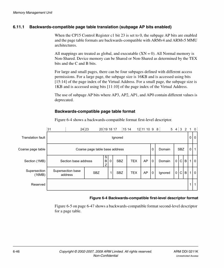
Memory Management Unit
6.11.1 Backwards-compatible page table translation (subpage AP bits enabled)
When the CP15 Control Register c1 bit 23 is set to 0, the subpage AP bits are enabled and the page table formats are backwards-compatible with ARMv4 and ARMv5 MMU architectures.
All mappings are treated as global, and executable (XN = 0). All Normal memory is Non-Shared. Device memory can be Shared or Non-Shared as determined by the TEX bits and the C and B bits.
For large and small pages, there can be four subpages defined with different access permissions. For a large page, the subpage size is 16KB and is accessed using bits [15:14] of the page index of the Virtual Address. For a small page, the subpage size is 1KB and is accessed using bits [11:10] of the page index of the Virtual Address.
The use of subpage AP bits where AP3, AP2, AP1, and AP0 contain different values is deprecated.
Backwards-compatible page table format
Figure 6-4 shows a backwards-compatible format first-level descriptor.
Figure 6-4 Backwards-compatible first-level descriptor format
Figure 6-5 on page 6-47 shows a backwards-compatible format second-level descriptor for a page table.
1 SBZ
0 SBZ TEX
1Coarse page table base address 0 Domain SBZ 0
0Ignored
31 20 19 12 11 10 9 8 5 4 3 2 1 0
0
0Section base addressSBZ
AP 0 Domain 0 C B 1
11
Translation fault
Coarse page table
Section (1MB)
15 14
Reserved
TEX 0Supersection base address SBZ AP 0 Ignored 0 C B 1Supersection
(16MB)
18 172324
6-46 Copyright © 2002-2007, 2009 ARM Limited. All rights reserved. ARM DDI 0211KNon-Confidential Unrestricted Access

Memory Management Unit
Figure 6-5 Backwards-compatible second-level descriptor format
For extended small page table entries without a TEX field you must use the value b000.
For details of TEX encodings see C and B bit, and type extension field encodings on page 6-15.
Figure 6-6 on page 6-48 shows an overview of the section, supersection, and page translation process using backwards-compatible descriptors.
0
SBZ
TEX AP3 B
B
1Large page table base address AP2 AP1 AP0 C 0
0Small page table base address AP3 AP2 AP1 AP0 C B 1
1Extended small page table base address TEX AP C 1
Translation fault
Large page(64KB)
Small page (4KB)
0Ignored
31 16 15 12 11 10 9 8 7 6 5 4 3 2 1 0
0
14
ARM DDI 0211K Copyright © 2002-2007, 2009 ARM Limited. All rights reserved. 6-47Unrestricted Access Non-Confidential

Memory Management Unit
Figure 6-6 Backwards-compatible section, supersection, and page translation
6.11.2 ARMv6 page table translation (subpage AP bits disabled)
When the CP15 Control Register c1 Bit 23 is set to 1, the subpage AP bits are disabled and the page tables have support for ARMv6 MMU features. Four new page table bits are added to support these features:
• The Not-Global (nG) bit, determines if the translation is marked as global (0), or process-specific (1) in the TLB. For process-specific translations the translation is inserted into the TLB using the current ASID, from the ContextID Register, CP15 c13.
• The Shared (S) bit, determines if the translation is for Non-Shared (0), or Shared (1) memory. This only applies to Normal memory regions. Device memory can be Shared or Non-Shared as determined by the TEX bits and the C and B bits.
• The Execute-Never (XN) bit, determines if the region is Executable (0) or Not-executable (1).
1001
00 = Invalid
00 = Invalid
01
11 = Reserved
Base addressfrom L1D[31:20]
Base addressfrom L1D[31:10]
Indexed by VA[19:0]
Indexed by VA[19:12]
Base addressfrom L2D[31:12]
Indexed by VA[11:0]
Indexed by VA[15:0]
Base addressfrom L2D[31:16]
16KB level onepage table
1MB section
Coarse pagetable
4KB small page
64KB large pageTranslationtable base
Indexed by VA[31:20]
31 0
31 0
31 0
10 (bit 18 = 0)
10 (bit 18 =1) Base addressfrom L1D[31:24]
Indexed by VA[23:0]
16MB supersection
16KB subpage16KB subpage16KB subpage16KB subpage
1KB subpage1KB subpage1KB subpage1KB subpage
11
Indexed by VA[11:0]
4KB extended small page
31 0Base addressfrom L2D[31:12]
6-48 Copyright © 2002-2007, 2009 ARM Limited. All rights reserved. ARM DDI 0211KNon-Confidential Unrestricted Access

Memory Management Unit
• Three access permission bits. The access permissions extension (APX) bit, provides an extra access permission bit.
All ARMv6 page table mappings support the TEX field.
ARMv6 page table format
Figure 6-7 shows the format of an ARMv6 first-level descriptor when subpages are enabled.
Figure 6-7 ARMv6 first-level descriptor formats with subpages enabled
Figure 6-8 shows the format of an ARMv6 first-level descriptor when subpages are disabled.
Figure 6-8 ARMv6 first-level descriptor formats with subpages disabled
1 SBZ
0 SBZ TEX
1Coarse page table base address 0 Domain SBZ 0
0Ignored
31 20 19 12 11 10 9 8 5 4 3 2 1 0
0
0Section base addressSBZ
AP 0 Domain 0 C B 1
11
Translation fault
Coarse page table
Section (1MB)
15 14
Reserved
TEX 0Supersection base address SBZ AP 0 Ignored 0 C B 1Supersection
(16MB)
18 172324
SAPX
APX
S0
1
nG TEX
1Coarse page table base address 0 Domain SBZ 0
0Ignored
31 20 19 12 11 10 9 8 5 4 3 2 1 0
0
1Reserved 1
Translation fault
Coarse page table
Supersection (16MB)
15 14
Reserved
17 1618
nG TEX 0Supersection base
address SBZ AP 0 Ignored XN C B 1
0Section base addressSBZ
AP 0 Domain XN C B 1Section (1MB)
2324
ARM DDI 0211K Copyright © 2002-2007, 2009 ARM Limited. All rights reserved. 6-49Unrestricted Access Non-Confidential

Memory Management Unit
In addition to the invalid translation, bits [1:0] = b00, translations for the reserved entry, bits [1:0] = b11, result in a translation fault.
Bit 18 of the first-level descriptor selects between a 1MB section and a 16MB supersection. For details of supersections see Supersections on page 6-6.
Figure 6-9 shows the format of an ARMv6 second-level descriptor.
Figure 6-9 ARMv6 second-level descriptor format
Figure 6-10 on page 6-51 shows an overview of the section, supersection, and page translation process using ARMv6 descriptors.
SnG
S
XN
APX
TEX B 1Large page table base address SBZ AP C 0
XNExtended small page table base address n
G
APX
TEX AP C B 1
Translation fault
Large page(64KB)
Small page (4KB)
0Ignored
31 16 15 12 11 10 9 8 7 6 5 4 3 2 1 0
0
14
6-50 Copyright © 2002-2007, 2009 ARM Limited. All rights reserved. ARM DDI 0211KNon-Confidential Unrestricted Access

Memory Management Unit
Figure 6-10 ARMv6 section, supersection, and page translation
6.11.3 Restrictions on page table mappings (page coloring)
The ARM1136JF-S processor uses virtually indexed, physically addressed caches. To prevent alias problems where cache sizes greater than 16KB have been implemented, you must restrict the mapping of pages that remap Virtual Address bits [13:12]. Bit[11] and bit[23] in the CP15 c0 Cache Type Register, the P bits for the instruction and data caches, indicate if this restriction is necessary (see c0, Cache Type Register on page 3-27 and Figure 3-11 on page 3-28).
This restriction, referred to as page coloring, enables these bits of the Virtual Address to be used to index into the cache without requiring hardware support to avoid alias problems. For pages marked as Non-Shared, if bit 11 or bit 23 of the Cache Type
1XN01
00 = Invalid
00 = Invalid
01
11 = Reserved
Base addressfrom L1D[31:20]
Base addressfrom L1D[31:10]
Indexed by VA[19:0]
Indexed by VA[19:12]
Base addressfrom L2D[31:12]
Indexed by VA[11:0]
Indexed by VA[15:0]
Base addressfrom L2D[31:16]
16Kbyte level onepage table
1MB section
Coarse pagetable
4KB extended small page
64KB large pageTranslationtable base
Indexed by VA[31:20]
31 0
31 0
31 0
10 (bit 18 = 0)
10 (bit 18 =1) Base addressfrom L1D[31:24]
Indexed by VA[23:0]
16MBsupersection
ARM DDI 0211K Copyright © 2002-2007, 2009 ARM Limited. All rights reserved. 6-51Unrestricted Access Non-Confidential

Memory Management Unit
Register is set, the restriction applies to pages that remap Virtual Address bits [13:12] and might cause aliasing problems when 4KB pages are used. To prevent this you must ensure the following restrictions are applied:
1. If multiple Virtual Addresses are mapped onto the same physical address then for all mappings, bits [13:12] of the Virtual Addresses must be equal and the same as bits [13:12] of the physical address. Imposing this requirement on the virtual addresses is sometimes called page coloring.
The same physical address can be mapped by TLB entries of different page sizes, including page sizes over 4KB.
2. Alternatively, if all mappings to a physical address are of a page size equal to 4KB, then the restriction that bits[13:12] of the Virtual Address must equal bits[13:12] of the physical address is not necessary. Bits[13:12] of all Virtual Address aliases must still be equal.
There is no restriction on the more significant bits in the Virtual Address equalling those in the physical address.
Avoiding the page coloring restriction
From release r1p0 of the ARM1136JF-S processor, the page coloring restriction can be removed by setting the CZ flag (bit[6]) in the CP15 Auxiliary Control Register, see c1, Auxiliary Control Register on page 3-69. If you set this flag, the sizes of the data and instruction caches will be restricted to 16KB.
Note Setting the CZ flag in the CP15 Auxiliary Control Register does not affect the contents of the CP15 Cache Type Register. However, when the CZ flag is set all caches will be limited to 16KB, even if a larger cache size is specified in the CP15 Cache Type Register.
6-52 Copyright © 2002-2007, 2009 ARM Limited. All rights reserved. ARM DDI 0211KNon-Confidential Unrestricted Access

Memory Management Unit
6.12 MMU descriptors
To support sections and pages, the ARM1136JF-S MMU uses a two-level descriptor definition. The first-level descriptor indicates whether the access is to a section or to a page table. If the access is to a page table, the ARM1136JF-S MMU determines the page table type and fetches a second-level descriptor.
6.12.1 First-level descriptor address
The ARM1136 contains:
• two Translation Table Base Registers, TTBR0 and TTBR1
• one Translation Table Base Control Register (TTBCR).
On a TLB miss, the top bits of the modified virtual address determine whether the first or second Translation Table Base is used.
The expected use of two translation tables is to reduce the cost of OS context switches.By enabling the OS, and each individual task or process, to have its own pagetable, it minimizes memory consumption.
In this model, the virtual address space is divided into two regions:
• 0x0 -> 1<<(32-N) that TTBR0 controls
• 1<<(32-N) -> 4GB that TTBR1 controls.
The value of N is set in the TTBCR. If N is zero, then TTBR0 is used for all addresses, and that gives legacy v5 behavior. If N is not zero, the OS and memory mapped IO are located in the upper part of the memory map, TTBR1, and the tasks or processes all occupy the same virtual address space in the lower part of the memory, TTBR0.
The translation table that TTBR0 points to can be truncated because it must only cover the first 1<<(32-N) bytes of memory. The first entry always corresponds to address 0x0, so this mechanism is more efficient if processes start at a low virtual address such as 0x0 or 0x8000. Table 6-15 lists the translation table size.
Table 6-15 Translation table size
N Upper boundary Translation table 0 size
0 4GB 16KB, 4 096 entries, v5 behavior, TTBR1 not used.
1 2GB 8KB, 2 048 entries
2 1GB 4KB, 1 024 entries
3 512MB 2KB, 512 entries
ARM DDI 0211K Copyright © 2002-2007, 2009 ARM Limited. All rights reserved. 6-53Unrestricted Access Non-Confidential

Memory Management Unit
The OS can maintain a different pagetable for each process, and update TTRB0 on a context switch. Using a truncated pagetable means that much less space is required to store the individual process page tables. Different processes can have different size pagetables, denoted by different values of N, by updating the TTBCR during the context switch.
It is not required that the OS pagetables pointed to by the TTBR1 are updated on a context switch.
Figure 6-11 on page 6-55 shows the generation of a first-level descriptor address.
4 256MB 1KB, 256 entries
5 128MB 512B, 128 entries
6 64MB 256B, 64 entries
7 32MB 128B, 32 entries
Table 6-15 Translation table size (continued)
N Upper boundary Translation table 0 size
6-54 Copyright © 2002-2007, 2009 ARM Limited. All rights reserved. ARM DDI 0211KNon-Confidential Unrestricted Access

Memory Management Unit
Figure 6-11 Generating a first-level descriptor address
Translation table base control
Modified virtual address
0 1if (N > 0 && MVA[31:32-N] != 0) {TTBR1[31:14], MVA[31:20], 2'b00}else {TTBR0[31:14-N], MVA[31-N:20], 2'b00}
Where N is the value of the Translation Table Base Control Register
First-level descriptor address
Translation Table Base Address
31 1413 2 1 0
Table index 0 0
First-level table index
31-N 2019 0
Modified virtual address
First-level table index
31 2019 0
Translation Table Base Address
31 14-N 13-N 2 1 0
Table index 0 0
Translation Table Base Register 0
Translation table base address
31 14-N 13-N 5 4 3 2 1 0
RGN 0 S C
Translation Table Base Register 1
Translation table base address
31 1413 5 4 3 2 1 0
RGN 0 S C
if (N > 0 && MVA[31:32-N] != 0) {TTBR1[31:14], MVA[31:20], 2'b00}else {TTBR0[31:14-N], MVA[31-N:20], 2'b00}
Where N is the value of the Translation Table Base Control Register
Translation table base control
ARM DDI 0211K Copyright © 2002-2007, 2009 ARM Limited. All rights reserved. 6-55Unrestricted Access Non-Confidential

Memory Management Unit
6.12.2 First-level descriptor
Using the first-level descriptor address, a request is made to external memory. This returns the first-level descriptor. By examining bits [1:0] of the first-level descriptor, the access type is indicated as shown in Table 6-16.
First-level translation and access fault
If bits [1:0] of the first-level descriptor are b00 or b11, a translation fault is generated. This causes either a Prefetch Abort or Data Abort in the ARM1136JF-S processor. Prefetch Aborts occur in the instruction MMU. Data Aborts occur in the data MMU.
If the first level description describes a section or supersection, an Access Flag fault is generated when all of the following conditions are met:
• the XP bit is set in the CP15 Control register
• the AFE bit is set in the CP15 Control register
• AP[0]=0.
See Access Flag fault on page 6-40 for more information, and see c1, Control Register on page 3-63 for details of setting the XP and AFE bits.
Note The Access Flag, and Access Flag faults, are only implemented from the rev1 (r1p0) release of the ARM1136JF-S processor.
First-level page table address
If bits [1:0] of the first-level descriptor are b01, then a page table walk is required. This process is described in Second-level page table walk on page 6-58.
Table 6-16 Access types from first-level descriptor bit values
Bit values Access type
b00 Translation fault
b01 Page table base address
b10 Section base address
b11 Reserved, results in translation fault
6-56 Copyright © 2002-2007, 2009 ARM Limited. All rights reserved. ARM DDI 0211KNon-Confidential Unrestricted Access

Memory Management Unit
First-level section base address
If bits [1:0] of the first-level descriptor are b10, a request to a section memory block has occurred. Figure 6-12 shows the translation process for a 1MB section using ARMv6 format (AP bits disabled).
Figure 6-12 Translation for a 1MB section, ARMv6 format
Following the first-level descriptor translation, the physical address is used to transfer to and from external memory the data requested from and to the ARM1136JF-S processor. This is done only after the domain and access permission checks are performed on the first-level descriptor for the section. These checks are described in Memory access control on page 6-11.
Figure 6-13 on page 6-58 shows the translation process for a 1MB section using backwards-compatible format (AP bits enabled).
0 S TEX 0Section base address
31 20 19 12 11 10 9 8 5 4 3 2 1 0
0 AP 0 Domain C B 1
First-level table index
31 20 19 0
Section index
Translation table base address
31 14 13 0
0Translation table base address
31 14 13 0
First-level table index 0
2 1
Physical address
First-level descriptor
First-level descriptor address
Modified virtual address
Translation Table Base Register
Section base address
31 20 19 0
Section index
1415161718
nG APX XN
ARM DDI 0211K Copyright © 2002-2007, 2009 ARM Limited. All rights reserved. 6-57Unrestricted Access Non-Confidential

Memory Management Unit
Figure 6-13 Translation for a 1MB section, backwards-compatible format
6.12.3 Second-level page table walk
If bits [1:0] of the first-level descriptor bits are b01, then a page table walk is required. The MMU requests the second-level page table descriptor from external memory. Figure 6-14 on page 6-59 shows the generation of a second-level page table address.
TEX 0Section base address
31 20 19 12 11 10 9 8 5 4 3 2 1 0
SBZ AP 0 Domain 0 C B 1
First-level table index
31 20 19 0
Section index
Translation table base address
31 14 13 0
0Translation table base address
31 14 13 0
First-level table index 0
2 1
Physical address
First-level descriptor
First-level descriptor address
Modified virtual address
Translation Table Base Register
Section base address
31 20 19 0
Section index
1415
6-58 Copyright © 2002-2007, 2009 ARM Limited. All rights reserved. ARM DDI 0211KNon-Confidential Unrestricted Access
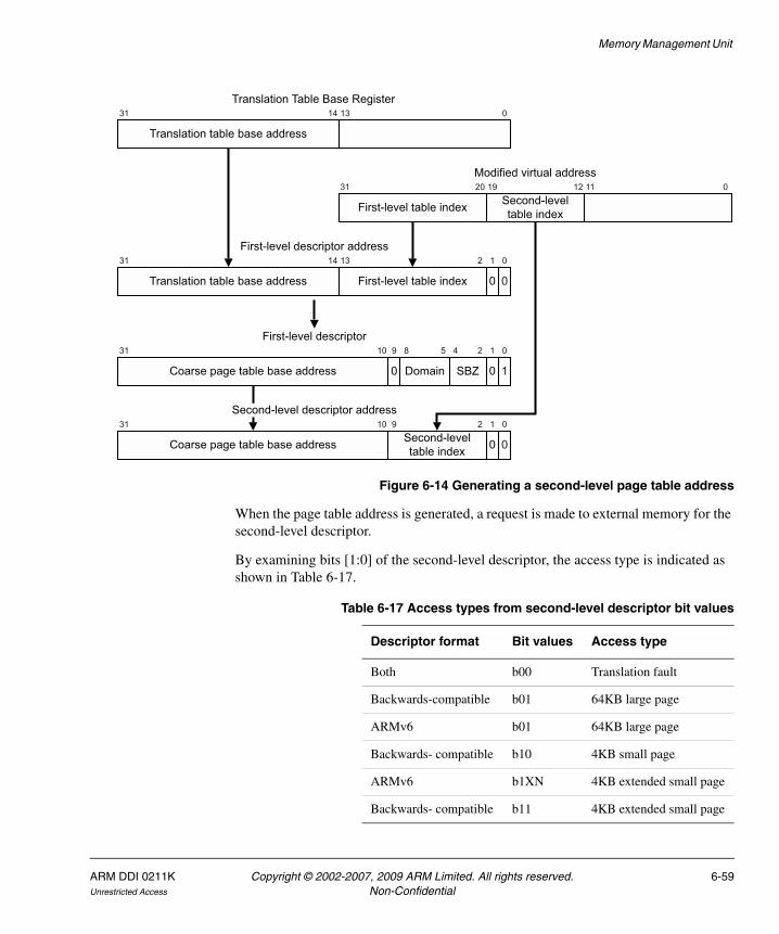
Memory Management Unit
Figure 6-14 Generating a second-level page table address
When the page table address is generated, a request is made to external memory for the second-level descriptor.
By examining bits [1:0] of the second-level descriptor, the access type is indicated as shown in Table 6-17.
SBZ 1Coarse page table base address
31 10 9 8 5 4 2 1 0
0 Domain 0
First-level table index
31 20 19 12 11 0Second-leveltable index
Translation table base address
31 14 13 0
0Coarse page table base address
31 10 9 2 1 0Second-leveltable index 0
0Translation table base address
31 14 13 0
First-level table index 0
2 1
First-level descriptor
First-level descriptor address
Modified virtual address
Translation Table Base Register
Second-level descriptor address
Table 6-17 Access types from second-level descriptor bit values
Descriptor format Bit values Access type
Both b00 Translation fault
Backwards-compatible b01 64KB large page
ARMv6 b01 64KB large page
Backwards- compatible b10 4KB small page
ARMv6 b1XN 4KB extended small page
Backwards- compatible b11 4KB extended small page
ARM DDI 0211K Copyright © 2002-2007, 2009 ARM Limited. All rights reserved. 6-59Unrestricted Access Non-Confidential

Memory Management Unit
Second-level translation and access fault
If bits [1:0] of the second-level descriptor are b00, then a translation fault is generated. This generates an abort to the ARM1136JF-S processor, either a Prefetch Abort for the instruction side or a Data Abort for the data side.
If the second level description describes a large page, a small page, or an extended small page, an Access Flag fault is generated when all of the following conditions are met:
• the XP bit is set in the CP15 Control register
• the AFE bit is set in the CP15 Control register
• AP[0]=0.
See Access Flag fault on page 6-40 for more information, and see c1, Control Register on page 3-63 for details of setting the XP and AFE bits.
Note The Access Flag, and Access Flag faults, are only implemented from the rev1 (r1p0) release of the ARM1136JF-S processor.
Second-level large page base address
If bits [1:0] of the second-level descriptor are b01, then a large page table walk is required. Figure 6-15 on page 6-61 shows the translation process for a 64KB large page using ARMv6 format (AP bits disabled).
6-60 Copyright © 2002-2007, 2009 ARM Limited. All rights reserved. ARM DDI 0211KNon-Confidential Unrestricted Access
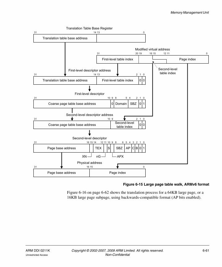
Memory Management Unit
Figure 6-15 Large page table walk, ARMv6 format
Figure 6-16 on page 6-62 shows the translation process for a 64KB large page, or a 16KB large page subpage, using backwards-compatible format (AP bits enabled).
STEX
1Coarse page table base address
31 10 9 8 5 4 2 1 0
0 Domain SBZ 0
First-level table index
31 20 19 12 11 0
Page index
Translation table base address
31 14 13 0
1Page base address
31 12 11 10 9 8 6 5 4 3 2 1 0
SBZ AP C B 0
0Coarse page table base address
31 10 9 2 1 0Second-level table index 0
0Translation table base address
31 14 13 0
First-level table index 0
2 1
Page indexPage base address
31 0
Second-level descriptor
Physical address
First-level descriptor
First-level descriptor address
Modified virtual address
Translation Table Base Register
16 15
16 15
16 15
14
Second-level table index
Second-level descriptor address
nG APXXN
ARM DDI 0211K Copyright © 2002-2007, 2009 ARM Limited. All rights reserved. 6-61Unrestricted Access Non-Confidential

Memory Management Unit
Figure 6-16 Large page table walk, backwards-compatible format
Using backwards-compatible format descriptors, the 64KB large page is generated by setting all of the AP bit pairs to the same values, AP3=AP2=AP1=AP0. If any one of the pairs are different, then the 64KB large page is converted into four 16KB large page subpages. The subpage access permission bits are chosen using the Virtual Address bits [15:14].
Second-level small page table walk
If bits [1:0] of the second-level descriptor are b10 for backwards-compatible format, then a small page table walk is required.
0 TEX
1Coarse page table base address
31 10 9 8 5 4 2 1 0
0 Domain SBZ 0
First-level table index
31 20 19 12 11 0
Page index
Translation table base address
31 14 13 0
1Page base address
31 12 11 10 9 8 7 6 5 4 3 2 1 0AP3
AP2
AP1
AP0 C B 0
0Coarse page table base address
31 10 9 2 1 0Second-level table index 0
0Translation table base address
31 14 13 0
First-level table index 0
2 1
Page indexPage base address
31 0
Second-level descriptor
Physical address
First-level descriptor
First-level descriptor address
Modified virtual address
Translation Table Base Register
16 15
1415
16 15
16
Second-level table index
Second-level descriptor address
6-62 Copyright © 2002-2007, 2009 ARM Limited. All rights reserved. ARM DDI 0211KNon-Confidential Unrestricted Access

Memory Management Unit
Figure 6-17 shows the translation process for a 4KB small page or a 1KB small page subpage using backwards-compatible format descriptors (AP bits enabled).
Figure 6-17 4KB small page or 1KB small subpage translations, backwards-compatible
Using backwards-compatible descriptors, the 4KB small page is generated by setting all of the AP bit pairs to the same values, AP3=AP2=AP1=AP0. If any one of the pairs are different, then the 4KB small page is converted into four 1KB small page subpages. The subpage access permission bits are chosen using the Virtual Address bits [11:10].
1Coarse page table base address
31 10 9 8 5 4 2 1 0
0 Domain SBZ 0
First-level table index
31 20 19 12 11 0Second-leveltable index Page index
Translation table base address
31 14 13 0
0Small page base address
31 12 11 10 9 8 7 6 5 4 3 2 1 0AP3
AP2
AP1
AP0 C B 1
0Coarse page table base address
31 10 9 2 1 0Second-level table
index 0
0Translation table base address
31 14 13 0
First-level table index 0
2 1
Page indexPage base address
31 12 11 0
Second-level descriptor
Physical address
First-level descriptor
First-level descriptor address
Modified virtual address
Translation Table Base Register
Second-level descriptor address
ARM DDI 0211K Copyright © 2002-2007, 2009 ARM Limited. All rights reserved. 6-63Unrestricted Access Non-Confidential

Memory Management Unit
Second-level extended small page table walk
If bits [1:0] of the second-level descriptor are b1XN for ARMv6 format descriptors, or b11 for backwards-compatible descriptors, then an extended small page table walk is required. Figure 6-18 shows the translation process for a 4KB extended small page using ARMv6 format descriptors (AP bits disabled).
Figure 6-18 4KB extended small page translations, ARMv6 format
Figure 6-19 on page 6-65 shows the translation process for a 4KB extended small page or a 1KB extended small page subpage using backwards-compatible format descriptors (AP bits enabled).
S
1Coarse page table base address
31 10 9 8 5 4 3 2 1 0
0 Domain SBZ 0
First-level table index
31 20 19 12 11 0Second-leveltable index Page index
Translation table base address
31 14 13 0
Extended small page base address
31 12 11 10 9 8 6 5 4 3 2 1 0
TEX AP C B 1
0Coarse page table base address
31 10 9 2 1 0Second-level table
index 0
0Translation table base address
31 14 13 0
First-level table index 0
2 1
Page indexPage base address
31 12 11 0
Second-level descriptor
Physical address
First-level descriptor
First-level descriptor address
Modified virtual address
Translation Table Base Register
nG APX XN
Second-level descriptor address
6-64 Copyright © 2002-2007, 2009 ARM Limited. All rights reserved. ARM DDI 0211KNon-Confidential Unrestricted Access

Memory Management Unit
Figure 6-19 4KB extended small page or 1KB extended small subpage translations,backwards-compatible
Using backwards-compatible descriptors, the 4KB extended small page is generated by setting all of the AP bit pairs to the same values, AP3=AP2=AP1=AP0. If any one of the pairs are different, then the 4KB extended small page is converted into four 1KB extended small page subpages. The subpage access permission bits are chosen using the Virtual Address bits [11:10].
1Coarse page table base address
31 10 9 8 5 4 2 1 0
0 Domain SBZ 0
First-level table index
31 20 19 12 11 0Second-leveltable index Page index
Translation table base address
31 14 13 0
1Extended small page base address
31 12 11 9 8 6 5 4 3 2 1 0
SBZ TEX AP C B 1
0Coarse page table base address
31 10 9 2 1 0Second-level table
index 0
0Translation table base address
31 14 13 0
First-level table index 0
2 1
Page indexPage base address
31 12 11 0
Second-level descriptor
Physical address
First-level descriptor
First-level descriptor address
Modified virtual address
Translation Table Base Register
Second-level descriptor address
ARM DDI 0211K Copyright © 2002-2007, 2009 ARM Limited. All rights reserved. 6-65Unrestricted Access Non-Confidential

Memory Management Unit
6.13 MMU software-accessible registers
The MMU is controlled by the system control coprocessor (CP15) registers, shown in Table 6-18, in conjunction with page table descriptors stored in memory.
You can access all the registers with instructions of the form:
MRC p15, 0, <Rd>, <CRn>, <CRm>, <Opcode_2>MCR p15, 0, <Rd>, <CRn>, <CRm>, <Opcode_2>
Where CRn is the system control coprocessor register. Unless specified otherwise, CRm and Opcode_2 Should Be Zero.
Table 6-18 CP15 register functions
Register Reference to description
TLB Type Register See c0, TLB Type Register on page 3-33
Control Register See c1, Control Register on page 3-63
Translation Table Base Register 0 See c2, Translation Table Base Register 0, TTBR0 on page 3-74
Translation Table Base Register 1 See c2, Translation Table Base Register 1, TTBR1 on page 3-76
Translation Table Base Control Register See c2, Translation Table Base Control Register, TTBCR on page 3-78
Domain Access Control Register See c3, Domain Access Control Register on page 3-80
Data Fault Status Register (DFSR) See c5, Data Fault Status Register, DFSR on page 3-83
Instruction Fault Status Register (IFSR) See c5, Instruction Fault Status Register, IFSR on page 3-86
Fault Address Register (FAR) See c6, Fault Address Register, FAR on page 3-88
Watchpoint Fault Address Register (WFAR) See c6, Watchpoint Fault Address Register, WFAR on page 3-89
Cache Operations Register See c7, Cache Operations Register on page 3-90
TLB Operations Register See c8, TLB Operations Register (invalidate TLB operation) on page 3-111
TLB Lockdown Register See c10, TLB Lockdown Register on page 3-121
Primary Region Remap Register See Primary Region Remap Register (PRRR) on page 3-125
Normal Memory Remap Register See Normal Memory Remap Register (NMRR) on page 3-127
FCSE PID Register See c13, FCSE PID Register on page 3-156
ContextID Register See c13, Context ID Register on page 3-159
6-66 Copyright © 2002-2007, 2009 ARM Limited. All rights reserved. ARM DDI 0211KNon-Confidential Unrestricted Access

Memory Management Unit
Note All the CP15 MMU registers, except CP15 c7 and CP15 c8, contain state that you read using MRC instructions and written to using MCR instructions. Registers c5 and c6 are also written by the MMU. Reading CP15 c7 and c8 is Unpredictable. See the register descriptions for more information.
User Read/Write Thread and Process ID Register See c13, Thread and process ID registers on page 3-160
User Read-only Thread and Process ID Register See c13, Thread and process ID registers on page 3-160
Privileged Only Thread and Process ID Register See c13, Thread and process ID registers on page 3-160
Table 6-18 CP15 register functions (continued)
Register Reference to description
ARM DDI 0211K Copyright © 2002-2007, 2009 ARM Limited. All rights reserved. 6-67Unrestricted Access Non-Confidential

Memory Management Unit
6.14 MMU and write buffer
During any translation table walk the MMU has access to external memory. Before the table walk occurs, the write buffer has to be flushed of any related writes to avoid read-after-write hazards.
When either the instruction MMU or data MMU contains valid TLB entries that are being modified, those TLB entries must be invalidated by software, and the Write Buffer drained using the Drain Write Buffer instruction before the new section or page is accessed.
6-68 Copyright © 2002-2007, 2009 ARM Limited. All rights reserved. ARM DDI 0211KNon-Confidential Unrestricted Access

Chapter 7 Level One Memory System
This chapter describes the ARM1136JF-S level one memory system. It contains the following sections:
• About the level one memory system on page 7-2
• Cache organization on page 7-3
• Tightly-coupled memory on page 7-8
• DMA on page 7-11
• TCM and cache interactions on page 7-13
• Cache debug on page 7-17
• Write buffer on page 7-18.
ARM DDI 0211K Copyright © 2002-2007, 2009 ARM Limited. All rights reserved. 7-1Unrestricted Access Non-Confidential

Level One Memory System
7.1 About the level one memory system
The ARM1136JF-S level one memory system consists of:
• separate instruction and data caches in a Harvard arrangement
• separate Instruction and Data Tightly-Coupled Memory (TCM) areas
• a DMA system for accessing the TCM
• a write buffer
• two MicroTLBs, backed by a Main TLB.
In parallel with each of the caches is an area of dedicated RAM on both the instruction and data sides. These regions are called TCM. You can implement 0 or 1 TCM on each of the Instruction and Data sides.
Each TCM has a dedicated base address that you can place anywhere in the physical address map, and does not have to be backed by memory implemented externally. The Instruction and Data TCMs have separate base addresses.
Each TCM can optionally support a SmartCache mode of operation. In this mode of operation, the TCM behaves as a large contiguous area of cache, starting at the base address.
Each TCM not configured to operate as SmartCache can be accessed by a DMA mechanism to enable this memory to be loaded from or stored to another location in memory while the processor core is running.
The MMU provides the facilities required by sophisticated operating systems to deliver protected virtual memory environments and demand paging. It also supports real-time tasks with features that provide predictable execution time.
Address translation is handled in a full MMU for each of the instruction and data sides. The MMU is responsible for protection checking, address translation, and memory attributes, some of which can be passed to the level two memory system.
The memory translations are cached in MicroTLBs for each of the instruction and data sides and for the DMA, with a single Main TLB backing the MicroTLBs.
7-2 Copyright © 2002-2007, 2009 ARM Limited. All rights reserved. ARM DDI 0211KNon-Confidential Unrestricted Access

Level One Memory System
7.2 Cache organization
Each cache is implemented as a four-way set associative cache of configurable size. They are virtually indexed and physically addressed. The cache sizes are configurable with sizes in the range of 4 to 64KB. Both the Instruction Cache and the Data Cache are capable of providing two words per cycle for all requesting sources.
Each cache way is architecturally limited to 16KB in size, because of the limitations of the virtually indexed, physically addressed implementation. The number of cache ways is fixed at four, but the cache way size can be varied between 1KB and 16KB in powers of 2. The line length is not configurable and is fixed at eight words per line.
Write operations must occur after the Tag RAM reads and associated address comparisons have completed. A three-entry write buffer is included in the cache to enable the written words to be held until they can be written to cache. One or two words can be written in a single store operation. The addresses of these outstanding writes provide an additional input into the Tag RAM comparison for reads.
To avoid a critical path from the Tag RAM comparison to the enable signals for the data RAMs, there is a minimum of one cycle of latency between the determination of a hit to a particular way, and the start of writing to the data RAM of that way. This requires the cache write buffer to be able to hold three entries, for back-to-back writes. Accesses that read the dirty bits must also check the cache write buffer for pending writes that result in dirty bits being set. The cache dirty bits for the Data Cache are updated when the cache write buffer data is written to the RAM. This requires the dirty bits to be held as a separate storage array (significantly, the tag arrays cannot be written, because the arrays are not accessed during the data RAM writes), but permits the dirty bits to be implemented as a small RAM.
The other main operations performed by the cache are cache line refills and write-back. These occur to particular cache ways, which are determined at the point of the detection of the cache miss by the victim selection logic.
To reduce overall power consumption, the number of full cache reads is reduced by the sequential nature of many cache operations, especially on the instruction side. On a cache read that is sequential to the previous cache read, only the data RAM Set that was previously read is accessed, if the read is within the same cache line. The Tag RAM is not accessed at all during this sequential operation.
To reduce unnecessary power consumption further, only the addressed words within a cache line are read at any time. With the required 64-bit read interface, this is achieved by disabling half of the RAMs on occasions when only a 32-bit value is required. The implementation uses two 32-bit wide RAMs to implement the cache data RAM shown
ARM DDI 0211K Copyright © 2002-2007, 2009 ARM Limited. All rights reserved. 7-3Unrestricted Access Non-Confidential

Level One Memory System
in Figure 7-1, with the words of each line folded into the RAMs on an odd and even basis. This means that cache refills can take several cycles, depending on the cache line lengths. The cache line length is eight words.
The control of the level one memory system and the associated functionality, together with other system wide control attributes are handled through the system control coprocessor, CP15. This is described in About the system control coprocessor on page 3-2.
The block diagram of the cache subsystem is as shown in Figure 7-1. This diagram does not show the cache refill paths.
Figure 7-1 Level one cache block diagram
DATARAMTAGRAM TCM
Comparator
Wayselect
Write buffer data (3x2 words)
Write buffer addresses(3 words)
MicroTLB
Victim selector
Missvictim
Cachehit
Dataout
MissPA andattributes
Micro TLBmiss and
Data Abort
RAMSet base address and size
CP15interface
Virtualaddress
Writedata
7-4 Copyright © 2002-2007, 2009 ARM Limited. All rights reserved. ARM DDI 0211KNon-Confidential Unrestricted Access

Level One Memory System
7.2.1 Features of the cache system
The level one cache system has the following features:
• The cache is a Harvard implementation.
• The caches are lockable at a granularity of a cache way, using Format C lockdown. See c9, Data and Instruction Cache Lockdown Registers on page 3-113.
• Cache replacement policies are Pseudo-Random or Round-Robin, as controlled by the RR bit in CP15 register c1. Round-Robin uses a single counter for all Sets, that selects the Way used for replacement.
• Cache line allocation uses the cache replacement algorithm when all cache lines are valid. If one or more lines is invalid, then the invalid cache line with the lowest way number is allocated to in preference to replacing a valid cache line. This mechanism does not allocate to locked cache ways unless all cache ways are locked. See Cache miss handling when all ways are locked down on page 7-7.
• Cache lines can be either write-back or write-through, determined by the MicroTLB entry.
• Only read allocation is supported.
• The cache can be disabled independently from the TCM, under control of the appropriate bits in CP15 c1.
• Data cache misses are nonblocking with a single outstanding Data Cache miss being supported.
• Streaming of sequential data from LDM and LDRD operations, and for sequential instruction fetches is supported.
7.2.2 Cache functional description
The cache and TCM exist to perform associative reads and writes on requested addresses. The steps involved in this for reads are:
1. The lower bits of the Virtual Address are used as the virtual index for the tag and RAM blocks, including the TCM.
2. In parallel the MicroTLB is accessed to perform the virtual to physical address translation.
3. The physical addresses read from the Tag RAMs and the TCM base address register, and the write buffer address registers, are compared with the physical address from the MicroTLB to form hit signals for each of the cache ways
ARM DDI 0211K Copyright © 2002-2007, 2009 ARM Limited. All rights reserved. 7-5Unrestricted Access Non-Confidential

Level One Memory System
4. The hit signals are used to select the data from the cache way that has a hit. Any bytes contained in both the data RAMs and the write buffer entries are taken from the write buffer. If two or three write buffer entries are to the same bytes, the most recently written bytes are taken.
The steps for writes are:
1. The lower bits of the Virtual Address are used as the virtual index for the tag blocks.
2. In parallel, the MicroTLB is accessed to perform the virtual to physical address translation.
3. The physical addresses read from the Tag RAMs and the TCM base address register are compared with the physical address from the MicroTLB to form hit signals for each of the cache ways.
4. If a cache way, or the TCM, has recorded a hit, then the write data is written to an entry in the cache write buffer, along with the cache way, or TCM, that it must take place to.
5. The contents of the cache write buffer are held until a subsequent write or CP15 operation requires space in the write buffer. At this point the oldest entry in the cache write buffer is written into the cache.
7.2.3 Cache control operations
The cache control operations that are supported by the ARM1136JF-S processor are described in c7, Cache Operations Register on page 3-90. ARM1136JF-S processors support all the block cache control operations in hardware.
Note From the rev1 (r1p0) release of the ARM1136JF-S processor, you can restrict the functional size of each cache to 16KB, when the physical cache is larger than this. This enables the processor to run software that does not support the ARMv6 page coloring restrictions. You enable this feature with the CZ bit, see c1, Auxiliary Control Register on page 3-69.
For more information about the ARMv6 page coloring restrictions see Restrictions on page table mappings (page coloring) on page 6-51.
7-6 Copyright © 2002-2007, 2009 ARM Limited. All rights reserved. ARM DDI 0211KNon-Confidential Unrestricted Access

Level One Memory System
7.2.4 Cache miss handling
A cache miss results in the requests required to do the line fill being made to the level two interface, with a write-back occurring if the line to be replaced contains dirty data.
The write-back data is transferred to the write buffer, which is arranged to handle this data as a sequential burst. Because of the requirement for nonblocking caches, additional write transactions can occur during the transfer of write-back data from the cache to the write buffer. These transactions do not interfere with the burst nature of the write-back data. The write buffer is responsible for handling the potential Read After Write (RAW) data hazards that might exist from a Data Cache line write-back. The caches perform critical word-first cache refilling. The internal bandwidth from the level two data read port to the data caches is eight bytes per cycle, and supports streaming.
Cache miss handling when all ways are locked down
The ARM architecture describes the behavior of the cache as being Unpredictable when all ways in the cache are locked down. However, for ARM1136JF-S processors a cache miss is serviced as if Way 0 is not locked.
7.2.5 Cache disabled behavior
If the cache is disabled, then the cache is not accessed for reads or for writes. This ensures that maximum power savings can be achieved. It is therefore important that before the cache is disabled, all of the entries are cleaned to ensure that the external memory has been updated. In addition, if the cache is enabled with valid entries in it, then it is possible that the entries in the cache contain old data. Therefore the cache must be disabled with clean and invalid entries.
Cache maintenance operations can be performed even if the cache is disabled.
7.2.6 Unexpected hit behavior
An unexpected hit is where the cache reports a hit on a memory location that is marked as Noncacheable or Shared. The unexpected hit behavior is that these hits are ignored and a level two access occurs. The unexpected hit is ignored because the cache hit signal is qualified by the cachability.
For writes, an unexpected cache hit does not result in the cache being updated. Therefore, writes appear to be Noncacheable accesses. For a data access, if it lies in the range of memory specified by the Instruction TCM configured as Local RAM, then the access is made to that RAM rather than to level two memory. This applies to both writes and reads.
ARM DDI 0211K Copyright © 2002-2007, 2009 ARM Limited. All rights reserved. 7-7Unrestricted Access Non-Confidential

Level One Memory System
7.3 Tightly-coupled memory
The TCM is designed to provide low-latency memory that can be used by the processor without the unpredictability that is a feature of caches.
You can use such memory to hold critical routines, such as interrupt handling routines or real-time tasks where the indeterminacy of a cache is highly undesirable. In addition you can used it to hold scratch pad data, data types whose locality properties are not well suited to caching, and critical data structures such as interrupt stacks.
You can configure the TCM in several ways:
• one TCM on the instruction side and one on the data side
• one TCM on the instruction or data side only
• no TCM on either side.
The TCM Status Register in CP15 c0 describes what TCM options and TCM sizes can be implemented, see c0, TCM Status Register on page 3-32.
Each TCM can optionally support a SmartCache mode of operation, see SmartCache behavior on page 7-9. In this mode the RAM behaves as a large contiguous area of cache, starting at the base address. As a result, the corresponding memory locations must also exist in the external memory system.
When a TCM is configured as a SmartCache it has the same:
• behavior as cache
• unexpected hit behavior as cache, see Unexpected hit behavior on page 7-7.
If a TCM is not configured to operate as SmartCache, then it behaves as Local RAM, see Local RAM behavior on page 7-9. Each Data TCM is implemented in parallel with the Data Cache and the Instruction TCM is implemented in parallel with the Instruction Cache. Each TCM has a single movable base address, specified in CP15 register c9, (see c9, Data TCM Region Register on page 3-116 and c9, Instruction TCM Region Register on page 3-118).
The size of each TCM can be different to the size of a cache way, but forms a single contiguous area of memory. The entire level one memory system is shown in Figure 7-1 on page 7-4.
You can disable each TCM to avoid an access being made to it. This gives a reduction in the power consumption. You can disable each TCM independently from the enabling of the associated cache, as determined by CP15 register c9.
The disabling of a TCM invalidates the base address, so there is no unexpected hit behavior for the TCM when configured as Local RAM.
7-8 Copyright © 2002-2007, 2009 ARM Limited. All rights reserved. ARM DDI 0211KNon-Confidential Unrestricted Access

Level One Memory System
7.3.1 SmartCache behavior
Instruction and Data TCMs support SmartCache in this implementation.
When a TCM is configured as SmartCache it forms a contiguous area of cache, with the contents of memory backed by external memory. Each line of the TCM, which is of the same length as the cache line (indicated in the Cache Type Register for the equivalent cache), can be individually set as being Valid or Invalid. Writing the RAM Region Register causes the valid information for each line to be cleared (marked as Invalid). When a read access is made to an Invalid line, the line is fetched from the level two memory system in exactly the same way as for a cache miss, and the fetched line is then marked as Valid.
For the TCM to exhibit SmartCache behavior, areas of memory that are covered by a TCM operating as SmartCache must be marked as Cacheable. For a memory access to a memory location that is marked as Noncacheable but is in an area covered by a TCM, if the corresponding SmartCache line is marked as Invalid, then the memory access does not cause the location to be fetched from external memory and marked as Valid. If the corresponding SmartCache line is marked as Valid, then the access is made to external memory.
If a TCM region configured as SmartCache covers an area of memory that is Shared, then the SmartCache is not loaded on a miss.
7.3.2 Local RAM behavior
When a TCM is configured as Local RAM it forms a continuous area of memory that is always valid if the TCM is enabled. Therefore it does not use the Valid bits for each line that is used for SmartCache. The TCM configured as Local RAM is used as part of the physical memory map of the system, and is not backed by a level of external memory with the same physical addresses. For this reason, the TCM behaves differently from the caches for regions of memory that are marked as being Write-Through Cacheable. In such regions, no external writes occur in the event of a write to memory locations contained in the TCM.
The DMA only operates to an area of TCM that is configured as Local RAM, to prevent any requirement of interactions between the cache refill and DMA operations. Attempting to perform a DMA to an area of TCM that is configured as SmartCache result in an internal DMA error (TCM DMA out of range).
ARM DDI 0211K Copyright © 2002-2007, 2009 ARM Limited. All rights reserved. 7-9Unrestricted Access Non-Confidential

Level One Memory System
7.3.3 Restriction on page table mappings
The TCMs are implemented in a physically indexed, physically addressed manner, giving the following behavior:
• the entries in the TCM do not have to be cleaned and/or invalidated by software for different virtual to physical mappings
• aliases to the same physical address can exist in memory regions that are held in the TCM.
As a result, the page mapping restrictions for the TCM are less restrictive than for the cache.
7.3.4 Restriction on page table attributes
The page table entries that describe areas of memory that are handled by the TCM can be described as being Cacheable or Noncacheable, but must not be marked as Shared. If they are marked as either Device or Strongly Ordered, or have the Shared attribute set then the locations that are contained within the TCM are treated as being Non-Shared, Noncacheable.
7-10 Copyright © 2002-2007, 2009 ARM Limited. All rights reserved. ARM DDI 0211KNon-Confidential Unrestricted Access

Level One Memory System
7.4 DMA
The level one DMA provides a background route to transfer blocks of data to or from the TCMs. It is used to move large blocks, rather than individual words or small structures.
The level one DMA is initiated and controlled by accessing the appropriate CP15 registers and instructions, see c11, DMA registers overview on page 3-130. The process specifies the internal start and end addresses and external start address, together with the direction of the DMA. The addresses specified are Virtual Addresses, and the level one DMA hardware includes translation of Virtual Addresses to Physical Addresses and checking of protection attributes.
The TLB, described in TLB organization on page 6-4 is used to hold the page table entries for the DMA, and ensures that the entries in a TLB used by the DMA are consistent with the page tables. Errors arising from protection checks are signaled to the processor using an interrupt. Completion of the DMA can also be configured by software to signal the processor with an interrupt using the same interrupt to the processor that the error uses.
The status of the DMA is read from the CP15 registers associated with the DMA.
The DMA controller is programmed using the CP15 coprocessor. DMA accesses can only be to or from the TCM, configured as Local RAM, and must not be from areas of memory that can be contained in the caches. That is, no coherency support is provided in the caches.
The ARM1136JF-S processor implements two DMA channels. Only one channel can be active at a time. The key features of the DMA system are:
• the DMA system runs in the background of processor operations
• DMA progress is accessible from software
• the DMA is programmed with Virtual Addresses, with a MicroTLB dedicated to the DMA function
• you can configure the DMA to work to either the instruction or data RAMs
• the DMA is allocated by a privileged process, enabling User access to control the DMA.
For some DMA events an interrupt is generated. If this happens the nDMAIRQ signal of the ARM1136JF-S processor is asserted. You can route this output pin to an external interrupt controller for prioritization and masking. This is the only mechanism by which the interrupt is signaled to the core.
ARM DDI 0211K Copyright © 2002-2007, 2009 ARM Limited. All rights reserved. 7-11Unrestricted Access Non-Confidential

Level One Memory System
Each DMA channel has its own set of control and status registers. The maximum number of DMA channels that can be defined is architecturally limited to 2. Only 1 DMA channel can be active at a time. If the other DMA channel has been started, it is queued to start performing memory operations after the currently active channel has completed.
The level one DMA behaves as a distinct master from the rest of the processor, and the same mechanisms for handling Shared memory regions must be used if the external addresses being accessed by the level one DMA system are also accessed by the rest of the processor. These are described in Memory attributes and types on page 6-24. If a User mode DMA transfer is performed using an external address that is not marked as Shared, an error is signaled by the DMA channel.
There is no ordering requirement of memory accesses caused by the level one DMA relative to those generated by reads and writes by the processor, while a channel is running. When a channel has completed running, all its transactions are visible to all other observers in the system. All memory accesses caused by the DMA occur in the order specified by the DMA channel, regardless of the memory type.
If a DMA is performed to Strongly Ordered memory (see Memory attributes and types on page 6-24), then a transaction caused by the DMA prevents any further transactions being generated by the DMA until the point at which the access is complete. A transaction is complete when it has changed the state of the target location or data has been returned to the DMA.
If the FCSE PID, the Domain Access Control Register, or the page table mappings are changed, or the TLB is flushed, while a DMA channel is in the Running or Queued state, then it is Unpredictable when the effect of these changes is seen by the DMA.
7-12 Copyright © 2002-2007, 2009 ARM Limited. All rights reserved. ARM DDI 0211KNon-Confidential Unrestricted Access

Level One Memory System
7.5 TCM and cache interactions
In the event that a TCM and a cache both contain the requested address, it is architecturally Unpredictable which memory the instruction data is returned from. It is expected that such an event only arises from a failure to invalidate the cache when the base register of the TCM is changed, and so is clearly a programming error.
For a Harvard arrangement of caches and TCM, data reads and writes can access any Instruction TCM configured as local memory for both reads and writes. This ensures that accesses to literal pools, Undefined instructions, and SWI numbers are possible, and aids debugging. For this reason, an Instruction TCM configured as local memory must behave as a unified TCM, but can be optimized for instruction fetches. This requirement only exists for the TCMs when configured as Local RAM.
You must not program an Instruction TCM to the same base address as a Data TCM and, if the two RAMs are different sizes, the regions in physical memory of the two RAMs must not be overlapped unless each TCM is configured to operate as SmartCache. This is because the resulting behavior is architecturally Unpredictable.
If a Data and an Instruction TCM overlap, and either is not configured as SmartCache, it is Unpredictable which memory the instruction data is returned from.
In these cases, you must not rely on the behavior of ARM1136JF-S processor that is intended to be ported to other ARM platforms.
7.5.1 DMA and core access arbitration
DMA and core accesses to both the Instruction TCM and the Data TCM can occur in parallel. So as not to disrupt the execution of the core, core-generated accesses have priority over those requested by the DMA engine.
7.5.2 Instruction accesses to TCM
If the Instruction TCM and the Instruction Cache both contain the requested instruction address, the ARM1136JF-S processor returns data from the TCM. The instruction prefetch port of the ARM1136JF-S processor cannot access the Data TCM. If an instruction prefetch misses the Instruction TCM and Instruction Cache but hits the Data TCM, then the result is an access to the level two memory.
An IMB must be inserted between a write to an Instruction TCM and the instructions being written being relied upon. In addition, any branch prediction mechanism must be invalidated or disabled if a branch in the Instruction TCM is overwritten.
ARM DDI 0211K Copyright © 2002-2007, 2009 ARM Limited. All rights reserved. 7-13Unrestricted Access Non-Confidential

Level One Memory System
7.5.3 Data and instruction accesses to TCM
If the Data TCM and the Data Cache both contain the requested data address for a read, the ARM1136JF-S processor returns data from the Data TCM. For a write, the write occurs to the Data TCM. The majority of data accesses are expected to go to the Data Cache or to the Data TCM, but it is necessary for the Instruction TCM to be read or written on occasion.
The Instruction TCM base addresses are read by the ARM1136JF-S processor data port as a possible source for data for all memory accesses. This increases the data comparisons associated with the data, compared with the number required for the instruction memory lookup, for the level one memory hit generation. This functionality is required for reading literal values and for debug purposes, such as setting software breakpoints.
SWP and other memory synchronization operations, such as load-exclusive and store-exclusive, to instruction TCM are not supported, and result in Unpredictable behavior. Access to the Instruction TCM involves a delay of at least two cycles in the reading or writing of the data. This delay enables the Instruction TCM access to be scheduled to take place only when the presence of a hit to the Instruction TCM is known. This saves power and avoids unnecessary delays being inserted into the instruction-fetch side. This delay is applied to all accesses in a multiple operation in the case of an LDM, an LDCL, an STM, or an STCL.
It is not required for instruction ports to be able to access the Data TCM. An attempt to access addresses in the range covered by a Data TCM from an instruction port does not result in an access to the Data TCM. In this case, the instruction is fetched from main memory. It is anticipated that such accesses can result in External Aborts in some systems, because the address range might not be supported in main memory.
Table 7-1 on page 7-15 summarizes the results of data accesses to TCM and the cache. This also embodies the unexpected hit behavior for the cache described in Unexpected hit behavior on page 7-7. In Table 7-1 on page 7-15, if the Data Cache or Data TCM are operating as SmartCache, they can only be hit if the memory location being accessed is marked as being Cacheable and Non-Shared.
The hit to the Data TCM and Instruction TCM refers to hitting an address in the range covered by that TCM.
7-14 Copyright © 2002-2007, 2009 ARM Limited. All rights reserved. ARM DDI 0211KNon-Confidential Unrestricted Access
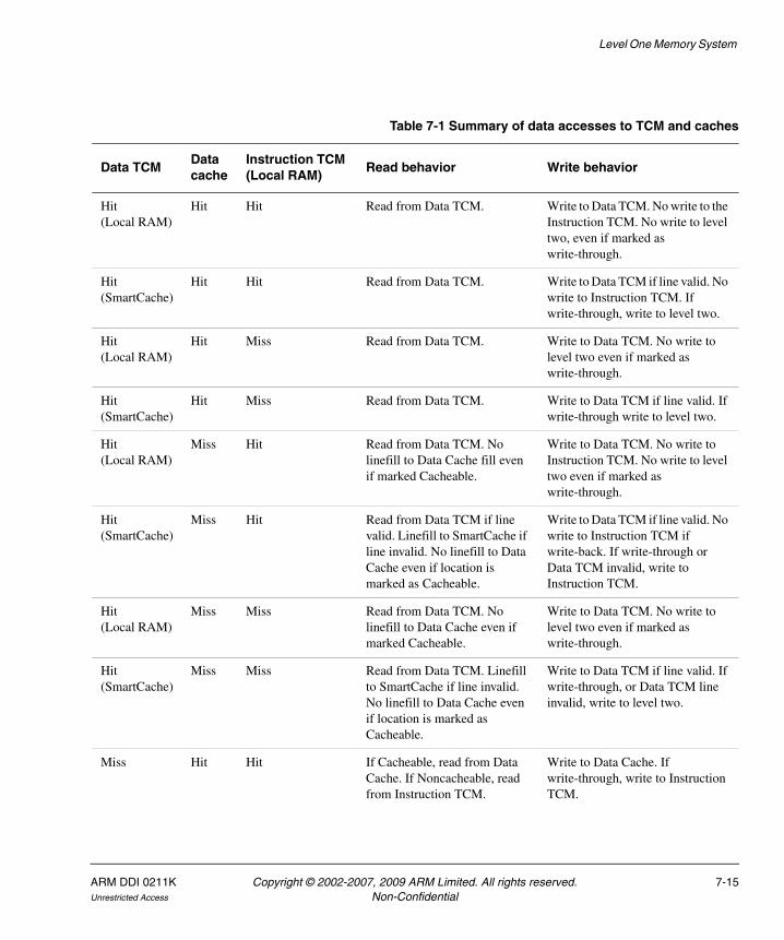
Level One Memory System
Table 7-1 Summary of data accesses to TCM and caches
Data TCMData cache
Instruction TCM (Local RAM)
Read behavior Write behavior
Hit (Local RAM)
Hit Hit Read from Data TCM. Write to Data TCM. No write to the Instruction TCM. No write to level two, even if marked as write-through.
Hit (SmartCache)
Hit Hit Read from Data TCM. Write to Data TCM if line valid. No write to Instruction TCM. If write-through, write to level two.
Hit (Local RAM)
Hit Miss Read from Data TCM. Write to Data TCM. No write to level two even if marked as write-through.
Hit (SmartCache)
Hit Miss Read from Data TCM. Write to Data TCM if line valid. If write-through write to level two.
Hit (Local RAM)
Miss Hit Read from Data TCM. No linefill to Data Cache fill even if marked Cacheable.
Write to Data TCM. No write to Instruction TCM. No write to level two even if marked as write-through.
Hit (SmartCache)
Miss Hit Read from Data TCM if line valid. Linefill to SmartCache if line invalid. No linefill to Data Cache even if location is marked as Cacheable.
Write to Data TCM if line valid. No write to Instruction TCM if write-back. If write-through or Data TCM invalid, write to Instruction TCM.
Hit (Local RAM)
Miss Miss Read from Data TCM. No linefill to Data Cache even if marked Cacheable.
Write to Data TCM. No write to level two even if marked as write-through.
Hit (SmartCache)
Miss Miss Read from Data TCM. Linefill to SmartCache if line invalid. No linefill to Data Cache even if location is marked as Cacheable.
Write to Data TCM if line valid. If write-through, or Data TCM line invalid, write to level two.
Miss Hit Hit If Cacheable, read from Data Cache. If Noncacheable, read from Instruction TCM.
Write to Data Cache. If write-through, write to Instruction TCM.
ARM DDI 0211K Copyright © 2002-2007, 2009 ARM Limited. All rights reserved. 7-15Unrestricted Access Non-Confidential

Level One Memory System
Table 7-2 summarizes the results of instruction accesses to TCM and the cache. This also embodies the unexpected hit behavior for the cache described in Unexpected hit behavior on page 7-7. In Table 7-2, the Instruction Cache, and the Instruction TCM if operating as SmartCache, can only be hit if the memory location being accessed is marked as being Cacheable and Non-Shared. The hit to the Instruction TCM refers to hitting an address in the range covered by that TCM.
Miss Hit Miss If Cacheable, read from Data Cache. If Noncacheable, read from level two.
Write to Data Cache. If write-through, write to level two.
Miss Miss Hit Read from Instruction TCM. No cache fill even if marked Cacheable.
Write to Instruction TCM. No write to level two even if marked as write-through.
Miss Miss Miss If Cacheable and cache enabled, cache linefill. If Noncacheable or cache disabled, read to level two.
Write to level two.
Table 7-1 Summary of data accesses to TCM and caches (continued)
Data TCMData cache
Instruction TCM (Local RAM)
Read behavior Write behavior
Table 7-2 Summary of instruction accesses to TCM and caches
Instruction TCM Instruction cache Data TCM Read behavior
Hit Hit Don’t care Unpredictable.
Hit (Local RAM) Miss Don’t care Read from Instruction TCM. No linefill to Instruction Cache even if marked Cacheable.
Hit (SmartCache) Miss Don’t care Read from Instruction TCM if line valid. Linefill to SmartCache if line invalid. No linefill to Instruction Cache even if marked Cacheable.
Miss Hit Don’t care Read from Instruction Cache.
Miss Miss Don’t care If Cacheable and cache enabled, cache linefill.
If Noncacheable or cache disabled, read to level two.
7-16 Copyright © 2002-2007, 2009 ARM Limited. All rights reserved. ARM DDI 0211KNon-Confidential Unrestricted Access

Level One Memory System
7.6 Cache debug
The debug architecture for the ARM1136JF-S processor is described in Chapter 13 Debug. The External Debug Interface is based on JTAG, and is as described in Chapter 14 Debug Test Access Port. The debug architecture enables the cache debug to be defined by the implementation. This functionality is defined here.
It is desirable for the debugger to examine the contents of the instruction and data caches during debug operations. This is achieved in two stages:
1. Reading the Tag RAM entries for each cache location.
2. Reading the data values for those addresses.
The debugger determines which valid addresses are stored in the cache. This is done by reading the Instruction and Data Cache Tag arrays using a CP15 instruction executed using the Instruction Transfer Register. The Instruction Transfer Register is accessed using scan chain 4 as described in Scan chain 4, Instruction Transfer Register (ITR) on page 14-14. The debugger must do this for each entry of each set within the cache. This access is performed by an MCR that transfers from the ARM register the Set and Index of the required line in the Tag RAM array. The contents of the line are then returned to the Instruction or Data Debug Cache Register as appropriate.
ARM DDI 0211K Copyright © 2002-2007, 2009 ARM Limited. All rights reserved. 7-17Unrestricted Access Non-Confidential

Level One Memory System
7.7 Write buffer
All memory writes take place using the write buffer. To ensure that the write buffer is not drained on reads, the following features are implemented:
• The write buffer is a FIFO of outstanding writes to memory. It consists of a set of addresses and a set of data words (together with their size information).
• If a sequence of data words is contained in the write buffer, these are denoted as applying to the same address by the write buffer storing the size of the store multiple. This reduces the number of address entries that have to be stored in the write buffer.
• In addition to this, a separate FIFO of write-back addresses and data words is implemented. Having a separate structure avoids complications associated with performing an external write while the write-though is being handled.
• The address of a new read access is compared against the addresses in the write buffer. If a read is to a location that is already in the write buffer, the read is blocked until the write buffer has drained sufficiently far for that location to be no longer in the write buffer. The sequential marker only applies to words in the same 8 word (8 word aligned) block, and the address comparisons are based on 8 word aligned addresses.
The ordering of memory accesses is described in Memory access control on page 6-11.
7-18 Copyright © 2002-2007, 2009 ARM Limited. All rights reserved. ARM DDI 0211KNon-Confidential Unrestricted Access

Chapter 8 Level Two Interface
The ARM1136JF-S processor is designed to be used within larger chip designs using Advanced Microcontroller Bus Architecture (AMBA). The ARM1136JF-S processor uses the level two interface as its interface to memory and peripherals.
This chapter describes the features of the level two interface not covered in the AMBA Specification. It contains the following sections:
• About the level two interface on page 8-2
• Synchronization primitives on page 8-7
• AHB-Lite control signals in the ARM1136JF-S processor on page 8-10
• Instruction Fetch Interface AHB-Lite transfers on page 8-22
• Data Read Interface AHB-Lite transfers on page 8-26
• Data Write Interface AHB-Lite transfers on page 8-53
• DMA Interface AHB-Lite transfers on page 8-70
• Peripheral Interface AHB-Lite transfers on page 8-73
• AHB-Lite on page 8-76.
ARM DDI 0211K Copyright © 2002-2007, 2009 ARM Limited. All rights reserved. 8-1Unrestricted Access Non-Confidential

Level Two Interface
8.1 About the level two interface
The level two memory interface provides a high-bandwidth interface to second level caches, on-chip RAM, peripherals, and interfaces to external memory. It is a key feature in ensuring high system performance, providing a higher bandwidth mechanism for filling the caches in a cache miss than has existed on previous ARM processors.
The ARM1136JF-S processor level two interconnect system uses the following 64-bit wide AHB-Lite interfaces:
• Instruction Fetch Interface
• Data Read Interface
• Data Write Interface
• DMA Interface.
It also includes the Peripheral Interface. This is a 32-bit AHB-Lite interface.
Figure 8-1 shows the level two interconnect interfaces.
Figure 8-1 Level two interconnect interfaces
These interfaces can support several simultaneous outstanding transactions, permitting high performance from level two memory systems that support parallelism, and also giving high utilization of pipelined memories such as SDRAM.
Each of the four 64-bit wide interfaces is an AHB-Lite interface, with additional signals to support the following additional features for the level two memory system:
• shared memory synchronization primitives
• multi-level cache support
• unaligned and mixed-endian data access.
ARM1136JF-S
Level two instruction side
controller
Level two data side controller
DMA
DMA(64-bit)
Peripheral(32-bit)
Dataread
(64-bit)
Datawrite
(64-bit)
Instruction fetch
(64-bit)
8-2 Copyright © 2002-2007, 2009 ARM Limited. All rights reserved. ARM DDI 0211KNon-Confidential Unrestricted Access

Level Two Interface
8.1.1 Level two interface clocking
In addition to the ARM1136JF-S clock CLKIN, the level two interfaces are clocked using:
• HCLKIRW for the instruction fetch, data read, and data write ports
• HCLKPD for the peripheral and DMA ports.
The two clocks used by each port can be either synchronous or asynchronous. Input pins on the ARM1136JF-S processor control selection between synchronous and asynchronous clocking, and ensure that the latency penalty for any synchronization is only applied when it is required.
Figure 8-2 compares the performance lost through synchronization penalty with the performance lost through reducing the core frequency to be an integer multiple of the bus frequency.
Figure 8-2 Synchronization penalty
You can independently configure HCLKIRW and HCLKPD to be synchronous or asynchronous. See Chapter 9 Clocking and Resets for more details.
13231302928272625242322212019181716151413121110987654321
1.21.41.61.82
2.22.42.62.83
3.23.43.63.84
AHB latency/cycles
Ratio ofCPU clock to AHB clock
(CLK : HCLK)
KeyMaximize performance by running asynchronous modeMaximize performance by running synchronous mode
ARM DDI 0211K Copyright © 2002-2007, 2009 ARM Limited. All rights reserved. 8-3Unrestricted Access Non-Confidential

Level Two Interface
8.1.2 Level two instruction-side controller
The level two instruction-side controller contains the level two Instruction Fetch Interface. See Instruction Fetch Interface.
The level two instruction-side controller handles all instruction-side cache misses including those for Noncacheable locations. It is responsible for the sequencing of cache operations for Instruction Cache linefills, making requests for the individual stores through the Prefetch Unit (PU) to the Instruction Cache. The decoupling involved means that the level two instruction-side controller contains some buffering.
Instruction Fetch Interface
The Instruction Fetch Interface is a read-only interface that services the Instruction Cache on cache misses, including the fetching of instructions for the PU that are held in memory marked as Noncacheable. The interface is optimized for cache linefills rather than individual requests.
8.1.3 Level two data-side controller
The level two data-side controller is responsible for the level two:
• Data Read Interface
• Data Write Interface
• Peripheral Interface.
The level two data-side controller handles:
• All external access requests from the Load Store Unit (LSU), including cache misses, data Write-Through operations, and Noncacheable data.
• SWP instructions and semaphore operations. It schedules all reads and writes on the two interfaces, which are closely related.
The level two data-side controller also handles the Peripheral Interface.
The level two data-side controller contains the Refill and Write-Back engines for the Data Cache. These make requests through the Load Store Unit for the individual cache operations that are required. The decoupling involved means that the level two data-side controller contains some buffering. The write buffer is an integral part of the level two data-side controller.
A separate block within the level two data-side controller schedules the reads required for hardware page table walks, and returns the appropriate page table information to the Main TLB.
8-4 Copyright © 2002-2007, 2009 ARM Limited. All rights reserved. ARM DDI 0211KNon-Confidential Unrestricted Access

Level Two Interface
Data Read Interface
The Data Read Interface performs reads and swap writes. It services the Data Cache on cache misses, handles TLB misses on hardware page table walks, and reads uncacheable locations. While cache miss handling is important, the latency between outstanding uncacheable loads is minimized. The same address never appears simultaneously on the Data Read Interface and the Data Write Interface.
Data Write Interface
The Data Write Interface is a write-only interface that services the writes out of the write buffer. This interface provides queuing of multiple writes.
Peripheral Interface
The Peripheral Interface is a bidirectional AHB-Lite interface that services peripheral devices. The bus is a single-master bus with the Peripheral Interface being the master. In ARM1136JF-S processors, the Peripheral Interface is used for peripherals that are private to the ARM1136JF-S processor, such as the Vectored Interrupt Controller or Watchdog Timer. Accesses to regions of memory that are marked as Device and Non-Shared are routed to the Peripheral Interface in preference to the Data Read Interface or Data Write Interface.
Peripheral Port Memory Remap Register
The Peripheral Port Memory Remap Register enables regions to be remapped to the Peripheral Interface when the MMU is disabled. For details of the Peripheral Port Memory Remap Register see Using the Peripheral Port Memory Remap Register on page 3-168.
8.1.4 DMA
The DMA is responsible for:
• Performing all external memory transactions required by the DMA engine, including requesting accesses from the Instruction TCM and Data TCM as required.
• Queuing the two DMA channels as required. The DMA Interface contains several registers that are CP15 registers dedicated for DMA use, see c11, DMA registers overview on page 3-130 for details.
ARM DDI 0211K Copyright © 2002-2007, 2009 ARM Limited. All rights reserved. 8-5Unrestricted Access Non-Confidential

Level Two Interface
The DMA contains:
• Its own MicroTLB that is backed up by the Main TLB. The DMA uses the PU and the LSU to schedule its accesses to the TCMs.
• Buffering to enable the decoupling of internal and external requests. This is because of variable latency between internal and external accesses.
DMA Interface
The DMA Interface is a bidirectional interface that services the DMA subsystem for writing and reading the TCMs. Although the DMA Interface is bidirectional, it is able to produce a stream of successive accesses that are in the same direction, followed by either a further stream in the same direction, or a stream in the opposite direction. Correspondingly the direction turnaround is not significantly optimized.
8-6 Copyright © 2002-2007, 2009 ARM Limited. All rights reserved. ARM DDI 0211KNon-Confidential Unrestricted Access

Level Two Interface
8.2 Synchronization primitives
On previous architectures, support for shared memory synchronization was with the read-locked-write operations that swap register contents with memory, the SWP and SWPB instructions. These support basic busy and free semaphore mechanisms. For details of the swap instructions, see the ARM Architecture Reference Manual.
ARMv6 and ARMv6k provide support for more comprehensive shared-memory synchronization primitives that scale for multiple-processor system designs. They introduce instructions that support multiple-processor and shared-memory inter-process communication:
• load exclusive, LDREX
• store exclusive, STREX
• load byte exclusive, LDREXB
• store byte exclusive, STREXB
• load halfword exclusive, LDREXH
• store halfword exclusive, STREXH
• load doubleword exclusive, LDREXD
• store doubleword exclusive, STREXD
• clear exclusive, CLREX.
Note The ARMv6k architecture features were introduce in the rev1 (r1p0) release of the ARM1136JF-S processor. This means that the LDREXB, LDREXH, LDREXD, STREXB, STREXH, STREXD, and CLREX instructions are only available from the rev1 (r1p0) release of the processor.
The exclusive access instructions rely on the ability to tag a physical address as exclusive access for a particular processor. This tag is later used to determine if an exclusive store to an address occurs.
For memory regions that have the Shared TLB attribute, any attempt to modify that address by any processor clears this tag.
For memory regions that do not have the Shared TLB attribute, any attempt to modify that address by the same processor that marked it as exclusive access clears this tag.
In both cases other events might cause the tag to be cleared. In particular, for memory regions that are not shared, it is Unpredictable whether a store by another processor to a tagged physical address causes the tag to be cleared.
ARM DDI 0211K Copyright © 2002-2007, 2009 ARM Limited. All rights reserved. 8-7Unrestricted Access Non-Confidential

Level Two Interface
Note All exclusive transactions must be a single access, or an indivisible burst if the bus width is less than 64 bits.
An External Abort on any load exclusive or store exclusive instruction puts the processor into Abort mode.
Note An External Abort on any load exclusive instruction can leave the ARM1136JF-S internal monitor in its exclusive state and might affect your software. If it does you must ensure that a CLREX is executed in your abort handler to clear the ARM1136JF-S internal monitor to an open state.
8.2.1 Load exclusive instruction
Load exclusive performs a load from memory and causes the physical address of the access to be tagged as exclusive access for the requesting processor. This causes any other physical address that has been tagged by the requesting processor to no longer be tagged as exclusive access.
8.2.2 Store exclusive instruction
Store exclusive performs a conditional store to memory. The store only takes place if the physical address is tagged as exclusive access for the requesting processor. This operation returns a status value. If the store updates memory the return value is 0, otherwise it is 1. In both cases, the physical address is no longer tagged as exclusive access for any processor.
8.2.3 Example of LDREX and STREX usage
This is an example of typical usage. Suppose you are trying to claim a lock:
Lock address : LockAddrLock free : 0x00Lock taken : 0xFF
MOV R1, #0xFF ;load the ‘lock taken’ valuetry LDREX R0, [LockAddr] ;load the lock value
CMP R0, #0 ;is the lock free?STREXEQ R0, R1, [LockAddr] ;try and claim the lockCMPEQ R0, #0 ;did this succeed?BNE try ;no – try again . . . .
;yes – we have the lock
8-8 Copyright © 2002-2007, 2009 ARM Limited. All rights reserved. ARM DDI 0211KNon-Confidential Unrestricted Access

Level Two Interface
The typical case, where the lock is free and you have exclusive access, is six instructions.
ARM DDI 0211K Copyright © 2002-2007, 2009 ARM Limited. All rights reserved. 8-9Unrestricted Access Non-Confidential

Level Two Interface
8.3 AHB-Lite control signals in the ARM1136JF-S processor
The following sections describe the ARM1136JF-S processor implementation of the AHB-Lite control signals:
• HTRANS[1:0]
• HSIZE[2:0] on page 8-11
• HBURST[2:0] on page 8-11
• HPROT[4:0] on page 8-12
• HPROT[5] and HRESP[2] on page 8-14
• HBSTRB[7:0] and HUNALIGN on page 8-16.
For additional information about AHB, see the AMBA Specification Rev 2.0.
8.3.1 Signal name suffixes
The signal names for each of the interfaces use the following suffixes to denote the interface that the signal applies to:
I Instruction Fetch Interface.
D DMA Interface.
R Data Read Interface.
W Data Write Interface.
P Peripheral Interface.
For example, HTRANS[1:0] is called HTRANSI[1:0] in the Instruction Fetch Interface.
8.3.2 HTRANS[1:0]
Table 8-1 shows the settings used to indicate the type of transfer on the interface.
If there are accesses required in a particular sequence and the level two interface is not able to proceed on that cycle, a BUSY cycle is inserted.
Table 8-1 HTRANS[1:0] settings
HTRANS[1:0] settings Type of transfer
b00 Idle
b10 Nonsequential
b11 Sequential
b01 Busy
8-10 Copyright © 2002-2007, 2009 ARM Limited. All rights reserved. ARM DDI 0211KNon-Confidential Unrestricted Access

Level Two Interface
For example, if the Instruction Data FIFO becomes full when performing a series of instruction fetches, and the bus clock HCLK is faster than the processor clock CLKIN, the level two interface inserts BUSY cycles until a FIFO slot becomes available.
The level two interface can also insert BUSY cycles when CLK is faster than HCLK. For example when successive branch mispredicts trigger Instruction cache linefills.
Similarly, in the data write case, if the level two system is completing the writes in a burst faster than the level one system can provide the address or data information, BUSY cycles might be inserted.
The system designer must ensure that all slaves attached to the ARM1136JF-S processor can handle the BUSY state.
8.3.3 HSIZE[2:0]
The ARM1136JF-S processor has 64-bit buses. HSIZE cannot be greater than 64 bits. Table 8-2 shows the encodings of HSIZE[2:0].
8.3.4 HBURST[2:0]
Table 8-3 shows the settings used to indicate the type of transfer on the interface.
Table 8-2 HSIZE[2:0] encoding
HSIZE[2] HSIZE[1] HSIZE[0] Size Description
0 0 0 8 bits Byte
0 0 1 16 bits Halfword
0 1 0 32 bits Word
0 1 1 64 bits Doubleword
Table 8-3 HBURST[2:0] settings
HBURST[2:0] settings Type of transfer
b000 Single
b001 Incr
b010 Wrap4
b011 Incr4
ARM DDI 0211K Copyright © 2002-2007, 2009 ARM Limited. All rights reserved. 8-11Unrestricted Access Non-Confidential

Level Two Interface
8.3.5 HPROT[4:0]
Table 8-4 shows the values of the HPROT[1:0] bits that can be used in level two caches.
To support the addition of on-chip second level caching the ARMv6 AHB-Lite extensions include an additional HPROT[4] bit that is used to extend the definition of the HPROT[3:2] bits. The additional bit provides information about the caching policy that is used for the transfer that is being performed.
Table 8-5 shows the how various combinations of HPROT[4:2] signals are encoded.
The timing of HPROT[4] is identical to the timing of the other HPROT signals, so it is an address phase signal and must remain constant throughout a burst.
The Allocate bit, HPROT[4], is used to provide additional information on the allocation scheme that must be used for the transfer. When the transfer is Noncacheable (HPROT[3] is LOW) then the Allocate bit is not used and must also be driven LOW by a master.
Table 8-4 HPROT[1:0] encoding
Signal Meaning
HPROT[0] 0 = Instruction cache linefill or core instruction fetch.
1 = Data cache linefill, core load or store operation, or page table walks.
HPROT[1] 0 = User mode.
1 = Privileged mode.
Table 8-5 HPROT[4:2] encoding
HPROT[4] Allocate
HPROT[3] Cacheable
HPROT[2] Bufferable
Description
0 0 0 Strongly Ordered, cannot be buffered
0 0 1 Device, can be buffered
0 1 0 Cacheable (Outer Noncacheable, do not allocate on reads or writes)
1 1 0 Cacheable Write-Through (allocate on reads only, no allocate on write)
0 1 1 Cacheable Write-Back (allocate on reads and writes)
1 1 1 Cacheable Write-Back (allocate on reads only, no allocate on write)
8-12 Copyright © 2002-2007, 2009 ARM Limited. All rights reserved. ARM DDI 0211KNon-Confidential Unrestricted Access
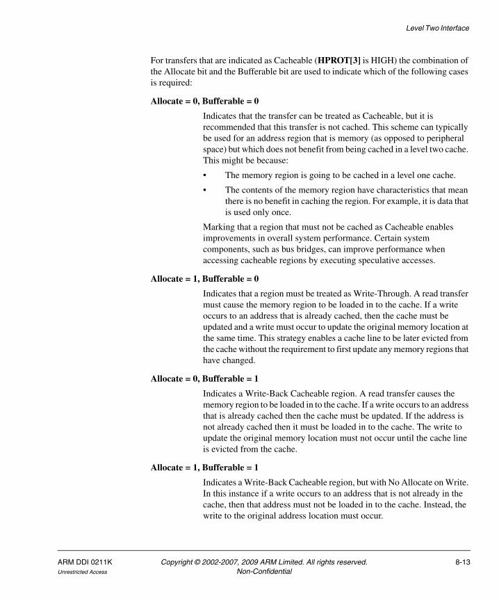
Level Two Interface
For transfers that are indicated as Cacheable (HPROT[3] is HIGH) the combination of the Allocate bit and the Bufferable bit are used to indicate which of the following cases is required:
Allocate = 0, Bufferable = 0
Indicates that the transfer can be treated as Cacheable, but it is recommended that this transfer is not cached. This scheme can typically be used for an address region that is memory (as opposed to peripheral space) but which does not benefit from being cached in a level two cache. This might be because:
• The memory region is going to be cached in a level one cache.
• The contents of the memory region have characteristics that mean there is no benefit in caching the region. For example, it is data that is used only once.
Marking that a region that must not be cached as Cacheable enables improvements in overall system performance. Certain system components, such as bus bridges, can improve performance when accessing cacheable regions by executing speculative accesses.
Allocate = 1, Bufferable = 0
Indicates that a region must be treated as Write-Through. A read transfer must cause the memory region to be loaded in to the cache. If a write occurs to an address that is already cached, then the cache must be updated and a write must occur to update the original memory location at the same time. This strategy enables a cache line to be later evicted from the cache without the requirement to first update any memory regions that have changed.
Allocate = 0, Bufferable = 1
Indicates a Write-Back Cacheable region. A read transfer causes the memory region to be loaded in to the cache. If a write occurs to an address that is already cached then the cache must be updated. If the address is not already cached then it must be loaded in to the cache. The write to update the original memory location must not occur until the cache line is evicted from the cache.
Allocate = 1, Bufferable = 1
Indicates a Write-Back Cacheable region, but with No Allocate on Write. In this instance if a write occurs to an address that is not already in the cache, then that address must not be loaded in to the cache. Instead, the write to the original address location must occur.
ARM DDI 0211K Copyright © 2002-2007, 2009 ARM Limited. All rights reserved. 8-13Unrestricted Access Non-Confidential

Level Two Interface
8.3.6 HPROT[5] and HRESP[2]
Two additional signals are provided in the ARMv6 AHB-Lite extensions to support an exclusive access mechanism. The exclusive access mechanism is used to provide additional functionality over and above that provided by the lock mechanism on AHB v2.0. The exclusive access mechanism enables the implementation of semaphore type operations without requiring the entire bus to remain locked to a particular master for the duration of the operation.
The advantage of this approach is that semaphore type operations do not impact on the critical bus access latency and they do not impact on the maximum achievable bandwidth.
The additional signals are:
HPROT[5] Exclusive bit, indicates that an access is part of an exclusive operation.
HRESP[2] Exclusive response, which indicates if the write part of an exclusive operation has succeeded or failed:
• HRESP[2] = 0 indicates that the exclusive operation has succeeded
• HRESP[2] = 1 indicates that the exclusive operation has failed.
The exclusive access mechanism operates is as follows:
1. A master performs a load exclusive from an address location.
2. At some later point in time the master attempts to complete the exclusive access by performing a store exclusive to the same address location.
3. The write access of the master is signaled as successful if no other master has updated (written to) the location between the read and write accesses.
If, however, another master has updated the location between the read and write accesses then the exclusive access is signaled as having failed and the address location is not updated.
The following points apply to the exclusive access mechanism:
• If a master attempts a store exclusive without first performing a load exclusive then the write is signaled as failing.
• A master can attempt a load exclusive to new location without first completing the read or write sequence to a another location that has previously been exclusively read from. In this instance the second exclusive sequence must continue as described in step 1. to step 3. above.
8-14 Copyright © 2002-2007, 2009 ARM Limited. All rights reserved. ARM DDI 0211KNon-Confidential Unrestricted Access

Level Two Interface
If the write portion of the earlier sequence does eventually occur then it is acceptable that the access is indicated as successful only if the sequence has truly succeeded. That is, the location has not been updated since the load exclusive from that master. Alternatively, the access can be automatically signaled as failing.
It is important that repeated occurrences of incomplete exclusive accesses, where only the read portion of the access happens, does not cause a lock up situation.
Exclusive access protocol
The protocols for exclusive accesses are summarized as follows:
• All AHB-Lite control signals must remain constant throughout a burst, this includes HPROT[5]. This means that a burst of accesses must not include an exclusive access as one item within the burst.
• A response on HRESP[2] indicating failure of the store exclusive access is a two-cycle response, as is the case for any other non-Okay value on HRESP.
• The mnemonic for a response indicating the failure of a store exclusive is Xfail. Table 8-6 shows the valid responses on HRESP[2:0] with associated mnemonics. All other values of HRESP[2:0] are reserved.
• It is not possible to indicate a combination of either Error, Retry, or Split with Xfail. The values b101, b110, and b111 are not valid responses. The Xfail response indicates that a store exclusive has not been transmitted to the destination because the exclusive access monitor knows that another domain has already over-written it. Therefore, because the access is not attempted, there can be no associated Error, Retry, or Split information.
Table 8-6 HRESP[2:0] mnemonics
HRESP[2:0] Mnemonic
b000 Okay.
b001 Error.
b010 Retry. Not supported.
b011 Split. Not supported.
b100 Xfail.
ARM DDI 0211K Copyright © 2002-2007, 2009 ARM Limited. All rights reserved. 8-15Unrestricted Access Non-Confidential

Level Two Interface
• The master cannot cancel the next access for an Xfail response if it is already indicating one on AHB-Lite. This is unlike:
— Split or Retry responses for which the master must cancel the next access
— Error responses for which the master might cancel the next access.
If a master does have to wait for the response to the store exclusive before issuing the next access, then it is recommended that it does one of the following:
— issues Idle cycles
— deasserts request line, HBUSREQ— issues Idle cycles and deasserts request line, HBUSREQ.
• An Error response to a load exclusive indicates that the data read back cannot be trusted. That is, the read is invalid and must be tried again after the reason for the error has been resolved.
• An Error response to a store exclusive indicates that the data has not been written, but does not necessarily mean that another process has written to that memory location, or that the data is not the most recent data. The store exclusive can be tried again at a later time, after the reason for the error has been resolved, and the success or failure of the store exclusive is determined by whether or not an Xfail response is eventually received.
8.3.7 HBSTRB[7:0] and HUNALIGN
To handle unaligned accesses and mixed-endian accesses the AHB-Lite extensions enable the use of byte lane strobes to indicate which byte lanes are active in a transfer. One HBSTRB signal is required for each byte lane on the data bus. That is, one HBSTRB bit for every eight bits of the data bus.
The HBSTRB signal is asserted in the same cycles as the other address and control signal of the transfer that it applies to. In other words it is an address phase signal.
HADDR and HSIZE are used to define the container within which the byte lane strobes can be active. The size of the transaction is sufficient to cover all the bytes being written and covers more bytes in the case of a mis-aligned transfer. HADDR is aligned to the size of transfer, as indicated by HSIZE, so that the address of the transfer is rounded down to the nearest boundary of the size of the transaction.
Byte strobes are required for both read and write transfers. Read sensitive devices must not be accessed using unaligned transfers so a master can choose, for a read transfer, to activate all byte strobes within the AHB v2.0 container (as defined by HADDR and HSIZE).
8-16 Copyright © 2002-2007, 2009 ARM Limited. All rights reserved. ARM DDI 0211KNon-Confidential Unrestricted Access

Level Two Interface
For forwards compatibility, if an AHB v2.0 master does not generate byte strobe signals then these can be generated directly from the HADDR and HSIZE signals. This generation process must take into account the endianness of the transfer.
The effect of endianess on the byte lane strobes is a function of the endianess model that is used. The strobes generated for the byte invariant big-endian, BE-8, and little-endian, LE-8, accesses are the same. For word invariant big-endian access, BE-32, the strobes are reversed within the word. See Chapter 4 Unaligned and Mixed-Endian Data Access Support for more details.
For backwards compatibility, an additional HUNALIGN signal is provided by a master that can produce unaligned accesses. This signal is only provided to assist with backwards compatibility and indicates when a single unaligned transfer occurs that requires more than one AHB v2.0 transfer without byte strobes. The HUNALIGN signal has address phase timing and must be asserted HIGH for unaligned transfers and LOW for AHB v2.0 compatible aligned transfers.
The mapping of byte strobes to data bus bits is fixed and is not dependent on the endianness of the access. Table 8-7 shows the mapping of HBSTRB to the write data bus for a 64-bit interface.
Note Not all possible combinations of byte lane strobes are generated by the ARM1136JF-S processor. The slaves that support these extensions must enable all possible combinations to provide compatibility with future AMBA components (for example, masters containing merging write buffers).
Table 8-7 Mapping of HBSTRB to HWDATA bits for a 64-bit interface
Byte strobe Data bus bits
HBSTRB[0] ⇒ HWDATA[7:0]
HBSTRB[1] ⇒ HWDATA[15:8]
HBSTRB[2] ⇒ HWDATA[23:16]
HBSTRB[3] ⇒ HWDATA[31:24]
HBSTRB[4] ⇒ HWDATA[39:32]
HBSTRB[5] ⇒ HWDATA[47:40]
HBSTRB[6] ⇒ HWDATA[55:48]
HBSTRB[7] ⇒ HWDATA[63:56]
ARM DDI 0211K Copyright © 2002-2007, 2009 ARM Limited. All rights reserved. 8-17Unrestricted Access Non-Confidential

Level Two Interface
Example uses of byte lane strobes
This section gives some example ARMv6 transfers on AHB-Lite and shows the byte strobe signals that are produced. The examples assume a 64-bit data bus.
Note When an access straddles a 32-bit data boundary then two transfers are required.
Table 8-8 shows examples of transfers that can be produced by the ARM136 JF-S processor.
Table 8-8 Byte lane strobes for example ARMv6 transfers
Transfer description Endianness HADDR HSIZE[2:0] HBSTRB[7:0] HUNALIGN
8-bit access to 0x1000 LE-8 or BE-8 0x1000 0x0 b00000001 0
BE-32 0x1000 0x0 b00001000 0
8-bit access to 0x1003 LE-8 or BE-8 0x1003 0x0 b00001000 0
BE-32 0x1003 0x0 b00000001 0
8-bit access to 0x1007 LE-8 or BE-8 0x1007 0x0 b10000000 0
BE-32 0x1007 0x0 b00010000 0
16-bit access to 0x1000 LE-8 or BE-8 0x1000 0x1 b00000011 0
BE-32 0x1000 0x1 b00001100 0
16-bit access to 0x1005 LE-8 or BE-8 0x1004 0x2 b01100000 1
BE-32 0x1004 0x2 b11000000 0a
16-bit access to 0x1007 LE-8 or BE-8 0x1007
0x1008
0x0
0x0
b10000000
b00000001
0
0
BE-32 0x1000 0x1 b00110000 0
32-bit access to 0x1000 All 0x1000 0x2 b00001111 0
32-bit access to 0x1002 LE-8 or BE-8 0x1002
0x1004
0x1
0x1
b00001100
b00110000
0
0
BE-32 0x1000 0x2 b00001111 0
8-18 Copyright © 2002-2007, 2009 ARM Limited. All rights reserved. ARM DDI 0211KNon-Confidential Unrestricted Access

Level Two Interface
8.3.8 Exclusive access timing
Figure 8-3 shows the basic operation of a load exclusive, followed at some arbitrary time later by a store exclusive. The store exclusive receives an Okay response indicating that the operation has been successful.
Figure 8-3 Exclusive access read and write with Okay response
Figure 8-4 on page 8-20 shows an exclusive access that receives an Xfail response. Although HWDATA is shown asserted for the write access, the target location must not be updated within the slave.
32-bit access to 0x1003 LE-8 or BE-8 0x1003
0x1004
0x0
0x2
b00001000
b01110000
0
1
BE-32 0x1000 0x2 b00001111 0
32-bit access to 0x1007 LE-8 or BE-8 0x1007
0x1008
0x0
0x2
b10000000
b00000111
0
1
BE-32 0x1004 0x2 b11110000 0
64-bit access to 0x1000 All 0x1000 0x3 b11111111 0
a. BE-32 access to misaligned locations do not cause misalignment, and in the case of halfword accesses, are architecturally Unpredictable.
Table 8-8 Byte lane strobes for example ARMv6 transfers (continued)
Transfer description Endianness HADDR HSIZE[2:0] HBSTRB[7:0] HUNALIGN
Idle Nseq Idle Nseq Idle Idle Idle
Xaddr Xaddr
HCLK
HTRANS
HADDR
HWRITE
HPROT[5]
XwdataHWDATA
Okay Okay Okay Okay Okay Okay OkayHRESP
HREADY
XrdataHRDATA
Idle
Okay
ARM DDI 0211K Copyright © 2002-2007, 2009 ARM Limited. All rights reserved. 8-19Unrestricted Access Non-Confidential

Level Two Interface
Figure 8-4 Exclusive access read and write with Xfail response
Figure 8-5 on page 8-21 shows an exclusive access that receives an Xfail response, but this time the master has already placed the next transfer (a read from address Naddr) onto the AHB-Lite address and control pins. If the two-cycle response is a Split or Retry, then the master has to force HTRANS to Idle after time T17, or has the option to do so if the response is Error. For the Xfail response, the master must continue with the transfer indicated after T16.
Idle Nseq Idle Nseq Idle Idle
Xaddr Xaddr
HCLK
HTRANS
HADDR
HWRITE
HPROT[5]
HWDATA
Okay Okay Okay Okay Xfail OkayHRESP
HREADY
HRDATA
Xwdata
Idle
Okay
Xrdata
8-20 Copyright © 2002-2007, 2009 ARM Limited. All rights reserved. ARM DDI 0211KNon-Confidential Unrestricted Access

Level Two Interface
Figure 8-5 Exclusive access read and write with Xfail response and following transfer
Idle Nseq Idle Nseq Nseq Idle
Xaddr Xaddr
HCLK
HTRANS
HADDR
HWRITE
HPROT[5]
HWDATA
Okay Okay Okay Okay Xfail OkayHRESP
HREADY
HRDATA
Xwdata
Nrdata
T0 T1 T2 T3 T14 T15 T16 T17 T18
Xrdata
Okay
Idle
Naddr
ARM DDI 0211K Copyright © 2002-2007, 2009 ARM Limited. All rights reserved. 8-21Unrestricted Access Non-Confidential

Level Two Interface
8.4 Instruction Fetch Interface AHB-Lite transfers
The tables in this section describe the AHB-Lite interface behavior for instruction side fetches to either Cacheable or Noncacheable regions of memory for the following interface signals:
• HBURSTI[2:0]• HTRANSI[1:0]• HADDRI[31:0]• HBSTRBI[7:0]• HUNALIGNI.
See Other AHB-Lite signals for Cacheable and Noncacheable instruction fetches on page 8-24 for details of the other AHB-Lite signals.
8.4.1 Cacheable fetches
Table 8-9 shows the values of HTRANSI, HADDRI, HBURSTI, HBSTRBI, and HUNALIGNI for Cacheable fetches from words 0-7.
Table 8-9 AHB-Lite signals for Cacheable fetches
Address[4:0] HTRANSI HADDRI HBURSTI HBSTRBI HUNALIGNI
0x00 (word 0)
0x04 (word 1)
Nseq 0x00 Incr4 b11111111 0
Seq 0x08
0x10
0x18
0x08 (word 2)
0x0C (word 3)
Nseq 0x08 Wrap4 b11111111 0
Seq 0x10
0x18
0x00
0x10 (word 4)
0x14 (word 5)
Nseq 0x10 Wrap4 b11111111 0
Seq 0x18
0x00
0x08
8-22 Copyright © 2002-2007, 2009 ARM Limited. All rights reserved. ARM DDI 0211KNon-Confidential Unrestricted Access

Level Two Interface
8.4.2 Noncacheable fetches
Table 8-10 shows the values of HTRANSI, HADDRI, HBURSTI, HBSTRBI, and HUNALIGNI for Noncacheable fetches from words 0-7.
0x18 (word 6)
0x1C (word 7)
Nseq 0x18 Wrap4 b11111111 0
Seq 0x00
0x08
0x10
Table 8-9 AHB-Lite signals for Cacheable fetches (continued)
Address[4:0] HTRANSI HADDRI HBURSTI HBSTRBI HUNALIGNI
Table 8-10 AHB-Lite signals for Noncacheable fetches
Address[4:0] HTRANSI HADDRI HBURSTI HBSTRBI HUNALIGNI
0x00 (word 0) Nseq 0x00 Incr or Incr4 b11111111 0
Seq 0x08
0x10
0x18
0x04 (word 1) Nseq 0x00 Incr or Incr4 b11110000 1
Seq 0x08 b11111111 1
0x10
0x18
0x08 (word 2) Nseq 0x08 Incr b11111111 0
Seq 0x10
0x18
0x0C (word 3) Nseq 0x08 Incr b11110000 1
Seq 0x10 b11111111 1
0x18
ARM DDI 0211K Copyright © 2002-2007, 2009 ARM Limited. All rights reserved. 8-23Unrestricted Access Non-Confidential

Level Two Interface
8.4.3 Other AHB-Lite signals for Cacheable and Noncacheable instruction fetches
The other AHB-Lite signals used in the Instruction Fetch Interface are:
HWRITEI Static 0, indicating a read.
HSIZEI[2:0] Static b011, indicating a size of 64 bits.
HPROTI[5] Static 0, indicating a non-exclusive transfer.
HPROTI[4:2] These bits encode the memory region attributes. Table 8-11 shows the HPROTI[4:2] encoding for memory region attributes.
0x10 (word 4) Nseq 0x10 Incr b11111111 0
Seq 0x18
0x14 (word 5) Nseq 0x10 Incr b11110000 1
Seq 0x18 b11111111 1
0x18 (word 6) Nseq 0x18 Single b11111111 0
0x1C (word 7) Nseq 0x18 Single b11110000 1
Table 8-10 AHB-Lite signals for Noncacheable fetches (continued)
Address[4:0] HTRANSI HADDRI HBURSTI HBSTRBI HUNALIGNI
Table 8-11 HPROTI[4:2] encoding
HPROTI[4:2] Memory region attribute
b000 Strongly Ordered
b001 Device
b010 Outer Noncacheable
b110 Outer Write-Through, No Allocate on Write
b111 Outer Write-Back, No Allocate on Write
b011 Outer Write-Back, Write Allocate
8-24 Copyright © 2002-2007, 2009 ARM Limited. All rights reserved. ARM DDI 0211KNon-Confidential Unrestricted Access

Level Two Interface
HPROTI[1] Encodes the CPSR state. Table 8-12 shows the HPROTI[1] encoding for the CPSR state.
HPROTI[0] Statically 0, indicating an Opcode Fetch.
HSIDEBANDI[3:1] Encodes the Inner Cacheable TLB attributes. Table 8-13 shows the HSIDEBANDI[3:1] encoding for the Inner Cacheable TLB attributes.
HSIDEBANDI[0] The TLB Shared bit.
HMASTLOCKI Static 0, indicating an unlocked transfer.
Table 8-12 HPROTI[1] encoding
HPROTI[1] CPSR state
0 User mode access
1 Privileged mode access
Table 8-13 HSIDEBANDI[3:1] encoding
HSIDEBAND[3:1] Attribute
b000 Strongly ordered
b001 Device
b010 Inner Noncacheable
b110 Inner Cacheable
ARM DDI 0211K Copyright © 2002-2007, 2009 ARM Limited. All rights reserved. 8-25Unrestricted Access Non-Confidential

Level Two Interface
8.5 Data Read Interface AHB-Lite transfers
The tables in this section describe the AHB-Lite interface behavior for Data Read Interface transfers for the following interface signals:
• HBURSTR[2:0]• HTRANSR[1:0]• HADDRR[31:0]• HBSTRBR[7:0]• HSIZER[2:0].
8.5.1 Linefills
A linefill comprises four accesses to the Data Cache if there is no External Abort returned. In the event of an External Abort, the doubleword and subsequent doublewords are not written into the Data Cache and the line is never marked as Valid. The four accesses are:
• Write Tag and data doubleword
• Write data doubleword
• Write data doubleword
• Write Valid = 1, Dirty = 0, and data doubleword.
The linefill can only progress to attempt to write a doubleword if it does not contain dirty data. This is determined in one of two ways:
• if the victim cache line is not valid, then there is no danger and the linefill progresses
• if the victim line is valid a signal encodes which doublewords are clean (either because they were not dirty or they have been cleaned).
The order of words written into the cache is critical-word first, wrapping at the upper cache line boundary.
8-26 Copyright © 2002-2007, 2009 ARM Limited. All rights reserved. ARM DDI 0211KNon-Confidential Unrestricted Access

Level Two Interface
Table 8-14 shows the values of HTRANSR, HADDRR, HBURSTR, HSIZER, and HBSTRBR for linefills.
Table 8-14 Linefills
Address[4:0] HTRANSR HADDRR HBURSTR HSIZER HBSTRBR
0x00-0x07 Nseq 0x00 Incr4 64-bit b11111111
Seq 0x08
0x10
0x18
0x08-0x0F Nseq 0x08 Wrap4 64-bit b11111111
Seq 0x10
0x18
0x00
0x10-0x17 Nseq 0x10 Wrap4 64-bit b11111111
Seq 0x18
0x00
0x08
0x18-0x1F Nseq 0x18 Wrap4 64-bit b11111111
Seq 0x00
0x08
0x10
ARM DDI 0211K Copyright © 2002-2007, 2009 ARM Limited. All rights reserved. 8-27Unrestricted Access Non-Confidential
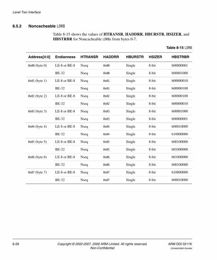
Level Two Interface
8.5.2 Noncacheable LDRB
Table 8-15 shows the values of HTRANSR, HADDRR, HBURSTR, HSIZER, and HBSTRBR for Noncacheable LDRBs from bytes 0-7.
Table 8-15 LDRB
Address[4:0] Endianness HTRANSR HADDRR HBURSTR HSIZER HBSTRBR
0x00 (byte 0) LE-8 or BE-8 Nseq 0x00 Single 8-bit b00000001
BE-32 Nseq 0x00 Single 8-bit b00001000
0x01 (byte 1) LE-8 or BE-8 Nseq 0x01 Single 8-bit b00000010
BE-32 Nseq 0x01 Single 8-bit b00000100
0x02 (byte 2) LE-8 or BE-8 Nseq 0x02 Single 8-bit b00000100
BE-32 Nseq 0x02 Single 8-bit b00000010
0x03 (byte 3) LE-8 or BE-8 Nseq 0x03 Single 8-bit b00001000
BE-32 Nseq 0x03 Single 8-bit b00000001
0x04 (byte 4) LE-8 or BE-8 Nseq 0x04 Single 8-bit b00010000
BE-32 Nseq 0x04 Single 8-bit b10000000
0x05 (byte 5) LE-8 or BE-8 Nseq 0x05 Single 8-bit b00100000
BE-32 Nseq 0x05 Single 8-bit b01000000
0x06 (byte 6) LE-8 or BE-8 Nseq 0x06 Single 8-bit b01000000
BE-32 Nseq 0x06 Single 8-bit b00100000
0x07 (byte 7) LE-8 or BE-8 Nseq 0x07 Single 8-bit b10000000
BE-32 Nseq 0x07 Single 8-bit b00010000
8-28 Copyright © 2002-2007, 2009 ARM Limited. All rights reserved. ARM DDI 0211KNon-Confidential Unrestricted Access

Level Two Interface
8.5.3 Noncacheable LDRH
Table 8-16 shows the values of HTRANSR, HADDRR, HBURSTR, HSIZER, and HBSTRBR for Noncacheable LDRHs from bytes 0-7.
Table 8-16 LDRH
Address[4:0] Endianness HTRANSR HADDRR HBURSTR HSIZER HBSTRBR
0x0 (byte 0) LE-8 or BE-8 Nseq 0x00 Single 16-bit b00000011
BE-32 Nseq 0x00 Single 16-bit b00001100
0x1 (byte 1) LE-8 or BE-8 Nseq 0x00 Single 32-bit b00000110a
BE-32 Nseq 0x00 Single 16-bit b00001100b
0x2 (byte 2) LE-8 or BE-8 Nseq 0x02 Single 16-bit b00001100
BE-32 Nseq 0x02 Single 16-bit b00000011
0x3 (byte 3) LE-8 or BE-8 Nseq 0x03 Single 8-bit b00001000
0x04 b00010000
BE-32 Nseq 0x02 Single 8-bit b00000011b
0x4 (byte 4) LE-8 or BE-8 Nseq 0x04 Single 16-bit b00110000
BE-32 Nseq 0x04 Single 16-bit b11000000
0x5 (byte 5) LE-8 or BE-8 Nseq 0x04 Single 32-bit b01100000a
BE-32 Nseq 0x04 Single 16-bit b11000000b
0x6 (byte 6) LE-8 or BE-8 Nseq 0x06 Single 16-bit b11000000
BE-32 Nseq 0x06 Single 16-bit b00110000
0x7 (byte 7) LE-8 or BE-8 Nseq 0x07 Single 8-bit b10000000
0x08 b00000001
BE-32 Nseq 0x06 Single 16-bit b00110000b
a. Denotes that HUNALIGNR is asserted for that transfer. This is only for ARMv6 unaligned loads and loads to normal memory, where reading more data than is necessary is possible.
b. Denotes that this behavior is Unpredictable.
ARM DDI 0211K Copyright © 2002-2007, 2009 ARM Limited. All rights reserved. 8-29Unrestricted Access Non-Confidential

Level Two Interface
8.5.4 Noncacheable LDR or LDM1
Table 8-17 shows the values of HTRANSR, HADDRR, HBURSTR, HSIZER, and HBSTRBR for Noncacheable LDRs or LDM1s.
Table 8-17 LDR or LDM1
Address[4:0] HTRANSR HADDRR HBURSTR HSIZER HBSTRBR
0x00 (byte 0) (word 0) Nseq 0x00 Single 32-bit b00001111
0x01 (byte 1) Nseq 0x00 Single 32-bit b00001110a
0x04 8-bit b00010000
0x02 (byte 2) Nseq 0x02 Single 16-bit b00001100
0x04 b00110000
0x03 (byte 3) Nseq 0x03 Single 8-bit b00001000
0x04 32-bit b01110000a
0x04 (byte 4) (word 1) Nseq 0x04 Single 32-bit b11110000
0x05 (byte 5) Nseq 0x04 Single 32-bit b11100000a
0x08 8-bit b00000001
0x06 (byte 6) Nseq 0x06 Single 16-bit b11000000
0x08 b00000011
0x07 (byte 7) Nseq 0x07 Single 8-bit b10000000
0x08 32-bit b00000111a
0x08 (word 2) Nseq 0x08 Single 32-bit b00001111
0x0C (word 3) Nseq 0x0C Single 32-bit b11110000
0x10 (word 4) Nseq 0x10 Single 32-bit b00001111
0x14 (word 5) Nseq 0x14 Single 32-bit b11110000
0x18 (word 6) Nseq 0x18 Single 32-bit b00001111
0x1C (word 7) Nseq 0x1C Single 32-bit b11110000
a. Denotes that HUNALIGNR is asserted for that transfer. This is only for ARMv6 unaligned loads and loads to normal memory, where reading more data than is necessary is possible.
8-30 Copyright © 2002-2007, 2009 ARM Limited. All rights reserved. ARM DDI 0211KNon-Confidential Unrestricted Access

Level Two Interface
8.5.5 Noncacheable LDRD or LDM2
Table 8-18 to Table 8-25 on page 8-32 show the values of HTRANSR, HADDRR, HBURSTR, HSIZER, and HBSTRBR for Noncacheable LDRDs or LDM2s.
Table 8-18 LDRD or LDM2 from word 0
HTRANSR HADDRR HBURSTR HSIZER HBSTRBR
Nseq 0x00 Single 64-bit b11111111
Table 8-19 LDRD or LDM2 from word 1
HTRANSR HADDRR HBURSTR HSIZER HBSTRBR
Nseq 0x04 Incr 32-bit b11110000
Seq 0x08 b00001111
Table 8-20 LDRD or LDM2 from word 2
HTRANSR HADDRR HBURSTR HSIZER HBSTRBR
Nseq 0x08 Single 64-bit b11111111
Table 8-21 LDRD or LDM2 from word 3
HTRANSR HADDRR HBURSTR HSIZER HBSTRBR
Nseq 0x0C Incr 32-bit b11110000
Seq 0x10 b00001111
ARM DDI 0211K Copyright © 2002-2007, 2009 ARM Limited. All rights reserved. 8-31Unrestricted Access Non-Confidential

Level Two Interface
8.5.6 Noncacheable LDM3
Table 8-26 on page 8-33 to Table 8-37 on page 8-36 show the values of HTRANSR, HADDRR, HBURSTR, HSIZER, and HBSTRBR for Noncacheable LDM3s from words 0 to 5.
Table 8-22 LDRD or LDM2 from word 4
HTRANSR HADDRR HBURSTR HSIZER HBSTRBR
Nseq 0x10 Single 64-bit b11111111
Table 8-23 LDRD or LDM2 from word 5
HTRANSR HADDRR HBURSTR HSIZER HBSTRBR
Nseq 0x14 Incr 32-bit b11110000
Seq 0x18 b00001111
Table 8-24 LDRD or LDM2 from word 6
HTRANSR HADDRR HBURSTR HSIZER HBSTRBR
Nseq 0x18 Single 64-bit b11111111
Table 8-25 LDRD or LDM2 from word 7
HTRANSR HADDRR HBURSTR HSIZER HBSTRBR
Nseq 0x1C Single 32-bit b11110000
Plus an LDR from 0x00 (byte 0).
8-32 Copyright © 2002-2007, 2009 ARM Limited. All rights reserved. ARM DDI 0211KNon-Confidential Unrestricted Access
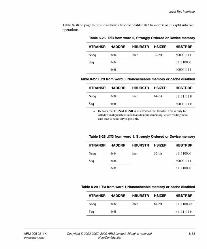
Level Two Interface
Table 8-38 on page 8-36 shows how a Noncacheable LDM3 to word 6 or 7 is split into two operations.
Table 8-26 LDM3 from word 0, Strongly Ordered or Device memory
HTRANSR HADDRR HBURSTR HSIZER HBSTRBR
Nseq 0x00 Incr 32-bit b00001111
Seq 0x04 b11110000
0x08 b00001111
Table 8-27 LDM3 from word 0, Noncacheable memory or cache disabled
HTRANSR HADDRR HBURSTR HSIZER HBSTRBR
Nseq 0x00 Incr 64-bit b11111111a
Seq 0x08 b00001111a
a. Denotes that HUNALIGNR is asserted for that transfer. This is only for ARMv6 unaligned loads and loads to normal memory, where reading more data than is necessary is possible.
Table 8-28 LDM3 from word 1, Strongly Ordered or Device memory
HTRANSR HADDRR HBURSTR HSIZER HBSTRBR
Nseq 0x04 Incr 32-bit b11110000
Seq 0x08 b00001111
0x0C b11110000
Table 8-29 LDM3 from word 1,Noncacheable memory or cache disabled
HTRANSR HADDRR HBURSTR HSIZER HBSTRBR
Nseq 0x00 Incr 64-bit b11110000a
Seq 0x08 b11111111a
ARM DDI 0211K Copyright © 2002-2007, 2009 ARM Limited. All rights reserved. 8-33Unrestricted Access Non-Confidential

Level Two Interface
a. Denotes that HUNALIGNR is asserted for that transfer. This is only for ARMv6 unaligned loads and loads to normal memory, where reading more data than is necessary is possible.
Table 8-30 LDM3 from word 2,Strongly Ordered or Device memory
HTRANSR HADDRR HBURSTR HSIZER HBSTRBR
Nseq 0x08 Incr 32-bit b00001111
Seq 0x0C b11110000
0x10 b00001111
Table 8-31 LDM3 from word 2, Noncacheable memory or cache disabled
HTRANSR HADDRR HBURSTR HSIZER HBSTRBR
Nseq 0x08 Incr 64-bit b11111111a
Seq 0x10 b00001111a
a. Denotes that HUNALIGNR is asserted for that transfer. This is only for ARMv6 unaligned loads and loads to normal memory, where reading more data than is necessary is possible.
Table 8-32 LDM3 from word 3, Strongly Ordered or Device memory
HTRANSR HADDRR HBURSTR HSIZER HBSTRBR
Nseq 0x0C Incr 32-bit b11110000
Seq 0x10 b00001111
0x14 b11110000
8-34 Copyright © 2002-2007, 2009 ARM Limited. All rights reserved. ARM DDI 0211KNon-Confidential Unrestricted Access
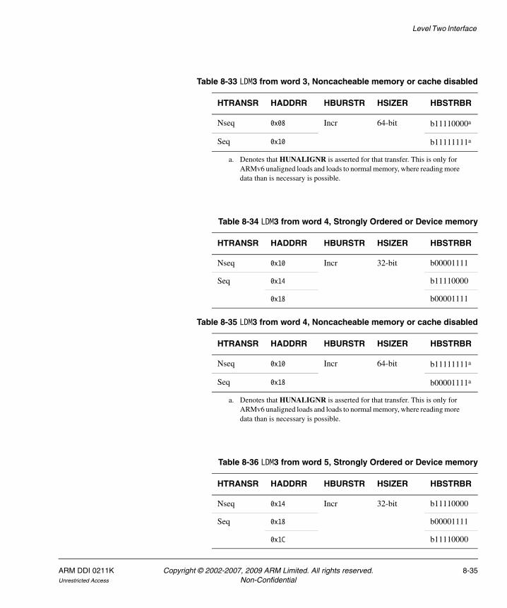
Level Two Interface
Table 8-33 LDM3 from word 3, Noncacheable memory or cache disabled
HTRANSR HADDRR HBURSTR HSIZER HBSTRBR
Nseq 0x08 Incr 64-bit b11110000a
a. Denotes that HUNALIGNR is asserted for that transfer. This is only for ARMv6 unaligned loads and loads to normal memory, where reading more data than is necessary is possible.
Seq 0x10 b11111111a
Table 8-34 LDM3 from word 4, Strongly Ordered or Device memory
HTRANSR HADDRR HBURSTR HSIZER HBSTRBR
Nseq 0x10 Incr 32-bit b00001111
Seq 0x14 b11110000
0x18 b00001111
Table 8-35 LDM3 from word 4, Noncacheable memory or cache disabled
HTRANSR HADDRR HBURSTR HSIZER HBSTRBR
Nseq 0x10 Incr 64-bit b11111111a
Seq 0x18 b00001111a
a. Denotes that HUNALIGNR is asserted for that transfer. This is only for ARMv6 unaligned loads and loads to normal memory, where reading more data than is necessary is possible.
Table 8-36 LDM3 from word 5, Strongly Ordered or Device memory
HTRANSR HADDRR HBURSTR HSIZER HBSTRBR
Nseq 0x14 Incr 32-bit b11110000
Seq 0x18 b00001111
0x1C b11110000
ARM DDI 0211K Copyright © 2002-2007, 2009 ARM Limited. All rights reserved. 8-35Unrestricted Access Non-Confidential

Level Two Interface
8.5.7 Noncacheable LDM4
Table 8-39 to Table 8-45 on page 8-38 show the values of HTRANSR, HADDRR, HBURSTR, HSIZER, and HBSTRBR for Noncacheable LDM4s from words 0 to 4.
Table 8-46 on page 8-39 shows how a Noncacheable LDM4 from words 5 to 7 is split into two operations.
Table 8-37 LDM3 from word 5, Noncacheable memory or cache disabled
HTRANSR HADDRR HBURSTR HSIZER HBSTRBR
Nseq 0x10 Incr 64-bit b11110000a
a. Denotes that HUNALIGNR is asserted for that transfer. This is only for ARMv6 unaligned loads and loads to normal memory, where reading more data than is necessary is possible.
Seq 0x18 b11111111a
Table 8-38 LDM3 from word 6 or 7, Noncacheable memory or cache disabled
Address[4:0] Operations
0x18 (word 6) LDM2 from 0x18 + LDR from 0x00
0x1C (word 7) LDR from 0x1C + LDM2 from 0x00
Table 8-39 LDM4 from word 0
HTRANSR HADDRR HBURSTR HSIZER HBSTRBR
Nseq 0x00 Incr 64-bit b11111111
Seq 0x08
8-36 Copyright © 2002-2007, 2009 ARM Limited. All rights reserved. ARM DDI 0211KNon-Confidential Unrestricted Access

Level Two Interface
Table 8-40 LDM4 from word 1, Strongly Ordered or Device memory
HTRANSR HADDRR HBURSTR HSIZER HBSTRBR
Nseq 0x04 Incr4 32-bit b11110000
Seq 0x08 b00001111
0x0C b11110000
0x10 b00001111
Table 8-41 LDM4 from word 1, Noncacheable memory or cache disabled
HTRANSR HADDRR HBURSTR HSIZER HBSTRBR
Nseq 0x00 Incr 64-bit b11110000a
a. Denotes that HUNALIGNR is asserted for that transfer. This is only for ARMv6 unaligned loads and loads to normal memory, where reading more data than is necessary is possible.
Seq 0x08 b11111111a
0x10 b00001111a
Table 8-42 LDM4 from word 2
HTRANSR HADDRR HBURSTR HSIZER HBSTRBR
Nseq 0x08 Incr 64-bit b11111111
Seq 0x10
ARM DDI 0211K Copyright © 2002-2007, 2009 ARM Limited. All rights reserved. 8-37Unrestricted Access Non-Confidential

Level Two Interface
Table 8-43 LDM4 from word 3, Strongly Ordered or Device memory
HTRANSR HADDRR HBURSTR HSIZER HBSTRBR
Nseq 0x0C Incr4 32-bit b11110000
Seq 0x10 b00001111
0x14 b11110000
0x18 b00001111
Table 8-44 LDM4 from word 3, Noncacheable memory or cache disabled
HTRANSR HADDRR HBURSTR HSIZER HBSTRBR
Nseq 0x08 Incr 64-bit b11110000a
a. Denotes that HUNALIGNR is asserted for that transfer. This is only for ARMv6 unaligned loads and loads to normal memory, where reading more data than is necessary is possible.
Seq 0x10 b11111111a
0x18 b00001111a
Table 8-45 LDM4 from word 4
HTRANSR HADDRR HBURSTR HSIZER HBSTRBR
Nseq 0x10 Incr 64-bit b11111111
Seq 0x18
8-38 Copyright © 2002-2007, 2009 ARM Limited. All rights reserved. ARM DDI 0211KNon-Confidential Unrestricted Access

Level Two Interface
8.5.8 Noncacheable LDM5
Table 8-47 to Table 8-54 on page 8-41 show the values of HTRANSR, HADDRR, HBURSTR, HSIZER, and HBSTRBR for Noncacheable LDM5s from words 0 to 3.
Table 8-55 on page 8-42 shows how a Noncacheable LDM5 from words 4 to 7 is split into two operations.
Table 8-46 LDM4 from word 5, 6, or 7
Address[4:0] Operations
0x14 (word 5) LDM3 from 0x14 + LDR from 0x00
0x18 (word 6) LDM2 from 0x18 + LDM2 from 0x00
0x1C (word 7) LDR from 0x1C + LDM3 from 0x00
Table 8-47 LDM5 from word 0, Strongly Ordered or Device memory
HTRANSR HADDRR HBURSTR HSIZER HBSTRBR
Nseq 0x00 Incr 32-bit b00001111
Seq 0x04 b11110000
0x08 b00001111
0x0C b11110000
0x10 b00001111
Table 8-48 LDM5 from word 0, Noncacheable memory or cache disabled
HTRANSR HADDRR HBURSTR HSIZER HBSTRBR
Nseq 0x00 Incr 64-bit b11111111a
Seq 0x08 b11111111a
0x10 b00001111a
a. Denotes that HUNALIGNR is asserted for that transfer. This is only for ARMv6 unaligned loads and loads to normal memory, where reading more data than is necessary is possible.
ARM DDI 0211K Copyright © 2002-2007, 2009 ARM Limited. All rights reserved. 8-39Unrestricted Access Non-Confidential
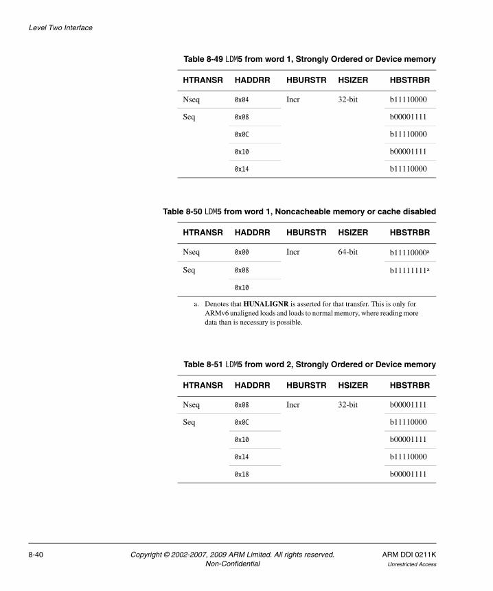
Level Two Interface
Table 8-49 LDM5 from word 1, Strongly Ordered or Device memory
HTRANSR HADDRR HBURSTR HSIZER HBSTRBR
Nseq 0x04 Incr 32-bit b11110000
Seq 0x08 b00001111
0x0C b11110000
0x10 b00001111
0x14 b11110000
Table 8-50 LDM5 from word 1, Noncacheable memory or cache disabled
HTRANSR HADDRR HBURSTR HSIZER HBSTRBR
Nseq 0x00 Incr 64-bit b11110000a
a. Denotes that HUNALIGNR is asserted for that transfer. This is only for ARMv6 unaligned loads and loads to normal memory, where reading more data than is necessary is possible.
Seq 0x08 b11111111a
0x10
Table 8-51 LDM5 from word 2, Strongly Ordered or Device memory
HTRANSR HADDRR HBURSTR HSIZER HBSTRBR
Nseq 0x08 Incr 32-bit b00001111
Seq 0x0C b11110000
0x10 b00001111
0x14 b11110000
0x18 b00001111
8-40 Copyright © 2002-2007, 2009 ARM Limited. All rights reserved. ARM DDI 0211KNon-Confidential Unrestricted Access
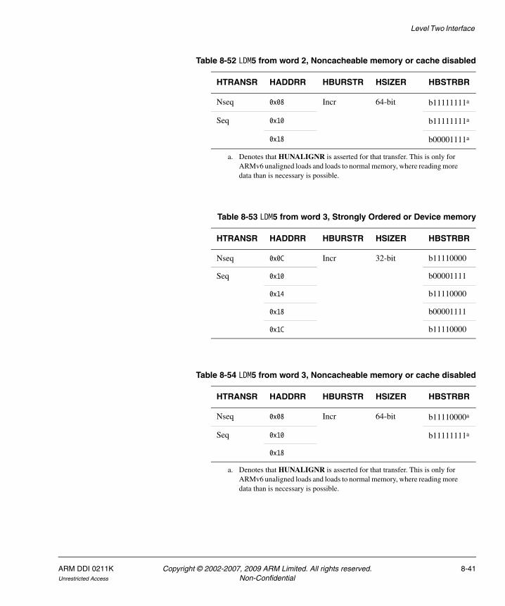
Level Two Interface
Table 8-52 LDM5 from word 2, Noncacheable memory or cache disabled
HTRANSR HADDRR HBURSTR HSIZER HBSTRBR
Nseq 0x08 Incr 64-bit b11111111a
Seq 0x10 b11111111a
0x18 b00001111a
a. Denotes that HUNALIGNR is asserted for that transfer. This is only for ARMv6 unaligned loads and loads to normal memory, where reading more data than is necessary is possible.
Table 8-53 LDM5 from word 3, Strongly Ordered or Device memory
HTRANSR HADDRR HBURSTR HSIZER HBSTRBR
Nseq 0x0C Incr 32-bit b11110000
Seq 0x10 b00001111
0x14 b11110000
0x18 b00001111
0x1C b11110000
Table 8-54 LDM5 from word 3, Noncacheable memory or cache disabled
HTRANSR HADDRR HBURSTR HSIZER HBSTRBR
Nseq 0x08 Incr 64-bit b11110000a
a. Denotes that HUNALIGNR is asserted for that transfer. This is only for ARMv6 unaligned loads and loads to normal memory, where reading more data than is necessary is possible.
Seq 0x10 b11111111a
0x18
ARM DDI 0211K Copyright © 2002-2007, 2009 ARM Limited. All rights reserved. 8-41Unrestricted Access Non-Confidential

Level Two Interface
8.5.9 Noncacheable LDM6
Table 8-56 to Table 8-59 on page 8-43 show the values of HTRANSR, HADDRR, HBURSTR, HSIZER, and HBSTRBR for Noncacheable LDM6s from words 0 to 2.
Table 8-60 on page 8-43 shows how a Noncacheable LDM6 from words 3 to 7 is split into two operations.
Table 8-55 LDM5 from word 4, 5, 6, or 7
Address[4:0] Operations
0x10 (word 4) LDM4 from 0x10 + LDR from 0x00
0x14 (word 5) LDM3 from 0x14 + LDM2 from 0x00
0x18 (word 6) LDM2 from 0x18 + LDM3 from 0x00
0x1C (word 7) LDR from 0x1C + LDM4 from 0x00
Table 8-56 LDM6 from word 0
HTRANSR HADDRR HBURSTR HSIZER HBSTRBR
Nseq 0x00 Incr 64-bit b11111111
Seq 0x08
0x10
Table 8-57 LDM6 from word 1, Strongly Ordered or Device memory
HTRANSR HADDRR HBURSTR HSIZER HBSTRBR
Nseq 0x04 Incr 32-bit b11110000
Seq 0x08 b00001111
0x0C b11110000
0x10 b00001111
0x14 b11110000
0x18 b00001111
8-42 Copyright © 2002-2007, 2009 ARM Limited. All rights reserved. ARM DDI 0211KNon-Confidential Unrestricted Access

Level Two Interface
Table 8-58 LDM6 from word 1, Noncacheable memory or cache disabled
HTRANSR HADDRR HBURSTR HSIZER HBSTRBR
Nseq 0x00 Incr4 64-bit b11110000a
Seq 0x08 b11111111a
0x10 b11111111a
0x18 b00001111a
a. Denotes that HUNALIGNR is asserted for that transfer. This is only for ARMv6 unaligned loads and loads to normal memory, where reading more data than is necessary is possible.
Table 8-59 LDM6 from word 2
HTRANSR HADDRR HBURSTR HSIZER HBSTRBR
Nseq 0x08 Incr 64-bit b11111111
Seq 0x10
0x18
Table 8-60 LDM6 from word 3, 4, 5, 6, or 7
Address[4:0] Operations
0x0C (word 3) LDM5 from 0x0C + LDR from 0x00
0x10 (word 4) LDM4 from 0x10 + LDM2 from 0x00
0x14 (word 5) LDM3 from 0x14 + LDM3 from 0x00
0x18 (word 6) LDM2 from 0x18 + LDM4 from 0x00
0x1C (word 7) LDR from 0x1C + LDM5 from 0x00
ARM DDI 0211K Copyright © 2002-2007, 2009 ARM Limited. All rights reserved. 8-43Unrestricted Access Non-Confidential

Level Two Interface
8.5.10 Noncacheable LDM7
Table 8-61 to Table 8-64 on page 8-45 show the values of HTRANSR, HADDRR, HBURSTR, HSIZER, and HBSTRBR for Noncacheable LDM7s from words 0 to 1.
Table 8-65 on page 8-45 shows how a Noncacheable LDM7 from words 2 to 7 is split into two operations.
Table 8-61 LDM7 from word 0, Strongly Ordered or Device memory
HTRANSR HADDRR HBURSTR HSIZER HBSTRBR
Nseq 0x00 Incr 32-bit b00001111
Seq 0x04 b11110000
0x08 b00001111
0x0C b11110000
0x10 b00001111
0x14 b11110000
0x18 b00001111
Table 8-62 LDM7 from word 0, Noncacheable memory or cache disabled
HTRANSR HADDRR HBURSTR HSIZER HBSTRBR
Nseq 0x00 Incr4 64-bit b11111111a
Seq 0x08
0x10
0x18 b00001111a
a. Denotes that HUNALIGNR is asserted for that transfer. This is only for ARMv6 unaligned loads and loads to normal memory, where reading more data than is necessary is possible.
8-44 Copyright © 2002-2007, 2009 ARM Limited. All rights reserved. ARM DDI 0211KNon-Confidential Unrestricted Access

Level Two Interface
Table 8-63 LDM7 from word 1, Strongly Ordered or Device memory
HTRANSR HADDRR HBURSTR HSIZER HBSTRBR
Nseq 0x04 Incr 32-bit b11110000
Seq 0x08 b00001111
0x0C b11110000
0x10 b00001111
0x14 b11110000
0x18 b00001111
0x1C b11110000
Table 8-64 LDM7 from word 1, Noncacheable memory or cache disabled
HTRANSR HADDRR HBURSTR HSIZER HBSTRBR
Nseq 0x00 Incr4 64-bit b11110000a
Seq 0x08 b11111111
0x10
0x18
a. Indicates that HUNALIGNR is asserted for the transfer. This is only for ARMv6 unaligned loads and loads to normal memory, where it is possible to read more data than is necessary.
Table 8-65 LDM7 from word 2, 3, 4, 5, 6, or 7
Address[4:0] Operations
0x08 (word 2) LDM6 from 0x08 + LDR from 0x00
0x0C (word 3) LDM5 from 0x0C + LDM2 from 0x00
0x10 (word 4) LDM4 from 0x10 + LDM3 from 0x00
0x14 (word 5) LDM3 from 0x14 + LDM4 from 0x00
0x18 (word 6) LDM2 from 0x18 + LDM5 from 0x00
0x1C (word 7) LDR from 0x1C + LDM6 from 0x00
ARM DDI 0211K Copyright © 2002-2007, 2009 ARM Limited. All rights reserved. 8-45Unrestricted Access Non-Confidential

Level Two Interface
8.5.11 Noncacheable LDM8
Table 8-66 shows the values of HTRANSR, HADDRR, HBURSTR, HSIZER, and HBSTRBR for Noncacheable LDM8s from word 0.
Table 8-67shows how a Noncacheable LDM8 from words 1 to 7 is split into two operation.
Table 8-66 LDM8 from word 0
HTRANSR HADDRR HBURSTR HSIZER HBSTRBR
Nseq 0x00 Incr4 64-bit b11111111
Seq 0x08
0x10
0x18
Table 8-67 LDM8 from word 1, 2, 3, 4, 5, 6, or 7
Address[4:0] Operations
0x04 (word 1) LDM7 from 0x04 + LDR from 0x00
0x08 (word 2) LDM6 from 0x08 + LDM2 from 0x00
0x0C (word 3) LDM5 from 0x0C + LDM3 from 0x00
0x10 (word 4) LDM4 from 0x10 + LDM4 from 0x00
0x14 (word 5) LDM3 from 0x14 + LDM5 from 0x00
0x18 (word 6) LDM2 from 0x18 + LDM6 from 0x00
0x1C (word 7) LDR from 0x1C + LDM7 from 0x00
8-46 Copyright © 2002-2007, 2009 ARM Limited. All rights reserved. ARM DDI 0211KNon-Confidential Unrestricted Access

Level Two Interface
8.5.12 Noncacheable LDM9
Table 8-68 shows how a Noncacheable LDM9 is split into two operations.
8.5.13 Noncacheable LDM10
Table 8-69 shows how a Noncacheable LDM10 is split into multiple operations.
Table 8-68 LDM9
Address[4:0] Operations
0x00 (word 0) LDM8 from 0x00 + LDR from 0x00
0x04 (word 1) LDM7 from 0x04 + LDM2 from 0x00
0x08 (word 2) LDM6 from 0x08 + LDM3 from 0x00
0x0C (word 3) LDM5 from 0x0C + LDM4 from 0x00
0x10 (word 4) LDM4 from 0x10 + LDM5 from 0x00
0x14 (word 5) LDM3 from 0x14 + LDM6 from 0x00
0x18 (word 6) LDM2 from 0x18 + LDM7 from 0x00
0x1C (word 7) LDR from 0x1C + LDM8 from 0x00
Table 8-69 LDM10
Address[4:0] Operations
0x00 (word 0) LDM8 from 0x00 + LDM2 from 0x00
0x04 (word 1) LDM7 from 0x04 + LDM3 from 0x00
0x08 (word 2) LDM6 from 0x08 + LDM4 from 0x00
0x0C (word 3) LDM5 from 0x0C + LDM5 from 0x00
0x10 (word 4) LDM4 from 0x10 + LDM6 from 0x00
0x14 (word 5) LDM3 from 0x14 + LDM7 from 0x00
0x18 (word 6) LDM2 from 0x18 + LDM8 from 0x00
0x1C (word 7) LDR from 0x1C + LDM8 from 0x00 + LDR from 0x00
ARM DDI 0211K Copyright © 2002-2007, 2009 ARM Limited. All rights reserved. 8-47Unrestricted Access Non-Confidential

Level Two Interface
8.5.14 Noncacheable LDM11
Table 8-70 shows how a Noncacheable LDM11 is split into multiple operations.
8.5.15 Noncacheable LDM12
Table 8-71 shows how a Noncacheable LDM12 is split into multiple operations.
Table 8-70 LDM11
Address[4:0] Operations
0x00 (word 0) LDM8 from 0x00 + LDM3 from 0x00
0x04 (word 1) LDM7 from 0x04 + LDM4 from 0x00
0x08 (word 2) LDM6 from 0x08 + LDM5 from 0x00
0x0C (word 3) LDM5 from 0x0C + LDM6 from 0x00
0x10 (word 4) LDM4 from 0x10 + LDM7 from 0x00
0x14 (word 5) LDM3 from 0x14 + LDM8 from 0x00
0x18 (word 6) LDM2 from 0x18 + LDM8 from 0x00 + LDR from 0x00
0x1C (word 7) LDR from 0x1C + LDM8 from 0x00 + LDM2 from 0x00
Table 8-71 LDM12
Address[4:0] Operations
0x00 (word 0) LDM8 from 0x00 + LDM4 from 0x00
0x04 (word 1) LDM7 from 0x04 + LDM5 from 0x00
0x08 (word 2) LDM6 from 0x08 + LDM6 from 0x00
0x0C (word 3) LDM5 from 0x0C + LDM7 from 0x00
0x10 (word 4) LDM4 from 0x10 + LDM8 from 0x00
0x14 (word 5) LDM3 from 0x14 + LDM8 from 0x00 + LDR from 0x00
0x18 (word 6) LDM2 from 0x18 + LDM8 from 0x00 + LDM2 from 0x00
0x1C (word 7) LDR from 0x1C + LDM8 from 0x00 + LDM3 from 0x00
8-48 Copyright © 2002-2007, 2009 ARM Limited. All rights reserved. ARM DDI 0211KNon-Confidential Unrestricted Access

Level Two Interface
8.5.16 Noncacheable LDM13
Table 8-72 shows how a Noncacheable LDM13 is split into multiple operations.
8.5.17 Noncacheable LDM14
Table 8-73 shows how a Noncacheable LDM14 is split into multiple operations.
Table 8-72 LDM13
Address[4:0] Operations
0x00 (word 0) LDM8 from 0x00 + LDM5 from 0x00
0x04 (word 1) LDM7 from 0x04 + LDM6 from 0x00
0x08 (word 2) LDM6 from 0x08 + LDM7 from 0x00
0x0C (word 3) LDM5 from 0x0C + LDM8 from 0x00
0x10 (word 4) LDM4 from 0x10 + LDM8 from 0x00 + LDR from 0x00
0x14 (word 5) LDM3 from 0x14 + LDM8 from 0x00 + LDM2 from 0x00
0x18 (word 6) LDM2 from 0x18 + LDM8 from 0x00 + LDM3 from 0x00
0x1C (word 7) LDR from 0x1C + LDM8 from 0x00 + LDM4 from 0x00
Table 8-73 LDM14
Address[4:0] Operations
0x00 (word 0) LDM8 from 0x00 + LDM6 from 0x00
0x04 (word 1) LDM7 from 0x04 + LDM7 from 0x00
0x08 (word 2) LDM6 from 0x08 + LDM8 from 0x00
0x0C (word 3) LDM5 from 0x0C + LDM8 from 0x00 + LDR from 0x00
0x10 (word 4) LDM4 from 0x10 + LDM8 from 0x00 + LDM2 from 0x00
0x14 (word 5) LDM3 from 0x14 + LDM8 from 0x00 + LDM3 from 0x00
0x18 (word 6) LDM2 from 0x18 + LDM8 from 0x00 + LDM4 from 0x00
0x1C (word 7) LDR from 0x1C + LDM8 from 0x00 + LDM5 from 0x00
ARM DDI 0211K Copyright © 2002-2007, 2009 ARM Limited. All rights reserved. 8-49Unrestricted Access Non-Confidential

Level Two Interface
8.5.18 Noncacheable LDM15
Table 8-74 shows how a Noncacheable LDM15 is split into multiple operations.
8.5.19 Noncacheable LDM16
Table 8-75 shows how a Noncacheable LDM16 is split into multiple operations.
Table 8-74 LDM15
Address[4:0] Operations
0x00 (word 0) LDM8 from 0x00 + LDM7 from 0x00
0x04 (word 1) LDM7 from 0x04 + LDM8 from 0x00
0x08 (word 2) LDM6 from 0x08 + LDM8 from 0x00 + LDR from 0x00
0x0C (word 3) LDM5 from 0x0C + LDM8 from 0x00 + LDM2 from 0x00
0x10 (word 4) LDM4 from 0x10 + LDM8 from 0x00 + LDM3 from 0x00
0x14 (word 5) LDM3 from 0x14 + LDM8 from 0x00 + LDM4 from 0x00
0x18 (word 6) LDM2 from 0x18 + LDM8 from 0x00 + LDM5 from 0x00
0x1C (word 7) LDR from 0x1C + LDM8 from 0x00 + LDM6 from 0x00
Table 8-75 LDM16
Address[4:0] Operations
0x00 (word 0) LDM8 from 0x00 + LDM8 from 0x00
0x04 (word 1) LDM7 from 0x04 + LDM8 from 0x00 + LDR from 0x00
0x08 (word 2) LDM6 from 0x08 + LDM8 from 0x00 + LDM2 from 0x00
0x0C (word 3) LDM5 from 0x0C + LDM8 from 0x00 + LDM3 from 0x00
0x10 (word 4) LDM4 from 0x10 + LDM8 from 0x00 + LDM4 from 0x00
0x14 (word 5) LDM3 from 0x14 + LDM8 from 0x00 + LDM5 from 0x00
0x18 (word 6) LDM2 from 0x18 + LDM8 from 0x00 + LDM6 from 0x00
0x1C (word 7) LDR from 0x1C + LDM8 from 0x00 + LDM7 from 0x00
8-50 Copyright © 2002-2007, 2009 ARM Limited. All rights reserved. ARM DDI 0211KNon-Confidential Unrestricted Access

Level Two Interface
8.5.20 SWP instructions
Table 8-76 and Table 8-77 show Cacheable and Noncacheable SWP instructions over the Data Read Interface respectively.
8.5.21 Page table walks
Table 8-78 shows page table walks over the Data Read Interface.
Table 8-76 Cacheable swap
Swap operation AHB-Lite operations
Swap read LDR or LDRB from the Data Read Interface
Swap write STR or STRB from the Data Write Interface
Table 8-77 Noncacheable swap
Swap operation AHB-Lite operations
Swap read LDR or LDRB from the Data Read Interface
Swap write STR or STRB from the Data Read Interface (HWRITER = 1)
Table 8-78 Page table walks
Address[2:0] HTRANSR HADDRR HBURSTR HSIZER HBSTRBR
0x0 Nseq 0x0 Single 32-bit b00001111
0x4 Nseq 0x4 Single 32-bit b11110000
ARM DDI 0211K Copyright © 2002-2007, 2009 ARM Limited. All rights reserved. 8-51Unrestricted Access Non-Confidential

Level Two Interface
8.5.22 Other AHB-Lite signals for Data Read ports
The other AHB-Lite signals for Data Read ports are:
HSIDEBAND[3:1]
Encodes the Inner Cacheable TLB attributes. Table 8-79 shows the HSIDEBAND[3:1] encoding for the Inner Cacheable TLB attributes.
HSIDEBAND[0] The TLB Shared bit.
Table 8-79 HSIDEBAND[3:1] encoding
HSIDEBAND[3:1] Attribute
b000 Strongly ordered
b001 Device
b010 Inner Noncacheable
b110 Inner Write-Through
bx11 Inner Write-Back
8-52 Copyright © 2002-2007, 2009 ARM Limited. All rights reserved. ARM DDI 0211KNon-Confidential Unrestricted Access

Level Two Interface
8.6 Data Write Interface AHB-Lite transfers
The tables in this section describe the AHB-Lite interface behavior for Data Write Interface transfers for the following interface signals:
• HBURSTW[2:0]• HTRANSW[1:0]• HADDRW[31:0]• HBSTRBW[7:0]• HSIZEW[2:0].
8.6.1 Stores on the AHB-Lite interface
For Cacheable or Noncacheable Write-Through stores over the Data Write Interface, Table 8-80 to Table 8-104 on page 8-66 show either:
• the values of HTRANSW, HADDRW, HBURSTW, HSIZEW, and HBSTRBW for the access
• how the access is split into multiple operations.
Table 8-80 STRB
Address[4:0] Endianess HTRANSW HADDRW HBURSTW HSIZEW HBSTRBW
0x00 (byte 0) LE-8 or BE-8 Nseq 0x00 Single 8-bit b00000001
BE-32 Nseq 0x00 Single 8-bit b00001000
0x01 (byte 1) LE-8 or BE-8 Nseq 0x01 Single 8-bit b00000010
BE-32 Nseq 0x01 Single 8-bit b00000100
0x02 (byte 2) LE-8 or BE-8 Nseq 0x02 Single 8-bit b00000100
BE-32 Nseq 0x02 Single 8-bit b00000010
0x03 (byte 3) LE-8 or BE-8 Nseq 0x03 Single 8-bit b00001000
BE-32 Nseq 0x03 Single 8-bit b00000001
0x04 (byte 4) LE-8 or BE-8 Nseq 0x04 Single 8-bit b00010000
BE-32 Nseq 0x04 Single 8-bit b10000000
0x05 (byte 5) LE-8 or BE-8 Nseq 0x05 Single 8-bit b00100000
BE-32 Nseq 0x05 Single 8-bit b01000000
ARM DDI 0211K Copyright © 2002-2007, 2009 ARM Limited. All rights reserved. 8-53Unrestricted Access Non-Confidential

Level Two Interface
0x06 (byte 6) LE-8 or BE-8 Nseq 0x06 Single 8-bit b01000000
BE-32 Nseq 0x06 Single 8-bit b00100000
0x07 (byte 7) LE-8 or BE-8 Nseq 0x07 Single 8-bit b10000000
BE-32 Nseq 0x07 Single 8-bit b00010000
Table 8-80 STRB (continued)
Address[4:0] Endianess HTRANSW HADDRW HBURSTW HSIZEW HBSTRBW
Table 8-81 STRH
Address[4:0] Endianess HTRANSW HADDRW HBURSTW HSIZEW HBSTRBW
0x00 (byte 0) LE-8 or BE-8 Nseq 0x00 Single 16-bit b00000011
BE-32 Nseq 0x00 Single 16-bit b00001100
0x01 (byte 1) LE-8 or BE-8 Nseq 0x00 Single 32-bit b00000110a
BE-32 Nseq 0x00 Single 16-bit b00001100b
0x02 (byte 2) LE-8 or BE-8 Nseq 0x02 Single 16-bit b00001100
BE-32 Nseq 0x02 Single 16-bit b00000011
0x03 (byte 3) LE-8 or BE-8 Nseq 0x03 Single 8-bit b00001000
0x04 b00010000
BE-32 Nseq 0x02 Single 16-bit b00000011b
0x04 (byte 4) LE-8 or BE-8 Nseq 0x04 Single 16-bit b00110000
BE-32 Nseq 0x04 Single 16-bit b11000000
0x05 (byte 5) LE-8 or BE-8 Nseq 0x04 Single 32-bit b01100000a
BE-32 Nseq 0x04 Single 16-bit b11000000
0x06 (byte 6) LE-8 or BE-8 Nseq 0x06 Single 16-bit b11000000
BE-32 Nseq 0x06 Single 16-bit b00110000b
8-54 Copyright © 2002-2007, 2009 ARM Limited. All rights reserved. ARM DDI 0211KNon-Confidential Unrestricted Access

Level Two Interface
0x07 (byte 7) LE-8 or BE-8 Nseq 0x07 Single 8-bit b10000000
0x08 b00000001
BE-32 Nseq 0x06 Single 16-bit b00110000b
a. Denotes that HUNALIGNW is asserted for that transfer. This is only used for ARMv6 unaligned stores.b. Denotes that this behavior is Unpredictable.
Table 8-81 STRH (continued)
Address[4:0] Endianess HTRANSW HADDRW HBURSTW HSIZEW HBSTRBW
Table 8-82 STR or STM1
Address[4:0] HTRANSW HADDRW HBURSTW HSIZEW HBSTRBW
0x00 (byte 0) (word 0) Nseq 0x00 Single 32-bit b00001111
0x01 (byte 1) Nseq 0x00 Single 32-bit b00001110a
0x04 8-bit b00010000
0x02 (byte 2) Nseq 0x02 Single 16-bit b00001100
0x04 b00110000
0x03 (byte 3) Nseq 0x03 Single 8-bit b00001000
0x04 32-bit b01110000a
0x04 (byte 4) (word 1) Nseq 0x04 Single 32-bit b11110000
0x05 (byte 5) Nseq 0x04 Single 32-bit b11100000a
0x08 8-bit b00000001
0x06 (byte 6) Nseq 0x06 Single 16-bit b11000000
0x08 b00000011
0x07 (byte 7) Nseq 0x07 Single 8-bit b10000000
0x08 32-bit b00000111a
0x08 (byte 8) (word 2) Nseq 0x08 Single 32-bit b00001111
0x0C (word 3) Nseq 0x0C Single 32-bit b11110000
0x10 (word 4) Nseq 0x10 Single 32-bit b00001111
ARM DDI 0211K Copyright © 2002-2007, 2009 ARM Limited. All rights reserved. 8-55Unrestricted Access Non-Confidential

Level Two Interface
0x14 (word 5) Nseq 0x14 Single 32-bit b11110000
0x18 (word 6) Nseq 0x18 Single 32-bit b00001111
0x1C (word 7) Nseq 0x1C Single 32-bit b11110000
a. Denotes that HUNALIGNW is asserted for that transfer. This is only used for ARMv6 unaligned stores.
Table 8-82 STR or STM1 (continued)
Address[4:0] HTRANSW HADDRW HBURSTW HSIZEW HBSTRBW
Table 8-83 STRD or STM2 to words 0, 1, 2, 3, 4, 5, or 6
Address[4:0] HTRANSW HADDRW HBURSTW HSIZEW HBSTRBW
0x00 (word 0) Nseq 0x00 Single 64-bit b11111111
0x04 (word 1) Nseq 0x04 Incr 32-bit b11110000
Seq 0x08 Incr 32-bit b00001111
0x08 (word 2) Nseq 0x08 Single 64-bit b11111111
0x0C (word 3) Nseq 0x0C Incr 32-bit b11110000
Seq 0x10 Incr 32-bit b00001111
0x10 (word 4) Nseq 0x10 Single 64-bit b11111111
0x14 (word 5) Nseq 0x14 Incr 32-bit b11110000
Seq 0x18 Incr 32-bit b00001111
0x18 (word 6) Nseq 0x18 Single 64-bit b11111111
Table 8-84 STRD or STM2 to word 7
Address[4:0] Operations
0x1C STR to 0x1C + STR to 0x00
8-56 Copyright © 2002-2007, 2009 ARM Limited. All rights reserved. ARM DDI 0211KNon-Confidential Unrestricted Access

Level Two Interface
Table 8-85 STM3 to words 0, 1, 2, 3, 4, or 5
Address[4:0] HTRANSW HADDRW HBURSTW HSIZEW HBSTRBW
0x00 (word 0) Nseq 0x00 Incr 32-bit b00001111
Seq 0x04 b11110000
0x08 b00001111
0x04 (word 1) Nseq 0x04 Incr 32-bit b11110000
Seq 0x08 b00001111
0x0C b11110000
0x08 (word 2) Nseq 0x08 Incr 32-bit b00001111
Seq 0x0C b11110000
0x10 b00001111
0x0C (word 3) Nseq 0x0C Incr 32-bit b11110000
Seq 0x10 b00001111
0x14 b11110000
0x10 (word 4) Nseq 0x10 Incr 32-bit b00001111
Seq 0x14 b11110000
0x18 b00001111
0x14 (word 5) Nseq 0x14 Incr 32-bit b11110000
Seq 0x18 b00001111
0x1C b11110000
Table 8-86 STM3 to words 6 or 7
Address[4:0] Operations
0x18 (word 6) STM2 to 0x18 + STR to 0x00
0x1C (word 7) STR to 0x1C + STM2 to 0x00
ARM DDI 0211K Copyright © 2002-2007, 2009 ARM Limited. All rights reserved. 8-57Unrestricted Access Non-Confidential

Level Two Interface
Table 8-87 STM4 to word 0, 1, 2, 3, or 4
Address[4:0] HTRANSW HADDRW HBURSTW HSIZEW HBSTRBW
0x00 (word 0) Nseq 0x00 Incr 64-bit b11111111
Seq 0x08
0x04 (word 1) Nseq 0x04 Incr4 32-bit b11110000
Seq 0x08 b00001111
0x0C b11110000
0x10 b00001111
0x08 (word 2) Nseq 0x08 Incr 64-bit b11111111
Seq 0x10
0x0C (word 3) Nseq 0x0C Incr4 32-bit b11110000
Seq 0x10 b00001111
0x14 b11110000
0x18 b00001111
0x10 (word 4) Nseq 0x10 Incr 64-bit b11111111
Seq 0x18
Table 8-88 STM4 to word 5, 6, or 7
Address[4:0] Operations
0x14 (word 5) STM3 to 0x14 + STR to 0x00
0x18 (word 6) STM2 to 0x18 + STM2 to 0x00
0x1C (word 7) STR to 0x1C + STM3 to 0x00
8-58 Copyright © 2002-2007, 2009 ARM Limited. All rights reserved. ARM DDI 0211KNon-Confidential Unrestricted Access
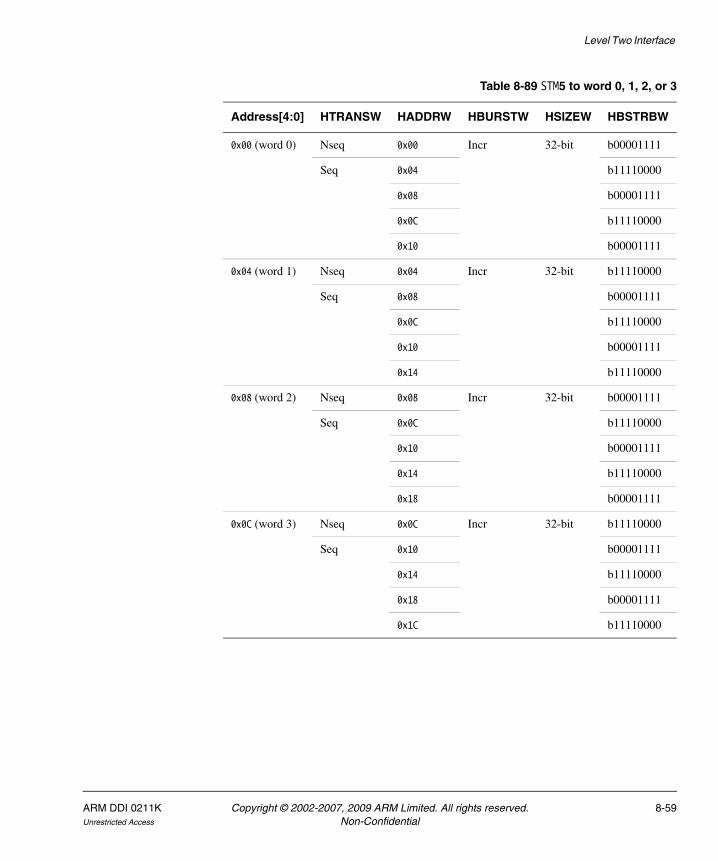
Level Two Interface
Table 8-89 STM5 to word 0, 1, 2, or 3
Address[4:0] HTRANSW HADDRW HBURSTW HSIZEW HBSTRBW
0x00 (word 0) Nseq 0x00 Incr 32-bit b00001111
Seq 0x04 b11110000
0x08 b00001111
0x0C b11110000
0x10 b00001111
0x04 (word 1) Nseq 0x04 Incr 32-bit b11110000
Seq 0x08 b00001111
0x0C b11110000
0x10 b00001111
0x14 b11110000
0x08 (word 2) Nseq 0x08 Incr 32-bit b00001111
Seq 0x0C b11110000
0x10 b00001111
0x14 b11110000
0x18 b00001111
0x0C (word 3) Nseq 0x0C Incr 32-bit b11110000
Seq 0x10 b00001111
0x14 b11110000
0x18 b00001111
0x1C b11110000
ARM DDI 0211K Copyright © 2002-2007, 2009 ARM Limited. All rights reserved. 8-59Unrestricted Access Non-Confidential

Level Two Interface
Table 8-90 STM5 to word 4, 5, 6, or 7
Address[4:0] Operations
0x10 (word 4) STM4 to 0x10 + STR to 0x00
0x14 (word 5) STM3 to 0x14 + STM2 to 0x00
0x18 (word 6) STM2 to 0x18 + STM3 to 0x00
0x1C (word 7) STR to 0x1C + STM4 to 0x00
Table 8-91 STM6 to word 0, 1, or 2
Address[4:0] HTRANSW HADDRW HBURSTW HSIZEW HBSTRBW
0x00 (word 0) Nseq 0x00 Incr 64-bit b11111111
Seq 0x08 b11111111
0x10 b11111111
0x04 (word 1) Nseq 0x04 Incr 32-bit b11110000
Seq 0x08 b00001111
0x0C b11110000
0x10 b00001111
0x14 b11110000
0x18 b00001111
0x08 (word 2) Nseq 0x08 Incr 64-bit b11111111
Seq 0x10 b11111111
0x18 b11111111
8-60 Copyright © 2002-2007, 2009 ARM Limited. All rights reserved. ARM DDI 0211KNon-Confidential Unrestricted Access

Level Two Interface
Table 8-92 STM6 to word 3, 4, 5, 6, or 7
Address[4:0] Operations
0x0C (word 3) STM5 to 0x0C + STR to 0x00
0x10 (word 4) STM4 to 0x10 + STM2 to 0x00
0x14 (word 5) STM3 to 0x14 + STM3 to 0x00
0x18 (word 6) STM2 to 0x18 + STM4 to 0x00
0x1C (word 7) STR to 0x1C + STM5 to 0x00
Table 8-93 STM7 to word 0 or 1
Address[4:0] HTRANSW HADDRW HBURSTW HSIZEW HBSTRBW
0x00 (word 0) Nseq 0x00 Incr 32-bit b00001111
Seq 0x04 b11110000
0x08 b00001111
0x0C b11110000
0x10 b00001111
0x14 b11110000
0x18 b00001111
0x04 (word 1) Nseq 0x04 Incr 32-bit b11110000
Seq 0x08 b00001111
0x0C b11110000
0x10 b00001111
0x14 b11110000
0x18 b00001111
0x1C b11110000
ARM DDI 0211K Copyright © 2002-2007, 2009 ARM Limited. All rights reserved. 8-61Unrestricted Access Non-Confidential

Level Two Interface
Table 8-94 STM7 to word 2, 3, 4, 5, 6, or 7
Address[4:0] Operations
0x08 (word 2) STM6 to 0x08 + STR to 0x00
0x0C (word 3) STM5 to 0x0C + STM2 to 0x00
0x10 (word 4) STM4 to 0x10 + STM3 to 0x00
0x14 (word 5) STM3 to 0x14 + STM4 to 0x00
0x18 (word 6) STM2 to 0x18 + STM5 to 0x00
0x1C (word 7) STR to 0x1C + STM6 to 0x00
Table 8-95 STM8 to word 0
HTRANSW HADDRW HBURSTW HSIZEW HBSTRBW
Nseq 0x00 Incr4 64-bit b11111111
Seq 0x08
0x10
0x18
Table 8-96 STM8 to word 1, 2, 3, 4, 5, 6, or 7
Address[4:0] Operations
0x04 (word 1) STM7 to 0x04 + STR to 0x00
0x08 (word 2) STM6 to 0x08 + STM2 to 0x00
0x0C (word 3) STM5 to 0x0C + STM3 to 0x00
0x10 (word 4) STM4 to 0x10 + STM4 to 0x00
0x14 (word 5) STM3 to 0x14 + STM5 to 0x00
0x18 (word 6) STM2 to 0x18 + STM6 to 0x00
0x1C (word 7) STR to 0x1C + STM7 to 0x00
8-62 Copyright © 2002-2007, 2009 ARM Limited. All rights reserved. ARM DDI 0211KNon-Confidential Unrestricted Access

Level Two Interface
Table 8-97 STM9
Address[4:0] Operations
0x00 (word 0) STM8 to 0x00 + STR to 0x00
0x04 (word 1) STM7 to 0x04 + STM2 to 0x00
0x08 (word 2) STM6 to 0x08 + STM3 to 0x00
0x0C (word 3) STM5 to 0x0C + STM4 to 0x00
0x10 (word 4) STM4 to 0x10 + STM5 to 0x00
0x14 (word 5) STM3 to 0x14 + STM6 to 0x00
0x18 (word 6) STM2 to 0x18 + STM7 to 0x00
0x1C (word 7) STR to 0x1C + STM8 to 0x00
Table 8-98 STM10
Address[4:0] Operations
0x00 (word 0) STM8 to 0x00 + STM2 to 0x00
0x04 (word 1) STM7 to 0x04 + STM3 to 0x00
0x08 (word 2) STM6 to 0x08 + STM4 to 0x00
0x0C (word 3) STM5 to 0x0C + STM5 to 0x00
0x10 (word 4) STM4 to 0x10 + STM6 to 0x00
0x14 (word 5) STM3 to 0x14 + STM7 to 0x00
0x18 (word 6) STM2 to 0x18 + STM8 to 0x00
0x1C (word 7) STR to 0x1C + STM8 to 0x00 + STR to 0x00
ARM DDI 0211K Copyright © 2002-2007, 2009 ARM Limited. All rights reserved. 8-63Unrestricted Access Non-Confidential

Level Two Interface
Table 8-99 STM11
Address[4:0] Operations
0x00 (word 0) STM8 to 0x00 + STM3 to 0x00
0x04 (word 1) STM7 to 0x04 + STM4 to 0x00
0x08 (word 2) STM6 to 0x08 + STM5 to 0x00
0x0C (word 3) STM5 to 0x0C + STM6 to 0x00
0x10 (word 4) STM4 to 0x10 + STM7 to 0x00
0x14 (word 5) STM3 to 0x14 + STM8 to 0x00
0x18 (word 6) STM2 to 0x18 + STM8 to 0x00 + STR to 0x00
0x1C (word 7) STR to 0x1C + STM8 to 0x00 + STM2 to 0x00
Table 8-100 STM12
Address[4:0] Operations
0x00 (word 0) STM8 to 0x00 + STM4 to 0x00
0x04 (word 1) STM7 to 0x04 + STM5 to 0x00
0x08 (word 2) STM6 to 0x08 + STM6 to 0x00
0x0C (word 3) STM5 to 0x0C + STM7 to 0x00
0x10 (word 4) STM4 to 0x10 + STM8 to 0x00
0x14 (word 5) STM3 to 0x14 + STM8 to 0x00 + STR to 0x00
0x18 (word 6) STM2 to 0x18 + STM8 to 0x00 + STM2 to 0x00
0x1C (word 7) STR to 0x1C + STM8 to 0x00 + STM3 to 0x00
8-64 Copyright © 2002-2007, 2009 ARM Limited. All rights reserved. ARM DDI 0211KNon-Confidential Unrestricted Access

Level Two Interface
Table 8-101 STM13
Address[4:0] Operations
0x00 (word 0) STM8 to 0x00 + STM5 to 0x00
0x04 (word 1) STM7 to 0x04 + STM6 to 0x00
0x08 (word 2) STM6 to 0x08 + STM7 to 0x00
0x0C (word 3) STM5 to 0x0C + STM8 to 0x00
0x10 (word 4) STM4 to 0x10 + STM8 to 0x00 + STR to 0x00
0x14 (word 5) STM3 to 0x14 + STM8 to 0x00 + STM2 to 0x00
0x18 (word 6) STM2 to 0x18 + STM8 to 0x00 + STM3 to 0x00
0x1C (word 7) STR to 0x1C + STM8 to 0x00 + STM4 to 0x00
Table 8-102 STM14
Address[4:0] Operations
0x00 (word 0) STM8 to 0x00 + STM6 to 0x00
0x04 (word 1) STM7 to 0x04 + STM7 to 0x00
0x08 (word 2) STM6 to 0x08 + STM8 to 0x00
0x0C (word 3) STM5 to 0x0C + STM8 to 0x00 + STR to 0x00
0x10 (word 4) STM4 to 0x10 + STM8 to 0x00 + STM2 to 0x00
0x14 (word 5) STM3 to 0x14 + STM8 to 0x00 + STM3 to 0x00
0x18 (word 6) STM2 to 0x18 + STM8 to 0x00 + STM4 to 0x00
0x1C (word 7) STR to 0x1C + STM8 to 0x00 + STM5 to 0x00
ARM DDI 0211K Copyright © 2002-2007, 2009 ARM Limited. All rights reserved. 8-65Unrestricted Access Non-Confidential

Level Two Interface
Table 8-103 STM15
Address[4:0] Operations
0x00 (word 0) STM8 to 0x00 + STM7 to 0x00
0x04 (word 1) STM7 to 0x04 + STM8 to 0x00
0x08 (word 2) STM6 to 0x08 + STM8 to 0x00 + STR to 0x00
0x0C (word 3) STM5 to 0x0C + STM8 to 0x00 + STM2 to 0x00
0x10 (word 4) STM4 to 0x10 + STM8 to 0x00 + STM3 to 0x00
0x14 (word 5) STM3 to 0x14 + STM8 to 0x00 + STM4 to 0x00
0x18 (word 6) STM2 to 0x18 + STM8 to 0x00 + STM5 to 0x00
0x1C (word 7) STR to 0x1C + STM8 to 0x00 + STM6 to 0x00
Table 8-104 STM16
Address[4:0] Operations
0x00 (word 0) STM8 to 0x00 + STM8 to 0x00
0x04 (word 1) STM7 to 0x04 + STM8 to 0x00 + STR to 0x00
0x08 (word 2) STM6 to 0x08 + STM8 to 0x00 + STM2 to 0x00
0x0C (word 3) STM5 to 0x0C + STM8 to 0x00 + STM3 to 0x00
0x10 (word 4) STM4 to 0x10 + STM8 to 0x00 + STM4 to 0x00
0x14 (word 5) STM3 to 0x14 + STM8 to 0x00 + STM5 to 0x00
0x18 (word 6) STM2 to 0x18 + STM8 to 0x00 + STM6 to 0x00
0x1C (word 7) STR to 0x1C + STM8 to 0x00 + STM7 to 0x00
8-66 Copyright © 2002-2007, 2009 ARM Limited. All rights reserved. ARM DDI 0211KNon-Confidential Unrestricted Access
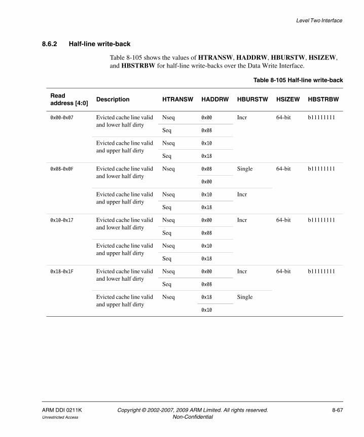
Level Two Interface
8.6.2 Half-line write-back
Table 8-105 shows the values of HTRANSW, HADDRW, HBURSTW, HSIZEW, and HBSTRBW for half-line write-backs over the Data Write Interface.
Table 8-105 Half-line write-back
Read address [4:0]
Description HTRANSW HADDRW HBURSTW HSIZEW HBSTRBW
0x00-0x07 Evicted cache line valid and lower half dirty
Nseq 0x00 Incr 64-bit b11111111
Seq 0x08
Evicted cache line valid and upper half dirty
Nseq 0x10
Seq 0x18
0x08-0x0F Evicted cache line valid and lower half dirty
Nseq 0x08 Single 64-bit b11111111
0x00
Evicted cache line valid and upper half dirty
Nseq 0x10 Incr
Seq 0x18
0x10-0x17 Evicted cache line valid and lower half dirty
Nseq 0x00 Incr 64-bit b11111111
Seq 0x08
Evicted cache line valid and upper half dirty
Nseq 0x10
Seq 0x18
0x18-0x1F Evicted cache line valid and lower half dirty
Nseq 0x00 Incr 64-bit b11111111
Seq 0x08
Evicted cache line valid and upper half dirty
Nseq 0x18 Single
0x10
ARM DDI 0211K Copyright © 2002-2007, 2009 ARM Limited. All rights reserved. 8-67Unrestricted Access Non-Confidential

Level Two Interface
8.6.3 Full-line write-back
Table 8-106 shows the values of HTRANSW, HADDRW, HBURSTW, HSIZEW, and HBSTRBW for full-line write-backs, evicted cache line valid and both halves dirty, over the Data Write Interface.
8.6.4 Store-exclusive
HPROT[5] and HRESP[2] on page 8-14 describes Store-exclusive.
Table 8-106 Full-line write-back
Read address [4:0] HTRANSW HADDRW HBURSTW HSIZEW HBSTRBW
0x00-0x07 Nseq 0x00 Incr4 64-bit b11111111
Seq 0x08
0x10
0x18
0x08-0x0F Nseq 0x08 Wrap4 64-bit b11111111
Seq 0x10
0x18
0x00
0x10-0x17 Nseq 0x10 Wrap4 64-bit b11111111
Seq 0x18
0x00
0x08
0x18-0x1F Nseq 0x18 Wrap4 64-bit b11111111
Seq 0x00
Seq 0x08
Seq 0x10
8-68 Copyright © 2002-2007, 2009 ARM Limited. All rights reserved. ARM DDI 0211KNon-Confidential Unrestricted Access
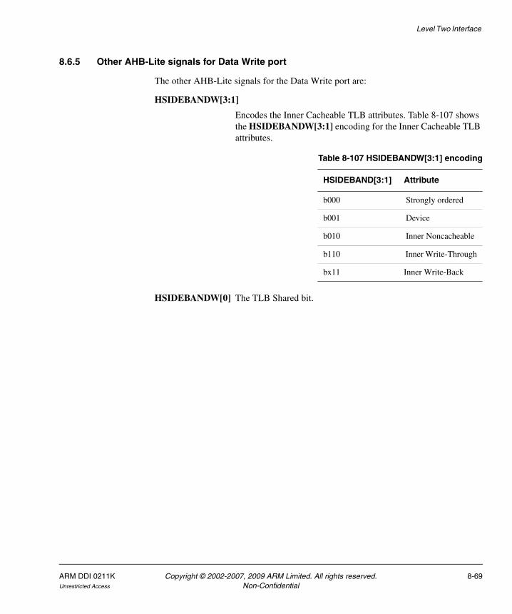
Level Two Interface
8.6.5 Other AHB-Lite signals for Data Write port
The other AHB-Lite signals for the Data Write port are:
HSIDEBANDW[3:1]
Encodes the Inner Cacheable TLB attributes. Table 8-107 shows the HSIDEBANDW[3:1] encoding for the Inner Cacheable TLB attributes.
HSIDEBANDW[0] The TLB Shared bit.
Table 8-107 HSIDEBANDW[3:1] encoding
HSIDEBAND[3:1] Attribute
b000 Strongly ordered
b001 Device
b010 Inner Noncacheable
b110 Inner Write-Through
bx11 Inner Write-Back
ARM DDI 0211K Copyright © 2002-2007, 2009 ARM Limited. All rights reserved. 8-69Unrestricted Access Non-Confidential

Level Two Interface
8.7 DMA Interface AHB-Lite transfers
AHB-Lite reads or writes over the DMA Interface use the standard AHB-Lite signals. The accesses also use the following AHB-Lite signals:
HBURSTD[2:0]
Statically set to Single. Only single transfers are supported.
HTRANSD[1:0]
Normally set to Idle, set to Nonseq to start a transfer.
HRESPD[0] There is only one response because Retry and Split are not supported.
HUNALIGND
Set if an unaligned transfer is to be carried out.
HBSTRBD[7:0]
One byte lane for each byte in the 64-bit word to be transferred. Each bit is set to indicate that the corresponding byte lane in HRDATAD and HWDATAD is in use.
Note When the stride is greater than the transaction size and more than one of
these transactions falls within a 64-bit transfer, any unaligned access settings of bits [7:0] can be generated within HBSTRBD.
HSIZED[2:0]
Indicates the transfer size, 8, 16, 32, or 64 bits.
HPROTD[4:2]
These bits encode the memory region attributes. Table 8-108 shows the HPROTD[4:2] encodings for the memory region attributes.
Table 8-108 HPROTD[4:2] encoding
HPROTD[4:2] Memory region attribute
b000 Strongly Ordered
b001 Device
b010 Outer Noncacheable
8-70 Copyright © 2002-2007, 2009 ARM Limited. All rights reserved. ARM DDI 0211KNon-Confidential Unrestricted Access

Level Two Interface
HPROTD[1] Indicates whether the transfer type is privileged or User. Usually the transfer type corresponds to the CPSR state of the processor, but a processor in a privileged mode can emulate User mode DMA accesses, see the description of the UM bit in c11, DMA Control Registers on page 3-141. Table 8-109 shows the HPROTD[1] encoding for the transfer.
HPROTD[0] Indicates that the transfer is an opcode fetch or data access. Table 8-109 shows the HPROTD[0] encoding for the transfer.
b110 Outer Write-Through, No Allocate on Write
b111 Outer Write-Back, No Allocate on Write
b011 Outer Write-Back, Write Allocate
Table 8-109 HPROTD[1] encoding
HPROTD[1] Transfer type
0 User
1 Privileged
Table 8-110 HPROTD[0] encoding
HPROTD[0] Attribute
0 Instruction
1 Data
Table 8-108 HPROTD[4:2] encoding (continued)
HPROTD[4:2] Memory region attribute
ARM DDI 0211K Copyright © 2002-2007, 2009 ARM Limited. All rights reserved. 8-71Unrestricted Access Non-Confidential

Level Two Interface
HSIDEBANDD[3:1]
Encodes the Inner Cacheable TLB attributes. Table 8-111 shows the HSIDEBANDD[3:1] encoding for the Inner Cacheable TLB attributes.
HSIDEBANDD[0]
Set if the addressed memory region is Shared.
Table 8-111 HSIDEBANDD[3:1] encoding
HSIDEBANDD[3:1] Attribute
b000 Strongly ordered
b001 Device
b010 Inner Noncacheable
b110 Inner Write-Through, No Allocate on Write
b111 Inner Write-Back, No Allocate on Write
b011 Inner Write-Back, Write Allocate
8-72 Copyright © 2002-2007, 2009 ARM Limited. All rights reserved. ARM DDI 0211KNon-Confidential Unrestricted Access

Level Two Interface
8.8 Peripheral Interface AHB-Lite transfers
The tables in this section describe the Peripheral Interface behavior for reads and writes for the following interface signals:
• HTRANSP[1:0]• HADDRP[31:0]• HBSTRBP[3:0]• HBURSTP[2:0]• HSIZEP[2:0].
See Other AHB-Lite signals for Peripheral Interface reads and writes on page 8-74 for details of the other AHB-Lite signals.
8.8.1 Reads and writes
Table 8-112 shows the values of HTRANSP, HADDRP, HBSTRBP, HBURSTP, and HSIZEP for example Peripheral Interface reads and writes.
Table 8-112 Example Peripheral Interface reads and writes
Example transfer (read or write) HTRANSP HADDRP HBSTRBP HBURSTP HSIZEP
Words 0-7 Nseq 0x00 b1111 Incr Word
Seq 0x04 b1111
Nseq 0x08 b1111
Seq 0x0C b1111
Nseq 0x10 b1111
Seq 0x14 b1111
Nseq 0x18 b1111
Seq 0x1C b1111
Words 0-3 Nseq 0x00 b1111 Incr Word
Seq 0x04 b1111
Nseq 0x08 b1111
Seq 0x0C b1111
ARM DDI 0211K Copyright © 2002-2007, 2009 ARM Limited. All rights reserved. 8-73Unrestricted Access Non-Confidential

Level Two Interface
8.8.2 Other AHB-Lite signals for Peripheral Interface reads and writes
The other AHB-Lite signals used in the Peripheral Interface are:
HWRITEP When HIGH indicates a write transfer, when LOW indicates a read.
HPROTP[4:0] HPROTP[4:2] encodes the memory region attributes. Table 8-113 shows the HPROTP[4:2] encoding for the memory region attributes.
Words 0-2 Nseq 0x00 b1111 Incr Word
Seq 0x04 b1111
Nseq 0x08 b1111
Words 0-1 Nseq 0x00 b1111 Incr Word
Seq 0x04 b1111
Word 2 Nseq 0x08 b1111 Single Word
Word 0, bytes 0 and 1 Nseq 0x00 b0011 Single Halfword
Word 1, bytes 2 and 3 Nseq 0x06 b1100 Single Halfword
Word 2, byte 3 Nseq 0x0B b1000 Single Byte
Table 8-112 Example Peripheral Interface reads and writes (continued)
Example transfer (read or write) HTRANSP HADDRP HBSTRBP HBURSTP HSIZEP
Table 8-113 HPROTP[4:2] encoding
HPROTP[4:2] Memory region attribute
b000 Strongly Ordered
b001 Device
b010 Outer Noncacheable
b110 Outer Write-Through, No Allocate on Write
b111 Outer Write-Back, No Allocate on Write
b011 Outer Write-Back, Write Allocate
8-74 Copyright © 2002-2007, 2009 ARM Limited. All rights reserved. ARM DDI 0211KNon-Confidential Unrestricted Access

Level Two Interface
HPROTP[1] encodes the CPSR state. Table 8-114 shows the HPROTP[1] encoding for the CPSR state.
HPROTP[0] statically 1 indicating a data access.
HSIDEBANDP[4:0]
Statically set to b0010 to indicate a Non-Shared Device access.
Table 8-114 HPROTP[1] encoding
HPROTP[1] CPSR state
0 User mode access
1 Privileged mode access
ARM DDI 0211K Copyright © 2002-2007, 2009 ARM Limited. All rights reserved. 8-75Unrestricted Access Non-Confidential

Level Two Interface
8.9 AHB-Lite
AHB-Lite is a subset of the full AHB specification for use in designs where only a single bus master is used. This can either be a simple single-master system, or a multi-layer AHB-Lite system where there is only one AHB master per layer.
Figure 8-6 shows a block diagram of a single-master system.
Figure 8-6 AHB-Lite single-master system
AHB-Lite simplifies the AHB specification by removing the protocol required for multiple bus masters, which includes the Request or Grant protocol to the arbiter and the Split or Retry responses from slaves.
Masters designed to the AHB-Lite interface specification are significantly simpler in terms of interface design, than a full AHB master. AHB-Lite enables faster design and verification of these masters, and you can add a standard off-the-shelf bus mastering wrapper to convert an AHB-Lite master for use in a full AHB system.
Any master that is already designed to the full AHB specification can be used in an AHB-Lite system with no modification.
The majority of AHB slaves can be used interchangeably in either an AHB or AHB-Lite system. This is because AHB slaves that do not use either the Split or Retry response are automatically compatible with both the full AHB and the AHB-Lite specification. It is only existing AHB slaves that do use Split or Retry responses that require you to use an additional standard off-the-shelf wrapper in your AHB-Lite system.
Any slave designed for use in an AHB-Lite system works in both a full AHB and an AHB-Lite design.
Slave#1
Slave#2
Slave#3
Master
8-76 Copyright © 2002-2007, 2009 ARM Limited. All rights reserved. ARM DDI 0211KNon-Confidential Unrestricted Access
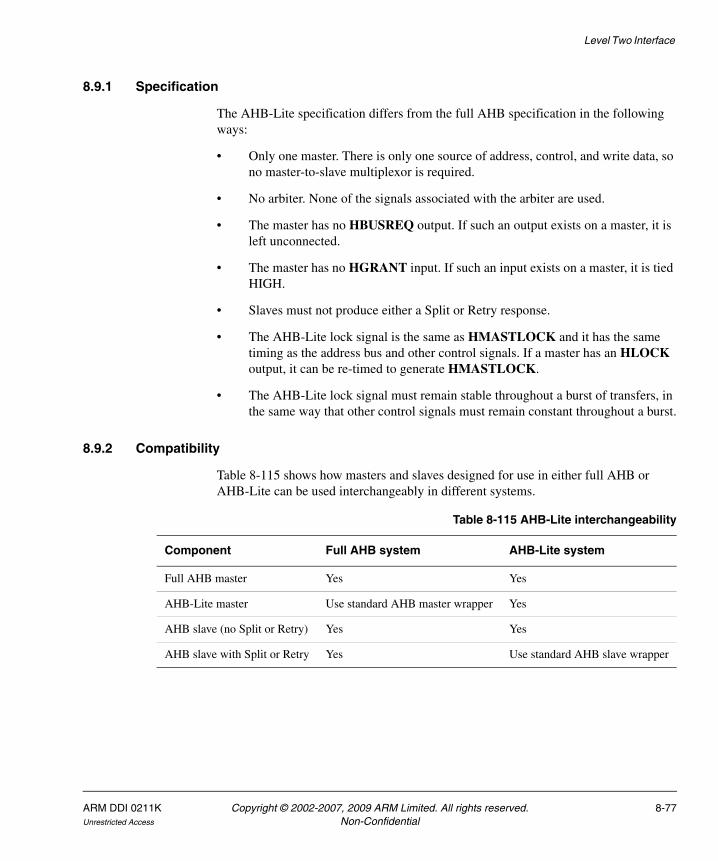
Level Two Interface
8.9.1 Specification
The AHB-Lite specification differs from the full AHB specification in the following ways:
• Only one master. There is only one source of address, control, and write data, so no master-to-slave multiplexor is required.
• No arbiter. None of the signals associated with the arbiter are used.
• The master has no HBUSREQ output. If such an output exists on a master, it is left unconnected.
• The master has no HGRANT input. If such an input exists on a master, it is tied HIGH.
• Slaves must not produce either a Split or Retry response.
• The AHB-Lite lock signal is the same as HMASTLOCK and it has the same timing as the address bus and other control signals. If a master has an HLOCK output, it can be re-timed to generate HMASTLOCK.
• The AHB-Lite lock signal must remain stable throughout a burst of transfers, in the same way that other control signals must remain constant throughout a burst.
8.9.2 Compatibility
Table 8-115 shows how masters and slaves designed for use in either full AHB or AHB-Lite can be used interchangeably in different systems.
Table 8-115 AHB-Lite interchangeability
Component Full AHB system AHB-Lite system
Full AHB master Yes Yes
AHB-Lite master Use standard AHB master wrapper Yes
AHB slave (no Split or Retry) Yes Yes
AHB slave with Split or Retry Yes Use standard AHB slave wrapper
ARM DDI 0211K Copyright © 2002-2007, 2009 ARM Limited. All rights reserved. 8-77Unrestricted Access Non-Confidential

Level Two Interface
8.9.3 AHB-Lite master interface
An AHB-Lite master has the same signal interface as a full AHB bus master, except that it does not support HBUSREQx and HGRANTx.
The lock functionality is still required because the master might be performing a transfer to a multi-interface slave. The slave must be given an indication that no other transfer must occur to the slave when the master requires locked access.
An AHB-Lite master is not required to support either the Split or Retry response and only the Okay and Error responses are required, so the AHB-Lite master interface does not require the HRESP[1] input.
8.9.4 AHB-Lite advantages
The advantage of using the AHB-Lite protocol is that the bus master does not have to support the following cases:
• Losing ownership of the bus. The clock enable for the master can be derived from the HREADY signal on the bus.
• Early terminated bursts. There is no requirement for the master to rebuild a burst due to early termination, because the master always has access to the bus.
• Split or Retry transfer responses. There is no requirement for the master to retain the address of the last transfer to be able to restart a previous transfer.
8.9.5 AHB-Lite conversion to full AHB
A standard wrapper is available to convert an AHB-Lite master to make it a full AHB master. This wrapper adds support for the features described above.
Because the AHB-Lite master has no bus request signal available, the wrapper generates this directly from the HTRANS signals.
8.9.6 AHB-Lite slaves
AHB slaves that do not use either the Split or Retry response can be used in either a full AHB or AHB-Lite system.
You can use any slave that does use Split or Retry responses in an AHB-Lite system by adding a standard wrapper. This wrapper provides the ability to store the previous transfer in the case of a Split or Retry response and restart the transfer when appropriate. This wrapper is very similar to that required to convert an AHB-Lite master for use in a full AHB system.
8-78 Copyright © 2002-2007, 2009 ARM Limited. All rights reserved. ARM DDI 0211KNon-Confidential Unrestricted Access

Level Two Interface
For compatibility with Multi-layer AHB, it is required that all AHB-Lite slaves still retain support for early terminated bursts.
8.9.7 Block diagram
Figure 8-7 shows a more detailed block diagram, including decoder and slave-to-master multiplexor connections.
Figure 8-7 AHB-Lite block diagram
Slave #2
Slave #3
Slave #1MasterHSELHADDRHWDATAHRDATA
HADDRHWDATAHRDATA
Decoder
Read data/response mux
HSELHADDRHWDATAHRDATA
HSELHADDRHWDATAHRDATA
ARM DDI 0211K Copyright © 2002-2007, 2009 ARM Limited. All rights reserved. 8-79Unrestricted Access Non-Confidential

Level Two Interface
8-80 Copyright © 2002-2007, 2009 ARM Limited. All rights reserved. ARM DDI 0211KNon-Confidential Unrestricted Access

Chapter 9 Clocking and Resets
This chapter describes the clocking and reset options available for ARM1136JF-S processors. It contains the following sections:
• Clocking on page 9-2
• Reset on page 9-6
• Reset modes on page 9-7.
ARM DDI 0211K Copyright © 2002-2007, 2009 ARM Limited. All rights reserved. 9-1Unrestricted Access Non-Confidential

Clocking and Resets
9.1 Clocking
The ARM1136JF-S processor has six functional clock inputs. These are paired into three clock domains. Externally to ARM1136JF-S, you must connect together CLKIN and FREECLKIN. The same is true of:
• HCLKIRW and FREEHCLKIRW• HCLKPD and FREEHCLKPD.
For information on how the clock domains are implemented see the ARM1136JF-S and ARM1136J-S Implementation Guide.
For the purposes of this chapter, you can ignore FREECLKIN, FREEHCLKIRW, and FREEHCLKPD clock domains. Table 9-1 shows the logical clock domains.
All clocks can be stopped indefinitely without loss of state.
You can preconfigure the ARM1136JF-S processor so that each AHB interface clock domain operates synchronously or asynchronously to the core clock domain.
9.1.1 Synchronous clocking
Synchronous clocking enables you to reduce the read and write latency, by removing the synchronization register in the external request path. However, the integer relationship of the clocks means it might not be possible to get the maximum performance from the core because of constraints placed on the bus frequency by components such as SDRAM controllers. With synchronous clocking it is not possible to run the core slower than the bus clocks.
Table 9-1 Clock domains
Logical blocks Clock Domain
Core CLKIN Core
Peripheral port DMA port HCLKPD PD
Instruction Fetch port
Data Read port
Data Write port
HCLKIRW IRW
9-2 Copyright © 2002-2007, 2009 ARM Limited. All rights reserved. ARM DDI 0211KNon-Confidential Unrestricted Access

Clocking and Resets
9.1.2 Asynchronous clocking
The main benefit of asynchronous clocking is that the core performance can be maximized, while running the buses at fixed system frequencies. Additionally, in sleep-mode situations when the core is not required to do much work, the core frequency can be lowered to reduce power consumption.
For low-power operation, if the ARM1136JF-S processor is configured asynchronously, it can be operated with the core clock slower than the bus clocks. See Chapter 10 Power Control for details of other aspects of power management.
9.1.3 Synchronization
For each AHB clock domain the ARM1136JF-S processor provides an AHB clock and two control inputs that you can use to configure synchronous or asynchronous operation, see Table 9-2.
These are state inputs. If they are tied HIGH they select a bypass path for every synchronization register, enabling synchronous operation.
Figure 9-1 on page 9-4 shows the synchronization between AHB and core clock domains.
Table 9-2 AHB clock domain control signals
Clock domain Control signals
IRW SYNCENIRW
HSYNCENIRW
PD SYNCENPD
HSYNCENPD
ARM DDI 0211K Copyright © 2002-2007, 2009 ARM Limited. All rights reserved. 9-3Unrestricted Access Non-Confidential

Clocking and Resets
Figure 9-1 Synchronization between AHB and core clock domains
Figure 9-2 shows the synchronization between core clock and AHB clock domains.
Figure 9-2 Synchronization between core and AHB clock domains
There are two synchronizer control signals per port to provide a clean static-timing view of the interface. Logically these must be held at the same level.
1
0
HRESETIRWn
HCLKIRWEN
HCLKIRW
EN
HCLKIRW
CLKIN
HCLKIRW domainCLKIN domain Synchronization
HCLKIRW
ARM1136 processor SoC
HSYNCENIRW
1
0
HCLKIRWEN
CLKIN
EN
HCLKIRW
Synchronization
CLKINSYNCENIRW
ARM1136 processorSoC
HCLKIRW domain CLKIN domain
nRST
nRESET
CLKIN
nRST
9-4 Copyright © 2002-2007, 2009 ARM Limited. All rights reserved. ARM DDI 0211KNon-Confidential Unrestricted Access

Clocking and Resets
For a given AHB clock domain, if synchronous operation is selected then the clock inputs for that domain must be connected to the same logical input as CLKIN. In this case, the AHB-Lite interfaces in the given clock domain can run at n:1 (AHB:Core) ratio to CLKIN using the enable signals, see Table 9-3.
9.1.4 Read latency penalty for synchronous operation
The nonsequential noncacheable read-latency for synchronous 1:1 clocking with zero-wait-state AHB is a six-cycle penalty over a cache hit on the data side (for a cache hit, data is returned in the DC2 cycle), and a five-cycle penalty over a cache hit on the instruction side.
In the first cycle after the data cache miss, a read-after-write hazard check is performed against the contents of the write buffer. This prevents stalling while waiting for the write buffer to drain. Following that, a request is made to the AHB-Lite interface, and subsequently a transfer is started on the AHB. In the next cycle data is returned to the AHB-Lite interface, from where it is returned first to the level one clock domain before being forwarded to the core. This is shown in Figure 9-3.
Figure 9-3 Read latency for synchronous 1:1 clocking
The same sequence appears on the instruction side, except that there is less to do in the equivalent RAW cycle.
Table 9-3 Synchronous mode clock enable signals
Domain AHB port Enable signals
IRW Instruction Fetch
Data Read, Data Write
HCLKIRWEN
PD DMA HCLKDEN
Peripheral HCLKPEN
DC1 DC2 RAW L2Req HTRANSR HRDATAR Data to L1Data to
LSU
Fe1 Fe2 L2Req HTRANSI HRDATAI Data to L1 Data to PU DC1
ARM DDI 0211K Copyright © 2002-2007, 2009 ARM Limited. All rights reserved. 9-5Unrestricted Access Non-Confidential

Clocking and Resets
9.2 Reset
The ARM1136JF-S processor has the following reset inputs:
HRESETPDn The HRESETPDn is the reset signal for the PD domain.
HRESETIRWn The HRESETIRWn is the reset signal for the IRW domain.
nRESETIN The nRESETIN signal is the main processor reset that initializes the majority of the ARM1136JF-S logic.
DBGnTRST The DBGnTRST signal is the DBGTAP reset. It does not reset the debug logic.
nPORESETIN The nPORESETIN signal is the power-on reset that initializes the CP14 debug logic. See CP14 registers reset on page 13-43 for details.
Note Although nPORESETIN does not reset the TAP controller,
DBGTDO is held low when nPORESETIN is asserted. This means that you must deassert nPORESETIN if you want to use any JTAG functionality, including JTAG bypass.
All of these are active LOW signals that reset logic in the ARM1136JF-S processor. You must take care when designing the logic that drives these reset signals.
Inside the ARM1136JF-S processor, each reset input is synchronized to the appropriate clock signal. You do not need to synchronize the clock signals.
9-6 Copyright © 2002-2007, 2009 ARM Limited. All rights reserved. ARM DDI 0211KNon-Confidential Unrestricted Access

Clocking and Resets
9.3 Reset modes
The reset signals present in the ARM1136JF-S processor design to enable you to reset different parts of the design independently. The reset signals, and the combinations and possible applications that you can use them in, are shown in Table 9-4.
Note If nRESETIN is set to 1 and nPORESETIN is set to 0 the behavior is architecturally Unpredictable. However, if nRESETIN and nPORESETIN are driven from the same source, the reset synchronization in the ARM1136JF-S processor ensures predictable behavior when the reset source is deasserted.
9.3.1 Power-on reset
You must apply power-on or cold reset to the ARM1136JF-S processor when power is first applied to the system. In the case of power-on reset, the leading (falling) edge of the reset signals, nRESETIN, HRESETPDn, HRESETIRWn and nPORESETIN, does not have to be synchronous to CLKIN. Because each reset signal is synchronized within the ARM1136JF-S processor, you do not have to synchronize these signals. Figure 9-4 on page 9-8 shows the application of power-on reset.
Table 9-4 Reset modes
Reset modenRESETIN HRESETPDn HRESETIRWn
DBGnTRST nPORESETIN Application
Power-on reset 0 x 0 Reset at power up, full system reset. Hard reset or cold reset.
Processor reset 0 x 1 Reset of processor core only, watchdog reset. Soft reset or warm reset.
DBGTAP reset 1 0 1 Reset of DBGTAP logic, without affecting any other part of the system.
Normal 1 1 1 No reset. Normal run mode.
ARM DDI 0211K Copyright © 2002-2007, 2009 ARM Limited. All rights reserved. 9-7Unrestricted Access Non-Confidential

Clocking and Resets
Figure 9-4 Power-on reset
To ensure correct reset behavior you must assert the reset signals for at least three CLKIN cycles. Adopting a three-cycle reset eases the integration of other ARM parts into the system, for example, ARM9TDMI-based designs.
You do not need to assert DBGnTRST on power-up.
9.3.2 CP14 debug logic
Because the nPORESETIN signal is synchronized within the ARM1136JF-S processor, you do not have to synchronize this signal.
9.3.3 Processor reset, nRESETIN
A processor reset, caused by asserting nRESETIN, initializes the majority of the ARM1136JF-S processor, excluding the PD and IRW clock domains, the ARM1136JF-S DBGTAP controller and the EmbeddedICE-RT logic.
Note To perform a warm reset of the ARM1136JF-S processor you must assert nRESETIN, HRESETPDn and HRESETIRWn. Although a separate reset is needed for each clock domain, you must always reset the AHB interfaces (the PD and IRW clock domains) when you reset the ARM1136JF-S processor core. See Clocking on page 9-2 for a description of the ARM1136JF-S processor clock domains.
A processor warm reset is typically used for resetting a system that has been operating for some time, for example, watchdog reset.
Because the nRESETIN signal is synchronized within the ARM1136JF-S processor, you do not have to synchronize this signal.
CLKIN
nRESETINHRESETPDn
HRESETIRWn
nPORESETIN
9-8 Copyright © 2002-2007, 2009 ARM Limited. All rights reserved. ARM DDI 0211KNon-Confidential Unrestricted Access

Clocking and Resets
9.3.4 HRESETPDn reset
The HRESETPDn signal is an active low reset for the PD clock domain of the ARM1136JF-S processor. It is synchronized to the HCLKPD clock inside the ARM1136JF-S processor, so you do not have to synchronize this signal.
See Clocking on page 9-2 for a description of the ARM1136JF-S processor clock domains.
9.3.5 HRESETIRWn reset
The HRESETIRWn signal is an active low reset for the IRW clock domain of the ARM1136JF-S processor. It is synchronized to the HCLKIRW clock inside the ARM1136JF-S processor, so you do not have to synchronize this signal.
See Clocking on page 9-2 for a description of the ARM1136JF-S processor clock domains.
Note In practice, the ARM1136JF-S processor core and AHB interface (PD and IRW) clock domains must always be reset at the same time.
9.3.6 DBGTAP reset
DBGTAP reset initializes the state of the ARM1136JF-S DBGTAP controller. DBGTAP reset is typically used by the RealView™ ICE module for hot connection of a debugger to a system.
DBGTAP reset enables initialization of the DBGTAP controller without affecting the normal operation of the ARM1136JF-S processor.
Note Although nPORESETIN does not reset the TAP controller, DBGTDO is held low when nPORESETIN is asserted. This means that if you want to use any JTAG functionality, including JTAG bypass, you must deassert nPORESETIN.
Because the DBGnTRST signal is synchronized within the ARM1136JF-S processor, you do not have to synchronize this signal.
9.3.7 Normal operation
During normal operation, none of the reset signals is asserted. However, if the DBGTAP port is not being used, the value of DBGnTRST does not matter.
ARM DDI 0211K Copyright © 2002-2007, 2009 ARM Limited. All rights reserved. 9-9Unrestricted Access Non-Confidential

Clocking and Resets
9-10 Copyright © 2002-2007, 2009 ARM Limited. All rights reserved. ARM DDI 0211KNon-Confidential Unrestricted Access

Chapter 10 Power Control
This chapter describes the ARM1136JF-S power control functions. It contains the following sections:
• About power control on page 10-2
• Power management on page 10-3.
ARM DDI 0211K Copyright © 2002-2007, 2009 ARM Limited. All rights reserved. 10-1Unrestricted Access Non-Confidential

Power Control
10.1 About power control
The features of the ARM1136JF-S processor that improve energy efficiency include:
• accurate branch and return prediction, reducing the number of incorrect instruction fetch and decode operations
• use of physically addressed caches, which reduces the number of cache flushes and refills, saving energy in the system
• the use of MicroTLBs reduces the power consumed in translation and protection look-ups each cycle
• the caches use sequential access information to reduce the number of accesses to the TagRAMs and to unwanted Data RAMs.
In the ARM1136JF-S processor extensive use is also made of gated clocks and gates to disable inputs to unused functional blocks. Only the logic actively in use to perform a calculation consumes any dynamic power.
10-2 Copyright © 2002-2007, 2009 ARM Limited. All rights reserved. ARM DDI 0211KNon-Confidential Unrestricted Access

Power Control
10.2 Power management
ARM1136JF-S processors support three levels of power management:
• Run mode
• Standby mode
• Shutdown mode on page 10-4
• plus partial support for a fourth level, Dormant mode on page 10-4.
10.2.1 Run mode
Run mode is the normal mode of operation in which all of the functionality of the core is available.
10.2.2 Standby mode
Standby mode disables most of the clocks of the device, while keeping the design powered up. This reduces the power drawn to the static leakage current, plus a tiny clock power overhead required to enable the device to wake up from the standby state.
The transition from Standby mode to Run mode is caused by one of:
• the arrival of an interrupt, whether masked or unmasked
• a debug request, when debug is enabled
• a reset.
The debug request can be generated by an externally generated debug request, using the EDBGRQ pin on the ARM1136JF-S processor, or from a Debug Halt instruction issued to the ARM1136JF-S processor through the debug scan chains. Entry into Standby Mode is performed by executing the Wait For Interrupt CP15 operation. To ensure that the memory system is not affected by the entry into the Standby state, the following operations are performed:
• A Drain Write Buffer operation ensures that all explicit memory accesses occurring in program order before the Wait For Interrupt have completed. This avoids any possible deadlocks that could be caused in a system where memory access triggers or enables an interrupt that the core is waiting for. This might require some TLB page table walks to take place as well.
• The DMA continues running during a Wait For Interrupt and any queued DMA operations are executed as normal. This enables an application using the DMA to set up the DMA to signal an interrupt once the DMA has completed, and then for the application to issue a Wait For Interrupt instruction. The degree of power-saving while the DMA is running is less than is the case if the DMA is not running.
ARM DDI 0211K Copyright © 2002-2007, 2009 ARM Limited. All rights reserved. 10-3Unrestricted Access Non-Confidential

Power Control
• Any other memory accesses that have been started at the time that the Wait For Interrupt instruction is executed are completed as normal. This ensures that the level two memory system does not see any disruption caused by the Wait For Interrupt.
• The debug channel remains active throughout a Wait For Interrupt. You must tie the DBGTCKEN signal to VSS to avoid clocking unnecessary logic to ensure best power-saving when not using debug.
Systems using the VIC interface must ensure that the VIC is not masking any interrupts that are required for restarting the ARM1136JF-S processor when in this mode of operation.
After the processor clocks have been stopped the signal STANDBYWFI is asserted to indicate that the ARM1136JF-S processor is in Standby mode.
10.2.3 Shutdown mode
Shutdown mode has the entire device powered down, and you must externally save all state, including cache and TCM state. The processor is returned to Run mode by the assertion of Reset. This state saving is performed with interrupts disabled, and finishes with a Drain Write Buffer operation. When all the state of the ARM1136JF-S processor is saved the ARM1136JF-S processor executes a Wait For Interrupt instruction. The signal STANDBYWFI is asserted to indicate that the processor can enter Shutdown mode.
10.2.4 Dormant mode
Dormant mode enables the core to be powered down, leaving the caches and the Tightly-Coupled Memory (TCM) powered up and maintaining their state.
The software visibility of the Valid bits is provided to enable an implementation to be extended for Dormant mode, but some hardware modification of the RAM blocks during implementation to include an input clamp is required for the full implementation of Dormant mode.
Considerations for Dormant mode
Dormant mode is partially supported on ARM1136JF-S processors, because care is required in implementing this on a standard synthesizable flow. The RAM blocks that are to remain powered up must be implemented on a separate power domain, and there is a requirement to clamp all of the inputs to the RAMs to a known logic level (with the chip enable being held inactive). This clamping is not implemented in gates as part of the default synthesis flow because it contributes to a tight critical path.
10-4 Copyright © 2002-2007, 2009 ARM Limited. All rights reserved. ARM DDI 0211KNon-Confidential Unrestricted Access

Power Control
Designers wanting to implement Dormant mode must add these clamps around the RAMs, either as explicit gates in the RAM power domain, or as pull-down transistors that clamp the values while the core is powered down.
The RAM blocks that must remain powered up during Dormant mode are:
• all Data RAMs associated with the cache and tightly-coupled memories
• all TagRAMs associated with the cache
• all Valid RAMs and Dirty RAMs associated with the cache.
The state of the Branch Target Address Cache is not maintained on entry into Dormant mode. Implementations of the ARM1136JF-S processor can optionally disable the RAMs associated with the Main TLB, so that a trade-off can be made between Dormant mode leakage power and the recovery time.
Before entering Dormant mode, the state of the ARM1136JF-S processor, excluding the contents of the RAMs that remain powered up in dormant mode, must be saved to external memory. These state saving operations must ensure that the following occur:
• All ARM registers, including CPSR and SPSR registers are saved.
• Any DMA operations in progress are stopped.
• All CP15 registers are saved, including the DMA state.
• All VFP registers are saved if the VFP contains defined state.
• Any locked entries in the Main TLB are saved.
• All debug-related state are saved.
• The Master Valid bits for the cache and SmartCache are saved. These are accessed using CP15 register c15 as described in c15, Cache and Main TLB Master Valid Registers on page 3-184.
• If the Main TLB is powered down on entry into the Dormant mode, then the Valid bits of the Main TLB are saved. These are accessed using CP15 register c15 as described in c15, Cache and Main TLB Master Valid Registers on page 3-184.
• A Drain Write Buffer instruction is executed to ensure that all state saving has been completed.
A Wait For Interrupt CP15 operation is then executed, enabling the signal STANDBYWFI to indicate that the ARM1136JF-S processor can enter Dormant mode.
• On entry into Dormant mode, the Reset signal to the ARM1136JF-S processor must be asserted by the external power control mechanism.
ARM DDI 0211K Copyright © 2002-2007, 2009 ARM Limited. All rights reserved. 10-5Unrestricted Access Non-Confidential

Power Control
Transition from Dormant state to Run state is triggered by the external power controller asserting Reset to the ARM1136JF-S processor until the power to the processor is restored. When power has been restored the core leaves reset and, by interrogating the external power control, can determine that the saved state must be restored.
10.2.5 Communication to the Power Management Controller
The Power Management Controller performs the powering up and powering down of the power domains of the processor. The Power Management Controller is a memory-mapped controller. The ARM1136JF-S processor accesses this controller using Strongly-Ordered accesses.
The STANDBYWFI signal can also be used to signal to the Power Management Controller that the ARM1136JF-S processor is ready to have its power state changed. STANDBYWFI is asserted in response to a Wait For Interrupt operation.
Note The Power Management Controller must not power down any of the processor power domains unless STANDBYWFI is asserted.
10-6 Copyright © 2002-2007, 2009 ARM Limited. All rights reserved. ARM DDI 0211KNon-Confidential Unrestricted Access

Chapter 11 Coprocessor Interface
This chapter describes the ARM1136JF-S coprocessor interface. It contains the following sections:
• About the coprocessor interface on page 11-2
• Coprocessor pipeline on page 11-3
• Token queue management on page 11-10
• Token queues on page 11-14
• Data transfer on page 11-18
• Operations on page 11-23
• Multiple coprocessors on page 11-27.
ARM DDI 0211K Copyright © 2002-2007, 2009 ARM Limited. All rights reserved. 11-1Unrestricted Access Non-Confidential

Coprocessor Interface
11.1 About the coprocessor interface
The ARM1136JF-S processor supports the connection of on-chip coprocessors through an external coprocessor interface. All types of coprocessor instruction are supported.
The ARM instruction set supports the connection of 16 coprocessors, numbered 0-15, to an ARM processor. In ARM1136JF-S processors, the following coprocessor numbers are reserved:
CP10 VFP control
CP11 VFP control
CP14 Debug and ETM control
CP15 System control.
You can use CP0-9, CP12, and CP13 for your own external coprocessors.
The ARM1136JF-S processor is designed to pass instructions to several coprocessors and exchange data with them. These coprocessors are intended to run in step with the core and are pipelined in a similar way to the core. Instructions are passed out of the Fetch stage of the core pipeline to the coprocessor and decoded. The decoded instruction is passed down its own pipeline. Coprocessor instructions can be canceled by the core if a condition code fails, or the entire coprocessor pipeline can be flushed in the event of a mispredicted branch. Load and store data are also required to pass between the core Logic Store Unit (LSU) and the coprocessor pipeline.
The coprocessor interface operates over a two-cycle delay. Any signal passing from the core to the coprocessor, or from the coprocessor to the core, is given a whole clock cycle to propagate from one to the other. This means that a signal crossing the interface is clocked out of a register on one side of the interface and clocked directly into another register on the other side. No combinatorial process must intervene. This constraint exists because the core and coprocessor can be placed a considerable distance apart and generous timing margins are necessary to cover signal propagation times. This delay in signal propagation makes it difficult to maintain pipeline synchronization, ruling out a tightly-coupled synchronization method.
ARM1136JF-S processors implement a token-based pipeline synchronization method that allows some slack between the two pipelines, while ensuring that the pipelines are correctly aligned for crucial transfers of information.
11-2 Copyright © 2002-2007, 2009 ARM Limited. All rights reserved. ARM DDI 0211KNon-Confidential Unrestricted Access

Coprocessor Interface
11.2 Coprocessor pipeline
The coprocessor interface achieves loose synchronization between the two pipelines by exchanging tokens from one pipeline to the other. These tokens pass down queues between the pipelines and can carry additional information. In most cases the primary purpose of the queue is to carry information about the instruction being processed, or to inform one pipeline of events occurring in the other.
Tokens are generated whenever a coprocessor instruction passes out of a pipeline stage associated with a queue into the next stage. These tokens are picked up by the partner stage in the other pipeline, and used to enable the corresponding instruction in that stage to move on. The movement of coprocessor instructions down each pipeline is matched exactly by the movement of tokens along the various queues that connect the pipelines.
If a pipeline stage has no associated queue, the instruction contained within it moves on in the normal way. The coprocessor interface is data-driven rather than control-driven.
11.2.1 Coprocessor instructions
Each coprocessor can only execute a subset of all possible coprocessor instructions. Coprocessors reject those instructions they cannot handle. Table 11-1 lists all the coprocessor instructions supported by ARM1136JF-S processors and gives a brief description of each. For more details of coprocessor instructions, see the ARM Architecture Reference Manual.
Table 11-1 Coprocessor instructions
InstructionData transfer
Vectored Description
CDP None No Processes information already held within the coprocessor
MRC Store No Transfers information from the coprocessor to the core registers
MCR Load No Transfers information from the core registers to the coprocessor
MRRC Store No Transfers information from the coprocessor to a pair of registers in the core
MCRR Load No Transfers information from a pair of registers in the core to the coprocessor
STC Store Yes Transfers information from the coprocessor to memory and might be iterated to transfer a vector
LDC Load Yes Transfers information from memory to the coprocessor and might be iterated to transfer a vector
ARM DDI 0211K Copyright © 2002-2007, 2009 ARM Limited. All rights reserved. 11-3Unrestricted Access Non-Confidential
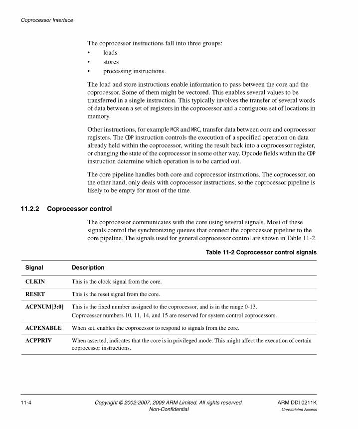
Coprocessor Interface
The coprocessor instructions fall into three groups:
• loads
• stores
• processing instructions.
The load and store instructions enable information to pass between the core and the coprocessor. Some of them might be vectored. This enables several values to be transferred in a single instruction. This typically involves the transfer of several words of data between a set of registers in the coprocessor and a contiguous set of locations in memory.
Other instructions, for example MCR and MRC, transfer data between core and coprocessor registers. The CDP instruction controls the execution of a specified operation on data already held within the coprocessor, writing the result back into a coprocessor register, or changing the state of the coprocessor in some other way. Opcode fields within the CDP instruction determine which operation is to be carried out.
The core pipeline handles both core and coprocessor instructions. The coprocessor, on the other hand, only deals with coprocessor instructions, so the coprocessor pipeline is likely to be empty for most of the time.
11.2.2 Coprocessor control
The coprocessor communicates with the core using several signals. Most of these signals control the synchronizing queues that connect the coprocessor pipeline to the core pipeline. The signals used for general coprocessor control are shown in Table 11-2.
Table 11-2 Coprocessor control signals
Signal Description
CLKIN This is the clock signal from the core.
RESET This is the reset signal from the core.
ACPNUM[3:0] This is the fixed number assigned to the coprocessor, and is in the range 0-13.
Coprocessor numbers 10, 11, 14, and 15 are reserved for system control coprocessors.
ACPENABLE When set, enables the coprocessor to respond to signals from the core.
ACPPRIV When asserted, indicates that the core is in privileged mode. This might affect the execution of certain coprocessor instructions.
11-4 Copyright © 2002-2007, 2009 ARM Limited. All rights reserved. ARM DDI 0211KNon-Confidential Unrestricted Access

Coprocessor Interface
11.2.3 Pipeline synchronization
Figure 11-1 shows an outline of the core and coprocessor pipelines and the synchronizing queues that communicate between them. Each queue is implemented as a very short First In First Out (FIFO) buffer.
No explicit flow control is required for the queues, because the pipeline lengths between the queues limits the number of items any queue can hold at any time. The geometry used means that only three slots are required in each queue.
The only status information required is a flag to indicate when the queue is empty. This is monitored by the receiving end of the queue, and determines if the associated pipeline stage can move on. Any information carried by the queue can also be read and acted upon at the same time.
Figure 11-1 Core and coprocessor pipelines
Figure 11-2 on page 11-6 provides a more detailed picture of the pipeline and the queues maintained by the coprocessor.
Fe2
Length
Core pipeline Coprocessor pipeline
De
Iss
Ex1
Ex2
Ex3
Wb
D
I
Ex1
Ex2
Ex3
Ex4
Ex5
Ex6
Instruction
LengthCancel
Accept
Finish
ARM DDI 0211K Copyright © 2002-2007, 2009 ARM Limited. All rights reserved. 11-5Unrestricted Access Non-Confidential

Coprocessor Interface
Figure 11-2 Coprocessor pipeline and queues
The instruction queue incorporates the instruction decoder and returns the length to the Ex1 stage of the core, using the length queue, which is maintained by the core. The coprocessor Issue stage sends a token to the core Ex2 stage through the accept queue, which is also maintained by the core. This token indicates to the core if the coprocessor is accepting the instruction in its Issue stage, or bouncing it.
The core can cancel an instruction currently in the coprocessor Ex1 stage by sending a signal with the token passed down the cancel queue. When a coprocessor instruction reads the Ex6 stage it might retire. How it retires depends on the instruction:
• Load instructions retire when they find load data available in the load data queue, see Loads on page 11-19
• Store instructions retire as soon as they leave the Ex1 stage, and are removed from the pipeline, see Stores on page 11-21
• CDP instructions retire when they read a token passed by the core down the finish queue.
Data transfer uses the load data and store data queues, which are shown in Figure 11-2 and explained in Data transfer on page 11-18.
I
Ex1
Ex2
Ex3
Ex4
Ex5
Ex6
Accept
Store data
D
Instruction
Length
Cancel
Load data
Finish
From core Fe2 stage
To core Fe1 stage
To LSU Add stage
From core Iss stage
To core Ex2 stage
From LSU Wbls stage
From core Wb stage
Decode stage
11-6 Copyright © 2002-2007, 2009 ARM Limited. All rights reserved. ARM DDI 0211KNon-Confidential Unrestricted Access

Coprocessor Interface
11.2.4 Pipeline control
The coprocessor pipeline is very similar to the core pipeline, but lacks the Fetch stages. Instructions are passed from the core directly into the Decode stage of the coprocessor pipeline, which takes the form of a FIFO queue.
The Decode stage then decodes the instruction, rejecting non-coprocessor instructions and any coprocessor instructions containing a non-matching coprocessor number.
The length of any vectored data transfer is also decided at this point and sent back to the core. The decoded instruction then passes into the Issue (I) stage. This stage decides if this particular instance of the instruction can be accepted. If it cannot, because it addresses a non-existent register, the instruction is bounced, informing the core that it cannot be accepted.
If the instruction is both valid and executable, it then passes down the execution pipeline, Ex1 to Ex6. At the bottom of the pipeline, in Ex6, the instruction waits for retirement, which it can do when it receives a matching token from another queue fed by the core.
Figure 11-3 shows the coprocessor pipeline, the main fields within each stage, and the main control signals. Each stage controls the flow of information from the previous stage in the pipeline by passing its Enable signal back. When a pipeline stage is not enabled, it cannot accept information from the previous stage.
Figure 11-3 Coprocessor pipeline
Decoded instruction Tag Full FlagsI stage control
Decoded instruction Tag Full FlagsEx1 stage control
Decoded instruction Tag Full FlagsEx2 stage control
Decoded instruction Tag Full FlagsEx6 stage control
Instruction queue and decoder
From core pipeline
I stage
Ex1 stage
Ex2 stage
Ex3 to Ex5 stages(not shown)
Ex6 stage
Enable
Enable
Enable
Enable
Stall I
Stall Ex1
Stall Ex6
Stall D
Ex3 to Ex5 stages are the same as the Ex2 stage
ARM DDI 0211K Copyright © 2002-2007, 2009 ARM Limited. All rights reserved. 11-7Unrestricted Access Non-Confidential

Coprocessor Interface
Each pipeline stage contains a decoded instruction, and a tag, plus a few status flags:
Full flag This flag is set whenever the pipeline stage contains an instruction.
Dead flag This flag is set to indicate that the instruction in the stage is a phantom. See Cancel operations on page 11-23.
Tail flag This flag is set to indicate that the instruction is the tail of an iterated instruction. See Loads on page 11-19.
There might also be other flags associated with the decoding of the instruction.
Each stage is controlled not only by its own state, but also by external signals and signals from the following state, as follows:
Stall This signal prevents the stage from accepting a new instruction or passing its own instruction on, and only affects the D, I, Ex1, and Ex6 stages.
Iterate This signal indicates that the instruction in the stage must be iterated in order to implement a multiple load or store and only applies to the Issue stage.
Enable This signal indicates that the next stage in the pipeline is ready to accept data from the current stage.
These signals are combined with the current state of the pipeline to determine if the stage can accept new data, and what the new state of the stage is going to be. Table 11-3 shows how the new state of the pipeline stage is derived.
Table 11-3 Pipeline stage update
Stall Enable input Iterate State Enable To next stage Remarks
0 0 X Empty 1 None Bubble closing
0 0 X Full 0 - Stalled by next stage
0 1 0 Empty 1 None Normal pipeline movement
0 1 0 Full 1 Current Normal pipeline movement
0 1 1 Empty - - Impossible
0 1 1 Full 0 Current Iteration (I stage only)
1 X X X 0 None Stalled (D, I, Ex1, and Ex6 only)
11-8 Copyright © 2002-2007, 2009 ARM Limited. All rights reserved. ARM DDI 0211KNon-Confidential Unrestricted Access
Coprocessor Interface
The Enable input comes from the next stage in the pipeline and indicates if data can be passed on. In general, if this signal is unasserted the pipeline stage cannot receive new data or pass on its own contents. However, if the pipeline stage is empty it can receive new data without passing any data on to the next stage. This is known as bubble closing, because it has the effect of filling up empty stages in the pipeline by enabling them to move on while lower stages are stalled.
11.2.5 Instruction tagging
It is sometimes necessary for the core to be able to identify instructions in the coprocessor pipeline. This is necessary for flushing (see Flush operations on page 11-25) so that the core can indicate to the coprocessor which instructions are to be flushed. The core therefore gives each instruction sent to the coprocessor a tag, which is drawn from a pool of values large enough so that all the tags in the pipeline at any moment are unique. Sixteen tags are sufficient to achieve this, requiring a four-bit tag field. Each time a tag is assigned to an instruction, the tag number is incremented modulo 16 to generate the next tag.
The flushing mechanism is simplified because successive coprocessor instructions have contiguous tags. The core manages this by only incrementing the tag number when the instruction passed to the coprocessor is a coprocessor instruction. This is done after sending the instruction, so the tag changes after a coprocessor instruction is sent, rather than before. It is not possible to increment the tag before sending the instruction because the core has not yet had time to decode the instruction to determine what kind of instruction it is. When the coprocessor Decode stage removes the non-coprocessor instructions, it is left with an instruction stream carrying contiguous tags.
The tags can also be used to verify that the sequence of tokens moving down the queues matches the sequence of instructions moving down the core and coprocessor pipelines.
11.2.6 Flush broadcast
If a branch has been mispredicted, it might be necessary for the core to flush both pipelines. Because this action potentially affects the entire pipeline, it is not passed across in a queue but is broadcast from the core to the coprocessor, subject to the same timing constraints as the queues. When the flush signal is received by the coprocessor, it causes the pipeline and the instruction queue to be cleared up to the instruction triggering the flush. This is explained in more detail in Flush operations on page 11-25.
ARM DDI 0211K Copyright © 2002-2007, 2009 ARM Limited. All rights reserved. 11-9Unrestricted Access Non-Confidential

Coprocessor Interface
11.3 Token queue management
The token queues, all of which are three slots long and function identically, are implemented as short FIFOs. An example implementation of the queues is described in:
• Queue implementation
• Queue modification
• Queue flushing on page 11-12.
11.3.1 Queue implementation
The queue FIFOs are implemented as three registers, with the current output selected by using multiplexors. Figure 11-4 shows this arrangement.
Figure 11-4 Token queue buffers
The queue consists of three registers, each of which is associated with a flag that indicates if the register contains valid data. New data are moved into the queue by being written into buffer A and continue to move along the queue if the next register is empty, or is about to become empty. If the queue is full, the oldest data, and therefore the first to be read from the queue, occupies buffer C and the newest occupies buffer A.
The multiplexors also select the current flag, which then indicates if the selected output is valid.
11.3.2 Queue modification
The queue is written to on each cycle. Buffer A accepts the data arriving at the interface, and the buffer A flag accepts the valid bit associated with the data. If the queue is not full, this results in no loss of data because the contents of buffer A are moved to buffer B during the same cycle.
Buffer AA
Buffer BB
Buffer CC
OutputV
Out
S1S0
0
10
1
Interconnect
11-10 Copyright © 2002-2007, 2009 ARM Limited. All rights reserved. ARM DDI 0211KNon-Confidential Unrestricted Access

Coprocessor Interface
If the queue is full, then the loading of buffer A is inhibited to prevent loss of data. In any case, no valid data is presented by the interface when the queue is full, so no data loss ensues.
The state of the three buffer flags is used to decide which buffer provides the queue output during each cycle. The output is always provided by the buffer containing the oldest data. This is buffer C if it is full, or buffer B or, if that is empty, buffer A.
A simple priority encoder, looking at the three flags, can supply the correct multiplexor select signals. The state of the three flags can also determine how data are moved from one buffer to another in the queue. Table 11-4 shows how the three flags are decoded.
New data can be moved into buffer A, provided the queue is not full, even if its flag is set, because the current contents of buffer A are moved to buffer B.
When the queue is read, the flag associated with the buffer providing the information must be cleared. This operation can be combined with an input operation so that the buffer is overwritten at the end of the cycle during which it provides the queue output. This can be implemented by using the read enable signal to mask the flag of the selected stage, making it available for input. Figure 11-5 on page 11-12 shows reading and writing a queue.
Table 11-4 Addressing of queue buffers
Flag C Flag B Flag A S1 S0 Remarks
0 0 0 X X Queue is empty
0 0 1 0 0 B = A
0 1 0 0 1 C = B
0 1 1 0 1 C = B, B = A
1 0 0 1 X -
1 0 1 1 X B = A
1 1 0 1 X -
1 1 1 1 X Queue is full. Input inhibited
ARM DDI 0211K Copyright © 2002-2007, 2009 ARM Limited. All rights reserved. 11-11Unrestricted Access Non-Confidential

Coprocessor Interface
Figure 11-5 Queue reading and writing
Four valid inputs (labeled One, Two, Three, and Four) are written into the queue, and are clocked into buffer A as they arrive. Figure 11-5 shows how these inputs are clocked from buffer to buffer until the first input reaches buffer C. At this point a read from the queue is required. Because buffer C is full, it is chosen to supply the data. Because it is being read, it is free to accept more input, and so it receives the value Two from buffer B, which in turn receives the value Three from buffer A. Because buffer A is being emptied by writing to buffer B, it can accept the value Four from the input.
11.3.3 Queue flushing
When the coprocessor pipeline is flushed, in response to a command from the core, some of the queues might also have to be flushed. There are two possible ways of flushing the queue:
• the entire queue is cleared
• the queue is flushed from a selected buffer, along with all data in the queue newer than the data in the selected buffer.
The method used depends on the point at which flushing begins in the coprocessor pipeline. See Flush operations on page 11-25 for more details.
A flush command has associated with it a tag value that indicates where the queue flushing starts. This is matched with the tag carried by every instruction.
One Two Three Four
One Two Three
One Two
One One One Two
Buffer A
Flag A
Buffer B
Flag B
Buffer C
Flag C
Read queue
Output
Valid input
11-12 Copyright © 2002-2007, 2009 ARM Limited. All rights reserved. ARM DDI 0211KNon-Confidential Unrestricted Access

Coprocessor Interface
If the queue is to be flushed from a selected buffer, the buffer is chosen by looking for a matching tag. When this is found, the flag associated with that buffer is cleared, and every flag newer than the selected one is also cleared. Figure 11-6 shows queue flushing.
Figure 11-6 Queue flushing
Each buffer in the queue has a tag comparator associated with it. The flush tag is presented to each comparator, to be compared with the tag belonging to each valid instruction held in the queue. The flush tag is compared with each tag in the queue. If the flush tag is the same as, or older than, any tag then that queue entry has its Full flag cleared. This indicates that it is empty. A less-than-or-equal-to comparison is used to identify tags that are to be flushed. If a tag in the pipeline later than the queue matches, the Flush all signal is asserted to clear the entire queue.
<= Tag A A Buffer A
<= Tag B B Buffer B
<= Tag C C Buffer C
Clear B
Clear C
Clear A
Flush tag
Flushall
ARM DDI 0211K Copyright © 2002-2007, 2009 ARM Limited. All rights reserved. 11-13Unrestricted Access Non-Confidential

Coprocessor Interface
11.4 Token queues
Each of the synchronizing queues is discussed in the following sections:
• Instruction queue
• Length queue on page 11-15
• Accept queue on page 11-16
• Cancel queue on page 11-16
• Finish queue on page 11-17.
11.4.1 Instruction queue
The core passes every instruction fetched from memory across the coprocessor interface, where it enters the instruction queue. Ideally it only passes on the coprocessor instructions, but has not, at this stage, had time to decode the instruction.
The coprocessor decodes the instruction on arrival in its own Decode stage and rejects the non-coprocessor instructions. The core does not require any acknowledgement of the removal of these instructions because each instruction type is determined within the coprocessors Decode stage. This means that the instruction received from the core must be decoded as soon as it enters the instruction queue. The instruction queue is a modified version of the standard queue, which incorporates an instruction decoder. Figure 11-7 shows an instruction queue implementation.
Figure 11-7 Instruction queue
The decoder decodes the instruction written into buffer A as soon as it arrives. The subsequent buffers, B and C, receive the decoded version of the instruction in buffer A.
The A flag now indicates that the data in buffer A are valid and represent a coprocessor instruction. This means that non-coprocessor or unrecognized instructions are immediately dropped from the instruction queue and are never passed on.
Buffer A
Buffer BB
Buffer CC
OutputV
Interconnect
Out
S1S0
0
10
1
DecoderA
11-14 Copyright © 2002-2007, 2009 ARM Limited. All rights reserved. ARM DDI 0211KNon-Confidential Unrestricted Access

Coprocessor Interface
The coprocessor must also compare the coprocessor number field in a coprocessor instruction and compare it with its own number, given by ACPNUM. If the number does not match, the instruction is invalid.
The instruction queue provides an interface to the core through the following signals, which are all driven by the core:
ACPINSTRV This signal is asserted when valid data are available from the core. It must be clocked directly into the buffer A flag, unless the queue is full, in which case it is ignored.
ACPINSTR[31:0] This is the instruction being passed to the coprocessor from the core, and must be clocked into buffer A.
ACPINSTRT[3:0] This is the flush tag associated with the instruction in ACPINSTR, and must be clocked into the tag associated with buffer A.
The instruction queue feeds the Issue stage of the coprocessor pipeline, providing a new input to the pipeline, in the form of a decoded instruction and its associated tag, whenever the queue is not empty.
11.4.2 Length queue
When a coprocessor has decoded an instruction it knows how long a vectored load or store operation is. This information is sent with the synchronizing token down the length queue, as the relevant instruction leaves the instruction queue to enter the Issue stage of the pipeline. The length queue is maintained by the core and the coprocessor communicates with the queue using the following signals:
CPALENGTH[3:0]
This is the length of a vectored data transfer to or from the coprocessor. It is determined by the decoder in the instruction queue and asserted as the decoded instruction moves into the Issue stage. If the current instruction does not represent a vectored data transfer, the length value is set to zero.
CPALENGTHT[3:0]
This is the tag associated with the instruction leaving the instruction queue, and is copied from the queue buffer supplying the instruction.
CPALENGTHHOLD
This is deasserted when the instruction queue is providing valid information to the core length queue. Otherwise, the signal is asserted to indicate that no valid data are available.
ARM DDI 0211K Copyright © 2002-2007, 2009 ARM Limited. All rights reserved. 11-15Unrestricted Access Non-Confidential

Coprocessor Interface
11.4.3 Accept queue
The coprocessor must decide in the Issue stage if it can accept an otherwise valid coprocessor instruction. It passes this information with the synchronizing token down the accept queue, as the relevant instruction passes from the Issue stage to Ex1.
If an instruction cannot be accepted by the coprocessor it is said to have been bounced. If the coprocessor bounces an instruction it does not remove the instruction from its pipeline, but converts it to a phantom. This is explained in more detail in Bounce operations on page 11-23.
The accept queue is maintained by the core and the coprocessor communicates with the queue using the following signals, which are all driven by the coprocessor:
CPAACCEPT
This is set to indicate that the instruction leaving the coprocessor Issue stage has been accepted.
CPAACCEPTT[3:0]
This is the tag associated with the instruction leaving the Issue stage.
CPAACCEPTHOLD
This is deasserted when the Issue stage is passing an instruction on to the Ex1 stage, whether it has been accepted or not. Otherwise, the signal is asserted to indicate that no valid data are available.
11.4.4 Cancel queue
The core might want to cancel an instruction that it has already passed on to the coprocessor. This can happen if the instruction fails its condition codes, which requires the instruction to be removed from the instruction stream in both the core and the coprocessor.
The queue, which is a standard queue as described in Token queue management on page 11-10, is maintained by the coprocessor and is read by the coprocessor Ex1 stage.
The cancel queue provides an interface to the core through the following signals, which are all driven by the core:
ACPCANCELV
This signal is asserted when valid data are available from the core. It must be clocked directly into the buffer A flag, unless the queue is full, in which case it is ignored.
11-16 Copyright © 2002-2007, 2009 ARM Limited. All rights reserved. ARM DDI 0211KNon-Confidential Unrestricted Access
Coprocessor Interface
ACPCANCEL
This is the cancel command being passed to the coprocessor from the core, and must be clocked into buffer A.
ACPCANCELT[3:0]
This is the flush tag associated with the cancel command, and must be clocked into the tag associated with buffer A.
The cancel queue is read by the coprocessor Ex1 stage, which acts on the value of the queued ACPCANCEL signal by removing the instruction from the Ex1 stage if the signal is set, and not passing it on to the Ex2 stage.
11.4.5 Finish queue
The finish queue maintains synchronism at the end of the pipeline by providing permission for CDP instructions in the coprocessor pipeline to retire. The queue, which is a standard queue as described in Token queue management on page 11-10, is maintained by the coprocessor and is read by the coprocessor Ex6 stage.
The finish queue provides an interface to the core using the ACPFINISHV signal, which is driven by the core.
This signal is asserted to indicate that the instruction in the coprocessor Ex6 stage can retire. It must be clocked directly into the buffer A flag, unless the queue is full, in which case it is ignored.
The finish queue is read by the coprocessor Ex6 stage, which can retire a CDP instruction if the finish queue is not empty.
ARM DDI 0211K Copyright © 2002-2007, 2009 ARM Limited. All rights reserved. 11-17Unrestricted Access Non-Confidential

Coprocessor Interface
11.5 Data transfer
Data transfers are managed by the LSU on the core side, and the pipeline itself on the coprocessor side. Transfers can be a single value or a vector. In the latter case, the coprocessor effectively converts a multiple transfer into a series of single transfers by iterating the instruction in the Issue stage. This creates an instance of the load or store instruction for each item to be transferred.
The instruction stays in the coprocessor Issue stage while it iterates, creating copies of itself that move down the pipeline. Figure 11-9 on page 11-19 illustrates this process for a load instruction.
The first of the iterated instructions, shown in uppercase, is the head and the others (shown in lowercase) are the tails. In the example shown the vector length is four so there is one head and three tails. At the first iteration of the instruction, the tail flag is set so that subsequent iterations send tail instructions down the pipeline. In the example shown in Figure 11-9 on page 11-19, instruction B has stalled in the Ex1 stage (which might be caused by the cancel queue being empty), so that instruction C does not iterate during its first cycle in the Issue stage, but only starts to iterate after the stall has been removed.
Figure 11-8 shows the extra paths required for passing data to and from the coprocessor.
Figure 11-8 Coprocessor data transfer
I
Ex1
Ex2
Ex3
Ex4
Ex5
Ex6
Store data
Load data
To LSU Add stage
From LSU WBls stage
11-18 Copyright © 2002-2007, 2009 ARM Limited. All rights reserved. ARM DDI 0211KNon-Confidential Unrestricted Access

Coprocessor Interface
Two data paths are required:
• One passes store data from the coprocessor to the core, and this requires a queue, which is maintained by the core.
• The other passes load data from the core to the coprocessor and requires no queue, only two pipeline registers.
Figure 11-9 shows instruction iteration for loads.
Figure 11-9 Instruction iteration for loads
Only the head instruction is involved in token exchange with the core pipeline, which does not iterate instructions in this way, the tail instructions passing down the pipeline silently.
When an iterated load or store instruction is cancelled or flushed, all the tail instructions (bearing the same tag) must be removed from the pipeline. Only the head instruction becomes a phantom when cancelled. Any tail instruction can be left intact in the pipeline because it has no further effect.
Because the cancel token is received in the coprocessor Ex1 stage, a cancelled iterated instruction always consists of a head instruction in Ex1 and a single tail instruction in the Issue stage.
11.5.1 Loads
Load data emerge from the WBls stage of the core LSU and are received by the coprocessor Ex6 stage. Each item in a vectored load is picked up by one instance of the iterated load instruction.
[C]BA C c c c D
[B]A B C c c c D
A B C c c c D
A B C c c c D
A B C c c c D
A B C c c c D
A B C c c c D
I
Ex1
Ex2
Ex3
Ex4
Ex5
Ex6
1 2 3 4 5 6 7 8 9 10 11 12 13 14Time
ARM DDI 0211K Copyright © 2002-2007, 2009 ARM Limited. All rights reserved. 11-19Unrestricted Access Non-Confidential

Coprocessor Interface
The pipeline timing is such that a load instruction is always ready, or just arrived, in Ex6 to pick up each data item. If a load instruction has arrived in Ex6, but the load information has not yet appeared, the load instruction must stall in Ex6, stalling the rest of the coprocessor pipeline.
The following signals are driven by the core to pass load data across to the coprocessor:
ACPLDVALID
This signal, when set, indicates that the associated data are valid.
ACPLDDATA[63:0]
This is the information passed from the core to the coprocessor.
Load buffers
To achieve correct alignment of the load data with the load instruction in the coprocessor Ex6 stage, the data must be double buffered when they arrive at the coprocessor. Figure 11-10 shows an example.
Figure 11-10 Load data buffering
The load data buffers function as pipeline registers and so require no flow control and do not have to carry any tags. Only the data and a valid bit are required. For load transfers to work:
• instructions must always arrive in the coprocessor Ex6 stage coincident with, or before, the arrival of the corresponding instruction in the core WBls stage
• finish tokens from the core must arrive at the same time as the corresponding load data items arrive at the end of the load data pipeline buffers
• the LSU must see the token from the accept queue before it enables a load instruction to move on from its Add stage.
Interconnect
InterconnectValid
Data
Valid
Data
WBls Ex6
Core Coprocessor
11-20 Copyright © 2002-2007, 2009 ARM Limited. All rights reserved. ARM DDI 0211KNon-Confidential Unrestricted Access

Coprocessor Interface
Loads and flushes
If a flush does not involve the core WBls stage it cannot affect the load data buffers, and the load transfer completes normally. If a flush is initiated by an instruction in the core WBls stage, this is not a load instruction because load instructions cannot trigger a flush. Any coprocessor load instructions behind the flush point find themselves stalled if they get as far as the Ex6 stage, for the lack of a finish token, so no data transfers can have taken place. Any data in the load data buffers expires naturally during the flush dead period while the pipeline reloads.
Loads and cancels
If a load instruction is canceled both the head and any tails must be removed. Because the cancellation happens in the coprocessor Ex1 stage, no data transfers can have taken place and therefore no special measures are required to deal with load data.
Loads and retirement
When a load instruction reaches the bottom of the coprocessor pipeline it must find a data item at the end of the load data buffer. This applies to both head and tail instructions. Load instructions do not use the finish queue.
11.5.2 Stores
Store data emerge from the coprocessor Issue stage and are received by the core LSU DC1 stage. Each item of a vectored store is generated because the store instruction iterates in the coprocessor Issue stage. The iterated store instructions then pass down the pipeline but have no further use, except to act as place markers for flushes and cancels.
The following signals control the transfer of store data across the coprocessor interface:
CPASTDATAV
This signal is asserted when valid data is available from the coprocessor.
CPASTDATAT[3:0]
This is the tag associated with the data being passed to the core.
CPASTDATA[63:0]
This is the information passed from the coprocessor to the core.
ARM DDI 0211K Copyright © 2002-2007, 2009 ARM Limited. All rights reserved. 11-21Unrestricted Access Non-Confidential

Coprocessor Interface
ACPSTSTOP
This signal from the core prevents additional transfers from the coprocessor to the core, and is raised when the store queue, maintained by the core, can no longer accept any more data. When the signal is deasserted, data transfers can resume.
When ACPSTSTOP is asserted, the data previously placed onto CPASTDATA must be left there, until new data can be transferred. This enables the core to leave data on CPASTDATA until there is sufficient space in the store data queue.
Store data queue
Because the store data transfer can be stopped at any time by the LSU, a store data queue is required. Additionally, because store data vectors can be of arbitrary length, flow control is required. A queue length of three slots is sufficient to enable flow control to be used without loss of data.
Stores and flushes
When a store instruction is involved in a flush, the store data queue must be flushed by the core. Because the queue continues to fill for two cycles after the core notifies the coprocessor of the flush (because of the signal propagation delay) the core must delay for two cycles before carrying out the store data queue flush. The dead period after the flush extends sufficiently far to enable this to be done.
Stores and cancels
If the core cancels a store instruction, the coprocessor must ensure that it sends no store data for that instruction. It can achieve this by either:
• delaying the start of the store data until the corresponding cancel token has been received in the Ex1 stage
• looking ahead into the cancel queue and start the store data transfer when the correct token is seen.
Stores and retirement
Because store instructions do not use the finish token queue they are retired as soon as they leave the Ex1 stage of the pipeline.
11-22 Copyright © 2002-2007, 2009 ARM Limited. All rights reserved. ARM DDI 0211KNon-Confidential Unrestricted Access

Coprocessor Interface
11.6 Operations
This section describes the various operations that can be performed and events that can take place.
11.6.1 Normal operation
In normal operation the core passes all instructions across to the coprocessor, and then increments the tag if the instruction was a coprocessor instruction. The coprocessor decodes the instruction and throws it away if it is not a coprocessor instruction or if it contains the wrong coprocessor number.
Each coprocessor instruction then passes down the pipeline, sending a token down the length queue as it moves into the Issue stage. The instruction then moves into the Ex1 stage, sending a token down the accept queue, and remains there until it has received a token from the cancel queue.
If the cancel token does not request that the instruction is cancelled, and is not a store instruction, it moves on to the Ex2 stage. The instruction then moves down the pipeline until it reaches the Ex6 stage. At this point it waits to receive a token from the finish queue, which enables it to retire, unless it is either:
• a store instruction, in which case it requires no token from the finish queue
• a load instruction, in which case it must wait until load data are available.
Store instruction are removed from the pipeline as soon as they leave the Ex1 stage.
11.6.2 Cancel operations
When the coprocessor instruction reaches the Ex1 stage it looks for a token in the cancel queue. If the token indicates that the instruction is to be cancelled, it is removed from the pipeline and does not pass to Ex2. Any tail instruction in the Issue stage is also removed.
11.6.3 Bounce operations
The coprocessor can reject an instruction by bouncing it when it reaches the Issue stage. This can happen to an instruction that has been accepted as a valid coprocessor instruction by the decoder, but that is found to be unexecutable by the Issue stage, perhaps because it refers to a non-existent register or operation.
If the coprocessor receives an instruction that is in the coprocessor extension space it must either execute or bounce the instruction. See Instructions which the coprocessor must bounce on page 11-24 for more information.
ARM DDI 0211K Copyright © 2002-2007, 2009 ARM Limited. All rights reserved. 11-23Unrestricted Access Non-Confidential

Coprocessor Interface
When the bounced instruction leaves the Issue stage to move into Ex1, the token sent down the accept queue has its bounce bit set. This causes the instruction to be removed from the core pipeline.
When the instruction moves into Ex1 it has its dead bit set, turning it into a phantom. This enables the instruction to remain in the pipeline to match tokens in the cancel queue.
The core posts a token for the bounced instruction before the coprocessor can bounce it, so the phantom is required to pick up the token for the bounced instruction. The instruction is otherwise inert, and has no other effect.
The core might already have decided to cancel the instruction being bounced. In this case, the cancel token just causes the phantom to be removed from the pipeline. If the core does not cancel the phantom it continues to the bottom of the pipeline.
Instructions which the coprocessor must bounce
A coprocessor must handle any instruction which matches these conditions:
• bits[27:24] are b110, b1101, or b1110
• bits[11:8] match its coprocessor number.
If the coprocessor receives an instruction matching these conditions it must either execute or bounce the instruction. Therefore, if it is not able to execute the instruction it must bounce it.
Note The coprocessor extension space consists of instructions with the following opcodes:
• opcode[27:23] == 0b11000
• opcode[21] == 0
Instructions that are in the coprocessor extension space and have bit[22] low are architecturally UNDEFINED. The ARM1136JF-S requires the coprocessor to bounce these instructions.
11-24 Copyright © 2002-2007, 2009 ARM Limited. All rights reserved. ARM DDI 0211KNon-Confidential Unrestricted Access

Coprocessor Interface
11.6.4 Flush operations
A flush can be triggered by the core in any stage from Issue to WBls inclusive. When this happens a broadcast signal is received by the coprocessor, passing it the tag associated with the instruction triggering the flush.
Because the tag is changed by the core after each new coprocessor instruction, the tag matches the first coprocessor instruction following the instruction causing the flush. The coprocessor must then find the first instruction that has a matching tag, working from the bottom of the pipeline upwards, and remove all instructions from that point upwards.
Unlike tokens passing down a queue, a flush signal has a fixed delay so that the timing relationship between a flush in the core and a flush in the coprocessor is known precisely.
Most of the token queues also be flushed and you can do this using the tags attached to each instruction. If a match has been found before the stage at the receiving end of a token queue is passed, then the token queue is just cleared.
Otherwise, it must be properly flushed by matching the tags in the queue. This operation must be performed on all the queues except the finish queue, which is updated in the normal way. Therefore, the coprocessor must flush the instruction and cancel queues.
The flushing operation can be carried out by the coprocessor as soon as the flush signal is received. The flushing operation is simplified because the instruction and cancel queues cannot be performing any other operation. This means that flushing does not have to be combined with queue updates for these queues.
There is a single cycle following a flush in which nothing happens that affects the flushed queues, and this provides a good opportunity to carry out the queue flushing operation.
The following signals provide the flush broadcast signal from the core:
ACPFLUSH
This signal is asserted when a flush is to be performed.
ACPFLUSHT[3:0]
This is the tag associated with the first instruction to be flushed.
ARM DDI 0211K Copyright © 2002-2007, 2009 ARM Limited. All rights reserved. 11-25Unrestricted Access Non-Confidential

Coprocessor Interface
11.6.5 Retirement operations
When an instruction reaches the bottom of the coprocessor pipeline it is retired. Table 11-5 shows the condition under which a particular coprocessor instruction retires on. How it retires depends on the kind of instruction it is and if it is iterated.
The conditions for each coprocessor instruction retirement are:
• all store instructions retire unconditionally on leaving Ex1 because no token is required in the finish queue
• CDP instructions require a token in the finish queue
• all load instructions must pick up data from the load pipeline
• phantom load instructions retire unconditionally.
Table 11-5 Coprocessor instruction retirement conditions
Instruction Type Retirement conditions
CDP - Must find a token in the finish queue.
MRC Store No conditions. Immediate retirement on leaving Ex1.
MCR Load All load instructions must find data in the load data pipeline from the core.
MRRC Store No conditions. Immediate retirement on leaving Ex1.
MCRR Load All load instructions must find data in the load data pipeline from the core.
STC Store No conditions. Immediate retirement on leaving Ex1.
LDC Load Must find data in the load data pipeline from the core.
11-26 Copyright © 2002-2007, 2009 ARM Limited. All rights reserved. ARM DDI 0211KNon-Confidential Unrestricted Access

Coprocessor Interface
11.7 Multiple coprocessors
There might be more than one coprocessor attached to the core, and so some means is required for dealing with multiple coprocessors. It is important, for reasons of economy, to ensure that as little of the coprocessor interface is duplicated. In particular, the coprocessors must share the length, accept, and store data queues, which are maintained by the core.
If these queues are to be shared, only one coprocessor can use the queues at any time. This is achieved by enabling only one coprocessor to be active at any time. This is not a serious limitation because only one coprocessor is in use at any time.
Typically, a processor is driven through driver software which drives just one coprocessor. Calls to the driver software, and returns from it, ensure that there are several core instructions between the use of one coprocessor and the use of a different coprocessor.
11.7.1 Interconnect considerations
If only one coprocessor is permitted to communicate with the core at any time, all coprocessors can share the coprocessor interface signals from the core. Signals from the coprocessors to the core can be ORed together, provided that every coprocessor holds its outputs to zero when it is inactive.
11.7.2 Coprocessor selection
Coprocessors are enabled by a signal ACPENABLE from the core. There are 12 of these signals, one for each coprocessor. Only one can be active at any time. In addition, instructions to the coprocessor include the coprocessor number, enabling coprocessors to reject instructions that do not match their own number. Core instructions are also rejected.
11.7.3 Coprocessor switching
When the core decodes a coprocessor instruction destined for a different coprocessor to that last addressed, it stalls this instruction until the previous coprocessor instruction has been retired. This ensures that all activity in the currently selected coprocessor has ceased.
The coprocessor selection is switched, disabling the last active coprocessor and activating the new coprocessor. The coprocessor that would have received the new coprocessor instruction ignores the instruction, because it disabled. Therefore, the instruction is resent by the core, and is now accepted by the newly activated coprocessor.
ARM DDI 0211K Copyright © 2002-2007, 2009 ARM Limited. All rights reserved. 11-27Unrestricted Access Non-Confidential

Coprocessor Interface
A coprocessor is disabled by the core by setting ACPENABLE LOW for the selected coprocessor. The coprocessor responds by ceasing all activity and setting all its output signals LOW.
When the coprocessor is enabled, which is signaled by setting ACPENABLE HIGH, it must immediately set the signals CPALENGTHHOLD and CPAACCEPTHOLD HIGH, and CPASTDATAV LOW, because the pipeline is empty at this point. The coprocessor can then start normal operation.
11-28 Copyright © 2002-2007, 2009 ARM Limited. All rights reserved. ARM DDI 0211KNon-Confidential Unrestricted Access
Chapter 12 Vectored Interrupt Controller Port
This chapter describes the ARM1136JF-S vectored interrupt controller port. It contains the following sections:
• About the PL192 Vectored Interrupt Controller on page 12-2
• About the ARM1136JF-S VIC port on page 12-3
• Timing of the VIC port on page 12-6
• Interrupt entry flowchart on page 12-9.
ARM DDI 0211K Copyright © 2002-2007, 2009 ARM Limited. All rights reserved. 12-1Unrestricted Access Non-Confidential

Vectored Interrupt Controller Port
12.1 About the PL192 Vectored Interrupt Controller
An interrupt controller is a peripheral that is used to handle multiple interrupt sources. Features usually found in an interrupt controller are:
• multiple interrupt request inputs, one for each interrupt source, and one interrupt request output for the processor interrupt request input
• software can mask out particular interrupt requests
• prioritization of interrupt sources for interrupt nesting.
In a system with an interrupt controller having the above features, software is still required to:
• determine which interrupt source is requesting service
• determine where the service routine for that interrupt source is loaded.
A Vectored Interrupt Controller (VIC) does both things in hardware. It supplies the starting address (vector address) of the service routine corresponding to the highest priority requesting interrupt source.
The PL192 VIC is an Advanced Microcontroller Bus Architecture (AMBA) compliant, System-on-Chip (SoC) peripheral that is developed, tested, and licensed by ARM Limited for use in ARM1136JF-S designs.
The ARM1136JF-S VIC port and the Peripheral Interface enable you to connect a PL192 VIC to an ARM1136JF-S processor. See ARM PrimeCell Vectored Interrupt Controller (PL192) Technical Reference Manual for more details.
12-2 Copyright © 2002-2007, 2009 ARM Limited. All rights reserved. ARM DDI 0211KNon-Confidential Unrestricted Access

Vectored Interrupt Controller Port
12.2 About the ARM1136JF-S VIC port
Figure 12-1 shows the VIC port and the Peripheral Interface connecting a PL192 VIC and an ARM1136JF-S processor.
Figure 12-1 Connection of a PL192 VIC to an ARM1136 processor
Note Do not be confused by the naming of the IRQADDRVSYNCEN and nVICSYNCEN signals. Although one is active HIGH and the other is active LOW, they are connected to a common external synchronization disable signal. See the signal descriptions in Table 12-1 on page 12-4 for more information.
The VIC port enables the processor to read the vector address as part of the IRQ interrupt entry. That is, the ARM1136JF-S processor takes a vector address from this interface instead of using the legacy 0x00000018 or 0xFFFF0018.
The VIC port does not support the reading of FIQ vector addresses.
The interrupt interface is designed to handle interrupts asserted by a controller that is clocked either synchronously or asynchronously to the ARM1136JF-S processor clock. This capability ensures that the controller can be used in systems that have either a synchronous or asynchronous interface between the core clock and the AHB clock.
nFIQnIRQ
IRQADDRVIRQADDR[31:2] VICVECTADDROUT[31:2]
VICIRQADDRVVICIRQACKnVICIRQnVICFIQ
PL192 VIC
ARM1136JF-S
nVICFIQIN
nVICIRQIN
VICINTSOURCE[(N-1):0]
VICVECTADDRIN[31:0]
AHB Lite Peripheral Interface
nVICSYNCEN
IRQACK
IRQADDRVSYNCEN
INTSYNCEN 0
External Synchronization
Signal
ARM DDI 0211K Copyright © 2002-2007, 2009 ARM Limited. All rights reserved. 12-3Unrestricted Access Non-Confidential

Vectored Interrupt Controller Port
The VIC port consists of the signals shown in Table 12-1.
IRQACK is driven by the ARM1136JF-S processor to indicate to an external VIC that the processor wants to read the IRQADDR input.
IRQADDRV is driven by a VIC to tell the ARM1136JF-S processor that the address on the IRQADDR bus is valid and being held, and so it is safe for the processor to sample it.
IRQACK and IRQADDRV together implement a four-phase handshake between the ARM1136JF-S processor and a VIC. See Timing of the VIC port on page 12-6 for more details.
12.2.1 Synchronization of the VIC port signals
The peripheral port clock signal HCLK can run at any frequency, synchronously or asynchronously to the ARM1136JF-S processor clock signal, CLKIN. The ARM1136JF-S processor VIC port can cope with any clocking mode.
nFIQ and nIRQ can be connected to either synchronous or asynchronous sources. Synchronizers are provided internally for the case of asynchronous sources. The INTSYNCEN pin is also provided to enable SoC designers to bypass the synchronizers if required. Similarly, a synchronizer is provided inside the ARM1136JF-S processor for the IRQADDRV signal. If this signal is known to be synchronous, the synchronizer can be bypassed by pulling IRQADDRVSYNCEN HIGH.
These signals enable SoC designers to reduce interrupt latency if it is known that the nFIQ, nIRQ, or IRQADDRV input is always driven by a synchronous source.
Table 12-1 VIC port signals
Signal name Direction Description
nFIQ Input Active LOW fast interrupt request signal
nIRQ Input Active LOW normal interrupt request signal
INTSYNCEN Input If this signal is asserted, the internal nFIQ and nIRQ synchronizers are bypassed
IRQADDRVSYNCEN Input If this signal is asserted, the internal IRQADDRV synchronizer is bypassed
IRQACK Output Active HIGH IRQ acknowledge
IRQADDRV Input Active HIGH valid signal for the IRQ interrupt vector address below
IRQADDR[31:2] Input IRQ interrupt vector address. IRQADDR[31:2] holds the address of the first ARM state instruction in the IRQ handler
12-4 Copyright © 2002-2007, 2009 ARM Limited. All rights reserved. ARM DDI 0211KNon-Confidential Unrestricted Access

Vectored Interrupt Controller Port
When connecting the PL192 VIC to the ARM1136JF-S processor, INTSYNCEN must be tied LOW regardless of the peripheral port clocking mode. This is because the PL192 nVICIRQ and nVICFIQ outputs are completely asynchronous, because there are combinational paths that cross this device through to these outputs. However, IRQADDRVSYNCEN must be set depending on the clocking mode.
12.2.2 Interrupt handler exit
The software acknowledges an IRQ interrupt handler exit to a VIC by issuing a write to the vector address register.
ARM DDI 0211K Copyright © 2002-2007, 2009 ARM Limited. All rights reserved. 12-5Unrestricted Access Non-Confidential
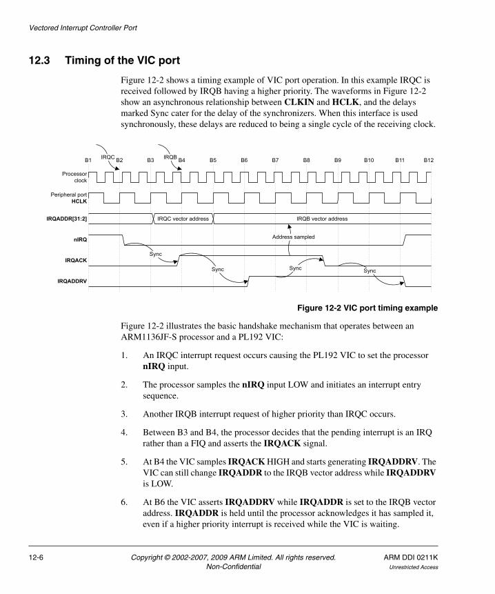
Vectored Interrupt Controller Port
12.3 Timing of the VIC port
Figure 12-2 shows a timing example of VIC port operation. In this example IRQC is received followed by IRQB having a higher priority. The waveforms in Figure 12-2 show an asynchronous relationship between CLKIN and HCLK, and the delays marked Sync cater for the delay of the synchronizers. When this interface is used synchronously, these delays are reduced to being a single cycle of the receiving clock.
Figure 12-2 VIC port timing example
Figure 12-2 illustrates the basic handshake mechanism that operates between an ARM1136JF-S processor and a PL192 VIC:
1. An IRQC interrupt request occurs causing the PL192 VIC to set the processor nIRQ input.
2. The processor samples the nIRQ input LOW and initiates an interrupt entry sequence.
3. Another IRQB interrupt request of higher priority than IRQC occurs.
4. Between B3 and B4, the processor decides that the pending interrupt is an IRQ rather than a FIQ and asserts the IRQACK signal.
5. At B4 the VIC samples IRQACK HIGH and starts generating IRQADDRV. The VIC can still change IRQADDR to the IRQB vector address while IRQADDRV is LOW.
6. At B6 the VIC asserts IRQADDRV while IRQADDR is set to the IRQB vector address. IRQADDR is held until the processor acknowledges it has sampled it, even if a higher priority interrupt is received while the VIC is waiting.
Processorclock
Peripheral port HCLK
IRQC vector address IRQB vector address IRQADDR[31:2]
nIRQ
IRQACK
IRQADDRV
IRQC IRQBB1 B2 B3 B4 B5 B6 B7 B8 B9 B10 B11 B12
Sync
Sync Sync Sync
Address sampled
12-6 Copyright © 2002-2007, 2009 ARM Limited. All rights reserved. ARM DDI 0211KNon-Confidential Unrestricted Access

Vectored Interrupt Controller Port
7. Around B8 the processor samples the value of the IRQADDR input bus and deasserts IRQACK.
8. When the VIC samples IRQACK LOW, it stacks the priority of the IRQB interrupt and deasserts IRQADDRV. It also deasserts nIRQ if there are no higher priority interrupts pending.
9. When the processor samples IRQADDRV LOW, it knows it can sample the nIRQ input again. Therefore, if the VIC requires some time for deasserting nIRQ, it must ensure that IRQADDRV stays HIGH until nIRQ has been deasserted.
The clearing of the interrupt is handled in software by the interrupt handling routine. This enables multiple interrupt sources to share a single interrupt priority. In addition, the interrupt handling routine must communicate to the VIC that the interrupt currently being handled is complete, using the memory-mapped or coprocessor-mapped interface, to enable the interrupt masking to be unwound.
12.3.1 PL192 VIC timing
As its part of the handshake mechanism, the PL192 VIC:
1. Synchronizes IRQACK on its way in if the peripheral port clocking mode is asynchronous or bypasses the synchronizers if it is in synchronous mode.
2. Asserts IRQADDRV when an address is ready at IRQADDR, and holds that address until IRQACK is sampled LOW, even if higher priority interrupts come along.
3. Stacks the priority that corresponds to the vector address present at IRQADDR when it samples the IRQACK signal LOW (while IRQADDRV is HIGH).
4. Clears IRQADDRV so the processor can recognize another interrupt. If nIRQ is also to be deasserted at this point because there are no higher priority interrupts pending, it is deasserted before or at the same time as IRQADDRV to ensure that the processor does not take the same interrupt again.
12.3.2 Core timing
As its part of the handshake mechanism, the core:
1. Starts an interrupt entry sequence when it samples the nIRQ signal asserted.
ARM DDI 0211K Copyright © 2002-2007, 2009 ARM Limited. All rights reserved. 12-7Unrestricted Access Non-Confidential

Vectored Interrupt Controller Port
2. Determines if an FIQ or an IRQ is going to be taken. This happens after the interrupt entry sequence is started. If it decides that an IRQ is going to be taken, it starts the VIC port handshake by asserting IRQACK. If it decides that the interrupt is an FIQ, then it does not assert IRQACK and the VIC port handshake is not initiated.
3. Ignores the value of the nFIQ input until the IRQ interrupt entry sequence is completed if it has decided that the interrupt is an IRQ.
4. Samples the IRQADDR input bus when both IRQACK and IRQADDRV are sampled asserted. The interrupt entry sequence proceeds with this value of IRQADDR.
5. Ignores the nIRQ signal while IRQADDRV is HIGH. This gives the VIC time to deassert the nIRQ signal if there is no higher priority interrupt pending.
6. Ignores the nFIQ signal while IRQADDRV is HIGH.
12-8 Copyright © 2002-2007, 2009 ARM Limited. All rights reserved. ARM DDI 0211KNon-Confidential Unrestricted Access

Vectored Interrupt Controller Port
12.4 Interrupt entry flowchart
Figure 12-3 is a flowchart for ARM1136JF-S interrupt recognition. It shows all the decisions and actions that have to be taken to complete interrupt entry.
Figure 12-3 Interrupt entry sequence
LR_fiq = RA+4
CPSR[5] = ARM state
SPSR_fiq = CPSR
PC[31:0] = 0x0000001CPC[31:0] = 0xFFFF001C
TRUE
!(nFIQ||F)
CPSR[4:0] = FIQ mode
CPSR[7] =FIQs and IRQs disabled
V==1
FALSE
TRUE
FALSE
!((nFIQ||F)||(nIRQ||I))
TRUE
!(IRQVECTADDRV&& VE)
TRUE
FALSE
FALSE
Take IRQACK HIGH
LR_irq = RA+4
SPSR_irq = CPSR
CPSR[4:0] = IRQ mode
CPSR[5] = ARM state
CPSR[7] =IRQs disabled
PC[31:0] = IRQVECT ADDR[31:2], 0b00
VE==1
FALSE
TRUE
VE==1
TRUE
FALSE
PC[31:0] = 0x00000018PC[31:0] = 0xFFFF0018
V==1FALSE
TRUE
FALSE
TRUE
!(IRQVECTADDRV==1)
ARM DDI 0211K Copyright © 2002-2007, 2009 ARM Limited. All rights reserved. 12-9Unrestricted Access Non-Confidential

Vectored Interrupt Controller Port
12-10 Copyright © 2002-2007, 2009 ARM Limited. All rights reserved. ARM DDI 0211KNon-Confidential Unrestricted Access

Chapter 13 Debug
This chapter contains details of the ARM1136JF-S debug unit to assist the development of application software, operating systems, and hardware. It contains the following sections:
• Debug systems on page 13-2
• About the debug unit on page 13-4
• Debug registers on page 13-7
• CP14 registers reset on page 13-43
• CP14 debug instructions on page 13-44
• Debug events on page 13-47
• Debug exception on page 13-51
• Debug state on page 13-53
• Debug communications channel on page 13-57
• Debugging in a cached system on page 13-58
• Debugging in a system with TLBs on page 13-59
• Monitor debug-mode debugging on page 13-60
• Halting debug-mode debugging on page 13-66
• External signals on page 13-68.
ARM DDI 0211K Copyright © 2002-2007, 2009 ARM Limited. All rights reserved. 13-1Unrestricted Access Non-Confidential

Debug
13.1 Debug systems
The ARM1136JF-S processor forms one component of a debug system that interfaces from the high-level debugging performed by you, to the low-level interface supported by the ARM1136JF-S processor. Figure 13-1 shows a typical system.
Figure 13-1 Typical debug system
This typical system has three parts:
• The debug host
• The protocol converter
• The ARM1136JF-S processor on page 13-3.
13.1.1 The debug host
The debug host is a computer, for example a personal computer, running a software debugger such as RealView™ Debugger. The debug host enables you to issue high-level commands such as set breakpoint at location XX, or examine the contents of memory from 0x0-0x100.
13.1.2 The protocol converter
The debug host is connected to the ARM1136JF-S development system using an interface, for example an RS232. The messages broadcast over this connection must be converted to the interface signals of the ARM1136JF-S processor. This function is performed by a protocol converter, for example, RealView ICE.
Host computer running RealView™ DebuggerDebughost
for example, RealView™ ICE
Development system containing ARM1136JF-SDebugtarget
Protocolconverter
13-2 Copyright © 2002-2007, 2009 ARM Limited. All rights reserved. ARM DDI 0211KNon-Confidential Unrestricted Access

Debug
13.1.3 The ARM1136JF-S processor
The ARM1136JF-S processor, with debug unit, is the lowest level of the system. The debug extensions enable you to:
• stall program execution
• examine its internal state and the state of the memory system
• resume program execution.
The debug host and the protocol converter are system-dependent.
ARM DDI 0211K Copyright © 2002-2007, 2009 ARM Limited. All rights reserved. 13-3Unrestricted Access Non-Confidential

Debug
13.2 About the debug unit
The ARM1136JF-S debug unit assists in debugging software running on the ARM1136JF-S processor. You can use an ARM1136JF-S debug unit, in combination with a software debugger program, to debug:
• application software
• operating systems
• ARM processor based hardware systems.
The debug unit enables you to:
• stop program execution
• examine and alter processor and coprocessor state
• examine and alter memory and input/output peripheral state
• restart the processor.
The DBGEN signal enables the debug unit.
The following sections describe the ways you can debug the ARM1136 processor:
• Halting debug-mode debugging
• Monitor debug-mode debugging on page 13-5
• Trace debugging. See Chapter 15 Trace Interface Port for interfacing with an ETM.
The ARM1136JF-S debug interface is based on the IEEE Standard Test Access Port and Boundary-Scan Architecture.
13.2.1 Halting debug-mode debugging
When the ARM1136JF-S debug unit is in Halting debug-mode, the processor halts when a debug event, such as a breakpoint, occurs. When the core is halted, an external host can examine and modify its state using the DBGTAP.
In Halting debug-mode you can examine and alter all processor state (processor registers), coprocessor state, memory, and input/output locations through the DBGTAP. This mode is intentionally invasive to program execution. Halting debug-mode requires:
• external hardware to control the DBGTAP
• a software debugger to provide the user interface to the debug hardware.
See CP14 c1, Debug Status and Control Register (DSCR) on page 13-13 to learn how to set the ARM1136JF-S debug unit into Halting debug-mode.
13-4 Copyright © 2002-2007, 2009 ARM Limited. All rights reserved. ARM DDI 0211KNon-Confidential Unrestricted Access
Debug
13.2.2 Monitor debug-mode debugging
When the ARM1136JS-S debug unit is in Monitor debug-mode, the processor takes a Debug exception instead of halting. A special piece of software, a monitor target, can then take control to examine or alter the processor state. Monitor debug-mode is essential in real-time systems where the core cannot be halted to collect information. For example, engine controllers and servo mechanisms in hard drive controllers that cannot stop the code without physically damaging the components.
When debugging in Monitor debug-mode the processor stops execution of the current program and starts execution of a monitor target. The state of the processor is preserved in the same manner as all ARM exceptions. For more information about exceptions and exception priorities see the ARM Architecture Reference Manual. The monitor target communicates with the debugger to access processor and coprocessor state, and to access memory contents and input/output peripherals. Monitor debug-mode requires a debug monitor program to interface between the debug hardware and the software debugger.
When debugging in Monitor debug-mode, you can program new debug events through CP14. This coprocessor is the software interface of all the debug resources such as the breakpoint and watchpoint registers. See CP14 c1, Debug Status and Control Register (DSCR) on page 13-13 to learn how to set the ARM1136JS-S debug unit into Monitor debug-mode.
13.2.3 Virtual Addresses and debug
Unless otherwise stated, all addresses in this chapter are Virtual Addresses (VA) as described in the ARM Architecture Reference Manual. For example, the Breakpoint Value Registers (BVR) and Watchpoint Value Registers (WVR) must be programmed with VAs.
The terms Instruction Virtual Address (IVA) and Data Virtual Address (DVA), where used, mean the VA corresponding to an instruction address and the VA corresponding to a data address respectively.
ARM DDI 0211K Copyright © 2002-2007, 2009 ARM Limited. All rights reserved. 13-5Unrestricted Access Non-Confidential
Debug
13.2.4 Programming the debug unit
The ARM1136JF-S debug unit is programmed using CoProcessor 14 (CP14). CP14 provides:
• instruction address comparators for triggering breakpoints
• data address comparators for triggering watchpoints
• a bidirectional Debug Communication Channel (DCC)
• all other state information associated with ARM1136JF-S debug.
CP14 is accessed using coprocessor instructions in Monitor debug-mode, and certain debug scan chains in Halting debug-mode, see Chapter 14 Debug Test Access Port to learn how to access the ARM1136JF-S debug unit using scan chains.
13-6 Copyright © 2002-2007, 2009 ARM Limited. All rights reserved. ARM DDI 0211KNon-Confidential Unrestricted Access

Debug
13.3 Debug registers
Figure 13-2 shows the arrangement of the Debug registers in CP14:
Figure 13-2 Debug registers
13.3.1 Accessing debug registers
To access the CP14 debug registers you must set Opcode_1 and CRn to 0. The Opcode_2 and CRm fields of the coprocessor instructions are used to encode the CP14 debug register number, where the register number is {<Opcode2>, <CRm>}.
Table 13-1 shows the CP14 debug register map. All of these registers are also accessible as scan chains from the DBGTAP. Table 13-3 on page 13-9 lists these registers and gives references to the full description of each register.
c0 000 Debug ID Register (DIDR) ‡
Vector Catch Register (VCR)Data Transfer Register (DTR) †Debug Status and Control Register (DSCR) ‡
Watchpoint Value Register (WVR)Breakpoint Control Register (BCR)
Watchpoint Control Register (WCR)
Breakpoint Value Register (BVR)
CRn CRmOpcode_1 Opcode_2
Read-only Read/write Write-only
Only accessible when debug monitor mode is enabled (bits[15:14] of the DSCR register = b10)
157
{0-5}4{0-5}5{0-1}{0-1}
67
Accessible in User mode‡ User read-only access when bit[12] of the DSCR register is 0† User read-write access when bit[12] of the DSCR register is 0
Table 13-1 CP14 debug register map
Binary addressDebug registernumber
CP14 debug register name AbbreviationOpcode_2 CRm
b000 b0000 c0 Debug ID Register DIDR
b000 b0001 c1 Debug Status and Control Register DSCR
b000 b0010 - b0100 c2 - c4 Reserved -
b000 b0101 c5 Data Transfer Register DTR
b000 b0110 c6 Reserved -
ARM DDI 0211K Copyright © 2002-2007, 2009 ARM Limited. All rights reserved. 13-7Unrestricted Access Non-Confidential

Debug
Note All the debug resources required for Monitor debug-mode debugging are accessible through CP14 registers. For Halting debug-mode debugging some additional resources are required. See Chapter 14 Debug Test Access Port.
b000 b0111 c7 Vector Catch Register VCR
b000 b1000 - b1111 c8 - c15 Reserved -
b001- b011 b0000 - b1111 c16 - c63 Reserved -
b100 b0000 - b0101 c64 - c69 Breakpoint Value Registers BVRya
b0110 - b111 c70 - c79 Reserved -
b101 b0000 - b0101 c80 - c85 Breakpoint Control Registers BCRya
b0110 - b1111 c86 - c95 Reserved -
b110 b0000 - b0001 c96 - c97 Watchpoint Value Registers WVRya
b0010 - b1111 c98 - c111 Reserved -
b111 b0000 - b0001 c112 - c113 Watchpoint Control Registers WCRya
b0010 - b1111 c114 - c127 Reserved -
a. y is the decimal representation of the binary number CRm.
Table 13-1 CP14 debug register map (continued)
Binary addressDebug registernumber
CP14 debug register name AbbreviationOpcode_2 CRm
13-8 Copyright © 2002-2007, 2009 ARM Limited. All rights reserved. ARM DDI 0211KNon-Confidential Unrestricted Access

Debug
13.3.2 Debug register descriptions
Table 13-2 lists definitions of terms used in register descriptions.
On a power-on reset, all the CP14 debug registers take the values indicated by the Reset value column in the register bit field definition tables. In these tables, a hyphen (-) means an Undefined reset value.
Table 13-2 Terms used in register descriptions
Term Description
R Read-only. Written values are ignored. However, you must write these bits as 0 or preserve them by writing back the value previously read from the same field on the same processor.
W Write-only. This bit cannot be read. Reads return an Unpredictable value.
RW Read or write.
C Cleared on read. This bit is cleared whenever the register is read.
UNP/SBZP Unpredictable or Should Be Zero or Preserved (SBZP). A read to this bit returns an Unpredictable value. It is written as 0 or preserved by writing the same value previously read from the same fields on the same processor. These bits are usually reserved for future expansion.
Core view This column defines the core access permission for a given bit.
External view This column defines the DBGTAP debugger view of a given bit.
Attributes This is used when the core and the DBGTAP debugger view are the same.
Table 13-3 List of CP14 debug registers
Register name Abbreviation Reference to description
Debug ID Register DIDR See CP14 c0, Debug ID Register (DIDR) on page 13-10
Debug Status and Control Register DSCR See CP14 c1, Debug Status and Control Register (DSCR) on page 13-13
Data Transfer Register DTR See CP14 c5, Data Transfer Registers (DTR) on page 13-20
Vector Catch Register VCR See CP14 c7, Vector Catch Register (VCR) on page 13-22
Breakpoint Value Registers BVRya See CP14 c64-c69, Breakpoint Value Registers (BVR) on page 13-25
ARM DDI 0211K Copyright © 2002-2007, 2009 ARM Limited. All rights reserved. 13-9Unrestricted Access Non-Confidential
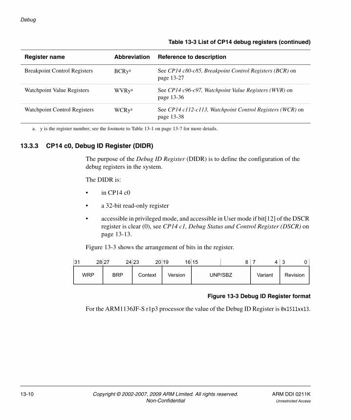
Debug
13.3.3 CP14 c0, Debug ID Register (DIDR)
The purpose of the Debug ID Register (DIDR) is to define the configuration of the debug registers in the system.
The DIDR is:
• in CP14 c0
• a 32-bit read-only register
• accessible in privileged mode, and accessible in User mode if bit[12] of the DSCR register is clear (0), see CP14 c1, Debug Status and Control Register (DSCR) on page 13-13.
Figure 13-3 shows the arrangement of bits in the register.
Figure 13-3 Debug ID Register format
For the ARM1136JF-S r1p3 processor the value of the Debug ID Register is 0x1511xx13.
Breakpoint Control Registers BCRya See CP14 c80-c85, Breakpoint Control Registers (BCR) on page 13-27
Watchpoint Value Registers WVRya See CP14 c96-c97, Watchpoint Value Registers (WVR) on page 13-36
Watchpoint Control Registers WCRya See CP14 c112-c113, Watchpoint Control Registers (WCR) on page 13-38
a. y is the register number; see the footnote to Table 13-1 on page 13-7 for more details.
Table 13-3 List of CP14 debug registers (continued)
Register name Abbreviation Reference to description
WRP
31 28 27 24 23 20 19 16 15 8 7 4 3 0
BRP Context Version UNP/SBZ Variant Revision
13-10 Copyright © 2002-2007, 2009 ARM Limited. All rights reserved. ARM DDI 0211KNon-Confidential Unrestricted Access

Debug
Table 13-4 shows the bit functions of the Debug ID Register.
The values of the following fields of the Debug ID Register agree with the values in CP15 c0, Main ID Register:
• DIDR[3:0] is the same as CP15 c0 bits [3:0]
• DIDR[7:4] is the same as CP15 c0 bits [23:20].
Table 13-4 Debug ID Register bit field definitions
Bits Name Attributes Function Value
[31:28] WRP R Number of Watchpoint Register Pairs. The number of pairs is one more than the value held in this field, so:
b0000 corresponds to 1 WRP,
b0001 corresponds to 2 WRPs,
up to b1111 for 16 WRPs.
The ARM1136JF-S processor has 2 WRPs.
b0001
[27: 24] BRP R Number of Breakpoint Register Pairs. The number of pairs is one more than the value held in this field. The minimum number of pairs is two, and b0000 is Reserved. So:
b0001 corresponds to 2 BRPs,
b0010 corresponds to 3 BRPs,
up to b1111 for 16 BRPs.
The ARM1136JF-S processor has 6 BRPs.
b0101
[23: 20] Context R Number of Breakpoint Register Pairs with context ID comparison capability. The number of pairs is one more than the value held in this field, so:
b0000 corresponds to 1 BRP with context ID comparison capability,
b0001 corresponds to 2 BRPs with context ID comparison capability,
up to b1111 for 16 BRPs with context ID comparison capability.
The ARM1136JF-S processor has 2 BRPs with context ID comparison capability.
b0001
[19:16] Version R Debug architecture version. b0001
[15:8] - UNP/SBZP Reserved. -
[7: 4] Variant R Implementation-defined variant number. This number is incremented on functional changes.
-a
[3: 0] Revision R Implementation-defined revision number. This number is incremented on bug fixes.
-a
a. These values agree with values in the CP15 c0 Main ID Register, see the description in this section.
ARM DDI 0211K Copyright © 2002-2007, 2009 ARM Limited. All rights reserved. 13-11Unrestricted Access Non-Confidential

Debug
See c0, Main ID Register on page 3-25 for a description of CP15 c0, ID Register.
Note The reason for duplicating these fields is that the Debug ID Register is accessible through scan chain 0. This enables an external debugger to determine the variant and revision numbers without stopping the core.
Accessing the Debug ID Register
Table 13-5 shows the results of attempted accesses to the Debug ID Register for each mode.
To access the Debug ID Register you read CP14 with:
• Opcode_1 set to 0
• CRn set to c0
• CRm set to c0
• Opcode_2 set to 0.
For example:
MRC p14,0,<Rd>,c0,c0,0 ; Read Debug ID Register
Table 13-5 Results of accesses to the Debug ID Register
Privileged read Privileged writeUser read, DSCR[12]a=0
User read, DSCR[12]a=1
User write
Data read Undefined Instruction exception
Data read Undefined Instruction exception
Undefined Instruction exception
a. Bit[12] of the DSCR register, see CP14 c1, Debug Status and Control Register (DSCR) on page 13-13. The value of this bit does not have any effect on any other mode of access to the Debug ID Register.
13-12 Copyright © 2002-2007, 2009 ARM Limited. All rights reserved. ARM DDI 0211KNon-Confidential Unrestricted Access
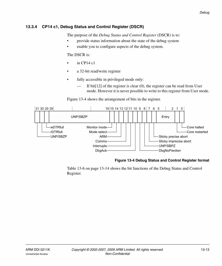
Debug
13.3.4 CP14 c1, Debug Status and Control Register (DSCR)
The purpose of the Debug Status and Control Register (DSCR) is to:
• provide status information about the state of the debug system
• enable you to configure aspects of the debug system.
The DSCR is:
• in CP14 c1
• a 32-bit read/write register
• fully accessible in privileged mode only:
— If bit[12] of the register is clear (0), the register can be read from User mode. However it is never possible to write to this register from User mode.
Figure 13-4 shows the arrangement of bits in the register.
Figure 13-4 Debug Status and Control Register format
Table 13-6 on page 13-14 shows the bit functions of the Debug Status and Control Register.
31 30 29 28 16 15 14 13 12 11 10 6 5 2 1 0
UNP/SBZP Entry
rDTRfullwDTRfull
UNP/SBZP
Monitor modeMode select
ARM
DbgAckInterrupts
Comms
9 78
Core restartedCore halted
Sticky imprecise abortUNP/SBPZDbgNoPwrdwn
Sticky precise abort
ARM DDI 0211K Copyright © 2002-2007, 2009 ARM Limited. All rights reserved. 13-13Unrestricted Access Non-Confidential

Debug
Table 13-6 Debug Status and Control Register bit field definitions
BitsField Name
Core view
External view
FunctionReset value
[31] - - - Reserved, UNP/SBZP. -
[30] rDTRfull R R Indicates the state of the DTR for read operations:
0 = rDTR empty
1 = rDTR full.
This flag is automatically set on writes by the DBGTAP debugger to the rDTR and is cleared on reads by the core of the same register. When the rDTRfull flag is set (1), no writes to the rDTR are enabled.
0
[29] wDTRfull R R Indicates the state of the DTR for write operations:
0 = wDTR empty
1 = wDTR full.
This flag is automatically cleared on reads by the DBGTAP debugger of the wDTR and is set on writes by the core to the same register.
0
[28:16] - - - Reserved, UNP/SBZP. -
[15] Monitor Mode Enable
RW R This bit is used to enable Monitor debug-mode:
0 = Monitor debug-mode disabled
1 = Monitor debug-mode enabled.
For the core to take a debug exception, Monitor debug-mode has to be both selected and enabled (bit[14] clear and bit[15] set).
0
[14] Mode Select R RW This bit is used to select Monitor debug-mode:
0 = Monitor debug-mode selected
1 = Halting debug-mode selected and enabled.
See the description of the Monitor Mode Enable bit, above.
0
13-14 Copyright © 2002-2007, 2009 ARM Limited. All rights reserved. ARM DDI 0211KNon-Confidential Unrestricted Access

Debug
[13] ARM R RW This bit is used to enable the execution of ARM instructions:
0 = ARM instruction execution disabled
1 = ARM instruction execution enabled.
When this bit is set, the core can be forced to execute ARM instructions in Debug state using the Debug Test Access Port.
Note If this bit is set when the core is not in Debug state, the behavior of the ARM1136JF-S processor is Unpredictable.
0
[12] Comms RW R This bit controls User mode access to the comms channel:
0 = User mode access to comms channel enabled
1 = User mode access to comms channel disabled.
If this bit is set and a User mode process tries to access the DIDR, DSCR, or the DTR, the Undefined Instruction exception is taken.a
0
[11] Interrupts R RW This bit controls interrupts:
0 = Interrupts enabled
1 = Interrupts disabled.
When set, the IRQ and FIQ input signals are inhibited.b
0
[10] DbgAck R RW If this bit is set, the DBGACK output signal (see External signals on page 13-68) is forced HIGH, regardless of the processor state.b
0
[9] DbgNoPwrdwn R RW Powerdown disable:
0 = DBGNOPWRDWN is LOW
1 = DBGNOPWRDWN is HIGH.
See External signals on page 13-68.
0
[8] - - - Reserved, UNP/SBZP. -
Table 13-6 Debug Status and Control Register bit field definitions (continued)
BitsField Name
Core view
External view
FunctionReset value
ARM DDI 0211K Copyright © 2002-2007, 2009 ARM Limited. All rights reserved. 13-15Unrestricted Access Non-Confidential

Debug
[7] Sticky imprecise aborts
R RC This bit indicates that an imprecise Data Abort has occurred:
0 = No imprecise Data Aborts have occurred since the last time this bit was cleared
1 = An imprecise Data Abort has occurred since the last time this bit was cleared.
This bit is cleared on reads of a DBGTAP debugger to the DSCR.
0
[6] Sticky precise abort
R RC This bit indicates that a precise Data Abort has occurred:
0 = No precise Data Abort has occurred since the last time this bit was cleared
1 = A precise Data Abort has occurred since the last time this bit was cleared.
This bit is cleared on reads of a DBGTAP debugger to the DSCR.
Note This flag is provided to detect Data Aborts generated by instructions issued to the processor using the Debug Test Access Port. Therefore, if the DSCR[13] execute ARM instruction enable bit is 0, the value of the sticky precise abort bit is Unpredictable.
0
[5:2] Entry RW R This field shows the method of entry to Debug state. See Table 13-7 on page 13-17 for the permitted values and their meaning.
b0000
[1] Core restarted R R This bit enables a debugger to check whether the processor has exited from Debug statec:
0 = the processor is exiting Debug state
1 = the processor has exited Debug state.
See Exiting from Debug state on page 13-18 for details of the use of this bit.
1
Table 13-6 Debug Status and Control Register bit field definitions (continued)
BitsField Name
Core view
External view
FunctionReset value
13-16 Copyright © 2002-2007, 2009 ARM Limited. All rights reserved. ARM DDI 0211KNon-Confidential Unrestricted Access
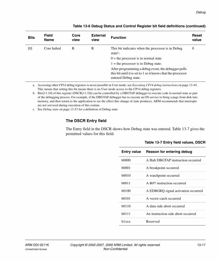
Debug
The DSCR Entry field
The Entry field in the DSCR shows how Debug state was entered. Table 13-7 gives the permitted values for this field.
[0] Core halted R R This bit indicates when the processor is in Debug statec:
0 = the processor is in normal state
1 = the processor is in Debug state.
After programming a debug event, the debugger polls this bit until it is set to 1 so it knows that the processor entered Debug state.
0
a. Accessing other CP14 debug registers is never possible in User mode, see Executing CP14 debug instructions on page 13-45. This means that setting this bit means there is no User mode access to the CP14 debug registers.
b. Bits[11:10] of this register (DSCR[11:10]) can be controlled by a DBGTAP debugger to execute code in normal state as part of the debugging process. For example, if the DBGTAP debugger has to execute an OS service to bring a page from disk into memory, and then return to the application to see the effect this change of state produces, ARM recommends that interrupts are not serviced during execution of this routine.
c. See Debug state on page 13-53 for a definition of Debug state.
Table 13-6 Debug Status and Control Register bit field definitions (continued)
BitsField Name
Core view
External view
FunctionReset value
Table 13-7 Entry field values, DSCR
Entry value Reason for entering debug
b0000 A Halt DBGTAP instruction occurred
b0001 A breakpoint occurred
b0010 A watchpoint occurred
b0011 A BKPT instruction occurred
b0100 A EDBGRQ signal activation occurred
b0101 A vector catch occurred
b0110 A data-side abort occurred
b0111 An instruction-side abort occurred
b1xxx Reserved
ARM DDI 0211K Copyright © 2002-2007, 2009 ARM Limited. All rights reserved. 13-17Unrestricted Access Non-Confidential

Debug
The Entry field, bits[5:2] of the DSCR, indicates:
• the reason for jumping to the Prefetch or Data Abort vector
• the reason for entering Debug state.
A Prefetch Abort or a Data Abort handler will use these to determine if it must jump to the monitor target. Additionally, a DBGTAP debugger or monitor target can determine the specific debug event that caused the Debug state or debug exception entry.
Exiting from Debug state
The Core halted bit of the DSCR, DSCR[0], can be read to check whether the processor is in normal or Debug state. However, it might not be reliable for a debugger to use this bit to check for exit from Debug state. This is because another debug event could cause Debug state to be re-entered before the debugger has successfully polled DSCR[0] to check for a return from Debug state. For this reason, the Core restarted bit, DSCR[1], is provided to enable reliable testing of exiting Debug state. An example of the use of DSCR[1] illustrates this point.
After executing a DBGTAP IR instruction, the debugger polls the Core restarted bit until it is set to 1. At that point, the debugger knows that the IR instruction was effective, even if another debug event immediately causes re-entry to Debug state.
Figure 13-5 shows the relationship between the Core restarted bit and the Core halted bit. In this illustration, almost as soon as the core has been restarted a breakpoint causes it to re-enter Debug state. If the debugger was polling the Core restarted bit to check for exit from Debug state it might miss the return to normal state, and conclude that the IR instruction had failed. However, in the illustration, the fact that the Core restarted signal has been reset to HIGH confirms that the IR instruction was successful.
Figure 13-5 Core restarted and Core halted bits
DSCR[1] Core restarted
DSCR[0] Core halted
breakpoint hit in Halt mode
DBGTAP RESTART
breakpoint hit in Halt mode
core in normal state
core in Debug state
core exiting Debug state
core in normal state
core in Debug state
core exits Debug state
13-18 Copyright © 2002-2007, 2009 ARM Limited. All rights reserved. ARM DDI 0211KNon-Confidential Unrestricted Access

Debug
Accessing the Debug Status and Control Register
Table 13-5 on page 13-12 shows the results of attempted accesses to the Debug Status and Control Register for each mode.
To access the Debug Status and Control Register you read or write CP14 with:
• Opcode_1 set to 0
• CRn set to c0
• CRm set to c1
• Opcode_2 set to 0.
For example:
MRC p14,0,<Rd>,c0,c1,0 ; Read Debug Status and Control RegisterMCR p14,0,<Rd>,c0,c1,0 ; Write Debug Status and Control Register
Table 13-8 Results of accesses to the Debug Status and Control Register
Privileged read Privileged writeUser read, DSCR[12]a=0
User read, DSCR[12]a=1
User write
Data read Data writeb Data read Undefined Instruction exception
Undefined Instruction exception
a. Bit[12] of the DSCR register. The value of this bit does not have any effect on any other mode of access to the Debug Status and Control Register.
b. Refer to Table 13-6 on page 13-14 for details of which bits of the DSCR register can be written.
ARM DDI 0211K Copyright © 2002-2007, 2009 ARM Limited. All rights reserved. 13-19Unrestricted Access Non-Confidential

Debug
13.3.5 CP14 c5, Data Transfer Registers (DTR)
The purpose of the Data Transfer Registers (DTRs) is to transfer data between the processor core and a DBGTAP debugger.
The DTRs are:
• in CP14 c5
• two 32-bit registers:
— the read-only rDTR (Read Data Transfer Register)
— the write-only wDTR (Write Data Transfer Register)
• accessible in privileged mode, and accessible in User mode if bit[12] of the DSCR register is clear (0), see CP14 c1, Debug Status and Control Register (DSCR) on page 13-13.
Note Throughout the description of the DTR, read and write refer to the core view of the registers.
Which of the two physical registers is accessed depends on the instruction used:
• writes, MCR and LDC instructions, access the wDTR
• reads, MRC and STC instructions, access the rDTR.
For details of the use of these registers with the rDTRfull flag and wDTRfull flag see Debug communications channel on page 13-57. Figure 13-6 shows the arrangement of bits in the registers. This arrangement is the same for both the rDTR and the wDTR.
Figure 13-6 Data Transfer Registers format
Table 13-9 shows the bit functions of the rDTR.
Data
31 0
Table 13-9 Read Data Transfer Register bit field definitions
Bits Core view External view Function
[31:0] R W Read data transfer register (read-only)
13-20 Copyright © 2002-2007, 2009 ARM Limited. All rights reserved. ARM DDI 0211KNon-Confidential Unrestricted Access

Debug
Table 13-10 shows the bit functions of the wDTR.
Accessing the Data Transfer Registers
Table 13-5 on page 13-12 shows the results of attempted accesses to the Data Transfer Registers for each mode.
To access the Data Transfer Registers you read or write CP14 with:
• Opcode_1 set to 0
• CRn set to c0
• CRm set to c5
• Opcode_2 set to 0.
For example:
MRC p14,0,<Rd>,c0,c5,0 ; Read the Read Data Transfer RegisterMCR p14,0,<Rd>,c0,c5,0 ; Write the Write Data Transfer Register
Table 13-10 Write Data Transfer Register bit field definitions
Bits Core view External view Function
[31:0] W R Write data transfer register (write-only)
Table 13-11 Results of accesses to the Data Transfer Registers
Privileged reada Privileged writeb User reada, DSCR[12]c=0
User writeb, DSCR[12]a=0
User read or write, DSCR[12]a=1
Data read Data write Data read Data write Undefined Instruction exception
a. Read operations access the Read Data Transfer Register (rDTR).b. Write operations access the Write Data Transfer Register (wDTR).c. Bit[12] of the DSCR register, see CP14 c1, Debug Status and Control Register (DSCR) on page 13-13. The value of this bit
does not have any effect on privileged mode access to the Data Transfer Registers.
ARM DDI 0211K Copyright © 2002-2007, 2009 ARM Limited. All rights reserved. 13-21Unrestricted Access Non-Confidential

Debug
13.3.6 CP14 c7, Vector Catch Register (VCR)
The purpose of the Vector Catch Register (VCR) is to enable vector catching. That is, to cause debug entry when a specified vector is committed for execution.
The VCR is:
• in CP14 c7
• a 32-bit read-write register
• only accessible in privileged mode, with debug monitor mode enabled.
Figure 13-7 shows the arrangement of bits in the register.
Figure 13-7 Vector Catch Register format
Table 13-12 shows the bit field functions of the Vector Catch Register.
ReservedUNP/SBZ
31 8 7 6 5 4 3 2 1 0
FIQIRQ
Vector catch enables
Reserved, UNP/SBZ
Data abort
Undefined
Prefetch abortSWI
Reset
Vector catch enables
Table 13-12 Vector Catch Register bit field definitions
Bits Attributes DescriptionNormal address
High vector address
Reset value
[31:8] - Reserved, UNP/SBZP - - -
[7] RW Vector catch enable, FIQ 0x0000001C 0xFFFF001C 0
[6] RW Vector catch enable, IRQ Most recenta IRQ address
Most recenta IRQ address
0
[5] - Reserved, UNP/SBZP - - -
[4] RW Vector catch enable, Data Abort 0x00000010 0xFFFF0010 0
[3] RW Vector catch enable, Prefetch Abort 0x0000000C 0xFFFF000C 0
13-22 Copyright © 2002-2007, 2009 ARM Limited. All rights reserved. ARM DDI 0211KNon-Confidential Unrestricted Access
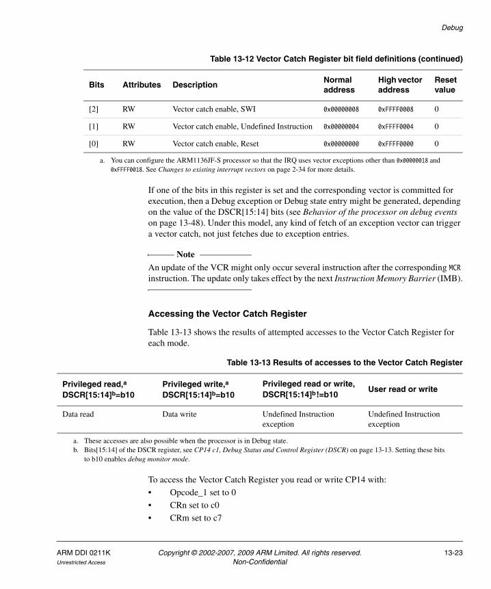
Debug
If one of the bits in this register is set and the corresponding vector is committed for execution, then a Debug exception or Debug state entry might be generated, depending on the value of the DSCR[15:14] bits (see Behavior of the processor on debug events on page 13-48). Under this model, any kind of fetch of an exception vector can trigger a vector catch, not just fetches due to exception entries.
Note An update of the VCR might only occur several instruction after the corresponding MCR instruction. The update only takes effect by the next Instruction Memory Barrier (IMB).
Accessing the Vector Catch Register
Table 13-13 shows the results of attempted accesses to the Vector Catch Register for each mode.
To access the Vector Catch Register you read or write CP14 with:
• Opcode_1 set to 0
• CRn set to c0
• CRm set to c7
[2] RW Vector catch enable, SWI 0x00000008 0xFFFF0008 0
[1] RW Vector catch enable, Undefined Instruction 0x00000004 0xFFFF0004 0
[0] RW Vector catch enable, Reset 0x00000000 0xFFFF0000 0
a. You can configure the ARM1136JF-S processor so that the IRQ uses vector exceptions other than 0x00000018 and 0xFFFF0018. See Changes to existing interrupt vectors on page 2-34 for more details.
Table 13-12 Vector Catch Register bit field definitions (continued)
Bits Attributes DescriptionNormal address
High vector address
Reset value
Table 13-13 Results of accesses to the Vector Catch Register
Privileged read,a DSCR[15:14]b=b10
Privileged write,a DSCR[15:14]b=b10
Privileged read or write, DSCR[15:14]b!=b10
User read or write
Data read Data write Undefined Instruction exception
Undefined Instruction exception
a. These accesses are also possible when the processor is in Debug state.b. Bits[15:14] of the DSCR register, see CP14 c1, Debug Status and Control Register (DSCR) on page 13-13. Setting these bits
to b10 enables debug monitor mode.
ARM DDI 0211K Copyright © 2002-2007, 2009 ARM Limited. All rights reserved. 13-23Unrestricted Access Non-Confidential

Debug
• Opcode_2 set to 0.
For example:
MRC p14,0,<Rd>,c0,c7,0 ; Read the Vector Catch RegisterMCR p14,0,<Rd>,c0,c7,0 ; Write the Vector Catch Register
13.3.7 Overview of breakpoint and watchpoint registers on the ARM1136JF-S processor
A breakpoint is set using a pair of registers:
• a Breakpoint Value Register (BVR)
• a Breakpoint Control Register (BCR).
There are six BVRs, BVR0 to BRV5, and six BCRs, BCR0 to BCR5. Together, a BVR and the corresponding BCR make a Breakpoint Register Pair (BRP). So, for example, BVR2 and BCR2 together make up BRP2.
In a similar way, a watchpoint is set using a pair of registers:
• a Watchpoint Value Register (WVR)
• a Watchpoint Control Register (WCR).
There are two WVRs, WVR0 and WRV1, and two WCRs, WCR0 and WCR1. Together, a WVR and the corresponding WCR make a Watchpoint Register Pair (WRP). So, for example, WVR0 and WCR0 together make up WRP0.
Normally, the contents of a BVR are compared with the IVA bus. However, two of the BVPs are Context ID capable, meaning that the BVR contents can be compared with the CP15 Context ID Register, c13, instead of with the IVA bus. For these BVPs, values in the BCR control whether the BVR is compared with the Context ID Register or with the IVA bus.
Table 13-14 summarizes the breakpoint and watchpoint registers that are implemented in the ARM1136JF-S processor.
Table 13-14 ARM1136JF-S breakpoint and watchpoint registers
Binary addressRegister number
CP14 debug register name AbbreviationContext ID capable?
Opcode_2 CRm
b100 b0000-b0011 c64-c67 Breakpoint Value Registers 0-3 BVR0-3 No
b0100-b0101 c68-c69 Breakpoint Value Registers 4-5 BVR4-5 Yes
13-24 Copyright © 2002-2007, 2009 ARM Limited. All rights reserved. ARM DDI 0211KNon-Confidential Unrestricted Access

Debug
13.3.8 CP14 c64-c69, Breakpoint Value Registers (BVR)
The purpose of the Breakpoint Value Registers (BVRs) is to hold a IVA or Context ID value that is to be used as a breakpoint for debugging purposes.
The BVRs are:
• in CP14 c64-c69
• six 32-bit read-write registers
• only accessible in privileged mode, with debug monitor mode enabled.
The BVRs can only be used in conjunction with the Breakpoint Control Registers (BCRs), see CP14 c80-c85, Breakpoint Control Registers (BCR) on page 13-27. Each BVR is associated with a BCR, to form a Breakpoint Register Pair (BRP). This pairing is described in Overview of breakpoint and watchpoint registers on the ARM1136JF-S processor on page 13-24.
Figure 13-8 shows the arrangement of bits in the Breakpoint Value Registers BVR0 to BVR3, and Figure 13-9 on page 13-26 shows the arrangement for BVR4 and BVR5.
Figure 13-8 Breakpoint Value Registers BVR0 to BVR3 format
b101 b0000-b0011 c80-c83 Breakpoint Control Registers 0-3 BCR0-3 No
b0100-b0101 c84-c85 Breakpoint Control Registers 4-5 BCR4-5 Yes
b110 b0000-b0001 c96-c97 Watchpoint Value Registers 0-1 WVR0-1 -
b111 b0000-b0001 c112-c113 Watchpoint Control Registers 0-1 WCR0-1 -
Table 13-14 ARM1136JF-S breakpoint and watchpoint registers (continued)
Binary addressRegister number
CP14 debug register name AbbreviationContext ID capable?
Opcode_2 CRm
Breakpoint address
31 2 1 0
UNP/SBZP
ARM DDI 0211K Copyright © 2002-2007, 2009 ARM Limited. All rights reserved. 13-25Unrestricted Access Non-Confidential

Debug
Figure 13-9 Breakpoint Value Registers BVR4 and BVR5 format
Table 13-15 shows the bit functions of the Breakpoint Value Registers BVR0 to BVR3, and Table 13-16 shows the bit functions of the Breakpoint Value Registers BVR4 and BVR5.
Because a BVR can only be used as part of a BRP, use of the BVRs is described in CP14 c80-c85, Breakpoint Control Registers (BCR) on page 13-27.
Accessing the Breakpoint Value Registers
Table 13-17 shows the results of attempted accesses to the Breakpoint Value Registers for each mode.
Breakpoint address
31 0
Table 13-15 Breakpoint Value Registers BVR0 to BVR3, bit field definitions
Bits Attributes Function
[31:2] RW Breakpoint address (IVA)
[1:0] - Reserved, UNP/SBZP
Table 13-16 Breakpoint Value Registers BVR4 and BVR5, bit field definitions
Bits Attributes Function
[31:0]a
a. When the register is used for IVA comparison, bits[1:0] are ignored.
RW Breakpoint address (IVA or Context ID)
Table 13-17 Results of accesses to the Breakpoint Value Registers
Privileged read,a DSCR[15:14]b=b10
Privileged write,a DSCR[15:14]b=b10
Privileged read or write, DSCR[15:14]b!=b10
User read or write
Data read Data write Undefined Instruction exception
Undefined Instruction exception
a. These accesses are also possible when the processor is in Debug state.
13-26 Copyright © 2002-2007, 2009 ARM Limited. All rights reserved. ARM DDI 0211KNon-Confidential Unrestricted Access

Debug
To access the Breakpoint Value Registers you read or write CP14 with:
• Opcode_1 set to 0
• CRn set to c0
• CRm set to the number of the BVR you want to access, from c0 for BVR0 to c5 for BVR5
• Opcode_2 set to 4.
For example:
MRC p14,0,<Rd>,c0,c1,4 ; Read Breakpoint Value Register 1MCR p14,0,<Rd>,c0,c3,4 ; Write Breakpoint Value Register 3
13.3.9 CP14 c80-c85, Breakpoint Control Registers (BCR)
The purpose of the Breakpoint Control Registers (BCRs) is to contain the control bits needed for setting breakpoints and linked breakpoints.
The BCRs are:
• in CP14 c80-c85
• six 32-bit read-write registers
• only accessible in privileged mode, with debug monitor mode enabled.
The BCRs can only be used in conjunction with the Breakpoint Value Registers (BVRs), see CP14 c64-c69, Breakpoint Value Registers (BVR) on page 13-25. Each BCR is associated with a BVR, to form a Breakpoint Register Pair (BRP). This pairing is described in Overview of breakpoint and watchpoint registers on the ARM1136JF-S processor on page 13-24. The use of the BRPs is described later in this section.
Figure 13-10 shows the arrangement of bits in the registers.
Figure 13-10 Breakpoint Control Registers format
Table 13-18 on page 13-28 shows the bit functions of the Breakpoint Control Registers.
b. Bits[15:14] of the DSCR register, see CP14 c1, Debug Status and Control Register (DSCR) on page 13-13. Setting these bits to b10 enables debug monitor mode.
BUNP/SBZP
31 22 21 20 19 16 15 9 8 5 4 3 2 1 0
M E LinkedBRP UNP/SBZP S
Byte address select
UNP/SBZP
ARM DDI 0211K Copyright © 2002-2007, 2009 ARM Limited. All rights reserved. 13-27Unrestricted Access Non-Confidential

Debug
Table 13-18 Breakpoint Control Registers, bit field definitions
Bits Name Attributes FunctionReset value
[31:22] - - Reserved, UNP/SBZP. -
[21] Ma RWa Meaning of the associated BVRa:
0 = The BVR holds an Instruction Virtual Address and is compared with the IVA bus.
1 = The BVR holds a Context ID and is compared with the CP15 Context ID Register.
For more information, see Table 13-20 on page 13-32.
-
[20] E RW Enable linking:
0 = Linking disabled.
1 = Linking enabled.
When this bit is set HIGH, the corresponding BRP is linked.
For more information, see Table 13-20 on page 13-32.
-
[19:16] Linked BRP
RW The binary number held in this field is the number of another BRP to link this one with, see Breakpoint and watchpoint linking on page 13-32for details.
This field is only used when bits[21:20] of this register are set to b01. It is ignored for other values of bits[21:20].
Note If bits[21:20]=b01 and this field links the BRP to itself, behavior is Unpredictable if a breakpoint debug event is generated.
-
[15:9] - Reserved, UNP/SBZP. -
[8:5] Byte address select
RW By default, breakpoint matching treats the address held in the BVR as a word address. You can use this field to program the breakpoint so it hits only if certain byte addresses are accessed. See Using a byte address as a breakpoint or watchpoint on page 13-31 for details.
This field must be set to b1111 if this BRP is programmed for Context ID comparison. See Breakpoints with a Context ID comparison on page 13-35 for more information.
-
13-28 Copyright © 2002-2007, 2009 ARM Limited. All rights reserved. ARM DDI 0211KNon-Confidential Unrestricted Access

Debug
Breakpoint register operations
The ARM1136JF-S processor supports thread-aware breakpoints and watchpoints. This means that breakpoints and watchpoints can be made conditional on the contents of the CP15 Context ID Register. The BRPs are used in the following ways:
• a single BRP used to set a breakpoint on:
— an IVA
— a Context ID
• two linked BRPs, to set a breakpoint on an IVA/context ID pair:
— one BRP holds the required IVA
— the second BRP holds the required Context ID
• a BRP linked with a Watchpoint Register Pair (WRP), to set a watchpoint on a DVA/context ID pair:
— the WRP holds the required watchpoint DVA
— the BRP holds the required Context ID.
[4:3] - - Reserved, UNP/SBZP. -
[2:1] S RW Supervisor Access. You can use this field to make the breakpoint conditional on the privilege of the access being made:
b00 = Reserved.
b01= Breakpoint only on privileged access.
b10 = Breakpoint only on User access.
b11 = Either. Breakpoint on any access.
This field must be set to b11 if this BRP is linked and holds a Context ID. This means this field must be set to b11 if bits[21:20] are set to b11. See Breakpoint and watchpoint linking on page 13-32 for more information.
-
[0] B RW Breakpoint enable. This bit is used to enable or disable the breakpoint:
0 = Breakpoint disabled
1 = Breakpoint enabled.
0
a. For registers BRC0 to BRC3, where the associated BVR is not context ID capable, the M field is not used and must be treated as UNP/SBZP.
Table 13-18 Breakpoint Control Registers, bit field definitions (continued)
Bits Name Attributes FunctionReset value
ARM DDI 0211K Copyright © 2002-2007, 2009 ARM Limited. All rights reserved. 13-29Unrestricted Access Non-Confidential

Debug
Whenever a BRP is used:
• the BVR holds the required watchpoint IVA or context ID
• the BCR specifies how the BRP is being used, including whether the BVR holds an IVA or a Context ID.
When a single BRP is used to set a breakpoint on an IVA, the contents of the BVR are compared with the IVA bus of the processor. When a match occurs, a breakpoint debug event is generated.
Breakpoint and watchpoint linking on page 13-32 describes the linked BRP and BRP/WRP operations, and Breakpoints with a Context ID comparison on page 13-35 gives more information about Context ID comparisons.
The following rules apply to the ARM1136JF-S processor for breakpoint debug event generation:
• The update of a BVR or a BCR can take effect several instructions after the corresponding MCR. It takes effect by the next IMB.
• Updates of the CP15 Context ID Register c13, can take effect several instructions after the corresponding MCR. However, the write takes place by the end of the exception return. This ensures that a User mode process, switched in by a processor scheduler, can break at its first instruction.
• Any BRP (holding an IVA) can be linked to any other one with context ID capability. Several BRPs (holding IVAs) can be linked to the same context ID capable BRP.
• If a BRP (holding an IVA) is linked with one that is not configured for context ID comparison and linking, it is Unpredictable whether a breakpoint debug event is generated or not.
See Breakpoint and watchpoint linking on page 13-32 for details of how the BCR[21:20] fields must be set when register pairs are linked.
• If a BRP (holding an IVA) is linked with one that is not implemented, it is Unpredictable if a breakpoint debug event is generated or not.
• If a BRP is linked with itself, it is Unpredictable if a breakpoint debug event is generated or not.
• If a BRP (holding an IVA) is linked with another BRP (holding a context ID value), and they are not both enabled (both BCR[0] bits set), the first one does not generate any breakpoint debug events.
13-30 Copyright © 2002-2007, 2009 ARM Limited. All rights reserved. ARM DDI 0211KNon-Confidential Unrestricted Access

Debug
Using a byte address as a breakpoint or watchpoint
By default, IVA and DVA matching is performed on the word address held in the BVR or WVR. The rest of this section describes IVA matching against the BVR. However, byte address selection for DVA matching against the WVR is identical.
For this operation, the Byte address select field of the BCR (BCR[8:5]) is set to b1111, However, you can use this field to program the breakpoint so it hits only if certain byte addresses are accessed. This is shown in Table 13-19.
The byte addresses in Table 13-19 are little-endian. This ensures that a breakpoint is triggered regardless of the endianness of the instruction fetch. For example, if a breakpoint is set on a certain Thumb instruction by setting BCR[8:5] = b0011, the breakpoint is triggered in both of these cases:
• the fetch is little-endian and IVA[1:0] is b00
• the fetch is big-endian and IVA[1:0] is b10.
Note The Byte address select field is still used when a BVR is being used for Context ID comparison. Therefore, the field must be set to b1111 when a BRP is programmed for context ID comparison. Otherwise breakpoint or watchpoint debug events might not be generated as expected. This means that whenever BCR[21] is set to 1, to enable Context ID comparison, BCR[8:5] must be set to b1111.
Table 13-19 Byte address select field values, bits[8:5], in the BCRs
Byte address select field Breakpoint hits
b0000 Never.
bxxx1 When the byte at address BVR[31:2]+0 is accessed.
bxx1x When the byte at address BVR[31:2]+1 is accessed.
bx1xx When the byte at address BVR[31:2]+2 is accessed.
b1xxx When the byte at address BVR[31:2]+3 is accessed.
b1111 When the word at address BVR[31:2] is accessed.
This is the default IVA matching.
ARM DDI 0211K Copyright © 2002-2007, 2009 ARM Limited. All rights reserved. 13-31Unrestricted Access Non-Confidential

Debug
Breakpoint and watchpoint linking
As indicated in Breakpoint register operations on page 13-29, there are two cases where BRPs are linked:
• two BRPs are linked, to define a breakpoint conditional on a Context ID:
— one BRP holds the required Context ID
— the second BRP holds the required IVA
• a BRP is linked to a WRP, to define a watchpoint conditional on a Context ID:
— the BRP holds the required Context ID
— the WRP holds the DVA for the watchpoint.
In both cases, two bits of the BCR must be set correctly to configure the linking; these are:
• BCR[21], the M (Meaning) bit. This bit configures whether the associated BVR is being used for IVA matching (=0) or for Context ID matching (=1).
• BCR[20], the E (Enable linking) bit. This bit configures whether BRP linking is disabled (=0) or enabled (=1).
Table 13-20 summarizes the meaning of BCR bits[21:20].
Table 13-20 Meaning of BCR[21:20] bits in a BCR
BCR[21:20] Meaning
b00 The associated BVR is compared with the IVA bus. This BRP is not linked with any other one. It generates a breakpoint debug event on an IVA match.
b01 The associated BVR is compared with the IVA bus. This BRP is linked with the BRP indicated by the Linked BRP field, BCR[19:16] of this BCR. A breakpoint debug event is generated based on both:
• matching the associated BVR with the IVA bus
• matching the contents of the linked BVR with the Context ID.
b10 The associated BVR is compared with the CP15 Context Id Register, c13. This BRP is not linked with any other one. It generates a breakpoint debug event on a context ID match.
b11 The associated BVR is compared with the CP15 Context Id Register, c13. Another BRP (of the BCR[21:20]=b01 type), or WRP (with WCR[20]=b1), is linked with this BRP. A breakpoint or watchpoint debug event is generated based on both:
• matching the associated BVR with the Context ID
• matching the linked BVR or WVR with the IVA or DVA bus.
13-32 Copyright © 2002-2007, 2009 ARM Limited. All rights reserved. ARM DDI 0211KNon-Confidential Unrestricted Access

Debug
Whenever you want to make a breakpoint or a watchpoint conditional on the Context ID, you link the BRP or WRP containing the required IVA or DVA to a BRP that contains the required Context ID. If you want to set up multiple breakpoints or watchpoints conditional on a single Context ID you can link multiple BRPs and WRPs to a single BRP that holds the required Context ID.
Remember that only BRP4 and BRP5 can be used to hold Context IDs.
See Setting breakpoints, watchpoints, and vector catch debug events on page 13-60 for detailed programming sequences for linked breakpoints and linked watchpoints.
Privilege level conditions with breakpoint or watchpoint linking
Bits[2:1] of the BCR or of the WCR, the S field, enable you to make the breakpoint or watchpoint conditional on the privilege level (User or privileged) of the access being made. If you want to apply an access mode condition to a breakpoint or watchpoint that links a BRP or WRP to a BRP holding a context ID you must take particular care over the S field values:
• The S field value (bits[2:1]) of the BRP or WRP holding the breakpoint or watchpoint match address take precedence over the S field of the BRP holding the Context ID. The S field of the BRP or WRP holding the match address must be set to the required privilege level of the breakpoint or watchpoint.
• The S field of the BRP holding the Context ID must be set to b11 = either. This is because, where breakpoints or watchpoints are linked it is Undefined whether the S field of the BRP holding the Context ID is included in the comparison.
Summary of defining a breakpoint conditional on a Context ID
One BRP must be set up to specify the required Context ID. This must be BRP4 or BRP5. If this BRP is not already set up you must:
• Program the BVR with the required Context ID.
• In the associated BCR:
— Set bit[21], the M bit, to 1, to specify that the BVR holds a Context ID.
— Set bit[20], the E bit, to 1, to specify that this BRP is linked.
— Set bits[8:5], the Byte address select field, to b1111, to ensure that all bytes of the BVR are used for Context ID matching.
— Set bits[2:1], the S field, to b11. See Privilege level conditions with breakpoint or watchpoint linking for an explanation of this setting.
— Set bit[0], the B field, to 1, to enable the breakpoint.
You must set up the second BRP to specify the required IVA:
• Program the BVR with the required IVA.
ARM DDI 0211K Copyright © 2002-2007, 2009 ARM Limited. All rights reserved. 13-33Unrestricted Access Non-Confidential

Debug
• In the associated BCR:
— Set bit[21], the M bit, to 0, to specify that the BVR holds an IVA.
— Set bit[20], the E bit, to 1, to specify that this BRP is linked to a second BRP.
— Set bits[19:16], the Linked BRP field, to indicate the number of the BRP that holds the required Context ID. This field will be b100 or b101, for BRP4 or BRP5.
— Set the Byte address select and S fields of the register if required, see Table 13-18 on page 13-28 for more information.
— Set bit[0], the B bit, to 1, to enable the breakpoint.
Summary of defining a watchpoint conditional on a Context ID
This is described here because it requires a BRP to hold the required Context ID. See CP14 c112-c113, Watchpoint Control Registers (WCR) on page 13-38 for more information about defining watchpoints.
A BRP must be set up to specify the required Context ID. This must be BRP4 or BRP5. If this BRP is not already set up you must:
• Program the BVR with the required Context ID.
• In the associated BCR:
— Set bit[21], the M bit, to 1, to specify that the BVR holds a Context ID.
— Set bit[20], the E bit, to 1, to specify that this BRP is linked.
— Set bits[8:5], the Byte address select field, to b1111, to ensure that all bytes of the BVR are used for Context ID matching.
— Set bits[2:1], the S field, to b11. See Privilege level conditions with breakpoint or watchpoint linking on page 13-33 for an explanation of this setting.
— Set bit[0], the B field, to 1, to enable the breakpoint.
You must also set up a WRP to specify the required DVA:
• Program the WVR with the required DVA.
• In the associated WCR:
— Set bit[20], the E bit, to 1, to specify that this WRP is linked to a BRP that holds a Context ID.
— Set bits[19:16], the Linked BRP field, to indicate the number of the BRP that holds the required Context ID. This field will be b100 or b101, for BRP4 or BRP5.
— Set the Byte address select, L/S and S fields of the register if required, see Table 13-24 on page 13-39 for more information.
— Set bit[0], the W bit, to 1, to enable the watchpoint.
13-34 Copyright © 2002-2007, 2009 ARM Limited. All rights reserved. ARM DDI 0211KNon-Confidential Unrestricted Access

Debug
Breakpoints with a Context ID comparison
This section contains additional information about setting breakpoints that involve a context ID comparison. The section Breakpoint and watchpoint linking on page 13-32 described setting a breakpoint, or a watchpoint, based on a combination of a Context ID match with an IVA or DVA match. In these cases, a breakpoint or watchpoint debug event is only generated if both the address and the context ID match at the same time. This means that unnecessary hits can be avoided when debugging a specific thread within a task.
Breakpoint debug events generated on context ID matches only are also supported. However, if the match occurs while the processor is running in a privileged mode and the debug logic is in Monitor debug-mode, it is ignored. This is to avoid the processor ending in an unrecoverable state.
Context ID matches are based on comparing the value held in a BVR with the value held in the CP15 Context ID Register, see c13, Context ID Register on page 3-159. The contents of the BVR are compared with the Context ID Register whenever bit[21], the M (Meaning) bit of the associated BCR is set to 1.
Note The Byte address select field of the BCR, BCR[8:5], is still used when the BVR is used for Context ID comparisons. You must set this field to b1111 whenever you configure a BRP for Context ID matching, to ensure the breakpoint or watchpoint debug events are generated correctly.
The S field of the BCR, BCR[2:1], is also applied to all Context ID comparisons. You will normally set this field to b11 when the associated BVR holds a Context ID. You must set this field to b11 when the Context ID comparison is linked to another BRP or WRP, see Privilege level conditions with breakpoint or watchpoint linking on page 13-33 for more information.
ARM DDI 0211K Copyright © 2002-2007, 2009 ARM Limited. All rights reserved. 13-35Unrestricted Access Non-Confidential

Debug
Accessing the Breakpoint Control Registers
Table 13-17 on page 13-26 shows the results of attempted accesses to the Breakpoint Control Registers for each mode.
To access the Breakpoint Control Registers you read or write CP14 with:
• Opcode_1 set to 0
• CRn set to c0
• CRm set to the number of the BCR you want to access, from c0 for BCR0 to c5 for BCR5
• Opcode_2 set to 5.
For example:
MRC p14,0,<Rd>,c0,c1,5 ; Read Breakpoint Control Register 1MCR p14,0,<Rd>,c0,c3,5 ; Write Breakpoint Control Register 3
13.3.10 CP14 c96-c97, Watchpoint Value Registers (WVR)
The purpose of the Watchpoint Value Registers (WVRs) is to hold a DVA value that is to be used as a breakpoint for debugging purposes.
The WVRs are:
• in CP14 c96-c97
• two 32-bit read-write registers
• only accessible in privileged mode, with debug monitor mode enabled.
The WVRs can only be used in conjunction with the Watchpoint Control Registers (WCRs), see CP14 c112-c113, Watchpoint Control Registers (WCR) on page 13-38. Each WVR is associated with a WCR, to form a Watchpoint Register Pair (WRP). This pairing is described in Overview of breakpoint and watchpoint registers on the ARM1136JF-S processor on page 13-24.
Table 13-21 Results of accesses to the Breakpoint Control Registers
Privileged read,a DSCR[15:14]b=b10
Privileged write,a DSCR[15:14]b=b10
Privileged read or write, DSCR[15:14]b!=b10
User read or write
Data read Data write Undefined Instruction exception
Undefined Instruction exception
a. These accesses are also possible when the processor is in Debug state.b. Bits[15:14] of the DSCR register, see CP14 c1, Debug Status and Control Register (DSCR) on page 13-13. Setting these bits
to b10 enables debug monitor mode.
13-36 Copyright © 2002-2007, 2009 ARM Limited. All rights reserved. ARM DDI 0211KNon-Confidential Unrestricted Access
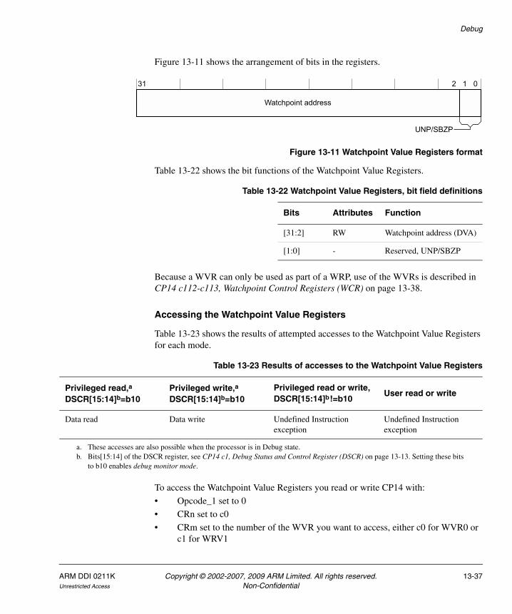
Debug
Figure 13-11 shows the arrangement of bits in the registers.
Figure 13-11 Watchpoint Value Registers format
Table 13-22 shows the bit functions of the Watchpoint Value Registers.
Because a WVR can only be used as part of a WRP, use of the WVRs is described in CP14 c112-c113, Watchpoint Control Registers (WCR) on page 13-38.
Accessing the Watchpoint Value Registers
Table 13-23 shows the results of attempted accesses to the Watchpoint Value Registers for each mode.
To access the Watchpoint Value Registers you read or write CP14 with:
• Opcode_1 set to 0
• CRn set to c0
• CRm set to the number of the WVR you want to access, either c0 for WVR0 or c1 for WRV1
Watchpoint address
31 2 1 0
UNP/SBZP
Table 13-22 Watchpoint Value Registers, bit field definitions
Bits Attributes Function
[31:2] RW Watchpoint address (DVA)
[1:0] - Reserved, UNP/SBZP
Table 13-23 Results of accesses to the Watchpoint Value Registers
Privileged read,a DSCR[15:14]b=b10
Privileged write,a DSCR[15:14]b=b10
Privileged read or write, DSCR[15:14]b!=b10
User read or write
Data read Data write Undefined Instruction exception
Undefined Instruction exception
a. These accesses are also possible when the processor is in Debug state.b. Bits[15:14] of the DSCR register, see CP14 c1, Debug Status and Control Register (DSCR) on page 13-13. Setting these bits
to b10 enables debug monitor mode.
ARM DDI 0211K Copyright © 2002-2007, 2009 ARM Limited. All rights reserved. 13-37Unrestricted Access Non-Confidential

Debug
• Opcode_2 set to 6.
For example:
MRC p14,0,<Rd>,c0,c1,6 ; Read Watchpoint Value Register 1MCR p14,0,<Rd>,c0,c0,6 ; Write Watchpoint Value Register 0
13.3.11 CP14 c112-c113, Watchpoint Control Registers (WCR)
The purpose of the Watchpoint Control Registers (WCRs) is to contain the control bits needed for setting watchpoints and linked watchpoints.
The WCRs are:
• in CP14 c112-c113
• two 32-bit read-write registers
• only accessible in privileged mode, with debug monitor mode enabled.
Figure 13-12 shows the arrangement of bits in the registers.
Figure 13-12 Watchpoint Control Registers format
WUNP/SBZP
31 21 20 19 16 15 9 8 5 4 3 2 1 0
E LinkedBRP UNP/SBZP L/S S
Byte address select
13-38 Copyright © 2002-2007, 2009 ARM Limited. All rights reserved. ARM DDI 0211KNon-Confidential Unrestricted Access

Debug
Table 13-24 shows the bit functions of the Watchpoint Control Registers.
Table 13-24 Watchpoint Control Registers, bit field definitions
Bits Name Attributes FunctionReset value
[31:21] - - Reserved, UNP/SBZP. -
[20] E RW Enable linking:
0 = Linking disabled
1 = Linking enabled.
When this bit is set, this watchpoint is linked with the BRP specified in bits[19:16], the Linked BRP field.
-
[19:16] Linked BRP
RW The binary number held in this field is the number of the BRP that is linked to this WRP. The linked BRP holds a Context ID to be used as part of the watchpoint definition.
Permitted values for this field are b0100 and b0101, corresponding to BRP4 and BRP5.
For more information see Breakpoint and watchpoint linking on page 13-32.
This field is ignored unless bit[20], the E bit, is set to 1.
-
[15:9] - Reserved, UNP/SBZP. -
[8:5] Byte address select
RW By default, watchpoint matching treats the address held in the WVR as a word address. You can use this field to program the watchpoint so it hits only if certain byte addresses are accessed.
Byte address selection is identical for the WVRs and the BVRs. See Using a byte address as a breakpoint or watchpoint on page 13-31 for details.
-
ARM DDI 0211K Copyright © 2002-2007, 2009 ARM Limited. All rights reserved. 13-39Unrestricted Access Non-Confidential
Debug
Watchpoint register operations
The watchpoint value contained in the WVR always corresponds to a DVA. Watchpoints can be set on:
• a DVA
• a DVA/Context ID pair.
For the second case, you have to link the WRP to a BRP that holds a Context ID. This can only be BRP4 or BRP5. Linking a WRP to a BRP in this way, to specify a watchpoint that is conditional on both a DVA and a Context ID, is described in the section Breakpoint and watchpoint linking on page 13-32.
In addition to the rules for breakpoint debug event generation, see Breakpoint register operations on page 13-29, the following rules apply to watchpoint debug event generation with the ARM1136JF-S processor:
• The update of a WVR or a WCR can take effect several instructions after the corresponding MCR. It is only guaranteed to have taken effect by the next 1MB.
[4:3] L/S RW Load or store access. You can use this field to make the watchpoint conditional on the type of access being made:
b00 = Reserved
b01 = Load
b10 = Store
b11 = Either.
See Watchpoints conditional on Load or Store operations on page 13-41 for more information.
-
[2:1] S RW Supervisor Access. You can use this field to make the breakpoint conditional on the privilege of the access being made:
b00 = Reserved
b01 = Watchpoint only on privileged access
b10 = Watchpoint only on User access
b11 = Either. Watchpoint on any access.
-
[0] W RW Watchpoint enable:
0 = Watchpoint disabled
1 = Watchpoint enabled.
0
Table 13-24 Watchpoint Control Registers, bit field definitions (continued)
Bits Name Attributes FunctionReset value
13-40 Copyright © 2002-2007, 2009 ARM Limited. All rights reserved. ARM DDI 0211KNon-Confidential Unrestricted Access

Debug
• A WRP can be linked to a BRP that has Context ID comparison capability. Several BRPs (holding IVAs) and WRPs can be linked with the same context ID capable BRP.
BRP4 and BRP5 are the BRPs that have Context ID capability.
• If a WRP is linked with a BRP that is not configured for Context ID comparison and linking, it is Unpredictable if a watchpoint debug event is generated or not. Whenever a WRP is linked to a BRP, the BCR[21:20] fields of the BRP must be set to b11.
• If a WRP is linked with a BRP that is not implemented, it is Unpredictable if a watchpoint debug event is generated or not.
• If a WRP is linked with a BRP and they are not both enabled, the WRP does not generate a watchpoint debug event.
The WRP and BRP are enabled by setting both BCR[0] and WCR[0] to 1.
Watchpoints conditional on Load or Store operations
The L/S field of a WCR, bits[4:3], can be used to make the watchpoint conditional on the type of access being made. Table 13-25 shows the permitted values for this field and their meanings.
Table 13-25 L/S field values, bits[4:3], in the WCRs
L/S field value Meaning
b00 Reserved.
b01 Watchpoint triggers on Load operations only.
b10 Watchpoint triggers on Store operations only.
b11 Either. Watchpoint triggers on all operations.
ARM DDI 0211K Copyright © 2002-2007, 2009 ARM Limited. All rights reserved. 13-41Unrestricted Access Non-Confidential

Debug
Table 13-26 shows how the L/S field is interpreted for different operations.
Accessing the Watchpoint Control Registers
Table 13-27 shows the results of attempted accesses to the Watchpoint Control Registers for each mode.
To access the Watchpoint Control Registers you read or write CP14 with:
• Opcode_1 set to 0
• CRn set to c0
• CRm set to the number of the WCR you want to access, either c0 for WCR0 or c1 for WCR1
• Opcode_2 set to 7.
For example:
MRC p14, 0, <Rd>, c0, c1, 7 ; Read Watchpoint Control Register 1MCR p14, 0, <Rd>, c0, c0, 7 ; Write Watchpoint Control Register 0
Table 13-26 Interpretation of the L/S field in the WCR for different operations
Operation L/S field settings for Watchpoint to trigger
SWP Load, Store or Either,
Load Exclusive, LDREX Load or Either.
Store Exclusive, STREX Store or Either.
The watchpoint will trigger regardless of whether the command succeeded.
Table 13-27 Results of accesses to the Watchpoint Control Registers
Privileged read,a DSCR[15:14]b=b10
Privileged write,a DSCR[15:14]b=b10
Privileged read or write, DSCR[15:14]b!=b10
User read or write
Data read Data write Undefined Instruction exception
Undefined Instruction exception
a. These accesses are also possible when the processor is in Debug state.b. Bits[15:14] of the DSCR register, see CP14 c1, Debug Status and Control Register (DSCR) on page 13-13. Setting these bits
to b10 enables debug monitor mode.
13-42 Copyright © 2002-2007, 2009 ARM Limited. All rights reserved. ARM DDI 0211KNon-Confidential Unrestricted Access

Debug
13.4 CP14 registers reset
The CP14 debug registers are all reset by the ARM1136JF-S processor power-on reset signal, nPORESETIN, see Power-on reset on page 9-7.
This ensures that a vector catch set on the reset vector is taken when nRESETIN is deasserted. It also ensure that the DBGTAP debugger can be connected when the processor is running without clearing CP14 debug setting, because DBGnTRST does not reset these registers.
ARM DDI 0211K Copyright © 2002-2007, 2009 ARM Limited. All rights reserved. 13-43Unrestricted Access Non-Confidential

Debug
13.5 CP14 debug instructions
Table 13-28 shows the CP14 debug instructions.
In Table 13-28, MRC p14,0,<Rd>,c0,c5,0 and STC p14,c5,<addressing mode> refer to the rDTR and MCR p14,0,<Rd>,c0,c5,0 and LDC p14,c5,<addressing mode> refer to the wDTR. See CP14 c5, Data Transfer Registers (DTR) on page 13-20 for more details.
The MRC p14,0,R15,c0,c1,0 instruction sets the CPSR flags as follows:
• N flag = DSCR[31]. This is an Unpredictable value.
• Z flag = DSCR[30]. This is the value of the rDTRfull flag.
Table 13-28 CP14 debug instructions
Binary addressRegister number Abbreviation Legal instructions
Opcode_2 CRm
b000 b0000 0 DIDR MRC p14, 0, <Rd>, c0, c0, 0a
b000 b0001 1 DSCR MRC p14, 0, <Rd>, c0, c1,0a
MRC p14, 0, R15, c0, c1,0
MCR p14, 0, <Rd>, c0, c1,0a
b000 b0101 5 DTR
(rDTR/wDTR)MRC p14, 0, <Rd>, c0, c5, 0a
MCR p14, 0, <Rd>, c0, c5, 0a
STC p14, c5, <addressing mode>
LDC p14, c5, <addressing mode>
b000 b0111 7 VCR MRC p14, 0, <Rd>, c0, c7, 0a
MCR p14, 0, <Rd>, c0, c7, 0a
b100 b0000-b1111 64-79 BVR MRC p14, 0, <Rd>, c0, cy,4a, b
MCR p14, 0, <Rd>, c0, cy,4a, b
b101 b0000-b1111 80-95 BCR MRC p14, 0, <Rd>, c0, cy,5a, b
MCR p14, 0, <Rd>, c0, cy,5a, b
b110 b0000-b1111 96-111 WVR MRC p14, 0, <Rd>, c0, cy, 6a, b
MCR p14, 0, <Rd>, c0, cy, 6a, b
b111 b0000-b1111 112-127 WCR MRC p14, 0, <Rd>, c0, cy, 7a, b
MCR p14, 0, <Rd>, c0, cy, 7a, b
a. <Rd> is any of the ARM registers R0-R14.b. y is the decimal representation for the binary number CRm.
13-44 Copyright © 2002-2007, 2009 ARM Limited. All rights reserved. ARM DDI 0211KNon-Confidential Unrestricted Access

Debug
• C flag = DSCR[29]. This is the value of the wDTRfull flag.
• V flag = DSCR[28]. This is an Unpredictable value.
Instructions that follow the MRC instruction can be conditioned to these CPSR flags.
13.5.1 Executing CP14 debug instructions
If the core is in Debug state (see Debug state on page 13-53), you can execute any CP14 debug instruction regardless of the processor mode.
If the processor tries to execute a CP14 debug instruction that either is not in Table 13-28 on page 13-44, or is targeted to a reserved register, such as a non-implemented BVR, the Undefined Instruction exception is taken.
You can access the DCC (read DIDR, read DSCR and read/write DTR) in User mode. All other CP14 debug instructions are privileged. If the processor tries to execute one of these in User mode, the Undefined Instruction exception is taken.
If the User mode access to DCC disable bit, DSCR[12], is set, all CP14 debug instructions are considered as privileged, and all attempted User mode accesses to CP14 debug registers generate an Undefined Instruction exception.
When DSCR bit 14 is set (Halting debug-mode selected and enabled), if the software running on the processor tries to access any register other than the DIDR, the DSCR, or the DTR, the core takes the Undefined Instruction exception. The same thing happens if the core is not in any debug mode (DSCR[15:14]=b00).
This lockout mechanism ensures that the software running on the core cannot modify the settings of a debug event programmed by the DBGTAP debugger.
Table 13-29 on page 13-46 shows the results of executing CP14 debug instructions.
ARM DDI 0211K Copyright © 2002-2007, 2009 ARM Limited. All rights reserved. 13-45Unrestricted Access Non-Confidential

Debug
Table 13-29 Debug instruction execution
State when executing CP14 debug instruction: Results of CP14 debug instruction execution:
Processor mode
Debug state
DSCR[15:14] (Mode enabled and selected)
DSCR[12] (DCC User accesses disabled)
Read DIDR, read DSCR and read/ write DTR
Write DSCR
Read/write other registers
x Yes xx x Proceed Proceed Proceed
User No xx 0 Proceed Undefined Instruction exception
Undefined Instruction exception
User No xx 1 Undefined Instruction exception
Privileged No b00 (None) x Proceed Proceed Undefined Instruction exception
Privileged No b01 (Halt) x Proceed Proceed Undefined Instruction exception
Privileged No b10 (Monitor) x Proceed Proceed Proceed
Privileged No b11 (Halt) x Proceed Proceed Undefined Instruction exception
13-46 Copyright © 2002-2007, 2009 ARM Limited. All rights reserved. ARM DDI 0211KNon-Confidential Unrestricted Access

Debug
13.6 Debug events
A debug event is any of the following:
• Software debug event
• External debug request signal on page 13-48
• Halt DBGTAP instruction on page 13-48.
13.6.1 Software debug event
A software debug event is any of the following:
• A watchpoint debug event. This occurs when:
— the DVA present in the data bus matches the watchpoint value
— all the conditions of the WCR match
— the watchpoint is enabled
— the linked Context ID-holding BRP (if any) is enabled and its value matches the context ID in CP15 c13.
• A breakpoint debug event. This occurs when:
— an instruction was fetched and the IVA present in the instruction bus matched the breakpoint value
— at the same time the instruction was fetched, all the conditions of the BCR matched
— the breakpoint was enabled
— at the same time the instruction was fetched, the linked Context ID-holding BRP (if any) was enabled and its value matched the context ID in CP15 c13
— the instruction is now committed for execution.
• A breakpoint debug event also occurs when:
— an instruction was fetched and the CP15 Context ID (register 13) matched the breakpoint value
— at the same time the instruction was fetched, all the conditions of the BCR matched
— the breakpoint was enabled
— the instruction is now committed for execution.
• A software breakpoint debug event. This occurs when a BKPT instruction is committed for execution.
ARM DDI 0211K Copyright © 2002-2007, 2009 ARM Limited. All rights reserved. 13-47Unrestricted Access Non-Confidential

Debug
• A vector catch debug event. This occurs when:
— The instruction at a vector location was fetched. This includes any kind of prefetches, not just the ones due to exception entry.
— At the same time the instruction was fetched, the corresponding bit of the VCR was set (vector catch enabled).
— The instruction is now committed for execution.
13.6.2 External debug request signal
The ARM1136JF-S processor has an external debug request input signal, EDBGRQ. When this signal is HIGH it causes the processor to enter Debug state when execution of the current instruction has completed. When this happens, the DSCR[5:2] method of entry bits are set to b0100.
This signal can be driven by the ETM to signal a trigger to the core. For example, if the processor is in Halting debug-mode and a memory permission fault occurs, an external trace analyzer can collect trace information around this trigger event at the same time that the processor is stopped to examine its state. See the Chapter 15 Trace Interface Port for more details. A DBGTAP debugger can also drive this signal.
13.6.3 Halt DBGTAP instruction
The Halt mechanism is used by the Debug Test Access Port to force the core into Debug state. When this happens, the DSCR[5:2] method of entry bits are set to b0000.
13.6.4 Behavior of the processor on debug events
This section describes how the processor behaves on debug events when not in Debug state. See Debug state on page 13-53 for information on how the processor behaves while in Debug state.
Behavior on a debug event depends on:
• Whether debug is enabled. The DBGEN signal enables debug when set to 1. See External signals on page 13-68 for more information.
• The selected debug mode. Bits[15:14] of the DSCR determines the debug modes. See CP14 c1, Debug Status and Control Register (DSCR) on page 13-13 for more information.
• The debug event that occurs.
13-48 Copyright © 2002-2007, 2009 ARM Limited. All rights reserved. ARM DDI 0211KNon-Confidential Unrestricted Access

Debug
Table 13-30 shows the processor behavior as a result of software debug events.
If DBGEN is set to 1, the processor enters Debug state regardless of any debug-mode selected by DSCR[15:14] when the external debug request signal, EDBGRQ, l is activated, or the Halt DBGTAP instruction is issued.
13.6.5 Effect of a debug event on CP15 registers
The four CP15 registers that can be set on a debug event are:
• Instruction Fault Status Register (IFSR)
• Data Fault Status Register (DFSR)
• Fault Address Register (FAR)
• Watchpoint Fault Address Register (WFAR).
They are set under the following circumstances:
• The IFSR is set whenever a breakpoint, software breakpoint, or vector catch debug event generates a Debug exception entry. It is set to indicate the cause for the Prefetch Abort vector fetch.
• The DFSR is set whenever a watchpoint debug event generates a Debug exception entry. It is set to indicate the cause for the Data Abort vector fetch.
• The ARM1136JF-S processor sets the FAR to an Unpredictable value.
• The WFAR is set whenever a watchpoint debug event generates either a Debug exception or Debug state entry. It is set to the VA of the instruction that caused the Watchpoint debug event, plus an offset dependent on the processor state. Table 13-33 on page 13-55 shows the offsets that are used.
Table 13-30 Processor behavior on software debug events
DBGEN DSCR[15:14] Mode selectedAction on software debug event, other than BKPT instruction
Action on BKPT instruction
0 bxx Debug disabled Ignored Prefetch Abort
1 b00 None Ignored Prefetch Abort
1 b01 or b11 Halting Enters Debug state Debug state entry
1 b10 Monitor Debug exception or Ignoreda Debug state entry
a. Prefetch Abort and Data Abort vector catch debug events are ignored. Unlinked context ID and address mismatch breakpoint debug events are ignored if the processor is running in a privileged mode.
ARM DDI 0211K Copyright © 2002-2007, 2009 ARM Limited. All rights reserved. 13-49Unrestricted Access Non-Confidential

Debug
Table 13-31 shows the setting of CP15 registers on debug events.
You must take care when setting a breakpoint or software breakpoint debug event inside the Prefetch Abort or Data Abort exception handlers, or when setting a watchpoint debug event on a data address that might be accessed by any of these handlers. These debug events overwrite the R14_abt, SPRS_abt and the CP15 registers listed in this section, leading to an unpredictable software behavior if the handlers did not have the chance of saving the registers.
Table 13-31 Setting of CP15 registers on debug events
Register
Debug exception taken due to: Debug state entry due to:
A breakpoint, software breakpoint, or vector catch debug event
A watchpoint debug event
A debug event other than a watchpoint
A watchpoint debug event
IFSR Cause of Prefetch Abort exception handler entry
Unchanged Unchanged Unchanged
DFSR Unchanged Cause of Data Abort exception handler entry
Unchanged Unchanged
FAR Unchanged Unpredictable value Unchanged Unchanged
WFAR Unchanged Address of the instruction causing the watchpoint debug event
Unchanged Address of the instruction causing the watchpoint debug event
13-50 Copyright © 2002-2007, 2009 ARM Limited. All rights reserved. ARM DDI 0211KNon-Confidential Unrestricted Access

Debug
13.7 Debug exception
When a Software debug event occurs and Monitor debug-mode is selected and enabled then a Debug exception is taken. Prefetch Abort and Data Abort Vector catch debug events are ignored though. Unlinked context ID breakpoint debug events are also ignored if the processor is running in a privileged mode and Monitor debug-mode is selected and enabled.
If the cause of the Debug exception is a watchpoint debug event, the processor performs the following actions:
• The DSCR[5:2] method of entry bits are set to indicate that a watchpoint occurred.
• The CP15 DFSR, FAR, and WFAR, are set as described in Effect of a debug event on CP15 registers on page 13-49.
• The same sequence of actions as in a Data Abort exception is performed. This includes setting the R14_abt, base register and destination registers to the same values as if this was a Data Abort.
The Data Abort handler is responsible for checking the DFSR or DSCR[5:2] bit to determine if the routine entry was caused by a debug exception or a Data Abort exception. On entry:
1. It must first check for the presence of a monitor target.
2. If present, the handler must disable the active watchpoints. This is necessary to prevent corruption of the DFSR because of an unexpected watchpoint debug event while servicing a Data Abort exception.
3. If the cause is a Debug exception the Data Abort handler branches to the monitor target.
Note • The FAR is set to an Unpredictable value.
• The address of the instruction that caused the watchpoint debug event can be found in the WFAR.
• The address of the instruction to restart at plus 0x08 can be found in the R14_abt register.
If the cause of the Debug exception is a breakpoint, software breakpoint or vector catch debug event, the processor performs the following actions:
• the DSCR[5:2] method of entry bits are set appropriately
ARM DDI 0211K Copyright © 2002-2007, 2009 ARM Limited. All rights reserved. 13-51Unrestricted Access Non-Confidential

Debug
• the CP15 IFSR register is set as described in Effect of a debug event on CP15 registers on page 13-49
• the same sequence of actions as in a Prefetch Abort exception is performed.
The Prefetch Abort handler is responsible for checking the IFSR or DSCR[5:2] bits to find out if the routine entry is caused by a Debug exception or a Prefetch Abort exception. If the cause is a Debug exception it branches to the monitor target.
Note The address of the instruction causing the Software debug event plus 0x04 can be found in the R14_abt register.
Table 13-32 shows the values in the link register after exceptions.
Table 13-32 Values in the link register after exceptions
Cause of the fault
ARM Thumb Jazelle Return address (RAa) meaning
Breakpoint RA+4 RA+4 RA+4 Breakpointed instruction address
Watchpoint RA+8 RA+8 RA+8 Address of the instruction where the execution resumes (a number of instructions after the one that hit the watchpoint)b
BKPT instruction RA+4 RA+4 RA+4 BKPT instruction address
Vector catch RA+4 RA+4 RA+4 Vector address
Prefetch Abort RA+4 RA+4 RA+4 Address of the instruction where the execution resumes
Data Abort RA+8 RA+8 RA+8 Address of the instruction where the execution resumes
a. This is the address of the first instruction the processor must executes on return from handling the debug event.b. With the ARM1136JF-S processor, watchpoints are imprecise. RA might not be the address of the instruction that follows the
one that hit the watchpoint, because the processor might stop a number of instructions later. The address of the instruction that hit the watchpoint is in the CP15 WFAR.
13-52 Copyright © 2002-2007, 2009 ARM Limited. All rights reserved. ARM DDI 0211KNon-Confidential Unrestricted Access

Debug
13.8 Debug state
When the conditions in Behavior of the processor on debug events on page 13-48 are met then the processor switches to Debug state. While in Debug state, the processor behaves as follows:
• The DSCR[0] core halted bit is set.
• The DBGACK signal is asserted, see External signals on page 13-68.
• The DSCR[5:2] method of entry bits are set appropriately.
• The CP15 IFSR, DFSR, and FAR registers are set as described in Effect of a debug event on CP15 registers on page 13-49. The WFAR is set to an Unpredictable value.
• The processor is halted. The pipeline is flushed and no instructions are fetched.
• The processor does not change the execution mode. The CPSR is not altered.
• The DMA engine keeps on running. The DBGTAP debugger can stop it and restart it using CP15 operations. See Chapter 7 Level One Memory System for details.
• Interrupts and exceptions are treated as described in Interrupts on page 13-55 and Exceptions on page 13-55.
• Software debug events are ignored.
• The external debug request signal is ignored.
• Debug state entry request commands are ignored.
• There is a mechanism, using the Debug Test Access Port, where the core is forced to execute an ARM state instruction. This mechanism is enabled using DSCR[13] execute ARM instruction enable bit.
• The core executes the instruction as if it is in ARM state, regardless of the actual value of the T and J bits of the CPSR. If you do set both the J and T bits the behavior is Unpredictable.
• In this state the core can execute any ARM state instruction, as if in a privileged mode. For example, if the processor is in User mode then the MRS instruction updates the PSRs and all the CP14 debug instructions can be executed. However, the processor still accesses the register bank and memory as indicated by the CPSR mode bits. For example, if the processor is in User mode then it sees the User mode register bank, and accesses the memory without any privilege.
ARM DDI 0211K Copyright © 2002-2007, 2009 ARM Limited. All rights reserved. 13-53Unrestricted Access Non-Confidential

Debug
• The PC behaves as described in Behavior of the PC in Debug state.
• A DBGTAP debugger can force the processor out of Debug state by issuing a Restart instruction, see Table 14-1 on page 14-6. The Restart command clears the DSCR[1] core restarted flag. When the processor has actually exited Debug state, the DSCR[1] core restarted bit is set and the DSCR[0] core halted bit and DBGACK signal are cleared.
13.8.1 Behavior of the PC in Debug state
In Debug state:
• The PC is frozen on entry to Debug state. That is, it does not increment on the execution of ARM instructions. However, branches and instructions that modify the PC directly do update it.
• If the PC is read after the processor has entered Debug state, it returns a value as described in Table 13-33 on page 13-55, depending on the previous state and the type of debug event.
• If a sequence for writing a certain value to the PC is executed while in Debug state, and then the processor is forced to restart, execution starts at the address corresponding to the written value. However, the CPSR has to be set to the return ARM, Thumb, or Jazelle state before the PC is written to, otherwise the processor behavior is Unpredictable.
• If the processor is forced to restart without having performed a write to the PC, the restart address is Unpredictable.
• If the PC or CPSR are written to while in Debug state, subsequent reads to the PC return an Unpredictable value.
• If a conditional branch is executed and it fails its condition code, an Unpredictable value is written to the PC.
Note If you switch the ARM1136JF-S processor from ARM to Jazelle state while in Debug state, R[15:9] is cleared. If you want keep all processor state, you must save R5 before the switch and then restore the saved value of R5 when the processor is in Jazelle state.
13-54 Copyright © 2002-2007, 2009 ARM Limited. All rights reserved. ARM DDI 0211KNon-Confidential Unrestricted Access

Debug
Table 13-33 shows the read PC value after Debug state entry for different debug events.
13.8.2 Interrupts
Interrupts are ignored regardless of the value of the I and F bits of the CPSR, although these bits are not changed because of the Debug state entry.
13.8.3 Exceptions
Exceptions are handled as follows while in Debug state:
Reset This exception is taken as in a normal processor state, ARM, Thumb, or Jazelle. This means the processor leaves Debug state as a result of the system reset.
Prefetch Abort
This exception cannot occur because no instructions are prefetched while in Debug state.
Debug This exception cannot occur because software debug events are ignored while in Debug state.
SWI If a SWI instruction is executed while in Debug state, the behavior of the ARM1136JF-S processor is Unpredictable.
Table 13-33 Read PC value after Debug state entry
Debug event ARM Thumb Jazelle Return address (RAa) meaning
Breakpoint RA+8 RA+4 RA Breakpointed instruction address
Watchpoint RA+8 RA+4 RA Address of the instruction where the execution resumes (several instructions after the one that hit the watchpoint)b
BKPT instruction RA+8 RA+4 RA BKPT instruction address
Vector catch RA+8 RA+4 RA Vector address
EDBGRQ signal activation
RA+8 RA+4 RA Address of the instruction where the execution resumes
Debug state entry request command
RA+8 RA+4 RA Address of the instruction where the execution resumes
a. This is the address of the first instruction the processor must executes on Debug state exit.b. With the ARM1136JF-S processor, watchpoints are imprecise. RA might not be the address of the instruction that follows the
one that hit the watchpoint, because the processor might stop a number of instructions later. The address of the instruction that hit the watchpoint is in the CP15 WFAR.
ARM DDI 0211K Copyright © 2002-2007, 2009 ARM Limited. All rights reserved. 13-55Unrestricted Access Non-Confidential

Debug
Undefined Instruction exceptions
If an Undefined instruction is executed while the processor is in Jazelle and Debug state, the behavior of the ARM1136JF-S processor is Unpredictable. If an Undefined instruction is executed while the processor is in ARM Debug state or Thumb Debug state, the behavior of the core is as follows:
• the PC, CPSR, and SPSR_und are set as for normal processor state exception entry
• R14_und is set to an Unpredictable value
• the processor remains in Debug state and does not fetch the exception vector.
Data abort
When a Data Abort occurs in Debug state, the behavior of the core is as follows:
• The PC, CPSR, and SPSR_abt are set as for a normal processor state exception entry.
• If the debugger has not written to the PC or the CPSR while in Debug state, R14_abt is set as described in the ARM Architecture Reference Manual.
• If the debugger has written to the PC or the CPSR while in Debug state, R14_abt is set to an Unpredictable value.
• The processor remains in Debug state and does not fetch the exception vector.
• The DFSR, and FAR are set as for a normal processor state exception entry. The WFAR is set to an Unpredictable value.
• The DSCR[6] sticky precise Data Abort bit, or the DSCR[7] sticky imprecise Data Aborts bit are set.
• The DSCR[5:2] method of entry bits are set to b0110.
If it is an imprecise Data Abort and the debugger has not written to the PC or CPSR, R14_abt is set as described in the Architecture Reference Manual. Therefore the processor is in the same state as if the exception was taken on the instruction that was cancelled by the Debug state entry sequence. This is necessary because it is not possible to guarantee that the debugger reads the PC before an imprecise Data Abort exception is taken.
13-56 Copyright © 2002-2007, 2009 ARM Limited. All rights reserved. ARM DDI 0211KNon-Confidential Unrestricted Access
Debug
13.9 Debug communications channel
There are two ways that a DBGTAP debugger can send data to or receive data from the core:
• The debug communications channel, when the core is not in Debug state. It is defined as the set of resources used for communicating between the DBGTAP debugger and a piece of software running on the core.
• The mechanism for forcing the core to execute ARM instructions, when the core is in Debug state. For details see Executing instructions in Debug state on page 14-24.
At the core side, the debug communications channel resources are:
• CP14 Debug Transfer Register c5 (DTR). Data coming from a DBGTAP debugger can be read by an MRC or STC instruction addressed to this register. The core can write to this register any data intended for the DBGTAP debugger, using an MCR or LDC instruction. Because the DTR comprises both a read (rDTR) and a write portion (wDTR), a data item written by the core can be held in this register at the same time as one written by the DBGTAP debugger.
• Some flags and control bits of CP14 Debug Status and Control Register c1 (DSCR):
— User mode access to comms channel disable, DSCR[12]. If this bit is set, only privileged software is able to access the debug communications channel. That is, access the DSCR and the DTR.
— wDTRfull flag, DSCR bit 29. When clear, this flag indicates to the core that the wDTR is ready to receive data. It is automatically cleared on reads of the wDTR by the DBGTAP debugger, and is set on writes by the core to the same register. If this bit is set and the core attempts to write to the wDTR, the register contents are overwritten and the wDTRfull flag remains set.
— rDTRfull flag, DSCR bit 30. When set, this flag indicates to the core that there is data available to read at the rDTR. It is automatically set on writes to the rDTR by the DBGTAP debugger, and is cleared on reads by the core of the same register.
The DBGTAP debugger side of the debug communications channel is described in Monitor debug-mode debugging on page 14-50.
ARM DDI 0211K Copyright © 2002-2007, 2009 ARM Limited. All rights reserved. 13-57Unrestricted Access Non-Confidential

Debug
13.10 Debugging in a cached system
Debugging must be non-intrusive in a cached system. In ARM1136JF-S systems, you can preserve the contents of the cache so the state of the target application is not altered, and to maintain memory coherency during debugging.
To preserve the contents of the level one cache, you can disable the Instruction Cache and Data Cache line fills so read misses from main memory do not update the caches. You can put the caches in this mode by programming the operation of the caches during debug using CP15 c15. See c15, Cache Debug Control Register on page 3-178. This facility is accessible from both the core and DBGTAP debugger sides.
In Debug state, the caches behave as follows, for memory coherency purposes:
• Cache reads behave as for normal operation.
• Writes are covered in Data Cache writes.
• ARMv6 includes CP15 instructions for cleaning and invalidating the cache content, See c7, Cache Operations Register on page 3-90. These instructions enable you to reset the processor memory system to a known safe state, and are accessible from both the core and the DBGTAP debugger side.
13.10.1 Data Cache writes
The problem with Data Cache writes is that, while debugging, you might want to write some instructions to memory, either some code to be debugged or a BKPT instruction. This poses coherency issues on the Instruction Cache.
In ARM1136JF-S systems, CP15 c15, the Cache Debug Control Register, enables you to use the following features:
• You can put the processor in a state where data writes work as if the cache is enabled and every region of memory is Write-Through. This facility is accessible from both the core and the DBGTAP debugger side. See c15, Cache Debug Control Register on page 3-178.
• ARMv6 architecture provides CP15 instructions for invalidating the Instruction Cache, described in c7, Cache Operations Register on page 3-90 to ensure that, after a write, there are no out-of-date words in the Instruction Cache.
13-58 Copyright © 2002-2007, 2009 ARM Limited. All rights reserved. ARM DDI 0211KNon-Confidential Unrestricted Access

Debug
13.11 Debugging in a system with TLBs
Debugging in a system with TLBs has to be as non-intrusive as possible. There has to be a way to put the TLBs in a state where their contents are not affected by the debugging process. This facility has to be accessible from both the core and the DBGTAP debugger side. The ARM1136JF-S processor enables you to put the TLBs in this mode using CP15 c15. See Control of main TLB and MicroTLB loading and matching on page 3-211.
The ARM1136JF-S processor also enables you to read the state of the MicroTLBs and Main TLB with no side effects. This facility is accessible through CP15 c15 operations. See c15, MMU debug operations overview on page 3-192 for more details.
ARM DDI 0211K Copyright © 2002-2007, 2009 ARM Limited. All rights reserved. 13-59Unrestricted Access Non-Confidential

Debug
13.12 Monitor debug-mode debugging
Monitor debug-mode debugging is essential in real-time systems when the integer unit cannot be halted to collect information. Engine controllers and servo mechanisms in hard drive controllers are examples of systems that might not be able to stop the code without physically damaging components. These are typical systems that can be debugged using Monitor debug-mode.
For situations that can only tolerate a small intrusion into the instruction stream, Monitor debug-mode is ideal. Using this technique, code can be suspended with an exception long enough to save off state information and important variables. The code continues when the exception handler is finished. The method of entry bits in the DSCR can be read to determine what caused the exception.
When in Monitor debug-mode, all breakpoint and watchpoint registers can be read and written with MRC and MCR instructions from a privileged processing mode.
13.12.1 Entering the monitor target
Monitor debug-mode is the default mode on power-on reset. Only a DBGTAP debugger can change the mode bit in the DSCR. When a software debug event occurs (as described in Software debug event on page 13-47) and Monitor debug-mode is selected and enabled, then a Debug exception is taken, although Prefetch Abort and Data Abort vector catch debug events are ignored. Debug exception entry is described in Debug exception on page 13-51. The Prefetch Abort handler can check the IFSR or the DSCR[5:2] bits, and the Data Abort handler can check the DFSR or the DSCR[5:2] bits, to find out the caused of the exception. If the cause was a Debug exception, the handler branches to the monitor target.
When the monitor target is running, it can determine and modify the processor state and new software debug events can be programmed.
13.12.2 Setting breakpoints, watchpoints, and vector catch debug events
When the monitor target is running, breakpoints, watchpoints, and vector catch debug events can be set. This can be done by executing MCR instructions to program the appropriate CP14 debug registers. The monitor target can only program these registers if the processor is in a privileged mode and Monitor debug-mode is selected and enabled, see Debug Status and Control Register bit field definitions on page 13-14.
You can program a vector catch debug event using CP14 Debug Vector Catch Register.
13-60 Copyright © 2002-2007, 2009 ARM Limited. All rights reserved. ARM DDI 0211KNon-Confidential Unrestricted Access

Debug
You can program a breakpoint debug event using CP14 Breakpoint Value Registers and CP14 Breakpoint Control Registers, see CP14 c64-c69, Breakpoint Value Registers (BVR) on page 13-25 and CP14 c80-c85, Breakpoint Control Registers (BCR) on page 13-27.
You can program a watchpoint debug event using CP14 Watchpoint Value Registers and CP14 Watchpoint Control Registers, see CP14 c96-c97, Watchpoint Value Registers (WVR) on page 13-36, and CP14 c112-c113, Watchpoint Control Registers (WCR) on page 13-38.
Setting a simple breakpoint on an IVA
You can set a simple breakpoint on an IVA as follows:
1. Read the BCR.
2. Clear the BCR[0] enable breakpoint bit in the read word and write it back to the BCR. Now the breakpoint is disabled.
3. Write the IVA to the BVR register.
4. Write to the BCR with its fields set as follows:
• BCR[21] meaning of BVR bit cleared, to indicate that the value loaded into BVR is to be compared with the IVA bus.
• BCR[20] enable linking bit cleared, to indicate that this breakpoint is not to be linked.
• BCR[8:5] byte address select BCR field as required.
• BCR[2:1] supervisor access BCR field as required.
• BCR[0] enable breakpoint bit set.
Note Any BVR can be compared with the IVA bus.
Setting a simple breakpoint on a context ID value
A simple breakpoint on a context ID value can be set, using one of the context ID capable BRPs, as follows:
1. Read the BCR.
2. Clear the BCR[0] enable breakpoint bit in the read word and write it back to the BCR. Now the breakpoint is disabled.
ARM DDI 0211K Copyright © 2002-2007, 2009 ARM Limited. All rights reserved. 13-61Unrestricted Access Non-Confidential

Debug
3. Write the context ID value to the BVR register.
4. Write to the BCR with its fields set as follows:
• BCR[21] meaning of BVR bit set, to indicate that the value loaded into BVR is to be compared with the CP15 Context Id Register c13.
• BCR[20] enable linking bit cleared, to indicate that this breakpoint is not to be linked.
• BCR[8:5] byte address select BCR field set to b1111.
• BCR[2:1] supervisor access BCR field as required.
• BCR[0] enable breakpoint bit set.
Note Any BVR can be compared with the IVA bus.
Setting a linked breakpoint
In the following sequence b is any of the breakpoint registers pairs with context ID comparison capability, and a is any of the implemented breakpoints different from b.
You can link IVA holding and Context ID-holding breakpoints register pairs as follows:
1. Read the BCRa and BCRb.
2. Clear the BCRa[0] and BCRb[0] enable breakpoint bits in the read words and write them back to the BCRs. Now the breakpoints are disabled.
3. Write the IVA to the BVRa register.
4. Write the context ID to the BVRb register.
5. Write to the BCRb with its fields set as follows:
• BCRb[21] meaning of BVR bit set, to indicate that the value loaded into BVRb is to be compared with the CP15 context ID register 13
• BCRb[20] enable linking bit, set
• BCRb[8:5] byte address select set to b1111
• BCRb[2:1] supervisor access set to b11
• BCRb[0] enable breakpoint bit set.
6. Write to the BCRa with its fields set as follows:
• BCRa[21] meaning of BVR bit cleared, to indicate that the value loaded into BVRa is to be compared with the IVA bus
13-62 Copyright © 2002-2007, 2009 ARM Limited. All rights reserved. ARM DDI 0211KNon-Confidential Unrestricted Access

Debug
• BCRa[20] enable linking bit set, in order to link this BRP with the one indicated by BCRa[19:16] (BRPb in this example)
• binary representation of b into BCR[19:6] linked BRP field
• BCRa[8:5] byte address select field as required
• BCRa[2:1] supervisor access field as required
• BCRa[0] enable breakpoint set.
Setting a simple watchpoint
You can set a simple watchpoint as follows:
1. Read the WCR.
2. Clear the WCR[0] enable watchpoint bit in the read word and write it back to the WCR. Now the watchpoint is disabled.
3. Write the DVA to the WVR register.
4. Write to the WCR with its fields set as follows:
• WCR[20] enable linking bit cleared, to indicate that this watchpoint is not to be linked
• WCR byte address select, load/store access, and supervisor access fields as required
• WCR[0] enable watchpoint bit set.
Note Any WVR can be compared with the DVA bus.
Setting a linked watchpoint
In the following sequence b is any of the BRPs with context ID comparison capability. You can use any of the WRPs.
You can link WRPs and Context ID-holding BRPs as follows:
1. Read the WCR and BCRb.
2. Clear the WCR[0] Enable watchpoint and the BCRb[0] Enable breakpoint bits in the read words and write them back to the WCR and BCRb. Now the watchpoint and the breakpoint are disabled.
3. Write the DVA to the WVR register.
ARM DDI 0211K Copyright © 2002-2007, 2009 ARM Limited. All rights reserved. 13-63Unrestricted Access Non-Confidential

Debug
4. Write the context ID to the BVRb register.
5. Write to the WCR with its fields set as follows:
• WCR[20] enable linking bit set, in order to link this WRP with the BRP indicated by WCR[19:16] (BRPb in this example)
• Binary representation of b into WCR[19:6] linked BRP field
• WCR byte address select, load/store access, and supervisor access fields as required
• WCR[0] enable watchpoint bit set.
6. Write to the BCRb with its fields set as follows:
• BCRb[21] meaning of BVR bit set to 1, to indicate that the value loaded into BVRb is to be compared with the CP15 Context ID Register.
• BCRb[20] enable linking bit, set to 1
• BCRb[8:5] byte address select set to b1111
• BCRb[2:1] supervisor access set to b11
• BCRb[0] enable breakpoint bit set to 1.
13.12.3 Setting software breakpoint debug events (BKPT instructions)
To set a software breakpoint on a particular Virtual Address, the monitor target must perform the following steps:
1. Read memory location and save actual instruction.
2. Write BKPT instruction to the memory location.
3. Read memory location again to check that the BKPT instruction has been written.
4. If it has not been written, determine the reason.
Note Cache coherency issues might arise when writing a BKPT instruction. See Debugging in a cached system on page 13-58.
13-64 Copyright © 2002-2007, 2009 ARM Limited. All rights reserved. ARM DDI 0211KNon-Confidential Unrestricted Access

Debug
13.12.4 Using the debug communications channel
To read a word sent by a DBGTAP debugger:
1. Read the DSCR register.
2. If DSCR[30] rDTRfull flag is clear, then go to 1.
3. Read the word from the rDTR, CP14 Data Transfer Register c5.
To write a word for a DBGTAP debugger:
1. Read the DSCR register.
2. If DSCR[29] wDTRfull flag is set, then go to 1.
3. Write the word to the wDTR, CP14 Data Transfer Register c5.
ARM DDI 0211K Copyright © 2002-2007, 2009 ARM Limited. All rights reserved. 13-65Unrestricted Access Non-Confidential
Debug
13.13 Halting debug-mode debugging
Halting debug-mode is used to debug the ARM1136JF-S processor using external hardware connected to the DBGTAP. The external hardware provides an interface to a DBGTAP debugger application. You can only select Halting debug-mode by setting the halt bit (bit 14) of the DSCR, which is only writable through the Debug Test Access Port. See Chapter 14 Debug Test Access Port.
In Halting debug-mode the processor stops executing instructions if one of the following events occurs:
• a breakpoint hits
• a watchpoint hits
• a BKPT instruction is executed
• the EDBGRQ signal is asserted
• a Halt instruction has been scanned into the DBGTAP Instruction Register
• a vector catch occurs.
When the processor is halted, it is controlled by sending instructions to the integer unit through the DBGTAP. Any valid instruction can be scanned into the processor, and the effect of the instruction upon the integer unit is as if it was executed under normal operation. Also accessible through the DBGTAP is a register to transfer data between CP14 and the DBGTAP debugger.
The integer unit is restarted by executing a DBGTAP Restart instruction.
From the r1p0 release, the system performance monitoring does not count any event while the processor is in Halting debug-mode. This means that the following counters are not incremented while in Halting debug-mode:
• Cycle Counter (CCNT), see c15, Cycle Counter Register (CCNT) on page 3-173
• Count 0 (PMN0), see c15, Count Register 0 (PMN0) on page 3-175
• Count 1 (PMN1), see c15, Count Register 1 (PMN1) on page 3-176.
13.13.1 Entering Debug state
When a debug event occurs and Halting debug-mode is selected and enabled then the processor enters Debug state as defined in Debug state on page 13-53.
When the core is in Debug state, the DBGTAP debugger can determine and modify the processor state and new debug events can be programmed.
13-66 Copyright © 2002-2007, 2009 ARM Limited. All rights reserved. ARM DDI 0211KNon-Confidential Unrestricted Access

Debug
13.13.2 Exiting Debug state
You can force the processor out of Debug state using the DBGTAP Restart instruction. See Exiting Debug state on page 14-5. The DSCR[1] core restarted bit indicates if the core has already returned to normal operation.
13.13.3 Programming debug events
In Halting debug-mode debugging you can program the following debug events:
• Setting breakpoints, watchpoints, and vector catch debug events
• Setting software breakpoints (BKPT instructions)
• Reading and writing to memory.
Setting breakpoints, watchpoints, and vector catch debug events
For setting breakpoints, watchpoints, and vector catch debug events when in Halting debug-mode, the debug host has to use the same CP14 debug registers and the same sequence of operations as in Monitor debug-mode debugging (see Setting breakpoints, watchpoints, and vector catch debug events on page 13-60). The only difference is that the CP14 debug registers are accessed using the DBGTAP scan chains, see The DBGTAP port and debug registers on page 14-6.
Note A DBGTAP debugger can access the CP14 debug registers whether the processor is in Debug state or not, so these debug events can be programmed while the processor is in ARM, Thumb, or Jazelle state.
Setting software breakpoints (BKPT instructions)
To set a software breakpoint, the DBGTAP debugger must perform the same steps as the monitor target (described in Setting breakpoints, watchpoints, and vector catch debug events on page 13-60). The difference is that CP14 debug registers are accessed using the DBGTAP scan chains, see Chapter 14 Debug Test Access Port.
Reading and writing to memory
See Debug sequences on page 14-34 for memory access sequences using the ARM1136JF-S Debug Test Access Port.
ARM DDI 0211K Copyright © 2002-2007, 2009 ARM Limited. All rights reserved. 13-67Unrestricted Access Non-Confidential

Debug
13.14 External signals
The following external signals are used by debug:
DBGACK Debug acknowledge signal. The processor asserts this output signal to indicate the system has entered Debug state. See Debug state on page 13-53 for a definition of the Debug state.
DBGEN Debug enable signal. When this signal is LOW, DSCR[15:14] is read as 0 and the processor cannot enter Debug state.
EDBGRQ External debug request signal. As described in External debug request signal on page 13-48, this input signal forces the processor into Debug state.
DBGNOPWRDWN
Powerdown disable signal generated from DSCR[9]. When this signal is HIGH, the system power controller is forced into Emulate mode. This is to avoid losing CP14 Debug state that can only be written through the DBGTAP. Therefore, DSCR[9] must only be set if Halting debug-mode debugging is necessary.
13-68 Copyright © 2002-2007, 2009 ARM Limited. All rights reserved. ARM DDI 0211KNon-Confidential Unrestricted Access

Chapter 14 Debug Test Access Port
This chapter introduces the Debug Test Access Port built into ARM1136JF-S processor. It contains the following sections:
• Debug Test Access Port and Halting debug-mode on page 14-2
• Synchronizing RealView™ ICE on page 14-3
• Entering Debug state on page 14-4
• Exiting Debug state on page 14-5
• The DBGTAP port and debug registers on page 14-6
• Debug registers on page 14-8
• Using the Debug Test Access Port on page 14-24
• Debug sequences on page 14-34
• Programming debug events on page 14-48
• Monitor debug-mode debugging on page 14-50.
ARM DDI 0211K Copyright © 2002-2007, 2009 ARM Limited. All rights reserved. 14-1Unrestricted Access Non-Confidential

Debug Test Access Port
14.1 Debug Test Access Port and Halting debug-mode
JTAG-based hardware debug using Halting debug-mode provides access to the ARM1136JF-S processor and debug unit. Access is through scan chains and the Debug Test Access Port (DBGTAP). Figure 14-1 shows the DBGTAP State Machine (DBGTAPSM).
Figure 14-1 JTAG DBGTAP state machine diagram
From IEEE Std 1149.1-2001. Copyright 2001 IEEE. All rights reserved.
tms=1
tms=0
tms=1 tms=1
tms=1 tms=0 tms=1 tms=0
tms=1
tms=1
tms=0
Run-Test/Idle
Test-Logic-Reset
Select-DR-Scan Select-IR-Scantms=1
Capture-DR
tms=0
tms=0
tms=0
Capture-IR
tms=0
Shift-IR
Exit1-IR
tms=1
Pause-IR
tms=0
Exit2-IR
tms=1
Update-IR
tms=1
tms=0
Shift-DR
Exit1-DR
tms=1
Pause-DR
tms=0
Exit2-DR
tms=1
Update-DR
tms=1
tms=0tms=0
tms=1
tms=0tms=0
tms=1
tms=0
14-2 Copyright © 2002-2007, 2009 ARM Limited. All rights reserved. ARM DDI 0211KNon-Confidential Unrestricted Access

Debug Test Access Port
14.2 Synchronizing RealView™ ICE
The system and test clocks must be synchronized externally to the macrocell. The ARM RealView ICE debug agent directly supports one or more cores within an ASIC design. To synchronize off-chip debug clocking with the ARM1136JF-S processor you must use a three-stage synchronizer. The off-chip device (for example, RealView ICE) issues a TCK signal and waits for the RTCK (Returned TCK) signal to come back. Synchronization is maintained because the off-chip device does not progress to the next TCK edge until after an RTCK edge is received. Figure 14-2 shows this synchronization.
Figure 14-2 RealView ICE clock synchronization
Note All of the D types are reset by DBGnTRST.
D Q
D Q
D Q D Q D Q D Q
CLKIN
CLKIN
Input sample and hold
ARM1136JF-S core
RealView ICE
CLKIN
DBGTDI
DBGTMS
DBGTCKEN
DBGTDO
DBGnTRSTnTRST
TDO
RTCK
TCK
TMS
CLKIN
TDI
RealView ICEinterface pads
FREEDBGTCKEN
EN
EN
ARM DDI 0211K Copyright © 2002-2007, 2009 ARM Limited. All rights reserved. 14-3Unrestricted Access Non-Confidential

Debug Test Access Port
14.3 Entering Debug state
Halting debug-mode is enabled by writing a 1 to bit 14 of the DSCR, see CP14 c1, Debug Status and Control Register (DSCR) on page 13-13. When this mode is enabled and the core is in a state where debug is permitted, the processor halts instead of taking an exception in software, if one of the following events occurs:
• A vector catch occurs
• A breakpoint hits
• A watchpoint hits
• A BKPT instruction is executed.
The processor also enters Debug state, provided that its state permits debug, when:
• A Halt instruction has been scanned in through the DBGTAP. The DBGTAP controller must pass through Run-Test/Idle to issue the Halt command to the processor.
• EDBGRQ is asserted.
If debug is enabled by DBGEN, scanning a Halt instruction in through the DBGTAP, or asserting EDBGRQ, halts the processor and causes it to enter Debug state, regardless of the selection of a Debug state in DSCR[15:14]. This means that a debugger can halt the processor immediately after reset in a situation where it cannot first enable Halting debug-mode during reset.
The core halted bit in the DSCR is set when Debug state is entered. At this point, the debugger determines why the integer unit was halted and preserves the processor state. The MRS instruction can be used to change modes and gain access to all banked registers in the machine.While in Debug state:
• the PC is not incremented
• interrupts are ignored
• all instructions are read from the instruction transfer register, scan chain 4.
Debug state is described in Debug state on page 13-53.
14-4 Copyright © 2002-2007, 2009 ARM Limited. All rights reserved. ARM DDI 0211KNon-Confidential Unrestricted Access

Debug Test Access Port
14.4 Exiting Debug state
To exit from Debug state, scan in the Restart instruction through the ARM1136JF-S DBGTAP. You might want to adjust the PC before restarting, depending on the way the integer unit entered Debug state. When the state machine enters the Run-Test/Idle state, normal operations resume. The delay, waiting until the state machine is in Run-Test/Idle, enables conditions to be set up in other devices in a multiprocessor system without taking immediate effect. When Run-Test/Idle state is entered, all the processors resume operation simultaneously. The core restarted bit is set when the Restart sequence is complete.
ARM DDI 0211K Copyright © 2002-2007, 2009 ARM Limited. All rights reserved. 14-5Unrestricted Access Non-Confidential

Debug Test Access Port
14.5 The DBGTAP port and debug registers
The ARM1136JF-S DBGTAP controller is the part of the debug unit that enables access through the DBGTAP to the on-chip debug resources, such as breakpoint and watchpoint registers. The DBGTAP controller is based on the IEEE 1149.1 standard and supports:
• a device ID register
• a Bypass Register
• a five-bit Instruction Register
• a five-bit Scan Chain Select Register.
In addition, the public instructions listed in Table 14-1 are supported.
Table 14-1 Supported public instructions
Binary code Instruction Description
b00000 EXTEST This instruction connects the selected scan chain between DBGTDI and DBGTDO. When the Instruction Register is loaded with the EXTEST instruction, the debug scan chains can be written. See Scan chains on page 14-11.
b00001 - Reserved.
b00010 SCAN_N Selects the Scan Chain Select Register (SCREG). This instruction connects SCREG between DBGTDI and DBGTDO. See Scan chain select register (SCREG) on page 14-10.
b00011 - Reserved.
b00100 Restart Forces the processor to leave Debug state. This instruction is used to exit from Debug state. The processor restarts when the Run-Test/Idle state is entered.
b00101 - Reserved.
b00110 - Reserved.
b00111 - Reserved.
b01000 Halt Forces the processor to enter Debug state. This instruction stops the processor and puts it into Debug state. The core can only be put into Debug state if Halting debug-mode is enabled.
b01001 - Reserved.
b01010-b01011 - Reserved.
b01100 INTEST This instruction connects the selected scan chain between DBGTDI and DBGTDO. When the instruction register is loaded with the INTEST instruction, the debug scan chains can be read. See Scan chains on page 14-11.
14-6 Copyright © 2002-2007, 2009 ARM Limited. All rights reserved. ARM DDI 0211KNon-Confidential Unrestricted Access

Debug Test Access Port
Note Sample/Preload, Clamp, HighZ, and ClampZ instructions are not implemented because the ARM1136JF-S DBGTAP controller does not support the attachment of external boundary scan chains.
All unused DBGTAP controller instructions default to the Bypass instruction.
b01101-b11100 - Reserved.
b11101 ITRsel When this instruction is loaded into the IR (Update-DR state), the DBGTAP controller behaves as if IR=EXTEST and SCREG=4. The ITRsel instruction makes the DBGTAP controller behave as if EXTEST and scan chain 4 are selected. It can be used to speed up certain debug sequences. See Using the ITRsel IR instruction on page 14-25 for the effects of using this instruction.
b11110 IDcode See IEEE 1149.1. Selects the DBGTAP controller Device ID Code Register.
The IDcode instruction connects the Device ID Code Register (or ID register) between DBGTDI and DBGTDO. The ID register is a 32-bit register that enables you to determine the manufacturer, part number, and version of a component using the DBGTAP.
See Device ID code register on page 14-9 for details of selecting and interpreting the ID register value.
b11111 Bypass See IEEE 1149.1. Selects the DBGTAP controller Bypass Register. The Bypass instruction connects a 1-bit shift register (the Bypass Register) between DBGTDI and DBGTDO. The first bit shifted out is a 0. All unused DBGTAP controller instruction codes default to the Bypass instruction. See Bypass register on page 14-8.
Table 14-1 Supported public instructions (continued)
Binary code Instruction Description
ARM DDI 0211K Copyright © 2002-2007, 2009 ARM Limited. All rights reserved. 14-7Unrestricted Access Non-Confidential

Debug Test Access Port
14.6 Debug registers
You can connect the following debug registers or scan chains between DBGTDI and DBGTDO:
• Bypass register
• Device ID code register on page 14-9
• Instruction Register on page 14-10
• Scan chain select register (SCREG) on page 14-10
• Scan chain 0, debug ID register (DIDR) on page 14-12
• Scan chain 1, Debug Status and Control Register (DSCR) on page 14-12
• Scan chain 4, Instruction Transfer Register (ITR) on page 14-14
• Scan chain 5 on page 14-16
• Scan chain 6 on page 14-19
• Scan chain 7 on page 14-19.
14.6.1 Bypass register
Purpose Bypasses the device by providing a path between DBGTDI and DBGTDO.
Length 1 bit.
Operating mode When the bypass instruction is the current instruction in the Instruction Register, serial data is transferred from DBGTDI to DBGTDO in the Shift-DR state with a delay of one TCK cycle. There is no parallel output from the Bypass Register. A logic 0 is loaded from the parallel input of the Bypass Register in the Capture-DR state. Nothing happens at the Update-DR state.
Order Figure 14-3 shows the operation of the Bypass Register.
Figure 14-3 Bypass register operation
0b0
DBGTDI DBGTDOBypass
14-8 Copyright © 2002-2007, 2009 ARM Limited. All rights reserved. ARM DDI 0211KNon-Confidential Unrestricted Access

Debug Test Access Port
14.6.2 Device ID code register
Purpose Device identification. To distinguish the ARM1136JF-S processor from other processors, the DBGTAP controller ID is unique for each. This means that a DBGTAP debugger such as RealView ICE can easily see which processor it is connected to. The Device ID Register version and manufacturer ID fields are routed to the edge of the chip so that partners can create their own Device ID numbers by tying the pins to HIGH or LOW values. The default manufacturer ID for the ARM1136JF-S processor is b11110000111. The part number field is hard-wired inside the ARM1136JF-S to 0x7B36. See c0, Main ID Register on page 3-25 for details on how ARM semiconductor partner-specific devices are identified.
Length 32 bits.
Operating mode When the ID code instruction is current, the shift section of the Device ID Code Register is selected as the serial path between DBGTDI and DBGTDO. There is no parallel output from the ID register. The 32-bit device ID code is loaded into this shift section during the Capture-DR state. This is shifted out during Shift-DR (least significant bit first) while a don’t care value is shifted in. The shifted-in data is ignored in the Update-DR state.
Order Figure 14-4 shows the bit order and operation of the ID code register.
Figure 14-4 Device ID code register operation
DBGTDI DBGTDOData[31:0]
1Version
31 28 27 12 11 1 0
Part number Manufacturer ID
ARM DDI 0211K Copyright © 2002-2007, 2009 ARM Limited. All rights reserved. 14-9Unrestricted Access Non-Confidential

Debug Test Access Port
14.6.3 Instruction Register
Purpose Holds the current DBGTAP controller instruction.
Length 5 bits.
Operating mode When in Shift-IR state, the shift section of the Instruction Register is selected as the serial path between DBGTDI and DBGTDO. At the Capture-IR state, the binary value b00001 is loaded into this shift section. This is shifted out during Shift-IR (least significant bit first), while a new instruction is shifted in (least significant bit first). At the Update-IR state, the value in the shift section is loaded into the Instruction Register so it becomes the current instruction. On DBGTAP reset, the IDcode becomes the current instruction.
Order Figure 14-5 shows the bit order and operation of the Instruction Register.
Figure 14-5 Instruction Register operation
14.6.4 Scan chain select register (SCREG)
Purpose Holds the currently active scan chain number.
Length 5 bits.
Operating mode After SCAN_N has been selected as the current instruction, when in Shift-DR state, the shift section of the Scan Chain Select Register is selected as the serial path between DBGTDI and DBGTDO. At the Capture-DR state, the binary value b10000 is loaded into this shift section. This is shifted out during Shift-DR (least significant bit first), while a new value is shifted in (least significant bit first). At the Update-DR state, the value in the shift section is loaded into the Scan Chain Select Register to become
0b00001
DBGTDI DBGTDOData[4:0]
IR[4:0]
4 0
14-10 Copyright © 2002-2007, 2009 ARM Limited. All rights reserved. ARM DDI 0211KNon-Confidential Unrestricted Access

Debug Test Access Port
the current active scan chain. All further instructions such as INTEST then apply to that scan chain. The currently selected scan chain only changes when a SCAN_N or ITRsel instruction is executed, or a DBGTAP reset occurs. On DBGTAP reset, scan chain 3 is selected as the active scan chain.
Order Figure 14-6 shows the bit order and operation of the Scan Chain Select Register.
Figure 14-6 Scan Chain Select Register operation
14.6.5 Scan chains
To access the debug scan chains you must:
1. Load the SCAN_N instruction into the IR. Now SCREG is selected between DBGTDI and DBGTDO.
2. Load the number of the desired scan chain. For example, load b00101 to access scan chain 5.
3. Load either INTEST or EXTEST into the IR.
4. Go through the DR leg of the DBGTAPSM to access the scan chain.
INTEST and EXTEST are used as follows:
INTEST Use INTEST for reading the active scan chain. Data is captured into the shift register at the Capture-DR state. The previous value of the scan chain is shifted out during the Shift-DR state, while a new value is shifted in. The scan chain is not updated during Update-DR. Those bits or fields that are defined as cleared on read are only cleared if INTEST is selected, even when EXTEST also captures their values.
0b10000
DBGTDI DBGTDOData[4:0]
SCREG[4:0]
4 0
ARM DDI 0211K Copyright © 2002-2007, 2009 ARM Limited. All rights reserved. 14-11Unrestricted Access Non-Confidential

Debug Test Access Port
EXTEST Use EXTEST for writing the active scan chain. Data is captured into the shift register at the Capture-DR state. The previous value of the scan chain is shifted out during the Shift-DR state, while a new value is shifted in. The scan chain is updated with the new value during Update-DR.
Note There are some exceptions to this use of INTEST and EXTEST to control reading and writing the scan chain. These are noted in the relevant scan chain descriptions.
Scan chain 0, debug ID register (DIDR)
Purpose Debug.
Length 8 + 32 = 40 bits.
Description Debug identification. This scan chain accesses CP14 debug register 0, the debug ID register. Additionally, the eight most significant bits of this scan chain contain an implementer code. This field is hardwired to 0x41, the implementer code for ARM Limited, as specified in the ARM Architecture Reference Manual. This register is read-only. Therefore, EXTEST has the same effect as INTEST.
Order Figure 14-7 shows the bit order and operation of scan chain 0.
Figure 14-7 Scan chain 0 operation
Scan chain 1, Debug Status and Control Register (DSCR)
Purpose Debug.
Length 32 bits.
Description This scan chain accesses CP14 register 1, the DSCR. This is mostly a read/write register, although certain bits are read-only for the Debug Test Access Port. See CP14 c1, Debug Status and Control Register (DSCR) on
DBGTDI DBGTDOData[39:0]
Implementor
39 32 31 0
DIDR[31:0]
14-12 Copyright © 2002-2007, 2009 ARM Limited. All rights reserved. ARM DDI 0211KNon-Confidential Unrestricted Access

Debug Test Access Port
page 13-13 for details of DSCR bit definitions, and for read/write attributes for each bit. Those bits defined as cleared on read are only cleared if INTEST is selected.
Order Figure 14-8 shows the bit order and operation of scan chain 1.
Figure 14-8 Scan chain 1 operation
The following DSCR bits affect the operation of other scan chains:
DSCR[30:29] rDTRfull and wDTRfull flags. These indicate the status of the rDTR and wDTR registers. They are copies of the rDTRempty (NOT rDTRfull) and wDTRfull bits that the DBGTAP debugger sees in scan chain 5.
DSCR[13] Execute ARM instruction enable bit. This bit enables the mechanism used for executing instructions in Debug state. It changes the behavior of the rDTR and wDTR registers, the sticky precise Data Abort bit, rDTRempty, wDTRfull, and InstCompl flags. See Scan chain 5 on page 14-16.
DSCR[6] Sticky precise Data Abort flag. If the core is in Debug state and the DSCR[13] execute ARM instruction enable bit is HIGH, then this flag is set on precise Data Aborts. See CP14 c1, Debug Status and Control Register (DSCR) on page 13-13.
Note Unlike DSCR[6], DSCR [7] sticky imprecise Data Aborts flag
does not affect the operation of the other scan chains.
DBGTDI DBGTDOData[31:0]
DSCR[31:0]
31 0
DSCR[31:0]
ARM DDI 0211K Copyright © 2002-2007, 2009 ARM Limited. All rights reserved. 14-13Unrestricted Access Non-Confidential

Debug Test Access Port
Scan chain 4, Instruction Transfer Register (ITR)
Purpose Debug.
Length 1 + 32 = 33 bits.
Description This scan chain accesses the Instruction Transfer Register (ITR), used to send instructions to the core through the Prefetch Unit (PU). It consists of 32 bits of information, plus an additional bit to indicate the completion of the instruction sent to the core (InstCompl). The InstCompl bit is read-only.
While in Debug state, an instruction loaded into the ITR can be issued to the core by making the DBGTAPSM go through the Run-Test/Idle state. The InstCompl flag is cleared when the instruction is issued to the core and set when the instruction completes.
For an instruction to be issued when going through Run-Test/Idle state, you must ensure the following conditions are met:
• The processor must be in Debug state.
• The DSCR[13] execute ARM instruction enable bit must be set. For details of the DSCR see CP14 c1, Debug Status and Control Register (DSCR) on page 13-13.
• Scan chain 4 or 5 must be selected.
• INTEST or EXTEST must be selected.
• Ready flag must be captured set. That is, the last time the DBGTAPSM went through Capture-DR the InstCompl flag must have been set.
• The DSCR[6] sticky precise Data Abort flag must be clear. This flag is set on precise Data Aborts.
For an instruction to be loaded into the ITR when going through Update-DR, you must ensure the following conditions are met:
• The processor can be in any state.
• The value of DSCR[13] execute ARM instruction enable bit does not matter.
• Scan chain 4 must be selected.
• EXTEST must be selected.
• Ready flag must be captured set. That is, the last time the DBGTAPSM went through Capture-DR the InstCompl flag must have been set.
14-14 Copyright © 2002-2007, 2009 ARM Limited. All rights reserved. ARM DDI 0211KNon-Confidential Unrestricted Access

Debug Test Access Port
• The value of DSCR[6] sticky precise Data Abort flag does not matter.
Order Figure 14-9 shows the bit order and operation of scan chain 4.
Figure 14-9 Scan chain 4 operation
It is important to distinguish between the InstCompl flag and the Ready flag:
• The InstCompl flag signals the completion of an instruction.
• The Ready flag is the captured version of the InstCompl flag, captured at the Capture-DR state. The Ready flag conditions the execution of instructions and the update of the ITR.
The following points apply to the use of scan chain 4:
• When an instruction is issued to the core in Debug state, the PC is not incremented. It is only changed if the instruction being executed explicitly writes to the PC. For example, branch instructions and move to PC instructions.
• If CP14 debug register c5 is a source register for the instruction to be executed, the DBGTAP debugger must set up the data in the rDTR before issuing the coprocessor instruction to the core. See Scan chain 5 on page 14-16.
• Setting DSCR[13] the execute ARM instruction enable bit when the core is not in Debug state leads to Unpredictable behavior.
• The ITR is write-only. When going through the Capture-DR state, an Unpredictable value is loaded into the shift register.
DBGTDI DBGTDOData[31:0]
ITR[31:0]
32 31 0
InstCompl
Ready
ARM DDI 0211K Copyright © 2002-2007, 2009 ARM Limited. All rights reserved. 14-15Unrestricted Access Non-Confidential

Debug Test Access Port
Scan chain 5
Purpose Debug.
Length 1 + 1 + 32 = 34 bits.
Description This scan chain accesses CP14 register c5, the data transfer registers, rDTR and wDTR.
• The rDTR is used to transfer words from the DBGTAP debugger to the core, and is read-only to the core and write-only to the DBGTAP debugger.
• The wDTR is used to transfer words from the core to the DBGTAP debugger, and is read-only to the DBGTAP debugger and write-only to the core.
The DBGTAP controller only sees one (read/write) register through scan chain 5, and the appropriate register is chosen depending on the instruction used. INTEST selects the wDTR, and EXTEST selects the rDTR.
Additionally, scan chain 5 contains some status flags. These are Ready and, depending on whether EXTEST or INTEST is selected, nRetry or Valid. These are the captured versions of the InstCompl, rDTRempty, and wDTRfull flags respectively. All are captured at the Capture-DR state.
Order Figure 14-10 shows the bit order and operation of scan chain 5 with EXTEST selected. Figure 14-11 on page 14-17 shows the bit order and operation of scan chain 5 with INTEST selected.
Figure 14-10 Scan chain 5 operation, EXTEST selected
DBGTDI DBGTDO
InstCompl
ReadynRetry
rDTRempty
EXTEST selected31 0
wDTR[31:0]
Data[31:0]
3233 31 0
rDTR[31:0]
14-16 Copyright © 2002-2007, 2009 ARM Limited. All rights reserved. ARM DDI 0211KNon-Confidential Unrestricted Access

Debug Test Access Port
Figure 14-11 Scan chain 5 operation, INTEST selected
You can use scan chain 5 for two purposes:
• As part of the Debug Communications Channel (DCC). The DBGTAP debugger uses scan chain 5 to exchange data with software running on the core. The software accesses the rDTR and wDTR using coprocessor instructions.
• For examining and modifying the processor state while the core is halted. For example, to read the value of an ARM register:
1. Issue an MCR cp14, 0, Rd, c0, c5, 0 instruction to the core to transfer the register contents to the CP14 debug c5 register.
2. Scan out the wDTR.
The DBGTAP debugger can use the DSCR[13] execute ARM instruction enable bit to indicate to the core that it is going to use scan chain 5 as part of the DCC or for examining and modifying the processor state. DSCR[13] = 0 indicates DCC use. The behavior of the rDTR and wDTR registers, the sticky precise Data Abort, rDTRempty, wDTRfull, and InstCompl flags changes accordingly:
• DSCR[13] = 0:
— The wDTRfull flag is set when the core writes a word of data to the DTR and cleared when the DBGTAP debugger goes through the Capture-DR state with INTEST selected. Valid indicates the state of the wDTR register, and is the captured version of wDTRfull. Although the value of wDTR is captured into the shift register, regardless of INTEST or EXTEST, wDTRfull is only cleared if INTEST is selected.
— The rDTR empty flag is cleared when the DBGTAP debugger writes a word of data to the rDTR, and set when the core reads it. nRetry is the captured version of rDTRempty.
— rDTR overwrite protection is controlled by the nRetry flag. If the nRetry flag is sampled clear, meaning that the rDTR is full, when going through the Capture-DR state, then the rDTR is not updated at the Update-DR state.
DBGTDI DBGTDO
InstCompl
ReadyValid
wDTRfull
INTEST selected
Data[31:0]
32
wDTR[31:0]
33
31 0
31 0
ARM DDI 0211K Copyright © 2002-2007, 2009 ARM Limited. All rights reserved. 14-17Unrestricted Access Non-Confidential

Debug Test Access Port
— The InstCompl flag is always set.
— The sticky precise Data Abort flag is Unpredictable. See CP14 c1, Debug Status and Control Register (DSCR) on page 13-13.
• DSCR[13] = 1:
— The wDTRfull flag behaves as if DSCR[13] is clear. However, the Ready flag can be used for handshaking in this mode.
— The rDTR empty flag status behaves as if DSCR[13] is clear. However, the Ready flag can be used for handshaking in this mode.
— rDTR overwrite protection is controlled by the Ready flag. If the InstCompl flag is sampled clear when going through Capture-DR, then the rDTR is not updated at the Update-DR state. This prevents an instruction that uses the rDTR as a source operand from having it modified before it has time to complete.
— The InstCompl flag changes from 1 to 0 when an instruction is issued to the core, and from 0 to 1 when the instruction completes execution.
— The sticky precise Data Abort flag is set on precise Data Aborts.
The behavior of the rDTR and wDTR registers, the sticky precise Data Abort, rDTRempty, wDTRfull, and InstCompl flags when the core changes state is as follows:
• The DSCR[13] execute ARM instruction enable bit must be clear when the core is not in Debug state. Otherwise, the behavior of the rDTR and wDTR registers, and the flags, is Unpredictable.
• When the core enters Debug state, none of the registers and flags are altered.
• When the DSCR[13] execute ARM instruction enable bit is changed from 0 to 1:
1. None of the registers and flags are altered.
2. Ready flag can be used for handshaking.
• The InstCompl flag must be set when the DSCR[13] execute ARM instruction enable bit is changed from 1 to 0. Otherwise, the behavior of the core is Unpredictable. If the DSCR[13] flag is cleared correctly, none of the registers and flags are altered.
• When the core leaves Debug state, none of the registers and flags are altered.
14-18 Copyright © 2002-2007, 2009 ARM Limited. All rights reserved. ARM DDI 0211KNon-Confidential Unrestricted Access

Debug Test Access Port
Scan chain 6
Purpose Embedded Trace Macrocell.
Length 1 + 7 + 32 = 40 bits.
Description This scan chain accesses the register map of the Embedded Trace Macrocell. See the description in the programmer’s model chapter in the Embedded Trace Macrocell Architecture Specification for details of register allocation.
To access this scan chain you must select INTEST. Accesses to scan chain 6 with EXTEST selected are ignored. In scan chain 6 you must use the nRW bit, bit[39], to distinguish between reads and writes, as described in the Embedded Trace Macrocell Architecture Specification.
Note For scan chain 6, the use of INTEST and EXTEST differs from their
standard use described at the start of this section.
Order Figure 14-12 shows the bit order and operation of scan chain 6.
Figure 14-12 Scan chain 6 operation
Scan chain 7
Purpose Debug.
Length 7 + 32 + 1 = 40 bits.
Description Scan chain 7 accesses the VCR, PC, BRPs, and WRPs. The accesses are performed with the help of read or write request commands. A read request copies the data held by the addressed register into scan chain 7. A write request copies the data held by the scan chain into the addressed register. When a request is finished the ReqCompl flag is set. The DBGTAP debugger must poll it and check it is set before another request can be issued.
The exact behavior of the scan chain is as follows:
• Either INTEST or EXTEST must be selected. INTEST and EXTEST have the same meaning in this scan chain.
DBGTDI DBGTDO
nRW
Address[6:0]
39 32 31 0
Data[31:0]
38
ARM DDI 0211K Copyright © 2002-2007, 2009 ARM Limited. All rights reserved. 14-19Unrestricted Access Non-Confidential

Debug Test Access Port
Note For scan chain 7, the use of INTEST and EXTEST differs from the
standard use described at the start of this section.
• If the value captured by the Ready/nRW bit at the Capture-DR state is 1, the data that is being shifted in generates a request at the Update-DR state. The Address field indicates the register being accessed (see Table 14-2 on page 14-21), the Data field contains the data to be written and the Ready/nRW bit holds the read/write information (0=read and 1=write). If the request is a read, the Data field is ignored.
• When a request is placed, the Address and Data sections of the scan chain are frozen. That is, their contents are not shifted until the request is completed. This means that, if the value captured in the Ready/nRW field at the Capture-DR state is 0, the shifted-in data is ignored and the shifted-out value is all 0s.
• After a read request has been placed, if the DBGTAPSM goes through the Capture-DR state and a logic 1 is captured in the Ready/nRW field, this means that the shift register has also captured the requested register contents. Therefore, they are shifted out at the same time as the Ready/nRW bit. The Data field is corrupted as new data is shifted in.
• After a write request has been placed, if the DBGTAPSM goes through the Capture-DR state and a logic 1 is captured in the Ready/nRW field, this means that the requested write has completed successfully.
• If the Address field is all 0s (address of the NULL register) at the Update-DR state, then no request is generated.
• A request to a reserved register generates Unpredictable behavior.
Order Figure 14-13 shows the bit order and operation of scan chain 7.
Figure 14-13 Scan chain 7 operation
Address[6:0]
39 33 32 1
Data[31:0]
Ready/nRW
0
nRW
ReqCompl
DBGTDODBGTDI
14-20 Copyright © 2002-2007, 2009 ARM Limited. All rights reserved. ARM DDI 0211KNon-Confidential Unrestricted Access
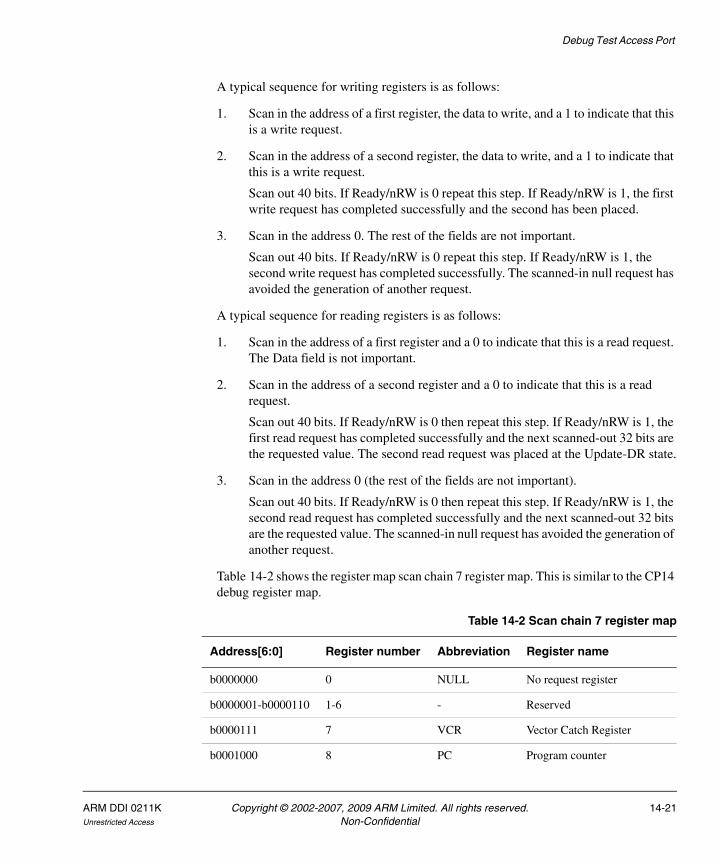
Debug Test Access Port
A typical sequence for writing registers is as follows:
1. Scan in the address of a first register, the data to write, and a 1 to indicate that this is a write request.
2. Scan in the address of a second register, the data to write, and a 1 to indicate that this is a write request.
Scan out 40 bits. If Ready/nRW is 0 repeat this step. If Ready/nRW is 1, the first write request has completed successfully and the second has been placed.
3. Scan in the address 0. The rest of the fields are not important.
Scan out 40 bits. If Ready/nRW is 0 repeat this step. If Ready/nRW is 1, the second write request has completed successfully. The scanned-in null request has avoided the generation of another request.
A typical sequence for reading registers is as follows:
1. Scan in the address of a first register and a 0 to indicate that this is a read request. The Data field is not important.
2. Scan in the address of a second register and a 0 to indicate that this is a read request.
Scan out 40 bits. If Ready/nRW is 0 then repeat this step. If Ready/nRW is 1, the first read request has completed successfully and the next scanned-out 32 bits are the requested value. The second read request was placed at the Update-DR state.
3. Scan in the address 0 (the rest of the fields are not important).
Scan out 40 bits. If Ready/nRW is 0 then repeat this step. If Ready/nRW is 1, the second read request has completed successfully and the next scanned-out 32 bits are the requested value. The scanned-in null request has avoided the generation of another request.
Table 14-2 shows the register map scan chain 7 register map. This is similar to the CP14 debug register map.
Table 14-2 Scan chain 7 register map
Address[6:0] Register number Abbreviation Register name
b0000000 0 NULL No request register
b0000001-b0000110 1-6 - Reserved
b0000111 7 VCR Vector Catch Register
b0001000 8 PC Program counter
ARM DDI 0211K Copyright © 2002-2007, 2009 ARM Limited. All rights reserved. 14-21Unrestricted Access Non-Confidential

Debug Test Access Port
The following points apply to the use of scan chain 7:
• Every time there is a request to read the PC, a sample of its value is copied into scan chain 7. Writes are ignored. The sampled value can be used for profiling of the code. See Interpreting the PC samples for details of how to interpret the sampled value.
• When accessing registers using scan chain 7, the processor can be either in Debug state or in normal state. This implies that breakpoints, watchpoints, and vector catches can be programmed through the Debug Test Access Port even if the processor is running. However, although a PC read can be requested in Debug state, the result is Undefined.
Interpreting the PC samples
The PC values read correspond to instructions committed for execution, including those that failed their condition code. These offsets are different for different processor states, so additional information is required:
• If a read request to the PC completes and Data[1:0] equals b00, the read value corresponds to an ARM state instruction whose 30 most significant bits of the offset address (instruction address + 8) are given in Data[31:2].
b0010011-b0111111 19-63 - Reserved
b1000000-b1000101 64-69 BVRya Breakpoint Value Registers
b1000110-b1001111 70-79 - Reserved
b1010000-b1010101 80-85 BCRya Breakpoint Control Registers
b1010110-b1011111 86-95 - Reserved
b1100000-b1100001 96-97 WVRya Watchpoint Value Registers
b1100010-1b101111 98-111 - Reserved
b1110000-b1110001 112-113 WCRya Watchpoint Control Registers
b1110010-b1111111 114-127 - Reserved
a. y is the decimal representation for the binary number Address[3:0]
Table 14-2 Scan chain 7 register map (continued)
Address[6:0] Register number Abbreviation Register name
14-22 Copyright © 2002-2007, 2009 ARM Limited. All rights reserved. ARM DDI 0211KNon-Confidential Unrestricted Access

Debug Test Access Port
• If a read request to the PC completes and Data[0] equals b1, the read value corresponds to a Thumb state instruction whose 31 most significant bits of the offset address (instruction address + 4) are given in Data[31:1].
• If a read request to the PC completes and Data[1:0] equals b10, the read value corresponds to a Jazelle bytecode whose 30 most significant bits of its address are given in Data[31:2] (the offset is 0). Because of the state encoding, the lower two bits of the bytecode address are not sampled. However, the information provided is enough for profiling the code.
• If the PC is read while the processor is in Debug state, the result is Unpredictable.
Scan chains 8-15
These scan chains are reserved.
Scan chains 16-31
These scan chains are unassigned.
14.6.6 Reset
The DBGTAP is reset either by asserting DBGnTRST, or by clocking it while the DBGTAPSM is in the Test-Logic-Reset state. The processor, including CP14 debug logic, is not affected by these events. See Reset modes on page 9-7 and CP14 registers reset on page 13-43 for details.
ARM DDI 0211K Copyright © 2002-2007, 2009 ARM Limited. All rights reserved. 14-23Unrestricted Access Non-Confidential

Debug Test Access Port
14.7 Using the Debug Test Access Port
This section contains the following subsections:
• Entering and leaving Debug state
• Executing instructions in Debug state
• Using the ITRsel IR instruction on page 14-25
• Transferring data between the host and the core on page 14-27
• Using the debug communications channel on page 14-27
• Target to host debug communications channel sequence on page 14-28
• Host to target debug communications channel on page 14-29
• Transferring data in Debug state on page 14-29
• Example sequences on page 14-30.
14.7.1 Entering and leaving Debug state
These debug sequences are described in detail in Debug sequences on page 14-34.
14.7.2 Executing instructions in Debug state
When the ARM1136JF-S processor is in Debug state, it can be forced to execute ARM state instructions using the DBGTAP. Two registers are used for this purpose, the Instruction Transfer Register (ITR) and the Data Transfer Register (DTR).
The ITR is used to insert an instruction into the processor pipeline. An ARM state instruction can be loaded into this register using scan chain number 4. When the instruction is loaded, and INTEST or EXTEST is selected, and scan chain 4 or 5 is selected, the instruction can be issued to the core by making the DBGTAPSM go through the Run-Test/Idle state, provided certain conditions are met (described in this section). This mechanism enables re-executing the same instruction over and over without having to reload it.
The DTR can be used in conjunction with the ITR to transfer data in and out of the core. For example, to read out the value of an ARM register:
1. issue an MCR p14,0,<Rd>,c0,c5,0 instruction to the core to transfer the Rd contents to the c5 register
2. scan out the wDTR.
The DSCR[13] execute ARM instruction enable bit controls the activation of the ARM instruction execution mechanism. If this bit is cleared, no instruction is issued to the core when the DBGTAPSM goes through Run-Test/Idle. Setting this bit while the core is not in Debug state leads to Unpredictable behavior. If the core is in Debug state and
14-24 Copyright © 2002-2007, 2009 ARM Limited. All rights reserved. ARM DDI 0211KNon-Confidential Unrestricted Access

Debug Test Access Port
this bit is set, the Ready and the sticky precise Data Abort flags condition the updates of the ITR and the instruction issuing as described in Scan chain 4, Instruction Transfer Register (ITR) on page 14-14.
As an example, this sequence stores out the contents of the ARM register R0:
1. SCAN_N into the IR.
2. 1 into the SCREG.
3. INTEST into the IR.
4. Scan out the contents of the DSCR. This action clears the sticky precise Data Abort and sticky imprecise Data Abort flags.
5. EXTEST into the IR.
6. Scan in the previously read value with the DSCR[13] execute ARM instruction enable bit set.
7. SCAN_N into the IR.
8. 4 into the SCREG.
9. EXTEST into the IR.
10. Scan the MCR p14,0,R0,c0,c5,0 instruction into the ITR.
11. Go through the Run-Test/Idle state of the DBGTAPSM.
12. SCAN_N into the IR.
13. 5 into the SCREG.
14. INTEST into the IR.
15. Scan out 34 bits. The 33rd bit indicates if the instruction has completed. If the bit is clear, repeat this step again.
16. The least significant 32 bits hold the contents of R0.
14.7.3 Using the ITRsel IR instruction
When the ITRsel instruction is loaded into the IR, at the Update-IR state, the DBGTAP controller behaves as if EXTEST and scan chain 4 are selected, but SCREG retains its value. It can be used to speed up certain debug sequences.
Figure 14-14 on page 14-26 shows the effect of the ITRsel IR instruction.
ARM DDI 0211K Copyright © 2002-2007, 2009 ARM Limited. All rights reserved. 14-25Unrestricted Access Non-Confidential

Debug Test Access Port
Figure 14-14 Behavior of the ITRsel IR instruction
Consider for example the preceding sequence to store out the contents of ARM register R0. This is the same sequence using the ITRsel instruction:
1. SCAN_N into the IR.
2. 1 into the SCREG.
3. INTEST into the IR.
4. Scan out the contents of the DSCR. This action clears the sticky precise Data Abort and sticky imprecise Data Abort flags.
5. EXTEST into the IR.
6. Scan in the previously read value with the DSCR[13] execute ARM instruction enable bit set.
7. SCAN_N into the IR.
8. 5 into the SCREG.
9. ITRsel into the IR. Now the DBGTAP controller works as if EXTEST and scan chain 4 is selected.
10. Scan the MCR p14,0,R0,c0,c5,0 instruction into the ITR.
11. Go through the Run-Test/Idle state of the DBGTAPSM.
12. INTEST into the IR. Now INTEST and scan chain 5 are selected.
13. Scan out 34 bits. The 33rd bit indicates if the instruction has completed. If the bit is clear, repeat this step again.
01=ITRSEL? Yes
IR SCREG
EXTEST
01
Scan chain4
Current IRinstruction
Currentscan chain
14-26 Copyright © 2002-2007, 2009 ARM Limited. All rights reserved. ARM DDI 0211KNon-Confidential Unrestricted Access

Debug Test Access Port
14. The least significant 32 bits hold the contents of R0.
The number of steps has been reduced from 16 to 14. However, the bigger reduction comes when reading additional registers. Using the ITRsel instruction there are 6 extra steps (9 to 14), compared with 10 extra steps (7 to 16) in the first sequence.
14.7.4 Transferring data between the host and the core
There are two ways in which a DBGTAP debugger can send or receive data from the core:
• using the DCC, when the ARM1136JF-S processor is not in Debug state
• using the instruction execution mechanism described in Executing instructions in Debug state on page 14-24, when the core is in Debug state.
This is described in:
• Using the debug communications channel
• Target to host debug communications channel sequence on page 14-28
• Host to target debug communications channel on page 14-29
• Transferring data in Debug state on page 14-29
• Example sequences on page 14-30.
14.7.5 Using the debug communications channel
The DCC is defined as the set of resources that the external DBGTAP debugger uses to communicate with a piece of software running on the core.
The DCC in the ARM1136JF-S processor is implemented using the two physically separate DTRs and a full/empty bit pair to augment each register, creating a bidirectional data port. One register can be read from the DBGTAP and is written from the processor. The other register is written from the DBGTAP and read by the processor. The full/empty bit pair for each register is automatically updated by the debug unit hardware, and is accessible to both the DBGTAP and to software running on the processor.
At the core side, the DCC resources are the following:
• CP14 Debug Transfer Register c5 (DTR). Data coming from a DBGTAP debugger can be read by an MRC or STC instruction addressed to this register. The core can write to this register any data intended for the DBGTAP debugger, using an MCR or LDC instruction. Because the DTR comprises both a read (rDTR) and a write portion (wDTR), a piece of data written by the core and another coming from the DBGTAP debugger can be held in this register at the same time.
ARM DDI 0211K Copyright © 2002-2007, 2009 ARM Limited. All rights reserved. 14-27Unrestricted Access Non-Confidential

Debug Test Access Port
• Some flags and control bits in CP14 Debug Status and Control Register c1 (DSCR):
DSCR[12] User mode access to DCC disable bit. If this bit is set, only privileged software can access the DCC. That is, access the DSCR and the DTR.
DSCR[29] The wDTRfull flag. When clear, this flag indicates to the core that the wDTR is ready to receive data from the core.
DSCR[30] The rDTRfull flag. When set, this flag indicates to the core that there is data available to read at the DTR.
At the DBGTAP side, the resources are the following:
• Scan chain 5 (see Scan chain 5 on page 14-16). The only part of this scan chain that it is not used for the DCC is the Ready flag. The rest of the scan chain is to be used in the following way:
rDTR When the DBGTAPSM goes through the Update-DR state with EXTEST and scan chain 5 selected, and the nRetry flag set, the contents of the Data field are loaded into the rDTR. This is how the DBGTAP debugger sends data to the software running on the core.
wDTR When the DBGTAPSM goes through the Capture-DR state with INTEST and scan chain 5 selected, the contents of the wDTR are loaded into the Data field of the scan chain. This is how the DBGTAP debugger reads the data sent by the software running on the core.
Valid flag When set, this flag indicates to the DBGTAP debugger that the contents of the wDTR that it has just captured are valid.
nRetry flag When set, this flag indicates to the DBGTAP debugger that the scanned-in Data field has been successfully written into the rDTR at the Update-DR state.
14.7.6 Target to host debug communications channel sequence
The DBGTAP debugger can use the following sequence for receiving data from the core:
1. SCAN_N into the IR.
2. 5 into the SCREG.
3. INTEST into the IR.
4. Scan out 34 bits of data. If the Valid flag is clear repeat this step again.
14-28 Copyright © 2002-2007, 2009 ARM Limited. All rights reserved. ARM DDI 0211KNon-Confidential Unrestricted Access

Debug Test Access Port
5. The least significant 32 bits hold valid data.
6. Go to step 4 again for reading out more data.
14.7.7 Host to target debug communications channel
The DBGTAP debugger can use the following sequence for sending data to the core:
1. SCAN_N into the IR.
2. 5 into the SCREG.
3. EXTEST into the IR.
4. Scan in 34 bits, the least significant 32 holding the word to be sent. At the same time, 34 bits were scanned out. If the nRetry flag is clear repeat this step again.
5. Now the data has been written into the rDTR. Go to step 4 again for sending in more data.
14.7.8 Transferring data in Debug state
When the core is in Debug state, the DBGTAP debugger can transfer data in and out of the core using the instruction execution facilities described in Executing instructions in Debug state on page 14-24 in addition to scan chain 5. You must ensure that the DSCR[13] execute ARM instruction enable bit is set for the instruction execution mechanism to work. When it is set, the interface for the DBGTAP debugger consists of the following:
• Scan chain 4 (see Scan chain 4, Instruction Transfer Register (ITR) on page 14-14). It is used for loading an instruction and for monitoring the status of the execution:
ITR When the DBGTAPSM goes through the Update-DR state with EXTEST and scan chain 4 selected, and the Ready flag set, the ITR is loaded with the least significant 32 bits of the scan chain.
InstCompl flag When clear, this flag indicates to the DBGTAP debugger that the last issued instruction has not yet completed execution. While Ready (captured version of InstCompl) is clear, no updates of the ITR and the rDTR occur and the instruction execution mechanism is disabled. No instruction is issued when going through Run-Test/Idle.
ARM DDI 0211K Copyright © 2002-2007, 2009 ARM Limited. All rights reserved. 14-29Unrestricted Access Non-Confidential

Debug Test Access Port
• Scan chain 5 (see Scan chain 5 on page 14-16). It is used for writing in or reading out the data and for monitoring the state of the execution:
rDTR When the DBGTAPSM goes through the Update-DR state with EXTEST and scan chain 5 selected, and the Ready flag set, the contents of the Data field are loaded into the rDTR.
wDTR When the DBGTAPSM goes through the Capture-DR state with INTEST or EXTEST selected, the contents of the wDTR are loaded into the Data field of the scan chain.
InstCompl flag When clear, this flag indicates to the DBGTAP debugger that the last issued instruction has not yet completed execution. While Ready (captured version of InstCompl) is clear, no updates of the ITR and the rDTR occur and the instruction execution mechanism is disabled. No instruction is issued when going through Run-Test/Idle.
• Some flags and control bits at CP14 debug register c1 (DSCR):
DSCR[13] Execute ARM instruction enable bit. This bit must be set for the instruction execution mechanism to work.
Sticky precise Data Abort flag DSCR[6]. When set, this flag indicates to the DBGTAP debugger that a precise Data Abort occurred while executing an instruction in Debug state. While this bit is set, the instruction execution mechanism is disabled. When this flag is set InstCompl stays HIGH, and additional attempts to execute an instruction appear to succeed but do not execute.
Sticky imprecise Data Abort flag DSCR[7]. When set, this flag indicates to the DBGTAP debugger that an imprecise Data Abort occurred while executing an instruction in Debug state. This flag does not disable the Debug state instruction execution.
14.7.9 Example sequences
This section includes some example sequences to illustrate how to transfer data between the DBGTAP debugger and the core when it is in Debug state. The examples are related to accessing the processor memory.
14-30 Copyright © 2002-2007, 2009 ARM Limited. All rights reserved. ARM DDI 0211KNon-Confidential Unrestricted Access

Debug Test Access Port
Target to host transfer
The DBGTAP debugger can use the following sequence for reading data from the processor memory system. The sequence assumes that the ARM register R0 contains a pointer to the address of memory at which the read has to start:
1. SCAN_N into the IR.
2. 1 into the SCREG.
3. INTEST into the IR.
4. Scan out the contents of the DSCR. This clears the sticky precise Data Abort and sticky imprecise Data Abort flags.
5. SCAN_N into the IR.
6. 4 into the SCREG.
7. EXTEST into the IR.
8. Scan in the LDC p14,c5,[R0],#4 instruction into the ITR.
9. SCAN_N into the IR.
10. 5 into the SCREG.
11. INTEST into the IR.
12. Go through Run-Test/Idle state. The instruction loaded into the ITR is issued to the processor pipeline.
13. Scan out 34 bits of data. If the Ready flag is clear repeat this step again.
14. The instruction has completed execution. Store the least significant 32 bits.
15. Go to step 12 again for reading out more data.
16. SCAN_N into the IR.
17. 1 into the SCREG.
18. INTEST into the IR.
19. Scan out the contents of the DSCR. This clears the sticky precise Data Abort and sticky imprecise Data Abort flags. If the sticky precise Data Abort is set, this means that during the sequence one of the instructions caused a precise Data Abort. All the instructions that follow are not executed. Register R0 points to the next word to be read, and after the cause for the abort has been fixed the sequence resumes at step 5.
ARM DDI 0211K Copyright © 2002-2007, 2009 ARM Limited. All rights reserved. 14-31Unrestricted Access Non-Confidential

Debug Test Access Port
Note If the sticky imprecise Data Aborts flag is set, an imprecise Data Abort has
occurred and the sequence restarts at step 1 after the cause of the abort is fixed and R0 is reloaded.
Host to target transfer
The DBGTAP debugger can use the following sequence for writing data to the processor memory system. The sequence assumes that the ARM register R0 contains a pointer to the address of memory at which the write has to start:
1. SCAN_N into the IR.
2. 1 into the SCREG.
3. INTEST into the IR.
4. Scan out the contents of the DSCR. This clears the sticky precise Data Abort and sticky imprecise Data Abort flags.
5. SCAN_N into the IR.
6. 4 into the SCREG.
7. EXTEST into the IR.
8. Scan in the STC p14,c5,[R0],#4 instruction into the ITR.
9. SCAN_N into the IR.
10. 5 into the SCREG.
11. EXTEST into the IR.
12. Scan in 34 bits, the least significant 32 holding the word to be sent. At the same time, 34 bits are scanned out. If the Ready flag is clear, repeat this step.
13. Go through Run-Test/Idle state.
14. Go to step 12 again for writing in more data.
15. Scan in 34 bits. All the values are don’t care. At the same time, 34 bits are scanned out. If the Ready flag is clear, repeat this step. The don’t care value is written into the rDTR (Update-DR state) just after Ready is seen set (Capture-DR state). However, the STC instruction is not re-issued because the DBGTAPSM does not go through Run-Test/Idle.
14-32 Copyright © 2002-2007, 2009 ARM Limited. All rights reserved. ARM DDI 0211KNon-Confidential Unrestricted Access
Debug Test Access Port
16. SCAN_N into the IR.
17. 1 into the SCREG.
18. INTEST into the IR.
19. Scan out the contents of the DSCR. This clears the sticky precise Data Abort and sticky imprecise Data Abort flags. If the sticky precise Data Abort is set, this means that during the sequence one of the instructions caused a precise Data Abort. All the instructions that follow are not executed. Register R0 points to the next word to be written, and after the cause for the abort has been fixed the sequences resumes at step 5.
Note If the sticky imprecise Data Abort flag is set, an imprecise Data Abort has
occurred and the sequence restarts at step 1 after the cause of the abort is fixed and c0 is reloaded.
ARM DDI 0211K Copyright © 2002-2007, 2009 ARM Limited. All rights reserved. 14-33Unrestricted Access Non-Confidential

Debug Test Access Port
14.8 Debug sequences
This section describes some sequences of operations that a debugger might execute as part of the debugging process. The purpose of this section is to show how the debug features work by providing a hypothetical usage model. A developer of a debugger for the ARM1136JF-S processor must not use the information provided in this section as a recommended implementation.
In Halting debug-mode, the processor stops when a debug event occurs enabling the DBGTAP debugger to do the following:
1. Determine and modify the current state of the processor and memory.
2. Set up breakpoints, watchpoints, and vector catches.
3. Restart the processor.
You enable this mode by setting CP14 debug DSCR[14] bit, which can only be done by the DBGTAP debugger.
From here it is assumed that the debug unit is in Halting debug-mode. Monitor debug-mode debugging is described in Monitor debug-mode debugging on page 14-50.
14.8.1 Debug macros
The debug code sequences in this section are written using a fixed set of macros. The mapping of each macro into a debug scan chain sequence is given in this section.
SCAN_N <n>
Select scan chain register number <n>:
1. Scan the SCAN_N instruction into the IR.
2. Scan the number <n> into the DR.
INTEST
1. Scan the INTEST instruction into the IR.
EXTEST
1. Scan the EXTEST instruction into the IR.
ITRsel
1. Scan the ITRsel instruction into the IR.
14-34 Copyright © 2002-2007, 2009 ARM Limited. All rights reserved. ARM DDI 0211KNon-Confidential Unrestricted Access

Debug Test Access Port
Restart
1. Scan the Restart instruction into the IR.
2. Go to the DBGTAP controller Run-Test/Idle state so that the processor exits Debug state.
INST <instr> [stateout]
Go through Capture-DR, go to Shift-DR, scan in an ARM instruction to be read and executed by the core and scan out the Ready flag, go through Update-DR. The ITR (scan chain 4) and EXTEST must be selected when using this macro.
1. Scan in:
• Any value for the InstCompl flag. This bit is read-only.
• 32-bit assembled code of the instruction (instr) to be executed, for ITR[31:0].
2. The following data is scanned out:
• The value of the Ready flag, to be stored in stateout.
• 32 bits to be ignored. The ITR is write-only.
DATA <datain> [<stateout> [dataout]]
Go through Capture-DR, go to Shift-DR. Scan in a data item and scan out another one, go through Update-DR. Either the DTR (scan chain 5) or the DSCR (scan chain 1) must be selected when using this macro.
1. If scan chain 5 is selected, scan in:
• Any value for the nRetry or Valid flag. These bits are read-only.
• Any value for the InstCompl flag. This bit is read-only.
• 32-bit datain value for rDTR[31:0].
2. The following data is scanned out:
• The contents of wDTR[31:0], to be stored in dataout.
• If the DSCR[13] execute ARM instruction enable bit is set, the value of the Ready flag is stored in stateout.
• If the DSCR[13] execute ARM instruction enable bit is clear, the nRetry or Valid flag (depending on whether EXTEST or INTEST is selected) is stored in stateout.
ARM DDI 0211K Copyright © 2002-2007, 2009 ARM Limited. All rights reserved. 14-35Unrestricted Access Non-Confidential

Debug Test Access Port
3. If scan chain 1 is selected, scan in:
• 32-bit datain value for DSCR[31:0].
Stateout and dataout fields are not used in this case.
DATAOUT <dataout>
1. Scan out a data value. DSCR (scan chain 1) and INTEST must be selected when using this macro.
2. If scan chain 1 is selected, scan out the contents of the DSCR, to be stored in dataout.
3. The scanned-in value is discarded, because INTEST is selected.
REQ <address> <data> <nR/W> [<stateout> [dataout]]
Go through Capture-DR, go to Shift-DR, scan in a request and scan out the result of the former one, go through Update-DR. Scan chain 7, and either INTEST or EXTEST, must be selected when using this macro.
1. Scan in:
• 7-bit address value for Address[6:0]
• 32-bit data value for Data[31:0]
• 1-bit nR/W value (0 for read and 1 for write) for the Ready/nRW field.
2. Scan out:
• the value of the Ready/nRW bit, to be stored in stateout
• the contents of the Data field, to be stored in dataout.
RTI
1. Go through Run-Test/Idle DBGTAPSM state. This forces the execution of the instruction currently loaded into the ITR, provided the execute ARM instruction enable bit (DSCR[13]) is set, the Ready flag was captured as set, and the sticky precise Data Abort flag is cleared.
14-36 Copyright © 2002-2007, 2009 ARM Limited. All rights reserved. ARM DDI 0211KNon-Confidential Unrestricted Access

Debug Test Access Port
14.8.2 General setup
You must setup the following control bits before DBGTAP debugging can take place:
• DSCR[14] Halt/Monitor debug-mode bit must be set to 1. It resets to 0 on power-up.
• DSCR[6] sticky precise Data Abort flag must be cleared down, so that aborts are not detected incorrectly immediately after startup.
The DSCR must be read, the DSCR[14] bit set, and the new value written back. The action of reading the DSCR automatically clears the DSCR[6] sticky precise Data Abort flag.
All individual breakpoints, watchpoints, and vector catches reset disabled on power-up.
14.8.3 Forcing the processor to halt
Scan the Halt instruction into the DBGTAP controller IR and go through Run-Test/Idle.
14.8.4 Entering Debug state
To enter Debug state you must:
1. Check whether the core has entered Debug state, as follows:
SCAN_N 1 ; select DSCRINTESTLOOP
DATAOUT readDSCRUNTIL readDSCR[0]==1 ; until Core Halted bit is set
2. Save DSCR, as follows:
DATAOUT readDSCRSave value in readDSCR
3. Save wDTR (in case it contains some data), as follows:
SCAN_N 5 ; select DTRINTESTDATA 0x00000000 Valid wDTRIf Valid==1 then Save value in wDTR
4. Set the DSCR[13] execute ARM instruction enable bit, so instructions can be issued to the core from now:
SCAN_N 1 ; select DSCRINTESTDATA modifiedDSCR ; modifiedDSCR equals readDSCR with bit
; DSCR[13] set
ARM DDI 0211K Copyright © 2002-2007, 2009 ARM Limited. All rights reserved. 14-37Unrestricted Access Non-Confidential

Debug Test Access Port
5. Before executing any instruction in Debug state you have to drain the write buffer. This ensures that no imprecise Data Aborts can return at a later point:
SCAN_N 4 ; select ITREXTESTINST MCR p15,0,Rd,c7,c10,4 ; drain write bufferLOOP
LOOPSCAN_N 4 ; select ITREXTESTRTIINST 0x0 Ready
Until Ready == 1SCAN_N 1INTESTDATAOUT readDSCR
Until readDSCR[7]==0SCAN_N 4EXTESTINST NOP ; NOP takes theRTI ; imprecise Data AbortsLOOP
INST 0 ReadyUntil Ready == 1SCAN_N 1INTESTDATAOUT readDSCR ; clears DSCR[7]
Note If there is a lingering imprecise Data Abort at the time of executing a drain write
buffer, the ARM architecture does not define it if this instruction completes successfully, or if it is cancelled by this abort. Therefore, this sequence issues the drain write buffer repeatedly until it completes successfully. An additional NOP instruction is inserted at the end of the drain write buffer sequence in case the device behavior is to recognize the imprecise Data Abort after this drain write buffer instruction completes.
6. Store out R0. It is going to be used to save the rDTR. Use the standard sequence of Reading a current mode ARM register in the range R0-R14 on page 14-41. Scan chain 5 and INTEST are now selected.
7. Save the rDTR and the rDTRempty bit in three steps:
a. The rDTRempty bit is the inverted version of DSCR[30] (saved in step 2). If DSCR[30] is clear (register empty) there is no requirement to read the rDTR, go to 7.
b. Transfer the contents of rDTR to R0:
14-38 Copyright © 2002-2007, 2009 ARM Limited. All rights reserved. ARM DDI 0211KNon-Confidential Unrestricted Access

Debug Test Access Port
ITRSEL ; select the ITR and EXTESTINST MRC p14,0,R0,c0,c5,0 ; instruction to copy CP14’s debug
; register c5 into R0RTILOOP
INST 0x00000000 ReadyUNTIL Ready==1 ; wait until the instruction ends
c. Read R0 using the standard sequence of Reading a current mode ARM register in the range R0-R14 on page 14-41.
8. Store out CPSR using the standard sequence of Reading the CPSR/SPSR on page 14-42.
9. Store out PC using the standard sequence of Reading the PC on page 14-42.
10. Adjust the PC to enable you to resume execution later:
• subtract 0x8 from the stored value if the processor was in ARM state when entering Debug state
• subtract 0x4 from the stored value if the processor was in Thumb state when entering Debug state
• subtract 0x0 from the stored value if the processor was in Jazelle state when entering Debug state.
These values are not dependent on the Debug state entry method, (see Behavior of the PC in Debug state on page 13-54). The entry state can be determined by examining the T and J bits of the CPSR.
11. Cache and MMU preservation measures must also be taken here. This includes saving all the relevant CP15 registers using the standard coprocessor register reading sequence described in Coprocessor register reads and writes on page 14-47.
14.8.5 Leaving Debug state
To leave Debug state:
1. Restore standard ARM registers for all modes, except R0, PC, and CPSR.
2. Cache and MMU restoration must be done here. This includes writing the saved registers back to CP15.
3. Ensure that rDTR and wDTR are empty:
ITRSEL ; select the ITR and EXTESTINST MCR p14,0,R0,c0,c5,0 ; instruction to copy R0 into
; CP14 debug register c5RTI
ARM DDI 0211K Copyright © 2002-2007, 2009 ARM Limited. All rights reserved. 14-39Unrestricted Access Non-Confidential
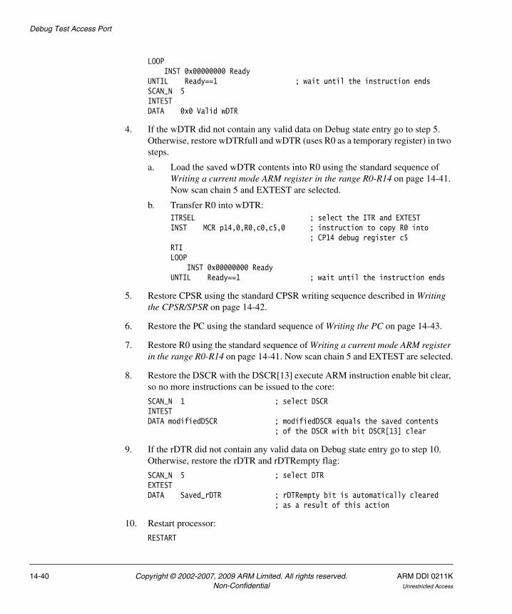
Debug Test Access Port
LOOPINST 0x00000000 Ready
UNTIL Ready==1 ; wait until the instruction endsSCAN_N 5INTESTDATA 0x0 Valid wDTR
4. If the wDTR did not contain any valid data on Debug state entry go to step 5. Otherwise, restore wDTRfull and wDTR (uses R0 as a temporary register) in two steps.
a. Load the saved wDTR contents into R0 using the standard sequence of Writing a current mode ARM register in the range R0-R14 on page 14-41. Now scan chain 5 and EXTEST are selected.
b. Transfer R0 into wDTR:ITRSEL ; select the ITR and EXTESTINST MCR p14,0,R0,c0,c5,0 ; instruction to copy R0 into
; CP14 debug register c5RTILOOP
INST 0x00000000 ReadyUNTIL Ready==1 ; wait until the instruction ends
5. Restore CPSR using the standard CPSR writing sequence described in Writing the CPSR/SPSR on page 14-42.
6. Restore the PC using the standard sequence of Writing the PC on page 14-43.
7. Restore R0 using the standard sequence of Writing a current mode ARM register in the range R0-R14 on page 14-41. Now scan chain 5 and EXTEST are selected.
8. Restore the DSCR with the DSCR[13] execute ARM instruction enable bit clear, so no more instructions can be issued to the core:
SCAN_N 1 ; select DSCRINTESTDATA modifiedDSCR ; modifiedDSCR equals the saved contents
; of the DSCR with bit DSCR[13] clear
9. If the rDTR did not contain any valid data on Debug state entry go to step 10. Otherwise, restore the rDTR and rDTRempty flag:
SCAN_N 5 ; select DTREXTESTDATA Saved_rDTR ; rDTRempty bit is automatically cleared
; as a result of this action
10. Restart processor:
RESTART
14-40 Copyright © 2002-2007, 2009 ARM Limited. All rights reserved. ARM DDI 0211KNon-Confidential Unrestricted Access

Debug Test Access Port
11. Wait until the core is restarted:
SCAN_N 1 ; select DSCRINTESTLOOP
DATAOUT readDSCRUNTIL readDSCR[1]==1 ; until Core Restarted bit is set
14.8.6 Reading a current mode ARM register in the range R0-R14
Use the following sequence to read a current mode ARM register in the range R0-R14:
SCAN_N 5 ; select DTRITRSEL ; select the ITR and EXTESTINST MCR p14,0,Rd,c0,c5,0 ; instruction to copy Rd into CP14 debug
; register c5RTIINTEST ; select the DTR and INTESTLOOP
DATA 0x00000000 Ready readDataUNTIL Ready==1 ; wait until the instruction endsSave value in readData
Note Register R15 cannot be read in this way because the effect of the required MCR is to take an Undefined Instruction exception.
14.8.7 Writing a current mode ARM register in the range R0-R14
Use the following sequence to write a current mode ARM register in the range R0-R14:
SCAN_N 5 ; select DTRITRSEL ; select the ITR and EXTESTINST MRC p14,0,Rd,c0,c5,0 ; instruction to copy CP14 debug
; register c5 into RdEXTEST ; select the DTR and EXTESTDATA Data2WriteRTILOOP
DATA 0x00000000 ReadyUNTIL Ready==1 ; wait until the instruction ends
Note Register R15 cannot be written in this way because the MRC instruction used would update the CPSR flags rather than the PC.
ARM DDI 0211K Copyright © 2002-2007, 2009 ARM Limited. All rights reserved. 14-41Unrestricted Access Non-Confidential

Debug Test Access Port
14.8.8 Reading the CPSR/SPSR
Here R0 is used as a temporary register:
1. Move the contents of CPSR/SPSR to R0.
SCAN_N 5 ; select DTRITRSEL ; select the ITR and EXTESTINST MRS R0,CPSR ; or SPSRRTILOOP
INST 0x00000000 ReadyUNTIL Ready==1 ; wait until the instruction ends
2. Perform the read of R0 using the standard sequence described in Reading a current mode ARM register in the range R0-R14 on page 14-41. Scan chain 5 and ITRsel are already selected.
14.8.9 Writing the CPSR/SPSR
Here R0 is used as a temporary register:
1. Load the desired value into R0 using the standard sequence described in Writing a current mode ARM register in the range R0-R14 on page 14-41. Now scan chain 5 and EXTEST are selected.
2. Move the contents of R0 to CPRS/SPRS:
ITRSEL ; select the ITR and EXTESTINST MSR CPSR,R0 ; or SPSRRTILOOP
INST 0x00000000 ReadyUNTIL Ready==1 ; wait until the instruction ends
It is not a problem to write to the T and J bits because they have no effect in the execution of instructions while in Debug state.
The CPSR mode and control bits can be written in User mode when the core is in Debug state. This is essential so that the debugger can change mode and then get at the other banked registers.
14.8.10 Reading the PC
Here R0 is used as a temporary register:
1. Move the contents of the PC to R0:
ITRSEL ; select the ITR and EXTESTINST MOV R0,PC
14-42 Copyright © 2002-2007, 2009 ARM Limited. All rights reserved. ARM DDI 0211KNon-Confidential Unrestricted Access

Debug Test Access Port
RTILOOP
INST 0x00000000 ReadyUNTIL Ready==1 ; wait until the instruction ends
2. Read the contents of R0 using the standard sequence described in Reading a current mode ARM register in the range R0-R14 on page 14-41.
14.8.11 Writing the PC
Here R0 is used as a temporary register:
1. Load R0 with the address to resume using the standard sequence described in Writing a current mode ARM register in the range R0-R14 on page 14-41. Now scan chain 5 and EXTEST are selected.
2. Move the contents of R0 to the PC:
ITRSEL ; select the ITR and EXTESTINST MOV PC,R0RTILOOP
INST 0x00000000 ReadyUNTIL Ready==1 ; wait until the instruction ends
14.8.12 General notes about reading and writing memory
On the ARM1136JF-S processor, an abort occurring in Debug state causes an Abort exception entry sequence to start, and so changes mode to Abort mode, and writes to R14_abt and SPSR_abt. This means that the Abort mode registers must be saved before performing a Debug state memory access.
The word-based read and write sequences are substantially more efficient than the halfword and byte sequences. This is because the ARM LDC and STC instructions always perform word accesses, and this can be used for efficient access to word width memory. Halfword and byte accesses must be done with a combination of loads or stores, and coprocessor register transfers, which is much less efficient.
When writing data, the Instruction Cache might become incoherent. In those cases, either a line or the whole Instruction Cache must be invalidated. In particular, the Instruction Cache must be invalidated before setting a software breakpoint or downloading code.
ARM DDI 0211K Copyright © 2002-2007, 2009 ARM Limited. All rights reserved. 14-43Unrestricted Access Non-Confidential

Debug Test Access Port
14.8.13 Reading memory as words
This sequence is optimized for a long sequential read.
This sequence assumes that R0 has been set to the address to load data from prior to running this sequence. R0 is post-incremented so that it can be used by successive reads of memory.
1. Load and issue the LDC instruction:
SCAN_N 5 ; select DTRITRSEL ; select the ITR and EXTESTINST LDC p14,c5,[R0],#4 ; load the content of the position of
; memory pointed by R0 into wDTR and; increment R0 by 4RTI
2. The DTR is selected in order to read the data:
INTEST ; select the DTR and INTEST
3. This loop keeps on reading words, but it stops before the latest read. It is skipped if there is only one word to read:
FOR(i=1; i <= (Words2Read-1); i++) DOLOOP
DATA 0x00000000 Ready readData ; gets the result of; the previous read
RTI ; issues the next readUNTIL Ready==1 ; wait until the instruction endsSave value in readData
ENDFOR
4. Wait for the last read to finish:
LOOPDATA 0x00000000 Ready readData
UNTIL Ready==1 ; wait until instruction endsSave value in readData
5. Now check whether an abort occurred:
SCAN_N 1 ; select DSCRINTESTDATAOUT DSCR ; this action clears the DSCR[6] flag
6. Scan out the contents of the DSCR. This clears the sticky precise Data Abort and sticky imprecise Data Abort flags. If the sticky precise Data Abort is set, this means that during the sequence one of the instructions caused a precise Data Abort. All the instructions that follow are not executed. Register R0 points to the next word to be written, and after the cause for the abort has been fixed the sequences resumes at step 1.
14-44 Copyright © 2002-2007, 2009 ARM Limited. All rights reserved. ARM DDI 0211KNon-Confidential Unrestricted Access

Debug Test Access Port
Note If the sticky imprecise Data Aborts flag is set, an imprecise Data Abort has
occurred and the sequence restarts at step 1 after the cause of the abort is fixed and R0 is reloaded.
14.8.14 Writing memory as words
This sequence is optimized for a long sequential write.
This sequence assumes that R0 has been set to the address to store data to prior to running this sequence. Register R0 is post-incremented so that it can be used by successive writes to memory:
1. The instruction is loaded:
SCAN_N 5 ; select DTRITRSEL ; select the ITR and EXTESTINST STC p14,c5,[R0],#4 ; store the contents of rDTR into the
; position of memory pointed by R0 and; increment it by 4
EXTEST ; select the DTR and EXTEST
2. This loop writes all the words:
FOR (i=1; i <= Words2Write; i++) DOLOOP
DATA Data2Write ReadyRTI
UNTIL Ready==1 ; wait until instruction endsENDFOR
3. Wait for the last write to finish:
LOOPDATA 0x00000000 Ready
UNTIL Ready==1 ; wait until instruction ends
4. Check for aborts, as described in Reading memory as words on page 14-44.
14.8.15 Reading memory as halfwords or bytes
The above sequences cannot be used to transfer halfwords or bytes because LDC and STC instructions always transfer whole words. Two operations are required to complete a halfword or byte transfer, from memory to ARM register and from ARM register to CP14 debug register. Therefore, performance is decreased because the load instruction cannot be kept in the ITR.
ARM DDI 0211K Copyright © 2002-2007, 2009 ARM Limited. All rights reserved. 14-45Unrestricted Access Non-Confidential

Debug Test Access Port
This sequence assumes that R0 has been set to the address to load data from prior to running the sequence. Register R0 is post-incremented so that it can be used by successive reads of memory. Register R1 is used as a temporary register:
1. Load and issue the LDRH or LDRB instruction:
ITRSEL ; select the ITR and EXTESTINST LDRH R1,[R0],#2 ; LDRB R1,[R0],#1 for byte readsRTILOOP
INST 0x00000000 ReadyUNTIL Ready==1 ; wait until instruction ends
2. Use the standard sequence described in Reading a current mode ARM register in the range R0-R14 on page 14-41 on register R1. Now scan chain 5 and INTEST are selected.
3. If there are more halfwords or bytes to be read go to 1.
4. Check for aborts, as described in Reading memory as words on page 14-44.
14.8.16 Writing memory as halfwords/bytes
This sequence assumes that R0 has been set to the address to store data to prior to running this sequence. Register R0 is post-incremented so that it can be used by successive writes to memory. Register R1 is used as a temporary register:
1. Write the halfword/byte onto R1 using the standard sequence described in Writing a current mode ARM register in the range R0-R14 on page 14-41. Scan chain 5 and EXTEST are selected.
2. Write the contents of R1 to memory:
ITRSEL ; select the ITR and EXTESTINST STRH R1,[R0],#2 ; STRB R1,[R0],#1 for byte writesRTILOOP
INST 0x00000000 ReadyUNTIL Ready==1 ; wait until instruction ends
3. If there are more halfwords or bytes to be read go to 1.
4. Now check for aborts as described in Reading memory as words on page 14-44.
14-46 Copyright © 2002-2007, 2009 ARM Limited. All rights reserved. ARM DDI 0211KNon-Confidential Unrestricted Access

Debug Test Access Port
14.8.17 Coprocessor register reads and writes
The ARM1136JF-S processor can execute coprocessor instructions while in Debug state. Therefore, the straightforward method to transfer data between a coprocessor and the DBGTAP debugger is using an ARM register temporarily. For this method to work, the coprocessor must be able to transfer all its registers to the core using coprocessor transfer instructions.
14.8.18 Reading coprocessor registers
1. Load the value into ARM register R0:
ITRSEL ; select the ITR and EXTESTINST MRC px,y,R0,ca,cb,zRTILOOP
INST 0x00000000 ReadyUNTIL Ready==1 ; wait until instruction ends
2. Use the standard sequence described in Reading a current mode ARM register in the range R0-R14 on page 14-41.
14.8.19 Writing coprocessor registers
1. Write the value onto R0, using the standard sequence. See Writing a current mode ARM register in the range R0-R14 on page 14-41 for more details. Scan chain 5 and EXTEST are selected.
2. Transfer the contents of R0 to a coprocessor register:
ITRSEL ; select the ITR and EXTESTINST MCR px,y,R0,ca,cb,zRTILOOP
INST 0x00000000 ReadyUNTIL Ready==1 ; wait until instruction ends
ARM DDI 0211K Copyright © 2002-2007, 2009 ARM Limited. All rights reserved. 14-47Unrestricted Access Non-Confidential

Debug Test Access Port
14.9 Programming debug events
The following operations are described:
• Reading registers using scan chain 7
• Writing registers using scan chain 7
• Setting breakpoints, watchpoints and vector catches on page 14-49
• Setting software breakpoints on page 14-49.
14.9.1 Reading registers using scan chain 7
A typical sequence for reading registers using scan chain 7 is as follows:
SCAN_N 7 ; select ITREXTESTREQ 1stAddr2Rd 0 0 ; read request for register 1stAddr2readFOR(i=2; i <= Words2Read; i++) DO
LOOPREQ ithAddr2Rd 0 0 Ready readData
; ith read request while waitingUNTIL Ready==1 ; wait until the previous request completesSave value in readData
ENDFORLOOP
REQ 0 0 0 Ready readData ; null request while waitingUNTIL Ready==1 ; wait until last request completesSave value in readData
14.9.2 Writing registers using scan chain 7
A typical sequence for writing to a register using scan chain 7 is as follows:
SCAN_N 7 ; select ITREXTESTREQ 1stAddr2Wr 1stData2Wr 0b1 ; write request for register 1stAddr2writeFOR(i=2; i <= Words2Write; i++) DO
LOOPREQ ithAddr2Wr ithData2Wr 1 Ready
; ith write request while waitingUNTIL Ready==1 ; wait until the previous request completes
ENDFORLOOP
REQ 0 0 0 Ready ; null request while waitingUNTIL Ready==1 ; wait until last request completes
14-48 Copyright © 2002-2007, 2009 ARM Limited. All rights reserved. ARM DDI 0211KNon-Confidential Unrestricted Access

Debug Test Access Port
14.9.3 Setting breakpoints, watchpoints and vector catches
You can program a vector catch debug event by writing to CP14 Debug Vector Catch Register.
You can program a breakpoint debug event by writing to CP14 debug 64-69 Breakpoint Value Registers and CP14 debug 80-84 Breakpoint Control Registers.
You can program a watchpoint debug event by writing to CP14 debug 96-97 Watchpoint Value Registers and CP14 debug 112-113 Watchpoint Control Registers.
Note An external debugger can access the CP14 debug registers whether the processor is in Debug state or not, so these debug events can be programmed on-the-fly (while the processor is in ARM, Thumb or Jazelle state).
See Setting breakpoints, watchpoints, and vector catch debug events on page 13-60 for the sequences of register accesses to program these software debug events. See Writing registers using scan chain 7 on page 14-48 to learn how to access CP14 debug registers using scan chain 7.
14.9.4 Setting software breakpoints
To set a software breakpoint on a certain Virtual Address, a debugger must go through the following steps:
1. Read memory location and save the actual instruction.
2. Write the BKPT instruction to the memory location.
3. Read memory location again to check that the BKPT instruction was written.
4. If it is not written, determine the reason.
All of these can be done using the previously described sequences.
Note Cache coherency issues might arise when writing a BKPT instruction. See Debugging in a cached system on page 13-58.
ARM DDI 0211K Copyright © 2002-2007, 2009 ARM Limited. All rights reserved. 14-49Unrestricted Access Non-Confidential

Debug Test Access Port
14.10 Monitor debug-mode debugging
If DSCR[14] Halt or Monitor debug-mode bit is clear, then the processor takes an exception (rather than halting) when a software debug event occurs. See Halting debug-mode debugging on page 13-66 for details.
When the exception is taken, the handler uses the DCC to transmit status information to, and receive commands from the host using a DBGTAP debugger. Monitor debug-mode is essential in real-time systems when the core cannot be halted to collect information.
14.10.1 Receiving data from the core
SCAN_N 5 ; select DTRINTESTFOREACH Data2Read
LOOPDATA 0x00000000 Valid readData
UNTIL Valid==1 ; wait until instruction endsSave value in readData
END
14.10.2 Sending data to the core
SCAN_N 5 ; select DTREXTESTFOREACH Data2Write
LOOPDATA Data2Write nRetry
UNTIL nRetry==1 ; wait until instruction endsEND
14-50 Copyright © 2002-2007, 2009 ARM Limited. All rights reserved. ARM DDI 0211KNon-Confidential Unrestricted Access
Chapter 15 Trace Interface Port
This chapter gives a brief description of the Embedded Trace Macrocell (ETM) support for the ARM1136JF-S processor. It contains the following section:
• About the ETM interface on page 15-2.
ARM DDI 0211K Copyright © 2002-2007, 2009 ARM Limited. All rights reserved. 15-1Unrestricted Access Non-Confidential

Trace Interface Port
15.1 About the ETM interface
The ARM1136JF-S trace interface port enables simple connection of an Embedded Trace Macrocell (ETM) to an ARM1136JF-S processor. The ETM provides instruction and data trace for the ARM1136JF-S family of processors.
All inputs are registered immediately inside the ETM unless specified otherwise. All outputs are driven directly from a register unless specified otherwise. All signals are relative to CLKIN unless specified otherwise.
The ETM interface includes the following groups of signals:
• an instruction interface
• a data address interface
• a pipeline advance interface
• a data value interface
• a coprocessor interface
• other connections to the core.
15.1.1 Instruction interface
The primary sampling point for these signals is on entry to write-back. See Typical pipeline operations on page 1-28. This ensures that instructions are traced correctly before any data transfers associated with them occur, as required by the ETM protocol.
Table 15-1 shows the instruction interface signals.
ETMIA is used for branch target address calculation.
Table 15-1 Instruction interface signals
Signal name Description Qualified by
ETMIACTL[17:0] Instruction interface control signals -
ETMIA[31:0] This is the address for:
(Executed ARM instruction) + 8
(Executed Thumb instruction) + 4
Executed Java bytecode
IAValid
ETMIARET[31:0] Address to return to if branch is incorrectly predicted IABpValid
15-2 Copyright © 2002-2007, 2009 ARM Limited. All rights reserved. ARM DDI 0211KNon-Confidential Unrestricted Access

Trace Interface Port
Other than this the ETM must know, for each cycle, the current address of the instruction in the Execute stage and the address of any branch phantom progressing through the pipeline. The ARM1136JF-S processor does not maintain the address of branch phantoms, instead it maintains the address to return to if the branch proves to be incorrectly predicted.
The instruction interface can trace a branch phantom without an associated normal instruction.
In the case of a branch that is predicted taken, the return address (for when the branch is not taken) is one instruction after the branch. Therefore, the branch address is:
ETMIABP = ETMIARET - <isize>
When the instruction is predicted not taken, the return address is the target of the branch. However, because the branch was not taken, it must precede the normal instruction. Therefore, the branch address is:
ETMIABP = ETMIA - <isize>
Table 15-2 shows the ETMIACTL[17:0] instruction interface control signals.
Table 15-2 ETMIACTL[17:0]
Bits Reference name Description Qualified by
[17] IASlotKill Kill outstanding slots. IAException
[16] IADAbort Data Abort. IAException
[15] IAExCancel Exception canceled previous instruction. IAException
[14:12] IAExInt b001 = IRQ
b101 = FIQ
b100 = Exception on Java bytecode execution
b110 = Imprecise Data Abort
b000 = Other exception.
IAException
[11] IAException Instruction is an exception vector. Nonea
[10] IABounce Kill the data slot associated with this instruction. There is only ever one of these instructions. Used for bouncing coprocessor instructions.
IADataInst
[9] IADataInst Instruction is a data instruction. This includes any load, store, or CPRT, but does not include preloads.
IAInstValid
[8] IAContextID Instruction updates context ID. IAInstValid
[7] IAIndBr Instruction is an indirect branch. IAInstValid
ARM DDI 0211K Copyright © 2002-2007, 2009 ARM Limited. All rights reserved. 15-3Unrestricted Access Non-Confidential

Trace Interface Port
Note When the nRESETIN signal is asserted, the last instruction traced before the reset might have ETMIA[31:0] == 0x00000000.
15.1.2 Data address interface
Data addresses are sampled at the ADD stage because they are guaranteed to be in order at this point. These are assigned a slot number for identification on retirement.
Table 15-3 shows the data address interface signals.
Table 15-4 on page 15-5 shows the ETMDACTL[17:0] signals.
[6] IABpCCFail Branch phantom failed its condition codes. IABpValid
[5] IAInstCCFail Instruction failed its condition codes. IAInstValid
[4] IAJBit Instruction executed in Jazelle state. IAValid
[3] IATBit Instruction executed in Thumb state. IAValid
[2] IABpValid Branch phantom executed this cycle. IAValid
[1] IAInstValid (Non-phantom) instruction executed this cycle. IAValid
[0] IAValid Signals on the instruction interface are valid this cycle. This is kept LOW when the ETM is powered down.
None
a. The exception signals become valid when the core takes the exception and remain valid until the next instruction is seen at the exception vector.
Table 15-2 ETMIACTL[17:0] (continued)
Bits Reference name Description Qualified by
Table 15-3 Data address interface signals
Signal name Description Qualified by
ETMDACTL[17:0] Data address interface control signals -
ETMDA[31:3] Address for data transfer DASlot != 00 AND !DACPRT
15-4 Copyright © 2002-2007, 2009 ARM Limited. All rights reserved. ARM DDI 0211KNon-Confidential Unrestricted Access

Trace Interface Port
Table 15-4 ETMDACTL[17:0]
BitsReference name
Description Qualified by
[17] DANSeq The data transfer is nonsequential from the last. This signal must be asserted on the first cycle of each instruction, in addition to the second transfer of a SWP or LDM PC, because the address of these transfers is not one word greater than the previous transfer, and therefore the transfer must have its address re-output.
During an unaligned access, this signal is only valid on the first transfer of the access.
DASlot != 00
[16] DALast The data transfer is the last for this data instruction. This signal is asserted for both halves of an unaligned access.
A related signal, DAFirst, can be implied from this signal, because the next transfer must be the first transfer of the next data instruction.
DASlot != 00
[15] DACPRT The data transfer is a CPRT. DASlot != 00
[14] DASwizzle Words must be byte swizzled for ARM big-endian mode.
During an unaligned access, this signal is only valid on the first transfer of the access.
DASlot != 00
[13:12] DARot Number of bytes to rotate right each word by.
During an unaligned access, these signals are only valid on the first transfer of the access.
DASlot != 00
[11] DAUnaligned First transfer of an unaligned access.
The next transfer must be the second half, for which this signal is not asserted.
DASlot != 00
[10:3] DABLSel Byte lane selects. DASlot != 00
[2] DAWrite Read or write.
During an unaligned access, this signal is only valid on the first transfer of the access.
DASlot != 00
[1:0] DASlot Slot occupied by data item. b00 indicates that no slot is in use in this cycle. This is kept at b00 when the ETM is powered down.
None
ARM DDI 0211K Copyright © 2002-2007, 2009 ARM Limited. All rights reserved. 15-5Unrestricted Access Non-Confidential

Trace Interface Port
15.1.3 Data value interface
The data values are sampled at the WBls stage. Here the load, store, MCR, and MRC data is combined. The memory view of the data is presented, which must be converted back to the register view depending on the alignment and endianness.
Data is not returned for at least two cycles after the address. However, it is not necessary to pipeline the address because the slot does not return data for a previous address during this time. Data values are defined to correspond to the most recent data addresses with the same slot number, starting from the previous cycle. In other words, data can correspond to an address from the previous cycle, but not to an address from the same cycle.
Table 15-5 shows the data value interface signals.
Table 15-6 describes the bits of ETMDDCTL[3:0] signal.
The data output values corresponding to the following CP15 operations are Unpredictable. Software development tools must not rely on these values:
MCR p15, 0, <Rd>, c7, c10, 1 ; Clean Data Cache Line using MVAMCR p15, 0, <Rd>, c7, c10, 2 ; Clean Data Cache Line using IndexMCR p15, 0, <Rd>, c7, c14, 1 ; Clean and Invalidate Data Cache Line using MVAMCR p15, 0, <Rd>, c7, c14, 2 ; Clean and Invalidate Data Cache Line using Index
Table 15-5 Data value interface signals
Signal name Description Qualified by
ETMDDCTL[3:0] Data value interface control signals -
ETMDD[63:0] Contains the data for a load, store, MRC, or MCR instruction DDSlot != 00
Table 15-6 ETMDDCTL[3:0]
Bits Reference name Description Qualified by
[3] DDImpAbort Imprecise Data Aborts on this slot. Data is ignored. DDSlot != 00
[2] DDFail STREX data write failed. DDSlot != 00
[1:0] DDSlot Slot occupied by data item. b00 indicates that no slot is in use this cycle. This is kept b00 when the ETM is powered down.
None
15-6 Copyright © 2002-2007, 2009 ARM Limited. All rights reserved. ARM DDI 0211KNon-Confidential Unrestricted Access

Trace Interface Port
15.1.4 Pipeline advance interface
There are three points in the ARM1136JF-S pipeline at which signals are produced for the ETM. These signals must be realigned by the ETM, so pipeline advance signals are provided.
The pipeline advance signals indicate when a new instruction enters pipeline stages Ex3, Ex2, and ADD, see Typical pipeline operations on page 1-28.
Table 15-7 shows the ETMPADV[2:0] pipeline advance interface signals.
The pipeline advance signals present in other interfaces are:
IAValid Instruction entered WBEx.
DASlot != 00 Data transfer entered DC1.
DDSlot != 00 Data transfer entered WBls.
Table 15-7 ETMPADV[2:0]
Bits Reference name Description Qualified by
[2] PAEx3a
a. This is kept LOW when the ETM is powered down.
Instruction entered Ex3 -
[1] PAEx2a Instruction entered Ex2 -
[0] PAAdda Instruction entered Ex1 and ADD -
ARM DDI 0211K Copyright © 2002-2007, 2009 ARM Limited. All rights reserved. 15-7Unrestricted Access Non-Confidential

Trace Interface Port
15.1.5 Coprocessor interface
This interface enables software to access ETM registers as registers in CP14. Rather than using the external coprocessor interface, the core provides a dedicated, cut-down coprocessor interface similar to that used by the debug logic.
The coprocessor interface signals are described in Table 15-8.
A complete transaction takes three cycles. The first and last cycles can overlap, giving a sustained rate of one every two cycles.
The ETM coprocessor interface also catches writes to the Context ID Register, CP15 c13 (see c13, Context ID Register on page 3-159). This enables the state of this register to be shadowed even when the core interface is powered down.
Only the following instructions are presented by the coprocessor interface:
MRC p14, 1, <Rd>, c0, c<reg[3:0]>, <reg[6:4]> ; Read ETM registerMCR p14, 1, <Rd>, c0, c<reg[3:0]>, <reg[6:4]> ; Write ETM registerMCR p15, 0, <Rd>, c13, c0, 1 ; Write Context ID Register
Where <reg[3:0]> and <reg[6:4]> are bits in the ETM register to be accessed.
Figure 15-1 on page 15-9 shows the encoding of the ETMCPADDRESS[14:0] signals.
Table 15-8 Coprocessor interface signals
Signal name Direction Description Qualified byRegister bound
ETMCPENABLE Output Interface enable. ETMCPWRITE and ETMCPADDRESS are valid this cycle, and the remaining signals are valid two cycles later.
None Yes
ETMCPCOMMIT Output Commit. If this signal is LOW two cycles after ETMCPENABLE is asserted, the transfer is canceled and must not take any effect.
ETMCPENABLE +2 Yes
ETMCPWRITE Output Read or write. Asserted for write. ETMCPENABLE Yes
ETMCPADDRESS[14:0] Output Register number. ETMCPENABLE Yes
ETMCPRDATA[31:0] Input Read data. ETMCPCOMMIT Yes
ETMCPWDATA[31:0] Output Write value. ETMCPCOMMIT Yes
15-8 Copyright © 2002-2007, 2009 ARM Limited. All rights reserved. ARM DDI 0211KNon-Confidential Unrestricted Access

Trace Interface Port
Figure 15-1 ETMCPADDRESS encoding
In Figure 15-1, the CP bit is 0 for CP14 or 1 for CP15.
Non-ETM instructions are not presented on this interface.
In contrast to the debug logic, the core makes no attempt to decode if a given ETM register exists or not. If a register does not exist, the write is silently ignored. For more details see the Embedded Trace Macrocell Architecture Specification.
15.1.6 Other connections to the core
Table 15-9 shows the other signals that are connected to the core.
14 12 11 8 7 4 3 2 0
Opcode1 CRn CRm C
POpcode
2
Table 15-9 Other connections
Signal name Direction Description
EVNTBUS[19:0] Output Gives the status of the performance monitoring events. See c15, Performance Monitor Control Register (PMNC) on page 3-168.
ETMEXTOUT[1:0] Input Provides feedback to the core of the EVNTBUS signals after being passed through ETM triggering facilities and comparators. This enables the performance monitoring facilities provide by ARM1136JF-S processors to be conditioned in the same way as ETM events. For more details see c15, Performance Monitor Control Register (PMNC) on page 3-168 and the ETM11RV Technical Reference Manual.
ETMPWRUP Input Indicates that the ETM is active. When LOW the trace interface must be clock gated to conserve power.
ARM DDI 0211K Copyright © 2002-2007, 2009 ARM Limited. All rights reserved. 15-9Unrestricted Access Non-Confidential

Trace Interface Port
15-10 Copyright © 2002-2007, 2009 ARM Limited. All rights reserved. ARM DDI 0211KNon-Confidential Unrestricted Access

Chapter 16 Cycle Timings and Interlock Behavior
This chapter describes the cycle timings and interlock behavior of integer instructions on the ARM1136JF-S processor. It contains the following sections:
• About cycle timings and interlock behavior on page 16-3
• Register interlock examples on page 16-9
• Data processing instructions on page 16-10
• QADD, QDADD, QSUB, and QDSUB instructions on page 16-13
• ARMv6 media data processing on page 16-14
• ARMv6 Sum of Absolute Differences (SAD) on page 16-16
• Multiplies on page 16-17
• Branches on page 16-19
• Processor state updating instructions on page 16-20
• Single load and store instructions on page 16-21
• Load and store double instructions on page 16-24
• Load and store multiple instructions on page 16-26
• RFE and SRS instructions on page 16-29
• Synchronization instructions on page 16-30
• Coprocessor instructions on page 16-31
• No operation instruction on page 16-32
ARM DDI 0211K Copyright © 2002-2007, 2009 ARM Limited. All rights reserved. 16-1Unrestricted Access Non-Confidential

Cycle Timings and Interlock Behavior
• SWI, BKPT, Undefined, and Prefetch Aborted instructions on page 16-33
• Thumb instructions on page 16-34.
16-2 Copyright © 2002-2007, 2009 ARM Limited. All rights reserved. ARM DDI 0211KNon-Confidential Unrestricted Access

Cycle Timings and Interlock Behavior
16.1 About cycle timings and interlock behavior
Complex instruction dependencies and memory system interactions make it impossible to describe briefly the exact cycle timing behavior for all instructions in all circumstances. The timings described in this chapter are accurate in most cases. If precise timings are required you must use a cycle-accurate model of the ARM1136JF-S processor.
Unless stated otherwise cycle counts and result latencies described in this chapter are best case numbers. They assume:
• no outstanding data dependencies between the current instruction and a previous instruction
• the instruction does not encounter any resource conflicts
• all data accesses hit in the MicroTLB and Data Cache, and do not cross protection region boundaries
• all instruction accesses hit in the Instruction Cache.
This section describes:
• Changes in instruction flow overview
• Instruction execution overview on page 16-5
• Conditional instructions on page 16-6
• Opposite condition code checks on page 16-7
• Definition of terms on page 16-5.
16.1.1 Changes in instruction flow overview
To minimize the number of cycles, because of changes in instruction flow, the ARM1136JF-S processor includes a:
• dynamic branch predictor
• static branch predictor
• return stack.
The dynamic branch predictor is a 128-entry direct-mapped branch predictor using VA bits [9:3]. The prediction scheme uses a two-bit saturating counter for predictions that are:
• Strongly Not Taken
• Weakly Not Taken
• Weakly Taken
• Strongly Taken.
ARM DDI 0211K Copyright © 2002-2007, 2009 ARM Limited. All rights reserved. 16-3Unrestricted Access Non-Confidential

Cycle Timings and Interlock Behavior
Only branches with a constant offset are predicted. Branches with a register-based offset are not predicted.
The static branch predictor operates on branches with a constant offset that are not predicted by the dynamic branch predictor. Static predictions are issued from the Iss stage of the main pipeline, consequently a statically predicted branch takes four cycles.
The return stack consists of three entries, and as with static predictions, issues a prediction from the Iss stage of the main pipeline. The return stack mispredicts if the value taken from the return stack is not the value that is returned by the instruction. Only unconditional returns are predicted. A conditional return pops an entry from the return stack but is not predicted. If the return stack is empty a return is not predicted. Items are placed on the return stack from the following instructions:
• BL #<immed>
• BLX #<immed>
• BLX Rx
Items are popped from the return stack by the following types of instruction:
• BX lr
• MOV pc, lr
• LDR pc, [sp], #cns
• LDMIA sp!, {….,pc}
A correctly predicted return stack pop takes four cycles.
16-4 Copyright © 2002-2007, 2009 ARM Limited. All rights reserved. ARM DDI 0211KNon-Confidential Unrestricted Access

Cycle Timings and Interlock Behavior
16.1.2 Definition of terms
Table 16-1 gives descriptions of cycle timing terms used in this chapter.
16.1.3 Instruction execution overview
The instruction execution pipeline is constructed from three parallel four-stage pipelines, see Table 16-2. For a complete description of these pipeline stages see Pipeline stages on page 1-26.
Table 16-1 Definition of cycle timing terms
Term Description
Cycles This is the minimum number of cycles required by an instruction.
Result latency This is the number of cycles before the result of this instruction is available for a following instruction requiring the result at the start of the ALU, MAC2, and DC1 stage. This is the normal case. Exceptions to this mark the register as an Early Reg.
Note The result latency is the number of cycles from the first cycle of an instruction.
Register lock latency For STM and STRD instructions only. This is the number of cycles that a register is write locked for by this instruction, preventing subsequent instructions that want to write the register from starting. This lock is required to prevent a following instruction from writing to a register before it has been read.
Early Reg The specified registers are required at the start of the Sh, MAC1, and ADD stage. Add one cycle to the result latency of the instruction producing this register for interlock calculations.
Late Reg The specified registers are not required until the start of the ALU, MAC2, and DC1 stage for the second execution. Subtract one cycle from the result latency of the instruction producing this register for interlock calculations.
FlagsCycleDistance The number of cycles between an instruction that sets the flags and the conditional instruction.
Table 16-2 Pipeline stages
Pipeline Stages
ALU Sh ALU Sat WBex
Multiply MAC1 MAC2 MAC3
Load/Store ADD DC1 DC2 WBls
ARM DDI 0211K Copyright © 2002-2007, 2009 ARM Limited. All rights reserved. 16-5Unrestricted Access Non-Confidential

Cycle Timings and Interlock Behavior
The ALU and multiply pipelines operate in a lock-step manner, causing all instructions in these pipelines to retire in order. The load/store pipeline is a decoupled pipeline enabling subsequent instructions in the ALU and multiply pipeline to complete underneath outstanding loads.
Extensive forwarding to the Sh, MAC1, ADD, ALU, MAC2, and DC1 stages enables many dependent instruction sequences to run without pipeline stalls. General forwarding occurs from the ALU, Sat, WBex and WBls pipeline stages. In addition, the multiplier contains an internal multiply accumulate forwarding path.
Most instructions do not require a register until the ALU stage. All result latencies are given as the number of cycles until the register is required by a following instruction in the ALU stage.
The following sequence takes four cycles:
LDR R1, [R2] ;Result latency threeADD R3, R3, R1 ;Register R1 required by ALU
If a subsequent instruction requires the register at the start of the Sh, MAC1, or ADD stage then an extra cycle must be added to the result latency of the instruction producing the required register. Instructions that require a register at the start of these stages are specified by describing that register as an Early Reg. The following sequence, requiring an Early Reg, takes five cycles:
LDR R1, [R2] ;Result latency three plus oneADD R3, R3, R1 LSL#6 ;plus one since Register R1 is required by Sh
Finally, some instructions do not require a register until their second execution cycle. If a register is not required until the ALU, MAC1, or DC1 stage for the second execution cycle, then a cycle can be subtracted from the result latency for the instruction producing the required register. If a register is not required until this later point, it is specified as a Late Reg. The following sequence where R1 is a Late Reg takes four cycles:
LDR R1, [R2] ;Result latency three minus oneADD R3, R1, R3, LSL R4 ;minus one since Register R1 is a Late Reg
;This ADD is a two issue cycle instruction
16.1.4 Conditional instructions
Most instructions execute in one or two cycles. If these instructions fail their condition codes then they take one and two cycles respectively.
16-6 Copyright © 2002-2007, 2009 ARM Limited. All rights reserved. ARM DDI 0211KNon-Confidential Unrestricted Access

Cycle Timings and Interlock Behavior
Multiplies, MRSs, and some CP14 and CP15 coprocessor instructions are the only instructions that require more than two cycles to execute. If one of these instructions fails its condition codes, then it takes a variable number of cycles to execute. The number of cycles is dependent on:
• the length of the operation
• the number of cycles between the setting of the flags and the start of the dependent instruction.
The worst-case number of cycles for a condition code failing multicycle instruction is five.
The following algorithm describes the number of cycles taken for multi-cycle instructions which condition code fail:
Min(NonFailingCycleCount, Max(5 - FlagCycleDistance, 3))
Where:
Max (a,b) returns the maximum of the two values a, b.
Min (a,b) returns the minimum of the two values a, b.
NonFailingCycleCount
is the number of cycles that the failing instruction would have taken had it passed.
FlagCycDistance is the number of cycles between the instruction that sets the flags and the conditional instruction, including interlocking cycles. For example:
• The following sequence has a FlagCycleDistance of 0 because the instructions are back-to-back with no interlocks:ADDS R1, R2, R3MULEQ R4, R5, R6
• The following sequence has a FlagCycleDistance of one:ADDS R1, R2, R3MOV R0, R0MULEQ R4, R5, R6
16.1.5 Opposite condition code checks
If instruction A and instruction B both write the same register the pipeline must ensure that the register is written in the correct order. Therefore interlocks might be required to correctly resolve this pipeline hazard.
ARM DDI 0211K Copyright © 2002-2007, 2009 ARM Limited. All rights reserved. 16-7Unrestricted Access Non-Confidential

Cycle Timings and Interlock Behavior
The only useful sequences where two instructions write the same register without an instruction reading its value in between are when the two instructions have opposite sets of condition codes. The ARM1136JF-S processor optimizes these sequences to prevent unnecessary interlocks. For example:
• The following sequences take two cycles to execute:— ADDNE R1, R5, R6
LDREQ R1, [R8]
— LDREQ R1, [R8]ADDNE R1, R5, R6
• The following sequence also takes two cycles to execute, because the STR instruction does not store the value of R1 produced by the QDADDNE instruction:
QDADDNE R1, R5, R6STREQ R1, [R8]
16-8 Copyright © 2002-2007, 2009 ARM Limited. All rights reserved. ARM DDI 0211KNon-Confidential Unrestricted Access
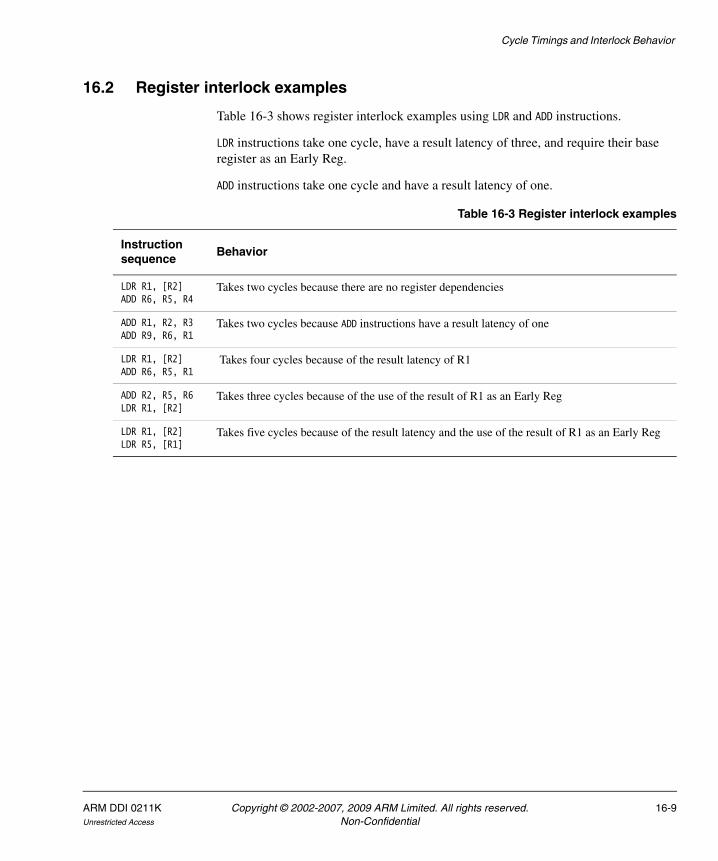
Cycle Timings and Interlock Behavior
16.2 Register interlock examples
Table 16-3 shows register interlock examples using LDR and ADD instructions.
LDR instructions take one cycle, have a result latency of three, and require their base register as an Early Reg.
ADD instructions take one cycle and have a result latency of one.
Table 16-3 Register interlock examples
Instruction sequence
Behavior
LDR R1, [R2]ADD R6, R5, R4
Takes two cycles because there are no register dependencies
ADD R1, R2, R3ADD R9, R6, R1
Takes two cycles because ADD instructions have a result latency of one
LDR R1, [R2]ADD R6, R5, R1
Takes four cycles because of the result latency of R1
ADD R2, R5, R6LDR R1, [R2]
Takes three cycles because of the use of the result of R1 as an Early Reg
LDR R1, [R2]LDR R5, [R1]
Takes five cycles because of the result latency and the use of the result of R1 as an Early Reg
ARM DDI 0211K Copyright © 2002-2007, 2009 ARM Limited. All rights reserved. 16-9Unrestricted Access Non-Confidential

Cycle Timings and Interlock Behavior
16.3 Data processing instructions
This section describes the cycle timing behavior for the AND, EOR, SUB, RSB, ADD, ADC, SBC, RSC, CMN, ORR, MOV, BIC, MVN, TST, TEQ, CMP, and CLZ instructions.
16.3.1 Cycle counts if destination is not the PC
Table 16-4 shows the cycle timing behavior for data processing instructions if the destination is not the PC. You can substitute ADD with any of the data processing instructions identified in the opening paragraph of this section.
16.3.2 Cycle counts if destination is the PC
Table 16-5 on page 16-11 shows the cycle timing behavior for data processing instructions if the destination is the PC. You can substitute ADD with any data processing instruction except for a MOV and CLZ. A CLZ with the PC as the destination is an Unpredictable instruction.
The timings for a MOV instruction are given separately in Table 16-5 on page 16-11.
Table 16-4 Data Processing instruction cycle timing behavior if destination is not PC
Example instruction CyclesEarly Reg
Late Reg
Result latency
Comment
ADD <Rd>, <Rn>, <Rm>> 1 - - 1 Normal case.
ADD <Rd>, <Rn>, <Rm>, LSL #<immed> 1 <Rm> - 1 Requires a shifted source register.
ADD <Rd>, <Rn>, <Rm>, LSL <Rs> 2 <Rs> <Rn> 2 Requires a register controlled shifted source register. Instruction takes two issue cycles. In the first cycle the shift distance Rs is sampled. In the second cycle the actual shift of Rm and the ADD instruction occurs.
16-10 Copyright © 2002-2007, 2009 ARM Limited. All rights reserved. ARM DDI 0211KNon-Confidential Unrestricted Access

Cycle Timings and Interlock Behavior
For condition code failing cycle counts, the cycles for the non-PC destination variants must be used.
16.3.3 Example interlocks
Most data processing instructions are single-cycle and can be executed back-to-back without interlock cycles, even if there are data dependencies between them. The exceptions to this are when the shifter or register controlled shifts are used.
Table 16-5 Data processing instruction cycle timing behavior if destination is the PC
Example instruction CyclesEarly Reg
Late Reg
Result latency
Comment
MOV pc, lr 4 - - - Correctly predicted return stack
MOV pc, lr 7 - - - Incorrectly predicted return stack
MOV <cond> pc, lr 5-7a - - - Conditional return, or return when return stack is empty
MOV pc, <Rd> 5 - - - MOV to PC, no shift required
MOV <cond> pc, <Rd> 5-7a - - - Conditional MOV to PC, no shift required
MOV pc, <Rn>, <Rm>, LSL #<immed> 6 <Rm> - - Conditional MOV to PC, with a shifted source register
MOV <cond> pc, <Rn>, <Rm>, LSL #<immed> 6-7a - - - Conditional MOV to PC, with a shifted source register
MOV pc, <Rn>, <Rm>, LSL <Rs> 7 <Rs> <Rn> - MOV to PC, with a register controlled shifted source register
ADD pc, <Rd>, <Rm> 7 - - - Normal case to PC
ADD pc, <Rn>, <Rm>, LSL #<immed> 7 <Rm> - - Requires a shifted source register
ADD pc, <Rn>, <Rm>, LSL <Rs> 8 <Rs> <Rn> - Requires a register controlled shifted source register
a. If the instruction is conditional and passes conditional checks it takes MAX(MaxCycles - FlagCycleDistance, MinCycles).If the instruction is unconditional it takes Min Cycles.
ARM DDI 0211K Copyright © 2002-2007, 2009 ARM Limited. All rights reserved. 16-11Unrestricted Access Non-Confidential

Cycle Timings and Interlock Behavior
Shifter
The shifter is in a separate pipeline stage from the ALU. A register required by the shifter is an Early Reg and requires an additional cycle of result availability before use. For example, the following sequence introduces a one-cycle interlock, and takes three cycles to execute:
ADD R1,R2,R3ADD R4,R5,R1 LSL #1
The second source register, which is not shifted, does not incur an extra data dependency check. Therefore, the following sequence takes two cycles to execute:
ADD R1,R2,R3ADD R4,R1,R9 LSL #1
Register controlled shifts
Register controlled shifts take two cycles to execute:
• the register containing the shift distance is read in the first cycle
• the shift is performed in the second cycle
• The final operand is not required until the ALU stage for the second cycle.
Because a shift distance is required, the register containing the shift distance is an Early Reg and incurs an extra interlock penalty. For example, the following sequence takes four cycles to execute:
ADD R1, R2, R3ADD R4, R2, R4, LSL R1
16-12 Copyright © 2002-2007, 2009 ARM Limited. All rights reserved. ARM DDI 0211KNon-Confidential Unrestricted Access

Cycle Timings and Interlock Behavior
16.4 QADD, QDADD, QSUB, and QDSUB instructions
This section describes the cycle timing behavior for the QADD, QDADD, QSUB, and QDSUB instructions.
These instructions perform saturating arithmetic. Their result is produced during the Sat stage, consequently they have a result latency of two. The QDADD and QDSUB instructions must double and saturate the register Rn before the addition. This operation occurs in the Sh stage of the pipeline, consequently this register is an Early Reg.
Table 16-6 shows the cycle timing behavior for QADD, QDADD, QSUB, and QDSUB instructions.
Table 16-6 QADD, QDADD, QSUB, and QDSUB instruction cycle timing behavior
Instructions Cycles Early Reg Result latency
QADD, QSUB 1 - 2
QDADD, QDSUB 1 <Rn> 2
ARM DDI 0211K Copyright © 2002-2007, 2009 ARM Limited. All rights reserved. 16-13Unrestricted Access Non-Confidential

Cycle Timings and Interlock Behavior
16.5 ARMv6 media data processing
Table 16-7 shows ARMv6 media data processing instructions and gives their cycle timing behavior.
All ARMv6 media data processing instructions are single-cycle issue instructions. These instructions produce their results in either the ALU or Sat stage, and have result latencies of one or two accordingly. Some of the instructions require an input register to be shifted before use and therefore are marked as requiring an Early Reg.
Table 16-7 ARMv6 media data processing instructions cycle timing behavior
Instructions Cycles Early Reg Result latency
SADD16, SSUB16, SADD8, SSUB8 1 - 1
USAD8, USADA8 1 <Rm>, <Rs> 3
UADD16, USUB16, UADD8, USUB8 1 - 1
SEL 1 - 1
QADD16, QSUB16, QADD8, QSUB8 1 - 2
SHADD16, SHSUB16, SHADD8, SHSUB8 1 - 2
UQADD16, UQSUB16, UQADD8, UQSUB8 1 - 2
UHADD16, UHSUB16, UHADD8, UHSUB8 1 - 2
SSAT16, USAT16 1 - 2
SADDSUBX, SSUBADDX 1 <Rm> 1
UADDSUBX, USUBADDX 1 <Rm> 1
SADD8TO16, SADD8TO32, SADD16TO32 1 <Rm> 1
SUNPK8TO16, SUNPK8TO32, SUNPK16TO32 1 <Rm> 1
UUNPK8TO16, UUNPK8TO32, UUNPK16TO32 1 <Rm> 1
UADD8TO16, UADD8TO32, UADD16TO32 1 <Rm> 1
REV, REV16, REVSH 1 <Rm> 1
PKHBT, PKHTB 1 <Rm> 1
SSAT, USAT 1 <Rm> 2
QADDSUBX, QSUBADDX 1 <Rm> 2
16-14 Copyright © 2002-2007, 2009 ARM Limited. All rights reserved. ARM DDI 0211KNon-Confidential Unrestricted Access

Cycle Timings and Interlock Behavior
SHADDSUBX, SHSUBADDX 1 <Rm> 2
UQADDSUBX, UQSUBADDX 1 <Rm> 2
UHADDSUBX, UHSUBADDX 1 <Rm> 2
Table 16-7 ARMv6 media data processing instructions cycle timing behavior (continued)
Instructions Cycles Early Reg Result latency
ARM DDI 0211K Copyright © 2002-2007, 2009 ARM Limited. All rights reserved. 16-15Unrestricted Access Non-Confidential

Cycle Timings and Interlock Behavior
16.6 ARMv6 Sum of Absolute Differences (SAD)
Table 16-8 shows ARMv6 SAD instructions and gives their cycle timing behavior.
16.6.1 Example interlocks
Table 16-9 shows interlock examples using USAD8 and USADA8 instructions.
Table 16-8 ARMv6 sum of absolute differences instruction timing behavior
Instructions Cycles Early Reg Result latency
USAD8 1 <Rm>, <Rs> 3a
a. Result latency is one less If the destination is the accumulate for a subsequent USADA8.
USADA8 1 <Rm>, <Rs> 3a
Table 16-9 Example interlocks
Instruction sequence
Behavior
USAD8 R1,R2,R3 ADD R5,R6,R1
Takes four cycles because USAD8 has a result latency of three, and the ADD requires the result of the USAD8 instruction.
USAD8 R1,R2,R3 MOV R9,R9MOV R9,R9ADD R5,R6,R1
Takes four cycles. The MOV instructions are scheduled during the result latency of the USAD8 instruction.
USAD8 R1,R2,R3USADA8 R1,R4,R5,R1
Takes three cycles. The result latency is one less because the result is used as the accumulate for a subsequent USADA8 instruction.
16-16 Copyright © 2002-2007, 2009 ARM Limited. All rights reserved. ARM DDI 0211KNon-Confidential Unrestricted Access
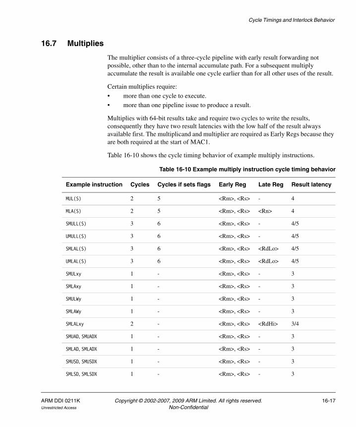
Cycle Timings and Interlock Behavior
16.7 Multiplies
The multiplier consists of a three-cycle pipeline with early result forwarding not possible, other than to the internal accumulate path. For a subsequent multiply accumulate the result is available one cycle earlier than for all other uses of the result.
Certain multiplies require:
• more than one cycle to execute.
• more than one pipeline issue to produce a result.
Multiplies with 64-bit results take and require two cycles to write the results, consequently they have two result latencies with the low half of the result always available first. The multiplicand and multiplier are required as Early Regs because they are both required at the start of MAC1.
Table 16-10 shows the cycle timing behavior of example multiply instructions.
Table 16-10 Example multiply instruction cycle timing behavior
Example instruction Cycles Cycles if sets flags Early Reg Late Reg Result latency
MUL(S) 2 5 <Rm>, <Rs> - 4
MLA(S) 2 5 <Rm>, <Rs> <Rn> 4
SMULL(S) 3 6 <Rm>, <Rs> - 4/5
UMULL(S) 3 6 <Rm>, <Rs> - 4/5
SMLAL(S) 3 6 <Rm>, <Rs> <RdLo> 4/5
UMLAL(S) 3 6 <Rm>, <Rs> <RdLo> 4/5
SMULxy 1 - <Rm>, <Rs> - 3
SMLAxy 1 - <Rm>, <Rs> - 3
SMULWy 1 - <Rm>, <Rs> - 3
SMLAWy 1 - <Rm>, <Rs> - 3
SMLALxy 2 - <Rm>, <Rs> <RdHi> 3/4
SMUAD, SMUADX 1 - <Rm>, <Rs> - 3
SMLAD, SMLADX 1 - <Rm>, <Rs> - 3
SMUSD, SMUSDX 1 - <Rm>, <Rs> - 3
SMLSD, SMLSDX 1 - <Rm>, <Rs> - 3
ARM DDI 0211K Copyright © 2002-2007, 2009 ARM Limited. All rights reserved. 16-17Unrestricted Access Non-Confidential

Cycle Timings and Interlock Behavior
Note Result latency is one less if the result is used as the accumulate register for a subsequent multiply accumulate.
SMMUL, SMMULR 2 - <Rm>, <Rs> - 4
SMMLA, SMMLAR 2 - <Rm>, <Rs> <Rn> 4
SMMLS, SMMLSR 2 - <Rm>, <Rs> <Rn> 4
SMLALD, SMLALDX 2 - <Rm>, <Rs> <RdHi> 3/4
SMLSLD, SMLSLDX 2 - <Rm>, <Rs> <RdHi> 3/4
UMAAL 3 - <Rm>, <Rs> <RdLo> 4/5
Table 16-10 Example multiply instruction cycle timing behavior (continued)
Example instruction Cycles Cycles if sets flags Early Reg Late Reg Result latency
16-18 Copyright © 2002-2007, 2009 ARM Limited. All rights reserved. ARM DDI 0211KNon-Confidential Unrestricted Access

Cycle Timings and Interlock Behavior
16.8 Branches
This section describes the cycle timing behavior for the B, BL, and BLX instructions.
Branches are subject to dynamic, static, and return stack predictions. Table 16-11 shows example branch instructions and their cycle timing behavior.
Table 16-11 Branch instruction cycle timing behavior
Example instruction Cycles Comment
B<immed>, BL<immed>, BLX<immed> 1 Dynamic prediction
B<immed>, BL<immed>, BLX<immed> 1 Correct not-taken static prediction
B<immed>, BL<immed>, BLX<immed> 4 Correct taken static prediction
B<immed>, BL<immed>, BLX<immed> 5-7a
a. Mispredicted branches, including taken unpredicted branches, take a varying number of cycles to execute depending on their distance from a flag setting instruction. The timing behavior is Cycle = MAX(MaxCycles - FlagCycleDistance, MinCycles).
Incorrect dynamic/static prediction
BX R14 4 Correct return stack prediction
BX R14 7 Incorrect return stack prediction
BX R14 5 Empty return stack
BX <cond> R14 5-7a Conditional return
BX <cond> <reg>, BLX <cond> <reg> 1 If not taken
BX <cond> <reg>, BLX <cond> <reg> 5-7a If taken
ARM DDI 0211K Copyright © 2002-2007, 2009 ARM Limited. All rights reserved. 16-19Unrestricted Access Non-Confidential

Cycle Timings and Interlock Behavior
16.9 Processor state updating instructions
This section describes the cycle timing behavior for the MRS, MRS, CPS, and SETEND instructions. Table 16-12 shows processor state updating instructions and their cycle timing behavior.
Table 16-12 Processor state updating instructions cycle timing behavior
Instruction Cycles Comments
MRS 1 All MRS instructions
MSR CPSR_f 1 MSR to CPSR flags only
MSR 4 All other MSRs to the CPSR
MSR SPSR 5 All MSRs to the SPSR
CPS <effect> <iflags> 1 Interrupt masks only
CPS <effect> <iflags>, #<mode> 2 Mode changing
SETEND 1 -
16-20 Copyright © 2002-2007, 2009 ARM Limited. All rights reserved. ARM DDI 0211KNon-Confidential Unrestricted Access

Cycle Timings and Interlock Behavior
16.10 Single load and store instructions
This section describes the cycle timing behavior for LDR, LDRT, LDRB, LDRBT, LDRSB, LDRH, LDRSH, STR, STRT, STRB, STRBT, STRH, and PLD instructions.
Table 16-13 on page 16-22 shows the cycle timing behavior for stores and loads, other than loads to the PC.
You can replace LDR with any of the above single load or store instructions. The following rules apply:
• They are single-cycle issue if a constant offset is used or if a register offset with no shift, or shift by 2 is used. Both the base and any offset register are Early Regs.
• They are two-cycle issue if either a negative register offset or a shift other than LSL #2 is used. Only the offset register is an Early Reg.
• If ARMv6 unaligned support is enabled then accesses to addresses not aligned to the access size generates two accesses to memory, and so consume the load/store unit for an additional cycle. This extra cycle is required if the base or the offset is not aligned to the access size, consequently the final address is potentially unaligned, even if the final address turns out to be aligned.
• If ARMv6 unaligned support is enabled and the final access address is unaligned there is an extra cycle of result latency.
• PLD (data preload hint instructions) have cycle timing behavior as for load instructions. Because they have no destination register, the result latency is not-applicable for such instructions. Since a PLD instruction is treated as any other load instruction by all levels of cache, standard data-dependency rules and eviction procedures are followed. The PLD instruction is ignored in case of an address translation fault, a cache hit or an abort during any stage of PLD execution. Only use the PLD instruction to preload from cacheable Normal memory.
• The updated base register has a result latency of one. For back-to-back load/store instructions with base write back, the updated base is available to the following load/store instruction with a result latency of 0.
ARM DDI 0211K Copyright © 2002-2007, 2009 ARM Limited. All rights reserved. 16-21Unrestricted Access Non-Confidential

Cycle Timings and Interlock Behavior
Table 16-14 shows the cycle timing behavior for loads to the PC.
Only cycle times for aligned accesses are given because unaligned accesses to the PC are not supported.
Table 16-13 Cycle timing behavior for stores and loads, other than loads to the PC
Example instruction CyclesMemory cycles
Result latency
Comments
LDR <Rd>, <addr_md_1cycle>a 1 1 3 Legacy access / ARMv6 aligned access
LDR <Rd>, <addr_md_2cycle>a 2 2 4 Legacy access / ARMv6 aligned access
LDR <Rd>, <addr_md_1cycle>a 1 2 3 Potentially ARMv6 unaligned access
LDR <Rd>, <addr_md_2cycle>a 2 3 4 Potentially ARMv6 unaligned access
LDR <Rd>, <addr_md_1cycle>a 1 2 4 ARMv6 unaligned access
LDR <Rd>, <addr_md_2cycle>a 1 2 4 ARMv6 unaligned access
a. See Table 16-15 on page 16-23 for an explanation of <addr_md_1cycle> and <addr_md_2cycle>.
Table 16-14 Cycle timing behavior for loads to the PC
Example instruction CyclesMemory cycles
Result latency
Comments
LDR pc, [sp, #cns] (!) 4 1 - Correctly return stack predicted
LDR pc, [sp], #cns 4 1 - Correctly return stack predicted
LDR pc, [sp, #cns] (!) 9 1 - Return stack mispredicted
LDR pc, [sp], #cns 9 1 - Return stack mispredicted
LDR <cond> pc, [sp, #cns] (!) 8 1 - Conditional return, or empty return stack
LDR <cond> pc, [sp], #cns 8 1 - Conditional return, or empty return stack
LDR pc, <addr_md_1cycle>a 8 1 - -
LDR pc, <addr_md_2cycle>a 9 2 - -
a. See Table 16-15 on page 16-23 for an explanation of <addr_md_1cycle> and <addr_md_2cycle>.
16-22 Copyright © 2002-2007, 2009 ARM Limited. All rights reserved. ARM DDI 0211KNon-Confidential Unrestricted Access

Cycle Timings and Interlock Behavior
ARM1136JF-S processor includes a three-entry return stack that can predict procedure returns. Any load to the PC with an immediate offset, and the stack pointer R13 as the base register is considered a procedure return.
For condition code failing cycle counts, you must use the cycles for the non-PC destination variants.
Table 16-15 shows the explanation of <addr_md_1cycle> and <addr_md_2cycle> used in Table 16-13 on page 16-22 and Table 16-14 on page 16-22.
16.10.1 Base register update
The base register update for load or store instructions occurs in the ALU pipeline. To prevent an interlock for back-to-back load or store instructions reusing the same base register, there is a local forwarding path to recycle the updated base register around the ADD stage. For example, the following instruction sequence take three cycles to execute:
LDR R5, [R2, #4]!LDR R6, [R2, #0x10]!LDR R7, [R2, #0x20]!
Table 16-15 <addr_md_1cycle> and <addr_md_2cycle> LDR example instruction
Example instruction Early Reg Comment
<addr_md_1cycle>
LDR <Rd>, [<Rn>, #cns] (!) <Rn> If an immediate offset, or a positive register offset with no shift or shift LSL #2, then one-issue cycle.
LDR <Rd>, [<Rn>, <Rm>] (!) <Rn>, <Rm>
LDR <Rd>, [<Rn>, <Rm>, LSL #2] (!) <Rn>, <Rm>
LDR <Rd>, [<Rn>], #cns <Rn>
LDR <Rd>, [<Rn>], <Rm> <Rn>, <Rm>
LDR <Rd>, [<Rn>], <Rm>, LSL #2 <Rn>, <Rm>
<addr_md_2cycle>
LDR <Rd>, [<Rn>, -<Rm>] (!) <Rm> If negative register offset, or shift other than LSL #2 then two-issue cycles.
LDR <Rd>, [Rm, -<Rm> <shf> <cns>] (!) <Rm>
LDR <Rd>, [<Rn>], -<Rm> <Rm>
LDR <Rd>, [<Rn>], -<Rm> <shf> <cns> <Rm>
ARM DDI 0211K Copyright © 2002-2007, 2009 ARM Limited. All rights reserved. 16-23Unrestricted Access Non-Confidential

Cycle Timings and Interlock Behavior
16.11 Load and store double instructions
This section describes the cycle timing behavior for the LDRD and STRD instructions.
The LDRD and STRD instructions:
• Are two-cycle issue if either a negative register offset or a shift other than LSL #2 is used. Only the offset register is an Early Reg.
• Are single-cycle issue if either a constant offset is used or if a register offset with no shift, or shift by 2 is used. Both the base and any offset register are Early Regs.
• Take only one memory cycle if the address is doubleword aligned.
• Take two memory cycles if the address is not doubleword aligned.
The updated base register has a result latency of one. For back-to-back load/store instructions with base write back, the updated base is available to the following load/store instruction with a result latency of 0.
To prevent instructions after a STRD from writing to a register before it has stored that register, the STRD registers have a lock latency that determines how many cycles it is before a subsequent instruction which writes to that register can start.
Table 16-16 shows the cycle timing behavior for LDRD and STRD instructions.
Table 16-17 on page 16-25 shows the explanation of <addr_md_1cycle> and <addr_md_2cycle> used in Table 16-16.
Table 16-16 Load and store double instructions cycle timing behavior
Example instruction Cycles Memory cyclesResult latency (LDRD)
Register lock latency (STRD)
Address is doubleword aligned
LDRD R1, <addr_md_1cycle>a 1 1 3/3 1,2
LDRD R1, <addr_md_2cycle>a 2 2 4/4 2,3
Address not doubleword aligned
LDRD R1, <addr_md_1cycle>a 1 2 3/4 1,2
LDRD R1, <addr_md_2cycle>a 2 3 4/5 2,3
a. See Table 16-17 on page 16-25 for an explanation of <addr_md_1cycle> and <addr_md_2cycle>.
16-24 Copyright © 2002-2007, 2009 ARM Limited. All rights reserved. ARM DDI 0211KNon-Confidential Unrestricted Access

Cycle Timings and Interlock Behavior
Table 16-17 <addr_md_1cycle> and <addr_md_2cycle> LDRD example instruction
Example instruction Early Reg Comment
<addr_md_1cycle>
LDRD <Rd>, [<Rn>, #cns] (!) <Rn> If an immediate offset, or a positive register offset with no shift or shift LSL #2, then one-issue cycle.
LDRD <Rd>, [<Rn>, <Rm>] (!) <Rn>, <Rm>
LDRD <Rd>, [<Rn>, <Rm>, LSL #2] (!) <Rn>, <Rm>
LDRD <Rd>, [<Rn>], #cns <Rn>
LDRD <Rd>, [<Rn>], <Rm> <Rn>, <Rm>
LDRD <Rd>, [<Rn>], <Rm>, LSL #2 <Rn>, <Rm>
<addr_md_2cycle>
LDRD <Rd>, [<Rn>, -<Rm>] (!) <Rm> If negative register offset, or shift other than LSL #2 then two-issue cycles.
LDRD Rd, [<Rm>, -<Rm> <shf> <cns>] (!) <Rm>
LDRD <Rd>, [<Rn>], -<Rm> <Rm>
LDRD< Rd>, [Rn], -<Rm> <shf> <cns> <Rm>
ARM DDI 0211K Copyright © 2002-2007, 2009 ARM Limited. All rights reserved. 16-25Unrestricted Access Non-Confidential

Cycle Timings and Interlock Behavior
16.12 Load and store multiple instructions
This section describes the cycle timing behavior for the LDM and STM instructions.
These instructions take one cycle to issue but then use multiple memory cycles to load or store all the registers. Because the memory datapath is 64-bits wide, two registers can be loaded or stored on each cycle. Following non-dependent, non-memory instructions can execute in the integer pipeline while these instructions complete. A dependent instruction is one that either:
• writes a register that has not yet been stored
• reads a register that has not yet been loaded.
Before a load or store multiple can begin all the registers in the register list must be available. For example, a STM cannot begin until all outstanding loads for registers in the register list have completed.
To prevent instructions after a store multiple from writing to a register before a store multiple has stored that register, the register list has a lock latency that determines how many cycles it is before a subsequent instruction which writes to that register can start.
16.12.1 Load and store multiples, other than load multiples including the PC
In all cases the base register, Rx, is an Early Reg.
Table 16-18 shows the cycle timing behavior of load and store multiples including the PC.
Table 16-18 Load and store multiples, other than load multiples including the PC
Example instruction CyclesMemory cycles
Result latency (LDM)
Register locklatency (STM)
First address 64-bit aligned
LDMIA Rx,{R1} 1 1 3 1
LDMIA Rx,{R1,R2} 1 1 3,3 1,2
LDMIA Rx,{R1,R2,R3} 1 2 3,3,4 1,2,2
LDMIA Rx,{R1,R2,R3,R4} 1 2 3,3,4,4 1,2,2,3
LDMIA Rx,{R1,R2,R3,R4,R5} 1 3 3,3,4,4,5 1,2,2,3,3
LDMIA Rx,{R1,R2,R3,R4,R5,R6} 1 3 3,3,4,4,5,5 1,2,2,3,3,4
LDMIA Rx,{R1,R2,R3,R4,R5,R6,R7} 1 4 3,3,4,4,5,5,6 1,2,2,3,3,4,4
16-26 Copyright © 2002-2007, 2009 ARM Limited. All rights reserved. ARM DDI 0211KNon-Confidential Unrestricted Access

Cycle Timings and Interlock Behavior
16.12.2 Load multiples, where the PC is in the register list
If an LDM loads the PC then the PC access is performed first to accelerate the branch, followed by the rest of the register loads. The cycle timings and all register load latencies for LDMs with the PC in the list are one greater than the cycle times for the same LDM without the PC in the list.
ARM1136JF-S processor includes a three-entry return stack which can predict procedure returns. Any LDM to the PC with the stack pointer (R13) as the base register, and which does not restore the SPSR to the CPSR, is predicted as a procedure return.
For condition code failing cycle counts, the cycles for the non-PC destination variants must be used. These are all single-cycle issue, consequently a condition code failing LDM to the PC takes one cycle.
In all cases the base register, Rx, is an Early Reg, and requires an extra cycle of result latency to provide its value.
First address not 64-bit aligned
LDMIA Rx,{R1} 1 1 3 1
LDMIA Rx,{R1,R2} 1 2 3,4 1,2
LDMIA Rx,{R1,R2,R3} 1 2 3,4,4 1,2,2
LDMIA Rx,{R1,R2,R3,R4} 1 3 3,4,4,5 1,2,2,3
LDMIA Rx,{R1,R2,R3,R4,R5} 1 3 3,4,4,5,5 1,2,2,3,4
LDMIA Rx,{R1,R2,R3,R4,R5,R6} 1 4 3,4,4,5,5,6 1,2,2,3,4,4
LDMIA Rx,{R1,R2,R3,R4,R5,R6,R7} 1 4 3,4,4,5,5,6,6 1,2,2,3,4,4,5
Table 16-18 Load and store multiples, other than load multiples including the PC (continued)
Example instruction CyclesMemory cycles
Result latency (LDM)
Register locklatency (STM)
ARM DDI 0211K Copyright © 2002-2007, 2009 ARM Limited. All rights reserved. 16-27Unrestricted Access Non-Confidential

Cycle Timings and Interlock Behavior
Table 16-19 shows the cycle timing behavior of load multiples, where the PC is in the register list.
16.12.3 Example interlocks
The following sequence that has an LDM instruction take five cycles, because R3 has a result latency of four cycles:
LDMIA R0, {R1-R7}ADD R10, R10, R3
The following that has an STM instruction takes five cycles to execute, because R6 has a register lock latency of four cycles:
STMIA R0, {R1-R7}ADD R6, R10, R11
Table 16-19 Cycle timing behavior of load multiples, where the PC is in the register list
Example instruction CyclesMemory Cycles
Result Latency
Comments
LDMIA sp!,{...,pc} 4 1+na 4, … Correctly return stack predicted
LDMIA sp!,{...,pc} 9 1+na 4, … Return stack mispredicted
LDMIA <cond> sp!,{...,pc} 9 1+na 4, … Conditional return, or empty return stack
LDMIA rx,{...,pc} 8 1+na 4, … Not return stack predicted
a. Where n is the number of memory cycles for this instruction if the PC had not been in the register list.
16-28 Copyright © 2002-2007, 2009 ARM Limited. All rights reserved. ARM DDI 0211KNon-Confidential Unrestricted Access

Cycle Timings and Interlock Behavior
16.13 RFE and SRS instructions
This section describes the cycle timing for the RFE and SRS instructions.
These instructions return from an exception and save exception return state respectively. The RFE instruction always requires two memory cycles. It first loads the SPSR value from the stack, and then the return address. The SRS instruction takes one or two memory cycles depending on doubleword alignment of the first address location.
In all cases the base register is an Early Reg, and requires an extra cycle of result latency to provide its value.
Table 16-20 shows the cycle timing behavior for RFE and SRS instructions.
Table 16-20 RFE and SRS instructions cycle timing behavior
Example instruction Cycles Memory Cycles
Address doubleword aligned
RFEIA <Rn> 9 2
SRSIA #<mode> 1 1
Address not doubleword aligned
RFEIA <Rn> 9 2
SRSIA #<mode> 1 2
ARM DDI 0211K Copyright © 2002-2007, 2009 ARM Limited. All rights reserved. 16-29Unrestricted Access Non-Confidential

Cycle Timings and Interlock Behavior
16.14 Synchronization instructions
This section describes the cycle timing behavior for the SWP, SWPB, CLREX and the load and store exclusive instructions.
In all cases the base register, Rn, is an Early Reg, and requires an extra cycle of result latency to provide its value. Table 16-21 shows the synchronization instructions cycle timing behavior.
Table 16-21 Synchronization instructions cycle timing behavior
Instruction Cycles Memory cycles Result latency
SWP Rd, <Rm>, [Rn] 2 2 3
SWPB Rd, <Rm>, [Rn] 2 2 3
LDREX <Rd>, [Rn] 1 1 3
STREX, Rd>, <Rm>, [Rn] 1 1 3
LDREXB <Rd>, [Rn]a
a. The LDREXB, LDREXH, LDREXD, STREXB, STREXH, STREXD, and CLREX instructions are only available from the rev1 (r1p0) release of the ARM1136JF-S processor.
1 1 3
STREXB, Rd>, <Rm>, [Rn]a 1 1 3
LDREXH <Rd>, [Rn]a 1 1 3
STREXH, Rd>, <Rm>, [Rn]a 1 1 3
LDREXD <Rd>, [Rn]a 1 1 3
STREXD, Rd>, <Rm>, [Rn]a 1 1 3
CLREXa 1 1 X
16-30 Copyright © 2002-2007, 2009 ARM Limited. All rights reserved. ARM DDI 0211KNon-Confidential Unrestricted Access

Cycle Timings and Interlock Behavior
16.15 Coprocessor instructions
This section describes the cycle timing behavior for the CDP, LDC, STC, LDCL, STCL, MCR, MRC, MCRR, and MRRC instructions.
The precise timing of coprocessor instructions is tightly linked with the behavior of the relevant coprocessor. The numbers below are best case numbers. For LDC or STC instructions the coprocessor can determine how many words are required. Table 16-22 shows the coprocessor instructions cycle timing behavior.
Table 16-22 Coprocessor instructions cycle timing behavior
Instruction Cycles Memory cycles Result latency
MCR 1 1 -
MCRR 1 1 -
MRC 1 1 3
MRRC 1 1 3/3
LDC or LDCL 1 As required -
STC or STCL 1 As required -
CDP 1 1 -
ARM DDI 0211K Copyright © 2002-2007, 2009 ARM Limited. All rights reserved. 16-31Unrestricted Access Non-Confidential

Cycle Timings and Interlock Behavior
16.16 No operation instruction
The no operation instruction, NOP, takes one cycle.
Note The NOP instruction is only available from the rev1 (r1p0) release of the ARM1136JF-S processor.
16-32 Copyright © 2002-2007, 2009 ARM Limited. All rights reserved. ARM DDI 0211KNon-Confidential Unrestricted Access

Cycle Timings and Interlock Behavior
16.17 SWI, BKPT, Undefined, and Prefetch Aborted instructions
This section describes the cycle timing behavior for SWIs, Undefined instruction, BKPTs and Prefetch Abort.
In all cases the exception is taken in the WBex stage of the pipeline. SWIs and most Undefined instructions that fail their condition codes take one cycle. A small number of Undefined instructions that fail their condition codes take two cycles. Table 16-23 shows the SWI, BKPT, Undefined, Prefetch Aborted instructions cycle timing behavior.
Table 16-23 SWI, BKPT, Undefined, Prefetch Aborted instructions cycle timingbehavior
Instruction Cycles
SWI 8
BKPT 8
Prefetch Abort 8
Undefined Instruction 8
ARM DDI 0211K Copyright © 2002-2007, 2009 ARM Limited. All rights reserved. 16-33Unrestricted Access Non-Confidential

Cycle Timings and Interlock Behavior
16.18 Thumb instructions
The cycle timing behavior for Thumb instructions follow the ARM equivalent instruction cycle timing behavior.
Thumb BL instructions that are encoded as two Thumb instructions, can be dynamically predicted. The predictions occurs on the second part of the BL pair, consequently a correct prediction takes two cycles.
16-34 Copyright © 2002-2007, 2009 ARM Limited. All rights reserved. ARM DDI 0211KNon-Confidential Unrestricted Access

Chapter 17 AC Characteristics
This chapter gives the timing diagrams and timing parameters for the ARM1136JF-S processor. It contains the following sections:
• ARM1136JF-S timing diagrams on page 17-2
• ARM1136JF-S timing parameters on page 17-3.
ARM DDI 0211K Copyright © 2002-2007, 2009 ARM Limited. All rights reserved. 17-1Unrestricted Access Non-Confidential

AC Characteristics
17.1 ARM1136JF-S timing diagrams
The AMBA bus interface of the ARM1136JF-S processor conforms to the AMBA Specification. See the AMBA Specification for the relevant timing diagrams for the ARM1136JF-S processor.
17-2 Copyright © 2002-2007, 2009 ARM Limited. All rights reserved. ARM DDI 0211KNon-Confidential Unrestricted Access
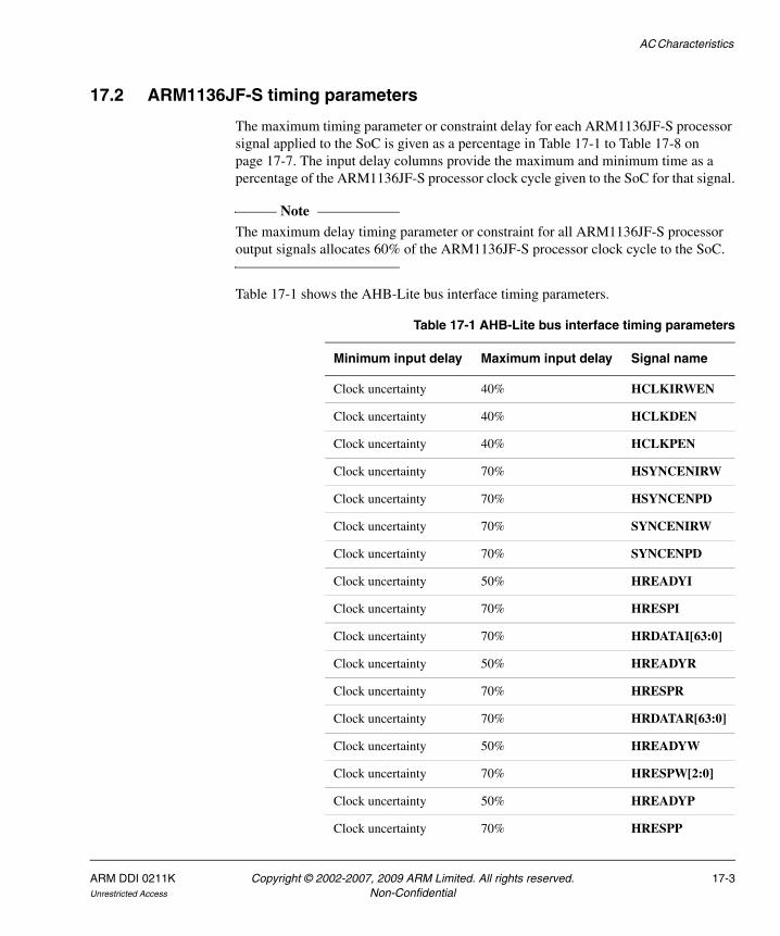
AC Characteristics
17.2 ARM1136JF-S timing parameters
The maximum timing parameter or constraint delay for each ARM1136JF-S processor signal applied to the SoC is given as a percentage in Table 17-1 to Table 17-8 on page 17-7. The input delay columns provide the maximum and minimum time as a percentage of the ARM1136JF-S processor clock cycle given to the SoC for that signal.
Note The maximum delay timing parameter or constraint for all ARM1136JF-S processor output signals allocates 60% of the ARM1136JF-S processor clock cycle to the SoC.
Table 17-1 shows the AHB-Lite bus interface timing parameters.
Table 17-1 AHB-Lite bus interface timing parameters
Minimum input delay Maximum input delay Signal name
Clock uncertainty 40% HCLKIRWEN
Clock uncertainty 40% HCLKDEN
Clock uncertainty 40% HCLKPEN
Clock uncertainty 70% HSYNCENIRW
Clock uncertainty 70% HSYNCENPD
Clock uncertainty 70% SYNCENIRW
Clock uncertainty 70% SYNCENPD
Clock uncertainty 50% HREADYI
Clock uncertainty 70% HRESPI
Clock uncertainty 70% HRDATAI[63:0]
Clock uncertainty 50% HREADYR
Clock uncertainty 70% HRESPR
Clock uncertainty 70% HRDATAR[63:0]
Clock uncertainty 50% HREADYW
Clock uncertainty 70% HRESPW[2:0]
Clock uncertainty 50% HREADYP
Clock uncertainty 70% HRESPP
ARM DDI 0211K Copyright © 2002-2007, 2009 ARM Limited. All rights reserved. 17-3Unrestricted Access Non-Confidential

AC Characteristics
Table 17-2 shows the coprocessor port timing parameters.
Clock uncertainty 70% HRDATAP[31:0]
Clock uncertainty 50% HREADYD
Clock uncertainty 70% HRESPD
Clock uncertainty 70% HRDATAD[63:0]
Table 17-2 Coprocessor port timing parameters
Minimum input delay Maximum input delay Signal name
Clock uncertainty 70% CPALENGTHHOLD
Clock uncertainty 70% CPAACCEPT
Clock uncertainty 70% CPAACCEPTHOLD
Clock uncertainty 70% CPASTDATAV
Clock uncertainty 70% CPALENGTH[3:0]
Clock uncertainty 70% CPALENGTHT[3:0]
Clock uncertainty 70% CPAACCEPTT[3:0]
Clock uncertainty 70% CPASTDATA[63:0]
Clock uncertainty 70% CPASTDATAT[3:0]
Clock uncertainty 70% CPAPRESENT[11:0]
Table 17-1 AHB-Lite bus interface timing parameters (continued)
Minimum input delay Maximum input delay Signal name
17-4 Copyright © 2002-2007, 2009 ARM Limited. All rights reserved. ARM DDI 0211KNon-Confidential Unrestricted Access

AC Characteristics
Table 17-3 shows the ETM interface port timing parameters.
Table 17-4 shows the interrupt port timing parameters.
Table 17-5 shows the debug timing parameters.
Table 17-3 ETM interface port timing parameters
Minimum input delay Maximum input delay Signal name
Clock uncertainty 60% ETMPWRUP
Clock uncertainty 60% nETMWFIREADY
Clock uncertainty 60% ETMEXTOUT[1:0]
Clock uncertainty 60% ETMCPRDATA[31:0]
Table 17-4 Interrupt port timing parameters
Minimum input delay Maximum input delay Signal name
Clock uncertainty 60% nFIQ
Clock uncertainty 60% nIRQ
Clock uncertainty 60% INTSYNCEN
Clock uncertainty 60% IRQADDRV
Clock uncertainty 60% IRQADDRVSYNCEN
Clock uncertainty 60% IRQADDR[31:2]
Table 17-5 Debug timing parameters
Minimum input delay Maximum input delay Signal name
Clock uncertainty 40% DBGTCKEN
Clock uncertainty 40% FREEDBGTCKEN
Clock uncertainty 50% DBGMANID[10:0]
Clock uncertainty 50% DBGTDI
Clock uncertainty 50% DBGTMS
Clock uncertainty 50% DBGVERSION[3:0]
ARM DDI 0211K Copyright © 2002-2007, 2009 ARM Limited. All rights reserved. 17-5Unrestricted Access Non-Confidential
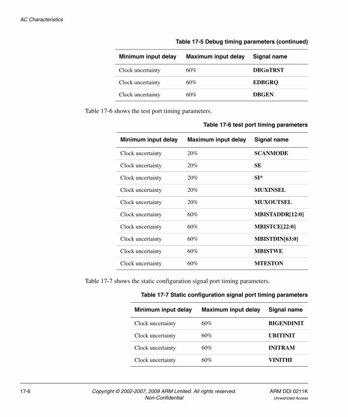
AC Characteristics
Table 17-6 shows the test port timing parameters.
Table 17-7 shows the static configuration signal port timing parameters.
Clock uncertainty 60% DBGnTRST
Clock uncertainty 60% EDBGRQ
Clock uncertainty 60% DBGEN
Table 17-6 test port timing parameters
Minimum input delay Maximum input delay Signal name
Clock uncertainty 20% SCANMODE
Clock uncertainty 20% SE
Clock uncertainty 20% SI*
Clock uncertainty 20% MUXINSEL
Clock uncertainty 20% MUXOUTSEL
Clock uncertainty 60% MBISTADDR[12:0]
Clock uncertainty 60% MBISTCE[22:0]
Clock uncertainty 60% MBISTDIN[63:0]
Clock uncertainty 60% MBISTWE
Clock uncertainty 60% MTESTON
Table 17-7 Static configuration signal port timing parameters
Minimum input delay Maximum input delay Signal name
Clock uncertainty 60% BIGENDINIT
Clock uncertainty 60% UBITINIT
Clock uncertainty 60% INITRAM
Clock uncertainty 60% VINITHI
Table 17-5 Debug timing parameters (continued)
Minimum input delay Maximum input delay Signal name
17-6 Copyright © 2002-2007, 2009 ARM Limited. All rights reserved. ARM DDI 0211KNon-Confidential Unrestricted Access

AC Characteristics
Table 17-8 shows the reset port timing parameters.
Table 17-8 Reset port timing parameters
Minimum input delay Maximum input delay Signal name
Clock uncertainty 20% nRESETIN
Clock uncertainty 20% nPORESETIN
Clock uncertainty 20% HRESETIRWn
Clock uncertainty 20% HRESETPDn
ARM DDI 0211K Copyright © 2002-2007, 2009 ARM Limited. All rights reserved. 17-7Unrestricted Access Non-Confidential

AC Characteristics
17-8 Copyright © 2002-2007, 2009 ARM Limited. All rights reserved. ARM DDI 0211KNon-Confidential Unrestricted Access

Appendix A Signal Descriptions
This appendix lists and describes the ARM1136JF-S signals. It contains the following sections:
• Global signals on page A-2
• Static configuration signals on page A-3
• Interrupt signals, including the VIC interface on page A-4
• AHB interface signals on page A-5
• Coprocessor interface signals on page A-14
• Debug interface signals, including JTAG on page A-16
• ETM interface signals on page A-17
• Test signals on page A-18.
Note Table A-1 on page A-2 to Table A-14 on page A-18 show output signals. These are set to 0 on reset unless otherwise stated.
ARM DDI 0211K Copyright © 2002-2007, 2009 ARM Limited. All rights reserved. A-1Unrestricted Access Non-Confidential

Signal Descriptions
A.1 Global signals
Table A-1 lists the ARM1136JF-S global signals.
Free clocks are the free running clocks with minimal insertion delay for clocking the clock gating circuitry. Free clocks must be balanced with the incoming clock signal, but not with the clocks clocking the core logic.
Table A-1 Global signals
Name Direction Description
CLKIN Input Core clock
FREECLKIN Input Free version of the core clock
FREEHCLKIRW Input Free version of HCLKIRW
FREEHCLKPD Input Free version of HCLKPD
HCLKDEN Input Clock enable for the DMA port to enable it to be clocked at a reduced rate
HCLKIRW Input HCLK for the I, R and W ports
HCLKIRWEN Input HCLKEN for the I, R and W ports
HCLKPD Input HCLK for the P and D ports
HCLKPEN Input Clock enable for the peripheral port to enable it to be clocked at a reduced rate
HRESETIRWn Input HRESETn for the I, R and W ports
HRESETPDn Input HRESETn for the P and D ports
HSYNCENIRW Input Synchronous control HCLK domain for I, R and W ports
HSYNCENPD Input Synchronous control HCLK domain for P and D ports
nPORESETIN Input Power on reset (resets debug logic)
nRESETIN Input Core reset
STANDBYWFI Output Indicates that the ARM1136JF-S processor is in Standby mode
SYNCENIRW Input Synchronous control CLKIN domain for I, R and W ports
SYNCENPD Input Synchronous control CLKIN domain for P and D ports
A-2 Copyright © 2002-2007, 2009 ARM Limited. All rights reserved. ARM DDI 0211KNon-Confidential Unrestricted Access

Signal Descriptions
A.2 Static configuration signals
Table A-2 lists the ARM1136JF-S static configuration signals.
Table A-2 Static configuration signals
Name Direction Description
COREASID[7:0] Output ASID used by the integer processor exported to memory system
DMAASID[7:0] Output ASID used by the DMA exported to memory system
BIGENDINIT Input When HIGH, indicates v5 big-endian mode
CFGBIGENDIRW Output Current state of the CP15 big-endian bit synchronized to HCLKIRW
CFGBIGENDPD Output Current state of the CP15 big-endian bit synchronized to HCLKPD
INITRAM Input When HIGH, indicates ITCM enabled at address 0x0
UBITINIT Input When HIGH, indicates ARMv6 unaligned behavior
VINITHI Input When HIGH, indicates High-Vecs mode
ARM DDI 0211K Copyright © 2002-2007, 2009 ARM Limited. All rights reserved. A-3Unrestricted Access Non-Confidential

Signal Descriptions
A.3 Interrupt signals, including the VIC interface
Table A-3 lists the interrupt signals, including those used with the VIC interface.
Table A-3 Interrupt signals
Name Direction Description
INTSYNCEN Input Indicates that VIC interface is asynchronous.
IRQACK Output Interrupt acknowledge.
IRQADDR[31:2] Input Address of the IRQ.
IRQADDRV Input Indicates IRQADDR is valid.
IRQADDRVSYNCEN Input Indicates that VIC IRQADDRV requires synchronizer.
nFIQ Input Fast interrupt request.a
nIRQ Input Interrupt request.a
nDMAIRQ Output Interrupt request by DMA. On reset this pin is set to 1.
nPMUIRQ Output Interrupt request by system performance monitor. On reset this pin is set to 1.
a. This signal must be held LOW until an appropriate interrupt response is received from the processor.
A-4 Copyright © 2002-2007, 2009 ARM Limited. All rights reserved. ARM DDI 0211KNon-Confidential Unrestricted Access
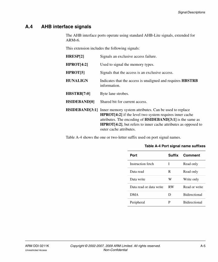
Signal Descriptions
A.4 AHB interface signals
The AHB interface ports operate using standard AHB-Lite signals, extended for ARMv6.
This extension includes the following signals:
HRESP[2] Signals an exclusive access failure.
HPROT[4:2] Used to signal the memory types.
HPROT[5] Signals that the access is an exclusive access.
HUNALIGN Indicates that the access is unaligned and requires HBSTRB information.
HBSTRB[7:0] Byte lane strobes.
HSIDEBAND[0] Shared bit for current access.
HSIDEBAND[3:1] Inner memory system attributes. Can be used to replace HPROT[4:2] if the level two system requires inner cache attributes. The encoding of HSIDEBAND[3:1] is the same as HPROT[4:2], but refers to inner cache attributes as opposed to outer cache attributes.
Table A-4 shows the one or two-letter suffix used on port signal names.
Table A-4 Port signal name suffixes
Port Suffix Comment
Instruction fetch I Read only
Data read R Read only
Data write W Write only
Data read or data write RW Read or write
DMA D Bidirectional
Peripheral P Bidirectional
ARM DDI 0211K Copyright © 2002-2007, 2009 ARM Limited. All rights reserved. A-5Unrestricted Access Non-Confidential

Signal Descriptions
A.4.1 Instruction fetch port signals
The instruction fetch port is a 64-bit wide AHB-Lite port that is read-only.
Table A-5 lists the ARM1136JF-S instruction fetch port signals.
Table A-5 Instruction fetch port signals
Name Direction Description
HADDRI[31:0] Output The 32-bit system instruction fetch port address bus.
HBSTRBI[7:0] Output Indicates which byte lanes are valid.
HBURSTI[2:0] Output Indicates if the transfer forms part of a burst. Four-beat bursts are supported and the burst can be either incrementing or wrapping.
HMASTLOCKI Output Instruction fetch port lock signal.
HPROTI[5:0] Output The protection control signals provide additional information about a bus access and are primarily intended for use by any module that wants to implement some level of protection. The signals indicate if:
• the transfer is an opcode fetch or data access
• the transfer is a Supervisor or User mode access
• the current access is Cacheable or Bufferable.
HRDATAI[63:0] Input The read data bus is used to transfer data and instructions from bus slaves to the bus master during read operations.
HREADYI Input When HIGH the HREADYI signal indicates that a transfer has finished on the bus. You can drive this signal LOW to extend a transfer.
HRESPI Input The transfer response provides additional information on the status of a transfer. Two responses are provided:
0 = Okay
1 = Error.
Connects to HRESP[0].
HSIDEBANDI[3:0] Output Signals Sharable and Inner Cacheable.
HSIZEI[2:0] Output Indicates the size of the instruction fetch port transfer:
• byte (8-bit)
• halfword (16-bit)
• word (32-bit)
• doubleword (64-bit).
The protocol enables larger transfer sizes up to a maximum of 1024 bits. On reset these pins are set to b011.
A-6 Copyright © 2002-2007, 2009 ARM Limited. All rights reserved. ARM DDI 0211KNon-Confidential Unrestricted Access

Signal Descriptions
A.4.2 Data read port signals
The data read port is a 64-bit wide AHB-Lite port that is read/write.
For AHB protocol reasons, locked reads and writes of SWP or SWPB instructions must occur on the same bus. Because of this, the data read port can perform writes of SWP and SWPB instructions.
Table A-6 lists the ARM1136JF-S data read port signals.
HTRANSI[1:0] Output Indicates the type of the current transfer on the instruction fetch port, which can be:
b00 = Idle
b10 = Nonsequential
b11 = Sequential
b01 = Busy.
HUNALIGNI Output When HIGH, indicates that the access is unaligned and that HBSTRBI information is required.
HWRITEI Output When HIGH this signal indicates a write transfer on the instruction fetch port, and when LOW a read transfer.
Table A-5 Instruction fetch port signals (continued)
Name Direction Description
Table A-6 Data read port signals
Name Direction Description
HADDRR[31:0] Output The 32-bit system data read port address bus.
HBSTRBR[7:0] Output Indicates which byte lanes are valid.
HBURSTR[2:0] Output Indicates if the transfer forms part of a burst. Four-beat bursts are supported and the burst can be either incrementing or wrapping.
HMASTLOCKR Output Data read port lock signal.
HPROTR[5:0] Output The protection control signals provide additional information about a bus access and are primarily intended for use by any module that wants to implement some level of protection. The signals indicate if:
• the transfer is an opcode fetch or data access
• if the transfer is a Supervisor or User mode access
• if the current access is Cacheable or Bufferable.
HRDATAR[63:0] Input Data read port read data bus.
ARM DDI 0211K Copyright © 2002-2007, 2009 ARM Limited. All rights reserved. A-7Unrestricted Access Non-Confidential

Signal Descriptions
HREADYR Input Data read port address ready.
HRESPR Input The transfer response provides additional information on the status of a transfer. Two responses are provided:
0 = Okay
1 = Error.
Connects to HRESP[0].
HSIDEBANDR[3:0] Output Signals Sharable and Inner Cacheable.
HSIZER[2:0] Output Indicates the size of the data read port transfer:
• byte (8-bit)
• halfword (16-bit)
• word (32-bit)
• doubleword (64-bit).
The protocol enables larger transfer sizes up to a maximum of 1024 bits.
HTRANSR[1:0] Output Indicates the type of the current transfer on the data read port:
b00 = Idle
b10 = Nonsequential
b11 = Sequential
b01 = Busy.
HUNALIGNR Output When HIGH, indicates that the access is unaligned and that HBSTRBR information is required.
HWDATAR[63:0] Output The data read port write data bus is used to transfer data from the bus master to the bus slave during write operations for SWP and SWPB instructions.
HWRITER Output When HIGH this signal indicates a write transfer of a SWP or SWPB instruction on the data read port, and when LOW a read transfer.
Table A-6 Data read port signals (continued)
Name Direction Description
A-8 Copyright © 2002-2007, 2009 ARM Limited. All rights reserved. ARM DDI 0211KNon-Confidential Unrestricted Access

Signal Descriptions
A.4.3 Data write port
The data write port is a 64-bit wide AHB-Lite port that is write-only.
Table A-7 lists the data write port signals.
Table A-7 Data write port signals
Name Direction Description
HADDRW[31:0] Output The 32-bit system data write port address bus.
HBSTRBW[7:0] Output Indicates which byte lanes are valid.
HBURSTW[2:0] Output Indicates if the transfer forms part of a burst. Four-beat bursts are supported and the burst can be either incrementing or wrapping.
HMASTLOCKW Output Data write port lock signal.
HPROTW[5:0] Output The protection control signals provide additional information about a bus access and are primarily intended for use by any module that wishes to implement some level of protection. The signals indicate if:
• the transfer is an opcode fetch or data access
• the transfer is a Supervisor or User mode access
• the current access is Cacheable or Bufferable.
HREADYW Input When HIGH the HREADYW signal indicates that a transfer has finished on the data write port bus. You can drive this signal LOW to extend a transfer.
HRESPW[2:0] Input The transfer response provides additional information on the status of a transfer. Three responses are provided:
b000 = Okay
b001 = Error
b100 = Xfail.
Note b010 = Retry and b011 = Split are not supported in AHB Lite.
HSIDEBANDW[3:0] Output Signals Sharable and Inner Cacheable.
HSIZEW[2:0] Output Indicates the size of the data write port transfer:
• byte (8-bit)
• halfword (16-bit)
• word (32-bit)
• doubleword (64-bit).
The protocol enables larger transfer sizes up to a maximum of 1024 bits.
ARM DDI 0211K Copyright © 2002-2007, 2009 ARM Limited. All rights reserved. A-9Unrestricted Access Non-Confidential

Signal Descriptions
A.4.4 Peripheral port signals
The peripheral port is a 32-bit wide AHB-Lite port that is read/write.
Table A-8 lists the peripheral port signals.
HTRANSW[1:0] Output Indicates the type of the current transfer on the data write port, which can be:
b00 = Idle
b10 = Nonsequential
b11 = Sequential
b01 = Busy.
HUNALIGNW Output When HIGH, indicates that the access is unaligned and that HBSTRBW information is required.
HWDATAW[63:0] Output The data write port write data bus is used to transfer data from the bus master to the bus slave during write operations.
HWRITEW Output When HIGH this signal indicates a write transfer on the data write port, and when LOW a read transfer. On reset this pin is set to 1.
WRITEBACK Output Indicates that the current transaction is a cache line eviction.
Table A-7 Data write port signals (continued)
Name Direction Description
Table A-8 Peripheral port signals
Name Direction Description
HADDRP[31:0] Output The 32-bit system peripheral port address bus.
HBSTRBP[3:0] Output Indicates which byte lanes are valid.
HBURSTP[2:0] Output Indicates if the transfer forms part of a burst. Four-beat bursts are supported and the burst can be either incrementing or wrapping.
HMASTLOCKP Output Peripheral port lock signal.
A-10 Copyright © 2002-2007, 2009 ARM Limited. All rights reserved. ARM DDI 0211KNon-Confidential Unrestricted Access

Signal Descriptions
HPROTP[5:0] Output The protection control signals provide additional information about a bus access and are primarily intended for use by any module that wants to implement some level of protection. The signals indicate if:
• the transfer is an opcode fetch or data access
• the transfer is a privileged mode or User mode access
• the current access is Cacheable or Bufferable.
HRDATAP[31:0] Input The read data bus is used to transfer data and instructions from bus slaves to the bus master during read operations.
HREADYP Input When HIGH the HREADYP signal indicates that a transfer has finished on the peripheral port data bus. You can drive this signal LOW to extend a transfer.
HRESPP Input The transfer response provides additional information on the status of a transfer. Two responses are provided:
0 = Okay
1 = Error.
HSIDEBANDP[3:0] Output Signals Sharable and Inner Cacheable. On reset HSIDEBANDP[3:0] is set to b0010.
HSIZEP[2:0] Output Indicates the size of the peripheral port transfer, which is typically:
• byte (8-bit)
• halfword (16-bit)
• word (32-bit)
• doubleword (64-bit).
The protocol enables larger transfer sizes up to a maximum of 1024 bits.
HTRANSP[1:0] Output Indicates the type of the current transfer on the peripheral port, which can be:
b00 = Idle
b10 = Nonsequential
b11 = Sequential
b01 = Busy.
HUNALIGNP Output When HIGH, indicates that the access is unaligned and that HBSTRBP information is required.
HWDATAP[31:0] Output The peripheral port write data bus is used to transfer data from the bus master to the bus slave during write operations.
HWRITEP Output When HIGH this signal indicates a write transfer on the peripheral port, and when LOW a read transfer.
Table A-8 Peripheral port signals (continued)
Name Direction Description
ARM DDI 0211K Copyright © 2002-2007, 2009 ARM Limited. All rights reserved. A-11Unrestricted Access Non-Confidential

Signal Descriptions
A.4.5 DMA port signals
The DMA port is a 64-bit wide AHB-Lite port that is read/write.
Table A-9 lists the DMA port signals.
Table A-9 DMA port signals
Name Direction Description
HADDRD[31:0] Output The 32-bit system DMA port address bus.
HBSTRBD[7:0] Output Indicates which byte lanes are valid.
HBURSTD[2:0] Output Indicates if the transfer forms part of a burst. Four-beat bursts are supported and the burst can be either incrementing or wrapping.
HMASTLOCKD Output DMA port lock signal.
HPROTD[5:0] Output The protection control signals provide additional information about a bus access and are primarily intended for use by any module that wants to implement some level of protection. The signals indicate if:
• the transfer is an opcode fetch or data access
• the transfer is a privileged mode or User mode access
• the current access is Cacheable or Bufferable.
HRDATAD[63:0] Input The read data bus is used to transfer data and instructions from bus slaves to the bus master during DMA read operations.
HREADYD Input When HIGH the HREADYD signal indicates that a transfer has finished on the bus. You can drive this signal LOW to extend a transfer.
HRESPD Input The transfer response provides additional information on the status of a transfer. Two responses are provided:
0 = Okay
1 = Error.
HSIDEBANDD[3:0] Output Signals Sharable and Inner Cacheable.
HSIZED[2:0] Output Indicates the size of the DMA port transfer:
• byte (8-bit)
• halfword (16-bit)
• word (32-bit)
• doubleword (64-bit).
The protocol enables larger transfer sizes up to a maximum of 1024 bits.
A-12 Copyright © 2002-2007, 2009 ARM Limited. All rights reserved. ARM DDI 0211KNon-Confidential Unrestricted Access
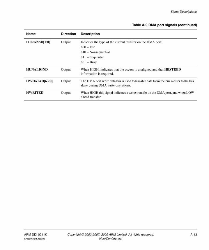
Signal Descriptions
HTRANSD[1:0] Output Indicates the type of the current transfer on the DMA port:
b00 = Idle
b10 = Nonsequential
b11 = Sequential
b01 = Busy.
HUNALIGND Output When HIGH, indicates that the access is unaligned and that HBSTRBD information is required.
HWDATAD[63:0] Output The DMA port write data bus is used to transfer data from the bus master to the bus slave during DMA write operations.
HWRITED Output When HIGH this signal indicates a write transfer on the DMA port, and when LOW a read transfer.
Table A-9 DMA port signals (continued)
Name Direction Description
ARM DDI 0211K Copyright © 2002-2007, 2009 ARM Limited. All rights reserved. A-13Unrestricted Access Non-Confidential

Signal Descriptions
A.5 Coprocessor interface signals
The interface signals from the core to the coprocessor are listed in Table A-10.
The interface signals from the coprocessor to the core are listed in Table A-11 on page A-15.
If no coprocessor is connected, the following control signals must be driven LOW:
• CPALENGTHHOLD• CPAACCEPT• CPAACCEPTHOLD.
Table A-10 Core to coprocessor signals
Name Direction Description
ACPCANCEL Output Asserted to indicate that the instruction is to be canceled.
ACPCANCELT[3:0] Output The tag accompanying the cancel signal in ACPCANCEL.
ACPCANCELV Output Asserted to indicate that ACPCANCEL is valid.
ACPENABLE[11:0] Output Enables the coprocessor when this is asserted. All lines driven by the coprocessor must be held to zero.
ACPFINISHV Output The finish token from the core WBls stage to the coprocessor Ex6 stage.
ACPFLUSH Output Flush broadcast from the core.
ACPFLUSHT[3:0] Output The tag to be flushed from.
ACPINSTR[31:0] Output The instruction passed from the core Fe2 stage to the coprocessor Decode stage.
ACPINSTRT[3:0] Output The tag accompanying the instruction in ACPINSTR.
ACPINSTRV Output Asserted to indicate that ACPINSTR carries a valid instruction.
ACPLDDATA[63:0] Output The load data from the core to the coprocessor.
ACPLDVALID Output Asserted to indicate that the data in ACPLDATA is valid.
ACPSTSTOP Output Asserted by the core to tell the coprocessor to stop sending store data.
ACPPRIV Output Asserted to indicate that the core is in Supervisor mode.
A-14 Copyright © 2002-2007, 2009 ARM Limited. All rights reserved. ARM DDI 0211KNon-Confidential Unrestricted Access

Signal Descriptions
Table A-11 Coprocessor to core signals
Name Direction Description
CPAACCEPT Input The bounce signal from the coprocessor issue stage to the core Ex2 stage.
CPAACCEPTHOLD Input Asserted to indicate that the bounce information in CPAACCEPT is not valid.
CPAACCEPTT[3:0] Input The tag accompanying the bounce signal in CPAACCEPT.
CPALENGTH[3:0] Input The length information from the coprocessor Decode stage to the core Ex1 stage.
CPALENGTHHOLD Input Asserted to indicate that the length information in CPALENGTH is not valid.
CPALENGTHT[3:0] Input The tag accompanying the length signal in CPALENGTH.
CPAPRESENT[11:0] Input Indicates which coprocessors are present.
CPASTDATA[63:0] Input The store data passing from the coprocessor to the core.
CPASTDATAT[3:0] Input The tag accompanying the store data in CPASTDATA.
CPASTDATAV Input Indicates that the store data to the core is valid.
ARM DDI 0211K Copyright © 2002-2007, 2009 ARM Limited. All rights reserved. A-15Unrestricted Access Non-Confidential
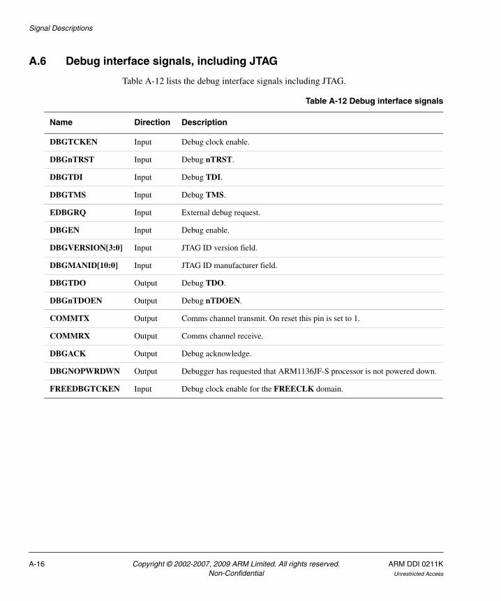
Signal Descriptions
A.6 Debug interface signals, including JTAG
Table A-12 lists the debug interface signals including JTAG.
Table A-12 Debug interface signals
Name Direction Description
DBGTCKEN Input Debug clock enable.
DBGnTRST Input Debug nTRST.
DBGTDI Input Debug TDI.
DBGTMS Input Debug TMS.
EDBGRQ Input External debug request.
DBGEN Input Debug enable.
DBGVERSION[3:0] Input JTAG ID version field.
DBGMANID[10:0] Input JTAG ID manufacturer field.
DBGTDO Output Debug TDO.
DBGnTDOEN Output Debug nTDOEN.
COMMTX Output Comms channel transmit. On reset this pin is set to 1.
COMMRX Output Comms channel receive.
DBGACK Output Debug acknowledge.
DBGNOPWRDWN Output Debugger has requested that ARM1136JF-S processor is not powered down.
FREEDBGTCKEN Input Debug clock enable for the FREECLK domain.
A-16 Copyright © 2002-2007, 2009 ARM Limited. All rights reserved. ARM DDI 0211KNon-Confidential Unrestricted Access
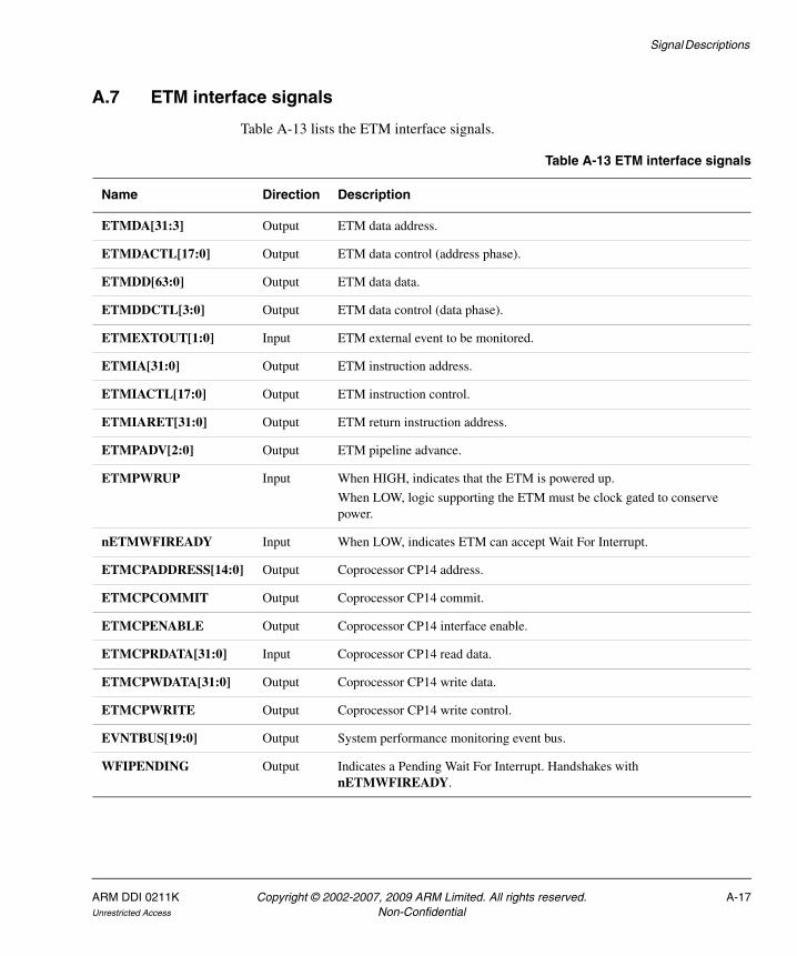
Signal Descriptions
A.7 ETM interface signals
Table A-13 lists the ETM interface signals.
Table A-13 ETM interface signals
Name Direction Description
ETMDA[31:3] Output ETM data address.
ETMDACTL[17:0] Output ETM data control (address phase).
ETMDD[63:0] Output ETM data data.
ETMDDCTL[3:0] Output ETM data control (data phase).
ETMEXTOUT[1:0] Input ETM external event to be monitored.
ETMIA[31:0] Output ETM instruction address.
ETMIACTL[17:0] Output ETM instruction control.
ETMIARET[31:0] Output ETM return instruction address.
ETMPADV[2:0] Output ETM pipeline advance.
ETMPWRUP Input When HIGH, indicates that the ETM is powered up.
When LOW, logic supporting the ETM must be clock gated to conserve power.
nETMWFIREADY Input When LOW, indicates ETM can accept Wait For Interrupt.
ETMCPADDRESS[14:0] Output Coprocessor CP14 address.
ETMCPCOMMIT Output Coprocessor CP14 commit.
ETMCPENABLE Output Coprocessor CP14 interface enable.
ETMCPRDATA[31:0] Input Coprocessor CP14 read data.
ETMCPWDATA[31:0] Output Coprocessor CP14 write data.
ETMCPWRITE Output Coprocessor CP14 write control.
EVNTBUS[19:0] Output System performance monitoring event bus.
WFIPENDING Output Indicates a Pending Wait For Interrupt. Handshakes with nETMWFIREADY.
ARM DDI 0211K Copyright © 2002-2007, 2009 ARM Limited. All rights reserved. A-17Unrestricted Access Non-Confidential

Signal Descriptions
A.8 Test signals
Table A-14 lists the test signals.
Table A-14 Test signals
Name Direction Description
SCANMODE Input In scan test mode.
SE Input Scan enable.
MBISTADDR[12:0] Input Memory Built-In Self Test (MBIST) address.
MBISTCE[22:0] Input MBIST chip enable.
MBISTDIN[63:0] Input MBIST data in.
MBISTDOUT[63:0] Output MBIST data out.
MBISTWE Input MBIST write enable.
MTESTON Input BIST test is enabled.
nVALFIQ Output Request for a fast interrupt. On reset this pin is set to 1.
nVALIRQ Output Request for an interrupt. On reset this pin is set to 1.
nVALRESET Output Request for a reset. On reset this pin is set to 1.
VALEDBGRQ Output Request for an external debug request.
MUXINSEL Input These are the test wrapper enable signals. See ARM1136JF-S and ARM1136J-S Implementation Guide for more details.
MUXOUTSEL Input
A-18 Copyright © 2002-2007, 2009 ARM Limited. All rights reserved. ARM DDI 0211KNon-Confidential Unrestricted Access

Appendix B Functional changes in the rev1 (r1pn) releases
This appendix describes the functional changes introduced in the r1p0 release of the ARM1136JF-S. It does not duplicate information given elsewhere in this manual, but tells you where you can find full details of the changes. The appendix contains the following sections:
• New instructions on page B-2
• Changes to unaligned access support on page B-3
• Memory system architecture changes on page B-4
• Debug changes on page B-7
• VFP changes, ARM1136JF-S only on page B-8
• Effects on coprocessor CP15 on page B-9.
Note • Product revisions on page 1-57 lists these changes.
• The ARM1136 signal list has not changed.
• All of the r1pn releases have the same functionality, as described in this manual.
ARM DDI 0211K Copyright © 2002-2007, 2009 ARM Limited. All rights reserved. B-1Unrestricted Access Non-Confidential

Functional changes in the rev1 (r1pn) releases
B.1 New instructions
The r1p0 release of the ARM1136JF-S and ARM1136J-S processors implements the ARMv6 instruction set with the ARMv6k additions. The instruction set is fully described in the ARM Architecture Reference Manual. This section lists the new commands in the r1p0 release.
B.1.1 Synchronization instructions
See the following sections for descriptions of these instructions:
• LDREXB on page 2-24
• STREXB on page 2-25
• LDREXH on page 2-27
• STREXH on page 2-28
• LDREXD on page 2-30
• STREXD on page 2-31
• CLREX on page 2-32.
B.1.2 Other instructions
There is one other new instruction. See the following sections for its description:
• NOP - True No Operation on page 2-33.
B-2 Copyright © 2002-2007, 2009 ARM Limited. All rights reserved. ARM DDI 0211KNon-Confidential Unrestricted Access

Functional changes in the rev1 (r1pn) releases
B.2 Changes to unaligned access support
The changed unaligned access support is described in Operation of unaligned accesses on page 4-17. The changes relate to the introduction of the new instructions LDREXB, LDREXD, LDREXH, STREXB, STREXD and STREXH.
The r1p0 release introduces three new access types, BSync, HWSync and DWSync. Table 4-2 on page 4-17 lists the instructions that relate to these access types, and Table 4-3 on page 4-18 includes the alignment fault occurrences for these access types.
ARM DDI 0211K Copyright © 2002-2007, 2009 ARM Limited. All rights reserved. B-3Unrestricted Access Non-Confidential

Functional changes in the rev1 (r1pn) releases
B.3 Memory system architecture changes
The following sections describe the changes in the memory system architecture which are introduced in the r1p0 release:
• Removal of page coloring restrictions
• Changes to access permissions
• Implementation of an Access Flag and Access Flag fault detection on page B-5
• TEX remap on page B-6.
B.3.1 Removal of page coloring restrictions
The page coloring restriction requires all virtual addresses of particular physical addresses to have common address bits[13:12]. It is explained in Restrictions on page table mappings (page coloring) on page 6-51. This requirement is an unwanted restriction on the memory management code for some advanced operating systems.
To remove this restriction, the r1p0 release introduces an additional flag, the CZ flag, in the CP15 Auxiliary Control Register. Setting this flag restricts the size of all instruction and data caches to 16KB. Therefore, if you set the CZ flag you remove the page coloring restriction, at the performance cost of limiting the cache size.
For more information, see:
• c1, Auxiliary Control Register on page 3-69
• Avoiding the page coloring restriction on page 6-52.
B.3.2 Changes to access permissions
Some memory management algorithms use a restricted set of access permissions, but require the read-only/read-write control to be orthogonal to the user/kernel access control. In the r1p0 release, one of the access permission bit encodings is re-defined, making it easy to support these algorithms.
The re-defined bit encoding is the case where:
• S=R=0
• APX=b1
• AP[1:0]=b11.
This encoding now indicates Privileged and User read-only access. In previous releases this encoding was reserved.
B-4 Copyright © 2002-2007, 2009 ARM Limited. All rights reserved. ARM DDI 0211KNon-Confidential Unrestricted Access

Functional changes in the rev1 (r1pn) releases
Table 6-1 on page 6-12 lists the access permission bit encodings, and Restricted access permissions and the Access Flag on page 6-13 describes how to implement access permissions to give orthogonal control of:
• read-only or read-write access
• user or kernel access.
Note In this edition of this manual, the section Memory access control on page 6-11 gives more emphasis to the fact that using the S and R bits is deprecated. Table 6-1 on page 6-12 no longer includes these bits. A new section, Use of the S and R bits (deprecated) on page 6-14, has been added for reference purposes.
B.3.3 Implementation of an Access Flag and Access Flag fault detection
Release r1p0 introduces an Access Flag, and associated Access Flag fault encodings.
If the access flag is enabled, AP[0] is redefined as the Access Flag. In this release, if you want to use the Access Flag you must manage it through software.
Note If you use the restricted set of access permissions, with read-only/read-write control orthogonal to user/kernel access control, the AP[0] bit in the page descriptors is redefined as the Access Flag. This scheme of access permissions is summarized in Changes to access permissions on page B-4 and described in detail in Restricted access permissions and the Access Flag on page 6-13.
Although the ARM1136JF-S architecture does not impose any restrictions on enabling the use of AP[0] as an Access Flag, this feature is only likely to be useful if you are using the restricted set of access permissions.
Enabling the Access Flag
The use of AP[0] as an Access Flag is enabled by setting the Access Flag Enable (AFE) flag, bit[29], in the CP15 Control Register. For more information see:
• Access Flag fault on page 6-40
• c1, Control Register on page 3-63.
ARM DDI 0211K Copyright © 2002-2007, 2009 ARM Limited. All rights reserved. B-5Unrestricted Access Non-Confidential

Functional changes in the rev1 (r1pn) releases
Access Flag faults
If you have set the AFE flag, you can use Access Flag faults to detect when a page or section is accessed for the first time. For more information see:
• Access Flag fault on page 6-40
• the entries for Access Flag fault in Table 6-13 on page 6-42.
B.3.4 TEX remap
By default, the ARMv6 MMU page table descriptors use a large number of bits to describe all of the options for inner and outer cacheability. These bits include:
• the Type EXtension field, TEX[2:0]• the Cacheable bit, C
• the Bufferable bit, B.
Applications are unlikely to need all of these options simultaneously. Therefore, from release r1p0, an alternative page description scheme is introduced. This scheme:
• does not use the TEX[2:1] bits
— these bits are available for use as OS-managed page table bits
• uses two new remap registers are used to configure the supported options:
— the Primary Region Remap Register (PRRR)
— the Normal Memory Remap Register (NMRR)
• is enabled by setting the TEX Remap Enable (TRE) flag, bit[28], in the CP15 c1 Control Register. See c1, Control Register on page 3-63.
The two MMU page description schemes are described in Memory region attributes on page 6-15, with the new TEX remapped scheme described in Configuration with TRE=1 (TEX remapping enabled) on page 6-18.
For descriptions of the two remap registers see:
• Primary Region Remap Register (PRRR) on page 3-125
• Normal Memory Remap Register (NMRR) on page 3-127.
B-6 Copyright © 2002-2007, 2009 ARM Limited. All rights reserved. ARM DDI 0211KNon-Confidential Unrestricted Access

Functional changes in the rev1 (r1pn) releases
B.4 Debug changes
From release r1p0, the system performance monitor does not count any events while the processor is in Halting debug-mode. See Halting debug-mode debugging on page 13-66 for more information.
ARM DDI 0211K Copyright © 2002-2007, 2009 ARM Limited. All rights reserved. B-7Unrestricted Access Non-Confidential

Functional changes in the rev1 (r1pn) releases
B.5 VFP changes, ARM1136JF-S only
From release r1p0, two new VFP registers are added, the Media and VFP Features Registers 0 and 1 (MVFR0 and MVFR1).
Note The ARM1136JF-S processor includes a VFP. The ARM1136J-S does not include a VFP, and therefore does not have any VFP registers.
See VFP11™ Vector Floating-point Coprocessor Technical Reference Manual for a description of the VFP. The r2p0 release of this manual includes descriptions of the MVFR registers.
B-8 Copyright © 2002-2007, 2009 ARM Limited. All rights reserved. ARM DDI 0211KNon-Confidential Unrestricted Access

Functional changes in the rev1 (r1pn) releases
B.6 Effects on coprocessor CP15
This section describes the changes to coprocessor CP15 introduced in the r1p0 release.
B.6.1 Register 0: CPU ID registers
The ID Code Register has been renamed as the Main ID Register, and the revision field of the register has changed. This register is accessed by:
MRC p15,c0,c<Rd>, c0, c0, {0, 4-7}
For more information see c0, Main ID Register on page 3-25.
In addition, a set of core feature ID registers have been added. These registers are listed in c0, Core feature ID registers on page 3-35. That section also describes each of the registers.
B.6.2 Register 1, System control registers
Additional flags are implemented in two of the registers:
• the AFE and TRE flags are introduced in the Control Register, see c1, Control Register on page 3-63
• the CZ flag is introduced in the Auxiliary Control Register, see c1, Auxiliary Control Register on page 3-69.
B.6.3 Register 5, Fault status registers
Additional values for the Status fields have been added, to indicate Access Flag faults. For details of these see Fault status and address on page 6-42.
The fault status registers are described in the sections:
• c5, Data Fault Status Register, DFSR on page 3-83
• c5, Instruction Fault Status Register, IFSR on page 3-86.
This change relates to the implement ion of an Access Flag, summarized in Implementation of an Access Flag and Access Flag fault detection on page B-5.
ARM DDI 0211K Copyright © 2002-2007, 2009 ARM Limited. All rights reserved. B-9Unrestricted Access Non-Confidential

Functional changes in the rev1 (r1pn) releases
B.6.4 Register 10, TLB lockdown and remapping registers
Two new remap registers are implemented. See:
• Primary Region Remap Register (PRRR) on page 3-125
• Normal Memory Remap Register (NMRR) on page 3-127.
Additional information about using these registers is given in the section Using the TEX remap registers on page 3-129.
B.6.5 Register 13, Process, Thread ID and Processor ID registers
Three new Thread and Process ID Registers are implemented. These are provided for OS management purposes, and must be managed by the OS. For more information see c13, Thread and process ID registers on page 3-160.
B-10 Copyright © 2002-2007, 2009 ARM Limited. All rights reserved. ARM DDI 0211KNon-Confidential Unrestricted Access

Appendix C Revisions
This appendix describes the technical changes between released issues of this book.
Table C-1 Differences between issue J and issue K
Change Location
Enhancements to instruction set descriptions ARM1136JF-S instruction sets summaries on page 1-36
Updated bit function descriptions for Variant number and Revision number
Table 3-4 on page 3-25
Updated Assoc field description Table 3-8 on page 3-28
Clarified cache cleaning operation Example 3-1 on page 3-99
Updated graphic Figure 3-43 on page 3-113
Clarified descriptions of the privilege of DMA transfers
• Table 3-111 on page 3-135 and Table 3-117 on page 3-142
• DMA Interface AHB-Lite transfers on page 8-70.
Updated text c15, Memory remap registers on page 3-162
Updated performance monitor control register description
c15, Performance Monitor Control Register (PMNC) on page 3-168
ARM DDI 0211K Copyright © 2002-2007, 2009 ARM Limited. All rights reserved. C-1Unrestricted Access Non-Confidential

Revisions
Clarified graphic Figure 6-2 on page 6-38
Added information table Table 6-15 on page 6-53
Updated dual TTBR description First-level descriptor address on page 6-53
Added LDRD and STRD instructions • Noncacheable LDRD or LDM2 on page 8-31
• Table 8-83 on page 8-56
• Table 8-84 on page 8-56.
Clarified table Table 9-2 on page 9-3
Clarified graphic Figure 12-1 on page 12-3
Updated C14 instruction syntax Chapter 13 Debug
Enhancement to the debug unit general description About the debug unit on page 13-4
Updated Debug state descriptions • Behavior of the processor on debug events on page 13-48
• Table 13-30 on page 13-49
• Entering Debug state on page 14-4
• Table 14-1 on page 14-6.
Clarified status bit[2] of TTBRs • c2, Translation Table Base Register 0, TTBR0 on page 3-74
• c2, Translation Table Base Register 1, TTBR1 on page 3-76
• Hardware page table translation on page 6-45
• MMU descriptors on page 6-53.
Updated nETMWFIREADY description Table A-13 on page A-17
Table C-1 Differences between issue J and issue K (continued)
Change Location
C-2 Copyright © 2002-2007, 2009 ARM Limited. All rights reserved. ARM DDI 0211KNon-Confidential Unrestricted Access

Glossary
This glossary describes some of the terms used in technical documents from ARM Limited.
Abort A mechanism that indicates to a core that it must halt execution of an attempted illegal memory access. An abort can be caused by the external or internal memory system as a result of attempting to access invalid instruction or data memory. An abort is classified as either a Prefetch or Data Abort, and an internal or External Abort.
See also Data Abort, External Abort and Prefetch Abort.
Abort model An abort model is the defined behavior of an ARM processor in response to a Data Abort exception. Different abort models behave differently with regard to load and store instructions that specify base register write-back.
Addressing mode A mechanism, shared by many different instructions, for generating values used by the instructions. For four of the ARM addressing modes, the values generated are memory addresses (which is the traditional role of an addressing mode). A fifth addressing mode generates values to be used as operands by data-processing instructions.
ARM DDI 0211K Copyright © 2002-2007, 2009 ARM Limited. All rights reserved. Glossary-1Unrestricted Access Non-Confidential

Glossary
Advanced High-performance Bus (AHB)A bus protocol with a fixed pipeline between address/control and data phases. The full AMBA AHB protocol specification includes a number of features that are not commonly required for master and slave IP developments and ARM Limited recommends only a subset of the protocol is usually used. This subset is defined as the AMBA AHB-Lite protocol.
See also Advanced Microcontroller Bus Architecture and AHB-Lite.
Advanced Microcontroller Bus Architecture (AMBA)A family of protocol specifications that describe a strategy for the interconnect. AMBA is the ARM open standard for on-chip buses. It is an on-chip bus specification that details a strategy for the interconnection and management of functional blocks that make up a System-on-Chip (SoC). It aids in the development of embedded processors with one or more CPUs or signal processors and multiple peripherals. AMBA complements a reusable design methodology by defining a common backbone for SoC modules.
Advanced Peripheral Bus (APB)A simpler bus protocol than AHB. It is designed for use with ancillary or general-purpose peripherals such as timers, interrupt controllers, UARTs, and I/O ports. Connection to the main system bus is through a system-to-peripheral bus bridge that helps to reduce system power consumption.
See also Advanced High-performance Bus.
AHB See Advanced High-performance Bus.
AHB-Lite A subset of the full AMBA AHB protocol specification. It provides all of the basic functions required by the majority of AMBA AHB slave and master designs, particularly when used with a multi-layer AMBA interconnect.
Aligned A data item stored at an address that is divisible by the number of bytes that defines the data size is said to be aligned. Aligned words and halfwords have addresses that are divisible by four and two respectively. The terms word-aligned and halfword-aligned therefore stipulate addresses that are divisible by four and two respectively.
AMBA See Advanced Microcontroller Bus Architecture.
APB See Advanced Peripheral Bus.
Application Specific Integrated Circuit (ASIC)An integrated circuit that has been designed to perform a specific application function. It can be custom-built or mass-produced.
Glossary-2 Copyright © 2002-2007, 2009 ARM Limited. All rights reserved. ARM DDI 0211KNon-Confidential Unrestricted Access

Glossary
Application Specific Standard Part/Product (ASSP)An integrated circuit that has been designed to perform a specific application function. Usually consists of two or more separate circuit functions combined as a building block suitable for use in a range of products for one or more specific application markets.
Architecture The organization of hardware and/or software that characterizes a processor and its attached components, and enables devices with similar characteristics to be grouped together when describing their behavior, for example, Harvard architecture, instruction set architecture, ARMv6 architecture.
ARM instruction A word that specifies an operation for an ARM processor to perform. ARM instructions must be word-aligned.
ARM state A processor that is executing ARM (32-bit) word-aligned instructions is operating in ARM state.
ASIC See Application Specific Integrated Circuit.
ASSP See Application Specific Standard Part/Product.
Banked registers Those physical registers whose use is defined by the current processor mode. The banked registers are R8 to R14.
Base register A register specified by a load or store instruction that is used to hold the base value for the instruction’s address calculation. Depending on the instruction and its addressing mode, an offset can be added to or subtracted from the base register value to form the virtual address that is sent to memory.
Base register write-backUpdating the contents of the base register used in an instruction target address calculation so that the modified address is changed to the next higher or lower sequential address in memory. This means that it is not necessary to fetch the target address for successive instruction transfers and enables faster burst accesses to sequential memory.
Beat Alternative word for an individual transfer within a burst. For example, an INCR4 burst comprises four beats.
See also Burst.
BE-8 Big-endian view of memory in a byte-invariant system.
See also BE-32, LE, Byte-invariant and Word-invariant.
BE-32 Big-endian view of memory in a word-invariant system.
See also BE-8, LE, Byte-invariant and Word-invariant.
ARM DDI 0211K Copyright © 2002-2007, 2009 ARM Limited. All rights reserved. Glossary-3Unrestricted Access Non-Confidential

Glossary
Big-endian Byte ordering scheme in which bytes of decreasing significance in a data word are stored at increasing addresses in memory.
See also Little-endian and Endianness.
Big-endian memory Memory in which:
• a byte or halfword at a word-aligned address is the most significant byte or halfword within the word at that address
• a byte at a halfword-aligned address is the most significant byte within the halfword at that address.
See also Little-endian memory.
Block address An address that comprises a tag, an index, and a word field. The tag bits identify the way that contains the matching cache entry for a cache hit. The index bits identify the set being addressed. The word field contains the word address that can be used to identify specific words, halfwords, or bytes within the cache entry.
See also Cache terminology diagram on the last page of this glossary.
Boundary scan chainA boundary scan chain is made up of serially-connected devices that implement boundary scan technology using a standard JTAG TAP interface. Each device contains at least one TAP controller containing shift registers that form the chain connected between TDI and TDO, through which test data is shifted. Processors can contain several shift registers to enable you to access selected parts of the device.
Branch phantom The condition codes of a predicted taken branch.
Branch prediction The process of predicting if conditional branches are to be taken or not in pipelined processors. Successfully predicting if branches are to be taken enables the processor to prefetch the instructions following a branch before the condition is fully resolved. Branch prediction can be done in software or by using custom hardware. Branch prediction techniques are categorized as static, in which the prediction decision is decided before run time, and dynamic, in which the prediction decision can change during program execution.
Breakpoint A mechanism provided by debuggers to identify an instruction at which program execution is to be halted. Breakpoints are inserted by the programmer to enable inspection of register contents, memory locations, variable values at fixed points in the program execution to test that the program is operating correctly. Breakpoints are removed after the program is successfully tested.
See also Watchpoint.
Glossary-4 Copyright © 2002-2007, 2009 ARM Limited. All rights reserved. ARM DDI 0211KNon-Confidential Unrestricted Access

Glossary
Burst A group of transfers to consecutive addresses. Because the addresses are consecutive, there is no requirement to supply an address for any of the transfers after the first one. This increases the speed at which the group of transfers can occur. Bursts over AHB buses are controlled using the HBURST signals to specify if transfers are single, four-beat, eight-beat, or 16-beat bursts, and to specify how the addresses are incremented.
See also Beat.
Byte An 8-bit data item.
Byte-invariant In a byte-invariant system, the address of each byte of memory remains unchanged when switching between little-endian and big-endian operation. When a data item larger than a byte is loaded from or stored to memory, the bytes making up that data item are arranged into the correct order depending on the endianness of the memory access. The ARM architecture supports byte-invariant systems in ARMv6 and later versions. When byte-invariant support is selected, unaligned halfword and word memory accesses are also supported. Multiword accesses are expected to be word-aligned.
See also Word-invariant.
Byte lane strobe A signal that is used for unaligned or mixed-endian data accesses to determine which byte lanes are active in a transfer. One bit of this signal corresponds to eight bits of the data bus.
Byte swizzling The reverse ordering of bytes in a word.
Cache A block of on-chip or off-chip fast access memory locations, situated between the processor and main memory, used for storing and retrieving copies of often used instructions and/or data. This is done to greatly reduce the average speed of memory accesses and so to increase processor performance.
See also Cache terminology diagram on the last page of this glossary.
Cache contention When the number of frequently-used memory cache lines that use a particular cache set exceeds the set-associativity of the cache. In this case, main memory activity increases and performance decreases.
Cache hit A memory access that can be processed at high speed because the instruction or data that it addresses is already held in the cache.
Cache line The basic unit of storage in a cache. It is always a power of two words in size (usually four or eight words), and is required to be aligned to a suitable memory boundary.
See also Cache terminology diagram on the last page of this glossary.
ARM DDI 0211K Copyright © 2002-2007, 2009 ARM Limited. All rights reserved. Glossary-5Unrestricted Access Non-Confidential

Glossary
Cache line index The number associated with each cache line in a cache way. Within each cache way, the cache lines are numbered from 0 to (set associativity) -1.
See also Cache terminology diagram on the last page of this glossary.
Cache lockdown To fix a line in cache memory so that it cannot be overwritten. Cache lockdown enables critical instructions and/or data to be loaded into the cache so that the cache lines containing them are not subsequently reallocated. This ensures that all subsequent accesses to the instructions/data concerned are cache hits, and therefore complete as quickly as possible.
Cache miss A memory access that cannot be processed at high speed because the instruction/data it addresses is not in the cache and a main memory access is required.
Cache set A cache set is a group of cache lines (or blocks). A set contains all the ways that can be addressed with the same index. The number of cache sets is always a power of two.
See also Cache terminology diagram on the last page of this glossary.
Cache set associativityThe maximum number of cache lines that can be held in a cache set.
See also Set-associative cache and Cache terminology diagram on the last page of this glossary.
Cache way A group of cache lines (or blocks). It is 2 to the power of the number of index bits in size.
See also Cache terminology diagram on the last page of this glossary.
Callee-save registerA register that a called procedure must preserve. To preserve a callee-save register, the called procedure would normally either not use the register at all, or store the register to the stack during procedure entry and re-load it from the stack during procedure exit.
See also Caller-save registers.
Caller-save registerA registers that a called procedure need not preserve. If the calling procedure requires the register value to be preserved, it must store and reload the value itself.
See also Callee-save registers.
Cast out See Victim.
CDP instruction Coprocessor data processing instruction. For the VFP11 coprocessor, CDP instructions are arithmetic instructions and FCPY, FABS, and FNEG.
See also Arithmetic instruction.
Glossary-6 Copyright © 2002-2007, 2009 ARM Limited. All rights reserved. ARM DDI 0211KNon-Confidential Unrestricted Access

Glossary
Clean A cache line that has not been modified while it is in the cache is said to be clean. To clean a cache is to write dirty cache entries into main memory. If a cache line is clean, it is not written on a line replacement following a cache miss because the next level of memory contains the same data as the cache.
See also Dirty.
Clock gating Gating a clock signal for a macrocell with a control signal and using the modified clock that results to control the operating state of the macrocell.
Clocks Per Instruction (CPI)See Cycles Per Instruction (CPI).
Coherency See Memory coherency.
Cold reset Also known as power-on reset. Starting the processor by turning power on. Turning power off and then back on again clears main memory and many internal settings. Some program failures can lock up the processor and require a cold reset to enable the system to be used again. In other cases, only a warm reset is required.
See also Warm reset.
Communications channelThe hardware used for communicating between the software running on the processor, and an external host, using the debug interface. When this communication is for debug purposes, it is called the Debug Comms Channel. In an ARMv6 compliant core, the communications channel includes the Data Transfer Register, some bits of the Data Status and Control Register, and the external debug interface controller, such as the DBGTAP controller in the case of the JTAG interface.
Condition field A four-bit field in an instruction that specifies a condition under which the instruction can execute.
Conditional executionIf the condition code flags indicate that the corresponding condition is true when the instruction starts executing, it executes normally. Otherwise, the instruction does nothing.
Context The environment that each process operates in for a multitasking operating system. In ARM processors, this is limited to mean the Physical Address range that it can access in memory and the associated memory access permissions.
See also Fast context switch.
Control bits The bottom eight bits of a Program Status Register (PSR). The control bits change when an exception arises and can be altered by software only when the processor is in a privileged mode.
ARM DDI 0211K Copyright © 2002-2007, 2009 ARM Limited. All rights reserved. Glossary-7Unrestricted Access Non-Confidential

Glossary
Coprocessor A processor that supplements the main processor. It carries out additional functions that the main processor cannot perform. Usually used for floating-point math calculations, signal processing, or memory management.
Copy back See Write-back.
Core A core is that part of a processor that contains the ALU, the datapath, the general-purpose registers, the Program Counter, and the instruction decode and control circuitry.
Core module In the context of an ARM Integrator, a core module is an add-on development board that contains an ARM processor and local memory. Core modules can run standalone, or can be stacked onto Integrator motherboards.
Core reset See Warm reset.
CPI See Cycles per instruction.
CPSR See Current Program Status Register.
Current Program Status Register (CPSR)The register that holds the current operating processor status.
Cycles Per instruction (CPI)Cycles per instruction (or clocks per instruction) is a measure of the number of computer instructions that can be performed in one clock cycle. This figure of merit can be used to compare the performance of different CPUs that implement the same instruction set against each other. The lower the value, the better the performance.
Data Abort An indication from a memory system to a core that it must halt execution of an attempted illegal memory access. A Data Abort is attempting to access invalid data memory.
See also Abort, External Abort, and Prefetch Abort.
Data cache A block of on-chip fast access memory locations, situated between the processor and main memory, used for storing and retrieving copies of often used data. This is done to greatly reduce the average speed of memory accesses and so to increase processor performance.
DBGTAP See Debug Test Access Port.
Debugger A debugging system that includes a program, used to detect, locate, and correct software faults, together with custom hardware that supports software debugging.
Glossary-8 Copyright © 2002-2007, 2009 ARM Limited. All rights reserved. ARM DDI 0211KNon-Confidential Unrestricted Access

Glossary
Debug Test Access Port (DBGTAP)The collection of four mandatory and one optional terminals that form the input/output and control interface to a JTAG boundary-scan architecture. The mandatory terminals are DBGTDI, DBGTDO, DBGTMS, and TCK. The optional terminal is TRST. This signal is mandatory in ARM cores because it is used to reset the debug logic.
Direct-mapped cacheA one-way set-associative cache. Each cache set consists of a single cache line, so cache look-up selects and checks a single cache line.
Direct Memory Access (DMA)An operation that accesses main memory directly, without the processor performing any accesses to the data concerned.
Dirty A cache line in a write-back cache that has been modified while it is in the cache is said to be dirty. A cache line is marked as dirty by setting the dirty bit. If a cache line is dirty, it must be written to memory on a line replacement following a cache miss because the next level of memory contains data that has not been updated. The process of writing dirty data to main memory is called cache cleaning.
See also Clean.
DMA See Direct Memory Access.
DNM See Do Not Modify.
Do Not Modify (DNM)In Do Not Modify fields, the value must not be altered by software. DNM fields read as Unpredictable values, and must only be written with the same value read from the same field on the same processor.
DNM fields are sometimes followed by RAZ or RAO in parentheses to show which way the bits might read for future compatibility, but programmers must not rely on this behavior.
Doubleword A 64-bit data item. The contents are taken as being an unsigned integer unless otherwise stated.
Doubleword-alignedA data item having a memory address that is divisible by eight.
Embedded Trace Macrocell (ETM)A hardware macrocell that, when connected to a processor core, outputs instruction and data trace information on a trace port. The ETM provides processor driven trace through a trace port compliant to the ATB protocol.
ARM DDI 0211K Copyright © 2002-2007, 2009 ARM Limited. All rights reserved. Glossary-9Unrestricted Access Non-Confidential

Glossary
Endianness Byte ordering. The scheme that determines the order in which successive bytes of a data word are stored in memory. An aspect of the system’s memory mapping.
See also Little-endian and Big-endian.
ETM See Embedded Trace Macrocell.
Event 1 (Simple): An observable condition that can be used by an ETM to control aspects of a trace.
2 (Complex): A boolean combination of simple events that is used by an ETM to control aspects of a trace.
Exception A fault or error event that is considered serious enough to require that program execution is interrupted. Examples include attempting to perform an invalid memory access, external interrupts, and undefined instructions. When an exception occurs, normal program flow is interrupted and execution is resumed at the corresponding exception vector. This contains the first instruction of the interrupt handler to deal with the exception.
Exception service routineSee Interrupt handler.
Exception vector See Interrupt vector.
External Abort An indication from an external memory system to a core that it must halt execution of an attempted illegal memory access. An External Abort is caused by the external memory system as a result of attempting to access invalid memory.
See also Abort, Data Abort and Prefetch Abort.
Fast context switchIn a multitasking system, the point at which the time-slice allocated to one process stops and the one for the next process starts. If processes are switched often enough, they can appear to a user to be running in parallel, as well as being able to respond quicker to external events that might affect them.
In ARM processors, a fast context switch is caused by the selection of a non-zero PID value to switch the context to that of the next process. A fast context switch causes each Virtual Address for a memory access, generated by the ARM processor, to produce a Modified Virtual Address which is sent to the rest of the memory system to be used in place of a normal Virtual Address. For some cache control operations Virtual Addresses are passed to the memory system as data. In these cases no address modification takes place.
See also Fast Context Switch Extension.
Glossary-10 Copyright © 2002-2007, 2009 ARM Limited. All rights reserved. ARM DDI 0211KNon-Confidential Unrestricted Access

Glossary
Fast Context Switch Extension (FCSE)An extension to the ARM architecture that enables cached processors with an MMU to present different addresses to the rest of the memory system for different software processes, even when those processes are using identical addresses.
See also Fast context switch.
FCSE See Fast Context Switch Extension.
Flat address mappingA system of organizing memory in which each Physical Address contained within the memory space is the same as its corresponding Virtual Address.
Fully-associative cacheA cache that has just one cache set that consists of the entire cache. The number of cache entries is the same as the number of cache ways.
See also Direct-mapped cache.
Halfword A 16-bit data item.
Halting debug-mode One of two mutually exclusive debug modes. In Halting debug-mode all processor execution halts when a breakpoint or watchpoint is encountered. All processor state, coprocessor state, memory and input/output locations can be examined and altered by the JTAG interface.
See also Monitor debug-mode.
High vectors Alternative locations for exception vectors. The high vector address range is near the top of the address space, rather than at the bottom.
Hit-Under-Miss (HUM)A buffer that enables program execution to continue, even though there has been a data miss in the cache.
Host A computer that provides data and other services to another computer. Especially, a computer providing debugging services to a target being debugged.
HUM See Hit-Under-Miss.
IGN See Ignore.
Ignore (IGN) Must ignore memory writes.
Illegal instruction An instruction that is architecturally Undefined.
IMB See Instruction Memory Barrier.
ARM DDI 0211K Copyright © 2002-2007, 2009 ARM Limited. All rights reserved. Glossary-11Unrestricted Access Non-Confidential

Glossary
Implementation-definedBehavior that is not architecturally defined, but is defined and documented by individual implementations.
Implementation-specificBehavior that is not architecturally defined, and does not have to be documented by individual implementations. Used when there are a number of implementation options available and the option chosen does not affect software compatibility.
Index See Cache index.
Index register A register specified in some load or store instructions. The value of this register is used as an offset to be added to or subtracted from the base register value to form the virtual address, which is sent to memory. Some addressing modes optionally enable the index register value to be shifted prior to the addition or subtraction.
Instruction cache A block of on-chip fast access memory locations, situated between the processor and main memory, used for storing and retrieving copies of often used instructions. This is done to greatly reduce the average time for memory accesses and so to increase processor performance.
Instruction cycle countThe number of cycles for which an instruction occupies the Execute stage of the pipeline.
Instruction Memory Barrier (IMB)An operation to ensure that the prefetch buffer is flushed of all out-of-date instructions.
Internal scan chain A series of registers connected together to form a path through a device, used during production testing to import test patterns into internal nodes of the device and export the resulting values.
Interrupt handler A program that control of the processor is passed to when an interrupt occurs.
Interrupt vector One of a number of fixed addresses in low memory, or in high memory if high vectors are configured, that contains the first instruction of the corresponding interrupt handler.
Invalidate To mark a cache line as being not valid by clearing the valid bit. This must be done whenever the line does not contain a valid cache entry. For example, after a cache flush all lines are invalid.
Jazelle architecture The ARM Jazelle architecture extends the Thumb and ARM processor states by adding a Jazelle state. The Jazelle architecture provides instruction set support for entering and returning from Java applications, real-time interrupt handling, and debug support for applications that mix Java and ARM or Thumb code. When in Jazelle state, the processor fetches and decodes Java bytecodes and maintains a Java operand stack.
Glossary-12 Copyright © 2002-2007, 2009 ARM Limited. All rights reserved. ARM DDI 0211KNon-Confidential Unrestricted Access

Glossary
Joint Test Action Group (JTAG)The name of the organization that developed standard IEEE 1149.1. This standard defines a boundary-scan architecture used for in-circuit testing of integrated circuit devices. It is commonly known by the initials JTAG.
JTAG See Joint Test Action Group.
LE Little endian view of memory in both byte-invariant and word-invariant systems.
See also Byte-invariant and Word-invariant.
Line See Cache line.
Little-endian Byte ordering scheme in which bytes of increasing significance in a data word are stored at increasing addresses in memory.
See also Big-endian and Endianness.
Little-endian memoryMemory in which:
• a byte or halfword at a word-aligned address is the least significant byte or halfword within the word at that address
• a byte at a halfword-aligned address is the least significant byte within the halfword at that address.
See also Big-endian memory.
Load/store architectureA processor architecture where data-processing operations only operate on register contents, not directly on memory contents.
Load Store Unit (LSU)The part of a processor that handles load and store transfers.
LSU See Load Store Unit.
Macrocell A complex logic block with a defined interface and behavior. A typical VLSI system comprises several macrocells (such as a processor, an ETM, and a memory block) plus application-specific logic.
Memory bank One of two or more parallel divisions of interleaved memory, usually one word wide, that enable reads and writes of multiple words at a time, rather than single words. All memory banks are addressed simultaneously and a bank enable or chip select signal determines which of the banks is accessed for each transfer. Accesses to sequential word addresses cause accesses to sequential banks. This enables the delays associated with accessing a bank to occur during the access to its adjacent bank, speeding up memory transfers.
ARM DDI 0211K Copyright © 2002-2007, 2009 ARM Limited. All rights reserved. Glossary-13Unrestricted Access Non-Confidential

Glossary
Memory coherency A memory is coherent if the value read by a data read or instruction fetch is the value that was most recently written to that location. Memory coherency is made difficult when there are multiple possible physical locations that are involved, such as a system that has main memory, a write buffer and a cache.
Memory Management Unit (MMU)Hardware that controls caches and access permissions to blocks of memory, and translates virtual addresses to physical addresses.
Microprocessor See Processor.
Miss See Cache miss.
MMU See Memory Management Unit.
Modified Virtual Address (MVA)A Virtual Address produced by the ARM processor can be changed by the current Process ID to provide a Modified Virtual Address (MVA) for the MMUs and caches.
See also Fast Context Switch Extension.
Monitor debug-modeOne of two mutually exclusive debug modes. In Monitor debug-mode the processor enables a software abort handler provided by the debug monitor or operating system debug task. When a breakpoint or watchpoint is encountered, this enables vital system interrupts to continue to be serviced while normal program execution is suspended.
See also Halting debug-mode.
MVA See Modified Virtual Address.
PA See Physical Address.
Penalty The number of cycles in which no useful Execute stage pipeline activity can occur because an instruction flow is different from that assumed or predicted.
Power-on reset See Cold reset.
Prefetching In pipelined processors, the process of fetching instructions from memory to fill up the pipeline before the preceding instructions have finished executing. Prefetching an instruction does not mean that the instruction has to be executed.
Prefetch Abort An indication from a memory system to the core that an instruction has been fetched from an illegal memory location. An exception must be taken if the processor attempts to execute the instruction. A Prefetch Abort can be caused by the external or internal memory system as a result of attempting to access invalid instruction memory.
See also Data Abort, External Abort and Abort.
Glossary-14 Copyright © 2002-2007, 2009 ARM Limited. All rights reserved. ARM DDI 0211KNon-Confidential Unrestricted Access

Glossary
Processor A processor is the circuitry in a computer system required to process data using the computer instructions. It is an abbreviation of microprocessor. A clock source, power supplies, and main memory are also required to create a minimum complete working computer system.
Physical Address (PA)The MMU performs a translation on Modified Virtual Addresses (MVA) to produce the Physical Address (PA) which is given to AHB to perform an external access. The PA is also stored in the data cache to avoid the necessity for address translation when data is cast out of the cache.
See also Fast Context Switch Extension.
RAZ See Read As Zero.
Read Reads are defined as memory operations that have the semantics of a load. That is, the ARM instructions LDM, LDRD, LDC, LDR, LDRT, LDRSH, LDRH, LDRSB, LDRB, LDRBT, LDREX, Address not doubleword aligned, STREX, SWP, and SWPB, and the Thumb instructions LDM, LDR, LDRSH, LDRH, LDRSB, LDRB, and POP.
Read As Zero (RAZ) When reading from this location, all bits in the field return zero.
RealView ICE A system for debugging embedded processor cores using a JTAG interface.
Region A partition of instruction or data memory space.
Remapping Changing the address of physical memory or devices after the application has started executing. This is typically done to allow RAM to replace ROM when the initialization has been completed.
Reserved A field in a control register or instruction format is reserved if the field is to be defined by the implementation, or produces Unpredictable results if the contents of the field are not zero. These fields are reserved for use in future extensions of the architecture or are implementation-specific. All reserved bits not used by the implementation must be written as 0 and read as 0.
Saved Program Status Register (SPSR)The register that holds the CPSR of the task immediately before the exception occurred that caused the switch to the current mode.
SBO See Should Be One.
SBZ See Should Be Zero.
SBZP See Should Be Zero or Preserved.
ARM DDI 0211K Copyright © 2002-2007, 2009 ARM Limited. All rights reserved. Glossary-15Unrestricted Access Non-Confidential
Glossary
Scan chain A scan chain is made up of serially-connected devices that implement boundary scan technology using a standard JTAG TAP interface. Each device contains at least one TAP controller containing shift registers that form the chain connected between TDI and TDO, through which test data is shifted. Processors can contain several shift registers to enable you to access selected parts of the device.
SCREG The currently selected scan chain number in an ARM TAP controller.
Set See Cache set.
Set-associative cacheIn a set-associative cache, lines can only be placed in the cache in locations that correspond to the modulo division of the memory address by the number of sets. If there are n ways in a cache, the cache is termed n-way set-associative. The set-associativity can be any number greater than or equal to 1 and is not restricted to being a power of two.
Should Be One (SBO)Should be written as 1 (or all 1s for bit fields) by software. Writing a 0 produces Unpredictable results.
Should Be Zero (SBZ)Should be written as 0 (or all 0s for bit fields) by software. Writing a 1 produces Unpredictable results.
Should Be Zero or Preserved (SBZP)Should be written as 0 (or all 0s for bit fields) by software, or preserved by writing the same value back that has been previously read from the same field on the same processor.
SPICE Simulation Program with Integrated Circuit Emphasis. An accurate transistor-level electronic circuit simulation tool that can be used to predict how an equivalent real circuit will behave for given circuit conditions.
SPSR See Saved Program Status Register.
Synchronization primitiveThe memory synchronization primitive instructions are those instructions that are used to ensure memory synchronization. That is, the LDREX, STREX, SWP, and SWPB instructions.
Tag The upper portion of a block address used to identify a cache line within a cache. The block address from the CPU is compared with each tag in a set in parallel to determine if the corresponding line is in the cache. If it is, it is said to be a cache hit and the line can be fetched from cache. If the block address does not correspond to any of the tags, it is said to be a cache miss and the line must be fetched from the next level of memory.
See also Cache terminology diagram on the last page of this glossary.
Glossary-16 Copyright © 2002-2007, 2009 ARM Limited. All rights reserved. ARM DDI 0211KNon-Confidential Unrestricted Access

Glossary
TCD See Trace Capture Device.
TCM See Tightly coupled memory.
Thumb instruction A halfword that specifies an operation for an ARM processor in Thumb state to perform. Thumb instructions must be halfword-aligned.
Thumb state A processor that is executing Thumb (16-bit) halfword aligned instructions is operating in Thumb state.
Tightly coupled memory (TCM)An area of low latency memory that provides predictable instruction execution or data load timing in cases where deterministic performance is required. TCMs are suited to holding:
• critical routines such as for interrupt handling
• scratchpad data
• data types whose locality is not suited to caching
• critical data structures, such as interrupt stacks.
TLB See Translation Look-aside Buffer.
Trace port A port on a device, such as a processor or ASIC, used to output trace information.
Translation Lookaside Buffer (TLB)A cache of recently used page table entries that avoid the overhead of page table walking on every memory access. Part of the Memory Management Unit.
Translation table A table, held in memory, that contains data that defines the properties of memory areas of various fixed sizes.
Translation table walkThe process of doing a full translation table lookup. It is performed automatically by hardware.
Unaligned A data item stored at an address that is not divisible by the number of bytes that defines the data size is said to be unaligned. For example, a word stored at an address that is not divisible by four.
Undefined (UND) Indicates an instruction that generates an Undefined instruction trap. See the ARM Architecture Reference Manual for more details on ARM exceptions.
UND See Undefined.
UNP See Unpredictable.
ARM DDI 0211K Copyright © 2002-2007, 2009 ARM Limited. All rights reserved. Glossary-17Unrestricted Access Non-Confidential

Glossary
Unpredictable (UNP)For reads, the data returned from the location can have any value. For writes, writing to the location causes unpredictable behavior, or an unpredictable change in device configuration. Unpredictable instructions must not halt or hang the processor, or any part of the system.
VA See Virtual Address.
Victim A cache line, selected to be discarded to make room for a replacement cache line that is required as a result of a cache miss. The way in which the victim is selected for eviction is processor-specific. A victim is also known as a cast out.
Virtual Address (VA)The MMU uses its page tables to translate a Virtual Address into a Physical Address. The processor executes code at the Virtual Address, which might be located elsewhere in physical memory.
See also Fast Context Switch Extension, Modified Virtual Address, and Physical Address.
Warm reset Also known as a core reset. Initializes the majority of the processor excluding the debug controller and debug logic. This type of reset is useful if you are using the debugging features of a processor.
Watchpoint A mechanism provided by debuggers to halt program execution when the data contained by a particular memory address is changed. Watchpoints are inserted by the programmer to allow inspection of register contents, memory locations, and variable values when memory is written to test that the program is operating correctly. Watchpoints are removed after the program is successfully tested. See also Breakpoint.
Way See Cache way.
WB See Write-back.
Word A 32-bit data item.
Word-invariant In a word-invariant system, the address of each byte of memory changes when switching between little-endian and big-endian operation, in such a way that the byte with address A in one endianness has address A EOR 3 in the other endianness. As a result, each aligned word of memory always consists of the same four bytes of memory in the same order, regardless of endianness. The change of endianness occurs because of the change to the byte addresses, not because the bytes are rearranged.
The ARM architecture supports word-invariant systems in ARMv3 and later versions. When word-invariant support is selected, the behavior of load or store instructions that are given unaligned addresses is instruction-specific, and is in general not the expected behavior for an unaligned access. ARM recommends that word-invariant systems use
Glossary-18 Copyright © 2002-2007, 2009 ARM Limited. All rights reserved. ARM DDI 0211KNon-Confidential Unrestricted Access

Glossary
the endianness that produces the desired byte addresses at all times, apart possibly from very early in their reset handlers before they have set up the endianness, and that this early part of the reset handler should use only aligned word memory accesses.
See also Byte-invariant.
Write Writes are defined as operations that have the semantics of a store. That is, the ARM instructions SRS, STM, STRD, STC, STRT, STRH, STRB, STRBT, STREX, SWP, and SWPB, and the Thumb instructions STM, STR, STRH, STRB, and PUSH.
Write-back (WB) In a write-back cache, data is only written to main memory when it is forced out of the cache on line replacement following a cache miss. Otherwise, writes by the processor only update the cache. This is also known as copyback.
Write buffer A block of high-speed memory, arranged as a FIFO buffer, between the data cache and main memory, whose purpose is to optimize stores to main memory.
Write completion The memory system indicates to the processor that a write has been completed at a point in the transaction where the memory system is able to guarantee that the effect of the write is visible to all processors in the system. This is not the case if the write is associated with a memory synchronization primitive, or is to a Device or Strongly Ordered region. In these cases the memory system might only indicate completion of the write when the access has affected the state of the target, unless it is impossible to distinguish between having the effect of the write visible and having the state of target updated.
This stricter requirement for some types of memory ensures that any side-effects of the memory access can be guaranteed by the processor to have taken place. You can use this to prevent the starting of a subsequent operation in the program order until the side-effects are visible.
Write-through (WT) In a write-through cache, data is written to main memory at the same time as the cache is updated.
WT See Write-through.
Cache terminology diagramThe diagram illustrates the following cache terminology:
• block address
• cache line
• cache set
• cache way
• index
• tag.
ARM DDI 0211K Copyright © 2002-2007, 2009 ARM Limited. All rights reserved. Glossary-19Unrestricted Access Non-Confidential

Glossary
Block address
TagTag
Tag
Tag Index Word
Hit(way number)
Read data(way that corresponds)
=
31
Tag
0
0
21
34567
n
Byte
Cache way Cache set
m 12 0
Cache line
2
Line numberWord number
Cache tag RAM Cache data RAM
Glossary-20 Copyright © 2002-2007, 2009 ARM Limited. All rights reserved. ARM DDI 0211KNon-Confidential Unrestricted Access