eZdsp F2812 Reference Technical - Electronics Datasheets
46
eZdsp TM F2812 2003 DSP Development Systems Reference Technical
-
Upload
khangminh22 -
Category
Documents
-
view
1 -
download
0
Transcript of eZdsp F2812 Reference Technical - Electronics Datasheets
eZdspTM F2812
2003 DSP Development Systems
Reference
Technical


eZdspTM F2812
Technical Reference
506265-0001 Rev. F
September 2003
SPECTRUM DIGITAL, INC.
12502 Exchange Dr., Suite 440 Stafford, TX. 77477
Tel: 281.494.4505 Fax: 281.494.5310
[email protected] www.spectrumdigital.com

IMPORTANT NOTICE
Spectrum Digital, Inc. reserves the right to make changes to its products or to discontinue any
product or service without notice. Customers are advised to obtain the latest version of relevant
information to verify data being relied on is current before placing orders.
Spectrum Digital, Inc. warrants performance of its products and related software to current
specifications in accordance with Spectrum Digital’s standard warranty. Testing and other quality
control techniques are utilized to the extent deemed necessary to support this warranty.
Please be aware, products described herein are not intended for use in life-support appliances,
devices, or systems. Spectrum Digital does not warrant, nor is it liable for, the product described
herein to be used in other than a development environment.
Spectrum Digital, Inc. assumes no liability for applications assistance, customer product design,
software performance, or infringement of patents or services described herein. Nor does Spectrum
Digital warrant or represent any license, either express or implied, is granted under any patent right,
copyright, or other intellectual property right of Spectrum Digital, Inc. covering or relating to any
combination, machine, or process in which such Digital Signal Processing development products or
services might be or are used.
WARNING
This equipment is intended for use in a laboratory test environment only. It generates, uses, and can
radiate radio frequency energy and has not been tested for compliance with the limits of computing
devices pursuant to subpart J of part 15 of FCC rules, which are designed to provide reasonable
protection against radio frequency interference. Operation of this equipment in other environments
may cause interference with radio communications, in which case the user, at his own expense, will
be required to take any measures necessary to correct this interference.
TRADEMARKS
eZdsp is a trademark of Spectrum Digital, Inc.
Copyright © 2003 Spectrum Digital, Inc.

Contents
1 Introduction to the eZdspTM F2812 . . . . . . . . . . . . . . . . . . . . . . . . . . . . . . . . . . . . . . . . . . . . 1-1
Provides a description of the eZdspTM F2812, key features, and board outline.
1.0 Overview of the eZdspTM F2812 . . . . . . . . . . . . . . . . . . . . . . . . . . . . . . . . . . . . . . . . . . . . 1-2
1.1 Key Features of the eZdspTM F2812 . . . . . . . . . . . . . . . . . . . . . . . . . . . . . . . . . . . . . . . . . 1-2
1.2 Functional Overview of the eZdspTM F2812 . . . . . . . . . . . . . . . . . . . . . . . . . . . . . . . . . . . 1-3
2 Operation of the eZdspTM F2812 . . . . . . . . . . . . . . . . . . . . . . . . . . . . . . . . . . . . . . . . . . . . . 2-1
Describes the operation of the eZdspTM F2812. Information is provided on the DSK’s various
interfaces.
2.0 The eZdspTM F2812 Operation . . . . . . . . . . . . . . . . . . . . . . . . . . . . . . . . . . . . . . . . . . . . 2-2
2.1 The eZdspTM F2812 Board . . . . . . . . . . . . . . . . . . . . . . . . . . . . . . . . . . . . . . . . . . . . . . 2-2
2.1.1 Power Connector . . . . . . . . . . . . . . . . . . . . . . . . . . . . . . . . . . . . . . . . . . . . . . . . . . . . . . 2-3
2.2 eZdspTM F2812 Memory . . . . . . . . . . . . . . . . . . . . . . . . . . . . . . . . . . . . . . . . . . . . . . . . . 2-3
2.2.1 Memory Map . . . . . . . . . . . . . . . . . . . . . . . . . . . . . . . . . . . . . . . . . . . . . . . . . . . . . . . . . . . 2-4
2.3 eZdspTM F2812 Connectors . . . . . . . . . . . . . . . . . . . . . . . . . . . . . . . . . . . . . . . . . . . . . . . 2-5
2.3.1 P1, JTAG Interface . . . . . . . . . . . . . . . . . . . . . . . . . . . . . . . . . . . . . . . . . . . . . . . . . . . . . 2-6
2.3.2 P2, Expansion Interface . . . . . . . . . . . . . . . . . . . . . . . . . . . . . . . . . . . . . . . . . . . . . . . . . . 2-7
2.3.3 P3, Parallel Port/JTAG Interface . . . . . . . . . . . . . . . . . . . . . . . . . . . . . . . . . . . . . . . . . . . 2-9
2.3.4 P4,P8,P7, I/O Interface . . . . . . . . . . . . . . . . . . . . . . . . . . . . . . . . . . . . . . . . . . . . . . . . 2-9
2.3.5 P5,P9, Analog Interface . . . . . . . . . . . . . . . . . . . . . . . . . . . . . . . . . . . . . . . . . . . . . . . . 2-11
2.3.6 P6, Power Connector . . . . . . . . . . . . . . . . . . . . . . . . . . . . . . . . . . . . . . . . . . . . . . . . . . 2-13
2.3.7 Connector Part Numbers . . . . . . . . . . . . . . . . . . . . . . . . . . . . . . . . . . . . . . . . . . . . . . 2-14
2.4 eZdspTM F2812 Jumpers . . . . . . . . . . . . . . . . . . . . . . . . . . . . . . . . . . . . . . . . . . . . . . . 2-14
2.4.1 JP1, XMP/MCn Select . . . . . . . . . . . . . . . . . . . . . . . . . . . . . . . . . . . . . . . . . . . . . . . . . 2-15
2.4.2 JP4, JP5, Voltage Jumpers . . . . . . . . . . . . . . . . . . . . . . . . . . . . . . . . . . . . . . . . . . . . 2-16
2.4.2.1 JP4, +3.3/5 Volts for P8, P2 . . . . . . . . . . . . . . . . . . . . . . . . . . . . . . . . . . . . . . . . . . . 2-17
2.4.2.2 JP5, +3.3/5 Volts for P4 . . . . . . . . . . . . . . . . . . . . . . . . . . . . . . . . . . . . . . . . . . . . . . 2-17
2.4.3 JP7,JP8,JP11,JP12, Boot Mode Select . . . . . . . . . . . . . . . . . . . . . . . . . . . . . . . . . . . . 2-18
2.4.4 JP9, PLL Select . . . . . . . . . . . . . . . . . . . . . . . . . . . . . . . . . . . . . . . . . . . . . . . . . . . . . . . 2-18
2.5 LEDS . . . . . . . . . . . . . . . . . . . . . . . . . . . . . . . . . . . . . . . . . . . . . . . . . . . . . . . . . . . . . . . 2-19
2.6 Test Points . . . . . . . . . . . . . . . . . . . . . . . . . . . . . . . . . . . . . . . . . . . . . . . . . . . . . . . . . 2-19
A eZdspTM F2812 Schematics . . . . . . . . . . . . . . . . . . . . . . . . . . . . . . . . . . . . . . . . . . . . . . . . . A-1
Contains the schematics for the socketed and unsocketed versions of the eZdspTM F2812
B eZdspTM F2812 Mechanical Information . . . . . . . . . . . . . . . . . . . . . . . . . . . . . . . . . . . . . B-1
Contains the mechanical information about the socketed and unsocketed versions of the eZdspTM
F2812

List of Figures
Figure 1-1, Block Diagram eZdspTM F2812 . . . . . . . . . . . . . . . . . . . . . . . . . . . . . . . . . . . . . 1-3
Figure 2-1, eZdspTM F2812 PCB Outline . . . . . . . . . . . . . . . . . . . . . . . . . . . . . . . . . . . . . . 2-2
Figure 2-2, eZdspTM F2812 Memory Space . . . . . . . . . . . . . . . . . . . . . . . . . . . . . . . . . . . 2-4
Figure 2-3, eZdspTM F2812 Connector Positions . . . . . . . . . . . . . . . . . . . . . . . . . . . . . . . . 2-5
Figure 2-4, Connector P1 Pin Locations . . . . . . . . . . . . . . . . . . . . . . . . . . . . . . . . . . . . . . . 2-6
Figure 2-5, Connector P2 Pin Locations . . . . . . . . . . . . . . . . . . . . . . . . . . . . . . . . . . . . . . . . 2-7
Figure 2-6, Connector P4/P8/P7 Connectors . . . . . . . . . . . . . . . . . . . . . . . . . . . . . . . . . . . 2-9
Figure 2-7, Connector P5/P9 Pin Locations . . . . . . . . . . . . . . . . . . . . . . . . . . . . . . . . . . . 2-11
Figure 2-8, Connector P6 Location . . . . . . . . . . . . . . . . . . . . . . . . . . . . . . . . . . . . . . . . . . 2-13
Figure 2-9, eZdspTM F2812 Power Connector . . . . . . . . . . . . . . . . . . . . . . . . . . . . . . . . . . 2-13
Figure 2-10, eZdspTM F2812 Jumper Positions . . . . . . . . . . . . . . . . . . . . . . . . . . . . . . . . 2-15
Figure 2-11, eZdspTM F2812 Voltage Jumper Positions(Bottom side) . . . . . . . . . . . . . . 2-16
List of Tables
Table 2-1, External Chip Select and Usages . . . . . . . . . . . . . . . . . . . . . . . . . . . . . . . . . . . 2-3
Table 2-2, eZdspTM F2812 Connectors . . . . . . . . . . . . . . . . . . . . . . . . . . . . . . . . . . . . . . . 2-5
Table 2-3, P1, JTAG Interface Connector . . . . . . . . . . . . . . . . . . . . . . . . . . . . . . . . . . . . . . 2-6
Table 2-4, P2, Expansion Interface Connector . . . . . . . . . . . . . . . . . . . . . . . . . . . . . . . . . . 2-8
Table 2-5, P4/P8, I/O Connectors . . . . . . . . . . . . . . . . . . . . . . . . . . . . . . . . . . . . . . . . . . 2-10
Table 2-6, P7, I/O Connector . . . . . . . . . . . . . . . . . . . . . . . . . . . . . . . . . . . . . . . . . . . . . . 2-11
Table 2-7, P5/P9, Analog Interface Connector . . . . . . . . . . . . . . . . . . . . . . . . . . . . . . . . . 2-12
Table 2-8, Connector Part Numbers . . . . . . . . . . . . . . . . . . . . . . . . . . . . . . . . . . . . . . . . 2-14
Table 2-9, eZdspTM F2812 Jumpers . . . . . . . . . . . . . . . . . . . . . . . . . . . . . . . . . . . . . . . . . . 2-14
Table 2-10, JP1, XMP/MCn Select . . . . . . . . . . . . . . . . . . . . . . . . . . . . . . . . . . . . . . . . . . . 2-15
Table 2-11, JP4, +3.3/5 Volts for P8, P2 . . . . . . . . . . . . . . . . . . . . . . . . . . . . . . . . . . . . . . 2-17
Table 2-12, JP5, +3.3/ Volts for P4 . . . . . . . . . . . . . . . . . . . . . . . . . . . . . . . . . . . . . . . . . . . 2-17
Table 2-13, JP7,JP8, JP11, JP12, Boot Mode Select . . . . . . . . . . . . . . . . . . . . . . . . . . . 2-18
Table 2-14, JP9, PLL Disable . . . . . . . . . . . . . . . . . . . . . . . . . . . . . . . . . . . . . . . . . . . . . . 2-18
Table 2-15, LEDs . . . . . . . . . . . . . . . . . . . . . . . . . . . . . . . . . . . . . . . . . . . . . . . . . . . . . . . . 2-19
Table 2-16, Test Points . . . . . . . . . . . . . . . . . . . . . . . . . . . . . . . . . . . . . . . . . . . . . . . . . . . 2-19

About This Manual
This document describes board level operations of the eZdspTM F2812 based on the
Texas Instruments TMS320F2812 Digital Signal Processor.
The eZdspTM F2812 is a stand-alone module permitting engineers and software
developers evaluation of certain characteristics of the TMS320F2812 DSP to
determine processor applicability to design requirements. Evaluators can create
software to execute onboard or expand the system in a variety of ways.
Notational Conventions
This document uses the following conventions.
The “eZdspTM F2812” will sometimes be referred to as the “eZdsp”.
“eZdsp” will include the socketed or unsocket version
Program listings, program examples, and interactive displays are shown in a special
italic typeface. Here is a sample program listing.
equations
!rd = !strobe&rw;
Information About Cautions
This book may contain cautions.
This is an example of a caution statement.
A caution statement describes a situation that could potentially damage your software,
hardware, or other equipment. The information in a caution is provided for your
protection. Please read each caution carefully.
Related Documents
Texas Instruments TMS320C28x DSP CPU and Instruction Set Reference Guide,
literature #SPRU430
Texas Instruments TMS320C28x Assembly Language Tools Users Guide,
literature #SPRU513
Texas Instruments TMS320C28x Optimizing C/C++ Compiler User’s Guide,
literature #SPRU514
Texas Instruments Code Composer Studio Getting Started Guide,
literature #SPRU509


1-1
Chapter 1
Introduction to the eZdspTM F2812
This chapter provides a description of the eZdspTM for the TMS320F2812
Digital Signal Processor, key features, and block diagram of the circuit
board.
Topic Page
1.0 Overview of the eZdspTM F2812 1-2
1.1 Key Features of the eZdspTM F2812 1-2
1.2 Functional Overview of the eZdspTM F2812 1-3

Spectrum Digital, Inc
1-2 eZdspTM F2812 Technical Reference
1.0 Overview of the eZdspTM F2812
The eZdspTM F2812 is a stand-alone card--allowing evaluators to examine the
TMS320F2812 digital signal processor (DSP) to determine if it meets their application
requirements. Furthermore, the module is an excellent platform to develop and run
software for the TMS320F2812 processor.
The eZdspTM F2812 is shipped with a TMS320F2812 DSP. The eZdspTM F2812
allows full speed verification of F2812 code. Two expansion connectors are provided
for any necessary evaluation circuitry not provided on the as shipped configuration.
To simplify code development and shorten debugging time, a C2000 Tools Code
Composer driver is provided. In addition, an onboard JTAG connector provides
interface to emulators, operating with other debuggers to provide assembly language
and ‘C’ high level language debug.
1.1 Key Features of the eZdspTM F2812
The eZdspTM F2812 has the following features:
• TMS320F2812 Digital Signal Processor
• 150 MIPS operating speed
• 18K words on-chip RAM
• 128K words on-chip Flash memory
• 64K words off-chip SRAM memory
• 30 MHz. clock
• 2 Expansion Connectors (analog, I/O)
• Onboard IEEE 1149.1 JTAG Controller
• 5-volt only operation with supplied AC adapter
• TI F28xx Code Composer Studio tools driver
• On board IEEE 1149.1 JTAG emulation connector

Spectrum Digital, Inc
1-3
1.2 Functional Overview of the eZdspTM F2812
Figure 1-1 shows a block diagram of the basic configuration for the eZdspTM F2812.
The major interfaces of the eZdsp are the JTAG interface, and expansion interface.
TMS320F28xx
ANALOG TO
DIGITAL
CONVERTER
PARALLEL
Figure 1-1, BLOCK DIAGRAM eZdspTM F2812
ANALOG
EXPANSION
I/O
EXPANSION
JTAGPORT/JTAG
CONTROLLER
PARALLEL
PORT
EXTERNALJTAG
30 Mhz.XTAL1/OSCIN
64K x 16SRAM
XZCS6AND7n

Spectrum Digital, Inc
1-4 eZdspTM F2812 Technical Reference
2-1
Chapter 2
Operation of the eZdspTM F2812
This chapter describes the operation of the eZdspTM F2812, key
interfaces and includes a circuit board outline.
Topic Page
2.0 The eZdspTM F2812 Operation 2-2
2.1 The eZdspTM F2812 Board 2-2
2.1.1 Power Connector 2-3
2.2 eZdspTM F2812 Memory 2-3
2.2.1 Memory Map 2-4
2.3 eZdspTM F2812 Connectors 2-5
2.3.1 P1, JTAG Interface 2-6
2.3.2 P2, Expansion Interface 2-7
2.3.3 P3, Parallel Port/JTAG Interface 2-9
2.3.4 P4,P8,P7, I/O Interface 2-9
2.3.5 P5,P9, Analog Interface 2-11
2.3.6 P6, Power Connector 2-13
2.3.7 Connector Part Numbers 2-14
2.4 eZdspTM F2812 Jumpers 2-14
2.4.1 JP1, XMP/MCn Select 2-15
2.4.2 JP4, JP5 Voltage Jumpers 2-16
2.4.2.1 JP4, +3.3/5 Volts for P8, P4 2-17
2.4.2.2 JP5, +3.3/5 Volts for P2 2-17
2.4.3 JP7,JP8,JP11,JP12, Boot Mode Select 2-18
2.4.4 JP9, PLL Disable 2-18
2.5 LEDs 2-19
2.6 Test Points 2-19

Spectrum Digital, Inc
2-2 eZdspTM F2812 Technical Reference
2.0 The eZdspTM F2812 Operation
This chapter describes the eZdspTM F2812, key components, and operation.
Information on the eZdsp’s various interfaces is also included. The eZdspTM F2812
consists of four major blocks of logic:
• Analog Interface Connector
• I/O Interface Connector
• JTAG Interface
• Parallel Port JTAG Controller Interface
2.1 The eZdspTM F2812 Board
The eZdspTM F2812 is a 5.25 x 3.0 inch, multi-layered printed circuit board, powered
by an external 5-Volt only power supply. Figure 2-1 shows the layout of both the
socketed and unsocketed version of the F2812 eZdsp.
Figure 2-1, eZdspTM F2812 PCB Outline

Spectrum Digital, Inc
2-3
2.1.1 Power Connector
The eZdspTM F2812 is powered by a 5-Volt only power supply, included with the
unit. The unit requires 500mA. The power is supplied via connector P6. If expansion
boards are connected to the eZdsp, a higher amperage power supply may be
necessary. Section 2.3.6 provides more information on connector P6.
2.2 eZdspTM F2812 Memory
The eZdsp includes the following on-chip memory:
• 128K x 16 Flash
• 2 blocks of 4K x 16 single access RAM (SARAM)
• 1 block of 8K x 16 SARAM
• 2 blocks of 1K x 16 SARAM
In addition 64K x 16 off-chip SRAM is provided. The processor on the eZdsp can be
configured for boot-loader mode or non-boot-loader mode.
The eZdsp can load ram for debug or FLASH ROM can be loaded and run. For larger
software projects it is suggested to do a initial debug with on eZdsp F2812 module
which supports a total RAM environment. With careful attention to the I/O mapping in
the software the application code can easily be ported to the F2812.
The table below shows the external chip select signal and its use.
Table 1: External Chip Select and Usage
Chip Select
SignalUse
XZCS0AND1n Expansion header
XZCS2n Expansion Header
XZCS6AND7n External SRAM

Spectrum Digital, Inc
2-4 eZdspTM F2812 Technical Reference
2.2.1 Memory Map
The figure below shows the memory map configuration on the eZdspTM F2812.
Note: The on-chip flash memory has a security key which can prevent visibility when
enabled.
Figure 2-2, eZdspTM F2812 Memory Space

Spectrum Digital, Inc
2-5
2.3 eZdspTM F2812 Connectors
The eZdspTM F2812 has five connectors. Pin 1 of each connector is identified by a
square solder pad. The function of each connector is shown in the table below:
The diagram below shows the position of each connector
Table 2: eZdspTM F2812 Connectors
Connector Function
P1 JTAG Interface
P2 Expansion
P3 Parallel Port/JTAG
Controller Interface
P4/P8/P7 I/O Interface
P5/P9 Analog Interface
P6 Power Connector
Figure 2-3, eZdspTM F2812 Connector Positions
P1
P5/P9
P3
P2
P6
P4/P8/P7

Spectrum Digital, Inc
2-6 eZdspTM F2812 Technical Reference
2.3.1 P1, JTAG Interface
The eZdspTM F2812 is supplied with a 14-pin header interface, P1. This is the
standard interface used by JTAG emulators to interface to Texas Instruments DSPs.
The positions of the 14 pins on the P1 connector are shown in the diagram below as
viewed from the top of the eZdsp.
The definition of P1, which has the JTAG signals is shown below.
Table 3: P1, JTAG Interface Connector
Pin # Signal Pin # Signal
1 TMS 2 TRST-
3 TDI 4 GND
5 PD (+5V) 6 no pin
7 TDO 8 GND
9 TCK-RET 10 GND
11 TCK 12 GND
13 EMU0 14 EMU1
Fig 2-4, P1 Pin Locations
1
2
P1
JTAG
1
2
3
4
57
8
9
10
11
12
13
14

Spectrum Digital, Inc
2-7
2.3.2 P2, Expansion Interface
The positions of the 60 pins on the P2 connector are shown in the diagram below as
viewed from the top of the eZdsp.
WARNING !The TMS320F2812 supports +3.3V Input/Output levelswhich are NOT +5V tolerant. Connecting the eZdsp toa system with +5V Input/Output levels will damage theTMS320F2812. If the eZdsp is connected to anothertarget then the eZdsp must be powered up first and powered down last to prevent lactchup conditions.
1
2
3
4
5
6
7
8
9
10
11
12
13
14
17
18
19
20
21
22
23
24
25
26
27
28
29
30
31
32
33
34
35
36
37
38
P2
Figure 2-5, Connector P2 Pin Locations
39
40
15
16
41
42
43
44
45
46
47
48
49
50
51
52
53
54
55
56
57
58
59
60

Spectrum Digital, Inc
2-8 eZdspTM F2812 Technical Reference
The definition of P2, which has the I/O signal interface is shown below.
* Default is No Connect (NC). User can jumper to +3.3V or +5V on backside of eZdsp
with JP5.
Table 4: P2, Expansion Interface Connector
Pin # Signal Pin # Signal
1 +3.3V/+5V/NC * 2 +3.3/+5V/NC *
3 XD0 4 XD1
5 XD2 6 XD3
7 XD4 8 XD5
9 XD6 10 XD7
11 XD8 12 XD9
13 XD10 14 XD11
15 XD12 16 XD13
17 XD14 18 XD15
19 XA0 20 XA1
21 XA2 22 XA3
23 XA4 24 XA5
25 XA6 26 XA7
27 XA8 28 XA9
29 XA10 30 XA11
31 XA12 32 XA13
33 XA14 34 XA15
35 GND 36 GND
37 XZCS0AND1n 38 XZCS2n
39 XREADY 40 10K Pull-up
41 XRnW 42 10K Pull-up
43 XWE 44 XRDn
45 +3.3V 46 XNMI/INT13
47 XRSn/RSn 48 No connect
49 GND 50 GND
51 GND 52 GND
53 XA16 54 XA17
55 XA18 56 XHOLDn
57 XHOLDAn 58 No connect
59 No connect 60 No connect

Spectrum Digital, Inc
2-9
2.3.3 P3, Parallel Port/JTAG Interface
The eZdspTM F2812 uses a custom parallel port-JTAG interface device. This device
incorporates a standard parallel port interface that supports ECP, EPP, and
SPP8/bidirectional communications. The device has direct access to the integrated
JTAG interface. Drivers for C2000 Code Composer tools are shipped with the eZdsp
modules
2.3.4 P4/P8/P7, I/O Interface
The connectors P4, P8, and P7 present the I/O signals from the DSP. The layout of
these connectors are shown below.
1 2 3 4 5 6 7 8 9 10 11 12 13 14 17 18 19 20
Figure 2-6, P4/P8/P7 Connectors
15 16 P4
P8
P7
1
1
2
2
3
3
4
4
5
5
6
6
7
7
8
8
9
9
10
10
11
12
13
14
15
16
17
18
19
20
21
22
23
24
25
26
27
28
29
30
31
32
33
34
35
36
37
38
39
40
Spectrum Digital, Inc
2-10 eZdspTM F2812 Technical Reference
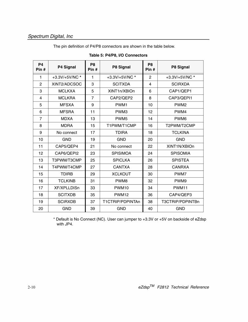
The pin definition of P4/P8 connectors are shown in the table below.
* Default is No Connect (NC). User can jumper to +3.3V or +5V on backside of eZdsp
with JP4.
Table 5: P4/P8, I/O Connectors
P4
Pin #P4 Signal
P8
Pin #P8 Signal
P8
Pin #P8 Signal
1 +3.3V/+5V/NC * 1 +3.3V/+5V/NC * 2 +3.3V/+5V/NC *
2 XINT2/ADCSOC 3 SCITXDA 4 SCIRXDA
3 MCLKXA 5 XINT1n/XBIOn 6 CAP1/QEP1
4 MCLKRA 7 CAP2/QEP2 8 CAP3/QEPI1
5 MFSXA 9 PWM1 10 PWM2
6 MFSRA 11 PWM3 12 PWM4
7 MDXA 13 PWM5 14 PWM6
8 MDRA 15 T1PWM/T1CMP 16 T2PWM/T2CMP
9 No connect 17 TDIRA 18 TCLKINA
10 GND 19 GND 20 GND
11 CAP5/QEP4 21 No connect 22 XINT1N/XBIOn
12 CAP6/QEPI2 23 SPISIMOA 24 SPISOMIA
13 T3PWM/T3CMP 25 SPICLKA 26 SPISTEA
14 T4PWM/T4CMP 27 CANTXA 28 CANRXA
15 TDIRB 29 XCLKOUT 30 PWM7
16 TCLKINB 31 PWM8 32 PWM9
17 XF/XPLLDISn 33 PWM10 34 PWM11
18 SCITXDB 35 PWM12 36 CAP4/QEP3
19 SCIRXDB 37 T1CTRIP/PDPINTAn 38 T3CTRIP/PDPINTBn
20 GND 39 GND 40 GND

Spectrum Digital, Inc
2-11
The pin definition of P7 connector is shown in the table below.
2.3.5 P5/P9, Analog Interface
The position of the 30 pins on the P5/P9 connectors are shown in the diagram below
as viewed from the top of the eZdsp.
Table 6: P7, I/O Connector
P7
Pin #P7 Signal
1 C1TRIPn
2 C2TRIPn
3 C3TRIPn
4 T2CTRIPn/EVASOCn
5 C4TRIPn
6 C5TRIPn
7 C6TRIPn
8 T4CTRIPn/EVBSOCn
9 No connect
10 GND
P9
Figure 2-7, Connector P5/P9 Pin Locations
7531
2018161412108642
19171513119
ANALOG
1 2 3 4 5 6 7 8 9 10
P5

Spectrum Digital, Inc
2-12 eZdspTM F2812 Technical Reference
The definition of P5/P9 signals are shown in the table below.
* Connect VREFLO to AGND or VREFLO of target system for proper ADC operation.
Table 7: P5/P9, Analog Interface Connector
P5
Pin #Signal
P9
Pin #Signal
P9
Pin #Signal
1 ADCINB0 1 GND 2 ADCINA0
2 ADCINB1 3 GND 4 ADCINA1
3 ADCINB2 5 GND 6 ADCINA2
4 ADCINB3 7 GND 8 ADCINA3
5 ADCINB4 9 GND 10 ADCINA4
6 ADCINB5 11 GND 12 ADCINA5
7 ADCINB6 13 GND 14 ADCINA6
8 ADCINB7 15 GND 16 ADCINA7
9 ADCREFM 17 GND 18 VREFLO *
10 ADCREFP 19 GND 20 No connect

Spectrum Digital, Inc
2-13
2.3.6 P6, Power Connector
Power (5 volts) is brought onto the eZdspTM F2812 via the P6 connector. The
connector has an outside diameter of 5.5 mm. and an inside diameter of 2 mm. The
position of the P6 connector is shown below.
The diagram of P6, which has the input power is shown below.
Figure 2-8, Connector P6 Location
PO
WE
R
TP1
PC Board
P6
+5V
Ground
Front View
Figure 2-9, eZdspTM F2812 Power Connector

Spectrum Digital, Inc
2-14 eZdspTM F2812 Technical Reference
2.3.7 Connector Part Numbers
The table below shows the part numbers for connectors which can be used on the
eZdspTM F2812. Part numbers from other manufacturers may also be used.
*SSW or SSQ Series can be used
2.4 eZdspTM F2812 Jumpers
The eZdspTM F2812 has 8 jumpers available to the user which determine how
features on the eZdspTM F2812 are utilized. The table below lists the jumpers and their
function. The following sections describe the use of each jumper.
Table 8: eZdspTM F2812 Suggested Connector Part Numbers
Connector Male Part Numbers Female Part Numbers
P1 SAMTEC TSW-1-10-07-G-T SAMTEC SSW-1-10-01-G-T
P2 SAMTEC TSW-1-20-07-G-T SAMTEC SSW-1-20-01-G-T
Table 9: eZdspTM F2812 Jumpers
Jumper # Size Function
Position As
Shipped From
Factory
JP1 1 x 3 XMP/MCn 2-3
JP4 1 x 3 +3.3/5 Volts to P8,P4 Not connected
JP5 1 x 3 +3.3/5 Volts to P2 Not Connected
JP7 1 x 2 Boot Mode 3 2-3
JP8 1 x 3 Boot Mode 2 2-3
JP9 1 x 3 PLL Disable 1-2
JP11 1 x 3 Boot Mode 1 1-2
JP12 1 x 3 Boot Mode 0 2-3
WARNING!
be installed in either the 1-2 or 2-3 position
Unless noted otherwise, all 1x3 jumpers must

Spectrum Digital, Inc
2-15
The diagram below shows the positions of six jumpers on the component side of the
eZdspTM F2812.
2.4.1 JP1, XMP/MCn Select
Jumper JP1 is used to select the XMP/MCn option. The 1-2 selection allows the DSP to
operate in the Microcontroller mode. The 2-3 selection allow the DSP to operate in the
Microprocessor mode. The positions are shown in the table below.
* as shipped from factory
Table 10: JP1, XMP/MCn Select
Position Function
1-2 Microprocessor mode
2-3 * Microcomputer mode
Figure 2-10, eZdspTM F2812 Jumper Positions
JP1DS2
JP12
JP7
TP2
DS1
JP8
JP11
JP9
TP1

Spectrum Digital, Inc
2-16 eZdspTM F2812 Technical Reference
2.4.2 JP4, JP5 Voltage Jumpers
Jumpers JP4 and JP5 are an unpopulated jumpers on the bottom side of the board that
provide either +3.3 volts or +5 volts to pins on the expansion connectors. These
jumpers are shipped uninstalled to prevent accidental damage by connecting wires or
circuitry to the expansion connector. The user may connect these jumpers by installing
a jumper wire or zero ohm resistor. The position of these jumpers are shown in the
figure below.
Figure 2-11, eZdspTM F2812 Voltage Jumper Positions (Bottom Side)
JP5
JP4

Spectrum Digital, Inc
2-17
2.4.2.1 JP4, +3.3/5 Volts for P8, P4
Jumper JP4 allows the user to provide either +3.3 or +5 volts to pins 1 and 2 of
expansion connector P8, and pin 1 of P4. The settings for this jumper are shown in the
table below
* As shipped from factory
2.4.2.2 JP5, +3.3/5 Volts for P2
Jumper JP5 allows the user to provide either +3.3 or +5 volts to pins 1 and 2 of
expansion connector P2. The settings for this jumper are shown in the table below.
* As shipped from factory
Table 11: JP4, +3.3/5 Volts for P8, P4
Position Function Jumper Position
1-2
Connect +5 Volts
to P8, pins 1,2,
and P4 pin1
2-3
Connect +3.3
Volts to P8, pins
1,2, and P4 pin1
No connect *
Table 12: JP5, +3.3/5 Volts for P2
Position Function Jumper Position
1-2
Connect +5 Volts to P2, pins
1,2
2-3
Connect +3.3 Volts to P2,
pins 1,2
No connect *
3.3V5V
JP4
JP4
3.3V5V
JP4
3.3V5V
3.3V5V
JP5
JP5
3.3V5V
JP5
3.3V5V

Spectrum Digital, Inc
2-18 eZdspTM F2812 Technical Reference
2.4.3 JP7, JP8, JP11, JP12, Boot Mode Select
Jumpers JP7, JP8, JP11, JP12 are used to determine what mode the DSP will use for
bootloading on power up. To set a signal high, place the jumper in the 1-2 position.
For a low signal, use the 2-3 position.The options are shown in the table below.
* factory default
2.4.4 JP9, PLL Disable
Jumper JP9 is used to enable/disable the use of the Phase Lock Loop (PLL) logic on
the DSP. The selection of the 1-2 position enables the use of the PLL. If the 2-3
position is used the PLL is disabled. This signal is latched at reset and may be used as
XF after reset. The positions are shown in the table below.
* as shipped from the factory
Table 13: JP7, JP8, JP11, JP12, Boot Mode Select
JP7, BOOT3
SCITXDA
JP8, BOOT2
MDXA
JP11, BOOT1
SPISTEA
JP12, BOOT0
SPICLKAMODE
1 X X X FLASH
0 1 X X SPI
0 0 1 1 SCI
0 0 1 0 H0 *
0 0 0 1 OTP
0 0 0 0 PARALLEL
Table 14: JP9, PLL Disable
Position Function
1-2 * PLL Enabled
2-3 PLL disabled

Spectrum Digital, Inc
2-19
2.5 LEDs
The eZdspTM F2812 has two light-emitting diodes. DS1 indicates the presence of
+5 volts and is normally ‘on’ when power is applied to the board. DS2 is under software
control and is tied to the XF pin on the DSP through a buffer. These are shown in the
table below.
2.6 Test Points
The eZdspTM F2812 has two test points. The signals they are tied to are shown in the
table below.
Table 15: LEDs
LED # Color Controlling Signal
DS1 Green +5 Volts
DS2 Green XF bit (XF high = on)
Table 16: Test Points
Test Point Signal
TP1 Ground
TP2 Analog Ground

Spectrum Digital, Inc
2-20 eZdspTM F2812 Technical Reference

A-1
Appendix A
eZdspTM F2812
Schematics
The schematics for the eZdspTM F2812 can be found on the CD-ROM that
accompanies this board. The schematics were drawn on ORCAD.
The schematics are correct for both the socketed and unsocketed version
of the eZdspTM.
Design Notes:
1. The TMS320F2812 X1/CLKIN pin is +1.8 volt input. The clock input is
buffered with a SN74LVC1G14 whose supply is +1.8 volts. This provides
+3.3 volts to the +1.8 volt clock translation. Refer to sheet 4 of the
schematics.
WARNING !The TMS320F2812 supports +3.3V Input/Output levelswhich are NOT +5V tolerant. Connecting the eZdsp toa system with +5V Input/Output levels will damage theTMS320F2812. If the eZdsp is connected to anothertarget then the eZdsp must be powered up first and powered down last to prevent lactchup conditions.

Spectru
m D
igita
l, Inc
A-2
eZ
dsp
TM
F2
81
2 T
ech
nic
al R
efe
rence
5
5
4
4
3
3
2
2
1
1
D D
C C
B B
A A
QA
4
C USED ON
ENGR-MGR
RLSE
DATE
DATE
REV
SH
DATE
5
C
62
DATE
REVISION STATUS OF SHEETS
REV
SH
DWN
C
DATE
ENGR
SH
DATE
C
CHK
B
MFG
1 APPLICATION
NEXT ASSY
DATE
3
C
REV
REVISIONS
DESCRIPTIONREV DATE APPROVED
A PROTOTYPES 04-April-2002
The TMS320F2812 EzDSP design is based onpreliminary information(SPRS174G) for theTMS320F2812 device. This schematic is subject tochange without notification. Spectrum Digital Inc.assumes no liability for applications assistance,customer product design or infringement of patentsdescribed herein.
B PRODUCTION RELEASE 07-June-2002
C UPDATE PER SPRS174G 20-Jan-2003
506262 C
TMS320F2812 EzDSP
B
1 6Wednesday, June 04, 2003
SPECTRUM DIGITAL INCORPORATED
Title
Size Document Number Rev
Date: Sheet of

Sp
ectru
m D
igita
l, Inc
A-3
5
5
4
4
3
3
2
2
1
1
D D
C C
B B
A A
DSP
LOCATE NEAR DSP
( 3.3V )
( 1.8V )
SINGLE POINT CONNECTION
TAIYO YUDEN EMK325F106ZH-T
SPECTRUM DIGITAL INCORPORATED
506262 C
TMS320F2812 EzDSP
B
2 6Wednesday, June 04, 2003
Title
Size Document Number Rev
Date: Sheet of
XA
0X
A1
XA
2X
A3
XA
4X
A5
XA
6X
A7
XA
8X
A9
XA
10
XA
11
XA
12
XA
13
XA
14
XA
15
XA
16
XA
17
XA
18
XD0XD1XD2XD3XD4XD5XD6XD7XD8XD9XD10XD11XD12XD13XD14XD15
VDDA1
ADCBGREFIN
VDDA1
VDD11.8V
C28_TRSTn (5)
C28_EMU1 (5)C28_EMU0 (5)
C28_TCK (5)C28_TMS (5)
XD[0..15] (3,4)
XRnW (4)
XZCS2n (4)
XMP_MCn (4)XREADY (4)
PWM1(4)PWM2(4)PWM3(4)PWM4(4)PWM5(4)PWM6(4)
PWM7(4)PWM8(4)PWM9(4)PWM10(4)PWM11(4)
CAP1_QEP1(4)CAP2_QEP2(4)CAP3_QEPI1(4)
CAP4_QEP3(4)CAP5_QEP4(4)CAP6_QEPI2(4)
T1PWM_T1CMP(4)T2PWM_T2CMP(4)
T3PWM_T3CMP(4)T4PWM_T4CMP(4)
TDIRA(4)TCLKINA(4)
TDIRB(4)TCLKINB(4)
PWM12(4)
SCITXDA (4)SCIRXDA (4)
CANTXA (4)CANRXA (4)
SPISIMOA (4)SPISOMIA (4)SPICLKA (4)SPISTEA (4)
T1CTRIP_PDPINTAn(4)
T3CTRIP_PDPINTBn(4)
MCLKXA (4)MCLKRA (4)MFSXA (4)MFSRA (4)MDXA (4)MDRA (4)
XF_XPLLDISn (4)XINT1n_XBIOn(4)XINT2n_ADCSOC(4)XNMIn_XINT3(4)
C1TRIPn(4)C2TRIPn(4)C3TRIPn(4)
C4TRIPn(4)C5TRIPn(4)C6TRIPn(4)
T2CTRIPn_EVASOCn(4)
T4TRIPn_EVBSOCn(4)
XHOLDn (4)XHOLDAn (4)
XZCS0AND1n (4)
XWEn (3,4)XZCS6AND7n (3)
1.8V(4,6)
XTESTSEL (3,4,5,6)
XRSn (5)
X1_CLKIN (4)
XCLKOUT (4)
VREFLO(4)
VDD3VFL(6)
SCITXDB (4)SCIRXDB (4)
C28_TDO (5)C28_TDI (5)
XRDn (3,4)
ADCINA0(4)ADCINA1(4)ADCINA2(4)ADCINA3(4)ADCINA4(4)ADCINA5(4)ADCINA6(4)ADCINA7(4)ADCINB0(4)ADCINB1(4)ADCINB2(4)ADCINB3(4)ADCINB4(4)ADCINB5(4)ADCINB6(4)ADCINB7(4)
ADCREFP(4)ADCREFM(4)
GND(3,4,5,6)
AGND(3,4,5,6)
XA[0..18] (3,4)3.3V
3.3V
TP2
AGND
1
C37
.001uF
C56
.001uF
RN2A
331 16
A BRN2B
332 15
A B
RN2D
334 13
A BRN2E
335 12
A BRN2F
336 11
A B
RN2C
333 14
A B
C3510UF CERAMIC LOW ESR
C3610UF CERAMIC LOW ESR
R2624.9K
AD
C
FL
AS
H -
3.3
V
VD
D I
/0 -
3.3
V
VD
D C
OR
E -
1.8
V
1.8
V
U8
TMS320F2812PGF
18
43
80
85
103
108
111
118
121
125
130
132
138
141
144
148
152
156
158
2124273033363954656873749697139147
44881338442511611715982
7776
134
160
6766
135136126131127137146
174173172171170169168167
23456789
1110161213
175164
9293949598
101102104106107109116117122123124
45464748495053555759607172616263
110115
7983
149151150
40413435
155157
8789
282526292220
140
9091
69
14
16
61
51
65
16
21
63
1 17
6
19
32
38
52
58
70
86
99
10
51
13
12
01
29
14
21
53
78
31
64
81
114
145
23
37
56
75
100
112
128
143
154
119
XA
0X
A1
XA
2X
A3
XA
4X
A5
XA
6X
A7
XA
8X
A9
XA
10
XA
11
XA
12
XA
13
XA
14
XA
15
XA
16
XA
17
XA
18
XD0XD1XD2XD3XD4XD5XD6XD7XD8XD9
XD10XD11XD12XD13XD14XD15
XZCS0AND1nXZCS2n
XZCS6AND7nXWEnXRDn
XRnWXREADY
XMP/MCnXHOLDn
XHOLDAn
X1/XCLKINX2
TESTSEL
XRSn
TEST1TEST2
TRSTnTCKTMSTDI
TDOEMU0EMU1
ADCINA0ADCINA1ADCINA2ADCINA3ADCINA4ADCINA5ADCINA6ADCINA7ADCINB0ADCINB1ADCINB2ADCINB3ADCINB4ADCINB5ADCINB6ADCINB7
ADCREFPADCREFMADCRESEXTAVSSREFBGAVDDREFBGADCLOADCBGREFIN
GPIOA0-PWM1GPIOA1-PWM2GPIOA2-PWM3GPIOA3-PWM4GPIOA4-PWM5GPIOA5-PWM6GPIOA6-T1PWM_T1CMPGPIOA7-T2PWM_T2CMPGPIOA8-CAP1_QEP1GPIOA9-CAP2_QEP2GPIOA10-CAP3_QEPI1GPIOA11-TDIRAGPIOA12-TCLKINAGPIOA13-C1TRIPnGPIOA14-C2TRIPnGPIOA15-C3TRIPn
GPIOB0-PWM7GPIOB1-PWM8GPIOB2-PWM9GPIOB3-PWM10GPIOB4-PWM11GPIOB5-PWM12GPIOB6-T3PWM_T3CMPGPIOB7-T4PWM_T4CMPGPIOB8-CAP4_QEP3GPIOB9-CAP5_QEP4GPIOB10-CAP6_QEPI2GPIOB11-TDIRBGPIOB12-TCLKINBGPIOB13-C4TRIPnGPIOB14-C5TRIPnGPIOB15-C6TRIPn
GPIOD0-T1CTRIP_PDPINTAnGPIOD1-T2CTRIPn_EVASOCnGPIOD5-T3CTRIP_PDPINTBnGPIOD6-T4CTRIPn_EVBSOCn
GPIOE0-XINT1_XBIOnGPIOE1-XINT2_ADCSOCGPIOE2-XNMI_XINT13
GPIOF0-SPISIMOAGPIOF1-SPISOMIAGPIOF2-SPICLKAGPIOF3-SPISTEA
GPIOF4-SCITXDAGPIOF5-SCIRXDA
GPIOF6-CANTXAGPIOF7-CANRXA
GPIOF8-MCLKXAGPIOF9-MCLKRAGPIOF10-MFSXAGPIOF11-MFSRA
GPIOF12-MDXAGPIOF13-MDRA
GPIOF14-XF-XPLLDISn
GPIOG4-SCITXDBGPIOG5-SCIRXDB
VD
D3
VF
L
VD
DA
1V
DD
A2
VS
SA
1V
SS
A2
VD
D1
VS
S1
VD
DA
IOV
SS
AIO
VS
S2
VS
S3
VS
S4
VS
S5
VS
S6
VS
S7
VS
S9
VS
S1
0V
SS
11
VS
S1
2V
SS
13
VS
S1
4V
SS
15
VS
S1
6
VS
S8
VD
DIO
1V
DD
IO2
VD
DIO
3V
DD
IO4
VD
DIO
5
VD
D2
VD
D3
VD
D4
VD
D5
VD
D6
VD
D7
VD
D8
VD
D9
VD
D1
0
XCLKOUT
C58
.1uF
L4
BLM21P221SN
TP3
TP
C21uF
C31uF
C57
.1uF
L3
BLM21P221SNC38
.1uF

Spectru
m D
igita
l, Inc
A-4
eZ
dsp
TM
F2
81
2 T
ech
nic
al R
efe
rence
5
5
4
4
3
3
2
2
1
1
D D
C C
B B
A A
ASRAM
64Kx16 and 256Kx16
Compatible
SPECTRUM DIGITAL INCORPORATED
506262 B
TMS320F2812 EzDSP
B
3 6Wednesday, June 04, 2003
Title
Size Document Number Rev
Date: Sheet of
XA15
XA10
XA13
XA5
XA2
XA8XA9
XA14
XA6
XA1XA0
XA4XA3
XA7
XA11XA12
XD4
XD15
XD1
XD13
XD3
XD0
XD12
XD10
XD7
XD5
XD2
XD9XD8
XD6
XD11
XD14
XA16XA17
XWEn(2,4)XRDn(2,4)
XA[0..18] (2,4)
XD[0..15] (2,4)
GND(2,4,5,6)
XZCS6AND7n(2)
3.3V
C220.1uF
C100.1uF
U4
IS61LV6416-12T
12345
18192021
2223
24252627424344
78910131415162930313235363738
61741
4039
28
11
33
12
34
A0A1A2A3A4A5A6A7A8
A9A10
A11A12A13A14A15A16A17
D0D1D2D3D4D5D6D7D8D9
D10D11D12D13D14D15
CSWEOE
BHEBLE
NC
VD
D1
VD
D2
VS
S1
VS
S2

Sp
ectru
m D
igita
l, Inc
A-5
8
8
7
7
6
6
5
5
4
4
3
3
2
2
1
1
D D
C C
B B
A A
XF
XF
XTESTSEL
XMPNMC
BO
OT
MO
DE
PLLDISn
BOOT-0
BOOT-1
BOOT-2
BOOT-3
BOOT-3 BOOT-2 BOOT-1 BOOT-0
FLASH
SPI
SCI
H0
OTP
PARALLEL
SCITXDA MDXA SPISTEA SPICLKAMODE
0
0
0
0
0
0
0
0
0
0
0 0
0
1
1
1
1
1
1
X X
X
X
X
SMT/4PIN DIP
OPTIONAL
Connect VREFLO to AGND or
to VREFLO of target system
for proper ADC operation.
Schematic change from version
A/B to C. F2812 clkin is 1.8V
input.
Tie off unused F24xx
compatible signals.
Make a solder connection on
JP4 and/or JP5 to the
appropriate power supply. TMS320F2812 suppor t s 3.3V
input /out put levels w hic h are
NOT 5V t o ler ant . Connec t ing
t he eZdsp t o a syst em w i t h 5V
input /out put levels w i l l dam age
t he TMS320F2812. If t he eZdsp
is c onn ec t ed t o anot her t a rget
t hen t he eZdsp m us t be
pow ered up f i rs t and pow ered
dow n las t t o prevent la t c hup
condi t ion s.
506262 C
TMS320F2812 EzDSP
B
4 6Wednesday, June 04, 2003
Title
Size Document Number Rev
Date: Sheet of
ISnSTRBn
DSP_RSn
ISn
STRBn
GND
SCIRXDA (2)CAP1_QEP1 (2)CAP3_QEPI1 (2)PWM2 (2)PWM4 (2)PWM6 (2)
SPISOMIA (2)SPISTEA (2)CANRXA (2)
XD0(2,3) XD1 (2,3)XD2(2,3) XD3 (2,3)XD4(2,3) XD5 (2,3)XD6(2,3) XD7 (2,3)XD8(2,3) XD9 (2,3)
XD10(2,3) XD11 (2,3)XD12(2,3) XD13 (2,3)XD14(2,3) XD15 (2,3)
XA0(2,3) XA1 (2,3)XA2(2,3) XA3 (2,3)XA4(2,3) XA5 (2,3)XA6(2,3) XA7 (2,3)XA8(2,3) XA9 (2,3)
XA10(2,3) XA11 (2,3)XA12(2,3) XA13 (2,3)XA14(2,3) XA15 (2,3)
XREADY(2)XRnW(2)XWEn(2,3) XRDn (2,3)
VREFLO (2)
T2PWM_T2CMP (2)TCLKINA (2)
PWM7 (2)PWM9 (2)PWM11 (2)CAP4_QEP3 (2)T3CTRIP_PDPINTBn (2)
DSP_RSn(5)
SCITXDA(2)XINT1n_XBIOn(2)CAP2_QEP2(2)PWM1(2)PWM3(2)PWM5(2)T1PWM_T1CMP(2)TDIRA(2)
SPISIMOA(2)SPICLKA(2)CANTXA(2)XCLKOUT(2)PWM8(2)PWM10(2)PWM12(2)
T1CTRIP_PDPINTAn(2)
XNMIn_XINT3 (2)
XINT1n_XBIOn (2)
XHOLDAn(2)
XA16(2,3)XA18(2)
XA17 (2,3)XHOLDn (2)
XTESTSEL (2,3,5,6)
ADCINA0 (2)ADCINA1 (2)ADCINA2 (2)ADCINA3 (2)ADCINA4 (2)ADCINA5 (2)ADCINA6 (2)ADCINA7 (2)
ADCINB0 (2)ADCINB1 (2)ADCINB2 (2)ADCINB3 (2)ADCINB4 (2)ADCINB5 (2)ADCINB6 (2)ADCINB7 (2)
MCLKRA(2)MCLKXA(2)
MDXA(2)MDRA(2)
MFSRA(2)MFSXA(2)
XINT2n_ADCSOC(2)
CAP5_QEP4(2)CAP6_QEPI2(2)
T3PWM_T3CMP(2)T4PWM_T4CMP(2)
TDIRB(2)TCLKINB(2)
XF_XPLLDISn(2)SCITXDB(2)SCIRXDB(2)
XF_XPLLDISn (2)
XMP_MCn (2)
SPICLKA (2)
SPISTEA (2)
MDXA (2)
SCITXDA (2)
C1TRIPn (2)C2TRIPn (2)C3TRIPn (2)
C4TRIPn (2)C5TRIPn (2)C6TRIPn (2)T4TRIPn_EVBSOCn (2)
T2CTRIPn_EVASOCn (2)
GND (2,3,5,6)
ADCREFP (2)ADCREFM (2)
AGND (2,3,5,6)
XZCS2n (2)XZCS0AND1n(2)
X1_CLKIN(2)
MCLK(5)
1.8V(2,6)
3.3V
3.3V
3.3V
3.3V
3.3V
3.3V
3.3V
+5V3.3V3.3V +5V
P7
123456789
10
JP12
JUMPER3B
1
32
R39 10K
R36 2.2K
JP9
JUMPER3B
1
32
R42 10K
R41 2.2K
R6
10KR5
10K
JP11
JUMPER3B
1
32
R35 2.2K
R38 10K
JP8
JUMPER3B
1
32
R37 2.2K
R40 10K
JP7
JUMPER3B
1
32
R30 2.2K
R31 10K
P4
1234567891011121314151617181920
P9
1 23 45 67 89 1011 1213 1415 1617 1819 20
P5
123456789
10
P8
1 23 45 67 89 1011 1213 1415 1617 1819 2021 2223 2425 2627 2829 3031 3233 3435 3637 3839 40
U14
SN74LVC1G14
24
35
P2
HEADER 30X2
1 23 45 67 89 1011 1213 1415 1617 1819 2021 2223 2425 2627 2829 3031 3233 3435 3637 3839 4041 4243 4445 4647 4849 5051 5253 5455 5657 5859 60
DS2LTST-C150GKTGREEN
JP4
JUMPER3_SMT
1
2
3ABC
JP5
JUMPER3_SMT
12
3ABC
R1
100JP3
JUMPER3_SMT
1
2
3A B C
C62.1uF
U12SN74AHC1G14
3
4
5
2
R43
220
U11
NO-POP
1
4
8
5
OFFn
GND
VCC
CLK
C43
0.1uF
JP1
JUMPER3B
1
32
L1
BLM21P221SN
R29
100
C42
33 pF

Spectru
m D
igita
l, Inc
A-6
eZ
dsp
TM
F2
81
2 T
ech
nic
al R
efe
rence
5
5
4
4
3
3
2
2
1
1
D D
C C
B B
A A
XDS510PP EMULATION HEADER
PLACE NEAR EACH MOUNTING HOLE
OPEN-DRAIN
CROSS COUPLE IN TO OUT
EXT_VER 00110-001
XRSn is logical AND of PONRSnIN and
emulator controlled reset. Power on default
is PONRnIN controls XRSn.
PPEMU0/1 CONNECT DIRECTLY TO F2812 FOR
EMULATOR WAIT-IN-RESET SUPPORT
CBLV-3C-30.000
IF U13 IS INSTALLED THEN
REMOVE R49 AND R48.
Locate R7,R54, C70 at the DSP XRSn pin
for best EMI/ESD noise immunity.
To/from expansion header
SPECTRUM DIGITAL INCORPORATED
506262 C
TMS320F2812 EzDSP
C
5 6Wednesday, June 04, 2003
Title
Size Document Number Rev
Date: Sheet of
PPBUSDIRPPBUSENn
XPPS4XPPS5XPPS7nXPPS3
PPD1PPINITn
PPD3PPSELn
PPALEn
PPERRn
PPSTRBn
PPD2
PPD0
5VPPTDOPPTCK
PPTMSPPTDI
XPPD6XPPD5XPPD4XPPD3XPPD2XPPD1XPPD0
XPPS3XPPS4XPPS5
XPPS7n
PP
BU
SE
Nn
PP
BU
SD
IR
XP
PC
3n
XP
PC
2X
PP
C1n
XP
PC
0n
PP
TR
ST
nX
TR
ST
n
XE
VN
T0
XT
DI
PP
TM
SX
TM
S
XT
DO
3.3VXEVNT1
TP
OW
LO
SS
nP
ON
RS
nIN
PP
TD
I
XPPC3n
XPPC2
XPPC0n
XTCK
PPTCK
PPTDO
IPP
TC
K
IPP
TD
O
XEVNT1
XEVNT0
XTCK
XTDO
XTDI
XTMS
XTRSTn
PONRSnIN
TPOWLOSSn
XPPD7
AL
T_
MC
LK
VC
CR
VC
CR
5V
PPTRSTn
PPD4
GND
XT
CK
I
GN
D
EMUOFF
GND
FP
GA
_V
CC
A
PPD7
PPSLCT
GND
3.3V
PPACKn
FPGA_VCCA
PPD6
GN
D
JC
LK
3.3V
FP
GA
_V
CC
A
3.3V
3.3
V
GN
D
3.3
V
PPD5
PPPE
GND
GND
GND
3.3
V
GND
GND
GND
GND
GN
D
GN
DG
ND
GN
D
GND3.3V
FPGA_VCCA
GND
XPPD0
XPPD7
XPPD2
XPPD6
XPPD1
XPPD3
XPPD5XPPD4
PPBSY
XPPC1n
5V
5V
MC
LK
3.3V
3.3V
GN
D
GN
D
GND
3.3
V
EM
UO
FF
PPEMU1
PPEMU0
5V
FPGA_VCCA
VCCR
DSP_RSn
PONRSnIN (6)
GND (2,3,4,6)
C28_TRSTn (2)
C28_EMU1 (2)
C28_EMU0 (2)
C28_TCK (2)
C28_TMS (2)
C28_TDI (2)
C28_TDO (2)
XRSn (2)
MCLK(4)
DSP_RSn (4)
3.3V
3.3V
3.3V
3.3V
3.3V
3.3V
3.3V
+5V
3.3V
+5V
R54
100
C7022nF
C470.1uF
C140.1uF
C130.1uF
C240.1uF
C260.1uF
C250.1uF
C110.1uF
C450.1uF
C230.1uF
C490.1uF
C681uF
U10
30 MHz
1
4
8
5
OFFn
GND
VCC
CLK
L2
BLM21P221SNC48
0.1uF
R51
40.2K 1%
R50
41.2K 1%
R48
0
U13
TPS72201
1
2
3 4
5IN
GND
EN NC/FB
OUT
C27
.1uF
C28
.001uF
R9 33
R47
1M
C67
.001uF
C16
.001uF
RN4D 334 13A B
RN4H 338 9A B
RN4A 331 16A BRN4B 332 15A BRN4C 333 14A B
R12
10K
RN4E 335 12A B
RN4F 336 11A BRN4G 337 10A B
RN3A 331 16A B
C50
.1uF
R11
10K
R22
10K
RN3E 335 12A B
RN3D 334 13A B
RN3C 333 14A B
RN3B 332 15A B
R8 33
RN3H 338 9A B
RN3G 337 10A B
RN3F 336 11A B
U2
74ABT245PW
23456789
191
1817161514131211
10
20
A1A2A3A4A5A6A7A8
GDIR
B1B2B3B4B5B6B7B8
GND
VCC
RN1H 338 9A B
RN1D 334 13A B
R10 33
RN1G 337 10A B
RN1C 333 14A B
RN1F 336 11A B
RN1B 332 15A B
R25
100
R23
10K
RN1A 331 16A B
RN1E 335 12A B
C30
33pf
P3
DB25_SHIELD
1325122411231022
921
820
719
618
517
416
315
214
1
A
B
R19
1M
C15
33pf
R24
100
R15
100
C34
33pf
U5
74ABT245PW
23456789
191
1817161514131211
10
20
A1A2A3A4A5A6A7A8
GDIR
B1B2B3B4B5B6B7B8
GND
VCC
R16
10K
R17
10K
C17
33pf
C52
33pf
R18
100
P1
HEADER 7X2
1 23 45 67 89 1011 1213 14
R13
10KC54
33pf
C53
33pf
R14
10K
R20
100
C29
33pf
C55
33pfC33
33pf
EMBEDDED PP JTAG CONTROLLER
SPECTRUM DIGITAL I NC.
506053-000 1B
U6
506053-0001B
123456789
10111213141516171819202122232425
26
27
28
29
30
31
32
33
34
35
36
37
38
39
40
41
42
43
44
45
46
47
48
49
50
51525354555657585960616263646566676869707172737475
76
77
78
79
80
81
82
83
84
85
86
87
88
89
90
91
92
93
94
95
96
97
98
99
100
GNDRSV1_TDI_IOEMUOFFXEVNT1PPEMU1RSV2RSV3_TMS_IOVCCIGNDXPPD0XPPD1XPPD2XPPD3XPPD4XPPD5XPPD6XPPD7RSV4RSV5VCCIXPPS3XPPS4XPPS5XPPS6XPPS7n
PP
BU
SE
Nn
RS
V6
PP
BU
SD
IRR
SV
7X
PP
C3
nX
PP
C2
XP
PC
1n
XP
PC
0n
RS
V8_
PR
B_
IOV
CC
AG
ND
VC
CR
_N
CA
LT
_M
CL
KH
CL
KR
SV
9P
ON
RS
nT
PO
WL
OS
Sn
VF
UN
C_
EN
VC
CI
EX
T_
VE
R7
EX
T_
VE
R6
EX
T_
VE
R5
EX
T_
VE
R4
EX
T_
VE
R3
EX
T_
VE
R2
GNDEXT_VER1EXT_VER0
VPOWER_ONnVPOWER_BLEED
VBUS_ENnVCCAVCCI
XBITIN3XBITIN2XBITIN1XBITIN0
XBITOUT3XBITOUT2XBITOUT1XBITOUT0
VCCAGNDGND
EXTERN_RSTnMCLKOUT2EN
MCLKOUT2MCLKOUTEN
MCLKOUTDSP_RSn
EM
UO
FF
_1
OD
EM
U1
_S
RC
OD
EM
U0
_S
RC
OD
EM
U1
nO
DE
MU
0n
PP
TD
IV
CC
IX
TD
OP
PT
MS
XT
MS
JC
LK
RS
V1
0X
TC
KI
VC
CR
_N
CV
CC
AG
ND
RS
V1
1_
PR
A_
IOP
PT
DO
XT
DI
PP
TC
KP
PT
RS
Tn
XT
RS
Tn
PP
EM
U0
XE
VN
T0
RS
V13
_T
CK
_IO
C31
33pf
C32
33pf
R32
33
R71.5K
C51
.001uF
R49
0
C46
NO-POP

Sp
ectru
m D
igita
l, Inc
A-7
5
5
4
4
3
3
2
2
1
1
D D
C C
B B
A A
+5V Max
16.9K 1.848V15.0K 1.773V13.7K 1.722V
PONRSnIN, GOES HIGH > 200ms AFTER ALL POWER
IS STABLE.
3.3V THEN 1.8V
POWER ON SEQUENCE NOTES
3.3V SUPPLY, VDDIOVDD3VFL, VDDA1,VDDA2
1.8V SUPPLY
2.2V
140ms-280ms
Q3
PONRSnIN
VOLTAGE SUPPLY MAX CURRENT TPS767D301 PD
1.8V
3.3V
333mA
307mA
1065mW
521mW
PD(max) = (Tj(max) - Ta)/Rja
= (125 - 35)/27.9
= 3255mW
TPS767D301 RATINGS
MAX Iout PER CHANNEL IS 1A
TPS767D301 PD = (Vin-Vout)*Iout
1586mW Total
TIE TPS767D301 POWER PAD TO GND
PLANE (TI-SLMA002)
SET Q3 TO TURN ON WHEN 3.3V SUPPLY IS
GREATER THEN 2.2 VOLTS. REGULATOR
TURN ON DELAY AND RAMP RATE WILL
ENSURE THAT 3.3V SUPPLY IS AT 2.5 VOLTS
OR HIGHER BEFORE THE 1.8V SUPPLY
REACHES 0.3 VOLTS.
18.2K 1.899V
U16 WILL TURN OFF THE 1.8V SUPPLY WHEN
INPUT POWER FALLS BELOW 2.94V. THIS SPEEDS
UP THE 1.8V SUPPLY TURN OFF.
RESETn of TPS3838 is open-drain.
U16 was added for testing but not
populated on production boards.
SPECTRUM DIGITAL INCORPORATED
506262 C
TMS320F2812 EzDSP
B
6 6Wednesday, June 04, 2003
Title
Size Document Number Rev
Date: Sheet of
1.8VONn1.8V (2,4)
1.8V (2,4)
PONRSnIN (5)
VDD3VFL (2)
GND(2,3,4,5)
+5V
3.3V
3.3V
3.3V
3.3V
R2
10K
TP1
GND
1
C80.1uF
C50.1uF
C410.1uF
C180.1uF
C210.1uF
C190.1uF
C400.1uF
C610.1uF
R46
10K
C390.1uF
C600.1uF
C90.1uF
C200.1uF
C60.1uF
R45 30.1K, 1%
C65
0.1uF
C66
0.1uFR33
16.9K, 1% + CT322uF
C64
0.1uF
C63
0.1uF
+ CT422uF
U9
TPS767D301
56
4
3
1112
10
9
1278
1314
151620212627
28
232425
22
171819
1IN1IN
1EN
1GND
2IN2IN
2EN
2GND
NCNCNCNCNCNC
NCNCNCNCNCNC
1RESET
1OUT1OUT
1FB/SENSE
2RESET
2OUT2OUT
2SENSE
TH
ER
MA
L_P
AD
+ CT122uF
+ CT522uF
+ CT247uF
C7
.1uF
C11uF
P6
C590.1uF
R53
1.5K 1%
U16
TPS3838K33DBV
1
2
3
4
5CT
GND
MRn
RESETn
VDD
Q3BSS138G
DS
R44220
R34
2.0K 1%
R52
0
DS1LTST-C150GKTGREEN
+ CT622uF

Spectrum Digital, Inc
A-8 eZdspTM F2812 Technical Reference

B-1
Appendix B
eZdspTM F2812
MechanicaI Information
This appendix contains the mechanical information about the socketed and
unsocketed versions of the eZdspTM F2812

Spectrum Digital, Inc
B-2 eZdspTM F2812 Technical Reference
Th
is d
raw
ing
is
no
t to
sc
ale

Spectrum Digital, Inc
B-3
Th
is d
raw
ing
is
no
t to
sc
ale

Spectrum Digital, Inc
B-4 eZdspTM F2812 Technical Reference


Printed in U.S.A., September 2003506265-0001 Rev. F