
West Bridge® Astoria™ Technical Reference Manual
250
West Bridge ® Astoria ™ Technical Reference Manual Document # 001-70142 Rev. *A Cypress Semiconductor 198 Champion Court San Jose, CA 95134-1709 Phone (USA): 800.858.1810 Phone (Intnl): 408.943.2600 http://www.cypress.com
-
Upload
khangminh22 -
Category
Documents
-
view
0 -
download
0
Transcript of West Bridge® Astoria™ Technical Reference Manual
West Bridge® Astoria™ Technical ReferenceManual
Document # 001-70142 Rev. *A
Cypress Semiconductor198 Champion Court
San Jose, CA 95134-1709
Phone (USA): 800.858.1810Phone (Intnl): 408.943.2600
http://www.cypress.com
2 West Bridge Astoria Technical Reference Manual, Document # 001-70142 Rev. *A
Copyrights
Copyrights
Copyright © 2012-2015 Cypress Semiconductor Corporation. All rights reserved.
Cypress, the Cypress Logo, and West Bridge are registered trademarks and Astoria, MoBL-USB, and ReNumeration aretrademarks of Cypress Semiconductor Corporation. Macintosh is a registered trademark of Apple Computer, Inc. Windows isa registered trademark of Microsoft Corporation. SmartMedia is a trademark of Toshiba Corporation. All other product or com-pany names used in this manual may be trademarks, registered trademarks, or servicemarks of their respective owners.
Purchase of I2C components from Cypress or one of its sublicensed Associated Companies conveys a license under thePhilips I2C Patent Rights to use these components in an I2C system, provided that the system conforms to the I2C StandardSpecification as defined by Philips. As from October 1st, 2006 Philips Semiconductors has a new trade name - NXP Semicon-ductors.
The information in this document is subject to change without notice and should not be construed as a commitment byCypress. While reasonable precautions have been taken, Cypress assumes no responsibility for any errors that may appearin this document. No part of this document may be copied or reproduced in any form or by any means without the prior writtenconsent of Cypress. Made in the U.S.A.
Disclaimer
CYPRESS MAKES NO WARRANTY OF ANY KIND, EXPRESS OR IMPLIED, WITH REGARD TO THIS MATERIAL,INCLUDING, BUT NOT LIMITED TO, THE IMPLIED WARRANTIES OF MERCHANTABILITY AND FITNESS FOR A PAR-TICULAR PURPOSE. Cypress reserves the right to make changes without further notice to the materials described herein.Cypress does not assume any liability arising out of the application or use of any product or circuit described herein. Cypressdoes not authorize its products for use as critical components in life-support systems where a malfunction or failure may rea-sonably be expected to result in significant injury to the user. The inclusion of Cypress’ product in a life-support systems appli-cation implies that the manufacturer assumes all risk of such use and in doing so indemnifies Cypress against all charges.
The acceptance of this document will be construed as an acceptance of the foregoing conditions.
This manual is the West Bridge Astoria Technical Reference Manual. It gives information for these chipsCYWB0216ABSCYWB0220ABSCYWB0224ABSCYWB0226ABSCYWB0320ABXCYWB0321ABX

West Bridge Astoria Technical Reference Manual, Document # 001-70142 Rev. *A 3
Contents
1. Contents 3
1. Introducing West Bridge® Astoria™ 91.1 Astoria Architecture ................................................................................................................101.2 Top Level Block Diagram........................................................................................................111.3 Top Level Functional Blocks...................................................................................................11
1.3.1 Processor Interface Port (P-Port)................................................................................111.3.2 USB Port (U-Port) .......................................................................................................121.3.3 Storage Port (S-Port)...................................................................................................12
1.3.3.1 SD/MMC Port (S-Port).................................................................................151.3.3.2 CE-ATA (S-Port)..........................................................................................171.3.3.3 GPIO[1:0].....................................................................................................17
1.4 Packages ................................................................................................................................171.5 Endpoints Overview................................................................................................................18
1.5.1 Logical Endpoints........................................................................................................181.5.2 Physical Endpoints......................................................................................................18
1.6 Document History ...................................................................................................................20
2. Endpoint Zero 21
2.1 Control Endpoint EP0 .............................................................................................................212.2 USB Requests ........................................................................................................................23
2.2.1 Get Status ...................................................................................................................242.2.2 Set Feature .................................................................................................................262.2.3 Clear Feature ..............................................................................................................272.2.4 Get Descriptor .............................................................................................................27
2.2.4.1 Get Descriptor-Device .................................................................................282.2.4.2 Get Descriptor-Device Qualifier...................................................................292.2.4.3 Get Descriptor-Configuration.......................................................................292.2.4.4 Get Descriptor-String...................................................................................302.2.4.5 Get Descriptor-Other Speed Configuration ................................................30
2.2.5 Set Descriptor .............................................................................................................302.2.5.1 Set Configuration ........................................................................................31
2.2.6 Get Configuration ........................................................................................................312.2.7 Set Interface................................................................................................................312.2.8 Get Interface ...............................................................................................................322.2.9 Set Address.................................................................................................................322.2.10 Sync Frame.................................................................................................................33
3. Enumeration and ReNumeration™ 35
3.1 Firmware Loading ...................................................................................................................353.1.1 Loading the Firmware from the Processor ..................................................................353.1.2 Legacy Boot Mode ......................................................................................................37

4 West Bridge Astoria Technical Reference Manual, Document # 001-70142 Rev. *A
Contents
3.1.3 Debug Boot Mode.......................................................................................................373.1.4 Register Configuration ................................................................................................383.1.5 The Default USB Device.............................................................................................383.1.6 Astoria Vendor Request for Firmware Load................................................................39
3.2 EEPROM Configuration Byte .................................................................................................403.3 The RENUM Bit ......................................................................................................................413.4 Astoria’s Response to Device Requests
(RENUM = 0)413.5 How the Firmware ReNumerates ...........................................................................................423.6 Multiple ReNumerations™......................................................................................................42
4. Interrupts 43
4.1 SFRs.......................................................................................................................................434.2 Interrupt Processing ...............................................................................................................45
4.2.1 Interrupt Masking ........................................................................................................454.2.1.1 Interrupt Priorities ........................................................................................45
4.2.2 Interrupt Sampling ......................................................................................................454.2.3 Interrupt Latency.........................................................................................................46
4.3 USB-Specific Interrupts ..........................................................................................................464.3.1 Resume Interrupt ........................................................................................................464.3.2 USB Interrupts ............................................................................................................46
4.3.2.1 SUTOK, SUDAV Interrupts .........................................................................494.3.2.2 SOF Interrupt...............................................................................................494.3.2.3 Suspend Interrupt........................................................................................494.3.2.4 USB RESET Interrupt..................................................................................494.3.2.5 HISPEED Interrupt ......................................................................................494.3.2.6 EP0ACK Interrupt........................................................................................494.3.2.7 Endpoint Interrupts ......................................................................................494.3.2.8 In-Bulk-NAK (IBN) Interrupt.........................................................................494.3.2.9 EPxPING Interrupt.......................................................................................494.3.2.10 ERRLIMIT Interrupt .....................................................................................504.3.2.11 EPxISOERR Interrupt..................................................................................50
4.4 USB-Interrupt Autovectors......................................................................................................504.4.1 USB Autovector Coding..............................................................................................51
4.5 GPIF Interrupt.........................................................................................................................514.6 GPIF Interrupt Autovectors.....................................................................................................52
4.6.1 GPIF Autovector Coding.............................................................................................52
5. Memory 55
5.1 Internal Data RAM..................................................................................................................555.1.1 The Lower 128............................................................................................................565.1.2 The Upper 128............................................................................................................565.1.3 Special Function Register Space ................................................................................56
5.2 Astoria Memory Map ..............................................................................................................57
6. Power Management 596.1 Power Domains ......................................................................................................................596.2 Power Supply Sequence ........................................................................................................616.3 Power Modes..........................................................................................................................61
6.3.1 Normal Mode ..............................................................................................................616.3.2 Standby Mode.............................................................................................................616.3.3 Suspend Mode............................................................................................................63

West Bridge Astoria Technical Reference Manual, Document # 001-70142 Rev. *A 5
Contents
6.3.3.1 Wakeup .......................................................................................................646.3.4 Core Power Down.......................................................................................................65
6.4 Power Management ...............................................................................................................66
7. Resets 67
7.1 Hard Reset .............................................................................................................................677.2 Reset by Register (Soft Reset)...............................................................................................697.3 Wakeup Mechanism...............................................................................................................717.4 USB Bus Reset.......................................................................................................................717.5 Astoria Disconnect..................................................................................................................71
8. Access to Endpoint Buffers 738.1 Physical And Logical Endpoints .............................................................................................738.2 High Speed and Full Speed Differences ................................................................................748.3 How the CPU Configures the Endpoints ................................................................................758.4 CPU Access to Astoria Endpoint Data ...................................................................................768.5 CPU Control of Astoria Endpoints ..........................................................................................77
8.5.1 Registers That Control EP0, EP1IN, and EP1OUT ....................................................778.5.1.1 EP0CS ........................................................................................................778.5.1.2 EP0BCH and EP0BCL ................................................................................778.5.1.3 USBIE, USBIRQ..........................................................................................788.5.1.4 EP01STAT ..................................................................................................788.5.1.5 EP1OUTCS.................................................................................................788.5.1.6 EP1OUTBC.................................................................................................788.5.1.7 EP1INCS.....................................................................................................788.5.1.8 wEP1INBC ..................................................................................................79
8.5.2 Registers That Control EP2, EP3, EP4, EP5, EP6, EP7, EP8 and EP9 ....................798.5.2.1 EP2468STAT ..............................................................................................798.5.2.2 EP2ISOINPKTS, EP4ISOINPKTS, EP6ISOINPKTS, EP8ISOINPKTS ......798.5.2.3 EP2CS, EP4CS, EP6CS, EP8CS ...............................................................798.5.2.4 EP2BCH:L, EP4BCH:L, EP6BCH:L, EP8BCH:L.........................................80
8.5.3 Registers That Control All Endpoints .........................................................................818.5.3.1 IBNIE, IBNIRQ, NAKIE, NAKIRQ................................................................818.5.3.2 EPIE, EPIRQ...............................................................................................828.5.3.3 USBERRIE, USBERRIRQ, ERRCNTLIM, CLRERRCNT ...........................828.5.3.4 TOGCTL......................................................................................................82
8.6 The Setup Data Pointer ..........................................................................................................838.6.1 Transfer Length...........................................................................................................838.6.2 Accessible Memory Spaces........................................................................................83
8.7 Autopointers ...........................................................................................................................83
9. Storage Block and TPIC 859.1 TPIC Registers .......................................................................................................................85
9.1.1 TPIC_P2S_SOFT_RESET Register ..........................................................................859.1.2 TPIC_P2S_CFG Register...........................................................................................869.1.3 TPIC_P2S_EN Register ............................................................................................869.1.4 TPIC_INT0_CLR Register ..........................................................................................87
9.2 SIB..........................................................................................................................................879.2.1 SIB_READ_WAIT_EN Register .................................................................................889.2.2 SIB_NAND_CFG Register ..........................................................................................889.2.3 SIB_MODE_CFG Register .........................................................................................89
9.3 GPIF and Slave FIFO.............................................................................................................90

6 West Bridge Astoria Technical Reference Manual, Document # 001-70142 Rev. *A
Contents
9.3.1 Slave FIFO:.................................................................................................................909.3.2 GPIF ...........................................................................................................................90
9.3.2.1 GPIF initialization ........................................................................................909.4 GPIO.......................................................................................................................................929.5 Reset SIB ...............................................................................................................................929.6 Sending Commands to the SD/MMC Card.............................................................................93
10. General Programmable Interface (GPIF) 95
10.1 GPIF Signals ..........................................................................................................................9510.1.1 Data Lines...................................................................................................................9510.1.2 GPIF Address Lines................................................................................................9510.1.3 GPIF Control Out Signals ...........................................................................................9610.1.4 Ready IN Signals ........................................................................................................9610.1.5 Interface Clock (IFCLK) ..............................................................................................9610.1.6 GPIF Designer ............................................................................................................96
11. Coprocessor Interface Logic 9711.1 Operational Modes .................................................................................................................97
11.1.1 Address and Data Buses Non Multiplexing Asynchronous Pseudo CRAM Mode......9911.1.2 Address and Data Buses Non Multiplexing Synchronous Mode.................................9911.1.3 Address and Data Buses Multiplexing Asynchronous Pseudo CRAM Mode..............9911.1.4 Address and Data Buses Multiplexing Synchronous Pseudo CRAM Mode ...............9911.1.5 Address and Data Buses Non Multiplexing Asynchronous SRAM Mode .................10011.1.6 Pseudo NAND (PNAND) Mode ................................................................................101
11.1.6.1 Pseudo NAND (PNAND) Configuration Registers Summary ....................10311.1.7 PI2C and PSPI Interface..........................................................................................109
11.1.7.1 PI2C Mode (Available on ADM, PNAND, and PSPI Modes).....................10911.1.7.2 PSPI Mode ................................................................................................109
11.1.8 Switching the P-Port from Asynchronous Mode to Synchronous Mode ................... 11211.1.9 Port Interface Configuration Register ....................................................................... 11211.1.10AC Timing Parameters.............................................................................................. 112
11.1.10.1 Pseudo CRAM Non Multiplexing Asynchronous Mode .............................11211.1.10.2 Pseudo CRAM Address Data Multiplexing Asynchronous Mode..............11611.1.10.3 Non Multiplexing Synchronous Mode........................................................11811.1.10.4 Address Data Multiplexing Synchronous Pseudo CRAM Mode................12111.1.10.5 Non Multiplexing Asynchronous SRAM Mode...........................................12311.1.10.6 Pseudo NAND (PNAND) mode.................................................................12611.1.10.7 PSPI and PI2C Interface ...........................................................................14111.1.10.8 Other P-Port Timings.................................................................................143
11.2 Address Space .....................................................................................................................14311.3 Interrupt ................................................................................................................................144
11.3.1 P-Port Interrupt Register...........................................................................................14411.3.2 P-Port Interrupt Mask Register .................................................................................145
11.4 Bootup Initialization ..............................................................................................................14611.4.1 Wakeup Mechanism .................................................................................................14611.4.2 Configuration Registers ............................................................................................146
11.5 Mailbox Registers .................................................................................................................151
12. CPU Introduction 15312.1 8051 Enhancements.............................................................................................................15412.2 Performance Overview.........................................................................................................15412.3 Software Compatibility..........................................................................................................155

West Bridge Astoria Technical Reference Manual, Document # 001-70142 Rev. *A 7
Contents
12.4 803x/805x Feature Comparison ...........................................................................................15512.5 Astoria/DS80C320 Differences.............................................................................................156
12.5.1 Serial Ports ...............................................................................................................15612.5.2 Timer 2......................................................................................................................15612.5.3 Timed Access Protection ..........................................................................................15612.5.4 Watchdog Timer........................................................................................................15612.5.5 Power Fail Detection.................................................................................................15612.5.6 Port I/O .....................................................................................................................15612.5.7 Interrupts...................................................................................................................156
12.6 Astoria Register Interface.....................................................................................................15712.7 Astoria Internal RAM ............................................................................................................15712.8 I/O Ports ...............................................................................................................................15712.9 Interrupts ..............................................................................................................................15812.10 Power Control.......................................................................................................................15812.11 Special Function Registers...................................................................................................15912.12 External Address/Data Buses...............................................................................................15912.13 Reset ....................................................................................................................................159
13. Instruction Set 161
13.1 Instruction Timing .................................................................................................................16413.1.1 Stretch Memory Cycles.............................................................................................16413.1.2 Dual Data Pointers....................................................................................................16513.1.3 Special Function Registers .......................................................................................165
14. Input/Output 16714.1 I/O Ports ...............................................................................................................................16714.2 SFR Registers ......................................................................................................................16814.3 I/O Port Alternate Functions .................................................................................................169
14.3.1 Port A Alternate Functions........................................................................................17014.3.2 Port B and Port D Alternate Functions......................................................................17114.3.3 Port C Alternate Functions........................................................................................172
14.4 I2C Bus Controller ................................................................................................................17314.4.1 Interfacing to I2C Peripherals ...................................................................................173
14.4.1.1 Multiple Bus Masters .................................................................................17314.4.2 Registers...................................................................................................................174
14.4.2.1 I2CS Register ............................................................................................17414.4.2.2 I2CDAT Register .......................................................................................17514.4.2.3 I2CTL Register ..........................................................................................175
14.4.3 Sending Data ............................................................................................................17514.4.4 Receiving Data..........................................................................................................176
14.5 EEPROM Boot Loader .........................................................................................................176
15. Timers and Serial Interface 17915.1 Timers...................................................................................................................................179
15.1.1 EZ-USB FX2LP and West Bridge Astoria Differences .............................................17915.1.2 Timer and Controller Mode .......................................................................................179
15.2 Serial Interface .....................................................................................................................18015.2.1 EZ-USB FX2LP and West Bridge Astoria Differences..............................................18015.2.2 Serial Interface Configuration Register and Mode....................................................181
16. Register Summary 183

8 West Bridge Astoria Technical Reference Manual, Document # 001-70142 Rev. *A
Contents

West Bridge Astoria Technical Reference Manual, Document # 001-70142 Rev. *A 9
1. Introducing West Bridge® Astoria™
The Universal Serial Bus (USB) is widely accepted as the connection method of choice for PC peripherals. USB delivered onits promises of easy attachment, an end to configuration problems, and true plug-and-play operation.
The West Bridge® Astoria™ device is a single-chip USB 2.0 peripheral controller that supports High-Speed USB (HS USB)
and mass storage access. The West Bridge® Arroyo™ device is a low-pin-count version of the West Bridge Astoria device.
This controller provides access from a processor interface and a High-Speed USB (HS-USB) interface to peripherals such asSD (ver. 1.1 and 2.0), full SDIO, MMC/MMC+, and CE-ATA. It supports arbitration for interleaving accesses between the pro-cessor interface, the HS-USB, and the peripherals, so that an external processor and an external USB host can transfer datato each other and to the mass-storage peripherals simultaneously. Figure 1-1 shows a high-level block diagram.
Note From this point, all descriptions of Astoria also apply to Arroyo, unless otherwise specified.
Figure 1-1. West Bridge Astoria High-Level Block Diagram

10 West Bridge Astoria Technical Reference Manual, Document # 001-70142 Rev. *A
Introducing West Bridge® Astoria™
1.1 Astoria Architecture
The Cypress West Bridge Astoria family supports the highbandwidth offered by the USB 2.0 high-speed mode. Astoriapacks all of the intelligence required by a USB peripheralinterface into a compact integrated circuit.
The Astoria chips offer these features:
■ An integrated, high-performance CPU based on the industry-standard 8051 processor
■ Automatic handling of most of the USB protocol, which simplifies code and accelerates the USB learning curve
■ Processor interface port (P-port) can be configured to Pseudo CRAM processor interface, SRAM interface, Pseudo Serial Peripheral Interface (PSPI) slave inter-face mode, PNAND interface or Address Data Multi-plexed (ADM) interface mode. The PI2C interface is available in the ADM and PSPI interface modes.
■ In Pseudo CRAM processor interface mode, the inter-face can be configured to non-multiplexing or multiplex-ing address and data buses.
■ Storage port (S-port) supports up to two SD, SDIO, MMC, MMC Plus, and CE-ATA. It can also support a peripheral with custom communication protocols.<we should define all of these acronyms>
■ It provides interleaved access among P-port processor interface, HS USB interface, and mass storage.
■ Available in 100-Pin VFBGA and 81-Pin WLCSP pack-ages.
The controller offers multiple access paths among three dif-ferent ports: the Processor port (for example, connecting toa handset baseband processor), the HS USB port (connect-ing to an external USB host), and the mass-storage port(connecting to mass-storage devices). DMA is supported sothat data transfers, such as transfers between the HS USBand the processor, and between the processor and massstorage can happen.
Usage models include the USB host accessing mass stor-age, the USB host exchanging data with the handset pro-cessor (used as a modem), and the handset processoraccessing mass storage. West Bridge Astoria enables theseaccesses to happen independently and interleaved, afteraccounting for the fact that a single resource (such as USBor mass storage) can issue or receive only one data transferat a time.
When any SD, SDIO, MMC, MMC Plus, and CE-ATA massstorage peripherals are not connected to the storage port,Astoria can connect peripherals with custom communicationprotocols. You can create the custom communication proto-col using internal general programmable interface (GPIF)functionality, connected to storage port. The GPIF serves asan 'internal' master, interfacing directly to the externalperipheral FIFOs and generating user-programmed controlsignals for the interface to external logic. Additionally, theGPIF can be made to wait for external events by sampling
external signals on its RDY pins. The GPIF runs much fasterthan the external peripheral FIFO data rate to give good pro-grammable resolution for the timing signals.
The Astoria's CPU is rich in features. It runs at a clock rateof up to 48 MHz and uses four clocks per instruction cycleinstead of the twelve required by a standard 8051.
The Astoria chip family uses an enhanced SIE/USB inter-face that simplifies Astoria code by implementing much ofthe USB protocol. In fact, Astoria can function as a full USBdevice even without firmware. All Astoria family chips oper-ate at 3.3 V. This simplifies the design of bus-powered USBdevices, because the 5 V power available at the USB con-nector can drive a 3.3 V regulator to deliver clean, isolatedpower to the Astoria chip.

West Bridge Astoria Technical Reference Manual, Document # 001-70142 Rev. *A 11
Introducing West Bridge® Astoria™
1.2 Top Level Block Diagram
Figure 1-2. West Bridge Astoria Block Diagram
1.3 Top Level Functional Blocks
The following sections provide an outline of the top levelfunctional blocks in Astoria.
1.3.1 Processor Interface Port (P-Port)
This port provides standard asynchronous and synchronousmemory interface that can connect to the processors. Theprocessor interface at the P-port can be configured to:
■ Pseudo CRAM memory interface mode
■ Synchronous nonmultiplexing AD mode (ADV# must pull low in this mode)
■ Asynchronous nonmultiplexing AD mode
■ Synchronous multiplexing AD mode
■ Asynchronous multiplexing AD mode
■ Standard SRAM interface. This supports asynchronous nonmultiplexing AD mode (ADV# must pull low in this mode)
■ Pseudo NAND (PNAND) interface mode
■ PSPI slave mode. In this mode, Astoria does not support daisy chain connection.
■ PI2C interface mode. This interface connects to an external EEPROM that allows Astoria to download the firmware image from the EEPROM. The interface is available in PNAND, multiplexing AD, and PSPI modes.
GPIO[1]/
SD2_C
D
GPIO[0]/
SD_C
D
SD_WP/
PC‐5
SD_CLK/
PC‐7
SD_POW/
PC‐6
SD_C
MD/
PC‐6
SD_D[7:0]/
PD[7:0]
GPIF_D
ATA
[7:0]\
SD_D[7:0]/
PD[7:0]
SD2_WP/
PC‐2
GPIF_RDY[0]
PA[5]
GPIF_CTL[0]
GPIF_CTL[1]
SD2_POW/
PC‐0
SD2_CMD/
PA‐7
SD2_CLK/
PA‐6
SD and GPIF Port(S‐Port)
RESETOUT/GPIF_RDY[1]
DQ[1]/AD[1]/IO[1]/SDO
DQ[0]/AD[0]/IO[0]/SDI
Configuration and Control Register Block
Access Control and Interlever
Processor Interface Port
(P‐Port)
MUX Endpoint Buffer A MUX
MUX
Endpoint Buffer B
MUX
8051 MCU
24 KB ProgRAM
CY Smart USB 2.0 Engine
USB 2.0XCVR
USB Port (U‐Port)
USB
Switch
GPIO
SD Eng
XTALIN
XTALOUT
XTALSLC1
XTALSLC0
SWD+
SWD‐
D‐D+
TEST[0]
DRQ#
TEST[1]
TEST[2]
RESET#
WAKEUP
DACK/CLE#
INT#/SINT#
WE#
OE#/RE#
ADV#/ALE
CE#/CS#/SS#
DQ[15:2]/AD[15:2]/IO[15:2]
AD[7]/SBDnLBD
AD[6]/SDA
AD[5]/SCL
AD[4]/WP#
AD[3:2]
A[1]/RB#
A[0]/CLE
CLK/SCK

12 West Bridge Astoria Technical Reference Manual, Document # 001-70142 Rev. *A
Introducing West Bridge® Astoria™
Through the P-port interface, the external processor canaccess the Astoria configuration and status registers, theinternal buffers for data to and from the U-port (HS USBport), and the removable media (SD, MMC, and others) alsoattached at the S-port.
1.3.2 USB Port (U-Port)
The USB port controls the interface to the High-Speed USB2.0 port. In accordance with the USB 2.0 specification,Astoria can also operate in Full-Speed USB mode. This portconsists of the USB SIE, transceiver, and USB switch. TheUSB switch in Astoria supports only Full-Speed USB com-munication. Arroyo does not provide the USB switch feature.The USB interface can access and be accessed by theP-port and the S-port.
The Astoria USB interface supports programmable CON-TROL/BULK/INTERRUPT/ISOCHRONOUS endpoints.
1.3.3 Storage Port (S-Port)
The S-port consist two separate buses: S1 and S2.
These ports can be configured individually as:
1. SD/SDIO/MMC/CE-ATA only interface
2. SD/SDIO/MMC/CE-ATA and GPIO interface
3. GPIO-only interface
4. GPIF and SD/SDIO/MMC/CE-ATA interface
5. GPIF-only interface
6. GPIF and GPIO interface
The standard 8051 ports A to D are mapped for variousalternate functions, for S-Port interfaces, in Astoria; Port Eis not available in West Bridge Astoria.
Figure 1-3 on page 12 through Figure 1-5 on page 13 illus-trates the connections for S-port configurations. Table 1-1on page 13 summarizes all configurations in the S-port.Table 1-2 on page 13 shows the S-port mapping in all con-figurations.
The S-port interface includes three different power domains:SSVDDQ, SNVDDQ, and GVDDQ. For the system design,the power domain connection depends on S-port configura-tion. You must connect the power domains of all interfacesignals to the same power source (for example, the samevoltage level). If the S-port is configured to “GPIF only Con-figuration,” SSVDDQ, SNVDDQ, and GVDDQ must connectto the same voltage level (for example, 3.3 V). In this case,the RESET and WAKEUP pin require a 3.3-V input signal(for example, VIH = 3.3 V).
Note Arroyo has only one storage bus.
Figure 1-3. Dual SD/SDIO/MMC/CE-ATA Configuration
Astoria
SD_CD
SD2_D[7:0]
SD_D[7:0]
SD_CLK, SD_CMD, SD_WP
SD2_CLK, SD2_CMD, SD2_WP
SD2_CD
SD SDIO MMC+MMC
CE-ATA
OR OR OR OR
SD SDIO MMC+MMCOR OR OR OR
CE-ATA

West Bridge Astoria Technical Reference Manual, Document # 001-70142 Rev. *A 13
Introducing West Bridge® Astoria™
Figure 1-4. SD/SDIO/MMC/CE-ATA and GPIO Configuration
Figure 1-5. GPIO-Only Configuration
Astoria
SD_CD
PA[7:5]
SD_D[7:0]
SD_CLK, SD_CMD, SD_WP
PB[7:0]
PC-5, PC-2, PC-0GPIO
SD SDIO MMC+MMCOR OR OR OR
CE-ATA
AstoriaPA[7:5]
PB[7:0]
GPIO
PD[7:0]
PC[7:0]
Table 1-1. S-Port Configurations Summary
Configuration Description
SD/SDIO/MMC/CE-ATA only interface Dual SD 2 × SD/SDIO/MMC/CE-ATA
SD/SDIO/MMC/CE-ATA and GPIO interface SD + GPIO 1 × SD/SDIO/MMC/CE-ATA and 14 × GPIO pins
GPIF-only interface GPIF 27 × GPIF pins
GPIO-only interface GPIO 27 × GPIO pins
GPIF and GPIO interface GPIF + GPIO 8 × GPIF_DATA, 2 × GPIF_CTL, 1 × GPIF_RDY and 16 GPIO Pins
GPIF and SD interface GPIF + SD 8 × GPIF_DATA, 2 × GPIF_CTL, 1 × GPIF_RDY and 1 × SD/SDIO/MMC/CE-ATA
Table 1-2. S-Port Mapping in All Configurations[a, b]
Configuration Default Dual SDSD / Port B
GPIOGPIF Only
(16-bit data)GPIO Only
GPIF (8-bit) / Port D GPIO
SD / GPIF
NANDCFG 0 0 0 1 0 0 0
IFCONFIG[0] 1 1 1 0 0 0 1
SIB_NAND_CFG[5] 0 0 0 1 1 1 0
SIB_NAND_CFG[0] 0 1 0 0 0 0 0
IFCONFIG2[0] 0 0 1 0 1 0 0
IFCONFIG2[1] 0 0 0 0 1 1 0

14 West Bridge Astoria Technical Reference Manual, Document # 001-70142 Rev. *A
Introducing West Bridge® Astoria™
Port A
OUT
0 NA* NA NA NA NA NA NA
1 NA NA NA NA NA NA NA
2 NA NA NA NA NA NA NA
3 NA NA NA NA NA NA NA
4 NA NA NA NA NA NA NA
5 GPIO - GPIO GPIO GPIO GPIO GPIO
6 GPIO - GPIO GPIO GPIO GPIO GPIO
7 GPIO - GPIO GPIO GPIO GPIO GPIO
IN
0 NA NA NA NA NA NA NA
1 NA NA NA NA NA NA NA
2 NA NA NA NA NA NA NA
3 NA NA NA NA NA NA NA
4 NA NA NA NA NA NA NA
5 GPIO - GPIO GPIO GPIO GPIO GPIO
6 GPIO SD2_CLK GPIO GPIO GPIO GPIO GPIO
7 GPIO SD2_CMD GPIO GPIO GPIO GPIO GPIO
Port BOUT GPIF_D[7:0] SD2_D[7:0] GPIO GPIF_D[7:0] GPIO GPIF_D[7:0] GPIF_D[7:0]
IN GPIF_D[7:0] SD2_D[7:0] GPIO GPIF_D[7:0] GPIO GPIF_D[7:0] GPIF_D[7:0]
Port C
OUT
0 GPIO SD2_POW GPIO GPIO GPIO GPIO GPIO
1 - - - GPIO GPIO GPIO -
2 GPIO - GPIO GPIO GPIO GPIO GPIO
3 - - - GPIO GPIO GPIO -
4 GPIO[0] GPIO[0] GPIO GPIO GPIO GPIO GPIO
5 GPIO[1] GPIO[1] GPIO GPIO GPIO GPIO GPIO
6 SD_POW SD_POW SD_POW GPIO GPIO GPIO SD_POW
7 - - - GPIO GPIO GPIO -
IN
0 GPIO SD2_POW GPIO GPIO GPIO GPIO GPIO
1 SD_WP SD_WP SD_WP GPIO GPIO GPIO SD_WP
2 GPIO SD2_WP GPIO GPIO GPIO GPIO GPIO
3 SD_CMD SD_CMD SD_CMD GPIO GPIO GPIO SD_CMD
4 GPIO[0] SD_CD SD_CD GPIO[0] GPIO[0] GPIO[0] SD_CD
5 GPIO[1] SD2_CD GPIO GPIO[1] GPIO[1] GPIO[1] GPIO[1]
6 SD_POW SD_POW SD_POW GPIO GPIO GPIO SD_POW
7 SD_CLK SD_CLK SD_CLK GPIO GPIO GPIO SD_CLK
Port DOUT SD_D[7:0] SD_D[7:0] SD_D[7:0] GPIF_D[15:8] GPIO GPIO SD_D[7:0]
IN SD_D[7:0] SD_D[7:0] SD_D[7:0] GPIF_D[15:8] GPIO GPIO SD_D[7:0]
GPIF_RDY[0] GPIF_RDY - - GPIF_RDY - GPIF_RDY GPIF_RDY
GPIF_RDY[1]/RESET_OUT RESET_OUT RESET_OUT RESET_OUT GPIF_RDY RESET_OUT RESET_OUT GPIF_RDY
GPIF_CTL0 GPIF_CTL - - GPIF_CTL - GPIF_CTL GPIF_CTL
1 GPIF_CTL - - GPIF_CTL - GPIF_CTL GPIF_CTL
a. IN GPIO highlighted in yellow.b. Unused shaded gray
Table 1-2. S-Port Mapping in All Configurations[a, b] (continued)
Configuration Default Dual SDSD / Port B
GPIOGPIF Only
(16-bit data)GPIO Only
GPIF (8-bit) / Port D GPIO
SD / GPIF
West Bridge Astoria Technical Reference Manual, Document # 001-70142 Rev. *A 15
Introducing West Bridge® Astoria™
1.3.3.1 SD/MMC Port (S-Port)
This interface port supports:
■ The Multimedia Card-System Specification, MMCA Technical Committee, Version 4.2.
■ CE-ATA - CE-ATA Digital Protocol CE-ATA Committee, Version 1.1, September 29, 2005.
■ SD Memory Card Specification - Part 1, Physical Layer Specification, SD Group, Version 1.1, October 15, 2004.
■ SD Memory Card Specification - Part 1, Physical Layer Specification, SD Group, Version 2.00, May 9, 2006
■ SD Specification - Part E1, SDIO Specification, SD Group, Version 1.10, August 18, 2004
The 8051 firmware sets the configuration of the S-port aseither 16-bit GPIF (no SD/MMC device) or 8-bit GPIF andSD/SDIO/MMC. The S-port can be configured to support upto two SD/SDIO/MMC ports. In this configuration, GPIF isnot supported at the S-port. West Bridge Astoria providessupport for 1-bit and 4-bit SD cards, and 1-bit, 4- bit, and 8-bit MMC, MMC+, and CE-ATA (Micro Hard Disk Drive)cards. Each SD/SDIO/MMC port supports one SD, SDIO,and MMC/MMC Plus/CE-ATA card.
Astoria supports SD commands, including the multisectorprogram command that is handled by the API.
SD_CLK Output Clock
During the data transfer, the SD_CLK clock can be enabled(turned on) or disabled (stopped) at any time by the internalflow-control mechanism. This flow-control mechanism stopsthe clock when it detects that the buffer (Endpoint) is over-flowing by the multiple blocks read from the SD/MMC/MMC+/CE-ATA card. The internal mechanism must be syn-chronized to the SD_CLK clock during its enable and dis-able switching. This requirement increases the performanceof Astoria during the SD read operation. The SD_CLK clockoutput frequency, configured as 400 kHz, 20 MHz, 24 MHz,and 48 MHz by 8051, is described:
■ 400 kHz: For SD/MMC/MMC+ card initialization
■ 20 MHz: For a card with frequency 0 to 20 MHz
■ 24 MHz: For a card with frequency 0 to 26 MHz
■ 48 MHz: For a card with frequency 0 to 52 MHz
Card Insertion and Removal Detection (CD)
Astoria can support the following card insertion andremoval detection mechanisms on the S-port:
■ Use of SD_D[3]/SD2_D[3] data for card insertion and removal detection. In this system design, this signal must have a 470-k pull down resistor connected to SD_D[3]/SD2_D[3]. In the SD card, internally, it has a 10-k pull-up resistor on the SD_D[3]/SD2_D[3]. When the card is inserted or removed from the SD/MMC con-nector, the voltage level changes at the SD_D[3]/ SD2_D[3] pin, which triggers an interrupt to the 8051.
This card insertion and removal detection mechanism may not be supported by the older MMC cards.
■ Use of GPIO[0]/GPIO[1] for card insertion and removal detection. Some SD/MMC connectors facilitate a micro-switch for card insertion and removal detection (CD). This microswitch is connected to GPIO[0]/GPIO[1]. When the card is inserted or removed from the SD/MMC connector, it turns the microswitch on and off and causes a voltage level change at GPIO[0]/GPIO[1] that triggers an interrupt to the 8051. The card detects microswitch polarity is assumed to be the same as the write-protect microswitch polarity explained in the following sections. LOW indicates that a card is inserted.
The card insertion and removal detection interrupt onboth SD_D[3]/SD2_D[3] and GPIO[0]/GPIO[1] can be inde-pendently masked (disabled). When the SD bus (SD_D[7:0]) has no ownership or has been allocated the proces-sor, the SD_D[3] is tristated, driven by the signal changesexternal to Astoria. In this case, if SD_D3 is used for cardinsertion and removal detection, it must mask the interruptto avoid unwanted interrupts.
The following four scenarios describe how to handle card aninsertion/removal detection interrupt from the 8051 firm-ware.
■ The SD bus has no ownership (the processor and Asto-ria do not own the SD Bus):
□ The SD bus is in tristate at all times
□ The card insertion/removal detection interrupt on SD_D[3] is disabled (masked).
■ THe SD bus initially has no ownership; Astoria then gets ownership:
□ Astoria gets ownership of the SD Bus.
□ The 8051 firmware clears the card insertion/removal detection interrupt status (or IRQ flag).
□ The 8051 enables (unmasks) the card insertion/removal detection interrupt.
■ The SD bus is owned by the processor, but is being allo-cated to Astoria:
□ The 8051 sends an SD bus request message to the processor.
□ When the processor releases the SD bus with a response message, Astoria writes a '1' to the SDIO- AVI field of the External Bus Allocation register to take ownership of the SD bus.
□ After Astoria takes ownership of the SD bus, the 8051 firmware clears the card insertion/removal detection interrupt status (or IRQ flag).
□ The 8051 enables (unmasks) the card insertion/removal detection interrupt.
■ The SD bus is owned by Astoria, but is allocated to the processor:
□ The processor sends an SD Bus request message to Astoria.

16 West Bridge Astoria Technical Reference Manual, Document # 001-70142 Rev. *A
Introducing West Bridge® Astoria™
□ When the SD bus is available to be allocated to the processor, the 8051 disables (masks) the card inser-tion/removal detection interrupt on SD_D[3].
□ The 8051 releases ownership to the processor.
□ The 8051 sends a message to the processor saying that the bus has been released.
Write Protection (WP)
The SD_WP (SD Write Protection) in the S-port connectsto the WP microswitch of t h e SD/MMC card connector.This signal pin is internally connected to the 8051 GPIO pinfor firmware to detect SD card write protection. Figure 1-6shows the connection of the WP microswitch to the SD_WPpin.
Figure 1-6. Connecting the WP Microswitch to the SD_WP Pin
SD_POW
SD_POW is an output pin that provides an option to controlthe power for the SD/MMC card or CE-ATA drive. This pinconnects to the external power switch control to turn on oroff the power for the SD/MMC card or CE-ATA drive. Theoutput signal of this pin is controlled by the 8051 firmware.Figure 1-7 on page 17 shows the this signal’s system con-nectivity.
SD/MMC System Interface Requirement
In the SD/MMC specification, pull-up and pull-down resistorsare required, as shown in Figure 1-7 on page 17. This fig-ure also shows the two different card mechanisms, thoughonly one is required in the system design.
If the system design uses SD_D[3] for card insertion andremoval detection, Q1 must be on at all times and R8 is notrequired. If the system design uses GPIO[0] for card inser-tion and removal detection, R11 must be a 10-k pull-up,instead of a 470-k pull-down.
SD_WP
VDD
10K
WP Microswitch
Table 1-3. S-Port Pin Definitions for SD/SDIO/MMC/MMC+
Astoria SDIO Port Pin Name
SD/SDIO/MMC/MMC Plus Card Pin # SD[a] SDIO 1-Bit Mode SDIO 4-Bit Mode MMC/MMC Plus[b] SPI Mode
SD_D[0]/SD2_D[0] 7 D0 Data D0 D0 Data Out
SD_D[1]/SD2_D[1] 8 D1 InterruptD1 or Interrupt (optional)
D1 N/A
SD_D[2]/SD2_D[2] 9 D2 Read wait (optional)D2 or Read Wait (optional)
D2 N/A
SD_D[3]/SD2_D[3] 1 Card Detect/D3 N/A D3 D3Chip Select (neg true)
SD_D[4]/SD2_D[4] 10 N/A N/A N/A D4 N/A
SD_D[5]/SD2_D[5] 11 N/A N/A N/A D5 N/A
SD_D[6]/SD2_D[6] 12 N/A N/A N/A D6 N/A
SD_D[7]/SD2_D[7] 13 N/A N/A N/A D7 N/A
SD_CLK/SD2_CLK 5 Clock Clock Clock Clock Clock
SD_CMD/SD2_CMD 2Command / Response
Command / Response
Command / Response
Command / Response
Data In
SD_POW/SD2_POWNot in SD/SDIO/ MMC spec
Power Switch Control
Power Switch Control
Power Switch Control
Power Switch Control
Power Switch Control
SD_WP/SD2_WPNot in SD/SDIO/ MMC spec
Write Protect Write Protect Write Protect Write Protect Write Protect
a. Data lines 1, 2 and 3 not used for 1 bit bus width.b. Number of data lines used depends on bus width selected (1, 4 or 8).

West Bridge Astoria Technical Reference Manual, Document # 001-70142 Rev. *A 17
Introducing West Bridge® Astoria™
Figure 1-7. SD/MMC System Interface Connection Requirement
1.3.3.2 CE-ATA (S-Port)
CE-ATA is a micro-hard-disk drive interface that is optimizedfor handheld and embedded applications storage. CE-ATAis layered on top of the MMC electrical interface using a pro-tocol that uses the existing MMC access primitives. Theinterface electrical and signaling definition is similar to theone defined in the MMC specification.
In the CE-ATA protocol, there are two mechanisms to detectcommand completion. The first mechanism is interrupt andthe second is polling (polling the status register from thedevice). Astoria uses only the interrupt mechanism for com-mand completion detection.
Astoria also supports the Command Completion Signal Dis-able (CCSD) protocol.
The detailed Data-In and Data-Out Command Protocol withthe Interrupt Enable are described in sections 5.1 (Data-In)and 6.1 (Data-Out) of the CE-ATA Host Design Guidance,Revision 1.0, September 29, 2005. Refer to this documentfor further details of the implementation.
1.3.3.3 GPIO[1:0]
GPIO[1:0] is mapped to 8051 Port C bit 5 and 4 (for exam-ple, PC[5:4]). These GPIO pins are multifunction pins. Innormal operation mode, these two pins can be configured toUART interface by setting the GPIO_UART_EN field of theUART Configuration register to ‘1’. In UART configuration,GPIO[0] is configured to TxD0 and GPIO[1] is configured toRxD0.
1.4 Packages
Astoria is available in 100-pin VFBGA and 81-pin WLCSPpackages. Arroyo is available in a 81-pin WLCSP package.See the product datasheet for pin assignment, ball map, andinterface option details.
DAT2 1
2
3
4
5
6
7
8
9
10
11
12
13
14
15
16
Astoria
DAT3
SD_D2
SD_D3
SD_D4
SD_CMD
SD_D5
SD_CLK
SD_D6
SD_D7
SD_D0
SD_D1
SD_WP
SD_POW
DAT4
CMD
DAT5
VSS
VDD
CLK
DAT6
VSS2
DAT7
DAT0
DAT1
WP
GND
SSVDDQ
10k ohm x 10
470k ohm
SD/MMC Connector
Q1
GPIO[0]/SD_CD
CD
SDSR13-X0-0X00
Connector SD Card MMC CardConnector Pin Mapping
1 9 9R
1
R2
R3
R4
R5
R6
R7
R8
R9
R10
R11
GVDDQ*
*GPIO[0]/SD_CD is in GVDDQ Power Domain
2 134 2567 38 49 51011 61213 714 81516
110211
3451261378

18 West Bridge Astoria Technical Reference Manual, Document # 001-70142 Rev. *A
Introducing West Bridge® Astoria™
1.5 Endpoints Overview
Astoria supports data transfer among its three ports throughendpoint (EP) buffering.
1.5.1 Logical Endpoints
Astoria supports 16 logical endpoints, which can be config-ured as shown in Figure 1-8 on page 19.
■ EP2, EP4, EP6, and EP8 are allocated to the U-port to S-port path (corresponding to Endpoint Buffers B in Figure 1-2 on page 11).
■ EP3, EP5, EP7, EP9, EP10, EP11, EP12, EP13, EP14, and EP15 are allocated to the U-port to P-port path (cor-responding to Endpoint Buffers A in Figure 1-2 on page 11).
■ Endpoints are allocated by the 8051 MCU within Astoria.
■ EP0 and EP1 endpoints are accessible only to the 8051 MCU within Astoria.
■ In addition to EP0 and EP1, the 8051 MCU within Astoria has access to all of the endpoint buffers (for example, EP2 to EP8).
■ Each endpoint can be configured to be “IN” or “OUT”
■ Up to 10 logical endpoints can be active at any time for the P-port to U-port path; there are up to 4 logical end-points combined for the U-port to S-port and the P-port to S-port paths. For example, if Astoria's U-port is not accessing the S-port, the P-port to S-port path can use up to 4 logical endpoints. Endpoint assignment and acti-vation is carried out in firmware. If the USB host tries to access an endpoint that is inactive, it will send a NAK.
■ During a DMA transfer request to the processor, the EPnDRQ field in the DRQ Status register, CY_AN_MEM_P0_DRQ indicates the logical endpoint for which the DMA request was made. Because EP0 and EP1 are not accessible by the processor port, EP0DRQ and EP1DRQ are reserved and are not asserted for DMA request to processor port.
1.5.2 Physical Endpoints
■ Logical endpoints are mapped to physical endpoints. Physical endpoints can be dedicated to a logical end-point or shared between multiple logical endpoints. Physical endpoints can only map to multiple logical end-points in the same direction. Logical to physical endpoint mapping is dynamic and can be changed by the 8051 firmware, with the exception of the EP0, EP1, EP2, EP4, EP5, EP6, and EP8 endpoints. EP0, EP1, EP2, EP4, EP5, EP6, and EP8 are always mapped to dedicated physical EP0, EP1, EP2, EP4, EP5, EP6, and EP8 end-points. Also, logical EP for the ISO channel requires ded-icated physical EP in the U-port to P-port (USB host to external processor) path. These ISO transfers can only use endpoint numbers 3, 5, 7, and 9.
■ There are a total of 11 physical endpoints: 4 physical endpoints (equivalent to 4 KB of buffering total) between the U-port and the P-port, 4 physical endpoints between the U-port and the S-port, and 3 physical endpoints for EP0, EP1IN, and EP1OUT (accessed only by 8051).
■ EP0 is the default CONTROL endpoint, a bidirectional endpoint that uses a single 64-byte buffer for both IN and OUT data.
■ EP1IN and EP1OUT use separate 64 byte buffers.
■ Logical endpoints {EP3, EP5, EP7, EP9, EP10, EP11, EP12, EP13, EP14, EP15} between U and P port can be mapped to the four physical endpoints between the U-port and the P-port.
■ When multiple logical endpoints are mapped to a single physical endpoint, the logical endpoints are served in a first-in-first-out basis.

West Bridge Astoria Technical Reference Manual, Document # 001-70142 Rev. *A 19
Introducing West Bridge® Astoria™
Figure 1-8. Endpoint Configuration
Figure 1-9. Logical and Physical Endpoint Mapping to U-Port
EP0
EP1
EP3
EP5
EP7
EP9
EP10
EP11
EP12
EP13
EP14
EP15
EP2
EP4
EP6
EP8
Phy EP2
Phy EP4
Phy EP6
Phy EP8
Phy EP3
Phy EP5
Phy EP7
Phy EP9
Phy EP0
Phy EP18051
P – Processor Port
S – Storage Port
U – USB Port
Logical Endpoint Physical Endpoint

20 West Bridge Astoria Technical Reference Manual, Document # 001-70142 Rev. *A
Introducing West Bridge® Astoria™
1.6 Document History
This section is a chronicle of the West Bridge® Astoria™ Technical Reference Manual.
Astoria Technical Reference Manual History
Release Date Version Originator Description of Change
02/24/2012 ** DBIR New document
03/16/2015 *A DBIRSunset Review
Updated template
West Bridge Astoria Technical Reference Manual, Document # 001-70142 Rev. *A 21
2. Endpoint Zero
Endpoint zero has particular significance in a USB system. It is a CONTROL endpoint, and every USB device requires one.The USB host uses special SETUP tokens to signal transfers that involve device control; only CONTROL endpoints acceptthese special tokens.
The USB host sends a suite of standard device requests over endpoint zero. These standard requests are fully defined in
Chapter 9 of the USB Specification. This chapter describes how the West Bridge® Astoria™ chip handles endpoint zerorequests.
Astoria provides extensive hardware support for handling endpoint-zero operations; this chapter describes those operationsand the Astoria resources that simplify the firmware that handles them.
Astoria provides a single 64-byte buffer, EP0BUF, which firmware handles exactly like a bulk endpoint buffer for the datastages of a CONTROL transfer. A second 8-byte buffer called SETUPDAT, which is unique to endpoint zero, holds data thatarrives in the SETUP stage of a CONTROL transfer. This relieves the Astoria firmware of the burden of tracking the threeCONTROL transfer phases (SETUP, DATA, and STATUS). Astoria also generates separate interrupt requests for the varioustransfer phases, further simplifying code.
Endpoint zero is always enabled and accessible by the USB host.
2.1 Control Endpoint EP0
Endpoint zero accepts a special SETUP packet, which contains an 8-byte data structure that provides host information aboutthe CONTROL transaction. CONTROL transfers include a final STATUS phase, constructed from standard PIDs (IN/OUT,DATA1, and ACK/NAK).
Some CONTROL transactions include all required data in their 8-byte Setup Data packet. Other CONTROL transactionsrequire more OUT data than fits into the eight bytes, or require IN data from the device. These transactions use standard bulk-like transfers to move the data. Note that, in Figure 2-1 on page 22, the DATA stage looks exactly like a bulk transfer. As withBULK endpoints, the endpoint zero byte count registers must be loaded to ACK each data transfer stage of a CONTROLtransfer.
The STATUS stage consists of an empty data packet with the opposite direction of the data stage, or an IN if there was nodata stage. This empty data packet gives the device a chance to ACK or NAK the whole CONTROL transfer.
The HSNAK bit delays the completion of a CONTROL transfer until the device can respond to a request. For example, if thehost issues a Set Interface Request, the Astoria firmware performs housekeeping chores, such as adjusting internal modesand reinitializing endpoints. During this time, the host issues handshake (STATUS stage) packets to which Astoria automati-cally responds with NAKs, indicating that it is ‘busy. When the firmware completes its housekeeping operations, it clears theHSNAK bit (by writing ‘1’ to it), which instructs Astoria to ACK the STATUS stage, ending the transfer. This handshake pre-vents the host from trying to use an interface before it is fully configured.
To perform an endpoint stall for the DATA or STATUS stage of an endpoint zero transfer (the SETUP stage can never stall),firmware must set both the STALL and HSNAK bits for endpoint zero.

22 West Bridge Astoria Technical Reference Manual, Document # 001-70142 Rev. *A
Endpoint Zero
Figure 2-1. A USB Control Transfer (With Data Stage)
Some CONTROL transfers do not have a DATA stage. Inthose cases, the code that processes the Setup data mustcheck the length field in the Setup data (in the 8-byte bufferat SETUPDAT) and arm endpoint zero for the DATA phase(by loading EP0BCH:L), only if the length field is nonzero.
Two interrupts tell the firmware that a SETUP packet hasarrived, as shown in Figure 2-2.
Figure 2-2. Two Interrupts Associated with EP0 CONTROL Transfers
Astoria asserts the SUTOK (Setup token) interrupt requestwhen it detects the Setup token at the beginning of a CON-TROL transfer. This interrupt is normally used for debugonly.
Astoria asserts the SUDAV (Setup data available) interruptrequest when the eight bytes of Setup data have beenreceived error-free and transferred to the SETUPDAT buffer.Astoria automatically takes care of any retries if it findserrors in the Setup data. These two interrupt request bitsmust be cleared by firmware.
Firmware responds to the SUDAV interrupt request by eitherdirectly inspecting the eight bytes at SETUPDAT or transfer-ring them to a local buffer for further processing. Servicingthe Setup data is a high priority, because the USB Specifica-tion says that CONTROL transfers must always be acceptedand never NAKed. It is possible, therefore, that a CONTROLtransfer could arrive while the firmware is still servicing aprevious one. In this case, firmware must abort the earlierCONTROL transfer service and service the new one. TheSUTOK interrupt gives advance warning that a new CON-TROL transfer is about to overwrite the eight SETUPDATbytes.
8051 clears HSNAK bit (writes 1 to it)or sets the STALL bit.
I N
A D D R
E N D P
C R C 5
Token Packet
D A T A 0
8 bytes Setup Data
C R C 1 6
Data Packet
ACK
H/S Pkt
S E T U P
A D D R
E N D P
C R C 5
Token Packet
D A T A 1
Payload Data
CRC16
Data Packet
D A T A 1
Data Pkt
ACK
IN
ADDR
ENDP
CRC5
Token Packet
DATA0
PayloadData
C R C 1 6
Data Packet
A C K
H/S Pkt
S Y N C
N A K
H/S Pkt
O U T
A D D R
E N D P
C R C 5
Token Packet
C R C 1 6
SETUP Stage
SUTOK Interrupt WB Astoria sets HSNAK = 1
SUDAV Interrupt
DATA Stage
EP0-IN Interrupt EP0-IN Interrupt
STATUS Stage
DATA1
OUT
ADDR
ENDP
CRC5
Token Packet
CRC16
....
H/S Pkt
Data Pkt
ACK
H/S Pkt
8051 clears HSNAK bit (writes 1 to it)or sets the STALL bit.
I N
A D D R
E N D P
C R C 5
Token Packet
D A T A 0
8 bytes Setup Data
C R C 1 6
Data Packet
ACK
H/S Pkt
S E T U P
A D D R
E N D P
C R C 5
Token Packet
D A T A 1
Payload Data
CRC16
Data Packet
D A T A 1
Data Pkt
ACK
IN
ADDR
ENDP
CRC5
Token Packet
DATA0
PayloadData
C R C 1 6
Data Packet
A C K
H/S Pkt
S Y N C
N A K
H/S Pkt
O U T
A D D R
E N D P
C R C 5
Token Packet
C R C 1 6
SETUP Stage
SUTOK Interrupt SUDAV Interrupt
DATA Stage
EP0-IN Interrupt EP0-IN Interrupt
STATUS Stage
DATA1
OUT
ADDR
ENDP
CRC5
Token Packet
CRC16
....
H/S Pkt
Data Pkt
ACK
H/S Pkt
DATA0
8 bytesSetupData
CRC16
Data Packet
ACK
H/S Pkt
SETUP
ADDR
ENDP
CRC5
Token Packet
SETUP Stage
SUTOKInterrupt
SUDAVInterrupt
8 RAMbytes
SETUPDAT

West Bridge Astoria Technical Reference Manual, Document # 001-70142 Rev. *A 23
Endpoint Zero
Figure 2-3. Registers Associated with EP0 Control Transfers
If the firmware stalls endpoint zero (by setting the STALLand HSNAK bits to 1), Astoria automatically clears the stallbit when the next SETUP token arrives.
Like all Astoria interrupt requests, the SUTOK and SUDAVbits can be directly tested and cleared by the firmware(cleared by writing ‘1’) even if their corresponding interruptsare disabled. Figure 2-3 shows the Astoria registers that areassociated with CONTROL transactions over EP0.
These registers augment those associated with normal bulktransfers, which are described in the Access to EndpointBuffers chapter on page 73.
Two bits in the USBIE (USB Interrupt Enable) registerenable the SUTOK and SUDAV interrupts. The actual inter-rupt-request bits are in the USBIRQ (USB InterruptRequests) register.
Astoria transfers the eight SETUP bytes into eight bytes ofRAM at SETUPDAT. A 16-bit pointer, SUDPTRH:L, giveshardware help for handling CONTROL IN transfers, in par-ticular the ‘Get Descriptor’ requests described later in thischapter.
2.2 USB Requests
The Universal Serial Bus Specification Version 2.0, Chapter9, USB Device Framework defines a set of Standard DeviceRequests. When the firmware is in control of endpoint zero(RENUM = 1), Astoria handles only one of these requests(Set Address) automatically; the firmware supports all of theothers. The firmware acts on device requests by decoding
the eight bytes contained in the SETUP packet and avail-able at SETUPDAT. Table 2-1 defines these eight bytes.
The Byte column in Table 2-1 shows the byte offset fromSETUPDAT. The Field column shows the different bytes inthe request, where the ‘bm’ prefix means bitmap, ‘b’ meansbyte [8 bits, 0 to 255], and ‘w’ means word [16 bits, 0 to65535].
Table 2-2 shows the values defined for bRequest, and howthe firmware responds to each request. The remainder ofthis chapter describes each of the requests in Table 2-2 indetail.
Note Table 2-2 applies when RENUM = 1, meaning that thefirmware, rather than the Astoria hardware, handles devicerequests.
8 Bytes of
SETUP DataInterrupt Enable:
Initialization
SETUPDAT
Data transfer
Registers Associated with Endpoint ZeroFor handling SETUP transactions
7 6 5 4 3 2 1 0EP0BCL
15 14 13 12 11 10 9 8EP0BCH
15 14 13 12 11 10 9 8SUDPTRH
7 6 5 4 3 2 1 0SUDPTRL
USBIE T D
SUDPTRCTL A
A=SDP Auto
A
USBIRQ
Interrupt Request:
T
Interrupt Control
DA
T=Setup Token
D=Setup Data
A=EP0 ACK
T=Setup TokenD=Setup Data
A=EP0 ACK
Table 2-1. The Eight Bytes in a USB SETUP Packet
Byte Field Meaning
0 bmRequestType Request Type, Direction, and Recipient.
1 bRequest The actual request (see Table 2-2).
2 wValueL16-bit value, varies according to bRequest.
3 wValueH
4 wIndexL16-bit field, varies according to bRequest.
5 wIndexH
6 wLengthL Number of bytes to transfer if there is a data phase.7 wLengthH

24 West Bridge Astoria Technical Reference Manual, Document # 001-70142 Rev. *A
Endpoint Zero
.
In the ReNumerated condition (RENUM = 1), Astoria passesall USB requests except Set Address to the firmware usingthe SUDAV interrupt.
Astoria implements one vendor-specific request: ‘FirmwareLoad,’ 0xA0. (The bRequest value of 0xA0 is valid only ifbyte 0 of the request, bmRequestType, is also ‘x10xxxxx,’indicating a vendor-specific request.) The 0xA0 firmwareload request may be used even after ReNumeration™, butis only valid while the 8051 is held in reset. If your applica-tion implements vendor-specific USB requests, and you donot want to use the Firmware Load feature, do not use thebRequest value 0xA0 for your custom requests. The Firm-ware Load feature is fully described in the Enumeration andReNumeration™ chapter on page 35.
To avoid future incompatibilities, vendor requests 0xA0 to0xAF are reserved by Cypress Semiconductor.
2.2.1 Get Status
The USB Specification defines three USB status requests. Afourth request, to an interface, is declared in the specifica-tion as ‘reserved’. The four status requests are:
■ Remote Wakeup (device request)
■ Self-Powered (device request)
■ Stall (endpoint request)
■ Interface request (reserved)
Astoria automatically asserts the SUDAV interrupt to tell thefirmware to decode the SETUP packet and supply theappropriate status information.
As Figure 2-4 shows, the firmware responds to the SUDAVinterrupt by decoding the eight bytes Astoria has copied intoRAM at SETUPDAT. The firmware answers a Get Statusrequest (bRequest = 0) by loading two bytes into theEP0BUF buffer and loading the byte count registerEP0BCH:L with the value 0x0002. Astoria then transmitsthese two bytes in response to an IN token. Finally, the firm-ware clears the HSNAK bit (by writing ‘1’ to it), whichinstructs Astoria to ACK the status stage of the transfer.
Table 2-2. How the Firmware Handles USB Device Requests (RENUM = 1)
bRequest Name Astoria Action Firmware Response
0x00 Get Status SUDAV Interrupt Supply RemWU, SelfPwr or Stall Bits
0x01 Clear Feature SUDAV Interrupt Clear RemWU, SelfPwr or Stall Bits
0x02 (Reserved) None Stall EP0
0x03 Set Feature SUDAV Interrupt Set RemWU, SelfPwr or Stall Bits
0x04 (Reserved) None Stall EP0
0x05 Set Address Update FNADDR Register None
0x06 Get Descriptor SUDAV Interrupt Supply table data over EP0-IN
0x07 Set Descriptor SUDAV Interrupt Application dependent
0x08 Get Configuration SUDAV Interrupt Send current configuration number
0x09 Set Configuration SUDAV Interrupt Change current configuration
0x0A Get Interface SUDAV Interrupt Supply alternate setting number from RAM
0x0B Set Interface SUDAV Interrupt Change alternate setting number
0x0C Sync Frame SUDAV Interrupt Supply a frame number over EP0-IN
Vendor Requests
0xA0 (Firmware Load) Upload / Download on-chip RAM ---
0xA1 to 0xAF SUDAV Interrupt Reserved by Cypress Semiconductor
All except 0xA0 SUDAV Interrupt Application dependent

West Bridge Astoria Technical Reference Manual, Document # 001-70142 Rev. *A 25
Endpoint Zero
Figure 2-4. Data Flow for a Get_Status Request
The following tables show the eight SETUP bytes for GetStatus Requests.
Get Status-Device queries the state of two bits, RemoteWakeup and Self-Powered. The Remote Wakeup bit showswhether the device is enabled to request remote wakeup(remote wakeup is explained in the Power Managementchapter on page 59). The Self-Powered bit shows whether
the device is self-powered (as opposed to USB bus-pow-ered).
The firmware returns these two bits by loading two bytesinto EP0BUF, then loading a byte count of 0x0002 intoEP0BCH:L.
Each endpoint has a STALL bit in its EPxCS register. If thisbit is set, any request to the endpoint returns a STALL hand-
IN
ADDR
ENDP
CRC5
Token Packet
DAT A0
8 bytesSetupData
CRC16
Data Packet
SETUP
ADDR
ENDP
CRC5
Token Packet
DATA1
2Bytes
CRC16
Data Packet
DATA1
Data Pkt
ACK
H/S Pkt
OUT
ADDR
ENDP
CRC5
Token Packet
CRC16
SETUP Stage
SUTOKInterrupt
SUDAVInterrupt
DATA Stage
STATUS Stage
8 RAMbytes
SETUPDAT
EP0BUF64-byteBuffer
2 EP0BC
ACK
H/S Pkt
ACK
H/S Pkt
Table 2-3. Get Status-Device (Remote Wakeup and Self-Powered Bits)
Byte Field Value MeaningFirmware Response
0 bmRequestType 0x80 IN, Device
Load two bytes into EP0BUF:
Byte 0: bit 0 = Self-Powered
Byte 0: bit 1 = Remote Wakeup
Byte 1: zero
1 bRequest 0x00 Get Status
2 wValueL 0x00
3 wValueH 0x00
4 wIndexL 0x00
5 wIndexH 0x00
6 wLengthL 0x02 Two bytes requested7 wLengthH 0x00
Table 2-4. Get Status-Endpoint (Stall Bits)
Byte Field Value MeaningFirmware Response
0 bmRequestType 0x82 IN, Endpoint
Load two bytes into EP0BUF:
Byte 0: bit 0 = Stall Bit for EP(n)
Byte 1: zero
1 bRequest 0x00 Get Status
2 wValueL 0x00
3 wValueH 0x00
4 wIndexL EP 0x00-0x08: OUT0-OUT8
0x80-0x88: IN0-IN8
5 wIndexH 0x00
6 wLengthL 0x02 Two bytes requested7 wLengthH 0x00
26 West Bridge Astoria Technical Reference Manual, Document # 001-70142 Rev. *A
Endpoint Zero
shake rather than ACK or NAK. The Get Status-Endpointrequest returns the STALL state for the endpoint shown inbyte 4 of the request. Note that bit 7 of the endpoint numberEP (byte 4) specifies direction (0 = OUT, 1 = IN).
Endpoint zero is a CONTROL endpoint, which by USB defi-nition is bidirectional. Therefore, it has only one stall bit.
Get Status/Interface is easy: the firmware returns two zerobytes through EP0BUF and clears the HSNAK bit (by writing‘1’ to it). The requested bytes are shown as ‘Reserved (resetto zero)’ in the USB Specification.
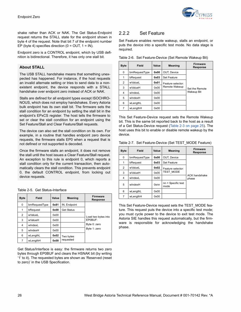
2.2.2 Set Feature
Set Feature enables remote wakeup, stalls an endpoint, orputs the device into a specific test mode. No data stage isrequired.
This Set Feature-Device request sets the Remote Wakeupbit. This is the same bit reported back to the host as a resultof a Get Status-Device request (Table 2-3 on page 25). Thehost uses this bit to enable or disable remote wakeup by thedevice.
This Set Feature-Device request sets the TEST_MODE fea-ture. This request puts the device into a specific test mode;you must cycle power to the device to exit test mode. TheAstoria SIE handles this request automatically, but the firm-ware is responsible for acknowledging the handshakephase.
About STALL
The USB STALL handshake means that something unex-pected has happened. For instance, if the host requestsan invalid alternate setting or tries to send data to a non-existent endpoint, the device responds with a STALLhandshake over endpoint zero instead of ACK or NAK.
Stalls are defined for all endpoint types except ISOCHRO-NOUS, which does not employ handshakes. Every Astoriabulk endpoint has its own stall bit. The firmware sets thestall condition for an endpoint by setting the stall bit in theendpoint’s EPxCS register. The host tells the firmware toset or clear the stall condition for an endpoint using theSet Feature/Stall and Clear Feature/Stall requests.
The device can also set the stall condition on its own. Forexample, in a routine that handles endpoint zero devicerequests, the firmware stalls EP0 when a request that isnot defined or not supported is decoded.
Once the firmware stalls an endpoint, it does not removethe stall until the host issues a Clear Feature/Stall request.An exception to this rule is endpoint 0, which reports astall condition only for the current transaction, then auto-matically clears the stall condition. This prevents endpoint0, the default CONTROL endpoint, from locking outdevice requests.
Table 2-5. Get Status-Interface
Byte Field Value MeaningFirmware Response
0 bmRequestType 0x81 IN, Endpoint
Load two bytes into EP0BUF:
Byte 0: zero
Byte 1: zero
1 bRequest 0x00 Get Status
2 wValueL 0x00
3 wValueH 0x00
4 wIndexL 0x00
5 wIndexH 0x00
6 wLengthL 0x02 Two bytes requested7 wLengthH 0x00
Table 2-6. Set Feature-Device (Set Remote Wakeup Bit)
Byte Field Value MeaningFirmware Response
0 bmRequestType 0x00 OUT, Device
Set the Remote Wakeup Bit
1 bRequest 0x03 Set Feature
2 wValueL 0x01 Feature selector: Remote Wakeup3 wValueH 0x00
4 wIndexL 0x00
5 wIndexH 0x00
6 wLengthL 0x00
7 wLengthH 0x00
Table 2-7. Set Feature-Device (Set TEST_MODE Feature)
Byte Field Value MeaningFirmware Response
0 bmRequestType 0x00 OUT, Device
ACK handshake phase
1 bRequest 0x03 Set Feature
2 wValueL 0x02 Feature selector: TEST_MODE3 wValueH 0x00
4 wIndexL 0x00
5 wIndexH 0xnn nn = Specific test mode
6 wLengthL 0x00
7 wLengthH 0x00

West Bridge Astoria Technical Reference Manual, Document # 001-70142 Rev. *A 27
Endpoint Zero
The only Set Feature-Endpoint request presently defined inthe USB Specification is to stall an endpoint. The firmwareresponds to this request by setting the STALL bit in theEPxCS register for the indicated endpoint EP (byte 4 of therequest). The firmware can stall an endpoint either on itsown or in response to the device request. Endpoint stalls arecleared by the host Clear Feature-Stall request.
The firmware responds to the Set Feature-Stall request byperforming the following tasks:
1. Set the STALL bit in the indicated endpoint’s EPxCS reg-ister.
2. Reset the data toggle for the indicated endpoint.
3. Restore the stalled endpoint to its default condition, ready to send or accept data after the stall condition is removed by the host (using a Clear Feature/Stall request). For EP1 IN, for example, firmware clears the BUSY bit in the EP1CS register; for EP1OUT, firmware loads any value into the EP1 byte-count register.
4. Clear the HSNAK bit in the EP0CS register (by writing 1 to it) to end the Set Feature/Stall CONTROL transfer.
Step 3 is also required whenever the host sends a Set Inter-face request.
2.2.3 Clear Feature
Clear Feature disables remote wakeup or to clear a stalledendpoint.
If the USB device supports remote wakeup (reported in itsdescriptor table when the device enumerates), the ClearFeature/Remote Wakeup request disables wakeup capabil-ity.
The Clear Feature/Stall request removes the stall conditionfrom an endpoint. The firmware responds by clearing theSTALL bit in the indicated endpoint’s EPxCS register.
2.2.4 Get Descriptor
During enumeration, the host queries a USB device to learnits capabilities and requirements using Get Descriptorrequests. Using tables of descriptors, the device sends back(over EP0-IN) such information as what device driver toload, how many endpoints it has, its different configurations,alternate settings it may use, and informative text stringsabout the device.
Astoria provides a special Setup Data Pointer to simplifyfirmware service for Get Descriptor requests. The firmwareloads this 16-bit pointer with the starting address of therequested descriptor and clears the HSNAK bit (by writing‘1’ to it), and Astoria transfers the whole descriptor.
Table 2-8. Set Feature-Endpoint (Stall)
Byte Field Value MeaningFirmware Response
0 bmRequestType 0x02 OUT, Endpoint
Set the STALL bit for the indicated endpoint.
1 bRequest 0x03 Set Feature
2 wValueL 0x00 Feature selector: STALL3 wValueH 0x00
4 wIndexL EP 0x00-0x08: OUT0-OUT8
0x80-0x88: IN0-IN8
5 wIndexH 0x00
6 wLengthL 0x00
7 wLengthH 0x00
Data Toggles
Astoria automatically maintains the endpoint toggle bits toensure data integrity for USB transfers. Firmware shoulddirectly manipulate these bits only for a very limited set ofcircumstances:
■ Set Feature/Stall
■ Set Configuration
■ Set Interface
Table 2-9. Clear Feature-Device (Clear Remote Wakeup Bit)
Byte Field Value MeaningFirmware Response
0 bmRequestType 0x00 OUT, Device
Clear the remote wakeup bit.
1 bRequest 0x01 Clear Feature
2 wValueL 0x01 Feature selector: Remote Wakeup3 wValueH 0x00
4 wIndexL 0x00
5 wIndexH 0x00
6 wLengthL 0x00
7 wLengthH 0x00
Table 2-10. Clear Feature-Endpoint (Clear Stall)
Byte Field Value MeaningFirmware Response
0 bmRequestType 0x02 OUT, Endpoint
Clear the STALL bit for the indicated endpoint.
1 bRequest 0x01 Clear Feature
2 wValueL 0x00 Feature selector: STALL3 wValueH 0x00
4 wIndexL EP 0x00-0x08: OUT0-OUT8
0x80-0x88: IN0-IN8
5 wIndexH 0x00
6 wLengthL 0x00
7 wLengthH 0x00

28 West Bridge Astoria Technical Reference Manual, Document # 001-70142 Rev. *A
Endpoint Zero
Figure 2-5. Using Setup Data Pointer (SUDPTR) for Get_Descriptor Requests
Figure 2-5 shows the use of the Setup Data Pointer. Thispointer is implemented as two registers, SUDPTRH andSUDPTRL. The base address of SUDPTRH:L must beword-aligned. Most Get Descriptor requests involve transfer-ring more data than fits into one packet. In the Figure 2-5example, the descriptor data consists of 91 bytes.
The CONTROL transaction starts in the usual way, withAstoria automatically transferring the eight bytes from theSETUP packet into RAM at SETUPDAT, then asserting theSUDAV interrupt request. The firmware decodes the GetDescriptor request, and responds by clearing the HSNAK bit(by writing ‘1’ to it), and then loading the SUDPTRH:L regis-ters with the address of the requested descriptor. Loadingthe SUDPTRL register causes Astoria to automaticallyrespond to two IN transfers with 64 bytes and 27 bytes ofdata using SUDPTRH:L as a base address, and then torespond to the STATUS stage with an ACK.
The usual endpoint-zero interrupts SUDAV and EP0INremain active during this automated transfer, so firmwarenormally disables these interrupts because the transferrequires no firmware intervention.
Three types of descriptors are defined: Device, Configura-tion, and String.
2.2.4.1 Get Descriptor-Device
As shown in Figure 2-5 on page 28, the firmware loads thetwo-byte SUDPTRH:L with the starting address of theDevice Descriptor table. The start address must be word-
IN
ADDR
ENDP
CRC5
Token Packet
DATA0
8 bytesSetupData
CRC16
Data Packet
ACK
H/S Pkt
SETUP
ADDR
ENDP
CRC5
Token Packet
DATA1
PayloadData
CRC16
Data Packet
ACK
IN
ADDR
ENDP
CRC5
Token Packet
DATA0
PayloadData
CRC16
Data Packet
ACK
H/S Pkt
SETUP Stage
SUDAV Interrupt
DATA Stage
EP0INInterrupt
EP0INInterrupt
STATUS Stage
DATA1
OUT
ADDR
ENDP
CRC5
Token Packet
CRC16
H/S Pkt
Data Pkt
ACK
H/S Pkt
SUDPTRH/L
64 bytes
27 bytes
8 RAMbytes
SETUPDAT
Table 2-11. Get Descriptor-Device
Byte Field Value MeaningFirmware Response
0 bmRequestType 0x80 IN, Device
Set SUDPTR H:L to start of Device Descriptor table in RAM.
1 bRequest 0x06 Get Descriptor
2 wValueL 0x00
3 wValueH 0x01 Descriptor type: Device
4 wIndexL 0x00
5 wIndexH 0x00
6 wLengthL LenL
7 wLengthH LenH

West Bridge Astoria Technical Reference Manual, Document # 001-70142 Rev. *A 29
Endpoint Zero
aligned. When SUDPTRL is loaded, Astoria automaticallyperforms the following operations:
1. Reads the requested number of bytes for the transfer from bytes 6 and 7 of the SETUP packet (LenL and LenH in Table 2-11).
2. Reads the requested descriptor’s length field to deter-mine the actual descriptor length.
3. Sends the smaller of (a) the requested number of bytes or (b) the actual number of bytes in the descriptor, over EP0BUF using the Setup Data Pointer as a data table index. This is the second phase of the three-phase CONTROL transfer. Astoria packetizes the data into multiple data transfers as necessary.
4. Checks for errors and retransmits data packets if neces-sary.
5. Responds to the third (handshake) phase of the CON-TROL transfer to terminate the operation.
The Setup Data Pointer can be used for any Get Descriptorrequest (for example, Get Descriptor-String).
It can also be used for vendor-specific requests. If bytes sixand seven of those requests contain the number of bytes inthe transfer (see Step 1, above), the Setup Data Pointerworks automatically, as it does for Get Descriptor requests;if bytes six and seven do not contain the length of the trans-fer, the length can be loaded explicitly (see the SDPAUTOparagraphs of section 8.6 The Setup Data Pointer onpage 83).
The firmware can do manual CONTROL transfers bydirectly loading the EP0BUF buffer with the various packetsand keeping track of which SETUP phase is in effect. This isa good USB training exercise, but not necessary because ofthe hardware support built into Astoria for CONTROL trans-fers.
For DATA stage transfers of fewer than 64 bytes, moving thedata into the EP0BUF buffer and then loading theEP0BCH:L registers with the byte count is equivalent toloading the Setup Data Pointer. However, this wastes band-width because it requires byte transfers into the EP0BUFBuffer; using the Setup Data Pointer does not.
2.2.4.2 Get Descriptor-Device Qualifier
The Device Qualifier descriptor is used only by devicescapable of high-speed (480 Mbps) operation; it describesinformation about the device that would change if the devicewere operating at the other speed (for example, if the deviceis currently operating at high speed, the device qualifierreturns information about how it would operate at full speed,and the reverse).
Device Qualifier descriptors are handled just like Devicedescriptors; the firmware loads the appropriate descriptoraddress (must be word-aligned) into SUDPTRH:L, thenAstoria does the rest.
2.2.4.3 Get Descriptor-Configuration
Table 2-12. Get Descriptor-Device Qualifier
Byte Field Value MeaningFirmware Response
0 bmRequestType 0x80 IN, Device
Set SUDPTR H:L to start of the appro-priate Device Quali-fier Descriptor table in RAM.
1 bRequest 0x06 Get Descriptor
2 wValueL 0x00
3 wValueH 0x06 Descriptor type: Device Qualifier
4 wIndexL 0x00
5 wIndexH 0x00
6 wLengthL LenL
7 wLengthH LenH
Table 2-13. Get Descriptor-Configuration
Byte Field Value MeaningFirmware Response
0 bmRequestType 0x80 IN, Device
Set SUDPTR H:L to start of String Descriptor table in RAM
1 bRequest 0x06 Get Descriptor
2 wValueL STR String Number
3 wValueH 0x03Descriptor type: String
4 wIndexL 0x00 (Language ID L)
5 wIndexH 0x00 (Language ID H)
6 wLengthL LenL
7 wLengthH LenH
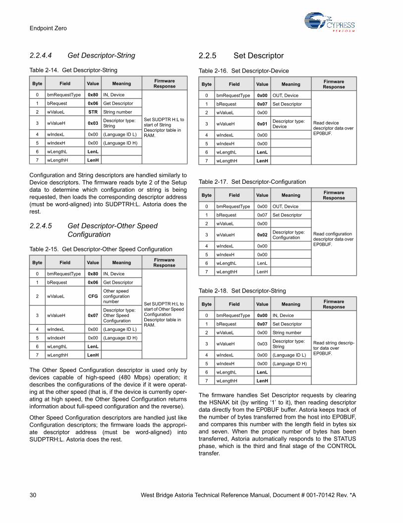
30 West Bridge Astoria Technical Reference Manual, Document # 001-70142 Rev. *A
Endpoint Zero
2.2.4.4 Get Descriptor-String
Configuration and String descriptors are handled similarly toDevice descriptors. The firmware reads byte 2 of the Setupdata to determine which configuration or string is beingrequested, then loads the corresponding descriptor address(must be word-aligned) into SUDPTRH:L. Astoria does therest.
2.2.4.5 Get Descriptor-Other Speed Configuration
The Other Speed Configuration descriptor is used only bydevices capable of high-speed (480 Mbps) operation; itdescribes the configurations of the device if it were operat-ing at the other speed (that is, if the device is currently oper-ating at high speed, the Other Speed Configuration returnsinformation about full-speed configuration and the reverse).
Other Speed Configuration descriptors are handled just likeConfiguration descriptors; the firmware loads the appropri-ate descriptor address (must be word-aligned) intoSUDPTRH:L. Astoria does the rest.
2.2.5 Set Descriptor
The firmware handles Set Descriptor requests by clearingthe HSNAK bit (by writing ‘1’ to it), then reading descriptordata directly from the EP0BUF buffer. Astoria keeps track ofthe number of bytes transferred from the host into EP0BUF,and compares this number with the length field in bytes sixand seven. When the proper number of bytes has beentransferred, Astoria automatically responds to the STATUSphase, which is the third and final stage of the CONTROLtransfer.
Table 2-14. Get Descriptor-String
Byte Field Value MeaningFirmware Response
0 bmRequestType 0x80 IN, Device
Set SUDPTR H:L to start of String Descriptor table in RAM.
1 bRequest 0x06 Get Descriptor
2 wValueL STR String number
3 wValueH 0x03 Descriptor type: String
4 wIndexL 0x00 (Language ID L)
5 wIndexH 0x00 (Language ID H)
6 wLengthL LenL
7 wLengthH LenH
Table 2-15. Get Descriptor-Other Speed Configuration
Byte Field Value MeaningFirmware Response
0 bmRequestType 0x80 IN, Device
Set SUDPTR H:L to start of Other Speed Configuration Descriptor table in RAM.
1 bRequest 0x06 Get Descriptor
2 wValueL CFGOther speedconfiguration number
3 wValueH 0x07 Descriptor type: Other Speed Configuration
4 wIndexL 0x00 (Language ID L)
5 wIndexH 0x00 (Language ID H)
6 wLengthL LenL
7 wLengthH LenH
Table 2-16. Set Descriptor-Device
Byte Field Value MeaningFirmware Response
0 bmRequestType 0x00 OUT, Device
Read device descriptor data over EP0BUF.
1 bRequest 0x07 Set Descriptor
2 wValueL 0x00
3 wValueH 0x01 Descriptor type: Device
4 wIndexL 0x00
5 wIndexH 0x00
6 wLengthL LenL
7 wLengthH LenH
Table 2-17. Set Descriptor-Configuration
Byte Field Value MeaningFirmware Response
0 bmRequestType 0x00 OUT, Device
Read configuration descriptor data over EP0BUF.
1 bRequest 0x07 Set Descriptor
2 wValueL 0x00
3 wValueH 0x02 Descriptor type: Configuration
4 wIndexL 0x00
5 wIndexH 0x00
6 wLengthL LenL
7 wLengthH LenH
Table 2-18. Set Descriptor-String
Byte Field Value MeaningFirmware Response
0 bmRequestType 0x00 IN, Device
Read string descrip-tor data over EP0BUF.
1 bRequest 0x07 Set Descriptor
2 wValueL 0x00 String number
3 wValueH 0x03 Descriptor type: String
4 wIndexL 0x00 (Language ID L)
5 wIndexH 0x00 (Language ID H)
6 wLengthL LenL
7 wLengthH LenH

West Bridge Astoria Technical Reference Manual, Document # 001-70142 Rev. *A 31
Endpoint Zero
Note The firmware controls the flow of data in the Datastage of a CONTROL transfer. After the firmware processeseach OUT packet, it writes any value into the endpoint’s bytecount register to rearm the endpoint.
Figure 2-6. Configurations, Interfaces, and Alternate Settings
The host issues a Set Configuration request to select a con-figuration, and a Get Configuration request to determine thecurrent configuration.
2.2.5.1 Set Configuration
When the host issues the Set Configuration request, thefirmware saves the configuration number (byte 2, CFG, inTable 2-19), performs any internal operations needed tosupport the configuration, and finally clears the HSNAK bit(by writing ‘1’ to it) to end the Set Configuration CONTROLtransfer.
Note After setting a configuration, the host issues Set Inter-face commands to set up the various interfaces contained inthe configuration.
2.2.6 Get Configuration
When the host issues the Get Configuration request, thefirmware returns the current configuration number. It loadsthe configuration number into EP0BUF, loads a byte countof one into EP0BCH:L, and finally clears the HSHAK bit (bywriting ‘1’ to it) to terminate the Set Configuration CONTROLtransfer.
2.2.7 Set Interface
This confusingly named USB command actually sets ‘alter-nate settings’ for a specified interface.
USB devices can have multiple concurrent interfaces. Forexample, a device may have an audio system that supportsdifferent sample rates, and a graphic control panel that sup-
Configurations, Interfaces, and Alternate Settings
A USB device has one or more configurations. Only oneconfiguration is active at any time.
A configuration has one or more interfaces, all of whichare concurrently active. Multiple interfaces allow differenthost-side device drivers to be associated with differentportions of a USB device.
Each interface has one or more alternate settings. Eachalternate setting has a collection of one or more end-points.
This structure is a software model; Astoria takes no actionwhen these settings change. However, the firmware mustreinitialize endpoints and reset the data toggle whenthe host changes configurations or interfaces’ alternatesettings.
To the firmware, a ‘configuration’ is a byte variable thatindicates the current setting.
Device
Config 2Low Power
Config 1High Power
Interface 1audio
Interface 0CDROMcontrol
Alt Setting0
Alt Setting1
Alt Setting3
Interface 2video
Interface 3data
storageConcurrent
One at a time
ep ep ep
One at a time
Table 2-19. Set Configuration
Byte Field Value MeaningFirmware Response
0 bmRequestType 0x00 OUT, Device
Read and store CFG, change con-figurations in firm-ware.
1 bRequest 0x09 Set Configuration
2 wValueL CFG Configuration number
3 wValueH 0x00
4 wIndexL 0x00
5 wIndexH 0x00
6 wLengthL 0x00
7 wLengthH 0x00
Table 2-20. Get Configuration
Byte Field Value MeaningFirmware Response
0 bmRequestType 0x80 IN, Device
Send CFG over EP0 after reconfig-uring.
1 bRequest 0x08 Get Configuration
2 wValueL 0x00
3 wValueH 0x00
4 wIndexL 0x00
5 wIndexH 0x00
6 wLengthL 1 LenL
7 wLengthH 0 LenH

32 West Bridge Astoria Technical Reference Manual, Document # 001-70142 Rev. *A
Endpoint Zero
ports different languages. Each interface has a collection ofendpoints. Except for endpoint 0, which each interface usesfor device control, interfaces cannot share endpoints.
Interfaces can report alternate settings in their descriptors.For example, the audio interface can have settings ‘0’, ‘1’,and ‘2’ for 8-kHz, 22-kHz, and 44-kHz sample rates, respec-tively. The panel interface can have settings ‘0’ and ‘1’ forEnglish and Spanish, respectively. The Set/Get Interfacerequests select among the alternate settings in an interface.
The firmware should respond to a Set Interface request bydoing the following:
1. Perform the internal operation requested (such as adjusting a sampling rate).
2. Reset the data toggles for every endpoint in the inter-face.
3. Restore the endpoints to their default conditions, ready to send or accept data. For EP1 IN, for example, firm-ware clears the BUSY bit in the EP1CS register; for EP1OUT, firmware loads any value into the EP1 byte-count register.
4. Clear the HSNAK bit (by writing ‘1’ to it) to end the Set Interface CONTROL transfer.
2.2.8 Get Interface
When the host issues the Get Interface request, the firm-ware returns the alternate setting for the requested interfaceIF and clears the HSNAK bit (by writing ‘1’ to it).
2.2.9 Set Address
When a USB device is first plugged in, it responds to deviceaddress 0 until the host assigns it a unique address usingthe Set Address request. Astoria copies this device addressinto the FNADDR (Function Address) register, and subse-quently responds only to requests to this address. Thisaddress is in effect until the USB device is unplugged, thehost issues a USB Reset, or the host powers down.
The FNADDR register is read-only. Whenever AstoriaReNumerates (see Enumeration and ReNumeration™chapter on page 35), it automatically resets FNADDR tozero, allowing the device to come back as new.
An Astoria program does not need to know the deviceaddress, because Astoria automatically responds only to thehost-assigned FNADDR value. The device address is read-able only for debug or diagnostic purposes.
Table 2-21. Set Interface (Actually, Set Alternate Setting #AS for Interface #IF)
Byte Field Value MeaningFirmware Response
0 bmRequestType 0x00 OUT, Device
Read and store byte 2 (AS) for Interface #IF, change setting for Interface #IF in firmware.
1 bRequest 0x0B Set Interface
2 wValueL AS Alternate setting number
3 wValueH 0x00
4 wIndexL IF Interface number
5 wIndexH 0x00
6 wLengthL 0x00
7 wLengthH 0x00
Table 2-22. Get Interface (Actually, Get Alternate Setting #AS for interface #IF)
Byte Field Value MeaningFirmware Response
0 bmRequestType 0x81 IN, Device
Send AS for Inter-face #IF over EP0.
1 bRequest 0x0A Get Interface
2 wValueL 0x00
3 wValueH 0x00
4 wIndexL IF Interface number
5 wIndexH 0x00
6 wLengthL 1 LenL
7 wLengthH 0 LenH

West Bridge Astoria Technical Reference Manual, Document # 001-70142 Rev. *A 33
Endpoint Zero
2.2.10 Sync Frame
The Sync Frame request establishes a marker in time so thehost and USB device can synchronize multiframe transfersover isochronous endpoints.
Suppose an isochronous transmission consists of a repeat-ing sequence of five 300-byte packets transmitted from hostto device over EP8-OUT. Both host and device maintainsequence counters that count repeatedly from 1 to 5 to keeptrack of the packets inside a transmission. To start up insync, both host and device must reset their counts to ‘0’ atthe same time (in the same frame).
To get in sync, the host issues the Sync Frame request withEP = EP8OUT (0x08). The firmware responds by loadingEP0BUF with a two-byte frame count for some future time;for example, the current frame plus 20. This marks frame‘current + 20’ as the sync frame, during which both sides ini-tialize their sequence counters to ‘0’. The current framecount is always available in the USBFRAMEL and USB-FRAMEH registers.
Multiple isochronous endpoints can be synchronized in thisway; the firmware can keep a separate internal sequencecount for each endpoint.
Table 2-23. Sync Frame
Byte Field Value MeaningFirmware Response
0 bmRequestType 0x82 IN, Endpoint
Send a frame num-ber over EP0 to synchronize end-point #EP
1 bRequest 0x0C Sync Frame
2 wValueL 0x00
3 wValueH 0x00
4 wIndexL EP Endpoint number
5 wIndexH 0x00
6 wLengthL 2 LenL
7 wLengthH 0 LenH
About USB Frames
In full-speed mode (12 Mbps), the USB host issues anSOF (Start Of Frame) packet once every millisecond.Every SOF packet contains an 11-bit (mod-2048) framenumber. The firmware services all isochronous transfersat SOF time, using a single SOF interrupt request andvector. If Astoria detects a missing or garbled SOF packet,it can use an internal counter to generate the SOF inter-rupt automatically.
In high-speed mode (480 Mbps), each frame is dividedinto eight 125-µs microframes. Although the frame coun-ter still increments only once per frame, the host issues anSOF every microframe. The host and device always syn-chronize on microframe 0 of the frame specified in thedevice’s response to the Sync Frame request; there is nomethod to synchronize on any other microframe.

34 West Bridge Astoria Technical Reference Manual, Document # 001-70142 Rev. *A
Endpoint Zero

West Bridge Astoria Technical Reference Manual, Document # 001-70142 Rev. *A 35
3. Enumeration and ReNumeration™
West Bridge® Astoria™ configuration is ‘soft’: Code and data are stored in internal RAM, which can be loaded from the pro-cessor using Astoria's processor port, as explained in 3.1.1 Loading the Firmware from the Processor or it can be loaded fromattached EEPROM, as explained in 3.1.2 Legacy Boot Mode. In these scenarios, Astoria-based USB peripherals can operatewithout ROM, EEPROM, or flash memory, shortening production lead times and making firmware updates very simple.
To support this soft configuration, Astoria is also capable of enumerating as a USB device without firmware, as explained in3.1.5 The Default USB Device on page 38. This automatically-enumerated USB device (the default USB device) contains a
set of interfaces and endpoints and can accept firmware downloaded from the host. However, at a minimum, an I2C bootEEPROM is required for production (see 3.1 Firmware Loading for more details).
Note For Astoria, two separate default USB devices exist, one for enumeration as a full-speed (12 Mbps) device, and theother for enumeration as a high-speed (480 Mbps) device. Astoria automatically performs the speed-detect protocol andchooses the proper default USB device. The two sets of default USB device descriptors are shown in Appendices A and B.
Once the default USB device enumerates and the host downloads firmware and descriptor tables to Astoria, it then starts exe-cuting the downloaded code, which electrically simulates a physical disconnect or connect from the USB and causes Astoriato enumerate again as a second device, this time taking on the USB personality defined by the downloaded code and descrip-tors. This patented secondary enumeration process is called ‘Renumeration™’.
An Astoria register bit called RENUM controls whether device requests over endpoint zero are handled by firmware or auto-matically by the default USB device. When RENUM = 0, the default USB device handles the requests automatically; whenRENUM = 1, firmware handles them.
3.1 Firmware Loading
If Astoria is configured to SRAM, PNAND, ADM, or PSPI modes, the firmware image can be also downloaded through any ofthese interfaces.
The 8051 is in reset state after power-on reset (POR) and the RSTCTRL field of the CY_AN_MEM_RST_CTRL_REG registeris b'01. After firmware download finishes, the processor must release the 8051 from reset by writing b'00 to the RSTCTRLfield of the CY_AN_MEM_RST_CTRL_REG register.
The program memory in Astoria is 24 KB; therefore, the maximum firmware size is 24 KB. The Program RAM is supplied byVDD (core) and the firmware must be reloaded every time VDD (core) is applied or reapplied, and on soft reset, hard reset,standby wake up, or core power down. There are three options for loading the 8051 MCU firmware to Program RAM:
■ Processor Boot mode
■ Legacy Boot mode (EEPROM from PI2C)
■ Debug Boot mode
3.1.1 Loading the Firmware from the Processor
After power-on reset, the processor at the P-port loads the 8051 firmware to the 8051 Program RAM. The firmware imagemust be split into chunks of 64 bytes for download. The last chunk of the firmware image can be between 2 and 64 bytes, butmust be an even number of bytes. The processor must first load the 4-byte SETUP packet through the EP2 buffer to Astoria.After that, the processor must start loading the firmware image, which is in chunks of 64 bytes. After the completion of thefirmware load, the P-port processor must release the 8051 MCU from reset by writing ‘00’ to RSTCTRL. The SETUP packet isshown in Figure 3-1 on page 36 and the firmware loading flowchart is shown in Figure 3-2 on page 37.
1. After a whole-chip reset, the 8051 MCU is in soft reset.

36 West Bridge Astoria Technical Reference Manual, Document # 001-70142 Rev. *A
Enumeration and ReNumeration™
Note The 8051 is in reset because the RSTCTRL defaults to ‘01’.
2. The processor polls the WAKEUP field in the Power Management Control and Status register (CY_AN_MEM_PWR_MAGT_STAT) to ensure that the PLL is locked before configuring the configuration regis-ters.
3. The processor must first configure the P-port Endian Configuration register and then configures the remaining configuration registers (addresses 0x80 through 0xFB).
4. The firmware is downloaded from the processor using the following steps. Astoria has a 24-KB program/data memory; the firmware image must be smaller than that. The downloaded firmware must be broken down into chunks of 2 to 64 bytes (the data packets must be trans-ferred in an even number of bytes) for download.
a. The processor writes the value ‘4’ to the COUNT field of EP2 Endpoint Buffer DMA register (CY_AN_MEM_P0_EP2_DMA_REG) and sets the DMAVAL field of the EP2 Endpoint Buffer DMA regis-ter. This step sends a request for the EP2 buffer for data transfer.
b. If the internal EP2 buffer is available, the EP2DRQ field in the DRQ Status register is set to '1' (for poll-ing) and the DRQ# signal (for DMA) is asserted. The DRQ signifies that the internal write FIFO is available.
c. After the EP2DRQ field is set to '1', the processor loads the four bytes of the SETUP packet to End-point Buffer EP2. In the SETUP packet, the first and second bytes define the Program RAM destination address (DA) and the third and fourth bytes define the total data packet length, dataLength (dataLength must be an even number). Figure 3-1 on page 36 shows the SETUP packet format.
d. After the 4-byte SETUP packet has been loaded to EP2, the processor resets the DMAVAL field of the EP2 Endpoint Buffer DMA register to zero. This step tells the internal mechanism that the download is complete, resets the EP2DRQ field to '0', and deas-serts the DRQ# signal.
e. Internally, Astoria takes the 4-byte SETUP packet (destination address and packet length) and encodes it to an 8-byte setup token.
f. After the SETUP packet has been sent, the proces-sor starts preparing to load the data packet (firmware image).
g. The processor writes dataLength (number of bytes of the following data packet) to the COUNT field (2 to 64, must be even number of bytes) and sets the DMAVAL field EP2 Endpoint Buffer DMA register (CY_AN_MEM_P0_EP2_DMA_REG) to '1'. As in step a, this step sends a request to the EP2 buffer for data transfer.
h. The processor waits for EP2 DRQ (either by polling the EP2DRQ or waiting for the assertion of DRQ# signal).
i. When EP2 is available, Astoria sets EP2DRQ to '1' and asserts the DRQ signal. The DRQ means that the internal write FIFO is empty.
j. When EP2DRQ is set or the DRQ# signal is asserted, the processor loads the data packet (firm-ware) to endpoint buffer EP2.
k. After the data packet has been loaded to EP2, the processor must reset the DMAVAL field of the EP2 Endpoint Buffer DMA register to zero. This step tells the internal mechanism that the download is com-plete, resets the EP2DRQ field to '0', and deasserts the DRQ signal.
l. Astoria resets EP2 DRQ and deasserts the DRQ# signal.
m. Repeat step g to step l until the firmware image has been completely downloaded.
n. After the firmware image has been completely down-loaded, the processor must set the WBOOT field of the Soft Reset Control register to indicate that the firmware image has been downloaded.
5. The processor releases the 8051 MCU from reset by writing ‘00’ to the RSTCTRL field of the CY_AN_MEM_RST_CTRL_REG register. The 8051 then starts executing its main program.
6. The firmware running on the 8051 clears the CFGMODE field in the P-port Interface Configuration Register (CY_AN_MEM_P0_VM_SET) by writing a zero. This step causes Astoria's RESETOUT pin and RSTCMPT field in Soft Reset Control register to go HIGH.
Note The CFGMODE field is accessible only to Astoria firmware.
Figure 3-1. The SETUP Packet Format
Program RAM Addr LSB
Program RAM Addr MSB
Data Packet Length LSB
Data Packet Length MSB
1st Byte
2nd Byte
3rd Byte
4th Byte
The Format of 4 bytes SETUP Packet
* Data Packet Length must be even number of byte

West Bridge Astoria Technical Reference Manual, Document # 001-70142 Rev. *A 37
Enumeration and ReNumeration™
Figure 3-2. Firmware Loading by Processor Flow Chart
3.1.2 Legacy Boot Mode
When the P-port is configured to PSPI (slave), ADM, orPNAND mode, Astoria supports the legacy boot mode. Inthis configuration, the EEPROM port is available in theP-port to download the firmware image from the EEPROMwith the PID/VID/DID value (in the EEPROM) to the internalProgram RAM.
If, at power-on reset, the state machine in Astoria detects an
EEPROM connected to its I2C with the value 0xC2 ataddress 0, Astoria loads the EEPROM data into on-chipRAM. It also sets the RENUM bit to 1, causing devicerequests to be handled by the firmware. After loading thefirmware image to the RAM, the 8051 is released from thereset and starts executing at X'0000.
If no firmware image is found from the EEPROM (or noEEPROM is connected), Astoria can download the firmwareimage from the processor through the PSPI, ADM, orPNAND interface.
The format of the EEPROM image for firmware image down-load is shown in Table 3-1.
3.1.3 Debug Boot Mode
The debug boot mode in Astoria has been extended tocover all processor interface modes. It has three majordebug modes: PCRAM debug mode, SRAM debug mode,and EIM debug mode. Table 3-2 lists all the normal anddebug modes in different processor interfaces. The debugmode is determined by the state of the test mode pins TEST[2:0] and PA[3:2] at power up (the WAKEUP pin must behigh).
When Astoria enters debug boot mode, the GPIO[1:0] pinsare configured by default as a UART interface (GPIO[0] =TXD0, GPIO[1] = RXD0), that allows firmware developers toconnect a debugger. The UART interface can be disabled bysetting the DEBUG_UART_DIS field to GPIO[1:0].
Load 8 bytes SETUP Packet
2 to 64 bytes Data Packet
(must be an even number of byte)
Start Firmware Download
Load Firmware Complete?
YES
Set RSTCTL field in CY_AN_MEM_RST_CTRL_REG register to “00”
Done
No
Table 3-1. EEPROM Data Format
EERPOM Address Contents
0 0xC2
1 Vendor ID (VID) L
2 Vendor ID (VID) H
3 Product ID (PID) L
4 Product ID (PID) H
5 Device ID (DID) L
6 Device ID (DID) H
7 Configuration byte
8 Length H
9 Length L
10 Start Address H
11 Start Address L
12 “C” - EEPROM Loaded Patent
13 “Y” - EEPROM Loaded Patent
14 Data Block
--
-- Length H
-- Length L
-- Start Address H
-- Start Address L
-- Data Block
--
-- 0x80
-- 0x01
-- 0xE6
-- 0x00
last 00000000

38 West Bridge Astoria Technical Reference Manual, Document # 001-70142 Rev. *A
Enumeration and ReNumeration™
3.1.4 Register Configuration
West Bridge Astoria's internal registers must be set up fol-lowing a hard reset or a whole reset in the Soft Reset Con-trol register. In this stage, the external processor providesthe values by writing to the registers.
Note that the default values in registers allow the processorto program the internal 8051 and access all registers.
At any time that the RESET# input is deasserted, the exter-nal processor can write to the configuration registers. Theprocessor must ensure that all registers are properly config-ured. It can override the values in the configuration registersin this setup. The 8051 firmware must reset the CFGMODEfield in the P-port Interface register to indicate the comple-tion of reset initialization. When complete, Astoria deassertsthe RESETOUT pin and resets the CFGMODE field in the P-port Interface Configuration register to '0'.
3.1.5 The Default USB Device
The default USB device consists of a single USB configura-tion containing one interface (interface 0) and alternate set-tings 0, 1, 2 and 3. The endpoints and MaxPacketSizesreported for this device are shown in Table 3-3 (full speed)and Table 3-4 (high speed). Note that alternate setting zeroconsumes no interrupt or isochronous bandwidth, as recom-mended by the USB Specification.
Note Although the physical size of the EP1 endpoint bufferis 64 bytes, it is reported as a 512-byte buffer for high-speedalternate setting 1. This keeps it compatible with the USBspecification, which allows only 512-byte bulk endpoints.
Table 3-2. Astoria Operation and Manufacture/Debug modes Selection
Astoria Operational Modes
Operational Mode Entry
ModesTEST[2] TEST[1] TEST[0] WAKEUP
VMTYPE field in
CY_AN_MEM_P0_VM_SET register
0 0 0 0 101 Stand By (Non ADM Pseudo CRAM Mode)
0 0 0 1 101 Normal (Non ADM Pseudo CRAM Mode)
0 0 1 1 101 Mfg / Debug (Non ADM Pseudo CRAM Mode)
0 0 0 0 111 Stand By (SRAM Mode)
0 0 0 1 111 Normal (SRAM Mode)
0 0 1 1 111 Mfg / Debug (SRAM Mode)
0 1 0 0 x Extended I/F Stand By
0 1 0 1 x Extended I/F Mode (EIM)
0 1 1 1 x Extended I/F (Mfg / Debug)
Table 3-3. Default Full-Speed Alternate Settings
Alternate Setting
0 1 2 3
ep0 64 64 64 64
ep1out 0 64 bulk 64 int 64 int
ep1in 0 64 bulk 64 int 64 int
ep2 0 64 bulk out (2x) 64 int out (2x) 64 iso out (2x)
ep4 0 64 bulk out (2x) 64 bulk out (2x) 64 bulk out (2x)
ep6 0 64 bulk in (2x) 64 int in (2x) 64 iso in (2x)
ep8 0 64 bulk in (2x) 64 bulk in (2x) 64 bulk in (2x)
Note ‘0’ means not implemented, ‘2x’ means double buffered.
Table 3-4. Default High-Speed Alternate Settings
Alternate Setting
0 1 2 3
ep0 64 64 64 64
ep1out 0 512 bulk 64 int 64 int
ep1in 0 512 bulk 64 int 64 int
ep2 0 512 bulk out (2x) 512 int out (2x) 512 iso out (2x)
ep4 0 512 bulk out (2x) 512 bulk out (2x) 512 bulk out (2x)
ep6 0 512 bulk in (2x) 512 int in (2x) 512 iso in (2x)
ep8 0 512 bulk in (2x) 512 bulk in (2x) 512 bulk in (2x)
Note: ‘0’ means ‘not implemented’, ‘2x’ means double buffered.
Table 3-3. Default Full-Speed Alternate Settings

West Bridge Astoria Technical Reference Manual, Document # 001-70142 Rev. *A 39
Enumeration and ReNumeration™
If you use this default alternate setting, do not send orreceive EP1 packets larger than 64 bytes.
3.1.6 Astoria Vendor Request for Firmware Load
Before ReNumeration, the host downloads data into Asto-ria’s internal RAM. The host can access two on-chip AstoriaRAM spaces: Program/Data RAM at 0x0000–0x5FFF andData RAM at 0xE000–0xE1F. It can download or uploadthese only when the CPU is held in reset. The host mustwrite to the CPUCS register to put the CPU in or out ofreset. These two RAM spaces may also be bootloaded by a
‘C2’ EEPROM connected to the I2C bus.
The USB Specification provides for vendor-specific requeststo be sent over endpoint zero. Astoria uses this feature totransfer data between the host and Astoria RAM. Astoriaautomatically responds to two Firmware Load requests, asshown in Table 3-5 and Table 3-6.
Note Astoria always handles these upload and downloadrequests, regardless of the state of the RENUM bit. Theupload start address must be word-aligned (that is, the startaddress must be evenly divisible by two).
The bRequest value 0xA0 is reserved for this purpose. Donot use it for another vendor request. Cypress Semiconduc-tor also reserves bRequest values 0xA1 through 0xAF;devices should not use these bRequest values.
A host loader program must write 0x01 to the CPUCS regis-ter to put the CPU into RESET, load all or part of the AstoriaRAM with firmware, then reload the CPUCS register with ‘0’to take the CPU out of RESET. The CPUCS register (at0xE600) is the only Astoria register that can be written usingthe Firmware Download command.
Another Use for the Default USB Device
The default USB device is established at power on to setup a USB device that can download firmware into Asto-ria’s RAM. Another useful feature of the default USBdevice is that Astoria code can be written to support thealready configured generic USB device. Before bringingthe CPU out of reset, Astoria automatically enables cer-tain endpoints and reports them to the host using descrip-tors. By using the default USB device (for example, bykeeping RENUM = 0), the firmware can, with very littlecode, perform meaningful USB transfers that use thesepreconfigured endpoints. This accelerates the USB learn-ing curve.
Table 3-5. Firmware Download
Byte Field Value MeaningAstoria
Response
0 bmRequest 0x40 Vendor Request, OUT
None required
1 bRequest 0xA0 Firmware Load
2 wValueL AddrLStarting Address
3 wValueH AddrH
4 wIndexL 0x00
5 wIndexH 0x00
6 wLenghtL LenLNumber of Bytes
7 wLengthH LenH
Table 3-6. Firmware Upload
Byte Field Value MeaningAstoria
Response
0 bmRequest 0xC0 Vendor Request, IN
None required
1 bRequest 0xA0 Firmware Load
2 wValueL AddrL Starting Address (must be word-aligned)3 wValueH AddrH
4 wIndexL 0x00
5 wIndexH 0x00
6 wLengthL LenLNumber of Bytes
7 wLengthH LenH
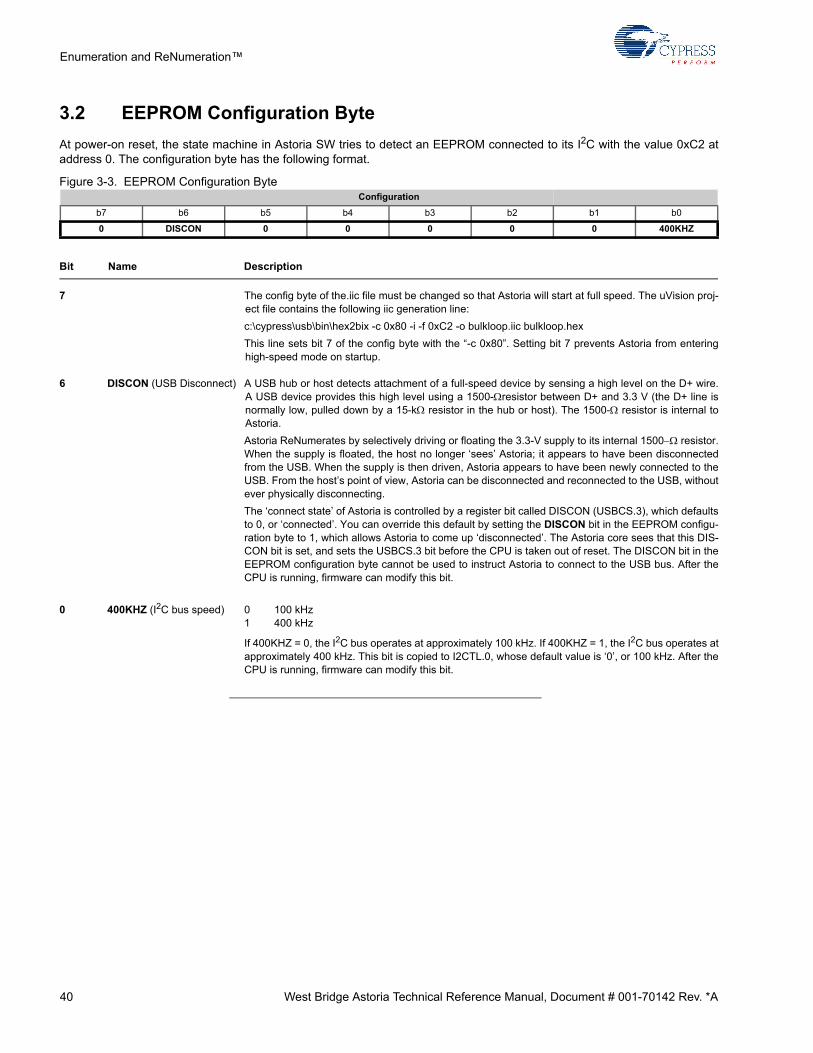
40 West Bridge Astoria Technical Reference Manual, Document # 001-70142 Rev. *A
Enumeration and ReNumeration™
3.2 EEPROM Configuration Byte
At power-on reset, the state machine in Astoria SW tries to detect an EEPROM connected to its I2C with the value 0xC2 ataddress 0. The configuration byte has the following format.
Figure 3-3. EEPROM Configuration Byte
7 The config byte of the.iic file must be changed so that Astoria will start at full speed. The uVision proj-ect file contains the following iic generation line:
c:\cypress\usb\bin\hex2bix -c 0x80 -i -f 0xC2 -o bulkloop.iic bulkloop.hex
This line sets bit 7 of the config byte with the “-c 0x80”. Setting bit 7 prevents Astoria from enteringhigh-speed mode on startup.
6 DISCON (USB Disconnect) A USB hub or host detects attachment of a full-speed device by sensing a high level on the D+ wire.A USB device provides this high level using a 1500-resistor between D+ and 3.3 V (the D+ line isnormally low, pulled down by a 15-k resistor in the hub or host). The 1500- resistor is internal toAstoria.
Astoria ReNumerates by selectively driving or floating the 3.3-V supply to its internal 1500 resistor.When the supply is floated, the host no longer ‘sees’ Astoria; it appears to have been disconnectedfrom the USB. When the supply is then driven, Astoria appears to have been newly connected to theUSB. From the host’s point of view, Astoria can be disconnected and reconnected to the USB, withoutever physically disconnecting.
The ‘connect state’ of Astoria is controlled by a register bit called DISCON (USBCS.3), which defaultsto 0, or ‘connected’. You can override this default by setting the DISCON bit in the EEPROM configu-ration byte to 1, which allows Astoria to come up ‘disconnected’. The Astoria core sees that this DIS-CON bit is set, and sets the USBCS.3 bit before the CPU is taken out of reset. The DISCON bit in theEEPROM configuration byte cannot be used to instruct Astoria to connect to the USB bus. After theCPU is running, firmware can modify this bit.
0 400KHZ (I2C bus speed) 0 100 kHz1 400 kHz
If 400KHZ = 0, the I2C bus operates at approximately 100 kHz. If 400KHZ = 1, the I2C bus operates atapproximately 400 kHz. This bit is copied to I2CTL.0, whose default value is ‘0’, or 100 kHz. After theCPU is running, firmware can modify this bit.
Configuration
b7 b6 b5 b4 b3 b2 b1 b0
0 DISCON 0 0 0 0 0 400KHZ
Bit Name Description

West Bridge Astoria Technical Reference Manual, Document # 001-70142 Rev. *A 41
Enumeration and ReNumeration™
3.3 The RENUM Bit
An Astoria control bit called ‘RENUM’ (ReNumerated) deter-mines whether USB device requests over endpoint zero arehandled by the default USB device or by Astoria firmware.At power-on reset, the RENUM bit (USBCS.1) is zero, indi-cating that the default USB device automatically handlesUSB device requests. After firmware is downloaded to Asto-ria and the CPU is running, it can set RENUM = 1 so thatsubsequent device requests are handled by the downloadedfirmware and descriptor tables. The Endpoint Zero chapteron page 21 describes how the firmware handles devicerequests while RENUM = 1.
3.4 Astoria’s Response to Device Requests (RENUM = 0)
Table 3-7 shows how the default USB device responds toendpoint zero device requests when RENUM = 0.
A USB host enumerates by issuing Set Address, GetDescriptor, and Set Configuration (to ‘1’) requests (the SetAddress and Get Descriptor requests are used only duringenumeration). After enumeration, the default USB deviceresponds to the following device requests from the host:
■ Set or clear an endpoint stall (Set/Clear Feature-End-point)
■ Read the stall status for an endpoint (Get Status-End-point)
■ Set/Read an 8-bit configuration number (Set/Get Config-uration)
■ Set/Read a 2-bit interface alternate setting (Set/Get Interface)
■ Download or upload Astoria on-chip RAM
Table 3-7. How the Default USB Device Handles EP0 Requests When RENUM = 0
bRequest Name Astoria Response
0x00 Get Status-Device Returns two zero bytes
0x00 Get Status-EndpointSupplies EP Stall bit for indicated EP
0x00 Get Status-Interface Returns two zero bytes
0x01 Clear Feature-Device None
0x01 Clear Feature-Endpoint Clears Stall bit for indicated EP
0x02 (reserved) None
0x03 Set Feature-Device Sets TEST_MODE feature
0x03 Set Feature-Endpoint Sets Stall bit for indicated EP
0x04 (reserved) None
0x05 Set Address Updates FNADDR register
0x06 Get Descriptor Supplies internal table
0x07 Set Descriptor None
0x08 Get Configuration Returns internal value
0x09 Set Configuration Sets internal value
0x0A Get Interface Returns internal value (0-3)
0x0B Set Interface Sets internal value (0-3)
0x0C Sync Frame None
Vendor Requests
0xA0 Firmware Load Upload/Download on-chip RAM
0xA1-0xAF ReservedReserved by Cypress Semiconductor
all other None

42 West Bridge Astoria Technical Reference Manual, Document # 001-70142 Rev. *A
Enumeration and ReNumeration™
3.5 How the Firmware ReNumerates
Two control bits in the USBCS (USB Control and Status) register control the ReNumeration process: DISCON and RENUM.
Figure 3-4. USB Control and Status Register
To simulate a USB disconnect, the firmware sets DISCON to ‘1’. To reconnect, the firmware clears DISCON to ‘0’.
Before reconnecting, the firmware sets or clears the RENUM bit to indicate whether the firmware or the default USB devicehandles device requests over endpoint zero. If RENUM = 0, the Default USB Device handles device requests; if RENUM = 1,the firmware does.
3.6 Multiple ReNumerations™
Astoria firmware can ReNumerate anytime. One use for this capability might be to ‘fine tune’ an isochronous endpoint’s band-width requests by trying various descriptor values and ReNumerating.
USBCS USB Control and Status E680
b7 b6 b5 b4 b3 b2 b1 b0
HSM 0 0 0 DISCON NOSYNSOF RENUM SIGRSUME
R/W R R R R/W R/W R/W R/W
0 0 0 0 0 1 0 0

West Bridge Astoria Technical Reference Manual, Document # 001-70142 Rev. *A 43
4. Interrupts
Astoria’s interrupt architecture is an enhanced and expanded version of the standard 8051’s. Astoria responds to the inter-rupts shown in Table 4-1; interrupt sources that are not present in the standard 8051 are shown in bold type.
The Natural Priority column in Table 4-1 shows the Astoria interrupt priorities. Astoria can assign each interrupt to a high orlow priority group; priorities are resolved within the groups using the natural priorities.
4.1 SFRs
These SFRs are associated with interrupt control:
■ IE - SFR 0xA8 (Table 4-2 on page 44)
■ IP - SFR 0xB8 (Table 4-3 on page 44)
■ EXIF - SFR 0x91 (Table 4-4 on page 44)
■ EICON - SFR 0xD8 (Table 4-5 on page 44)
■ EIE - SFR 0xE8 (Table 4-6 on page 44)
■ EIP - SFR 0xF8 (Table 4-7 on page 44)
The IE and IP SFRs give interrupt enable and priority control for the standard interrupt unit, as with the standard 8051. TheseSFRs also provide control bits for the Serial Port 1 interrupt.
The EXIF, EICON, EIE and EIP registers provide flags, enable control, and priority control.
Table 4-1. Astoria Interrupts
Astoria Interrupt Source Interrupt Vector Natural Priority
IE0 TPIC INT 0x0003 1
TF0 Timer 0 Overflow 0x000B 2
IE1 SIB INT 0x0013 3
TF1 Timer 1 Overflow 0x001B 4
RI_0 & TI_0 USART0 Rx & Tx 0x0023 5
TF2 Timer 2 Overflow 0x002B 6
Resume WAKEUP / WU2 Pin or USB Resume 0x0033 0
Reserved Reserved 0x003B 7
USBINT USB INT 0x0043 8
MBINT MAILBOX INT 0x004B 9
IE4 GPIF INT 0x0053 10

44 West Bridge Astoria Technical Reference Manual, Document # 001-70142 Rev. *A
Interrupts
Table 4-2. IE Register — SFR 0xA8
Bit Function
IE.7 EA – Global interrupt enable. Controls masking of all interrupts except USB wakeup (resume). EA = 0 disables all interrupts except USB wakeup. When EA = 1, interrupts are enabled or masked by their individual enable bits.
IE.6 ES1 – Reserved
IE.5 ET2 – Enable Timer 2 interrupt. ET2 = 0 disables Timer 2 interrupt (TF2). ET2=1 enables interrupts generated by the TF2 flag.
IE.4 ES0 – Enable Serial Port 0 interrupt. ES0 = 0 disables Serial Port 0 interrupts (TI_0 and RI_0). ES0 = 1 enables interrupts generated by the TI_0 or RI_0 flag.
IE.3 ET1 – Enable Timer 1 interrupt. ET1 = 0 disables Timer 1 interrupt (TF1). ET1 = 1 enables interrupts generated by the TF1 flag.
IE.2 EX1 – Enable SIB interrupt 1. EX1 = 0 disables SIB interrupt 1 (IE1). EX1 = 1 enables interrupts generated by the SIB.
IE.1 ET0 – Enable Timer 0 interrupt. ET0 = 0 disables Timer 0 interrupt (TF0). ET0 = 1 enables interrupts generated by the TF0 flag.
IE.0 EX0 – Enable TPIC interrupt. EX0 = 0 disables TPIC interrupt 0 (IE0). EX0 = 1 enables interrupts generated by the TPIC pin.
Table 4-3. IP Register — SFR 0xB8
Bit Function
IP.7 Reserved. Read as ‘1’.
IP.6 PS1 – Reserved
IP.5 PT2 – Timer 2 interrupt priority control. PT2 = 0 sets Timer 2 inter-rupt (TF2) to low priority. PT2 = 1 sets Timer 2 interrupt to high pri-ority.
IP.4 PS0 – Serial Port 0 interrupt priority control. PS0 = 0 sets Serial Port 0 interrupt (TI_0 or RI_0) to low priority. PS0 = 1 sets Serial Port 0 interrupt to high priority.
IP.3 PT1 – Timer 1 interrupt priority control. PT1 = 0 sets Timer 1 inter-rupt (TF1) to low priority. PT1 = 1 sets Timer 1 interrupt to high pri-ority.
IP.2 PX1 – SIB priority control. PX1 = 0 sets SIB interrupt 1 (IE1) to low priority. PT1 = 1 sets SIB interrupt 1 to high priority.
IP.1 PT0 – Timer 0 interrupt priority control. PT0 = 0 sets Timer 0 inter-rupt (TF0) to low priority. PT0 = 1 sets Timer 0 interrupt to high pri-ority.
IP.0 PX0 – TPIC interrupt 0 priority control. PX0 = 0 sets external inter-rupt 0 (IE0) to low priority. PX0 = 1 sets external interrupt 0 to high priority.
Table 4-4. EXIF Register — SFR 0x91
Bit Function
EXIF.7 IE5 – SIB Interrupt flag. IE5 = 1 indicate a SIB interrupt. IE5 must be cleared by software.
EXIF.6 IE4 – GPIF Interrupt flag. IE4 =1 indicate a GPIF interrupt. IE4 must be cleared by software. Setting IE4 in software generates an interrupt, if enabled.
EXIF.5 MBINT – Mail Box Interrupt flag. MBINT = 1 indicates a Mail Box Interrupt. MBINT must be cleared by software. Setting MBINT in software generates an interrupt, if enabled.
EXIF.4 USBINT – USB Interrupt flag. USBINT = 1 indicates an USB interrupt. USBINT must be cleared by software. Setting USBINT in software generates an interrupt, if enabled.
EXIF.3 Reserved. Read as ‘1’.
EXIF.2-0 Reserved. Read as ‘0’.
Table 4-5. EICON Register — SFR 0xD8
Bit Function
EICON.7 SMOD1 – Reserved.
EICON.6 Reserved. Read as ‘1’.
EICON.5 ERESI – Enable Resume interrupt. ERESI = 0 disables the Resume interrupt. ERESI = 1 enables interrupts generated by the resume event.
EICON.4 RESI – Wakeup interrupt flag. RESI = 1 indicates a false-to-true transition was detected at the WAKEUP or WU2 pin, or that USB activity has resumed from the suspended state. RESI must be cleared by software before exiting the interrupt service routine, otherwise the interrupt is immediately be reas-serted. Setting RESI = 1 in software generates a wakeup interrupt, if enabled.
EICON.3 INT6 – Reserved
EICON.2-0 Reserved. Read as ‘0’.
Table 4-6. EIE Register — SFR 0xE8
Bit Function
EIE.7-5 Reserved. Read as ‘1’.
EIE.4 EX6 – Reserved
EIE.3 EX5 - Reserved
EIE.2 EX4 – Enable GPIF interrupt. EX4 = 0 disables GPIF interrupt (GPIFINT). EX4 = 1 enables interrupts generated by the GPIF Interrupt.
EIE.1 EMB – Enable Mail Box interrupt (MBINT). EMB = 0 disables t h e Mail Box interrupt. EMB = 1 enables Mail Box interrupts
EIE.0 EUSB – Enable USB interrupt (USBINT). EUSB = 0 disables USB interrupts. EUSB = 1 enables interrupts generated by the USB Interface.
Table 4-7. EIP Register — SFR 0xF8
Bit Function
EIP.7-5 Reserved. Read as ‘1’.
EIP.4 PX6 – Reserved
EIP.3 PX5 – Reserved
EIP.2 PX4 – GPIF Interrupt priority control. PX4 = 0 sets GPIF inter-rupt to low priority. PX4=1 sets GPIF interrupt to high priority.
EIP.1 PMB – MBOXINT priority control. PMB = 0 sets mail box inter-rupt to low priority. PMB=1 sets mailbox interrupt to high priority.
EIP.0 PUSB – USBINT priority control. PUSB = 0 sets USB interrupt to low priority. PUSB=1 sets USB interrupt to high priority.

West Bridge Astoria Technical Reference Manual, Document # 001-70142 Rev. *A 45
Interrupts
4.2 Interrupt Processing
When an enabled interrupt occurs, Astoria completes the instruction it is currently executing, then vectors to the address ofthe interrupt service routine (ISR) associated with that interrupt (see Table 4-8). Astoria executes the ISR to completionunless another interrupt of higher priority occurs. Each ISR ends with a RETI (return from interrupt) instruction. After execut-ing the RETI, Astoria continues executing firmware at the instruction following the one that was executing when the interruptoccurred.
Note Astoria always completes the instruction in progress before servicing an interrupt. If the instruction in progress is RETI,or a write access to any of the IP, IE, EIP, or EIE SFRs, Astoria completes one additional instruction before servicing the inter-rupt.
4.2.1 Interrupt Masking
The EA bit in the IE SFR (IE.7) is a global enable for allinterrupts except the RESUME (USB wakeup) interrupt,which is always enabled. When EA = 1, each interrupt isenabled or masked by its individual enable bit. When EA =0, all interrupts are masked except the USB wakeup inter-rupt.
Table 4-8 provides a summary of interrupt sources, flags,enables, and priorities.
4.2.1.1 Interrupt Priorities
There are two stages of interrupt priority: assigned interruptlevel and natural priority. Assigned priority is set by Astoriafirmware; natural priority is as shown in Table 4-8, and isfixed.
Note The assigned interrupt level (highest, high, or low)takes precedence over natural priority.
The RESUME (USB wakeup) interrupt always has highestassigned priority, and is the only interrupt that ca. All otherinterrupts can be assigned either high or low priority.
In addition to an assigned priority level (high or low), eachinterrupt also has a natural priority, as listed in Table 4-8.Simultaneous interrupts with the same assigned prioritylevel (for example, both high) are resolved according to theirnatural priority. For example, if INT0 and INT1 are bothassigned high priority and both occur simultaneously, INT0takes precedence due to its higher natural priority.
After an interrupt is being serviced, only an interrupt of ahigher assigned priority level can interrupt the service rou-tine. That is, an ISR for a low-assigned-level interrupt canonly be interrupted by a high-assigned-level interrupt. AnISR for a high-assigned-level interrupt can only be inter-rupted by the RESUME interrupt.
4.2.2 Interrupt Sampling
The internal timers and serial ports generate interrupts bysetting the interrupt flag bits shown in Table 4-8. These inter-rupts are sampled once per instruction cycle (that is, onceevery four CLKOUT cycles).
The remaining interrupts (GPIF, USB, TPIC, SIB and MailBox interrupts) are edge-sensitive only.
Table 4-8. Interrupt Flags, Enables, Priority Control, and Vectors
Interrupt DescriptionInterrupt Request
FlagInterrupt Enable
Assigned Priority Control
Natural Priority
Interrupt Vector
RESUME Resume interrupt EICON.4 EICON.5 Always Highest 0 (highest) 0x0033
IE0 TPIC interrupt TCON.1 IE.0 IP.0 1 0x0003
TF0 Timer 0 interrupt TCON.5 IE.1 IP.1 2 0x000B
IE1 SIB interrupt TCON.3 IE.2 IP.2 3 0x0013
TF1 Timer 1 interrupt TCON.7 IE.3 IP.3 4 0x001B
TI_0 or RI_0 Serial port 0 transmit or receive interrupt
SCON0.1 (TI.0)
SCON0.0 (RI_0)
IE.4 IP.4 5 0x0023
TF2 or EXF2 Timer 2 interrupt T2CON.7 (TF2)
T2CON.6 (EXF2)
IE.5 IP.5 6 0x002B
TI_1 or RI_1 Reserved SCON1.1 (TI_1)
SCON1.0 (RI_1)
IE.6 IP.6 7 0x003B
USBINT Autovectored USB interrupt EXIF.4 EIE.0 EIP.0 8 0x0043
MBINT Mailbox interrupt EXIF.5 EIE.1 EIP.1 9 0x004B
IE4 Autovectored GPIF interrupt EXIF.6 EIE.2 EIP.2 10 0x0053
IE5 Reserved EXIF.7 EIE.3 EIP.3 11 0x005B
IE6 Reserved EICON.3 EIE.4 EIP.4 12 0x0063

46 West Bridge Astoria Technical Reference Manual, Document # 001-70142 Rev. *A
Interrupts
4.2.3 Interrupt Latency
Interrupt response time depends on Astoria’s current state.The fastest response time is five instruction cycles: one todetect the interrupt, and four to perform the LCALL to theISR.
The maximum latency is 13 instruction cycles. This 13-cyclelatency occurs when Astoria is currently executing a RETIinstruction followed by a MUL or DIV instruction. The 13instruction cycles in this case are: one to detect the interrupt,three to complete the RETI, five to execute the DIV or MUL,and four to execute the LCALL to the ISR.
This 13-instruction-cycle latency excludes autovectorlatency for the USB and GPIF interrupts (see sections 4.4USB-Interrupt Autovectors on page 50 and 4.6 GPIF Inter-rupt Autovectors on page 52), and any instructions requiredto perform housekeeping, as shown in Figure 4-2 onpage 48. Autovectoring adds a fixed four-instruction cycle,so the maximum latency for an autovectored USB or GPIFinterrupt is 13 + 4 = 17 instruction cycles.
4.3 USB-Specific Interrupts
Astoria provides 28 USB-specific interrupts. One, RESUME,has its own dedicated interrupt; the other 27 share the ‘USB’interrupt.
4.3.1 Resume Interrupt
After Astoria has entered its idle state, it responds to anexternal signal on its WAKEUP/WU2 pins or resumption ofUSB bus activity by restarting its oscillator and resumingfirmware execution.
The Power Management chapter on page 59 describessuspend/resume signaling in detail, and presents an exam-ple that uses the Wakeup interrupt.
4.3.2 USB Interrupts
Table 4-9 shows the 27 USB requests that share the USBInterrupt. Figure 4-1 on page 47 shows the USB Interruptlogic; the bottom IRQ, EP8ISOERR, is expanded in the dia-gram to show the logic that is associated with each USBinterrupt request. Table 4-9. Individual USB Interrupt Sources
PriorityINT2VEC
ValueSource Notes
1 00 SUDAV SETUP data available
2 04 SOF Start of Frame (or microframe)
3 08 SUTOK Setup token received
4 0C SUSPEND USB Suspend request
5 10 USB RESET Bus reset
6 14 HISPEED Entered high-speed operation
7 18 EP0ACKAstoria ACKed the CONTROL Hand-shake
8 1C reserved
9 20 EP0-IN EP0-IN ready to be loaded with data
10 24 EP0-OUT EP0-OUT has USB data
11 28 EP1-IN EP1-IN ready to be loaded with data
12 2C EP1-OUT EP1-OUT has USB data
13 30 EP2IN: buffer available. OUT: buffer has data
14 34 EP4IN: buffer available. OUT: buffer has data
15 38 EP6IN: buffer available. OUT: buffer has data
16 3C EP8IN: buffer available. OUT: buffer has data
17 40 IBN IN-Bulk-NAK (any IN endpoint)
18 44 reserved
19 48 EP0PING EP0 OUT was pinged and it NAKed
20 4C EP1PING EP1 OUT was pinged and it NAKed
21 50 EP2PING EP2 OUT was pinged and it NAKed
22 54 EP4PING EP4 OUT was pinged and it NAKed
23 58 EP6PING EP6 OUT was pinged and it NAKed
24 5C EP8PING EP8 OUT was pinged and it NAKed
25 60 ERRLIMITBus errors exceeded the programmed limit
26 64 reserved
27 68 reserved
28 6C reserved
29 70 EP2ISOERR ISO EP2 OUT PID sequence error
30 74 EP4ISOERR ISO EP4 OUT PID sequence error
31 78 EP6ISOERR ISO EP6 OUT PID sequence error
32 7C EP8ISOERR ISO EP8 OUT PID sequence error
Table 4-9. Individual USB Interrupt Sources (continued)
PriorityINT2VEC
ValueSource Notes

West Bridge Astoria Technical Reference Manual, Document # 001-70142 Rev. *A 47
Interrupts
Figure 4-1. USB Interrupts
Referring to the logic inside the dotted lines of Figure 4-1,each USB interrupt source has an interrupt request latch.Astoria sets IRQ bits automatically; firmware clears an IRQbit by writing a ‘1’ to it. The output of each latch is ANDedwith an Interrupt Enable Bit then ORed with the other USBInterrupt request sources.
Astoria prioritizes the USB interrupts and constructs an Aut-ovector, which appears in the INT2VEC register. The inter-rupt vector values IV[4:0] are shown to the left of theinterrupt sources (shaded boxes in Figure 4-1); zero is thehighest priority, 31 is the lowest. If two USB interrupts occursimultaneously, the prioritization affects which one is indi-cated first in the INT2VEC register.
If Autovectoring is enabled, the INT2VEC byte replaces thecontents of address 0x0045 in Astoria’s program memory.This causes Astoria to automatically vector to a differentaddress for each USB interrupt source. This mechanism is
explained in detail in section 4.4 USB-InterruptAutovectors on page 50.
Because of the OR gate in Figure 4-1, assertion of any ofthe individual USB interrupt sources sets Astoria’s ‘main’USB Interrupt request bit (EXIF.4). This main USB interruptis enabled by setting EIE.0 to ‘1’.
To clear the main USB interrupt request, firmware clears theEXIF.4 bit to ‘0’.
After servicing a USB interrupt, Astoria firmware clears theindividual USB source’s IRQ bit by setting it to ‘1’. If anyother USB interrupts are pending, the act of clearing the IRQbit causes Astoria to generate another pulse for the highest-priority pending interrupt. If more than one is pending, eachis serviced in the priority order shown in Figure 4-1, startingwith SUDAV (priority 00) as the highest priority, and endingwith EP8ISOERR (priority 31) as the lowest.
USB Interrupt
SUTOK
SUDAV SOF
EIE.0
EXIF.4(rd)
EXIF.4(0)
S
R
"USB" Interrupt
USBERRIE.7
USBERRIRQ.7 (1)
S
R USBERRIRQ.7 (rd)
EP4ISOERR EP6ISOERR
EP8ISOERR
0 IV4 IV3 IV2 IV1 IV0 0 0INT2VEC
00 01 02
29 30
31
Interrupt Request Latch

48 West Bridge Astoria Technical Reference Manual, Document # 001-70142 Rev. *A
Interrupts
Note The main USB interrupt request is cleared by clearingthe EXIF.4 bit to ‘0’; each individual USB interrupt is clearedby setting its IRQ bit to ‘1’.
Note It is important in any USB Interrupt Service Routine(ISR) to clear the main USB interrupt before clearing theindividual USB interrupt request latch. This is because as
soon as the individual USB interrupt is cleared, any pendingUSB interrupt immediately tries to generate another mainUSB interrupt. If the main USB IRQ bit has not been previ-ously cleared, the pending interrupt is lost.
Figure 4-2 illustrates a typical USB ISR.
Figure 4-2. The Order of Clearing Interrupt Requests is Important
The registers associated with the individual USB interrupt sources are described in section 8.5 CPU Control of AstoriaEndpoints on page 77. Each interrupt source has an enable (IE) and a request (IRQ) bit. Firmware sets the IE bit to ‘1’ toenable the interrupt. Astoria sets an IRQ bit to ‘1’ to request an interrupt, and the firmware clears an IRQ bit by writing a ‘1’ toit.
USB_ISR: push dps
push dpl
push dph
push dpl1
push dph1
push acc
;
mov a,EXIF ; FIRST clear the USB (INT2) interrupt request
clr acc.4
mov EXIF,a ; Note: EXIF reg is not bit-addressable
;
mov dptr,#USBERRIRQ ; now clear the USB interrupt request
mov a,#10000000b ; use EP8ISOERR as example
movx @dptr,a
;
; (service the interrupt here)
;
pop acc
pop dph1
pop dpl1
pop dph
pop dpl
pop dps
;
reti

West Bridge Astoria Technical Reference Manual, Document # 001-70142 Rev. *A 49
Interrupts
4.3.2.1 SUTOK, SUDAV Interrupts
Figure 4-3. SUTOK and SUDAV Interrupts
SUTOK and SUDAV are supplied to Astoria by CONTROLendpoint zero. The first part of a USB CONTROL transfer isthe SETUP stage shown in Figure 4-3 (a full CONTROLtransfer is shown in Figure 2-1 on page 22). When Astoriadecodes a SETUP packet, it asserts the SUTOK (Setuptoken) interrupt request. After Astoria has received the eightbytes error-free and copied them into the eight internal reg-isters at SETUPDAT, it asserts the SUDAV interrupt request.
Firmware responds to the SUDAV interrupt by reading theeight SETUP data bytes to decode the USB request. Seethe Endpoint Zero chapter on page 21.
The SUTOK interrupt is provided to give advance warningthat the eight register bytes at SETUPDAT are about to beoverwritten. It is useful for debug and diagnostic purposes.
4.3.2.2 SOF Interrupt
Figure 4-4. A Start Of Frame (SOF) Packet
A USB Start-of-Frame Interrupt Request is asserted whenthe host sends a Start of Frame (SOF) packet. SOFs occuronce per millisecond in full-speed (12 Mbps) mode, andonce every 125 µs in high-speed (480Mbps) mode.
When Astoria receives an SOF packet, it copies the eleven-bit frame number (FRNO in Figure 4-4) into theUSBFRAMEH:L registers and asserts the SOF interruptrequest. Isochronous endpoint data may be serviced usingthe SOF interrupt.
4.3.2.3 Suspend Interrupt
If Astoria detects a ‘suspend’ condition from the host, itasserts the SUSP (Suspend) interrupt request. A fulldescription of Suspend-Resume signaling appears in thePower Management chapter on page 59.
4.3.2.4 USB RESET Interrupt
The USB host signals a bus reset by driving both D+ and D–low for at least 10 ms. When Astoria detects the onset ofUSB bus reset, it asserts the URES interrupt request.
4.3.2.5 HISPEED Interrupt
This interrupt is asserted when the host grants high-speed(480 Mbps) access to Astoria.
4.3.2.6 EP0ACK Interrupt
This interrupt is asserted when Astoria has acknowledgedthe STATUS stage of a CONTROL transfer on endpoint 0.
4.3.2.7 Endpoint Interrupts
These interrupts are asserted when an endpoint requiresservice.
For an OUT endpoint, the interrupt request means that OUTdata has been sent from the host, validated by Astoria, andis in the endpoint buffer memory.
For an IN endpoint, the interrupt request means that thedata previously loaded by Astoria into the IN endpoint bufferhas been read and validated by the host, making the IN end-point buffer ready to accept new data.
4.3.2.8 In-Bulk-NAK (IBN) Interrupt
When the host sends an IN token to any IN endpoint thatdoes not have data to send, Astoria automatically NAKs theIN token and asserts this interrupt.
4.3.2.9 EPxPING Interrupt
These interrupts are active only during high-speed (480Mbps) operation.
High-speed USB implements a PING-NAK mechanism forOUT transfers. When the host wishes to send OUT data toan endpoint, it first sends a PING token to see if the end-
DATA0
8 bytesSetupData
CRC16
Data Packet
ACK
H/S Pkt
SETUP
ADDR
ENDP
CRC5
Token Packet
SETUP Stage
SUTOKInterrupt
SUDAVInterrupt
SOF
FRNO
CRC5
Token Pkt
Table 4-10. Endpoint Interrupts
Interrupt Name
Description
EP0-IN EP0-IN ready to be loaded with data (BUSY bit 1-to-0)
EP0-OUT EP0-OUT has received USB data (BUSY bit 1-to-0)
EP1-IN EP1-IN ready to be loaded with data (BUSY bit 1-to-0)
EP1-OUT EP1-OUT has received USB data (BUSY bit 1-to-0)
EP2IN: Buffer available (Empty Flag 1-to-0)
OUT: Buffer has received USB data (Empty Flag 0-to-1)
EP4IN: Buffer available (Empty Flag 1-to-0)
OUT: Buffer has received USB data (Empty Flag 0-to-1)
EP6IN: Buffer available (Empty Flag 1-to-0)
OUT: Buffer has received USB data (Empty Flag 0-to-1)
EP8IN: Buffer available (Empty Flag 1-to-0)
OUT: Buffer has received USB data (Empty Flag 0-to-1)

50 West Bridge Astoria Technical Reference Manual, Document # 001-70142 Rev. *A
Interrupts
point is ready (for example, if it has an empty buffer). If abuffer is not available, Astoria returns a NAK handshake.PING-NAK transactions continue to occur until an OUT buf-fer is available, at which time Astoria answers a PING withan ACK handshake and the host sends the OUT data to theendpoint.
The EPxPING interrupt is asserted when the host PINGs anendpoint and Astoria responds with a NAK because no end-point buffer memory is available.
4.3.2.10 ERRLIMIT Interrupt
This interrupt is asserted when the USB error-limit counterhas exceeded the preset error limit threshold. See section8.5.3.3 USBERRIE, USBERRIRQ, ERRCNTLIM,CLRERRCNT on page 82 for full details.
4.3.2.11 EPxISOERR Interrupt
These interrupts are asserted when an ISO data PID ismissing or arrives out of sequence, or when an ISO packetis dropped because no buffer space is available (to receivean OUT packet).
4.4 USB-Interrupt Autovectors
The main USB interrupt is shared by 27 interrupt sources. Tosave the code and processing time that normally would berequired to identify the individual USB interrupt source, Asto-ria provides a second level of interrupt vectoring, called ‘Aut-ovectoring.’ When a USB interrupt is asserted, Astoriapushes the program counter onto its stack then jumps toaddress 0x0043, where it expects to find a ‘jump’ instructionto the USB Interrupt service routine.
The Astoria jump instruction is encoded as follows:
If Autovectoring is enabled (AV2EN = 1 in the INTSETUPregister), Astoria substitutes its INT2VEC byte (seeTable 4-9 on page 46) for the byte at address 0x0045.Therefore, if the high byte (‘page’) of a jump-table address ispreloaded at location 0x0044, the automatically insertedINT2VEC byte at 0x0045 directs the jump to the correctaddress out of the 27 addresses within the page.
As shown in Table 4-12, the jump table contains a series ofjump instructions, one for each individual USB interruptsource’s ISR.
Table 4-11. Astoria Jump Instruction
Address Op-Code Hex Value
0x0043 LJMP 0x02
0x0044 AddrH 0xHH
0x0045 AddrL 0xLL
Table 4-12. A Typical USB-Interrupt Jump Table
Table Offset Instruction
0x00 LJMP SUDAV_ISR
0x04 LJMP SOF_ISR
0x08 LJMP SUTOK_ISR
0x0C LJMP SUSPEND_ISR
0x10 LJMP USBRESET_ISR
0x14 LJMP HISPEED_ISR
0x18 LJMP EP0ACK_ISR
0x1C LJMP SPARE_ISR
0x20 LJMP EP0IN_ISR
0x24 LJMP EP0OUT_ISR
0x28 LJMP EP1IN_ISR
0x2C LJMP EP1OUT_ISR
0x30 LJMP EP2_ISR
0x34 LJMP EP4_ISR
0x38 LJMP EP6_ISR
0x3C LJMP EP8_ISR
0x40 LJMP IBN_ISR
0x44 LJMP SPARE_ISR
0x48 LJMP EP0PING_ISR
0x4C LJMP EP1PING_ISR
0x50 LJMP EP2PING_ISR
0x54 LJMP EP4PING_ISR
0x58 LJMP EP6PING_ISR
0x5C LJMP EP8PING_ISR
0x60 LJMP ERRLIMIT_ISR
0x64 LJMP SPARE_ISR
0x68 LJMP SPARE_ISR
0x6C LJMP SPARE_ISR
0x70 LJMP EP2ISOERR_ISR
0x74 LJMP EP2ISOERR_ISR
0x78 LJMP EP2ISOERR_ISR
0x7C LJMP EP2ISOERR_ISR

West Bridge Astoria Technical Reference Manual, Document # 001-70142 Rev. *A 51
Interrupts
Figure 4-5. The USB Autovector Mechanism in Action
4.4.1 USB Autovector Coding
To employ autovectoring for the USB interrupt:
1. Insert a jump instruction at 0x0043 to a table of jump instructions to the various USB interrupt service rou-tines. Make sure the jump table starts on a 0x0100-byte page boundary.
2. Code the jump table with jump instructions to each indi-vidual USB interrupt service routine. This table has two important requirements, arising from the format of the INT2VEC Byte (zero-based, with the two LSBs set to ‘0’):
a. It must begin on a page boundary (address 0xnn00).
b. The jump instructions must be four bytes apart.
3. Place the interrupt service routines anywhere in mem-ory.
4. Write initialization code to enable the USB interrupt (INT2) and Autovectoring.
Figure 4-5 illustrates an ISR that services endpoint 2. Whenendpoint 2 requires service, Astoria asserts the USB inter-rupt request, vectoring to location 0x0043.
The jump instruction at this location, which was originallycoded as ‘LJMP 0400’, becomes ‘LJMP 042C’ becauseAstoria automatically inserts 2C, the INT2VEC value for EP2(Table 4-12 on page 50).
Astoria jumps to 0x042C, where it executes the jumpinstruction to the EP2 ISR, arbitrarily located for this exam-ple at address 0x0119.
Once Astoria vectors to 0x0043, initiation of the endpoint-specific ISR takes only eight instruction cycles.
4.5 GPIF Interrupt
Just as the USB interrupt is shared among 27 individualUSB-interrupt sources, the GPIF interrupt is shared among14 individual GPIF sources.
The GPIF Interrupt, like the USB Interrupt, can employ auto-vectoring. Table 4-13 shows the priority and INT4VEC val-ues for the 14 GPIF interrupt sources.
When GPIF interrupt sources are asserted, Astoria priori-tizes them and constructs an Autovector, which appears inthe INT4VEC register; ‘0’ is the highest priority, ‘14’ is thelowest. If two GPIF interrupts occur simultaneously, the pri-oritization affects which one is first indicated in the INT4VEC
EP2_ISR:
USB_Jmp_Table:
LJMP
04
2C
0x0043
0x0044
0x0045
2CINT2VEC
Automaticallycopied by WB Astoria LJMP EP2_ISR
01
19
0x042C
0x042D
0x042E
0x0400
0x0119
USB Interrupt Vector
Table 4-13. Individual GPIF Interrupt Sources
PriorityINT4VEC
ValueSource Notes
1 80 EP2PF Endpoint 2 Programmable flag
2 84 EP4PF Endpoint 4 Programmable flag
3 88 EP6PF Endpoint 6 Programmable flag
4 8C EP8PF Endpoint 8 Programmable flag
5 90 EP2EF Endpoint 2 Empty flag
6 94 EP4EF Endpoint 4 Empty flag
7 98 EP6EF Endpoint 6 Empty flag
8 9C EP8EF Endpoint 8 Empty flag
9 A0 EP2FF Endpoint 2 Full flag
10 A4 EP4FF Endpoint 4 Full flag
11 A8 EP6FF Endpoint 6 Full flag
12 AC EP8FF Endpoint 8 Full flag
13 B0 GPIFDONEGPIF operation complete
(See the General Programmable Inter-face chapter on page 103)
14 B4 GPIFWFGPIF waveform
(See the General Programmable Inter-face chapter on page 103)

52 West Bridge Astoria Technical Reference Manual, Document # 001-70142 Rev. *A
Interrupts
register. If Autovectoring is enabled, the INT4VEC bytereplaces the contents of address 0x0055 in Astoria’s pro-gram memory. This causes Astoria to automatically vector toa different address for each GPIF interrupt source. Thismechanism is explained in detail in section 4.6 GPIF Inter-rupt Autovectors.
Note It is important in any GPIF Interrupt Service Routine(ISR) to clear the main INT4 Interrupt before clearing theindividual GPIF interrupt request latch. This is because assoon as the individual GPIF interrupt is cleared, any pendingindividual GPIF interrupt immediately tries to generateanother main INT4 Interrupt. If the main INT4 IRQ bit hasnot been previously cleared, the pending interrupt is lost.
The registers associated with the individual FIFO/GPIFinterrupt sources are described in section 8.5 CPU Controlof Astoria Endpoints on page 77. Each interrupt source hasan enable (IE) and a request (IRQ) bit. Firmware sets the IEbit to ‘1’ to enable the interrupt. Astoria sets an IRQ bit to ‘1’to request an interrupt, and the firmware clears an IRQ bit bysetting it to ‘1’.
Note The main GPIF interrupt request is cleared by clearingthe EXIF.6 bit to ‘0’; each individual GPIF interrupt is clearedby setting its IRQ bit to ‘1’.
4.6 GPIF Interrupt Autovectors
The main GPIF interrupt is shared by 14 interrupt sources.To save the code and processing time that is normallyrequired to sort out the individual GPIF interrupt source,Astoria provides a second level of interrupt vectoring, calledAutovectoring. When a GPIF interrupt is asserted, Astoriapushes the program counter onto its stack then jumps toaddress 0x0053, where it expects to find a ‘jump’ instructionto the GPIF interrupt service routine.
The Astoria jump instruction is encoded as follows:
If Autovectoring is enabled (AV4EN = 1 in the INTSETUPregister), Astoria substitutes its INT4VEC byte (seeTable 4-13 on page 51) for the byte at address 0x0055.Therefore, if the high byte (‘page’) of a jump-table address ispreloaded at location 0x0054, the automatically insertedINT4VEC byte at 0x0055 directs the jump to the correctaddress out of the 14 addresses within the page.
As shown in Table 4-15, the jump table contains a series ofjump instructions, one for each individual GPIF interruptsource’s ISR.
4.6.1 GPIF Autovector Coding
To use autovectoring for the GPIF interrupt:
1. Insert a jump instruction at 0x0053 to a table of jump instructions to the various GPIF interrupt service rou-tines. Make sure the jump table starts at a 0x0100-byte page boundary plus 0x80.
2. Code the jump table with jump instructions to each indi-vidual GPIF interrupt service routine. This table has two important requirements, arising from the format of the INT4VEC byte (0x80-based, with the 2 LSBs set to 0):
a. It must begin on a page boundary + 0x80 (address 0xnn80).
b. The jump instructions must be four bytes apart.
3. Place the interrupt service routines anywhere in memory.
4. Write initialization code to enable the GPIF interrupt (INT4) and Autovectoring.
Figure 4-6 illustrates an ISR that services EP4’s Full flag.When EP4 goes full, Astoria asserts the GPIF interruptrequest, vectoring to location 0x0053.
The jump instruction at this location, which was originallycoded as ‘LJMP 0480’, becomes ‘LJMP 04A4’ becauseAstoria automatically inserts A4, the INT4VEC value forEP4FF (Table 4-12 on page 50).
Astoria jumps to 0x04A4, where it executes the jumpinstruction to the EP4FF ISR, arbitrarily located for thisexample at address 0x0321.
Once Astoria vectors to 0x0053, initiation of the endpoint-specific ISR takes only eight instruction cycles.
Table 4-14. Astoria JUMP Instruction
Address Op-Code Hex Value
0x0053 LJMP 0x02
0x0054 AddrH 0xHH
0x0055 AddrL 0xLL
Table 4-15. A Typical GPIF-Interrupt Jump Table
Table Offset Instruction
0x80 LJMP EP2PF_ISR
0x84 LJMP EP4PF_ISR
0x88 LJMP EP6PF_ISR
0x8C LJMP EP8PF_ISR
0x90 LJMP EP2EF_ISR
0x94 LJMP EP4EF_ISR
0x98 LJMP EP6EF_ISR
0x9C LJMP EP8EF_ISR
0xA0 LJMP EP2FF_ISR
0xA4 LJMP EP4FF_ISR
0xA8 LJMP EP6FF_ISR
0xAC LJMP EP8FF_ISR
0xB0 LJMP GPIFDONE_ISR
0xB4 LJMP GPIFWF_ISR

West Bridge Astoria Technical Reference Manual, Document # 001-70142 Rev. *A 53
Interrupts
Figure 4-6. The FIFO/GPIF Autovector Mechanism in Action
EP4FF_ISR:
FIFO_GPIF_Jmp_Table:
LJMP
04
A4
0x0053
0x0044
0x0055
A4INT4VEC
Automaticallycopied by WB Astoria LJMP EP4FF_ISR
01
19
0x04A4
0x04A5
0x04A6
0x0480
0x0321
FIFO/GPIF Interrupt Vector

54 West Bridge Astoria Technical Reference Manual, Document # 001-70142 Rev. *A
Interrupts
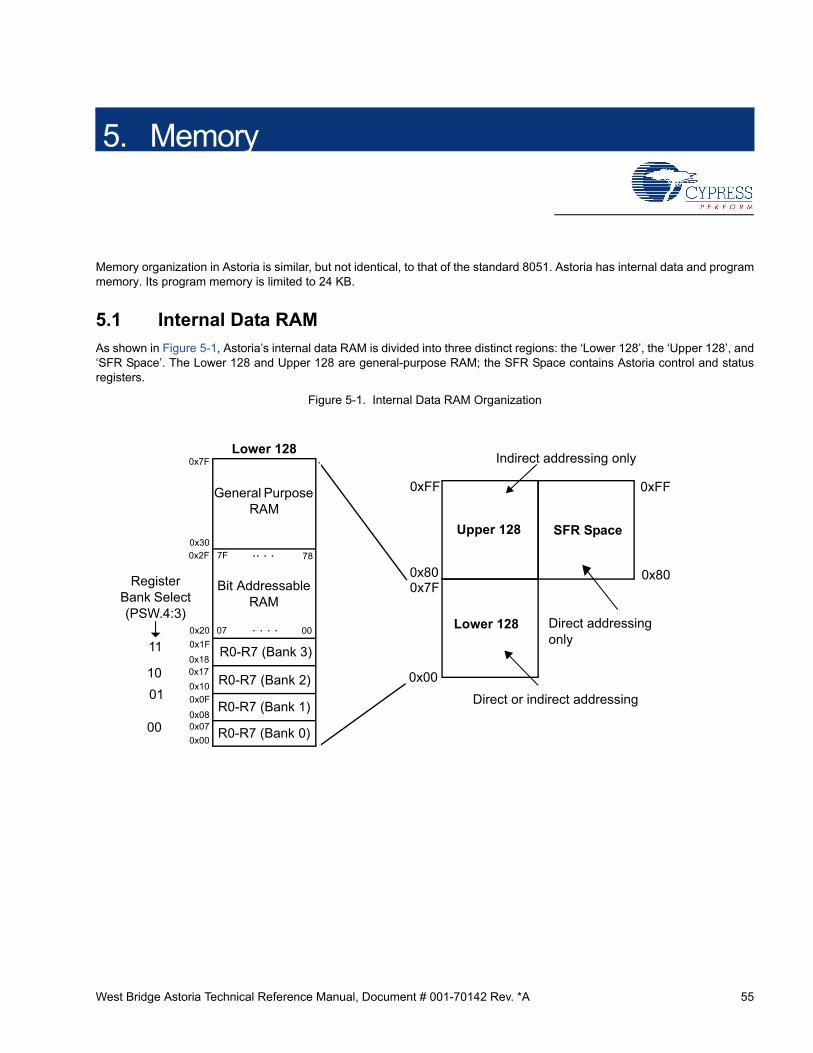
West Bridge Astoria Technical Reference Manual, Document # 001-70142 Rev. *A 55
5. Memory
Memory organization in Astoria is similar, but not identical, to that of the standard 8051. Astoria has internal data and programmemory. Its program memory is limited to 24 KB.
5.1 Internal Data RAM
As shown in Figure 5-1, Astoria’s internal data RAM is divided into three distinct regions: the ‘Lower 128’, the ‘Upper 128’, and‘SFR Space’. The Lower 128 and Upper 128 are general-purpose RAM; the SFR Space contains Astoria control and statusregisters.
Figure 5-1. Internal Data RAM Organization
0x00
0xFF
0x7F0x80
Lower 128
Upper 128 SFR Space
0xFF
0x80
Lower 128
0x00R0-R7 (Bank 0)
0x070x08
R0-R7 (Bank 1)0x0F
0x10 R0-R7 (Bank 2)
R0-R7 (Bank 3)
0x170x18
0x1F
0x20
0x2F0x30
0x7F
0007
787F .. . .
. . . .
Bit AddressableRAM
General Purpose RAM
Direct or indirect addressing
Indirect addressing only
Direct addressing only
00
01
10
11
Register Bank Select(PSW.4:3)

56 West Bridge Astoria Technical Reference Manual, Document # 001-70142 Rev. *A
Memory
5.1.1 The Lower 128
The Lower 128 occupies internal data RAM locations 0x00–0x7F. All of the Lower 128 can be accessed as general-purposeRAM, using either direct or indirect addressing (for more information about Astoria addressing modes, see the InstructionSet chapter on page 161).
Two segments of the Lower 128 can be accessed in other ways.
■ Locations 0x00–0x1F contain four banks of eight registers each, numbered R0 through R7. The current bank is selected using the ‘register-select’ bits (RS1:RS0) in the PSW special-function register; code that references registers R0–R7 accesses them only in the currently selected bank.
■ Locations 0x20–0x2F are bit addressable. Each of the 128 bits in this segment can be individually addressed, either by its bit address (0x00 to 0x7F) or by reference to the byte which contains it (0x20.0 to 0x2F.7).
5.1.2 The Upper 128
The Upper 128 occupies internal data RAM locations 0x80–0xFF; all 128 bytes can be accessed as general-purpose RAM,but only by using indirect addressing (for more information about Astoria addressing modes, see the Instruction Set chapteron page 161).
Since Astoria’s stack is internally accessed using indirect addressing, it is a good idea to put the stack in the Upper 128; thisfrees the Lower 128, which is easier to access, for general-purpose use.
5.1.3 Special Function Register Space
The Special Function Register (SFR) space, like the Upper 128, is accessed at internal data RAM locations 0x80–0xFF. Asto-ria keeps SFR space separate from the Upper 128 by using different addressing modes to access the two regions: SFRs canonly be accessed using ‘direct’ addressing, and the Upper 128 can only be accessed using ‘indirect’ addressing.
The sixteen SFRs at locations 0x80, 0x88, …, 0xF0, 0xF8 are bit-addressable. Each of the 128 bits in these registers can beaddressed individually, either by its bit address (0x80 to 0xFF) or by reference to the byte that contains it (for example,0x80.0, 0xC8.7, and so on).

West Bridge Astoria Technical Reference Manual, Document # 001-70142 Rev. *A 57
Memory
5.2 Astoria Memory Map
Figure 5-2. On-Chip Memory Map
Figure 5-2 shows the memory map for memory at 0x0000 to 0xFFFF.
512 bytes of Scratch RAM are available at 0xE000 to 0xE1FF. This is data RAM only; code cannot be executed from it. The128 bytes at 0xE400–0xE47F hold the four waveform descriptors for the GPIF. The area from 0xE500 to 0xE6FF containsAstoria control and status registers.
Memory blocks 0xE200 to 0xE3FF, 0xE700 to 0xE73F, and 0xE800 to 0xEFFF are reserved; do not use them for data stor-age.
The remaining RAM contains the endpoint buffers. These buffers are accessible either as addressable data RAM (using the‘MOVX’ instruction) or as FIFOs (using the Autopointer, described in section 8.7 Autopointers on page 83).
0000
5FFF
6000 CFFF
D000
DFFF
E000 E1FF E200
E7FF E800 EFFF
F000
FFFF 4 KB (Endpoint Buffers
2,4,6,8 for U to S and P to S Transactions)
2 KB (Reserved)
256 B(EP0 and EP1 (192 B),
Reserved (64 B))
Unused
(Reserved)
24 KB(Code and Data RAM)
0.5 KB (Scratch RAM)
E3FF E400 E47F 128 B
GPIF Waveforms
E480
E4FF
128 B MECC
E500
E6FF
0.5 KB Control and Status Registers
E700
0.5 KB (Reserved)
4 KB (Endpoint Buffers 3,5,7,9 for P to U
Transactions)

58 West Bridge Astoria Technical Reference Manual, Document # 001-70142 Rev. *A
Memory
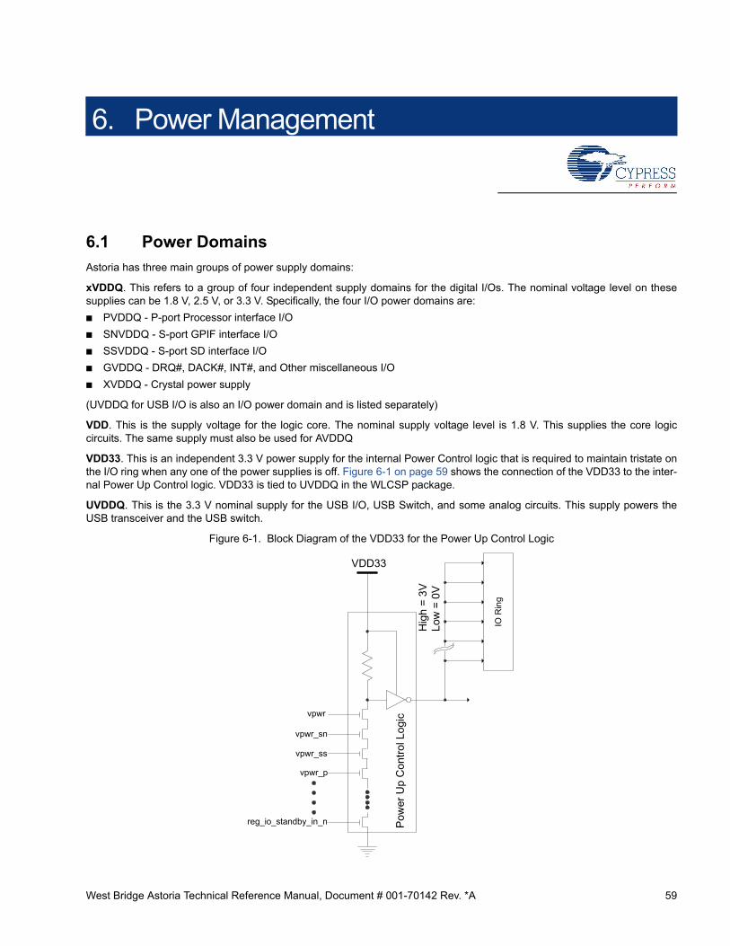
West Bridge Astoria Technical Reference Manual, Document # 001-70142 Rev. *A 59
6. Power Management
6.1 Power Domains
Astoria has three main groups of power supply domains:
xVDDQ. This refers to a group of four independent supply domains for the digital I/Os. The nominal voltage level on thesesupplies can be 1.8 V, 2.5 V, or 3.3 V. Specifically, the four I/O power domains are:
■ PVDDQ - P-port Processor interface I/O
■ SNVDDQ - S-port GPIF interface I/O
■ SSVDDQ - S-port SD interface I/O
■ GVDDQ - DRQ#, DACK#, INT#, and Other miscellaneous I/O
■ XVDDQ - Crystal power supply
(UVDDQ for USB I/O is also an I/O power domain and is listed separately)
VDD. This is the supply voltage for the logic core. The nominal supply voltage level is 1.8 V. This supplies the core logiccircuits. The same supply must also be used for AVDDQ
VDD33. This is an independent 3.3 V power supply for the internal Power Control logic that is required to maintain tristate onthe I/O ring when any one of the power supplies is off. Figure 6-1 on page 59 shows the connection of the VDD33 to the inter-nal Power Up Control logic. VDD33 is tied to UVDDQ in the WLCSP package.
UVDDQ. This is the 3.3 V nominal supply for the USB I/O, USB Switch, and some analog circuits. This supply powers theUSB transceiver and the USB switch.
Figure 6-1. Block Diagram of the VDD33 for the Power Up Control Logic
IO R
ing
vpwr
vpwr_sn
vpwr_ss
vpwr_p
reg_io_standby_in_n
VDD33
Hig
h =
3V
Low
= 0
V
Pow
er U
p C
ont
rol L
ogi
c

60 West Bridge Astoria Technical Reference Manual, Document # 001-70142 Rev. *A
Power Management
Figure 6-2. Astoria Power Supply Domains
All I/O supplies of Astoria must be ON when a system is active even if Astoria is not being used.
In the VFBGA package, if the USB switch is not connected to any external devices, the UVDDQ can be powered down withVDD in the core power down mode. On the other hand, if USB switch is connected to external device, the UVDDQ must beON during the core power down mode.
In WLCSP package, the UVDDQ must be ON during the core power down mode.
The core VDD can be deactivated at any time to preserve power. All I/Os tristate when the core is disabled. Table 6-1 andTable 6-2 on page 61 show the power supply requirement for each power domain in VFBGA and WLCSP packages for eachoperatIon mode.
Table 6-1. Power Supply Requirement in VFBGA for each OperatIon Mode
Mode UVALID Bit VDD UVDDQ VDD33 AVDDQ XVDDQ GVDDQ SSVDDQ SNVDDQ PVDDQ Remark
Normal opera-tIon
Controlled by UVALID Register
ON ON ON ON ON ON ON ON ON
Controlled by UVALID Register
ONOFF
(illegal)ON On On On On On On
Illegal Configura-tIon
Suspend mode
Maintain the last state
ON ON ON ON ON ON ON ON ON
Maintain the last state
ONOFF
(illegal)ON ON ON ON ON ON ON
Illegal Configura-tIon
Standby
Low ON ON ON ON ON ON ON ON ON
Low ONOFF
(illegal)ON ON ON ON ON ON ON
Illegal Configura-tIon
Core Power Down
Low OFF ON ON OFF ON ON ON ON ON
If the Switch is used, it must use this configuratIon in Core Power Down mode
Low OFF OFF ON OFF ON ON ON ON ON
SWD+/SWD– and D+/D– cannot be driven when UVDDQ is off.This is illegal con-figuratIon if the Switch is used.
Device Power Down
Unknown OFF OFF OFF OFF OFF OFF OFF OFF OFF
SWD+/SWD– and D+/D– can't be driven when UVDDQ is off
Illegal Configu-ratIons *
Unknown X X OFF X X X X X X
Notes
ON: Power Supply is ON
OFF: Power supply is OFF
*All Astoria power supplies must be on when VDD33 is off.
USB-IOD-COREI/O
UVDDQVDDxVDDQ
D+
D-

West Bridge Astoria Technical Reference Manual, Document # 001-70142 Rev. *A 61
Power Management
6.2 Power Supply Sequence
The power supplies can be independently sequenced without damaging the part. Astoria must not be operated any IllegalPower ConfiguratIon as shown in Table 6-1 on page 60 and Table 6-2 on page 61. All power supplies must be up and stablebefore the device can operate. In the absence of all supplies being stable, the remaining domains are in low-power (standby)state.
6.3 Power Modes
6.3.1 Normal Mode
Normal Mode is the mode in which Astoria is fully functional. This is the mode in which data transfer functIons described inthis document are performed.
6.3.2 Standby Mode
Standby Mode is the mode in which Astoria is in a low-power state. This is the lowest power mode of Astoria while still main-taining external supply levels. This mode is entered through the deassertion of the WAKEUP input pin or the setting of theSTNDBY bit in the Power Management Control and Status Register. If this mode is entered by deassertion of the WAKEUPinput pin, it must be exited by asserting the WAKEUP pin. If this mode is entered by setting the STNDBY bit, it must be exitedby one of the following:
■ Assertion of CE# in P-Port register
■ Change the state of GPIO[0]/SD_CD, GPIO[1]/SD2_CD, SD_D3, or SD2_D3
Table 6-2. Power Supply Requirement in WLCSP for each Operation Mode
Mode UVALID Pin VDD UVDDQ VDD33 AVDDQ XVDDQ GVDDQ SSVDDQ SNVDDQ PVDDQ Remark
Normal operatIon
Controlled by UVALID Register
ON ON ON ON ON ON ON ON ON
Controlled by UVALID Register
ONOFF
(illegal)ON On On On On On On
Illegal Configura-tIon
Suspend mode
Maintain the last state
ON ON ON ON ON ON ON ON ON
Maintain the last state
ONOFF
(illegal)ON ON ON ON ON ON ON
Illegal Configura-tIon
Standby
Low ON ON ON ON ON ON ON ON ON
Low ONOFF
(illegal)ON ON ON ON ON ON ON
Illegal Configura-tIon
Core Power Down
Low OFF ON OFF ON ON ON ON ON ON
Low ONOFF
(illegal)ON ON ON ON ON ON ON
Illegal Configura-tIon
Device Power Down
Unknown OFF OFF OFF OFF OFF OFF OFF OFF OFF
SWD+/SWD- and D+/D- Can't be driven when UVDDQ is off
Illegal Configura-tIons *
Unknown X X X X X X X X X
Notes
ON: Power supply is onOFF: Power supply is off
*All Astoria power supplies must be on when VDD33 is off.
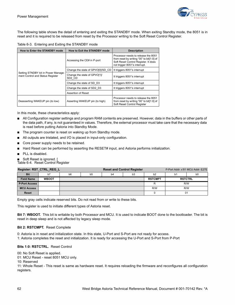
62 West Bridge Astoria Technical Reference Manual, Document # 001-70142 Rev. *A
Power Management
The following table shows the detail of entering and exiting the STANDBY mode. When exiting Standby mode, the 8051 is inreset and it is required to be released from reset by the Processor writing to the Soft Reset Control Register.
In this mode, these characteristics apply:
■ All ConfiguratIon register settings and program RAM contents are preserved. However, data in the buffers or other parts of the data path, if any, is not guaranteed in values. Therefore, the external processor must take care that the necessary data is read before putting Astoria into Standby Mode.
■ The program counter is reset on waking up from Standby mode.
■ All outputs are tristated, and I/O is placed in input-only configuration.
■ Core power supply needs to be retained.
■ Hard Reset can be performed by asserting the RESET# input, and Astoria performs initializatIon.
■ PLL is disabled.
■ Soft Reset is ignored. [
Empty gray cells indicate reserved bits. Do not read from or write to these bits.
This register is used to initiate different types of Astoria reset.
Bit 7: WBOOT. This bit is writable by both Processor and MCU. It is used to indicate BOOT done to the bootloader. The bit isreset in deep sleep and is not affected by legacy sleep mode.
Bit 2: RSTCMPT. Reset Complete
0: Astoria is in reset and initialization state. In this state, U-Port and S-Port are not ready for access.1: Astoria completes the reset and initialization. It is ready for accessing the U-Port and S-Port from P-Port
Bits 1:0: RSTCTRL. Reset Control
00: No Soft Reset is applied. 01: MCU Reset - reset 8051 MCU only. 10: Reserved 11: Whole Reset - This reset is same as hardware reset. It requires reloading the firmware and reconfigures all configurationregisters.
Table 6-3. Entering and Exiting the STANDBY mode
How to Enter the STANDBY mode How to Exit the STANDBY mode Description
Setting STNDBY bit in Power Manage-ment Control and Status Register
Accessing the CE# in P-port
Processor needs to release the 8051 from reset by writing “00” to bit[1:0] of Soft Reset Control Register. It does not trigger 8051's interrupt.
Change the state of GPI/O[0]/SD_CD It triggers 8051's interrupt
Change the state of GPI/O[1]/SD2_CD
It triggers 8051's interrupt
Change the state of SD_D3 It triggers 8051's interrupt
Change the state of SD2_D3 It triggers 8051's interrupt
Assertion of Reset
Deasserting WAKEUP pin (to low) Asserting WAKEUP pin (to high)Processor needs to release the 8051 from reset by writing “00” to bit[1:0] of Soft Reset Control Register
Table 6-4. Reset Control Register
Register: RST_CTRL_REG_L Reset and Control Register P-Port Addr: x’81 MCU Addr: E27E
Bit b7 b6 b5 b4 b3 b2 b1 b0
Field Name WBOOT RSTCMPT RSTCTRL
P-Port Access R R/W
MCU Access R/W R/W
Reset 0 01

West Bridge Astoria Technical Reference Manual, Document # 001-70142 Rev. *A 63
Power Management
RST_CTRL_REG = 0x00; /*Clear the reset register. This releases the Astoria microcontroller from reset and begins running the code at address zero.*/
RST_CTRL_REG = 0x01; /* Soft reset */
RST_CTRL_REG = 0x03; /* Hard reset */
[
Empty gray cells indicate reserved bits. Do not read from or write to these bits.
This register indicates the power status of the Astoria SW (for example, if the Astoria SW woke up from standby mode) andallows Standby to be initiated by register write.
Bit 1: STANDBY. This field initiates Standby mode in the Astoria SW when written with '1'. After initiating standby, the pro-cessor must deassert CE# until the Standby duration has elapsed. There are six different options to exit from Standby modethat are initiated by this bit. The detail is shown in Table 6-3 on page 62. This bit is automatically reset to '0' by hardware uponAstoria SW wake up from Standby mode.
Standby control (to initiate Standby mode)0: Normal operating mode1: Initiate Standby mode
Bit 0: WAKEUP. This field indicates whether the Astoria SW has woken up. “Woken up” is defined as PLL being locked andthe Astoria SW being ready to function and communicate to all ports. WAKEUP is asserted following deassertion of RESET#hard reset or full-chip soft reset.
Wake up (from standby mode)0: Not awake from standby mode1: Awake from standby mode.
To put Astoria in Standby mode:PWR_MAGT_STAT = 0x02;
6.3.3 Suspend Mode
Suspend is a request (indicated by a 3-millisecond ‘J’ state on the USB bus) from the USB host or hub to the device. Thisrequest is usually sent by the host when it enters a low-power “suspended” state. USB devices are required to enter a low-power state in response to this request.
This mode is entered by Astoria when bit 0 of the PCON register is set (external processor can only initiate entry into thismode through Mailbox commands). This mode is exited by the D+ bus going low, state change at GPIO[1]/SD2_CD orGPIO[0]/SD_CD (such as insertion or removal of SD/MMC card), or by asserting CE# LOW.
Table 6-5. Power Management Control and Status Register
Register: CY_AN_MEM_PWR_MAGT_STAT Power Management Control and Status Register x’95
Bit b15 b14 b13 b12 b11 b10 b9 b
Field Name
Access
Reset
Register: CY_AN_MEM_PWR_MAGT_STAT Power Management Control and Status Register
Bit b7 b6 b5 b4 b3 b2 b1 b0
Field Name STNDBY WAKEUP
Access R/W R
Reset 0 0

64 West Bridge Astoria Technical Reference Manual, Document # 001-70142 Rev. *A
Power Management
In the Suspend mode of Astoria:
■ The clocks are shut off. The PLL is disabled.
■ All I/Os maintain their prevIous state.
■ U-Port (USB switch) maintains the previous state.
■ Core power supply needs to be retained.
■ The states of the ConfiguratIon registers, endpoint buffers, and the program RAM are maintained. All transactions need to be complete before Astoria enters Suspend mode (state of outstanding transactions are not preserved).
■ The firmware resumes its operatIon from where it was suspended, because the program counter is not reset.
■ Only inputs that are sensed are RESET#, GPIO[0], GPIO[1], D+, and CE#. The last three are wake-up sources (each can be individually enabled or disabled).
■ Hard Reset can be performed by asserting the RESET# input, and Astoria performs initializatIon.
6.3.3.1 Wakeup
Registers that need to be configured to decide the wakeup mechanism:
[
Empty gray cells indicate reserved bits. Do not read from or write to these bits.
Wakeup from Suspend through SD1 pins.
Bit 5: STATUS_WAKEUP_SD_D3. Wakeup status from SD_D3
Bit 4: STATUS_WAKEUP_SD_D1. Wakeup status from SD_D1
Bit 3: POL_WAKEUP_SD_D3. Polarity of SD_D3 for a wakeup
Bit 2: POL_WAKEUP_SD_D1. Polarity of SD_D1 for a wakeup
Bit 1: EN_WAKEUP_SD_D3. Enable wakeup from suspend through SD_D3
Bit 0: EN_WAKEUP_SD_D1. Enable wakeup from suspend through SD_D1
[
Empty gray cells indicate reserved bits. Do not read from or write to these bits.
Wakeup from Suspend through SD2 pins.
Bit 5: STATUS_WAKEUP_SD2_D3. Wakeup status from SD2_D3
Table 6-6. SD1 Wakeup Register
Register: SD1_WAKEUP SD1 Wakeup Register E674
Bit b7 b6 b5 b4 b3 b2 b1 b0
Field NameSTATUS_WAKE
UP_SD_D3STATUS_WAKE
UP_SD_D1POL_WAKEUP_
SD_D3POL_WAKEUP_
SD_D1EN_WAKEUP_
SD_D3EN_WAKEUP_
SD_D1
Access R/W R/W R/W R/W R/W R/W
Reset 0 0 0 0 0 0
Table 6-7. SD2 Wakeup Register
Register: SD2_WAKEUP SD2 Wakeup Register E675
Bit b7 b6 b5 b4 b3 b2 b1 b0
Field NameSTATUS_WAKE
UP_SD2_D3STATUS_WAKE
UP_SD_2D1POL_WAKEUP_
SD2_D3POL_WAKEUP_
SD2_D1EN_WAKEUP_
SD2_D3EN_WAKEUP_
SD2_D1
Access R/W R/W R/W R/W R/W R/W
Reset 0 0 0 0 0 0

West Bridge Astoria Technical Reference Manual, Document # 001-70142 Rev. *A 65
Power Management
Bit 4: STATUS_WAKEUP_SD2_D1. Wakeup status from SD2_D1
Bit 3: POL_WAKEUP_SD2_D3. Polarity of SD2_D3 for a wakeup
Bit 2: POL_WAKEUP_SD2_D1. Polarity of SD2_D1 for a wakeup
Bit 1: EN_WAKEUP_SD2_D3. Enable wakeup from suspend through SD2_D3
Bit 0: EN_WAKEUP_SD2_D1. Enable wakeup from suspend through SD2_D1
[
Empty gray cells indicate reserved bits. Do not read from or write to these bits.
Wakeup from Suspend through GPIO pins.
Bit 2: STATUS_WAKEUP_GPIO1. Wakeup status from GPIO[1]
Bit 1: POL_WAKEUP_GPIO1. Polarity of GPIO[1] for wakeup
Bit 0: EN_WAKEUP_GPIO1. Enable wakeup from suspend through GPIO[1]
One wakeup scenario is described below for your reference. Astoria will come out of standby when the GPIO1 value is oneand if there is any activity on the USB D+ signal.
SD1_WAKEUP = 0x00;
SD2_WAKEUP = 0x00;
GPIO_WAKEUP = 0x03;
PLB_WAKEUP = 0x04;
6.3.4 Core Power Down
The core power supply VDD is powered down in this state. AVDDQ is tied to the same supply as VDD and is, therefore, alsopowered down. This mode is entered by powering down VDD and AVDDQ simultaneously, and exited by powering up VDDand AVDDQ, performing the reset and initializatIon sequence, following by firmware download. All endpoint buffers, Configu-ratIon registers and the program RAM do not maintain state. It is necessary to reload the firmware on exiting from this mode.It has an optIon that the UVDDQ can be powered down or stay on while VDD is powered down when SWD+/SWD- is no con-nected. The UVDDQ cannot be powered down when SWD+/SWD- is connected, or VDD is active. When UVDDQ is powereddown, D+/D- can't be driven by external device. Table 6-1 on page 60 shows the detail of Core Power Down requirement.
In the WLCSP option, AVDDQ is internally tied to XVDDQ. As a result, the clock input at XTALIN must be brought to a steadyLOW level before entry into Core Power Down mode. In WLCSP, VDD33 is tied to UVDDQ internally. UVDDQ must be ONduring the core power down mode.
Table 6-8. GPIO Wakeup Register
Register: GPIO_WAKEUP GPIO Wakeup Register E676
Bit b7 b6 b5 b4 b3 b2 b1 b0
Field NameSTATUS_WAKE
UP_GPIO1POL_WAKEUP_
GPIO1EN_WAKEUP_
GPIO1
Access R/W R/W R/W
Reset 0 0 0

66 West Bridge Astoria Technical Reference Manual, Document # 001-70142 Rev. *A
Power Management
6.4 Power Management
Figure 6-3. Power Management
Power management in the Astoria device is contingent upon several factors. Figure 6-3 depicts the sequence of events in apower up or power down operatIon.
■ After Power On Reset, the USB switch is on and U-port is allocated to external transceiver (PHY).
■ Astoria then follows the initializatIon procedures described in sectIon Bootup Initialization on page 146.
■ After the initializatIon is complete and RESETOUT has been asserted to the Processor by Astoria, the processor config-ures the allocation of the U-port by writing the USBALLO field in External Bus AllocatIon Register and UVALID field in the PMU Update Register.
■ Device enters normal operatIon mode.
■ If VDD (core) supply is powered-down, then the USB switch is on and the device enters power down mode. The entire reset and initializatIon cycle has to be repeated to resume normal operatIon.
■ VDD33 is required to be connected to 3.3 V at all times during operatIon (even in standby, power down, or suspend modes).
UVDDQ
VDD
RESET#
WAKEUP
USBALLO bit in EBA
Register
0V
3.3V
0V
1.8V
RESETOUT
Reset and Initialization of
Astoria
Enter Standby
mode
D+/D-
10us
USB Switch is ONNormal Operation D+/D-
Singal Level
0V
3.3V
VDD33VDD33 must be provided 3.3V all time during the opertation
Normal Operation D+/D- Singal Level
Hi-Z
Enter Core Power Down
mode
Normal Operation D+/D-
Singal Level
Core Power Down mode
Standby mode
Normal Operation Mode
Normal Operation
ModeNormal
Operation Mode
Reset and Initialization
USB Switch is ON USB Switch is ON

West Bridge Astoria Technical Reference Manual, Document # 001-70142 Rev. *A 67
7. Resets
There are three different reset functions on Astoria: Hard Reset, CPU Reset, and USB Reset.
Figure 7-1. Astoria Resets
7.1 Hard Reset
The RESET# pin can be connected to an external R-C network or other external reset source in order to ensure that, whenpower is first applied, Astoria is held in reset until the operating parameters (VCC voltage, crystal frequency, PLL frequency,and others) stabilize. The 24 MHz oscillator and PLL stabilize 5 ms after VCC reaches 3.0 V. An R-C network can satisfy thepower-on reset requirements of Astoria. See Figure 7-1 for a sample connection scheme (for example, R = 27K ohm, C =1 µF).
The RESET# pin can also be asserted at any time after Astoria is running. If Astoria’s XTALIN pin is driven by an externalclock source that continues to run while the chip is in reset, RESET# need only be asserted for 200 µs. Otherwise, it must beasserted for at least 5 ms.
Power-on default values for all Astoria register bits are shown in Registers chapter. At power-on reset:
■ Endpoint data buffers and byte counts are uninitialized
■ The CPU clock speed is set to 12 MHz, the CPU is held in reset
■ All port pins are configured as general purpose input pins
■ USB interrupts are disabled and USB interrupt requests are cleared
■ Bulk IN and OUT endpoints are unarmed, and their stall bits are cleared. Astoria NAKs IN and OUT tokens while the CPU is reset.
■ Endpoint data toggle bits are cleared to ‘0’

68 West Bridge Astoria Technical Reference Manual, Document # 001-70142 Rev. *A
Resets
■ The RENUM bit is cleared to ‘0’. This means that the Default USB Device, not the firmware, responds to USB device requests.
■ The USB Function Address register is cleared to ‘0’
■ The endpoints are configured for the Default USB Device
■ Interrupt autovectoring is turned Off
■ Configuration Zero, Alternate Setting Zero is in effect
■ The D+ pull up resistor is disconnected from the data line during a hard reset
The Hard Reset involves a total of three pins: the RESET# input, the RESETOUT output and the WAKEUP input. When theRESET# input pin is pulsed, Astoria deasserts (drives LOW) the RESETOUT output (RSTCMPT field in the Soft Reset Con-trol Register is tied to RESETOUT signal). The WAKEUP pin is “don't care” while RESET# is driven LOW. The WAKEUP pinmust be asserted HIGH for initialization to occur. When Astoria is ready for general operations (after firmware is initialized), itasserts the RESETOUT signal HIGH. A Hard Reset pulse must be carried out every time Astoria's core has been powereddown and is then powered back up.
The use of the RESET# pin has these characteristics:
■ For as long as RESET# input is asserted, RESETOUT is deasserted LOW. All other I/Os are high-Z during RESET# assertion.
■ After RESET# is deasserted, RESETOUT remains deasserted. If WAKEUP is also asserted at this time, Astoria starts performing the internal initialization which includes loading the 8051 MCU firmware. During this initialization time, the pro-cessor also configures the P-port Endian Configuration Register and other configuration registers.
■ No data transfer functions must be performed on Astoria until the Processor has configured all configuration registers, loaded the 8051 firmware, and Configuration Mode has been exited (8051 firmware needs to reset the CFGMODE field of P-port Interface Configuration Register to '0').
■ To summarize the behavior of Astoria based on the level of the RESET# AND WAKEUP pins, refer the following table.
* Astoria enters this mode if it has been properly reset and initialized previously. If not initialized previously, the behavior is asfollows:
RESET#=1, WAKEUP=0: Astoria tri-states RESETOUT until RESET# has been pulsed, WAKEUP has been asserted and ini-tialization has been completed. Astoria does not enter initialization until WAKEUP is asserted.
RESET#=1, WAKEUP=1: Device does not enter initialization mode until RESET# has been pulsed and WAKEUP has beenasserted. In this case, WAKEUP is asserted but RESET# is not. Astoria continues to remain in preinitialization state.
Table 7-1. RESET# and WAKEUP behavior
RESET# WAKEUP Action
0 Don't Care Device in Reset
1 0 Standby mode*
1 1 Normal mode of operation*

West Bridge Astoria Technical Reference Manual, Document # 001-70142 Rev. *A 69
Resets
At initial power up and each time the core is powered up, it is mandatory for a Hard Reset (asserting RESET# input) to beperformed with the WAKEUP pin asserted.
Figure 7-2. Reset and Initialization Timing Diagram
7.2 Reset by Register (Soft Reset)
The Soft Reset involves the processor setting the bits appropriately in the Soft Reset Control Register. The RSTCTRL bits inthe Soft Reset Control Register control the type of Soft Reset. There are two types of Soft Reset, namely:
■ MCU PC Reset - During MCU PC Reset, only the 8051 MCU Program Counter is reset to the starting address (its Pro-gram RAM contents are maintained). This reset does not cause the 8051 MCU and all its registers reset (all registers are not changed). The firmware code does not need to be reloaded following an 8051 MCU PC Reset.
■ Whole Device Reset - This Reset is identical to Hard Reset described in the previous section. The firmware code must be reloaded following a Whole Device Reset.
When the Processor performs a Whole Device soft reset of Astoria by writing “11” to the RSTCTRL field, Astoria internallygenerates a reset pulse. After the internal reset pulse deasserts, the RSTCTRL field must be set to “01” to keep the 8051 inreset during download of the firmware code and register configuration.
The processor requires resetting the RSTCTRL field to “00” after finish loading the firmware from P-port. The 8051 thenbegins the firmware initialization.
If Astoria is configured to PNAND interface mode and requires the support of loading the processor's boot code from theNAND at the S-port, the 8051 is required to load its firmware image to the internal RAM first after power on reset or hardreset. After 8051 firmware has been loaded and being executed, the 8051 manages to download processor's boot code fromthe NAND flash (at S-port) through the PNAND interface. Astoria has two setups to load the firmware image.
The 8051 firmware image can be saving in the EEPROM, which connect to the PI2C interface. After power on reset or hardreset, Astoria loads the firmware image from the EEPROM. The 8051 firmware requires resetting the CFGMODE field in the
Pro
cess
or
con
figu
res
CY
_AN
_M
EM
_P
0_E
ND
IAN
T
Reg
iste
r fo
r E
ndia
nt c
onfig
urat
ion.
If fi
rmw
are
load
by
Pro
cess
or:
Pro
cess
or w
rite
s “0
0”
to
RS
TC
TR
L fie
ld to
re
leas
e 8
051
fro
m r
ese
t sta
te.
8051
st
art
s to
exe
cute
the
firm
wa
re.
Loa
d th
e fi
rmw
are
eith
er fr
om
Pro
cess
or,
I2C
EE
PR
OM
o
r U
SB
Por
t (te
st m
ode)
Pro
cess
or c
onfig
ures
all
conf
igur
atio
n re
gist
ers
8051
firm
war
e r
eset
CF
GM
OD
E f
ield
to r
ele
ase
the
A
stor
ia fr
om th
e in
itial
izat
ion
stat
e
WA
KE
UP
fie
ld o
f CY
_AN
_M
EM
_PW
R_M
AG
T_
ST
AT
R
egis
ter
= 1
indi
cate
s th
at t
he
inte
rnal
PL
L ge
ts lo
cked
RESET#
RESETOUT and
RSTCMPT
Ext
erna
l po
wer
an
d cl
ock
are
sta
ble
WAKEUP
CF
GM
OD
E fi
eld
in C
Y_A
N_M
EM
_P
0_V
M_
SE
T is
set

70 West Bridge Astoria Technical Reference Manual, Document # 001-70142 Rev. *A
Resets
“P-port Interface Configuration Register” to '0' to exit from Soft Reset when all configuration registers have been loaded. Afterthat, RESETOUT is deasserted and Astoria enters into normal operation mode.
Soft Reset Control Register
Access Note
The default value of bits 0-1 is 01. The default value of bits 3-6 and 8-15 is U/D. The rest of the bits have the default value 0.
Bit 7: WBOOT. This field is readable and writable by both Processor and 8051. This field is used to indicate if the firmwareimage has been downloaded to the RAM or not. This field must be set by P-port processor after completing the firmwaredownload.
Warm boot
0:Cold boot, it requires to download the firmware image
1:Warm boot, the firmware image has downloaded in the RAM
* This field is reset by POR, soft reset, hard reset, standby-wakeup, or power down mode. But this field is not reset by MCUreset and suspend resume.
Bit 2: RSTCMPT
This field is used to report Astoria's status after reset. This field is the same value as the RESETOUT pin. When this field is'0', it indicates Astoria is in initialization state. After reset deassert, Astoria is in initialization state that locking its internal PLL,loading the 8051 firmware, initial the configuration registers. In this state, Astoria is not in the normal operation except down-load the firmware from P-port and read/write to the configuration registers.
Reset Complete
0:Astoria is in reset and initialization state. In this state, U-port and S-port is not ready for access.
1:Astoria completes the reset and initialization. It is ready for accessing the U-port and S-port from P-port
Bit 1: RSTCTRL
Reset Control. This field selects the different software reset for Astoria:
MCU Reset - This reset resets the 8051 MCU only. After this reset, Astoria is not required to reload the firmware or reconfig-ure the Astoria configuration registers.
Whole Device Reset - This reset acts similar to a hardware reset by resetting the whole Astoria. This reset requires reloadingof the firmware and reconfiguration of all configuration registers.
* Active 8051 soft reset state from RSTCTRL settings is mapped to Bit-0 of 8051 “CPU Control and Status Register”(CPUCS). The location of CPUCS register is at the address of x'E600.
Reset Control
00:No Soft Reset is applied
01:MCU Reset - reset 8051 MCU only.
10:Reserved
11:Whole Reset - this reset is same as hardware reset. It requires reloading the firmware and reconfigures all configurationregisters.
Address Name Bit 7 Bit 6 Bit 5 Bit 4 Bit 3 Bit 2 Bit 1 Bit 0 Access : Reset
x'81 CY_AN_MEM_RST_CTRL_REG
WBOOT RSTCMPT RSTCTRL RW : #
Bit 15 Bit 14 Bit 13 Bit 12 Bit 11 Bit 10 Bit 9 Bit 8 Access : Reset
R : #

West Bridge Astoria Technical Reference Manual, Document # 001-70142 Rev. *A 71
Resets
7.3 Wakeup Mechanism
After the device is properly reset and initialized, Astoria stays in normal operation mode as long as the WAKEUP pin isasserted. When WAKEUP is deasserted, Astoria enters standby mode. When WAKEUP is asserted, Astoria exits standbymode. Astoria interrupts the Processor and sets the PMINT field in the P-port Interrupt Register and the WAKEUP field in thePower Management Control and Status Register. The interrupt bit is cleared when the Processor reads the Power Manage-ment Control and Status Register.
If the WAKEUP pin is not used by an application, it must be tied HIGH to enable normal operation.
7.4 USB Bus Reset
The host signals a USB bus reset by driving an SE0 state (both D+ and D- data lines low) for a minimum of 10 ms. Astoriasenses this condition, requests the USB Interrupt (INT2), and supplies the interrupt vector for a USB Reset. After a USB busreset, the following occurs:
■ Data toggle bits are cleared to ‘0’.
■ The device address is reset to ‘0’.
■ If the Default USB Device is active, the USB configuration and alternate settings are reset to ‘0’.
■ Astoria renegotiates with the host for high-speed (480 Mbps) mode.
Note that the RENUM bit is unchanged after a USB bus reset. Therefore, if a device has ReNumerated™ and loaded a newpersonality, it retains the new personality through a USB bus reset.
7.5 Astoria Disconnect
Although not strictly a ‘reset,’ the disconnect-reconnect sequence used for ReNumeration™ affects Astoria in ways similar tothe other resets. When Astoria simulates a disconnect-reconnect, the following occurs:
■ Endpoint STALL bits are cleared.
■ Data toggles are reset to ‘0’.
■ The Function Address is reset to ‘0’.
■ If the Default USB Device is active, the USB configuration and alternate settings are reset to ‘0’.

72 West Bridge Astoria Technical Reference Manual, Document # 001-70142 Rev. *A
Resets

West Bridge Astoria Technical Reference Manual, Document # 001-70142 Rev. *A 73
8. Access to Endpoint Buffers
Astoria supports transfer of data among its three ports through endpoint (EP) buffering. Mailbox registers within Astoria facili-tate communication or message-passing between the 8051 MCU and the processor.
When an application requires the CPU to process the data as it flows between external logic and the USB — or when there isno external logic — firmware can access the endpoint buffers either as blocks of RAM or (using a special auto-incrementingpointer) as a FIFO.
Even when external logic or the built-in General Programmable Interface (GPIF) is handling high-bandwidth data transfersthrough the four large endpoint FIFOs without any CPU intervention, the firmware has certain responsibilities:
■ Configure the endpoints
■ Respond to host requests on CONTROL endpoint zero
■ Control and monitor GPIF activity
■ Handle all application-specific tasks using its USARTs, counter-timers, interrupts, I/O pins, and so on
8.1 Physical And Logical Endpoints
Astoria has a total of 11 physical endpoints. EP0 and EP1 are small, 64-byte endpoints, which are accessible only by theCPU; they cannot be connected directly to external logic.
EP2, EP3, EP4, EP5, EP6, EP7, EP8 and EP9 are large, configurable endpoints designed to meet the high-bandwidthrequirements of USB 2.0. Although data normally flows through the large endpoint buffers under control of the FIFO inter-faces described in Chapter 10, the CPU can access the large endpoints if necessary.
EP2, EP4, EP6 and EP8 are allocated for U-Port to S-port path. EP3, EP5, EP7 and EP9 are allocated for P-Port to U-Portpath.
Astoria supports 16 logical endpoints. Logical endpoints are mapped to physical endpoints. Physical endpoints can be dedi-cated to a logical endpoint or shared between multiple logical endpoints. Physical endpoints can only map to multiple logicalendpoints in the same direction. Logical to physical endpoint mapping is dynamic and can be changed by 8051 firmware withthe exception of the EP0, EP1, EP2, EP4, EP5, EP6, and EP8 endpoints.
■ Logical endpoints {EP3, EP5, EP7, EP9, EP10, EP11, EP12, EP13, EP14, EP15} between U and P port can be mapped to the 4 physical endpoints between the U-port and the P-port.
■ Logical endpoints {EP2, EP4, EP6, and EP8} between the U-port and the S-port are mapped to the four physical end-points between the U-port and the S-port.

74 West Bridge Astoria Technical Reference Manual, Document # 001-70142 Rev. *A
Access to Endpoint Buffers
Figure 8-1. Logical and Physical Endpoint Mapping to U-Port
8.2 High Speed and Full Speed Differences
The data payload size and transfer speed requirements dif-fer between full speed (12 Mbps) and high speed (480Mbps). Astoria architecture is optimized for high-speedtransfers, but does not limit full-speed transfers:
■ Instead of many small endpoint buffers, Astoria provides a reduced number of large buffers
■ Astoria provides double, triple, or quad buffering on its large endpoints (EP2, 3, 4, 5, 6, 7, 8, and 9)
■ The CPU need not participate in data transfers. Instead, dedicated Astoria logic and unified endpoint/interface FIFOs move data on and off the chip without any CPU intervention.
In Astoria, endpoint buffers appear to have different sizesdepending on whether it is operating at full or high speed.This is due to the difference in maximum data payload sizes
allowed by the USB specification for the two modes, as illus-trated by Table 8-1.
Although the EP2, EP3, EP4, EP5, EP6, EP8, and EP9 buf-fers are physically large, they appear as smaller buffers forthe non-isochronous types when Astoria is operating at fullspeed. This is to account for the smaller maximum data pay-load sizes.
When operating at high speed, firmware can configure thelarge endpoints’ size, type, and buffering depth; when oper-ating at full speed, type and buffering are configurable butthe buffer size is always fixed at 64 bytes for the non-iso-chronous types.
Table 8-1. Maximum Data Payload Sizes for Full Speed and High Speed
Transfer Type Max Data Payload Size
Full Speed High Speed
CONTROL (EP0 only) 8,16,32,64 64
BULK 8,16,32,64 512
INTERRUPT 1-64 1-1024
ISOCHRONOUS 1-1023 1-1024

West Bridge Astoria Technical Reference Manual, Document # 001-70142 Rev. *A 75
Access to Endpoint Buffers
8.3 How the CPU Configures the Endpoints
Endpoints are configured using the registers shown in Table 8-2.
PLB_EPxCFG (where x can be 3, 5, 7, 9, 10, 11, 12, 13, 14and 15) register is to set the logical endpoint configuration.
Note THe Registers chapter gives full bit-level details for allendpoint configuration registers.
Endpoint 0 does not require a configuration register since itis fixed as valid, IN/OUT, CONTROL, 64 bytes, single-buff-ered. EP0 uses a single 64-byte buffer both for IN and OUTtransfers. EP1 uses separate 64 byte buffers for IN and OUTtransfers.
Endpoints EP2 and EP6 are the most flexible endpoints, asthey are configurable for size (512 or 1024 bytes in high-speed mode, 64 bytes in full-speed mode for the non-iso-chronous types) and depth of buffering (double, triple, orquad). Endpoints EP4 and EP8 are fixed at 512 bytes, dou-ble-buffered in high-speed mode. They are fixed at 64 bytes,double-buffered in full-speed mode for the non-isochronoustypes.
The bits in the EPxCFG registers control the following:
■ Valid. Set to ‘1’ (default) to enable the endpoint. A non-valid endpoint does not respond to host IN or OUT pack-ets.
■ Type. Two bits, TYPE1:0 (bits 5 and 4) set the endpoint type.
□ 00 = invalid
□ 01 = ISOCHRONOUS (EP2,4,6,8 only)
□ 10 = BULK (default)
□ 11 = INTERRUPT
■ Direction. 1 = IN, 0 = OUT.
■ Buffering. EP2 and EP6 only. Two bits, BUF1:0 control the depth of buffering.
□ 00 = quad
□ 01 = invalid
□ 10 = double (default)
□ 11 = triple
‘Buffering’ refers to the number of RAM blocks available tothe endpoint. With double buffering, for example, USB datacan fill or empty an endpoint buffer at the same time thatanother packet from the same endpoint fills or empties fromthe external logic. This technique maximizes performanceby saving each side, USB and external-logic interface, fromwaiting for the other side. Multiple buffering is most effectivewhen the providing and consuming rates are comparablebut bursty (as is the case with USB and many other inter-faces, such as disk drives). Assigning more RAM blocks (tri-ple and quad buffering) provides more ‘smoothing’ of thebursty data rates. A simple way to determine the appropriatebuffering depth is to start with the minimum, then increase ituntil no NAKs appear on the USB side and no wait statesappear on the interface side.
Table 8-2. Endpoint Configuration Registers
Address Name Configurable Parameters
0xE610 EP1OUTCFG valid, type1 (always OUT, 64 bytes, single-buffered)
0xE611 EP1INCFG valid, type1 (always IN, 64 bytes, single-buffered)
0xE612 EP2CFG valid, direction, type, size, buffering
0xE613 EP4CFGvalid, direction, type (always 512 bytes, double-buffered in high-speed mode, 64 bytes double-buffered in full-speed mode for non-iso)
0xE614 EP6CFG valid, direction, type, size, buffering
0xE615 EP8CFGvalid, direction, type (always 512 bytes double-buffered in high-speed mode, 64 bytes double-buffered in full-speed mode for non-iso)
0xE312PLB_EP2CFG(Physical Endpoint 3 configuration)
buffering, direction and size (512 bytes or 1024 bytes)
0xE313PLB_EP4CFG(Physical Endpoint 5 configuration)
Only buffering and direction. Size is fixed to 512 bytes
0xE314PLB_EP6CFG(Physical Endpoint 7 configuration)
buffering, direction and size (512 bytes or 1024 bytes)
0xE315PLB_EP8CFG(Physical Endpoint 9 configuration)
Only buffering and direction. Size is fixed to 512 bytes.
Note For EP1, ‘type’ may be set to Interrupt or Bulk only. Even though these buffers are 64 bytes in size, they are reported as 512 for USB 2.0 compliance. The user must never transfer packets larger than 64 bytes to EP1.

76 West Bridge Astoria Technical Reference Manual, Document # 001-70142 Rev. *A
Access to Endpoint Buffers
Note The Valid bit is ignored when buffer space is allocatedby Astoria (for example, BUF[1:0] takes precedence overthe Valid bit).
When you are not using all of the endpoints in the endpointconfiguration, disable the unused endpoints by writing azero into the “valid” bit of the corresponding EPxCFGregister without disturbing the default state of the other bitsin the register.
For example, if the endpoint configuration 11, which utilizesonly endpoints 2 and 8, must be used, configure theendpoints as follows.
EP2CFG = 0xDB;
SYNCDELAY;
EP8CFG = 0x92;
SYNCDELAY;
EP4CFG &= 0x7F;
SYNCDELAY;
EP6CFG &=0x7F;
SYNCDELAY;
The bits in the PLB_EPxCFG (Physical endpoints:EP3, 5, 7 and 9) registers control the following:
■ BUF. Two bits (bits 1 and 0) control the amount of buffer-ing.
00 = quad
01 = invalid
10 = double (default)
11 = triple
■ SIZE. 0 = 512 bytes, 1 = 1024 bytes.
■ Direction. 0 = OUT, 1 = IN.
The bits in the PLB_EPxCFG (Logical endpoints:EP3, 5, 7, 9, 10, 11, 12, 13, 14 and 15) registerscontrol the following:
■ Valid. Set to ‘1’ (default) to enable the endpoint. A non-valid endpoint does not respond to host IN or OUT pack-ets
■ PEP1 and PEP0. Two bits, control the depth of buffering.
00 = quad
01 = invalid
10 = double (default)
11 = triple
■ Type. Two bits, TYPE1:0 set the endpoint type
00 = invalid
01 = ISOCHRONOUS
10 = BULK (default)
11 = INTERRUPT
■ NAK. NAK the transfer on this endpoint.
■ STALL. Firmware sets STALL=1 to instruct Astoria to return the Stall PID (instead of ACK or NAK) in response to an IN or OUT transfer. Astoria continues to respond to IN or OUT transfers with the Stall PID until the firmware clears this bit.
■ FLUSH. Skip the packet; similar to SKIP bit in the OUTP-KTEND/INPKTEND.
8.4 CPU Access to Astoria Endpoint Data
Endpoint data is visible to the CPU at the addresses shownin Table 8-3. Whenever the application calls for endpointbuffers smaller than the physical buffer sizes shown inTable 8-3, the CPU accesses the endpoint data starting fromthe lowest address in the buffer. For example, if EP2 has areported MaxPacketSize of 512 bytes, the CPU accessesthe data in the lower portion of the EP2 buffer (that is, from0xF000 to 0xF1FF). Similarly, if Astoria is operating in full-speed mode (which dictates a maximum bulk packet size ofonly 64 bytes), only the lower 64 bytes of the endpoint (forexample, 0xF000-0xF03F for EP2) are used for bulk data.
Note EP0BUF is for the (optional) data stage of a Controltransfer. The eight bytes of data from the Control packetappear in a separate Astoria RAM buffer called SETUPDAT,at 0xE6B8-0xE6BF.
The CPU can only access the ‘active’ buffer of a multiple-buffered endpoint. In other words, firmware must treat aquad-buffered 512-byte endpoint as being only 512 byteswide, even though the quad-buffered endpoint actually occu-pies 2048 bytes of RAM. Also, when EP2 and EP6 are con-figured such that EP4 and/or EP8 are unavailable, thefirmware must never attempt to access the buffers corre-sponding to those unavailable endpoints.
For example, if EP2 is configured for triple-buffered 1024-byte operation, the firmware should access EP2 only at0xF000-0xF3FF. The firmware should not access the EP4 or
Table 8-3. Endpoint Buffers in RAM Space
Name Address Size (bytes)
EPOBUF 0xE740-0xE77F 64
EP1OUTBUF 0xE780-0xE7BF 64
EP1INBUF 0xE7C0-0xE7FF 64
EP2FIFOBUF 0xF000-0xF3FF 1024
EP4FIFOBUF 0xF400-0xF7FF 1024
EP6FIFOBUF 0xF800-0xFBFF 1024
EP8FIFOBUF 0xFC00-0xFFFF 1024
EP3FIFOBUF 0xD000-0xD3FF 1024
EP5FIFOBUF 0xD400-0xD7FF 1024
EP7FIFOBUF 0xD800-0xDBFF 1024
EP9FIFOBUF 0xDC00-0xDFFF 1024

West Bridge Astoria Technical Reference Manual, Document # 001-70142 Rev. *A 77
Access to Endpoint Buffers
EP6 buffers in this configuration, since they do not exist (theRAM space which they would normally occupy is used toimplement the EP2 triple-buffering).
8.5 CPU Control of Astoria Endpoints
From the CPU’s point of view, the ‘small’ and ‘large’ end-points operate slightly differently, due to the multiple-packetbuffering scheme used by the large endpoints.
The CPU uses internal registers to control the flow of end-point data. Since the small endpoints EP0 and EP1 are pro-grammed differently than the large endpoints EP2, EP3,EP4, EP5,EP6, EP, EP8, and EP9 these registers fall intothree categories:
■ Registers that apply to the small endpoints (EP0, EP1IN, and EP1OUT)
■ Registers that apply to the large endpoints (EP2, EP3, EP4, EP5,EP6, EP, EP8, and EP9)
■ Registers that apply to both sets of endpoints
8.5.1 Registers That Control EP0, EP1IN, and EP1OUT
8.5.1.1 EP0CS
Firmware uses this register to coordinate Control transfersover endpoint 0. The EP0CS register contains three bits:HSNAK, Busy and Stall.
HSNAK
HSNAK is automatically set to ‘1’ whenever the SETUPtoken of a Control transfer arrives. Astoria logic automati-cally NAKs the status (handshake) stage of the Controltransfer until the firmware clears the HSNAK bit by writing ‘1’to it. This mechanism gives the firmware a chance to hold offsubsequent transfers until it completes the actions requiredby the Control transfer.
Note Firmware must clear the HSNAK bit after servicingevery Control transfer.
BUSY
The read-only Busy bit is relevant only for the data stage ofa Control transfer. BUSY=1 indicates that the endpoint iscurrently being serviced by USB, so firmware should notaccess the endpoint data.
‘Busy’ is automatically cleared to ‘0’ whenever the SETUPtoken of a Control transfer arrives. The Busy bit is set to ‘1’under different conditions for IN and OUT transfers.
For EP0 IN transfers, Astoria logic will NAK all IN tokens toEP0 until the firmware has ‘armed’ EP0 for IN transfers bywriting to the EP0BCH:L Byte Count register, which setsBUSY=1 to indicate that firmware should not access thedata. Once the endpoint data is sent and acknowledged,Busy is automatically cleared to ‘0’ and the EP0IN interruptrequest bit is asserted. After Busy is automatically cleared to‘0’, the firmware may refill the EP0IN buffer.
For EP0 OUT transfers, Astoria logic will NAK all OUTtokens to EP0 until the firmware has ‘armed’ EP0 for OUTtransfers by writing any value to the EP0BCL register. Busyis automatically set to ‘1’ when the firmware writes toEP0BCL, and Busy is automatically cleared to ‘0’ after thedata has been correctly received and ACK’d. When Busytransitions to zero, Astoria also generates an EP0OUT inter-rupt request.
Note Astoria’s autovectored interrupt system automaticallytransfers control to the appropriate Interrupt Service Routine(ISR) for the endpoint requiring service. TheInterrupts chapter on page 43 describes this mechanism.
STALL
Set STALL=1 to instruct Astoria to return the Stall responseto a Control transfer. This is generally done when the firm-ware does not recognize an incoming USB request. Accord-ing to the USB specification, endpoint zero must alwaysaccept transfers, so Stall is automatically cleared to ‘0’whenever a SETUP token arrives. If it is desired to stall atransfer and also clear HSNAK to ‘0’ (by writing a ‘1’ to it),the firmware should set STALL=1 first, in order to ensurethat the Stall bit is set before the ‘acknowledge’ phase of theControl transfer can complete.
8.5.1.2 EP0BCH and EP0BCL
These are the byte count registers for bytes sent as theoptional data stage of a Control transfer. Although the EP0buffer is only 64 bytes wide, the byte count registers are 16bits wide to allow using the Setup Data Pointer to send USBIN data records that consist of multiple packets.
To use the Setup Data Pointer in its most-general mode,firmware clears the SUDPTR AUTO bit and writes the word-aligned address of a data block into the Setup Data Pointer,
Table 8-4. Registers that control EP0 and EP1
Address Name Function
0xE6A0 EP0CS EP0 HSNAK, Busy, Stall
0xE68A
0xE68B
EP0BCH
EP0BCL
EP0 Byte Count (MSB)
EP0 Byte Count (LSB)
0xE65C
0xE65D
USBIE
USBIRQ
EP0 Interrupt Enables
EP0 Interrupt Requests
SFR 0xBA EP01STAT Endpoint 0 and 1 Status
0xE6A1 EP1OUTCS EP1OUT Busy, Stall
0xE68D EP1OUTBC EP1OUT Byte Count
0xE6A2 EP1INCS EP1IN Busy, Stall
0xE68F EP1INBC EP1IN Byte Count

78 West Bridge Astoria Technical Reference Manual, Document # 001-70142 Rev. *A
Access to Endpoint Buffers
then loads the EP0BCH:L registers with the total number ofbytes to transfer. Astoria automatically transfers the entireblock, partitioning the data into MaxPacketSize packets asnecessary.
Note The Setup Data Pointer is the subject of section 8.6The Setup Data Pointer on page 83.
For IN transfers without using the Setup Data Pointer, firm-ware loads data into EP0BUF, then writes the number ofbytes to transfer into EP0BCH and EP0BCL. The packet isarmed for IN transfer when the firmware writes to EP0BCL,so EP0BCH should always be loaded first. These transfersare always 64 bytes or less, so EP0BCH must be loadedwith ‘0’ (and EP0BCL must be in the range [0-64]). EP0BCHholds that zero value until firmware overwrites it.
For EP0 OUT transfers, the byte count registers indicate thenumber of bytes received in EP0BUF. Byte counts for EP0OUT transfers are always 64 or fewer, so EP0BCH is alwayszero after an OUT transfer. To re-arm the EP0 buffer for afuture OUT transfer, the firmware simply writes any value toEP0BCL.
Note The EP0BCH register must be initialized on reset,since its power-on-reset state is undefined.
8.5.1.3 USBIE, USBIRQ
Three interrupts — SUTOK, SUDAV, and EP0ACK — areused to manage Control transfers over endpoint zero. Theindividual enables for these three interrupt sources are inthe USBIE register, and the interrupt-request flags are in theUSBIRQ register.
Each of the three interrupts signals the completion of a dif-ferent stage of a Control transfer.
■ SUTOK. (Setup Token) asserts when Astoria receives the SETUP token.
■ SUDAV. (Setup Data Available) asserts when Astoria logic has loaded the eight bytes from the SETUP stage into the 8-byte buffer at SETUPDAT.
■ EP0ACK. (Endpoint Zero Acknowledge) asserts when the handshake stage has completed.
The SUTOK interrupt is not normally used; it is provided fordebug and diagnostic purposes. Firmware generally ser-vices the Control transfer by responding to the SUDAV inter-rupt, since this interrupt fires only after the eight setup bytesare available for examination in the SETUPDAT buffer.
8.5.1.4 EP01STAT
The Busy bits in EP0CS, EP1OUTCS, and EP1INCS(described later in this chapter) are replicated in this SFR;they are provided here in order to allow faster access (viathe MOV instruction rather than MOVX) to those bits.
Three status bits are provided in the EP01STAT register; thestatus bits are the following:
■ EP1INBSY. 1 = EP1IN is busy
■ EP1OUTBSY. 1 = EP1OUT is busy
■ EP0BSY. 1 = EP0 is busy
8.5.1.5 EP1OUTCS
This register is used to coordinate Bulk or Interrupt transfersover EP1OUT. The EP1OUTCS register contains two bits,Busy and Stall.
BUSY
This bit indicates when the firmware can read data from theEndpoint 1 OUT buffer. BUSY=1 means that the SIE ‘owns’the buffer, so firmware should not read (or write) the buffer.BUSY=0 means that the firmware may read from (or writeto) the buffer. A 1-to-0 Busy transition asserts the EP1OUTinterrupt request, signaling that new EP1OUT data is avail-able.
‘Busy’ is automatically cleared to ‘0’ after Astoria verifies theOUT data for accuracy and ACKs the transfer. If a transmis-sion error occurs, Astoria automatically retries the transfer;error recovery is transparent to the firmware.
Firmware arms the endpoint for OUT transfers by writingany value to the byte count register EP1OUTBC, whichautomatically sets BUSY=1.
At power-on (or whenever a 0-to-1 transition occurs on theRESET# pin), the Busy bit is set to ‘0’, so Astoria will NAK allEP1OUT transfers until the firmware arms EP1OUT by writ-ing any value to EP1OUTBC.
STALL
Firmware sets STALL=1 to instruct Astoria to return the StallPID (instead of ACK or NAK) in response to an EP1OUTtransfer. Astoria continues to respond to EP1OUT transferswith the Stall PID until the firmware clears this bit.
8.5.1.6 EP1OUTBC
Firmware may read this 7-bit register to determine the num-ber of bytes (0-64) in EP1OUTBUF.
Firmware writes any value to EP1OUTBC to arm anEP1OUT transfer.
8.5.1.7 EP1INCS
This register is used to coordinate Bulk or Interrupt transfersover EP1IN. The EP1INCS register contains two bits: Busyand Stall.
BUSY
This bit indicates when the firmware can load data into theEndpoint 1 IN buffer. BUSY=1 means that the SIE ‘owns’ thebuffer, so firmware should not write (or read) the buffer.BUSY=0 means that the firmware may write data into (orread from) the buffer. A 1-to-0 Busy transition asserts the

West Bridge Astoria Technical Reference Manual, Document # 001-70142 Rev. *A 79
Access to Endpoint Buffers
EP1IN interrupt request, signaling that the EP1IN buffer isfree and ready to be loaded with new data.
The firmware schedules an IN transfer by loading up to 64bytes of data into EP1INBUF, then writing the byte countregister EP1INBC with the number of bytes loaded (0-64).Writing the byte count register automatically sets BUSY=1,indicating that the transfer over USB is pending. After Asto-ria subsequently receives an IN token, sends the data, andsuccessfully receives an ACK from the host, Busy is auto-matically cleared to ‘0’ to indicate that the buffer is ready toaccept more data. This generates the EP1IN interruptrequest, which signals that the buffer is again available.
At power on, or whenever a 0-to-1 transition occurs on theRESET# pin, the Busy bit is set to ‘0’, meaning that Astoriawill NAK all EP1IN transfers until the firmware arms the end-point by writing the number of bytes to transfer into theEP1INBC register.
STALL
Firmware sets STALL=1 to instruct Astoria to return the StallPID (instead of ACK or NAK) in response to an EP1IN trans-fer. Astoria continues to respond to EP1IN transfers with theStall PID until the firmware clears this bit.
8.5.1.8 wEP1INBC
Firmware arms an IN transfer by loading this 7-bit registerwith the number of bytes (0-64) it has previously loaded intoEP1INBUF.
8.5.2 Registers That Control EP2, EP3, EP4, EP5, EP6, EP7, EP8 and EP9
Note In order to achieve the high transfer rates required byUSB 2.0’s high-speed mode, and to maximize full-speedtransfer rates, Astoria’s CPU should not participate in trans-fers to and from the ‘large’ endpoints. Instead, those end-points are usually connected directly to external logic (seechapter General Programmable Interface (GPIF), onpage 95 for details). Although especially suited for high-speed (480 Mbps) transfers, the functionality of these end-points is identical at full speed, except for packet size.
Some applications, however, may require the firmware tohave at least some small amount of control over the largeendpoints. For those applications, Astoria provides the reg-isters shown in Table 8-5.
8.5.2.1 EP2468STAT
The Endpoint Full and Endpoint Empty status bits(described below, in section Section 8.5.2.3) are replicatedhere in order to allow faster access by the firmware.
There is a register similar to this for the endpoints betweenU-port to P-port. It is EP3579STAT.
8.5.2.2 EP2ISOINPKTS, EP4ISOINPKTS, EP6ISOINPKTS, EP8ISOINPKTS
These registers only apply to ISOCHRONOUS IN end-points. Refer to the EPxISOINPKTS register descriptions inthe Registers chapter for details.
Astoria has the capability of sending a zero-length packet(ZLP) when the host issues an IN token to an isochronousIN endpoint and the SIE does not have any data available.
These registers do not affect full-speed (12 Mbps) operation;full-speed isochronous transfers are always fixed at onepacket per frame.
8.5.2.3 EP2CS, EP4CS, EP6CS, EP8CS
Because the four large Astoria endpoints offer double, tripleor quad buffering, a single Busy bit is not sufficient to conveythe state of these endpoint buffers. Therefore, these end-points have multiple bits (NPAK, FULL, EMPTY) that can beinspected in order to determine the state of the endpoint buf-fers.
Note Multiple-buffered endpoint data must be read or writtenonly at the buffer addresses given in Table 8-3 on page 76.Astoria automatically switches the multiple buffers in and outof the single addressable buffer space.
Table 8-5. Registers that Control EP2,EP4,EP6 and EP8
Address Name Function
SFR 0xAA EP2468STAT EP2, 4, 6, 8 empty/full
SFR 0xEA EP3579STAT EP3, 5, 7, 9 empty/full
0xE648 INPKTEND force end of IN packet
0xE649 OUTPKTEND skip or commit an OUT packet
0xE640 EP2ISOINPKTSISO IN packets per frame or micro-frame
0xE6A3 EP2CS npak, full, empty, stall
0xE690 EP2BCH byte count (H)
0xE691 EP2BCL byte count (L)
0xE641 EP4ISOINPKTSISO IN packets per frame or micro-frame
0xE6A4 EP4CS npak, full, empty, stall
0xE694 EP4BCH byte count (H)
0xE695 EP4BCL byte count (L)
0xE642 EP6ISOINPKTS ISO IN packets per frame/microframe
0xE6A5 EP6CS npak, full, empty, stall
0xE698 EP6BCH byte count (H)
0xE699 EP6BCL byte count (L)
0xE643 EP8ISOINPKTS ISO IN packets per frame/microframe
0xE6A6 EP8CS npak, full, empty, stall
0xE69C EP8BCH byte count (H)
0xE69D EP8BCL byte count (L)
Table 8-5. Registers that Control EP2,EP4,EP6 and EP8
Address Name Function

80 West Bridge Astoria Technical Reference Manual, Document # 001-70142 Rev. *A
Access to Endpoint Buffers
NPAK[2:0] (EP2, EP6) and NPAK[1:0] (EP4, EP8)
NPAK values have different interpretations for IN and OUTendpoints:
■ OUT Endpoints. NPAK indicates the number of packets received over USB and ready for the firmware to read.
■ IN Endpoints. NPAK indicates the number of IN packets committed to USB (i.e., loaded and armed for USB transfer), and thus unavailable to the firmware.
The NPAK fields differ in size to account for the depth ofbuffering available to the endpoints. Only double buffering isavailable for EP4 and EP8 (two NPAK bits), and up to quadbuffering is available for EP2 and EP6 (three NPAK bits).
FULL
While FULL and EMPTY apply to transfers in both direc-tions, ‘FULL’ is more useful for IN transfers. It has the samemeaning as ‘Busy’, but applies to multiple-buffered IN end-points. FULL=1 means that all buffers are committed toUSB, and none are available for firmware access.
For IN transfers, FULL=1 means that all buffers are commit-ted to USB, so firmware should not load the endpoint bufferwith any more data. When FULL=1, NPAK holds 2, 3, or 4depending on the buffering depth (double, triple or quad).This indicates that all buffers are in use by the USB transferlogic. As soon as one buffer becomes available, FULL iscleared to ‘0’ and NPAK is decremented by one, indicatingthat all but one of the buffers are committed to USB (i.e., oneis available for firmware access). As IN buffers are trans-ferred over USB, NPAK decrements to indicate the numberstill pending, until all are sent and NPAK=0.
EMPTY
While FULL and EMPTY apply to transfers in both direc-tions, EMPTY is more useful for OUT transfers. EMPTY=1means that the buffers are empty; all received packets (2, 3,or 4, depending on the buffering depth) have been serviced.
STALL
Firmware sets STALL=1 to instruct Astoria to return the StallPID (instead of ACK or NAK) in response to an IN or OUTtransfer. Astoria continues to respond to IN or OUT transferswith the Stall PID until the firmware clears this bit.
8.5.2.4 EP2BCH:L, EP4BCH:L, EP6BCH:L, EP8BCH:L
Endpoints EP2 and EP6 have 11-bit byte count registers toaccount for their maximum buffer sizes of 1024 bytes. End-points EP4 and EP8 have 10-bit byte count registers toaccount for their maximum buffer sizes of 512 bytes.
The byte count registers function similarly to the EP0 andEP1 byte count registers:
■ For an IN transfer, the firmware loads the byte count reg-isters to arm the endpoint (if EPxBCH must be loaded, it should be loaded first, since the endpoint is armed when EPxBCL is loaded).
■ For an OUT transfer, the firmware reads the byte count registers to determine the number of bytes in the buffer, then writes any value to the low byte count register to re-arm the endpoint. See the ‘Skip’ section, below, for fur-ther details.
SKIP
Normally, the CPU interface and outside-logic interface tothe endpoint FIFOs are independent, with separate sets ofcontrol bits for each interface. The AUTOOUT mode and theSKIP bit implement an ‘overlap’ between these twodomains. A brief introduction to the AUTOOUT mode isgiven below.
When outside logic is connected to the interface FIFOs, thenormal data flow is for Astoria to commit OUT data packetsto the outside interface FIFO as they become available. Thisensures an uninterrupted flow of OUT data from the host tothe outside world, and preserves the high bandwidthrequired by the high-speed mode.
In some cases, it may be desirable to insert a ‘hook’ into thisdata flow, so that – rather than Astoria automatically commit-ting the packets to the outside interface as they are receivedover USB – firmware receives an interrupt for every receivedOUT packet, then has the option either to commit the packetto the outside interface (the output FIFO), or to discard it.The firmware might, for example, inspect a packet header tomake this skip/commit decision.
To enable this ‘hook’, the AUTOOUT bit is cleared to ‘0’. IfAUTOOUT = 0 and an OUT endpoint is re-armed by writingto its low byte-count register, the actual value written to theregister becomes significant:
■ If the SKIP bit (bit 7 of each EPxBCL register) is cleared to ‘0’, the packet is committed to the output FIFO and thereby made available to the FIFO’s master (either external logic or the internal GPIF).
■ If the SKIP bit is set to ‘1’, the just-received OUT packet is not committed to the output FIFO for transfer to the external logic; instead, the packet is ignored, its buffer is immediately made available for the next OUT packet, and the output FIFO (and external logic) never even ‘knows’ that it arrived.
Note The AUTOOUT bit appears in bit 4 of the EndpointFIFO Configuration Registers EP2FIFOCFG, EP4FIFOCFG,EP6FIFOCFG and EP8FIFOCFG.

West Bridge Astoria Technical Reference Manual, Document # 001-70142 Rev. *A 81
Access to Endpoint Buffers
8.5.3 Registers That Control All Endpoints
8.5.3.1 IBNIE, IBNIRQ, NAKIE, NAKIRQ
These registers contain the interrupt-enable and interrupt-request bits for two endpoint conditions: IN-BULK-NAK andPING.
IN-BULK-NAK
When the host requests an IN packet from an Astoria BULKendpoint, the endpoint NAKs (returns the NAK PID) until theendpoint buffer is filled with data and armed for transfer, atwhich point Astoria answers the IN request with data.
Until the endpoint is armed, a flood of IN-NAKs can tie upbus bandwidth. Therefore, if the IN endpoints are not alwayskept full and armed, it may be useful to know when the hostis ‘knocking at the door’, requesting IN data.
The IN-BULK-NAK (IBN) interrupt provides this notification.The IBN interrupt fires whenever a Bulk endpoint NAKs anIN request. The IBNIE/IBNIRQ registers contain individualenable and request bits per endpoint, and the NAKIE/NAKIRQ registers each contain a single bit, IBN, that is theOR’d combination of the individual bits in IBNIE/IBNIRQ,respectively.
Firmware enables an interrupt by setting the enable bit high,and clears an interrupt request bit by writing a ‘1’ to it.
Note The Astoria interrupt system is described in detail inthe Interrupts chapter on page 43
The IBNIE register contains an individual interrupt-enable bitfor each endpoint: EP0, EP1, EP2, EP4, EP6, and EP8.These bits are valid only if the endpoint is configured as aBulk or Interrupt endpoint. The IBNIRQ register similarly
contains individual interrupt request bits for the six end-points.
The IBN interrupt-service routine should take the followingactions, in this order:
1. Clear the USB (INT2) interrupt request (by writing ‘0’ to it).
2. Inspect the endpoint bits in IBNIRQ to determine which IN endpoint just NAK’d.
3. Take the required action (set a flag, arm the endpoint, etc.), then clear the individual IBN bit in IBNIRQ for the serviced endpoint (by writing ‘1’ to it).
4. Repeat steps (2) and (3) for any other endpoints that require IBN service, until all IRQ bits are cleared.
5. Clear the IBN bit in the NAKIRQ register (by writing ‘1’ to it).
Note Because the IBN bit represents the OR’d combinationof the individual IBN interrupt requests, it does not ‘fire’again until all individual IBN interrupt requests have beenserviced and cleared.
PING
PING is the ‘flip side’ of IBN; it is used for high-speed (480Mbps) Bulk OUT transfers. Thus, PING is only applicable toAstoria.
When operating at full speed, every host OUT transfer con-sists of the OUT PID and the endpoint data, even if the end-point is NAKing (not ready). While the endpoint is not ready,the host repeatedly sends all the OUT data; if it is repeatedlyNAK’d, bus bandwidth is wasted.
USB 2.0 introduced a new mechanism, called PING, thatmakes better use of bus bandwidth for ‘unready’ Bulk OUTendpoints.
At high speed, the host can ‘ping’ a Bulk OUT endpoint todetermine if it is ready to accept data, holding off the OUTdata transfer until it can actually be accepted. The hostsends a PING token, and Astoria responds with:
■ An ACK to indicate that there is space in the OUT end-point buffer
■ A NAK to indicate ‘not ready, try later’.
The PING interrupts indicate that an Astoria Bulk OUT end-point returned a NAK in response to a PING.
Note PING only applies at high speed (480 Mbps).
Unlike the IBN bits, which are combined into a single IBNinterrupt for all endpoints, each Bulk OUT endpoint has aseparate PING interrupt (EP0PING, EP1PING, EP2PING,…, EP8PING). Interrupt-enables for the individual interruptsare in the NAKIE register; the interrupt-requests are in theNAKIRQ register.
The interrupt service routine for the PING interrupts shouldperform the following steps, in the order shown:
Table 8-6. Registers That Control All Endpoints
Address
Name Description
0xE658 IBNIE IN-BULK-NAK individual interrupt enables
0xE659 IBNIRQ IN-BULK-NAK individual interrupt requests
0xE65A NAKIE PING plus combined IBN-interrupt enable
0xE65B NAKIRQ PING plus combined IBN-interrupt request
0xE65C USBIESUTOK, SUDAV, EP0-ACK, SOF interrupt enables
0xE65D USBIRQSUTOK, SUDAV, EP0-ACK, and SOF inter-rupt requests
0xE65E EPIE Endpoint interrupt enables
0xE65F EPIRQ Endpoint interrupt requests
0xE662 USBERRIE USB error interrupt enables
0xE663 USBERRIE USB error interrupt requests
0xE664 ERRCNTLIM USB error counter and limit
0xE665 CLRERRCNT Clear error count
0xE683 TOGCTL Endpoint data toggles

82 West Bridge Astoria Technical Reference Manual, Document # 001-70142 Rev. *A
Access to Endpoint Buffers
1. Clear the INT2 interrupt request.
2. Take the action for the requesting endpoint.
3. Clear the appropriate EPxPING bit for the endpoint.
8.5.3.2 EPIE, EPIRQ
These registers are used to manage interrupts from theAstoria endpoints. In general, an interrupt request isasserted whenever the following occurs:
■ An IN endpoint buffer becomes available for the CPU to load.
■ An OUT endpoint has new data for the CPU to read.
For the small endpoints (EP0 and EP1IN/OUT), these condi-tions are synonymous with the endpoint Busy bit making a1-to-0 transition (busy to not-busy). As with all Astoria inter-rupts, this one is enabled by writing a ‘1’ to its enable bit, andthe interrupt flag is cleared by writing a ‘1’ to it.Note Do not attempt to clear an IRQ bit by reading the IRQ register, OR’ing its contents with a bit mask (for example, 00010000), then writing the contents back to the register. Since a ‘1’ clears an IRQ bit, this clears all the asserted IRQ bits rather than just the desired one. Instead, simply write a single ‘1’ (for example, 00010000) to the register.
8.5.3.3 USBERRIE, USBERRIRQ, ERRCNTLIM, CLRERRCNT
These registers are used to monitor the ‘health’ of the USBconnection between Astoria and the host.
USBERRIE
This register contains the interrupt-enable bits for the ‘Iso-chronous Endpoint Error’ interrupts and the ‘USB Error Limit’interrupt.
An ‘Isochronous Endpoint Error’ occurs when Astoriadetects a PID sequencing error for a high-bandwidth, high-speed ISO endpoint.
USBERRIRQ
This register contains the interrupt flags for the ‘IsochronousEndpoint Error’ interrupts and the ‘USB Error Limit’ interrupt.
ERRCNTLIM
Astoria firmware sets the USB error limit to any value from 1to 15 by writing that value to the lower nibble of this register;when that many USB errors (CRC errors, Invalid PIDs, gar-
bled packets, etc.) have occurred, the ‘USB Error Limit’interrupt flag is set. At power-on-reset, the error limitdefaults to 4 (0100 binary).
The upper nibble of this register contains the current USBerror count.
CLRERRCNT
Writing any value to this register clears the error count in theupper nibble of ERRCNTLIM. The lower nibble ofERRCNTLIM is not affected.
8.5.3.4 TOGCTL
As described in Chapter 1, the host and device maintain adata toggle bit, which is toggled between data packet trans-fers. There are certain times when the firmware must resetan endpoint’s data toggle bit to ‘0’:
■ After a configuration changes (for example, after the host issues a Set Configuration request).
■ After an interface’s alternate setting changes (i.e., after the host issues a Set Interface request).
■ After the host sends a ‘Clear Feature - Endpoint Stall’ request to an endpoint.
For the first two, the firmware must clear the data toggle bitsfor all endpoints contained in the affected interfaces. For thethird, only one endpoint’s data toggle bit is cleared.
The TOGCTL register contains bits to set or clear an end-point data toggle bit, as well as to read the current state of atoggle bit.
At this writing, there is no known reason for firmware to setan endpoint toggle to ‘1’. Also, since Astoria handles all datatoggle management, normally there is no reason to knowthe state of a data toggle. These capabilities are included inthe TOGCTL register for completeness and debug pur-poses.
A two-step process is employed to clear an endpoint datatoggle bit to ‘0’. First, writes the TOGCTL register with anendpoint address (EP3:EP0) plus a direction bit (I/O). Then,keeping the endpoint and direction bits the same, write a ‘1’to the ‘R’ (reset) bit. For example, to clear the data toggle forEP6 configured as an ‘IN’ endpoint, write the following val-ues sequentially to TOGCTL:
■ 00010110
■ 00110110
TOGCTL Data Toggle Control E683
b7 b6 b5 b4 b3 b2 b1 b0
Q S R I/O EP3 EP2 EP1 EP0
R R/W R/W R/W R/W R/W R/W R/W
x x x x x x x x

West Bridge Astoria Technical Reference Manual, Document # 001-70142 Rev. *A 83
Access to Endpoint Buffers
8.6 The Setup Data Pointer
The USB host sends device requests using Control trans-fers over endpoint 0. Some requests require Astoria toreturn data over EP0. During enumeration, for example, thehost issues Get Descriptor requests that ask for the device’scapabilities and requirements. The returned data can spanmany packets, so it must be partitioned into packet-sizedblocks, then the blocks must be sent at the appropriatetimes (for example, when the EP0 buffer becomes ready).
The Setup Data Pointer automates this process of returningIN data over EP0, simplifying the firmware.
Note For the Setup Data Pointer to work properly, EP0’sMaxPacketSize must be set to 64, and the address ofSUDPTRH:L must be word-aligned (for example, the LSB ofSUDPTRL must be ‘0’).
Table 8-7 lists the registers which configure the Setup DataPointer.
To send a block of data, the block’s word-aligned startingaddress is loaded into SUDPTRH:L. The block length mustpreviously have been set; the method for accomplishing thisdepends on the state of the SDPAUTO bit:
■ SDPAUTO = 0 (Manual Mode): Used for general-pur-pose block transfers. Firmware writes the block length to EP0BCH:L.
■ SDPAUTO = 1 (Auto Mode): Used for sending Device, Configuration, String, Device Qualifier, and Other Speed Configuration descriptors only. The block length is auto-matically read from the ‘length’ field of the descriptor itself; no explicit loading of EP0BCH:L is necessary.
Writing to SUDPTRL starts the transfer; Astoria automati-cally sends the entire block, packetizing as necessary.
For example, to answer a Get Descriptor - Device request,firmware sets SDPAUTO = 1, then loads the address of thedevice descriptor into SUDPTRH:L. Astoria then automati-cally loads the EP0 data buffer with the required number ofpackets and transfers them to the host.
To command Astoria to ACK the status (handshake) packet,the firmware clears the HSNAK bit (by writing ‘1’ to it) beforestarting the Setup Data Pointer transfer.
If the firmware needs to know when the transaction is com-plete (for example, sent and acknowledged), it can enablethe EP0ACK interrupt before starting the Setup Data Pointertransfer.
Note When SDPAUTO = 0, writing to EP0BCH:L only setsthe block length; it does not arm the transfer (the transfer isarmed by writing to SUDPTRL). Therefore, before perform-ing an EP0 transfer which does not use the Setup DataPointer (i.e., one which is meant to be armed by writing toEP0BCL), SDPAUTO must be set to ‘1’.
8.6.1 Transfer Length
When the host makes any EP0IN request, Astoria respectsthe following two length fields:
■ the requested number of bytes (from the last two bytes of the SETUP packet received from the host)
■ the available number of bytes, supplied either as a length field in the actual descriptor (SDPAUTO = 1) or in EP0BCH:L (SDPAUTO = 0)
In accordance with the USB Specification, Astoria sends thesmaller of these two length fields.
8.6.2 Accessible Memory Spaces
The Setup Data Pointer can access data in either of twoRAM spaces:
■ On-chip Main RAM (16 KB at 0x0000-0x3FFF)
■ On-chip Scratch RAM (512 bytes at 0xE000-0xE1FF)
Note The Setup Data Pointer cannot be used to access off-chip memory at any address.
8.7 Autopointers
Endpoint data is available to the CPU in RAM buffers (seeTable 8-3 on page 76). In some cases, it is faster for thefirmware to access endpoint data as though it were in aFIFO register. Astoria provides two special data pointers,called ‘Autopointers’, that automatically increment after eachbyte transfer. Using the Autopointers, firmware can accesscontiguous blocks of on- or off-chip data memory as a FIFO.
Each Autopointer is controlled by a 16-bit address register(AUTOPTRnH:L), a data register (XAUTODATn), and a con-trol bit (APTRnINC). An additional control bit, APTREN,enables both Autopointers.
A read from (or write to) an Autopointer data register actu-ally accesses the address pointed to by the correspondingAutopointer address register, which increments on everydata-register access. To read or write a contiguous block ofmemory (for example, an endpoint buffer) using an Auto-pointer, load the Autopointer’s address register with thestarting address of the block, then repeatedly read or writethe Autopointer’s data register.
The AUTOPTRnH:L registers may be written or read at anytime to determine the current Autopointer address.
Table 8-7. Registers Used To Control the Setup Data Pointer
Address Register Name Function
0xE6B3 SUDPTRH High address
0xE6B4 SUDPTRL Low address
0xE6B5 SUDPTRCTL SDPAUTO bit

84 West Bridge Astoria Technical Reference Manual, Document # 001-70142 Rev. *A
Access to Endpoint Buffers
Most of the Autopointer registers are in SFR Space for quickaccess; the data registers are available only in External Dataspace.
The Autopointers are configured using three bits in theAUTOPTRSETUP register: one bit (APTREN) enables bothautopointers, and two bits (one for each Autopointer, calledAPTR1INC and APTR2INC, respectively) control whether ornot the address increments for every Autodata access.
Enabling the Autopointers has one side effect: Any ‘code’access (an instruction fetch, for instance) from addresses0xE67B and 0xE67C returns the AUTODATA values, ratherthan the code-memory values at these two addresses. Thisintroduces a two-byte ‘hole’ in the code memory.
Note There is no 2-byte hole in the data memory at0xE67B:E67C; the hole only appears in the program mem-ory.
Note The Autopointers must not be used to read or writeregisters in the 0xE600 to 0xE6FF range; Autopointeraccesses within that range produce undefined results.
Table 8-8. Registers that control the Autopointers
Address Register Name Function
SFR 0xAF AUTOPTRSETUP Increment/freeze, off-chip access enable
SFR 0x9A AUTOPTR1H Address high
SFR 0x9B AUTOPTR1L Address low
0xE67B XAUTODAT1 Data
SFR 0x9D AUTOPTR2H Address high
SFR 0x9E AUTOPTR2L Address low
0xE67C XAUTODAT2 Data

West Bridge Astoria Technical Reference Manual, Document # 001-70142 Rev. *A 85
9. Storage Block and TPIC
The Token Processor Interface (TPIC) block is the interface between the PLB (Processor Logic Block), PIB (Processor Inter-face Block), SLB (Storage Logic Block) and UIB (USB Interface Block) blocks. It manages the following interactions:
■ USB – Storage (UIB – SLB) transfers
■ P-port – Storage (PIB – SLB) transfers
■ USB – P-port (UIB – PLB) transfers
The registers that control the TPIC functionality are described in this chapter.
9.1 TPIC Registers
9.1.1 TPIC_P2S_SOFT_RESET Register
An example of using this register is shown below.
When Processor connected to P-port of Astoria aborts the transfer then there is a need to reset the TPIC. To reset the Pro-cessor Interface Block write state machine, 0x04 needs to be written to this register.
TPIC_P2S_SOFT_RESET = 0x04;
The value of the TPIC_P2S_SOFT_RESET register under Reset condition is 0x00. It can be forced to that state using thebelow mentioned code.
TPIC_P2S_SOFT_RESET = 0x00;
REG NAME P-port Addr MCU Addr
TPIC_P2S_SOFT_RESET N/A x'E240
Field Name Descriptions
P2S switch eN/Able register
Bit Field DescriptionP-PORT ACCESS
ResetMCU
ACCESS
0 Reserved N/A 0 RW
1 TPIC_Block_ResetWhen high, it resets TPIC block except this register.
N/A 0 RW
2 PIB_P2S_wirte_state_ResetWhen high, it resets PIB P2S write state machine
N/A 0 RW
3 SLB_IN_OUT_PING_ResetWhen high, it resets SLB IN/OUT/PING state machine.
N/A 0 RW
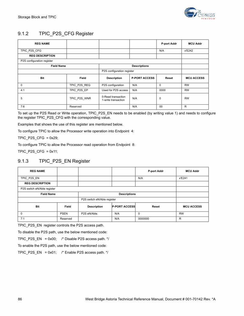
86 West Bridge Astoria Technical Reference Manual, Document # 001-70142 Rev. *A
Storage Block and TPIC
9.1.2 TPIC_P2S_CFG Register
To set up the P2S Read or Write operation, TPIC_P2S_EN needs to be enabled (by writing value 1) and needs to configurethe register TPIC_P2S_CFG with the corresponding value.
Examples that shows the use of this register are mentioned below.
To configure TPIC to allow the Processor write operation into Endpoint 4:
TPIC_P2S_CFG = 0x29;
To configure TPIC to allow the Processor read operation from Endpoint 8:
TPIC_P2S_CFG = 0x11;
9.1.3 TPIC_P2S_EN Register
TPIC_P2S_EN register controls the P2S access path.
To disable the P2S path, use the below mentioned code:
TPIC_P2S_EN = 0x00; /* Disable P2S access path. */
To enable the P2S path, use the below mentioned code:
TPIC_P2S_EN = 0x01; /* Enable P2S access path. */
REG NAME P-port Addr MCU Addr
TPIC_P2S_CFG N/A x'E242
REG DESCRIPTION
P2S configuration register
Field Name Descriptions
P2S configuration register
Bit Field Description P-PORT ACCESS Reset MCU ACCESS
0 TPIC_P2S_REQ P2S configuration N/A 0 RW
4:1 TPIC_P2S_EP Used for P2S access N/A 0000 RW
5 TPIC_P2S_WNR0-Read transaction1-write transaction
N/A 0 RW
7:6 Reserved N/A 00 R
REG NAME P-port Addr MCU Addr
TPIC_P2S_EN N/A x'E241
REG DESCRIPTION
P2S switch eN/Able register
Field Name Descriptions
P2S switch eN/Able register
Bit Field Description P-PORT ACCESS Reset MCU ACCESS
0 PSEN P2S eN/Able. N/A 0 RW
7:1 Reserved N/A 0000000 R

West Bridge Astoria Technical Reference Manual, Document # 001-70142 Rev. *A 87
Storage Block and TPIC
9.1.4 TPIC_INT0_CLR Register
Interrupt from the TPIC is mapped to the INT0 interrupt of the 8051 inside Astoria. The service routine corresponding to thisinterrupt does the enabling of P2S access path by writing one to the TPIC_P2S_EN register if storage is allocated to proces-sor port.
To enable TPIC interrupt:
IE_EX0 = 1; /* Enable TPIC interrupt. */
To clear the TPIC interrupt:
TPIC_INT0_CLR = 1;
9.2 SIB
This block contains the interface logic for the SDIO/MMC/SPI port. Based on various configurations and command interrupts,it generates the commands and accepts response at SD interface. The SDIO Interface Block will be positioned between theSLB and the physical I/Os on the SPort. This block support Full SDIO functionality. This block contains the following interfacefunctions.
■ Configuration & Interrupt Block
■ CRC Modules for command and data
■ SERDES: For converting the 16 bit parallel data to the data width at the interface
■ Data Interface Control: Formatting of incoming/ outgoing data with the start bit, direction, CRC and the end bit according to the configuration.
■ Command Interface Control: Formatting of outgoing command and validating incoming command
■ Interface Clock Control
■ Card Detection through Dat-3. A separate card detect input, if available from the card connector is available through the GPIO [0] input.
■ Interrupt and Read Wait support to enable full SDIO
The Write-Protect input, if available from the card connector on the board, is connected directly to the 8051 for firmware tohandle.
Two instances of this block are present in this device to support the second SD/MMC/CE-ATA port. This second SD/MMC/CE-ATA port pins are multiplexed on the GPIF Interface pins. Card detection for the second SD card is through Dat-3 or GPIO[1] input.
Additional Registers are added in this block to enable the operation of second SD and disable the primary SD during 16-bitGPIF operation. Full SDIO features are enabled through these registers.
REG NAME P-port Addr MCU Addr
TPIC_INT0_CLR N/A x'E243
REG DESCRIPTION
8051 can clear the interrupt from TPIC(INT0) by writing one this register
Field Name Descriptions
Bit Field Description P-PORT ACCESS Reset MCU ACCESS
0 INT0_CLR N/A 0 RW
7:1 Reserved LEP configuration N/A 0000000 R

88 West Bridge Astoria Technical Reference Manual, Document # 001-70142 Rev. *A
Storage Block and TPIC
9.2.1 SIB_READ_WAIT_EN Register
9.2.2 SIB_NAND_CFG Register
SIB can be configured by changing the bit fields of theSIB_NAND_CFG register.
SIB_NAND_CFG register bit fields offer the control of thefollowing:
■ Selection between GPIF or SD
■ If both ports are used for connecting SD cards then to switch between them. This can be done by toggling the SD_SEL bit field.
■ Choosing Ready and Control lines for GPIF
■ Disabling the primary SD for 16-bit GPIF operation.
■ To enable the FULL SDIO functionality for the selected storage port.
Dual SD mode can be enabled by
SIB_NAND_CFG |= 0x01; /* Enable Dual SD */
In dual SD mode, SD card on the first storage port can be selected by
REG NAME P-port Addr MCU Addr
SIB_READ_WAIT_EN N/A x'E22A
REG DESCRIPTION
Field Name Descriptions
Bit Field Description P-PORT ACCESS Reset MCU ACCESS
0 ENEnable Read Wait to SDIO device on DAT[1]
N/A 0 R/W
7:1 Reserved N/A 0000000 R
REG NAME P-port Addr MCU Addr
SIB_NAND_CFG N/A x'E22B
REG DESCRIPTION
Field Name Descriptions
Bit Field DescriptionP-PORT ACCESS
Reset MCU ACCESS
0 NAND_SD_SELUsed for selecting nand/sd device. 0 -> NAND is enabled. 1 -> 2nd SD is enabled.
N/A 0 R/W
1 SD_SEL
Selects SD devices for transac-tion. 0 -> transaction is being for 1st SD. 1 -> transaction is being for 2nd SD
N/A 0 R/W
2 NAND_RB2_ENBEnable 2nd R/B# functionality on RESETOUT pin
N/A 0 R/W
3 NAND_RB3_ENB Enable 3rd R/B# on SSD_CMD N/A 0 R/W
4 NAND_RB4_ENBEnable 4th R/B# functionality on SSD_CLK pin
N/A 0 R/W
5 SD1_DISABLEDisable primary SD port for Multi-ple Nand operation
N/A 0 R/W
6 FULL_SDIO_ENABLE Enable Full SDIO functionality N/A 0 R/W
7 PAD_NANDCFGShows the status of PAD_NANDCFG pin
N/A 0 RW

West Bridge Astoria Technical Reference Manual, Document # 001-70142 Rev. *A 89
Storage Block and TPIC
SIB_NAND_CFG &= ~(0x02); /* Select SD1 */
In dual SD mode, SD card on the second storage port can be selected by
SIB_NAND_CFG |= 0x03; /*select SD2*/
To enable the GPIF mode:
SIB_NAND_CFG |= 0x04;
The second SD block has a reduced set of the SIB_NAND_CFG register. Only bit 6 which enables the full SDIO functionalityis used and all other bits are de-featured.
9.2.3 SIB_MODE_CFG Register
REG NAME P-port Addr MCU Addr
SIB2_NAND_CFG N/A X'E4EB
REG DESCRIPTION
Field Name Descriptions
Bit Field Description P-PORT ACCESS Reset MCU ACCESS
5:0 Reserved Reserved N/A 5'b00000 RW
6 sib2_sdio_irqFor detecting sdio irq for sib2
N/A 1'b0 RW
7 Reserved Reserved N/A 1'b0 R
REG NAME P-port Addr MCU Addr
SIB_MODE_CFG N/A x'E21F
REG DESCRIPTION
Mode Configuration Register
Field Name Descriptions
Mode Configuration Register
Bit Field Description P-PORT ACCESS Reset MCU ACCESS
1:0 MODE
Mode Configuration Register2'b00:reserved2'b01:MMC /MMC+ mode2'b10:SD/SDIO mode2'b11:SPI mode
N/A 10 RW
3:2 DATABUSWIDTH
Data bus width: Not valid in SPI modeFor MMC card2'b00: 1bit2'b01: 4bit2'b10: 8bit2'b11:reservedFor SD/SDIO card2'b00:1bit data width2'b01:4 bit data width2'b10:reserved2'b11:reserved
N/A 01 RW
4 EN_CMD_COMP enable command completion feature N/A 0 RW
5 GCTL_SD_CLK_DISPower saving mode0x0: clock is enabled.0x1: clock is disabled.
N/A 0 RW
6 CARD_BUSY_DETThis bit enables the SD state machine to wait for busy during the first block of data in multi block write
N/A 0 RW
7 STOP_CLOCK_ENThis bit enables SIB to perform detection of overflow and stop the clock to the SD card
N/A 0 RW

90 West Bridge Astoria Technical Reference Manual, Document # 001-70142 Rev. *A
Storage Block and TPIC
Before initializing the SD card, SIB needs to be configured as 1 bit SD mode so that Astoria can talk with any type of SD cardwithout any data width issue.
SIB_MODE_CFG = 0x02; /* Configure as 1 bit SD mode by default. */
In the case of MMC card:
SIB_MODE_CFG = 0x01; /* Configure for 1 bit MMC mode. */
There is a stop clock feature that has been implemented in Astoria which can be enabled by configuring the bit 7 ofSIB_MODE_CFG register. On enabling the clock stop feature if the EPs are full, the clock is stopped preventing further datafrom being received.
SIB_MODE_CFG |= 0x80; //Enable the SD stop clock feature for overflow handling.
In the case of applications where any storage card (SD/MMC) is connected to Astoria, current consumed by Astoria can bereduced by disabling the card clock when that storage card is not being accessed.
To disable the card clock:
SIB_MODE_CFG |= 0x20;
Again clock can be enabled just before accessing that storage card.
To enable the card clock:
SIB_MODE_CFG &= 0xDF;
9.3 GPIF and Slave FIFO
The SIB interface is implemented using both the GPIF and SF interfaces.
9.3.1 Slave FIFO:
If any storage card (SD/MMC/CE-ATA) is connected to storage port, before initializing the card Slave FIFO interface needs tobe set up.
There is a function in the firmware to set the SIB in Slave FIFO mode by writing the IFCONFIG register with 0xA3 value asshown below.
IFCONFIG = 0xA3;/* Enable Slave FIFO mode. */
The below mentioned function is used to initialize the slave FIFO mode.
Void CyAnFwStorSetupSF (void)
{
FLAGOUT0 = 0x00; // FLAGA = PF(sel), FLAGB = FF(sel)
FLAGOUT1 = 0x00; // FLAGC = EF(sel), FLAGD = PF(EP2)
9.3.2 GPIF
There is a function in the firmware to set the SIB in GPIF master mode by writing the IFCONFIG register with 0xCA value asshown below.
IFCONFIG = 0xCA;/* Enable GPIF master mode. */
9.3.2.1 GPIF initialization
GPIF initialization is done as shown below:
Void CyAnFwStorSetupGpif (void)
{
/* Perform GPIF initialization. */

West Bridge Astoria Technical Reference Manual, Document # 001-70142 Rev. *A 91
Storage Block and TPIC
EP2TIL = 0x00; // GPIF transfer from EP2 stops when TC runs out.
EP2GPIFFLAG = 0x01;
EP4TIL = 0x00; // GPIF transfer from EP4 stops when TC runs out.
EP4GPIFFLAG = 0x01;
EP6TIL = 0x00; // GPIF transfer to EP6 stops when TC runs out.
EP6GPIFFLAG = 0x02;
EP8TIL = 0x00; // GPIF transfer to EP8 stops when TC runs out.
EP8GPIFFLAG = 0x02;
ABORT = 0xFF; // Abort past GPIF transactions.
FLOW_STATE = 0x00; // GPIF - Flow mode is not used.
READYCFG = 0xE0; // Use IntRdy and TCXpire.
CTLOUTCFG = 0x00; // CMOS outputs for CTL.
IDLE_CS = 0x00; // GPIF idle state controls.
IDLE_CTLOUT = 0x03; // Only CTL0 and CTL1 are used.
WFSELECT = 0x4E; // Setup waveform order.
READYSTAT = 0x03; // Set the default state of RDY to 1.
/* Copy the GPIF waveforms into the GPIF buffers. */
AUTOPTRSETUP = 0x07; /* Enable both Auto pointers. */
CyAnMemCopy (GPIF_WAVE_DATA, (uint8_t xdata *)glGpifWaveforms,
CYAN_GPIF_DATA_LEN); }

92 West Bridge Astoria Technical Reference Manual, Document # 001-70142 Rev. *A
Storage Block and TPIC
9.4 GPIO
The S-Port also can operate as a GPIO in addition to being a GPIF/SD port. This is a new feature added in Astoria.
/* Tristate the SD card pins after the write, so that we the IO drives can be turned off. */
If only one card is connected to port 0:
P0_RES_MASK_L |= 0x0C;
P0_RSE_ALLOCATE_L = 0x00;
P0_RES_MASK_L &= 0xF3;
If second storage port is also connected to a card:
P0_RES_MASK_L |= 0x03;
P0_RSE_ALLOCATE_L = 0x00;
P0_RES_MASK_L &= 0xFC;
9.5 Reset SIB
Reset SIB in case of CRC or timeout error from the card. A piece of code to do that is mentioned below.
/* Reset the SIB. */
SIB_CNTR_CFG_1 = 0; _nop_ ();
SIB_INTR_IN = 0x20;
CyAnDevDelay1ms ();
REG NAME P-port Addr MCU Addr
P0_RSE_ALLOCATE_L x'98 x'E2A4
REG DESCRIPTION
This register is used for resource allocation for the S-Port.
Field Name Descriptions
Bit Field Description P-PORT ACCESS Reset MCU ACCESS
0 SDIOAVISDIO External Bus Availability Status, 0: Available, 1: Allocated
RW 0 RW
1 SDIOALLO
SDIO External Bus Allocation, 0: Allocated to Astoria (S-Port), 1: Tri-State (allocate to the Proces-sor)
R 1 R
2 NANDAVIGPIF Bus Availability Status, 0: Available, 1: Allocated
RW 1 RW
3 NANDALLO
GPIF bus External Bus Alloca-tion, 0: Allocated to Antioch (S-Port), 1: Tri-State (allocate to the Processor)
R 0 R
4 USBAVIUSB External Bus Availability Semaphore Status, 0: Available, 1: Reserved for future use
RW 0 RW
5 USBALLOUSB External Bus Allocation, 0: Allocated to U-Port, 1: Reserved for future use
R 1 R
6 Reserved(USBTRAVI) USB Transceiver Availability Semaphore
R 0 R
7 Reserved(USBTRALO) USB Transceiver Allocation
R 0 R

West Bridge Astoria Technical Reference Manual, Document # 001-70142 Rev. *A 93
Storage Block and TPIC
9.6 Sending Commands to the SD/MMC Card
For more details about the commands that can be send to SD card, refer to SD card specification version 2.0.
SIB has 8 command registers starting from SIB_CMD_REG_0 to SIB_CMD_REG_7, to send commands to the SD card.
SIB has 17 response registers starting from SIB_RESP_REG_0 to SIB_RESP_REG_16, to store the response data that itgets from the SD card.
SIB_RESP_FMT_0 and SIB_RESP_FMT_1 are used to configure the SIB with the expected number of bits in the responsedata.
SIB_INTR_IN register needs to be updated when 8051 wants to interrupt the SIB. For example, this register needs to be writ-ten in the cases where Astoria needs to send a command or to perform a read/write operation from/to the SD card.
SIB_INTR_OUT register gets updated by the interrupts generated by the SIB when some specific events are done from theSIB side. For example in the cases where a command is sent or a response is received by the SIB.
More details on handling these registers can be found in the Astoria firmware.

94 West Bridge Astoria Technical Reference Manual, Document # 001-70142 Rev. *A
Storage Block and TPIC

West Bridge Astoria Technical Reference Manual, Document # 001-70142 Rev. *A 95
10. General Programmable Interface (GPIF)
The General Programmable Interface (GPIF) is an internal master to Astoria’s endpoint FIFOs. It replaces the external‘Glue’ logic that might otherwise be required to build an interface between Astoria and the outside world.
Astoria’s GPIF is derived from EZ-USB FX2LP. All associated registers are same as that of EZ-USB FX2LP but Astoria doesnot expose the entire signals externally. This chapter only covers the hardware differences between the EZ-USB FX2LP’sGPIF and the West Bridge Astoria’s GPIF. See Chapter 10 of EZ-USB TRM form more details on GPIF Interface and GPIFProgramming.
See GPIF on page 90 of this document for steps on configuring the storage port in GPIF mode.
Note West Bridge Astoria’s GPIF internals are exactly similar to EZ-USB FX2LP’s GPIF but all the pins are not available forexternal interface. The differences are given in this table.
Note Storage Port 0 of Astoria can be configured for SD/MMC, GPIO or GPIF. If 8 bit data bus width mode is used then theStorage Port 1 can be used in GPIO mode or SD/SDIO/MMC mode. If GPIF is configured for 16 bit mode then the StoragePort 1 is not available for other function like GPIO or SD/MMC/SDIO. The Storage Port 1 of West Bridge Astoria cannot beused for GPIF 8 bit mode.
Note Read and Write are from Astoria’s point of view. ‘Read’ waveforms transfer data from the outside world to Astoria;‘Write’ waveforms transfer data from Astoria to the outside world.
Astoria firmware can assign the FIFO read and FIFO write waveforms to any of the four FIFOs, and the GPIF generates theproper strobes and handshake signals to the outside-world interface as data is transferred into or out of that FIFO.
10.1 GPIF Signals
See section 10.1.1 in EZ-USB TRM for details on Typical GPIF Interface and Hardware details. this sections describes theGPIF signal exposed by West Bridge Astoria.
10.1.1 Data Lines
The GPIF Data Bus is a collection of the GPIF_D[15:0] pins.
■ An 8-bit wide GPIF interface uses pins GPIF_D[7:0].
■ A 16 bit-wide GPIF interface uses pins GPIF_D[15:0].
10.1.2 GPIF Address Lines
West Bridge Astoria does not expose address pins externally. It is similar to EZ-USB FX2LP 56 pin package. While using theGPIF designer for building the GPIF Waveform, for West Bridge Astoria, EZ-USB FX2LP 56 pin package must be selected.
Signals FX2LP Astoria
Address lines 9 Not available
Control signals 6 2
External Ready inputs 6 4
Data Lines 8/16 8/16
IFCLK Available Not Available

96 West Bridge Astoria Technical Reference Manual, Document # 001-70142 Rev. *A
General Programmable Interface (GPIF)
10.1.3 GPIF Control Out Signals
West Bridge Astoria brings out only two (GPIF_CTL [1:0]) control signals. Please refer section 10.2.3 of EZ-USB TRM formore details on control signals.
10.1.4 Ready IN Signals
West Bridge Astoria brings out four ready in signals. By default state only GPIF_RDY1 is configured. Other three ready sig-nals GPIF_RDY2, 3 and 4 can be configured using SIB_NAND_CFG register (0xE22B).
Please refer section 10.2.4 of EZ-USB TRM for more details on Ready IN signals.
10.1.5 Interface Clock (IFCLK)
West Bridge Astoria does not bring out IFCLK.
10.1.6 GPIF Designer
The EZ-USB FX2LP GPIF designer tool can be used to build the GPIF waveform by selecting FX2LP 56 pin Package.

West Bridge Astoria Technical Reference Manual, Document # 001-70142 Rev. *A 97
11. Coprocessor Interface Logic
The processor port interface allows access to the end point buffer memory blocks and configuration registers. Randomaccess is allowed to the configuration registers. The P-port data bus can be configured to be in Little Endian or Big Endianmode through the P-port Interface Configuration Register. To reduce port address pin count, the end point buffers can beindividually addressed, but their contents are accessed in burst (FIFO) mode.
11.1 Operational Modes
The P-port can be configured to support different processor interfaces by setting up the TEST[2:0], PA[3:2], and the VMTYPEfield in the P-port Interface Configuration Register (CY_AN_MEM_P0_VM_SET). Table 11-2 and Table 11-3 on page 98 listall interface configuration options of the P-port in normal operation.
The P-port can be configured in one of these five modes:
■ Pseudo CRAM Non Multiplexing Mode
In this mode, TEST[2:0] is set to b'000 and default value in the VMTYPE field of the CY_AN_MEM_P0_VM_SET register.
□ Address and Data buses non multiplexing Asynchronous mode
□ Address and Data buses non multiplexing Synchronous mode (ADV# is required to pull low in this mode)
■ Pseudo CRAM Multiplexing Mode
In this mode, TEST[2:0] is set to b'010, PA[7] and PA[3:2] are set to b'101 and the default value in the VMTYPE field of the CY_AN_MEM_P0_VM_SET register.
□ Address and Data buses multiplexing Asynchronous mode
□ Address and Data buses multiplexing Synchronous mode
■ SRAM Non Multiplexing Mode
In this mode, ADV# is required to pull low, TEST[2:0] is set to b'000, and the value in the VMTYPE field of the CY_AN_MEM_P0_VM_SET register must be set to b'111.
□ Address and Data buses non multiplexing Asynchronous SRAM mode
■ Pseudo NAND (PNAND) Mode (8 bit and 16 bit)
In this mode, TEST[2:0] is set to b'010, and PA[3:2] is set to b'00. PA[7] is used to select the Astoria behavior: Small or Big Block device.
■ PSPI and PI2C Mode
In this mode, TEST[2:0] is set to b'010, and PA[7] and PA[3:2] is set to b'110.
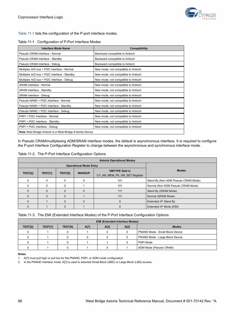
98 West Bridge Astoria Technical Reference Manual, Document # 001-70142 Rev. *A
Coprocessor Interface Logic
Table 11-1 lists the configuration of the P-port interface modes.
In Pseudo CRAM/multiplexing ADM/SRAM interface modes, the default is asynchronous interface. It is required to configurethe P-port Interface Configuration Register to change between the asynchronous and synchronous interface mode.
Notes
1. A[7] must pull high or pull low for the PNAND, PSPI, or ADM mode configuration.
2. In the PNAND interface mode, A[7] is used to selected Small Block (SBD) or Large Block (LBD) access.
Table 11-1. Configuration of P-Port Interface Modes
Interface Mode Name Compatibility
Pseudo CRAM interface - Normal Backward compatible to Antioch
Pseudo CRAM interface - Standby Backward compatible to Antioch
Pseudo CRAM interface - Debug Backward compatible to Antioch
Multiplex A/D bus + PI2C interface - Normal New mode, not compatible to Antioch
Multiplex A/D bus + PI2C interface - Standby New mode, not compatible to Antioch
Multiplex A/D bus + PI2C interface - Debug New mode, not compatible to Antioch
SRAM interface - Normal New mode, not compatible to Antioch
SRAM interface - Standby New mode, not compatible to Antioch
SRAM interface - Debug New mode, not compatible to Antioch
Pseudo NAND + PI2C Interface - Normal New mode, not compatible to Antioch
Pseudo NAND + PI2C Interface - Standby New mode, not compatible to Antioch
Pseudo NAND + PI2C Interface - Debug New mode, not compatible to Antioch
PSPI + PI2C Interface - Normal New mode, not compatible to Antioch
PSPI + PI2C Interface - Standby New mode, not compatible to Antioch
PSPI + PI2C Interface - Debug New mode, not compatible to Antioch
Note West Bridge Antioch is a West Bridge A-family Device
Table 11-2. The P-Port Interface Configuration Options
Astoria Operational Modes
Operational Mode Entry
ModesTEST[2] TEST[1] TEST[0] WAKEUP
VMTYPE field in
CY_AN_MEM_P0_VM_SET Register
0 0 0 0 101 Stand By (Non ADM Pseudo CRAM Mode)
0 0 0 1 101 Normal (Non ADM Pseudo CRAM Mode)
0 0 0 0 111 Stand By (SRAM Mode)
0 0 0 1 111 Normal (SRAM Mode)
0 1 0 0 X Extended I/F Stand By
0 1 0 1 X Extended I/F Mode (EIM)
Table 11-3. The EMI (Extended Interface Modes) of the P-Port Interface Configuration Options
EIM (Extended Interface Modes)
TEST[2] TEST[1] TEST[0] A[7] A[3] A[2] Modes
0 1 0 1 0 0 PNAND Mode - Small Block Device
0 1 0 0 0 0 PNAND Mode - Large Block Device
0 1 0 1 1 0 PSPI Mode
0 1 0 1 0 1 ADM Mode (Pseudo CRAM)

West Bridge Astoria Technical Reference Manual, Document # 001-70142 Rev. *A 99
Coprocessor Interface Logic
11.1.1 Address and Data Buses Non Multiplexing Asynchronous Pseudo CRAM Mode
This is the default mode at power up. During this mode the CLK input is held low. This mode requires the use of the ADV# pin(address valid pin). The address inputs are latched when ADV# is HIGH. When ADV# is LOW, the address latch is transpar-ent, whereby any change in Address is reflected to internal access logic. CE# needs to be asserted at least tCVS before therising edge of ADV# and must remain asserted throughout the entire operation.
This mode uses the industry-standard SRAM control bus (CE#, OE#, WE#). READ operations are initiated by bringing CE#and OE# LOW while keeping WE# HIGH. Valid data is driven out of the DQ bus after the specified access time has elapsed.
WRITE operations occur when CE# and WE# are driven LOW. During asynchronous WRITE operations, the OE# level is a“Don't Care,” and WE# overrides OE#. The data to be written is latched on the rising edge of CE# or WE# (whichever occursfirst).
The most significant address bit, A[7], determines whether configuration registers or endpoint buffer memory is accessed.When the configuration memory is selected by asserting address bit A[7], the address bus points to an exact location of aconfiguration register. When A[7] is deasserted, A[6:0] provides the address of the endpoint buffer being accessed. Accessfrom within the selected endpoint buffer is performed through internal address counters.
When the endpoint buffers are selected, each address change starts access at the top of the buffers. The DMA engine in theexternal processor is expected to maintain the correct access count.
In this mode the P-port interface works up to the equivalent of 33 MHz providing a port bandwidth up to 66 MB per second.
11.1.2 Address and Data Buses Non Multiplexing Synchronous Mode
Similar to the asynchronous mode, the synchronous mode can be used to access both the configuration registers and theendpoint buffers. Address bit A[7] determines whether the configuration registers or the endpoint buffers are accessed. Unlikethe asynchronous mode, all address, chip enable, and read/write enable inputs are asserted or deasserted with respect to theCLK input. These control inputs have to meet their respective setup and hold time constraints. Valid read data is placed on theDQ bus after the specified clock-to-output access time. The DQ bus tristates after tCKHZ following a CLK rising edge withCE# deasserted. OE# is “don't care” during write or deselect cycles. ADV# is required to pull low in this mode.
When the endpoint buffers are selected, each address change starts access at the top of the buffers. The DMA engine in theexternal processor is expected to maintain the correct access count.
In this mode the P-port interface works up to the equivalent of 33 MHz providing a port bandwidth up to 66 MB per second.
11.1.3 Address and Data Buses Multiplexing Asynchronous Pseudo CRAM Mode
The address and data multiplexing (ADM) allows address and data signals to share the same bus (DQ). During this mode theCLK input is kept low and A[7:0] pins are ignored. Similar to non multiplexing mode, ADV#, WE# and CE# are used to per-form the read/write operation. Address signals are first applied to the DQ bus along with CE# LOW. The addresses areloaded from the DQ bus in response to rising edge of the ADV# signal and values of DQ8-DQ15 signals are ignored. It is nec-essary to meet the setup (tAVS) and hold (tAVH) times given in Table 11-8 on page 116 with valid address information to prop-erly latch in the addresses.
After the address signals are successfully latched in, a read operation is issued where WE# stays HIGH. The DQ busbecomes tri-stated after the address/signal on the DQ bus meets tAVH. The read data is driven on the DQ bus tOE after OE#is asserted LOW and held until tOHZ or tHZ after the rising edge of OE# or CE#, whichever comes first.
A write operation is issued when WE# is asserted LOW after the address is latched in. OE# is a don't care during write oper-ations. The write data is applied to the DQ bus immediately after the address signal on the DQ bus meets the hold time(tAVH). Write data is written with the rising edge of either WE# or CE#, whichever comes first, and meets data setup (tSD)and hold (tHD) times.
11.1.4 Address and Data Buses Multiplexing Synchronous Pseudo CRAM Mode
Similar to ADM asynchronous mode, the ADM synchronous mode can be used to access both the configuration registers andthe endpoint buffers. During this mode, OE# input is asynchronous. The DQ bus, ADV#, CE#, and WE# inputs are assertedor deasserted with respect to the rising edge of CLK. These control inputs have to meet their respective setup and hold time.

100 West Bridge Astoria Technical Reference Manual, Document # 001-70142 Rev. *A
Coprocessor Interface Logic
For both read and write operations, the address is latched in from the DQ bus at the rising edge of CLK with ADV# low. For aread operation, the DQ bus is tri-stated after the address signals are latched in and meet hold time tHD. After the latencywhen addresses are latched in, valid read data is driven on the DQ bus after the specified clock-to-output access time. TheDQ bus is tri-stated tCKHZ after the rising edge of CLK with CE# high. For write operation, OE# is “don't care”. Data is avail-able immediately after the address signals are latched in and meet hold time tHD. At the following CLK data is written. Afterthe data meets hold time tOH, the next address or data can be applied to DQ bus.
In addition, both burst read and burst write are supported. After the address is latched in from the DQ bus, data can be burstfor read or write for every clock cycle and up to the size of the endpoint buffer as long as the input signals remain unchangedin read or write mode. During burst mode the latched-in address remains unchanged to ensure the burst read/write operationis from/to the same endpoint buffer.
Similar to the non multiplexing mode, during the address latch-in the value of the most significant address bit (DQ[7] in ADM)selects access to either the endpoint buffer or configuration register. When an endpoint buffer is selected, each addresschange starts access at the top of the buffers. The DMA engine in the external processor is expected to maintain the correctaccess count. If the number of accesses on a buffer exceeds the buffer size, the internal burst counter wraps.
In this mode, the processor interface port can work at clock speeds up to 33 MHz providing port bandwidth up to 66 MB persecond.
11.1.5 Address and Data Buses Non Multiplexing Asynchronous SRAM Mode
This is a standard asynchronous SRAM interface. ADV# is required to pull low in this mode. This interface is used to accessboth the configuration registers and the endpoint buffers of Astoria. ADV# is tied LOW externally in this mode. Registeraccesses are asynchronous single-reads, while endpoint buffer accesses are similar to asynchronous page mode accesses.Register accesses are performed in the same method as the non multiplexed asynchronous Pseudo CRAM interface. DuringDMA transaction to or from an endpoint buffer, A[7] is maintained at “0”, while A[6:0] toggles as in a page mode access. Morespecifics of the endpoint access in this mode are:
■ Endpoint Read
□ Address Transition Controlled
• During an endpoint access, the address during the first cycle of access must be the address of the endpoint being accessed (0x02 for endpoint 2, and so on).
• Subsequent accesses require the address to be changed, which is consistent with the burst behavior of the most processors. This toggle of the address is detected by the Address Transition Detect (ATD) circuit to advance the FIFO pointer internally.
• The subsequent addresses is not decoded if address bit A[7] changes (requires to be held at '0'). All data is trans-ferred to or from the endpoint that was addressed in the first cycle.
• An endpoint transaction can be made in multiple burst transfers, with register accesses in between. A burst transfer is terminated when CE# is deasserted. The register access is determined by change of address bit A[7] to 1'b1.
• On resumption of an endpoint burst transfer after register accesses, it is not required that the endpoint address be reasserted on the first cycle of the burst (the processor must return to the same endpoint unless it was terminated).
• An endpoint transaction is terminated when the DMAVAL field for that endpoint is cleared by a write to the Endpoint Buffer DMA register.

West Bridge Astoria Technical Reference Manual, Document # 001-70142 Rev. *A 101
Coprocessor Interface Logic
■ Endpoint Write
□ WE# Controlled
An endpoint write transaction may be facilitated by toggling the WE# signal while maintaining CE# LOW throughout and also keeping the address constant with the particular endpoint address.
□ CE# Controlled
An endpoint write transaction may be facilitated by toggling the CE# signal while maintaining WE# LOW throughout and also keeping the address constant with the particular endpoint address.
Note This is not a description of the pins of the entire P-port interface; it represents only the asynchronous SRAM interface pins.
11.1.6 Pseudo NAND (PNAND) Mode
Figure 11-1. Astoria's Pnand Interface Connected to Processor's Nand Flash Interface
Astoria supports an interface similar to a NAND interface on the P-port (Pseudo NAND interface or Pnand interface). Thisinterface allows connecting Astoria to the processor's NAND flash interface. The processor can load its image from the NANDflash, which is connected to the S-port, or exchange data with the USB-host connected to Astoria's U-port, and access stor-age devices on Astoria's S-port.
In the PNAND interface mode, the maximum speed of the P-port to support the random access with Column Address Change(CASDO and CASDI) commands on endpoint buffers is 30 MHz (beyond 30 MHz, the P-port does not support the randomaccess with Column Address Change commands on endpoint buffers). However, the maximum speed of P-port to support therandom access with Column Address Change (CASDO and CASDI) commands on the P-port registers is 33 MHz.
In PNAND interface mode, because the R/B# pin is a push-pull (not a open-drain), it does not require external pull up for theR/B#. This is shown in the following figure.
Table 11-4. Asynchronous SRAM Interface Signals
Pin Name IO Signal Description
CE# I Chip Enable
WE# I Write Enable
OE# I Output Enable
A[7:0] I Address Bus
DQ[15:0] IO Data Bus
AstoriaProcessor
S-Port
U-P
ort
Pnand interface
Nand
Processor's Nand Flash port
Astoria SW's P-port configured for
Pnand Interface
USB Host
Handheld Device
SD/ MMC/
CE-ATA

102 West Bridge Astoria Technical Reference Manual, Document # 001-70142 Rev. *A
Coprocessor Interface Logic
Figure 11-2. R/B# Pull up Connection in PNAND Mode
Table 11-5. Astoria P-port Pins Mapped to Pnand Interface Pins
Astoria P-Port Pin Name IO Aliased Pnand Pin Name Function Comments
CLK I Unused
CE# I CS# Chip Select
A0 I CLE Command Latch
A1 IO R/B# Read/Busy
A[3:2] I Unused
A4 I WP Write Protect
A[6:5] I Unused
A[7] I SBDnLBD Device type (SBD/LBD)
DQ[15:0] IO IO[15:0] Data bus
ADV# I ALE Address Latch Enable
OE# I RE# Read Enable
WE# I WE# Write Enable
INT# O INT# Interrupt Request
DRQ# O DRQ# DMA Request
DACK# I DACK# DMA Acknowledgement
Table 11-6. Pnand Pin Descriptions
Pin Descriptions
CS# Chip Select
Chip select pin is used to select Astoria's P-port. When PN_CS# is High, device does not go into Standby state. WAKEUP pin must be used to place Astoria in Standby.
CLE Command Latch Enable PN_CLE along with PN_ALE signal is used to distinguish between command, address and data on PN_IO pins.
R/B#Ready The PN_Ready signal when High, indicates that Astoria has data ready for reading in endpoint buffer(s) and/or Astoria has an empty buf-fer(s) ready for writing to endpoints. The processor is allowed to access Astoria's registers irrespective of the state of PN_Ready pin. Astoria's endpoint buffers may be accessed only when Astoria's PN_Ready pin is asserted.
WP# Write Protect
SBDnLBD Selects Nand flash interface type; Small Block Device (SBD) type (1) or Large Block Device (LBD) type (0).
IO[15:0]
PN_IO[7:0] pins are used to transfer command and address to Astoria's P-port.
PN_IO[7:0] pins are used to transfer data to and from Astoria's P-port when Pnand-interface width is 8-bits.
PN_IO[15:0] pins are used to transfer data to and from Astoria's P-port when Pnand-interface width is 16-bits.
ALE This signal along with CLE is used to differentiate between command, address and data on PN_IO pins.
RE# Read Enable
The RE# input is the serial data-out control, and when active drives the data onto the IO bus. Data is valid tREA after the falling edge of RE# which also increments the internal column address counter by one.
WE# Write Enable
Command, Address and Data on PN_IO pins are latched on the rising edge of WE# pin.
INT# Indicates that an interrupt event has occurred. The Processor must read the P-port Interrupt register to determine the cause of the interrupt.
Astoria
R/B#
Processor
PNAND InterfaceNAND Interface
R/B#

West Bridge Astoria Technical Reference Manual, Document # 001-70142 Rev. *A 103
Coprocessor Interface Logic
11.1.6.1 Pseudo NAND (PNAND) Configuration Registers Summary
The following tables summarize the configuration and control registers for PNAND interface.
PNAND Status Mask Register
This register is used to mask the INT and DRQ status bit.
Bit 5: DRQ_Mask. Mask bit for DRQ Status bit. When DRQ_Mask is disabled, DRQ status is reported as zero in response toa Read Status command.
0: Disable DRQ Status bit
1: Enable DRQ Status bit
Bit 4: INT_Mask. Mask Interrupt Status bit. When INT_Mask is disabled, INT status is reported as zero in response to aRead Status command.
0:Disable Interrupt Status bit
1:Enable Interrupt Status bit
Reserved bits are grayed out.
PNAND Interface Configuration Register
Bit 9: FORCE_EP2RSM. FORCE_EP2RSM forces REG_READY_MASK to enable EP2 endpoint status when page-readand page-program nand commands are issued to logical nand address space. Block erase and Reset commands alwayscause the REG_READY_MASK to be forced to enable EP2 endpoint status. This configuration bit is relevant only whenENABLE_LNA is set to '1'.
0: Disable REG_READY_MASK EP2 status
1: Enable REG_READY_MASK EP2 status
Bit 8: EN_LNA. This bit enables Logical Nand Address space. This mode reserves endpoint EP2 for logical nand emulation.Firmware must allocate appropriate buffers to EP2 for logical nand emulation.
0: PNAND Interface Mode
1: Logical NAND Emulation Mode
Bit 7:6: EPA_BIT_POS. This field specifies the lsb position of the 5-bit EPA field on the row address byte.
00: bit 0 (Default value on hardware reset)
01: bit 1
10: bit 2
11: bit 3
Address Name Bit 7 Bit 6 Bit 5 Bit 4 Bit 3 Bit 2 Bit 1 Bit 0 Access : Reset
x'D9 PNAND_STATUS_MASK
DRQ_Mask INT_Mask RW : 0
Bit 15 Bit 14 Bit 13 Bit 12 Bit 11 Bit 10 Bit 9 Bit Access : Reset
R : 0
Address Name Bit 7 Bit 6 Bit 5 Bit 4 Bit 3 Bit 2 Bit 1 Bit 0 Access : Reset
x'DA REG_PNAND_CFG
EPA_BIT_POS EPA_BYTE_POS RA_COUNT SBDnLBD IOWIDTH RW : 0
Bit 15 Bit 14 Bit 13 Bit 12 Bit 11 Bit 10 Bit 9 Bit 8 Access : Reset
FORCE_EP2RSM EN_LNA RW : 0

104 West Bridge Astoria Technical Reference Manual, Document # 001-70142 Rev. *A
Coprocessor Interface Logic
Bit 5:4: EPA_BYTE_POS. This field specifies the row address cycle where the endpoint buffer address field is located. Thisis applicable for both small and large block nand devices emulation.
00: First row address cycle (Default value on hardware reset)
01: Second row address cycle
10: Third Row address cycle
11: Fourth row address cycle
Bit 3:2: RA_COUNT. This value determines specifies the number of row-address bytes to be specified in page-read, page-program and block erase commands for small and large block devices.
00: 3 cycles (Default value on hardware reset)
01: 4 cycles
10: Reserved
11: Reserved
Bit 1: SBDnLBD. In Small block device mode, the second command cycle for Page-read command is not expected. AfterRA_COUNT row-address cycles are received the ready-status bit is cleared for the corresponding endpoint.
0: Large block device mode
1: Small block device mode
Bit 0: IOWIDTH. In Pnand configuration, the P-port comes up on hardware reset with data-bus width of 8-bits. Address andcommands are transferred on the lower 8-pins irrespective of IOWIDTH configuration.
0: 8-bit interface (Default value on hardware reset)
1: 16-bit interface
PNAND Ready Status Register
The REG_READY register indicates if data is ready for reading or if free buffer is ready for write operation.
Bit 15: EP15RS. Endpoint 15 Ready Status
0: Endpoint 15 Busy
1: Endpoint 15 Ready
Bit 14: EP14RS. Endpoint 14 Ready Status
0: Endpoint 14 Busy
1: Endpoint 14 Ready
Bit 13: EP13RS. Endpoint 13 Ready Status
0: Endpoint 13 Busy
1: Endpoint 13 Ready
Address Name Bit 7 Bit 6 Bit 5 Bit 4 Bit 3 Bit 2 Bit 1 Bit 0 Access : Reset
x'DB REG_READY
EP7RS EP6RS EP5RS EP4RS EP3RS EP2RS R : 0
Bit 15 Bit 14 Bit 13 Bit 12 Bit 11 Bit 10 Bit 9 Bit 8 Access : Reset
EP15RS EP14RS EP13RS EP12RS EP11RS EP10RS EP9RS EP8RS R : 0
West Bridge Astoria Technical Reference Manual, Document # 001-70142 Rev. *A 105
Coprocessor Interface Logic
Bit 12: EP12RS. Endpoint 12 Ready Status
0: Endpoint 12 Busy
1: Endpoint 12 Ready
Bit 11: EP11RS. Endpoint 11 Ready Status
0: Endpoint 11 Busy
1: Endpoint 11 Ready
Bit 10: EP10RS. Endpoint 10 Ready Status
0: Endpoint 10 Busy
1: Endpoint 10 Ready
Bit 9: EP9RS. Endpoint 9 Ready Status
0: Endpoint 9 Busy
1: Endpoint 9 Ready
Bit 8: EP8RS. Endpoint 8 Ready Status
0: Endpoint 8 Busy
1: Endpoint 8 Ready
Bit 7: EP7RS. Endpoint 7 Ready Status
0: Endpoint 7 Busy
1: Endpoint 7 Ready
Bit 6: EP6RS. Endpoint 6 Ready Status
0: Endpoint 6 Busy
1: Endpoint 6 Ready
Bit 5: EP5RS. Endpoint 5 Ready Status
0: Endpoint 5 Busy
1: Endpoint 5 Ready
Bit 4: EP4RS. Endpoint 4 Ready Status
0: Endpoint 4 Busy
1: Endpoint 4 Ready
Bit 3: EP3RS. Endpoint 3 Ready Status
0: Endpoint 3 Busy
1: Endpoint 3 Ready
Bit 2: EP2RS. Endpoint 2 Ready Status
0: Endpoint 2 Busy
1: Endpoint 2 Ready

106 West Bridge Astoria Technical Reference Manual, Document # 001-70142 Rev. *A
Coprocessor Interface Logic
PNAND Ready Status Mask Register
The REG_READY_MASK register along with REG_READY register determines the state of PN_RB# output signal.
Bit 15: EP15RSM. Endpoint 15 Ready Status Mask
0: Disable Endpoint 15 Ready Status
1: Enable Endpoint 15 Ready Status
Bit 14: EP14RSM. Endpoint 14 Ready Status Mask
0: Disable Endpoint 14 Ready Status
1: Enable Endpoint 14 Ready Status
Bit 13: EP13RSM. Endpoint 13 Ready Status Mask
0: Disable Endpoint 13 Ready Status
1: Enable Endpoint 13 Ready Status
Bit 12: EP12RSM. Endpoint 12 Ready Status Mask
0: Disable Endpoint 12 Ready Status
1: Enable Endpoint 12 Ready Status
Bit 11: EP11RSM. Endpoint 11 Ready Status Mask
0: Disable Endpoint 11 Ready Status
1: Enable Endpoint 11 Ready Status
Bit 10: EP10RSM. Endpoint 10 Ready Status Mask
0: Disable Endpoint 10 Ready Status
1: Enable Endpoint 10 Ready Status
Bit 9: EP9RSM. Endpoint 9 Ready Status Mask
0: Disable Endpoint 9 Ready Status
1: Enable Endpoint 9 Ready Status
Bit 8: EP8RSM. Endpoint 8 Ready Status Mask
0: Disable Endpoint 8 Ready Status
1: Enable Endpoint 8 Ready Status
Bit 7: EP7RSM. Endpoint 7 Ready Status Mask
0: Disable Endpoint 7 Ready Status
1: Enable Endpoint 7 Ready Status
Address Name Bit 7 Bit 6 Bit 5 Bit 4 Bit 3 Bit 2 Bit 1 Bit 0 Access : Reset
x'DC REG_READY_MASK
EP7RSM EP6RSM EP5RSM EP4RSM EP3RSM EP2RSM RW : 0
Bit 15 Bit 14 Bit 13 Bit 12 Bit 11 Bit 10 Bit 9 Bit 8 Access : Reset
EP15RSM EP14RSM EP13RSM EP12RSM EP11RSM EP10RSM EP9RSM EP8RSM RW : 0

West Bridge Astoria Technical Reference Manual, Document # 001-70142 Rev. *A 107
Coprocessor Interface Logic
Bit 6: EP6RSM. Endpoint 6 Ready Status Mask
0: Disable Endpoint 6 Ready Status
1: Enable Endpoint 6 Ready Status
Bit 5: EP5RSM. Endpoint 5 Ready Status Mask
0: Disable Endpoint 5 Ready Status
1: Enable Endpoint 5 Ready Status
Bit 4: EP4RSM. Endpoint 4 Ready Status Mask
0: Disable Endpoint 4 Ready Status
1: Enable Endpoint 4 Ready Status
Bit 3: EP3RSM. Endpoint 3 Ready Status Mask
0: Disable Endpoint 3 Ready Status
1: Enable Endpoint 3 Ready Status
Bit 2: EP2RSM. Endpoint 2 Ready Status Mask
0: Disable Endpoint 2 Ready Status
1: Enable Endpoint 2 Ready Status
PNAND ROW Address Mask0 Register
This register is used to mask the ROW address byte 1 and byte 0.
Bit 15:8: RAB1. Holds the ROW address mask for ROW address Byte 1.
Bit 7:0: RAB0. Holds the ROW address mask for ROW address Byte 0.
PNAND ROW Address Mask1 Register
This register is used to mask the ROW address byte 3 and byte 2.
Bit 15:8: RAB3. Holds the ROW address mask for ROW address Byte 3.
Bit 7:0: RAB2. Holds the ROW address mask for ROW address Byte 2
Address Name Bit 7 Bit 6 Bit 5 Bit 4 Bit 3 Bit 2 Bit 1 Bit 0 Access : Reset
x'DD PNAND_RA_MASK0_REG
RAB0 RW : 0
Bit 15 Bit 14 Bit 13 Bit 12 Bit 11 Bit 10 Bit 9 Bit 8 Access : Reset
RAB1 RW : 0
Address Name Bit 7 Bit 6 Bit 5 Bit 4 Bit 3 Bit 2 Bit 1 Bit 0 Access : Reset
x'DE PNAND_RA_MASK1_REG
RAB2 RW : 0
Bit 15 Bit 14 Bit 13 Bit 12 Bit 11 Bit 10 Bit 9 Bit 8 Access : Reset
RAB3 RW : 0

108 West Bridge Astoria Technical Reference Manual, Document # 001-70142 Rev. *A
Coprocessor Interface Logic
PNAND ROW Address Value0 Register
This register is used to hold for ROW address byte 1 and byte 0.
Bit 15:8: RAVB0. Holds value for ROW address Byte 1
Bit 7:0: RAVB1. Holds value for ROW address Byte 0
PNAND ROW Address Value1 Register
This register is used to hold for ROW address byte 3 and byte 2.
Bit 15:8: RAVB0. Holds value for ROW address Byte 3.
Bit 7:0: RAVB1. Holds value for ROW address Byte 2.
PNAND Alternate Read Register
Two alternate first command cycle values for page-read command are programmed in this register. These alternate commandcodes are valid (that is, recognized by hardware) only if corresponding alternate-command valid-bit is set in
REG_ALT_CMDVAL register. This is applicable for large block devices only.
Bit 15:8: ARD2. Holds second Alternate first command cycle value for page-read command.
Bit 7:0: ARD1. Holds first Alternate first command cycle value for page-read command.
PNAND Alternate Program Register
Two alternate first command cycle values for page-program command are programmed in this register. These alternate com-mand codes are valid (that is, recognized by hardware) only if corresponding alternate-command valid-bit is set in
REG_ALT_CMDVAL register. This is applicable for large block devices only.
Bit 15:8: APROG2. Holds second Alternate first command cycle value for page-program command.
Bit 7:0: APROG1. Holds first Alternate first command cycle value for page-program command.
Address Name Bit 7 Bit 6 Bit 5 Bit 4 Bit 3 Bit 2 Bit 1 Bit 0 Access : Reset
x'DF PNAND_RA_VALUE0_REG
RAVB0 RW : 0
Bit 15 Bit 14 Bit 13 Bit 12 Bit 11 Bit 10 Bit 9 Bit 8 Access : Reset
RAVB1 RW : 0
Address Name Bit 7 Bit 6 Bit 5 Bit 4 Bit 3 Bit 2 Bit 1 Bit 0 Access : Reset
x'E0 PNAND_RA_VALUE1_REG
RAVB0 RW : 0
Bit 15 Bit 14 Bit 13 Bit 12 Bit 11 Bit 10 Bit 9 Bit 8 Access : Reset
RAVB1 RW : 0
Address Name Bit 7 Bit 6 Bit 5 Bit 4 Bit 3 Bit 2 Bit 1 Bit 0 Access : Reset
x'E1 PNAND_ALT_READ_REG
ARD1 RW : 0
Bit 15 Bit 14 Bit 13 Bit 12 Bit 11 Bit 10 Bit 9 Bit 8 Access : Reset
ARD2 RW : 0
Address Name Bit 7 Bit 6 Bit 5 Bit 4 Bit 3 Bit 2 Bit 1 Bit 0 Access : Reset
x'E2 PNAND_ALT_PROG_REG
APROG1 RW : 0
Bit 15 Bit 14 Bit 13 Bit 12 Bit 11 Bit 10 Bit 9 Bit 8 Access : Reset
APROG2 RW : 0

West Bridge Astoria Technical Reference Manual, Document # 001-70142 Rev. *A 109
Coprocessor Interface Logic
11.1.7 PI2C and PSPI Interface
11.1.7.1 PI2C Mode (Available on ADM, PNAND, and PSPI Modes)
A brief description of the PI2C Mode functionality is detailed here. For more details, refer chapter 13 of the EZ-USB TRM.
The PI2C bus controller uses the SCL (Serial Clock) and SDA (Serial Data) pins, and performs two functions:
■ General purpose interfacing to PI2C peripherals
■ Boot loading from a serial EEPROM
The bus frequency defaults to approximately 100 kHz for compatibility, and it can be configured to run at 400 kHz for devicesthat support the higher speed.
When Astoria is taken out of reset, it checks for the presence of an EEPROM on the PI2C bus. If an EEPROM is detected, theloader reads the first EEPROM byte to determine how to enumerate.
The functionality in Astoria is supported by the following method:
If an EEPROM containing firmware is attached to the PI2C bus, the firmware is automatically loaded from the EEPROM intothe program RAM. The CPU is then taken out of reset to execute this boot-loaded code. In this case, the VID/PID/DID valuesare encapsulated in the firmware The EEPROM must contain the value 0xC2 in its first byte to indicate this mode to Astoria,so this mode is called a “C2 Load”.
11.1.7.2 PSPI Mode
The PSPI module allows a full duplex, synchronous, serial communication between the processor and Astoria. The interfacesignal names and function are:
■ MISO - Master In, Slave Out data line
■ MOSI - Master Out, Slave In data line
■ SCK - Serial Clock
■ SS - Slave Select, active low
Data is transferred by means of an 8-bit shift register, and so it must be noted that the basic unit of data for the PSPI interfaceis 8 bits.
The following figure gives an overview of the connections and functions of the interface. There are configuration registerswhich are typically used to control various aspects of the operation, but these are not included in the figure for clarity.
Figure 11-3. Full Duplex Master Slave PSPI Configuration
The typical operation of the PSPI interface follows:
■ The Astoria PSPI interface in P-port is slave mode.
■ The maximum operating frequency of the PSPI interface is 26 MHz.
SHIFT REGISTER
SHIFT REGISTER
BAUD RATE GENERATOR
MISO
MOSI
SCK
SS
MISO
MOSI
SCK
SS
MASTER DEVICE SLAVE DEVICE

110 West Bridge Astoria Technical Reference Manual, Document # 001-70142 Rev. *A
Coprocessor Interface Logic
■ The Astoria PSPI interface also supports a custom designed protocol for interaction with the Astoria P-port EP buffers and registers. This 4-byte “Header” based scheme allows specifying the source/destination EP or register address along with the size of the data transfer. This scheme provides a much more efficient method of transfer of larger data payloads, therefore meeting the throughput requirements of the application.
■ Astoria in P-port can be programmed as sync or async mode. It must be noted that the PSPI interface does not operate when the P-port is configured as a synchronous interface.
PSPI Protocol
The PSPI protocol uses header information at the start of each transaction to determine the following:
■ Direction of data transfer (that is, whether the user is reading from or writing to Astoria).
■ Number of data bytes to be transferred.
■ Source or destination address of data being transferred.
The following assumptions are made:
■ Direction can be indicated by a single bit (for example, 1 = write, 0 = read).
■ Count is given a nominal max byte count of 2^13, that is, 8K bytes.
■ A 16-bit address is used.
■ P-port registers are 16-bit and it is assumed that the basic unit of data is 16-bit also.
This leads to the header scheme shown in the following figure.
Figure 11-4. Header Scheme for Use with Astoria - Processor Protocol over PSPI
1. Typical Operation
A typical register access in the PSPI interface:
a. Header information is compiled in the following method: specify register address to be read or written to; R#/W set to match operation; Count set to 2 (2 bytes per register access)
b. Send the Header.
c. If writing to the register, follow the header with the data to be written.
d. If reading the register, then the register contents are the 2 bytes immediately following the header.
A typical EP access in the PSPI interface:
e. Header Address must be specified as the EP address to be read or written to.
f. Header R#/W must be set to match the desired operation.
g. Header Count must be set to match the number of bytes to be transferred.
h. Send the Header.
i. If writing to the EP, then follow the header with the data to be written.
j. If reading the EP, then the EP contents are the bytes immediately following the header.
2. Endian Control
Endian configuration remains under the control of the P-port register (P0_ENDIAN_L/H). No byte swapping is performed within the PSPI block. Data is deserialized as shown in Figure 11-5.
DATAn[7:0] DATA0[7:0] COUNT[7:0] COUNT[14:8] R/W# ADDR_L[7:0] ADDR_H[7:0]
BYTE0BYTE1BYTE2BYTE3DATA PACKET
HEADER INFORMATION

West Bridge Astoria Technical Reference Manual, Document # 001-70142 Rev. *A 111
Coprocessor Interface Logic
Figure 11-5. Endian Control Using PSPI Interface
3. Echo Sequence
In the event that the processor and PSPI interface fall out of sync either through user error1 or some other event, then a mechanism to “retrain” the PSPI interface is provided. Astoria provides an Echo Sequence Scheme which operates in the following method:
a. If the special Echo Sequence Character is captured as Header Byte 1, then the Astoria PSPI module passes four bytes of the same character back to the Processor. Astoria immediately returns to wait for new Header information.
b. The Echo Character is programmable through the SPI_ECHOCHAR register. The reset value of this register is 07 hex.
c. As a result, if the Processor loses sync with Astoria and then repeatedly sends four bytes of the echo character, it eventually places the echo character in Header 1 and triggers the generation of the echo character sequence by Astoria.
d. It is recommended to use four echo character bytes because this covers all possible offsets of location within the Header.
e. It is also recommended to send the four bytes at a time rather than a continuous stream of echo characters. This allows the Processor to determine whether an echo sequence has been generated by Astoria.
f. After the Processor captures the fourth byte of the echo sequence from Astoria, it knows the PSPI is back in sync and can then send a new Header for the next transaction.
4. Interrupting an EP access
The Header protocol supports the scenario whereby the Processor can stop accessing an EP, switch over to make a reg-ister read or write, and then complete the access to the EP.
The one proviso is that the processor must know up front that this may be necessary. For example, if the register access is designed to allow interrupt servicing (for example, determining the cause of an interrupt generated on PINT) while the Processor is performing a large data transfer, then the processor must schedule such an access.
It is not possible for the processor to specify the COUNT value of the full transfer, stop half way through to perform a reg-ister access, and return to the EP. The Header protocol does not support such flexibility. Instead, the processor must split the access in two (or more), specify a small COUNT value, and check the status of interrupts at the breakpoint. When the processor wishes to complete the transaction, the COUNT must be re-specified as the remainder value.
5. Odd Packet Support
Odd packet support is provided in the PSPI interface. It is possible to read and write odd numbers of bytes and the PSPI module transfers data accordingly. The following points must be noted:
a. The Processor is going to write an odd number of bytes, the COUNT value must correspond to the odd number, and the PSPI module “stuffs” the final byte with zeros to form a 16-bit word before it is written, that is, {final byte, 8'b0}.
1. For example, by programming the wrong count value in the Header.
BYTEn BYTEn+1 BYTEn+2
[15:0]
[7:0] [15:8]
DATA IN PATH TO PIB
ENDIAN CONTROL
SPI PATH
NON SPI PATH
FROM P‐PORT via GCTL
BYTEn BYTEn+1
SPI MODE
15 0

112 West Bridge Astoria Technical Reference Manual, Document # 001-70142 Rev. *A
Coprocessor Interface Logic
b. If the Processor reads an odd number of bytes, the COUNT value in the Header must correspond to the odd number, and the PSPI module transmits the odd number of bytes to the processor. The last odd byte is taken as the upper byte of the 16-bit word read from the EP/Register.
11.1.8 Switching the P-Port from Asynchronous Mode to Synchronous Mode
After reset, the P-port of Astoria is in asynchronous mode. If the Processor needs to switch the P-port from asynchronous tosynchronous mode, configuration of the P-port for synchronous mode is required after the selection of Endian mode (thesecond access). The following procedure shows how to configure the Astoria P-port for synchronous mode:
1. After RESET# deasserts, the Processor selects the Endian type in asynchronous mode (Astoria is in asynchronous mode by default).
2. The Processor set the IFMODE field to '1' in the P-port Interface Configuration Register to select the synchronous mode.
3. The Processor configures its bus interface to synchronous mode.
4. The Processor waits for 150 ns for Astoria to complete the switching from asynchronous to synchronous mode.
5. The Processor can now configure the rest of the configuration registers in Astoria and download the firmware to the Astoria Program RAM in synchronous mode.
Note Astoria does not allow dynamic switching between the asynchronous and synchronous mode. ADV# is required to pulllow in PCRAM synchronous and SRAM asynchronous modes.
11.1.9 Port Interface Configuration Register
Bit field definitions are provided in P-port Interface Configuration Register.
11.1.10 AC Timing Parameters
All AC timing parameters must refer to Astoria datasheet for the latest update.
11.1.10.1 Pseudo CRAM Non Multiplexing Asynchronous Mode
* Refer to the Astoria datasheet for the latest timing parameters
Table 11-7. Non Multiplexing Asynchronous Pseudo CRAM Mode Timing Parameters
Parameter Description Min Max Unit
Read Timing Parameters
Interface Bandwidth (MBps) 66.7 MBps
tAA Address to Data Valid 30 ns
tOH Data Output Hold from Address Change 3 ns
tEA Chip enable access time 30 ns
tAADV ADV# to Data Valid Access Time 30 ns
tAVS Address Valid to ADV# HIGH 5 ns
tAVH ADV# HIGH to Address Hold 2[2] ns
tCVS CE# LOW setup time to ADV# HIGH 5 ns
tVPH ADV# HIGH Time 15[1] ns
tVP ADV# pulse width LOW 7.5 ns
tOE OE# LOW to Data Valid 22.5 ns
tOLZ OE# LOW to Low-Z 3 ns
tOHZ OE# HIGH to High-Z 0 22.5 ns
tLZ CE# LOW to Low-Z 3 ns
tHZ CE# HIGH to High-Z 22.5 ns
Write Timing Parameters
tCW CE# LOW to Write End 30 ns
This pattern in the following timing diagrams represents “Don’t Care”

West Bridge Astoria Technical Reference Manual, Document # 001-70142 Rev. *A 113
Coprocessor Interface Logic
Notes
1. In applications where access cycle time is at lease 60 ns, tVPH can be relaxed to 12 ns.
2. In applications where back-to-back accesses are not performed on different endpoint addresses, the minimum tAVH spec can be relaxed to 0 ns.
Figure 11-6. Non Multiplexing Asynchronous Pseudo CRAM Mode Single Read Timing Parameters
tAW Address Valid to Write End 30 ns
tAS Address and ADV# Setup to Write Start 0 ns
tADVS ADV# Setup to Write Start 0 ns
tWP WE# Pulse Width 22 ns
tWPH WE# HIGH Time 10 ns
tCPH CE# HIGH Time 10
tAVS Address Valid to ADV# HIGH 5 ns
tAVH ADV# HIGH to Address Hold 2[2] ns
tCVS CE# LOW setup time to ADV# HIGH 5 ns
tVPH ADV# HIGH Time 15[1] ns
tVP ADV# pulse width LOW 7.5 ns
tVS ADV# LOW to End of Write 30 ns
tDW Data Setup to Write End 18 ns
tDH Data Hold from Write End 0 ns
tWHZ Write to DQ HIGH-Z Output 22.5 ns
tOW End of write to Low-Z output 3 ns
Table 11-7. Non Multiplexing Asynchronous Pseudo CRAM Mode Timing Parameters (continued)
Parameter Description Min Max Unit
A
ADV#
CE#
OE#
R/W#
DQ
tAA
tEA
tOE
tOLZ
tOHZ
tLZ
tHZ
Valid Address
High-Z
tVPH tAVS tAVH
tVP
Valid Output
tAADV
tOH
tCVS

114 West Bridge Astoria Technical Reference Manual, Document # 001-70142 Rev. *A
Coprocessor Interface Logic
Figure 11-7. Non Multiplexing Asynchronous Pseudo CRAM Mode Back-to-Back Read Timing Parameters
Figure 11-8. Non Multiplexing Asynchronous Pseudo CRAM Mode Back-to-Back Write Timing Parameters
A
ADV#
CE#
OE#
WE#
DQ
tAA
tEA
tOHZ
tLZ
tHZ
High-Z
tVPH tAVS tAVH
tVP
tAADV
Valid Address Valid Address
Valid Output Valid Output
A
ADV#
CE#
OE#
WE#
DQ_IN High-Z
tVPH
tAVS tAVH
tVP
Valid Address
Valid Input Valid Input
tDW tDH
DQ_OUT
tVS
tAS
tWHZtLZ
Valid Address
tAW
tCW
tOW
tWPH tWP
tADVS
tCPH

West Bridge Astoria Technical Reference Manual, Document # 001-70142 Rev. *A 115
Coprocessor Interface Logic
Figure 11-9. Non Multiplexing Asynchronous Pseudo CRAM Mode Read to Write Timing Parameters
Figure 11-10. Non Multiplexing Asynchronous Pseudo CRAM Mode Write to Read Timing Parameters
A
ADV#
CE#
OE#
WE#
DQ_INHigh-Z
tVPH
tAVS tAVH
tVP
Valid Address
Valid Input Valid Input
tDW tDH
DQ_OUT
tVS
tAS
tWHZ
Valid Address
tAW
tOW
tWP
tAA
tOE
tOLZ
tLZ
High-Z
tVPH tAVS tAVH
tVPtAADV
Valid Address
Valid Output
tOHZ
tEA
A
ADV#
CE#
OE#
WE#
DQ_INHigh-Z
tVPH
tAVS tAVH
tVP
Valid Address
Valid Input Valid Input
tDW tDH
DQ_OUT
tVS
tAS
tWHZ
Valid Address
tAW
tOW
tWP
tAA
tOE
tOLZ
tLZ
High-Z
tVPH tAVS tAVH
tVPtAADV
Valid Address
Valid Output
tOHZ
tEA
116 West Bridge Astoria Technical Reference Manual, Document # 001-70142 Rev. *A
Coprocessor Interface Logic
11.1.10.2 Pseudo CRAM Address Data Multiplexing Asynchronous Mode
See the Astoria datasheet for the latest timing parameters
Table 11-8. Address Data Multiplexing Asynchronous Pseudo CRAM Mode Timing Parameters
Parameter Description Min Max Unit
Read Timing Parameters
Interface Bandwidth (MBps) 50 MBps
tAA Address to Data Valid 30 ns
tEA Chip enable access time 30 ns
tAADV ADV# to Data Valid Access Time 30 ns
tAVS Address Valid to ADV# HIGH 5 ns
tAVH ADV# HIGH to Address Hold 2 ns
tCVS CE# LOW setup time to ADV# HIGH 5 ns
tVPH ADV# HIGH Time 15 ns
tVP ADV# pulse width LOW 7.5 ns
tAVDOE ADV# HIGH to OE# LOW 0 ns
tOE OE# LOW to Data Valid 22.5 ns
tOLZ OE# LOW to Low-Z 3 ns
tOHZ OE# HIGH to High-Z 22.5 ns
tLZ CE# LOW to Low-Z 3 ns
tHZ CE# HIGH to High-Z 22.5 Ns
Write Timing Parameters
tCW CE# LOW to Write End 30 ns
tAW Address Valid to Write End 30 ns
tAVDWE ADV# HIGH to Write Start 0 ns
tWP WE# Pulse Width 22 ns
tAVS Address Valid to ADV# HIGH 5 ns
tAVH ADV# HIGH to Address Hold 2 ns
tCVS CE# LOW setup time to ADV# HIGH 5 ns
tVPH ADV# HIGH Time 15 ns
tVP ADV# pulse width LOW 7.5 ns
tVS ADV# LOW to end of Write 30 ns
tDS Data Setup to Write End 18 ns
tDH Data Hold from Write End 0 ns

West Bridge Astoria Technical Reference Manual, Document # 001-70142 Rev. *A 117
Coprocessor Interface Logic
Figure 11-11. Address Data Multiplexing Asynchronous Pseudo CRAM Single Read Timing Parameters
Figure 11-12. Address Data Multiplexing Asynchronous Pseudo CRAM Single Write Timing Parameters
A<7:0>/DQ<15:0>
ADV#
CE#
OE#
WE#
Valid Data
tAA
tOE
tOLZtOHZ
tHZ
High-Z
tVPH
tAVS tAVH
tVP
tAADV
Valid Address
tEAtLZ
High-Z
Logic High
tAVDOE
tCVS
A<7:0>/DQ<15:0>
ADV#
CE#
WE#
tAW
tWP
tVPH
tAVS tAVH
tVP
Valid Address
tCW
High-Z
tAVDWE
Valid Input
tDS tDH
tVS
tCVS
118 West Bridge Astoria Technical Reference Manual, Document # 001-70142 Rev. *A
Coprocessor Interface Logic
11.1.10.3 Non Multiplexing Synchronous Mode
See the Astoria datasheet for the latest timing parameters.
Figure 11-13. Non Multiplexing Synchronous Mode Write Timing Parameters
Table 11-9. Non Multiplexing Synchronous Mode Parameters
Parameter Description Min Max Unit
FREQ Interface clock frequency 33 MHz
tCLK Clock period 30 ns
tCLKH Clock high time 12 ns
tCLKL Clock low time 12 ns
tWHAddress Hold Time (write to the register) for the first time that Processor configures the P-port from non-ADM Asynchronous Mode to non-ADM Synchronous Mode
0 ns
tS CE#/R/W#/ADDR Setup time 7.5 ns
tH CE#/R/W#/ADDR Hold time 1.5 ns
tCO Clock to valid data 18 ns
tOH Clock to data hold time 2 ns
tOLZ OE# LOW to data low-Z 3 ns
tOHZ OE# HIGH to data high-Z 22.5 ns
tOE OE# LOW to Data Valid 22.5 ns
tCKHZ Clock to data high-Z 18 ns
tCKLZ Clock to data low-Z 3 ns
A[7:0]
CE#
CLK
OE#
tS tH
tCLK
DQ[15:0](input)
WE#
tCLKH
tCLKL
An An+1 An+2 An+3
DQ[15:0](output)
Dn Dn+1 Dn+2 Dn+3
High-Z
Note: - Assumes previous cycle had CE# deselected- OE# is don’t care during write operations
tWH

West Bridge Astoria Technical Reference Manual, Document # 001-70142 Rev. *A 119
Coprocessor Interface Logic
Figure 11-14. Non Multiplexing Synchronous Mode Read Timing Parameters
Figure 11-15. Non Multiplexing Synchronous Mode Read (OE# Fixed LOW) Timing Parameters
A[7:0]
CE#
CLK
OE#
tS tH
tCLK
DQ[15:0](input)
WE#
tCLKH
tCLKL
An An+1 An+2 An+3
DQ[15:0](output)
Dn Dn+1
High-Z
Note: - Assumes previous cycle had CE# deselected
An+4
High-Z
tOHtCO
tCKLZ
tOHZ tOLZ
tOE
A[7:0]
CE#
CLK
OE#
tS tH
WE#
Ax Ax+1
DQ[15:0](output)
Note: - Assumes previous several cycles were Read
tOH
Dx-1Dx-2
tCO
Dx
tCKHZ
Ax+2
Dx Dx+1

120 West Bridge Astoria Technical Reference Manual, Document # 001-70142 Rev. *A
Coprocessor Interface Logic
Figure 11-16. Non Multiplexing Synchronous Mode Read to Write (OE# Controlled) Timing Parameters
Figure 11-17. Non Multiplexing Synchronous Mode Read to Write (OE# fixed LOW) Timing Parameters
A[7:0]
CE#
CLK
OE#
tS tH
tCLK
DQ[15:0](input)
WE#
tCLKH
tCLKL
Ax Ax+1 An An+1
DQ[15:0](output)
High-Z
Note: - Assumes previous several cycles were Read- (Ax) and (Ax+1) cycles are turnaround. (Ax+1) operation does not cross pipeline.
An+2
tOHDn Dn+1
tOHZDx-1Dx-2
tCO
tS tH
Dn+2
Dx
A[7:0]
CE#
CLK
OE#
tS tH
tCLK
DQ[15:0](input)
WE#
tCLKH
tCLKL
Ax Ax+1 Ax+2 An
DQ[15:0](output)
High-Z
Note: - Assumes previous several cycles were Read- In this scenario, OE# is held LOW- (Ax) and (Ax+1) cycles are turnaround. (Ax+1) operation does not cross pipeline.- No operation is performed during the Ax+2 cycle (true turnaround operation)
An+1
tOH
Dn Dn+1
Dx-1Dx-2
tCO
tS tH
tCO
Dx
tWHZ

West Bridge Astoria Technical Reference Manual, Document # 001-70142 Rev. *A 121
Coprocessor Interface Logic
Figure 11-18. Non Multiplexing Synchronous Mode Write to Read Timing Parameters
11.1.10.4 Address Data Multiplexing Synchronous Pseudo CRAM Mode
See the Astoria datasheet for the latest timing parameters.
Table 11-10. Address Data Multiplexing Synchronous Mode Parameters
Parameter Description Min Max Unit
FREQ Interface clock frequency 33 MHz
tAVHAddress hold time (write to the register) for the first time that Processor configure the P-port Astoria from ADM Async mode to ADM Sync mode
2 ns
tCLK Clock period 30 ns
tCLKH Clock high time 12 ns
tCLKL Clock low time 12 ns
tS CE#/WE#/DQ Setup time 7.5 ns
tH CE#/WE#/DQ Hold time 1.5 ns
tCO Clock to valid data 18 ns
tOH Clock to data hold time 2 ns
tAVDOE ADV# HIGH to OE# LOW 0 ns
tAVDWE ADV# HIGH to WE# LOW 0 ns
tHZ CE# HIGH to data high-Z 22.5 ns
tOHZ OE# HIGH to data high-Z 22.5 ns
tOLZ OE# LOW to data low-Z 3 ns
tOE OE# LOW to data valid 22.5 ns
A[7:0]
CE#
CLK
OE#
tS tH
tCLK
DQ[15:0](input)
WE#
tCLKH
tCLKL
An An+1 An+2 An+3
DQ[15:0](output)
High-Z
Note: - Assumes previous cycle has CE# deselected- In this scenario, OE# is held LOW
An+4
Dn Dn+1
tS tH
Dn+2
tOHtCO
tCKLZ
tWH

122 West Bridge Astoria Technical Reference Manual, Document # 001-70142 Rev. *A
Coprocessor Interface Logic
Figure 11-19. Address Data Multiplexing Synchronous Mode Burst Read Timing Parameters (Burst of 4 with latency=2, WE#=High)
Figure 11-20. Address data Multiplexing Synchronous Mode Burst Write Timing Parameters (Burst of 4 with latency=2, OE# is ignored)
A<7:0>/DQ<15:0>
ADV#
CE#
OE#
WE#
tAVDOE
tS
Valid Address
Logic High
tS
D0 D1
tH
tS tH
tOH
tCO
D2 D3
tHZ
tOHZ
tCLKH tCLKL
tCLK
tOLZ
CLK
tOE
tAVH *
* tAVH is the ADM address hold time (write to the register) for the first time that Processor configure the P-Port Astoria from ADM Async mode to ADM Sync mode
A<7:0>/DQ<15:0>
ADV#
CE#
WE#
tAVDWE
tS
Valid Address
tS
D1
tH
tS tH
tDHtDS
D2 D3
tDH
tCLKH tCLKL
tCLK
tS
CLK
D0
tAVH *
* tAVH is the ADM address hold time (write to the register) for the first time that Processor configure the P-Port Astoria from ADM Async mode to ADM Sync mode

West Bridge Astoria Technical Reference Manual, Document # 001-70142 Rev. *A 123
Coprocessor Interface Logic
11.1.10.5 Non Multiplexing Asynchronous SRAM Mode
* See the Astoria datasheet for the latest timing parameters.
Table 11-11. Non Multiplexing Asynchronous SRAM Mode Parameters
Parameter Description Min Max Unit
Read Timing Parameters
Interface Bandwidth (MBPS) 66.7 MBPS
tRC Read Cycle Time 30 ns
tAA Address to Data Valid 30 ns
tOH Data Output Hold from Address Change 3 ns
tEA Chip enable access time 30 ns
tOE OE# LOW to Data Valid 22.5 ns
tOLZ OE# LOW to Low-Z 3 ns
tOHZ OE# HIGH to High-Z 0 22.5 ns
tLZ CE# LOW to Low-Z 3 ns
tHZ CE# HIGH to High-Z 22.5 ns
Write Timing Parameters
ttWC Write Cycle Time 30 ns
tCW CE# LOW to Write End 30 ns
tAW Address Valid to Write End 30 ns
tAS Address Setup to Write Start 0 ns
tAH
Address Hold time from WE# or CE# End for PCRAM to SRAM change (Astoria is default in PCRAM mode after RESET. This timing is the requirement for the first time to access the P-port Interface Configuration Register to change Astoria to PSRAM mode)
2 ns
Address Hold time from WE# or CE# End for PSRAM mode. 0 ns
tWP WE# Pulse Width 22 ns
tWPH WE# HIGH Time 10 ns
tCPH CE# HIGH Time 10
tDS Data Setup to Write End 18 ns
tDH Data Hold from Write End 0 ns
tWHZ Write to DQ HIGH-Z Output 22.5 ns
tOW End of write to Low-Z output 3 ns
tDPW DRQ# Pulse Width 110 ns

124 West Bridge Astoria Technical Reference Manual, Document # 001-70142 Rev. *A
Coprocessor Interface Logic
Figure 11-21. Non Multiplexing Asynchronous SRAM Read Timing
tRC
tAA
tOH
tRC
tEA
tOE
tOLZ
tOHZ
tHZ
tLZ
ADDRESS
DATA OUT DATA VALIDPREVIOUS DATA VALID
ADDRESS
CE#
OE#
DATA OUTDATA VALID
HIGH IMPEDANCEHIGH IMPEDANCE
Endpoint Read – Address Transition Controlled Timing (OE# is asserted)
OE# Controlled Timing

West Bridge Astoria Technical Reference Manual, Document # 001-70142 Rev. *A 125
Coprocessor Interface Logic
Figure 11-22. Non Multiplexing Asynchronous SRAM Write Timing (WE# and CE# Controlled)
Write Cycle 2 CE# Controlled, OE# High During Write
tWC
tCW
tAW
tAS
tAH
tDS tDH
tWHZ
VALID DATA
ADDRESS
DATA I/O
tWP
CE#
WE#
OE#
Write Cycle 1 WE# Controlled, OE# High During Write
tWPH
VALID DATA
tWC
tCW
tAW
tAS
tAH
tDS tDH
tWHZ
VALID DATA
ADDRESS
DATA I/O
tWP
CE#
WE#
OE#
tCPH
VALID DATA

126 West Bridge Astoria Technical Reference Manual, Document # 001-70142 Rev. *A
Coprocessor Interface Logic
Figure 11-23. Non Multiplexing Asynchronous SRAM Write Timing (WE# Controlled, OE# Low)
11.1.10.6 Pseudo NAND (PNAND) mode
Note The number of ROW addresses show in the timing diagrams is based on the default value of 3 row address cycles. Thisnumber of cycles is configurable through settings in PNAND_CFG register.
See the Astoria datasheet for the latest timing parameters.
Table 11-12. PNAND Mode Parameters (From the Samsung SLC NAND datasheet)
Parameter Description Min Max Unit
tADL Address to Data Loading Time
Non LNA mode Register Write
100 ns
Non LNA mode EP Write 100 ns
LNA mode 450 ns
tALH ALE Hold time 5 ns
tALS ALE Setup time 15 ns
tAR ALE to RE# Delay 10 ns
tBERS Block Erase Time Depends on MCU/S-Port NAND ns
tCEA CE# Access time 24 ns
tCH CE# Hold time 5 ns
tCHZ CE# high to output HI-Z 40 ns
tCLH CLE Hold time 5 ns
tCLR CLE to RE# delay 10 ns
tCLS CLE Setup time 15 ns
tCS CE# Setup time 20 ns
tDH Data Hold time 5 ns
tDS Data Setup time 15 ns
tOH Data Output Hold time 15 ns
tPROG
Program time for LNA mode Depends on MCU/S-Port NAND ns
Program time for register write in non LNA 130 ns
Program time for EP write in non LNA mode 130 ns
tWC
tCW
tAW
tAS
tAH
tDS tDH
VALID DATA
CE#
WE#
DATA I/O
tWP
tOWtWHZ
Write Cycle 3 WE# Controlled. OE# Low
West Bridge Astoria Technical Reference Manual, Document # 001-70142 Rev. *A 127
Coprocessor Interface Logic
Note tADL is the time from the WE# rising edge of final address cycle to WE# rising edge of first data cycle.
Figure 11-24. PNAND Mode Command Latch Cycle
tR
Busy duration during non LNA register read using page-read
130 ns
Busy duration during non LNA EP page-read 130 ns
Busy duration during LNA Page Read (SBD/LBD) Depends on MCU/S-Port NAND ns
tRCRead Cycle Time (VFBGA Package) 30 ns
Read Cycle Time (WLCSP Package) 33 ns
tREARE# for Register Access time 24 ns
RE# for EP Access time 24 ns
tREH RE# high hold time 10 ns
tRHW RE# high to WE# low 40 ns
tRHZ RE# high to output HI-Z 40 ns
tRP RE# pulse Width 15 ns
tRR Ready to RE# Low 20 ns
tRST Device reset Time Depends on MCU/S-Port NAND us
tWB WE# high to Busy 100 ns
tWCWrite Cycle time (VFBGA Package) 30 ns
Write Cycle time (WLCSP Package) 33 ns
tWH WE# high Hold time 10 ns
tWHRWE# high to RE# low in Non LNA mode 30 ns
WE# high to RE# low in LNA mode 450 ns
tWP WE# pulse width 15 ns
Table 11-12. PNAND Mode Parameters (From the Samsung SLC NAND datasheet) (continued)
Parameter Description Min Max Unit
CLE
CE#
WE#
ALE
I/Ox
tCLS tCLH
tCS tCH
tWP
tALS tALH
tDS tDH
Command

128 West Bridge Astoria Technical Reference Manual, Document # 001-70142 Rev. *A
Coprocessor Interface Logic
Figure 11-25. PNAND Mode Address Latch Cycle
Figure 11-26. PNAND Mode Input Data Latch Cycle
tCLS
tCS
tWC tWC tWC tWC
tWP tWP tWP tWP
tALS tALS tALS tALS tALH
tWH tWH tWH tWH
tDH
tALS
tDS tDS tDHtDS tDH tDS tDH tDS tDH
tALHtALH tALH tALH
CLE
CE#
WE#
ALE
I/Ox Col.Add2 Row.Add1 Row.Add2 Row.Add3Col.Add1
tWP tWP tWP
tWH
tDS tDS tDStDH tDH tDH
DIN 0 DIN 1 DIN final
tWC
tALS
tCLH
tCH
CLE
CE#
ALE
WE#
I/Ox

West Bridge Astoria Technical Reference Manual, Document # 001-70142 Rev. *A 129
Coprocessor Interface Logic
Figure 11-27. PNAND Mode Serial Access Cycle After Read
Figure 11-28. PNAND Mode Status Read Cycle
tREH
tRR tRC
tREA tREA tREA
tRHZ
Dout Dout Dout
tRHZ
tOH
tCEA
tCHZ
tOH
CE#
RE#
I/Ox
R/B#
tCLS
tCLR
tCS
tWP
tDS tDH tREA
tWHR
tCEA
tIR
tRHZ
tCHZ
tOH
tOH
70h Status Output
tCLHCLE
CE#
WE#
RE#
I/Ox

130 West Bridge Astoria Technical Reference Manual, Document # 001-70142 Rev. *A
Coprocessor Interface Logic
Figure 11-29. PNAND Mode LBD Read Operation
Figure 11-30. PNAND SBD Read Operation
tR
tRR
tWC
tRCtRHZ
tARtWB
Busy
tCLR
00h Col Add1 Col Add2Row Add1
Row Add2
Row Add3
30h Dout NDout N+1
Dout M
Column Address Row Address
CLE
CE#
WE#
ALE
RE#
I/Ox
R/B#
tRP
tR
tRR
tWC
tRCtRHZ
tWB
Busy
00h, 01h, or *50h
Col Add1Row Add1
Row Add2
Row Add3
Dout N Dout N+1
Dout M
ColumnAddress Row Address
CLE
CE#
WE#
ALE
RE#
I/Ox
R/B#
tRP
* For the Command 50h, A[3:0] in Col Add1 are valid address and A[7:4] are Don’t care
tAR

West Bridge Astoria Technical Reference Manual, Document # 001-70142 Rev. *A 131
Coprocessor Interface Logic
Figure 11-31. PNAND Mode LBD Random Data Operation (CASDO)
Figure 11-32. PNAND Mode Register Read using CASDO in 8-Bit Mode
tRCtR
tCLR
tWHRtWB
tAR
tRR
tREA
Busy
00h Col Add1Row Add1
30h Dout NDout N+1
05h E0h Dout MCol Add2Row Add2
Row Add3 Col Add1 Col Add2
Dout M+1
Column Address Row Address Column Address
CLE
ALE
I/Ox
WE#
R/B#
CE#
RE#
tRP
tRHW
tCLR
tWHR
tREA
05h E0hCol
Add1Col
Add2Column Address
CLE
ALE
I/Ox
WE#
R/B#
CE#
RE#
DOUT1 *DOUT2
* This timing diagram shows the 8-bit register read. For 16-bit register read, DOUT2 is not available
tCH

132 West Bridge Astoria Technical Reference Manual, Document # 001-70142 Rev. *A
Coprocessor Interface Logic
Figure 11-33. PNAND Mode LBD Read Operation (With CE# Don't Care)
CLE
ALE
I/Ox
WE#
R/B#
CE#
tWB
Busy
Column Address Row Address
RE#
00h Col Add1
Col Add2
Row Add1
Row Add2
Row Add3 30h Dout N Dout
N+1
tR
DoutM
DoutI/Ox
CE#
RE#
tCEA
tREA

West Bridge Astoria Technical Reference Manual, Document # 001-70142 Rev. *A 133
Coprocessor Interface Logic
Figure 11-34. PNAND Mode SBD Read Operation (With CE# Don't Care)
CLE
ALE
I/Ox
WE#
R/B#
CE#
Column Address
Row Address
RE#
00h Col Add1
Row Add1
Row Add2
Row Add3
tWB
Busy
Dout N Dout N+1
tR
DoutM
DoutI/Ox
CE#
RE#
tCEA
tREA

134 West Bridge Astoria Technical Reference Manual, Document # 001-70142 Rev. *A
Coprocessor Interface Logic
Figure 11-35. PNAND Mode LBD Page Program Operation
tWB
80hCol
Add1Row Add1
Col Add2
Row Add2
Row Add3
Column Address
Row Address
tPROG
tWC
tADL
Serial Data Input Command
Din N
Din M
10h
70h I/O0
1 up to m Byte Serial Input
Program Command
M = 2112byte in 8-bit interfaceM = 1056 in 16-bit interface
I/O0=0 Successful ProgramI/O0=1 Error in Program
Note: tADL is the time from WE rising edge of final address cycle to the WE rising edge of first data cycle
Read Status Command
CLE
ALE
I/Ox
WE#
R/B#
CE#
RE#
tWHR

West Bridge Astoria Technical Reference Manual, Document # 001-70142 Rev. *A 135
Coprocessor Interface Logic
Figure 11-36. PNAND mode SBD Page Program Operation
Figure 11-37. PNAND Mode LBD Page Program Operation with Random Data Input (CASDI)
80hCol
Add1Row Add1
Row Add2
Column Address
Row Address
tPROG
tWC
tADL
Serial Data Input
Command
Din N
Din M
10h 70h I/O0
1 up to m Byte Serial Input
Program Command
M = 528 byte in 8-bit interfaceM = 264 byte in 16-bit interface
I/O0=0 Successful ProgramI/O0=1 Error in Program
Read Status Command
CLE
ALE
I/Ox
WE#
R/B#
CE#
RE#
Row Add3
tWB
tWB
80hCol
Add1Row Add1
Col Add2
Row Add2
Row Add3
Column Address
Row Address
tPROG
tWC
Serial Data Input Command
Din J
Din K 70h I/O0
Read Status Command
tADL
Din N
Din M
Col Add2
Col Add1 10h
Serial Input
Program Command
Random Data Input Command
Column Address
Serial Input
85h
CLE
ALE
I/Ox
CE#
WE#
RE#
R/B#
tWHR
*Random Programming (CASDI) to endpoint is only supported during logical NAND emulation (LNA mode) of LBD device. Partial page programming is not supported

136 West Bridge Astoria Technical Reference Manual, Document # 001-70142 Rev. *A
Coprocessor Interface Logic
Figure 11-38. PNAND Mode Register Write Using CASDI for 8-Bit
tADL
DIN1 *DIN2Col Add1
Random Data Input Command
Serial Input
85h
CLE
ALE
I/Ox
CE#
WE#
RE#
R/B#
Col Add2
* This timing diagram shows the 8-bit register write. For 16-bit register write, DIN2 should not be available
tWC

West Bridge Astoria Technical Reference Manual, Document # 001-70142 Rev. *A 137
Coprocessor Interface Logic
Figure 11-39. PNAND Mode LBD Page Program Operation (With CE# Don't Care)
tWB
80hCol
Add1Row Add1
Col Add2
Row Add2
Row Add3
Column Address
Row Address
tPROG
tWC
tADL
Serial Data Input Command
Din N
Din M
10h 70h I/O0
1 up to M Byte Serial Input
Program Command
M = 2112 byte in 8-bit interfaceM = 1056 byte in 16-bit interface
I/O0=0 Successful ProgramI/O0=1 Error in Program
Note: tADL is the time from WE rising edge of final address cycle to the WE rising edge of first data cycle
Read Status Command
CLE
ALE
I/Ox
WE#
R/B#
CE#
RE#
tWHR
CE#
WE#
tCS
tWP
tCH

138 West Bridge Astoria Technical Reference Manual, Document # 001-70142 Rev. *A
Coprocessor Interface Logic
Figure 11-40. PNAND Mode SBD Page Program Operation (With CE# Don't Care)
80hCol
Add1Row Add1
Row Add2
Column Address
Row Address
tPROG
tWC
tADL
Serial Data Input
Command
Din N
Din M
10h 70h I/O0
1 up to m Byte Serial Input
Program Command
M = 528 byte in 8-bit interfaceM = 264 byte in 16-bit interface
I/O0=0 Successful ProgramI/O0=1 Error in Program
Read Status Command
CLE
ALE
I/Ox
WE#
R/B#
CE#
RE#
Row Add3
tWB
CE#
WE#
tCS
tWP
tCH

West Bridge Astoria Technical Reference Manual, Document # 001-70142 Rev. *A 139
Coprocessor Interface Logic
Figure 11-41. PNAND Mode Block Erase Operation
Figure 11-42. PNAND Mode MultiBlocks (up to 4 Blocks) Erase
tWC
60hRow Add2
Row Add1
Row Add3 D0h 70h I/O 0
BusyAuto Block Erase Setup Command
Row Address
Read Status Command
I/O0=0 Successful EraseI/O0=1 Error in Erase
Erase Command
tWBtBERS
CLE
ALE
I/Ox
R/B#
RE#
WE#
CE#
60hRow Add2
Row Add1
Row Add3 D0h 70h I/O 0
BusyAuto Block Erase Setup Command
Row Address
Read Status Command
I/O0=0 Successful EraseI/O0=1 Error in Erase
Erase Command
tWB tBERS
CLE
ALE
I/Ox
R/B#
RE#
WE#
CE#
tWC
60hRow Add2
Row Add1
Row Add3 D0h
Auto Block Erase Setup Command
Row Address
Erase Command
4th Block Erase1st Block Erase
2nd and 3rd Block Erase
Note: The multi-block erase can support up to 4 blocks erase

140 West Bridge Astoria Technical Reference Manual, Document # 001-70142 Rev. *A
Coprocessor Interface Logic
Figure 11-43. PNAND Mode Read ID Operation
Figure 11-44. PNAND Mode Read ID2 Operation
90h
CLE
ALE
WE#
I/Ox
RE#
CE#
tAR
tREA
Byte 0
Read ID Command Address 1cycle
Byte 1 Byte 2 Byte 3 Byte 4 Byte 5
Byte 0 – Byte 5 are the values of registers of PNAD_RD_ID0 to PNAND_RD_ID5.
Can up to six bytes
00h
91h 00h
CLE
ALE
WE#
I/Ox
RE#
CE#
tAR
tREA
Ext_ID
Read ID Command Address 1cycle

West Bridge Astoria Technical Reference Manual, Document # 001-70142 Rev. *A 141
Coprocessor Interface Logic
Figure 11-45. PNAND Mode Reset Operation
11.1.10.7 PSPI and PI2C Interface
* Refer to the Astoria datasheet for the latest timing parameters.
Table 11-13. PSPI Mode Parameters
Symbol DescriptionSpecification
UnitsMin Max
fOP Operating Frequency 26 MHz
tCYC Cycle time 38.5 ns
tLead Enable lead time 19.23 tCYC
tLag Enable lag time 19.23 tCYC
tSCKH Clock high time 17.33 ns
tSCKL Clock low time 17.33 ns
tSU Data setup time (inputs) 7 ns
tH Data hold time (inputs) 7 ns
tV Data valid time, after enable edge 18 ns
tHO Data hold time, after enable edge 0 ns
tWB
tRST
CLE
CE#
WE#
R/B#
I/Ox FFh

142 West Bridge Astoria Technical Reference Manual, Document # 001-70142 Rev. *A
Coprocessor Interface Logic
Figure 11-46. PSPI Timing Diagram
Table 11-14. PI2C Interface Standard Mode Parameters
Parameter DescriptionSpecification
UnitsMin Max
F Operating Frequency 82 KHz
tBUF Bus Free time between stop and start condition 4.7 - µs
tHD: STA Hold time after (Repeated) Start condition. After this period, the first clock is generated
4.0 - µs
tSU: STA Repeated Start condition setup time 4.7 - µs
tSU: STO Stop Condition setup time 4.0 µs
tHD: DAT Data Hold time 0 - ns
tSU: DAT Data setup time 250 - ns
tTIMEOUT Detect clock low timeout NA NA ms
tLOW Clock low period 4.7 - µs
tHIGH Clock high period 4.0 - µs
tLOW: SEXT Cumulative clock low extend time (slave device) NA NA ms
tr Rise time 1000 ns
tf Fall time 300 ns
Table 11-15. PI2C Interface Fast Mode Parameters
Parameter DescriptionSpecification
UnitsMin Max
F Operating Frequency 312 KHz
tBUF Bus Free time between stop and start condition 1.3 - µs
tHD: STA Hold time after (Repeated) Start condition. After this period, the first clock is generated
0.6 - µs
tSU: STA Repeated Start condition setup time 0.6 - µs
tSU: STO Stop Condition setup time 0.6 µs
tHD: DAT Data Hold time 0 0.9 ns
tSU: DAT Data setup time 100 - ns
tTIMEOUT Detect clock low timeout NA NA ms
tLOW Clock low period 1.3 - µs
tCYC
tSCKH
tSCKL
tLead
tSU tH
tLag
tV tHO
SS#
SCK
MISO
MOSI (MSB)BIT-7 IN BIT-6 IN (LSB)
BIT-0 IN
(MSB) BIT-7 OUT BIT-6 OUT (LSB) BIT-7 OUT Note
Note Not defined but normal MSB of character just received
tHO

West Bridge Astoria Technical Reference Manual, Document # 001-70142 Rev. *A 143
Coprocessor Interface Logic
Figure 11-47. PI2C Timing Diagram
11.1.10.8 Other P-Port Timings
DRQ# Min Pulse Width (tDPW): The minimum duration that DRQ# is deasserted following a DRQ acknowledgement (clear ofDMAVAL) is 110 ns in Async mode, or 5 P-port clock (CLK) cycles in Sync mode.
Same Register Write-to-Read Holdoff (tWRHO): A read of a particular register must wait for a holdoff period following a writeoperation to that same register address. This ensures that valid updated data is read. In Async mode, this holdoff time is 150 ns. In Sync mode, this holdoff time is 7 P-port clock (CLK) cycles.
Register Update-to-Read Holdoff (tURHO): Some status registers are updated as side-effect from accesses to other registers(for example, clearing the DMAVAL field automatically clears the associated endpoint buffer bit within the DRQ StatusRegister). A holdoff time must elapse from the first register access before the update is reflected in a subsequent readoperation. This holdoff time is identical to the tWRHO above.
11.2 Address Space
Astoria has three address spaces for the Process access: Endpoint Buffers, Firmware Loading (during the reset initialization),and Registers. The following table summarizes these address space with the address range.
The most significant address A[7] determines whether configuration registers or EP buffer memory is accessed. When theconfiguration memory is selected by asserting address A[7], the address bus points to an exact location of a configurationregister. When A[7] is deasserted, A[6:0] provide the address of the endpoint buffer being accessed. Access from within theselected endpoint buffer is performed through internal address counters.
tHIGH Clock high period 0.6 - µs
tLOW: SEXT Cumulative clock low extend time (slave device) NA NA ms
tr Rise time 300 ns
tf Fall time 300 ns
Table 11-16. Astoria Address Space Summary
Address Space Name Address Space Range (A[7:0])
Endpoint Buffers x'02 - x'0F
Firmware Loading x'02 (through the EP2)
Configuration/Control Registers x'80 - x'FF
Table 11-15. PI2C Interface Fast Mode Parameters (continued)
Parameter DescriptionSpecification
UnitsMin Max
tf
tr
tHD;STA
tLOW
tHD;DAT
tSU;DAT
tHIGH
tSU;STA
tBUF
tSU;STOtHD;STA
S Sr SP
SDA
SCL
70%
30%
50%
50% 50%
70%
30%

144 West Bridge Astoria Technical Reference Manual, Document # 001-70142 Rev. *A
Coprocessor Interface Logic
11.3 Interrupt
The interrupt signal (INT) is triggered by different events in the P-port Interrupt register, which is the highest hierarchyinterrupt status register. Each of the interrupt events can be masked and unmarked by the corresponding field in P-portInterrupt Mask register. The following figure shows the interrupt hierarchy block diagram. Section 11.3.1 P-Port InterruptRegister and Table 11.3.2 on page 145 show all the interrupt registers. Note that the INT# is in GVDDQ power domain.
Figure 11-48. Astoria Interrupt Events Hierarchy Block Diagram
11.3.1 P-Port Interrupt Register
This register is the top level interrupt register. When a hardware interrupt is asserted, the processor must read this register toidentify what event(s) triggered the interrupt. The details of the event can be read through the status register that correspondsto the bit field. The interrupts can be masked by the CY_AN_MEM_P0_INT_MASK_REG register. The Processor can monitorthe particular interrupt event by polling this register.
Bit 14: PLLLOCKINT. PLL Lock Loss Interrupt. This bit set to '1' when the internal PLL lock loses. Processor needs to readPLL Lock Loss Status Register (CY_AN_MEM_PLL_LOCK_LOSS_STAT) to clear the status0: Disable DRQ Status bit.
0: PLL lock does not lose
1: PLL lock loses
Address Name Bit 7 Bit 6 Bit 5 Bit 4 Bit 3 Bit 2 Bit 1 Bit 0 Access : Reset
x'D9 CY_AN_MEM_P0_INTR_REG
MCUINT R : 0
Bit 15 Bit 14 Bit 13 Bit 12 Bit 11 Bit 10 Bit 9 Bit 8 Access : Reset
PLLLOCKINT PMINT MBINT DRQINT R : 0
MPLLLOCKINT
PLLLOCKINT
MCUINT
CY_AN_MEM_P0_INTR_REG
P-Port Interrupt
Register
Int#
DRQINT
CY_AN_MEM_Pn_MCU_STATRegister
CY_AN_MEM_PLL_LOCK_LOSS_STATRegister
CY_AN_MEM_P0_DRQ_REGRegister
DRQSTAT
MMBINT
MDRQINT
MMCUINT
CY_AN_MEM_P0_INT_MASK_REG
P-Port Interrupt Mask
Register
CY_AN_MEM_P0_MAILBOX Register MBINT
MPMINT
PMINTCY_AN_MEM_PWR_MAGT_STAT Register

West Bridge Astoria Technical Reference Manual, Document # 001-70142 Rev. *A 145
Coprocessor Interface Logic
Bit 13: PMINT. Power Management Interrupt. This bit set to '1' when Astoria wakes up from stand by mode (as indicated bythe WAKEUP field of the Power Management Control and Status Register). This field is cleared by reading the Power Man-agement Control and Status Register.
0: No interrupt from Power Management Control and Status register
1: Interrupt from Power Management Control and Status register (for example, wake up)
Bit 12: MBINT. Mailbox interrupt. This bit is set to '1' when 8051 MCU sends a message to the P-port Mailbox Register. Thisbit is cleared when the processor read the P-port Mailbox Register.
0 No message is sent by 8051
1 Receive a message from 8051.
This status bit is cleared by reading the P-port Mailbox Register
Bit 11: DRQINT. DRQ Event Interrupt. This bit is set to '1' to indicate one or more than one DRQ event happened. It requiresreading the DRQ Status Register to find out which DRQ event trigger the interrupt.
0: No DRQ event
1: One or more than one DRQ event happened (need to read the DRQ register to find out the DRQ event)
Bit 5: MCUINT. MCU (8051) Interrupt. This bit is set to '1' to indicate that the internal MCU (8051) has asserted an interrupt.The MCU interrupt events are indicated by CY_AN_MEM_P0_MCU_STAT register. This bit is reset to '0' after reading theCY_AN_MEM_P0_MCU_STAT register.
0:MCU does not generate an interrupt
1:MCU interrupt asserted
11.3.2 P-Port Interrupt Mask Register
This register corresponds to the bit field of CY_AN_MEM_P0_INTR_REG register to enable or disable the interrupt eventsthat generate the hardware interrupts to the Processors at P-port.
Bit 14: MPLLLOCKINT. Mask PLL Lock Loss Interrupt. Set '1' to this bit field to enable the PLL Lock Loss Interrupt. Resetthis bit field to '0' disable the PLL Lock Loss Interrupt.
Bit 13: MPMINT. Mask Power Management interrupt. Set '1' to this bit field to enable the Power Management Interrupt (forexample, Wake Up from standby mode). Reset this bit field to '0' disable the Power Management Interrupt
0: Disable Power Management interrupt
1: Enable Power Management Interrupt
Bit 12: MMBINT. Mask Mailbox interrupt. Set '1' to this bit field to enable the Mail Box Interrupt. Reset this bit field to '0'disable the Mail Box Interrupt
0: Disable Mailbox Interrupt
1: Enable Mailbox Interrupt
Bit 11: MDRQINT. Mask DRQ Event Interrupt. Set '1' to this bit field to enable the DRQ Event Interrupt. Reset this bit field to'0' disable the DRQ Event Interrupt.
0:Disable DRQ Event Interrupt
Address Name Bit 7 Bit 6 Bit 5 Bit 4 Bit 3 Bit 2 Bit 1 Bit 0 Access : Reset
x'D91 CY_AN_MEM_P0_INT_MASK_REG
MMCUINT RW : 0
Bit 15 Bit 14 Bit 13 Bit 12 Bit 11 Bit 10 Bit 9 Bit 8 Access : Reset
MPLLLOCKINT MPMINT MMBINT MDRQINT RW : 0

146 West Bridge Astoria Technical Reference Manual, Document # 001-70142 Rev. *A
Coprocessor Interface Logic
1:Enable DRQ Event Interrupt
Bit 5: MMCUINT. Mask MCU (8051) Interrupt. Set '1' to this bit field to enable the MCU interrupt. Reset this bit field to '0'disable the MCU interrupt.
0:Disable MCU interrupt
1:Enable MCU interrupt
11.4 Bootup Initialization
The initialization of Astoria involves three steps: Reset, Configuration of registers, and Firmware loading. Initialization takesplace on hard reset, which is triggered by the RESET# input pin, and Whole Device soft reset, which is triggered by writing“11” to the RSTCTRL field of the Soft Reset Control Register. The hard reset and Whole Device soft reset have the samebehavior. Figure 7-2 on page 69 shows the high level reset and initialization timing diagram. See “Firmware Loading” onpage 35. for details about firmware loading.
11.4.1 Wakeup Mechanism
After the device is properly reset and initialized, Astoria stays in normal operation mode as long as the WAKEUP pin isasserted. When WAKEUP is deasserted, Astoria enters standby mode as described in section Operational Modes onpage 97. When WAKEUP is asserted, Astoria exits standby mode. Astoria interrupts the Processor and sets the PMINT fieldin the P-port Interrupt Register and the WAKEUP field in the Power Management Control and Status Register. The interruptbit is cleared when the Processor reads the Power Management Control and Status Register.
If the WAKEUP pin is not used by an application, it must be tied HIGH to enable normal operation.
11.4.2 Configuration Registers
This register is used to configure the bus Endian order for the P-port interface. This register must be configured first afterpower on reset (or reset) before loading the firmware from the processor. Both bit 0 and bit 8 must have the same valuewritten to them. Therefore, irrespective of the actual Endian configuration of the bus before configuration, it is configured tothe right Endian configuration once bit 0 and bit 8 are set to the correct value.
P-Port Endian Configuration Registers
Bit 8: ENDIANH. P-Port Byte Order: This field configures the 16-bit P-port interface byte ordering to be Little Endian or BigEndian ordering. This field must be configured first after reset.
P-Port endian selection
0: P-Port is set to Little Endian
1: P-Port is set to Big Endian
Address Name Bit 7 Bit 6 Bit 5 Bit 4 Bit 3 Bit 2 Bit 1 Bit 0 Access : Reset
x'82 CY_AN_MEM_P0_ENDIAN
ENDIANL RW : 0
Bit 15 Bit 14 Bit 13 Bit 12 Bit 11 Bit 10 Bit 9 Bit 8 Access : Reset
ENDIANH RW : 0

West Bridge Astoria Technical Reference Manual, Document # 001-70142 Rev. *A 147
Coprocessor Interface Logic

148 West Bridge Astoria Technical Reference Manual, Document # 001-70142 Rev. *A
Coprocessor Interface Logic
Bit 0: ENDIANL. P-Port Byte Order: This field configures the 16-bit P-port interface byte ordering to be Little Endian or BigEndian ordering. This field must be configured first after reset.
P-Port endian selection
0: P-Port is set to Little Endian
1: P-Port is set to Big Endian
P-Port Interface Configuration Registers
This register is used to configure the P-port interface.
Access Note
The default value of bits 0-2 is 101. The default value of bits 3, 4, 5, 7, 8, 9, and 10 is 0, the default value of bit 6 is 1, and the default value for bit 13-15 is U/D.
Bit 12: DACKPOL. DACK# Polarity Select - This field determines the polarity of the DACK# input signal. DACK# is activeLOW when DRQPOL = '0'. DACK# is active HIGH when '1'.
Polarity Select for DACK# Input signal
0: Active LOW
1: Active HIGH
Bit 11: DRQPOL. DRQ# Polarity Select - This field determines the polarity of the DRQ# output signal. DRQ# is active LOWwhen DRQPOL = '0'. DRQ# is active HIGH when '1'.
Polarity Select for DRQ# Output signal
0: Active LOW
1: Active HIGH
Bit 10: DRQOVERD. DRQ# signal Override - This field contains the value to drive out from DRQ# when OVERRIDE = '1'.
Override Value for DRQ# output signal
0: Drive LOW
1: Drive HIGH
Bit 9: INTOVERD. INT# signal Override - This field contains the value to drive out from INT# when OVERRIDE = '1'.
Override Value for INT# output signal
0: Drive LOW
1: Drive HIGH
Bit 8: OVERRIDE. Override Enable - This field is used to force deterministic values onto the INT# and DRQ# outputs (asdetermined by INTOVERD and DRQOVERD bits). It is only used for debug.
Override Enable
0: No Override (normal operation)
1: Override INT# and DRQ# with values determined by INTOVERD and DRQOVERD, respectively
Bit 7: DACKEOB. This bit is used to configure the DMA acknowledge signal (DACK#) from the Processor to behave in ACKor EOB mode.
DMA Acknowledge Configuration
Address Name Bit 7 Bit 6 Bit 5 Bit 4 Bit 3 Bit 2 Bit 1 Bit 0 Access : Reset
x'83 CY_AN_MEM_P0_VM_SET
DACKEOB CFGMODE IFMODE VMTYPE RW : #
Bit 15 Bit 14 Bit 13 Bit 12 Bit 11 Bit 10 Bit 9 Bit 8 Access : Reset
DACKPOL DRQPOL DRQOVERD INTOVERD OVERRIDE RW : #

West Bridge Astoria Technical Reference Manual, Document # 001-70142 Rev. *A 149
Coprocessor Interface Logic
0: EOB mode
1: ACK mode
Bit 6: CFGMODE. Configuration Mode - This field is read-only to the Processor. This field is set to '1' when Astoria performseither Hard Reset or Soft Reset. CFGMODE= '1' indicates that Astoria is in configuration mode. In this mode, the Processorcan load the 8051 firmware code to the internal RAM through the P-port interface, and write/update the configurationregisters. After the configuration is complete and 8051 reset deasserted by the Processor, 8051 firmware must reset this fieldto '0' to exit to normal operation mode.
Astoria can't directly enter into Configuration Mode by setting this field to '1' during normal operation. If it requires a firmwareupgrade, it can use the Software Reset to enter into Configuration Mode to load the firmware. However, when this mode isentered, the U-port and S-port are disconnected, the ongoing transfer process is stopped and the transferring data, which inthe endpoint buffer, is corrupted.
Configuration Mode
0: Normal operation mode.
1: Configuration mode (can't write '1' to this field).
*This bit must be reset to '0' by 8051 firmware after completing all the configuration process.
Bit 5: IFMODE. Interface Mode - This field is program the interface mode of Astoria. Astoria can interface with the Processoreither in asynchronous or synchronous mode. Astoria is in asynchronous mode after power up.
P-Port Interface Mode
0: Asynchronous Interface Mode
1: Synchronous Interface Mode
Bit 2: VMTYPE. P-Port Interface Type - This field is used to configure the interface type that connects to the P-port.
P-Port Interface Type
000: Reserved
001: Reserved
010: Reserved
011: Reserved
100: Reserved
101: PCRAM (Antioch interface mode)
110: Reserved
111:SRAM interface mode
UART Configuration Registers
This register is used to enable/disable the UART in GPIO[1:0].
Access Note
The default value of bits 2-15 is U/D.
Bit 1: DEBUG_UART_DIS. By default, GPIO[1:0] is configured to UART in debug mode. The GPIO[1:0] can be configuredto GPIO[1:0] or NAND_CE[4:3]# by setting this field to “1”.
Address Name Bit 7 Bit 6 Bit 5 Bit 4 Bit 3 Bit 2 Bit 1 Bit 0 Access : Reset
x'86 CY_AN_MEM_UART_CONFIG
DEBUG_UART_DIS
GPIO_UART_EN
RW : #
Bit 15 Bit 14 Bit 13 Bit 12 Bit 11 Bit 10 Bit 9 Bit 8 Access : Reset
RW : #

150 West Bridge Astoria Technical Reference Manual, Document # 001-70142 Rev. *A
Coprocessor Interface Logic
Disable UART in debug mode (GPIO_UART_EN field must reset to “0”)
0: Enable UART. GPIO[0] is configured to TxD0, GPIO[1] is configured to
1: RxD0GPIO[1:0] is configured to GPIO[1:0] or NAND_CE[4:3]#
Bit 0: GPIO_UART_EN. In normal operation mode, GPIO[1:0] can be configured by setting this field to “1”.
Enable UART in normal operation mode
0: GPIO[1:0] is configured to GPIO[1:0] or NAND_CE[4:3]#
1: Enable UART. GPIO[0] is configured to TxD0, GPIO[1] is configured to RxD0
8051 MCU Status Registers
These registers contain the status of the MCU. A read of this register clears it, and clears the MCUINT field of itscorresponding CY_AN_MEM_P0_INTR_REG register.
Bit 1: CARDREM. This field is set when an SD/MMC card has been removed. It is cleared when this register is read.
0: No action has occurred.
1: An SD/MMC Card has been Removed.
Bit 0: CARDINS. This field is set when an SD/MMC card has been inserted. It is cleared when this register is read.
0: No action has occurred.
1: An SD/MMC Card has been inserted.
PLL Lock Loss Status Register
This register shows the status of PLL Lock.
Bit 0: PLLSTAT. PLL Lock Loss Status. This field shows the status of PLL Lock. If this bit field is set, it indicates the PLLLock is lost. When this field is set, it triggers an interrupt (if MPLLLOCKINT field is set). The status of this field is cleared byreading this register.
0: PLL Lock is not lost
1: PLL Lock is lost
Astoria Configuration ID Register
A read from this register returns the Version Number and Hardware ID.
Access Note
Address Name Bit 7 Bit 6 Bit 5 Bit 4 Bit 3 Bit 2 Bit 1 Bit 0 Access : Reset
x'94 CY_AN_MEM_P0_MCU_STAT
CARDREM CARDINS R : 0
Bit 15 Bit 14 Bit 13 Bit 12 Bit 11 Bit 10 Bit 9 Bit 8 Access : Reset
R : 0
Address Name Bit 7 Bit 6 Bit 5 Bit 4 Bit 3 Bit 2 Bit 1 Bit 0 Access : Reset
x'C4 CY_AN_MEM_PLL_LOCK_LOSS_STAT
PLLSTAT R : 0
Bit 15 Bit 14 Bit 13 Bit 12 Bit 11 Bit 10 Bit 9 Bit 8 Access : Reset
R : 0
Address Name Bit 7 Bit 6 Bit 5 Bit 4 Bit 3 Bit 2 Bit 1 Bit 0 Access : Reset
x'80 CY_AN_MEM_CM_WB_CFG_ID
HDID** VER* R : #
Bit 15 Bit 14 Bit 13 Bit 12 Bit 11 Bit 10 Bit 9 Bit 8 Access : Reset
HDID R : #

West Bridge Astoria Technical Reference Manual, Document # 001-70142 Rev. *A 151
Coprocessor Interface Logic
*Version is '0' for Astoria first silicon, and incremented by one for each subsequent silicon.
**Hardware ID is x'A20 for Astoria silicon (CYWB0224AB).
Bit 3:0: VER. Version Number. This field stores the version number for the West Bridge Astoria device.
This field stores the West Bridge Astoria silicon version number.
Bit 15:4: HDID. Hardware ID. This field stores the West Bridge Astoria device ID.
This field stores the West Bridge Astoria device ID.
11.5 Mailbox Registers
Astoria provides a total of 8 mailbox registers for communication between the Processor at P-port and 8051 MCU. Four of themailbox registers are for the Processor to send a message to the 8051 MCU. The other four mailbox registers P-port MailboxRegister are for the 8051 MCU to send a message to the Processor. There are 8 bytes of mailbox message capability eachfor the Processor and the 8051 MCU.
When the Processor sends the message to 8051 through the 8051 MCU Mailbox Register, Astoria internally generates aninterrupt to 8051 MCU to indicate that a message has been sent by the Processor. At the same time, the MBNOTRD field in8051 MCU Mailbox Status Register is set to '1'. The MBNOTRD field in 8051 MCU Mailbox Status Register is set to '1' toshow to the Processor that the 8051 has not read the message from the 8051 MCU Mailbox Register. This field is clearedwhen 8051 reads the message from 8051 MCU Mailbox Status Register. When 8051 sends a message to the Processorthrough the P-port Mailbox Register, MBINT field in the P-port Interrupt Register is set to '1' and an interrupt signal at P-porttriggers the Processor's interrupt. Processor reads the P-port Mailbox Register to clear the MBINT field.
“Commands” to Astoria are communicated from the processor to the 8051 MCU within Astoria through the four 8051 MCUMailbox Registers. Astoria communicates the status or results of the commands back to the Processor using the four P-portMailbox Registers.
8051 MCU Mailbox Register
These registers are used for message-passing between the Processor and the 8051 MCU within Astoria. This register isread-write to the Processor and read-only to the 8051 MCU. When the Processor write to CY_AN_MEM_MCU_MAILBOX0register, it triggers an internal interrupt to the 8051 MCU. In this case, if the Processor passes multi bytes message to 8051MCU, it must first write to CY_AN_MEM_MCU_MAILBOX1 to CY_AN_MEM_MCU_MAILBOX3 and then final write toCY_AN_MEM_MCU_MAILBOX0 register. The internal interrupt is cleared when the 8051 MCU reads this register. The inter-rupt is not cleared if the Processor reads this register.
Bit 15:0: MESSAGE. Mailbox message from Processor to 8051 MCU. This field contains the 16-bit message that theProcessor communicates to the 8051 MCU.
The following table lists the 8051 MCU Mailbox Registers and their corresponding addresses. For further details, refer section
8051 MCU Mailbox Register on page 151
Address Name Bit 7 Bit 6 Bit 5 Bit 4 Bit 3 Bit 2 Bit 1 Bit 0 Access : Reset
x'F8
CY_AN_MEM_MCU_MAILBOX0
MESSAGE RW : 0
Bit 15 Bit 14 Bit 13 Bit 12 Bit 11 Bit 10 Bit 9 Bit Access : Reset
MESSAGE RW : 0
Table 11-17. 8051 MCU Mailbox Register
Name Address
CY_AN_MEM_MCU_MAILBOX1 x'F9
CY_AN_MEM_MCU_MAILBOX2 x'FA
CY_AN_MEM_MCU_MAILBOX3 x'FB

152 West Bridge Astoria Technical Reference Manual, Document # 001-70142 Rev. *A
Coprocessor Interface Logic
P-Port Mailbox Register
These registers are used for message-passing between the 8051 MCU and the Processor. These registers are read-only tothe Processor and can be read-write by the 8051 MCU. When the 8051 MCU writes the message intoCY_AN_MEM_P0MAILBOX0, which triggers an interrupt to the Processor. In this case, if 8051 MCU pass multi bytesmessage to Processor, it must first write to CY_AN_MEM_P0MAILBOX1 to CY_AN_MEM_P0MAILBOX3 registers and thanfinal writes to CY_AN_MEM_P0MAILBOX0. The interrupt is cleared when the Processor reads this register. The interrupt isnot cleared if the 8051 MCU reads the register.
Bit 15:0: MESSAGE. This field contains the 16-bit message that the 8051 MCU communicates to the Processor.
Mailbox message from 8051 MCU to Processor
The following table lists the 8051 MCU Mailbox Registers and their corresponding addresses. For further details, refer section
P-Port Mailbox Register on page 152.
8051 MCU Mailbox Status Register
This register shows the status that if the 8051 MCU complete reading the message from the Mailbox Register.
Access Note
The default value of bits 1-15 is U/D.
Bit 0: MBNOTRD. Mailbox Not Read. This field shows the status of the 8051 MCU Mailbox Registers. When the processorsends the message to 8051 MCU through the 8051 MCU Mailbox Register this field is set to '1'. When the 8051 has read themessage, which was sent by the Processor, from the 8051 MCU Mailbox Register, this field is reset to '0'. The processorrequires checking this field before sending the message to the 8051 MCU Mailbox Register.
0: 8051 MCU Mailbox register is empty or have been read by 8051
1: 8051 has not read the message from the 8051 MCU Mailbox register
Address Name Bit 7 Bit 6 Bit 5 Bit 4 Bit 3 Bit 2 Bit 1 Bit 0 Access : Reset
x'F0 CY_AN_MEM_P0_MAILBOX0
MESSAGE R : 0
Bit 15 Bit 14 Bit 13 Bit 12 Bit 11 Bit 10 Bit 9 Bit 8 Access : Reset
MESSAGE R : 0
Table 11-18. P-Port Mailbox Register
Name Address
CY_AN_MEM_P0_MAILBOX1 x'F1
CY_AN_MEM_P0_MAILBOX2 x'F2
CY_AN_MEM_P0_MAILBOX3 x'F3
Address Name Bit 7 Bit 6 Bit 5 Bit 4 Bit 3 Bit 2 Bit 1 Bit 0 Access : Reset
x'92 CY_AN_MEM_MCU_MB_STAT
MBNOTRD R : #
Bit 15 Bit 14 Bit 13 Bit 12 Bit 11 Bit 10 Bit 9 Bit 8 Access : Reset
R : #

West Bridge Astoria Technical Reference Manual, Document # 001-70142 Rev. *A 153
12. CPU Introduction
Astoria’s CPU, an enhanced 8051, is described in chapters Instruction Set, Input/Output, and Timers and Serial Interface.This chapter introduces the processor, its interface to Astoria logic, and describes architectural differences from a standard8051. Figure 12-1 is a block diagram of the Astoria’s 8051-based CPU.
Figure 12-1. Astoria CPU Features
8-bit CPU
Oscillator
Crystal
Register
RAM
(256 bytes) Serial Port0 Timer0
Serial Port1*Timer1
Timer2
Bus ControlInterrupt
ControlI/O Ports**
* Serial port 1 is not externally accessible**The West Bridge family implements I/O ports differently than in the standard 8051

154 West Bridge Astoria Technical Reference Manual, Document # 001-70142 Rev. *A
CPU Introduction
12.1 8051 Enhancements
Astoria uses the standard 8051 instruction set, so it is supported by industry-standard 8051 compilers and assemblers.Instructions execute faster on Astoria than on the standard 8051.
■ Wasted bus cycles are eliminated; an instruction cycle uses only four clocks, rather than the standard 8051’s 12 clocks
■ Astoria’s CPU clock runs at 12 MHz, 24 MHz, or 48 MHz—up to four times the clock speed of the standard 8051
In addition to speed improvements, Astoria includes these architectural CPU enhancements:
■ A second data pointer
■ A third, 16 bit timer (TIMER2)
■ Two Autopointers (auto-incrementing data pointers)
■ Vectored USB and GPIF interrupts
■ Sleep mode with three wakeup sources
■ An I2C™ bus controller that runs at 100 or 400 kHz
■ Astoria specific SFRs
■ Separate buffers for the SETUP and DATA portions of a USB CONTROL transfer
■ A hardware pointer for SETUP data, plus logic to pro- cess entire CONTROL transfers automatically
■ CPU clock-rate selection of 12, 24 or 48 MHz
■ Breakpoint facility
12.2 Performance Overview
Astoria offers increased performance by executing instructions in a 4-clock bus cycle, as opposed to the 12-clock bus cycle inthe standard 8051 (see Figure 12-2 on page 155). This shortened bus timing improves the instruction execution rate for mostinstructions by a factor of three over the standard 8051 architectures.
Some instructions require a different number of instruction cycles on Astoria than they do on the standard 8051. In the stan-dard 8051, all instructions except for MUL and DIV take one or two instruction cycles to complete. In Astoria, instructions cantake between one and five instruction cycles to complete. However, due to the shortened bus timing of Astoria, every instruc-tion executes faster than on a standard 8051, and the average speed improvement over the entire instruction set is approxi-mately 2.5×. Table 12-1 catalogs the speed improvements.
Table 12-1. Astoria Speed Compared to Standard 8051**
Of the 246 Astoria opcodes...
150 execute at 3.0× standard speed
51 execute at 1.5× standard speed
43 execute at 2.0× standard speed
2 execute at 2.4× standard speed
Average Improvement: 2.5×
** Comparison is between Astoria and standard 8051 running at the sameclock frequency.

West Bridge Astoria Technical Reference Manual, Document # 001-70142 Rev. *A 155
CPU Introduction
Figure 12-2. Astoria to Standard 8051 Timing Comparison
12.3 Software Compatibility
Astoria is object code compatible with the industry standard 8051 microcontroller. That is, object code compiled with an indus-try standard 8051 compiler or assembler executes on Astoria and is functionally equivalent. However, because Astoria uses adifferent instruction timing than the standard 8051, existing code with timing loops may require modification.
Astoria instruction timing is identical to that of the Dallas Semiconductor DS80C320.
12.4 803x/805x Feature Comparison
Table 12-2 provides a feature-by-feature comparison between Astoria and several common 803x/805x devices.
Table 12-2. Comparison Between Astoria and Other 803x/805x Devices
FeatureIntel
Dallas DS80C320Cypress
Astoria8031 8051 80C32 80C52
Clocks per instruction cycle 12 12 12 12 4 4
Program / Data Memory - 4 KB ROM - 8 KB ROM - 24 KB RAM
Internal RAM 128 bytes 128 bytes 256 bytes 256 bytes 256 bytes 256 bytes
Data Pointers 1 1 1 1 2 2
Serial Ports 1 1 1 1 2 2
16-bit Timers 2 2 3 3 3 3
Interrupt sources (internal and external) 5 5 6 6 13 13
Stretch data-memory cycles no no no no yes yes
PSEN
ALE
XTAL1
AD0-AD7
PSEN
PORT2
Astoria
Standard
PORT2
Single-Byte, Single-Cycle Instruction Timing
AD0-AD7
4
12
8051

156 West Bridge Astoria Technical Reference Manual, Document # 001-70142 Rev. *A
CPU Introduction
12.5 Astoria/DS80C320 Differences
Although Astoria is similar to the DS80C320 in terms of hardware features and instruction cycle timing, there are some impor-tant differences between Astoria and the DS80C320.
12.5.1 Serial Ports
Astoria does not implement serial port framing-error detection and does not implement slave address comparison for multi-processor communications. This also means that Astoria also does not implement these SFRs:
■ SADDR0
■ SADDR1
■ SADEN0
■ SADEN1.
12.5.2 Timer 2
Astoria does not implement Timer 2 downcounting mode or the downcount enable bit (TMOD2, Bit 0). Also, Astoria does notimplement Timer 2 output enable (T2OE) bit (TMOD2, Bit 1).
Timers are used internally; no external signals like timer output or input are available.
12.5.3 Timed Access Protection
Astoria does not implement timed access protection and, therefore, does not implement the TA SFR.
12.5.4 Watchdog Timer
Astoria does not implement a watchdog timer.
12.5.5 Power Fail Detection
Astoria does not implement a power fail detection circuit.
12.5.6 Port I/O
Astoria’s port I/O implementation is significantly different from that of the DS80C320, mainly because of the alternate func-tions shared with most of the I/O pins. See Input/Output, on page 167.
12.5.7 Interrupts
Although the basic interrupt structure of Astoria is similar to that of the DS80C320, five of the interrupt sources are different:
For more information, see the Instruction Set chapter on page 161.
Table 12-3. Differences between Astoria and DS80C320 Interrupts
Interrupt Priority
Dallas DS80C320 Cypress Astoria
0 Power Fail RESUME (USB Wakeup)
1 IE0 TPIC
3 IE1 SIB
8 External Interrupt 2 USB
9 External Interrupt 3 Mail Box
10 External Interrupt 4 GPIF
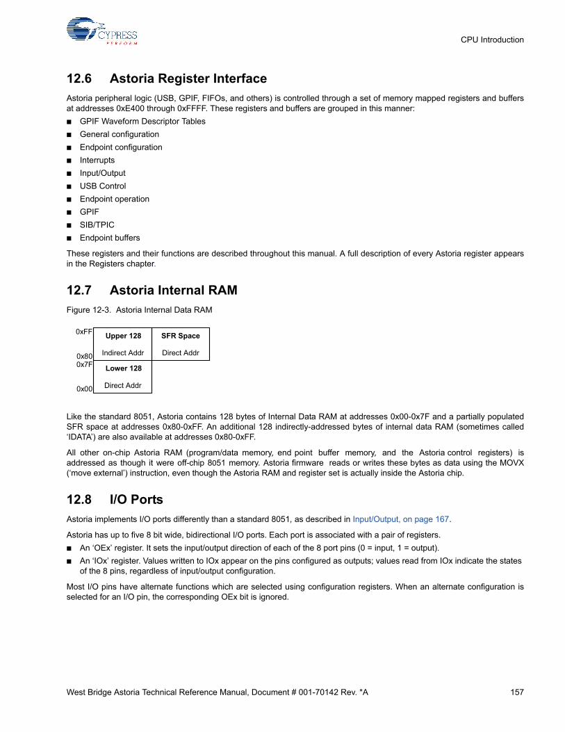
West Bridge Astoria Technical Reference Manual, Document # 001-70142 Rev. *A 157
CPU Introduction
12.6 Astoria Register Interface
Astoria peripheral logic (USB, GPIF, FIFOs, and others) is controlled through a set of memory mapped registers and buffersat addresses 0xE400 through 0xFFFF. These registers and buffers are grouped in this manner:
■ GPIF Waveform Descriptor Tables
■ General configuration
■ Endpoint configuration
■ Interrupts
■ Input/Output
■ USB Control
■ Endpoint operation
■ GPIF
■ SIB/TPIC
■ Endpoint buffers
These registers and their functions are described throughout this manual. A full description of every Astoria register appearsin the Registers chapter.
12.7 Astoria Internal RAM
Figure 12-3. Astoria Internal Data RAM
Like the standard 8051, Astoria contains 128 bytes of Internal Data RAM at addresses 0x00-0x7F and a partially populatedSFR space at addresses 0x80-0xFF. An additional 128 indirectly-addressed bytes of internal data RAM (sometimes called‘IDATA’) are also available at addresses 0x80-0xFF.
All other on-chip Astoria RAM (program/data memory, end point buffer memory, and the Astoria control registers) isaddressed as though it were off-chip 8051 memory. Astoria firmware reads or writes these bytes as data using the MOVX(‘move external’) instruction, even though the Astoria RAM and register set is actually inside the Astoria chip.
12.8 I/O Ports
Astoria implements I/O ports differently than a standard 8051, as described in Input/Output, on page 167.
Astoria has up to five 8 bit wide, bidirectional I/O ports. Each port is associated with a pair of registers.
■ An ‘OEx’ register. It sets the input/output direction of each of the 8 port pins (0 = input, 1 = output).
■ An ‘IOx’ register. Values written to IOx appear on the pins configured as outputs; values read from IOx indicate the states of the 8 pins, regardless of input/output configuration.
Most I/O pins have alternate functions which are selected using configuration registers. When an alternate configuration isselected for an I/O pin, the corresponding OEx bit is ignored.
Lower 128
Direct Addr
SFR Space
Direct Addr
Upper 128
Indirect Addr
0x00
0x7F0x80
0xFF

158 West Bridge Astoria Technical Reference Manual, Document # 001-70142 Rev. *A
CPU Introduction
12.9 Interrupts
All standard 8051 interrupts, plus additional interrupts, are supported by Astoria. Table 12-4 lists the Astoria interrupts.
Astoria uses INT2 for 27 different USB interrupts. To help determine which interrupt is active, Astoria provides a feature calledAutovectoring, which dynamically changes the address pointed to by the ‘jump’ instruction at the INT2 vector address. Thissecond level of vectoring automatically transfers control to the appropriate USB interrupt service routine (ISR). Astoria inter-rupt system, including a full description of the Autovector mechanism, is the subject of the Interrupts chapter on page 43.
12.10 Power Control
Astoria implements a low power mode that allows it to be used in USB bus powered devices (which are required by the USBspecification to draw no more than 500 A when suspended) and other low power applications. The mechanism by whichAstoria enters and exits this low power mode is described in detail in the Power Management chapter on page 59.
Table 12-4. Astoria Interrupts
Standard 8051 Interrupts Additional Astoria Interrupts Source
INT0 Internal, TPIC
INT1 Internal, SIB
Timer 0 Internal, Timer 0
Timer 1 Internal, Timer 1
Tx0 & Rx0 Internal, USART0
INT2 Internal, USB
INT3 Internal, Mail Box
INT4Internal, GPIF
WAKEUP Pin WAKEUP
Timer 2 Internal, Timer 2

West Bridge Astoria Technical Reference Manual, Document # 001-70142 Rev. *A 159
CPU Introduction
12.11 Special Function Registers
Astoria was designed to keep coding as standard as possible, to allow easy integration of existing 8051 software develop-ment tools. Astoria Special Function Registers (SFR) are summarized in Table 12-5. Standard 8051 SFRs are shown in nor-mal type and Astoria-added SFRs are shown in bold type. Full details of the SFRs are in the Register Summary chapter onpage 183.
Note All unlabeled SFRs are reserved.
*Port E is not externally available.
12.12 External Address/Data Buses
The 128-pin version of Astoria provides external, non-multiplexed 16-bit address and 8 bit data buses. This differs from thestandard 8051, which multiplexes eight pins among three sources: I/O port 0, the external data bus, and the low byte of theexternal address bus.
A standard 8051 system with external memory requires a demultiplexing address latch, strobed by the 8051 ALE (AddressLatch Enable) pin. The external latch is not required by the Astoria chip, and no ALE signal is provided. In addition to eliminat-ing the need for this external latch, the non-multiplexed Astoria bus saves one cycle per memory-fetch and allows externalmemory to be connected without sacrificing I/O pins.
Astoria is the sole master of the bus, providing read and write signals to the off-chip memory. The address bus is output-only,and cannot be floated.
12.13 Reset
The various Astoria resets and their effects are described in the Resets chapter on page 67.
Table 12-5. Astoria Special Function Registers (SFR)
x 8x 9x Ax Bx Cx Dx Ex Fx
0 IOA IOB IOC IOD SCON1 PSW ACC B
1 SP EXIF INT2CLR IOE SBUF1
2 DPL0 MPAGE INT4CLR OEA
3 DPH0 OEB
4 DPL1 OEC
5 DPH1 OED
6 DPS OEE
7 PCON
8 TCON SCON0 IE IP T2CON EICON EIE EIP
9 TMOD SBUF0
A TL0 AUTOPTRH1 EP2468STAT EP01STAT RCAP2L
B TL1 AUTOPTRL1 EP24FIFOFLGS GPIFTRIG RCAP2H
C TH0 EP68FIFOFLGS TL2
D TH1 AUTOPTRH2 GPIFSGLDATH TH2
E CKCON AUTOPTRL2 GPIFSGLDATLX
F AUTOPTRSETUP GPIFSGLDATLNOX

160 West Bridge Astoria Technical Reference Manual, Document # 001-70142 Rev. *A
CPU Introduction

West Bridge Astoria Technical Reference Manual, Document # 001-70142 Rev. *A 161
13. Instruction Set
This chapter is a technical overview and description of the Astoria assembly-language instruction set.
All Astoria instructions are binary code compatible with the standard 8051. Astoria instructions affect bits, flags, and other sta-tus functions just as the 8051 instructions do. Instruction timing, however, is different both in terms of the number of clockcycles per instruction cycle and the number of instruction cycles used by each instruction.
Table 13-2 on page 162 lists the Astoria instruction set and the number of instruction cycles required to complete eachinstruction. Table 13-1 defines the symbols and mnemonics used in Table 13-2.
Table 13-1. Legend for Instruction Set Table
Symbol Function
A Accumulator
Rn Register (R0–R7, in the bank selected by RS1:RS0)
direct Internal RAM location (0x00-0x7F in the ‘Lower 128’, or 0x80-0xFF in ‘SFR’ space)
@Ri Internal RAM location (0x00-0x7F in the ‘Lower 128’, or 0x80-0xFF in the ‘Upper 128’) pointed to by R0 or R1
rel Program-memory offset (-128 to +127 bytes relative to the first byte of the following instruction). Used by conditional jumps and SJMP.
bit Bit address (0x20-x2F in the ‘Lower 128,’ and SFRs 0x80, 0x88, …, 0xF0, 0xF8)
#data 8-bit constant (0-255)
#data16 16-bit constant (0-65535)
addr16 16-bit destination address; used by LCALL and LJMP, which branch anywhere in program memory
addr1111-bit destination address; used by ACALL and AJMP, which branch only within the current 2K page of program memory (i.e., the upper 5 address bits are copied from the PC)
PCProgram Counter; holds the address of the currently-executing instruction. For the purposes of ‘ACALL’, ‘AJMP’, and ‘MOVC A,@A+PC’ instruc-tions, the PC holds the address of the first byte of the instruction following the currently-executing instruction.

162 West Bridge Astoria Technical Reference Manual, Document # 001-70142 Rev. *A
Instruction Set
Table 13-2. Astoria Instruction Set
Mnemonic Description Bytes Cycles PSW Flags Affected Opcode (Hex)
Arithmetic
ADD A, Rn Add register to A 1 1 CY OV AC 28-2F
ADD A, direct Add direct byte to A 2 2 CY OV AC 25
ADD A, @Ri Add data memory to A 1 1 CY OV AC 26-27
ADD A, #data Add immediate to A 2 2 CY OV AC 24
ADDC A, Rn Add register to A with carry 1 1 CY OV AC 38-3F
ADDC A, direct Add direct byte to A with carry 2 2 CY OV AC 35
ADDC A, @Ri Add data memory to A with carry 1 1 CY OV AC 36-37
ADDC A, #data Add immediate to A with carry 2 2 CY OV AC 34
SUBB A, Rn Subtract register from A with borrow 1 1 CY OV AC 98-9F
SUBB A, direct Subtract direct byte from A with borrow 2 2 CY OV AC 95
SUBB A, @Ri Subtract data memory from A with borrow 1 1 CY OV AC 96-97
SUBB A, #data Subtract immediate from A with borrow 2 2 CY OV AC 94
INC A Increment A 1 1 04
INC Rn Increment register 1 1 08-0F
INC direct Increment direct byte 2 2 05
INC @ Ri Increment data memory 1 1 06-07
DEC A Decrement A 1 1 14
DEC Rn Decrement Register 1 1 18-1F
DEC direct Decrement direct byte 2 2 15
DEC @Ri Decrement data memory 1 1 16-17
INC DPTR Increment data pointer 1 3 A3
MUL AB Multiply A and B (unsigned; product in B:A) 1 5 CY=0 OV A4
DIV ABDivide A by B
(unsigned; quotient in A, remainder in B)1 CY=0 OV 84
DA A Decimal adjust A 1 1 CY D4
Logical
ANL, Rn AND register to A 1 1 58-5F
ANL A, direct AND direct byte to A 2 2 55
ANL A, @Ri AND data memory to A 1 1 56-57
ANL A, #data AND immediate to A 2 2 54
ANL direct, A AND A to direct byte 2 2 52
ANL direct, #data AND immediate data to direct byte 3 3 53
ORL A, Rn OR register to A 1 1 48-4F
ORL A, direct OR direct byte to A 2 2 45
ORL A, @Ri OR data memory to A 1 1 46-47
ORL A, #data OR immediate to A 2 2 44
ORL direct, A OR A to direct byte 2 2 42
ORL direct, #data OR immediate data to direct byte 3 3 43
XRL A, Rn Exclusive-OR register to A 1 1 68-6F
XRL A, direct Exclusive-OR direct byte to A 2 2 65
XRL A, @Ri Exclusive-OR data memory to A 1 1 66-67
XRL A, #data Exclusive-OR immediate to A 2 2 64
XRL direct, A Exclusive-OR A to direct byte 2 2 62
XRL direct, #data Exclusive-OR immediate to direct byte 3 3 63
CLR A Clear A 1 1 E4
CPL A Complement A 1 1 F4

West Bridge Astoria Technical Reference Manual, Document # 001-70142 Rev. *A 163
Instruction Set
SWAP A Swap nibbles of a 1 1 C4
RL A Rotate A left 1 1 23
RLC A Rotate A left through carry 1 1 CY 33
RR A Rotate A right 1 1 03
RRC A Rotate A right through carry 1 1 CY 13
Data Transfer
MOV A, Rn Move register to A 1 1 E8-EF
MOV A, direct Move direct byte to A 2 2 E5
MOV A, @Ri Move data byte at Ri to A 1 1 E6-E7
MOV A, #data Move immediate to A 2 2 74
MOV Rn, A Move A to register 1 1 F8-FF
MOV Rn, direct Move direct byte to register 2 2 A8-AF
MOV Rn, #data Move immediate to register 2 2 78-7F
MOV direct, A Move A to direct byte 2 2 F5
MOV direct, Rn Move register to direct byte 2 2 88-8F
MOV direct, direct Move direct byte to direct byte 3 3 85
MOV direct, @Ri Move data byte at Ri to direct byte 2 2 86-87
MOV direct, #data Move immediate to direct byte 3 3 75
MOV @Ri, MOV A to data memory at address Ri 1 1 F6-F7
MOV @Ri, Move direct byte to data memory at address Ri 2 2 A6-A7
MOV @Ri, Move immediate to data memory at address Ri 2 2 76-77
MOV DPTR, #data16 Move 16-bit immediate to data pointer 3 3 90
MOVC A, @A+DPTR Move code byte at address DPTR+A to A 1 3 93
MOVC A, @A+PC Move code byte at address PC+A to A 1 3 83
MOVX A, @Ri Move external data at address Ri to A 1 2-9* E2-E3
MOVX A, @DPTR Move external data at address DPTR to A 1 2-9* E0
MOVX @Ri Move A to external data at address Ri 1 2-9* F2-F3
MOVX @DPT Move A to external data at address DPTR 1 2-9* F0
PUSH direct Push direct byte onto stack 2 2 C0
POP direct Pop direct byte from stack 2 2 D0
XCH A, Rn Exchange A and register 1 1 C8-CF
XCH A, direct Exchange A and direct byte 2 2 C5
XCH A, @Ri Exchange A and data memory at address Ri 1 1 C6-C7
XCHD A, @Ri
Exchange the low-order nibbles of A and data memory at address Ri 1 1 D6-D7
* Number of cycles is user-selectable. See Stretch Memory Cycles on page 164
Boolean
CLR C Clear carry 1 1 CY=0 C3
CLR bit Clear direct bit 2 2 C2
SETB C Set carry 1 1 CY=1 D3
SETB bit Set direct bit 2 2 D2
CPL C Complement carry 1 1 CY B3
CPL bit Complement direct bit 2 2 B2
ANL C, bit AND direct bit to carry 2 2 CY 82
ANL C, /bit AND inverse of direct bit to carry 2 2 CY B0
ORL C, bit OR direct bit to carry 2 2 CY 72
ORL C, /bit OR inverse of direct bit to carry 2 2 CY A0
Table 13-2. Astoria Instruction Set (continued)
Mnemonic Description Bytes Cycles PSW Flags Affected Opcode (Hex)

164 West Bridge Astoria Technical Reference Manual, Document # 001-70142 Rev. *A
Instruction Set
13.1 Instruction Timing
Instruction cycles in Astoria are four clock cycles in length, rather than the 12 clock cycles per instruction cycle in the standard8051. For full details of the instruction cycle timing differences between Astoria and the standard 8051, See “PerformanceOverview” on page 154.
In the standard 8051, all instructions except for MUL and DIV take one or two instruction cycles to complete. In Astoria,instructions can take between one and five instruction cycles to complete. For calculating the timing of software loops, etc.,use the ‘Cycles’ column from Table 13-2. The ‘Bytes’ column indicates the number of bytes occupied by each instruction.
By default, Astoria’s timer/counters run at 12 clock cycles per increment so that timer-based events have the same timing aswith the standard 8051. The timers can also be configured to run at 4 clock cycles per increment to take advantage of thehigher speed of Astoria’s CPU.
13.1.1 Stretch Memory Cycles
Astoria can execute an MOVX instruction in as few as two instruction cycles. However, it is sometimes desirable to stretchthis value (for example to access slow memory or slow memory-mapped peripherals such as USARTs or LCDs). Astoria’s‘stretch memory cycle’ (Wait States) feature enables Astoria firmware to adjust the speed of data memory accesses (programmemory code fetches are not affected).
The three LSBs of the Clock Control Register (CKCON, at SFR location 0x8E) control the stretch value; stretch valuesbetween zero and seven may be used. A stretch value of zero adds zero instruction cycles, resulting in MOVX instructions
MOV C, bit Move direct bit to carry 2 2 CY A2
MOV bit, C Move carry to direct bit 2 2 92
Branching
ACALL addr11 Absolute call to subroutine 2 3 11-F1
LCALL addr16 Long call to subroutine 3 4 12
RET Return from subroutine 1 4 22
RETI Return from interrupt 1 4 32
AJMP addr11 Absolute jump unconditional 2 3 01-E1
LJMP addr16 Long jump unconditional 3 4 02
SJMP rel Short jump (relative address) 2 3 80
JC rel Jump if carry = 1 2 3 40
JNC rel Jump if carry = 0 2 3 50
JB bit, rel Jump if direct bit = 1 3 4 20
JNB bit, rel Jump if direct bit = 0 3 4 30
JBC bit, rel Jump if direct bit = 1, then clear the bit 3 4 10
JMP @ A+DPTR Jump indirect to address DPTR+A 1 3 73
JZ rel Jump if accumulator = 0 2 3 60
JNZ rel Jump if accumulator is non-zero 2 3 70
CJNE A, direct, rel Compare A to direct byte; jump if not equal 3 4 CY B5
CJNE A, #d, rel Compare A to immediate; jump if not equal 3 4 CY B4
CJNE Rn, #d, rel Compare register to immediate; jump if not equal 3 4 CY B8-BF
CJNE @ Ri, #d, rel Compare data memory to immediate; jump if not equal 3 4 CY B6-B7
DJNZ Rn, rel Decrement register; jump if not zero 2 3 D8-DF
DJNZ direct, rel Decrement direct byte; jump if not zero 3 4 D5
Miscellaneous
NOP No operation 1 1 00
There is an additional reserved opcode (A5) that performs the same function as NOP. All mnemonics are copyright 1980, Intel Corporation.
Table 13-2. Astoria Instruction Set (continued)
Mnemonic Description Bytes Cycles PSW Flags Affected Opcode (Hex)

West Bridge Astoria Technical Reference Manual, Document # 001-70142 Rev. *A 165
Instruction Set
which execute in two instruction cycles. A stretch value of seven adds seven instruction cycles, resulting in MOVX instructionswhich execute in nine instruction cycles. The stretch value can be changed dynamically under program control.
At power on reset, the stretch value defaults to one (three cycle MOVX); for the fastest data memory access, Astoria softwaremust explicitly set the stretch value to zero. The stretch value affects only data memory access (not program memory).
The stretch value affects the width of the read/write strobe and all related timing. Using a higher stretch value results in awider read/write strobe, which allows the memory or peripheral more time to respond.
Table 13-3 lists the data memory access speeds for stretch values zero through seven. MD2-0 are the three LSBs of theClock Control Register (CKCON.2-0). The strobe width timing shown is typical.
CPUCS.4:3 sets the basic clock reference for Astoria. These bits can be modified by Astoria firmware at any time. At poweron reset, CPUCS.4:3 is set to ‘00’ (12 MHz).
13.1.2 Dual Data Pointers
Astoria uses dual data pointers to accelerate data memory block moves. The standard 8051 data pointer (DPTR) is a 16 bitpointer used to address external data RAM or peripherals. Astoria maintains the standard data pointer as DPTR0 at thestandard SFR locations 0x82 (DPL0) and 0x83 (DPH0); it is not necessary to modify existing code to use DPTR0.
Astoria adds a second data pointer (DPTR1) at SFR locations 0x84 (DPL1) and 0x85 (DPH1). The SEL bitt 0 of the DPTRSelect Register, DPS, at SFR 0x86), selects the active pointer. When SEL = 0, instructions that use the DPTR useDPL0:DPH0. When SEL = 1, instructions that use the DPTR will use DPL1:DPH1. No other bits of the DPS SFR are used.
All DPTR related instructions use the data pointer selected by the SEL Bit. Switching between the two data pointers by tog-gling the SEL bit relieves Astoria firmware from the burden of saving source and destination addresses when doing a blockmove; therefore, using dual data pointers provides significantly increased efficiency when moving large blocks of data.
The fastest way to toggle the SEL bit between the two data pointers is via the ‘INC DPS’ instruction, which toggles bit 0 ofDPS between ‘0’ and ‘1’.
The SFR locations related to the dual data pointers are:
0x82 DPL0 DPTR0 low byte0x83 DPH0 DPTR0 high byte0x84 DPL1 DPTR1 low byte0x85 DPH1 DPTR1 high byte0x86 DPS DPTR Select (Bit 0)
13.1.3 Special Function Registers
The four SFRs listed here are related to CPU operation and program execution. Except for the Stack Pointer (SP), each of theregisters is bit addressable.
0x81 SP Stack Pointer0xD0 PSW Program Status Word
Table 13-3. Data Memory Stretch Values
MD2 MD1 MD0MOVX
Instruction Cycles
Read/Write Strobe Width
(Clocks)
Strobe Width @ 12 MHz
CPUCS.4:3 = 00
Strobe Width
@ 24 MHz CPUCS.4:3 = 01
Strobe Width
@ 48 MHz CPUCS.4:3 = 10
0 0 0 2 2 167 ns 83.3 ns 41.7 ns
0 0 1 3 (default) 4 333 ns 167 ns 83.3 ns
0 1 0 4 8 667 ns 333 ns 167 ns
0 1 1 5 12 1000 ns 500 ns 250 ns
1 0 0 6 16 1333 ns 667 ns 333 ns
1 0 1 7 20 1667 ns 833 ns 417 ns
1 1 0 8 24 2000 ns 1000 ns 500 ns
1 1 1 9 28 2333 ns 1167 ns 583 ns

166 West Bridge Astoria Technical Reference Manual, Document # 001-70142 Rev. *A
Instruction Set
0xE0 ACC Accumulator Register0xF0 B B Register
Table 13-4 lists PSW bit functions.
Table 13-4. PSW Register - SFR 0xD0
Bit Function
PSW.7CY - Carry flag. This is the unsigned carry bit. The CY flag is set when an arithmetic operation results in a carry from bit 7 to bit 8, and cleared otherwise. In other words, it acts as a virtual bit 8. The CY flag is cleared on multiplication and division. See the ‘PSW Flags Affected’ column in Table 13-2 on page 162.
PSW.6AC - Auxiliary carry flag. Set to ‘1’ when the last arithmetic operation resulted in a carry into (during addition) or borrow from (during sub- traction) the high order nibble, otherwise cleared to ‘0’ by all arithmetic operations. See the ‘PSW Flags Affected’ column in Table 13-2 on page 162.
PSW.5 F0 - User flag 0. Available to Astoria firmware for general purpose.
PSW.4
PSW.3
RS1 - Register bank select bit 1.
RS0 - Register bank select bit 0.
RS1:RS0 select a register bank in internal RAM: RS1 RS0Bank Selected
00Register bank 0, addresses 0x00-0x07
01Register bank 1, addresses 0x08-0x0F
10Register bank 2, addresses 0x10-0x17
11Register bank 3, addresses 0x18-0x1F
PSW.2OV - Overflow flag. This is the signed carry bit. The OV flag is set when a positive sum exceeds 0x7F or a negative sum (in two’s compli-ment notation) exceeds 0x80. After a multiply, OV = 1 if the result of the multiply is greater than 0xFF. After a divide, OV = 1 if a divide-by-0 occurred. See the ‘PSW Flags Affected’ column in Table 13-2 on page 162.
PSW.1 F1 - User flag 1. Available to Astoria firmware for general purpose.
PSW.0P - Parity flag. Contains the modulo-2 sum of the 8 bits in the accumulator (for example, set to ‘1’ when the accumulator contains an odd number of ‘1’ bits, set to ‘0’ when the accumulator contains an even number of ‘1’ bits).

West Bridge Astoria Technical Reference Manual, Document # 001-70142 Rev. *A 167
14. Input/Output
Astoria has two input/output systems:
■ A set of programmable I/O pins
■ A programmable I2C bus controller
The I/O pins are configurable for a general purpose I/O or for alternate functions (GPIF data, SDIO, USART, and others). Thischapter describes the use of the pins in the general purpose configuration, and the methods by which the pins may be config-ured for alternate functions
This chapter also gives both the programming information for the I2C interface and the operating details of the EEPROMbootloader. The role of the bootloader is described in the Enumeration and ReNumeration™ chapter on page 35.
14.1 I/O Ports
Astoria’s I/O ports are implemented differently than those of a standard 8051 and are derived from FX2LP’s I/O ports.
Astoria has up to four 8-pin bidirectional I/O ports, labeled A**, B, C, and D. Individual I/O pins are labeled Px.n, where x is theport (A, B, C or D) and n is the pin number (0 to 7).
Note Only three pins are accessible externally on Port A. See Table 1-3 for more details about port pins. Since Astoria isderived from FX2LP, I/O port E related control and configuration registers are available but this port is not externally accessi-ble.
Each port is associated with a pair of registers:
■ An OEx register (where x is A, B, C, D, or E), which sets the input/output direction of each of the 8 pins (0 = input, 1 = out-put). See the OEx register on page 168.
■ An IOx register (where x is A, B, C, D, or E). Values written to IOx appear on the pins which are configured as outputs; val-ues read from IOx indicate the states of the 8 pins, regardless of input/output configuration. See the IOx register on page 169.
Most I/O pins have alternate functions which may be selected using configuration registers. Each alternate function is unidi-rectional; Astoria ‘knows’ whether the function is an input or an output, so when an alternate configuration is selected for an I/O pin, the corresponding OEx bit is ignored (see Figures Figure 14-2 on page 169 and Figure 14-3 on page 170).
The default (power on reset) state of all I/O ports is:
■ Alternate configurations off
■ All I/O pins configured as inputs
Figure 14-1 on page 168 shows the basic structure of an Astoria I/O pin.

168 West Bridge Astoria Technical Reference Manual, Document # 001-70142 Rev. *A
Input/Output
Figure 14-1. Astoria I/O Pin
14.2 SFR RegistersOEA Port A Output Enable SFR 0xB2
b7 b6 b5 v4 v3 b2 b1 b0
D7 D6 D5 D4 D3 D2 D1 D0
R/W R/W R/W R/W R/W R/W R/W R/W
0 0 0 0 0 0 0 0
OEB Port B Output Enable SFR 0xB3
b7 b6 b5 b4 b3 b2 b1 b0
D7 D6 D5 D4 D3 D2 D1 D0
R/W R/W R/W R/W R/W R/W R/W R/W
0 0 0 0 0 0 0 0
OEC Port C Output Enable SFR 0xB4
b7 b6 b5 b4 b3 b2 b1 b0
D7 D6 D5 D4 D3 D2 D1 D0
R/W R/W R/W R/W R/W R/W R/W R/W
0 0 0 0 0 0 0 0
OED Port D Output Enable SFR 0xB5
b7 b6 b5 b4 b3 b2 b1 b0
D7 D6 D5 D4 D3 D2 D1 D0
R/W R/W R/W R/W R/W R/W R/W R/W
0 0 0 0 0 0 0 0
OEE Port E Output Enable SFR 0xB6
b7 b6 b5 b4 b3 b2 b1 b0
D7 D6 D5 D4 D3 D2 D1 D0
R/W R/W R/W R/W R/W R/W R/W R/W
0 0 0 0 0 0 0 0
OEx Bit
IOx Bit I/O Pin
Read
Write

West Bridge Astoria Technical Reference Manual, Document # 001-70142 Rev. *A 169
Input/Output
14.3 I/O Port Alternate Functions
Each I/O pin may be configured for an alternate (for example, non general purpose I/O) function. These alternate functionsare selected through various configuration registers, as described here.
The I/O pin logic for alternate function outputs is slightly different than for alternate function inputs, as shown in Figures 14-2(output) and 14-3 (input).
Figure 14-2. I/O Pin Logic when Alternate Function is an OUTPUT
IOA Port A (Bit-Addressable) SFR 0x80
b7 b6 b5 b4 b3 b2 b1 b0
D7 D6 D5 D4 D3 D2 D1 D0
R/W R/W R/W R/W R/W R/W R/W R/W
x x x x x x x x
IOB Port B (Bit-Addressable) SFR 0x90
b7 b6 b5 b4 b3 b2 b1 b0
D7 D6 D5 D4 D3 D2 D1 D0
R/W R/W R/W R/W R/W R/W R/W R/W
x x x x x x x x
IOC Port C (Bit-Addressable) SFR 0xA0
b7 b6 b5 b4 b3 b2 b1 b0
D7 D6 D5 D4 D3 D2 D1 D0
R/W R/W R/W R/W R/W R/W R/W R/W
x x x x x x x x
IOD Port D (Bit-Addressable) SFR 0xB0
b7 b6 b5 b4 b3 b2 b1 b0
D7 D6 D5 D4 D3 D2 D1 D0
R/W R/W R/W R/W R/W R/W R/W R/W
x x x x x x x x
OEx Bit
IOx Bit I/O Pin
Read
Write
Alternate Function(Output)
OEx Bit
IOx Bit I/O Pin
Read
Write
Alternate Function(Output)
a) General-Purpose I/O Configuration b) Alternate-Function Configuration

170 West Bridge Astoria Technical Reference Manual, Document # 001-70142 Rev. *A
Input/Output
Figure 14-2 shows an I/O pin whose alternate function is always an output.
In Figure 14-2a, the I/O pin is configured for a general purpose I/O. In this configuration, the alternate function is disconnectedand the pin functions normally.
In Figure 14-2b, the I/O pin is configured as an alternate-function output. In this configuration, the IOx/OEx output buffer isdisconnected from the I/O pin, so writes to IOx and OEx have no effect on the I/O pin. ‘Reads’ from IOx, however, continue towork normally; the state of the I/O pin (and the state of the alternate function) is always available.
Figure 14-3 shows an I/O pin whose alternate function is always an input.
In Figure 14-3a, the I/O pin is configured for general purpose I/O. There is an important difference between alternate-functioninputs and the alternate function outputs shown earlier in Figure 14-2 on page 169:
Note Alternate-function inputs are never disconnected; they are always listening.
If the alternate function’s interrupt is enabled, signals on the I/O pin may trigger that interrupt. If the pin is to be used only forgeneral purpose I/O, the alternate function’s interrupt must be disabled.
Figure 14-3. I/O Pin Logic when the Alternate Function is an INPUT
In Figure 14-3b, the I/O pin is configured as an alternate function input. Just as with alternate function outputs, the IOx/OExoutput buffer is disconnected from the I/O pin, so writes to IOx and OEx have no effect on the I/O pin. ‘Reads’ from I/Ox, how-ever, continue to work normally; the state of the I/O pin (and therefore, the input to the alternate function) is always available.
14.3.1 Port A Alternate Functions
Alternate functions for the Port A pins are selected by bits in three registers, as shown in Tables 14-1 and 14-2.
Table 14-1. Register Bits that Select Port A Alternate Functions
b7 b6 b5 b4 b3 b2 b1 b0
IFCONFIG
(0xE601) IFCLKSRC 3048MHZ IFCLKOE IFCLKPOL ASYNC GSTATE IFCFG1 IFCFG0
SIB_NAND_CFG
(0xE22B)-
FULL_SDIO_ENABLE
SD1_DISABLE RB4_ENB RB3_ENB RB2_ENB SD_SELNAND_SD_SE
L
OEx Bit
IOx Bit I/O Pin
Read
Write
Alternate Function(Input)
OEx Bit
IOx Bit I/O Pin
Read
Write
Alternate Function(Input)
a) General-Purpose I/O Configuration b) Alternate-Function Configuration

West Bridge Astoria Technical Reference Manual, Document # 001-70142 Rev. *A 171
Input/Output
14.3.2 Port B and Port D Alternate Functions
When IFCFG1 = 1, all eight Port B pins are configured for an alternate configuration (FIFO Data 7:0).When IFCFG1 = 1 andIFCFG0=1, all eight Port B pins are configured for an alternate configuration SD2_D[0:7]
When IFCFG1 = 1 and IFCFG0=1, all eight Port D pins are configured for an alternate configuration SD_D[0:7]..
Table 14-2. Port A Alternate Function Configuration
Port A Pin Alternate Function Alternate Function is Selected By...
PA.0 N/A[1] N/A
PA.1 N/A N/A
PA.2 N/A N/A
PA.3 N/A N/A
PA.4 N/A N/A
PA.5 N/A N/A
PA.6 SD2_CLK IFCFG1 = 1, IFCFG0 = 1, NAND_SD_SEL=1
PA.7 SD2_CMD IFCFG1 = 1, IFCFG0 = 1, NAND_SD_SEL=1
[1] P ins PA[0:4] are not external ly accessib le.
Table 14-3. Register Bits that Select Port B and Port D Alternate Functions
b7 b6 b5 b4 b3 b2 b1 b0
IFCONFIG
(0xE601) IFCLKSRC 3048MHZ IFCLKOE IFCLKPOL ASYNC GSTATE IFCFG1 IFCFG1
SIB_NAND_CFG
(0xE22B)-
FULL_SDIO_ENABLE
SD1_DISABLE RB4_ENB RB3_ENB RB2_ENB SD_SEL NAND_SD_SEL
Table 14-4. Port B Alternate-Function Configuration
Port B Pin Alternate Function Alternate Function is Selected By... Alternate Function is Described in...
PB.7:0 GPIF_D[7:0] IFCFG1 = 1, IFCFG0 = 0, NAND_SD_SEL=0 PB.7:0
PB.7:0 SD2_D[7:0] IFCFG1 = 1, IFCFG0 = 1, NAND_SD_SEL=1 PB.7:0
Table 14-5. Port D Alternate-Function Configuration
Port D Pin Alternate Function Alternate Function is Selected By... Alternate Function is Described in...
PD.7:0 SD_D[7:0] IFCFG1 = 1, IFCFG0 = 1, SD1_DISABLE=0 PD.7:0

172 West Bridge Astoria Technical Reference Manual, Document # 001-70142 Rev. *A
Input/Output
14.3.3 Port C Alternate Functions
Each Port C pin may be individually configured for an alternate function used for the SD/MMC interface..
Table 14-6. Register Bits That Select Port C Alternate Functions
b7 b6 b5 b4 b3 b2 b1 b0
IFCONFIG
(0xE601) IFCLKSRC 3048MHZ IFCLKOE IFCLKPOL ASYNC GSTATE IFCFG1 IFCFG1
SIB_NAND_CFG
- FULL_SDIO_ENABLE
SD1_DISABLE RB4_ENB RB3_ENB RB2_ENB SD_SEL NAND_SD_SEL
Table 14-7. Port C Alternate Function Configuration
Port C Pin Alternate Function Alternate Function is Selected By...
PC.0 SD2_POW IFCFG1 = 1, IFCFG0 = 1, NAND_SD_SEL=1
PC.1 SD_WP IFCFG1 = 1, IFCFG0 = 1, SD1_DISABLE=0
PC.2 SD2_WP IFCFG1 = 1, IFCFG0 = 1, NAND_SD_SEL=1
PC.3 SD_CMD IFCFG1 = 1, IFCFG0 = 1, SD1_DISABLE=0
PC.4 SD_CD IFCFG1 = 1, IFCFG0 = 1, SD1_DISABLE=0
PC.5 SD2_CD IFCFG1 = 1, IFCFG0 = 1, NAND_SD_SEL=1
PC.6 SD_POW IFCFG1 = 1, IFCFG0 = 1, SD1_DISABLE=0
PC.7 SD_CLK IFCFG1 = 1, IFCFG0 = 1, SD1_DISABLE=0

West Bridge Astoria Technical Reference Manual, Document # 001-70142 Rev. *A 173
Input/Output
14.4 I2C Bus Controller
The I2C bus controller uses the SCL (Serial Clock) and SDA (Serial Data) pins, and performs two functions:
■ General purpose interfacing to I2C peripherals
■ Boot loading from a serial EEPROM
Note Pull up resistors are required on the SDA and SCL lines when configured in Extended interface mode. Each line mustbe pulled up to Vcc through a 2.2 K ohm resistor.
The bus frequency defaults to approximately 100 kHz for compatibility, and it can be configured to run at 400 kHz for devicesthat support the higher speed.
14.4.1 Interfacing to I2C Peripherals
Figure 14-4 illustrates the waveforms for an I2C transfer. SCL and SDA are open drain Astoria pins which must be pulled upto Vcc with external resistors. Astoria is a bus master only, meaning that it generates clock pulses on SCL. Once the masterdrives SCL low, external slave devices can hold SCL low to extend clock-cycle times.
Serial data is permitted to change state only while SCL is low, and must be valid while SCL is high. Two exceptions to this ruleare the ‘start’ and ‘stop’ conditions. A ‘start’ condition is defined as a high-to-low transition on SDA while SCL is high, and a‘stop’ condition is defined as a low-to-high transition on SDA while SCL is high. Data is sent MSB first. During the last bit time
(clock #9 in Figure 14-4), the transmitting device floats the SDA line to allow the receiving device to acknowledge the transferby pulling SDA low.
14.4.1.1 Multiple Bus Masters
Astoria acts only as a bus master, never as a slave. Conflicts with a second master can be detected, however, by checking forBERR=1 (see section 14.4.2.1 I2CS Register on page 174).
Each peripheral (slave) device on the I2C bus has a unique address. The first byte of an I2C transaction contains theaddress of the desired peripheral. Figure 14-5 shows the format for this first byte, which is sometimes called a control byte.
Astoria sends the bit sequence shown in Figure 14-5 to select the peripheral at a particular address, to establish the transferdirection (using R/W), and to determine if the peripheral is present by testing for ACK.
The four most significant bits (SA3:0) are the peripheral chip’s slave address. I2C devices are internally hardwired to pre-assigned slave addresses by device type. EEPROMs, for instance, are assigned slave address 1010. The next three bits(DA2:0) usually reflect the states of the device’s address pins. A device with three address pins can be strapped to one of
eight distinct addresses, which allows, for example, up to eight serial EEPROMs to be individually addressed on one I2Cbus.
The eighth bit (R/W) sets the direction for the data transfer to follow (1 = master read, 0 = master write). Most address trans-fers are followed by one or more data transfers, with the ‘stop’ condition generated after the last data byte is transferred.
In Figure 14-5, the master clocks the 7 bit slave/device address out on SDA, then sets the R/W bit high at clock 8, indicatingthat a read transfer follows this address byte. At clock 9, the master releases SDA and treats it as an input; the peripheraldevice responds to its address by asserting ACK. At clock 10, the master begins to clock in data from the slave on the SDApin.
Figure 14-4. General I2C Transfer
SDA
SCL 1 2 3 4 5 6 7 8 9
D7 ACKD6 D5 D4 D3 D2 D1 D0
start stop
SDA
SCL

174 West Bridge Astoria Technical Reference Manual, Document # 001-70142 Rev. *A
Input/Output
Figure 14-5. Addressing an I2C Peripheral
14.4.2 Registers
The three registers shown in this section are used to conduct transfers over the I2C bus.
14.4.2.1 I2CS Register
Bit 7: START. When START = 1, the next write to I2DAT generates a ‘start’ condition followed by the byte of data written toI2DAT. The START bit is automatically cleared to 0 after the ACK interval (clock 9 in Figure 14-4 on page 173). START is acontrol bit.
Bit 6: STOP. When STOP = 1 after the ACK interval (clock 9 in Figure 14-4 on page 173), a ‘stop’ condition is generated.STOP may be set by firmware at any time before, during, or after the 9-bit data transaction. STOP is automatically clearedafter the ‘stop’ condition is generated. STOP is a control bit.
An interrupt request is available to signal that the stop condition is complete; see STOPIE, below.
Bit 5: LASTRD. An I2C master reads data by floating the SDA line and issuing clock pulses on the SCL line. After everyeight bits, the master drives SDA low for one clock to indicate ACK. To signal the last byte of a multi-byte transfer, the masterfloats SDA at ACK time to instruct the slave to stop sending. LASTRD is a control bit.
When LASTRD = 1 at ACK time, Astoria floats the SDA line. The LASTRD bit may be set at any time before or during the datatransfer; it is automatically cleared after the ACK interval.
Note Setting LASTRD does not automatically generate a ‘stop’ condition. At the end of a read transfer, the STOP bit shouldalso be set.
Bits 3 and 4: ID1, ID0. These bits are automatically set by the boot loader to indicate the Boot EEPROM addressing mode.They are normally used only for debug purposes; for full details, see section 14.5 EEPROM Boot Loader on page 176.
Bit 2: BERR. This bit indicates a bus error. BERR=1 indicates that there was bus contention during the preceding transfer,which results when an outside device drives the bus when it should not, or when another bus master wins arbitration andtakes control of the bus. BERR is a status bit.
When a bus error is detected, Astoria immediately cancels its current transfer, floats the SCL and SDA lines, and sets DONE
and BERR. BERR remains set until it is updated at the next ACK interval. The I2C master does not drive SCL till BERR isreset. If the bus error causes the master to detect bus contention and slave to be stuck in the middle of a transfer. Then thereis no in-built contention resolution method to workaround this deadlock. If there is a possibility of this condition then thedesign must implement a method of resetting the slave or clocking the slave till the next ACK.
Note DONE is set with BERR only when bus contention occurs during a transfer. If BERR is set and the bus is still busywhen firmware attempts to restart a transfer, that transfer request is ignored and the DONE flag is not set. If contention isexpected, therefore, Astoria firmware should incorporate a timeout to test for this condition. See Steps 1 and 3 ofSection 14.4.3 and Section 14.4.4.
I2CS I2C Bus Control and Status E678
b7 b6 b5 b4 b3 b2 b1 b0
START STOP LASTRD ID1 ID0 BERR ACK DONE
R/W R/W R/W R R R R R
0 0 0 x x 0 0 0
1 2 3 4 5 6 7 8 9
SA3 ACKSA2 SA1 SA0 DA2 DA1 DA0
start
SDA D7 D6
10 11
R/W
SCL
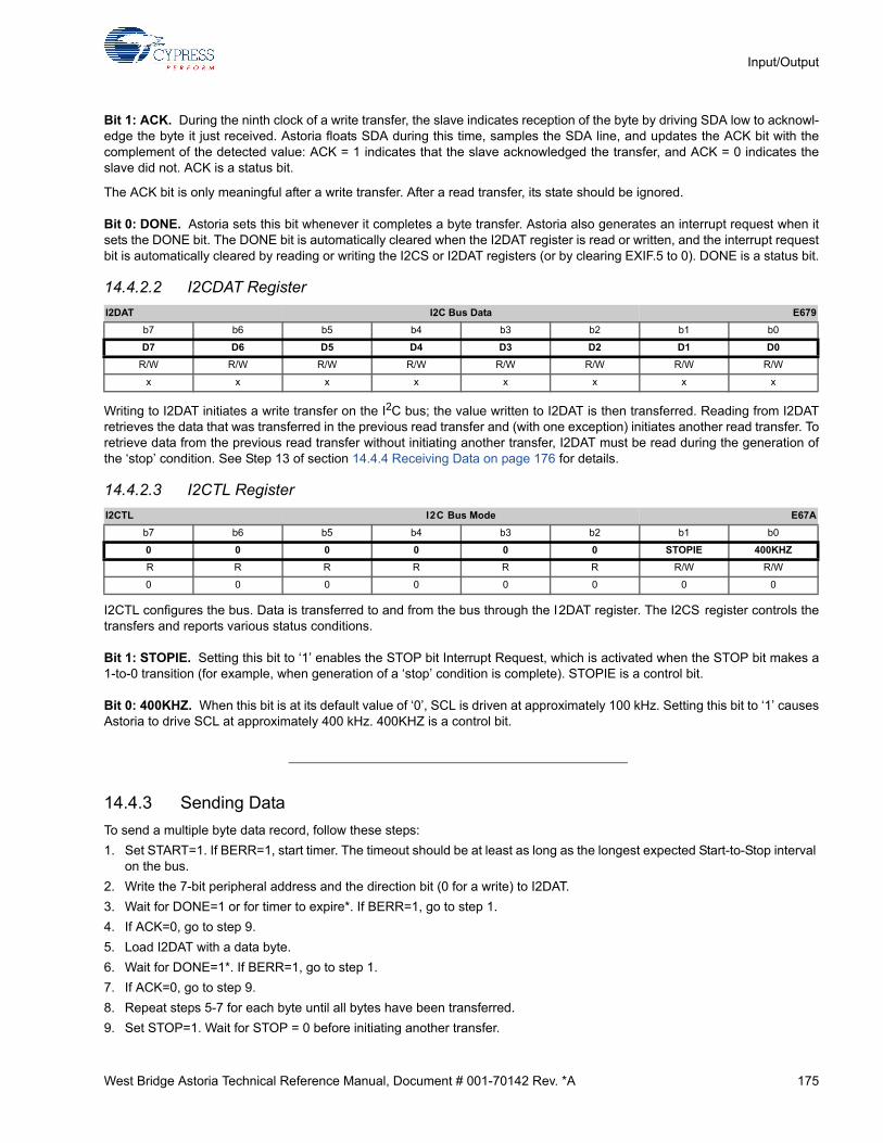
West Bridge Astoria Technical Reference Manual, Document # 001-70142 Rev. *A 175
Input/Output
Bit 1: ACK. During the ninth clock of a write transfer, the slave indicates reception of the byte by driving SDA low to acknowl-edge the byte it just received. Astoria floats SDA during this time, samples the SDA line, and updates the ACK bit with thecomplement of the detected value: ACK = 1 indicates that the slave acknowledged the transfer, and ACK = 0 indicates theslave did not. ACK is a status bit.
The ACK bit is only meaningful after a write transfer. After a read transfer, its state should be ignored.
Bit 0: DONE. Astoria sets this bit whenever it completes a byte transfer. Astoria also generates an interrupt request when itsets the DONE bit. The DONE bit is automatically cleared when the I2DAT register is read or written, and the interrupt requestbit is automatically cleared by reading or writing the I2CS or I2DAT registers (or by clearing EXIF.5 to 0). DONE is a status bit.
14.4.2.2 I2CDAT Register
Writing to I2DAT initiates a write transfer on the I2C bus; the value written to I2DAT is then transferred. Reading from I2DATretrieves the data that was transferred in the previous read transfer and (with one exception) initiates another read transfer. Toretrieve data from the previous read transfer without initiating another transfer, I2DAT must be read during the generation ofthe ‘stop’ condition. See Step 13 of section 14.4.4 Receiving Data on page 176 for details.
14.4.2.3 I2CTL Register
I2CTL configures the bus. Data is transferred to and from the bus through the I2DAT register. The I2CS register controls thetransfers and reports various status conditions.
Bit 1: STOPIE. Setting this bit to ‘1’ enables the STOP bit Interrupt Request, which is activated when the STOP bit makes a1-to-0 transition (for example, when generation of a ‘stop’ condition is complete). STOPIE is a control bit.
Bit 0: 400KHZ. When this bit is at its default value of ‘0’, SCL is driven at approximately 100 kHz. Setting this bit to ‘1’ causesAstoria to drive SCL at approximately 400 kHz. 400KHZ is a control bit.
14.4.3 Sending Data
To send a multiple byte data record, follow these steps:
1. Set START=1. If BERR=1, start timer. The timeout should be at least as long as the longest expected Start-to-Stop interval on the bus.
2. Write the 7-bit peripheral address and the direction bit (0 for a write) to I2DAT.
3. Wait for DONE=1 or for timer to expire*. If BERR=1, go to step 1.
4. If ACK=0, go to step 9.
5. Load I2DAT with a data byte.
6. Wait for DONE=1*. If BERR=1, go to step 1.
7. If ACK=0, go to step 9.
8. Repeat steps 5-7 for each byte until all bytes have been transferred.
9. Set STOP=1. Wait for STOP = 0 before initiating another transfer.
I2DAT I2C Bus Data E679
b7 b6 b5 b4 b3 b2 b1 b0
D7 D6 D5 D4 D3 D2 D1 D0
R/W R/W R/W R/W R/W R/W R/W R/W
x x x x x x x x
I2CTL I2C Bus Mode E67A
b7 b6 b5 b4 b3 b2 b1 b0
0 0 0 0 0 0 STOPIE 400KHZ
R R R R R R R/W R/W
0 0 0 0 0 0 0 0

176 West Bridge Astoria Technical Reference Manual, Document # 001-70142 Rev. *A
Input/Output
14.4.4 Receiving Data
To read a multiple-byte data record, follow these steps:
1. Set START=1. If BERR = 1, start timer. The timeout should be at least as long as the longest expected Start-to-Stop inter-val on the bus.
2. Write the 7-bit peripheral address and the direction bit (1 for a read) to I2DAT.
3. Wait for DONE=1 or for timer to expire*. If BERR=1, go to step 1.
4. If ACK=0, set STOP=1 and go to step 15.
5. Read I2DAT to initiate the first burst of nine SCL pulses to clock in the first byte from the slave. Discard the value that was read from I2DAT.
6. Wait for DONE=1. If BERR=1, go to step 1.
7. Read the just-received byte of data from I2DAT. This read also initiates the next read transfer.
8. Repeat steps 6 and 7 for each byte until ready to read the second-to-last byte.
9. Wait for DONE=1. If BERR=1, go to step 1.
10. Before reading the second-to-last I2DAT byte, set LASTRD=1.
11. Read the second-to-last byte from I2DAT. With LASTRD=1, this initiates the final byte read on the bus.
12. Wait for DONE=1. If BERR=1, go to step 1.
13. Set STOP=1.
14. Read the final byte from I2DAT immediately (the next instruction) after setting the STOP bit. By reading I2DAT while the ‘stop’ condition is being generated, the just-received data byte is retrieved without initiating an extra read transaction (nine more SCL pulses) on the I2Cbus.
15. Wait for STOP = 0 before initiating another transfer.
14.5 EEPROM Boot Loader
In Debug mode or In Debug mode with extended interface mode, whenever the Astoria is taken out of reset via the reset pin,
its bootloader checks for the presence of an EEPROM on the I2C bus. If an EEPROM is detected, the loader reads the firstEEPROM byte to determine how to enumerate. The various enumeration modes are described in the Enumeration andReNumeration™ chapter on page 35.
The Astoria bootloader supports two I2C EEPROM types:
■ EEPROMs with slave address 1010 that use an 8-bit internal address (for example, 24LC00, 24LC01/B, 24LC02/B).
■ EEPROMs with slave address 1010 that use a 16-bit internal address (for example, 24AA64, 24LC128, 24AA256).
EEPROMs with densities up to 256 bytes require only a single address byte; larger EEPROMs require two address bytes.Astoria must determine which EEPROM type is connected — one or two address bytes — so that it can properly read theEEPROM.
Astoria uses EEPROM device-address pins A2, A1, and A0 to determine whether to send out one or two bytes of address.As shown in Table 14-8, single byte address EEPROMs must be strapped to address 000, while double byte addressEEPROMs must be strapped to address 001.
Note Many single byte address EEPROMs are special cases, because the EEPROM responds to all eight device
addresses. If one of these EEPROM’s is used for boot loading, no other EEPROMs may share the bus. Consult the
EEPROM datasheet for details.

West Bridge Astoria Technical Reference Manual, Document # 001-70142 Rev. *A 177
Input/Output
After determining whether a one or two byte address EEPROM is attached, Astoria reports its results in the ID1 and ID0bits, as shown in Table 16-12.
Note Astoria does not check for bus contention during the bootloading process; if another I2C master is sharing the bus, thatmaster must not attempt to initiate any transfers while the Astoria bootloader is running.
[1] This EEPROM does not have device address pins.
ID1 ID0 Meaning
0 0 No EEPROM detected
0 1 One byte address load EEPROM detected
1 0 Two byte address load EEPROM detected
1 1 Not used
Table 14-8. Strap Boot EEPROM Address Lines to These Values
Bytes Example EEPROM A2 A1 A0
16 24LC00[1] N/A N/A N/A
128 24LC01 0 0 0
256 24LC02 0 0 0
4K 24LC32 0 0 1
8K 24LC64 0 0 1
16K 24LC128 0 0 1

178 West Bridge Astoria Technical Reference Manual, Document # 001-70142 Rev. *A
Input/Output

West Bridge Astoria Technical Reference Manual, Document # 001-70142 Rev. *A 179
15. Timers and Serial Interface
Astoria’s timer and serial interface are very similar to the EZ-USB FX2LP, with some differences. This chapter gives youtechnical information about how to configure and use the timer and serial interface.
Astoria does not support the Counter Function. Features supported by Astoria’s Timers and Serial interface are subset of fea-tures supported by EZ-USB FX2LP. Please see Chapter 14 of the EZ-USB TRM for more details on FX2LP’s Timers and SerialInterfaces.
15.1 Timers
Astoria includes three timers (Timer 0, Timer 1, and Timer 2). Each timer operates with a clock rate based on Astoria’s inter-nal clock (CLKOUT). Timers 1 and 2 may be used for baud clock generation for the serial interface (see section 15.2 SerialInterface on page 180 for details of the serial interface).
Note Astoria can be configured to operate at 12, 24, or 48 MHz. In timer mode, the timer/counters run at the same speed asAstoria, and they are not affected by the CLKOE and CLKINV configuration bits (CPUCS.1 and CPUCS.2).
Each timer consists of a 16 bit register that is accessible to software as two SFRs.
■ Timer 0 TH0 and TL0
■ Timer 1 TH1 and TL1
■ Timer 2 TH2 and TL2
15.1.1 EZ-USB FX2LP and West Bridge Astoria Differences
The implementation of the timers is similar to that of the EZ-USB FX2LP. Table 17-1 summarizes the differences in timerimplementation between the EZ-USB FX2LP and Astoria.
The key difference in Astoria’s timer features is that Astoria does not give any external signals to or from timers. All the timersare used for internal logic only.
15.1.2 Timer and Controller Mode
See the EZ-USB FX2LP TRM Section 14.2.2 to 14.2.7 for details on Timer 0, Timer 1 and Timer 2 control registers and theirmode of operation. Astoria does not give any external signal to/from timers. Details on external Input to timers and outputfrom timers are not applicable for West Bridge Astoria’s Timers.
Table 15-1. Timer Implementation Comparison
Feature EZ-USB FX2LP Astoria
Number of timers 3 3
Timer 0/1 overflow available as output signalsYes; T0OUT, T1OUT (one CLKOUT pulse)
No
Timer 2 output enable Yes n/a
Timer 2 down-count enable No n/a
Timer 2 overflow available as output signal Yes; T2OUT (one CLKOUT pulse) n/a

180 West Bridge Astoria Technical Reference Manual, Document # 001-70142 Rev. *A
Timers and Serial Interface
15.2 Serial Interface
Astoria provides two serial ports. The serial port 0 operates almost exactly as a standard 8051 serial port; depending on theconfigured mode (see Table 15-2), its baud-clock source can be CLKOUT/4 or CLKOUT/12, Timer 1, Timer 2, or the High-Speed Baud Rate Generator (see section 17.3.2 High- Speed Baud Rate Generator on page 202). Astoria’s serial interface isderived from EZ-USB FX2LP. EZ-USB FX2LP has two serial ports, port 0 and port. West Bridge Astoria provides access toonly one serial port, port 0 although Astoria contains registers for setting serial port 1, the signals related to port 1 are not exter-nally available.
Each serial port operates only in asynchronous mode. The serial port operates in full duplex mode. Astoria double buffersthe incoming data so that a byte of incoming data can be received while the firmware is reading the previously received byte.
Each serial port can operate in one of four modes, as outlined in Table 15-2.
The registers associated with the serial ports are:.Since Serial Interface is derived from EZ-USB FX2LP, the associated regis-ters are same as that of FX2LP but Port 1 and associate functionality is not externally available in WB Astoria as well as Syn-chronous mode 0 is not supported in Astoria.
■ PCON (SFR 0x87) Bit 7, Serial Port rate control
■ SMOD0
■ SCON0 (SFR 0x98) Serial Port control
■ SBUF0 (SFR 0x99) Serial Port transmit/receive buffer
■ T2CON (SFR 0xC8) Baud clock source for modes 1 and 3
■ UART230 (0xE608) High-Speed Baud Rate Generator enable
15.2.1 EZ-USB FX2LP and West Bridge Astoria Differences
Table 15-2. Serial Port Modes
Mode Sync/ Async Baud-Clock Source Data Bits Start/Stop 9th Bit Function
0 N/A N/A N/A N/A N/A
1 Async
Timer 1
Timer 2
High-Speed Baud Rate Generator
8 1 start, 1 stop None
2 Async CLKOUT/32 or CLKOUT/64 9 1 start, 1 stop 0, 1, or parity
3 Async
Timer 1
Timer 2
High-Speed Baud Rate Generator
9 1 start, 1 stop 0, 1, or parity
Note:
The High-Speed Baud Rate Generator provides 115.2K or 230.4K baud rates
Mode 0 is not supported in Astoria.
Table 15-3. Serial Interface Implementation Comparison
Feature FX2LP Astoria
Number of serial ports 2 1
Framing error detection not implemented not implemented
Slave address comparison for multiprocessor communication not implemented not implemented

West Bridge Astoria Technical Reference Manual, Document # 001-70142 Rev. *A 181
Timers and Serial Interface
15.2.2 Serial Interface Configuration Register and Mode
See the EZ-USB TRM sections 14.3.1 to 14.3.7 for detail on associated registers and the modes.
Notes
■ Astoria does not have serial port 1 so details related to serial port 1 are invalid for West Bridge Astoria.
■ Astoria does not support mode 0.

182 West Bridge Astoria Technical Reference Manual, Document # 001-70142 Rev. *A
Timers and Serial Interface

West Bridge Astoria Technical Reference Manual, Document # 001-70142 Rev. *A 183
16. Register Summary
Table 16 on page 183 is a summary of all Astoria registers.
In the ‘b7-b0’ columns, bit positions that contain a ‘0’ or a ‘1’ cannot be written to and, when read, always return the valueshown (‘0’ or ‘1’). Bit positions that contain ‘-’ are available but unused.
The ‘Default’ column shows each register’s hard reset value (‘x’ indicates ‘undefined’).
The ‘MCU Access’ column indicates each register’s read or write, or both accessibility from firmware.
The ‘P-Port Access’ column indicates each register’s read or write, or both accessibility from P-Port

184 West Bridge Astoria Technical Reference Manual, Document # 001-70142 Rev. *A
Register Summary
Table 16-1. Astoria Registers and Buffers
MCU Addr Hex
P-port Hex
Size Name Description b7 b6 b5 b4 b3 b2 b1 b0 DefaultMCU
AccessP-port Access
Notes
80 N/A 1 IOA(1) Port A (bit addressable)
D7 D6 D5 D4 D3 D2 D1 D0 xxxxxxxx RW N/A
81 N/A 1 SP Stack Pointer D7 D6 D5 D4 D3 D2 D1 D0 00000111 RW N/A
82 N/A 1 DPL0 Data Pointer 0 L A7 A6 A5 A4 A3 A2 A1 A0 00000000 RW N/A
83 N/A 1 DPH0 Data Pointer 0 H A15 A14 A13 A12 A11 A10 A9 A8 00000000 RW N/A
84 N/A 1 DPL1(1) Data Pointer 1 L A7 A6 A5 A4 A3 A2 A1 A0 00000000 RW N/A
85 N/A 1 DPH1(1) Data Pointer 1 H A15 A14 A13 A12 A11 A10 A9 A8 00000000 RW N/A
86 N/A 1 DPS1(1) Data Pointer 0/1 Select
0 0 0 0 0 0 0 SEL 00000000 rrrrrrrb N/A
87 N/A 1 PCON Power Control SMOD0 0 1 1 0 0 0 IDLE 00110000 brrrrrrb N/A
88 N/A 1 TCONTimer/Counter Control (bit addressable)
TF1 TR1 TF0 TR0 IE1 IT1 IE0 IT0 00000000 RW N/A
89 N/A 1 TMODTimer/Counter Mode Control
GATE1 CT1 M11 M01 GATE0 CT0 M10 M00 00000000 RW N/A
8A N/A 1 TL0 Timer0 Reload L D7 D6 D5 D4 D3 D2 D1 D0 00000000 RW N/A
8B N/A 1 TL1 Timer 1 Reload L D7 D6 D5 D4 D3 D2 D1 D0 00000000 RW N/A
8C N/A 1 TH0 Timer 0 Reload H D15 D14 D13 D12 D11 D10 D9 D8 00000000 RW N/A
8D N/A 1 TH1 Timer 1 Reload H D15 D14 D13 D12 D11 D10 D9 D8 00000000 RW N/A
8E N/A 1 CKCON(1) Clock Control 0 0 T2M T1M T0M MD2 MD1 MD0 00000001 rrbbbbbb N/AMOVX = 3 instr. cycles (default)
8F N/A 1 Reserved
90 N/A 1 IOB(1) Port B (bit addressable)
D7 D6 D5 D4 D3 D2 D1 D0 xxxxxxxx RW N/A
91 N/A 1 EXIF(1) External Inter-rupt Flags
IE5 IE4 I2CINT USBINT 1 0 0 0 00001000 bbbbrrrr N/A
92 N/A 1 MPAGE(1)Upper Address Byte of MOVX using@R0/@R1
A15 A14 A13 A12 A11 A10 A9 A8 00000000 RW N/A
Used with the indi-rect addressing instructions, i.e. MOVX @R0,A where
MPAGE = upper addr byte and R0 con-tains lower addr byte
an app. example would be to copy EP1 out/in data to a buffer
93 N/A 5 Reserved

185 West Bridge Astoria Technical Reference Manual, Document # 001-70142 Rev. *A
Register Summary
98 N/A 1 SCON0Serial Port 0 Control (bit addressable)
SM0_0 SM1_0 SM2_0 REN_0 TB8_0 RB8_0 TI_0 RI_0 00000000 RW N/A
99 N/A 1 SBUF0Serial Port 0 Data Buffer
D7 D6 D5 D4 D3 D2 D1 D0 00000000 RW N/A
9A N/A 1 AUTOPTRH1(1) Auto Pointer Address 1 High
A15 A14 A13 A12 A11 A10 A9 A8 00000000 RW N/A
9B N/A 1 AUTOPTRL1(1) Auto Pointer Address 1 Low
A7 A6 A5 A4 A3 A2 A1 A0 00000000 RW N/A
9C N/A 1 Reserved
9D N/A 1 AUTOPTRH2(1) Auto Pointer Address 2 High
A15 A14 A13 A12 A11 A10 A9 A8 00000000 RW N/A
9E N/A 1 AUTOPTRL2(1) Auto Pointer Address 2 Low
A7 A6 A5 A4 A3 A2 A1 A0 00000000 RW N/A
9F N/A 1 Reserved
A0 N/A 1 IOC(1) Port C (bit addressable)
D7 D6 D5 D4 D3 D2 D1 D0 xxxxxxxx RW N/A
A1 N/A 1 INT2CLR(1) Interrupt 2 Clear X x x x x x x x xxxxxxxx W1C N/AWriting any value to it will clear Interrupt 2.
A2 N/A 1 INT4CLR(1) Interrupt 4 Clear X x x x x x x x xxxxxxxx W1C N/AWriting any value to it will clear Interrupt 4.
A3 N/A 5 Reserved
A8 N/A 1 IEInterrupt Enable (bit addressable)
EA ES1 ET2 ES0 ET1 EX1 ET0 EX0 00000000 RW N/A
A9 N/A 1 Reserved
AA N/A 1 EP2468STAT(1) Endpoints 2,4,6,8 Status Flags
EP8F EP8E EP6F EP6E EP4F EP4E EP2F EP2E 01011010 R N/ACheck Empty/Full status of EP 2,4,6,8 using MOV
AB N/A 1 EP24FIFOFLGS(1) Endpoint 2,4 Slave FIFO Flags
0 EP4PF EP4EF EP4FF 0 EP2PF EP2EF EP2FF 00100010 R N/A
Check Prg/Empty/Full status of EP 2,4 slave FIFO using MOV instr
AC N/A 1 EP68FIFOFLGS(1) Endpoint 6,8 Slave FIFO Flags
0 EP8PF EP8EF EP8FF 0 EP6PF EP6EF EP6FF 01100110 R N/A
Check Prg/Empty/Full status of EP 6,8 slave FIFO using MOV instr
AD N/A 2 Reserved
Table 16-1. Astoria Registers and Buffers (continued)
MCU Addr Hex
P-port Hex
Size Name Description b7 b6 b5 b4 b3 b2 b1 b0 DefaultMCU
AccessP-port Access
Notes
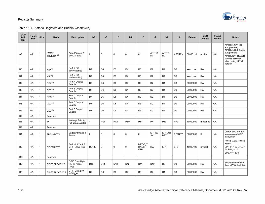
186 West Bridge Astoria Technical Reference Manual, Document # 001-70142 Rev. *A
Register Summary
AF N/A 1AUTOP-
TRSETUP(1)Auto Pointers 1 and 2 Setup
0 0 0 0 0APTR2INC
APTR1INC
APTREN 00000110 rrrrrbbb N/A
APTRxINC=1 inc autopointers; APTRxINC=0 freeze autopointers
APTREN=1 RD/WR strobes asserted when using MOVX version
B0 N/A 1 IOD(1) Port D (bit addressable)
D7 D6 D5 D4 D3 D2 D1 D0 xxxxxxxx RW N/A
B1 N/A 1 IOE(1) Port E (bit addressable)
D7 D6 D5 D4 D3 D2 D1 D0 xxxxxxxx RW N/A
B2 N/A 1 OEA(1) Port A Output Enable
D7 D6 D5 D4 D3 D2 D1 D0 00000000 RW N/A
B3 N/A 1 OEB(1) Port B Output Enable
D7 D6 D5 D4 D3 D2 D1 D0 00000000 RW N/A
B4 N/A 1 OEC(1) Port C Output Enable
D7 D6 D5 D4 D3 D2 D1 D0 00000000 RW N/A
B5 N/A 1 OED(1) Port D Output Enable
D7 D6 D5 D4 D3 D2 D1 D0 00000000 RW N/A
B6 N/A 1 OEE(1) Port E Output Enable
D7 D6 D5 D4 D3 D2 D1 D0 00000000 RW N/A
B7 N/A 1 Reserved
B8 N/A 1 IPInterrupt Priority (bit addressable)
1 PS1 PT2 PS0 PT1 PX1 PT0 PX0 10000000 rbbbbbbb N/A
B9 N/A 1 Reserved
BA N/A 1 EP01STAT(1) Endpoint 0 and 1 Status
0 0 0 0 0EP1INBSY
EP1OUTBSY
EP0BSY 00000000 R N/ACheck EP0 and EP1 status using MOV instruction
BB N/A 1 GPIFTRIG(1)Endpoint 2,4,6,8 GPIF Slave Trig-ger
DONE 0 0 0MECC_TRANS-FER
RW EP1 EP0 10000100 rrrrbbbb N/A
RW=1 reads, RW=0 writes;
EP[1:0] = 00 EP2, = 01 EP4, = 10
EP6, = 11 EP8
BC N/A 1 Reserved
BD N/A 1 GPIFSGLDATH(1)GPIF Data High (16-bit mode only)
D15 D14 D13 D12 D11 D10 D9 D8 00000000 RW N/AEfficient versions of their MOVX buddies
BE N/A 1 GPIFSGLDATLX(1) GPIF Data Low w/Trigger
D7 D6 D5 D4 D3 D2 D1 D0 00000000 RW N/A
Table 16-1. Astoria Registers and Buffers (continued)
MCU Addr Hex
P-port Hex
Size Name Description b7 b6 b5 b4 b3 b2 b1 b0 DefaultMCU
AccessP-port Access
Notes

187 West Bridge Astoria Technical Reference Manual, Document # 001-70142 Rev. *A
Register Summary
BF N/A 1GPIFSGLDATL-
NOX(1)GPIF Data Low, NoTrigger
D7 D6 D5 D4 D3 D2 D1 D0 00000000 R N/A
Note: READ only, this should help you decide when to appropriately use it
C0 N/A 8 Reserved
C8 N/A 1 T2CONTimer Counter/Control 2 (bit addressable)
TF2 EXF2 RCLK TCLK EXEN2 TR2 CT2 CPRL2 00000000 RW N/A
C9 N/A 1 Reserved
CA N/A 1 RCAP2LCapture for timer 2, auto-reload, up counter
D7 D6 D5 D4 D3 D2 D1 D0 00000000 RW N/A
CB N/A 1 RCAP2HCapture for timer 2, auto-reload, up counter
D15 D14 D13 D12 D11 D10 D9 D8 00000000 RW N/A
CC N/A 1 TL2 Timer 2 Reload L D7 D6 D5 D4 D3 D2 D1 D0 00000000 RW N/A
CD N/A 1 TH2 Timer 2 Reload H D15 D14 D13 D12 D11 D10 D9 D8 00000000 RW N/A
CE N/A 2 Reserved
D0 N/A 1 PSWProgram Status Word (bit addressable)
CY AC F0 RS1 RS0 OV F1 P 00000000 RW N/A
D1 N/A 7 Reserved
D8 N/A 1 EICON(1) External Inter-rupt Controller
SMOD1 1 ERESI RESIINT6 (Reserved)
0 0 0 01000000 brbbbrrr N/A
RESI - reflects D+ / WU/WU2 src while SUSPEND (PCON.1), clocks off
D9 N/A 7 Reserved
E0 N/A 1 ACCAccumulator (bit addressable)
D7 D6 D5 D4 D3 D2 D1 D0 00000000 RW N/A
E1 N/A 1 INT5CLR(1) Interrupt 5 Clear x x x x x x x X xxxxxxxx N/A W1C
E2 N/A 1 INT6CLR(1) Interrupt 6 Clear x x x x x x x X xxxxxxxx N/A W1C
E3 N/A 5 Reserved
E8 N/A 1 EIE(1) External Inter-rupt Enable
1 1 1 EX6 EX5 EX4 EMBINT EUSB 11100000 N/A rrrbbbbb
E9 N/A 1 Reserved
EA N/A 1 EP3579STAT(1) Endpoints 3,5,7,9 Status Flags
EP9F EP9E EP7F EP7E EP5F EP5E EP3F EP3E 01011010 R N/A
Table 16-1. Astoria Registers and Buffers (continued)
MCU Addr Hex
P-port Hex
Size Name Description b7 b6 b5 b4 b3 b2 b1 b0 DefaultMCU
AccessP-port Access
Notes

188 West Bridge Astoria Technical Reference Manual, Document # 001-70142 Rev. *A
Register Summary
EB N/A 1 EP35FIFOFLGS(1) Endpoint 3,5 Slave FIFO Flags
0 EP5PF EP5EF EP5FF 0 EP3PF EP3EF EP3FF 00100010 R N/A
EC N/A 1 EP79FIFOFLGS(1) Endpoint 7,9 Slave FIFO Flags
0 EP9PF EP9EF EP9FF 0 EP7PF EP7EF EP7FF 01100110 R N/A
ED N/A 3 Reserved
F0 N/A 1 BB (bit address-able)
D7 D6 D5 D4 D3 D2 D1 D0 00000000 RW N/A
F1 N/A 7 Reserved
F8 N/A 1 EIP(1)External Inter-rupt Priority Con-trol
1 1 1 PX6 PX5 PX4 PMBINT PUSB 11100000 rrrbbbbb N/A
F9 N/A 7 Reserved
1. SFRs not part of the standard 8051 architecture
MCU Registers
E200 N/A 1 SIB_CMD_REG_0Contents of data to be sent on command bus.
CMD0[7] CMD0[6] CMD0[5] CMD0[4] CMD0[3] CMD0[2] CMD0[1] CMD0[0] 00000000 RW N/A
E201 N/A 1 SIB_CMD_REG_1Contents of data to be sent on command bus.
CMD1[7] CMD1[6] CMD1[5] CMD1[4] CMD1[3] CMD1[2] CMD1[1] CMD1[0] 00000000 RW N/A
E202 N/A 1 SIB_CMD_REG_2Contents of data to be sent on command bus.
CMD2[7] CMD2[6] CMD2[5] CMD2[4] CMD2[3] CMD2[2] CMD2[1] CMD2[0] 00000000 RW N/A
E203 N/A 1 SIB_CMD_REG_3Contents of data to be sent on command bus.
CMD3[7] CMD3[6] CMD3[5] CMD3[4] CMD3[3] CMD3[2] CMD3[1] CMD3[0] 00000000 RW N/A
E204 N/A 1 SIB_CMD_REG_4Contents of data to be sent on command bus.
CMD4[7] CMD4[6] CMD4[5] CMD4[4] CMD4[3] CMD4[2] CMD4[1] CMD4[0] 00000000 RW N/A
E205 N/A 1 SIB_CMD_REG_5Contents of data to be sent on command bus.
CMD5[7] CMD5[6] CMD5[5] CMD5[4] CMD5[3] CMD5[2] CMD5[1] CMD5[0] 00000000 RW N/A
E206 N/A 1 SIB_CMD_REG_6Contents of data to be sent on command bus.
CMD6[7] CMD6[6] CMD6[5] CMD6[4] CMD6[3] CMD6[2] CMD6[1] CMD6[0] 00000000 RW N/A
E207 N/A 1 SIB_CMD_REG_7Contents of data to be sent on command bus.
CMD7[7] CMD7[6] CMD7[5] CMD7[4] CMD7[3] CMD7[2] CMD7[1] CMD7[0] 00000000 RW N/A
Table 16-1. Astoria Registers and Buffers (continued)
MCU Addr Hex
P-port Hex
Size Name Description b7 b6 b5 b4 b3 b2 b1 b0 DefaultMCU
AccessP-port Access
Notes

189 West Bridge Astoria Technical Reference Manual, Document # 001-70142 Rev. *A
Register Summary
E208 N/A 1SIB_RESP_REG_0
Response Data received from the card on response bus.
RESP0[7]
RESP0[6]
RESP0[5]
RESP0[4]RESP0[3]
RESP0[2]
RESP0[1]
RESP0[0] 00000000 R N/A
E209 N/A 1SIB_RESP_REG_1
Response Data received from the card on response bus.
RESP1[7]
RESP1[6]
RESP1[5]
RESP1[4]RESP1[3]
RESP1[2]
RESP1[1]
RESP1[0] 00000000 R N/A
E20A N/A 1SIB_RESP_REG_2
Response Data received from the card on response bus.
RESP2[7]
RESP2[6]
RESP2[5]
RESP2[4]RESP2[3]
RESP2[2]
RESP2[1]
RESP2[0] 00000000 R N/A
E20B N/A 1SIB_RESP_REG_3
Response Data received from the card on response bus.
RESP3[7]
RESP3[6]
RESP3[5]
RESP3[4]RESP3[3]
RESP3[2]
RESP3[1]
RESP3[0] 00000000 R N/A
E20C N/A 1SIB_RESP_REG_4
Response Data received from the card on response bus.
RESP4[7]
RESP4[6]
RESP4[5]
RESP4[4]RESP4[3]
RESP4[2]
RESP4[1]
RESP4[0] 00000000 R N/A
E20D N/A 1SIB_RESP_REG_5
Response Data received from the card on response bus.
RESP5[7]
RESP5[6]
RESP5[5]
RESP5[4]RESP5[3]
RESP5[2]
RESP5[1]
RESP5[0] 00000000 R N/A
E20E N/A 1SIB_RESP_REG_6
Response Data received from the card on response bus.
RESP6[7]
RESP6[6]
RESP6[5]
RESP6[4]RESP6[3]
RESP6[2]
RESP6[1]
RESP6[0] 00000000 R N/A
E20F N/A 1SIB_RESP_REG_7
Response Data received from the card on response bus.
RESP7[7]
RESP7[6]
RESP7[5]
RESP7[4]RESP7[3]
RESP7[2]
RESP7[1]
RESP7[0] 00000000 R N/A
E210 N/A 1SIB_RESP_REG_8
Response Data received from the card on response bus.
RESP8[7]
RESP8[6]
RESP8[5]
RESP8[4]RESP8[3]
RESP8[2]
RESP7[1]
RESP8[0] 00000000 R N/A
E211 N/A 1SIB_RESP_REG_9
Response Data received from the card on response bus.
RESP9[7]
RESP9[6]
RESP9[5]
RESP9[4]RESP9[3]
RESP9[2]
RESP9[1]
RESP9[0] 00000000 R N/A
E212 N/A 1SIB_RESP_REG_10
Response Data received from the card on response bus.
RESP10[7]
RESP10[6]
RESP10[5]
RESP10[4]
RESP10[3]
RESP10[2]
RESP10[1]
RESP10[0]
00000000 R N/A
Table 16-1. Astoria Registers and Buffers (continued)
MCU Addr Hex
P-port Hex
Size Name Description b7 b6 b5 b4 b3 b2 b1 b0 DefaultMCU
AccessP-port Access
Notes
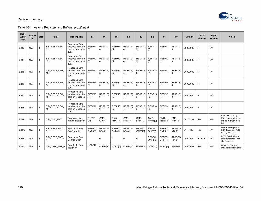
190 West Bridge Astoria Technical Reference Manual, Document # 001-70142 Rev. *A
Register Summary
E213 N/A 1SIB_RESP_REG_11
Response Data received from the card on response bus.
RESP11[7]
RESP11[6]
RESP11[5]
RESP11[4]
RESP11[3]
RESP11[2]
RESP11[1]
RESP11[0]
00000000 R N/A
E214 N/A 1SIB_RESP_REG_12
Response Data received from the card on response bus.
RESP12[7]
RESP12[6]
RESP12[5]
RESP12[4]
RESP12[3]
RESP12[2]
RESP12[1]
RESP12[0]
00000000 R N/A
E215 N/A 1SIB_RESP_REG_13
Response Data received from the card on response bus.
RESP13[7]
RESP13[6]
RESP13[5]
RESP13[4]
RESP13[3]
RESP13[2]
RESP13[1]
RESP13[0]
00000000 R N/A
E216 N/A 1SIB_RESP_REG_14
Response Data received from the card on response bus.
RESP14[7]
RESP14[6]
RESP14[5]
RESP14[4]
RESP14[3]
RESP14[2]
RESP14[1]
RESP14[0]
00000000 R N/A
E217 N/A 1SIB_RESP_REG_15
Response Data received from the card on response bus.
RESP15[7]
RESP15[6]
RESP15[5]
RESP15[4]
RESP15[3]
RESP15[2]
RESP15[1]
RESP15[0]
00000000 R N/A
E218 N/A 1SIB_RESP_REG_16
Response Data received from the card on response bus.
RESP16[7]
RESP16[6]
RESP16[5]
RESP16[4]
RESP16[3]
RESP16[2]
RESP16[1]
RESP16[0]
00000000 R N/A
E219 N/A 1 SIB_CMD_FMTCommand for-mat configuration
P_END_DIS
CMD-COMP
CMD-FRMT[5]
CMD-FRMT[4]
CMD-FRMT[3]
CMD-FRMT[2]
CMD-FRMT[1]
CMD-FRMT[0]
00100101 RW N/A
CMDFRMT[5:0] = Field to select com-mand format 63/64 bit.
E21A N/A 1SIB_RESP_FMT_0
Response Field Configuration
RESPCONF0[7]
RESPCONF0[6]
RESPCONF0[5]
RESPCONF0[4]
RESPCONF0[3]
RESPCONF0[2]
RESPCONF0[1]
RESPCONF0[0]
01111110 RW N/ARESPCONF0[7:0] = LSB Response Field Configuration
E21B N/A 1SIB_RESP_FMT_1
Response Field Configuration
0 0 0 0 0RESPCONF1[2]
RESPCONF1[1]
RESPCONF1[0]
00000000 rrrrrbbb N/ARESPCONF1[2:0] = MSB Response Field Configuration
E21C N/A 1 SIB_DATA_FMT_0Data Field Con-figuration
NOBD[7]
NOBD[6] NOBD[5] NOBD[4] NOBD[3] NOBD[2] NOBD[1] NOBD[0] 00000001 RW N/A NOBD [7:0] = LSB Data field configuration
Table 16-1. Astoria Registers and Buffers (continued)
MCU Addr Hex
P-port Hex
Size Name Description b7 b6 b5 b4 b3 b2 b1 b0 DefaultMCU
AccessP-port Access
Notes

191 West Bridge Astoria Technical Reference Manual, Document # 001-70142 Rev. *A
Register Summary
E21D N/A 1 SIB_DATA_FMT_1Data Field Con-figuration
INTC-TRLBIT
EPDATA-WIDTH
EP_NUM[1]
EP_NUM[0]
NOB-DCONT[3]
NOB-DCONT[2]
NOB-DCONT[1]
NOB-DCONT[0]
00000000 RW N/A
NOBDCONT[3:0] = NOBD continued. MSB Data field Con-figuration
EP_NUM[1:0] = EP buffer , which MMC.SDIO will read.write data.
00:EP2
01:EP4
10:EP4
11:EP6
E21E N/A 1 SIB_CRC_CFGCRC Configura-tion Register
COR_CRC
MASK_CRC_STATUS_ERR
0R_CRC_E_N
0RD_CRC_EN
0 0 00010100 bbrbrbrr N/A
E21F N/A 1 SIB_MODE_CFGMode Configura-tion Register
STOP_CLOCK_EN
CARD_BUSY_DET
GCTL_SD_CLK_DIS
EN_CMD_COMP
DATA-BUS-WIDTH[1]
DATA-BUS-WIDTH[0]
MODE[1]
MODE[0] 00000110 RW N/A
DATABUS-WIDTH[1:0] = Data bus width :Not valid in SPI mode
For MMC card
00: 1bit
01: 4bit
10: 8bit
11:reserved
For SD/SDIO card
00:1bit data width
01:4 bit data width
10:reserved
11:reserved
MODE[1:0] = Mode Configuration Regis-ter
00:reserved
01:MMC /MMC+ mode
10:SD/SDIO mode
11:SPI mode
E220 N/A 1 Reserved
Table 16-1. Astoria Registers and Buffers (continued)
MCU Addr Hex
P-port Hex
Size Name Description b7 b6 b5 b4 b3 b2 b1 b0 DefaultMCU
AccessP-port Access
Notes

192 West Bridge Astoria Technical Reference Manual, Document # 001-70142 Rev. *A
Register Summary
E221 N/A 1 SIB_INTR_INInput Interrupts from 8051
0 0RST-CONT
SEND-ABORT
0RDDCARD
WRD-CARD
SNDCMD 00000000 rrbbrbbb N/A
The bits are in state “0” except for when the interrupts is received. These interrupts are cleared on Read by the SD controller block.
E222 N/A 1 SIB_INTR_OUTInterrupt gener-ated by the SIB block
SDIO Interrupt
CRC-DATA
CRCRESRCVD
DATASTRD
BLKDA-TASENT
RSP-TIME-OUT
RCV-DRES
CMD-SENT
00000000 W1C N/A
E223 N/A 1SIB_CNTR_CFG_0
Idle Count regis-ters Set 1
0MAX-CLK[6]
MAX-CLK[5]
MAX-CLK[4]
MAX-CLK[3]
MAX-CLK[2]
MAX-CLK[1]
MAX-CLK[0]
01000111 rbbbbbbb N/A
MAXCLK[6:0] = Maximum number of clock cycles between command and response (NRC)
Value of 0 – 0 clock cycles
The user should pro-gram Counter value as "card NRC + 7" or higher.
E224 N/A 1SIB_CNTR_CFG_1
Idle Count regis-ters Set 1
NUM-CLK[7]
NUM-CLK[6]
NUM-CLK[5]
NUM-CLK[4]
NUM-CLK[3]
NUM-CLK[2]
NUM-CLK[1]
NUM-CLK[0]
00001000 RW N/A
NUMCLK[7:0] = Number of clock cycles between last bit of response and command (NRC)The value of 0 corre-sponds to 0 cycles
E225 N/A 1SIB_CNTR_CFG_2
Idle Count regis-ters Set 2
NUM-CONSE[7]
NUM-CONSE[6]
NUM-CONSE[5]
NUM-CONSE[4]
0 0 0 0 10000000 bbbbrrrr N/A
NUMCONSE[7:0] = Number of clock cycles between 2 consecutive com-mands (NCC)
E226 N/A 1SIB_CNTR_CFG_3
Idle Count regis-ters Set 3
NUM-CRES[7]
NUM-CRES[6]
NUM-CRES[5]
NUM-CRES[4]
NUM-CRES[3]
NUM-CRES[2]
NUM-CRES[1]
NUM-CRES[0]
00000010 RW N/A
NUMCRES[7:0] = Number of clock cycles between com-mand/response and write data (NWR). The 8051 issue port command
Table 16-1. Astoria Registers and Buffers (continued)
MCU Addr Hex
P-port Hex
Size Name Description b7 b6 b5 b4 b3 b2 b1 b0 DefaultMCU
AccessP-port Access
Notes

193 West Bridge Astoria Technical Reference Manual, Document # 001-70142 Rev. *A
Register Summary
E227 N/A 1SIB_CNTR_CFG_4
Read data time-out count register
RDTM-OUT[7]
RDTM-OUT[6]
RDTM-OUT[5]
RDTM-OUT[4]
RDTM-OUT[3]
RDTM-OUT[2]
RDTM-OUT[1]
RDTM-OUT[0]
11111111 RW N/A
RDTMOUT[7:0] = Count register for read data timeout
This value indicates the maximum amount of time between the com-mand and read-data before issuing a timeout to 8051. The value of 0 corre-sponds to 0 cycle gap for timeout.
The 8051 issue port command.
E228 N/A 1SIB_CNTR_CFG_5
Read data time-out count register
CNTR5[7]
CNTR5[6]
CNTR5[5]
CNTR5[4]CNTR5[3]
CNTR5[2]
CNTR5[1]
CNTR5[0] 11111111 RW N/A
CNTR5[7:0] = Count register for read data timeout
This value indicates the maximum amount of time between the com-mand and read-data before issuing a timeout to 8051. The value of 0 corre-sponds to 0 cycle gap for timeout.
The 8051 issue port command.
E229 N/A 1SIB_CNTR_CFG_6
Read data time-out count register
CNTR6[7]
CNTR6[6]
CNTR6[5]
CNTR6[4]CNTR6[3]
CNTR6[2]
CNTR6[1]
CNTR6[0] 00001111 RW N/A
CNTR6[7:0] = Count register for read data time-out
This value indicates the maximum amount of time between the com-mand and read-data before issuing a timeout to 8051. The value of 0 corre-sponds to 0 cycle gap for timeout.
The 8051 issue port command.
Astoria Registers
Table 16-1. Astoria Registers and Buffers (continued)
MCU Addr Hex
P-port Hex
Size Name Description b7 b6 b5 b4 b3 b2 b1 b0 DefaultMCU
AccessP-port Access
Notes

194 West Bridge Astoria Technical Reference Manual, Document # 001-70142 Rev. *A
Register Summary
E22A N/A 1SIB_READ_WAIT_ENB
SDIO read wait enable register
0 0 0 0 0 0 0 EN 00000000 rrrrrrrb N/A
E22B N/A 1 SIB_NAND_CFGStorage Configu-ration Register
PAD_NANDCFG
FULL_SDIO_ENABLE
SD1_DISABLE
NAND_RB4_ENB
NAND_RB3_ENB
NAND_RB2_ENB
SD_SELNAND_SD_SEL
00000000 RW N/A
MCU Registers
E22C N/A 1SIB_DATABLK_SIZE0
The max. amount of data to be sent in one block (LSB)
DATABLKS0[7]
DATABLKS0[6]
DATABLKS0[5]
DATABLKS0[4]
DATABLKS0[3]
DATABLKS0[2]
DATABLKS0[1]
DATABLKS0[0]
00000000 RW N/A
DATABLKS0[7:0] = Number of bytes of data to be sent to SD card in one block. This should be com-patible to BLOCK_LEN field programmed in SD card. The value of 0 corresponds to 1 byte. The max value of BLOCK_LEN is 512 bytes in SD card. The 8051 issue port command.
E22D N/A 1SIB_DATABLK_SIZE1
The max. amount of data to be sent in one block (MSB)
0 0 0 0DATABLKS1[3]
DATABLKS1[2]
DATABLKS1[1]
DATABLKS1[0]
00000010 rrrrbbbb N/A
DATABLKS1[7:0] = Number of bytes of data to be sent to SD card in one block. This should be com-patible to BLOCK_LEN field programmed in SD card. The value of 0 corresponds to 1 byte. The max value of BLOCK_LEN is 512 bytes in SD card.The 8051 issue port command.
E22E N/A 1SIB_WR_DATA_CFG
Write data config-uration register
0 0 0 0 0 0EXP-BUSY
EXP-CRCR
00000011 rrrrrrbb N/A
E22F N/A 1SIB_CARD_CRC_RESP
CRC response from the card after write com-mand
0 0DATA_SM_BUSY
COMMAND_SM_BUSY
CRCERR
CRCFC[2]
CRCFC[1]
CRCFC[0]
00001000 R N/A
CRCFC[2:0] = CRC Response from the card. The 8051 issue port command
E230 N/A 1SIB_RESP_REG_17
Response Data received from the card on response bus.
RESP17[7]
RESP17[6]
RESP17[5]
RESP17[4]
RESP17[3]
RESP17[2]
RESP17[1]
RESP17[0]
00000000 R N/A D[7:0] = RESP17
Table 16-1. Astoria Registers and Buffers (continued)
MCU Addr Hex
P-port Hex
Size Name Description b7 b6 b5 b4 b3 b2 b1 b0 DefaultMCU
AccessP-port Access
Notes

195 West Bridge Astoria Technical Reference Manual, Document # 001-70142 Rev. *A
Register Summary
E231 N/A 1 SIB_INTR_OUT_1Interrupt gener-ated by the SIB block
BLOCK_COMP
SPI_ACC_STAT
FIFO_O_DET
BLOCKS_RECEIVED
CARD_DET
INT_GGP[1]
INT_GGP[0]
CMD_COMP_INT
0000XXX0 W1C N/A
INT_GGP[1:0] = Trigerred corre-sponding to PAD_GGPI[1:0], mask==0, the inter-rupt will be reported to 8051
Bit1 for GPIO[0] and bit2 GPIO[1]
E232 N/A 1SIB_INTR_IN_MASK
SIB interrupt mask register
0 0RSTCONT_MASK
SENDABORT_MASK
0RDDCARD_MASK
WRDCARD_MASK
SNDCMD_MASK
00000000 rrbbrbbb N/A
E233 N/A 1SIB_INTR_OUT_ENABLE
SIB interrupt enable register 1
0CRCDATA_ENABLE
CRCRESRCVD_ENABLE
DATASTRD_ENABLE
BLKDATASENT_ENABLE
RSPTIMEOUT_ENABLE
RCVDRES_ENABLE
CMDSENT_ENABLE
00000000 RW N/A
E234 N/A 1SIB_INTR_OUT_1_ENABLE
SIB interrupt enable register 2
BLOCK_COMP_ENABLE
SPI_ACC_STAT_ENABLE
FIFO_O_DET_ENABLE
BLOCKS_RECEIVED_ENABLE
CARD_DET_ENABLE
INT_GGP_ENABLE[1]
INT_GGP_ENABLE[0]
CMD_COMP_INT_ENABLE
00000000 RW N/AN/A
E235 N/A 1 SIB_SPI_CFGSIB SPI configu-ration register
0 C_LOCK OR CI_ECCIN_C_CTRL
ERR_RD
ST_TOK SPI_CS 00000000rwwww-wbb
N/A
Astoria Registers
E236 N/A 1SIB_CNTR_CFG_7
Read time coun-ter extension
0 0 0 CNTR7[4]CNTR7[3]
CNTR7[2]
CNTR7[1]
CNTR7[0] 00000000 rrrbbbbb N/A
CNTR7[4:0] = Count register for read data time-out
This value indicates the maximum amount of time between the com-mand and read-data before issuing a timeout to 8051. The value of 0 corre-sponds to 0 cycle gap for timeout.
The 8051 issue port command.
E237 N/A 1 Reserved
MCU Registers
E238 N/A 1PIB_MANUAL_COMMIT_BCNT_LO
Eight lsb bits of the ten-bit byte count value
byte_count[7]
byte_count[6]
byte_count[5]
byte_count[4]
byte_count[3]
byte_count[2]
byte_count[1]
byte_count[0]
00000000 RW N/A
Table 16-1. Astoria Registers and Buffers (continued)
MCU Addr Hex
P-port Hex
Size Name Description b7 b6 b5 b4 b3 b2 b1 b0 DefaultMCU
AccessP-port Access
Notes

196 West Bridge Astoria Technical Reference Manual, Document # 001-70142 Rev. *A
Register Summary
E239 N/A 1PIB_MANUAL_COMMIT_BCNT_HI
Three msb bits of the ten-bit byte count value
0 0 0 0 0byte_count[10]
byte_count[9]
byte_count[8]
00000000 rrrrrbbb N/A
E23A N/A 1PIB_MANUAL_COMMIT_EPNUM
During Manual Commit Mode, this register stores the EP number for the P2U Transaction
0 0manual_commit_valid[1]
manual_commit_valid[0]
lep_num[3]
lep_num[2]`
lep_num[1]
lep_num[0]
00000000 rrbbbbbb N/A
lep_num[3:0] = Logi-cal EP number of the incoming packet from PLB.
manual_commit_valid[1:0] = Physical EP number of the incom-ing and outgoing packet from/to PLB.
E23B N/A 1 Reserved
E23C N/A 1PIB_S2P_RD_MINSIZE_LO
S2P minimum read size register
MINSIZE_L[7]
MINSIZE_L[6]
MINSIZE_L[5]
MINSIZE_L[4]
MINSIZE_L[3]
MINSIZE_L[2]
MINSIZE_L[1]
MINSIZE_L[0]
01000000 RW N/AMINSIZE_L[7:0] = Byte count[7:0]
E23D N/A 1PIB_S2P_RD_MINSIZE_HI
These register will be used to indicate how much data needs to be in FIFO before it is sent to External pro-cessor.
0 0 0 0 0 0 0MINSIZE_H
00000000 rrrrrrrb N/AMINSIZE_H = Byte count[8]
E23E N/A 2 Reserved
E240 N/A 1TPIC_P2S_SOFT_RESET
TPIC soft reset register
0 0 0 0
SLB_IN_OUT_PING_Reset
PIB_P2S_wirte_state_Reset
TPIC_Block_Reset
0 00000000 rrrrbbbb N/A
E241 N/A 1 TPIC_P2S_ENP2S switch enable register
0 0 0 0 0 0 0 PSEN 00000000 rrrrrrrb N/A
E242 N/A 1 TPIC_P2S_CFGP2S configura-tion register
0 0TPIC_P2S_WNR
TPIC_P2S_EP[3]
TPIC_P2S_EP[2]
TPIC_P2S_EP[1]
TPIC_P2S_EP[0]
TPIC_P2S_REQ
00000000 rrbbbbbb N/ATPIC_P2S_EP[3:0] = Endpoint used for P2S access
E243 N/A 1 TPIC_INT0_CLR
8051 can clear the interrupt from TPIC(INT0) by writing one this register
0 0 0 0 0 0 0INT0_CLR
00000000 rrrrrrrb N/A
E244 N/A 1TPIC_DEBUG_S2P
S2P debug regis-ter
USB_BLOCK
S2P_zero_length_det
S2P_odd_byte_det
S2P_state[3]
S2P_state[2]
S2P_state[1]
S2P_state[0]
S2P_state_error_dets
00000000 R N/AS2P_state[3:0] = The wrong read state value.
Table 16-1. Astoria Registers and Buffers (continued)
MCU Addr Hex
P-port Hex
Size Name Description b7 b6 b5 b4 b3 b2 b1 b0 DefaultMCU
AccessP-port Access
Notes

197 West Bridge Astoria Technical Reference Manual, Document # 001-70142 Rev. *A
Register Summary
E245 N/A 1TPIC_DEBUG_P2S2P
S2P and P2S debug register
S2P_state[3]
S2P_state[2]
S2P_state[1]
S2P_state[0]
P2S_state[3]
P2S_state[2]
P2S_state[1]
P2S_state[0]
00010001 R N/A
S2P_state[3:0] = The S2P read state machine
P2S_state[3:0 ] = The P2S write state machine.
E246 N/A 1TPIC_DEBUG_P2S
P2S debug regis-ter 1
P2S_enable_usb_nblk
P2S_slb_stall_resp_err
P2S_slb_nak_resp_err
P2S_state[3]
P2S_state[2]
P2S_state[1]
P2S_state[0]
P2S_state_error_det
00000000 R N/AP2S_state[3:0] = The wrong write state value.
E247 N/A 1TPIC_DEBUG_P2S_REQ
P2S debug regis-ter 2
P2S_enable_usb_nblk[3]
P2S_enable_usb_nblk[2]
P2S_enable_usb_nblk[1]
P2S_enable_usb_nblk[0]
P2S_REQ_during_non_S_port_token
P2S_REQ_during_out_token
P2S_REQ_during_in_token
P2S_REQ_during_ping_token
00000000 R N/A
P2S_enable_usb_nblk[3:0] = P2S_REQ was deasserted in which P2S or S2P state machine. P2S_WNR=1 P2S write state machine. P2S_WNR=1 P2S write state machine.
E248 N/A 1TPIC_DEBUG_FW_ST
Firmware down-load state machine debug register
0 0FW_state[4]
FW_state[3]
FW_state[2]
FW_state[1]
FW_state[0]
FW_state_error_det
00000000 R N/A
FW_state[4:0] = The wrong Firmware download state value.
E249 N/A 1 TPIC_DEBUG_FWFirmware debug register
FW_DWLD_cpu_reset_error
FW_plb_in_data_error
FW_plb_out_stall_resp_error
FW_plb_out_nak_resp_error
FW_plb_stup_stall_resp_error
FW_plb_stup_nak_resp_error
FW_plb_stup_no_ack_resp_error
FW_ep0_nrdy_error
00000000 R N/A
E24A N/A 1TPIC_P2S_OUT_RDY_TIME
P2S configura-tion register
Reserved
ReservedReserved
ReservedP2S_OUT_RDY_TIME[3]
P2S_OUT_RDY_TIME[2]
P2S_OUT_RDY_TIME[1]
P2S_OUT_RDY_TIME[0]
00000110 rrrrbbbb N/A
P2S_OUT_RDY_TIME[3:0] = How long TPIC should wait to after the end of every P2S write to qualify slb_tpic_epstat_ep_out_curr_rdy signal for next P2S write.
E24B N/A 5 Reserved
SPI Registers
E250 N/A 1MCU_SPI_STATUS
Astoria SPI sta-tus register
0 0 OVRF TRXC ECHO SPHR SPTEF SPIF 00000010 RW1C N/A
E251 N/A 1MCU_SPI_CONTROL
Holds information on control signals
OVRFE SPMOD LSBFE TRXCEN ECHOE SPHRE SPTIE SPIE 01000000 RW N/A
Table 16-1. Astoria Registers and Buffers (continued)
MCU Addr Hex
P-port Hex
Size Name Description b7 b6 b5 b4 b3 b2 b1 b0 DefaultMCU
AccessP-port Access
Notes

198 West Bridge Astoria Technical Reference Manual, Document # 001-70142 Rev. *A
Register Summary
E252 N/A 1MCU_SPI_TXDATA
SPI Transmit Data Register
SPI_TXDATA[7]
SPI_TXDATA[6]
SPI_TXDATA[5]
SPI_TXDATA[4]
SPI_TXDATA[3]
SPI_TXDATA[2]
SPI_TXDATA[1]
SPI_TXDATA[0]
00000000 RW N/A
SPI_TXDATA[7:0] = This register is writ-ten to be the 8051 provided the SPTEF flag is set. The use of this register is only available when SPMODE is 0.
E253 N/A 1MCU_SPI_RXDATA
SPI Receive Data Register
SPI_RXDATA[7]
SPI_RXDATA[6]
SPI_RXDATA[5]
SPI_RXDATA[4]
SPI_RXDATA[3]
SPI_RXDATA[2]
SPI_RXDATA[1]
SPI_RXDATA[0]
00000000 R N/A
SPI_RXDATA[7:0] = This register contains the latest received data byte when SPIF status indicator is set to 1. The use of this register is only avail-able when SPMODE is 0.
E254 N/A 1MCU_SPI_HEADER1
SPI Header Byte1
SPI_HEADER1[7]
SPI_HEADER1[6]
SPI_HEADER1[5]
SPI_HEADER1[4]
SPI_HEADER1[3]
SPI_HEADER1[2]
SPI_HEADER1[1]
SPI_HEADER1[0]
00000000 R N/A
SPI_HEADER1[7:0] = This contains the first byte of the 4-byte header. Its con-tents are valid once SPHR status indica-tor is set to 1.
E255 N/A 1MCU_SPI_HEADER2
SPI Header Byte2
SPI_HEADER2[7]
SPI_HEADER2[6]
SPI_HEADER2[5]
SPI_HEADER2[4]
SPI_HEADER2[3]
SPI_HEADER2[2]
SPI_HEADER2[1]
SPI_HEADER2[0]
00000000 R N/A
SPI_HEADER2[7:0] = This contains the second byte of the 4-byte header. Its con-tents are valid once SPHR status indica-tor is set to 1.
E256 N/A 1MCU_SPI_HEADER3
SPI Header Byte3
SPI_HEADER3[7]
SPI_HEADER3[6]
SPI_HEADER3[5]
SPI_HEADER3[4]
SPI_HEADER3[3]
SPI_HEADER3[2]
SPI_HEADER3[1]
SPI_HEADER3[0]
00000000 R N/A
SPI_HEADER3[7:0] = This contains the third byte of the 4-byte header. Its con-tents are valid once SPHR status indica-tor is set to 1.
E257 N/A 1MCU_SPI_HEADER4
SPI Header Byte4
SPI_HEADER4[7]
SPI_HEADER4[6]
SPI_HEADER4[5]
SPI_HEADER4[4]
SPI_HEADER4[3]
SPI_HEADER4[2]
SPI_HEADER4[1]
SPI_HEADER4[0]
00000000 R N/A
SPI_HEADER4[7:0] = This contains the fourth byte of the 4-byte header. Its con-tents are valid once SPHR status indica-tor is set to 1.
Table 16-1. Astoria Registers and Buffers (continued)
MCU Addr Hex
P-port Hex
Size Name Description b7 b6 b5 b4 b3 b2 b1 b0 DefaultMCU
AccessP-port Access
Notes

199 West Bridge Astoria Technical Reference Manual, Document # 001-70142 Rev. *A
Register Summary
E258 N/A 1MCU_SPI_ECHOCHAR
SPI Echo Char-acter Register
ECHO_CHAR[7]
ECHO_CHAR[6]
ECHO_CHAR[5]
ECHO_CHAR[4]
ECHO_CHAR[3]
ECHO_CHAR[2]
ECHO_CHAR[1]
ECHO_CHAR[0]
00000111 RW N/A
ECHO_CHAR[7:0] = The character used in the Echo Sequence scheme to “retrain” the PSPI interface is user selectable by writing to this register. The register reset value is the development working value of 07h.
E259 N/A 7 Reserved
MCU Registers/ P-port Registers
E260 80 1CM_WB_CFG_ID_L
Astoria Configu-ration Identifica-tion (ID) Register
0 0 0 0 VER[3] VER[2] VER[1] VER[0] 00000000 R RA read from this reg-ister will return the User ID, Version Number and Hard-ware ID.
VER[3:0] = This field stores the West Bridge Astoria sili-con version number, first version "0000"
HDID[7:0] = 0.x'A2 for Astoria
E261 80 1CM_WB_CFG_ID_H
Astoria Configu-ration Identifica-tion (ID) Register
HDID[7] HDID[6] HDID[5] HDID[4] HDID[3] HDID[2] HDID[1] HDID[0] 10100010 R R
E262 85 1 PMU_UPDATE_LPMU Update Register
0 0 0 0 0SDI-OUP-DATE
USBUP-DATE
UVALID 00000000 rrrrrbbb rrrrrbbb
E263 85 1 PMU_UPDATE_HPMU Update Register
Reserved
ReservedReserved
ReservedReserved
Reserved
Reserved
Reserved 00000000 R R
Table 16-1. Astoria Registers and Buffers (continued)
MCU Addr Hex
P-port Hex
Size Name Description b7 b6 b5 b4 b3 b2 b1 b0 DefaultMCU
AccessP-port Access
Notes

200 West Bridge Astoria Technical Reference Manual, Document # 001-70142 Rev. *A
Register Summary
E264 F0 1 P0_MAILBOX0_LP-port Mailbox Register0
MESSAGE0[7]
MESSAGE0[6]
MESSAGE0[5]
MESSAGE0[4]
MESSAGE0[3]
MESSAGE0[2]
MESSAGE0[1]
MESSAGE0[0]
00000000 RW RThese registers are used for message-passing between the Processor and the 8051 MCU within Astoria. These regis-ters are read-only to the Processor and can only be written to by the 8051 MCU. When the 8051 MCU writes the message into P0_MAILBOX0, which triggers an interrupt to the Pro-cessor. In this case, if 8051 MCU pass multi bytes message to Processor, it must first write to P0_MAILBOX1 to P0_MAILBOX3 reg-isters and than final writes to P0_MAILBOX0. The interrupt is cleared when the Processor reads this register. The interrupt will not be cleared if the 8051 MCU reads the register.
E265 F0 1 P0_MAILBOX0_HP-port Mailbox Register0
MESSAGE0[15]
MESSAGE0[14]
MESSAGE0[13]
MESSAGE0[12]
MESSAGE0[11]
MESSAGE0[10]
MESSAGE0[9]
MESSAGE0[8]
00000000 RW R
E266 F1 1 P0_MAILBOX1_LP-port Mailbox Register1
MESSAGE1[7]
MESSAGE1[6]
MESSAGE1[5]
MESSAGE1[4]
MESSAGE1[3]
MESSAGE1[2]
MESSAGE1[1]
MESSAGE1[0]
00000000 RW R
E267 F1 1 P0_MAILBOX1_HP-port Mailbox Register1
MESSAGE1[15]
MESSAGE1[14]
MESSAGE1[13]
MESSAGE1[12]
MESSAGE1[11]
MESSAGE1[10]
MESSAGE1[9]
MESSAGE1[8]
00000000 RW R
E268 F2 1 P0_MAILBOX2_LP-port Mailbox Register2
MESSAGE2[7]
MESSAGE2[6]
MESSAGE2[5]
MESSAGE2[4]
MESSAGE2[3]
MESSAGE2[2]
MESSAGE2[1]
MESSAGE2[0]
00000000 RW R
E269 F2 1 P0_MAILBOX2_HP-port Mailbox Register2
MESSAGE1[15]
MESSAGE1[14]
MESSAGE1[13]
MESSAGE1[12]
MESSAGE1[11]
MESSAGE1[10]
MESSAGE1[9]
MESSAGE1[8]
00000000 RW R
E26A F3 1 P0_MAILBOX3_LP-port Mailbox Register3
MESSAGE3[7]
MESSAGE3[6]
MESSAGE3[5]
MESSAGE3[4]
MESSAGE3[3]
MESSAGE3[2]
MESSAGE3[1]
MESSAGE3[0]
00000000 RW R
E26B F3 1P0_MAILBOX3_LH
P-port Mailbox Register3
MESSAGE3[15]
MESSAGE3[14]
MESSAGE3[13]
MESSAGE3[12]
MESSAGE3[11]
MESSAGE3[10]
MESSAGE3[9]
MESSAGE3[8]
00000000 RW R
Table 16-1. Astoria Registers and Buffers (continued)
MCU Addr Hex
P-port Hex
Size Name Description b7 b6 b5 b4 b3 b2 b1 b0 DefaultMCU
AccessP-port Access
Notes

201 West Bridge Astoria Technical Reference Manual, Document # 001-70142 Rev. *A
Register Summary
E26C F8 1MCU_MAILBOX0_L
8051 MCU Mail-box Register0
MESSAGE0[7]
MESSAGE0[6]
MESSAGE0[5]
MESSAGE0[4]
MESSAGE0[3]
MESSAGE0[2]
MESSAGE0[1]
MESSAGE0[0]
00000000 R RWThese registers are used for message-passing between the Processor and the 8051 MCU within Astoria. This register is read-write to the Processor and read-only to the 8051 MCU. When the Pro-cessor write to MCU_MAILBOX0 register, it triggers an interrupt to the 8051 MCU. In this case, if the Processor passes multi bytes message to 8051 MCU, it must first write to MCU_MAILBOX1 to MCU_MAILBOX3 and then final write to MCU_MAILBOX0 register. The interrupt is cleared when the 8051 MCU reads this register. The interrupt will not be cleared if the Processor reads this register.
E26D F8 1MCU_MAILBOX0_H
8051 MCU Mail-box Register0
MESSAGE0[15]
MESSAGE0[14]
MESSAGE0[13]
MESSAGE0[12]
MESSAGE0[11]
MESSAGE0[10]
MESSAGE0[9]
MESSAGE0[8]
00000000 R RW
E26E F9 1MCU_MAILBOX1_L
8051 MCU Mail-box Register1
MESSAGE1[7]
MESSAGE1[6]
MESSAGE1[5]
MESSAGE1[4]
MESSAGE1[3]
MESSAGE1[2]
MESSAGE1[1]
MESSAGE1[0]
00000000 R RW
E26F F9 1MCU_MAILBOX1_H
8051 MCU Mail-box Register1
MESSAGE1[15]
MESSAGE1[14]
MESSAGE1[13]
MESSAGE1[12]
MESSAGE1[11]
MESSAGE1[10]
MESSAGE1[9]
MESSAGE1[8]
00000000 R RW
E270 FA 1MCU_MAILBOX2_L
8051 MCU Mail-box Register2
MESSAGE2[7]
MESSAGE2[6]
MESSAGE2[5]
MESSAGE2[4]
MESSAGE2[3]
MESSAGE2[2]
MESSAGE2[1]
MESSAGE2[0]
00000000 R RW
E271 FA 1MCU_MAILBOX2_H
8051 MCU Mail-box Register2
MESSAGE1[15]
MESSAGE1[14]
MESSAGE1[13]
MESSAGE1[12]
MESSAGE1[11]
MESSAGE1[10]
MESSAGE1[9]
MESSAGE1[8]
00000000 R RW
E272 FB 1MCU_MAILBOX3_L
8051 MCU Mail-box Register3
MESSAGE3[7]
MESSAGE3[6]
MESSAGE3[5]
MESSAGE3[4]
MESSAGE3[3]
MESSAGE3[2]
MESSAGE3[1]
MESSAGE3[0]
00000000 R RW
E273 FB 1MCU_MAILBOX3_H
8051 MCU Mail-box Register3
MESSAGE3[15]
MESSAGE3[14]
MESSAGE3[13]
MESSAGE3[12]
MESSAGE3[11]
MESSAGE3[10]
MESSAGE3[9]
MESSAGE3[8]
00000000 R RW
E274 90 1 P0_INTR_REG_LP-port Interrupt Status Register
0 0 MCUINT 0 0 0 0 0 00000000 R RWhen a hardware interrupt is asserted, the Processor needs to read this register to identify what event(s) triggered the interrupt. The inter-rupts can be masked by the CY_AN_MEM_P0_INT_MASK_REG register.
E275 90 1 P0_INTR_REG_HP-port Interrupt Status Register
0PLL-LOCKINT
PMINT MBINT DRQINT 0 0 0 00000000 R R
Table 16-1. Astoria Registers and Buffers (continued)
MCU Addr Hex
P-port Hex
Size Name Description b7 b6 b5 b4 b3 b2 b1 b0 DefaultMCU
AccessP-port Access
Notes

202 West Bridge Astoria Technical Reference Manual, Document # 001-70142 Rev. *A
Register Summary
E276 91 1P0_INT_MASK_REG_L
P-port Interrupt Mask Register
0 0MMCUINT
0 0 0 0 0 00000000 rrbrrrrr rrbrrrrrThis register corre-sponds to the bit field of P0_INTR_REG register to enable or disable the interrupt events that generate the hardware inter-rupts to the Proces-sors at P-Port.
E277 91 1P0_INT_MASK_REG_H
P-port Interrupt Mask Register
0MPLL-LOCKINT
MPMINT MMBINTMDRQ-INT
0 0 0 00000000 rbbbbrrr rbbbbrrr
E278 82 1 P0_ENDIAN_LP-port Endian Configuration Register
0 0 0 0 0 0 0 ENDIANL 00000000 rrrrrrrb rrrrrrrbThis register must be configured first after power on reset (or reset) before loading the firmware from the Processor.
E279 82 1 P0_ENDIAN_HP-port Endian Configuration Register
0 0 0 0 0 0 0ENDI-ANH
00000000 rrrrrrrb rrrrrrrb
E27A 83 1 P0_VM_SET_LP-port Interface Configuration Register
DACKEOB
CFG-MODE
IFMODE ReservedReserved
VMTYPE[2]
VMTYPE[1]
VMTYPE[0]
01000101 RW brbrrrrr
VMTYPE[1:0 ] = P-Port Interface Type,
000: Reserved
001: Reserved
010: Reserved
011: Reserved
100: Reserved
101: CRAM
110: Reserved
111: SRAM
E27B 83 1 P0_VM_SET_HP-port Interface Configuration Register
0 0 0DACK-POL
DRQPOL
DRQOVERD
INTOVERD
OVER-RIDE
00000000 rrrbbbbb rrrbbbbb
E27C 92 1 MCU_MB_STAT_L8051 MCU Mail-box Status Regis-ter
0 0 0 0 0 0 0MBNOTRD
00000000 rrrrrrrb R
E27D 92 1 MCU_MB_STAT_H8051 MCU Mail-box Status Regis-ter
0 0 0 0 0 0 0 0 00000000 R R
Table 16-1. Astoria Registers and Buffers (continued)
MCU Addr Hex
P-port Hex
Size Name Description b7 b6 b5 b4 b3 b2 b1 b0 DefaultMCU
AccessP-port Access
Notes

203 West Bridge Astoria Technical Reference Manual, Document # 001-70142 Rev. *A
Register Summary
E27E 81 1RST_CTRL_REG_L
Software Reset Control Register
WBOOT 0 0 0 0RSTC-MPT
RSTC-TRL[1]
RSTC-TRL[0]
00000001 brrrrbbb brrrrrbbThis register is used to initiate different types of Astoria reset
RSTCTRL[1:0] = Reset Control,
00: No Soft Reset is applied.
01:MCU Reset – reset 8051 MCU only.
10: Reserved
11: Whole Reset – this reset is same as hardware reset. It requires reloading the firmware and reconfigures all con-figuration registers.
E27F 81 1RST_CTRL_REG_H
Software Reset Control Register
0 0 0 0 0 0 0 0 00000000 R R
E280 94 1 P0_MCU_STAT_L8051 MCU Status Register
0 0 0 0 0 0CARDREM
CAR-DINS
00000000 rrrrrrbb RThis register indi-cates MCU interrupt events. A read of this register will clear the particular field, as well as the MCUINT field of P0_INTR_REG reg-ister.
E281 94 1 P0_MCU_STAT_H8051 MCU Status Register
0 0 0 0 0 0 0 0 00000000 R R
E282 A0 1 P0_DRQ_LDRQ Status Reg-ister
EP7DRQ
EP6DRQEP5DRQ
EP4DRQ EP3DRQEP2DRQ
0 0 00000000 R R
E283 A0 1 P0_DRQ_HDRQ Status Reg-ister
EP15DRQ
EP14DRQ
EP13DRQ
EP12DRQ
EP11DRQ
EP10DRQ
EP9DRQ
EP8DRQ 00000000 R R
E284 A1 1 P0_DRQ_MASK_LDRQ Mask Reg-ister
MEP7DRQ
MEP6DRQ
MEP5DRQ
MEP4DRQ
MEP3DRQ
MEP2DRQ
0 0 00000000 RW RW
E285 A1 1P0_DRQ_MASK_H
DRQ Mask Reg-ister
MEP15DRQ
MEP14DRQ
MEP13DRQ
MEP12DRQ
MEP11DRQ
MEP10DRQ
MEP9DRQ
MEP8DRQ
00000000 RW RW
E286 A2 1P0_EP2_DMA_REG_L
Endpoint 2 Buf-fer DMA Register
COUNT[7]
COUNT[6]
COUNT[5]
COUNT[4]
COUNT[3]
COUNT[2]
COUNT[1]
COUNT[0]
00000000 RW RW COUNT[10:0] = con-tain the number of bytes that are in the DMA transferE287 A2 1
P0_EP2_DMA_REG_H
Endpoint 2 Buf-fer DMA Register
0 0 0 DMAVAL 0COUNT[10]
COUNT[9]
COUNT[8]
00000000 rrrbrbbb rrrbrbbb
E288 A3 1P0_EP3_DMA_REG_L
Endpoint 3 Buf-fer DMA Register
COUNT[7]
COUNT[6]
COUNT[5]
COUNT[4]
COUNT[3]
COUNT[2]
COUNT[1]
COUNT[0]
00000000 RW RW COUNT[10:0] = con-tain the number of bytes that are in the DMA transferE289 A3 1
P0_EP3_DMA_REG_H
Endpoint 3 Buf-fer DMA Register
0 0 0 DMAVAL 0COUNT[10]
COUNT[9]
COUNT[8]
00000000 rrrbrbbb rrrbrbbb
Table 16-1. Astoria Registers and Buffers (continued)
MCU Addr Hex
P-port Hex
Size Name Description b7 b6 b5 b4 b3 b2 b1 b0 DefaultMCU
AccessP-port Access
Notes

204 West Bridge Astoria Technical Reference Manual, Document # 001-70142 Rev. *A
Register Summary
E28A A4 1P0_EP4_DMA_REG_L
Endpoint 4 Buf-fer DMA Register
COUNT[7]
COUNT[6]
COUNT[5]
COUNT[4]
COUNT[3]
COUNT[2]
COUNT[1]
COUNT[0]
00000000 RW RW COUNT[10:0] = con-tain the number of bytes that are in the DMA transferE28B A4 1
P0_EP4_DMA_REG_H
Endpoint 4 Buf-fer DMA Register
0 0 0 DMAVAL 0COUNT[10]
COUNT[9]
COUNT[8]
00000000 rrrbrbbb rrrbrbbb
E28C A5 1P0_EP5_DMA_REG_L
Endpoint 5 Buf-fer DMA Register
COUNT[7]
COUNT[6]
COUNT[5]
COUNT[4]
COUNT[3]
COUNT[2]
COUNT[1]
COUNT[0]
00000000 RW RW COUNT[10:0] = con-tain the number of bytes that are in the DMA transferE28D A5 1
P0_EP5_DMA_REG_H
Endpoint 5 Buf-fer DMA Register
0 0 0 DMAVAL 0COUNT[10]
COUNT[9]
COUNT[8]
00000000 rrrbrbbb rrrbrbbb
E28E A6 1P0_EP6_DMA_REG_L
Endpoint 6 Buf-fer DMA Register
COUNT[7]
COUNT[6]
COUNT[5]
COUNT[4]
COUNT[3]
COUNT[2]
COUNT[1]
COUNT[0]
00000000 RW RW COUNT[10:0] = con-tain the number of bytes that are in the DMA transferE28F A6 1
P0_EP6_DMA_REG_H
Endpoint 6 Buf-fer DMA Register
0 0 0 DMAVAL 0COUNT[10]
COUNT[9]
COUNT[8]
00000000 rrrbrbbb rrrbrbbb
E290 A7 1P0_EP7_DMA_REG_L
Endpoint 7 Buf-fer DMA Register
COUNT[7]
COUNT[6]
COUNT[5]
COUNT[4]
COUNT[3]
COUNT[2]
COUNT[1]
COUNT[0]
00000000 RW RW COUNT[10:0] = con-tain the number of bytes that are in the DMA transferE291 A7 1
P0_EP7_DMA_REG_H
Endpoint 7 Buf-fer DMA Register
0 0 0 DMAVAL 0COUNT[10]
COUNT[9]
COUNT[8]
00000000 rrrbrbbb rrrbrbbb
E292 A8 1P0_EP8_DMA_REG_L
Endpoint 8 Buf-fer DMA Register
COUNT[7]
COUNT[6]
COUNT[5]
COUNT[4]
COUNT[3]
COUNT[2]
COUNT[1]
COUNT[0]
00000000 RW RW COUNT[10:0] = con-tain the number of bytes that are in the DMA transferE293 A8 1
P0_EP8_DMA_REG_H
Endpoint 8 Buf-fer DMA Register
0 0 0 DMAVAL 0COUNT[10]
COUNT[9]
COUNT[8]
00000000 rrrbrbbb rrrbrbbb
E294 A9 1P0_EP9_DMA_REG_L
Endpoint 9 Buf-fer DMA Register
COUNT[7]
COUNT[6]
COUNT[5]
COUNT[4]
COUNT[3]
COUNT[2]
COUNT[1]
COUNT[0]
00000000 RW RW COUNT[10:0] = con-tain the number of bytes that are in the DMA transferE295 A9 1
P0_EP9_DMA_REG_H
Endpoint 9 Buf-fer DMA Register
0 0 0 DMAVAL 0COUNT[10]
COUNT[9]
COUNT[8]
00000000 rrrbrbbb rrrbrbbb
E296 AA 1P0_EP10_DMA_REG_L
Endpoint 10 Buf-fer DMA Register
COUNT[7]
COUNT[6]
COUNT[5]
COUNT[4]
COUNT[3]
COUNT[2]
COUNT[1]
COUNT[0]
00000000 RW RW COUNT[10:0] = con-tain the number of bytes that are in the DMA transferE297 AA 1
P0_EP10_DMA_REG_H
Endpoint 10 Buf-fer DMA Register
0 0 0 DMAVAL 0COUNT[10]
COUNT[9]
COUNT[8]
00000000 rrrbrbbb rrrbrbbb
E298 AB 1P0_EP11_DMA_REG_L
Endpoint 11 Buf-fer DMA Register
COUNT[7]
COUNT[6]
COUNT[5]
COUNT[4]
COUNT[3]
COUNT[2]
COUNT[1]
COUNT[0]
00000000 RW RW COUNT[10:0] = con-tain the number of bytes that are in the DMA transferE299 AB 1
P0_EP11_DMA_REG_H
Endpoint 11 Buf-fer DMA Register
0 0 0 DMAVAL 0COUNT[10]
COUNT[9]
COUNT[8]
00000000 rrrbrbbb rrrbrbbb
E29A AC 1P0_EP12_DMA_REG_L
Endpoint 12 Buf-fer DMA Register
COUNT[7]
COUNT[6]
COUNT[5]
COUNT[4]
COUNT[3]
COUNT[2]
COUNT[1]
COUNT[0]
00000000 RW RW COUNT[10:0] = con-tain the number of bytes that are in the DMA transferE29B AC 1
P0_EP12_DMA_REG_H
Endpoint 12 Buf-fer DMA Register
0 0 0 DMAVAL 0COUNT[10]
COUNT[9]
COUNT[8]
00000000 rrrbrbbb rrrbrbbb
Table 16-1. Astoria Registers and Buffers (continued)
MCU Addr Hex
P-port Hex
Size Name Description b7 b6 b5 b4 b3 b2 b1 b0 DefaultMCU
AccessP-port Access
Notes

205 West Bridge Astoria Technical Reference Manual, Document # 001-70142 Rev. *A
Register Summary
E29C AD 1P0_EP13_DMA_REG_L
Endpoint 13 Buf-fer DMA Register
COUNT[7]
COUNT[6]
COUNT[5]
COUNT[4]
COUNT[3]
COUNT[2]
COUNT[1]
COUNT[0]
00000000 RW RW COUNT[10:0] = con-tain the number of bytes that are in the DMA transferE29D AD 1
P0_EP13_DMA_REG_H
Endpoint 13 Buf-fer DMA Register
0 0 0 DMAVAL 0COUNT[10]
COUNT[9]
COUNT[8]
00000000 rrrbrbbb rrrbrbbb
E29E AE 1P0_EP14_DMA_REG_L
Endpoint 14 Buf-fer DMA Register
COUNT[7]
COUNT[6]
COUNT[5]
COUNT[4]
COUNT[3]
COUNT[2]
COUNT[1]
COUNT[0]
00000000 RW RW COUNT[10:0] = con-tain the number of bytes that are in the DMA transferE29F AE 1
P0_EP14_DMA_REG_H
Endpoint 14 Buf-fer DMA Register
0 0 0 DMAVAL 0COUNT[10]
COUNT[9]
COUNT[8]
00000000 rrrbrbbb rrrbrbbb
E2A0 AF 1P0_EP15_DMA_REG_L
Endpoint 15 Buf-fer DMA Register
COUNT[7]
COUNT[6]
COUNT[5]
COUNT[4]
COUNT[3]
COUNT[2]
COUNT[1]
COUNT[0]
00000000 RW RW COUNT[10:0] = con-tain the number of bytes that are in the DMA transferE2A1 AF 1
P0_EP15_DMA_REG_H
Endpoint 15 Buf-fer DMA Register
0 0 0 DMAVAL 0COUNT[10]
COUNT[9]
COUNT[8]
00000000 rrrbrbbb rrrbrbbb
E2A2 95 1PWR_MAGT_STAT_L
Power Manage-ment Control and Status Register
0 0 0 0 0 0STNDBY
WAKEUP 00000000 R rrrrrrbr
E2A3 95 1PWR_MAGT_STAT_H
Power Manage-ment Control and Status Register
0 0 0 0 0 0 0 0 00000000 R R
E2A4 98 1P0_RSE_ALLOCATE_L
External Bus Allocation Regis-ters
Reserved
ReservedUSBALLO
USBAVINAN-DALLO
NAN-DAVI
SDIO-ALLO
SDIOAVI 00100110 rrrbrbrb rrrbrbrb
USBTRALO = Reserved
USBTRAVI = Reserved
E2A5 98 1P0_RSE_ALLOCATE_H
External Bus Allocation Regis-ters
0 0 0 0 0 0 0FORCE (Reserved)
00000000 R RFORCE= Reserved. May be read as ‘1’ or ‘0’.
E2A6 9A 1 P0_RES_MASK_LExternal Bus Allocation Mask Registers
0 0MUSB-BUS[1]
MUSB-BUS[0]
MNAND-BUS[1]
MNAND-BUS[0]
MSDIO-BUS[1]
MSDIO-BUS[0]
00111111 rrbbbbbb rrbbbbbb
MSDIOBUS[1:0] = SD External Bus Allocation Mask
MNANDBUS[1:0] = NAND External Bus Allocation Mask
MUSBBUS[1:0] = USB External Bus Allocation Mask
00: Mask Enabled 01: Invalid
10: Invalid
11: Unmasked
E2A7 9A 1 P0_RES_MASK_HExternal Bus Allocation Mask Registers
0 0 0 0 0 0 0 0 00000000 R R
Table 16-1. Astoria Registers and Buffers (continued)
MCU Addr Hex
P-port Hex
Size Name Description b7 b6 b5 b4 b3 b2 b1 b0 DefaultMCU
AccessP-port Access
Notes

206 West Bridge Astoria Technical Reference Manual, Document # 001-70142 Rev. *A
Register Summary
Astoria Registers
E2A8 N/A 1 PNAND_CMD0Holds command passed in com-mand cycle 1
VALUE[7]
VALUE[6]VALUE[5]
VALUE[4]VALUE[3]
VALUE[2]
VALUE[1]
VALUE[0] 00000000 R N/A
E2A9 N/A 1 PNAND_CMD1Holds command passed in com-mand cycle 2
VALUE[7]
VALUE[6]VALUE[5]
VALUE[4]VALUE[3]
VALUE[2]
VALUE[1]
VALUE[0] 00000000 R N/A
E2AA N/A 1 PNAND_CMD2Holds command passed in com-mand cycle 3
VALUE[7]
VALUE[6]VALUE[5]
VALUE[4]VALUE[3]
VALUE[2]
VALUE[1]
VALUE[0] 00000000 R N/A
E2AB N/A 1 PNAND_CA0Holds first col-umn address byte
VALUE[7]
VALUE[6]VALUE[5]
VALUE[4]VALUE[3]
VALUE[2]
VALUE[1]
VALUE[0] 00000000 R N/A
E2AC N/A 1 PNAND_CA1Holds second column address byte
VALUE[7]
VALUE[6]VALUE[5]
VALUE[4]VALUE[3]
VALUE[2]
VALUE[1]
VALUE[0] 00000000 R N/A
E2AD N/A 1 PNAND_RA0Holds first row address byte
VALUE[7]
VALUE[6]VALUE[5]
VALUE[4]VALUE[3]
VALUE[2]
VALUE[1]
VALUE[0] 00000000 R N/A
E2AE N/A 1 PNAND_RA1Holds second row address byte
VALUE[7]
VALUE[6]VALUE[5]
VALUE[4]VALUE[3]
VALUE[2]
VALUE[1]
VALUE[0] 00000000 R N/A
E2AF N/A 1 PNAND_RA2Holds third row address byte
VALUE[7]
VALUE[6]VALUE[5]
VALUE[4]VALUE[3]
VALUE[2]
VALUE[1]
VALUE[0] 00000000 R N/A
E2B0 N/A 1 PNAND_RA3Holds fourth row address byte
VALUE[7]
VALUE[6]VALUE[5]
VALUE[4]VALUE[3]
VALUE[2]
VALUE[1]
VALUE[0] VALUE[7]VALUE[6]
VALUE[5]
E2B0
E2B1 N/A 1 Reserved
E2B2 N/A 1PNAND_RD_ID0_L
Holds the 1st byte of ID regis-ter contents
VALUE[7]
VALUE[6]VALUE[5]
VALUE[4]VALUE[3]
VALUE[2]
VALUE[1]
VALUE[0] 00000000 R N/A
E2B3 N/A 1PNAND_RD_ID0_H
Holds the 2nd byte of ID regis-ter contents
VALUE[7]
VALUE[6]VALUE[5]
VALUE[4]VALUE[3]
VALUE[2]
VALUE[1]
VALUE[0] 00000000 R N/A
E2B4 N/A 1PNAND_RD_ID1_L
Holds the 3rd byte of ID regis-ter contents
VALUE[7]
VALUE[6]VALUE[5]
VALUE[4]VALUE[3]
VALUE[2]
VALUE[1]
VALUE[0] 00000000 R N/A
E2B5 N/A 1PNAND_RD_ID1_H
Holds the 4th byte of ID regis-ter contents
VALUE[7]
VALUE[6]VALUE[5]
VALUE[4]VALUE[3]
VALUE[2]
VALUE[1]
VALUE[0] 00000000 R N/A
E2B6 N/A 1PNAND_RD_ID2_L
Holds the 5th byte of ID regis-ter contents
VALUE[7]
VALUE[6]VALUE[5]
VALUE[4]VALUE[3]
VALUE[2]
VALUE[1]
VALUE[0] 00000000 R N/A
Table 16-1. Astoria Registers and Buffers (continued)
MCU Addr Hex
P-port Hex
Size Name Description b7 b6 b5 b4 b3 b2 b1 b0 DefaultMCU
AccessP-port Access
Notes

207 West Bridge Astoria Technical Reference Manual, Document # 001-70142 Rev. *A
Register Summary
E2B7 N/A 1PNAND_RD_ID2_H
Holds the 6th byte of ID regis-ter contents
VALUE[7]
VALUE[6]VALUE[5]
VALUE[4]VALUE[3]
VALUE[2]
VALUE[1]
VALUE[0] 00000000 R N/A
Astoria / P-port Registers
E2B8 DA 1PNAND_CONFIG_L
PNAND Inter-face Configura-tion Register
EPA_BIT_POS[1]
EPA_BIT_POS[0]
EPA_BYTE_POS[1]
EPA_BYTE_POS[0]
RA_COUNT[1]
RA_COUNT[0]
SBDn-LBD
IOWIDTH 000001x0 bbbbbbrbbbbbbbrb
SBDnLBD is a read only bit and reflect the value of PA[7]
E2B9 DA 1PNAND_CONFIG_H
PNAND Inter-face Configura-tion Register
0 0 0 0
FSM_reset (Reserved)
seq_rd_en (Reserved)
ForceEP2Rsm
EN_LNA 00000000 rrrrbbbb rrrrbbbb
E2BA DB 1PNAND_READY_L
PNAND Ready Status Register
EP7RS EP6RS EP5RS EP4RS EP3RS EP2RS 0 0 00000000 RW R
E2BB DB 1PNAND_READY_H
PNAND Ready Status Register
EP15RS EP14RS EP13RS EP12RS EP11RS EP10RS EP9RS EP8RS 00000000 RW R
E2BC DC 1PNAND_READY_MASK_L
PNAND Ready Status Mask Register
EP7RSM
EP6RSMEP5RSM
EP4RSM EP3RSMEP2RSM
0 0 10101000 bbbbbbrr bbbbbbrr
E2BD DC 1PNAND_READY_MASK_H
PNAND Ready Status Mask Register
EP15RSM
EP14RSM
EP13RSM
EP12RSM
EP11RSM
EP10RSM
EP9RSM
EP8RSM 11111110 RW RW
E2BE D9 1PNAND_STATUS_MASK_L
PNAND Status Mask Register
0 0 0DRQ_MASK
INT_MASK
0 0 0 00000000 rrrbbrrr rrrbbrrr
E2BF D9 1PNAND_STATUS_MASK_H
PNAND Status Mask Register
0 0 0 0 0 0 0 0 00000000 R R
E2C0 DD 1PNAND_RA_MASK0_L
PNAND ROW Address Mask0 Register
RAB0[7] RAB0[6] RAB0[5] RAB0[4] RAB0[3] RAB0[2] RAB0[1] RAB0[0] 00000000 RW RW
RAB0[7:0] = Holds the row address mask for row address byte 0
E2C1 DD 1PNAND_RA_MASK0_H
PNAND ROW Address Mask0 Register
RAB1[7] RAB1[6] RAB1[5] RAB1[4] RAB1[3] RAB1[2] RAB1[1] RAB1[0] 00000000 RW RW
RAB1[7:0] = Holds the row address mask for row address byte 1
E2C2 DE 1PNAND_RA_MASK1_L
PNAND ROW Address Mask1 Register
VALUE[7]
VALUE[6]VALUE[5]
VALUE[4]VALUE[3]
VALUE[2]
VALUE[1]
VALUE[0] 00000000 RW RW
VALUE[7:0] = Holds the row address mask for row address byte 2
E2C3 DE 1PNAND_RA_MASK1_H
PNAND ROW Address Mask1 Register
VALUE[7]
VALUE[6]VALUE[5]
VALUE[4]VALUE[3]
VALUE[2]
VALUE[1]
VALUE[0] 00000000 RW RW
VALUE[7:0] = Holds the row address mask for row address byte 3
Table 16-1. Astoria Registers and Buffers (continued)
MCU Addr Hex
P-port Hex
Size Name Description b7 b6 b5 b4 b3 b2 b1 b0 DefaultMCU
AccessP-port Access
Notes

208 West Bridge Astoria Technical Reference Manual, Document # 001-70142 Rev. *A
Register Summary
E2C4 DF 1PNAND_RA_VALUE0_L
PNAND ROW Address Value0 Register
VALUE[7]
VALUE[6]VALUE[5]
VALUE[4]VALUE[3]
VALUE[2]
VALUE[1]
VALUE[0] 00000000 RW RWVALUE[7:0] = Holds Value for row address bytes 0
E2C5 DF 1PNAND_RA_VALUE0_H
PNAND ROW Address Value0 Register
VALUE[7]
VALUE[6]VALUE[5]
VALUE[4]VALUE[3]
VALUE[2]
VALUE[1]
VALUE[0] 00000000 RW RWVALUE[7:0] = Holds Value for row address bytes 1
E2C6 E0 1PNAND_RA_VALUE1_L
PNAND ROW Address Value1 Register
VALUE[7]
VALUE[6]VALUE[5]
VALUE[4]VALUE[3]
VALUE[2]
VALUE[1]
VALUE[0] 00000000 RW RWVALUE[7:0] = Holds Value for row address bytes 2
E2C7 E0 1PNAND_RA_VALUE1_H
PNAND ROW Address Value1 Register
VALUE[7]
VALUE[6]VALUE[5]
VALUE[4]VALUE[3]
VALUE[2]
VALUE[1]
VALUE[0] 00000000 RW RWVALUE[7:0] = Holds Value for row address bytes 3
E2C8 E1 1PNAND_ALT_READ_L
PNAND Alternate Read Register
VALUE[7]
VALUE[6]VALUE[5]
VALUE[4]VALUE[3]
VALUE[2]
VALUE[1]
VALUE[0] 00000000 RW R
VALUE[7:0] = Holds one alternative first command cycle value for page read command.
E2C9 E1 1PNAND_ALT_READ_H
PNAND Alternate Read Register
VALUE[7]
VALUE[6]VALUE[5]
VALUE[4]VALUE[3]
VALUE[2]
VALUE[1]
VALUE[0] 00000000 RW R
VALUE[7:0] = Holds one alternative first command cycle value for page read command.
E2CA E2 1PNAND_ALT_PROG_L
PNAND Alternate Program Regis-ter
APROG1[7]
APROG1[6]
APROG1[5]
APROG1[4]
APROG1[3]
APROG1[2]
APROG1[1]
APROG1[0]
00000000 RW R
VALUE[7:0] = Holds one alternative first command cycle value for page pro-gram command.
E2CB E2 1PNAND_ALT_PROG_H
PNAND Alternate Program Regis-ter
APROG2[7]
APROG2[6]
APROG2[5]
APROG2[4]
APROG2[3]
APROG2[2]
APROG2[1]
APROG2[0]
00000000 RW R
VALUE[7:0] = Holds one alternative first command cycle value for page pro-gram command.
E2CC N/A 1PNAND_ALT_VALID
Holds the com-mand valid bits for alternate commands.
0 0 0 0ALT_PROGRAM_2
ALT_PROGRAM_1
ALT_READ_2
ALT_READ_1
00000000 rrrrbbbb N/A
E2CD N/A 1PNAND_REG_VALID
Holds information of command and address registers
RA3_VALID
RA2_VALID
RA1_VALID
RA0_VALID
CA1_VALID
CA0_VALID
CMD2_VALID
CMD1_VALID
00000000 R N/A
E2CE N/A 1PNAND_INTR_MASK
Used by MCU to mask Pnand interrupts
0 0 0EmptyInt-Mask
ResetInt-Mask
Era-seInt-Mask
ReadInt-Mask
ProgInt-Mask
00000000 rrrbbbbb N/A
E2CF N/A 1 PNAND_STATUSHolds status information
WP ReadyReady_CP
DRQ INT 0 Fail_CP Fail 00000000 rrbrrrbb Rstatus read is used to access this register
Table 16-1. Astoria Registers and Buffers (continued)
MCU Addr Hex
P-port Hex
Size Name Description b7 b6 b5 b4 b3 b2 b1 b0 DefaultMCU
AccessP-port Access
Notes

209 West Bridge Astoria Technical Reference Manual, Document # 001-70142 Rev. *A
Register Summary
MCU Registers / P-port Registers
E2D0 C0 1IROS_SLB_DATARET_L
SLB RAM Sleep Mode Data Retention Control
SLB_Buffer_RAM[6]
SLB_Buffer_RAM[5]
SLB_Buffer_RAM[4]
SLB_Buffer_RAM[3]
SLB_Buffer_RAM[2]
SLB_Buffer_RAM[1]
SLB_Buffer_RAM[0]
SLB_Program_Code_RAM
00000001 RW RW
E2D1 C0 1IROS_SLB_DATARET_H
SLB RAM Sleep Mode Data Retention Control
0 0 0 0
SLB_8051_Internal_Memory
SLB_GPIF_Waveform_RAM
0SLB_Buffer_RAM_8
00000000 rrrrbbrb rrrrbbrb
E2D2 C1 1 IROS_IO_CFG_LDrive Strength and Slew Rate Control Register
0 0PPIO-SLEW
PPIO-DRVST[1]
PPIO-DRVST[0]
GPIO-SLEW
GPIO-DRVST[1]
GPIO-DRVST[0]
00000000 rrbbbbbb rrbbbbbb
E2D3 C1 1 IROS_IO_CFG_HDrive Strength and Slew Rate Control Register
0 0SNPIO-SLEW
SNPIO-DRVST[1]
SNPIO-DRVST[0]
SSPIO-SLEW
SSPIO-DRVS[1]T
SSPIO-DRVST[0]
00000000 rrbbbbbb rrbbbbbb
E2D4 C2 1IROS_PLL_CFG_0_L
ReservedPLL_Char_Cfg[7]
PLL_Char_Cfg[6]
PLL_Char_Cfg[5]
PLL_Char_Cfg[4]
PLL_Char_Cfg[3]
PLL_Char_Cfg[2]
PLL_Char_Cfg[1]
PLL_Char_Cfg[0]
00000000 RW RW
E2D5 C2 1IROS_PLL_CFG_0_H
ReservedPLL_Char_Cfg[15]
PLL_Char_Cfg[14]
PLL_Char_Cfg[13]
PLL_Char_Cfg[12]
PLL_Char_Cfg[11]
PLL_Char_Cfg[10]
PLL_Char_Cfg[9]
PLL_Char_Cfg[8]
00000000 RW RW
E2D6 C3 1IROS_PXB_DATARET_L
PLB and PIB RAM Sleep Mode Data Retention Contr ( Reserved)
PLB_Buffer_RAM[7]
PLB_Buffer_RAM[6]
PLB_Buffer_RAM[5]
PLB_Buffer_RAM[4]
PLB_Buffer_RAM[3]
PLB_Buffer_RAM[2]
PLB_Buffer_RAM[1]
PLB_Buffer_RAM[0]
00000000 RW RW
E2D7 C3 1IROS_PXB_DATARET_H
PLB and PIB RAM Sleep Mode Data Retention Contr ( Reserved)
0 0 0 0 0 0PIB_PIB_FIFO_RAM
PLB_Small_RAM
00000000 rrrrrrbb rrrrrrbb
E2D8 C4 1 PLL_STATUS_L ReservedPLL_Char_Cfg[7]
PLL_Char_Cfg[6]
PLL_Char_Cfg[5]
PLL_Char_Cfg[4]
PLL_Char_Cfg[3]
PLL_Char_Cfg[2]
PLL_Char_Cfg[1]
PLL_Char_Cfg[0]
00000000 RW RW
E2D9 C4 1 PLL_STATUS_H Reserved 0 0 0 0PLL-LOCK-STATUS
PLL_Char_en_xh
PLL_Char_Cfg[9]
PLL_Char_Cfg[8]
00000000 rrrrrbbb rrrrrbbb
E2DA C5 1IROS_SLEEP_CFG_L
SLB RAM Sleep Mode Data Retention Control (Reserved)
0
Defeat_ssport_io_disable_in_sleep
Defeat_snport_io_disable_in_sleep
Defeat_pport_io_disable_in_sleep
Defeat_gport_io_disable_in_sleep
Defeat_logic_sleep_devices
Defeat_memory_sleep_devices
Defeat_global_io_disable
00000000 rbbbbbbbrbbbbbbb
Table 16-1. Astoria Registers and Buffers (continued)
MCU Addr Hex
P-port Hex
Size Name Description b7 b6 b5 b4 b3 b2 b1 b0 DefaultMCU
AccessP-port Access
Notes

210 West Bridge Astoria Technical Reference Manual, Document # 001-70142 Rev. *A
Register Summary
E2DB C5 1IROS_SLEEP_CFG_H
SLB RAM Sleep Mode Data Retention Control (Reserved)
0 0 0 0 0 0 0 0 00000000 R R
Astoria Registers
E2DC N/A 1PNAND_INTR_REG
Specifies the cause of interrupt to 8051 MCU.
0 0 LNA EmptyInt ResetInt EraseInt ReadInt ProgInt 00000000 rrbbbbbb N/A
For Details refer PNAND Spec.
status read is used to access register PNAND_STATUS_MP
E2DD N/A 1PNAND_STATUS_MP
Holds multi-plane status informa-tion
WP Ready 0 MP3 MP2 MP1 MP0 MP_Fail 00000000 rrrbbbbb R
E2DE N/A 1PNAND_RD_ID0_91L
Holds the 1st byte of read ID2 operation results
VALUE[7]
VALUE[6]VALUE[5]
VALUE[4]VALUE[3]
VALUE[2]
VALUE[1]
VALUE[0] 00000000 RW N/A
E2DF N/A 1PNAND_RD_ID0_91H
Holds the 2nd byte of read ID2 operation results
VALUE[7]
VALUE[6]VALUE[5]
VALUE[4]VALUE[3]
VALUE[2]
VALUE[1]
VALUE[0] 00000000 RW N/A
E2E0 N/A 1PNAND_INTR_OFFSET
PNAND LNA Interrupt register
0 0 0pnand_intr_offset[2]
pnand_intr_offset[1]
pnand_intr_offset[0]
0 0 00000000 R N/A
E2E1 N/A 1INTR_STATUS_REG
Contains the interrupts details
0 0 0 0 I2C Int SPI IntPNAND Int
Mailbox Int
00000000 R N/A
Astoria Registers / P-port Registers
E2E2 86 1 UART_CONFIG_LUART configura-tion
Reserved
ReservedReserved
ReservedReserved
Reserved
DEBUG_UART_DIS
GPIO_UART_EN
00000000 RW RW
E2E3 86 1 UART_CONFIG_HUART configura-tion
0 0 0 0 0 0 0 0 00000000 R R
E2E4 87 1 SD1_SLEEP_CFGWakeup from Suspend through SD2 pins
0 0SD_D3_WAKEUP_POL
SD_D1_WAKEUP_POL
GPIO_0_WAKEUP_POL
SD_D3_WAKEUP_EN
SD_D1_WAKEUP_EN
GPIO_0_WAKEUP_EN
00000000 rrbbbbbb rrbbbbbb
E2E5 87 1 SD2_SLEEP_CFGWakeup from Suspend through SD2 pins
0 0SD2_D3_WAKEUP_POL
SD2_D1_WAKEUP_POL
GPIO_1_WAKEUP_POL
SD2_D3_WAKEUP_EN
SD2_D1_WAKEUP_EN
GPIO_1_WAKEUP_EN
00000000 rrbbbbbb rrbbbbbb
MCU Registers / P-port Registers
E2E6 N/A 1MCU_PIB_UFIFO_STAT
Reserved ufifo9_E ufifo9_F ufifo7_E ufifo7_F ufifo5_E ufifo5_F ufifo3_E ufifo3_F 10101010 R N/A
E2E7 N/A 1PIB_SBUF_SFIFO_STAT
Reserved 0 0sbuf_empty
sbuf_fullsfifo_empty_cpu_clk
sfifo_full_cpu_clk
sfifo_empty_word_clk
sfifo_full_word_clk
00101010 R N/A
Table 16-1. Astoria Registers and Buffers (continued)
MCU Addr Hex
P-port Hex
Size Name Description b7 b6 b5 b4 b3 b2 b1 b0 DefaultMCU
AccessP-port Access
Notes
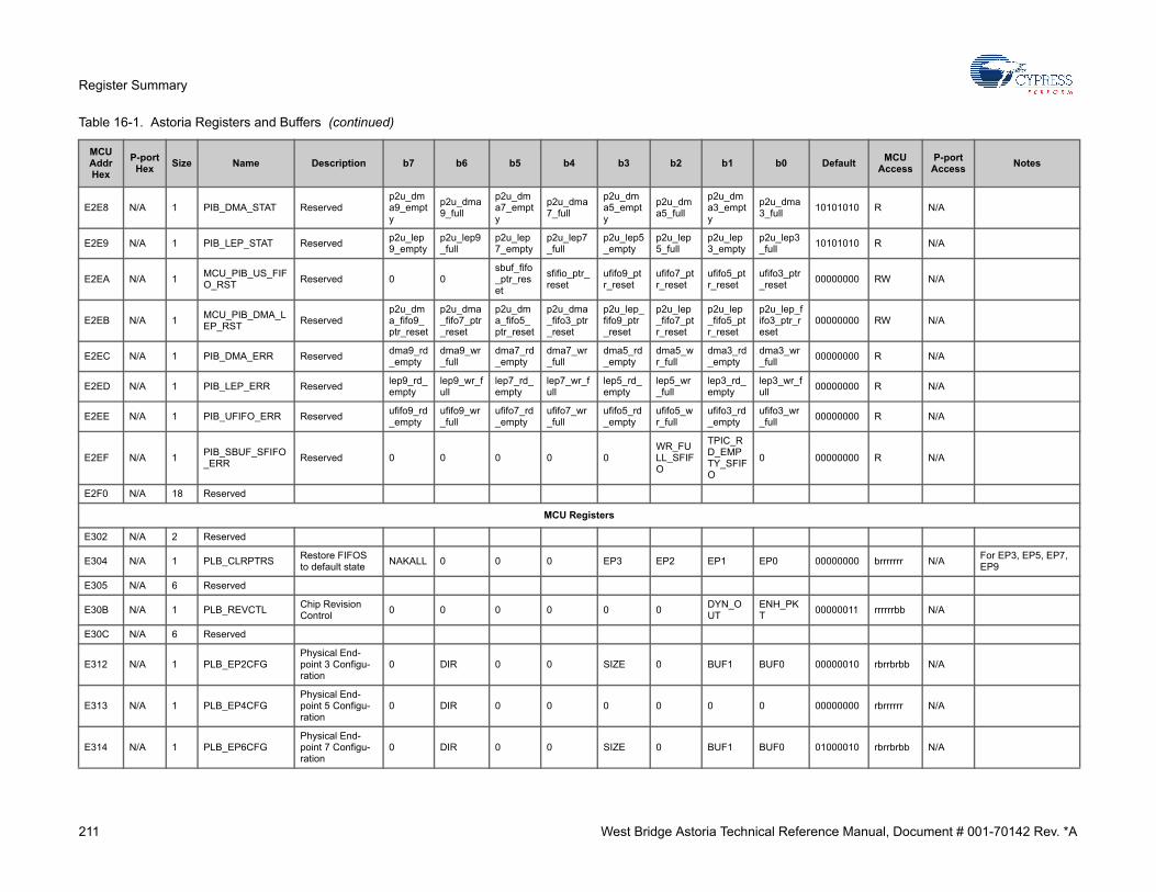
211 West Bridge Astoria Technical Reference Manual, Document # 001-70142 Rev. *A
Register Summary
E2E8 N/A 1 PIB_DMA_STAT Reservedp2u_dma9_empty
p2u_dma9_full
p2u_dma7_empty
p2u_dma7_full
p2u_dma5_empty
p2u_dma5_full
p2u_dma3_empty
p2u_dma3_full
10101010 R N/A
E2E9 N/A 1 PIB_LEP_STAT Reservedp2u_lep9_empty
p2u_lep9_full
p2u_lep7_empty
p2u_lep7_full
p2u_lep5_empty
p2u_lep5_full
p2u_lep3_empty
p2u_lep3_full
10101010 R N/A
E2EA N/A 1MCU_PIB_US_FIFO_RST
Reserved 0 0sbuf_fifo_ptr_reset
sfifio_ptr_reset
ufifo9_ptr_reset
ufifo7_ptr_reset
ufifo5_ptr_reset
ufifo3_ptr_reset
00000000 RW N/A
E2EB N/A 1MCU_PIB_DMA_LEP_RST
Reservedp2u_dma_fifo9_ptr_reset
p2u_dma_fifo7_ptr_reset
p2u_dma_fifo5_ptr_reset
p2u_dma_fifo3_ptr_reset
p2u_lep_fifo9_ptr_reset
p2u_lep_fifo7_ptr_reset
p2u_lep_fifo5_ptr_reset
p2u_lep_fifo3_ptr_reset
00000000 RW N/A
E2EC N/A 1 PIB_DMA_ERR Reserveddma9_rd_empty
dma9_wr_full
dma7_rd_empty
dma7_wr_full
dma5_rd_empty
dma5_wr_full
dma3_rd_empty
dma3_wr_full
00000000 R N/A
E2ED N/A 1 PIB_LEP_ERR Reservedlep9_rd_empty
lep9_wr_full
lep7_rd_empty
lep7_wr_full
lep5_rd_empty
lep5_wr_full
lep3_rd_empty
lep3_wr_full
00000000 R N/A
E2EE N/A 1 PIB_UFIFO_ERR Reservedufifo9_rd_empty
ufifo9_wr_full
ufifo7_rd_empty
ufifo7_wr_full
ufifo5_rd_empty
ufifo5_wr_full
ufifo3_rd_empty
ufifo3_wr_full
00000000 R N/A
E2EF N/A 1PIB_SBUF_SFIFO_ERR
Reserved 0 0 0 0 0WR_FULL_SFIFO
TPIC_RD_EMPTY_SFIFO
0 00000000 R N/A
E2F0 N/A 18 Reserved
MCU Registers
E302 N/A 2 Reserved
E304 N/A 1 PLB_CLRPTRSRestore FIFOS to default state
NAKALL 0 0 0 EP3 EP2 EP1 EP0 00000000 brrrrrrr N/AFor EP3, EP5, EP7, EP9
E305 N/A 6 Reserved
E30B N/A 1 PLB_REVCTLChip Revision Control
0 0 0 0 0 0DYN_OUT
ENH_PKT
00000011 rrrrrrbb N/A
E30C N/A 6 Reserved
E312 N/A 1 PLB_EP2CFGPhysical End-point 3 Configu-ration
0 DIR 0 0 SIZE 0 BUF1 BUF0 00000010 rbrrbrbb N/A
E313 N/A 1 PLB_EP4CFGPhysical End-point 5 Configu-ration
0 DIR 0 0 0 0 0 0 00000000 rbrrrrrr N/A
E314 N/A 1 PLB_EP6CFGPhysical End-point 7 Configu-ration
0 DIR 0 0 SIZE 0 BUF1 BUF0 01000010 rbrrbrbb N/A
Table 16-1. Astoria Registers and Buffers (continued)
MCU Addr Hex
P-port Hex
Size Name Description b7 b6 b5 b4 b3 b2 b1 b0 DefaultMCU
AccessP-port Access
Notes

212 West Bridge Astoria Technical Reference Manual, Document # 001-70142 Rev. *A
Register Summary
E315 N/A 1 PLB_EP8CFGPhysical End-point 9 Configu-ration
0 DIR 0 0 0 0 0 0 01000000 rbrrrrrr N/A
E316 N/A 2 Reserved
E318 N/A 1 PLB_EP2FIFCFGEndpoint 3 Slave FIFO Configura-tion
0 INFM1 OEP1AUTO-OUT
AUTOINZERO-LENIN
0WORD-WIDE
00000101 rbbbbbrb N/A
E319 N/A 1 PLB_EP4FIFCFGEndpoint 5 Slave FIFO Configura-tion
0 INFM1 OEP1AUTO-OUT
AUTOINZERO-LENIN
0WORD-WIDE
00000101 rbbbbbrb N/A
E31A N/A 1 PLB_EP6FIFCFGEndpoint 7 Slave FIFO Configura-tion
0 INFM1 OEP1AUTO-OUT
AUTOINZERO-LENIN
0WORD-WIDE
00000101 rbbbbbrb N/A
E31B N/A 1 PLB_EP8FIFCFGEndpoint 9 Slave FIFO Configura-tion
0 INFM1 OEP1AUTO-OUT
AUTOINZERO-LENIN
0WORD-WIDE
00000101 rbbbbbrb N/A
E31C N/A 4 Reserved
E320 N/A 1PLB_EP2PKTLENH
ReservedReserved
ReservedReserved
ReservedReserved
Reserved
Reserved
Reserved 00000010 R N/A
E321 N/A 1PLB_EP2PKTLENL
ReservedReserved
ReservedReserved
ReservedReserved
Reserved
Reserved
Reserved 00000000 R N/A
E322 N/A 1PLB_EP4PKTLENH
ReservedReserved
ReservedReserved
ReservedReserved
Reserved
Reserved
Reserved 00000010 R N/A
E323 N/A 1PLB_EP4PKTLENL
ReservedReserved
ReservedReserved
ReservedReserved
Reserved
Reserved
Reserved 00000000 R N/A
E324 N/A 1PLB_EP6PKTLENH
ReservedReserved
ReservedReserved
ReservedReserved
Reserved
Reserved
Reserved 00000010 R N/A
E325 N/A 1PLB_EP6PKTLENL
ReservedReserved
ReservedReserved
ReservedReserved
Reserved
Reserved
Reserved 00000000 R N/A
E326 N/A 1PLB_EP8PKTLENH
ReservedReserved
ReservedReserved
ReservedReserved
Reserved
Reserved
Reserved 00000010 R N/A
E327 N/A 1PLB_EP8PKTLENL
ReservedReserved
ReservedReserved
ReservedReserved
Reserved
Reserved
Reserved 00000000 R N/A
E328 N/A 8 Reserved
E330 N/A 1PLB_EP2ALMOSTH
Endpoint 2/Slave FIFO Program-mable-Level Flag HIGH
DECIS PKTSTATIN_PKTS[2]
IN_PKTS[1]
IN_PKTS[0]
0 PFC[9] PFC[8] 10001000 bbbbbrbb N/APFC[9:0] = contains the current packet bytes to be trans-ferred when the EPx-FIFOPFH register requires data.E331 N/A 1
PLB_EP2ALMOSTL
Endpoint 2/Slave FIFO Prog. Flag LOW
PFC[7 PFC[6] PFC[5] PFC[4] PFC[3] PFC[2] PFC[1] PFC[0] 00000000 RW N/A
Table 16-1. Astoria Registers and Buffers (continued)
MCU Addr Hex
P-port Hex
Size Name Description b7 b6 b5 b4 b3 b2 b1 b0 DefaultMCU
AccessP-port Access
Notes

213 West Bridge Astoria Technical Reference Manual, Document # 001-70142 Rev. *A
Register Summary
E332 N/A 1PLB_EP4ALMOSTH
Endpoint 4/Slave FIFO Program-mable-Level Flag HIGH
DECIS PKTSTAT 0IN_PKTS[1]
IN_PKTS[0]
0 0 PFC[8] 10001000 bbrbbrrb N/APFC[8:0] = contains the current packet bytes to be trans-ferred when the EPx-FIFOPFH register requires data.E333 N/A 1
PLB_EP4ALMOSTL
Endpoint 4/Slave FIFO Prog. Flag LOW
PFC[7 PFC[6] PFC[5] PFC[4] PFC[3] PFC[2] PFC[1] PFC[0] 00000000 RW N/A
E334 N/A 1PLB_EP6ALMOSTH
Endpoint 6/Slave FIFO Program-mable-Level Flag HIGH
DECIS PKTSTATIN_PKTS[2]
IN_PKTS[1]
IN_PKTS[0]
0 PFC[9] PFC[8] 00001000 bbbbbrbb N/APFC[9:0] = contains the current packet bytes to be trans-ferred when the EPx-FIFOPFH register requires data.E335 N/A 1
PLB_EP6ALMOSTL
Endpoint 6/Slave FIFO Prog. Flag LOW
PFC[7 PFC[6] PFC[5] PFC[4] PFC[3] PFC[2] PFC[1] PFC[0] 00000000 RW N/A
E336 N/A 1PLB_EP8ALMOSTH
Endpoint 8/Slave FIFO Program-mable-Level Flag HIGH
DECIS PKTSTAT 0IN_PKTS[1]
IN_PKTS[0]
0 0 PFC[8] 00001000 bbrbbrrb N/APFC[8:0] = contains the current packet bytes to be trans-ferred when the EPx-FIFOPFH register requires data.E337 N/A 1
PLB_EP8ALMOSTL
Endpoint 8/Slave FIFO Prog. Flag LOW
PFC[7 PFC[6] PFC[5] PFC[4] PFC[3] PFC[2] PFC[1] PFC[0] 00000000 RW N/A
E338 N/A 1 PLB_EP12CFGLEP12 Configu-ration Register
VALID PEP1 PEP0 TYPE1 TYPE0 NAK STALL FLUSH 10010000 RW N/A
E339 N/A 1 PLB_EP13CFGLEP13 Configu-ration Register
VALID PEP1 PEP0 TYPE1 TYPE0 NAK STALL FLUSH 10010000 RW N/A
E336A N/A 1 PLB_EP14CFGLEP14 Configu-ration Register
VALID PEP1 PEP0 TYPE1 TYPE0 NAK STALL FLUSH 10010000 RW N/A
E33B N/A 1 PLB_EP15CFGLEP15 Configu-ration Register
VALID PEP1 PEP0 TYPE1 TYPE0 NAK STALL FLUSH 10010000 RW N/A
E33C N/A 4 Reserved
E340 N/A 1PLB_EP2ISOINPKTS
Physical End-point 3 (if ISO) IN Packets Per Frame
AADJ 0 0 0 0 0INPPF[1]
INPPF[0] 00000001 brrrrrbb N/A
E341 N/A 1 Reserved
E342 N/A 1PLB_EP6ISOINPKTS
Physical End-point 7 (if ISO) IN Packets Per Frame
AADJ 0 0 0 0 0INPPF[1]
INPPF[0] 00000001 brrrrrbb N/A
E343 N/A 5 Reserved
E348 N/A 1 PLB_INPKTENDForce IN Packet End
SKIP 0 0 0 EP3 EP2 EP1 EP0 xxxxxxxx W N/AREVCTL.0=1 to enable this feature
Table 16-1. Astoria Registers and Buffers (continued)
MCU Addr Hex
P-port Hex
Size Name Description b7 b6 b5 b4 b3 b2 b1 b0 DefaultMCU
AccessP-port Access
Notes

214 West Bridge Astoria Technical Reference Manual, Document # 001-70142 Rev. *A
Register Summary
E349 N/A 1PLB_OUTPKTEND
Force OUT Packet End
SKIP 0 0 0 EP3 EP2 EP1 EP0 xxxxxxxx W N/AREVCTL.0=1 to enable this feature
E34A N/A 1 PLB_EP3CFGLEP3 Configura-tion Register
VALID PEP1 PEP0 TYPE1 TYPE0 NAK STALL FLUSH 10010000 RW N/A
E34B N/A 1 PLB_EP5CFGLEP5 Configura-tion Register
VALID PEP1 PEP0 TYPE1 TYPE0 NAK STALL FLUSH 10010000 RW N/A
E34C N/A 1 PLB_EP7CFGLEP7 Configura-tion Register
VALID PEP1 PEP0 TYPE1 TYPE0 NAK STALL FLUSH 10010000 RW N/A
E34D N/A 1 PLB_EP9CFGLEP9 Configura-tion Register
VALID PEP1 PEP0 TYPE1 TYPE0 NAK STALL FLUSH 10010000 RW N/A
E34E N/A 1 PLB_EP10CFGLEP10 Configu-ration Register
VALID PEP1 PEP0 TYPE1 TYPE0 NAK STALL FLUSH 10010000 RW N/A
E34F N/A 1 PLB_EP11CFGLEP11 Configu-ration Register
VALID PEP1 PEP0 TYPE1 TYPE0 NAK STALL FLUSH 10010000 RW N/A
E350 N/A 1 PLB_EP2FLAGIE
Physical EP3 Slave FIFO Flag Interrupt Enable (INT4)
0 0 0 0 EDGEPF PF EF FF 00000000 rrrrbbbb N/A
E351 N/A 1PLB_EP2FLAGIRQ
Physical End-point 3 Interrupt flag enable
0 0 0 0 0 PF EF FF 00000000 W1C N/A
E352 N/A 1 PLB_EP4FLAGIE
Physical EP5 Slave FIFO Flag Interrupt Enable (INT4)
0 0 0 0 EDGEPF PF EF FF 00000000 rrrrbbbb N/A
E353 N/A 1PLB_EP4FLAGIRQ
Physical End-point 5 Interrupt flag enable
0 0 0 0 0 PF EF FF 00000000 W1C N/A
E354 N/A 1 PLB_EP6FLAGIE
Physical EP7 Slave FIFO Flag Interrupt Enable (INT4)
0 0 0 0 EDGEPF PF EF FF 00000000 rrrrbbbb N/A
E355 N/A 1PLB_EP6FLAGIRQ
Physical End-point 7 Interrupt flag enable
0 0 0 0 0 PF EF FF 00000000 W1C N/A
E356 N/A 1 PLB_EP8FLAGIE
Physical EP9 Slave FIFO Flag Interrupt Enable (INT4)
0 0 0 0 EDGEPF PF EF FF 00000000 rrrrbbbb N/A
E357 N/A 1PLB_EP8FLAGIRQ
Physical End-point 9 Interrupt flag enable
0 0 0 0 0 PF EF FF 00000000 W1C N/A
Table 16-1. Astoria Registers and Buffers (continued)
MCU Addr Hex
P-port Hex
Size Name Description b7 b6 b5 b4 b3 b2 b1 b0 DefaultMCU
AccessP-port Access
Notes

215 West Bridge Astoria Technical Reference Manual, Document # 001-70142 Rev. *A
Register Summary
E358 N/A 1 PLB_IBNIEIN-BULK-NAK Interrupt Request Enable(INT52)
0 0 EP9 EP7 EP5 EP3 0 0 00000000 rrbbbbrr N/A
E359 N/A 1 PLB_IBNIN-BULK-NAK Interrupt Request (INT52)
0 0 EP9 EP7 EP5 EP3 0 0 00000000 W1C N/A
E35A N/A 1 PLB_EPPINGIENEndpoint Ping-NAK / IBN Inter-rupt Enable
EP9 EP7 EP5 EP3 0 0 0 IBN 00000000 bbbbrrrb N/A
E35B N/A 1 PLB_EPPINGIRQ
Endpoint Ping-NAK/IBN Inter-rupt Request (INT2)
EP9 EP7 EP5 EP3 0 0 0 IBN 00000000 bbbbrrrb N/A
E35C N/A 2 Reserved
E35E N/A 1 PLB_EPIENEndpoint Inter-rupt Enables
EP9 EP7 EP5 EP3 0 0 0 0 00000000 bbbbrrrr N/A
E35F N/A 1 PLB_EPIRQEndpoint Inter-rupt Requests (INT2)
EP9 EP7 EP5 EP3 0 0 0 0 00000000 W1C N/A
E360 N/A 2 Reserved
E362 N/A 1 PLB_EPERRIENUSB Error Inter-rupt Enables
ISOEP8 ISOEP6 ISOEP4 ISOEP2 0 0 0ERRLIMIT
00000000 bbbbrrrb N/A
E363 N/A 1 PLB_EPERRIRQUSB Error Inter-rupt Requests
ISOEP8 ISOEP6 ISOEP4 ISOEP2 0 0 0ERRLIMIT
00000000 W1C N/A
E364 N/A 1 PLB_ERRLIMITUSB ERROR LIMIT and Count
EC[3] EC[2] EC[1] EC[0] LIMIT[3] LIMIT[2] LIMIT[1] LIMIT[0] 00000100 rrrrbbbb N/A
LIMIT[1:0] = USB bus error count and limit. The firmware can enable the inter-rupt to cause an interrupt when the limit is reached. The default limit count is 4
EC[3:0] = Error count has a maximum value of 15
E365 N/A 1PLB_CLRERRCNT
Clear Error Count b7 b6 b5 b4 b3 b2 b1 b0 xxxxxxxx W1C N/A
E366 N/A 1 PLB_INT2IVECINTERRUPT 5 (USB) Autovector
0 I2V4 I2V3 I2V2 I2V1 I2V0 0 0 00000000 R N/AI2V indicates the source of an interrupt from the USB Core.
Table 16-1. Astoria Registers and Buffers (continued)
MCU Addr Hex
P-port Hex
Size Name Description b7 b6 b5 b4 b3 b2 b1 b0 DefaultMCU
AccessP-port Access
Notes

216 West Bridge Astoria Technical Reference Manual, Document # 001-70142 Rev. *A
Register Summary
E367 N/A 1 PLB_INT4IVECInterrupt 6 (slave FIFOs & GPIF) Autovector
0 0 I4V3 I4V2 I4V1 I4V0 0 0 10000000 R N/AI4V indicates the source of an interrupt from the USB Core.
E368 N/A 40 Reserved
E390 NA/ 1 PLB_EP2BCHPhysical End-point 3 Byte Count High
LEP_TAG[3]
LEP_TAG[2]
LEP_TAG[1]
LEP_TAG[0]
x BC10 BC9 BC8 xxxxxxxx rrrrrbbb N/ALEP_TAG[3:0] = LEP Number corre-sponding to the pay-load in this PEP buffer
BC[10:8] = Endpoint 2 Byte Count
E391 N/A 1 PLB_EP2BCLPhysical End-point 3 Byte Count Low
BC7 BC6 BC5 BC4 BC3 BC2 BC1 BC0 xxxxxxxx RW N/A
E392 N/A 2 Reserved
E394 N/A 1 PLB_EP4BCHPhysical End-point 5 Byte Count High
LEP_TAG[3]
LEP_TAG[2]
LEP_TAG[1]
LEP_TAG[0]
x x BC9 BC8 xxxxxxxx rrrrrrbb N/ALEP_TAG[3:0] = LEP Number corre-sponding to the pay-load in this PEP buffer
BC[10:8] = Endpoint 4 Byte Count
E395 N/A 1 PLB_EP4BCLPhysical End-point 5 Byte Count Low
BC7 BC6 BC5 BC4 BC3 BC2 BC1 BC0 xxxxxxxx RW N/A
E396 N/A 2 Reserved
E398 NA/ 1 PLB_EP6BCHPhysical End-point 7 Byte Count High
LEP_TAG[3]
LEP_TAG[2]
LEP_TAG[1]
LEP_TAG[0]
x BC10 BC9 BC8 xxxxxxxx rrrrrbbb N/ALEP_TAG[3:0] = LEP Number corre-sponding to the pay-load in this PEP buffer
BC[10:8] = Endpoint 6 Byte Count
E399 N/A 1 PLB_EP6BCLPhysical End-point 7 Byte Count Low
BC7 BC6 BC5 BC4 BC3 BC2 BC1 BC0 xxxxxxxx RW N/A
E39A N/A 2 Reserved
E39C N/A 1 PLB_EP8BCHPhysical End-point 9 Byte Count High
LEP_TAG[3]
LEP_TAG[2]
LEP_TAG[1]
LEP_TAG[0]
x x BC9 BC8 xxxxxxxx rrrrrrbb N/ALEP_TAG[3:0] = LEP Number corre-sponding to the pay-load in this PEP buffer
BC[10:8] = Endpoint 8 Byte Count
E39D N/A 1 PLB_EP8BCLPhysical End-point 9 Byte Count Low
BC7 BC6 BC5 BC4 BC3 BC2 BC1 BC0 xxxxxxxx RW N/A
E39E N/A 5 Reserved
E3A3 N/A 1 PLB_EP2CSPhysical End-point 3 Control and Status
0 NPAK2 NPAK1 NPAK0 FULL EMPTY 0 0 0010100 R N/A
NPAK[2:0] = The number of packets in the FIFO. 0-4 Pack-ets.
Table 16-1. Astoria Registers and Buffers (continued)
MCU Addr Hex
P-port Hex
Size Name Description b7 b6 b5 b4 b3 b2 b1 b0 DefaultMCU
AccessP-port Access
Notes

217 West Bridge Astoria Technical Reference Manual, Document # 001-70142 Rev. *A
Register Summary
E3A4 N/A 1 PLB_EP4CSPhysical End-point 5 Control and Status
0 0 NPAK1 NPAK0 FULL EMPTY 0 0 0010100 R N/A
NPAK[1:0] = The number of packets in the FIFO. 0-2 Pack-ets.
E3A5 N/A 1 PLB_EP6CSPhysical End-point 7 Control and Status
0 NPAK2 NPAK1 NPAK0 FULL EMPTY 0 0 0000100 R N/A
NPAK[2:0] = The number of packets in the FIFO. 0-4 Pack-ets.
E3A6 N/A 1 PLB_EP8CSPhysical End-point 9 Control and Status
0 0 NPAK1 NPAK0 FULL EMPTY 0 0 0000100 R N/A
NPAK[1:0] = The number of packets in the FIFO. 0-2 Pack-ets.
E3A7 N/A 1 PLB_EP2FLAGSPhysical EP3 sta-tus Flags
0 0 0 0 0 PF EF FF 00000010 R N/A
E3A8 N/A 1 PLB_EP4FLAGSPhysical EP5 sta-tus Flags
0 0 0 0 0 PF EF FF 00000010 R N/A
E3A9 N/A 1 PLB_EP6FLAGSPhysical EP7 sta-tus Flags
0 0 0 0 0 PF EF FF 00000110 R N/A
E3AA N/A 1 PLB_EP8FLAGSPhysical EP9 sta-tus Flags
0 0 0 0 0 PF EF FF 00000110 R N/A
Table 16-1. Astoria Registers and Buffers (continued)
MCU Addr Hex
P-port Hex
Size Name Description b7 b6 b5 b4 b3 b2 b1 b0 DefaultMCU
AccessP-port Access
Notes

218 West Bridge Astoria Technical Reference Manual, Document # 001-70142 Rev. *A
Register Summary
E3AB N/A 1PLB_EP2FIFOBCNTH
Physical End-point 3 Slave FIFO Total Byte Count HIGH
0 0 0 BC12 BC11 BC10 BC9 BC8 00000000 R N/A
Total number of bytes in Endpoint FIFO.
EP2 max 4096
EP4 max 1024
EP6 max 2048
EP8 max 1024
E3AC N/A 1PLB_EP2FIFOBCNTL
Physical End-point 3 Slave FIFO Total Byte Count Low
BC7 BC6 BC5 BC4 BC3 BC2 BC1 BC0 00000000 R N/A
E3AD N/A 1PLB_EP4FIFOBCNTH
Physical End-point 5 Slave FIFO Total Byte Count HIGH
0 0 0 0 0 BC10 BC9 BC8 00000000 R N/A
E3AE N/A 1PLB_EP4FIFOBCNTL
Physical End-point 5 Slave FIFO Total Byte Count Low
BC7 BC6 BC5 BC4 BC3 BC2 BC1 BC0 00000000 R N/A
E3AF N/A 1PLB_EP6FIFOBCNTH
Physical End-point 7 Slave FIFO Total Byte Count HIGH
0 0 0 0 BC11 BC10 BC9 BC8 00000000 R N/A
E3B0 N/A 1PLB_EP6FIFOBCNTL
Physical End-point 7 Slave FIFO Total Byte Count Low
BC7 BC6 BC5 BC4 BC3 BC2 BC1 BC0 00000000 R N/A
E3B1 N/A 1PLB_EP8FIFOBCNTH
Physical End-point 9 Slave FIFO Total Byte Count HIGH
0 0 0 0 0 BC10 BC9 BC8 00000000 R N/A
E3B2 N/A 1PLB_EP8FIFOBCNTL
Physical End-point 9 Slave FIFO Total Byte Count Low
BC7 BC6 BC5 BC4 BC3 BC2 BC1 BC0 00000000 R N/A
E3B3 N/A 76 Reserved
GPI Waveform Memories
E400 N/A 128GPIF WAVE-FORM RAM
GPIF Waveform Descriptor 0, 1, 2, 3 data
D7 D6 D5 D4 D3 D2 D1 D0 xxxxxxxx RW N/AAssociated / pointed to by GPIFWFSE-LECT
Astoria Registers
E480 N/A 1 MECC_CFGHolds MECC configuration information
MLC_ECC_EN
Mode2x 0Deco-deCfg[1]
Deco-deCfg[0]
0Data-Path Width
AddSOH 00000000 bbrbbrbb N/A
Table 16-1. Astoria Registers and Buffers (continued)
MCU Addr Hex
P-port Hex
Size Name Description b7 b6 b5 b4 b3 b2 b1 b0 DefaultMCU
AccessP-port Access
Notes

219 West Bridge Astoria Technical Reference Manual, Document # 001-70142 Rev. *A
Register Summary
E481 N/A 1 MECC_SELDecoder/Encoder select
0 0 0 0 0 0 0 DecNenc 00000000 rrrrrrrb N/A
It resets MECC regis-ters and byte counts. Subsequent read/write transfers from/to Nand causes ECC value to be com-puted. ECC compu-tation is stopped after selected data byte count.
E482 N/A 1 MECC_CMD
This register is used for initiating a command to the decoder.
0 0 0detedt_cmd[1]
detedt_cmd[0]
0 0 0 00000000 rrrbbrrr N/AWrites to this regis-ter are ignored when Encoder is enabled.
E483 N/A 1 MECC_STAT
Provides status during all stages and at the end of operation.
mecc_status[7]
mecc_status[6]
mecc_status[5]
mecc_status[4]
mecc_status[3]
mecc_status[2]
mecc_status[1]
mecc_status[0]
00000000 R N/A
`bxxxx_xxx0: Wait `bxxxx_xxx1: Done Encoder status Codes: `b0000_0000: EncodeWait `b0000_0001: NoEr-rors Decoder status Codes: `b0000_0000: Deco-deErrCheckWait `b0000_0001: NoEr-rors `b0000_0011: DecodeErrCheck-Done `b0000_0110: ErrCountWait `b0000_0111: ErrCountDone `b0000_1110: ErrLocWait `b0001_1110: ErrDe-tectWait `b0001_1111: ErrDe-tectDone `b0011_1110: ErrCorrectWait `b0011_1111: ErrCor-rectDone `b1000_0111: TooManyErrors Other codes are reserved.
Table 16-1. Astoria Registers and Buffers (continued)
MCU Addr Hex
P-port Hex
Size Name Description b7 b6 b5 b4 b3 b2 b1 b0 DefaultMCU
AccessP-port Access
Notes
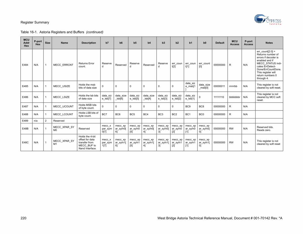
220 West Bridge Astoria Technical Reference Manual, Document # 001-70142 Rev. *A
Register Summary
E484 N/A 1 MECC_ERRCNTReturns Error count.
Reserved
ReservedReserved
ReservedReserved
err_count[2]
err_count[1]
err_count[0]
00000000 R N/A
err_count[2:0] = Returns number of errors if decoder is enabled and if MECC_STATUS indi-cates ErrDetect-Done/ErrCountDone. This register will return numbers 0 through 4.
E485 N/A 1 MECC_USIZEHolds the msb bits of data size
0 0 0 0 0 0data_size_msb[1]
data_size_msb[0]
00000011 rrrrrrbb N/AThis register is not cleared by soft reset.
E486 N/A 1 MECC_LSIZEHolds the lsb bits of data size
data_size_lsb[7]
data_size_lsb[6]
data_size_lsb[5]
data_size_lsb[4]
data_size_lsb[3]
data_size_lsb[2]
data_size_lsb[1]
0 11111110 bbbbbbbr N/AThis register is not cleared by MCC soft reset.
E487 N/A 1 MECC_UCOUNTHolds MSB bits of byte count.
0 0 0 0 0 0 BC9 BC8 00000000 R N/A
E488 N/A 1 MECC_LCOUNTHolds LSB bits of byte count.
BC7 BC6 BC5 BC4 BC3 BC2 BC1 BC0 00000000 R N/A
E489 n/a 2 Reserved
E48B N/A 1MECC_XPAR_SYM0
Reservedmecc_xpar_sym0[7]
mecc_xpar_sym0[6]
mecc_xpar_sym0[5]
mecc_xpar_sym0[4]
mecc_xpar_sym0[3]
mecc_xpar_sym0[2]
mecc_xpar_sym0[1]
mecc_xpar_sym0[0]
00000000 RW N/AReserved bits. Reads zero.
E48C N/A 1MECC_XPAR_SYM1
Holds the 4-bit offset for data transfer from MECC_BUF to Nand Interface.
mecc_xpar_sym1[7]
mecc_xpar_sym1[6]
mecc_xpar_sym1[5]
mecc_xpar_sym1[4]
mecc_xpar_sym1[3]
mecc_xpar_sym1[2]
mecc_xpar_sym1[1]
mecc_xpar_sym1[0]
00000000 RW N/AThis register is not cleared by soft reset
Table 16-1. Astoria Registers and Buffers (continued)
MCU Addr Hex
P-port Hex
Size Name Description b7 b6 b5 b4 b3 b2 b1 b0 DefaultMCU
AccessP-port Access
Notes

221 West Bridge Astoria Technical Reference Manual, Document # 001-70142 Rev. *A
Register Summary
E48D N/A 1 MECC_SOH0Holds the over-head bytes infor-mation.
mecc_soh0[7]
mecc_soh0[6]
mecc_soh0[5]
mecc_soh0[4]
mecc_soh0[3]
mecc_soh0[2]
mecc_soh0[1]
mecc_soh0[0]
00000000 RW N/A
The CPU modifies this register. This register is not cleared by soft reset. This register be same for multiple sectors/pages within a block.
E48E N/A 1 MECC_SOH1Holds the over-head bytes infor-mation.
mecc_soh1[7]
mecc_soh1[6]
mecc_soh1[5]
mecc_soh1[4]
mecc_soh1[3]
mecc_soh1[2]
mecc_soh1[1]
mecc_soh1[0]
00000000 RW N/A
E48F N/A 1 MECC_SOH2Holds the over-head bytes infor-mation.
mecc_soh2[7]
mecc_soh2[6]
mecc_soh2[5]
mecc_soh2[4]
mecc_soh2[3]
mecc_soh2[2]
mecc_soh2[1]
mecc_soh2[0]
00000000 RW N/A
E490 N/A 1 MECC_SOH3Holds the over-head bytes infor-mation.
mecc_soh3[7]
mecc_soh3[6]
mecc_soh3[5]
mecc_soh3[4]
mecc_soh3[3]
mecc_soh3[2]
mecc_soh3[1]
mecc_soh3[0]
00000000 RW N/A
E491 N/A 1 MECC_SOH4Holds the over-head bytes infor-mation.
mecc_soh4[7]
mecc_soh4[6]
mecc_soh4[5]
mecc_soh4[4]
mecc_soh4[3]
mecc_soh4[2]
mecc_soh4[1]
mecc_soh4[0]
00000000 RW N/A
E492 N/A 1 MECC_SOH5Holds the over-head bytes infor-mation.
mecc_soh5[7]
mecc_soh5[6]
mecc_soh5[5]
mecc_soh5[4]
mecc_soh5[3]
mecc_soh5[2]
mecc_soh5[1]
mecc_soh5[0]
00000000 RW N/A
E493 N/A 1MECC_ERRLOC_U0
Holds the error location of 1st error
0 0 0 0 0 0err_locations0_msb[1]
err_locations0_msb[0]
00000000 R N/ARegister is cleared when decoder is reset
E494 N/A 1MECC_ERRLOC_L0
Holds the error location of 1st error
err_locations0_lsb[7]
err_locations0_lsb[6]
err_locations0_lsb[5]
err_locations0_lsb[4]
err_locations0_lsb[3]
err_locations0_lsb[2]
err_locations0_lsb[1]
err_locations0_lsb[0]
00000000 R N/A
E495 N/A 1 MECC_ERR_U0Holds the error magnitude of 1st error
0 0 0 0 0 0err0_msb[1]
err0_msb[0]
00000000 R N/ARegister is cleared when decoder is reset.
E496 N/A 1 MECC_ERR_L0Holds the error magnitude of 1st error
err0_lsb[7]
err0_lsb[6]
err0_lsb[5]
err0_lsb[4]
err0_lsb[3]
err0_lsb[2]
err0_lsb[1]
err0_lsb[0]
00000000 R N/A
E497 N/A 1MECC_ERRLOC_U1
Holds the error location of 1st error
0 0 0 0 0 0err_locations1_msb[1]
err_locations1_msb[0]
00000000 R N/ARegister is cleared when decoder is reset
E498 N/A 1MECC_ERRLOC_L1
Holds the error location of 1st error
err_locations1_lsb[7]
err_locations1_lsb[6]
err_locations1_lsb[5]
err_locations1_lsb[4]
err_location10_lsb[3]
err_locations1_lsb[2]
err_locations1_lsb[1]
err_locations1_lsb[0]
00000000 R N/A
E499 N/A 1 MECC_ERR_U1Holds the error magnitude of 1st error
0 0 0 0 0 0err1_msb[1]
err1_msb[0]
00000000 R N/ARegister is cleared when decoder is reset.
E49A N/A 1 MECC_ERR_L1Holds the error magnitude of 1st error
err1_lsb[7]
err1_lsb[6]
err1_lsb[5]
err1_lsb[4]
err1_lsb[3]
err1_lsb[2]
err1_lsb[1]
err1_lsb[0]
00000000 R N/A
Table 16-1. Astoria Registers and Buffers (continued)
MCU Addr Hex
P-port Hex
Size Name Description b7 b6 b5 b4 b3 b2 b1 b0 DefaultMCU
AccessP-port Access
Notes

222 West Bridge Astoria Technical Reference Manual, Document # 001-70142 Rev. *A
Register Summary
E49B N/A 1MECC_ERRLOC_U2
Holds the error location of 1st error
0 0 0 0 0 0err_locations2_msb[1]
err_locations2_msb[0]
00000000 R N/ARegister is cleared when decoder is reset
E49C N/A 1MECC_ERRLOC_L2
Holds the error location of 1st error
err_locations2_lsb[7]
err_locations2_lsb[6]
err_locations2_lsb[5]
err_locations2_lsb[4]
err_locations2_lsb[3]
err_locations2_lsb[2]
err_locations2_lsb[1]
err_locations2_lsb[0]
00000000 R N/A
E49D N/A 1 MECC_ERR_U2Holds the error magnitude of 1st error
0 0 0 0 0 0err2_msb[1]
err2_msb[0]
00000000 R N/ARegister is cleared when decoder is reset.
E49E N/A 1 MECC_ERR_L2Holds the error magnitude of 1st error
err2_lsb[7]
err2_lsb[6]
err2_lsb[5]
err2_lsb[4]
err2_lsb[3]
err2_lsb[2]
err2_lsb[1]
err2_lsb[0]
00000000 R N/A
E49F N/A 1MECC_ERRLOC_U3
Holds the error location of 1st error
0 0 0 0 0 0err_locations3_msb[1]
err_locations3_msb[0]
00000000 R N/ARegister is cleared when decoder is reset
E4A0 N/A 1MECC_ERRLOC_L3
Holds the error location of 1st error
err_locations3_lsb[7]
err_locations3_lsb[6]
err_locations3_lsb[5]
err_locations3_lsb[4]
err_locations3_lsb[3]
err_locations3_lsb[2]
err_locations3_lsb[1]
err_locations3_lsb[0]
00000000 R N/A
E4A1 N/A 1 MECC_ERR_U3Holds the error magnitude of 1st error
0 0 0 0 0 0err3_msb[1]
err3_msb[0]
00000000 R N/ARegister is cleared when decoder is reset.
E4A2 N/A 1 MECC_ERR_L3Holds the error magnitude of 1st error
err3_lsb[7]
err3_lsb[6]
err3_lsb[5]
err3_lsb[4]
err3_lsb[3]
err3_lsb[2]
err3_lsb[1]
err3_lsb[0]
00000000 R N/A
E4A3 N/A 1 MECC_BUF0 MECC buffermecc_buf0[7]
mecc_buf0[6]
mecc_buf0[5]
mecc_buf0[4]
mecc_buf0[3]
mecc_buf0[2]
mecc_buf0[1]
mecc_buf0[0]
00000000 RW N/A
E4A4 N/A 1 MECC_BUF1 MECC buffermecc_buf1[7]
mecc_buf1[6]
mecc_buf1[5]
mecc_buf1[4]
mecc_buf1[3]
mecc_buf1[2]
mecc_buf1[1]
mecc_buf1[0]
00000000 RW N/A
E4A5 N/A 1 MECC_BUF2 MECC buffermecc_buf2[7]
mecc_buf2[6]
mecc_buf2[5]
mecc_buf2[4]
mecc_buf2[3]
mecc_buf2[2]
mecc_buf2[1]
mecc_buf2[0]
00000000 RW N/A
E4A6 N/A 1 MECC_BUF3 MECC buffermecc_buf3[7]
mecc_buf3[6]
mecc_buf3[5]
mecc_buf3[4]
mecc_buf3[3]
mecc_buf3[2]
mecc_buf3[1]
mecc_buf3[0]
00000000 RW N/A
E4A7 N/A 1 MECC_BUF4 MECC buffermecc_buf4[7]
mecc_buf4[6]
mecc_buf4[5]
mecc_buf4[4]
mecc_buf4[3]
mecc_buf4[2]
mecc_buf4[1]
mecc_buf4[0]
00000000 RW N/A
E4A8 N/A 1 MECC_BUF5 MECC buffermecc_buf5[7]
mecc_buf5[6]
mecc_buf5[5]
mecc_buf5[4]
mecc_buf5[3]
mecc_buf5[2]
mecc_buf5[1]
mecc_buf5[0]
00000000 RW N/A
E4A9 N/A 1 MECC_BUF6 MECC buffermecc_buf6[7]
mecc_buf6[6]
mecc_buf6[5]
mecc_buf6[4]
mecc_buf6[3]
mecc_buf6[2]
mecc_buf6[1]
mecc_buf6[0]
00000000 RW N/A
E4AA N/A 1 MECC_BUF7 MECC buffermecc_buf7[7]
mecc_buf7[6]
mecc_buf7[5]
mecc_buf7[4]
mecc_buf7[3]
mecc_buf7[2]
mecc_buf7[1]
mecc_buf7[0]
00000000 RW N/A
Table 16-1. Astoria Registers and Buffers (continued)
MCU Addr Hex
P-port Hex
Size Name Description b7 b6 b5 b4 b3 b2 b1 b0 DefaultMCU
AccessP-port Access
Notes

223 West Bridge Astoria Technical Reference Manual, Document # 001-70142 Rev. *A
Register Summary
E4AB N/A 1 MECC_BUF8 MECC buffermecc_buf8[7]
mecc_buf8[6]
mecc_buf8[5]
mecc_buf8[4]
mecc_buf8[3]
mecc_buf8[2]
mecc_buf8[1]
mecc_buf8[0]
00000000 RW N/A
E4AC N/A 1 MECC_BUF9 MECC buffermecc_buf9[7]
mecc_buf9[6]
mecc_buf9[5]
mecc_buf9[4]
mecc_buf9[3]
mecc_buf9[2]
mecc_buf9[1]
mecc_buf9[0]
00000000 RW N/A
E4AD N/A 1 MECC_BUF10 MECC buffermecc_buf10[7]
mecc_buf10[6]
mecc_buf10[5]
mecc_buf10[4]
mecc_buf10[3]
mecc_buf10[2]
mecc_buf10[1]
mecc_buf10[0]
00000000 RW N/A
E4AE N/A 1 MECC_BUF11 MECC buffermecc_buf11[7]
mecc_buf11[6]
mecc_buf11[5]
mecc_buf11[4]
mecc_buf11[3]
mecc_buf11[2]
mecc_buf11[1]
mecc_buf11[0]
00000000 RW N/A
E4AF N/A 1 MECC_BUF12 MECC buffermecc_buf12[7]
mecc_buf12[6]
mecc_buf12[5]
mecc_buf12[4]
mecc_buf12[3]
mecc_buf12[2]
mecc_buf12[1]
mecc_buf12[0]
00000000 RW N/A
E4B0 N/A 1 MECC_BUF13 MECC buffermecc_buf13[7]
mecc_buf13[6]
mecc_buf13[5]
mecc_buf13[4]
mecc_buf13[3]
mecc_buf13[2]
mecc_buf13[1]
mecc_buf13[0]
00000000 RW N/A
E4B1 N/A 1 MECC_BUF14 MECC buffermecc_buf14[7]
mecc_buf14[6]
mecc_buf14[5]
mecc_buf14[4]
mecc_buf14[3]
mecc_buf14[2]
mecc_buf14[1]
mecc_buf14[0]
00000000 RW N/A
E4B2 N/A 1 MECC_BUF15 MECC buffermecc_buf15[7]
mecc_buf15[6]
mecc_buf15[5]
mecc_buf15[4]
mecc_buf15[3]
mecc_buf15[2]
mecc_buf15[1]
mecc_buf15[0]
00000000 RW N/A
E4B3 N/A 13 Reserved
E4C0 N/A 1SIB2_CMD_REG_0
Contents of data to be sent on command bus.
CMD0[7] CMD0[6] CMD0[5] CMD0[4] CMD0[3] CMD0[2] CMD0[1] CMD0[0] 00000000 RW N/A
E4C1 N/A 1SIB2_CMD_REG_1
Contents of data to be sent on command bus.
CMD1[7] CMD1[6] CMD1[5] CMD1[4] CMD1[3] CMD1[2] CMD1[1] CMD1[0] 00000000 RW N/A
E4C2 N/A 1SIB2_CMD_REG_2
Contents of data to be sent on command bus.
CMD2[7] CMD2[6] CMD2[5] CMD2[4] CMD2[3] CMD2[2] CMD2[1] CMD2[0] 00000000 RW N/A
E4C3 N/A 1SIB2_CMD_REG_3
Contents of data to be sent on command bus.
CMD3[7] CMD3[6] CMD3[5] CMD3[4] CMD3[3] CMD3[2] CMD3[1] CMD3[0] 00000000 RW N/A
E4C4 N/A 1SIB2_CMD_REG_4
Contents of data to be sent on command bus.
CMD4[7] CMD4[6] CMD4[5] CMD4[4] CMD4[3] CMD4[2] CMD4[1] CMD4[0] 00000000 RW N/A
E4C5 N/A 1SIB2_CMD_REG_5
Contents of data to be sent on command bus.
CMD5[7] CMD5[6] CMD5[5] CMD5[4] CMD5[3] CMD5[2] CMD5[1] CMD5[0] 00000000 RW N/A
E4C6 N/A 1SIB2_CMD_REG_6
Contents of data to be sent on command bus.
CMD6[7] CMD6[6] CMD6[5] CMD6[4] CMD6[3] CMD6[2] CMD6[1] CMD6[0] 00000000 RW N/A
E4C7 N/A 1SIB2_CMD_REG_7
Contents of data to be sent on command bus.
CMD7[7] CMD7[6] CMD7[5] CMD7[4] CMD7[3] CMD7[2] CMD7[1] CMD7[0] 00000000 RW N/A
Table 16-1. Astoria Registers and Buffers (continued)
MCU Addr Hex
P-port Hex
Size Name Description b7 b6 b5 b4 b3 b2 b1 b0 DefaultMCU
AccessP-port Access
Notes

224 West Bridge Astoria Technical Reference Manual, Document # 001-70142 Rev. *A
Register Summary
E4C8 N/A 1SIB2_RESP_REG_0
Response Data received from the card on response bus.
RESP0[7]
RESP0[6]
RESP0[5]
RESP0[4]RESP0[3]
RESP0[2]
RESP0[1]
RESP0[0] 00000000 R N/A
E4C9 N/A 1SIB2_RESP_REG_1
Response Data received from the card on response bus.
RESP1[7]
RESP1[6]
RESP1[5]
RESP1[4]RESP1[3]
RESP1[2]
RESP1[1]
RESP1[0] 00000000 R N/A
E4CA N/A 1SIB2_RESP_REG_2
Response Data received from the card on response bus.
RESP2[7]
RESP2[6]
RESP2[5]
RESP2[4]RESP2[3]
RESP2[2]
RESP2[1]
RESP2[0] 00000000 R N/A
E4CB N/A 1SIB2_RESP_REG_3
Response Data received from the card on response bus.
RESP3[7]
RESP3[6]
RESP3[5]
RESP3[4]RESP3[3]
RESP3[2]
RESP3[1]
RESP3[0] 00000000 R N/A
E4CC N/A 1SIB2_RESP_REG_4
Response Data received from the card on response bus.
RESP4[7]
RESP4[6]
RESP4[5]
RESP4[4]RESP4[3]
RESP4[2]
RESP4[1]
RESP4[0] 00000000 R N/A
E4CD N/A 1SIB2_RESP_REG_5
Response Data received from the card on response bus.
RESP5[7]
RESP5[6]
RESP5[5]
RESP5[4]RESP5[3]
RESP5[2]
RESP5[1]
RESP5[0] 00000000 R N/A
E4CE N/A 1SIB2_RESP_REG_6
Response Data received from the card on response bus.
RESP6[7]
RESP6[6]
RESP6[5]
RESP6[4]RESP6[3]
RESP6[2]
RESP6[1]
RESP6[0] 00000000 R N/A
E4CF N/A 1SIB2_RESP_REG_7
Response Data received from the card on response bus.
RESP7[7]
RESP7[6]
RESP7[5]
RESP7[4]RESP7[3]
RESP7[2]
RESP7[1]
RESP7[0] 00000000 R N/A
E4D0 N/A 1SIB2_RESP_REG_8
Response Data received from the card on response bus.
RESP8[7]
RESP8[6]
RESP8[5]
RESP8[4]RESP8[3]
RESP8[2]
RESP7[1]
RESP8[0] 00000000 R N/A
E4D1 N/A 1SIB2_RESP_REG_9
Response Data received from the card on response bus.
RESP9[7]
RESP9[6]
RESP9[5]
RESP9[4]RESP9[3]
RESP9[2]
RESP9[1]
RESP9[0] 00000000 R N/A
E4D2 N/A 1SIB2_RESP_REG_10
Response Data received from the card on response bus.
RESP10[7]
RESP10[6]
RESP10[5]
RESP10[4]
RESP10[3]
RESP10[2]
RESP10[1]
RESP10[0]
00000000 R N/A
Table 16-1. Astoria Registers and Buffers (continued)
MCU Addr Hex
P-port Hex
Size Name Description b7 b6 b5 b4 b3 b2 b1 b0 DefaultMCU
AccessP-port Access
Notes

225 West Bridge Astoria Technical Reference Manual, Document # 001-70142 Rev. *A
Register Summary
E4D3 N/A 1SIB2_RESP_REG_11
Response Data received from the card on response bus.
RESP11[7]
RESP11[6]
RESP11[5]
RESP11[4]
RESP11[3]
RESP11[2]
RESP11[1]
RESP11[0]
00000000 R N/A
E4D4 N/A 1SIB2_RESP_REG_12
Response Data received from the card on response bus.
RESP12[7]
RESP12[6]
RESP12[5]
RESP12[4]
RESP12[3]
RESP12[2]
RESP12[1]
RESP12[0]
00000000 R N/A
E4D5 N/A 1SIB2_RESP_REG_13
Response Data received from the card on response bus.
RESP13[7]
RESP13[6]
RESP13[5]
RESP13[4]
RESP13[3]
RESP13[2]
RESP13[1]
RESP13[0]
00000000 R N/A
E4D6 N/A 1SIB2_RESP_REG_14
Response Data received from the card on response bus.
RESP14[7]
RESP14[6]
RESP14[5]
RESP14[4]
RESP14[3]
RESP14[2]
RESP14[1]
RESP14[0]
00000000 R N/A
E4D7 N/A 1SIB2_RESP_REG_15
Response Data received from the card on response bus.
RESP15[7]
RESP15[6]
RESP15[5]
RESP15[4]
RESP15[3]
RESP15[2]
RESP15[1]
RESP15[0]
00000000 R N/A
E4D8 N/A 1SIB2_RESP_REG_16
Response Data received from the card on response bus.
RESP16[7]
RESP16[6]
RESP16[5]
RESP16[4]
RESP16[3]
RESP16[2]
RESP16[1]
RESP16[0]
00000000 R N/A
E4D9 N/A 1 SIB2_CMD_FMTCommand for-mat configuration
P_END_DIS
CMD-COMP
CMD-FRMT[5]
CMD-FRMT[4]
CMD-FRMT[3]
CMD-FRMT[2]
CMD-FRMT[1]
CMD-FRMT[0]
00100101 RW N/A
E4DA N/A 1SIB2_RESP_FMT_0
LSB Response Field Configura-tion
RESPCONF0[7]
RESPCONF0[6]
RESPCONF0[5]
RESPCONF0[4]
RESPCONF0[3]
RESPCONF0[2]
RESPCONF0[1]
RESPCONF0[0]
01111110 RW N/A
E4DB N/A 1SIB2_RESP_FMT_1
MSB Response Field Configura-tion
0 0 0 0 0RESPCONF1[2]
RESPCONF1[1]
RESPCONF1[0]
00000000 rrrrrbbb N/A
E4DC N/A 1SIB2_DATA_FMT_0
Data Field Con-figuration
NOBD[7]
NOBD[6] NOBD[5] NOBD[4] NOBD[3] NOBD[2] NOBD[1] NOBD[0] 00000001 RW N/ANOBD [7:0] = LSB Data field configura-tion
Table 16-1. Astoria Registers and Buffers (continued)
MCU Addr Hex
P-port Hex
Size Name Description b7 b6 b5 b4 b3 b2 b1 b0 DefaultMCU
AccessP-port Access
Notes

226 West Bridge Astoria Technical Reference Manual, Document # 001-70142 Rev. *A
Register Summary
E4DD N/A 1SIB2_DATA_FMT_1
Data Field Con-figuration
INTC-TRLBIT
EPDATA-WIDTH
EP_NUM[1]
EP_NUM[0]
NOB-DCONT[3]
NOB-DCONT[2]
NOB-DCONT[1]
NOB-DCONT[0]
00000000 RW N/A
NOBDCONT[3:0] = NOBD continued. MSB Data field Con-figuration
EP_NUM[1:0] = EP buffer, which MMC.SDIO will read.write data.
00:EP2
01:EP4
10:EP4
11:EP6
E4DE N/A 1 SIB2_CRC_CFGCRC Configura-tion Register
COR_CRC
MASK_CRC_STATUS_ERR
0R_CRC_E_N
0RD_CRC_EN
0 0 00010100 bbrbrbrr N/A
E4DF N/A 1 SIB2_MODE_CFGMode Configura-tion Register
STOP_CLOCK_EN
CARD_BUSY_DET
GCTL_SD_CLK_DIS
EN_CMD_COMP
DATA-BUS-WIDTH[1]
DATA-BUS-WIDTH[0]
MODE[1]
MODE[0] 00000110 RW N/A
DATABUS-WIDTH[1:0] = Data bus width: Not valid in SPI mode
For MMC card
00: 1bit
01: 4bit
10: 8bit
11:reserved
For SD/SDIO card
00:1bit data width
01:4 bit data width
10:reserved
11:reserved
MODE[1:0] = Mode Configuration Register
00:reserved
01:MMC /MMC+ mode
10:SD/SDIO mode
11:SPI mode
E4E0 N/A 1 Reserved
Table 16-1. Astoria Registers and Buffers (continued)
MCU Addr Hex
P-port Hex
Size Name Description b7 b6 b5 b4 b3 b2 b1 b0 DefaultMCU
AccessP-port Access
Notes

227 West Bridge Astoria Technical Reference Manual, Document # 001-70142 Rev. *A
Register Summary
E4E1 N/A 1 SIB2_INTR_INInput Interrupts from 8051
0 0RST-CONT
SEND-ABORT
0RDDCARD
WRD-CARD
SNDCMD 00000000 rrbbrbbb N/A
The bits are in state “0” except for when the interrupts is received. These interrupts are cleared on Read by the SD controller block.
E4E2 N/A 1 SIB2_INTR_OUTInterrupt gener-ated by the SIB block
SDIO Interrupt
CRC-DATA
CRCRESRCVD
DATASTRD
BLKDA-TASENT
RSP-TIME-OUT
RCV-DRES
CMD-SENT
00000000 W1C N/A
E4E3 N/A 1SIB2_CNTR_CFG_0
Idle Count regis-ters Set 1
0MAX-CLK[6]
MAX-CLK[5]
MAX-CLK[4]
MAX-CLK[3]
MAX-CLK[2]
MAX-CLK[1]
MAX-CLK[0]
01000111 rbbbbbbb N/A
MAXCLK[6:0] = Maximum number of clock cycles between command and response E4E4(NRC)
Value of 0 – 0 clock cycles
The user should pro-gram Counter value as "card NRC + 7" or higher.
E4E4 N/A 1SIB2_CNTR_CFG_1
Idle Count regis-ters Set 1
NUM-CLK[7]
NUM-CLK[6]
NUM-CLK[5]
NUM-CLK[4]
NUM-CLK[3]
NUM-CLK[2]
NUM-CLK[1]
NUM-CLK[0]
00001000 RW N/A
NUMCLK[7:0] = Number of clock cycles between last bit of response and command (NRC). The value of 0 corre-sponds to 0 cycles
E4E5 N/A 1SIB2_CNTR_CFG_2
Idle Count regis-ters Set 2
NUM-CONSE[7]
NUM-CONSE[6]
NUM-CONSE[5]
NUM-CONSE[4]
0 0 0 0 10000000 bbbbrrrr N/A
NUMCONSE[7:0] = Number of clock cycles between 2 consecutive com-mands (NCC)
E4E6 N/A 1SIB2_CNTR_CFG_3
Idle Count regis-ters Set 3
NUM-CRES[7]
NUM-CRES[6]
NUM-CRES[5]
NUM-CRES[4]
NUM-CRES[3]
NUM-CRES[2]
NUM-CRES[1]
NUM-CRES[0]
00000010 RW N/A
NUMCRES[7:0] = Number of clock cycles between com-mand/response and write data (NWR). The 8051 issue port command
Table 16-1. Astoria Registers and Buffers (continued)
MCU Addr Hex
P-port Hex
Size Name Description b7 b6 b5 b4 b3 b2 b1 b0 DefaultMCU
AccessP-port Access
Notes

228 West Bridge Astoria Technical Reference Manual, Document # 001-70142 Rev. *A
Register Summary
E4E7 N/A 1SIB2_CNTR_CFG_4
Read data time-out count register
RDTM-OUT[7]
RDTM-OUT[6]
RDTM-OUT[5]
RDTM-OUT[4]
RDTM-OUT[3]
RDTM-OUT[2]
RDTM-OUT[1]
RDTM-OUT[0]
11111111 RW N/A
RDTMOUT[7:0] = Count register for read data timeout
This value indicates the maximum amount of time between the com-mand and read-data before issuing a timeout to 8051. The value of 0 corre-sponds to 0 cycle gap for timeout.
The 8051 issue port command.
E4E8 N/A 1SIB2_CNTR_CFG_5
Read data time-out count register
CNTR5[7]
CNTR5[6]
CNTR5[5]
CNTR5[4]CNTR5[3]
CNTR5[2]
CNTR5[1]
CNTR5[0] 11111111 RW N/A
CNTR5[7:0] = Count register for read data timeout
This value indicates the maximum amount of time between the com-mand and read-data before issuing a timeout to 8051. The value of 0 corre-sponds to 0 cycle gap for timeout.
The 8051 issue port command.
E4E9 N/A 1SIB2_CNTR_CFG_6
Read data time-out count register
CNTR6[7]
CNTR6[6]
CNTR6[5]
CNTR6[4]CNTR6[3]
CNTR6[2]
CNTR6[1]
CNTR6[0] 00001111 RW N/A
CNTR6[7:0] = Count register for read data timeout
This value indicates the maximum amount of time between the com-mand and read-data before issuing a timeout to 8051. The value of 0 corre-sponds to 0 cycle gap for timeout.
The 8051 issue port command.
E4EA N/A 1 Reserved
Table 16-1. Astoria Registers and Buffers (continued)
MCU Addr Hex
P-port Hex
Size Name Description b7 b6 b5 b4 b3 b2 b1 b0 DefaultMCU
AccessP-port Access
Notes

229 West Bridge Astoria Technical Reference Manual, Document # 001-70142 Rev. *A
Register Summary
E4EB N/A 1 SIB2_NAND_CFGSDIO IRQ Detect for SIB2
0sib2_sdio_irq
0 0 0 0 0 0 00000000 rbrrrrrr N/A
E4EC N/A 1SIB2_DATABLK_SIZE0
The max. amount of data to be sent in one block (LSB)
DATABLKS0[7]
DATABLKS0[6]
DATABLKS0[5]
DATABLKS0[4]
DATABLKS0[3]
DATABLKS0[2]
DATABLKS0[1]
DATABLKS0[0]
00000000 RW N/A
DATABLKS0[7:0] = Number of bytes of data to be sent to SD card in one block. This should be com-patible to BLOCK_LEN field programmed in SD card. The value of 0 corresponds to 1 byte. The max value of BLOCK_LEN is 512 bytes in SD card.The 8051 issue port command.
E4ED N/A 1SIB2_DATABLK_SIZE1
The max. amount of data to be sent in one block (MSB)
0 0 0 0DATABLKS1[3]
DATABLKS1[2]
DATABLKS1[1]
DATABLKS1[0]
00000010 rrrrbbbb N/A
DATABLKS1[7:0] = Number of bytes of data to be sent to SD card in one block. This should be com-patible to BLOCK_LEN field programmed in SD card. The value of 0 corresponds to 1 byte. The max value of BLOCK_LEN is 512 bytes in SD card.The 8051 issue port command .
E4EE N/A 1SIB2_WR_DATA_CFG
Write data config-uration register
0 0 0 0 0 0EXP-BUSY
EXP-CRCR
00000011 rrrrrrbbb N/A
E4EF N/A 1SIB2_CARD_CRC_RESP
CRC response from the card after write com-mand
0 0DATA_SM_BUSY
COMMAND_SM_BUSY
CRCERR
CRCFC[2]
CRCFC[1]
CRCFC[0]
00001000 R N/A
CRCFC[2:0] = CRC Response from the card.The 8051 issue port command
E4F0 N/A 1SIB2_RESP_REG_17
Response Data received from the card on response bus.
RESP17[7]
RESP17[6]
RESP17[5]
RESP17[4]
RESP17[3]
RESP17[2]
RESP17[1]
RESP17[0]
00000000 R N/A D[7:0] = RESP17
Table 16-1. Astoria Registers and Buffers (continued)
MCU Addr Hex
P-port Hex
Size Name Description b7 b6 b5 b4 b3 b2 b1 b0 DefaultMCU
AccessP-port Access
Notes

230 West Bridge Astoria Technical Reference Manual, Document # 001-70142 Rev. *A
Register Summary
E4F1 N/A 1SIB2_INTR_OUT_1
Interrupt gener-ated by the SIB block
BLOCK_COMP
SPI_ACC_STAT
FIFO_O_DET
BLOCKS_RECEIVED
CARD_DET
INT_GGP[1]
INT_GGP[0]
CMD_COMP_INT
0000XXX0 W1C N/A
INT_GGP[1:0] = Trig-gered corresponding to PAD_GGPI[1:0], mask==0, the inter-ruptwill be reported to 8051
Bit1 for GPIO[0] and bit2 GPIO[1]
E4F2 N/A 1SIB2_INTR_IN_MASK
SIB2 interrupt mask register
0 0RSTCONT_MASK
SENDABORT_MASK
0RDDCARD_MASK
WRDCARD_MASK
SNDCMD_MASK
00000000 rrbbrbbb N/A
E4F3 N/A 1SIB2_INTR_OUT_ENABLE
SIB2 interrupt enable register 1
SDIOCRCDATA_ENABLE
CRCRESRCVD_ENABLE
DATASTRD_ENABLE
BLKDATASENT_ENABLE
RSPTIMEOUT_ENABLE
RCVDRES_ENABLE
CMDSENT_ENABLE
00000000 RW N/A
E4F4 N/A 1SIB2_INTR_OUT_1_ENABLE
SIB2 interrupt enable register 2
BLOCK_COMP_ENABLE
SPI_ACC_STAT_ENABLE
FIFO_O_DET_ENABLE
BLOCKS_RECEIVED_ENABLE
CARD_DET_ENABLE
INT_GGP_ENABLE[1]
INT_GGP_ENABLE[0]
CMD_COMP_INT_ENABLE
00000000 RW N/AN/A
E4F5 N/A 1 SIB2_SPI_CFGSIB2 SPI config-uration register
0 C_LOCK OR CI_ECCIN_C_CTRL
ERR_RD
ST_TOK SPI_CS 00000000 W1C N/A
E4F6 N/A 1SIB2_CNTR_CFG_7
Read time coun-ter extension
0 0 0 CNTR7[4]CNTR7[3]
CNTR7[2]
CNTR7[1]
CNTR7[0] 00000000 rrrbbbbb N/A
CNTR7[4:0] = Count register for read data timeout
This value indicates the maximum amount of time between the com-mand and read-data before issuing a timeout to 8051. The value of 0 corre-sponds to 0 cycle gap for timeout.
The 8051 issue port command.
E4F7 N/A 9 Reserved
MCU Registers
E500 N/A 1 VID_LOLow byte of the vendor ID
vid7 vid6 vid5 vid4 vid3 vid2 vid1 vid0 00000000 R N/A
E501 N/A 1 VID_HIHigh byte of the vendor ID
vid15 vid14 vid13 vid12 vid11 vid10 vid9 vid8 00000000 R N/A
E502 N/A 1 PID_LOLow byte of the Product ID
pid7 pid6 pid5 pid4 pid3 pid2 pid1 pid0 00000000 R N/A
Table 16-1. Astoria Registers and Buffers (continued)
MCU Addr Hex
P-port Hex
Size Name Description b7 b6 b5 b4 b3 b2 b1 b0 DefaultMCU
AccessP-port Access
Notes

231 West Bridge Astoria Technical Reference Manual, Document # 001-70142 Rev. *A
Register Summary
E503 N/A 1 PID_HIHigh byte of the Product ID
pid15 pid14 pid13 pid12 pid11 pid10 pid9 pid8 00000000 R N/A
E504 N/A 1 DID_LOLow byte of the Device ID
did7 did6 did5 did4 did3 did2 did1 did0 00000000 R N/A
E505 N/A 1 DID_HIHigh byte of the Device ID
did15 did14 did13 did12 did11 did10 did9 did8 00000000 R N/A
E506 N/A 250 Reserved
E600 N/A 1 CPUCSCPU Control and Status
0 0 PORTC-STB
CLKSPD1
CLKSPD0
CLKINV CLKOE 8051RES 00000010 rrbbbbbr N/A
PORTCSTB=1: reads/writes to PORTC generate RD# and WR# strobes CLKSPD1:0=8051 clock speed: 00=12, 01-24, 10=48, 11=X CLKINV=1 to invert CLKOUT signal CLKOE=1 to drive CLKOUT pin 8051RES=1 to reset 8051 (Only the USB host can write to this bit (via the 0xA0 firm-ware load com-mand).)
Table 16-1. Astoria Registers and Buffers (continued)
MCU Addr Hex
P-port Hex
Size Name Description b7 b6 b5 b4 b3 b2 b1 b0 DefaultMCU
AccessP-port Access
Notes

232 West Bridge Astoria Technical Reference Manual, Document # 001-70142 Rev. *A
Register Summary
E601 N/A 1 IFCONFIG
Interface Config-uration (Ports, GPIF, slave FIFOs)
IFCLK-SRC
3048MHZ
IFCLKOE
IFCLK-POL
ASYNC GSTATE IFCFG1 IFCFG0 10000000 RW N/A
IFCLKSRC: FIFO/GPIF Clock Source: 0:external (IFGCLK pin); 1:internal 3048MHZ: Internal FIFO/GPIF clock freq: 0=30 MHz, 1=48 MHz IFCLKOE: FIFO/GPIF Clock Out-put Enable (on IFCLK pin) IFCLKPOL: FIFO/GPIF clock polarity (on IFCLK pin)
ASYNC: 1=Slave FIFOs operate in asynchronous mode; 0=Slave FIFOs oper-ate in synchronous mode GSTATE: 1:drive GSTATE[0:2] on PORTE[0:2] IFCFG[1:0]: 00: ports; 01: reserved; 10: GPIF; 11: Slave FIFO (ext master)
E602 N/A 1 FLAGOUT0 Reserved FLAGB3 FLAGB2 FLAGB1 FLAGB0 FLAGA3 FLAGA2 FLAGA1 FLAGA0 00000000 RW N/A FLAGx[3:0] where x=A,B,C or D FIFO Flag: 0000: PF for FIFO selected by FIFOADR[1:0] pins. 0001-0011: reserved 0100: EP2 PF, 0101: EP4PF, 0110: EP6PF, 0111: EP8 PF 1000: EP2 EF, 1001: EP4EF, 1010: EP6EF, 1011: EP8 EF 1100: EP2 FF, 1101: EP4FF, 1110: EP6FF, 1111: EP8FF
E603 N/A 1 FLAGOUT1 Reserved FLAGD3 FLAGD2 FLAGD1 FLAGD0 FLAGC3 FLAGC2 FLAGC1 FLAGC0 00000000 RW N/A
E604 N/A 1 CLRPTRSRestore FIFOS to default state
NAKALL 0 0 0 EP3 EP2 EP1 EP0 00000000 brrrrrrr N/AReset EP2, EP4, EP6, EP8 FIFOs
E605 N/A 1 BPCTLBreakpoint Con-trol
0 0 0 0 BREAK BPPULSE
BPEN 0 00000000 rrrrbbbr N/A
E606 N/A 1 BPADRHBreakpoint Address H
A15 A14 A13 A12 A11 A10 A9 A8 00000000 RW N/A
Table 16-1. Astoria Registers and Buffers (continued)
MCU Addr Hex
P-port Hex
Size Name Description b7 b6 b5 b4 b3 b2 b1 b0 DefaultMCU
AccessP-port Access
Notes

233 West Bridge Astoria Technical Reference Manual, Document # 001-70142 Rev. *A
Register Summary
E607 N/A 1 BPADRLBreakpoint Address L
A7 A6 A5 A4 A3 A2 A1 A0 00000000 RW N/A
E608 N/A 1 UART230230K baud inter-nally generated reference clock
0 0 0 0 0 0230UART1
230UART0
00000000 rrrrrrbb N/A
E609 N/A 1 FIFOPOLARSlave FIFO Inter-face pins polarity
SGL_INSGL_OUT
PKTEND
SLOE SLRD SLWR EF FF 00000000 RW N/A
Polarity for SGL_IN and SGL_OUT
0 (default) = Active High
1 = Active low
For remaining bits:
0=active low, 1=active high
E60A N/A 1 REVID Chip Revision rv7 rv6 rv5 rv4 rv3 rv2 rv1 rv0 N/A R N/A
E60B N/A 1 REVCTLChip Revision Control
0 0 0 0 0 0DYN_OUT
ENH_PKT
00000000 rrrrrrbb N/A
E60C N/A 1 HOLD_AMOUNTMSTB Hold Time (for UDMA)
0 0 0 0 0 0HOLD-TIME[1]
HOLD-TIME[0]
00000000 rrrrrrbb N/A
E60D N/A 1 XCLKCFGConfigures the XCLOCK fre-quency
0sd_clock_delay[2]
sd_clock_delay[1]
sd_clock_delay[0]
0 0mcu_xclk_div_from_slow
mcu_xclk_div_new_method
00000000 rbbbrrbb N/A
E60E N/A 1 XCLKDIV
Divide value of the master clock referred to in XCLKCFG.1
mcu_xclk_div_val[7]
mcu_xclk_div_val[6]
mcu_xclk_div_val[5]
mcu_xclk_div_val[4]
mcu_xclk_div_val[3]
mcu_xclk_div_val[2]
mcu_xclk_div_val[1]
mcu_xclk_div_val[0]
00010000 RW N/A
Legal values: If XCLKCFG.1 = 0: [10..64] If XCLK-CFG.1 = 1:[2..255]
Astoria Registers
Table 16-1. Astoria Registers and Buffers (continued)
MCU Addr Hex
P-port Hex
Size Name Description b7 b6 b5 b4 b3 b2 b1 b0 DefaultMCU
AccessP-port Access
Notes

234 West Bridge Astoria Technical Reference Manual, Document # 001-70142 Rev. *A
Register Summary
E60F N/A 1 IFCONFIG2hold SD configu-rations
0mcu_fast_sd2_xclk
mcu_sd2_xclk_oe
mcu_sd2_xclk_is_inv
0 0portd_gpio_en
portb_gpio_en
00000000 rbbbrrbb N/A
MCU Registers
E610 N/A 1 PLB_EP1OUTCFGEndpoint 1-OUT Configuration
VALID 0 TYPE1 TYPE0 0 0 0 0 10100000 brbbrrrr N/ADefault: BULK OUT 64
E611 N/A 1 PLB_EP1INCFGEndpoint 1-IN Configuration
VALID 0 TYPE1 TYPE0 0 0 0 0 10100000 brbbrrrr N/ADefault: BULK OUT 64
E612 N/A 1 EP2CFGEndpoint 2 Con-figuration
VALID DIR TYPE1 TYPE0 SIZE 0 BUF1 BUF0 10100010 bbbbbrbb N/ADefault: BULK OUT 512 double buffered
E613 N/A 1 EP4CFGEndpoint 4 Con-figuration
VALID DIR TYPE1 TYPE0 0 0 0 0 10100000 bbbbrrrr N/ADefault: BULK OUT (512 double buffered only choice)
E614 N/A 1 EP6CFGEndpoint 6 Con-figuration
VALID DIR TYPE1 TYPE0 SIZE 0 BUF1 BUF0 11100010 bbbbbrbb N/ADefault: BULK IN 512 double buffered
E615 N/A 1 EP8CFGEndpoint 8 Con-figuration
VALID DIR TYPE1 TYPE0 0 0 0 0 11100000 bbbbrrrr N/ADefault: BULK IN (512 double buffered only choice)
Astoria Registers
E616 N/A 1 XCLKCFG2Configures the SD2 XCLOCK frequency
0sd2_clock_delay[2]
sd2_clock_delay[1]
sd2_clock_delay[0]
0 0
mcu_sd2_xclk_div_from_slow
mcu_sd2_xclk_div_new_method
00000000 rbbbrrbb N/A
E617 N/A 1 XCLKDIV2
Divide value of the master clock referred to in XCLKCFG2
mcu_sd2_xclk_div_val[7]
mcu_sd2_xclk_div_val[6]
mcu_sd2_xclk_div_val[5]
mcu_sd2_xclk_div_val[4]
mcu_sd2_xclk_div_val[3]
mcu_sd2_xclk_div_val[2]
mcu_sd2_xclk_div_val[1]
mcu_sd2_xclk_div_val[0]
00010000 RW N/A
Legal values: If XCLKCFG2.1 = 0: [10..64] If XCLKCFG2.1 = 1:[2..255]
MCU Registers
Table 16-1. Astoria Registers and Buffers (continued)
MCU Addr Hex
P-port Hex
Size Name Description b7 b6 b5 b4 b3 b2 b1 b0 DefaultMCU
AccessP-port Access
Notes

235 West Bridge Astoria Technical Reference Manual, Document # 001-70142 Rev. *A
Register Summary
E618 N/A 1 EP2FIFCFGEndpoint 2/Slave FIFO Configura-tion
0 INFM1 OEP1AUTO-OUT
AUTOINZERO-LENIN
0WORD-WIDE
00000101 rbbbbbrb N/AINFM1 (In FULL flag minus 1): 0=normal, 1=flags active one byte early
OEP1 (Out EMPTY flag plus 1): 0=nor-mal, 1=flags active one byte early
AUTOOUT=1--valid OUT packet auto-matically becomes part of OUT FIFO AUTOOUT=0--8051 decides if to commit data to the OUT FIFO
AUTOIN=1--SIE packetizes/dis-patches IN-FIFO data using EPx- AUTOINLEN AUTOIN=0--8051 dispatches an IN packet by writing byte count WORD-WIDE=1: PB=FD[0:7], PD=FD[8:15]; =1: PB=FD[0:7], PD=PD ZEROLENIN: 0=dis-able; 1=send zero len pkt on PKTEND - If any of the four WORD-WIDE bits=1, core configures PD as FD15:8
E619 N/A 1 EP4FIFCFGEndpoint 4/Slave FIFO Configura-tion
0 INFM1 OEP1AUTO-OUT
AUTOINZERO-LENIN
0WORD-WIDE
00000101 rbbbbbrb N/A
E61A N/A 1 EP6FIFCFGEndpoint 6/Slave FIFO Configura-tion
0 INFM1 OEP1AUTO-OUT
AUTOINZERO-LENIN
0WORD-WIDE
00000101 rbbbbbrb N/A
E61B N/A 1 EP8FIFCFGEndpoint 8/Slave FIFO Configura-tion
0 INFM1 OEP1AUTO-OUT
AUTOINZERO-LENIN
0WORD-WIDE
00000101 rbbbbbrb N/A
E61C N/A 4 Reserved
Table 16-1. Astoria Registers and Buffers (continued)
MCU Addr Hex
P-port Hex
Size Name Description b7 b6 b5 b4 b3 b2 b1 b0 DefaultMCU
AccessP-port Access
Notes

236 West Bridge Astoria Technical Reference Manual, Document # 001-70142 Rev. *A
Register Summary
E620 N/A 1 EP2PKTLENHEndpoint 2 AUTOIN Packet Length H
0 0 0 0 0 PL10 PL9 PL8 00000010 rrrrrbbb N/A
Default is 512 byte packets; can set smaller IN packets. SIE divides IN-FIFO data into this-length packets when AUTOIN=1. When AUTOIN=0, 8051 loads a byte count for every packet (in EPxBCH/L). EP2,6 can have 1024 max bytes, EP4,8 can have 512 max bytes. these registers only used for AUTOIN
E621 N/A 1 EP2PKTLENLEndpoint 2 AUTOIN Packet Length L
PL7 PL6 PL5 PL4 PL3 PL2 PL1 PL0 00000000 RW N/A
E622 N/A 1 EP4PKTLENHEndpoint 4 AUTOIN Packet Length H
0 0 0 0 0 0 PL9 PL8 00000010 rrrrrrbb N/A
E623 N/A 1 EP4PKTLENLEndpoint 4 AUTOIN Packet Length L
PL7 PL6 PL5 PL4 PL3 PL2 PL1 PL0 00000000 RW N/A
E624 N/A 1 EP6PKTLENHEndpoint 6 AUTOIN Packet Length H
0 0 0 0 0 PL10 PL9 PL8 00000010 rrrrrbbb N/A
E625 N/A 1 EP6PKTLENLEndpoint 6 AUTOIN Packet Length L
PL7 PL6 PL5 PL4 PL3 PL2 PL1 PL0 00000000 RW N/A
E626 N/A 1 EP8PKTLENHEndpoint 8 AUTOIN Packet Length H
0 0 0 0 0 0 PL9 PL8 00000010 rrrrrrbb N/A
E627 N/A 1 EP8PKTLENLEndpoint 8 AUTOIN Packet Length L
PL7 PL6 PL5 PL4 PL3 PL2 PL1 PL0 00000000 RW N/A
E628 N/A 1 ECC_CFGECC Configura-tion
0 0 0 0 0 0 DP16 ECCM 00000000 rrrrrrbb N/AECCM selects the ECC block size mode.
E629 N/A 1 ECC_RESET ECC Reset b7 b6 b5 b4 b3 b2 b1 b0 00000000 W1C N/A
Writing any value to this register resets the ECC logic. After ECCRESET is writ-ten, ECC will be
calculated on the next 512 bytes passed across the GPIF or Slave FIFO interface.
E62A N/A 1 ECC1_BYTE0 ECC1 Byte0 LINE15 LINE14 LINE13 LINE12 LINE11 LINE10 LINE9 LINE8 00000000 R N/ALINE [15:8] This is the second eight bits of the line parity
E62B N/A 1 ECC1_BYTE1 ECC1 Byte1 LINE7 LINE6 LINE5 LINE4 LINE3 LINE2 LINE1 LINE0 00000000 R N/ALINE[7:0] This is the lower eight bits of the line parity
Table 16-1. Astoria Registers and Buffers (continued)
MCU Addr Hex
P-port Hex
Size Name Description b7 b6 b5 b4 b3 b2 b1 b0 DefaultMCU
AccessP-port Access
Notes
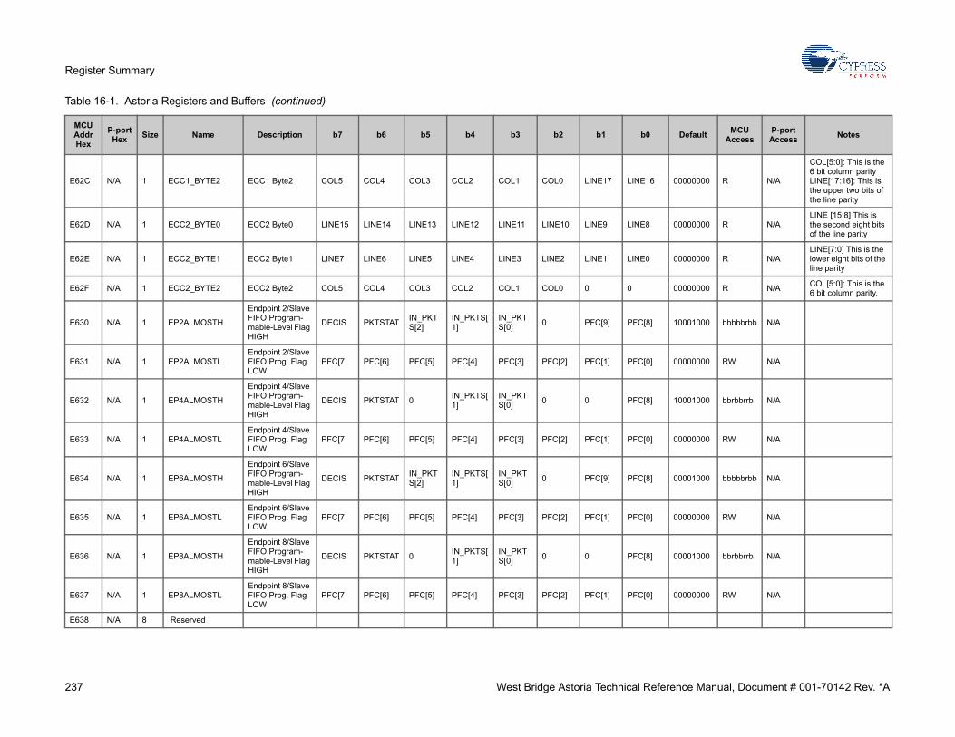
237 West Bridge Astoria Technical Reference Manual, Document # 001-70142 Rev. *A
Register Summary
E62C N/A 1 ECC1_BYTE2 ECC1 Byte2 COL5 COL4 COL3 COL2 COL1 COL0 LINE17 LINE16 00000000 R N/A
COL[5:0]: This is the 6 bit column parity LINE[17:16]: This is the upper two bits of the line parity
E62D N/A 1 ECC2_BYTE0 ECC2 Byte0 LINE15 LINE14 LINE13 LINE12 LINE11 LINE10 LINE9 LINE8 00000000 R N/ALINE [15:8] This is the second eight bits of the line parity
E62E N/A 1 ECC2_BYTE1 ECC2 Byte1 LINE7 LINE6 LINE5 LINE4 LINE3 LINE2 LINE1 LINE0 00000000 R N/ALINE[7:0] This is the lower eight bits of the line parity
E62F N/A 1 ECC2_BYTE2 ECC2 Byte2 COL5 COL4 COL3 COL2 COL1 COL0 0 0 00000000 R N/ACOL[5:0]: This is the 6 bit column parity.
E630 N/A 1 EP2ALMOSTH
Endpoint 2/Slave FIFO Program-mable-Level Flag HIGH
DECIS PKTSTATIN_PKTS[2]
IN_PKTS[1]
IN_PKTS[0]
0 PFC[9] PFC[8] 10001000 bbbbbrbb N/A
E631 N/A 1 EP2ALMOSTLEndpoint 2/Slave FIFO Prog. Flag LOW
PFC[7 PFC[6] PFC[5] PFC[4] PFC[3] PFC[2] PFC[1] PFC[0] 00000000 RW N/A
E632 N/A 1 EP4ALMOSTH
Endpoint 4/Slave FIFO Program-mable-Level Flag HIGH
DECIS PKTSTAT 0IN_PKTS[1]
IN_PKTS[0]
0 0 PFC[8] 10001000 bbrbbrrb N/A
E633 N/A 1 EP4ALMOSTLEndpoint 4/Slave FIFO Prog. Flag LOW
PFC[7 PFC[6] PFC[5] PFC[4] PFC[3] PFC[2] PFC[1] PFC[0] 00000000 RW N/A
E634 N/A 1 EP6ALMOSTH
Endpoint 6/Slave FIFO Program-mable-Level Flag HIGH
DECIS PKTSTATIN_PKTS[2]
IN_PKTS[1]
IN_PKTS[0]
0 PFC[9] PFC[8] 00001000 bbbbbrbb N/A
E635 N/A 1 EP6ALMOSTLEndpoint 6/Slave FIFO Prog. Flag LOW
PFC[7 PFC[6] PFC[5] PFC[4] PFC[3] PFC[2] PFC[1] PFC[0] 00000000 RW N/A
E636 N/A 1 EP8ALMOSTH
Endpoint 8/Slave FIFO Program-mable-Level Flag HIGH
DECIS PKTSTAT 0IN_PKTS[1]
IN_PKTS[0]
0 0 PFC[8] 00001000 bbrbbrrb N/A
E637 N/A 1 EP8ALMOSTLEndpoint 8/Slave FIFO Prog. Flag LOW
PFC[7 PFC[6] PFC[5] PFC[4] PFC[3] PFC[2] PFC[1] PFC[0] 00000000 RW N/A
E638 N/A 8 Reserved
Table 16-1. Astoria Registers and Buffers (continued)
MCU Addr Hex
P-port Hex
Size Name Description b7 b6 b5 b4 b3 b2 b1 b0 DefaultMCU
AccessP-port Access
Notes

238 West Bridge Astoria Technical Reference Manual, Document # 001-70142 Rev. *A
Register Summary
E640 N/A 1 EP2ISOINPKTSEndpoint 2 (if ISO) IN Packets Per Frame
AADJ 0 0 0 0 0INPPF[1]
INPPF[0] 00000001 brrrrrbb N/A
E641 N/A 1 Reserved
E642 N/A 2 EP6ISOINPKTSEndpoint 6 (if ISO) IN Packets Per Frame
AADJ 0 0 0 0 0INPPF[1]
INPPF[0] 00000001 brrrrrbb N/A
E643 N/A 5 Reserved
E648 N/A 1 INPKTENDForce IN Packet End
SKIP 0 0 0 EP3 EP2 EP1 EP0 xxxxxxxx W N/AREVCTL.0=1 to enable this feature
E649 N/A 1 OUTPKTENDForce OUT Packet End
SKIP 0 0 0 EP3 EP2 EP1 EP0 xxxxxxxx W N/AREVCTL.0=1 to enable this feature
E64A N/A 6 Reserved
E650 N/A 1 EP2FLAGIEEP2 Slave FIFO Flag Interrupt Enable (INT4)
0 0 0 0 EDGEPF PF EF FF 00000000 rrrrbbbb N/AEDGEPF=0; Rising edge EDGEPF=1; Falling edge
E651 N/A 1 EP2FLAGIRQEP2 Interrupt flag enable
0 0 0 0 0 PF EF FF 00000000 W1C N/A
E652 N/A 1 EP4FLAGIEEP4 Slave FIFO Flag Interrupt Enable (INT4)
0 0 0 0 EDGEPF PF EF FF 00000000 rrrrbbbb N/A
E653 N/A 1 EP4FLAGIRQEP4 Interrupt flag enable
0 0 0 0 0 PF EF FF 00000000 W1C N/A
E654 N/A 1 EP6FLAGIEEP6 Slave FIFO Flag Interrupt Enable (INT4)
0 0 0 0 EDGEPF PF EF FF 00000000 rrrrbbbb N/A
E655 N/A 1 EP6FLAGIRQEP6 Interrupt flag enable
0 0 0 0 0 PF EF FF 00000000 W1C N/A
E656 N/A 1 EP8FLAGIEEP8 Slave FIFO Flag Interrupt Enable (INT4)
0 0 0 0 EDGEPF PF EF FF 00000000 rrrrbbbb N/A
E657 N/A 1 EP8FLAGIRQEP8 Interrupt flag enable
0 0 0 0 0 PF EF FF 00000000 W1C N/A
E658 N/A 1 IBNIEIN-BULK-NAK Interrupt Enable (INT2)
0 0 EP8 EP6 EP4 EP2 EP1 EP0 00000000 rrbbbbbb N/A
E659 N/A 1 IBNIN-BULK-NAK Interrupt Request (INT2)
0 0l EP8 EP6 EP4 EP2 EP1 EP0 00000000 W1C N/A
Table 16-1. Astoria Registers and Buffers (continued)
MCU Addr Hex
P-port Hex
Size Name Description b7 b6 b5 b4 b3 b2 b1 b0 DefaultMCU
AccessP-port Access
Notes

239 West Bridge Astoria Technical Reference Manual, Document # 001-70142 Rev. *A
Register Summary
E65A N/A 1 EPPINGIENEndpoint Ping-NAK / IBN Inter-rupt Enable
EP8 EP6 EP4 EP2 EP1 EP0 0 IBN 00000000 bbbbbbrb N/A
E65B N/A 1 EPPINGIRQ
Endpoint Ping-NAK/IBN Inter-rupt Request (INT2)
EP8 EP6 EP4 EP2 EP1 EP0 0 IBN 00000000 W1C N/A
E65C N/A 1 USBIEN USB Int Enables 0 EP0ACK HSGRANT
URES SUSP SUTOK SOF SUDAV 00000000 rbbbbbbb N/A
E65D N/A 1 USBIRQUSB Interrupt Requests
0 EP0ACK HSGRANT
URES SUSP SUTOK SOF SUDAV 00000000 W1C N/A
E65E N/A 1 EPIENEndpoint Inter-rupt Enables
EP8 EP6 EP4 EP2 EP1OUT EP1IN EP0OUT EP0IN 00000000 RW N/A
E65F N/A 1 EPIRQEndpoint Inter-rupt Requests (INT2)
EP8 EP6 EP4 EP2 EP1OUT EP1IN EP0OUT EP0IN 00000000 W1C N/A
E660 N/A 1 GPIFIEGPIF Interrupt Enables
0 0 0 0 0 0 GPIFWFGPIF-DONE
00000000 RW N/A
E661 N/A 1 GPIFIRQGPIF Interrupt Request (INT4)
SGLDAT_WR
SGLDAT_RD
0 0 0 0 GPIFWFGPIF-DONE
00000000 W1C N/A
E662 N/A 1 EPERRIENUSB Error Inter-rupt Enables
ISOEP8 ISOEP6 ISOEP4 ISOEP2 0 0 0ERRLIMIT
00000000 bbbbrrrb N/A
E663 N/A 1 EPERRIRQUSB Error Inter-rupt Requests
ISOEP8 ISOEP6 ISOEP4 ISOEP2 0 0 0ERRLIMIT
00000000 W1C N/A
E664 N/A 1 ERRLIMITUSB Error Coun-ter and Limit
EC[3] EC[2] EC[1] EC[0] LIMIT[3] LIMIT[2] LIMIT[1] LIMIT[0] 00000100 rrrrbbbb N/A
LIMIT[1:0] = USB bus error count and limit. The firmware can enable the inter-rupt to cause an interrupt when the limit is reached. The default limit count is 4
EC[3:0] = Error count has a maximum value of 15
E665 N/A 1 CLRERRCNT Clear Error CountCLR_ERR_CNT[7]
CLR_ERR_CNT[6]
CLR_ERR_CNT[5]
CLR_ERR_CNT[4]
CLR_ERR_CNT[3]
CLR_ERR_CNT[2]
CLR_ERR_CNT[1]
CLR_ERR_CNT[0]
xxxxxxxx W N/A
E666 N/A 1 INT2IVECINTERRUPT 2 (USB) Autovector
0 I2V4 I2V3 I2V2 I2V1 I2V0 0 0 00000000 R N/AI2V indicates the source of an interrupt from the USB Core.
Table 16-1. Astoria Registers and Buffers (continued)
MCU Addr Hex
P-port Hex
Size Name Description b7 b6 b5 b4 b3 b2 b1 b0 DefaultMCU
AccessP-port Access
Notes

240 West Bridge Astoria Technical Reference Manual, Document # 001-70142 Rev. *A
Register Summary
E667 N/A 1 INT4IVECInterrupt 4 (slave FIFOs & GPIF) Autovector
0 0 I4V3 I4V2 I4V1 I4V0 0 0 10000000 R N/AI4V indicates the source of an interrupt from the USB Core.
E668 N/A 1 INTSETUPInterrupt 2&4 Setup
AV5EN 0 0 AV6EN AV2EN 0INT4SRC
AV4EN 00000000 brrbbrbb
E669 N/A 7 Reserved
E670 N/A 1 PORTACFGIO PORTA Alter-nate Configura-tion
FLAGDS
SLCS 0 0 0 0 INT1 INT0 00000000 RW N/A
INT[1:0] = Setting these bits to '1' con-figures these PORTA pins as the INT1 or INT0 pins.
E671 N/A 1 PORTCCFGIO PORTC Alter-nate Configura-tion
GPIF_ADR[7]
GPIF_ADR[6]
GPIF_ADR[5]
GPIF_ADR[4]
GPIF_ADR[3]
GPIF_ADR[2]
GPIF_ADR[1]
GPIF_ADR[0]
00000000 RW N/A
Set these pins to “1” to configure this port to output the lower address of enabled GPIF address pins. Additional bit set in PORTECFG, bit 7.
E672 N/A 1 PORTECFGIO PORTE Alter-nate Configura-tion
GPIF_ADR
T2EX INT6RXDOUT1
RXDOUT0
TOUT2 TOUT1 TOUT0 00000000 RW N/A
TOU[2:0] = Serial mode 0 provides synchronous, half-duplex serial commu-nication. For Serial Port 0,serial data out-put occurs on the RXD0OUT pin, serial data is received on the RXD0 pin, and the TXD0 pin pro-vides the shift clock for both transmit and receive. Mode 0: Clock Output Modes 1-3: Serial Port 0 Data Output.
RXDOUT[1:0] = Mode 0: USART1:0 Synchro-nous Data Output.
E673 N/A 1 Reserved
Astoria Registers
E674 N/A 1 SD1_WAKEUPWakeup from Suspend through SD1 pins
0 0
STATUS_WAKEUP_SD_D3
STATUS_WAKEUP_SD_D1
POL_WAKEUP_SD_D3
POL_WAKEUP_SD_D1
EN_WAKEUP_SD_D3
EN_WAKEUP_SD_D1
00000000 rrbbbbbb N/A
Table 16-1. Astoria Registers and Buffers (continued)
MCU Addr Hex
P-port Hex
Size Name Description b7 b6 b5 b4 b3 b2 b1 b0 DefaultMCU
AccessP-port Access
Notes

241 West Bridge Astoria Technical Reference Manual, Document # 001-70142 Rev. *A
Register Summary
E675 N/A 1 SD2_WAKEUPWakeup from Suspend through SD2 pins
0 0
STATUS_WAKEUP_SD2_D3
STATUS_WAKEUP_SD2_D1
POL_WAKEUP_SD2_D3
POL_WAKEUP_SD2_D1
EN_WAKEUP_SD2_D3
EN_WAKEUP_SD2_D1
00000000 rrbbbbbb N/A
E676 N/A 1 GPIO_WAKEUPWakeup from Suspend through GPIO pins
0 0 0 0 0
STATUS_WAKEUP_GPIO1
POL_WAKEUP_GPIO1
EN_WAKEUP_GPIO1
00000000 rrrrrbbb N/A
MCU Registers
E677 N/A 1 Reserved
E678 N/A 1 PLB_I2CSI2C-Compatible Bus Control & Status
START STOP LASTRD ID1 ID0 BERR ACK DONE 00000000 bbbrrrrr N/A
E679 N/A 1 PLB_I2DATI2C-Compatible Bus Data
D7 D6 D5 D4 D3 D2 D1 D0 00000000 RW N/A
Eight bits of data; writing or reading this register triggers a bus transaction.
E67A N/A 1 PLB_I2FREQI2C-Compatible Bus Control
0 0 0 0 0 0 STOPIE 400KHZ 00000000 rrrrrrbb N/A
E67B N/A 1MOVXAUTODATA1
Autotr1 MOVX access, when APTREN=1
D7 D6 D5 D4 D3 D2 D1 D0 xxxxxxxx RW N/A
E67C N/A 1MOVXAUTODATA2
Autotr2 MOVX access, when APTREN=1
D7 D6 D5 D4 D3 D2 D1 D0 xxxxxxxx RW N/A
E67D N/A 1 CRCH UDMA CRC MSB CRC15 CRC14 CRC13 CRC12 CRC11 CRC10 CRC9 CRC8 01001010 RW N/A
E67E N/A 1 CRCL UDMA CRC LSB CRC7 CRC6 CRC5 CRC4 CRC3 CRC2 CRC1 CRC0 10111010 RW N/A
E67F N/A 1 CRCQUALIFIERUDMA CRC Qualifier
QEN-ABLE
0 0 0 QSTATEQSIGNAL2
QSIGNAL1
QSIGNAL0
00000000 brrrbbbb N/A
E680 N/A 1 PLB_USBCSUSB Control and Status
HSM 0 0USB_FS_IDLE
DISCONNOSYN-SOF
RENUMSIG-RSUME
00001010 rrrbbbbb N/A
E681 N/A 1 Reserved
E682 N/A 1 PLB_WAKEUPWakeup Control and Status
WU2 WUWU2POL
WUPOL 0 DPEN WU2EN WUENxxx000101
wwb-brbbb
N/A
E683 N/A 1 TOGCTLData Toggle Con-trol
Q S R IO EP3 EP2 EP1 EP0 00000000rwwbbbbb
N/A
E684 N/A 1 PLB_FRMHUSB Frame Count High
0 0 0 0 0 FC10 FC9 PFC8 00000000 R N/A
E685 N/A 1 PLB_FRMLUSB Frame Count Low
FC7 FC6 FC5 FC4 FC3 FC2 FC1 FC0 00000000 R N/A
Table 16-1. Astoria Registers and Buffers (continued)
MCU Addr Hex
P-port Hex
Size Name Description b7 b6 b5 b4 b3 b2 b1 b0 DefaultMCU
AccessP-port Access
Notes

242 West Bridge Astoria Technical Reference Manual, Document # 001-70142 Rev. *A
Register Summary
E686 N/A 1 PLB_MICROSOFUSB Microframe Count
0 0 0 0 0 MF2 MF1 MF0 00000000 R N/A
E687 N/A 1 PLB_FNADDRUSB Function Address
0 FA6 FA5 FA4 FA3 FA2 FA1 FA0 00000000 R N/A
E688 N/A 2 Reserved
E68A N/A 1 PLB_EP0BCHEP0 Byte Count High
BC15 BC14 BC13 BC12 BC11 BC10 BC9 BC8 xxxxxxxx R N/AEven though the EP0 buffer is only 64 bytes, the EP0 byte count is expanded to 16 bits to allow using the SUDPTR with a custom length, instead of USB-dic-tated length (from Setup Data Packet and number of requested bytes). The byte count bits in parentheses apply only when SDP-AUTO (SUDP-TRCTL.0) = 0.
E68B N/A 1 PLB_EP0BCLEP0 Byte Count Low
BC7 BC6 BC5 BC4 BC3 BC2 BC1 BC0 xxxxxxxx R N/A
E68C N/A 1 Reserved
E68D N/A 1 PLB_EP1OUTBCEndpoint 1 OUT Byte Count
0 BC6 BC5 BC4 BC3 BC2 BC1 BC0 xxxxxxxx rbbbbbbb N/A
E68E N/A 1 Reserved
E68F N/A 1 PLB_EP1INBCEndpoint 1 IN Byte Count
0 BC6 BC5 BC4 BC3 BC2 BC1 BC0 xxxxxxxx rbbbbbbb N/A
Table 16-1. Astoria Registers and Buffers (continued)
MCU Addr Hex
P-port Hex
Size Name Description b7 b6 b5 b4 b3 b2 b1 b0 DefaultMCU
AccessP-port Access
Notes

243 West Bridge Astoria Technical Reference Manual, Document # 001-70142 Rev. *A
Register Summary
E690 N/A 1 EP2BCHEndpoint 2 Byte Count High
0 0 0 0 0 BC10 BC9 BC8 00000000 rrrrrbbb N/A
EP2 and EP6 can be either 512 or 1024 bytes.
EP4 and EP8 can be 512 bytes only.
E691 N/A 1 EP2BCLEndpoint 2 Byte Count Low
BC7 BC6 BC5 BC4 BC3 BC2 BC1 BC0 00000000 RW N/A
E692 N/A 2 Reserved
E694 N/A 1 EP4BCHEndpoint 4 Byte Count High
0 0 0 0 0 0 BC9 BC8 00000000 rrrrrrbb N/A
E695 N/A 1 EP4BCLEndpoint 4 Byte Count Low
BC7 BC6 BC5 BC4 BC3 BC2 BC1 BC0 00000000 RW N/A
E696 N/A 2 Reserved
E698 N/A 1 EP6BCHEndpoint 6 Byte Count High
0 0 0 0 0 BC10 BC9 BC8 00000000 rrrrrbbb N/A
E699 N/A 1 EP6BCLEndpoint 6 Byte Count Low
BC7 BC6 BC5 BC4 BC3 BC2 BC1 BC0 00000000 RW N/A
E69A N/A 2 Reserved
E69C N/A 1 EP8BCHEndpoint 8 Byte Count High
0 0 0 0 0 0 BC9 BC8 00000000 rrrrrrbb N/A
E69D N/A 1 EP8BCLEndpoint 8 Byte Count Low
BC7 BC6 BC5 BC4 BC3 BC2 BC1 BC0 00000000 RW N/A
E69E N/A 2 Reserved
E6A0 N/A 1 PLB_EP0CSEP0 Control and Status
HSNAK 0 0 0 0 0 BUSY STALL 00000000 wrrrrrrb N/A
E6A1 N/A 1 PLB_EP1OUTCSEndpoint 1 OUT Control and Sta-tus
0 0 0 0 0 0 BUSY STALL 00000000 rrrrrrrb N/A
E6A2 N/A 1 PLB_EP1INCSEndpoint 1 IN Control and Sta-tus
0 0 0 0 0 0 BUSY STALL 00000000 rrrrrrrb N/A
E6A3 N/A 1 EP2CSEndpoint 2 Con-trol and Status
0 NPAK2 NPAK1 NPAK0 FULL EMPTY 0 STALL 0010100 rrrrrrrb N/A
NPAK2:0=number of packets in the FIFO, 0-4. NPAK1:0=num-ber of packets in the FIFO, 0-2
E6A4 N/A 1 EP4CSEndpoint 4 Con-trol and Status
0 0 NPAK1 NPAK0 FULL EMPTY 0 STALL 0010100 rrrrrrrb N/A
E6A5 N/A 1 EP6CSEndpoint 6 Con-trol and Status
0 NPAK2 NPAK1 NPAK0 FULL EMPTY 0 0STALL 0000100 rrrrrrrb N/A
E6A6 N/A 1 EP8CSEndpoint 8 Con-trol and Status
0 0 NPAK1 NPAK0 FULL EMPTY 0 STALL 0000100 rrrrrrrb N/A
E6A7 N/A 1 EP2FLAGSEndpoint 2 slave FIFO Flags
0 0 0 0 0 PF EF FF 00000010 R N/A
Table 16-1. Astoria Registers and Buffers (continued)
MCU Addr Hex
P-port Hex
Size Name Description b7 b6 b5 b4 b3 b2 b1 b0 DefaultMCU
AccessP-port Access
Notes

244 West Bridge Astoria Technical Reference Manual, Document # 001-70142 Rev. *A
Register Summary
E6A8 N/A 1 EP4FLAGSEndpoint 4 slave FIFO Flags
0 0 0 0 0 PF EF FF 00000010 R N/A
E6A9 N/A 1 EP6FLAGSEndpoint 6 slave FIFO Flags
0 0 0 0 0 PF EF FF 00000110 R N/A
E6AA N/A 1 EP8FLAGSEndpoint 8 slave FIFO Flags
0 0 0 0 0 PF EF FF 00000110 R N/A
E6AB N/A 1 EP2FIFOBCNTHEndpoint 2 Slave FIFO Total Byte Count HIGH
0 0 0 BC12 BC11 BC10 BC9 BC8 00000000 R N/A
EP2 max 4096
EP4 max 1024
EP6 max 2048
EP8 max 1024
E6AC N/A 1 EP2FIFOBCNTLEndpoint 2 Slave FIFO Total Byte Count LOW
BC7 BC6 BC5 BC4 BC3 BC2 BC1 BC0 00000000 R N/A
E6AD N/A 1 EP4FIFOBCNTHEndpoint 4 Slave FIFO Total Byte Count HIGH
0 0 0 0 0 BC10 BC9 BC8 00000000 R N/A
E6AE N/A 1 EP4FIFOBCNTLEndpoint 4 Slave FIFO Total Byte Count LOW
BC7 BC6 BC5 BC4 BC3 BC2 BC1 BC0 00000000 R N/A
E6AF N/A 1 EP6FIFOBCNTHEndpoint 6 Slave FIFO Total Byte Count HIGH
0 0 0 0 BC11 BC10 BC9 BC8 00000000 R N/A
E6B0 N/A 1 EP6FIFOBCNTLEndpoint 6 Slave FIFO Total Byte Count LOW
BC7 BC6 BC5 BC4 BC3 BC2 BC1 BC0 00000000 R N/A
E6B1 N/A 1 EP8FIFOBCNTHEndpoint 8 Slave FIFO Total Byte Count HIGH
0 0 0 0 0 BC10 BC9 BC8 00000000 R N/A
E6B2 N/A 1 EP8FIFOBCNTLEndpoint 8 Slave FIFO Total Byte Count LOW
BC7 BC6 BC5 BC4 BC3 BC2 BC1 BC0 00000000 R N/A
E6B3 N/A 1 PLB_SUDPTRHSetup Data Pointer High Address Byte
A15 A14 A13 A12 A11 A10 A9 A8 00000000 RW N/A
E6B4 N/A 1 PLB_SUDPTRLSetup Data Pointer Low Address Byte
A7 A6 A5 A4 A3 A2 A1 A0 00000000 bbbbbbbr N/A
This buffer is used as a target or source by the Setup Data Pointer and it must be WORD (2-byte) aligned. This 16-bit pointer, SUDPTRH:L provides hardware assistance for han-dling CONTROL IN transfers.
Table 16-1. Astoria Registers and Buffers (continued)
MCU Addr Hex
P-port Hex
Size Name Description b7 b6 b5 b4 b3 b2 b1 b0 DefaultMCU
AccessP-port Access
Notes

245 West Bridge Astoria Technical Reference Manual, Document # 001-70142 Rev. *A
Register Summary
E6B5 N/A 1PLB_SUDPTRAUTO
Setup Data Pointer AUTO Mode
0 0 0 0 0 0 0SDP-AUTO
00000001 rrrrrrrb N/A
E6B6 N/A 2 Reserved
8 Bytes of Setup Data
E6B8 N/A 1 PLB_SETUPDAT0SETUPDAT[0] = bmRequestType
D7 D6 D5 D4 D3 D2 D1 D0 00000000 R N/A
D7: Data Transfer Direction; 0=host-to-device, 1=device-to-host D6…5 Type; 0=standard, 1=class, 2=vendor, 3=reserved D4…0 Recipient; 0=device, 1=interface, 2=end-point, 3=other, 4…31=reserved
E6B9 N/A 1 PLB_SETUPDAT1SETUPDAT[1] = bmRequest
D7 D6 D5 D4 D3 D2 D1 D0 00000000 R N/A Specific request
E6BA N/A 1 PLB_SETUPDAT2SETUPDAT[2:3] = wValue
D7 D6 D5 D4 D3 D2 D1 D0 00000000 R N/A Word-sized field that varies according to requestE6BB N/A 1 PLB_SETUPDAT3 D7 D6 D5 D4 D3 D2 D1 D0 00000000 R N/A
E6BC N/A 1 PLB_SETUPDAT4
SETUPDAT[4:5] = wIndex
D7 D6 D5 D4 D3 D2 D1 D0 00000000 R N/A Word-sized field that varies according to request; typically used to pass an index or offset
E6BD N/A 1 PLB_SETUPDAT5 D7 D6 D5 D4 D3 D2 D1 D0 00000000 R N/A
E6BE N/A 1 PLB_SETUPDAT6SETUPDAT[6:7] = wLength
D7 D6 D5 D4 D3 D2 D1 D0 00000000 R N/A Number of bytes to transfer if there is a data stageE6BF N/A 1 PLB_SETUPDAT7 D7 D6 D5 D4 D3 D2 D1 D0 00000000 R N/A
E6C0 N/A 1 WFSELECTWaveform Selec-tor
SIN-GLEWR[1]
SIN-GLEWR[0]
SIN-GLERD[1]
SIN-GLERD[0]
FIFOWR[1]
FIFOWR[0]
FIFORD[1]
FIFORD[0]
11100100 RW N/A Select waveform
E6C1 N/A 1 IDLE_CSGPIF Done, GPIF IDLE drive mode
DONE 0 0 0 0 0 0 IDLEDRV 10000000 rrrrrrrb N/A
E6C2 N/A 1 IDLE_CTLOUTInactive Bus, CTL states
CTLOE1 CTLOE0 CTL5 CTL4 CTL3 CTL2 CTL1 CTL0 11111111 RW N/A
CTL5:0 CTL Output States
CTLOE1:0 CTL Out-put Enables
E6C3 N/A 1 CTLOUTCFG CTL Drive Type TRICTL 0 CTL5 CTL4 CTL3 CTL2 CTL1 CTL0 00000000 brbbbbbb N/ACTL5:0 CTL Output Drive Type
Table 16-1. Astoria Registers and Buffers (continued)
MCU Addr Hex
P-port Hex
Size Name Description b7 b6 b5 b4 b3 b2 b1 b0 DefaultMCU
AccessP-port Access
Notes
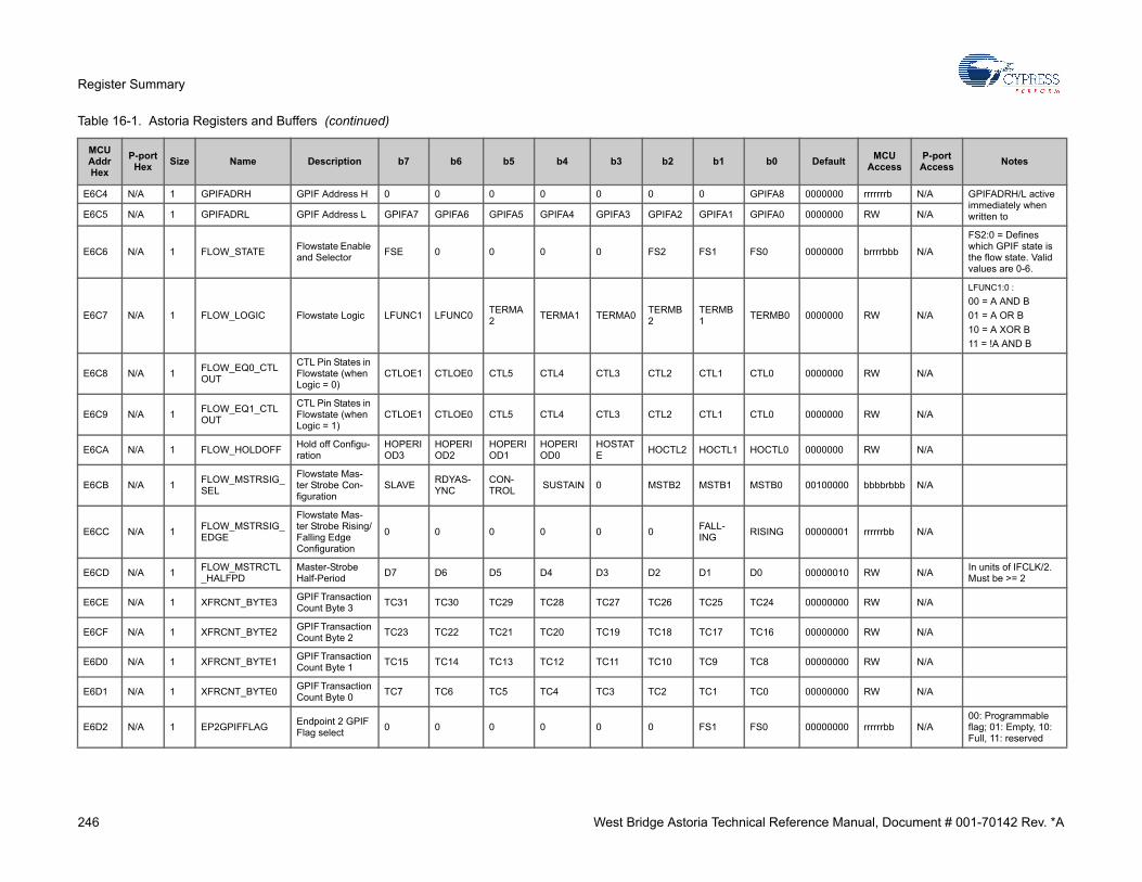
246 West Bridge Astoria Technical Reference Manual, Document # 001-70142 Rev. *A
Register Summary
E6C4 N/A 1 GPIFADRH GPIF Address H 0 0 0 0 0 0 0 GPIFA8 0000000 rrrrrrrb N/A GPIFADRH/L active immediately when written toE6C5 N/A 1 GPIFADRL GPIF Address L GPIFA7 GPIFA6 GPIFA5 GPIFA4 GPIFA3 GPIFA2 GPIFA1 GPIFA0 0000000 RW N/A
E6C6 N/A 1 FLOW_STATEFlowstate Enable and Selector
FSE 0 0 0 0 FS2 FS1 FS0 0000000 brrrrbbb N/A
FS2:0 = Defines which GPIF state is the flow state. Valid values are 0-6.
E6C7 N/A 1 FLOW_LOGIC Flowstate Logic LFUNC1 LFUNC0TERMA2
TERMA1 TERMA0TERMB2
TERMB1
TERMB0 0000000 RW N/A
LFUNC1:0 :
00 = A AND B
01 = A OR B
10 = A XOR B
11 = !A AND B
E6C8 N/A 1FLOW_EQ0_CTLOUT
CTL Pin States in Flowstate (when Logic = 0)
CTLOE1 CTLOE0 CTL5 CTL4 CTL3 CTL2 CTL1 CTL0 0000000 RW N/A
E6C9 N/A 1FLOW_EQ1_CTLOUT
CTL Pin States in Flowstate (when Logic = 1)
CTLOE1 CTLOE0 CTL5 CTL4 CTL3 CTL2 CTL1 CTL0 0000000 RW N/A
E6CA N/A 1 FLOW_HOLDOFFHold off Configu-ration
HOPERIOD3
HOPERIOD2
HOPERIOD1
HOPERIOD0
HOSTATE
HOCTL2 HOCTL1 HOCTL0 0000000 RW N/A
E6CB N/A 1FLOW_MSTRSIG_SEL
Flowstate Mas-ter Strobe Con-figuration
SLAVERDYAS-YNC
CON-TROL
SUSTAIN 0 MSTB2 MSTB1 MSTB0 00100000 bbbbrbbb N/A
E6CC N/A 1FLOW_MSTRSIG_EDGE
Flowstate Mas-ter Strobe Rising/Falling Edge Configuration
0 0 0 0 0 0FALL-ING
RISING 00000001 rrrrrrbb N/A
E6CD N/A 1FLOW_MSTRCTL_HALFPD
Master-Strobe Half-Period
D7 D6 D5 D4 D3 D2 D1 D0 00000010 RW N/AIn units of IFCLK/2. Must be >= 2
E6CE N/A 1 XFRCNT_BYTE3GPIF Transaction Count Byte 3
TC31 TC30 TC29 TC28 TC27 TC26 TC25 TC24 00000000 RW N/A
E6CF N/A 1 XFRCNT_BYTE2GPIF Transaction Count Byte 2
TC23 TC22 TC21 TC20 TC19 TC18 TC17 TC16 00000000 RW N/A
E6D0 N/A 1 XFRCNT_BYTE1GPIF Transaction Count Byte 1
TC15 TC14 TC13 TC12 TC11 TC10 TC9 TC8 00000000 RW N/A
E6D1 N/A 1 XFRCNT_BYTE0GPIF Transaction Count Byte 0
TC7 TC6 TC5 TC4 TC3 TC2 TC1 TC0 00000000 RW N/A
E6D2 N/A 1 EP2GPIFFLAGEndpoint 2 GPIF Flag select
0 0 0 0 0 0 FS1 FS0 00000000 rrrrrrbb N/A00: Programmable flag; 01: Empty, 10: Full, 11: reserved
Table 16-1. Astoria Registers and Buffers (continued)
MCU Addr Hex
P-port Hex
Size Name Description b7 b6 b5 b4 b3 b2 b1 b0 DefaultMCU
AccessP-port Access
Notes
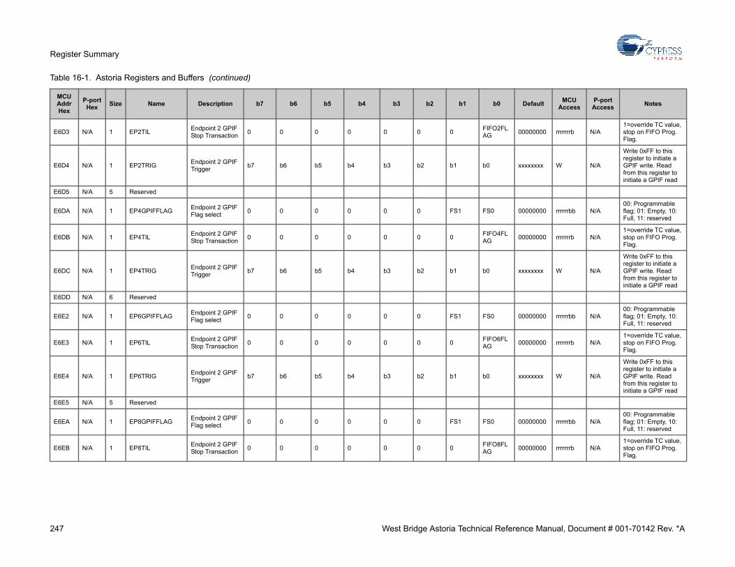
247 West Bridge Astoria Technical Reference Manual, Document # 001-70142 Rev. *A
Register Summary
E6D3 N/A 1 EP2TILEndpoint 2 GPIF Stop Transaction
0 0 0 0 0 0 0FIFO2FLAG
00000000 rrrrrrrb N/A1=override TC value, stop on FIFO Prog. Flag.
E6D4 N/A 1 EP2TRIGEndpoint 2 GPIF Trigger
b7 b6 b5 b4 b3 b2 b1 b0 xxxxxxxx W N/A
Write 0xFF to this register to initiate a GPIF write. Read from this register to initiate a GPIF read
E6D5 N/A 5 Reserved
E6DA N/A 1 EP4GPIFFLAGEndpoint 2 GPIF Flag select
0 0 0 0 0 0 FS1 FS0 00000000 rrrrrrbb N/A00: Programmable flag; 01: Empty, 10: Full, 11: reserved
E6DB N/A 1 EP4TILEndpoint 2 GPIF Stop Transaction
0 0 0 0 0 0 0FIFO4FLAG
00000000 rrrrrrrb N/A1=override TC value, stop on FIFO Prog. Flag.
E6DC N/A 1 EP4TRIGEndpoint 2 GPIF Trigger
b7 b6 b5 b4 b3 b2 b1 b0 xxxxxxxx W N/A
Write 0xFF to this register to initiate a GPIF write. Read from this register to initiate a GPIF read
E6DD N/A 6 Reserved
E6E2 N/A 1 EP6GPIFFLAGEndpoint 2 GPIF Flag select
0 0 0 0 0 0 FS1 FS0 00000000 rrrrrrbb N/A00: Programmable flag; 01: Empty, 10: Full, 11: reserved
E6E3 N/A 1 EP6TILEndpoint 2 GPIF Stop Transaction
0 0 0 0 0 0 0FIFO6FLAG
00000000 rrrrrrrb N/A1=override TC value, stop on FIFO Prog. Flag.
E6E4 N/A 1 EP6TRIGEndpoint 2 GPIF Trigger
b7 b6 b5 b4 b3 b2 b1 b0 xxxxxxxx W N/A
Write 0xFF to this register to initiate a GPIF write. Read from this register to initiate a GPIF read
E6E5 N/A 5 Reserved
E6EA N/A 1 EP8GPIFFLAGEndpoint 2 GPIF Flag select
0 0 0 0 0 0 FS1 FS0 00000000 rrrrrrbb N/A00: Programmable flag; 01: Empty, 10: Full, 11: reserved
E6EB N/A 1 EP8TILEndpoint 2 GPIF Stop Transaction
0 0 0 0 0 0 0FIFO8FLAG
00000000 rrrrrrrb N/A1=override TC value, stop on FIFO Prog. Flag.
Table 16-1. Astoria Registers and Buffers (continued)
MCU Addr Hex
P-port Hex
Size Name Description b7 b6 b5 b4 b3 b2 b1 b0 DefaultMCU
AccessP-port Access
Notes

248 West Bridge Astoria Technical Reference Manual, Document # 001-70142 Rev. *A
Register Summary
E6EC N/A 1 EP8TRIGEndpoint 2 GPIF Trigger
b7 b6 b5 b4 b3 b2 b1 b0 xxxxxxxx W N/A
Write 0xFF to this register to initiate a GPIF write. Read from this register to initiate a GPIF read
E6ED N/A 3 Reserved
E6F0 N/A 1 SGLDATHGPIF Data High (16-bit mode only)
D15 D14 D13 D12 D11 D10 D9 D8 00000000 RW N/A
Contains the data written to or read from the FD15:8 (PORTD) pins using the GPIF waveform.
E6F1 N/A 1 SGLDATLRead/Write GPIF Data L and trig-ger trans-action
D7 D6 D5 D4 D3 D2 D1 D0 00000000 RW N/A
Contains the data written to or read from the FD7:0 (PORTB) pins. Read-ing or writing low-byte triggers a GPIF transaction.
E6F2 N/A 1 SGLDATLNOXRead GPIF Data L, no transaction trigger
D7 D6 D5 D4 D3 D2 D1 D0 00000000 RW N/A
Contains the data written to or read from the FD7:0 (PORTB) pins. Read or write low byte does not trigger GPIF transaction.
E6F3 N/A 1 READYCFGInternal RDY,Sync/Async, RDY pin states
INTRDY SASTCXRDY5
0 0 0 0 0 00000000 bbbrrrrr N/A
INTRDY is 8051 'ready', like RDYn pins. RDYn indicate pin states
SAS=1: synchro-nous, 0:asynchro-nous (2-flops) RDYn inputs
E6F4 N/A 1 READYSTATGPIF Ready Sta-tus
0 0 RDY5 RDY4 RDY3 RDY2 RDY1 RDY0 00xxxxxx R N/A
Instantaneous states of the RDY pins. The current state of the RDY[5:0] pins, sam-pled at each rising edge of the GPIF clock.
E6F5 N/A 1 ABORTAbort GPIF Waveforms
b7 b6 b5 b4 b3 b2 b1 b0 00000000 W N/A
Write 0xFF to imme-diately abort a GPIF transaction and tran-sition to the Idle State.
E6F6 N/A 10 Reserved
Table 16-1. Astoria Registers and Buffers (continued)
MCU Addr Hex
P-port Hex
Size Name Description b7 b6 b5 b4 b3 b2 b1 b0 DefaultMCU
AccessP-port Access
Notes

249 West Bridge Astoria Technical Reference Manual, Document # 001-70142 Rev. *A
Register Summary
E700 N/A Reserved
F000 N/A1024
EP2 Buffer
512/1024-byte EP 2 / slave FIFO buffer (IN or OUT
D7 D6 D5 D4 D3 D2 D1 D0 xxxxxxxx RW N/AFor 512 use only 0xF000-0xF1FF
F400 N/A 512 EP4 Buffer512 EP 4 / slave FIFO buffer (IN or OUT
D7 D6 D5 D4 D3 D2 D1 D0 xxxxxxxx RW N/A
F600 N/A 512 Reserved
F800 N/A1024
EP6 Buffer
512/1024-byte EP 6 / slave FIFO buffer (IN or OUT
D7 D6 D5 D4 D3 D2 D1 D0 xxxxxxxx RW N/AFor 512 use only 0xF000-0xF1FF
FC00 N/A 512 EP8 Buffer512 EP 8 / slave FIFO buffer (IN or OUT
D7 D6 D5 D4 D3 D2 D1 D0 xxxxxxxx RW N/A
FE00 N/A 512 Reserved
Table 16-1. Astoria Registers and Buffers (continued)
MCU Addr Hex
P-port Hex
Size Name Description b7 b6 b5 b4 b3 b2 b1 b0 DefaultMCU
AccessP-port Access
Notes

250 West Bridge Astoria Technical Reference Manual, Document # 001-70142 Rev. *A
Register Summary