EPR and ab initio calculation study on the EI4 center in 4H- and 6H-SiC
Upload
independentCategory
view
3download
0
15
1
Research ArticleReceived: 17 June 2009 Revised: 22 December 2009 Accepted: 22 December 2009 Published online in Wiley Interscience: 15 February 2010
(www.interscience.wiley.com) DOI 10.1002/sia.3195
Annealing effect on the structuraland magnetic properties of nickel ferrite thinfilmsG. Dixit,a∗ J. P. Singh,a R. C. Srivastava,a H. M. Agrawal,a R. J. Choudharyb
and A. Guptab
Nickel ferrite is a soft magnetic material with inverse spinel structure. Soft ferrite films are used in microwave devices, integratedplanar circuits, etc., because of their high resistivity. In this work, thin films of nickel ferrite were deposited on Si (100) substrateby using pulsed laser deposition (PLD) technique. The thickness of the film was measured by surface profilometer and also byX-ray reflectivity (XRR). The films were annealed at three different temperatures to observe the effect on the structural andmagnetic properties of the film. The films were characterised by X-ray diffraction (XRD), Raman spectroscopy and vibratingsample magnetometer (VSM) to study the structural and magnetic properties. Copyright c© 2010 John Wiley & Sons, Ltd.
Keywords: ferrites; thin films; annealing; PLD; XRD; Raman spectroscopy; VSM; XRR
Introduction
Ferrite thin films with spinel structure are of current researchinterest as they have the potential for applications in magneticrecording, high-frequency microwave devices, etc., because oftheir low conductivity (compared to metal films) and highsaturation magnetisation (compared to garnet). Reports havebeen published on the preparation of various types of ferritefilms using different techniques.[1 – 7] In this work, thin films ofnickel ferrite with inverse spinel structure were deposited by usingpulsed laser deposition (PLD) technique. Although properties ofbulk ferrites are fairly well understood in powder form but inthin film various factors such as choice of substrate, temperatureof substrate during deposition, etc., do affect the microstructure,which in turn define the properties of the film. In the case of aferrite film, during deposition the O2 gas is flowed into the PLDchamber to maintain the stoichiometry of the film. The pressure ofthe gas affects film stress; high pressure causes less stress and lowpressure causes high stress.[8] Earlier studies have deposited nickelferrite thin films by using PLD technique[9] and studied the effectof growth parameters on the structural and magnetic propertiesof the film.[10 – 12] We have deposited the films of nickel ferrite withoptimised parameters. Our aim was to study the effect of heattreatment on the microstructure and therefore on the propertiesof the films. We have annealed the films at different temperaturesranging from 600 to 1000 ◦C and studied the changes in thestructural and magnetic properties of the film as a function ofannealing temperature.
Experimental Details
Nanopowder of NiFe2O4 was synthesised by using the nitratesof nickel and iron, and citric acid as host. Aqueous solutions ofiron and nickel salts were prepared separately in stoichiometricproportion by dissolving the salts in double distilled water.
Aqueous solution of citric acid was added to the salt solutionhaving a cation to citric acid ratio of 1 : 2. This solution was heatedat 85 ◦C with continuous stirring for 2 h. The viscous solutionthus obtained was dried overnight in an oven at 100 ◦C to getthe precursor powder. This precursor was heated at 500 ◦C for2 h. The powder obtained was pressed in a pellet form and usedas target for the preparation of film by using PLD technique.The substrate used for film deposition was Si (100) of thesize 10 mm × 10 mm. A Lambda Physik KrF excimer laser ofwavelength 248 nm was used for deposition. The deposition wasdone for 16 min and the thickness of the film was determinedby Taylestep profilometer. The films were also characterised byX-ray reflectivity (XRR) (Bruker AXS D8 Discover) measurementfor the exact determination of thickness and the data was fittedusing Parrot Software. To study the effect of heat treatment, thefilms were annealed at different temperatures ranging from 600to 1000 ◦C for 2 h and then cooled to room temperature in thefurnace. All the samples were characterised by X-ray diffraction(XRD) using Cu–Kα radiation (Rigaku, Japan) for the confirmationof phase and structure. For microstructural study, the films werecharacterised using field emission scanning electron microscope(FESEM). For this purpose, the surface of the film was coated withgold. Besides, in order to study the change in the microstructuralstate and other local environments, the films were characterised byRaman spectroscopy. The micro-Raman system used in this studyconsists of 200 mW Ar-ion laser (514.532 nm), single grating 0.5 mspectrometer, charge-coupled device (CCD) detector (1100 × 330pixels) and holographic optics. The focal spot-size was 10–20 µm.
∗ Correspondence to: G. Dixit, UGC-DAE CSR, Indore-452017, India.E-mail: [email protected]
a Department of Physics, G. B. Pant University of Ag & Technolgy, Pantnagar,Uttarakhnad-263145, India
b UGC-DAE CSR, Indore-452017, India
Surf. Interface Anal. 2010, 42, 151–156 Copyright c© 2010 John Wiley & Sons, Ltd.

15
2
G. Dixit et al.
Figure 1. XRD patterns of target and films of nickel ferrite annealed at different temperatures. Inset shows the enlarged view of 1000 ◦C annealed film (∗represents the peaks corresponding to substrate).
A spectral range of 200–800 cm−1 was examined in this studyusing 1800 grooves/mm grating. The spectrometer was regularlycalibrated using Ar emission spectrum. The exposure time was10 min for recording the Raman spectrum. Magnetic propertiesof the films were studied by using the VSM Quantum DesignPPMS (model 6000), and M–H measurements were done at roomtemperature and also at 10 K.
Results and Discussion
Figure 1 shows the XRD pattern of the target and nickel ferritefilms. The pattern confirms the spinel phase and polycrystallinenature of the films in all the cases. No textured growth of thefilms could be obtained even after annealing up to 1000 ◦C. Inthis pattern, the nickel ferrite peaks are indexed according toJCPDS file no. 742 081. The peak appearing at approximately 29◦
corresponds to NiFe2O4 (220) peak with the 2θ position shiftedtowards the lower angle.[13] This peak disappears in films annealedat 1000 ◦C. The peaks which are labelled with asterisks correspondto substrate. The peaks appearing at approximately 39◦ and 48◦
correspond to α-Fe2O3 phase JCPDS no. 330 664.[14,15] The targetused for film preparation does not contain any peak correspondingto the α-Fe2O3 phase and has a pure single spinel phase of nickelferrite. The pattern shows that annealing at 1000 ◦C removes allthe extra peaks. Other studies also observed that annealing at1000 ◦C removes many of the defects in the film.[16] There is a veryintense peak at 32◦ in films annealed at 800 ◦C and 1000 ◦C, whichcorresponds to the substrate.[13] It does not appear in as-depositedfilms as well as in films annealed at 600 ◦C. The absence or presenceof certain peaks in XRD of the film could be due to some kind oftexturing[17] (which the film tends to adopt) or change in growthdirection after annealing.[18] Crystallite size and lattice parameterfor all films are calculated using the Scherrer formula from the
Table 1. Evaluated parameters from XRD and SEM for nickel ferritefilms
Parameters As-deposited 600 ◦C 800 ◦C 1000 ◦C
Crystallite size(nm)
20 ± 1 31 ± 5 51 ± 2 39 ± 2
Grain size bySEM (nm)
22 26 24 25
Latticeparameter(Å)
8.54 ± 0.05 8.58 ± 0.05 8.64 ± 0.03 8.32 ± 0.05
most intense peak:[19 – 21]
D = kλ
BCosθ
where D is the crystallite size, B is the full width at half maximain radian, θ is the peak position and λ is the wavelength of X-rayused (Cu–Kα line). The estimated parameters are tabulated inTable 1 as a function of annealing temperature. The crystallitesize and lattice parameter increase with annealing temperatureup to 800 ◦C and then they decrease at 1000 ◦C. The increase inlattice parameter up to 800 ◦C annealed film is due to the straindeveloped in the films, which is reflected in the shifting of 2θ
position towards the lower angle.[19,22] Figure 2 shows the XRRplot of the as-deposited film. The value of thickness is found tobe approximately 62 nm while the surface profilometer gives thevalue 80 nm. Figure 3 shows the scanning electron microscope(SEM) micrographs for all the four films. A number of scans weremade but the grains could not be seen clearly. This may bebecause of masking caused by the gold coating on the film’ssurface. The average grain size estimated from SEM does not show
www.interscience.wiley.com/journal/sia Copyright c© 2010 John Wiley & Sons, Ltd. Surf. Interface Anal. 2010, 42, 151–156

15
3
Annealing effect on properties of nickel ferrite thin films
Figure 2. X-ray reflectivity curve for as deposited film.
much variation with annealing temperature (Table 1). The peaksappearing in XRD correspond to the spinel structure. In order todifferentiate NiFe2O4 from other possible phases, such as Fe3O4
or γ -Fe2O3 which have similar spinel structures and thereforesimilar XRD patterns, the samples were further investigated byusing Raman spectroscopy. Ferrites have cubic spinel structuresthat belong to the space group Oh
7(Fd3m). Although the full unitcell contains 56 atoms as there are 8 molecules per unit cell, only14 atoms are in the asymmetric unit and therefore 42 vibrationalmodes are expected. Group theory predicts the following modes
in spinel structure:
A1g(R) + Eg(R) + T1g + 3 T2g(R) + 2A2u + 2Eu + 5 T1u(IR) + 2T2u
The T1g, A2u, Eu and T2u modes are silent. There are five first-order Raman active modes (A1g + Eg + 3T2g). In spinel structure,only the sites with symmetries 43m and 3m, occupied by a cationin tetrahedral coordination and O2− respectively, contribute toRaman activity. Figure 4 shows the Raman spectra of as-depositedand annealed films. Nickel ferrite has inverse spinel structurewhere there are 8Ni+2 and 8Fe+2 at octahedral site and 8Fe+2
at tetrahedral site per unit cell. Raman peaks over the regionof 660–720 cm−1 represent the modes of tetrahedral group inthe ferrites and those in the 460–660 cm−1 region represent themodes of octahedral group. The peak appearing at 520 cm−1 isdue to Si (100) substrate. The characteristic peaks of nickel ferriteappear at 333, 481, 671 and 703 cm−1 with a shoulder at 572 cm−1
in the as-deposited film.[23] The band appearing at 214 cm−1 alsocorresponds to the ferrite structure.[24] After annealing, there isa shift in the position of bands as can be seen from Table 2. Onseeing the plots by enlarging, the following details can be found foras-deposited film: the peak broadening is the highest; the 600 ◦Cand 1000 ◦C annealed films show almost similar broadening; andthe 800 ◦C annealed film shows a broadening that is larger thanthat for 600 ◦C and 1000 ◦C annealed films while smaller thanthat for as-deposited film. The observed broadening may be dueto nanophase character, cation inversion, presence of vacancies(or the sum of three). The largest particle size (as determinedby XRD) for 800 ◦C annealed film indicates the dominancy ofcation inversion or vacancy for higher broadening of Ramanband in comparison to other annealed films. The cation inversion
(a) (b)
(c) (d)
Figure 3. SEM pictures of (a) as-deposited (b) 600 ◦C (c) 800 ◦C and (d) 1000 ◦C annealed films.
Surf. Interface Anal. 2010, 42, 151–156 Copyright c© 2010 John Wiley & Sons, Ltd. www.interscience.wiley.com/journal/sia
15
4
G. Dixit et al.
Figure 4. Raman spectra for the nickel ferrite films.
Table 2. Raman bands for nickel ferrite films at different annealingtemperatures
Raman modes (cm−1)
As-deposited 600 ◦C 800 ◦C 1000 ◦C
214 210 212 211
333 336 333 329
481 484 483 482
572 579 577 583
671 674 659 672
703 702 702 699
affects magnetic properties significantly. Figures 5 and 6 show themagnetic hysteresis curves at 300 and 10 K for all the films. At both10 and 300 K, the magnetic moments do not saturate even upto a field of 20 kOe. If one-dimensional defects such as point-likedefects or fluctuations of magnetic anisotropy play a role, themagnetic moment at a given applied field (H) can be written inthe following way:[25 – 27]
4πM = Q(1 − a/H0.5 − b/H − c/H2) + eH (1)
where 4πM is the actual value of magnetisation that is observedat field H; and Q, a, b, c and e are constants. The value of Q shouldcorrespond to a value of 4πM at infinite field. The last term eHis caused due to an increase in spontaneous magnetisation bythe external field and is generally assumed to be negligible. Thesecond term a/H0.5 is attributed to point-like defect or magneticanisotropy fluctuation on atomic scale. The third term b/H isattributed to the local internal stress caused by dislocations andnonmagnetic inclusions or voids. The fourth term c/H2 is attributedto the weak and large-scale fluctuations in anisotropy. So, to obtainthe value of saturation magnetisation in case of lack of saturationof M–H curve, high field data is fitted according to the followingequation, which is based on Eqn (1).
M = Q(1 − (H∗/H)n) (2)
Figure 5. M–H curves of nickel ferrite films at 300 K.
Figure 6. M–H curves of nickel ferrite films at 10 K.
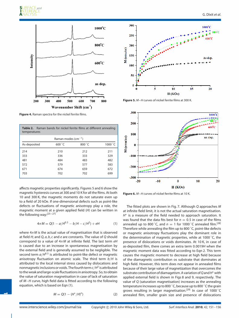
The fitted plots are shown in Fig. 7. Although Q approaches Mat infinite field limit, it is not the actual saturation magnetisation.H∗ is a measure of the field needed to approach saturation. Itwas found that the data fits best for n = 0.5 in case of the filmsannealed up to 800 ◦C, and n = 1 for 1000 ◦C annealed film.[28]
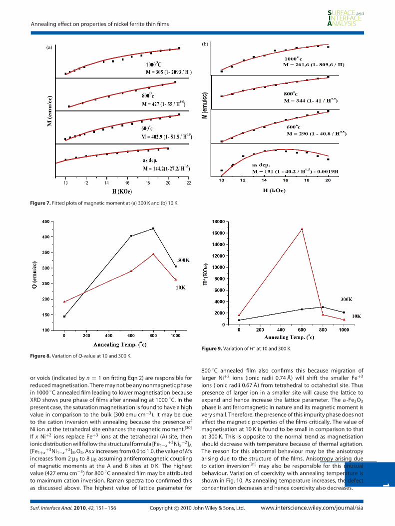
Therefore while annealing the film up to 800 ◦C, point-like defectsor magnetic anisotropy fluctuations play the dominant role inthe determination of magnetic properties, while at 1000 ◦C, thepresence of dislocations or voids dominates. At 10 K, in case ofas-deposited film, there comes an extra term 0.0019H when themagnetic moment data was fitted according to Eqn 2. This termcauses the magnetic moment to decrease at high field becauseof the diamagnetic contribution os substrate that dominates athigh field. However, this term does not appear in annealed filmsbecause of their large value of magnetization that overcomes thesubstrate contribution of diamagetism. A variation of Q and H∗ withapplied external field is shown in Figs 8 and 9, respectively. Thevalue of Q (saturation magnetisation) increases as the annealingtemperature increases up to 800 ◦C, because up to 800 ◦C the graingrows resulting in larger magnetisation.[29] In case of 1000 ◦Cannealed film, smaller grain size and presence of dislocations
www.interscience.wiley.com/journal/sia Copyright c© 2010 John Wiley & Sons, Ltd. Surf. Interface Anal. 2010, 42, 151–156
15
5
Annealing effect on properties of nickel ferrite thin films
(a)(b)
Figure 7. Fitted plots of magnetic moment at (a) 300 K and (b) 10 K.
Figure 8. Variation of Q-value at 10 and 300 K.
or voids (indicated by n = 1 on fitting Eqn 2) are responsible forreduced magnetisation. There may not be any nonmagnetic phasein 1000 ◦C annealed film leading to lower magnetisation becauseXRD shows pure phase of films after annealing at 1000 ◦C. In thepresent case, the saturation magnetisation is found to have a highvalue in comparison to the bulk (300 emu cm−3). It may be dueto the cation inversion with annealing because the presence ofNi ion at the tetrahedral site enhances the magnetic moment.[30]
If x Ni+2 ions replace Fe+3 ions at the tetrahedral (A) site, thenionic distribution will follow the structural formula [Fe1−x
+3Nix+2]A
[Fe1+x+3Ni1−x
+2]B.O4. As x increases from 0.0 to 1.0, the value of Msincreases from 2 µB to 8 µB assuming antiferromagnetic couplingof magnetic moments at the A and B sites at 0 K. The highestvalue (427 emu cm−3) for 800 ◦C annealed film may be attributedto maximum cation inversion. Raman spectra too confirmed thisas discussed above. The highest value of lattice parameter for
Figure 9. Variation of H∗ at 10 and 300 K.
800 ◦C annealed film also confirms this because migration oflarger Ni+2 ions (ionic radii 0.74 Å) will shift the smaller Fe+3
ions (ionic radii 0.67 Å) from tetrahedral to octahedral site. Thuspresence of larger ion in a smaller site will cause the lattice toexpand and hence increase the lattice parameter. The α-Fe2O3
phase is antiferromagnetic in nature and its magnetic moment isvery small. Therefore, the presence of this impurity phase does notaffect the magnetic properties of the films critically. The value ofmagnetisation at 10 K is found to be small in comparison to thatat 300 K. This is opposite to the normal trend as magnetisationshould decrease with temperature because of thermal agitation.The reason for this abnormal behaviour may be the anisotropyarising due to the structure of the films. Anisotropy arising dueto cation inversion[31] may also be responsible for this unusualbehaviour. Variation of coercivity with annealing temperature isshown in Fig. 10. As annealing temperature increases, the defectconcentration decreases and hence coercivity also decreases.
Surf. Interface Anal. 2010, 42, 151–156 Copyright c© 2010 John Wiley & Sons, Ltd. www.interscience.wiley.com/journal/sia

15
6
G. Dixit et al.
Figure 10. Variation of coercivity at 10 K.
Conclusion
Thin films of nickel ferrite were found to have spinel structureand polycrystalline nature. Even after annealing, no texturedgrowth was found. Fe2O3 phase, present in the as-deposited film,disappears after annealing at 1000 ◦C. Raman spectra show fivecharacteristic bands of ferrite which undergo shift with annealingtemperature. Normally, in ferrite films the value of magnetisationremains lower in comparison to the bulk, but in the present caseit was found to be larger. The observed behaviour of magneticproperties after annealing is attributed to the effects of grain size,anisotropy, defects, presence of impurities and change in cationdistribution. Thus we conclude that the annealing temperaturewhich affects the phase and stoichiometry of a film is an importantparameter that controls the structural and magnetic properties ofthe film.
Acknowledgements
We, Gagan Dixit and J. P. Singh, are grateful to the U.G.C. andC.S.I.R., respectively, for awarding JRF. We are also thankful to Dr D.M. Phase, Dr V. Sathe and Dr Alok Banerjee for their keen interestand important suggestions in depositing thin films by using PLDtechnique and characterising them by using XRD, Raman and VSMmeasurements at UGC-DAE CSR, Indore.
References
[1] C. M. Williams, D. B. Chrisey, P. Lubitz, K. S. Grabowski, C. M. Cottel,J. Appl. Phys. 1994, 75, 1676.
[2] F. J. Cadieu, R. Rani, W. Mendoza, B. Peng, S. A. Shaheen, M. J.Hurben, C. E. Patton, J. Appl. Phys. 1997, 81, 4801.
[3] M. Matsuoka, Y. Matsuda, Y. Yoshi, M. Naoe, J. Magn. Magn. Mater1986, 54, 1603.
[4] S. A. Oliver, C. Vittoria, G. Balestrino, S. Martelluchi, G. Petrocelli,A. Tabano, P. Paroli, IEEE Trans. Magn. 1994, MAG-30, 4933.
[5] D. T. Margulies, F. T. Parker, F. E. Spada, R. S. Goldman, J. Li,R. Sinclair, A. E. Berkowitz, Phys. Rev. B 1996, 53, 9175.
[6] G. Caruntu, I. Dumitru, G. G. Bush, D. Caruntu, C. J. O. Connor, J.Phys.D: Appl. Phys. 2005, 38, 811.
[7] B. R. Acharya, S. Prasad, N. Venkataramani, S. N. Shringi, R. Krishnan,J. Appl. Phys. 1996, 79, 478.
[8] O. F. Caltum, J. Optoelectron. Adv. Mater. 2005, 7, 739.[9] O. F. Caltum, J. Optoelectron. Adv. Mater. 2004, 6, 935.
[10] P. Samarasekara, R. Rani, F. J. Cadieu, J. Appl. Phys. 2006, 79, 5425.[11] T. Johnson Matthew, G. Paul Kotula, C. Barry Carter, J. Crystal Growth
1999, 206, 299.[12] C. N. Chinnasamy, S. D. Yoon, A. Yang, A. Baraskar, C. Vittoria,
V. G. Harris, J. Appl. Phys. 2007, 01, 09M517.[13] F. Liu, C. Yang, T. Ren, A. Z. Wang, Jun Yu, L. Liu, J. Magn. Magn.
Mater. 2007, 309, 75.[14] S. H. Pawar, P. S. Patil, R. D. Madhale, C. D. Lokhande, Indian J. Pure
& Appl. Phys. 1989, 77, 227.[15] X. Wang, X. Chen, X. Ma, H. Zheng, M. Ji, Z. Zhang, Chem. Phys. Lett.
2004, 384, 391.[16] S. Venzke, R. B. Van Dover, J. M. Phillips, E. M. Gyorgy, T. Siegrist,
C. H. Chen, D. Werder, R. M. Fleming, R. J. Felder, E. Coleman,R. Opila, J. Mater. Res. 1996, 11, 1187.
[17] J. Dash, S. Prasad, N. Venkataramani, R. Krishnan, P. Kishan,N. Kumar, S. D. Kulkarni, S. K. Date, J. Appl. Phys. 1999, 86, 3303.
[18] M. Sorescu, L. Dia Mandescu, R. Swaminathan, M. E. Mc Henry,M. Feder, J. Appl. Phys. 2008, 97, 10G105.
[19] B. D. Cullity, Elements of X-ray Diffraction, Addison WesleyPublishing: Massachusetts, 1959.
[20] M. H. Mahmoud, C. M. Williams, J. Cai, I. Siu, J. C. Walker, J. Magn.Magn. Mater. 2003, 261, 314.
[21] M. H. Ibrahim, M. S. Seehra, G. Srinivasan, J. App. Phys. 1994, 75,6822.
[22] J. Bruneaux, H. Cachet, M. Froment, A. Messad, ThinSolid Films 1991,197, 129.
[23] P. R. Graves, C. Johnston, J. J. Campaniello, Mat. Res. Bull. 1988, 23,1651.
[24] M. V. Vasic, B. Antic, A. Kremenovic, A. S. Nikolic, M. Stoiljkovic,N. Bibic, V. Spasojevic, Ph. Colomban, Nanotechnology 2006, 17,4877.
[25] A. H. Morrish, The Physical Princilpes of Magnetism, Wiley: New York,1965.
[26] T. Kaneyoshi, Introduction to Amorphous Magnets, World Scientific:Singapore, 1992.
[27] E. M. Chudnovsky, W. M. Saslow, R. A. Sarota, Phy. Rev. B 1986, 33,251.
[28] J. Dash, S. Prasad, N. Venkataramani., R. Krishnan, P. Kishan,N. Kumar, S. D. Kulkarni, S. K. Date, J. Appl. Phys. 1999, 86, 3303.
[29] Y. C. Yang, J. Ding, J. B. Yi, B. H. Liu, T. Yu, Z. X. Shen, J. Magn. Magn.Mater. 2004, 282, 211.
[30] U. Luders, M. Bibes, J. F. Bobo, M. Cantoni, R. Bertacco,J. Fontcuberta, Phys. Rev. B 2005, 71, 134419.
[31] M. Desai, S. Prasad, N. Venkataramani, I. Samajdar, A. K. Nigam,N. Keller, R. Krishnan, E. M. Baggio-Saitovitch, B. R. Pujada, A. Rossi,J. Appl. Phys. 2002, 91, 7592.
www.interscience.wiley.com/journal/sia Copyright c© 2010 John Wiley & Sons, Ltd. Surf. Interface Anal. 2010, 42, 151–156
Copyright © 2022 FDOKUMEN