Dynamics of slow wave activity in narcoleptic patients under bed rest conditions
Upload
khangminh22Category
view
0download
0
Analysis and Synthesis of Slow Wave Structures
for Millimetre wave TWTs
Robert Michael Alan Waring
BSc
A Thesis Submitted for the degree of Doctor of
Philosophy
June 2020
Engineering Department Lancaster University, UK

Abstract
Traveling wave tubes (TWTs) and backward wave oscillators (BWOs) are the
only solution for high power amplification and RF generation at millimetre waves
and THz frequencies. With advances in microfabrication technology, it is
now possible to realise these devices with dimensions to support those
frequency regimes. Promising applications of millimetre wave TWTs are as
high-power amplifiers for wireless communications systems, imaging and
satellite communications. BWOs would enable new plasma diagnostic in
nuclear fusion capabilities and high-resolution imaging. TWTs are usually
constructed using a helical waveguide as slow wave structure (SWS) by which
wave energy can propagate. However, fabrication of a helix small enough to
support mm-wave is not feasible. Novel SWSs are required suitable to be
fabricated with the available processes.
The challenge of the simulation of TWTs or BWOs utilising a new SWS is the
lack of fast code and the need to rely on powerful, yet slow, 3D electromagnetic
software, which are computationally intensive. Both helices and the coupled
cavity TWT can be simulated by fast simulation codes
using Lagrangian methods. One of the aims of this thesis is to create a fast
code for simulating arbitrary three-dimensional SWS, in particular the double
corrugated waveguide. The code was validated by comparison with data of a
Ka-band TWT available in literature.
The second aim is the design of circuits based on double corrugated
waveguide SWSs for TWTs and BWO at different frequency to enable different

applications. New topologies of couplers were investigated. Extensive 3-
dimensional simulations were performed to define dimensions and
performance at different frequency bands.

i
Table of Contents
Chapter 1 Introduction and Background .......................................................... 1
1.1 Applications .................................................................................................... 2
1.1.1 High data rate communications..................................................................... 2
1.1.2 Space millimetre wave TWTs ........................................................................ 3
1.1.3 THz Imaging ..................................................................................................... 3
1.2 Beam-wave Theory ......................................................................................... 4
1.2.1 Dispersion Characteristics ............................................................................. 5
1.2.2 Dispersion of a Helical Waveguide and Rectangular Waveguide ........... 6
1.2.3 Harmonics ........................................................................................................ 7
1.2.4 Interaction Impedance .................................................................................... 9
1.2.5 Beam-Wave Interaction: Forward Wave Amplifier Operation .................. 9
1.2.6 Beam-Wave Interaction: Backward Wave Oscillator Operation ............ 11
1.2.7 Magnetic Focussing Field ............................................................................ 13
1.3 Construction of TWT and BWO ..................................................................... 14
1.3.1 The Helix SWS .............................................................................................. 15
1.4 TWTs at the Millimetre Wavelength .............................................................. 16
1.5 SWSs for Millimetre Wave TWTs .................................................................. 17
1.5.1 Folded Waveguide Travelling Wave Tube ................................................ 17
1.5.2 Double Corrugated Waveguide ................................................................... 19
1.6 Fabrication .................................................................................................... 21
1.7 Simulations ................................................................................................... 22

ii
1.8 Lagrangian Formulation ................................................................................ 22
1.8.1 Derivation of the General Amplifier Equations .......................................... 24
1.8.2 Normalised Lagrangian Variables ............................................................... 27
1.8.3 Generalised Amplifier Equations................................................................. 29
1.8.4 Space Charge Force ..................................................................................... 33
1.8.5 Space Charge waves .................................................................................... 34
1.8.6 Weighting Functions ..................................................................................... 40
1.8.7 Eigenmode and Finite Difference Time Domain Simulation ................... 41
1.8.8 Performance and comparison ..................................................................... 42
1.9 Conclusions .................................................................................................. 43
1.10 Organisation of the Thesis ............................................................................ 43
Chapter 2 Novel approach to Large Signal Lagrangian for Asymmetric SWSs
46
2.1 Large Signal Model ....................................................................................... 47
2.2 Modification to the Lagrangian Model............................................................ 47
2.2.1 Non-cylindrically Symmetric Configurations .............................................. 49
2.2.2 Rotational Asymmetry in Space Charge .................................................... 51
2.2.3 Rotational Asymmetry in electric field ........................................................ 54
2.2.4 Axial Variation in electric field ...................................................................... 55
2.2.5 Applying the Weighting Functions .............................................................. 57
2.2.6 Structure of the Code .................................................................................... 58
2.3 Results .......................................................................................................... 65

iii
2.3.1 Validation: Ka-Band DCW TWT – 34 GHz ................................................ 66
2.3.2 Convergence .................................................................................................. 69
2.3.3 Weighting Functions: Results ...................................................................... 71
2.3.4 Energy of each charge group ...................................................................... 71
2.3.5 Electron phase positions .............................................................................. 73
2.3.6 Saturation Point ............................................................................................. 74
2.4 Results over the bandwidth ........................................................................... 75
2.4.1 Weighting Factors ......................................................................................... 76
2.4.2 Electron Energy ............................................................................................. 77
2.4.3 Electron Trajectories ..................................................................................... 79
2.4.4 Saturation Point ............................................................................................. 80
2.4.5 Gain and Power across the Bandwidth ...................................................... 82
2.5 Simulation Time ............................................................................................ 83
2.6 Conclusions .................................................................................................. 84
Chapter 3 3D Design of DCW for millimetre wave TWTs ............................... 87
3.1 Eigenmode Simulations ................................................................................ 88
3.2 Fabrication .................................................................................................... 92
3.3 Design of the Coupler ................................................................................... 93
3.3.1 Bend Tapering ............................................................................................... 95
3.4 Coupler Comparisons for 346 GHz DCW BWO ............................................ 97
3.4.1 Conclusion .................................................................................................... 101
3.5 100 GHz BWO ............................................................................................ 101

iv
3.5.1 Cold Parameters .......................................................................................... 101
3.6 270GHz TWT .............................................................................................. 105
3.6.1 Cold parameters .......................................................................................... 106
3.7 W-Band TWT for TWEETHER Project ........................................................ 109
3.7.1 DCW Design for 92-95 GHz – Square Pillars ......................................... 110
3.7.2 DCW Design for 92-95 GHz – Triangular Pillars .................................... 112
3.7.3 Couplers........................................................................................................ 114
3.7.4 Straight Taper Square Pillars .................................................................... 114
3.7.5 Bend Tapering Square Pillars ................................................................... 117
3.8 Conclusions ................................................................................................ 118
Chapter 4 Conclusions and Future Work ..................................................... 121
4.1 Thesis Purpose ........................................................................................... 121
4.2 Summary of Findings .................................................................................. 122
4.2.1 Modified Lagrangian Model ....................................................................... 122
4.2.2 DCW for millimetre wave TWTs ................................................................ 123
4.3 Successes and Limitations .......................................................................... 124
4.3.1 Modified Lagrangian Code ......................................................................... 124
4.3.2 DCW for millimetre wave TWTs ................................................................ 125
4.4 Future Work ................................................................................................ 126
4.4.1 Lagrangian Model Extension ..................................................................... 126
4.4.2 Coupler design and PIC Simulations ....................................................... 127
Chapter 5 Bibliography ................................................................................ 128

v
Chapter 6 APPENDIX A: Code .................................................................... 133
Chapter 7 APPENDIX B: S-Parameters ....................................................... 156
Chapter 8 List of Published Papers.............................................................. 157

vi
I. List of Figures
Figure 1 Example of a given SWS with a range of frequencies with constant Phase
Velocity as a function of Frequency (blue) and a beam line (orange) of constant
electron velocity ....................................................................................................................... 5
Figure 2 Definitions of a, the width of a rectangular waveguide, and b, the height ...... 7
Figure 3 Example of spatial and frequency Harmonics over 3𝜋 of phase difference
[23] ............................................................................................................................................. 8
Figure 4 Electron bunching in the case of 𝑈𝐵 = 𝜈𝑝ℎ, where a), b) and c) are
positions in time [21] ............................................................................................................. 10
Figure 5 Output spectrum of a BWO [26] .......................................................................... 12
Figure 6 A typical axially symmetrical periodic permanent-magnet system (PPM) [21]
................................................................................................................................................. 14
Figure 7 Traveling-wave tube. 1, Electron gun; 2, input–output; 3, helix slow-wave
structure; 4, focusing magnet; 5, electron beam; 6, collector. [21] ................................ 14
Figure 8 Detailed TWT Schematic, with the beam focussing illustrated. [29] .............. 15
Figure 9 Computational cycle of a PIC simulation [31] ................................................... 16
Figure 10 Three-dimensional diagram of a normal FW [41] ........................................... 18
Figure 11 Rendition of the FW TWT, with electron beam [42] ....................................... 19
Figure 12 Rendition of the double corrugated waveguide with electron beam [26] .... 19
Figure 13 Introduction of pillars to the waveguide ........................................................... 20
Figure 14 Design of the DCW [23] Left is the cross section perpendicular to the beam
axis, and right is the cross section parallel to the beam axis and from the side of the
DCW. ....................................................................................................................................... 21
Figure 15 Lagrangian formulation of beam wave interaction. It depicts one
wavelength of wave, and a section of electron beam the same length. The section of
electron beam is divided in charge groups called charge groups. The + and – indicate
the potential of the wave. ..................................................................................................... 23

vii
Figure 16 Equivalent circuit for the one dimensional transmission line [50] ................ 25
Figure 17 Diagram of the boundary conditions used to solve equation (62) and (64) 38
Figure 18 The electric field in a helix based TWT. On average the field is asymmetric,
and only relies upon radial position. ................................................................................... 40
Figure 19 Yee Lattice [62] .................................................................................................... 42
Figure 20 Cross section of the DCW TWT. The radius is not singularly valued as the
helical SWS. Also shown are the definitions of angles for the calculation of effective
radii .......................................................................................................................................... 48
Figure 21 Cross section of the helical waveguide with the outer copper casing, the
inner helical SWS, the electron beam in the centre, and the dielectric support rods.
The black line shows the radius of the helix with respect to the beam centre ............. 48
Figure 22 Effective radii for space charge calculations example. In this case, a unit
DCW is used. Inset is the unit DCW .................................................................................. 49
Figure 23 The field distribution of the DCW, with approximate beam position shown.
Computed in CST-MWS [59] The red is high electric field strength and the blue is low
electric field strength. ............................................................................................................ 50
Figure 24 Axial Field variance of a DCW [59] The red is high electric field strength
and the blue is low electric field strength ........................................................................... 51
Figure 25 Sub-charge group model, where 𝜃 is defined in equation 12 and 𝑟𝑖 is
defined in equation (13)........................................................................................................ 52
Figure 26 The field values were extracted along the lines shown above, with 10 radial
lines for r=0 to r = 𝑏𝑟 = beam radius, and one axial line one period in length. They
were calculated in CST MWS Eigenmode solver ............................................................. 53
Figure 27 Example of axial variation of electric field for a DCW in the Ka-band along
the z-axis. This was calculated using CST [59] The black arrow indicates the beam
direction .................................................................................................................................. 57
Figure 28 Flow chart of the code ........................................................................................ 59

viii
Figure 29 Ka-Band DCW dispersion curve and beam line ............................................. 67
Figure 30 Ka-Band DCW Average Interaction Impedance. The interaction impedance
is averaged over the volume of the electron beam in one period of the DCW. The
beam is considered to be a perfect cylinder ..................................................................... 68
Figure 31 The time of the simulation as a function of number of charge groups, njt.. 69
Figure 32 The peak output power, as a function of number of charge groups, njt. .... 69
Figure 33 Radial (a) and axial (b) Weighting factors ....................................................... 70
Figure 34 Electron energy from CST, in keV [65] ............................................................ 71
Figure 35 Charge group energies as a function of axial position .................................. 72
Figure 36 Charge group phases as a function of axial position ..................................... 73
Figure 37 Gain of the signal as a function of the axial postion in the interaction region
................................................................................................................................................. 74
Figure 38 Power output, 𝑃𝑤, signal as a function of the axial postion in the interaction
region ...................................................................................................................................... 74
Figure 39 Radial weighting functions vs radial position per frequency ......................... 76
Figure 40 The electronic charge group energies as functions of axial postion for each
signal frequency. The y-axis of (g) is greater beace much more energy is lost by the
electrons. ................................................................................................................................ 78
Figure 41 Trajectories of the charge groups expressed in terms of phase position
relative to the RF signal........................................................................................................ 79
Figure 42 Power output as calculated by the modified Lagrangian code per frequency
................................................................................................................................................. 81
Figure 43 The gain of the tube as a function of signal frequency as calculated by CST
(blue) and the modified Lagrangian code (red) ................................................................ 82
Figure 44 The power output of the tube as a function of signal frequency as
calculated by CST (blue) and the modified Lagrangian code (red). The interaction
length considered for the Langrangian code was 20cm ................................................. 83

ix
Figure 45 The amount of time for one run of the Lagrangian simulator, at single
frequency ................................................................................................................................ 83
Figure 46 Front view of the period of the DCW ................................................................ 88
Figure 47 Side view of the period of the DCW ................................................................. 88
Figure 48 Study on the synchronous beam voltage and interaction impedance for
variations in parameters of the DCW. (a) Waveguide width, (b) Waveguide height, (c)
Pillar height, (d) Period. [23] ................................................................................................ 90
Figure 49 Height tapering of the pillars and width tapering of the waveguide. The long
straight lines in the image represent the edges of the waveguide. 𝑑𝐻 is the change in
pillar height per period of the tapering section .................................................................. 93
Figure 50 Width tapering of the waveguide and lateral tapering of the pillars. 𝑑𝑇𝑤 is
the change in distance between the pillars ....................................................................... 94
Figure 51 Height tapering of the height of the waveguide .............................................. 95
Figure 52 P', the periodicity of the pillars in the bend ...................................................... 95
Figure 53 Illustration of the electron beam unimpeded due to shaped pillars ............. 96
Figure 54 Dispersion curve of 346 GHz DCW BWO ....................................................... 98
Figure 55 Top view of the lateral tapering and side view of the lateral tapering ......... 98
Figure 56 Configuration of the linear height tapering from the top, and from the side,
showing the height tapeirng ................................................................................................. 98
Figure 57 Simulated 𝑆11 of the lateral tapering and height tapering configurations .. 99
Figure 58 Simulated 𝑆21of the lateral tapering and height tapering configurations ... 99
Figure 59 Top view of the y-component of the electric field in the height .................. 100
Figure 60 Top view of the y-component of the electric field in the lateral tapering at
346 GHz ................................................................................................................................ 100
Figure 61 On-axis and average interaction impedance for the 100 GHz BWO ........ 102

x
Figure 62 Dispersion curve for the 100 GHz BWO, with a beam line intersecting at
100 GHz with a beam voltage of 10850V ........................................................................ 103
Figure 63 z-component of the electric field distribution for the 100 GHz BWO ......... 103
Figure 64 Tapering configuration ..................................................................................... 104
Figure 65 Simulated 𝑆21 for the 100 GHz BWO ............................................................ 104
Figure 66 Simulated 𝑆11 for for 100 GHz BWO ............................................................. 105
Figure 67 Y-component of the electric field in the tapering at 100 GHz ..................... 105
Figure 68 Dispersion curve of the 270 GHZ DCW TWT, with an intersecting beam
line at 13.67 kV .................................................................................................................... 106
Figure 69 Average and on-axis interaction impedance of the 270 GHz DCW TWT 106
Figure 70 z-component of the electric field distribution of the 270 GHz DCW TWT 107
Figure 71 Configuration of the coupler ............................................................................ 108
Figure 72 Top view of tapering of the pillars; and the field distribution around the
tapering for the 270 GHz DCW TWT ............................................................................... 108
Figure 73 Simulated 𝑆2,1 parameters for the 270 GHz DCW TWT ............................ 109
Figure 74 Simulated 𝑆1,1 paramters for the 270GHz DCW TWT ................................ 109
Figure 75 Dispersion curve over the bandwidth shown in terms of phase difference.
The beam line is shown, with a voltage of 10.3 kV ........................................................ 111
Figure 76 Average and on-axis interaction impedance over the bandwidth as a
function of frequency for the square pillar DCW period ................................................ 111
Figure 77 Top view of the triangle pillared DCW period ............................................... 112
Figure 78 Period of the 90 GHz DCW period with triangular pillars ............................ 113
Figure 79 Dispersion curve over the bandwidth shown in terms of phase difference.
The beam line is shown, with a voltage of 10.55 kV ...................................................... 113
Figure 80 Average and on-axis interaction impedance over the bandwidth as a
function of frequency for the triangular pillared DCW .................................................... 114

xi
Figure 81 The side view and top view of the straight tapering for the W-band DCW
TWT ....................................................................................................................................... 115
Figure 82 Simulated 𝑆1,1 paramters for the W-band DCW with square pillars in the
‘straight’ configuration ......................................................................................................... 115
Figure 83 Simulated 𝑆2,1 paramters for the W-band DCW with square pillars in the
‘straight’ configuration ......................................................................................................... 116
Figure 84 The y-component of the propagating field in the taper ................................ 116
Figure 85 S11 of the tapering with the pillars in the bend of the tube showing the
shaped and unshaped pillars. The configuration is inset. ............................................. 117
Figure 86 𝑆21 of the tapering with the pillars in the bend of the tube, showing the
shaped and unshaped pillars. ........................................................................................... 118
Figure 87 Field establishing around the bend................................................................. 118
II. List of Tables
Table 1 Input Parameters[65] …………………………………………………………...66
Table 2 Operational Voltage comparison………………………………………………..67
Table 3 Difference in conductivity between pure copper and the modelling of copper with finite surface roughness [33]…………………………………………………………88
Table 4 Parameters of the 346 GHz DCW BWO……………………………………….96
Table 5 Parameters of the pillar tapering in the linear height tapering configuration for
346 GHz BWO………………………………………………………...……………………96
Table 6 Parameters of the pillar tapering in the lateral tapering configuration 346 GHz
BWO…………………………………………………………………………………………96
Table 7 Parameters of the DCW for 100 GHz BWO………………………………….100
Table 8 Parameters of the pillar tapering in the lateral tapering configuration for 100 GHz BWO………………………………………………………………………………….103
Table 9 Parameters of the 270 GHz DCW TWT………………………………...…….106
xii
Table 10 Parameters of the pillar tapering in the lateral tapering configuration for 270 GHz TWT…………………………………………………………………………………..107
Table 11 Parameter list of the 90 GHz DCW period with square pillars………….…109
Table 12 Parameters of the pillar tapering in the linear height tapering configuration for W-band DCW…………………………………………………………………….……113

xiii
III. List of Symbols
uB Beam velocity [m/s]
η Charge/Mass of electron (1.76x10¹¹ Ckg−1)
νp Phase velocity [m/s]
ω Angular frequency [Radians/s]
kz z-component of wave number [1/m]
f Frequency [1/s]
Lz Period of helix [m]
rh Radius of hlix [m]
βnm Propagation constant of mode TEmn in square waveguide
[1/m]
kmn Wavenumber of mode TEmn of square waveguide [1/m]
kmnc Wavenumber corresponding to cut-off frequency of mode
TEmn of square waveguide [1/m]
m, n Mode numbers
a, b Dimensions of square waveguide [m]
ϕ Phase difference in spatial harmonic [Radians]
Z Interaction impedance [Ohms]
E Electric field strength [V/m]
Pa Average power flow through period of waveguide [Watts]
Bb Brillouin field [Tesla]
Ib Beam current [Ampere]
ϵ0 Permittivity of free space [F/m]
b Beam radius [m]
V Beam voltage [Volts]

xiv
h Height of pillars in DCW [m]
w Width of pillars in DCW [m]
tp Distance between pillars in DCW [m]
δ Difference in pillar height and beam axis height [m]
P Period [m]
dz Integration step [m]
Lt Length of structure [m]
N Number of integration steps
ν0 Characteristic phase velocity [m/s]
C Pierce gain parameter
dl Loss factor
ρ Charge density [C/m]
θy Phase difference between wave and hypothetical wave
travelling at initial electron beam velocity
y Normalised distance along tube
Φ Phase of charge group relative to wave
Φ0 Initial phase of charge group relative to wave
v Electron velocity vector [m/s]
B Magnetic Flux density [Webers/m]
t Time [s]
A(y) Normalised amplitude of wave
ut Transverse velocity [m/s]
u Normalised Velocity
ωp Plasma frequency [Radians/s]
σ Space charge charge density [C/m]

xv
e Electron charge (−1.6 × 10⁻¹⁹ C)
Ez z-component of electric field
δz Small perturbation [m]
m Electron rest mass (9.11 × 10⁻³¹kg)
ΦE Scalar potential of electric field [V]
A Magnetic vector potential [Tm]
H Magnetic Field Strength [A/m]
ID DC Current [A]
τ Beam propagation constant [Radian/m]
c Speed of Light (2.998 × 10⁸ m/s)
θDCW Angle about the beam axis in DCW
αθ Angle vertical from the beam axis to the corner of the DCW
βθ Angle from corner of the DCW to the top corner of the pillar in
the DCW
γθ Angle from corner of pillar to horizontal through beam axis
ϵθ Angle from horizontal to base of pillar
ζθ Angle from base of pillar to negative vertical
r1, r2 , . . , ri Radii of concentric rings of subdivide charge group
Nc Number of sectors in subdivision
NR Number of concentric rings subdivision
θs Angle of sectors
Fz Axial filling factor
λ ’ Wavelength in waveguide
ΦP Periodic phase
Nj Total number of charge groups with same initial phase

xvi
γr Relativistic Lorentz Factor
Pw Power of the wave [Watts]
IV. List of Acronyms
SWS Slow wave structure
TWT Traveling wave tube
BWO Backward wave oscillator
mm-wave Millimetre wavelength
THz Terahertz
TWTA Traveling wave tube amplifier
CW Continuous wave
LO Local oscillator
DCW Double corrugated waveguide
PPM Periodic permanent magnet
PIC Particle in cell
CNC Computer numerical control
LIGA
Lithographie, Galvanoformung, Abformung (Lithography, Electroplating,
and Molding)
FWG
Folded waveguide

1
Chapter 1 Introduction and Background
This thesis comprises two parts. One on the realization of fast simulation tools
for arbitrary slow wave structures (SWSs) for travelling wave tubes (TWTs) and
backward wave oscillators (BWOs). Provided will be a background regarding
helical TWTs and their common uses. The requirements of TWTs in the
millimetre wave (mm-wave) and terahertz (THz) frequency regime, as well as
already existing simulation methodologies will be discussed.
The second part is on the simulation of different double corrugated waveguide
slow wave structures for different frequency band both for TWTs and BWOs up
to 0.346 THz.
High efficiency, wide bandwidth, low cost TWT Amplifiers (TWTAs) for mm-
wave and THz frequency range will be an integral part of many applications,
including medical imaging, wireless communications, security and defence [1]
[2].
TWTs are vacuum electronic device used for amplifying electromagnetic
signals. Traditionally used at microwave frequency, the first TWTs used a
conducting wire wound into a helical shape as the SWS by which an RF signal
would propagate [3]. A source of DC energy in the form of an electron beam is
provided by an electron gun. The signal interacts with the DC beam, and
through the process of velocity and current modulation, the electrons would
transfer energy to the AC RF signal. The spent DC electron beam is then picked
up by a collector. The waves which interact with the DC beam are called ‘slow’
because the structure reduces the phase velocity of the wave.

2
1.1 Applications
TWTs have applications in many technological areas where high power over a
wide frequency band is required. Similarly, backward wave oscillators are
promising sources for THz and sub-THz radiation, albeit intrinsically
narrowband at single beam voltage.
1.1.1 High data rate communications
With the world’s data transfer growing, with a predicted sevenfold increase in
monthly data usage resulting in a total of 49 exabytes by 2021 [4], systems able
to cope with this demand must be designed. An important challenge to
overcome for wireless communications is the limited bandwidth at microwave
frequencies. Higher frequencies in the mm-wave regime can open the door to
wider bandwidths available for data transfer, increasing the data rate [5] [6].
Due to the high attenuation of the atmosphere at mm-waves, especially in high
humidity and rainy conditions, high transmission power of 10s of Watts [7] is
required for long distance communication. Solid-state technology cannot
provide this level of power. The link budget requires tens of Watt of power.
TWTs at mm-wave are a solution to the increased need for large data transfers
and demand for super-fast internet. At millimetre waves, architectures are being
designed to distribute internet by Point to multipoint systems, at the mm-wave
frequency bands of 90 GHz and 140 GHz. Although it has been shown that
data-rates up 40 Gbps can be achieved with point to point above 100GHz, the
range of such transfer is limited.
TWTs are so far the only devices capable of permitting tens of Watts power for
wireless communication at the millimetre wave to exploit frequency bands
3
above 90 GHz [8]. Affordable TWTs for this purpose are currently in
development, namely in the H2020 TWEETHER [9] project, and more recently,
in the H2020 ULTRAWAVE project [10] [11].
1.1.2 Space millimetre wave TWTs
TWTs continue to be the main high-power amplifier for general communications
spacecraft applications [12]. Terrestrial networks cannot cover all the areas for
future wireless communications with data growth this extreme. As such, new
architectures and solutions are necessary. High-data-rate satellite
communications are considered complementary in solving this issue, along with
terrestrial networks. Satellites are a convenient solution for the coverage for
communities and projects in remote areas, where it may not be feasible to
connect to an optical fibre backbone. Areas include remote deserts, and the
sea, as well as areas struck by natural disaster such as tsunamis and
earthquakes. Thus, Ku-band (12-18 GHz) and Ka-band (26.5-40 GHz) satellite
solution can provide data rate of up to 150 Gbps. W- band (71-76 GHz) has
been allocated for multi-Gbit satellite downlink [13] [14] [15], and is a further
area where at present the TWT is the only viable option.
1.1.3 THz Imaging
THz imaging is important for non-destructive analysis of certain properties of
materials, components or systems. Many materials are transparent to THz
radiation whilst being opaque to other RF frequencies [16] [17]. THz imaging
can effectively evaluate dielectric materials in fields such as pharmaceuticals,
biomedicine, security and aerospace industries, as well as use in materials
4
characterisation [18]. THz can be emitted for either continuous wave (CW) or
pulsed source imaging. Due to the relatively low wavelength of THz signals,
THz imaging offers higher resolution imaging when compared to microwave
signals. THz radiation is non-ionising and does not carry a threat towards living
organic tissue.
BWOs are a good candidate as CW sources in the THz regime [19]. For
example, in plasma diagnostics for fusion reactors, a BWO with operating
frequency 0.346 THz is designed as local oscillator (LO) for a matrix of
receivers to investigate the behaviour of the plasma utilising Thomson
scattering [20].
1.2 Beam-wave Theory
The principal mechanism by which a TWT and BWO function is through beam-
wave interaction. SWSs make this possible by synchronising the phase velocity
of the relevant harmonic of the RF signal with that of electrons in an electron
beam of given accelerating voltage, whilst also confining the wave in such a
way for strong coupling to exist between the wave and electrons to maximise
power transfer. The electrons are confined using specific magnetic field
configurations. The synchronising of the wave with the electron beam is
controlled by taking advantage of waveguide dispersion characteristics. The
relevant harmonic can also be chosen through waveguide characteristic, and
the coupling of the wave to the electron beam is characterised using interaction
impedance.

5
1.2.1 Dispersion Characteristics
Dispersion is where the phase velocity of a wave is dependent on its frequency.
In a waveguide, this can be achieved by periodic geometry. By carefully
designing the period of the geometry, it is possible to lower the phase velocity
of the wave, and make this phase velocity constant over a band of frequencies.
This means the structure would have low dispersion.
Figure 1 illustrates constant phase velocity over a band of frequencies. The
phase velocity is given by
νp =
ω(f)
kz(f)= const.
(1)
where ω is the angular frequency of the signal, and kz is the wavenumber.
There is a region in the middle of Figure 1 where the phase velocity remains
constant for varying frequency. In this region, the wave can be in synchronism
with a given speed of electrons, and the speed of the electrons is a function of
accelerating voltage. This can only occur for wide bandwidth if the SWS has
low dispersion.
Figure 1 Example of a given SWS with a range of frequencies with constant Phase Velocity as a function of Frequency (blue) and a beam line
(orange) of constant electron velocity
Ph
ase
Vel
oci
ty
Frequency

6
1.2.2 Dispersion of a Helical Waveguide and Rectangular Waveguide
Consider a helical waveguide, where the wire making up the coil is one-
dimensional. The phase velocity is
νph = csin(Ψ) (2)
where
Ψ = tan−1
L
2πr
(3)
L is the period of the helix and r is the radius of the helix, c is the speed of light.
This is simplified version of the helical waveguide has very low dispersion,
meaning it supports many different frequencies with the same phase velocity.
For a rectangular waveguide, the phase velocity is
νpmn=
ω
βmn (4)
Where
βmn = √(kmn − kcmn
) (5)
kcmn is the wave number corresponding to the critical cut-off frequency of the
waveguide, and kmn is the free space wave number. βmn is the propagation
constant for the mode. The critical cut-off frequency is the lowest frequency at
which an RF wave will not propagate through a waveguide. Shown in Figure 2
is a waveguide with width a and height b. In the case of this waveguide, the cut-
off frequency is defined as [21], [22]
kcmn= √(
mπ
a)2
+ (nπ
b)2
(6)

7
In the limit of a and b tending towards infinity, kcnm tends towards zero and
the free space case dominates.
These two examples show how the wave phase velocity of a wave propagating
through different structures varies.
1.2.3 Harmonics
The phase velocity, as stated, should be constant within the range of
continuous operational frequencies. However, it is possible choose for which
frequency or spatial harmonic the phase velocity is constant.
For a helix, the fundamental forward space harmonic is used with a phase
difference 0 < ϕ < π radians. However, as the frequency increases and
different structures are used for the SWS, it is necessary to use the first forward
wave harmonic instead of the fundamental, that is, the region with a phase
difference 2π < ϕ < 3π radians. This is because the synchronous beam
voltage becomes too high for compact power supplies. Figure 3 shows an
example of the space harmonics [23]. While frequency harmonics are different
frequencies with the same phase difference, space harmonics refer to identical
frequencies with differing phase shift. The intercepts are regions of
synchronicity for the wave and the electron beam. The second frequency
Figure 2 Definitions of a, the width of a rectangular waveguide, and b, the height

8
harmonic is shown in the red. The beam line also intercepts this higher
frequency harmonic, but as they have a lower coupling capability to the electron
beam, they do not interfere with the interaction with the fundamental frequency
harmonic. The fundamental mode couples much more strongly. However, in
some cases, the higher frequency harmonics are utilised [24].
The x-axis of Figure 3 represents the phase difference of the signal. When the
phase difference is 0 < ϕ < π, the signal is in the fundamental harmonic. This
is where conventional TWTs operate. BWOs operate in the phase difference of
π < ϕ < 2π. When the phase difference is 2π < ϕ < 3π, the space harmonic
utilised is the 1st forward space harmonic. This is where structures such as the
double corrugated waveguide (DCW) operate, due to the fundamental
harmonic not being suitable, because the beam voltage required for operation
would be much too high in the fundamental harmonic.
Figure 3 Example of spatial and frequency Harmonics over 3𝜋 of phase difference [23]
9
1.2.4 Interaction Impedance
Interaction impedance is the ability of the RF wave to extract energy from the
electron beam. Its sole purpose is to provide a figure of merit as of the ability of
the structure to confine the field in the close vicinity of the electron bunch. In
the case of the helical waveguide, this can be achieved by having a low
waveguide radius to beam radius ratio and is capable of provide tens of Ohms.
It is defined mathematically as [25]
Z =
|E |2
2β2Pa
(7)
where |E | is the amplitude of accelerating electric field at a given point in the
SWS, and Pa is the average power flow through the period. β is the propagation
constant of the electric field. The z-axis is defined as the axis along which the
electron beam travels.
1.2.5 Beam-Wave Interaction: Forward Wave Amplifier Operation
Using the described physics of dispersion, harmonics, and interaction
impedance, the interaction between the electron beam and wave can be
described.
The coupling between the electrons and the appropriate harmonic of an RF
wave causes a beam modulation effect. This means electrons in the beam
‘bunch’ together, resulting in regions of high current and low current. This is
known as current modulation. A bunch is a region of high electron density, and
an anti-bunch is a region of low electron density.
10
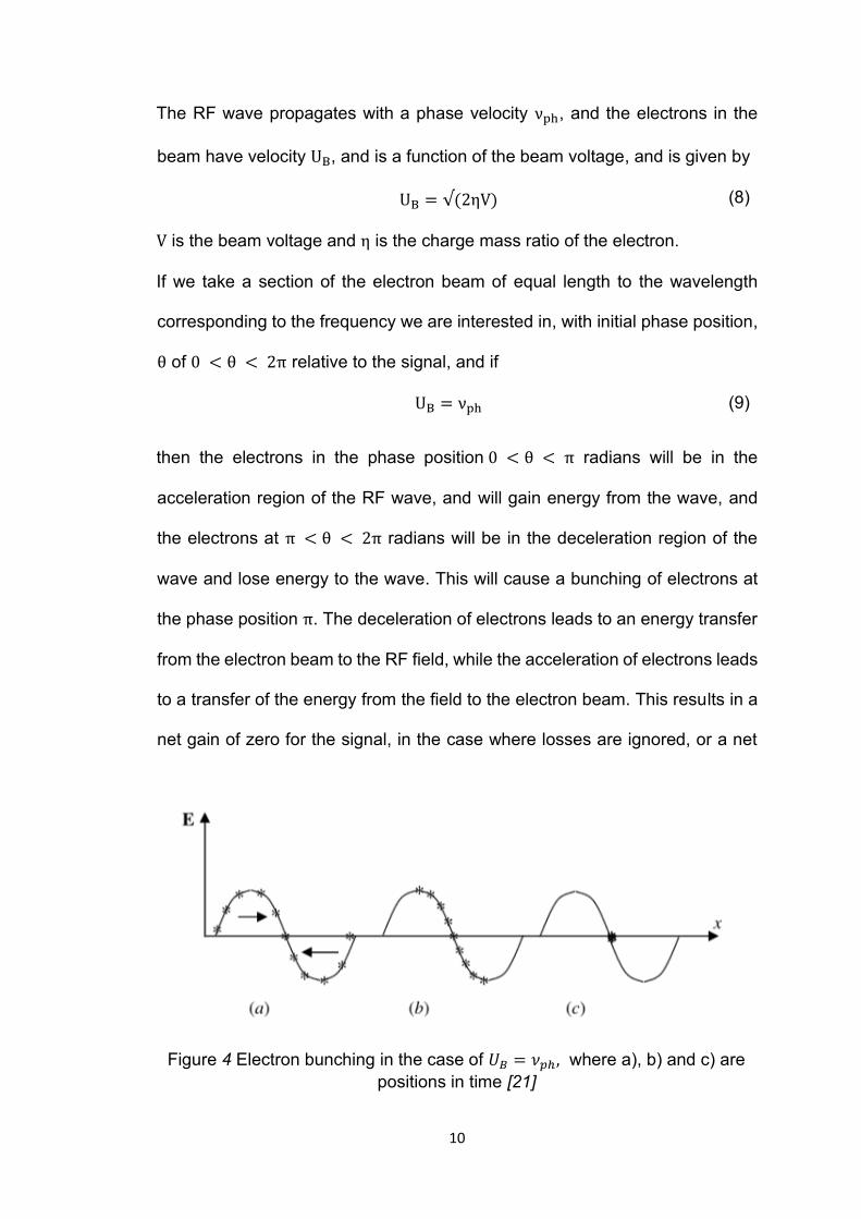
The RF wave propagates with a phase velocity νph, and the electrons in the
beam have velocity UB, and is a function of the beam voltage, and is given by
UB = √(2ηV) (8)
V is the beam voltage and η is the charge mass ratio of the electron.
If we take a section of the electron beam of equal length to the wavelength
corresponding to the frequency we are interested in, with initial phase position,
θ of 0 < θ < 2π relative to the signal, and if
UB = νph (9)
then the electrons in the phase position 0 < θ < π radians will be in the
acceleration region of the RF wave, and will gain energy from the wave, and
the electrons at π < θ < 2π radians will be in the deceleration region of the
wave and lose energy to the wave. This will cause a bunching of electrons at
the phase position π. The deceleration of electrons leads to an energy transfer
from the electron beam to the RF field, while the acceleration of electrons leads
to a transfer of the energy from the field to the electron beam. This results in a
net gain of zero for the signal, in the case where losses are ignored, or a net
Figure 4 Electron bunching in the case of 𝑈𝐵 = 𝜈𝑝ℎ, where a), b) and c) are
positions in time [21]

11
negative gain in the realistic case of non-zero losses. The bunching is shown
in Figure 4 [21].
However, if the beam voltage is chosen to correspond to an electron velocity of
slightly faster than the RF wave’s phase velocity in the structure, where
UB > νp (10)
Then bunching will occur in the deceleration region of the wave, leading to
amplification of the wave. The faster electrons in acceleration region will move
to the deceleration region, and the electrons in the deceleration region, will lose
velocity and form a bunch of electrons in the deceleration region with the
accelerated electrons. An anti-bunch occurs in the RF region of negative
potential. The electrons in the deceleration region lose energy to RF wave due
to being decelerated. This causes an amplification of the RF wave. The initial
interaction between the wave and electron beam will result in a loss of RF
energy, due to the electrons at the back of the beam leeching energy from the
signal as they progress from the acceleration region to the deceleration region
of the wave.
1.2.6 Beam-Wave Interaction: Backward Wave Oscillator Operation
BWOs, unlike TWTs, work by the interaction of an electron beam with the first
negative space harmonic of a signal [21]. The phase velocity is in the opposite
direction of the group velocity of the signal, which means energy travels in the
opposite direction to the electron beam.

12
If a circuit can support a negative spatial harmonic with a known phase velocity
as a function of frequency, and an electron beam is injected with a beam
velocity equal to that phase velocity, then a signal will be stimulated at that
frequency with a group velocity in the direction opposite to that of the electron
beam. This direction is towards the cathode. The electron beam is interacting
with this negative harmonic and transferring energy to the signal. This energy
is transported by the signal with its group velocity, in the opposite direction.
Thus, the stimulated energy is carried to the cathode end of the tube. This
induces velocity modulation in the electrons at the cathode end of the BWO,
which in turn produces greater current modulation at the collector end of the
BWO, stimulating more wave energy. This interaction in the BWO is inherently
regenerative. For low beam currents, regenerative amplification is observed,
and for higher beam currents, oscillation occurs. Figure 5 [26] shows the output
spectrum of a typical BWO.
While single frequency, the circuit is tuneable to a degree defined by the
dispersion characteristics of the structure, by varying the beam voltage. For
Figure 5 Output spectrum of a BWO [26]

13
instance, in Figure 3 the backward harmonic is shown between π and 2π
radians on the phase axis. Varying the beam voltage changes the slope of the
beam line, and so changes the intersection point of the beam line and the
dispersion curve, which changes the operational frequency of the circuit. BWOs
can be excellent sources at millimetre wave and THz frequency, due to their
simple operation [27]. BWOs also share the same setbacks as the TWTs as
the size of the structure is inversely proportional to the desired operational
frequencies, meaning at higher frequencies, fabrication becomes more difficult.
1.2.7 Magnetic Focussing Field
It is important to keep the electron beam in TWTs and BWOs with a given
voltage and current confined. Brillouin flow is where the confining force of the
magnetic field exactly opposes the repelling force of the space charge of the
electrons. Correctly defining the confining field allows for accurate shaping of
the electron beam. Equation (11) is the Brillouin flow equation [28].
Bb = √√2Ib
ϵ0πb2η32√V
(11)
Bb is the brillouin field, Ib is the beam current, ϵ0 is the permittivity of free space,
br is the beam radius, η is the mass-charge ratio of the electron and V is the
beam voltage.
14
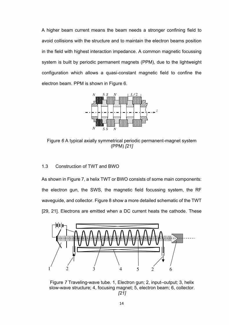
A higher beam current means the beam needs a stronger confining field to
avoid collisions with the structure and to maintain the electron beams position
in the field with highest interaction impedance. A common magnetic focussing
system is built by periodic permanent magnets (PPM), due to the lightweight
configuration which allows a quasi-constant magnetic field to confine the
electron beam. PPM is shown in Figure 6.
1.3 Construction of TWT and BWO
As shown in Figure 7, a helix TWT or BWO consists of some main components:
the electron gun, the SWS, the magnetic field focussing system, the RF
waveguide, and collector. Figure 8 show a more detailed schematic of the TWT
[29, 21]. Electrons are emitted when a DC current heats the cathode. These
Figure 7 Traveling-wave tube. 1, Electron gun; 2, input–output; 3, helix slow-wave structure; 4, focusing magnet; 5, electron beam; 6, collector.
[21]
Figure 6 A typical axially symmetrical periodic permanent-magnet system (PPM) [21]

15
electrons are focussed into a shaped beam by electrodes and accelerated. This
accelerated beam then enters the SWS, where DC energy from the beam
amplifies the AC RF signal. The beam is kept focussed by magnets surrounding
the SWS, which apply a magnetic field. These magnets are either a solenoid or
PPM. The electron beam then enters a collector which collects the spent beam.
1.3.1 The Helix SWS
The helical SWS is wound helical metallic tape. The electron beam is provided
by a thermionic electron gun. The length of the tube is carefully chosen so the
beam wave interaction has maximum energy transfer from the beam to the
signal. Too short and the tube will lack gain, too long and the beam will begin
to leech energy from the wave. Relatively low velocity of the RF signal allows
for a similarly low beam voltage for electron beam. This voltage is called the
synchronous beam voltage. At the end of the SWS the electron beam is
conveyed in a collector, which may reduce energy losses and increase
efficiency [30]. At microwave frequency, helices are typically the SWS used in
the amplification process of RF waves, because of their multi-octave bandwidth
and high interaction properties. Advanced, three-dimensional electromagnetic
simulation programs are used in the design process of such structures. Due to
Figure 8 Detailed TWT Schematic, with the beam focussing illustrated. [29]
16
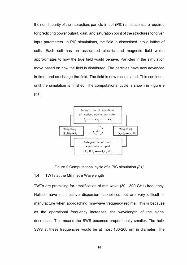
the non-linearity of the interaction, particle-in-cell (PIC) simulations are required
for predicting power output, gain, and saturation point of the structures for given
input parameters. In PIC simulations, the field is discretised into a lattice of
cells. Each cell has an associated electric and magnetic field which
approximates to how the true field would behave. Particles in the simulation
move based on how the field is distributed. The particles have now advanced
in time, and so change the field. The field is now recalculated. This continues
until the simulation is finished. The computational cycle is shown in Figure 9
[31].
1.4 TWTs at the Millimetre Wavelength
TWTs are promising for amplification of mm-wave (30 - 300 GHz) frequency.
Helices have multi-octave dispersion capabilities but are very difficult to
manufacture when approaching mm-wave frequency regime. This is because
as the operational frequency increases, the wavelength of the signal
decreases. This means the SWS becomes proportionally smaller. The helix
SWS at these frequencies would be at most 100-200 μm in diameter. The
Figure 9 Computational cycle of a PIC simulation [31]

17
fabricated helix SWS would be far too delicate for reliable performance at best,
and impossible to fabricate at worst.
However, advances in microfabrication techniques such as high accuracy
computer numerical controlled (CNC) milling [32] [33] and Lithographie,
Galvanoformung, Abformung (LIGA) processes [34] [35] increased the
potential of TWTs and BWOs to that of use in the millimetre wave and terahertz
frequencies [36], through the use of structures beyond that of helical SWS. As
such, novel and realisable structures can be designed and developed.
1.5 SWSs for Millimetre Wave TWTs
Novel SWSs must have suitable interaction impedance and low losses, over a
wide bandwidth, and be manufacturable. The phase velocity must be reduced
such that the synchronous beam voltage is low at around 10-30 kV for
portability. In the following the most promising SWSs will be described.
1.5.1 Folded Waveguide Travelling Wave Tube
The folded waveguide (FWG) is a simple solution for a SWS of high power, high
frequency and wide bandwidth TWTs. As shown in Figure 10, the geometry is
obtained by the folding of a rectangular waveguide. The signal takes a longer
path than the direct route taken by the electron beam. The electron beam
voltage can be tuned such that the signal and the electron beam meet at the
same time where the waveguide and the beam tunnel cross.
As the FWTWT is essentially a rectangular waveguide, the tapering of the
structure only requires the widening or narrowing of the width and breadth of
the waveguide. Because the TE10 mode of the signal in the input waveguide is
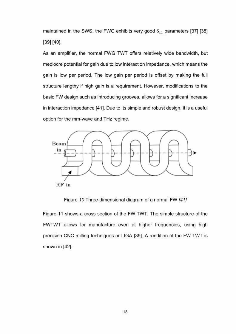
18
maintained in the SWS, the FWG exhibits very good S11 parameters [37] [38]
[39] [40].
As an amplifier, the normal FWG TWT offers relatively wide bandwidth, but
mediocre potential for gain due to low interaction impedance, which means the
gain is low per period. The low gain per period is offset by making the full
structure lengthy if high gain is a requirement. However, modifications to the
basic FW design such as introducing grooves, allows for a significant increase
in interaction impedance [41]. Due to its simple and robust design, it is a useful
option for the mm-wave and THz regime.
Figure 11 shows a cross section of the FW TWT. The simple structure of the
FWTWT allows for manufacture even at higher frequencies, using high
precision CNC milling techniques or LIGA [39]. A rendition of the FW TWT is
shown in [42].
Figure 10 Three-dimensional diagram of a normal FW [41]

19
1.5.2 Double Corrugated Waveguide
Double corrugated waveguide (DCW) is an effective solution for use in a TWT
or BWO in the millimetre wave and THz regime. A rendition is shown in Figure
12 [26]. The DCW is comprised of two parts which may be aligned and then
connected. This simplicity allows for easy assembly. One part is a hollow
rectangular metal waveguide with two parallel rows of metal pillars.
Figure 12 Rendition of the double corrugated waveguide with electron beam [26]
Figure 11 Rendition of the FW TWT, with electron beam [42]

20
The second part is a metal plate which will close the waveguide. The pillars are
separated width wise by a distance defined as the tunnel width. There are one
pair of pillars per SWS period. The simple design allows for easy assembly.
Fabrication can be realised by CNC milling or LIGA process.
As a SWS, the DCW supports a hybrid TE10 mode of operation, and as such a
coupler section is required to transform the TE10 mode in to the hybrid mode
where the signal enters the waveguide, and back again at the output, where
the amplified signal leaves the device. The input and output waveguides are
standard rectangular waveguide flanges [43]. Shown in Figure 13 is a method
for coupling the SWS to the input and output waveguides. The width and height
of the waveguide taper must be gradually increased or decreased to match that
of the SWS. Similarly, the pillars must be gradually built, to ensure the wave
impedance is matched along the structure. The gradual introduction of pillars
allows a reduction of reflections. The taper must be optimised so as little of the
input signal is lost to reflections as possible. This is especially important in low
power devices or devices whose input power is very low [44] [45] [46] [47] [23].
The DCW is suitable for wideband amplification in the millimetre wave and
Figure 13 Introduction of pillars to the waveguide

21
terahertz regions. However, the beam line slope of the first forward spatial
harmonic is the usable harmonic. This is because the synchronous beam
voltage is too high when the fundamental harmonic is used. This limits the
interaction impedance. Figure 14 shows the parameters considered in the
design of the geometry of the DCW.
1.6 Fabrication
SWSs are scalable into the mm-wave frequency regime. CNC machining
technology allows for the micron scale tolerances and surface roughness
required for the sub-THz regime [32] [33].
The LIGA process is based on the exposure of thick photoresist to a specific
light source, and is used to build a relatively high aspect ratio 3D moulds, with
arbitrary 2D patterns. The mould may then be used for electroplating
microstructures such as mm-wave and THz regime SWS. In principle, the
process allows for highly accurate structures and repeatability and can account
for low tolerances of only a few microns [34].
Figure 14 Design of the DCW [23] Left is the cross section perpendicular to the beam axis, and right is the cross section parallel to the beam axis and
from the side of the DCW.

22
1.7 Simulations
Full 3D particle-in-cell (PIC) electromagnetic simulators are used for the
process of designing TWTs. This is to ensure the final device exhibits adequate
power output and gain. Full PIC simulations can take a long time. However, in
the case of tubes whose SWS is based upon the helix [48] [49] [50], the coupled
cavity [51] [52] [53], the folded waveguide [54], and for devices whose SWS are
modified versions of these [55], the mathematics for modelling the interaction
and fast Lagrangian codes exist, which may be used to expedite the design
process [56].
1.8 Lagrangian Formulation
Since the invention of the TWT, many methods have been derived to study the
operation of the TWT in small signal regime. A basic postulate for the modelling
of the TWT is defining the electron beam as a drifting charged fluid, with a single
valued velocity and charge density functions at each displacement plane. This
method is called Eularian formulation and is best suited to small signal analysis.
Another possible formulation is the Lagrangian formulation. This is achieved by
sub-dividing the electron beam into charge groups, or charge groups, and
following these charge groups through the interaction. This formulation is well
suited for non-linear interactions, such as the large signal analysis [50]. The
Lagrangian formulation is shown illustratively in Figure 15, for the initial state of
the electron beam with respect to the phase of the RF signal.
The Lagrangian formulation is utilised because nonlinear effects caused by the
Lorentz force equation and the charge continuity equation become significant
in the large signal case. The Lagrangian formulation uses well-defined charge

23
groups defined over a single RF wavelength of the signal supported by the
SWS. This wavelength refers to the wavelength of the mode of the signal in the
SWS. This method allows for the capture of the many of the nonlinear effects
of the beam-wave interaction. Each of these charge group can move
independently, and can slow down, reverse, and swap phase positions, which
captures much of the non-linear behaviours of the system.
The transmission line model is a convenient way of modelling the beam wave
interaction between the structure and electron beam, due to its inherent
simplicity [50]. An example is shown in Figure 16 .
The beam wave interaction is a continuous process, and as such, the effect of
the beam wave coupling must be evaluated at each integration step of the
simulation. The integration step dz is defined as
dz =
L
N
(12)
Where L is the length of the structure and N is the number of integration steps.
Figure 15 Lagrangian formulation of beam wave interaction. It depicts one wavelength of wave, and a section of electron beam the same length. The section of electron beam is divided in charge groups called charge groups.
The + and – indicate the potential of the wave.

24
Initial velocity and phase positions are assigned to each charge group and each
group has a fixed radius and a fixed charge and mass defined by the current
density of the electron beam and the radius and number of charge groups [50].
Each charge group is free to move independently of the other charge groups,
with exception to influence of space charge waves. In this case, the charge
groups may slow down, pass through each other and reverse, and will feel a
repulsive force relative to the other charge groups.
The relative position of each charge group with respect to the other charge
groups produces much of the space charge forces acting upon the system. The
space charge potential of the beam is produced by calculating the electric field
potential of each charge group and integrating over the length of the beam
wavelength to give the electric potential of the beam and averaged to over the
volume of the charge group to give the space charge potential between two
identical charge groups.
1.8.1 Derivation of the General Amplifier Equations
The derivation for the general amplifier equations in one dimension is presented
in this section. The transmission line equation for a one-dimensional line is [50]
where ρ and V, the charge density and signal amplitude, are functions of z and
t. vp is the characteristic phase velocity of the one-dimensional line, Z0 is the
characteristic interaction impedance. C is the Pierce Gain Parameter, where Ib
is the electron beam current and V0 is the electron beam voltage at the cathode
and the attenuation per undisturbed wavelength of the circuit is dl, defined as
∂z
2V −1
νp2∂t
2V −2ωCdl
νp2
∂tV = −Z0
νp{∂t
2ρ + 2ωCdl ∂t ρ} (13)

25
C is defined as
To derive equation (13), the transmission line equation, consider the equivalent
circuit for a TWT as shown in Figure 16 [50].
(16) defines the phase lag of the RF signal. It is defined as the phase difference
between the RF signal and a hypothetical wave travelling at UB, which is the
initial velocity of the electrons in the electron beam and is a function of the beam
voltage V0. Assuming the phase velocity of the signal and the initial electron
velocity are the same, thus satisfying equation (9), the lag exists because of
beam loading effects, where the field of the electron beam alters the field of the
propagating wave. This means the electric field of the electron beam changes
the field of the RF waves such that the phase velocity of the wave changes.
dl =
R
2ωLC
(14)
C3 =
Z0Ib4V0
(15)
θy(y) =y
C− ωt − Φ(y,Φ0,j)
(16)
Figure 16 Equivalent circuit for the one dimensional transmission line [50]

26
The Lorentz equation (17) is the starting point for which the RF signal’s effects
upon the electrons is derived.
The electric field is comprised of the field provided by the signal, the circuit field,
and the field electron beam, the space charge field. Splitting these fields gives
equation (18).
As we are only interested in the z-component of the fields, when the divergence
theorem is applied we obtain equation (19)
E(z, t) =
∂Vc(z, t)
∂z+
∂Vsc(z, t)
∂z
(19)
And the left-hand side of equation (17) reduces to
dvz
dt=
d2z
dt2
(20)
This produces equation (21)
The last physical phenomena to define is the charge continuity equation, or
charge conservation. Consider a small amount of charge entering the field at
an input plane [50]. This charge must appear at some other plane sometime
later. This is shown mathematically as
ρ(z, t)dz = ρ(z, t)dz|z=0,t=0 (22)
The initial charge density can be described as follows with the initial beam
current and the initial electron velocity.
dν
dt= −|η|[E + ν × B ]
(17)
E = E c + E sc = ∇ (Vc + Vsc) (18)
d2z
dt2= |η| {[
∂Vc(z, t)
∂z+
∂Vsc(z, t)
∂z]}
(21)

27
ρ(z = 0, t = 0) =
I0uB
(23)
Combining equations (22) and (23) gives the continuity equation of state for the
system.
ρ(z, t) =
I0u0
|dz0
dz|
(24)
This set of equations is all that is required to derive the set of generalised
amplifier equations when combined with the definitions for the normalised
Lagrangian variables.
1.8.2 Normalised Lagrangian Variables
Normalised equations are used to simplify the problem [50]. They are derived
using normalised Lagrangian variables. The variables axial position, z, and
time, t, are transformed into normalized variables y and Φ0,j by
y =
Cωz
u0
(25)
where C is the gain parameter, ω is the angular velocity of the RF signal, z is
the unnormalized position along the tube and U0 is the initial electron velocity,
and
Φ0,j = ωt0,j (26)
where t0,j and Φ0, j are the entry time and phase, relative to the RF signal,
respectively. Using the normalised variables described, a normalised
expression for the potential of the circuit is defined as [50]
V(y,Φ) = Re [
Z0I0C
A(y)e−jΦ] (27)

28
where A(y) is the normalised voltage amplitude of the RF signal at normalised
position y.
The normalised velocity is found by visualising the particle velocity in terms of
y and Φ0,j, and is expressed in the form
ut(y,Φ0) = u0(1 + 2Cu(y,Φ0,j)) (28)
ν0(y = 0) =u0
1 + Cdθdy
|y=0
(29)
where
dθ
dy|y=0 = −b
(30)
The combination of these equations and the normalised variables lead to the
normalised amplifier equations. The transmission line equation is transformed
into the circuit equation of the system and is given by
−C(ω
1 + Cb)Z0I0 [
d2A(y)
dy2
− A(y) [(1
C−
dθ
dy)2
− (1 + Cb
C)2
]] cos(Φ(y,Φ0))
+[(
1
C−
dθ
dy) (−2
dA(y)
dy) + A(y)
d2θ
dy2
−2d
C(1 + Cb)2A(y)] sin(Φ(y,Φ0))
(31)
= ν0Z0 [
∂2ρ1
∂t2+ 2ωdl
∂ρ1
∂t]

29
The Force equation is given by the combination of the normalised parameters
and the Lorentz equation of the form shown in equation (32).
d2y
dt2= −|η| {
Z0I0ω
u0[dA(y)
dycos(Φ(y,Φ0))
− A(y) sin(Φ(y,Φ0)) [1
C−
dθ
dy]] − Esc−z(y,Φ)}
(32)
Lastly, the continuity equation is found by considering the rate of change of z
and z0 with respect to t, time, and is found to be
1.8.3 Generalised Amplifier Equations
Using the above results, the generalised amplifier equations for a TWT may be
found. This set of equations can be used to analyse any helical TWT in the one-
dimensional approximation.
To start, the harmonics of the linear charge density must be considered. The
linear charge density has many harmonics, but only ρ1, the fundamental, is
considered here. This is because it is assumed that ρ1 only excites the circuit
since Z01, the interaction impedance of fundamental frequency dominates. This
means that Z01 is much greater than the interaction impedances of the higher
harmonics, or Z01≫ Z01
, Z01, Z01
….,
While it is possible to consider ρn∀ n, doing so requires knowledge of Z0,n ∀ n,
and the additional phase relationships between circuit voltage elements. The
Fourier expansion of the beam charge density is analysed at the first frequency
harmonic n = 1.
ρ(y,Φ) =
I0u0
|dΦ0
dΦ|
1
1 + 2Cu(y,Φ0)
(33)

30
The full Fourier expansion of equation (33) is
ρ(z, t) = ∑[An sin(−nΦ) + Bncos (−nΦ)]
∞
n=1
(34)
Where
(−nΦ) = nωt − ∫ nβ(z)dz
z
0
(35)
The Fourier coefficients are
An =
1
π∫ ρn(z,Φ) sin(−nΦ)dΦ
2π
0
(36)
Bn =
1
π∫ ρn(z,Φ) cos(−nΦ)dΦ
2π
0
(37)
The Lagrangian variable continuity equation (33) is used to write equation (34)
as
As we are only interested in n = 1, we use the first term in the series to find the
derivatives found in the right-hand side of equation (31), the circuit equation.
ρ(y,Φ) = Re [
I0u0π
∑e−jnΦ {∫cos(Φ(y,Φ0′)) dΦ0′
1 + 2Cu(y,Φ0′)
2π
0
∞
n=1
+ j∫sin(Φ(y,Φ0′)) dΦ0′
1 + 2Cu(y,Φ0′)
2π
0
}]
(38)
31
ρ1 = cosΦρ1c + sinΦρ1s
∂ρ1
∂t
(39)
∂ρ1
∂t=
∂ρ1
∂Φ
∂Φ
∂t
(40)
∂2ρ1
∂t2=
∂ρ1
∂Φ
∂2Φ
∂t2+ (
∂Φ
∂t)2 ∂2ρ1
∂Φ2
(41)
Where ρ1c and ρ1s are the integrals from equation (31) for n=1.
From this, we can obtain the general form of the circuit equations describing
the beam driven circuit. Since the coefficients on each side of the equation are
not functions of Φ and that cos(Φ) and sin(Φ) are orthogonal, all that remains
is to equate the coefficients and produce the following two equations.
A(y) [
d2θ(y)
dy2−
2dl
C(1 + Cb)2] + 2
dA(y)
dy(dθ(y)
dy−
1
C)
= −(1 + Cb
πC) [∫
sin(Φ(y,Φ0′)) dΦ0′
1 + 2Cu(y,Φ0′)
2π
0
− 2Cdl ∫cos(Φ(y,Φ0′)) dΦ0′
1 + 2Cu(y,Φ0′)
2π
0
]
(43)
d2A(y)
dy2− A(y) [(
1
C−
dθ(y)
dy) − (
1 + Cb
C)2
]
= −(1 + Cb
πC) [∫
cos(Φ(y,Φ0′)) dΦ0′
1 + 2Cu(y,Φ0′)
2π
0
+ 2Cdl ∫sin(Φ(y,Φ0′)) dΦ0′
1 + 2Cu(y,Φ0′)
2π
0
]
(42)

32
Equations (42) and (43) describe the driving of the circuit fields. The left-hand
side of the equations are homogeneous, and the right-hand side of the
equations are inhomogeneous because the circuit wave is being driven by the
electron beam.
The acceleration of the electron beam is due to the RF field and the internal
space charge of the electron beam. The space charge integral is found from
the analysis of the harmonics of the linear charge density. It is not enough to
calculate the space charge from only the first or first few harmonics: all the
harmonics must be considered. This will be discussed in more detail later. The
equation for the force experienced by the electron beam is found as [50]
[1 + 2Cu(y,Φ0)
∂u(y,Φ0)
∂y]
= −A(y) [1 − Cdθ(y)
dy] sin(Φ(y,Φ0))
+ CdA(y)
dycos(Φ(y,Φ0)) + S. C.
(44)
S.C. stands for space charge force. The space charge force is the force felt by
an electron from each of the other electrons, and will be considered in the next
section.
The final equation of the generalised amplifier equations is the Velocity-Phase
equation. This equation relates the change in charge group phase relative to
the RF field, the phase lag θ(y) between a hypothetical wave travelling at initial
beam velocity u0 and the RF wave travelling at v0, and the charge group’s
normalised velocity, and is given by
∂Φ(y,Φ0)
∂y+
dθ(y)
dy=
1
C[1 −
1
1 + 2Cu(y,Φ0)]
(45)

33
The generalised amplifier equations can be used for any configuration of helical
of TWTA, for any beam radius, helix radius etc. The method of solving them is
to treat the problem as an initial value problem, and to solve the equations at
predetermined calculation planes, where the output values at these planes are
used as the new initial values, until saturation is reached and the output power
of the TWTA is calculated [50] [21].
1.8.4 Space Charge Force
The space charge forces due to the repulsive forces between the electrons in
the beam are one of the main parameters needed for correctly modelling the
beam wave interaction. This is because energy flow from the DC beam to RF
signal relies on how well the device can manipulate the electronic charge group
bunching capabilities of the supported RF mode when it interacts with the
electron beam, and is greatly affected by space charge.
Space charge causes oscillations, called Langmuir waves. In free space these
have an associated frequency known as the plasma oscillation frequency,
which arises whenever there is a perturbation. It is like a pressure-density wave.
The disturbance may be in the form of an electromagnetic wave, from an
external source or from the movement of neighbouring electrons. The plasma
oscillation frequency affects the strength of the axial space charge forces, or
more precisely, may damp the forces. In metallic confinement, such as in a
waveguide, the plasma frequency is reduced due to interactions with the
conducting walls of the waveguide and is a function of distance between the
boundary and the electron beam. This reduction is modelled by introducing a

34
value called the plasma frequency reduction factor. For a waveguide with
cylindrical symmetry, the plasma frequency reduction factor is constant for all
angles perpendicular to the axis of motion and acts to lessen the oscillation
frequency of the space charge oscillations, and as such reduce the effect of
space charge forces [50] [21].
In the one-dimensional case, the axial component of the electronic space
charge force is considered. This describes how the electron bunches repel each
other axially along the circuit and is responsible for some of the bunching effects
modelled in the simulations. For the proposed code, a simple version of the
axial space charge force was considered, which gives the space charge integral
the form [50]
1
(1 + Cb)(ωp
ω)2
∫e|Φ−Φ0′| sgn(Φ − Φ0
′ )dΦ0′
1 + 2Cu(y,Φ0′)
2π
0
= F1−z(Φ − Φ0′ )
= eu0|Φ−Φ0′|
ωb′ sgn(Φ − Φ0′ )
(46)
This expression sums over the force felt by a reference electron group caused
by each other electron group. This gives an approximate value for the space
charge force. This is convenient as the explicit solution would require the
calculation of many Bessel’s functions per iteration of the code.
1.8.5 Space Charge waves
If one considers an infinite one-dimensional slab of electric charge, perturbed
in some way by a small factor in the z-direction, δz, an oscillation is produced.
The charge density of this can be described as
σ = enδz (47)

35
where e is the electronic charge and n is the number of electronic charges on
this leading face.
An equal and opposite charge density will be produced due to this perturbation,
and will produce an electric field of the form
Ez = −σ
ϵ0= −enδz/ϵ0 (48)
Applying Newton’s law to this equation we obtain
m
d2δz
dt2= eEx = −mωp
2δz (49)
which when combined with equation (48) produces
−mωp2δz = −ne2δz/ϵ0 (50)
Simplifying to
ωp
2 =ne2
ϵ0m
(51)
where m is the mass of an electron. This equation can be rewritten as
ωp
2 =eID
mϵ0u0
(52)
Where ID is the dc current density and u0 is the dc beam velocity, defined as
UB = √(
2Ve
m)
(53)
In any finite electron beam, fringing effects reduce the longitudinal electric field,
and in the case of an electron beam confined by conducting surfaces, fringing
is further increased. This is due to the geometry of the tube, and the shape of
the electric field between the beam and the wall. Due to this fringing effect, the
plasma oscillation frequency is reduced.

36
To derive the plasma frequency reduction factor, first, we must derive the
propagation constant of the space charge waves relating to the reduced
frequency.
First, we consider Maxwell’s equations.
E = −∆ΦE −
1
c
∂AH
∂t
(54)
H = ∇ × AH (55)
Where E is the electric field vector, H is the magnetic field vector, ΦE is the
scalar potential of the electric field, and AH is the magnetic potential vector.
These reduce in the wave equations
[∇2 −
1
c2
∂2
∂t2]ΦE = ρ
(56)
[∇2 −
1
c2
∂2
∂t2] AH =
−ρν
c
(57)
∇ ∙ AH
= −1
c
∂ΦE
∂t
(58)
Only the wave solution is desired, so it is useful to denote the scalar electric
potential, charge density, and velocity respectively, as
ΦE = Φ1ei(ωt−γz) ρ = ρ1e
i(ωt−γz) v = νzei(ωt−γz)
Equations (56) and (57) can be written in terms of cylindrical coordinates to give
∂2Φ1
∂r2+
1
r
∂Φ1
∂r+
1
r2
∂2Φ1
∂θ+ (k2 − γ2)Φ1 = ρ1
(59)
ρ1 may be written in terms as ΦE1 as

37
ρ1 =
eρ0
m
γ2 − k2
(ω − γν0)ΦE1
(60)
Which gives
∂2ΦE1
∂r2+
1
r
∂ΦE1
∂r+
1
r2
∂2ΦE1
∂θ+ (k2 − γ2) [1 −
eρ0
m(ω − γν0)2]ΦE1
= 0 (61)
with a solution is given in the form
ΦE1= BnJn(Tr)einθ (62)
where Bn is a constant, Jn is the nth Bessel’s function of the first kind, and T is
T = {(k2 − γ2) [1 −
eρ0
m(ω − γν0)2]}
1/2
(63)
In the space between the electron plasma and the conducting walls of the tube,
the solution is known as
ΦE2= Cn(In(τr) + DnKn(τr)) (64)

38
Where Cn and Dn are constants to be determined, In, and Kn are modified
Bessel functions. τ is defined as
τ = (γ2 − k2)1/2 = ω/u0 (65)
Figure 17 shows the boundary conditions for the solution. The constant Dn is
determined by considering the tangential electric field at r = Rb, the
conducting wall, where the tangential electric field must equal zero. That is
ΦE2|r=Rb = 0 (66)
Thus, by solving equation (64) for the condition stipulated in equation (66), we
obtain
Dn = −
In(τRb)
Kn(τRb)
(67)
Figure 17 Diagram of the boundary conditions used to solve equation (62) and (64)

39
The conditions left to be satisfied are at r = b, the beam radius. The field must
be continuous at this point, which means equation (68) and equation (69) must
be satisfied. This condition will be used to determine the ratio of Cn/Bn, and to
consider γ in terms of the given parameters.
∂ΦE1
∂r|r=b =
∂ΦE2
∂r|r=b
(69)
Equating equation (62) and equation (64) yields equation (70)
Cn
Bn=
In(τb) + DnKn(τb)
Jn(Tb)
(70)
And differentiating both equation (62) and equation (64) and equating the
results gives
Cn
Bn=
(τb)
(Tb)
In′ (τb) + DnKn′(τb)
Jn′ (Tb)
(71)
Which when combined and rearranged leads to the transcendental equation
(Tb)
Jn′ (Tb)
Jn(Tb)= (τb)
In′ (τb) + DnKn′(τb)
In(τb) + DnKn(τb)
(72)
Equation (68) may be numerically solved for T, and then T substituted into
equation (69) to find the plasma frequency reduction factor [57] [58].
ΦE1|r=b = ΦE2
|r=b (68)
ωq
ωp= √
1
1 + (Tτ)
2
(73)

40
1.8.6 Weighting Functions
The electromagnetic field supported in TWT or BWO is not uniform. The field
changes as a function of radius in the case of the helical TWT. This can be
modelled using weighting functions. The advantage of weighting functions
comes from being able to maintain a single valued interaction impedance, even
though different parts of the beam will experience more or less coupling to the
wave than other parts.
Figure 18 shows the electric field for a helical TWT. For the cases of cylindrical
symmetry such as this, the radially dependent electric field strength, equation
(74) [50] may be used to calculate rotationally invariant weighting functions for
different parts of the beam separated radially.
f(r) =
I02(τb) − I1
2(τb)
I02(τr)
(74)
This method requires only knowledge of the frequency, the voltage of the
electron beam, the radius of the tube and radius of the electron beam, or the
radius of the charge group in the electron beam for subdivided configurations.
As such, equation (74) is not a function of angular position of the electronic
charge group, as would be expected for a cylindrically symmetric system.
Figure 18 The electric field in a helix based TWT. On average the field is asymmetric, and only relies upon radial position.
11
41
1.8.7 Eigenmode and Finite Difference Time Domain Simulation
Fully three-dimensional (3D) solver, such as CST [59] and MAGIC3D use a
different approach to solving electromagnetic systems. They solve Maxwell’s
Equations directly in either integral form or differential form using linear
algebraic techniques. These are powerful tools, as many structures are not
analytically solvable due to extremely irregular shapes. In terms of TWT design,
two solvers are used; eigenmode simulations and finite difference time domain
(FDTD).
Eigenmode simulations calculate the cold parameter of a SWS. The cold
parameters refer to the structure in the presence of a RF wave but no electron
beam. The eigenmode of a given closed-region possess a discrete spectrum of
frequencies. The simulation considers a closed region in the form of a single
period of the SWS being designed. The frequencies of the dispersion curve
correspond to allowed values of the propagation constant as a function of the
range of phase differences being investigated [60]. The average power flow
through the period is also calculated. This data is used to calculate the
interaction impedance of the SWS. By the dispersion curve the synchronous
beam voltage is obtained.
The eigenmode simulator uses either the Advanced Krylov Subspace method
or the Jacobi-Davidson method to solve Maxwell’s equations for the closed
resonant structures, such as a single period of a SWS [61].
FDTD is used to calculate the S-Parameters of the full structure and the full hot-
test simulation of the device. To discretize Maxwell's equations with second-
order accuracy for homogeneous regions where there are no discontinuous
material boundaries, FDTD methods store different field components for

42
different grid locations. This discretization is known as a Yee lattice. The Yee
lattice in the 3D case is shown in Figure 19 [62].
For the hot simulations the PIC solver is used. Hot simulation means the
interaction of the electron beam and the signal is simulated using an electron
beam with an initial radius, current and voltage, and signal with a single
frequency and initial power. The PIC solver is self-consistent, which means the
solver takes the fields produced by the particles directly for each time step of
the simulation. This makes it ideal for TWTs and BWOs, where the nonlinearity
of the interaction between particles and fields is of great importance [63].
1.8.8 Performance and comparison
Full 3D simulators are general purpose tools, meaning they can solve for
arbitrary structures, like the DCW TWT or the FW TWT. The general amplifier
equations were derived above for the TWT. However, these Lagrangian codes
only work for structures with a specific symmetry in the form of cylindrical
symmetry. The cost of being general purpose comes in the form of large
Figure 19 Yee Lattice [62]

43
computational effort and time. Lagrangian codes for specific structure may take
on the order of minutes [64], whilst fully 3D simulators may take of order tens
hours [23].
1.9 Conclusions
The helix is a good SWS for amplifiers and oscillators up to about 60 GHz.
Above that, the structure becomes too small to reliably manufacture, and are
fragile. Different SWSs are required for higher frequency amplification in the
mm-wave and THz frequency regime.
The DCW is a promising SWS for the mm-wave and THz frequency regime.
This is because of the viable fabrication techniques CNC-milling and LIGA, as
well as easy construction.
Lagrangian simulators can be fast methods of simulating many variations of a
TWT or BWO in a short period of time. Lagrangian simulators exist for TWTs
and BWOs with helix SWSs. However, there is no Lagrangian simulator for
asymmetric structures. As such, it would be useful to have a Lagrangian
simulator to expedite the design process of asymmetric SWS suitable for mm-
wave and THz frequency regime.
1.10 Organisation of the Thesis
The thesis is organised in the following manner. Chapter 2 describes the novel
Lagrangian method for asymmetric SWSs. The motivation for this part of the
thesis is driven by the need for a fast method of simulating beam-wave
interaction in TWTs and BWOs in the mm-wave frequency regime, where novel

44
periodic structures are required for use as the SWS of the tube, due to helices
being unsuitable.
The definitions of the large signal model, including the methods for calculating
the space charge forces acting upon the electron beam, and the weighting
functions describing the field distribution caused by the SWS, are presented.
The novel modifications proposed are described in detail, as is the structure of
the code used to validate the model. The validation is performed by comparison
of the output of the code with the output of 3D electromagnetic simulations. The
outputs compared are the saturation point and power output.
Chapter 3 describes the design of DCWs at novel frequencies, for mm-wave
TWTs, and uses CST-MWS as the simulation software. The motivation comes
from advances in micro-fabrication technology allowing for the realisation of
structures small enough to be useful in new high frequency regimes such as
mm-waves and THz frequencies. The comparison of two tapering
configurations for coupling the SWS to input and output waveguides are
described. These two configurations are the lateral tapering of the pillars, and
the height tapering of the pillars of the DCW. The S11 and S21 S-parameters are
presented, as well as the field distribution at the transition from TE10 supported
by the input waveguide to the hybrid TE10 mode supported by the DCW. A 346
GHz BWO is used for the purpose.
A DCW for use in a BWO operating at 100 GHz is described, as well as a TWT
operating with a central frequency of 270 GHz. The dispersion relation of the
periodic structures is analysed for the phase velocity of the relevant spatial
harmonic, to calculate the synchronous beam voltage, and the interaction
impedances as a function of frequency is presented.

45
The tapering configuration for these two DCWs, utilising the lateral tapering
configuration, is also described, with the S11 and S21 parameters being
presented with the TE10 to hybrid TE10 mode transition.
A W-band DCW is also described with an operating frequency band of 92-95
GHz for use in wireless applications. Two configurations for the DCW SWS are
discussed; the square pillared DCW and the triangular pillared DCW. A bend
taper is described in which the pillars near where the electron beam enters the
tube must be altered in shape to allow room for the electron beam to propagate.
The S11and S21 parameters for the bend taper with no alterations and the bend
taper with alterations are presented and compared.
General conclusions are then discussed, as well as limitations of the work and
added insights with opportunities for future work.
46
Chapter 2 Novel approach to Large Signal Lagrangian for
Asymmetric SWSs
Full 3D simulators are general purpose. They may simulate a large range of
different electromagnetic systems. This makes them powerful but slow when
using conventional computers. Specialist simulators, written for a single device,
such as Lagrangian simulator can be very fast. Lagrangian simulators exist for
helical and coupled cavity SWS TWT and BWO but are not accurate for TWTs
utilising the asymmetrical structures as the DCW. This has been explained in
detail in Chapter 1.
The problem to be solved here is to modify the helical waveguide solution for
accurate simulations of the DCW, taking into account the lack of rotational
symmetry exhibited by this waveguide configuration.
A novel approach to the large signal model based on the modified Lagrangian
theory for helical waveguide circuit will be described. The approach changes
how space charge forces are modelled. Weighting functions corresponding to
not only radial position, but also axial positions are utilised, and factors which
affect space charge forces are considered in a novel way. The Lagrangian
equations derived previously will model the interaction between the beam and
the RF signal and will do so in terms of the circuit field amplitude, and
normalised electronic charge group velocity and phase. The 3D simulator CST
will be utilised in the calculation of the input variables required for the calculation
of the weighing functions at low computational cost. An eigenmode simulation
is not computationally intensive and may take much less than 1 hour to
complete. The modified Lagrangian code will be validated by comparison with

47
the results of a Ka-band DCW TWT [65]. This structure was originally simulated
in CST-PS (particle studio) [59]. Comparisons will be made between the
saturation point of the interaction and the output powers simulated via each
method.
2.1 Large Signal Model
Differently from the helix, most novel SWSs designed to be used in the mm-
wave and THz TWTs present non-cylindrical symmetry, but arbitrary symmetry.
This means, when rotated about the beam axis, the structure does not look the
same at any angle of rotation except for a few specific angles dependent on the
structure. The DCW is an SWS with this property. This affects the computation
of the space charge, as the plasma frequency reduction factor is not constant.
It is instead a function of the space between the beam and the surrounding
metal structure. A different method of calculating a plasma frequency reduction
factor must be found. Space charge is discussed in detail in Chapter 1.
The model proposed is based on the one-dimensional Lagrangian equations of
motion of electrons and the beam-wave interaction between the electrons and
RF wave as derived by Rowe [48] [50], also presented in Chapter 1.
2.2 Modification to the Lagrangian Model
In the case of cylindrical symmetry, a single value for the plasma frequency
reduction factor is enough for modelling this damping. Solving equation (72)
yields the radial propagation constant of the space charge waves and using the
value τ = ω/u0, the plasma frequency reduction factor can be found for a given

48
tube radii and beam radii. However, if the structure is not rotationally symmetric,
there is no single value for the plasma frequency reduction factor. Similarly, the
electric field values in structures with no rotational symmetry cannot be solved
for with a simple equation such as equation (74). Further, structures such as
the DCW have a varying axial electric field, above the natural oscillations of the
wave, giving rise to increased complexity.
Figure 20 Cross section of the DCW TWT. The radius is not singularly valued as the helical SWS. Also shown are the definitions of angles for the
calculation of effective radii
Figure 21 Cross section of the helical waveguide with the outer copper casing, the inner helical SWS, the electron beam in the centre, and the dielectric support rods. The black line shows the radius of the helix with
respect to the beam centre

49
2.2.1 Non-cylindrically Symmetric Configurations
As shown in Figure 20 and Figure 21, the DCW has a non-rotationally
symmetric geometry. Shown in Figure 22 is the effective radii for the DCW. For
a given angle perpendicular to the z-axis of a DCW, different distances from the
axis to the nearest edge will be observed as a function of angle. Between the
pillars, a range of angle will result in observing the nearest section of the
structure to be farther or closer. The space charge forces which are affected by
the proximity to the conducting walls are non-rotationally symmetric due to the
dependence on the radius of the waveguide, or more specifically, the plasma
frequency reduction factor is a function of the radius of the tube, and the radius
of the electron beam. As the DCW has no cylindrical symmetry, a piece-wise
like solution, whereby each section of the electron beam with a different
distance from the walls of the waveguide, or ‘effective radius’, will have its own
plasma frequency reduction factor, independent of those of the other charge
groups, could be of use. Each portion of the beam will experience different
Figure 22 Effective radii for space charge calculations example. In this case, a unit DCW is used. Inset is the unit DCW

50
space charge forces. The axial space charge forces are largely a function of
frequency, beam size and tube radius, and although an exact analytically
solvable solution does not exist, the plasma frequency reduction factor, which
has the major effect on the gain of the tube, can be numerically solved for each
section of the electron beam.
Similarly, the electric field distribution, and as such the interaction impedance
seen by each sub divisions will vary with radial and angular position. Varying
electric field strength inside the DCW is shown in Figure 23. Each sub division
must be assigned a weighting function corresponding to its position in the field.
These values can be calculated using either an electromagnetic model of the
SWS or by eigenmode simulator.
Figure 23 The field distribution of the DCW, with approximate beam
position shown. Computed in CST-MWS [59] The red is high electric field
strength and the blue is low electric field strength.

51
The electric field values can be computed along any desired curve and used to
calculate weighting functions with the aid of the interaction impedance values.
Axial variations in the field strength and so interaction impedance is also an
issue to be considered. Figure 24 shows a top down view of an DCW period.
The black boxes signify electronic charge groups of the electron beam.
2.2.2 Rotational Asymmetry in Space Charge
In the Lagrangian formulation, the electron beam is split into several charge
groups, each occupying a given initial phase position relative to the pre-beam
loaded RF signal, with the reduced wavelength of the wave with respect to the
mode of the field in the SWS. These charge groups can move independently of
each other, apart from the electromagnetic interactions. The charge groups are
further sub-divided in terms of radial distribution and angular distribution of
charge. These are called sub-charge groups.
Figure 24 Axial Field variance of a DCW [59] The red is high electric field strength and the blue is low electric field strength

52
The sub divisions are shown in Figure 25.
A tube such as the DCW has no well-defined single valued radius. Equations
for calculating the effective radius of such a structure have been derived.
Conveniently, only the RF frequency, beam voltage, beam radius and tube
radius are required to find the solution to equation (72) and (73), so to find an
plasma frequency reduction factor merely requires the definition of the effective
radius, given by equations (75) and (76). α and ϵ are defined in Figure 20.
r’(θDCW) =
{
[b − (h − δ)][1 + tan(θDCW)]
12 for θDCW < α
[a2
4+ [b − (h − δ)]2]
12
for θDCW = α
a
2[1 + cot(θDCW)]1/2 for θDCW > α
(75)
Figure 25 Sub-charge group model, where 𝜃 is defined in equation 12 and
𝑟𝑖 is defined in equation (13)

53
r’(θDCW) =
{
t2⁄
cos (θDCW − π2⁄ )
for θDCW < ϵ
h − δ
sin (θDCW −π2)
for θDCW > ϵ
(76)
The effective radii and range of T from equation (72) and equation (73) being
tested are used by a code written using MATLAB [66]. An array for each side
of the equation is produced. An element wise division is then performed.
Element wise means that the corresponding element in each array are divided.
Consider two matrices with i columns and j rows, called A and B. Element Ai,j
of the array A is divided by element Bi,j of array B. The elements after this
operation that are not close to unity are discarded. The interception points, and
so the roots of the transcendental equation are found.
Figure 26 The field values were extracted along the lines shown above, with 10 radial lines for r=0 to r = 𝑏𝑟 = beam radius, and one axial line one
period in length. They were calculated in CST MWS Eigenmode solver

54
There are an infinite number of intersection points, but we limit the computation
to the first order solutions. Each of these roots T is fed into equation (68), which
produces a set of plasma reduction factors dependent on θ , i.e. the angular
position in the waveguide, or more precisely, the beam.
2.2.3 Rotational Asymmetry in electric field
The interaction impedance, shown in equation (7), of the circuit is an important
factor in the process of solving for the gain of the tube. However, as the
interaction impedance is a function of the electric field, and the electric field
doesn’t vary in a rotationally symmetric way, a method of finding coupling
factors is required. As stated, for a tube of cylindrical topology, the weighting
function is solvable analytically.
Each charge group is sub-divided into concentric rings and sectors, Nr rings
and Nc sections providing in total Nr × Nc sub charge groups. These sub charge
groups can be assigned independent weighting factors associated with the field
variance over a 2-dimensional slice of one period of an SWS, taken at the
centre of one period of the structure. The field was extracted along Nc lines
constrained by the radius of the electron beam. Each of the lines were angularly
separated by 360/Nc degrees, and radially extended from the centre of the
beam to the radial edge of the beam, giving each line a length of the beam
radius br, so the field is known at the electron beams position. The electric field
values E(θ, r) along each line and the on-axis interaction impedance at the
phase value corresponding the phase difference of the frequency can be
C = √KzI04V0
3
(77)

55
extracted from CST. The lines along which the values were extracted is shown
in Figure 26. Equation (7) where Kz is the interaction impedance, and β and Pf
are the propagation constant and power flow of the wave respectively, are used
to calculate the electric field value associated with the on-axis interaction
impedance. Then, each field value was normalised with respect to this value,
resulting in an initial set of weighting functions. The angles and radii of the lines
are calculated using equation (78) and equations (79) respectively [50].
θS =
360
Nc
(78)
ri = br√i
r
(79)
2.2.4 Axial Variation in electric field
The axial weighting function derived for the double corrugated waveguide relies
on knowing where each electronic charge group exists relative to the SWS at
each iteration of the code.
We assume that the system of electrons and RF wave are moving at a constant
velocity of initial electron velocity uB, so each iteration step has a constant shift
in distance, δy.
The supported mode of the signal in the DCW, a hybrid TE10 mode, forces the
wavelength of the signal in the structure to be near the periodicity of the
structure, but not exactly. As such, a factor to account for the difference in
length of the period to the wavelength must be introduced. This is defined as
Fz =
λ′
P
(80)

56
Where Fz is the axial filling factor, or the amount of the structure ‘filled’ by one
wavelength of the signal per period, λ’ is the wavelength in the structure as a
function of frequency, a P is the period of the structure.
To find the fraction of one period at which the charge group exists, we must
take the phase position of the charge group Φ(y = y0, ϕ0), where y is the
normalised position of the charge group, Φ0 is the initial phase position of the
charge group. Dividing this by 2π gives an absolute value of the position of the
charge group relative to the SWS, or a periodic phase. This operation, however,
assumes that the spread of the electrons initially is equal to the period of the
structure; that is, λ′ = P.
As such, the next step is to multiply the periodic phase by the axial filling factor,
giving
ΦP(y = y0, ϕ0) =
Φ(y = y0, ϕ0)
2πFz =
Φ(y = y0, ϕ0)
2π
λ′
P
(81)
This gives the periodic phase for the initial configuration of the signal, electron
beam and SWS. However, the RF signal and electron beam are moving, and
so this must be considered to solve for the dynamic case.
Each integration step moves the RF signal forward by an amount defined as
δz, and in terms of fractions of the period, gives
δΦP =
nδz
P
(82)
Giving a dynamic periodic phase defined as
ΦP(y = y0, ϕ0) =
Φ(y = y0, ϕ0)
2π
λ′
P+
nδz
P
(83)

57
Which may be reduced to
ΦP(y = y0, ϕ0) =
Φ(y = y0, ϕ0)
βP+
nδz
P
(84)
Figure 27 shows the axial weighting functions of an example DCW. The periodic
phase position of the electronic charge group is calculated using equation (84)
and a weighting factor is applied with regards to the values in Figure 27.
2.2.5 Applying the Weighting Functions
The weighting functions are used in the circuit equations of the system. This is
because the circuit equations calculate the amount of energy being transferred
from the electron beam to the RF wave per integration step. The weighting
function is to adjust this energy transfer from each sub-charge group dependent
on its position in the field. This is done by multiplying the integration for each
sub-charge group per radial and angular position weighting function. This is
Figure 27 Example of axial variation of electric field for a DCW in the Ka-band along the z-axis. This was calculated using CST [59] The black arrow
indicates the beam direction

58
then multiplied by the axial weighting factor of the average position of the
electronic charge groups. This produces, from equations (42) and (43)
where Ftot(r = r′, θs = θ′) is the total weighting factor of the charge group
corresponding to θ’ and r′. Nj is the total number of charge groups.
2.2.6 Structure of the Code
The code for the modified Lagrangian simulator was written using MATLAB.
The code was separated into five MATLAB scripts.
Figure 28 shows the flow chart of the code.
d2A(y)
dy2− A(y) [(
1
C−
dθ(y)
dy) − (
1 + Cb
C)2
]
= −Ftot(r, θ)
N(1 + Cb
πC) [∫
cos(Φ(y,Φ0′)) dΦ0′
1 + 2Cu(y, Φ0′)
2π
0
+ 2Cd∫sin(Φ(y,Φ0′)) dΦ0′
1 + 2Cu(y,Φ0′)
2π
0
]
(85)
A(y) [d2θ(y)
dy2−
2d
C(1 + Cb)2] + 2
dA(y)
dy(dθ(y)
dy−
1
C)
= −Ftot(r, θ)
N(1 + Cb
πC) [∫
sin(Φ(y,Φ0′)) dΦ0′
1 + 2Cu(y,Φ0′)
2π
0
− 2Cd∫cos(Φ(y,Φ0′)) dΦ0′
1 + 2Cu(y,Φ0′)
2π
0
]
(86)

59
Figure 28 Flow chart of the code
, , , ,
,
, , ,
,
2
2 , 2
2
, . .
2
2 2
2 , , . .
, , , ,
,
, , , , ,

60
V. Main
The script ‘main’ is where the initial parameters, RF wave conditions and
electron beam conditions are defined. This includes the electron beam voltage
and current, and the circuit interaction impedance, from which the gain
parameter is calculated. The initial phase positions of the electron groups were
set as equally distributed over 2π radians. As each initial phase group is split
into sub-groups, we call the variable for each group j. The sub-groups are
defined by calling each concentric ring n, and each sector m. n and m are
chosen from an accuracy and speed of simulation perspective. m and n are
chosen to have a good resolution of the varying field. For each group j, all
subgroups m and n have the same initial phase, such that
Φ(y = 0,Φ0j,m,n
) = Φ0j,m,n=
2πj
Nj
(86)
where j = 1,2,...,Nj, and Nj is the total number of entering charge groups. These
values are placed in an array the size of the number of charge groups. The
initial non-normalized velocity of the charge groups was calculated using the
relativistic formula for accelerated electrons
u0 = √(γr + 1)ηV0
γr2
(87)
γr = (
ηV0
c2) + 1
(88)
For voltages of order 104 V, γr ≈ 1.02, which is a small value. This value of
velocity is used in the normalisation process of the axial position, along with the
gain parameter C and the RF frequency ω. The dy in all the equations is defined
from the normalised value of dz, which is the value by which the number of
iterations is defined. The length of the interaction period is divided by this

61
number to calculate the number of steps. This value is generally around 1000
iterative steps. This is because the transmission line equation is a stiff equation,
and as such, requires the definition of a maximum integration step to produce
a meaningful output. For mm-waves, the Pierce gain parameter is typically of
order 10−2Ω, the angular frequency of order 1012 radians/s, and the electron
velocity associated with the beam voltage is of order 108m/s. These values will
vary, but for the structures the code is being tested on, they are correct in terms
of order of magnitude. It was found the maximum dy needed to be of order
10−2. When these approximations are inserted into equation (26), we obtain
10−2~
10−21012
108dz
Giving
dz~10−4m
When it is considered that a typical mm-wave TWT interaction region, that is,
the length inside the tube that the electron beam interacts with the RF wave, is
of order L = 10−1m, then
N =
L
dz~
10−1
10−4= 103
Thus, the number of integration steps needs to be of order 103 for stable output.
The normalised velocities of the electron bunches defined as zero at the input
plane, and as such the initial array for the electron velocities is an array of
zeroes the number of charge groups in size, exactly like the initial phase
positions of the charge groups.
The initial value for the normalised wave amplitude, A(y), is calculated using
the power equation for the power at each plane.

62
Pw(y) = 2CI0V0A2(y)
1 − Cdθ(y)dy
1 + Cb
(89)
where Pw(y), the power of the wave, is measured in Watts.
dθ
dy|y=0 = −b
( 90)
and as such, the calculation for A(0) becomes
A(0) = √Pw(0)
CI0V0
( 91)
The initial rate of change of A(y) is
dA
dy|y=0 = −A(0)(1 + Cb)d
(92)
The initial value of θ(0) = 0. These are all the values required for solving this
set of equations using an initial value problem approach.
These values are now placed into an array consisting of 4+2Njt elements, the
first four being A(y = 0),dA(y=0)
dy, θ(y = 0) and
dθ(y=0)
dy ,the next NjT
being the
initial normalised velocities, and the last NjT being the initial phases of each
charge group. These values are used as the initial values for integrations. The
plasma frequency reduction factors and weighting functions are also input in
this script.
VI. Initialisation
The initial values are placed into an array. As before:
(𝜕𝐴
𝜕𝑦|𝑦=0, 𝐴(0),
𝜕𝜃
𝜕𝑦|𝑦=0, 𝜃(0), 𝑢(𝜙(0, 𝜙1)) ⋯ 𝑢(𝜙(0, 𝜙𝑁)), 𝜙(0, 𝜙1) ⋯ 𝜙(0, 𝜙𝑁))

63
Additional rows are added per iteration of the solver, which allows for the study
of the evolution of the interaction.
VII. Circuit Equation Integral Solver
The values of the integrals in the circuit equations (42) and (43) are calculated
using the composite Simpson’s Rule [67], which is
∫ f(x)dx ≈h
3[f(x0) + 2 ∑f(x2j)
n2−1
j=1
+ 2∑f(x2j−1) + f(xn)
n2
j=1
]b
a
(93)
For our purposes, a = 0, and b = 2π, and each x value is the phase position
of the nth charge group. The range is 0 < ϕ < 2π because in the nonlinear
region of the solution, before bunching occurs, that is approximately the spread
of the values of the phases of the charge groups (and is exactly that at the input
plane). This solution leaves two second order differential equation to be solved.
Equation (84), the equation for the position of the charge group in the signal, is
also solved and implemented in this script. The solution then uses a look up
table to find the appropriate axial weighting function for the charge group. This
is multiplied with the appropriate radial weighing function and then with the
circuit equation. This accounts for the position of the charge group in the
electromagnetic wave.
VIII. Space Charge Solver
The axial force equation has a space charge component Esc−z, which is
solved using equation (46), using the values calculated from the plasma
frequency reduction factors in Main.
64
IX. Differential Equation Solver
The axial force equation (47) and the Velocity Phase equation (48) are
differential equations whose solutions find the next values for the normalised
axial velocity and phase position, for each charge group, respectively. They are
first order differential equations.
The circuit equation differential equations are second order differential
equations for the normalised RF wave amplitude and phase angle between the
RF wave and the hypothetical wave travelling at u0. These and the axial force
equation and the Velocity-Phase equation can be solved by implementing the
Fourth-order Runga-Kutta method, which is given by
k1 = hf1(xn, yn)
k2 = hf(xn +
1
2h, yn +
1
2k1)
k2 = hf(xn +
1
2h, yn +
1
2k2)
(94)
k4 = hf(xn + h, yn + k3)
yn+1 = yn +
1
6k1 +
1
3k2 +
1
3k3 +
1
6k4
For the first order equations, the Velocity Phase equation and the Axial Force
equation, the routine housing the method is used once per charge group per
iteration, giving a new phase position and axial velocity for each charge group.
For the second order differential equations, the method is run twice each. The
second order equation in A(y) is solved for dA(y)
dy, and this output is saved. Using
this value, the method is used again to produce A(y). The same process is used
with the second order differential equation in θ(y).

65
The new values of the phase positions, charge group velocities, the rate of
change of the RF voltage amplitude, the RF voltage amplitude, the rate of
change of the phase angle and the phase angle are all saved at the new initial
values, and the process is run again, until the defined number of steps has
been reached.
X. Output Analysis
After the desired number of iterations has been reached, an array is generated
with 4 + NjT columns and N rows, where N is the number of iterations, which
corresponds to the number of planes along the TWT at which calculations were
made and output. This allows analysis of how the charge groups interact with
the RF wave and with each other.
The more interesting features include the bunching phenomena along the
structure, that is, how the charge groups interact around saturation point, and
the increase in power of the RF wave.
2.3 Results
Following are the results of found from testing the code against the results of
full 3D simulator CST. Discussed will be the output power and saturation point
of the signal and the interaction, the energies of the electron groups and the
trajectories in phase of the electron groups. The code was run on a PC with
3.50 GHz processor speed and 16.0 GB of RAM. The simulation used 31
charge groups, each with 100 sub charge groups. This amount of charge
groups and sub charge groups was chosen because it found to be a good

66
balance between fast simulation time and accuracy at the centre of the band of
frequencies considered.
2.3.1 Validation: Ka-Band DCW TWT – 34 GHz
The code was tested in its accuracy by comparing the output power, gain and
saturation point against a simulation of a DCW for a Ka-Band DCW TWT in
literature [65] at 34 GHz. Table 1 shows the input parameters.
Table 1 Input Parameters [65]
f Frequency 32-38 GHz
𝛃 Propagation Constant Varies as a function
of frequency
dl Loss 0.01729 dB/period
P Input Power 20 dBm
V Voltage 10880 V
I Current 0.2 A
𝐙𝟎 Interaction Impedance Varies
L Length of Tube 35 cm
N Integration Number 1400
𝐖𝐫 Weighting factors (radial and
angular)
Varies
F Axial Weighting Factors Varies

67
The tube length is about 25 cm, however 35 cm of interaction length is
simulated to explore more of the interaction.
The eigenmode simulations of this structure showed a synchronous beam
voltage of 10.93 kV. The beam voltage used in the PIC simulations was about
12 kV, and the beam voltage used in the Lagrangian simulation was 10.9 kV.
This is less than the synchronous beam voltage of the eigenmode simulation,
and less than the beam voltage used in the CST PIC simulation. The beam
voltages of the different programs are shown in Table 2. The values are
different because due to differences in how the beam interacts and modifies
the field in the hot simulation compared to the cold simulation.
Figure 29 Ka-Band DCW dispersion curve and beam line
Table 2 Operational Voltage comparison
Parameter CST (Eigenmode) CST(PIC) Modified
Lagrangian
Voltage/V 10930 12000 10880

68
The synchronous beam and the interaction impedances across the band are
shown in Figure 29 and Figure 30 respectively.
Figure 30 Ka-Band DCW Average Interaction Impedance. The interaction impedance is averaged over the volume of the electron beam in one period of the DCW. The beam is considered to be a perfect cylinder

69
2.3.2 Convergence
A convergence study was performed and it was found that 31 charge groups
found a balance between accuracy and time. Figure 32 shows how the time of
the simulation increased with the number of simulations, and Figure 31 shows
how the peak power of the wave varied with the number of charge groups. The
Figure 32 The time of the simulation as a function of number of charge groups, njt.
Figure 31 The peak output power, as a function of number of charge groups, njt.

70
frequency used for the study was the central frequency, 34 GHz. 10x10
subcharge groups were chosen to capture enough of the variance of the field
radial and axially in the DCW.
(a)
(b) Figure 33 Radial (a) and axial (b) Weighting factors
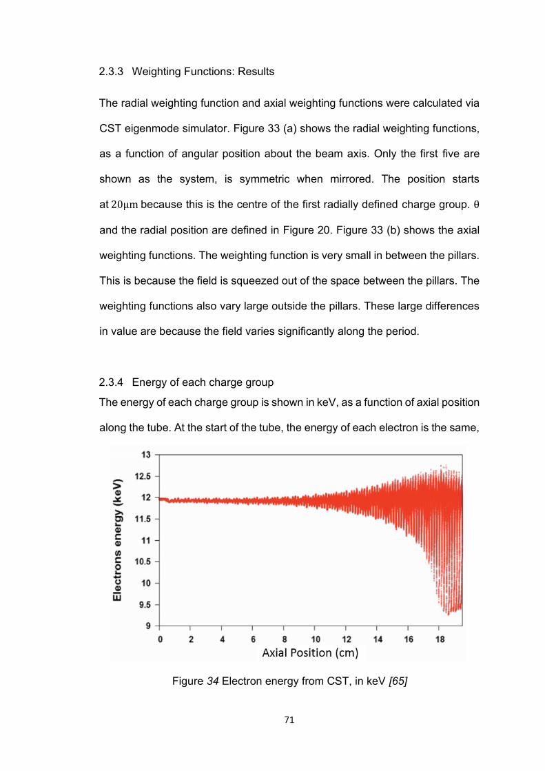
71
2.3.3 Weighting Functions: Results
The radial weighting function and axial weighting functions were calculated via
CST eigenmode simulator. Figure 33 (a) shows the radial weighting functions,
as a function of angular position about the beam axis. Only the first five are
shown as the system, is symmetric when mirrored. The position starts
at 20μm because this is the centre of the first radially defined charge group. θ
and the radial position are defined in Figure 20. Figure 33 (b) shows the axial
weighting functions. The weighting function is very small in between the pillars.
This is because the field is squeezed out of the space between the pillars. The
weighting functions also vary large outside the pillars. These large differences
in value are because the field varies significantly along the period.
2.3.4 Energy of each charge group
The energy of each charge group is shown in keV, as a function of axial position
along the tube. At the start of the tube, the energy of each electron is the same,
Figure 34 Electron energy from CST, in keV [65]

72
as the voltage of the cathode is constant. As the electrons interact with the RF
signal and each other, they lose or gain energy.
The difference in initial electron energy is seen. Figure 34 is the electron energy
as calculated by CST-PS. Figure 35 is calculated by the modified Lagrangian
model. In Figure 34, each point is the energy of a charge group at that axial
position. As the group moves forward along the tube, it gains or loses energy.
In Figure 35, each curve is a charge group, and in the same way, it loses or
gains energy as it moves along the tube. Each curve follows the change in
energy of an individual charge group. The largest decrease in energy is shown
at between 18cm and 20cm in the CST-PS evaluation, whereas the largest
decrease in energy as calculated by the modified code is at 20cm to 25cm.
Figure 35 Charge group energies as a function of axial position

73
2.3.5 Electron phase positions
The phase positions of each charge group are shown in Figure 36. It can be
seen that the sub charge groups with identical initial phase position spread out,
due to the difference in plasma frequency reduction factors and strength of
interaction with the field. This is because of different distances to the wall of the
tube, and different field intensities felt by the beam and a function of angular
position, respectively. Strong bunching is defined as where the trajectories are
close. Again, the strongest bunching occurs between 20cm and 25cm. This is
seen in the density of the trajectories of the charge groups.
Figure 36 Charge group phases as a function of axial position
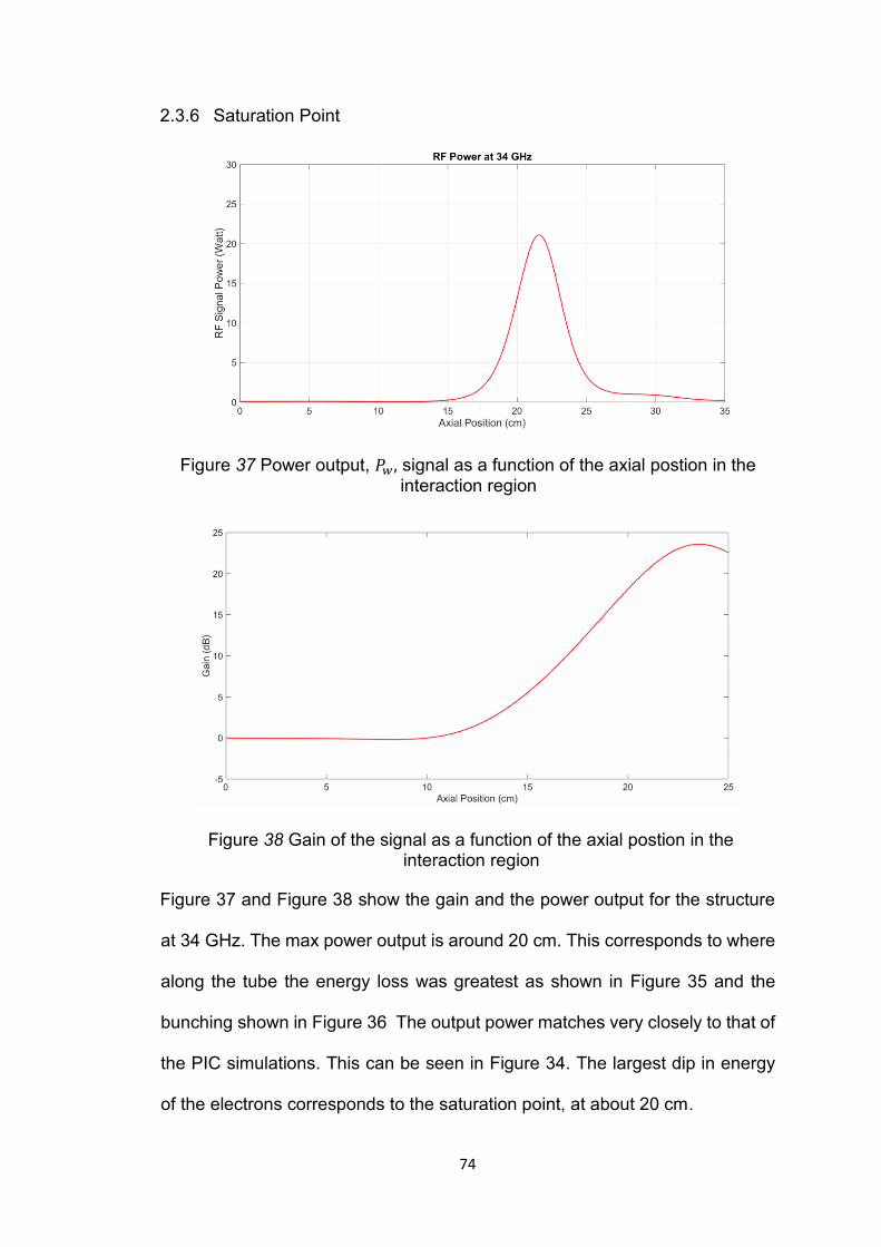
74
2.3.6 Saturation Point
Figure 37 and Figure 38 show the gain and the power output for the structure
at 34 GHz. The max power output is around 20 cm. This corresponds to where
along the tube the energy loss was greatest as shown in Figure 35 and the
bunching shown in Figure 36 The output power matches very closely to that of
the PIC simulations. This can be seen in Figure 34. The largest dip in energy
of the electrons corresponds to the saturation point, at about 20 cm.
Figure 37 Power output, 𝑃𝑤, signal as a function of the axial postion in the interaction region
Figure 38 Gain of the signal as a function of the axial postion in the interaction region

75
2.4 Results over the bandwidth
Presented below the different parameters over the bandwidth 32-38 GHz. The
model accurately describes the interaction and agrees well with the 3D
simulators across the middle and upper end of the bandwidth. However, the
model fails to properly describe the interaction at the low end of the bandwidth,
at around 32 GHz, where the gain becomes much lower than predicted by the
full 3D simulator, before growing large near 30 cm of interaction length. This is
because the difference in phase velocity of the RF signal and the electron
velocity becomes too great. The gain will be from the interaction impedance
being greater at the edge of the band. This is also true of the upper part of the
band. The electron beam is much faster than the wave, and the interaction
impedance is large.
In the model, the electron beam is confined to initial radii. If the electrons were
allowed more degrees of freedom, the gain may be reduced in the edge regions
of the band, and the saturation point more in line with the PIC simulation.

76
2.4.1 Weighting Factors
Figure 39 show the radial weighting functions and the axial weighting functions
of the ka-band DCW respectively. The axial weighting functions are shown in
Figure 33 (b).
The radial weighting functions as expected lose strength away from the centre
of the beam. Also, as expected for a rotational asymmetric SWS, the weighting
(a) (b)
(c) (d)
(e) (f)
(g)
Figure 39 Radial weighting functions vs radial position per frequency

77
factors decrease at different rates, as a function of the angle about the beam
axis. This is because of how the field varies near the copper in the structure.
The field near the pillars is lower than in the centre of the structure. The
weighting factors near the edge of the lower edge of the band, Figure 39 (a)
and (b) have the lowest weighting factors. The weighting factors increase with
frequency, as seen in Figure 39 (c), (d), (e), (f), and (g). This is also true with
the axial weighting factors. The axial weighting functions have very small values
in the centre of the period, and large values outside of the pillars.
2.4.2 Electron Energy
The electron energy can be seen in Figure 40 as functions of axial position.
Figure 40(a), at the edge of the band, shows little interaction until the 30 cm of
interaction, where there is suddenly a lot of interaction. Figure 40 (b) shows
more interaction with the signal. In the centre of the band, Figure 40 (c), (d),
(e), and (f), show signficant interaction with the signal. There is a distinct drop
in average electron energy at around 20 cm along the interaction, where more
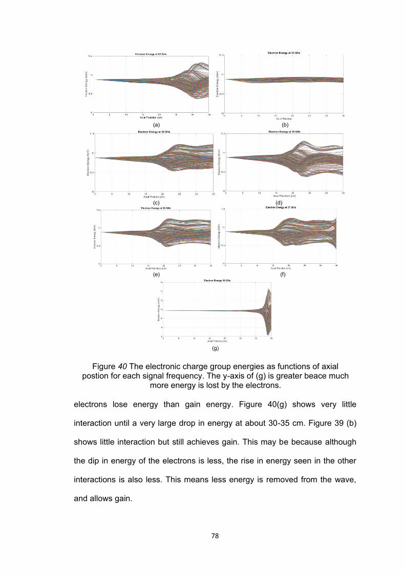
78
electrons lose energy than gain energy. Figure 40(g) shows very little
interaction until a very large drop in energy at about 30-35 cm. Figure 39 (b)
shows little interaction but still achieves gain. This may be because although
the dip in energy of the electrons is less, the rise in energy seen in the other
interactions is also less. This means less energy is removed from the wave,
and allows gain.
(a) (b)
(c) (d)
(e) (f)
(g)
Figure 40 The electronic charge group energies as functions of axial postion for each signal frequency. The y-axis of (g) is greater beace much
more energy is lost by the electrons.
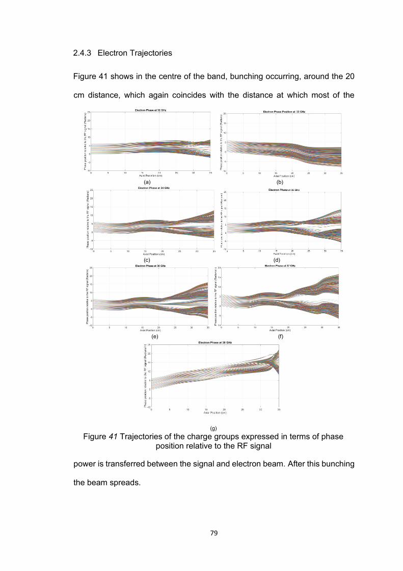
79
2.4.3 Electron Trajectories
Figure 41 shows in the centre of the band, bunching occurring, around the 20
cm distance, which again coincides with the distance at which most of the
power is transferred between the signal and electron beam. After this bunching
the beam spreads.
(a) (b)
(c) (d)
(e) (f)
(g)
Figure 41 Trajectories of the charge groups expressed in terms of phase position relative to the RF signal

80
The bunching is shown by how close the trajectories of the electronic charge
groups are. The closer they are in phase, shown on the y-axis, for a given value
of axial position, shown on the x-axis, the more “bunched” the charge groups
are at that position. Conversely, where the trajectories are far apart is where
anti-bunches occur. In Figure 41(a) it is seen that there is little bunching of the
electrons until around 30-35 cm. This is shown by how the electron trajectories
are not seen to become significantly close together until around 30-35 cm.
However, in Figure 41(b), (c), (d), (e), and (f), there is considerable crossing
and closeness of the electron trajectories near the 20-25 cm region. This means
there is significant bunching of the electronic charge groups, allowing for energy
to be transferred from the electrons to the RF signal around the 20-25 cm
region. This coincides with the large dip in average electron energy seen in the
previous subsection.
2.4.4 Saturation Point
The saturation points are shown in Figure 42. Saturation is when the RF electric
field power has reached its maximum, and further operation will cause a
decrease in wave energy, with the energy being lost to the electron beam. This
is seen in the graphs as the output power reaching a maximum and then
decreasing.
In Figure 42 (a), it is seen that there is little power being transferred to the RF
signal by the 20 cm axial position. However, later along the tube there is a large
amount of power being transferred from the beam to the signal compared to
the frequencies in the centre of the band. In Figure 42(b) power is being
successfully transferred but not as much as in Figure 42 (c), (d), (e), or (f).

81
These graphs show that significant power is being transferred from the
electrons to the RF signal. This is consistent with the electron energies and the
electron trajectories shown previously in Figure 40 and Figure 41. The
saturation point occurs at about 20 cm. Figure 40 (g) shows a power output two
orders of magnitude greater than in the centre of the band.
(a) (b)
(c) (d)
(e) (f)
(g)
Figure 42 Power output as calculated by the modified Lagrangian code per frequency

82
2.4.5 Gain and Power across the Bandwidth
Figure 43 and Figure 44 show the gain and the output power as functions of
frequency for the 3D electromagnetic simulator CST and the modified
Lagrangian code. The choice of output power for each frequency is chosen by
the interaction length equal to the maximum output power of the 34 GHz
simulation, at just over 34 GHz This is to mimic the tube being optimised for 34
GHz, and then the output power of the other frequencies following that. As can
be seen, there is good agreement over most of the band, except for the edges
of the band, which seem to be shifted by approximately 1 GHz up in frequency.
This is likely because of beam loading. When the electron beam enters the
tube, so does its electric field. This field modifies the field established by the
wave. This is captured by the simulation performed by CST-PS. However, it is
not captured by the modified Lagrangian code.
Figure 43 The gain of the tube as a function of signal frequency as calculated by CST (blue) and the modified Lagrangian code (red)

83
2.5 Simulation Time
Figure 45 shows how long the simulation ran before completion. Approximately
1800s (half of one hour) per frequency. This is much faster than 3D simulators,
Figure 44 The power output of the tube as a function of signal frequency as calculated by CST (blue) and the modified Lagrangian code (red). The interaction
length considered for the Langrangian code was 20cm
Figure 45 The amount of time for one run of the Lagrangian simulator, at single frequency

84
which may take many hours per simulation, but much slower than the
unmodified version of the model, which takes seconds for single simulations.
This is slower as with the additional space charge and weighting function
calculations, along with using 3100 subcharge groups, the number of
calculations per integration step has been increased. Including the time for the
eigenmode simulation, and the Lagrangian simulations, the simulation time
across the band was 4-5 hours.
2.6 Conclusions
In this chapter, the Lagrangian code [50] designed for the helix SWS was
modified for use in the simulation of SWS with irrotational symmetry. This was
done by introducing a new model for the space charge forces and a method for
producing weighting functions.
The code was verified by comparing its results with the results of full 3D
simulator CST [59], simulating a Ka-band DCW TWT [65]. A workstation with
3.50 GHz processor speed and 16.0 GB of RAM was used. The simulation used
31 charge groups, each with 100 sub charge groups.
A convergence study was performed and it was found that good accuracy was
found at 31 charge groups, when taking in to account the simulation time, which
was rapidly increasing as more charge groups were added.
Shown in Figure 40, Figure 41, and Figure 42 are the saturation points. They
show that for the middle and upper range of the bandwidth, the saturation points
were accurately simulated for a value of about 20 cm. Figure 40 shows where
the average energies of the charge groups decreases, Figure 41 shows where
the bunching is seen, and Figure 42 shows where the RF power maximises.

85
The max RF power is shown to be between 15-25 Watts. This agrees with the
3D simulator.
However, in the lower part of the band, the code fails to capture the expected
power and saturation point. As shown in in Figure 42, however, the RF power
does become very large past the 30 cm interaction length of the code. The
same is true of the upper part of the band 38 GHz. Past 30 cm interaction length
the output power become very large.
The lower accuracy at low frequency could be due to the difference in wave
phase velocity and electron velocity, where the difference between the two in
the lower half of the band becomes too great.
The extreme upper band also had little interaction in the first 30 cm of interaction
length. After this, the wave is amplified by a very large amount, of the order of
104 Watts. This may be due to the large interaction impedance at the edge of
the band, and the beam being much faster than the signal in this range.
The simulation time for the modified code is about 1800 seconds for a single
frequency, shown in Figure 45. The eigenmode simulation, where the data for
the weighting functions is extracted, takes a similar amount of time to run, at
about 1800s. The combination of time is still much faster than the 3D simulator
on the same machine, where a single frequency PIC simulation would take tens
of hours. However, this time is much slower than for the unmodified code, which
can take seconds per frequency. This can be attributed to the space charge
calculations and the calculation of each charge groups position in the field, as
well as the code using 3100 charge groups.
In conclusion, the code has been tested for the Ka-band DCW. It showed to
accurately describe the beam-wave interaction for the middle and upper range

86
of the band but is not accurate at the lower band. The difference in the lower
half of the band becomes too great. To overcome this, it may be necessary to
rederive the equations in a higher dimension, to capture some of the gain which
may be missing due to limitations in this model. This could include angular
motion and radial motion of the sub charge groups.

87
Chapter 3 3D Design of DCW for millimetre wave TWTs
The second part of the thesis is the design of double corrugated waveguides
and related couplers for millimetre waves TWT and BWOs. The simulations
are:
• A comparison of couplers of DCW for a 346 GHz BWO. The couplers
considered are lateral tapering and height tapering of the pillars of the
DCW;
• A DCW for a100 GHz BWO using lateral tapering;
• A DCW for a 270 GHz TWT using lateral tapering;
• A DCW for a W-band TWT using triangular pillars;
• A DCW for a W-band TWT using square pillars with a taper using height
tapering of the pillars;
• A comparison of “straight” tapering and “bend” taper configuration for the
DCW using the W-band TWT.
The design process for the DCW TWT begins with the beam parameters. These
are the beam voltage, beam current and beam diameter.
The beam diameter defines the minimum distance between the pillars, and the
beam diameter and current, and the beam voltage, define the requirements for
the confining magnetic field provided by a periodic permanent magnet (PPM).
The parameters of the DCW are shown in Figure 46 and Figure 47. These must
be highly optimised to meet the tube requirements. This was achieved by small
variations in the parameters of the periodic structure, like modifying the period
or the pillar dimensions, and comparing the eigenmode simulations to find the
optimal periodic structure in terms of synchronous beam voltage and interaction
impedance.

88
3.1 Eigenmode Simulations
The eigenmode simulations for the design of the SWS uses one period of the
structure and produce a dispersion curve, interaction impedance and loss.
The eigenmode of a given closed-region possess eigenmodes corresponding
to frequency and phase difference. The simulation considers a closed region in
Figure 46 Front view of the period of the DCW
Figure 47 Side view of the period of the DCW

89
the form of a single period of the SWS being designed. The frequencies of the
dispersion curve correspond to allowed values of the propagation constant as
a function of the range of phase differences being investigated [60].
For the forward wave operation of the DCW, phases of 2π < ϕ < 3π are
utilised, and for the first negative harmonic, phase of π < ϕ < 2π are utilised.
This is because, for the DCW, as the frequency increases, the beam-wave
interaction at the fundamental harmonic becomes demanding technologically.
This is because the beam voltage becomes very large in the fundamental
harmonic. This is an issue if a compact power supply is required [68].
The interaction impedance, phase velocity of the RF wave, all as functions of
frequency or phase difference can be found using the dispersion curve and
power flow. A value of loss relating to the conductivity of the material being
used may be calculated. The skin depth of the copper, the material considered
as for the structure, constrains the acceptable surface roughness of the copper
after machining. This can be modelled by using a reduced conductivity.
In the simulations described, the material is oxygen free high conductivity
copper. Shown in Table 3 are the different conductivities. A conservative value
of 1.8 × 10⁷ S/m was used, from an assumed surface roughness of about
0.1 μm.
Table 3 Difference in conductivity between pure copper and the modelling of copper with finite surface roughness [33]
Cu Conductivity Cu Conductivity (Reduced with
surface roughness ≈ 0.1 𝜇𝑚)
5.8 × 10⁷ 𝑆/𝑚 1.8 × 10⁷ 𝑆/𝑚
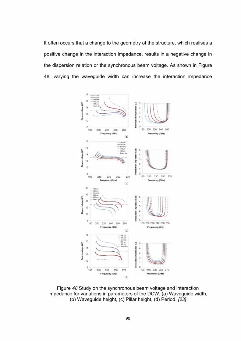
90
It often occurs that a change to the geometry of the structure, which realises a
positive change in the interaction impedance, results in a negative change in
the dispersion relation or the synchronous beam voltage. As shown in Figure
48, varying the waveguide width can increase the interaction impedance
Figure 48 Study on the synchronous beam voltage and interaction impedance for variations in parameters of the DCW. (a) Waveguide width,
(b) Waveguide height, (c) Pillar height, (d) Period. [23]

91
significantly, at the cost of the dispersion relation changing in such a way that
the desired condition of a constant phase velocity over a wide frequency
bandwidth will be lost. Similarly, increasing the height of the pillars will produce
a slight increase in interaction impedance and a lower synchronous beam
voltage, without much change to the slope of the dispersion curve, but will move
the central frequency and the bandwidth out of the desired range. This
information is used as a guide for optimisation of the DCW period, as there are
many parameters which can be modified simultaneously.
The dispersion curve calculated is optimised for a wide bandwidth of
synchronisation in the desired space harmonic.
In the following we will derive the equation of the synchronous beam line as a
function of period, frequency, beam voltage and phase. The period of the
structure for a specific frequency range is a function of the frequency. The
phase difference ϕ may be defined in equation (95) as
ϕ = kzP (95)
Where kz is the phase constant, and P is the period of the DCW computed as
distance between the axis of two adjacent pillars. Using equation (4) and
equation (8), we can equate the phase velocity νp with the electron velocity UB,
we can obtain
√2ηV0 =
2πf
kz
(96)
Combining equation (95) and (96) for kz and substituting gives
√2ηV0 =
2πfP
ϕ
(97)
which rearranged gives

92
P =
ϕ ∙ 5.93.105√V0
2πf
(98)
The interaction impedance considered is that averaged over the radius of the
electron beam and period of the structure, that is, the volume of the electron
beam, although it can be useful to consider the on-axis interaction impedance
for more precise comparisons of structures where the electron beam radius is
not the same.
3.2 Fabrication
Fabrication of the designs is considered at every step. Due to the simplicity of
the DCW, the main constraint is the distance between pillars and the distance
between the walls.
In CNC milling, the size of the tooling is the limiting factor to the resolution. In
the LIGA process, the limitation is in the inability for LIGA to produce height
differences in the pillars.
THz DCW has been fabricated by both these methods [26] [20], so in terms of
the realisation, where the highest frequency is 346 GHz, only internal
manufacturing processes were considered as limiting factor. The limiting factor
of the distance between pillars was the beam radius. It was decided to leave at
least a distance of 50 𝜇𝑚 to account for radial beam oscillations.

93
3.3 Design of the Coupler
An important aspect of the design of a TWT or BWO is to assure the matching
from the input and output signal to the mode present in the interaction region.
In the case of the DCW, we need to match the TE10 mode of the rectangular
waveguide to the TE10 hybrid mode of the DCW SWS. The S11 must be
optimised to reduce the reflection of incident signals.
The aim is reducing S11 as much as possible, and to have S21 as close to 0 dB
as possible. In practice, of course, this is impossible, as reflections due the
impedance at the tapering not matching and electrical losses to the structure
are finite.
Figure 49 shows how this can be achieved by tapering the height of the pillars
of the SWS each period in the tapering sections, along with smoothly tapering
the width of the rectangular waveguide. The change in pillar height is dH. The
width tapering, and pillar height tapering are performed in the same place.
Figure 49 Height tapering of the pillars and width tapering of the waveguide. The long straight lines in the image represent the edges of the
waveguide. 𝑑𝐻 is the change in pillar height per period of the tapering section

94
Shown in Figure 50 is an alternative to the height tapering technique named the
‘lateral’ tapering technique. It consists of pillars of identical height, but different
spatial positions, symmetrically moving towards the wall of the waveguide. This
tapering, depending on the ratio of the width tapering dimensions of the
waveguide and the lateral shift in pillar position per tapering period, may result
in a required pillar modification for pillars close to the wall of the tapering. An
example of this would be if the pillar is too close to the wall to be reliably
manufactured. As such, it may be necessary to extend these pillars in to the
wall of the structure. The modified width of the pillar is labelled as Wm.
A good S11 parameter can be achieved with a long enough tapering section.
However, it is often the case that this length would be limited due to design
constraints. This means the other parts of the tapering must be more optimised.
Figure 50 Width tapering of the waveguide and lateral tapering of the pillars. 𝑑𝑇𝑤 is the change in distance between the pillars

95
Figure 51 show what is meant by height tapering of the waveguide. This is
required if the standard flange is too tall or short for the waveguide. A good 𝑆11
parameter is defined here as better than -15 dB. The bandwidth is defined as
the band of frequencies over which the 𝑆11 is less than -15 dB, or as the
predefined operation frequency of the tube.
3.3.1 Bend Tapering
A bend type tapering is also considered. When the linear tapering is applied,
there are long regions of weak interaction between the signal and the electron
beam, but where the beam still requires confining by a magnetic field. This extra
length can account for a significant proportion of the tube.
Figure 51 Height tapering of the height of the waveguide
Figure 52 P', the periodicity of the pillars in the bend

96
By considering a 90 degree bend, such that the tapering occurs perpendicular
to the direction of the interaction region, the size of the device can be reduced
[65].
As shown in Figure 52, the complexity of such a geometry arises when trying
to maintain the mode of the structure around the bend, where the periodicity of
the SWS is not well defined, and as such may impact on the stability of the
operational mode. To match the period as close as possible, it was decided to
maintain the periodicity of the structure along the centre of the pillars; that is
the distance between the centres of the SWS in the bend.
Another issue is where a pillar may be in the way of the electron beam. The
solution is to shape or move the pillars on the trajectory of the beam. This must
be done carefully to avoid potential reflections at the bend. Figure 53 shows the
crossing of the corner of a pillar by the electron beam.
Figure 53 Illustration of the electron beam unimpeded due to shaped pillars

97
3.4 Coupler Comparisons for 346 GHz DCW BWO
Comparisons of the couplers for the 346 GHz is described in the following. The
parameters of the DCW for the 346 GHz BWO are shown in Table 4. Figure 56
shows the height tapering of the pillars, and Table 5 shows the associated
parameters. The configuration consists of 14 tapered pillars, each differing in
height by 10 μm. Figure 55 shows the lateral tapering of pillars. 4 of the pillars
are attach to the wall of the waveguide. The parameters of the lateral shaping
are presented in Table 6. Dispersion curve is shown in Figure 54.
Table 5 Parameters of the pillar tapering in the linear height tapering configuration for 346 GHz BWO
Parameter Value/𝝁𝒎
dH 10
Table 6 Parameters of the pillar tapering in the lateral tapering
configuration 346 GHz BWO
Parameter Value/𝝁𝒎
dTw 33
𝑊𝑚 74
Table 4 Parameters of the 346 GHz DCW BWO
Parameter Value/𝝁𝒎
A 1500
B 300
T 230
W 70
S 70
H 150
P 170

98
Figure 55 Top view of the lateral tapering and side view of the lateral tapering
Figure 56 Configuration of the linear height tapering from the top, and from the side, showing the height tapeirng
Figure 54 Dispersion curve of 346 GHz DCW BWO

99
Figure 57 and Figure 58 show the S11 and S21 of the lateral and height tapering
configurations of the couplers for the 346 DCW BWO. Both configurations for
the coupler have S11 better than -15 dB reflection over a bandwidth of greater
than 10 GHz. The S21 parameter is better than -2 dB across the whole band.
Figure 57 Simulated 𝑆11 of the lateral tapering and height tapering configurations
Figure 58 Simulated 𝑆21of the lateral tapering and height tapering configurations

100
Figure 59 and Figure 60 show from the top of the y-component of the electric
fields as the mode of the field transforms in to a TE10 hybrid mode supported
by the DCW for the height tapering and lateral tapering respectively.
Figure 59 Top view of the y-component of the electric field in the height
Figure 60 Top view of the y-component of the electric field in the lateral tapering at 346 GHz

101
3.4.1 Conclusion
It has been shown that both height tapering and lateral tapering of the pillars in
the DCW are viable techniques for matching the DCW’s hybrid TE10 mode with
the TE10 mode of the flange. Both are capable of wideband acceptance of
signals, with S11 of better than -15 dB over a bandwidth wider than 10 GHz.
3.5 100 GHz BWO
A design of a 100 GHz BWO is described. The parameters of the DCW at
100GHz are shown in Table 7. The BWO works at the first backward wave
harmonic.
3.5.1 Cold Parameters
The cold parameter results calculated using eigenmode simulation are
described. The parameters of DCW are shown in Table 7. The voltage required
Table 7 Parameters of the DCW for 100 GHz BWO
Parameter Value/𝝁𝒎
A 5200
B 750
T 780
W 225
S 225
H 550
P 445

102
was 10.85 kV. The beam radius was 340 𝜇𝑚. This limits the pillar distance to
780 𝜇𝑚.
Figure 62 is the dispersion diagram and the dotted black line shows the beam
line corresponding to this beam voltage. The beam line intercepts the
dispersion curve at 100 GHz.
For this 100 GHz BWO, the synchronous beam voltage is close to 10kV, with
an average interaction impedance over the electron beam cross section of ~0.4
Ohm, as shown in Figure 61.
The interaction impedance and synchronous beam voltage were achieved by
careful selection of the period of the SWS, which tends to be smaller for the
first backwards space harmonic than for the forward wave harmonic used by
Figure 61 On-axis and average interaction impedance for the 100 GHz BWO

103
the DCW. This is because the period of the structure is proportional to the
phase difference. Figure 63 shows the Ez field distribution taken at a cross-
section perpendicular to the beam axis.
Figure 62 Dispersion curve for the 100 GHz BWO, with a beam line intersecting at 100 GHz with a beam voltage of 10850V
Figure 63 z-component of the electric field distribution for the 100 GHz BWO
Table 8 Parameters of the pillar tapering in the lateral tapering configuration for 100 GHz BWO
Parameter Value/𝝁𝒎
dTw 60
𝑊𝑚 202.5

104
For the 100 GHz BWO, the lateral tapering configuration for the pillars was
utilised. Figure 64 shows the empty tapering section. The parameters are
shown in Table 8.
Figure 66 shows the S11 for the 100 GHz BWO from 60 GHz to 115 GHz.
Figure 65 show the S21 for the same frequency range. The S11 is better than -
15 dB from 100 GHz to 107 GHz, and the S21 is better than -3 dB over the same
range.
Figure 65 Simulated 𝑆21 for the 100 GHz BWO
Figure 64 Tapering configuration

105
Figure 67 shows the y-component of the RF wave at 100 GHz as it changes
from TE10 to the hybrid TE10 of the DCW. The y-component is shown as it best
shows the conversion of the mode.
3.6 270GHz TWT
A design for a DCW for a 270 GHz TWT is described. The parameters of the
DCW are shown in Table 9. The first forward wave harmonic is used.
Figure 66 Simulated 𝑆11 for for 100 GHz BWO
Figure 67 Y-component of the electric field in the tapering at 100 GHz
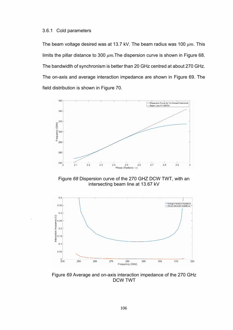
106
3.6.1 Cold parameters
The beam voltage desired was at 13.7 kV. The beam radius was 100 𝜇𝑚. This
limits the pillar distance to 300 𝜇𝑚.The dispersion curve is shown in Figure 68.
The bandwidth of synchronism is better than 20 GHz centred at about 270 GHz.
The on-axis and average interaction impedance are shown in Figure 69. The
field distribution is shown in Figure 70.
Figure 69 Average and on-axis interaction impedance of the 270 GHz DCW TWT
Figure 68 Dispersion curve of the 270 GHZ DCW TWT, with an intersecting beam line at 13.67 kV

107
Figure 70 z-component of the electric field distribution of the 270 GHz DCW TWT
Table 9 Parameters of the 270 GHz DCW TWT
Parameter Value/𝝁𝒎
A 520
B 320
T 300
W 70
S 70
H 190
P 300

108
For the 270 GHz TWT, the lateral tapering configuration for the pillars was
utilised. The configuration is show in Figure 71. Table 10 shows the parameters
of the tapering. There are 18 pillars in the tapering section. 6 of these pillars
are attached to the wall of the waveguide. Figure 72 shows the y-component of
the RF wave at 270 GHz as it changes from TE10 to the hybrid TE10 of the DCW.
The y-component is shown as it best shows the conversion of the mode.
Figure 73 shows the simulated S21 for the 270 GHz TWT from 240 GHz to 310
GHz. Figure 74 shows the simulated S11 for the same frequency range. The S11
Figure 72 Top view of tapering of the pillars; and the field distribution around the tapering for the 270 GHz DCW TWT
Figure 71 Configuration of the coupler
Table 10 Parameters of the pillar tapering in the lateral tapering configuration for 270 GHz TWT
Parameter Value/𝝁𝒎
dTw 5
𝑊𝑚 77

109
is better than -15 dB from 267 GHz to 277 GHz, and the S21 is better than -5
dB over the same range.
3.7 W-Band TWT for TWEETHER Project
A W-band TWT is described for application in wireless communications in the
TWEETHER project [69].
Two configurations of the pillars are investigated; square pillars and triangular
pillars. The bandwidth required was at least 3 GHz, 92-95 GHz.
Figure 74 Simulated 𝑆1,1 paramters for the 270GHz DCW TWT
Figure 73 Simulated 𝑆2,1 parameters for the 270 GHz DCW TWT

110
The straight taper and the bend taper are compared. The pillar tapering will be
height tapering in both cases. The beam radius was 100 𝜇𝑚. This limits the
pillar distance to 300 𝜇𝑚.
3.7.1 DCW Design for 92-95 GHz – Square Pillars
Described is W-band DCW with square pillars. The constraints were a beam
radius of 100 microns. This means the gap between the pillars must be at least
300 microns. The beam voltage is fixed at 10.1 kV. Table 11 shows the
parameters of the DCW.
Table 11 Parameter list of the 90 GHz DCW period with square pillars
Parameter Value/𝜇𝑚
A 1156
B 689
T 300
W 150
S 150
H 511
P 800

111
Shown in Figure 76 is an interaction impedance of 1 Ohm on average. Figure
75 shows the dispersion curve of the DCW. The beam line corresponds to 10.3
kV and shows a synchronous bandwidth of greater than 9 GHz.
Figure 75 Dispersion curve over the bandwidth shown in terms of phase difference. The beam line is shown, with a voltage of 10.3 kV
Figure 76 Average and on-axis interaction impedance over the bandwidth as a function of frequency for the square pillar DCW period

112
3.7.2 DCW Design for 92-95 GHz – Triangular Pillars
Shown in Figure 77 and Figure 78 is the geometry of the DCW with triangular
pillars. The triangular cross section pillars are triangular prisms. They are
positioned in the waveguide in the same way as the square pillars in terms of
distance from the waveguide wall and distance from each other, both in the
axial direction and width-wise. Each triangular cross section is an isosceles
triangle. The base of the isosceles triangles face each other. The distance
between them is the beam tunnel width. The parameters are the same as in
Table 11.
This configuration has been shown to result in a higher interaction impedance,
in this case of around 50% [70]. This could be because of the triangular pillars
allowing a higher energy field to exist in between the periods of the structure.
Figure 80 shows the interaction impedance. An average of about 2 Ohms was
achieved on average.
Figure 77 Top view of the triangle pillared DCW period

113
The synchronous beam voltage is about 10.6 kV. This is similar to the DCW
with square pillars, described in the previous section.
Figure 79 shows the dispersion curve of the DCW.
Figure 78 Period of the 90 GHz DCW period with triangular pillars
Figure 79 Dispersion curve over the bandwidth shown in terms of phase difference. The beam line is shown, with a voltage of 10.55 kV
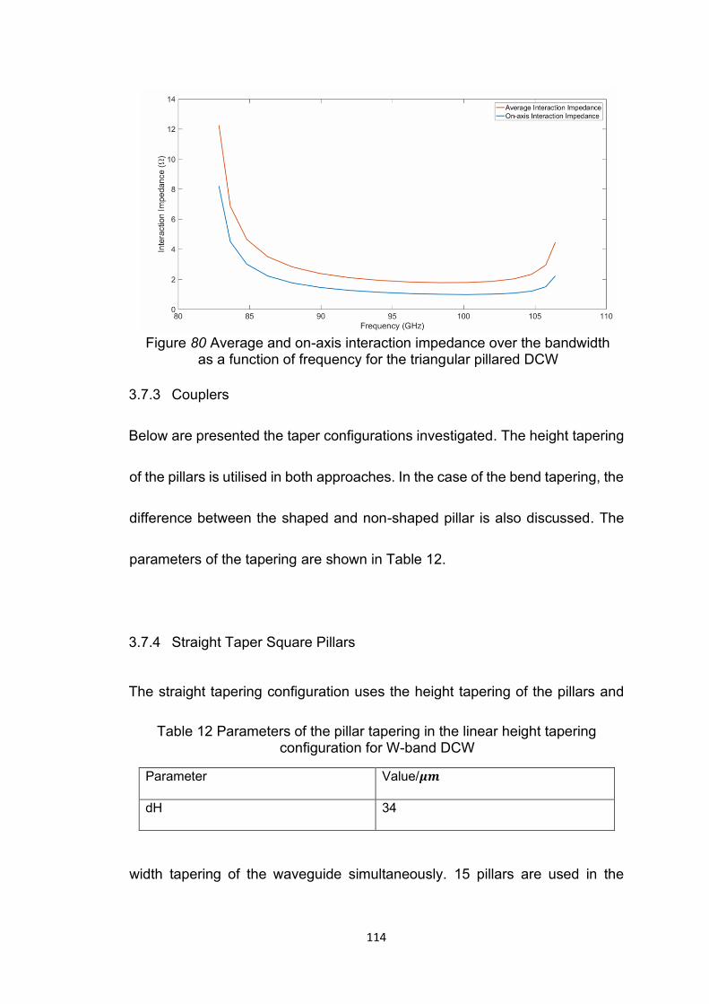
114
3.7.3 Couplers
Below are presented the taper configurations investigated. The height tapering
of the pillars is utilised in both approaches. In the case of the bend tapering, the
difference between the shaped and non-shaped pillar is also discussed. The
parameters of the tapering are shown in Table 12.
3.7.4 Straight Taper Square Pillars
The straight tapering configuration uses the height tapering of the pillars and
width tapering of the waveguide simultaneously. 15 pillars are used in the
Table 12 Parameters of the pillar tapering in the linear height tapering configuration for W-band DCW
Parameter Value/𝝁𝒎
dH 34
Figure 80 Average and on-axis interaction impedance over the bandwidth as a function of frequency for the triangular pillared DCW

115
tapering section. Figure 81 a) shows the side view of the tapering configuration
and Figure 81 b) shows the top view. The value of dH = ~34 μm.
Figure 82 shows the simulated S11 for the W-band TWT from 80 GHz to 110
GHz. Figure 83 show the simulated S21 for the same frequency range. The S11
is better than -15 dB, and the S21 is better than -3 dB over the whole range of
the device 92-95 GHz.
Figure 82 Simulated 𝑆1,1 paramters for the W-band DCW with square
pillars in the ‘straight’ configuration
(a)
(b)
Figure 81 The side view and top view of the straight tapering for the W-band DCW TWT

116
Figure 84 shows the y-component of the field in the taper. It can be seen how
the field converts from the TE10 mode to the hybrid mode supported by the
DCW.
Figure 83 Simulated 𝑆2,1 paramters for the W-band DCW with square
pillars in the ‘straight’ configuration
Figure 84 The y-component of the propagating field in the taper

117
3.7.5 Bend Tapering Square Pillars
The bend tapering configuration is shown inset in Figures 85 and 86. The pillars
at the bend that cross into the region in which the beam will exist must be
shaped to avoid potential collisions of the beam and pillars. As shown in in
Figure 85 and Figure 86 the S1,1 and S2,1 parameters were affected only slightly.
This is because the cut was only very small. The S1,1 is better than -15 dB over
10 GHz between 90 and 100 GHz, and the S2,1 is better than -3 dB from 85 GHz
to 98 GHz. Figure 87 shows the field around the bend.
Figure 85 S11 of the tapering with the pillars in the bend of the tube showing
the shaped and unshaped pillars. The configuration is inset.

118
3.8 Conclusions
In this chapter, a comparison of two coupler configurations has been performed,
and several SWSs and couplers using the DCW have been designed.
Two coupler configurations have been investigated for the DCW using a BWO
designed for 346 GHz central frequency. Height tapering and lateral tapering
of pillars of the DCW have been shown to be capable of producing the S-
Figure 86 𝑆21 of the tapering with the pillars in the bend of the tube, showing the shaped and unshaped pillars.
Figure 87 Field establishing around the bend

119
parameters required for successful operation of DCW. The height tapering
configuration performed with S11 better than -15 dB across a bandwidth of
greater than 30 GHz. The lateral tapering performed similarly, with S11 better
than -15 dB over the same range. The S21 is better than -5 dB over the range.
A BWO at 100 GHz was designed utilising the DCW with adequate interaction
impedance of about 0.4 Ω and a low synchronous beam voltage of 10.85 kV.
The tapering configuration considered was lateral tapering and achieved S11
better than -15 dB over a bandwidth of 100 GHz to 107 GHz, and S21 better
than -3 dB over the same range.
A TWT at 270 GHz was also designed employing the DCW. Due to the
requirement of a large tunnel width, the interaction impedance calculated was
low, at about 0.15 Ω. The synchronous beam voltage is about 13.7 kV. The
tapering configuration again was lateral tapering and achieved S11 better than
-15 dB over a bandwidth of 267 GHz to 277 GHz, and S21 better than -5 dB over
the same range.
A W-band TWT at 95 GHz was also designed. The minimum bandwidth
required was 3 GHz from 92 GHz to 95 GHz. Two DCW configurations were
considered for the period. The square pillar design and the triangular pillar
design. The square pillar DCW achieved an interaction impedance of over 1 Ω.
The synchronous beam voltage was 10.1 kV. The triangular pillars achieved an
average interaction impedance of over 2 Ω and a synchronous beam voltage of
about 10.5 kV. The design period enabled a bandwidth ~10 GHz.
The square pillars were moved on into the tapering stage. The straight tapering
achieved S11 better than -15 dB over almost all the band, and S21 better than -
3 dB over all the band. The bend taper with no pillar shaping and with pillar

120
shaping were almost identical, with the shaped pillar configuration having
slightly better S-parameters. The S1,1 is better than -15 dB over 10 GHz
bandwidth, and the S2,1 is better than -3 dB over the entire band.
The DCW is also capable of maintaining good S-Parameters whilst the
corrugations bend around a curve, which includes several of the pillars being
‘shaped’ so that the pillars do no impede the passing of the electron beam. The
mode of the DCW is only minorly disrupted as it propagates through the bend.
It was shown that with correct shaping there is no significant difference in S-
parameters between shaped pillar and no shaped pillar in the W-band case,
and just as good S-parameters as with the case in W-band with no bended
taper.
It should be noted that as well as having a lower cut off frequency, the DCW
also has an upper cut off frequency. This is seen in the S11 parameters, where
consistently, there almost total reflection of the received signal below and
certain frequency, and above a certain frequency. The same is observed in the
S21 parameters, where there is close to zero transmission of the received signal
above and below certain frequencies, depending on the waveguide. This
suggests that the coupler and the SWS act as a band pass filter.
121
Chapter 4 Conclusions and Future Work
The motivation for this work came from advances in microfabrication
technology, which has made the fabrication of structures small enough for
operation in the mm-wave and THz frequency regimes feasible. Since the
helical waveguide, the premier SWS in terms of bandwidth, is too difficult to
fabricate at such small dimensions (~100 μm radius), new structures must be
investigated. Many of these SWSs, such as the DCW, are asymmetric in
topology.
4.1 Thesis Purpose
A novel Lagrangian method for quickly simulating the beam wave interaction
in TWTs with asymmetric SWSs has been presented. It included a novel
method for calculating weighting factors to model the differences in electric field
strength in the TWT, affecting the coupling of the wave to the beam, and novel
method for the computation the space charge forces experienced by the
electron beam, using a variable plasma frequency reduction factor. The space
charge method calculated a different plasma frequency reduction factor for
each charge group, dependent on the angular position of the charge group
about the beam axis.
DCW tubes were also designed, using the commercial software CST-MWS. A
comparison was performed, comparing lateral pillar tapering and height pillar
tapering. This was performed using a simulated 346 GHz BWO. DCW TWTS
were designed at frequencies of 270 GHz and 92-95 GHz, and BWO was
designed at 100 GHz. The dispersion characteristic and interaction impedance
were calculated, as well as the S-parameters of the coupler designed for each

122
structure. A comparison was also investigated in the design process of the 92-
95 GHz DCW TWT. Triangular pillars were compared with the square pillars,
and a bend taper was designed, exploring difference in performance when a
shaped pillar is utilised to allow for the passage of the electron beam.
Future work to continue the research described in the thesis would be extend
the Lagrangian model to a 3D model, and to perform PIC simulations for the
TWTs and BWOs designed.
4.2 Summary of Findings
In the following, the main findings of the studies will be restated.
4.2.1 Modified Lagrangian Model
The modified Lagrangian model was validated using a full 3D PIC simulation
performed by CST-PS. The tube used is a simulated Ka-band DCW TWT, with
central frequency 34 GHz. The output power and saturation point were
compared across the bandwidth of interest. A workstation with 3.50 GHz
processor speed and 16.0 GB of RAM was used. The simulation used 31
charge groups, each with 100 sub charge groups.
The saturation point was accurately modelled for the middle and upper part of
the bandwidth, at between 20-25 cm. The maximum power output is modelled
to be 15-25 Watts, which is consistent with the full 3D PIC simulator CST-PS.
However, in the lower part and the very upper part of the bandwidth, the code
does not very accurately describe the interaction when compared to the PIC
simulator. However, the lower frequencies and very edge of the upper

123
frequencies show little interaction until 30 cm of interaction length, where the
output power becomes very large. This is not consistent with the PIC code.
The simulation time for a single frequency using the modified code is about
1800s. This is much faster than the fully 3D simulator. On the same machine a
full PIC simulation would take 5-10 hours.
4.2.2 DCW for millimetre wave TWTs
Two coupler configurations for a 346 GHz DCW BWO were compared. Height
tapering and lateral tapering configurations were considered, and it has been
shown that both are capable of performing well in terms of S11 and S21 S-
parameters. Both achieved S11 better than -15 dB over a 30 GHz range of
frequencies, and S21 better than -5 dB over the same range.
The BWO operating at 100 GHz described has an adequate interaction
impedance, at 0.4 Ω, and the synchronous beam voltage was 10.85 kV, which
is low. The lateral tapering configuration considered in the design of the coupler
achieved S11 better than -15 dB over a bandwidth of 7 GHz, from 100 GHz to
107 GHz, and S21 better than -3 dB over the same range.
The TWT operating at central frequency 270 GHz described has an interaction
impedance which was low, at 0.15 Ω, and a synchronous beam voltage of 13.7
kV, which is low. The lateral tapering configuration was considered achieved
S11 better than -15 dB over a bandwidth of 10 GHz, from 267 GHz to 277 GHz,
and S21 better than -5 dB over the same range.
The W-band TWT with the square pillars achieved a good interaction
impedance of over 1 Ω. The synchronous beam voltage was 10.1 kV. The
triangular pillars achieved a very good interaction impedance of 2 Ω. The

124
synchronous beam voltage was 10.5 GHz. The bandwidth achieved for both
designs was about 10 GHz.
The square pillar design was used in the design of the tapering. Height tapering
was used for the purpose, and straight tapering and bend tapering was
compared. In the bend tapering design, a pillar must be shaped to allow space
for the electron beam. The bend tapers with and without a shaped pillar were
compared. The straight tapering achieved S11 better than -15 dB over almost
all the band. The S21 is better than -3 dB over all the band. The bend taper with
no pillar shaping and with pillar shaping were almost identical, with the shaped
pillar configuration having slightly better S-parameters. The S11 is better than -
15 dB over 10 GHz bandwidth, and the S21 is better than -3 dB over the entire
band.
4.3 Successes and Limitations
The following outlines the success and limitations of the research, and attempts
to explain the limitations of the work.
4.3.1 Modified Lagrangian Code
The modified Lagrangian code accurately modelled the power output and
saturation point of the Ka-band DCW in the middle and upper part of the
frequency band. However, it somewhat failed in the lower part of the band, and
at the very edge of the upper part of the band. The difficulty to accurately
describe the lower band is attributed to the difference in wave phase velocity
and electron velocity. The difference between the two in the lower half of the
band becomes too great.

125
The extreme upper band also had little interaction in the first 30 cm of interaction
length, and then a very large amount of power, of about 10^4 Watts, was
transferred from electron beam to wave. This may be due to the large
interaction impedance at the edge of the band, and the beam being much faster
than the signal in this range.
To overcome this, it may be necessary to rederive the equations in a higher
dimension, to capture some of the gain which may be missing due to limitations
in this model. This could include angular motion and radial motion of the sub
charge groups. In terms of the gain being too much, this will capture earlier
interactions, limiting the gain to more realistic levels.
Further, after the saturation points, the energy of the signal decreases.
However, after a short distance of a few centimetres, the energy of the wave
grows again. This may be attributed to secondary bunching, where, after
energy has transferred back to the electron beam, energy is then transferred
again to the wave.
4.3.2 DCW for millimetre wave TWTs
Much of the design constraints on the DCW are derived from the beam
properties and the method of fabrication. In the eigenmode simulations for the
SWS, the interaction impedance is greatly influenced by the gap between the
pillars. However, the gap size is constrained by the electron beam width. Better
interaction impedance could be achieved with a narrower beam, but may come
at the cost of lower beam current, affecting gain.

126
For the coupler designs, the main constraints were, along with attempting to
make the coupler as short as possible to limit the volume of the device, the gap
between the wall and the pillar, and the minimum height of a pillar.
In terms of the approach to machining the design, the main concern is the
diameter of the tooling used. If it is too wide, a small gap will not be realisable
as the tapering pillars approach the wall. This results in needing a modified
pillar extended in to the wall of the pillar.
When considering the LIGA process, it would be only possible to create pillars
of equal height. This means for the W-band TWT, fabrication is limited to
machining.
4.4 Future Work
Following are suggestions for future research opportunities using the presented
work and results.
4.4.1 Lagrangian Model Extension
Extending the Lagrangian model to three dimensions would involve including
radial space charge oscillations of the electron beam. This would mean the
electronic charge groups would also by allowed to change their radial position.
Also, the charge groups would be allowed to rotate around the beam axis. This
would also mean that the weighting functions for each charge group would be
dynamic. Further, models could be derived for the coupler and the beam wave
interaction before the SWS is fully introduced. This would capture losses before
the interaction, and any amount of beam modulation before the main interaction
occurs.

127
4.4.2 Coupler design and PIC Simulations
Future work involving the DCW design would include the PIC simulations of the
designed DCW TWT and BWOs, to find the potential gain and bandwidth of the
devices and the optimum device length. Fabrication and practical tests and
comparison with simulation should also be performed.
In terms of design, more investigation into the effects of shaping pillars should
be performed. This includes shaping the pillar in the bend taper to allow space
for the electron beam, and extending pillars in to the wall of the structure during
lateral tapering.
Furthermore, as fabrication techniques become more sophisticated, the DCW
SWSs performance as in an TWT or BWO could be analysed in the THz regime.

128
Chapter 5 Bibliography
[1] P. . “T z T y ” IEEE TRans. Microw. Theory Techn., vol. 50, no. 3,
pp. 910-928, March 2002.
[2] M. T “C E T z T y ” Nature Photon, vol. 1, no. 1, pp. 97-
105, December 2007.
[3] J. C A. A. “T T y T W T ” IEEE
Spectrum, pp. 38-43, September 205.
[4] “ //www. . / / / / / / -provider/visual-
networking-index-vni/complete-white-paperc11-481360. ” 2017. [ ].
Available: https://www.cisco.com/c/en/us/solutions/collateral/service-
provider/visual-networking-index-vni/complete-white-paperc11-481360.html.
[5] J. W “F The future of multi-G/ w ” Microwave Magazine, vol.
10, no. 3, pp. 104-112, 2006.
[6] J. T k A. . T k . k “10-Gbit/s Bi-directional wireless
data transmission system using 120-GHz- ” 2012 IEEE
Radio and Wireless Symposium, 2012.
[7] C. Paoloni, F. André, S. Kohler, V. Krozer, Q. T. Le, R. Letizia, A. Sabaawi, G. Ulisse and R.
Z “A T W T 92 – 95 G z w ”
IRMMW-THZ, Copenhagen, 2016.
[8] F. M A. z C. P “M llimeter wave point to multipoint for affordable
y k w k ” IEEE Wireless Communications and
Networking Conference, Barcelona, Spain, 2018.
[9] C. Paoloni, F. Magne, F. André, X. Begaud, V. Krozer, M. Marilier, A. Ramírez, J. R. Ruiz,
. V . Z “TWEET E F G W-band BAckhaul and
A w k T y ” EuCNC, Oulu, Finland, 2017.
[10] C. P “ h capacity millimeter wave wireless networks enabled by traveling
wav ” SIMULIA Community News, May 2018.
[11] C. P “ C y M W W w k E y
T W T ” CST European User Conference , Unterschleissheim, Germany,
2018.
[12] D. S. Komm, R. T. Benton, H. C. L W. L. M X. Z “A
TWT E ” IEEE Transactions on Electron Devices, vol. 48, no. 1, pp. 174-176,
January 2001.
[13] A. Jebril, M. Lu T. “WAVE—A new satellite mission in W-band ”
in Proc. IEEE Aerop. Conf. , 2005.
[14] E. T. C T. C. L. M . P “W
solutions for EHF broadband satellite communications ” IEEE Commun. Mag., vol. 53,
no. 3, pp. 18-23, March 2015.
[15] P. A. . Ay M. L w . “A w E
y ” Proc. Ieee 18th Int. Vac. Elctron. Conf., 2017.
[16] G. Z M. M T. W k P. P k “T z erties of
y y ” J. OPt. Soc. Am, vol. 19, no. 6, pp. 1476-1479, 2002.

129
[17] T. . w k . T. . . B k F. B. F “F y ” Applied
Optics, vol. 15, no. 8, pp. 1919-192, 1976.
[18] F. “A ics composite material inspection with a terahertz time-
y y ” Optical Engineering, 16 December 2013.
[19] A. Dobroiu, M. Yamashita, Y. N. Ohshima, Y. Morit C. . w “T z
Imaging system based on a bacward-wav ” Applied Optics, vol. 43, no. 30, pp.
5637-5646, 2004.
[20] C. Paoloni, D. Gamzina, L. Himes, B. Popovic, R. Barchfeld, L. Yue, Y. Zheng, X. . Tang, Y.
Tang, P. Pan . L . L z M. M J. F . C L J “T z B kw -
W P F ” IEEE Transactions on Plama
Science, vol. 44, no. 4, pp. 369-376, April 2016.
[21] S. E. Tsimring, Electron Beams and Microwave Vacuum Electronics, John Wiley and Sons,
Inc, 2006.
[22] D. Lioubtchenko, S. Tretyakov and S. Dudorov, Millimeter wave Waveguides, London:
Kluwer Academic Publishers, 2003.
[23] C. P M. M “ w G-band traveling wave
” IEEE Transactions on Electron Devices, vol. 61, no. 12, pp. 4259-4263, 2014.
[24] . . E. G. W ky “T -W T A ” in
International Symposium on Antennas and Propagation and USNC/URSI National Radio
Science Meeting, Memphis, Tennessee, 2014.
[25] J. R. P “E -w ” The Bell System Technical Journal, vol.
29, no. 3, pp. 390 - 460, 1950.
[26] C. Paoloni, A. Di Carlo, F. Brunetti, M. Mineo, G. Ulisse, A. Durand, V. Krozer, K. M, A. M.
Fiorella, M. Dispenza, S. A, V. Zhurbenko, F. Bouamrane, T. Bouvet, S. Megtert, E.
T C. C j . G “ F 1 T z Backward Wave
A ” Terahertz Science and Technology, vol. 4, no. 4, pp. 149-162, 2011.
[27] . . J “B kw -Wave Oscil ” Proceedings of the IRE, vol. 43, no. 6, pp.
684-697, 1955.
[28] G. “G z w ” Transactions of the American Institute of Electrical
Engineers, Part I: Communication and Electronics, vol. 79, no. 2, pp. 144-148, 1960.
[29] E. B “E y æ B ” E y æ B 2010. [Online].
Available: https://www.britannica.com/technology/traveling-wave-
tube/media/1/603591/138. [Accessed 28 July 2019].
[30] A. S. Gilmour, Klystrons, Traveling Wave Tubes, Magnetrons, Crossed-Field Amplifiers
and Gyrotrons, Artech HOuse, 2011.
[31] C. K. BIrdsall and A. B. Langdon, Plasma physics via computer simulation, Newyork,
London: Taylor and Francis Group, 1985.
[32] . G z “ -CNC machining of sub-T z ” IEEE
Trans. Electron Devices, vol. 63, no. 10, pp. 4067-4073, October 2016.
[33] . G z “ T z
performan . ” IEEE Trans. Nanotechnology, vol. 15, no. 1, pp. 85-93, 2016.
[34] . A. M. A C. P “UV-LIGA microfabrication process for sub-terahertz
waveguides utilizing multiple layered SU-8 ” Journal of Micromechanics and
Microengineering, vol. 26, no. 9, p. 8, 2016.

130
[35] S. A V. y . M . P. . L z C. P “UV-LIGA
0.3 T z w ” Journel of Micromechanics
and Microengineering, vol. 26, no. 9.
[36] J. . B k “V w z ” IEEE Trans. THz
Sci. Technol., vol. 1, no. 1, pp. 54-75, September 2011.
[37] Y. . . W. C J. J. C “A y Q w
traveling-w ” IEEE Transcations on Plasma Science, vol. 30, no. 3, pp. 1017-1023,
2002.
[38] J. . B k “A w uide circuits for
millimeter-w w ” IEEE Electron Devices, vol. 52, no. 5, pp. 685-
694, 2005.
[39] S. Bhattacharjee et al “F w -wave tube sources for terahertz
” IEEE Transactions on Plasma Science, vol. 32, no. 3, pp. 1002-1014, 2004.
[40] M. L “A G -Loaded Folded Waveguide for Millimeter-Wave
Traveling-Wave Tube ” IEEE Transactions on Plasma Science, vol. 38, no. 7, pp. 1574-
1578, 2010.
[41] M.-L. L . “ sign of a Novel Folded Waveguide for 60 GHz Traveling Wave
T ” Chin. Phys. Lett., vol. 33, no. 4, 2016.
[42] “TWEET E . / y ” TWEETHER, 2015. [Online]. Available:
https://tweether.eu/sites/default/files/images/technology/Longitudinal-Section-
%28one%20half%29-of-folded-waveguide.png. [Accessed 2019].
[43] www. . “ . ” F [ ]. A // . /w -
content/uploads/2015/09/Waveguide-and-Flange-Information.pdf. [Accessed 2017].
[44] M. M C. P “ -Corrugated Rectangular Waveguide Slow-Wave
T z V ” IEEE Transactions on Electron Devices, vol. 57,
no. 11, pp. 3169-3175, 2010.
[45] C. P “ z 1-THz cascade backward wave
w ” IEEE Transactions on Electron
Devices, vol. 60, no. 3, pp. 1236-1243, 2013.
[46] C. Paoloni M. M “0.22 T z TWT w ”
IEEE International Transactions on Electron Devices, Piscataway, 2014.
[47] J. F. A. M. M C. P “ z kw
wave oscillato ” IEEE ITransactions on Electron Devices, vol. 61, no. 6, pp. 1715-1720,
2014.
[48] J. E. w “A L A y T W A T y G
” IRE Transactions on Electron Devices, vol. 3, no. 1, pp. 39-56, 1955.
[49] . . A L. M. W w “C A TWT ” 1973 International
Electron Devices Meeting, Washington, D.C., 1973.
[50] J. E. Rowe, Nonlinear Electron-wave Interaction Phenomena, New York: Academic Press,
1965.
[51] D. Che “V C T E-CC Using a Ka-Band Coupled-Cavity
TWT ” : 2006 IEEE InternationVacuum Electronics Conference held Jointly with 2006
IEEE International Vacuum Electron Sources, Monterey, 2006.
[52] A. N. Vlasov et a “M y TWT w TE LA ” 2009 IEEE
International Vacuum Electronics Conference, Rome, 2009.

131
[53] A. . V T. M. A . A. C y k y . C B. L “A
Computationally efficient Two-Dimensional Model for the Beam-Wave Interaction in a
coupled- y TWT ” IEEE Transactions on Plasma Science, vol. 40, pp. 1575-1589, 2012.
[54] M. y . J. V y . . “A y
rectangular folded-waveguide slow-wave structu ” International Journel of Electron
Communications, 2009.
[55] C. C. M “A L A y B TWT ” 2007 IEEE 34th International
Conference on Plasma Science (ICOPS), Albuquerque, 2007.
[56] C. Paoloni, J. David, A. Durand and M. M “F T z kw
w . ” European/UK-China Workshop on Millimeter Waves and Terahertz
Technologies, Chengdu, 2014.
[57] G. M. B T. G. M “P F y F E B ”
IRE Transactions - Electron Devices, vol. 2, no. 2, pp. 3-11, 1955.
[58] . . L. “P F y F ” Defense Science Journel,
vol. 58, no. 6, pp. 768-770, 2008.
[59] CST, CST STUDIO SUITE, Darmstadt, Germany [ONLINE]. Available: https://www.cst.com.
[60] . M z “ F T L ky M E ” IRE
Transactions on Antennas and Propagation , vol. 4, no. 3, pp. 192-194, 1956.
[61] C T “ //www. . / / # ” C T, 01 02 2019. [Online]. Available:
https://www.cst.com/solutions/solvers#. [Accessed 2014-2019].
[62] E. Ferretti, The Cell Method: A Purely Algebraic Computational Method in Physics and
Engineering, New York: Momentum Press, 2014.
[63] D. Davidson, Computational Electromagnetics for RF and Microwave Engineering,
Cambridge: University Press, 2010.
[64] . C T. A B. L . W y “CHRISTINE 3D: A 3D Multi-Frequency
L C x T W T ” Internation Vacuum
LEectronics Conference 2000, Monterey, 2000.
[65] C. P M. M M. y P. G. “ C W
Ka-B T W T ” IEEE TRANSACTIONS ON ELECTRON DEVICES, vol. 62, no.
11, pp. 3851-3856, 2015.
[66] Mathworks, MATLAB, [Online] Available:https://uk.mathworks.com/products/matlab.
[67] K. E. Atkinson, An Introduction to Numerical Analysis, Joh Wiley & Sons, 1989.
[68] C. P M. M “0.22 T z TWT w ”
in 15th IEEE International Vacuum Electronic Conference, Piscataway, N.J., 2014.
[69] C. Paoloni, F. Magne, F. Andre, X. Begaud, V. Krozer, Marilier, A. Ramirez, J. R. Ruiz, R.
V . Z “TWEET E F G W-band Backhaul and Access
w k T y ” 26th European Conference on Networks and Communications
(EuCNC 2017), Oulu, 2017.
[70] M. M C. P “
waveguide by geometrical shaping of the c ” 14th IEEE International
Vacuum Electronics Conference, Paris, 2013.
[71] C. . C W. L. M “L Advancements in high power millimeter wave
TWT ” IEEE Trans. Plasma Sci., vol. 138, no. 6, pp. 1227-1238, 2010.
[72] T. w k “F w ” SPIE
Opt. Secur. Law Enforcement, 1977.

132
[73] . W C. P “L M W TWT B -
rotationally Symmetric Slow-Wave Structure ” Journal of Electromagnetic Waves and
Applications, vol. 31, no. 17, pp. 1902-1923, 2017.
[74] . W C. P “L L M ” UK/Europe-
China Workshop on Millimetre-Waves and Terahertz Technologies, Liverpool, UK, 2017.
[75] C. Paoloni, D. Gamzina, B. Popovic, L. Himes, R. Barchfield, R. Letizia, Y. Tang, H. Li, R.
W J. Z P. P J. F L “ w 0.346 T z
BW w w ” UK-Europe-China Workshop on mm-waves and THz
Technologies, Qingdao, China, 2016.

133
Chapter 6 APPENDIX A: Code
Main
function [power] = main(~)
profile on;
global uy phi dz u0 C njt d j omega V0 I0 Z0 L omegap bprime
global eta c period F_axial_w beta
global A dthy thy dA nrt F F2 FSP l b1
global numnstep nat CZ
format long
c=2.997925*10^8; %speed of light
njt =31; %total number of charge groups
nrt=10; %total number of concentric rings
nat=10; %total number of segments
eta = 1.758820024*10^11; %charge mass ratio of electron
epsilon = 8.85418782*10^(-12);
eg= eta/(c^2);
%Input parameters
Numberofsteps=1000;
V0=108800; %Voltage
I0=0.2; %Beam current

134
Z0=0.9; %Interaction Impedance
fr = 34e9;
power=20; %Power in dBm
L=0.25; %LEngth of tube in meters
dz=L/Numberofsteps; %integration Step
bprime=250e-6; %Beam radius
period=2.21e-3; %periodicity of the DCW
beta=3452.5706141711; %propagtion constant
a=1500e-6; %average radius
alpha=0.017927; %attenuation
ldbperm = alpha/period;
ldbl=ldbperm*lambda
bessj0 = inline('besselj(0,x)');
q=20;
for q1 = 1:q
mul(q1) = fzero(bessj0,[(q1-1) q1]*pi);
%Calculates first n roots of the bessel function J
end
uy(1:njt,1:nrt,1:nat) = 0;
phi(1:njt,1:nrt,1:nat) = 0;
gamma = eta/(c^2)*V0+1
135
u0=sqrt((2*eta*V0))
omega = fr*2*pi
pfrf(1:nrt,1)=0.652;
pfrf(1:nrt,2)=0.492;
pfrf(1:nrt,3)=0.471;
pfrf(1:nrt,4)=0.471;
pfrf(1:nrt,5)=0.492; %effective radii
pfrf(1:nrt,6)=0.652;
pfrf(1:nrt,7)=0.472;
pfrf(1:nrt,8)=0.472;
pfrf(1:nrt,9)=0.472;
pfrf(1:nrt,10)=0.472;
for nn=1:nrt
for nnn=1:nat
omegap(nn,nnn) = pfrf(nn,nnn)*sqrt(eta*I0/(pi*epsilon*bprime*bprime*u0));
end %plasma frequency
end
v0phase = omega/beta; %phase velocity

136
C = (I0*Z0/(4*V0))^(1/3); %Gain parameter
b1 = (u0-v0phase)/(C*v0phase) %synchronicity parameter
pw = 10^(power/10)/1000; %power in watts
for n11=1:nat
for n1=1:nrt
for i2 = 1:njt
j = i2-1;
phi(i2,n1,n11) = (2*pi*(i2-1))/(njt); %initial phase for charge groups
uy(i2,n1,n11) = 0; %initial velocities
end
end
end
%Ring Weighting function%
rprop=1/sqrt(2);
r1=bprime/2;

137
% for n10 = 1:nrt
% rprime = sqrt(n10)*r1
fileID = fopen('34GHz.txt','r');
formatSpec = '%f %f';
sizeF = [10 10];
F = fscanf(fileID,formatSpec,sizeF)
fclose(fileID);
fileID = fopen('on_axis_wf.txt','r');
formatSpec1 = '%g';
sizeF2 = [72 1];
F2 = fscanf(fileID,formatSpec1,sizeF2)
fclose(fileID);
fileID = fopen('34_axial_impedances_cut.txt','r');
formatSpec2 = '%g';
sizeF3 = [7 1];
F3 = fscanf(fileID,formatSpec2,sizeF3)
fclose(fileID);
fileID=fopen('weight_axial_34.2.txt','r');
formatSpec='%g';
sizeFW=[2208,1];
F_axial_w = (fscanf(fileID,formatSpec, sizeFW));
fclose(fileID);

138
for pos=1:sizeF3
CZ(pos)=(I0*F3(pos)/(4*V0))^(1/3) ;
end
numnstep=1;
for nat1=1:nat
end
disp(mul(1))
FSP(1:njt,1:nrt,1:njt)=0;
FSP2(1:njt,1:nrt)=0;
% Space Charge Weighting Function%
for nn = 1:nrt
for j1 = 1:njt
O=1;
SIGN1(j1)=0;
ABS1(j1)=0;
for f1 = 1:njt
%
FSPa(1:q)=0;
Phi_diff= phi(f1,nn,nn)-phi(j1,nn,nn);
SIGN(f1,j1)=sign(Phi_diff);

139
ABS(f1,j1)=abs(Phi_diff);
for l=1:q
LL(l)=(((besselj(1,mul(l)*(bprime/a)))/(mul(l)*besselj(1,mul(l))))^2);
FSPa(l)=1*exp(((-
1*mul(l)*u0)/(a*omega))*ABS(f1,j1))*LL(l)*SIGN(f1,j1)*u0/(omega*bprime);
FSP(j1,nn,O) = FSP2(j1,nn)+FSPa(l);
end
O=O+1;
SIGN1(j1)=SIGN1(j1)+SIGN(f1,j1);
ABS1(j1)=ABS1(j1)+ABS(f1,j1)*SIGN(j1);
end
nhytebheb=1;
end
nhytebheb=1;
end
d=ldbl*0.01836/C ;
for k = 1

140
A(k) = sqrt(pw/(2*I0*V0*C)) %normalised rf power/voltage
dthy(k) = -b1; %initial rate of change of phase
dA(k) = -d*A(k)*(1+C*b1); %initial rate of change of rf wave amplitude
thy(k) = 0; %phase between rf and cold rf
end
rungekuttause1();
end
end
profile viewer;
end
141
Initialisation
function [zpos]=rungekuttause1(~)
global njt nrt u0 omega Power nat
global omegap c1 c2
global b1 C phi uy F d
global X1 I0 V0
global nstep dy
global A dthy thy dA
iii=1;
pq=1;
b=b1;
number=1;
n222=0;
for n22 = 1:nat
for n2 = 1:nrt
for i2 = 1:njt
phi1(i2+njt*(n2+n22+n222)-2*njt) = phi(i2,n2,n22);
uy1(i2+njt*(n2+n22+n222)-2*njt) = uy(i2,n2,n22);
end
end
n222=n222+nat-1;;
end
phi1 = transpose(phi1);

142
uy1 = transpose(uy1);
thyhfuierhfu=1;
X0 = [dA;A;dthy;thy;uy1;phi1];
circuit=1;
[Y,X1] = rk4(@f,0,dy*nstep,X0,nstep);
for i5 = 1:nstep
X1(i5,2);
Power(i5) = 2*C*I0*V0*(X1(i5,2)*X1(i5,2))*(1-C*X1(i5,3))/(1+C*b) ;
powerL(i5) = 10*log10(Power(i5)*1000);
gain(i5) = 20*log10(X1(i5,2)/X1(1,2));
end
= 299792458;
for i=1:1001
zpostion(i)=Y(i)*u0/omega/C;
end

143
gh=1;
function dXdY = f(Y,X)
zpos(number)=Y*u0/omega/C;
dXdY = zeros(1,4+2*njt*nrt*nat); %creates array for dX/dY
[c1,c2]=circuiteqn(1); %outputs circuit equation integral calculation
n444=0;
for n44=1:nat;
for n4=1:nrt;
for i7=1:njt
uy(i7,n4,n44)=X(4+i7+n444*njt);
phi(i7,n4,n44)=X(4+i7+nrt*nat*njt+n444*njt);
end
n444=n444+1;
end
end
n444=0;
for n4 = 1:nrt
for n44=1:nat

144
for i9=1:njt
dXdY(4+i9+njt*nrt*nat+(n444)*njt)=-X(3)+(1/C)*(1-
1/(1+2*C*uy(i9,n4,n44)));
%dphi/dy, solves for phi of each charge group
end
n444=n444+1;
end
% n444=n444+1;
end
n555=0;
for n5=1:nrt;
for n55=1:nat
for m11=1:njt
se=se1(m11,n5,n55);%space charge acting on charge group
phi0= phi(m11,n5,n55);
sin1=-X(2)*(1-X(3)*C)*sin(phi0)+C*X(1)*cos(phi0);
asin1 = F(n5,n55)*sin1;
SPC=(1/(1+C*b))*((omegap(n5,n55)/(omega*C))^2)*se/(1+2*C*uy(m11,n5,n5
5));
dXdY(4+m11+njt*n555)=1*((asin1)/(1+2*C*uy(m11,n5,n55)))+SPC;

145
%solves for du/dy for u for each charge group
end
n555=n555+1;
end
end
hmmm=12;
dXdY(1)=-(1+C*b/(pi*C))*c2+X(2)*(((1/C-X(3))^2)-((1+C*b)/C)^2);
%d2A/dy2, solving for da/dy
dXdY(2)=X(1);
%dA(y)/dy solving for A(y)
dXdY(3)=(-(1+C*b)/(pi*C)*c1-(2*X(1)*(X(3)-
1/C))/X(2))+(2*d/C)*((1+C*b))^2 ;
%d2theta(y)/dy2
dXdY(4)=X(3);
%dtheta(Y)/dy
dXdY=transpose(dXdY);
end
number=number+1

146
end

147
Circuit Equation solver
function [d2tdy2, d2Ady2] = circuiteqn(k)
global C uy d phi njt nrt F numnstep nat F2 dz second_phase
global period weight_test F_axial_w J2 MJ beta
n33=1;
h = 2*pi/(njt-1);
J2(:,:)=0;
for n31 = 1:nrt
for n32 =1:nat
cos1=0;cos2=0;cos3=0;cos4=0;
sin1=0;sin2=0;sin3=0;sin4=0;
J2=1;
phi1 = phi(1,n31,n32);
CZ2=(((phi(1,5,5)/(2*pi))*(2*pi/(beta*period)*period) +(numnstep-
1)*dz/4));
second_phase(numnstep,1)=mod(CZ2,period);

148
weight_test(numnstep,1)=round((second_phase(numnstep,1)/period)*2207)+
1;
pos=weight_test(numnstep,1);
J3(1)=F_axial_w(pos);
uy1 = uy(1,n31,n32);
cos1 = J2*cos(phi1)/(1+2*C*uy1);
sin1 = J2*sin(phi1)/(1+2*C*uy1);
for k2 = 2:2:njt-1
J2(k2)=1;
phi2 = phi(k2,n31,n32);
CZ2=(((phi(k2,5,5)/(2*pi))*(2*pi/(beta*period)*period)+(numnstep-
1)*dz/4));
second_phase(numnstep,k2)=mod(CZ2,period);
149
weight_test(numnstep,k2)=round((second_phase(numnstep,k2)/period)*2207)
+1;
pos=weight_test(numnstep,k2);
J3(k2)=F_axial_w(pos);
uy2 = uy(k2,n31,n32);
cos2 = J2(k2)*cos2+cos(phi2)/(1+2*C*uy2);
sin2 = J2(k2)*sin2+sin(phi2)/(1+2*C*uy2);
end
for k2 = 3:2:njt-2
J2(k2)=1;
phi3 = phi(k2,n31,n32);
CZ2=(((phi(k2,5,5)/(2*pi))*(2*pi/(beta*period)*period)+(numnstep-
1)*dz/4));
second_phase(numnstep,k2)=mod(CZ2,period);

150
weight_test(numnstep,k2)=round((second_phase(numnstep,k2)/period)*2207)
+1 ;
pos=weight_test(numnstep,k2);
J3(k2)=F_axial_w(pos);
uy3 = uy(k2,n31,n32);
cos3 = J2(k2)*cos3+cos(phi3)/(1+2*C*uy3);
sin3 = J2(k2)*sin3+sin(phi3)/(1+2*C*uy3);
end
J2(njt)=1;
phi4 = phi(njt,n31,n32);
CZ2=(((phi(njt,5,5)/(2*pi))*(2*pi/(beta*period)*period)+(numnstep-
1)*dz/4));
second_phase(numnstep,njt)=mod(CZ2,period);

151
weight_test(numnstep,njt)=round((second_phase(numnstep,njt)/period)*2207)
+1;
pos=weight_test(numnstep,njt);
J3(njt)=F_axial_w(pos);
uy4 = uy(njt,n31,n32);
cos4 = J2(njt)*cos(phi4)/(1+2*C*uy4);
sin4 = J2(njt)*sin(phi4)/(1+2*C*uy4);
sumcostot = (cos1+4*cos2+2*cos3+cos4);
sumsintot = (sin1+4*sin2+2*sin3+sin4);
J=F(n31,n32);
MJ(numnstep)=mean(J3);
d1(n33) = J*mean(J3)*(h/3)*(sumsintot + 2*C*d*1)/(0.9*0.9*nrt*nat)
;

152
d2(n33) = J*mean(J3)*(h/3)*(sumcostot - 2*C*d*1)/(0.9*0.9*nrt*nat);
n33=n33+1;
end
n33=nat*n31+1;
end
d2tdy2=sum(d1);
d2Ady2=sum(d2);
numnstep=numnstep+1;

153
Space charge solver
function sc = spacecharge2(m,n,p)
global C omega nrt omegap njt uy phi u0 bprime FSP b1
phicharge group = phi(m,n,p); %equals the reference number of the
charge group for which space charge force is being evaluated
f = 1/(1+C*b1)*(omegap(n,p)/omega/C)^2;
phicharge group = phi(m,n,p);
K=(-1*u0/omega/bprime);
si=2*pi/(njt-1)/3;
sumuy1=0;sumuy2=0;sumuy3=0;sumuy4=0;
sumphi1=0;sumphi2=0;sumphi3=0;sumphi4=0;
uy1=uy(1,n,p);
sumuy1=1/(1+2*C(1)*uy1);
sumphi1=FSP(m,n,1)*exp(K*abs(phicharge group-
phi(1,n,p)))*sign(phicharge group-phi(1,n,p));
for k2=2:2:njt-2;
uy1=uy(k2,n,p);

154
sumuy2=sumuy2+1/(1+2*C(1)*uy1);
sumphi2=sumphi2+FSP(m,n,k2)*exp(K*abs(phicharge group-
phi(k2,n,p)))*sign(phicharge group-phi(k2,n,p));
end
for k2=3:2:njt-1;
uy1=uy(k2,n,p);
sumuy3=sumuy3+1/(1+2*C(1)*uy1);
sumphi3=sumphi3+FSP(m,n,k2)*exp(K*abs(phicharge group-
phi(k2,n)))*sign(phicharge group-phi(k2,n,p));
end
uy1=uy(njt,n,p);
sumuy4=1/(1+2*C(1)*uy1);
sumphi4=FSP(m,n,njt)*exp(K*abs(phicharge group-phi(njt,n)))*sign(phicharge
group-phi(njt,n,p));
sumuytot=(sumuy1+4*sumuy2+2*sumuy3+sumuy4);
sumphitot=(sumphi1 + 4*sumphi2+2*sumphi3+sumphi4);
sc = si*f*sumuytot*sumphitot;
155
Differential equation solver
function [Y,X] = rk4(fun,Y0,Yf,X0,n)
% global c1 c2
dY=(Yf-Y0)/n;
Y(1) = Y0;
X(1,:)=X0;
for k=1:n
Y(k+1) = Y0+k*dY;
Y(k)=Y0+k*dY;
k1 = feval(fun,Y(k),X(k,:));
k2 = feval(fun,Y(k)+dY/2,X(k,:) + dY/2*k1');
k3 = feval(fun,Y(k)+dY/2,X(k,:) + dY/2*k2');
k4 = feval(fun,Y(k)+dY,X(k,:) + dY*k3');
X(k+1,:)=X(k,:)+dY/6*(k1'+2*k2'+2*k3' +k4');
end
end

156
Chapter 7 APPENDIX B: S-Parameters
For a 2-port system with an input port and an output port, there are 4 S-
parameters. These are shown in equation B.1, scattering matrix. Consider a
waveguide with two ports, 1 and 2. The schematic is shown in Figure B. 1. If a
signal is stimulated at port 1, then S11 is the ratio of the signal reflected to port
1 and the input signal at port 1. S21 is the ratio of signal input at port 1 and
incident on port 2. The variable a1 is the wave incident on port 1, and a2 is the
wave incident on port 2. The variable b1 represents the wave reflected from
port 1, and similarly b2 represents the signal reflected from port 2. The
difference of these two parameters is what is lost as attenuation and electrical
losses due to finite conductivity of the structure, and surface roughness
increasing the distance the signal propagates through the structure. The
parameters of interest are S11 and S21, as the full TWT or BWO is symmetrical.
The relationship between the S, and the a and b variables is shown below.
𝐒 = (
S11 S12
S21 S22)
B.1
(b1
b2) = 𝐁 = 𝐒 × 𝐀 = (
S11 S12
S21 S22) × (
a1
a2)
B.2
Figure B 1 Incident and reflected signals
Figure B.1 S-parameters
157
Chapter 8 List of Published Papers
1. Waring, R & Paoloni, C 2018, 'Lagrangian Large Signal Model for
Double Corrugated Waveguide' Paper presented at IVEC 2018,
Monterey, United States, 24/04/18 - 27/04/18,
2. Waring, R & Paoloni, C 2017, 'Lagrangian Large Signal Model for
Double Corrugated Waveguides'.
3. Waring, R & Paoloni, C 2017, 'Lagrangian simulator for Millimetre Wave
TWT Based on Non-rotationally Symmetric Slow-Wave
Structure' Journal of Electromagnetic Waves and Applications, vol. 31, no.
17, pp. 1902-1913
4. Paoloni, C, Gamzina, D, Popovic, B, Himes, L, Barchfeld, R, Letizia, R,
Tang, Y, Li, H, Waring, R, Zhang, J, Pan, P, Feng, J & Luhmann Jr., NC
2016, 'Double corrugated waveguide 0.346 THz BWO with wide beam
channel' Paper presented at 41st International Conference on Infrafred,
Millimeter and Terahertz Waves, Copenhagen,
Denmark, 25/09/16 - 30/09/16
5. Waring, R & Paoloni, C 2015, A Fast Model of a 1-D Nonlinear Beam-
Wave Interaction for a 225GHz TWT. in 8th UK-Europe-China Workshop
on mm-waves and THz Technologies. IEEE, 8th European/UK-China

158
Workshop on Millimeter Waves and Terahertz Technologies (UCMMT
2014) , Cardiff, United Kingdom, 14/09/15
Copyright © 2022 FDOKUMEN