Interacting spreading processes in multilayer networks - arXiv
200 IEEE TRANSACTIONS ON MICROWAVE THEORY AND TECHNIQUES, VOL. 53, NO. 1, JANUARY 2005
A New Full-Wave Hybrid Differential–IntegralApproach for the Investigation of Multilayer
Structures Including NonuniformlyDoped Diffusions
Sidina Wane, Member, IEEE, Damienne Bajon, Member, IEEE, Henri Baudrand, Senior Member, IEEE, andPatrice Gamand
Abstract—A novel hybrid differential–integral approach, basedon the transverse wave formulation (TWF) is presented for full-wave investigation of multilayer structures including inhomoge-neous layer stacks with arbitrary doping profiles. In combiningboth the benefits of spatial and spectral resolutions, the TWF offersa natural framework for the implementation of multiresolutionand multiscale approaches from physical considerations. The pos-sibility of separating the transverse TE and TM components of theTWF solution is discussed. Original isolation structures based onthe oxide deep-trenches technique are proposed and demonstratesignificant isolation capability in the context of RF integrated-cir-cuit applications.
Index Terms—Deep trench (DT), inhomogeneous layer stacks,multiscale (MS)–multiresolution (MR), transverse wave formula-tion (TWF).
I. INTRODUCTION
E LECTROMAGNETIC coupling in mixed integrated cir-cuits occurs at the component level, as well as at the block
function scale, and represents a significant limitation for circuitperformances. In typical RF integrated-circuit (RFIC) structuresthe coupling mainly results from the semiconductor nature ofthe substrates, the presence of active layers with different dopingprofiles, and induced depletion regions.
To face the challenge of reducing parasitic coupling andsubstrate noise, with the constant increase of compactnessand frequency clocks, RFIC designers continually imagineinnovative isolation strategies between sensitive componentsor noisy blocks. Numerous isolation techniques have beenproposed, among which, deep-trench (DT) techniques con-sisting of dielectric trenches or guard ring (GR) techniqueshave demonstrated high isolation enhancement [1]–[3].
The efficiency of these techniques are generally evaluatedfrom measurements [1] and have not met, up to now, proper de-
Manuscript received April 21, 2004; revised July 8, 2004.S. Wane and H. Baudrand are with the Ecole Nationale Supérieure
de l’Electronique, l’Electrotechnique, d’Informatique, d’Hydraulique etdes Télécommunications, Toulouse, 31071 Toulouse, France (e-mail:[email protected]).
D. Bajon is with the Ecole Nationale Supérieure de l’Aéronautique etde l’Espace, SUPAERO 31055 Toulouse Cédex, France (e-mail: [email protected]).
P. Gamand is with Philips Semiconductors, 14079 Caen, France.Digital Object Identifier 10.1109/TMTT.2004.839905
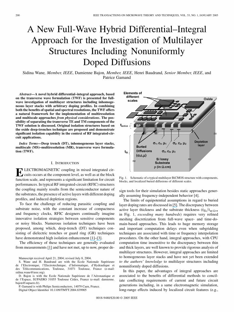
Fig. 1. Schematic of a typical multilayer BiCMOS structure with components,blocks, and localized buried diffusions of different scales.
sign tools for their simulation besides static approaches gener-ally assuming frequency-independent behavior [4].
The limits of equipotential assumptions in regard to buriedlayer doping rates are discussed in [5]. The discrepancy betweenactive layer thickness and the substrate thickness (in Fig. 1, exceeding many hundreds) requires very refinedmeshing discretization from full-wave space- and time-do-main-based approaches. This leads to huge memory storageand important computation delays even when subgriddingtechniques are associated with time or frequency interpolationprocedures. On the other hand, integral approaches, with CPUcomputation time insensitive to the discrepancy between thinand thick layers, are well known to provide rigorous analysis ofmultilayer structures. However, integral approaches are limitedto homogeneous layer stacks and have not yet been extendedto the authors’ knowledge to multilayer structures includingnonuniformly doped diffusions.
In this paper, the advantages of integral approaches areassociated to the benefits of differential methods to concil-iate conflicting requirements of current and future circuitgenerations including, in a same electromagnetic simulation,long-range effects induced by localized circuit features (e.g.,
0018-9480/$20.00 © 2005 IEEE
WANE et al.: NEW FULL-WAVE HYBRID DIFFERENTIAL–INTEGRAL APPROACH FOR INVESTIGATION OF MULTILAYER STRUCTURES 201
DT, GR, n-well, or p-well). This association, in the contextof an original approach based on transverse wave formulation(TWF), offers a natural framework for multiscale (MS) andmultiresolution (MR) analyses.
The TWF handles bounded operators and circumvents the in-version of an integral operator in treating, in an iterative way,the integral relations in the spectral domain and the continuityconditions in the spatial domain. TWF properly distinguishesthe topological characteristics of circuits from their embeddingenvironment. The MR analysis allows the dependence of sensi-tive topological details on the circuit performances to be inves-tigated. The MS approach, in controlling the optimum spectralexpansion of integral operators, provides indications for an ap-propriate choice of meshing cell dimensions.
In the spatial domain, a wavelet-based MR analysis intro-duces the original concept of layout approximation throughcharacteristic functions defining an image of circuit metaland/or dielectric sub-domains. Techniques brought fromsignal-processing theory [6]–[8] are introduced in order toapproximate circuit layout characteristic functions at differentresolutions. Although wavelet-based formulations have beenintensively used in the method of moments (MoM), the conceptof characteristic function to approximate circuit layouts is orig-inal. The previous studies on wavelets were principally directedtoward performing a thresholding procedure to render the MoMmatrix as sparse as possible with a better representation ofboundary and edge conditions [9]–[13].
In the spectral domain, the splitting of the TWF solution intosolenoidal and nonsolenoidal parts allows, at each iteration loop,the transverse TE and TM modes to be separately computed.
It is shown that the transverse wave solenoidal and non-solenoidal components are coupled in the space domain byedge boundary conditions, particularly at high frequencies.
At low frequencies, the coupling between the TE and TMparts can be neglected, as in partial-element equivalent-cir-cuit (PEEC)-based methods, the magnetostatic (TE part) andelectrostatic (TM part) can be independently computed fora given circuit. While PEEC-based approaches lead to exactdecomposition forms of the boundary value problem into itsmagnetostatic and electrostatic forms at zero frequency [14],in MoM formulations, numerical instabilities can be observedat very low frequencies [15], [16]. It is in this prospect thatloop-star decomposition basis functions were originally intro-duced to solve the low-frequency problems of the MoM [17].The issue of numerical stability improvement of the adaptiveintegral method (AIM) at low frequencies is addressed in [18],where loop-charge expansion functions are found preferable toloop-tree and loop-star formulations for better spectral prop-erties of the MoM impedance matrix. In [19], the separationof the unknown surface current, from the MoM, into TE andquasi-TM components, is applied to single patches and antennaarrays to reduce the condition number of the moment matrix.In the proposed TWF approach, numerical instabilities relatedto matrix poor condition numbers are circumvented by theintroduction of the transverse waves in place of the tangentialelectromagnetic fields that allows one to handle scatteringoperators instead of manipulating unbounded impedance oradmittance operators.
Section II provides the theoretical background of the TWFand its extension to multilayered structures including inhomo-geneous layers and will constitute the theoretical support of theMS and MR approaches developed in Section III. The presentin-depth description of the proposed hybrid method in associ-ation with the proposed original MS and MR approaches arepresented for the first time, although some examples not re-peated in this paper have been presented in conference proceed-ings [2], [5], [20], [21]. Section IV is devoted to RFIC applica-tion examples where original isolation strategies based on oxidedeep trenches (DTs) are proposed and demonstrate high isola-tion efficiency.
II. THEORETICAL BACKGROUND
A. TWF
Dyadic Green’s functions (DGF) for the structure in Fig. 2 areclassically constructed from the immittance approach [22]–[24]in reference to admittance operators for homogeneous media.When expanded on the transverse TE and TM basis functions(eigenfunctions of ), the DGF lead to diagonal representationsin the spectral domain, which can be easily computed using fastFourier algorithms [23]. Taking advantage of these attributesand overcoming diverse instabilities, related, for instance, to theexistence of pole singularities in the DGF investigated in [25],the TWF introduces reflection operators built from the admit-tance operator and free of poles.
To handle bounded operators, the TWF introduces, in placeof electromagnetic tangential fields and on a surface ,their linear combinations given by the relation
(1)
where is an arbitrary real wave impedance and. In (1), if and if
and being, respectively, referenced as transverse incident andreflected waves following the outgoing normal vector to thesurface . By use of (1) and from the well-known relation
, the reflection operator is formally derived as
(2)
where is the identity operator.Each homogeneous layer of order , in Fig. 2, between interfaces and is characterized by the
reflection operator relating the incident and reflected waves
following
(3)
For the operators and , respectively, associated to the topand bottom layers, (3) is rewritten as
(4)
202 IEEE TRANSACTIONS ON MICROWAVE THEORY AND TECHNIQUES, VOL. 53, NO. 1, JANUARY 2005
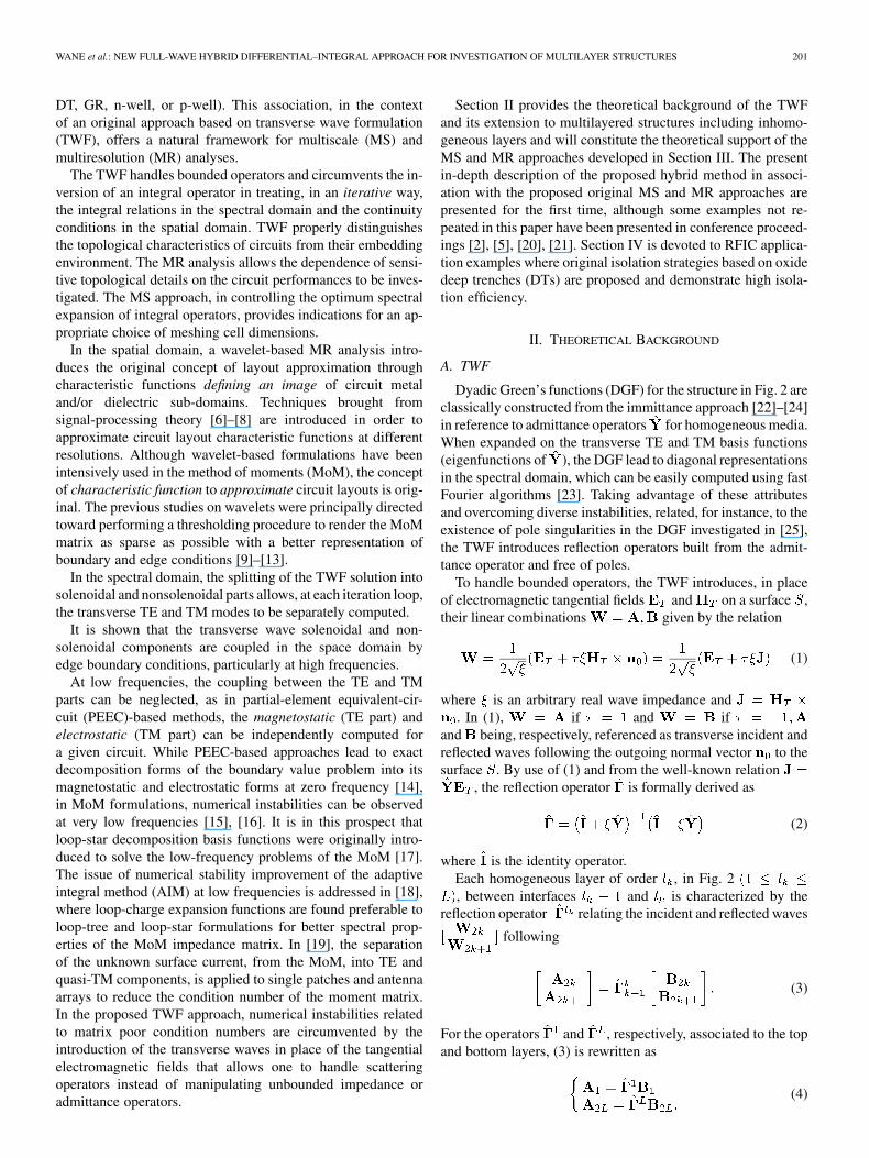
Fig. 2. Multilayer structure with different metallic interfaces andspace-domain discretization into cells of order (i ; j ) and dimension�x by �y on which pixel functions P (x; y) are defined, embedded in abox of size L � L .
In the spectral domain, the modal expansion of the reflectionoperator following the Dirac notation is given by
(5)
in which are the transverse TE and TM eigenfunc-tions of both the admittance and reflection operators verifying
(the Kronecker symbol). isthe total number of TE and TM modes.
On an interface of order in Fig. 2 ,the layout pattern consists of complementary sub-do-mains , sub referring to the nature of the sub-domain,
, respectively, for source, dielectric,metal sub-domains, and specified local relationships betweentangential fields [see, e.g., Appendix B for the case of thicksurface impedance model of metallic losses (Fig. 24)]. Onthe sub-domain, the continuity conditions impressed on
incident and reflected waves take the form
(6)
with where the projection operator
on the sub-domainis such that
ifotherwise
(7)
with being the characteristic function of the sub-
domain . on the source sub-domain is
detailed in the following. The continuity condition operator isexpanded, in the spatial domain, on the basis of pixel functions
defined as Heaviside functions restricted to themeshing cell of order (Fig. 2)
(8)
with being the total number of pixels.To manipulate the reflection operator and the continuity
condition operator on their diagonal form in, respec-tively, the spectral and spatial domains, the transverse waves
are expanded both on the andbasis functions
(9)
The toggling between the spatial and spectral wave expansionsuses a mode-pixel transform readily based on fast Fourier trans-forms (FFTs).
B. Extension of the TWF to Multilayered Structures IncludingNonuniformly Doped Diffusions
On inhomogeneous layers characterized by a complex dopingprofile , the transversefields obey coupled differential equations derived from elimi-nating normal components in Maxwell equations on their localform [26]. The transverse operator relating the transverse com-
ponents of the electromagnetic fields
can be derived in the form of an evolution equation
where (10)
where the asymmetric linear operator , not depending on theposition (Fig. 3), has the block-partitioned structure
and being given by
(11)
with and denoting the pulsation.
WANE et al.: NEW FULL-WAVE HYBRID DIFFERENTIAL–INTEGRAL APPROACH FOR INVESTIGATION OF MULTILAYER STRUCTURES 203
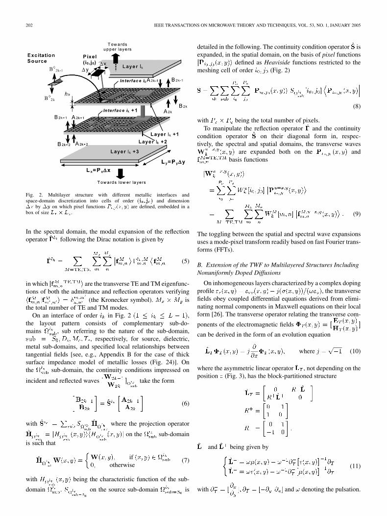
Fig. 3. Cross section of a layer stack including an inhomogeneous layer anddefinition of the incident and reflected waves on both sides of the nonuniformlydoped diffusions.
previously introduced in (1) and on one hand,and on the other hand are, respectively, related by the linearoperators and , which are detailedin [3]
(12)
Let and be, respec-
tively, the electric and magnetic tangential field at both sides (and ) of the inhomogeneous layer. A first-order approxima-tion of the spatial derivatives and , in theright-hand-side term of (12), assuming an inhomogeneous layerof small thickness , is considered with a two-dimensional fi-nite-difference formulation in the spatial domain
(13)
From (13), the scattering matrix of the inhomogeneous layerof small thickness can be expressed in the spatial domain as
(14)
For the numerical representation of the sub-blocks in (14),the computational domain is subdivided from the regular pixelsmesh into elementary cells in which the incident and reflectedwaves are expanded using triangular shape functions. The tri-angular elements being of small dimension in reference to thewavelength, the incident and reflected waves interior to eachdiscretizing cell are accurately approximated. The use of trian-gular shape functions allows steep gradients in the permittivity
and permeability space derivatives in (12) tobe avoided.
(a) (b)
(c)
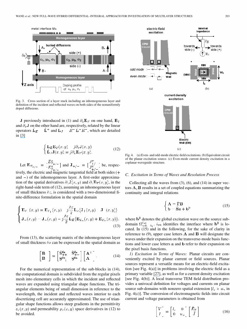
Fig. 4. (a) Even- and odd-mode electric-field excitations. (b) Equivalent circuitof the planar excitation source. (c) Even-mode current density excitation in acoplanar-waveguide structure.
C. Excitation in Terms of Waves and Resolution Process
Collecting all the waves from (3), (6), and (14) in super vec-tors results in a set of coupled equations summarizing thecontinuity and integral relations
(15)
where denotes the global excitation wave on the source sub-domain . identifies the interface where is lo-cated. In (15) and in the following, for the sake of clarity inreference to (9), upper case letters and will designate thewaves under their expansion on the transverse-mode basis func-tions and lower case letters and refer to their expansion onthe pixel basis functions.
1) Excitation in Terms of Waves: Planar circuits are con-veniently excited by planar current or field sources. Planarsources represent a versatile means for an electric-field excita-tion [see Fig. 4(a)] in problems involving the electric field as aprimary variable [27], as well as for a current density excitation[see Fig. 4(b)]. A local transverse TEM field distribution pro-vides a univocal definition for voltages and currents on planarsource sub-domains with nonzero spatial extension [ inFig. 4(c)]. The conversion of electromagnetic fields into circuitcurrent and voltage parameters is obtained from
(16)
204 IEEE TRANSACTIONS ON MICROWAVE THEORY AND TECHNIQUES, VOL. 53, NO. 1, JANUARY 2005
where and
assuming a polarization for the excitation source (the directionis given by the magnetic wall’s direction).Transverse fields on the source sub-domain are related
by the continuity relation
(17)
The weighting scalar array in (6) of the continuity con-
dition operator is deduced from (17) as follows:
(18)
The excitation wave on the interface is related to theelectromagnetic excitation field in Fig. 4(b) by
(19)where and are the reference imped-ances in sides .
2) Iterative Resolution Process: Starting from the waveexcitation source , the TWF leads to an iterative schemeavoiding any operator inversion procedure to solve (15) asfollows:
(20)
where is the iteration order. All along the iterations, by suc-cessive reflections, the waves and grow as
(21)
The terms in (21) obey and. For numerical efficiency reasons, it is convenient
to process with the iterative scheme on the wave growths gov-erned by
(22)
The convergence of (22) is reached when the normsand tend toward zero. The convergence speed isdriven by the spectral radius of and . The conver-gence condition can be expressed as
and (23)
where designates the spectral radius of the operator .It is essential to underline that, due to the internal impedance
in the source domain all along the iterative process, the condi-tion is satisfied. The no-
tation refers to the norm of the vector restricted to
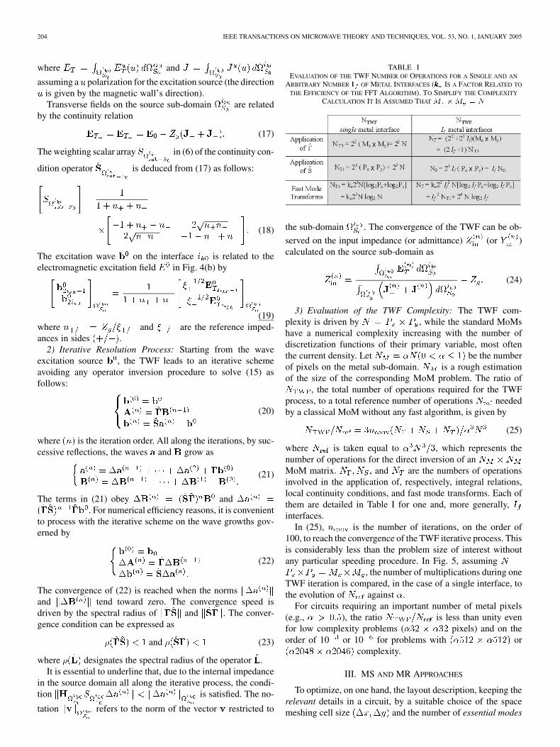
TABLE IEVALUATION OF THE TWF NUMBER OF OPERATIONS FOR A SINGLE AND AN
ARBITRARY NUMBER I OF METAL INTERFACES (kkk IS A FACTOR RELATED TO
THE EFFICIENCY OF THE FFT ALGORITHM). TO SIMPLIFY THE COMPLEXITY
CALCULATION IT IS ASSUMED THAT M �M = N
the sub-domain . The convergence of the TWF can be ob-
served on the input impedance (or admittance) (or )calculated on the source sub-domain as
(24)
3) Evaluation of the TWF Complexity: The TWF com-plexity is driven by , while the standard MoMshave a numerical complexity increasing with the number ofdiscretization functions of their primary variable, most oftenthe current density. Let be the numberof pixels on the metal sub-domain. is a rough estimationof the size of the corresponding MoM problem. The ratio of
, the total number of operations required for the TWFprocess, to a total reference number of operations neededby a classical MoM without any fast algorithm, is given by
(25)
where is taken equal to , which represents thenumber of operations for the direct inversion of anMoM matrix. and are the numbers of operationsinvolved in the application of, respectively, integral relations,local continuity conditions, and fast mode transforms. Each ofthem are detailed in Table I for one and, more generally,interfaces.
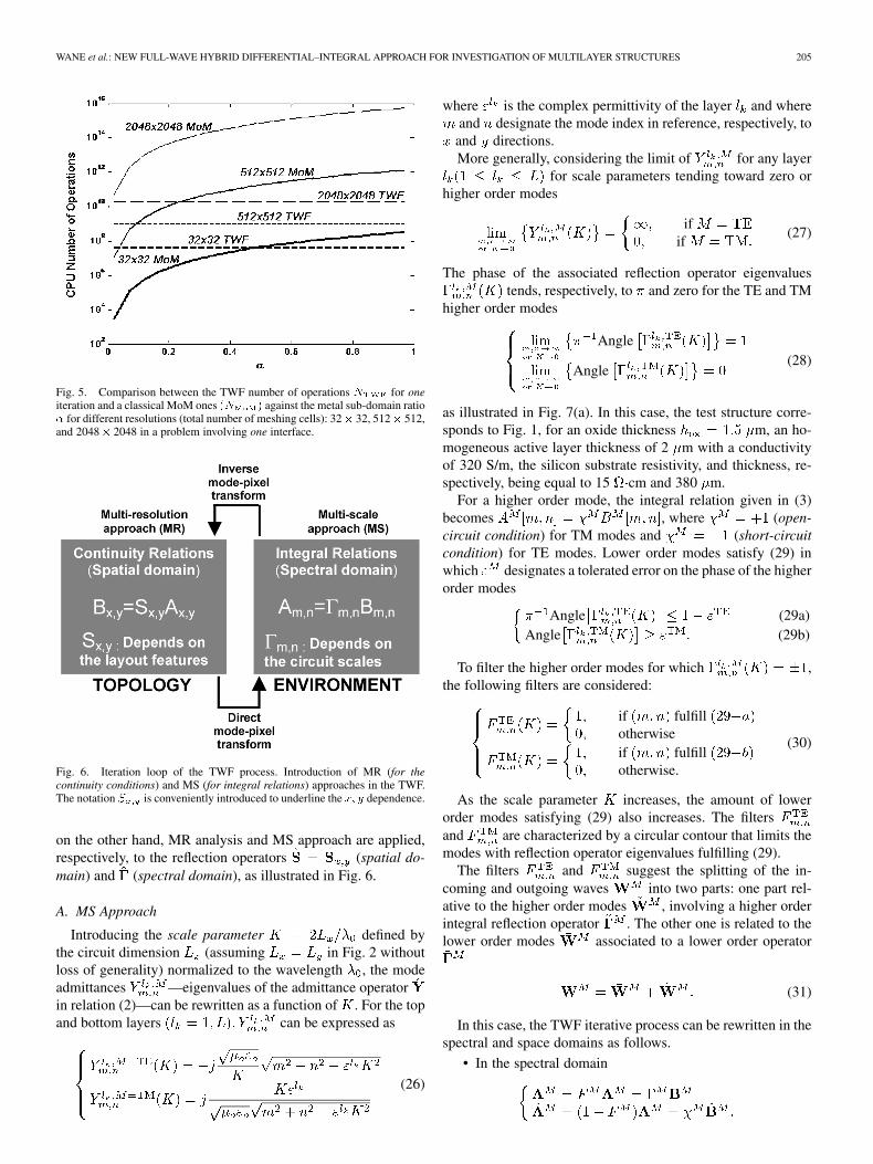
In (25), is the number of iterations, on the order of100, to reach the convergence of the TWF iterative process. Thisis considerably less than the problem size of interest withoutany particular speeding procedure. In Fig. 5, assuming
, the number of multiplications during oneTWF iteration is compared, in the case of a single interface, tothe evolution of against .
For circuits requiring an important number of metal pixels(e.g., ), the ratio is less than unity evenfor low complexity problems ( pixels) and on theorder of 10 or 10 for problems with or
complexity.
III. MS AND MR APPROACHES
To optimize, on one hand, the layout description, keeping therelevant details in a circuit, by a suitable choice of the spacemeshing cell size and the number of essential modes
WANE et al.: NEW FULL-WAVE HYBRID DIFFERENTIAL–INTEGRAL APPROACH FOR INVESTIGATION OF MULTILAYER STRUCTURES 205
Fig. 5. Comparison between the TWF number of operations N for oneiteration and a classical MoM ones (N ) against the metal sub-domain ratio� for different resolutions (total number of meshing cells): 32� 32, 512� 512,and 2048� 2048 in a problem involving one interface.
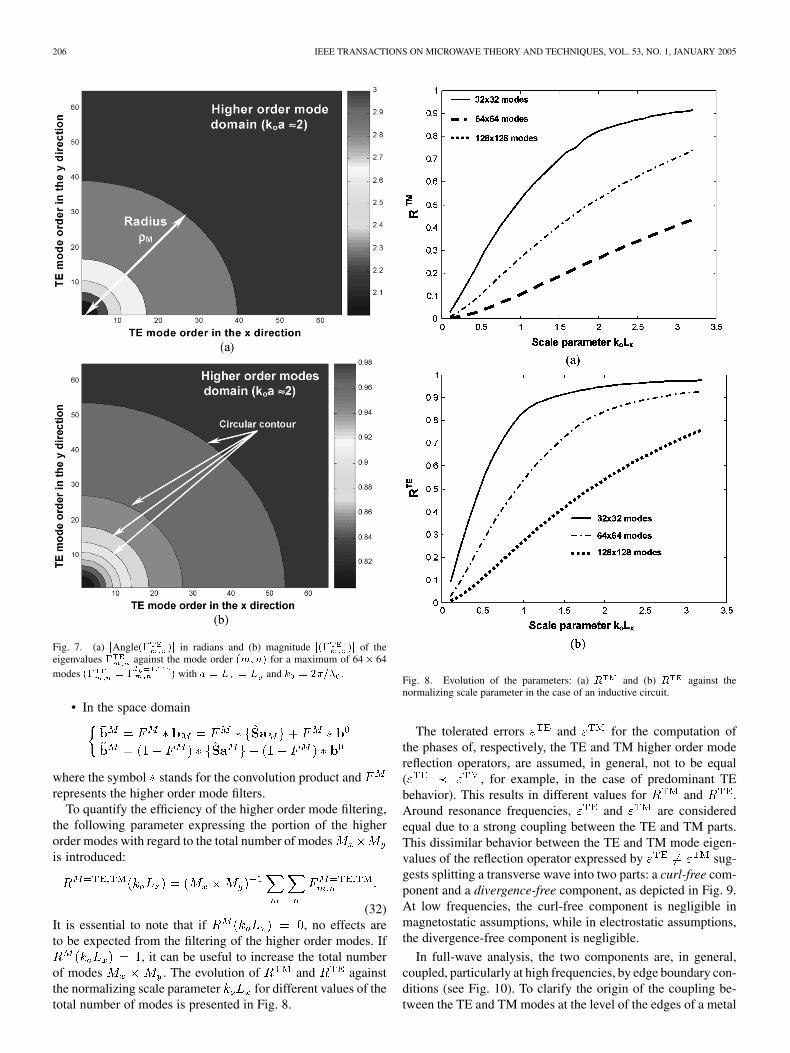
Fig. 6. Iteration loop of the TWF process. Introduction of MR (for thecontinuity conditions) and MS (for integral relations) approaches in the TWF.The notation S is conveniently introduced to underline the x; y dependence.
on the other hand, MR analysis and MS approach are applied,respectively, to the reflection operators (spatial do-main) and (spectral domain), as illustrated in Fig. 6.
A. MS Approach
Introducing the scale parameter defined bythe circuit dimension (assuming in Fig. 2 withoutloss of generality) normalized to the wavelength , the modeadmittances —eigenvalues of the admittance operatorin relation (2)—can be rewritten as a function of . For the topand bottom layers can be expressed as
(26)
where is the complex permittivity of the layer and whereand designate the mode index in reference, respectively, toand directions.More generally, considering the limit of for any layer
for scale parameters tending toward zero orhigher order modes
ifif
(27)
The phase of the associated reflection operator eigenvaluestends, respectively, to and zero for the TE and TM
higher order modes
Angle
Angle(28)
as illustrated in Fig. 7(a). In this case, the test structure corre-sponds to Fig. 1, for an oxide thickness m, an ho-mogeneous active layer thickness of 2 m with a conductivityof 320 S/m, the silicon substrate resistivity, and thickness, re-spectively, being equal to 15 cm and 380 m.
For a higher order mode, the integral relation given in (3)becomes , where (open-circuit condition) for TM modes and (short-circuitcondition) for TE modes. Lower order modes satisfy (29) inwhich designates a tolerated error on the phase of the higherorder modes
Angle (29a)Angle (29b)
To filter the higher order modes for which ,the following filters are considered:
if fulfillotherwiseif fulfillotherwise.
(30)
As the scale parameter increases, the amount of lowerorder modes satisfying (29) also increases. The filtersand are characterized by a circular contour that limits themodes with reflection operator eigenvalues fulfilling (29).
The filters and suggest the splitting of the in-coming and outgoing waves into two parts: one part rel-ative to the higher order modes , involving a higher orderintegral reflection operator . The other one is related to thelower order modes associated to a lower order operator
(31)
In this case, the TWF iterative process can be rewritten in thespectral and space domains as follows.
• In the spectral domain
206 IEEE TRANSACTIONS ON MICROWAVE THEORY AND TECHNIQUES, VOL. 53, NO. 1, JANUARY 2005
Fig. 7. (a) jAngle(� )j in radians and (b) magnitude j(� )j of theeigenvalues � against the mode order (m;n) for a maximum of 64� 64modes (� = � ) with a = L = L and k = 2�=� .
• In the space domain
where the symbol stands for the convolution product andrepresents the higher order mode filters.
To quantify the efficiency of the higher order mode filtering,the following parameter expressing the portion of the higherorder modes with regard to the total number of modesis introduced:
(32)It is essential to note that if , no effects areto be expected from the filtering of the higher order modes. If
, it can be useful to increase the total numberof modes . The evolution of and againstthe normalizing scale parameter for different values of thetotal number of modes is presented in Fig. 8.
Fig. 8. Evolution of the parameters: (a) R and (b) R against thenormalizing scale parameter in the case of an inductive circuit.
The tolerated errors and for the computation ofthe phases of, respectively, the TE and TM higher order modereflection operators, are assumed, in general, not to be equal( , for example, in the case of predominant TEbehavior). This results in different values for and .Around resonance frequencies, and are consideredequal due to a strong coupling between the TE and TM parts.This dissimilar behavior between the TE and TM mode eigen-values of the reflection operator expressed by sug-gests splitting a transverse wave into two parts: a curl-free com-ponent and a divergence-free component, as depicted in Fig. 9.At low frequencies, the curl-free component is negligible inmagnetostatic assumptions, while in electrostatic assumptions,the divergence-free component is negligible.
In full-wave analysis, the two components are, in general,coupled, particularly at high frequencies, by edge boundary con-ditions (see Fig. 10). To clarify the origin of the coupling be-tween the TE and TM modes at the level of the edges of a metal

WANE et al.: NEW FULL-WAVE HYBRID DIFFERENTIAL–INTEGRAL APPROACH FOR INVESTIGATION OF MULTILAYER STRUCTURES 207
Fig. 9. Decomposition of a wave distribution into a curl-free component anda divergence-free component with a coupling between the two components.
Fig. 10. Representation of metal sub-domain parallel (==) and orthogonal (?)edges. Illustration of sharp and smooth characteristic function variations on themetal edges.
sub-domain, it is convenient to consider Maxwell’s equationsunder the following form:
and (33)
where and , respectively, represent the restrictionof the divergence and curl operators to the tangential planeand designates the partial derivative operation following thenormal direction to the tangential plane. Decomposing the elec-tric and magnetic tangential fields into their TE and TM com-ponents and leads to
and (34)
Relations (34) show that the curl-free component refers to theTE modes and the divergence-free component corresponds toTM modes. The edge conditions being incorporated, (34) canbe rewritten in terms of incident and reflected transverse wavesas
(35)
with
on edgeon edge
Fig. 11. (a) Schematic of an MS circuit layout with macroblock, microblock,and middle-block levels. (b) Zoom on a line interconnect between a middleblock and macroblock.
in Fig. 10 where is a diagonal matrix and representsthe coupling matrix between the TE and TM modes. Thedirection is relative to the excitation source polarization. Theexpression of the coupling between the transverse wave TEand TM components is derived in Appendix A in the case ofisotropic media (see Fig. 23).
A numerical evaluation of the coupling between the TE andTM modes in the case of an interconnect line connecting a mac-roblock to a middle block in Fig. 11 (where all microblocks,middle blocks, and macroblocks are on the same metal level) isinvestigated in Fig. 12.
It is proven that the coupling between the two types of modesis localized at the level of the metal sub-domain edge cells. Thiscoupling can be neglected at low frequencies (less than 6 GHzfor the test structure). Thus, for frequencies less than 6 GHz,the TE- and TM-mode contributions can be separately com-puted. Below the first resonant frequency of the structure, theTE modes are dominant because of the inductive nature of theinterconnect line. The possibility of neglecting the coupling be-tween TE and TM modes allows a parallel processing of the
208 IEEE TRANSACTIONS ON MICROWAVE THEORY AND TECHNIQUES, VOL. 53, NO. 1, JANUARY 2005
Fig. 12. Numerical evaluation of the coupling between the TE and TM modesfor a line interconnect for a scale parameter K = 0:1 at 1 GHz.
TWF iterative scheme. In a multilevel approach, the hypothesisof low coupling between TE and TM modes for low-scale de-scriptions can help to separately compute low-frequency mag-netostatic and electrostatic behavior.
To keep the benefit of separating the TE and TM modes athigh operating frequencies, a subdivision of the circuit into mac-roblocks of dimension can be introduced. With an ap-propriate choice of the number of macroblocks, the couplingbetween the TE and TM modes can be neglected. Since TE orTM lower order modes belong to the circle area (seeFig. 7) defined by the relation where the ra-dius is , an optimum cell size for the space description ofthe circuit layout can be obtained from a specified scale param-eter . If represents the total number of unit cells of size
, an optimum cell size can be chosen so thatwith .
B. MR Approach: The Concept of Layout “Approximation”
When describing a circuit layout, the passing from a refinedmeshing to a coarser representation, in general, leads to a certainapproximation of the circuit dimensions. This approximation, aslong as its effects on the electromagnetic behavior of the circuitremain negligible, results in significant reduction of the compu-tation complexity.
The layout of Fig. 13 represents concentric rings separated bya gap. For unit meshing cell size less than the gap resolution, thewhole structure details can be described. For a larger cell size,all the different rings do not appear discernible. By construc-tion, the characteristic function of the metal, dielectric, or sourcesub-domain presents a sharp space variation at the sub-domainedges. A representation of sharp variation in a metal charac-teristic function at the metal sub-domain edges is illustrated inFig. 10.
To avoid steep gradients of the characteristic functions re-sponsible for discontinuities of the parallel and perpendicularelectromagnetic-field components, a wavelet MR basis is intro-duced. This is to expand not the magnetic or theelectric fields as classically done with the MoM
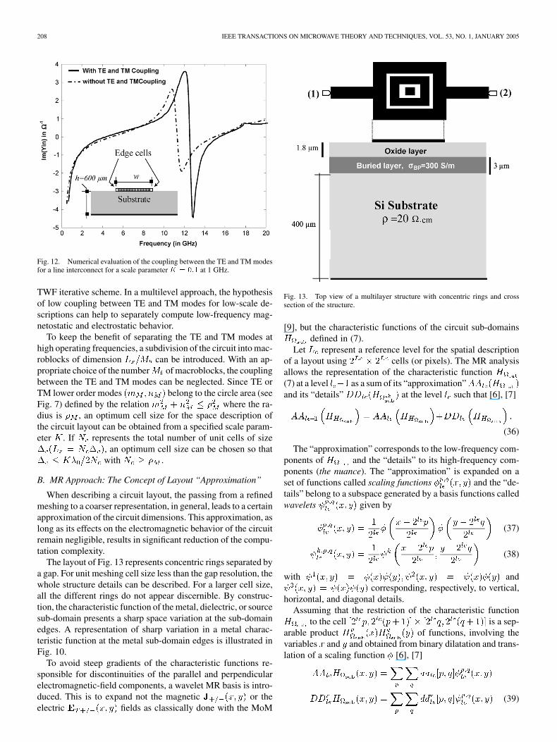
Fig. 13. Top view of a multilayer structure with concentric rings and crosssection of the structure.
[9], but the characteristic functions of the circuit sub-domainsdefined in (7).
Let represent a reference level for the spatial descriptionof a layout using cells (or pixels). The MR analysisallows the representation of the characteristic function(7) at a level as a sum of its “approximation”and its “details” at the level such that [6], [7]
(36)
The “approximation” corresponds to the low-frequency com-ponents of and the “details” to its high-frequency com-ponents (the nuance). The “approximation” is expanded on aset of functions called scaling functions and the “de-tails” belong to a subspace generated by a basis functions calledwavelets given by
(37)
(38)
with andcorresponding, respectively, to vertical,
horizontal, and diagonal details.Assuming that the restriction of the characteristic function
to the cell is a sep-arable product of functions, involving thevariables and and obtained from binary dilatation and trans-lation of a scaling function [6], [7]
(39)

WANE et al.: NEW FULL-WAVE HYBRID DIFFERENTIAL–INTEGRAL APPROACH FOR INVESTIGATION OF MULTILAYER STRUCTURES 209
Fig. 14. Representation of the metal sub-domain characteristic function of thestructure in Fig. 13 at the scales: (a) l = 7 and (b) l = 4.
with and.
Among the diverse families of wavelets, Haar waveletsknown to not produce Gibb’s phenomena [28] are consideredin the following for the multilevel analysis of the layout repre-sented in Fig. 13. Using Haar-wavelets-based decomposition,an MR analysis of the layout characteristic function (metalsub-domain) is presented in Fig. 14 at the scales and
. The effect of the scale representation of the layout onthe transmission and insertion parameters of the circuit is alsogiven in Fig. 15. The influence of the layout approximation onthe transmission parameter is seen to not exceed 3 dB when thescale varies from to .
In trend studies where designers, in general, make use of com-parative approaches, circuits with disparate space meshing res-olutions can be investigated. This is carried out using a coarserdescription as far as the impact of such approximation in theglobal performance of the structure remains less than a certainmargin, as in the case observed in Fig. 15.
However, for some sensitive circuits, a lower scale represen-tation of a layout circuit can produce a severe degradation in thecircuit performance. This idea was presented in [20] where theexistence of a critical scale has been shown to be required for anaccurate description of significant layout details.
Fig. 15. Influence of the multilevel approximation of the layout characteristicfunction in Fig. 13 on the transmission and insertion parameters.
Fig. 16. Top view of the inhomogeneous substrate including P+ contacts,oxide-trench, guard-ring, P-well, or N-well [3].
IV. APPLICATION TO MULTILAYER STRUCTURES INCLUDING
NONUNIFORMLY DOPED DIFFUSIONS
The proposed full-wave hybrid approach is used to investigatesubstrate coupling effects on pad-to-pad isolation capabilities(Fig. 16). Simulation results obtained with the proposed hybridmethod for a substrate resistivity in the 5–30 cm range arefavorably compared to published measurements [29], [30] andto commercial design tools (Sonnet software) in Fig. 17(a) forreference structures without DTs. In Fig. 17(b), a comparisonbetween the results obtained by Momentum software and oursimulation results for both low (20 cm) and high (10 cm)resistivity substrate is presented. In [5], the dependence of DTtechnique efficiency on the buried layer doping rate is investi-gated, and comparison with measurements and Substrate Stormdesign tools are presented.
The efficiency of the DT technique to reduce substrate cou-pling is investigated on a reference structure with identical 25-m pads separated by 50 m, as depicted in the inset of Fig. 18.The substrate resistivity and buried layer conductivity are equal,respectively, to 20 cm and 800 S/m.
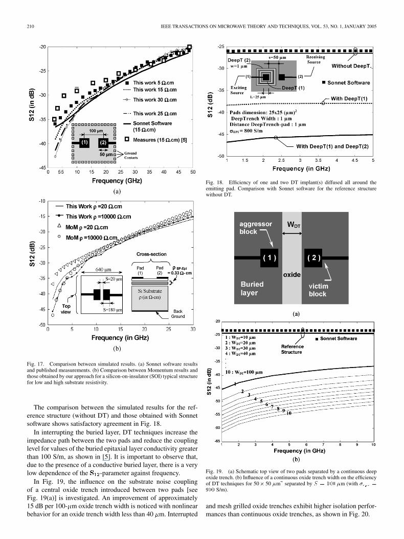
210 IEEE TRANSACTIONS ON MICROWAVE THEORY AND TECHNIQUES, VOL. 53, NO. 1, JANUARY 2005
Fig. 17. Comparison between simulated results. (a) Sonnet software resultsand published measurements. (b) Comparison between Momentum results andthose obtained by our approach for a silicon-on-insulator (SOI) typical structurefor low and high substrate resistivity.
The comparison between the simulated results for the ref-erence structure (without DT) and those obtained with Sonnetsoftware shows satisfactory agreement in Fig. 18.
In interrupting the buried layer, DT techniques increase theimpedance path between the two pads and reduce the couplinglevel for values of the buried epitaxial layer conductivity greaterthan 100 S/m, as shown in [5]. It is important to observe that,due to the presence of a conductive buried layer, there is a verylow dependence of the -parameter against frequency.
In Fig. 19, the influence on the substrate noise couplingof a central oxide trench introduced between two pads [seeFig. 19(a)] is investigated. An improvement of approximately15 dB per 100- m oxide trench width is noticed with nonlinearbehavior for an oxide trench width less than 40 m. Interrupted
Fig. 18. Efficiency of one and two DT implant(s) diffused all around theemitting pad. Comparison with Sonnet software for the reference structurewithout DT.
Fig. 19. (a) Schematic top view of two pads separated by a continuous deepoxide trench. (b) Influence of a continuous oxide trench width on the efficiencyof DT techniques for 50� 50 �m separated by S = 100 �m (with � =
900 S/m).
and mesh grilled oxide trenches exhibit higher isolation perfor-mances than continuous oxide trenches, as shown in Fig. 20.
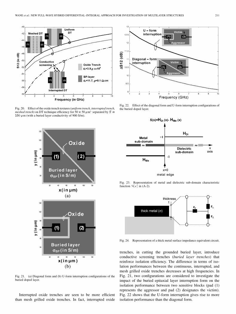
WANE et al.: NEW FULL-WAVE HYBRID DIFFERENTIAL–INTEGRAL APPROACH FOR INVESTIGATION OF MULTILAYER STRUCTURES 211
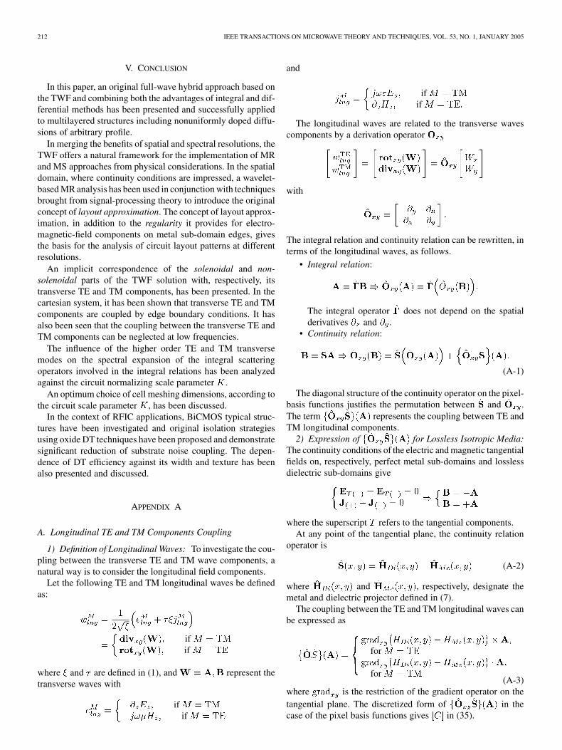
Fig. 20. Effect of the oxide trench textures (uniform trench, interrupted trench,meshed trench) on DT technique efficiency for 50� 50 �m separated by S =100 �m (with a buried layer conductivity of 900 S/m).
Fig. 21. (a) Diagonal form and (b) U-form interruption configurations of theburied doped layer.
Interrupted oxide trenches are seen to be more efficientthan mesh grilled oxide trenches. In fact, interrupted oxide
Fig. 22. Effect of the diagonal form and U-form interruption configurations ofthe buried doped layer.
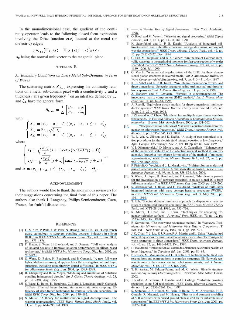
Fig. 23. Representation of metal and dielectric sub-domain characteristicfunction S(x) in (A-2).
Fig. 24. Representation of a thick metal surface impedance equivalent circuit.
trenches, in cutting the grounded buried layer, introduceconductive screening trenches (buried layer trenches) thatreinforce isolation efficiency. The difference in terms of iso-lation performances between the continuous, interrupted, andmesh grilled oxide trenches decreases at high frequencies. InFig. 21, two configurations are considered to investigate theimpact of the buried epitaxial layer interruption form on theisolation performance between two sensitive blocks (pad (1)represents the aggressor and pad (2) designates the victim).Fig. 22 shows that the U-form interruption gives rise to moreisolation performance than the diagonal form.
212 IEEE TRANSACTIONS ON MICROWAVE THEORY AND TECHNIQUES, VOL. 53, NO. 1, JANUARY 2005
V. CONCLUSION
In this paper, an original full-wave hybrid approach based onthe TWF and combining both the advantages of integral and dif-ferential methods has been presented and successfully appliedto multilayered structures including nonuniformly doped diffu-sions of arbitrary profile.
In merging the benefits of spatial and spectral resolutions, theTWF offers a natural framework for the implementation of MRand MS approaches from physical considerations. In the spatialdomain, where continuity conditions are impressed, a wavelet-based MR analysis has been used in conjunction with techniquesbrought from signal-processing theory to introduce the originalconcept of layout approximation. The concept of layout approx-imation, in addition to the regularity it provides for electro-magnetic-field components on metal sub-domain edges, givesthe basis for the analysis of circuit layout patterns at differentresolutions.
An implicit correspondence of the solenoidal and non-solenoidal parts of the TWF solution with, respectively, itstransverse TE and TM components, has been presented. In thecartesian system, it has been shown that transverse TE and TMcomponents are coupled by edge boundary conditions. It hasalso been seen that the coupling between the transverse TE andTM components can be neglected at low frequencies.
The influence of the higher order TE and TM transversemodes on the spectral expansion of the integral scatteringoperators involved in the integral relations has been analyzedagainst the circuit normalizing scale parameter .
An optimum choice of cell meshing dimensions, according tothe circuit scale parameter , has been discussed.
In the context of RFIC applications, BiCMOS typical struc-tures have been investigated and original isolation strategiesusing oxide DT techniques have been proposed and demonstratesignificant reduction of substrate noise coupling. The depen-dence of DT efficiency against its width and texture has beenalso presented and discussed.
APPENDIX A
A. Longitudinal TE and TM Components Coupling
1) Definition of Longitudinal Waves: To investigate the cou-pling between the transverse TE and TM wave components, anatural way is to consider the longitudinal field components.
Let the following TE and TM longitudinal waves be definedas:
ifif
where and are defined in (1), and represent thetransverse waves with
ifif
and
ifif
The longitudinal waves are related to the transverse wavescomponents by a derivation operator
with
The integral relation and continuity relation can be rewritten, interms of the longitudinal waves, as follows.
• Integral relation:
The integral operator does not depend on the spatialderivatives and .
• Continuity relation:
(A-1)
The diagonal structure of the continuity operator on the pixel-basis functions justifies the permutation between and .The term represents the coupling between TE andTM longitudinal components.
2) Expression of for Lossless Isotropic Media:The continuity conditions of the electric and magnetic tangentialfields on, respectively, perfect metal sub-domains and losslessdielectric sub-domains give
where the superscript refers to the tangential components.At any point of the tangential plane, the continuity relation
operator is
(A-2)
where and , respectively, designate themetal and dielectric projector defined in (7).
The coupling between the TE and TM longitudinal waves canbe expressed as
for
for(A-3)
where is the restriction of the gradient operator on thetangential plane. The discretized form of in thecase of the pixel basis functions gives in (35).
WANE et al.: NEW FULL-WAVE HYBRID DIFFERENTIAL–INTEGRAL APPROACH FOR INVESTIGATION OF MULTILAYER STRUCTURES 213
In the monodimensional case, the gradient of the conti-nuity operator leads to the following closed-form expressioninvolving the Dirac function located at the metal (ordielectric) edges:
being the normal unit vector to the tangential plane.
APPENDIX B
A. Boundary Conditions on Lossy Metal Sub-Domains in Termof Waves
The scattering matrix expressing the continuity rela-tions on a metal sub-domain pixel with a conductivity and athickness at a given frequency on an interface defined byand have the general form
with
where
and .
ACKNOWLEDGMENT
The authors would like to thank the anonymous reviewers fortheir suggestions concerning the final form of this paper. Theauthors also thank J. Langanay, Philips Semiconductor, Caen,France, for fruitful discussions.
REFERENCES
[1] C. S. Kim, P. Park, J.-W. Park, N. Hwang, and H. K. Yu, “Deep trenchguard technology to suppress coupling between inductors in siliconRFIC,” in IEEE MTT-S Int. Microwave Symp. Dig., vol. 3, Jun. 2001,pp. 1873–1876.
[2] D. Bajon, S. Wane, H. Baudrand, and P. Gamand, “Full wave analysisof isolated pockets to improve isolation performances in silicon basedtechnology,” in IEEE MTT-S Int. Microwave Symp. Dig., Jun. 2002, pp.987–990.
[3] S. Wane, D. Bajon, H. Baudrand, and P. Gamand, “A new full-wavehybrid differential–integral approach for the investigation of multilayerstructures including nonuniformly doped diffusions,” in IEEE MTT-SInt. Microwave Symp. Dig., Jun. 2004, pp. 1395–1398.
[4] R. Gharpurey and R. G. Meyer, “Modeling and simulation of Substratecoupling in integrated circuits,” Int. J. Circuit Theory Applicat., vol. 23,pp. 381–394, Aug. 1995.
[5] S. Wane, D. Bajon, H. Baudrand, C. Biard, J. Langanay, and P. Gamand,“Effects of buried layers doping rate on substrate noise coupling: Ef-ficiency of deep-trench techniques to improve isolation capability,” inIEEE RFIC Symp. Dig., Jun. 2004, pp. 179–182.
[6] S. Mallat, “A theory for multiresolution signal decomposition: Thewavelet representation,” IEEE Trans. Pattern Anal. Mach. Intell., vol.11, no. 7, pp. 674–693, Jul. 1989.
[7] , A Wavelet Tour of Signal Processing. New York: Academic,1998.
[8] O. Rioul and M. Vetterli, “Wavelet and signal processing,” IEEE SignalProcess., vol. 8, no. 4, pp. 14–38, Oct. 1991.
[9] K. Sabetfakhri and L. P. B. Katehi, “Analysis of integrated mil-limeter-wave and submillimeter-wave waveguides using orthogonalwavelet expansions,” IEEE Trans. Microw. Theory Tech., vol. 42, no.12, pp. 2412–2422, Dec. 1994.
[10] G. Pan, M. Toupikov, and B. K. Gilbert, “On the use of Coifman inter-vallic wavelets in the method of moments for fast construction of waveletsparcified matrices,” IEEE Trans. Antennas Propag., vol. 47, no. 7, pp.1189–1200, Jul. 1999.
[11] G. Vecchi, “A numerical regularization of the EFIE for three dimen-sional planar structures in layered media,” Int. J. Microwave MillimeterWave Computer-Aided Engineering, vol. 7, pp. 410–431, Nov. 1997.
[12] K. F. Sabet and L. P. B. Katehi, “An integral formulation of two- andthree-dimensional dielectric structures using orthonormal multiresolu-tion expansions,” Int. J. Numer. Modeling, vol. 11, pp. 3–19, 1998.
[13] Z. Baharav and Y. Leviatan, “Wavelet in electromagnetics: Theimpedance matrix compression (IMC) method,” Int. J. Numer. Mod-eling, vol. 11, pp. 69–84, 1998.
[14] A. Ruehli, “Equivalent circuit models for three-dimensional multicon-ductor systems,” IEEE Trans. Microw. Theory Tech., vol. MTT-22, no.3, pp. 216–221, Mar. 1974.
[15] J. Zhao and W. C. Chew, “Multilevel fast multipole algorithm at very lowfrequencies,” in Fast and Efficient Algorithms in Computational Electro-magnetics. Boston, MA: Artech House, 2001, pp. 151–202.
[16] , “Integral equation solution of Maxwell’s equations from zero fre-quency to microwave frequencies,” IEEE Trans. Antennas Propag., vol.48, no. 10, pp. 1635–1645, Oct. 2000.
[17] W. L. Wu, A. Glisson, and D. Kajfer, “A study of two numerical solu-tion procedures for the electric field integral equation at low frequency,”Appl. Comput. Electromagn. Soc. J., vol. 10, pp. 69–80, Nov. 1995.
[18] V. I. Okhmatovski, J. D. Morsey, and A. C. Cangellaris, “Enhancementof the numerical stability of the adaptive integral method at low fre-quencies through a loop-charge formulation of the method of momentsapproximation,” IEEE Trans. Microw. Theory Tech., vol. 52, no. 3, pp.962–970, Mar. 2004.
[19] P. Pirinoli, G. Vecchi, and L. L. Matekovits, “Multiresolution analysis ofprinted antennas and circuits: A dual isoscalar approach,” IEEE Trans.Antennas Propag., vol. 49, no. 6, pp. 858–874, Jun. 2001.
[20] S. Wane, D. Bajon, H. Baudrand, and P. Gamand, “Multilevel approachfor the investigation of substrate parasitics in mixed-signal IC’s fromfull-wave analysis,” in IEEE RFIC Symp. Dig., Jun. 2003, pp. 263–266.
[21] S. Akatimagool, D. Bajon, and H. Baudrand, “Analysis of multi-layerintegrated inductors with wave concept iterative procedure (WCIP),”in IEEE MTT-S Int. Microwave Symp. Dig., vol. 3, May 2001, pp.1941–1944.
[22] T. Itoh, “Spectral domain immitance approach for dispersion character-istics of generalized transmission lines,” in IEEE Trans. Microw. TheoryTech., vol. MTT-28, Jul. 1980, pp. 733–736.
[23] R. Mittra, H. Chan, and T. Cwik, “Techniques for analyzing fre-quency selective surfaces—A review,” Proc. IEEE, vol. 76, no. 12, pp.1523–1615, Dec. 1988.
[24] R. Sorrentino, “The transverse resonance method,” in Numerical Tech-niques for Microwaves and Millimeter Wave Passive Components, T.Itoh, Ed. New York: Wiley, 1989, ch. 4, pp. 496–591.
[25] J. C. Chao, Y. J. Liu, F. J. Rizzo, P. A. Martin, and L. Udpa, “Regularizedintegral equations for curvilinear boundary elements for electromagneticwave scattering in three dimensions,” IEEE Trans. Antennas Propag.,vol. 43, no. 12, pp. 1416–1422, Dec. 1995.
[26] H. Baudrand, “Introduction au calcul des éléments de circuits passifs enhyperfréquence,” in Cépadues Ed., Jan. 2001, pp. 80–84.
[27] P. Russer, M. Mongiardo, and L. B Felsen, “Electromagnetic field rep-resentations and computations in complex structures III: Network rep-resentations of the connection and subdomain circuits,” Int. J. Numer.Modeling, vol. 15, pp. 127–145, Jan. 2002.
[28] T. K. Sarkar, M. Salazar-Palma, and M. C. Wicks, Wavelet Applica-tions in Engineering Electromagnetics. Norwood, MA: Artech House,2002.
[29] J. Raskin, A. Viviani, D. Flandre, and J. Colinge, “Substrate crosstalkreduction using SOI technology,” IEEE Trans. Electron Devices, vol.44, no. 12, pp. 2252–2261, Dec. 1997.
[30] S. Stefanou, J. S. Hamel, M. Bain, P. Baine, B. M. Armstrong, H. S.Gamble, R. Mauntel, and M. Huang, “Physics and compact modelingof SOI substrates with buried ground plane (GPSOI) for substrate noisesuppression,” in IEEE MTT-S Int. Microwave Symp. Dig., Jun. 2001, pp.1877–1880.

214 IEEE TRANSACTIONS ON MICROWAVE THEORY AND TECHNIQUES, VOL. 53, NO. 1, JANUARY 2005
Sidina Wane (M’98) was born in Kaedi, Mauri-tania, in 1972. He received the Eng.-Dipl. degree inelectrical engineering (with high honors) and D.E.A.degree in optics and microwave communication Sys-tems (with high honors), from the Ecole Nationaled’Ingénieurs de Tunis (ENIT), Tunis, Tunisia, in1998 and 1999, respectively, and the Ph.D. degreein microwaves and electronics (with high honors)from the Institut National Polytechnique of Toulouse(INPT), Toulouse, France, in 2002.
He is currently with Ecole Nationale Supérieure del’Electronique, l’Electrotechnique, d’Informatique, d’Hydraulique et des Télé-communications (ENSEEIHT), Toulouse, France. His research interests includemodern numerical techniques for modeling electromagnetic fields and wavesand computer-aided design of millimeter-wave and microwave circuits.
Dr. Wane was the recipient of the Genie Electrique, Electronique, Télécom-munications (GEET) Award and Leopold Escande Award in 2002 for his Ph.D.dissertation. He was also the recipient of the 1998 Optics and Microwave Com-munication Systems Prize for his engineering dissertation.
Damienne Bajon (M’88) received the B.Sc. and theM.Sc. degrees in electrical engineering from the Uni-versité Paul Sabatier, Toulouse, France, in 1981, andthe Ph.D. degree in microwaves and electronics (withhigh honors) from the Institut National Polytechniqueof Toulouse (INPT), Toulouse, France, in 1985.
In 1989, she joined the Ecole Nationale Supérieurede l’Aéronautique et de l’Espace (SUPAERO),Toulouse, France, as an Assistant Professor, whereshe is in charge of electromagnetic research activitiesand teaches numerical electromagnetic methods and
microwave theory and techniques. She had been actively involved in the re-search activity of the Groupe de Recherche en Electromagnetisme (GRE) withthe Laboratoire de Microondes, Ecole Nationale Supérieure de l’Electronique,l’Electrotechnique, d’Informatique, d’Hydraulique et des Télécommunications(ENSEEIHT), Toulouse, France since 1985. Her research interests includecomputational electromagnetics for the modeling of microwave active compo-nents, and microwave and millimeter-wave passive circuits.
Dr. Bajon has been involved in the organization of several international con-ferences and symposia and serves as a reviewer for several journals. She iscurrently the secretary of the IEEE-Microwave Theory and Techniques (MTT)French Chapter.
Henri Baudrand (M’86–SM’90) was born inChatou, France, in 1939. He received the Dipl.Ing.and Ph.D. degrees from the National PolytechnicInstitute, Toulouse, France, in 1962 and 1966,respectively.
Since 1966, he has been involved with themodeling of active and passive microwave circuitsby integral methods in the Electronic Laboratory,Ecole Nationale Supérieure de l’Electronique,l’Electrotechnique, d’Informatique, d’Hydrauliqueet des Télécommunications (ENSEEHIT), Toulouse,
France, where he is currently a Professor of microwaves in charge of theMicrowave Research Group. He has authored or coauthored over 100 papersin journals, 250 papers in international meetings, Introduction au calcul deséléments de circuits passifs en hyperfréquences [tomes I and II (exercises)],and Conception de circuits linéaires et non linéaires en microondes (editionsCEPADUES).
Dr. Baudrand is a Doctor Honoris Causa of Iasi (Romania) University. He waschairman of the French chapter of the IEEE Microwave Theory and TechniquesSociety (IEEE MTT-S) and the IEEE Electron Devices Society from 1996 to1998.
Patrice Gamand was born in Henu, France, inMarch 1959. He received the Ph.D. degree in mi-croelectronics from the University of Lille, Lille,France, in 1984.
In 1984, he joined Philips Research Laboratories,Limeil-Brevannes, France, where he was involvedwith microwave and millimeter-waves integratedcircuits. In 1993, he joined Philips Semiconductors,Caen, France, as Design Group Leader, wherehe develops read/write amplifiers for hard diskdrives (HDDs). In 1998, he became involved with
telecommunication activity as Sector Manager in charge of the development ofcellular RF application-specific integrated circuits (ASICs). Since 2001, he hasbeen with the Competence Centre RF, Philips Semiconductor, as DevelopmentServices Manager and then as Technology Manager driving innovation. He hasauthored or coauthored over 20 technical papers. He holds 25 patents.
Copyright © 2022 FDOKUMEN